 | –≠–ª–µ–∫—Ç—Ä–æ–Ω–Ω—ã–π –∫–æ–º–ø–æ–Ω–µ–Ω—Ç: T7264 | –°–∫–∞—á–∞—Ç—å:  PDF PDF  ZIP ZIP |
T7264 U-Interface 2B1Q Transceiver
Data Sheet
April 1998
Features
s
U-interface 2B1Q transceiver
-- Range over 18 kft on 26 AWG
-- ISDN basic-rate 2B+D
-- Full-duplex, 2-wire operation
-- 2B1Q four-level line code
-- Conforms to ANSI North American Standard
T1.601-1992
-- Supports NT quiet mode and insertion loss test
mode for maintenance
s
K2 interface
-- 2B+D data
-- 512 kbits/s TDM interface
-- Frame and superframe markers
-- Embedded operations channel (eoc)
-- U-interface M bits and crc results
-- Device control and status
s
Other
-- Single +5 V (
±
5%) supply
-- ≠40
∞
C to +85
∞
C
-- 44-pin PLCC
s
Power consumption
-- Operating 275 mW typical
-- Idle mode 30 mW typical
s
Analog front end
-- On-chip line driver for 2.5 V pulses
-- On-chip balance network
-- Sigma-delta A/D converter
-- Internal 15.36 MHz crystal oscillator
-- Supports 15.36 MHz external clock input
s
Digital signal processor
-- Digital timing recovery (pull range
±
250 ppm)
-- Echo cancellation (linear and nonlinear)
-- Accommodates distortion from bridged taps
-- Scrambling/descrambling
-- crc calculations
-- Selectable LT or NT operation
-- Start-up sequencing with timers
-- Activation/deactivation support
-- Cold start in 3.5 seconds (typical)
-- Warm start in 200 ms (typical)
-- U-frame formatting and decoding
Description
The Lucent Technologies Microelectronics Group
T7264 U-Interface 2B1Q Transceiver integrated cir-
cuit provides full-duplex, basic-rate (2B+D) integrated
services digital network (ISDN) communications on a
2-wire digital subscriber loop at either the LT or NT
and conforms to the ANSI North American Standard
T1.601-1992. The single +5 V CMOS device is pack-
aged in a 44-pin plastic leaded chip carrier (PLCC).
5-5161
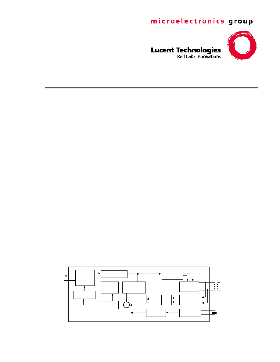
Figure 1. T7264 Simplified Block Diagram
2-WIRE
2B1Q
U-INTERFACE
LINE
DRIVER
A/D
ECHO
CANCELER
BALANCE
NETWORK
≠
+
SCRAMBLER
DESCRAM.
SIGNAL
DETECT
K2 BUS
FORMAT,
DECODE
AGC
K2
XTAL OSC.
15.36 MHz
DEC
2B1Q
ENCODER
DFE
DIG. PLL
T7264

Table of Contents
Contents
Page
Contents
Page
2
Lucent Technologies Inc.
Data Sheet
April 1998
T7264 U-Interface 2B1Q Transceiver
Features .......................................................................... 1
Description ....................................................................... 1
Pin Information ................................................................ 3
Functional Overview ......................................................... 6
Device Interface and Connections.................................... 7
Analog Device Interface ................................................ 7
Power Supply Connections............................................ 8
Clock Operation ............................................................. 8
Reset Operation............................................................. 8
Reset Sequences and Clock Synchronization ............ 8
Reset Time.................................................................. 9
Idle Mode ..................................................................... 10
NT Maintenance .......................................................... 10
K2 Interface Description ................................................ 11
K2 NT and LT Timing Sources ..................................... 12
K2 Bits Description ...................................................... 13
K2 Bit Levels ................................................................ 20
U-Interface Description .................................................. 21
K2 Functional Description .............................................. 22
K2 Framing Bits ........................................................... 23
K2 eoc and Loopback Response Timing .................... 24
K2 Device Status and Control Bits............................... 25
The adea Bit ................................................................ 26
The nebe, febe, rfebe, and ccrc Bits ............................ 27
NT or LT Operation ........................................................ 28
Minimal Example ............................................................ 29
Activation and the K2 Interface ...................................... 30
Priority ......................................................................... 31
Applications .................................................................... 32
Absolute Maximum Ratings ........................................... 34
Handling Precautions ..................................................... 34
Recommended Operating Conditions ............................ 34
Electrical Characteristics ............................................... 35
Loop-Range Performance Characteristics ..................... 36
Timing Characteristics ................................................... 37
Switching Test Input/Output Waveform .......................... 38
Outline Diagram ............................................................. 39
Ordering Information ...................................................... 39
Appendix A. Questions and Answers ............................ 40
Introduction .................................................................. 40
U-Interface ................................................................... 40
K2 Interface ................................................................ 46
Miscellaneous ............................................................. 49
Appendix B. Differences Between the T-7264- - -ML,
T-7264- - -ML2 and T-7264A- -ML Devices ................... 53
Technology................................................................... 53
Standard ...................................................................... 53
List of Figures
Figure 1. T7264 Simplified Block Diagram ....................... 1
Figure 2. Pin Diagram ...................................................... 3
Figure 3. Quat Example ................................................... 6
Figure 4. Line Interface and Protection ............................ 7
Figure 5. Recommended Power Supply
Connections .................................................................. 8
Figure 6. RESET Waveform Normal Operation ............... 9
Figure 7. RESET Timing for Synchronized Clocks .......... 9
Figure 8. K2 Interface Timing ......................................... 11
Figure 9. K2 Octets ........................................................11
Figure 10. K2 Interface LT and NT .................................12
Figure 11. K2 Interface Frame Format ...........................14
Figure 12. U-Interface Frame and Superframe ..............21
Figure 13. U-Interface Superframe Bit Groups ..............21
Figure 14. K2 Octet Description .....................................22
Figure 15. K2 Functional Description .............................22
Figure 16. K2-to-U Mapping ...........................................23
Figure 17. U-to-K2 Mapping ...........................................24
Figure 18. K2 Response Timing .....................................24
Figure 19. T7264 nebe/febe/crc Block Diagram .............28
Figure 20. Use of rfebe in a Multilink Configuration .......28
Figure 21. State Sequence for DSL Transceiver
Start-Up .......................................................................32
Figure 22. Loop Application ...........................................33
Figure 23. 2-Wire Terminal Application ..........................33
Figure 24. Digital Pair Gain Application .........................33
Figure 25. Timing Diagram Referenced to F ..................37
Figure 26. Timing Diagram Referenced to C ..................37
Figure 27. RESET Timing Diagram ................................38
Figure 28. Switching Test Waveform ..............................38
List of Tables
Table 1. Pin Functions ......................................................3
Table 2. Pin Descriptions ..................................................4
Table 3. Clock Configuration ............................................6
Table 4. K2 Interface Serial Data Bit Map ......................13
Table 5. B1, B2, D, and S1 Octets (Overview) ...............15
Table 6. B1, B2, D, and S1 Octets (Functions) ...............15
Table 7. UM1 and UM2 Octets--eoc Bits (Overview) ....16
Table 8. UM1 and UM2 Octets--eoc Bits (Functions) ....16
Table 9. UM2 and UM3 Octet--UCS Bits (Overview) ....17
Table 10. UM2 and UM3 Octet--UCS Bits (Functions) ..17
Table 11. DS Octet (Overview)--Device Status .............18
Table 12. DS Octet (Functions)--Device Status ............18
Table 13. DC Octet (Overview) ......................................19
Table 14. DC Octet (Functions) ......................................19
Table 15. K2 Data Out (DO) Bit Levels ...........................20
Table 16. K2 Device Control (DC) Bit Levels ..................20
Table 17. U-Interface Bit Assignment .............................22
Table 18. DC Octet Description (Control) .......................25
Table 19. DS Octet Description (Status) ........................25
Table 20. adea, ldea, and dea Function .........................26
Table 21. MODE0 Pin Functionality ...............................28
Table 22. Minimal Implementation ..................................29
Table 23. Definitions of Signals During Start-Up ............31
Table 24. Power Consumption .......................................35
Table 25. Performance Ratings ......................................35
Table 26. Crystal Characteristics: Fundamental
Mode Crystal ...............................................................35
Table 27. Internal PLL Characteristics ...........................36
Table 28. Digital dc Characteristics (Over Operating
Ranges) ......................................................................36
Table 29. Clock Timing ...................................................37
Table 30. MTC Requirements and Characteristics
(LT Mode) ....................................................................38
Table 31. RESET Timing ................................................ 38
Data Sheet
April 1998
T7264 U-Interface 2B1Q Transceiver
Lucent Technologies Inc.
3
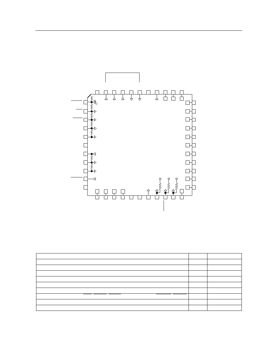
Pin Information
The U transceiver consists of a single chip composed of an analog front end (which performs the line interfacing
and data conversion functions) and a digital signal processor (which performs the algorithm-specific signal pro-
cessing, control, and access functions).
5-5804(F)
Notes:
C = crystal oscillator pins.
A = analog pins.
Figure 2. Pin Diagram
Table 1. Pin Functions
Device Pin Function
Type
Number of Pins
+5 V Power & Ground (V
DD
, GND)
Power
14
Analog Line Interface (HP, HN, LOP, LON)
Analog
4
Voltage Reference (VRP, VRN, VCM)
Analog
3
Receiver to A/D Converter (SDINN, SDINP)
Analog
2
Clock Related (X1, X2, CKOUT, CKSEL, MCLK, RCLKEN)
Digital
6
K2 Interface Connection (MTC, C, DI, DO, F)
Digital
5
Device Status & Control (FFC, HIGHZ, ILOSS, MODE0, MODE1, OSYNC, RESET)
Digital
7
Do Not Connect
NC
3
Total
--
44
7
9
10
11
12
13
14
15
8
ILOSS
FFC
RESET
MODE0
GND
D
MODE1
NC
NC
NC
16
17
OSYNC
V
DDD
SDINN
SDINP
V
DDA
HP
GND
A
LON
V
DDA
LOP
HN
VRN
VRP
DO
F
V
DDD
C
DI
MTC
GND
D
RCLKEN
V
DDA
GND
A
GND
A
X1
GND
O
V
DDO
X2
CKOUT
GND
D
MCLK
CKSEL
HIGHZ
GND
D
VCM
6
4
3
2
1
44
43
42
5
41
40
39
37
36
35
34
33
32
31
38
30
29
18
20
21
22
23
24
25
26
19
27
28
A
A
A
A
A
A
A
A
A
A
A
A
A
A
C
C
C
C
A
T7264
K2 INTERFACE
4
Lucent Technologies Inc.
Data Sheet
April 1998
T7264 U-Interface 2B1Q Transceiver
Pin Information
(continued)
Table 2. Pin Descriptions
Pin
Symbol
Type
Name/Function
1
DI
I
K2 Transmit Data Input.
Serial data input passing transmit data across K2 in-
terface at 512 kbits/s. Latched on falling edge of C clock.
2
MTC
I
Master Timing Clock.
8 kHz clock input. In LT mode (MODE0 = 1), all clocks
except CKOUT in the 15.36 MHz and 7.68 MHz modes are locked to this input
clock. In the NT mode (MODE0 = 0), this input is not used.
3
C
O
512 kbits/s K2 Bit Clock Output.
Synchronized to F. Defines K2 bit period (ris-
ing edge to rising edge).
4
DO
O
K2 Receive Data Output.
Serial data output passing receive data across K2 in-
terface at 512 kbits/s. Changes on the rising edge of C clock.
5
F
O
8 kHz Clock Output.
Defines K2 frame (rising edge to rising edge). In LT mode
(MODE0 = 1), this clock is locked to MTC at 0
∞
phase shift with
±
65 ns of jitter
(for jitter-free MTC). In NT mode (MODE0 = 0), this clock is derived from the
U-interface signal.
6, 17
V
DDD
P
+5 V Supply for Digital Circuits.
Internally connected together.
7
RESET
I
Reset (Active-Low).
Asynchronous Schmitt trigger input. This pin maintains
the transceiver in reset indefinitely without the need to access the K2 interface.
It must be held low for three consecutive F clock periods for active or idle mode
or 1.5 ms after power on. After power-on reset or idle mode reset, an additional
1.0 ms is required before the device is fully functional.
RESET
overrides all other
transceiver control signals, halts loop transmission, clears the transceiver adap-
tive filter coefficients, and resets the phase-locked loop. After a reset, the next
activation is a cold start. Unlike afrst (software reset via the K2 interface), when
this pin is held low, synchronization is lost between F and MTC (LT). After this
pin goes high, F and MTC regain synchronization. All output clocks remain func-
tional during reset.
8
FFC
I
Freeze Frequency Control (Active-Low).
Asynchronous input. Freeze the
clock frequency control (i.e., the internal state variables of the timing recovery
remain constant). This control is operative in both LT and NT modes. This pin is
latched on the rising edge of every RCLKEN.
9
ILOSS
I
Insertion Loss Test (Active-Low).
NT ONLY. When enabled, the transmitter
continuously transmits the sequence SN1. The receiver remains reset. The
transceiver performs a reset when this pin returns to its inactive state.
ILOSS
is
latched on the rising edge of F. Leave this pin unconnected or tied to V
DD
in LT
mode.
10, 11
MODE[0:1]
I
Mode 0 and 1.
Two-pin field selecting chip mode:
MODE0
Action
0
Configure for chip being used on the NT end of loop.
1
Configure for chip being used on the LT end of loop.
MODE1
Action
0
Disables autoreporting of nebe to febe.
1
Enables autoreporting of nebe to febe.
12, 22,
27, 44
GND
D
P
Ground Supply for Digital Circuits.
Internally connected together.

Data Sheet
April 1998
T7264 U-Interface 2B1Q Transceiver
Lucent Technologies Inc.
5
Pin Information
(continued)
Table 2. Pin Descriptions
(continued)
Pin
Symbol
Type
Name/Function
13,
14, 15
NC
--
No Connect.
These pins are connected to internal nodes of the device. Make no con-
nection to them.
16
OSYNC
O
Out of Sync (Active-Low).
Indicates that framing on the loop signal has not been ac-
quired (or has been lost). Equivalent to the K2 interface oof bit in the DS octet. Can sink
or source 1.6 mA to drive a low-current external LED. Clocked out on the rising edge
of C.
18
V
DDO
P/I
+5 V Supply for the Crystal Oscillator.
Ground when driving MCLK with an external
15.36 MHz clock.
19
GND
O
P
Ground Supply for Oscillator.
20
X1
I
Connection #1 for a 15.36 MHz Crystal.
21
X2
I
Connection #2 for a 15.36 MHz Crystal.
23
CKOUT
O
Clock Output.
See Table 3.
24
MCLK
I
Master Clock.
See Table 3.
25
CKSEL
I
Clock Select.
See Table 3.
26
HIGHZ
I
High Impedance (Active-Low).
Causes all digital outputs to become 3-stated.
28
VCM
--
Common-Mode Voltage Reference for the Analog Circuits.
Connect via a 0.1
µ
F
capacitor to GND
A
as close to this pin and pin 34 as possible.
29
VRP
--
Positive Voltage Reference for the Analog Circuits.
Connect via a 0.1
µ
F capacitor
to GND
A
as close to this pin and pin 34 as possible.
30
VRN
--
Negative Voltage Reference for the Analog Circuits.
Connect via a 0.1
µ
F capacitor
to GND
A
as close to this pin and pin 34 as possible.
31
HN
I
Hybrid Network Connection, Negative Side.
Connect directly to the negative side of
the transformer.
32
LOP
O
Line Driver Output Terminal, Positive Side.
Connect to the positive side of the trans-
former.
33,
39, 42
V
DDA
P
+5 V Supply for Analog Circuits.
34,
40, 41
GND
A
P
Ground Supply for Analog Circuits.
35
LON
O
Line Driver Output Terminal, Negative Side.
Connect to the negative side of the
transformer.
36
HP
I
Hybrid Network Connection, Positive Side.
Connect directly to the positive side of
the transformer.
37
SDINN
I
Sigma-Delta A/D Converter Input, Negative Side.
Connect via an 820 pF
±
5%
capacitor to SDNIP.
38
SDINP
I
Sigma-Delta A/D Converter Input, Positive Side.
Connect via an 820 pF
±
5%
capacitor to SDNIN.
43
RCLKEN
O
80 kHz Receive Baud Clock.
Defines receive baud period (rising edge to rising edge).

6
Lucent Technologies Inc.
Data Sheet
April 1998
T7264 U-Interface 2B1Q Transceiver
Pin Information
(continued)
Table 3. Clock Configuration
* The 10.24 MHz CKOUT is high for one-half of a 15.36 MHz period and low for one 15.36 MHz period. To compensate for the difference be-
tween the phase-locked and free-run frequencies, one-half 15.36 MHz clock periods are occasionally either removed from or added to the low
time of the 10.24 MHz period.
Functional Overview
5-5162F
Figure 3. Quat Example
V
DDO
MCLK
CKSEL
CKOUT
*
+5 V
+5 V
+5 V
+5 V
0
0
1
1
0
1
0
1
15.36 MHz (free-running)
10.24 MHz (phase-locked)
7.68 MHz (free-running)
3-stated (default)
0 V
0 V
15.36 MHz
15.36 MHz
0
1
15.36 MHz (free-running)
3-stated
≠1
01
+3
10
+1
11
≠3
00
≠3
00
+1
11
+3
10
≠3
00
≠1
01
≠1
01
+1
11
≠1
01
≠3
00
+3
10
+3
10
≠1
01
+1
11
+3
+1
≠1
≠3
QUAT
BITS
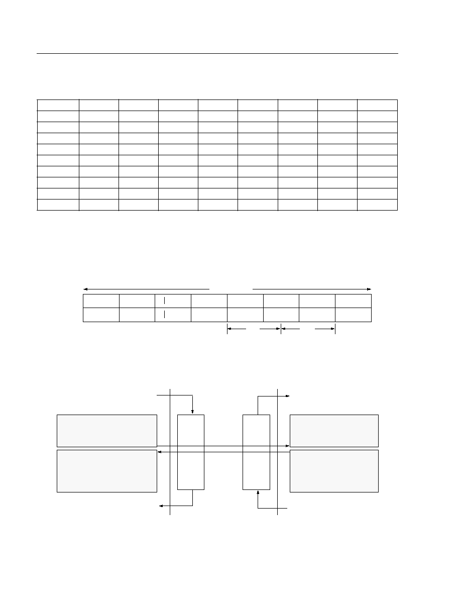
The T7264 chip conforms to the T1.601 ANSI North
American 1992 Standard for 2B1Q line encoding. The
2B1Q line code provides a four-level pulse amplitude
modulation code with no redundancy. Data is grouped
into pairs of bits for conversion to quaternary (quat)
symbols. Figure 3 above shows an example of this cod-
ing method.
The analog front end provides the 2B1Q line coder
(D/A conversion), pulse shaper, line driver, first-order
line balance network, crystal oscillator clock genera-
tion, and sigma-delta A/D conversion. The line driver
provides pulses which allow the 2.5 V template of the
T1.601 specification to be met when connected to the
proper transformer and interface circuitry. The A/D con-
verter is implemented using a double-loop, sigma-delta
modulator.
A crystal oscillator provides the 15.36 MHz master
clock for the chip. An on-chip, digital phase-locked loop
provides the ability to synchronize the chip clock to the
system clock in the LT or to the line clock in the NT.
Provisions are made for using either an on-chip crystal
oscillator with an external crystal, or using an external
clock source.
The T7264 takes input at the K2 interface and formats
this information for the U-interface through a scram-
bling algorithm and the addition of synchronization bits
for U framing. This data is then transferred to the 2B1Q
encoder for transmission over the U loop. Signals com-
ing from the U loop are first passed through the sigma-
delta A/D converter and then sent for extensive signal
processing. The T7264 provides decimation of the
sigma-delta output (DEC), linear and nonlinear echo
cancellation, automatic gain control (AGC), signal
detection, decision feedback equalization (DFE), timing
recovery (TR), descrambling, line-code polarity detec-
tion, and rate adaption for output onto the K2 interface.
The DFE circuit provides the functionality necessary for
proper operation on subscriber loops with bridged taps.
Lucent Technologies Inc.
7
Data Sheet
April 1998
T7264 U-Interface 2B1Q Transceiver
Functional Overview
(continued)
The device provides rapid cold start and warm start op-
eration. From a cold start, the device is typically opera-
tional within 3.5 s. The device supports activation/
deactivation, and, when properly deactivated, it stores
the adaptive filter coefficients such that upon the next
activation request, a faster warm start is possible. A
warm start typically requires 200 ms for the device to be-
come operational.
The T7264 has an on-chip activation/deactivation state
machine and timers, and automatically moves from
state T0 to T7 (as specified in the T1.601 standard) dur-
ing activation. This simplifies the implementation of the
T1.601 (Appendix C) state table. The signals from the
device control and status octets on the K2 interface pro-
vide the control necessary to complete the state table.
The activation/deactivation process is controlled over
the K2 interface.
The T7264 has a low-power mode which it automatically
enters when it is in the idle state. The idle state occurs
after deactivation, loss of sync on the U-interface, or re-
leasing reset. In the low-power mode, power consump-
tion is typically 30 mW.
Device Interface and Connections
The T7264 transceiver allows systems to meet the
loop-range requirements of ANSI Standard T1.601
when the transceiver is used with the proper peripheral
circuitry. Devices achieve better than 10
≠7
bit error rate
over 18 kft of 26 AWG loop cable.
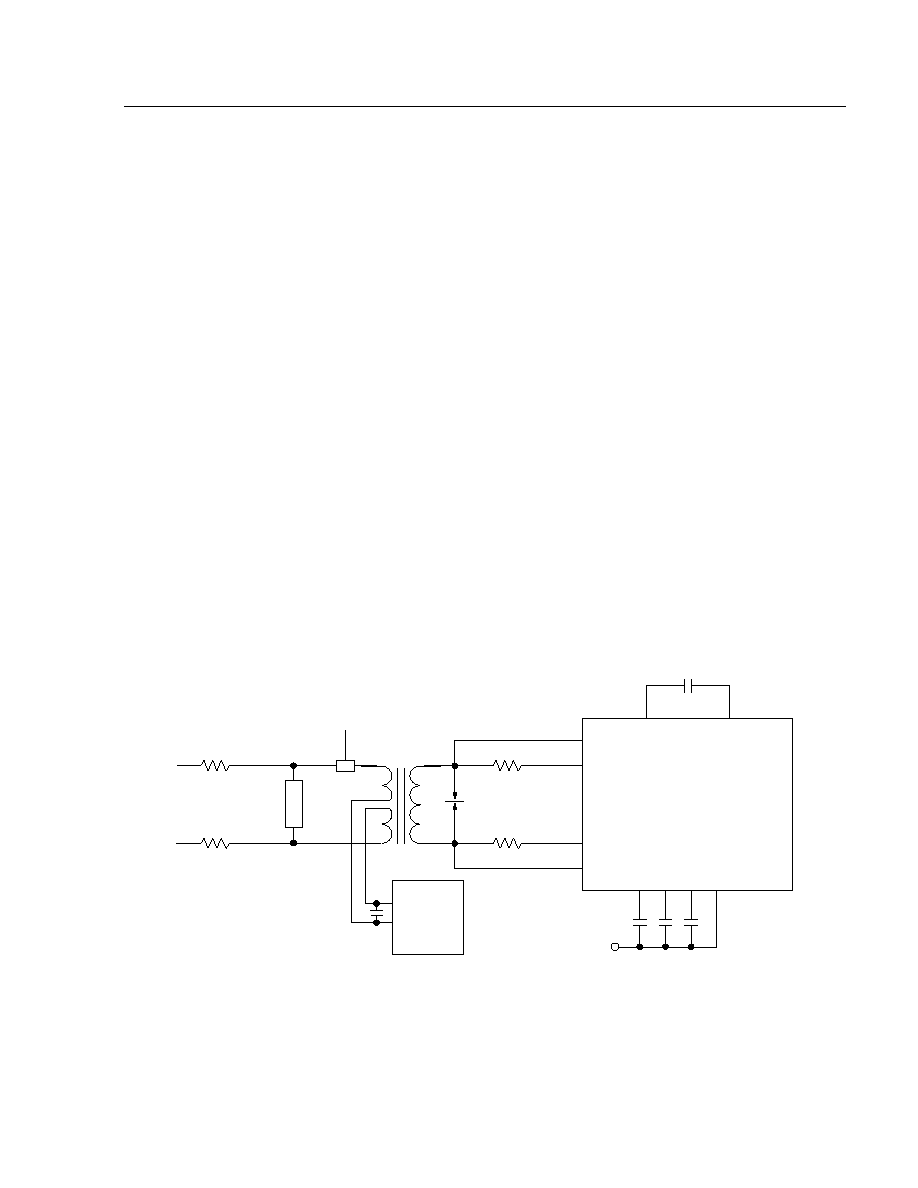
Analog Device Interface
Proper line termination is required, utilizing appropriate
interface components, to meet the 2.5 V pulse tem-
plate. The output of the T7264 should first pass through
a pair of 16.9
resistors and into a 1.5:1 ratio trans-
former, such as the Lucent 2754H (or the short-lead
version 2754H2). The output of the transformer is cou-
pled through a 1.0
µ
F capacitor, is passed through a
pair of 16.9
resistors, and then drives the 135
line.
Surge protection circuitry is necessary on each side of
the transformer when the U loop is external to a build-
ing. The protection between the 16.9
resistors and
the transformer should be a Lucent 521A surge protec-
tor or equivalent. A relay may be needed to disconnect
the loop plant for local loopback testing. Figure 4 shows
a recommended circuit for interfacing the T7264 to the
line; however, the specific interface is system depen-
dent.
5-5803Fa
Note:
3000 pF
±
1% capacitors from HP and HN to GND
A
may improve operation of the tone decoder in the presence of interfering common-
mode signals.
Figure 4. Line Interface and Protection
0.1
µ
F
GND
A
T7264
LON
HN
HP
LOP
SDINP
SDINN
VRP
VRCM
VRN
GND
A
1
9
7
5
521A
SURGE
PROTECTION
1.5:1
SURGE
PROTECTION
16.9
±
7%
LOOPBACK
RELAY
10
6
2754H
16.9
±
7%
16.9
±
1%
16.9
±
1%
820 pF
±
5%
1.0
µ
F
29
28
30
24
37
38
31
35
32
36
dc
REMOTE
POWER
SOURCE
LUCENT
701C
8
8
Lucent Technologies Inc.
Data Sheet
April 1998
T7264 U-Interface 2B1Q Transceiver
Device Interface and Connections
(continued)
Power Supply Connections
Figure 5 shows a recommended power supply connec-
tion. C is a 10
µ
F capacitor. Each pair of power and
ground pins should be decoupled with 0.1
µ
F and
1.0
µ
F capacitors. Each of the three leads (VCM, VRP,
and VRN) associated with the voltage reference should
be decoupled with 0.1
µ
F capacitors. Place the capaci-
tors as close as possible to the power or reference and
ground pins which they decouple.
Clock Operation
The master clock for the T7264 may either be internally
generated by the on-chip crystal oscillator or supplied
by the user via the MCLK pin. In the latter case, V
DDO
must be grounded. In the LT mode, an on-chip digital
phase-locked loop phase locks the F clock to the exter-
nally supplied MTC clock, unless FFC is active-low. In
NT mode, F synchronizes to the signal received from
the LT through the U-interface. If the on-chip crystal os-
cillator is used, the crystal must conform to the require-
ments given in Table 26.
Reset Operation
The T7264 can be reset via the K2 interface (issuing
afrst for three consecutive K2 frames) or via hardware
(RESET). The only difference between these two resets
is that, in the LT mode, the timing recovery filter is reset
only by a hardware reset. The RESET pin can be used
to hold the transceiver in reset indefinitely. If a hardware
reset is used when the chip is being powered up,
RESET must be held low for 1.5 ms; however, if the
chip is already powered up, then holding RESET low for
three K2 frames is sufficient.
The reset state is terminated, and the chip enters idle
mode on the K2 frame following the end of the reset sig-
nal.
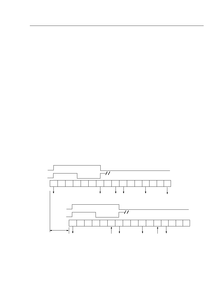
Reset Sequences and Clock Synchronization
In normal use, a power-on reset can be obtained by
connecting a capacitor to the RESET pin. The internal
pull-up resistor, acting with an on-chip Schmitt trigger
on this pin, can be used to reset the chip. In this case,
the RESET waveform is shown in Figure 6.
When using this reset procedure, the various clocks
generated by the transceiver are not synchronized.
However, during testing, it can be useful to initialize all
the counters of the clock generator so that the various
clocks generated by the transceiver can be synchro-
nized to the test equipment. The RESET pin can ac-
complish this by applying the sequence shown in Figure
7. Furthermore, the RESET pin transitions should align
with falling edges of MCLK. If the internal crystal oscil-
lator is used, this can be accomplished by configuring
CKOUT for 15.36 MHz and ensuring that RESET tran-
sitions align with the falling edge of CKOUT. The user
should be aware, however, that if this clock synchroni-
zation reset sequence is used after a period of normal
operation, the phase of the clocks generated by the
T7264 (such as F, RCLKEN, C, CKOUT, etc.) may sud-
denly change as a result of the clock resynchronization.
5-5164a
Figure 5. Recommended Power Supply Connections
C
+5 V
SYSGND
V
DDD
6, 17, 18
GND
D
12, 22, 27, 44
DIGITAL
ANALOG
GND
O
TO V
DDD
(INTERNAL VCXO)
OR GND
D
(EXTERNAL MCLK)
VCM, 28
VRP, 29
VRN, 30
0.1
µ
F
33, 39, 42
GND
A
V
DDO
V
DDA
0.1
µ
F
0.1
µ
F
(34, 40, 41)
19

Data Sheet
April 1998
T7264 U-Interface 2B1Q Transceiver
Lucent Technologies Inc.
9
Device Interface and Connections
(continued)
Reset Time
Reset time depends on the conditions under which the chip is reset. There are three cases to consider:
s
When the chip is initially powered on, the RESET pin must be held low (below 0.5 V) for 1.5 ms. This allows
1.0 ms for the oscillator start-up and 0.5 ms for the digital reset process. An additional 1.0 ms is needed to allow
the analog circuitry to fully power up before the chip becomes fully functional.
s
When the chip is in the idle mode, a software or hardware reset, applied for a minimum of three K2 frames, starts
the reset process. As before, the analog circuitry requires an additional 1.0 ms before the chip becomes fully
functional.
s
If the chip is already fully powered up and functional, a software or hardware reset, applied for a minimum of
three K2 frames, is sufficient to complete the reset process.
When the chip is in the reset state, the output of the line driver is at 0 V and the transmit data is also 0 V.
5-5165a
Figure 6. RESET Waveform Normal Operation
5-5166a
Figure 7. RESET Timing for Synchronized Clocks
RESET PIN
INTERNAL RESET
(AFTER SCHMITT
TRIGGER)
t
t
DEVICE REACHES POWER-ON
MODE (FULLY FUNCTIONAL)
4.75 V
POWER SUPPLY VOLTAGE
1.5 ms MIN
1.0 ms
0 0 1
4.75 V
POWER SUPPLY VOLTAGE
RESET PIN
1
NORMAL
RESET
AS IN FIGURE 6
UNDEFINED
UNDEFINED
1 MCLK PERIOD
2 MCLK PERIODS
F
C
2.5 ms
3 K2
FRAMES

10
10
Lucent Technologies Inc.
Data Sheet
April 1998
T7264 U-Interface 2B1Q Transceiver
Device Interface and Connections
(continued)
Idle Mode
A low-power idle mode is implemented on the T7264 to
reduce the power consumption to typically 30 mW when
it is not active. All internal coefficients are saved in this
idle mode to reduce time for a subsequent start-up.
There are three ways that idle mode can be entered:
s
If the loop is operational, the local deactivation com-
mand (ldea) in the LT mode via the K2 interface
causes the deactivation procedure specified in the
ANSI standard. At the conclusion of the deactivation
procedure, shutdown of the line driver and activation
of the tone detector occurs. If no tone is detected
within 48 ms, the idle mode is entered. This 48 ms
window constitutes the RECEIVE RESET criteria in
the ANSI standard.
s
If a failure condition is encountered (e.g., the loop
never comes up), a procedure similar to deactivation
is followed. The only difference is the duration of the
window, which is set internally by the type of failure
condition.
s
As long as either the afrst (via the K2 interface) or
the RESET pin is active, the transceiver remains in
the powerup reset state. At the cessation of the reset
condition, the transceiver changes to the idle state.
There are four ways of bringing the device out of the
idle mode:
s
An initiate start-up procedure (istp) command is
received via the K2 interface by the device.
s
A reset (afrst or external RESET) command is
received by the device.
s
A tone is detected by the tone detector.
s
A command to enter any of the test modes (loopback
and insertion loss) is received by the device.
Internal timing ensures that the digital signal processor
blocks do not change state during the idle mode-to-
powerup process. In addition, the start-up process has
been designed to prevent glitches on the line as the
driver powers up.
NT Maintenance
ANSI T1.601-1992 defines NT quiet mode operation
and an insertion loss measurement, and support for
these is available from the T7264. Detection of the trig-
ger signals is done by other hardware which notifies the
system controller, and the system controller then sig-
nals the T7264 as needed to do the following:
s
To enter the quiet mode, the chip is placed in reset.
s
When an insertion loss measurement is requested,
ILOSS
(pin 9) is asserted low. This causes the trans-
mitter to continuously send SN1 and places the
receiver in reset. When the test is completed or ter-
minated, ILOSS is asserted high and the chip is
reset. Priority between RESET and ILOSS is
described in the Priority section of this document
(page 31).
Lucent Technologies Inc.
11
Data Sheet
April 1998
T7264 U-Interface 2B1Q Transceiver
K2 Interface Description
The K2 interface consists of five pins on the T7264: the
data out (DO), data in (DI), data clock (C), K2 frame
sync (F), and master timing clock (MTC). C is a 512 kHz
output signal for clocking data into and out of the device
with 1 bit per clock cycle. F is an 8 kHz signal indicating
the beginning of a K2 frame. MTC is used in LT mode
and must be an 8 kHz
±
32 ppm system clock to meet
T1.601 requirements.
In LT mode, F is phase-locked to the MTC input through
the on-chip digital phase-locked loop. Jitter in MTC is
tracked by F at frequencies below 0.5 Hz. MTC jitter at
frequencies higher than 0.5 Hz is attenuated by the
phase-locked loop (PLL). In the NT mode, the F clock is
derived from incoming data from the U loop.
The first bit of a K2 frame begins simultaneously with
the rising edge of F. Transitions on DO occur following
the rising edge of C, and DI is latched on the falling
edge of C. Figure 8 shows the relationship between the
C, F, DO, and DI.
The K2 frame consists of eight octets for a total of
64 bits. These bits are transferred synchronously over
a 512 kHz interface with a frame rate of 8 kHz or 125
µ
s.
The major purpose of the K2 interface is to provide
2B+D data transfer between other devices and the chip.
In addition, there are framing bits (DF), U-interface
maintenance and control bits (UM), and device
control/status bits (DC/DS).
5-5167F
Figure 8. K2 Interface Timing
5-5158
Figure 9. K2 Octets
C
F
DO
DI
1
2
3
4
5
6
7
8
1
2
3
4
5
6
7
8
B1 TIME SLOT
C
F
DO
B1
B2
DF
UM1
UM3
DS
UM2
All 1s
DI
B1
B2
D
UM1
UM3
DC
UM2
All 1s

12
12
Lucent Technologies Inc.
Data Sheet
April 1998
T7264 U-Interface 2B1Q Transceiver
K2 Interface Description
(continued)
K2 NT and LT Timing Sources
In LT applications, all devices typically derive their tim-
ing from the same MTC. Additional logic in the LT, such
as a T7270, can provide concentration of multiple K2 in-
terfaces onto a single higher-speed highway.
In a PBX application, the U-interface loops can be used
as trunks. If more than one incoming U trunk is to be
used, additional circuitry may be needed to provide
elastic store, time-slot allocation, and master frame tim-
ing to synchronize the K2 interfaces received at each
trunk onto a common interface.
In NT1 applications, K2 frame timing is also derived
from the received 2B1Q data on the U loop. A T7264
chip can be connected to an S/T-interface device (such
as the T7252A) to form an NT1. Figure 10 shows the K2
interface connection in a CO application and NT1 appli-
cation. For terminal applications, the derived K2 timing
could be the source of all timing within the equipment (if
only a single U-interface is needed).
5-5169
Figure 10. K2 Interface LT and NT
T7264
MTC
F
C
DO
DI
F
C
DI
DO
MASTER
TIMING
T7264
MTC
F
C
DO
DI
F
C
DI
DO
K2-TO-
SYSTEM
BACK-
PLANE
LOGIC
F
C
DI
DO
S/T
T7252A
T7264
MTC
F
C
DO
DI
V
DD
2-WIRE U-
INTERFACE
NT
LT
2-WIRE U-
INTERFACE
∑ ∑ ∑
K2-TO-
SYSTEM
BACK-
PLANE
LOGIC
K2 NT1 LOGIC
F
C
DI
DO
4-WIRE S/T
-INTERF
A
C
E
NT
LT
∑ ∑ ∑
CO SWITCH
NT1
Lucent Technologies Inc.
13
Data Sheet
April 1998
T7264 U-Interface 2B1Q Transceiver
K2 Interface Description
(continued)
K2 Bits Description
Table 4 summarizes the K2 interface bits which are
common to all configurations. The K2 frame consists of
eight octets of data. The first three octets contain the
18 bits of 2B+D data. Bits 5--8 of the third octet contain
U frame and superframe timing (DF). Octet 4 (S1) is
reserved for future use and should always be set to 1.
Octets 5, 6, and 7 are directly mapped to the U-inter-
face M (UM) maintenance bits which are transparent to
the device, except the adea bit. Octet 8 is for device
status (DS) and device control (DC). These bits must
be manipulated according to the T1.601 standard to
obtain proper system-level operation.
Figure 11 describes the four different K2 interface for-
mats for DO and DI at the NT and LT. Tables 5--14 de-
scribe the position and meaning of the various bits on
the K2 interface. Tables 15 and 16 show the active logic
level for these bits, their value during reset/idle, and
their value when the transceiver is operational.
Table 4. K2 Interface Serial Data Bit Map
Bits marked with 1 should always be set to a 1. Bits marked as Rxx are reserved by T1.601 and should be set
to a 1.
* Items differ dependent upon NT or LT mode.
Don't care.
Time ----------------------------------------------------------->
Symbol
Octet
Bit 1
Bit 2
Bit 3
Bit 4
Bit 5
Bit 6
Bit 7
Bit 8
B1
1
B11
B12
B13
B14
B15
B16
B17
B18
B2
2
B21
B22
B23
B24
B25
B26
B27
B28
D
3
D1
D2
1
1
1
1
1
1
DF
3
D1
D2
1
1
RSF
RF
TSF
TF
S1
4
1
1
1
1
1
1
1
1
UM1
5
a1
a2
a3
dm
i1
i2
i3
i4
UM2
6
i5
i6
i7
i8
act
R
1, 5
R
1, 6
*
UM3
7
R
2, 5
*
*
*
*
R
6, 4
*
*
DS
8
nebe
xact
1
oof
1
rsksi
1
DC
8
ccrc
istp
lpbk
afrst
ldea
1
sksi
xpcy

14
Lucent Technologies Inc.
Data Sheet
April 1998
T7264 U-Interface 2B1Q Transceiver
K2 Interface Description
(continued)
5-5170
Figure 11. K2 Interface Frame Format
DO
AT
NT
DI
B1
B2
D
S
1
UM1
UM2
UM3
DC
DO
LT
B1
B2
DF
S1
UM1
UM2
UM3
DS
B1
B2
DF
S1
UM1
UM2
UM3
DS
DI
NT
B1
B2
D
UM1
UM2
UM3
DC
12
34
5
6
78
OCTET
DI
AT
NT
a c t
R 1 5
R 1 6
a d e a
R 2 5
r f e b e
R 3 4
R 4 4
R 5 4
R 6 4
u o a
a i b
c c r c
i s t p
l p b k
a f r s t
l d e a
s k s i
x p c y
a 1
a 2
a 3
d m
i 1
i 2
i 3
i 4
i 5
i 6
i 7
i 8
eoc
B1 CHANNEL
B2 CHANNEL
D
11111111111111
a 1
a 2
a 3
d m
i 1
i 2
i 3
i 4
i 5
i 6
i 7
i 8
eoc
B1 CHANNEL
B2 CHANNEL
D
11
r s f
r f
t s f
t f
11111111
a 1
a 2
a 3
d m
i 1
i 2
i 3
i 4
i 5
i 6
i 7
i 8
eoc
B1 CHANNEL
B2 CHANNEL
D
1111111111111
1
a c t
R 1 5
R 1 6
R 2 5
R 3 4
R 4 4
R 5 4
R 6 4
u o a
a i b
c c r c
i s t p
l p b k
a f r s t
l d e a
s k s i
x p c y
a c t
R 1 5
R 1 6
p s 1
R 2 5
r f e b e
p s 2
n t m
c s o
R 6 4
s a i
n i b
n e b e
x a c t
o o f
r s k s i
d e a
f e b e
1
a c t
R 1 5
R 1 6
p s 1
R 2 5
p s 2
n t m
c s o
R 6 4
s a i
n i b
n e b e
x a c t
o o f
r s k s i
a 1
a 2
a 3
d m
i 1
i 2
i 3
i 4
i 5
i 6
i 7
i 8
eoc
B1 CHANNEL
B2 CHANNEL
D
1
1
r s f
r f
t s f
t f
11111111
f e b e
1
11
1
1
11
DI
AT
LT
DO
AT
LT
1
0
o r
1
0
o
r
S

Data Sheet
April 1998
T7264 U-Interface 2B1Q Transceiver
Lucent Technologies Inc.
15
K2 Interface Description
(continued)
Table 5. B1, B2, D, and S1 Octets (Overview)
Table 6. B1, B2, D, and S1 Octets (Functions)
Octet
Octet #
DO/DI
Bit 1
Bit 2
Bit 3
Bit 4
Bit 5
Bit 6
Bit 7
Bit 8
B1
1
DO/DI
B11
B12
B13
B14
B15
B16
B17
B18
B2
2
DO/DI
B21
B22
B23
B24
B25
B26
B27
B28
D
3
DI
D1
D2
1
1
1
1
1
1
DF
3
DO
D1
D2
1
1
RSF
RF
TSF
TF
S1
4
DO/DI
1
1
1
1
1
1
1
1
Octet
Bit #
Symbol
Name/Function
B1
1--8
B11--B18
B1 Octet. The B1 octet is used for transferring basic access channel B1. B11 is the
first bit of the B1 octet sent or received.
B2
1--8
B21--B28
B2 Octet. The B2 octet is used for transferring basic access channel B2. B21 is the
first bit of the B2 octet sent or received.
D
1--2
D1, D2
D Octet. The two D-channel bits are transmitted in the first 2 bits of the D octet. D1
is the first bit of the D pair sent or received.
DF
5
RSF
Receive Superframing. 12.5% duty cycle at an 83.333 Hz rate (12 ms).
0--Last 84 K2 frames of the superframe.
0 to 1--Marks the first K2 frame of 2B+D data. Corresponds to the first 2B+D data
of the U superframe.
1--First 12 K2 frames and during reset state up to point T6 or T7.
DF
6
RF
Receive Framing. 50% duty cycle at a 666.66 Hz rate (1.5 ms).
0--Last six K2 frames of the U frame.
0 to 1--Marks every 12th K2 frame of 2B+D data.
Corresponds to the first 2B+D data of the U frame.
1--First six K2 frames and during reset state up to point T6 or T7.
DF
7
TSF
Transmit Superframing. 12.5% duty cycle at an 83.333 Hz rate (12 ms).
0--Last 84 K2 frames of the superframe
0 to 1--Marks the first K2 frame of 2B+D data.
Corresponds to the first 2B+D data of the U superframe.
1--First 12 K2 frames and during reset state up to point T6 or T7.
DF
8
TF
Transmit Framing. 50% duty cycle at a 666.66 Hz rate (1.5 ms).
0--Last six K2 frames of the U frame.
0 to 1--Marks every 12th K2 frame of 2B+D data.
Corresponds to the first 2B+D data of the U frame.
1--First six K2 frames and during reset state up to point T6 or T7.
S1
1--8
S11--S18
S1 Octet. All bits of the S1 octet are set to 1.

16
Lucent Technologies Inc.
Data Sheet
April 1998
T7264 U-Interface 2B1Q Transceiver
K2 Interface Description
(continued)
Table 7. UM1 and UM2 Octets--eoc Bits (Overview)
Table 8. UM1 and UM2 Octets--eoc Bits (Functions)
Additional details on eoc bits can be found in T1.601.
Octet
Octet #
DO/DI
Bit 1
Bit 2
Bit 3
Bit 4
Bit 5
Bit 6
Bit 7
Bit 8
UM1
5
DO/DI
a1
a2
a3
dm
i1
i2
i3
i4
UM2
6
DO/DI
i5
i6
i7
i8
See next page.
Octet
Bit #
Symbol
Name/Function
UM1, 2
1--8, 1--4
eoc
eoc Bits. The eoc bits are passed transparently from the U-interface to the
K2 interface and from the K2 to the U-interface. The transceiver maintains
the eoc information at the K2 interface until a new block of eoc information
is available.
UM1
1--3
a1--a3
eoc Address.
000--NT address.
001--LT to NT intermediate address.
010--110--LT to NT, decrement address and pass on.
001--101--NT to LT, increment address and pass on.
111--Broadcast address.
UM1
4
dm
Data or Message Indicator.
0--Data.
1--Message.
UM1, 2
5--8, 1--4
i1--i4,
i5--i8
Information. eoc channel message information.
01010000--Operate 2B+D loopback.
01010001--Operate B1 channel loopback.
01010010--Operate B2 channel loopback.
01010011--Request corrupt crc.
01010100--Notify of corrupted crc.
11111111--Return to normal.
00000000--Hold state.
10101010--Unable to comply.
Refer to T1.601 for codes which are reserved, nonstandard, or internal net-
work use.

Data Sheet
April 1998
T7264 U-Interface 2B1Q Transceiver
Lucent Technologies Inc.
17
K2 Interface Description
(continued)
Table 9. UM2 and UM3 Octet--UCS Bits (Overview)
Table 10. UM2 and UM3 Octet--UCS Bits (Functions)
Octet
Octet #
DO/DI
Bit 1
Bit 2
Bit 3
Bit 4
Bit 5
Bit 6
Bit 7
Bit 8
UM2
6
DO
LT
/[DI
NT
]
See previous page.
act
R
1, 5
R
1, 6
ps1
UM2
6
DO
NT
/[DI
LT
]
See previous page.
act
R
1, 5
R
1, 6
[a]dea
UM3
7
DO
LT
/[DI
NT
]
R
2, 5
[r]febe
ps2
ntm
cso
R
6, 4
sai
nib
UM3
7
DO
NT
/[DI
LT
]
R
2, 5
[r]febe
R
3, 4
R
4, 4
R
5, 4
R
6, 4
uoa
aib
Octet
Bit #
Symbol
Name/Function
UM2
5
act
Activation. Passed transparently from the K2 to the U-interface and from the U to the
K2 except during a start-up when it is forced to a 0 on the K2.
0--Pending activation.
1--Ready to transmit information.
UM2
6, 7
R
x, y
Reserved Bits. Passed transparently from the K2 to the U-interface and from the U
to the K2. Transmit should always be set to a 1.
UM2
8
ps1
(DO
LT
/
DI
NT
)
Power Status #1. Passed transparently from the K2 to the U-interface at the NT and
from the U to the K2 at the LT.
0--Primary power out.
1--Primary power is normal.
When both ps1 and ps2 are 0, this indicates a dying gasp.
UM2
8
[a]dea
(DO
NT
/
DI
LT
)
[AND with] Deactivate. In LT mode, this bit is used in conjunction with the ldea bit
from the K2, then passed to the U-interface as the transmitted dea bit. In NT mode,
this bit is passed transparently from the U to the K2 interface. Allows deactivation
warning to the far-end NT without deactivating the local transceiver.
0--Deactivation warning.
1--Normal.
UM3
1, 6
R
x, y
Reserved Bits. Passed transparently from the K2 to the U-interface and from the U
to the K2 interface. Transmit should always be set to a 1.
UM3
2
[r]febe
[Receive] Far-End Block Error. If the MODE1 = 1, rfebe is ANDed with nebe and the
result is sent out as the U-interface febe bit. If the MODE1 = 0, rfebe is passed trans-
parently from the K2 (DO
LT
/DI
NT
) to the U-interface febe bit. For either setting of
MODE1, the febe bit is passed transparently from the U-interface to the K2 interface.
0--Error indication passed to the originator.
1--No error, or feature is not utilized.
UM3
3
ps2
(DO
LT
/
DI
NT
)
Power Status #2. Passed transparently from the K2 to the U-interface at the NT and
from the U to the K2 at the LT.
0--Secondary power out.
1--Secondary power normal.
When both ps1 and ps2 are 0, this indicates a dying gasp.
UM3
4
ntm
(DO
LT
/
DI
NT
)
NT Test Mode. Passed transparently from the K2 to the U-interface at the NT and
from the U to the K2 at the LT.
0--The NT is currently in a test mode.
1--Normal.

18
Lucent Technologies Inc.
Data Sheet
April 1998
T7264 U-Interface 2B1Q Transceiver
K2 Interface Description
(continued)
Table 10. UM2 and UM3 Octet--UCS Bits (Functions) (continued)
Table 11. DS Octet (Overview)--Device Status
Table 12. DS Octet (Functions)--Device Status
Octet
Bit #
Symbol
Name/Function
UM3
5
cso
(DO
LT
/
DI
NT
)
Cold Start Only. Passed transparently from the K2 to the U-interface at the NT and
from the U to the K2 at the LT.
0--Cold and warm start capability.
1--Cold start only.
UM3
3, 4,
5
R
x, y
(DO
NT
/DI
LT
)
Reserved Bits. Passed transparently from the K2 to the U-interface (DI
LT
) and from
the U to the K2 interface (DO
NT
). Transmit should always set to a 1.
UM3
7
sai
(DI
NT
/
DO
LT
)
S/T-Interface Activity Indicator. Passed transparently from the K2 to the U-inter-
face at the NT and from the U to the K2 interface at the LT.
0--No activity at the S/T-interface.
1--Activity (INFO1 or INFO3) at S/T-interface.
UM3
7
uoa
(DI
LT
/
DO
NT
)
U-Interface Only Activation. Passed transparently from the K2 to the U-interface
at the LT and from the U to the K2 interface at the NT.
0--Request S/T deactivation at the NT.
1--Allow S/T activation at the NT.
UM3
8
nib
(DI
NT
/
DO
LT
)
Network Indicator Bit. Passed transparently from the K2 to the U-interface at the
NT and from the U to the K2 interface at the LT. Reserved for network use. Normally
set to 1 in customer premises equipment.
UM3
8
aib
(DI
LT
/
DO
NT
)
Alarm Indication Bit. Passed transparently from the K2 to U-interface at the LT
and from the U to the K2 interface at the NT.
0--Failure of intermediate 2B+D transparent element.
1--Transmission path is established between NT and local exchange.
Octet
Octet #
DO/DI
Bit 1
Bit 2
Bit 3
Bit 4
Bit 5
Bit 6
Bit 7
Bit 8
DS
8
DO
nebe
xact
--
1
oof
1
rsksi
1
Octet
Bit #
Symbol
Name/Function
DS
1
nebe
Near-End Block Error.
0--crc error detected in previously received U frame.
1--Normal.
DS
2
xact
Transceiver Active.
0--Transceiver in reset state.
0 to 1--Detection of a tone or istp = 0.
1--Transceiver active.
1 to 0--On reset, 480 ms after loss of sync or deactivation.
DS
3
--
Undefined. May be either a 1 or a 0.
DS
4, 6, 8
--
Reserved. In normal operation, these bits are 1.
DS
5
oof
Out of Frame.
0--Out of frame.
1 to 0--Initiates the 480 ms loss of synchronization timer.
1--Normal.
DS
7
rsksi
Reflected System-to-K2. This bit reflects the value of the sksi bit received over the
K2 interface.

Data Sheet
April 1998
T7264 U-Interface 2B1Q Transceiver
Lucent Technologies Inc.
19
K2 Interface Description
(continued)
Table 13. DC Octet (Overview)
Table 14. DC Octet (Functions)
Octet
Octet #
DO/DI
Bit 1
Bit 2
Bit 3
Bit 4
Bit 5
Bit 6
Bit 7
Bit 8
DC
8
DI
ccrc
istp
lpbk
afrst
ldea
1
sksi
xpcy
Octet
Bit #
Symbol
Name/Function
DC
1
ccrc
Corrupt Cyclic Redundancy Check. This bit is used to corrupt the crc information
transmitted by the transceiver to the U-interface.
0--Corrupt crc generation as long as bit is low.
1--Generate correct crc (normal).
DC
2
istp
Initiate Start-Up. This bit is used to notify the transceiver of an activation request.
Should be set to a 1 during loopback. If xact = 1, istp is ignored; if xact = 0:
0--Initiate start-up (activation request).
1--Reset state (transceiver inactive).
DC
3
lpbk
Local Loopback.
0--Loopback.
1--Normal.
Loop back the complete 160 kbits/s U-interface bit stream at the analog output. Loop-
back turns off echo canceler and reconfigures the descrambler. Device should be re-
set and line disconnected before loopback test; istp should be set to a 1 during
loopback.
DC
4
afrst
Adaptive Filter Reset.
0--Normal.
1--Reset.
2B+D and UM set equal to 1 on DO. Reset halts loop transmission and clears the
transceiver's adaptive filter coefficients, overriding all other transceiver control sig-
nals. This provides the same functionality as the RESET pin on the T7264, except F
to MTC synchronization (LT) is not lost.
DC
5
ldea
Local Deactivation.
0 -- Normal.
1 -- Deactivate. DO 2B+D and UM set equal to 1.
Upon receiving ldea = 1 from the system device, the transceiver will save adaptive fil-
ter coefficients. In the LT, the device sends three or four U superframes of dea = 0,
then ceases transmission and enters the idle state. In the NT, the device deactivates
upon signal loss and enters the idle state. In the NT, ldea should be set before the loss
of signal (on second dea = 0) and held until xact goes low for proper deactivation.
DC
6
--
Reserved. For normal operation, this bit must be set to 1.
DC
7
sksi
System-to-K2. This bit may be set high or low without affecting the state of the trans-
ceiver. sksi is reflected back from the T7264 across the K2 interface by means of the
rsksi bit.
DC
8
xpcy
Transparency.
0--Transparent 2B+D.
1--LT mode 2B+D = 0 transmitted across the U-interface.
1--NT mode 2B+D = 1 transmitted across the U-interface.
This bit only affects the data transmitted on the U-interface. The U-to-K2 interface al-
ways remains transparent after start-up.
20
Lucent Technologies Inc.
Data Sheet
April 1998
T7264 U-Interface 2B1Q Transceiver
K2 Interface Description
(continued)
K2 Bit Levels
Table 15. K2 Data Out (DO) Bit Levels
(+) Active = 1
(T) Transparent
(≠) Active = 0
(P) Pulsing
Table 16. K2 Device Control (DC) Bit Levels
(+) Active = 1
(x) Either 1 or 0
(≠) Active = 0
Bit Name
Description
True Level
Reset/Idle
Operational
U-Interface Related
B1, B2
ISDN 64 kbits/s B1, B2 Octet
1
T
D
ISDN 16 kbits/s D Bits
1
T
RSF, TSF
Receive/Transmit Superframe
+
1
P
RF, TF
Receive/Transmit Frame
+
1
P
UM Bits
eoc
eoc addr, d/m, and info bits
+
1
T
act
Activate
+
0
1
dea
Deactivate
≠
1
1
ps1, ps2
Primary/Sec. Power Status
+
1
1
febe
Far-end Block Error
≠
1
1
ntm
NT in Test Mode
≠
1
1
cso
Cold Start Only
+
1
0 or 1
sai
S/T Activity Indicator
+
1
1
uoa
U Only Activation
≠
1
1
nib
Network Indicator Bit
≠
1
1
aib
Alarm Indication Bit
≠
1
1
R
Reserved
≠
1
1
DS Bits
nebe
Near-end Bit Error
≠
1
1
xact
Transceiver Active
+
0
1
oof
Out of Frame
≠
0
1
Bit Name
Description
True Level
Reset/Idle
Operational
ccrc
Corrupt the Outgoing crc
≠
x
1
istp
Initiate Start-up
≠
1
0 then x
lpbk
Loopback
≠
1
1
afrst
Reset
+
1 then x
0
ldea
Local Deactivate
+
1 then x
0
xpcy
Transparency
≠
1
0

Data Sheet
April 1998
T7264 U-Interface 2B1Q Transceiver
Lucent Technologies Inc.
21
U-Interface Description
Data is transmitted over the U-interface in 240-bit groups called U frames. Each U frame consists of an 18-bit syn-
chronization word (ISW or SW), 12 blocks of 2B+D data (216 bits), and six overhead bits (M). A U-interface super-
frame consists of eight U frames grouped together. The beginning of a U superframe is indicated by the inverted
sync word (ISW). The six overhead bits from each of the eight U frames, when taken together, form the 48 M bits.
The following diagram shows how U frames, superframes, and M bits are mapped.
5-5171
Figure 12. U-Interface Frame and Superframe
Of the 48 M bits, 24 bits form the embedded operations channel (eoc) for sending messages from the LT to the NT
and responses from the NT to the LT. There are two eoc messages per superframe with 12 bits per eoc message
(eoc1 and eoc2). Another 12 bits serve as control and status bits (UCS). The last 12 bits form the cyclic redun-
dancy check (crc) which is calculated over the 2B+D data and the M4 bits of the previous superframe. Figure 13
shows the different groups of bits in the superframe.
5-5172
Figure 13. U-Interface Superframe Bit Groups
U1
U2
U3
U4
U5
U6
U7
U8
ISW[18]
M[6]
(2B+D) X 12 [216 bits]
U-INTERFACE M BITS [48]
U-SUPERFRAME SPAN = 12 ms
U-FRAME SPAN = 1.5 ms
BIT #
1--18
19--234
235
236
237
238
239
240
FRAME #
Sync
12(2B+D)
M1
M2
M3
M4
M5
M6
1
ISW
CONTROL & STATUS (UCS)
2
3
eoc1
4
5
SW
2B+D
6
7
8
eoc2
crc
22
Lucent Technologies Inc.
Data Sheet
April 1998
T7264 U-Interface 2B1Q Transceiver
U-Interface Description
(continued)
Table 17. U-Interface Bit Assignment
* LT(NT). Values in parentheses () indicate meaning at the NT.
K2 Functional Description
The K2 interface provides the mechanism for transferring data and control information between the system and the
T7264. A K2 frame consists of eight DO octets and eight DI octets which occur every 125
µ
s (every frame sync).
Figure 14 shows the K2 frame structure.
5-5173
Figure 14. K2 Octet Description
Figure 15 shows the points of origination and destination of bits on the K2 and U-interfaces at the LT and NT.
5-5174
Figure 15. K2 Functional Description
Bit #
1--18
19--234
235
236
237
238
239
240
Frame #
Sync
12(2B+D)
M1
M2
M3
M4
M5
M6
1
ISW
2B+D
eoc
a1
eoc
a2
eoc
a3
act
R
1, 5
R
1, 6
2
SW
2B+D
eoc
dm
eoc
i1
eoc
i2
dea (ps
1
)*
R
2, 5
febe
3
SW
2B+D
eoc
i3
eoc
i4
eoc
i5
R
3, 4
(ps
2
)*
crc
1
crc
2
4
SW
2B+D
eoc
i6
eoc
i7
eoc
i8
R
4, 4
(ntm)*
crc
3
crc
4
5
SW
2B+D
eoc
a1
eoc
a2
eoc
a3
R
5, 4
(cso)*
crc
5
crc
6
6
SW
2B+D
eoc
dm
eoc
i1
eoc
i2
R
6, 4
crc
7
crc
8
7
SW
2B+D
eoc
i3
eoc
i4
eoc
i5
uoa (sai)*
crc
9
crc
10
8
SW
2B+D
eoc
i6
eoc
i7
eoc
i8
aib (nib)*
crc
11
crc
12
DI
DO
B1
B2
D
UM1
UM2
UM3
DC
S1
B1
B2
D
UM1
UM2
UM3
DS
1s
S1
DF
TIME (125
µ
s)
eoc
UCS
T7264
LT
T7264
NT
B1/B2/D - R(6)
UM1, 2 - eoc(12)
UM2, 3 - ps1, act, febe,
ps2, ntm, cso, sai, nib
DF - RSF, RF, TSF, TF
DS - nebe, xact, wstrt, oof
UM2, 3 - adea, act, rfebe, uoa, nib
UM1, 2 - eoc(12)
B1/B2/D - R(9)
DC - ccrc, afrst, istp,
lpbk, xpcy, ldea
DF - RSF, RF, TSF, TF
DS - nebe, xact, wstrt, oof
DC - ccrc, afrst, istp,
lpbk, xpcy, ldea
B1/B2/D - R(6)
UM1, 2 - eoc(12)
UM2, 3 - ps1, act, rfebe,
ps2, ntm, cso, sai, nib
2B1Q
2-WIRE
U-
INTERFACE
K2
K2
DI
DO
DO
DI
UM2, 3 - dea, act, febe, uoa, aib
UM1, 2 - eoc (12)
B1/B2/D - R (9)
Lucent Technologies Inc.
23
Data Sheet
April 1998
T7264 U-Interface 2B1Q Transceiver
K2 Functional Description
(continued)
The U superframe and the K2 superframe both occur
once every 12 ms. The U frame consists of 240 bits,
with eight U frames per superframe, transferred at a
data rate of 160 kbits/s. The K2 superframe consists of
96 K2 frames transferred at a data rate of 512 kbits/s.
In mapping the K2 to U, the blocks of 2B+D data, which
occur once every K2 frame, are accumulated within the
T7264 and are output in groups of twelve blocks per
U frame onto the U-interface. The last 6 bits of the D
octet and the S1 octet are unused on DI. While every
K2 frame has bits allocated for eoc messages, only two
messages per U superframe are needed. K2 frame
number 11 (K11) provides the data for the first eoc
message on the U-interface, and K2 frame K59 pro-
vides the data for the second eoc message. The other
94 K2 frames are unused. Every K2 frame also has bits
allocated for UCS data; however, only a single set of
UCS data is needed in a U superframe. K2 frame num-
ber K11 provides the UCS data while the other 95 K2
frames are unused. The crc is automatically generated
by the T7264 and presented to the U-interface. The DC
octet is used to transfer control data to the T7264 and is
sampled every K2 frame.
In mapping the U to K2, the 2B+D data, which occur in
groups of 216 bits (12 times [2B+D]), are accumulated
within the T7264 and output as one 2B+D block per K2
frame. The last 4 bits of the D octet provide indication
onto the K2 interface about when data transferred on
the K2 interface corresponds to data transferred on the
U-interface for both transmit and receive. The eoc bits
are collected by the T7264 and changed on the K2
interface twice per superframe on K2 frames K47 (held
until K94) and K95 (held until K46). The UCS bits are
collected by the T7264 and changed on the K2 inter-
face once per superframe on K2 frame K95 (held until
K94). The DS octet is used to transfer device status
from the T7264 to the K2 interface. The crc is automat-
ically calculated in the T7264, and a single bit (nebe) in
the DS octet provides indication of a crc error.
K2 Framing Bits
The four DF bits (the last 4 bits of the D octet on DO)
indicate when the 2B+D data from the K2 interface and
U-interface correspond. A system can monitor these
signals to determine when the T7264 is transmitting or
receiving specific data. RSF and TSF mark the first
frame (K0) of a superframe. RF and TF add resolution
in identifying the start of each U frame (every twelfth K2
frame). Figure 16 shows when eoc and UCS data is
transferred to and from the K2 interface. It also indi-
cates the occurrence of the RSF, TSF, RF, and TF bits.
Notice that the DI and DO superframes are not aligned,
and therefore RSF and TSF occur at different times.
5-5175
Figure 16. K2-to-U Mapping
RSF
RF
DI
DO
K0
K1
K12
K47
K59
K60
. . .
. . .
K95
. . .
. . .
K11
K48
NEW
eoc
NEW eoc
& UCS
RSF, RF
RF
RF
RF
. . .
K6
K94
K0
K1
K12
K47
K59
K60
. . .
. . .
K95
. . .
. . .
K11
K48
eoc & UCS
MUST BE VALID
eoc
MUST BE VALID
. . .
K6
K94
TSF
TF
2 K2
FRAMES
IN NT
TSF, TF
TF
TF
TF

24
Lucent Technologies Inc.
Data Sheet
April 1998
T7264 U-Interface 2B1Q Transceiver
K2 Functional Description
(continued)
Figure 17 shows how the U-interface bits are grouped into eoc1, eoc2, UCS, and crc bits. It also shows how these
bit groups are mapped from the U-interface to the K2 interface.
5-5176
* The U-inverted sync word (ISW) is mapped to the K2 interface as the receive superframe (RSF) bit and the transmit superframe (TSF) bit. The
occurrence of these bits defines the first K2 frame.
Figure 17. U-to-K2 Mapping
K2 eoc and Loopback Response Timing
Each U frame contains 12 2B+D data blocks. These blocks are jitter accommodated and synchronized within the
T7264 and output on the K2 interface. This introduces delay between the U-interface and the K2 interface. The re-
ceive and transmit framing on the U-interface do not occur at the same time. The ANSI standard specifies that the
delay from U input to U output in the NT is 0.75 ms (6 K2 frames). The relationship between the K2 frame sync and
the U-interface frame can change each time the device frames up.
The timing delay from receive to transmit affects the eoc timing as follows: The eoc is made available on the K2
interface at DO K2 frames K47 and K95, and it is sampled on DI K2 frames K59 and K11. This 11-frame difference
plus the two-frame delay discussed above allows a total of 13 K2 frames (1625
µ
s) for the system to process the
eoc information and respond. Thus, the system is guaranteed to have at least 1625
µ
s to respond to an eoc mes-
sage. Figure 18 shows the received and transmitted K2 frame in the NT.
5-5177
Figure 18. K2 Response Timing
M6
M5
M4
M3
M2
M1
FRAME #
SYNC
1
2
3
4
5
6
7
8
ISW*
U - SW
K - RF, TF
OUTPUT
K0,
K12,
K24,
. . .
K84
U - eoc1
K - UM1 & UM2 (#1--4)
INPUT K11 OUTPUT
K47--K94
U - crc
K - OUTPUT
DS - #1 (nebe)
K - INPUT
DC - #1 (ccrc)
U - 2B+D
K - B1,
B2, D
K0, K1,
. . . K95
BIT #
1--18
19--234
235
236
237
238
239
240
12(2B+D)
U - eoc2
K - UM1 & UM2 (#1--4)
INPUT K59 OUTPUT
K95--K46
U - CONTROL & STATUS (UCS)
K - UM2 (#5--8) & UM3
INPUT K11 OUTPUT K95--K94
K11
. . .
K59
. . .
K0
K47
. . .
. . .
K95
K95
. . .
. . .
. . .
. . .
. . .
. . .
. . .
. . .
. . .
. . .
. . .
. . .
. . .
RECEIVED K2 FRAMES AT NT
TRANSMITTED K2
FRAMES AT NT
SAMPLE eoc
& UCS
SAMPLE eoc
NEW eoc
NEW eoc
& UCS
. . .
2 K2
FRAMES
1625
µ
s
1625
µ
s

Lucent Technologies Inc.
25
Data Sheet
April 1998
T7264 U-Interface 2B1Q Transceiver
K2 Functional Description
(continued)
K2 Device Status and Control Bits
The T7264 device status bits are transmitted over the
K2 interface in the DS octet. The status information
includes the nebe, xact, and oof bits which are used to
determine the status of the line interface and to control
the activate/deactivate state machine.
The T7264 device control bits are transmitted over the
K2 interface in the DC octet. The control information
includes the ccrc, istp, lpbk, afrst, ldea, and xpcy bits
which provide the control necessary to implement the
activation/deactivation state machine.
Tables 18 and 19 show how the DC bits are sampled
and when the DS bits are available. Note that a Y in the
column marked Hyst (hysteresis) indicates that the vali-
dation occurs on both entry and exit from the condition.
An N in the Hyst column indicates that the validation
occurs only on entry into that condition. For validation,
a signal must be present for three consecutive K2
frames.
In LT mode, setting the ldea (local deactivation) bit
causes the transceiver to send 3 or 4 superframes of
dea = 0 across the U-interface, save the adaptive filter
coefficients, and cease transmission.
In the NT mode, the ldea bit is used to ensure that the
transceiver is capable of a warm start on the next acti-
vation; however, the transceiver must be given
advance warning prior to loss of signal. This should be
done by filtering dea = 0 for two superframe occur-
rences prior to setting ldea = 1. This causes the trans-
ceiver to freeze echo canceler coefficients. The
transceiver then either deactivates upon detection of
loss of signal or resumes training the echo canceler if
ldea = 0 is received instead of detecting loss of signal.
In both LT and NT modes, the lpbk (local loopback) bit
is used to request a local loopback within the trans-
ceiver from the K2 input (DI) to the K2 output (DO).
During loopback, the transceiver turns off the echo
canceler (disables the canceler output from the
summing node) and reconfigures the descrambler. To
perform loopback, set afrst = 1 and lpbk = 1, discon-
nect the U-interface metallic connection to the loop
plant, then set afrst = 0 and lpbk = 0. Loopback has
become valid when oof = 1. In order to terminate the
loopback, set afrst = 1 and lpbk = 1. Reconnect the
loop plant, then set afrst = 0. During the entire loop-
back test, istp = 1 and xpcy may be either 0 or 1.
Table 18. DC Octet Description (Control)
Table 19. DS Octet Description (Status)
Control (DC)
Description
Hyst
Timing
ccrc bit
Corrupt crc
N
Sample K2 frames 9, 10, 11 for three consecutive ccrc = true K2
frames. Continues to corrupt until the condition goes away.
istp
Initiate Start-up
N
Sample for three consecutive K2 frames to validate.
ldea
Local Deactivate
Y
Sample for three consecutive K2 frames to validate.
xpcy
Transparency
Y
Sample for three consecutive K2 frames to validate.
afrst
Reset
Y
Sample for three consecutive K2 frames to validate.
lpbk
Loopback
Y
Sample for three consecutive K2 frames to validate.
Status (DS)
Description
Timing
nebe
Near-end Block Error
Presented to K2 interface on frame K95 to K94.
xact
Transceiver Active
Presented to K2 interface as it occurs.
oof
Out of Sync
Presented to K2 interface as it occurs.
26
Lucent Technologies Inc.
Data Sheet
April 1998
T7264 U-Interface 2B1Q Transceiver
K2 Functional Description
(continued)
The adea Bit
The adea bit is only available when the MODE0 pin is set to 1 (LT mode). Setting adea = 0 causes the LT to set
dea = 0 on the U-interface without deactivating itself. By contrast, setting ldea = 1 at the LT causes the LT to set dea
= 0 on the U-interface, save adaptive filter coefficients, and deactivate itself after sending dea = 0 for three consec-
utive U superframes.
In loop configurations with multiple U-interfaces, as shown in T1.601, adea is used to propagate dea = 0 beyond the
local link (the link between the LT in an ISDN serving switch to the next NT downstream-type element of the loop)
and can be used to deactivate a nonlocal link without deactivating the local link.
Table 20 shows the effects of the adea and ldea bits at the LT.
Table 20. adea, ldea, and dea Function
adea at LT
ldea at LT
Action
0
0
dea = 0 is sent downstream, but no local deactivation occurs.
X
1
dea = 0 is sent downstream for 3 or 4 superframes, echo canceler coefficients are
frozen, and transmission ceases.
1
0
dea = 1 is sent downstream (normal operation).

Lucent Technologies Inc.
27
Data Sheet
April 1998
T7264 U-Interface 2B1Q Transceiver
K2 Functional Description
(continued)
The nebe, febe, rfebe, and ccrc Bits
Errors in the received 12-bit crc from the U-interface are
indicated via the nebe (near-end block error) bit. The
nebe bit is a local status bit that is set to 0 each time a
crc error is detected. Errors in transmitted crc can be
forced by setting the ccrc (corrupt crc) bit low. Because
the crc error detection and corruption is handled via the
nebe and ccrc bits, there is no need to have direct
control or access to the 12 crc bits via the K2 interface.
Normally, the T7264 automatically reflects the nebe bit
back to the far end as the ANSI-defined febe (far-end
block error) bit. The MODE1 pin (pin 11) and rfebe bit
can be used to alter the interaction between nebe and
febe as shown in Figure 19. Normally, MODE1 and
rfebe are HIGH, so febe is the direct result of the current
state of nebe. Now rfebe can be directly used to control
the state of febe.
The intended application for rfebe and MODE1 is one
having multiple U links as shown in T1.601-1992,
Figure E1. In this application, a performance monitoring
approach called path performance monitoring can be
used. This treats all links between the NT and LT as one
complete link, or path. Thus, any febes or nebes that
occur at an intermediate element should be propagated
to an endpoint. In this way, the febe and nebe counts at
the endpoints represent the performance of the system
as a whole.
Figure 20 shows how a multilink system with one inter-
mediate element (IE) could use MODE1, rfebe, nebe,
febe, and ccrc to propagate crc errors to the endpoints.
For simplicity, this figure represents only one direction
of propagation of nebe and febe, namely nebes propa-
gated toward the LT and febes propagated toward the
NT. This circuitry would be duplicated in the opposite
direction to form a complete system. At the endpoints,
MODE1 = 1 and rfebe = 1, so nebe and febe behave
normally. At IE, MODE1 = 0 so that rfebe, rather than
nebe, controls the state of febe toward the far end. For
clarity, the effect of MODE1 is shown as a coil control
for an SPDT relay that selects either nebe or V
CC
as the
upper input to the AND gate.
First, consider the case of a nebe occurring at the IE's
LT-mode T7264. This means that a crc error occurred
from NT to IE. The IE's K2 interface logic connects
nebe directly to the ccrc bit of the NT-mode T7264 to
force a ccrc error toward the LT. This will now show up
as a nebe at the LT, effectively propagating nebe from
IE to LT.
Now, at the LT, the nebe is reflected back toward the
IE as a febe. At the IE, the K2 interface logic connects
febe directly to the rfebe bit of the LT-mode T7264. This
generates a febe from IE to NT, completing the path for
the original crc error. Thus, the result of an error from
NT to IE is a nebe reported at the LT and a febe report-
ed at the NT. This illustrates how the two links and the
IE are treated as a single entity from a performance
monitoring standpoint.

28
Lucent Technologies Inc.
Data Sheet
April 1998
T7264 U-Interface 2B1Q Transceiver
K2 Functional Description
(continued)
5-5178a
Figure 19. T7264 nebe/febe/crc Block Diagram
5-5179a
Figure 20. Use of rfebe in a Multilink Configuration
NT or LT Operation
The MODE0 pin determines whether the device is being used in an LT system as the originator of the U-interface
signals or in the NT mode as the terminator of the U-interface signal. Table 21 is provided as a reference to show
the different functions of the chip in NT and LT modes.
Table 21. MODE0 Pin Functionality
LT (MODE0 = 1)
NT (MODE0 = 0)
U-interface timing derived from MTC
K2 timing derived from the U-interface
Transmit adea AND ldea for dea, uoa, aib
Transmit ps1, ps2, ntm, cso, sai, nib
U transmit-to-receive timing dependent upon line delay
U transmit-to-receive timing fixed at 0.75 ms
ldea stops transmission
Loss of signal stops transmission
LT scrambling algorithm
NT scrambling algorithm
LT start-up timing
NT start-up timing
TL tone generation
TN tone generation
TN tone recognition
TL tone recognition
K2 INTERFACE
nebe
MODE1
rfebe
crc
CHECKER
febe
U-INTERFACE
T7264
PIN #11
2B+D+M
ccrc
febe
NT
T7264 (NT)
crc
GENERATOR
T7264 (LT)
crc
CHECKER
nebe
+V
rfebe
MODE1 = 0
crc
GENERATOR
ccrc
febe
T7264 (LT)
crc
CHECKER
nebe
+V
rfebe
K2 INTERFACE
2B+D+M
T7264 (NT)
U-
INTER-
febe
2B+D+M
MODE1 = 1
rfebe = 1
LT
febe
INTERMEDIATE ELEMENT
FACE
U-
INTER-
FACE
LOGIC

Data Sheet
April 1998
T7264 U-Interface 2B1Q Transceiver
Lucent Technologies Inc.
29
Minimal Example
The simplest application of the T7264 in an NT1 is to assume only cold starts and always return an unable-to-com-
ply for the eoc message. In this situation, the K2 interface signals are configured as shown in Table 22.
Table 22. Minimal Implementation
Note that this is only an example and not a valid T1.601 configuration. However, it could be useful for laboratory
testing.
Bit Name
Description
Minimal State
Description
B1, B2
ISDN 64 kbits/s B1, B2 Octet
T
Transparent
D
ISDN 16 kbits/s D Bits
T
Transparent
Data In
a
Address
000
NT Address
dm
Data or Message
1
Message
i
Information
10101010
Unable to Comply
act
Activation
INFO3
Transceiver Active
ps1, ps2
Primary/Sec. Power Status
1
Always True
rfebe
Received Far-end Bit Error
1
Not Applicable
ntm
NT in Test Mode
1
Never Used
cso
Cold Start Only
1
Always Cold Start
R
Reserved
1
Never Used
Data Out
dea
Deactivation
1
Ignore
ccrc
Corrupt the Outgoing crc
1
Never Used
istp
Initiate Start-up
0
Always Starting
lpbk
Loopback
1
Never Used
afrst
Reset (Adaptive Filter Reset)
0
Never Used--RESET Pin Used
ldea
Local Deactivation
0
Never Used--Always Active
xpcy
Transparency
NOT act
Received K2 act Bit

30
30
Lucent Technologies Inc.
Data Sheet
April 1998
T7264 U-Interface 2B1Q Transceiver
Activation and the K2 Interface
The signal definitions and start-up states (Table 23 and
Figure 21) of the U-interface during activation are as re-
quired by T1.601. The T7264 handles these details au-
tomatically upon assertion of istp on the K2 interface or
detection of a tone on the U-interface. Still, for some us-
ers it is useful to know what is happening at the K2 in-
terface during the start-up sequence and how the
system should be reacting. The following is an explana-
tion of what happens during a typical start-up sequence.
For simplification, it is assumed that the uoa and sai
bits, defined in T1.601-1992, are held at 1 during start-
up.
1. From RESET to T6
At each end, xact changes from 0 to 1 to indicate that
an activation request has been issued at the near end
(via istp) or a wake-up tone has been detected from the
far end and the transceiver is beginning the start-up se-
quence. All other K2 bits are held in their reset state by
the transceiver in the U-to-K2 direction at both the NT
and the LT (see Table 15 for these RESET values). In
the K2-to-U direction, the 2B+D and U overhead bits are
internally overwritten by the transceivers. These bits
should be initialized by the system to reflect their de-
sired state at the time transparency is achieved. Table
23 lists the values of the overwritten U bits at various
stages of activation.
2. At T6
At the NT, oof goes high causing 2B+D transparency
from the U to the K2 interface at the NT transceiver.
Note that the NT always frames up before the LT, due
to the structure of the transceiver start-up algorithms.
Before T6, the NT transceiver was forcing 2B+D data on
the K2 interface to all 1s. After this, the 2B+D bits on the
K2 interface contain whatever is being received at the
NT's U-interface on the 2B+D channels from T4 until
transparency is established (see Table 23 and Figure
21, signal SL2).
M bits in the downstream direction become transparent
over the entire link. Prior to this, the NT transceiver was
forcing all M bits to 1 in the downstream (U-to-K2) direc-
tion, except act, which was being forced to 0. In the
downstream direction (K2-to-U) at the LT, M bits are al-
ready being passed transparently and have been since
T4. At T6, oof = 1 at the NT causes the NT to start pass-
ing M bits transparently in the downstream direction.
M bits in the upstream direction become transparent at
the NT transceiver (K2-to-U). Prior to this, the NT trans-
ceiver was internally overwriting the upstream M bits to
all 1s per the ANSI standard (see Table 23 and Figure
21, signal SN2).
After detecting oof = 1, the NT can set its act = 1, then
wait for act = 1 from the LT. The NT is still forcing 2B+D
in the upstream direction to all 1s and continues to do
so until:
a) It receives act = 1 from the LT
b) It receives an eoc loopback message from the LT
When either of the above occurs, the NT must set
xpcy = 0, which enables 2B+D transparency in the up-
stream direction.
3. At T7
At the LT, oof goes high causing 2B+D transparency
from the U to the K2 interface at the LT transceiver. Be-
fore T7, the LT transceiver was forcing 2B+D data on
the K2 interface to all 1s. After this, the 2B+D bits on the
K2 interface contain whatever is being received at the
LT's U-interface on the 2B+D channels. This is all 1s ini-
tially, because the NT transceiver at the far end is forc-
ing transmission of all 1s on the U-interface 2B+D
channels from T1 until the transparency is established
(see Table 23 and Figure 21, signal SN1--SN3).
M bits in the upstream direction become transparent
over the entire link. Prior to this, the LT transceiver was
forcing all the M bits to 1 in the upstream (U-to-K2) di-
rection, except act, which was being forced to 0. In the
upstream (K2-to-U) direction at the NT, M bits are al-
ready being passed transparently and have been since
T6. At T7, oof = 1 at the LT causes the LT to start pass-
ing M bits transparently in the U-to-K2 direction and,
thus, affects full M-bit transparency in the upstream di-
rection.
Since the LT is receiving M4 bits from the NT, it can de-
tect when the NT has changed its act bit from 0 to 1. Af-
ter getting act = 1 three consecutive times from the NT,
the LT may set its xpcy = 0 and act = 1, resulting in
2B+D transparency in the downstream direction over
the entire link. Prior to this, the LT transceiver was inter-
nally overwriting the downstream 2B+D data to all 0s
per T1.601.

Lucent Technologies Inc.
31
Data Sheet
April 1998
T7264 U-Interface 2B1Q Transceiver
Activation and the K2 Interface
(continued)
There is one case in which the LT never receives act = 1
from the NT. If the LT is connected to an NT1, which
has no TE controlling it, the NT can never send act = 1.
T1.601 (Section 6.4.6.6) states that transparency
required to perform loopbacks must be provided
when loopbacks are requested, even when the NT is
not sending act = 1. In this case, the LT, once it has
received oof = 1, must transmit the proper eoc message
to enable the desired remote loopback. The NT1 must
set its xpcy = 0 in response to the eoc loopback
message. Upon receiving the echoed message from
the NT, the LT must set xpcy = 0. Now, transparency is
established over the entire link without having set the
act bits to 1.
Upon receiving act = 1 three consecutive times from
the LT, or upon receiving an eoc loopback message as
discussed above, the NT sets its xpcy = 0, affecting
2B+D transparency in the upstream direction over the
entire link. Prior to this, the NT transceiver was inter-
nally overwriting the upstream 2B+D data to all 1s per
T1.601. The link is now fully operational.
Table 23. Definitions of Signals During Start-Up
* Tones have alternating pattern of four +3s, followed by four ≠3s, and no SW.
See Figure 21 for start and/or stop time of this signal.
Signals SN3 and SL3 continue indefinitely (or until deactivation).
Notes:
TN, TL
--
Tones produced by NT or LT, respectively.
SNx, SLx --
Pulse patterns produced by NT or LT, respectively.
Tx
--
Notation refers to transition instants defined in Figure 21.
Absent
--
Under superframe, this notation means that only SW is transmitted, not ISW.
Normal
--
Normal means that the M bits are transmitted onto the 2-wire line as required during normal operation (e.g., valid crc bits, eoc
bits, and indicator bits are transmitted).
Normal+
--
Except to perform a loopback, 2B+D bits remain in the previous state (SN2 or SL2) until both act bits indicate full transparency
of the B- and D-channels (i.e., the 2B+D bits of SN3 and SL3 must remain set to 1 and 0, respectively, until transparency is
achieved at both ends of the DSL).
Priority
Priorities exist for responding to several signals as follows:
1. RESET
2. afrst
3. ILOSS
4. tone detection
5. istp
6. lpbk
Signal
Sync Word
(SW)
Superframe
(ISW)
2B+D
M
Start
Stop
Time
(Frames)
TN
±
3*
±
3*
±
3*
±
3*
6
SN1
Present
Absent
1
1
T1
T2
--
SN2
Present
Absent
1
1
T5
T6
--
SN3
Present
Present
Normal
+
Normal
T6
--
TL
±
3*
±
3*
±
3*
±
3*
2
SL1
Present
Absent
1
1
T3
T4
--
SL2
Present
Present
0
Normal
T4
T7
--
SL3
Present
Present
Normal
Normal
T7
--
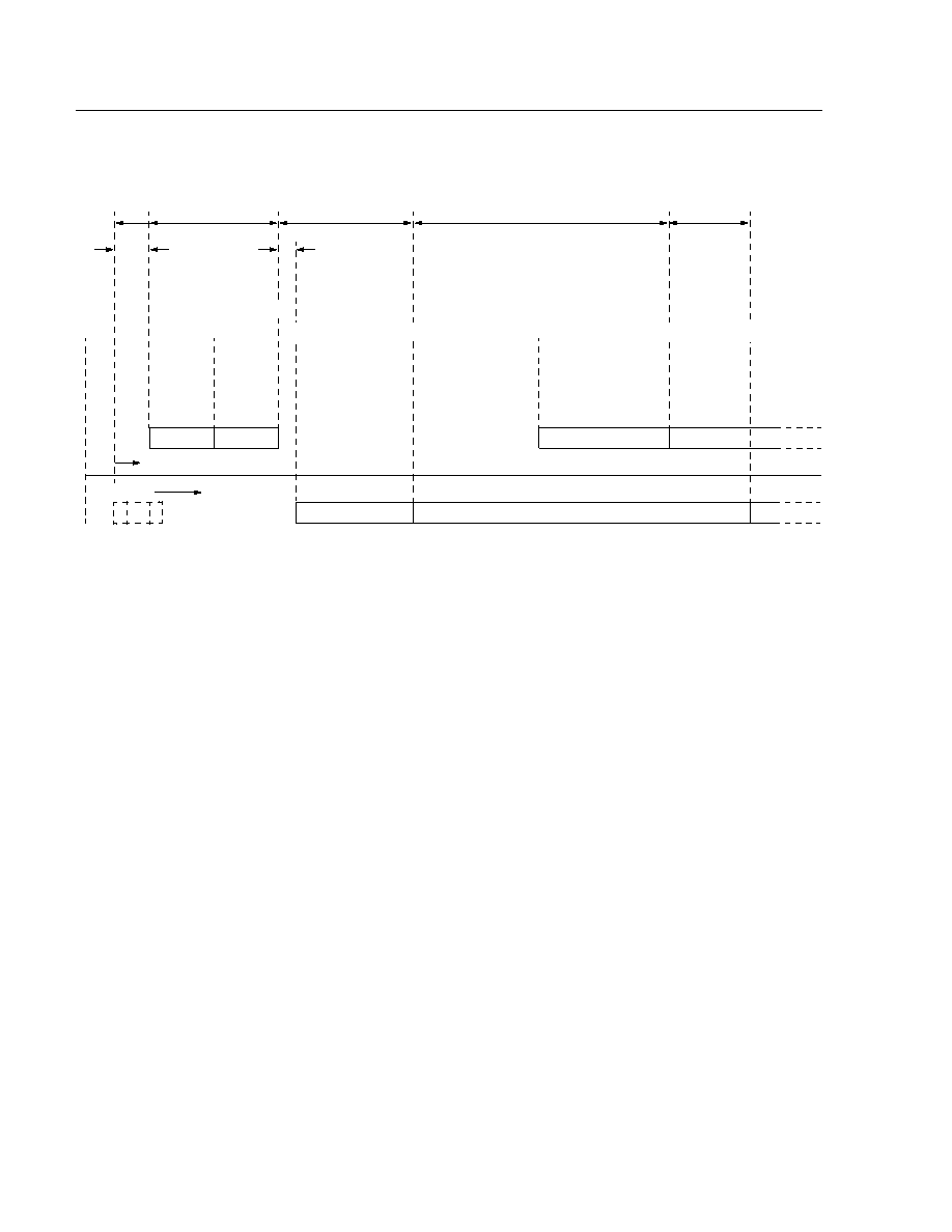
32
Lucent Technologies Inc.
Data Sheet
April 1998
T7264 U-Interface 2B1Q Transceiver
Activation and the K2 Interface
(continued)
5-5180
Notes:
T0
Reset state.
T1
Network and NT are awake.
T2
NT discontinues transmission, indicating that the NT is ready to receive signal.
T3
Network responds to termination of signal and begins transmitting signal toward the NT.
T4
Network begins transmitting SL2 toward the NT, indicating that the network is ready to receive SN2.
T5
NT begins transmitting SN2 toward the network, indicating that NT has acquired SW frame and detected SL2.
T6
NT has acquired superframe marker, and is fully operational.
T7
Network has acquired superframe marker, and is fully operational.
Figure 21. State Sequence for DSL Transceiver Start-Up
Applications
The T7264 is intended for use in both switch and customer premises equipment including a central office (CO), a
private branch exchange (PBX), a 2-wire to 4-wire converter (NT1), and terminal equipment (TE). The physical ter-
mination of the U-interface at the network end is referred to as the line termination (LT); the physical termination at
the user end is referred to as the network termination (NT). Figure 22 shows a loop configuration using several U-
interface devices at various locations.
The T7264 provides system access to the U loop through the K2 interface. The K2 interface is a TDM serial interface
which provides access to 2B+D data, U-interface maintenance, and T7264 device control/status.
Figure 23 shows a 2-wire terminal application with the T7264 providing the U-interface. The T7270 provides the
microprocessor with access to the individual octets of the K2 data stream. The B1 and B2 data could be transferred
to either a codec for voice communications, such as the T7513A, or to an HDLC controller for data communications,
such as the T7121. Another T7121 could provide microprocessor access to D-channel HDLC processing. The
microprocessor would control initialization, activation/deactivation, D-channel processing, and maintenance func-
tions.
A
B
C
D
A + C
5 s FOR COLD START
A + C
150 ms FOR WARM START
B + D
10 s FOR COLD START
B + D
150 ms FOR WARM START
4 ms
480 ms
T0
T1
T5
TN
SN1
(OP-
TIONAL)
6
FRAMES
NT
NETWORK
NT
NETWORK
SL1 (OPTIONAL)
SL2
SL3
SN2
SN3
TL
2 FRAMES
T2
T3
T6
T7
T4

Data Sheet
April 1998
T7264 U-Interface 2B1Q Transceiver
Lucent Technologies Inc.
33
Applications
(continued)
Figure 24 shows a digital pair gain application with the T7264 providing the U-interface. In this system, the U-inter-
face is used as a digital pipe to multiplex two analog voice lines onto the B channels. Thus, one twisted pair can
provide two analog lines. The T7270 forms the interface between the microprocessor, the K2 bus, and the codecs.
The T7121 can be used for HDLC formatting on the B or D channels to provide enhanced features. The divider pro-
vides the 2.048 MHz clock for the codecs, which are interfaced to the TSI via its CHI ports. The codecs and battery
feeds provide the analog interface to the telephones.
5-5181
Figure 22. Loop Application
5-5182
Figure 23. 2-Wire Terminal Application
5-5183
Figure 24. Digital Pair Gain Application
2-WIRE 2B1Q
U-INTERFACE
2-WIRE 2B1Q
U-INTERFACE
U
NT
U
LT
U
LT
SWITCH
PBX
or
NT1
4-WIRE S/T
U
NT
2-WIRE
2B1Q
U-INTERFACE
MICRO-
PROCESSOR
T7270
K2
T7121
HDLC
T7513B
CODEC
T7121
HDLC
HANDSET
D
B1
B2
DATA
T7264
CHI
TRANSFORMER/
PROTECTION
U-INTERFACE
2754H/
521A
2B1Q
T7264
TSI
T7270
HIFI-64
T7121
10.24 MHz
K2 INTERFACE
CODEC
CODEC
T7513B
BATTERY FEED
ANALOG INTERFACE
BATTERY FEED
LB1276AF
4TH CHI
MICROPROCESSOR
RS232C
FOR
MAINTENANCE
MONITOR TERMINAL
ASYNC DATA PORT
DIVIDER
2.048 MHz
CHI
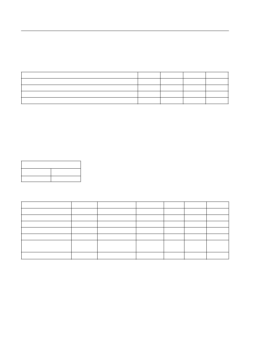
34
Lucent Technologies Inc.
Data Sheet
April 1998
T7264 U-Interface 2B1Q Transceiver
Absolute Maximum Ratings
Stresses in excess of the absolute maximum ratings can cause permanent damage to the device. These are abso-
lute stress ratings only. Functional operation of the device is not implied at these or any other conditions in excess
of those given in the operations sections of this data sheet. Exposure to absolute maximum ratings for extended
periods can adversely affect device reliability.
Handling Precautions
Although protection circuitry has been designed into this device, proper precautions should be taken to avoid expo-
sure to electrostatic discharge (ESD) during handling and mounting. Lucent employs a human-body model (HBM)
and charged-device model (CDM) for ESD-susceptibility testing and protection design evaluation. ESD voltage
thresholds are dependent on the circuit parameters used to define the model. No industry-wide standard has been
adopted for the CDM. However, a standard HBM (resistance = 1500
, capacitance = 100 pF) is widely used and,
therefore, can be used for comparison. The HBM ESD threshold presented here was obtained by using these cir-
cuit parameters:
Recommended Operating Conditions
* To meet ANSI T1.601 free-run line rate requirement, NT tolerance is 100 ppm.
x = tolerance of MTC.
Parameter
Min
Typ
Max
Unit
Storage Temperature
≠55
--
125
∞
C
Lead Temp (soldering or bonding)
--
--
300
∞
C
Any Pin to GND
≠0.5
--
6.5
V
Power Dissipation (package limit)
--
--
700
mW
ESD Threshold Voltage
Device
Voltage
T7264-ML
>500
Parameter
Symbol
Test Conditions
Min
Typ
Max
Unit
Ambient Temp
T
A
V
DD
= 5 V
±
5%
≠40
--
85
∞
C
Any V
DD
V
DD
--
4.75
5.0
5.25
V
GND to GND
V
GG
--
≠10
--
10
mV
Voltage Ref Capacitor
CVR
--
0.08
0.1
0.2
µ
F
Master Clock Frequency
MCLK
--
--
15.36
--
MHz
Master Clock Tolerance
MCLK
NT Mode
LT Mode
≠225*
≠225 + x*
--
--
225*
225 ≠ x*
ppm
ppm
Master Clock Duty Cycle
MCLK
--
47
--
53
%
Data Sheet
April 1998
T7264 U-Interface 2B1Q Transceiver
Lucent Technologies Inc.
35
Electrical Characteristics
All characteristics are for a 15.36 MHz crystal, 135
line load, random 2B+D data,
V
DD
= 5 V
±
0.25 V, ≠40
∞
C to +85
∞
C, output capacitance = 50 pF.
Table 24. Power Consumption
Table 25. Performance Ratings
Table 26. Crystal Characteristics: Fundamental Mode Crystal
These are the characteristics of a crystal for meeting the
±
100 ppm requirements of T1.601 for NT operation.
The parasitic capacitance of the PC board to which the T7264 crystal is mounted must be kept within the range
0.6
±
0.4 pF.
For LT operation or for NT applications that can tolerate a free-running frequency tolerance of up to
±
150 ppm, T
OL
and C
m
may be relaxed as long as they satisfy the following:
| T
OL
+ (3300 ppm) x C
m
(in pF) |
150 ppm
using the nominal value of C
m
. All other parameters are unchanged except that the shunt capacitance, C
O
, should
change in proportion with any change in C
m
.
Possible sources for 15.36 MHz crystals for use with the T7264 include:
* MTRON is a registered trademark of MTRON Industries, Inc., a wholly owned subsidiary of Lynch Corporation. (Lynch is a registered trade-
mark of Lynch Corporation.)
Parameter
Test Conditions
Min
Typ
Max
Unit
Power Consumption
Operating, Random Data
--
275
350
mW
Power Consumption
Powerdown Mode
--
30
50
mW
Parameter
Test Conditions
Min
Typ
Max
Unit
Warm Start Time
--
--
200
--
ms
Cold Start Time
--
--
3.5
--
s
Error Rate over 18 kft
26 AWG cable
--
--
10
≠7
--
Parameter
Symbol
Test Conditions
Specifications
Unit
Center Frequency
F
O
With 25.0 pF of loading
15.36011
MHz
Tolerance Including Calibration,
Temperature Stability, and Aging
T
OL
--
±
60
ppm
Drive Level
D
L
Maximum
0.5
mW
Series Resistance
R
S
Maximum
20
Shunt Capacitance
C
O
--
3.0
±
20%
pF
Motional Capacitance
Cm
--
12
±
20%
fF
CTS Knights
MTRON*
Saronix
Tom Haney at 1-704-684-0242
P/N 020-2807-0
William J. Winch
(Winch Sales Associates)
at 1-908-613-1515
P/N 4044-001
Laura Derrickson at 1-800-227-8974
(in CA, 1-800-422-3355
P/N SRX5144(-N)
For LT applications, a relaxed specification part is avail-
able where TOL =
±
85 ppm and Cm = 18 fF
±
20%.
P/N SRX5152(≠N [no vinyl coating])
36
Lucent Technologies Inc.
Data Sheet
April 1998
T7264 U-Interface 2B1Q Transceiver
Electrical Characteristics
(continued)
Table 27. Internal PLL Characteristics
* Set by digital PLL; therefore, variations track MTC (LT mode) or U-interface line rate (NT mode).
Table 28. Digital dc Characteristics (Over Operating Ranges)
Loop-Range Performance Characteristics
The T7264 transceiver is designed to allow systems to meet the loop-range requirements of ANSI Standard T1.601-
1992 when the transceiver is used with the proper peripheral circuitry.
The line driver provides pulses that produce the 2.5 V template required of the T1.601 specification when connected
to the proper transformer and interface circuitry.
Parameter
Test Conditions
Min
Typ
Max
Unit
Total Pull Range
--
±
250
--
--
ppm
Jitter Transfer Function
≠3 dB point (LT)
≠3 dB point (NT), 18 kft 26 AWG
--
--
0.45*
5*
--
--
Hz
Hz
Jitter Peaking
at 0.15 Hz typical (LT)
at 1.5 Hz typical (NT)
--
--
0.4*
1.0*
--
--
dB
dB
Parameter
Symbol
Test Conditions
Min
Typ
Max
Unit
Input Leakage Current:
Low
High
Low
High
I
IL
I
IH
I
ILpu
I
IHpu
V
IL
= 0 (pin 1, 2)
V
IH
= V
DD
(pin 1, 2)
V
IL
= 0 (pins 7--11, 14--15, 24--26)
V
IH
= V
DD
(pins 7--11, 14--15, 24--26)
≠10
--
≠52
--
--
--
--
--
--
10
≠10
10
µ
A
µ
A
µ
A
µ
A
Input Voltage:
Low
High
Low-to-High Threshold
High-to-Low Threshold
Low
High
V
IL
V
IH
V
ILs
V
IHs
V
ILc
V
IHc
All Pins Except Pin 7, 10, 11, 24
All Pins Except Pin 7, 10, 11, 24
Pin 7
Pin 7
Pins 10, 11, 24
Pins 10, 11, 24
--
2.0
V
DD
≠ 0.5
--
--
0.7 V
DD
--
--
--
--
--
--
0.8
--
--
0.5
0.2 V
DD
--
V
V
V
V
V
V
Output Leakage:
Low
High
I
OZL
I
OZH
V
OL
= 0; Pin 26 = 0
V
OH
= V
DD;
Pin 26 = 0
10
--
--
--
--
≠10
µ
A
µ
A
Output Leakage:
Low, TTL
High, TTL
V
OL
V
OH
I
OL
= 1.6 mA, Pins 3, 4, 5, 16
I
OL
= 3.3 mA, Pin 43
I
OL
= 6.5 mA, Pins 13, 23
I
OH
= 2.4 mA, Pins 3, 4, 5, 16
I
OH
= 5.1 mA, Pin 43
I
OH
= 10.4 mA, Pins 13, 23
--
--
--
2.4
2.4
2.4
--
--
--
--
--
--
0.4
0.4
0.4
--
--
--
V
V
V
V
V
V
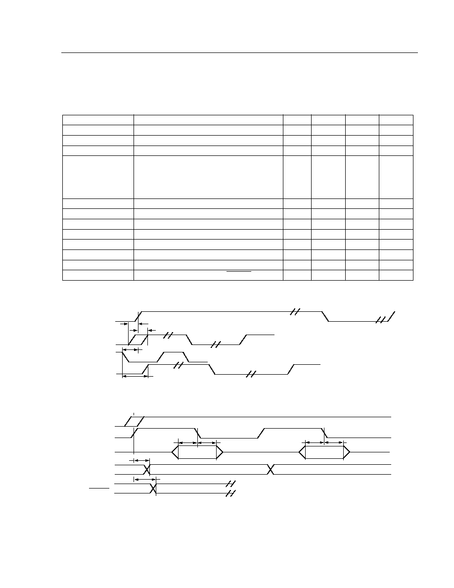
Data Sheet
April 1998
T7264 U-Interface 2B1Q Transceiver
Lucent Technologies Inc.
37
Timing Characteristics
Output Capacitance = 50 pF, T
A
= ≠40
∞
C to +85
∞
C, V
DD
= 5 V
±
5%, GND = 0 V, crystal frequency = 15.36 MHz.
Table 29. Clock Timing (See Figures 25, 26, and 28.)
*
Includes the effect of phase steps generated by the digital phase-locked loop.
5-5184
Figure 25. Timing Diagram Referenced to F
5-5185
Figure 26. Timing Diagram Referenced to C
Symbol
Parameter
Min
Typ
Max
Unit
F
8 kHz Duty Cycle
49.8
--
50.2
%
C
512 kHz Duty Cycle
46
--
54
%
RCLKEN
80 kHz Duty Cycle
48
--
52
%
CKOUT
Duty Cycle:
In 7.68 MHz Mode
In 15.36 MHz Mode
Pulse Width (high)
In 10.24 MHz Mode
45
40
23*
--
--
--
55
60
52*
%
%
%
tR1, tF1
Rise or Fall Time
--
30
--
ns
tCHFH, tFHCH
Clock (C) High to Frame Sync (F)
≠15
--
15
ns
tRCHRCH
CKOUT Clock to RCLKEN Clock Enable
--
--
25
ns
tCOLFH
CKOUT Clock to Frame Sync (F)
--
--
50
ns
tDIVCL, tCLDIZ
Receive Data (DI) Setup & Hold Time
50
--
--
ns
tCHDOV
Clock (C) High to Data (DO) Valid
--
--
50
ns
tR2, tF2
CKOUT Clock Rise or Fall
--
15
--
ns
tCHOSV
Clock (C) High to Out of Sync OSYNC Valid
--
--
60
ns
F
CKOUT
tCOLFH
C
tFHCH
tF1
tF1
tR1
tF2
tR2
RCLKEN
tF1
tR1
tRCHRCH
tCHFH
C
DO
tCHDOV
DI
tDIVCL
tCLDIZ
OSYNC
tCHOSV
tDIVCL
tCLDIZ
F
BIT 1
BIT 1 OF B1 DATA
BIT 2
BIT 2 OF B1 DATA
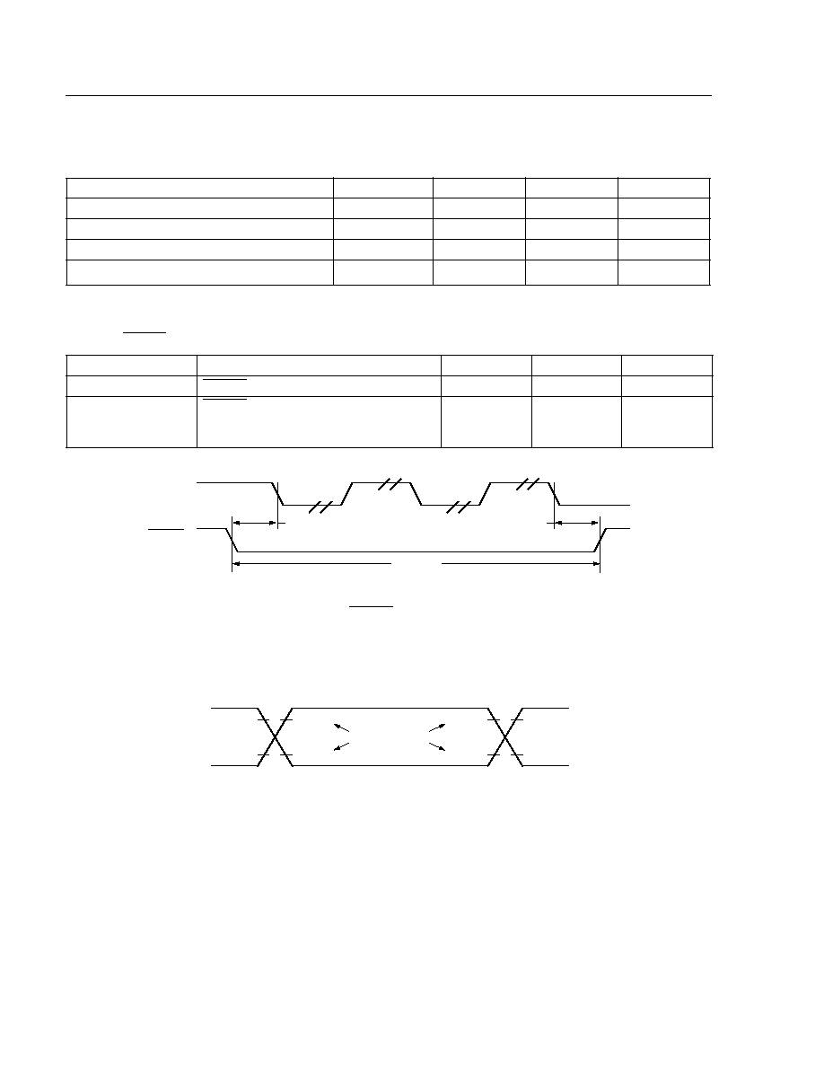
38
Lucent Technologies Inc.
Data Sheet
April 1998
T7264 U-Interface 2B1Q Transceiver
Timing Characteristics
(continued)
Table 30. MTC Requirements and Characteristics* (LT Mode)
* To meet ANSI T1.601-1992, see note for Recommended Operating Conditions.
One UI = 12.5
µ
s.
Table 31. RESET Timing (See Figures 27 and 28.)
5-5186
Figure 27. RESET Timing Diagram
Switching Test Input/Output Waveform
5-5187
Figure 28. Switching Test Waveform
Parameter
Min
Typ
Max
Unit
MTC Clock Period
125 ≠ 32 ppm
125
125 + 32 ppm
µ
s
MTC High/Low Time
8
--
--
MCLKs
MTC Rise/Fall Time
--
--
60
ns
MTC Jitter
--
--
0.259
UI
Symbol
Parameter
Min
Max
Unit
tRSLFL, tFLRSH
RESET Setup and Hold Time
60
--
ns
tRSLRSH
RESET Low Time:
From Idle Mode or Normal Operation
From Power On
3
1.5
--
--
K2 frames
ms
F
RESET
(RS)
tRSLFL
tFLRSH
tRSLRSH
2.0 V
0.8 V
TEST POINTS
2.4 V
0.4 V
2.0 V
0.8 V
2.4 V
0.4 V

Data Sheet
April 1998
T7264 U-Interface 2B1Q Transceiver
Lucent Technologies Inc.
39
Outline Diagram
Dimensions are in millimeters.
5-2506
Notes:
Meets all JEDEC standards.
Pin 1 index mark may be a dimple or numeric located in zones indicated.
Ordering Information
Code
Package
Temperature
Comcode
T7264A- -ML-D
44-pin PLCC
≠40
∞
C to +85
∞
C
107890170
T7264A- -ML-DT
44-pin PLCC
≠40
∞
C to +85
∞
C
107997124
4.57
MAX
1.27 TYP
0.53
MAX
0.10
SEATING PLANE
0.51 MIN
TYP
1
6
40
7
17
29
39
18
28
PIN #1 IDENTIFIER
ZONE
16.66 MAX
17.65 MAX
16.66
MAX
17.65
MAX

40
40
Lucent Technologies Inc.
Data Sheet
April 1998
T7264 U-Interface 2B1Q Transceiver
Appendix A. Questions and Answers
Introduction
The questions and answers are divided into three cate-
gories: U-interface, K2 interface, and miscellaneous.
For detailed application information, also refer to the
application notes Implementation of an ANSI Standard
ISDN NT1 Using the Lucent T7262A/63, T7252A,
T7270, and an 8-Bit Microcontroller and Performance
Factors in Line-Powered 2B1Q Applications.
U-Interface
Q1: Is the line interface for the T7264 the same as the
T7262A/63?
A1:
The interface is different in that the T7262A/63
uses a Lucent 2754G transformer (2.5:1 turns
ratio), and the T7264 uses a Lucent 2754H trans-
former (1.5:1 turns ratio).
Other changes to the line interface include
device-side resistors of 16.9
±
1% and line-side
resistors of 16.9
±
7%. Part of the line-side
resistance will likely be a PTC in those applica-
tions requiring power cross protection.
The T7264 device-side protection is unchanged
(521A diodes), and the dc blocking capacitor is
unchanged (Illinois Capacitor* 1.0
µ
F
±
5%).
Line-side protection must be tailored to individual
system needs.
Q2: Why is a higher transformer magnetizing
inductance used (as compared to other
vendors)?
A2:
It has been determined that a higher inductance
provides better linearity. Furthermore, it has been
found that a higher inductance at the far end pro-
vides better receiver performance at the near end
and better probability of start-up at long loop
lengths.
Q3: Can the T7264 be used with a transformer that
has a magnetizing inductance of 20 mH?
A3:
The echo canceler and tail canceler are
optimized for a transformer inductance of approx-
imately 80 mH and will not work with a value this
low.
Q4: Are the Lucent U-interface transformers available
as surface-mount components?
A4:
Not at this time.
Q5: Are there any future plans to make a smaller
height 2-wire transformer?
A5:
Due to the rigid design specifications for the
transformer, vendors have found it difficult to
make the transformer any smaller. We are con-
tinuing to work with transformer vendors to see if
we can come up with a smaller solution.
Q6: The line interface components' specifications
require 16.9
resistors on the line side of the
transformer. We would like to change this value
for our application. Can the U-interface line-side
circuit be redesigned to change the value of the
line-side resistors?
A6:
Yes. For example, the line-side resistances can
be reflected back to the device side of the trans-
former so that, instead of having 16.9
on each
side of the transformer, there are no resistors on
the line side of the transformer and 24.4
resis-
tors on the device side (16.9 + 16.9/N
2
, where N
is the turns ratio of the transformer). However,
there may be some performance penalty in this
case since the on-chip hybrid network is opti-
mized for 16.9
of resistance on the device side
of the transformer.
* Illinois Capacitor is a registered trademark of Illinois Capacitor Inc.

Lucent Technologies Inc.
41
Data Sheet
April 1998
T7264 U-Interface 2B1Q Transceiver
Appendix A. Questions and Answers
(continued)
Q7: Why are the line-side resistors (16.9
) rated at
7% tolerance in Figure 4 of the data sheet?
A7:
This tolerance was determined based on
analysis of the output voltage tolerance of the
T7262A/63 solution as compared to the T7264
solution, taking into account the tolerances of the
transformer, resistors, etc. It is not a standard
resistor tolerance, such as 5%, because as much
flexibility as possible was desired. The 16.9
resistor is often a combination of a resistor and a
positive temperature coefficient (PTC) surge-
protection resistor, and PTCs generally have
wider tolerances.
Some 2B1Q manufacturers try to match the
PTCs in such a way that their variations from the
nominal value are in the same direction. How-
ever, it is important to use as tight a tolerance as
possible for the following reasons:
s
The 16.9
resistor is also part of the termina-
tion impedance looking into Tip/Ring. ANSI
specifies this impedance at 135
nominal, and
the impedance template over the specified
frequencies is derived from the return loss
requirement (T1.601, Sections 7.1, 7.2, and
Figure 19). A tighter tolerance on the 16.9
resistors allows more margin on the return loss
template.
s
If resistors are unmatched, longitudinal balance
(described in T1.601, Section 7.3) may be
affected. Designers can experimentally deter-
mine the maximum tolerance allowed in their
system by varying the 16.9
resistors slightly
and observing the effect on the parameters
mentioned above.
Q8: The dc blocking capacitor specified is 1
µ
F. Can it
be increased to at least 2
µ
F?
A8:
Yes. This value can be increased without any det-
rimental effect.
Q9: The application diagram in the data sheet shows
the loopback relay on the line side of the trans-
former. Why is it not shown on the device side?
A9:
The relay can be located on the device side
between the 521A surge protector and the trans-
former, and the local loopback will function prop-
erly. It is shown on the line side because in many
applications the relay is a DPDT type and is also
used for metallic access to some line testing
equipment (at an LT, for example).
Q10: If the relay is on the line side, what type should it
be?
A10: Relay type is application-dependent. An example
of a relay which would work in most cases is an
Aromat* DS Series 2 A relay.
Q11: Clarify the meaning of the note concerning the
3000 pF capacitors in the U-line interface figure
(Figure 4).
A11: The capacitors are not absolutely required. The
ANSI T1.601 specification contains no require-
ments on longitudinal noise immunity. Therefore,
these capacitors are not required in order to meet
the specification. However, there are guidelines
in IEC 801-6 which suggest a noise immunity of
up to 10 Vrms between 150 kHz and 250 MHz. At
these levels, the 10 kHz tone detector in the
T7264 may be desensitized such that tone detec-
tion is not guaranteed on long loops. The
3000 pF was selected to provide attenuation of
this common-mode noise so that tone detector
sensitivity is not adversely affected. Since the
3000 pF capacitor was selected based only on
guidelines, it is not mandatory, but it is recom-
mended in applications which may be susceptible
to high levels of common-mode noise. The final
decision depends on the specific application.
* Aromat is a registered trademark of Aromat Corporation.

42
42
Lucent Technologies Inc.
Data Sheet
April 1998
T7264 U-Interface 2B1Q Transceiver
Appendix A. Questions and Answers
(continued)
Q12: Why must secondary protection, such as the
521A protection diode, be used?
A12: The purpose of the 521A is to protect against
metallic surges below the breakdown level of the
primary protector.
Such metallic surges will be coupled through the
transformer and could cause device damage if
the currents are high. The 521A does not provide
absolute protection for the device, but rather
works in conjunction with the built-in protection
on the device leads.
The breakdown voltage level for secondary pro-
tection devices must be chosen to be above the
normal working voltage of the signal and typically
below the breakdown voltage level of the next
stage of protection. The 521A has a minimum
breakdown voltage level of 6.95 V and a maxi-
mum breakdown voltage of 8.0 V.
The chip pins which the 521A protects are
pins 36 (HP), 31 (HN), 32 (LOP), and 35 (LON).
The 16.9
resistors will help to protect pins 32
and 35, but pins 31 and 36 will be directly
exposed to the voltage across the 521A. The on-
chip protection on these pins consists of output
diodes and a pair of polysilicon resistors. These
pins have been thoroughly tested to ensure that
an 8 V level will not damage them; therefore, no
third level of protection is needed between the
521A and the HP and HN pins.
The 521A has a maximum reverse surge voltage
level of 10 V at 50 A. Sustained currents this
large are not a concern in this application, since it
is assumed that some form of primary protection
is being used, such as the Teccor* P2103AA
SIDACtor *. Thus, there should never be more
than 8.0 V across the 521A, except for possibly
an ESD or lightning hit. In these cases, the T7264
is able to withstand at least
±
500 V (human-body
model) on its pins.
Another consideration is the capacitive loading
that the protection device presents to the target
device. This is generally required to be negligible
at the operating frequency.
From a practical point of view, the device is
chosen to meet not only voltage, current, and
capacitance requirements, but also to meet price,
availability, manufacturing, and second-
sourcing requirements. The 521A device is a
general-purpose device that meets system
requirements for voltage, current, capacitance,
price, etc., for some of Lucent's customers. Other
devices which may be acceptable alternates are
as follows: Motorola
SA6.0C (through-hole and
surface-mount), Microsemi SMSJ6.0C-SMB (sur-
face-mount), and SGS-Thomson
SM6T6V8C
(surface-mount).
Q13: Bellcore TR-TSY-000078, Section 3.2.4.1, prohib-
its using silver metallization, but the 521A protec-
tion diodes have silver-plated leads. Does this
indicate an incompatibility problem?
A13: Bellcore TR-TSY-000078, Section 3.2.4.1 prohib-
its silver ". . . when electromigration is a problem."
The 521A diodes are only used as secondary
protection, and, therefore, almost never carry any
current. Electromigration occurs only when there
is a high current flow for an extended period of
time. Since the diodes are never subjected to this
condition, electromigration is not a problem, and
the silver plating is acceptable.
Q14: Where can information be obtained on lightning
and surge protection requirements for 2B1Q
products?
A14: ANSI T1.601, Appendix B, provides a list of
applicable specifications to which you may refer.
Also, there are many manufacturers of overvolt-
age protection devices who are familiar with the
specifications and would be willing to assist in
surge protection design. The ITU-T K series
recommendations are also a good source of
information on protection, especially Recommen-
dation K.11, "Principles of Protection Against
Overvoltages and Overcurrents," which presents
an overview of protection principles.
* Teccor and SIDACtor are trademarks of Teccor, Inc.
Motorola is a registered trademark of Motorola, Inc.
SGS-Thomson is a registered trademark of SGS-Thomson
Microelectronics, Inc.

Lucent Technologies Inc.
43
Data Sheet
April 1998
T7264 U-Interface 2B1Q Transceiver
Appendix A. Questions and Answers
(continued)
Q15: ITU-T specification K.21 describes a lightning
surge test for NT1s (see Figure 1/K.21 and
Table 1/K.21, Test #1) in which both Tip and Ring
are connected to the source and a 1.5 kV voltage
surge is applied between this point and the
GND of the NT1. What are the protection consid-
erations for this test? Are the HP and HN pins
susceptible to damage?
A15: The critical component in this test is the trans-
former since its breakdown voltage must be
greater than 1.5 kV. Assuming this is the case,
the only voltage that will make it through to the
secondary side of the transformer will be prima-
rily due to the interwinding capacitance of the
transformer coils.
This capacitance will look like an impedance to
the common-mode surge and will therefore limit
current on the device side of the transformer. The
device-side voltage will be clamped by the 521A
device. The maximum breakdown voltage of the
521A is 8 V. The 16.9
resistors will help protect
the LOP and LON pins on the T7264 from this
voltage. However, this voltage will be seen
directly on pins 36 and 31 (HP and HN) on the
T7264. The on-chip protection on these pins con-
sists of output diodes and a pair of polysilicon
resistors. These pins have been thoroughly
tested to ensure that an 8 V level will not damage
them; therefore, no third level of protection is
needed between the 521A and the HP and HN
pins.
Q16: How is it possible to guarantee the
±
0.35 dB
power spectrum tolerance on the U-interface?
A16: By trimming to
±
0.1 dB; the rest of the variation is
for power supply, temperature, and aging.
Q17: Is the
±
100 ppm free-run frequency (NT mode)
recommendation met in the T7264?
A17: In the free-run mode, the output frequency is
primarily dependent upon the crystal, not the sili-
con design. For low-cost crystals, initial toler-
ance, temperature, and aging effects may
account for two-thirds of this budget, and just a
couple of pF of variation in load capacitance will
use up the rest. Thus, the
±
100 ppm goal can be
met if the crystal parameters are well controlled.
See the Crystal Characteristics information in the
data sheet (Table 26).
Q18: It has been noted in some other designs that the
crystal has a capacitor from each pin to ground.
Changing these capacitances allows the fre-
quency to be adjusted to compensate for board
parasitics. Can this be done with the T7264 crys-
tal? Also, can we use a crystal from our own
manufacturer?
A18: The crystal for the T7264 is tuned to a particular
load capacitance that does not include external
capacitors. The advantage to this is that no exter-
nal components are required. The disadvantage
is that board parasitics must be very small. The
data sheet notes that the board parasitics must
be within the range of 0.6 pF
±
0.4 pF. Lucent
does not require that a particular crystal be used,
but we strongly recommend adhering to the crys-
tal parameters specified in the data sheet. A
crystal which deviates from these parameters
can work under most conditions, but we cannot
guarantee that it will start up and/or meet the
±
100 ppm requirement under all operating condi-
tions.
Q19: Is there a test pin available for generating a +3/≠3
sequence so that pulse templates can be
measured easily?
A19: There is no such pin. But a sequence of four +3s,
followed by four ≠3s (and so on) is the 10 kHz
wakeup tone (TN, TL in ANSI T1.601, Figure 17)
that each transceiver outputs when initiating a
start-up. This tone is produced when the K2 bit,
istp in the dc octet, is asserted. At the NT, this
tone lasts for 9 ms (90 pulses), and at the LT, it
lasts for 3 ms (30 pulses). This should be long
enough to capture the data on a digitizer or stor-
age scope for analysis.
Q20: What are the average cold start and warm start
times?
A20: Lab measurements have shown the average cold
start time to be about 3.3 s--4.2 s over all loop
lengths, and the average warm start time to be
around 125 ms--190 ms over all loop lengths.
Q21: What is the U-interface's response time to an
incoming wakeup tone from the LT?
A21: Response time is about 1 ms.
Q22: What is the minimum time for a U-interface
reframe after a momentary (<480 ms) loss of
synchronization?
A22: Five superframes (60 ms).

44
44
Lucent Technologies Inc.
Data Sheet
April 1998
T7264 U-Interface 2B1Q Transceiver
Appendix A. Questions and Answers
(continued)
Q23: Can the range of the T7264 on the U-interface be
specified in terms of loss? What is the range for
over straight 24 AWG wire?
A23: ANSI Standard T1.601, Section 5.1, states that
transceivers meeting the U-interface standard are
intended to operate over cables up to the limits of
18 kft (5.5 km) 1300
resistance design. Resis-
tance design rules specify that a loop (of single-
or mixed-gauge cable; e.g., 22 AWG, 24 AWG,
and 26 AWG) should have a maximum dc resis-
tance of 1300
, a maximum working length of
18 kft, and a maximum total bridged tap length of
6 kft.
The standard states that, in terms of loss, this is
equivalent to a maximum insertion loss of 42 dB
@ 40 kHz. Lucent has found that, for assessing
the condition of actual loops in the field in a
2B1Q system, specifying insertion loss as
33.4 dB @ 20 kHz more closely models ANSI
circuit operation. This is equivalent to a straight
26 AWG cable with 1300
dc resistance
(~15.6 kft).
The above goals are for actual loops in the out-
side loop plant. These loops may be subjected to
noise and jitter. In addition, as mentioned above,
there may be bridge taps at various points on the
loop. The T1.601 standard defines 15 loops, plus
the null, or 0 length loop, which are intended to
represent a generic cross section of the actual
loop plant.
A 2B1Q system must perform over all these loops
in the presence of impairments with an error rate
of <1e≠7. Loop #1 (18 kft, where 16.5 kft is
26 AWG cable and 1.5 kft is 24 AWG cable) is the
longest, and so has the most loss (37.6 dB @
20 kHz and 47.5 dB @ 40 kHz). Note that this is
more loss than discussed in the preceding para-
graph. The difference is based on test require-
ments vs. field deployment. The test
requirements are somewhat more stringent than
the field goal in order to provide some margin
against severe impairments, complex bridged
taps, etc.
If a transceiver can operate over Loop #1 error-
free, it should have adequate range to meet all
the other loops specified in T1.601. Loop #1 has
no bridged taps, so passing Loop #1 does not
guarantee that a transceiver will successfully
start up on every loop. Also, due to the complex
nature of 2B1Q transceiver start-up algorithms,
there may be shorter loops which could cause
start-up problems if the transceiver algorithm is
not robust. The T7264 has been tested on all of
the ANSI loops per the T1.601 standard and
passes them all successfully. Two loops com-
monly used in the lab to evaluate the perfor-
mance of the T7264 silicon are as follows:
The T7264 is able to start up and operate error-
free on both of these loops. Neither of these
loops is specified in the ANSI standard, but both
are useful for evaluation purposes. The first loop
is used because it is simple to construct and easy
to emulate using a lumped parameter cable
model, and it is very similar to ANSI Loop #1, but
slightly worse. Thus, if a transceiver can start up
on this loop and operate error-free, its range will
be adequate to meet the longest ANSI loop.
The second loop is used because, due to its diffi-
cult bridge tap structure and its length, it stresses
the transceiver start-up algorithms more than any
of the ANSI-defined loops. Thus, if a transceiver
can start up on this loop, it should be able to meet
any of the ANSI-defined loops which have bridge
taps. Also, on a straight 26 AWG loop, the T7264
can successfully start up at lengths up to 21 kft.
This fact, combined with reliable start-up on the
15 kft 2BT loop above, illustrates that the T7264
provides ample start-up sensitivity, loop range,
and robustness on all ANSI loops.
Another parameter of interest is pulse height loss
(PHL). PHL can be defined as the loss in dB of
the peak of a 2B1Q pulse relative to a 0 length
loop. For an 18 kft 26 AWG loop, the PHL is
about 36 dB, which is 2 dB worse than on ANSI
Loop #1. A signal-to-noise ratio (SNR) measure-
ment can be performed on the received signal
after all the signal processing is complete (i.e., at
the input to the slicer in the decision feedback
equalizer). This is a measure of the ratio of the
recovered 2B1Q pulse height vs. the noise
remaining on the signal. The SNR must be
greater than 22 dB in order to operate with a bit
error rate of <1e≠7.
Loop
Config-
uration
Bridge Taps
(BT)
Loss @
20 kHz
(dB)
Loss @
40 kHz
(dB)
18 kft
26 AWG
None
38.7
49.5
15 kft
26 AWG
2 at near end,
each 3 kft,
22 AWG
37.1
46.5
Lucent Technologies Inc.
45
Data Sheet
April 1998
T7264 U-Interface 2B1Q Transceiver
Appendix A. Questions and Answers
(continued)
A23: (continued)
With no impairments, the T7264 SNR is typically
32 dB on the 18 kft 26 AWG loop. When all ANSI-
specified impairments are added, the SNR is
about 22.7 dB, still leaving adequate margin to
guarantee error-free operation over all ANSI
loops.
Finally, to estimate range over straight 24 AWG
cable, the 18 kft loop loss can be used as a limit
(since the T7264 can operate successfully with
that amount of loss), and the following calcula-
tions can be made:
= 24 kft
Therefore, the operating range over 24 AWG
cable is expected to be about 24 kft.
Q24: What cable simulator is used for evaluating the
T7264?
A24: The original version of the transceiver was tested
using real cable for ANSI loop performance mea-
surements. However, currently, the Lucent Tech-
nologies Microelectronics Group laboratory uses
the TAS2200A* Cable Emulator for evaluation
purposes.
Q25: The data sheet states that the T7264 meets the
ANSI T1.601-1992 standard. Is there detailed
evaluation data available on loops 1 and 4?
A25: The results shown in the following table for some
typical devices have been obtained in laboratory
testing. Loops 1 and 4 are the most difficult
cases.
Q26: What does the energy spectrum of a 2B1Q signal
look like?
A26: Figure A1 (curve P1) in the ANSI T1.601
standard gives a good idea of what this spectrum
looks like.
Q27: Does the return loss measurement described in
ANSI T1.601, Section 7, require that the T7264
terminate a metallic cable with 135
during
powerdown?
A27: No. ANSI and ETSI specifications do not require
this. They require that the device be placed in an
active mode with the transmitter producing 0 V
(same as quiet mode) while performing the return
loss measurements. The T7264 is placed in this
mode by pulling the
RESET
pin low.
Q28: How is the T7264 set to quiet mode?
A28: The device is placed in the quiet mode by pulling
the
RESET
pin low. In this mode, the transmitter is
on, but is producing 0 V.
Q29: Please clarify the meaning of ANSI Standard
T1.601, Section 7.4.2, Jitter Requirement #3.
A29: The intent of this requirement is to ensure that
after a deactivation and subsequent activation
attempt (warm start), the phase of the receive
and transmit signals at the NT will be within the
specified limits relative to what they were prior to
deactivation. This is needed so that the LT, upon
a warm-start attempt, can make an accurate
assumption about the phase of the incoming NT
signal with respect to its transmit signal. Note that
the T7264 meets this requirement by design
because the NT phase offset from transmit to
receive is always fixed.
Q30: How can proprietary messages be passed across
the U-interface?
A30: The embedded operations channel (eoc)
provides one way of doing this. ANSI defines 64
8-bit messages which can be used for non-
standard applications. They range in value from
binary 00010000 to 01000000.
There is also a provision for sending bulk data
over the eoc. Setting the data/message indicator
bit to 0 indicates the current 8-bit eoc word con-
tains data that is to be passed transparently with-
out being acted on. Note that there is no
response time requirement placed on the NT in
this case (i.e., the NT does not have to echo the
message back to the LT). Also note that as of
1993 this is only an ANSI provision and is not an
ANSI requirement. The T7264 does support this
provision.
* TAS2200A is a trademark of Telecom Analysis Systems Incorpo-
rated.
Loss of 18 kft 26 AWG loop @ 20 kHz
38.7 dB
Loss per kft of 24 AWG cable @ 20 kHz 1.6 dB
ANSI
Loop #
Configuration
1992 ANSI
XTALK Margin
(dB)
1
LT
1.9
4
LT
7.6
38.7 dB
1.6 dB/kft
---------------------------

46
46
Lucent Technologies Inc.
Data Sheet
April 1998
T7264 U-Interface 2B1Q Transceiver
Appendix A. Questions and Answers
(continued)
K2 Interface
Q31: How are powerdown and warm start performed in
the T7264?
A31: The powerdown/warmstart sequence is as fol-
lows:
s
At the LT, the series of events begins with the
assertion of ldea = 1. This causes the device to
begin the automatic deactivation sequence. As
long as the device control bits (istp, lpbk, and
afrst) and the
RESET
and
ILOSS
pins remain
inactive during this time, the LT device con-
cludes deactivation by entering the powerdown
state. From this condition, the loop can be
reactivated by using a warm start.
s
At the NT, the device receives at least three
consecutive ldea = 0 bits from the LT during
deactivation. These bits must be read from the
K2 interface and interpreted to indicate that a
deactivation is occurring. Once this condition is
detected, the external controller must set
ldea = 1 at the NT, causing the device to freeze
its signal processor coefficients and power
down when a loss of signal from the LT is
detected. During this time, the device control
bits (istp, Ipbk, afrst, etc.) and the
RESET
and
ILOSS
pins must remain inactive at the NT.
From this condition, the loop can be reactivated
with a warm start.
Q32: Does the device automatically reset and attempt
a cold start if out of frame (oof) occurs after a
warm start?
A32: When an oof condition occurs, the device enters
a reframing algorithm and attempts to regain syn-
chronization. During this time, the device is still
active. If, after 480 ms, the device has not
regained synchronization, it goes into the deac-
tive state, from which the next start-up attempt
will result in a cold start. This conforms to the
state tables shown in Appendix C of ANSI
T1.601.
Q33: What is the purpose of the sksi bit in the device
control (DC) octet?
A33: Its primary use is to detect a "stuck at one" condi-
tion on the K2 interface. It is reflected back onto
the K2 interface as rsksi in the DS octet. Setting
sksi to 0 will guarantee that at least one bit (rsksi)
will be zero on the received K2 interface.
Q34: What should the state of the other bits in the DC
octet be during a local U-loopback?
A34: To perform a loopback, the following sequence of
bits are set in the DC octet, where 1 resets the
device and puts it into a known state, 2 asserts
the loopback, and 3 resets the chip again and
removes the loopback. The other DC bits should
be kept in their inactive state:
Q35: What is the state of the DO bits when OSYNC
goes low momentarily after the link is up?
A35: The 2B+D data and U-overhead bits are passed
transparently from the U-interface to the K2
interface. Since this U-information is likely to be
invalid during this time, the system should recog-
nize this and disregard the data and overhead
bits during this time. Note that this situation is dif-
ferent than when OSYNC is low prior to a start-
up. In the latter case, the 2B+D and overhead bits
are internally overwritten by the transceiver to
default values until synchronization is achieved
(see the data sheet for these values). In either
case, the DS bits are always valid.
Q36: ANSI requires 0.75 ms to process the eoc mes-
sage at the NT before echoing it. The T7264 data
sheet, however, states that the time from when
an incoming message becomes available and the
next message goes out is 1.75 ms. How can the
T7264 meet the standard?
A36: The 0.75 ms in the ANSI requirement refers to
the delay between the start of the received
U frame and the start of the transmitted U frame.
In the eoc bit locations, there are SW/ISW plus
12 2B+D blocks of data between the last bit of
one eoc message and the first bit of the next one.
This provides an additional 1.46 ms of processing
time or a total of 2.21 ms. Of course, some of this
time is consumed by the T7264 in moving data
between the U and K2 interfaces. After these
delays are taken into consideration, 1.75 ms
remain to process data.
1. afrst = 1, Ipbk = x, istp = 1, xpcy = x [loopback
= inactive]
2. afrst = 0, Ipbk = 0, istp = 1, xpcy = x [loopback
= active]
3. afrst = 1, Ipbk = 1, istp = 1, xpcy = x [loopback
= inactive]
Lucent Technologies Inc.
47
Data Sheet
April 1998
T7264 U-Interface 2B1Q Transceiver
Appendix A. Questions and Answers
(continued)
Q37: What are the requirements on the transmission
and reception of eoc data on the K2 interface?
A37: This is described on page 24, Figure 18, of this
data sheet. To summarize, the received eoc data
changes at K2 frames 47 and 95 (where frame 0
is marked by the rising edge of RSF). The most
recent eoc data is continuously available on the
K2 bus in the intervals between frames 47 and
95. The eoc data to be transmitted must be
present on the K2 interface at outgoing K2
frames 11 and 59 (where frame 0 is marked by
the rising edge of TSF). Since it is sampled only
at those times, it does not matter what is present
in those bit positions in the intervals between
frames K11 and K59.
For an LT, normally it will not matter in which K2
frames the eoc data is written and read, as long
the read/writes are done at 6 ms intervals (i.e.,
every 48 K2 frames). This is because there is no
critical timing involved between the reception of
an eoc message and its response, as there is at
an NT.
For an NT, ANSI T1.601, Section 8.3.2, specifies
that the eoc response must occur in the next
available outgoing eoc frame. This means that the
system has 13 K2 frames between the reception
of a new eoc message at frame K95 (relative to
RSF) and the transmission of the response to
that message. Thus, the eoc timing at the NT
should be referenced to RSF. Because of well-
defined timing between RSF and TSF at the NT,
there is no reason to use TSF for eoc timing.
Q38: The data sheet states that adea = 0 and Idea = 1
should not be used at the same time; why not?
A38: This mode is not recommended because it could
result in a system-level problem. Consider a typi-
cal deactivation sequence for a network having a
remote NT1 (i.e., an LT-to-NT connection with at
least one intermediate element, as shown in
ANSI T1.601, Figure E1)
.
The following table
shows the events at the NT and LT when the LT
initiates a deactivation. The LT uses adea in the
case of an intermediate element to propagate the
deactivation bit downstream without shutting
itself down (as it would do if ldea were set
instead):
* This stores the coefficients and prepares the transceiver for
deactivation. Deactivation will occur on loss of signal from
the intermediate element.
Stores the coefficients and deactivates the LT transmitter
(stops transmitting).
Notice that adea = 0 and ldea = 1 are permitted
at the last step. This is because the NT has
already stored its coefficients; however, if
Idea = 1 were set earlier (for example, in step 2),
the LT might deactivate before the downstream
elements had stored their coefficients, and a
clean deactivation would not occur. Therefore, to
help avoid turning off the LT before all the down-
stream elements store their coefficients, this
state was defined as invalid.
Also, note that Idea = 1 will cause a chip set in
the LT mode to store coefficients and deactivate,
but it only causes a chip set in the NT mode to
store coefficients. Deactivation at the NT only
occurs upon loss of the U-interface signal.
Note: The preceding deactivation procedure is
only an illustration. In a nonrepeater envi-
ronment, step 2 could be adea = ldea = 1,
which would cause the LT to automatically
save its coefficients and, within three or
four K2 frames, deactivate. This case
assumes that the NT has properly
detected dea = 0 and then stored its coeffi-
cients within those three or four frames.
LT
State
LT K2
Data In
NT K2
Data Out
NT Action
Normal
Operation
adea = 1
ldea = 0
dea = 1
--
Downstream
Deactivate
adea = 0
ldea = 0
dea = 0 Set Idea = 1
upon third
consecutive
dea = 0*
After an appropriate amount of time to allow the
message to propagate and the NT to react.
LT Deactivates
ldea = 1
adea = 1
x
Detects loss
of signal and
deactivates

48
48
Lucent Technologies Inc.
Data Sheet
April 1998
T7264 U-Interface 2B1Q Transceiver
Appendix A. Questions and Answers
(continued)
Q39: What is the relationship between istp and ldea?
A39: The istp bit should be set to 1 before or at the
same time as ldea is set to 1. Once the chip set is
deactivated, setting istp to 0 for at least three K2
frames will initiate start-up. However, it is neces-
sary for ldea to be 0 before time T7 (see ANSI
Table 5, Figure 16) for the start-up process to be
successfully completed.
Q40: When should nebes and febes be counted?
A40: During activation, nebes and febes will occur at
each end of the link between the time framing is
initially achieved and the time the link is fully
operational at each end. These nebe/febe
occurrences are normal and are of no interest.
Therefore, nebe/febe counters should be reset to
zero after the link is fully operational. This is most
easily achieved by delaying about 500 ms after
getting oof = 1 and then resetting the nebe/febe
counters.
Q41: How is the D+ channel for 3-DS0 TDM applica-
tions generated (Bellcore TR-TSY-000397)?
A41: Since the crc bits are not passed to the K2 inter-
face, the D+ channel cannot be formed directly;
those bits must be generated externally. Also, a
recent standard ballot addressed this issue by
noting that, in general, the form of the D+ channel
is application-dependent, so a broad standard is
not being developed.
Q42: How does RSF behave during a reframe?
A42: RSF behavior is transparent to the oof (out-of-
frame) condition. Whenever the chip thinks it has
found an ISW, it forces RSF high. RSF stays high
for 12 K2 frames, at which point it goes low until
the occurrence of the next ISW.
Q43: Does the K2 F clock do anything strange when a
RESET
is asserted? This clock is being used to
initialize an elastic store, and it seems to be pro-
ducing some strange glitches.
A43: There are two ways to reset the chip:
1. Assert the
RESET
pin low.
2. Assert the K2 afrst bit (DC octet) high.
The difference between these two resets is that
#1 resets the entire chip, including the on-chip
PLL, while #2 resets everything except the PLL.
Therefore, for both resets, the counter which con-
trols the frequency gets loaded to its initial value,
but the counter which controls the phase only
gets reset when the
RESET
pin is asserted.
In the case described, this means that with either
reset #1 or #2, the frequency counter controlling
F will be reinitialized, which could cause a
strange duty cycle on F for one clock period. But
once this initialization occurs, the F clock immedi-
ately starts behaving normally, even if the
RESET
control remains active (also, in the case of reset
#1, the PLL starts to acquire). From a system
standpoint, you can always count on F behaving
predictably when
RESET
is released because
reset #1 or #2 must be asserted for at least 3 K2
frames, and the F clock duty cycle will stabilize
after one K2 frame. So any logic for an elastic
store which uses F should initialize upon exit from
the reset state. However, be sure to consider the
effect the shift in F may have on other parts of the
system.
Q44: What is the phase relationship between MTC and
F at the LT?
A44: F is phase-locked to MTC by a second-order PLL
that has a ≠3 dB frequency of approximately
0.5 Hz and has about 0.4 dB of peaking.
Lucent Technologies Inc.
49
Data Sheet
April 1998
T7264 U-Interface 2B1Q Transceiver
Appendix A. Questions and Answers
(continued)
Miscellaneous
Q45: Does the T7264 have a second source?
A45: It is manufactured at multiple Lucent ME loca-
tions, but no second source outside Lucent is
currently available.
Q46: Are digital I/Os TTL or CMOS compatible?
A46: Both. All I/Os are CMOS. They are specified at
TTL because the current requirement makes this
more difficult to meet. At higher output voltages,
the current will be less, perhaps 100 mA at 3.5 V.
Q47: What is the current sinking capability of OSYNC?
A47: The OSYNC lead supports a standard TTL load
and will sink (or source) 1.6 mA.
Q48: What are the tolerances of the various discrete
components around the chip set?
A48: Discrete components and their tolerances are as
follows:
Q49: If a switching power regulator is used in the
system, is there a frequency to which it should be
set?
A49: A switching frequency of 80 kHz or higher
multiples, synchronous to the 2B1Q band clock,
would be optimal. An 80 kHz clock is available at
pin 43 that is synchronous with the 2B1Q signals.
Q50: Please explain how to use the
FFC
pin in detail
and its purpose.
A50: The
FFC
pin can be used in applications where
the MTC clock is switched from one source to
another and may have glitches during the switch.
One example of this is in DLC applications when
the system switches to a protection clock board,
and a new MTC clock is used. Before the protec-
tion switch,
FFC
should be brought low to freeze
the internal states of the timing recovery circuitry.
After the new clock has stabilized,
FFC
can be
brought high again and the T7264 circuitry will
lock to the new clock without dropping the U-
interface. Without the
FFC
function, the U-inter-
face might be dropped while the new clock is
being applied.
Q51: What is the meaning of free-running and phase-
locked in Table 3 of this data sheet?
A51: In Table 3, CKOUT is defined to be either
3-stated, 15.36 MHz free-running, 7.68 MHz free-
running, or 10.24 MHz phase-locked. Free-run-
ning means that the CKOUT clock is directly
derived from the 15.36 MHz crystal oscillator
clock that is not synchronous with the U-interface
line rate. Phase-locked means that the
10.24 MHz CKOUT clock is synchronous with the
U-interface line rate. This clock does not have
50% duty cycle, and will experience occasional
duty-cycle adjustments (i.e., phase steps) to
keep it synchronous with the U-interface. (See
the note at the bottom of Table 3 in the data
sheet.)
Q52: What are the filter characteristics of the PLL at
the NT?
A52: The ≠3 dB frequency is approximately 5 Hz;
peaking is about 1.2 dB.
Q53: Is it possible to get a T7264-based LT to operate
properly with a NT without supplying an MTC
clock?
A53: Yes. Tying MTC to +5 V will yield a
±
100 ppm
MTC, which a Lucent NT will be able to lock to in
most cases. This configuration should be used for
laboratory purposes only. For all serious perfor-
mance testing, a
±
32 ppm (or better) MTC should
be used.
Q54: If there are several NT-mode T7264s on a board,
can only one crystal be used to run them?
A54: Yes. The following is an explanation of how this is
accomplished (refer to Table 3 on page 6 of this
data sheet). First, connect a crystal in the normal
fashion to one T7264; the V
DDO
, MCLK, and
CKSEL pins should be set per the first entry in
Table 3 (+5/0/0). Now set the V
DDO
, MCLK, and
CKSEL pins on all the other T7264s as per the
last entry in Table 3 (0/15.36/1), and use the
15.36 MHz signal coming from CKOUT (pin 23)
of the first T7264 to provide the 15.36 MHz input
to MCLK (pin 24) on the others.
Line-Side Resistors
16.9
±
7%
dc Blocking Capacitor
1.0
µ
F
±
5%
Device-Side Resistors
16.9
±
1%
Bypass Capacitors
0.1
µ
F
±
10%
Bypass Capacitors
1.0
µ
F
±
10%

50
50
Lucent Technologies Inc.
Data Sheet
April 1998
T7264 U-Interface 2B1Q Transceiver
Appendix A. Questions and Answers
(continued)
Q55: Will the T7264 run in NT mode with the K2 clock
slaved to an external backplane?
A55: The T7264 does not support this mode. For those
applications where this is an issue, systems
designers have generally provided some elastic
store on the K2-to-backplane ASIC. The elastic
store must be sized according to the amount of
jitter which can be introduced into a system and
the amount of jitter gain in the system APLLs.
For example, assume that the backplane clock is
derived from a recovered T1 clock. The worst-
case jitter for a T1 line is 0.259 UI at frequencies
of 0.001 Hz--10 Hz. Considering that an LT-
mode T7264 APLL has jitter peaking of 0.4 dB at
0.15 Hz, the 0.259 UI of jitter could be amplified
to 0.271 UI. Since 0.271 UI of 80 kHz is 3.39
µ
s,
this is how much elastic store is required.
Note that this is a simplified example: there may
be other APLLs in the system (for example, the
T1-to-backplane clock APLL), and their peaking
must be factored in also. In addition, it is
desirable to design in some margin.
Q56: Is there a recommended method for powering the
T7264? For example, is it desirable to separate
the power supplies, etc.?
A56: The T7264 is not extremely sensitive to power
supply schemes. Following standard practices of
decoupling power supplies close to the chip and,
if power and ground planes are not used, keeping
power traces away from high-frequency signals,
etc., should yield acceptable results. Separating
the T7264 analog power supplies from the digital
power supplies near the chip can yield a small
improvement, and the same holds true for using
power and ground planes vs. discrete traces.
Note: If analog and digital power supplies are
separated, the XTAL power supply (V
DDO
)
should be tied to the digital supplies
(V
DDD
).
Q57: What is the effect of ramping down the power
supply voltage on the device? When will it provide
a valid reset? This condition can occur when a
line-powered NT1's line cord is repeatedly
plugged in and removed and plugged in again
before the power supply has had enough time to
fully ramp up.
A57: The device's reset is more dependent on the
RESET
pin than the power supply to the device.
As long as the proper input conditions on the
RESET
pin (see Table 32) are met, the device will
have a valid reset. Note that this input is a
Schmitt-trigger input.
Q58: Does the output jitter of the 9 kHz F clock on an
NT-mode T7264 meet the 5% peak-to-peak jitter
requirement described in ITU-T I.430, Section
8.3, assuming the S/T transceiver is the T7252A?
A58: Yes, the 5% requirement applies to high-
frequency jitter (>50 Hz) at the NT. The T7264
produces approximately 100 ns of high-frequency
jitter in the NT mode on F, and the T7252A can
accept up to 160 ns of high-frequency jitter on its
input clock and still meet the I.430 requirement.
Q59: What should be known before having a T7264-
based product conformance tested at Bellcore?
A59: A copy of the Bellcore Test Bed Interface Specifi-
cation should be obtained from Bellcore to get
the latest requirements.
The Bellcore specification, when last reviewed by
Lucent, required that a unit under test provide
access to the following signals or state indicators.
(The T7264 pin name in upper case, or K2 bit
name, lower case, which corresponds to the
Bellcore-required signal, is enclosed in braces.)
Transceiver Status Signals:
Fully operational state indicator {oof or OSYNC}
Full reset state indicator
{xact}
Loss-of-frame alignment (opt)
{oof or OSYNC}
RX crc check indicator (opt)
{nebe}
Transceiver Control Signals:
Transceiver full reset
{
RESET
}
Transceiver activation
{istp}
LT transceiver deactivation
{ldea}
Transmit M1--M4 bit control
{K2 access}
Transmit 2B+D payload gating {received act}
Continuous scrambled output
{
ILOSS
at NT}
test mode
{Ipbk at LT}
Intertransceiver Signals (LT only):
Superframe timing
{conditioned tsf}
2.56 MHz clock
{CKOUT/4}
Note: T7264 must be optioned for a 10.24 MHz
CKOUT.
2B+D Test Access
18-bit bursted clock and corresponding 2B+D
serial data stream must be accessible in both
transmit and receive directions.

Lucent Technologies Inc.
51
Data Sheet
April 1998
T7264 U-Interface 2B1Q Transceiver
Appendix A. Questions and Answers
(continued)
Q60: In the idle mode, when afrst or
RESET
is active,
the current increases from 6 mA (powerdown
mode) to 40 mA--50 mA (normal mode). Is this
proper behavior for the T7264? Also, is this a cor-
rect interpretation of the data sheet description of
idle mode (page 10, third paragraph)?
A60: This behavior is proper for the T7264. The reason
more current is needed in the reset state (i.e.,
RESET
pin or afrst bit active) is that much of the
analog circuitry (line driver, band gap voltage ref-
erences, A/D, and D/A) is powered down during
the idle state, but is active during the reset state.
Notice that idle and reset are two different states:
reset state overrides idle when the RESET pin or
afrst is active. The reset state is normally a tran-
sient state which only lasts a short time, unless
the reset function is being constantly asserted.
This means that
RESET
should not be used indis-
criminately as part of a general start-up proce-
dure. The meaning of the third paragraph on
page 10 in the data sheet is that at the end of a
RESET
condition, the transceiver will change to
the idle state (only momentarily if a start-up
request is being made via the istp bit or a far-end
wakeup tone). In this way, the data sheet is con-
sistent with these results.
Q61: Can you provide detailed information on the
active power consumption of the T7264?
A61: When discussing active power measurement
figures, it is important to note that the conditions
under which power measurements are made are
not always completely stated by 2B1Q integrated
circuit vendors. For example, loop length is not
typically mentioned in regard to power dissipa-
tion, yet power dissipation on a short loop is
noticeably greater than on a long loop. There are
two reasons for the increased power dissipation
at shorter loop lengths:
1. The overall loop impedance is smaller, requir-
ing a higher current to drive the loop.
2. The far-end transceiver is closer, requiring the
near-end transceiver to sink more far-end cur-
rent in order to maintain virtual ground at its
transmitter outputs.
The lab measurements in the following table pro-
vide examples of how power dissipation varies
with loop length for a specific T7264 with its
15.36 MHz CKOUT output enabled and driving
40 pF (see the next table below for information on
CKOUT). Note that power dissipation with a zero
length loop (the worst-case loop) is about 35 mW
higher than a loop of >3 kft length. Thus, loop
length needs to be considered when determining
worst-case power numbers.
* This is the configuration used in Method B discussed on the
next page.
Also, in the case of the T7264, the use of the out-
put clock CKOUT (pin 23) must be considered
since its influence on power dissipation is signifi-
cant. Some applications may make use of this
clock, while others may leave it 3-stated. The
power dissipation of CKOUT is as follows:
The methods used to evaluate typical and worst-
case power consumption are based on Lucent's
commitment to provide its customers with accu-
rate and reliable data. Measurements are per-
formed as part of the factory test procedure using
automated test equipment. Bench top tests are
performed in actual ISDN systems to correlate
the automated test data with a typical implemen-
tation. A conservative margin is then added to the
test results for publication in the data sheets.
Loop Configuration
Power (mW)
18 kft/26 AWG
273
6 kft/26 AWG
273
3 kft/26 AWG
277
2 kft/26 AWG
280
1 kft/26 AWG
288
0.5 kft/26 AWG
296
0 kft
308
135
load, ILOSS or lpbk
active, no far-end transceiver*
281.5
CKOUT
Frequency
(MHz)
Power Due to
CKOUT 40 pF
Load (mW)
Power Due to
CKOUT No
Load (mW)
15.36
21.3
11.0
10.24
17.7
9.1
7.68
12.6
6.6
52
52
Lucent Technologies Inc.
Data Sheet
April 1998
T7264 U-Interface 2B1Q Transceiver
Appendix A. Questions and Answers
(continued)
A61: (continued)
The following tables provide power consumption
data in several formats to allow customers to
compare transceiver solutions.
The three test condition categories reflected in
the tables have been designated Method A,
which reflects T7264 data sheet measurements;
Method B, which reflects data obtained with a
method used by other vendors; and Method C,
which details revised T7264 measurements.
Method A
* This is the worst-case loop.
3 mW should be added for 85
∞
C.
The test conditions reflected in Method B repre-
sent a configuration used by other silicon vendors
which eliminates the far-end transceiver from the
network. This configuration should not be used to
determine a system's total power requirements,
but it can be used for comparison purposes
among silicon solutions.
Method B
* The transceiver under test must be in a local U-loopback
mode.
3 mW should be added for 85
∞
C.
Anticipated customer configuration.
The conditions and test results in Method C are
the product of recent investigations into the
device's mature test data. They can be used to
reliably determine system-level power consump-
tion requirements.
Method C
* This is the worst-case loop.
3 mW should be added for 85
∞
C.
Anticipated customer configuration.
Test Condition
Value
Loop Configuration
0 kft*
Temperature
25
∞
C
Power Supply Voltage
5 V
CKOUT
15.36 MHz
Max. Power Consumption
350 mW
Test Condition
Value
Loop Configuration
135
load only*
Temperature
25
∞
C
Power Supply Voltage
5 V
CKOUT
3-stated
Max. Power Consumption
275 mW
Test Condition
Value
Loop Configuration
0 kft*
Temperature
25
∞
C
Power Supply Voltage
5 V
CKOUT
3-stated
Max. Power Consumption
300 mW

Data Sheet
April 1998
T7264 U-Interface 2B1Q Transceiver
Lucent Technologies Inc.
53
Appendix B. Differences Between the T-7264- - -ML, T-7264- - -ML2, and
T-7264A- -ML Devices
Technology
The T-7264- - -ML device is a 0.9
µ
m CMOS technology device, while the T-7264- - -ML2 and the T-7264A- -ML are
0.6
µ
m CMOS technology devices.
Standard
In 1996, the European Telecommunications Standards Institute (ETSI) added a microinterruption immunity require-
ment to ETR 080 (Sections 5.4.5 and 6.2.5).
Section 5.4.5 in ETSI ETR 080 states the following:
s
A microinterruption is a temporary line interruption due to external mechanical activity on the copper wires con-
stituting the transmission path.
s
The effect of a microinterruption on the transmission system can be a failure of the digital transmission link.
s
The objective of this requirement is that the presence of a microinterruption of specified maximum length shall
not deactivate the system, and the system shall activate if it has deactivated due to longer interruption.
Section 6.2.5 in ETSI ETR 080 states the following:
s
A system shall tolerate a microinterruption up to t = 5 ms, when simulated with a repetition interval of t = 5 ms.
Since this is a new requirement, implementers were allowed until the end of 1997 to adhere to this requirement.
The T7264 device was upgraded to fully comply with this standard and the device was given an A suffix (T7264A).
A proposal was added to the Living List (which is intended to collect issues and observations for a possible future
update of ETSI ETR 080) to change the value of the microinterruption requirement from 5 ms to 10 ms. The current
T7264A device from Lucent Technologies Microelectronics Group meets and exceeds this new requirement.
The above change to the transceiver has been fully verified, and test reports are available upon request.

Lucent Technologies Inc. reserves the right to make changes to the product(s) or information contained herein without notice. No liability is assumed as a result of their use or application. No
rights under any patent accompany the sale of any such product(s) or information.
Copyright © 1998 Lucent Technologies Inc.
All Rights Reserved
April 1998
DS97-413ISDN (Replaces DS90-184SMOS, AY93-032TCOM, and TN93-003TCOM)
For additional information, contact your Microelectronics Group Account Manager or the following:
INTERNET: http://www.lucent.com/micro
E-MAIL: docmaster@micro.lucent.com
N. AMERICA: Microelectronics Group, Lucent Technologies Inc., 555 Union Boulevard, Room 30L-15P-BA, Allentown, PA 18103
1-800-372-2447, FAX 610-712-4106 (In CANADA: 1-800-553-2448, FAX 610-712-4106)
ASIA PACIFIC: Microelectronics Group, Lucent Technologies Singapore Pte. Ltd., 77 Science Park Drive, #03-18 Cintech III, Singapore 118256
Tel. (65) 778 8833, FAX (65) 777 7495
CHINA: Microelectronics Group, Lucent Technologies (China) Co., Ltd., A-F2, 23/F, Zao Fong Universe Building, 1800 Zhong Shan Xi Road,
Shanghai 200233 P. R. China Tel. (86) 21 6440 0468, ext. 316, FAX (86) 21 6440 0652
JAPAN: Microelectronics Group, Lucent Technologies Japan Ltd., 7-18, Higashi-Gotanda 2-chome, Shinagawa-ku, Tokyo 141, Japan
Tel. (81) 3 5421 1600, FAX (81) 3 5421 1700
EUROPE: Data Requests: MICROELECTRONICS GROUP DATALINE: Tel. (44) 1189 324 299, FAX (44) 1189 328 148
Technical Inquiries: GERMANY: (49) 89 95086 0 (Munich), UNITED KINGDOM: (44) 1344 865 900 (Bracknell),
FRANCE: (33) 1 41 45 77 00 (Paris), SWEDEN: (46) 8 600 7070 (Stockholm), FINLAND: (358) 9 4354 2800 (Helsinki),
ITALY: (39) 2 6601 1800 (Milan), SPAIN: (34) 1 807 1441 (Madrid)