 | –≠–ª–µ–∫—Ç—Ä–æ–Ω–Ω—ã–π –∫–æ–º–ø–æ–Ω–µ–Ω—Ç: T7503 | –°–∫–∞—á–∞—Ç—å:  PDF PDF  ZIP ZIP |
Data Sheet
February 1998
T7503 Dual PCM Codec with Filters
Features
s
+5 V only
s
Automatic powerdown mode
s
Low-power, latch-up-free CMOS technology
s
On-chip sample and hold, autozero, and precision
voltage reference
s
Differential architecture for high noise immunity
and power supply rejection
s
Automatic master clock frequency selection
s
2.048 MHz or 4.096 MHz fixed data rate
s
Frame sync controlled channel swapping
s
Differential analog I/O
s
300
output drivers
s
Operating temperature range: ≠40
∞
C to +85
∞
C
s
µ
-law companding
Applications
s
Speakerphone
s
Telephone answering device (TAD)
s
POTS for ISDN
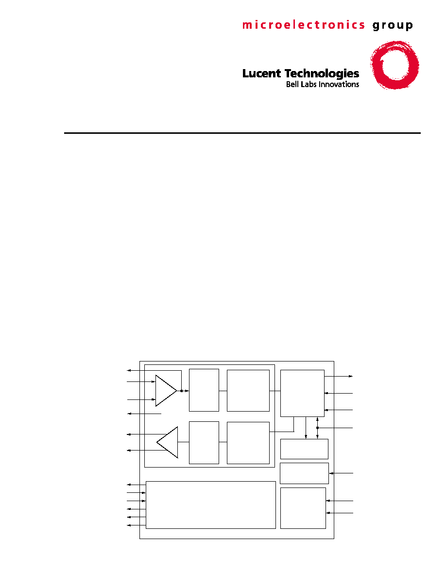
Description
The T7503 device is a single-chip, two-channel
µ
-law PCM codec with filters. This integrated circuit
provides analog-to-digital and digital-to-analog
conversion. It provides the transmit and receive
filtering necessary to interface a voice telephone
circuit to a time-division multiplexed (TDM) system.
The device features a differential transmit amplifier,
and the power receive amplifier is capable of driving
600
differentially. PCM timing is defined by a single
frame sync pulse. This device operates in a delayed
timing mode (digital data is valid one clock cycle after
frame sync goes high). The T7503 is packaged in a
20-pin SOJ.
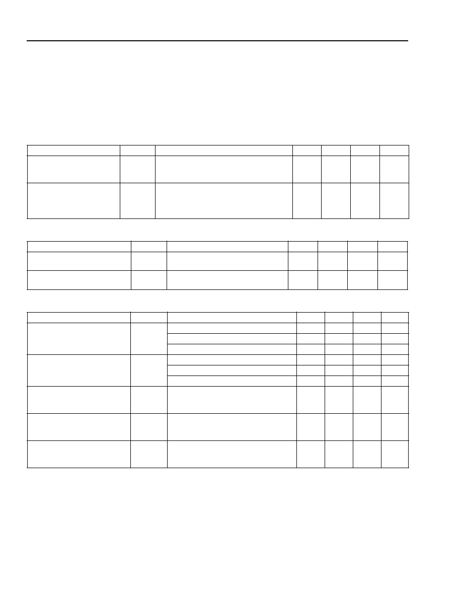
Figure 1. Block Diagram
5-3609.b
GS
X
0
VF
X
IN0
VF
R
OP0
GS
X
1
VF
X
IN1
VF
X
IP1
≠
+
FILTER
NETWORK
ENCODER
CHANNEL 0
+2.4 V
DECODER
PCM
INTERFACE
POWERDOWN
CONTROL
INTERNAL TIMING
& CONTROL
BIAS
CIRCUITRY
&
REFERENCE
CHANNEL 1
FILTER
NETWORK
D
X
D
R
GNDD
MCLK
V
DD
(1)
VF
X
IP0
VCM0
VF
R
ON0
VCM1
VF
R
OP1
VF
R
ON1
FS
GNDA (2)
2
Lucent Technologies Inc.
Data Sheet
February 1998
T7503 Dual PCM Codec with Filters
Functional Description
The T7503 has one frame sync (FS) input that determines transmit and receive data timing for both channels. The
width of the FS pulse determines the order of the two channels on the PCM buses. If FS is nominally one MCLK
period wide (see Figure 5), the data for channel 0 is first. If FS is nominally two or more MCLK periods wide (Figure
6), the data for channel 1 is first. During a single 125
µ
s frame, the frame sync input is supplied a single pulse.
The frequency of the master clock must be either 2.048 MHz or 4.096 MHz. Internal circuitry determines the
master clock frequency during the powerup reset interval.
Powerdown is achieved by removing the FS pulse for at least 500
µ
s with MCLK active, after which MCLK may be
removed. Both channels are powered down together. Powerdown is not guaranteed if MCLK is lost, unless the
device is already in the powerdown mode.
5-3787
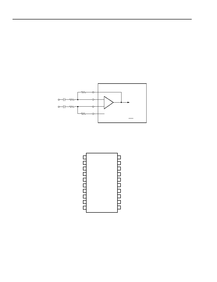
Figure 2. Typical Analog Input Section
Pin Information
5-3788
Figure 3. Pin Diagram
VF
X
INn
TO
CODEC
FILTERS
2.4 V
GAIN =
R
FN
R
IN
GS
Xn
R
IN
R
FN
≠
+
R
IP
VF
X
IPn
VCM0
R
FP
T - 7503 - - - EL
VF
R
OP0
VF
R
ON0
GNDA0
VF
X
IN0
VF
X
IP0
GS
X
0
VCM0
FS
MCLK
GNDD
VF
R
ON1
GNDA1
VF
X
IN1
VF
X
IP1
GS
X
1
VCM1
D
R
D
X
1
2
3
4
5
6
7
8
9
10
20
19
18
17
16
15
14
13
12
11
VF
R
OP1
V
DD

Lucent Technologies Inc.
3
Data Sheet
February 1998
T7503 Dual PCM Codec with Filters
Pin Information
(continued)
* I
d
indicates a pull-down device is included on this lead.
Table 1. Pin Descriptions
Symbol
Pin
Type
Name/Function
VF
X
IN1
VF
X
IN0
17
4
I
Voice Frequency Transmitter Negative Input.
Analog
inverting input to the
uncommitted operational amplifier at the transmit filter input.
VF
X
IP1
VF
X
IP0
16
5
I
Voice Frequency Transmitter Positive Input.
Analog
noninverting input to the
uncommitted operational amplifier at the transmit filter input.
GS
X
1
GS
X
0
15
6
O
Gain Set for Transmitter.
Output of the transmit uncommitted operational amplifi-
er. The pin is the input to the transmit differential filters.
VF
R
OP1
VF
R
OP0
20
1
O
Voice Frequency Receiver Positive Output.
This pin can drive 300
(or greater)
loads.
VF
R
ON1
VF
R
ON0
19
2
O
Voice Frequency Receiver Negative Output.
This pin can drive 300
(or great-
er) loads.
V
DD
8
--
+5 V Power Supply
. This pin should be bypassed to analog ground with at least
0.1
µ
F of capacitance as close to the device as possible. V
DD
serves both analog
and digital internal circuits.
GNDA1
GNDA0
18
3
--
Analog Grounds
. Both ground pins must be connected on the circuit board. AGND
serves both analog and digital internal circuits.
D
R
12
I
Receive PCM Data Input
. The data on this pin is shifted into the device on the fall-
ing edges of MCLK. Sixteen consecutive bits of data (8 bits for channel 0, and
8 bits for channel 1) are entered after the FS pulse has been detected.
D
X
11
O
Transmit PCM Data Output
. This pin remains in the high-impedance state except
during active transmit time slots. Sixteen consecutive bits of data (8 bits for channel
0 and 8 bits for channel 1) are shifted out on the rising edge of MCLK. Data is shift-
ed out on the rising edge of MCLK.
MCLK
9
I
Master Clock Input
. The frequency must be 2.048 MHz or 4.096 MHz. This clock
serves as the bit clock for all PCM data transfer. A 40% to 60% duty cycle is re-
quired.
GNDD
10
--
Digital Ground
. Ground connection for the digital circuitry.
FS
13
I
d
*
Frame Sync
. This signal is an edge trigger and must be high for a minimum of one
MCLK cycle. This signal must be derived from MCLK. If FS is low for 500
µ
s while
MCLK remains active, then the device fully powers down. An internal pull-down de-
vice is included on FS.
VCM0
VCM1
7
14
O
Voltage Common Mode
. 2.4 Vdc.
4
Lucent Technologies Inc.
Data Sheet
February 1998
T7503 Dual PCM Codec with Filters
Absolute Maximum Ratings
Stresses in excess of the absolute maximum ratings can cause permanent damage to the device. These are
absolute stress ratings only. Functional operation of the device is not implied at these or any other conditions in
excess of those given in the operational sections of this data sheet. Exposure to absolute maximum ratings for
extended periods can adversely affect device reliability.
Handling Precautions
Although protection circuitry has been designed into this device, proper precautions should be taken to avoid
exposure to electrostatic discharge (ESD) during handling and mounting. Lucent Technologies Microelectronics
Group employs a human-body model (HBM) and a charged-device model (CDM) for ESD-susceptibility testing and
protection design evaluation. ESD voltage thresholds are dependent on the circuit parameters used to define the
model. No industry-wide standard has been adopted for CDM. However, a standard HBM (resistance = 1500
,
capacitance = 100 pF) is widely used and therefore can be used for comparison purposes. The HBM ESD
threshold presented here was obtained by using these circuit parameters:
Electrical Characteristics
Specifications apply for T
A
= ≠40
∞
C to +85
∞
C, V
DD
= 5 V
±
5%, MCLK = either 2.048 MHz or 4.096 MHz, and
GND = 0 V, unless otherwise noted.
dc Characteristics
Table 2. Digital Interface
Parameter
Symbol
Min
Max
Unit
Storage Temperature Range
T
stg
≠55
150
∞
C
Power Supply Voltage
V
DD
--
6.5
V
Voltage on Any Pin with Respect to Ground
--
≠0.5
0.5 + V
DD
V
Maximum Power Dissipation (package limit)
P
D
--
600
mW
HBM ESD Threshold Voltage
Device
Rating
T7503 >2000
V
Parameter
Symbol
Test Conditions
Min
Typ
Max
Unit
Input Low Voltage
V
IL
All digital inputs
--
--
0.8
V
Input High Voltage
V
IH
All digital inputs
2.0
--
--
V
Output Low Voltage
V
OL
D
X
, I
L
= 3.2 mA
--
--
0.4
V
Output High Voltage
V
OH
D
X
, I
L
= ≠3.2 mA
2.4
--
--
V
D
X
, I
L
= ≠320
µ
A
3.5
--
--
V
Input Current Pins Without Pull-
down
I
I
Any digital input GND < V
IN
< V
DD
≠10
±
0.01
10
µ
A
Input Current Pin with Pull-down
I
I
Any digital input GND < V
IN
< V
DD
2
10
150
µ
A
Output Current in High-impedance
State
I
OZ
D
X
≠30
±
0.02
30
µ
A
Input Capacitance
C
I
--
--
--
5
pF
Lucent Technologies Inc.
5
Data Sheet
February 1998
T7503 Dual PCM Codec with Filters
Electrical Characteristics
(continued)
dc Characteristics
(continued)
Table 3. Power Dissipation
Power measurements are made at MCLK = 4.096 MHz, outputs unloaded.
Transmission Characteristics
Table 4. Analog Interface
Parameter
Symbol
Test Conditions
Min
Typ
Max
Unit
Powerdown Current
I
DDO
MCLK present and FS
0.4 V
--
0.1
1
mA
Powerup Current
I
DDU
MCLK, FS
pulse present
--
18
25
mA
Parameter
Symbol
Test Conditions
Min
Typ
Max
Unit
Input Resistance, FS
X
I
R
VFXI
VFxI = 2.4 V
1.0
--
--
M
Input Leakage Current, VF
X
I
I
BVFXI
VFxI = 2.4 V
≠2.4
±
0.01
2.4
µ
A
Input Capacitance, VF
X
IN, VF
X
IP
--
--
--
10
pF
Input Offset Voltage of Uncommitted
Op Amp, VF
X
IN ≠ VF
X
IP
--
--
≠5
--
5
mV
Input Common-mode Voltage Range,
VF
X
IN, VF
X
IP
--
--
1.2
--
V
DD
≠ 1.75
V
Input Common-mode Rejection Ratio,
VF
X
IN, VF
X
IP
--
--
--
60
--
dB
Gain Bandwidth Product (10 kHz) of Un-
committed Op Amp
--
--
--
3000
--
kHz
Equivalent Input Noise Between VF
X
IN
and VF
X
IP at GS
X
--
--
--
≠30
--
dBrnC
Output Voltage Range, GS
X
--
--
0.5
--
V
DD
≠ 0.5
V
dc Open-loop Voltage Gain, GS
X
A
VOL
--
90
--
--
dB
Differential Output dc Offset Voltage
--
--
≠80
±
10
80
mV
Load Capacitance, GS
X
CL
X1
--
--
--
50
pF
Load Resistance, GS
X
RL
X1
--
10
--
--
k
VCM Output Voltage Referenced to GND
--
--
2.25
2.35
2.5
V
VCM Output Load Capacitance
--
--
0
--
50
pF
Load Resistance, V
CM
RL
VCM
--
10
--
--
k
Load Resistance, VF
R
O
RL
VFRO
--
300
--
--
Load Capacitance, VF
R
O
CL
VFRO
--
--
--
100
pF
Output Resistance, VF
R
O
RO
VFRO
0 dBm0, 1020 Hz PCM
code applied to D
R
--
0.3
3
Output Voltage, VF
R
O
VO
R
Alternating
±
zero
µ
-law
PCM code applied to D
R
2.25
2.35
2.5
V
Output Leakage Current, VF
R
O, Power-
down
IO
VFRO
--
≠30
±
0.02
30
µ
A
Output Voltage Swing, VF
R
O
V
SWR
RL = 300
3.2
--
--
Vp-p
6
Lucent Technologies Inc.
Data Sheet
February 1998
T7503 Dual PCM Codec with Filters
Transmission Characteristics
(continued)
ac Transmission Characteristics
Unless otherwise noted, the analog input is a 0 dBm0, 1020 Hz sine wave; the input amplifier is set for unity gain.
The digital input is a PCM bit stream equivalent to that obtained by passing a 0 dBm0, 1020 Hz sine wave through
an ideal encoder. The output level is sin(x)/x-corrected.
Table 5. Absolute Gain
Table 6. Gain Tracking
Table 7. Distortion
Parameter
Symbol
Test Conditions
Min
Typ
Max
Unit
Encoder Milliwatt
Response (transmit gain
tolerance)
EmW
Signal input of 0.775 Vrms
µ
-law
≠0.25
--
0.25
dBm0
Decoder Milliwatt
Response (receive gain
tolerance)
DmW
Measured single-ended relative to
0.775 Vrms
µ
-law,
PCM input of 0 dBm0 1020 Hz
RL = 10 k
≠0.25
--
0.25
dBm0
Parameter
Symbol
Test Conditions
Min
Typ
Max
Unit
Transmit Gain Tracking Error
Sinusoidal Input
GT
X
+3 dBm0 to ≠37 dBm0
≠37 dBm0 to ≠50 dBm0
≠0.25
≠0.50
--
--
0.25
0.50
dB
dB
Receive Gain Tracking Error
Sinusoidal Input
GT
R
+3 dBm0 to ≠37 dBm0
≠37 dBm0 to ≠50 dBm0
≠0.25
≠0.50
--
--
0.25
0.50
dB
dB
Parameter
Symbol
Test Conditions
Min
Typ
Max
Unit
Transmit Signal to Distortion
SD
X
µ
-law +3 dBm0
VF
X
I
≠30 dBm0
36
--
--
dB
µ
-law ≠30 dBm0
VF
X
I
≠40 dBm0
30
--
--
dB
µ
-law ≠40 dBm0
VFxI
≠45 dBm0
25
--
--
dB
Receive Signal to Distortion
SD
R
µ
-law +3 dBm0
VF
R
O
≠30 dBm0
36
--
--
dB
µ
-law ≠30 dBm0
VF
R
O
≠40 dBm0
30
--
--
dB
µ
-law ≠40 dBm0
VF
R
O
≠45 dBm0
25
--
--
dB
Single Frequency Distortion,
Transmit
SFD
X
200 Hz--3400 Hz, 0 dBm0 input,
output any other single
frequency
3400 Hz
--
--
≠38
dBm0
Single Frequency Distortion,
Receive
SFD
R
200 Hz--3400 Hz, 0 dBm0 input,
output any other single
frequency
3400 Hz
--
--
≠40
dBm0
Intermodulation Distortion
IMD
Transmit or receive, two frequencies
in the range (300 Hz--3400 Hz)
at ≠6 dBm0
--
--
≠42
dBm0
Lucent Technologies Inc.
7
Data Sheet
February 1998
T7503 Dual PCM Codec with Filters
Transmission Characteristics
(continued)
ac Transmission Characteristics
(continued)
Table 8. Envelope Delay Distortion
Overload Compression
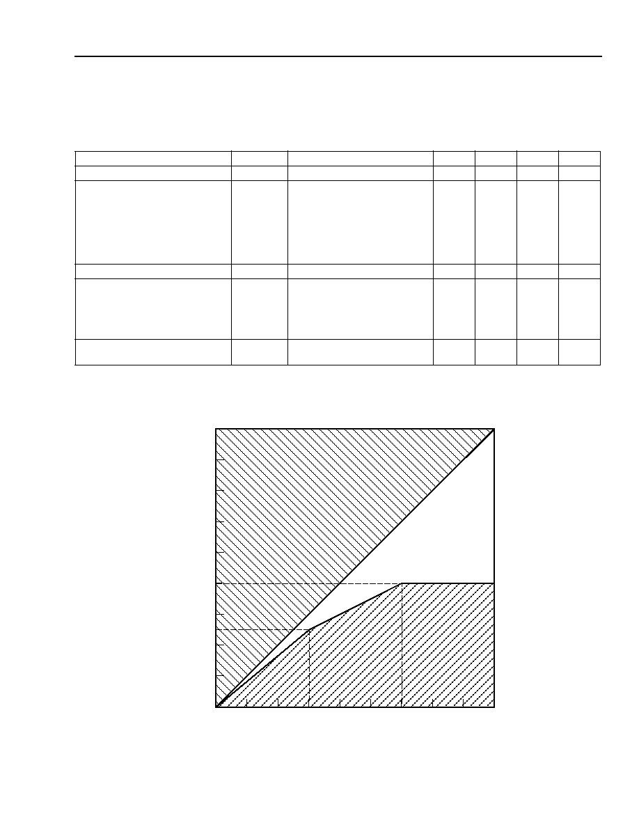
Figure 4 shows the region of operation for encoder signal levels above the reference input power (0 dBm0).
5-3586
Figure 4. Overload Compression
Parameter
Symbol
Test Conditions
Min
Typ
Max
Unit
T
X
Delay, Absolute
D
XA
f = 1600 Hz
--
--
230
µ
s
T
X
Delay, Relative to 1600 Hz
D
XR
f = 500 Hz--600 Hz
f = 600 Hz--800 Hz
f = 800 Hz--1000 Hz
f = 1000 Hz--1600 Hz
f = 1600 Hz--2600 Hz
f = 2600 Hz--2800 Hz
f = 2800 Hz--3000 Hz
--
--
--
--
--
--
--
--
--
--
--
--
--
--
220
145
75
40
75
105
155
µ
s
µ
s
µ
s
µ
s
µ
s
µ
s
µ
s
R
X
Delay, Absolute
D
RA
f = 1600 Hz
--
--
275
µ
s
R
X
Delay, Relative to 1600 Hz
D
RR
f = 500 Hz--1000 Hz
f = 1000 Hz--1600 Hz
f = 1600 Hz--2600 Hz
f = 2600 Hz--2800 Hz
f = 2800 Hz--3000 Hz
≠40
≠30
--
--
--
--
--
--
--
--
--
--
90
125
175
µ
s
µ
s
µ
s
µ
s
µ
s
Round Trip Delay, Absolute
D
RTA
With or between channels
f = 1600 Hz
--
--
470
µ
s
1
2
3
4
5
6
7
8
9
1
2
3
4
5
6
7
8
9
ACCEPTABLE
REGION
FUNDAMENTAL INPUT POWER (dBm)
FUNDAMENTAL OUTPUT POWER (dBm)
8
Lucent Technologies Inc.
Data Sheet
February 1998
T7503 Dual PCM Codec with Filters
Transmission Characteristics
(continued)
ac Transmission Characteristics
(continued)
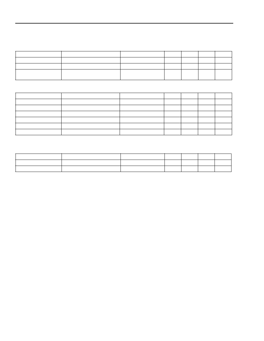
Table 9. Noise
Table 10. Receive Gain Relative to Gain at 1.02 kHz
Table 11. Transmit Gain Relative to Gain at 1.02 kHz
Parameter
Symbol
Test Conditions
Min
Typ
Max
Unit
Transmit Noise
µ
-Law
N
XC
--
--
13
18
dBrnC0
Input amplifier gain = 36 dB
--
16
19
dBrnC0
Receive Noise
µ
-Law
N
RC
PCM code is alternating positive
and negative zero.
--
6
13
dBrnC0
Noise, Single Frequency
N
RS
f = 0 kHz--100 kHz,
VF
X
IN = 0 Vrms, measurement at
VF
R
O, D
R
= D
X
--
--
≠53
dBm0
Power Supply Rejection Transmit
PSR
X
V
DD
= 5.0 Vdc + 100 mVrms:
f = 0 kHz--4 kHz
f = 4 kHz--50 kHz
36
30
--
--
--
--
dB
dB
Power Supply Rejection Receive
PSR
X
PCM code is positive one LSB.
V
DD
= 5.0 Vdc + 100 mVrms:
f = 0 kHz--4 kHz
f = 4 kHz--25 kHz
f = 25 kHz--50 kHz
36
40
30
--
--
--
--
--
--
dB
dB
dB
Spurious Out-of-Band Signals at
VF
R
O Relative to Input
SOS
0 dBm0, 300 Hz--3400 Hz input
PCM code applied:
4600 Hz--7600 Hz
7600 Hz--8400 Hz
8400 Hz--50 kHz
--
--
--
--
--
--
≠30
≠40
≠30
dB
dB
dB
Frequency (Hz)
Min
Typ
Max
Unit
Below 3000
≠0.150
±
0.04
0.150
dB
3140 ≠0.570
±
0.04
0.150
dB
3380 ≠0.735
≠0.50
0.010
dB
3860 --
≠10.70
≠9.400
dB
4600 and above
--
--
≠28
dB
Frequency (Hz)
Min
Typ
Max
Unit
16.67
--
≠50
≠30
dB
40
--
≠34
≠26
dB
50
--
≠36
≠30
dB
60
--
≠50
≠30
dB
200
≠1.800
≠0.5
0
dB
300 to 3000
≠0.150
±
0.04
0.150
dB
3140
≠0.570
±
0.04
0.150
dB
3380
≠0.735
≠0.50
0.010
dB
3860
--
≠10.70
≠9.400
dB
4600 and above
--
--
≠32
dB
Lucent Technologies Inc.
9
Data Sheet
February 1998
T7503 Dual PCM Codec with Filters
Transmission Characteristics
(continued)
ac Transmission Characteristics
(continued)
* For Table 12, crosstalk into the transmit channels (VF
X
IN) can be significantly affected by parasitic capacitive feeds from GS
X
and VF
R
O out-
puts. PWB layouts should be arranged to keep these parasitics low. The resistor value of RF (from GS
X
to VF
X
IN) should also be kept as low
as possible (while maintaining the load on GS
X
above 10 k
per Table 4) to minimize crosstalk.
* For Table 13, crosstalk into the transmit channels (VF
X
IN) can be significantly affected by parasitic capacitive feeds from GS
X
and VF
R
O out-
puts. PWB layouts should be arranged to keep these parasitics low. The resistor value of RF (from GS
X
to VF
X
IN) should also be kept as low
as possible (while maintaining the load on GS
X
above 10 k
per Table 4) to minimize crosstalk.
Table 12. Interchannel Crosstalk (Between Channels) R
F
=
400 k
*
Parameter
Symbol
Test Conditions
Min
Typ
Max
Unit
Transmit to Receive
Crosstalk 0 dBm0
Transmit Levels
CT
XX-RY
f = 300 Hz--3400 Hz
idle PCM code for channel under test;
0 dBm0 into any other single-channel VF
X
IN
--
--
≠75
dB
Receive to Transmit
Crosstalk 0 dBm0
Receive Levels
CT
RX-XY
f = 300 Hz--3400 Hz
VF
X
IN = 0 Vrms for channel under test;
0 dBm0 code level on any other single-channel D
R
--
--
≠75
dB
Transmit to Trans-
mit Crosstalk
0 dBm0 Transmit
Levels
CT
XX-XY
f = 300 Hz--3400 Hz
0 dBm0 applied to any single-channel
VF
X
IN except channel under test,
which has VF
X
IN = 0 Vrms
--
--
≠75
dB
Receive to Receive
Crosstalk 0 dBm0
Receive Levels
CT
RX-RY
f = 300 Hz--3400 Hz
0 dBm0 code level on any single-channel D
R
except
channel under test which has idle code applied
--
--
≠75
dB
Table 13. Intrachannel Crosstalk (Within Channels) R
F
=
400 k
*
Parameter
Symbol
Test Conditions
Min
Typ
Max
Unit
Transmit to Receive
Crosstalk 0 dBm0
Transmit Levels
CT
XX-RX
f = 300 Hz--3400 Hz
idle PCM code for channel under test;
0 dBm0 into VF
X
IN
--
--
≠65
dB
Receive to Transmit
Crosstalk 0 dBm0
Receive Levels
CT
RX-XX
f = 300 Hz--3400 Hz
VF
X
IN = 0 Vrms for channel under test;
0 dBm0 code level on D
R
--
--
≠65
dB
10
Lucent Technologies Inc.
Data Sheet
February 1998
T7503 Dual PCM Codec with Filters
Timing Characteristics
Table 14. Clock Section (See Figures 5 and 6.)
Table 15. Transmit Section (See Figures 5 and 6.)
* Timing parameter tMCHDZ is referenced to a high-impedance state.
Table 16. Receive Section (See Figures 5 and 6.)
Symbol
Parameter
Test Conditions
Min
Typ
Max
Unit
tMCHMCL1
Clock Pulse Width
--
97
--
--
ns
tCDC
Duty Cycle, MC
--
40
--
60
%
tMCH1MCH2
tMCL2MCL1
Clock Rise and
Fall Time
--
0
--
15
ns
Symbol
Parameter
Test Conditions
Min
Typ
Max
Unit
tMCHDV
Data Enabled on TS Entry
0 < C
LOAD
< 100 pF
0
--
60
ns
tMCHDV1
Data Delay from MC
0 < C
LOAD
< 100 pF
0
--
60
ns
tMCHDZ*
Data Float on TS Exit
C
LOAD
= 0
10
--
100
ns
tFSHMCL
Frame-sync Hold Time
--
50
--
--
ns
tMCLFSH
Frame-sync High Setup
--
50
--
--
ns
tFSLMCL
Frame-sync Low Setup
--
50
--
--
ns
Symbol
Parameter
Test Conditions
Min
Typ
Max
Unit
tDVMCL
Receive Data Setup
--
30
--
--
ns
tMCLDV
Receive Data Hold
--
15
--
--
ns

Lucent Technologies Inc.
11
Data Sheet
February 1998
T7503 Dual PCM Codec with Filters
Timing Characteristics
(continued)
5-3581.c
Figure 5. Short FS Transmit and Receive Timing (Channel 0 First)
5-3581.d
Figure 6. Long FS Transmit and Receive Timing (Channel 1 First)
MCLK
FS
Dx
tFSHMCL
TIME SLOT
1
2
3
4
5
6
7
8
9
tFSLMCL
CH 0
BIT 1
CH 0
BIT 2
CH 0
BIT 3
CH 0
BIT 4
CH 0
BIT 5
CH 0
BIT 6
CH 0
BIT 7
CH 0
BIT 8
tMCHDV
tMCHDZ
D
R
BIT
8
BIT
1
BIT
3
BIT
2
BIT
6
BIT
7
tDVMCL
BIT
1
BIT
2
BIT
3
BIT
4
BIT
5
tMCLDV
D
R
STABLE
tMCHMCL1
tMCHDV1
tMCL2MCL1
tMCH1MCH2
10
11
16
CH 1
BIT 1
CH1
BIT 2
CH 1
BIT 3
CH 1
BIT 8
BIT
8
D
R
STABLE
MCLK
FS
Dx
tFSHMCL
TIME SLOT
1
2
3
4
5
6
7
8
9
tFSLMCL
CH 1
BIT 1
CH 1
BIT 2
CH 1
BIT 3
CH 1
BIT 4
CH 1
BIT 5
CH 1
BIT 6
CH 1
BIT 7
CH 1
BIT 8
tMCHDV
tMCHDZ
D
R
BIT
8
BIT
1
BIT
3
BIT
2
BIT
6
BIT
7
tDVMCL
BIT
1
BIT
2
BIT
3
BIT
4
BIT
5
tMCLDV
D
R
STABLE
tMCHMCL1
tMCHDV1
tMCL2MCL1
tMCH1MCH2
10
11
16
CH 0
BIT 1
CH0
BIT 2
CH 0
BIT 3
CH 0
BIT 8
BIT
8
D
R
STABLE

12
Lucent Technologies Inc.
Data Sheet
February 1998
T7503 Dual PCM Codec with Filters
Applications
Figure 7 shows one possible analog connection. Fully differential structures used for the inputs minimize the noise
gain from the internal 2.4 V bias voltage to the output of the single-ended transmitter op amp. The forward path gain
is G, and by using resistors on the positive side that are a factor of 1/(2G + 1) of those on the negative side, the
microphone and transformer feeds are kept well balanced. Using this ratio, G can be as low as unity (0 dB) without
exceeding the common-mode limit of the op amp.
Users have wide latitude when selecting between a balanced amplifier configuration or a single-ended
configuration. Single-ended configurations usually need fewer external components (e.g., R
IP
=
and R
FP
= 0 in
Figure 2) but have two disadvantages: one, dc blocking from the source is typically required; two, internally
generated noise at the common-mode pin VCM0 or VCM1 is amplified by G. For G > 10 (20 dB), this noise gain
can become the factor that could limit performance. Single-ended configurations can be used even with
microphones and transformers (R
IP
= 0 in these cases), but parasitic issues become somewhat more complex; so
single-ended configurations are only suggested for gains of four (12 dB) or less.
5-3789.a
Figure 7. Typical T7503 Application
2.4 V
MICROPHONE
SPEAKER
DSP
D
X
D
R
MCLK
FS
2.4 V
T7503
CENTRAL
OFFICE
LINE
G x R
SPEAKER
DRIVER
+
≠
+
≠
+
≠
+
≠
R
R
(
2G + 1)
R
R
(
2G + 1)
G x R
(
2G + 1)
G x R
G x R
(
2G + 1)
Lucent Technologies Inc.
13
Data Sheet
February 1998
T7503 Dual PCM Codec with Filters
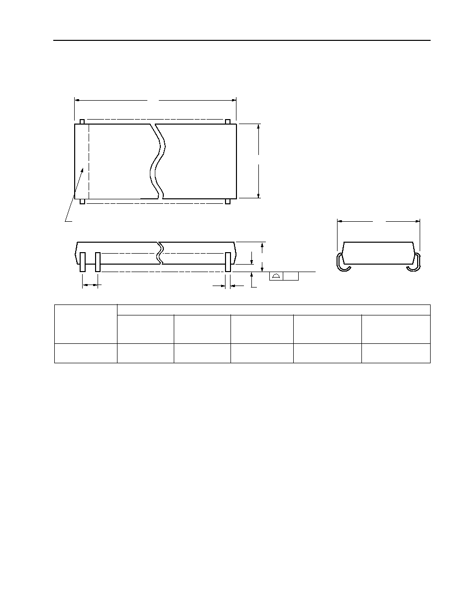
Outline Diagram
Controlling dimensions are in inches.
5-4413r4
Package
Description
Package Dimensions
Number
of Pins
(N)
Maximum
Length
(L)
Maximum Width
Without Leads
(B)
Maximum Width
Including Leads
(W)
Maximum Height
Above Board
(H)
SOJ (Small
Outline, J-Lead)
20
12.95
7.62
8.81
3.18
N
1
B
PIN #1 IDENTIFIER ZONE
L
0.51 MAX
H
0.79 MAX
0.10
SEATING PLANE
1.27 TYP
W

14
Lucent Technologies Inc.
Data Sheet
February 1998
T7503 Dual PCM Codec with Filters
Ordering Information
Device Code
Package
Temperature
Comcode
T - 7503 - - - EL
20-Pin SOJ
≠40
∞
C to +85
∞
C
107648925

Lucent Technologies Inc.
15
Data Sheet
February 1998
T7503 Dual PCM Codec with Filters
Notes

Data Sheet
T7503 Dual PCM Codec with Filters
For additional information, contact your Microelectronics Group Account Manager or the following:
INTERNET: http://www.lucent.com/micro
E-MAIL: docmaster@micro.lucent.com
U.S.A.: Microelectronics Group, Lucent Technologies Inc., 555 Union Boulevard, Room 30L-15P-BA, Allentown, PA 18103
1-800-372-2447, FAX 610-712-4106 (In CANADA: 1-800-553-2448, FAX 610-712-4106)
ASIA PACIFIC: Microelectronics Group, Lucent Technologies Singapore Pte. Ltd., 77 Science Park Drive, #03-18 Cintech III, Singapore 118256
Tel. (65) 778 8833, FAX (65) 777 7495
JAPAN: Microelectronics Group, Lucent Technologies Japan Ltd., 7-18, Higashi-Gotanda 2-chome, Shinagawa-ku, Tokyo 141, Japan
Tel. (81) 3 5421 1600, FAX (81) 3 5421 1700
EUROPE: Data Requests: MICROELECTRONICS GROUP DATALINE: Tel. (44) 1189 324 299, FAX (44) 1189 328 148
Technical Inquiries: GERMANY: (49) 89 95086 0 (Munich), UNITED KINGDOM: (44) 1344 865 900 (Bracknell),
FRANCE: (33) 1 41 45 77 00 (Paris), SWEDEN: (46) 8 600 7070 (Stockholm), FINLAND: (358) 9 4354 2800 (Helsinki),
ITALY: (39) 2 6601 1800 (Milan), SPAIN: (34) 1 807 1441 (Madrid)
Lucent Technologies Inc. reserves the right to make changes to the product(s) or information contained herein without notice. No liability is assumed as a result of their use or application. No
rights under any patent accompany the sale of any such product(s) or information.
Copyright © 1998 Lucent Technologies Inc.
All Rights Reserved
February 1998
DS98-097ALC (Replaces DS96-373ALC)
Printed On
Recycled Paper