 | –≠–ª–µ–∫—Ç—Ä–æ–Ω–Ω—ã–π –∫–æ–º–ø–æ–Ω–µ–Ω—Ç: T7504 | –°–∫–∞—á–∞—Ç—å:  PDF PDF  ZIP ZIP |
Document Outline
- Features
- Description
- Functional Description
- Pin Information
- Absolute Maximum Ratings
- Handling Precautions
- Electrical Characteristics
- Transmission Characteristics
- ac Transmission Characteristics
- Timing Characteristics
- Applications
- Outline Diagram
- Ordering Information
- List of Figures
- Figure 1. Block Diagram For 28-Pin DIP and 28-Pin PLCC
- Figure 2. Typical Analog Input Section
- Figure 3. 28-Pin PLCC Pin Diagram
- Figure 4. 44-Pin MQFP Pin Diagram
- Figure 5. Overload Compression
- Figure 6. T7504 Transmit and Receive Timing, FSEP = 1 MCLK
- Figure 7. T7504 Receive Timing, FSEP > 1 MCLK
- Figure 8. T5504 Transmit and Receive Timing, FSEP = 1 MCLK
- Figure 9. T5504 Receive Timing, FSEP > 1 MCLK
- Figure 10. Typical Frame Sync Timing (2 MHz Operation)
- Figure 11. Typical T7504 and T5504/SLIC Interconnection
- List of Tables
- Table 1. Pin Descriptions
- Table 2. Digital Interface
- Table 3. Power Dissipation
- Table 4. Analog Interface
- Table 5. Absolute Gain
- Table 6. Gain Tracking
- Table 7. Distortion
- Table 8. Envelope Delay Distortion
- Table 9. Noise
- Table 10. Receive Gain Relative to Gain at 1.02 kHz
- Table 11. Transmit Gain Relative to Gain at 1.02 kHz
- Table 12. Interchannel Crosstalk (Between Channels) ...
- Table 13. Intrachannel Crosstalk (Within Channels) ...
- Table 14. Clock Section
- Table 15. T7504 Transmit Section
- Table 16. T5504 Transmit Section
- Table 17. T7504 and T5504 Receive Section
- Contact Us
T7504 and T5504 Quad PCM Codecs with Filters
Data Sheet
March 1999
Features
s
5 V only
s
Low-power, latch-up-free CMOS technology
-- 37 mW/channel typical operating power
dissipation
-- 1 mW/channel typical powerdown dissipation
s
Automatic master clock frequency selection
-- 2.048 MHz or 4.096 MHz
s
On-chip sample and hold, autozero, and precision
voltage reference
s
Differential architecture for high noise immunity
and power supply rejection
s
Flexible time-slotted PCM interface
-- 2.048 MHz or 4.096 MHz data rate
s
Meets or exceeds ITU-T G.711--G.714 require-
ments and VF characteristics of D3/D4 (as per
Lucent Technologies PUB43801)
s
Operating temperature range: ≠40
∞
C to +85
∞
C
s
µ
-law/A-law companding selectable
Description
The T7504 and T5504 devices are single-chip, four-
channel
µ
-law/A-law PCM codecs with filters. These
integrated circuits provide analog-to-digital and
digital-to-analog conversion. They provide the
transmit and receive filtering necessary to interface a
voice telephone circuit to a time-division multiplexed
system. These devices are available in 28-pin
PLCCs. The T7504 is also available in a 44-pin
MQFP.
The T5504 differs from the T7504 in its timing mode.
The T5504 operates in the nondelay timing mode
(digital data valid when frame sync goes high), and
the T7504 operates in the delayed timing mode
(digital data is valid one clock cycle after frame sync
goes high) (see Figures 6--9).
5-3579.d(C)
Figure 1. Block Diagram For 28-Pin DIP and 28-Pin PLCC
GS
X
0
VF
X
IN0
VF
R
O0
GS
X
1
VF
X
INF1
VF
R
O1
GS
X
2
VF
X
IN2
VF
R
O2
GS
X
3
VF
X
IN3
VF
R
O3
≠
+
FILTER
NETWORK
ENCODER
CHANNEL 0
+2.4 V
DECODER
PCM
INTERFACE
POWERDOWN
CONTROL
INTERNAL TIMING
& CONTROL
BIAS
CIRCUITRY
&
REFERENCE
CHANNEL 1
CHANNEL 2
CHANNEL 3
FILTER
NETWORK
D
X
D
R
FS
X
0
FS
X
1
FS
X
2
FS
X
3
FSEP
GNDD
MCLK
ASEL
V
DD
(2)
GNDA (4) (PLCC ONLY)
V
DD
(2) (MQFP ONLY)
GNDA (5) (MQFP ONLY)
2
2
Lucent Technologies Inc.
Data Sheet
March 1999
T7504 and T5504 Quad PCM Codecs with Filters
Functional Description
Four channels of PCM data input and output are
passed through only two ports, D
X
and D
R
, so some
type of time-slot assignment is necessary. The scheme
used here is to utilize timing modes of 32 or 64 time
slots corresponding to master clock frequencies of
either 2.048 MHz or 4.096 MHz, respectively. Each
device has four transmit frame sync (FS
X
) inputs, one
for each channel. During a single 125
µ
s frame, each
transmit frame sync input is supplied a single pulse.
The timing of the pulse indicates the beginning of the
time slot during which the data for that channel is
clocked out of the device. During a frame, transmit
frame sync pulses must be separated from each other
by one or more time slots. A channel is placed in a
standby (low-power) mode if its FS
X
input has been low
for 500
µ
s.
There is a single frame sync separation input (FSEP).
The number of negative clock edges minus one that
occurs while FSEP is high is the delay (in clock
periods) that is placed between the rising edge of a
transmit frame sign bit and the falling edge used by the
receiver to sample the sign bit. There must always be a
pulse on the FSEP input since this input provides the
8 kHz signal required to maintain internal timing. If the
FSEP pulse is one clock period or less, the device
makes the transmit edges and receive sampling edges
one half clock period apart. The entire device is placed
in a powerdown mode if FSEP remains low for 500
µ
s.
Time slot zero is defined as starting on the first rising
MCLK edge after FSEP = 1 is detected by a negative
MCLK edge. In the T7504, MCLK negative-going
edges that detect the start of FSEP and FS
X
N must be
integer multiples of eight MCLK periods apart (zero
multiples are allowed). Since FSEP is assumed to
define time slot 0, the number of multiples separating
FS
X
N and FSEP is the time-slot number. In the T5504,
FS
X
N for time slot 0 nominally starts on the MCLK
positive edge following the negative edge which
detects FSEP.
The frequency of the master clock must be either
2.048 MHz or 4.096 MHz. Internal circuitry determines
the master clock frequency during the powerup reset
interval.
Powerdown is not guaranteed if MCLK is lost unless
the device is already in the powerdown mode due to
FSEP low for at least 500
µ
s.
The analog input section in Figure 2 includes an on-
chip op amp that is used in conjunction with external,
user-supplied resistors to vary encoder passband gain.
The feedback resistance (R
F
) should range from 10 k
to 200 k
and capacitance from GSx to ground should
be kept to less than 50 pF. The input signal at VF
X
IN
should be ac coupled. For best performance, the maxi-
mum gain of this op amp should be limited to 20 dB or
less.
5-3786
Figure 2. Typical Analog Input Section
VF
X
IN
TO
CODEC
FILTERS
2.4 V
GAIN =
R
X
GS
X
R
I
R
F
≠
+
R
I

Lucent Technologies Inc.
3
Data Sheet
March 1999
T7504 and T5504 Quad PCM Codecs with Filters
Pin Information
5-3580.b
Figure 3. 28-Pin PLCC Pin Diagram
5-4770
Figure 4. 44-Pin MQFP Pin Diagram
GNDA3
DR
DX
GNDD
FSEP
12
13
14
15
16
17
18
5
6
7
8
9
10
11
MCLK
ASEL
V
DD
VF
X
IN2
GS
X
2
VF
R
O2
GNDA2
FS
X
0
V
DD
GNDA0
VF
X
IN0
GNDA1
GS
X
0
VF
R
O0
25
24
23
22
21
20
19
VF
R
O3
VF
X
IN1
VF
X
IN3
GS
X
1
4
3
2
1
27
28
26
FS
X
2
FS
X
1
T - 7504 - - - ML
GS
X
3
VF
R
O1
FS
X
3
T - 5504 - - - ML
MCLK
ASEL
V
DD
V
DDA
NC
NC
VF
X
IN2
GS
X
2
VF
R
O2
GNDA2
NC
1
2
3
4
5
6
7
8
9
10
11
12
13
14
15
16
17
18
19
20
21
22
33
32
31
30
29
28
27
26
25
24
23
44
43
42
41
40
39
38
37
36
35
34
FS
X
0
NC
V
DD
V
DDA
NC
NC
VF
X
IN0
GS
X
0
VF
R
O0
GNDA1
GNDA0
NC
GNDD
NC
FSEP
NC
NC
NC
GNDA3
NC
GNDA4
NC
D
R
D
X
FS
X
3
FS
X
2
FS
X
1
VF
R
O3
GS
X
1
T7504---JL
VF
R
O1
VF
X
IN3
GS
X
3
VF
X
IN1

4
Lucent Technologies Inc.
Data Sheet
March 1999
T7504 and T5504 Quad PCM Codecs with Filters
Pin Information
(continued)
* I
d
Indicates a pull-down device is included on this lead.
Table 1. Pin Descriptions
Symbol
Pin
Type
*
Name/Function
PLCC
MQFP
VF
X
IN3
VF
X
IN2
VF
X
IN1
VF
X
IN0
14
8
16
22
15
8
19
26
I
Voice Frequency Transmitter Input.
Analog inverting input to the uncommitted
operational amplifier at the transmit filter input. Connect the signal to be digitized
to this pin through a resistor R
I
(see
Figure 2
).
GS
X
3
GS
X
2
GS
X
1
GS
X
0
13
9
17
21
14
9
20
25
O
Gain Set for Transmitter.
Output of the transmit uncommitted operational
amplifier. The pin is the input to the transmit differential filters. Connect the pin to
its corresponding VF
X
IN through a resistor R
F
(see
Figure 2
).
VF
R
O3
VF
R
O2
VF
R
O1
VF
R
O0
12
10
18
20
13
10
21
24
O
Voice Frequency Receiver Output.
This pin can drive 2000
(or greater) loads.
V
DD
[1:0]
V
DDA
[1:0]
7, 24
--
3, 31
4, 30
--
5 V Digital and Analog Power Supplies
. All pins must be connected on the circuit
board. Each pin should be bypassed to ground with at least 0.1
µ
F of capacitance
as close to the device as possible. For the DIP and PLCC packages, V
DD
serves
both analog and digital internal circuits.
GNDA4
GNDA3
GNDA2
GNDA1
GNDA0
--
15
11
19
23
18
16
11
23
27
--
Analog Grounds
. All ground pins must be connected on the circuit board.
D
R
4
44
I
Receive PCM Data Input
. The data on this pin is shifted into the device on the fall-
ing edges of MCLK. Data is only entered for valid time slots as defined by the re-
lationship of the pulses on the FS
X
inputs and the pulse on the FSEP input.
D
X
3
43
O
Transmit PCM Data Output
. This pin remains in the high-impedance state except
during active transmit time slots. An active transmit time slot is defined as one in
which a pulse is present on one of the FSx inputs. Data is shifted out on the rising
edge of MCLK.
MCLK
5
1
I
Master Clock Input
. The frequency must be 2.048 MHz or 4.096 MHz. This clock
serves as the bit clock for all PCM data transfer. A 40% to 60% duty cycle is re-
quired.
GNDD
2
41
--
Digital Ground
. Ground connection for the digital circuitry. All ground pins must be
connected on the circuit board.
FS
X
3
FS
X
2
FS
X
1
FS
X
0
28
27
26
25
36
35
34
33
I
d
Transmit Frame Sync
. This signal is an edge trigger and must be high for a min-
imum of one MCLK cycle. This signal must be derived from MCLK. The division ra-
tio is 1:256 or 1:512 (FS
X
:MCLK). Each FS
X
input must have a pulse present at the
start of the desired active output time slot. Pulses on the various FS
X
inputs must
be separated by one or more integer multiples of time slots. An internal pull-down
device is included on each FS
X
.
ASEL
6
2
I
d
A-Law/
µ
-Law Select
. A logic low selects
µ
-law coding. A logic high selects A-law
coding. A pull-down device is included.
FSEP
1
37
I
Frame Sync Separation
. The pulse width of this 8 kHz signal defines the timing
offset between the transmit and receive frames. Internally generated receive frame
sync pulses are delayed from the corresponding transmit frame sync pulse rising
edge by one less than the FSEP pulse width in negative MCLK edges. If the pulse
width is one MCLK period or less, the transmit and receive frame syncs are made
coincident. Loss of FSEP causes the device to powerdown. If the master clock fre-
quency is 2.048 MHz or 4.096 MHz, delays of 255 or 511 clock pulses are not al-
lowed, respectively. Timing relationships between FSEP, FS
X
N, and time slot 0 are
given in Figures
6
--
9
.
Lucent Technologies Inc.
5
Data Sheet
March 1999
T7504 and T5504 Quad PCM Codecs with Filters
Absolute Maximum Ratings
Stresses in excess of the absolute maximum ratings can cause permanent damage to the device. These are
absolute stress ratings only. Functional operation of the device is not implied at these or any other conditions in
excess of those given in the operational sections of this data sheet. Exposure to absolute maximum ratings for
extended periods can adversely affect device reliability.
Handling Precautions
Although protection circuitry has been designed into this device, proper precautions should be taken to avoid
exposure to electrostatic discharge (ESD) during handling and mounting. Lucent Technologies Microelectronics
Group employs a human-body model (HBM) and a charged-device model (CDM) for ESD susceptibility testing and
protection design evaluation. ESD voltage thresholds are dependent on the circuit parameters used to define the
model. No industry-wide standard has been adopted for CDM. However, a standard HBM (resistance = 1500
,
capacitance = 100 pF) is widely used and, therefore, can be used for comparison purposes. The HBM ESD
threshold presented here was obtained by using these circuit parameters:
Electrical Characteristics
Specifications apply for T
A
= ≠40
∞
C to +85
∞
C, V
DD
= 5 V
±
5%, MCLK = either 2.048 MHz or 4.096 MHz, and
GND = 0 V, unless otherwise noted.
dc Characteristics
Table 2. Digital Interface
Parameter
Symbol
Min
Max
Unit
Storage Temperature Range
T
stg
≠55
150
∞
C
Power Supply Voltage
V
DD
--
6.5
V
Voltage on Any Pin with Respect to Ground
--
≠0.5
0.5 + V
DD
V
Maximum Power Dissipation (package limit)
P
D
--
600
mW
HBM ESD Threshold Voltage
Device
Rating
T7504
>2000 V
T5504
>2000 V
Parameter
Symbol
Test Conditions
Min
Typ
Max
Unit
Input Low Voltage
V
IL
All digital inputs
--
--
0.8
V
Input High Voltage
V
IH
All digital inputs
2.0
--
--
V
Output Low Voltage
V
OL
D
X
, I
L
= 3.2 mA
--
--
0.4
V
Output High Voltage
V
OH
D
X
, I
L
= ≠3.2 mA
2.4
--
--
V
D
X
, I
L
= ≠320
µ
A
3.5
--
--
V
Input Current, Pins without Pull-down
I
I
Any digital input GND < V
IN
<
V
DD
≠10
--
10
µ
A
Input Current, Pins with Pull-down
I
I
Any digital input GND < V
IN
<
V
DD
--
--
150
µ
A
Output Current in High-impedance State
I
OZ
D
X
≠30
--
30
µ
A
Input Capacitance
C
I
--
--
--
5
pF
6
Lucent Technologies Inc.
Data Sheet
March 1999
T7504 and T5504 Quad PCM Codecs with Filters
Electrical Characteristics
(continued)
Table 3. Power Dissipation
Power measurements are made at MCLK = 4.096 MHz, outputs unloaded.
Transmission Characteristics
Table 4. Analog Interface
Parameter
Symbol
Test Conditions
Min
Typ
Max
Unit
Powerdown Current
I
DD0
MCLK present, FS
X
[3:0] = 0.4 V, FSEP = 0.4 V
--
0.2
1
mA
Powerup Current
I
DD1
MCLK, FS
X
[3:0], FSEP present
--
30
40
mA
Standby Current
I
DDS
MCLK, FSEP present; FS
X
[3:0] = 0.4 V
--
6
10
mA
Parameter
Symbol
Test Conditions
Min
Typ
Max
Unit
Input Resistance, VF
X
IN
R
VFXI
0.25 V < VFxI < 4.75 V
1.0
--
--
M
Input Leakage Current, VF
X
IN
I
BVFXI
0.25 V < VFxI < 4.75 V
--
--
2.4
µ
A
dc Open-loop Voltage Gain, GS
X
A
VOL
--
5000
--
--
--
Open-loop Unity Gain Bandwidth, GS
X
f
O
--
1
3
--
MHz
Load Capacitance, GS
X
CL
X1
--
--
--
50
pF
Load Resistance, GS
X
RL
X1
--
10
--
--
k
Input Voltage, VF
X
IN
V
IX
Relative to ground
2.25 2.35
2.5
V
Load Resistance, VF
R
O
RL
VF
R
O
--
2000
--
--
Load Capacitance, VF
R
O
CL
VF
R
O
--
--
--
100
pF
Output Resistance, VF
R
O
RO
VF
R
O
0 dBm0, 1020 Hz PCM code
applied to D
R
--
--
20
Partial powerdown FS
X
= 0 for
channel under test
3000
--
10000
Output Voltage, VF
R
O
VO
R
Alternating
±
zero
µ
-law PCM
code applied to D
R
2.25 2.35
2.5
V
Output Voltage, VF
R
O, Standby
VO
RPD
FS
X
[3:0] = 0.4 V, FSEP = active,
no load
2.15
2.4
2.65
V
Output Leakage Current, VF
R
O, Pow-
erdown
IO
VF
R
O
FSEP = 0.4 V
≠30
--
30
µ
A
Output Voltage Swing, VF
R
O
V
SWR
RL = 2000
3.2
--
--
Vp-p
Lucent Technologies Inc.
7
Data Sheet
March 1999
T7504 and T5504 Quad PCM Codecs with Filters
Transmission Characteristics
(continued)
ac Transmission Characteristics
Unless otherwise noted, the analog input is a 0 dBm0, 1020 Hz sine wave; the input amplifier is set for unity gain.
The digital input is a PCM bit stream equivalent to that obtained by passing a 0 dBm0, 1020 Hz sine wave through
an ideal encoder. The output level is sin(x)/x-corrected.
Table 5. Absolute Gain
Table 6. Gain Tracking
Table 7. Distortion
Parameter
Symbol
Test Conditions
Min
Typ
Max
Unit
Encoder Milliwatt
Response (transmit gain toler-
ance)
EmW
Signal input of 0.775 Vrms,
µ
-law or
A-law
≠0.25
--
0.25
dBm0
Decoder Milliwatt
Response (receive gain toler-
ance)
DmW
Measured relative to 0.775 Vrms
µ
-law
or A-law,
PCM input of 0 dBm0 1020 Hz
RL = 10 k
≠0.25
--
0.25
dBm0
Parameter
Symbol
Test Conditions
Min
Typ
Max
Unit
Transmit Gain Tracking Error
Sinusoidal Input
µ
-Law/A-Law
GT
X
+3 dBm0 to ≠37 dBm0
≠37 dBm0 to ≠50 dBm0
≠0.25
≠0.50
--
--
0.25
0.50
dB
dB
Receive Gain Tracking Error
Sinusoidal Input
µ
-Law/A-Law
GT
R
+3 dBm0 to ≠37 dBm0
≠37 dBm0 to ≠50 dBm0
≠0.25
≠0.50
--
--
0.25
0.50
dB
dB
Parameter
Symbol
Test Conditions
Min
Typ
Max
Unit
Transmit Signal to Distortion
SD
X
µ
-law 3 dBm0
VF
X
I
≠30 dBm0
A-law 3 dBm0
VF
X
I
≠30 dBm0
36
35
--
--
--
--
dB
dB
µ
-law ≠30 dBm0
VF
X
I
≠40 dBm0
A-law ≠30 dBm0
VF
X
I
≠40 dBm0
30
29
--
--
--
--
dB
dB
µ
-law ≠40 dBm0
VFxI
≠45 dBm0
A-law ≠40 dBm0
VFxI
≠45 dBm0
25
25
--
--
--
--
dB
dB
Receive Signal to Distortion
SD
R
µ
-law 3 dBm0
VF
R
O
≠30 dBm0
A-law 3 dBm0
VF
R
O
≠30 dBm0
36
35
--
--
--
--
dB
dB
µ
-law ≠30 dBm0
VF
R
O
≠40 dBm0
A-law ≠30 dBm0
VF
R
O
≠40 dBm0
30
29
--
--
--
--
dB
dB
µ
-law ≠40 dBm0
VF
R
O
≠45 dBm0
A-law ≠40 dBm0
VF
R
O
≠45 dBm0
25
25
--
--
--
--
dB
dB
Single Frequency Distortion,
Transmit
SFD
X
200 Hz--3400 Hz, 0 dBm0 input,
output any other single
frequency
3400 Hz
--
--
≠38
dBm0
Single Frequency Distortion,
Receive
SFD
R
200 Hz--3400 Hz, 0 dBm0 input,
output any other single
frequency
3400 Hz
--
--
≠40
dBm0
Intermodulation Distortion
IMD
Transmit or receive, two frequencies
in the range (300 Hz--3400 Hz)
at ≠6 dBm0
--
--
≠42
dBm0
8
Lucent Technologies Inc.
Data Sheet
March 1999
T7504 and T5504 Quad PCM Codecs with Filters
Transmission Characteristics
(continued)
Table 8. Envelope Delay Distortion
* Varies as a function of time slots chosen.
Overload Compression
Figure 5 shows the region of operation for encoder signal levels above the reference input power (0 dBm0).
5-3586
Figure 5. Overload Compression
Parameter
Symbol
Test Conditions
Min
Typ
Max
Unit
T
X
Delay, Absolute*
D
XA
f = 1600 Hz
--
--
175 to 425
µ
s
T
X
Delay, Relative to 1600 Hz
D
XR
f = 500 Hz--600 Hz
f = 600 Hz--800 Hz
f = 800 Hz--1000 Hz
f = 1000 Hz--1600 Hz
f = 1600 Hz--2600 Hz
f = 2600 Hz--2800 Hz
f = 2800 Hz--3000 Hz
--
--
--
--
--
--
--
--
--
--
--
--
--
--
220
145
75
40
75
105
155
µ
s
µ
s
µ
s
µ
s
µ
s
µ
s
µ
s
R
X
Delay, Absolute*
D
RA
f = 1600 Hz
--
--
150 to 405
µ
s
R
X
Delay, Relative to 1600 Hz
D
RR
f = 500 Hz--1000 Hz
f = 1000 Hz--1600 Hz
f = 1600 Hz--2600 Hz
f = 2600 Hz--2800 Hz
f = 2800 Hz--3000 Hz
≠40
≠30
--
--
--
--
--
--
--
--
--
--
90
125
175
µ
s
µ
s
µ
s
µ
s
µ
s
Round Trip Delay, Absolute*
D
RTA
Any time slot/channel to
any time slot/channel
f = 1600 Hz
--
--
325 to 650
µ
s
1
2
3
4
5
6
7
8
9
1
2
3
4
5
6
7
8
9
ACCEPTABLE
REGION
FUNDAMENTAL INPUT POWER (dBm)
FUNDAMENTAL OUTPUT POWER (dBm)
Lucent Technologies Inc.
9
Data Sheet
March 1999
T7504 and T5504 Quad PCM Codecs with Filters
Transmission Characteristics
(continued)
Table 9. Noise
Table 10. Receive Gain Relative to Gain at 1.02 kHz
Table 11. Transmit Gain Relative to Gain at 1.02 kHz
Parameter
Symbol
Test Conditions
Min
Typ
Max
Unit
Transmit Noise
µ
-Law
N
XC
--
--
--
18
dBrnC0
Input amplifier gain = 20 dB
--
--
19
dBrnC0
Transmit Noise
A-Law
N
XP
--
--
--
≠68
dBm0p
Receive Noise
µ
-Law
N
RC
PCM code is alternating positive
and negative zero
--
--
13
dBrnC0
Receive Noise
A-Law
N
RP
PCM code is A-law positive one
--
--
≠75
dBm0p
Noise, Single Frequency
f = 0 kHz--100 kHz
N
RS
VF
X
IN = 0 Vrms, measurement at
VF
R
O, D
R
= D
X
--
--
≠53
dBm0
Power Supply Rejection Transmit
PSR
X
V
DD
= 5.0 Vdc + 100 mVrms:
f = 0 kHz--4 kHz
f = 4 kHz--50 kHz
36
30
--
--
--
--
dB
dB
Power Supply Rejection Receive
PSR
X
PCM code is positive one LSB
V
DD
= 5.0 Vdc + 100 mVrms:
f = 0 kHz--4 kHz
f = 4 kHz--25 kHz
f = 25 kHz--50 kHz
36
40
30
--
--
--
--
--
--
dB
dB
dB
Spurious Out-of-Band Signals at
VF
R
O Relative to Input
SOS
0 dBm0, 300 Hz--3400 Hz input
PCM code applied:
4600 Hz--7600 Hz
7600 Hz--8400 Hz
8400 Hz--50 kHz
--
--
--
--
--
--
≠30
≠40
≠30
dB
dB
dB
Frequency (Hz)
Min
Typ
Max
Unit
Below 3000
≠0.150
±
0.04
0.150
dB
3140 ≠0.570
±
0.04
0.150
dB
3380 ≠0.885
≠0.58
0.010
dB
3860 --
≠10.7
≠9.4
dB
4600 and above
--
--
≠28
dB
Frequency (Hz)
Min
Typ
Max
Unit
16.67
--
≠50
≠30
dB
40
--
≠34
≠26
dB
50
--
≠36
≠30
dB
60
--
≠50
≠30
dB
200
≠1.8
≠0.5
0
dB
300 to 3000
≠0.150
±
0.04
0.150
dB
3140
≠0.570
±
0.04
0.150
dB
3380
≠0.885
≠0.58
0.010
dB
3860
--
≠10.7
≠9.4
dB
4600 and above
--
--
≠32
dB
10
Lucent Technologies Inc.
Data Sheet
March 1999
T7504 and T5504 Quad PCM Codecs with Filters
Transmission Characteristics
(continued)
Table 12. Interchannel Crosstalk (Between Channels) R
F
=
200 k
(See note below.)
Table 13. Intrachannel Crosstalk (Within Channels) R
F
=
200 k
(See Note below.)
Note: For Tables 11 and 12, crosstalk into the transmit channels (VF
X
IN) can be significantly affected by parasitic
capacitive feeds from GS
X
and VF
R
O outputs. PWB layouts should be arranged to keep these parasitics
low. The resistor value of R
F
(from GS
X
to VF
X
IN) should also be kept as low as possible (while maintaining
the load on GS
X
above 10 k
per Table 4) to minimize crosstalk.
Parameter
Symbol
Test Conditions
Min
Typ
Max
Unit
Transmit to Receive
Crosstalk 0 dBm0
Transmit Levels
CT
XX-RY
f = 300 Hz--3400 Hz
idle PCM code for channel under test;
0 dBm0 into any other single channel VF
X
IN
--
≠95
≠75
dB
Receive to Transmit
Crosstalk 0 dBm0
Receive Levels
CT
RX-XY
f = 300 Hz--3400 Hz
VF
X
IN = 0 Vrms for channel under test;
0 dBm0 code level on any other single channel D
R
--
≠92
≠75
dB
Transmit to Trans-
mit Crosstalk
0 dBm0 Transmit
Levels
CT
XX-XY
f = 300 Hz--3400 Hz
0 dBm0 applied to any single channel
VF
X
IN except channel under test,
which has VF
X
IN = 0 Vrms
--
≠90
≠75
dB
Receive to Receive
Crosstalk 0 dBm0
Receive Levels
CT
RX-RY
f = 300 Hz--3400 Hz
0 dBm0 code level on any single channel D
R
except
channel under test, which has idle code applied
--
≠95
≠75
dB
Parameter
Symbol
Test Conditions
Min
Typ
Max
Unit
Transmit to Receive
Crosstalk 0 dBm0
Transmit Levels
CT
XX-RX
f = 300 Hz--3400 Hz
idle PCM code for channel under test;
0 dBm0 into VF
X
IN
--
≠95
≠65
dB
Receive to Transmit
Crosstalk 0 dBm0
Receive Levels
CT
RX-XX
f = 300 Hz--3400 Hz
VF
X
IN = 0 Vrms for channel under test;
0 dBm0 code level on D
R
--
≠73
≠65
dB
Lucent Technologies Inc.
11
Data Sheet
March 1999
T7504 and T5504 Quad PCM Codecs with Filters
Timing Characteristics
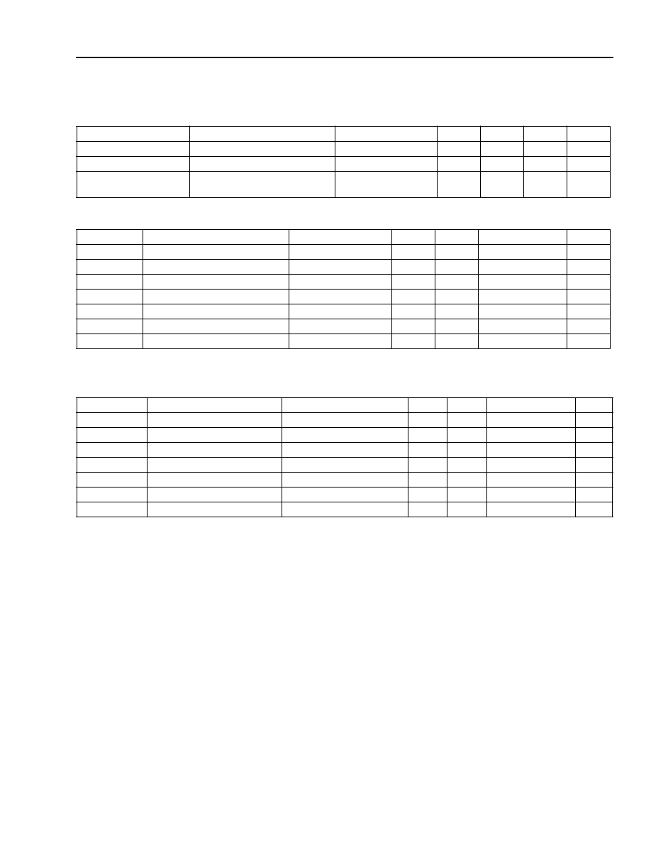
Table 14. Clock Section (See Figures 6, 7, 8, and 9.)
Table 15. T7504 Transmit Section (See Figure 6.)
* Timing parameter tMCLDZ is referenced to a high-impedance state.
Table 16. T5504 Transmit Section (See Figure 8.)
* Timing parameter tMCHDZ is referenced to a high-impedance state.
Symbol
Parameter
Test Conditions
Min
Typ
Max
Unit
tMCHMCL1
Clock Pulse Width
--
97
--
--
ns
tCDC
Duty Cycle, MC
--
40
--
60
%
tMCH1MCH2
tMCL2MCL1
Clock Rise and
Fall Time
--
0
--
15
ns
Symbol
Parameter
Test Conditions
Min
Typ
Max
Unit
tMCHDV
Data Enabled on TS Entry
0 < C
LOAD
< 100 pF
0
--
60
ns
tMCHDV1
Data Delay from MC
0 < C
LOAD
< 100 pF
0
--
60
ns
tMCLDZ*
Data Float on TS Exit
C
LOAD
= 0
15
--
100
ns
tFSHMCL
Frame-sync Hold Time
--
50
--
--
ns
tMCLFSH
Frame-sync High Setup
--
50
--
--
ns
tFSLMCL
Frame-sync Low Setup
--
50
--
--
ns
tFSHFSL
Frame-sync Pulse Width
--
0.1
--
125 ≠ tMCHMCH
µ
s
Symbol
Parameter
Test Conditions
Min
Typ
Max
Unit
tFSHDV
Data Enabled on TS Entry
0 < C
LOAD
< 100 pF
0
--
80
ns
tMCHDV1
Data Delay from FS
X
0 < C
LOAD
< 100 pF
0
--
60
ns
tMCHDZ*
Data Float on TS Exit
C
LOAD
= 0
0
--
30
ns
tFSHMCL
Frame-sync Hold Time
--
50
--
--
ns
tMCLFSH
Frame-sync High Setup
--
50
--
--
ns
tFSLMCL
Frame-sync Low Setup
--
50
--
--
ns
tFSHFSL
Frame-sync Pulse Width
--
0.1
--
125 ≠ tMCHMCH
µ
s
12
Lucent Technologies Inc.
Data Sheet
March 1999
T7504 and T5504 Quad PCM Codecs with Filters
Timing Characteristics
(continued)
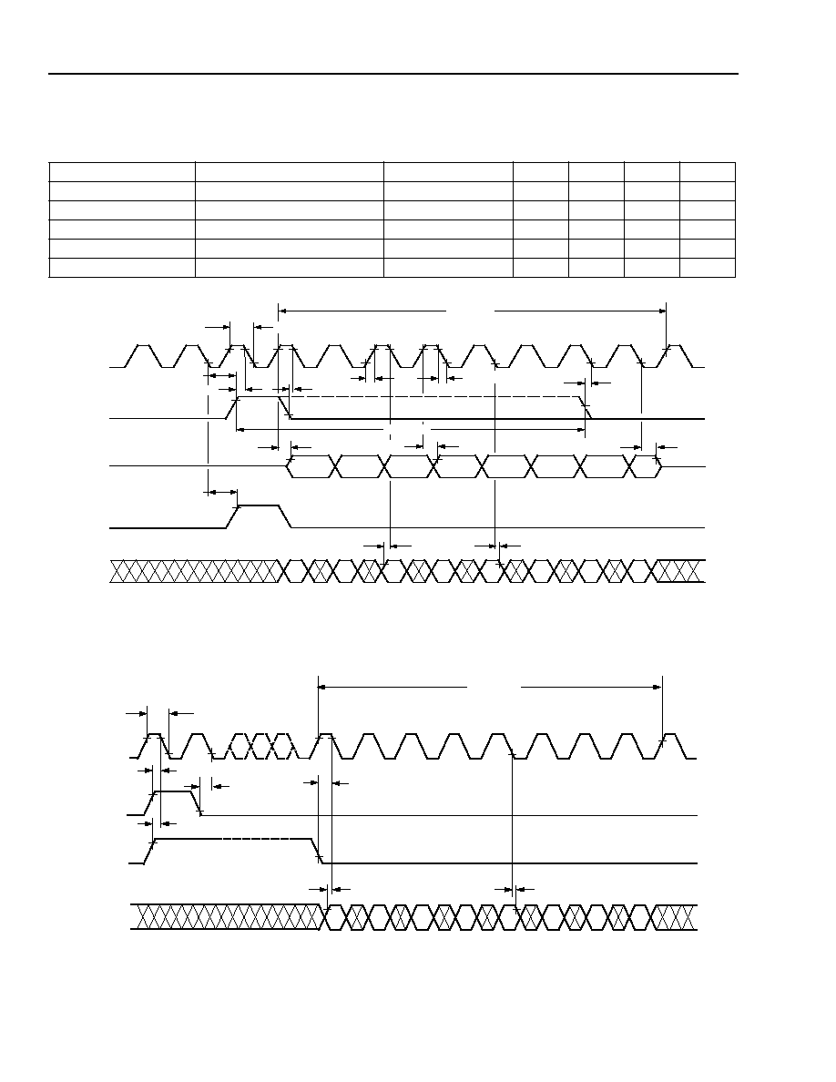
Table 17. T7504 and T5504 Receive Section (See Figures 6, 7, 8, and 9.)
5-3581
Figure 6. T7504 Transmit and Receive Timing, FSEP = 1 MCLK
5-3582
Figure 7. T7504 Receive Timing, FSEP > 1 MCLK
Symbol
Parameter
Test Conditions
Min
Typ
Max
Unit
tDVMCL
Receive Data Setup
--
30
--
--
ns
tMCLDV
Receive Data Hold
--
15
--
--
ns
tSPHMCL
Frame Separation Hold Time
--
50
--
--
ns
tMCLSPH
Frame Separation High Setup
--
50
--
--
ns
tSPLMCL
Frame Separation Low Setup
--
50
--
--
ns
MCLK
FSx
N
Dx
FSEP
TIME SLOT
1
2
3
4
5
6
7
8
1
tFSLMCL
tMCH1MCH2
tFSLMCL
BIT 1
BIT 2
BIT 3
BIT 4
BIT 5
BIT 6
BIT 7
BIT 8
tMCHDV
tMCLDZ
D
R
tDVMCL
BIT
1
BIT
2
BIT
3
BIT
4
BIT
5
BIT
6
BIT
7
BIT
8
tMCLDV
D
R
STABLE
tMCHMCL1
tMCHDV1
tMCL2MCL1
FSHFSL
tMCLSPH
tFSHMCL
tMCLFSH
MCLK
FS
X
N
FSEP
D
R
tDVMCL
BIT
1
BIT
2
BIT
3
BIT
4
BIT
5
BIT
6
BIT
7
BIT
8
tMCLDV
D
R
STABLE
TIME SLOT
1
2
3
4
5
6
7
8
tFSLMCL
tMCHMCL1
tSPLMCL
tSPHMCL
tFSHMCL
Lucent Technologies Inc.
13
Data Sheet
March 1999
T7504 and T5504 Quad PCM Codecs with Filters
Timing Characteristics
(continued)
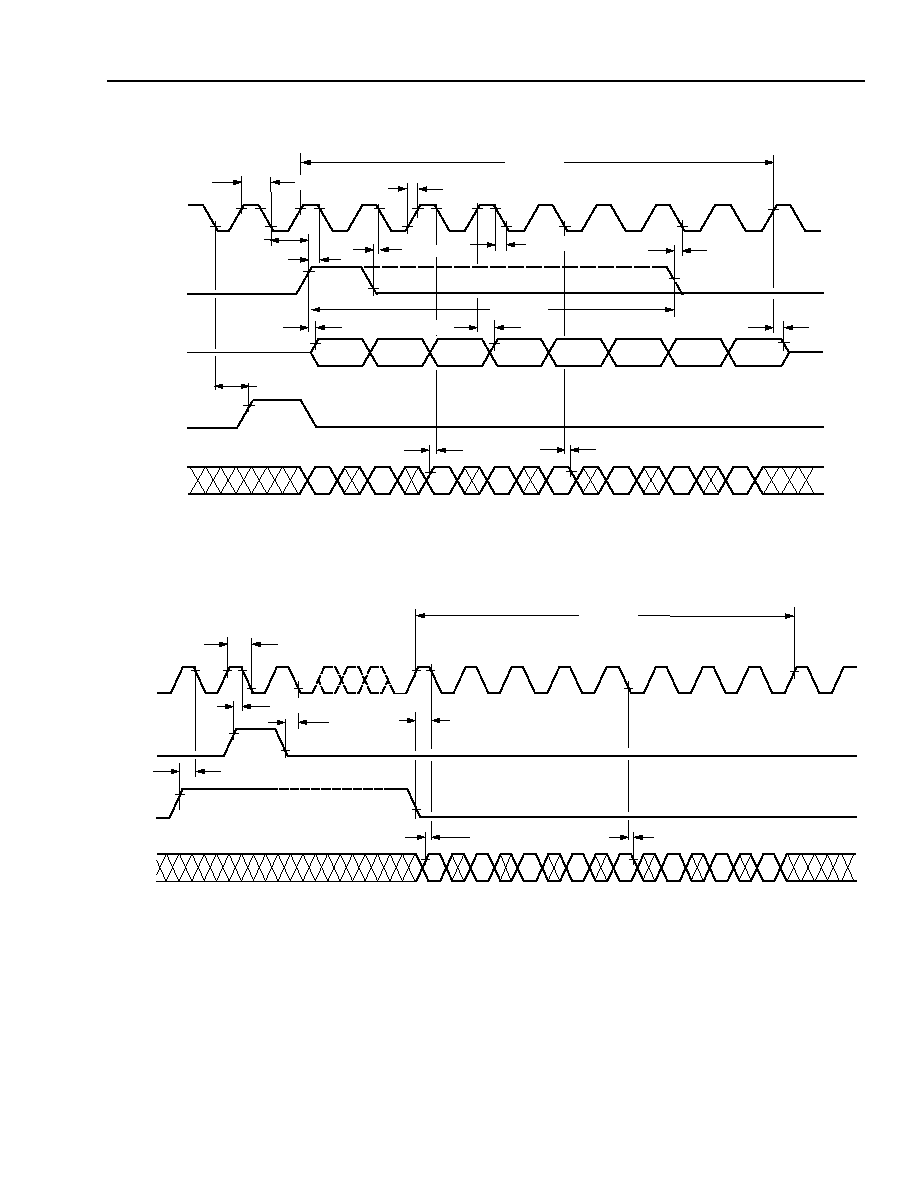
5-3581.a
Figure 8. T5504 Transmit and Receive Timing, FSEP = 1 MCLK
5-3582.a
Figure 9. T5504 Receive Timing, FSEP > 1 MCLK
MCLK
FSx
N
Dx
FSEP
tFSHMCL
TIME SLOT
1
2
3
4
5
6
7
8
1
tFSLMCL
BIT 1
BIT 2
BIT 3
BIT 4
BIT 5
BIT 6
BIT 7
BIT 8
tFSHDV
tMCHDZ
D
R
tDVMCL
BIT
1
BIT
2
BIT
3
BIT
4
BIT
5
BIT
6
BIT
7
BIT
8
tMCLDV
D
R
STABLE
tMCHMCL1
tMCHDV1
tMCL2MCL1
tMCH1MCH2
tFSLMCL
FSHFSL
tMCLFSH
tMCLSPH
MCLK
FS
X
N
FSEP
D
R
tDVMCL
tMCLDV
D
R
STABLE
TIME SLOT
1
2
3
4
5
6
7
8
tFSLMCL
tMCHMCL1
tSPLMCL
tSPHMCL
tFSHMCL
BIT
1
BIT
2
BIT
3
BIT
4
BIT
5
BIT
6
BIT
7
BIT
8
14
Lucent Technologies Inc.
Data Sheet
March 1999
T7504 and T5504 Quad PCM Codecs with Filters
Timing Characteristics
(continued)
5-3583.a
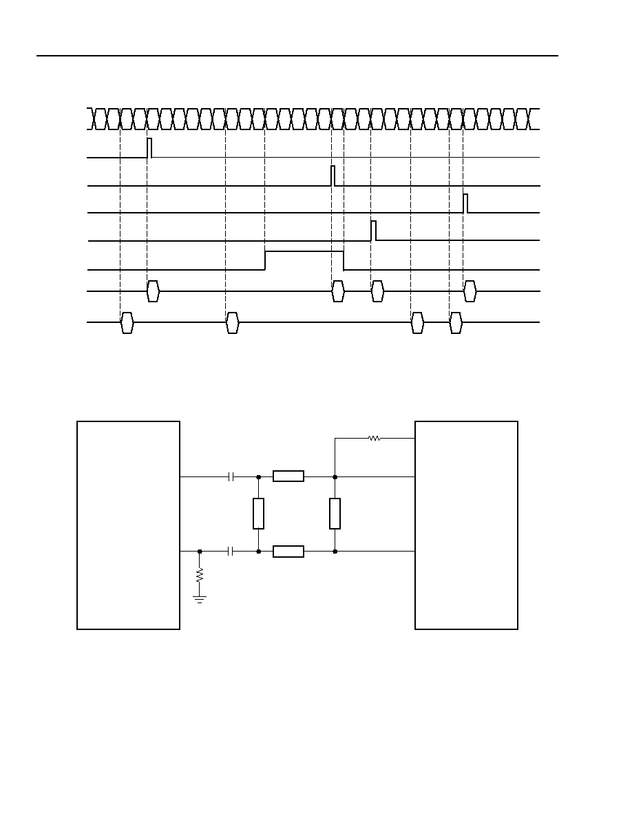
Figure 10. Typical Frame Sync Timing (2 MHz Operation)
Applications
5-3584
Figure 11. Typical T7504 and T5504/SLIC Interconnection
21 22 23 24 25 26 27 28 29 30 31
0
1
2
3
4
5
6
7
8
9
10 11 12 13 14 15 16 17 18 19 20
20
19
FS
X
0
FS
X
1
FS
X
2
FS
X
3
FSEP
D
X
D
R
X0
R0
X1
X3
R1
R3
X2
R2
TIME
SLOTS
V
TR
ACIN
SLIC
0.1 µF
0.1 µF
RG
RF
ZHB
ZT1
ZT2
ZRCV
GSXn
VF
X
INn
VF
R
On
T7504
T5504
Lucent Technologies Inc.
15
Data Sheet
March 1999
T7504 and T5504 Quad PCM Codecs with Filters
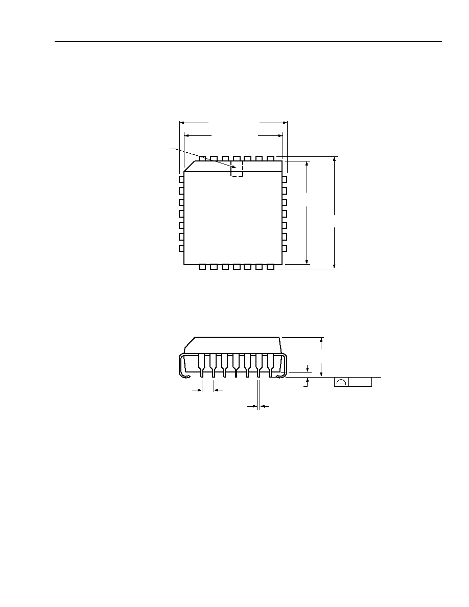
Outline Diagrams
28-Pin PLCC
Controlling dimensions are in inches.
5-2608r05(F)
1.27 TYP
0.330/0.533
0.10
SEATING PLANE
0.51 MIN
TYP
4.572
MAX
12
18
11
5
4
1
26
25
19
12.446
±
0.127
PIN #1 IDENTIFIER
ZONE
11.506
±
0.076
11.506
±
0.076
12.446
±
0.127
16
Lucent Technologies Inc.
Data Sheet
March 1999
T7504 and T5504 Quad PCM Codecs with Filters
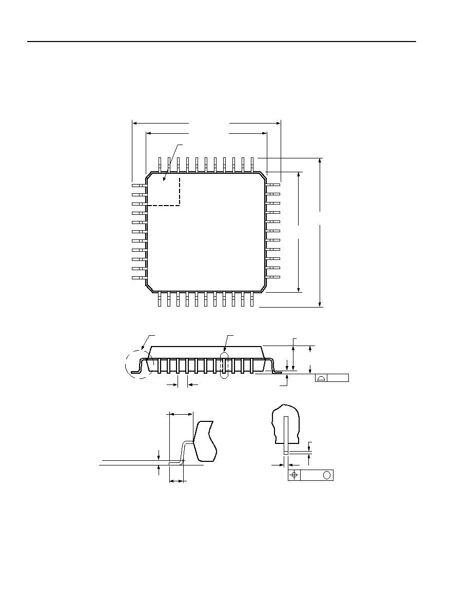
Outline Diagrams
(continued)
44-Pin MQFP
Controlling dimensions are in inches.
5-2111r12(F)
44
1
10.00
±
0.20
13.20
±
0.20
10.00
±
0.20
13.20
±
0.20
PIN #1 IDENTIFIER ZONE
11
12
22
23
33
34
0.80 TYP
DETAIL A
2.35
MAX
0.10
SEATING
PLANE
1.95/2.10
DETAIL B
0.25 MAX
0.30/0.45
0.20
M
0.130/0.230
DETAIL B
0.25
0.73/1.03
1.60 REF
GAGE PLANE
SEATING PLANE
DETAIL A

Lucent Technologies Inc.
17
Data Sheet
March 1999
T7504 and T5504 Quad PCM Codecs with Filters
Ordering Information
Device Code
Package
Temperature
Timing Mode
Comcode
T - 7504 - - - ML
28-Pin, PLCC
≠40
∞
C to +85
∞
C
Delayed
107203184
T - 7504 - - - JL-DB
44-Pin, MQFP
Dry Pack Tray
≠40
∞
C to +85
∞
C
Delayed
107740466
T - 7504 - - - ML-TR
28-Pin, PLCC
Tape & Reel
≠40
∞
C to +85
∞
C
Delayed
107231680
T - 5504 - - - ML
28-Pin, PLCC
≠40
∞
C to +85
∞
C
Nondelayed
107364044
T - 5504 - - - ML-TR
28-Pin, PLCC
Tape & Reel
≠40
∞
C to +85
∞
C
Nondelayed
107364051

Lucent Technologies Inc. reserves the right to make changes to the product(s) or information contained herein without notice. No liability is assumed as a result of their use or application. No
rights under any patent accompany the sale of any such product(s) or information.
Copyright © 1999 Lucent Technologies Inc.
All Rights Reserved
March 1999
DS99-201ALC (Replaces DS99-184ALC)
For additional information, contact your Microelectronics Group Account Manager or the following:
INTERNET: http://www.lucent.com/micro
E-MAIL: docmaster@micro.lucent.com
N. AMERICA:
Microelectronics Group, Lucent Technologies Inc., 555 Union Boulevard, Room 30L-15P-BA, Allentown, PA 18103
1-800-372-2447, FAX 610-712-4106 (In CANADA: 1-800-553-2448, FAX 610-712-4106)
ASIA PACIFIC: Microelectronics Group, Lucent Technologies Singapore Pte. Ltd., 77 Science Park Drive, #03-18 Cintech III, Singapore 118256
Tel. (65) 778 8833, FAX (65) 777 7495
CHINA: Microelectronics Group, Lucent Technologies (China) Co., Ltd., A-F2, 23/F, Zao Fong Universe Building, 1800 Zhong Shan Xi Road, Shanghai
200233 P. R. China
Tel. (86) 21 6440 0468, ext. 316, FAX (86) 21 6440 0652
JAPAN: Microelectronics Group, Lucent Technologies Japan Ltd., 7-18, Higashi-Gotanda 2-chome, Shinagawa-ku, Tokyo 141, Japan
Tel. (81) 3 5421 1600, FAX (81) 3 5421 1700
EUROPE: Data Requests: MICROELECTRONICS GROUP DATALINE: Tel. (44) 1189 324 299, FAX (44) 1189 328 148
Technical Inquiries: GERMANY: (49) 89 95086 0 (Munich), UNITED KINGDOM: (44) 1344 865 900 (Ascot),
FRANCE: (33) 1 40 83 68 00 (Paris), SWEDEN: (46) 8 594 607 00 (Stockholm), FINLAND: (358) 9 4354 2800 (Helsinki),
ITALY: (39) 02 6608131 (Milan), SPAIN: (34) 1 807 1441 (Madrid)