 | –≠–ª–µ–∫—Ç—Ä–æ–Ω–Ω—ã–π –∫–æ–º–ø–æ–Ω–µ–Ω—Ç: T7504-ML | –°–∫–∞—á–∞—Ç—å:  PDF PDF  ZIP ZIP |
Data Sheet
February 2002
T7504 and T5504 Quad PCM Codecs with Filters
Features
s
5 V only
s
Low-power, latch-up-free CMOS technology
-- 37 mW/channel typical operating power
dissipation
-- 1 mW/channel typical powerdown dissipation
s
Automatic master clock frequency selection
-- 2.048 MHz or 4.096 MHz
s
On-chip sample and hold, autozero, and precision
voltage reference
s
Differential architecture for high noise immunity
and power supply rejection
s
Flexible time-slotted PCM interface
-- 2.048 MHz or 4.096 MHz data rate
s
Meets or exceeds ITU-T G.711--G.712 require-
ments and VF characteristics of D3/D4 (as per
Agere Systems Inc.'s PUB43801)
s
Operating temperature range: ≠40 ∞C to +85 ∞C
s
µ-law/A-law companding selectable
Description
The T7504 and T5504 devices are single-chip, four-
channel µ-law/A-law PCM codecs with filters. These
integrated circuits provide analog-to-digital and
digital-to-analog conversion. They provide the
transmit and receive filtering necessary to interface a
voice telephone circuit to a time-division multiplexed
system. These devices are available in 28-pin
PLCCs. The T7504 is also available in a 44-pin
MQFP.
The T5504 differs from the T7504 in its timing mode.
The T5504 operates in the nondelay timing mode
(digital data valid when frame sync goes high), and
the T7504 operates in the delayed timing mode
(digital data is valid one clock cycle after frame sync
goes high) (see Figures 6--9).
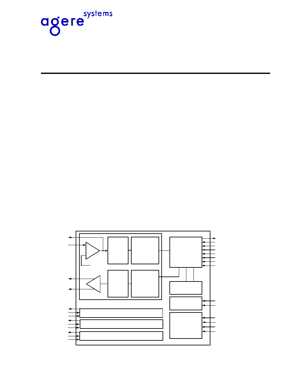
Figure 1. Block Diagram For 28-Pin DIP and 28-Pin PLCC
5-3579 (F).d
GS
X
0
VF
X
IN0
VF
R
OP0
GS
X
1
VF
X
IN1
VF
R
O1
≠
+
FILTER
ENCODER
CHANNEL 0
2.4 V
DECODER
PCM
POWERDOWN
INTERNAL TIMING
BIAS
CHANNEL 1
D
X
D
R
PSx0
MCLK
VF
R
ON0
GNDA (4) (PLCC ONLY)
NETWORK
INTERFACE
CONTROL
AND CONTROL
CIRCUITRY
AND
REFERENCE
V
DD
(2)
FILTER
NETWORK
PSx1
PSx2
PSx3
PSEP
GNDD
ASEL
V
DD
(2) (MQFP ONLY)
GNDA (5) (MQFP ONLY)
CHANNEL 2
CHANNEL 3
GS
X
3
VF
X
IN3
VF
R
O3
GS
X
2
VF
X
IN2
VF
R
O2
2
2
Agere Systems Inc.
Data Sheet
February 2002
T7504 and T5504 Quad PCM Codecs with Filters
Functional Description
Four channels of PCM data input and output are
passed through only two ports, D
X
and D
R
, so some
type of time-slot assignment is necessary. The scheme
used here is to utilize timing modes of 32 or 64 time
slots corresponding to master clock frequencies of
either 2.048 MHz or 4.096 MHz, respectively. Each
device has four transmit frame sync (FS
X
) inputs, one
for each channel. During a single 125 µs frame, each
transmit frame sync input is supplied a single pulse.
The timing of the pulse indicates the beginning of the
time slot during which the data for that channel is
clocked out of the device. During a frame, transmit
frame sync pulses must be separated from each other
by one or more time slots. A channel is placed in a
standby (low-power) mode if its FS
X
input has been low
for 500 µs.
There is a single frame sync separation input (FSEP).
The number of negative clock edges minus one that
occurs while FSEP is high is the delay (in clock
periods) that is placed between the rising edge of a
transmit frame sign bit and the falling edge used by the
receiver to sample the sign bit. There must always be a
pulse on the FSEP input since this input provides the
8 kHz signal required to maintain internal timing. If the
FSEP pulse is one clock period or less, the device
makes the transmit edges and receive sampling edges
one half clock period apart. The entire device is placed
in a powerdown mode if FSEP remains low for 500 µs.
Time slot zero is defined as starting on the first rising
MCLK edge after FSEP = 1 is detected by a negative
MCLK edge. In the T7504, MCLK negative-going
edges that detect the start of FSEP and FS
X
N must be
integer multiples of eight MCLK periods apart (zero
multiples are allowed). Since FSEP is assumed to
define time slot 0, the number of multiples separating
FS
X
N and FSEP is the time-slot number. In the T5504,
FS
X
N for time slot 0 nominally starts on the MCLK
positive edge following the negative edge which
detects FSEP.
The frequency of the master clock must be either
2.048 MHz or 4.096 MHz. Internal circuitry determines
the master clock frequency during the powerup reset
interval.
Powerdown is not guaranteed if MCLK is lost unless
the device is already in the powerdown mode due to
FSEP low for at least 500 µs.
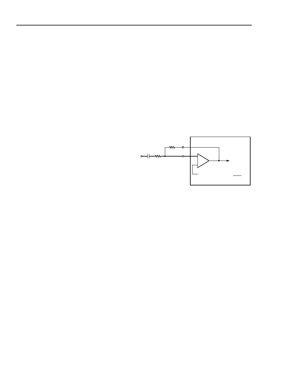
The analog input section in Figure 2 includes an on-
chip op amp that is used in conjunction with external,
user-supplied resistors to vary encoder passband gain.
The feedback resistance (R
F
) should range from 10 kæ
to 200 kæ and capacitance from GSx to ground should
be kept to less than 50 pF. The input signal at VF
X
IN
should be ac coupled. For best performance, the maxi-
mum gain of this op amp should be limited to 20 dB or
less.
Figure 2. Typical Analog Input Section
VF
X
IN
TO
2.4 V
GS
X
R
I
R
F
≠
+
CODEC
FILTERS
GAIN =
R
x
R
I
5-3786 (F)

Agere Systems Inc.
3
Data Sheet
February 2002
T7504 and T5504 Quad PCM Codecs with Filters
Pin Information
Figure 3. 28-Pin PLCC Pin Diagram
Figure 4. 44-Pin MQFP Pin Diagram
FSx0
V
DD
GNDA0
VFxIN0
GSx0
VF
R
O0
ASEL
VFxIN2
GSx2
VF
R
O2
5
6
7
8
9
10
11
4
2
1
28
27
3
12
14
15
16
17
18
13
25
24
23
22
21
20
19
F
SEP
GN
D
A
3
VF
R
O3
VF
R
O1
GSx1
VFxIN3
GSx3
VF
x
I
N
1
T-7504 - - - ML
V
DD
MCLK
GNDA2
GNDA1
FS
x
2
FS
x
3
GND
D
DX
D
R
26
FS
x
1
T-5504 - - - ML
5-3580 (F).b
5-4770 (F)
FSx0
NC
V
DD
V
DD
A
NC
NC
44
42
41 40
39
43
33
32
31
30
29
28
27
G
NDD
T-7504 - - - ML
GNDA0
NC
NC
NC
DX
D
R
38
NC
37 36
35
FS
EP
FS
x2
FS
x3
34
FS
x1
VFxIN0
GSx0
VF
R
O0
26
25
24
23
GNDA1
MCLK
ASEL
V
DD
V
DD
A
NC
NC
1
2
3
4
5
6
7
NC
VFxIN2
GSx2
VF
R
O2
8
9
10
11
GNDA2
22
20
19
18
17
21
VF
xI
N
1
NC
GNDA4
GS
x1
VF
R
O1
NC
16
GNDA3
15
14
13
VF
xIN3
VF
R
O3
G
Sx3
12
NC
4
Agere Systems Inc.
Data Sheet
February 2002
T7504 and T5504 Quad PCM Codecs with Filters
Pin Information
(continued)
* I
d
Indicates a pull-down device is included on this lead.
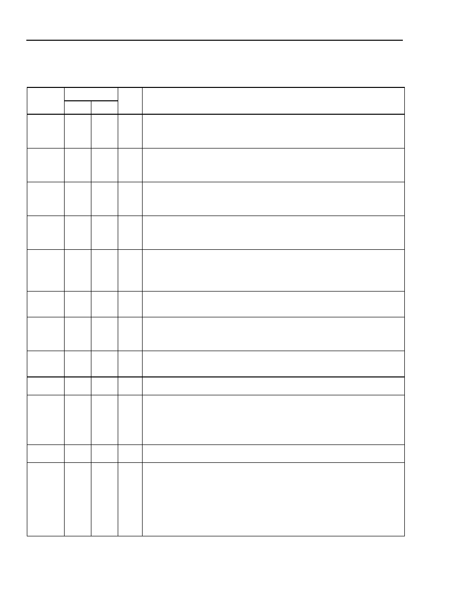
Table 1. Pin Descriptions
Symbol
Pin
Type*
Name/Function
PLCC
MQFP
VF
X
IN3
VF
X
IN2
VF
X
IN1
VF
X
IN0
14
8
16
22
15
8
19
26
I
Voice Frequency Transmitter Input. Analog inverting input to the uncommitted
operational amplifier at the transmit filter input. Connect the signal to be digitized
to this pin through a resistor R
I
(see
Figure 2).
GS
X
3
GS
X
2
GS
X
1
GS
X
0
13
9
17
21
14
9
20
25
O
Gain Set for Transmitter. Output of the transmit uncommitted operational
amplifier. The pin is the input to the transmit differential filters. Connect the pin to
its corresponding VF
X
IN through a resistor R
F
(see
Figure 2
).
VF
R
O3
VF
R
O2
VF
R
O1
VF
R
O0
12
10
18
20
13
10
21
24
O
Voice Frequency Receiver Output. This pin can drive 2000 æ (or greater) loads.
V
DD
[1:0]
V
DDA
[1:0]
7, 24
--
3, 31
4, 30
--
5 V Digital and Analog Power Supplies. All pins must be connected on the circuit
board. Each pin should be bypassed to ground with at least 0.1 µF of capacitance
as close to the device as possible. For the DIP and PLCC packages, V
DD
serves
both analog and digital internal circuits.
GNDA4
GNDA3
GNDA2
GNDA1
GNDA0
--
15
11
19
23
18
16
11
23
27
--
Analog Grounds. All ground pins must be connected on the circuit board.
D
R
4
44
I
Receive PCM Data Input. The data on this pin is shifted into the device on the fall-
ing edges of MCLK. Data is only entered for valid time slots as defined by the rela-
tionship of the pulses on the FS
X
inputs and the pulse on the FSEP input.
D
X
3
43
O
Transmit PCM Data Output. This pin remains in the high-impedance state except
during active transmit time slots. An active transmit time slot is defined as one in
which a pulse is present on one of the FSx inputs. Data is shifted out on the rising
edge of MCLK.
MCLK
5
1
I
Master Clock Input. The frequency must be 2.048 MHz or 4.096 MHz. This clock
serves as the bit clock for all PCM data transfer. A 40% to 60% duty cycle is re-
quired.
GNDD
2
41
--
Digital Ground. Ground connection for the digital circuitry. All ground pins must be
connected on the circuit board.
FS
X
3
FS
X
2
FS
X
1
FS
X
0
28
27
26
25
36
35
34
33
I
d
Transmit Frame Sync. This signal is an edge trigger and must be high for a min-
imum of one MCLK cycle. This signal must be derived from MCLK. The division ra-
tio is 1:256 or 1:512 (FS
X
:MCLK). Each FS
X
input must have a pulse present at the
start of the desired active output time slot. Pulses on the various FS
X
inputs must
be separated by one or more integer multiples of time slots. An internal pull-down
device is included on each FS
X
.
ASEL
6
2
I
d
A-Law/µ-Law Select. A logic low selects µ-law coding. A logic high selects A-law
coding. A pull-down device is included.
FSEP
1
37
I
Frame Sync Separation. The pulse width of this 8 kHz signal defines the timing
offset between the transmit and receive frames. Internally generated receive frame
sync pulses are delayed from the corresponding transmit frame sync pulse rising
edge by one less than the FSEP pulse width in negative MCLK edges. If the pulse
width is one MCLK period or less, the transmit and receive frame syncs are made
coincident. Loss of FSEP causes the device to powerdown. If the master clock fre-
quency is 2.048 MHz or 4.096 MHz, delays of 255 or 511 clock pulses are not al-
lowed, respectively. Timing relationships between FSEP, FS
X
N, and time slot 0 are
given in
Figures 6--9
.
Agere Systems Inc.
5
Data Sheet
February 2002
T7504 and T5504 Quad PCM Codecs with Filters
Absolute Maximum Ratings
Stresses in excess of the absolute maximum ratings can cause permanent damage to the device. These are
absolute stress ratings only. Functional operation of the device is not implied at these or any other conditions in
excess of those given in the operational sections of this data sheet. Exposure to absolute maximum ratings for
extended periods can adversely affect device reliability.
Handling Precautions
Although protection circuitry has been designed into this device, proper precautions should be taken to avoid
exposure to electrostatic discharge (ESD) during handling and mounting. Agere employs a human-body model
(HBM) and a charged-device model (CDM) for ESD susceptibility testing and protection design evaluation. ESD
voltage thresholds are dependent on the circuit parameters used to define the model. No industry-wide standard
has been adopted for CDM. However, a standard HBM (resistance = 1500 æ, capacitance = 100 pF) is widely used
and, therefore, can be used for comparison purposes. The HBM ESD threshold presented here was obtained by
using these circuit parameters:
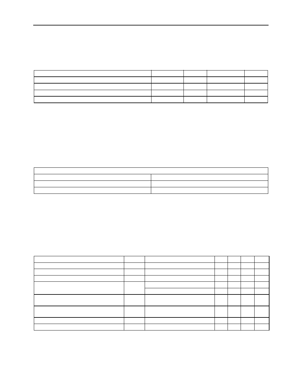
Electrical Characteristics
Specifications apply for T
A
= ≠40 ∞C to +85 ∞C, V
DD
= 5 V ± 5%, MCLK = either 2.048 MHz or 4.096 MHz, and
GND = 0 V, unless otherwise noted.
dc Characteristics
Table 2. Digital Interface
Parameter
Symbol
Min
Max
Unit
Storage Temperature Range
T
stg
≠55
150
∞C
Power Supply Voltage
V
DD
--
6.5
V
Voltage on Any Pin with Respect to Ground
--
≠0.5
0.5 + V
DD
V
Maximum Power Dissipation (package limit)
P
D
--
600
mW
HBM ESD Threshold Voltage
Device
Rating
T7504
>2000 V
T5504
>2000 V
Parameter
Symbol
Test Conditions
Min
Typ
Max
Unit
Input Low Voltage
V
IL
All digital inputs
--
--
0.8
V
Input High Voltage
V
IH
All digital inputs
2.0
--
--
V
Output Low Voltage
V
OL
D
X
, I
L
= 3.2 mA
--
--
0.4
V
Output High Voltage
V
OH
D
X
, I
L
= ≠3.2 mA
2.4
--
--
V
D
X
, I
L
= ≠320 µA
3.5
--
--
V
Input Current, Pins without Pull-down
I
I
Any digital input GND < V
IN
<
V
DD
≠10
--
10
µA
Input Current, Pins with Pull-down
I
I
Any digital input GND < V
IN
<
V
DD
--
--
150
µA
Output Current in High-impedance State
I
OZ
D
X
≠30
--
30
µA
Input Capacitance
C
I
--
--
--
5
pF