 | –≠–ª–µ–∫—Ç—Ä–æ–Ω–Ω—ã–π –∫–æ–º–ø–æ–Ω–µ–Ω—Ç: T7507 | –°–∫–∞—á–∞—Ç—å:  PDF PDF  ZIP ZIP |

Data Sheet
August 1999
T7507 Quad PCM Codec with Filters,
Termination Impedance, and Hybrid Balance
Features
s
5 V only
s
Low-power, latch-up-free CMOS technology:
-- 37 mW/channel typical operating power
dissipation
-- 1 mW/channel typical powerdown dissipation
s
Fixed master clock frequency: 2.048 MHz
s
On-chip sample and hold, autozero, and precision
voltage reference
s
Differential architecture for high noise immunity
and power supply rejection
s
PCM interface:
-- Fixed 2.048 MHz data rate
-- Delayed and nondelayed PCM modes
-- Fully flexible time-slot assignment
-- Transmit and receive aligned or offset
s
Transmit PCM data output enable
s
Serial control interface with controlling processor
s
Latched parallel control interface with SLIC and
switch
s
Meets or exceeds D3/D4 (as per Lucent PUB
43801) and ITU-T G.711--G.714 requirements
s
Operating temperature range: ≠40 ∞C to +85 ∞C
s
A-law companding
s
Hybrid balance and termination impedance:
-- 200
in series with 680
|| 0.1 µF
(People's Republic of China Z
T
)
-- Matched with L8567 SLIC
s
Programmable receive gain (≠3.5 dB or ≠7 dB),
fixed transmit gain (0 dB) when matched with
L8567 SLIC
s
44-pin PLCC
Description
The T7507 device is a single-chip, four-channel
A-law PCM codec with filters. This integrated circuit
provides analog-to-digital and digital-to-analog con-
version. It provides the transmit and receive filtering
necessary to interface a voice telephone circuit to a
time-division multiplexed system. This device is pack-
aged in a 44-pin PLCC.
This codec is intended for use with Lucent Technolo-
gies Microelectronics Group's L8567 SLIC. When
used with that SLIC, the line tip/ring pair is termi-
nated in the network required for central office appli-
cations in the People's Republic of China (PRC).
Proper hybrid balance and transmit and receive
gains are also obtained.
This device uses a serial data control scheme to
interface with the controlling processor. This device
has a latched parallel data control scheme to provide
control bits to, and receive status bits from, the SLIC
and switch. This interface is designed to be compati-
ble with the Lucent L8567 SLIC and L7583 solid-
state switch.

2
Lucent Technologies Inc.
Data Sheet
August 1999
Termination Impedance, and Hybrid Balance
T7507 Quad PCM Codec with Filters,
Table of Contents
Contents
Page
Features ......................................................................1
Description...................................................................1
Pin Information ............................................................5
Functional Description .................................................7
PCM Interface ........................................................7
Analog Interface .....................................................8
Transmission Levels...............................................8
Microprocessor Serial Data Control and L8567
SLIC/L7583 Switch (or EMR) Control
Interfaces .............................................................8
Enable Transfers when CCLK Is Bursted
with CSEL ...........................................................9
Enable Transfers when CCLK Is Not
Restricted to CSEL Low.......................................9
Input Word Definition............................................12
Output Word Definition .........................................14
Powerup ...............................................................14
T7507 ..............................................................14
Output Word....................................................14
EN Status ........................................................14
Input Word--PCM Interface ............................14
Input Word--Relay Control/Timing .................14
Input Word--Control Mode .............................14
State Definitions ...................................................14
Powerup ..........................................................14
Standby ...........................................................14
Full-Chip Powerdown ......................................14
Absolute Maximum Ratings.......................................15
Handling Precautions ................................................15
Electrical Characteristics ...........................................15
dc Characteristics.................................................15
Transmission Characteristics ....................................16
ac Transmission Characteristics ..........................17
Overload Compression ...................................18
Chip Set Performance Specifications ........................21
Gain......................................................................21
Gain Flatness--In Band .......................................21
Gain Flatness--Out of Band--High
Frequencies .......................................................21
Gain Flatness--Out of Band--Low
Frequencies .......................................................22
Loss vs. Level Relative to Loss at ≠10 dBm
Input at 1020 Hz ................................................22
Return Loss ..........................................................22
Hybrid Balance .....................................................22
Microprocessor Interface ...........................................23
Timing Characteristics ...............................................25
Applications ...............................................................28
Outline Diagram.........................................................29
44-Pin PLCC ........................................................29
Ordering Information..................................................30
Figures
Page
Figure 1. Block Diagram ............................................ 4
Figure 2. Pin Diagram................................................. 5
Figure 3. Typical Analog Input Section ...................... 8
Figure 4. Overload Compression ............................. 18
Figure 5. Termination Impedance ............................ 21
Figure 6. Transmit and Receive Direction
Frequency-Dependent Loss Relative
to Gain at 3400 Hz ................................... 21
Figure 7. Loss vs. Level ........................................... 22
Figure 8. Return Loss .............................................. 22
Figure 9. Hybrid Balance ......................................... 22
Figure 10. SLIC/Switch Interface Timing ................. 24
Figure 11. Microprocessor Interface Write
Timing .................................................... 24
Figure 12. T7507 Transmit and Receive Timing,
FSEP = 1 MCLK or IFS = 1, Delayed
Timing (D0 = 0) ...................................... 26
Figure 13. T7507 Transmit and Receive Timing,
FSEP = 1 MCLK or IFS = 1, Nondelayed
Timing (D0 = 1) ...................................... 26
Figure 14. T7507 Receive Timing, FSEP > 1
MCLK and IFS = 0, Delayed Timing
(D3 = 0) .................................................. 27
Figure 15. Typical Frame Sync Timing (IFS = 0) ..... 27
Figure 16. Basic Loop Start Application Using
the T7507 and the L7583 Switch for
200
+ (680
|| 100 nF) Complex
Termination and Hybrid Balance ............ 28

Lucent Technologies Inc.
3
Data Sheet
August 1999
Termination Impedance, and Hybrid Balance
T7507 Quad PCM Codec with Filters,
Table of Contents
(continued)
Tables
Page
Table 1. Pin Descriptions ........................................................................................................................................ 5
Table 2. Microprocessor Interface Descriptions ....................................................................................................11
Table 3. C0, C1 Channel Select .............................................................................................................................12
Table 4. M, D4, D3, D2, D1, D0 Mode Select and Data .........................................................................................12
Table 5. M = 0 Mode (PCM Time-Slot Assignment) ...............................................................................................12
Table 6. M = 1, D4 = 0 Mode (Relay State Control and Delayed/Nondelayed Timing) .........................................13
Table 7. M = 1, D4 = 1 Mode (Codec State Control and SLIC State Control) .......................................................13
Table 8. Digital Interface .......................................................................................................................................15
Table 9. Power Dissipation ....................................................................................................................................16
Table 10. Analog Interface ....................................................................................................................................16
Table 11. Absolute Gain ........................................................................................................................................17
Table 12. Gain Tracking .........................................................................................................................................17
Table 13. Distortion ................................................................................................................................................17
Table 14. Envelope Delay Distortion .....................................................................................................................18
Table 15. Decoder Limits Relative to Gain at 1020 Hz ...........................................................................................19
Table 16. Encoder Limits, Includes Effect of Termination Impedance Filter Relative to Gain at 1020 Hz ..............19
Table 17. Termination Impedance Limits Relative to Gain at 1020 Hz ...................................................................19
Table 18. Hybrid Path Limits Relative to Gain at 1020 Hz ......................................................................................19
Table 19. Noise .....................................................................................................................................................20
Table 20. Interchannel Crosstalk (Between Channels) .........................................................................................20
Table 21. Gain ........................................................................................................................................................21
Table 22. Gain Flatness--In Band .........................................................................................................................21
Table 23. Gain Flatness--Out of Band--Low Frequencies ..................................................................................22
Table 24. T7507 Microprocessor Interface Timing .................................................................................................23
Table 25. Clock Section ..........................................................................................................................................25
Table 26. T7507 Transmit Section (Delayed Timing)..............................................................................................25
Table 27. T7507 Transmit Section (Nondelayed Timing)........................................................................................25
Table 28. T7507 Receive Section ..........................................................................................................................25
4
Lucent Technologies Inc.
Data Sheet
August 1999
Termination Impedance, and Hybrid Balance
T7507 Quad PCM Codec with Filters,
Description
(continued)
5-3579.a(F)
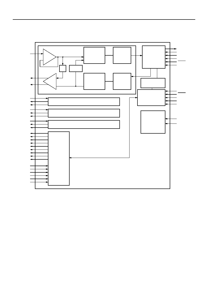
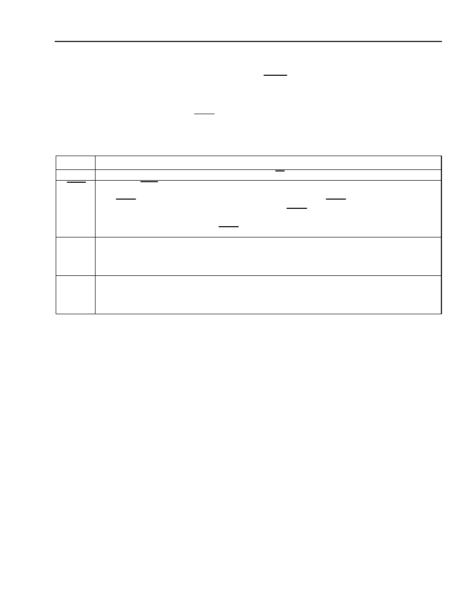
Figure 1. Block Diagram
VF
X
IN1
VF
R
ON1
VF
R
OP1
VF
X
IN0
VF
R
ON0
≠
+
BANDPASS
ENCODER
CHANNEL 0
DECODER
PCM
POWERDOWN
INTERNAL TIMING
BIAS
CHANNEL 1
CHANNEL 2
CHANNEL 3
LOW-PASS
D
X
D
R
FSEP
IFS
D
X
EN
GNDD
MCLK
CCLK
V
DD
(2)
GNDA (4)
Z
T
HYBAL
VF
R
OP0
VF
X
IN2
VF
R
ON2
VF
R
OP2
VF
X
IN3
VF
R
ON3
VF
R
OP3
DI
DO
CSEL
EN0
C
EN1
C
EN2
C
EN3
C
RD1
C
RD2
C
RD3
C
B0
C
B1
C
NSTAT
C
NTSD
C
NTSD0
NTSD1
NTSD2
NTSD3
SLIC &
FILTER
NETWORK
FILTER
NETWORK
CONTROL
INTERFACE
& CONTROL
CIRCUITRY
&
REFERENCE
SWITCH
CONTROL
INTERFACE
Lucent Technologies Inc.
5
Data Sheet
August 1999
Termination Impedance, and Hybrid Balance
T7507 Quad PCM Codec with Filters,
Pin Information
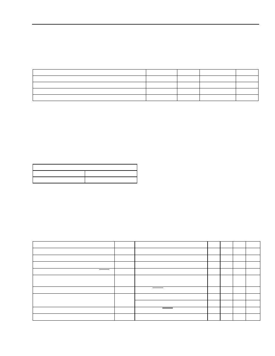
5-5347a(F)
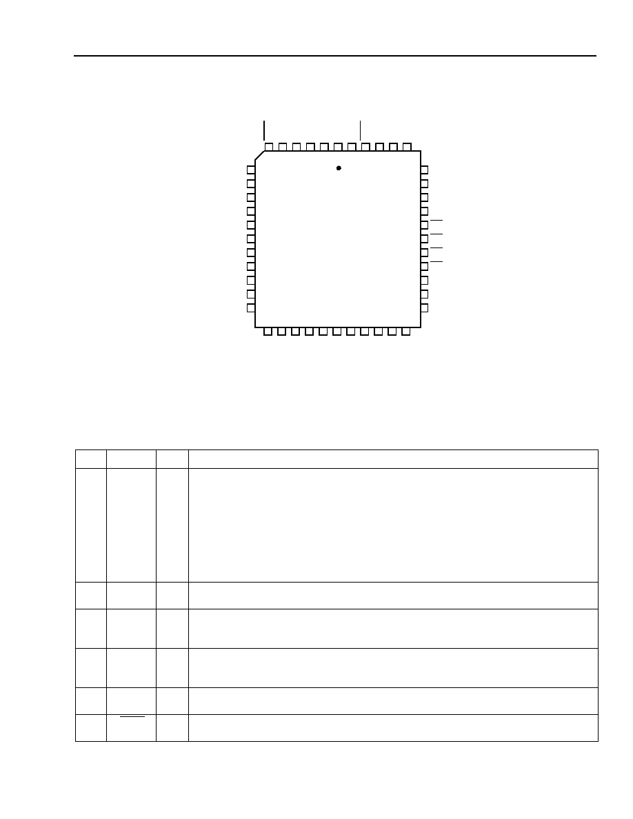
Figure 2. Pin Diagram
Table 1. Pin Descriptions
Pin
Symbol
Type
Name/Function
1
FSEP
I
d
Frame Sync Separation. The pulse width of this 8 kHz signal defines the timing offset
between the transmit and receive frames. If the IFS pin is 0, internally generated receive
frame sync pulses are delayed from the corresponding transmit frame sync pulse rising
edge by one less than the FSEP pulse width in negative MCLK edges. If the pulse width
is one MCLK period or less or if IFS is high, the transmit and receive frame syncs are
made coincident. Loss of FSEP causes the device to power down. A delay of 255 clock
pulses is not allowed. Timing relationships between FSEP and time slot 0 are given in
Figures 12--14. This input is also the frame sync for all the codec filters and PCM inter-
face timing generated from MCLK. An internal pull-down is on FSEP.
2
GNDD
--
Digital Ground. Ground connection for the digital circuitry. All ground pins must be con-
nected on the circuit board.
3
D
X
O
Transmit PCM Data Output. This pin remains in the high-impedance state except during
active transmit time slots. An active transmit time slot is defined by programming, FSEP,
and the state of IFS. Data is shifted out on the rising edge of MCLK.
4
D
R
I
Receive PCM Data Input. The data on this pin is shifted into the device on the falling
edges of MCLK. Data is only entered for valid time slots as defined by the relationship of
the time-slot programming pulse on the FSEP input, and the state of IFS.
5
MCLK
I
Master Clock Input. The frequency must be 2.048 MHz. This clock serves as the bit
clock for all PCM data transfer. A 40% to 60% duty cycle is required.
6
DxEN
O
Transmit PCM Data Output Flag. An open-drain output that pulses low during the
period when the D
X
output is enabled.
39
38
37
36
35
34
33
32
31
30
29
NTSD0
NTSD1
NTSD3
NTSD2
EN0
C
EN1
C
EN3
C
EN2
C
V
DD
VF
X
IN0
AGND0
NTSD
C
NSTAT
C
B1
C
B0
C
RD3
C
RD2
C
RD1
C
V
DD
VF
X
IN2
AGND2
VF
R
ON2
7
8
9
10
11
12
13
14
15
16
17
T7507
6
5
4
3
1
2
44 43 42 41 40
25
18
20 21 22
26 27
19
28
24
23
D
X
EN
M
CLK
D
R
D
X
GNDD
FS
EP
IF
S
CS
EL
CCLK
DI
DO
VF
R
OP
2
VF
R
OP
3
VF
R
ON3
A
G
ND3
VF
X
IN
3
A
G
ND1
VF
X
IN
1
VF
R
ON1
VF
R
OP
1
VF
R
OP
0
VF
R
ON0
6
Lucent Technologies Inc.
Data Sheet
August 1999
Termination Impedance, and Hybrid Balance
T7507 Quad PCM Codec with Filters,
Pin Information
(continued)
Table 1. Pin Descriptions (continued)
Pin
Symbol
Type
Name/Function
7
NTSD
C
I
Not Thermal Shutdown Status Input--L8567 SLIC. Logic level status input from L8567
SLIC indicating if SLIC is in thermal shutdown or normal device operation. This input is
accepted from the latched parallel data output of the SLIC and outputted on the serial
data output bus DO to the microcontroller. This pin is meant to be a shared output among
the four channels associated with the quad T7507, using the EN control to determine
valid data among the four channels.
8
NSTAT
C
I
Not Loop Closure/Not Ring Trip Status Input. Logic level status input from L8567
SLIC indicating loop on-/off-hook status. This input is accepted from the latched parallel
data output of the SLIC and outputted on the serial data output bus DO to the microcon-
troller. This pin is meant to be a shared output among the four channels associated with
the quad T7507, using the EN control to determine valid data among the four channels.
9
10
B1c
B0c
O
SLIC State Control. These logic level outputs control the state of the L8567 SLIC. These
pins are meant to be a shared output among the four channels associated with the quad
T7507, using the EN control to determine valid data among the four channels.
11
12
13
RD3
C
RD2
C
RD1
C
O
Driver Control. These logic level outputs control the state of an electromechanical relay
driver on the L8567 SLIC or a solid-state relay contact on the L7583 via the L7583 logic
control inputs. These pins are meant to be a shared output among the four channels
associated with the quad T7507, using the EN control to determine valid data among the
four channels.
14
31
V
DD
--
5 V Analog Power Supplies. Both pins must be connected on the circuit board.
Each pin should be bypassed to ground with at least 0.1 µF of capacitance as close to
the device as possible.
22
15
24
30
VF
X
IN3
VF
X
IN2
VF
X
IN1
VF
X
IN0
I
Voice Frequency Transmitter Input. Analog inverting input to the noninverting opera-
tional amplifier at the transmit filter input. Connect the signal to be digitized to this pin
through a capacitor C
I
(see Figure 3).
21
16
23
29
AGND3
AGND2
AGND1
AGND0
--
Analog Grounds. All ground pins must be connected on the circuit board.
20
17
25
28
VF
R
ON3
VF
R
ON2
VF
R
ON1
VF
R
ON0
O
Voice Frequency Receiver Negative Output. This pin can drive 2000
(or greater)
loads.
19
18
26
27
VF
R
OP3
VF
R
OP2
VF
R
OP1
VF
R
OP0
O
Voice Frequency Receive Positive Output. This pin can drive 2000
(or greater)
loads.
39
38
36
37
NTSD0
NTSD1
NTSD2
NTSD3
I
Not Thermal Shutdown Status Input--L7583 Switch. Logic level status input from
L7583 solid-state switch indicating if switch is in thermal shutdown or normal device
operation. This input is accepted on a per-line basis from the four switches associated
with the quad T7507, and outputted on the serial data output bus DO to the microcontrol-
ler. If unused, tie to ground or 5 V.

Data Sheet
August 1999
Lucent Technologies Inc.
7
Termination Impedance, and Hybrid Balance
T7507 Quad PCM Codec with Filters,
Pin Information
(continued)
Table 1. Pin Descriptions (continued)
Pin
Symbol
Type
Name/Function
35
34
32
33
EN0
C
EN1
C
EN2
C
EN3
C
O
Enable. Per-line data enable control for L8567 SLIC and L7583 solid-state switch. Con-
nect to EN pin of L8567 SLIC and LATCH input of L7583 switch on a per-line basis.
When low, data latch on L8567 and L7583 inputs are transparent and data will flow
through the latch. When low, data is valid on L8567 supervision outputs. When high, data
input latches on L8567 and L7583 are latched and data on L8567 supervision outputs is
not valid. These pulses are generated internally by the T7507 and are generated
sequentially when CCLK is present.
40
DO
O
Data Output for Serial Microprocessor Interface.
41
DI
I
Data Input for Serial Microprocessor Interface.
42
CCLK
I
Control Clock for Serial Microprocessor Interface. This is the clock for the micro inter-
face, SLIC, and switch parallel interface. This clock shifts serial information into the DI pin
during valid write-read cycles (defined by detection of valid CSEL). This clock can be
asynchronous to other system clocks.
Note: Maximum clock frequency is 2.048 MHz.
43
CSEL
I
u
Chip Select for Serial Microprocessor Interface (Active-Low). Chip select for serial
microprocessor interface. An internal pull-up is on CSEL.
44
IFS
I
d
Inhibit Frame Separation. If this bit is set to 0, FSEP functions as defined. If this bit is
set to 1, the width of FSEP has no effect on Dx and D
R
timing relationship. In this case,
timing is as if FSEP = 1 MCLK. An internal pull-down is on IFS.
Functional Description
PCM Interface
Four channels of PCM data input and output are
passed through two ports, D
X
and D
R
, so some type of
time-slot assignment is necessary. The scheme used
here is to utilize a timing mode of 32 time slots corre-
sponding to a fixed master clock frequency of
2.048 MHz. Transmit to PCM data is output on pin D
X,
and receive from PCM data is input on pin D
R
. Time-
slot assignment is done via the serial control data inter-
face and is fully flexible. Any channel of any codec may
be assigned to any of the 32 time slots. See Table 2 for
additional details.
Delayed or nondelayed timing is selectable via the
serial control data interface. In the nondelayed mode,
time slot 0 nominally begins on the rising edge of
FSEP. In the delayed mode, time slot 0 nominally starts
on the MCLK positive edge following the negative edge
that detects FSEP. The start of PCM data can be
delayed in 8 MCLK increments by programming the
time-slot bits via the microprocessor interface.
There is a single frame sync separation input pin,
FSEP. This input provides two functions: it provides a
clock for internal timing, and it sets the timing offset (if
any) between the transmit and receive frames for a
given channel on the PCM highway. There must always
be an 8 kHz signal on FSEP, since this input provides
the 8 kHz clock required to maintain internal timing. By
adjusting the duty cycle of FSEP, the offset between
the transmit and receive frames for a given channel on
the PCM highway is set. The number of negative clock
edges minus one that occurs while FSEP is high is the
delay (in clock periods) that is placed between the ris-
ing edge of a transmit frame sign bit and the falling
edge used by the receiver to sample the sign bit. If
FSEP is high for one clock period or less, the device
makes the transmit edges and receive sampling edges
one-half clock period apart.
Alternately, the inhibit frame separation (IFS) pin can
be used to force the one-half clock period state, regard-
less of the length of FSEP. If the IFS pin is tied low,
FSEP functions as defined above in determining the
PCM transmit/receive offset. If IFS is tied high, the
width of FSEP has no effect on the D
X
/D
R
timing rela-
tionship; timing is as if FSEP = 1 MCLK. Regardless of
how IFS is tied, an 8 kHz signal must still be applied to
FSEP to maintain internal timing. Tying IFS high simply
negates the effect of the duty cycle of FSEP on the D
X
/
D
R
timing relationship.
8
8
Lucent Technologies Inc.
Data Sheet
August 1999
Termination Impedance, and Hybrid Balance
T7507 Quad PCM Codec with Filters,
Functional Description
(continued)
PCM Interface
(continued)
The entire device is placed in a powerdown mode if
FSEP remains low for 500 µs. Powerdown is not guar-
anteed if MCLK is lost unless the device is already in
the powerdown mode due to FSEP low for at least
500 µs.
The T7507 also offers an output pin, DxEN. This pin is
an open-drain output that pulses low during the period
when the D
X
output is enabled.
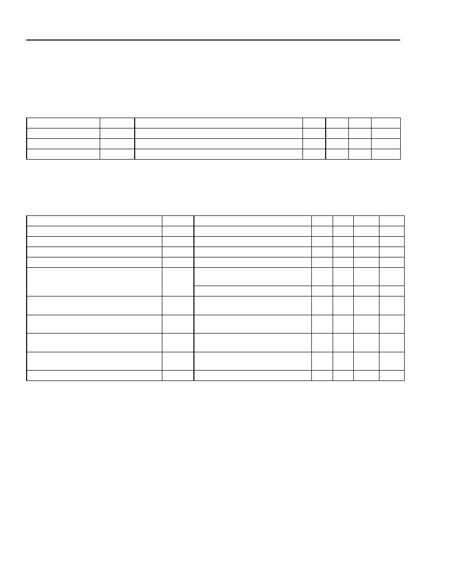
Analog Interface
The analog input section (Figure 3) includes an on-chip
buffer op amp and internal gain. Feedback paths (Z
T
and HYBAL in Figure 1) are included in the T7507 to
generate signals needed for termination impedance
and hybrid balance.
When matched with a SLIC with a transconductance
from tip/ring of 39.75 V/A and a differential gain to
tip/ring of 2 (such as the Lucent Technologies L8567),
and when a solid-state switch (such as the Lucent
L7583) and 50
of series protection are used, the
T7507 will synthesize a complex line termination
impedance and hybrid balance network of 200
+
680
|| 100 nF. Additionally, the T7507 will fix the
line circuit tip/ring to PCM transmit gain at 0 dB (at
1000 Hz, ≠0.7 dB, +0.3 dB) and will allow a user-select-
able (via the serial control input) PCM to tip/ring receive
gain of ≠3.5 dB or ≠7.0 dB (at 1000 Hz, ≠0.7 dB,
+0.3 dB). Thus, the ac interface between the T7507
and the L8567 SLIC consists of a single dc blocking
capacitor in the transmit direction, and a direct connec-
tion requiring no external components in the receive
direction. The T7507/L8567/L7583 chip set is designed
to meet all MPT requirements for the People's Republic
of China.
Transmission Levels
Zero transmission-level points are specified relative to
the digital milliwatt sequence prescribed by ITU-T rec-
ommendation G.711. Under these conditions, an ana-
log input of 0.0452 Vrms applied to VF
X
IN produces a
0 dBm digital code, while a 0 dBm code input at D
R
produces an output of 0.394 Vrms differentially at
VF
R
ON/VF
R
OP when using the ≠7.0 dB gain mode
(data bit D4 = 0).
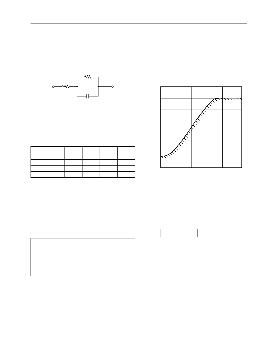
5-4821(F)
Figure 3. Typical Analog Input Section
Microprocessor Serial Data Control and
L8567 SLIC/L7583 Switch (or EMR) Control
Interfaces
The basic logic control scheme is a serial data interface
between the microcontroller and the T7507. Through
this interface, an 8-bit input control word and an 8-bit
output status word is passed between the T7507 and
microcontroller. The input control word contains infor-
mation for the T7507, L8567 SLIC, and L7583 switch.
The output status word contains off-hook and thermal
shutdown status information from the L8567 SLIC and
L7583 switch. See the Input Word Definition and Out-
put Word Definition sections of this data sheet for spe-
cific details on the input and output words.
Control and status information are passed between the
T7507 and L8567 SLIC/L7583 switch via a latched par-
allel data interface. Data latches are integrated into the
L8567 SLIC inputs and outputs and L7583 switch
inputs. Thus, a given data I/O on the T7507 serves the
corresponding data I/O on the L8567 SLIC for the four
channels associated with the quad T7507. Additionally,
a given data output on the T7507 serves the corre-
sponding data inputs on the L7583 switch for the four
channels associated with the quad T7507. Status infor-
mation from the L7583 switch is passed to the T7507
on a per-line basis.
The T7507 control interface consists of an 8-bit input
serial shift register, an 8-bit output serial shift register,
an 8-bit loop status input latch, logic to generate the
enable (EN) pulses required to control the SLIC and
switch data latches, interface logic/buffers between the
DI shift register and the internal codec control, and
interface logic buffers between the SLIC/switch output
control leads.
SLIC
26 dB
TO
CODEC
FILTERS
T7507
C
1
0.07
µ
F
VF
X
IN
R
100 k
V
CM
= 2.4 V

Lucent Technologies Inc.
9
Data Sheet
August 1999
Termination Impedance, and Hybrid Balance
T7507 Quad PCM Codec with Filters,
Functional Description
(continued)
Microprocessor Serial Data Control and
L8567 SLIC/L7583 Switch (or EMR) Control
Interfaces
(continued)
The serial data interface has pins for data in (DI), data
out (DO), chip select (CSEL), and control clock
(CCLK). Data is read by the microcontroller from the
output shift register at the T7507 DO lead. The T7507
reads data from the microcontroller into the data input
shift register at the DI lead. The loop status latch stores
updated supervision information from the SLIC and
switch until it is transferred to the DO shift register.
On the falling edge of CSEL, the first bit of DO output
data becomes valid and ready for transmission in the
time specified by tCSLCCL. On the next falling CCLK
edge, the microprocessor will read the first bit of valid
data from the T7507 DO output. Also, on this first falling
CCLK edge, the T7507 will read the first bit of control
information on the DI input from the microcontroller.
Thus, upon the falling CSEL edge, the microcontroller
must have valid data ready at its data out lead in a time
specified by tCIVCCL.
On the next seven falling CCLK edges, the remaining
seven status bits are read by the microcontroller at the
T7507 DO lead and the remaining 7 control input bits
are read by the T7507 at the DI lead from the micro-
controller.
During the time tCCLCSH, which is the period after the
eight falling CCLK edges, the data at the DI register is
applied to the T7507 codec and made available to the
L8567 SLIC and L7583 switch input data latches. Data
is applied only if CSEL is low and has remained low on
the eighth negative edge of CCLK.
Upon the falling edge of CSEL, DO data is passed from
the loop status latch to the DO shift register. During the
period when CSEL is low, DO status data will not be
passed from the loop status latch to the DO shift regis-
ter. Consecutive read/write periods are not allowed.
CSEL must remain high for a specified time, tCSHCSL,
before CSEL can transition low again.
During CSEL low interval, the T7507 generates an EN
pulse low for one of the four channels served by the
particular T7507. These EN pulses are generated
sequentially. Thus, if EN0 is generated on a given
CSEL low, EN1 will be generated during the next CSEL
low, etc. Only one of the four EN outputs associated
with a given T7507 codec will be low during a given
CSEL interval.
Enable Transfers when CCLK Is Bursted with
CSEL
When EN is low, status information from the SLIC and
switch is updated in the T7507 8-bit loop status latch.
This data will be transferred into the data out shift regis-
ter and shifted out to the microcontroller on the next
CSEL cycle. Thus, to make a write from the L8567
SLIC or L7583 switch, it takes two CSEL cycles: the
first to create an EN pulse for a given channel and to
shift updated status information to the 8-bit status latch,
and the second CSEL cycle to shift the updated chan-
nel information to the microcontroller. Each time the
CSEL goes low and status information is shifted to the
microcontroller, only one of the four channels has new
status data; the other channels are shifting out status
data that has previously been presented to the micro-
controller. Thus, it takes five CSEL cycles to a T7507
device to ensure that supervision data for each of the
four channels associated with the T7507 device has
been updated.
When EN goes low, updated control information is also
fed to the SLIC and switch from the T7507. Since EN
for each channel is generated sequentially during suc-
cessive CSEL, four CSELs to a given T7507 device are
required to ensure that updated control information is
given to each of the four channels.
Note that to apply ringing, before the ring relay is acti-
vated to apply power ringing to the subscriber loop, the
L8567 SLIC must first be changed from the low-power
scan mode to the active mode. This is because the ring
trip detector is not active when the L8567 SLIC is in the
low-power scan mode. Thus, application of ringing to a
given channel may require as many as eight CSEL
cycles to the T7507 associated with the channel.
Enable Transfers when CCLK Is Not
Restricted to CSEL Low
The T7507 will continue to generate EN pulses
sequentially, free-running with CCLK falling edges,
when CSEL is not applied low. Thus, if there are long
periods of time when CSEL low is not presented to a
given T7507 device, enable pulse low will be generated
sequentially during this time. This feature allows for the
most recent SLIC and switch status information to be
maintained in the 8-bit loop status latch during long
periods of time when CSEL to a given T7507 device is
maintained high.

10
10
Lucent Technologies Inc.
Data Sheet
August 1999
Termination Impedance, and Hybrid Balance
T7507 Quad PCM Codec with Filters,
Functional Description
(continued)
Enable Transfers when CCLK Is Not
Restricted to CSEL Low
(continued)
If CSEL drops low, during the time an EN for a given
channel is low, the write cycle to/from the codec will be
aborted. However, the EN pulse that will be generated
during the eight CCLK cycles that CSEL is low will be
for the channel whose EN pulse was aborted by the
CSEL dropping low. Thus, for example, if EN2 is low
and during the time EN2 is low CSEL is also low, EN2
will immediately go high and any associated write is
aborted. Then the EN that is generated because CSEL
is low is for channel 2.
The T7507 generates the required enable control sig-
nals for the L8567 input data latches, the output data
latches, and the L7583 input data latch. A logic low on
the L8567 or L7583 latch enable input allows data to
flow through the latch. A logic high on the latch enable
of the L8567 or L7583 latches the latch. The latch
enable is output on a per-line basis from the EN0c,
EN1c, EN2c, and EN3c outputs of the T7507. The
L8567 SLIC and L7583 latches are level sensitive, so
when ENx is low, the data from the SLIC and switch
latch flows directly to the T7507 loop status latch. After
a high-to-low CSEL transition, on the next falling edge
of CCLK, data is transferred from the loop status latch
to the serial shift register. Therefore, it is not desirable
to update the loop status register on this CCLK edge.
For this reason, EN pulses are generated during the
rising edge of CCLK.
Note that loop status information from the four chan-
nels is accepted on a multiplexed basis at the NSTATc
input of the T7507. This information is decoded by the
T7507 and placed at the appropriate bit in the 8-bit out-
put word. NSTAT is a wired-OR of the loop closure and
ring trip status from the L8567 SLIC.
Thermal shutdown information from the four SLICs is
accepted on a multiplexed basis at the NTSDc input of
the T7507. Thermal shutdown information from the
L7583 switch is accepted on a per-line basis from the
four L7583s associated with the quad T7507. The ther-
mal shutdown information from the SLICs is decoded
by the T7507 and then ANDed with the thermal shut-
down information from the corresponding L7583. This
thermal shutdown information for the SLIC and switch
is then placed at the appropriate bit in the 8-bit output
word.
The control word contains control information for the
T7507, L8567 SLIC, and L7583 switch. Thus, the con-
trol bits for the L8567 SLIC and L7583 switch need to
be transferred via the latched parallel control interface.
SLIC control information for the four channels is trans-
ferred on a multiplexed basis through the B0c and B1c
output leads on the T7507. L7583 control information
(or L8567 relay driver information) is transferred on a
multiplexed basis through the RD1c, RD2c, and RD3c
output leads.
Three features for the T7507 can be programmed via
the serial data interface. The channel receive gain and
codec powerup or powerdown are set on a per-channel
basis. Delayed and nondelayed timing mode is set glo-
bally; all four channels are set to the same mode via
the serial data bus. Additionally, PCM time-slot assign-
ment is set via the serial data input bus.
The L8567 B0, B1 state control inputs are latched data
inputs. Control data is sent to these inputs via the B0c
and B1c outputs of the T7507. The B0c and B1c out-
puts of the T7507 are meant to control the four SLICs
associated with the quad T7507.
Switch control information is sent to the IN
RING
,
IN
TESTin
, or IN
TESTin
logic control inputs of the L7583
switch, or to the RD1I, RD2I, and RD3I relay driver con-
trol inputs of the L8567 SLIC (if EMRS are used) via
the RD1c, RD2c, and RD3c T7507 parallel data control
outputs. Again, the L7583 state control inputs and the
L8567 relay driver control inputs are latched, so control
information from the RD1c, RD2c, and RD3c T7507
control outputs are meant to control four lines.
The L8567 SLIC outputs loop status information via the
latched NSTAT output. NSTAT is a wired-OR or the out-
puts of the L8567 SLIC's loop closure detector and ring
trip detector. The loop status information is input to the
T7507 via the NSTATc input. Since the L8567 SLIC
NSTAT bit is latched, the SLIC output from the four
channels associated with the T7507 are accepted at
NSTATc.
The L8567 SLIC also outputs a thermal shutdown flag
via the latched NTSD output. This thermal shutdown
information is input to the T7507 via the NTSDc input.
Since the L8567 SLIC NSTAT and NTSD bits are
latched, the SLIC output from the four channels associ-
ated with the T7507 are accepted at NSTATc and
NTSD, respectively.
The L7583 also outputs thermal shutdown status via
the TSD output. The TSD output on the L7583 is not
latched, so the TSD information is input to the T7507
for the four channels associated with the quad T7507
on a per-line basis via the NTSD0, NTSD1, NTSD2,
and NTSD3 T7507 inputs.
The multiplexed thermal shutdown information from the
four L8567 SLICs and the per-line thermal shutdown
information from the four L7583 switches are manipu-
lated by the T7507 into a per-channel thermal shut-
down bit and output on the serial data output DO pin.
Lucent Technologies Inc.
11
Data Sheet
August 1999
Termination Impedance, and Hybrid Balance
T7507 Quad PCM Codec with Filters,
Functional Description
(continued)
Enable Transfers when CCLK Is Not Restricted to CSEL Low
(continued)
It is recommended that a polling process be used during idle periods to ensure that a loop closure detection is rec-
ognized by the microcontroller. The maximum nominal control clock (CCLK) frequency is 2.048 MHz. Also note
that DO is 3-stated based on the state of CSEL. This allows multiple DO outputs from multiple T7507s to be tied to
a common DO bus.
Table 2. Microprocessor Interface Descriptions
Symbol
Description
CCLK
May be gapped; Maximum frequency is 2.048 MHz.
EN
pulses are generated on rising CCLK edges.
CSEL
A low-going
CSEL
initiates a write to the T7507 via the DI pin. At the same time, this initiates a read
from the T7507 on the DO pin. Data is written and read on the first eight CCLK negative transitions
after CSEL goes low. Data is applied to the T7507 operation only if CSEL is low on the eighth nega-
tive edge of CCLK. Consecutive writes are not allowed; CSEL must go high for a minimum 50 ns
between write cycles. Additionally, data is shifted from the loop status latch to the serial shift register
on the first falling CCLK pulse after CSEL goes low.
DI
Pin for serial input data. Input data is an 8-bit word which sends control information from the micro-
controller to the T7507, L8567 SLIC, and L7583 switch. T7507 information is codec state information
and PCM time-slot assignment. L8567 and L7583 control information is passed to these components
via parallel control output pins. See Input Word Definition section for additional details.
DO
Pin for serial data output. Output data is an 8-bit word which sends status information from T7507 par-
allel status inputs to the microcontroller via the serial data interface. Status information is received
from the T7507 via the parallel control inputs from the L8567 SLIC and L7583 switch. See Output
Word Definition section for additional details.

12
Lucent Technologies Inc.
Data Sheet
August 1999
Termination Impedance, and Hybrid Balance
T7507 Quad PCM Codec with Filters,
Functional Description
(continued)
Input Word Definition
The control data input on DI is an 8-bit word of the format:
C1 C0 M D4 D3 D2 D1 D0
Bits C0 and C1 are the channel select bits. Bit M is a mode control bit. Bits D0, D1, D2, and D3 are data bits. Bit D4
can be either a mode control bit or a data bit. If M is set to 0, the data word is set to the PCM time-slot assignment
mode and bit D4 is a data bit. If M is set to 1, then D4 is also a mode set bit. If M, D4 = 1, 0, then the data word rep-
resents the relay/switch control delayed/nondelayed timing mode. If M, D4 = 1, 1 then the data word represents the
codec/SLIC control mode.
* Delayed/nondelayed PCM timing is a global parameter--all channels are programmed to the most recent value. To program PCM timing, use
C0 = C1 = 0. (That is channel 0.) M = 1, D4 = 0. When programming C1, C0 = 01, M = 1, D4 = 0, then D3 must be programmed to 0. When C1,
C0 = 10, 11, M = 1, D4 = 0, then D3 is ignored.
Note: Do not assign two channels to the same time slot. If two channels are assigned to the same time slot, the result is indeterminate. It is rec-
ommended that time-slot assignment should only be done when the channel is powered down. If multiple chips are tied to the same D
X
bus, this can result in bus contention. Thus, reassignment of time slots should be done before the channel is powered up. For all codecs,
upon powerup, channel 0 will be assigned to time slot 0, channel 1 will be assigned to time slot 1, channel 2 will be assigned to time slot
2, and channel 3 will be assigned to time slot 3.
Table 3. C0, C1 Channel Select
C1
C0
Channel
0
0
0
0
1
1
1
0
2
1
1
3
Table 4. M, D4, D3, D2, D1, D0 Mode Select and Data
M
D4
D3
D2
D1
D0
0
Time-Slot
Assignment
Time-Slot
Assignment
Time-Slot
Assignment
Time-Slot
Assignment
Time-Slot
Assignment
1
0
Delayed/Nondelayed
PCM Timing Mode or
Reserved*
Relay State
Control Information
3
Relay State
Control Information
2
Relay State
Control Information 1
1
1
T7507 Per Channel
Powerup/Powerdown
Channel Receive
Gain
B1 SLIC Control Bit
B0 SLIC Control Bit
Table 5. M = 0 Mode (PCM Time-Slot Assignment)
D4
D3
D2
D1
D0
Function
0
0
0
0
0
Time Slot 0
0
0
0
0
1
Time Slot 1
.
.
.
1
1
1
1
1
Time Slot 31

Lucent Technologies Inc.
13
Data Sheet
August 1999
Termination Impedance, and Hybrid Balance
T7507 Quad PCM Codec with Filters,
Functional Description
(continued)
Input Word Definition
(continued)
Table 6. M = 1, D4 = 0 Mode (Relay State Control and Delayed/Nondelayed Timing)
* Delayed or nondelayed timing is a global parameter. All channels will use the most recently programmed value.
Note: Upon powerup, D3 = D2 = D1 = D0 = 0; that is, delayed timing mode and all relay drivers in the not active state, or 0, 0, 0, are applied to
L7583 solid-state relay, which is the idle/talk state.
Table 7. M = 1, D4 = 1 Mode (Codec State Control and SLIC State Control)
* Receive gain of ≠3.5 and ≠7.0 will be achieved in a 200
+ 680
|| 0.1 µF termination, when using the T7507 with the L8567 SLIC, L7583
switch, and 50
protection resistors.
D3
D2
D1
D0
Function
0
X
X
X
Delayed timing mode (see Figure 12)*. With C0 = C1 = 00, bit D3 set PCM delayed or non-
delayed timing. With C0, C1 = 01, 10, 11, bit D3 is ignored.
1
X
X
X
Nondelayed timing mode (see Figure 13)*. With C0 = C1 = 00, bit D3 set PCM delayed or
nondelayed timing. With C0, C1 = 01, 10, 11, bit D3 is ignored.
X
0
X
X
T7507 driver output RD3c at logic low. If T7507 driver output RD3c is applied to the L8567
SLIC RD3I input, this will place the relay driver output on the L8567, RD3O, into the relay
not active state. If T7507 output RD3c is used to drive the logic inputs of an L7583 solid-
state switch, a logic 0 is applied.
X
1
X
X
T7507 driver output RD3c at logic high. If T7507 driver output RD3c is applied to the L8567
SLIC RD3I input, this will place the relay driver output on the L8567, RD3O, into the relay
active state. If T7507 output RD3c is used to drive the logic inputs of an L7583 solid-state
switch, a logic 1 is applied.
X
X
0
X
T7507 driver output RD2c at logic low. If T7507 driver output RD2c is applied to the L8567
SLIC RD3I input, this will place the relay driver output on the L8567, RD2O, into the relay
not active state. If T7507 output RD2c is used to drive the logic inputs of an L7583 solid-
state switch, a logic 0 is applied.
X
X
1
X
T7507 driver output RD2c at logic high. If T7507 driver output RD2c is applied to the L8567
SLIC RD3I input, this will place the relay driver output on the L8567, RD2O, into the relay
active state. If T7507 output RD2c is used to drive the logic inputs of an L7583 solid-state
switch, a logic 1 is applied.
X
X
X
0
T7507 driver output RD1c at logic low. If T7507 driver output RD1c is applied to the L8567
SLIC RD3I input, this will place the relay driver output on the L8567, RD1O, into the relay
not active state. If T7507 output RD1c is used to drive the logic inputs of an L7583 solid-
state switch, a logic 0 is applied.
X
X
X
1
T7507 driver output RD1c at logic high. If T7507 driver output RD1c is applied to the L8567
SLIC RD3I input, this will place the relay driver output on the L8567, RD1O, into the relay
active state. If T7507 output RD1c is used to drive the logic inputs of an L7583 solid-state
switch, a logic 1 is applied.
D3
D2
D1
D0
Function
0
X
X
X
T7507 Channel Standby
1
X
X
X
T7507 Channel Powerup
X
0
X
X
Channel Receive Gain ≠3.5 dB*
X
1
X
X
Channel Receive Gain ≠7.0 dB*
X
X
1
1
L8567 SLIC Powerup, Forward Battery
X
X
0
1
L8567 SLIC Powerup, Reverse Battery
X
X
1
0
L8567 SLIC Low-Power Scan
X
X
0
0
L8567 Disconnect

14
14
Lucent Technologies Inc.
Data Sheet
August 1999
Termination Impedance, and Hybrid Balance
T7507 Quad PCM Codec with Filters,
Functional Description
(continued)
Output Word Definition
The status data input on D0 is an 8-bit word of the for-
mat:
NSTAT-Ch0, NTSD-Ch0, NSTAT-Ch1, NTSD-Ch1,
NSTAT-Ch2, NTSD-Ch2, NSTAT-Ch3, NTSD-Ch3
Where:
NSTAT-Ch[0:3] is the wired-OR loop supervision
status of the off-hook detector and ring trip detector
from Channel [0:3].
NTSD-Ch[0:3] is the wire-ORed thermal shutdown
status of the L8567 SLIC and L7583 for Channel
[0:3].
Powerup
This section defines the state of the T7507 when power
is first applied to the device.
T7507
Upon initial application of power, the T7507 is in the
full-chip powerdown state and delayed timing mode.
Output Word
With the initial CSEL, after application of power, all
eight bits of the output word are undefined. With subse-
quent CSEL, all eight bits of the output word will be set
to zero. The output word will remain all 0s until applica-
tion of EN pulses to update the output status informa-
tion. An output word of all 0s implies that all four
channels are in thermal shutdown state and are off-
hook.
EN Status
Upon application of power, all four EN channels will be
at logic 1 (which means that no control data is trans-
ferred to, and no status information is received from,
the SLIC or switch). All EN will remain at logic 1 until
application of an initial FSEP pulse, at which time EN is
created as defined in the Microprocessor Interface sec-
tion of this data sheet.
Input Word--PCM Interface
Upon application of power, the PCM time-slot assign-
ment defaults to the following time-slot assignment:
CH0 Time Slot 0
CH1 Time Slot 1
CH2 Time Slot 2
Ch3 Time Slot 3
Input Word--Relay Control/Timing
Upon application of power, all relay driver control inputs
are forced to logic 0. If the relay driver outputs are tied
to the L8567 relay driver inputs, upon application of an
EN signal, the relay drivers are forced into the off state.
If applied to the L7583 control input, upon application
of an EN pulse, the L7583B is forced into the idle/talk
state.
Input Word--Control Mode
Upon application of power, the receive gain is ≠3.5 dB
and with the B0/B1 control outputs set to 0/0. Note that
B0/B1 = 0/0, the L8567 SLIC is set into the disconnect
state upon application of EN pulse.
State Definitions
Powerup
All circuits are active. All channels are ready for trans-
mission. EN pulses are generated free-running with
CCLK.
Standby
This mode is programmed on a per-channel basis via
the microprocessor control interface. In this mode, indi-
vidual channels are powered down (not ready for trans-
mission). All reference circuits are always powered up.
EN pulses are generated free-running with CCLK. Ana-
log outputs are held at a nominal 2.35 V.
Full-Chip Powerdown
This is a global parameter; that is, all channels are glo-
bally set into this mode. In this mode, all channels and
all reference circuits are powered down. EN is forced to
logic high. The T7507 is in this state upon application
of power. The T7507 enters this state if FSEP is
removed for four 8 kHz frames. The T7507 will remain
in this state until reapplication of FSEP.
Lucent Technologies Inc.
15
Data Sheet
August 1999
Termination Impedance, and Hybrid Balance
T7507 Quad PCM Codec with Filters,
Absolute Maximum Ratings
Stresses in excess of the absolute maximum ratings can cause permanent damage to the device. These are
absolute stress ratings only. Functional operation of the device is not implied at these or any other conditions in
excess of those given in the operational sections of this data sheet. Exposure to absolute maximum ratings for
extended periods can adversely affect device reliability.
Handling Precautions
Although protection circuitry has been designed into this device, proper precautions should be taken to avoid expo-
sure to electrostatic discharge (ESD) during handling and mounting. Lucent employs a human-body model (HBM)
and a charged-device model (CDM) for ESD-susceptibility testing and protection design evaluation. ESD voltage
thresholds are dependent on the circuit parameters used to define the model. No industry-wide standard has been
adopted for CDM. However, a standard HBM (resistance = 1500
, capacitance = 100 pF) is widely used and
therefore can be used for comparison purposes. The HBM ESD threshold presented here was obtained by using
these circuit parameters:
Electrical Characteristics
Specifications apply for T
A
= ≠40 ∞C to +85 ∞C, V
DD
= 5 V ± 5%, MCLK = 2.048 MHz, and GND = 0 V, unless other-
wise noted.
dc Characteristics
Table 8. Digital Interface
Parameter
Symbol
Min
Max
Unit
Storage Temperature Range
T
stg
≠55
150
∞C
Power Supply Voltage
V
DD
--
6.5
V
Voltage on Any Pin with Respect to Ground
--
≠0.5
0.5 + V
DD
V
Maximum Power Dissipation (package limit)
P
D
--
600
mW
HBM ESD Threshold Voltage
Device
Rating
T7507
>2000 V
Parameter
Symbol
Test Conditions
Min
Typ
Max
Unit
Input Low Voltage
V
IL
All digital inputs
--
--
0.8
V
Input High Voltage
V
IH
All digital inputs
2.0
--
--
V
Input Current
I
I
Any digital input GND < V
IN
< V
DD
≠10
--
10
µA
Input Current, Pins with Pull-up (
CSEL
)
I
I
Any digital input GND < V
IN
< V
DD
2
--
150
µA
Input Current, Pins with Pull-down
(FSEP, IFS)
I
I
Any digital input GND < V
IN
< V
DD
≠2
--
≠150
µA
Output Low Voltage
V
OL
DxEN
, D
X
= 3.2 mA
--
--
0.4
V
Output High Voltage
V
OH
D
X
= ≠3.2 mA
2.4
--
--
V
D
X
= ≠320 µA
3.5
--
--
V
Output Current in High-impedance State
I
OZ
DxEN
, D
X
≠30
--
30
µA
Input Capacitance
C
I
--
--
--
5
pF
16
Lucent Technologies Inc.
Data Sheet
August 1999
Termination Impedance, and Hybrid Balance
T7507 Quad PCM Codec with Filters,
Electrical Characteristics
(continued)
dc Characteristics
(continued)
Table 9. Power Dissipation
Power measurements are made with outputs unloaded.
* A nominal 6 mA decrease in current per channel put into standby.
Transmission Characteristics
Table 10. Analog Interface
Parameter
Symbol
Test Conditions
Min
Typ
Max
Unit
Powerdown Current
I
DDO
MCLK present; FSEP = 0.4 V
--
0.4
1
mA
Powerup Current*
I
DD1
MCLK, FSEP present; all channels powered up
--
33
40
mA
Standby Current
I
DDS
MCLK, FSEP present; all channels powered down
--
7
10
mA
Parameter
Symbol
Test Conditions
Min
Typ
Max
Unit
Input Resistance, VF
X
IN
R
VF
X
I
1 V < |VFxI| < 4 V
100
--
300
k
Input Voltage, VF
X
IN
V
IX
Relative to ground
2.25 2.35
2.5
V
Load Resistance, VF
R
ON to VF
R
OP
RL
VF
R
O
Differential load
2
--
--
k
Load Capacitance, VF
R
ON to VF
R
OP
CL
VF
R
O
--
--
--
100
pF
Output Resistance, VF
R
O
RO
VF
R
O
0 dBm0, 1020 Hz PCM code
applied to D
R
--
2
20
Channel under test in powerdown 3000
--
10000
dc Output Voltage, VF
R
OP, VF
R
ON
V
OR
Alternating ±0 A-law PCM
code applied to D
R
2.20 2.35
2.5
V
dc Output Voltage, VF
R
OP, VF
R
ON
Standby
VO
RPD
FSEP = active, no load, channel
under test in powerdown
2.15 2.35
2.65
V
Differential dc Output
VF
R
OP ≠ VF
R
ON
V
OR
Alternating ±0 A-law PCM code
applied to D
R
≠60
--
60
mV
Output Leakage Current, VF
R
OP,
VF
R
ON Powerdown
IO
VF
R
O
FSEP = 0.4 V
≠30
--
30
µA
Output Voltage Swing, VF
R
OP ≠ VF
R
ON
V
SWR
RL = 2 k
(differential)
2.6
--
--
Vp-p
Lucent Technologies Inc.
17
Data Sheet
August 1999
Termination Impedance, and Hybrid Balance
T7507 Quad PCM Codec with Filters,
Transmission Characteristics
(continued)
ac Transmission Characteristics
Unless otherwise noted, the analog input is a ≠26 dBm (at 813
), 1020 Hz sine wave. The digital input is a PCM
bit stream equivalent to that obtained by passing a 0 dBm0, 1020 Hz sine wave through an ideal encoder. The out-
put level is sin(x)/x-corrected.
Table 11. Absolute Gain
* Combination test results are translated into system-level characteristics guaranteed by Table 21, Figure 8, and Figure 9.
Overall system-level tolerances are +0.3 dB to ≠0.7 dB in both directions. Therefore, nominal analog levels are shifted by ≠0.2 dB.
Parameter
Symbol
Test Conditions
Min*
Typ
Max*
Unit
Encoder Milliwatt
Response (transmit gain
tolerance)
EmW
Signal input of 0.0452 Vrms
(≠26 dBm at 813
at 1020 Hz)
--
≠0.20
--
dBm0
Decoder Milliwatt
Response (receive gain
tolerance)
DmW
Measured differential relative to
0.902 Vrms,
PCM input of 0 dBm0 1020 Hz
RL = 10 k
, receive gain in ≠7.0 dB mode
--
≠7.20
--
dBm0
Relative Gain Variation
Referenced to DmW
RGR
Decoder gain = ≠3.5 dB mode
--
3.5
--
dB
Table 12. Gain Tracking
Parameter
Symbol
Test Conditions
Min
Typ
Max
Unit
Transmit Gain Tracking Error
Sinusoidal Input A-law
GT
X
+3 dBm0 to ≠37 dBm0
≠37 dBm0 to ≠50 dBm0
≠0.25
≠0.50
--
--
0.25
0.50
dB
dB
Receive Gain Tracking Error
Sinusoidal Input A-law
GT
R
+3 dBm0 to ≠37 dBm0
≠37 dBm0 to ≠50 dBm0
≠0.25
≠0.50
--
--
0.25
0.50
dB
dB
Table 13. Distortion
Parameter
Symbol
Test Conditions
Min
Typ
Max
Unit
Transmit Signal to Distortion
SD
X
3 dBm0
VF
X
I
≠30 dBm0
35
--
--
dB
≠30 dBm0
VF
X
I
≠40 dBm0
29
--
--
dB
≠40 dBm0
VFxI
≠45 dBm0
25
--
--
dB
Receive Signal to Distortion
SD
R
3 dBm0
VF
R
O
≠30 dBm0
35
--
--
dB
≠30 dBm0
VF
R
O
≠40 dBm0
29
--
--
dB
≠40 dBm0
VF
R
O
≠45 dBm0
25
--
--
dB
Single-frequency Distortion,
Transmit
SFD
X
200 Hz--3400 Hz, 0 dBm0 input,
output any other single
frequency
3400 Hz
--
--
≠38
dBm0
Single-frequency Distortion,
Receive
SFD
R
200 Hz--3400 Hz, 0 dBm0 input,
output any other single
frequency
3400 Hz
--
--
≠40
dBm0
Intermodulation Distortion
IMD
Transmit or receive, two frequencies
in the range (300 Hz--3400 Hz)
at ≠6 dBm0
--
--
≠42
dBm0

18
Lucent Technologies Inc.
Data Sheet
August 1999
Termination Impedance, and Hybrid Balance
T7507 Quad PCM Codec with Filters,
Transmission Characteristics
(continued)
ac Transmission Characteristics
(continued)
Table 14. Envelope Delay Distortion
* Varies as a function of time slots chosen.
Overload Compression
Figure 4 shows the region of operation for encoder signal levels above the reference input power (0 dBm0).
5-3586(F)
Figure 4. Overload Compression
Parameter
Symbol
Test Conditions
Min
Typ
Max
Unit
T
X
Delay, Absolute*
D
XA
f = 1600 Hz
--
--
165 to 425
µs
T
X
Delay, Relative to 1600 Hz
D
XR
f = 500 Hz--600 Hz
f = 600 Hz--800 Hz
f = 800 Hz--1000 Hz
f = 1000 Hz--1600 Hz
f = 1600 Hz--2600 Hz
f = 2600 Hz--2800 Hz
f = 2800 Hz--3000 Hz
--
--
--
--
--
--
--
--
--
--
--
--
--
--
220
145
75
40
75
105
155
µs
µs
µs
µs
µs
µs
µs
R
X
Delay, Absolute*
D
RA
f = 1600 Hz
135
--
135 to 395
µs
R
X
Delay, Relative to 1600 Hz
D
RR
f = 500 Hz--1000 Hz
f = 1000 Hz--1600 Hz
f = 1600 Hz--2600 Hz
f = 2600 Hz--2800 Hz
f = 2800 Hz--3000 Hz
≠44
≠30
--
--
--
--
--
--
--
--
--
--
90
125
175
µs
µs
µs
µs
µs
Round Trip Delay, Absolute*
D
RTA
Any time slot/channel to
any time slot/channel
f = 1600 Hz
--
--
305 to 625
µs
1
2
3
4
5
6
7
8
9
1
2
3
4
5
6
7
8
9
ACCEPTABLE
REGION
FUNDAMENTAL INPUT POWER (dBm)
FUND
AM
EN
T
A
L
O
U
T
P
UT PO
W
E
R (
d
Bm)
Lucent Technologies Inc.
19
Data Sheet
August 1999
Termination Impedance, and Hybrid Balance
T7507 Quad PCM Codec with Filters,
Transmission Characteristics
(continued)
ac Transmission Characteristics
(continued)
Table 15. Decoder Limits Relative to Gain at 1020 Hz
Table 16. Encoder Limits, Includes Effect of Termination Impedance Filter Relative to Gain at 1020 Hz
Table 17. Termination Impedance Limits Relative to Gain at 1020 Hz
Table 18. Hybrid Path Limits Relative to Gain at 1020 Hz
Frequency (Hz)
Min
Typ
Max
Unit
15.6
≠0.150
--
0.150
dB
46.8
≠0.150
--
0.150
dB
62.5
≠0.150
--
0.150
dB
453
≠0.150
--
0.150
dB
2734
≠0.150
--
0.150
dB
3140
≠0.550
--
0.150
dB
3375
≠0.850
--
0.150
dB
3984
--
--
≠13.40
dB
5015
--
--
≠28.00
dB
Frequency (Hz)
Min
Typ
Max
Unit
15.6
--
--
≠30.500
dB
46.8
--
--
≠25.600
dB
62.5
--
--
≠29.400
dB
453
0.400
--
0.700
dB
2734
≠2.950
--
≠2.650
dB
3140
≠3.950
--
≠3.250
dB
3375
≠4.550
--
≠3.850
dB
3984
--
--
≠18.30
dB
5015
--
--
≠35.00
dB
Frequency (Hz)
Min
Typ
Max
Unit
46.8
0
--
1
dB
62.5
0.3
--
0.8
dB
453
0.45
--
0.65
dB
2734
≠2.95
--
≠2.65
dB
3140
≠3.60
--
≠3.20
dB
3375
≠4.05
--
≠3.55
dB
3984
≠5.05
--
≠4.45
dB
5015
≠6.35
--
≠5.65
dB
Frequency (Hz)
Min
Typ
Max
Unit
46.8
--
--
≠26.000
dB
62.5
--
--
≠30.000
dB
453
≠0.180
--
0.180
dB
2734
≠0.410
--
≠0.050
dB
3140
≠0.700
--
0.100
dB
3375
≠1.640
--
≠0.840
dB
3984
--
--
≠25.00
dB
20
Lucent Technologies Inc.
Data Sheet
August 1999
Termination Impedance, and Hybrid Balance
T7507 Quad PCM Codec with Filters,
Transmission Characteristics
(continued)
ac Transmission Characteristics
(continued)
Table 19. Noise
Table 20. Interchannel Crosstalk (Between Channels)
Note: For interchannel, crosstalk into the transmit channels (VFxIN) can be significantly affected by parasitic capacitive feeds from VF
R
O out-
puts. PWB layouts should be arranged to keep these parasitics low. The equivalent resistor looking from VFxIN toward VITR (Figure 16)
should be kept as low as possible to minimize crosstalk. A maximum of 7 k
at 3 kHz is recommended. This is easily achievable in this
design with the structure as shown in Figure 16.
Parameter
Symbol
Test Conditions
Min
Typ
Max
Unit
Transmit Noise
N
XP
--
--
--
≠68
dBm0p
Receive Noise
N
RP
PCM code is A-law positive one
--
--
≠75
dBm0p
Noise, Single Frequency
f = 0 kHz--100 kHz
N
RS
VF
X
IN = 0 Vrms, measurement at
VF
R
O, D
R
= D
X
--
--
≠53
dBm0
Power Supply Rejection Transmit
PSR
X
V
DD
= 5.0 Vdc + 100 mVrms:
f = 0 kHz--4 kHz
f = 4 kHz--50 kHz
36
30
--
--
--
--
dB
dB
Power Supply Rejection Receive
PSR
X
PCM code is positive one LSB.
V
DD
= 5.0 Vdc + 100 mVrms:
f = 0 kHz--4 kHz
f = 4 kHz--25 kHz
f = 25 kHz--50 kHz
36
40
30
--
--
--
--
--
--
dB
dB
dB
Spurious Out-of-band Signals at
VF
R
O Relative to Input
SOS
0 dBm0, 300 Hz--3400 Hz input
PCM code applied:
4600 Hz--7600 Hz
7600 Hz--8400 Hz
8400 Hz--50 kHz
--
--
--
--
--
--
≠30
≠40
≠30
dB
dB
dB
Parameter
Symbol
Test Conditions
Min
Typ
Max
Unit
Transmit to Receive
Crosstalk 0 dBm0
Transmit Levels
CT
XX-RY
f = 300 Hz--3400 Hz
idle PCM code for channel under test;
0 dBm0 into any other single-channel VF
X
IN
--
≠90
≠75
dB
Receive to Transmit
Crosstalk 0 dBm0
Receive Levels
CT
RX-XY
f = 300 Hz--3400 Hz
VF
X
IN = 0 Vrms for channel under test;
0 dBm0 code level on any other single-channel D
R
--
≠90
≠75
dB
Transmit to Trans-
mit Crosstalk
0 dBm0 Transmit
Levels
CT
XX-XY
f = 300 Hz--3400 Hz
0 dBm0 applied to any single-channel
VF
X
IN except channel under test,
which has VF
X
IN = 0 Vrms
--
≠90
≠75
dB
Receive to Receive
Crosstalk 0 dBm0
Receive Levels
CT
RX-RY
f = 300 Hz--3400 Hz
0 dBm0 code level on any single-channel D
R
except
channel under test, which has idle code applied
--
≠90
≠75
dB
Lucent Technologies Inc. 21
Data Sheet
August 1999
Termination Impedance, and Hybrid Balance
T7507 Quad PCM Codec with Filters,
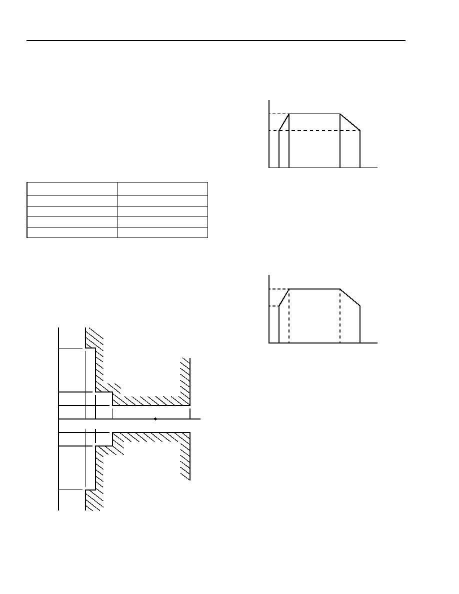
Chip Set Performance Specifications
When using the T7507, L8567 SLIC, L7583
solid-state switch, and 50
protection resistors, the
following line card requirements are achieved; specified
termination impedance is shown in Figure 5.
5-5324a(F)
Figure 5. Termination Impedance
Gain
Gain Flatness--In Band
Gain Flatness--Out of Band--High
Frequencies
The transmit and receive directions' frequency-depen-
dent loss relative to gain at 3400 Hz is shown below.
This specification is met by using the T7507, L8567
SLIC, L7583 solid-state switch, and 50
protection
resistors (200
+ 680
|| 0.1 µF termination).
5-5340(F)
Figure 6. Transmit and Receive Direction
Frequency-Dependent Loss Relative to
Gain at 3400 Hz
The loss for frequencies 3400 Hz < f < 4600 Hz is given
by:
b = 12.5
Table 21. Gain
Gain @
1020 Hz
Min Typ Max Unit
Transmit ≠0.7 0 0.3 dB
Receive ≠4.2 ≠3.5 ≠3.2 dB
Receive ≠7.7 ≠7.0 ≠6.7 dB
Table 22. Gain Flatness--In Band
The in-band frequency-dependent loss relative to
gain at frequency = 1020 Hz, for the transmit and
receive directions. This specification is met by using
the T7507, L8567 SLIC, L7583 solid-state switch, and
50
protection resistors (200
+ 680
|| 0.1 µF
termination).
Frequency (Hz) Min Max Unit
300--400 ≠0.3 1.00 dB
400--600 ≠0.3 0.75 dB
600--2400 ≠0.3 0.35 dB
2400--3000 ≠0.3 0.55 dB
3000--3400 ≠0.3 1.50 dB
680
0.1
µ
F
200
0
≠5
10
12.5
20
25
30
LO
SS
(dB
)
3400 4000 4600 5000
ACCEPTABLE
REGION
FREQUENCY (Hz)
1
4000 f
≠
(
)
1200
-----------------------------
sin
≠
dB
22
22
Lucent Technologies Inc.
Data Sheet
August 1999
Termination Impedance, and Hybrid Balance
T7507 Quad PCM Codec with Filters,
Chip Set Performance Specifications
(continued)
Gain Flatness--Out of Band--Low
Frequencies
Transmit direction only, loss relative to 1020 Hz. This
specification is met by using the T7507, L8567 SLIC,
L7583 solid-state switch, and 50
protection resistors
(200
+ 680
|| 0.1 µF termination).
Table 23. Gain Flatness--Out of Band--Low
Frequencies
Loss vs. Level Relative to Loss at ≠10 dBm
Input at 1020 Hz
This specification is met by using the T7507, L8567
SLIC, L7583 solid-state switch, and 50
protection
resistors (200
+ 680
|| 0.1 µF termination).
5-5341(F)
Figure 7. Loss vs. Level
Return Loss
The following template is achieved.
5-5325(F)
Figure 8. Return Loss
Hybrid Balance
The following template is achieved.
5-5326(F)
Figure 9. Hybrid Balance
Frequency (Hz)
Min Loss (dB)
16.67
30
40
26
50
30
60
30
+3 dBm0
≠10
≠40
≠50
≠55
1.6
0.6
0.3
0
≠0.3
≠0.6
≠1.6
LO
SS
(dB
)
18
RL (d
B)
14
300 500
2000
3400
FREQUENCY (Hz)
20
T
B
RL (
d
B)
16
300 500
2500
3400
FREQUENCY (Hz)

Lucent Technologies Inc.
23
Data Sheet
August 1999
Termination Impedance, and Hybrid Balance
T7507 Quad PCM Codec with Filters,
Microprocessor Interface
Table 24. T7507 Microprocessor Interface Timing
Frequency of CCLK = 2.048 MHz.
Symbol
Parameter
Test Conditions
Min
Max
Unit
tCCLCCH
Time of CCLK Low
--
160
--
ns
tCCHCCL
Time of CCLK High
--
160
--
ns
tCCHCCH
Period of CCLK
--
488
--
ns
tCCH1CCH2 Rise Time of CCLK
--
--
50
ns
tCCL1CCL2
Fall Time of CCLK
--
--
50
ns
tCSLCCL
CSEL
Low to CCLK Transition
Measured from first
CCLK low transition
50
--
ns
tCCLCSH
CCLK Low to
CSEL
High
Measured from eighth
CCLK low transition
30
--
ns
tCIVCCL
Setup Time, Data Input/Output Valid to CCLK Low
--
50
--
ns
tCCLCIX
Hold Time, CCLK Low to Data Input/Output Invalid
--
50
--
ns
tCSHCSL
Minimum Time Between Writes
--
50
--
ns
tSU1BO2
Setup Time for B0--B1 Data
--
488
--
ns
tSU2BO1
Setup Time for B0--B1 Data
--
488
--
ns
tSU1RD
Setup Time for RD1, RD2, RD3 Data
--
488
--
ns
tSU2RD
Setup Time for RD1, RD2, RD3 Data
--
488
--
ns
tENL
Enable Pulse Width
--
977
--
ns

24
Lucent Technologies Inc.
Data Sheet
August 1999
Termination Impedance, and Hybrid Balance
T7507 Quad PCM Codec with Filters,
Microprocessor Interface
(continued)
5-5808(F)
Figure 10. SLIC/Switch Interface Timing
5-4517.b(F)
Figure 11. Microprocessor Interface Write Timing
1465 ns AT CCLK
CCLK
EN
NSTAT/NTSD
tSU1BO2
tCCL1CCL2
RD1, RD2, RD3
CSEL
B0/B1
tENL
tCCH1CCH2
2.048 MHz
tSU1RD
tSU2BO1
tSU2RD
tCCHCCH
tCSHCSL
tCCLCSH
tCCL1CCL2
tCCHCCL
tCCLCCH
tCCH1CCH2
tCCLCIX
tCCLCIX
tCSLCCL
tCIVCCL
tCIVCCL
D0
D1
C1
D2
D3
D4
M
D0
M
NSTAT
CH0
NTSD
CH0
NSTAT
CH1
NTSD
CH1
NSTAT
CH2
NTSD
CH2
NTSD
CH3
NSTAT
CH3
NSTAT
CH0
CCLK
CSEL
DI
DO
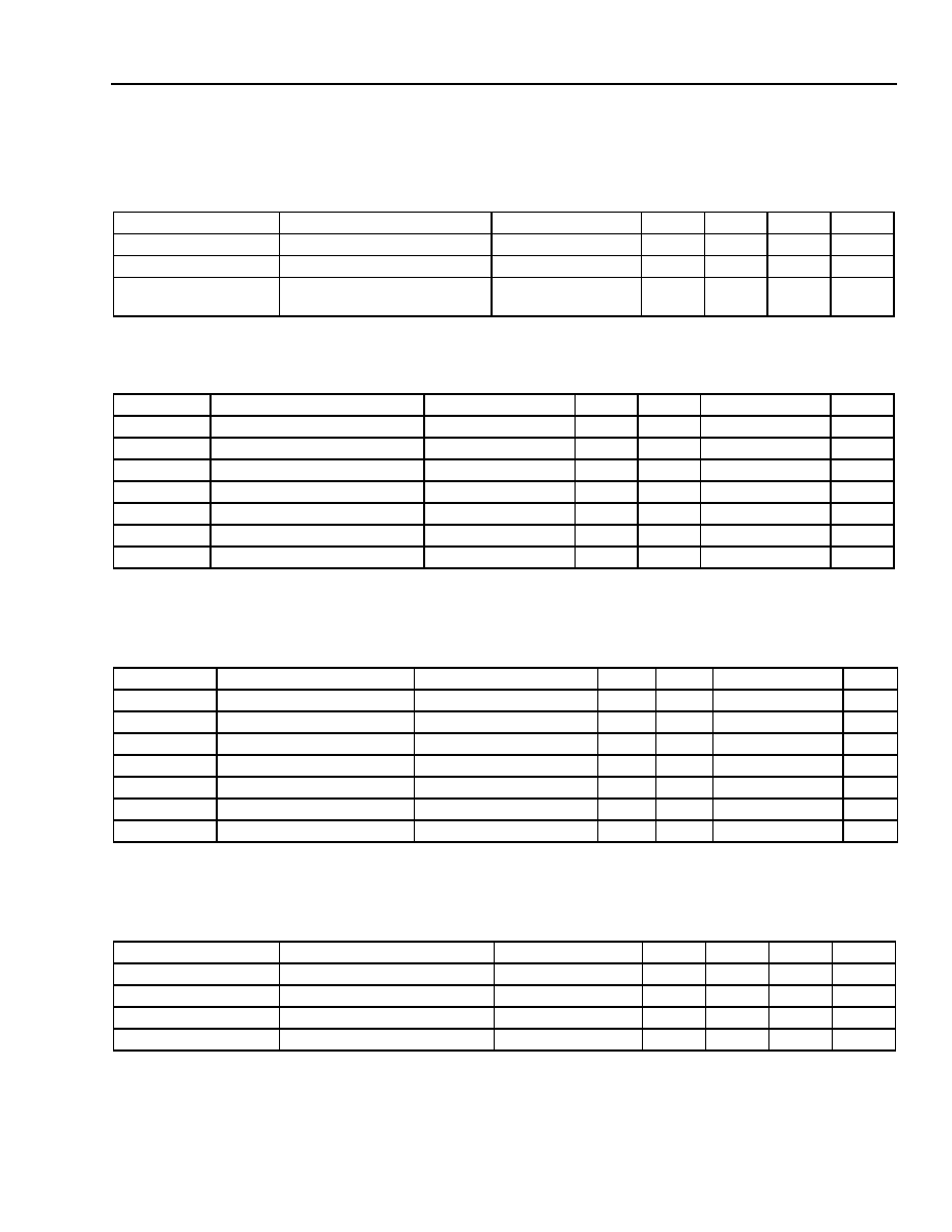
Lucent Technologies Inc.
25
Data Sheet
August 1999
Termination Impedance, and Hybrid Balance
T7507 Quad PCM Codec with Filters,
Timing Characteristics
Table 25. Clock Section
See Figures 12--14.
Table 26. T7507 Transmit Section (Delayed Timing)
See Figure 12.
* Timing parameter tMCLDZ is referenced to a high-impedance state.
Table 27. T7507 Transmit Section (Nondelayed Timing)
See Figure 13.
* Timing parameter tMCHDZ is referenced to a high-impedance state.
Table 28. T7507 Receive Section
See Figures 12--14.
Symbol
Parameter
Test Conditions
Min
Typ
Max
Unit
tMCHMCL1
Clock Pulse Width
--
97
--
--
ns
tCDC
Duty Cycle, MC
--
40
--
60
%
tMCH1MCH2
tMCL2MCL1
Clock Rise and
Fall Time
--
0
--
15
ns
Symbol
Parameter
Test Conditions
Min
Typ
Max
Unit
tMCHDV
Data Enabled on TS Entry
0 < C
LOAD
< 100 pF
0
--
60
ns
tMCHDV1
Data Delay from MC
0 < C
LOAD
< 100 pF
0
--
60
ns
tMCLDZ*
Data Float on TS Exit
C
LOAD
= 0
15
--
100
ns
tSPHMCL
Frame-sync Hold Time
--
50
--
--
ns
tMCLSPH
Frame-sync High Setup
--
50
--
--
ns
tSPLMCL
Frame-sync Low Setup
--
50
--
--
ns
tSPHSPL
Frame-sync Pulse Width
--
0.1
--
125 ≠ tMCHMCH
µs
Symbol
Parameter
Test Conditions
Min
Typ
Max
Unit
tSPHDV
Data Enabled on TS Entry
0 < C
LOAD
< 100 pF
0
--
80
ns
tMCHDV1
Data Delay from FS
X
0 < C
LOAD
< 100 pF
0
--
60
ns
tMCHDZ*
Data Float on TS Exit
C
LOAD
= 0
0
--
30
ns
tSPHMCL
Frame-sync Hold Time
--
50
--
--
ns
tMCLSPH
Frame-sync High Setup
--
50
--
--
ns
tSPLMCL
Frame-sync Low Setup
--
50
--
--
ns
tSPHSPL
Frame-sync Pulse Width
--
0.1
--
125 ≠ tMCHMCH
µs
Symbol
Parameter
Test Conditions
Min
Typ
Max
Unit
tDVMCL
Receive Data Setup
--
30
--
--
ns
tMCLDV
Receive Data Hold
--
15
--
--
ns
tSPHMCL
Frame Separation Hold Time
--
50
--
--
ns
tSPLMCL
Frame Separation Low Setup
--
50
--
--
ns
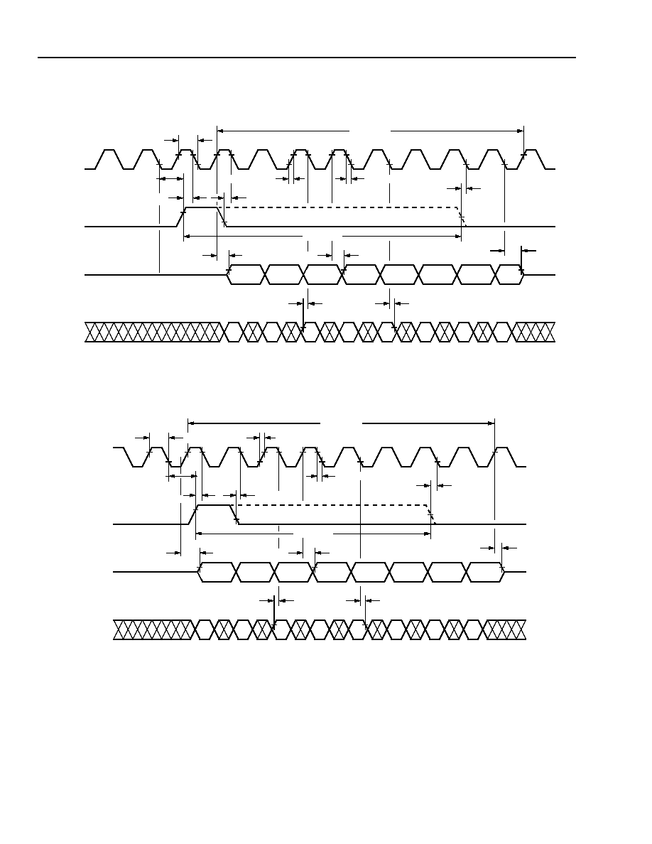
26
Lucent Technologies Inc.
Data Sheet
August 1999
Termination Impedance, and Hybrid Balance
T7507 Quad PCM Codec with Filters,
Timing Characteristics
(continued)
5-3581.g(F)
Figure 12. T7507 Transmit and Receive Timing, FSEP = 1 MCLK or IFS = 1, Delayed Timing (D0 = 0)
5-3581.h(F)
Figure 13. T7507 Transmit and Receive Timing, FSEP = 1 MCLK or IFS = 1, Nondelayed Timing (D0 = 1)
tMCHMCL1
tSPHMCL
tMCH1MCH2
tMCL2MCL1
BIT
1
BIT
2
BIT
3
BIT
4
BIT
5
BIT
6
BIT
7
BIT
8
BIT 1
BIT 2
BIT 3
BIT 5
BIT 4
BIT 6
BIT 7
BIT 8
1
2
3
4
5
6
7
8
1
MCLK
FSEP
Dx
TIME SLOT
tSPLMCL
tSPLMCL
tMCHDV1
tMCLDZ
D
R
tDVMCL
tMCLDV
D
R
STABLE
tMCHDV1
tSPHSPL
tMCLSPH
tSPHMCL
tMCH1MCH2
tMCL2MCL1
BIT
1
BIT
2
BIT
3
BIT
4
BIT
5
BIT
6
BIT
7
BIT
8
BIT 1
BIT 2
BIT 3
BIT 5
BIT 4
BIT 6
BIT 7
BIT 8
1
2
3
4
5
6
7
8
1
MCLK
FSEP
Dx
TIME SLOT
tSPLMCL
tSPLMCL
tMCHDV1
tMCHDZ
D
R
tDVMCL
tMCLDV
D
R
STABLE
tMCHDV1
tSPHSPL
tMCLSPH
tMCHMCL1

Lucent Technologies Inc.
27
Data Sheet
August 1999
Termination Impedance, and Hybrid Balance
T7507 Quad PCM Codec with Filters,
Timing Characteristics
(continued)
5-3582.b(F)
Figure 14. T7507 Receive Timing, FSEP > 1 MCLK and IFS = 0, Delayed Timing (D3 = 0)
5-4853(F)
Figure 15. Typical Frame Sync Timing (IFS = 0)
Programming:
00010111
CHANNEL 0 IN TIME SLOT 23
00100101
CHANNEL 1 IN TIME SLOT 5
01001111
CHANNEL 2 IN TIME SLOT 15
01101000
CHANNEL 3 IN TIME SLOT 8
BIT
1
BIT
2
BIT
3
BIT
4
BIT
5
BIT
6
BIT
7
BIT
8
1
2
3
4
5
6
7
8
MCLK
FSEP
D
R
tDVMCL
tMCLDV
D
R
STABLE
TIME SLOT
tMCHMCL1
tSPLMCL
tSPHMCL
19 20 21 22 23 24 25 26 27 28 29 30 31
0
1
2
3
4
5
6
7
8
9
10 11 12 13 14 15 16 17 18 19 20
X0
R2
R0
X1
X3
R1
R3
X2
FSEP
D
X
D
R
TIME
SLOTS
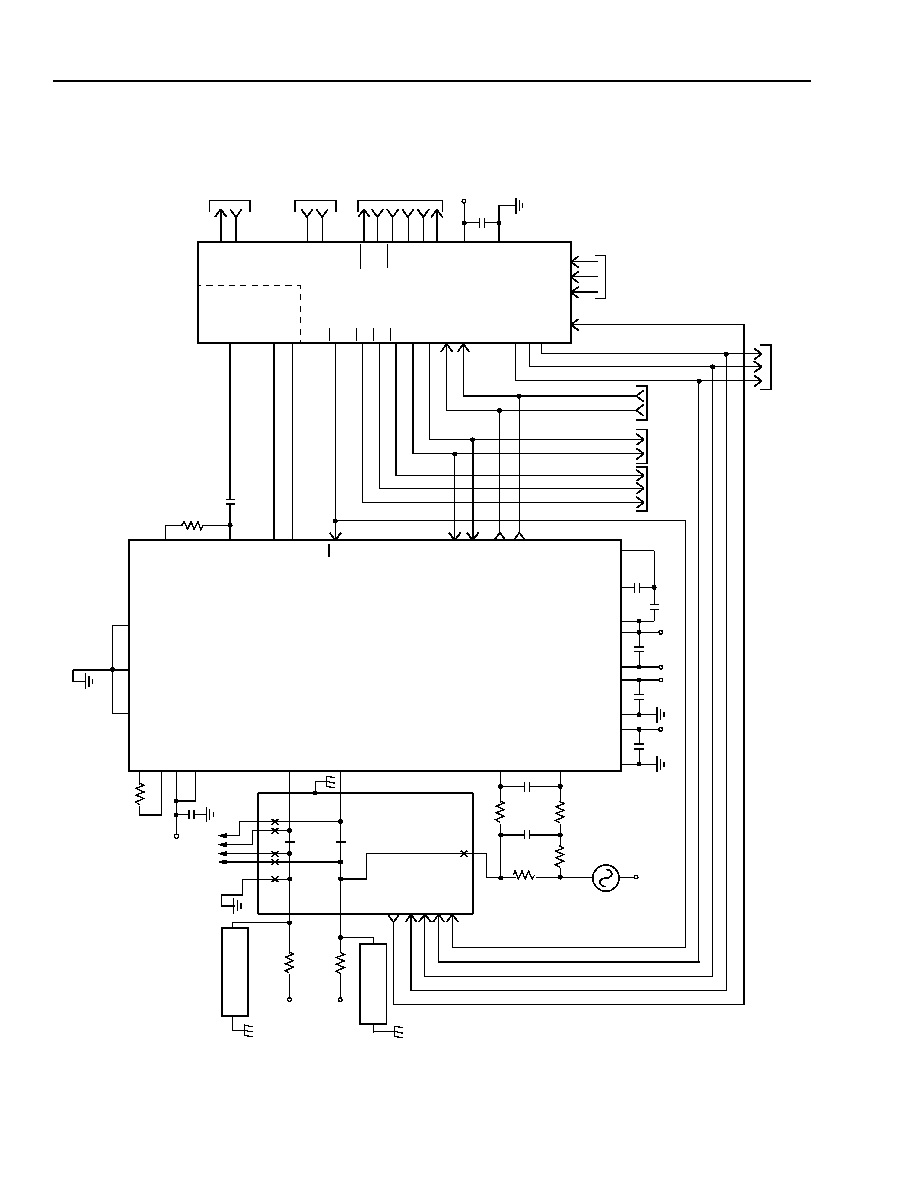
28
Lucent Technologies Inc.
Data Sheet
August 1999
Termination Impedance, and Hybrid Balance
T7507 Quad PCM Codec with Filters,
Applications
5-5807a(F)
Figure 16. Basic Loop Start Application Using the T7507 and the L7583 Switch for 200
+ (680
|| 100 nF)
Complex Termination and Hybrid Balance
R
PR
O
G
63.4
k
PW
R
DC
OU
T
I
PR
O
G
TO
T
E
S
T
B
U
S
T
RING
T
LI
NE
T
BA
T
TI
P
RING
CR
O
W
BA
R
R
PT
50
R
PR
50
RRING
PR
PT
RT
S
P
RT
S
P
2.0 M
C
RT
S
2
0
.
27
µ
F
C
RT
S
1
0.022
µ
F
R
TS
1
40
2
R
TS
2
274 k
R
TS
N
2.0
M
V
BA
T
V
RI
NG
0.1
µ
F
C
BA
T
1
BGND
V
BAT1
0.1
µ
F
C
DD
DGND
V
DD
0.1
µ
F
C
CC
V
CC
AGND
AGND
C
F1
C
F2
C
F1
0.4
7
µ
F
0.1
µ
F
C
F2
NT
S
D
NST
A
T
B1
B0
0.1
µ
F
C
DD
V
DD
AG
N
D
DI
CCL
K
CS
EL
MC
LK
TI
M
I
N
G
AND
CONT
R
O
L
IF
S
FS
EP
SY
NC
D
R
D
X
PC
M
HIG
H
W
A
Y
RC
V
N
RCV
P
VT
X
0.1
µ
F
CB2
R
TG
7.87 k
TG
L8
567 S
L
IC
1
/
4 T
7507
CODEC
FG
N
D
R
BA
T
L
7583
SW
I
T
CH
RT
S
N
V
BA
T
2
VF
R
ON
VF
R
OP
VF
X
IN
TS
D
IN
TE
S
T
ou
t
INRING
IN
TE
S
T
in
LA
TC
H
V
BA
T
2
RD1
I
RD2
I
RD3
I
DO
T
O
L8
567
EN
0
EN
1
EN
2
EN
3
B0
C
B1
C
NS
T
A
T
C
NT
SD
C
RD1
C
RD2
C
RD3
C
NT
SD0
EN
SL
I
C
AND
L758
3
SW
I
T
C
H
1,
2, OR
3
TO
L8
567
SL
I
C
1,
2
,
AND 3
FR
O
M
L8567
SL
I
C
1, 2,
A
ND 3
T
O
L758
3B
1
,
2
,
AND 3
D
X
EN
C
BA
T
2
0.
1
µ
F
PE
R
CHA
NNEL
C
O
MMON
NTSD1
NTSD2
NTSD3
F
R
OM L7583
1,
2, A
N
D
3
PR
O
T
EC
T
O
R
CR
O
W
B
A
R
PR
O
T
E
C
T
O
R

Lucent Technologies Inc.
29
Data Sheet
August 1999
Termination Impedance, and Hybrid Balance
T7507 Quad PCM Codec with Filters,
Outline Diagram
44-Pin PLCC
Controlling dimensions are in millimeters.
Note: The dimensions in this outline diagram are intended for informational purposes only. For detailed schemat-
ics to assist your design efforts, please contact your Lucent Technologies Sales Representative.
5-2506r.8(F)
4.57
MAX
1.27 TYP
0.53
MAX
0.10
SEATING PLANE
0.51 MIN
TYP
1
6
40
7
17
29
39
18
28
PIN #1 IDENTIFIER
ZONE
16.66 MAX
17.65 MAX
16.66
MAX
17.65
MAX
Lucent Technologies Inc. reserves the right to make changes to the product(s) or information contained herein without notice. No liability is assumed as a result of their use or application. No
rights under any patent accompany the sale of any such product(s) or information.
Copyright © 1999 Lucent Technologies Inc.
All Rights Reserved
August 1999
DS99-273ALC (Replaces DS99-080ALC)
For additional information, contact your Microelectronics Group Account Manager or the following:
INTERNET: http://www.lucent.com/micro
E-MAIL: docmaster@micro.lucent.com
N. AMERICA:
Microelectronics Group, Lucent Technologies Inc., 555 Union Boulevard, Room 30L-15P-BA, Allentown, PA 18103
1-800-372-2447, FAX 610-712-4106 (In CANADA: 1-800-553-2448, FAX 610-712-4106)
ASIA PACIFIC: Microelectronics Group, Lucent Technologies Singapore Pte. Ltd., 77 Science Park Drive, #03-18 Cintech III, Singapore 118256
Tel. (65) 778 8833, FAX (65) 777 7495
CHINA: Microelectronics Group, Lucent Technologies (China) Co., Ltd., A-F2, 23/F, Zao Fong Universe Building, 1800 Zhong Shan Xi Road, Shanghai
200233 P. R. China Tel. (86) 21 6440 0468, ext. 316, FAX (86) 21 6440 0652
JAPAN: Microelectronics Group, Lucent Technologies Japan Ltd., 7-18, Higashi-Gotanda 2-chome, Shinagawa-ku, Tokyo 141, Japan
Tel. (81) 3 5421 1600, FAX (81) 3 5421 1700
EUROPE: Data Requests: MICROELECTRONICS GROUP DATALINE: Tel. (44) 7000 582 368, FAX (44) 1189 328 148
Technical Inquiries: GERMANY: (49) 89 95086 0 (Munich), UNITED KINGDOM: (44) 1344 865 900 (Ascot),
FRANCE: (33) 1 40 83 68 00 (Paris), SWEDEN: (46) 8 594 607 00 (Stockholm), FINLAND: (358) 9 4354 2800 (Helsinki),
ITALY: (39) 02 6608131 (Milan), SPAIN: (34) 1 807 1441 (Madrid)
Data Sheet
August 1999
Termination Impedance, and Hybrid Balance
T7507 Quad PCM Codec with Filters,
Ordering Information
Device Part No. Description Package Comcode
T - 7507 - - - ML2-D Quad PCM Codec (Dry-bagged) 44-Pin PLCC 108496704
T - 7507 - - - ML2-DT Quad PCM Codec (Dry-bagged, Tape and Reel) 44-Pin PLCC 108496712