 | –≠–ª–µ–∫—Ç—Ä–æ–Ω–Ω—ã–π –∫–æ–º–ø–æ–Ω–µ–Ω—Ç: T7633 | –°–∫–∞—á–∞—Ç—å:  PDF PDF  ZIP ZIP |
Document Outline
- AY99-010BBAC (T7633 Device Advisory for Version 1.0 of the Device)
- Introduction
- Microprocessor Timing Requirements
- Microprocessor Interface
- Table 1. Microprocessor Interface I/O Timing Specifications
- Figure 1. Mode 1ÑRead Cycle Timing (MPMODE = 0, MPMUX = 0)
- Figure 2. Mode 1ÑWrite Cycle Timing (MPMODE = 0, MPMUX = 0)
- Figure 3. Mode 2ÑRead Cycle Timing (MPMODE = 0, MPMUX = 1)
- Figure 4. Mode 2ÑWrite Cycle Timing (MPMODE = 0, MPMUX = 1)
- Figure 5. Mode 3ÑRead Cycle Timing (MPMODE = 1, MPMUX = 0)
- Figure 6. Mode 3ÑWrite Cycle Timing (MPMODE = 1, MPMUX = 0)
- Figure 7. Mode 4ÑRead Cycle Timing (MPMODE = 1, MPMUX = 1)
- Figure 8. Mode 4ÑWrite Cycle Timing (MPMODE = 1, MPMUX = 1)
- Data Pattern Limitation for Proper Functionality of the LIU Internal Full Local Loopback (FLLOOP)
- Asynchronous SYSCK and PLLCK with Jitter Attenuator in the Line Transmit Path
- AY99-010PDH Replaces AY99-007T1E1 to Incorporate the Following Updates
- Contact Us
- AY99-033BBAC (T7633 Device Advisory Describing Differences Between Version 1.0 and Version 2.0 of Device)
- Introduction
- Data Sheet Changes
- Device Operation Updates
- LIU Full Local Loopback (FLLOOP)
- Microprocessor Interface Timing
- Contact Us
- DS02-244BBAC (T7633 Dual T1/E1 3.3 V Short-Haul Terminator)
- Features
- List of Figures
- Figure 1. T7633 Block Diagram (One of Two Channels)
- Figure 2. T7633 Block Diagram: Receive Section (One of Two Channels)
- Figure 3. T7633 Block Diagram: Transmit Section (One of Two Channels)
- Figure 4. Pin Assignment
- Figure 5. Block Diagram of Line Interface Unit: Single Channel
- Figure 6. T1/DS1 Receiver Jitter Accommodation Without Jitter Attenuator
- Figure 7. T1/DS1 Receiver Jitter Transfer Without Jitter Attenuator
- Figure 8. CEPT/E1 Receiver Jitter Accommodation Without Jitter Attenuator
- Figure 9. CEPT/E1 Receiver Jitter Transfer Without Jitter Attenuator
- Figure 10. DSX-1 Isolated Pulse Template
- Figure 11. ITU-T G.703 Pulse Template
- Figure 12. T1/DS1 Receiver Jitter Accommodation with Jitter Attenuator
- Figure 13. T1/DS1 Jitter Transfer of the Jitter Attenuator
- Figure 14. CEPT/E1 Receiver Jitter Accommodation with Jitter Attenuator
- Figure 15. CEPT/E1 Jitter Transfer of the Jitter Attenuator
- Figure 16. Line Termination Circuitry
- Figure 17. T7633 Line Interface Unit Approximate Equivalent Analog I/O Circuits
- Figure 18. Block Diagram of Framer Line Interface
- Figure 19. Transmit Framer TLCK to TND, TPD and Receive Framer RND, RPD to RLCK Timing
- Figure 20. T1 Frame Structure
- Figure 21. T1 Transparent Frame Structure
- Figure 22. T7633 Facility Data Link Access Timing of the Transmit and Receive Framer Sections
- Figure 23. ITU 2.048 Basic Frame, CRC-4 Multiframe, and Channel Associated Signaling Multiframe S...
- Figure 24. CEPT Transparent Frame Structure
- Figure 25. Receive CRC-4 Multiframe Search Algorithm Using the 100 ms Internal Timer
- Figure 26. Receive CRC-4 Multiframe Search Algorithm for Automatic, CRC-4/Non-CRC-4 Equipment Int...
- Figure 27. Facility Data Link Access Timing of the Transmit and Receive Framer Sections in the CE...
- Figure 28. Transmit and Receive Sa Stack Accessing Protocol
- Figure 29. Timing Specification for RFRMCK, RFRMDATA, and RFS in DS1 Mode
- Figure 30. Timing Specification for TFS, TLCK, and TPD in DS1 Mode
- Figure 31. Timing Specification for RFRMCK, RFRMDATA, and RFS in CEPT Mode
- Figure 32. Timing Specification for RFRMCK, RFRMDATA, RFS, and RSSFS in CEPT Mode
- Figure 33. Timing Specification for RCRCMFS in CEPT Mode
- Figure 34. Timing Specification for TFS, TLCK, and TPD in CEPT Mode
- Figure 35. Timing Specification for TFS, TLCK, TPD, and TSSFS in CEPT Mode
- Figure 36. Timing Specification for TFS, TLCK, TPD, and TCRCMFS in CEPT Mode
- Figure 37. Relation Between RLCK1 and Interrupt (Pin 99)
- Figure 38. Timing for Generation of LOPLLCK (Pin 39/143)
- Figure 39. The T and V Reference Points for a Typical CEPT E1 Application
- Figure 40. Loopback and Test Transmission Modes
- Figure 41. 20-Stage Shift Register Used to Generate the Quasi-Random Signal
- Figure 42. 15-Stage Shift Register Used to Generate the Pseudorandom Signal
- Figure 43. T7633 Facility Data Link Access Timing of the Transmit and Receive Framer Sections
- Figure 44. Block Diagram for the Receive Facility Data Link Interface
- Figure 45. Block Diagram for the Transmit Facility Data Link Interface
- Figure 46. Local Loopback Mode
- Figure 47. Remote Loopback Mode
- Figure 48. T7633 Phase Detector Circuitry
- Figure 49. Nominal Concentration Highway Interface Timing (for FRM_PR43 bit 0Ñbit 2 = 100 (Binary))
- Figure 50. CHIDTS Mode Concentration Highway Interface Timing
- Figure 51. Associated Signaling Mode Concentration Highway Interface Timing
- Figure 52. CHI Timing with ASM and CHIDTS Enabled
- Figure 53. TCHIDATA and RCHIDATA to CHICK Relationship with CMS = 0 (CEX = 3 and CER = 4, Respect...
- Figure 54. CHI TCHIDATA and RCHIDATA to CHICK Relationship with CMS = 1 (CEX = 3 and CER = 6, Res...
- Figure 55. Receive CHI (RCHIDATA) Timing
- Figure 56. Transmit CHI (TCHIDATA) Timing
- Figure 57. Block Diagram of the T7633's Boundary-Scan Test Logic
- Figure 58. BS TAP Controller State Diagram
- Figure 59. Mode 1ÑRead Cycle Timing (MPMODE = 0, MPMUX = 0)
- Figure 60. Mode 1ÑWrite Cycle Timing (MPMODE = 0, MPMUX = 0)
- Figure 61. Mode 2ÑRead Cycle Timing (MPMODE = 0, MPMUX = 1)
- Figure 62. Mode 2ÑWrite Cycle Timing (MPMODE = 0, MPMUX = 1)
- Figure 63. Mode 3ÑRead Cycle Timing (MPMODE = 1, MPMUX = 0)
- Figure 64. Mode 3ÑWrite Cycle Timing (MPMODE = 1, MPMUX = 0)
- Figure 65. Mode 4ÑRead Cycle Timing (MPMODE = 1, MPMUX = 1)
- Figure 66. Mode 4ÑWrite Cycle Timing (MPMODE = 1, MPMUX = 1)
- List of Tables
- Table 1. Pin Descriptions
- Table 2. Digital Loss of Signal Standard Select
- Table 3. LOSSD and RCVAIS Control Configurations (Not Valid During Loopback Modes)
- Table 4. DS1 LIU Receiver Specifications
- Table 5. CEPT LIU Receiver Specifications
- Table 6. Transmit Line Interface Short-Haul Equalizer/Rate Control
- Table 7. DSX-1 Pulse Template Corner Points (from CB119, T1.102)
- Table 8. DS1 Transmitter Specifications
- Table 9. CEPT Transmitter Specifications
- Table 10. Loopback Control
- Table 11. SYSCK (16x, CKSEL = 1) Timing Specifications
- Table 12. SYSCK (1x, CKSEL = 0) Timing Specifications
- Table 13. Termination Components by Application1
- Table 14. AMI Encoding
- Table 15. DS1 ZCS Encoding
- Table 16. DS1 B8ZS Encoding
- Table 17. ITU HDB3 Coding
- Table 18. T-Carrier Hierarchy
- Table 19. D4 Superframe Format
- Table 20. DDS Channel-24 Format
- Table 21. SLC-96 Data Link Block Format
- Table 22. SLC-96 Line Switch Message Codes
- Table 23. Transmit and Receive SLC-96 Stack Structure
- Table 24. Extended Superframe (ESF) Structure
- Table 25. T1 Loss of Frame Alignment Criteria
- Table 26. T1 Frame Alignment Procedures
- Table 27. Robbed-Bit Signaling Options
- Table 28. SLC-96 9-State Signaling Format
- Table 29. 16-State Signaling Format
- Table 30. Allocation of Bits 1 to 8 of the FAS Frame and the NOT FAS Frame
- Table 31. ITU CRC-4 Multiframe Structure
- Table 32. ITU CEPT Time Slot 16 Channel Associated Signaling Multiframe Structure
- Table 33. CEPT IRSM Signaling Multiframe Structure
- Table 34. Transmit and Receive Sa Stack Structure
- Table 35. Associated Signaling Mode CHI 2-Byte Time-Slot Format for DS1 Frames
- Table 36. Associated Signaling Mode CHI 2-Byte Time-Slot Format for Stuffed Channels
- Table 37. Associated Signaling Mode CHI 2-Byte Time-Slot Format for CEPT
- Table 38. Red Alarm or Loss of Frame Alignment Conditions
- Table 39. Remote Frame Alarm Conditions
- Table 40. Alarm Indication Signal Conditions
- Table 41. Sa6 Bit Coding Recognized by the Receive Framer
- Table 42. Sa6 Bit Coding of NT1 Interface Events Recognized by the Receive Framer
- Table 43. AUXP Synchronization and Clear Sychronization Process
- Table 44. Event Counters Definition
- Table 45. Summary of the Deactivation of SSTSSLB and SSTSLLB Modes as a Function of Activating th...
- Table 46. Register FRM_PR69 Test Patterns
- Table 47. Register FRM_PR70 Test Patterns
- Table 48. Automatic Enable Commands
- Table 49. On-Demand Commands
- Table 50. Receive ANSI Code
- Table 51. Performance Report Message Structure*
- Table 52. FDL Performance Report Message Field Definition
- Table 53. Octet Contents and Definition
- Table 54. Receive Status of Frame Byte
- Table 55. HDLC Frame Format
- Table 56. Receiver Operation in Transparent Mode
- Table 57. Summary of the T7633ês Concentration Highway Interface Parameters
- Table 58. Programming Values for TOFF[2:0] and ROFF[2:0] when CMS = 0
- Table 59. Programming Values for TOFF[2:0] when CMS = 1
- Table 60. Programming Values for ROFF[2:0] when CMS = 1
- Table 61. TAP Controller States in the Data Register Branch
- Table 62. TAP Controller States in the Instruction Register Branch
- Table 63. T7633ês Boundary-Scan Instructions
- Table 64. IDCODE Register
- Table 65. Microprocessor Configuration Modes
- Table 66. Mode [1Ñ4] Microprocessor Pin Definitions
- Table 67. Microprocessor Input Clock Specifications
- Table 68. T7633 Register Address Map
- Table 69. Microprocessor Interface I/O Timing Specifications�
- Table 70. Status Register and Corresponding Interrupt Enable Register for Functional Blocks
- Table 71. Asserted Value and Deasserted State for GREG4 Bit 4 and Bit 6 Logic Combinations
- Table 72. Register Summary
- Table 73. Global Register Set (0x000Ñ0x008)
- Table 74. Primary Block Interrupt Status Register (GREG0) (000)
- Table 75. Primary Block Interrupt Enable Register (GREG1) (001)
- Table 76. Global Loopback Control Register (GREG2) (002)
- Table 77. Global Loopback Control Register (GREG3) (003)
- Table 78. Global Control Register (GREG4) (004)
- Table 79. Device ID and Version Registers (GREG5ÑGREG7) (005Ñ007)
- Table 80. Line Interface Units Register Set1 ((400Ñ40F); (A00ÑA0F))
- Table 81. LIU Alarm Status Register (LIU_REG0) (400, A00)
- Table 82. LIU Alarm Interrupt Enable Register (LIU_REG1) (401, A01)
- Table 83. LIU Control Register (LIU_REG2) (402, A02)
- Table 84. LIU Control Register (LIU_REG3) (403, A03)
- Table 85. LIU Register (LIU_REG4) (404, A04)
- Table 86. LIU Configuration Register (LIU_REG5) (405, A05)
- Table 87. LIU Configuration Register (LIU_REG6) (406, A06)
- Table 88. Framer Status and Control Blocks Address Range (Hexadecimal)
- Table 89. Interrupt Status Register (FRM_SR0) (600; C00)
- Table 90. Facility Alarm Condition Register (FRM_SR1) (601; C01)
- Table 91. Remote End Alarm Register (FRM_SR2) (602; C02)
- Table 92. Facility Errored Event Register-1 (FRM_SR3) (603; C03)
- Table 93. Facility Event Register-2 (FRM_SR4) (604; C04)
- Table 94. Exchange Termination and Exchange Termination Remote End Interface Status Register (FRM...
- Table 95. Network Termination and Network Termination Remote End Interface Status Register (FRM_S...
- Table 96. Facility Event Register (FRM_SR7) (607; C07)
- Table 97. Bipolar Violation Counter Registers (FRM_SR8ÑFRM_SR9) ((608Ñ609); (C08ÑC09))
- Table 98. Framing Bit Error Counter Registers (FRM_SR10ÑFRM_SR11) ((60AÑ60B); (C0AÑC0B))
- Table 99. CRC Error Counter Registers (FRM_SR12ÑFRM_SR13) ((60CÑ60D); (C0CÑC0D))
- Table 100. E-Bit Counter Registers (FRM_SR14ÑFRM_SR15) ((60EÑ60F); (C0EÑC0F))
- Table 101. CRC-4 Errors at NT1 from NT2 Counter Registers (FRM_SR16ÑFRM_SR17) ((610Ñ611); (C10ÑC11))
- Table 102. E Bit at NT1 from NT2 Counter (FRM_SR18ÑFRM_SR19) ((612Ñ613); (C12ÑC13))
- Table 103. ET Errored Seconds Counter (FRM_SR20ÑFRM_SR21) ((614Ñ615); (C14ÑC15))
- Table 104. ET Bursty Errored Seconds Counter (FRM_SR22ÑFRM_SR23) ((616Ñ617); (C16ÑC17))
- Table 105. ET Severely Errored Seconds Counter (FRM_SR24ÑFRM_SR25) ((618Ñ619); (C18ÑC19))
- Table 106. ET Unavailable Seconds Counter (FRM_SR26ÑFRM_SR27) ((61AÑ61B); (C1AÑC1B))
- Table 107. ET-RE Errored Seconds Counter (FRM_SR28ÑFRM_SR29) ((61CÑ61D); (C1CÑC1D))
- Table 108. ET-RE Bursty Errored Seconds Counter (FRM_SR30ÑFRM_SR31) ((61EÑ61F); (C1EÑC1F))
- Table 109. ET-RE Severely Errored Seconds Counter (FRM_SR32ÑFRM_SR33) ((620Ñ621); (C20ÑC21))
- Table 110. ET-RE Unavailable Seconds Counter (FRM_SR34ÑFRM_SR35) ((622Ñ623); (C22ÑC23))
- Table 111. NT1 Errored Seconds Counter (FRM_SR36ÑFRM_SR37) ((624Ñ625); (C24ÑC25))
- Table 112. NT1 Bursty Errored Seconds Counter (FRM_SR38ÑFRM_SR39) ((626Ñ627); (C26ÑC27))
- Table 113. NT1 Severely Errored Seconds Counter (FRM_SR40ÑFRM_SR41) ((628Ñ629); (C28ÑC29))
- Table 114. NT1 Unavailable Seconds Counter (FRM_SR42ÑFRM_SR43) ((62AÑ62B); (C2AÑC2B))
- Table 115. NT1-RE Errored Seconds Counter (FRM_SR44ÑFRM_SR45) ((62CÑ62D); (C2CÑC2D))
- Table 116. NT1-RE Bursty Errored Seconds Counter (FRM_SR46ÑFRM_SR47) ((62EÑ62F); (C2EÑC2F))
- Table 117. NT1-RE Severely Errored Seconds Counter (FRM_SR48ÑFRM_SR49) ((630Ñ631); (C30ÑC31))
- Table 118. NT1-RE Unavailable Seconds Counter (FRM_SR50ÑFRM_SR51) ((632Ñ633); (C32ÑC33))
- Table 119. Receive NOT-FAS TS0 Register (FRM_SR52) (634; C34)
- Table 120. Receive Sa Register (FRM_SR53) (635; C35)
- Table 121. SLC-96 FDL Receive Stack (FRM_SR54ÑFRM_SR63) ((636Ñ63F); (C36ÑC3F))
- Table 122. CEPT Sa Receive Stack (FRM_SR54ÑFRM_SR63) ((636Ñ63F); (C36ÑC3F))
- Table 123. Transmit Framer ANSI Performance Report Message Status Register Structure
- Table 124. Received Signaling Registers: DS1 Format (FRM_RSR0ÑFRM_RSR23) ((640Ñ658); (C40ÑC58))
- Table 125. Receive Signaling Registers: CEPT Format (FRM_RSR0ÑFRM_RSR31) ((640Ñ65F); (C40Ñ C5F))
- Table 126. Summary of Interrupt Group Enable Registers (FRM_PR0ÑFRM_PR7) ((660Ñ667); (C60ÑC67))
- Table 127. Primary Interrupt Group Enable Register (FRM_PR0) (660; C60)
- Table 128. Interrupt Enable Register (FRM_PR1) (661; C61)
- Table 129. Interrupt Enable Register (FRM_PR2) (662; C62)
- Table 130. Interrupt Enable Register (FRM_PR3) (663; C63)
- Table 131. Interrupt Enable Register (FRM_PR4) (664; C64)
- Table 132. Interrupt Enable Register (FRM_PR5) (665; C65)
- Table 133. Interrupt Enable Register (FRM_PR6) (666; C66)
- Table 134. Interrupt Enable Register (FRM_PR7) (667; C67)
- Table 135. Framer Mode Bits Decoding (FRM_PR8) (668; C68)
- Table 136. Line Code Option Bits Decoding (FRM_PR8) (668; C68)
- Table 137. CRC Option Bits Decoding (FRM_PR9) (669, C69)
- Table 138. Alarm Filter Register (FRM_PR10) (66A; C6A)
- Table 139. Errored Event Threshold Definition
- Table 140. Errored Second Threshold Register (FRM_PR11) (66B; C6B)
- Table 141. Severely Errored Second Threshold Registers (FRM_PR12ÑFRM_PR13) ((66CÑ66D; C6CÑC6D))
- Table 142. ET1 Errored Event Enable Register (FRM_PR14) (66E; C6E)
- Table 143. ET1 Remote End Errored Event Enable Register (FRM_PR15) (66F; C6F)
- Table 144. NT1 Errored Event Enable Register (FRM_PR16) (670; C70)
- Table 145. NT1 Remote End Errored Event Enable Registers (FRM_PR17ÑFRM_PR18) ((671Ñ672); (C71ÑC72))
- Table 146. Automatic AIS to the System and Automatic Loopback Enable Register (FRM_PR19) (673; C73)
- Table 147. Transmit Test Pattern to the Line Enable Register (FRM_PR20) (674; C74)
- Table 148. Framer FDL Control Command Register (FRM_PR21) (675; C75)
- Table 149. Framer Transmit Line Idle Code Register (FRM_PR22) (676; C76)
- Table 150. Framer System Stuffed Time-Slot Code Register (FRM_PR23) (677; C77)
- Table 151. Primary Time-Slot Loopback Address Register (FRM_PR24) (678; C78)
- Table 152. Loopback Decoding of Bits LBC[2:0] in FRM_PR24, Bits 7Ñ5
- Table 153. Secondary Time-Slot Loopback Address Register (FRM_PR25) (679; C79)
- Table 154. Loopback Decoding of Bits LBC[1:0] in FRM_PR25, Bits 6Ñ5
- Table 155. Framer Reset and Transparent Mode Control Register (FRM_PR26) (67A, C7A)
- Table 156. Transmission of Remote Frame Alarm and CEPT Automatic Transmission of A Bit = 1 Contro...
- Table 157. CEPT Automatic Transmission of E Bit = 0 Control Register (FRM_PR28) (67C; C7C)
- Table 158. Sa4ÑSa8 Source Register (FRM_PR29) (67D; C7D)
- Table 159. Sa Bits Source Control for Bit 5ÑBit 7 in FRM_PR29
- Table 160. Sa4ÑSa8 Control Register (FRM_PR30) (67E; C7E)
- Table 161. Sa Transmit Stack (FRM_PR31ÑFRM_PR40) ((67FÑ688); (C7FÑC88))
- Table 162. SLC-96 Transmit Stack (FRM_PR31ÑFRM_PR40) ((67FÑ688); (C7FÑC88))
- Table 163. Transmit SLC-96 FDL Format
- Table 164. CEPT Time Slot 16 X-Bit Remote Multiframe Alarm and AIS Control Register (FRM_PR41) (6...
- Table 165. Framer Exercise Register (FRM_PR42) (68A; C8A)
- Table 166. Framer Exercises, FRM_PR42 Bit 5ÑBit 0 (68A; C8A)
- Table 167. DS1 System Interface Control and CEPT FDL Source Control Register (FRM_PR43) (68B; C8B)
- Table 168. Signaling Mode Register (FRM_PR44) (68C; C8C)
- Table 169. CHI Common Control Register (FRM_PR45) (68D; C8D)
- Table 170. CHI Common Control Register (FRM_PR46) (68E; C8E)
- Table 171. CHI Transmit Control Register (FRM_PR47) (68F; C8F)
- Table 172. CHI Receive Control Register (FRM_PR48) (690; C90)
- Table 173. CHI Transmit Time-Slot Enable Registers (FRM_PR49ÑFRM_PR52) ((691Ñ694); (C91ÑC94))
- Table 174. CHI Receive Time-Slot Enable Registers (FRM_PR53ÑFRM_PR56) ((695Ñ698); (C95ÑC98))
- Table 175. CHI Transmit Highway Select Registers (FRM_PR57ÑFRM_PR60) ((699Ñ69C); (C99ÑC9C))
- Table 176. CHI Receive Highway Select Registers (FRM_PR61ÑFRM_PR64) ((69DÑ6A0); (C9DÑCA0))
- Table 177. CHI Transmit Control Register (FRM_PR65) (6A1; CA1)
- Table 178. CHI Receive Control Register (FRM_PR66) (6A2; CA2)
- Table 179. Auxiliary Pattern Generator Control Register (FRM_PR69) (6A5; CA5)*
- Table 180. Pattern Detector Control Register (FRM_PR70) (6A6; CA6)*
- Table 181. Transmit Signaling Registers: DS1 Format (FRM_TSR0ÑFRM_TSR23) ((6E0Ñ6F7); (CE0ÑCF7))
- Table 182. Transmit Signaling Registers: CEPT Format (FRM_TSR0ÑFRM_TSR31) ((6E0Ñ6FF); (CE0Ñ CFF))
- Table 183. FDL Register Set (800Ñ80E); (E00ÑE0E)
- Table 184. FDL Configuration Control Register (FDL_PR0) (800; E00)
- Table 185. FDL Control Register (FDL_PR1) (801; E01)
- Table 186. FDL Interrupt Mask Control Register (FDL_PR2) (802; E02)
- Table 187. FDL Transmitter Configuration Control Register (FDL_PR3) (803; E03)
- Table 188. FDL Transmitter FIFO Register (FDL_PR4) (804; E04)
- Table 189. FDL Transmitter Mask Register (FDL_PR5) (805; E05)
- Table 190. FDL Receiver Interrupt Level Control Register (FDL_PR6) (806; E06)
- Table 191. FDL Register FDL_PR7
- Table 192. FDL Receiver Match Character Register (FDL_PR8) (808; E08)
- Table 193. FDL Transparent Control Register (FDL_PR9) (809; E09)
- Table 194. FDL Transmit ANSI ESF Bit Codes (FDL_PR10) (80A; E0A)
- Table 195. FDL Interrupt Status Register (Clear on Read) (FDL_SR0) (80B; E0B)
- Table 196. FDL Transmitter Status Register (FDL_SR1) (80C; E0C)
- Table 197. FDL Receiver Status Register (FDL_SR2) (80D; E0D)
- Table 198. Receive ANSI FDL Status Register (FDL_SR3) (80E; E0E)
- Table 199. FDL Receiver FIFO Register (FDL_SR4) (807; E07)
- Table 200. Global Register Set
- Table 201. Line Interface Unit Register Set1
- Table 202. Framer Unit Status Register Map
- Table 203. Receive Signaling Registers Map
- Table 204. Framer Unit Parameter Register Map
- Table 205. Transmit Signaling Registers Map
- Table 206. Facility Data Link Register Map
- Table 207. ESD Protection Characteristics
- Table 208. Logic Interface Characteristics (TA = Ö40 ∞C to +85 ∞C, VDD = 3.3 V ± 5%, VSS = 0)
- Feature Descriptions
- Functional Description
- Pin Information
- Line Interface Unit: Block Diagram
- Line Interface Unit: Receive
- Line Interface Unit: Transmit
- Line Interface Unit: Jitter Attenuator
- Line Interface Unit: Loopbacks
- Line Interface Unit: Other Features
- SYSCK Reference Clock
- Line Interface Unit: Line Interface Networks
- LIU-Framer Interface
- Frame Formats
- CEPT Time Slot 0 FAS/NOT FAS Control Bits
- Signaling Access
- Auxiliary Framer I/O Timing
- Alarms and Performance Monitoring
- Facility Data Link (FDL)
- Phase-Lock Loop Circuit
- Framer-System (CHI) Interface
- Concentration Highway Interface (CHI)
- JTAG Boundary-Scan Specification
- Microprocessor Interface
- Reset
- Interrupt Generation
- Register Architecture
- Global Register Architecture
- Global Register Structure
- Line Interface Unit (LIU) Register Architecture
- Line Interface Alarm Register
- Line Interface Alarm Interrupt Enable Register
- Line Interface Control Registers
- Framer Register Architecture
- FDL Register Architecture
- FDL Parameter/Control Registers (800Ñ80E; E00ÑE0E)
- Register Maps
- Absolute Maximum Ratings
- Operating Conditions
- Handling Precautions
- Electrical Characteristics
- Power Supply Bypassing
- Outline Diagram
- Ordering Information
- Index
- Trademark Information
- Contact Us

Device Advisory
September 1999
T7633 Device Advisory for Version 1.0 of the Device
Introduction
This advisory applies to the T7633 Dual T1/E1 3.3 V Short-Haul Terminator as described in the May 1998
T7633 Dual T1/E1 3.3 V Short-Haul Terminator
Advance Data Sheet (DS98-244TIC).
Microprocessor Timing Requirements
This section describes a modification to the microprocessor interface timing information to guarantee proper
function of the line interface clear on read status register, LIU_REG0, at address 400 and A00 (hex).
For clear on read (COR) register LIU_REG0 to clear, the chip select (CS) and address value (AD0--AD7 and
A8--A11, or A0--A11) must be active for either of the following intervals after the completion of the read (RD)
or data strobe (DS) pulse.
1. If present, two microprocessor clock (MPCK) cycles.
s
33 MHz maximum.
s
3 MHz minimum.
2. Two internal SYSCK cycles, if MPCK is not present.
s
The internal SYSCK is a clock at 16 times the line rate (24.704 MHz for DS1 or 32.768 MHz for CEPT).
Two internal SYSCK cycles, at 16 times the line rate, are equivalent to 81 ns for DS1 and 61 ns for CEPT. If
MPCK is present, this time interval can range from 61 ns to 667 ns depending upon the particular repetition
rate selected for MPCK. The microprocessor interface timing table from the T7633 advance data sheet is
shown in Table 1, Microprocessor Interface I/O Timing Specifications on page 2 with the revised timing incor-
ported in the table (notes * and ). The timing diagrams, which did not change, are shown in Figure 1--
Figure 8.
For the case where MPCK is not present, it is recommended that the hold time between the deassertion of RD
or DS and the deassertion of CS be at least 110 ns to provide a safety margin.
This requirement is not specified in the T7633 advance data sheet.
The framer portion of the terminator internally latches the decoded register address within its logic for clearing
the framer CORs, and it does not require this timing modification.

2
Agere Systems Inc.
Device Advisory
September 1999
T7633 Device Advisory for Version 1.0 of the Device
Microprocessor Interface
I/O Timing
In modes 1 and 3, asserting ALE_AS signal low is used to enable the internal address bus. In modes 2 and 4, the
falling edge of ALE_AS signal is used to latch the address bus.
* For Figure 1:
s
If AS = 0 (AS is not used or is inactive), then the address must be valid until CS = 1 and
-- If MPCK is used (MPCK is active), then t11 must exceed two MPCK periods,
-- If MPCK is not used (MPCK is inactive), then t11 must exceed two 16x line clock periods. A t11 of 110 ns is suggested.
s
If AS is used (AS is active), then
-- If MPCK is used (MPCK is active), then t11 must exceed two MPCK periods,
-- If MPCK is not used (MPCK is inactive), then t11 must exceed two 16x line clock periods. A t11 of 110 ns is suggested.
For Figure 3:
s
If MPCK is used (MPCK is active), then t11 must exceed two MPCK periods,
s
If MPCK is not used (MPCK is inactive), then t11 must exceed two 16x line clock periods. A t11 of 110 ns is suggested.
Table 1. Microprocessor Interface I/O Timing Specifications
Symbol
Configuration
Parameter
Setup
(ns)
(Min)
Hold
(ns)
(Min)
Delay
(ns)
(Max)
t1
Modes 1 & 2
AS Asserted Width
--
10
--
t2
Address Valid to AS Deasserted
10
--
--
t3
AS Deasserted to Address Invalid
--
10
--
t4
--
--
--
--
t5
R/W Valid to Both CS and DS Asserted
4
--
--
t6
Address Valid and AS Asserted to DS Asserted (Read)
0
--
--
t7
CS Asserted to DTACK Low Impedance
--
--
12
t8
DS Asserted to DTACK Asserted
--
--
15
t9
DS Asserted to AD Low Impedance (Read)
--
--
15
t10
DTACK Asserted to Data Valid
--
--
25
t11
DS Deasserted to CS Deasserted (Read)
--
*
--
t12
DS Deasserted to R/W Invalid
--
5
--
t13
DS Deasserted to DTACK Deasserted
--
--
12
t14
CS Deasserted to DTACK High Impedance
--
--
10
t15
DS Deasserted to Data Invalid (Read)
--
5
--
t16
Address Valid and AS Asserted to DS Asserted (Write)
10
--
--
t17
Data Valid to DS Asserted
10
--
--
t18
DS Deasserted to CS Deasserted (Write)
--
5
--
t19
DS Deasserted to Data Valid
--
10
--
t20
DS Asserted Width (Write)
--
10
--
t21
Address Valid to AS Falling Edge
10
--
--
t22
AS Falling Edge to Address Invalid
--
10
--
t23
AS Falling Edge to DS Asserted (Read)
0
--
--
t24
AS Falling Edge to DS Asserted (Write)
10
--
--
t25
CS Asserted to DS Asserted (Write)
10
--
--

Agere Systems Inc.
3
Device Advisory
September 1999
T7633 Device Advisory for Version 1.0 of the Device
Microprocessor Interface
(continued)
I/O Timing
(continued)
Table 1. Microprocessor Interface I/O Timing Specifications (continued)
For Figure 5:
s
If ALE = 0 (ALE is not used or is inactive), then the address must be valid until CS = 1 and
-- If MPCK is used (MPCK is active), then t40 must exceed two MPCK periods,
-- If MPCK is not used (MPCK is inactive), then t40 must exceed two 16x line clock periods. A t40 of 110 ns is suggested.
s
If ALE is used ( ALE is active), then
-- If MPCK is used (MPCK is active), then t40 must exceed two MPCK periods,
-- If MPCK is not used (MPCK is inactive), then t40 must exceed two 16x line clock periods. A t40 of 110 ns is suggested.
For Figure 7:
s
If MPCK is used (MPCK is active), then t40 must exceed two MPCK periods,
s
If MPCK is not used (MPCK is inactive), then t40 must exceed two 16x line clock periods. A t40 of 110 ns is suggested.
The read and write timing diagrams for all four microprocessor interface modes are shown in Figures 1--8.
Symbol Configuration
Parameter
Setup
(ns)
(Min)
Hold
(ns)
(Min)
Delay
(ns)
(Max)
t31
Modes 3 & 4
ALE Asserted Width
--
10
--
t32
Address Valid to ALE Deasserted
10
--
--
t33
ALE Deasserted to Address Invalid
--
10
--
t34
CS Asserted to RD Asserted
0
--
--
t35
Address Valid and ALE Asserted to RD Asserted
0
--
--
t36
CS Asserted to RDY Low Impedance
--
--
12
t37
Rising Edge MPCK to RDY Asserted
--
--
15
t38
RD Asserted to AD Low Impedance
--
--
15
t39
RD Asserted to Data Valid
--
--
40
t40
RD Deasserted to CS Deasserted
--
--
t41
RD Deasserted to RDY Deasserted
--
--
15
t42
CS Deasserted to RDY High Impedance
--
--
10
t43
RD Deasserted to Data Invalid (High Impedance)
--
5
--
t44
CS Asserted to WR Asserted
0
--
--
t45
Address Valid and ALE Asserted to WR Asserted
10
--
--
t46
Data Valid to WR Asserted
10
--
--
t47
WR Deasserted to CS Deasserted
--
5
--
t48
WR Deasserted to RDY Deasserted
--
--
15
t49
WR Deasserted to Data Invalid
--
10
--
t50
RD Asserted Width
--
40
--
t51
WR Asserted Width
--
10
--
t52
Address Valid to ALE Falling Edge
10
--
--
t53
ALE Falling Edge to Address Invalid
--
10
--
t54
ALE Falling Edge to RD Asserted
0
--
--
t55
ALE Falling Edge to WR Asserted
10
--
--

4
Agere Systems Inc.
Device Advisory
September 1999
T7633 Device Advisory for Version 1.0 of the Device
Microprocessor Interface
(continued)
I/O Timing
(continued)
5-6422(F)r.1
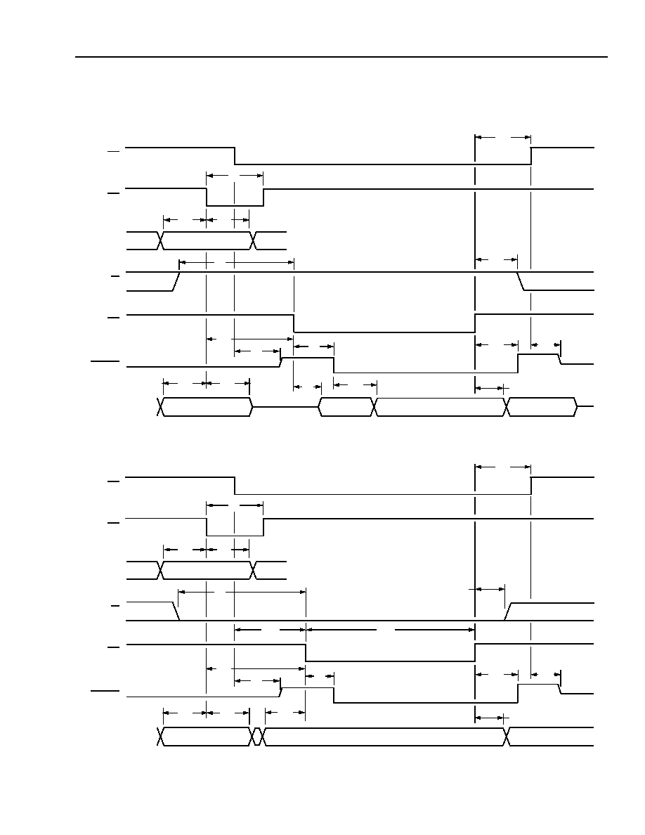
Figure 1. Mode 1--Read Cycle Timing (MPMODE = 0, MPMUX = 0)
5-6423(F)
Figure 2. Mode 1--Write Cycle Timing (MPMODE = 0, MPMUX = 0)
AD[0:7]
DTACK
DS
R/W
A[0:11]
AS
CS
t1
t2
t3
VALID ADDRESS
t5
t6
t7
t8
t10
t9
VALID DATA
t13
t15
t14
t12
t11
AD[0:7]
DTACK
DS
R/W
A[0:11]
AS
CS
t1
t2
t3
VALID ADDRESS
t16
t25
t7
t8
t17
VALID DATA
t13
t19
t14
t12
t18
t5
t20
Agere Systems Inc.
5
Device Advisory
September 1999
T7633 Device Advisory for Version 1.0 of the Device
Microprocessor Interface
(continued)
I/O Timing
(continued)
5-6424(F)
Figure 3. Mode 2--Read Cycle Timing (MPMODE = 0, MPMUX = 1)
5-6425(F)
Figure 4. Mode 2--Write Cycle Timing (MPMODE = 0, MPMUX = 1)
AD[0:7]
DTACK
DS
R/W
A[8:11]
AS
CS
t1
t21
t22
VALID ADDRESS
t5
t23
t7
t8
t10
t9
VALID DATA
t13
t15
t14
t12
t11
VALID ADDRESS
t21
t22
AD[0:7]
DTACK
DS
R/W
A[8:11]
AS
CS
t1
t21
t22
VALID ADDRESS
t5
t24
t7
t8
t17
VALID DATA
t13
t19
t14
t12
t18
VALID ADDRESS
t21
t22
t25
t20
6
Agere Systems Inc.
Device Advisory
September 1999
T7633 Device Advisory for Version 1.0 of the Device
Microprocessor Interface
(continued)
I/O Timing
(continued)
5-6426(F)r.1
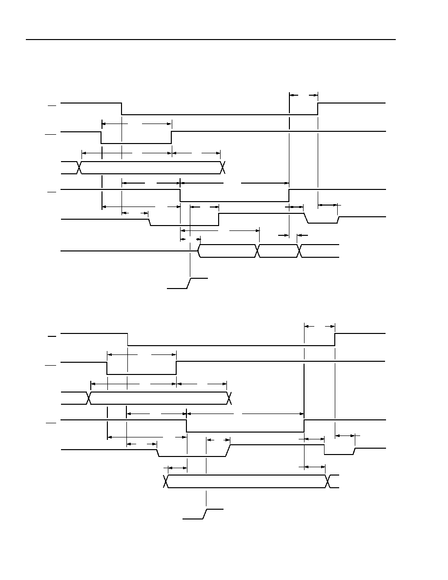
Figure 5. Mode 3--Read Cycle Timing (MPMODE = 1, MPMUX = 0)
5-6427(F)
Figure 6. Mode 3--Write Cycle Timing (MPMODE = 1, MPMUX = 0)
MPCK
AD[0:7]
RDY
RD
A[0:11]
ALE
CS
t31
t32
t33
VALID ADDRESS
t34
t50
t35
VALID DATA
t42
t41
t37
t36
t40
t39
t38
t43
MPCK
AD[0:7]
RDY
WR
A[0:11]
ALE
CS
t31
t32
t33
VALID ADDRESS
t44
t51
t45
VALID DATA
t42
t37
t36
t47
t46
t48
t49

Agere Systems Inc.
7
Device Advisory
September 1999
T7633 Device Advisory for Version 1.0 of the Device
Microprocessor Interface
(continued)
I/O Timing
(continued)
5-6428(F)r.1
Figure 7. Mode 4--Read Cycle Timing (MPMODE = 1, MPMUX = 1)
5-6429(F)r.1
Figure 8. Mode 4--Write Cycle Timing (MPMODE = 1, MPMUX = 1)
MPCK
AD
RDY
RD
A[8:11]
ALE
CS
t31
VALID ADDRESS
VALID DATA
t52
t53
t34
t54
t36
t37
t39
t38
VALID ADDRESS
t52
t53
t43
t41
t42
t40
t50
MPCK
AD
RDY
WR
A[8:11]
ALE
CS
t31
VALID ADDRESS
VALID DATA
t52
t53
t44
t55
t36
t37
VALID ADDRESS
t52
t53
t49
t48
t42
t47
t51
t46

8
Agere Systems Inc.
Device Advisory
September 1999
T7633 Device Advisory for Version 1.0 of the Device
Data Pattern Limitation for Proper Functionality of the LIU Internal Full Local
Loopback (FLLOOP)
One of the loopback modes built into the T7633 is the line interface (LIU) full local loopback (FLLOOP). This mode
connects the LIU transmit driver to the LIU line receiver circuit. This loopback mode is controlled by register
LIU_REG5 bit 2 and bit 3. The FLLOOP function is activated when LIU_REG5, bit 2 = 1 and bit 3 = 0.
Issue
In the case of a data pattern with more than 400 continuous zeros, this loopback mode could possibly be unreli-
able. The possible failure mode is the following:
1.
Latching of the data in either the one or zero state, and/or
2.
An improper period for the recovered line clock (RLCK).
The condition of an all-zero data pattern should not occur in framed T1 or E1 signals, nor should it occur in signals
that use B8ZS, HDB3, or ZCS coding. As a consequence, this possible fault in the FLLOOP function should have
minimal impact on T1 and E1 system applications of the T7633. If the case of an all-zeros data stream is used as a
special system test or diagnostic condition, these devices may be forced into the above fault condition when the
T7633 is in the FLLOOP state.
Solution
To avoid this possible fault condition, the FLLOOP loopback mode should not be used unless the data pattern is
limited to one not containing in excess of 400 contiguous zeros. Alternatively, limits on the content of the data
stream may be eliminated by using an equivalent external loopback in place of the FLLOOP loopback, or by using
an alternative internal loopback, such as DLLOOP in the LIU or BLB (board loopback) of the framer.
Asynchronous SYSCK and PLLCK with Jitter Attenuator in the Line Transmit Path
A feature of the T7633 Line Interface Unit (LIU) is a jitter attenuator that can be optionally included in either the line
receive or line transmit path. The jitter attenuator mode is controlled by the LIU register LIU_REG3 bits 0 and 1
(JAR and JAT). This register is located at address 403(hex) or A03(hex). Control of the jitter attenuator mode is
independent for each channel of the terminator.
Issue
In the case when the jitter attenuator is in the line transmit path and the transmit line clock, which is derived from
PLLCK, is asynchronous with SYSCK, errors may be generated in the line transmit data. These errors may appear
as pattern slips.
Solution
To avoid generation of these errors,
1.
PLLCK should be synchronous to SYSCK if the jitter attenuator is used in the transmit path,
or
2.
The jitter attenuator should not be used in the line transmit path.

Agere Systems Inc.
9
Device Advisory
September 1999
T7633 Device Advisory for Version 1.0 of the Device
AY99-010PDH Replaces AY99-007T1E1 to Incorporate the Following Updates
1.
Separate AY99-007T1E1 into two advisories: one applying to the T7630 and one applying to the T7633. This
advisory (AY99-010PDH) applies to the T7633.
2.
Page 8, added Asynchronous SYSCK and PLLCK with Jitter Attenuator in the Line Transmit Path section.

Copyright © 2002 Agere Systems Inc.
All Rights Reserved
September 1999
AY99-010PDH (Replaces AY99-007T1E1 and must accompany DS02-244BBAC)
For additional information, contact your Agere Systems Account Manager or the following:
INTERNET: http://www.agere.com
E-MAIL: docmaster@agere.com
N. AMERICA:
Agere Systems Inc., 555 Union Boulevard, Room 30L-15P-BA, Allentown, PA 18109-3286
1-800-372-2447, FAX 610-712-4106 (In CANADA: 1-800-553-2448, FAX 610-712-4106)
ASIA: Agere Systems Hong Kong Ltd., Suites 3201 & 3210-12, 32/F, Tower 2, The Gateway, Harbour City, Kowloon
Tel. (852) 3129-2000, FAX (852) 3129-2020
CHINA: (86) 21-5047-1212 (Shanghai), (86) 10-6522-5566 (Beijing), (86) 755-695-7224 (Shenzhen)
JAPAN: (81) 3-5421-1600 (Tokyo), KOREA: (82) 2-767-1850 (Seoul), SINGAPORE: (65) 6778-8833, TAIWAN: (886) 2-2725-5858 (Taipei)
EUROPE: Tel. (44) 7000 624624, FAX (44) 1344 488 045
Agere Systems Inc. reserves the right to make changes to the product(s) or information contained herein without notice. No liability is assumed as a result of their use or application.
Agere, Agere Systems, and the Agere logo are trademarks of Agere Systems Inc.

Device Advisory
August 1999
T7633 Device Advisory Describing Differences
Between Version 1.0 and Version 2.0 of Device
Introduction
This advisory applies only to the T7633 Dual T1/E1 3.3 V Short-Haul Terminator, and it describes the differ-
ences between the two versions of the device.
Data Sheet Changes
Table 148, Framer FDL Control Command Register (FRM_PR21) on page 189 of the May 1998
T7633 Dual
T1/E1 3.3 V Short-Haul Terminator
Advance Data Sheet (DS02-244BBAC).
s
In version 1.0 of the device, bit 0 is reserved and must be cleared (write to 0).
s
In version 2.0 of the device, bit 0 = 1 disables the receive frame sync (RFS) output when the receive framer
is in a loss of frame alignment (LFA) state; when bit 0 = 0, the device operates the same as version 1.0 of the
device.
Device Operation Updates
LIU Full Local Loopback (FLLOOP)
In version 1.0 of the device, when FLLOOP is enabled, the device occasionally drops 1s from the data pattern.
This behavior is 1s density dependent, therefore, some data sequences are more sensitive than others.
In version 2.0 of the device, the sensitivity to 1s density no longer occurs.
Microprocessor Interface Timing
In version 1.0 of the device, the LIU alarm status register (LIU_REG0) is clear-on-read (COR) and requires a
modification to the microprocesser interface timing to guarantee proper operation. The timing requirements are
described in the December 1998
T7633 Device Advisory for Version 1.0 of the Device
(AY99-007T1E1).
In version 2.0 of the device, the timing modification is no longer required.

Copyright © 2002 Agere Systems Inc.
All Rights Reserved
August 1999
AY99-033PDH (Must accompany DS02-244BBAC)
For additional information, contact your Agere Systems Account Manager or the following:
INTERNET: http://www.agere.com
E-MAIL: docmaster@agere.com
N. AMERICA:
Agere Systems Inc., 555 Union Boulevard, Room 30L-15P-BA, Allentown, PA 18109-3286
1-800-372-2447, FAX 610-712-4106 (In CANADA: 1-800-553-2448, FAX 610-712-4106)
ASIA: Agere Systems Hong Kong Ltd., Suites 3201 & 3210-12, 32/F, Tower 2, The Gateway, Harbour City, Kowloon
Tel. (852) 3129-2000, FAX (852) 3129-2020
CHINA: (86) 21-5047-1212 (Shanghai), (86) 10-6522-5566 (Beijing), (86) 755-695-7224 (Shenzhen)
JAPAN: (81) 3-5421-1600 (Tokyo), KOREA: (82) 2-767-1850 (Seoul), SINGAPORE: (65) 6778-8833, TAIWAN: (886) 2-2725-5858 (Taipei)
EUROPE: Tel. (44) 7000 624624, FAX (44) 1344 488 045
Agere Systems Inc. reserves the right to make changes to the product(s) or information contained herein without notice. No liability is assumed as a result of their use or application.
Agere, Agere Systems, and the Agere logo are trademarks of Agere Systems Inc.

Advance Data Sheet
May 2002
T7633 Dual T1/E1 3.3 V Short-Haul Terminator
Features
The T7633 Dual T1/E1 Terminator consists of two
independent, highly integrated, software-config-
urable, full-featured short-haul transceiver/framers.
The T7633 provides glueless interconnection from a
T1/E1 line to a digital PCM system. Minimal external
clocks are needed. Only a system clock/frame sync
and a phase-locked line rate clock are required. Sys-
tem diagnostic and performance monitoring capabil-
ity with integrated programmable test pattern
generator/detector and loopback modes is provided.
Power Requirements and Package
s
Single 3.3 V ± 5% supply.
s
Low power: 375 mW per channel maximum.
s
144-pin TQFP package.
s
Operating temperature range: ≠40 ∞C to +85 ∞C.
T1/E1 Line Interface Features
s
Full T1/E1 pulse template compliance.
s
Receiver provides equalization for up to 11 dB of
loss.
s
Digital clock and data recovery.
s
Line coding: B8ZS, HDB3, ZCS, and AMI.
s
Line interface coupling and matching networks for
T1 and E1 (120
and 75
).
T1/E1 Framer Features
s
Supports T1 framing modes ESF, D4,
SLC
Æ
-96,
T1DM DDS.
s
Supports G.704 basic and CRC-4 multiframe for-
mat E1 framing and procedures consistent with
G.706.
s
Supports unframed transmission format.
s
T1 signaling modes: transparent; ESF 2-state,
4-state, and 16-state; D4 2-state and 4-state;
SLC
-
96 2-state, 4-state, 9-state, and 16-state. E1 sig-
naling modes: transparent, CAS, CCS, and IRMS.
s
Alarm reporting and performance monitoring per
AT&T
Æ
,
ANSI
Æ
, and ITU-T standards.
s
Programmable, independent transmit and receive
system interfaces at a 2.048 MHz, 4.096 MHz, or
8.192 MHz data rate.
s
System interface master mode for generation of
system frame sync from the line source.
s
Internal phase-locked loop (with external VCXO)
for generation of system clock from the line source.
Facility Data Link Features
s
HDLC or transparent modes.
s
Automatic transmission and detection of
ANSI
T1.403 FDL performance report message and bit-
oriented codes.
s
64-byte FIFO in both transmit and receive direc-
tions.
Microprocessor Interface
s
33 MHz, 8-bit data interface, no wait-states.
s
Intel
Æ
or
Motorola
Æ
interface modes with multi-
plexed or demultiplexed buses.
s
Directly addressable control registers.
Applications
s
Customer Premises Equipment--CSU/DSU,
routers, digital PBX, channel banks (CB), base
transceiver stations (BTS-picocell), small switches,
and digital subscriber loop access multiplexers
(DSLAM).
s
Loop/Access--DLC/IDLC, DCS, BTS (microcell/
macrocell), DSLAMs, and multiplexers (terminal,
synchronous/asynchronous, add drop).
s
Central Office--Digital switches, DCS, CB,
access concentrators, remote switch modules
(RSM), and DSLAMs.
s
Test Equipment--Transmission/BERT tester.

2
Agere Systems Inc.
Advance Data Sheet
May 2002
T7633 Dual T1/E1 3.3 V Short-Haul Terminator
Table of Contents
Contents
Page
Features ................................................................................................................................................................... 1
Power Requirements and Package .................................................................................................................... 1
T1/E1 Line Interface Features............................................................................................................................ 1
T1/E1 Framer Features ...................................................................................................................................... 1
Facility Data Link Features................................................................................................................................. 1
Microprocessor Interface.................................................................................................................................... 1
Applications ........................................................................................................................................................ 1
Feature Descriptions .............................................................................................................................................. 13
T1/E1 Line Interface Features.......................................................................................................................... 13
T1/E1 Framer Features .................................................................................................................................... 13
Facility Data Link Features............................................................................................................................... 14
User-Programmable Microprocessor Interface ................................................................................................ 14
Functional Description ............................................................................................................................................ 15
Pin Information ....................................................................................................................................................... 19
Line Interface Unit: Block Diagram ......................................................................................................................... 26
Line Interface Unit: Receive ................................................................................................................................... 26
Data Recovery.................................................................................................................................................. 26
Jitter Accommodation and Jitter Transfer Without the Jitter Attenuator ........................................................... 27
Receive Line Interface Configuration Modes ................................................................................................... 27
T1/DS1 LIU Receiver Specifications ................................................................................................................ 30
CEPT LIU Receiver Specifications ................................................................................................................... 31
Line Interface Unit: Transmit .................................................................................................................................. 34
Output Pulse Generation.................................................................................................................................. 34
LIU Transmitter Configuration Modes .............................................................................................................. 35
LIU Transmitter Alarms .................................................................................................................................... 35
DSX-1 Transmitter Pulse Template and Specifications ................................................................................... 37
CEPT Transmitter Pulse Template and Specifications .................................................................................... 38
Line Interface Unit: Jitter Attenuator ....................................................................................................................... 40
Generated (Intrinsic) Jitter................................................................................................................................ 40
Jitter Transfer Function .................................................................................................................................... 40
Jitter Accommodation....................................................................................................................................... 41
Jitter Attenuator Enable (Transmit or Receive Path) ........................................................................................ 41
Line Interface Unit: Loopbacks ............................................................................................................................... 44
Full Local Loopback (FLLOOP)........................................................................................................................ 44
Remote Loopback (RLOOP) ............................................................................................................................ 44
Digital Local Loopback (DLLOOP) ................................................................................................................... 44
Line Interface Unit: Other Features ........................................................................................................................ 45
LIU Powerdown (PWRDN) ............................................................................................................................... 45
Loss of Framer Receive Line Clock (LOFRMRLCK Pin).................................................................................. 45
In-Circuit Testing and Driver High-Impedance State (3-STATE)...................................................................... 45
LIU Delay Values.............................................................................................................................................. 45
SYSCK Reference Clock........................................................................................................................................ 46
Line Interface Unit: Line Interface Networks........................................................................................................... 48
LIU-Framer Interface .............................................................................................................................................. 50
LIU-Framer Physical Interface.......................................................................................................................... 50
Interface Mode and Line Encoding................................................................................................................... 52
DS1: Zero Code Suppression (ZCS)................................................................................................................ 53
CEPT: High-Density Bipolar of Order 3 (HDB3)............................................................................................... 54

Agere Systems Inc.
3
Advance Data Sheet
May 2002
T7633 Dual T1/E1 3.3 V Short-Haul Terminator
Table of Contents
(continued)
Contents
Page
Frame Formats........................................................................................................................................................55
T1 Framing Structures ......................................................................................................................................55
T1 Loss of Frame Alignment (LFA) ...................................................................................................................62
T1 Frame Recovery Alignment Algorithms .......................................................................................................63
T1 Robbed-Bit Signaling ...................................................................................................................................64
CEPT 2.048 Basic Frame, CRC-4 Time Slot 0, and Signaling Time Slot 16 Multiframe Structures .................66
CEPT 2.048 Basic Frame Structure..................................................................................................................67
CEPT Loss of Basic Frame Alignment (LFA)....................................................................................................69
CEPT Loss of Frame Alignment Recovery Algorithm .......................................................................................69
CEPT Time Slot 0 CRC-4 Multiframe Structure ................................................................................................70
CEPT Loss of CRC-4 Multiframe Alignment (LTS0MFA)..................................................................................71
CEPT Loss of CRC-4 Multiframe Alignment Recovery Algorithms ...................................................................72
CEPT Time Slot 16 Multiframe Structure ..........................................................................................................76
CEPT Loss of Time Slot 16 Multiframe Alignment (LTS16MFA) ......................................................................78
CEPT Loss of Time Slot 16 Multiframe Alignment Recovery Algorithm............................................................78
CEPT Time Slot 0 FAS/NOT FAS Control Bits .......................................................................................................79
FAS/NOT FAS Si- and E-Bit Source .................................................................................................................79
NOT FAS A-Bit (CEPT Remote Frame Alarm) Sources ...................................................................................80
NOT FAS Sa-Bit Sources..................................................................................................................................80
Sa Facility Data Link Access.............................................................................................................................81
NOT FAS Sa Stack Source and Destination.....................................................................................................82
CEPT Time Slot 16 X0--X2 Control Bits ..........................................................................................................84
Signaling Access.....................................................................................................................................................85
Transparent Signaling .......................................................................................................................................85
DS1: Robbed-Bit Signaling ...............................................................................................................................85
CEPT: Time Slot 16 Signaling...........................................................................................................................86
Auxiliary Framer I/O Timing ....................................................................................................................................87
Alarms and Performance Monitoring.......................................................................................................................91
Interrupt Generation ..........................................................................................................................................91
Alarm Definition.................................................................................................................................................91
Event Counters Definition .................................................................................................................................97
Loopback and Transmission Modes .................................................................................................................99
Line Test Patterns ...........................................................................................................................................102
Automatic and On-Demand Commands .........................................................................................................106
Facility Data Link (FDL).........................................................................................................................................108
Receive Facility Data Link Interface................................................................................................................108
Transmit Facility Data Link Interface...............................................................................................................114
HDLC Operation..............................................................................................................................................115
Transparent Mode...........................................................................................................................................118
Diagnostic Modes............................................................................................................................................120
Phase-Lock Loop Circuit .......................................................................................................................................122
Framer-System (CHI) Interface .............................................................................................................................124
DS1 Modes .....................................................................................................................................................124
CEPT Modes...................................................................................................................................................124
Receive Elastic Store ......................................................................................................................................124
Transmit Elastic Store .....................................................................................................................................124
Concentration Highway Interface (CHI) ................................................................................................................125
CHI Parameters ..............................................................................................................................................126
CHI Frame Timing...........................................................................................................................................129
CHI Offset Programming.................................................................................................................................132

4
Agere Systems Inc.
Advance Data Sheet
May 2002
T7633 Dual T1/E1 3.3 V Short-Haul Terminator
Table of Contents
(continued)
Contents
Page
JTAG Boundary-Scan Specification ..................................................................................................................... 135
Principle of the Boundary Scan ...................................................................................................................... 135
Test Access Port Controller............................................................................................................................ 136
Instruction Register ........................................................................................................................................ 138
Boundary-Scan Register ................................................................................................................................ 139
BYPASS Register........................................................................................................................................... 139
IDCODE Register ........................................................................................................................................... 139
3-State Procedures ........................................................................................................................................ 139
Microprocessor Interface ...................................................................................................................................... 140
Overview ........................................................................................................................................................ 140
Microprocessor Configuration Modes............................................................................................................. 140
Microprocessor Interface Pinout Definitions ................................................................................................... 141
Microprocessor Clock (MPCLK) Specifications.............................................................................................. 142
Microprocessor Interface Register Address Map ........................................................................................... 142
I/O Timing....................................................................................................................................................... 142
Reset .................................................................................................................................................................... 149
Hardware Reset (Pin 43/139)......................................................................................................................... 149
Software Reset/Software Restart ................................................................................................................... 149
Interrupt Generation ............................................................................................................................................. 149
Register Architecture ............................................................................................................................................ 150
Global Register Architecture................................................................................................................................. 154
Global Register Structure ..................................................................................................................................... 155
Primary Block Interrupt Status Register (GREG0) ......................................................................................... 155
Primary Block Interrupt Enable Register (GREG1) ........................................................................................ 155
Global Loopback Control Register (GREG2) ................................................................................................. 156
Global Loopback Control Register (GREG3) ................................................................................................. 156
Global Control Register (GREG4) .................................................................................................................. 157
Device ID and Version Registers (GREG5--GREG7) ................................................................................... 157
Line Interface Unit (LIU) Register Architecture..................................................................................................... 158
Line Interface Alarm Register ............................................................................................................................... 159
Alarm Status Register (LIU_REG0)................................................................................................................ 159
Line Interface Alarm Interrupt Enable Register .................................................................................................... 159
Alarm Interrupt Enable Register (LIU_REG1) ................................................................................................ 159
Line Interface Control Registers ........................................................................................................................... 160
LIU Control Register (LIU_REG2) .................................................................................................................. 160
LIU Control Register (LIU_REG3) .................................................................................................................. 161
LIU Control Register (LIU_REG4) .................................................................................................................. 162
LIU Configuration Register (LIU_REG5) ........................................................................................................ 162
LIU Configuration Register (LIU_REG6) ........................................................................................................ 163
Framer Register Architecture ............................................................................................................................... 164
Framer Status/Counter Registers................................................................................................................... 165
Framer Parameter/Control Registers ............................................................................................................. 180
FDL Register Architecture .................................................................................................................................... 211
FDL Parameter/Control Registers (800--80E; E00--E0E) .................................................................................. 212
Register Maps ...................................................................................................................................................... 219
Global Registers............................................................................................................................................. 219
Line Interface Unit Parameter/Control and Status Registers ......................................................................... 219
Framer Parameter/Control Registers (READ-WRITE) ................................................................................... 220
Receive Framer Signaling Registers (READ-ONLY) ..................................................................................... 222
Framer Unit Parameter Register Map ............................................................................................................ 223
Transmit Signaling Registers (READ/WRITE) ............................................................................................... 226
Facility Data Link Parameter/Control and Status Registers (READ-WRITE) ................................................. 227

Agere Systems Inc.
5
Advance Data Sheet
May 2002
T7633 Dual T1/E1 3.3 V Short-Haul Terminator
Table of Contents
(continued)
Contents
Page
Absolute Maximum Ratings ..................................................................................................................................228
Operating Conditions ............................................................................................................................................228
Handling Precautions ............................................................................................................................................228
Electrical Characteristics .......................................................................................................................................229
Logic Interface Characteristics........................................................................................................................229
Power Supply Bypassing ......................................................................................................................................229
Outline Diagram ....................................................................................................................................................230
144-Pin TQFP .................................................................................................................................................230
Ordering Information .............................................................................................................................................231
Index .....................................................................................................................................................................232

6
Agere Systems Inc.
Advance Data Sheet
May 2002
T7633 Dual T1/E1 3.3 V Short-Haul Terminator
List of Figures
Figure
Page
Figure 1. T7633 Block Diagram (One of Two Channels)........................................................................................ 15
Figure 2. T7633 Block Diagram: Receive Section (One of Two Channels)............................................................ 17
Figure 3. T7633 Block Diagram: Transmit Section (One of Two Channels)........................................................... 18
Figure 4. Pin Assignment ....................................................................................................................................... 19
Figure 5. Block Diagram of Line Interface Unit: Single Channel ............................................................................ 26
Figure 6. T1/DS1 Receiver Jitter Accommodation Without Jitter Attenuator.......................................................... 32
Figure 7. T1/DS1 Receiver Jitter Transfer Without Jitter Attenuator ...................................................................... 32
Figure 8. CEPT/E1 Receiver Jitter Accommodation Without Jitter Attenuator ....................................................... 33
Figure 9. CEPT/E1 Receiver Jitter Transfer Without Jitter Attenuator ................................................................... 33
Figure 10. DSX-1 Isolated Pulse Template ............................................................................................................ 37
Figure 11. ITU-T G.703 Pulse Template ................................................................................................................ 38
Figure 12. T1/DS1 Receiver Jitter Accommodation with Jitter Attenuator.............................................................. 42
Figure 13. T1/DS1 Jitter Transfer of the Jitter Attenuator....................................................................................... 42
Figure 14. CEPT/E1 Receiver Jitter Accommodation with Jitter Attenuator........................................................... 43
Figure 15. CEPT/E1 Jitter Transfer of the Jitter Attenuator.................................................................................... 43
Figure 16. Line Termination Circuitry ..................................................................................................................... 48
Figure 17. T7633 Line Interface Unit Approximate Equivalent Analog I/O Circuits ................................................ 49
Figure 18. Block Diagram of Framer Line Interface................................................................................................ 50
Figure 19. Transmit Framer TLCK to TND, TPD and Receive Framer RND, RPD to RLCK Timing...................... 51
Figure 20. T1 Frame Structure ............................................................................................................................... 55
Figure 21. T1 Transparent Frame Structure........................................................................................................... 56
Figure 22. T7633 Facility Data Link Access Timing of the Transmit and Receive Framer Sections ...................... 58
Figure 23. ITU 2.048 Basic Frame, CRC-4 Multiframe, and Channel Associated Signaling Multiframe
Structures............................................................................................................................................... 66
Figure 24. CEPT Transparent Frame Structure ..................................................................................................... 68
Figure 25. Receive CRC-4 Multiframe Search Algorithm Using the 100 ms Internal Timer................................... 73
Figure 26. Receive CRC-4 Multiframe Search Algorithm for Automatic, CRC-4/Non-CRC-4 Equipment
Interworking as Defined by ITU (From ITU Rec. G.706, Annex B.2.2 - 1991) ...................................... 75
Figure 27. Facility Data Link Access Timing of the Transmit and Receive Framer Sections in the CEPT Mode ... 81
Figure 28. Transmit and Receive Sa Stack Accessing Protocol ............................................................................ 83
Figure 29. Timing Specification for RFRMCK, RFRMDATA, and RFS in DS1 Mode............................................. 87
Figure 30. Timing Specification for TFS, TLCK, and TPD in DS1 Mode ................................................................ 87
Figure 31. Timing Specification for RFRMCK, RFRMDATA, and RFS in CEPT Mode .......................................... 88
Figure 32. Timing Specification for RFRMCK, RFRMDATA, RFS, and RSSFS in CEPT Mode ............................ 88
Figure 33. Timing Specification for RCRCMFS in CEPT Mode.............................................................................. 89
Figure 34. Timing Specification for TFS, TLCK, and TPD in CEPT Mode ............................................................. 89
Figure 35. Timing Specification for TFS, TLCK, TPD, and TSSFS in CEPT Mode ................................................ 90
Figure 36. Timing Specification for TFS, TLCK, TPD, and TCRCMFS in CEPT Mode .......................................... 90
Figure 37. Relation Between RLCK1 and Interrupt (Pin 99)................................................................................... 91
Figure 38. Timing for Generation of LOPLLCK (Pin 39/143).................................................................................. 93
Figure 39. The T and V Reference Points for a Typical CEPT E1 Application....................................................... 96
Figure 40. Loopback and Test Transmission Modes............................................................................................ 101
Figure 41. 20-Stage Shift Register Used to Generate the Quasi-Random Signal................................................ 102
Figure 42. 15-Stage Shift Register Used to Generate the Pseudorandom Signal ............................................... 103
Figure 43. T7633 Facility Data Link Access Timing of the Transmit and Receive Framer Sections .................... 108
Figure 44. Block Diagram for the Receive Facility Data Link Interface ................................................................ 109
Figure 45. Block Diagram for the Transmit Facility Data Link Interface ............................................................... 114
Figure 46. Local Loopback Mode ......................................................................................................................... 120
Figure 47. Remote Loopback Mode ..................................................................................................................... 121
Figure 48. T7633 Phase Detector Circuitry .......................................................................................................... 123
Figure 49. Nominal Concentration Highway Interface Timing (for FRM_PR43 bit 0--bit 2 = 100 (Binary)) ......... 129
Figure 50. CHIDTS Mode Concentration Highway Interface Timing .................................................................... 130

Agere Systems Inc.
7
Advance Data Sheet
May 2002
T7633 Dual T1/E1 3.3 V Short-Haul Terminator
List of Figures
(continued)
Figure
Page
Figure 51. Associated Signaling Mode Concentration Highway Interface Timing.................................................131
Figure 52. CHI Timing with ASM and CHIDTS Enabled .......................................................................................131
Figure 53. TCHIDATA and RCHIDATA to CHICK Relationship with CMS = 0 (CEX = 3 and CER = 4,
Respectively) .......................................................................................................................................133
Figure 54. CHI TCHIDATA and RCHIDATA to CHICK Relationship with CMS = 1 (CEX = 3 and CER = 6,
Respectively) .......................................................................................................................................133
Figure 55. Receive CHI (RCHIDATA) Timing .......................................................................................................134
Figure 56. Transmit CHI (TCHIDATA) Timing .......................................................................................................134
Figure 57. Block Diagram of the T7633's Boundary-Scan Test Logic...................................................................135
Figure 58. BS TAP Controller State Diagram........................................................................................................136
Figure 59. Mode 1--Read Cycle Timing (MPMODE = 0, MPMUX = 0) ................................................................145
Figure 60. Mode 1--Write Cycle Timing (MPMODE = 0, MPMUX = 0) ................................................................145
Figure 61. Mode 2--Read Cycle Timing (MPMODE = 0, MPMUX = 1) ................................................................146
Figure 62. Mode 2--Write Cycle Timing (MPMODE = 0, MPMUX = 1) ................................................................146
Figure 63. Mode 3--Read Cycle Timing (MPMODE = 1, MPMUX = 0) ................................................................147
Figure 64. Mode 3--Write Cycle Timing (MPMODE = 1, MPMUX = 0) ................................................................147
Figure 65. Mode 4--Read Cycle Timing (MPMODE = 1, MPMUX = 1) ................................................................148
Figure 66. Mode 4--Write Cycle Timing (MPMODE = 1, MPMUX = 1) ................................................................148

8
Agere Systems Inc.
Advance Data Sheet
May 2002
T7633 Dual T1/E1 3.3 V Short-Haul Terminator
List of Tables
Table
Page
Table 1. Pin Descriptions........................................................................................................................................ 20
Table 2. Digital Loss of Signal Standard Select ..................................................................................................... 28
Table 3. LOSSD and RCVAIS Control Configurations (Not Valid During Loopback Modes) ................................. 29
Table 4. DS1 LIU Receiver Specifications.............................................................................................................. 30
Table 5. CEPT LIU Receiver Specifications ........................................................................................................... 31
Table 6. Transmit Line Interface Short-Haul Equalizer/Rate Control ..................................................................... 34
Table 7. DSX-1 Pulse Template Corner Points (from CB119, T1.102) .................................................................. 37
Table 8. DS1 Transmitter Specifications ................................................................................................................ 38
Table 9. CEPT Transmitter Specifications.............................................................................................................. 39
Table 10. Loopback Control ................................................................................................................................... 44
Table 11. SYSCK (16x, CKSEL = 1) Timing Specifications ................................................................................... 46
Table 12. SYSCK (1x, CKSEL = 0) Timing Specifications ..................................................................................... 46
Table 13. Termination Components by Application................................................................................................ 48
Table 14. AMI Encoding ......................................................................................................................................... 52
Table 15. DS1 ZCS Encoding ................................................................................................................................ 53
Table 16. DS1 B8ZS Encoding............................................................................................................................... 53
Table 17. ITU HDB3 Coding................................................................................................................................... 54
Table 18. T-Carrier Hierarchy................................................................................................................................. 55
Table 19. D4 Superframe Format........................................................................................................................... 57
Table 20. DDS Channel-24 Format ........................................................................................................................ 58
Table 21.
SLC
-96 Data Link Block Format ............................................................................................................. 59
Table 22.
SLC
-96 Line Switch Message Codes ..................................................................................................... 60
Table 23. Transmit and Receive
SLC
-96 Stack Structure...................................................................................... 60
Table 24. Extended Superframe (ESF) Structure................................................................................................... 61
Table 25. T1 Loss of Frame Alignment Criteria...................................................................................................... 62
Table 26. T1 Frame Alignment Procedures............................................................................................................ 63
Table 27. Robbed-Bit Signaling Options ................................................................................................................ 64
Table 28.
SLC
-96 9-State Signaling Format........................................................................................................... 64
Table 29. 16-State Signaling Format...................................................................................................................... 65
Table 30. Allocation of Bits 1 to 8 of the FAS Frame and the NOT FAS Frame..................................................... 67
Table 31. ITU CRC-4 Multiframe Structure ............................................................................................................ 70
Table 32. ITU CEPT Time Slot 16 Channel Associated Signaling Multiframe Structure........................................ 76
Table 33. CEPT IRSM Signaling Multiframe Structure........................................................................................... 77
Table 34. Transmit and Receive Sa Stack Structure.............................................................................................. 82
Table 35. Associated Signaling Mode CHI 2-Byte Time-Slot Format for DS1 Frames .......................................... 86
Table 36. Associated Signaling Mode CHI 2-Byte Time-Slot Format for Stuffed Channels ................................... 86
Table 37. Associated Signaling Mode CHI 2-Byte Time-Slot Format for CEPT ..................................................... 86
Table 38. Red Alarm or Loss of Frame Alignment Conditions ............................................................................... 92
Table 39. Remote Frame Alarm Conditions ........................................................................................................... 92
Table 40. Alarm Indication Signal Conditions......................................................................................................... 93
Table 41. Sa6 Bit Coding Recognized by the Receive Framer .............................................................................. 95
Table 42. Sa6 Bit Coding of NT1 Interface Events Recognized by the Receive Framer ....................................... 96
Table 43. AUXP Synchronization and Clear Sychronization Process .................................................................... 96
Table 44. Event Counters Definition....................................................................................................................... 97
Table 45. Summary of the Deactivation of SSTSSLB and SSTSLLB Modes as a Function of
Activating the Primary Loopback Modes .............................................................................................. 100
Table 46. Register FRM_PR69 Test Patterns ...................................................................................................... 103
Table 47. Register FRM_PR70 Test Patterns ...................................................................................................... 104
Table 48. Automatic Enable Commands .............................................................................................................. 106
Table 49. On-Demand Commands....................................................................................................................... 107
Table 50. Receive
ANSI
Code.............................................................................................................................. 110

Agere Systems Inc.
9
Advance Data Sheet
May 2002
T7633 Dual T1/E1 3.3 V Short-Haul Terminator
List of Tables
(continued)
Table
Page
Table 51. Performance Report Message Structure...............................................................................................110
Table 52. FDL Performance Report Message Field Definition..............................................................................111
Table 53. Octet Contents and Definition ...............................................................................................................111
Table 54. Receive Status of Frame Byte ..............................................................................................................112
Table 55. HDLC Frame Format.............................................................................................................................115
Table 56. Receiver Operation in Transparent Mode .............................................................................................119
Table 57. Summary of the T7633's Concentration Highway Interface Parameters ..............................................126
Table 58. Programming Values for TOFF[2:0] and ROFF[2:0] when CMS = 0.....................................................132
Table 59. Programming Values for TOFF[2:0] when CMS = 1 .............................................................................132
Table 60. Programming Values for ROFF[2:0] when CMS = 1 .............................................................................132
Table 61. TAP Controller States in the Data Register Branch ..............................................................................137
Table 62. TAP Controller States in the Instruction Register Branch .....................................................................137
Table 63. T7633's Boundary-Scan Instructions ....................................................................................................138
Table 64. IDCODE Register ..................................................................................................................................139
Table 65. Microprocessor Configuration Modes ...................................................................................................140
Table 66. Mode [1--4] Microprocessor Pin Definitions .........................................................................................141
Table 67. Microprocessor Input Clock Specifications ...........................................................................................142
Table 68. T7633 Register Address Map ...............................................................................................................142
Table 69. Microprocessor Interface I/O Timing Specifications ..............................................................................143
Table 70. Status Register and Corresponding Interrupt Enable Register for Functional Blocks...........................149
Table 71. Asserted Value and Deasserted State for GREG4 Bit 4 and Bit 6 Logic Combinations .......................149
Table 72. Register Summary ................................................................................................................................150
Table 73. Global Register Set (0x000--0x008) ....................................................................................................154
Table 74. Primary Block Interrupt Status Register (GREG0) (000).......................................................................155
Table 75. Primary Block Interrupt Enable Register (GREG1) (001)......................................................................155
Table 76. Global Loopback Control Register (GREG2) (002) ...............................................................................156
Table 77. Global Loopback Control Register (GREG3) (003) ...............................................................................156
Table 78. Global Control Register (GREG4) (004) ...............................................................................................157
Table 79. Device ID and Version Registers (GREG5--GREG7) (005--007) .......................................................157
Table 80. Line Interface Units Register Set ((400--40F); (A00--A0F)) ................................................................158
Table 81. LIU Alarm Status Register (LIU_REG0) (400, A00) ..............................................................................159
Table 82. LIU Alarm Interrupt Enable Register (LIU_REG1) (401, A01)...............................................................159
Table 83. LIU Control Register (LIU_REG2) (402, A02) .......................................................................................160
Table 84. LIU Control Register (LIU_REG3) (403, A03) .......................................................................................161
Table 85. LIU Register (LIU_REG4) (404, A04)....................................................................................................162
Table 86. LIU Configuration Register (LIU_REG5) (405, A05) .............................................................................162
Table 87. LIU Configuration Register (LIU_REG6) (406, A06) .............................................................................163
Table 88. Framer Status and Control Blocks Address Range (Hexadecimal) ......................................................164
Table 89. Interrupt Status Register (FRM_SR0) (600; C00) .................................................................................165
Table 90. Facility Alarm Condition Register (FRM_SR1) (601; C01) ....................................................................166
Table 91. Remote End Alarm Register (FRM_SR2) (602; C02) ...........................................................................167
Table 92. Facility Errored Event Register-1 (FRM_SR3) (603; C03) ....................................................................168
Table 93. Facility Event Register-2 (FRM_SR4) (604; C04) .................................................................................169
Table 94. Exchange Termination and Exchange Termination Remote End Interface
Status Register (FRM_SR5) (605; C05) ...............................................................................................171
Table 95. Network Termination and Network Termination Remote End Interface
Status Register (FRM_SR6) (606; C06) ...............................................................................................172
Table 96. Facility Event Register (FRM_SR7) (607; C07) ....................................................................................173
Table 97. Bipolar Violation Counter Registers (FRM_SR8--FRM_SR9) ((608--609); (C08--C09)) ...................173
Table 98. Framing Bit Error Counter Registers (FRM_SR10--FRM_SR11) ((60A--60B); (C0A--C0B)) ............173
Table 99. CRC Error Counter Registers (FRM_SR12--FRM_SR13) ((60C--60D); (C0C--C0D)) ......................174
Table 100. E-Bit Counter Registers (FRM_SR14--FRM_SR15) ((60E--60F); (C0E--C0F)) ..............................174

10
Agere Systems Inc.
Advance Data Sheet
May 2002
T7633 Dual T1/E1 3.3 V Short-Haul Terminator
List of Tables
(continued)
Table
Page
Table 101. CRC-4 Errors at NT1 from NT2 Counter Registers (FRM_SR16--FRM_SR17)
((610--611); (C10--C11)) ................................................................................................................ 174
Table 102. E Bit at NT1 from NT2 Counter (FRM_SR18--FRM_SR19) ((612--613); (C12--C13)) ................... 174
Table 103. ET Errored Seconds Counter (FRM_SR20--FRM_SR21) ((614--615); (C14--C15)) ...................... 175
Table 104. ET Bursty Errored Seconds Counter (FRM_SR22--FRM_SR23) ((616--617); (C16--C17))........... 175
Table 105. ET Severely Errored Seconds Counter (FRM_SR24--FRM_SR25) ((618--619); (C18--C19)) ....... 175
Table 106. ET Unavailable Seconds Counter (FRM_SR26--FRM_SR27) ((61A--61B); (C1A--C1B)).............. 175
Table 107. ET-RE Errored Seconds Counter (FRM_SR28--FRM_SR29) ((61C--61D); (C1C--C1D)) ............. 175
Table 108. ET-RE Bursty Errored Seconds Counter (FRM_SR30--FRM_SR31) ((61E--61F); (C1E--C1F)) ... 175
Table 109. ET-RE Severely Errored Seconds Counter (FRM_SR32--FRM_SR33)
((620--621); (C20--C21)).................................................................................................................. 175
Table 110. ET-RE Unavailable Seconds Counter (FRM_SR34--FRM_SR35) ((622--623); (C22--C23)) ......... 176
Table 111. NT1 Errored Seconds Counter (FRM_SR36--FRM_SR37) ((624--625); (C24--C25)) .................... 176
Table 112. NT1 Bursty Errored Seconds Counter (FRM_SR38--FRM_SR39) ((626--627); (C26--C27))......... 176
Table 113. NT1 Severely Errored Seconds Counter (FRM_SR40--FRM_SR41) ((628--629); (C28--C29))..... 176
Table 114. NT1 Unavailable Seconds Counter (FRM_SR42--FRM_SR43) ((62A--62B); (C2A--C2B)) ........... 176
Table 115. NT1-RE Errored Seconds Counter (FRM_SR44--FRM_SR45) ((62C--62D); (C2C--C2D)) ........... 176
Table 116. NT1-RE Bursty Errored Seconds Counter (FRM_SR46--FRM_SR47)
((62E--62F); (C2E--C2F))................................................................................................................. 177
Table 117. NT1-RE Severely Errored Seconds Counter (FRM_SR48--FRM_SR49)
((630--631); (C30--C31)).................................................................................................................. 177
Table 118. NT1-RE Unavailable Seconds Counter (FRM_SR50--FRM_SR51) ((632--633); (C32--C33))....... 177
Table 119. Receive NOT-FAS TS0 Register (FRM_SR52) (634; C34)................................................................ 177
Table 120. Receive Sa Register (FRM_SR53) (635; C35)................................................................................... 177
Table 121.
SLC
-96 FDL Receive Stack (FRM_SR54--FRM_SR63) ((636--63F); (C36--C3F)) ........................ 178
Table 122. CEPT Sa Receive Stack (FRM_SR54--FRM_SR63) ((636--63F); (C36--C3F)) ............................. 178
Table 123. Transmit Framer
ANSI
Performance Report Message Status Register Structure ............................. 179
Table 124. Received Signaling Registers: DS1 Format (FRM_RSR0--FRM_RSR23)
((640--658); (C40--C58)).................................................................................................................. 179
Table 125. Receive Signaling Registers: CEPT Format (FRM_RSR0--FRM_RSR31)
((640--65F); (C40--C5F)) ................................................................................................................. 179
Table 126. Summary of Interrupt Group Enable Registers (FRM_PR0--FRM_PR7)
((660--667); (C60--C67)).................................................................................................................. 180
Table 127. Primary Interrupt Group Enable Register (FRM_PR0) (660; C60) ..................................................... 181
Table 128. Interrupt Enable Register (FRM_PR1) (661; C61) ............................................................................. 182
Table 129. Interrupt Enable Register (FRM_PR2) (662; C62) ............................................................................. 182
Table 130. Interrupt Enable Register (FRM_PR3) (663; C63) ............................................................................. 182
Table 131. Interrupt Enable Register (FRM_PR4) (664; C64) ............................................................................. 182
Table 132. Interrupt Enable Register (FRM_PR5) (665; C65) ............................................................................. 182
Table 133. Interrupt Enable Register (FRM_PR6) (666; C66) ............................................................................. 182
Table 134. Interrupt Enable Register (FRM_PR7) (667; C67) ............................................................................. 182
Table 135. Framer Mode Bits Decoding (FRM_PR8) (668; C68)......................................................................... 183
Table 136. Line Code Option Bits Decoding (FRM_PR8) (668; C68) .................................................................. 183
Table 137. CRC Option Bits Decoding (FRM_PR9) (669, C69)........................................................................... 184
Table 138. Alarm Filter Register (FRM_PR10) (66A; C6A).................................................................................. 185
Table 139. Errored Event Threshold Definition .................................................................................................... 185
Table 140. Errored Second Threshold Register (FRM_PR11) (66B; C6B) .......................................................... 186
Table 141. Severely Errored Second Threshold Registers (FRM_PR12--FRM_PR13)
((66C--66D; C6C--C6D)).................................................................................................................. 186
Table 142. ET1 Errored Event Enable Register (FRM_PR14) (66E; C6E) .......................................................... 186
Table 143. ET1 Remote End Errored Event Enable Register (FRM_PR15) (66F; C6F)...................................... 187
Table 144. NT1 Errored Event Enable Register (FRM_PR16) (670; C70)........................................................... 187

Agere Systems Inc.
11
Advance Data Sheet
May 2002
T7633 Dual T1/E1 3.3 V Short-Haul Terminator
List of Tables
(continued)
Table
Page
Table 145. NT1 Remote End Errored Event Enable Registers (FRM_PR17--FRM_PR18)
((671--672); (C71--C72)) ..................................................................................................................187
Table 146. Automatic AIS to the System and Automatic Loopback Enable Register
(FRM_PR19) (673; C73) .....................................................................................................................188
Table 147. Transmit Test Pattern to the Line Enable Register (FRM_PR20) (674; C74) .....................................188
Table 148. Framer FDL Control Command Register (FRM_PR21) (675; C75) ....................................................189
Table 149. Framer Transmit Line Idle Code Register (FRM_PR22) (676; C76) ...................................................189
Table 150. Framer System Stuffed Time Slot Code Register (FRM_PR23) (677; C77) .......................................189
Table 151. Primary Time-Slot Loopback Address Register (FRM_PR24) (678; C78) ..........................................190
Table 152. Loopback Decoding of Bits LBC[2:0] in FRM_PR24, Bits 7--5 ..........................................................190
Table 153. Secondary Time-Slot Loopback Address Register (FRM_PR25) (679; C79) .....................................191
Table 154. Loopback Decoding of Bits LBC[1:0] in FRM_PR25, Bits 6--5 ..........................................................191
Table 155. Framer Reset and Transparent Mode Control Register (FRM_PR26) (67A, C7A) .............................192
Table 156. Transmission of Remote Frame Alarm and CEPT Automatic Transmission of A Bit = 1
Control Register (FRM_PR27) (67B, C7B) .........................................................................................193
Table 157. CEPT Automatic Transmission of E Bit = 0 Control Register (FRM_PR28) (67C; C7C) ....................194
Table 158. Sa4--Sa8 Source Register (FRM_PR29) (67D; C7D)........................................................................195
Table 159. Sa Bits Source Control for Bit 5--Bit 7 in FRM_PR29 ........................................................................195
Table 160. Sa4--Sa8 Control Register (FRM_PR30) (67E; C7E) ........................................................................196
Table 161. Sa Transmit Stack (FRM_PR31--FRM_PR40) ((67F--688); (C7F--C88)) .......................................197
Table 162.
SLC
-96 Transmit Stack (FRM_PR31--FRM_PR40) ((67F--688); (C7F--C88))................................197
Table 163. Transmit
SLC
-96 FDL Format .............................................................................................................197
Table 164. CEPT Time Slot 16 X-Bit Remote Multiframe Alarm and AIS Control Register
(FRM_PR41) (689; C89) .....................................................................................................................198
Table 165. Framer Exercise Register (FRM_PR42) (68A; C8A) ..........................................................................198
Table 166. Framer Exercises, FRM_PR42 Bit 5--Bit 0 (68A; C8A) .....................................................................199
Table 167. DS1 System Interface Control and CEPT FDL Source Control Register (FRM_PR43) (68B; C8B) ...201
Table 168. Signaling Mode Register (FRM_PR44) (68C; C8C)............................................................................202
Table 169. CHI Common Control Register (FRM_PR45) (68D; C8D) ..................................................................203
Table 170. CHI Common Control Register (FRM_PR46) (68E; C8E) ..................................................................204
Table 171. CHI Transmit Control Register (FRM_PR47) (68F; C8F) ...................................................................205
Table 172. CHI Receive Control Register (FRM_PR48) (690; C90) .....................................................................205
Table 173. CHI Transmit Time-Slot Enable Registers (FRM_PR49--FRM_PR52) ((691--694); (C91--C94)) ...206
Table 174. CHI Receive Time-Slot Enable Registers (FRM_PR53--FRM_PR56) ((695--698); (C95--C98)) ....206
Table 175. CHI Transmit Highway Select Registers (FRM_PR57--FRM_PR60) ((699--69C); (C99--C9C)).....206
Table 176. CHI Receive Highway Select Registers (FRM_PR61--FRM_PR64) ((69D--6A0); (C9D--CA0)) .....207
Table 177. CHI Transmit Control Register (FRM_PR65) (6A1; CA1) ...................................................................207
Table 178. CHI Receive Control Register (FRM_PR66) (6A2; CA2) ....................................................................207
Table 179. Auxiliary Pattern Generator Control Register (FRM_PR69) (6A5; CA5) .............................................208
Table 180. Pattern Detector Control Register (FRM_PR70) (6A6; CA6) ..............................................................209
Table 181. Transmit Signaling Registers: DS1 Format (FRM_TSR0--FRM_TSR23)
((6E0--6F7); (CE0--CF7)) .................................................................................................................210
Table 182. Transmit Signaling Registers: CEPT Format (FRM_TSR0--FRM_TSR31)
((6E0--6FF); (CE0--CFF)) .................................................................................................................210
Table 183. FDL Register Set (800--80E); (E00--E0E) ........................................................................................211
Table 184. FDL Configuration Control Register (FDL_PR0) (800; E00) ...............................................................212
Table 185. FDL Control Register (FDL_PR1) (801; E01) .....................................................................................212
Table 186. FDL Interrupt Mask Control Register (FDL_PR2) (802; E02) .............................................................213
Table 187. FDL Transmitter Configuration Control Register (FDL_PR3) (803; E03) ............................................214
Table 188. FDL Transmitter FIFO Register (FDL_PR4) (804; E04)......................................................................214
Table 189. FDL Transmitter Mask Register (FDL_PR5) (805; E05) .....................................................................214
Table 190. FDL Receiver Interrupt Level Control Register (FDL_PR6) (806; E06) ..............................................215

12
Agere Systems Inc.
Advance Data Sheet
May 2002
T7633 Dual T1/E1 3.3 V Short-Haul Terminator
List of Tables
(continued)
Table
Page
Table 191. FDL Register FDL_PR7...................................................................................................................... 215
Table 192. FDL Receiver Match Character Register (FDL_PR8) (808; E08)....................................................... 215
Table 193. FDL Transparent Control Register (FDL_PR9) (809; E09) ................................................................ 216
Table 194. FDL Transmit
ANSI
ESF Bit Codes (FDL_PR10) (80A; E0A) ............................................................ 216
Table 195. FDL Interrupt Status Register (Clear on Read) (FDL_SR0) (80B; E0B) ............................................ 217
Table 196. FDL Transmitter Status Register (FDL_SR1) (80C; E0C).................................................................. 218
Table 197. FDL Receiver Status Register (FDL_SR2) (80D; E0D)...................................................................... 218
Table 198. Receive
ANSI
FDL Status Register (FDL_SR3) (80E; E0E) .............................................................. 218
Table 199. FDL Receiver FIFO Register (FDL_SR4) (807; E07) ......................................................................... 218
Table 200. Global Register Set ............................................................................................................................ 219
Table 201. Line Interface Unit Register Set.......................................................................................................... 219
Table 202. Framer Unit Status Register Map ....................................................................................................... 220
Table 203. Receive Signaling Registers Map....................................................................................................... 222
Table 204. Framer Unit Parameter Register Map ................................................................................................ 223
Table 205. Transmit Signaling Registers Map...................................................................................................... 226
Table 206. Facility Data Link Register Map.......................................................................................................... 227
Table 207. ESD Threshold Voltage ...................................................................................................................... 228
Table 208. Logic Interface Characteristics (T
A
= ≠40 ∞C to 85 ∞C, V
DD
= 3.3 V ± 5%, V
SS
= 0).......................... 229

Agere Systems Inc.
13
Advance Data Sheet
May 2002
70 W, 1 GHz, 28 V, N-Channel, Laterally-Diffused, Enhancement
T7633 Dual T1/E1 3.3 V Short-Haul Terminator
Feature Descriptions
s
Two independent T1/E1 channels each consisting of
a T1/E1 short-haul line interface and a T1/E1 framer
with HDLC formatting on the facility data link inter-
face.
s
Memory-mapped read and write registers.
s
Maskable interrupt events.
s
Hardware and software resets.
s
Onboard software-selectable pseudorandom test
pattern generator and detector for line performance
monitoring.
s
3-state outputs.
s
Single 3 V ± 5% supply.
s
5 V tolerant TTL inputs.
s
Low power consumption: 650 mW max.
T1/E1 Line Interface Features
s
Transmitter includes transmit encoder (B8ZS or
HDB3), pulse shaping, and line driver.
s
Five pulse equalization settings for template compli-
ance at DSX cross connect.
s
Receive includes equalization, digital clock and data
recovery (immune to false lock), and receive
decoder.
s
CEPT/E1 interference immunity as required by
G.703.
s
Transmit jitter <0.02 UI.
s
Receive generated jitter <0.05 UI.
s
Jitter attenuator selectable for use in transmit or
receive path. Jitter attenuation characteristics are
data pattern independent.
s
For use with 100
DS1 twisted-pair, 120
E1
twisted-pair, and 75
E1 coaxial cable.
s
Common transformer for transmit/receive.
s
Analog LOS alarm for signals less than ≠18 dB for
greater than 1 ms or 10-bit to 255-bit symbol periods
(selectable).
s
Digital LOS alarm for 100 zeros (DS1) or 255 zeros
(E1).
s
Diagnostic loopback modes.
s
Compliant with
AT&T
CB119(10/79);
ITU G.703(88), G.732(88), G.735-9(88),
G.823-4(3/93), I.431(3/93);
ANSI
T1.102(93), T1.
408(90); ETSI ETS-300-011(4/92),
ETS-300-166(8/93), ETS-300-233(5/94, 3/95),
TBR12(12/93, 1/96), TBR13(1/96);
Telcordia Tech-
nologies
Æ
TR-TSY-000009(5/86), TSY-000170(1/
93), GR-253-CORE(12/95), GR-499-CORE(12/95),
GR-820-CORE(11/94), GR-1244-CORE(6/95).
T1/E1 Framer Features
s
Framing formats:
-- Compliant with T1 standards
ANSI
T1.231 (1997),
AT&T
TR54016,
AT&T
TR62411 (1998).
-- Unframed, transparent transmission in T1 and E1
formats.
-- DS1 extended superframe (ESF).
-- DS1 superframe (SF): D4;
SLC
-96; T1DM DDS;
T1DM DDS with FDL access.
-- DS1 independent transmit and receive framing
modes when using the ESF and D4 formats.
-- Compliant with ITU CEPT framing recommenda-
tion:
1. G.704 and G.706 basic frame format.
2. G.704 Section 2.3.3.4 and G.706 Section 4.2:
CRC-4 multiframe search algorithm.
3. G.706 Annex B: CRC-4 multiframe search
algorithm with 400 ms timer for interworking of
CRC-4 and non-CRC-4 equipment.
4. G.706 Section 4.3.2 Note 2: monitoring of 915
CRC-4 checksum errors for loss of frame
state.
s
Framer line codes:
-- DS1: alternate mark inversion (AMI); binary eight
zero code suppression (B8ZS); per-channel zero
code suppression; decoding bipolar violation mon-
itor; monitoring of eight or fifteen bit intervals with-
out positive or negative pulses error indication.
-- DS1 independent transmit and receive path line
code formats when using AMI/ZCS and B8ZS cod-
ing.
-- ITU-CEPT: AMI; high-density bipolar 3 (HDB3) en-
coding and decoding bipolar violation monitoring,
monitoring of four bit intervals without positive or
negative pulses error indication.
-- Single-rail option.

14
14
Agere Systems Inc.
Advance Data Sheet
May 2002
T7633 Dual T1/E1 3.3 V Short-Haul Terminator
Feature Descriptions
(continued)
T1/E1 Framer Features
(continued)
s
Signaling:
-- DS1: extended superframe 2-state, 4-state, and
16-state per-channel robbed bit.
-- DS1: D4 superframe 2-state and 4-state per-
channel robbed bit.
-- DS1:
SLC
-96 superframe 2-state, 4-state, 9-state,
and 16-state per-channel robbed bit.
-- DS1: channel-24 message-oriented signaling.
-- ITU CEPT: channel associated signaling (CAS)
and T7230A mode common channel signaling
(CCS).
-- ITU CEPT: international remote switching module
(IRMS).
-- Transparent (all data channels).
s
Alarm reporting, performance monitoring, and main-
tenance:
--
ANSI
T1.403-1995,
AT&T
TR 54016, and ITU
G.826 standard error checking.
-- Error and status counters:
1. Bipolar violations.
2. Errored frame alignment signals.
3. Errored CRC checksum block.
4. CEPT: received E bit = 0.
5. Errored, severely errored, and unavailable
seconds.
-- Selectable errored event monitoring for errored
and severely errored seconds processing with
programmable thresholds for errored and severely
errored second monitoring.
-- CEPT: Selectable automatic transmission of E bit
to the line.
-- CEPT: Sa6 coded remote end CRC-4 error E bit =
0 events.
-- Programmable automatic and on-demand alarm
transmission:
1. Automatic transmission of remote frame alarm
to the line while in loss of frame alignment
state.
2. Automatic transmission of alarm indication
signal (AIS) to the system while in loss of
frame alignment state.
-- Multiple loopback modes.
-- Optional automatic line and payload loopback ac-
tivate and deactivate modes.
-- CEPT nailed-up connect loopback and CEPT
nailed-up broadcast transmission TS-X in TS-0
transmit mode.
-- Selectable test patterns for line transmission.
-- Detection of framed and unframed pseudorandom
and quasi-random test patterns.
-- Programmable squelch and idle codes.
s
System interface:
-- Autonomous transmit and receive system interfac-
es.
-- Independent transmit and receive frame synchro-
nization input signals.
-- Independent transmit and receive system inter-
face clock.
-- 2.048 Mbits/s, 2.048 MHz concentration highway
interface (CHI) default mode.
-- Optional 4.096 Mbits/s and 8.192 Mbits/s data
rates.
-- Optional 4.096 MHz, 8.192 MHz, and 16.384 MHz
frequency system clock.
-- Programmable clock edge for latching frame syn-
chronization signals.
-- Programmable clock edge for latching transmit
and receive data.
-- Programmable bit and byte offset.
-- Programmable CHI master mode for the genera-
tion of the transmit CHI FS from internal logic with
timing derived from the receive line clock signal.
s
Digital phase comparator for clock generation in the
receive and transmit paths.
Facility Data Link Features
s
HDLC or transparent mode.
s
Automatic transmission of the ESF performance
report messages (PRM).
s
Detection of the ESF PRM.
s
Detection of the
ANSI
ESF FDL bit-oriented codes.
s
64-byte FIFO in both transmit and receive directions.
s
Programmable FIFO full- and empty-level interrupt.
s
SLC
-96: FDL transmit and receive register access of
D bits.
User-Programmable Microprocessor Inter-
face
s
33 MHz read and write access with no wait-states.
s
12-bit address, 8-bit data interface.
s
Programmable
Intel
or
Motorola
interface modes.
s
Demultiplexed or multiplexed address and data bus.
s
Directly addressable internal registers.
s
No clock required.
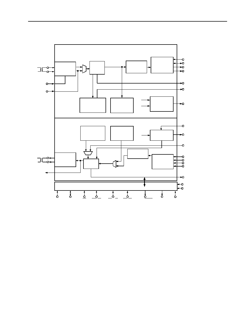
Agere Systems Inc.
15
Advance Data Sheet
May 2002
T7633 Dual T1/E1 3.3 V Short-Haul Terminator
Functional Description
5-4512(F).cr.2
Figure 1. T7633 Block Diagram (One of Two Channels)
RECEIVE
CHANNEL [1--2]
MICROPROCESSOR INTERFACE
INTERRUPT
RDY_DTACK
WR_DS
RD_R/W
ALE_AS
CS
AD[7:0]
A[11:0]
TCHICK
RTIP_RPD[1--2]
RRING_RND[1--2]
RLCK[1--2]
CEPT: TS16)
OR
(DS1: ROBBED-BIT
SIGNALING UNIT
RECEIVE
TRANSMIT
CONCENTRATION
HIGHWAY
INTERFACE
PHASE DETECTOR
CHANNEL DIGITAL
RECEIVE
RECEIVE FACILITY
DATA LINK MONITOR
TRANSPARENT
FRAMING)
(HDLC OR
RECEIVE LINE
INTERFACE
UNIT
RECEIVE
FRAMER
UNIT
(2 FRAMES)
ELASTIC STORE
RECEIVE
TTIP[1--2]
TRING[1--2]
TRANSMIT
FRAMER
UNIT
PHASE DETECTOR
CHANNEL DIGITAL
TRANSMIT
SYSCK[1--2]
TRANSMIT FACILITY
DATA LINK MONITOR
TRANSPARENT
FRAMING)
(HDLC OR
XMIT FRAMER
TCLK
RCHICK
CHANNEL [1--2]
TRANSMIT
RECEIVE
CONCENTRATION
HIGHWAY
INTERFACE
(2 FRAMES)
ELASTIC STORE
TRANSMIT
TRANSMIT LINE
INTERFACE
UNIT
CEPT: TS16)
OR
(DS1: ROBBED-BIT
SIGNALING UNIT
TRANSMIT
TCHICK[1--2]
TCHIFS[1--2]
TCHIDATA[1--2]
TCHIDATAB[1--2]
RFDL[1--2], RFDLCK[1--2]
RFRMCK[1--2], RFRMDATA[1--2],
RFS[1--2], RSSFS[1--2],
DIV-RLCK[1--2], DIV-TCHICK[1--2],
TCHICK-EPLL[1--2]
RCHICK[1--2]
RCHIFS[1--2]
RCHIDATA[1--2]
TFS[1--2], TSSFS[1--2],
DIV-PLLCK[1--2], DIV-RCHICK[1--2],
PLLCK-EPLL[1--2]
PLLCK[1--2]
TFDL[1--2], TFDLCK[1--2]
RCHDATAB[1--2]
MPMODE
MPMUX
(XLIU)
(RCHI)
(RLIU)
(TCHI)
RLCK
TND[1--2],
TCRCMFS[1--2]
TPD[1--2],
RCRCMFS[1--2]
MPCK
TLCK[1--2]

16
Agere Systems Inc.
Advance Data Sheet
May 2002
T7633 Dual T1/E1 3.3 V Short-Haul Terminator
Functional Description
(continued)
The Agere Systems Inc. T7633 Dual T1/E1 Terminator provides two complete T1/E1 interfaces each consisting of
a fully integrated, full-featured, short-haul line interface transceiver and a full-featured primary rate framer with an
HDLC formatter for facility data link access. The T7633 provides glueless interconnection from a T1 or E1 analog
line interface to devices interfacing to its concentration highway interface (CHI); for example, the T7270 Time Slot
Interchanger or T7115A Synchronous Protocol Data Formatter.
The line interface receiver performs clock and data recovery using a digital phase-locked loop, thereby avoiding
false lock conditions that are common when recovering sparse data patterns with an analog implementation. The
receiver's equalization circuit guarantees a high level of interference immunity. The receive line unit monitors the
amplitude at the receive input for analog loss of signal detection and the pulse density of the receive signal for dig-
ital loss of signal detection. The receive line unit may be programmed to detect bipolar violations. The line interface
unit may be optionally bypassed.
The line interface unit's transmit equalization is done with low-impedance output drivers that provide shaped wave-
forms to the transformer, guaranteeing template conformance. The transmitter will interface to the digital cross con-
nect (DSX) at lengths up to 655 feet for DS1 operation, and line impedances of 75 W or 120 W for CEPT-E1
operation. The transmit line unit monitors nonfunctional links due to faults at the primary of the transmit transformer
and periods of no data transmission.The line codes supported in the framer unit include AMI, T1 B8ZS, per-chan-
nel T1 zero code suppression and ITU-CEPT HDB3.
The T7633 supports T1 D4, T1DM, and
SLC
-96 superframes; extended superframe (ESF); ITU-CEPT-E1 basic
frame; ITU-CEPT-E1 time slot 0 multiframe; and time slot 16 multiframe formats.
The receive framer monitors the following alarms: loss of receive clock, loss of frame, alarm indication signal (AIS),
remote frame alarms, and remote multiframe alarms. These alarms are detected as defined by the appropriate
ANSI
,
AT&T
, and ITU standards.
Performance monitoring as specified by
AT&T
,
ANSI
, and ITU is provided through counters monitoring bipolar vio-
lation, frame bit errors, CRC errors, CEPT E bit = 0 conditions, CEPT Sa6 codes, errored events, errored seconds,
bursty errored seconds, severely errored seconds, and unavailable seconds.
In-band loopback activation and deactivation codes can be transmitted to the line via the payload or the facility data
link. In-band loopback activation and deactivation codes in the payload or the facility data link are detected.
System, payload, and line loopbacks are programmable.
The default system interface is a 2.048 Mbits/s data and 2.048 MHz clock concentration highway interface (CHI)
serial bus. This CHI interface consists of independent transmit and receive paths. The CHI interface can be recon-
figured into several modes: a 2.048 Mbits/s data interface and 4.096 MHz clock interface, a 4.096 Mbits/s data
interface and 4.096 MHz clock interface, a 4.096 Mbits/s data interface and 8.192 MHz clock interface, a
8.192 Mbits/s data interface and 8.192 MHz clock interface, and 8.192 Mbits/s data interface and 16.384 MHz
clock interface.
The signaling formats supported are T1 per-channel robbed-bit signaling (RBS), channel-24 message-oriented sig-
naling (MOS), ITU-CEPT-E1 channel-associated signaling (CAS), common channel signaling (CCS) (Agere
T7230A mode), and international remote switching module (IRMS). In the T1, RBS mode voice and data channels
are programmable. The entire payload can be programmed into a data-only (no signaling channels) mode, i.e.,
transparent mode. Signaling access can be through the on-chip signaling registers or the system CHI port in the
associated signaling mode. Data and its associated signaling information can be accessed through the CHI in
either DS1 or CEPT-E1 modes.
Extraction and insertion of the facility data link in ESF, T1DM,
SLC
-96, or CEPT-E1
modes are provided through a
four-port serial interface or through a microprocessor-accessed, 64-byte FIFO either with HDLC formatting or
transparently. In the T7633's
SLC
-96 or CEPT-E1 frame formats, a facility data link (FDL) is provided for FDL
access. The bit-oriented ESF data-link messages defined in
ANSI
T1.403-1995 are monitored by the receive
framer's facility data link unit and are transmitted by the transmit framer FDL
The receive framer includes a two-frame elastic store buffer for jitter attenuations that performs control slips and
provides indication of slip directions.

Agere Systems Inc.
17
Advance Data Sheet
May 2002
T7633 Dual T1/E1 3.3 V Short-Haul Terminator
Functional Description
(continued)
Accessing internal registers is done via the demultiplexed/multiplexed address and data bus microprocessor inter-
face using either the
Intel
80188 (or 80X88) interface protocol with independent read and write signals or the
Motorola
MC680X0 or M68360 interface protocol with address and data strobe signals.
The T7633 is manufactured using low-power CMOS technology and is packaged in an 144-pin thin quad flat pack
(TQFP) with 20 mils lead pitch.
5-4513(F).cr.2
Figure 2. T7633 Block Diagram: Receive Section (One of Two Channels)
RTIP_RPD
RRING_RND
RLCK
RECOVERY
DATA
DIGITAL
OR TRANSMIT)
(OPTIONAL:
ATTENUATION
JITTER
RECEIVE
AND MONITOR
BPV DECODER
TRANSMIT
CONCENTRATION
HIGHWAY
INTERFACE
(RATE ADAPTER)
TCHIFS
(2 FRAMES)
RECEIVE
ELASTIC
STORE
BUFFER
MONITOR
RECEIVE SLIP
INTERNAL
SYSTEM CLOCK
TCHICK
≠ MICROPROCESSOR ACCESS
≠ CONCENTRATION HIGHWAY ACCESS
≠ CEPT CHANNEL ASSOCIATED AND
COMMON CHANNEL SIGNALING
≠ DS1 ROBBED-BIT SIGNALING (RBS)
RECEIVE SIGNALING EXTRACTER:
RFDLCK
RFDL
& SIGNALING MULTIFRAME
≠ CEPT: BASIC FRAME, CRC-4 MULTIFRAME,
≠ ESF
≠ SF: D4,
SLC-96, DDS
RE-ALIGNER, AND SYNC GENERATOR:
RECEIVE T1/E1 FRAME ALIGNMENT MONITOR,
≠ UNAVAILABLE SECONDS
≠ SEVERELY ERRORED SECONDS
≠ BURSTY ERRORED SECONDS
≠ ERRORED SECONDS
≠ ERRORED EVENTS
≠ BIPOLAR VIOLATION ERRORS
RECEIVE PERFORMANCE MONITOR:
≠ SLIPS
≠ ALARM INDICATION SIGNAL (AIS)
≠ CEPT REMOTE MULTIFRAME ALARM
≠ REMOTE FRAME ALARM
≠ DIGITAL LOSS OF SIGNAL
≠ ANALOG LOSS OF SIGNAL
RECEIVE ALARM MONITOR:
∑ MESSAGE-ORIENTED MESSAGES
∑ BIT-ORIENTED MESSAGES
≠
ANSI T1.403-1989 ESF FORMAT:
≠ DDS ACCESS
≠
SLC-96 FORMAT
AND MONITOR:
RECEIVE FACILITY DATA LINK EXTRACTER
RFRMCK
FRONT END
RECEIVE
ANALOG
ANALOG
CLOCK AND
LINE INTERFACE UNIT BYPASS
RPD-LIU, RND-LIU,
RPDE, RNDE, RLCKE
RPD, RND, RLCK
RECEIVE PATTERN MONITOR:
≠ QUASI-RANDOM: 2
20
≠ 1
≠ PSEUDORANDOM: 2
15
≠ 1
≠
ANSI T1.403 BIT-ORIENTED AND ESF-FDL ACTIVATE
AND DEACTIVATE LINE LOOPBACK CODES
≠ CEPT AUXILIARY PATTERN (CEPT = 01)
≠ CEPT ACTIVATE AND DEACTIVATE LOOPBACK
≠ CEPT Sa6 CODES
≠ T1/E1 CRC ERRORS
RECEIVE FDL HDLC EXTRACTER:
≠ 64-byte RECEIVE FIFO
≠ TRANSPARENT MODE (NO HDLC FRAMING)
≠ MICROPROCESSOR ACCESS
TCHIDATA
TCHIDATAB
FRAMER
RLCK-LIU
CODES
TEST PATTERN DETECTOR
≠ MARK (ALL1s)
≠ QRSS (QUASI-RANDOM: 2
20
≠ 1)
≠ 2
5
≠ 1
≠ 2
6
≠ 1 (53)
≠ 2
9
≠ 1 (511)
≠ 2
11
≠ 1 (2047)
≠ 2
15
≠ 1 (PSEUDORANDOM)
≠ 2
20
≠ 1
≠ 2
23
≠ 1
≠ 1:1 (ALTERNATING 10)

18
Agere Systems Inc.
Advance Data Sheet
May 2002
T7633 Dual T1/E1 3.3 V Short-Haul Terminator
Functional Description
(continued)
5-4514(F).dr.2
Figure 3. T7633 Block Diagram: Transmit Section (One of Two Channels)
TTIP
TRING
TRANSMIT DATA
MONITOR
PULSE
EQUALIZER
AND
WIDTH
CONTROLLER
ALL 1s SIGNAL
(AIS)
SYSCK
˜
16
JITTER
(OPTIONAL:
RECEIVE)
ATTENUATION
TRANSMIT OR
BPV
(OPTIONAL)
ENCODER
TLCK, TND, TPD
TRANSMIT CRC GENERATOR:
≠ ESF
≠ CEPT
TRANSMIT T1/E1 FRAME FORMATTER,
AND FRAME SYNC GENERATOR:
≠ SF: D4,
SLC-96, DDS; SIGNALING
≠ ESF
≠ CEPT: BASIC FRAME, CRC-4
MULTIFRAME, & SIGNALING MULTIFRAME
≠ TRANSPARENT FRAMING
SUPERFRAME
TRANSMIT FACILITY DATA LINK
≠
SLC-96 FORMAT
≠ DDS ACCESS
≠
ANSI T1.403-1989 ESF FORMAT:
∑ BIT-ORIENTED MESSAGES
∑ MESSAGE-ORIENTED MESSAGES
TRANSMIT FDL HDLC INSERTER:
≠ 64-byte TRANSMIT FIFO
≠ TRANSPARENT MODE
≠ MICROPROCESSOR ACCESS
(NO HDLC FRAMING)
INSERTER:
TFDLCK
TFDL
LINE FORMAT ENCODER
(AMI; B8ZS; HDB3)
TLCK, TND, TPD
AUTOMATIC AND ON-DEMAND COMMANDS:
≠ AIS (LINE, SYSTEM, FDL)
≠ LOOPBACKS
≠ REMOTE FRAME ALARMS (RFA)
≠ CEPT E BIT = 0
≠ CEPT TS16 AIS
≠ CEPT TS16 RPA
TRANSMIT ELASTIC
STORE BUFFER
(2 FRAMES)
RECEIVE CONCENTRATION
HIGHWAY INTERFACE
(RATE ADAPTER)
RCHICK
RCHIFS
RCHIDATA
TRANSMIT ALARM MONITOR:
≠ LOSS OF SYSTEM BIFRAME ALIGNMENT
≠ SYSTEM ALARM INDICATION SIGNAL (AIS)
RCHIDATAB
TRANSMIT SIGNALING INSERTER:
≠ DS1 ROBBED-BIT SIGNALING (RBS)
≠ CEPT CHANNEL ASSOCIATED AND
≠ CONCENTRATION HIGHWAY ACCESS
≠ MICROPROCESSOR ACCESS
COMMON-CHANNEL SIGNALING
LOSS
OF
TLCK
TEST PATTERN GENERATOR
≠ MARK (ALL1s)
≠ QRSS
≠ 2
5
≠ 1
≠ 2
6
≠ 1 (53)
≠ 2
9
≠ 1 (511)
≠ 2
11
≠ 1 (2047)
≠ 2
15
≠ 1
≠ 2
20
≠ 1
≠ 2
23
≠ 1
≠ 1:1 (ALTERNATING 10)
PLLCK

Agere Systems Inc.
19
Advance Data Sheet
May 2002
T7633 Dual T1/E1 3.3 V Short-Haul Terminator
Pin Information
The package type and pin assignment for the T7633 (Terminator-II) is illustrated in Figure 4.
5-4712(F).cr.2
Figure 4. Pin Assignment
GRND
CK
SEL
1
RF
RM
C
K
1
RL
CK1
TL
C
K
1
T
ND1
TP
D
1
GRNDA1
NC
RRING_RND1
RTIP_RPD1
NC
VDDA1
GRNDX1
TRING1
VDDX1
TTIP1
GRNDX1
NC
GRNDX2
TTIP2
VDDX2
TRING2
GRNDX2
VDDA2
NC
RTIP_RPD2
RRING_RND2
NC
GRNDA2
TP
D
2
T
ND2
TL
C
K
2
RL
C
K
2
CKS
E
L
2
GRND
36
37
VD
D
RF
RM
CK
2
RF
RM
D
A
T
A
2
RF
S
2
RS
SF
S
2
RCRCM
F
S
2
RF
D
L
CK
2
RF
DL
2
T
CHICK
2
T
CHIF
S
2
T
C
HI
DA
T
A
2
T
CHIDA
T
AB2
D
I
V
-
RL
CK2
DIV
-
T
C
HICK2
T
C
HI
CK
-
E
P
L
L
2
TF
S2
TS
SFS
2
T
CRCM
F
S
2
TF
D
L
C
K
2
TF
D
L
2
RCHICK
2
RCHIF
S
2
RCH
I
D
A
T
A2
RCHIDA
T
A
B2
PLLCK2
DIV-PLLCK2
PLLCK-EPLL2
SYSCK2
LOFR
M
R
LC
K
2
L
O
PL
L
C
K2
DS
1
/
C
E
P
T
2
F
R
AM
ER
2
3-S
T
A
T
E
2
RE
SET
2
VD
D
38
39
40
41
42
43
44
45
46
47
48
49
50
51
52
53
54
55
56
57
58
59
60
61
62
63
64
65
66
67
68
69
70
71
72
35
34
33
32
31
30
29
28
27
26
25
24
23
22
21
20
19
18
17
16
15
14
13
12
11
10
9
8
7
6
5
4
3
2
1
73
74
75
76
77
78
79
80
81
82
83
84
85
86
87
88
89
90
91
92
93
94
95
96
97
98
99
100
101
102
103
104
105
106
107
108
VDD
WR_DS
JTAGTRST
JTAGTMS
JTAGTCK
JTAGTDI
JTAGTDO
MPCK
RDY_DTACK
INTERRUPT
A11
A10
A9
A8
A7
A6
A5
A4
A2
A3
A1
A0
AD7
AD6
AD5
AD4
AD3
AD2
AD1
AD0
ALE_AS
CS
MPMUX
RD_R/W
MPMODE
GRND
144
143
142
141
140
139
138
137
136
135
134
133
132
131
130
129
128
127
126
125
124
123
122
121
120
11
9
11
8
11
7
11
6
11
5
11
4
11
3
11
2
111
11
0
109
VDD
RF
RM
DA
T
A
1
RF
S
1
RSSF
S1
RCRCM
F
S
1
RF
DL
CK
1
RF
DL
1
T
CHICK
1
T
CHIF
S
1
T
CHIDA
T
A
1
T
CHIDA
T
A
B
1
DIV
-
RL
CK1
DIV
-
T
C
HICK1
T
CHICK
-
E
PL
L
1
TF
S1
TS
SFS
1
T
CRC
M
F
S1
T
F
DL
CK1
TF
D
L
1
RCHICK1
RCHIF
S
1
RCHIDA
T
A
1
RCHIDA
T
A
B1
PLLCK1
DIV-PLLCK1
DIV-RCHICK1
PLLCK-EPLL1
SYSCK1
LOFRMRLCK1
LOP
LLC
K
1
DS
1
/
CE
P
T
1
F
R
AM
ER
1
3-S
T
A
T
E
1
RE
SET
1
SECO
N
D
GRND
DIV-RCHICK2
JT
M

20
Agere Systems Inc.
Advance Data Sheet
May 2002
T7633 Dual T1/E1 3.3 V Short-Haul Terminator
Pin Information
(continued)
Table 1 shows the list of T7633 pins and a functional description for each.
Table 1. Pin Descriptions
* I
U
indicates an internal pull-up.
Pin
Symbol
Type*
Description
C1
C2
1, 36, 73, 109
GRND
P
Digital Ground Reference.
2
38
LOFRMRLCK
O
Loss of Framer Receive Line Clock. This pin is asserted high (1)
when the framer internal receive line clock does not toggle for a 250
µ
s
interval. Once asserted, this signal is deasserted on the first edge of the
framer internal receive line clock.
Terminator Mode: (FRAMER, pin 41/141 = 1) LOFRMRLCK is
asserted high when SYSCK clock, pin 3/35, is absent.
Framer Mode: (FRAMER, pin 41/141 = 0) LOFRMRLCK is asserted
high when RLCK clock, pin 47/135, is absent.
3
35
SYSCK
I
u
LIU System Clock. The clock signal used for clock and data recovery
and jitter attenuation. This clock must be ungapped and free of jitter.
For CKSEL = 1: a 16x clock (for DS1, SYSCK = 24.704 MHz ± 100
ppm and for CEPT, SYSCK = 32.768 MHz ± 100 ppm). For CKSEL = 0:
a 1x clock (for DS1, SYSCK = 1.544 MHz ± 100 ppm and for CEPT,
SYSCK = 2.048 MHz ± 100 ppm).
4
34
PLLCK-EPLL
O
Error Phase-Lock Loop Signal. The error signal proportional to the
phase difference between DIV-PLLCK and DIV-RCHICK as detected by
the internal PLL circuitry (refer to the Phase-Lock Loop Circuit section
on page 122).
5
33
DIV-RCHICK
O
Divided-Down RCHI Clock. 32 kHz or 8 kHz clock signal derived from
the RCHICK input signal.
6
32
DIV-PLLCK
O
Divided-Down PLLCK Clock. 32 kHz or 8 kHz clock signal derived
from the PLLCK input signal.
7
31
PLLCK
I
Transmit Framer Phase-Locked Line Interface Clock. Clock signal
used to time the transmit framer. This signal must be phase-locked to
RCHICK clock signal and be ungapped and free of jitter. For
FRM_PR45, bit 0 (HFLF) = 0, in DS1 PLLCK = 1.544 MHz and in CEPT
PLLCK = 2.048 MHz. For FRM_PR45, bit 0 (HFLF) = 1 in DS1 PLLCK =
6.176 MHz and in CEPT PLLCK = 8.192 MHz.
8
30
GRND
A
P
Analog Ground Reference.
9, 12, 19,
26, 29
NC
--
No Connect.

Agere Systems Inc.
21
Advance Data Sheet
May 2002
T7633 Dual T1/E1 3.3 V Short-Haul Terminator
Pin Information
(continued)
Table 1. Pin Descriptions (continued)
* I
U
indicates an internal pull-up.
After RESET is deasserted, the channel is in the default framing mode, as a function of the DS1/CEPT pin.
Pin
Symbol
Type*
Description
C1
C2
10
28
RRING_RND
I
Receive Bipolar Ring. Negative bipolar input data from the receive
analog line isolation transformer.
Receive Negative Rail Data. Valid when the FRAMER pin is
strapped to 0 V. Nonreturn-to-zero (NRZ) serial data latched by the
rising edge of RLCK. Data rates: DS1-1.544 Mbits/s; CEPT-
2.048 Mbits/s. In the single-rail mode, when RND = 1 the receive
bipolar violation counter increments once for each rising edge of
RLCK.
11
27
RTIP_RPD
I
Receive Bipolar Tip. Positive bipolar input data from the receive
analog line isolation transformer.
Receive Positive Rail Data. Valid when the FRAMER pin is
strapped to 0 V. NRZ serial data latched by the rising edge of RLCK.
Data rates: DS1-1.544 Mbits/s; CEPT-2.048 Mbits/s. Optional
single-rail NRZ receive data latched by the rising edge of RLCK.
13
25
V
DDA
P
Analog 3.3 V Power Supply. 3.3 V ± 5%.
14, 18 20, 24
GRNDX
P
Transmit Line Driver Ground Reference.
15
23
TRING
O
Transmit Bipolar Ring. Negative bipolar output data to the transmit
analog isolation transformer.
16
22
V
DD
X
P
Transmit Line Driver 3.3 V Power Supply. 3.3 V ± 5%.
17
21
TTIP
O
Transmit Bipolar Tip. Positive bipolar output data to the transmit
analog isolation transformer.
37, 72,
108, 144
V
DD
P
3.3 V Power Supply. 3.3 V ± 5%.
143
39
LOPLLCK
O
Loss of PLLCK Clock. This pin is asserted high when the PLLCK
clock does not toggle for a 250 µs interval. This pin is deasserted
250 µs after PLLCK clock restarts toggling.
142
40
DS1/CEPT
I
u
DS1/CEPT. Strap to V
DD
to enable defaults for DS1 operation. Strap
to V
SS
to enable defaults for CEPT operation.
141
41
FRAMER
I
u
Framer Mode. Strap to V
DD
to enable integrated LIU and framer
operation. Strap to V
SS
to bypass the LIU section; the receive framer
is sourced directly from the RPD, RND, and RLCK pins while the
TPD, TND, and TLCK pins are driven by the transmit framer.
140
42
3-STATE
I
u
3-State (Active-Low). Asserting this pin low forces the channel
outputs into a high-impedance state. Asserting both 3-state pins low
forces all outputs into a high-impedance state.
139
43
RESET
I
u
Reset (Active-Low). Asserting this pin low resets the channel.
Asserting both RESET pins low resets the entire device including
the global registers.
138
44
TPD
O
Transmit Line Interface Positive-Rail Data. This signal is the
transmit framer positive NRZ output data. Data changes on the
rising edge of TLCK. In the single-rail mode, TPD = transmit framer
data.

22
Agere Systems Inc.
Advance Data Sheet
May 2002
T7633 Dual T1/E1 3.3 V Short-Haul Terminator
Pin Information
(continued)
Table 1. Pin Descriptions (continued)
* I
U
indicates an internal pull-up.
Pin
Symbol
Type*
Description
C1
C2
137
45
TND
O
Transmit Line Interface Negative-Rail Data. This signal is the
transmit framer negative NRZ output data. Data changes on the rising
edge of TLCK. In the single-rail mode, TND = 0.
136
46
TLCK
O
Transmit Framer Line Interface Clock. Optional 1.544 MHz DS1 or
2.048 MHz output signal from the transmit framer. TND and TPD data
changes on the rising edge of TLCK.
135
47
RLCK
I
Receive Framer Line Interface Clock. Valid when the FRAMER pin is
strapped to 0 V. This is the 1.544 MHz DS1 or 2.048 MHz input clock
signal used by the receive framer to latch RPD and RND data.
134
49
RFRMCK
O
Receive Framer Clock. Output receive framer clock signal used to
clock out the receive framer output signals. In normal operation, this is
the recovered receive line clock signal.
133
48
CKSEL
I
u
LIU System Clock Mode. This pin selects either a 16x rate clock for
SYSCK (CKSEL = 1) or a primary line rate clock for SYSCK
(CKSEL = 0).
132
50
RFRMDATA
O
Receive Framer Data. This signal is the decoded data input to the
receive elastic store. During loss of frame alignment, this signal is
forced to 1.
131
51
RFS
O
Receive Frame Sync. This active-high signal is the 8 kHz frame
synchronization pulse generated by the receive framer.
130
52
RSSFS
O
Receive Framer Signaling Superframe Sync. This active-high signal
is the CEPT signaling superframe (multiframe) synchronization pulse
in the receive framer.
129
53
RCRCMFS
O
Receive Framer CRC-4 Multiframe Sync. This active-high signal is
the CEPT CRC-4 multiframe synchronization pulse in the receive
framer.
128
54
RFDLCK
O
Receive Facility Data Link Clock. In DS1-DDS with data link access,
this is an 8 kHz clock signal. Otherwise, this is a 4 kHz clock signal.
The receive data link bit changes on the falling edge of RFDLCK.
127
55
RFDL
O
Receive Facility Data Link. Serial output facility data link bit stream
extracted from the receive line data stream by the receive framer. In
DS1-DDS with data link access, this is an 8 kbits/s signal; otherwise,
4 kbits/s. In the CEPT frame format, RFDL can be programmed to one
of the Sa bits of the NOT FAS frame TS0. During loss of frame
alignment, this signal is 1.
126
56
TCHICK
I
Transmit Concentration Highway Interface (CHI) Clock.
2.048 MHz, 4.096 MHz, 8.192 MHz, or 16.384 MHz. This clock must
be free of jitter.
125
57
TCHIFS
I/O
Transmit CHI Frame Sync. Transmit CHI 8 kHz input frame
synchronization pulse phase-locked to TCHICK. In the CHI master
mode, the transmit CHI generates the 8 kHz frame sync to control the
CHI.

Agere Systems Inc.
23
Advance Data Sheet
May 2002
T7633 Dual T1/E1 3.3 V Short-Haul Terminator
Pin Information
(continued)
Table 1. Pin Descriptions (continued)
* I
U
indicates an internal pull-up.
Pin
Symbol
Type*
Description
C1
C2
124
58
TCHIDATA
O
Transmit CHI Data. Serial output system data at 2.048 Mbits/s,
4.096 Mbits/s, or 8.192 Mbits/s. This port is forced into a high-
impedance state for all inactive time slots.
123
59
TCHIDATAB
O
Transmit CHI Data B. Serial output system data at 2.048 Mbits/s,
4.096 Mbits/s, or 8.192 Mbits/s. This port is forced into a high-
impedance state for all inactive time slots.
122
60
DIV-RLCK
O
Divided-Down Receive Line Clock. 8 kHz clock signal derived from
the recovered receive line interface unit clock or the RLCK input
signal.
121
61
DIV-TCHICK
O
Divided-Down CHI Clock. 8 kHz clock signal derived from the
transmit CHI CLOCK input signal.
120
62
TCHICK-EPLL
O
Error Phase-Lock Loop Signal. The error signal proportional to the
phase difference between DIV-TCHICK and DIV-RLCK as detected
from the internal PLL circuitry (refer to the Phase-Lock Loop Circuit
section on page 122).
119
63
TFS
O
Transmit Framer Frame Sync. This signal is the 8 kHz frame
synchronization pulse in the transmit framer. This signal is active-high.
118
64
TSSFS
O
Transmit Framer Signaling Superframe Sync. This signal is the
CEPT signaling superframe (multiframe) synchronization pulse in the
transmit framer. This signal is active-high.
117
65
TCRCMFS
O
Transmit Framer CRC-4 Multiframe Sync. This signal is the CEPT
CRC-4 submultiframe synchronization pulse in the transmit framer.
This signal is active-high.
116
66
TFDLCK
O
Transmit Facility Data Link Clock. In DS1-DDS with data link
access, this is an 8 kHz clock signal; otherwise, 4 kHz. The transmit
frame latches data link bits on the falling edge of TFDLCK.
115
67
TFDL
I
Transmit Facility Data Link. Optional serial input facility data link bit
stream inserted into the transmit line data stream by the transmit
framer. In DS1-DDS with data link access, this is an 8 kbits/s signal;
otherwise, 4 kbits/s. In the CEPT frame format, TFDL can be
programmed to one of the Sa bits of the NOT-FAS frame time slot 0.
114
68
RCHICK
I
Receive Concentration Highway Interface (CHI) Clock. 2.048 MHz,
4.096 MHz, 8.192 MHz, or 16.384 MHz. This clock must be free of
jitter.
113
69
RCHIFS
I
Receive CHI Frame Sync. Receive CHI 8 kHz frame synchronization
pulse phase-locked to RCHICK.
112
70
RCHIDATA
I
Receive CHI Data. Serial input system data at 2.048 Mbits/s,
4.096 Mbits/s, or 8.192 Mbits/s.
111
71
RCHIDATAB
I
Receive CHI Data B. Serial input system data at 2.048 Mbits/s,
4.096 Mbits/s, or 8.192 Mbits/s.

24
Agere Systems Inc.
Advance Data Sheet
May 2002
T7633 Dual T1/E1 3.3 V Short-Haul Terminator
Pin Information
(continued)
Table 1. Pin Descriptions (continued)
* I
U
indicates an internal pull-up.
After RESET is deasserted, the channel is in the default framing mode, as a function of the DS1/CEPT pin.
Asserting this pin low will initially force RDY to a low state.
Pin
Symbol
Type*
Description
74
MPMODE
I
u
MPMODE. Strap to ground to enable the
Motorola
68360
microprocessor protocol (MODE1 or MODE2). Strapped to V
DD
to
enable the
Intel
80X86/88 microprocessor protocol (MODE3 or
MODE4).
75
RD_R/W
I
Read (Active-Low). In the
Intel
interface mode, the T7633 drives
the data bus with the contents of the addressed register while RD
is low.
Read/Write. In the
Motorola
interface mode, this signal is asserted
high for read accesses; this pin is asserted low for write accesses.
76
MPMUX
I
u
MPMUX. Strap to V
SS
to enable the demultiplexed address and
data bus mode. Strap to V
DD
to enable the multiplexed address
and data bus mode.
77
CS
I
Chip Select (Active-Low). In the
Intel
interface mode, this pin
must be asserted low to initiate a read or write access and kept low
for the duration of the access; asserting CS low forces RDY out of
its high-impedance state into a 0 state.
78
ALE_AS
I
Address Latch Enable/Address Strobe. In the address/data bus
multiplex mode of the microprocessor, when this signal transitions
from high to low, the state of the address bus is latched into
internal address registers. In the demultiplexed address mode, the
address is transparent through the T7633 and is latched on the
rising edge of the ALE_AS signal. Alternatively, in the demultiplex
mode, this pin may be connected to ground to make the address
transparent through the T7633.
79--86
AD0--AD7
I/O
Microprocessor Address_Data Bus. Multiplexed address and
bidirectional data bus used for read and write accesses. High-
impedance output.
87--98
A0--A11
I
Microprocessor Address Bus. Address bus used to access the
internal registers.
99
INTERRUPT
O
Interrupt. INTERRUPT is asserted indicating an internal interrupt
condition/event has been generated. This pin is deasserted after
the generating register is read. As a default, interrupt assertion is a
logic one. Interrupt events/conditions are maskable through the
control registers. Interrupt assertion may be inverted (active-low)
or programmed for wired OR or AND operation by setting register
GREG 4 bit 4 and bit 6.

Agere Systems Inc.
25
Advance Data Sheet
May 2002
T7633 Dual T1/E1 3.3 V Short-Haul Terminator
Pin Information
(continued)
Table 1. Pin Descriptions (continued)
* I
U
indicates an internal pull-up; I
d
indicates an internal pull-down.
Pin
Symbol
Type*
Description
100
RDY_DTACK
O
Ready. In the
Intel
interface mode, this pin is asserted high to
indicate the completion of a read or write access; this pin is forced
into a high-impedance state while CS is high.
Data Transfer Acknowledge (Active-Low). In the
Motorola
interface mode, DTACK is asserted low to indicate the completion
of a read or write access; DTACK is 1 otherwise.
101
MPCK
I
u
Microprocessor Clock. Microprocessor clock used in the
Intel
mode to generate the READY signal.
102
JTAGTDO
O
JTAG Data Output. Serial output data sampled on the falling edge
of TCK from the boundary-scan test circuitry.
103
JTAGTDI
I
u
JTAG Data Input. Serial input data sampled on the rising edge of
TCK for the boundary-scan test circuitry.
104
JTAGTCK
I
u
JTAG Clock Input. TCK provides the clock for the boundary-scan
test logic.
105
JTAGTMS
I
u
JTAG Mode Select (Active-Low). The signal values received at
TMS are sampled on the rising edge of TCK and decoded by the
boundary-scan TAP controller to control boundary-scan test opera-
tions.
106
JTAGTRST
I
d
JTAG Reset Input (Active-Low). Assert this pin low to asynchro-
nously initialize/reset the boundary-scan test logic.
107
WR_DS
I
Write (Active-Low). In the
Intel
mode, the value present on the
data bus is latched into the addressed register on the positive edge
of the signal applied to WR.
Data Strobe (Active-Low). In the
Motorola
mode, when AS is low
and R/W is low (write), the value present on the data bus is latched
into the addressed register on the positive edge of the signal
applied to DS; when AS is low and R/W is high (read), the T7633
drives the data bus with the contents of the addressed register
while DS is low.
110
SECOND
O
Second Pulse. A one second timer with an active-high pulse. The
duration of the pulse is one RLCK cycle. The receive line clock of
FRAMER1 (RLCK1) is the default clock source for the internal sec-
ond pulse timer. When LOFRMCLK1 is active, the receive line
clock of FRAMER2 is used as the clock signal source for the inter-
nal second pulse timer. The second pulse is used for performance
monitoring.
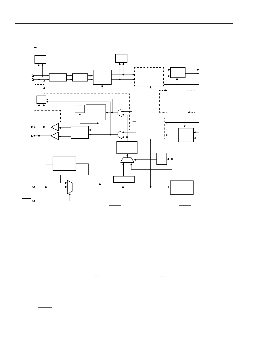
26
Agere Systems Inc.
Advance Data Sheet
May 2002
T7633 Dual T1/E1 3.3 V Short-Haul Terminator
Line Interface Unit: Block Diagram
The T7633 LIU diagram is shown in Figure 5. Only a single transceiver is shown here for illustration purposes.
5-4556(F).cr.4
* INTSYSCK always runs at 16 times the primary line rate. If CKSEL = 1, INTSYSCK is equal to SYSCK. If CKSEL = 0, INTSYSCK is sourced
from the internal 16x clock multiplier.
Figure 5. Block Diagram of Line Interface Unit: Single Channel
Line Interface Unit: Receive
Data Recovery
The receive line-interface unit (RLIU) transmission format is bipolar alternate mark inversion (AMI). The RLIU
accepts input data with a data rate tolerance of ±130 ppm (DS1) or ±80 ppm (E1). The RLIU first restores the
incoming data and detects analog loss of signal. Subsequent processing is optional and depends on the program-
mable LIU configuration established within the microprocessor interface registers. The RLIU utilizes an equalizer to
operate on line length with typically up to 15 dB of loss at 772 kHz (DS1) or 13 dB loss at 1.024 MHz (E1). The sig-
nal is then peak-detected and sliced to produce digital representations of the data. Selectable digital loss of signal,
jitter attenuation, and data decoding are performed.
The clock is recovered by a digital phase-locked loop that uses SYSCK as a reference to lock to the data rate com-
ponent. Because the reference clock is a multiple of the received data rate, the internal RLCK (RLCK-LIU) output
will always be a valid DS1/CEPT clock that eliminates false lock conditions. During periods with no receive input
signal from the line, the free-run frequency of RLCK-LIU is defined to be either SYSCK/16 or SYSCK depending on
the state of CKSEL. RLCK-LIU is always active with a duty cycle centered at 50%, deviating by no more than ±5%.
Valid data is recovered within the first few bit periods after the application of SYSCK.
INTSYSCK
*
TO RECEIVE
FROM TRANSMIT
FRAMER
RTIP
RRING
FLLOOP
(NO LIU AIS)
EQUALIZER
SLICERS
CLOCK AND
DATA
RECOVERY
RDLOS
RND_BPV
RPD
RLCK
DECODER
DLLOOP
RLOOP
TLCK-LIU
TND-LIU
JITTER
(RECEIVE PATH)
TPD-LIU
FLLOOP
(DURING LIU AIS)
PULSE-
WIDTH
CONTROLLER
TDM
LOTC
PULSE
EQUALIZER
TRANSMIT
DRIVER
TTIP
TRING
SYSCK
LOSS OF
SYSCK
MONITOR
DIVIDE BY 16
ALARM
SIGNAL (AIS)
ENCODER
FRAMER
RALOS
INDICATION
ATTENUATOR
JITTER
(TRANSMIT PATH)
ATTENUATOR
(CLOCK)
(DATA)
LOSS
OF
TLCK
16x
CLOCK
MULTIPLIER
CKSEL
INTSYSCK
*

Agere Systems Inc.
27
Advance Data Sheet
May 2002
T7633 Dual T1/E1 3.3 V Short-Haul Terminator
Line Interface Unit: Receive
(continued)
Jitter Accommodation and Jitter Transfer Without the Jitter Attenuator
The RLIU is designed to accommodate large amounts of input jitter. The RLIU's jitter performance exceeds the
requirements shown in the RLIU Specification Table 4 and Table 5. Typical receiver performance without the jitter
attenuator in the path is shown in Figures 6--9. Typical receiver performance with the jitter attenuator is given in
Figures 12--15. Jitter transfer is independent of input ones density on the line interface.
Receive Line Interface Configuration Modes
Zero Substitution Decoding (CODE)
When single-rail operation is selected with DUAL = 0 (register LIU_REG3, bit 3), the LIU B8ZS/HDB3 zero substi-
tution decoding can be selected via the CODE bit (register LIU_REG3, bit 2). If CODE = 1, the B8ZS/HDB3 decod-
ing function is enabled in the receive path. Decoded receive data appears at the internal LIU-to-framer RPD
interface (RPD-LIU). Code violations, including BPVs, appear at the internal LIU-to-framer RND_BPV interface
(RND-LIU). If CODE = 0, the receive data is passed unaltered to RPD-LIU, and all bipolar violations (such as two
consecutive 1s if the same polarity) appear at RND-LIU. The default configuration is single-rail, DUAL = 0, with the
decoding active, CODE = 1.
If DUAL = 0, the receive framer must be programmed to the single-rail mode and the receive framer's interval LIU-
to-framer RPD input will be the receive data port. If DUAL = 0, then the receive framer's bipolar violation count will
increment by 1 whenever the internal LIU-to-framer RND_BPV signal is one. The bipolar violation count is incre-
mented on the rising edge of the receive framer's RLCK clock signal.

28
Agere Systems Inc.
Advance Data Sheet
May 2002
T7633 Dual T1/E1 3.3 V Short-Haul Terminator
Line Interface Unit: Receive
(continued)
Receive Line Interface Configuration Modes
(continued)
Receive Line Interface Unit (RLIU) Alarms
Analog Loss of Signal (ALOS) Alarm. An analog signal detector monitors the receive signal amplitude and
reports its status in the analog loss of signal alarm bit ALOS (register LIU_REG0, bit 0). Analog loss of signal is
indicated (ALOS = 1) if the amplitude at the RRING and RTIP inputs drops below a voltage approximately 18 dB
below the nominal signal amplitude. The ALOS alarm condition will clear when the receive signal amplitude returns
to a level greater than 14 dB below normal. The ALOS alarm status bit will latch the alarm and remain set until
being cleared by a read (clear on read). Upon the transition from ALOS = 0 to ALOS = 1, a microprocessor inter-
rupt will be generated if the ALOS interrupt enable bit ALOSIE (register LIU_REG1, bit 0) is set. The reset default is
ALOSIE = 0.
The ALOS circuitry provides 4 dB of hysteresis to prevent alarm chattering. The time required to detect ALOS is
selectable. When ALTIMER = 0 (register LIU_REG4, bit 0), ALOS is declared between 1 ms and 2.6 ms after los-
ing signal as required by I.431(3/93) and ETS-300-233 (5/94). If ALTIMER = 1, ALOS is declared between 10-bit
and 255-bit symbol periods after losing signal as required by G.775 (11/95). The timing is derived from the SYSCK
clock. The detection time is independent of signal amplitude before the loss condition occurs. Normally, ALTIMER
= 1 would be used only in E1 mode since no T1/DS1 standards require this mode. In T1/DS1 mode, this bit should
normally be zero. The reset default is ALTIMER = 0.
The behavior of the receiver RLIU outputs under ALOS conditions is dependent on the loss shutdown (LOSSD)
control bit (register LIU_REG3, bit 4) in conjunction with the receive alarm indication select (RCVAIS) control bit
(register LIU_REG4, bit 1) as described in the Loss Shutdown (LOSSD) and Receiver AIS (RCVAIS) section on
page 29.
Digital Loss of Signal (DLOS) Alarm. A digital loss of signal (DLOS) detector guarantees the received signal
quality as defined in the appropriate
ANSI
,
Telcordia Technologies
, and ITU standards. The digital loss of signal
alarm is reported in the RLIU alarm status register (register LIU_REG0, bit 1). For DS1 operation, digital loss of sig-
nal (DLOS = 1) is indicated if 100 or more consecutive 0s occur in the receive data stream. The DLOS condition is
deactivated when the average ones density of at least 12.5% is received in 100 contiguous pulse positions. The
DLOS alarm status bit will latch the alarm and remain set until being cleared by a read (clear on read). The
LOSSTD control bit (register LIU_REG2, bit 2) selects the conformance protocols for the DLOS alarm indication
per Table 2. Setting LOSSTD = 1 adds an additional constraint that there are less than 15 consecutive zeros in the
DS1 data stream before DLOS is deactivated. The reset default is LOSSTD = 0.
For E1 operation, DLOS is indicated when 255 or more consecutive 0s occur in the receive data stream. The
DLOS indication is deactivated when the average ones density of at least 12.5% is received in 255 contiguous
pulse positions. LOSSTD has no effect in E1 mode.
Upon the transition from DLOS = 0 to DLOS = 1, a microprocessor interrupt will be generated if the DLOS interrupt
enable bit DLOSIE (register LIU_REG1, bit 1) is set. The reset default is DLOSIE = 0.
The DLOS alarm may occur when FLLOOP is activated (See "Line Interface Unit: Loopbacks" on page 44.) due to
the abrupt change in signal level at the receiver input. Setting the FLLOOP alarm prevention PFLALM = 1 (register
LIU_REG 4, bit 2) prevents the DLOS alarm from occurring when FLLOOP is activated by quickly resetting the
receiver's internal peak detector. It will not prevent the DLOS alarm during the FLLOOP period but only avoids the
alarm created by the signal amplitude transient. The reset default is PFLALM = 0.
Table 2. Digital Loss of Signal Standard Select
LOSSTD
DS1 Mode
CEPT Mode
0
T1M1.3/93-005, ITU-T G.775
ITU-T G.775
1
TR-TSY-000009
ITU-T G.775

Agere Systems Inc.
29
Advance Data Sheet
May 2002
T7633 Dual T1/E1 3.3 V Short-Haul Terminator
Line Interface Unit: Receive
(continued)
Receive Line Interface Configuration Modes
(continued)
Loss Shutdown (LOSSD) and Receiver AIS (RCVAIS). The loss shutdown (LOSSD) control bit (register
LIU_REG3, bit 4) acts in conjunction with the receive alarm indication select (RCVAIS) control bit (register
LIU_REG4, bit 1) to place the digital RLIU signals (RPD-LIU, RND-LIU, RLCK-LIU) in a predetermined state when
a digital loss of signal (DLOS) or analog loss of signal (ALOS) alarm occurs.
If LOSSD = 0 and RCVAIS = 0, the RND-LIU, RPD-LIU, and RLCK-LIU signals will be unaffected by the DLOS
alarm condition. However, when an ALOS alarm condition is indicated in the LIU alarm status register (register
LIU_REG0, bit 0), the RPD-LIU and RND-LIU signals are forced to 0 state and the RLCK-LIU free runs (at the
INTSYSCK/16 frequency).
If LOSSD = 1, RCVAIS = 0, and a DLOS alarm condition is indicated in the LIU alarm status register (register
LIU_REG0, bit 1) or an ALOS alarm condition is indicated, the RPD-LIU and RND-LIU signals are forced to the
0 state and the RLCK-LIU free runs (at the INTSYSCK/16 frequency).
If LOSSD = 0, RCVAIS = 1, and a DLOS or an ALOS alarm condition is indicated in the LIU alarm status register
(register LIU_REG0, bits 0 or 1), the RPD-LIU and RND-LIU signals will present an alarm indication signal (AIS, all
ones) based on the free-running INTSYSCK/16 frequency.
If LOSSD = 1, RCVAIS = 1, and a DLOS or an ALOS alarm condition is indicated in LIU alarm status register (reg-
ister LIU_REG0, bits 0 or 1), the RPD-LIU and RND-LIU signals are forced to 0 state and the RLCK-LIU free runs
at the INTSYSCK/16 frequency.
The RND-LIU, RPD-LIU, and RLCK-LIU signals will be remain unaffected if any loopback (FLLOOP, RLOOP,
DLLOOP) is activated independent of LOSSD and RCVAIS settings.
The default reset state is LOSSD = 0 and RCVAIS = 0.
The LOSSD and RCVAIS behavior is summarized in Table 3.
LIU Receiver Bipolar Violation (BPV) Alarm. The receiver LIU bipolar violation (BPV) alarm is used only in the
single-rail mode. When B8ZS(DS1)/HDB3(E1) coding is not used (i.e., CODE = 0), any violations in the receive
data (such as two or more consecutive 1s on a rail) are indicated on the RND-LIU output. When B8ZS(DS1)/
HDB3(E1) coding is used (i.e., CODE = 1), the HDB3/B8ZS code violations, including BPVs, are reflected on the
RND-LIU output.
Table 3. LOSSD and RCVAIS Control Configurations (Not Valid During Loopback Modes)
LOSSD
RCVAIS
ALARM
RPD/RND
RLCK
0
0
ALOS
0
Free Runs
0
0
DLOS
Normal Data
Recovered Clock
1
0
ALOS
0
Free Runs
1
0
DLOS
0
Free Runs
0
1
ALOS
AIS (all ones)
Free Runs
0
1
DLOS
AIS (all ones)
Free Runs
1
1
ALOS
0
Free Runs
1
1
DLOS
0
Free Runs

30
Agere Systems Inc.
Advance Data Sheet
May 2002
T7633 Dual T1/E1 3.3 V Short-Haul Terminator
Line Interface Unit: Receive
(continued)
T1/DS1 LIU Receiver Specifications
During T1/DS1 operation, the LIU receiver will perform as specified in Table 4.
1. Below the nominal pulse amplitude of 3.0 V with the line interface circuitry specified in the Line Interface Unit: Line Interface Networks on
page 48.
2. Cable loss at 772 kHz.
3. Using Agere transformer 2795L and components listed in Table 13.
Table 4. DS1 LIU Receiver Specifications
Parameter
Min
Typ
Max
Unit
Spec
Analog Loss of Signal:
Threshold to Assert
Threshold to Clear
Hysteresis
Time to Assert (ALTIMER = 0)
23
17.5
--
1.0
18
14
4
16.5
12.5
--
2.6
dB
1
dB
1
dB
ms
I.431
--
--
I.431
Receiver Sensitivity
2
11
15
--
dB
--
Jitter Transfer:
3 dB Bandwidth
Peaking
--
--
3.84
--
--
0.1
kHz
dB
Figure 7 on page 32
Figure 13 on page 42
Generated Jitter
--
0.04
0.05
UI
pk-pk
TR-TSY-000499,
ITU-T G.824
Jitter Accommodation
--
--
--
--
Figure 6 on page 32
Figure 12 on page 42
Return Loss:
3
51 kHz to 102 kHz
102 kHz to 1.544 MHz
1.544 MHz to 2.316 MHz
14
20
16
--
--
--
--
--
--
dB
dB
dB
--
--
--
Digital Loss of Signal:
ITU-T G.775,
T1M1.3/93-005
--
TR-TRY-000009
ITU-T G.775, T1M1.3/
93-005
Flag Asserted When Consecutive Bit
Positions Contain
100
--
--
zeros
Flag Deasserted when
Data Density Is
and
12.5
--
--
%ones
Maximum Consecutive Zeros Are
--
--
--
--
15
99
zeros
zeros

Agere Systems Inc.
31
Advance Data Sheet
May 2002
T7633 Dual T1/E1 3.3 V Short-Haul Terminator
Line Interface Unit: Receive
(continued)
CEPT LIU Receiver Specifications
During E1 operation, the LIU receiver will perform as specified in Table 5.
1.Below the nominal pulse amplitude of 3.0 V for 120
and 2.37 V for 75
applications with the line circuitry specified in the Line Interface
Unit: Line Interface Networks on page 48.
2.Cable loss at 1.024 MHz.
3.Amount of cable loss for which the receiver will operate error-free in the presence of a ≠18 dB interference signal summing with the intended
signal source.
4.Using Agere transformer 2795K or 2795J and components listed in Table 13.
Table 5. CEPT LIU Receiver Specifications
Parameter
Min
Typ
Max
Unit
Spec
Analog Loss of Signal:
Threshold to Assert
Threshold to Clear
Hysteresis
Time to Assert (ALTIMER = 0)
Time to Assert (ALTIMER = 1)
23
17.5
--
1.0
10
18
14
4
--
--
16.5
12.5
--
2.6
255
dB
1
dB
1
dB
ms
UI
I.431, ETSI 300 233
--
--
I.431, ETSI 300 233
G.775
Receiver Sensitivity
2
11
13.5
--
dB
--
Interference Immunity:
3
9
12
--
dB
ITU-T G.703
Jitter Transfer:
3 dB Bandwidth, Single-pole Roll Off
Peaking
--
--
5.1
--
--
0.5
kHz
dB
Figure 9 on page 33
Figure 15 on page 43
Generated Jitter
--
0.04
0.05
UI
pk-pk
ITU-T G.823, I.431
Jitter Accommodation
--
--
--
--
Figure 8 on page 33
Figure 14 on page 43
Return Loss:
4
51 kHz to 102 kHz
102 kHz to 2.048 MHz
2.048 MHz to 3.072 MHz
14
20
16
--
--
--
--
--
--
dB
dB
dB
ITU-T G.703
Digital Loss of Signal:
--
ITU-T G.775
Flag Asserted When Consecutive Bit
Positions Contain
255
--
--
zeros
Flag Deasserted When Data Density Is
(LOSSTD = 1)
12.5
--
--
%ones
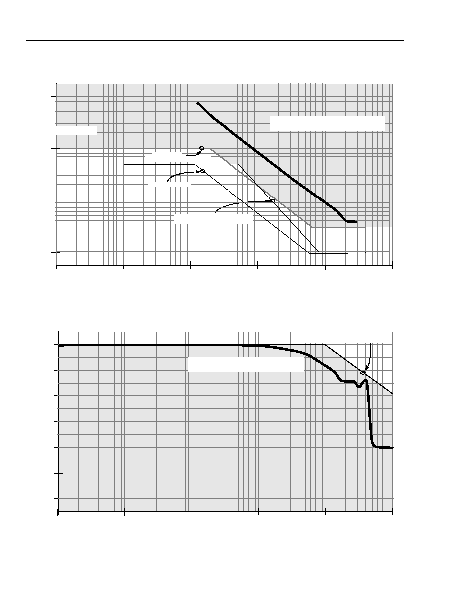
32
Agere Systems Inc.
Advance Data Sheet
May 2002
T7633 Dual T1/E1 3.3 V Short-Haul Terminator
Line Interface Unit: Receive
(continued)
5-5260(F)r.4
Figure 6. T1/DS1 Receiver Jitter Accommodation Without Jitter Attenuator
5-5261(F)
Figure 7. T1/DS1 Receiver Jitter Transfer Without Jitter Attenuator
0.1 UI
1.0 UI
10 UI
100 UI
10
100
1 k
10 k
1
28 UI
FREQUENCY (Hz)
100 k
TYPICAL
(SUBJECT TO DEVICE CHARACTERIZATION)
(NON-SONET CAT II INTERFACES)
GR-499-CORE
I.431(DS1), G.824(DS1)
TR-TSY-000009 (DS1, MUXES)
GR-499/1244-CORE (CAT I INTERFACES)
T1.408/I.431(DS1)/G.824(DS1)
60
40
20
0
1
10
100
1k
10 k
50
30
10
100 k
FREQUENCY (Hz)
J
I
TTE
R OUT/
J
ITT
ER
IN (
d
B
)
TYPICAL
(SUBJECT TO DEVICE CHARACTERIZATION)
GR-499-CORE
(NON-SONET CAT II TO CAT II)

Agere Systems Inc.
33
Advance Data Sheet
May 2002
T7633 Dual T1/E1 3.3 V Short-Haul Terminator
Line Interface Unit: Receive
(continued)
5-5262(F)r.3
Figure 8. CEPT/E1 Receiver Jitter Accommodation Without Jitter Attenuator
5-5263(F)
Figure 9. CEPT/E1 Receiver Jitter Transfer Without Jitter Attenuator
0.1 UI
1.0 UI
10 UI
100 UI
10
100
1 k
10 k
1
37 UI
FREQUENCY (Hz)
G.823
20.5 UI
12e-6 Hz
100 k
TYPICAL
(SUBJECT TO DEVICE CHARACTERIZATION)
G.823,ETSI-300-011A1
I.431(CEPT)/ETS-300-011
I.431(CEPT)/ETS-300-011
FREQUENCY (H
Z
)
JI
TTE
R OUT
/
J
ITT
ER
IN (
d
B
)
60
40
20
0
1
10
100
1 k
10 k
50
30
10
100 k
TYPICAL
(SUBJECT TO DEVICE CHARACTERIZATION)
G.735-9 W/O JITTER REDUCER

34
Agere Systems Inc.
Advance Data Sheet
May 2002
T7633 Dual T1/E1 3.3 V Short-Haul Terminator
Line Interface Unit: Transmit
Output Pulse Generation
The line interface transmitter accepts a line rate clock and NRZ data in single-rail mode (DUAL = 0) or positive and
negative NRZ data in dual-rail mode (DUAL = 1) from the transmit framer unit or, optionally, the system interface.
The line interface transmitter converts this data to a balanced bipolar signal (AMI format) with optional B8ZS(DS1)/
HDB3(E1) encoding and optional jitter attenuation. Low-impedance output drivers produce the line transmit pulses.
Positive 1s are output as positive pulses on TTIP, and negative 1s are output as positive pulses on TRING. Binary
0s are converted to null pulses.
In DSX-1 applications, transmit pulse shaping is controlled by the on-chip pulse-width controller and pulse equal-
izer. The pulse-width controller produces high-speed timing signals to accurately control the transmit pulse widths.
This eliminates the need for a tightly controlled transmit clock duty cycle that is usually required in discrete imple-
mentations. The pulse equalizer controls the amplitudes and shapes of the pulses. Different pulse equalizations
are selected through settings of EQ2, EQ1, and EQ0 bits (register LIU_REG6, bits 0 to 2) as described in Table 6,
Transmit Line Interface Short-Haul Equalizer/Rate Control, below.
The reset default state of the equalization bits EQ2, EQ1, and EQ0 can be predetermined by setting the
DS1_CEPT pin. The default transmit equalization is EQ2, EQ1, and EQ0 = 000 (0 dB T1/DS1) when DS1_CEPT =
1; EQ2, EQ1, and EQ0 = 110 (CEPT 120
/75
) when DS1_CEPT = 0. This feature aids in transmitting AIS at the
correct rate upon completion of hardware reset; See "LIU Transmitter Alarm Indication Signal Generator (XLAIS)"
on page 35.
1.In DS1 mode, the distance to the DSX for 22-Gauge PIC (ABAM) cable is specified. Use the maximum cable loss figures for other cable
types. In CEPT mode, equalization is specified for coaxial or twisted-pair cable.
2.Reset default state is EQ2, EQ1, and EQ0 = 000 when pin DS1_CEPT = 1 and EQ2, EQ1, and EQ0 = 110 when pin DS1_CEPT = 0.
3.Loss measured at 772 kHz.
4.In 75
applications, Option 1 is recommended over Option 2 for lower LIU power dissipation. Option 2 allows for the use of the same trans-
former as in CEPT 120
applications (see the Line Interface Unit: Line Interface Networks on page 48).
Table 6. Transmit Line Interface Short-Haul Equalizer/Rate Control
Short-Haul Applications
EQ2
EQ1
EQ0
Service
Clock Rate
Transmitter Equalization
1,2
Maximum
Cable Loss
to DSX
3
Feet
Meters
dB
0
0
0
DSX-1
1.544 MHz
0 to 131
0 to 40
0.6
0
0
1
131 to 262
40 to 80
1.2
0
1
0
262 to 393
80 to 120
1.8
0
1
1
393 to 524
120 to 160
2.4
1
0
0
524 to 655
160 to 200
3.0
1
0
1
CEPT
4
2.048 MHz
75
(Option 2)
--
1
1
0
120
or 75
(Option 1)
1
1
1
Not Used

Agere Systems Inc.
35
Advance Data Sheet
May 2002
T7633 Dual T1/E1 3.3 V Short-Haul Terminator
Line Interface Unit: Transmit
(continued)
LIU Transmitter Configuration Modes
LIU Transmitter Zero Substitution Encoding (CODE)
LIU transmitter zero substitution (B8ZS/HDB3) encoding can be activated only in the single-rail (DUAL = 0) sys-
tem/framer interface mode. It is activated by setting CODE = 1 (register LIU_REG3, bit 2). Data transmitted from
the framer interface on TPD-LIU will be B8ZS/HDB3 encoded before appearing on TTIP and TRING at the line
interface.
LIU Transmitter Alarm Indication Signal Generator (XLAIS)
When the transmit alarm indication signal control is set (XLAIS = 1) for a given channel (see register LIU_REG5,
bit 1), a continuous stream of bipolar 1s is transmitted to the line interface. The internal LIU to framer TPD interface
(TPD) and internal LIU to framer TND interface (TND) signals are ignored during this mode. The XLAIS control is
ignored when a remote loopback (RLOOP) is selected using loopback control bits LOOPA and LOOPB (register
LIU_REG5, bits 2 to 3). The clock source used for the alarm indication signal is TLCK if present or INTSYSCK if
TLCK is not present. The clock tolerance must meet the nominal transmission specifications of 1.544 MHz ±
32 ppm for DS1 (T1), or 2.048 MHz ± 50 ppm CEPT (E1).
The XLAIS bit is defaulted to 1 on hardware reset allowing the transmitter to send AIS as soon as clocks are avail-
able, without needing to write the LIU registers
1
. Because the transmit equalization bits are needed to determine
the correct system rate (DS1/E1), the reset default state of the equalization bits EQ2, EQ1, EQ0 (register
LIU_REG6, bits 0--2) can be predetermined by setting the DS1_CEPT pin (see Table 6 on page 34). The default
transmit equalization is EQ2, EQ1, and EQ0 = 000 (0 dB T1/DS1) when DS1_CEPT = 1, and EQ2, EQ1, and EQ0
= 110 (CEPT 120
/75
) when DS1_CEPT = 0. The transmit equalization bits can be subsequently programmed
to any state by writing the LIU register regardless of the state of the DS1_CEPT pin. The DS1_CEPT pin is only
used to determine the reset default state of the equalization bits.
1. If TLCK from the framer is present, automatic transmission of AIS upon reset will occur only if the CHI common control register FRM_PR45
bit 0 = 0, the default, or low-frequency PLLCK mode. In this case, PLLCK will be equal to the line transmit rate, either 1.544 MHz for DS1 or
2.048 MHz for CEPT.
LIU Transmitter Alarms
Loss of LIU Transmit Clock (LOTC) Alarm
A loss of LIU transmit clock alarm (LOTC = 1, see register LIU_REG0, bit 3) is indicated if any of the clocks used in
the LIU transmitter paths are absent. This includes loss of TLCK-LIU input, loss of RLCK-LIU during remote loop-
back, loss of jitter attenuator output clock (when enabled in transmit path), or the internal loss of clock from the
pulse-width controller. For all of these conditions, the LIU transmitter timing clock is lost and no data can be driven
onto the line. Output drivers TTIP and TRING are placed in a high-impedance state when this alarm is active. The
LOTC alarm asserts between 3
µ
s and 16
µ
s after the clock is lost, and deasserts immediately after detecting the
first clock edge. The LOTC alarm status bit will latch the alarm and remain set until being cleared by a read (clear
on read). Upon the transition from LOTC = 0 to LOTC = 1, an interrupt will be generated if the LOTC interrupt
enable bit LOTCIE (register LIU_REG1, bit 3) is set. The reset default is LOTCIE = 0.
An LOTC alarm may occur when RLOOP is activated and deactivated due to the phase transient that occurs as
TLCK-LIU switches its source to and from RLCK-LIU. Setting the RLOOP alarm prevention PRLALM = 1 (register
LIU_REG4, bit 3) prevents the LOTC alarm from occurring at the activation and deactivation of RLOOP but allows
the alarm to operate normally during the RLOOP active period. The reset default is PRLALM = 0.

36
Agere Systems Inc.
Advance Data Sheet
May 2002
T7633 Dual T1/E1 3.3 V Short-Haul Terminator
Line Interface Unit: Transmit
(continued)
LIU Transmitter Alarms
(continued)
LIU Transmitter Driver Monitor (TDM) Alarm
The transmit driver monitor detects two conditions: a nonfunctional link due to faults on the primary of the transmit
line transformer, and periods of no data transmission. The TDM alarm (register LIU_REG0, bit 2) is the OR'd func-
tion of both faults and provides information about the integrity of the LIU transmitter signal path.
The first monitoring function is provided to detect nonfunctional links and protect the LIU transmitter from damage.
The alarm is set (TDM = 1) when one of the LIU transmitter line drivers (TTIP or TRING) is shorted to power supply
or ground, or TTIP and TRING are shorted together. Under these conditions, internal circuitry protects the LIU
transmitter from damage and excessive power supply current consumption by forcing the TTIP and TRING output
drivers into a high-impedance state. The monitor detects faults on the transformer primary side, but the transformer
secondary faults may not be detected. The monitor operates by comparing the line pulses with the transmit inputs.
After 32 transmit clock cycles, the LIU transmitter is powered up in its normal operating mode. The LIU transmitter
drivers attempt to correctly transmit the next data bit. If the error persists, TDM remains active to eliminate alarm
chatter and the transmitter is again internally protected for another 32 transmit clock cycles. This process is
repeated until the error condition is removed, and then the TDM alarm is deactivated. The TDM alarm status bit will
latch the alarm and remain set until being cleared by a read (clear on read).
The second monitoring function is to indicate periods of no data transmission. The alarm is set (TDM = 1) when 33
consecutive zeros have been transmitted. The alarm is cleared (TDM = 0) on the detection of a single pulse. This
alarm condition does not alter the functionality of the signal path.
Upon the transition from TDM = 0 to TDM = 1, a microprocessor interrupt will be generated if the TDM interrupt
enable bit TDMIE (register LIU_REG1, bit 2) is set. The reset default is TDMIE = 0.
A TDM alarm may occur when RLOOP is activated and deactivated. If the PRLALM bit is not set, then RLOOP may
activate an LOTC alarm, which will put the output drivers TTIP and TRING in a high-impedance state as described
in Loss of LIU Transmit Clock (LOTC) Alarm on page 35. The high-impedance state of the drivers may in turn gen-
erate a TDM alarm.
Setting the HIGHZ alarm prevention PHIZALM = 1 (register LIU_REG4, bit 4) prevents the TDM alarm from occur-
ring when the drivers are in a high-impedance state. The reset default is PHIZALM = 0.
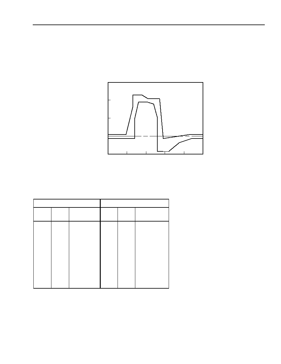
Agere Systems Inc.
37
Advance Data Sheet
May 2002
T7633 Dual T1/E1 3.3 V Short-Haul Terminator
Line Interface Unit: Transmit
(continued)
DSX-1 Transmitter Pulse Template and Specifications
The DS1 pulse shape template is specified at the DSX (defined by CB119 and
ANSI
T1.102) and is illustrated in
Figure 10. The LIU transmitter also meets the pulse template specified by ITU-T G.703 (not shown).
5-1160(C)r.4
Figure 10. DSX-1 Isolated Pulse Template
Table 7. DSX-1 Pulse Template Corner Points (from CB119, T1.102)
Maximum Curve
Minimum Curve
UI
ns
Normalized
Amplitude
UI
ns
Normalized
Amplitude
≠0.77
≠0.39
≠0.27
≠0.27
≠0.12
0.0
0.27
0.25
0.93
1.16
0
250
325
325
425
500
675
725
1100
1250
0.05
0.05
0.80
1.15
1.15
1.05
1.05
≠0.07
0.05
0.05
≠0.77
≠0.23
≠0.23
≠0.15
0.0
0.15
0.23
0.23
0.46
0.66
0.93
1.16
0
350
350
400
500
600
650
650
800
925
1100
1250
≠0.05
≠0.05
0.50
0.95
0.95
0.90
0.50
≠0.45
≠0.45
≠0.20
≠0.05
≠0.05
NORMALIZED AMPLITUDE (A)
1.0
0.5
0
≠0.5
0
250
500
750
1000
1250
TIME (ns)
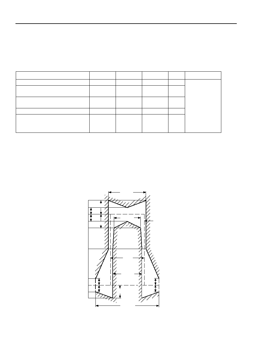
38
Agere Systems Inc.
Advance Data Sheet
May 2002
T7633 Dual T1/E1 3.3 V Short-Haul Terminator
Line Interface Unit: Transmit
(continued)
DSX-1 Transmitter Pulse Template and Specifications
(continued)
During DS1 operation, the LIU transmitter TTIP and TRING pins will perform as specified in Table 8.
1. With the line circuitry specified in Table 13.
2.Total power difference.
3.Measured in a 2 kHz band around the specified frequency.
4.Using Agere transformer 2795L and components in Table 13.
5.Below the power at 772 kHz.
CEPT Transmitter Pulse Template and Specifications
CEPT pulse shape template is specified at the system output (defined by ITU-T G.703) and is illustrated in Figure
11.
5-3145(C)r.3
Figure 11. ITU-T G.703 Pulse Template
Table 8. DS1 Transmitter Specifications
Parameter
Min
Typ
Max
Unit
Spec
Output Pulse Amplitude at DSX
1
2.5
3.0
3.5
V
AT&T
CB119,
ANSI
T1.102
Output Pulse Width at Line Side of
Transformer
1
325
350
375
ns
Output Pulse Width at Device Pins
TTIP and TRING
1
330
350
370
ns
Positive/Negative Pulse Imbalance
2
--
0.1
0.4
dB
Power Levels:
3,4
772 kHz
12.6
--
17.9
dBm
1.544 MHz
5
29
39
--
dB
10%
488 ns
(244 + 244)
219 ns
(244 ≠ 25)
10%
0%
NOMINAL PULSE
269 ns
(244 + 25)
20%
10%
10%
V = 100%
20%
50%
10%
10%
244 ns
194 ns
(244 ≠ 50)
20%

Agere Systems Inc.
39
Advance Data Sheet
May 2002
T7633 Dual T1/E1 3.3 V Short-Haul Terminator
Line Interface Unit: Transmit
(continued)
CEPT Transmitter Pulse Template and Specifications
(continued)
During E1 operation, the LIU transmitter TTIP and TRING pins will perform as specified in Table 9.
1.With the line circuitry specified in Table 13, measured at the transformer secondary.
2.Using Agere transformer 2795K or 2795J and components in Table 13.
Table 9. CEPT Transmitter Specifications
Parameter
Min
Typ
Max
Unit
Spec
Output Pulse Amplitude
1
:
75
120
2.13
2.7
2.37
3.0
2.61
3.3
V
V
ITU-T G.703
Output Pulse Width at Line Side of
Transformer
1
219
244
269
ns
Output Pulse Width at Device Pins TTIP
and TRING
1
224
244
264
ns
Positive/Negative Pulse Imbalance:
Pulse Amplitude
Pulse Width
≠4
≠4
±1.5
±1
4
4
%
%
Zero Level (percentage of pulse
amplitude)
≠5
0
5
%
Return Loss:
2
120
51 kHz to 102 kHz
102 kHz to 2.048 MHz
2.048 MHz to 3.072 MHz
Return Loss:
2
75
51 kHz to 102 kHz
102 kHz to 3.072 MHz
9
15
11
7
9
--
--
--
--
--
--
--
--
--
--
dB
dB
dB
dB
dB
CH-PTT
ETS 300 166:
1993

40
Agere Systems Inc.
Advance Data Sheet
May 2002
T7633 Dual T1/E1 3.3 V Short-Haul Terminator
Line Interface Unit: Jitter Attenuator
A selectable jitter attenuator is provided for narrow-bandwidth jitter transfer function applications. When placed in
the LIU receive path, the jitter attenuator provides narrow-bandwidth jitter filtering for line-synchronization. The jitter
attenuator can also be placed in the LIU transmit path to provide clock smoothing for applications such as synchro-
nous/asynchronous demultiplexers. In these applications, TLCK-LIU will have an instantaneous frequency that is
higher than the data rate and some TLCK-LIU periods are suppressed (gapped) in order to set the average long-
term TLCK-LIU frequency to within the transmit line rate specification. The jitter attenuator will smooth the gapped
clock.
Generated (Intrinsic) Jitter
Generated jitter is the amount of jitter appearing on the output port when the applied input signal has no jitter. The
jitter attenuator outputs a maximum of 0.04 UI peak-to-peak intrinsic jitter.
Jitter Transfer Function
The jitter transfer function describes the amount of jitter that is transferred from the input to the output over a range
of frequencies. The jitter attenuator exhibits a single-pole roll-off (20 dB/decade) jitter transfer characteristic that
has no peaking and a nominal filter corner frequency (3 dB bandwidth) of less than 4 Hz for DS1 operation and
approximately 10 Hz for CEPT operation. Optionally, a lower bandwidth of approximately 1.25 Hz can be selected
in CEPT operation by setting JABW0 = 1 (register LIU_REG4, bit 5) for systems desiring compliance with ETSI-
TBR12 and TBR13 jitter attenuation requirements. The reset default is JABW0 = 0. For a given frequency, different
jitter amplitudes will cause a slight variation in attenuation because of finite quantization effects. Jitter amplitudes of
less than approximately 0.2 UI will have greater attenuation than the single-pole roll-off characteristic. The jitter
transfer curve is independent of data patterns. Typical jitter transfer curves of the jitter attenuator are given in Fig-
ure 13 and Figure 15.

Agere Systems Inc.
41
Advance Data Sheet
May 2002
T7633 Dual T1/E1 3.3 V Short-Haul Terminator
Line Interface Unit: Jitter Attenuator
(continued)
Jitter Accommodation
The minimum jitter accommodation of the jitter attenuator occurs when the SYSCK frequency and the input clock's
long-term average frequency are at their extreme frequency tolerances. When the jitter attenuator is used in the
LIU transmit path, the minimum accommodation is 28 UI peak-to-peak at the highest jitter frequency of
15 kHz. Typical receiver jitter accommodation curves including the jitter attenuator in the LIU receive path are
given in Figure 12 and Figure 14.
When the jitter attenuator is placed in the data path, a difference between the SYSCK/16 frequency and the incom-
ing line rate for receive applications, or the TCLK rate for transmit applications will result in degraded low-
frequency jitter accommodation performance. The peak-to-peak jitter accommodation (JApp) for frequencies from
above the corner frequency of the jitter attenuator (Fc) to approximately 100 Hz is given by the following equation
where:
fdata = 1.544 MHz for DS1 or 2.048 MHz for E1,
for JABW0 = 0, fc = 3.8 Hz for DS1 or 10 Hz for E1,
and for JABW0 = 1, fc = 1.25 Hz for E1,
˝fsysclk = SYSCK tolerance in ppm,
˝fdata = data tolerance in ppm.
Note that for lower corner frequencies the jitter accommodation is more sensitive to clock tolerance than for higher
corner frequencies. When JABW0 = 1 and the jitter attenuator is used in the receive data path, the tolerance on
SYSCK should be tightened to ±20 ppm in order to meet the jitter accommodation requirements of TBR12/13 as
given in G.823 for line data rates of ±50 ppm.
Jitter Attenuator Enable (Transmit or Receive Path)
The jitter attenuator is placed in the LIU receive path by setting JAR = 1 (register LIU_REG3, bit 0). The jitter atten-
uator is selected in the LIU transmit path by setting JAT = 1 (register LIU_REG3, bit 1). When JAR = 1 and JAT = 1
or when JAR = 0 and JAT = 0, the jitter attenuator is disabled. Note that the power consumption increases slightly
on a per-channel basis when the jitter attenuator is active. The reset default case is JAR = JAT = 0.
JApp
64
2
f
sysclk
f
data
≠
(
)
f
data
2
f
c
------------------------------------------------------------------
≠
UI
=
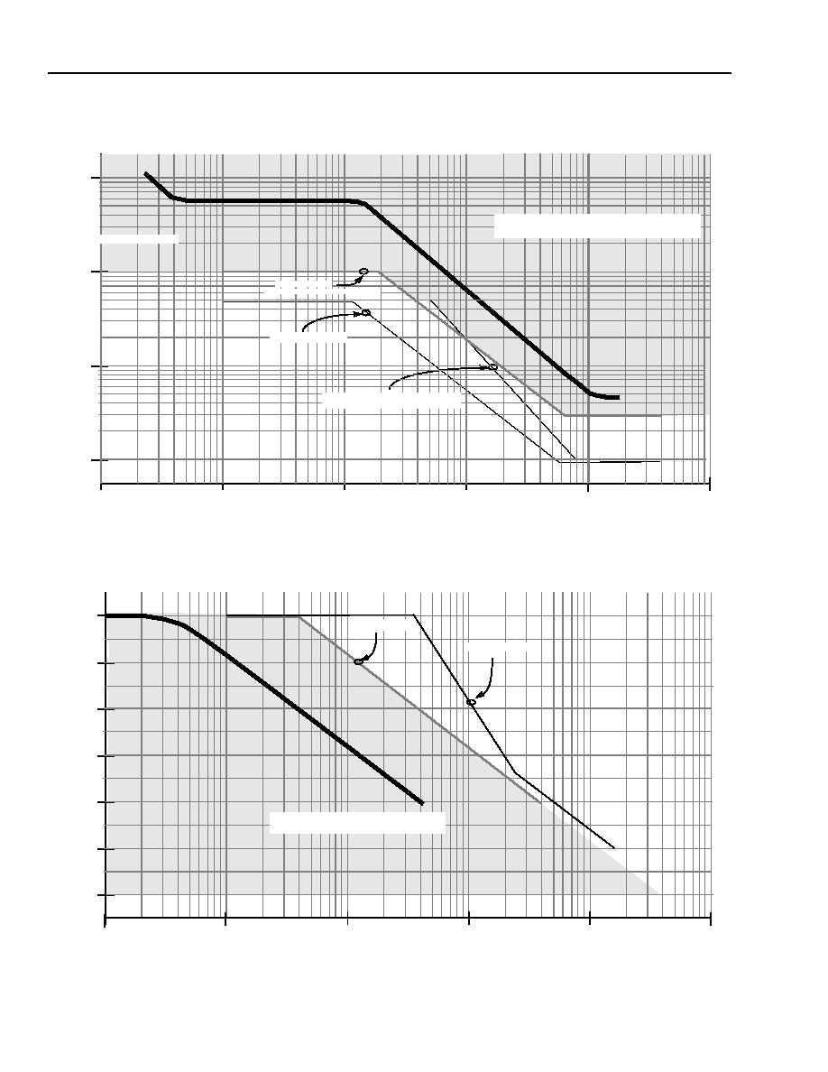
42
Agere Systems Inc.
Advance Data Sheet
May 2002
T7633 Dual T1/E1 3.3 V Short-Haul Terminator
Line Interface Unit: Jitter Attenuator
(continued)
5-5264(F)r.4
Figure 12. T1/DS1 Receiver Jitter Accommodation with Jitter Attenuator
5-5265(F)r.1
Figure 13. T1/DS1 Jitter Transfer of the Jitter Attenuator
0.1 UI
1.0 UI
10 UI
100 UI
10
100
1 k
10 k
1
28 UI
FREQUENCY (Hz)
100 k
TR-TSY-000009 (DS1, MUXES)
GR-499/1244-CORE (CAT I INTERFACES)
I.431(DS1), G.824(DS1)
TYPICAL
(SUBJECT TO DEVICE CHARACTERIZATION)
(NON-SONET CAT II INTERFACES)
GR-499-CORE
T1.408/I.431(DS1)/G.824(DS1)
60
40
20
0
1
10
100
1 k
10 k
50
30
10
100 k
FREQUENCY (Hz)
J
I
T
T
ER
OUT/
JI
TTE
R I
N
(
d
B)
TYPICAL
(SUBJECT TO DEVICE CHARACTERIZATION)
TR-TSY-000009
GR-253-CORE

Agere Systems Inc.
43
Advance Data Sheet
May 2002
T7633 Dual T1/E1 3.3 V Short-Haul Terminator
Line Interface Unit: Jitter Attenuator
(continued)
5-5266(F)r.2
Figure 14. CEPT/E1 Receiver Jitter Accommodation with Jitter Attenuator
5-5267(Fr.1
Figure 15. CEPT/E1 Jitter Transfer of the Jitter Attenuator
0.1 UI
1.0 UI
10 UI
100 UI
10
100
1 k
10 k
1
37 UI
FREQUENCY (Hz)
G.823
20.5 UI
12e-6 Hz
100 k
TYPICAL
(SUBJECT TO DEVICE CHARACTERIZATION)
G.823,ETSI-300-011A1
I.431(CEPT)/ETS-300-011
I.431(CEPT)/ETS-300-011
JABW0 = 0
JABW0 = 1
FREQUENCY (Hz)
J
ITT
ER
OUT/J
I
TTE
R I
N
(
d
B)
60
40
20
0
1
10
100
1 k
10 k
50
30
10
100 k
TYPICAL
(SUBJECT TO DEVICE CHARACTERIZATION)
JABW0 = 1
JABW0 = 0
ETSI TBR12/13
ETSI-300-011
I.431, G.735-9 WITH JITTER REDUCER
G.735-9 AT NATIONAL BOUNDARIES

44
Agere Systems Inc.
Advance Data Sheet
May 2002
T7633 Dual T1/E1 3.3 V Short-Haul Terminator
Line Interface Unit: Loopbacks
The LIU has independent loopback paths that are activated using LOOPA and LOOPB control bits (register
LIU_REG5, bits 2 to 3) as shown in Table 10. The locations of these loopbacks are illustrated in Figure 5, Block
Diagram of Line Interface Unit: Single Channel, on page 26.
Full Local Loopback (FLLOOP)
A full local loopback (FLLOOP) connects the LIU transmit driver input to the receive analog front-end circuitry. Valid
transmit output data continues to be sent to the network. If the LIU transmitter AIS signal (all-1s signal) is sent to
the network, by setting the XLAIS bit (register LIU_REG5, bit 1), the looped data is not affected. The ALOS alarm
continues to monitor the receive line interface signal (RTIP and RRING) while the DLOS alarm monitors the looped
data.
See Digital Loss of Signal (DLOS) Alarm section on page 28 regarding the behavior of the DLOS alarm upon acti-
vation of FLLOOP.
Remote Loopback (RLOOP)
A remote loopback (RLOOP) connects the recovered clock and retimed data to the LIU transmitter at the framer
interface and sends the data back to the line. The LIU receiver front end, clock/data recovery, encoder/decoder (if
enabled), jitter attenuator (if enabled), and LIU transmitter driver circuitry are all exercised during this loopback.
The transmit clock, transmit data, and the transmit AIS inputs are ignored. Valid receive output data continues to be
sent to RPD-LIU and RND-LIU. This loopback mode is very helpful in isolating failures between systems.
See Loss of LIU Transmit Clock (LOTC) Alarm section on page 35 and LIU Transmitter Driver Monitor (TDM) Alarm
on page 36 regarding the behavior of the LOTC and TDM alarms upon activation and deactivation of RLOOP.
Digital Local Loopback (DLLOOP)
A digital local loopback (DLLOOP) connects the transmit clock and data through the encoder/decoder pair to the
receive clock and data output pins. This loopback is operational regardless of whether the encoder/decoder pair is
enabled or disabled. The alarm indication signal can be transmitted (XLAIS = 1) without any effect on the looped
signal.
1. The reset default condition is LOOPA = LOOPB = 0 (no loopback).
2. During the transmit AIS condition, the looped data will be the transmitted data from the framer or system interface and not the all 1s signal.
3. Transmit AIS request is ignored.
Table 10. Loopback Control
Operation
Symbol
LOOPA
LOOPB
Normal
1
--
0
0
Full Local Loopback
FLLOOP
2
0
1
Remote Loopback
RLOOP
3
1
0
Digital Local Loopback
DLLOOP
1
1

Agere Systems Inc.
45
Advance Data Sheet
May 2002
T7633 Dual T1/E1 3.3 V Short-Haul Terminator
Line Interface Unit: Other Features
LIU Powerdown (PWRDN)
Each LIU channel has an independent powerdown mode controlled by PWRDN (register LIU_REG5, bit 0). This
provides power savings for systems which use backup channels. If PWRDN = 1, the corresponding LIU channel
will be in a standby mode consuming only a small amount of power. It is recommended that the alarm registers for
the powered down LIU channel be disabled by setting ALOSIE = DLOSIE = TDMIE = LOTCIE = 0 (register
LIU_REG1, bits 0--3). If an LIU channel in powerdown mode needs to be placed back into service, the channel
should be turned on (PWRDN = 0) approximately 5 ms before data is applied.
Loss of Framer Receive Line Clock (LOFRMRLCK Pin)
The LOFRMRLCK (pin 2/38) is set when the internal framer receive line clock is absent. During this alarm condi-
tion, the clock recovery and jitter attenuator functions are automatically disabled. If JAR = 1, the RLCK-LIU, RPD-
LIU, RND-LIU, and DLOS signals will be unknown.
In-Circuit Testing and Driver High-Impedance State (3-STATE)
If 3-STATE (pin 42/140) is activated (3-STATE = 0), the outputs TTIP, TRING, RDY_DTACK, INTERRUPT, and
AD[7:0] are placed in a high-impedance state. The TTIP and TRING outputs have a limiting high-impedance capa-
bility of approximately 8 k
.
LIU Delay Values
The transmit coder has 5 UI delay whether it is in the path or not and whether it is B8ZS or HDB3. Its delay is only
removed when in single-rail mode. The remainder of the transmit path has 4.6 UI delay. The receive decoder has
5 UI delay whether it is in the path or not and whether it is B8ZS or HDB3. Its delay is only removed when in single-
rail mode or CDR = 0. The equalizer plus slicer delay is nearly 0 UI delay. The jitter attenuator delay is nominally
33 UI but can be 2 UI--64 UI depending on state. The digital phase-locked loop used for timing recovery has 8 UI
delay.
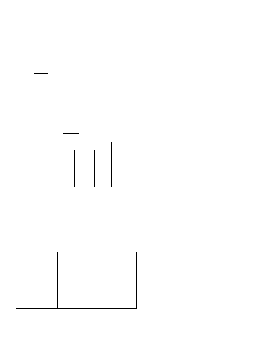
46
Agere Systems Inc.
Advance Data Sheet
May 2002
T7633 Dual T1/E1 3.3 V Short-Haul Terminator
SYSCK Reference Clock
The LIU requires an externally applied clock, SYSCK pins 3 and 35, for the clock and data recovery function and
the jitter attenuation option. SYSCK must be a continuously active (i.e., ungapped, unjittered, and unswitched) and
an independent reference clock such as from an external system oscillator or system clock for proper operation. It
must not be derived from any recovered line clock (i.e., from RLCK or any synthesized frequency of RLCK).
SYSCK may be supplied in one of two formats. The format is selected for each channel by CKSEL pins 48 and
133. For CKSEL = 1, a clock at 16x the primary line data rate clock (24.704 MHz for DS1 and 32.768 MHz for
CEPT) is applied to SYSCK. For CKSEL = 0, a primary line data rate clock (1.544 MHz for DS1 and 2.048 MHz for
CEPT) is applied to SYSCK.
The CKSEL pin has an internal pull-up resistor allowing the pin to be left open, i.e., a no connect, in applications
using a 16x reference clock and pulled down to ground for applications using a primary line data rate clock.
16x SYSCK Reference Clock
The specifications for SYSCK using a 16x reference clock are defined in Table 11. The 16x reference clock is
selected when CKSEL = 1.
* When JABW0 = 1 and the jitter attenuator is used in the receive data path, the tolerance on SYSCK should be tightened to ±20 ppm in order
to meet the jitter accommodation requirements of TBR12/13 as given in G.823 for line data rates of ±50 ppm.
If SYSCK is used as the source for AIS (see LIU Transmitter Alarm Indication Signal Generator (XLAIS) on page 35), it must meet the nomi-
nal transmission specifications of 1.544 MHz ± 32 ppm for DS1 (T1), or 2.048 MHz ± 50 ppm for CEPT (E1).
Primary Line Rate SYSCK Reference Clock and Internal Reference Clock Synthesizer
In some applications, it is more desirable to provide a reference clock at the primary data rate. In such cases, the
LIU can utilize an internal 16x clock synthesizer allowing the SYSCK pin to accept a primary data rate clock. The
specifications for SYSCK using a primary rate reference clock are defined in Table 12.
Table 12. SYSCK (1x, CKSEL = 0) Timing Specifications
* When JABW0 = 1 and the jitter attenuator is used in the receive data path, the tolerance on SYSCK should be tightened to ±20 ppm in order
to meet the jitter accommodation requirements of TBR12/13 as given in G.823 for line data rates of ±50 ppm.
If SYSCK is used as the source for AIS (see LIU Transmitter Alarm Indication Signal Generator (XLAIS) on page 35), it must meet the nomi-
nal transmission specifications of 1.544 MHz ± 32 ppm for DS1 (T1), or 2.048 MHz ± 50 ppm for CEPT (E1).
Table 11. SYSCK (16x, CKSEL = 1) Timing Specifications
Parameter
Value
Unit
Min
Typ
Max
Frequency
DS1
CEPT
--
--
24.704
32.768
--
--
MHz
MHz
Range*,
≠100
--
100
ppm
Duty Cycle
40
--
60
%
Parameter
Value
Unit
Min
Typ
Max
Frequency
DS1
CEPT
--
--
1.544
2.048
--
--
MHz
MHz
Range*,
≠100
--
100
ppm
Duty Cycle
40
--
60
%
Rise and Fall Times
(10%--90%)
--
--
5
ns

Agere Systems Inc.
47
Advance Data Sheet
May 2002
T7633 Dual T1/E1 3.3 V Short-Haul Terminator
SYSCK Reference Clock
(continued)
The data rate reference clock and the internal clock synthesizer is selected when CKSEL = 0. In this mode, a valid
and stable data rate reference clock must be applied to the SYSCK pin before and during the time a hardware
reset is activated (RESET = 0). The reset must be held active for a minimum of two data rate clock periods to
ensure proper resetting of the clock synthesizer circuit. Upon the deactivation of the reset pin (RESET = 1), the LIU
will extend the reset condition internally for approximately 1/2(2
12
≠ 1) line clock periods, or 1.3 ms for DS1 and
1 ms for CEPT after the hardware reset pin has become inactive allowing the clock synthesizer additional time to
settle. No activity such as microprocessor read/write should be performed during this period. The device will be
operational 2.7 ms after the deactivation of the hardware reset pin. Issuing an LIU software restart (LIU_REG2 bit
5 (RESTART) = 1) does not impact the clock synthesizer circuit.

48
Agere Systems Inc.
Advance Data Sheet
May 2002
T7633 Dual T1/E1 3.3 V Short-Haul Terminator
Line Interface Unit: Line Interface Networks
The transmit and receive tip and ring connections provide a matched interface to the line cable when used with a
proper matching network. The diagram in Figure 16 shows the appropriate external components to interface to the
cable for a single transmit/receive channel. The component values are summarized in Table 13, based on the spe-
cific application.
5-3693(C).e
Figure 16. Line Termination Circuitry
1. Resistor tolerances are ±1%. Transformer turns ratio tolerances are ±2%.
2. Use Agere 2795L transformer.
3. For CEPT 75
applications, Option 1 is recommended over Option 2 for lower device power dissipation. Option 2 increases power dissipa-
tion by 13 mW per channel when driving 50% ones data. Option 2 allows for the use of the same transformer as in CEPT 120
applications.
4. Use Agere 2795K transformer.
5. Use Agere 2795J transformer.
6. A ±5% tolerance is allowed for the transmit load termination.
Table 13. Termination Components by Application
1
Symbol
Name
Cable Type
Unit
DS1
2
Twisted
Pair
CEPT 75
3
Coaxial
CEPT 120
5
Twisted Pair
Option 1
4
Option 2
5
C
C
Center Tap Capacitor
0.1
0.1
0.1
0.1
µ
F
C
P
Line Shunt Capacitor
--
150
150
150
R
P
Receive Primary Impedance
200
200
200
200
R
R
Receive Series Impedance
332
143
261
698
R
S
Receive Secondary Impedance
210
147
182
365
Z
EQ
Equivalent Line Termination
100
75
75
120
Tolerance
±4
±4 ±4
±4
%
R
T
Transmit Series Impedance
0
7.5
5.36
7.5
R
L
Transmit Load Termination
6
100
75
75
120
N
Transformer Turns Ratio
2.1
1.93
2.45
2.45
--
RTIP
RRING
TTIP
TRING
DEVICE
(1 CHANNEL)
R
L
R
S
R
R
R
R
RECEIVE DATA
R
P
Z
EQ
R
T
R
T
N:1
TRANSMIT DATA
TRANSFORMER
EQUIPMENT
INTERFACE
1:N
C
C
C
P
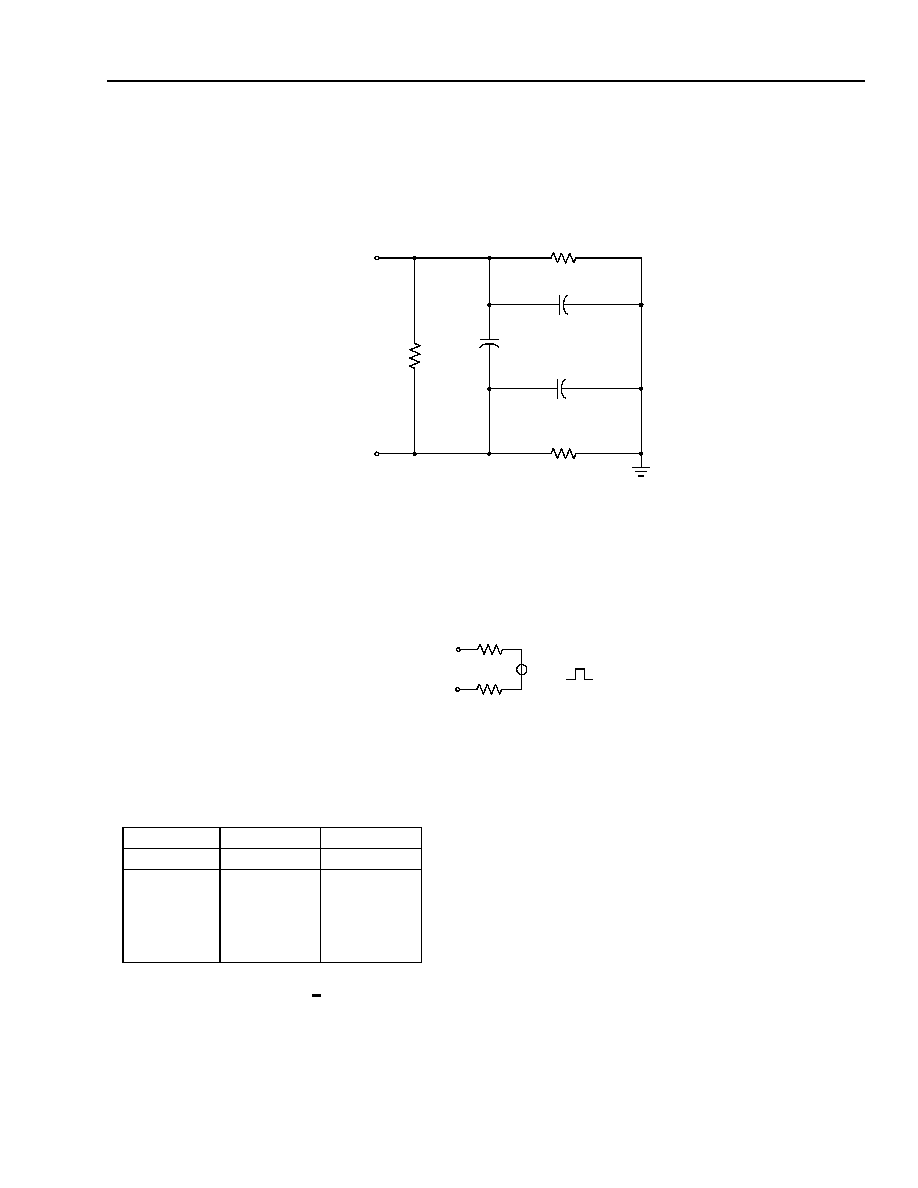
Agere Systems Inc.
49
Advance Data Sheet
May 2002
T7633 Dual T1/E1 3.3 V Short-Haul Terminator
Line Interface Unit: Line Interface Networks
(continued)
The transmit and receive tip and ring connections should be provided with a matched and protected interface to
the line (i.e., terminating impedance to match the characteristic impedance of the line cable and secondary line
protection). For the purpose of line protection and matching network design, the equivalent input impedance of the
receiver and the equivalent output circuit of the transmitter can be assumed to be as shown in Figure 17.
5-6232(F).b
* Approximately 0.3 V--2.0 V peak.
Approximate pulse voltage source (peak).
Figure 17. T7633 Line Interface Unit Approximate Equivalent Analog I/O Circuits
Mode
Peak
Unit
DS1
1.6
V
CEPT:
75
:
Option 1
Option 2
120
2.3
2.1
2.3
V
V
V
RECEIVER
PULSE
VOLTAGE SOURCE
TRANSMITTER
OUTPUT
1
--1.5
47 k
2 pF
20 k
INPUT*
A. Receiver Input Approximate Equivalent Circuit
B. Transmitter Output Approximate Equivalent Circuit
1
--1.5
3 pF
20 k
3 pF
GRND
A

50
Agere Systems Inc.
Advance Data Sheet
May 2002
T7633 Dual T1/E1 3.3 V Short-Haul Terminator
LIU-Framer Interface
LIU-Framer Physical Interface
The transmit framer-LIU interface for the T7633 consists of the TND, TPD, and TLCK pins. In normal operations,
TND, TPD, and TLCK are directly connected to the transmit line interface and the TPD, TND, and TLCK pins are
driven from the transmit framer. The receive framer-LIU interface for the T7633 consists of the RPD, RND_BPV,
and RLCK internal signals. In normal operations, RND, RPD, and RLCK are directly sourced from the internal
receive line interface unit. In the framer mode, FRAMER = 0, the RPD, RND, and RLCK pins are directly connected
to the receive framer (the internal receive line interface unit is bypassed). Figure 18 illustrates the interfaces of the
transmit and receive framer units.
5-4557(F).br.2
Figure 18. Block Diagram of Framer Line Interface
TTIP
TRING
TRANSMIT LINE
INTERFACE
UNIT
TLCK
TND
TPD
TLCK TPD TND
TRANSMIT
FRAMER
TRANSMIT
HDLC
FACILITY DATA
LINK
INTERFACE
RECEIVE
CONCENTRATION
HIGHWAY
INTERFACE
TFDLCK
TFDL
RCHIDATA
RCHICK
RECEIVE HDLC
FACILITY DATA
LINK INTERFACE
RECEIVE
FRAMER
1
0
RLCK
RPD
RND_BPV
RTIP
RRING
RECEIVE LINE
INTERFACE
UNIT
FRAMER
TRANSMIT
CONCENTRATION
HIGHWAY
INTERFACE
TCHIDATA
RFDLCK
RFDL
(XLIU)
(XFRMR)
(RCHI)
(XCHI)
(RFRMR)
(RLIU)
LINE INTERFACE
SYSTEM INTERFACE
PLLCK
TCHIFS
TCHICK
RFRMCK
LIU_RLCK
LIU_RND/BPV
LIU_RPD
FRM_RLCK
FRM_RND
FRM_RPD
RCHIFS
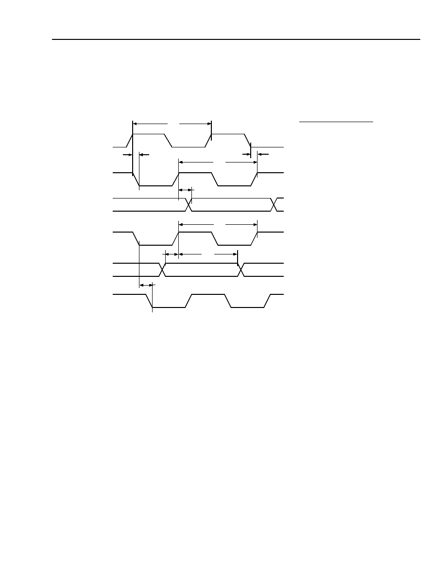
Agere Systems Inc.
51
Advance Data Sheet
May 2002
T7633 Dual T1/E1 3.3 V Short-Haul Terminator
LIU-Framer Interface
(continued)
LIU-Framer Physical Interface
(continued)
Figure 19 shows the timing requirements for the transmit and receive framer interfaces in the LIU-bypass mode.
5-4558(F).cr.3
Figure 19. Transmit Framer TLCK to TND, TPD and Receive Framer RND, RPD to RLCK Timing
162 ns
t1-DS1
648 ns
t1
t2r-f
t2f-r
t3
t4
t5
PLLCK
TLCK
TND, TPD
RLCK
RND, RPD
RFRMCK
t7 = RPD, RND HOLD FROM RISING RLCK = 40 ns
t6
t7
t8
t2r-f: t2f-r: PLLCK TO TLCK DELAY = 50 ns
t3-DS1 = 648 ns
t3-CEPT = 488 ns
t4 = TLCK TO VALID TPD, TND = 30 ns
t5-CEPT = 488 ns
t5-DS1 = 648 ns
t6 = RPD, RND SETUP TO RISING RLCK = 40 ns
t8r-f: t8f-r: RLCK TO RFRMCK DELAY = 50 ns
FRM_PR45 BIT 0 (HFLF)
HFLF = 0
HFLF = 1
122 ns
t1-CEPT
488 ns

52
Agere Systems Inc.
Advance Data Sheet
May 2002
T7633 Dual T1/E1 3.3 V Short-Haul Terminator
LIU-Framer Interface
(continued)
Interface Mode and Line Encoding
Single Rail
The default mode for the LIU-framer interface is single-rail, register LIU_REG3 bit 3 (DUAL) = 0 and register
FRM_PR8 bit 7 = 1, bit 6 = 1, and bit 5 = 0.
In the single-rail terminator mode (FRAMER = 1), the LIU bipolar encoder and decoder may be enabled by setting
register LIU_REG3 bit 2 (CODE) to 1. Signals passed on the internal LIU-framer interface are data (LIU_RPD and
TPD), clock (LIU_RLCK and TLCK), and received bipolar violations (LIU_RND/BPV). When LIU_RND/BPV = 1,
the BPV counter increments by one on the rising edge of LIU_RLCK.
In the single-rail framer mode (FRAMER = 0), external signals to and from the framer are data (RTIP_RPD, pin 11/
27 and TPD, pin 44/138), clock (RLCK, pin 47/135, and TLCK, pin 46/136), and received bipolar violations
(RRING_RND, pin 10/28). When RRING_RND = 1, the BPV counter increments by one on the rising edge of
RLCK. In this mode, TND (pin 45/137) is forced to the 0 state.
Dual Rail
Dual-rail LIU-framer interface mode is selected by setting LIU_REG3 bit 3 (DUAL) = 1 and by selecting one of the
dual-rail framer modes of FRM_PR8 bit 5--bit 7.
In the dual-rail terminator mode (FRAMER = 1), the framer bipolar encoder and decoder are enabled. Signals
passed on the internal LIU-framer interface are data (LIU_RPD, LIU_RND, TPD, and TND), and clock (LIU_RLCK
and TLCK). When bipolar violations are detected by the framer, the BPV counter increments by one on the rising
edge of LIU_RLCK.
In the dual-rail framer mode (FRAMER = 0), external signals to and from the framer are data (RTIP_RPD, pin 11/
27, RRING_RND, pin 10/28, TPD, pin 44/138, and TND, pin 45/137) and clock (RLCK, pin 47/135, and TLCK, pin
46/136). When bipolar violations are detected by the framer, the BPV counter increments by one on the rising edge
of RLCK.
DS1: Alternate Mark Inversion (AMI)
The default line code used for T1 is alternate mark inversion (AMI). The coding scheme represents a 1 with a pulse
(mark) on the positive or negative rail and a 0 with no pulse on either rail. This scheme is shown in Table 14.
Table 14. AMI Encoding
The T1 "ones density rule" states that:
In every 24 bits of information to be transmitted, there must be at least three pulses, and no more than 15
zeros may be transmitted consecutively [
AT&T
TR62411 (1988),
ANSI
T1.231 (1997)].
Receive ones density is monitored by the receive line interface as per T1M1.3/93-005, ITU G.775, or TR-TSY-
000009.
The receive framer indicates excessive zeros upon detecting any zero string length greater than fifteen contiguous
zeros (no pulses on either RPD or RND). Both excessive zeros and coding violations are indicated as bipolar viola-
tions.
Input Bit Stream
1011
0000
0111
1010
AMI Data
≠0+≠
0000
0+≠+
≠0+0
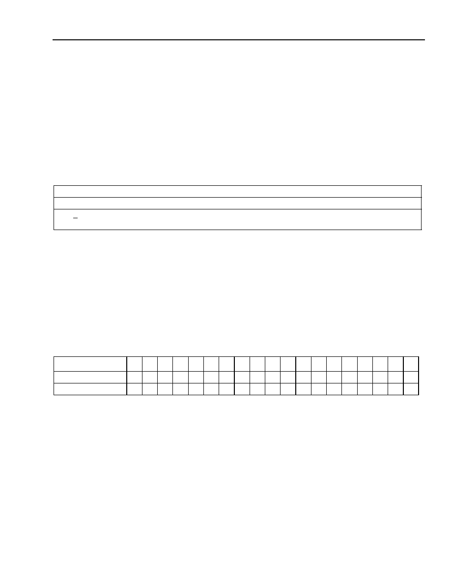
Agere Systems Inc.
53
Advance Data Sheet
May 2002
T7633 Dual T1/E1 3.3 V Short-Haul Terminator
LIU-Framer Interface
(continued)
DS1: Zero Code Suppression (ZCS)
Zero code suppression is a technique known as pulse stuffing in which the seventh bit of each time slot is stuffed
with a one. The line format (shown in Table 15) limits the data rate of each time slot from 64 kbits/s to 56 kbits/s.
The default ZCS format stuffs the seventh bit of those ALL-ZERO time slots programmed for robbed-bit signaling
(as defined in the signaling control registers with the F and G bits).
The receive framer indicates excessive zeros upon detecting any zero string length greater than fifteen contiguous
zeros (no pulses on either RPD or RND). Both excessive zeros and coding violations are indicated as bipolar vio-
lations.
Table 15. DS1 ZCS Encoding
DS1: Binary 8 Zero Code Suppression (B8ZS)
Clear channel transmission can be accomplished using Binary 8 Zero Code Suppression (B8ZS). Eight consecu-
tive 0s are replaced with the B8ZS code. This code consists of two bipolar violations in bit positions 4 and 7 and
valid bipolar marks in bit positions 5 and 8. The receiving end recognizes this code and replaces it with the original
string of eight 0s.
The receive framer indicates excessive zeros upon detecting a block of eight (8) or more consecutive 0s (no
pulses on either RPD or RND). Both excessive zeros and coding violations are indicated as bipolar violations.
Table 16 shows the encoding of a string of 0s using B8ZS. B8ZS is recommended when ESF format is used. V
represents a violation of the bipolar rule, and B represents an inserted pulse conforming to the AMI rule.
Input Bit Stream
00000000
01010000
00000000
00000000
ZCS Data (Framer Mode)
00000010
01010010
00000010
00000010
T7633 Default ZCS
00000010
01010000
00000000
(data time slot remains clear)
00000010
Table 16. DS1 B8ZS Encoding
Bit Positions
1
2
3
4
5
6
7
8
--
--
--
1
2
3
4
5
6
7
8
Before B8ZS
0
0
0
0
0
0
0
0
1
0
1
0
0
0
0
0
0
0
0
After B8ZS
0
0
0
V
B
0
V
B
B
0
B
0
0
0
V
B
0
V
B

54
Agere Systems Inc.
Advance Data Sheet
May 2002
T7633 Dual T1/E1 3.3 V Short-Haul Terminator
LIU-Framer Interface
(continued)
CEPT: High-Density Bipolar of Order 3 (HDB3)
The line code used for CEPT is described in ITU Rec. G.703 Section 6.1 as high-density bipolar of order 3 (HDB3).
HDB3 uses a substitution code that acts on strings of four 0s. The substitute HDB3 codes are 000V and B00V,
where V represents a violation of the bipolar rule and B represents an inserted pulse conforming to the AMI rule
defined in ITU Rec. G.701, item 9004. The choice of the B00V or 000V is made so that the number of B pulses
between consecutive V pulses is odd. In other words, successive V pulses are of alternate polarity so that no direct
current (dc) component is introduced. The substitute codes follow each other if the string of 0s continues. The
choice of the first substitute code is arbitrary. A line code error consists of two pulses of the same polarity that is not
defined as one of the two substitute codes. Excessive zeros consist of any zero string length greater than four con-
tiguous zeros. Both excessive zeros and coding violations are indicated as bipolar violations. An example is shown
in Table 17.
Table 17. ITU HDB3 Coding
Input Bit Stream
1011
0000
01
0000
0000
0000
0000
HDB3-coded Data
1011
000V
01
000V
B00V
B00V
B00V
HDB3-coded Levels
≠0+≠
000≠
0+
000+
≠00≠
+00+
≠00≠
HDB3 with 5 Double BPVs
≠0+≠
≠000
0+
+00+
0≠ ≠ ≠
+00+
≠00≠
1-BPV
3-BPV
5-BPV
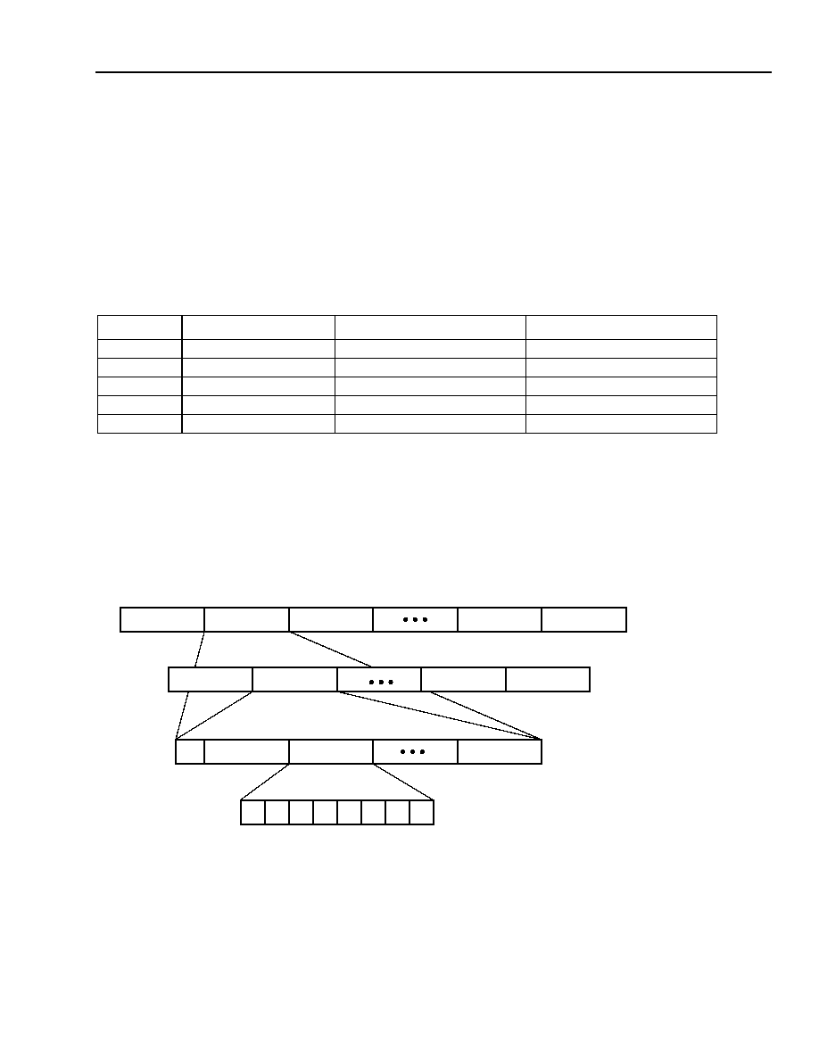
Agere Systems Inc.
55
Advance Data Sheet
May 2002
T7633 Dual T1/E1 3.3 V Short-Haul Terminator
Frame Formats
The supported North American T1 framing formats are superframe (D4,
SLC
-96, and digital data service-DDS) and
extended superframe (ESF). The device can be programmed to support the ITU-CEPT-E1 basic format with and
without CRC-4 multiframe formatting. This section describes these framing formats.
T1 Framing Structures
T1 is a digital transmission system which multiplexes twenty-four 64 kbits/s time slots (DS0) onto a serial link. The
T1 system is the lowest level of hierarchy on the North American T-carrier system, as shown in Figure 20.
Frame, Superframe, and Extended Superframe Definitions
Each time slot (DS0) is an assembly of 8 bits sampled every 125 µs. The data rate is 64 kbits/s and the sample
rate is 8 kHz. Time-division multiplexing 24 DS0 time slots together produces a 192-bit (24 DS0s) frame. A framing
bit is added to the beginning of each frame to allow for detection of frame boundaries and the transport of addi-
tional maintenance information. This 193-bit frame, also referred to as a DS1 frame, is repeated every 125 µs to
yield the 1.544 Mbits/s T1 data rate. DS1 frames are bundled together to form superframes or extended super-
frames.
5-4559(F).br.1
Figure 20. T1 Frame Structure
Table 18. T-Carrier Hierarchy
T Carrier
DS0 Channels
Bit Rate (Mbits/s)
Digital Signal Level
T1
24
1.544
DS1
T1-C
48
3.152
DS1C
T2
96
6.312
DS2
T3
672
44.736
DS3
T4
4032
274.176
DS4
FRAME 1
FRAME 2
FRAME 3
FRAME 24
FRAME 23
FRAME 1
FRAME 2
FRAME 11
FRAME 12
F BIT
TIME SLOT 1
TIME SLOT 2
TIME SLOT 24
1
2
3
4
5
6
7
8
24-FRAME EXTENDED
ESF = 3.0 ms
12-FRAME SUPERFRAME
SF = 1.5 ms
193-bit FRAME
DS1 = 125
µ
s
8-bit TIME SLOT
DS0 = 5.19
µ
s
SUPERFRAME
56
Agere Systems Inc.
Advance Data Sheet
May 2002
T7633 Dual T1/E1 3.3 V Short-Haul Terminator
Frame Formats
(continued)
T1 Framing Structures
(continued)
Transparent Framing Format
The transmit framer can be programmed to transparently transmit 193 bits of system data to the line. The system
interface must be programmed such that the stuffed time slots are 1, 5, 9, 13, 17, 21, 25, and 29 (FRM_PR43 bits
2--0 must be set to 000) and either transparent framing mode 1 or transparent framing mode 2 is enabled
(FRM_PR26 bit 3 or bit 4 must be set to 1).
In transparent mode 1 or mode 2, the transmit framer extracts from the receive system data bit 8 of time slot 1 and
inserts this bit into the framing bit position of the transmit line data. The other 7 bits of the receive system time slot
1 are ignored by the transmit framer. The receive framer will extract the f-bit (or 193rd bit) of the receive line data
and insert it into bit 8 of time slot 1 of the system data; the other bits of time slot 1 are set to 0.
Frame integrity is maintained in both the transmit and receive framer sections.
5-5989(F).ar.1
Figure 21. T1 Transparent Frame Structure
In transparent framing mode 1, the receive framer is forced not to reframe on the receive line data. Other than
bipolar violations and unframed AIS monitoring, there is no processing of the receive line data. The receive framer
will insert the 193rd bit of the receive line data into bit 8 of time slot 1 of the transmit system data.
In transparent framing mode 2, the receive framer functions normally on receive line data. All normal monitoring of
receive line data is performed and data is passed to the transmit CHI as programmed. The receive framer will
insert the extracted framing bit of the receive line data into bit 8 of time slot 1 of the transmit system data. The
remaining bits in time slot 1 are set to 0.
TIME SLOT 1
(STUFF TIME SLOT)
32 TIME-SLOT CHI FRAME
TIME SLOT 2
TIME SLOT 3
TIME SLOT 31 TIME SLOT 32
0
0
0
0
0
0
0
F BIT
TRAMSMIT FRAMER'S
193-bit FRAME
DS1 = 125
µ
s
TIME SLOT 1
TIME SLOT 2
TIME SLOT 24
F BIT

Agere Systems Inc.
57
Advance Data Sheet
May 2002
T7633 Dual T1/E1 3.3 V Short-Haul Terminator
Frame Formats
(continued)
T1 Framing Structures
(continued)
D4 Frame Format
D4 superframe format consists of 12 DS1 frames. Table 19 shows the structure of the D4 superframe.
1. Frame 1 is transmitted first.
2. Following
ANSI
T1.403, the bits are numbered 0--2315. Bit 0 is transmitted first. Bits in each DS0 time slot are numbered 1 through 8, and
bit 1 of each DS0 is transmitted first.
3. The remote alarm forces bit 2 of each time slot to a 0-state when enabled. The Japanese remote alarm forces framing bit 12 (bit number
2123) to a 1-state when enabled.
4. Signaling option none uses bit 8 for traffic data.
5. Frames 6 and 12 contain the robbed-bit signaling information in bit 8 of each voice channel, when enabled.
The receive framer uses both the F
T
and F
S
framing bits during its frame alignment procedure.
Table 19. D4 Superframe Format
Frame
Number
1
Framing Bits
Bit Used in Each Time Slot
Signaling Options
Bit
Number
2
Terminal
Frame F
T
Signal
Frame
F
S
Traffic
(All
Channels)
Remote
Alarm
3
Signal-
ing
None
4
2-State
4-State
1
0
1
--
1--8
2
--
--
--
--
2
193
--
0
1--8
2
--
--
--
--
3
386
0
--
1--8
2
--
--
--
--
4
579
--
0
1--8
2
--
--
--
--
5
772
1
--
1--8
2
--
--
--
--
6
5
965
--
1
1--7
2
8
--
A
A
7
1158
0
--
1--8
2
--
--
--
--
8
1351
--
1
1--8
2
--
--
--
--
9
1544
1
--
1--8
2
--
--
--
--
10
1737
--
1
1--8
2
--
--
--
--
11
1930
0
--
1--8
2
--
--
--
--
12
5
2123
--
0
1--7
2
8
--
A
B
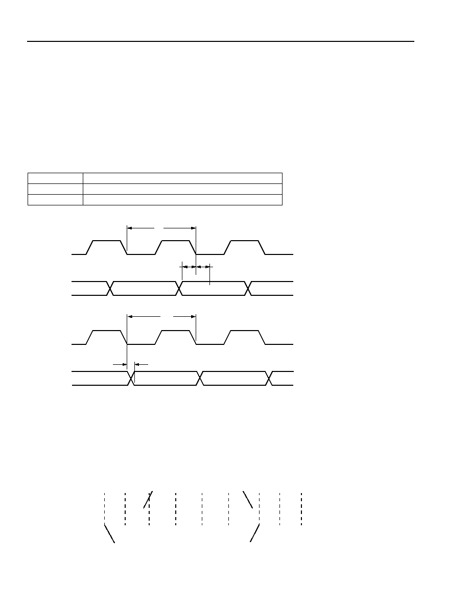
58
Agere Systems Inc.
Advance Data Sheet
May 2002
T7633 Dual T1/E1 3.3 V Short-Haul Terminator
Frame Formats
(continued)
T1 Framing Structures
(continued)
Digital Data Service (DDS) Frame Format
The superframe format for DDS is the same as that given for D4. DDS is intended to be used for data-only traffic,
and as such, the system should ensure that the framer is in the nonsignaling mode. DDS uses time slot 24 (FAS
channel) to transmit the remote frame alarm and data link bits. The format for time slot 24 is shown in Table 20. The
facility data link timing is shown in Figure 22 below.
5-3910(F).cr.1
Figure 22. T7633 Facility Data Link Access Timing of the Transmit and Receive Framer Sections
SLC
-96 Frame Format
SLC
-96 superframe format consists of 12 DS1 frames similar to D4. The F
T
pattern is exactly the same as D4. The
F
S
pattern uses that same structure as D4 but also incorporates a 24-bit data link word as shown below.
5-6421(F)r.1
Table 20. DDS Channel-24 Format
Time Slot 24 = 10111YD0
Y = (bit 6)
Remote frame alarm: 1 = no alarm state; 0 = alarm state
D = (bit 7)
Data link bits (8 kbits/s)
t8
t9
t9
t10
t11
t8: TFDLCK CYCLE =
t9: TFDL TO TFDLCK SETUP/HOLD = 40 ns
t10: RFDLCK CYCLE =
t11: RFDLCK TO RFDL DELAY = 40 ns
TFDLCK
TFDL
RFDLCK
RFDL
250
µ
s (ALL OTHER
MODES)
125
µ
s (DDS)
250
µ
s (ALL OTHER
MODES)
125
µ
s (DDS)
Fs =
. . .
000111000111D
1
DDDDDDDDDDDDDDDDDDDDDDD
24
000111000111DDD . . .
SLC
-96 24-bit DATA LINK WORD
SLC
-96 36-FRAME D-bit SUPERFRAME INTERVAL
(72 DS1 FRAMES)
FRAME
N ≠1
FRAME
N
FRAME
N + 1
FRAME
N + 2
FRAME
N + 3
FRAME
N + 4
FRAME
N + 5
FRAME
N + 6
FRAME
N + 7
FRAME
N + 8

Agere Systems Inc.
59
Advance Data Sheet
May 2002
T7633 Dual T1/E1 3.3 V Short-Haul Terminator
Frame Formats
(continued)
T1 Framing Structures
(continued)
External TFDL Source. Data may be inserted and extracted from the
SLC
-96 data link from either the external
facility data link (TFDL) ports or the
SLC
-96 data stack. Source selection is controlled by FRM_PR21 bit 6 and
FRM_PR29 bit 5--bit 7.
The transmit framer synchronizes on TFDL = 000111000111 . . . and forces a superframe boundary based on this
pattern. When sourcing an external bit stream, it is the system's responsibility to ensure that TFDL data contain the
pattern of 000111000111 . . . . The D pattern sequence is shown in Table 21. Table 22 shows the encoding for the
line switch field.
Table 21.
SLC
-96 Data Link Block Format
Data Link Block
Bit Definition
Bit Value
D
1 (leftmost bit)
C
1
-- concentrator bit
0 or 1
D
2
C
2
-- concentrator bit
0 or 1
D
3
C
3
-- concentrator bit
0 or 1
D
4
C
4
-- concentrator bit
0 or 1
D
5
C
5
-- concentrator bit
0 or 1
D
6
C
6
-- concentrator bit
0 or 1
D
7
C
7
-- concentrator bit
0 or 1
D
8
C
8
-- concentrator bit
0 or 1
D
9
C
9
-- concentrator bit
0 or 1
D
10
C
10
-- concentrator bit
0 or 1
D
11
C
11
-- concentrator bit
0 or 1
D
12
Spoiler bit 1
0
D
13
Spoiler bit 2
1
D
14
Spoiler bit 3
0
D
15
M
1
-- maintenance bit
0 or 1
D
16
M
2
-- maintenance bit
0 or 1
D
17
M
3
-- maintenance bit
0 or 1
D
18
A1 -- alarm bit
0 or 1
D
19
A2 -- alarm bit
0 or 1
D
20
S
1
-- line-switch bit
Defined in Table 22
D
21
S
2
-- line-switch bit
Defined in Table 22
D
22
S
3
-- line-switch bit
Defined in Table 22
D
23
S
4
-- line-switch bit
Defined in Table 22
D
24 (rightmost bit)
Spoiler bit 4
1

60
Agere Systems Inc.
Advance Data Sheet
May 2002
T7633 Dual T1/E1 3.3 V Short-Haul Terminator
Frame Formats
(continued)
T1 Framing Structures
(continued)
Internal
SLC
-96 Stack Source. Optionally, a
SLC
-96 FDL stack may be used to insert and correspondingly extract
the FDL information in the
SLC
-96 frame format.
The transmit
SLC
-96 FDL bits are sourced from the transmit framer
SLC
-96 FDL stack. The
SLC
-96 FDL stack
(see FRM_PR31--FRM_PR35) consists of five 8-bit registers that contain the
SLC
-96 FS and D-bit information as
shown in Table 23. The transmit stack data is transmitted to the line when the stack enable mode is active in the
parameter registers FRM_PR21 bit 6 = 1 and FRM_PR29 bit 5--bit 7 = x10 (binary).
The receive
SLC
-96 stack data is received when the receive framer is in the superframe alignment state. In the
SLC
-96 mode, while in the loss of superframe alignment (LSFA) state, updating of the receive framer
SLC
-96 stack
is halted and neither the receive stack interrupt nor receive stack flag are asserted.
Table 23. Transmit and Receive
SLC
-96 Stack Structure
Bit 5--bit 0 of the first 2 bytes of the
SLC
-96 FDL stack in Table 23 are transmitted to the line as the
SLC
-96 F
S
sequence. Bit 7 of the third stack register is transmitted as the C
1
bit of the
SLC
-96 D sequence. The spoiler bits
(SPB1, SPB2, SPB3, and SPB4) are taken directly from the transmit stack. The protocol for accessing the
SLC
-96
stack information for the transmit and receive framer is described below. The transmit
SLC
-96 stack must be writ-
ten with valid data when transmitting stack data.
The device indicates that it is ready for an update of its transmit stack by setting register FRM_SR4 bit 5 (
SLC
-96
transmit FDL stack ready) high. At this time, the system has about 9 ms to update the stack. Data written to the
stack during this interval will be transmitted during the next
SLC
-96 superframe D-bit interval. By reading bit 5 in
register SR4, the system clears this bit so that it can indicate the next time the transmit stack is ready. If the trans-
mit stack is not updated, then the content of the stack is retransmitted to the line. The start of the
SLC
-96 36-frame
F
S
interval of the transmit framer is a function of the first 2 bytes of the
SLC
-96 transmit stack registers. These
bytes must be programmed as shown in Table 23. Programming any other state into these two registers disables
the proper transmission of the
SLC
-96 D bits. Once programmed correctly, the transmit
SLC
-96 D-bit stack is trans-
mitted synchronous to the transmit
SLC
-96 superframe structure.
On the receive side, the device indicates that it has received data in the receive FDL stack (registers FRM_SR54--
FRM_SR58) by setting bit 4 in register FRM_SR4 (
SLC
-96 receive FDL stack ready) high. The system then has
about 9 ms to read the content of the stack before it is updated again (old data lost). By reading bit 4 in register
FRM_SR4, the system clears this bit so that it can indicate the next time the receive stack is ready. As explained
above, the
SLC
-96 receive stack is not updated when superframe alignment is lost.
Table 22.
SLC
-96 Line Switch Message Codes
S
1
S
2
S
3
S
4
Code Definition
1
1
1
1
Idle
1
1
1
0
Switch line A receive
1
1
0
1
Switch line B transmit
1
1
0
0
Switch line C transmit
1
0
1
0
Switch line D transmit
0
1
0
1
Switch line B transmit and receive
0
1
0
0
Switch line B transmit and receive
0
0
1
0
Switch line B transmit and receive
Register
Number
Bit 7
(MSB)
Bit 6
Bit 5
Bit 4
Bit 3
Bit 2
Bit 1
Bit 0
(LSB)
1 (LSR)
0
0
0
0
0
1
1
1
2
0
0
0
0
0
1
1
1
3
C
1
C
2
C
3
C
4
C
5
C
6
C
7
C
8
4
C
9
C
10
C
11
SPB
1
= 0 SPB
2
= 1 SPB
3
= 0
M
1
M
2
5
M
3
A
1
A
2
S
1
S
2
S
3
S
4
SPB
4
= 1

Agere Systems Inc.
61
Advance Data Sheet
May 2002
T7633 Dual T1/E1 3.3 V Short-Haul Terminator
Frame Formats
(continued)
T1 Framing Structures
(continued)
Extended Superframe Format
The extended superframe format consists of 24 DS1 frames. The F bits are used for frame alignment, superframe
alignment, error checking, and facility data link transport. Table 24 shows the ESF frame format.
1. Frame 1 is transmitted first.
2. The remote alarm is a repeated 1111111100000000 pattern in the DL when enabled.
3. Following
ANSI
T1.403, the bits are numbered 0--4361. Bit 0 is transmitted first. Bits in each DS0 time slot are numbered 1 through 8, and
bit 1 of each DS0 is transmitted first.
4. The C
1
to C
6
bits are the cyclic redundancy check-6 (CRC-6) checksum bits calculated over the previous extended superframe.
5. Signaling option none uses bit 8 for traffic data.
6. Frames 6, 12, 18, and 24 contain the robbed-bit signaling information in bit 8 of each voice channel, when enabled.
The ESF format allows for in-service error detection and diagnostics on T1 circuits. ESF format consist of 24 fram-
ing bits: 6 for framing synchronization (2 kbits/s); 6 for error detection (2 kbits/s); and 12 for in-service monitoring
and diagnostics (4 kbits/s).
Table 24. Extended Superframe (ESF) Structure
Frame
Number
1
Frame Bit
Bit Use in Each Time
Slot
Signaling Option
2
Bit
Number
3
F
E
D
L
CRC-6
4
Traffic
Signaling
None
5
2-State
4-State
16-State
1
0
--
D
--
1--8
--
--
--
--
--
2
193
--
--
C
1
1--8
--
--
--
--
--
3
386
--
D
--
1--8
--
--
--
--
--
4
579
0
--
--
1--8
--
--
--
--
--
5
772
--
D
--
1--8
--
--
--
--
--
6
6
965
--
--
C
2
1--7
8
--
A
A
A
7
1158
--
D
--
1--8
--
--
--
--
--
8
1351
0
--
--
1--8
--
--
--
--
--
9
1544
--
D
--
1--8
--
--
--
--
--
10
1737
--
--
C
3
1--8
--
--
--
--
--
11
1930
--
D
--
1--8
--
--
--
--
--
12
6
2123
1
--
--
1--7
8
--
A
B
B
13
2316
--
D
--
1--8
--
--
--
--
--
14
2509
--
--
C
4
1--8
--
--
--
--
--
15
2702
--
D
--
1--8
--
--
--
--
--
16
2895
0
--
--
1--8
--
--
--
--
--
17
3088
--
D
--
1--8
--
--
--
--
--
18
6
3281
--
--
C
5
1--7
8
--
A
A
C
19
3474
--
D
--
1--8
--
--
--
--
--
20
3667
1
--
--
1--8
--
--
--
--
--
21
3860
--
D
--
1--8
--
--
--
--
--
22
4053
--
--
C
6
1--8
--
--
--
--
--
23
4246
--
D
--
1--8
--
--
--
--
--
24
6
4439
1
--
--
1--7
8
--
A
B
D

62
Agere Systems Inc.
Advance Data Sheet
May 2002
T7633 Dual T1/E1 3.3 V Short-Haul Terminator
Frame Formats
(continued)
T1 Framing Structures
(continued)
Cyclic redundancy checking is performed over the entire ESF data payload (4,608 data bits, with all 24 framing bits
(F
E
, D
L
, CRC-6) set to 1 during calculations). The CRC-6 bits transmitted in ESF will be determined as follows:
s
The check bits, c1 through c6, contained in ESF(n + 1) will always be those associated with the contents of
ESF(n), the immediately preceding ESF. When there is no ESF immediately preceding, the check bits may be
assigned any value.
s
For the purpose of CRC-6 calculation only, every F bit in ESF(n) is set to 1. ESF(n) is altered in no other way.
s
The resulting 4632 bits of ESF(n) are used, in order of occurrence, to construct a polynomial in x such that the
first bit of ESF(n) is the coefficient of the term x
4631
and the last bit of ESF(n) is the coefficient of the term x
0
.
s
The polynomial is multiplied by the factor x
6
, and the result is divided, modulo 2, by the generator polynomial x
6
+ x + 1. The coefficients of the remainder polynomial are used, in order of occurrence, as the ordered set of
check bits, c1 through c6, that are transmitted in ESF(n + 1). The ordering is such that the coefficient of the term
x
5
in the remainder polynomial is check bit c1 and the coefficient of the term x
0
in the remainder polynomial is
check bit c6.
The ESF remote frame alarm consists of a repeated eight 1s followed by eight 0s transmitted in the data link posi-
tion of the framing bits.
T1 Loss of Frame Alignment (LFA)
Loss of frame alignment condition for the superframe or the extended superframe formats is caused by the inability
of the receive framer to maintain the proper sequence of frame bits. The number of errored framing bits required to
detect a loss of frame alignment is given is Table 25.
The receive framer indicates the loss of frame and superframe conditions by setting the LFA and LSFA bits
(FRM_SR1 bit 0 and bit 1), respectively, in the status registers for the duration of the conditions. The local system
may give indication of its LFA state to the remote end by transmitting a remote frame alarm (RFA). In addition, in
the LFA state, the system may transmit an alarm indication signal (AIS) to the system interface.
Table 25. T1 Loss of Frame Alignment Criteria
Format
Number of Errored Framing Bits That Will Cause a Loss of Frame Alignment
Condition
D4
2 errored frame bits (F
T
or F
S
) out of 4 consecutive frame bits if FRM_PR10 bit 2 = 1.
2 errored F
T
bits out of 4 consecutive F
T
bits if PRM_PR10 bit 2 = 0.
SLC
-96
2 errored frame bits (F
T
or F
S
) out of 4 consecutive frame bits if FRM_PR10 bit 2 = 1.
2 errored F
T
bits out of 4 consecutive F
T
bits if FRM_PR10 bit 2 = 0.
DDS: Frame
3 errored frame bits (F
T
or F
S
) or channel 24 FAS pattern out of 12 consecutive frame bits.
ESF
2 errored F
E
bits out of 4 consecutive F
E
bits or optionally 320 or more CRC-6 errored
checksums within a one second interval if loss of frame alignment due to excessive CRC-6
errors is enabled in FRM_PR9.

Agere Systems Inc.
63
Advance Data Sheet
May 2002
T7633 Dual T1/E1 3.3 V Short-Haul Terminator
Frame Formats
(continued)
T1 Frame Recovery Alignment Algorithms
When in a loss of frame alignment state, the receive framer searches for a new frame alignment and forces its
internal circuitry to this new alignment. The receive framer's synchronization circuit inhibits realignment in T1 fram-
ing formats when repetitive data patterns emulate the T1 frame alignment patterns. T1 frame synchronization will
not occur until all frame sequence emulating patterns disappear and only one valid pattern exists. The loss of
frame alignment state will always force a loss of superframe alignment state. Superframe alignment is established
only after frame alignment has been determined in the D4 and
SLC
-96 frame format. Table 26 gives the require-
ments for establishing T1 frame and superframe alignment.
Table 26. T1 Frame Alignment Procedures
Frame Format
Alignment Procedure
D4: Frame
Using the F
T
frame position as the starting point, frame alignment is established when
24 consecutive F
T
and F
S
frame bits, excluding the twelfth F
S
bit, (48 total frames) are
received error-free. Once frame alignment is established, then superframe alignment is
determined.
D4: Superframe
After frame alignment is determined, two valid superframe bit sequences using the F
S
bits must be received error-free to establish superframe alignment.
SLC
-96: Frame
Using the F
T
frame position as the starting point, frame alignment is established when
24 consecutive F
T
frame bits (48 total frames) are received error-free. Once frame
alignment is established, then superframe alignment is determined.
SLC
-96: Superframe
After frame alignment is determined, superframe alignment is established on the first
valid superframe bit sequence 000111000111.
DDS: Frame
Using the F
T
frame position as the starting point, frame alignment is established when
six consecutive F
T
/F
S
frame bits and the DDS FAS in time slot 24 are received error-
free. In the DDS format, there is no search for a superframe structure.
ESF
Frame and superframe alignment is established simultaneously using the F
E
framing
bit. Alignment is established when 24 consecutive F
E
bits are received error-free. Once
frame/superframe alignment is established, the CRC-6 receive monitor is enabled.
64
Agere Systems Inc.
Advance Data Sheet
May 2002
T7633 Dual T1/E1 3.3 V Short-Haul Terminator
Frame Formats
(continued)
T1 Robbed-Bit Signaling
To enable signaling, register FRM_PR44 bit 0 (TSIG) must be set to 0.
Robbed-bit signaling, used in either ESF or SF framing formats, "robs" the eighth bit of the voice channels of every
sixth (6th) frame. The signaling bits are designated A, B, C, and D, depending on the signaling format used. The
robbed-bit signaling format used is defined by the state of the F and G bits in the signaling registers (see DS1:
Robbed-Bit Signaling on page 85). The received channel robbed-bit signaling format is defined by the correspond-
ing transmit signaling F and G bits. Table 27 shows the state of the transmitted signaling bits as a function of the F
and G bits.
* See register FRM_PR43 bit 3 and bit 4.
The robbed-bit signaling format for each of the 24 T1 transmit channels is programmed on a per-channel basis by
setting the F and G bits in the transmit signaling direction.
SLC
-96 9-State Signaling
SLC
-96 9-state signaling state is enabled by setting both the F and G bits in the signaling registers to the 0 state,
setting the
SLC
-96 signaling control register FRM_PR43 bit 3 to 1, and setting register FRM_PR44 bit 0 to 0.Table
28 shows the state of the transmitted signaling bits to the line as a function of the A, B, C and D bit settings in the
transmit signaling registers. In Table 28 below, X indicates either a 1 or a 0 state, and T indicates a toggle, transi-
tion from either 0 to 1 or 1 to 0, of the transmitted signaling bit.
In the line receive direction, this signaling mode functions identically to the preceding transmit path description.
Table 27. Robbed-Bit Signaling Options
G
F
Robbed-Bit Signaling Format
Frame
6
12
18
24
0
0
ESF: 16-State
SLC
*: 9-State, 16-State
A
B
C
D
0
1
4-State
A
B
A
B
1
0
Data channel (no signaling)
PAYLOAD DATA
1
1
2-State
A
A
A
A
Table 28.
SLC
-96 9-State Signaling Format
Transmit Signaling Register Settings
Transmit to the Line Signal Bits
SLC
-96 Signaling States
A
B
C
D
A = f(A,C)
B = f(B,D)
State 1
0
0
0
0
0
0
State 2
0
0
0
1
0
T
State 3
0
1
0
X
0
1
State 4
0
0
1
0
T
0
State 5
0
0
1
1
T
T
State 6
0
1
1
X
T
1
State 7
1
0
X
0
1
0
State 8
1
0
X
1
1
T
State 9
1
1
X
X
1
1

Agere Systems Inc.
65
Advance Data Sheet
May 2002
T7633 Dual T1/E1 3.3 V Short-Haul Terminator
Frame Formats
(continued)
T1 Robbed-Bit Signaling
(continued)
16-State Signaling
The default signaling mode while in
SLC
-96 framing is 16-state signaling.
SLC
-96 16-state signaling is enabled by
setting both the F and G bits in the signaling registers to the 0 state, setting the
SLC
-96 signaling control register
FRM_PR43 bit 3 and bit 4 to 0, and setting register FRM_PR44 bit 0 to 0. Table 29 shows the state of the transmit-
ted signaling bits to the line as a function of the A, B, C, and D bit settings in the transmit signaling registers. In
Table 29 below, under Transmit to the Line Signal Bits, A and B are transmitted into one
SLC
-96 12-frame signal-
ing superframe, while A' and B' are transmitted into the next successive
SLC
-96 12-frame signaling superframe.
In the line receive direction, this signaling mode functions identically to the preceding transmit path description.
The signaling mapping of this 16-state signaling mode is equivalent to the mapping of the
SLC
-96 9-state signaling
mode.
Table 29. 16-State Signaling Format
Transmit Signaling Register Settings
Transmit to the Line Signal Bits
SLC
-96 Signaling States
A
B
C
D
A
B
A'
B'
State 0
0
0
0
0
0
0
0
0
State 1
0
0
0
1
0
0
0
1
State 2
0
0
1
0
0
0
1
0
State 3
0
0
1
1
0
0
1
1
State 4
0
1
0
0
0
1
0
0
State 5
0
1
0
1
0
1
0
1
State 6
0
1
1
0
0
1
1
0
State 7
0
1
1
1
0
1
1
1
State 8
1
0
0
0
1
0
0
0
State 9
1
0
0
1
1
0
0
1
State 10
1
0
1
0
1
0
1
0
State 11
1
0
1
1
1
0
1
1
State 12
1
1
0
0
1
1
0
0
State 13
1
1
0
1
1
1
0
1
State 14
1
1
1
0
1
1
1
0
State 15
1
1
1
1
1
1
1
1
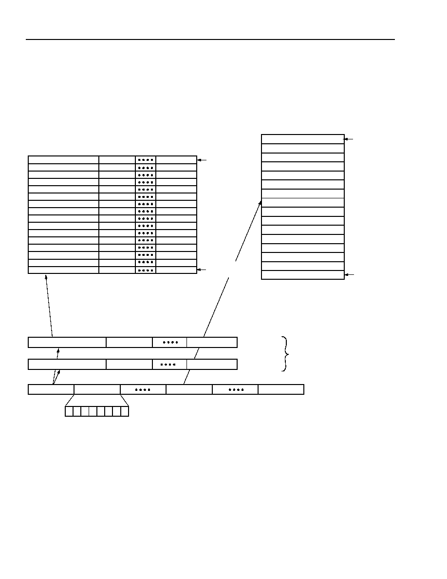
66
Agere Systems Inc.
Advance Data Sheet
May 2002
T7633 Dual T1/E1 3.3 V Short-Haul Terminator
Frame Formats
(continued)
CEPT 2.048 Basic Frame, CRC-4 Time Slot 0, and Signaling Time Slot 16 Multiframe Struc-
tures
As defined in ITU Rec. G.704, the CEPT 2.048 frame, CRC-4 multiframe, and channel associated signaling multi-
frame structures are illustrated in Figure 23.
5-4548(F).cr.1
Figure 23. ITU 2.048 Basic Frame, CRC-4 Multiframe, and Channel Associated Signaling Multiframe
Structures
0 1 A S
A4
S
A5
S
A6
S
A7
S
A8
C
1
0 0 1 1 0 1 1
C
2
0 0 1 1 0 1 1
0 1 A S
A4
S
A5
S
A6
S
A7
S
A8
C
3
0 0 1 1 0 1 1
1 1 A S
A4
S
A5
S
A6
S
A7
S
A8
C
4
0 0 1 1 0 1 1
0 1 A S
A4
S
A5
S
A6
S
A7
S
A8
C
1
0 0 1 1 0 1 1
1 1 A S
A4
S
A5
S
A6
S
A7
S
A8
C
2
0 0 1 1 0 1 1
1 1 A S
A4
S
A5
S
A6
S
A7
S
A8
C
3
0 0 1 1 0 1 1
E 1 A S
A4
S
A5
S
A6
S
A7
S
A8
C
4
0 0 1 1 0 1 1
E 1 A S
A4
S
A5
S
A6
S
A7
S
A8
TIME SLOT 1
TIME SLOT 1
TIME SLOT 1
TIME SLOT 1
TIME SLOT 1
TIME SLOT 1
TIME SLOT 1
TIME SLOT 1
TIME SLOT 1
TIME SLOT 1
TIME SLOT 1
TIME SLOT 1
TIME SLOT 1
TIME SLOT 1
TIME SLOT 1
TIME SLOT 1
TIME SLOT 31
TIME SLOT 31
TIME SLOT 31
TIME SLOT 31
TIME SLOT 31
TIME SLOT 31
TIME SLOT 31
TIME SLOT 31
TIME SLOT 31
TIME SLOT 31
TIME SLOT 31
TIME SLOT 31
TIME SLOT 31
TIME SLOT 31
TIME SLOT 31
TIME SLOT 31
FRAME 0 OF CRC-4
MULTIFRAME
TIME SLOT 0
TIME SLOT 1
TIME SLOT 16
TIME SLOT 31
Si 1 A S
A4
S
A5
S
A6
S
A7
S
A8
TIME SLOT 1
TIME SLOT 31
Si 0 0 1 1 0 1 1
TIME SLOT 1
TIME SLOT 31
FRAME 15 OF CRC-4
MULTIFRAME
FAS FRAME
NOT FAS FRAME
0 0 0 0 X
0
Y
M
X
1
X
2
1
2
3
4
5
6
7
8
8-bit TIME SLOT = 3.90625
µ
s
256-bit FRAME = 125
µ
s
PRIMARY BASIC FRAME
STRUCTURE
A
1
B
1
C
1
D
1
A
16
B
16
C
16
D
16
A
2
B
2
C
2
D
2
A
17
B
17
C
17
D
17
A
3
B
3
C
3
D
3
A
18
B
18
C
18
D
18
A
4
B
4
C
4
D
4
A
19
B
19
C
19
D
19
A
5
B
5
C
5
D
5
A
20
B
20
C
20
D
20
A
6
B
6
C
6
D
6
A
21
B
21
C
21
D
21
A
7
B
7
C
7
D
7
A
22
B
22
C
22
D
22
A
8
B
8
C
8
D
8
A
23
B
23
C
23
D
23
A
9
B
9
C
9
D
9
A
24
B
24
C
24
D
24
A
10
B
10
C
10
D
10
A
25
B
25
C
25
D
25
A
11
B
11
C
11
D
11
A
26
B
26
C
26
D
26
A
12
B
12
C
12
D
12
A
27
B
27
C
27
D
27
A
13
B
13
C
13
D
13
A
28
B
28
C
28
D
28
A
14
B
14
C
14
D
14
A
29
B
29
C
29
D
29
A
15
B
15
C
15
D
15
A
30
B
30
C
30
D
30
FRAME 0 TIME
CHANNEL ASSOCIATED
SIGNALING MULTIFRAME
IN TIME SLOT 16
CHANNEL NUMBERS REFER TO TELEPHONE
CHANNEL NUMBERS. TIME SLOTS 1 TO 15 AND
17 TO 31 ARE ASSIGNED TO TELEPHONE
CHANNELS NUMBERED FROM 1 TO 30.
FRAME 15
CRC-4 MULTIFRAME IN
TIME SLOT 0
TIME SLOT 16
MULTIFRAME
SLOT 16
MULTIFRAME

Agere Systems Inc.
67
Advance Data Sheet
May 2002
T7633 Dual T1/E1 3.3 V Short-Haul Terminator
Frame Formats
(continued)
CEPT 2.048 Basic Frame Structure
The ITU Rec. G.704 Section 2.3.1 defined frame length is 256 bits, numbered 1 to 256. The frame repetition rate is
8 kHz. The allocation of bits numbered 1 to 8 of the frame is shown in Table 30.
Table 30. Allocation of Bits 1 to 8 of the FAS Frame and the NOT FAS Frame
The function of each bit in Table 30 is described below:
1.
The Si bits are reserved for international use. A specific use for these bits is described in Table 31, ITU CRC-4
Multiframe Structure on page 70. If no use is realized, these bits should be fixed at 1 on digital paths crossing
an international border.
2.
Bit 2 of the NOT FAS frames is fixed to 1 to assist in avoiding simulations of the frame alignment signal.
3.
Bit 3 of the NOT FAS is the remote alarm indication (A bit). In undisturbed operation, this bit is set to 0; in alarm
condition, set to 1.
4.
Bits 4--8 of the NOT FAS (Sa4--Sa8) may be recommended by ITU for use in specific point-to-point applica-
tions. Bit Sa4 may be used as a message-based data link for operations, maintenance, and performance mon-
itoring. If the data link is accessed at intermediate points with consequent alterations to the Sa4 bit, the CRC-4
bits must be updated to retain the correct end-to-end path termination functions associated with the CRC-4
procedure. The receive framer does not implement the CRC-4 modifying algorithm described in ITU Rec.
G.706 Annex C. Bits Sa4--Sa8, where these are not used, should be set to 1 on links crossing an international
border.
5.
MSB = most significant bit and is transmitted first.
6.
LSB = least significant bit and is transmitted last.
Basic Frames
Bit 1
(MSB)
Bit 2
Bit 3
Bit 4
Bit 5
Bit 6
Bit 7
Bit 8
(LSB)
Frame Alignment Signal (FAS)
Si
0
0
1
1
0
1
1
Not Frame Alignment Signal (NOT FAS)
Si
1
A
Sa4
Sa5
Sa6
Sa7
Sa8

68
Agere Systems Inc.
Advance Data Sheet
May 2002
T7633 Dual T1/E1 3.3 V Short-Haul Terminator
Frame Formats
(continued)
CEPT 2.048 Basic Frame Structure
(continued)
Transparent Framing Format
The transmit framer can be programmed to transparently transmit 256 bits of system data to the line. The transmit
framer must be programmed to either transparent framing mode 1 or transparent framing mode 2 (see Framer
Reset and Transparent Mode Control Register (FRM_PR26) on page 192).
In transparent mode 1 or mode 2, the transmit framer transmits all 256 bits of the RCHI payload unmodified to the
line. Time slot 1 of the RCHI, determined by the RCHIFS signal, is inserted into the FAS/NOTFAS time slot of the
transmit line interface.
Frame integrity is maintained in both the transmit and receive framer sections.
5-5988(F)
Figure 24. CEPT Transparent Frame Structure
In transparent framing mode 1, the receive framer is forced not to reframe on the receive line data. Other than
bipolar violations and unframed AIS monitoring, there is no processing of the receive line data. The entire receive
line payload is transmitted unmodified to the CHI.
In transparent framing mode 2, the receive framer functions normally on the receive line data. All normal monitor-
ing of receive line data is performed and data is transmitted to the CHI as programmed.
TIME SLOT 1
32 TIME-SLOT CHI FRAME
TIME SLOT 2
TIME SLOT 3
TIME SLOT 31 TIME SLOT 32
TIME SLOT 1
32 TIME-SLOT LINE FRAME
TIME SLOT 2
TIME SLOT 3
TIME SLOT 31 TIME SLOT 32

Agere Systems Inc.
69
Advance Data Sheet
May 2002
T7633 Dual T1/E1 3.3 V Short-Haul Terminator
Frame Formats
(continued)
CEPT Loss of Basic Frame Alignment (LFA)
Frame alignment is assumed to be lost when:
1.
As described in ITU Rec. G.706 Section 4.1.1, three consecutive incorrect frame alignment signals have been
received.
2.
So as to limit the effect of spurious frame alignment signals, when bit 2 in time slot 0 in NOT FAS frames have
been received with an error on three consecutive occasions.
3.
Optionally, as described in ITU Rec. G.706 Section 4.3.2, by exceeding a count of >914 errored CRC-4 blocks
out of 1000, with the understanding that a count of
915 errored CRC blocks indicates false frame alignment.
4.
On demand via the control registers.
In the LFA state:
1.
No additional FAS or NOT FAS errors are processed.
2.
The received remote frame alarm (received A bit) is deactivated.
3.
All NOT-FAS bit (Si bit, A bit, and Sa4 to Sa8 bits) processing is halted.
4.
Receive Sa6 status bits are set to 0.
5.
Receive Sa6 code monitoring and counting is halted.
6.
All receive Sa stack data updates are halted. The receive Sa stack ready, register FRM_SR4 bit 6 and bit 7, is
set to 0. If enabled, the receive Sa stack interrupt bit is set to 0.
7.
Receive data link (RFDL) is set to 1 and RFDCLK maintains previous alignment.
8.
Optionally, the remote alarm indication (A = 1) may be automatically transmitted to the line if register
FRM_PR27 bit 0 is set to 1.
9.
Optionally, the alarm indication signal (AIS) may be automatically transmitted to the system if register
FRM_PR19 bit 0 is set to 1.
10. If CRC-4 is enabled, loss of CRC-4 multiframe alignment is forced.
11. If CRC-4 is enabled, the monitoring and processing of CRC-4 checksum errors is halted.
12. If CRC-4 is enabled, all monitoring and processing of received E-bit information is halted.
13. If CRC-4 is enabled, the receive continuous E-bit alarm is deactivated.
14. If CRC-4 is enabled, optionally, E bit = 0 is transmitted to the line for the duration of loss of CRC-4 multiframe
alignment if register FRM_PR28 bit 4 is set to 1.
15. If time slot 16 signaling is enabled, loss of the signaling multiframe alignment is forced.
16. If time slot 16 signaling is enabled, updating of the signaling data is halted.
CEPT Loss of Frame Alignment Recovery Algorithm
The receive framer begins the search for basic frame alignment one bit position beyond the position where the LFA
state was detected. As defined in ITU Rec. G.706.4.1.2, frame alignment will be assumed to have been recovered
when the following sequence is detected:
1.
For the first time, the presence of the correct frame alignment signal in frame n.
2.
The absence of the frame alignment signal in the following frame detected by verifying that bit 2 of the basic
frame is a 1 in frame n + 1.
3.
For the second time, the presence of the correct frame alignment in the next frame, n + 2.
Failure to meet 2 or 3 above will initiate a new basic frame search in frame
n + 2.

70
Agere Systems Inc.
Advance Data Sheet
May 2002
T7633 Dual T1/E1 3.3 V Short-Haul Terminator
Frame Formats
(continued)
CEPT Time Slot 0 CRC-4 Multiframe Structure
The CRC-4 multiframe is in bit 1 of each NOT FAS frame. As described in ITU Rec. G.704 Section 2.3.3.1, where
there is a need to provide additional protection against simulation of the frame alignment signal, and/or where there
is a need for an enhanced error monitoring capability, then bit 1 of each frame may be used for a cyclic redundancy
check-4 (CRC-4) procedure as detailed below. The allocation of bits 1--8 of time slot 0 of every frame is shown in
Table 31 for the complete CRC-4 multiframe.
Table 31. ITU CRC-4 Multiframe Structure
Notes:
C1 to C4 = cyclic redundancy check-4 (CRC-4) bits.
E = CRC-4 error indication bits.
Sa4 to Sa8 = spare bits.
A = remote frame alarm (RFA) bit (active-high); referred to as the A bit.
The CRC-4 multiframe consists of 16 frames numbered 0 to 15 and is divided into two eight-frame submultiframes
(SMF), designated SMF-I and SMF-II that signifies their respective order of occurrence within the CRC-4 multi-
frame structure. The SMF is the CRC-4 block size (2048 bits). In those frames containing the frame alignment sig-
nal (FAS), bit 1 is used to transmit the CRC-4 bits. There are four CRC-4 bits, designated C1, C2, C3, and C4 in
each SMF. In those frames not containing the frame alignment signal (NOT FAS), bit 1 is used to transmit the 6-bit
CRC-4 multiframe alignment signal and two CRC-4 error indication bits (E). The multiframe alignment signal is
defined in ITU Rec. G.704 Section 2.3.3.4, as 001011. Transmitted E bits should be set to 0 until both basic frame
and CRC-4 multiframe alignment are established. Thereafter, the E bits should be used to indicate received
errored submultiframes by setting the binary state of one E bit from 1 to 0 for each errored submultiframe. The
received E bits will always be taken into account, by the receive E-bit processor
1
, even when the SMF that con-
tains them is found to be errored. In the case where there exists equipment that does not use the E bits, the state
of the E bits should be set to a binary 1 state.
1. The receive E-bit processor will halt the monitoring of the received E bit during the loss of CRC-4 multiframe alignment.
Submultiframe
(SMF)
Frame
Number
Bits
1
2
3
4
5
6
7
8
I
0
C1
0
0
1
1
0
1
1
1
0
1
A
Sa4
Sa5
Sa6
Sa7
Sa8
2
C2
0
0
1
1
0
1
1
3
0
1
A
Sa4
Sa5
Sa6
Sa7
Sa8
4
C3
0
0
1
1
0
1
1
5
1
1
A
Sa4
Sa5
Sa6
Sa7
Sa8
6
C4
0
0
1
1
0
1
1
Multiframe
7
0
1
A
Sa4
Sa5
Sa6
Sa7
Sa8
II
8
C1
0
0
1
1
0
1
1
9
1
1
A
Sa4
Sa5
Sa6
Sa7
Sa8
10
C2
0
0
1
1
0
1
1
11
1
1
A
Sa4
Sa5
Sa6
Sa7
Sa8
12
C3
0
0
1
1
0
1
1
13
E
1
A
Sa4
Sa5
Sa6
Sa7
Sa8
14
C4
0
0
1
1
0
1
1
15
E
1
A
Sa4
Sa5
Sa6
Sa7
Sa8

Agere Systems Inc.
71
Advance Data Sheet
May 2002
T7633 Dual T1/E1 3.3 V Short-Haul Terminator
Frame Formats
(continued)
CEPT Time Slot 0 CRC-4 Multiframe Structure
(continued)
The CRC-4 word, located in submultiframe N, is the remainder after multiplication by x
4
and then division
(modulo 2) by the generator polynomial x
4
+ x + 1, of the polynomial representation of the submultiframe N ≠ 1.
Representing the contents of the submultiframe check block as a polynomial, the first bit in the block, i.e., frame 0,
bit 1 or frame 8, bit 1, is taken as being the most significant bit and the least significant bit in the check block is
frame 7 or frame 15, bit 256. Similarly, C
1
is defined to be the most significant bit of the remainder and C
4
the least
significant bit of the remainder. The encoding procedure, as described in ITU Rec. G.704 Section 2.3.3.5.2, fol-
lows:
1.
The CRC-4 bits in the SMF are replaced by binary 0s.
2.
The SMF is then acted upon the multiplication/division process referred to above.
3.
The remainder resulting from the multiplication/division process is stored, ready for insertion into the respec-
tive CRC-4 locations of the next SMF.
The decoding procedure, as described in ITU Rec. G.704 Section 2.3.3.5.3, follows:
1.
A received SMF is acted upon by the multiplication/division process referred to above, after having its CRC-4
bits extracted and replaced by 0s.
2.
The remainder resulting from this division process is then stored and subsequently compared on a bit-by-bit
basis with the CRC bits received in the next SMF.
3.
If the remainder calculated in the decoder exactly corresponds to the CRC-4 bits received in the next SMF, it is
assumed that the checked SMF is error-free.
CEPT Loss of CRC-4 Multiframe Alignment (LTS0MFA)
Loss of basic frame alignment forces the receive framer into a loss of CRC-4 multiframe alignment state. This state
is reported by way of the status registers FRM_SR1 bit 2. Once basic frame alignment is achieved, a new search
for CRC-4 multiframe alignment is initiated. During a loss of CRC-4 multiframe alignment state:
1. The CRC-4 error counter is halted.
2. The CRC-4 error monitoring circuit for errored seconds and severely errored seconds is halted.
3. The received E-bit counter is halted.
4. The received E-bit monitoring circuit for errored seconds and severely errored seconds at the remote end
interface is halted.
5. Receive continuous E-bit monitoring is halted.
6. All receive Sa6 code monitoring and counting functions are halted.
7. The updating of the receive Sa stack is halted and the receive Sa stack interrupt is deactivated.
8. Optionally, A = 1 may be automatically transmitted to the line if register FRM_PR27 bit 2 is set to 1.
9. Optionally, E = 0 may be automatically transmitted to the line if register FRM_PR28 bit 4 is set to 1.
10. Optionally, if LTS0MFA monitoring in the performance counters is enabled, by setting registers FRM_PR14
through FRM_PR17 bit 1 to 1, then these counts are incremented once per second for the duration of the
LTS0MFA state.

72
Agere Systems Inc.
Advance Data Sheet
May 2002
T7633 Dual T1/E1 3.3 V Short-Haul Terminator
Frame Formats
(continued)
CEPT Loss of CRC-4 Multiframe Alignment Recovery Algorithms
Several optional algorithms exist in the receive framer. These are selected through programming of register
FRM_PR9.
CRC-4 Multiframe Alignment Algorithm with 8 ms Timer
The default algorithm is as described in ITU Rec. G.706 Section 4.2. The recommendation states that if a condition
of assumed frame alignment has been achieved, CRC-4 multiframe alignment is deemed to have occurred if at
least two valid CRC-4 multiframe alignment signals can be located within 8 ms, the time separating two CRC-4
multiframe signals being 2 ms or a multiple of 2 ms. The search for the CRC-4 multiframe alignment signal is made
only in bit 1 of NOT FAS frames. If multiframe alignment cannot be achieved within 8 ms, it is assumed that frame
alignment is due to a spurious frame alignment signal and a new parallel search for basic frame alignment is initi-
ated. The new search for the basic frame alignment is started at the point just after the location of the assumed
spurious frame alignment signal. During this parallel search for basic frame alignment, there is no indication to the
system of a receive loss of frame alignment (RLFA) state. During the parallel search for basic frame alignment and
while in primary basic frame alignment, data will flow through the receive framer to the system interface as defined
by the current primary frame alignment. The receive framer will continuously search for CRC-4 multiframe align-
ment.
CRC-4 Multiframe Alignment Algorithm with 100 ms Timer
The CRC-4 multiframe alignment with 100 ms timer mode is enabled by setting FRM_PR9 to 0XXXX1X1 (binary).
This CRC-4 multiframe reframe mode starts a 100 ms timer upon detection of basic frame alignment. This is a par-
allel timer to the 8 ms timer. If CRC-4 multiframe alignment cannot be achieved within the time limit of 100 ms due
to the CRC-4 procedure not being implemented at the transmitting side, then an indication is given, and actions are
taken equivalent to those specified for loss of basic frame alignment, namely:
1.
Optional automatic transmission of A = 1 to the line if register FRM_PR27 bit 3 is set to 1.
2.
Optional automatic transmission of E = 0 to the line if register FRM_PR28 bit 5 is set to 1.
3.
Optional automatic transmission of AIS to the system if register FRM_PR19 bit 1 is set to 1.
Agere Systems Inc.
73
Advance Data Sheet
May 2002
T7633 Dual T1/E1 3.3 V Short-Haul Terminator
Frame Formats
(continued)
CEPT Loss of CRC-4 Multiframe Alignment Recovery Algorithms
(continued)
5-3909(F).er.2
Figure 25. Receive CRC-4 Multiframe Search Algorithm Using the 100 ms Internal Timer
∑ SET E BITS ACCORDING TO ITU REC. G.704, SECTION 2.3.3.4
OUT OF PRIMARY BFA:
∑ OPTIONALLY DISABLE TRAFFIC BY TRANSMITTING AIS TO THE SYSTEM
∑ OPTIONALLY TRANSMIT A = 1 AND E = 0 TO LINE
∑ INHIBIT INCOMING CRC-4 PERFORMANCE MONITORING
BFA SEARCH?
IN PRIMARY BFA:
∑ ENABLE TRAFFIC TO THE SYSTEM
∑ TRANSMIT A = 0 AND OPTIONALLY E = 0 TO THE LINE
∑ START 8 ms AND 100 ms TIMERS
∑ ENABLE PRIMARY BFA LOSS CHECKING PROCESS
CRC-4 MFA SEARCH (ITU REC. G.706, SECTION 4.2 -
NOTE 2)
CAN CRC-4
MFA BE FOUND
IN 8 ms?
PARALLEL
BFA SEARCH
100 ms
TIMER
ELAPSED?
YES
NO
NO
NO
YES
YES
ASSUME CRC-4 MULTIFRAME ALIGNMENT:
∑ CONFIRM PRIMARY BFA ASSOCIATED WITH CRC-4 MFA
∑ ADJUST PRIMARY BFA IF NECESSARY
SET 100 ms TIMER EXPIRATION STATUS BIT TO THE 1 STATE:
∑ OPTIONALLY TRANSMIT A BIT = 1 TO THE LINE INTERFACE FOR
THE DURATION OF LTS0MFA = 1
∑ OPTIONALLY TRANSMIT AIS TO THE SYSTEM INTERFACE FOR THE
START CRC-4 PERFORMANCE MONITORING:
∑ SET E BITS ACCORDING TO ITU REC. G.704, SECTION 2.3.3.4
CRC-4
COUNT > 914
IN 1 SECOND OR
CONTINUE CRC-4 PERFORMANCE MONITORING:
YES
YES
NO
NO
DURATION OF LTS0MFA = 1
IS 100 ms TRX = 1
?
YES
NO
SET INTERNAL 100 ms TIMER EXPIRATION STATUS BIT TO 0:
∑ IF TRANSMITTING A BIT = 1 TO THE LINE INTERFACE, TRANSMIT A BIT = 0
∑ IF TRANSMITTING AIS TO THE SYSTEM INTERFACE, ENABLE DATA
TRANSMISSION TO THE SYSTEM INTERFACE
LFA = 1?
GOOD?
IS
?
YES
NO
100 ms TRX = 1
INTERNAL
SET INTERNAL 100 ms TIMER EXPIRATION STATUS BIT TO 1:
PRIMARY
∑ IF TRANSMITTING E = 0 TO THE LINE INTERFACE, TRANSMIT E BIT = 1
∑ OPTIONALLY TRANSMIT E BIT = 0 TO THE LINE INTERFACE FOR
THE DURATION OF LTSOMFA = 1

74
Agere Systems Inc.
Advance Data Sheet
May 2002
T7633 Dual T1/E1 3.3 V Short-Haul Terminator
Frame Formats
(continued)
CEPT Loss of CRC-4 Multiframe Alignment Recovery Algorithms
(continued)
CRC-4 Multiframe Alignment Search Algorithm with 400 ms Timer
The CRC-4 multiframe alignment with 400 ms timer mode is enabled by setting FRM_PR9 to 0XXX1XX1 (binary).
This receive CRC-4 multiframe reframe mode is the modified CRC-4 multiframe alignment algorithm described in
ITU Rec. 706 Annex B, where it is referred to as CRC-4-to-Non-CRC-4 equipment interworking. A flow diagram of
this algorithm is illustrated in Figure 26 on page 75. When the interworking algorithm is enabled, it supersedes the
100 ms algorithm described on page 72 and in Figure 25 on page 73. This algorithm assumes that a valid basic
frame alignment signal is consistently present but the CRC-4 multiframe alignment cannot be achieved by the end
of the total CRC-4 multiframe alignment search period of 400 ms, if the distant end is a non-CRC-4 equipment. In
this mode, the following consequent actions are taken:
1.
An indication that there is no incoming CRC-4 multiframe alignment signal.
2.
All CRC-4 processing on the receive 2.048 Mbits/s signal is inhibited.
3.
CRC-4 data is transmitted to the distant end with both E bits set to zero.
This algorithm allows the identification of failure of CRC-4 multiframe alignment generation/detection, but with cor-
rect basic framing, when interworking between each piece of equipment having the modified CRC-4 multiframe
alignment algorithm.
As described in ITU Rec. G.706 Section B.2.3:
1.
A 400 ms timer is triggered on the initial recovery of the primary basic frame alignment.
2.
The 400 ms timer reset if and only if:
A. The criteria for loss of basic frame alignment as described in ITU Rec. G.706 Section 4.1.1 is achieved.
B. If 915 out of 1000 errored CRC-4 blocks are detected resulting in a loss of basic frame alignment as
described in ITU Rec. G.706 Section 4.3.2.
C. On-demand reframe is requested.
D. The receive framer is programmed to the non-CRC-4 mode.
3.
The loss of basic frame alignment checking process runs continuously, irrespective of the state of the CRC-4
multiframe alignment process below it.
4.
A new search for frame alignment is initiated if CRC-4 multiframe alignment cannot be achieved in 8 ms, as
described in ITU Rec. G.706 Section 4.2. This new search for basic frame alignment will not reset the 400 ms
timer or invoke consequent actions associated with loss of the primary basic frame alignment. In particular, all
searches for basic frame alignment are carried out in parallel with, and independent of, the primary basic frame
loss checking process. All subsequent searches for CRC-4 multiframe alignment are associated with each
basic framing sequence found during the parallel search.
5.
During the search for CRC-4 multiframe alignment, traffic is allowed through, upon, and to be synchronized to,
the initially determined primary basic frame alignment.
6.
Upon detection of the CRC-4 multiframe before the 400 ms timer elapsing, the basic frame alignment associ-
ated with the CRC-4 multiframe alignment replaces, if necessary, the initially determined basic frame align-
ment.
7.
If CRC-4 multiframe alignment is not found before the 400 ms timer elapses, it is assumed that a condition of
interworking between equipment with and without CRC-4 capability exists and the actions described above are
taken.
8.
If the 2.048 Mbits/s path is reconfigured at any time, then it is assumed that the (new) pair of path terminating
equipment will need to re-establish the complete framing process, and the algorithm is reset.

Agere Systems Inc.
75
Advance Data Sheet
May 2002
T7633 Dual T1/E1 3.3 V Short-Haul Terminator
Frame Formats
(continued)
CEPT Loss of CRC-4 Multiframe Alignment Recovery Algorithms
(continued)
5-3909(F).fr.3
Figure 26. Receive CRC-4 Multiframe Search Algorithm for Automatic, CRC-4/Non-CRC-4 Equipment
Interworking as Defined by ITU (From ITU Rec. G.706, Annex B.2.2 - 1991)
∑ SET E BITS ACCORDING TO ITU REC. G.704, SECTION 2.3.3.4
OUT OF PRIMARY BFA:
∑ OPTIONALLY DISABLE TRAFFIC BY TRANSMITTING AIS TO THE SYSTEM
∑ OPTIONALLY TRANSMIT A BIT = 1 AND E BIT = 0 TO LINE
∑ INHIBIT INCOMING CRC-4 PERFORMANCE MONITORING
BFA SEARCH?
IN PRIMARY BFA:
∑ ENABLE TRAFFIC NOT TRANSMITTING AIS TO THE SYSTEM
∑ TRANSMIT A = 0 AND OPTIONALLY E = 0 TO THE LINE
∑ START 400 ms TIMER
∑ ENABLE PRIMARY BFA LOSS CHECKING PROCESS
CRC-4 MFA SEARCH (ITU REC. G.706, SECTION 4.2)
CAN CRC-4
MFA BE FOUND
IN 8 ms?
PARALLEL
BFA SEARCH
400 ms
TIMER
ELAPSED?
YES
NO
NO
NO
YES
YES
ASSUME CRC-4-TO-CRC-4 INTERWORKING:
∑ CONFIRM PRIMARY BFA ASSOCIATED WITH CRC-4 MFA
∑ ADJUST PRIMARY BFA IF NECESSARY
START CRC-4 PERFORMANCE MONITORING:
∑ SET E BITS ACCORDING TO ITU REC. G.704, SECTION 2.3.3.4
CRC-4
COUNT > 914
IN 1 SECOND OR
CONTINUE CRC-4 PERFORMANCE MONITORING:
YES
YES
NO
NO
?
∑ KEEP A = 0 IN OUTGOING CRC-4 DATA
ASSUME CRC-4-TO-NON-CRC-4 INTERWORKING:
∑ TRANSMIT A BIT = 0 TO THE LINE INTERFACE
∑ STOP INCOMING CRC-4 PROCESSING
∑ CONFIRM PRIMARY BFA
∑ TRANSMIT E BIT = 0 TO THE LINE INTERFACE
∑ INDICATE "NO CRC-4 MFA"
PRIMARY
LFA = 1?

76
Agere Systems Inc.
Advance Data Sheet
May 2002
T7633 Dual T1/E1 3.3 V Short-Haul Terminator
Frame Formats
(continued)
CEPT Time Slot 16 Multiframe Structure
The T7633 supports three CEPT signaling modes: channel associated signaling (CAS) or per-channel signaling
(PSC0 and PSC1); common channel signaling (CCS) (T7230A mode)
1
; and international remote switching module
(IRSM) signaling.
1. See Agere Systems
T7230A Primary Access Framer/Controller
Preliminary Data Sheet (DS96-007TIC) pages 49--50.
Channel Associated Signaling (CAS)
The channel associated signaling (CAS) mode utilizes time slot 16 of the FAS and NOT FAS frames. The CAS for-
mat is a multiframe consisting of 16 frames where frame 0 of the multiframe contains the multiframe alignment pat-
tern of four zeros in bits 1 through 4. Table 32 illustrates the CAS multiframe of time slot 16. The T7633 can be
programmed to force the transmitted line CAS multiframe alignment pattern to be transmitted in the FAS frame by
selecting the PCS0 option or in the NOT FAS frame by selecting the PCS1 option. Alignment of the transmitted line
CAS multiframe to the CRC-4 multiframe is arbitrary.
Table 32. ITU CEPT Time Slot 16 Channel Associated Signaling Multiframe Structure
Notes:
Frame 0 bits 1--4 define the time slot 16 multiframe alignment.
X0--X2 = time slot 16 spare bits defined in FRM_PR41 bit 0--bit 2.
Y
M
= yellow alarm, time slot 16 remote multiframe alarm (RMA) bit (1 = alarm condition).
Common Channel Signaling (T7230A Mode) (CCS)
In the common channel signaling mode, selected if FRM_PR44 bit 4 = 1, data contained in the transmit signaling
registers, FRM_TSR0--FRM_TSR31, is written transparently into time slot 16 of the transmit line bit stream. The
received signaling data from time slot 16 is stored transparently in receive signaling registers FRM_RSR0--
FRM_RSR31.
Time Slot 16
Channel
Associated
Signaling
Multiframe
Frame
Number
Bit
1
2
3
4
5
6
7
8
0
0
0
0
0
X
0
Y
M
X
1
X
2
1
A
1
B
1
C
1
D
1
A
16
B
16
C
16
D
16
2
A
2
B
2
C
2
D
2
A
17
B
17
C
17
D
17
3
A
3
B
3
C
3
D
3
A
18
B
18
C
18
D
18
4
A
4
B
4
C
4
D
4
A
19
B
19
C
19
D
19
5
A
5
B
5
C
5
D
5
A
20
B
20
C
20
D
20
6
A
6
B
6
C
6
D
6
A
21
B
21
C
21
D
21
7
A
7
B
7
C
7
D
7
A
22
B
22
C
22
D
22
8
A
8
B
8
C
8
D
8
A
23
B
23
C
23
D
23
9
A
9
B
9
C
9
D
9
A
24
B
24
C
24
D
24
10
A
10
B
10
C
10
D
10
A
25
B
25
C
25
D
25
11
A
11
B
11
C
11
D
11
A
26
B
26
C
26
D
26
12
A
12
B
12
C
12
D
12
A
27
B
27
C
27
D
27
13
A
13
B
13
C
13
D
13
A
28
B
28
C
28
D
28
14
A
14
B
14
C
14
D
14
A
29
B
29
C
29
D
29
15
A
15
B
15
C
15
D
15
A
30
B
30
C
30
D
30

Agere Systems Inc.
77
Advance Data Sheet
May 2002
T7633 Dual T1/E1 3.3 V Short-Haul Terminator
Frame Formats
(continued)
CEPT Time Slot 16 Multiframe Structure
(continued)
International Remote Switching Module (IRSM) Signaling
This signaling mode is similar to the channel associated signaling mode, i.e., time slot 16 contains the signaling
multiframe information (ABCD signaling bits). In addition, time slot 0 Sa5 to Sa8 bit positions of the NOT FAS
frame contains per-channel control information. The format of the time slot 0 per-channel control information is
illustrated in Table 33. The IRSM mode forces the transmit framer to align the time slot 16 multiframe to the FAS
frame (PCS0 mode).
Table 33. CEPT IRSM Signaling Multiframe Structure
Notes:
Si = time slot 0 control bits. If programmed for CRC-4 mode, then these bits contain the CRC-4 multiframe pattern, checksum, and E-bit
information.
Ei = IRSM per-channel control bits.
X0--X2 = time slot 16 spare bits defined in FRM_PR41 bit 0--bit 2.
Ai--Di = time slot 16 channel associated signaling bits.
Y
M
= yellow alarm, time slot 16 remote multiframe alarm (RMA) bit (1 = alarm condition).
Frame
Number
IRSM Bits in Time Slot 0
Bits in Time Slot 16
1
2
3
4
5
6
7
8
1
2
3
4
5
6
7
8
0
S
i
0
0
1
1
0
1
1
0
0
0
0
X
0
Y
M
X
1
X
2
1
S
i
1
A
D
E
0
E
1
E
16
E
17
A
1
B
1
C
1
D
1
A
16
B
16
C
16
D
16
2
S
i
0
0
1
1
0
1
1
A
2
B
2
C
2
D
2
A
17
B
17
C
17
D
17
3
S
i
1
A
D
E
2
E
3
E
18
E
19
A
3
B
3
C
3
D
3
A
18
B
18
C
18
D
18
4
S
i
0
0
1
1
0
1
1
A
4
B
4
C
4
D
4
A
19
B
19
C
19
D
19
5
S
i
1
A
D
E
4
E
5
E
20
E
21
A
5
B
5
C
5
D
5
A
20
B
20
C
20
D
20
6
S
i
0
0
1
1
0
1
1
A
6
B
6
C
6
D
6
A
21
B
21
C
21
D
21
7
S
i
1
A
D
E
6
E
7
E
22
E
23
A
7
B
7
C
7
D
7
A
22
B
22
C
22
D
22
8
S
i
0
0
1
1
0
1
1
A
8
B
8
C
8
D
8
A
23
B
23
C
23
D
23
9
S
i
1
A
D
E
8
E
9
E
24
E
25
A
9
B
9
C
9
D
9
A
24
B
24
C
24
D
24
10
S
i
0
0
1
1
0
1
1
A
10
B
10
C
10
D
10
A
25
B
25
C
25
D
25
11
S
i
1
A
D
E
10
E
11
E
26
E
27
A
11
B
11
C
11
D
11
A
26
B
26
C
26
D
26
12
S
i
0
0
1
1
0
1
1
A
12
B
12
C
12
D
12
A
27
B
27
C
27
D
27
13
S
i
1
A
D
E
12
E
13
E
28
E
29
A
13
B
13
C
13
D
13
A
28
B
28
C
28
D
28
14
S
i
0
0
1
1
0
1
1
A
14
B
14
C
14
D
14
A
29
B
29
C
29
D
29
15
S
i
1
A
D
E
14
E
15
E
30
E
31
A
15
B
15
C
15
D
15
A
30
B
30
C
30
D
30

78
Agere Systems Inc.
Advance Data Sheet
May 2002
T7633 Dual T1/E1 3.3 V Short-Haul Terminator
Frame Formats
(continued)
CEPT Loss of Time Slot 16 Multiframe Alignment (LTS16MFA)
Loss of basic frame alignment forces the receive framer into a loss of time slot 16 signaling multiframe alignment
state. In addition, as defined in ITU Rec. G.732 Section 5.2, time slot 16 signaling multiframe is assumed lost when
two consecutive time slot 16 multiframe 4-bit all-zero patterns is received with an error. In addition, the time slot 16
multiframe is assumed lost when, for a period of two multiframes, all bits in time slot 16 are in state 0. This state is
reported by way of the status registers FRM_SR1 bit 1. Once basic frame alignment is achieved, the receive
framer will initiate a search for the time slot 16 multiframe alignment. During a loss of time slot 16 multiframe align-
ment state:
1.
The updating of the signaling data is halted.
2.
The received control bits forced to the binary 1 state.
3.
The received remote multiframe alarm indication status bit is forced to the binary 0 state.
4.
Optionally, the transmit framer can transmit to the line the time slot 16 signaling remote multiframe alarm if reg-
ister FRM_PR41 bit 4 is set to 1.
5.
Optionally, the transmit framer can transmit the alarm indication signal (AIS) in the system transmit time slot 16
data if register FRM_PR44 bit 6 is set to 1.
CEPT Loss of Time Slot 16 Multiframe Alignment Recovery Algorithm
The time slot 16 multiframe alignment recovery algorithm is as described in ITU Rec. G.732 Section 5.2. The rec-
ommendation states that if a condition of assumed frame alignment has been achieved, time slot 16 multiframe
alignment is deemed to have occurred when the 4-bit time slot 16 multiframe pattern of 0000 is found in time slot
16 for the first time, and the preceding time slot 16 contained at least one bit in the binary 1 state.

Agere Systems Inc.
79
Advance Data Sheet
May 2002
T7633 Dual T1/E1 3.3 V Short-Haul Terminator
CEPT Time Slot 0 FAS/NOT FAS Control Bits
FAS/NOT FAS Si- and E-Bit Source
The Si bit can be used as an 8 kbits/s data link to and from the remote end, or in the CRC-4 mode, it can be used
to provide added protection against false frame alignment. The sources for the Si bits that are transmitted to the
line are the following:
1.
CEPT with no CRC-4 and FRM_PR28 bit 0 = 1: the TSiF control bit (FRM_PR28 bit 1) is transmitted in bit 1 of
all FAS frames and the TSiNF control bit (FRM_PR28 bit 2) is transmitted in bit 1 of all NOT FAS frames.
2.
The CHI system interface (CEPT with no CRC-4 and FRM_PR28 bit 0 = 0)
1
.
This option requires the received system data (RCHIDATA) to maintain a biframe alignment pattern where
frames containing Si bit information for the NOT FAS frames have bit 2 of time slot 0 in the binary 1 state fol-
lowed by frames containing Si bit information for the FAS frames that have bit 2 of time slot 0 in the binary 0
state. This ensures the proper alignment of the Si received system data to the transmit line Si data. Whenever
this requirement is not met by the system, the transmit framer will enter a loss of biframe alignment condition
(indication is given in the status registers) and then search for the pattern; in the loss of biframe alignment
state, transmitted line data is corrupted (only when the system interface is sourcing Sa or Si data). When the
transmit framer locates a new biframe alignment pattern, an indication is given in the status registers and the
transmit framer resumes normal operations.
3.
CEPT with CRC-4
2
: manual transmission of E bit = 0:
A. If FRM_PR28 bit 0 = 0, then the TSiF bit (FRM_PR28 bit 1) is transmitted in bit 1 of frame 13 (E bit) and
the TSiNF bit (FRM_PR28 bit 2) is transmitted in bit 1 of frame 15 (E bit).
B. If FRM_PR28 bit 0 = 1, then each time 0 is written into TSiF (FRM_PR28 bit 1) one E bit = 0 is transmitted
in frame 13, and each time 0 is written into TSiNF (FRM_PR28 bit 2) one E bit = 0 is transmitted in frame
15.
4.
CEPT with CRC-4
2
, automatic transmission of E bit = 0:
A. Optionally, one transmitted E bit is set to 0 by the transmit framer, as described in ITU Rec. G.704 Section
2.3.3.4, for each received errored CRC-4 submultiframe detected by the receive framer if FRM_PR28
bit 3 = 1.
B. Optionally, as described in ITU Rec. G.704 Section 2.3.3.4, both E bits are set to 0 while in a received loss
of CRC-4 multiframe alignment state
3
if FRM_PR28 bit 4 = 1.
C. Optionally, when the 100 ms or 400 ms timer is enabled and the timer has expired, as described in ITU
Rec. G.706 Section B.2.2, both E bits are set to 0 for the duration of the loss of CRC-4 multiframe
alignment state
3
if FRM_PR28 bit 5 = 1.
Otherwise, the E bits are transmitted to the line in the 1 state.
1.Whenever bits (e.g., Si, Sa, etc.) are transmitted from the system transparently, FRM_PR29 must first be momentarily written to 001xxxxx
(binary). Otherwise, the transmit framer will not be able to locate the biframe alignment.
2.The receive E-bit processor will halt the monitoring of received E bits during loss of CRC-4 multiframe alignment.
3.Whenever loss of frame alignment occurs, then loss of CRC-4 multiframe alignment is forced. Once frame alignment is established, then and
only then, is the search for CRC-4 multiframe alignment initiated. The receive framer unit, when programmed for CRC-4, can be in a state of
LFA and LTS0MFA or in a state of LTS0MFA only, but cannot be in a state of LFA only.

80
Agere Systems Inc.
Advance Data Sheet
May 2002
T7633 Dual T1/E1 3.3 V Short-Haul Terminator
CEPT Time Slot 0 FAS/NOT FAS Control Bits
(continued)
NOT FAS A-Bit (CEPT Remote Frame Alarm) Sources
The A bit, as described in ITU Rec. G.704 Section 2.3.2 Table 4a/G.704, is the remote alarm indication bit. In
undisturbed conditions, this bit is set to 0 and transmitted to the line. In the loss of frame alignment (LFA) state, this
bit may be set to 1 and transmitted to the line as determined by register FRM_PR27. The A bit is set to 1 and trans-
mitted to the line for the following conditions:
1.
Setting the transmit A bit = 1 control bit by setting register FRM_PR27 bit 7 to 1.
2.
Optionally for the following alarm conditions as selected through programming register FRM_PR27.
A. The duration of loss of basic frame alignment as described in ITU Rec. G.706 Section 4.1.1
1
, or ITU Rec.
G.706 Section 4.3.2
2
if register FRM_PR27 bit 0 = 1.
B. The duration of loss of CRC-4 multiframe alignment if register FRM_PR27 bit 2 = 1.
C. The duration of loss of signaling time slot 16 multiframe alignment if register FRM_PR27 bit 1 = 1.
D. The duration of loss of CRC-4 multiframe alignment after either the 100 ms or 400 ms timer expires if
register FRM_PR27 bit 3 = 1.
E. The duration of receive Sa6_8hex
3
if register FRM_PR27 bit 4 = 1.
F.
The duration of receive Sa6_Chex
3
if register FRM_PR27 bit 5 = 1.
1. LFA is due to framing bit errors.
2. LFA is due to detecting 915 out of 1000 received CRC-4 errored blocks.
3. See Table 41, Sa6 Bit Coding Recognized by the Receive Framer on page 95, for a definition of this Sa6 pattern.
NOT FAS Sa-Bit Sources
*
The Sa bits, Sa4--Sa8, in the NOT FAS frame can be a 4 kbits/s data link to and from the remote end. The sources
and value for the Sa bits are:
1.
The Sa source register FRM_PR29 bit 0--bit 4 if FRM_PR29 bit 7--bit 5 = 000 (binary) and FRM_PR30 bit 4--
bit 0 = 11111 (binary).
2.
The facility data link external input (TFDL) if register FRM_PR29 bit 7 = 1 and register FRM_PR21 bit 6 = 1.
3.
The internal FDL-HDLC if register FRM_PR29 bit 7 = 1 and register FRM_PR21 bit 6 = 0.
4.
The Sa transmit stack if register FRM_PR29 bit 7--bit 5 are set to 01x (binary).
5.
The CHI system interface if register FRM_PR29 bit 7--bit 5 are set to 001 (binary). This option requires the
received system data (RCHIDATA) to maintain a biframe alignment pattern where (1) frames containing Sa bit
information have bit 2 of time slot 0 in the binary 1 state and (2) these NOT FAS frames are followed by frames
not containing Sa bit information, the FAS frames, which have bit 2 of time slot 0 in the binary 0 state. This
ensures the proper alignment of the Sa received system data to the transmit line Sa data. Whenever this
requirement is not met by the system, the transmit framer will enter a loss of biframe alignment condition indi-
cated in the status register, FRM_SR1 bit 4, and then search for the pattern. In the loss of biframe alignment
state, transmitted line data is corrupted (only when the system interface is sourcing Sa or Si data). When the
transmit framer locates a new biframe alignment pattern, an indication is given in the status registers and the
transmit framer resumes normal operations.
The receive Sa data is present at:
A. The Sa received stack, registers FRM_SR54--FRM_SR63, if the T7633 is programmed in the Sa stack
mode.
B. The system transmit interface.
The status of the received Sa bits and the received Sa stack is available in status register FRM_SR4. The transmit
and receive Sa bit for the FDL can be selected by setting register FRM_PR43 bit 0--bit 2 as shown in Table 167.
* Whenever bits (e.g., Si, Sa, etc.) are transmitted from the system transparently, FRM_PR29 must first be momentarily written to 001xxxxx
(binary). Otherwise, the transmit framer will not be able to locate the biframe alignment.

Agere Systems Inc.
81
Advance Data Sheet
May 2002
T7633 Dual T1/E1 3.3 V Short-Haul Terminator
CEPT Time Slot 0 FAS/NOT FAS Control Bits
(continued)
Sa Facility Data Link Access
The data link interface may be used to source one of the Sa bits. Access is controlled by registers FRM_PR29,
FRM_PR30, and FRM_PR43, see NOT FAS Sa-Bit Sources on page 80. The receive Sa data is always present at
the receive facility data link output pin, RFDL, along with a valid clock signal at the receive facility clock output pin,
RFDLCK. During a loss of frame alignment (LFA) state, the RFDL signal is forced to a 1 state while RFDLCK
continues to toggle on the previous frame alignment. When basic frame alignment is found, RFDL is as received
from the selected receive Sa bit position and RFDLCK is forced (if necessary) to the new alignment. The data rate
for this access mode is 4 kHz. The access timing for the transmit and receive facility data is illustrated in Figure 27
below. During loss of receive clock (LOFRMRLCK), RFDL and RFDLCK are frozen in a state at the point of the
LOFRMRLCK being asserted.
5-3910(F).dr.1
Figure 27. Facility Data Link Access Timing of the Transmit and Receive Framer Sections in the CEPT
Mode
t8
t9
t9
t10
t11
t8: TFDLCK CYCLE = 250
µ
s
t9: TFDL TO TFDLCK SETUP/HOLD = 40 ns
t10: RFDLCK CYCLE = 250
µ
s
t11: RFDLCK TO RFDL DELAY = 40 ns
TFDLCK
TFDL
RFDLCK
RFDL

82
Agere Systems Inc.
Advance Data Sheet
May 2002
T7633 Dual T1/E1 3.3 V Short-Haul Terminator
CEPT Time Slot 0 FAS/NOT FAS Control Bits
(continued)
NOT FAS Sa Stack Source and Destination
The transmit Sa4 to Sa8 bits may be sourced from the transmit Sa stack, registers FRM_PR31--FRM_PR40. The
Sa stack consists of ten 8-bit registers that contain 16 NOT FAS frames of Sa information as shown in Table 23.
The transmit stack data may be transmitted either in non-CRC-4 mode or in CRC-4 mode to the line.
The receive stack data, registers FRM_SR54--FRM_SR63, is valid in both the non-CRC-4 mode and the CRC-4
mode. In the non-CRC-4 mode while in the loss of frame alignment (LFA) state, updating of the receive Sa stack is
halted and the transmit and receive stack interrupts are deactivated. In the CRC-4 mode while in the loss of time
slot 0 multiframe alignment (LTS0MFA) state, updating of the receive Sa stack is halted and the transmit and
receive stack interrupts are deactivated.
Table 34. Transmit and Receive Sa Stack Structure
The most significant bit of the first byte is transmitted to the line in frame 1 of a double CRC-4 multiframe. The least
significant bit of the second byte is transmitted to the line in frame 31 of the double CRC-4 multiframe. The protocol
for accessing the Sa Stack information for the transmit and receive Sa4 to Sa8 bits is shown in Figure 28 and
described briefly below.
The device indicates that it is ready for an update of its transmit stack by setting register FRM_SR4 bit 7 (CEPT
transmit Sa stack ready) high. At this time, the system has about 4 ms to update the stack. Data written to the stack
during this interval will be transmitted during the next double CRC-4 multiframe. By reading register FRM_SR4
bit 7, the system clears this bit so that it can indicate the next time the transmit stack is ready. If the transmit stack
is not updated, then the content of the stack is retransmitted to the line. The 32-frame interval of the transmit framer
in the Non-CRC-4 mode is arbitrary. Enabling transmit CRC-4 mode forces the updating of the internal transmit
stack at the end of the 32-frame CRC-4 double multiframe; the transmit Sa stack is then transmitted synchronous
to the transmit CRC-4 multiframe structure.
On the receive side, the T7633 indicates that it has received data in the receive Sa stack, register FRM_SR54--
FRM_SR63, by setting register FRM_SR4 bit 6 (CEPT receive Sa stack ready) high. The system then has about
4 ms to read the contents of the stack before it is updated again (old data lost). By reading register FRM_SR4 bit 6,
the system clears this bit so that it can indicate the next time the receive stack is ready. The receive framer always
updates the content of the receive stack so unread data will be overwritten. The last 16 valid Sa4 to Sa8 bits are
always stored in the receive Sa stack on a double-multiframe boundary. The 32-frame interval of the receive framer
in the non-CRC-4 mode is arbitrary. Enabling the receive CRC-4 mode forces updating of the receive Sa stack at
the end of the 32-frame CRC-4 double multiframe. The receive Sa stack is received synchronous to the CRC-4
multiframe structure.
Register
Number
Bit 7
(MSB)
Bit 6
Bit 5
Bit 4
Bit 3
Bit 2
Bit 1
Bit 0
(LSB)
1
Sa4-1
Sa4-3
Sa4-5
Sa4-7
Sa4-9
Sa4-11
Sa4-13
Sa4-15
2
Sa4-17
Sa4-19
Sa4-21
Sa4-23
Sa4-25
Sa4-27
Sa4-29
Sa4-31
3
Sa5-1
Sa5-3
Sa5-5
Sa5-7
Sa5-9
Sa5-11
Sa5-13
Sa5-15
4
Sa5-17
Sa5-19
Sa5-21
Sa5-23
Sa5-25
Sa5-27
Sa5-29
Sa5-31
5
Sa6-1
Sa6-3
Sa6-5
Sa6-7
Sa6-9
Sa6-11
Sa6-13
Sa6-15
6
Sa6-17
Sa6-19
Sa6-21
Sa6-23
Sa6-25
Sa6-27
Sa6-29
Sa6-31
7
Sa7-1
Sa7-3
Sa7-5
Sa7-7
Sa7-9
Sa7-11
Sa7-13
Sa7-15
8
Sa7-17
Sa7-19
Sa7-21
Sa7-23
Sa7-25
Sa7-27
Sa7-29
Sa7-31
9
Sa8-1
Sa8-3
Sa8-5
Sa8-7
Sa8-9
Sa8-11
Sa8-13
Sa8-15
10 Sa8-17
Sa8-19
Sa8-21
Sa8-23
Sa8-25
Sa8-27
Sa8-29
Sa8-31
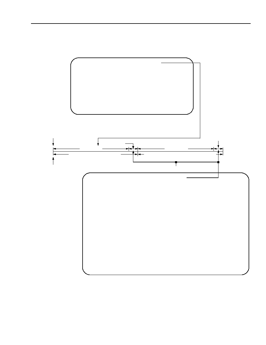
Agere Systems Inc.
83
Advance Data Sheet
May 2002
T7633 Dual T1/E1 3.3 V Short-Haul Terminator
CEPT Time Slot 0 FAS/NOT FAS Control Bits
(continued)
NOT FAS Sa Stack Source and Destination
(continued)
5-3911(F).c
Figure 28. Transmit and Receive Sa Stack Accessing Protocol
SYSTEM ACCESS Sa STACK (SASS) INTERVAL:
TRANSMIT FRAMER UNIT TRANSMITS TO THE LINE
THE DATA IN THE TRANSMIT Sa STACK WRITTEN DURING
THE PREVIOUS SASS INTERVAL.
THE SYSTEM CAN UPDATE THE TRANSMIT Sa STACK
REGISTERS FOR TRANSMISSION IN THE NEXT CRC-4
DOUBLE MULTIFRAME.
THE SYSTEM CAN READ THE RECEIVE Sa STACK REGISTERS
TO ACCESS THE Sa BITS EXTRACTED DURING THE PREVIOUS
VALID (IN MULTIFRAME ALIGNMENT) DOUBLE CRC-4
MULTIFRAME.
START OF CRC-4 DOUBLE MULTIFRAME:
∑ BASIC FRAME ALIGNMENT FOUND, OR,
∑ CRC-4 MULTIFRAME ALIGNMENT FOUND.
1)
2)
3)
31 FRAMES
SYSTEM ACCESS Sa STACK INTERVAL
CRC-4 DOUBLE MULTIFRAME
START FRAME 1 OF 32 IN DMF.
INTERNAL Sa STACK UPDATE INTERVAL
31 FRAMES
1-FRAME INTERVAL
CRC-4 DOUBLE MULTIFRAME: 32 FRAMES
SYSTEM ACCESS IS DISABLED DURING THIS INTERVAL:
THE INTERNAL TRANSMIT Sa STACK IS UPDATED
FROM THE FRAMER UNIT'S 10-byte TRANSMIT STACK CONTROL
REGISTERS DURING THIS 1-FRAME INTERVAL.
ACCESS TO THE STACK CONTROL REGISTERS IS DISABLED
DURING THIS 1-FRAME INTERVAL.
1)
2)
ONCE LOADED, THE INFORMATION IN THE INTERNAL TRANSMIT
Sa STACK IS TRANSMITTED TO THE LINE DURING THE NEXT
CRC-4 DOUBLE MULTIFRAME, ALIGNED TO THE CRC-4 MULTIFRAME.
IF THE TRANSMIT Sa STACK IS NOT UPDATED, THEN THE
CONTENT OF THE TRANSMIT Sa STACKS IS RETRANSMITTED
TO THE LINE.
THE SYSTEM READ-ONLY RECEIVE STACK IS UPDATED FROM
THE INTERNAL RECEIVE STACK INFORMATION REGISTERS.
IN NON-CRC-4 MODE, THE RECEIVE Sa STACK EXTRACTING
CIRCUITRY ASSUMES AN ARBITRARY DOUBLE 16-FRAME MULTIFRAME STRUCTURE
(32 FRAMES), AND DATA IS EXTRACTED ONLY IN THE FRAME ALIGNED STATE.
IN CRC-4 MODE, THE RECEIVE Sa STACK INFORMATION IS ALIGNED
TO A CRC-4 DOUBLE MULTIFRAME STRUCTURE (32 FRAMES), AND THE
DATA IS EXTRACTED ONLY IN CRC-4 MULTIFRAME ALIGNED STATE.
1 FRAME
3)
4)
5)
6)
7)
(DMF): 32 FRAMES

84
Agere Systems Inc.
Advance Data Sheet
May 2002
T7633 Dual T1/E1 3.3 V Short-Haul Terminator
CEPT Time Slot 0 FAS/NOT FAS Control Bits
(continued)
NOT FAS Sa Stack Source and Destination
(continued)
Interrupts indicating the transmit Sa stack or the receive Sa stack are ready for system access are available, see
register FRM_SR4 bit 6 and bit 7.
CEPT Time Slot 16 X0--X2 Control Bits
Each of the three X bits in frame 0 of the time slot 16 multiframe can be used as a 0.5 kbits/s data link to and from
the remote end. The transmitted line X bits are sourced from control register FRM_PR41 bit 0--bit 2. In the loss of
TS16 multiframe alignment (LTS16MFA) state, receive X bits are set to 1 in status register FRM_SR53.

Agere Systems Inc.
85
Advance Data Sheet
May 2002
T7633 Dual T1/E1 3.3 V Short-Haul Terminator
Signaling Access
Signaling information can be accessed by three different methods: transparently through the CHI, via the control
registers, or via the CHI associated signaling mode.
Transparent Signaling
This mode is enabled by setting register FRM_PR44 bit 0 to 1.
Data at the received RCHIDATA interface passes through the framer undisturbed. The framer generates an arbi-
trary signaling multiframe in the transmit and receive directions to facilitate the access of signaling information at
the system interface.
DS1: Robbed-Bit Signaling
Microprocessor Control Registers
To enable signaling, register FRM_PR44 bit 0 must be set to 0 (default).
The information written into the F and G bits of the transmit signaling registers, FRM_TSR0--FRM_TSR23, define
the robbed-bit signaling mode for each channel for both the transmit and receive directions. The per-channel pro-
gramming allows the system to combine voice channels with data channels within the same frame.
The receive-channel robbed-bit signaling mode is always defined by the state of the F and G bits in the corre-
sponding transmit signaling registers for that channel. The received signaling data is stored in the receive signaling
registers, FRM_RSR0--FRM_RSR23, while receive framer is in both the frame and superframe alignment states.
Updating the receive signaling registers can be inhibited on-demand, by setting register FRM_PR44 bit 3 to 1, or
automatically when either a framing error event, a loss of frame, or superframe alignment state is detected or a
controlled slip event occurs. The signaling inhibit state is valid for at least 32 frames after any one of the following:
a framing errored event, a loss of frame and/or superframe alignment state, or a controlled slip event.
In the common channel signaling mode, data written in the transmit signaling registers is transmitted in channel 24
of the transmit line bit stream. The F and G bits are ignored in this mode. The received signaling data from channel
24 is stored in receive signaling registers FRM_RSR0--FRM_RSR23 for T1.
Associated Signaling Mode
This mode is enabled by setting register FRM_PR44 bit 2 to 1.
Signaling information in the associated signaling mode (ASM) is allocated an 8-bit system time slot in conjunction
with the pay load data information for a particular channel. The default system data rate in the ASM mode is
4.096 Mbits/s. Each system channel consists of an 8-bit payload time slot followed by its corresponding 8-bit sig-
naling time slot. The format of the signaling byte is identical to that of the signaling registers.
In the ASM mode, writing the transmit signaling registers will corrupt the transmit signaling data. In the transmit sig-
naling register ASM (TSR-ASM) format, enabled by setting register FRM_PR44 bit 2 and bit 5 to 1, the system
must write into the F and G bit
1
of the transmit signaling registers to program the robbed-bit signaling state mode of
each DS0. The ABCD bits are sourced from the RCHI ports when TSR-ASM mode is enabled.
1. All other bits in the signaling registers are ignored, while the F and G bits in the received RCHIDATA stream are ignored.
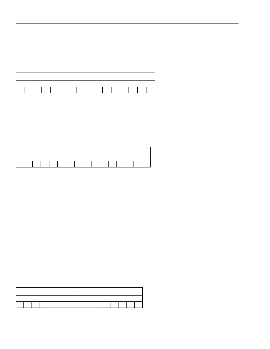
86
Agere Systems Inc.
Advance Data Sheet
May 2002
T7633 Dual T1/E1 3.3 V Short-Haul Terminator
Signaling Access
(continued)
DS1: Robbed-Bit Signaling
(continued)
Table 35 illustrates the ASM time-slot format for valid channels.
* X indicates bits that are undefined by the framer.
The identical sense of the received system P bit in the transmitted signaling data is echoed back to the system in the received signaling
information.
The DS1 framing formats require rate adaptation from the line-interface 1.544 Mbits/s bit stream to the system-
interface 4.096 Mbits/s bit stream. The rate adaptation results in the need for stuffed time slots on the system inter-
face. Table 36 illustrates the ASM format for T1 stuffed channels used by the T7633. The stuffed data byte contains
the programmable idle code in register FRM_PR23 (default = 7F (hex)), while the signaling byte is ignored.
* X indicates bits which are undefined by the framer.
CEPT: Time Slot 16 Signaling
Microprocessor Control Registers
To enable signaling, register FRM_PR44 bit 0 must be set to 0 (default).
The information written into transmit signaling control registers FRM_TSR0--FRM_TSR31 define the state of the
ABCD bits of time slot 16 transmitted to the line.
The received signaling data from time slot 16 is stored in receive signaling registers FRM_RSR0--FRM_RSR31.
Associated Signaling Mode
Signaling information in the associated signaling mode (ASM), register FRM_PR44 bit 2 = 1, is allocated an 8-bit
system time slot in conjunction with the data information for a particular channel. The default system data rate in
the ASM mode is 4.096 Mbits/s. Each system channel consists of an 8-bit payload time slot followed by its associ-
ated 8-bit signaling time slot. The format of the signaling byte is identical to the signaling registers.
Table 37 illustrates the ASM time-slot format for valid CEPT E1 time slots.
* In the CEPT IRSM format, this bit position contains the per-channel E0-31 control information. In all other formats, this bit is ignored.
In the CEPT formats, these bits are undefined.
The P bit is the parity-sense bit calculated over the 8 data bits, the ABCD (and E) bits, and the P bit. The identical sense of the received sys-
tem P bit in the transmitted signaling data is echoed back to the system in the received signaling information.
Table 35. Associated Signaling Mode CHI 2-Byte Time-Slot Format for DS1 Frames
DS1: ASM CHI Time Slot
PAYLOAD DATA
SIGNALING INFORMATION*
1
2
3
4
5
6
7
8
A
B
C
D
X
F
G
P
Table 36. Associated Signaling Mode CHI 2-Byte Time-Slot Format for Stuffed Channels
ASM CHI Time Slot
PAYLOAD DATA
SIGNALING INFORMATION*
0
1
1
1
1
1
1
1
X
X
X
X
X
X
X
X
Table 37. Associated Signaling Mode CHI 2-Byte Time-Slot Format for CEPT
CEPT ASM CHI Time Slot
PAYLOAD DATA
SIGNALING INFORMATION
1
2
3
4
5
6
7
8
A
B
C
D E* X
X
P

Agere Systems Inc.
87
Advance Data Sheet
May 2002
T7633 Dual T1/E1 3.3 V Short-Haul Terminator
Auxiliary Framer I/O Timing
Transmit and receive clock and data signals are provided by terminals RFRMCK (receive framer clock), RFRM-
DATA (receive framer data), RFS (receive frame sync), RSSFS (receive framer signaling superframe sync),
RCRCMFS (receive frame CRC-4 multiframe sync), TFS (transmit framer frame sync), TSSFS (transmit framer
signaling superframe sync), and TCRCMFS (transmit framer CRC-4 multiframe sync).
The receive signals are synchronized to the internal recovered receive line clock, RFRMCK, and the transmit sig-
nals are synchronized to the transmit line clock, TLCK. Note that TLCK is derived from the external PLLCK which
must be phase-locked to the system (CHI) clock, RCHICK, see Table 1, Pin Descriptions on page 20, pin 7 and pin
31.
Detailed timing specifications for these signals are given in Figure 29--Figure 36.
5-6290(F)r.5
Figure 29. Timing Specification for RFRMCK, RFRMDATA, and RFS in DS1 Mode
5-6292(F)r.6
Figure 30. Timing Specification for TFS, TLCK, and TPD in DS1 Mode
RFRMCK
RFS
RFRMDATA
TIME SLOT 1
TIME SLOT 24
BIT 8
BIT 1
DATA VALID
BIT 0
125
µ
s
TLCK
TFS
TPD
TS1
125
µ
s
TS1
(SINGLE
RAIL)
TS2
TS24
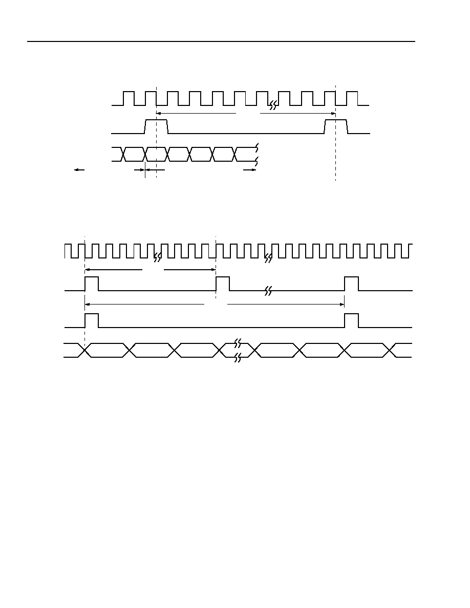
88
Agere Systems Inc.
Advance Data Sheet
May 2002
T7633 Dual T1/E1 3.3 V Short-Haul Terminator
Auxiliary Framer I/O Timing
(continued)
5-6294(F)r.5
Figure 31. Timing Specification for RFRMCK, RFRMDATA, and RFS in CEPT Mode
5-6295(F)r.7
Figure 32. Timing Specification for RFRMCK, RFRMDATA, RFS, and RSSFS in CEPT Mode
RFRMCK
RFS
RFRMDATA
FAS/NFAS: TIME SLOT 0
TIME SLOT 31
BIT 8
BIT 1
DATA VALID
BIT 0
125
µ
s
RFRMCK
RFS
RSSFS
RFRMDATA
TS0 OF THE FRAME AFTER THE
FRAME CONTAINING THE
2 ms
SIGNALING MULTIFRAME
PATTERN (0000)
TS0 OF THE FRAME AFTER THE
FRAME CONTAINING THE
SIGNALING MULTIFRAME
PATTERN (0000)
125
µ
s
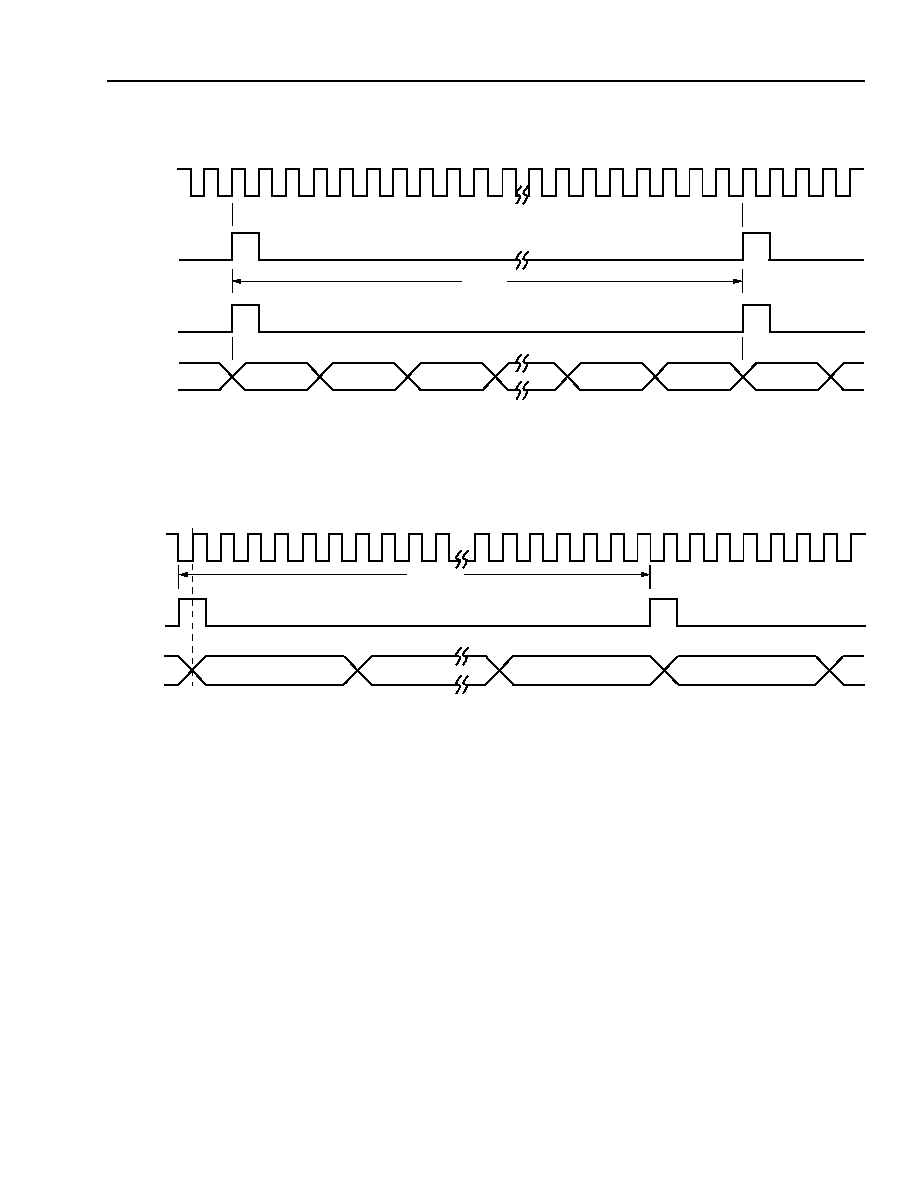
Agere Systems Inc.
89
Advance Data Sheet
May 2002
T7633 Dual T1/E1 3.3 V Short-Haul Terminator
Auxiliary Framer I/O Timing
(continued)
5-6296(F)r.5
Figure 33. Timing Specification for RCRCMFS in CEPT Mode
5-6297(F)r.5
Figure 34. Timing Specification for TFS, TLCK, and TPD in CEPT Mode
RFRMCLK
RFS
RCRCMFS
RFRMDATA
TS0 OF FRAME #0
OF MULTIFRAME
TS0 OF FRAME #0
OF MULTIFRAME
2 ms
TLCK
TFS
TPD
TS0 OF FRAME X
125
µ
s
TS0 OF FRAME X + 1
(SINGLE
RAIL)
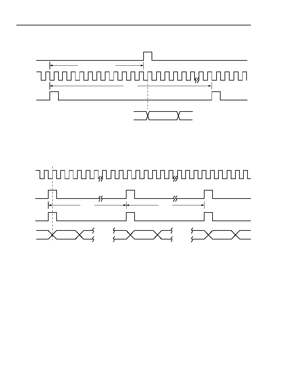
90
Agere Systems Inc.
Advance Data Sheet
May 2002
T7633 Dual T1/E1 3.3 V Short-Haul Terminator
Auxiliary Framer I/O Timing
(continued)
5-6298(F)r.5
Figure 35. Timing Specification for TFS, TLCK, TPD, and TSSFS in CEPT Mode
5-6299(F)r.5
Figure 36. Timing Specification for TFS, TLCK, TPD, and TCRCMFS in CEPT Mode
TFS
TLCK
TSSFS
TPD
(SINGLE
TS0 OF THE FRAME
2 ms
11 CLOCK CYCLES
CONTAINING THE SIGNALING
MULTIFRAME PATTERN (0000)
RAIL)
TLCK
TFS
TCRCMFS
TPD
(SINGLE
TS0 OF FRAME #8
1 ms
OF MULTIFRAME
RAIL)
TS0 OF FRAME #0
OF MULTIFRAME
TS0 OF FRAME #0
OF MULTIFRAME
1 ms

Agere Systems Inc.
91
Advance Data Sheet
May 2002
T7633 Dual T1/E1 3.3 V Short-Haul Terminator
Alarms and Performance Monitoring
Interrupt Generation
A global interrupt (pin 99) may be generated if enabled by register GREG1. This interrupt is clocked using channel
1 framer receive line clock (RLCK1). If RLCK1 is absent, the interrupt is clocked using RLCK2, the receive line
clock of channel 2. If both RLCK1 and RLCK2 are absent, clocking of interrupts is controlled by an interval 2.048
MHz clock generated from the CHI clock. Timing of the interrupt is shown in Figure 37. There is no relation
between MPCK (pin 101) and the interrupt, i.e., MPCK maybe asynchronous with any of the other terminator
clocks.
5-6563(F)
Figure 37. Relation Between RLCK1 and Interrupt (Pin 99)
Alarm Definition
The receive framer monitors the receive line data for alarm conditions and errored events, and then presents this
information to the system through the microprocessor interface status registers. The transmit framer, to a lesser
degree, monitors the receive system data and presents the information to the system through the microprocessor
interface status registers. Updating of the status registers is controlled by the receive line clock signal. When the
receive loss of clock monitor determines that the receive line clock signal is lost, the system clock is used to clock
the status registers and all status information should be considered corrupted.
Although the precise method of detecting or generating alarm and error signals differs between framing modes, the
functions are essentially the same. The alarm conditions monitored on the received line interface are:
1. Red alarm or the loss of frame alignment indication (FRM_SR1 bit 0).
The red alarm indicates that the receive frame alignment for the line has been lost and the data cannot be
properly extracted. The red alarm is indicated by the loss of frame condition for the various framing formats as
defined in Table 38.
RLCK1
INTERRUPT
(PIN 99)

92
Agere Systems Inc.
Advance Data Sheet
May 2002
T7633 Dual T1/E1 3.3 V Short-Haul Terminator
Alarms and Performance Monitoring
(continued)
Alarm Definition
(continued)
2. Yellow alarm or the remote frame alarm (FRM_SR1 bit 0).
This alarm is an indication that the line remote end is in a loss of frame alignment state. Indication of remote
frame alarm (commonly referred to as a yellow alarm) as for the different framing formats is shown in Table 39.
3. Blue alarm or the alarm indication signal (AIS).
The alarm indication signal (AIS), sometimes referred to as the blue alarm, is an indication that the remote end
is out-of-service. Detection of an incoming alarm indication signal is defined in Table 40.
Table 38. Red Alarm or Loss of Frame Alignment Conditions
Framing Format
Number of Errored Framing Bits That Will Cause a Red Alarm (Loss of Frame
Alignment) Condition
D4
2 errored frame bits (F
T
or F
S
) out of 4 consecutive frame bits if FRM_PR10 bit 2 = 1.
2 errored F
T
bits out of 4 consecutive F
T
bits if PRM_PR10 bit 2 = 0.
SLC
-96
2 errored frame bits (F
T
or F
S
) out of 4 consecutive frame bits if FRM_PR10 bit 2 = 1.
2 errored F
T
bits out of 4 consecutive F
T
bits if FRM_PR10 bit 2 = 0.
DDS: Frame
3 errored frame bits (F
T
or F
S
) or channel 24 FAS pattern out of 12 consecutive frame bits.
ESF
2 errored F
E
bits out of 4 consecutive F
E
bits or, optionally, 320 or more CRC6 errored
checksums within a one second interval if loss of frame alignment due to excessive CRC-6
errors is enabled in FRM_PR9.
CEPT
Three consecutive incorrect FAS patterns or three consecutive incorrect NOT FAS patterns;
or optionally, greater than 914 received CRC-4 checksum errors in a one second interval if
loss of frame alignment due to excessive CRC-6 errors is enabled in FRM_PR9.
Table 39. Remote Frame Alarm Conditions
Framing Format
Remote Frame Alarm Format
Superframe: D4
Bit 2 of all time slots in the 0 state.
Superframe: D4-Japanese
The twelfth (12th) framing bit in the 1 state in two out of three consecutive super-
frames.
Superframe: DDS
Bit 6 of time slot 24 in the 0 state.
Extended Superframe (ESF)
An alternating pattern of eight 1s followed by eight 0s in the ESF data link.
CEPT: Basic Frame
Bit 3 of the NOT FAS frame in the 1 state in three consecutive frames.
CEPT: Signaling Multiframe
Bit 6 of the time slot 16 signaling frame in the 1 state.

Agere Systems Inc.
93
Advance Data Sheet
May 2002
T7633 Dual T1/E1 3.3 V Short-Haul Terminator
Alarms and Performance Monitoring
(continued)
Alarm Definition
(continued)
4. The SLIP condition (FRM_SR3 bit 6 and bit 7).
SLIP is defined as the state in which the receive elastic store buffer's write address pointer from the receive
framer and the read address pointer from the transmit concentration highway interface are equal
1
.
A.
The negative slip (Slip-N) alarm indicates that the receive line clock (RLCK) - transmit CHI clock (TCHICK)
monitoring circuit detects a state of overflow caused by RLCK and TCHICK being out of phase-lock and
the period of the received frame being less than that of the system frame. One system frame is deleted.
B.
The positive slip (Slip-P) alarm indicates the line clock (RLCK) - transmit CHI clock (TCHICK) monitoring
circuit detects a state of underflow caused by RLCK and TCHICK being out of phase-lock and the period
of the received frame being greater than that of the system frame. One system frame is repeated.
5. The loss of framer receive clock (LOFRMRLCK, pins 2 and 38).
In the framer mode, FRAMER = 0 (pin 41/141), LOFRMRLCK alarm is asserted high when an interval of
250
µ
s has expired with no transition of RLCK (pin 135/47) detected. The alarm is disabled on the first transi-
tion of RLCK. In the terminator mode, FRAMER = 1 (pin 41/141), LOFRMRLCK is asserted high when SYSCK
(pin 3/35) does not toggle for 250 µs. The alarm is disabled on the first transition of SYSCK.
6. The loss of PLL clock (LOPLLCK, pins 39 and 143).
LOPLLCK alarm is asserted high when an interval of 250
µ
s has expired with no transition of PLLCK detected.
The alarm is disabled 250 µs after the first transition of PLLCK. Timing for LOPLLCK is shown in Figure 38.
1. After a reset, the read and write pointers of the receive path elastic store will be set to a known state.
5-6564(F)r.2
Figure 38. Timing for Generation of LOPLLCK (Pin 39/143)
Table 40. Alarm Indication Signal Conditions
Framing Format
Remote Frame Alarm Format
T1
Loss of frame alignment occurs and the incoming signal has two (2) or fewer zeros in
each of two consecutive double frame periods (386 bits).
CEPT ETSI
As described in Draft prETS 300 233:1992 Section 8.2.2.4, loss of frame alignment
occurs and the framer receives a 512 bit period containing two or less binary zeros. This
is enabled by setting register FRM_PR10 bit 1 to 0.
CEPT ITU
As described in ITU Rec. G.775, the incoming signal has two or fewer zeros in each of
two consecutive double frame periods (512 bits). AIS is cleared if each of two consecu-
tive double frame periods contains three or more zeros or frame alignment signal (FAS)
has been found. This is enabled by setting register FRM_PR10 bit 1 to 1.
PLLCK
LOPLLCK
RCHICK
250
µ
s
250
µ
s

94
Agere Systems Inc.
Advance Data Sheet
May 2002
T7633 Dual T1/E1 3.3 V Short-Haul Terminator
Alarms and Performance Monitoring
(continued)
Alarm Definition
(continued)
7. Received bipolar violation errors alarm, FRM_SR3 bit 0.
This alarm indicates any bipolar decoding error or detection of excessive zeros.
8. Received excessive CRC errors alarm, FRM_SR3 bit 3.
In ESF, this alarm is asserted when 320 or more CRC-6 checksum errors are detected within a one second
interval. In CEPT, this alarm is asserted when 915 or more CRC-4 checksum errors are detected within a one
second interval.
9. The CEPT continuous E-bit alarm (CREBIT) (FRM_SR2 bit 2).
CREBIT is asserted when the receive framer detects:
A.
Five consecutive seconds where each 1 second interval contains
991 received E bits = 0 events.
B.
Simultaneously no LFA occurred.
C.
Optionally, no remote frame alarm (A bit = 1) was detected if register FRM_PR9 bit 0, bit 4, and bit 5 are
set to 1.
D.
Optionally, neither Sa6-F
hex
nor Sa6-E
hex
codes were detected if register FRM_PR9 bit 0, bit 4, and bit 6
are set to 1.
The five second timer is started when:
E.
CRC-4 multiframe alignment is achieved.
F.
And optionally, A = 0 is detected if register FRM_PR9 bit 0, bit 4, and bit 5 are set to 1.
G.
And optionally, neither Sa6_F
hex
1
nor Sa6_E
hex
1
is detected if register FRM_PR9 bit 0, bit 4, and bit 6 are
set to 1.
The five second counter is restarted when:
H.
LFA occurs, or
I.
990 E bit = 0 events occur in 1 second, or
J.
Optionally, an A bit = 1 is detected if register FRM_PR9 bit 0, bit 4, and bit 5 are set to 1.
K.
Optionally, a valid Sa6 pattern 1111 (binary) or Sa6 pattern 1110 (binary) code was detected if register
FRM_PR9 bit 0, bit 4, and bit 6 are set to 1.
This alarm is disabled during loss of frame alignment (LFA) or loss of CRC-4 multiframe alignment (LTS0MFA).
1. See Table 41, Sa6 Bit Coding Recognized by the Receive Framer on page 95, for the definition of this Sa6 pattern.

Agere Systems Inc.
95
Advance Data Sheet
May 2002
T7633 Dual T1/E1 3.3 V Short-Haul Terminator
Alarms and Performance Monitoring
(continued)
Alarm Definition
(continued)
10. Failed state alarm or the unavailable state alarm, FRM_SR5 bit 3 and bit 7 and FRM_SR6 bit 3 and bit 7.
This alarm is defined as the unavailable state at the onset of ten consecutive severely errored seconds. In this
state, the receive framer inhibits incrementing of the severely errored and errored second counters for the
duration of the unavailable state. The receive framer deasserts the unavailable state condition at the onset of
ten consecutive errored seconds which were not severely errored.
11. The 4-bit Sa6 codes (FRM_SR2 bit 3--bit 7).
Sa6 codes are asserted if three consecutive 4-bit patterns have been detected. The alarms are disabled when
three consecutive 4-bit Sa6 codes have been detected that are different from the pattern previously detected.
The receive framer monitors the Sa6 bits for special codes described in ETS Draft prETS 300 233:1992 Sec-
tion 9.2. The Sa6 codes are defined in Table 41 and Table 42. The Sa6 codes in Table 41 may be recognized
as an asynchronous bit stream in either non-CRC-4 or CRC-4 modes as long as the receive framer is in the
basic frame alignment state. In the CRC-4 mode, the receive framer can optionally recognize the received Sa6
codes in Table 41 synchronously to the CRC-4 submultiframe structure as long as the receive framer is in the
CRC-4 multiframe alignment state (synchronous Sa6 monitoring can be enabled by setting register
FRM_PR10 bit 1 to 1). The Sa6 codes in Table 42 are only recognized synchronously to the CRC-4 submulti-
frame and when the receive framer is in CRC-4 multiframe alignment. The detection of three (3) consecutive 4-
bit patterns are required to indicate a valid received Sa6 code. The detection of Sa6 codes is indicated in status
register FRM_SR2 bit 3--bit 7. Once set, any three-nibble (12-bit) interval that contains any other Sa6 code will
clear the current Sa6 status bit. Interrupts may be generated by the Sa6 codes given in Table 41.
Table 41. Sa6 Bit Coding Recognized by the Receive Framer
Code
First Receive Bit (MSB)
Last Received Bit (LSB)
Sa6_8
hex
1
0
0
0
Sa6_A
hex
1
0
1
0
Sa6_C
hex
1
1
0
0
Sa6_E
hex
1
1
1
0
Sa6_F
hex
1
1
1
1
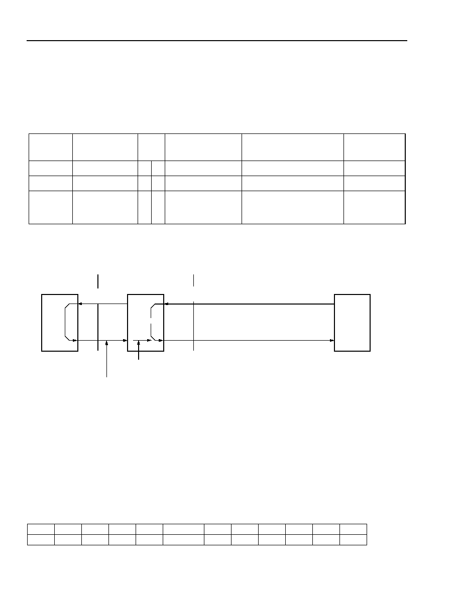
96
Agere Systems Inc.
Advance Data Sheet
May 2002
T7633 Dual T1/E1 3.3 V Short-Haul Terminator
Alarms and Performance Monitoring
(continued)
Alarm Definition
(continued)
Table 42 defines the three 4-bit Sa6 codes that are always detected synchronously to the CRC-4 submultiframe
structure, and are only used for counting NT1 events.
The reference points for receive CRC-4, E bit, and Sa6 decoding are illustrated in Figure 39.
5-3913(F)r.8
Figure 39. The T and V Reference Points for a Typical CEPT E1 Application
12. CEPT auxiliary pattern alarm (AUXP) (FRM_SR1 bit 6).
The received auxiliary alarm, register FRM_SR1 bit 6 (AUXP), is asserted when the receive framer is in the
LFA state and has detected more than 253 10 (binary) patterns for 512 consecutive bits. In a 512-bit interval,
only two 10 (binary) patterns are allowable for the alarm to be asserted and maintained. The 512-bit interval is
a sliding window determined by the first 10 (binary) pattern detected. This alarm is disabled when three or more
10 (binary) patterns are detected in 512 consecutive bits. The search for AUXP is synchronized with the first
alternating 10 (binary) pattern as shown in Table 43.
Table 43. AUXP Synchronization and Clear Sychronization Process
Table 42. Sa6 Bit Coding of NT1 Interface Events Recognized by the Receive Framer
Code
First Receive
Bit (MSB)
Last Received Bit
(LSB)
Event at NT1
Counter Size
(bits)
Sa6_1
hex
0
0
0
1
E = 0
16
Sa6_2
hex
0
0
1
0
CRC-4 Error
16
Sa6_3
hex
0
0
1
1
CRC-4 Error & E = 0
This code will cause both
counters to increment.
--
00
10
10
01
11
11
00
00
0
10
00
10
--
sync
--
--
--
clear sync
--
--
--
sync
. . .
. . .
NT2
E BIT = 0
NT1
ET
V REFERENCE
E BIT = 0, ERROR EVENT DETECTED AT THE NT1 REMOTE
CRC-4 ERRORS AT THE NT1
E BIT = 0, ERROR EVENT AT THE ET REMOTE
CRC-4 ERRORS AT THE ET,
CRC-4 ERRORS DETECTED FROM NT1 REMOTE, THEN SET Sa6 = 001X
E = 0 DETECTED FROM NT1 REMOTE, THEN SET Sa6 = 00X1
POINT
T REFERENCE
POINT
COUNT:
1) CRC ERRORS,
2) E = 0,
3) Sa6 = 001X, AND
4) Sa6 = 00X1
Sa6
CRC ERROR
DETECTED
CRC ERROR
DETECTED
(NT1 REMOTE)
E BIT = 0

Agere Systems Inc.
97
Advance Data Sheet
May 2002
T7633 Dual T1/E1 3.3 V Short-Haul Terminator
Alarms and Performance Monitoring
(continued)
Event Counters Definition
The error events monitored in the receive framer's status registers are defined in Table 44 for the hardwired (default)
threshold values. The errored second and severely errored second threshold registers can be programmed through
FRM_PR11--FRM_PR13 such that the errored and severely errored second counters function as required by
system needs.
Table 44. Event Counters Definition
Error Event
Functional Mode
Definition
Counter Size
(bits)
Bipolar Viola-
tions (BPVs)
AMI
Any bipolar violation or 16 or more consecutive
zeros
16
B8ZS
Any BPV, code violation, or any 8-bit interval with no
one pulse
CEPT HDB3
Any BPV, code violation, or any 4-bit interval with no
one pulse
Frame Align-
ment Errors
(FERs)
SF: D4
Any F
T
or F
S
bit errors (FRM_PR10 bit 2 = 1) or any
F
T
bit errors (FRM_PR10 bit 2 = 0)
8
SF:
SLC
-96
Any F
T
or F
S
bit errors (FRM_PR10 bit 2 = 1) or any
F
T
bit errors (FRM_PR10 bit 2 = 0)
SF: DDS
Any F
T
, F
S
, or time slot 24 FAS bit error
ESF
Any F
E
bit error
CEPT
Any FAS (0011011) or NOT FAS (bit 2) bit error if
register FRM_PR10, bit 2 = 0.
Any FAS (0011011) bit error if register FRM_PR10,
bit 2 = 1.
CRC Checksum
Errors
ESF or CEPT with CRC
Any received checksum in error
16
Excessive CRC
Errors
ESF
320 checksum errors in a one second interval
NONE
CEPT with CRC
915 checksum errors in a one second interval
Received
E bits = 0
CEPT with CRC-4
E bits = 0 in frame 13 and frame 15
16
Errored Second
Events
All
Any one of the relevant error conditions enabled in
registers FRM_PR14--FRM_PR18 within a one sec-
ond interval
16
DS1: non ESF
Any framing bit errors within a one second interval
DS1: ESF
Any CRC-6 errors within a one second interval
CEPT without CRC-4
Any framing errors within a one second interval
CEPT with CRC-4 (ET1) Any CRC-4 errors within a one second interval
CEPT with CRC-4 (ET1
remote)
Any E bit = 0 event within a one second interval
CEPT with CRC-4 (NT1) Any Sa6 = 001x (binary) code event within a one
second interval
CEPT with CRC-4 (NT1
remote)
Any Sa6 = 00x1 (binary) code event within a one
second interval

98
Agere Systems Inc.
Advance Data Sheet
May 2002
T7633 Dual T1/E1 3.3 V Short-Haul Terminator
Alarms and Performance Monitoring
(continued)
Event Counters Definition
(continued)
Table 44. Event Counters Definition (continued)
The receive framer enters an unavailable state condition at the onset of ten consecutive severely errored second
events. When in the unavailable state, the receive framer deasserts the unavailable state alarms at the onset of ten
consecutive seconds which were not severely errored.
Error Event
Functional Mode
Definition
Counter Size
(bits)
Bursty Errored
Second Events
DS1: non ESF
Greater than 1 but less than 8 framing bit errors
within a one second interval
16
DS1: ESF
Greater than 1 but less than 320 CRC-6 errors within
a one second interval
CEPT without CRC-4
Greater than 1 but less than 16 framing bit errors
within a one second interval
CEPT with CRC-4 (ET1) Greater than 1 but less than 915 CRC-4 errors within
a one second interval
CEPT with CRC-4 (ET1
remote)
Greater than 1 but less than 915 E bit = 0 events
within a one second interval
CEPT with CRC-4 (NT1) Greater than 1 but less than 915 Sa6=001x (binary)
code events within a one second interval
CEPT with CRC-4 (NT1
remote)
Greater than 1 but less than 915 Sa6=00x1 (binary)
code events within a one second interval
Severely Errored
Second Events
All
Any one of the relevant error conditions enabled in
registers FRM_PR14--FRM_PR18 within a one sec-
ond interval
16
DS1: non ESF
8 or more framing bit errors within a one second
interval
DS1: ESF
320 or more CRC-6 errors within a one second inter-
val
CEPT with no CRC-4
16 or more framing bit errors within a one second
interval
CEPT with CRC-4 (ET1) 915 or more CRC-4 errors within a one second inter-
val
CEPT with CRC-4 (ET1
remote)
915 or more E bit = 0 events within a one second
interval
CEPT with CRC-4 (NT1) 915 or more Sa6=001x (binary) code events within a
one second interval
CEPT with CRC-4 (NT1
remote)
915 or more Sa6=00x1 (binary) code events within a
one second interval
Unavailable
Second Events
All
A one second period in the unavailable state
16

Agere Systems Inc.
99
Advance Data Sheet
May 2002
T7633 Dual T1/E1 3.3 V Short-Haul Terminator
Alarms and Performance Monitoring
(continued)
Loopback and Transmission Modes
Primary Loopback Modes
Framer primary loopback mode is controlled by register FRM_PR24. There are seven primary loopback and trans-
mission test modes supported:
1.
Line loopback (LLB).
2.
Board loopback (BLB).
3.
Single time-slot system loopback (STSSLB).
4.
Single time-slot line loopback (STSLLB).
5.
CEPT nailed-up broadcast transmission (CNUBT).
6.
Payload loopback (PLLB).
7.
CEPT nailed-up connect loopback (CNUCLB).
The loopback and transmission modes are described in detail below:
1.
The LLB mode loops the receive line data and clock back to the transmit line. The received data is processed
by the receive framer and transmitted to the system interface. This mode can be selected by setting register
FRM_PR24 to 001xxxxx (binary).
2.
The BLB mode loops the receive system data back to the system after:
A. The transmit framer processes the data, and
B. The receive framer processes the data.
In the BLB mode, AIS is always transmitted to the line interface. This mode can be selected by setting register
FRM_PR24 to 010xxxxx (binary).
3.
The STSSLB mode loops one and only one received system time slot back to the transmit system interface.
The selected looped back time-slot data is not processed by either the transmit framer or the receive framer.
The selected time slot does not pass through the receive elastic store buffer and therefore will not be affected
by system-AIS, RLFA conditions, or controlled slips events. Once selected, the desired time-slot position has
the programmable idle code in register FRM_PR22 transmitted to the line interface one frame before imple-
menting the loopback and for the duration of the loopback. This mode can be selected by setting register
FRM_PR24 to 011A
4
A
3
A
2
A
1
A
0
, where A
4
A
3
A
2
A
1
A
0
is the binary address of the selected time slot.
4.
The STSLLB mode loops one and only one received line time slot back to the transmit line. The selected time-
slot data is looped to the line after being processed by the receive framer, and it passes through the receive
elastic store. The selected time slot has the programmable idle code in register FRM_PR22 transmitted to the
system interface one frame before implementing the loopback and for the duration of the loopback. In CEPT,
selecting time slot 0 has the effect of deactivating the current loopback mode while no other action will be
taken (time slot 0 will not be looped back to the line and should not be chosen). This mode can be selected by
setting register FRM_PR24 to 100A
4
A
3
A
2
A
1
A
0
, where A
4
A
3
A
2
A
1
A
0
is the binary address of the selected time
slot.
5.
The CNUBT mode transmits received-line time slot X to the system in time slots X and time slot 0 (of the next
frame). Any time slot can be broadcast. This mode can be selected by setting register FRM_PR24 to
101A
4
A
3
A
2
A
1
A
0
where A
4
A
3
A
2
A
1
A
0
is the binary address of the selected time slot.

100
Agere Systems Inc.
Advance Data Sheet
May 2002
T7633 Dual T1/E1 3.3 V Short-Haul Terminator
Alarms and Performance Monitoring
(continued)
Loopback and Transmission Modes
(continued)
6. The PLLB mode loops the received line data and clock back to the transmit line while inserting (replacing) the
facility data link in the looped back data. Two variations of the payload loopback are available. In the pass
through framing/CRC bit mode (chosen by setting register FRM_PR24 to 111xxxxx (binary)), the framing and
CRC bits are looped back to the line transmit data. In the regenerated framing/CRC bit mode (chosen by
setting register FRM_PR24 to 110xxxxx (binary) and register FRM_PR10 bit 3 to 0), the framing and CRC bits
are regenerated by the transmit framer. The payload loopback is only available for ESF and CEPT modes.
7. The CNUCLB mode loops received system time slot X back to the system in time slot 0. The selected time slot
is not routed through the receive elastic store buffer and therefore will not be affected by system-AIS, RLFA
conditions, or controlled slips. Any time slot can be looped back to the system. Time slot X transmitted to the
line is not affected by this loopback mode. Looping received system time slot 0 has no effect on time slot 0
transmitted to the line, i.e., the transmit framer will always overwrite the FAS and NOT FAS data in time slot 0
transmitted to the line. This mode can be selected by setting register FRM_PR24 to 110A
4
A
3
A
2
A
1
A
0
and
register FRM_PR10 bit 3 to 1, where A
4
A
3
A
2
A
1
A
0
is the binary address of the selected time slot.
Secondary Loopback Modes
There are two secondary loopback modes supported:
1.
Secondary-single time-slot system loopback (S-STSSLB)
2.
Secondary-single time-slot line loopback (S-STSLLB)
The loopbacks are described in detail below:
1. The secondary-STSSLB mode loops one and only one received system time slot back to the transmit system
interface. The selected time-slot data looped back is not processed by either the transmit framer or the receive
framer. The selected time slot does not pass through the receive elastic store buffer and therefore will not be
affected by system-AIS, RLFA conditions, or controlled slips events. Whenever the secondary loopback register
is programmed to the same time slot as the primary register, the primary loopback mode will control that time
slot. Once selected, the desired time-slot position has the programmable line idle code in register FRM_PR22
transmitted to the line interface one frame before implementing the loopback and for the duration of the
loopback.
2. The secondary-STSLLB mode loops one and only one line time slot back to the line. The selected time slot data
is looped to the line after being processed by the receive framer and it passes through the receive elastic store.
The selected time slot has the programmable idle code in register FRM_PR22 transmitted to the system
interface one frame before implementing the loopback and for the duration of the loopback. In CEPT, selecting
time slot 0 has the effect of deactivating the current loopback mode while no other action will be taken (time slot
0 will not be looped back to the line and should not be chosen in this mode).
Table 45 defines the deactivation of the two secondary loopback modes as a function of the activation of the pri-
mary loopback and test transmission modes.
Table 45. Summary of the Deactivation of SSTSSLB and SSTSLLB Modes as a Function of Activating the
Primary Loopback Modes
Primary Loopback Mode
Deactivation of S-STSSLB
Deactivation of S-STSLLB
STSSLB
If primary time slot = secondary
If primary time slot = secondary
STSLLB
If primary time slot = secondary
If primary time slot = secondary
BLB
Always
Always
CNUBT
If the secondary time slot is TS0 or if the
primary time slot = secondary
If primary time slot = secondary
LLB
Always
Always
NUCLB
If the secondary time slot is TS0 or if the
primary time slot = secondary
If primary time slot = secondary
PLLB
Always
Always
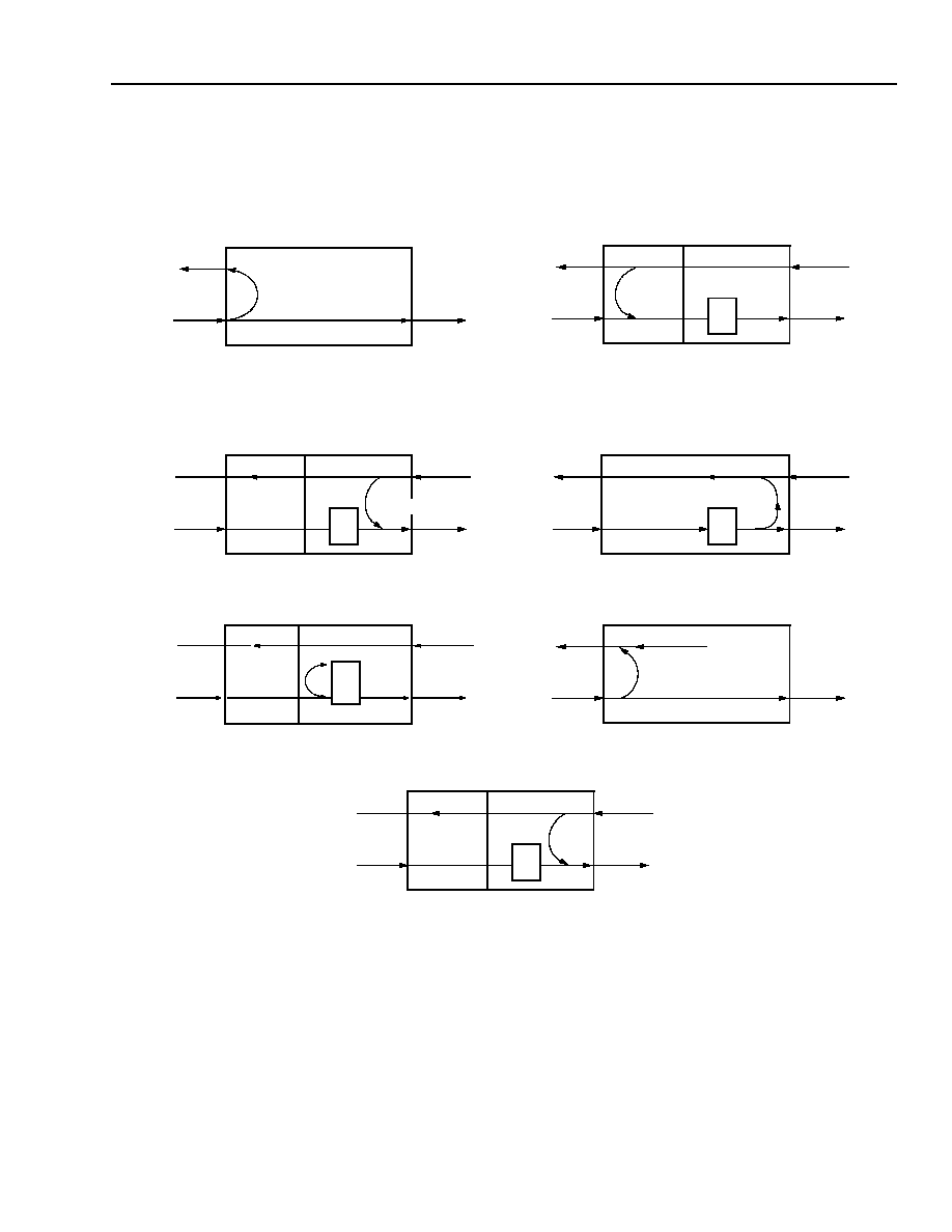
Agere Systems Inc.
101
Advance Data Sheet
May 2002
T7633 Dual T1/E1 3.3 V Short-Haul Terminator
Alarms and Performance Monitoring
(continued)
Loopback and Transmission Modes
(continued)
Figure 40 illustrates the various loopback modes implemented by each framer unit.
5-3914(F).cr.3
Figure 40. Loopback and Test Transmission Modes
FRAMER
FRAMER
LINE
ES
SYSTEM
(3) SINGLE TIME-SLOT SYSTEM LOOPBACK
FRAMER
LINE
ES
SYSTEM
(2) BOARD LOOPBACK
AIS
RECEIVE SYSTEM DATA
LINE
SYSTEM
(1) LINE LOOPBACK
IS IGNORED
INSERT ONLY TIME SLOT X
LINE
ES
SYSTEM
(4) SINGLE TIME-SLOT LINE LOOPBACK
TRANSMIT PROGRAMMABLE IDLE CODE
IN REGISTER FRM_PR22
LINE
ES
SYSTEM
(5) CEPT NAILED-UP BROADCAST TRANSMISSION
TRANSMIT LINE TS-X IN
SYSTEM TS-X AND SYSTEM TS-0
FRAMER
LINE
ES
SYSTEM
(7) CEPT NAILED-UP CONNECT LOOPBACK
LOOPBACK TS-X IN TS-0
TRANSMIT FRAMER
LINE
SYSTEM
(6) PAYLOAD LINE LOOPBACK
TRANSMIT PROGRAMMABLE LINE IDLE CODE
IN REGISTER FRM_PR22
LOOPBACK TS-X
IN OUTGOING SYSTEM TS-X
IN OUTGOING LINE TS-X
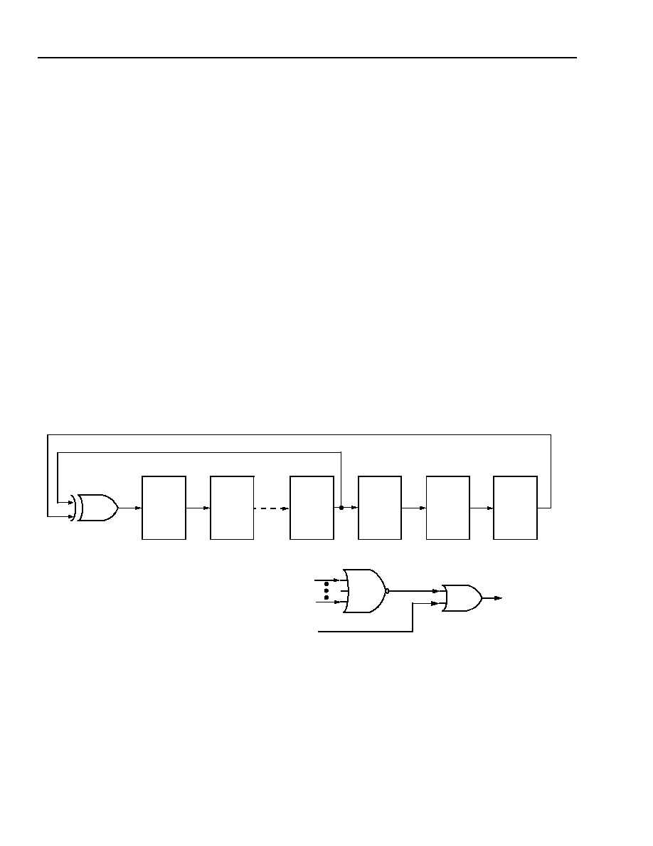
102
Agere Systems Inc.
Advance Data Sheet
May 2002
T7633 Dual T1/E1 3.3 V Short-Haul Terminator
Alarms and Performance Monitoring
(continued)
Line Test Patterns
Test patterns may be transmitted to the line through either register FRM_PR20 or register FRM_PR29. Only one of
these sources may be active at the same time. Signaling must be inhibited while sending these test patterns.
Transmit Line Test Patterns--Using Register FRM_PR20
The transmit framer can be programmed through register FRM_PR20 to transmit various test patterns. These test
patterns, when enabled, overwrite the received CHI data. The test patterns available using register FRM_PR20
are:
1.
The unframed-AIS pattern which consists of a continuous bit stream of 1s (. . . 111111 . . .) enabled by setting
register FRM_PR20 bit 0 to 1.
2.
The unframed-auxiliary pattern which consists of a continuous bit stream of alternating 1s and 0s (. . .
10101010 . . .) enabled by setting register FRM_PR20 bit 1 to 1.
3.
The quasi-random test signal, enabled by setting register FRM_PR20 bit 3 to 1, which consists of:
A. A pattern produced by means of a twenty stage shift register with feedback taken from the 17th and 20th
stages via an exclusive-OR gate to the first stage. The output is taken from the 20th stage and is forced to
a 1 state whenever the next 14 stages (19 through 6) are all 0. The pattern length is 1,048,575 or
2
20
≠ 1 bits. This pattern is described in detail in
AT&T
Technical Reference 62411 [5] Appendix and
illustrated in Figure 41.
B. Valid framing bits.
C. Valid transmit facility data link (TFDL) bit information.
D. Valid CRC bits.
5-3915(F).dr.1
Figure 41. 20-Stage Shift Register Used to Generate the Quasi-Random Signal
4.
The pseudorandom test pattern, enabled by setting register FRM_PR20 bit 2 to 1, which consists of:
A. A 2
15
≠ 1 pattern inserted in the entire payload (time slots 1--24 in DS1 and time slots 1--32 in CEPT), as
described by ITU Rec. 0.151 and illustrated in Figure 42.
B. Valid framing pattern.
C. Valid transmit facility data link (TFDL) bit data.
D. Valid CRC bits.
D
D-TYPE FLIP-FLOPS
#1
D
D
#2
#17
D
#18
D
D
#19
#20
A
B
C
XOR
#6
#19
NOR
#20
QUASI-RANDOM TEST OUTPUT
OR

Agere Systems Inc.
103
Advance Data Sheet
May 2002
T7633 Dual T1/E1 3.3 V Short-Haul Terminator
Alarms and Performance Monitoring
(continued)
Line Test Patterns
(continued)
5-3915(F).er.1
Figure 42. 15-Stage Shift Register Used to Generate the Pseudorandom Signal
5.
The idle code test pattern, enabled by setting register FRM_PR20 bit 6 to 1, which consists of:
A. The programmable idle code, programmed through register FRM_PR22, in time slots 1--24 in DS1 and
0--31 in CEPT.
B. Valid framing pattern.
C. Valid transmit facility data link (TFDL) bit data.
D. Valid CRC bits.
Transmit Line Test Patterns--Using Register FRM_PR69
Framed or unframed patterns indicated in Table 46 may be generated and sent to the line by register FRM_PR69
and by setting register FRM_PR20 to 00 (hex). Selection of transmission of either a framed or unframed test pat-
tern is made through FRM_PR69 bit 3. If one of the test patterns of register FRM_PR69 is enabled, a single bit
error can be inserted into the transmitted test pattern by toggling register FRM_PR69 bit 1 from 0 to 1.
Table 46. Register FRM_PR69 Test Patterns
Pattern
Register FRM_PR69
Bit 7 Bit 6
Bit 5
Bit 4
MARK (all ones AIS)
0
0
0
0
QRSS (2
20
≠ 1 with zero suppression)
0
0
0
1
2
5
≠ 1
0
0
1
0
63 (2
6
≠ 1)
0
0
1
1
511 (2
9
≠ 1) (V.52)
0
1
0
0
2
9
≠ 1
0
1
0
1
2047 (2
11
≠ 1) (O.151)
0
1
1
0
2
11
≠ 1 (reversed)
0
1
1
1
2
15
≠ 1 (O.151)
1
0
0
0
2
20
≠ 1 (V.57)
1
0
0
1
2
20
≠ 1 (CB113/CB114)
1
0
1
0
2
23
≠ 1 (O.151)
1
0
1
1
1:1 (alternating)
1
1
0
0
D
XOR
D-TYPE FLIP-FLOPS
#1
D
D
#2
#3
D
#13
D
D
#14
#15
A
B
C
PSEUDORANDOM
TEST OUTPUT

104
Agere Systems Inc.
Advance Data Sheet
May 2002
T7633 Dual T1/E1 3.3 V Short-Haul Terminator
Alarms and Performance Monitoring
(continued)
Line Test Patterns
(continued)
Receive Line Pattern Monitor--Using Register FRM_SR7
The receive framer pattern monitor continuously monitors the received line, detects the following fixed framed pat-
terns, and indicates detection in register FRM_SR7 bit 6 and bit 7.
1.
The pseudorandom test pattern as described by ITU Rec. O.151 and illustrated in Figure 42. Detection of the
pattern is indicated by register FRM_SR7 bit 6 = 1.
2.
The quasi-random test pattern described in
AT&T
Technical Reference 62411[5] Appendix and illustrated in
Figure 41. Detection of the pattern is indicated by register FRM_SR7 bit 7 = 1.
In DS1 mode, the received 193 bit frame must consist of 192 bits of pattern plus 1 bit of framing information. In
CEPT mode, the received 256 bit frame must consist of 248 bits of pattern plus 8 bits (TS0) of framing information.
No signaling, robbed bit in the case of T1 and TS16 signaling in the case of CEPT, may be present for successful
detection of these two test patterns.
To establish lock to the pattern, 256 sequential bits must be received without error. When lock to the pattern is
achieved, the appropriate bit of register FRM_SR7 is set to a 1. Once pattern lock is established, the monitor can
withstand up to 32 single bit errors per frame without a loss of lock. Lock will be lost if more than 32 errors occur
within a single frame. When such a condition occurs, the appropriate bit of register FRM_SR7 is deasserted. The
monitor then resumes scanning for pattern candidates.
Receive Line Pattern Detector--Using Register FRM_PR70
Framed or unframed patterns indicated in Table 47 may be detected using register FRM_PR70. Detection of the
selected test pattern is indicated when register FRM_PR7 bit 4 is set to 1. Selection of a framed or unframed test
pattern is made through FRM_PR70 bit 3. Bit errors in the received test pattern are indicated when register
FRM_SR7 bit 5 = 1. The bit errors are counted and reported in registers FRM_SR8 and FRM_SR9, which are nor-
mally the BPV counter registers. (In this test mode, the BPV counter registers do not count BPVs but count only bit
errors in the received test pattern.)
Table 47. Register FRM_PR70 Test Patterns
Pattern
Register FRM_PR70
Bit 7 Bit 6
Bit 5
Bit 4
MARK (all ones AIS)
0
0
0
0
QRSS (2
20
≠ 1 with zero suppression)
0
0
0
1
2
5
≠ 1
0
0
1
0
63 (2
6
≠ 1)
0
0
1
1
511 (2
9
≠ 1) (V.52)
0
1
0
0
2
9
≠ 1
0
1
0
1
2047 (2
11
≠ 1) (O.151)
0
1
1
0
2
11
≠ 1 (reversed)
0
1
1
1
2
15
≠ 1 (O.151)
1
0
0
0
2
20
≠ 1 (V.57)
1
0
0
1
2
20
≠ 1 (CB113/CB114)
1
0
1
0
2
23
≠ 1 (O.151)
1
0
1
1
1:1 (alternating)
1
1
0
0

Agere Systems Inc.
105
Advance Data Sheet
May 2002
T7633 Dual T1/E1 3.3 V Short-Haul Terminator
Alarms and Performance Monitoring
(continued)
Line Test Patterns
(continued)
The pattern detector continuously monitors the received line for the particular pattern selected in register
FRM_PR70 bit 7--bit 4 (DPTRN). To establish detector lock to the pattern, 256 sequential bits must be detected.
Once the detector has locked onto the selected pattern, it will remain locked and count all single bit errors until reg-
ister FRM_PR70 bit 2 (DBLKSEL) is set to 0. If the lock to the selected pattern is lost, the detection indicator is
deasserted (register FRM_SR7 bit 4) and the detector resumes monitoring for the selected pattern.
To select a pattern or change the pattern to be detected, the following programming sequence must be followed.
s
DBLKSEL (register FRM_PR70 bit 2) is set to 0.
s
The new pattern to be detected is selected by setting register FRM_PR70 bit 7--bit 4 to the desired value.
s
DBLKSEL (register FRM_PR70 bit 2) is set to 1.

106
Agere Systems Inc.
Advance Data Sheet
May 2002
T7633 Dual T1/E1 3.3 V Short-Haul Terminator
Alarms and Performance Monitoring
(continued)
Automatic and On-Demand Commands
Various alarms can be transmitted either automatically as a result of various alarm conditions or on demand. After
reset, all automatic transmissions are disabled. The user can enable the automatic or on-demand actions by set-
ting the proper bits in the automatic and on-demand action registers as identified below in Table 48. Table 48
shows the programmable automatically transmitted signals and the triggering mechanisms for each. Table 49
shows the on-demand commands.
Table 48. Automatic Enable Commands
Action
Trigger
Enabling Register Bit
Transmit Remote Frame Alarm
(RFA)
Loss of frame alignment (RLFA)
FRM_PR27 bit 0 = 1
Loss of CEPT time slot 16 multiframe
alignment (RTS16LMFA)
FRM_PR27 bit 1 = 1
Loss of CEPT time slot 0 multiframe
alignment (RTS0LMFA)
FRM_PR27 bit 2 = 1
Detection of the timer (100 ms or
400 ms) expiration due to loss of CEPT
multiframe alignment
FRM_PR27 bit 3 = 1
FRM_PR9 bit 7--bit 0 = 0xxxx1x1 or
0xxx1xx1
Detection of the CEPT RSa6 = 8 (hex)
code
FRM_PR27 bit 4 = 1
Detection of the CEPT RSa6 = C (hex)
code
FRM_PR27 bit 5 = 1
Transmit CEPT E Bit = 0
Detection of CEPT CRC-4 error
FRM_PR28 bit 3 = 1
RTS0LMFA
FRM_PR28 bit 4 = 1
Detection of the timer (100 ms or
400 ms) expiration due to loss of CEPT
multiframe alignment
FRM_PR28 bit 5 = 1
FRM_PR9 bit 7--bit 0 = 0xxxx1x1 or
0xxx1xx1
Transmit AIS to System
RLFA
FRM_PR19 bit 0 = 1
Detection of the timer (100 ms or
400 ms) expiration due to loss of CEPT
multiframe alignment
FRM_PR19 bit 1 = 1
FRM_PR9 bit 7--bit 0 = 0xxxx1x1 or
0xxx1xx1
Transmit CEPT Time Slot 16
Remote Multiframe Alarm to
Line
RTS16LMFA
FRM_PR41 bit 4 = 1
Transmit CEPT AIS in Time Slot
16 to System
RTS16LMFA
FRM_PR44 bit 6 = 1
Automatic Enabling of DS1 Line
Loopback On/Off
Line loopback on/off code
FRM_PR19 bit 4 =1
Automatic Enabling of ESF FDL
Line Loopback On/Off
ESF line loopback on/off code
FRM_PR19 bit 6 =1
Automatic Enabling of ESF FDL
Payload Loopback On/Off
ESF payload loopback on/off code
FRM_PR19 bit 7 =1

Agere Systems Inc.
107
Advance Data Sheet
May 2002
T7633 Dual T1/E1 3.3 V Short-Haul Terminator
Alarms and Performance Monitoring
(continued)
Automatic and On-Demand Commands
(continued)
Table 49. On-Demand Commands
Type
Frame Format
Action
Enabling Register Bit
Transmit Remote Frame Alarm D4 (Japanese) F
S
bit in frame 12 = 1
FRM_PR27 bit 6 = 1
D4 (US)
Bit 2 of all time slots = 0
FRM_PR27 bit 7 = 1
DDS
Bit 6 in time slot 24 = 0
ESF
Pattern of 1111111100000000 in
the FDL F-bit position
CEPT
A bit = 1
Transmit Time Slot 16 Remote
Multiframe Alarm to the Line
CEPT
Time slot 16 remote alarm bit = 1
FRM_PR41 bit 5 = 1
Transmit Data Link AIS
(Squelch)
SLC
-96, ESF
Transmit data link bit = 1
FRM_PR21 bit 4 = 1
Transmit Line Test Patterns
All
Transmit test patterns to the line
interface
See Transmit Line Test
Patterns--Using Register
FRM_PR20 section on
page 102 and Transmit
Line Test Patterns--Using
Register FRM_PR69
section on page 103.
Transmit System AIS
All
Transmits AIS to the system
FRM_PR19 bit 3 = 1
Transmit System Signaling AIS
(Squelch)
T1
Transmit ABCD = 1111 to the
system
FRM_PR44 bit 1 = 1
CEPT
Transmit AIS in system time slot 16 FRM_PR44 bit 7 = 1
Receive Signaling Inhibit
All
Suspend the updating of the
receive signaling registers
FRM_PR44 bit 3 = 1
Receive Framer Reframe
All
Force the receive framer to reframe FRM_PR26 bit 2 = 1
Transmit Line Time Slot 16
CEPT
Transmit AIS in time slot 16 to the
line
FRM_PR41 bit 6 = 1
Enable Loopback
All
Enables system and line loopbacks See Loopback and
Transmission Modes
section on page 99.
Framer Software Reset
All
The framer and FDL are placed in
the reset state for four RCLK clock
cycles. The framer parameter
registers are forced to the default
value.
FRM_PR26 bit 0 = 1
Framer Software Restart
All
The framer and FDL are placed in
the reset state as long as this bit is
set to 1. The framer parameter
registers are not changed from their
programmed values.
FRM_PR26 bit 1 = 1

108
Agere Systems Inc.
Advance Data Sheet
May 2002
T7633 Dual T1/E1 3.3 V Short-Haul Terminator
Facility Data Link (FDL)
Data may be extracted from and inserted into the facility data link in
SLC
-96, DDS, ESF, and CEPT framing
formats. In CEPT, any one of the Sa bits can be declared as the facility data link by programming register
FRM_PR43 bit 0--bit 2. Access to the FDL is made through:
1.
The FDL pins (RFDL, RFDLCK, TFDL, and TFDLCK). Figure 27 shows the timing of these signals.
2.
The 64-byte FIFO of the FDL HDLC block. FDL information passing through the FDL HDLC section may be
framed in HDLC format or passed through transparently.
5-3910(F).cr.1
Figure 43. T7633 Facility Data Link Access Timing of the Transmit and Receive Framer Sections
In the ESF frame format, automatic assembly and transmission of the performance report message (PRM) as
defined in both
ANSI
T1.403-1995 and
Telcordia Technologies
TR-TSY-000194 Issue 1, 12--87 is managed by
the receive framer and transmit FDL sections. The
ANSI
T1.403-1995 bit-oriented data link messages (BOM) can
be transmitted by the transmit FDL section and recognized and stored by the receive FDL section.
Receive Facility Data Link Interface
Summary
A brief summary of the receive facility data link functions is given below:
1.
Bit-oriented message (BOM) operation. The
ANSI
T1.403-1995 bit-oriented data link messages are
recognized and stored in register FDL_SR3. The number of times that an
ANSI
code must be received for
detection can be programmed from 1 to 10 by writing to register FDL_PR0 bit 4-- bit 7. When a valid
ANSI
code is detected, register FDL_SR0 bit 7 (FRANSI) is set.
2.
HDLC operation. This is the default mode of operation when the FDL receiver is enabled (register FDL_PR1
bit 2 = 1). The HDLC framer detects the HDLC flags, checks the CRC bytes, and stores the data in the FDL
receiver FIFO (register FDL_SR4) along with a status of frame (SF) byte.
3.
HDLC operation with performance report messages (PRM). This mode is enabled by setting register
FDL_PR1 bit 2 and bit 6 to 1. In this case, the receive FDL will store the 13 bytes of the PRM report field in the
FDL receive FIFO (register FDL_SR4) along with a status of frame (SF) byte.
4.
Transparent operation. Enabling the FDL and setting register FDL_PR9 bit 6 (FTM) to 1 disables the HDLC
processing. Incoming data link bits are stored in the FDL receive FIFO (register FDL_SR4).
t8
t9
t9
t10
t11
t8: TFDLCK CYCLE =
t9: TFDL TO TFDLCK SETUP/HOLD = 40 ns
t10: RFDLCK CYCLE =
t11: RFDLCK TO RFDL DELAY = 40 ns
TFDLCK
TFDL
RFDLCK
RFDL
250
µ
s (ALL OTHER
MODES)
125
µ
s (DDS)
250
µ
s (ALL OTHER
MODES)
125
µ
s (DDS)

Agere Systems Inc.
109
Advance Data Sheet
May 2002
T7633 Dual T1/E1 3.3 V Short-Haul Terminator
Facility Data Link (FDL)
(continued)
Receive Facility Data Link Interface
(continued)
5.
Transparent operation with pattern match. Enabling the FDL and setting registers FDL_PR9 bit 5
(FMATCH) and FDL_PR9 bit 6 (FTM) to 1 forces the FDL to start storing data in the FDL receive FIFO (register
FDL_SR4) only after the programmable match character defined in register FDL_PR8 bit 0--bit 7 has been
detected. The match character and all subsequent bytes are placed into the FDL receive FIFO.
The FDL interface to the receive framer is illustrated in Figure 44.
5-4560(F).ar.1
Figure 44. Block Diagram for the Receive Facility Data Link Interface
Receive
ANSI
T1.403 Bit-Oriented Messages (BOM)
1. The receive FDL monitor will detect any of the
ANSI
T1.403 ESF bit-oriented messages (BOMs) and generate
an interrupt, enabled by register FDL_PR6 bit 7, upon detection. Register FDL_SR0 bit 7 (FRANSI) is set to 1
upon detection of a valid BOM and then cleared when read.
2. The received ESF FDL bit-oriented messages are received in the form 111111110X
0
X
1
X
2
X
3
X
4
X
5
0 (the left-most
bit is received first). The bits designated as X are the defined
ANSI
ESF FDL code bits. These code bits are
written into the received
ANSI
FDL status register FDL_SR3 when the entire code is received.
3. The minimum number of times a valid code must be received before it is reported can be programmed from 1 to
10 using register FDL_PR0 bit 4--bit 7.
RECEIVE LINE
DATA
RECEIVE
FRAMER
LOSS OF FRAME
ALIGNMENT
RECEIVE FDL
DATA
EXTRACTER
RFDL
RFDLCK
RECEIVE
FACILITY DATA
ANSI T1.403-1995
BIT-ORIENTED DATA
LINK MESSAGES
MONITOR
ONE 8-bit REGISTER
IDENTIFYING THE ESF
BIT-ORIENTED CODE
TRANSPARENT
MICROPROCESSOR INTERFACE
RECEIVE FACILITY
DATA LINK FIFO
RECEIVE FACILITY
DATA LINK HDLC
RFDL
RFDLCK
64 8-bit LOCATIONS

110
Agere Systems Inc.
Advance Data Sheet
May 2002
T7633 Dual T1/E1 3.3 V Short-Haul Terminator
Facility Data Link (FDL)
(continued)
Receive Facility Data Link Interface
(continued)
The received
ANSI
FDL status byte, register FDL_SR3, has the following format.
Receive
ANSI
Performance Report Messages (PRM)
As defined in
ANSI
T1.403, the performance report messages consist of 15 bytes, starting and ending with an
HDLC flag. The receive framer status information consists of four pairs of octets, as shown in Table 51. Upon
detection of the PRM message, the receive FDL extracts the 13 bytes of the PRM report field and stores it in the
receive FDL FIFO along with the status of frame byte.
* The rightmost bit (bit 1) is transmitted first for all fields except for the 2 bytes of the FCS that are transmitted leftmost bit (bit 8) first.
The definition of each PRM field is shown in Table 52, and octet content is shown in Table 53.
Table 50. Receive
ANSI
Code
B7
B6
B5
B4
B3
B2
B1
B0
0
0
X
5
X
4
X
3
X
2
X
1
X
0
Table 51. Performance Report Message Structure*
Octet
Number
PRM B7 PRM B6 PRM B5 PRM B4 PRM B3 PRM B2 PRM B1 PRM B0
1
Flag
2
SAPI
C/R
EA
3
TEI
EA
4
Control
5
G3
LV
G4
U1
U2
G5
SL
G6
6
FE
SE
LB
G1
R
G2
Nm
Nl
7
G3
LV
G4
U1
U2
G5
SL
G6
8
FE
SE
LB
G1
R
G2
Nm
Nl
9
G3
LV
G4
U1
U2
G5
SL
G6
10
FE
SE
LB
G1
R
G2
Nm
Nl
11
G3
LV
G4
U1
U2
G5
SL
G6
12
FE
SE
LB
G1
R
G2
Nm
Nl
13--14
FCS
15
Flag

Agere Systems Inc.
111
Advance Data Sheet
May 2002
T7633 Dual T1/E1 3.3 V Short-Haul Terminator
Facility Data Link (FDL)
(continued)
Receive Facility Data Link Interface
(continued)
Table 52. FDL Performance Report Message Field Definition
PRM Field
Definition
G1 = 1
CRC Error Event = 1
G2 = 1
1
<
CRC Error Event
5
G3 = 1
5
<
CRC Error Event
10
G4 = 1
10
<
CRC Error Event
100
G5 = 1
100
<
CRC Error Event
319
G6 = 1
CRC Error Event
320
SE = 1
Severely Errored Framing Event
1 (FE will = 0)
FE =1
Frame Synchronization Bit Error Event
1 (SE will = 0)
LV = 1
Line Code Violation Event
1
SL = 1
Slip Event
1
LB = 1
Payload Loopback Activated
U1, U2 = 0
Reserved
R = 0
Reserved (default value = 0)
Nm, Nl = 00,
01, 10, 11
One-Second Report Modulo 4 Counter
Table 53. Octet Contents and Definition
Octet
Number
Octet
Contents
Definition
1
01111110
Opening LAPD Flag
2
00111000
00111010
From CI: SAPI = 14, C/R = 0, EA = 0
From Carrier: SAPI = 14, C/R = 1, EA = 0
3
00000001
TEI = 0, EA = 1
4
00000011
Unacknowledged Frame
5, 6
Variable
Data for Latest Second (T)
7, 8
Variable
Data for Previous Second (T ≠ 1)
9, 10
Variable
Data for Earlier Second (T ≠ 2)
11, 12
Variable
Data for Earlier Second (T ≠ 3)
13, 14
Variable
CRC-16 Frame Check Sequence
15
01111110
Closing LAPD Flag

112
Agere Systems Inc.
Advance Data Sheet
May 2002
T7633 Dual T1/E1 3.3 V Short-Haul Terminator
Facility Data Link (FDL)
(continued)
Receive Facility Data Link Interface
(continued)
Receive HDLC Mode
This is the default mode of the FDL. The receive FDL receives serial data from the receive framer, identifies HDLC
frames, reconstructs data bytes, provides bit destuffing as necessary, and loads parallel data in the receive FIFO.
The receive queue manager forms a status of frame (SF) byte for each HDLC frame and stores the SF byte in the
receive FDL FIFO (register FDL_SR4) after the last data byte of the associated frame. HDLC frames consisting of
n bytes will have n + 1 bytes stored in the receive FIFO. The frame check sequence bytes (CRC) of the received
HDLC frame are not stored in the receive FIFO. When receiving
ANSI
PRM frames, the frame check sequence
bytes are stored in the receive FIFO.
The SF byte has the following format.
Bit 7 of the SF status byte is the CRC status bit. A 1 indicates that an incorrect CRC was detected. A 0 indicates
the CRC is correct. Bit 6 of the SF status byte is the abort status. A 1 indicates the frame associated with this status
byte was aborted (i.e., the abort sequence was detected after an opening flag and before a subsequent closing
flag). An abort can also cause bits 7 and/or 4 to be set to 1. An abort is not reported when a flag is followed by
seven 1s. Bit 5 is the FIFO overrun bit. A 1 indicates that a receive FIFO overrun occurred (the 64-byte FIFO size
was exceeded). Bit 4 is the FIFO bad byte count that indicates whether or not the bit count received was a multiple
of eight (i.e., an integer number of bytes). A 1 indicates that the bit count received after 0-bit deletion was not a
multiple of eight, and a 0 indicates that the bit count was a multiple of eight. When a non-byte-aligned frame is
received, all bits received are present in the receive FIFO. The byte before the SF status byte contains less than
eight valid data bits. The HDLC block provides no indication of how many of the bits in the byte are valid. User
application programming controls processing of non-byte-aligned frames. Bit 3--bit 0 of the SF status byte are not
used and are set to 0. A good frame is implied when the SF status byte is 00 (hex).
Receive FDL FIFO
Whenever an SF byte is present in the receive FIFO, the end of frame registers FDL_SR0 bit 4 (FREOF) and
FDL_SR2 bit 7 (FEOF) bits are set. The receiver queue status (register FDL_SR2 bit 0--bit 6) bits report the
number of bytes up to and including the first SF byte. If no SF byte is present in the receive FIFO, the count directly
reflects the number of data bytes available to be read. Depending on the FDL frame size, it is possible for multiple
frames to be present in the receive FIFO. The receive fill level indicator register FDL_PR6 bit 0--bit 5 (FRIL) can
be programmed to tailor the service time interval to the system. The receive FIFO full register FDL_SR0 bit 3 (FRF)
interrupt is set in the interrupt status register when the receive FIFO reaches the preprogrammed full position. An
FREOF interrupt is also issued when the receiver has identified the end of frame and has written the SF byte for
that frame. An FDL overrun interrupt register FDL_SR0 bit 5 (FROVERUN) is generated when the receiver needs
to write either status or data to the receive FIFO while the receive FIFO is full. An overrun condition will cause the
last byte of the receive FIFO to be overwritten with an SF byte indicating the overrun status. A receive idle register
FDL_SR0 bit 6 (FRIDL) interrupt is issued whenever 15 or more continuous 1s have been detected.
Table 54. Receive Status of Frame Byte
RSF B7
RSF B6
RSF B5
RSF B4
RSF B3
RSF B2
RSF B1
RSF B0
BAD CRC
ABORT
RFIFO
OVERRUN
BAD BYTE
COUNT
0
0
0
0

Agere Systems Inc.
113
Advance Data Sheet
May 2002
T7633 Dual T1/E1 3.3 V Short-Haul Terminator
Facility Data Link (FDL)
(continued)
Receive Facility Data Link Interface
(continued)
The receive queue status bits, register FDL_SR2 bit 0--bit 6 (FRQS), are updated as bytes are loaded into the
receive FIFO. The SF status byte is included in the byte count. When the first SF status byte is placed in the FIFO,
register FDL_SR0 bit 4 (FREOF) is set to 1, and the status freezes until the FIFO is read. As bytes are read from
the FIFO, the queue status decrements until it reads 1. The byte read when register FDL_SR2 bit 0--bit 6 =
0000001 and the FREOF bit is 1 is the SF status byte describing the error status of the frame just read. Once the
first SF status byte is read from the FIFO, the FIFO status is updated to report the number of bytes to the next SF
status byte, if any, or the number of additional bytes present. When FREOF is 0, no SF status byte is currently
present in the FIFO, and the FRQS bits report the number of bytes present. As bytes are read from the FIFO, the
queue status decrements with each read until it reads 0 when the FIFO is totally empty. The FREOF bit is also 0
when the FIFO is completely empty. Thus, the FRQS and FREOF bit provide a mechanism to recognize the end of
1 frame and the beginning of another. Reading the FDL receiver status register does not affect the FIFO buffers. In
the event of a receiver overrun, an SF status byte is written to the receive FIFO. Multiple SF status bytes can be
present in the FIFO. The FRQS reports only the number of bytes to the first SF status byte.
To allow users to tailor receiver FIFO service intervals to their systems, the receiver interrupt level bits in register
FDL_PR6 bit 0--bit 5 (FRIL) are provided. These bits are coded in binary and determine when the receiver full
interrupt, register FDL_SR0 bit 3 (FRF), is asserted. The interrupt pin transition can be masked by setting register
FDL_PR2 bit 3 (FRFIE) to 0. The value programmed in the FRIL bits equals the total number of bytes necessary to
be present in the FIFO to trigger an FRF interrupt. The FRF interrupt alone is not sufficient to determine the
number of bytes to read, since some of the bytes may be SF status bytes. The FRQS bits and FREOF bit allow the
user to determine the number of bytes to read. The FREOF interrupt can be the only interrupt for the final frame of
a group of frames, since the number of bytes received to the end of the frame cannot be sufficient to trigger an
FRF interrupt.
Programming Note: Since the receiver writing to the receive FIFO and the host reading from the receive FIFO are
asynchronous events, it is possible for a host read to put the number of bytes in the receive FIFO just below the
programmed FRIL level and a receiver write to put it back above the FRIL level. This causes a new FRF interrupt,
and has the potential to cause software problems. It is recommended that during service of the FRF interrupt, the
FRF interrupt be masked FRFIE = 0, and the interrupt register be read at the end of the service routine, discarding
any FRF interrupt seen, before unmasking the FRF interrupt.
Receiver Overrun
A receiver overrun occurs if the 64-byte limit of the receiver FIFO is exceeded, i.e., data has been received faster
than it has been read out of the receive FIFO. Upon overrun, an SF status byte with the overrun bit (bit 5) set to 1
replaces the last byte in the FIFO. The SF status byte can have other error conditions present. For example, it is
unlikely the CRC is correct. Thus, care should be taken to prioritize the possible frame errors in the software
service routine. The last byte in the FIFO is overwritten with the SF status byte regardless of the type of byte (data
or SF status) being overwritten. The overrun condition is reported in register FDL_SR0 bit 5 and causes the
interrupt pin to be asserted if it is not masked (register FDL_PR2 bit 5 (FROVIE)). Data is ignored until the
condition is cleared and a new frame begins. The overrun condition is cleared by reading register FDL_SR0 bit 5
and reading at least 1 byte from the receive FIFO. Because multiple frames can be present in the FIFO, good
frames as well as the overrun frame can be present. The host can determine the overrun frame by looking at the
SF status byte.
114
Agere Systems Inc.
Advance Data Sheet
May 2002
T7633 Dual T1/E1 3.3 V Short-Haul Terminator
Facility Data Link (FDL)
(continued)
Transmit Facility Data Link Interface
The FDL interface of the transmit framer is shown in Figure 45, indicating the priority of the FDL sources.
The remote frame alarm, enabled using register FRM_PR27, is given the highest transmission priority by the
transmit framer.
The
ANSI
T1.403-1995 bit-oriented data link message transmission is given priority over performance report
messages and the automatic transmission of the performance report messages is given priority over FDL HDLC
transmission. Idle code is generated by the FDL unit when no other transmission is enabled.
The FDL transmitter is enabled by setting register FDL_PR1 bit 3 to 1.
5-4561(F).a
Figure 45. Block Diagram for the Transmit Facility Data Link Interface
Transmit
ANSI
T1.403 Bit-Oriented Messages (BOM)
When the
ANSI
BOM mode is enabled by setting register FDL_PR10 bit 7 to 1, the transmit FDL can send any of
the
ANSI
T1.403 ESF bit-oriented messages automatically through the FDL bit in the frame.
The transmit ESF FDL bit-oriented messages of the form 111111110X
0
X
1
X
2
X
3
X
4
X
5
0 are taken from the transmit
ANSI
FDL parameter register FDL_PR10 bit 0--bit 5. The ESF FDL bit-oriented messages will be repeated while
register FDL_PR10 bit 7 (FTANSI) is set to 1.
MICROPROCESSOR INTERFACE
TRANSMIT
FDL FIFO
RECEIVE
FRAMER
TRANSMIT FDL
HDLC FRAMER
TRANSMIT FDL
CLOCK GENERATOR
TRANSPARENT
TFDL
TFDLCK
TFDLCK
TRANSMIT
PERFORMANCE
REPORT MESSAGE
ASSEMBLER
TRANSMIT
ANSI
T1.403 FDL BIT
CODE
GENERATOR
FDL
IDLE CODE
GENERATOR
FDL
YELLOW
ALARM
TRANSMIT
FRAME
ASSEMBLER

Agere Systems Inc.
115
Advance Data Sheet
May 2002
T7633 Dual T1/E1 3.3 V Short-Haul Terminator
Facility Data Link (FDL)
(continued)
Transmit Facility Data Link Interface
(continued)
Transmit
ANSI
Performance Report Messages (PRM)
When the
ANSI
PRM mode is enabled by setting register FDL_PR1 bit 7 to 1, the transmit FDL assembles and
transmits the
ANSI
performance report message once every second.
After assembling the
ANSI
PRM message, the receive framer stores the current second of the message in
registers FRM_SR62 and FRM_SR63 and transfers the data to the FDL transmit FIFO. After accumulating three
seconds (8 bytes) of the message, the FDL transmit block appends the header and the trailer (including the
opening and closing flags) to the PRM messages and transmits it to the framer for transmission to the line.
Table 51--Table 53 show the complete format of the PRM HDLC packet.
HDLC Operation
HDLC operation is the default mode of operation. The transmitter accepts parallel data from the transmit FIFO,
converts it to a serial bit stream, provides bit stuffing as necessary, adds the CRC-16 and the opening and closing
flags, and sends the framed serial bit stream to the transmit framer. HDLC frames on the serial link have the
following format.
All bits between the opening flag and the CRC are considered user data bits. User data bits such as the address,
control, and information fields for LAPB or LAPD frames are fetched from the transmit FIFO for transmission. The
16 bits preceding the closing flag are the frame check sequence, cyclic redundancy check (CRC), bits.
Zero-Bit Insertion/Deletion (Bit Stuffing/Destuffing)
The HDLC protocol recognizes three special bit patterns: flags, aborts, and idles. These patterns have the
common characteristic of containing at least six consecutive 1s. A user data byte can contain one of these special
patterns. Transmitter zero-bit stuffing is done on user data and CRC fields of the frame to avoid transmitting one of
these special patterns. Whenever five 1s occur between flags, a 0 bit is automatically inserted after the fifth 1, prior
to transmission of the next bit. On the receive side, if five successive 1s are detected followed by a 0, the 0 is
assumed to have been inserted and is deleted (bit destuffing).
Table 55. HDLC Frame Format
Opening Flag
User Data Field
Frame Check
Sequence (CRC)
Closing Flag
01111110
8 bits
16 bits
01111110

116
Agere Systems Inc.
Advance Data Sheet
May 2002
T7633 Dual T1/E1 3.3 V Short-Haul Terminator
Facility Data Link (FDL)
(continued)
HDLC Operation
(continued)
Flags
1
All flags have the bit pattern 01111110 and are used for frame synchronization. The FDL HDLC block automatically
sends two flags between frames. If the chip-configuration register FDL_PR0 bit 1 (FLAGS) is cleared to 0, the 1s
idle byte (11111111) is sent between frames if no data is present in the FIFO. If FLAGS is set to 1, the FDL HDLC
block sends continuous flags when the transmit FIFO is empty. The FDL HDLC does not transmit consecutive
frames with a shared flag; therefore, two successive flags will not share the intermediate 0.
An opening flag is generated at the beginning of a frame (indicated by the presence of data in the transmit FIFO
and the transmitter enable register FDL_PR1 bit 3 = 1). Data is transmitted per the HDLC protocol until a byte is
read from the FIFO while register FDL_PR3 bit 7 (FTFC) set to 1. The FDL HDLC block follows this last user data
byte with the CRC sequence and a closing flag.
The receiver recognizes the 01111110 pattern as a flag. Two successive flags may or may not share the
intermediate 0 bit and are identified as two flags (i.e., both 011111101111110 and 0111111001111110 are recognized
as flags by the FDL HDLC block). When the second flag is identified, it is treated as the closing flag. As mentioned
above, a flag sequence in the user data or CRC bits is prevented by zero-bit insertion and deletion. The HDLC
receiver recognizes a single flag between frames as both a closing and opening flag.
1.Regardless of the time-fill byte used, there always is an opening and closing flag with each frame. Back-to-back frames are separated by two
flags.
Aborts
An abort is indicated by the bit pattern of the sequence 01111111. A frame can be aborted by writing a 1 to register
FDL_PR3 bit 6 (FTABT). This causes the last byte written to the transmit FIFO to be replaced with the abort
sequence upon transmission. Once a byte is tagged by a write to FTABT, it cannot be cleared by subsequent writes
to register FDL_PR3. FTABT has higher priority than FDL transmit frame complete (FTFC), but FTABT and FTFC
should never be set to 1 simultaneously since this causes the transmitter to enter an invalid state requiring a
transmitter reset to clear. A frame should not be aborted in the very first byte following the opening flag. An easy
way to avoid this situation is to first write a dummy byte into the queue and then write the abort command to the
queue.
When receiving a frame, the receiver recognizes the abort sequence whenever it receives a 0 followed by seven
consecutive 1s. The receive FDL unit will abort a frame whenever the receive framer detects a loss of frame
alignment. This results in the abort bit, and possibly the bad byte count bit and/or bad CRC bits, being set in the
status of frame status byte (see Table 54, Receive Status of Frame Byte on page 112) which is appended to the
receive data queue. All subsequent bytes are ignored until a valid opening flag is received.
Idles
In accordance with the HDLC protocol, the HDLC block recognizes 15 or more contiguous received 1s as idle.
When the HDLC block receives 15 contiguous 1s, the receiver idle bit register FDL_SR0 bit 6 (RIDL) is set.
For transmission, the 1s idle byte is defined as the binary pattern 11111111 (FF (hex)). If the FLAGS control bit in
register FDL_PR0 bit 1 is 0, the 1s idle byte is sent as the time-fill byte between frames. A time-fill byte is sent
when the transmit FIFO is empty and the transmitter has completed transmission of all previous frames. Frames
are sent back-to-back otherwise.

Agere Systems Inc.
117
Advance Data Sheet
May 2002
T7633 Dual T1/E1 3.3 V Short-Haul Terminator
Facility Data Link (FDL)
(continued)
HDLC Operation
(continued)
CRC-16
For given user data bits, 16 additional bits that constitute an error-detecting code (CRC-16) are added by the
transmitter. As called for in the HDLC protocol, the frame check sequence bits are transmitted most significant bit
first and are bit stuffed. The cyclic redundancy check (or frame check sequence) is calculated as a function of the
transmitted bits by using the ITU-T standard polynomial:
x
16
+ x
12
+ x
5
+ 1
The transmitter can be instructed to transmit a corrupted CRC by setting register FDL_PR2 bit 7 (FTBCRC) to 1.
As long as the FTBCRC bit is set, the CRC is corrupted for each frame transmitted by logically flipping the least
significant bit of the transmitted CRC.
The receiver performs the same calculation on the received bits after destuffing and compares the results to the
received CRC-16 bits. An error indication occurs if, and only if, there is a mismatch.
Transmit FDL FIFO
Transmit FDL data is loaded into the 64-byte transmit FIFO via the transmit FDL data register, FDL_PR4. The
transmit FDL status register indicates how many additional bytes can be added to the transmit FIFO. The transmit
FDL interrupt trigger level register FDL_PR3 bit 0--bit 5 (FTIL) can be programmed to tailor service time intervals
to the system environment. The transmitter empty interrupt bit is set in the FDL interrupt status register FDL_SR0
bit 1 (FTEM) when the transmit FIFO has sufficient empty space to add the number of bytes specified in register
FDL_PR3 bit 0--bit 5. There is no interrupt indicated for a transmitter overrun that is writing more data than empty
spaces exist. Overrunning the transmitter causes the last valid data byte written to be repeatedly overwritten,
resulting in missing data in the frame.
Data associated with multiple frames can be written to the transmit FIFO by the controlling microprocessor.
However, all frames must be explicitly tagged with a transmit frame complete, register FDL_PR3 bit 7 (FTFC), or a
transmit abort, register FDL_PR3 bit 6 (FTABT). The FTFC is tagged onto the last byte of a frame written into the
transmitter FIFO and instructs the transmitter to end the frame and attach the CRC and closing flag following the
tagged byte. Once written, the FTFC cannot be changed by another write to register FDL_PR3. If FTFC is not
written before the last data byte is read out for transmission, an underrun occurs (FDL_SR0 bit 2). When the
transmitter has completed a frame, with a closing flag or an abort sequence, register FDL_SR0 bit 0 (FTDONE) is
set to 1. An interrupt is generated if FDL_PR2 bit 0 (FTDIE) is set to 1.
Sending 1-Byte Frames
Sending 1-byte frames with an empty transmit FIFO is not recommended. If the FIFO is empty, writing two data
bytes to the FIFO before setting FTFC provides a minimum of eight TFDLCK periods to set FTFC. When 1 byte is
written to the FIFO, FTFC must be written within 1 TFDLCK period to guarantee that it is effective. Thus, 1-byte
frames are subject to underrun aborts. One-byte frames cannot be aborted with FTABT. Placing the transmitter in
1s-idle mode, register FDL_PR0 bit 1 (FLAGS) = 0, lessens the frequency of underruns. If the transmit FIFO is not
empty, then 1-byte frames present no problems.
Transmitter Underrun
After writing a byte to the transmit queue, the user has eight TFDLCK cycles in which to write the next byte before
a transmitter underrun occurs. An underrun occurs when the transmitter has finished transmitting all the bytes in
the queue, but the frame has not yet been closed by setting FTFC. When a transmitter underrun occurs, the abort
sequence is sent at the end of the last valid byte transmitted. A FTDONE interrupt is generated, and the transmitter
reports an underrun abort until the interrupt status register is read.

118
Agere Systems Inc.
Advance Data Sheet
May 2002
T7633 Dual T1/E1 3.3 V Short-Haul Terminator
Facility Data Link (FDL)
(continued)
HDLC Operation
(continued)
Using the Transmitter Status and Fill Level
The transmitter-interrupt level bits, register FDL_PR3 bit 0--bit 5, allow the user to instruct the FDL HDLC block to
interrupt the host processor whenever the transmitter has a predetermined number of empty locations. The
number of locations selected determines the time between transmitter empty, register FRM_SR0 bit 1 (FTEM),
interrupts. The transmitter status bits, register FDL_SR1, report the number of empty locations in the FDL
transmitter FIFO. The transmitter empty dynamic bit, register FDL_SR1 bit 7 (FTED), like the FTEM interrupt bit, is
set to 1 when the number of empty locations is less than or equal to the programmed empty level. FTED returns to
0 when the transmitter is filled to above the programmed empty level. Polled interrupt systems can use FTED to
determine when they can write to the FDL transmit FIFO.
Transparent Mode
The FDL HDLC block can be programmed to operate in the transparent mode by setting register FDL_PR9 bit 6
(FTRANS) to 1. In the transparent mode of operation, no HDLC processing is performed on user data. The
transparent mode can be exited at any time by setting FDL_PR9 bit 6 (FTRANS) to 0. It is recommended that the
transmitter be disabled when changing in and out of transparent mode. The transmitter should be reset by setting
FDL_PR1 bit 5 (FTR) to 1 whenever the mode is changed.
In the transmit direction, the FDL HDLC takes data from the transmit FIFO and transmits that data exactly bit-for-bit
on the TFDL interface. Transmit data is octet-aligned to the first TFDLCK after the transmitter has been enabled.
The bits are transmitted least significant bit first. When there is no data in the transmit FIFO, the FDL HDLC either
transmits all 1s, or transmits the programmed HDLC transmitter idle character (register FDL_PR5) if register
FDL_PR9 bit 6 (FMATCH) is set to 1. To cause the transmit idle character to be sent first, the character must be
programmed before the transmitter is enabled.
The transmitter empty interrupt, register FDL_SR0 bit 1 (FTEM), acts as in the HDLC mode. The transmitter-done
interrupt, register FDL_SR0 bit 0 (FTDONE), is used to report an empty FDL transmit FIFO. The FTDONE interrupt
thus provides a way to determine transmission end. Register FDL_SR0 bit 2 (FTUNDABT) interrupt is not active in
the transparent mode.
In the receive direction, the FDL HDLC block loads received data from the RFDL interface directly into the receive
FIFO bit-for-bit. The data is assumed to be least significant bit first. If FMATCH register FDL_PR9 bit 6 is 0, the
receiver begins loading data into the receive FIFO beginning with the first RFDLCK detected after the receiver has
been enabled. If the FMATCH bit is set to 1, the receiver does not begin loading data into the FIFO until the
receiver match character has been detected. The search for the receiver match character is in a sliding window
fashion if register FDL_PR9 bit 4 (FALOCT) bit is 0 (align to octet), or only on octet boundaries if FALOCT is set to
1. The octet boundary is aligned relative to the first RFDLCK after the receiver has been enabled. The matched
character and all subsequent bytes are placed in the receive FIFO. An FDL receiver reset, register FDL_PR1 bit 4
(FRR) = 1, causes the receiver to realign to the match character if FMATCH is set to 1.

Agere Systems Inc.
119
Advance Data Sheet
May 2002
T7633 Dual T1/E1 3.3 V Short-Haul Terminator
Facility Data Link (FDL)
(continued)
Transparent Mode
(continued)
The receiver full (FRF) and receiver overrun (FROVERUN) interrupts in register FDL_SR0 act as in the HDLC
mode. The received end of frame (FREOF) and receiver idle (FRIDL) interrupts are not used in the transparent
mode. The match status (FMSTAT) bit is set to 1 when the receiver match character is first recognized. If the
FMATCH bit is 0, the FMSTAT (FDL_PR9 bit 3) bit is set to 1 automatically when the first bit is received, and the
octet offset status bits (FDL_PR9 bit 0--bit 2) read 000. If the FMATCH bit is programmed to 1, the FMSTAT bit is
set to 1 upon recognition of the first receiver match character, and the octet offset status bits indicate the offset
relative to the octet boundary at which the receiver match character was recognized. The octet offset status bits
have no meaning until the FMSTAT bit is set to 1. An octet offset of 111 indicates byte alignment.
An interrupt for recognition of the match character can be generated by setting the FRIL level to 1. Since the
matched character is the first byte written to the FIFO, the FRF interrupt occurs with the writing of the match
character to the receive FIFO.
Programming Note: The match bit (FMATCH) affects both the transmitter and the receiver. Care should be taken
to correctly program both the transmit idle character and the receive match character before setting FMATCH. If
the transmit idle character is programmed to FF (hex), the FMATCH bit appears to affect only the receiver.
The operation of the receiver in transparent mode is summarized in Table 56.
Table 56. Receiver Operation in Transparent Mode
FALOCT
FMATCH
Receiver Operation
X
0
Serial-to-parallel conversion begins with first RFDLCK after FRE, register
FDL_PR1 bit 2, is set. Data loaded to receive FIFO immediately.
0
1
Match user-defined character using sliding window. Byte aligns once character is
recognized. No data to receive FIFO until match is detected.
1
1
Match user-defined character, but only on octet boundary. Boundary based on
first RFDLCK after FRE, register FDL_PR1 bit 2, set. No data to receive FIFO
until match is detected.
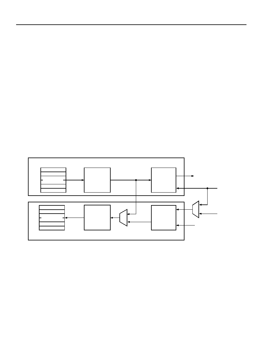
120
Agere Systems Inc.
Advance Data Sheet
May 2002
T7633 Dual T1/E1 3.3 V Short-Haul Terminator
Facility Data Link (FDL)
(continued)
Diagnostic Modes
Loopbacks
The serial link interface can operate in two diagnostic loopback modes: (1) local loopback and (2) remote loopback.
The local loopback mode is selected when register FDL_PR1 bit 1 (FLLB) is set to 1. The remote loopback is
selected when register FDL_PR1 bit 0 (FRLB) is set to 1. For normal traffic, i.e., to operate the transmitter and
receiver independently, the FLLP bit and the FRLB bits should both be cleared to 0. Local and remote loopbacks
cannot be enabled simultaneously.
In the local loopback mode:
1. TFDLCK clocks both the transmitter and the receiver.
2. The transmitter and receiver must both be enabled.
3. The transmitter output is internally connected to the receiver input.
4. The TFDL is active.
5. The RFDL input is ignored.
6. The communication between the transmit and receive FIFO buffers and the microprocessor continues normally.
5-4562(F)r.2
Figure 46. Local Loopback Mode
XMIT HDLC FDL BLOCK
XMIT HDLC
FDL XMIT
INTERFACE
XMIT FIFO
RCVR FIFO
RCVR HDLC
FDL RCVR
INTERFACE
TFDL
TFDLCK
RFDLCK
RFDL
RCVR HDLC FDL BLOCK

Agere Systems Inc.
121
Advance Data Sheet
May 2002
T7633 Dual T1/E1 3.3 V Short-Haul Terminator
Facility Data Link (FDL)
(continued)
Diagnostic Modes
(continued)
In the remote loopback mode:
1. Transmitted data is retimed with a maximum delay of 2 bits.
2. Received data is retransmitted on the TFDL.
3. The transmitter should be disabled. The receiver can be disabled or, if desired, enabled. Received data is sent
as usual to the receive FIFO if the receiver is enabled.
5-4563(F)r.1
Figure 47. Remote Loopback Mode
XMIT HDLC FDL BLOCK
XMIT HDLC
FDL XMIT
INTERFACE
XMIT FIFO
RCVR FIFO
RCVR HDLC
FDL RCVR
INTERFACE
TFDL
TFDLCK
RFDLCK
RFDL
RCVR HDLC FDL BLOCK

122
Agere Systems Inc.
Advance Data Sheet
May 2002
T7633 Dual T1/E1 3.3 V Short-Haul Terminator
Phase-Lock Loop Circuit
The T7633 allows for independent transmit path and receive path clocking. The device provides outputs to control
variable clock oscillators on both the transmit and receive paths. As such, the system may have both the transmit
and receive paths phase-locked to two autonomous clock sources.
The block diagram of the T7633 phase detector circuitry is shown in Figure 48 on page 123. The T7633 uses elas-
tic store buffers (two frames) to accommodate the transfer of data from the system interface clock rate of
2.048 Mbits/s to the line interface clock rate of either 1.544 Mbits/s or 2.048 Mbits/s.The transmit line side of the
T7633 does not have any mechanism to monitor data overruns or underruns (slips) in its elastic store buffer. This
interface relies on the requirement that the PLLCK clock signal (variable) is phase-locked to the RCHICK clock sig-
nal (reference). When this requirement is not met, uncontrolled slips may occur in the transmit elastic store buffer
that would result in corrupting data and no indication will be given. Typically, a variable clock oscillator (VCXO) is
used to drive the PLLCK signal. The T7633 provides a phase error signal (PLLCK-EPLL) that can be used to con-
trol the VCXO. The PLLCK-EPLL signal is generated by monitoring the divided-down PLLCK (DIV-PLLCK) and
RCHICK (DIV-RCHICK) signals. The DIV-RCHICK signal is used as the reference to determine the phase differ-
ence between DIV-RCHICK and DIV-PLLCK. While DIV-RCHICK and DIVPLLCK are phase-locked, the PLLCK-
EPLL signal is in a high-impedance state. A phase difference between DIV-RCHICK and DIV-PLLCK drives
PLLCK-EPLL to either 5 V or 0 V. An RC circuit (typically, R = 1 k
and C = 0.1
µ
F) is used to filter these PLLCK-
EPLL pulses to control the VCXO.
The system can force TCHICK to be phase-locked to RLCK by using RLCK as a reference signal to control a
VCXO that is sourcing the TCHICK signal. The T7633 uses the receive line signal (RLCK) as the reference and the
TCHICK signal as the variable signal. The T7633 provides a phase error signal (TCHICK-EPLL) that can be used
to control the VCXO generating TCHICK. The TCHICK-EPLL signal is generated by monitoring the divided-down
TCHICK signal (DIV-TCHICK) and RLCK (DIV-RLCK) signals. The DIV-RLCK signal is used as the reference to
determine the phase difference between DIV-TCHICK and DIV-RLCK. While DIV-RLCK and DIV-TCHICK are
phase-locked, the TCHICK-EPLL signal is in a high-impedance state. A phase difference between DIV-RLCK and
DIV-TCHICK drives TCHICK-EPLL to either 5 V or 0 V. An RC circuit (typically, R = 1 k
and C = 0.1
µ
F) is used to
filter these TCHICK-EPLL pulses to control the VCXO. In this mode, the T7633 can be programmed to act as a
master timing source and is capable of generating the system frame synchronization signal through the TCHIFS
pin by setting FRM_PR45 bit 4 to 1.
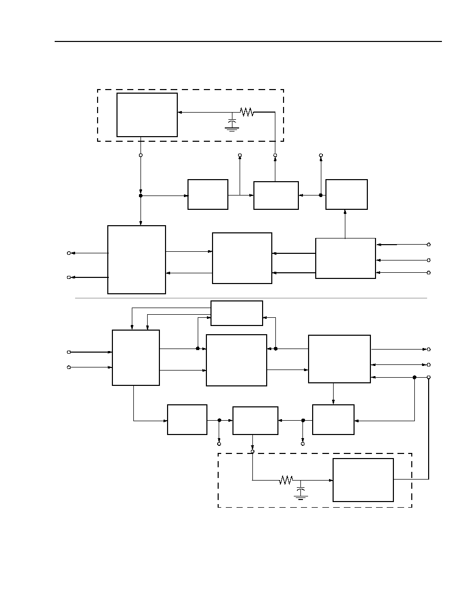
Agere Systems Inc.
123
Advance Data Sheet
May 2002
T7633 Dual T1/E1 3.3 V Short-Haul Terminator
Phase-Lock Loop Circuit
(continued)
5-5268(F)r.2
Figure 48. T7633 Phase Detector Circuitry
TPD, TND
TLCK
TRANSMIT
FRAMER
RECEIVE
CONCENTRATION
HIGHWAY
INTERFACE
RCHIDATA
RCHICK
RCHIFS
TRANSMIT
CONCENTRATION
HIGHWAY
INTERFACE
RECEIVE
2-FRAME
ELASTIC STORE
BUFFER
RECEIVE
FRAMER
RPD, RND
RLCK
READ ADDRESS
TRANSMIT
2-FRAME
ELASTIC STORE
BUFFER
PLLCK
DIVIDER
CIRCUIT
INTERNAL_XLCK
PLLCK
DIV-PLLCK
DIGITAL
PHASE
DETECTOR
RCHICK
DIVIDER
CIRCUIT
PLLCK-EPLL
DIV-RCHICK
VOLTAGE-
CONTROLLED
CRYSTAL
OSCILLATOR
(VCXO)
TCHICK
TCHIDATA
TCHIFS
SYSTEM DATA
WRITE ADDRESS
SYSTEM DATA
READ ADDRESS
FACILITY DATA
WRITE ADDRESS
FACILITY DATA
SLIP
MONITOR
BUFFER OVERRUN
BUFFER UNDERRUN
RLCK
DIVIDER
CIRCUIT
DIGITAL
PHASE
DETECTOR
TCHICK
DIVIDER
CIRCUIT
DIV-RLCK
DIV-TCHICK
TCHICK_EPLL
VOLTAGE-
CONTROLLED
CRYSTAL
OSCILLATOR
(VCXO)
INTERNAL_TCHICK
INTERNAL_RLCK
INTERNAL_RCHICK
EXTERNAL CIRCUIT
EXTERNAL CIRCUIT

124
Agere Systems Inc.
Advance Data Sheet
May 2002
T7633 Dual T1/E1 3.3 V Short-Haul Terminator
Framer-System (CHI) Interface
DS1 Modes
The DS1 framing formats require rate adaptation from the 1.544 Mbits/s line interface bit stream to the system
interface which functions at multiples of a 2.048 Mbits/s bit stream. The rate adaptation results in the need for eight
stuffed time slots on the system interface since there are only 24 DS1 (1.544 Mbits/s) payload time slots while
there are 32 system (2.048 Mbits/s) time slots. Placement of the stuffed time slots is defined by register
FRM_PR43 bit 0--bit 2.
CEPT Modes
The framer maps the line time slots into the corresponding system time slot one-to-one. Framing time slot 0, the
FAS and NFAS bytes, are placed in system time slot 0.
Receive Elastic Store
The receive interface between the framer and the system (CHI) includes a 2-frame elastic store buffer to enable
rate adaptation. The receive line elastic store buffer contains circuitry that monitors the read and write pointers for
potential data overrun and underrun (slips) conditions. Whenever this slip circuitry determines that a slip may occur
in the receive elastic store buffer, it will adjust the read pointer such that a controlled slip is performed. The con-
trolled slip is implemented by dropping or repeating a complete frame at the frame boundaries. The occurrence of
controlled slips in the receive elastic store are indicated in the status register FRM_SR3 bit 6 and bit 7.
Transmit Elastic Store
The transmit interface between the framer and the system (CHI) includes a 2-frame elastic store buffer to enable
rate adaptation. The line transmit clock applied to PLLCK (pins 7/31) must be phase-locked to RCHICK. No indica-
tion of a slip in the transmit elastic store is given.

Agere Systems Inc.
125
Advance Data Sheet
May 2002
T7633 Dual T1/E1 3.3 V Short-Haul Terminator
Concentration Highway Interface (CHI)
Each framer has a dual, high-speed, serial interface to the system known as the concentration highway interface
(CHI). This flexible bus architecture allows the user to directly interface to other Agere components which use this
interface, as well as to
Mitel
Æ
and
AMD
Æ
TDM highway interfaces, with no glue logic. Configured via the highway
control registers FRM_PR45 through FRM_PR66, this interface can be set up in a number of different configura-
tions.
The following is a list of the CHI features:
1. Agere standard interface for communication devices.
2. Two pairs of transmit and receive paths to carry data in 8-bit time slots.
3. Programmable definition of highways through offset and clock-edge options which are independent for transmit
and receive directions.
4. Programmable idle code substitution of received time slots.
5. Programmable 3-state control of each transmit time slot.
6. Independent transmit and receive framing signals to synchronize each direction of data flow.
7. An 8 kHz frame synchronization signal internally generated from the received line clock.
8. Compatible with
Mitel
and
AMD
PCM highways.
Supported is the optional configuration of the CHI which presents the signaling information along with the data in
any framing modes when the device is programmed for the associated signaling mode (ASM). This mode is dis-
cussed in the signaling section.
Data can be transmitted or received on either one of two interface ports, called CHIDATA and CHIDATAB. The
user-supplied clocks (RCHICLK and TCHICLK) control the timing on the transmit or receive paths. Individual time
slots are referenced to the frame synchronization (RCHIFS and TCHIFS) pulses. Each frame consists of 32 time
slots at a programmable data rate of 2.048 Mbits/s, 4.096 Mbits/s, or 8.192 Mbits/s requiring a clock (TCHICK and
RCHICK) of the same rate. Alternatively, a mode is supported in which the clocks (TCHICK and RCHICK) can be
twice the data rate, the CMS mode. This mode is controlled by register FRM_PR45 bit 1. The clock and data rates
of the transmit and receive highways are programmed independently.
Rate adaptation is required for all DS1 formats between the 1.544 Mbits/s line rate and 2.048 Mbits/s,
4.966 Mbits/s, or 8.182 Mbits/s CHI rate. This is achieved by means of stuffing eight idle time slots into the existing
twenty-four time slots of the T1 frame. Idle time slots can occur every fourth time slot (starting in the first, second,
third, or fourth time slot) or be grouped together at the end of the CHI frame as described in register FRM_PR43
bit 0--bit 2. The positioning of the idle time slots is the same for transmit and receive directions. Idle time slots con-
tain the programmable code of register FRM_PR23. Unused time slots can be disabled by forcing the TCHIDATA
interface to a high-impedance state for the interval of the disabled time slots.

126
Agere Systems Inc.
Advance Data Sheet
May 2002
T7633 Dual T1/E1 3.3 V Short-Haul Terminator
Concentration Highway Interface (CHI)
(continued)
CHI Parameters
The CHI parameters that define the receive and transmit paths are given in Table 57.
Table 57. Summary of the T7633's Concentration Highway Interface Parameters
Name
Description
HWYEN
Highway Enable (FRM_PR45 bit 7). A 1 in this bit enables the transmit and receive
concentration highway interfaces. This allows the framer to be fully configured before
transmission to the highway. A 0 forces the idle code as defined in register
FRM_PR22, to be transmitted to the line in all payload time slots while TCHIDATA is
forced to a high-impedance state for all CHI transmitted time slots.
CHIMM
Concentration Highway Master Mode (PRM_PR45 bit 4). The default mode
CHIMM = 0 enables an external system frame synchronization signal (TCHIFS) to
drive the transmit CHI. A 1 enables the transmit CHI to generate a system frame syn-
chronization signal from the receive line clock. The transmit CHI system frame syn-
chronization signal is generated on the TCHIFS output pin. Applications using the
receive line clock as the reference clock signal of the system are recommended to
enable this mode and use the TCHIFS signal generated by the framer. The receive
CHI path is not affected by this mode.
CHIDTS
CHI Double Time-Slot Mode (FRM_PR65 bit 1 and FRM_PR66 bit 1). CHIDTS
defines the 4.096 Mbits/s and 8.192 Mbits/s CHI modes. CHIDTS = 0 enables the 32
contiguous time-slot mode. This is the default mode. CHIDTS = 1 enables the double
time-slot mode in which the transmit CHI drives TCHIDATA for one time slot and then
3-states for the subsequent time slot, and the receive CHI latches data from RCHI-
DATA for one time slot and then ignores the following time slot and so on. CHIDTS =
1 allows two CHIs to interleave frames on a common bus.
TFE
Transmit Frame Edge (FRM_PR46 bit 3). TFE = 0 (or 1), TCHIFS is sampled on the
falling (or rising) edge of TCHICK. In CHIMM (CHI master mode), the TCHIFS pin
outputs a transmit frame strobe to provide synchronization for TCHIDATA. When
TFE = 1 (or 0), TCHIFS is centered around rising (or falling) edge of TCHICK. In this
mode, TCHIFS can be used for receive data on RCHIDATA. The timing for TCHIFS in
CHIMM = 1 mode is identical to the timing for TCHIFS in CHIMM = 0 mode.
RFE
Receive Frame Edge (FRM_PR46 bit 7). RFE = 0 (or 1), RCHIFS is sampled on the
falling (or rising) edge of RCHICK.
CDRS0--CDRS1
CHI Data Rate (FRM_PR45 bit 2 and bit 3). Two-bit control for selecting the CHI data
rate. The default state (00) enables the 2.048 Mbits/s.
CDRS Bit:
2 3
CHI Data Rate
0 0
2.048 Mbits/s
0 1
4.096 Mbits/s
1 0
8.192 Mbits/s
1 1
Reserved
CMS
Clock Select Mode (FRM_PR45 bit 1). When CMS = 0, the concentration highway
clocks (TCHICK and RCHCK) and data (RCHIDATA, RCHIDATAB, TCHIDATA, or
TCHIDATAB) have the same rate. When CMS = 1, the concentration highway clocks
are twice the rate of CHI data.
TCE
Transmitter Clock Edge (FRM_PR47 bit 6). TCE = 0 (or 1), TCHIDATA is clocked on
the falling (or rising) edge of TCHICK.
RCE
Receiver Clock Edge (FRM_PR48 bit 6). RCE = 0 (or 1), RCHIDATA is latched on
the falling (or rising) edge of RCHICK.

Agere Systems Inc.
127
Advance Data Sheet
May 2002
T7633 Dual T1/E1 3.3 V Short-Haul Terminator
Concentration Highway Interface (CHI)
(continued)
CHI Parameters
(continue)
Table 57. Summary of the T7633's Concentration Highway Interface Parameters (continued)
Name
Description
TTSE31--TTSE0
Transmit Time-Slot Enable 31--0 (FRM_PR49--FRM_PR52). These bits define
which transmit CHI time slots are enabled. A 1 enables the TCHIDATA or TCHI-
DATAB time slot. A 0 forces the CHI transmit highway time slot to be 3-stated.
RTSE31--RTSE0
Receive Time-Slot Enable 31--0 (FRM_PR53--FRM_PR56). These bits define
which receive CHI time slots are enabled. A 1 enables the RCHIDATA or RCH-
DATAB time slots. A 0 disables the time slot and transmits the programmable idle
code of register FRM_PR22 to the line interface.
THS31--THS0
Transmit Highway Select 31--0 (FRM_PR57--FRM_PR60). These bits define
which transmit CHI highway, TCHIDATA or TCHIDATAB, contains valid data for the
active time slot. A 0 enables TCHIDATA; a 1 enables the TCHIDATAB.
RHS31--RHS0
Receive Highway Select 31--0 (FRM_PR61--FRM_PR64). These bits define which
receive CHI highway, RCHIDATA or RCHIDATAB, contains valid data for the active
time slot. A 0 enables RCHIDATA; a 1 enables the RCHIDATAB.
TOFF2--TOFF0
Transmitter Bit Offset (FRM_PR46 bit 0--bit 2). These bits are used in conjunction
with the transmitter byte offset to define the beginning of the transmit frame. They
determine the offset relative to TCHIFS, for the first bit of transmit time slot 0. For CMS
= 1, the offset is twice the number of TCHICK clock periods by which transmission of
the first bit is delayed. For CMS = 0, the offset is the number of TCHICK cycles by
which the first bit is delayed.
ROFF2--ROFF0
Receiver Bit Offset (FRM_PR46 bit 4--bit 6). These bits are used in conjunction with
the receiver byte offset to define the beginning of the receiver frame. They determine
the offset relative to the RCHIFS, for the first bit of receive time slot 0. For CMS = 1,
the offset is twice the number of RCHICK clock periods by which the first bit is delayed.
For CMS = 0, the offset is the number of RCHICK cycles by which the first bit is
delayed.
TBYOFF6--TBYOFF0
Transmitter Byte Offset (FRM_PR47 bit 0--bit 5 and FRM_PR65 bit 0). These bits
determine the offset from the TCHIFS to the beginning of the next frame on the
transmit highway. Note that in the ASM mode, a frame consists of 64 contiguous bytes;
whereas in other modes, a frame contains 32 contiguous bytes. Allowable offsets:
2.048 Mbits/s
0--31 bytes.
4.096 Mbits/s
0--63 bytes.
8.192 Mbits/s
0--127 bytes.
RBYOFF6--RBYOFF0
Receiver Byte Offset (FRM_PR48 bit 0--bit 5 and FRM_PR66 bit 0). These bits
determine the offset from RCHIFS to the beginning of the receive CHI frame. Note that
in the ASM mode, a frame consists of 64 contiguous bytes; whereas in other modes,
a frame contains 32 contiguous bytes. Allowable offsets:
2.048 Mbits/s
0--31 bytes.
4.096 Mbits/s
0--63 bytes.
8.192 Mbits/s
0--127 bytes.

128
Agere Systems Inc.
Advance Data Sheet
May 2002
T7633 Dual T1/E1 3.3 V Short-Haul Terminator
Concentration Highway Interface (CHI)
(continued)
CHI Parameters
(continued)
Table 57. Summary of the T7633's Concentration Highway Interface Parameters (continued)
Name
Description
TLBIT
Transmit Least Significant Bit First (FRM_PR47 bit 7). When TLBIT = 0 (the
default mode), the most significant bit (bit 0) of each time slot is transmitted first.
When TLBIT = 1, the least significant bit (bit 7) of each time slot is transmitted first.
RLBIT
Receive Least Significant Bit First (FRM_PR48 bit 7). When RLBIT = 0 (the default
mode), the first bit of each time slot received on the received data input is received as
the most significant bit (bit 0) of each time slot. When RLBIT = 1, the first bit of each
time slot on the received data input is received as the least significant bit (bit 7) of
each time slot.
ASM
Associated Signaling Mode (FRM_PR44 bit 2). When enabled, the associate sig-
naling mode configures the CHI to carry both payload data and its associated signal-
ing information. Enabling this mode must be in conjunction with the programming of
the CHI data rate to either 4.048 Mbits/s or 8.096 Mbits/s. Each time slot consists of
16 bits where 8 bits are data and the remaining 8 bits are signaling information.
STS0--STS2
Stuffed Time Slots (FRM_PR43 bit 0--bit 2). Valid only in T1 framing formats, these
3 bits define the location of the eight stuffed CHI (unused) time slots.

Agere Systems Inc.
129
Advance Data Sheet
May 2002
T7633 Dual T1/E1 3.3 V Short-Haul Terminator
Concentration Highway Interface (CHI)
(continued)
CHI Frame Timing
CHI Timing with CHIDTS Disabled
Figure 49 illustrates the CHI frame timing when CHIDTS is disabled (registers FRM_PR65 bit 1 (TCHIDTS) and
FRM_PR66 bit 1 (RCHDTS) = 0) and the CHI is not in the associated signaling mode (FRM_PR44 bit 2 (ASM) =
0). The frames are 125
µ
s long and consist of 32 contiguous time slots.
In DS1 frame modes, the CHI frame consists of 24 payload time slots and eight stuffed (unused) time slots.
In CEPT frame modes, the CHI frame consists of 32 payload time slots.
5-5269(F).ar.2
* The position of the stuffed time is controlled by register FRM_PR43 bit 0--bit 2.
Figure 49. Nominal Concentration Highway Interface Timing (for FRM_PR43 bit 0--bit 2 = 100 (Binary))
CHIFS
125
µ
s
TCHIDATA
FRAME 1
FRAME 1
FRAME 2
RCHIDATA
FRAME 2
8.192 Mbits/s CHI:
FRAME 1
FRAME 2
RCHIDATA
4.096 Mbits/s CHI:
2.048 Mbits/s CHI:
TCHIDATA
FRAME 1
FRAME 2
HIGH IMPEDANCE
HIGH IMPEDANCE
24 VALID TIME SLOTS
HIGH IMPEDANCE
FRAME 2
TCHIDATA
FRAME 2
RCHIDATA
DS1 FORMAT
FRAME 1
FRAME 2
2.048 Mbits/s CHI:
RCHIDATA
TCHIDATA
or
CEPT FORMAT
32 VALID TIME SLOTS
24 VALID TIME SLOTS
8 STUFFED
SLOTS*
FRAME 1
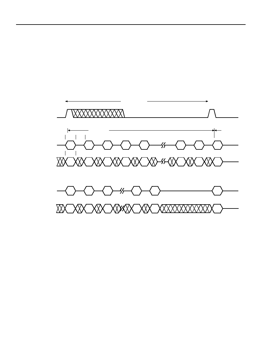
130
Agere Systems Inc.
Advance Data Sheet
May 2002
T7633 Dual T1/E1 3.3 V Short-Haul Terminator
Concentration Highway Interface (CHI)
(continued)
CHI Frame Timing
(continued)
CHI Timing with CHIDTS Enabled
Figure 50 illustrates the CHI frame timing when CHIDTS is enabled (registers FRM_PR65 bit 1 (TCHIDTS) and
FRM_PR66 bit 1 (RCHIDTS) = 1) and ASM is disabled (register FRM_PR44 bit 2 (ASM) = 0). In the CHIDTS
mode, valid CHI payload time slots are alternated with high-impedance intervals of one time-slot duration. This
mode is valid only for 4.096 Mbits/s and 8.192 Mbits/s CHI rates.
5-6454(F)r.3
Figure 50. CHIDTS Mode Concentration Highway Interface Timing
CHIFS
125
µ
s
TCHIDATA
TS0
RCHIDATA
8.192 Mbits/s CHI
RCHIDATA
4.096 Mbits/s CHI
TCHIDATA
HIGH IMPEDANCE
TS1
TS2
TS3
TS0
TS1
TS2
TS3
TS31
TS0
TS31
TS0
FRAME 1
TIME
SLOT
8 bits
TIME
SLOT
FRAME 2
TS0
TS1
TS31
TS31
TS0
TS0
TS1
TS0
TS4
TS30
TS4
T30
TS2
TS30
TS2
TS30
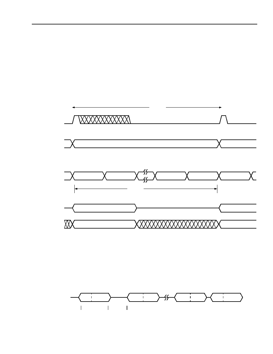
Agere Systems Inc.
131
Advance Data Sheet
May 2002
T7633 Dual T1/E1 3.3 V Short-Haul Terminator
Concentration Highway Interface (CHI)
(continued)
CHI Frame Timing
(continued)
CHI Timing with Associated Signaling Mode Enabled
Figure 51 illustrates the CHI frame timing when the associated signaling mode is enabled (register FRM_PR44 bit
2 (ASM) = 1) and the CHIDTS mode is disabled (registers FRM_PR65 bit 1 (TCHIDTS) = 0 and FRM_PR66 bit 1
(RCHDTS) = 0). The frames are 125
µ
s long and consist of 32 contiguous 16-bit time slots.
In DS1 frame formats, each frame consists of 24 time slots and eight stuffed time slots. Each time slot consists of
two octets.
In CEPT modes, each frame consists of 32 time slots. Each time slot consists of two octets.
5-5270(F).ar.3
Figure 51. Associated Signaling Mode Concentration Highway Interface Timing
CHI Timing with Associated Signaling Mode and CHIDTS Enabled
Figure 52 illustrates the CHI frame timing in the associated signaling mode (register FRM_PR44 bit 2 (ASM) = 1)
and CHIDTS enabled (registers FRM_PR65 bit 1 (TCHIDTS) = 1 and FRM_PR66 bit 1 (RCHIDTS) = 1).
5-6454(F).ar.2
* High-impedance state for TCHIDATA and not received (don't care) for RCHIDATA.
Figure 52. CHI Timing with ASM and CHIDTS Enabled
CHIFS
125
µ
s
FRAME 1
FRAME 2
8.192 Mbits/s CHI:
RCHIDATA
4.096 Mbits/s CHI:
TCHIDATA
FRAME 1
FRAME 1
FRAME 2
FRAME 2
HIGH IMPEDANCE
RCHIDATA
TCHIDATA
or
FRAME = 64 bytes: 32 DATA + 32 SIGNALING
DATA AND SIGNALING BYTES ARE INTERLEAVED
SIGNALING 0
DATA 0
SIGNALING 31
DATA 0
DATA 31
FRAME
DATA SIGNALING
TS0
TS1
TS31
TS0
16 bits
1 TIME SLOT
16 bits
1 TIME SLOT
8.192 Mbits/s CHI WITH ASM (ASSOCIATED SIGNALING MODE) ENABLED
DATA SIGNALING
TCHIDATA
OR
RCHIDATA
*
*
*
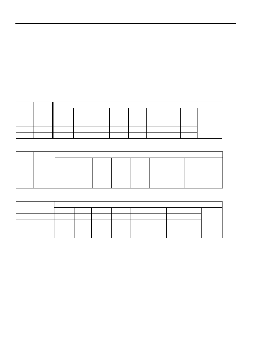
132
Agere Systems Inc.
Advance Data Sheet
May 2002
T7633 Dual T1/E1 3.3 V Short-Haul Terminator
Concentration Highway Interface (CHI)
(continued)
CHI Offset Programming
To facilitate bit offset programming, two additional internal parameters are introduced: CEX is defined as the clock
edge with which the first bit of time slot 0 is transmitted; CER is defined as the clock edge on which bit 0 of time slot
0 is latched. CEX and CER are counted relative to the edge on which the CHIFS signal is sampled. Values of CEX
and CER depend upon the values of the parameters described above.
The following three tables give decimal values of CEX and CER for various values of CMS, TFE, RFE, TCE, RCE,
TOFF[2:0], and ROFF[2:0]. The byte (time slot) offsets are assumed to be zero in the following examples.
Table 58. Programming Values for TOFF[2:0] and ROFF[2:0] when CMS = 0
Table 59. Programming Values for TOFF[2:0] when CMS = 1
Table 60. Programming Values for ROFF[2:0] when CMS = 1
RFE/
TFE
RCE/
TCE
ROFF[2:0] or TOFF[2:0]
000
001
010
011
100
101
110
111
CER
or
CEX
(decimal)
0
0
4
6
8
10
12
14
16
18
0
1
3
5
7
9
11
13
15
17
1
0
3
5
7
9
11
13
15
17
1
1
4
6
8
10
12
14
16
18
TFE
TCE
TOFF[2:0]
000
001
010
011
100
101
110
111
CEX
(decimal)
0
0
4
8
12
16
20
24
28
32
0
1
3
7
11
15
19
23
27
31
1
0
3
7
11
15
19
23
27
31
1
1
4
8
12
16
20
24
28
32
RFE
RCE
ROFF[2:0]
000
001
010
011
100
101
110
111
CER
(decimal)
0
0
6
10
14
18
22
26
30
34
0
1
5
9
13
17
21
25
29
33
1
0
5
9
13
17
21
25
29
33
1
1
6
10
14
18
22
26
30
34

Agere Systems Inc.
133
Advance Data Sheet
May 2002
T7633 Dual T1/E1 3.3 V Short-Haul Terminator
Concentration Highway Interface (CHI)
(continued)
CHI Offset Programming
(continued)
Figure 53 shows an example of the relative timing of CHI 2.048 Mbits/s data with the following parameters:
1.
CMS = 0, TFE, RFE = 0.
2.
TCE = 1, TOFF[2:0] = 000, TBYOFF[6:0] = 0000000, TLBIT = 0,
3.
RCE = 0, ROFF[2:0] = 000, RBYOFF[6:0] = 0000000, RLBIT = 0.
5-2202(F).cr.1
Figure 53. TCHIDATA and RCHIDATA to CHICK Relationship with CMS = 0 (CEX = 3 and CER = 4,
Respectively)
Figure 54 shows an example of the relative timing of CHI 2.048 Mbits/s data with the following parameters:
1.
CMS = 1, TFE,RFE = 0.
2.
TCE = 1, TOFF[2:0] = 000, TBYOFF[6:0] = 0000000, TLBIT = 0,
3.
RCE = 0, ROFF[2:0] = 000, RBYOFF[6:0] = 0000000, RLBIT = 0.
5-2203(F).cr.1
Figure 54. CHI TCHIDATA and RCHIDATA to CHICK Relationship with CMS = 1 (CEX = 3 and CER = 6,
Respectively)
CHIFS IS SAMPLED ON THIS EDGE: FE = 0
1
2
3
4
5
6
7
8
BIT 0, TS 0
BIT 1, TS 0
BIT 2, TS 0
CEX = 3
CER = 4
BIT 0, TS 0
BIT 1, TS 0
BIT 2, TS 0
HIGH IMPEDANCE
RCHIDATA: RCE = 0
TCHIDATA: TCE = 1
TCHIFS, RCHIFS
CHICK
CHIFS IS SAMPLED ON THIS EDGE: FE = 0
1
2
3
4
5
6
7
8
BIT 0, TS 0
BIT 1, TS 0
CEX = 3
CER = 6
BIT 0, TS 0
HIGH IMPEDANCE
RCHIDATA: RCE = 0
TCHIDATA: TCE = 1
TCHIFS, RCHIFS
CHICK
BIT 1, TS 0
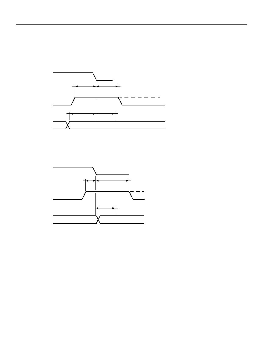
134
Agere Systems Inc.
Advance Data Sheet
May 2002
T7633 Dual T1/E1 3.3 V Short-Haul Terminator
Concentration Highway Interface (CHI)
(continued)
CHI Offset Programming
(continued)
Figure 55 and Figure 56 illustrate the CHI timing.
5-3916(F).cr.1
Note: For case illustrated, RFE = 0, and RCE = 0.
Figure 55. Receive CHI (RCHIDATA) Timing
5-3917(F).c
Note: For case illustrated, TFE = 0 and TCE = 0.
Figure 56. Transmit CHI (TCHIDATA) Timing
RCHICLK
RCHIFS
RCHIDATA
t14S
t14H
t14S: RCHIFS SETUP = 30 ns min
t15H
t14H: RCHIFS HOLD = 45 ns min
t15S: RCHIDATA SETUP = 25 ns min
t15S
t15S: RCHIDATA HOLD = 25 ns min
TCHICLK
TCHIFS
TCHIDATA
t14S
t14H
t14S: TCHIFS SETUP = 35 ns min
t19
t14H: TCHIFS HOLD = 45 ns min
t19: TCHICK TO TCHIDATA DELAY = 25 ns max
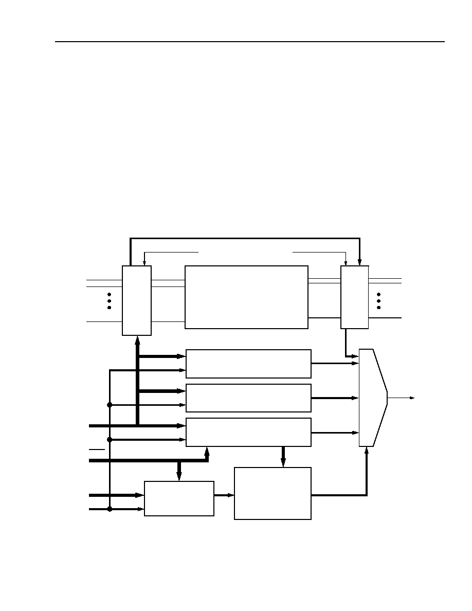
Agere Systems Inc.
135
Advance Data Sheet
May 2002
T7633 Dual T1/E1 3.3 V Short-Haul Terminator
JTAG Boundary-Scan Specification
Principle of the Boundary Scan
The boundary scan (BS) is a test aid for chip, module, and system testing. The key aspects of BS are as follows:
1. Testing the connections between ICs on a particular board.
2. Observation of signals to the IC pins during normal operating functions.
3. Controlling the built-in self-test (BIST) of an IC. T7633 does not support BS-BIST.
Designed according to the
IEEE
Æ
Std. 1149.1-1990 standard, the BS test logic consists of a defined interface: the
test access port (TAP). The TAP is made up of four signal pins assigned solely for test purposes. The fifth test pin
ensures that the test logic is initialized asynchronously. The BS test logic also comprises a 16-state TAP controller,
an instruction register with a decoder, and several test data registers (BS register, BYPASS register, and IDCODE
register). The main component is the BS register that links all the chip pins to a shift register by means of special
logic cells. The test logic is designed in such a way that it is operated independently of the application logic of the
T7633 (the mode multiplexer of the BS output cells may be shared). Figure 57 illustrates the block diagram of the
T7633's BS test logic.
5-3923(F)r.4
Figure 57. Block Diagram of the T7633's Boundary-Scan Test Logic
BOUNDARY-SCAN REGISTER
TDI
TRST
TMS
TCK
TAP
CONTROLLER
INSTRUCTION
DECODER
OUT
TDO
IN
MUX
CHIP KERNEL
(UNAFFECTED BY BOUNDARY-SCAN TEST)
IDCODE REGISTER
BYPASS REGISTER
INSTRUCTION REGISTER
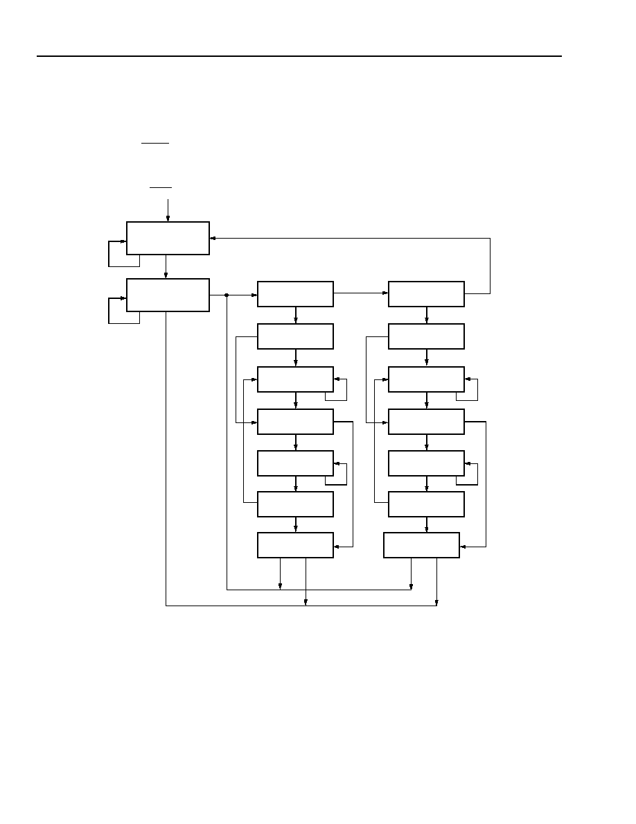
136
Agere Systems Inc.
Advance Data Sheet
May 2002
T7633 Dual T1/E1 3.3 V Short-Haul Terminator
JTAG Boundary-Scan Specification
(continued)
Test Access Port Controller
The test access port controller is a synchronous sequence controller with 16 states. The state changes are preset
by the TMS, TCK, and TRST signals and by the previous state. The state change always take place when the TCK
edge rises. Figure 58 shows the TAP controller state diagram.
5-3924(F)r.5
Figure 58. BS TAP Controller State Diagram
The value shown next to each state transition in Figure 58 represents the signal present at TMS at the time of a ris-
ing edge at TCK.
The description of the TAP controller states is given in
IEEE
Std. 1149.1-1990 Section 5.1.2 and is reproduced in
Table 61 and Table 62.
SELECT DR
CAPTURE DR
1
0
0
1
1
SHIFT DR
EXIT1 DR
PAUSE DR
0
1
EXIT2 DR
UPDATE DR
1
1
0
0
0
0
TEST LOGIC
RESET
RUN TEST/
IDLE
1
0
SELECT IR
CAPTURE IR
1
0
0
1
1
SHIFT IR
EXIT1 IR
PAUSE IR
0
1
EXIT2 IR
UPDATE IR
1
1
0
0
0
0
TRST = 0
0
1
1

Agere Systems Inc.
137
Advance Data Sheet
May 2002
T7633 Dual T1/E1 3.3 V Short-Haul Terminator
JTAG Boundary-Scan Specification
(continued)
Test Access Port Controller
(continued)
Table 61. TAP Controller States in the Data Register Branch
Table 62. TAP Controller States in the Instruction Register Branch
Name
Description
TEST LOGIC RESET
The BS logic is switched in such a way that normal operation of the ASIC is
adjusted. The IDCODE instruction is initialized by TEST LOGIC RESET.
Irrespective of the initial state, the TAP controller has achieved TEST LOGIC
RESET after five control pulses at the latest when TMS = 1. The TAP controller
then remains in this state. This state is also achieved when TRST = 0.
RUN TEST/IDLE
Using the appropriate instructions, this state can activate circuit parts or initiate
a test. All of the registers remain in their present state if other instructions are
used.
SELECT DR
This state is used for branching to the test data register control.
CAPTURE DR
The test data is loaded in the test data register parallel to the rising edge of TCK
in this state.
SHIFT DR
The test data is clocked by the test data register serially to the rising edge of TCK
in the state. The TDO output driver is active.
EXIT (1/2) DR
This temporary state causes a branch to a subsequent state.
PAUSE DR
The input and output of test data can be interrupted in this state.
UPDATE DR
The test data is clocked into the second stage of the test data register parallel to
the falling edge of TCK in this state.
Name
Description
SELECT IR
This state is used for branching to the instruction register control.
CAPTURE IR
The instruction code 0001 is loaded in the first stage of the instruction register
parallel to the rising edge of TCK in this state.
SHIFT IR
The instructions are clocked into the instruction register serially to the rising edge
of TCK in the state. The TDO output driver is active.
EXIT (1/2) IR
This temporary state causes a branch to a subsequent state.
PAUSE IR
The input and output of instructions can be interrupted in this state.
UPDATE IR
The instruction is clocked into the second stage of the instruction register parallel
to the falling edge of TCK in this state.

138
Agere Systems Inc.
Advance Data Sheet
May 2002
T7633 Dual T1/E1 3.3 V Short-Haul Terminator
JTAG Boundary-Scan Specification
(continued)
Instruction Register
The instruction register (IR) is 4 bits in length. Table 63 shows the BS instructions implemented by the T7633.
Table 63. T7633's Boundary-Scan Instructions
The instructions not supported in T7633 are INTEST, RUNBIST, TOGGLE. A fixed binary 0001 pattern (the 1 into
the least significant bit) is loaded into the IR in the capture-IR controller state. The IDCODE instruction (binary
0001) is loaded into the IR during the test-logic-reset controller state and at powerup.
The following is an explanation of the instructions supported by T7633 and their effect on the devices' pins.
EXTEST:
This instruction enables the path cells, the pins of the ICs, and the connections between ASICs to be tested via the
circuit board. The test data can be loaded in the chosen position of the BS register by means of the SAMPLE/PRE-
LOAD instruction. The EXTEST instruction selects the BS register as the test data register. The data at the function
inputs is clocked into the BS register on the rising edge of TCK in the CAPTURE-DR state. The contents of the BS
register can be clocked out via TDO in the SHIFT-DR state. The value of the function outputs is solely determined
by the contents of the data clocked into the BS register and only changes in the UPDATE-DR state on the falling
edge of TCK.
IDCODE:
Information regarding the manufacturer's ID for Agere, the IC number, and the version number can be read out
serially by means of the IDCODE instruction. The IDCODE register is selected, and the BS register is set to normal
mode in the UPDATE-IR state. The IDCODE is loaded at the rising edge of TCK in the CAPTURE-DR state. The
IDCODE register is read out via TDO in the SHIFT-DR state.
HIGHZ:
All 3-statable outputs are forced to a high-impedance state, and all bidirectional ports to an input state by means of
the HIGHZ instruction. The impedance of the outputs is set to high in the UPDATE-IR state. The function outputs
are only determined in accordance with another instruction if a different instruction becomes active in the UPDATE-
IR state. The BYPASS register is selected as the test data register. The HIGHZ instruction is implemented in a sim-
ilar manner to that used for the BYPASS instruction.
SAMPLE/PRELOAD:
The SAMPLE/PRELOAD instruction enables all the inputs and outputs pins to be sampled during operation (SAM-
PLE) and the result to be output via the shift chain. This instruction does not impair the internal logic functions.
Defined values can be serially loaded in the BS cells via TDI while the data is being output (PRELOAD).
Instruction
Code
Act. Register
TDI
TDO
Mode
Function
Output Defined Via
EXTEST
0000
Boundary Scan
TEST
Test external
connections
BS Register
IDCODE
0001
Identification
NORMAL
Read Manuf.
Register
Core Logic
HIGHZ
0100
BYPASS
X
3-state
Output -- High Impedance
SAMPLE/PRELOAD
0101
Boundary Scan
NORMAL
Sample/load
Core Logic
BYPASS
1111
BYPASS
NORMAL
Min. shift path
Core Logic
EVERYTHING ELSE
--
BYPASS
X
--
Output -- High Impedance

Agere Systems Inc.
139
Advance Data Sheet
May 2002
T7633 Dual T1/E1 3.3 V Short-Haul Terminator
JTAG Boundary-Scan Specification
(continued)
Instruction Register
(continued)
BYPASS:
This instruction selects the BYPASS register. A minimal shift path exists between TDI and TDO. The BYPASS reg-
ister is selected after the UPDATE-IR. The BS register is in normal mode. A 0 is clocked into the BYPASS register
during CAPTURE-DR state. Data can be shifted by the BYPASS register during SHIFT-DR. The contents of the BS
register do not change in the UPDATE-DR state. Please note that a 0 that was loaded during CAPTURE-DR
appears first when the data is being read out.
Boundary-Scan Register
The boundary-scan register is a shift register, whereby one or more BS cells are assigned to every digital T7633
pin (with the exception of the pins for the BS architecture, analog signals, and supply voltages). The T7633's
boundary-scan register bit-to-pin assignment is to be determined.
BYPASS Register
The BYPASS register is a one-stage, shift register that enables the shift chain to be reduced to one stage in the
T7633.
IDCODE Register
The IDCODE register identifies the T7633 by means of a parallel, loadable, 32-bit shift register. The code is loaded
on the rising edge of TCK in the CAPTURE-DR state. The 32-bit data is organized into four sections as follows.
Table 64. IDCODE Register
3-State Procedures
The 3-state input participates in the boundary scan. It has a BS cell, but buffer blocking via this input is suppressed
for the EXTEST instruction. The 3-state input is regarded as a signal input that is to participate in the connection
test during EXTEST. The buffer blocking function should not be active during EXTEST to ensure that the update
pattern at the T7633 outputs does not become corrupted.
Version
Part Number
Manufacturer ID
1
Bits 31--28
Bits 27--12
Bits 11--1
Bit 0
0001
0111 011000110011
0000 0011101
1

140
Agere Systems Inc.
Advance Data Sheet
May 2002
T7633 Dual T1/E1 3.3 V Short-Haul Terminator
Microprocessor Interface
Overview
The T7633 device is equipped with a microprocessor interface that can operate with most commercially available
microprocessors. The microprocessor interface provides access to all the internal registers through a 12-bit
address bus and an 8-bit data bus. Inputs MPMODE and MPMUX (pins 74 and 76) are used to configure this inter-
face into one of four possible modes, as shown in Table 65. The MPMUX setting selects either a multiplexed (8-bit
address/data bus, AD[7:0]) or a demultiplexed (12-bit address bus, A[11:0] and an 8-bit data bus AD[7:0]) mode of
operation. The MPMODE setting selects the associated set of control signals required to access a set of registers
within the device.
The microprocessor interface can operate at speeds up to 33 MHz in interrupt-driven or polled mode without
requiring any wait-states. For microprocessors operating at greater than 33 MHz, the RDY_DTACK output (pin
100) may be used to introduce wait-states in the read/write cycles.
In the interrupt-driven mode, one or more device alarms will assert the INTERRUPT output (pin 99) once per alarm
activation. After the microprocessor identifies the source(s) of the alarm(s) (by reading the global interrupt register)
and reads the specific alarm status registers, the INTERRUPT output will deassert. In the polled mode, however,
the microprocessor monitors the various device alarm status by periodically reading the alarm status registers
within the line interface unit, framer, and HDLC blocks without the use of INTERRUPT. In both interrupt and polled
methods of alarm servicing, the status registers within an identified block will clear on a microprocessor read cycle
only when the alarm condition within that block no longer exists; otherwise, the alarm status register bit remains
set.
The powerup default states for the line interface unit, framer, and the HDLC blocks are discussed in their respec-
tive sections. All read/write registers within these blocks must be written by the microprocessor on system start-up
to guarantee proper device functionality. Register addresses not defined in this data sheet must not be writ-
ten.
Details concerning the microprocessor interface configuration modes, pinout definitions, clock specifications,
register address map, I/O timing specifications, and the I/O timing diagrams are described in the following sections.
Microprocessor Configuration Modes
Table 65 highlights the four microprocessor modes controlled by the MPMUX and MPMODE inputs (pins 76 and
74).
*
ALE_AS may be connected to ground in this mode.
The DTACK signal is asynchronous to the MPCLK signal.
Table 65. Microprocessor Configuration Modes
Mode
MPMODE
MPMUX
Address/Data Bus
Generic Control, Data, and
Output Pin Names
Mode 1
0
0
DEMUXed*
CS
,
AS
,
DS
, R/
W
, A[11:0], AD[7:0], INT,
DTACK
Mode 2
0
1
MUXed
CS
,
AS
,
DS
, R
/W
, A[11:8], AD[7:0], INT,
DTACK
Mode 3
1
0
DEMUXed*
CS
,
ALE
,
RD
,
WR
, A[11:0], AD[7:0], INT, RDY
Mode 4
1
1
MUXed
CS
,
ALE
,
RD
,
WR
, A[11:8], AD[7:0], INT, RDY
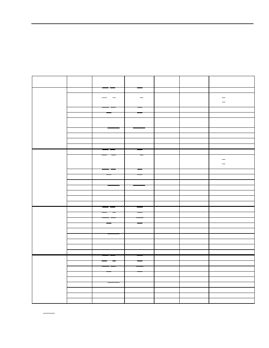
Agere Systems Inc.
141
Advance Data Sheet
May 2002
T7633 Dual T1/E1 3.3 V Short-Haul Terminator
Microprocessor Interface
(continued)
Microprocessor Interface Pinout Definitions
The Mode [1--4] specific pin definitions are given in Table 66. Note that the microprocessor interface uses the
same set of pins in all modes.
1. INTERRUPT output is synchronous to the internal clock source RLCK-LIU. If RLCK_LIU is absent, the reference clock for interrupt timing
becomes an interval 2.048 MHz clock derived from the CHI clock.
2. The DTACK output is asynchronous to MPCLK.
3. MPCLK is needed if RDY output is required to be synchronous to MPCLK.
4. In the default (reset) mode, INTERRUPT is active-high. It can be made active-low by setting register GREG4 bit 6 to 1.
Table 66. Mode [1--4] Microprocessor Pin Definitions
Configuration
Pin Number
Device Pin Name
Generic
Pin Name
Pin_Type
Assertion
Sense
Function
Mode 1
107
WR_DS
DS
Input
Active-Low
Data Strobe
75
RD_R/W
R/W
Input
--
Read/Write
R/W = 1 => Read
R/W = 0 => Write
77
ALE_AS
AS
Input
Active-Low
Address Strobe
78
CS
CS
Input
Active-Low
Chip Select
99
INTERRUPT
INTERRUPT
1
Output
Active-High/
Low
4
Interrupt
100
RDY_DTACK
DTACK
2
Output
Active-Low
Data Acknowledge
86--79
AD[7:0]
AD[7:0]
I/O
--
Data Bus
98--87
A[11:0]
A[11:0]
Input
--
Address Bus
101
MPCLK
MPCLK
Input
--
Microprocessor Clock
Mode 2
107
WR_DS
DS
Input
Active-Low
Data Strobe
75
RD_R/W
R/W
Input
--
Read/Write
R/W = 1 => Read
R/W = 0 => Write
77
ALE_AS
AS
Input
--
Address Strobe
78
CS
CS
Input
Active-Low
Chip Select
99
INTERRUPT
INTERRUPT
1
Output
Active-High/Low
Interrupt
100
RDY_DTACK
DTACK
2
Output
Active-Low
Data Acknowledge
86--79
AD[7:0]
AD[7:0]
I/O
--
Address/Data Bus
98--87
A[11:8], AD[7:0]
A[11:8], AD[7:0]
Input
--
Address/Data Bus
101
MPCLK
MPCLK
Input
--
Microprocessor Clock
Mode 3
107
WR_DS
WR
Input
Active-Low
Write
75
RD_R/W
RD
Input
Active-Low
Read
77
ALE_AS
ALE
Input
Active-Low
Address Latch Enable
78
CS
CS
Input
Active-Low
Chip Select
99
INTERRUPT
INTERRUPT
1
Output
Active-High/Low
Interrupt
100
RDY_DTACK
RDY
3
Output
Active-High
Ready
86--79
AD[7:0]
AD[7:0]
I/O
--
Data Bus
98--87
A[11:0]
A[11:0]
Input
--
Address Bus
101
MPCLK
MPCLK
Input
--
Microprocessor Clock
Mode 4
107
WR_DS
WR
Input
Active-Low
Write
75
RD_R/W
RD
Input
Active-Low
Read
77
ALE_AS
ALE
Input
--
Address Latch Enable
78
CS
CS
Input
Active-Low
Chip Select
99
INTERRUPT
INTERRUPT
1
Output
Active-High/Low
Interrupt
100
RDY_DTACK
RDY
3
Output
Active-High
Ready
86--79
AD[7:0]
AD[7:0]
I/O
--
Address/Data Bus
98--87
A[11:8], AD[7:0]
A[11:8], AD[7:0]
Input
--
Address/Data Bus
101
MPCLK
MPCLK
Input
--
Microprocessor Clock

142
Agere Systems Inc.
Advance Data Sheet
May 2002
T7633 Dual T1/E1 3.3 V Short-Haul Terminator
Microprocessor Interface
(continued)
Microprocessor Clock (MPCLK) Specifications
The microprocessor interface is designed to operate at clock speeds up to 33 MHz without requiring any wait-
states. Wait-states may be needed if higher microprocessor clock speeds are required. The microprocessor clock
(MPCLK, pin 101) specification is shown in Table 67. This clock must be supplied only if the RDY (MODE 3 and
MODE 4) is required to be synchronous to MPCLK.
Microprocessor Interface Register Address Map
The register address space is divided into eight (8) contiguous banks of 512 addressable units each. Each
addressable unit is an 8-bit register. These register banks are labeled as REGBANK[7:0]. The register address
map table gives the address range of these register banks and their associated circuit blocks. REGBANK0 con-
tains the global registers which are common to all the circuit blocks on T7633. REGBANK1 is reserved and must
not be written. REGBANK[2, 5] are attached to the LIU circuit blocks. REGBANK[3, 6] are attached to the framer
circuit blocks. REGBANK[4, 7] are attached to the FDL circuit blocks. The descriptions of the individual register
banks can be found in the appropriate sections of this document. In these descriptions, all addresses are given in
hexadecimal. Addresses out of the range specified by Table 68 must not be addressed. If they are written,
they must be written to 0. An inadvertent write to an out-of-range address may be corrected by a device
reset.
1.Core registers are common to all circuit blocks on T7633.
I/O Timing
The I/O timing specifications for the microprocessor interface are given in Table 69. The microprocessor interface
pins are compatible with CMOS/TTL I/O levels. All outputs, except the address/data bus AD[7:0], are rated for a
capacitive load of 50 pF. The AD[7:0] outputs are rated for a 100 pF load.
Table 67. Microprocessor Input Clock Specifications
Name
Symbol
Period
and
Tolerance
T
rise
Typ
T
fall
Typ
Duty Cycle
Unit
Min High
Min Low
MPCLK
t1
30 to 323
2
2
12
12
ns
Table 68. T7633 Register Address Map
Register Bank Label
Start Address
(in Hex)
End Address
(in Hex)
Circuit Block Name
REGBANK0
000
007
T7633 Global Registers
1
REGBANK1
--
--
Reserved
REGBANK2
400
406
Line Interface Unit 1 (LIU1)
REGBANK3
600,
6E0
6A6,
6FF
Framer1
REGBANK4
800
80E
Facility Data Link 1 (FDL1)
REGBANK5
A00
A06
Line Interface Unit 2 (LIU2)
REGBANK6
C00,
CE0
CA6,
CFF
Framer2
REGBANK7
E00
E0E
Facility Data Link 2 (FDL2)
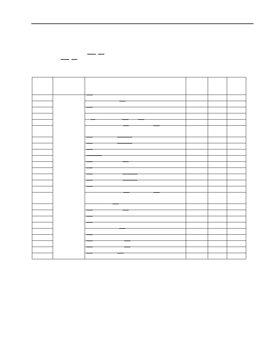
Agere Systems Inc.
143
Advance Data Sheet
May 2002
T7633 Dual T1/E1 3.3 V Short-Haul Terminator
Microprocessor Interface
(continued)
I/O Timing
(continued)
In modes 1 and 3, asserting ALE_AS signal low is used to enable the internal address bus. In modes 2 and 4, the
falling edge of ALE_AS signal is used to latch the address bus.
Table 69. Microprocessor Interface I/O Timing Specifications
Symbol Configuration
Parameter
Setup
(ns)
(Min)
Hold
(ns)
(Min)
Delay
(ns)
(Max)
t1
Modes 1 & 2
AS Asserted Width
--
10
--
t2
Address Valid to AS Deasserted
10
--
--
t3
AS Deasserted to Address Invalid
--
10
--
t4
--
--
--
--
t5
R/W Valid to Both CS and DS Asserted
4
--
--
t6
Address Valid and AS Asserted to DS Asserted
(Read)
0
--
--
t7
CS Asserted to DTACK Low Impedance
--
--
12
t8
DS Asserted to DTACK Asserted
--
--
15
t9
DS Asserted to AD Low Impedance (Read)
--
--
15
t10
DTACK Asserted to Data Valid
--
--
25
t11
DS Deasserted to CS Deasserted (Read)
--
5
--
t12
DS Deasserted to R/W Invalid
--
5
--
t13
DS Deasserted to DTACK Deasserted
--
--
12
t14
CS Deasserted to DTACK High Impedance
--
10
t15
DS Deasserted to Data Invalid (Read)
--
5
--
t16
Address Valid and AS asserted to DS Asserted
(Write)
10
--
--
t17
Data Valid to DS Asserted
10
--
--
t18
DS Deasserted to CS Deasserted (Write)
--
5
--
t19
DS Deasserted to Data Valid
--
10
--
t20
DS Asserted Width (Write)
--
10
--
t21
Address Valid to AS Falling Edge
10
--
--
t22
AS Falling Edge to Address Invalid
--
10
--
t23
AS Falling Edge to DS Asserted (Read)
0
--
--
t24
AS Falling Edge to DS Asserted (Write)
10
--
--
t25
CS Asserted to DS Asserted (Write)
10
--
--

144
Agere Systems Inc.
Advance Data Sheet
May 2002
T7633 Dual T1/E1 3.3 V Short-Haul Terminator
Microprocessor Interface
(continued)
I/O Timing
(continued)
Table 69. Microprocessor Interface I/O Timing Specifications (continued)
The read and write timing diagrams for all four microprocessor interface modes are shown in Figures 59--66.
Symbol
Configuration
Parameter
Setup
(ns)
(Min)
Hold
(ns)
(Min)
Delay
(ns)
(Max)
t31
Modes 3 & 4
ALE Asserted Width
--
10
--
t32
Address Valid to ALE Deasserted
10
--
--
t33
ALE Deasserted to Address Invalid
--
10
--
t34
CS Asserted to RD Asserted
0
--
--
t35
Address Valid and ALE Asserted to RD Asserted
0
--
--
t36
CS Asserted to RDY Low Impedance
--
--
12
t37
Rising Edge MPCK to RDY Asserted
--
--
15
t38
RD Asserted to AD Low Impedance
--
--
15
t39
RD Asserted to Data Valid
--
--
40
t40
RD Deasserted to CS Deasserted
--
5
--
t41
RD Deasserted to RDY Deasserted
--
--
15
t42
CS Deasserted to RDY High Impedance
--
--
10
t43
RD Deasserted to Data Invalid (High Impedance)
--
5
--
t44
CS Asserted to WR Asserted
0
--
--
t45
Address Valid and ALE Asserted to WR Asserted
10
--
--
t46
Data Valid to WR Asserted
10
--
--
t47
WR Deasserted to CS Deasserted
--
5
--
t48
WR Deasserted to RDY Deasserted
--
--
15
t49
WR Deasserted to Data Invalid
--
10
--
t50
RD Asserted Width
--
40
--
t51
WR Asserted Width
--
10
--
t52
Address Valid to ALE Falling Edge
10
--
--
t53
ALE Falling Edge to Address Invalid
--
10
--
t54
ALE Falling Edge to RD Asserted
0
--
--
t55
ALE Falling Edge to WR Asserted
10
--
--
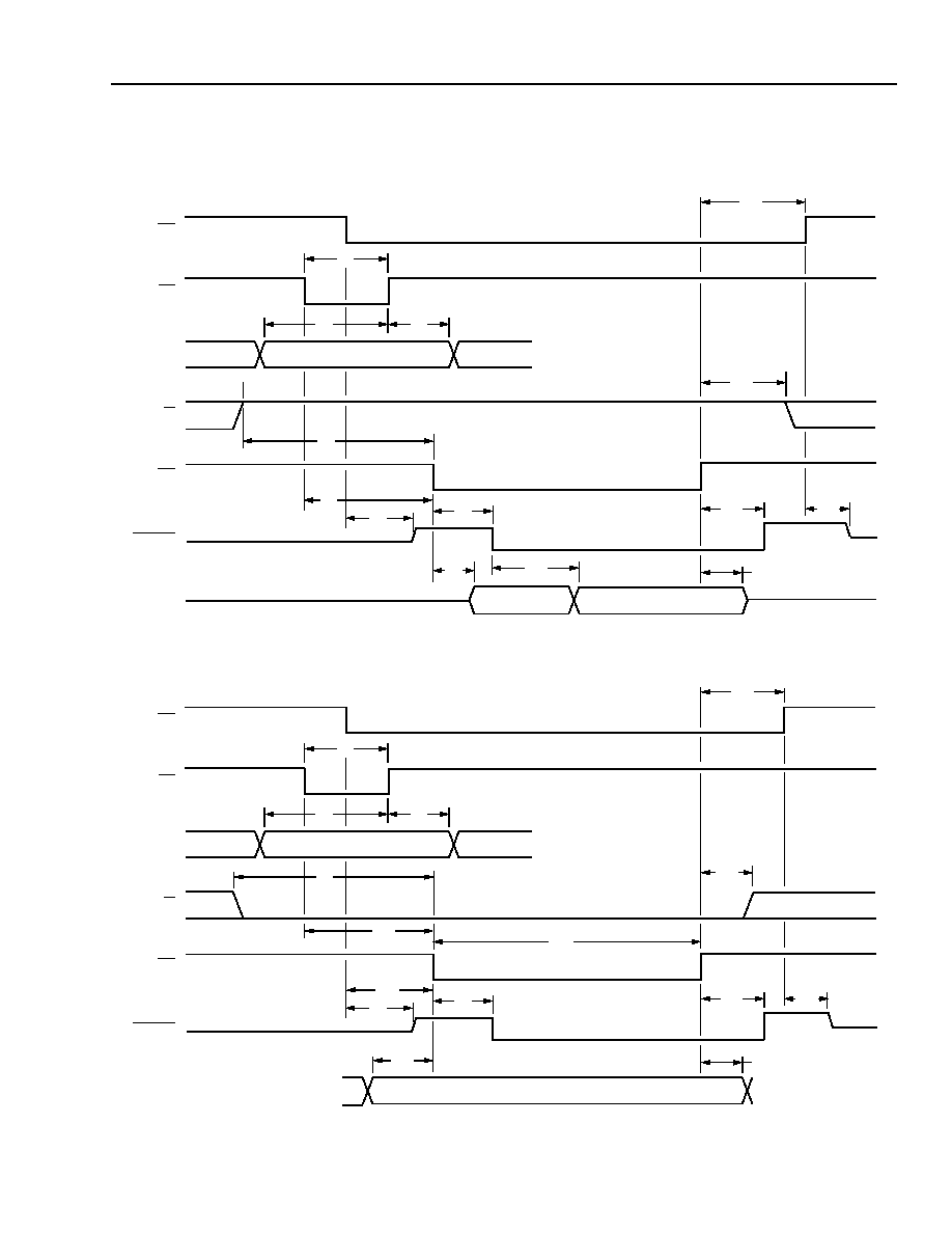
Agere Systems Inc.
145
Advance Data Sheet
May 2002
T7633 Dual T1/E1 3.3 V Short-Haul Terminator
Microprocessor Interface
(continued)
I/O Timing
(continued)
5-6422(F)r.1
Figure 59. Mode 1--Read Cycle Timing (MPMODE = 0, MPMUX = 0)
5-6423(F)
Figure 60. Mode 1--Write Cycle Timing (MPMODE = 0, MPMUX = 0)
AD[0:7]
DTACK
DS
R/W
A[0:11]
AS
CS
t1
t2
t3
VALID ADDRESS
t5
t6
t7
t8
t10
t9
VALID DATA
t13
t15
t14
t12
t11
AD[0:7]
DTACK
DS
R/W
A[0:11]
AS
CS
t1
t2
t3
VALID ADDRESS
t16
t25
t7
t8
t17
VALID DATA
t13
t19
t14
t12
t18
t5
t20
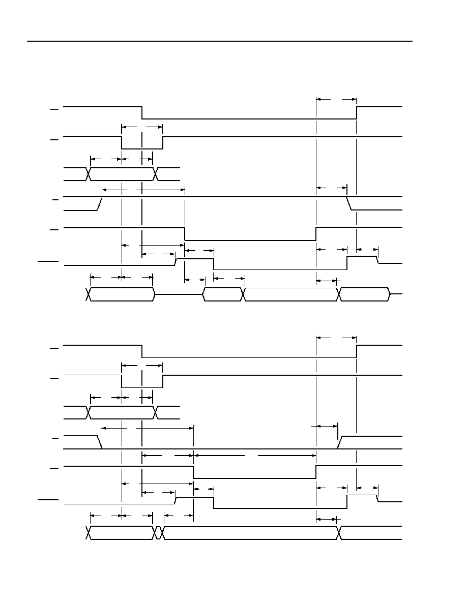
146
Agere Systems Inc.
Advance Data Sheet
May 2002
T7633 Dual T1/E1 3.3 V Short-Haul Terminator
Microprocessor Interface
(continued)
I/O Timing
(continued)
5-6424(F)
Figure 61. Mode 2--Read Cycle Timing (MPMODE = 0, MPMUX = 1)
5-6425(F)
Figure 62. Mode 2--Write Cycle Timing (MPMODE = 0, MPMUX = 1)
AD[0:7]
DTACK
DS
R/W
A[8:11]
AS
CS
t1
t21
t22
VALID ADDRESS
t5
t23
t7
t8
t10
t9
VALID DATA
t13
t15
t14
t12
t11
VALID ADDRESS
t21
t22
AD[0:7]
DTACK
DS
R/W
A[8:11]
AS
CS
t1
t21
t22
VALID ADDRESS
t5
t24
t7
t8
t17
VALID DATA
t13
t19
t14
t12
t18
VALID ADDRESS
t21
t22
t25
t20
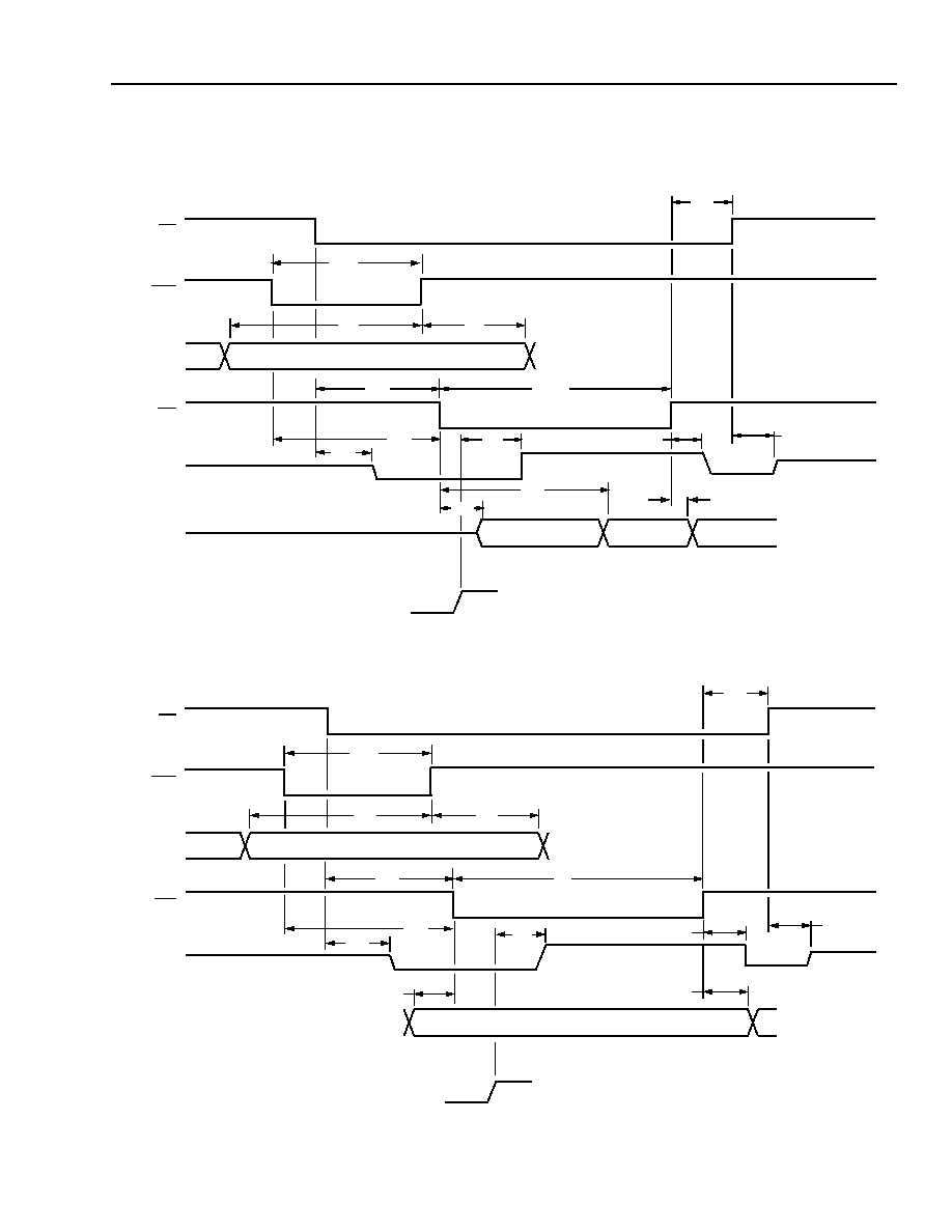
Agere Systems Inc.
147
Advance Data Sheet
May 2002
T7633 Dual T1/E1 3.3 V Short-Haul Terminator
Microprocessor Interface
(continued)
I/O Timing
(continued)
5-6426(F)r.1
Figure 63. Mode 3--Read Cycle Timing (MPMODE = 1, MPMUX = 0)
5-6427(F)
Figure 64. Mode 3--Write Cycle Timing (MPMODE = 1, MPMUX = 0)
MPCK
AD[0:7]
RDY
RD
A[0:11]
ALE
CS
t31
t32
t33
VALID ADDRESS
t34
t50
t35
VALID DATA
t42
t41
t37
t36
t40
t39
t38
t43
MPCK
AD[0:7]
RDY
WR
A[0:11]
ALE
CS
t31
t32
t33
VALID ADDRESS
t44
t51
t45
VALID DATA
t42
t37
t36
t47
t46
t48
t49
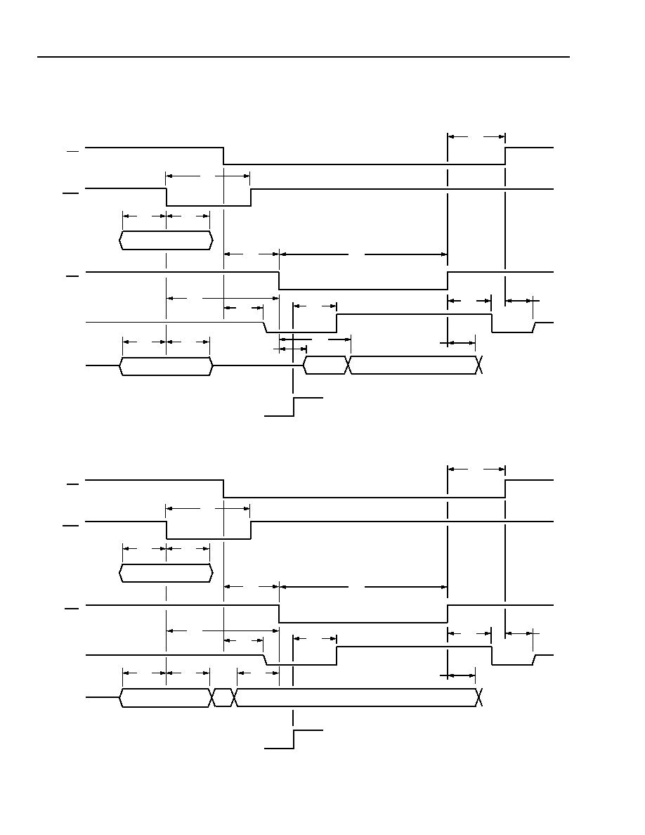
148
Agere Systems Inc.
Advance Data Sheet
May 2002
T7633 Dual T1/E1 3.3 V Short-Haul Terminator
Microprocessor Interface
(continued)
I/O Timing
(continued)
5-6428(F)r.1
Figure 65. Mode 4--Read Cycle Timing (MPMODE = 1, MPMUX = 1)
5-6429(F)r.1
Figure 66. Mode 4--Write Cycle Timing (MPMODE = 1, MPMUX = 1)
MPCK
AD
RDY
RD
A[8:11]
ALE
CS
t31
VALID ADDRESS
VALID DATA
t52
t53
t34
t54
t36
t37
t39
t38
VALID ADDRESS
t52
t53
t43
t41
t42
t40
t50
MPCK
AD
RDY
WR
A[8:11]
ALE
CS
t31
VALID ADDRESS
VALID DATA
t52
t53
t44
t55
t36
t37
VALID ADDRESS
t52
t53
t49
t48
t42
t47
t51
t46

Agere Systems Inc.
149
Advance Data Sheet
May 2002
T7633 Dual T1/E1 3.3 V Short-Haul Terminator
Reset
Both hardware and software resets are provided.
Hardware Reset (Pin 43/139)
Hardware reset is enabled by asserting RESET to 0. Each channel has independent resets, RESET1 (pin 139) for
channel 1 and RESET2 (pin 43) for channel 2. The device is in an inactive condition when RESET is 0, and
becomes active when RESET is returned to 1. Upon completion of a reset cycle, the LIU register default values are
controlled by the setting of DS1/CEPT (pin 40/142), as given in Table 6, Transmit Line Interface Short-Haul Equal-
izer/Rate Control on page 34. If DS1/CEPT is 1, the defaults are set for DS1 with line equalization for a 1 ft. to
131 ft. span. If DS1/CEPT is 0, the defaults are set for CEPT with a line equalization for 120
twisted pair or
75
coax option 1.
Hardware reset of a single channel returns all LIU, framer, and FDL registers of that channel to their default values,
as listed in the individual register descriptions and register maps, Table 200--Table 206. Reset of a single channel
does not reset the global registers. Hardware reset of both channels simultaneously, both pin 43 and pin 139 set to
0, results in a complete device reset including a reset of the global registers.
Software Reset/Software Restart
Independent software reset for each functional block of the device is available. The LIU may be placed in restart
through register LIU_REG2 bit 5 (RESTART). The framer may be reset through register FRM_PR26 bit 0 (SWRE-
SET), or placed in restart through FRM_PR26 bit 1 (SWRESTART). The FDL receiver may be reset through regis-
ter FDL_PR26 bit 1 (FRR), and the FDL transmitter may be reset through FDL_PR1 bit 5 (FTR). The reset
functions, framer SWRESET (framer software reset), FDL FRR (FDL receiver reset), and FTR (FDL transmitter
reset), reset the block and return all parameter/control registers for the block to their default values. The restart
functions, LIU RESTART and framer SWRESTART (framer software restart), reset the block but do not alter the
value of the parameter/control registers.
Interrupt Generation
An interrupt may be generated by any of the conditions reported in the status registers. For a bit (condition) in a
status register to create an interrupt, the corresponding interrupt enable bit must be set and the interrupt block
enable in the global register for the source block must be set, see Table 70 below. Once the source interrupt regis-
ter is read, the interrupt for that condition is deasserted.
Table 70. Status Register and Corresponding Interrupt Enable Register for Functional Blocks
Default for interrupt assertion is a logical 1 (high) value. But the assertion value and deasserted state is program-
mable through register GREG4 bit 4 and bit 6 and may take on the following state, see Table 71 below.
Table 71. Asserted Value and Deasserted State for GREG4 Bit 4 and Bit 6 Logic Combinations
Functional Block
Status Register
Interrupt Enable Register
Primary Block
GREG0
GREG1
Line Interface
LIU_REG0
LIU_REG1
Framer
FRM_SR0--FRM_SR7
FRM_PR0--FRM_PR7
Facility Data Link
FDL_SR0
FDL_PR2
Greg4
INTERRUPT (Pin 99)
Functionality
Bit 4
Bit 6
Asserted Value
Deasserted Value
0
0
High
Low
--
1
0
High
3-state
Wired OR
0
1
Low
High
--
1
1
Low
3-state
Wired AND

150
Agere Systems Inc.
Advance Data Sheet
May 2002
T7633 Dual T1/E1 3.3 V Short-Haul Terminator
Register Architecture
Table 72 is an overview of the register architecture. The table is a summary of the register function and address.
Complete detail of each register is given in the following sections.
Table 72. Register Summary
Register
Function
Register Address (hex)
Channel 1
Channel 2
Global Registers
GREG0
Primary Block Interrupt Status
000
GREG1
Primary Block Interrupt Enable
001
GREG2
Global Loopback Control
002
GREG3
Global Loopback Control
003
GREG4
Global Control
004
GREG5
Device ID and Version
005
GREG6
Device ID and Version
006
GREG7
Device ID and Version
007
LIU Registers
LIU_REG0
LIU Alarm Status
400
A00
LIU_REG1
LIU Alarm Interrupt Enable
401
A01
LIU_REG2
LIU Control
402
A02
LIU_REG3
LIU Control
403
A03
LIU_REG4
LIU Control
404
A04
LIU_REG5
LIU Configuration
405
A05
LIU_REG6
LIU Configuration
406
A06
Framer Registers
Status Registers
FRM_SR0
Interrupt Status
600
C00
FRM_SR1
Facility Alarm Condition
601
C01
FRM_SR2
Remote End Alarm
602
C02
FRM_SR3
Facility Errored Event
603
C03
FRM_SR4
Facility Event
604
C04
FRM_SR5
Exchange Termination and Exchange Termination Remote End
Interface Status
605
C05
FRM_SR6
Network Termination and Network Termination Remote End
Interface Status
606
C06
FRM_SR7
Facility Event
607
C07
FRM_SR8,
FRM_SR9
Bipolar Violation Counter
608, 609
C08, C09
FRM_SR10,
FRM_SR11
Framing Bit Error Counter
60A, 60B
C0A, C0B
FRM_SR12,
FRM_SR13
CRC Error Counter
60C, 60D
C0C, C0D
FRM_SR14,
FRM_SR15
E-bit Counter
60E, 60F
C0E, C0F

Agere Systems Inc.
151
Advance Data Sheet
May 2002
T7633 Dual T1/E1 3.3 V Short-Haul Terminator
Register Architecture
(continued)
Table 72. Register Summary (continued)
Register
Function
Register Address (hex)
Channel 1
Channel 2
FRM_SR16,
FRM_SR17
CRC-4 Error at NT1 from NT2 Counter
610, 611
C10, C11
FRM_SR18,
FRM_SR19
E-bit at NT1 from NT2 Counter
612, 613
C12, C13
FRM_SR20,
FRM_SR21
ET Errored Seconds Counter
614, 615
C14, C15
FRM_SR22,
FRM_SR23
ET Bursty Errored Seconds Counter
616, 617
C16, C17
FRM_SR24,
FRM_SR25
ET Severely Errored Seconds Counter
618, 619
C18, C19
FRM_SR26,
FRM_SR27
ET Unavailable Seconds Counter
61A, 61B
C1A, C1B
FRM_SR28,
FRM_SR29
ET-RE Errored Seconds Counter
61C, 61D
C1C, C1D
FRM_SR30,
FRM_SR31
ET-RE Bursty Errored Seconds Counter
61E, 61F
C1E, C1F
FRM_SR32,
FRM_SR33
ET-RE Severely Errored Seconds Counter
620, 621
C20, C21
FRM_SR34,
FRM_SR35
ET-RE Unavailable Seconds Counter
622, 623
C22, C23
FRM_SR36,
FRM_SR37
NT1 Errored Seconds Counter
624, 625
C24, C25
FRM_SR38,
FRM_SR39
NT1 Bursty Errored Seconds Counter
626, 627
C26, C27
FRM_SR40,
FRM_SR41
NT1 Severely Errored Seconds Counter
628, 629
C28, C29
FRM_SR42,
FRM_SR43
NT1 Unavailable Seconds Counter
62A, 62B
C2A, C2B
FRM_SR44,
FRM_SR45
NT1-RE Errored Seconds Counter
62C, 62D
C2C, C2D
FRM_SR46,
FRM_SR47
NT1-RE Bursty Errored Seconds Counter
62E, 62F
C2E, C2F
FRM_SR48,
FRM_SR49
NT1-RE Severely Errored Seconds Counter
630, 631
C30, C31
FRM_SR50,
FRM_SR51
NT1-RE Unavailable Seconds Counter
632, 633
C32, C33
FRM_SR52
Receive NOT-FAS TS0
634
C34
FRM_SR53
Received Sa
635
C35
FRM_SR54--
FRM_SR63
SLC
-96 FDL/CEPT Sa Receive Stack
636--63F
C36--C3F

152
Agere Systems Inc.
Advance Data Sheet
May 2002
T7633 Dual T1/E1 3.3 V Short-Haul Terminator
Register Architecture
(continued)
Table 72. Register Summary (continued)
Register
Function
Register Address (hex)
Channel 1
Channel 2
Received Signaling Registers
FRM_RSR0--
FRM_RSR31
Received Signaling
640--65F
C40--C5F
Parameter/Control Registers
FRM_PR0--
FRM_PR7
Interrupt Group Enable
660--667
C60--C67
FRM_PR8
Framer Mode Option
668
C68
FRM_PR9
Framer CRC Control Option
669
C69
FRM_PR10
Alarm Filter
66A
C6A
FRM_PR11
Errored Second Threshold
66B
C6B
FRM_PR12,
FRM_PR13
Severely Errored Second Threshold
66C. 66D
C6C, C6D
FRM_PR14
Errored Event Enable
66E
C6E
FRM_PR15
ET Remote End Errored Event Enable
66F
C6F
FRM_PR16
NT1 Errored Event Enable
670
C70
FRM_PR17,
FRM_PR18
NT1 Remote End Errored Event Enable
671, 672
C71, C72
FRM_PR19
Automatic AIS to the System and Automatic Loopback Enable
673
C73
FRM_PR20
Transmit to the Line Command
674
C74
FRM_PR21
Framer FDL Loopback Transmission Codes Command
675
C75
FRM_PR22
Framer Transmit Line Idle Code
676
C76
FRM_PR23
Framer Transmit System Idle Code
677
C77
FRM_PR24
Primary Loopback Control
678
C78
FRM_PR25
Secondary Loopback Control
679
C79
FRM_PR26
System Frame Sync Mask Source
67A
C7A
FRM_PR27
Transmission of Remote Frame Alarm and CEPT Automatic
Transmission of A bit = 1 Control
67B
C7B
FRM_PR28
CEPT Automatic Transmission of E bit = 0
67C
C7C
FRM_PR29
Sa4--Sa8 Source
67D
C7D
FRM_PR30
Sa4--Sa8 Control
67E
C7E
FRM_PR31--
FRM_PR40
Sa Transmit Stack/
SLC
-96 Transmit Stack
67F--688
C7F--C88
FRM_PR41
Si-bit Source
689
C89
FRM_PR42
Frame Exercise
68A
C8A
FRM_PR43
System Interface Control
68B
C8B
FRM_PR44
Signaling Mode
68C
C8C
FRM_PR45
CHI Common Control
68D
C8D
FRM_PR46
CHI Common Control
68E
C8E
FRM_PR47
CHI Transmit Control
68F
C8F
FRM_PR48
CHI Receive Control
690
C90

Agere Systems Inc.
153
Advance Data Sheet
May 2002
T7633 Dual T1/E1 3.3 V Short-Haul Terminator
Register Architecture
(continued)
Table 72. Register Summary (continued)
Register
Function
Register Address (hex)
Channel 1
Channel 2
FRM_PR49--
FRM_PR52
Transmit CHI Time-Slot Enable
691--694
C91--C94
FRM_PR53--
FRM_PR56
Receive CHI Time-Slot Enable
695--698
C95--C98
FRM_PR57--
FRM_PR60
CHI Transmit Highway Select
699--69C
C99--C9C
FRM_PR61--
FRM_PR64
CHI Receive Highway Select
69D--6A0
C9D--CA0
FRM_PR65
CHI Transmit Control
6A1
CA1
FRM_PR66
CHI Receive Control
6A2
CA2
FRM_PR69
Auxiliary Pattern Generator Control
6A5
CA5
FRM_PR70
Auxiliary Pattern Detector Control
6A6
CA6
Transmit Signaling Registers
FRM_TSR0--
FRM_TSR31
Transmit Signaling
6E0--6F7
CE0--CF7
Facility Data Link Registers
FDL Parameter/Control Registers
FDL_PR0
FDL Configuration Control
800
E00
FDL_PR1
FDL Control
801
E01
FDL_PR2
FDL Interrupt Mask Control
802
E02
FDL_PR3
FDL Transmitter Configuration Control
803
E03
FDL_PR4
FDL Transmitter FIFO
804
E04
FDL_PR5
FDL Transmitter Mask
805
E05
FDL_PR6
FDL Receive Interrupt Level Control
806
E06
FDL_PR7
Not Assigned
--
--
FDL_PR8
FDL Receive Match Character
808
E08
FDL_PR9
FDL Transparent Control
809
E09
FDL_PR10
FDL Transmit
ANSI
ESF Bit Codes
80A
E0A
FDL Status Registers
FDL_SR0
FDL Interrupt Status
80B
E0B
FDL_SR1
FDL Transmitter Status
80C
E0C
FDL_SR2
FDL Receiver Status
80D
E0D
FDL_SR3
FDL
ANSI
Bit Codes Status
80E
E0E
FDL_SR4
FDL Receive FIFO
807
E07

154
Agere Systems Inc.
Advance Data Sheet
May 2002
T7633 Dual T1/E1 3.3 V Short-Haul Terminator
Global Register Architecture
REGBANK0 contains the status and programmable control registers for all global functions. The address of these
registers is 000 (hex) to 008 (hex). These registers control both channels of the terminator.
The register bank architecture is shown in Table 73. The register bank consists of 8-bit registers classified as pri-
mary block interrupt status register, primary block interrupt enable register, global loopback control register, global
terminal control register, device identification register, and global internal interface control register.
GREG0 is a clear on read (COR) register. This register is cleared by the framer internal received line clock
(LIU_RLCK of Figure 18, Block Diagram of Framer Line Interface on page 50). At least two RFRMCK cycles
(1.3 µs for DS1 and 1.0 µs for CEPT) must be allowed between successive reads of the same COR register to
allow it to properly clear.
The default values are shown in parentheses.
Table 73. Global Register Set (0x000--0x008)
The following section describes the global registers in Table 74--Table 79.
Global Register
[Address (hex)]
Bit 7
Bit 6
Bit 5
Bit 4
Bit 3
Bit 2
Bit 1
Bit 0
GREG0[000]
Reserved
(0)
FDL2INT
(0)
FRMR2INT
(0)
LIU2INT
(0)
Reserved
(0)
FDL1INT
(0)
FRMR1INT
(0)
LIU1INT
(0)
GREG1[001]
Reserved
(0)
FDL2IE
(0)
FRMR2IE
(0)
LIU2IE
(0)
Reserved
(0)
FDL1IE
(0)
FRMR1IE
(0)
LIU1IE
(0)
GREG2[002]
TID2-RSD1
(0)
TSD2-RSD1
(0)
TID1-RSD1
(0)
TSD1-RSD1
(0)
TSD2-RID1
(0)
TID2-RID1
(0)
TSD1-RID1
(0)
TID1-RID1
(0)
GREG3[003]
TID1-RSD2
(0)
TSD1-RSD2
(0)
TID2-RSD2
(0)
TSD2-RSD2
(0)
TSD1-RID2
(0)
TID1-RID2
(0)
TSD2-RID2
(0)
TID2-RID2
(0)
GREG4[004]
Reserved
(0)
ALIE
(0)
SECCTRL
(0)
ITC
(0)
T1-R2
(0)
T2-R1
(0)
Reserved
(0)
Reserved
(0)
GREG5[005]
0
1
1
1
0
1
1
0
GREG6[006]
0
0
1
1
0
0
1
1
GREG7[007]
0
0
0
0
0
0
0
1

Agere Systems Inc.
155
Advance Data Sheet
May 2002
T7633 Dual T1/E1 3.3 V Short-Haul Terminator
Global Register Structure
Primary Block Interrupt Status Register (GREG0)
A bit set to 1 indicates the block has recently generated an interrupt. This register is cleared on read.
Table 74. Primary Block Interrupt Status Register (GREG0) (000)
Primary Block Interrupt Enable Register (GREG1)
This register enables the individual blocks to assert the interrupt pin.
Table 75. Primary Block Interrupt Enable Register (GREG1) (001)
Bit
Symbol
Description
0
LIU1INT
Line Interface Unit 1 Interrupt. A 1 indicates LIU1 generated an interrupt.
1
FRMR1INT
Framer 1 Interrupt. A 1 indicates framer 1 generated an interrupt.
2
FDL1INT
Facility Data Link 1 Interrupt. A 1 indicates FDL1 generated an interrupt.
3
--
Reserved.
4
LIU2INT
Line Interface Unit 2 Interrupt. A 1 indicates LIU2 generated an interrupt.
5
FRMR2INT
Framer 2 Interrupt. A 1 indicates framer 2 generated an interrupt.
6
FDL2INT
Facility Data Link 2 Interrupt. A 1 indicates FDL2 generated an interrupt.
7
--
Reserved.
Bit
Symbol
Description
0
LIU1IE
Line Interface 1 Interrupt Enable. A 1 enables LIU1 interrupts.
1
FRMR1IE
Framer 1 Interrupt Enable. A 1 enables framer 1 interrupts.
2
FDL1IE
Facility Data Link 1 Interrupt Enable. A 1 enables FDL1 interrupts.
3
--
Reserved. Write to 0.
4
LIU2IE
Line Interface 2 Interrupt Enable. A 1 enables LIU2 interrupts.
5
FRMR2IE
Framer 2 Interrupt Enable. A 1 enables framer 2 interrupts.
6
FDL2IE
Facility Data Link 2 Interrupt Enable. A 1 enables FDL2 interrupts.
7
--
Reserved. Write to 0.

156
Agere Systems Inc.
Advance Data Sheet
May 2002
T7633 Dual T1/E1 3.3 V Short-Haul Terminator
Global Register Structure
(continued)
Global Loopback Control Register (GREG2)
This register enables the framer inputs RCHIDATA1 and RCHIDATAB1 to be driven by various internal sources. A
1 enables the specified loopback. The default of the register 00 (hex) disables all loopbacks and enables external
sources to drive these inputs.
Table 76. Global Loopback Control Register (GREG2) (002)
Global Loopback Control Register (GREG3)
This register enables the framer inputs RCHIDATA2and RCHIDATAB2 to be driven by various internal sources. A 1
enables the specified loopback. The default of the register 00 (hex) disables all loopbacks and enables external
sources to drive these inputs.
Table 77. Global Loopback Control Register (GREG3) (003)
Bit
Symbol
Description
0
TID1--RID1
TCHIDATA1 to RCHIDATA1 Connection.
1
TSD1--RID1
TCHIDATAB1 to RCHIDATA1 Connection.
2
TID2--RID1
TCHIDATA2 to RCHIDATA1 Connection.
3
TSD2--RID1
TCHIDATAB2 to RCHIDATA1 Connection.
4
TSD1--RSD1 TCHIDATAB1 to RCHIDATAB1 Connection.
5
TID1--RSD1
TCHIDATA1 to RCHIDATAB1 Connection.
6
TSD2--RSD1 TCHIDATAB2 to RCHIDATAB1 Connection.
7
TID2--RSD1
TCHIDATA2 to RCHIDATAB1 Connection.
Bit
Symbol
Description
0
TID2--RID2
TCHIDATA2 to RCHIDATA2 Connection.
1
TSD2--RID2
TCHIDATAB2 to RCHIDATA2 Connection.
2
TID1--RID2
TCHIDATA1 to RCHIDATA2 Connection.
3
TSD1--RID2
TCHIDATAB1 to RCHIDATA2 Connection.
4
TSD2--RSD2 TCHIDATAB2 to RCHIDATAB2 Connection.
5
TID2--RSD2
TCHIDATA2 to RCHIDATAB2 Connection.
6
TSD1--RSD2 TCHIDATAB1 to RCHIDATAB2 Connection.
7
TID1--RSD2
TCHIDATA1 to RCHIDATAB2 Connection.

Agere Systems Inc.
157
Advance Data Sheet
May 2002
T7633 Dual T1/E1 3.3 V Short-Haul Terminator
Global Register Structure
(continued)
Global Control Register (GREG4)
This register enables LIU1 to LIU2 loopbacks (bit 2 and bit 3), interrupt 3-state control (bit 4), source of the output
second pulse (bit 5), and interrupt polarity (bit 6).
Table 78. Global Control Register (GREG4) (004)
Device ID and Version Registers (GREG5--GREG7)
These bits define the device and version number.
Table 79. Device ID and Version Registers (GREG5--GREG7) (005--007)
Bit
Symbol
Description
0
--
Reserved. Write to zero.
1
--
Reserved. Write to zero.
2
T2-R1
TLCK2, TPD2, and TND2 to RLCK1, RPD1, and RND1 Connection. A 1 makes the indi-
cated loopback.
3
T1-R2
TLCK1, TPD1, and TND1 to RLCK2, RPD2, and RND2 Connection. A 1 makes the indi-
cated loopback.
4
ITC
INTERRUPT 3-State Control. This bit along with bit 6 in this register (ALIE) allows the
interrupt pin to be programmed for active-high, active-low, wire OR, or wire AND opera-
tion, as described below:
Bits
Description
4 6
0 0
Programs the interrupt pin to be active-high (1 state) when there is an interrupt
condition and to be inactive (0 state) when there is no interrupt condition.
0 1
Programs the interrupt pin to be active-low (0 state) when there is an interrupt
condition and to be inactive (1 state) when there is no interrupt condition.
1 0
Programs the interrupt pin to be active-high (1 state) when there is an interrupt
condition and to be in the high-impedance state (3-state) when there is no inter-
rupt condition. This allows the interrupt to be wire OR'd with other interrupt pins
on the system board. A pull-down resister is needed on the system board.
1 1
Programs the interrupt pin to be active-low (0 state) when there is an interrupt
condition and to be in the high-impedance state (3-state) when there is no inter-
rupt condition. This allows the interrupt to be wire AND'd with other interrupt
pins on the system board. A pull-up resister is needed on the system board.
5
SECCTRL
SECOND Pulse Source Control. A 0 enables framer 1 to source the output second pulse
(SECOND). A 1 enables framer 2 to source the output second pulse.
6
ALIE
Active-Low Interrupt Enable. A 1 enables active-low interrupt.
7
--
Reserved. Write to zero.
Register
Bit 7
Bit 6
Bit 5
Bit 4
Bit 3
Bit 2
Bit 1
Bit 0
Device Code
GREG5
0
1
1
1
0
1
1
0
Device Code
GREG6
0
0
1
1
0
0
1
1
Version #
GREG7
0
0
0
0
0
0
0
1
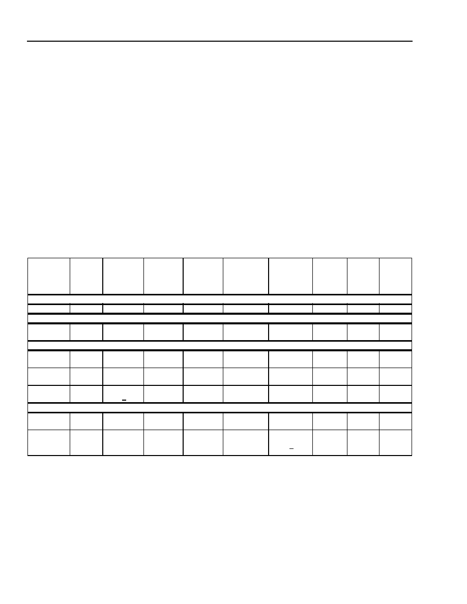
158
Agere Systems Inc.
Advance Data Sheet
May 2002
T7633 Dual T1/E1 3.3 V Short-Haul Terminator
Line Interface Unit (LIU) Register Architecture
REGBANK2 and REGBANK5 contain the status and programmable registers for the line interface unit channels
LIU1 and LIU2 respectively. The base address for REGBANK2 is 400(hex) and for REGBANK5 is A00(hex). Within
these register banks the bit map is identical for both LIU1 and LIU2.
The register bank architecture for LIU1 and LIU2 is shown in Table 80. The register bank consists of 8-bit registers
classified as alarm status register, alarm mask register, status register, status interrupt mask register, control regis-
ters, and configuration registers.
Register LIU_REG0 is the alarm status register used for storing the various LIU alarms and status. It is a read-only,
clear-on-read (COR) register. This register is cleared on the rising edge of MPCLK, if present, or on the rising edge
of the internally generated 2.048 MHz clock derived from the CHI clock if MPCLK is not present. Register
LIU_REG1 contains the individual interrupt enable bits for the alarms in LIU_REG0.
Register LIU_REG2, LIU_REG3, and LIU_REG4 are designated as control registers while LIU_REG5 and
LIU_REG6 are configuration registers. These are used to set up the individual LIU channel functions and parame-
ters.
The default values are shown in parentheses.
The following sections describe the LIU registers in more detail.
1. The logic value in parentheses below each bit definition is the default state upon completion of hardware reset.
2. These bits must be written to 1.
Table 80. Line Interface Units Register Set
1
((400--40F); (A00--A0F))
LIU
Register
LIU
Register
[Address
(HEX)]
Bit 7
Bit 6
Bit 5
Bit 4
Bit 3
Bit 2
Bit 1
Bit 0
Alarm Register (Read Only) (Latches Alarm, Clear On Read)
LIU_REG0
400; A00
0
0
0
0
LOTC
TDM
DLOS
ALOS
Alarm Interrupt Enable Register (Read/Write)
LIU_REG1
401; A01
Reserved
(0)
Reserved
(0)
Reserved
(0)
Reserved
(0)
LOTCIE
(0)
TDMIE
(0)
DLOSIE
(0)
ALOSIE
(0)
Control Registers (Read/Write)
LIU_REG2
402; A02
Reserved
(0)
Reserved
(0)
RESTART
(0)
HIGHZ
(0)
Reserved
(0)
LOSST
(0)
Reserved
(0)
Reserved
(0)
LIU_REG3
403; A03
Reserved
2
(1)
Reserved
2
(1)
Reserved
2
(1)
LOSSD
(0)
DUAL
(0)
CODE
(1)
JAT
(0)
JAR
(0)
LIU_REG4
404; A04
Reserved
0
Reserved
(0)
JABW0
(0)
PHIZALM
(0)
PRLALM
(0)
PFLALM
(0)
RCVAIS
(0)
ALTIMER
(0)
Configuration Registers (Read/Write)
LIU_REG5
405; A05
Reserved
(0)
Reserved
(0)
Reserved
(0)
Reserved
(0)
LOOPA
(0)
LOOPB
(0)
XLAIS
(1)
PWRDN
(0)
LIU_REG6
406; A06
Reserved
(0)
Reserved
(0)
Reserved
(0)
Reserved
(0)
Reserved
0
EQ2
(0,DS1)
(1,CEPT)
EQ1
(0,DS1)
(1,CEPT)
EQ0
(0)

Agere Systems Inc.
159
Advance Data Sheet
May 2002
T7633 Dual T1/E1 3.3 V Short-Haul Terminator
Line Interface Alarm Register
Alarm Status Register (LIU_REG0)
Bits 0--3 of this register represent the status of the line interface receiver and transmitter alarms ALOS, DLOS,
TDM, and LOTC. The alarm indicators are active-high and automatically clear on a microprocessor read if the cor-
responding alarm conditions no longer exist. However, persistent alarm conditions will cause these bits to remain
set even after a microprocessor read. This is a read-only register.
Table 81. LIU Alarm Status Register (LIU_REG0) (400, A00)
Line Interface Alarm Interrupt Enable Register
Alarm Interrupt Enable Register (LIU_REG1)
The bits in the alarm interrupt enable register allow the user to selectively enable generation of an interrupt by
each channel alarm. The enable bits correspond to their associated alarm status bits in the alarm status register,
LIU-REG0. The interrupt enable function is active-high. When an enable bit is set, the corresponding alarm is
enabled to generate an interrupt. Otherwise, the alarm is disabled from generating an interrupt.
The enable function only impacts the ability to generate an interrupt signal. The proper alarm status will be
reflected in LIU_REG0 even when the corresponding enable bit is set to zero. Any other LIU behavior associated
with an alarm event will operate normally even if the interrupt is not enabled.
This is a read/write register.
Bit
Symbol
Description
0
ALOS
Receive Analog Loss of Signal. A 1 indicates the LIU receive channel has detected
an analog loss of signal condition/event.
1
DLOS
Receive Digital Loss of Signal. A 1 indicates the LIU receive channel has detected a
digital loss of signal condition/event.
2
TDM
Transmit Driver Monitor Alarm. A 1 indicates the LIU transmit channel has detected
a transmit driver monitor alarm condition/event.
3
LOTC
Transmit Loss of Transmit Clock Alarm. A 1 indicates the LIU transmit channel has
detected a loss of transmit clock condition/event.
4--7
--
Reserved.
Table 82. LIU Alarm Interrupt Enable Register (LIU_REG1) (401, A01)
Bit
Symbol
Description
0
ALOSIE
Enable Analog Loss of Signal Interrupt. A 1 enables an interrupt in response to
ALOS alarm.
1
DLOSIE
Enable Digital Loss of Signal Interrupt. A 1 enables an interrupt in response to
DLOS alarm.
2
TDMIE
Enable Transmit Driver Monitor Interrupt. A 1 enables an interrupt in response to
TDM alarm.
3
LOTCIE
Enable loss of Transmit Clock Interrupt. A 1 enables an interrupt in response to
LOTC alarm.
4--7
--
Reserved. Write to 0.

160
Agere Systems Inc.
Advance Data Sheet
May 2002
T7633 Dual T1/E1 3.3 V Short-Haul Terminator
Line Interface Control Registers
The bits in the control registers allow the user to configure the various device functions for the individual line inter-
face channels 1 and 2. All the control bits (with the exception of LOSSTD) are active-high.
LIU Control Register (LIU_REG2)
Table 83. LIU Control Register (LIU_REG2) (402, A02)
Bit
Symbol
Description
0
--
Reserved. Write to 0.
1
--
Reserved. Write to 0.
2
LOSSTD
The LOSSTD bit selects the conformance protocol for the DLOS receiver alarm
function. LOSSTD = 0 selects standards T1M1.3/93-005, ITU-T G.755 for DS1
mode and ITU-T G.755 for CEPT mode. LOSSTD = 1 selects standards TR-TSY-
000009 for DS1 and ITU-T G.775 for CEPT.
3
--
Reserved. Write to 0.
4
HIGHZ
The HIGHZ bit places the LIU in a high-impedance state. When HIGHZ = 1, the
TTIP and TRING transmit drivers for the specified channel are placed in a high-
impedance state.
5
RESTART
The RESTART bit is used for device initialization through the microprocessor inter-
face. RESTART = 1 resets the data path circuits. Data path circuits will be reset, but
the microprocessor registers state will not be altered by a restart action.
6--7
--
Reserved. Write to 0.

Agere Systems Inc.
161
Advance Data Sheet
May 2002
T7633 Dual T1/E1 3.3 V Short-Haul Terminator
Line Interface Control Registers
(continued)
LIU Control Register (LIU_REG3)
The default value of this register is E4 (hex).
1. These registers must be written to 1 for the LIU-to-framer interface to be functional.
LOSSD and RCVAIS Control Configurations (Not Valid During Loopback Modes) (from Table 3, page 29)
Table 84. LIU Control Register (LIU_REG3) (403, A03)
Bit
Symbol
Description
0
JAR
The JAR bit is used to enable and disable the jitter attenuator function in the receive
path. The JAR and JAT control bits are mutually exclusive, i.e., either JAR or the JAT
control bit can be set, but not both. JAR = 1 places jitter attenuator in the receive path.
1
JAT
The JAT bit is used to enable and disable the jitter attenuator function in the transmit
path. The JAT and JAR control bits are mutually exclusive, i.e., either JAT or the JAR
control bit can be set, but not both. JAT = 1 places jitter attenuator in the transmit path.
2
CODE
The CODE bit is used to enable and disable the B8ZS/HDB3 zero substitution coding
in the transmit and decoding in the receive path. CODE is used in conjunction with the
DUAL bit and is valid only for single-rail operation. CODE = 1 activates the coding/
decoding functions. The default value is CODE = 1.
3
DUAL
The DUAL bit is used to select single- or dual-rail mode of operation. DUAL = 1 selects
the dual-rail mode.
4
LOSSD
The LOSSD bit selects the shut down function for the receiver during digital loss of sig-
nal alarm (DLOS). LOSSD operates in conjunction with the RCVAIS bit (see Table 3,
LOSSD and RCVAIS Control Configurations (Not Valid During Loopback Modes), from
page 29 repeated below for reference.
LOSSD
RCVAIS
ALARM
RPD/RND
RLCK
0
0
ALOS
0
Free Runs
0
0
DLOS
Normal Data
Recovered Clock
1
0
ALOS
0
Free Runs
1
0
DLOS
0
Free Runs
0
1
ALOS
AIS (all ones)
Free Runs
0
1
DLOS
AIS (all ones)
Free Runs
1
1
ALOS
0
Free Runs
1
1
DLOS
0
Free Runs

162
Agere Systems Inc.
Advance Data Sheet
May 2002
T7633 Dual T1/E1 3.3 V Short-Haul Terminator
Line Interface Control Registers
(continued)
LIU Control Register (LIU_REG4)
LIU Configuration Register (LIU_REG5)
The control bits in the channel configuration register 5 are used to select powerdown mode, AIS generation, and
loopbacks for the LIU. The PWRDN and XLAIS bits are active-high. This is a read/write register. The default value
of this register is 02 (hex).
Loopback Control (from Table 10, page 44)
1. The reset default condition is LOOPA = LOOPB = 0 (no loopback).
2. During the transmit AIS condition, the looped data will be the transmitted data from the framer or system interface and not the all 1s signal.
3. Transmit AIS request is ignored.
Table 85. LIU Register (LIU_REG4) (404, A04)
Bit
Symbol
Description
0
ALTIMER
The ALTIMER bit is used to select the time required to declare ALOS. ALTIMER =
0 selects 1 ms--2.6 ms. ALTIMER = 1 selects 10 bit to 255 bit periods.
1
RCVAIS
The RCVAIS bit selects the shut down function for the receiver during analog loss
of signal alarm (ALOS). RCVAIS operates in conjunction with the LOSSD bit. See
LIU-REG3.
2
PFLALM
PFLALM prevents the DLOS alarm from occurring during FLLOOP activation.
PFLALM = 1 activates the PFLALM function.
3
PRLALM
PRLALM prevents the LOTC alarm from occurring during RLOOP activation/deac-
tivation. PRLALM = 1 activates the PRLALM function.
4
PHIZALM
PHIZALM prevents the TDM alarm from occurring when the driver are in a high-
impedance state. PHIZALM = 1 activates the PHIZALM function.
5
JABW0
JABW0 = 1 selects the lower bandwidth jitter attenuator option in CEPT mode.
6--7
--
Reserved. Write to 0.
Table 86. LIU Configuration Register (LIU_REG5) (405, A05)
Bit
Symbol
Description
0
PWRDN
PWRDN = 1 activates powerdown.
1
XLAIS
XLAIS = 1 enables transmission of an all 1s signal to the line interface. XLAIS = 1
after a reset allowing immediate generation of alarm signal as long as a clock
source is present. The default value is XLAIS = 1.
2
LOOPB
The LOOPA bit is used in conjunction with LOOPB to select the channel loopback
modes. See Table 10, Loopback Control, from page 44 repeated below for refer-
ence.
3
LOOPA
4--7
--
Reserved. Write to 0.
Operation
Symbol
LOOPA
LOOPB
Normal
1
--
0
0
Full Local Loopback
FLLOOP
2
0
1
Remote Loopback
RLOOP
3
1
0
Digital Local Loopback
DLLOOP
1
1
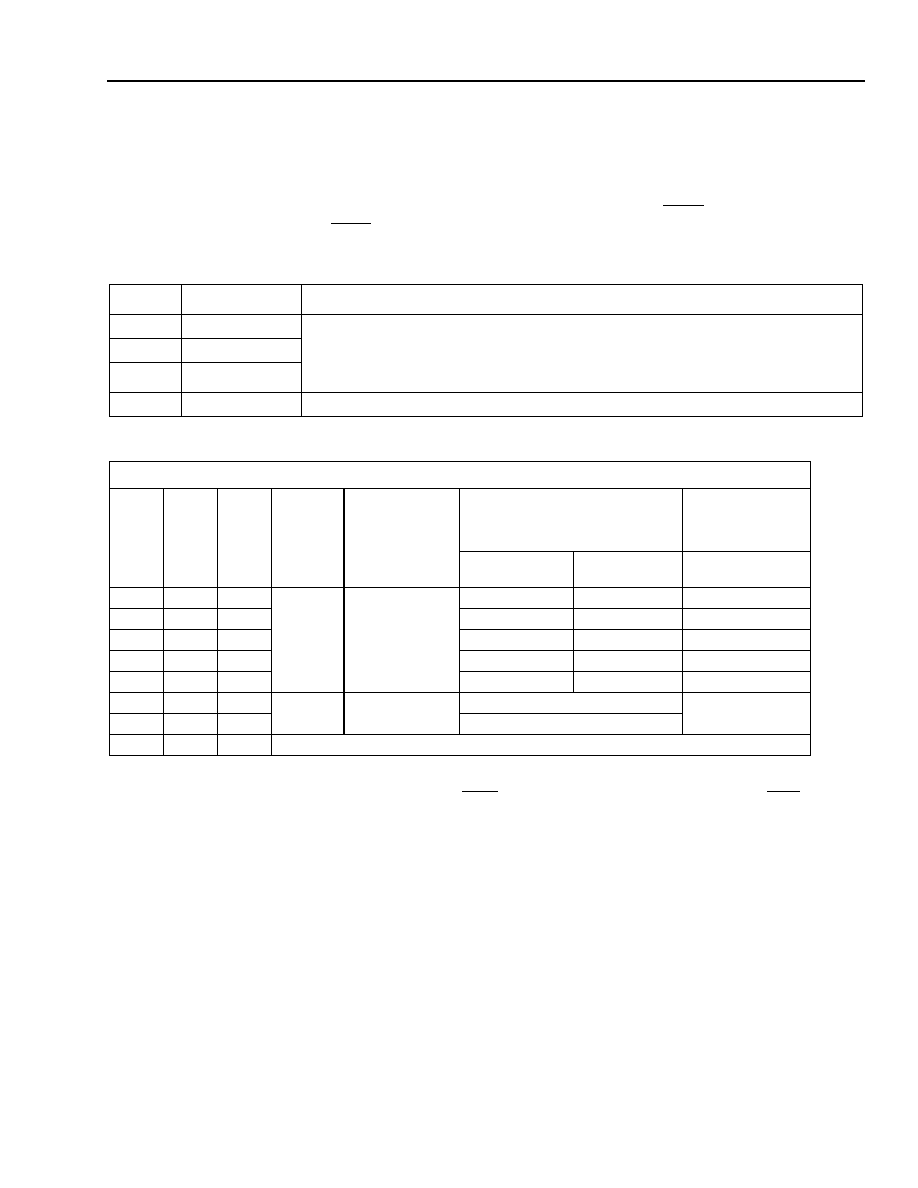
Agere Systems Inc.
163
Advance Data Sheet
May 2002
T7633 Dual T1/E1 3.3 V Short-Haul Terminator
Line Interface Control Registers
(continued)
LIU Configuration Register (LIU_REG6)
The control bits in the channel configuration register 6 are used to select LIU transmit equalization settings. This is
a read/write register. The default value of this register is 00 (hex) in DS1 when DS1/CEPT (pin 40/142) is set to 1,
and 06 (hex) in CEPT when DS1/CEPT (pin 40/142) is set to 0.
Transmit Line Interface Short-Haul Equalizer/Rate Control (from Table 6, page 34)
1.In DS1 mode, the distance to the DSX for 22-Gauge PIC (ABAM) cable is specified. Use the maximum cable loss figures for other cable
types. In CEPT mode, equalization is specified for coaxial or twisted-pair cable.
2.Reset default state is EQ2, EQ1, and EQ0 = 000 when pin DS1_CEPT = 1 and EQ2, EQ1, and EQ0 = 110 when pin DS1_CEPT = 0.
3.Loss measured at 772 kHz.
4.In 75
applications, Option 1 is recommended over Option 2 for lower LIU power dissipation. Option 2 allows for the use of the same trans-
former as in CEPT 120
applications (see Line Interface Unit: Line Circuitry section).
Table 87. LIU Configuration Register (LIU_REG6) (406, A06)
Bit
Symbol
Description
0
EQ0
The EQ0, EQ1, and EQ2 bits select the type of service (DS1 or CEPT) and the
associated transmitter cable equalization/line build out/termination impedances.
See Table 6, Transmit Line Interface Short-Haul Equalizer/Rate Control, from
page 34 repeated below for reference.
1
EQ1
2
EQ2
3--7
--
Reserved. Write to 0.
Short-Haul Applications
EQ2
EQ1
EQ0
Service
Clock Rate
Transmitter Equalization
1,2
Maximum
Cable Loss
to DSX
3
Feet
Meters
dB
0
0
0
DSX-1
1.544 MHz
0 to 131
0 to 40
0.6
0
0
1
131 to 262
40 to 80
1.2
0
1
0
262 to 393
80 to 120
1.8
0
1
1
393 to 524
120 to 160
2.4
1
0
0
524 to 655
160 to 200
3.0
1
0
1
CEPT
4
2.048 MHz
75
(Option 2)
--
1
1
0
120
or 75
(Option 1)
1
1
1
Not Used

164
Agere Systems Inc.
Advance Data Sheet
May 2002
T7633 Dual T1/E1 3.3 V Short-Haul Terminator
Framer Register Architecture
REGBANK3 and REGBANK6 contain the status and programmable control registers for the framer and system
(CHI) interface channels FRM1 and FRM2. The base address for REGBANK3 is 600 (hex) and for REGBANK6 is
C00 (hex). Within these register banks, the bit map is identical for both FRM1 and FRM2.
The framer registers are structures as shown in Table 88. Default values are given in the individual register defini-
tion tables.
Table 88. Framer Status and Control Blocks Address Range (Hexadecimal)
The complete register map for the framer is given in Table 202--Table 204 on page 220--page 223.
All status registers are clocked with the internal framer receive line clock (RFRMCK).
Bits in status registers FRM_SR1 and FRM_SR7 are set at the onset of the condition and are cleared on read
when the given condition is no longer present. These registers can generate interrupts if the corresponding register
bits are enabled in interrupt enable registers FRM_PR0--FRM_PR7.
On all 16-bit counter registers (FRM_SR8--FRM_SR51), both bytes are cleared only after reading both bytes,
regardless of the order in which they are read. Once a read is initiated on one of the bytes, the updating of that
counter is disabled and remains disabled until both bytes are read. All events during this interval are lost. Updating
of the counter registers is stopped when all of the bits are set to 1. Updating resumes after the registers are cleared
on read. These register pairs may be read in any order, but they must be read in pairs, i.e., a read of 1 byte must be
followed immediately by a read of the remaining byte of the pair.
Status registers FRM_SR0--FRM_SR63 are clear-on-read (COR) registers. These registers are cleared by the
framer internal received line clock (RFRMCK). At least two RFRMCK cycles (1.3 µs for DS1 and 1.0 µs for CEPT)
must be allowed between successive reads of the same COR register to allow it to properly clear.
Framer Register Block
Status Registers (COR) ((600--63F); (C00--C3F))
Receive Signaling Registers ((640--65F); (C40--C5F))
Parameter (Configuration) Registers ((660--6A6); (C60--CA6))
Transmit Signaling Registers ((6E0--6FF); (CE0--CFF))

Agere Systems Inc.
165
Advance Data Sheet
May 2002
T7633 Dual T1/E1 3.3 V Short-Haul Terminator
Framer Register Architecture
(continued)
Framer Status/Counter Registers
Registers FRM_SR0--FRM_SR63 report the status of each framer. All are clear-on-read, read only registers.
Interrupt Status Register (FRM_SR0)
The interrupt pin (INTERRUPT) goes active when a bit in this register and its associated interrupt enable bit in reg-
isters FRM_PR0--FRM_PR7 are set, and the interrupt for the framer block is enabled in register GREG1.
Table 89. Interrupt Status Register (FRM_SR0) (600; C00)
Bit
Symbol
Description
0
FAC
Facility Alarm Condition. A 1 indicates a facility alarm occurred (go read FRM_SR1).
1
RAC
Remote Alarm Condition. A 1 indicates a remote alarm occurred (go read FRM_SR2).
2
FAE
Facility Alarm Event. A 1 indicates a facility alarm occurred (go read FRM_SR3 and
FRM_SR4).
3
ESE
Errored Second Event. A 1 indicates an errored second event occurred (go read
FRM_SR5, FRM_SR6, and FRM_SR7).
4
TSSFE
Transmit Signaling Superframe Event. A 1 indicates that a MOS (or CCS for CEPT)
superframe block has been transmitted and the transmit signaling data buffers are ready
for new data.
5
RSSFE
Receive Signaling Superframe Event. A 1 indicates that a MOS (or CCS for CEPT)
superframe block has been received and the receive signaling data buffers must be read.
6
--
Reserved.
7
S96SR
SLC
-96 Stack Ready. A 1 indicates that either the transmit framer
SLC
-96 stack is ready
for more data or the receive framer
SLC
-96 stack contains new data.

166
Agere Systems Inc.
Advance Data Sheet
May 2002
T7633 Dual T1/E1 3.3 V Short-Haul Terminator
Framer Register Architecture
(continued)
Framer Status/Counter Registers
(continued)
Facility Alarm Condition Register (FRM_SR1)
The bits in the facility alarm condition register (FRM_SR1) indicate alarm state of the receive framer section. Inter-
rupts from this register are generated once at the onset of the alarm condition. If the alarm condition is still present
at the time of the read, the bit will remain in the 1 state for the duration of the alarm condition. If the alarm condition
is no longer present at the time of the read, then the bit is cleared on read.
Table 90. Facility Alarm Condition Register (FRM_SR1) (601; C01)
Bit
Symbol
Description
0
LFA
Loss of Frame Alignment. A 1 indicates the receive framer is in a loss of frame
alignment and is currently searching for a new alignment.
1
LSFA,
LTS16MFA
Loss of Signaling Superframe Alignment. A 1 indicates the receive framer is in a loss
of signaling superframe alignment in the DS1 framing formats. A search for a new
signaling superframe alignment starts once frame alignment is established.
Loss of Time Slot 16 Signaling Multiframe Alignment. A 1 indicates the receive framer
is in a loss of time slot 16 signaling multiframe alignment in the CEPT mode. A search for
a new time slot 16 signaling multiframe alignment starts once frame alignment is
established. This bit is 0 when the T7633 is programmed for the transparent signaling
mode, register FRM_PR44 bit 0 (TSIG) = 1.
2
LTSFA,
LTS0MFA
Loss of Transmit Superframe Alignment. A 1 indicates superframe alignment pattern
in the transmit facility data link as defined for
SLC
-96 is lost. Only valid for
SLC
-96 mode.
This bit is 0 in all other DS1 modes.
Loss of Time Slot 0 CRC-4 Multiframe Alignment. A 1 indicates an absence of CRC-
4 multiframe alignment after initial basic frame alignment is established. A 0 indicates
either CRC-4 checking is disabled or CRC-4 multiframe alignment has been successfully
detected.
3
LFALR
Loss of Frame Alignment Since Last Read. A 1 indicates that the LFA state indicated
in bit 0 of this register is the same LFA state as the previous read.
4
LBFA
Loss of Biframe Alignment. A 1 indicates that the CEPT biframe alignment pattern
(alternating 10 in bit 2 of time slot 0 of each frame) in the receive system data is errored.
This alignment pattern is required when transmitting the Si or Sa bits transparently. Only
valid in the CEPT mode. This bit is 0 in all other modes.
5
RTS16AIS
Receive Time Slot 16 Alarm Indication Signal. A 1 indicates the receive framer
detected time slot 16 AIS in the CEPT mode. This bit is 0 in the DS1 modes.
6
AUXP
Auxiliary Pattern. A 1 indicates the detection of a valid AUXP (unframed 1010 . . .
pattern) in the CEPT mode. This bit is 0 in the DS1 modes.
7
AIS
Alarm Indication Signal. A 1 indicates the receive framer is currently receiving an AIS
pattern from its remote line end.

Agere Systems Inc.
167
Advance Data Sheet
May 2002
T7633 Dual T1/E1 3.3 V Short-Haul Terminator
Framer Register Architecture
(continued)
Framer Status/Counter Registers
(continued)
Remote End Alarm Register (FRM_SR2)
A bit set to 1 indicates the receive framer has recently received the given alarm. Interrupts from this register are
generated once at the beginning of the alarm condition. If the alarm is still present at the time of the read, the bit
will remain in the 1 state for the duration of the alarm condition. If the alarm condition is no longer present at the
time of the read, then the bit is cleared on read.
Table 91. Remote End Alarm Register (FRM_SR2) (602; C02)
Bit
Symbol
Description
0
RFA
Remote Framer Alarm. A 1 indicates the receive framer detected a remote frame
(yellow) alarm.
1
RJYA,
RTS16MFA
Remote Japanese Yellow Alarm. A 1 indicates the receive framer detected the
Japanese format remote frame alarm.
Remote Multiframe Alarm. A 1 indicates the receive framer detected a time slot 16
remote frame alarm in the CEPT mode.
2
CREBIT
Continuous Received E Bits. A 1 indicates the detection of a five-second interval con-
taining
991 E bit = 0 events in each second. This bit is 0 in the DS1 mode.
3
Sa6=8
Received Sa6 = 8. A 1 indicates the receive framer detected a Sa6 code equal to 1000.
This bit is 0 in the DS1 mode.
4
Sa6=A
Received Sa6 = A. A 1 indicates the receive framer detected a Sa6 code equal to 1010.
This bit is 0 in the DS1 mode.
5
Sa6=C
Received Sa6 = C. A 1 indicates the receive framer detected a Sa6 code equal to 1100.
This bit is 0 in the DS1 mode.
6
Sa6=E
Received Sa6 = E. A 1 indicates the receive framer detected a Sa6 code equal to 1110.
This bit is 0 in the DS1 mode.
7
Sa6=F
Received Sa6 = F. A 1 indicates the receive framer detected a Sa6 code equal to 1111.
This bit is 0 in the DS1 mode.

168
Agere Systems Inc.
Advance Data Sheet
May 2002
T7633 Dual T1/E1 3.3 V Short-Haul Terminator
Framer Register Architecture
(continued)
Framer Status/Counter Registers
(continued)
Facility Errored Event Register (FRM_SR3)
A bit set to 1 indicates the receive framer has recently received the given errored event.
Table 92. Facility Errored Event Register-1 (FRM_SR3) (603; C03)
Bit
Symbol
Description
0
LFV
Line Format Violation. A 1 indicates the receive framer detected a bipolar line coding or
excessive zeros violation.
1
FBE
Frame-Bit Errored. A 1 indicates the receive framer detected a frame-bit or frame
alignment pattern error.
2
CRCE
CRC Errored. A 1 indicates the receive framer detected CRC errors.
3
ECE
Excessive CRC Errors. A 1 indicates the receive framer detected an excessive CRC
errored condition. This bit is only valid in the ESF and CEPT with CRC-4 modes;
otherwise, it is 0.
4
REBIT
Received E Bit = 0. A 1 indicates the receive framer detected a E bit = 0 in either frame
13 or 15 of the time slot 0 of CRC-4 multiframe. This bit is 0 in the DS1 modes.
5
LCRCATMX
Lack of CRC-4 Multiframe Alignment Timer Expire Indication. A 1 indicates that either
the 100 ms or the 400 ms CRC-4 interworking timer expired. Active only immediately after
establishment of the initial basic frame alignment. This bit is 0 in the DS1 modes.
6
SLIPO
Receive Elastic Store Slip: Buffer Overflow. A 1 indicates the receive elastic store
performed a control slip due to an elastic buffer overflow condition.
7
SLIPU
Receive Elastic Store Slip: Buffer Underflow. A 1 indicates the receive elastic store
performed a control slip due to an elastic buffer underflow condition.

Agere Systems Inc.
169
Advance Data Sheet
May 2002
T7633 Dual T1/E1 3.3 V Short-Haul Terminator
Framer Register Architecture
(continued)
Framer Status/Counter Registers
(continued)
Table 93. Facility Event Register-2 (FRM_SR4) (604; C04)
Bit
Symbol
Description
0
NFA
New Frame Alignment. A 1 indicates the receive framer established a new frame
alignment which differs from the previous alignment.
1
SSFA
Signaling Superframe Alignment. A 1 indicates the receive framer has established the
signaling superframe alignment. In the SF modes (D4 and
SLC
-96) and CEPT modes,
this alignment is established only after primary frame alignment is determined.
2
LLBOFF,
BFA
T1 Line Loopback Off Code Detect. A 1 indicates the receive framer detected the DS1
line loopback disable code in the payload. This code is defined in
AT&T
Technical
Reference 62411 as a framed 001 pattern where the frame bit is inserted into the pattern.
New Biframe Alignment Established. A 1 indicates the transmit framer has established
a biframe alignment for the transmission of transparent Si and or Sa bits from the system
data in the CEPT mode.
3
LLBON,
CMA
T1 Line Loopback On Code Detect. A 1 indicates the receive framer detected the line
loopback enable code in the payload. This code is defined in
AT&T
Technical Reference
62411 as a framed 00001 pattern where the frame bit is inserted into the pattern.
New CEPT CRC-4 Multiframe Alignment. A 1 indicates the CEPT CRC-4 multiframe
alignment in the receive framer has been established.

170
Agere Systems Inc.
Advance Data Sheet
May 2002
T7633 Dual T1/E1 3.3 V Short-Haul Terminator
Framer Register Architecture
(continued)
Framer Status/Counter Registers
(continued)
Table 93. Facility Event Register-2 (FRM_SR4) (604; C04) (continued)
Bit
Symbol
Description
4
FDL-PLBON,
SLCRFSR
ESF FDL Payload Loopback On Code Detect. A 1 indicates the receive framer detected
the line loopback enable code in the payload. This code is defined in
ANSI
T1.403-1995
as a 1111111100101000 pattern in the facility data link, where the leftmost bit is the MSB.
SLC
-96 Receive FDL Stack Ready. A 1 indicates that the receive FDL stack should be
read. This bit is cleared on read. Data in the receive FIFO must be read within 9 ms of this
interrupt. This bit is not updated during loss of frame or signaling superframe alignment.
5
FDL-PLBOFF,
SLCTFSR
ESF FDL Payload Loopback Off Code Detect. A 1 indicates the receive framer
detected the line loopback disable code in the payload. This code is defined in
ANSI
T1.403-1995 as a 1111111101001100 pattern in the facility data link, where the leftmost
bit is the MSB.
SLC
-96 Transmit FDL Stack Ready. A 1 indicates that the transmit FDL stack is ready
for new data. This bit is cleared on read. Data written within 9 ms of this interrupt will be
transmitted in the next
SLC
-96 D-bit superframe interval.
6
FDL-LLBON,
RSaSR
ESF FDL Line Loopback On Code Detect. A 1 indicates the receive framer detected the
line loopback enable code in the payload. This code is defined in
ANSI
T1.403-1995 as a
1111111101110000 pattern in the facility data link, where the left most bit is the MSB.
CEPT Receive Sa Stack Ready. A 1 indicates that the receive Sa6 stack should be read.
This bit is clear on the first access to the Sa receive stack or at the beginning of frame 0
of the CRC-4 double-multiframe. Data in the receive FIFO must be read within 4 ms of
this interrupt. This bit is not updated during LFA.
7
FDL-LLBOFF,
TSaSR
ESF FDL Line Loopback Off Code Detect. A 1 indicates the receive framer detected the
line loopback disable code in the payload. This code is defined in
ANSI
T1.403-1995 as
a 1111111100011100 pattern in the facility data link, where the left most bit is the MSB.
CEPT Transmit Sa Stack Ready. A 1 indicates that the transmit Sa stack is ready for
new data. This bit is cleared on the first access to the Sa transmit stack or at the beginning
of frame 0 of the CRC-4 double multiframe. Data written within 4 ms of this interrupt will
be transmitted in the next CRC-4 double multiframe interval.

Agere Systems Inc.
171
Advance Data Sheet
May 2002
T7633 Dual T1/E1 3.3 V Short-Haul Terminator
Framer Register Architecture
(continued)
Framer Status/Counter Registers
(continued)
The following registers are dedicated to the exchange termination and its remote end interface. The alarm
conditions to trigger errored seconds and severely errored seconds are defined in Table 44, Event Counters
Definition on page 97 and the ET and ET-RE enable registers, FRM_PR14 and FRM_PR15. The thresholds are
defined in registers FRM_PR11--FRM_PR13.
Table 94. Exchange Termination and Exchange Termination Remote End Interface
Status Register (FRM_SR5) (605; C05)
Bit
Symbol
Description
0
ETES
ET Errored Second. A 1 indicates the receive framer detected an errored second at the
exchange termination (ET).
1
ETBES
ET Bursty Errored Second. A 1 indicates the receive framer detected a bursty errored
second at the ET.
2
ETSES
ET Severely Errored Second. A 1 indicates the receive framer detected a severely
errored second at the ET.
3
ETUAS
ET Unavailable State. A 1 indicates the receive framer has detected at least ten
consecutive severely errored seconds. Upon detecting ten consecutive nonseverely
errored seconds, the receive framer will clear this bit. ITU Recommendation G.826 is
used resulting in a ten-second delay in the reporting of this condition.
4
ETREES
ET-RE Errored Second. A 1 indicates the receive framer detected an errored second at
the exchange termination remote end (ET-RE).
5
ETREBES
ET-RE Bursty Errored Second. A 1 indicates the receive framer detected a bursty
errored second at the ET-RE.
6
ETRESES
ET-RE Severely Errored Second. A 1 indicates the receive framer detected a severely
errored second at the ET-RE.
7
ETREUAS
ET-RE Unavailable State. A 1 indicates the receive framer has detected at least ten
consecutive severely errored seconds. Upon detecting ten consecutive nonseverely
errored seconds, the receive framer will clear this bit. ITU Recommendation G.826 is
used resulting in a ten-second delay in the reporting of this condition.

172
Agere Systems Inc.
Advance Data Sheet
May 2002
T7633 Dual T1/E1 3.3 V Short-Haul Terminator
Framer Register Architecture
(continued)
Framer Status/Counter Registers
(continued)
The following status registers are dedicated to the NT1 and the NT1 remote end (NT1-RE) interface. The alarm
conditions to evaluate errored seconds and severely errored seconds are defined in Table 44, Event Counters
Definition on page 97
and the NT1 and NT1-RE enable registers, FRM_PR16--FRM_PR18. The thresholds are
defined in registers FRM_PR11--FRM_PR13.
Table 95. Network Termination and Network Termination Remote End Interface Status
Register (FRM_SR6) (606; C06)
Bit
Symbol
Description
0
NTES
NT Errored Second. A 1 indicates the receive framer detected an errored second at the
network termination (NT).
1
NTBES
NT Bursty Errored Second. A 1 indicates the receive framer detected a bursty errored
second at the NT.
2
NTSES
NT Severely Errored Second. A 1 indicates the receive framer detected a severely
errored second at the NT.
3
NTUAS
NT Unavailable State. A 1 indicates the receive framer has detected at least ten
consecutive severely errored seconds. Upon detecting ten consecutive nonseverely
errored seconds, the receive framer will clear this bit. ITU Recommendation G.826 is used
resulting in a ten-second delay in the reporting of this condition.
4
NTREES
NT-RE Errored Second. A 1 indicates the receive framer detected an errored second at
the exchange termination remote end (ET-RE).
5
NTREBES
NT-RE Bursty Errored Second. A 1 indicates the receive framer detected a bursty
errored second at the ET-RE.
6
NTRESES
NT-RE Severely Errored Second. A 1 indicates the receive framer detected a severely
errored second at the NT-RE.
7
NTREUAS
NT-RE Unavailable State. A 1 indicates the receive framer has detected at least ten
consecutive severely errored seconds. Upon detecting ten consecutive nonseverely
errored seconds, the receive framer will clear this bit. ITU Recommendation G.826 is used
resulting in a ten-second delay in the reporting of this condition.

Agere Systems Inc.
173
Advance Data Sheet
May 2002
T7633 Dual T1/E1 3.3 V Short-Haul Terminator
Framer Register Architecture
(continued)
Framer Status/Counter Registers
(continued)
Bit 0--bit 4 in this register are set high when the receive framer comes out of the unavailable state, while bit 4--bit
7 report detection of the receive test patterns.
Table 96. Facility Event Register (FRM_SR7) (607; C07)
* It is possible for one of these bits to be set to 1, if the received line data is all zeros.
Bipolar Violation Counter Register (FRM_SR8--FRM_SR9)
This register contains the 16-bit count of received bipolar violations, line code violations, or excessive zeros.
Table 97. Bipolar Violation Counter Registers (FRM_SR8--FRM_SR9) ((608--609); (C08--C09))
Frame Bit Errored Counter Register (FRM_SR10--FRM_SR11)
This register contains the 16-bit count of framing bit errors. Framing bit errors are not counted during loss of frame
alignment.
Table 98. Framing Bit Error Counter Registers (FRM_SR10--FRM_SR11) ((60A--60B); (C0A--C0B))
Bit
Symbol
Description
0
OUAS
Out of Unavailable State. A 1 indicates the receive framer detected ten consecutive
seconds that were not severely errored while in the unavailable state at the ET.
1
EROUAS
Out of Unavailable State at the ET-RE. A 1 indicates the receive framer detected ten
consecutive seconds that were not severely errored while in the unavailable state at the
ET-RE.
2
NT1OUAS
Out of Unavailable State at the NT1. A 1 indicates the receive framer detected ten
consecutive seconds that were not severely errored while in the unavailable state at the
NT.
3
NROUAS
Out of Unavailable State NT1-RE. A 1 indicates the receive framer detected ten
consecutive seconds that were not severely errored while in the unavailable state at the
NT-RE.
4
DETECT
Test Pattern Detected. A 1 indicates the pattern detector has locked onto the pattern
specified by the PTRN configuration bits defined in register FRM_PR70.
5
PTRNBER
Test Pattern Bit Error. A 1 indicates the pattern detector has found one or more single
bit errors in the pattern that it is currently locked onto.
6
RPSUEDO
Receiving Pseudorandom Pattern. A 1 indicates the receive framer pattern monitor
circuit is currently detecting the 2
15
≠ 1 pseudorandom pattern*.
7
RQUASI
Receiving Quasi-Random Pattern. A 1 indicates the receive framer pattern monitor
circuit is currently detecting the 2
20
≠ 1 quasi-random pattern*.
Register
Byte
Bit
Symbol
Description
FRM_SR8
MSB
7--0
BPV15--BPV8
BPVs Counter.
FRM_SR9
LSB
7--0
BPV7--BPV0
BPVs Counter.
Register
Byte
Bit
Symbol
Description
FRM_SR10
MSB
7--0
FBE15--FBE8
Frame Bit Counter.
FRM_SR11
LSB
7--0
FBE7--FBE0
Frame Bit Errored Counter.

174
Agere Systems Inc.
Advance Data Sheet
May 2002
T7633 Dual T1/E1 3.3 V Short-Haul Terminator
Framer Register Architecture
(continued)
Framer Status/Counter Registers
(continued)
CRC Error Counter Register (FRM_SR12--FRM_SR13)
This register contains the 16-bit count of CRC errors. CRC errors are not counted during loss of CRC multiframe
alignment.
Table 99. CRC Error Counter Registers (FRM_SR12--FRM_SR13) ((60C--60D); (C0C--C0D))
E-Bit Counter Register (FRM_SR14--FRM_SR15)
This register contains the 16-bit count of received E bit = 0 events. E bits are not counted during loss of CEPT
CRC-4 multiframe alignment.
Table 100. E-Bit Counter Registers (FRM_SR14--FRM_SR15) ((60E--60F); (C0E--C0F))
CRC-4 Errors at NT1 from NT2 Counter Registers (FRM_SR16--FRM_SR17)
This register contains the 16-bit count of each occurrence of Sa6 code 001X, detected synchronously to the CEPT
CRC-4 multiframe.
Table 101. CRC-4 Errors at NT1 from NT2 Counter Registers (FRM_SR16--FRM_SR17) ((610--611);
(C10--C11))
E Bit at NT1 from NT2 Counter Registers (FRM_SR18--FRM_SR19)
This register contains the 16-bit count of each occurrence of Sa6 code 00X1, detected synchronously to the CEPT
CRC-4 multiframe. E bits are not counted during loss of CEPT CRC-4 multiframe alignment.
Table 102. E Bit at NT1 from NT2 Counter (FRM_SR18--FRM_SR19) ((612--613); (C12--C13))
Register
Byte
Bit
Symbol
Description
FRM_SR12
MSB
7--0
CEC15--CEC8
CRC Errored Counter.
FRM_SR13
LSB
7--0
CEC7--CEC0
CRC Errored Counter.
Register
Byte
Bit
Symbol
Description
FRM_SR14
MSB
7--0
REC15--REC8
E-Bit Counter.
FRM_SR15
LSB
7--0
REC7--REC0
E-Bit Counter.
Register
Byte
Bit
Symbol
Description
FRM_SR16
MSB
7--0
CNT15--CNT8
CRC-4 Errors at NT1 Counter.
FRM_SR17
LSB
7--0
CNT7--CNT0
CRC-4 Errors at NT1 Counter.
Register
Byte
Bit
Symbol
Description
FRM_SR18
MSB
7--0
ENT15--ENT8
E Bit at NT1 Counter.
FRM_SR19
LSB
7--0
ENT7--ENT0
E Bit at NT1 Counter.

Agere Systems Inc.
175
Advance Data Sheet
May 2002
T7633 Dual T1/E1 3.3 V Short-Haul Terminator
Framer Register Architecture
(continued)
Framer Status/Counter Registers
(continued)
The following status registers, FRM_SR20--FRM_SR51, contain the 16-bit count of errored seconds, bursty
errored seconds, severely errored seconds, and unavailable seconds at the ET, ET-RE, NT1, and NT1-RE
terminals.
Table 103. ET Errored Seconds Counter (FRM_SR20--FRM_SR21) ((614--615); (C14--C15))
Table 104. ET Bursty Errored Seconds Counter (FRM_SR22--FRM_SR23) ((616--617); (C16--C17))
Table 105. ET Severely Errored Seconds Counter (FRM_SR24--FRM_SR25) ((618--619); (C18--C19))
Table 106. ET Unavailable Seconds Counter (FRM_SR26--FRM_SR27) ((61A--61B); (C1A--C1B))
Table 107. ET-RE Errored Seconds Counter (FRM_SR28--FRM_SR29) ((61C--61D); (C1C--C1D))
Table 108. ET-RE Bursty Errored Seconds Counter (FRM_SR30--FRM_SR31) ((61E--61F); (C1E--C1F))
Table 109. ET-RE Severely Errored Seconds Counter (FRM_SR32--FRM_SR33) ((620--621); (C20--C21))
Register
Byte
Bit
Symbol
Description
FRM_SR20
MSB
7--0
ETES15--ETES8
ET Errored Seconds Counter.
FRM_SR21
LSB
7--0
ETES7--ETES0
ET Errored Seconds Counter.
Register
Byte
Bit
Symbol
Description
FRM_SR22
MSB
7--0
ETBES15--ETBES8 ET Bursty Errored Seconds Counter.
FRM_SR23
LSB
7--0
ETBES7--ETBES0
ET Bursty Errored Seconds Counter.
Register
Byte
Bit
Symbol
Description
FRM_SR24
MSB
7--0
ETSES15--ETSES8 ET Severely Errored Seconds Counter.
FRM_SR25
LSB
7--0
ETSES7--ETSES0
ET Severely Errored Seconds Counter.
Register
Byte
Bit
Symbol
Description
FRM_SR26
MSB
7--0
ETUS15--ETUS8
ET Unavailable Seconds Counter Bits.
FRM_SR27
LSB
7--0
ETUS7--ETUS0
ET Unavailable Seconds Counter Bits.
Register
Byte
Bit
Symbol
Description
FRM_SR28
MSB
7--0
ETREES15--ETREES8 ET-RE Errored Seconds Counter.
FRM_SR29
LSB
7--0
ETREES7--ETREES0 ET-RE Errored Seconds Counter.
Register
Byte
Bit
Symbol
Description
FRM_SR30
MSB
7--0
ETREBES15--ETREBES8 ET-RE Bursty Errored Seconds Counter.
FRM_SR31
LSB
7--0
ETREBES7--ETREBES0 ET-RE Bursty Errored Seconds Counter.
Register
Byte
Bit
Symbol
Description
FRM_SR32
MSB
7--0
ETRESES15--ETRESES8 ET-RE Severely Errored Seconds Counter.
FRM_SR33
LSB
7--0
ETRESES7--ETRESES0 ET-RE Severely Errored Seconds Counter.

176
Agere Systems Inc.
Advance Data Sheet
May 2002
T7633 Dual T1/E1 3.3 V Short-Haul Terminator
Framer Register Architecture
(continued)
Framer Status/Counter Registers
(continued)
Table 110. ET-RE Unavailable Seconds Counter (FRM_SR34--FRM_SR35) ((622--623); (C22--C23))
Table 111. NT1 Errored Seconds Counter (FRM_SR36--FRM_SR37) ((624--625); (C24--C25))
Table 112. NT1 Bursty Errored Seconds Counter (FRM_SR38--FRM_SR39) ((626--627); (C26--C27))
Table 113. NT1 Severely Errored Seconds Counter (FRM_SR40--FRM_SR41) ((628--629); (C28--C29))
Table 114. NT1 Unavailable Seconds Counter (FRM_SR42--FRM_SR43) ((62A--62B); (C2A--C2B))
Table 115. NT1-RE Errored Seconds Counter (FRM_SR44--FRM_SR45) ((62C--62D); (C2C--C2D))
Register
Byte
Bit
Symbol
Description
FRM_SR34
MSB
7--0
ETREUS15--ETRESES8
ET-RE Unavailable Seconds Counter.
FRM_SR35
LSB
7--0
ETRESES7--ETRESES0 ET-RE Unavailable Seconds Counter.
Register
Byte
Bit
Symbol
Description
FRM_SR36
MSB
7--0
NTES15--NTES8
NT1 Errored Seconds Counter.
FRM_SR37
LSB
7--0
NTES7--NTES0
NT1 Errored Seconds Counter.
Register
Byte
Bit
Symbol
Description
FRM_SR38
MSB
7--0
NTBES15--NTBES8
NT1 Bursty Errored Seconds Counter.
FRM_SR39
LSB
7--0
NTBES7--NTBES0
NT1 Bursty Errored Seconds Counter.
Register
Byte
Bit
Symbol
Description
FRM_SR40
MSB
7--0
NTSES15--NTSES8
NT1 Severely Errored Seconds Counter.
FRM_SR41
LSB
7--0
NTSES7--NTSES0
NT1 Severely Errored Seconds Counter.
Register
Byte
Bit
Symbol
Description
FRM_SR42
MSB
7--0
NTUS15--NTUS8
NT1 Unavailable Seconds Counter Bits.
FRM_SR43
LSB
7--0
NTUS7--NTUS0
NT1 Unavailable Seconds Counter Bits.
Register
Byte
Bit
Symbol
Description
FRM_SR44
MSB
7--0
NTREES15--NTREES8
NT1-RE Errored Seconds Counter.
FRM_SR45
LSB
7--0
NTREES7--NTREES0
NT1-RE Errored Seconds Counter.

Agere Systems Inc.
177
Advance Data Sheet
May 2002
T7633 Dual T1/E1 3.3 V Short-Haul Terminator
Framer Register Architecture
(continued)
Framer Status/Counter Registers
(continued)
Table 116. NT1-RE Bursty Errored Seconds Counter (FRM_SR46--FRM_SR47) ((62E--62F); (C2E--C2F))
Table 117. NT1-RE Severely Errored Seconds Counter (FRM_SR48--FRM_SR49) ((630--631); (C30--C31))
Table 118. NT1-RE Unavailable Seconds Counter (FRM_SR50--FRM_SR51) ((632--633); (C32--C33))
Received NOT-FAS TS0 RSa Register (FRM_SR52)
This register contains the last (since last read) valid received RSa8-- RSa4 bits, A bit, and Si bit of NOT-FAS time
slot 0 and the Si bit of FAS time slot 0 while the receive framer was in basic frame alignment.
Table 119. Receive NOT-FAS TS0 Register (FRM_SR52) (634; C34)
Received Sa Register (FRM_SR53)
This register contains the last (since last read) valid time slot 16 spare bits of the frame containing the time slot 16
signaling multiframe alignment. These bits are updated only when the receive framer is in signaling multiframe
alignment.
Table 120. Receive Sa Register (FRM_SR53) (635; C35)
Register
Byte
Bit
Symbol
Description
FRM_SR46
MSB
7--0
NTREBES15--NTREBES8 NT1-RE Bursty Errored Seconds Counter.
FRM_SR47
LSB
7--0
NTREBES7--NTREBES0 NT1-RE Bursty Errored Seconds Counter.
Register
Byte
Bit
Symbol
Description
FRM_SR48
MSB
7--0
NTRESES15--NTRESES8 NT1-RE Severely Errored Seconds Counter.
FRM_SR49
LSB
7--0
NTRESES7--NTRESES0 NT1-RE Severely Errored Seconds Counter.
Register
Byte
Bit
Symbol
Description
FRM_SR50
MSB
7--0
NTREUS15--NTREUS8
NT1-RE Unavailable Seconds Counter Bits.
FRM_SR51
LSB
7--0
NTREUS7--NTREUS0
NT1-RE Unavailable Seconds Counter Bits.
Bit 7
Bit 6
Bit 5
Bit 4
Bit 3
Bit 2
Bit 1
Bit 0
NOT-FAS bit 1
(CEPT without CRC-4)
or
frame 15 E bit
(CEPT with CRC-4)
FAS bit 1
(CEPT without CRC-4)
or
frame 13 E bit
(CEPT with CRC-4)
A bit
Sa4
Sa5
Sa6
Sa7
Sa8
Bit 7
Bit 6
Bit 5
Bit 4
Bit 3
Bit 2
Bit 1
Bit 0
0
0
0
0
0
X2
X1
X0

178
Agere Systems Inc.
Advance Data Sheet
May 2002
T7633 Dual T1/E1 3.3 V Short-Haul Terminator
Framer Register Architecture
(continued)
Framer Status/Counter Registers
(continued)
SLC-
96 FDL/CEPT Sa Receive Stack (FRM_SR54--FRM_SR63)
In the
SLC
-96 frame format, FRM_SR54 through FRM_SR58 contain the received
SLC
-96 facility data link data
block. When the framer is in a loss of frame alignment or loss of signaling superframe alignment, these registers
are not updated.
Note: The RSP[1:4] are the received spoiler bits.
Table 121.
SLC-
96 FDL Receive Stack (FRM_SR54--FRM_SR63) ((636--63F); (C36--C3F))
In the CEPT frame format, FRM_SR54 through FRM_SR63 contain the received Sa4 through Sa8 from the last
valid CRC-4 double-multiframe. In non-CRC-4 mode, these registers are only updated during a basic frame
aligned state. In CRC-4 mode, these registers are only updated during the CRC-4 multiframe alignment state.
Table 122. CEPT Sa Receive Stack (FRM_SR54--FRM_SR63) ((636--63F); (C36--C3F))
Register
Bit 7
Bit 6
Bit 5
Bit 4
Bit 3
Bit 2
Bit 1
Bit 0
FRM_SR54
0
0
R-0
R-0
R-0
R-1
R-1
R-1
FRM_SR55
0
0
R-0
R-0
R-0
R-1
R-1
R-1
FRM_SR56
RC
1
RC
2
RC
3
RC
4
RC
5
RC
6
RC
7
RC
8
FRM_SR57
RC
9
RC
10
RC
11
RSPB
1
= 0 RSPB
2
= 1 RSPB
3
= 0
RM
1
RM
2
FRM_SR58
RM
3
RA
1
RA
2
RS
1
RS
2
RS
3
RS
4
RSPB
4
= 1
FRM_SR59--
FRM_SR61
0
0
0
0
0
0
0
0
Register
Bit 7
Bit 6
Bit 5
Bit 4
Bit 3
Bit 2
Bit 1
Bit 0
FRM_SR54
Sa4-1
Sa4-3
Sa4-5
Sa4-7
Sa4-9
Sa4-11
Sa4-13
Sa4-15
FRM_SR55
Sa4-17
Sa4-19
Sa4-21
Sa4-23
Sa4-25
Sa4-27
Sa4-29
Sa4-31
FRM_SR56
Sa5-1
Sa5-3
Sa5-5
Sa5-7
Sa5-9
Sa5-11
Sa5-13
Sa5-15
FRM_SR57
Sa5-17
Sa5-19
Sa5-21
Sa5-23
Sa5-25
Sa5-27
Sa5-29
Sa5-31
FRM_SR58
Sa6-1
Sa6-3
Sa6-5
Sa6-7
Sa6-9
Sa6-11
Sa6-13
Sa6-15
FRM_SR59
Sa6-17
Sa6-19
Sa6-21
Sa6-23
Sa6-25
Sa6-27
Sa6-29
Sa6-31
FRM_SR60
Sa7-1
Sa7-3
Sa7-5
Sa7-7
Sa7-9
Sa7-11
Sa7-13
Sa7-15
FRM_SR61
Sa7-17
Sa7-19
Sa7-21
Sa7-23
Sa7-25
Sa7-27
Sa7-29
Sa7-31
FRM_SR62
Sa8-1
Sa8-3
Sa8-5
Sa8-7
Sa8-9
Sa8-11
Sa8-13
Sa8-15
FRM_SR63
Sa8-17
Sa8-19
Sa8-21
Sa8-23
Sa8-25
Sa8-27
Sa8-29
Sa8-31

Agere Systems Inc.
179
Advance Data Sheet
May 2002
T7633 Dual T1/E1 3.3 V Short-Haul Terminator
Framer Register Architecture
(continued)
Framer Status/Counter Registers
(continued)
The receive framer stores the current second of the
ANSI
Performance Report Message transmitted to the
remote end in registers FRM_SR62 and FRM_SR63. The structure of the PRM status registers is shown in Table
123.
Received Signaling Registers: DS1 Format
Table 124. Received Signaling Registers: DS1 Format (FRM_RSR0--FRM_RSR23) ((640--658); (C40--C58))
1.Bit 6 and Bit 5 of the DS1 receive signaling registers are copied from bit 6 and bit 5 of the DS1 transmit signaling registers.
Receive Signaling Registers: CEPT Format
Table 125. Receive Signaling Registers: CEPT Format (FRM_RSR0--FRM_RSR31) ((640--65F); (C40--
C5F))
1.This bit contains the IRSM information in time slot 0. In PCS0 or PCS1 signaling mode, this bit is undefined.
Table 123. Transmit Framer
ANSI
Performance Report Message Status Register Structure
Transmit
Framer PRM
Status Bytes
TSPRM B7
TSPRM B6
TSPRM B5
TSPRM B4
TSPRM B3
TSPRM B2
TSPRM B1
TSPRM B0
FRM_SR62
G3
LV
G4
U1
U2
G5
SL
G6
FRM_SR63
FE
SE
LB
G1
R
G2
Nm
Nl
Received Signal Registers
Bit 7
Bit
6
1
Bit 5
Bit 4
Bit 3
Bit 2
Bit 1
Bit 0
DS1 Received Signaling Registers (0--23)
P
G
F
X
D
C
B
A
Voice Channel with 16-State Signaling
X
0
0
X
D
C
B
A
Voice Channel with 4-State Signaling
X
0
1
X
X
X
B
A
Voice Channel with 2-State Signaling
X
1
1
X
X
X
X
A
Data Channel
X
1
0
X
X
X
X
X
Receive Signal Registers
Bit 7
Bit 6--5
Bit 4
1
Bit 3
Bit 2
Bit 1
Bit 0
FRM_RSR0: IRSM Mode
Only
X
X
E0
X
X
X
X
FRM_RSR1--FRM_RSR15
P
X
E[1:15]
D[1:15]
C[1:15]
B[1:15]
A[1:15]
FRM_RSR16: IRSM Only
X
X
E16
X
X
B
A
FRM_RSR[17:31]
P
X
E[17:31]
D[17:31]
C[17:31]
B[17:31]
A[17:31]

180
Agere Systems Inc.
Advance Data Sheet
May 2002
T7633 Dual T1/E1 3.3 V Short-Haul Terminator
Framer Register Architecture
(continued)
Framer Parameter/Control Registers
Registers FRM_PR0--FRM_PR70 define the mode configuration of each framer. All are read/write registers.
These registers are initially set to a default value upon a hardware reset, which is indicated in the register defini-
tion.
Interrupt Group Enable Registers (FRM_PR0--FRM_PR7)
The bits in this register group enable the status registers FRM_SR0--FRM_SR7 to assert the interrupt pin. The
default value of these registers is 00 (hex).
FRM_PR0 is the primary interrupt group enable register which enables the event groups in interrupt status register
FRM_SR0. A bit set to 1 in this register enables the corresponding bit in the interrupt status register FRM_SR0 to
assert the interrupt pin.
FRM_PR1--FRM_PR7 are the secondary interrupt enable registers. A bit set to 1 in these registers enables the
corresponding bit in the status register to assert the interrupt pin.
Table 126. Summary of Interrupt Group Enable Registers (FRM_PR0--FRM_PR7) ((660--667); (C60--C67))
Parameter/
Control
Register
Status
Register
Enabled
Status
Register
Bit 7
Status
Register
Bit 6
Status
Register
Bit 5
Status
Register
Bit 4
Status
Register
Bit 3
Status
Register
Bit 2
Status
Register
Bit 1
Status
Register
Bit 0
FRM_PR0
FRM_SR0
S96SR
Reserved
RSSFE
TSSFE
ESE
(read
FRM_SR5,
FRM_SR6,
and
FRM_SR7)
FAE
(read
FRM_SR3
and
FRM_SR4)
RAC
(read
FRM_SR2)
FAC
(read
FRM_SR1)
FRM_PR1
FRM_SR1
AIS
AUXP
RTS16AIS
LBFA
LFALR
LTSFA
(LTS0MFA)
LSFA
(LTS16MFA)
LFA
FRM_PR2
FRM_SR2
RSa6=F
RSa6=E
RSa6=C
RSa6=A
RSa6=8
CREBIT
RJYA
(RTS16MFA
)
RFA
FRM_PR3
FRM_SR3
SLIPU
SLIPO
LCRCATMX
REBIT
ECE
CRCE
FBE
LFV
FRM_PR4
FRM_SR4 FDL_LLBOFF
(TSaSR)
FDL_LLBON
(RSaSR)
FDL_PLBOFF
(SLCTFSR)
FDL_PLBON
(SLCRFSR)
LLBON
(CMA)
LLBOFF
(BFA)
SSFA
CFA
FRM_PR5
FRM_SR5
ETREUAS
ETRESES
ETREBES
ETREES
ETUAS
ETSES
ETBES
ETES
FRM_PR6
FRM_SR6
NTREUAS
NTRESES
NTREBES
NTREES
NTUAS
NTSES
NTBES
NTES
FRM_PR7
FRM_SR7
RQUASI
RPSUEDO
PTRNBER
DETECT
NROUAS
NT1OUAS
EROUAS
OUAS

Agere Systems Inc.
181
Advance Data Sheet
May 2002
T7633 Dual T1/E1 3.3 V Short-Haul Terminator
Framer Register Architecture
(continued)
Framer Parameter/Control Registers
(continued)
Primary Interrupt Enable Register (FRM_PR0)
The default value of this register is 00 (hex).
Table 127. Primary Interrupt Group Enable Register (FRM_PR0) (660; C60)
Bit
Symbol
Description
0
SR1IE
Status Register 1 Interrupt Enable Bit. A 1 enables register FRM_SR1 event interrupts.
1
SR2IE
Status Register 2 Interrupt Enable Bit. A 1 enables register FRM_SR2 event interrupts.
2
SR34IE
Status Registers 3 and 4 Interrupt Enable Bit. A 1 enables registers FRM_SR3 and
FRM_SR4 event interrupts.
3
SR567IE
Status Registers 5, 6, and 7 Interrupt Enable Bit. A 1 enables registers FRM_SR5,
FRM_SR6, and FRM_SR7 event interrupts.
4
TSRIE
Transmit Signaling Ready Interrupt Enable Bit. A 1 enables interrupts when transmit
signaling buffers are ready (MOS or CCS modes).
5
RSRIE
Receive Signaling Ready Interrupt Enable Bit. A 1 enables interrupts when receive
signaling buffers are ready (MOS or CCS modes).
6
--
Reserved. Write to 0.
7
SLCIE
SLC
-96 Interrupt Enable Bit. A 1 enables interrupts when
SLC
-96 receive or transmit
stacks are ready.

182
Agere Systems Inc.
Advance Data Sheet
May 2002
T7633 Dual T1/E1 3.3 V Short-Haul Terminator
Framer Register Architecture
(continued)
Framer Parameter/Control Registers
(continued)
Secondary Interrupt Enable Registers (FRM_PR1--FRM_PR7)
A bit set to 1 in registers FRM_PR1--FRM_PR7 enables the generation of interrupts whenever the corresponding
bit in registers FRM_SR1--FRM_SR7 is set. The default value of these registers is 00 (hex).
Table 128. Interrupt Enable Register (FRM_PR1) (661; C61)
Table 129. Interrupt Enable Register (FRM_PR2) (662; C62)
Table 130. Interrupt Enable Register (FRM_PR3) (663; C63)
Table 131. Interrupt Enable Register (FRM_PR4) (664; C64)
Table 132. Interrupt Enable Register (FRM_PR5) (665; C65)
Table 133. Interrupt Enable Register (FRM_PR6) (666; C66)
Table 134. Interrupt Enable Register (FRM_PR7) (667; C67)
Bit
Symbol
Description
0--7
SR1B0IE--
SR1B7IE
Status Register 1 Interrupt Enable. A 1 enables events monitored in register FRM_SR1
to generate interrupts. Each bit position in this enable register corresponds to the same
bit position in the status register.
Bit
Symbol
Description
0--7
SR2B0IE--
SR2B7IE
Status Register 2 Interrupt Enable. A 1 enables events monitored in register FRM_SR2
to generate interrupts. Each bit position in this enable register corresponds to the same
bit position in the status register.
Bit
Symbol
Description
0--7
SR3B0IE--
SR3B7IE
Status Register 3 Interrupt Enable. A 1 enables events monitored in register FRM_SR3
to generate interrupts. Each bit position in this enable register corresponds to the same
bit position in the status register.
Bit
Symbol
Description
0--7
SR4B0IE--
SR4B7IE
Status Register 4 Interrupt Enable. A 1 enables events monitored in register FRM_SR4
to generate interrupts. Each bit position in this enable register corresponds to the same
bit position in the status register.
Bit
Symbol
Description
0--7
SR5B0IE--
SR5B7IE
Status Register 5 Interrupt Enable. A 1 enables events monitored in register FRM_SR5
to generate interrupts. Each bit position in this enable register corresponds to the same
bit position in the status register.
Bit
Symbol
Description
0--7
SR6B0IE--
SR6B7IE
Status Register 6 Interrupt Enable. A 1 enables events monitored in register FRM_SR6
to generate interrupts. Each bit position in this enable register corresponds to the same
bit position in the status register.
Bit
Symbol
Description
0--7
SR7B0IE--
SR7B7IE
Status Register 7 Interrupt Enable. A 1 enables events monitored in register FRM_SR7
to generate interrupts. Each bit position in this enable register corresponds to the same
bit position in the status register.

Agere Systems Inc.
183
Advance Data Sheet
May 2002
T7633 Dual T1/E1 3.3 V Short-Haul Terminator
Framer Register Architecture
(continued)
Framer Parameter/Control Registers
(continued)
Framer Mode Option Register (FRM_PR8)
The default value of this register is C0 (hex).
Table 135. Framer Mode Bits Decoding (FRM_PR8) (668; C68)
Table 136. Line Code Option Bits Decoding (FRM_PR8) (668; C68)
FRM_PR8 Frame Format
Bit 7
Bit 6
Bit 5
Bit 4
FMODE4
Bit 3
FMODE3
Bit 2
FMODE2
Bit 1
FMODE1
Bit 0
FMODE0
ESF
X
X
X
0
0
0
0
0
D4
X
X
X
0
0
0
0
1
DDS
X
X
X
0
0
0
1
0
DDS with FDL
X
X
X
0
0
0
1
1
SLC
-96
X
X
X
0
0
1
0
0
Transmit ESF
Receive D4
X
X
X
1
0
0
0
0
Transmit D4
Receive ESF
X
X
X
1
0
0
0
1
CEPT
with No CRC-4
CCS
X
X
X
0
1
0
0
0
PCS Mode 0
X
X
X
0
1
0
0
1
PCS Mode 1
X
X
X
0
1
0
1
0
CEPT
with CRC-4
CCS
X
X
X
0
1
1
0
0
PCS Mode 1
X
X
X
0
1
1
0
1
PCS Mode 0
X
X
X
0
1
1
1
0
Line Code Format
Bit 7
LC2
Bit 6
LC1
Bit 5
LC0
Bit 4
Bit 3
Bit 2
Bit 1
Bit 0
B8ZS (T/R)
0
0
0
X
X
X
X
X
ZCS (T/R)
0
0
1
X
X
X
X
X
HDB3 (T/R)
0
1
0
X
X
X
X
X
Single Rail (DEFAULT)
1
1
0
X
X
X
X
X
AMI (T/R)
0
1
1
X
X
X
X
X
B8ZS (T), AMI (R)
1
0
0
X
X
X
X
X
ZCS (T), B8ZS (R)
1
0
1
X
X
X
X
X
AMI (T), B8ZS (R)
1
1
1
X
X
X
X
X

184
Agere Systems Inc.
Advance Data Sheet
May 2002
T7633 Dual T1/E1 3.3 V Short-Haul Terminator
Framer Register Architecture
(continued)
Framer Parameter/Control Registers
(continued)
Framer CRC Control Option Register (FRM_PR9)
This register defines the CRC options for the framer. The default setting is 00 (hex).
Table 137. CRC Option Bits Decoding (FRM_PR9) (669, C69)
FRM_PR9 CRC Options
Bit 7
Bit 6
Bit 5
Bit 4
Bit 3
Bit 2
Bit 1
Bit 0
Loss of Frame Alignment Due to Excessive CRC
Errors (ESF
320, CEPT
915 in a one-second
interval)
0
X
X
X
X
X
1
1
CRC-4 with 100 ms Timer
0
X
X
X
X
1
X
1
CRC-4 Interworking Search with 400 ms Timer
0
X
X
X
1
X
X
1
CRC-4 with 990 REB Counter
0
X
X
1
X
X
X
1
CRC-4 with 990 REB Counter: A Bit = 1 Restart
0
X
1
1
X
X
X
1
CRC-4 with 990 REB Counter: Sa6-F or Sa6-E
Restart
0
1
X
1
X
X
X
1
XCRC-4/R-NO CRC-4
1
X
X
X
X
X
X
0
X-NOCRC-4/RCRC4
1
X
X
X
X
X
X
1
CRC Default Mode (No CRC)
0
0
0
0
0
0
0
0

Agere Systems Inc.
185
Advance Data Sheet
May 2002
T7633 Dual T1/E1 3.3 V Short-Haul Terminator
Framer Register Architecture
(continued)
Framer Parameter/Control Registers
(continued)
Alarm Filter Register (FRM_PR10)
The bits in this register enable various control options. The default setting is 00 (hex).
Table 138. Alarm Filter Register (FRM_PR10) (66A; C6A)
Bit 6 and bit 7 of FRM_PR10 control the evaluation of the bursty errored parameter as defined in Table 139 below.
The EST parameter refers to the errored second threshold defined in register FRM_PR11. The SEST parameter
refers to the severely errored second threshold defined in registers FRM_PR12 and FRM_PR13.
Bit
Symbol
Description
0
SSa6M
Synchronous Sa6 Monitoring. A 0 enables the asynchronous monitoring of the Sa6
codes relative to the receive CRC-4 submultiframe. A 1 enables synchronous monitoring
of the Sa6 pattern relative to the receive CRC-4 submultiframe.
1
AISM
AIS Detection Mode. A 0 enables the detection of received line AIS as described in
ETSI Draft prETS 300 233:1992. A 1 enables the detection of received line AIS as
described in ITU Rec. G.775.
2
FEREN
NFFE
FER Enable (DS1 Only). A 0 enables only the detection of F
T
framing bit errors in D4
and
SLC
-96 modes. A 1 enables the detection of F
T
and F
S
framing bit errors.
Not FAS Framing Bit Error Control (CEPT Only). A 0 enables the monitoring of
errored FAS and errored NOT FAS frames in the framing bit error counter, registers
FRM_SR10 and FRM_SR11. A 1 enables the monitoring of only errored FAS frames in
this error counter.
3
CNUCLBEN
CNUCLB Enable (CEPT Only). A 0 enables payload loopback with regenerated framing
and CRC bits in register FRM_PR24. A 1 enables CEPT nailed-up connect loopback in
register FRM_PR24.
4
--
Reserved. Set to 0.
5
RABF
Receive A-Bit Filter (CEPT Only). A 0 makes the occurrence of three consecutive
A bit = 1 events assert and three consecutive A bit = 0 events deassert the remote frame
alarm, register FRM_SR2 bit 0. A 1 enables the occurrence of a single A-bit event to
deassert the remote frame alarm.
Table 139. Errored Event Threshold Definition
Bit 7,
FRM_PR10
ESM1
Bit 6,
FRM_PR10
ESM0
Errored Second (ES)
Definition
Bursty Errored Second
(BES) Definition
Severely Errored
Second (SES)
Definition
0
0
Default values in Table 44, Event Counters Definition on page 97.
0
1
ES = 1 when:
Errored events > EST
BES = 0
SES = 1 when:
Errored events > SEST
Other Combinations
Reserved.

186
Agere Systems Inc.
Advance Data Sheet
May 2002
T7633 Dual T1/E1 3.3 V Short-Haul Terminator
Framer Register Architecture
(continued)
Framer Parameter/Control Registers
(continued)
Errored Second Threshold Register (FRM_PR11)
This register defines the errored event threshold for an errored second (ES). A one-second interval with errors less
than the ES threshold value will not be detected as an errored second. Programming 00 (hex) into this register dis-
ables the errored second threshold monitor circuitry if register FRM_PR10 bit 6 = 1 and bit 7 = 0. The default value
of this register is 00 (hex).
Table 140. Errored Second Threshold Register (FRM_PR11) (66B; C6B)
Severely Errored Second Threshold Register (FRM_PR12--FRM_PR13)
This 16-bit register defines the errored event threshold for a severely errored second (SES). A one-second interval
with errors less than the SES threshold value is not a severely errored second. Programming 00 (hex) into these
two registers disables the severely errored second threshold monitor circuitry if register FRM_PR10 bit 6 = 1 and
bit 7 = 0. The default value of these registers is 00 (hex).
Table 141. Severely Errored Second Threshold Registers (FRM_PR12--FRM_PR13) ((66C--66D;
C6C--C6D))
ET1 Errored Event Enable Register
1
(FRM_PR14)
These bits enable the errored events used to determine errored and severely errored seconds at the local ET inter-
face. ETSLIP, ETAIS, ETLMFA, and ETLFA are the SLIP, AIS, LMFA, and LFA errored events, respectively, as
referred to the local ET interface. A 1 in the bit position enables the corresponding errored event. The default value
of this register is 00 (hex).
Table 142. ET1 Errored Event Enable Register (FRM_PR14) (66E; C6E)
Register
Symbol
Description
FRM_PR11
EST7--EST0
ES Threshold Register.
Register
Symbol
Description
FRM_PR12
SEST15--SEST8
SES MSB Threshold Register.
FRM_PR13
SEST7--SEST0
SES LSB Threshold Register.
Register
Bit 7
Bit 6
Bit 5
Bit 4
Bit 3
Bit 2
Bit 1
Bit 0
FRM_PR14
0
0
0
0
ETSLIP
ETAIS
ETLMFA
ETLFA

Agere Systems Inc.
187
Advance Data Sheet
May 2002
T7633 Dual T1/E1 3.3 V Short-Haul Terminator
Framer Register Architecture
(continued)
Framer Parameter/Control Registers
(continued)
ET1 Remote End Errored Event Enable Register
1
(FRM_PR15)
These bits enable the errored events used to determine errored and severely errored seconds at the ET's remote
end interface. ETRESa6-F, ETRESa6-E, ETRESa6-8, ETRERFA, ETRESLIP, ETREAIS, ETRELMFA, and ETRELFA
are the Sa6-F, Sa6-E, Sa6-8, RFA, SLIP, AIS, LMFA, and LFA errored events, respectively, as referred to the ET
remote end interface. A 1 in the bit position enables the corresponding errored event. The default value of this reg-
ister is 00 (hex).
Table 143. ET1 Remote End Errored Event Enable Register (FRM_PR15) (66F; C6F)
NT1 Errored Event Enable Register
1
(FRM_PR16)
These bits enable the errored events used to determine errored and severely errored seconds at the network ter-
mination-1 interface. NTSa6-C, NTSa6-8, NTSLIP, NTAIS, NTLMFA, and NTLFA are the Sa6-C, Sa6-8, SLIP, AIS,
LMFA, and LFA errored events, respectively, as referred to the NT1 interface. A 1 in the bit position enables the
corresponding errored event. The default value of this register is 00 (hex).
Table 144. NT1 Errored Event Enable Register (FRM_PR16) (670; C70)
NT1 Remote End Errored Event Enable Register
1
(FRM_PR17--FRM_PR18)
These bits enable the errored events used to determine errored and severely errored seconds at the network ter-
mination-1 remote end interface. NTRERFA, NTRESLIP, NTREAIS, NTRELMFA, NTRELFA, NTRESa6-C,
NTRESa6-F, NTRESa6-E, and NTRESa6-8 are the RFA, SLIP, AIS, LMFA, LFA, Sa6-C, Sa6-F, Sa6-E, and Sa6-8
errored events, respectively, as referred to the NT-1 remote end interface. The default value of this register is 00
(hex).
Table 145. NT1 Remote End Errored Event Enable Registers (FRM_PR17--FRM_PR18) ((671--672);
(C71--C72))
1. One occurrence of any one of these events causes an errored second count increment and a severely errored second count increment.
Register
Bit 7
Bit 6
Bit 5
Bit 4
Bit 3
Bit 2
Bit 1
Bit 0
FRM_PR15
ETRESa6-F ETRESa6-E ETRESa6-8 ETRERFA ETRESLIP ETREAIS ETRELMFA ETRELFA
Register
Bit 7
Bit 6
Bit 5
Bit 4
Bit 3
Bit 2
Bit 1
Bit 0
FRM_PR16
NTSa6-C
0
NTSa6-8
0
NTSLIP
NTAIS
NTLMFA
NTLFA
Register
Bit 7
Bit 6
Bit 5
Bit 4
Bit 3
Bit 2
Bit 1
Bit 0
FRM_PR17
0
0
0
NTRERFA
NTRESLIP
NTREAIS
NTRELMFA
NTRELFA
FRM_PR18
0
0
0
0
NTRESa6-C NTRESa6-F NTRESa6-E
NTRESa6-8

188
Agere Systems Inc.
Advance Data Sheet
May 2002
T7633 Dual T1/E1 3.3 V Short-Haul Terminator
Framer Register Architecture
(continued)
Framer Parameter/Control Registers
(continued)
Automatic AIS to the System and Automatic Loopback Enable Register
The default value of this register is 00 (hex).
Table 146. Automatic AIS to the System and Automatic Loopback Enable Register (FRM_PR19) (673; C73)
Transmit Test Pattern to the Line Enable Register
1
This register enables the transmit framer to transmit various test signals to the line interface. The default value of
this register is 00 (hex). Note that between enabling the transmission of line loopback on and off codes this register
must be set to 00 (hex) (i.e., to enable transmission of line loopback on code and then off code, write into this reg-
ister 10 (hex), then 00 (hex), and finally 20 (hex)).
Table 147. Transmit Test Pattern to the Line Enable Register (FRM_PR20) (674; C74)
1. To transmit test signals using this register, registers FRM_PR69 and FRM_PR70 must be set to 00 (hex).
Bit
Symbol
Description
0
ASAIS
Automatic System AIS. A 1 transmits AIS to the system whenever the receive framer is
in the loss of receive frame alignment (RLFA) state.
1
ASAISTMX
Automatic System AIS CEPT CRC-4 Timer Expiration. A 1 transmits AIS to the sys-
tem after the CRC-4 100 ms or 400 ms timer expires. AIS is transmitted for the duration
of the loss of CRC-4 multiframe alignment state.
2
--
Reserved. Set to 0.
3
TSAIS
Transmit System AIS. A 1 transmits AIS to the system.
4
ALLBE
Automatic Line Loopback Enable. A 1 enables the framer section to execute the DS1
line loopback on or off commands without system intervention.
5
--
Reserved. Set to 0.
6
AFDLLBE
Automatic FDL Line Loopback Enable. A 1 enables the framer section to execute a
line ESF FDL loopback on or off command without system intervention.
7
AFDPLBE
Automatic FDL Payload Loopback Enable. A 1 enables the framer section to execute
a payload ESF FDL loopback on or off command without system intervention.
Bit
Symbol
Description
0
TUFAIS
Unframed AIS to Line Interface (All Ones Pattern).
1
TUFAUXP
Unframed AUXP to Line Interface in CEPT Mode (Alternating 010101 Unframed
Pattern).
2
TPRS
Transmit Pseudorandom Signal to Line Interface (2
15
≠ 1).
3
TQRS
Transmit Quasi-Random Signal to Line Interface (2
20
≠ 1) (
ANSI
T1.403).
4
TLLBON
Transmit Framed Payload Line Loopback On Code: 00001.
5
TLLBOFF
Transmit Framed Payload Line Loopback Off Code: 001.
6
TLIC
Transmit Line Idle Code of FRM_PR22. When this bit = 1, the line idle code of
FRM_PR22 is transmitted to the line in all time slots.
7
TICRC
Transmit Inverted CRC.

Agere Systems Inc.
189
Advance Data Sheet
May 2002
T7633 Dual T1/E1 3.3 V Short-Haul Terminator
Framer Register Architecture
(continued)
Framer Parameter/Control Registers
(continued)
Framer FDL Control Command Register (FRM_PR21)
The default value of this register is 00 (hex).
Table 148. Framer FDL Control Command Register (FRM_PR21) (675; C75)
Framer Transmit Line Idle Code Register (FRM_PR22)
The value programmed in this register is transmitted as the line idle code. The default value is 7F (hex).
Table 149. Framer Transmit Line Idle Code Register (FRM_PR22) (676; C76)
Framer System Stuffed Time-Slot Code Register (FRM_PR23)
The value programmed in this register is transmitted in the stuffed time slots on the CHI in the DS1 modes. The
default value is 7F (hex).
Table 150. Framer System Stuffed Time-Slot Code Register (FRM_PR23) (677; C77)
Bit
Symbol
Description
0
--
Reserved. Must be set to 0.
1
--
Reserved. Must be set to 0.
2
--
Reserved. Must be set to 0.
3
--
Reserved. Must be set to 0.
4
TFDLLAIS
Transmit Facility Data Link AIS to the Line. A 1 sends AIS in the line side data link.
5
TFDLSAIS
Transmit Facility Data Link AIS to the System. A 1 sends AIS in the system data link
side.
6
TFDLC
Transmit FDL Control Bit. A 0 enables the transmission of the FDL bit from the internal
FDL-HDLC unit (default). A 1 enables the transmission of the FDL bit from either TFDL
input (pin 67 and 115) or from the internal transmit stack depending on the state of
FRM_PR29 bit 5--bit 7. When the
SLC
-96 stack transmission is enabled (register
FRM_PR26 bit 5--bit 7 = x10 (binary), the FDL bit is sourced from the
SLC
-96 transmit
stack (register FRM_PR31--FRM_PR35). Otherwise, it is sourced from TFDL
(pins 67/115).
7
TC/R=1
Transmit ESF_PRM C/R = 1 (TC/R = 1). A 0 transmits the ESF performance report mes-
sage with the C/R bit = 0. (See
ANSI
T1.403-1995 for the PRM structure and content.) A
1 transmits the ESF performance report message with the C/R bit = 1.
Bit
Symbol
Description
0--7
TLIC0--TLIC7
Transmit Line Idle Code 0--7. These 8 bits define the idle code transmitted to the
line.
Bit
Symbol
Description
0--7
SSTSC0--
SSTSC7
System Stuffed Time-Slot Code 0--7. These 8 bits define the idle code transmitted
in the stuffed time slots to the system (CHI).

190
Agere Systems Inc.
Advance Data Sheet
May 2002
T7633 Dual T1/E1 3.3 V Short-Haul Terminator
Framer Register Architecture
(continued)
Framer Parameter/Control Registers
(continued)
Primary Loopback Mode Control and Time Slot Address (FRM_PR24)
This register contains the loopback mode control and the 5-bit address of the line or system time slot to be looped
back. The default value is 00 (hex) (no loopback).
Table 151. Primary Time-Slot Loopback Address Register (FRM_PR24) (678; C78)
Table 152. Loopback Decoding of Bits LBC[2:0] in FRM_PR24, Bits 7--5
Bit
Symbol
Description
0--4
TSLBA0--
TSLBA4
Time-Slot Loopback Address.
5--7
LBC0--LBC2
Loopback Control Bits[2:0].
LBC2
LBC1
LBC0
Function
0
0
0
No Loopback.
0
0
1
Line Loopback (LLB). The received line data is looped back to the transmit line data.
0
1
0
Board Loopback (BLB). The received system data is looped back to the transmit
system data and AIS is sent as the line transmit data.
0
1
1
Single Time-Slot System Loopback (STSSLB). System (CHI) loopback of the time
slot selected by bit 4--bit 0. Idle code selected by FRM_PR22 is inserted in the line
payload in place of the looped back time slot.
1
0
0
Single Time-Slot Line Loopback (STSSLB). Line loopback of time slot selected by
bit 4--bit 0. Idle code selected by FRM_PR22 is inserted in the system (CHI) payload
in place of the looped back time slot.
1
0
1
CEPT Nailed-up Broadcast Transmission (CNUBT). Time slot selected by
bit 4--bit 0 is transmitted normally and also placed into time slot 0.
1
1
0
Payload Line Loopback with Regenerated Framing and CRC Bits. This mode is
selected if FRM_PR10 bit 3 = 0. The received channelized-payload data is looped
backed to the line. The framing bits are generated within the transmit framer. The
regenerated framing information includes the F-bit pattern, the CRC checksum bit,
and the system's facility data link bit stream. This loopback mode can be used with
the CEPT framing mode. The entire time slot 0 data (FAS and NOT FAS) is regener-
ated by the transmit framer. The receive framer processes and monitors the incoming
line data normally in this loopback mode and transmits the formatted data to the sys-
tem in the normal format via the CHI.
CEPT Nailed-up Connect Loopback (CNUCLB). The received system time slot
selected by this register bit 4--bit 0 is looped back to the system in time slot 0. This
mode is selected if FRM_PR10 bit 3 = 1.
1
1
1
Payload Line Loopback with Passthrough Framing and CRC Bits. The received
channelized/payload data, the CRC bits, and the frame alignment bits are looped
back to the line. The system's facility data link bit stream is inserted into the looped
back data and transmitted to the line. In ESF, the FDL bits are ignored when calculat-
ing the CRC-6 checksum. In CEPT, the FDL bits are included when calculating the
CRC-4 checksum, and as such this loopback mode generates CRC-4 errors back at
the remote end.

Agere Systems Inc.
191
Advance Data Sheet
May 2002
T7633 Dual T1/E1 3.3 V Short-Haul Terminator
Framer Register Architecture
(continued)
Framer Parameter/Control Registers
(continued)
Secondary Loopback Control and ID and Address (FRM_PR25)
This register allows for a second single-time-slot loopback mode. This loopback is valid if the secondary time slot
loopback address is different from the primary loopback address and the device is not in a line, board, or payload
loopback, see FRM_PR24. This register contains the secondary loopback mode control and the 5-bit address for
the secondary line or system time slot to be looped back to the line or system. The default value is 00 (hex) (no
loopback).
Table 153. Secondary Time-Slot Loopback Address Register (FRM_PR25) (679; C79)
Table 154. Loopback Decoding of Bits LBC[1:0] in FRM_PR25, Bits 6--5
Bit
Symbol
Description
0--4
STSLBA0--STSLBA4
Secondary Time-Slot Loopback Address.
5--6
SLBC0--SLBC1
Secondary Loopback Control Bits[1:0].
7
--
Reserved. Write to 0.
LBC1
LBC0
Function
0
0
No Loopback.
0
1
Secondary Single Time-Slot System Loopback.
1
0
Secondary Single Time-Slot Line Loopback.
1
1
Reserved.

192
Agere Systems Inc.
Advance Data Sheet
May 2002
T7633 Dual T1/E1 3.3 V Short-Haul Terminator
Framer Register Architecture
(continued)
Framer Parameter/Control Registers
(continued)
Framer Reset and Transparent Mode Control Register (FRM_PR26)
The default value of this register is 00 (hex).
Table 155. Framer Reset and Transparent Mode Control Register (FRM_PR26) (67A, C7A)
Bits
Symbol
Description
0
SWRESET
Framer Software Reset. The framer and FDL sections are placed in the reset state for
four clock cycles of the frame internal line clock (RFRMCK). The parameter registers are
forced to the default values. This bit is self-cleared.
1
SWRESTART Framer Software Restart. The framer and FDL sections are placed in the reset state as
long as this bit is set to 1. The framer's parameter registers are not changed from their
programmed state. The FDL parameter registers are changed from their programmable
state. This bit must be cleared.
2
FRFRM
Framer Reframe. A 0-to-1 transition of this bit forces the receive framer into the loss of
frame alignment (LFA) state which forces a search of frame alignment. Subsequent
reframe commands must have this bit in the 0 state first.
3
TFM1
Transparent Framing Mode 1. A 1 forces the transmit framer to pass system data
unmodified to the line and the receive framer to pass line data unmodified to the system.
The receive framer is forced not to align to the input receive data.
DS1: register FRM_PR43 bit 2--bit 0 must be set to 000. The F bit is located in time slot
0, bit 7. The transmit framer extracts bit 7 of time slot 0 from RCHIDATA and places this
bit in the F-bit position of the transmit line data. The receive framer inserts the bit in the
F-bit position of the receive line data into time slot 0, bit 7 of the TCHIDATA.
CEPT: RCHIDATA time slot 0 is inserted into time slot 0 of the transmit line data. Receive
line time slot 0 is inserted into time slot 0 of TCHIDATA.
4
TFM2
Transparent Framing Mode 2. A 1 forces the transmit framer to pass system data
unmodified to the line. The receive framer functions normally as programmed.
DS1: register FRM_PR43 bit 2--bit 0 must be set to 000. The F bit is located in
time slot 0, bit 7. The transmit framer extracts bit 7 of time slot 0 from RCHIDATA and
places this bit in the F-bit position of the transmit line data.
CEPT: RCHIDATA time slot 0 is inserted into time slot 0 of the transmit line data.
5
SYSFSM
System Frame Sync Mask. A 1 masks the system frame synchronization signal in the
transmit framer section.
Note: The transmit framer must see at least one valid system synchronization pulse to
initialize its counts; afterwards, this bit may be set. For those applications that have jitter
on the transmit clock signal relative to the system clock signal, enable this bit so that the
jitter is isolated from the transmit framer.
6--7
--
Reserved. Write to 0.

Agere Systems Inc.
193
Advance Data Sheet
May 2002
T7633 Dual T1/E1 3.3 V Short-Haul Terminator
Framer Register Architecture
(continued)
Framer Parameter/Control Registers
(continued)
Automatic and Manual Transmission of the Remote Frame Alarm Control Register (FRM_PR27)
The default value of this register is 00 (hex).
Table 156. Transmission of Remote Frame Alarm and CEPT Automatic Transmission of A Bit = 1
Control Register (FRM_PR27) (67B, C7B)
Bit
Symbol
Description
0
ARLFA
Automatic Remote Frame Alarm on LFA (ARLFA). A 1 transmits the remote frame
alarm to the line whenever the receive framer detects loss of frame alignment (RLFA).
1
AAB16LMFA
Automatic A Bit on LMFA (CEPT only). A 1 transmits A = 1 to the line whenever the
receive framer detects loss of time slot 16 signaling multiframe alignment
(RTS16LMFA).
2
AAB0LMFA
Automatic A Bit on LMFA (CEPT only). A 1 transmits A = 1 to the line whenever the
receive framer detects loss of time slot 0 multiframe alignment (RTS0LMFA).
3
ATMRX
Automatic A Bit on CRC-4 Multiframe Reframer Timer Expiration (CEPT only). A 1
transmits A = 1 to the line when the receive framer detects the expiration of either the
100 ms or 400 ms timers due to loss of multiframe alignment.
4
AARSa6_8
Automatic A Bit on RSa6_8
(CEPT only). A 1 transmits A = 1 to the line whenever the
receive framer detects the Sa6 = 1000 pattern.
5
AARSa6_C
Automatic A Bit on RSa6_C
(CEPT only). A 1 transmits A = 1 to the line whenever the
receive framer detects the Sa6 = 1100 pattern.
6
TJRFA
Transmit D4 Japanese Remote Frame Alarm. A 1 transmits a valid Japanese remote
frame alarm for the D4 frame format.
7
TRFA
Transmit Remote Frame Alarm. A 1 transmits a valid remote frame alarm for the corre-
sponding frame format.

194
Agere Systems Inc.
Advance Data Sheet
May 2002
T7633 Dual T1/E1 3.3 V Short-Haul Terminator
Framer Register Architecture
(continued)
Framer Parameter/Control Registers
(continued)
Automatic and Manual Transmission of E Bit = 0 Control Register
The default value of this register is 00 (hex).
Table 157. CEPT Automatic Transmission of E Bit = 0 Control Register (FRM_PR28) (67C; C7C)
* Whenever bits (e.g., Si, Sa, etc.) are transmitted from the system transparently, FRM_PR29 must first be momentarily written to 001XXXXX
(binary). Otherwise, the transmit framer will not be able to locate the biframe alignment.
Bit
Symbol
Description
0
SIS,
T1E
Si-Bit Source. In CEPT with NO CRC-4 mode, a 1 transmits TSiF and TSiNF in the Si
bit position to the line in FAS and NOT FAS, respectively. A 0, in non-CRC-4 mode,
transmits system Si data to the line transparently*.
Transmit One E = 0. In CEPT with CRC-4 mode, a 0 transmits E = TSiF in frame 13 and
E = TSiNF in frame 15. A 1 transmits one E bit = 0 for each write access to TSiF = 0 or
TSiNF = 0.
1
TSiF
Transmit Bit 1 in FAS. In CEPT with no CRC-4, this bit can be transmitted to the line in
bit 1 of the FAS. In CRC-4 mode, this bit is used for E-bit data in frame 13.
2
TSiNF
Transmit Bit 1 in NOT FAS. In CEPT with no CRC-4, this bit can be transmitted to the
line in bit 1 of the NOT FAS. In CRC-4 mode, this bit is used for E-bit data in frame 15.
3
ATERCRCE
Automatic Transmit E Bit = 0 for Received CRC-4 Errored Events. A 1 transmits
E = 0 to the line whenever the receive framer detects a CRC-4 errored checksum.
4
ATELTS0MFA Automatic Transmit E Bit = 0 for Received Loss of CRC-4 Multiframe Alignment. A
1 transmits E = 0 to the line whenever the receive framer detects a loss of CRC-4 multi-
frame alignment condition.
5
ATERTX
Automatic Transmit E Bit = 0 on Expiration of CEPT CRC-4 Loss of Multiframe
Timer. A 1 transmits E = 0 to the line whenever the receive framer detects the expiration
of either the 100 ms or 400 ms timer due to the loss of CRC-4 multiframe alignment.
6--7
--
These Bits Are Zero.

Agere Systems Inc.
195
Advance Data Sheet
May 2002
T7633 Dual T1/E1 3.3 V Short-Haul Terminator
Framer Register Architecture
(continued)
Framer Parameter/Control Registers
(continued)
Sa4--Sa8 Source Register (FRM_PR29)
These bits contain the fixed transmit Sa bits and define the source of the Sa bits. The default value of this register
is 00 (hex).
Table 158. Sa4--Sa8 Source Register (FRM_PR29) (67D; C7D)
Table 159. Sa Bits Source Control for Bit 5--Bit 7 in FRM_PR29
* Whenever bits (e.g., Si, Sa, etc.) are transmitted from the system transparently, FRM_PR29 must first be momentarily written to 001XXXXX
(binary). Otherwise, the transmit framer will not be able to locate the biframe alignment.
Bit
Symbol
Description
0--4
TSa4--TSa8
Transmit Sa4--Sa8 Bit.
5--7
SaS5--SaS7
Sa Source Control Bits[2:0].
SaS7
SaS6
SaS5
Function
1
0
0
A single Sa bit, selected in register FRM_PR43, is sourced from either the external
transmit facility data input port TFDL (FRM_PR21 bit 6 = 1) or from the internal FDL-
HDLC block (FRM_PR21 bit 6 = 0). The remaining Sa bits are sourced by this register
bit 0--bit 4 if enabled in register FRM_PR30, or transparently from the system inter-
face*.
1
0
1
A single Sa bit, selected in register FRM_PR43, is sourced from either the external
transmit facility data input port TFDL (FRM_PR21 bit 6 = 1) or from the internal FDL-
HDLC block (FRM_PR21 bit 6 = 0). The remaining Sa bits are transmitted transpar-
ently from the system interface*.
1
1
x
A single Sa bit, selected in register FRM_PR43, is sourced from either the external
transmit facility data input port TFDL (FRM_PR21 bit 6 = 1) or from the internal FDL-
HDLC block (FRM_PR21 bit 6 = 0). The remaining Sa bits are sourced from the trans-
mit Sa stack registers (FRM_PR31--FRM_PR40) if enabled in register FRM_PR30,
or transparently from the system interface*.
0
1
x
SLC
-96 Mode. Transmit
SLC
-96 stack and the
SLC
-96 interrupts are enabled. The
SLC
-96 FDL bits are sourced from the transmit
SLC
-96 stack, registers FRM_PR31--
FRM_PR40.
CEPT Mode. Transmit Sa stack and the Sa interrupts are enabled. The Sa bits are
sourced from the transmit Sa stack (FRM_PR31--FRM_PR40) if enabled in register
FRM_PR30, or transparently from the system interface*.
0
0
1
Sa[4:8] bits are transmitted from the system interface transparently through the
framer*.
0
0
0
Sa[4:8] bits are sourced by bit 0--bit 4 of this register if enabled in register
FRM_PR30, or transparently from the system interface*.

196
Agere Systems Inc.
Advance Data Sheet
May 2002
T7633 Dual T1/E1 3.3 V Short-Haul Terminator
Framer Register Architecture
(continued)
Framer Parameter/Control Registers
(continued)
Sa4--Sa8 Control Register (FRM_PR30)
In conjunction with FRM_PR29 bit 5--bit 7, these bits define the source of the individual Sa4--Sa8 bits. The
default value of this register is 00 (hex).
Table 160. Sa4--Sa8 Control Register (FRM_PR30) (67E; C7E)
Bit
Symbol
Description
0--4
TESa4--TESa8
Transparent Enable Sa4--Sa8 Bit Mask. A 1 enables the transmission of the cor-
responding Sa bits from the Sa source register (FRM_PR29 bit 0--bit 4) or from the
transmit Sa stack. A 0 allows the corresponding Sa bit to be transmitted transpar-
ently from the system interface.
5--6
--
Reserved. Write to 0.
7
TDNF
Transmit Double NOTFAS System Time Slot. A 0 enables the transmission of the
FAS and NOTFAS on the TCHIDATA interface. A 1 enables the NOTFAS to be
transmitted twice on the TCHIDATA interface, and the received time slot 0 from the
RCHIDATA is assumed to carry NOTFAS data that is repeated twice.

Agere Systems Inc.
197
Advance Data Sheet
May 2002
T7633 Dual T1/E1 3.3 V Short-Haul Terminator
Register Architecture
(continued)
Framer Parameter/Control Registers
(continued)
Sa Transmit Stack Register (FRM_PR31--FRM_PR40)
In CEPT frame format, registers FRM_PR31--FRM_PR40 are used to program the Sa bits in the CEPT multiframe
NOT-FAS words. If CRC-4 is enabled, this data is transmitted to the line synchronously to the CRC-4 multiframe.
The default value of these registers is 00 (hex).
Table 161. Sa Transmit Stack (FRM_PR31--FRM_PR40) ((67F--688); (C7F--C88))
SLC
-96 Transmit Stack (FRM_PR31--FRM_PR40)
In
SLC
-96 frame format, registers FRM_PR31--FRM_PR35 are used to source the transmit facility data link bits in
the F
S
bit positions. The default value of these registers is 00 (hex).
Table 162.
SLC
-96 Transmit Stack (FRM_PR31--FRM_PR40) ((67F--688); (C7F--C88))
In
SLC
-96 frame format, the bits in registers FRM_PR31--FRM_PR35 are transmitted using the format shown in
Table 163.
Table 163. Transmit
SLC
-96 FDL Format
Register
Bit 7
Bit 6
Bit 5
Bit 4
Bit 3
Bit 2
Bit 1
Bit 0
FRM_PR31
Sa4-1
Sa4-3
Sa4-5
Sa4-7
Sa4-9
Sa4-11
Sa4-13
Sa4-15
FRM_PR32
Sa4-17
Sa4-19
Sa4-21
Sa4-23
Sa4-25
Sa4-27
Sa4-29
Sa4-31
FRM_PR33
Sa5-1
Sa5-3
Sa5-5
Sa5-7
Sa5-9
Sa5-11
Sa5-13
Sa5-15
FRM_PR34
Sa5-17
Sa5-19
Sa5-21
Sa5-23
Sa5-25
Sa5-27
Sa5-29
Sa5-31
FRM_PR35
Sa6-1
Sa6-3
Sa6-5
Sa6-7
Sa6-9
Sa6-11
Sa6-13
Sa6-15
FRM_PR36
Sa6-17
Sa6-19
Sa6-21
Sa6-23
Sa6-25
Sa6-27
Sa6-29
Sa6-31
FRM_PR37
Sa7-1
Sa7-3
Sa7-5
Sa7-7
Sa7-9
Sa7-11
Sa7-13
Sa7-15
FRM_PR38
Sa7-17
Sa7-19
Sa7-21
Sa7-23
Sa7-25
Sa7-27
Sa7-29
Sa7-31
FRM_PR39
Sa8-1
Sa8-3
Sa8-5
Sa8-7
Sa8-9
Sa8-11
Sa8-13
Sa8-15
FRM_PR40
Sa8-17
Sa8-19
Sa8-21
Sa8-23
Sa8-25
Sa8-27
Sa8-29
Sa8-31
Register
Bit 7
Bit 6
Bit 5
Bit 4
Bit 3
Bit 2
Bit 1
Bit 0
FRM_PR31
0
0
X-0
X-0
X-0
X-1
X-1
X-1
FRM_PR32
0
0
X-0
X-0
X-0
X-1
X-1
X-1
FRM_PR33
XC
1
XC
2
XC
3
XC
4
XC
5
XC
6
XC
7
XC
8
FRM_PR34
XC
9
XC
10
XC
11
XSPB
1
= 0 XSPB
2
= 1 XSPB
3
= 0
XM
1
XM
2
FRM_PR35
XM
3
XA
1
XA
2
XS
1
XS
2
XS
3
XS
4
XSPB
4
=1
FRM_PR36--
FRM_PR40
0
0
0
0
0
0
0
0
FS=
000111000111
XC1
XC2
XC3
XC4
XC5
XC6
XC7
XC8
XC9
XC10
XC11 XSPB1 XSPB2 XSPB3 XM1 XM2 XM3 XA1 XA2 XS1 XS2 XS3 XS4 XSPB4

198
Agere Systems Inc.
Advance Data Sheet
May 2002
T7633 Dual T1/E1 3.3 V Short-Haul Terminator
Framer Register Architecture
(continued)
Framer Parameter/Control Registers
(continued)
CEPT Time Slot 16 X-Bit Remote Multiframe Alarm and AIS Control Register (FRM_PR41)
The default value of this register is 00 (hex).
Table 164. CEPT Time Slot 16 X-Bit Remote Multiframe Alarm and AIS Control Register (FRM_PR41) (689;
C89)
Framer Exercise Register (FRM_PR42)
This register is used for exercising the device in a test mode. In normal operation, it and should be set to 00 (hex).
The default value of this register is 00 (hex).
Table 165. Framer Exercise Register (FRM_PR42) (68A; C8A)
Bit
Symbol
Description
0--2
TTS16X0--TTS16X2 Transmit Time Slot 16 X0--X2 Bits. The content of these bits are written into
CEPT signaling multiframe time slot 16 X bits.
3
XS
X-Bit Source. A 1 enables the TTS16X[2:0] bits to be written into CEPT time slot
16 signaling multiframe frame. A 0 transmits the X bits transparently.
4
ALTTS16RMFA
Automatic Line Transmit Time Slot 16 Remote Multiframe Alarm. A 1
enables the transmission of CEPT time slot 16 signaling remote multiframe alarm
when the receive framer is in the loss of CEPT signaling (RTS16LMFA) state.
5
TLTS16RMFA
Transmit Line Time Slot 16 Remote Multiframe Alarm. A 1 enables the trans-
mission of CEPT time slot 16 signaling remote multiframe alarm.
6
TLTS16AIS
Transmit Line Time Slot 16 AIS. A 1 enables the transmission of CEPT time
slot 16 alarm indication signal.
7
--
Reserved. Write to 0.
Bit
Description
FEX0--FEX5
Framer Exercise Bits 0--5 (FEX0--FEX5). See Table 166.
FEX6
FEX7
Second Pulse Interval.
0
0
1 Second Pulse.
0
1
500 ms Pulse.
1
0
100 ms Pulse.
1
1
Reserved.

Agere Systems Inc.
199
Advance Data Sheet
May 2002
T7633 Dual T1/E1 3.3 V Short-Haul Terminator
Framer Register Architecture
(continued)
Framer Parameter/Control Registers
(continued)
Table 166. Framer Exercises, FRM_PR42 Bit 5--Bit 0 (68A; C8A)
Exercise
Type
FEX5 FEX4 FEX3 FEX2
FEX1 FEX0
Exercise
Framing
Format
Facility
Status
0
0
1
0
0
0
Line format violation
All
CRC checksum error
ESF or CEPT
Receive remote frame alarm
D4 or ESF
0
0
1
0
0
1
Alarm indication signal detection
All
Loss of frame alignment
CEPT
Receive remote frame alarm
Japanese D4
0
0
1
0
1
0
Time slot 0 1-bit shift
CEPT
Transmit corrupt CRC
ESF & CEPT
0
0
1
0
1
1
Frame-bit error & loss of frame align-
ment
All
Loss of time slot 16 multiframe align-
ment
CEPT
Remote frame alarm
D4 & DDS
CRC bit errors
ESF & CEPT
0
0
1
1
0
0
Frame-bit errors
All
0
0
1
1
0
1
Frame-bit errors & loss of frame
alignment
All
Loss of time slot 16 multiframe align-
ment
CEPT
0
0
1
1
1
0
Frame-bit error & loss of frame align-
ment
All
Change of frame alignment
ESF, DDS &
CEPT
Loss of time slot 16 multiframe align-
ment
CEPT
0
0
1
1
1
1
Excessive CRC checksum errors
ESF & CEPT

200
Agere Systems Inc.
Advance Data Sheet
May 2002
T7633 Dual T1/E1 3.3 V Short-Haul Terminator
Framer Register Architecture
(continued)
Framer Parameter/Control Registers
(continued)
Table 166. Framer Exercises, FRM_PR42 Bit 5--Bit 0 (68A; C8A) (continued)
Exercise Type
FEX5 FEX4 FEX3
FEX2
FEX1
FEX0
Exercise
Framing
Format
Performance
Status
0
1
0
0
0
0
Errored second
All
0
1
0
0
0
1
Bursty errored second
0
1
0
0
1
0
Severely errored second
0
1
0
0
1
1
Severely errored second count
0
1
0
1
0
0
Unavailable state
0
1
0
1
0
1
Factory test
0
1
0
1
1
0
Increment status counters
SR6--SR14
0
1
0
1
1
1
Increment status counters
SR6--SR14
Status Counters
1
0
0
0
0
1
CRC error counter
All
1
0
0
0
1
0
Errored event counter
1
0
X
0
1
1
Errored second counter
1
0
0
1
0
0
Severely errored second counter
1
0
0
1
0
1
Unavailable second counter
1
0
0
1
1
0
Line format violation counter
1
0
0
1
1
1
Frame bit error counter
--
All other combinations
Reserved
--

Agere Systems Inc.
201
Advance Data Sheet
May 2002
T7633 Dual T1/E1 3.3 V Short-Haul Terminator
Framer Register Architecture
(continued)
Framer Parameter/Control Registers
(continued)
DS1 System Interface Control and CEPT FDL Source Control Register (FRM_PR43)
The default value of this register is 00 (hex).
Table 167. DS1 System Interface Control and CEPT FDL Source Control Register (FRM_PR43) (68B; C8B)
Bit
Symbol
Description
0--2
STS0--STS2
SaFDL0--
SaFDL2
In DS1 mode, bit 0--bit 2 program the positions of the stuffed time slots on the CHI. The
content of the stuffed time slot can be programmed using register FRM_PR23.
Bits 210
000 = SDDDSDDDSDDDSDDDSDDDSDDDSDDDSDDD
001 = DSDDDSDDDSDDDSDDDSDDDSDDDSDDDSDD
010 = DDSDDDSDDDSDDDSDDDSDDDSDDDSDDDSD
011 = DDDSDDDSDDDSDDDSDDDSDDDSDDDSDDDS
100 = DDDDDDDDDDDDDDDDDDDDDDDDSSSSSSSS
In CEPT mode, bit 0--bit 2 program the Sa bit source of the facility data link.
Bits 210
000: Sa4 = FDL
001: Sa5 = FDL
010: Sa6 = FDL
011: Sa7 = FDL
100: Sa8 = FDL
In both DS1 and CEPT modes, only the bit values shown above may be selected.
3
SSC
SLC
-96 Signaling Control (DS1 Only). A 1 enables the
SLC
-96 9-state signaling mode.
A 0 enables 16-state signaling in the
SLC
-96 framing mode.
4--7
--
Reserved. Write to 0.

202
Agere Systems Inc.
Advance Data Sheet
May 2002
T7633 Dual T1/E1 3.3 V Short-Haul Terminator
Framer Register Architecture
(continued)
Framer Parameter/Control Registers
(continued)
Signaling Mode Register (FRM_PR44)
This register programs various signaling modes. The default value is 00 (hex).
Table 168. Signaling Mode Register (FRM_PR44) (68C; C8C)
Bit
Symbol
Description
0
TSIG
Transparent Signaling. A 0 enables signaling information to be inserted into and
extracted from the data stream. The signaling source is either the signaling registers or
the system data (in the associated signaling mode). In DS1 modes, the choice of data or
voice channels assignment for each channel is a function of the programming of the F
and G bits in the transmit signaling registers. A 1 enables data to pass through the
device transparently. All channels are treated as data channels.
1
STOMP
Stomp Mode. A 0 allows the received signaling bits to pass through the receive signal-
ing circuit unmodified. In DS1 robbed-bit signaling modes, a 1 enables the receive sig-
naling circuit to replace (in those time slots programmed for signaling) all signaling bits
(in the receive line bit stream) with a 1, after extracting the valid signaling information. In
CEPT time slot 16 signaling modes, a 1 enables the received signaling circuit substitute
of the signaling combination of ABCD = 0000 to ABCD = 1111.
2
ASM
Associated Signaling Mode. A 1 enables the associate signaling mode which config-
ures the CHI to carry both data and its associated signaling information. Enabling this
mode must be in conjunction with the programming of the CHI data rate to 4.096 Mbits/s
or 8.192 Mbit/s. Each channel consists of 16 bits where 8 bits are data and the remaining
8 bits are signaling information.
3
RSI
Receive Signaling Inhibit. A 1 inhibits updating of the receive signaling buffer.
4
MOS_CCS
Message-Oriented Signaling or Common Channel Signaling. DS1: A 1 enables the
channel 24 message-oriented signaling mode. CEPT: A 1 enables the time slot 16 com-
mon channel signaling mode.
5
IRSM
TSR-ASM
IRSM Mode (CEPT Only). A 1 enables the CEPT IRSM mode.
TSR-ASM Mode (DS1 Only). In the DS1 mode, setting this bit and FRM_PR44 bit 2
(ASM) to 1 enables the transmit signaling register F and G bits to define the robbed-bit
signaling format while the ABCD bit information is extracted from the CHI interface. The
F and G bits are copied to the receive signaling block and are used to extract the signal-
ing information from the receive line.
6
ASTSAIS
Automatic System Transmit Signaling AIS (CEPT Only). A 1 transmits AIS in system
time slot 16 during receive loss of time slot 16 signaling multiframe alignment state.
7
TCSS
Transmit CEPT System Signaling Squelch (CEPT Only). AIS is transmitted in time
slot 16 of the transmit system data.

Agere Systems Inc.
203
Advance Data Sheet
May 2002
T7633 Dual T1/E1 3.3 V Short-Haul Terminator
Framer Register Architecture
(continued)
Framer Parameter/Control Registers
(continued)
CHI Common Control Register (FRM_PR45)
These bits define the common attributes of the CHI for TCHIDATA, TCHIDATAB, RCHIDATA, and RCHDATAB.
The default value of this register is 00 (hex).
Table 169. CHI Common Control Register (FRM_PR45) (68D; C8D)
Bit
Symbol
Description
0
HFLF
High-Frequency/Low-Frequency PLLCK Clock Mode. A 0 enables the low-frequency
PLLCK mode for the divide down circuit in the internal phase-lock loop section (DS1
PLLCK = 1.544 MHz; CEPT PLLCK = 2.048 MHz). The divide down circuit will produce
an 8 kHz signal on DIV-PLLCK, pin 6 and pin 32. A 1 enables the high-frequency PLLCK
mode for the divide down circuit in the internal phase-lock loop section (DS1: PLLCK =
6.176 (4 x 1.544) MHz; CEPT: 8.192 (4 x 2.048) MHz). The divide down circuit will pro-
duce a 32 kHz signal on DIV-PLLCK.
1
CMS
Concentration Highway Clock Mode. A 0 enables the CHI clock frequency and CHI
data rate to be equal. A 1 enables CHI clock frequency to be twice the CHI data rate.
This control bit affects both the transmit and receive interfaces.
2--3
CDRS0--
CDRS1
Concentration Highway Interface Data Rate Select.
Bits
CHI Data Rate
2 3
0 0
2.048 Mbits/s
0 1
4.096 Mbits/s
1 0
8.192 Mbits/s
1 1
Reserved
4
CHIMM
Concentration Highway Master Mode. A 0 enables external system's frame synchroni-
zation signal (TCHIFS) to drive the transmit path of the framer's concentration highway
interface. A 1 enables the framer's transmit concentration interface to generate a system
frame synchronization signal derived from the receive line interface. The framer's system
frame synchronization signal is generated on the TCHIFS output pin. Applications using
the receive line clock as the reference clock signal of the system are recommended to
enable this mode and use the TCHIFS signal generated by the framer. The receive CHI
path is not affected by this mode.
5--6
--
Reserved. Write to 0.
7
HWYEN
Highway Enable. A 1 in this bit position enables transmission to the concentration high-
way. This allows the T7633 to be fully configured before transmission to the highway. A 0
forces the idle code as defined in register FRM_PR22 to be transmitted to the line in all
payload time slots and the Transmit CHI pin is forced to a high-impedance state for all
CHI transmitted time slots.

204
Agere Systems Inc.
Advance Data Sheet
May 2002
T7633 Dual T1/E1 3.3 V Short-Haul Terminator
Framer Register Architecture
(continued)
Framer Parameter/Control Registers
(continued)
CHI Common Control Register (FRM_PR46)
This register defines the common attributes of the transmit and receive CHI. The default value is 00 (hex).
Table 170. CHI Common Control Register (FRM_PR46) (68E; C8E)
Bit
Symbol
Description
0--2
TOFF0--
TOFF2
Transmit CHI Bit Offset. These 3 bits define the bit offset from TCHIFS for each trans-
mit time slot.
CMS = 0: the offset is the number of TCHICK clock periods by which the first bit is
delayed from TCHIFS.
CMS = 1: the offset is twice the number of TCHICK clock periods by which the first bit is
delayed from TCHIFS.
3
TFE
Transmit Frame Clock Edge. A 0 (1) enables the falling (rising) edge of TCHICK to
latch in the frame synchronization signal, TCHIFS.
4--6
ROFF0--
ROFF2
Receive CHI Bit Offset. These 3 bits define the bit offset from RCHIFS for each
received time slot.
CMS = 0: the offset is the number of RCHICK clock periods by which the first bit is
delayed from RCHIFS.
CMS = 1: the offset is twice the number of RCHICK clock periods by which the first bit is
delayed from RCHIFS.
7
RFE
Received Frame Clock Edge. A 0 (1) enables the falling (rising) edge of RCHICK to
latch in the frame synchronization signal, RCHIFS.

Agere Systems Inc.
205
Advance Data Sheet
May 2002
T7633 Dual T1/E1 3.3 V Short-Haul Terminator
Framer Register Architecture
(continued)
Framer Parameter/Control Registers
(continued)
CHI Transmit Control Register (FRM_PR47)
The default value of this register is 00 (hex).
Table 171. CHI Transmit Control Register (FRM_PR47) (68F; C8F)
CHI Receive Control Register (FRM_PR48)
The default value of this register is 00 (hex).
Table 172. CHI Receive Control Register (FRM_PR48) (690; C90)
Bit
Symbol
Description
0--5
TBYOFF0--
TBYOFF5
Transmit Byte Offset. Combined with FRM_PR65 bit 0 (TBYOFF6), these 6 bits define
the byte offset from TCHIFS to the beginning of the next transmit CHI frame on TCHI-
DATA.
6
TCE
Transmitter Clock Edge. A 1 (0) enables the rising (falling) edge of TCHICK to clock out
data on TCHIDATA.
7
TLBIT
Transmit Least Significant Bit First. A 0 forces the most significant bit of each time slot
(bit 0) to be transmitted first. A 1 forces the least significant bit of each time slot to be
transmitted first.
Bit
Symbol
Description
0--5
RBYOFF0--
RBYOFF5
Receiver Byte Offset. Combined with FRM_PR66 bit 0 (RBYOFF6), these 6 bits define
the byte offset from RCHIFS to the beginning of the next receive CHI frame on RCHI-
DATA.
6
RCE
Receiver Clock Edge. A 1 (0) enables the rising (falling) edge of RCHICK to latch
data on RCHIDATA.
7
RLBIT
Receive Least Significant Bit First. A 0 forces bit 0 of the time slot as the most signifi-
cant bit of the time slot. A 1 forces bit 7 of the time slot as the most significant bit of the
time slot.

206
Agere Systems Inc.
Advance Data Sheet
May 2002
T7633 Dual T1/E1 3.3 V Short-Haul Terminator
Framer Register Architecture
(continued)
Framer Parameter/Control Registers
(continued)
CHI Transmit Time-Slot Enable Registers (FRM_PR49--FRM_PR52)
These four registers define which transmit CHI time slots are enabled. A 1 enables the TCHIDATA or TCHIDATAB
time slot. A 0 forces the CHI transmit highway time slot to be 3-stated. The default value of this register is 00 (hex).
Table 173. CHI Transmit Time-Slot Enable Registers (FRM_PR49--FRM_PR52) ((691--694); (C91--C94))
CHI Receive Time-Slot Enable Registers (FRM_PR53--FRM_PR56)
These four registers define which receive CHI time slots are enabled. A 1 enables the RCHIDATA or RCHI-
DATAB time slots. A 0 disables the time slot and transmits the programmable idle code of register FRM_PR22 to
the line in the corresponding time slot. The default value of this register is FF (hex).
Table 174. CHI Receive Time-Slot Enable Registers (FRM_PR53--FRM_PR56) ((695--698); (C95--C98))
CHI Transmit Highway Select Registers (FRM_PR57--FRM_PR60)
These four registers define which transmit CHI highway TCHIDATA or TCHIDATAB contains valid data for the
active time slot. A 0 enables TCHIDATA, and a 1 enables TCHIDATAB. The default value of this register is
00 (hex).
Table 175. CHI Transmit Highway Select Registers (FRM_PR57--FRM_PR60) ((699--69C); (C99--C9C))
Register
Bit
Symbol
Description
FRM_PR49
7--0
TTSE31--TTSE24 Transmit Time-Slot Enable Bits 31--24.
FRM_PR50
7--0
TTSE23--TTSE16 Transmit Time-Slot Enable Bits 23--16.
FRM_PR51
7--0
TTSE15--TTSE8
Transmit Time-Slot Enable Bits 15--8.
FRM_PR52
7--0
TTSE7--TTSE0
Transmit Time-Slot Enable Bits 7--0.
Register
Bit
Symbol
Description
FRM_PR53
7--0
RTSE31--
RTSE24
Receive Time-Slot Enable Bits 31--24.
FRM_PR54
7--0
RTSE23--
RTSE16
Receive Time-Slot Enable Bits 23--16.
FRM_PR55
7--0
RTSE15--RTSE8 Receive Time-Slot Enable Bits 15--8.
FRM_PR56
7--0
RTSE7--RTSE0
Receive Time-Slot Enable Bits 7--0.
Register
Bit
Symbol
Description
FRM_PR57
7--0
THS31--THS24
Transmit Highway Select Bits 31--24.
FRM_PR58
7--0
THS23--THS16
Transmit Highway Select Bits 23--16.
FRM_PR59
7--0
THS15--THS8
Transmit Highway Select Bits 15--8.
FRM_PR60
7--0
THS7--THS0
Transmit Highway Select Bits 7--0.

Agere Systems Inc.
207
Advance Data Sheet
May 2002
T7633 Dual T1/E1 3.3 V Short-Haul Terminator
Framer Register Architecture
(continued)
Framer Parameter/Control Registers
(continued)
CHI Receive Highway Select Registers (FRM_PR61--FRM_PR64)
These four registers define which receive CHI highway RCHIDATA or RCHIDATAB contains valid data for the
active time slot. A 0 enables RCHIDATA and a 1 enables RCHIDATAB. The default value of these registers is 00
(hex).
Table 176. CHI Receive Highway Select Registers (FRM_PR61--FRM_PR64) ((69D--6A0); (C9D--CA0))
CHI Transmit Control Register (FRM_PR65)
The default value of this register is 00 (hex).
Table 177. CHI Transmit Control Register (FRM_PR65) (6A1; CA1)
CHI Receive Control Register (FRM_PR66)
The default value of this register is 00 (hex).
Table 178. CHI Receive Control Register (FRM_PR66) (6A2; CA2)
Reserved Parameter/Control Registers
Registers FRM_PR67 and FRM_PR68, addresses 6A3 and 6A4 or CA3 and CA4, are reserved. Write these regis-
ters to 0.
Register
Bit
Symbol
Description
FRM_PR61
7--0
RHS31--RHS24
Receive Highway Select Bits 31--24.
FRM_PR62
7--0
RHS23--RHS16
Receive Highway Select Bits 23--16.
FRM_PR63
7--0
RHS15--RHS8
Receive Highway Select Bits 15--8.
FRM_PR64
7--0
RHS7--RHS0
Receive Highway Select Bits 7--0.
Bit
Symbol
Description
0
TBYOFF6
Transmit CHI 64-Byte Offset. A 1 enables a 64-byte offset from TCHIFS to the begin-
ning of the next transmit CHI frame on TCHIDATA. A 0 enables a 0-byte offset (if bit 0--
bit 5 of FRM_PR47 = 0). Combing bit 0--bit 5 of FRM_PR47 with this bit allows pro-
gramming the byte offset from 0--127.
1
TCHIDTS
Transmit CHI Double Time-Slot Mode. A 1 enables the transmit CHI double time-slot
mode. In this mode, the TCHI clock runs at twice the rate of TCHIDATA.
2--7
--
Reserved. Write to 0.
Bit
Symbol
Description
0
RBYOFF6
Receive CHI 64-Byte Offset. A 1 enables a 64-byte offset from RCHIFS to the begin-
ning of the next receive CHI frame on RCHIDATA. A 0 enables a 0-byte offset (if bit 0--
bit 5 of FRM_PR48 = 0). Combing bit 0--bit 5 of FRM_PR48 with this bit allows pro-
gramming the byte offset from 0--127.
1
RCHIDTS
Receive CHI Double Time-Slot Mode. A 1 enables the transmit CHI double time-slot
mode. In this mode, the RCHI clock runs at twice the rate of RCHIDATA.
2--7
--
Reserved. Write to 0.

208
Agere Systems Inc.
Advance Data Sheet
May 2002
T7633 Dual T1/E1 3.3 V Short-Haul Terminator
Framer Register Architecture
(continued)
Framer Parameter/Control Registers
(continued)
Auxiliary Pattern Generator Control Register (FRM_PR69)
The following register programs the auxiliary pattern generator in the transmit framer. The default value of this reg-
ister is 00 (hex).
Table 179. Auxiliary Pattern Generator Control Register (FRM_PR69) (6A5; CA5)*
* To generate test pattern signals using this register, register FRM_PR20 must be set to 00 (hex).
Bit
Symbol
Description
0
ITD
Invert Transmit Data. Setting this bit to 1 inverts the transmitted pattern.
1
TPEI
Test Pattern Error Insertion. Toggling this bit from a 0 to a 1 inserts a single bit error in
the transmitted test pattern.
2
GBLKSEL
Generator Block Select. Setting this bit to 1 enables the generation of test patterns in
this register.
3
GFRMSEL
Generator Frame Test Pattern. Setting this bit to 1 results in the generation of an
unframed pattern. A 0 results in a framed pattern (T1 and CEPT).
4--7
GPTRN0--
GPTRN3
Generator Pattern Select. These 4 bits select which random pattern is to be transmit-
ted.
Bits
7
6
5
4
0
0
0
0
MARK (all ones) (AIS)
0
0
0
1
QRSS (2
20
≠ 1 with zero suppression)
0
0
1
0
2
5
≠ 1
0
0
1
1
63 (2
6
≠ 1)
0
1
0
0
511 (2
9
≠ 1) (V.52)
0
1
0
1
2
9
≠ 1
0
1
1
0
2047 (2
11
≠ 1) (O.151)
0
1
1
1
2
11
≠ 1 (reversed)
1
0
0
0
2
15
≠ 1 (O.151)
1
0
0
1
2
20
≠ 1 (V.57)
1
0
1
0
2
20
≠ 1 (CB113/CB114)
1
0
1
1
2
23
≠ 1 (O.151)
1
1
0
0
1:1 (alternating)

Agere Systems Inc.
209
Advance Data Sheet
May 2002
T7633 Dual T1/E1 3.3 V Short-Haul Terminator
Framer Register Architecture
(continued)
Framer Parameter/Control Registers
(continued)
Pattern Detector Control Register (FRM_PR70)
The following register programs the pattern detector in the receive framer. The default value of this register is 00
(hex).
Table 180. Pattern Detector Control Register (FRM_PR70) (6A6; CA6)*
* To generate/detect test pattern signals using this register, register FRM_PR20 must be set to 00 (hex).
Bit
Symbol
Description
0
IRD
Invert Receive Data. Setting this bit to 1 enables the pattern detector to detect the
inverse of the selected pattern.
1
--
Reserved. Write to 0.
2
DBLKSEL
Detector Block Select. Setting this bit to 1 enables the detection of test patterns in this
register.
3
DUFTP
Detect Unframed Test Pattern. Setting this bit to 1 results in the search for an unframed
pattern. A 0 results in a search for a framed pattern (T1 and CEPT).
4--7
DPTRN0--
DPTRN3
Detector Pattern Select. These 4 bits select which random pattern is to be detected.
Bits
7
6
5
4
0
0
0
0
MARK (all ones) (AIS)
0
0
0
1
QRSS (2
20
≠ 1 with zero suppression)
0
0
1
0
2
5
≠ 1
0
0
1
1
63 (2
6
≠ 1)
0
1
0
0
511 (2
9
≠ 1) (V.52)
0
1
0
1
2
9
≠ 1
0
1
1
0
2047 (2
11
≠ 1) (O.151)
0
1
1
1
2
11
≠ 1 (reversed)
1
0
0
0
2
15
≠ 1 (O.151)
1
0
0
1
2
20
≠ 1 (V.57)
1
0
1
0
2
20
≠ 1 (CB113/CB114)
1
0
1
1
2
23
≠ 1 (O.151)
1
1
0
0
1:1 (alternating)

210
Agere Systems Inc.
Advance Data Sheet
May 2002
T7633 Dual T1/E1 3.3 V Short-Haul Terminator
Framer Register Architecture
(continued)
Framer Parameter/Control Registers
(continued)
Transmit Signaling Registers: DS1 Format (FRM_TSR0--FRM_TSR23)
These registers program the transmit signaling registers for the DS1 and CEPT mode. The default value of these
registers is 00 (hex).
Table 181. Transmit Signaling Registers: DS1 Format (FRM_TSR0--FRM_TSR23) ((6E0--6F7); (CE0--CF7))
Transmit Signaling Registers: CEPT Format (FRM_TSR0--FRM_TSR31)
Table 182. Transmit Signaling Registers: CEPT Format (FRM_TSR0--FRM_TSR31) ((6E0--6FF); (CE0--
CFF))
* This bit contains the IRSM information in time slot 0. In PCS0 or PCS1 signaling mode, this bit is undefined.
Transmit Signal Registers
Bit 7
Bit 6
Bit 5
Bit 4
Bit 3
Bit 2
Bit 1
Bit 0
DS1 Transmit Signaling Registers (0--23)
P
G
F
X
D
C
B
A
ESF Format: Voice Channel with 16-State Signaling
SLC
-96: 9-State Signaling (depending on the setting in
register FRM_PR43)
X
0
0
X
D
C
B
A
Voice Channel with 4-State Signaling
X
0
1
X
X
X
B
A
Voice Channel with 2-State Signaling
X
1
1
X
X
X
A
A
Data Channel (no signaling)
X
1
0
X
X
X
X
X
Transmit Signal Registers
Bit 7
Bit 6--5
Bit 4*
Bit 3
Bit 2
Bit 1
Bit 0
FRM_TSR0: IRSM Mode
Only
X
X
E0
X
X
X
X
FRM_TSR1--FRM_TSR15
P
X
E[1:15]
D[1:15]
C[1:15]
B[1:15]
A[1:15]
FRM_TSR16: IRSM Mode
Only
X
X
E16
X
X
B
A
FRM_TSR17--FRM_TSR31
P
X
E[17:31]
D[17:31]
C[17:31]
B[17:31]
A[17:31]

Agere Systems Inc.
211
Advance Data Sheet
May 2002
T7633 Dual T1/E1 3.3 V Short-Haul Terminator
FDL Register Architecture
REGBANK5 and REGBANK7 contain the status and programmable control registers for the facility data link chan-
nels FDL1 and FDL2, respectively. The base address for REGBANK5 is 400 (hex) and for REGBANK7 is
E00 (hex). Within these register banks, the bit map is identical for both FDL1 and FDL2.
The register bank architecture for FDL1 and FDL2 is shown in Table 183. The register bank consists of 8-bit regis-
ters classified as either (programmable) parameter registers or status registers. Default values are shown in paren-
theses.
Table 183. FDL Register Set (800--80E); (E00--E0E)
FDL Register
[Address (hex)]
Bit 7
Bit 6
Bit 5
Bit 4
Bit 3
Bit 2
Bit 1
Bit 0
FDL_PR0[800;E00]
FRANSIT3
(1)
FRANSIT2
(0)
FRANSIT1
(1)
FRANSIT0
(0)
Reserved
(0)
Reserved
(0)
FLAGS
(0)
FDINT
(0)
FDL_PR1[801;E01]
FTPRM
(0)
FRPF
(0)
FTR
(0)
FRR
(0)
FTE
(0)
FRE
(0)
FLLB
(0)
FRLB
(0)
FDL_PR2[802;E02]
FTBCRC
(0)
FRIIE
(0)
FROVIE
(0)
FREOFIE
(0)
FRFIE
(0)
FTUNDIE
(0)
FTEIE
(0)
FTDIE
(0)
FDL_PR3[803;E03]
FTFC
(0)
FTABT
(0)
FTIL5
(0)
FTIL4
(0)
FTIL3
(0)
FTIL2
(0)
FTIL1
(0)
FTIL0
(0)
FDL_PR4[804;E04]
FTD7
(0)
FTD6
(0)
FTD5
(0)
FTD4
(0)
FTD3
(0)
FTD2
(0)
FTD1
(0)
FTD0
(0)
FDL_PR5[805;E05]
FTIC7
(0)
FTIC6
(0)
FTIC5
(0)
FTIC4
(0)
FTIC3
(0)
FTIC2
(0)
FTIC1
(0)
FTIC0
(0)
FDL_PR6[806;E06]
FRANSIE
(0)
AFDLBPM
(0)
FRIL5
(0)
FRIL4
(0)
FRIL3
(0)
FRIL2
(0)
FRIL1
(0)
FRIL0
(0)
FDL_PR8[808;E08]
FRMC7
(0)
FRMC6
(0)
FRMC5
(0)
FRMC4
(0)
FRMC3
(0)
FRMC2
(0)
FRMC1
(0)
FRMC0
(0)
FDL_PR9[809;E09]
Reserved
(0)
FTM
(0)
FMATCH
(0)
FALOCT
(0)
FMSTAT
(0)
FOCTOF2
(0)
FOCTOF1
(0)
FOCTOF0
(0)
FDL_PR10[80A;E0A]
FTANSI
(0)
Reserved
(0)
FTANSI5
(0)
FTANSI4
(0)
FTANSI3
(0)
FTANSI2
(0)
FTANSI1
(0)
FTANSI0
(0)
FDL_SR0[80B;E0B]
FRANSI
FRIL
FROUERUN
FREOF
FRF
FTUNDABT
FTE77
FTDONE
FDL_SR1[80C;E0C]
FTED
FTQS6
FTQS5
FTQS4
FTQS3
FTQS2
FTQS1
FTQS0
FDL_SR2[80D;E0D]
FREOF
FRQS6
FRQS5
FRQS4
FRQS3
FRQS2
FRQS1
FRQS0
FDL_SR3[80E;E0E]
0
0
X5
X4
X3
X2
X1
X0
FDL_SR4[807;E0F]
FRD7
FRD6
FRD5
FRD4
FRD3
FRD2
FRD1
FRD0

212
Agere Systems Inc.
Advance Data Sheet
May 2002
T7633 Dual T1/E1 3.3 V Short-Haul Terminator
FDL Parameter/Control Registers (800--80E; E00--E0E)
These registers define the mode configuration of each framer unit. These registers are initially set to a default value
upon a hardware reset. These registers are all read/write registers.
Default states of all bits in this register group are also indicated in the parameter/control register map.
Table 184. FDL Configuration Control Register (FDL_PR0) (800; E00)
* The FRANSIT bits (FDL_PR0 bits 4--7) must be changed only following an FDL reset or when the FDL is idle.
Table 185. FDL Control Register (FDL_PR1) (801; E01)
Bit
Symbol
Description
0
FDINT
Dynamic Interrupt. FDINT = 0 causes multiple occurrences of the same event to gener-
ate a single interrupt before the interrupt bit is cleared by reading register FDL_SR0.
FDINT = 1 causes multiple interrupts to be generated. This bit should normally be set to
0.
1
FLAGS
Flags. FLAGS = 0 forces the transmission of the idle pattern (11111111) in the absence
of transmit FDL information. FLAGS = 1 forces the transmission of the flag pattern
(01111110) in the absence of transmit FDL information. This bit resets to 0.
2--3
--
Reserved. Write to 0.
4--7
FRANSIT0--
FRANSIT3
Receive
ANSI
Bit Code Threshold. These bits define the number of ESF
ANSI
bit
codes needed for indicating a valid code. The default is ten (1010 (binary))*.
Bit
Symbol
Description
0
FRLB
Remote Loopback. FRLB = 1 loops the received facility data back to the transmit facility
data interface. This bit resets to 0.
1
FLLB
Local Loopback. FLLB = 1 loops transmit facility data back to the receive facility data
link interface. The receive facility data link information from the framer interface is
ignored. This bit resets to 0.
2
FRE
FDL Receiver Enable. FRE = 1 activates the FDL receiver. FRE = 0 forces the FDL
receiver into an inactive state. This bit resets to 0.
3
FTE
FDL Transmitter Enable. FTE = 1 activates the FDL transmitter. FTE = 0 forces the FDL
transmitter into an inactive state. This bit resets to 0.
4
FRR
FDL Receiver Reset. FRR = 1 generates an internal pulse that resets the FDL receiver.
The FDL receiver FIFO and related circuitry are cleared. The FREOF, FRF, FRIDL, and
OVERRUN interrupts are cleared. This bit resets to 0.
5
FTR
FDL Transmitter Reset. FTR = 1 generates an internal pulse that resets the FDL trans-
mitter. The FDL transmit FIFO and related circuitry are cleared. The FTUNDABT bit is
cleared, and the FTEM interrupt is set; the FTDONE bit is forced to 0 in the HDLC mode
and forced to 1 in the transparent mode. This bit resets to 0.
6
FRPF
FDL Receive PRM Frames. FRPF = 1 allows the receive FDL unit to write the entire
receive performance report message including the frame header and CRC data into the
receive FDL FIFO. This bit resets to 0.
7
FTPRM
Transmit PRM Enable. When this bit is set, the receive framer will write into the transmit
FDL FIFO its performance report message data. The current second of this data is
stored in the receive framer's status registers. The receive framer's PRM is transmitted
once per second. The PRM is followed by either idles or flags transmitted after the PRM.
When this bit is 0, the transmit FDL expects data from the microprocessor interface.

Agere Systems Inc.
213
Advance Data Sheet
May 2002
T7633 Dual T1/E1 3.3 V Short-Haul Terminator
FDL Parameter/Control Registers (800--80E; E00--E0E)
(continued)
Table 186. FDL Interrupt Mask Control Register (FDL_PR2) (802; E02)
Bit
Symbol
Description
0
FTDIE
FDL Transmit-Done Interrupt Enable. When this interrupt enable bit is set, an
INTERRUPT pin transition is generated after the last bit of the closing flag or abort
sequence is sent. In the transparent mode (register FDL_PR9 bit 6 = 1), an INTERRUPT
pin transition is generated when the transmit FIFO is completely empty. FTDIE is cleared
upon reset.
1
FTEIE
FDL Transmitter-Empty Interrupt Enable. When this interrupt-enable bit is set, an
INTERRUPT pin transition is generated when the transmit FIFO has reached the pro-
grammed empty level (see register FDL_PR3). FTEIE is cleared upon reset.
2
FTUNDIE
FDL Transmit Underrun Interrupt Enable. When this interrupt-enable bit is set, an
INTERRUPT pin transition is generated when the transmit FIFO has underrun. FTUNDIE
is cleared upon reset and is not used in the transparent mode.
3
FRFIE
FDL Receiver-Full Interrupt Enable. When this interrupt-enable bit is set, an
INTERRUPT pin transition is generated when the receive FIFO has reached the pro-
grammed full level (see register FDL_PR6). FRFIE is cleared upon reset.
4
FREOFIE
FDL Receive End-of-Frame Interrupt Enable. When this interrupt-enable bit is set, an
INTERRUPT pin transition is generated when an end-of-frame is detected by the FDL
receiver. FREOFIE is cleared upon reset and is not used in the transparent mode.
5
FROVIE
FDL Receiver Overrun Interrupt Enable. When this interrupt-enable bit is set, an
INTERRUPT pin transition is generated when the receive FIFO overruns. FROVIE is
cleared upon reset.
6
FRIIE
FDL Receiver Idle-Interrupt Enable. When this interrupt-enable bit is set, an
INTERRUPT pin transition is generated when the receiver enters the idle state. FRIIR is
cleared upon reset and is not used in the transparent mode.
7
FTBCRC
FDL Transmit Bad CRC. Setting this bit to 1 forces bad CRCs to be sent on all transmit-
ted frames (for test purposes) until the FTBCRC bit is cleared to 0.

214
Agere Systems Inc.
Advance Data Sheet
May 2002
T7633 Dual T1/E1 3.3 V Short-Haul Terminator
FDL Parameter/Control Registers (800--80E; E00--E0E)
(continued)
Table 187. FDL Transmitter Configuration Control Register (FDL_PR3) (803; E03)
1. Do not set FTABT = 1 and FTFC = 1 at the same time.
Table 188. FDL Transmitter FIFO Register (FDL_PR4) (804; E04)
Table 189. FDL Transmitter Mask Register (FDL_PR5) (805; E05)
Bit
Symbol
Description
0--5
FTIL0--FTIL5 FDL Transmitter Interrupt Level. These bits specify the minimum number of empty
positions in the transmit FIFO which triggers a transmitter-empty (FTEM) interrupt.
Encoding is in binary; bit 0 is the least significant bit. A code of 001010 will generate an
interrupt when the transmit FIFO has ten or more empty locations. The code 000000
generates an interrupt when the transmit FIFO is empty. The number of empty transmit
FIFO locations is obtained by reading the transmit FDL status register FDL_SR1.
6
1
FTABT
FDL Transmitter Abort. FTABT = 1 forces the transmit FDL unit to abort the frame at the
last user data byte waiting for transmission. When the transmitter reads the byte tagged
with FTABT, the abort sequence (01111111) is transmitted in its place. A full byte is guar-
anteed to be transmitted. Once set for a specific data byte, the internal FTABT status
cannot be cleared by writing to this bit. Clearing this bit has no effect on a previously writ-
ten FTABT. The last value written to FTABT is available for reading.
7
1
FTFC
FDL Transmitter Frame Complete. FTFC = 1 forces the transmit FDL unit to terminate
the frame normally after the last user data byte is written to the transmit FIFO. The CRC
sequence and a closing flag are appended. FTFC should be set to 1 within 1 ms of writ-
ing the last byte of the frame in the transmit FIFO. When the transmit FIFO is empty, writ-
ing two data bytes to the FIFO before setting FTCF provides a minimum of 1 ms to write
FTFC = 1. Once set for a specific data byte, the internal FTFC status bit cannot be
cleared by writing to this bit. Clearing this bit has no effect on a previously written FTFC.
The last value written to FTFC is available for reading.
Bit
Symbol
Description
0--7
FTD0--FTD7 FDL Transmit Data. The user data to be transmitted via the FDL block are loaded
through this register.
Bit
Symbol
Description
0--7
FTIC0--
FTIC7
FDL Transmitter Idle Character. This character is used only in transparent mode (regis-
ter FDL_PR9 bit 6 = 1). When the pattern match bit (register FDL_PR9 bit 5) is set to 1,
the FDL transmit unit sends this character whenever the transmit FIFO is empty. The
default is to send the 1s idle character, but any character can be programmed by the
user.

Agere Systems Inc.
215
Advance Data Sheet
May 2002
T7633 Dual T1/E1 3.3 V Short-Haul Terminator
FDL Parameter/Control Registers (800--80E; E00--E0E)
(continued)
Table 190. FDL Receiver Interrupt Level Control Register (FDL_PR6) (806; E06)
Table 191. FDL Register FDL_PR7
Table 192. FDL Receiver Match Character Register (FDL_PR8) (808; E08)
Bit
Symbol
Description
0--5
FRIL0--FRIL5 FDL Receive Interrupt Level. Bit 0--bit 5 define receiver FIFO full threshold value that
will generate the corresponding FRF interrupt. FRIL = 000000 forces the receive FDL
FIFO to generate an interrupt when the receive FIFO is completely full. FRIL = 001111
will force the receive FDL FIFO to generate an interrupt when the receive FIFO contains
15 or more bytes.
6
--
Reserved. Write to 0.
7
FRANSIE
FDL Receiver
ANSI
Bit Codes Interrupt Enable. If this bit is set to 1, an interrupt pin
condition is generated whenever a valid
ANSI
code is received.
Bit
Symbol
Description
0--7
--
Reserved.
Bit
Symbol
Description
0--7
FRMC0--
FRMC7
Receiver FDL Match Character. This character is used only in transparent mode (regis-
ter FDL_PR9 bit 6 = 1). When the pattern match bit (register FDL_PR9 bit 5) is set to 1,
the receive FDL unit searches the incoming bit stream for the receiver match character.
Data is loaded into the receive FIFO only after this character has been identified. The
byte identified as matching the receiver match character is the first byte loaded into the
receive FIFO. The default is to search for a flag, but any character can be programmed
by the user. The search for the receiver match character can be in a sliding window fash-
ion (register FDL_PR9 bit 4 = 0) or only on byte boundaries (register FDL_PR9 bit 4 = 1).

216
Agere Systems Inc.
Advance Data Sheet
May 2002
T7633 Dual T1/E1 3.3 V Short-Haul Terminator
FDL Parameter/Control Registers (800--80E; E00--E0E)
(continued)
Table 193. FDL Transparent Control Register (FDL_PR9) (809; E09)
* The octet boundary is relative the first receive clock edge after the receiver has been enabled (ENR, FDL_PR1 bit 2 = 1).
Table 194. FDL Transmit
ANSI
ESF Bit Codes (FDL_PR10) (80A; E0A)
Bit
Symbol
Description
0--2
FOCTOF0--
FOCTOF2
FDL Octet Offset (Read Only). These bits record the offset relative to the octet bound-
ary when the receive character was matched. The FOCTOF bits are valid when register
FDL_PR9 bit 3 (FMSTAT) is set to 1. A value of 111 (binary) indicates byte alignment.
3
FMSTAT
Match Status (Read Only). When this bit is set to 1 by the receive FDL unit, the receiver
match character has been recognized. The octet offset status bits (FDL_PR9 bit[2:0])
indicates the offset relative to the octet boundary* at which the receive character was
matched. If no match is being performed (register FDL_PR9 bit 5 = 0), the FMSTAT bit is
set to 1 automatically when the first byte is received, and the octet offset status bits (reg-
ister FDL_PR9 bit 0--bit 2) are set to 111 (binary).
4
FALOCT
Frame-Sync Align. When this bit is set to 1, the receive FDL unit searches for the
receive match character (FDL-PR8) only on an octet boundary. When this bit is 0, the
receive FDL unit searches for the receive match character in a sliding window fashion.
5
FMATCH
Pattern Match. FMATCH affects both the transmitter and receiver. When this bit is set to
1, the FDL does not load data into the receive FIFO until the receive match character
programmed in register FDL_PR8 has been detected. The search for the receive match
character is in a sliding window fashion if register FDL_PR9 bit 4 is 0, or only on octet
boundaries if register FDL_PR9 bit 4 is set to 1. When this bit is 0, the receive FDL unit
loads the matched byte and all subsequent data directly into the receive FIFO. On the
transmit side, when this bit is set to 1 the transmitter sends the transmit idle character
programmed into register FDL_PR5 when the transmit FIFO has no user data. The
default idle is to transmit the HDLC 1s idle character (FF hexadecimal); however, any
value can be used by programming the transmit idle character register FDL_PR5. If this
bit is 0, the transmitter sends 1s idle characters when the transmit FIFO is empty.
6
FTM
FDL Transparent Mode. When this bit is set to 1, the FDL unit performs no HDLC pro-
cessing on incoming or outgoing data.
7
--
Reserved. Write to 0.
Bit
Symbol
Description
0--5
FTANSI0--
FTANSI5
FDL ESF Bit-Oriented Message Data. The transmit ESF FDL bit messages are in the
form 111111110X
0
X
1
X
2
X
3
X
4
X
5
0, where the order of transmission is from left to right.
6
--
Reserved. Write to 0.
7
FTANSI
Transmit
ANSI
Bit Codes. When this bit is set to 1, the FDL unit will continuously trans-
mit the
ANSI
code defined using register FDL_PR10 bit 0--bit 5 as the ESF bit code
messages. This bit must stay high long enough to ensure the
ANSI
code is sent at least
10 times.

Agere Systems Inc.
217
Advance Data Sheet
May 2002
T7633 Dual T1/E1 3.3 V Short-Haul Terminator
FDL Parameter/Control Registers (800--80E; E00--E0E)
(continued)
Table 195. FDL Interrupt Status Register (Clear on Read) (FDL_SR0) (80B; E0B)
* If an FDL receive FIFO overrun occurs, as indicated by register FDL_SR0 bit 5 (FROVERUN) = 1, the FDL must be reset to restore proper
operation of the FIFO. Following an FDL receive FIFO overrun, data extracted prior to the required reset may be corrupted.
Bit
Symbol
Description
0
FTDONE
Transmit Done. This status bit is set to 1 when transmission of the current FDL frame
has been completed, either after the last bit of the closing flag or after the last bit of an
abort sequence. In the transparent mode (FDL_PR9 bit 6 = 1), this status bit is set when
the transmit FIFO is completely empty. A hardware interrupt is generated only if the cor-
responding interrupt-enable bit (FDL_PR2 bit 0) is set. This status bit is cleared to 0 by a
read of this register.
1
FTEM
Transmitter Empty. If this bit is set to 1, the FDL transmit FIFO is at or below the pro-
grammed depth. A hardware interrupt is generated only if the corresponding interrupt-
enable bit (FDL_PR2 bit 1) is set. If DINT (FDL_PR0 bit 0) is 0, this status bit is cleared
by a read of this register. If FDINT (FDL_PR0 bit 0) is set to 1, this bit actually represents
the dynamic transmit empty condition, and is cleared to 0 only when the transmit FIFO is
loaded above the programmed empty level.
2
FTUNDABT
FDL Transmit Underrun Abort. A 1 indicates that an abort was transmitted because of
a transmit FIFO underrun. A hardware interrupt is generated only if the corresponding
interrupt-enable bit (FDL_PR2 bit 2) is set. This status bit is cleared to 0 by a read of this
register. This bit must be cleared to 0 before further transmission of data is allowed. This
interrupt is not generated in the transparent mode.
3
FRF
FDL Receiver Full. This bit is set to 1 when the receive FIFO is at or above the pro-
grammed full level (FDL_PR6). A hardware interrupt is generated if the corresponding
interrupt-enable bit (FDL_PR2 bit 3) is set. If FDINT (FDL_PR0 bit 0) is 0, this status bit
is cleared to 0 by a read of this register. If FDINT (FDL_PR0 bit 0) is set to 1, then this bit
is cleared only when the receive FIFO is read (or emptied) below the programmed full
level*.
4
FREOF
FDL Receive End of Frame. This bit is set to 1 when the receiver has finished receiving
a frame. It becomes 1 upon reception of the last bit of the closing flag of a frame or the
last bit of an abort sequence. A hardware interrupt is generated only if the corresponding
interrupt-enable bit (FDL_PR2 bit 4) is set. This status bit is cleared to 0 by a read of this
register. This interrupt is not generated in the transparent mode.
5
FROVERUN
FDL Receiver Overrun. This bit is set to 1 when the receive FIFO has overrun its
capacity. A hardware interrupt is generated only if the corresponding interrupt-enable bit
(FDL_PR2 bit 5) is set. This status bit is cleared to 0 by a read of this register*.
6
FRIDL
FDL Receiver Idle. This bit is set to 1 when the FDL receiver is idle (i.e., 15 or more
consecutive 1s have been received). A hardware interrupt is generated only if the corre-
sponding interrupt-enable bit (FDL_PR2 bit 6) is set. This status bit is cleared to 0 by a
read of this register. This interrupt is not generated in the transparent mode.
7
FRANSI
FDL Receive
ANSI
Bit Codes. This bit is set to 1 when the FDL receiver recognizes a
valid T1.403 ESF FDL bit code. The receive
ANSI
bit code is stored in register
FDL_SR3. An interrupt is generated only if the corresponding interrupt enable of register
FDL_PR6 bit 7 = 1. This status bit is cleared to 0 by a read this register.

218
Agere Systems Inc.
Advance Data Sheet
May 2002
T7633 Dual T1/E1 3.3 V Short-Haul Terminator
FDL Parameter/Control Registers (800--80E; E00--E0E)
(continued)
Table 196. FDL Transmitter Status Register (FDL_SR1) (80C; E0C)
Table 197. FDL Receiver Status Register (FDL_SR2) (80D; E0D)
* Immediately following an FDL reset, the value in bit 0--bit 6 of this status register equals the number of bytes that may be read from the FDL
receive FIFO, register FDL_SR4. After the initial read of the FDL receive FIFO, the value is bit 0--bit 6 of this status register is one greater
than the actual number of bytes that may be read from the FIFO. Only valid FIFO bytes, as specified by this status register, may be read from
the FIFO.
Received FDL
ANSI
Bit Codes Status Register (FDL_SR3)
The 6-bit code extracted from the
ANSI
code 111111110X
0
X
1
X
2
X
3
X
4
X
5
0 is stored in this register.
Table 198. Receive
ANSI
FDL Status Register (FDL_SR3) (80E; E0E)
Receive FDL FIFO Register (FDL_SR4)
This FIFO stores the received FDL data. Only valid FIFO bytes indicated in register FDL_SR2 may be read. Read-
ing nonvalid FIFO locations or reading the FIFO when it is empty will corrupt the FIFO pointer and will require an
FDL reset to restore proper FDL operation.
Table 199. FDL Receiver FIFO Register (FDL_SR4) (807; E07)
Bit
Symbol
Description
0--6
FTQS0--
FTQS6
FDL Transmit Queue Status. Bit 0--bit 6 indicate how many bytes can be added to the
transmit FIFO. The bits are encoded in binary where bit 0 is the least significant bit.
7
FTED
FDL Transmitter Empty Dynamic. FTED = 1 indicates that the number of empty loca-
tions available in the transmit FIFO is greater than or equal to the value programmed in
the FTIL bits (FDL_PR3).
Bit
Symbol
Description
0--6
FRQS0--
FRQS6
FDL Receive Queue Status. Bit 0--bit 6 indicate how many bytes are in the receive
FIFO, including the first status of Frame (SF) byte. The bits are encoded in binary where
bit 0 is the least significant bit*.
7
FEOF
FDL End of Frame. When FEOF = 1, the receive queue status indicates the number of
bytes up to and including the first SF byte.
B7
B6
B5
B4
B3
B2
B1
B0
0
0
X5
X4
X3
X2
X1
X0
Bit
Symbol
Description
0--7
FRD0--FRD7 FDL Receive Data. The user data received via the FDL block are read through this reg-
ister.

Agere Systems Inc.
219
Advance Data Sheet
May 2002
T7633 Dual T1/E1 3.3 V Short-Haul Terminator
Register Maps
Global Registers
Table 200. Global Register Set
Line Interface Unit Parameter/Control and Status Registers
Table 201. Line Interface Unit Register Set
1
1. The logic value in parentheses below each bit definition is the default state upon completion of hardware reset.
2. These bits must be written to 1.
REG
CLEAR-
ON-READ
(COR)
READ (R)
WRITE (W)
Bit 7
Bit 6
Bit 5
Bit 4
Bit 3
Bit 2
Bit 1
Bit 0
REGISTER
ADDRESS
(hexadecimal)
GREG0
COR
Reserved
(0)
FDL2INT
(0)
FRMR2INT
(0)
LIU2INT
(0)
Reserved
(0)
FDL1INT
(0)
FRMR1INT
(0)
LIU1INT
(0)
000
GREG1
R/W
Reserved
(0)
FDL2IE
(0)
FRMR2IE
(0)
LIU2IE
(0)
Reserved
(0)
FDL1IE
(0)
FRMR1IE
(0)
LIU1IE
(0)
001
GREG2
R/W
TID2-RSD1
(0)
TSD2-RSD1
(0)
TID1-RSD1
(0)
TSD1-RSD1
(0)
TSD2-RID1
(0)
TID2-RID1
(0)
TSD1-RID1
(0)
TID1-RID1
(0)
002
GREG3
R/W
TID1-RSD2
(0)
TSD1-RSD2
(0)
TID2-RSD2
(0)
TSD2-RSD2
(0)
TSD1-RID2
(0)
TID1-RID2
(0)
TSD2-RID2
(0)
TID2-RID2
(0)
003
GREG4
R/W
Reserved
(0)
ALIE
(0)
SECCTRL
(0)
ITC
(0)
T1-R2
(0)
T2-R1
(0)
Reserved
(0)
Reserved
(0)
004
GREG5
R
0
1
1
1
0
1
1
0
005
GREG6
R
0
0
1
1
0
0
1
1
006
GREG7
R
0
0
0
0
0
0
0
1
007
LIU_REG
CLEAR-
ON-READ
(COR)
READ (R)
WRITE
(W)
Bit 7
Bit 6
Bit 5
Bit 4
Bit 3
Bit 2
Bit 1
Bit 0
REGISTER ADDRESS
(hexadecimal)
FRAMER 1
FRAMER 2
LIU_REG0
COR
served
served
served
served
LOTC
TDM
DLOS
ALOS
400
A00
LIU_REG1
R/W
served
(0)
served
(0)
served
(0)
served
(0)
LOTCIE
(0)
TDMIE
(0)
DLOSIE
(0)
ALOSIE
(0)
401
A01
LIU_REG2
R/W
served
(0)
served
(0)
RESTART
(0)
HIGHZ
(0)
Reserved
(0)
LOSSTD
(0)
Reserved
(0)
Reserved
(0)
402
A02
LIU_REG3
R/W
(1)
(1)
(1)
LOSSD
(0)
DUAL
(0)
CODE
(1)
JAT
(0)
JAR
(0)
403
A03
LIU_REG4
R/W
served
(0)
served
(0)
JABW0
(0)
PHIZALM
(0)
PRLALM
(0)
PFLALM
(0)
RCVAIS
(0)
ALTIMER
(0)
404
A04
LIU_REG5
R/W
served
(0)
served
(0)
served
(0)
served
(0)
LOOPA
(0)
LOOPB
(0)
XLAIS
(1)
PWRDN
(0)
405
A05
LIU_REG6
R/W
served
(0)
served
(0)
served
(0)
served
(0)
Reserved
(0)
EQ2
(0,DS1)
(1,CEPT)
EQ1
(0,DS1)
(1,CEPT)
EQ0
(0)
406
A06

220
Agere Systems Inc.
Advance Data Sheet
May 2002
T7633 Dual T1/E1 3.3 V Short-Haul Terminator
Register Maps
(continued)
Framer Parameter/Control Registers (READ-WRITE)
Table 202. Framer Unit Status Register Map
FRAMER
STATUS
CLEAR-ON-
READ
(COR)
READ (R)
WRITE (W)
Bit 7
Bit 6
Bit 5
Bit 4
Bit 3
Bit 2
Bit 1
Bit 0
REGISTER ADDRESS
(hexadecimal)
FRAMER
1
FRAMER
2
FRM_SR0
COR
S96SR
0
RSSFE
TSSFE
ESE
FAE
RAC
FAC
600
C00
FRM_SR1
COR
AIS
AUXP
RTS16AIS
LBFA
LFALR
LTSFA
LTS0MFA
LSFA
LTS16MFA
LFA
601
C01
FRM_SR2
COR
RSa6=F
RSa6=E
RSa6=C
RSa6=A
RSa6=8
CREBIT
RJYA
RTS16MFA
RFA
602
C02
FRM_SR3
COR
SLIPU
SLIPO
LCRCATMX
REBIT
ECE
CRCE
FBE
LFV
603
C03
FRM_SR4
COR
FDL-LLBOFF
TSaSR
FDL-LLBON
RSaSR
FDL-PLBOFF
FDL-PLBON
LLBON
CMA
LLBOFF
BFA
SSFA
NFA
604
C04
FRM_SR5
COR
ETREUAS
ETRESES
ETREBES
ETREES
ETUAS
ETSES
ETBES
ETES
605
C05
FRM_SR6
COR
NTREUAS
NTRESES
NTREBES
NTREES
NTUAS
NTSES
NTBES
NTES
606
C06
FRM_SR7
COR
RQUASI
RPSEUDO
PTRNBER
DETECT
NROUAS
NT1OUAS
EROUAS
OUAS
607
C07
FRM_SR8
COR
BPV15
BPV14
BPV13
BPV12
BPV11
BPV10
BPV9
BPV8
608
C08
FRM_SR9
COR
BPV7
BPV6
BPV5
BPV4
BPV3
BPV2
BPV1
BPV0
609
C09
FRM_SR10
COR
FE15
FE14
FE13
FE12
FE11
FE10
FE9
FE8
60A
C0A
FRM_SR11
COR
FE7
FE6
FE5
FE4
FE3
FE2
FE1
FE0
60B
C0B
FRM_SR12
COR
CEC15
CEC14
CEC13
CEC12
CEC11
CEC10
CEC9
CEC8
60C
C0C
FRM_SR13
COR
CEC7
CEC6
CEC5
CEC4
CEC3
CEC2
CEC1
CEC0
60D
C0D
FRM_SR14
COR
REC15
REC14
REC13
REC12
REC11
REC10
REC9
REC8
60E
C0E
FRM_SR15
COR
REC7
REC6
REC5
REC4
REC3
REC2
REC1
REC0
60F
C0F
FRM_SR16
COR
CNT15
CNT14
CNT13
CNT12
CNT11
CNT10
CNT9
CNT8
610
C10
FRM_SR17
COR
CNT7
CNT6
CNT5
CNT4
CNT3
CNT2
CNT1
CNT0
611
C11
FRM_SR18
COR
ENT15
ENT14
ENT13
ENT12
ENT11
ENT10
ENT9
ENT8
612
C12
FRM_SR19
COR
ENT7
ENT6
ENT5
ENT4
ENT3
ENT2
ENT1
ENT0
613
C13
FRM_SR20
COR
ETES15
ETES14
ETES13
ETES12
ETES11
ETES10
ETES9
ETES8
614
C14
FRM_SR21
COR
ETES7
ETES6
ETES5
ETES4
ETES3
ETES2
ETES1
ETES0
615
C15
FRM_SR22
COR
ETBES15
ETBES14
ETBES13
ETBES12
ETBES11
ETBES10
ETBES9
ETBES8
616
C16
FRM_SR23
COR
ETBES7
ETBES6
ETBES5
ETBES4
ETBES3
ETBES2
ETBES1
ETBES0
617
C17
FRM_SR24
COR
ETSES15
ETSES14
ETSES13
ETSES12
ETSES11
ETSES10
ETSES9
ETSES8
618
C18
FRM_SR25
COR
ETSES7
ETSES6
ETSES5
ETSES4
ETSES3
ETSES2
ETSES1
ETSES0
619
C19
FRM_SR26
COR
ETUS15
ETUS14
ETUS13
ETUS12
ETUS11
ETUS10
ETUS9
ETUS8
61A
C1A
FRM_SR27
COR
ETUS7
ETUS6
ETUS5
ETUS4
ETUS3
ETUS2
ETUS1
ETUS0
61B
C1B
FRM_SR28
COR
ETREES15
ETREES14
ETREES13
ETREES12
ETREES11
ETREES10
ETREES9
ETREES8
61C
C1C
FRM_SR29
COR
ETREES7
ETREES6
ETREES5
ETREES4
ETREES3
ETREES2
ETREES1
ETREES0
61D
C1D
FRM_SR30
COR
ETREBES15
ETREBES14
ETREBES13
ETREBES12
ETREBES11
ETREBES10
ETREBES9
ETREBES8
61E
C1E
FRM_SR31
COR
ETREBES7
ETREBES6
ETREBES5
ETREBES4
ETREBES3
ETREBES2
ETREBES1
ETREBES0
61F
C1F
FRM_SR32
COR
ETRESES15
ETRESES14
ETRESES13
ETRESES12
ETRESES11
ETRESES10
ETRESES9
ETRESES8
620
C20
FRM_SR33
COR
ETRESES7
ETRESES6
ETRESES5
ETRESES4
ETRESES3
ETRESES2
ETRESES1
ETRESES0
621
C21
FRM_SR34
COR
ETREUS15
ETREUS14
ETREUS13
ETREUS12
ETREUS11
ETREUS10
ETREUS9
ETREUS8
622
C22
FRM_SR35
COR
ETREUS7
ETREUS6
ETREUS5
ETREUS4
ETREUS3
ETREUS2
ETREUS1
ETREUS0
623
C23

Agere Systems Inc.
221
Advance Data Sheet
May 2002
T7633 Dual T1/E1 3.3 V Short-Haul Terminator
Register Maps
(continued)
Framer Parameter/Control Registers (READ-WRITE)
(continued)
Table 202. Framer Unit Status Register Map (continued)
1. Unbracketed contents are valid for DS1 modes. Bracketed contents, [], are valid for CEPT mode.
FRAMER
STATUS
CLEAR-ON-
READ (COR)
READ (R)
WRITE (W)
Bit 7
Bit 6
Bit 5
Bit 4
Bit 3
Bit 2
Bit 1
Bit 0
REGISTER ADDRESS
(hexadecimal)
FRAMER 1
FRAMER 2
FRM_SR36
COR
NTES15
NTES14
NTES13
NTES12
NTES11
NTES10
NTES9
NTES8
624
C24
FRM_SR37
COR
NTES7
NTES6
NTES5
NTES4
NTES3
NTES2
NTES1
NTES0
625
C25
FRM_SR38
COR
NTBES15
NTBES14
NTBES13
NTBES12
NTBES11
NTBES10
NTBES9
NTBES8
626
C26
FRM_SR39
COR
NTBES7
NTBES6
NTBES5
NTBES4
NTBES3
NTBES2
NTBES1
NTBES0
627
C27
FRM_SR40
COR
NTSES15
NTSES14
NTSES13
NTSES12
NTSES11
NTSES10
NTSES9
NTSES8
628
C28
FRM_SR41
COR
NTSES7
NTSES6
NTSES5
NTSES4
NTSES3
NTSES2
NTSES1
NTSES0
629
C29
FRM_SR42
COR
NTUS15
NTUS14
NTUS13
NTUS12
NTUS11
NTUS10
NTUS9
NTUS8
62A
C2A
FRM_SR43
COR
NTUS7
NTUS6
NTUS5
NTUS4
NTUS3
NTUS2
NTUS1
NTUS0
62B
C2B
FRM_SR44
COR
NTREES15
NTREES14
NTREES13
NTREES12
NTREES11
NTREES10
NTREES9
NTREES8
62C
C2C
FRM_SR45
COR
NTREES7
NTREES6
NTREES5
NTREES4
NTREES3
NTREES2
NTREES1
NTREES0
62D
C2D
FRM_SR46
COR
NTREBES15
NTREBES14
NTREBES13
NTREBES12
NTREBES11
NTREBES10
NTREBES9
NTREBES8
62E
C2E
FRM_SR47
COR
NTREBES7
NTREBES6
NTREBES5
NTREBES4
NTREBES3
NTREBES2
NTREBES1
NTREBES0
62F
C2F
FRM_SR48
COR
NTRESES15
NTRESES14
NTRESES13
NTRESES12
NTRESES11
NTRESES10
NTRESES9
NTRESES8
630
C30
FRM_SR49
COR
NTRESES7
NTRESES6
NTRESES5
NTRESES4
NTRESES3
NTRESES2
NTRESES1
NTRESES0
631
C31
FRM_SR50
COR
NTREUS15
NTREUS14
NTREUS13
NTREUS12
NTREUS11
NTREUS10
NTREUS9
NTREUS8
632
C32
FRM_SR51
COR
NTREUS7
NTREUS6
NTREUS5
NTREUS4
NTREUS3
NTREUS2
NTREUS1
NTREUS0
633
C33
FRM_SR52
COR
NFB1
[FI5E]
FBI
[FI3E]
A bit
Sa4
Sa5
Sa6
Sa7
Sa8
634
C34
FRM_SR53
COR
0
0
0
0
0
RX2
RX1
RX0
635
C35
FRM_SR54
1
COR
0
[Sa4-1]
0
[Sa4-3]
R-0
[Sa4-5]
R-0
[Sa4-7]
R-0
[Sa4-9]
R-1
[Sa4-11]
R-1
[Sa4-13]
R-1
[Sa4-15]
636
C36
FRM_SR55
1
COR
0
[Sa4-17]
0
[Sa4-19]
R-0
[Sa4-21]
R-0
[Sa4-23]
R-0
[Sa4-25]
R-1
[Sa4-27]
R-1
[Sa4-29]
R-1
[Sa4-31]
637
C37
FRM_SR56
1
COR
RC
1
[Sa5-1]
RC
2
[Sa5-3]
RC
3
[Sa5-5]
RC
4
[Sa5-7]
RC
5
[Sa5-9]
RC
6
[Sa5-11]
RC
7
[Sa5-13]
RC
8
[Sa5-15]
638
C38
FRM_SR57
1
COR
RC
9
[Sa5-17]
RC
10
[Sa5-19]
RC
11
[Sa5-21]
RSPB
1
= 0
[Sa5-23]
RSPB
2
= 1
[Sa5-25]
RSPB
3
= 0
[Sa5-27]
RM
1
[Sa5-29]
RM
2
[Sa5-31]
639
C39
FRM_SR58
1
COR
RM
3
[Sa6-1]
RA
1
[Sa6-3]
RA
2
[Sa6-5]
RS
1
[Sa6-7]
RS
2
[Sa6-9]
RS
3
[Sa6-11]
RS
4
[Sa613]
RSPB
4
= 1
[Sa6-15]
63A
C3A
FRM_SR59
1
COR
0
[Sa6-17]
0
[Sa6-19]
0
[Sa6-21]
0
[Sa6-23]
0
[Sa6-25]
0
[Sa6-27]
0
[Sa6-29]
0
[Sa6-31]
63B
C3B
FRM_SR60
1
COR
0
[Sa7-1]
0
[Sa7-3]
0
[Sa7-5]
0
[Sa7-7]
0
[Sa7-9]
0
[Sa7-11]
0
[Sa7-13]
0
[Sa7-15]
63C
C3C
FRM_SR61
1
COR
0
[Sa7-17]
0
[Sa7-19]
0
[Sa7-21]
0
[Sa7-23]
0
[Sa7-25]
0
[Sa7-27]
0
[Sa7-29]
0
[Sa7-31]
63D
C3D
FRM_SR62
1
COR
G3
[Sa8-1]
LV
[Sa8-3]
G4
[Sa8-5]
U1
[Sa8-7]
U2
[Sa8-9]
G5
[Sa8-11]
SL
[Sa8-13]
G6
[Sa8-15]
63E
C3E
FRM_SR63
1
COR
FE
[Sa8-17]
SE
[Sa8-19]
LB
[Sa8-21]
G1
[Sa8-23]
R
[Sa8-25]
G2
[Sa8-27]
Nm
[Sa8-29]
Nl
[Sa8-31]
63F
C3F

222
Agere Systems Inc.
Advance Data Sheet
May 2002
T7633 Dual T1/E1 3.3 V Short-Haul Terminator
Register Maps
(continued)
Receive Framer Signaling Registers (READ-ONLY)
Table 203. Receive Signaling Registers Map
1. In the CEPT IRSM signaling modes, these bits are in the 0 state and should be ignored.
2. In the DS1 robbed-bit signaling modes, these bits are copied from the corresponding transmit signaling registers. In the CEPT signaling
modes, these bits are in the 0 state and should be ignored.
3. In the DS1 signaling modes, these registers contain unknown data.
4. In DS1 4-state and 2-state signaling, these bits contain unknown data.
5. In DS1 2-state signaling, these bits contain unknown data.
6. In the CEPT signaling modes, the A-, B-, C-, D-, and P-bit information of these registers contains unknown data.
7. Signifies unknown data.
Receive
Signaling
CLEAR-
ON-READ
(COR)
READ (R)
WRITE (W)
Bit 7
1
Bit 6
1,2
Bit 5
1,2
Bit 4
3
Bit 3
4
Bit 2
4
Bit 1
5
Bit 0
REGISTER ADDRESS
(hexadecimal)
FRAMER 1
FRAMER 2
FRM_RSR0
6
R
P
G_0
F_0
E_0
D_0
C_0
B_0
A_0
640
C40
FRM_RSR1
R
P
G_1
F_1
E_1
D_1
C_1
B_1
A_1
641
C41
FRM_RSR2
R
P
G_2
F_2
E_2
D_2
C_2
B_2
A_2
642
C42
FRM_RSR3
R
P
G_3
F_3
E_3
D_3
C_3
B_3
A_3
643
C43
FRM_RSR4
R
P
G_4
F_4
E_4
D_4
C_4
B_4
A_4
644
C44
FRM_RSR5
R
P
G_5
F_5
E_5
D_5
C_5
B_5
A_5
645
C45
FRM_RSR6
R
P
G_6
F_6
E_6
D_6
C_6
B_6
A_6
646
C46
FRM_RSR7
R
P
G_7
F_7
E_7
D_7
C_7
B_7
A_7
647
C47
FRM_RSR8
R
P
G_8
F_8
E_8
D_8
C_8
B_8
A_8
648
C48
FRM_RSR9
R
P
G_9
F_8
E_8
D_8
C_8
B_8
A_8
649
C49
FRM_RSR10
R
P
G_10
F_10
E_10
D_10
C_10
B_10
A_10
64A
C4A
FRM_RSR11
R
P
G_11
F_11
E_11
D_11
C_11
B_11
A_11
64B
C4B
FRM_RSR12
R
P
G_12
F_12
E_12
D_12
C_12
B_12
A_12
64C
C4C
FRM_RSR13
R
P
G_13
F_13
E_13
D_13
C_13
B_13
A_13
64D
C4D
FRM_RSR14
R
P
G_14
F_14
E_14
D_14
C_14
B_14
A_14
64E
C4E
FRM_RSR15
R
P
G_15
F_15
E_15
D_15
C_15
B_15
A_15
64F
C4F
FRM_RSR16
6
R
P
G_16
F_16
E_16
D_16
C_16
B_16
A_16
650
C50
FRM_RSR17
R
P
G_17
F_17
E_17
D_17
C_17
B_17
A_17
651
C51
FRM_RSR18
R
P
G_18
F_18
E_18
D_18
C_18
B_18
A_18
652
C52
FRM_RSR19
R
P
G_19
F_19
E_19
D_19
C_19
B_19
A_19
653
C53
FRM_RSR20
R
P
G_20
F_20
E_20
D_20
C_20
B_20
A_20
654
C54
FRM_RSR21
R
P
G_21
F_21
E_21
D_21
C_21
B_21
A_21
655
C55
FRM_RSR22
R
P
G_22
F_22
E_22
D_22
C_22
B_22
A_22
656
C56
FRM_RSR23
R
P
G_23
F_23
E_23
D_23
C_23
B_23
A_23
657
C57
FRM_RSR24
3
R
P
X
7
X
E_24
D_24
C_24
B_24
A_24
658
C58
FRM_RSR25
3
R
P
X
X
E_25
D_25
C_25
B_25
A_25
659
C59
FRM_RSR26
3
R
P
X
X
E_26
D_26
C_26
B_26
A_26
65A
C5A
FRM_RSR27
3
R
P
X
X
E_27
D_27
C_27
B_27
A_27
65B
C5B
FRM_RSR28
3
R
P
X
X
E_28
D_28
C_28
B_28
A_28
65C
C5C
FRM_RSR29
3
R
P
X
X
E_29
D_29
C_29
B_29
A_29
65D
C5D
FRM_RSR30
3
R
P
X
X
E_30
D_30
C_30
B_30
A_30
65E
C5E
FRM_RSR31
3
R
P
X
X
E_31
D_31
C_31
B_31
A_31
65F
C5F

Agere Systems Inc.
223
Advance Data Sheet
May 2002
T7633 Dual T1/E1 3.3 V Short-Haul Terminator
Register Maps
(continued)
Framer Unit Parameter Register Map
Table 204. Framer Unit Parameter Register Map
1. Definition in CEPT mode.
FRAMER
CONTROL
CLEAR-
ON-READ
(COR)
READ (R)
WRITE (W)
Bit 7
Bit 6
Bit 5
Bit 4
Bit 3
Bit 2
Bit 1
Bit 0
REGISTER ADDRESS
(hexadecimal)
FRAMER 1
FRAMER 2
FRM_PR0
R/W
SLCIE
(0)
Reserved
(0)
RSRIE
(0)
TSRIE
(0)
SR567IE
(0)
SR34IE
(0)
SR2IE
(0)
SR1IE
(0)
660
C60
FRM_PR1
R/W
SR1B7IE
(0)
SR1B6IE
(0)
SR1B5IE
(0)
SR1B4IE
(0)
SR1B3IE
(0)
SR1B2IE
(0)
SR1B1IE
(0)
SR1B0IE
(0)
661
C61
FRM_PR2
R/W
SR2B7IE
(0)
SR2B6IE
(0)
SR2B5IE
(0)
SR2B4IE
(0)
SR2B3IE
(0)
SR2B2IE
(0)
SR2B1IE
(0)
SR2B0IE
(0)
662
C62
FRM_PR3
R/W
SR3B7IE
(0)
SR3B6IE
(0)
SR3B5IE
(0)
SR3B4IE
(0)
SR3B3IE
(0)
SR3B2IE
(0)
SR3B1IE
(0)
SR3B0IE
(0)
663
C63
FRM_PR4
R/W
SR4B7IE
(0)
SR4B6IE
(0)
SR4B5IE
(0)
SR4B4IE
(0)
SR4B3IE
(0)
SR4B2IE
(0)
SR4B1IE
(0)
SR4B0IE
(0)
664
C64
FRM_PR5
R/W
SR5B7IE
(0)
SR5B6IE
(0)
SR5B5IE
(0)
SR5B4IE
(0)
SR5B3IE
(0)
SR5B2IE
(0)
SR5B1IE
(0)
SR5B0IE
(0)
665
C65
FRM_PR6
R/W
SR6B7IE
(0)
SR6B6IE
(0)
SR6B5IE
(0)
SR6B4IE
(0)
SR6B3IE
(0)
SR6B2IE
(0)
SR6B1IE
(0)
SR6B0IE
(0)
666
C66
FRM_PR7
R/W
SR7B7IE
(0)
SR7B6IE
(0)
SR7B5IE
(0)
SR7B4IE
(0)
SR7B3IE
(0)
SR7B2IE
(0)
SR7B1IE
(0)
SR7B0IE
(0)
667
C67
FRM_PR8
R/W
LC2
(1)
LC1
(1)
LC0
(0)
FMODE4
(0)
FMODE3
(0)
FMODE2
(0)
FMODE1
(0)
FMODE0
(0)
668
C68
FRM_PR9
R/W
CRCO7
(0)
CRCO6
(0)
CRCO5
(0)
CRCO4
(0)
CRCO3
(0)
CRCO2
(0)
CRCO1
(0)
CRCO0
(0)
669
C69
FRM_PR10
R/W
ESM1
(0)
ESM0
(0)
RABF
(0)
Reserved
(0)
CNUCLBEN
(0)
FEREN
[NFFE]
1
(0)
AISM
(0)
SSa6M
(0)
66A
C6A
FRM_PR11
R/W
EST7
(0)
EST6
(0)
EST5
(0)
EST4
(0)
EST3
(0)
EST2
(0)
EST1
(0)
EST0
(0)
66B
C6B
FRM_PR12
R/W
SEST15
(0)
SEST14
(0)
SEST13
(0)
SEST12
(0)
SEST11
(0)
SEST10
(0)
SEST9
(0)
SEST8
(0)
66C
C6C
FRM_PR13
R/W
SEST7
(0)
SEST6
(0)
SEST5
(0)
SEST4
(0)
SEST3
(0)
SEST2
(0)
SEST1
(0)
SEST0
(0)
66D
C6D
FRM_PR14
R/W
0
0
0
0
ETSLIP
(0)
ETAIS
(0)
ETLMFA
(0)
ETLFA
(0)
66E
C6E
FRM_PR15
R/W
ETRESa6-F
(0)
ETRESa6-E
(0)
ETRESa6-8
(0)
ETRERFA
(0)
ETRESLIP
(0)
ETREAIS
(0)
ETRELMFA
(0)
ETRELFA
(0)
66F
C6F
FRM_PR16
R/W
NTSa6-C
(0)
0
NTSa6-8
(0)
0
NTSLIP
(0)
NTAIS
(0)
NTLMFA
(0)
NTLFA
(0)
670
C70
FRM_PR17
R/W
0
0
0
NTRERFA
(0)
NTRESLIP
(0)
NTREAIS
(0)
NTRELMFA
(0)
NTRELFA
(0)
671
C71
FRM_PR18
R/W
0
0
0
0
NTRESa6-C
(0)
NTRESa6-F
(0)
NTRESa6-E
(0)
NTRESa6-8
(0)
672
C72
FRM_PR19
R/W
AFDPLBE
(0)
AFDLLBE
(0)
Reserved
(0)
ALLBE
(0)
TSAIS
(0)
Reserved
(0)
ASAISTMX
(0)
ASAIS
(0)
673
C73
FRM_PR20
R/W
TICRC
(0)
TLIC
(0)
TLLBOFF
(0)
TLLBON
(0)
TQRS
(0)
TPRS
(0)
TUFAUXP
(0)
TUFAIS
(0)
674
C74

224
Agere Systems Inc.
Advance Data Sheet
May 2002
T7633 Dual T1/E1 3.3 V Short-Haul Terminator
Register Maps
(continued)
Framer Unit Parameter Register Map
(continued)
Table 204. Framer Unit Parameter Register Map (continued)
FRAMER
CONTROL
CLEAR-
ON-READ
(COR)
READ (R)
WRITE (W)
Bit 7
Bit 6
Bit 5
Bit 4
Bit 3
Bit 2
Bit 1
Bit 0
REGISTER ADDRESS
(hexadecimal)
FRAMER 1
FRAMER 2
FRM_PR21
R/W
TC/R=1
(0)
TFDLC
(0)
TFDLSAIS
(0)
TFDLLAIS
(0)
Reserved
(0)
Reserved
(0)
Reserved
(0)
Reserved
(0)
675
C75
FRM_PR22
R/W
TLIC7
(0)
TLIC6
(1)
TLIC5
(1)
TLIC4
(1)
TLIC3
(1)
TLIC2
(1)
TLIC1
(1)
TLIC0
(1)
676
C76
FRM_PR23
R/W
SSTSC7
(0)
SSTSC6
(1)
SSTSC5
(1)
SSTSC4
(1)
SSTSC3
(1)
SSTSC2
(1)
SSTSC1
(1)
SSTSC0
(1)
677
C77
FRM_PR24
R/W
LBC2
(0)
LBC1
(0)
LBC0
(0)
TSLBA4
(0)
TSLBA3
(0)
TSLBA2
(0)
TSLBA1
(0)
TSLBA0
(0)
678
C78
FRM_PR25
R/W
Reserved
(0)
SLBC1
(0)
SLBC0
(0)
STSLBA4
(0)
STSLBA3
(0)
STSLBA2
(0)
STSLBA1
(0)
STSLBA0
(0)
679
C79
FRM_PR26
R/W
Reserved
(0)
Reserved
(0)
SYSFSM
(0)
TFM2
(0)
TFM1
(0)
FRFRM
(0)
SWRESTART
(0)
SWRESET
(0)
67A
C7A
FRM_PR27
R/W
TRFA
(0)
TJRFA
(0)
AARSa6_C
(0)
AARSa6_8
(0)
ATMX
(0)
AAB0LMFA
(0)
AAB16LMFA
(0)
ARLFA
(0)
67B
C7B
FRM_PR28
R/W
0
0
ATERTX
(0)
ATELTS0MFA
(0)
ATECRCE
(0)
TSiNF
(0)
TSiF
(0)
SIS,
T1E
(0)
67C
C7C
FRM_PR29
R/W
SaS7
(0)
SaS6
(0)
SaS5
(0)
TSa8
(0)
TSa7
(0)
TSa6
(0)
TSa5
(0)
TSa4
(0)
67D
C7D
FRM_PR30
R/W
TDNF
(0)
Reserved
(0)
Reserved
(0)
TESa8
(0)
TESa7
(0)
TESa6
(0)
TESa5
(0)
TESa4
(0)
67E
C7E
FRM_PR31
R/W
0
Sa4-1
0
Sa4-3
X-0
Sa4-5
X-0
Sa4-7
X-0
Sa4-9
X-1
Sa4-11
X-1
Sa4-13
X-1
Sa4-15
67F
C7F
FRM_PR32
R/W
0
Sa4-17
0
Sa4-19
X-0
Sa4-21
X-0
Sa4-23
X-0
Sa4-25
X-1
Sa4-27
X-1
Sa4-29
X-1
Sa4-31
680
C80
FRM_PR33
R/W
XC
1
Sa5-1
XC
2
Sa5-3
XC
3
Sa5-5
XC
4
Sa5-7
XC
5
Sa5-9
XC
6
Sa5-11
XC
7
Sa5-13
XC
8
Sa5-15
681
C81
FRM_PR34
R/W
XC
9
Sa5-17
XC
10
Sa5-19
XC
11
Sa5-21
XSPB
1
= 0
Sa5-23
XSPB
2
= 1
Sa5-25
XSPB
3
= 0
Sa5-27
XM
1
Sa5-29
XM
2
Sa5-31
682
C82
FRM_PR35
R/W
XM
3
Sa6-1
XA
1
Sa6-3
XA
2
Sa6-5
XS
1
Sa6-7
XS
2
Sa6-9
XS
3
Sa6-11
XS
4
Sa613
XSPB
4
= 1
Sa6-15
683
C83
FRM_PR36
R/W
Sa6-17
Sa6-19
Sa6-21
Sa6-23
Sa6-25
Sa6-27
Sa6-29
Sa6-31
684
C84
FRM_PR37
R/W
Sa7-1
Sa7-3
Sa7-5
Sa7-7
Sa7-9
Sa7-11
Sa7-13
Sa7-15
685
C85
FRM_PR38
R/W
Sa7-17
Sa7-19
Sa7-21
Sa7-23
Sa7-25
Sa7-27
Sa7-29
Sa7-31
686
C86
FRM_PR39
R/W
Sa8-1
Sa8-3
Sa8-5
Sa8-7
Sa8-9
Sa8-11
Sa8-13
Sa8-15
687
C87
FRM_PR40
R/W
Sa8-17
Sa8-19
Sa8-21
Sa8-23
Sa8-25
Sa8-27
Sa8-29
Sa8-31
688
C88
FRM_PR41
R/W
Reserved
(0)
TLTS16AIS
(0)
TLTS16RMFA
(0)
ALTTS16RMF
A
(0)
XS
(0)
TTS16X2
(0)
TTS16X1
(0)
TTS16X0
(0)
689
C89

Agere Systems Inc.
225
Advance Data Sheet
May 2002
T7633 Dual T1/E1 3.3 V Short-Haul Terminator
Register Maps
(continued)
Framer Unit Parameter Register Map
(continued)
Table 204. Framer Unit Parameter Register Map (continued)
FRAMER
CONTROL
CLEAR-
ON-READ
(COR)
READ (R)
WRITE (W)
Bit 7
Bit 6
Bit 5
Bit 4
Bit 3
Bit 2
Bit 1
Bit 0
REGISTER
ADDRESS
(hexadecimal)
FR 1
FR 2
FRM_PR42
R/W
FEX7
(0)
FEX6
(0)
FEX5
(0)
FEX4
(0)
FEX3
(0)
FEX2
(0)
FEX1
(0)
FEX0
(0)
68A
C8A
FRM_PR43
R/W
Reserved
(0)
Reserved
(0)
Reserved
(0)
Reserved
(0)
SSC
(0)
STS2
[SaFDL2]
(0)
STS1
[SaFDL1]
(0)
STS0
[SaFDL0]
(1)
68B
C8B
FRM_PR44
R/W
TCSS
(0)
ASTSAIS
(0)
IRSM
TSR-ASM
(0)
MOS_CSS
(0)
RSI
(0)
ASM
(0)
STOMP
(0)
TSIG
(0)
68C
C8C
FRM_PR45
R/W
HWYEN
(0)
Reserved
(0)
Reserved
(0)
CHIMM
(0)
CDRS1
(0)
CDRS0
(0)
CMS
(0)
HFLF
(0)
68D
C8D
FRM_PR46
R/W
RFE
(0)
ROFF2
(0)
ROFF1
(0)
ROFF0
(0)
TFE
(0)
TOFF2
(0)
TOFF1
(0)
TOFF0
(0)
68E
C8E
FRM_PR47
R/W
TLBIT
(0)
TCE
(0)
TBYOFF5
(0)
TBYOFF4
(0)
TBYOFF3
(0)
TBYOFF2
(0)
TBYOFF1
(0)
TBYOFF0
(0)
68F
C8F
FRM_PR48
R/W
RLBIT
(0)
RCE
(0)
RBYOFF5
(0)
RBYOFF4
(0)
RBYOFF3
(0)
RBYOFF2
(0)
RBYOFF1
(0)
RBYOFF0
(0)
690
C90
FRM_PR49
R/W
TTSE31
(0)
TTSE30
(0)
TTSE29
(0)
TTSE28
(0)
TTSE27
(0)
TTSE26
(0)
TTSE25
(0)
TTSE24
(0)
691
C91
FRM_PR50
R/W
TTSE23
(0)
TTSE22
(0)
TTSE21
(0)
TTSE20
(0)
TTSE19
(0)
TTSE18
(0)
TTSE17
(0)
TTSE16
(0)
692
C92
FRM_PR51
R/W
TTSE15
(0)
TTSE14
(0)
TTSE13
(0)
TTSE12
(0)
TTSE11
(0)
TTSE10
(0)
TTSE9
(0)
TTSE8
(0)
693
C93
FRM_PR52
R/W
TTSE7
(0)
TTSE6
(0)
TTSE5
(0)
TTSE4
(0)
TTSE3
(0)
TTSE2
(0)
TTSE1
(0)
TTSE0
(0)
694
C94
FRM_PR53
R/W
RTSE31
(0)
RTSE30
(0)
RTSE29
(0)
RTSE28
(0)
RTSE27
(0)
RTSE26
(0)
RTSE25
(0)
RTSE24
(0)
695
C95
FRM_PR54
R/W
RTSE23
(0)
RTSE22
(0)
RTSE21
(0)
RTSE20
(0)
RTSE19
(0)
RTSE18
(0)
RTSE17
(0)
RTSE16
(0)
696
C96
FRM_PR55
R/W
RTSE15
(0)
RTSE14
(0)
RTSE13
(0)
RTSE12
(0)
RTSE11
(0)
RTSE10
(0)
RTSE9
(0)
RTSE8
(0)
697
C97
FRM_PR56
R/W
RTSE7
(0)
RTSE6
(0)
RTSE5
(0)
RTSE4
(0)
RTSE3
(0)
RTSE2
(0)
RTSE1
(0)
RTSE0
(0)
698
C98
FRM_PR57
R/W
THS31
(0)
THS30
(0)
THS29
(0)
THS28
(0)
THS27
(0)
THS26
(0)
THS25
(0)
THS24
(0)
699
C99
FRM_PR58
R/W
THS23
(0)
THS22
(0)
THS21
(0)
THS20
(0)
THS19
(0)
THS18
(0)
THS17
(0)
THS16
(0)
69A
C9A
FRM_PR59
R/W
THS15
(0)
THS14
(0)
THS13
(0)
THS12
(0)
THS11
(0)
THS10
(0)
THS9
(0)
THS8
(0)
69B
C9B
FRM_PR60
R/W
THS7
(0)
THS6
(0)
THS5
(0)
THS4
(0)
THS3
(0)
THS2
(0)
THS1
(0)
THS0
(0)
69C
C9C
FRM_PR61
R/W
RHS31
(0)
RHS30
(0)
RHS29
(0)
RHS28
(0)
RHS27
(0)
RHS26
(0)
RHS25
(0)
RHS24
(0)
69D
C9D
FRM_PR62
R/W
RHS23
(0)
RHS22
(0)
RHS21
(0)
RHS20
(0)
RHS19
(0)
RHS18
(0)
RHS17
(0)
RHS16
(0)
69E
C9E
FRM_PR63
R/W
RHS15
(0)
RHS14
(0)
RHS13
(0)
RHS12
(0)
RHS11
(0)
RHS10
(0)
RHS9
(0)
RHS8
(0)
69F
C9F
FRM_PR64
R/W
RHS7
(0)
RHS6
(0)
RHS5
(0)
RHS4
(0)
RHS3
(0)
RHS2
(0)
RHS1
(0)
RHS0
(0)
6A0
CA0
FRM_PR65
R/W
Reserved
(0)
Reserved
(0)
Reserved
(0)
Reserved
(0)
Reserved
(0)
Reserved
(0)
TCHIDTS
(0)
TBYOFF6
(0)
6A1
CA1
FRM_PR66
R/W
Reserved
(0)
Reserved
(0)
Reserved
(0)
Reserved
(0)
Reserved
(0)
Reserved
(0)
RCHIDTS
(0)
RBYOFF6
(0)
6A2
CA2
FRM_PR67
--
Reserved
Reserved
Reserved
Reserved
Reserved
Reserved
Reserved
Reserved
6A3
CA3
FRM_PR68
--
Reserved
Reserved
Reserved
Reserved
Reserved
Reserved
Reserved
Reserved
6A4
CA4
FRM_PR69
R/W
GPTRN3
(0)
GPTRN2
(0)
GPTRN1
(0)
GPTRN0
(0)
GFRMSEL
(0)
GBLKSEL
(0)
TPEI
(0)
ITD
(0)
6A5
CA5
FRM_PR70
R/W
DPTRN3
(0)
DPTRN2
(0)
DPTRN1
(0)
DPTRN0
(0)
DUFTP
(0)
DBLKSEL
(0)
reserved
(0)
IRD
(0)
6A6
CA6

226
Agere Systems Inc.
Advance Data Sheet
May 2002
T7633 Dual T1/E1 3.3 V Short-Haul Terminator
Register Maps
(continued)
Transmit Signaling Registers (READ/WRITE)
Table 205. Transmit Signaling Registers Map
1. In the normal DS1 robbed-bit signaling modes, these bits define the corresponding receive channel signaling mode and are copied into the
received signaling registers. In the CEPT signaling modes, these bits are ignored.
2. In the CEPT IRSM signaling mode, E-bit information is valid. In all other CEPT modes, these bits contain unknown data. In DS1 modes, this
bit contains unknown data.
3. In DS1 4-state and 2-state signaling modes, these bits contain unknown data.
4. In DS1 2-state signaling mode, these bits contain unknown data.
5. In the CEPT signaling modes, the A-, B-, C-, D-, and P-bit information of these registers contains unknown data.
6. In the DS1 signaling modes, these registers contain unknown data.
7. Signifies known data.
TRANSMIT
SIGNALING
CLEAR-
ON-READ
(COR)
READ (R)
WRITE (W)
Bit 7
Bit 6
1
Bit 5
1
Bit 4
2
Bit 3
3
Bit 2
3
Bit 1
4
Bit 0
REGISTER ADDRESS
(hexadecimal)
FR 1
FR 2
FRM_TSR0
5
R/W
P
G_0
F_0
E_0
D_0
C_0
B_0
A_0
6E0
CE0
FRM_TSR1
R/W
P
G_1
F_1
E_1
D_1
C_1
B_1
A_1
6E1
CE1
FRM_TSR2
R/W
P
G_2
F_2
E_2
D_2
C_2
B_2
A_2
6E2
CE2
FRM_TSR3
R/W
P
G_3
F_3
E_3
D_3
C_3
B_3
A_3
6E3
CE3
FRM_TSR4
R/W
P
G_4
F_4
E_4
D_4
C_4
B_4
A_4
6E4
CE4
FRM_TSR5
R/W
P
G_5
F_5
E_5
D_5
C_5
B_5
A_5
6E5
CE5
FRM_TSR6
R/W
P
G_6
F_6
E_6
D_6
C_6
B_6
A_6
6E6
CE6
FRM_TSR7
R/W
P
G_7
F_7
E_7
D_7
C_7
B_7
A_7
6E7
CE7
FRM_TSR8
R/W
P
G_8
F_8
E_8
D_8
C_8
B_8
A_8
6E8
CE8
FRM_TSR9
R/W
P
G_9
F_8
E_8
D_8
C_8
B_8
A_8
6E9
CE9
FRM_TSR10
R/W
P
G_10
F_10
E_10
D_10
C_10
B_10
A_10
6EA
CEA
FRM_TSR11
R/W
P
G_11
F_11
E_11
D_11
C_11
B_11
A_11
6EB
CEB
FRM_TSR12
R/W
P
G_12
F_12
E_12
D_12
C_12
B_12
A_12
6EC
CEC
FRM_TSR13
R/W
P
G_13
F_13
E_13
D_13
C_13
B_13
A_13
6ED
CED
FRM_TSR14
R/W
P
G_14
F_14
E_14
D_14
C_14
B_14
A_14
6EE
CEE
FRM_TSR15
R/W
P
G_15
F_15
E_15
D_15
C_15
B_15
A_15
6EF
CEF
FRM_TSR16
5
R/W
P
G_16
F_16
E_16
D_16
C_16
B_16
A_16
6F0
CF0
FRM_TSR17
R/W
P
G_17
F_17
E_17
D_17
C_17
B_17
A_17
6F1
CF1
FRM_TSR18
R/W
P
G_18
F_18
E_18
D_18
C_18
B_18
A_18
6F2
CF2
FRM_TSR19
R/W
P
G_19
F_19
E_19
D_19
C_19
B_19
A_19
6F3
CF3
FRM_TSR20
R/W
P
G_20
F_20
E_20
D_20
C_20
B_20
A_20
6F4
CF4
FRM_TSR21
R/W
P
G_21
F_21
E_21
D_21
C_21
B_21
A_21
6F5
CF5
FRM_TSR22
R/W
P
G_22
F_22
E_22
D_22
C_22
B_22
A_22
6F6
CF6
FRM_TSR23
R/W
P
G_23
F_23
E_23
D_23
C_23
B_23
A_23
6F7
CF7
FRM_TSR24
6
R/W
P
X
7
X
E_24
D_24
C_24
B_24
A_24
6F8
CF8
FRM_TSR25
6
R/W
P
X
X
E_25
D_25
C_25
B_25
A_25
6F9
CF9
FRM_TSR26
6
R/W
P
X
X
E_26
D_26
C_26
B_26
A_26
6FA
CFA
FRM_TSR27
6
R/W
P
X
X
E_27
D_27
C_27
B_27
A_27
6FB
CFB
FRM_TSR28
6
R/W
P
X
X
E_28
D_28
C_28
B_28
A_28
6FC
CFC
FRM_TSR29
6
R/W
P
X
X
E_29
D_29
C_29
B_29
A_29
6FD
CFD
FRM_TSR30
6
R/W
P
X
X
E_30
D_30
C_30
B_30
A_30
6FE
CFE
FRM_TSR31
6
R/W
P
X
X
E_31
D_31
C_31
B_31
A_31
6FF
CFF

Agere Systems Inc.
227
Advance Data Sheet
May 2002
T7633 Dual T1/E1 3.3 V Short-Haul Terminator
Register Maps
(continued)
Facility Data Link Parameter/Control and Status Registers (READ-WRITE)
Table 206. Facility Data Link Register Map
TRANSMIT
SIGNALING
CLEAR-
ON-READ
(COR)
READ (R)
WRITE
(W)
Bit 7
Bit 6
Bit 5
Bit 4
Bit 3
Bit 2
Bit 1
Bit 0
REGISTER ADDRESS
(hexadecimal)
FR 1
FR 2
FDL_PR0
R/W
FRANSIT3
(1)
FRANSIT2
(0)
FRANSIT1
(1)
FRANSIT0
(0)
Reserved
(0)
Reserved
(0)
FLAGS
(0)
FDINT
(0)
800
E00
FDL_PR1
R/W
FTPRM
(0)
FRPF
(0)
FTR
(0)
FRR
(0)
FTE
(0)
FRE
(0)
FLLB
(0)
FRLB
(0)
801
E01
FDL_PR2
R/W
FTBCRC
(0)
FRIIE
(0)
FROVIE
(0)
FREOFIE
(0)
FRFIE
(0)
FTUNDIE
(0)
FTEIE
(0)
FTDIE
(0)
802
E02
FDL_PR3
R/W
FTFC
(0)
FTABT
(0)
FTIL5
(0)
FTIL4
(0)
FTIL3
(0)
FTIL2
(0)
FTIL1
(0)
FTIL0
(0)
803
E03
FDL_PR4
R/W
FTD7
(0)
FTD6
(0)
FTD5
(0)
FTD4
(0)
FTD3
(0)
FTD2
(0)
FTD1
(0)
FTD0
(0)
804
E04
FDL_PR5
R/W
FTIC7
(0)
FTIC6
(0)
FTIC5
(0)
FTIC4
(0)
FTIC3
(0)
FTIC2
(0)
FTIC1
(0)
FTIC0
(0)
805
E05
FDL_PR6
R/W
FRANSIE
(0)
Reserved
(0)
FRIL5
(0)
FRIL4
(0)
FRIL3
(0)
FRIL2
(0)
FRIL1
(0)
FRIL0
(0)
806
E06
FDL_PR7
Reserved
Reserved
Reserved
Reserved
Reserved
Reserved
Reserved
Reserved
Reserved
--
--
FDL_PR8
R/W
FRMC7
(0)
FRMC6
(0)
FRMC5
(0)
FRMC4
(0)
FRMC3
(0)
FRMC2
(0)
FRMC1
(0)
FRMC0
(0)
808
E08
FDL_PR9
R/W
Reserved
(0)
FTM
(0)
FMATCH
(0)
FALOCT
(0)
FMSTAT
(0)
FOCTOF2
(0)
FOCTOF1
(0)
FOCTOF0
(0)
809
E09
FDL_PR10
R/W
FTANSI
(0)
Reserved
(0)
FTANSI5
(0)
FTANSI4
(0)
FTANSI3
(0)
FTANSI2
(0)
FTANSI1
(0)
FTANSI0
(0)
80A
E0A
FDL_SR0
COR
FRANSI
FRIDL
FROVERUN
FREOF
FRF
FTUNDABT
FTEM
FTDONE
80B
E0B
FDL_SR1
R
FTED
FTQS6
FTQS5
FTQS4
FTQS3
FTQS2
FTQS1
FTQS0
80C
E0C
FDL_SR2
R
FREOF
FRQS6
FRQS5
FRQS4
FRQS3
FRQS2
FRQS1
FRQS0
80D
E0D
FDL_SR3
R
0
0
X5
X4
X3
X2
X1
X0
80E
E0E
FDL_SR4
R
FRD7
(0)
FRD6
(0)
FRD5
(0)
FRD4
(0)
FRD3
(0)
FRD2
(0)
FRD1
(0)
FRD0
(0)
807
E07

228
Agere Systems Inc.
Advance Data Sheet
May 2002
T7633 Dual T1/E1 3.3 V Short-Haul Terminator
Absolute Maximum Ratings
Stresses in excess of the absolute maximum ratings can cause permanent damage to the device. These are abso-
lute stress ratings only. Functional operation of the device is not implied at these or any other conditions in excess
of those given in the operational sections of the data sheet. Exposure to absolute maximum ratings for extended
periods can adversely affect device reliability.
Operating Conditions
Handling Precautions
Although ESD protection circuitry has been designed into this device, proper precautions must be taken to avoid
exposure to electrostatic discharge (ESD) and electrical overstress (EOS) during all handling, assembly, and test
operations. Agere employs both a human-body model (HBM) and a charged-device model (CDM) qualification
requirement in order to determine ESD-susceptibility limits and protection design evaluation. ESD voltage thresh-
olds are dependent on the circuit parameters used in each of the models, as defined by JEDEC's JESD22-A114
(HBM) and JESD22-C101 (CDM) standards.
Table 207. ESD Protection Characteristics
CAUTION: MOS devices are susceptible to damage from electrostatic charge. Reasonable precautions in handling
and packaging MOS devices should be observed.
Parameter
Symbol
Min
Max
Unit
V
DD
Supply Voltage Range
V
DD
0
4.6
V
Maximum Voltage (digital pins) with Respect to V
DD
--
--
0.3
V
Minimum Voltage (digital pins) with Respect to GRND
--
≠0.3
--
V
Maximum Allowable Voltages (RTIP, RRING) with
Respect to V
DD
--
--
0.5
V
Minimum Allowable Voltages (RTIP, RRING) with
Respect to GRND
--
≠0.5
--
V
Storage Temperature Range
T
stg
≠65
125
∞C
Parameter
Symbol
Min
Typ
Max
Unit
Power Supply
V
DD
3.13
3.30
3.47
V
Power Dissipation
P
D
--
400
650
mW
Ambient Temperature
T
A
≠40
--
85
∞C
Device
Minimum Threshold
HBM
CDM
Corner
Noncorner
T7633
2000 V
1000 V

Agere Systems Inc.
229
Advance Data Sheet
May 2002
T7633 Dual T1/E1 3.3 V Short-Haul Terminator
Electrical Characteristics
Logic Interface Characteristics
Table 208. Logic Interface Characteristics (T
A
= ≠40 ∞C to +85 ∞C, V
DD
= 3.3 V ± 5%, V
SS
= 0)
* Sinking.
Sourcing.
100 pF allowed for AD[7:0] (pins 86 to 79), and A[11:0] (pins 98 to 87).
Notes:
All buffers use TTL levels.
All inputs are driven between 2.4 V and 0.4 V.
An internal 50 k
pull-up is provided on the 3-STATE, RESET, DS1/CEPT, FRAMER, SYSCLK, CKSEL, MPMODE, MPMUX, CS, MPCLK,
JTAGTDI, JTAGTCK, and JTAGTMS pins.
An internal 50 k
pull-down is provided on the JTAGRST pin.
Power Supply Bypassing
External bypassing is required for each channel. A 1.0
µ
F capacitor must be connected between V
DD
X and
GRNDX. In addition, a 0.1
µ
F capacitor must be connected between V
DD
and GRND, and a 0.1
µ
F capacitor must
be connected between V
DDA
and GRND
A
. Ground plane connections are required for GRNDX, GRND, and
GRND
A
. Power plane connections are also required for V
DD
X and V
DD
. The need to reduce high-frequency cou-
pling into the analog supply (V
DDA
) may require an inductive bead to be inserted between the power plane and the
V
DDA
pin of each channel.
Capacitors used for power supply bypassing should be placed as close as possible to the device pins for maximum
effectiveness.
Parameter
Symbol
Test Conditions
Min
Max
Unit
Input Voltage:
Low
High
V
IL
V
IH
I
IL
= ≠70 µA*
I
IH
= 10 µA
0
2.0
0.8
V
DD
V
V
Input Leakage
I
L
--
--
10
µA
Output Voltage:
Low
High
V
OL
V
OH
I
OL
= ≠5.0 mA*
I
OH
= 5.0 mA
0
V
DD
≠ 0.5
0.5
V
DD
V
V
Input Capacitance
C
I
--
--
3.0
pF
Load Capacitance
C
L
--
--
50
pF
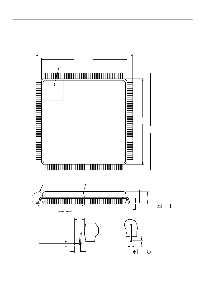
230
Agere Systems Inc.
Advance Data Sheet
May 2002
T7633 Dual T1/E1 3.3 V Short-Haul Terminator
Outline Diagram
144-Pin TQFP
Dimensions are in millimeters.
5-3815(F)r.6
DETAIL A
0.45/0.75
GAGE PLANE
SEATING PLANE
1.00 REF
0.25
DETAIL B
0.19/0.27
0.08
M
0.106/0.200
1.60 MAX
SEATING PLANE
0.08
0.50 TYP
1.40
±
0.05
0.05/0.15
DETAIL A
DETAIL B
PIN #1 IDENTIFIER ZONE
20.00
±
0.20
22.00
±
0.20
109
144
1
36
37
72
73
108
20.00
±
0.20
22.00
±
0.20

Agere Systems Inc.
231
Advance Data Sheet
May 2002
T7633 Dual T1/E1 3.3 V Short-Haul Terminator
Ordering Information
Device Code
Package
Temperature
Comcode
(Ordering Number)
T - 7633 - - - TL - DB
144-Pin TQFP
≠40 ∞C to +85 ∞C
108194895

232
232
Agere Systems Inc.
Advance Data Sheet
May 2002
T7633 Dual T1/E1 3.3 V Short-Haul Terminator
Index
Numerics
100 ms timer 72
1-byte Frames 117
3-State Procedures 139
8 ms 72
A
A bit 80, 94, 107
Aborts 116
aborts 115
Absolute Maximum Ratings 228
AIS 102, 106
Alarm Filter Register 185
Alarm Indication Signal 35
alarm indication signal 62, 92
Alarm Register 159
alternate mark inversion 52
AMI 52
AMI Encoding 52
Analog Loss of Signal 30, 31
Analog Loss of Signal (ALOS) 28
Analog Loss of Signal (ALOS) Alarm 28
ANSI
108
ASM 85
ASM time-slot format 86
Associated Signaling Mode 85, 128
Automatic AIS 188
Automatic and On-Demand Commands 106
automatically transmitting E bits 79
auxiliary pattern 102
B
B8ZS 27
B8ZS Encoding 53
Basic Frame Structure 66, 67
biframe alignment 79, 80
Binary 8 Zero Code Suppression 53
Bipolar Violation Counter Register 173
bit destuffing 115
bit offset 132
bit stuffing 115
BLB 99
Blue alarm 92
Board loopback 99
boundary scan 135
Boundary-Scan Register 139
Boundary-Scan Test Logic 135
BYPASS 139
BYPASS Register 139
BYPASS register 135
Bypassing 47, 229
C
CAS 76
CEPT
High-Density Bipolar of Order 3 (HDB3) 54
CEPT 2.048 frame 66
CEPT Loss of Basic Frame Alignment 69
CEPT Loss of Frame Alignment Recovery Algorithm 69
CEPT nailed-up broadcast transmission (CNUBT) 99
CEPT nailed-up connect loopback (CNUCLB) 99
CEPT Sa Receive Stack 178
CER 132
CEX 132
Channel Associated Signaling 76
channel associated signaling multiframe structures 66
CHI 125
CHI Common Control Register 204
CHI Data Rate 126
CHI Offset Programming 132
CHI parameters 126
CHI Receive Control Register 205, 207
CHI Receive Highway Select Registers 207
CHI system interface 79
CHI timing with associated signaling mode enabled 131
CHI Transmit Control Register 205, 207
CHI Transmit Highway Select Registers 206
CHIDATA 125
Clock Select Mode 126
clocking 122
CMS 132, 133
CNUBT mode 99
CNUCLB mode 100
Concentration Highway Interface (CHI) 125
Concentration Highway Master Mode 126
continuous E-bit 94
CRC Error Counter Register 174
CRC Option Bits Decoding 184
CRC-16 117
CRC-4 70, 79, 82
CRC-4 error counter 71
CRC-4 Errors at NT1 from NT2 Counter Register 174
CRC-4 multiframe 66, 70
CRC-4 multiframe alignment 74
CRC-4 Multiframe Alignment Algorithm with 100 ms
Timer 72
CRC-4 Multiframe Alignment Algorithm with 8 ms Timer
72
CRC-4 Multiframe Alignment Search Algorithm with
400 ms Timer 74
CRC-4/Non-CRC-4 Equipment Interworking 75
CRC-4-to-Non-CRC-4 equipment interworking 74
cyclic redundancy check-4 70
Cyclic redundancy checking 62
Index
(continued)

Agere Systems Inc.
233
Advance Data Sheet
May 2002
70 W, 1 GHz, 28 V, N-Channel, Laterally-Diffused, Enhancement
T7633 Dual T1/E1 3.3 V Short-Haul Terminator
D
D4 57
D4 Frame Format 57
data link interface 81
Data Recovery 26
DDS 58
default mode 52
Delay 45
Device ID and Version Registers 157
diagnostic loopback modes 120
Digital Data Service 58
Digital Local Loopback (DLLOOP) 44
Digital Loss of Signal 30, 31
Digital Loss of Signal (DLOS) 28
Digital Loss of Signal (DLOS) Alarm 28
double CRC-4 multiframe 82
DS0 55
DS1 55
Alternate Mark Inversion (AMI) 52
Binary 8 Zero Code Suppression (B8ZS) 53
Zero Code Suppression (ZCS) 53
DSX-1 Transmitter Pulse Template and Specifications
37
DUAL 27
E
E bit 106
E Bit at NT1 from NT2 Counter Register 174
E bits 70
E-bit 94
E-Bit Counter Register 174
E-bit monitoring 71
elastic store buffers 122
Electrical Characteristics 229
electrostatic discharge 228
error events 97
Errored Event Threshold Definition 185
Errored Second Threshold Register 186
ESF 61
ESF bit-oriented messages 109, 114
ET Bursty Errored Seconds Counter 175
ET Errored Seconds Counter 175
ET Severely Errored Seconds Counter 175
ET Unavailable Seconds Counter 175
ET1 Errored Event Enable Register 186
ET1 Remote End Errored Event Enable Register 187
ET-RE Bursty Errored Seconds Counter 175
ET-RE Errored Seconds Counter 175
ET-RE Severely Errored Seconds Counter 175
ET-RE Unavailable Seconds Counter 176
Exchange Termination and Exchange Termination Re-
mote End Interface Status Register 171
Extended Superframe 61
EXTEST 138
F
F and G bits 85
Facility Alarm Condition Register 166
Facility Data Link 108
facility data link 80
Facility Data Link Access Timing 58
Facility Errored Event Register-1 168
Facility Event Register 173
Facility Event Register-3 170
Failed state 95
FAS 67
FAS/NOT FAS Si- and E-Bit Source 79
FDL 108
FDL Control Command Register 189
FDL Control Register 212
FDL HDLC 108
FDL interface 109
FDL Interrupt Mask Control Register 213
FDL Interrupt Status Register 217
FDL Parameter/Control Registers 212
FDL Receiver Interrupt Level Control Register 215
FDL Receiver Match Character Register 215
FDL Receiver Status Register 218
FDL Transmit
ANSI
ESF Bit Codes 216
FDL Transmitter Configuration Control Register 214
FDL Transmitter Mask Register 214
FDL Transmitter Status Register 218
FDL Transparent Control Register 216
Flags 116
flags 115
Frame Alignment Signal 67
frame check sequence 117
Frame Format 55
Frame Formats 55
Frame, Superframe, and Extended Superframe Defini-
tions 55
Framer Exercise Register 198
Framer Mode Bits Decoding 183
Framer Parameter/Control Registers 180, 181, 182,
183, 184, 185, 186, 187, 188, 189, 190, 191,
192, 193, 194, 195, 196, 197, 198, 199, 200,
201, 202, 203, 204, 205, 206, 207, 208, 209,
210
Framer Register Structure 164
Framer Status/Counter Registers 165, 166, 167, 168,
169, 170, 171, 172, 173, 174, 175, 176, 177,
178, 179
Framer Transmit Line Idle Code 189
Framer Transmit System Idle Code 189
Framing Bit Errored Counter Register 173
Full Local Loopback (FLLOOP) 44

234
234
Agere Systems Inc.
Advance Data Sheet
May 2002
T7633 Dual T1/E1 3.3 V Short-Haul Terminator
Index
(continued)
G
Generated (Intrinsic) Jitter 40
Global Internal Interface Control Register 157
Global Loopback Control Register 156
Global Loopback Control Register 156
Global Register Architecture 154
Global Register Set 154
Global Register Structure 155
Global Terminal Control Register 157
H
Handling Precautions 228
HDB3 27
HDB3 Coding 54
HDLC Operation 115
High-Impedance State 45
Highway Enable 126
HIGHZ 138
human-body model 228
I
IDCODE 138
IDCODE Register 139
IDCODE register 135
idle code 86, 103
Idles 116
idles 115
In-Circuit Testing 45
instruction register 138
Interrupt Enable Register 159
Interrupt Generation 149
Interrupt Group Enable Registers 180
Interrupt Status Register 165
interworking 168
IRSM Signaling 77
ITU 66
ITU Rec. 0.151 102
ITU Rec. 706 Annex B 74
ITU Rec. G.704 Section 2.3.1 67
ITU Rec. G.704 Section 2.3.3.1 70
ITU Rec. G.704 Section 2.3.3.4 79
ITU Rec. G.704 Section 2.3.3.5.2 71
ITU Rec. G.704 Section 2.3.3.5.3 71
ITU Rec. G.706 Annex C 67
ITU Rec. G.706 Section 4.1.1 69
ITU Rec. G.706 Section 4.2 72, 74
ITU Rec. G.706 Section 4.3.2 69
ITU Rec. G.706 Section B.2.2 79
ITU Rec. G.706 Section B.2.3 74
ITU Rec. G.706.4.1.2 69
ITU Rec. G.732 Section 5.2 78
ITU Rec. G.775 93
ITU-T standard polynomial 117
J
JAR 41
Jitter 27
Jitter Accommodation 27, 30, 31, 41
Jitter Attenuator 27, 40
Jitter Attenuator Enable (Transmit or Receive Path) 41
Jitter Tolerance 41
Jitter Transfer 27, 30, 31, 40
Jitter Transfer Function 40
L
LFA 62
Line Code Option Bits Decoding 183
Line Enable Register 188
Line Interface Unit 26
Jitter Attenuator 40
Line Circuitry 48
Loopbacks 44
Receiver 26
Transmit 34
Line Interface Units (LIU) Register Architecture 158
Line Interface Units Register Set 158
Line loopback 99
Line Termination 48
LIU Alarms 28
LIU Powerdown (PD) 45
LIU Receiver Bipolar Violation (BPV) Alarm 29
LIU Transmitter Alarm Indication Signal Generator
(XLAIS) 35
LIU Transmitter Alarms 35
LIU Transmitter Configuration Modes 35
LIU Transmitter Driver Monitor (TDM) Alarm 36
LIU Transmitter Zero Substitution Encoding (CODE) 35
LIU-bypass mode 51
LIU-Framer Physical Interface 50
LLB 99
local loopback 120
Logic Interface Characteristics 229
loopback 99
Loopback Decoding 190, 191
Loopbacks 44
loss of CRC-4 multiframe alignment 71
Loss of Frame Alignment 62
loss of frame alignment 91
Loss of LIU Transmit Clock (LOTC) Alarm 35
loss of PLL clock 93
loss of receive clock 93
Loss of SYSCK (LORLCK) 45
loss of time slot 16 signaling multiframe alignment 78
Loss Shutdown (LOSSD) and Receiver AIS (RCVAIS)
29
LOSSD and RCVAIS Control Configurations 29

Agere Systems Inc.
235
Advance Data Sheet
May 2002
70 W, 1 GHz, 28 V, N-Channel, Laterally-Diffused, Enhancement
T7633 Dual T1/E1 3.3 V Short-Haul Terminator
Index
(continued)
M
Maintenance
LoopBack and Transmission Modes 99, 100, 101
match bit 119
Microprocessor Clock (MPCLK) Specifications 142
microprocessor interface 140
microprocessor modes 140
MPMODE 140
MPMUX 140
N
negative slip 93
Network Termination and Network Termination Remote
End Interface Status Register 172
no CRC-4 79
NOT FAS 80
NOT FAS frames 67
NOT FAS Sa Stack Source and Destination 82, 83, 84
NOT FAS Sa4 bit Sources 80
NT1 Bursty Errored Seconds Counter 176
NT1 Errored Event Enable Register 187
NT1 Errored Seconds Counter 176
NT1 Remote End Errored Event Enable Register 187
NT1 Severely Errored Seconds Counter 176
NT1 Unavailable Seconds Counter 176
NT1-RE Bursty Errored Seconds Counter 177
NT1-RE Errored Seconds Counter 176
NT1-RE Severely Errored Seconds Counter 177
NT1-RE Unavailable Seconds Counter 177
O
Operating Conditions 228
Ordering 231
Ordering Information 231
Outline Diagram 230
Output Pulse Generation 34
P
Parameters 126, 127, 128
Payload loopback 99
performance report message 108, 115
Performance Report Messages 110
performance report messages 114
phase-lock 122
PLLB 100
positive slip 93
Power Supply 47, 229
Powerdown 45
Primary Block Interrupt Enable Register 155
Primary Block Interrupt Status Register 155
Principle of the Boundary Scan 135
PRM 110
pseudorandom test pattern 102
Pulse Template 37, 38, 39
Q
quasi-random test signal 102
R
Rate adaptation 125
RCE 133
Rec. G.704 66
Receive
ANSI
FDL Status Register 218
Receive
ANSI
T1.403 Bit-Oriented Messages 109
Receive CRC-4 Multiframe Search Algorithm Using the
100 ms Internal Timer 73
Receive Facility Data Link Interface 108
Receive FDL FIFO 112
Receive Frame Edge 126
receive framer 50
Receive Framer Reframe 107
Receive HDLC Mode 112
Receive Highway Select 127
Receive Least Significant Bit First 128
receive line elastic store buffer 124
Receive Line Interface Configuration Modes 27
Receive NOT-FAS TS0 Register 177
receive queue status 113
receive Sa stack 71
Receive Signaling Inhibit 107
Receive Signaling Registers
CEPT Format 179
Receive Time-Slot Enable 127
Receive Time-Slot Enable Registers 206
received E-bit counter 71
received end of frame 119
Received Sa Register 177
Received Signaling Registers 179
DS1 Format 179
Receiver Alarms 28, 29
Receiver Bit Offset 127
Receiver Byte Offset 127
Receiver Clock Edge 126
Receiver FDL FIFO Register 218
receiver full 113, 119
receiver idle 119
receiver overrun 113, 119
Red alarm 91
Register Maps 219
remote alarm indication 67
Remote End Alarm Register 167
Remote Frame Alarm 106
remote frame alarm 62, 92
remote loopback 120, 121
Remote Loopback (RLOOP) 44
Reset 149
Return Loss 30, 31
RFE 132, 133
Robbed-Bit Signaling 85

236
236
Agere Systems Inc.
Advance Data Sheet
May 2002
T7633 Dual T1/E1 3.3 V Short-Haul Terminator
Index
(continued)
S
Sa bits 80, 81
Sa Bits Sourcing Decoding 195
Sa Facility Data Link Access 81
Sa stack 80, 82
Sa4--Sa8 Control Register 196
Sa4--Sa8 Source Register 195
Sa6 code monitoring 71
Sa6 codes 95, 96
Sa6 patterns 95
SAMPLE/PRELOAD 138
Secondary Loopback Control 191
secondary loopback modes 100
Secondary System Time-Slot Loopback Address 191
Secondary-single time-slot line loopback 100
Secondary-single time-slot system loopback 100
Severely Errored Second Threshold Register 186
Si bit 79
Si bits in frames 13 and 15 79
Si-Bit Source Register 198
Signaling Access 85
Signaling Mode Register 202
Single Rail 52
Single time-slot line loopback (STSLLB) 99
Single time-slot system loopback (STSSLB) 99
SLC
-96 58
SLC
-96 9-State Signaling 64
SLC
-96 Data Link Block Format 59
SLC
-96 FDL Receive Stack 178
SLC
-96 FDL stack 60
SLC
-96 Transmit Stack 197
SLIP 93
spurious frame alignment 72
status of frame (SF) byte 112
status registers 91
STSLLB 99
STSSLB 99
Stuffed Time Slots 128
System Frame Sync Mask Source 192
System Interface Control Register 201
System Time-Slot Loopback Address 190
T
T1 Frame Recovery Alignment Algorithms 63
T1 Frame Structure 55
T1 framing formats 128
T1 Framing Structures 55
T1 Robbed-Bit Signaling 64, 65
T1 stuffed channels 86
T1.403-1995 108
TAP 135
Telcordia Technologies
108
test access port 135
test access port controller 136
TFE 132, 133
time slot 16 multiframe alignment recovery algorithm 78
Time Slot 16 Signaling 86
timing requirements for the transmit and receive framer
interfaces 51
Transformer 48
Transmission of E Bit 194
Transmit
ANSI
T1.403 Bit-Oriented Messages 114
transmit elastic store buffer 122
Transmit Facility Data Link Interface 114
Transmit FDL FIFO 117
Transmit Frame Edge 126
Transmit Framer
ANSI
Performance Report Message
Status Register 179
transmit framer interface 50
Transmit Highway Select 127
transmit idle character 118
Transmit Least Significant Bit First 128
Transmit Remote Frame Alarm 107
Transmit Signaling Registers
CEPT Format 210
DS1 Format 210
transmit signaling registers 85
Transmit Time Slot 16 Remote Multiframe Alarm 107
Transmit Time-Slot Enable 127
Transmit Time-Slot Enable Registers 206
Transmitter FDL FIFO Register 214
Transmitter Bit Offset 127
Transmitter Byte Offset 127
Transmitter Clock Edge 126
transmitter empty 118
Transmitter Underrun 117
Transparent Framing 56
transparent framing mode 1 56
transparent framing mode 2 56
Transparent Mode 118
transparent mode 119
TR-TSY-000194 Issue 1, 12-87 108
U
unavailable state alarm 95
X
XCE 133
Y
Yellow alarm 92
Z
ZCS 53
ZCS Encoding 53
Zero Code Suppression 53
Zero Substitution 27
Zero Substitution Decoding (CODE) 27
Zero-Bit Insertion/Deletion 115

Agere Systems Inc.
237
Advance Data Sheet
May 2002
70 W, 1 GHz, 28 V, N-Channel, Laterally-Diffused, Enhancement
T7633 Dual T1/E1 3.3 V Short-Haul Terminator
Notes

Copyright © 2002 Agere Systems Inc.
All Rights Reserved
May 2002
DS02-244BBAC (Replaces DS98-244TIC)
For additional information, contact your Agere Systems Account Manager or the following:
INTERNET:
http://www.agere.com
E-MAIL:
docmaster@agere.com
N. AMERICA:
Agere Systems Inc., 555 Union Boulevard, Room 30L-15P-BA, Allentown, PA 18109-3286
1-800-372-2447, FAX 610-712-4106 (In CANADA: 1-800-553-2448, FAX 610-712-4106)
ASIA:
Agere Systems Hong Kong Ltd., Suites 3201 & 3210-12, 32/F, Tower 2, The Gateway, Harbour City, Kowloon
Tel. (852) 3129-2000, FAX (852) 3129-2020
CHINA: (86) 21-5047-1212 (Shanghai), (86) 10-6522-5566 (Beijing), (86) 755-695-7224 (Shenzhen)
JAPAN: (81) 3-5421-1600 (Tokyo), KOREA: (82) 2-767-1850 (Seoul), SINGAPORE: (65) 6778-8833, TAIWAN: (886) 2-2725-5858 (Taipei)
EUROPE:
Tel. (44) 7000 624624, FAX (44) 1344 488 045
Agere Systems Inc. reserves the right to make changes to the product(s) or information contained herein without notice. No liability is assumed as a result of their use or application.
Agere, Agere Systems, and the Agere logo are trademarks of Agere Systems Inc.
SLC
is a registered trademark of Lucent Technologies Inc.
AT&T
is a registered trademark of AT&T Inc.
ANSI
is a registered trademark of the American National Standards Institute.
Intel
is a registered trademark of Intel Corporation.
Motorola
is a registered trademark of Motorola, Inc.
Telcordia Technologies
is a registered trademark of Telcordia Technologies Inc.
Mitel
is a registered trademark of Mitel Corporation.
AMD
is a registered trademark of Advanced Micro Devices, Inc.
IEEE
is a registered trademark of The Institute of Electrical and Electronics Engineers, Inc.