 | –≠–ª–µ–∫—Ç—Ä–æ–Ω–Ω—ã–π –∫–æ–º–ø–æ–Ω–µ–Ω—Ç: T7693 | –°–∫–∞—á–∞—Ç—å:  PDF PDF  ZIP ZIP |

Data Sheet
July 2002
T7690 5.0 V T1/E1 Quad Line Interface
T7693 3.3 V T1/E1 Quad Line Interface
1 Features
s
Four fully integrated T1/E1 line interfaces
s
Includes all driver, receiver, equalization, clock recovery,
and jitter attenuation functions
s
Ultralow power consumption
s
Robust operation for increased system margin
s
High interference immunity
s
On-chip transmit equalization for improved sensitivity
s
Low-impedance drivers for reduced power consumption
s
Selectable transmit or receive jitter attenuation/clock
smoothing
s
3-state transmit drivers
s
High-speed microprocessor interface
s
Automatic transmit monitor function
s
Per-channel powerdown
s
For use in systems that are compliant with AT&T
Æ
CB119; TR-TSY-000170, TR-TSY-000009, TR-TSY-
000499, TR-TSY-000253; ANSI
Æ
T1.102 and T1.403;
ITU-T G.703, G.732, G.735-9, G.775, G.823-4, and I.431
s
Common transformer for transmit/receive
s
Fine-pitch (25 mil spacing) surface-mount package, 100-
pin bumpered quad flat pack
s
≠40 ∞C to +85 ∞C operating temperature range
2 Applications
s
SONET/SDH multiplexers
s
Asynchronous multiplexers (M13)
s
Digital access cross connects (DACs)
s
Channel banks
s
Digital radio base stations, remote wireless
modules
s
PBX interfaces
3 Overview
The T7690 and T7693 are fully integrated quad line inter-
faces containing four transmit and receive channels for use
in both North American (T1/DS1) and European (E1/CEPT)
applications. The devices have many of the same functions
as the Agere T7290A and provide additional flexibility for
the system designer.
Included is a parallel microprocessor interface that allows
the user to define the architecture, initiate loopbacks, and
monitor alarms. The interface is compatible with many
commercially available microprocessors.
The receiver performs clock and data recovery using a fully
integrated digital phase-locked loop. This digital implemen-
tation prevents false lock conditions that are common when
recovering sparse data patterns with analog phase-locked
loops. Equalization circuitry in the receiver guarantees a
high level of interference immunity. As an option, the raw
sliced data (no retiming) can be output on the receive data
pins.
Transmit equalization is implemented with low-impedance
output drivers that provide shaped waveforms to the trans-
former, guaranteeing template conformance. The quad
device will interface to the digital cross connect (DSX) at
lengths of up to 655 ft. for DS1 operation, or to line imped-
ances of 75
or 120
for CEPT operation.
A selectable jitter attenuator may be placed in the receive
signal path for low-bandwidth, line-synchronous applica-
tions, or it may be placed in the transmit path for multi-
plexer applications where DS1/CEPT signals are
demultiplexed from higher rate signals. The jitter attenuator
will perform the clock smoothing required on the resulting
demultiplexed gapped clock.

Table of Contents
Contents
Page
Contents
Page
2
Agere Systems Inc.
Data Sheet
July 2002
T7693 3.3 V T1/E1 Quad Line Interface
T7690 5.0 V T1/E1 Quad Line Interface
1 Features ........................................................................ 1
2 Applications ................................................................... 1
3 Overview ........................................................................ 1
4 Single Channel Block Diagram ...................................... 4
5 Pin Information ............................................................. 5
5.1 System Interface Pin Options ................................. 9
6 Receiver ...................................................................... 11
6.1 Data Recovery ...................................................... 11
6.2 Jitter ...................................................................... 11
6.3 Receiver Configuration Modes ............................. 11
6.3.1 Clock/Data Recovery Mode (CDR) ............. 11
6.3.2 Zero Substitution Decoding (CODE) ........... 11
6.3.3 Alternate Logic Mode (ALM) ....................... 11
6.3.4 Alternate Clock Mode (ACM) ...................... 11
6.3.5 Loss Shutdown (LOSSD) ............................ 12
6.4 Receiver Alarms ................................................... 12
6.4.1 Analog Loss-of-Signal (ALOS) Alarm .......... 12
6.4.2 Digital Loss-of-Signal (DLOS) Alarm ........... 12
6.4.3 Bipolar Violation (BPV) Alarm ..................... 12
6.5 DS1 Receiver Specifications ................................ 13
6.6 CEPT Receiver Specifications .............................. 14
7 Transmitter .................................................................. 15
7.1 Output Pulse Generation ...................................... 15
7.2 Jitter ...................................................................... 15
7.3 Transmitter Configuration Modes ......................... 16
7.3.1 Zero Substitution
Encoding/Decoding (CODE) ....................... 16
7.3.2 All Ones (AIS, Blue Signal)
Generator (TBS) .......................................... 16
7.4 Transmitter Alarms ............................................... 16
7.4.1 Loss-of-Transmit Clock (LOTC) Alarm ........ 16
7.4.2 Transmit Driver Monitor (TDM) Alarm ......... 16
7.5 DS1 Transmitter Pulse Template
and Specifications ................................................ 16
7.6 CEPT Transmitter Pulse Template
and Specifications ................................................ 17
8 Jitter Attenuator ........................................................... 19
8.1 Data Delay ............................................................ 19
8.2 Generated (Intrinsic) Jitter .................................... 19
8.3 Jitter Transfer Function ......................................... 19
8.4 Jitter Tolerance ..................................................... 19
8.5 Jitter Attenuator Enable ........................................ 19
8.5.1 Jitter Attenuator Receive
Path Enable (JAR) ...................................... 19
8.5.2 Jitter Attenuator Transmit
Path Enable (JAT) ....................................... 20
8.6 Loopbacks ............................................................ 20
8.6.1 Full Local Loopback (FLLOOP) ................... 20
8.6.2 Remote Loopback (RLOOP) ....................... 20
8.6.3 Digital Local Loopback (DLLOOP) .............. 20
8.7 Other Features ..................................................... 20
8.7.1 Powerdown (PWRDN) ................................ 20
8.7.2 RESET (
5(6(7
, SWRESET) .......................20
8.8 Loss of XCLK Reference Clock (LOXC) ...............21
8.9 In-Circuit Testing and Driver 3-State (ICT) ............21
9 Microprocessor Interface ..............................................22
9.1 Overview ...............................................................22
9.2 Microprocessor Configuration Modes ...................22
9.3 Microprocessor Interface Pinout Definitions ..........23
9.4 Microprocessor Clock (MPCLK) Specifications .....24
9.5 Internal Chip Select Function ................................24
9.6 Microprocessor Interface Register Architecture ....24
9.6.1 Alarm Register Overview (0000, 0001) ........26
9.6.2 Alarm Mask Register Overview
(0010, 0011) ................................................26
9.6.3 Global Control Register Overview
(0100, 0101) ................................................27
9.6.4 Channel Configuration Register Overview
(0110--1001) ...............................................27
9.6.5 Other Registers ............................................28
10 Timing Characteristics ................................................29
10.1 I/O Timing ...........................................................29
10.2 Interface Data Timing .........................................34
10.2.1 Logic Interface Characteristics .................35
10.3 XCLK Reference Clock .......................................35
11 Electrical Characteristics ............................................36
11.1 Power Supply Bypassing ....................................36
11.2 Power Specifications ...........................................36
11.3 Absolute Maximum Ratings ................................37
11.4 Handling Precautions ..........................................37
11.5 Operating Conditions ..........................................37
12 External Line Termination Circuitry ............................38
12.1 T7690 .................................................................38
12.2 T7693 .................................................................39
13 Outline Diagram .........................................................40
13.1 100-Pin BQFP ....................................................40
Figures
Page
Figure 4-1. Block Diagram (Single Channel)......................4
Figure 5-1. Pin Diagram .....................................................5
Figure 7-1. DSX-1 Isolated Pulse Template.....................17
Figure 7-2. ITU-T G.703 Pulse Template.........................17
Figure 10-1. Mode 1--Read Cycle Timing
(MPMODE = 0, MPMUX = 0).......................30
Figure 10-2. Mode 1--Write Cycle Timing
(MPMODE = 0, MPMUX = 0).......................30
Figure 10-3. Mode 2--Read Cycle Timing
(MPMODE = 0, MPMUX = 1).......................31
Figure 10-4. Mode 2--Write Cycle Timing
(MPMODE = 0, MPMUX = 1).......................31
Figure 10-5. Mode 3--Read Cycle Timing
(MPMODE = 1, MPMUX = 0).......................32

Agere Systems Inc.
3
Data Sheet
July 2002
T7693 3.3 V T1/E1 Quad Line Interface
T7690 5.0 V T1/E1 Quad Line Interface
Table of Contents
(continued)
Figure
Page
Figure
Page
Figure 10-6. Mode 3--Write Cycle Timing
(MPMODE = 1, MPMUX = 0) ...................... 32
Figure 10-7. Mode 4--Read Cycle Timing
(MPMODE = 1, MPMUX = 1) ...................... 33
Figure 10-8. Mode 4--Write Cycle Timing
(MPMODE = 1, MPMUX = 1) ...................... 33
Table
Page
Table 5-1. Pin Descriptions................................................ 6
Table 5-2. Pin Mapping.................................................... 10
Table 6-1. Digital Loss-of-Signal Standard Select ........... 12
Table 6-2. DS1 Receiver Specifications .......................... 13
Table 6-3. CEPT Receiver Specifications........................ 14
Table 7-1. Equalizer/Rate Control.................................... 15
Table 7-2. DSX-1 Pulse Template Corner Points
(From CB119) ................................................. 17
Table 7-3. DS1 Transmitter Specifications....................... 17
Table 7-4. CEPT Transmitter Specifications .................... 18
Table 8-1. List of Low-Bandwidth Jitter
Specification Documents ................................ 19
Table 8-2. Loopback Control............................................ 20
Table 9-1. Microprocessor Configuration Modes ............. 22
Table 9-2. MODE [1--4] Microprocessor
Pin Definitions................................................. 23
Table 9-3. Microprocessor Input Clock Specifications ..... 24
Table 9-4. Register Set .................................................... 25
Figure 10-9. Interface Data Timing (ACM = 0) .................34
Figure 12-1. T7690 External Line Termination Circuitry ..38
Figure 12-2. T7693 External Line Termination Circuitry ..39
Table
Page
Table 9-5. Alarm Registers...............................................26
Table 9-6. Alarm Mask Registers .....................................26
Table 9-7. Global Control Register (0100)........................27
Table 9-8. Global Control Register (0101)........................27
Table 9-9. Channel Configuration Registers ....................28
Table 10-1. Microprocessor Interface I/O Timing
Specifications.................................................29
Table 10-2. Interface Data Timing ....................................34
Table 10-3. Logic Interface Characteristics ......................35
Table 10-4. XCLK Timing Specifications ..........................35
Table 11-1. Power Specifications .....................................36
Table 11-2. Absolute Maximum Ratings...........................37
Table 11-3. Handling Precaution ......................................37
Table 11-4. Recommended Operating Conditions ...........37
Table 12-1. Termination Components by Application .......38
Table 12-2. Termination Components by Application .......39
T7690 5.0 V T1/E1 Quad Line Interface
Data Sheet
T7693 3.3 V T1/E1 Quad Line Interface
July 2002
4
4
Agere Systems Inc.
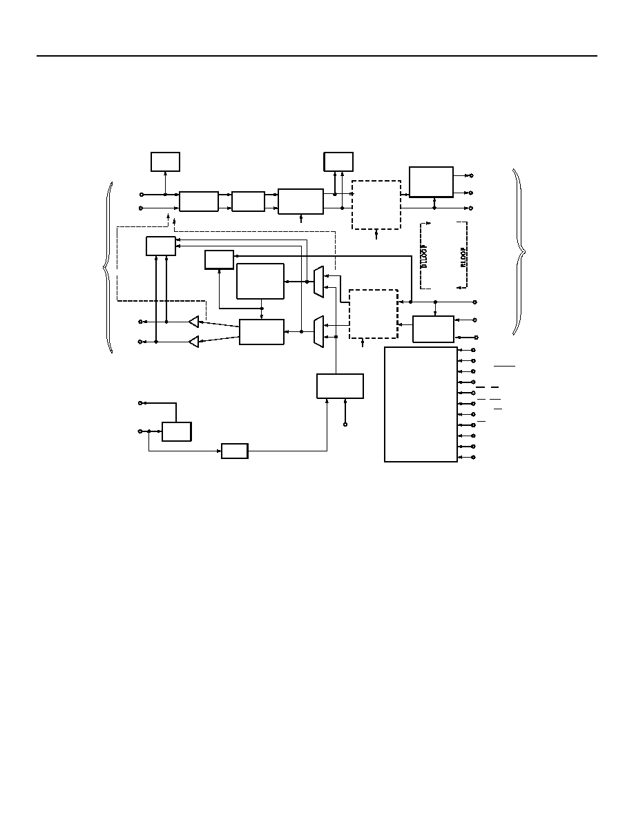
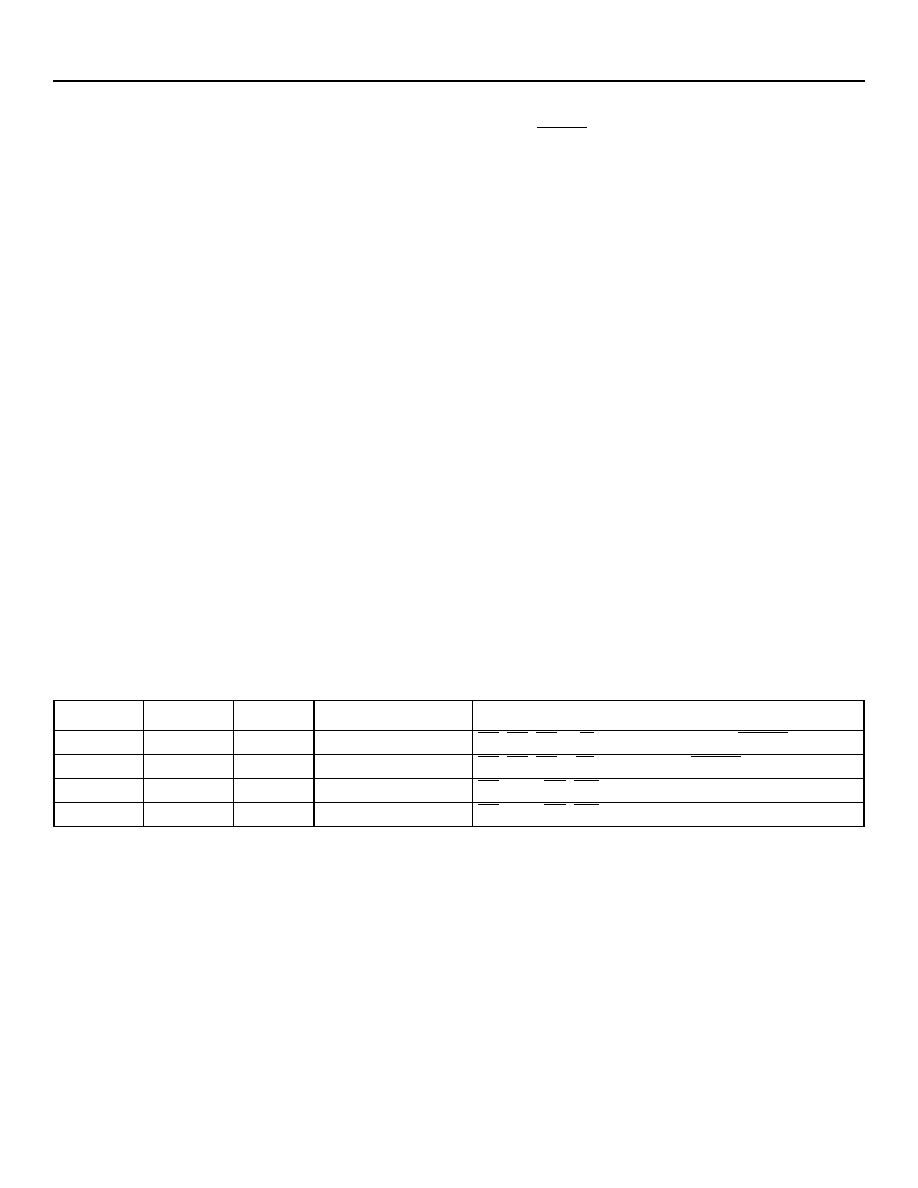
4 Single Channel Block Diagram
The T7690/T7693 block diagram is shown in Figure 4-1. For illustration purposes, only one of the four on-chip line inter-
faces is shown. Pin names, that apply to all four channels, are followed by the designation [1--4].
* Function can be bypassed by using the microprocessor interface.
Figure 4-1. Block Diagram (Single Channel)
'/26
&/2&.'$7$
5(&29(5<
6/,&(56
(48$/,=(5
$/26
%39
'(&2'(5
/27&
7'0
38/6(
:,'7+
&21752//(5
38/6(
(48$/,=(5
(1&2'(5
%/8(
6,*1$/ $,6�
/2;&
0,&52352&(6625
,17(5)$&(
5'1%39>@
5&/.$/26>@
55,1*>@
;&/.
7&/.>@
73'71'>@
%&/.
77,3>@
75,1*>@
'5,9(56
/2;&
;&/.
03&/.
0302'(
0308;
&6
$/(B$6
5'B5:
:5B'6
,17
5'<B'7$&.
$'>@
$>@
)//223
)//223
12 %/8( 6,*1$/�
'85,1* %/8( 6,*1$/�
57,3>@
71'>@
-,77(5
$77(18$725
7; 25 5; 3$7+�
-,77(5
$77(18$725
7; 25 5; 3$7+�
53'5'$7$>@
;&/.
;&/.
6<67(0
,17(5)$&(
/,1(
,17(5)$&(
Agere Systems Inc.
5
Data Sheet
T7690 5.0 V T1/E1 Quad Line Interface
July 2002
T7693 3.3 V T1/E1 Quad Line Interface
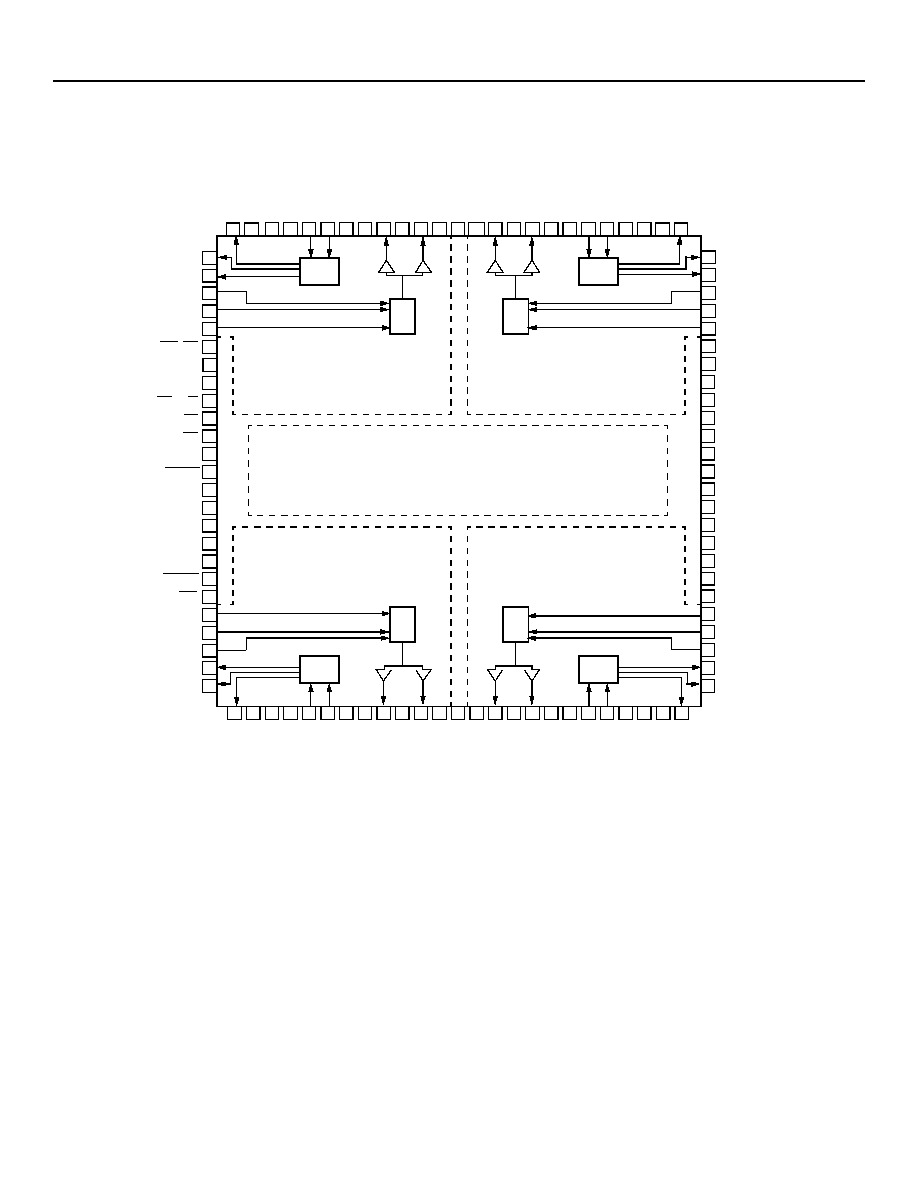
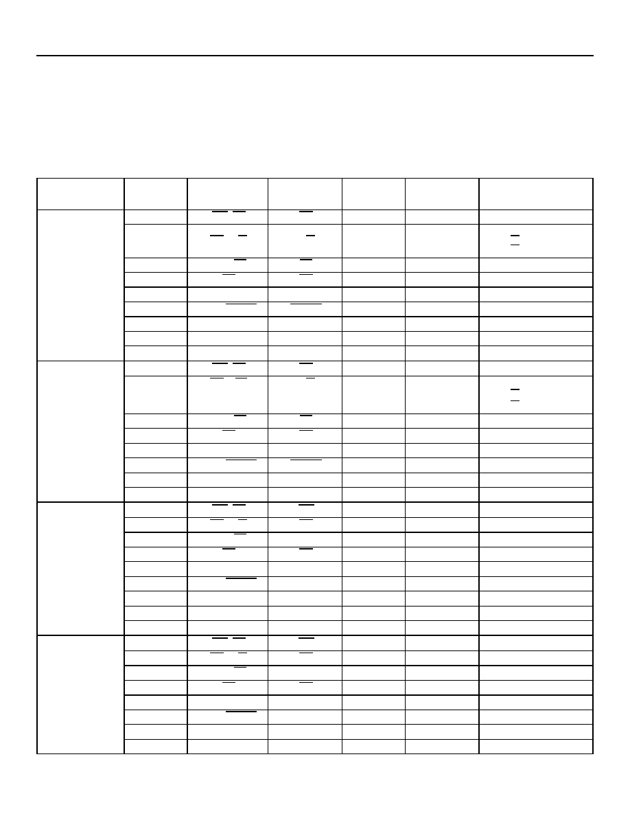
5 Pin Information
5-3684(C)r.2
Figure 5-1. Pin Diagram
73'7'$7$
71'
7&/.
53'5'$7$
5
1'
%39
5&/.$/26
5(6(7
5&/.$/26
5
1'
%39
53'5'$7$
7&/.
71'
73'7'$7$
75
,1
*
9
''
;
77
,3
*
1';
73'7'$7$
71'
7&/.
53'5'$7$
51'
%
39
5&/.$/26
,&7
9
''$
*1'
$
57
,3
55,1*
5&/.$/26
51'
%39
53'5'$7$
7&/.
71'
73'7'$7$
$
$
$
$
&6
$'
$'
$'
$'
$'
$'
$'
$'
9
''&
;&/.
%&/.
*1'
&
03&/.
0302'(
5'<B'7$&.
,17
:5B'6
5'B5:
$/(B$6
0308;
/2;&
*
1';
*1'
'
9
'''
75
,
1
*
9
''
;
77
,3
*
1';
9
''$
*1'
$
57
,
3
55,1*
*1';
*1
'
'
9
'''
75
,
1
*
9
''
;
77
,3
*1';
9
''$
*1'
$
55,1*
57
,3
*1';
*1'
'
9
'''
75
,
1
*
9
''
;
77
,3
*1';
9
''$
*1'
$
57
,
3
55,1*
*1';
*1'
'
9
'''
*1'
&
9
''&
7
5
CHANNEL 2
7
5
*1'
6
*1
'
6
7
5
CHANNEL 4
7
5
CHANNEL 3
MICROPROCESSOR INTERFACE
CHANNEL 1

T7690 5.0 V T1/E1 Quad Line Interface
Data Sheet
T7693 3.3 V T1/E1 Quad Line Interface
July 2002
5 Pin Information
(continued)
6
6
Agere Systems Inc.
Table 5-1. Pin Descriptions
Pin
Symbol
Type*
Name/Description
1, 51
GND
S
P
Ground Reference for Substrate.
2, 6
GNDX1
P
Ground Reference for Line Drivers.
46, 50
GNDX2
52, 56
GNDX3
96, 100
GNDX4
3
TTIP1
O
Transmit Bipolar Tip. Positive bipolar transmit output data to the analog line inter-
face.
49
TTIP2
53
TTIP3
99
TTIP4
4
V
DD
X1
P
Power Supply for Line Drivers. The T7690 device requires a 5 V ± 5% power sup-
ply on these pins. The T7693 device requires a 3.3 V ± 5% power supply on these
pins.
48
V
DD
X2
54
V
DD
X3
98
V
DD
X4
5
TRING1
O
Transmit Bipolar Ring. Negative bipolar transmit output data to the analog line
interface.
47
TRING2
55
TRING3
97
TRING4
7
V
DDA
1
P
Power Supply for Analog Circuitry. The T7690 device requires a 5 V ± 5% power
supply on these pins. The T7693 device requires a 3.3 V ± 5% power supply on
these pins.
45
V
DDA
2
57
V
DDA
3
95
V
DDA
4
8
RTIP1
I
Receive Bipolar Tip. Positive bipolar receive input data from the analog line inter-
face.
44
RTIP2
58
RTIP3
94
RTIP4
9
RRING1
I
Receive Bipolar Ring. Negative bipolar receive input data from the analog line
interface.
43
RRING2
59
RRING3
93
RRING4
10
GND
A
1
P
Ground Reference for Analog Circuitry.
42
GND
A
2
60
GND
A
3
92
GND
A
4
11
GND
D
1
P
Ground Reference for Digital Circuitry.
41
GND
D
2
61
GND
D
3
91
GND
D
4
* P = power, I = input, O = output, and Iu
= input with internal pull-up.

Data Sheet
T7690 5.0 V T1/E1 Quad Line Interface
July 2002
T7693 3.3 V T1/E1 Quad Line Interface
5 Pin Information
(continued)
Agere Systems Inc.
7
12
V
DDD
1
P
Power Supply for Digital Circuitry. The T7690 device requires a 5 V ± 5% power
supply on these pins. The T7693 device requires a 3.3 V ± 5% power supply on
these pins.
40
V
DDD
2
62
V
DDD
3
90
V
DDD
4
13
RND1/BPV1
O
Receive Negative Data. When in dual-rail (DUAL = 1: register 5, bit 4) clock recov-
ery mode (CDR = 1: register 5, bit 0), this signal is the receive negative NRZ output
data to the terminal equipment. When in data slicing mode (CDR = 0), this signal is
the raw sliced negative output data of the front end.
Bipolar Violation. When in single-rail (DUAL = 0: register 5, bit 4) clock recovery
mode (CDR = 1: register 5, bit 0), and CODE = 1 (register 5, bit 3), this signal is
asserted high to indicate the occurrence of a code violation in the receive data
stream. If CODE = 0, this signal is asserted to indicate the occurrence of a bipolar
violation in the receive data system.
39
RND2/BPV2
63
RND3/BPV3
89
RND4/BPV4
14
RPD1/
RDATA1
O
Receive Positive Data. When in dual-rail (DUAL = 1: register 5, bit 4) clock recov-
ery mode (CDR = 1: register 5, bit 0), this signal is the receive positive NRZ output
data to the terminal equipment. When in data slicing mode (CDR = 0), this signal is
the raw sliced positive output data of the front end.
Receive Data. When in single-rail (DUAL = 0: register 5, bit 4) clock recovery mode
(CDR = 1: register 5, bit 0), this signal is the receive NRZ output data.
38
RPD2/
RDATA2
64
RPD3/
RDATA3
88
RPD4/
RDATA4
15
RCLK1/
ALOS1
O
Receive Clock. In clock recovery mode (CDR = 1: register 5, bit 0), this signal is the
receive clock for the terminal equipment. The duty cycle of RCLK is 50% ± 5%.
Analog Loss-of-Signal. In data slicing mode (CDR = 0: register 5, bit 0), this signal
is asserted high to indicate low-amplitude receive data at the RTIP/RRING inputs.
37
RCLK2/
ALOS2
65
RCLK3/
ALOS3
87
RCLK4/
ALOS4
16
TND1
I
Transmit Negative Data. Transmit negative NRZ input data from the terminal
equipment.
36
TND2
66
TND3
86
TND4
17
TPD1/TDATA1
I
Transmit Positive Data. When in dual-rail mode (DUAL = 1: register 5, bit 4), this
signal is the transmit positive NRZ input data from the terminal equipment.
Transmit Data. When in single-rail mode (DUAL = 0: register 5, bit 4), this signal is
the transmit NRZ input data from the terminal equipment.
35
TPD2/TDATA2
67
TPD3/TDATA3
85
TPD4/TDATA4
18
TCLK1
I
Transmit Clock. DS1 (1.544 MHz ± 32 ppm) or CEPT (2.048 MHz ± 50 ppm) clock
signal from the terminal equipment.
34
TCLK2
68
TCLK3
84
TCLK4
Table 5-1. Pin Descriptions (continued)
Pin
Symbol
Type*
Name/Description
* P = power, I = input, O = output, and Iu
= input with internal pull-up.

T7690 5.0 V T1/E1 Quad Line Interface
Data Sheet
T7693 3.3 V T1/E1 Quad Line Interface
July 2002
5 Pin Information
(continued)
8
8
Agere Systems Inc.
19
WR_DS
I
Write (Active-Low). If MPMODE = 1 (pin 21), this pin is asserted low by the micro-
processor to initiate a write cycle.
Data Strobe (Active-Low). If MPMODE = 0 (pin 21), this pin becomes the data
strobe for the microprocessor. When R/W = 0 (write), a low applied to this pin
latches the signal on the data bus into internal registers.
20
MPMUX
I
Microprocessor Multiplex Mode. Setting MPMUX = 1 allows the microprocessor
interface to accept multiplexed address and data signals. Setting MPMUX = 0
allows the microprocessor interface to accept demultiplexed (separate) address and
data signals.
21
MPMODE
I
Microprocessor Mode. When MPMODE = 1, the device uses the address latch
enable type microprocessor read/write protocol with separate read and write con-
trols. Setting MPMODE = 0 allows the device to use the address strobe type micro-
processor read/write protocol with a separate data strobe and a combined read/
write control.
22
RD_R/W
I
Read (Active-Low). If MPMODE = 1 (pin 21), this pin is asserted low by the micro-
processor to initiate a read cycle.
Read/Write. If MPMODE = 0, this pin is asserted high by the microprocessor to indi-
cate a read cycle or asserted low to indicate a write cycle.
23
ALE_AS
I
Address Latch Enable. If MPMODE = 1 (pin 21), this pin becomes the address
latch enable for the microprocessor. When this pin transitions from high to low, the
address bus inputs are latched into the internal registers.
Address Strobe (Active-Low). If MPMODE = 0, this pin becomes the address
strobe for the microprocessor. When this pin transitions from high to low, the
address bus inputs are latched into the internal registers.
24
CS
I
X
Chip Select (Active-Low). This pin is asserted low by the microprocessor to enable
the microprocessor interface. If MPMUX = 1 (pin 20), CS can be externally tied low
to use the internal chip selection function (see
Section 9.5
). An internal 100 k
pull-
up is on this pin.
25
INT
O
Interrupt. This pin is asserted high to indicate an interrupt produced by an alarm
condition in register 0 or 1. The activation of this pin can be masked by microproces-
sor registers 2, 3, and 4.
26
RDY_DTACK
O
Ready. If MPMODE = 1 (pin 21), this pin is asserted high to indicate the device has
completed a read or write operation. This pin is in a 3-state condition when CS (pin
24) is high.
Data Transfer Acknowledge (Active-Low). If MPMODE = 0, this pin is asserted
low to indicate the device has completed a read or write operation.
27, 78
GND
C
P
Ground Reference for Microprocessor Interface and Control Circuitry.
28, 77
V
DDC
P
Power Supply for Microprocessor Interface and Control Circuitry. The T7690
device requires a 5 V ± 5% power supply on these pins. The T7693 device requires
a 3.3 V ± 5% power supply on these pins.
29
XCLK
I
X
Reference Clock. A valid reference clock (24.704 MHz ± 100 ppm for DS1 opera-
tion, 32.768 MHz ± 100 ppm for CEPT operation) must be provided at this input for
certain applications (see
Section 10.3
). XCLK must be an independent, continu-
ously active, ungapped, and unjittered clock to guarantee device performance spec-
ifications. An internal 100 k
pull-up is on this pin.
Table 5-1. Pin Descriptions (continued)
Pin
Symbol
Type*
Name/Description
* P = power, I = input, O = output, and Iu
= input with internal pull-up.
Data Sheet
T7690 5.0 V T1/E1 Quad Line Interface
July 2002
T7693 3.3 V T1/E1 Quad Line Interface
5 Pin Information
(continued)
Agere Systems Inc.
9
5.1 System Interface Pin Options
The system interface can be configured to operate in a number of different modes, as shown in
Table 5-2
. Dual-rail or sin-
gle-rail operation is possible using the DUAL control bit (register 5, bit 4). Dual-rail mode is enabled when DUAL = 1; single-
rail mode is enabled when DUAL = 0. In dual-rail operation, data received from the line interface on RTIP and RRING
appears on RPD (pins 14, 38, 64, and 88) and RND (pins 13, 39, 63, and 89) at the system interface and data transmitted
from the system interface on TPD (pins 17, 35, 67, and 85) and TND (pins 16, 36, 66, and 86) appears on TTIP and TRING
at the line interface. In single-rail operation, data received from the line interface on RTIP and RRING appears on RDATA
(pins 14, 38, 64, 88) at the system interface and data transmitted from the system interface on TDATA (pins 17, 35, 67, and
85) appears on TTIP and TRING at the line interface.
In both dual-rail and single-rail operation, the clock/data recovery mode is selectable via the CDR bit (register 5, bit 0).
When CDR = 1, the clock and data recovery is enabled and the system interface operates in a nonreturn-to-zero (NRZ) dig-
ital format. When CDR = 0, the clock and data recovery is disabled and the system interface operates on unretimed sliced
data in RZ data format (see
Section 6.1
).
30
BCLK
I
X
Blue Clock. Input clock signal used to transmit the blue signal (alarm indication sig-
nal (AIS) all 1s data pattern). In DS1 mode, this clock is 1.544 MHz ± 32 ppm, and in
CEPT mode, this clock is 2.048 MHz ± 50 ppm. An internal 100 k
pull-up is on this
pin.
31
LOXC
O
Loss-of-XCLK. This pin is asserted high when the XCLK signal (pin 29) is not
present.
32
RESET
I
u
Hardware Reset (Active-Low). If RESET is forced low, all internal states in the line
interface paths are reset and data flow through each channel will be momentarily
disrupted (see the RESET (RESET, SWRESET) section). The RESET pin must be
held low for a minimum of 10 µs. An internal 50 k
pull-up is on this pin.
33
ICT
I
u
In-Circuit Test Control (Active-Low). If ICT is forced low, certain output pins are
placed in a high-impedance state (see the In-Circuit Testing and Driver 3-State (ICT)
section). An internal 50 k
pull-up is on this pin.
69
AD7
I/O
Microprocessor Interface Address/Data Bus. If MPMUX = 0 (pin 20), these pins
become the bidirectional, 3-statable data bus. If MPMUX = 1, these pins become
the multiplexed address/data bus. In this mode, only the lower 4 bits (AD[3:0]) are
used for the internal register addresses.
70
AD6
71
AD5
72
AD4
73
AD3
74
AD2
75
AD1
76
AD0
79
A3
I
Microprocessor Interface Address. If MPMUX = 0 (pin 20), these pins become
the address bus for the microprocessor interface registers.
If MPMUX = 1, A3 (pin 79) can be externally tied high to use the internal chip selec-
tion function (see
Section 9.5
). If this function is not used, A[3:0] must be externally
tied low.
80
A2
81
A1
82
A0
83
MPCLK
I
Microprocessor Interface Clock. Microprocessor interface clock rates from twice
the frequency of the line clock (3.088 MHz for DS1 operation, 4.096 MHz for CEPT
operation) to 16.384 MHz are supported.
Table 5-1. Pin Descriptions (continued)
Pin
Symbol
Type*
Name/Description
* P = power, I = input, O = output, and Iu
= input with internal pull-up.

T7690 5.0 V T1/E1 Quad Line Interface
Data Sheet
T7693 3.3 V T1/E1 Quad Line Interface
July 2002
5 Pin Information
(continued)
10
10
Agere Systems Inc.
In single-rail mode only, B8ZS/HDB3 encoding/decoding may be selected by setting CODE = 1 (register 5, bit 3). This
allows coding violations, such as receiving two consecutive 1s of the same polarity from the line interface, to be output on
BPV (pins 13, 39, 63, and 89), see
Section 7.3.1
.
Table 5-2. Pin Mapping
Configuration
RCLK/ALOS RPD/RDATA
RND/BPV
TPD/TDATA
TND
Dual-rail System Interface with Clock Recovery
RCLK
RPD
RND
TPD
TND
Dual-rail System Interface with Data Slicing Only
ALOS
RPD
RND
Single-rail System Interface with Clock Recovery
RCLK
RDATA
BPV
TDATA
Not
Used
Single-rail System Interface with Data Slicing Only
ALOS
RPD
RND

Agere Systems Inc.
11
Data Sheet
T7690 5.0 V T1/E1 Quad Line Interface
July 2002
T7693 3.3 V T1/E1 Quad Line Interface
6 Receiver
6.1 Data Recovery
The receive line interface transmission format of the device
is bipolar alternate mark inversion (AMI). It accepts input
data with a frequency tolerance of ±130 ppm (DS1) or
±80 ppm (CEPT). The receiver first restores the incoming
data and detects analog loss-of-signal. Subsequent pro-
cessing is optional and depends on the programmable
device configuration established within the microprocessor
interface registers. The receiver operates with high interfer-
ence immunity, utilizing an equalizer to restore fast rise/fall
times following maximum cable loss. The signal is then
peak-detected and sliced to produce digital representations
of the data.
Selectable clock recovery of the sliced data, digital loss-of-
signal, jitter attenuation, and data decoding are performed.
For applications bypassing the clock recovery function
(CDR = 0), the receive digital output format is unretimed
sliced data (RZ positive and negative data). For clock
recovery applications (CDR = 1), the receive digital output
format is nonreturn to zero (NRZ) with selectable dual-rail
or single-rail system interface. The recovered clock (RCLK,
pins 15, 37, 65, and 87) is only provided when CDR = 1
(see
Table 5-2
).
Timing recovery is performed by a digital phase-locked
loop that uses XCLK (pin 29) as a reference to lock to the
incoming data. Because the reference clock is a multiple of
the received data rate, the output RCLK (pins 15, 37, 65,
and 87) will always be a valid DS1/CEPT clock that elimi-
nates false-lock conditions. During periods with no input
signal, the free-run frequency is defined to be XCLK/16.
RCLK is always active with a duty-cycle centered at 50%,
deviating by no more than ±5%. Valid data is recovered
within the first few bit periods after the application of XCLK.
The delay of the data through the receive circuitry is
approximately 1 to 14 bit periods, depending on the CDR
and CODE configurations. Additional delay is introduced if
the jitter attenuator is selected for operation in the receive
path (see
Section 8.1
).
6.2 Jitter
The receiver is designed to accommodate large amounts of
input jitter. The receiver jitter performance far exceeds the
requirements shown in
Table 6-2
and
Table 6-3
. Jitter
transfer is independent of input ones density on the line
interface.
6.3 Receiver Configuration Modes
6.3.1 Clock/Data Recovery Mode (CDR)
The clock/data recovery function in the receive path is
selectable via the CDR bit (register 5, bit 0). If CDR = 1, the
clock and data recovery function is enabled and provides a
recovered clock (RCLK) with retimed data (RPD/RDATA,
RND). If CDR = 0, the clock and data recovery function is
disabled, and the RZ data from the slicers is provided over
RPD and RND to the system. In this mode, ALOS is avail-
able on the RCLK/ALOS pins, and downstream functions
selected by microprocessor register 5 (JAR, ACM, LOSSD)
are ignored.
6.3.2 Zero Substitution Decoding (CODE)
When single-rail operation is selected with DUAL = 0 (reg-
ister 5, bit 4), the B8ZS/HDB3 zero substitution decoding
can be selected via the CODE bit (register 5, bit 3). If
CODE = 1, the B8ZS/HDB3 decoding function is enabled in
the receive path and decoded receive data and code viola-
tions appear on the RDATA and BPV pins, respectively. If
CODE = 0, receive data and any bipolar violations (such as
two consecutive 1s of the same polarity) appear on the
RDATA and BPV pins, respectively.
6.3.3 Alternate Logic Mode (ALM)
The alternate logic mode (ALM) control bit (register 5, bit 5)
selects the receive and transmit data polarity (i.e., active-
high vs. active-low). If ALM = 0, the receiver circuitry (and
transmit input) assumes the data to be active-low polarity. If
ALM = 1, the receiver circuitry (and transmit input)
assumes the data to be active-high polarity. The ALM con-
trol is used in conjunction with the ACM control (register 5,
bit 6) to determine the receive data retiming mode.
6.3.4 Alternate Clock Mode (ACM)
The alternate clock mode (ACM) control bit (register 5, bit
6) selects the positive or negative clock edge of the receive
clock (RCLK) for receive data retiming. The ACM control is
used in conjunction with ALM (register 5, bit 5) control to
determine the receive data retiming modes. If ACM = 1, the
receive data is retimed on the positive edge of the receive
clock. If ACM = 0, the receive data is retimed on the nega-
tive edge of the receive clock.
Note: This control does not affect the timing relationship
for the transmitter inputs.

T7690 5.0 V T1/E1 Quad Line Interface
Data Sheet
T7693 3.3 V T1/E1 Quad Line Interface
July 2002
6 Receiver
(continued)
12
12
Agere Systems Inc.
6.3.5 Loss Shutdown (LOSSD)
The loss shutdown (LOSSD) control bit (register 5, bit 7)
places the digital receiver outputs (RPD, RND) in a prede-
termined state when a digital loss-of-signal (DLOS) alarm
occurs in register 0 and 1, bits 1 and 5. If LOSSD = 1, the
RPD and RND outputs are forced to their inactive states
(selected by ALM) and the receive clock (RCLK) free runs
during a DLOS alarm condition. If LOSSD = 0, the RPD,
RND, and RCLK outputs will remain unaffected during the
DLOS alarm condition.
6.4 Receiver Alarms
6.4.1 Analog Loss-of-Signal (ALOS) Alarm
An analog loss-of-signal (ALOS) detector monitors the
incoming signal amplitude and reports its status to the
alarm registers 0 and 1. During DS1 and CEPT modes of
operation, analog loss-of-signal is indicated (ALOS = 1) if
the amplitude at the receive input drops below a voltage
that is 17 dB below the nominal pulse amplitude. The slicer
outputs are clamped to the inactive state and the clock
recovery will provide a free-running RCLK when ALOS = 1.
The alarm circuitry also provides 4 dB of hysteresis to elim-
inate ALOS chattering. The time required to detect ALOS is
between 1 ms and 2.6 ms and is timed by the blue clock
(see
Section 7.3.2
). Detection time is independent of signal
amplitude before the loss condition occurs.
6.4.2 Digital Loss-of-Signal (DLOS) Alarm
A digital loss-of-signal (DLOS) detector guarantees the
quality of the signal as defined in standards documents,
and reports its status to the alarm registers 0 and 1. During
DS1 operation, digital loss-of-signal (DLOS = 1) is indi-
cated if 100 or more consecutive 0s occur in the receive
data stream.
The DLOS indication is deactivated when the average ones
density of at least 12.5% is received in 100 contiguous
pulse positions. During CEPT operation, DLOS is indicated
when 255 or more consecutive 0s occur in the receive data
stream. The DLOS indication is deactivated when the aver-
age ones density of at least 12.5% is received in 255 con-
tiguous pulse positions. The LOSSTD control bit (register
4, bit 2) selects the conformance protocols for DLOS per
Table 6-1. TR-TSY-000009 adds the additional constraint
of no more than 15 consecutive 0s when determining the
12.5% 1s density.
6.4.3 Bipolar Violation (BPV) Alarm
The bipolar violation (BPV) alarm is used only in single-rail
mode of operation of the device (see
Section 5.1
). When
B8ZS(DS1)/HDB3(CEPT) coding is not used
(i.e., CODE = 0), any violations in the receive data (such as
two or more consecutive 1s on a rail) are indicated on the
RND/BPV pins. When B8ZS(DS1)/HDB3(CEPT) coding is
used (i.e., CODE = 1), the HDB3/B8ZS code violations are
reflected on the RND/BPV pins.
Table 6-1. Digital Loss-of-Signal Standard Select
LOSSTD
DS1 Mode
CEPT Mode
0
T1M1.3/93-005
ITU-T G.775
ITU-T G.775
1
TR-TSY-000009
ITU-T G.775

Data Sheet
T7690 5.0 V T1/E1 Quad Line Interface
July 2002
T7693 3.3 V T1/E1 Quad Line Interface
6 Receiver
(continued)
Agere Systems Inc.
13
6.5 DS1 Receiver Specifications
During DS1 operation, the receiver will perform as specified in Table 6-2
.
* Below the nominal pulse amplitude of 3.0 V using Agere transformers:
2745G3 for T7690 and components with values in
Figure 12-1
and
Table 12-1
.
2664AL for T7693 and components with values in
Figure 12-2
and
Table 12-2
.
Amount of cable loss.
Using Agere transformers:
2745G3 for T7690 and components with values in
Figure 12-1
and
Table 12-1
.
2664AL for T7693 and components with values in
Figure 12-2
and
Table 12-2
.
Table 6-2. DS1 Receiver Specifications
Parameter
Min
Typ
Max
Unit
Specification
Analog Loss-of-Signal:
Threshold
Hysteresis
20
--
17
4
--
--
dB*
dB
--
--
Maximum Sensitivity
11
15
--
dB
--
Jitter Transfer:
3 dB Bandwidth, Single-pole Rolloff
Peaking
--
--
3.84
--
--
0.1
kHz
dB
TR-TSY-000499
TR-TSY-000499
Generated Jitter
--
0.032
0.04
UI
p-p
TR-TSY-000499,
ITU-T G.824
Jitter Tolerance
--
--
--
--
ITU-T G.823-4,
TR-TSY-000009,
TR-TSY-000499,
TR-TSY-000170
Return Loss
:
51 kHz to 102 kHz
102 kHz to 1.544 MHz
1.544 MHz to 2.316 MHz
14
20
16
--
--
--
--
--
--
dB
dB
dB
--
--
--
Digital Loss-of-Signal:
Flag Asserted, Consecutive Bit Posi-
tions
Flag Deasserted
Data Density
Maximum Consecutive
Zeros
100
12.5
--
--
--
--
--
--
--
--
15
99
zeros
% ones
zeros
zeros
--
--
TR-TSY-000009
ITU-T G.775,
T1M1.3/93-005

T7690 5.0 V T1/E1 Quad Line Interface
Data Sheet
T7693 3.3 V T1/E1 Quad Line Interface
July 2002
6 Receiver
(continued)
14
14
Agere Systems Inc.
6.6 CEPT Receiver Specifications
During CEPT operation, the receiver will perform as specified in Table 6-3.
* Below the nominal pulse amplitude of 3.0 V for 120
and 2.37 V for 75
applications using Agere transformers:
2745CA for T7690 (CEPT 75
option 2 and CEPT 120
applications) and components with values in
Figure 12-1
and
Table 12-1
.
2664AJ for T7693 (CEPT 75
option 2 and CEPT 120
applications) and components with values in
Figure 12-2
and
Table 12-2
.
2745AJ2 for T7690 (CEPT 75
option 1) and components with values in
Figure 12-1
and
Table 12-1
.
2664AK for T7693 (CEPT 75
option 1) and components with values in
Figure 12-2
and
Table 12-2
.
Amount of cable loss allowed when a ≠18 dB asynchronous interference signal is added with the desired signal source.
Using Agere transformers:
2745CA for T7690 (CEPT 75
option 2 and CEPT 120
applications) and components with values in
Figure 12-1
and
Table 12-1
.
2664AJ for T7693 (CEPT 75
option 2 and CEPT 120
applications) and components with values in
Figure 12-2
and
Table 12-2
.
2745AJ2 for T7690 (CEPT 75
option 1) and components with values in
Figure 12-1
and
Table 12-1
.
2664AK for T7693 (CEPT 75
option 1) and components with values in
Figure 12-2
and
Table 12-2
.
Table 6-3. CEPT Receiver Specifications
Parameter
Min
Typ
Max
Unit
Specification
Analog Loss-of-Signal:
Threshold
Hysteresis
20
--
17
4
--
--
dB*
dB
ITU-T G.775
ETSI 300 233:1992
Maximum Sensitivity
:
11
13.5
--
dB
ITU-T G.703
Jitter Transfer:
3 dB Bandwidth, Single-pole Rolloff
Peaking
--
--
5.1
--
--
0.5
kHz
dB
ITU-T G.735-9
Generated Jitter
--
0.032
0.04
UI
p-p
ITU-T G.823, I.431
Jitter Tolerance
--
--
--
--
ITU-T G.823, I.431
Return Loss
:
51 kHz to 102 kHz
102 kHz to 2.048 MHz
2.048 MHz to 3.072 MHz
14
20
16
--
--
--
--
--
--
dB
dB
dB
ITU-T G.703
Digital Loss-of-Signal:
Flag Asserted, Consecutive Bit Posi-
tions
Flag Deasserted
255
12.5
--
--
--
--
zeros
% ones
ITU-T G.775

Agere Systems Inc.
15
Data Sheet
T7690 5.0 V T1/E1 Quad Line Interface
July 2002
T7693 3.3 V T1/E1 Quad Line Interface
7 Transmitter
7.1 Output Pulse Generation
The transmitter accepts a clock with NRZ data in single-rail mode (DUAL = 0: register 5, bit 4) or positive and negative NRZ
data in dual-rail mode (DUAL = 1) from the system. The device converts this data to a balanced bipolar signal (AMI format)
with optional B8ZS(DS1)/HDB3(CEPT) encoding and jitter attenuation. Low-impedance output drivers produce these
pulses on the line interface. Positive 1s are output as a positive pulse on TTIP, and negative 1s are output as a positive
pulse on TRING. Binary 0s are converted to null pulses. The total delay of the data from the system interface to the transmit
driver is approximately 3 to 11 bit periods, depending on the CODE (register 5, bit 3) configuration.
Additional delay results if the jitter attenuator is selected for use in the transmit path (see
Section 8.1
).
Transmit pulse shaping is controlled by the on-chip pulse-width controller and pulse equalizer. The pulse-width controller
produces the high-speed timing signals to accurately control the transmit pulse widths. This eliminates the need for a tightly
controlled transmit clock duty cycle that is usually required in discrete implementations. The pulse equalizer controls the
amplitudes of these pulse shapes. Different pulse equalizations are selected through proper settings of EQA, EQB, and
EQC (registers 6 to 9, bits 5 to 7) as described in Table 7-1.
* In DS1 mode, the distance to the DSX for 22-gauge PIC (ABAM) cable is specified. Use the maximum cable loss figures for other cable types. In CEPT
mode, equalization is specified for coaxial or twisted-pair cable.
Loss measured at 772 kHz.
In 75
applications, option 1 is recommended over option 2 for lower device power dissipation. Option 2 allows for the same transformer as used in
CEPT 120
applications.
7.2 Jitter
The intrinsic jitter of the transmit path, i.e., the jitter at TTIP/TRING when no jitter is applied to TCLK (and the jitter attenua-
tor is not selected, JAT = 0), is typically 5 ns
p-p
and will not exceed 0.02 UI
p-p
.
Table 7-1. Equalizer/Rate Control
EQA
EQB
EQC
Service
Clock Rate
Transmitter Equalization*
Maximum
Cable Loss
Feet
Meters
dB
0
0
0
DS1
1.544 MHz
0 ft. to 131 ft.
0 m to 40 m
0.6
0
0
1
131 ft. to 262 ft.
40 m to 80 m
1.2
0
1
0
262 ft. to 393 ft.
80 m to 120 m
1.8
0
1
1
393 ft. to 524 ft.
120 m to 160 m
2.4
1
0
0
524 ft. to 655 ft.
160 m to 200 m
3.0
1
0
1
CEPT
¡
2.048 MHz
75
(Option 2)
--
1
1
0
120
or 75
(Option 1)
--
1
1
1
Not Used
--
--
--

T7690 5.0 V T1/E1 Quad Line Interface
Data Sheet
T7693 3.3 V T1/E1 Quad Line Interface
July 2002
7 Transmitter
(continued)
16
16
Agere Systems Inc.
7.3 Transmitter Configuration Modes
7.3.1 Zero Substitution Encoding/Decoding (CODE)
Zero substitution encoding/decoding (B8ZS/HDB3) can be
activated only in the single-rail system interface mode
(DUAL = 0) by setting CODE = 1 (register 5, bit 3). Data
received from the line interface on RTIP and RRING will be
B8ZS/HDB3 decoded before appearing on RDATA (pins
14, 38, 64, 88) at the system interface. Likewise, data
transmitted from the system interface on TDATA (pins 17,
35, 67, 85) will be B8ZS/HDB3 encoded before appearing
on TTIP and TRING at the line interface. This mode also
allows coding violations, such as receiving two consecutive
1s of the same polarity from the line interface, to be output
on BPV (pins 13, 39, 63, and 89).
7.3.2 All Ones (AIS, Blue Signal) Generator (TBS)
When the transmit blue signal control is set (TBS = 1) for a
given channel (registers 6 to 9, bit 2), a continuous stream
of bipolar 1s is transmitted to the line interface (AIS). The
TPD/TDATA and TND inputs are ignored during this mode.
The TBS input is ignored when a remote loopback
(RLOOP) is selected using loopback control bits LOOPA
and LOOPB (registers 6 to 9, bits 3 and 4). (See
Section
8.6
.)
To maintain application flexibility, the clock source used for
the blue signal is selected by configuring BCLK (pin 30). If
a data rate clock is input on the BCLK pin, it will be used to
transmit the blue signal. If BCLK = 0, then TCLK is used to
transmit the blue signal (the smoothed clock from the jitter
attenuator is used if JAT = 1 is selected). If BCLK = 1, then
XCLK (after being divided by a factor of 16) is used to
transmit the blue signal. After BCLK is established, a mini-
mum of 16 µs is required for the device to properly select
the clock. For any of the above options, the clock tolerance
must meet the normal line transmission rates (DS1
1.544 MHz ± 32 ppm; CEPT 2.048 MHz ± 50 ppm).
7.4 Transmitter Alarms
7.4.1 Loss-of-Transmit Clock (LOTC) Alarm
A loss-of-transmit clock alarm (LOTC = 1) is indicated if any
of the clocks in the transmit path disappear (registers 0 and
1, bits 3 and 7). This includes loss of TCLK input, loss of
RCLK during remote loopback, loss-of-jitter attenuator out-
put clock (when enabled), or the loss-of-clock from the
pulse-width controller.
For all of these conditions, a core transmitter timing clock is
lost and no data can be driven onto the line. Output drivers
TTIP and TRING are placed in a high-impedance state
when this alarm condition is active. The LOTC interrupt is
asserted between 3 µs and 16 µs after the clock disap-
pears, and deasserts immediately after detecting the first
clock edge.
7.4.2 Transmit Driver Monitor (TDM) Alarm
The transmit driver monitor detects two conditions: a non-
functional link due to faults on the primary of the transmit
transformer, and periods of no data transmission. The TDM
alarm (registers 0 and 1, bits 2 and 6) is the ORed function
of both faults and provides information about the integrity of
the transmit signal path.
The first monitoring function is provided to detect nonfunc-
tional links and protect the device from damage. The alarm
is set (TDM = 1) when one of the transmitter's line drivers
(TTIP or TRING) is shorted to power supply or ground, or
TTIP and TRING are shorted together. Under these condi-
tions, internal circuitry protects the device from damage
and excessive power supply current consumption by 3-stat-
ing the output drivers. The monitor detects faults on the
transformer primary, but transformer secondary faults may
not be detected. The monitor operates by comparing the
line pulses with the transmit inputs as in a bit error detect
mode. After 32 transmit clock cycles, the transmitter is
powered up in its normal operating mode. The drivers
attempt to correctly transmit the next data bit. If the error
persists, TDM remains active to eliminate alarm chatter
and the transmitter is internally protected for another 32
transmit clock cycles. This process is repeated until the
error condition is removed and the TDM alarm is deacti-
vated.
The second monitoring function is to indicate periods of no
data transmission. The alarm is set (TDM = 1) when 32
consecutive zeros have been transmitted and is cleared on
the detection of a single pulse. This alarm condition does
not alter the state or functionality of the signal path.
7.5 DS1 Transmitter Pulse Template and Specifi-
cations
The DS1 pulse shape template is specified at the DSX
(defined by CB119 and ANSI T1.102) and is illustrated in
Figure 7-1
. The device also meets the pulse template spec-
ified by ITU-T G.703 (not shown).
Data Sheet
T7690 5.0 V T1/E1 Quad Line Interface
July 2002
T7693 3.3 V T1/E1 Quad Line Interface
7 Transmitter
(continued)
Agere Systems Inc.
17
5-1160(C)r.6
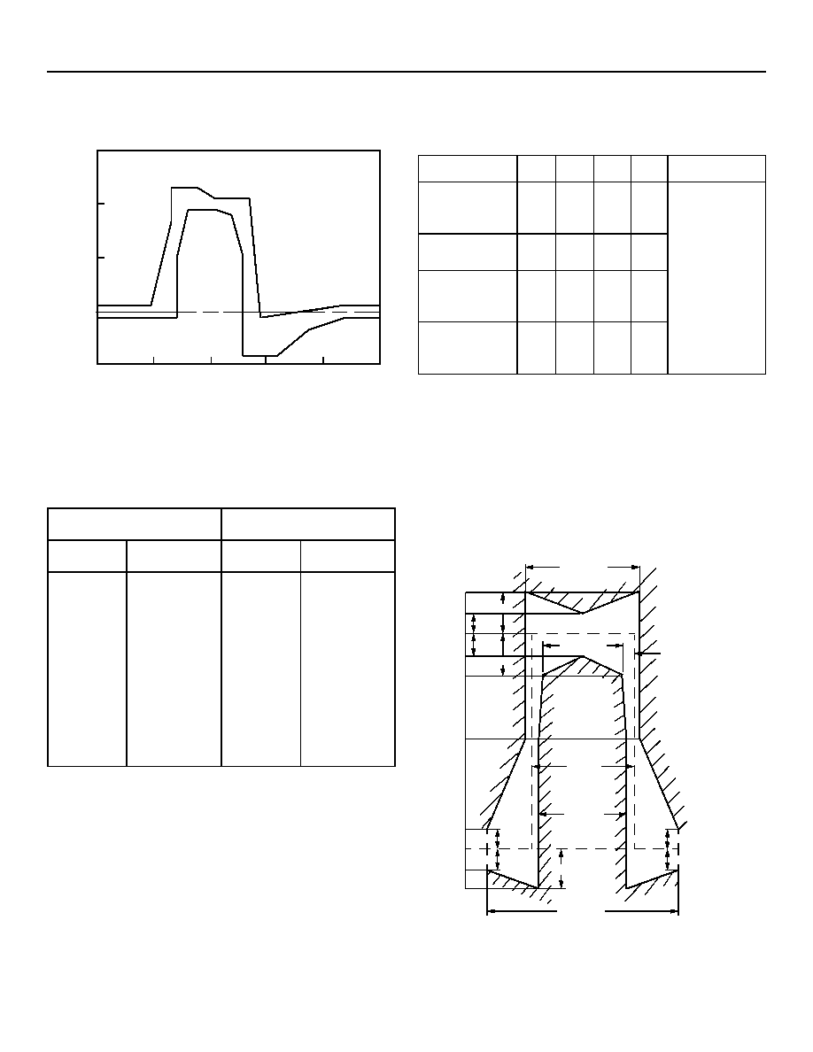
Figure 7-1. DSX-1 Isolated Pulse Template
During DS1 operation, the transmitter tip/ring (TTIP/TRING
pins) will perform as specified in Table 7-3.
* Total power difference.
Measured in a 2 kHz band around the specified frequency.
Below the power at 772 kHz.
7.6 CEPT Transmitter Pulse Template and
Specifications
CEPT pulse shape template is specified at the system out-
put (defined by ITU-T G.703) and is shown in Figure 7-2.
5-3145(C)r.8
Figure 7-2. ITU-T G.703 Pulse Template
Table 7-2. DSX-1 Pulse Template Corner Points
(From CB119)
Maximum Curve
Minimum Curve
ns
V
ns
V
0
250
325
325
425
500
675
725
1100
1250
--
--
0.05
0.05
0.80
1.15
1.15
1.05
1.05
≠0.07
0.05
0.05
--
--
0
350
350
400
500
600
650
650
800
925
1100
1250
≠0.05
≠0.05
0.50
0.95
0.95
0.90
0.50
≠0.45
≠0.45
≠0.20
≠0.05
≠0.05
±
7,0( QV�
12
5
0
$
/
,=('$
0
3
/
,
78'
(
$
�
Table 7-3. DS1 Transmitter Specifications
Parameter
Min
Typ Max Unit Specification
Output Pulse
Amplitude at
DSX*
2.5
2.8
3.5
V
AT&T CB119,
ANSI T1.102
Output Pulse
Width
338
350
362
ns
Positive/Nega-
tive Pulse
Imbalance
--
0.1
0.4
dB
Power Levels
:
772 kHz
1.544 MHz
¡
12.6
29
--
39
17.9
--
dBm
dB
QV
�
QV
± �
QV
QV
± �
QV
�
9
120,1$/ 38/6(

T7690 5.0 V T1/E1 Quad Line Interface
Data Sheet
T7693 3.3 V T1/E1 Quad Line Interface
July 2002
7 Transmitter
(continued)
18
18
Agere Systems Inc.
During CEPT operation, the transmitter tip/ring (TTIP/TRING pins) will perform as specified in Table 7-4
.
* In accordance with the interfaces described in the
Section 11.3
and the
Section 11.4
, measured at the transformer secondary.
Using Agere transformers:
2745CA for T7690 (CEPT 75
option 2 and CEPT 120
applications) and components with values in
Figure 12-1
and
Table 12-1
.
2664AJ for T7693 (CEPT 75
option 2 and CEPT 120
applications) and components with values in
Figure 12-2
and
Table 12-2
.
2745AJ2 for T7690 (CEPT 75
option 1) and components with values in
Figure 12-1
and
Table 12-1
.
2664AK for T7693 (CEPT 75
option 1) and components with values in
Figure 12-2
and
Table 12-2.
Table 7-4. CEPT Transmitter Specifications
Parameter
Min
Typ
Max
Unit
Specification
Output Pulse Amplitude*:
75
120
2.13
2.7
2.37
3.0
2.61
3.3
V
V
ITU-T G.703
Output Pulse Width
232
244
256
ns
Positive/Negative Pulse Imbalance:
Pulse Amplitude
Pulse Width
≠4
≠4
±1.5
±1.0
4
4
%
%
Zero Level (percentage of pulse amplitude)
≠5
0
5
%
Return Loss
:
51 kHz to 102 kHz
102 kHz to 2.048 MHz
2.048 MHz to 3.072 MHz
9
15
11
--
--
--
--
--
--
dB
dB
dB
CH-PTT

Agere Systems Inc.
19
Data Sheet
T7690 5.0 V T1/E1 Quad Line Interface
July 2002
T7693 3.3 V T1/E1 Quad Line Interface
8 Jitter Attenuator
The selectable jitter attenuator is provided for narrow-band-
width jitter transfer function applications. This selection is
done via control bits, which are global and affect all four
channels. One application is to provide narrow-bandwidth
jitter filtering for line-synchronization in the receive path.
Another use of the jitter attenuator is to provide clock
smoothing in the transmit signaling path for applications
such as synchronous/asynchronous demultiplexers. In
these applications, TCLK will have an instantaneous fre-
quency that is higher than the data rate and periods of
TCLK are suppressed (gapped) in order to set the average
long-term TCLK frequency to within the transmit line rate
specification.
The jitter attenuator does not degrade the jitter specifica-
tions of the receiver clock/data recovery circuit. In addition,
the jitter attenuator must meet the specifications for nar-
row-bandwidth applications as listed in Table 8-1.
8.1 Data Delay
Providing narrow-bandwidth jitter filtering requires data
buffering to increase the data delay through the jitter atten-
uator. The nominal data delay for the jitter attenuator is 33
bit periods, with a maximum data delay of 66 bit periods.
This delay is dependent on the input clock frequency,
XCLK frequency, input jitter, and gapped clock patterns.
8.2 Generated (Intrinsic) Jitter
Generated jitter is the amount of jitter appearing on the out-
put port when the applied input signal has no jitter. The jitter
attenuator of this device outputs a maximum of 0.04 UI
peak-to-peak intrinsic jitter.
8.3 Jitter Transfer Function
The jitter transfer function describes the amount of jitter in
specific equipment that is transferred from the input to the
output over a frequency range.
The jitter attenuator exhibits a single-pole rolloff (20 dB/
decade) jitter transfer characteristic that has no peaking
and a nominal filter corner frequency (3 dB bandwidth) for
DS1 and CEPT operation of less than 10 Hz. For a given
frequency, different jitter amplitudes will cause slight varia-
tions in attenuation because of finite quantization effects.
Jitter amplitudes of less than approximately 0.2 UI will have
greater attenuation than the single-pole rolloff characteris-
tic.
Measurement of the jitter transfer function involves stimu-
lating the circuit with a sinusoidal jitter test signal. The dif-
ference between the output signal power and the test
signal power, at a given frequency, is the jitter transfer.
When output signal power is below the noise floor, it cannot
be measured. Halting the jitter transfer function measure-
ments because of noise floor limitations is acceptable dur-
ing conformance testing.
8.4 Jitter Tolerance
The minimum jitter tolerance of the jitter attenuator occurs
when the XCLK frequency and the long-term average fre-
quency of the input clock are at their extreme-frequency tol-
erances. The minimum tolerance is 28 UI peak-to-peak at
the highest jitter frequency of 15 kHz.
8.5 Jitter Attenuator Enable
The jitter attenuator is selected using the JAR and JAT bits
(register 5, bits 1 and 2) of the microprocessor interface.
These control bits are global and affect all four channels
unless a given channel is in the powerdown mode
(PWRDN = 1). Because there is only one attenuator func-
tion in the device, selection must be made between either
the transmit or receive path. If both JAT and JAR are acti-
vated at the same time, the jitter attenuator will be disabled.
Note that the power consumption increases slightly on a
per-channel basis when the jitter attenuator is active, as
described in
Table 11-1
. If jitter attenuation is selected, a
valid XCLK (pin 29) signal must be available.
8.5.1 Jitter Attenuator Receive Path Enable (JAR)
When the jitter attenuator receive bit is set (JAR = 1), the
attenuator is enabled in the receive data path between the
clock/data recovery and the decoder (see
Figure 4-1
).
Under this condition, the jitter characteristics of the jitter
attenuator apply for the receiver. When JAR = 0, the clock/
data recovery outputs bypass the disabled attenuator and
directly enter the decoder function. The receive path will
then exhibit the jitter characteristics of the clock recovery
function as described in
Section 6.2
. If CDR = 0 (register 5,
bit 0), the JAR bit is ignored because clock recovery will be
disabled.
Table 8-1. List of Low-Bandwidth Jitter Specification
Documents
Application
DS1
CEPT
TR-TSY-000009, TR-TSY-000253,
TR-TSY-000499
ITU-T G.735
ITU-T I.431

T7690 5.0 V T1/E1 Quad Line Interface
Data Sheet
T7693 3.3 V T1/E1 Quad Line Interface
July 2002
8 Jitter Attenuator
(continued)
20
20
Agere Systems Inc.
8.5.2 Jitter Attenuator Transmit Path Enable (JAT)
When the jitter attenuator transmit bit is set (JAT = 1), the
attenuator is enabled in the transmit data path between the
encoder and the pulse-width controller/pulse equalizer (see
Figure 4-1
). Under this condition, the jitter characteristics of
the jitter attenuator apply for the transmitter. When JAT = 0,
the encoder outputs bypass the disabled attenuator and
directly enter the pulse-width controller/pulse equalizer.
The transmit path will then pass all jitter from TCLK to line
interface outputs TTIP/TRING.
8.6 Loopbacks
The device has three independent loopback paths that are
activated using LOOPA and LOOPB (registers 6 to 9, bits 3
and 4) as shown in Table 8-2. The locations of these loop-
backs are illustrated in
Figure 4-1
.
* During the transmit blue signal condition, the looped data will be the
transmitted data from the system and not the all-1s signal.
Transmit blue signal request is ignored.
8.6.1 Full Local Loopback (FLLOOP)
A full local loopback (FLLOOP) connects the transmit line
driver input to the receiver analog front-end circuitry. Valid
transmit output data continues to be sent to the network. If
the transmit blue signal (all-1s AIS signal) is sent to the net-
work, the looped data is not affected. The ALOS alarm con-
tinues to monitor the receive line interface signal while
DLOS monitors the looped data.
8.6.2 Remote Loopback (RLOOP)
A remote loopback (RLOOP) connects the recovered clock
and retimed data to the transmitter at the system interface
and sends the data back to the line. The receiver front end,
clock/data recovery, encoder/decoder (if enabled) jitter
attenuator (if enabled), and transmit driver circuitry are all
exercised during this loopback.
The transmit clock, transmit data, and TBS inputs are
ignored. Valid receive output data continues to be sent to
the system interface. This loopback mode is very useful for
isolating failures between systems.
8.6.3 Digital Local Loopback (DLLOOP)
A digital local loopback (DLLOOP) connects the transmit
clock and data through the encoder/decoder pair to the
receive clock and data output pins at the system interface.
This loopback is operational if the encoder/decoder pair is
enabled or disabled. The blue signal can be transmitted
without any effect on the looped signal.
8.7 Other Features
8.7.1 Powerdown (PWRDN)
Each line interface channel has an independent power-
down mode controlled by PWRDN (registers 6 to 9, bit 0).
This provides power savings for systems that use backup
channels. If PWRDN = 1, the corresponding channel will be
in a standby mode, consuming only a small amount of
power. It is recommended that the alarm registers for the
corresponding channel be masked with MASK = 1 (regis-
ters 6 to 9, bit 1) during powerdown mode. If a line interface
channel in powerdown mode needs to be placed into ser-
vice, the channel should be turned on (PWRDN = 0)
approximately 5 ms before data is applied.
If a line interface channel will never be in service, the V
DDA
and V
DDD
pins can be connected to the ground plane,
resulting in no power consumption.
8.7.2 RESET (RESET, SWRESET)
The device provides both a hardware reset (RESET;
pin 32) and a software reset (SWRESET; register 4, bit 1)
that are functionally equivalent. When the device is in reset,
all signal-path and alarm monitor states are initialized to a
known starting configuration. The status registers and INT
(pin 25) are also cleared. The writable microprocessor
interface registers are not affected by reset, with the excep-
tion of bits in register 4 (see
Section 9.6.3
). During a reset
condition, data transmission will be momentarily interrupted
and the device will respond to those register bits affected
by the reset. On powerup of the device, the software reset
bit (register 4, bit 1) is not initialized. It must be written to a
0 prior to writing the other bits in register 4.
Table 8-2. Loopback Control
Operation
Symbol
LOOPA
LOOPB
Normal
--
0
0
Full Local Loopback
FLLOOP*
0
1
Remote Loopback
RLOOP
1
0
Digital Local
Loopback
DLLOOP
1
1

Data Sheet
T7690 5.0 V T1/E1 Quad Line Interface
July 2002
T7693 3.3 V T1/E1 Quad Line Interface
8 Jitter Attenuator
(continued)
Agere Systems Inc.
21
The reset condition is initiated by setting RESET = 0 or
SWRESET = 1 for a minimum of 10 µs. After leaving the
reset condition (with RESET = 1 or SWRESET = 0), only
the bits in register 4 need to be restored.
8.8 Loss of XCLK Reference Clock (LOXC)
The LOXC output (pin 31) is active when the XCLK refer-
ence clock (pin 29) is absent. The LOXC flag is asserted
between 150 ns and 700 ns after XCLK disappears, and
deasserts immediately after detecting the first clock edge of
XCLK.
During the LOXC alarm condition, the clock recovery and
jitter attenuator functions are automatically disabled.
Therefore, if CDR = 1 and/or JAR = 1, the RCLK, RPD,
RND, and DLOS outputs will be unknown. If CDR = 0, there
will be no effect on the receiver. If the jitter attenuator is
enabled in the transmit path (JAT = 1) during this alarm
condition, then LOTC = 1 will also be indicated.
8.9 In-Circuit Testing and Driver 3-State (ICT)
The function of the ICT input (pin 33) is determined by the
ICTMODE bit (register 4, bit 3). If ICTMODE = 0 and ICT is
activated (ICT = 0), then all output buffers (TTIP, TRING,
RCLK, RPD, RND, LOXC, RDY_DTACK, INT, AD[7:0]) are
placed in a high-impedance state. For in-circuit testing, the
RESET pin can be used to activate ICTMODE = 0 without
having to write the bit. If ICTMODE = 1 and ICT = 0, then
only the TTIP and TRING outputs of all channels will be
placed in a high-impedance state. The TTIP and TRING
outputs have a limiting high-impedance capability of
approximately 8 k
.
22
22
Agere Systems Inc.
Data Sheet
July 2002
T7693 3.3 V T1/E1 Quad Line Interface
T7690 5.0 V T1/E1 Quad Line Interface
9 Microprocessor Interface
9.1 Overview
The device is equipped with a microprocessor interface
that can operate with most commercially available micro-
processors. Inputs MPMUX and MPMODE (pins 20 and
21) are used to configure this interface into one of four pos-
sible modes, as shown in Table 9-1. The MPMUX setting
selects either a multiplexed 8-bit address/data bus
(AD[7:0]) or a demultiplexed 4-bit address bus (A[3:0]) and
an 8-bit data bus (AD[7:0]). The MPMODE setting selects
the associated set of control signals required to access a
set of registers within the device.
When the microprocessor interface is configured to operate
in the multiplexed address/data bus modes (MPMUX = 1),
the user has access to an internal chip select function that
allows the microprocessor to selectively read/write a spe-
cific T7693 in a multiple T7693 environment (see
Section
9.5
).
The microprocessor interface can operate at speeds up to
16.384 MHz in interrupt-driven or polled mode without
requiring any wait-states.
For microprocessors operating at greater than 16.384 MHz,
the RDY_DTACK output is used to introduce wait-states in
the read/write cycles.
In the interrupt-driven mode, one or more device alarms will
assert the active-high INT output (pin 25) once per alarm
activation. After the microprocessor reads the alarm status
registers, the INT output will deassert. In the polled mode,
however, the microprocessor monitors the various device
alarm status by periodically reading the alarm status regis-
ters without the use of INT (pin 25). In both interrupt and
polled methods of alarm servicing, the status register will
clear on a microprocessor read cycle only when the alarm
condition within the signaling channel no longer exists; oth-
erwise, the register bit remains set.
Due to the device flexibility, there are no default power-up
or reset states, except for register 4. All read/write registers
must be written by the microprocessor on system start-up
to guarantee proper device functionality.
Details concerning microprocessor interface configuration
modes, pinout definitions, clock specifications, register
bank architecture, and the I/O timing specifications and dia-
grams are described in the following sections.
9.2 Microprocessor Configuration Modes
Table 9-1 highlights the four microprocessor modes controlled by the MPMUX and MPMODE inputs (pins 20 and 21).
Table 9-1. Microprocessor Configuration Modes
Mode
MPMODE
MPMUX
Address/Data Bus
Generic Control, Data, and Output Pin Names
MODE 1
0
0
DEMUXed
CS, AS, DS, R/W, A[3:0], AD[7:0], INT, DTACK
MODE 2
0
1
MUXed
CS, AS, DS, R/W, AD[7:0], INT, DTACK
MODE 3
1
0
DEMUXed
CS, ALE, RD, WR, A[3:0], AD[7:0], INT, RDY
MODE 4
1
1
MUXed
CS, ALE, RD, WR, AD[7:0], INT, RDY
Data Sheet
T7690 5.0 V T1/E1 Quad Line Interface
July 2002
T7693 3.3 V T1/E1 Quad Line Interface
9 Microprocessor Interface
(continued)
Agere Systems Inc.
23
9.3 Microprocessor Interface Pinout Definitions
The MODE [1--4] specific pin definitions are given in Table 9-2. Note that the microprocessor interface uses the same set
of pins in all modes.
Table 9-2. MODE [1--4] Microprocessor Pin Definitions
Configuration
Pin
Number
Device Pin
Name
Generic
Pin Name
Pin_Type
Assertion
Sense
Function
MODE 1
19
WR_DS
DS
Input
Active-Low
Data Strobe
22
RD_R/W
R/W
Input
--
Read/Write
R/W = 1 => Read
R/W = 0 => Write
23
ALE_AS
AS
Input
--
Address Strobe
24
CS
CS
Input
Active-Low
Chip Select
25
INT
INT
Output
Active-High
Interrupt
26
RDY_DTACK
DTACK
Output
Active-Low
Data Acknowledge
69--76
AD[7:0]
AD[7:0]
I/O
--
Data Bus
79--82
A[3:0]
A[3:0]
Input
--
Address Bus
83
MPCLK
MPCLK
Input
--
Microprocessor Clock
MODE 2
19
WR_DS
DS
Input
Active-Low
Data Strobe
22
RD_R/W
R/W
Input
--
Read/Write
R/W = 1 => Read
R/W = 0 => Write
23
ALE_AS
AS
Input
--
Address Strobe
24
CS
CS
Input
Active-Low
Chip Select
25
INT
INT
Output
Active-High
Interrupt
26
RDY_DTACK
DTACK
Output
Active-Low
Data Acknowledge
69--76
AD[7:0]
AD[7:0]
I/O
--
Address/Data Bus
83
MPCLK
MPCLK
Input
--
Microprocessor Clock
MODE 3
19
WR_DS
WR
Input
Active-Low
Write
22
RD_R/W
RD
Input
Active-Low
Read
23
ALE_AS
ALE
Input
--
Address Latch Enable
24
CS
CS
Input
Active-Low
Chip Select
25
INT
INT
Output
Active-High
Interrupt
26
RDY_DTACK
RDY
Output
Active-High
Ready
69--76
AD[7:0]
AD[7:0]
I/O
--
Data Bus
79--82
A[3:0]
A[3:0]
Input
--
Address Bus
83
MPCLK
MPCLK
Input
--
Microprocessor Clock
MODE 4
19
WR_DS
WR
Input
Active-Low
Write
22
RD_R/W
RD
Input
Active-Low
Read
23
ALE_AS
ALE
Input
--
Address Latch Enable
24
CS
CS
Input
Active-Low
Chip Select
25
INT
INT
Output
Active-High
Interrupt
26
RDY_DTACK
RDY
Output
Active-High
Ready
69--76
AD[7:0]
AD[7:0]
I/O
--
Address/Data Bus
83
MPCLK
MPCLK
Input
--
Microprocessor Clock

T7690 5.0 V T1/E1 Quad Line Interface
Data Sheet
T7693 3.3 V T1/E1 Quad Line Interface
July 2002
9 Microprocessor Interface
(continued)
24
24
Agere Systems Inc.
9.4 Microprocessor Clock (MPCLK) Specifications
The microprocessor interface is designed to operate at clock speeds up to 16.384 MHz without requiring any wait-states.
Wait-states may be needed if higher microprocessor clock speeds are required. The microprocessor clock (MPCLK, pin 83)
specification is shown in Table 9-3. This clock must be supplied only if the RDY_DTACK and INT outputs are required to be
synchronous to MPCLK. Otherwise, the MPCLK pin must be connected to ground (GND
D
).
9.5 Internal Chip Select Function
When the microprocessor interface is configured to operate in the multiplexed address/data bus modes (MPUX = 1), the
user has access to an internal chip select function. This function allows a microprocessor to selectively read or write a spe-
cific quad line interface device in a system of up to eight devices on the microprocessor bus. Externally tying CS = 0 (pin
24) and A3 = 1 (pin 79) on every line interface device enables the internal chip select function. Individual device addresses
are established by externally connecting the other three address pins A[2:0] to a unique address value in the range of 000
through 111. In order for a line interface device to respond to the register read or write request from the microprocessor, the
address data bus AD[6:4] (pins 70, 71, 72) must match the specific address defined on A[2:0]. If CS and A3 pins are tied
low, the internal chip select function is disabled and all line interface devices will respond to a microprocessor write request.
However, if CS = 1, none of the line interface devices will respond to the microprocessor read/write request.
9.6 Microprocessor Interface Register Architecture
The register bank architecture of the microprocessor interface is shown in
Table 9-4
. The register bank consists of sixteen
8-bit registers classified as alarm registers, global control registers, and channel configuration/maintenance registers. Reg-
isters 0 and 1 are the alarm registers used for storing the various device alarm status and are read-only. All other registers
are read/write. Registers 2 and 3 contain the individual mask bits for the alarms in registers 0 and 1. Registers 4 and 5 are
designated as the global control registers used to set up the functions for all four channels. The channel configuration reg-
isters in registers 6 through 9 are used to configure the individual channel functions and parameters. Registers 10 and 11
must be cleared by the user after a powerup for proper device operation. Registers 12 through 15 are reserved for propri-
etary functions and must not be addressed during operation. The following sections describe these registers in detail.
Table 9-3. Microprocessor Input Clock Specifications
Name
Symbol
Period and
Tolerance
T
rise
Typ
T
fall
Typ
Duty Cycle
Unit
Min High
Min Low
MPCLK
t1
61 to 323
5
5
27
27
ns

Data Sheet
T7690 5.0 V T1/E1 Quad Line Interface
July 2002
T7693 3.3 V T1/E1 Quad Line Interface
9 Microprocessor Interface
(continued)
Agere Systems Inc.
25
Notes:
A numerical suffix appended to the bit name identifies the channel number.
Bits shown in parentheses indicate the state forced during a reset condition.
All registers must be configured by the user before the device can operate as required for the particular application.
Register 10 and register 11 must be written to 0 after powerup of the device.
Registers 12--15 are reserved and should not be written. If they are written they must always be written with 0s.
Table 9-4. Register Set
Register
Address
Bit 7
Bit 6
Bit 5
Bit 4
Bit 3
Bit 2
Bit 1
Bit 0
Alarm Registers (Read Only)
0
0000
LOTC2
TDM2
DLOS2
ALOS2
LOTC1
TDM1
DLOS1
ALOS1
1
0001
LOTC4
TDM4
DLOS4
ALOS4
LOTC3
TDM3
DLOS3
ALOS3
Alarm Mask Registers (Read/Write)
2
0010
MLOTC2
MTDM2
MDLOS2
MALOS2
MLOTC1
MTDM1
MDLOS1
MALOS1
3
0011
MLOTC4
MTDM4
MDLOS4
MALOS4
MLOTC3
MTDM3
MDLOS3
MALOS3
Global Control Registers (Read/Write)
4
0100
HIGHZ4 (1)
HIGHZ3 (1)
HIGHZ2 (1)
HIGHZ1 (1)
ICTMODE (0)
LOSSTD
SWRESET
GMASK (1)
5
0101
LOSSD
ACM
ALM
DUAL
CODE
JAT
JAR
CDR
Channel Configuration Registers (Read/Write)
6
0110
EQA1
EQB1
EQC1
LOOPA1
LOOPB1
TBS1
MASK1
PWRDN1
7
0111
EQA2
EQB2
EQC2
LOOPA2
LOOPB2
TBS2
MASK2
PWRDN2
8
1000
EQA3
EQB3
EQC3
LOOPA3
LOOPB3
TBS3
MASK3
PWRDN3
9
1001
EQA4
EQB4
EQC4
LOOPA4
LOOPB4
TBS4
MASK4
PWRDN4
10
1010
0
0
0
0
0
0
0
0
11
1011
0
0
0
0
0
0
0
0
12--15
1100--
1111
RESERVED

T7690 5.0 V T1/E1 Quad Line Interface
Data Sheet
T7693 3.3 V T1/E1 Quad Line Interface
July 2002
9 Microprocessor Interface
(continued)
26
26
Agere Systems Inc.
9.6.1 Alarm Register Overview (0000, 0001)
The bits in the alarm registers represent the status of the transmitter and receiver alarms LOTC, TDM, DLOS, and ALOS
for all four channels as shown in Table 9-6. The alarm indicators are active-high and automatically clear on a microproces-
sor read if the corresponding alarm condition no longer exists. Persistent alarm conditions will cause the bit to remain set.
These are read-only registers.
* The numerical suffix identifies the channel number.
9.6.2 Alarm Mask Register Overview (0010, 0011)
The bits in the alarm mask registers in Table 9-6 allow the microprocessor to selectively mask each channel alarm and pre-
vent it from generating an interrupt. The mask bits correspond to the alarm status bits in the alarm registers and are active-
high to disable the corresponding alarm from generating an interrupt. These registers are read/write registers.
* The numerical suffix identifies the channel number.
Table 9-5. Alarm Registers
Bits
Symbol*
Description
Alarm Register (0)
0, 4
ALOS[1:2]
Analog loss-of-signal alarm for channels 1 and 2.
1, 5
DLOS[1:2]
Digital loss-of-signal alarm for channels 1 and 2.
2, 6
TDM[1:2]
Transmit driver monitor alarm for channels 1 and 2.
3, 7
LOTC[1:2]
Loss-of-transmit clock alarm for channels 1 and 2.
Alarm Register (1)
0, 4
ALOS[3:4]
Analog loss-of-signal alarm for channels 3 and 4.
1, 5
DLOS[3:4]
Digital loss-of-signal alarm for channels 3 and 4.
2, 6
TDM[3:4]
Transmit driver monitor alarm for channels 3 and 4.
3, 7
LOTC[3:4]
Loss-of-transmit clock alarm for channels 3 and 4.
Table 9-6. Alarm Mask Registers
Bits
Symbol*
Description
Alarm Mask Register (2)
0, 4
MALOS[1:2]
Mask analog loss-of-signal alarm for channels 1 and 2.
1, 5
MDLOS[1:2]
Mask digital loss-of-signal alarm for channels 1 and 2.
2, 6
MTDM[1:2]
Mask transmit driver monitor alarm for channels 1 and 2.
3, 7
MLOTC[1:2]
Mask loss-of-transmit clock alarm for channels 1 and 2.
Alarm Mask Register (3)
0, 4
MALOS[3:4]
Mask analog loss-of-signal alarm for channels 3 and 4.
1, 5
MDLOS[3:4]
Mask digital loss-of-signal alarm for channels 3 and 4.
2, 6
MTDM[3:4]
Mask transmit driver monitor alarm for channels 3 and 4.
3, 7
MLOTC[3:4]
Mask loss-of-transmit clock alarm for channels 3 and 4.

Data Sheet
T7690 5.0 V T1/E1 Quad Line Interface
July 2002
T7693 3.3 V T1/E1 Quad Line Interface
9 Microprocessor Interface
(continued)
Agere Systems Inc.
27
9.6.3 Global Control Register Overview (0100, 0101)
The bits in the global control registers in Table 9-7 and Table 9-8 allow the microprocessor to configure the various device
functions over all the four channels. All the control bits (with the exception of LOSSTD and ICTMODE) are active-high.
These are read/write registers.
9.6.4 Channel Configuration Register Overview (0110--1001)
The control bits in the channel configuration registers in
Table 9-9
are used to select equalization, loopbacks, AIS genera-
tion, channel alarm masking, and the channel powerdown mode for each channel (1--4). The PWRDN[1--4], MASK[1--4],
and TBS[1--4] bits are active-high. These are read/write registers.
Table 9-7. Global Control Register (0100)
Bit
Symbol
Description
Global Control Register (4)
0
GMASK
The GMASK bit globally masks all the channel alarms when GMASK = 1, preventing all the
receiver and transmitter alarms from generating an interrupt. GMASK = 1 after a device reset.
1
SWRESET
The SWRESET provides the same function as the hardware reset. It is used for device initial-
ization through the microprocessor interface. The software reset bit must be cleared after pow-
erup prior to writing any other bits in register 4.
2
LOSSTD
The LOSSTD bit selects the conformance protocol for the DLOS receiver alarm function.
3
ICTMODE
The ICTMODE bit changes the function of the
,&7
pin. ICTMODE = 0 after a device reset.
4--7
HIGHZ[1:4]
A HIGHZ bit is available for each individual channel. When HIGHZ = 1, the TTIP and TRING
transmit drivers for the specified channel are placed in a high-impedance state. HIGHZ[1:4] = 1
after a device reset.
Table 9-8. Global Control Register (0101)
Bit
Symbol
Description
Global Control Register (5)
0
CDR
The CDR bit is used to enable and disable the clock/data recovery function.
1
JAR
The JAR is used to enable and disable the jitter attenuator function in the receive path. The JAR
and JAT control bits are mutually exclusive; i.e., either JAR or the JAT control bit can be set, but not
both.
2
JAT
The JAT is used to enable and disable the jitter attenuator function in the transmit path. The JAT
and JAR control bits are mutually exclusive; i.e., either JAT or the JAR control bit should be set, but
not both.
3
CODE
The CODE bit is used to enable and disable the B8ZS/HDB3 zero substitution coding (decoding) in
the transmit (receive) path. It is used in conjunction with the DUAL bit and is valid only for single-rail
operation.
4
DUAL
The DUAL bit is used to select single or dual-rail mode of operation.
5
ALM
The ALM bit selects the transmit and receive data polarity (i.e., active-low or active-high). The ALM
and ACM bits are used together to determine the transmit and receive data retiming modes.
6
ACM
The ACM bit selects the positive or negative edge of the receive clock (RCLK[1:4]) for receive data
retiming. The ACM and ALM bits are used together to determine the transmit and receive data
retiming modes.
7
LOSSD
The LOSSD bit selects the shutdown function for the digital loss-of-signal alarm (DLOS).

T7690 5.0 V T1/E1 Quad Line Interface
Data Sheet
T7693 3.3 V T1/E1 Quad Line Interface
July 2002
9 Microprocessor Interface
(continued)
28
28
Agere Systems Inc.
* A numerical suffix identifies the channel number.
Channel suffix not shown in the description.
9.6.5 Other Registers
The bits in registers 10 and 11 must be cleared by the microprocessor after a device powerup.
Table 9-9. Channel Configuration Registers
Bit
Symbol*
Description
Channel Configuration Registers (6--9)
0
PWRDN[1:4]
The PWRDN bit powers down a channel when not used.
1
MASK[1:4]
The MASK bit masks all interrupts for the channel.
2
TBS[1:4]
The TBS bit enables transmission of an all 1s signal to the line interface.
3
4
LOOPB[1:4]
LOOPA[1:4]
The LOOPB and LOOPA bits select the channel loopback modes.
5
6
7
EQC[1:4],
EQB[1:4],
EQA[1:4]
The EQC, EQB, and EQA bits select the type of service (DS1 or CEPT) and the associated
transmitter cable equalization/termination impedances.
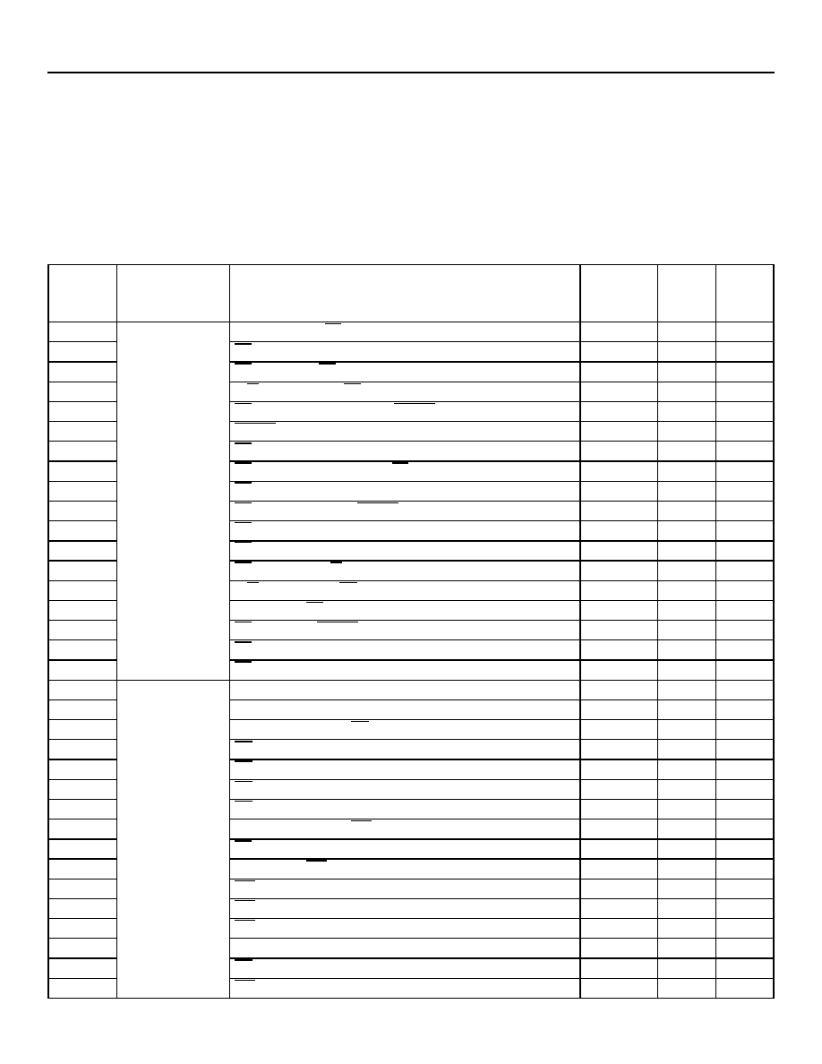
Agere Systems Inc.
29
Data Sheet
T7690 5.0 V T1/E1 Quad Line Interface
July 2002
T7693 3.3 V T1/E1 Quad Line Interface
10 Timing Characteristics
10.1 I/O Timing
The I/O timing specifications for the microprocessor interface are given in Table 10-1. The microprocessor interface pins
use CMOS I/O levels. All outputs, except the address/data bus AD[7:0], are rated for a capacitive load of 50 pF. The
AD[7:0] outputs are rated for a 100 pF load. The minimum read and write cycle time is 200 ns for all device configurations.
Table 10-1. Microprocessor Interface I/O Timing Specifications
Symbol
Configuration
Parameter
Setup
(ns)
(Min)
Hold
(ns)
(Min)
Delay
(ns)
(Max)
t1
Modes 1 and 2
Address Valid to AS Asserted (Read, Write)
15
--
--
t2
AS Asserted to Address Invalid (Read, Write)
--
10
--
t3
AS Asserted to DS Asserted
50
--
--
t4
R/W High (Read) to DS Asserted
25
--
--
t5
DS Asserted (Read, Write) to DTACK Asserted
--
--
20
t6
DTACK Asserted to Data Valid (Read)
--
--
70
t7
DS Asserted (Read) to Data Valid
--
--
90
t8
DS Negated (Read, Write) to AS Negated
--
--
25
t9
DS Negated (Read) to Data Invalid
--
--
15
t10
DS Negated (Read) to DTACK Negated
--
--
15
t11
AS (Read, Write) Asserted Width
--
150
--
t12
DS (Read) Asserted Width
--
100
--
t13
AS Asserted to R/W Low (Write)
25
--
--
t14
R/W Low (Write) to DS Asserted
25
--
--
t15
Data Valid to DS Negated (Write)
25
--
--
t16
DS Negated to DTACK Negated (Write)
--
--
20
t17
DS Negated to Data Invalid (Write)
--
25
--
t18
DS (Write) Asserted Width
--
100
--
t19
Modes 3 and 4
Address Valid to ALE Asserted Low (Read, Write)
15
--
--
t20
ALE Asserted Low (Read, Write) to Address Invalid
--
10
--
t21
ALE Asserted Low to RD Asserted (Read)
30
--
--
t22
RD Asserted (Read) to Data Valid
--
--
90
t23
RD Asserted (Read) to RDY Asserted
--
--
75
t24
RD Negated to Data Invalid (Read)
--
--
20
t25
RD Negated to RDY Negated (Read)
--
--
25
t26
ALE Asserted Low to WR Asserted (Write)
30
--
--
t27
CS Asserted to RDY Asserted Low
--
--
16
t28
Data Valid to WR Negated (Write)
25
--
--
t29
WR Asserted (Write) to RDY Asserted
--
--
73
t30
WR Negated to RDY Negated (Write)
--
--
22
t31
WR Negated to Data Invalid
--
25
--
t32
ALE Asserted (Read, Write) Width
--
150
--
t33
RD Asserted (Read) Width
--
100
--
t34
WR Asserted (Write) Width
--
100
--
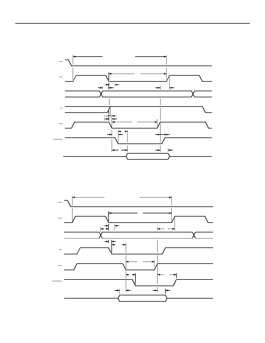
T7690 5.0 V T1/E1 Quad Line Interface
Data Sheet
T7693 3.3 V T1/E1 Quad Line Interface
July 2002
10 Timing Characteristics
(continued)
30
30
Agere Systems Inc.
The read and write timing diagrams for all four microprocessor interface modes are shown in Figures 10-1--Figures 10-8.
5-3685(C)r.3
Figure 10-1. Mode 1--Read Cycle Timing (MPMODE = 0, MPMUX = 0)
5-3686(C)r.3
Figure 10-2. Mode 1--Write Cycle Timing (MPMODE = 0, MPMUX = 0)
W
W
W
'6
$6
&6
0,1,080 5($' &<&/(
9$/,' $''5(66
9$/,' '$7$
$>@
5:
W
W
W
W
W
W
W
$'>@
'7$&.
W
W
W
W
W
'6
$6
&6
0,1,080 :5,7( &<&/(
9$/,' $''5(66
9$/,' '$7$
$>@
5:
W
W
W
W
W
W
W
$'>@
'7$&.
W
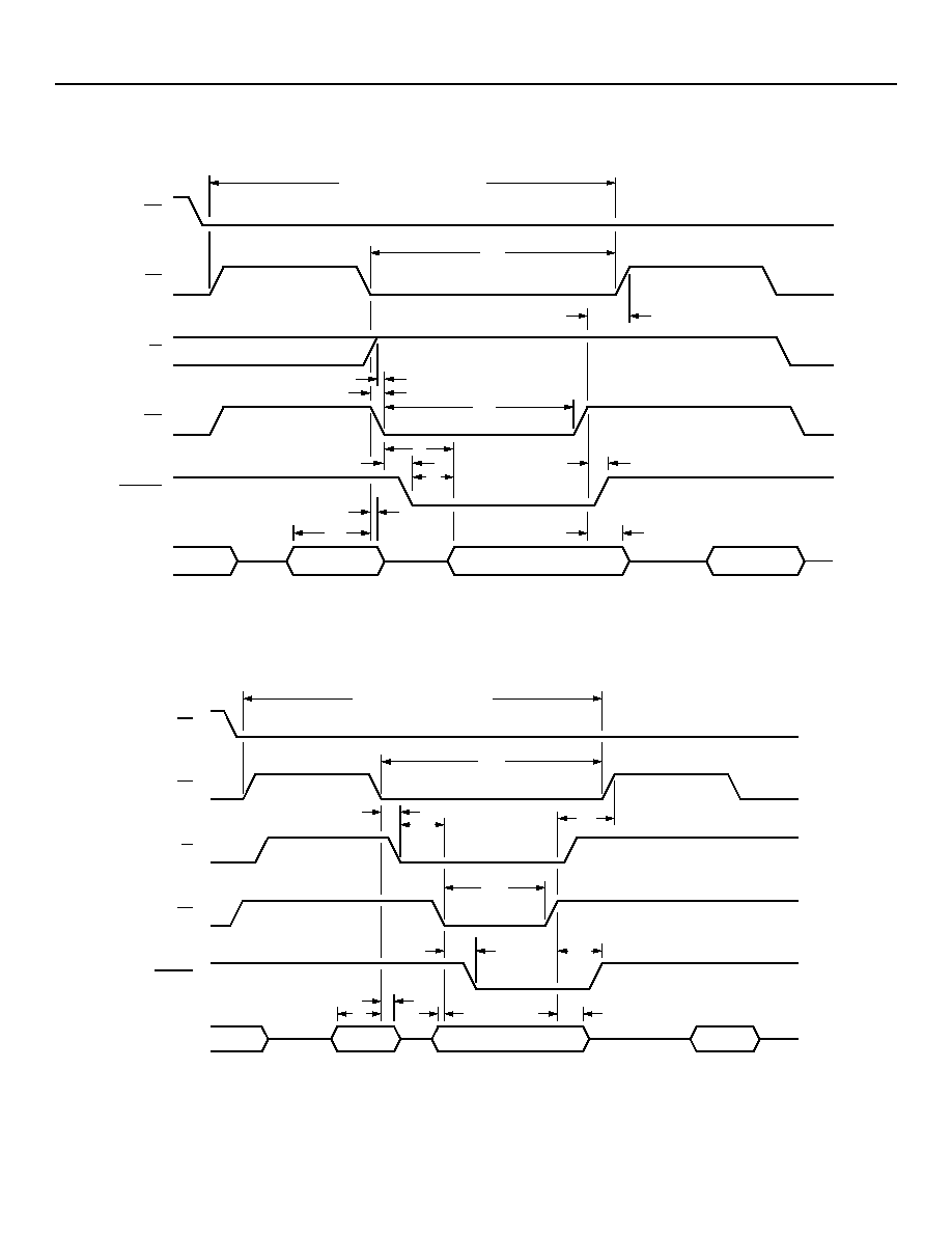
Data Sheet
T7690 5.0 V T1/E1 Quad Line Interface
July 2002
T7693 3.3 V T1/E1 Quad Line Interface
10 Timing Characteristics
(continued)
Agere Systems Inc.
31
5-3687(C)r.4
Figure 10-3. Mode 2--Read Cycle Timing (MPMODE = 0, MPMUX = 1)
5-3688(C)r.4
Figure 10-4. Mode 2--Write Cycle Timing (MPMODE = 0, MPMUX = 1)
W
W
W
'6
$6
&6
0,1,080 5($' &<&/(
9$/,' '$7$
5:
W
W
W
W
W
W
$'>@
'7$&.
W
9$/,'
$''5(66
9$/,'
$''5(66
9$/,'
'$7$
W
W
9$/,'
$''5(66
9$/,'
$''5(66
9$/,' '$7$
9$/,'
'$7$
&6
$6
5:
'6
'7$&.
$'>@
0,1,080 :5,7( &<&/(
W
W
W
W
W
W
W
W
W
W
W
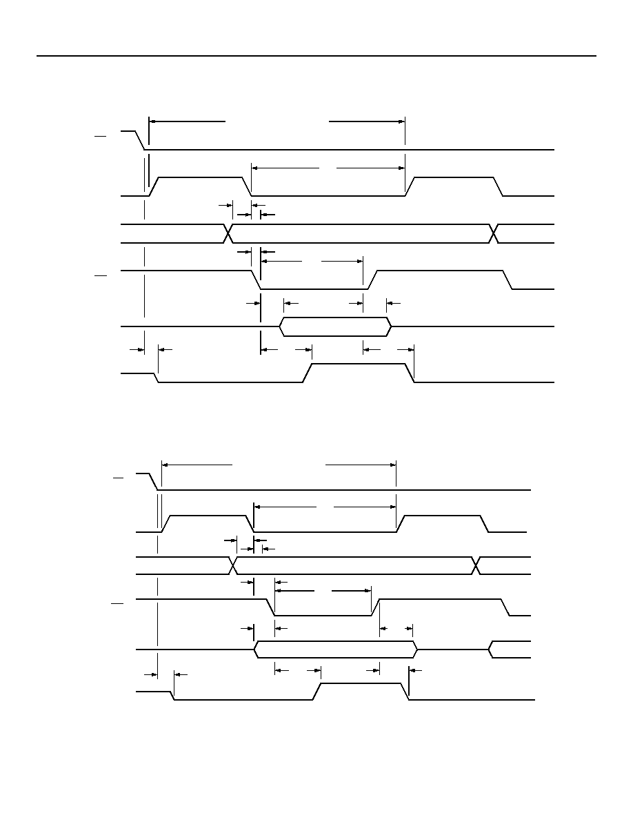
T7690 5.0 V T1/E1 Quad Line Interface
Data Sheet
T7693 3.3 V T1/E1 Quad Line Interface
July 2002
10 Timing Characteristics
(continued)
32
32
Agere Systems Inc.
5-3689(C)r.3
Figure 10-5. Mode 3--Read Cycle Timing (MPMODE = 1, MPMUX = 0)
5-3690(C)r.3
Figure 10-6. Mode 3--Write Cycle Timing (MPMODE = 1, MPMUX = 0)
0,1,080 5($' &<&/(
W
9$/,' $''5(66
$/(
&6
$>@
5'
$'>@
5'<
9$/,' '$7$
W
W
W
W
W
W
W
W
W
&6
$/(
$>@
:5
$'>@
5'<
0,1,080 :5,7( &<&/(
W
W
W
9$/,' $''5(66
W
W
W
W
WW
W
9$/,' '$7$
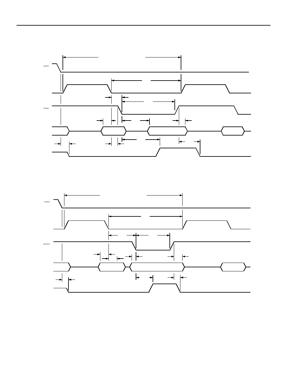
Data Sheet
T7690 5.0 V T1/E1 Quad Line Interface
July 2002
T7693 3.3 V T1/E1 Quad Line Interface
10 Timing Characteristics
(continued)
Agere Systems Inc.
33
5-3691(C)r.4
Figure 10-7. Mode 4--Read Cycle Timing (MPMODE = 1, MPMUX = 1)
5-3692(C)r.4
Figure 10-8. Mode 4--Write Cycle Timing (MPMODE = 1, MPMUX = 1)
&6
$/(
5'
$'>@
5'<
0,1,080 5($' &<&/(
W
W
W
W
W
W
W
W
W
W
9$/,'
'$7$
9$/,' '$7$
9$/,'
$''5(66
9$/,'
$''5(66
&6
$/(
:5
$'>@
5'<
9$/,'
'$7$
9$/,'
$''5(66
9$/,'
$''5(66
9$/,' '$7$
0,1,080 :5,7( &<&/(
W
W
W
W
W
W
W
W
W
W
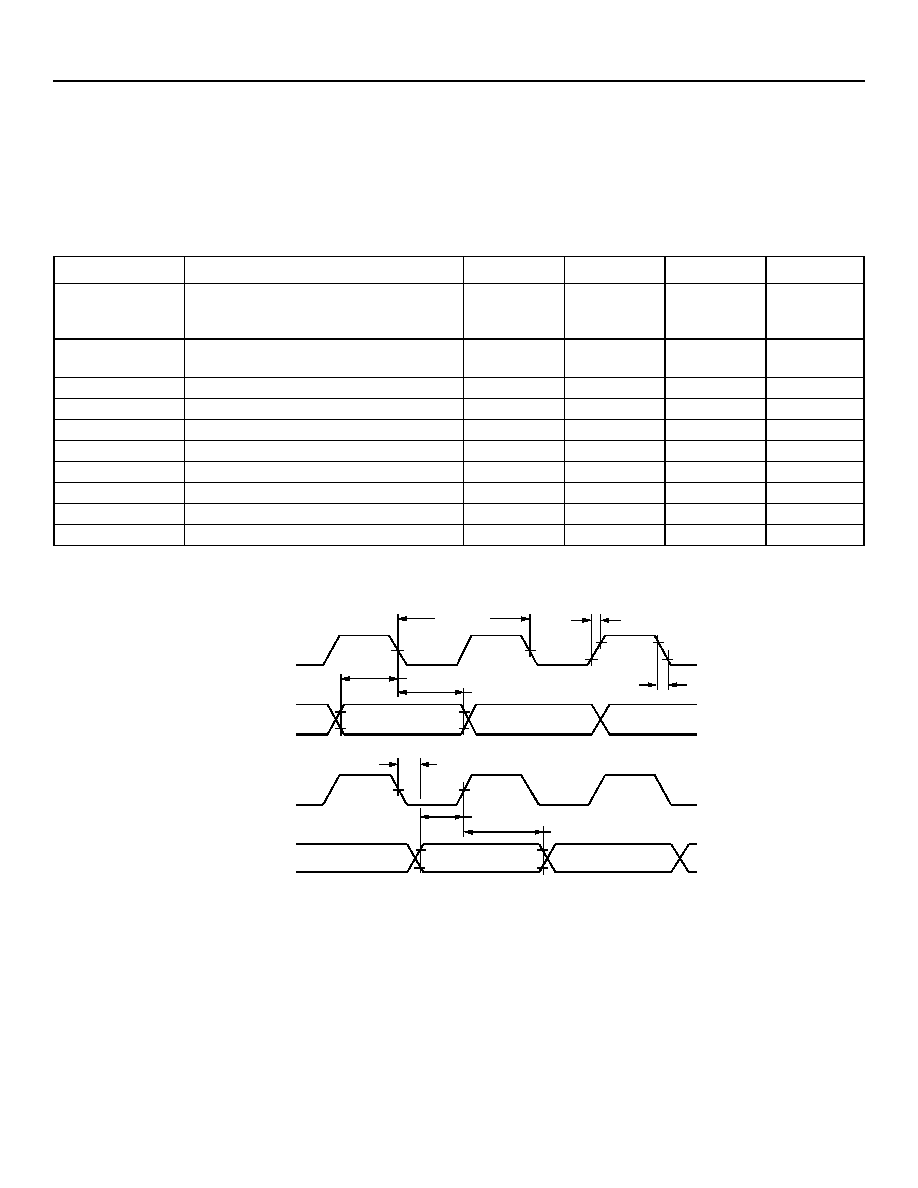
T7690 5.0 V T1/E1 Quad Line Interface
Data Sheet
T7693 3.3 V T1/E1 Quad Line Interface
July 2002
10 Timing Characteristics
(continued)
34
34
Agere Systems Inc.
10.2 Interface Data Timing
* Refers to each individual bit period for JAT = 0 applications.
Refers to each individual bit period for JAT = 1 applications using a gapped TCLK.
5-1156(C)r.5
* Invert RCLK for ACM = 1.
Figure 10-9. Interface Data Timing (ACM = 0)
Table 10-2. Interface Data Timing
The digital system interface timing is shown in Figure 10-9 for ACM = 0. If ACM = 1, then the RCLK signal in Figure 10-9
will be inverted.
Symbol
Parameter
Min
Typ
Max
Unit
tTCLTCL
Average TCLK Clock Period:
DS1
CEPT
--
--
647.7
488.0
--
--
ns
ns
tTDC
TCLK Duty Cycle*
TCLK Minimum High/Low Time
30
100
--
--
70
--
%
ns
tTDVTCL
Transmit Data Setup Time
50
--
--
ns
tTCLTDX
Transmit Data Hold Time
40
--
--
ns
tTCH1TCH2
Clock Rise Time (10%/90%)
--
--
40
ns
tTCL2TCL1
Clock Fall Time (90%/10%)
--
--
40
ns
tRCHRCL
RCLK Duty Cycle
45
50
55
%
tRDVRCH
Receive Data Setup Time
140
--
--
ns
tRCHRDX
Receive Data Hold Time
180
--
--
ns
tRCLRDV
Receive Propagation Delay
--
--
40
ns
7 &/./,
8
73'
/, 8
25
71'/,
8
5&/./,
8
53'
/, 8
25
51'/,8
W7 &+7&+
W 7 &/7
&/
W7'9
7 &/
W7 &/7';
W5&/5'9
W5'95&+
W 5&+5';
W7 &/7&/

Data Sheet
T7690 5.0 V T1/E1 Quad Line Interface
July 2002
T7693 3.3 V T1/E1 Quad Line Interface
10 Timing Characteristics
(continued)
Agere Systems Inc.
35
10.2.1 Logic Interface Characteristics
An internal 50 k
pull-up is provided on the ICT and RESET pins. An internal 100 k
pull-up is provided on the CS, XCLK,
and BCLK pins. This requires these input pins to sink no more than 20 µA. All buffers use CMOS levels.
* 100 pF allowed for AD[7:0] (pins 69 to 76).
10.3 XCLK Reference Clock
The device requires a high-frequency reference clock for both clock/data recovery and jitter attenuation options (CDR = 1,
JAR = 1, or JAT = 1). The XCLK signal (pin 29) is conditionally required if the MPCLK signal (pin 83) is not supplied for
interrupt generation in the microprocessor interface. For any other device configuration, XCLK is not required. If it is
required, XCLK must be a continuously active (i.e., ungapped, unjittered, and unswitched) and an independent reference
clock such as an external system oscillator or system clock for proper operation. It must not be derived from any recovered
line clock (i.e., from RCLK or any synthesized frequency of RCLK). The specifications for XCLK are defined in Table 10-4.
Table 10-3. Logic Interface Characteristics
Parameter
Symbol
Test Conditions
Min
Max
Unit
Input Voltage:
Low
High
V
IL
V
IH
--
GND
D
V
DD
≠ 1.0
1.0
V
DD
V
V
Input Leakage
I
L
--
--
1.0
µA
Output Voltage:
Low
High
V
OL
V
OH
≠5.0 mA
5.0 mA
GND
D
V
DD
≠ 1.0
0.5
V
DDD
V
V
Input Capacitance
C
I
--
--
3.0
pF
Load Capacitance*
C
L
--
--
50
pF
Table 10-4. XCLK Timing Specifications
Parameter
Value
Unit
Min
Typ
Max
Frequency
DS1
CEPT
--
--
24.704
32.768
--
--
MHz
MHz
Range
≠100
--
100
ppm
Duty Cycle
40
--
60
%

T7690 5.0 V T1/E1 Quad Line Interface
Data Sheet
T7693 3.3 V T1/E1 Quad Line Interface
July 2002
36
36
Agere Systems Inc.
11 Electrical Characteristics
11.1 Power Supply Bypassing
External bypassing is required for all channels. A 1.0 µF capacitor must be connected between V
DD
X and GNDX. In addi-
tion, a 0.1 µF capacitor must be connected between V
DDD
and GND
D
, and a 0.1 µF capacitor must be connected between
V
DDA
and GND
A
. Ground plane connections are required for GNDX, GND
D
, and GND
A
. Power plane connections are also
required for V
DD
X and V
DDD
. The need to reduce high-frequency coupling into the analog supply (V
DDA
) may require an
inductive bead to be inserted between the power plane and the V
DDA
pin of every channel.
External bypassing is also required for the microprocessor power supply pins. A 0.1 µF capacitor must be connected
between every pair of V
DDC
and GND
C
pins. V
DDC
and GND
C
are connected directly to the power and ground planes,
respectively.
Capacitors used for power supply bypassing should be placed as close as possible to the device pins for maximum effec-
tiveness.
11.2 Power Specifications
Device power specification includes power to the line for a specified data ones density. Power and temperature for the
T7690 device is as follows: V
DD
= 5 V; T
A
= 25 ∞C. Power and temperature for the T7693 device is as follows: V
DD
= 3.3 V;
T
A
= 25 ∞C.
* A single channel (receive and transmit paths) for 50% ones density data.
For standby purposes. If a channel will never be used, connecting all V
DD
pins to the ground plane is recommended, resulting in no power consumption.
For nominal V
DD
, T
A
= 25 ∞C. Every function and channel operational with 50% ones density.
ß For V
DD
= 5.25 V and T
A
= 25 ∞C. Every function and channel operational with 100% ones density.
** For V
DD
= 3.465 V and T
A
= 25 ∞C. Every function and channel operational with 100% ones density.
Table 11-1. Power Specifications
Parameter
T7690
T7693
Unit
DS1
CEPT
DS1
CEPT
Per Channel:*
CDR = 0, JAx = 0 (transmit, receiver in data slicing mode,
no jitter attenuator)
CDR = 1, JAx = 0 (transmit, receiver in clock recovery
mode, no jitter attenuator)
CDR = 1, JAx = 1 (transmit, receiver in clock recovery
mode, jitter attenuator active)
During Powerdown Mode (PWRDN = 1)
83
97
100
2.5
85
106
109
2.5
104
118
120
3
75
96
99
4
mW
mW
mW
mW
Quad Total:
Typical
¡
Max
412
780
450
760
490
970**
405
720**
mW
mW
Data Sheet
T7690 5.0 V T1/E1 Quad Line Interface
July 2002
T7693 3.3 V T1/E1 Quad Line Interface
11 Electrical Characteristics
(continued)
Agere Systems Inc.
37
11.3 Absolute Maximum Ratings
Stresses in excess of the absolute maximum ratings can cause permanent or latent damage to the device. These are abso-
lute stress ratings only. Functional operation of the device is not implied at these or any other conditions in excess of those
given in the operational sections of this device specification. Exposure to absolute maximum ratings for extended periods
can adversely affect device reliability.
Table 11-2. Absolute Maximum Ratings
11.4 Handling Precautions
Although ESD protection circuitry has been designed into this device, proper precautions must be taken to avoid exposure
to electrostatic discharge (ESD) and electrical overstress (EOS) during all handling, assembly, and test operations. Agere
employs both a human-body model (HBM) and a charged-device model (CDM) qualification requirement in order to deter-
mine ESD-susceptibility limits and protection design evaluation. ESD voltage thresholds are dependent on the circuit
parameters used in each of the models, as defined by JEDEC's JESD22-A114 (HBM) and JESD22-C101 (CDM)
standards.
11.5 Operating Conditions
* Requirements under all loading conditions are the following: each single transmit pulse requires a 90 mA current spike from the power supply for
approximately 100 ns. Circuit pack routing of V
DD
should minimize impedance.
Parameter
Min
Max
Unit
dc Supply Voltage
≠0.5
6.5
V
Storage Temperature
≠65
125
∞C
Maximum Voltage (digital pins) with Respect to V
DDD
--
0.5
V
Minimum Voltage (digital pins) with Respect to GND
D
≠0.5
--
V
Maximum Allowable Voltages (RTIP[1--4], RRING[1--4]) with Respect to V
DD
--
0.5
V
Minimum Allowable Voltages (RTIP[1--4], RRING[1--4]) with Respect to GND
≠0.5
--
V
Table 11-3. Handling Precaution
Device
Minimum HBM Threshold
Minimum CDM Threshold
T7690
>1500 V
>2000 V
T7693
>1000 V
>2000
Table 11-4. Recommended Operating Conditions
Parameter
Symbol
Min
Typ
Max
Unit
Ambient Temperature
T
A
≠40
--
85
∞C
T7690 Power Supply
V
DD
4.75
5.0
5.25
V
T7693 Power Supply*
V
DD
3.135
3.3
3.465
V
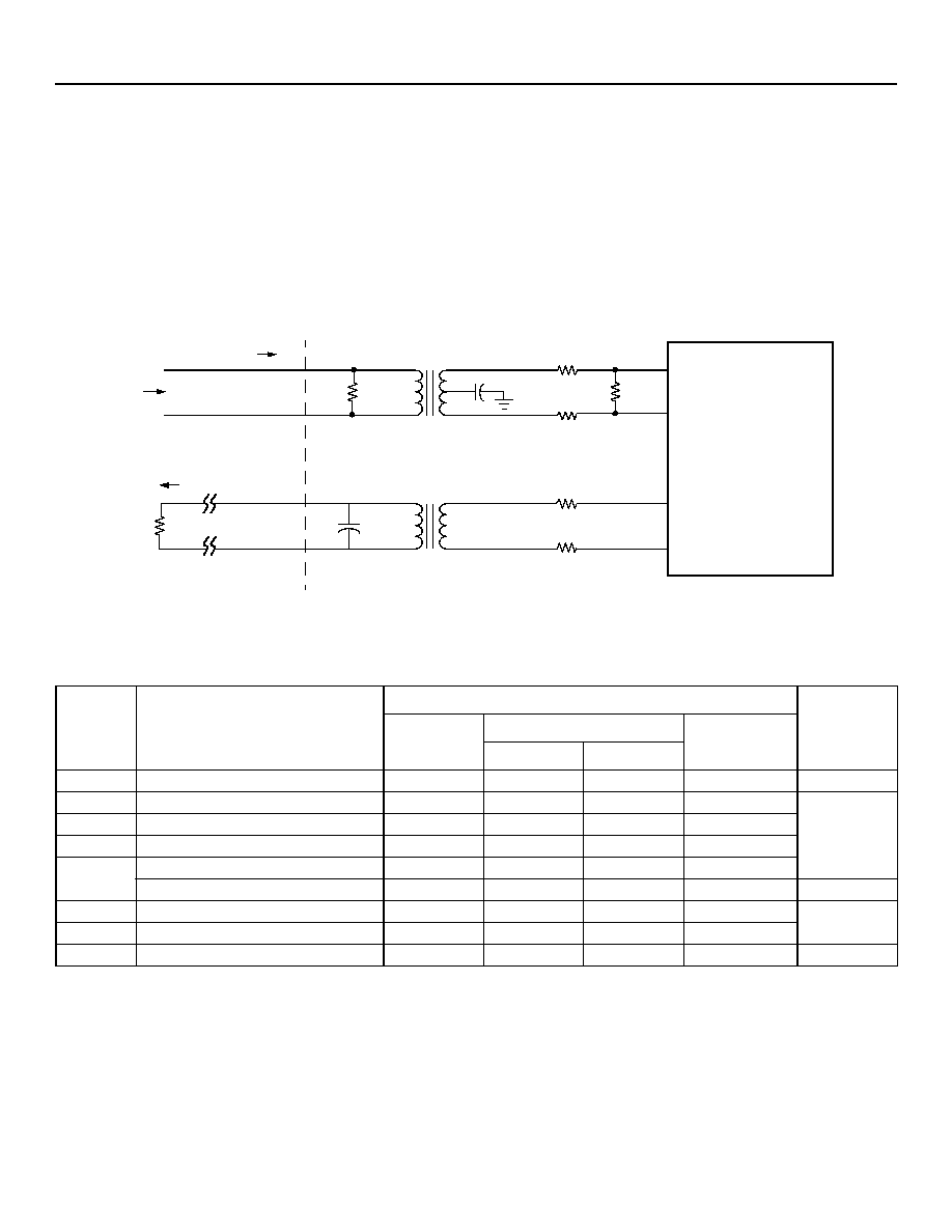
T7690 5.0 V T1/E1 Quad Line Interface
Data Sheet
T7693 3.3 V T1/E1 Quad Line Interface
July 2002
38
38
Agere Systems Inc.
12 External Line Termination Circuitry
12.1 T7690
The transmit and receive tip/ring connections provide a matched interface to the cable (i.e., terminating impedance
matches the characteristic impedance of the cable). The diagram in Figure 12-1 shows the appropriate external compo-
nents to interface to the cable for a single transmit/receive channel. The component values are summarized in Table 12-1,
based on the specific application.
5-3693(C).d
Figure 12-1. T7690 External Line Termination Circuitry
* Resistor tolerances are ±1%. Transformer turns ratio tolerances are ±2%.
For CEPT 75
applications, option 1 is recommended over option 2 for lower device power dissipation.
Table 11-1
shows the power for option 1; option
2 increases power dissipation by 13 mW per channel when driving 50% ones data. Option 2 allows for the same transformer as used in CEPT 120
applications.
A ±5% tolerance is allowed for the transmit load termination.
Table 12-1. Termination Components by Application*
Symbol
Name
Cable Type
Unit
DS1
Twisted Pair
CEPT 75
Coaxial
CEPT 120
Twisted Pair
Option 1
Option 2
C
C
Center Tap Capacitor
0.1
0.1
0.1
0.1
µF
R
P
Receive Primary Impedance
200
200
200
200
R
R
Receive Series Impedance
71.5
28.7
59
174
R
S
Receive Secondary Impedance
113
82.5
102
205
Z
EQ
Equivalent Line Termination
100
75
75
120
Tolerance
±4
±4
±4
±4
%
R
T
Transmit Series Impedance
0
26.1
15.4
26.1
R
L
Transmit Load Termination
¡
100
75
75
120
N
Transformer Turns Ratio
1.14
1.08
1.36
1.36
--
57,3
55,1*
77,3
75,1*
'(9,&(
&+$11(/�
5
/
5
6
5
5
5
5
5(&(,9( '$7$
5
3
=
(4
5
7
5
7
1
75$160,7 '$7$
75$16)250(5
(48,30(17
,17(5)$&(
1
&
&
&
3
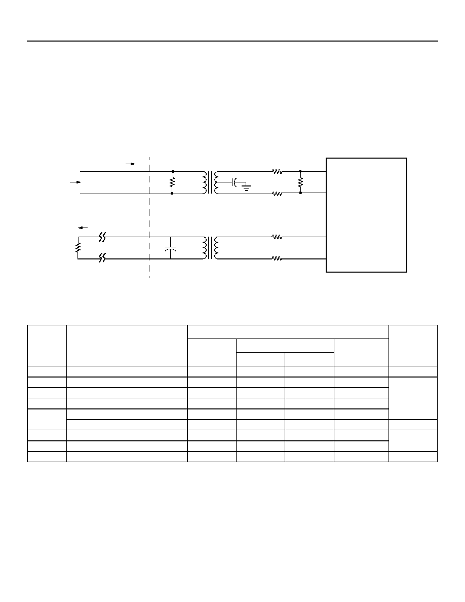
Data Sheet
T7690 5.0 V T1/E1 Quad Line Interface
July 2002
T7693 3.3 V T1/E1 Quad Line Interface
12 External Line Termination Circuitry
(continued)
Agere Systems Inc.
39
12.2 T7693
The transmit and receive tip/ring connections provide a matched interface to the cable (i.e., terminating impedance
matches the characteristic impedance of the cable). The diagram in Figure 12-2 shows the appropriate external compo-
nents to interface to the cable for a single transmit/receive channel. The component values are summarized in Table 12-2,
based on the specific application.
5-3693(C).dr.1
Figure 12-2. T7693 External Line Termination Circuitry
* Resistor tolerances are ±1%. Transformer turns ratio tolerances are ±2%.
For CEPT 75
applications, option 1 is recommended over option 2 for lower device power dissipation.
Table 11-1
shows the power for option 1; option
2 increases power dissipation by 13 mW per channel when driving 50% ones data. Option 2 allows for the same transformer as used in CEPT 120
applications.
A ±5% tolerance is allowed for the transmit load termination.
Table 12-2. Termination Components by Application*
Symbol
Name
Cable Type
Unit
DS1
Twisted Pair
CEPT 75
Coaxial
CEPT 120
Twisted Pair
Option 1
Option 2
C
C
Center Tap Capacitor
0.1
0.1
0.1
0.1
µF
R
P
Receive Primary Impedance
200
200
200
200
R
R
Receive Series Impedance
336
143
261
698
R
S
Receive Secondary Impedance
210
147
182
365
Z
EQ
Equivalent Line Termination
100
75
75
120
Tolerance
±4
±4
±4
±4
%
R
T
Transmit Series Impedance
0
7.5
5.36
7.5
R
L
Transmit Load Termination
¡
100
75
75
120
N
Transformer Turns Ratio
2.1
1.91
2.42
2.42
--
57,3
55,1*
77,3
75,1*
'(9,&(
&+$11(/�
5
/
5
6
5
5
5
5
5(&(,9( '$7$
5
3
=
(4
5
7
5
7
1
75$160,7 '$7$
75$16)250(5
(48,30(17
,17(5)$&(
1
&
&
&
3
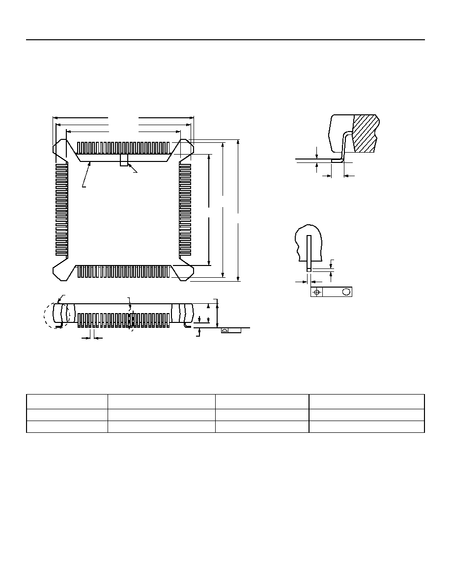
T7690 5.0 V T1/E1 Quad Line Interface
Data Sheet
T7693 3.3 V T1/E1 Quad Line Interface
July 2002
40
40
Agere Systems Inc.
13 Outline Diagram
13.1 100-Pin BQFP
Dimensions are in millimeters.
Ordering Information
Device Code
Package
Temperature
Comcode (Ordering Number)
T - 7690 - - - FL-DB
100-Pin BQFP
≠40 ∞C to +85 ∞C
107202434
T - 7693 - - - FL-DB
100-Pin BQFP
≠40 ∞C to +85 ∞C
107202723
3,1
,'(17,),(5
=21(
±
±
±
±
±
±
('*( &+$0)(5
'(7$,/ $
0$;
'(7$,/ %
±
7<3
6($7,1* 3/$1(
±
'(7$,/ %
±
0
±
'(7$,/ $
*$*( 3/$1(
6($7,1* 3/$1(

Agere Systems Inc.
41
Data Sheet
July 2002
T7693 3.3 V T1/E1 Quad Line Interface
T7690 5.0 V T1/E1 Quad Line Interface
Notes

Agere Systems Inc. reserves the right to make changes to the product(s) or information contained herein without notice. No liability is assumed as a result of their use or application.
Agere, Agere Systems, and the Agere logo are trademarks of Agere Systems Inc.
Copyright © 2002 Agere Systems Inc.
All Rights Reserved
July 2002
DS02-318BBAC (Replaces DS02-307BBAC)
For additional information, contact your Agere Systems Account Manager or the following:
INTERNET:
http://www.agere.com
E-MAIL:
docmaster@agere.com
N. AMERICA: Agere Systems Inc., 555 Union Boulevard, Room 30L-15P-BA, Allentown, PA 18109-3286
1-800-372-2447, FAX 610-712-4106 (In CANADA: 1-800-553-2448, FAX 610-712-4106)
ASIA:
Agere Systems Hong Kong Ltd., Suites 3201 & 3210-12, 32/F, Tower 2, The Gateway, Harbour City, Kowloon
Tel. (852) 3129-2000, FAX (852) 3129-2020
CHINA: (86) 21-5047-1212 (Shanghai), (86) 755-25881122 (Shenzhen)
JAPAN: (81) 3-5421-1600 (Tokyo), KOREA: (82) 2-767-1850 (Seoul), SINGAPORE: (65) 6778-8833, TAIWAN: (886) 2-2725-5858 (Taipei)
EUROPE:
Tel. (44) 7000 624624, FAX (44) 1344 488 045
AT&T is a registered trademark of AT&T in the U.S.A. and other countries.
ANSI is a registered trademark of American National Standards Institute, Inc.