 | –≠–ª–µ–∫—Ç—Ä–æ–Ω–Ω—ã–π –∫–æ–º–ø–æ–Ω–µ–Ω—Ç: T8102A | –°–∫–∞—á–∞—Ç—å:  PDF PDF  ZIP ZIP |
Document Outline
- AY00006.pdf
- AY99030.pdf
- DS00028.pdf
- 1 Product Overview
- 2 Architecture and Functional Description
- 3 Using the TSI Devices
- 4 Electrical Characteristics
- 5 Outline Diagrams
- 6 Ordering Information
- Appendix A. Application of Clock Modes
- Appendix B. Minimum Delay and Constant Delay Connections
- Appendix C. CAM Readback and Pattern Fill Mode
- List of Figures
- Figure 1. 208 SQFPÑTop View
- Figure 2. 217 PBGAÑTop View
- Figure 3. Block Diagram of the TSI Devices
- Figure 4. Local Bus Section Function
- Figure 5. Local Bus Memory Connection Modes
- Figure 6. Local Streams, Memory Structure
- Figure 7. Local Memory (T8100A, T8105 Only), Fill Patterns
- Figure 8. Simplified Local Memory State Timing, 65.536 MHz Clock
- Figure 9. CAM Architecture
- Figure 10. Simplified H-Bus State Timing, 65.536 MHz Clock
- Figure 11. Illustration of CAM Cycles
- Figure 12. Subrate Switching Example
- Figure 13. Modifications for Subrate Switching
- Figure 14. Unpacking Example Using Local Loopback
- Figure 15. Constant Delay/Minimum Delay Example
- Figure 16. Clocking Section
- Figure 17. A, B, and C Clock Fallback State Diagram
- Figure 18. Programming Sequence
- Figure 19. Frame Group Output Options
- Figure 20. External Connection to PLLs
- Figure 21. Physical Connections for H.110
- Figure 22. Local-to-Local Connection Programming (T8100A, T8105 Only)
- Figure 23. CAM Programming, H-Bus-to-Local Connection
- Figure 24. Clock Alignment
- Figure 25. Frame Diagram
- Figure 26. Detailed Timing Diagram
- Figure 27. Detailed Clock Skew Diagram
- Figure 28. ac Electrical Characteristics, Local Streams, and Frames
- Figure 29. Microprocessor Access Intel Multiplexed Write Cycle
- Figure 30. Microprocessor Access Intel Multiplexed Read Cycle
- Figure 31. Microprocessor Access Motorola Write Cycle
- Figure 32. Microprocessor Access Motorola Read Cycle
- Figure 33. Microprocessor Access Intel Demultiplexed Write Cycle
- Figure 34. Microprocessor Access Intel Demultiplexed Read Cycle
- Figure 35. E1, CT Bus Master, Compatibility Clock Master, Clock Source = 2.048 MHz from Trunk
- Figure 36. T1, CT Bus Master, Compatibility Clock Master, Clock Source = 1.544 MHz from Trunk
- Figure 37. E1, Slave to CT Bus, Clock Source Is Either a 16 MHz or a 4 MHz or a 2 MHz and Frame, ...
- Figure 38. T1, Slave to CT Bus, Clock Source Is Either a 16 MHz or a 4 MHz or a 2 MHz and Frame, ...
- Figure 39. Constant Delay Connections, CON[1:0] = 0X
- Figure 40. Minimum Delay Connections, CON[1:0] = 0X
- Figure 41. Mixed Minimum/Constant Delay Connections, CON[1:0 = 10]
- Figure 42. Extended Linear (Mixed Minimum/Constant) Delay, CON[1:0] = 11
- List of Tables
- Table 1. Pin Descriptions: Clocking and Framing Pins
- Table 2. Pin Descriptions: Local Streams Pins
- Table 3. Pin Descriptions: H-Bus Pins
- Table 4. Pin Descriptions: Microprocessor Interface Pins
- Table 5. Pin Descriptions: JTAG Pins
- Table 6. Pin Descriptions: Power Pins
- Table 7. Pin Descriptions: Other Pins
- Table 8. Addresses of Programming Registers
- Table 9. Master Control and Status Register
- Table 10. Address Mode Register
- Table 11. Control Register Memory Space
- Table 12. CKM: Clocks, Main Clock Selection, 0x00
- Table 13. CKN: Clocks, NETREF Selections, 0x01
- Table 14. CKP: Clocks, Programmable Outputs, 0x02
- Table 15. CKR: Clocks, Resource Selection, 0x03
- Table 16. CKS: Clocks, Secondary (Fallback) Selection, 0x04
- Table 17. CK32: Clocks, Locals 3 and 2, 0x05
- Table 18. CK10: Clocks, Locals 1 and 0, 0x06
- Table 19. CKMD: Clocks, Main Divider; CKND: Clocks, NETREF Divider; CKRD: Clocks, Resource Divide...
- Table 20. LBS: Local Stream Control, 0x0C
- Table 21. CON: Connection Delay Type, 0x0E
- Table 22. HSL: H-Bus Stream Control, Low Byte, 0x10
- Table 23. HSH: H-Bus Stream Control, High Byte, 0x11
- Table 24. GPD, General-Purpose Direction Control Register, 0x17
- Table 25. GPR: General-Purpose I/O Register, 0x18
- Table 26. FRLA: Frame Group A, Start Address Low, 0x20
- Table 27. FRHA: Frame Group A, High Address and Control, 0x21
- Table 28. FRLB: Frame Group B, Start Address Low, 0x22
- Table 29. FRHB: Frame Group B, High Address and Control, 0x23
- Table 30. FRPL: Frame Group B, Programmed Output, Low, 0x24
- Table 31. FRPH: Frame Group B, Programmed Output, High, 0x25
- Table 32. CLKERR1: Clock Error Register, Error Indicator, 0x28
- Table 33. CLKERR2: Clock Error Register, Current Status, 0x29
- Table 34. SYSERR: System Error Register, 0x2A
- Table 35. CKW: Clock Error/Watchdog Masking Register, 0x2B
- Table 36. CLKERR3: Clock Error Register, Current Status, 0x2C
- Table 37. DIAG1: Diagnostics Register 1, 0x30
- Table 38. DIAG2: Diagnostics Register 2, 0x31
- Table 39. DIAG3: Diagnostics Register 3, 0x32
- Table 40. DEV_ID: Device Identification Register, 0xFE
- Table 41. GMODE: Global Mode Register, 0xFF
- Table 42. LBS: Local Stream Control, 0x0C
- Table 43. HSL: H-Bus Stream Control, Low Byte, 0x10
- Table 44. HSH: H-Bus Stream Control, High Byte, 0x11
- Table 45. Permitted Tag Extensions
- Table 46. CKM: Clocks, Main Clock Selection, 0x00
- Table 47. CKN: Clocks, NETREF Selections, 0x01
- Table 48. CKP: Clocks, Programmable Outputs, 0x02
- Table 49. CKR: Clocks, Resource Selection, 0x03
- Table 50. CKS: Clocks, Secondary (Fallback) Selection, 0x04
- Table 51. CK32 and CK10: Clocks, Locals 3, 2, 1, and 0, 0x05 and 0x06
- Table 52. CON Register 0x0E
- Table 53. LREF Pairs
- Table 54. CKM (0x00) CKSEL Values to Select LREF Pairs
- Table 55. FRHA, Frame Group A High Address and Control, 0x21
- Table 56. FRHB, Frame Group B High Address and Control, 0x23
- Table 57. FRPH: Frame Group B, Programmed Output, High, 0x25
- Table 58. CLKERR1 and CLKERR2: Error Indicator and Current Status, 0x28 and 0x29
- Table 59. CLKERR3: Error Indicator and Current Status, 0x2C
- Table 60. SYSERR: System Error Register, 0x2A
- Table 61. JTAG Instruction Set
- Table 62. JTAG Scan Register
- Table 63. DIAG1: Diagnostics Register 1, 0x30
- Table 64. DIAG2: Diagnostics Register 2, 0x31
- Table 65. DIAG3: Diagnostics Register 3, 0x32
- Table 66. Device Identification Register, 0xFE
- Table 67. GMODE: Global Mode Register, 0xFF
- Table 68. LPUE Control Pins
- Table 69. Time-Slot Bit Decoding
- Table 70. IDR: Indirect Data Register, Local Connections Only
- Table 71. IDR: Indirect Data Register, H-Bus Connections Only
- Table 72. Crystal Specifications
- Table 73. Use of an Oscillator as an Alternative to Using a Crystal
- Table 74. Electrical Drive SpecificationsÑCT_C8 and /CT_FRAME
- Table 75. dc Electrical Characteristics, All Other Pins
- Table 76. ac Electrical Characteristics, Timing, H-Bus (H.100 Spec., Rev. 1.0)
- Table 77. ac Electrical Characteristics, Skew Timing, H-Bus (H.100 Spec., Rev. 1.0)
- Table 78. Reset and Power On
- Table 79. ac Electrical Characteristics, Local Streams, and Frames
- Table 80. L_SC[3:0] and Frame Group Rise and Fall Time
- Table 81. Microprocessor Access Timing
- Table 82. Clock Register Programming Profile for the Four Previous Examples
- Table 83. Table of Special Cases (Exceptions)
- Contact Us

Advisory
January 2000
Ambassador
TM
T8100A, T8102, and T8105
H.100/H.110 Interface and Time-Slot Interchangers
Introduction
This advisory describes a flaw in some devices that
the initial factory test program did not detect. The
flaw exists in some version 2 and version 3 T8100A,
T8102, and T8105 devices in both the SQFP and
BGA package types. An enhanced factory test pro-
gram has been in place since January 2000, and all
devices shipped after this date are good devices.
Problem: Data Memory Error
An error in the CAM data memories may cause the
corruption of stream data bits and/or bytes. The prob-
lem may also occur in the microprocessor read path.
Stream data may have an occasional '0' that should
be a '1'. An entire bad byte may also occur. The prob-
lem going away with lower V
DD
is a prime indicator of
this problem. Not all devices are bad.
Workaround
There is no workaround for this flaw.
Corrective Action
Version 2 and version 3 devices that have the second
line of markings ending with W01, W02, W03, W04,
W05, W06, W07, W08, and W09 may be returned
through Lucent's return material authorization (RMA)
process for replacement or credit. Devices that have
the second line of markings ending with W10, W11,
and W12 are known good devices and do not have to
be returned. To return devices, contact your sales
person for an RMA number. Enter the RMA number
within the following return address:
Lucent Technologies
Christa Bromfield
RMA #______
555 Union Blvd., Rm. 31L-30R BU
Allentown, PA 18103
Explanation of Version Markings
The three versions can be identified by markings on
the device and apply to the T8100A, T8102, and
T8105.
Version 1
If there are only seven digits on the last line of the
device code marking, and there is not an S following
the 4-digit date code, the device is version 1 and
applies to both the SQFP and BGA package types.
Version 2
1.
If there are seven digits on the last line of the
device code followed by a space and the letters
V2, the device is version 2; or
2.
If there is an S following the 4-digit date code on
line 2, the device is version 2. This marking
applies to both SQFP and BGA package types.
Version 3
1.
For the BGA package type, if the first line ends in
BAL3, the device is version 3; or
2.
For the SQFP package type, if the first line ends
in SC3, the device is version 3.

Lucent Technologies Inc. reserves the right to make changes to the product(s) or information contained herein without notice. No liability is assumed as a result of their use or application. No
rights under any patent accompany the sale of any such product(s) or information.
Ambassador is a trademark of Lucent Technologies Inc.
Copyright © 2000 Lucent Technologies Inc.
All Rights Reserved
January 2000
AY00-006CTI (Must accompany AY99-030NTNB-4 and DS00-028CTI)
For additional information, contact your Microelectronics Group Account Manager or the following:
INTERNET: http://www.lucent.com/micro
E-MAIL: docmaster@micro.lucent.com
N. AMERICA:
Microelectronics Group, Lucent Technologies Inc., 555 Union Boulevard, Room 30L-15P-BA, Allentown, PA 18103
1-800-372-2447, FAX 610-712-4106 (In CANADA: 1-800-553-2448, FAX 610-712-4106)
ASIA PACIFIC: Microelectronics Group, Lucent Technologies Singapore Pte. Ltd., 77 Science Park Drive, #03-18 Cintech III, Singapore 118256
Tel. (65) 778 8833, FAX (65) 777 7495
CHINA: Microelectronics Group, Lucent Technologies (China) Co., Ltd., A-F2, 23/F, Zao Fong Universe Building, 1800 Zhong Shan Xi Road, Shanghai
200233 P. R. China Tel. (86) 21 6440 0468, ext. 316, FAX (86) 21 6440 0652
JAPAN: Microelectronics Group, Lucent Technologies Japan Ltd., 7-18, Higashi-Gotanda 2-chome, Shinagawa-ku, Tokyo 141, Japan
Tel. (81) 3 5421 1600, FAX (81) 3 5421 1700
EUROPE: Data Requests: MICROELECTRONICS GROUP DATALINE: Tel. (44) 7000 582 368, FAX (44) 1189 328 148
Technical Inquiries: GERMANY: (49) 89 95086 0 (Munich), UNITED KINGDOM: (44) 1344 865 900 (Ascot),
FRANCE: (33) 1 40 83 68 00 (Paris), SWEDEN: (46) 8 594 607 00 (Stockholm), FINLAND: (358) 9 4354 2800 (Helsinki),
ITALY: (39) 02 6608131 (Milan), SPAIN: (34) 1 807 1441 (Madrid)

Advisory
November 1999, Rev. 4
Exceptions and Clarifications for
Ambassador
TM
T8100A, T8102,
and T8105 H.100/H.110 Interface and Time-Slot Interchangers
Device Exceptions
Users of the
Ambassador
T8100A, T8102, and
T8105 devices should be aware of the following
device operation exceptions and the associated solu-
tions:
1. When a compatibility clock is programmed as a
slave, and the board generates A or B clocks, the
watchdog will indicate an error on the A or B
clocks it generates. The error will be reported
even though the generated clocks are good.
Workaround: Use the master board to accurately
monitor the clocks.
2. When a compatibility clock is programmed as a
slave, and the clock selector is set to A or B
clocks with slide phase alignment, the slave board
does not lock and the generated frame continues
sliding.
Workaround: None.
Product Status: Device redesign required.
3. Models of the
Ambassador
T8100A, T8102, and
T8105 devices exhibit intermittent corrupted time-
slot data. H.100 stream 0 time slot 1 (for outgoing
data) and H.100 stream 1 time slot 127 (for
incoming data at 8.192 MHz, time slot 63 for
4.096 MHz, and time slot 31 for 2.048 MHz) are
the most likely stream/time slots to be corrupted.
However, intermittent time-slot corruption may
occur in other stream/time slots.
The time-slot corruption problem occurs when a
T810x device is used in slave-timing mode, as
described in Section 2.5 of the Data Sheet. In a
typical slave timing application, a T810x device is
set to phase align to an incoming bitclock/frame
reference pair (i.e., slave to CT_C8_A/FRAME_A,
CT_C8_B/FRAME_B, C4/FR_COMP, etc.). Both
SNAP and SLIDE alignment modes are affected.
Devices that don't require phase alignment to
these clocks (i.e., the primary bus master) should
not exhibit stream data corruption.
Root Cause: The analog PLL has an error which
introduces an unexpected 6 ns--7 ns of skew.
This skew causes the phase alignment circuit to
fail intermittently, whether in the SNAP or SLIDE
mode. An intermittent SLIDE produces an internal
frame signal that does not align and phase lock
with an incoming frame reference. An intermittent
SNAP forces a reset of the internal counters and
results in corrupted stream data.
Workaround: There is no workaround. The solu-
tion is a fix to the silicon. Samples are scheduled
for release in August 1999.
4. Version 2 models of the
Ambassador
T8100A,
T8102, and T8105 devices can exhibit intermittent
corrupted time slot data in one specific configura-
tion. The problem occurs when a master T810x
device is given an 8 kHz signal as the timing
reference and multiplies it up to 2.048 MHz or
4.096 MHz in the digital PLL (DPLL). The DPLL
introduces sufficient jitter on the A or B master
output clocks that slave devices falsely interpret
as a loss of sync and either snap or slide align to
this false sync indication. This, in turn, causes
corruption of time slot data. Any master timing ref-
erence that does not make use of the DPLL does
not exhibit the problem.
Workaround: Do not use an 8 kHz signal as the A
or B master timing reference, since this requires
use of the DPLL. Instead, supply a jitter-free tim-
ing reference at any of the other allowable fre-
quencies (2.048, 4.096, 8.192 or 16.384 MHz).
Product Status: The solution is a fix to the
silicon.

Lucent Technologies Inc. reserves the right to make changes to the product(s) or information contained herein without notice. No liability is assumed as a result of their use or application. No
rights under any patent accompany the sale of any such product(s) or information.
Ambassador is a trademark of Lucent Technologies Inc.
Copyright © 1999 Lucent Technologies Inc.
All Rights Reserved
Printed in U.S.A.
November 1999
AY99-030NTNB-4 (Replaces AY99-030NTNB-3 and must accompany DS00-028CTI)
For additional information, contact your Microelectronics Group Account Manager or the following:
INTERNET:
http://www.lucent.com/micro
E-MAIL:
docmaster@micro.lucent.com
N. AMERICA:
Microelectronics Group, Lucent Technologies Inc., 555 Union Boulevard, Room 30L-15P-BA, Allentown, PA 18103
1-800-372-2447, FAX 610-712-4106 (In CANADA: 1-800-553-2448, FAX 610-712-4106)
ASIA PACIFIC: Microelectronics Group, Lucent Technologies Singapore Pte. Ltd., 77 Science Park Drive, #03-18 Cintech III, Singapore 118256
Tel. (65) 778 8833, FAX (65) 777 7495
CHINA:
Microelectronics Group, Lucent Technologies (China) Co., Ltd., A-F2, 23/F, Zao Fong Universe Building, 1800 Zhong Shan Xi Road, Shanghai
200233 P. R. China Tel. (86) 21 6440 0468, ext. 316, FAX (86) 21 6440 0652
JAPAN:
Microelectronics Group, Lucent Technologies Japan Ltd., 7-18, Higashi-Gotanda 2-chome, Shinagawa-ku, Tokyo 141, Japan
Tel. (81) 3 5421 1600, FAX (81) 3 5421 1700
EUROPE:
Data Requests: MICROELECTRONICS GROUP DATALINE: Tel. (44) 7000 582 368, FAX (44) 1189 328 148
Technical Inquiries: GERMANY: (49) 89 95086 0 (Munich), UNITED KINGDOM: (44) 1344 865 900 (Ascot),
FRANCE: (33) 1 40 83 68 00 (Paris), SWEDEN: (46) 8 594 607 00 (Stockholm), FINLAND: (358) 9 4354 2800 (Helsinki),
ITALY: (39) 02 6608131 (Milan), SPAIN: (34) 1 807 1441 (Madrid)
Advisory
November 1999
and T8105 H.100/H.110 Interface and Time-Slot Interchangers
Exceptions and Clarifications for
Ambassador T8100A, T8102,
Device Clarifications
The three device clarifications listed in this space have
been incorporated into DS00-028CTI.

Advance Data Sheet
November 1999
Ambassador
TM
T8100A, T8102, and T8105
H.100/H.110 Interfaces and Time-Slot Interchangers
1 Product Overview
1.1 Features
s
Complete solution for interfacing board-level cir-
cuitry to the H.100 telephony bus
s
H.100 compliant interface; all mandatory signals
s
Programmable connections to any of the 4096 time
slots on the H.100 bus
s
Up to 16 local serial inputs and 16 local serial
outputs, programmable for 2.048 Mbits/s,
4.096 Mbits/s, and 8.192 Mbits/s operation per CHI
specifications
s
Programmable switching between local time slots,
up to 1024 connections
s
Subrate switching of nibbles, dibits, or bits
s
Backward compatible to T8100 through software
s
Programmable switching between local time slots
and H.100 bus, up to 512 (T8102, T8105 only)
connections
s
Choice of frame integrity or minimum latency
switching on a per-time-slot basis
-- Frame integrity to ensure proper switching of
wideband data
-- Minimum latency switching to reduce delay in
voice channels
s
On-chip phase-locked loop (PLL) for H.100,
MVIP
*,
or SC-Bus clock operation in master or slave clock
modes
s
Serial TDM bus rate and format conversion
between most standard buses
s
Optional 8-bit parallel input and/or 8-bit parallel
output for local TDM interfaces
s
High-performance microprocessor interface
-- Provides access to device configuration regis-
ters and to time-slot data
-- Supports both
Motorola
nonmultiplexed and
Intel
multiplexed/nonmultiplexed modes
s
Two independently programmable groups of up to
12 framing signals each
s
Devices available in 0.25 micron technology
s
3.3 V supply with 5 V tolerant inputs and TTL-com-
patible outputs
s
Boundary-scan testing support
s
208-pin, plastic SQFP package
s
217-ball BGA package (industrial temperature
range)
1.2 Description
These products in the
Ambassador
T8100 family pro-
vide a complete time-slot switch and an interface for
the H.100/H.110 time-division multiplexed (TDM)
buses. The T8100 family includes devices with hier-
archical switching as well as a capacity of up to 512
local to H.100 connections. The hierarchical switch-
ing allows up to 1024 local connections without using
H.100 bus bandwidth. The family also includes the
T8102 device for a low-cost solution in nonhierarchi-
cal systems.
All three TSI chips are backward compatible with the
bus standards
MVIP
-90 and
Dialogic
's
ß
SC-Bus, as
well as supporting the newer standards, H-
MVIP
and
ECTF H.100. Other features include a built-in PLL for
H.100,
MVIP
, or SC-Bus clock operation in master or
slave clock modes and two independently program-
mable groups of up to 12 framing signals each. Pack-
aged in both a 208-pin SQFP and a 217-ball BGA,
the T8100 TSI devices provide an economic solution
for the computer telephony market.
*
MVIP
is a registered trademark of GO-MVIP, Inc.
Motorola
is a registered trademark of Motorola, Inc.
Intel
is a registered trademark of Intel Corporation.
ß
Dialogic
is a registered trademark of Dialogic Corporation.

2
Lucent Technologies Inc.
Advance Data Sheet
November 1999
H.100/H.110 Interfaces and Time-Slot Interchangers
Ambassador T8100A, T8102, and T8105
Table of Contents
Contents
Page
1 Product Overview .....................................................1
1.1 Features..............................................................1
1.2 Description ..........................................................1
1.3 Pin Information ....................................................6
1.4
Ambassador
TSI Architecture ...........................12
1.5 Selecting Between T8105, T8102, T8100A,
and T8100 .........................................................12
1.6 Enhanced Local Stream Addressing.................12
1.7 Full H.100 Stream Address Support .................12
1.8 Onboard PLLs and Clock Monitors ...................12
1.9 Phase Alignment of Referenced and
Generated Frames ............................................12
1.10 Interfaces ........................................................13
1.10.1 Microprocessors ........................................13
1.10.2 Framing Groups ........................................13
1.10.3 General-Purpose Register and I/O............13
1.11 Applications.....................................................13
1.12 Application Overview ......................................13
2 Architecture and Functional Description.................13
2.1 Register/Memory Maps .....................................15
2.1.1 Main Registers ............................................15
2.1.2 Master Control and Status Register ............15
2.1.3 Address Mode Register...............................16
2.1.4 Control Register Memory Space .................17
2.2 Local Bus Section .............................................23
2.2.1 Constant Frame Delay and Minimum
Delay Connections ......................................24
2.2.2 Serial and Parallel .......................................24
2.2.3 Data Rates and Time-Slot Allocation ..........25
2.2.4 LBS: Local Stream Control, 0x0C ...............28
2.2.5 State Counter Operation .............................29
2.2.6 Software to Reset the Local Connection
Memory .......................................................29
2.3 H-Bus Section ...................................................30
2.3.1 Memory Architecture ...................................30
2.3.2 CAM Operation and Commands .................32
2.3.3 H-Bus Access..............................................36
2.3.4 L-Bus Access ..............................................37
2.3.5 H-Bus Rate Selection and Connection
Address Format...........................................37
2.4 Subrate Switching for the
Ambassador
Family................................................................39
2.4.1 Description, Operation, and Application ......39
2.4.2 Definitions ...................................................39
2.4.3 Subrate Switching on H.100/H.110 .............39
2.4.4 Using the Existing Architecture ...................40
2.4.5 Limitations ...................................................42
2.4.6 Minimum vs. Constant Delay.......................43
2.4.7 Example of a Practical Application ..............43
2.5 Clocking Section ...............................................43
2.5.1 Clock and NETREF Selection .....................45
Contents
Page
2.5.2 Dividers and Rate Multipliers...................... 45
2.5.3 State Machines........................................... 45
2.5.4 Frame Sync ................................................ 45
2.5.5 Bit Sliding (Frame Locking) ........................ 45
2.5.6 MTIE........................................................... 46
2.5.6.1 MTIE Compliance ................................. 46
2.5.6.2 Relationship of the Bit Slider to MTIE ... 46
2.5.6.3 Using the Bit Slider ............................... 46
2.5.7 Clock Fallback ............................................ 47
2.5.8 Clock Control Register Definitions.............. 49
2.5.8.1 Basic Fallback Mode............................. 54
2.5.8.2 CKMD, CKND, CKRD: Clocks, Main,
NETREF, Resource Dividers
0x07, 0x08, 0x09 .................................. 55
2.5.9 LREF Pairing .............................................. 57
2.5.9.1 LREF Port Configuration....................... 57
2.5.9.2 Operation .............................................. 58
2.5.9.3 Example of LREF Pairing on a T8100A 58
2.5.9.4 Advantages of LREF Pairing ................ 58
2.6 Interface Section .............................................. 58
2.6.1 Microprocessor Interface............................ 58
2.6.2 General-Purpose Register.......................... 58
2.6.3 Framing Groups ......................................... 59
2.6.3.1 Frame Group Timing............................. 60
2.7 Error Registers ................................................. 62
2.8 The JTAG Test Access Port............................. 64
2.8.1 Overview of the JTAG Architecture ............ 64
2.8.2 Overview of the JTAG Instructions............. 64
2.8.3 Elements of JTAG Logic............................. 65
2.9 Testing and Diagnostics................................... 66
2.9.1 Testing Operations ..................................... 66
2.9.2 Diagnostics................................................. 66
3 Using the TSI Devices ........................................... 69
3.1 Resets .............................................................. 69
3.1.1 Hardware Reset ......................................... 69
3.1.2 Software Reset........................................... 69
3.1.3 Power-On Reset......................................... 69
3.2 Device Settings ................................................ 70
3.2.1 Architecture ................................................ 70
3.3 Basic Connections ........................................... 71
3.3.1 LPUE Control Pins ..................................... 71
3.3.2 H.100/H.110 Data Pin Series
Termination ................................................ 71
3.3.3 H.110 Hot Swap ......................................... 71
3.3.4 Physical Connections for H.100 ................. 72
3.3.5 Physical Connections for H.110 ................. 72
3.3.6 PC Board BGA Considerations .................. 72
3.4 Using the LAR, AMR, and IDR for
Connections ..................................................... 73
3.4.1 Setting Up Local Connections (T8100A,
T8105 Only)................................................ 73

Advance Data Sheet
November 1999
Lucent Technologies Inc.
3
H.100/H.110 Interfaces and Time-Slot Interchangers
Ambassador T8100A, T8102, and T8105
Table of Contents
(continued)
Contents
Page
3.4.2 Setting Up H-Bus Connections....................75
3.4.3 Programming Examples ..............................78
3.4.4 Miscellaneous Commands ..........................81
4 Electrical Characteristics ........................................82
4.1 Absolute Maximum Ratings ..............................82
4.2 Handling Precautions ........................................82
4.3 Crystal Information ............................................83
4.4 Reset Pulse.......................................................83
4.5 Thermal Considerations ....................................83
4.5.1 Thermal Considerations for the 208 SQFP .83
4.5.2 Thermal Considerations for the 217 PBGA .83
4.6 dc Electrical Characteristics, H-Bus (ECTF
H.100 Spec., Rev. 1.0) ......................................84
4.6.1 Electrical Drive Specifications--CT_C8
and /CT_FRAME............................................84
4.7 dc Electrical Characteristics, All Other Pins ......84
4.8 H-Bus Timing (Extract from H.100 Spec.,
Rev. 1.0)............................................................85
4.8.1 Clock Alignment .........................................85
4.8.2 Frame Diagram ...........................................85
4.8.3 Detailed Timing Diagram.............................86
4.8.4 ac Electrical Characteristics, Timing,
H-Bus (H.100 Spec., Rev. 1.0)....................87
4.8.5 Detailed Clock Skew Diagram.....................88
4.8.6 ac Electrical Characteristics, Skew
Timing, H-Bus (H.100 Spec., Rev. 1.0) .......88
4.8.7 Reset and Power On ...................................89
4.9 ac Electrical Characteristics, Local Streams,
and Frames .......................................................89
4.10 ac Electrical Characteristics, Microprocessor
Timing .............................................................91
4.10.1 Microprocessor Access
Intel
Multiplexed
Write and Read Cycles..............................91
4.10.2 Microprocessor Access
Motorola
Write
and Read Cycles .......................................92
4.10.3 Microprocessor Access
Intel
Demultiplexed
Write and Read Cycles..............................93
5 Outline Diagrams....................................................94
5.1 208-Pin Square Quad Flat Package (SQFP) ....94
5.2 217-Ball Plastic Ball Grid Array (PBGA) ...........95
6 Ordering Information...............................................96
Appendix A. Application of Clock Modes...................97
Appendix B. Minimum Delay and Constant
Delay Connections ..............................103
B.1 Connection Definitions....................................103
B.2 Delay Type Definitions....................................104
B.2.1 Exceptions to Minimum Delay...................105
B.2.2 Lower Stream Rates .................................105
B.2.3 Mixed Minimum/Constant Delay ...............106
Appendix C. CAM Readback and Pattern
Fill Mode .............................................107
Figures
Page
Figure 1. 208 SQFP--Top View ................................. 6
Figure 2. 217 PBGA--Top View ................................. 7
Figure 3. Block Diagram of the TSI Devices............. 14
Figure 4. Local Bus Section Function ....................... 23
Figure 5. Local Bus Memory Connection Modes...... 24
Figure 6. Local Streams, Memory Structure ............. 25
Figure 7. Local Memory (T8100A, T8105 Only),
Fill Patterns ............................................... 26
Figure 8. Simplified Local Memory State
Timing, 65.536 MHz Clock ........................ 29
Figure 9. CAM Architecture ...................................... 31
Figure 10. Simplified H-Bus State Timing,
65.536 MHz Clock ................................... 33
Figure 11. Illustration of CAM Cycles ....................... 35
Figure 12. Subrate Switching Example .................... 39
Figure 13. Modifications for Subrate Switching ........ 41
Figure 14. Unpacking Example Using Local
Loopback ................................................. 42
Figure 15. Constant Delay/Minimum Delay
Example .................................................. 43
Figure 16. Clocking Section...................................... 44
Figure 17. A, B, and C Clock Fallback State
Diagram ................................................... 47
Figure 18. Programming Sequence.......................... 48
Figure 19. Frame Group Output Options .................. 61
Figure 20. External Connection to PLLs ................... 71
Figure 21. Physical Connections for H.110 .............. 72
Figure 22. Local-to-Local Connection
Programming (T8100A, T8105 Only) ...... 74
Figure 23. CAM Programming, H-Bus-to-Local
Connection .............................................. 76
Figure 24. Clock Alignment ...................................... 85
Figure 25. Frame Diagram ....................................... 85
Figure 26. Detailed Timing Diagram ......................... 86
Figure 27. Detailed Clock Skew Diagram ................. 88
Figure 28. ac Electrical Characteristics,
Local Streams, and Frames .................... 90
Figure 29. Microprocessor Access
Intel
Multiplexed Write Cycle ........................... 91
Figure 30. Microprocessor Access
Intel
Multiplexed Read Cycle........................... 91
Figure 31. Microprocessor Access
Motorola
Write Cycle .............................................. 92
Figure 32. Microprocessor Access
Motorola
Read Cycle .............................................. 92
Figure 33. Microprocessor Access
Intel
Demultiplexed Write Cycle ...................... 93
Figure 34. Microprocessor Access
Intel
Demultiplexed Read Cycle ...................... 93

4
Lucent Technologies Inc.
Advance Data Sheet
November 1999
H.100/H.110 Interfaces and Time-Slot Interchangers
Ambassador T8100A, T8102, and T8105
Table of Contents
(continued)
Figures
Page
Figure 35. E1, CT Bus Master, Compatibility
Clock Master, Clock Source = 2.048 MHz
from Trunk ................................................98
Figure 36. T1, CT Bus Master, Compatibility
Clock Master, Clock Source = 1.544 MHz
from Trunk ................................................99
Figure 37. E1, Slave to CT Bus, Clock Source
Is Either a 16 MHz or a 4 MHz or a 2 MHz
and Frame, NETREF Source = 2.048 MHz
from Trunk ..............................................100
Figure 38. T1, Slave to CT Bus, Clock Source
Is Either a 16 MHz or a 4 MHz or a 2 MHz
and Frame, NETREF Source = 1.544 MHz
from Trunk ..............................................101
Figure 39. Constant Delay Connections,
CON[1:0] = 0X ........................................104
Figure 40. Minimum Delay Connections,
CON[1:0] = 0X ........................................105
Figure 41. Mixed Minimum/Constant Delay
Connections, CON[1:0 = 10] ..................106
Figure 42. Extended Linear (Mixed Minimum/Constant)
Delay, CON[1:0] = 11 .............................107
Tables
Page
Table 1. Pin Descriptions: Clocking and Framing
Pins ...............................................................8
Table 2. Pin Descriptions: Local Streams Pins ............9
Table 3. Pin Descriptions: H-Bus Pins .........................9
Table 4. Pin Descriptions: Microprocessor Interface
Pins .............................................................10
Table 5. Pin Descriptions: JTAG Pins .......................10
Table 6. Pin Descriptions: Power Pins ......................11
Table 7. Pin Descriptions: Other Pins .......................11
Table 8. Addresses of Programming Registers ..........15
Table 9. Master Control and Status Register ............15
Table 10. Address Mode Register ..............................16
Table 11. Control Register Memory Space ................17
Table 12. CKM: Clocks, Main Clock Selection,
0x00 ..........................................................18
Table 13. CKN: Clocks, NETREF Selections,
0x01 ..........................................................18
Table 14. CKP: Clocks, Programmable Outputs,
0x02 ..........................................................18
Table 15. CKR: Clocks, Resource Selection,
0x03 ..........................................................18
Tables
Page
Table 16. CKS: Clocks, Secondary (Fallback)
Selection, 0x04 ........................................ 18
Table 17. CK32: Clocks, Locals 3 and 2, 0x05 ........ 18
Table 18. CK10: Clocks, Locals 1 and 0, 0x06 ........ 18
Table 19. CKMD: Clocks, Main Divider; CKND:
Clocks, NETREF Divider; CKRD: Clocks,
Resource Divider, 0x07, 0x08, 0x09 ........ 19
Table 20. LBS: Local Stream Control, 0x0C ............ 19
Table 21. CON: Connection Delay Type, 0x0E ........ 19
Table 22. HSL: H-Bus Stream Control, Low Byte,
0x10 ......................................................... 19
Table 23. HSH: H-Bus Stream Control, High Byte,
0x11 ......................................................... 19
Table 24. GPD, General-Purpose Direction Control
Register, 0x17 ............................................ 19
Table 25. GPR: General-Purpose I/O Register,
0x18 ......................................................... 20
Table 26. FRLA: Frame Group A, Start Address
Low, 0x20 ................................................. 20
Table 27. FRHA: Frame Group A, High Address and
Control, 0x21 ............................................ 20
Table 28. FRLB: Frame Group B, Start Address
Low, 0x22 ................................................. 20
Table 29. FRHB: Frame Group B, High Address
and Control, 0x23 ..................................... 20
Table 30. FRPL: Frame Group B, Programmed
Output, Low, 0x24 .................................... 21
Table 31. FRPH: Frame Group B, Programmed
Output, High, 0x25 ................................... 21
Table 32. CLKERR1: Clock Error Register, Error
Indicator, 0x28 ......................................... 21
Table 33. CLKERR2: Clock Error Register, Current
Status, 0x29 ............................................. 21
Table 34. SYSERR: System Error Register,
0x2A ......................................................... 21
Table 35. CKW: Clock Error/Watchdog Masking
Register, 0x2B ......................................... 21
Table 36. CLKERR3: Clock Error Register, Current
Status, 0x2C............................................... 21
Table 37. DIAG1: Diagnostics Register 1, 0x30 ....... 22
Table 38. DIAG2: Diagnostics Register 2, 0x31 ....... 22
Table 39. DIAG3: Diagnostics Register 3, 0x32 ....... 22
Table 40.
DEV_ID: Device Identification Register,
0xFE .......................................................... 22
Table 41.
GMODE: Global Mode Register, 0xFF...... 22
Table 42. LBS: Local Stream Control, 0x0C ............ 28

Advance Data Sheet
November 1999
Lucent Technologies Inc.
5
H.100/H.110 Interfaces and Time-Slot Interchangers
Ambassador T8100A, T8102, and T8105
Table of Contents
(continued)
Tables
Page
Table 43. H
SL: H-Bus Stream Control, Low Byte,
0x10............................................................37
Table 44. H
SL: H-Bus Stream Control, High Byte,
0x11............................................................38
Table 45. Permitted Tag Extensions .......................... 40
Table 46. CKM: Clocks, Main Clock Selection,
0x00 ........................................................... 49
Table 47. CKN: Clocks, NETREF Selections,
0x01 ........................................................... 50
Table 48. CKP: Clocks, Programmable Outputs,
0x02 ........................................................... 51
Table 49. CKR: Clocks, Resource Selection,
0x03 ........................................................... 52
Table 50. CKS: Clocks, Secondary (Fallback)
Selection, 0x04 .......................................... 53
Table 51. CK32 and CK10: Clocks, Locals 3, 2, 1,
and 0, 0x05 and 0x06 ................................ 55
Table 52. CON Register 0x0E .................................... 56
Table 53. LREF Pairs.................................................. 57
Table 54.
CKM (0x00) CKSEL Values to Select
LREF Pairs ................................................. 57
Table 55. FRHA, Frame Group A High Address
and Control, 0x21 ..................................... 59
Table 56. FRHB, Frame Group B High Address
and Control, 0x23 ...................................... 59
Table 57. FRPH: Frame Group B, Programmed
Output, High, 0x25 .................................... 61
Table 58. CLKERR1 and CLKERR2: Error Indicator
and Current Status, 0x28 and 0x29 ........... 62
Table 59. CLKERR3: Error Indicator and Current
Status, 0x2C ............................................. 63
Table 60. SYSERR: System Error Register,
0x2A .......................................................... 63
Table 61. JTAG Instruction Set ................................. 64
Table 62. JTAG Scan Register ................................. 65
Tables
Page
Table 63. DIAG1: Diagnostics Register 1, 0x30..........67
Table 64. DIAG2: Diagnostics Register 2, 0x31..........68
Table 65. DIAG3: Diagnostics Register 3, 0x32..........68
Table 66. Device Identification Register, 0xFE ...........70
Table 67. GMODE:
Global Mode Register, 0xFF .......70
Table 68. LPUE Control Pins ......................................71
Table 69. Time-Slot Bit Decoding ..............................73
Table 70. IDR: Indirect Data Register, Local
Connections Only ......................................74
Table 71. IDR: Indirect Data Register, H-Bus
Connections Only .....................................75
Table 72. Crystal Specifications .................................83
Table 73.
Use of an Oscillator as an Alternative to
Using a Crystal ..........................................83
Table 74. Electrical Drive Specifications--CT_C8
and /CT_FRAME .......................................84
Table 75. dc Electrical Characteristics, All
Other Pins ..................................................84
Table 76. ac Electrical Characteristics, Timing,
H-Bus (H.100 Spec., Rev. 1.0) .................87
Table 77. ac Electrical Characteristics, Skew
Timing, H-Bus (H.100 Spec., Rev. 1.0) ....88
Table 78. Reset and Power On ..................................89
Table 79. ac Electrical Characteristics, Local
Streams, and Frames ................................89
Table 80. L_SC[3:0] and Frame Group Rise and
Fall Time .....................................................89
Table 81. Microprocessor Access Timing ..................93
Table 82. Clock Register Programming Profile for
the Four Previous Examples ...................102
Table 83. Table of Special Cases (Exceptions) .......105
6
Lucent Technologies Inc.
Advance Data Sheet
November 1999
H.100/H.110 Interfaces and Time-Slot Interchangers
Ambassador T8100A, T8102, and T8105
1 Product Overview
(continued)
1.3 Pin Information
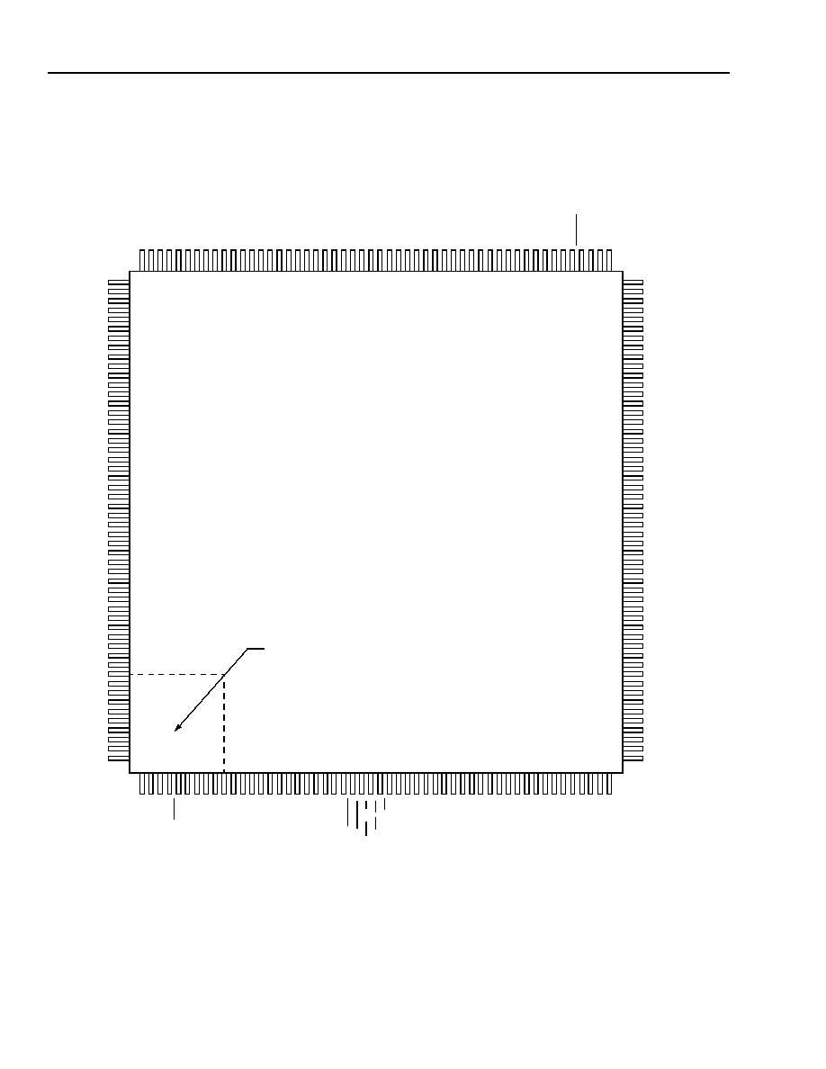
5-6118cF
Figure 1. 208 SQFP--Top View
CT_D28
CT_D30
VSS
LDO1
LDO3
LDO4
LDO6
CT_D27
VDD
CT_D29
CT_D31
LDO0
LDO2
VDD
LDO5
LDO7
VSS
LDO8
LDO9
LDO10
LDO11
VDD
LDO12
LDO13
LDO14
LDO15
VSS
LDI1
LDI3
LDI5
LDI7
LDI8
LDI10
LDI12
LDI14
(NC)
VSS
XCS
LDI0
LDI2
LDI4
LDI6
VDD
LDI9
LDI11
LDI13
LDI15
TCLKOUT
LPUE
PLL2GND
(NC)
PLL2VDD
/C16+
VSS
FGA1
FGA3
FGA5
FGA6
FGA8
/C4
VSS
/C16≠
FGA0
FGA2
FGA4
VDD
FGA7
FGA9
FGA10
FGA11
VSS
FGB0
FGB1
FGB2
FGB3
FGB4
FGB5
VDD
FGB7
FGB9
FGB11
GP0
GP2
GP4
TODJAT/GP6
VDD
(NC)
(NC)
VSS
FGB6
FGB8
FGB10
VSS
GP1
GP3
GP5
FROMDJAT/GP7
(NC)
(NC)
PRIREFOUT
(NC)
EN1
4MHZIN
PLL1VDD
CT
_
D
2
4
CT
_
D
2
3
CT
_
D
2
1
VDD
CT
_
D
1
8
CT
_
D
1
6
CT
_
D
1
5
CT
_
D
2
6
CT
_
D
2
5
VS
S
CT
_
D
2
2
CT
_
D
2
0
CT
_
D
1
9
CT
_
D
1
7
VS
S
CT
_
D
1
4
CT
_
D
1
3
CT
_
D
1
2
VS
S
CT
_
D
1
1
CT
_
D
1
0
(
NC)
CT
_
D
9
CT
_
D
8
VDD
CT
_
D
7
CT
_
D
5
VS
S
CT
_
D
2
CT
_
D
1
VS
S
VS
S
VS
S
/F
R_
COM
P
CT
_
N
E
T
RE
F
2
VS
S
VS
S
CT
_
D
6
CT
_
D
4
CT
_
D
3
VDD
CT
_
D
0
/
C
T_
F
R
AM
E_
A
C
T
_
C
8_A
CT
_
N
E
T
RE
F
1
/
C
T_
F
R
AM
E_
B
C
T
_
C
8_B
SCL
K
SCL
K
X
2
VDD
C2
VS
S
(
NC)
XT
A
L
O
U
T
VD
D
L_R
E
F
6
L_R
E
F
4
L_R
E
F
2
L_R
E
F
0
(
NC)
P
LL1GN
D
VSS
XT
AL
I
N
L_R
E
F
7
L_R
E
F
5
L_R
E
F
3
L_R
E
F
1
VSS
L_S
C
3
L_S
C
2
L_S
C
1
L_S
C
0
VD
D
A1
A0
AL
E
CS
RD
(D
S
)
RDY (
D
T
A
CK
)
VSS
D6
D4
D2
D0
CL
KE
RR
VSS
TC
L
K
TD
I
TR
S
T
WR
(R/W
)
RE
SET
D7
D5
D3
D1
VD
D
S
YSE
RR
TTS
TM
S
TD
O
DPUE
EN2
(
NC)
3M
H
Z
IN
208
52
53
1
104
105
157
156
PIN #1 IDENTIFIER ZONE
Lucent Technologies Inc.
7
Advance Data Sheet
November 1999
H.100/H.110 Interfaces and Time-Slot Interchangers
Ambassador T8100A, T8102, and T8105
1 Product Overview
(continued)
1.3 Pin Information
(continued)
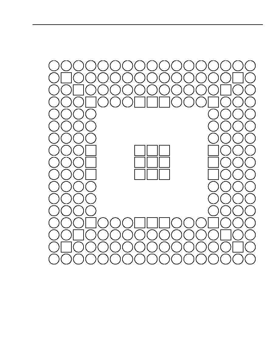
5-6626a(F)
Figure 2. 217 PBGA--Top View
U
T
R
P
N
M
L
K
J
H
G
F
E
D
C
B
A
1
2
3
4
5
6
7
8
9
10
11
12
13
14
15
16
17
VSS
VDD
VSS
VDD
VSS
VSS
VDD
VSS
VDD
VSS
VDD
VSS
VDD
VSS
VSS
VSS
VSS
VSS
VSS
VSS
VSS
VSS
VSS
VSS
VSS
VSS
VSS
VSS
VSS
VSS
VDD
VSS
VDD
8
Lucent Technologies Inc.
Advance Data Sheet
November 1999
H.100/H.110 Interfaces and Time-Slot Interchangers
Ambassador T8100A, T8102, and T8105
1 Product Overview
(continued)
1.3 Pin Information
(continued)
Table 1. Pin Descriptions: Clocking and Framing Pins
Symbol
Pin
Ball
Type
Name/Description
L_REF[7:0]
45--38 P3, N4, R1, P2, N3, M4,
P1, N2
I
Local Frame Reference Inputs. 50 k
internal pull-up.
/C16+
/C16≠
102
101
R14
P13
I/O
H-
MVIP 16.384 MHz Clock Signals. Differential 24 mA drive,
Schmitt in, 50 k
internal pull-up.
/C4
104
U16
I/O
MVIP 4.096 MHz Clock. 8 mA drive, Schmitt in, 50 k
internal
pull-up.
C2
106
T17
I/O
MVIP 2.048 MHz Clock. 8 mA drive, Schmitt in, 50 k
internal
pull-up.
SCLK
110
R17
I/O
SC-Bus 2/4/8 MHz Clock. 24 mA drive, Schmitt in, 50 k
internal
pull-up.
SCLKX2
108
P15
I/O
SC-Bus Inverted 4/8 MHz Clock (Active-Low). 24 mA drive,
Schmitt in, 50 k
internal pull-up.
L_SC[3:0]
36--33
M3, N1, M2, M1
O
Local Selected Clocks. 1.024 MHz, 2.048 MHz, 4.096 MHz,
8.192 MHz, 16.384 MHz, frame (8 kHz), or secondary (NETREF).
8 mA drive, 3-state.
FGA[5:0]
94--99
R12, T13, U14, P12,
R13, T14
O
Frame Group A. 8 mA drive, 3-state.
FGA[11:6]
87--92
T11, P11, R11, U12,
T12, U13
FGB[5:0]
80--85 U9, R9, U10, T10, R10,
U11
O
Frame Group B. 8 mA drive, 3-state.
FGB[11:6]
73--78
U6, T7, R8, U7, T8, U8
PRIREFOUT
58
P5
O
Output from Primary Clock Selector/Divider. 8 mA drive.
PLL1V
DD
53
U1
--
PLL #1 VCO Power. This pin must be connected to power, even if
PLL #1 is not used.
PLL1GND
51
No ball for this
signal, internally
connected.
--
PLL #1 VCO Ground. This pin must be connected to ground,
even if PLL #1 is not used.
EN1
55
T3
I
PLL #1 Enable. Requires cap to V
SS
to form power-on reset, or
may be driven with RESET line. 50 k
internal pull-up.
4MHZIN
54
U2
I
PLL #1 Rate Multiplier. Can be 2.048 MHz or 4.096 MHz.
50 k
internal pull-up.
PLL2V
DD
208
A2
--
PLL #2 VCO Power. This pin must be connected to power, even if
PLL #2 is not used.
PLL2GND
206
No ball for this
signal, internally
connected.
--
PLL #2 VCO Ground. This pin must be connected to ground,
even if PLL #2 is not used.
EN2
3
C2
I
PLL #2 Enable. Requires cap to V
SS
to form power-on reset, or
may be driven with RESET line. 50 k
internal pull-up.
3MHZIN
1
A1
I
PLL #2 Rate Multiplier. Input, 50 k
internal pull-up.
XTALIN
47
R2
I
16.384 MHz Crystal Connection or External Clock Input.
XTALOUT
48
T1
O
16.384 MHz Crystal, Feedback Connection.
TCLKOUT
203
C4
O
Selected output to drive framers. 8 mA drive, 3-state.
CLKERR
13
E1
O
Clock Error. Logical OR of CLKERR register flags (only). 8 mA
drive, 3-state.
SYSERR
12
F3
O
System Error. Logical OR of all CLKERR and SYSERR register
flags. 8 mA drive, 3-state.
Lucent Technologies Inc.
9
Advance Data Sheet
November 1999
H.100/H.110 Interfaces and Time-Slot Interchangers
Ambassador T8100A, T8102, and T8105
1 Product Overview
(continued)
1.3 Pin Information
(continued)
Table 2. Pin Descriptions: Local Streams Pins
Table 3. Pin Descriptions: H-Bus Pins
Symbol
Pin
Ball
Type
Name/Description
LDI[15:8]
LDI[7:0]
201--194
192--185
A3, B4, C5, D6, A4, B5, C6, A5
B6, A6, C7, D7, B7, A7, C8, B8
I
Local Data Input Streams. 50 k
inter-
nal pull-up.
LDO[15:12]
LDO[11:8]
LDO[7:4]
LDO[3:0]
182--179
177--174
172--169
167--164
C9, A9, B9, A10
B10, A11, C10, B11
D11, C11, B12, A13
B13, A14, C13, D12
O
Local Data Output Streams. 8 mA
drive, 3-state.
Symbol
Pin
Ball
Type
Name/Description
CT_D[31:28]
CT_D[27:24]
CT_D[23:20]
CT_D[19:16]
CT_D[15:12]
CT_D[11:10]
CT_D[9:8]
CT_D[7:4]
CT_D[3:2]
CT_D[1:0]
162--159
157--154
152--149
147--144
142--139
137--136
134--133
131--128
126--125
123--122
A15, D13, C14, B15
A17, C16, D15, E14
C17, D16, E15, F14
D17, E16, F15, E17
F16, F17, G15, G14
G16, G17
H15, H16
H17, J15, J17, J16
K17, K16
L17, K15
I/O
H-Bus, Data Lines. Variable rate 2 Mbits/s,
4 Mbits/s, 8 Mbits/s. 5 V tolerant, PCI compliant,
50 k
internal pull-up.
/CT_FRAME_A
120
L14
I/O
H-Bus, 8 kHz, Frame. 5 V tolerant, PCI compliant,
24 mA drive, Schmitt in. No pull-up.
/CT_FRAME_B
114
P17
I/O
H-Bus, Alternate 8 kHz Frame. 5 V tolerant, PCI
compliant, 24 mA drive. Schmitt in. No pull-up.
/FR_COMP
115
M15
I/O
H-Bus, Compatibility Frame Signal. 24 mA drive,
Schmitt in, 50 k
internal pull-up.
CT_NETREF1
116
N17
I/O
H-Bus, Network Reference 1. 8 kHz, 2.048 MHz,
or 1.544 MHz. PCI driver. Not internally pulled up.
CT_NETREF2
113
N15
I/O
H-Bus, Network Reference 2. 8 kHz, 2.048 MHz,
or 1.544 MHz. PCI driver. Not internally pulled up.
CT_C8_A
118
M16
I/O
H-Bus, Main Clock. 5 V tolerant, PCI compliant,
24 mA drive, Schmitt in. No pull-up.
CT_C8_B
112
M14
I/O
H-Bus, Alternate Main Clock. 5 V tolerant, PCI
compliant, 24 mA drive, Schmitt in. No pull-up.
LPUE
205
B3
I
Local Pull-Up Enable. A low disables all pull-ups
other than the CT_Dxx lines and the legacy clocks
C2, /C4, /C16+, /C16≠, SCLK, SCLKX2, and
/FR_COMP. 50 k
internal pull-up. See Section
3.3.5 Physical Connections for H.110.
DPUE
4
D3
I
Data Pull-Up Enable. High enables pull-ups on
CT_Dxx only for H.100, low disables for H.110.
50 k
internal pull-up.
10
Lucent Technologies Inc.
Advance Data Sheet
November 1999
H.100/H.110 Interfaces and Time-Slot Interchangers
Ambassador T8100A, T8102, and T8105
1 Product Overview
(continued)
1.3 Pin Information
(continued)
Table 4. Pin Descriptions: Microprocessor Interface Pins
Table 5. Pin Descriptions: JTAG Pins
Symbol
Pin
Ball Type
Name/Description
RESET
24
J1
I
Master Reset (Active-Low). See Section 3.1 Resets. 50 k
internal pull-
up.
A[1:0]
31--30 L4,
L2
I
Microprocessor Interface, Address Lines. Internal 20 k
pull-down.
D[7:0]
22--15
H1,
H2,
G1,
H3,
G2,
F1,
G4,
G3
I/O
Microprocessor Interface, Data Lines. 8 mA drive, 50 k
internal pull-up.
ALE
29
L1
I
Address Latch Enable. Internal 20 k
pull-down.
CS
28
K3
I
Chip Select (Active-Low). 50 k
internal pull-up.
RD (DS)
27
K2
I
Read Strobe (
Intel
Mode [Active-Low]), Data Strobe (
Motorola
[Active-
Low]). 50 k
internal pull-up.
WR (R/W)
26
K1
I
Write Strobe (
Intel
[Active-Low]), Read/Write Select (
Motorola
[Active-
Low]). 50 k
internal pull-up.
RDY (DTACK)
25
J3
O
Data Ready (
Intel
), Data Transfer (
Motorola
[Active-Low]).
8 mA, open drain (user should add pull-up to this line).
Symbol
Pin
Ball
Type
Name/Description
TCLK
9
E3
I
JTAG Clock Input.
TMS
8
F4
I
JTAG Mode Select. 50 k
internal pull-up.
TDI
7
D2
I
JTAG Data Input. 50 k
internal pull-up.
TDO
6
C1
O
JTAG Data Output. 8 mA drive, 3-state.
TRST
5
E4
I
JTAG Reset (Active-Low). 50 k
internal pull-up.

Lucent Technologies Inc.
11
Advance Data Sheet
November 1999
H.100/H.110 Interfaces and Time-Slot Interchangers
Ambassador T8100A, T8102, and T8105
1 Product Overview
(continued)
1.3 Pin Information
(continued)
Table 6. Pin Descriptions: Power Pins
Table 7. Pin Descriptions: Other Pins
Symbol
Pin
Ball
Type
Name/Description
V
SS
11, 23, 37, 49, 57,
72, 86, 100, 103,
105, 109, 111, 117,
119, 121, 127, 138,
143, 153, 163, 173,
184, 204
B2, B16, C3, C15,
D4, D9, D14, H8,
H9, H10, J4, J8, J9,
J10, J14, K8, K9,
K10, L15, N14, P4,
P9, P14, P16, R3,
R15, T2, T15, T16,
U15, U17
--
Chip Ground.
V
DD
14, 32, 46, 63, 79,
93, 107, 124, 132,
148, 158, 168, 178,
193
A16, D8, D10, F2,
H4, H14, K4, K14,
L16, P8, P10, T9
--
3.3 V Supply Voltage. Decouple every V
DD
pin
with a 0.1
µ
F
ceramic capacitor to V
SS
. 1000 pF or
0.01
µ
F capacitors may be used in addition to the
0.1
µ
F capacitor to provide additional decoupling.
Place the capacitor as close to the V
DD
pin as pos-
sible.
Symbol
Pin
Ball
Type
Name/Description
GP[5:0]
66--71
T5, R6, U5, T6,
R7, P7
I/O
General-Purpose Bidirectional Register. 8 mA
drive, Schmitt in, 50 k
internal pull-up.
TODJAT/GP6
65
U4
I/O
Output from Selector to Drive DJAT (for
NETREF) or GP Register Bit 6.
8 mA drive, Schmitt in, 50 k
internal pull-up.
FROMDJAT/GP7
64
R5
I/O
Smoothed Input to NETREF Divider and Driv-
ers or GP Register Bit 7.
8 mA drive, input, Schmitt in, 50 k
internal pull-
up.
XCS
183
A8
O
Serial Output from Connection Memory. 8 mA
drive, 3-state.
TTS
10
D1
I
Test Type Select. 0 = JTAG, 1 = forced output
test, internal pull-down.
(NC)
2, 50, 52,
56, 59, 60,
61, 62, 135,
202, 207
A12, B1, B14, B17,
C12, D5, E2, J2,
L3, M17, N16, P6,
R4, R16, T4, U3
--
Reserved, No Connection.

12
12
Lucent Technologies Inc.
Advance Data Sheet
November 1999
H.100/H.110 Interfaces and Time-Slot Interchangers
Ambassador T8100A, T8102, and T8105
1 Product Overview
(continued)
1.4
Ambassador TSI Architecture
The
Ambassador
programmable TSIs have been
designed to meet today's switching requirements. The
T8100A and T8105 TSIs have a hierarchical switching
capability. They can switch between the local input bus
and the local output bus. They also switch between the
H.100/H.110 bus and local bus. The T8102 TSI
switches between the H.100/H.110 bus and the local
bus.
All three TSIs have circuitry for subrate switching and
can interface to other computer telephony standards
such as
MVIP
, SC-Bus, and MC-1*.
1.5 Selecting Between T8105, T8102,
T8100A, and T8100
1.6 Enhanced Local Stream Addressing
Local stream addressing has 1024 locations. Separate
connection and data memories (T8100A, T8105 only)
maintain all necessary information for local stream
interconnections. The streams may operate at maxi-
mum rate on eight physical inputs and eight physical
outputs. Choices for slower input or output rates
allow enabling of additional physical inputs or outputs
for a maximum of 16 pins each. Data rates are
2.048 Mbits/s, 4.096 Mbits/s, or 8.192 Mbits/s.
In addition to the enhanced serial streaming, the local
memories may be used for 8-line-serial-in/1-byte-paral-
lel-out, 1-byte-parallel-in/8-line-serial-out, or 1-byte-
parallel-in/1-byte-parallel-out options. All three data
rates are supported in the parallel modes. The
addresses for the local memories (T8100A, T8105
only) have been simplified so that stream and time-slot
designations are automatically translated to the appro-
priate memory address, regardless of rate or serial/par-
allel modes.
* MC-1 is a multichassis communication standard based on
MVIP
.
The devices support this standard.
1.7 Full H.100 Stream Address Support
The devices provide access to the full 4096 H.100 bus
slots (32 streams x 128 slots) or any standard subset
(H-
MVIP
has a maximum 24 streams x 128 time
slots, for example). The number of stored time-slot
addresses is limited to 512 (T8102, T8105 only) at any
one time, but these may be updated on the fly. In addi-
tion, accesses to and from the H.100 bus can be
directed through the 1024 local stream/time slots, giv-
ing a total space of 5120 time slots. Data rates are pro-
grammable on each of the 32 physical streams,
selected in groups of four. The rates are 2.048 Mbits/s,
4.096 Mbits/s, or 8.192 Mbits/s.
1.8 Onboard PLLs and Clock Monitors
The devices use rate multipliers and state machines to
generate onboard frequencies for supporting the
H.100, H-
MVIP
,
MVIP
, MC-1, and SC-Buses. Pins are
provided for coupling the internal clock circuitry with
commonly available clock adapters and jitter attenua-
tors. If external resources are not available, an internal
digital phase-locked loop (DPLL) can be used to gener-
ate all the bus frequencies and remain synchronized to
an 8 kHz reference. One of several clock input refer-
ence sources may be selected, and separate input-
active detection logic can identify the loss of the individ-
ual input references. The entire clocking structure oper-
ates from a 16.384 MHz crystal or external input.
1.9 Phase Alignment of Referenced and
Generated Frames
If this resource is selected, special control logic will cre-
ate bit-sliding in the data streams when the reference
frame and generated frame are out of phase. The bit-
sliding refers to removing a fraction of a bit time per
frame until the frames are in phase.
Features
T8100
T8100A
T8102
T8105
Subrate
switching
--
Local-to-local
connections
1,024
1,024
--
1,024
Local-to-H.100
connections
256
256
512
512
CT_NETREFs
1
2
2
2

Lucent Technologies Inc.
13
Advance Data Sheet
November 1999
H.100/H.110 Interfaces and Time-Slot Interchangers
Ambassador T8100A, T8102, and T8105
1 Product Overview
(continued)
1.10 Interfaces
1.10.1 Microprocessors
The devices provide the user a choice of either
Motor-
ola
or
Intel
interfacing through an 8-bit data bus, a 2-bit
address bus, and multifunction control pins. All access
to the devices' memory blocks and registers use indi-
rect addressing.
1.10.2 Framing Groups
Two groups of programmable framing signals are avail-
able. Each group is composed of 12 sequenced lines
operating in one of four modes. The devices support
1-bit, 2-bit, 1-byte, and 2-byte pulse widths. Starting
position of the pulse sequences are also programma-
ble.
1.10.3 General-Purpose Register and I/O
A general-purpose, 8-bit, input/output port is provided
as either byte-wide I/O or bit addressed I/O.
1.11 Applications
s
Computer-telephony systems
s
Enhanced service platforms
s
WAN access devices
s
PBXs
s
Wireless base stations
1.12 Application Overview
The integration of computers and telecommunications
has enabled a wide range of new communications
applications and has fueled an enormous growth in
communications markets. A key element in the devel-
opment of computer-based communications equipment
has been the addition of an auxiliary telecom bus to
existing computer systems. Most manufacturers of
high-capacity, computer-based telecommunications
equipment have incorporated some such telecom
bus in their systems. Typically, these buses and bus
interfaces are designed to transport and switch
N x 64 kbits/s low-latency telecom traffic between
boards within the computer, independent of the com-
puter's I/O and memory buses. At least a half dozen of
these PC-based telecom buses emerged in the early
1990s for use within equipment based on ISA/EISA
and MCA computers.
With the advent of the H.100 bus specification by the
Enterprise Computer Telephony Forum, the computer-
telephony industry has agreed on a single telecom bus
for use with PCI and compact PCI computers. H.100
facilitates interoperation of components, thus providing
maximum flexibility to equipment manufacturers, value-
added resellers, system integrators, and others build-
ing computer-based telecommunications applications.
2 Architecture and Functional
Description
The devices are H.100-compliant and provide a com-
plete interface between the H.100 bus and a wide vari-
ety of telephony interface components, processors,
and other circuits. The bus interface provides all signals
needed for the H.100 bus, the H-
MVIP
and
MVIP
-90
buses, or the SC-Bus. Local interfaces include 16 serial
inputs and 16 serial outputs based on the Lucent Tech-
nologies Microelectronics Group concentration high-
way interface (CHI). The T8100A and the T8105
include two built-in time-slot interchangers. The first
provides a local switching domain with up to 1024 pro-
grammable connections between time slots on the local
CHI inputs and outputs. The second provides program-
mable connections between any time slot on the H.100
bus and any time slot in the local switching domain.
The T8105 has 512 programmable connections while
the T8100A has 256. The T8102 has only 1 TSI for
switching up to 512 programmable connections on the
H.100 bus and any time slot in the local switching
domain. All
Ambassador
devices are configured via a
microprocessor interface. This interface can also read
and write time slot and device data. Onboard clock cir-
cuitry, including a DPLL, supports all H.100 clock
modes including
MVIP
and SC-Bus compatibility
clocks. The local CHI interfaces support PCM rates of
2.048 Mbits/s, 4.096 Mbits/s, and 8.192 Mbits/s. Each
device has internal circuitry to support either minimum
latency or multi-time-slot frame integrity. Frame integrity
is a requisite feature for applications that switch wide-
band data (ISDN H-channels). Minimum latency is
advantageous in voice applications.
All three TSIs have the following four major sections:
s
Local bus--refers to the local streams.
s
H-bus--refers to the H.100/H.110/H-
MVIP
and
legacy streams.
s
Interface--refers to the microprocessor interface,
frame groups, and general-purpose I/O (GPIO).
s
Timing--the rate multipliers, DPLL, and clocking
functions.
14
Lucent Technologies Inc.
Advance Data Sheet
November 1999
H.100/H.110 Interfaces and Time-Slot Interchangers
Ambassador T8100A, T8102, and T8105
2 Architecture and Functional Description
(continued)
Figure 3 shows a block diagram of the TSI devices. The devices operate on a 3.3 V supply for both the core and
I/Os, though the I/Os are TTL compatible and 5 V tolerant.
5-6101.a (F)
* For T8100 and T8100A, there are only 256 locations.
T8102 does not have local data memory.
Figure 3. Block Diagram of the TSI Devices
...
...
...
H.100, H.110, H-
MVIP, MVIP, SC-BUS
INTERNAL
CLOCKS AND
STATE
COUNTER
S/P AND P/S CONVERTERS
512*
LOCATION
DATA
SRAM
THREE 512*
LOCATION
CONNECTION
CAMs
1024
LOCATION
DATA
MEMORY
OUTPUT
LOGIC
AND P/S
CONVERT
INPUT
LOGIC
AND S/P
CONVERT
1024
LOCATION
CONNECTION
MEMORY
TIMING AND
CONTROL
MICROPROCESSOR
INTERFACE
FRAME GROUP
INTERFACE
LOGIC
FRAME
GROUPS
ADDR[1:0]
DATA[7:0]
µ
P CONTROLS
MISC. I/O
CLOCKS AND REFS
INTERNAL
DATA
INTERNAL
ADDRESS
AND
CONTROL
LOCAL OUT
LOCAL IN

Lucent Technologies Inc.
15
Advance Data Sheet
November 1999
H.100/H.110 Interfaces and Time-Slot Interchangers
Ambassador T8100A, T8102, and T8105
2 Architecture and Functional Description
(continued)
2.1 Register/Memory Maps
In this section, a general overview of the registers and the indirect mapping to different memory spaces is
described. More detailed descriptions for using the registers in software can be found in Section 3.4 Using the
LAR, AMR, and IDR for Connections.
(Throughout this document, all registers are defined with the MSB on the left and the LSB on the right.)
2.1.1 Main Registers
The address bits are used to map a large memory space.
All registers default to 0 at powerup.
Table 8. Addresses of Programming Registers
2.1.2 Master Control and Status Register
Table 9. Master Control and Status Register
A1
A0
Symbol
Name/Description
0
0
MCR
Master Control and Status Register (read/write)
0
1
LAR
Lower Address Register--Lower Indirect Address (time slot) (write only)
1
0
AMR
Address Mode Register--Upper Address (stream) and Address Type (write only)
1
1
IDR
Indirect Data Register (read/write)
Symbol
Bit
Name/Description
MR
7
Master (Software) Reset. A high reinitializes the registers.
CER
6
Clock Error Reset. A high resets the error bits of the CLKERR registers.
SER
5
System Error Reset. A high resets the error bits of the SYSERR register. (Note that MR,
CER, and SER are automatically cleared after the requested reset is complete.)
AP
4
Active Page. This bit identifies which of the double-buffered data memories are active. A
zero indicates buffer 0; a one indicates buffer 1. The AP identifies which data buffer is being
accessed during a write operation (i.e., input from local streams or input from H-bus).
HBE
3
H-Bus Enable. On powerup or software reset, all H-bus pins (including clocks) are disabled.
HBE must be set high to reenable the 3-stated buffers.
LBE
2
Local Bus Enable. Same function as HBE for local data outputs.
LCE
1
Local Clock Enable. Enables all other local functions: clocks, frame groups, etc. (Note that
the TCLKOUT is disabled during a Master Reset and is unaffected by HBE, LBE, or LCE,
though there are control bits for this signal in the CKP register. See Section 2.5.8 Clock Con-
trol Register Definitions for a description of the CKP register.) 3-stated if disabled.
CB
0
CAM Busy. A status bit indicating microprocessor activity in any of the CAM blocks. A high
means that one (or more) of the CAMs is being accessed by the microprocessor. In most
cases, this bit will read low since there are many internal operational cycles dedicated to the
microprocessor, which allow it to finish quickly.

16
Lucent Technologies Inc.
Advance Data Sheet
November 1999
H.100/H.110 Interfaces and Time-Slot Interchangers
Ambassador T8100A, T8102, and T8105
2 Architecture and Functional Description
(continued)
2.1 Register/Memory Maps
(continued)
2.1.3 Address Mode Register
The AMR is defined in Table 10 below where (aaaa) is the stream address and the LAR is the time-slot address of
the selected memory space.
Note: All unused AMR values are reserved.
Table 10. Address Mode Register
Bits
7--4
Bits
3--0
Register Function
0000
0000
Control Registers.
0001
(aaaa) Local Bus, Data Memory 1.
0010
(aaaa) Local Bus, Data Memory 2.
0100
(aaaa) Local Bus, Connection Memory, Time-Slot Field.
0101
(aaaa) Local Bus, Connection Memory, Stream, and Control Bit Field.
0111
0000
Local Bus, Holding Registers, Reset.
1001
1001
0000
0001
CAM, Data Memory 1. Lower 256 Addresses.
CAM, Data Memory 1. Upper 256 Addresses (T8102, T8105 only).
1010
1010
0000
0001
CAM, Data Memory 2. Lower 256 Addresses.
CAM, Data Memory 2. Upper 256 Addresses (T8102, T8105 only).
1011
0000 CAM, Connection, Time-Slot Field.
1011
0001
CAM, Connection, Stream, and Control Bit Field.
1011
0010
CAM, Connection, Tag Field.
1011
0011
CAM, Connection, Subrate Control, Tag Field MSB.
1110
0000
CAM, Even, Make Connection (MKCE). Write to Next Free Location.
1110
0001
CAM, Odd, Make Connection (MKCO). Write to Next Free Location.
1110
0011
CAM, Local, Make Connection (MKCL). Write to Next Free Location.
1110
0100
CAM, Even, Break Connection (BKCE).
1110
0101
CAM, Odd, Break Connection (BKCO).
1110
0111
CAM, Local, Break Connection (BKCL).
1110
1100
1000
1000
CAM, Even, Clear Location (CLLE). Lower 256 Range. Requires LAR.
CAM, Even, Clear Location (CLLE). Upper 256 Range. Requires LAR (T8102, T8105 only).
1110
1100
1001
1001
CAM, Odd, Clear Location (CLLO). Lower 256 Range. Requires LAR.
CAM, Odd, Clear Location (CLLO). Upper 256 Range. Requires LAR (T8102, T8105 only).
1110
1100
1011
1011
CAM, Local, Clear Location (CLLL). Lower 256 Range. Requires LAR.
CAM, Local, Clear Location (CLLL). Upper 256 Range. Requires LAR (T8102, T8105 only).
1110
1100
1100
1100
CAM, Even, Read Location (RDCE). Lower 256 Range. Requires LAR, IDR Holds Results.
CAM, Even, Read Location (RDCE). Upper 256 Range. Requires LAR, IDR Holds Results (T8102, T8105 only).
1110
1100
1101
1101
CAM, Odd, Read Location (RDCO). Lower 256 Range. Requires LAR, IDR Holds Results.
CAM, Odd, Read Location (RDCO). Upper 256 Range. Requires LAR, IDR Holds Results (T8102, T8105 only).
1110
1100
1111
1111
CAM, Local, Read Location (RDCL). Lower 256 Range. Requires LAR, IDR Holds Results.
CAM, Local, Read Location (RDCL). Upper 256 Range. Requires LAR, IDR Holds Results (T8102, T8105 only).
1111
0000
CAM, Even, Find Entry (FENE). IDR Holds Results.
1111
0001
CAM, Odd, Find Entry (FENO). IDR Holds Results.
1111
0011
CAM, Local, Find Entry (FENL). IDR Holds Results.
1111
1000
CAM, Even, Reset (RSCE).
1111
1001
CAM, Odd, Reset (RSCO).
1111
1011
CAM, Local, Reset (RSCL).
1111
1100
CAM, Holding Registers, Reset (RCH).
1111
1111
CAM, Initialize (CI). Reset All CAM Locations and Holding Registers.

Lucent Technologies Inc.
17
Advance Data Sheet
November 1999
H.100/H.110 Interfaces and Time-Slot Interchangers
Ambassador T8100A, T8102, and T8105
2 Architecture and Functional Description
(continued)
2.1 Register/Memory Maps
(continued)
2.1.4 Control Register Memory Space
Function of LAR values when AMR = 0x00. All control registers reset to 0x00. All designations of MSB (most signif-
icant bit) and LSB (least significant bit) are shown.
Table 11. Control Register Memory Space
Register Address
Register Mnemonic
Description
Refer to Section
0, 0x00
CKM
Clocks, Main Clock Selections
2.5.8
1, 0x01
CKN
Clocks, NETREF Selections
2.5.8
2, 0x02
CKP
Clocks, Programmable Outputs
2.5.8
3, 0x03
CKR
Clocks, Resource Selection
2.5.8
4, 0x04
CKS
Clocks, Secondary (Fallback) Selection
2.5.8
5, 0x05
CK32
Clocks, Locals 3 and 2
2.5.8
6, 0x06
CK10
Clocks, Locals 1 and 0
2.5.8
7, 0x07
CKMD
Clocks, Main Divider
2.5.8
8, 0x08
CKND
Clocks, NETREF Divider
2.5.8
9, 0x09
CKRD
Clocks, Resource Divider
2.5.8
10--11, 0x0A--0x0B
(Reserved)
--
--
12, 0x0C
LBS
Local Stream Control
2.2.4
13, 0x0D
(Reserved)
--
--
14, 0x0E
CON
Connection Delay Type
Appendix B
15, 0x0F
(Reserved)
--
--
16, 0x10
HSL
H-Bus Stream Control, Low Byte
2.3.5
17, 0x11
HSH
H-Bus Stream Control, High Byte
2.3.5
18--22, 0x12--0x16
(Reserved)
--
--
23, 0x17
GPD
General-purpose Register, Direction Control
2.6.2
24, 0x18
GPR
General-purpose I/O Register
2.6.2
25--31, 0x19--0x1F
(Reserved)
--
--
32, 0x20
FRLA
Frame Group A, Start Address, Low
2.6.3
33, 0x21
FRHA
Frame Group A, High Address and Control
2.6.3
34, 0x22
FRLB
Frame Group B, Start Address, Low
2.6.3
35, 0x23
FRHB
Frame Group B, High Address and Control
2.6.3
36, 0x24
FRPL
Frame Group B, Programmed Output, Low
2.6.3
37, 0x25
FRPH
Frame Group B, Programmed Output, High
2.6.3
38--39, 0x26--0x27
(Reserved)
--
--
40, 0x28
CLKERR1
Clock Error Register, Error Indicator
2.7
41, 0x29
CLKERR2
Clock Error Register, Current Status
2.7
42, 0x2A
SYSERR
System Error Register
2.7
43, 0x2B
CKW
Clock Error/Watchdog Masking Register
2.5.7 & 2.7
44, 0x2C
CLKERR3
Clock Error Register, Current Status
2.7
45--47, 0x2D--0x2F
(Reserved)
--
--
48, 0x30
DIAG1
Diagnostics Register 1
2.9.2
49, 0x31
DIAG2
Diagnostics Register 2
2.9.2
50, 0x32
DIAG3
Diagnostics Register 3
2.9.2
51--253, 0x33--0xFD
(Reserved)
--
--
254, 0xFE
DEV_ID
Device Revision Status Register
3.2.1
255, 0xFF
GMODE
Global Mode Register
3.2.1
18
18
Lucent Technologies Inc.
Advance Data Sheet
November 1999
H.100/H.110 Interfaces and Time-Slot Interchangers
Ambassador T8100A, T8102, and T8105
2 Architecture and Functional
Description
(continued)
2.1 Register/Memory Maps
(continued)
2.1.4 Control Register Memory Space (continued)
This section is a summary of the register functions. The
reader is encouraged to read through the rest of this
specification to learn the details of the individual regis-
ters and their interactions with the overall architecture.
Table 12. CKM: Clocks, Main Clock Selection, 0x00
Table 13. CKN: Clocks, NETREF Selections, 0x01
Table 14. CKP: Clocks, Programmable Outputs,
0x02
Table 15. CKR: Clocks, Resource Selection, 0x03
Table 16. CKS: Clocks, Secondary (Fallback)
Selection, 0x04
Table 17. CK32: Clocks, Locals 3 and 2, 0x05
Table 18. CK10: Clocks, Locals 1 and 0, 0x06
Bit
Description
7
Phase Alignment Enable
6
Phase Alignment Select
5
Compatibility Clock Direction
4
Input Clock Invert
3
Input Clock Select, MSB
2
Input Clock Select
1
Input Clock Select
0
Input Clock Select, LSB
Bit
Description
7
NETREF1 Output Enable
6
NETREF2 Output Enable
5
Bypass Select
4
Input Clock Invert
3
Input Clock Select, MSB
2
Input Clock Select
1
Input Clock Select
0
Input Clock Select, LSB
Bit
Description
7
TCLK Select, MSB
6
TCLK Select
5
TCLK Select, LSB
4
CT_C8 Pins, Input Type Select
3
CT_C8A Output Enable
2
CT_C8B Output Enable
1
CT_C8 Pins, Output Type Select
0
/FR_COMP Pulse Width
Bit
Description
7
Resource Select, MSB
6
Resource Select, LSB
5
PLL #1 Bypass
4
PLL #1 Rate Select
3
PLL #2 Bypass
2
PLL #2 Rate Select
1
SCLK Output Select, MSB
0
SCLK Output Select, LSB
Bit
Description
7
Secondary Resource Select, MSB
6
Secondary Resource Select, LSB
5
Fallback Type Select, MSB
4
Fallback Type Select, LSB
3
Fallback, Force Selection of Secondary Input
2
Secondary Input Clock Select, MSB
1
Secondary Input Clock Select
0
Secondary Input Clock Select, LSB
Bit
Description
7
Local Clock 3 Select, MSB
6
Local Clock 3 Select
5
Local Clock 3 Select
4
Local Clock 3 Select, LSB
3
Local Clock 2 Select, MSB
2
Local Clock 2 Select
1
Local Clock 2 Select
0
Local Clock 2 Select, LSB
Bit
Description
7
Local Clock 1 Select, MSB
6
Local Clock 1 Select
5
Local Clock 1 Select
4
Local Clock 1 Select, LSB
3
Local Clock 0 Select, MSB
2
Local Clock 0 Select
1
Local Clock 0 Select
0
Local Clock 0 Select, LSB

Lucent Technologies Inc.
19
Advance Data Sheet
November 1999
H.100/H.110 Interfaces and Time-Slot Interchangers
Ambassador T8100A, T8102, and T8105
2 Architecture and Functional
Description
(continued)
2.1 Register/Memory Maps
(continued)
2.1.4 Control Register Memory Space (continued)
Table 19. CKMD: Clocks, Main Divider; CKND:
Clocks, NETREF Divider; CKRD: Clocks,
Resource Divider, 0x07, 0x08, 0x09
Table 20. LBS: Local Stream Control, 0x0C
Table 21. CON: Connection Delay Type, 0x0E
Table 22. HSL: H-Bus Stream Control, Low Byte,
0x10
Table 23. HSH: H-Bus Stream Control, High Byte,
0x11
Table 24. GPD, General-Purpose Direction Control
Register, 0x17
Bit
Description
7
Divide Value, MSB
6
Divide Value
5
Divide Value
4
Divide Value
3
Divide Value
2
Divide Value
1
Divide Value
0
Divide Value, LSB
Bit
Description
7
Parallel/Serial Select, MSB
6
Parallel/Serial Select, LSB
5
Local Group A Rate Select, MSB
4
Local Group A Rate Select, LSB
3
Local Group B Rate Select, MSB
2
Local Group B Rate Select, LSB
1
Local Group C Rate Select, MSB
0
Local Group C Rate Select, LSB
Bit
Description
7
Reserved
6
Enable GPD (bitwise general-purpose
register)
5
Select NETREF1/NETREF2 as main clock in.
4
L_REF type select (stand-alone or paired)
3
Invert L_REF Frame Strobe
2
Invert L_REF Bit Clock
1
Disable Connection-by-Connection Delay
Setting
0
Global FME Setting
Bit
Description
7
H-Bus Group D Rate Select, MSB
6
H-Bus Group D Rate Select, LSB
5
H-Bus Group C Rate Select, MSB
4
H-Bus Group C Rate Select, LSB
3
H-Bus Group B Rate Select, MSB
2
H-Bus Group B Rate Select, LSB
1
H-Bus Group A Rate Select, MSB
0
H-Bus Group A Rate Select, LSB
Bit
Description
7
H-Bus Group H Rate Select, MSB
6
H-Bus Group H Rate Select, LSB
5
H-Bus Group G Rate Select, MSB
4
H-Bus Group G Rate Select, LSB
3
H-Bus Group F Rate Select, MSB
2
H-Bus Group F Rate Select, LSB
1
H-Bus Group E Rate Select, MSB
0
H-Bus Group E Rate Select, LSB
Bit
Description
7
Direction Control for GPR Bit 7, 0 = In; 1 = Out.
6
Direction Control for GPR Bit 6, 0 = In; 1 = Out.
5
Direction Control for GPR Bit 5, 0 = In; 1 = Out.
4
Direction Control for GPR Bit 4, 0 = In; 1 = Out.
3
Direction Control for GPR Bit 3, 0 = In; 1 = Out.
2
Direction Control for GPR Bit 2, 0 = In; 1 = Out.
1
Direction Control for GPR Bit 1, 0 = In; 1 = Out.
0
Direction Control for GPR Bit 0, 0 = In; 1 = Out.

20
20
Lucent Technologies Inc.
Advance Data Sheet
November 1999
H.100/H.110 Interfaces and Time-Slot Interchangers
Ambassador T8100A, T8102, and T8105
2 Architecture and Functional
Description
(continued)
2.1 Register/Memory Maps
(continued)
2.1.4 Control Register Memory Space (continued)
Table 25. GPR: General-Purpose I/O Register, 0x18
Table 26. FRLA: Frame Group A, Start Address
Low, 0x20
Table 27. FRHA: Frame Group A, High Address and
Control, 0x21
Table 28. FRLB: Frame Group B, Start Address
Low, 0x22
Table 29. FRHB: Frame Group B, High Address and
Control, 0x23
Bit
Description
7
General-Purpose I/O, MSB
6
General-Purpose I/O
5
General-Purpose I/O
4
General-Purpose I/O
3
General-Purpose I/O
2
General-Purpose I/O
1
General-Purpose I/O
0
General-Purpose I/O, LSB
Bit
Description
7
Start Address, Bit 7, or Programmed Output,
Bit 7
6
Start Address, Bit 6, or Programmed Output,
Bit 6
5
Start Address, Bit 5, or Programmed Output,
Bit 5
4
Start Address, Bit 4, or Programmed Output,
Bit 4
3
Start Address, Bit 3, or Programmed Output,
Bit 3
2
Start Address, Bit 2, or Programmed Output,
Bit 2
1
Start Address, Bit 1, or Programmed Output,
Bit 1
0
Start Address, LSB, or Programmed Output,
Bit 0
Bit
Description
7
Rate Select, MSB
6
Rate Select, LSB
5
Pulse Width Select, MSB
4
Pulse Width Select, LSB
3
Frame Invert, or Programmed Output, Bit 11
2
Start Address, MSB, or Programmed Output,
Bit 10
1
Start Address, Bit 9, or Programmed Output,
Bit 9
0
Start Address, Bit 8, or Programmed Output,
Bit 8
Bit
Description
7
Start Address, Bit 7
6
Start Address, Bit 6
5
Start Address, Bit 5
4
Start Address, Bit 4
3
Start Address, Bit 3
2
Start Address, Bit 2
1
Start Address, Bit 1
0
Start Address, LSB
Bit
Description
7
Rate Select, MSB
6
Rate Select, LSB
5
Pulse Width Select, MSB
4
Pulse Width Select, LSB
3
Frame Inversion Select
2
Start Address, MSB
1
Start Address, Bit 9
0
Start Address, Bit 8

Lucent Technologies Inc.
21
Advance Data Sheet
November 1999
H.100/H.110 Interfaces and Time-Slot Interchangers
Ambassador T8100A, T8102, and T8105
2 Architecture and Functional
Description
(continued)
2.1 Register/Memory Maps
(continued)
2.1.4 Control Register Memory Space (continued)
Table 30. FRPL: Frame Group B, Programmed
Output, Low, 0x24
Table 31. FRPH: Frame Group B, Programmed
Output, High, 0x25
Table 32. CLKERR1: Clock Error Register, Error
Indicator, 0x28
Table 33. CLKERR2: Clock Error Register, Current
Status, 0x29
Table 34. SYSERR: System Error Register, 0x2A
Table 35. CKW: Clock Error/Watchdog Masking
Register, 0x2B
Table 36. CLKERR3: Clock Error Register, Current
Status, 0x2C
Bit
Description
7
Programmed Output, Bit 7
6
Programmed Output, Bit 6
5
Programmed Output, Bit 5
4
Programmed Output, Bit 4
3
Programmed Output, Bit 3
2
Programmed Output, Bit 2
1
Programmed Output, Bit 1
0
Programmed Output, Bit 0
Bit
Description
7
Group A Output Pins Select, MSB
6
Group A Output Pins Select, LSB
5
(Reserved, Use 0)
4
Group B Output Pins Select
3
Programmed Output, Bit 11
2
Programmed Output, Bit 10
1
Programmed Output, Bit 9
0
Programmed Output, Bit 8
Bit
Description
7
C8A or Frame A Error
6
C8B or Frame B Error
5
/FR_COMPn Error
4
C16+ or C16≠ Error
3
C4n or C2 Error
2
SCLKX2
Error
1
SCLK Error
0
NETREF Error
Bit
Description
7
C8A or Frame A Fault Status
6
C8B or Frame B Fault Status
5
/FR_COMPn Fault Status
4
C16+ or C16≠ Fault Status
3
C4n or C2 Fault Status
2
SCLKX2
Fault Status
1
SCLK Fault Status
0
NETREF[2:1] Fault Status
Bit
Description
7
Even CAM Underflow Error (No Match)
6
Odd CAM Underflow Error (No Match)
5
Local CAM Underflow Error (No Match)
4
Even CAM Overflow or No-Match Error
3
Odd CAM Overflow or No-Match Error
2
Local CAM Overflow or No-Match Error
1
H-Bus Data Memory Access Error
0
Fallback Enable Indicator
Bit
Description
7
C8A and Frame A Error Mask
6
C8B and Frame B Error Mask
5
/FR_COMP Error Mask
4
C16+ and C16≠ Error Mask
3
/C4 and C2 Error Mask
2
SCLKX2
Error Mask
1
SCLK Error Mask
0
NETREF1 Error Mask
Bit
Description
7
(Reserved)
6
(Reserved)
5
NETREF2 Error
4
NETREF1 Error
3
(Reserved)
2
(Reserved)
1
(Reserved)
0
NETREF2 Error Mask
22
22
Lucent Technologies Inc.
Advance Data Sheet
November 1999
H.100/H.110 Interfaces and Time-Slot Interchangers
Ambassador T8100A, T8102, and T8105
2 Architecture and Functional
Description
(continued)
2.1 Register/Memory Maps
(continued)
2.1.4 Control Register Memory Space (continued)
Table 37. DIAG1: Diagnostics Register 1, 0x30
Table 38. DIAG2: Diagnostics Register 2, 0x31
Table 39. DIAG3: Diagnostics Register 3, 0x32
Table 40. DEV_ID: Device Identification Register,
0xFE
Table 41. GMODE: Global Mode Register, 0xFF
Bit
Description
7
Frame Group A Output Select, MSB
6
Frame Group A Output Select, LSB
5
Frame Group B Output Select, MSB
4
Frame Group B Output Select, LSB
3
Memory Fill Enable
2
Memory Fill Pattern Select, MSB
1
Memory Fill Pattern Select, LSB
0
Memory Fill Status Bit (Read Only)
Bit
Description
7
Frame Groups Cycle Test Enable
6
Break State Counter into Subsections
5
Bypass Internal Frame with /FR_COMPn
4
(Reserved)
3
Enable State Counter Parallel Load
2
Parallel Load Value of State Counter, MSB
1
Parallel Load Value of State Counter, Bit 9
0
Parallel Load Value of State Counter, Bit 8
Bit
Description
7
Parallel Load Value of State Counter, Bit 7
6
Parallel Load Value of State Counter, Bit 6
5
Parallel Load Value of State Counter, Bit 5
4
Parallel Load Value of State Counter, Bit 4
3
Parallel Load Value of State Counter, Bit 3
2
Parallel Load Value of State Counter, Bit 2
1
Parallel Load Value of State Counter, Bit 1
0
Parallel Load Value of State Counter, LSB
Bit
Description
7
Device Identification Number, MSB
6
Device Identification Number
5
Device Identification Number
4
Device Identification Number, LSB
3
Device Version Number, MSB
2
Device Version Number
1
Device Version Number
0
Device Version Number, LSB
Bit
Description
7
Mode Emulation Set 2 (ME2)
6
Mode Emulation Set 1 (ME1)
5
Subrate Enable (SE)
4
(Reserved)
3
EMUL, MSB
2
EMUL
1
EMUL
0
EMUL, LSB
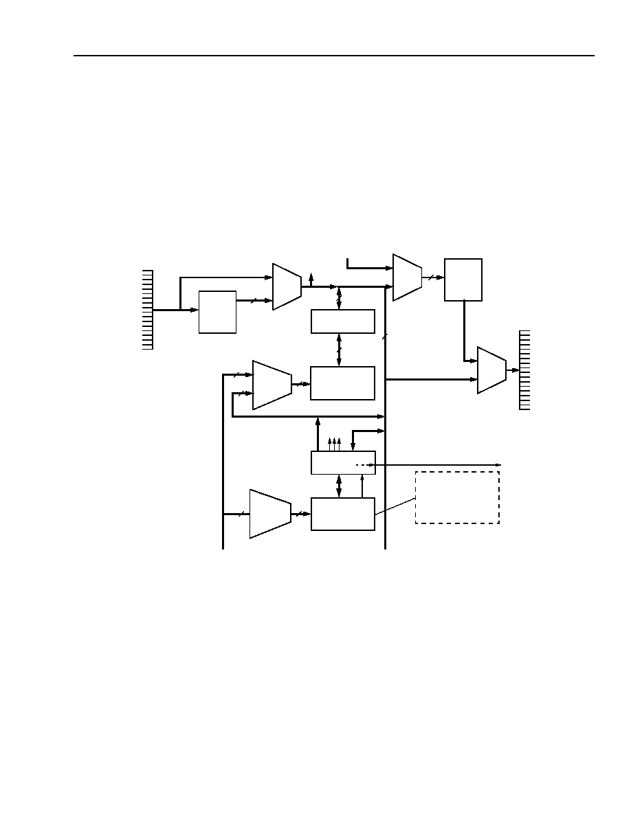
Lucent Technologies Inc.
23
Advance Data Sheet
November 1999
H.100/H.110 Interfaces and Time-Slot Interchangers
Ambassador T8100A, T8102, and T8105
2 Architecture and Functional Description
(continued)
2.2 Local Bus Section
Figure 4 shows the local bus section function diagram.
Note:
Routing and MUXing for the H-bus section is included since the H-bus requires access to the converters
for local bus-to-H-bus or H-bus-to-local bus transfers (the H-bus is discussed in Section 2.3 H-Bus Sec-
tion).
XCS is a pseudo serial stream, read out from the connection memory on each memory access. It is read out
directly, i.e., not passing through any parallel/serial converters or holding registers, so it precedes the connection
associated with it by one time slot.
5-6102F
Figure 4. Local Bus Section Function
All of the
Ambassador
family TSIs have a local bus, but only the T8100A and T8105 have local connection memory
and local data memory for time-slot interchanging.
S/P
BYPASS
ADDRESS
BUFFER &
DECODER
CAM-
LOCAL
SELECT
P/S
BYPASS
PARALLEL
TO
SERIAL
(P/S)
DATA BUFFER-
REGISTER
FROM CAM
SERIAL
TO
PARALLEL
(S/P)
(1024 LOCATIONS
x BITS) x 2
DATA
MEMORY
CONNECTION
BUFFER-
REGISTER
CTL BITS
(PATTERN MODE)
1024 LOCATIONS
x 15 bits
CONNECTION
MEMORY
LOCAL STREAM
LOCAL STREAM
TO CAM
INTERNAL
EACH LOCATION:
STREAM = 4 bits
TIME SLOT = 7 bits
TIME-SLOT ENABLE BIT
CONSTANT/MIN DELAY BIT
PATTERN MODE BIT
XCS BIT
INTERNAL
(AMR) + (LAR)
8
8
11
11
10
10
11
8
8
ADDRESS
BUFFER &
DECODER
8
XCS
ADDRESS
BUS
DATA BUS
INPUTS
OUTPUTS
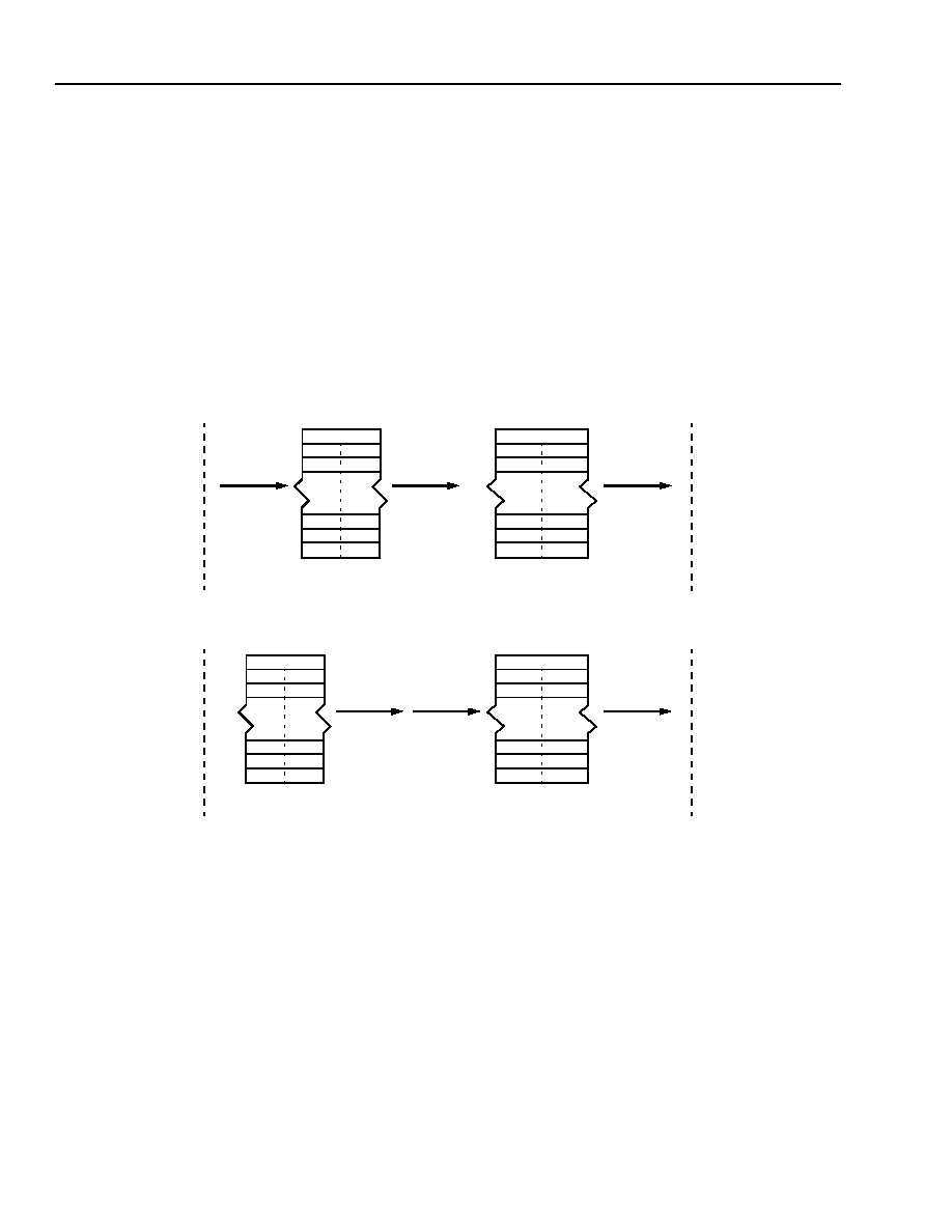
24
Lucent Technologies Inc.
Advance Data Sheet
November 1999
H.100/H.110 Interfaces and Time-Slot Interchangers
Ambassador T8100A, T8102, and T8105
2 Architecture and Functional Description
(continued)
2.2 Local Bus Section
(continued)
2.2.1 Constant Frame Delay and Minimum Delay Connections
The local bus section contains the local connection memory (T8100A, T8105 only) and the double-buffered local
data memory. Collectively, the connection memory and data memory are referred to as local memory since it is
used for implementing local-to-local switching only. Operation is similar to other time-slot interchangers. Data is
written into the memory in a fixed order and then read out according to the indirect addresses held in the connec-
tion memory. If any of the connections on the devices are operating in constant frame delay (also called constant
delay) mode, then the output data is accessed from a second block of data memory. The input data will not be out-
put until the next frame boundary has been crossed and the memory blocks have swapped functions. Figure 5
shows an example of a set of connections which create the delay types referred to as minimum delay and constant
delay.
5-6103F
Figure 5. Local Bus Memory Connection Modes
2.2.2 Serial and Parallel
Nominally, the memory will be accessed by serial data streams which will require conversion of serial-to-parallel
(S/P) for write accesses and parallel-to-serial (P/S) for read accesses. Since the local memory can have up to 16
serial inputs and 16 serial outputs, there will be a maximum of 16 S/P converters and 16 P/S converters operating
simultaneously. If desired, eight of the S/P converters, local inputs 0--7, can be bypassed for a direct parallel write
to the data memory. Likewise, eight of the P/S converters, local outputs 0--7, can be bypassed for a direct parallel
read of the data memory. Unused S/P or P/S converters are nonfunctional in these modes.
Note: The normal serial-to-serial local streaming is not available simultaneously with any of the parallel modes.
FRAME N DATA
DATA BLOCK 0
0
1
2
3
1020
1021
1022
1023
WRITE N
READ N
MINIMUM DELAY
CONNECTION
FRAME N ≠ 1 DATA
DATA BLOCK 1
0
1
2
3
1020
1021
1022
1023
READ N ≠ 1
CONSTANT DELAY
CONNECTION
FRAME N DATA
DATA BLOCK 0
0
1
2
3
1020
1021
1022
1023
READ N
CONSTANT DELAY
CONNECTION
FRAME N + 1 DATA
DATA BLOCK 1
0
1
2
3
1020
1021
1022
1023
WRITE N + 1
READ N + 1
MINIMUM DELAY
CONNECTION
FRAME N + 1
FRAME N
Lucent Technologies Inc.
25
Advance Data Sheet
November 1999
H.100/H.110 Interfaces and Time-Slot Interchangers
Ambassador T8100A, T8102, and T8105
2 Architecture and Functional
Description
(continued)
2.2 Local Bus Section
(continued)
2.2.3 Data Rates and Time-Slot Allocation
At its maximum, the T8100A and the T8105 will be able
to process 1024 nonblocking local-to-local connections.
The data rate 8.192 Mbits/s corresponds to 128 time
slots, 4.096 Mbits/s corresponds to 64 time slots, and
2.048 Mbits/s corresponds to 32 time slots. Since differ-
ent data rates require different amounts of memory, the
local memory can be filled in a number of ways. A non-
blocking switch permits any time slot on any stream to
be switched to another time slot on any stream in any
direction.
The local streams are arranged in three groups: A,
B, and C. Group A corresponds to the local data pins
0--7, group B with local data pins 8--11, and group C
with local data pins 12--15. The groups may be oper-
ated at any of the three data rates: 2.048 Mbits/s,
4.096 Mbits/s, or 8.192 Mbits/s; however, group B is
activated only when group A is operating below
8.192 Mbits/s. Likewise, group C is activated when
group B is operating below 8.192 Mbits/s.
Note: In order to efficiently fill the memory, the mem-
ory locations are read or filled in the same order
regardless of their activation or rate.
The streams are scanned in intervals equal to
8.192 Mbits/s time slots: first group A from 0 through 7,
then group B from 8 through 11, then group C from 12
through 15. If a group is active, the data is input from or
output to the streams in that group. If a group is operat-
ing below 8.192 Mbits/s and has already been scanned
(at the 8.192 Mbits/s rate), then the data transfer oper-
ation is ignored.
For addressing, the user directly provides stream and
time-slot information. The devices will map this into the
physical memory, regardless of which stream groups
are active or at what rate. While this makes program-
ming simpler, it makes the internal operation more diffi-
cult to understand. Several diagrams are required to
illustrate how the memory utilization works.
Unassigned time slots in the local output section are
3-stated. Therefore, multiple lines can be connected
together.
Figure 6 below shows the overall structure of the local
memory:
Note: Both the connection and two data memories are
arranged in four blocks of 256 locations each
(i.e., 4 x [4 x 64]).
The arrangement is important to establishing a mem-
ory fill pattern which supports all of the various groups
and rates. The rows of each memory, which are split
into four groups of 4, correspond to the 16 streams.
The columns correspond to 64 time-slot addresses.
5-6104F
Figure 6. Local Streams, Memory Structure
4
4
4
4
64
4
4
4
4
64
LOCATION 0
CONNECTION
LOCATION 15
EACH (SMALL) SQUARE
LOCATION 1023
DATA MEMORY 0
DATA MEMORY 1
EACH (SMALL)
TO/FROM
REPRESENTS 15 bits
OF CONNECTION
INFORMATION
SQUARE
REPRESENTS
1 byte OF DATA
LOCAL
STREAMS
MEMORY
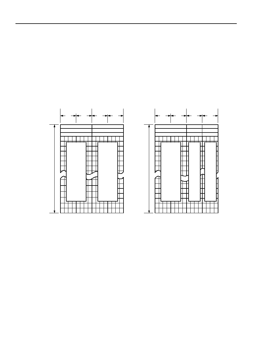
26
Lucent Technologies Inc.
Advance Data Sheet
November 1999
H.100/H.110 Interfaces and Time-Slot Interchangers
Ambassador T8100A, T8102, and T8105
2 Architecture and Functional Description
(continued)
2.2 Local Bus Section
(continued)
2.2.3 Data Rates and Time-Slot Allocation (continued)
Examples of how the memory is filled are found in Figure 7.
Note: Again, the user needs only to provide stream and time-slot addresses; the devices will generate the internal
memory addresses.
Both the connection and data memories are filled using the same algorithm. In the case where group C is running
at 8.192 Mbits/s, group B is at 4.096 Mbits/s (or 2.048 Mbits/s), and group A is at 2.048 Mbits/s, then an additional
virtual memory space of 4 x 64 locations is created from unused locations in other parts of the memory.
5-6105F
Figure 7. Local Memory (T8100A, T8105 Only), Fill Patterns
TIME SLOT 0
TIME SLOT 2
TIME SLOT
4
TIME SLOT 1
TIME SLOT 3
TIME SLOT 5
TIME SLOT 0
TIME SLOT 1
TIME SLOT 2
TIME SLOT 0
TIME SLOT 2
TIME SLOT 4
TIME SLOT 1
TIME SLOT 3
TIME SLOT 5
STREAM
0--3
STREAM
4--7
STREAM
0--3
STREAM
4--7
STREAM
0--3
STREAM
4--7
STREAM
8--11
STREAM
8--11
GROUP A,
GROUP A,
GROUP A,
64 TIME SLOTS
64 TIME SLOTS
GROUP A AT 8.192 Mbits/s
GROUPS B AND C OFF
GROUP A AT 4.096 Mbits/s
GROUP B AT 8.192 Mbits/s
AND GROUP C OFF
EVEN
ODD
GROUP
B, EVEN
GROUP
B, ODD
TIME SLOTS
TIME SLOTS
ALL
TIME
SLOTS
TIME
SLOTS
TIME
SLOTS
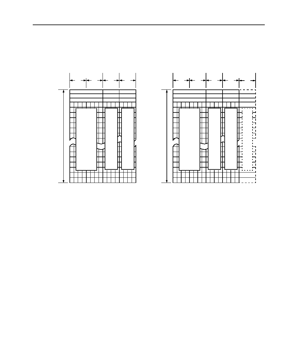
Lucent Technologies Inc.
27
Advance Data Sheet
November 1999
H.100/H.110 Interfaces and Time-Slot Interchangers
Ambassador T8100A, T8102, and T8105
2 Architecture and Functional Description
(continued)
2.2 Local Bus Section
(continued)
2.2.3 Data Rates and Time-Slot Allocation (continued)
5-6106F
Figure 7. Local Memory (T8100A, T8105 Only), Fill Patterns (continued)
In any of the parallel modes (S/P, P/S, P/P), the local memories (T8100A, T8105 only) treat parallel data as a
series of sequential time slots (i.e., all one stream): 8.192 Mbits/s corresponds to 1024 time slots, 4.096 Mbits/s
corresponds to 512 time slots, and 2.048 Mbits/s corresponds to 256 time slots. The memory locations are
scanned in order from 0 to 1023 at 8.192 Mbits/s, even locations are scanned at 4.096 Mbits/s (odd locations are
skipped), and at 2.048 Mbits/s, every second even location is scanned.
TIME SLOT 0
TIME SLOT 1
TIME SLOT 2
TIME SLOT 0
TIME SLOT 1
TIME SLOT 2
TIME SLOT 0
TIME SLOT 1
TIME SLOT 2
STREAM
0--3
STREAM
4--7
STREAM
8--11
STREAM
12--15
GROUP A,
64 TIME SLOTS
GROUP A AT 4.096 Mbits/s
GROUP B AT 4.096 Mbits/s
GROUP C AT 4.096 Mbits/s
TIME SLOT 0
TIME SLOT 1
TIME SLOT 2
TIME SLOT 0
TIME SLOT 2
TIME SLOT 4
TIME SLOT 0
(USED FOR GROUP C)
TIME SLOT 1
STREAM
0--3
STREAM
4--7
STREAM
8--11
STREAM
12--15
GROUP A,
64 TIME SLOTS
GROUP A AT 2.048 Mbits/s
GROUP B AT 4.096 Mbits/s
GROUP C AT 8.192 Mbits/s
GROUP
C, ODD (
V
IRT
U
A
L
) T
I
ME
S
L
OT
S
STREAM
12--15
TIME SLOT 1
TIME SLOT 3
TIME SLOT 5
GROUP
C,
GROUP
B,
GROUP
B,
GROUP
C,
EVEN
TIME
SLOTS
ALL
TIME
SLOTS
ALL
TIME
SLOTS
ALL
TIME
SLOTS
ALL
TIME
SLOTS
ALL
TIME
SLOTS

28
Lucent Technologies Inc.
Advance Data Sheet
November 1999
H.100/H.110 Interfaces and Time-Slot Interchangers
Ambassador T8100A, T8102, and T8105
2 Architecture and Functional Description
(continued)
2.2 Local Bus Section
(continued)
2.2.4 LBS: Local Stream Control, 0x0C
The normal mode of operation for local streams is serial in/serial out, but parallel modes are available. Modes and
data rates are controlled by register LBS. The mapping is shown below. See the preceding pages for a full descrip-
tion.
Table 42. LBS: Local Stream Control, 0x0C
There are no additional registers required for addressing the local memory other than the main address registers
(discussed in Section 2.1 Register/Memory Maps). The data and connection memory locations (T8100A, T8105
only) can be queried for their contents by indirect reads through the main address registers; however, the memory
locations are referred to by the stream and time-slot designators, rather than physical address locations, to simplify
the queries.
Reg
R/W
Bit 7
Bit 6
Bit 5
Bit 4
Bit 3
Bit 2
Bit 1
Bit 0
LBS
--
P/S
SGa
SGb
SGc
Symbol
Bit
Description
P/S
7--6
P/S = 00. Serial In/Serial Out.
The SGa bits control the group A pins, SGb bits control the group B pins, and SGc bits
control the group C pins. As serial streams, input and output rates within the same
group are constrained to be identical so both inputs and outputs share the same 2 bits
for programming.
The SGb bits are enabled when SGa
11.
The SGc bits are enabled when SGb
11.
P/S = 01. Serial In/Parallel Out.
SGa sets input (serial) rate using the rate definition within this table.
SGb is reserved.
SGc sets the output (parallel) rate using the rate definition within this table.
P/S = 10. Parallel In/Serial Out.
SGa sets input (parallel) rate.
SGb is reserved.
SGc sets output (serial) rate.
P/S = 11. Parallel In/Parallel Out.
SGa sets input (parallel) rate.
SGb is reserved.
SGc sets output (parallel) rate.
SGa
5--4
SGa = 00, 3-state.
SGa = 01, 2.048 Mbits/s.
SGa = 10, 4.096 Mbits/s.
SGa = 11, 8.192 Mbits/s.
SGb
3--2
SGb = 00, 3-state.
SGb = 01, 2.048 Mbits/s.
SGb = 10, 4.096 Mbits/s.
SGb = 11, 8.192 Mbits/s.
SGc
1--0
SGc = 00, 3-state.
SGc = 01, 2.048 Mbits/s.
SGc = 10, 4.096 Mbits/s.
SGc = 11, 8.192 Mbits/s.
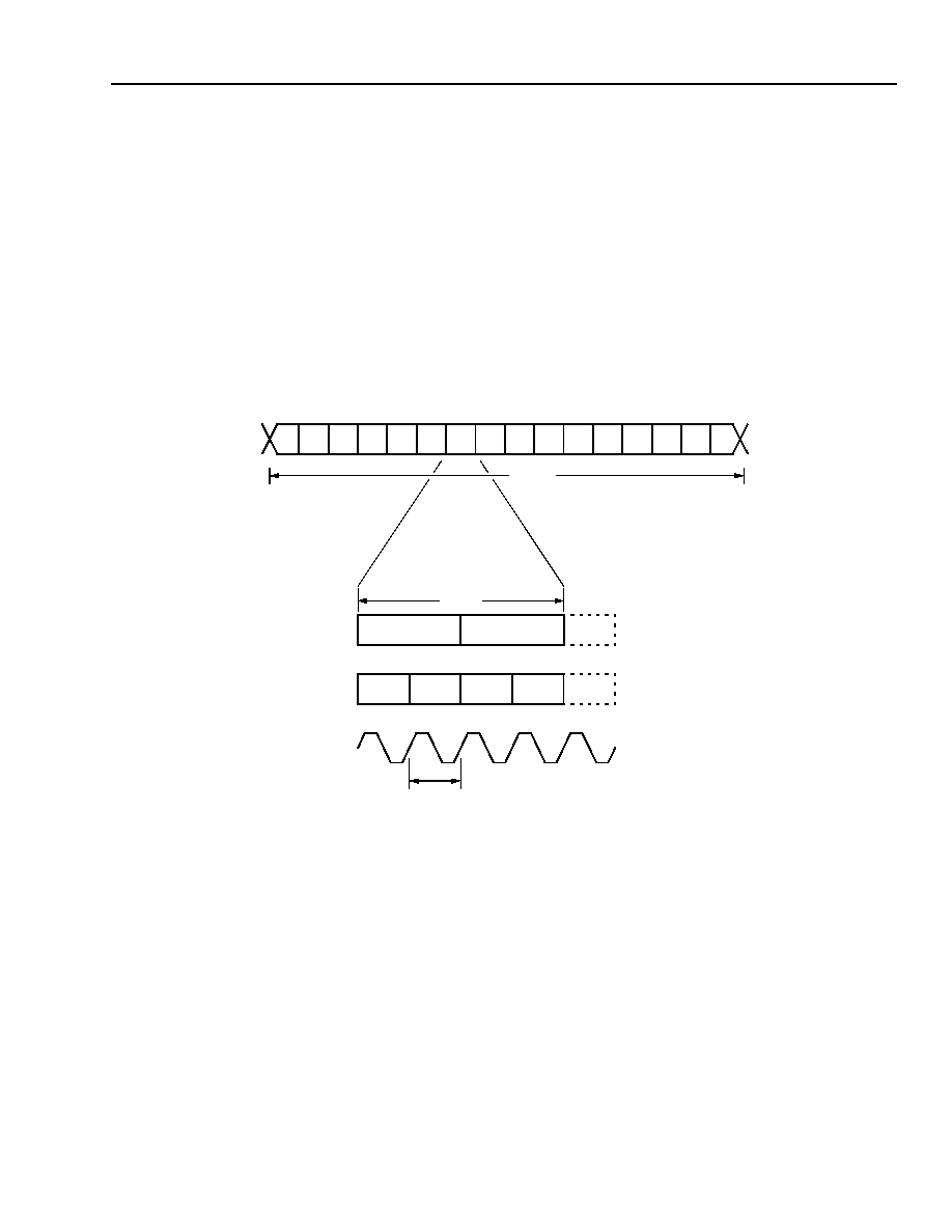
Lucent Technologies Inc.
29
Advance Data Sheet
November 1999
H.100/H.110 Interfaces and Time-Slot Interchangers
Ambassador T8100A, T8102, and T8105
2 Architecture and Functional Description
(continued)
2.2 Local Bus Section
(continued)
2.2.5 State Counter Operation
All operations are synchronized to the master state counter. The state counter is, in turn, synchronized to the inter-
nal frame signal and driven by an internal 65.536 MHz clock. In normal operation, the internal frame and clock are
synchronized to either the H-bus or trunks (see Section 2.5 Clocking Section for a more detailed explanation of
clocking options). The local memory states (T8100A, T8105 only) are illustrated in Figure 8. The state counter is a
modulo-8192 counter (7 bits for time slot, 4 bits for stream, 2 bits for state function) which can also be reset and
loaded with other values for diagnostic purposes (as described in Section 2.9 Testing and Diagnostics). The H-bus
memories are also referenced to this state counter so that the devices maintain synchronization with the H-bus to
ensure proper access to the bus as well as ensure synchronization between the H-bus and local memory struc-
tures. The H-bus memories are discussed in Section 2.3 H-Bus Section.
5-6107F
Figure 8. Simplified Local Memory State Timing, 65.536 MHz Clock
2.2.6 Software to Reset the Local Connection Memory
When the device is powered up, random connections may exist. To clear the upper 6 bits and, therefore, all control
bits, the following sequence of instructions should be followed:
1. Write AMR = 0x00.
2. Write LAR = 0x30.
3. Write IDR = 0x0C.
4. Monitor Diag-1, 0x30, bit 0. This bit is set when the operation is complete (steps 1 through 3).
5. Write LAR = 0x30.
6. Write IDR = 0x00. This brings the device out of diagnostics mode.
After executing the instructions, the contents of the local connection memory will contain its corresponding 10-bit
address. The upper 6 bits are cleared to zero. The lower 10 bits will have an address.
61 ns
L0
L1
L2
L3
L4
L5
L6
L7
L8
L9
L10
L11
L12
L13
L14
L15
976 ns
CONNECTION
H6 READ
MICROPROCESSOR
MEMORY
DATA
SRAM
CLOCK
H6 WRITE
H6 READ
MICRO-
PRO-
MICRO-
PRO-
15.25 ns
CESSOR
CESSOR

30
30
Lucent Technologies Inc.
Advance Data Sheet
November 1999
H.100/H.110 Interfaces and Time-Slot Interchangers
Ambassador T8100A, T8102, and T8105
2 Architecture and Functional
Description
(continued)
2.3 H-Bus Section
2.3.1 Memory Architecture
To access the H-bus, the devices use a new twist
on an existing approach to accessing large address
spaces: the data is stored in an independent double-
buffered SRAM which acts like the local data memory,
but the connection information for the H-bus is held in
three 512 location CAMs (T8102, T8105 only). Two
CAMs are used for two groups of 16 H-bus streams
each, and one CAM for all 16 local input/output pairs.
Each CAM compares 16 streams for read and write
and allows access time to the host microprocessor for
updates to the connections. Thus, each stream is
allotted three operations per 976 ns time slot, so there
are a maximum of 48 accesses per CAM per time
slot. The CAMs must operate at a rate of at least
20.34 ns/access*. The selected technology operates at
13 ns/access maximum, so an internal clock speed of
15.26 ns (65.536 MHz) is used.
For the following discussions, the reader should refer to
Figure 9. The combined comparison plus retrieval
operations take two CAM cycles, leaving little time for
microprocessor updates. To circumvent this, a separate
SRAM (actually, a register file) is tied to each CAM.
Each entry of this register file is associated with an
entry in the CAM on a location-by-location basis. (For
example, physical address 0xA7 in the CAM is coupled
with physical address 0xA7 of the register file.) The
CAMs will have only the comparand field for stream
and time-slot addresses, and the associated register
files will hold the data field, which is comprised of a tag
(an indirect pointer to the double-buffered data SRAM)
and some control bits. Using the associated SRAM
allows the operations to be pipelined so that the data
retrieval occurs while the CAMs are doing the next
comparison. The SRAM is double-buffered to permit
constant delay or minimum delay on a connection-by-
connection basis, as described in Section 2.2.1 Con-
stant Frame Delay and Minimum Delay Connections,
and as illustrated in Figure 5.
* The H-bus presents a unique set of problems. A full nonblocking,
double-buffered switch of 5120 locations has significant barriers in
size and in control of memory access time. Further, the traffic
between the local bus and H-bus is generally limited to a small
number of time slots at any given moment (120 full duplex is typical,
although we are permitting 256 duplex or 512 (T8102, T8105 only)
simplex connections), but the requirement to access any time slot
out of the full range of 5120 locations remains. To solve this, content
addressable memories (CAM) are utilized. They provide access to
the full 5120 locations through an encoded width (13 bits), but
require a depth equal to the maximum number of connections
required (512 [T8102, T8105 only]).
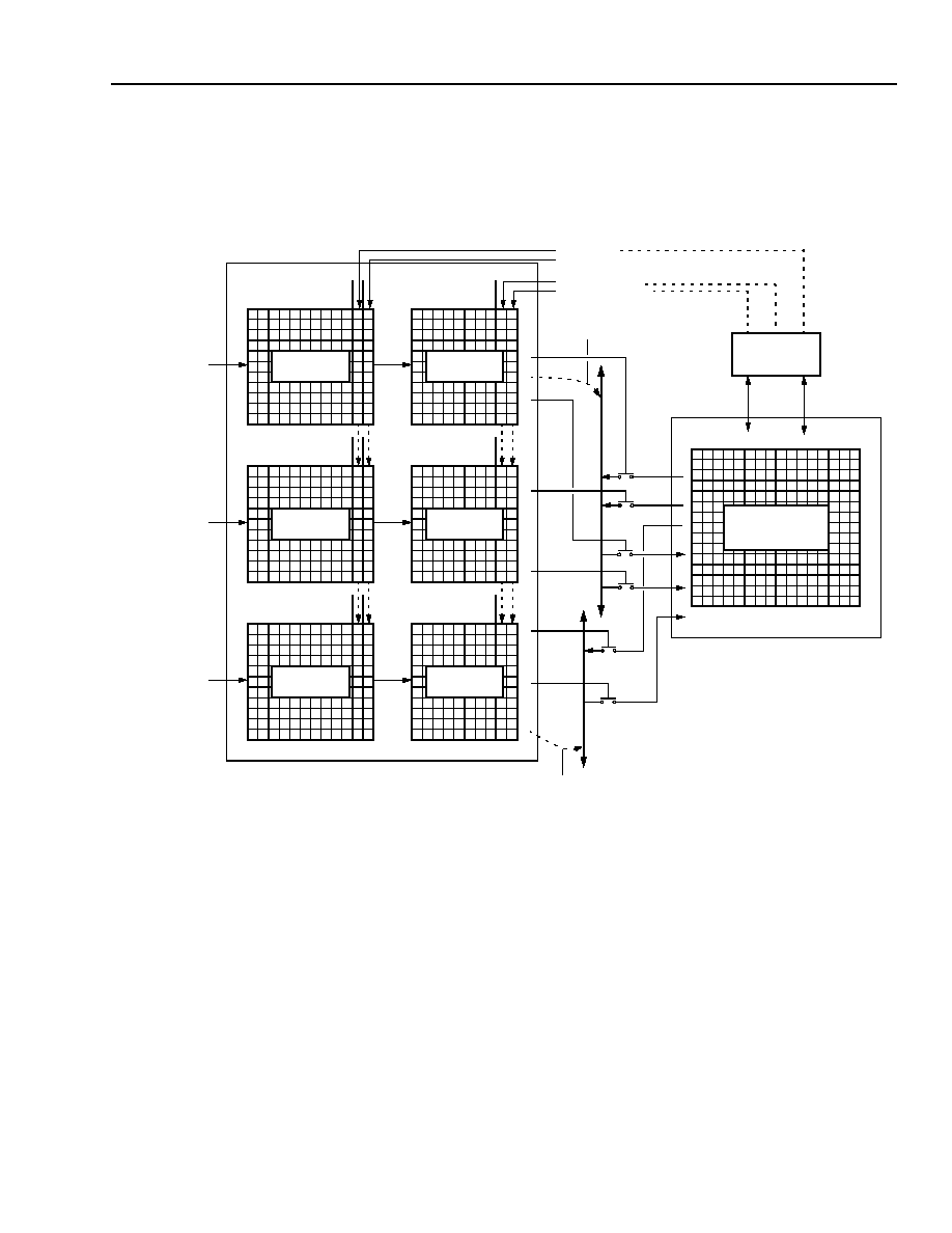
Lucent Technologies Inc.
31
Advance Data Sheet
November 1999
H.100/H.110 Interfaces and Time-Slot Interchangers
Ambassador T8100A, T8102, and T8105
2 Architecture and Functional Description
(continued)
2.3 H-Bus Section
(continued)
2.3.1 Memory Architecture (continued)
5-6108F
Figure 9. CAM Architecture
The maximum number of connections is set by the number of locations in the data SRAM and the CAMs. In this
implementation, 512 simplex (T8102, T8105 only) connections are permitted. Since one connection requires two
CAM entries pointing to a common data location, the maximum number of connections could be reduced to 256
simplex if all connection entries reside within only one CAM. The maximum number of connections is increased
above 512 simplex if the connection type is broadcast, i.e., from one to many.
CAM-E
CE-SRAM
11
1
A
A
.....................
0
255
........................
7
0
T
T
..................
ADDRESS
TAG
H-BUS:
A12 = 0
CAM-O
CO-SRAM
11
1
A
A
.....................
0
255
........................
7
0
T
T
..................
ADDRESS
TAG
H-BUS:
1 = 01
CAM-L
CL-SRAM
10
0
A
A
.....................
0
255
........................
7
0
T
T
..................
ADDRESS
TAG
A12:A11 = 11
READ/WRITE
VALID ENTRY MARKER
PATTERN/NORMAL
DATA SRAM SELECT
7
0
D
D
..................
7
0
D
D
..................
DATA BUFFER 0 DATA BUFFER 1
0
255
........................
DATA SRAM
READ/WRITE AND
SRAM SELECT
H-BUS
LOCAL I/O
PATTERN MODE
OUTPUTS TAG
TO H-BUS
PATTERN MODE
OUTPUTS TAG
TO LOCAL OUT
THIS IS THE H-BUS CONNECTION MEMORY:
3 CAMS, MAXIMUM OF 48 ACCESSES PER 976 ns
TIME SLOT, REQUIRES <20 ns/ACCESS
THIS IS THE H-BUS DATA MEMORY:
EFFECTIVE ACCESS TIME < 10 ns
EVEN STREAMS
ODD STREAMS
LOCAL 0--15
A0 = 0
A12 = 0
A0 = 1

32
32
Lucent Technologies Inc.
Advance Data Sheet
November 1999
H.100/H.110 Interfaces and Time-Slot Interchangers
Ambassador T8100A, T8102, and T8105
2 Architecture and Functional
Description
(continued)
2.3 H-Bus Section
(continued)
2.3.2 CAM Operation and Commands
The three CAMs operate in parallel. Each CAM's com-
parand field is compared with the state counter (Sec-
tion 2.2.5 State Counter Operation) which holds the
existing stream and time-slot value*. If there is a match,
the CAM issues a hit. If there is more than one match,
then it is considered a multiple hit. Likewise, no match
is a miss. As a part of the state counter, a bit is toggled
for read/write. The read/write bit is stored in the CAM,
so it becomes part of the value to be compared. If the
comparison for a write yields a hit, then there is a
request for write access to the data memory for the
incoming data from the H-bus. If the comparison for a
read yields a hit, then there is a request for a read
access from the data memory for outgoing data to the
H-bus. A miss implies no action. Any multiple hit within
one CAM block is treated as a controlled error although
it is not reported. The action taken is to acknowledge
the hit which corresponds to the lowest physical
address of the CAM. A multiple hit is assigned to be
more than one valid connection. These are prioritized
such that the match with the lowest physical address
(i.e., closest to CAM location 0x0) is the address which
is processed. Thus, errors are handled in a controlled
manner. Multiple hits can occur because multiple loca-
tions are assigned to the same time slot. Good soft-
ware and careful coding can help avoid this problem. A
controlled error has no impact on performance, and the
CAM contents are not changed as a result of the error.
The data SRAMs are actually dual-port register files
which will process both writes and reads on each clock
cycle of the clock. The devices can process a read and
write request from each CAM and two microprocessor
requests during the time of one address comparison.
Due to the fixed order of operations, the data SRAM
cannot overflow or underflow like the CAMs. The timing
is shown in Figure 10.
* As mentioned in Section 2.2.5 State Counter Operation, for each
stream and time-slot value, the state counter goes through four
functional states for each stream and time slot. These states are
used to synchronize the CAMs, pipeline register files, data SRAMs,
and microprocessor accesses just as they are used to synchronize
local memory operations and the frame groups. (Microprocessor
accesses to the memories are initiated asynchronously, though the
actual microprocessor cycles are synchronous.)
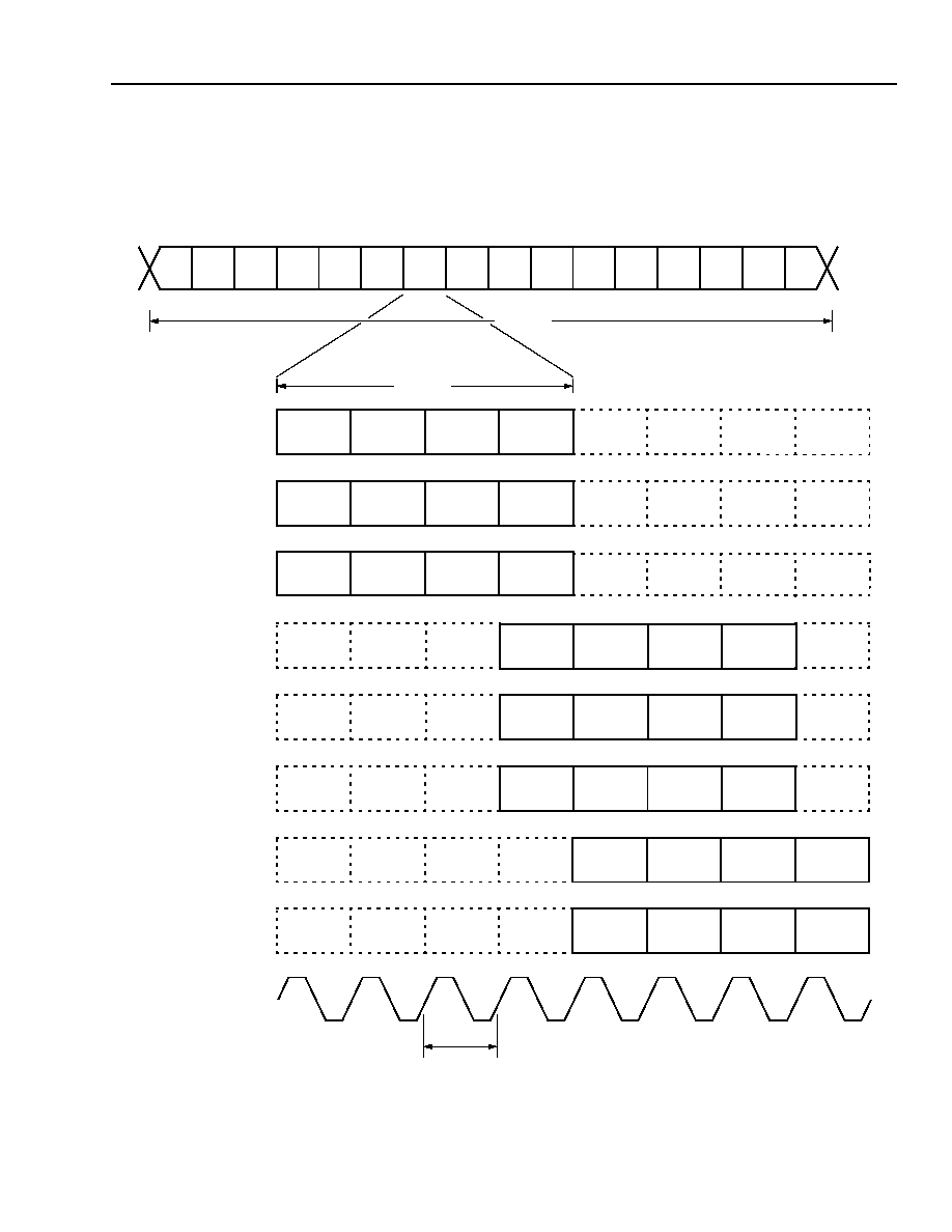
Lucent Technologies Inc.
33
Advance Data Sheet
November 1999
H.100/H.110 Interfaces and Time-Slot Interchangers
Ambassador T8100A, T8102, and T8105
2 Architecture and Functional Description
(continued)
2.3 H-Bus Section
(continued)
2.3.2 CAM Operation and Commands (continued)
5-6109F
Figure 10. Simplified H-Bus State Timing, 65.536 MHz Clock
61 ns
H0
H2
H4
H6
H8
H10
H12
H14
H16
H18
H20
H22
H24
H26
H28
H30
976 ns
CLOCK
15.25 ns
H12 WRITE
H12 READ
MICRO-
PRO-
MICRO-
PRO-
H13
H13 READ
MICRO-
PRO-
MICRO-
PRO-
L6 WRITE
L6 READ
MICRO-
PRO-
MICRO-
PRO-
CAM-E
CAM-O
CAM-L
C0-SRAM
C1-SRAM
CL-SRAM
H12 WRITE
H12 READ
H13
H13 READ
MICRO-
PRO-
L6 WRITE
L6 READ
MICRO-
PRO-
MICRO-
PRO-
CESSOR
CESSOR
CESSOR
CESSOR
WRITE
CESSOR
CESSOR
WRITE
CESSOR
CESSOR
CESSOR
MICRO-
PRO-
CESSOR
MICRO-
PRO-
CESSOR
MICRO-
PRO-
CESSOR
H1
L0
H3
L1
H5
L2
H7
L3
H9
L4
H11
L5
H13
L6
H15
L7
H17
L8
H19
L9
H21
L10
H23
L11
H25
L12
H27
L13
H29
L14
H31
L15
DATA SRAM WRITES
DATA SRAM READS
EVEN (H12)
LOCAL (L6)
MICRO-
ODD (H13)
EVEN (H12)
ODD (H13)
MICRO-
LOCAL (L6)
PRO-
CESSOR
PRO-
CESSOR

34
34
Lucent Technologies Inc.
Advance Data Sheet
November 1999
H.100/H.110 Interfaces and Time-Slot Interchangers
Ambassador T8100A, T8102, and T8105
2 Architecture and Functional
Description
(continued)
2.3 H-Bus Section
(continued)
2.3.2 CAM Operation and Commands (continued)
A number of commands are available to control the
CAMs. Connections can be made or broken, entry data
can be searched for, individual locations may be read
or cleared, or the CAMs can be reset. The address
mode register (AMR) (see Section 2.1 Register/Mem-
ory Maps) is used to issue the CAM control commands.
Some commands require the use of the lower address
register (LAR), and some use the IDR as a transfer reg-
ister.
The tags in each CAM's associated register file refer-
ence the storage location of the data being transferred,
so each CAM/tag location also has control information.
The three control bits are read-to/write-from data
SRAM (i.e., a direction bit, located in the CAM and
used during the comparison operations), a pattern
mode enable, which bypasses the data SRAM and out-
puts the tag directly into the specified time slot for
writes to the bus, and an SRAM buffer select that con-
trols the minimum delay or constant delay select,
equivalent to the local memory's (T8100A, T8105 only)
selection of minimum or constant delay.
In addition, the CAM carries a valid entry bit. This is an
identifier for the status of the CAM (and corresponding
register file) location. If the bit is low, as all validity bits
are after a reset, then the location is available to be
written into. When data is written into a location, then
this bit is set, indicating that this is a valid entry. If spe-
cific data is no longer valid, such as when a connection
is broken, then the bit is cleared.
The CAM commands make use of either one or two
cycles. The two cycles are described pictorially in Fig-
ure 11. The reader will note that matching and retrieval
are actually separate cycles. The need for two cycles
accounts for the requirement of the pipeline register
files.
Detailed descriptions of the commands follow:
The basic make connection command is referred to as
MKCn, where n is the CAM designator*. The MKCn
uses two CAM cycles: first, the CAM is searched to
determine where to find the next free location (as deter-
mined by the validity bits), and during the second cycle,
the next empty location is written into. The MKCn com-
mand uses holding registers which convey the connec-
tion information to the CAM and its associated register
file. The four holding registers contain the lower con-
nection address (i.e., time slot), the upper connection
address (stream plus control bits), the tag LSBs, the
subrate control (7 bits), and the tag MSB. An attempt to
write to a full CAM (all 512 locations fully occupied in
the T8102 and T8105) results in an overflow error
flagged through the system error register, SYSERR
(see Section 2.7 Error Registers).
Note: A single MKCn command only specifies one-
half of a connection. The MKCn specifies the
connection address and a pointer to the data
memory, but a second connection address and
pointer to the same data memory location must
also be provided for a complete connection.
* The H-bus CAM covering the 16 even-numbered H-bus streams is
designated E, the H-bus CAM covering the 16 odd-numbered H-bus
streams is designated O, and the CAM that services the 16 local
stream pairs is designated L.
Lucent Technologies Inc.
35
Advance Data Sheet
November 1999
H.100/H.110 Interfaces and Time-Slot Interchangers
Ambassador T8100A, T8102, and T8105
2 Architecture and Functional Description
(continued)
2.3 H-Bus Section
(continued)
2.3.2 CAM Operation and Commands (continued)
5-6110.cF
Figure 11. Illustration of CAM Cycles
APPLY COMPARAND,
I.E., STREAM + TIME SLOT
ONE CYCLE CAM
OPERATION:
MATCH COMPARAND
OR
GET STATUS
FLAGS
RETRIEVE
PHYSICAL LOCATION
CONTROLS,
I.E., SEARCH
FOR EMPTY
ONE CYCLE CAM
OPERATION:
GET COMPARAND OR
TAG, OR
CHANGE STATUS
FLAGS
CONTROLS
APPLY PHYSICAL LOCATION TO
CAM, I.E., LOCATION 0--511
RETRIEVE COMPARAND OR DATA,
I.E., GET STREAM + TIME SLOT FROM CAM
OR GET TAG FROM PIPELINE REGISTER FILE
APPLY COMPARAND,
I.E., STREAM + TIME SLOT
CONTROLS
FLAGS
TWO CYCLE CAM
OPERATIONS:
IDENTIFY COMPARAND
AND RETRIEVE TAG
OR
IDENTIFY COMPARAND
AND CHANGE STATUS
PHYSICAL
PHYSICAL
LOCATION
LOCATION
RETRIEVE DATA,
I.E., GET TAG FROM PIPELINE REGISTER FILE
IDENTIFY HIT OR EMPTY
(FLAGS) THEN RETRIEVE
PHYSICAL LOCATION IN CAM,
I.E., LOCATION 0--255
OUT
IN

36
36
Lucent Technologies Inc.
Advance Data Sheet
November 1999
H.100/H.110 Interfaces and Time-Slot Interchangers
Ambassador T8100A, T8102, and T8105
2 Architecture and Functional Descrip-
tion
(continued)
2.3 H-Bus Section
(continued)
2.3.2 CAM Operation and Commands (continued)
If the user determines that a stream/time slot is no
longer valid, then the validity bit may be cleared by pre-
senting the connection address to the CAM and by
using the BKCn, break connection, command. The
connection that the user intends to break, which con-
sists of the time slot, and the stream plus control bits,
but not the tag, is transferred to the holding registers
prior to issuing this command. This is a two-cycle com-
mand: during the first cycle, the connection address is
presented to the CAM to identify which physical loca-
tion holds that connection address, and then, in the
second cycle, the validity bit is cleared for the identified
physical location. If there is a miss, it flags a no-match
error through the underflow bit in SYSERR.
Note: A complete connection break requires two
BKCn commands, one for each half of the con-
nection, as with the MKCn command.
The clear location (upper/lower) command, CLLn, is a
one-cycle command. The LAR contains the physical
address (i.e., the physical CAM location) to be cleared
(when AMR bit 5 equals 1, the lower bits, 0--255, are
cleared; when 0, the upper bits, 256--511, are
cleared). When it is presented to the CAM, the validity
bit is cleared, returning the location to an empty status
(i.e., it becomes available for new make connection
commands). The CLLn can also be regarded as the
second cycle of a break connection command. CLLn is
valuable if several outputs are driven from a common
input (broadcast) and the user wishes to break one of
the output connections, but leave the others intact.
When the physical location in the CAM is identified,
either by software tracking or by use of the find entry
command (later in this section), then the CLLn can be
issued.
If the user wishes to poll the CAM for its contents, then
the RDCn or read CAM (upper/lower) command can be
used to query a particular location (AMR bit 5: when 1,
equals 0--255, when 0, equals 256--511 [T8102,
T8105 only]) in a specific block using the LAR for the
location address. The contents of the CAM and tag
location are transferred to the holding registers, and
then the time slot, stream plus control, and tag are
returned (in sequence) from four consecutive IDR
reads (see Section 3.4.2 Setting Up H-Bus Connec-
tions on page 75 for more details). The MSB of the time
slot is the validity bit. The actual RDCn operation is
one-cycle.
The converse of the RDCn is the FENn, or find entry
command. It can be thought of as the first cycle of a
BKCn command. Only time slot and stream plus con-
trol bits are necessary for identifying the location. The
tag is not needed. The values returned (in sequence)
from two consecutive IDR reads (T8102, T8105 only)
or just one read (T8100A) (see Section 3.4.2 Setting
Up H-Bus Connections on page 75 for more details) to
the IDR is the physical location of the entry in the CAM
block, bits [7:0] then bit 8, if it is found. If the entry is not
found, then the underflow error bit in the SYSERR reg-
ister will be set. FENn is a one-cycle command.
RSCn is the reset CAM command, and this renders all
locations in one CAM block invalid. This can be consid-
ered a CLLn for all locations in the CAM. Two special
resets are the RCH command, which resets only the
holding registers, and the CI command, which resets
all three CAM blocks and the holding registers. All
resets are one-cycle.
2.3.3 H-Bus Access
There are 32 bidirectional pins available for accessing
the H-bus. The direction of the pins is selected by the
CAM read and write bits. Data rates for the pins are
selected in accordance with the H.100/H.110 specifica-
tions. Unassigned time slots on the H-bus are 3-stated.
Details about rate selection are provided below. Two
bits of the 13-bit address are used to select the CAM
block as indicated in Figure 9. The remaining
11 bits plus a read/write bit form a comparand that is
stored in a CAM location.
Lucent Technologies Inc.
37
Advance Data Sheet
November 1999
H.100/H.110 Interfaces and Time-Slot Interchangers
Ambassador T8100A, T8102, and T8105
2 Architecture and Functional Description
(continued)
2.3 H-Bus Section
(continued)
2.3.4 L-Bus Access
The input and output of the CAM have the appropriate links to the local stream pins so that the H-bus streams may
be routed to and from the local bus streams. The LBS register (Section 2.2.4 LBS: Local Stream Control, 0x0C)
programs the local stream rates even if accessed by the CAMs. To address the local bus CAM block, the two most
significant address bits of the physical address are set to the appropriate values as described in Figure 9. The
other bits form the comparand along with a read/write bit. When the CAM is outputting data to the local bus, it has
priority over the local bus memory. In other words, if both the local bus and H-bus access the same local stream
and time slot, the H-bus data memory will provide the actual data, not the local connection.
2.3.5 H-Bus Rate Selection and Connection Address Format
Operating rates are selected in a manner similar to the local side. Two registers, HSH and HSL, shown below,
define the operation of the 32 streams. Again, SGx refers to stream groups: HSH holds SGh--SGe where SGh
programs streams 28--31, SGg programs streams 24--27, SGf programs streams 20--23, and SGe programs
streams 16--19. HSL holds SGd--SGa where SGd programs streams 12--15, SGc programs streams 8--11,
SGb programs streams 4--7, and SGa programs streams 0--3.
Table 43. HSL: H-Bus Stream Control, Low Byte, 0x10
Reg
R/W
Bit 7
Bit 6
Bit 5
Bit 4
Bit 3
Bit 2
Bit 1
Bit 0
HSL
--
SGd
SGc
SGb
SGa
Symbol
Bit
Description
SGd
7
H-Bus Group D Rate Select, MSB. Programs streams 12--15. SGn = 00, 3-state
SGn = 01, 2.048 Mbits/s
SGn = 10, 4.096 Mbits/s
SGn = 11, 8.192 Mbits/s
6
H-Bus Group D Rate Select, LSB.
SGc
5
H-Bus Group C Rate Select, MSB. Programs streams 8--11.
4
H-Bus Group C Rate Select, LSB.
SGb
3
H-Bus Group B Rate Select, MSB.
Programs streams 4--7.
2
H-Bus Group B Rate Select, LSB.
SGa
1
H-Bus Group A Rate Select, MSB.
Programs streams 0--3.
0
H-Bus Group A Rate Select, LSB.
38
Lucent Technologies Inc.
Advance Data Sheet
November 1999
H.100/H.110 Interfaces and Time-Slot Interchangers
Ambassador T8100A, T8102, and T8105
2 Architecture and Functional Description
(continued)
2.3 H-Bus Section
(continued)
2.3.5 H-Bus Rate Selection and Connection Address Format (continued)
Table 44. HSH: H-Bus Stream Control, High Byte, 0x11
A quick summary:
The CAMs and the pipeline register files operate as connection memories. The key CAM operation is based on 11
bits of stream and time slot plus 1 bit of read/write in the CAM locations compared against the state counter which
tracks the current stream and time slots (Section 2.2.5 State Counter Operation). Each H-bus CAM is looking for
matches on 16 of the 32 H-bus streams, and the local CAM is looking for a match on 16 local inputs and 16 local
outputs per time slot.
Thirteen bits are required to cover the 5120 possible time slots, but the MSB, LSB combination is used to deter-
mine which H-bus CAM is accessed: even H-bus (0, 0), odd H-bus (0, 1). The local H-bus is accessed by selecting
the upper 2 MSBs, both equal to 1. The CAM address can be thought of as following this format:
This format is rate independent. The CAM select field is part of the address mode register (AMR) for CAM com-
mands (Section 2.1.3 Address Mode Register and Section 2.3.2 CAM Operation and Commands). Program-
ming examples for setting up connections can be found in Section 3.3 Basic Connections.
Reg
R/W
Bit 7
Bit 6
Bit 5
Bit 4
Bit 3
Bit 2
Bit 1
Bit 0
HSL
--
SGh
SGg
SGf
SGe
Symbol
Bit
Description
SGh
7
H-Bus Group H Rate Select, MSB.
Programs streams 28--31.
SGn = 00, 3-state
SGn = 01, 2.048 Mbits/s
SGn = 10, 4.096 Mbits/s
SGn = 11, 8.192 Mbits/s
6
H-Bus Group H Rate Select, LSB.
SGg
5
H-Bus Group G Rate Select, MSB. Programs streams 24--27.
4
H-Bus Group G Rate Select, LSB.
SGf
3
H-Bus Group F Rate Select, MSB. Programs streams 20--23.
2
H-Bus Group F Rate Select, LSB.
SGe
1
H-Bus Group E Rate Select, MSB.
Programs streams 16--19.
0
H-Bus Group E Rate Select, LSB.
CAM Select Field Time-Slot Field Stream Field
2 bits
7 bits
4 bits
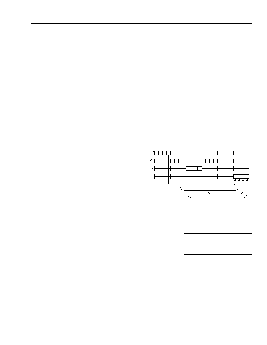
Lucent Technologies Inc.
39
Advance Data Sheet
November 1999
H.100/H.110 Interfaces and Time-Slot Interchangers
Ambassador T8100A, T8102, and T8105
2 Architecture and Functional Descrip-
tion
(continued)
2.4 Subrate Switching for the
Ambassador
Family
2.4.1 Description, Operation, and Application
This section describes the means of implementing sub-
rate telephony switching by leveraging the existing
pipelined multistream CAM architecture. In addition,
there are implications for extending H.100/H.110 to
incorporate subrate switching without violating the
existing timing or definitions. A practical example of a
system which requires subrate switching is described
in 2.4.7 Example of a Practical Application on page 43.
2.4.2 Definitions
Subrate refers to switching fractional portions of the
data found in traditional TDM streams. Subrate does
not refer to changes in the bit rate, i.e., when the bit
rate changes, the total number of time slots per second
changes, but each time slot still contains data which is
propagated at the same data rate, namely 64 kbits/s.
Subrate refers to data propagated at rates less than
64 kbits/s.
The data byte for a given time slot can be thought of as
two nibbles, and if each of these nibbles represents a
distinct voice or signal, then it would be correct to
say that the nibbles are operating at 32 kbits/s
(= 4 bits/frame x 8K frames/second), and that the
theoretical channel capacity of the TDM stream has
increased by a factor of two. Likewise, if the data byte
is broken into four distinct dibits, then the rate is
16 kbits/s, and the capacity of the stream has
increased by a factor of 4. Finally, in the extreme case,
a data byte is treated as 8 bits, each of which has a
rate of 8 kbits/s, which means that the stream capacity
has increased by a factor of 8.
The above definition also leads to the concept of den-
sity. If only one piece of subrate data is used in a byte,
then it can be referred to as sparsely packed. Like-
wise, if all positions of the data byte contain subrate
data, the byte is fully packed or densely packed.
Packing thus refers to the utilization of the subrate data
positions in a byte.
Subrate switching refers to the transfer of subrate
data pieces (nibbles, dibits, or bits), just as switching
implies the transfer of data bytes. True subrate switch-
ing is the ability to move subrate data from any subrate
position to any other subrate position. Obviously, there
are restrictions which must be employed to make sub-
rate switching practical. This is discussed in the next
section.
2.4.3 Subrate Switching on H.100/H.110
H.100/H.110 are based on byte-oriented TDM data
streams. H.100/H.110 have well-defined electrical
parameters to describe when an output driver gains
access to the bus and when it releases the bus (at the
end of the byte). There are no provisions in either
H.100 or H.110 to extend these electrical parameters
to include driving the bus on an individual bit basis, and
due to the propagation characteristics of the bus wires
on H.100, it is not desirable to attempt to drive the bus
this way.
Since H.100/H.110 data must always be switched as
whole bytes on H.100/H.110, subrate data will have to
be packed into the bytes prior to switching. The data
bytes are not necessarily constrained to using fully
packed bytes. Any portion of a byte may be used.
An example is shown in Figure 12.
5-7152F
Progressive assembly of the output data in a location in
the H-bus data buffer as each input subrate data piece
is received:
Figure 12. Subrate Switching Example
TIME SLOT n:
A4
X
X
X
TIME SLOT n + 1:
A4
D3
X
X
TIME SLOT n + 2:
A4
D3
X
C1
TIME SLOT n + 3:
A4
D3
B2
C1
THE FULLY ASSEMBLED BYTE WILL BE
READ FROM THE DATA BUFFER FOR
OUTPUT DURING TIME SLOT n + 5.
A1 A2 A3 A4
D1 D2 D3 D4
B1 B2 B3 B4
C1 C2 C3 C4
A4 D3 B2 C1
INP
U
T
S
OUT
P
UT
T
I
ME
S
L
OT
:
n
n + 1
n + 2
n + 3
n + 4
n + 5

40
40
Lucent Technologies Inc.
Advance Data Sheet
November 1999
H.100/H.110 Interfaces and Time-Slot Interchangers
Ambassador T8100A, T8102, and T8105
2 Architecture and Functional Descrip-
tion
(continued)
2.4 Subrate Switching for the
Ambassador
Family
(continued)
2.4.4 Using the Existing Architecture
It is possible to create a subrate switching structure uti-
lizing a variant of the existing pipelined multistream
CAM architecture. Since access to the H-bus continues
to require bytes, the CAM size does not change. CAMs
will continue to track stream and time-slot addresses.
The changes to the architecture are all related to the
data storage as it comes in from the bus. The most fun-
damental change is that selected subrate data pieces
can be individually stored, not necessarily the entire
incoming data byte. For example, the uppermost dibit
can be stored and the other dibits ignored. Thus, with
several incoming data bytes contributing subrate
pieces, a new data byte, composed of one or more
subrate pieces from different sources, can be con-
structed. (See Figure 12.)
Structurally, the change in the data buffers is from the
existing 512 x 8 (T8102, T8105 only) register file (or
256 x 8 for the T8100A) to eight 512 x 1 (T8102, T8105
only) register files (or eight 256 x 1 register files). Each
of these columns has a separate write enable. To sup-
port this change, the tag register associated with each
CAM must be extended by 7 bits to identify the source
of the subrate data (i.e., identify which piece of the
incoming byte is to be used) and the destination of the
subrate data (i.e., identify which bits of the data loca-
tion will be written into). Table 45 Permitted Tag Exten-
sions below lists the permitted entries in the extension
of the tag. While the writes into the data buffers are fine
grained, as small as a single bit write, the reads must
be as a whole byte to maintain the byte-orientation of
the H.100/H.110 bus as described previously.
Table 45. Permitted Tag Extensions
The subrate switching is optional; a bit in the identifica-
tion register will permit the subrate operation. The bit
defaults to zero, so that the tag extension is ignored
and the data buffers are treated as 512 x 8 (T8102,
T8105 only). If set, the columns are individually
addressed by the tag extensions.
Tag
Extensions
Bit
6
5
4
3
2
1
0
MSB
Source
Field
Destination
Field
Byte
(1 entry only)
0
00x
00x
Nibble
(4 combinations)
0
010--011
010--011
Dibit
(16 combinations)
0
100--111
100--111
Bit
(64 combinations)
1
000--111
000--111
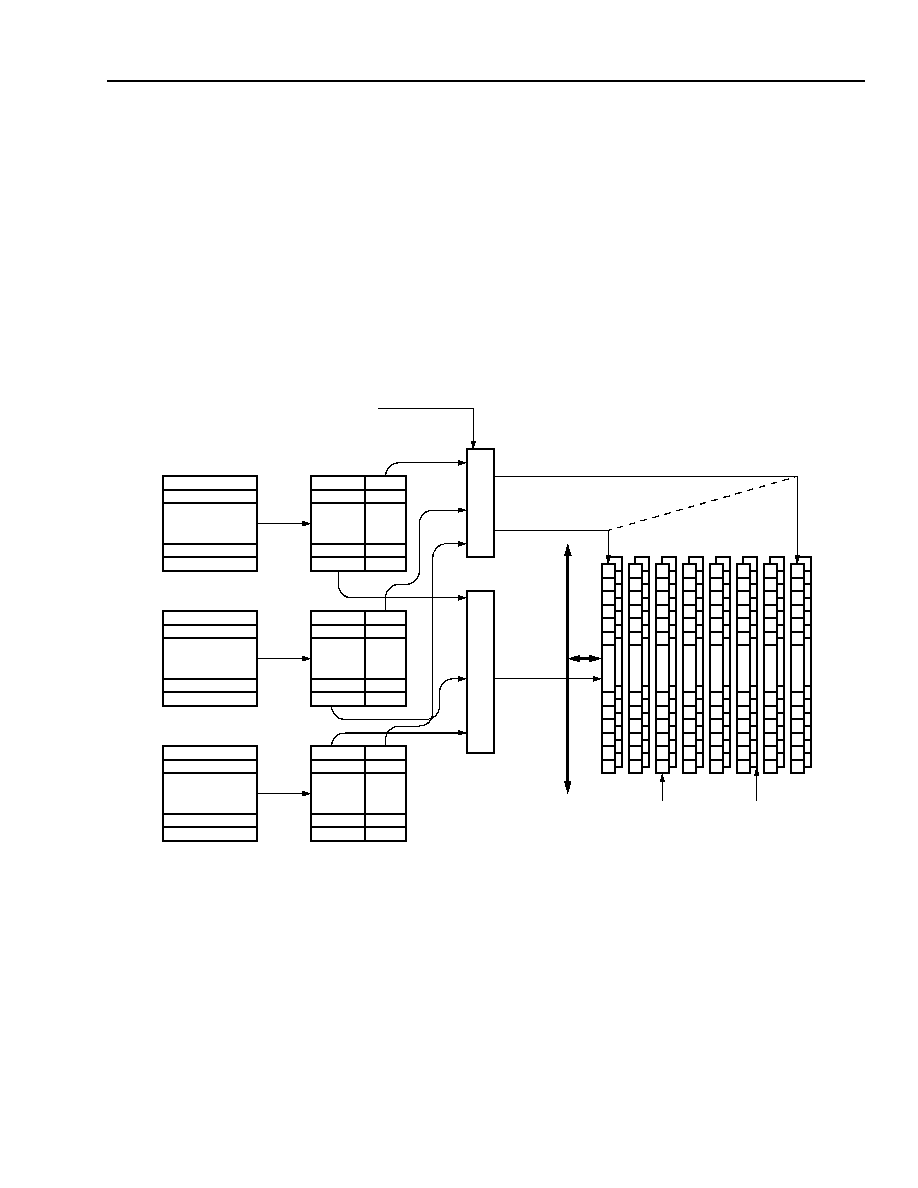
Lucent Technologies Inc.
41
Advance Data Sheet
November 1999
H.100/H.110 Interfaces and Time-Slot Interchangers
Ambassador T8100A, T8102, and T8105
2 Architecture and Functional Description
(continued)
2.4 Subrate Switching for the
Ambassador Family
(continued)
2.4.4 Using the Existing Architecture (continued)
Figure 13 illustrates the changes to the architecture of the
Ambassador
family.
The subrate enable bit (GMODE bit 5) is intended as a static control; that is, if subrate is going to be performed,
this bit must be set before attempting any CAM operations. The internal circuit monitors the state of this bit, and
performs different command protocols depending on its value. For a T8100A device with subrate disabled, the pro-
tocol is identical to that of a T8100; that is, the SCT register is not used, writes to it and reads from it are disabled,
and the internal state machine expects (and will only handle) three IDR reads for an RDC command. For a T8100A
device with subrate enabled, writes to and reads from SCT are enabled, and the internal state machine expects
(and will only handle) four IDR reads for an RDC command.
5-7151F
Figure 13. Modifications for Subrate Switching
DATA
BUFFER 0
DATA
BUFFER 1
WRITE ENABLES
WORD
ADDRESS
SUBRATE
ENABLE
CAMS
TAGS
.
.
.
.
.
.
.
.
.
.
.
.
.
.
.
.
.
.
.
.
.
.
.
.
.
.
.
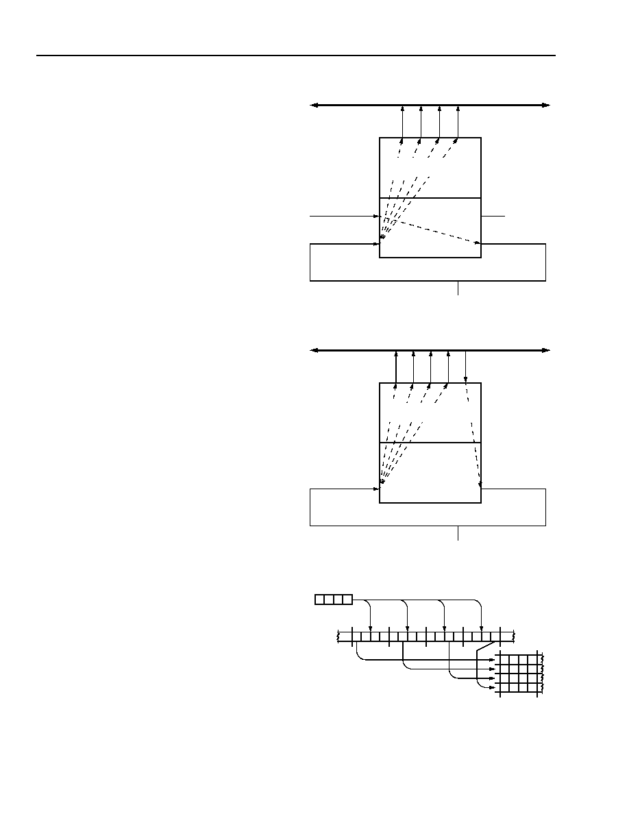
42
42
Lucent Technologies Inc.
Advance Data Sheet
November 1999
H.100/H.110 Interfaces and Time-Slot Interchangers
Ambassador T8100A, T8102, and T8105
2 Architecture and Functional Descrip-
tion
(continued)
2.4 Subrate Switching for the
Ambassador
Family
(continued)
2.4.5 Limitations
While the structure described above is a relatively sim-
ple extension to the existing architecture, it also
imposes one limitation which must be overcome by
application. To prevent changes in the CAM size and
operation, the assumption is that the data is utilized
only once after the stream plus time slot has been rec-
ognized. (This prevents the multiple hit/multiple access
scenario, in which a byte which contains multiple sub-
rate pieces will not have to be accessed several times.)
To gain access to all subrate pieces present in one
incoming byte, that same byte must be broadcast on
multiple stream plus time slots. In this case, each sub-
rate piece can be switched to the appropriate output.
The ideal scenario is to make use of local switching
(either the local TSI or the local CAM) to provide a
loopback for broadcasting the byte in question. Specifi-
cally, the byte is switched to multiple time slots on a
local output. (The packed byte is coming either from a
local input or from the H.100 bus.) The local output is
physically tied to a free local input, and, in turn, the
multiple time slots are subrate switched to the appropri-
ate outputs (on the H.100 bus, for example). This intro-
duces an additional delay of one frame, but allows for
efficient utilization of the H.100 bus as a subrate
switching fabric (see Figure 14).
5-7148F
5-7149F
5-7149F
Figure 14. Unpacking Example Using Local
Loopback
(OR LOCAL-LOCAL
VIA LOCAL CAM)
LOCAL INPUT 1
4 TIME SLOTS
LOCAL OUT 1
4 TIME SLOTS
LOOPBACK WIRE
OUTPUT
CONNECTIONS
H.100 BUS
LOCAL TSI
H-BUS TSI
(INCLUDING SUBRATE)
LOCAL INPUT 0
1 TIME SLOT
(OR LOCAL-LOCAL
VIA LOCAL CAM)
LOCAL INPUT 1
4 TIME SLOTS
LOCAL OUT 1
4 TIME SLOTS
LOOPBACK WIRE
OUTPUT
CONNECTIONS
H.100 BUS
LOCAL TSI
H-BUS TSI
(INCLUDING SUBRATE)
INPUT
1 TIME SLOT
A1 A2 A3 A4 A1 A2 A3 A4 A1 A2 A3 A4 A1 A2 A3 A4
A1 A2 A3 A4
A1
A2
A3
A4
(LOCAL BROADCAST)
INPUT
LOCAL OUTPUT
-
LOOPBACK INPUT
H-BUS OUTPUTS (EXAMPLE SHOWS SEPARATE STREAMS)
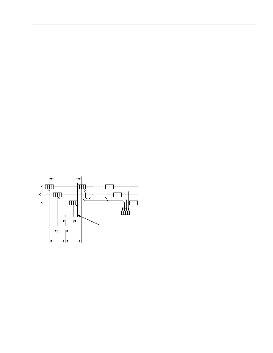
Lucent Technologies Inc.
43
Advance Data Sheet
November 1999
H.100/H.110 Interfaces and Time-Slot Interchangers
Ambassador T8100A, T8102, and T8105
2 Architecture and Functional Descrip-
tion
(continued)
2.4 Subrate Switching for the
Ambassador
Family
(continued)
2.4.6 Minimum vs. Constant Delay
The same issues involved with virtual framing exist in
subrate switching as in traditional switching. The sce-
nario is one in which the subrate data comes from sev-
eral sources which cross a frame boundary. The
selection of the framing bit remains identical to the byte
scenario. To maintain the virtual frame, some subrate
data must have the frame bit (FME) set, and some
must have them cleared. Operationally, there is no dif-
ference. Since the inputs and outputs are identified by
stream and time-slot addresses, charts from Appendix
B of this data sheet can be used to determine the FME
bit setting. Figure 15 below shows an example of virtual
framing for subrate connections.
FME settings for individual subrate pieces, in order to
maintain virtual frame integrity across the true frame
boundary, are based on the description in Appendix B
(all streams 8 Mbits/s).
5-7147F
Figure 15. Constant Delay/Minimum Delay Example
2.4.7 Example of a Practical Application
Three 16 kbits/s GSM voice channels are presented
with either 1 or 2 bits of HDLC/LAPD. The user wishes
to strip out the HDLC/LAPD information and pass
through the voice channels with minimum latency.
Specific requirements are listed below:
1.
The ability to extract 1 or 2 bits from any time slot
presented. The time slots are presented via T1/E1
or from the H.100 bus. The extracted bits will be
treated as an HDLC/LAPD channel and must be
presented separately to a host CPU.
2.
The ability to inject a 1 or 2 bit stream into any
time slot.
3.
The bit positions to be extracted/injected must be
programmable. In the case of injection, the
injected bits will overwrite the value of the bits pre-
viously occupying those positions.
4.
The ability to switch full time slots presented to it
while performing injection/extraction.
The terms injection and extraction are synonymous
with packing and unpacking.
Clearly, the applications for subrate switching are
numerous. In the 16 kbits/s GSM world alone, the
H.100 bus could be thought of as a 16,384 subrate
time-slot bus. Since the subrate is programmable on a
time slot by time-slot basis, mixed subrates are possi-
ble as well, even within a single time slot.
2.5 Clocking Section
The clocking section performs several functions which
are detailed in the following paragraphs. In general,
when the devices are in bus master mode, there will be
one or more companion devices which provide the
basic clock extraction and jitter attenuation from a
source (such as a trunk). As a slave, the devices can
work independently of, or in conjunction with, external
resources. Examples of different operating modes are
provided in Appendix A. Refer to Figure 16 for a block
diagram of the devices clocking section.
When the devices are used as bus masters, an input
clock of a tolerance of
±
32 ppm is required. This can
come from several sources. For example:
s
±
32 ppm crystal tolerance is the suggested value if
either the DPLL is used or fallback to the oscillator is
enabled while mastering the bus. Otherwise, a crys-
tal with a lesser tolerance can be used.
s
If a crystal is not used, a 16.384 MHz (
±
32 ppm toler-
ance or less) signal must be provided to the XTALIN
pin, and XTALOUT should be left unconnected.
s
The L_REF inputs can also be used and must con-
form to
±
32 ppm in a bus master situation.
FME = 0
VIRTUAL FRAME
INP
U
T
S
OU
T
P
U
T
FRAME BOUNDARY
FME = 1
FME = 1
TS
= ≠1
TS
= +2
TS
= +126
TS
= +1
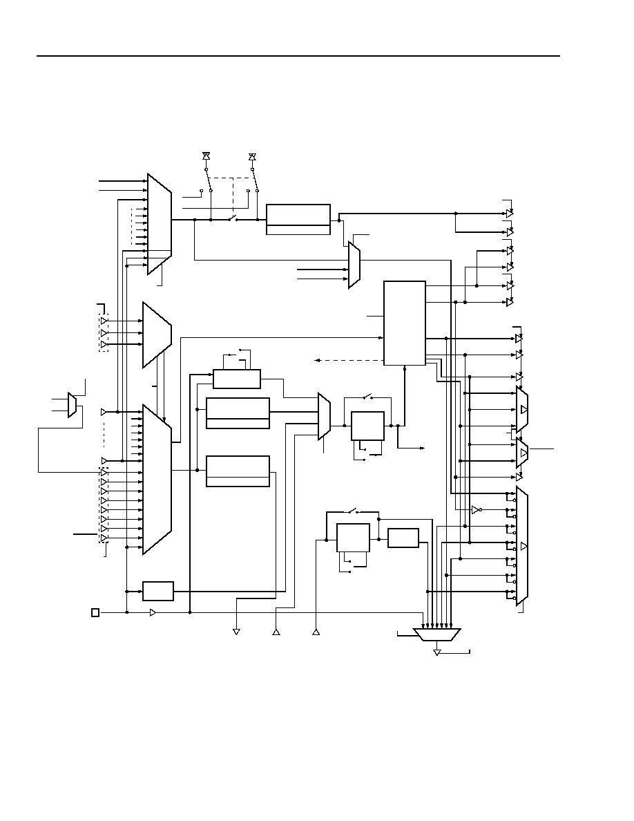
44
Lucent Technologies Inc.
Advance Data Sheet
November 1999
H.100/H.110 Interfaces and Time-Slot Interchangers
Ambassador T8100A, T8102, and T8105
2 Architecture and Functional Description
(continued)
2.5 Clocking Section
(continued)
5-6111dF
* The path for XTALIN divide-by-4 is for fallback only.
Figure 16. Clocking Section
CT_NETREF2
FRAME
SEL.
x16
x32
x16
4 MHz
2 MHz
FRAME SYNC
DPLL
NETREF
DIVIDE-BY-N
DIVIDE REGISTER
CLOCK
RESOURCE
SELECT
DIVIDE-
BY-4
GP6
GP7
NETREF
INT/EXT
SELECT
BIT SLIDER
CONTROLS
BIT SLIDER
STATE
MACHINES
PLL #1
PLL #1
RATE SELECT
65.536 MHz
PLL #2
PLL #2 BYPASS
RATE SELECT
PRIREFOUT
4MHzIN
3MHzIN
TCLKOUT
TCLKOUT
ENABLE
TCLKOUT
SELECT
x 8
NET-
˜
BY 8
NETREF
SELECT
THESE INPUTS
FORM
TRANSCEIVERS
WITH THE
CORRESPONDING
OUTPUTS
/CT_FRAME_A
/CT_FRAME_B
/FR_COMP
CLOCK
SEL.
CLOCK
SEL.
AND
INPUT
STATE
MACH.
L_REF0
L_REF7
CT_C8_A
CT_C8_B
/C16
±
/C4
C2
SCLK
SCLKX2
THESE INPUTS
FORM
TRANSCEIVERS
WITH THE
CORRESPONDING
OUTPUTS
XTALIN
TODJAT/GP6
FROMDJAT/GP7
DJAT BYPASS
L_SC CTL
FRAME
FRAME
SEC8K
FRAME
FRAME
EN_B
C8
C8
EN_A
EN_NETREF1
CT_NETREF1
CT_C8_A
/CT_FRAME_A
CT_C8_B
/CT_FRAME_B
COMPATIBILITY
/CT16
±
C2
/C4
SCLK
SCLKX2
/FR_COMP
L_SC0
SCSEL
(1 OF 4
L_SC[1:3]
NOT SHOWN)
16.384 MHz
2.048 MHz
4.096 MHz
2.048 MHz
8.192 MHz
4.096 MHz
8.192 MHz
2.048 MHz
4.096 MHz
8.192 MHz
16.384 MHz
PLL#2
˜
2
INTERNAL CONTROL
CLOCKS AND SYNC
CT_NETREF1
CON[5]
CT_NETREF2
CT_NETREF1
EN_NETREF2
CT_NETREF2
(FALLBACK PATH*)
CT_NETREF2
CT_NETREF1
4.096 MHz
CLOCKS DIRECTION
BYPASS
REF
SEL.
RESOURCE
DIVIDE-BY-N
DIVIDE REGISTER
MAIN
DIVIDE-BY-N
DIVIDE REGISTER
DIVIDE-
BY-2
CT_NETREF
(AND GP6/7 ENABLE)
MEMORY
CLOCK

Lucent Technologies Inc.
45
Advance Data Sheet
November 1999
H.100/H.110 Interfaces and Time-Slot Interchangers
Ambassador T8100A, T8102, and T8105
2 Architecture and Functional Descrip-
tion
(continued)
2.5 Clocking Section
(continued)
2.5.1 Clock and NETREF Selection
Three selectors provide device input clocking. The
clock selector and frame selector operate from a com-
mon set of selection options in register CKM (see Sec-
tion 2.5.8 Clock Control Register Definitions for register
details), where FRAMEA is selected along with clock
C8A and FRAMEB is selected along with clock C8B.
Typically, one of the local references (L_REF[0:7]) will
be selected when the devices are operating as mas-
ters, though the local oscillator is also available. As a
slave, the most common selections will be one of the
bus types. Each bus type has a state machine associ-
ated with it for determining the frame sync. All clock
inputs are sampled to check for proper switching. If the
expected clock edge does not occur, and there is no
switching on CT_NETREF for 125
µ
s, a bit correspond-
ing to the errant clock is set in the CLKERR register
(see Section 2.7 Error Registers for more details).
NETREF can be created from one of the local refer-
ences or from the oscillator independent of the clock
generation.
2.5.2 Dividers and Rate Multipliers
The clock and NETREF selections are routed to divid-
ers*. In the case of NETREF, the divider is
usually used to reduce a bit rate clock to 8 kHz,
so the most common divisors will be 1, 193
(1.544 MHz/8 kHz), and 256 (2.048 MHz/8 kHz),
although a full range of values (from 1--256) is possi-
ble. For the clock selector, the signal will most often be
routed through the main divider when the devices are
operating as masters or through the resource divider
when operating as slaves. Both the main and resource
dividers are fully programmable.
The ultimate destination for the main or resource
divider is intended to be PLL #1. PLL #1 accepts either
a 2.048 MHz or 4.096 MHz input and will rate multiply
up to 65.536 MHz. The divisor of the main or resource
dividers is chosen in conjunction with the rate select of
the PLL, i.e., a divisor which generates a 4.096 MHz
output and a rate selection of x16, or a divisor which
generates a 2.048 MHz output and a rate selection of
x32. This provides a great deal of flexibility in adapting
to a variety of (external) clock adapters and jitter atten-
uators while acting as a master, as well as slaving to
several bus types.
A digital PLL that can rate multiply to either 2.048 MHz
or 4.096 MHz from an 8 kHz source in the absence of
an external clock adapter is also provided. PLL #1 can
be bypassed for diagnostic purposes or if an external
clock adapter is used that provides a high-speed output
(65.536 MHz). The input to the DPLL is an 8 kHz sig-
nal.
A second rate multiplier is provided for supporting T1
applications. It is optimized around either a 1.544 MHz
or 3.088 MHz input rate which multiplies to 24.704 MHz
and is then divided down to provide 50% duty cycle
clocks of 12.352 MHz, though the direct 24.704 MHz is
available as well. A bypass is provided so that an exter-
nal clock can be buffered through the TCLK output. The
internal oscillator or the various outputs derived from
PLL #1 can also be selected for the TCLK output.
2.5.3 State Machines
The purpose of the state machines is to generate
internal control signals for the remainder of the circuitry
and to provide all bus clocks when operating as a mas-
ter. The state machines operate from the 65.536 MHz
clock generated by PLL #1, and they are time refer-
enced to the frame sync derived from the selected
clock and frame inputs. As a master, the time sync is
based on the device's own generated frame.
The dominant internal control signals are a noninverted
32.768 MHz clock, an inverted 16.384 MHz state clock,
and a noninverted 122 ns wide sync pulse centered
around the beginning of a frame. The memories are
synchronized to the 65.536 MHz clock.
2.5.4 Frame Sync
Frame sync is not generated in absence of an external
frame clock. The state machinces will randomly syn-
chronize to the 65.536 MHz clock.
2.5.5 Bit Sliding (Frame Locking)
The devices generate frame signals based on the
incoming clock and frame references and device gen-
erated clock signals. When slaving, it is sometimes
necessary to align the edges of this generated frame
signal to the incoming frame reference.
* If the A clocks have been selected as the clock source through the
CKM register (described in Section 2.5.8 Clock Control Register
Definitions), then the CT_C8A is the signal sent to the main and
resource dividers; likewise, selecting B clocks results in sending
CT_C8B; the
MVIP
selection sends /C4; the H-
MVIP
selection
sends the recovered /C16 (derived from differential inputs); select-
ing SC2 sends SCLKX2; and SC4/8 sends SCLK to the dividers.

46
46
Lucent Technologies Inc.
Advance Data Sheet
November 1999
H.100/H.110 Interfaces and Time-Slot Interchangers
Ambassador T8100A, T8102, and T8105
2 Architecture and Functional Descrip-
tion
(continued)
2.5 Clocking Section
(continued)
2.5.5 Bit Sliding (Frame Locking) (continued)
The devices generate frame signals based on the
incoming clock and frame references and device gen-
erated clock signals. When slaving, it is sometimes
necessary to align the edges of this generated frame
signal to the incoming frame reference.
To accomplish this, the devices will compare the
referenced frames with the current state of its clock
state machine, and if the difference exceeds one
65.536 MHz clock cycle, the entire stream will have a
fraction of a bit time removed from each frame; this is
referred to as bit sliding. The process will repeat until
the measurements fall within one clock cycle. The
actual bit sliding will take place by reducing the gener-
ated frame by one 65.536 MHz clock cycle at the
beginning of the frame. This means that the frame
edges will phase-align at the rate of approximately
15.26 ns per frame. The maximum phase difference is
slightly less than one frame or 124.985 µs. Thus, it will
require approximately 8000 frames, or 1 second, to
phase-align the frame. This is mean time interval error
(MTIE) complaint.
The alternatives to bit sliding are snap alignment and
no alignment. Snap alignment refers to an instanta-
neous phase alignment, i.e., a reset at the frame
boundary. This mode is common to other devices. If no
alignment is chosen, the device's generated frame is
frequency-locked to the incoming frame sync, but not
phase-aligned.
2.5.6 MTIE
MTIE is defined in AT&T technical reference TR62411.
MTIE is a characteristic of wander. Wander is defined
as clock phase deviations that are less than 10 Hz in
frequency. MTIE defines the amplitude of the wander.
The maximum amplitude, in the DS1/T1 world, is 1 µs
(about 1.5 bit times). This is measured by sampling the
delta of actual clock edges from the ideal positions over
2048 bit times (1.326 ms). The secondary requirement
is that no two edges may deviate by more than 81 ns
(1/8 bit time).
Apply this to the essentially E1-like timing in the
H.100/110/
MVIP
/SC-Bus worlds:
1.5 bit times is about 750 ns
2048 samples is 1 ms
1/8 bit time is about 61 ns
2.5.6.1 MTIE Compliance
T810X is MTIE compliant; however, the user must pay
attention to the system application. The T810X
requires Stratum 4e clocks, which are already sup-
posed to meet 32 ppm stability and 1 µs MTIE compli-
ance, and will in turn remain Stratum 4e on the out-
bound side. External trunks, T1 or E1, must be run
through framers (and a jitter attenuator, if not present in
the framer) to help ensure the input requirement. Given
this, the T810X is compliant in that it will not introduce
phase hits into the system which are uncontrolled, nei-
ther as high frequency (jitter) nor as low frequency
(wander).
For a given clock, the T810X should respond in such a
way that the wander does not perturb the outbound
clocks greater than 61 ns per 2.048 MHz cycle, or more
than a total of 750 ns over any 1 ms measuring period.
These numbers are aided by the analog PLL. Any
phase hit is smoothed to 800 ps/65 MHz clock cycle
which is 25.6 ns/2.048 MHz clock cycle. Thus, the
61 ns/bit time is met. The 750 ns number is constrained
by the input requirement. Given that the inbound side
will be no greater than 750 ns over the 1 ms sampling
period, the T810X's outbound clocks will show a
maximum deviation in the 1 ms period on the order of
315 ns. In truth, framers, with accurate crystals, tend to
absorb much of the wander in slip buffers, so this num-
ber should be very small.
While not a specific requirement of Stratum 4e, all
T810X products do provide holdover capability. The
T810X will respond, in a controlled fashion, to a change
of clock source. Again, the measurement method
for this uses the MTIE specification. The worst-case
response will be a 25.6 ns shift of clock edge per
0.048 MHz clock cycle less than the MTIE specifica-
tion.
2.5.6.2 Relationship of the Bit Slider to MTIE
Strictly speaking, the bit slider is not related to MTIE in
that MTIE makes no provision for frame wander. The bit
slider itself however, will not introduce more than
15.26 ns/frame of additional shift, when enabled. The
slider does not affect the PLL or the clocks on a con-
stant basis, it simply walks the generated frame into
alignment with the received frame. Thus, the stability
of the clock edges remains constant in the long term,
but individual edges may deviate by an additional
amount, making the edge-to-edge absolute maximum
25.6 ns + 15.3 ns = 40.9 ns.
The critical item to relating MTIE with the bit slider is
that the bit slider won't make the T810X fail MTIE.
2.5.6.3 Using the Bit Slider
The bit slider is primarily intended for maintaining the
local side of an application. Specifically, some DSPs
have limited synchronizing ability and once they are
phase-aligned with the frame, a loss of frame sync can
be disruptive. The bit slider allows a change of source
to gracefully realign to a new frame without tripping up
the synchronization. There is limited benefit on the
H.100 side--snap mode is equivalent to slide in terms
of A/B clock fail-over, but the local side is much differ-
ent.
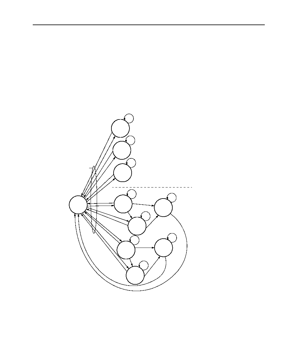
Lucent Technologies Inc.
47
Advance Data Sheet
November 1999
H.100/H.110 Interfaces and Time-Slot Interchangers
Ambassador T8100A, T8102, and T8105
2 Architecture and Functional Description
(continued)
2.5 Clocking Section
(continued)
2.5.6 MTIE (continued)
2.5.6.3 Using the Bit Slider (continued)
A secondary benefit may come about in T8100A/02/05 applications which use sliding between frames on local ref-
erence inputs. In this case, a board that is mastering an H.100/H.110 system, can pull an entire system slowly into
frame alignment with external trunks, instead of just frequency locking to external trunks.
2.5.7 Clock Fallback
5-6112F
Figure 17. A, B, and C Clock Fallback State Diagram
DIAG_ABC
DIAG_AB
C_ONLY
B_ONLY
B_ERROR
B_MASTER
A_ERROR
A_ONLY
A_MASTER
INITIAL
DIAGNOSTIC/FORCED CLOCKING
FALLBACK CLOCKING, ASSUMES
FALLBACK ENABLED IN CKS REGISTER
B CLOCKS FAIL
B CLOCKS FAIL
A CLOCKS FAIL
A CLOCKS FAIL
A CLOCKS
B CLOCKS FAIL
REPROGRAM
A CLOCKS
REPROGRAM
B CLOCKS
DIAG_ABC = DRIVES A CLOCKS, B CLOCKS,
AND C CLOCKS, NO FALLBACK PERMITTED
DIAG_AB = DRIVES A CLOCKS AND B CLOCKS,
NO FALLBACK PERMITTED
C_ONLY = DRIVES C CLOCKS ONLY,
NO FALLBACK PERMITTED
B_ONLY = DRIVES B CLOCKS,
CAN DRIVE
C CLOCKS IN
FALLBACK CONDITION
A_ONLY = DRIVES A CLOCKS,
CAN DRIVE
C CLOCKS IN
FALLBACK CONDITION
B_MASTER = DRIVES B AND C CLOCKS,
ALL CLOCKS SHUT OFF IN
FALLBACK CONDITION
A_MASTER = DRIVES A AND C CLOCKS,
ALL CLOCKS SHUT OFF IN
FALLBACK CONDITION
B_ERROR = NO CLOCKING,
WAITING FOR B CLOCKS TO BE
REPROGRAMMED
A_ERROR = NO CLOCKING,
WAITING FOR A CLOCKS TO BE
REPROGRAMMED
THE DEVICES ENTER AND
LEAVE THESE STATES
FAIL
BASED ON REGISTER
COUNTERS
48
48
Lucent Technologies Inc.
Advance Data Sheet
November 1999
H.100/H.110 Interfaces and Time-Slot Interchangers
Ambassador T8100A, T8102, and T8105
2 Architecture and Functional Descrip-
tion
(continued)
2.5 Clocking Section
(continued)
2.5.7 Clock Fallback (continued)
The following conditions must be met before fallback is
initiated:
s
Fallback must be enabled in register CKS.
s
Failure of one or more of the clocks selected through
the CKSEL bits in the CKM register.
s
All clocks which comprise the selection from CKSEL
must be unmasked in register CKW (see Section 2.7
Error Registers).
The devices contain a fallback register which enables a
backup set of controls for the clock resources during a
clock failure. In addition, a fallback state machine pro-
vides some basic decision-making for controlling some
of the clock outputs when the feature is enabled. While
slaving to the bus, the primary course of action in fall-
back is the swap between the A clocks and B clocks as
the primary synchronization sources. A slave may
become a master only under software control; i.e.,
there is no automatic promotion mechanism. As a mas-
ter, the devices detect their own failures and remove
their clocks from the bus. If a failure is detected on the
other main set (e.g., B master detects failures on the A
master), then the devices can assume the role of the
primary synchronization source by driving all compati-
bility clocks (H-
MVIP
and SC-Bus). Clock failures are
flagged through the CLKERR1, CLKERR2, and
CLKERR3 registers (Section 2.7 Error Registers).
Additional fallback details are discussed in relationship
to the clock registers in the next section. The divide-by-
4 block for XTALIN, shown in Figure 16, is used only for
fallback. See Figure 17 for a diagram of the basic state
machine which controls the A, B, and C (compatibility)
clocks. Figure 18 shows a diagram for programming the
device's registers when a fallback condition is detected.
Figure 18 shows the steps required to program the reg-
isters when a fallback condition is detected.
Restarting the clocks after a fallback condition:
1. Clear the CKW register to prevent any more clock errors.
2. Clear CKM bit 5 (CCD) to be a slave.
3. Clear CKP bits 2 and 3 to prevent sourcing a compatility clock.
4. Set CKM bit 5 (CCD) to be a master again.
5. Set CKP bits 2 and 3 to drive the appropriate A or B clocks.
6. Clear SYSERR and CLKERR bits via MCR.
7. Set the appropriate bits in CKW to enable watchdogs.
5-7250aF
Figure 18. Programming Sequence
REPROGRAM PRIMARY
SELECTION:
CKR, CKM, CKP,
CKMD, CKRD
ENABLE OUTPUTS:
MCR = 0x0E
ENABLE WATCHDOGS:
CKW
0x00
PROGRAM PRIMARY
SELECTION:
CKR, CKM, CKP,
CKMD, CKRD
DISABLE WATCHDOGS:
CKW = 0x00
CLEAR FALLBACK ERROR:
MCR = 0x6E
PROGRAM OTHER
REGISTERS
REPROGRAM SECONDARY
SELECTION: CKS,
IF REQUIRED
ENABLE WATCHDOGS:
CKW
0x00
DISABLE WATCHDOGS:
CKW = 0x00
PROGRAM SECONDARY
SELECTION: CKS
PROGRAM OTHER
CLOCKS: CKN, CKND,
CK32, CK10
CONNECT
FALLBACK?
YES, INTERRUPT
SERVICE ROUTINE
RETURN FROM
INTERRUPT
(IN
NO
OPERATION)
Lucent Technologies Inc.
49
Advance Data Sheet
November 1999
H.100/H.110 Interfaces and Time-Slot Interchangers
Ambassador T8100A, T8102, and T8105
2 Architecture and Functional Description
(continued)
2.5 Clocking Section
(continued)
2.5.8 Clock Control Register Definitions
Table 46. CKM: Clocks, Main Clock Selection, 0x00
The first register, 0x00, is the clock main (CKM) register. There are ten registers to control the various aspects of
clocking.
* Selecting A clocks synchronizes the devices to CT_C8A and /CT_FRAMEA; selecting B clocks synchronizes the devices to CT_C8B and
/CT_FRAMEB;
MVIP
uses /C4, C2, and /FR_COMP; H-
MVIP
uses /C16+/≠, /C4, C2, and /FR_COMP; SC2 uses SCLKX2 and /FR_COMP;
SC4/8 requires SCLK, SCLKX2, and /FR_COMP. MC-1 fallback clocks use the same inputs and state machine as the A clocks and B clocks
with an inversion selected from register CKP. A pictorial view of the various clocks is shown in Section 4.8.1 Clock Alignment.
Reg
R/W
Bit 7
Bit 6
Bit 5
Bit 4
Bit 3
Bit 2
Bit 1
Bit 0
CKM
--
PAE
PAS
CCD
CKI
CKSEL
Symbol
Bit
Description
PAE
7
Phase Alignment Enable.
PAE = 0,
Retains frequency lock without phase alignment.
PAE = 1,
Enables phase alignment.
PAS
6
Phase Alignment.
PAS = 0,
Phase alignment, snap.
PAS = 1,
Phase alignment, slide.
CCD
5
The CCD bit is the compatibility clock direction. This controls the I/O for the compatibility
clocks /C16+/≠, /C4, C2, SCLK, SCLKX2, and /FR_COMP (compatibility frame). The user can
think of the CCD bit (in some respects) as a master/slave select for the compatibility clocks,
though other registers require proper setup to establish true master or slave operation. The
devices will assume control of this bit during a fallback if the previously designated compatibil-
ity clock master fails.
CCD = 0,
Slave, monitors compatibility signals.
CCD = 1,
Master, drives compatibility signals.
Note:
If bit 4 of the programmable clocks register, CKP, is low, then the state machines of the
A clock and B clock will assume this is an MC-1 system and interpret the clocks as
/C4(L/R) and FRAME(L/R). If this bit is high, then it interprets the clocks as C8(A/B)
and FRAME(A/B).
CKI
4
CKI is used to invert the output of the clock selector, i.e., the signal which feeds the main
divider, resource divider, and DPLL:
CKI = 0,
Normal.
CKI = 1,
Invert.
CKSEL
3--0 The decode for the clock selector (CKSEL) is illustrated below. These selections determine
which input state machine is utilized*:
CKSEL = 0000,
Internal oscillator.
CKSEL = 0001,
CT_NETREF1 or CT_NETREF2 (CON register bit 5 selects:
if 0 then CT_NETREF1 is selected, if 1 CT_NETREF2).
CKSEL = 0010,
A clocks (C8A & FRAMEA); ECTF or MC-1.
CKSEL = 0011,
B clocks (C8B & FRAMEB); ECTF or MC-1.
CKSEL = 0100,
MVIP
is selected, /C4 is selected as the clock reference for PLL #1.
CKSEL = 0101,
H-
MVIP
is selected, /C16 is selected as the clock reference for
PLL #1.
CKSEL = 0110,
SC-Bus, 2 MHz. SCLKX2 is selected as the clock reference for
PLL #1.
CKSEL = 0111,
SC-Bus, 4 MHz or 8 MHz. SCLK is selected as the clock
reference for PLL #1.
CKSEL = 1000--1111 Selects local references 0--7. When bit 4 of the CON register is set,
these bits select pairs of synchronized inputs.

50
Lucent Technologies Inc.
Advance Data Sheet
November 1999
H.100/H.110 Interfaces and Time-Slot Interchangers
Ambassador T8100A, T8102, and T8105
2 Architecture and Functional Description
(continued)
2.5 Clocking Section
(continued)
2.5.8 Clock Control Register Definitions (continued)
Table 47. CKN: Clocks, NETREF Selections, 0x01
Clock register 0x01 is CKN, the CT_NETREF select register. This register selects features for generating and rout-
ing the CT_NETREF signal.
Reg
R/W
Bit 7
Bit 6
Bit 5
Bit 4
Bit 3
Bit 2
Bit 1
Bit 0
CKN
--
NR12EN
NDB
NRI
NRSEL
Symbol
Bit
Description
NR12EN
7--6 NR12EN enables the selection between NETREF1 and NETREF2.
NR12EN = 00,
The value of NRSEL[3:0] of CKN determines what is routed to the
L_SCs.
NR12EN = 01,
Enable NETREF2 for output, route NETREF1 input to the L_SCs.
NR12EN = 10,
Enable NETREF1 for output, route NETREF2 input to the L_SCs.
NR12EN = 11,
Enable both NETREF[1:2] for output, route output of NETREF
divide-by-N to LSCs.
NDB
5
NDB = 0,
TODJAT pin comes from NETREF selector, and FROMDJAT pin
goes to NETREF divider.
NDB = 1,
NETREF selector goes directly to NETREF divider.
NRI
4
NRI inverts the output of the NETREF selector.
NRI = 0,
Normal.
NRI = 1,
Invert.
NRSEL
3--0 The NRSEL is similar to CKSEL but with fewer choices:
NRSEL = 0000,
Internal oscillator divided by 8.
NRSEL = 0001,
Internal oscillator.
NRSEL = 0010,
Select NETREF1 as input.
NRSEL = 0011,
Select NETREF2 as input.
NRSEL = 0100--0111, (Reserved.)
NRSEL = 1000--1111, Local references 0--7.

Lucent Technologies Inc.
51
Advance Data Sheet
November 1999
H.100/H.110 Interfaces and Time-Slot Interchangers
Ambassador T8100A, T8102, and T8105
2 Architecture and Functional Description
(continued)
2.5 Clocking Section
(continued)
2.5.8 Clock Control Register Definitions (continued)
Table 48. CKP: Clocks, Programmable Outputs, 0x02
Clock register 0x02, CKP, is the programmed clocks register. It is used for programming the CT_C8 clocks and
enabling its outputs. It is also used to program the TCLK selector. CT_C8 may be operated as either 8 MHz (nor-
mal or inverted) or 4 MHz (normal or inverted). C8IS is used to invert the synchronization on C8A and C8B when
they are selected for input. The C8 and FRAME signals, which are also generated internally, are routed to both the
CT_C8A and /CT_FRAMEA and to the CT_C8B and /CT_FRAMEB. The CAE and CBE pins enable these output
pairs independently. The C8C4 pin selects 8.192 MHz or 4.096 MHz signals to be output on C8A and C8B (for sup-
porting for either ECTF or MC-1 applications). CFW selects the output width of the compatibility frame. The register
format is as follows.
Reg
R/W
Bit 7
Bit 6
Bit 5
Bit 4
Bit 3
Bit 2
Bit 1
Bit 0
CKP
--
PTS
C8IS
CAE
CBE
C8C4
CFW
Symbol
Bit
Description
PTS
7--5 The three PTS bits select the output sent to the TCLK. This output is intended to be used for
driving framers.
PTS = 000,
3-state.
PTS = 001,
Oscillator, buffered output.
PTS = 010,
PLL #2, direct output .
PTS = 011,
PLL #2, output divided by 2.
PTS = 100,
2.048 MHz from state machines.
PTS = 101,
4.096 MHz from state machines.
PTS = 110,
8.192 MHz from state machines.
PTS = 111,
16.384 MHz from state machines.
C8IS
4
C8IS = 0,
MC-1 (A and B clocks inputs interpreted as /C4 with /FRAME).
C8IS = 1,
ECTF (A and B clocks inputs interpreted as C8 with /FRAME).
CAE
3
CAE = 0,
Disable CT_C8A & /CT_FRAMEA outputs.
CAE = 1,
Enable CT_C8A & /CT_FRAMEA outputs. (The devices will auto-
matically disable these on an A clock failure.)
CBE
2
CBE = 0,
Disable CT_C8B & /CT_FRAMEB outputs.
CBE = 1,
Enable CT_C8B & /CT_FRAMEB outputs. (The devices will auto-
matically disable these on a B clock failure.)
C8C4
1
C8C4 = 0,
Inverted 4.096 MHz (MC-1 output mode).
C8C4 = 1,
Noninverted 8.192 MHz (ECTF output mode).
CFW
0
CFW = 0,
Narrow (122 ns) /FR_COMP.
CFW = 1,
Wide (244 ns) /FR_COMP.
52
Lucent Technologies Inc.
Advance Data Sheet
November 1999
H.100/H.110 Interfaces and Time-Slot Interchangers
Ambassador T8100A, T8102, and T8105
2 Architecture and Functional Description
(continued)
2.5 Clocking Section
(continued)
2.5.8 Clock Control Register Definitions (continued)
Table 49. CKR: Clocks, Resource Selection, 0x03
Clock register 0x03, CKR, is the clock resources register. It is used for selecting and programming miscellaneous
internal resources, the two PLLs, the DPLL, and the clock resource selector. It is also used to program the
SCLK/SCLKX2 clock outputs. The register format is as follows:
Reg
R/W
Bit 7
Bit 6
Bit 5
Bit 4
Bit 3
Bit 2
Bit 1
Bit 0
CKR
--
CRS
P1B
P1R
P2B
P2R
SCS
Symbol
Bit
Description
CRS
7--6 The CRS[7:6] bits are used to select the input to PLL #1.
CRS = 00,
External input (through the 4MHzIN pin).
CRS = 01,
Resource divider.
CRS = 10,
DPLL @ 2.048 MHz.
CRS = 11,
DPLL @ 4.096 MHz.
P1B
5
P1B and P1R control PLL #1.
P1B = 0,
Normal PLL #1 operation.
P1B = 1,
Bypass PLL #1.
P1R
4
P1R = 0,
PLL #1 rate multiplier = 16.
P1R = 1,
PLL #1 rate multiplier = 32.
P2B
3
P2B and P2R control PLL #2.
P2B = 0,
Normal PLL #2 operation.
P2B = 1,
Bypass PLL #2.
P2R
2
P2R = 0,
PLL #2 rate multiplier = 8.
P2R = 1,
PLL #2 rate multiplier = 16.
SCS
1--0 The SCS[1:0] bits are used to program the outgoing SC-Bus compatibility signals.
SCS = 00,
SC-Bus outputs 3-stated.
SCS = 01,
SCLK @ 2.048 MHz, SCLKX2 @ 4.096 MHz.
SCS = 10,
SCLK @ 4.096 MHz, SCLKX2 @ 8.192 MHz.
SCS = 11,
SCLK @ 8.192 MHz, SCLKX2 @ phase shifted 8.192 MHz.

Lucent Technologies Inc.
53
Advance Data Sheet
November 1999
H.100/H.110 Interfaces and Time-Slot Interchangers
Ambassador T8100A, T8102, and T8105
2 Architecture and Functional Description
(continued)
2.5 Clocking Section
(continued)
2.5.8 Clock Control Register Definitions (continued)
Table 50. CKS: Clocks, Secondary (Fallback) Selection, 0x04
Clock register 0x04 is CKS, the secondary clock selection register. This is also referred to as fallback. When pro-
gramming the clock registers, writing to CKW and CKS should be programmed last. The register is defined as fol-
lows.
Reg
R/W
Bit 7
Bit 6
Bit 5
Bit 4
Bit 3
Bit 2
Bit 1
Bit 0
CKS
--
FRS
FTS
FF
FCSEL
Symbol
Bit
Description
FRS
7--6 FRS provides an alternate clock resource selection. FRS forces the clock resource selector to
choose a new source for PLL #1.
FRS = 00,
External input (through the 4MHzIN pin).
FRS = 01,
Resource divider.
FRS = 10,
DPLL @ 2.048 MHz.
FRS = 11,
DPLL @ 4.096 MHz.
Note: The decode is the same as that of the CRS bits (in the clock resource register, CKR).
FTS
5--4 FTS determines the basic fallback mode (see Section 2.5.8.1 Basic Fallback Mode).
FTS = 00,
This is automatic fallback to the oscillator divided by 4,
thus 4.096 MHz.
FTS = 01,
This disables fallback.
FTS = 10,
This is one of the two major fallback selections.
FTS = 11,
This fallback selection specifically supports standard H.100 and
H.110 applications.
FF
3
FF forces the use of the FRS, FTS, and FCSEL. FF is used as a test of the fallback, but can
also be used as a software-initiated fallback.
FF = 0,
Normal operation.
FF = 1,
Force use of secondary (fallback) resources.
FCSEL
2--0 FCSEL is used to select an alternate synchronization source. The FCSEL choices are a subset
of the CKSEL values from the CKM register above. The list is presented below:
FCSEL = 000,
Internal oscillator divided by 4.
FCSEL = 001,
NETREF2.
FCSEL = 010,
A clocks (C8A & FRAMEA); ECTF or MC-1.
FCSEL = 011,
B clocks (C8B & FRAMEB); ECTF or MC-1.
FCSEL = 100,
NETREF1.
FCSEL = 101--111,
Selects local references 1--3.

54
54
Lucent Technologies Inc.
Advance Data Sheet
November 1999
H.100/H.110 Interfaces and Time-Slot Interchangers
Ambassador T8100A, T8102, and T8105
2 Architecture and Functional Descrip-
tion
(continued)
2.5 Clocking Section
(continued)
2.5.8 Clock Control Register Definitions (continued)
2.5.8.1 Basic Fallback Mode
Note:
The fallback mechanism is sticky in that the
device will not fallback again if the clocks which
were used for fallback fail.
The four modes are described below.
FTS 00 The resource multiplexer is bypassed, thus
selection of this mode of operation assumes
that PLL #1 has been set up for a x16 multiply
(in CKR). The PLL selection cannot be
changed during fallback, so both primary and
secondary choices must supply the same fre-
quency into PLL #1. Thus, in the case of FTS =
00, it is assumed that the primary clock selec-
tion has been set up for 4.096 MHz.
FTS 01 The secondary selections will be ignored. The
clock error registers will continue to report tran-
sient and stuck errors (if unmasked by CKW),
but will not induce the fallback sequence.
There are three reasons to use this: as an aid
in initializing the T8100, as a diagnostic tool, or
in a software-only fallback system. This last
item requires some additional explanation.
There is a provision in the ECTF H.100 and
H.110 specifications which provide for a piece
of hardware to support both hardware and soft-
ware based fallback. In the software-only
selection, the part must still report clock fail-
ures. This is accomplished through the CLK-
ERR pin, which provides the interrupt to the
host, and CLKERR1, CLKERR2, CLKERR3,
and CKW, which provide the details of the fail-
ures. An interrupt will thus trigger a software
sequence which will reprogram the clocks. In
the hardware based fallback, the selection is
automatic with the intent of maintaining stable
operation until the software can service the
device.
FTS 10 The choice to move into fallback is triggered by
an error on the main (primary) clock selection,
as defined by the lower 4 bits of CKM. The
main clock selection will have as few as one
signal associated with it (main clock selection =
NETREF) or as many as five (main clock
selection = H-
MVIP
, which is /C16+, /C16-, /C4,
C2, and /FR_COMP). Thus, a failure on any
clock in the main selection will induce fall-
back. Note that these signals must be
unmasked, as well. So in the case of
NETREF above, the lowest bit of CKW must be
set. In the case of H-
MVIP
, at least bits 3, 4,
and 5 must be set in CKW. Any additional
CKW bits which are set (but not required) will
flag a failure on the CLKERR pin and will be
set in the CLKERR registers but will not induce
a fallback. Further, if fallback is initiated, the
CLKERR and the SYSERR pins will go high.
The fallback will occur to the selections made
in the CKS register. One additional note: this
does not apply to the local reference inputs
(selections 1000--1111 in the lower 4 bits of
CKM). Since these typically come from fram-
ers or HDLC controllers, these devices have
their own error reporting systems.
FTS 11 This selection induces fallback on the failure of
either the A or B clocks independent of the
main clock selection. (A and B must be
unmasked in CKW.) Since this is intended for
H.100 and H.110, it would be unwise to pro-
gram the main selection to be anything other
than A clocks or B clocks. For H.100, the FTS
= 11 selection also enables a state machine
which controls the compatibility clocks. If bit 5
has been set in the primary clock programming
and is also programmed to drive either the A or
B clocks, then a self-detected failure will cause
the T8100 to remove its clocks from the H.100
bus, both its main (A or B clock set) and the
compatibility clocks. Likewise, if bit 5 was not
set in the primary clock programming and if the
part is slaving to one set (A or B) and driving
the other (B or A, respectively) then a failure
detected on the clock it is slaving to will auto-
matically cause the device to drive the compat-
ibility clocks. In this way, an H.100 system with
an A and B clock set can maintain the opera-
tion of compatibility clocks in addition to main-
taining H.100 clocking.

Advance Data Sheet
November 1999
Lucent Technologies Inc.
55
H.100/H.110 Interfaces and Time-Slot Interchangers
Ambassador T8100A, T8102, and T8105
2 Architecture and Functional Description
(continued)
2.5 Clocking Section
(continued)
2.5.8 Clock Control Register Definitions (continued)
2.5.8.1 Basic Fallback Mode (continued)
Table 51. CK32 and CK10: Clocks, Locals 3, 2, 1, and 0, 0x05 and 0x06
Registers 0x05 and 0x06 set up L_SC0, 1, 2, and 3. The outputs L_SC[3:0] can be used as bit clocks for the local
streams or as a secondary NETREF. These are programmed using CK32 and CK10, which are presented below.
Reg
R/W
Bit 7
Bit 6
Bit 5
Bit 4
Bit 3
Bit 2
Bit 1
Bit 0
CK32
--
LSC3
LSC2
CK10
--
LSC1
LSC0
Register
Symbol
Bit
Description
CK32
LSC3
7--4
LSCn = 0000, Output low.
LSCn = 0001, Local frame (positive pulse).
LSCn = 0010, NETREF (Sec8K).
LSCn = 0011, PLL #2
˜
2.
LSCn = 0100, 2.048 MHz.
LSCn = 0101, 4.096 MHz.
LSCn = 0110, 8.192 MHz.
LSCn = 0111, 16.384 MHz.
LSCn = 1000, Output high.
LSCn = 1001, Local frame, inverted.
LSCn = 1010, NETREF, inverted (negative pulse).
LSCn = 1011, PLL #2
˜
2, inverted.
LSCn = 1100, 2.048 MHz, inverted.
LSCn = 1101, 4.096 MHz, inverted.
LSCn = 1110, 8.192 MHz, inverted.
LSCn = 1111, 16.384 MHz, inverted.
CK32
LSC2
3--0
CK10
LSC1
7--4
CK10
LSC0
3--0
2.5.8.2 CKMD, CKND, CKRD: Clocks, Main,
NETREF, Resource Dividers, 0x07, 0x08, and 0x09
The remaining clock registers are used to program the
three dividers. The main divider is programmed
through CKMD; the resource divider, through CKRD;
and the NETREF divider, through CKND. The dividers
are fully programmable.
s
MAIN and RESOURCE dividers (CKMD, CKRD)
-- For BINARY divider values of 1, 2, 4, 8, 16, 32, 64,
128, and 256, output is 50% duty cycle.
-- For divider value of 193, output is almost 50%
duty cycle (low-level duration is one clock cycle
shorter than high-level duration).
-- For all other divider values, output is a pulse,
whose width is one full clock period.
s
NETREF dividers (CKND)
-- For binary divider values of 1, 2, 4, 8, 16, 32, 64,
and 128, output is 50% duty cycle.
-- For divider values of 256, 193, plus all other non-
binary values, output is a pulse, whose width is
one half of a clock period, asserted during the
second half of the divider clock period.
In general, the register value is the binary equivalent of
the divisor-minus-one; e.g., an intended divisor of 193
is reduced by 1 to 192, so the register is loaded with
the binary equivalent of 192, which is 0xC0.
0x00 => Divide by 1 (bypass divider)
0x01 => Divide by 2
:
0xC0 => Divide by 193
:
0xFF => Divide by 256

56
Lucent Technologies Inc.
Advance Data Sheet
November 1999
H.100/H.110 Interfaces and Time-Slot Interchangers
Ambassador T8100A, T8102, and T8105
2 Architecture and Functional Description
(continued)
2.5 Clocking Section
(continued)
2.5.8 Clock Control Register Definitions (continued)
2.5.8.2 CKMD, CKND, CKRD: Clocks, Main, NETREF, Resource Dividers, 0x07, 0x08, and 0x09 (continued)
The CON register controls various features of the device. It has a bit for enabling/disabling the use of the GPD reg-
ister and a bit for selecting NETREF_1 or NETREF_2. It also has 3 bits for using the L_REF pairing feature. The
last 2 bits are programmed when using the minimum and constant delay settings for data transfers. The description
and use of the bit(s) for a particular feature is described in the section which pertains to the feature.
Table 52. CON Register 0x0E
Reg
R/W
Bit 7
Bit 6
Bit 5
Bit 4
Bit 3
Bit 2
Bit 1
Bit 0
CON
--
RES
GPDENB
NETSEL
LREFENB
LREFIFS
LREFIBC
CED
GFME
Symbol
Bit
Description
Reserved
7
Reserved.
GPDENB
6
0: Disables the GPD register.
1: Enables the GPD register.
NETSEL
5
0: Select NETREF_1.
1: Select NETREF_2.
LREFENB
4
0: LREF's are 8 unsynchronized inputs.
1: LREF's are 4 pairs of synchronized inputs.
LREFIFS
3
0: LREF frame strobe is not inverted.
1: LREF frame strobe is inverted.
LREFIBC
2
0: LREF bit clock is not inverted.
1: LREF bit clock is inverted.
CED
1
0: Individual FME bits are used for all transfers.
1: Value of GFME (CON register bit 0) is used for all transfers.
GFME
0
0: Only reverse connections provide constant delay.
1: Only forward connections provide constant delay.

Lucent Technologies Inc.
57
Advance Data Sheet
November 1999
H.100/H.110 Interfaces and Time-Slot Interchangers
Ambassador T8100A, T8102, and T8105
2 Architecture and Functional Description
(continued)
2.5 Clocking Section
(continued)
2.5.9 LREF Pairing
The
Ambassador
devices have a feature which is programmable by software called LREF pairing (a pair of pins).
This means that a pair of synchronizing clocks (a bit clock and a frame clock) can be input through the LREF port,
and the T810X will phase-lock and derive all of its timing from them. LREF pairing can be considered as an exten-
sion to the CT_C8A, CT_C8B, and CT_FRAME_A, CT_FRAME_B pairs of clocks. When this option is selected,
the onboard DPLL is bypassed and the LREF frame input becomes the internal frame synchronization clock. The
LREF bit clock is routed to the dividers and finally to the analog PLL.
2.5.9.1 LREF Port Configuration
When LREF pairing is enabled (CON register, bit 4 = 1), the LREF port is configured as described in Table 53. The
pairs must be used as listed in the table (they cannot be mixed and/or matched). In addition to the enable/disable
control bit, the CON register has 2 additional control bits for inverting the frame strobe and bit clock.
Table 53. LREF Pairs
Table 54. CKM (0x00) CKSEL Values to Select LREF Pairs
To use LREF pairing, the bits 3:0 (CKSEL) in the CKM register must be programmed to one of the following values
to select one of the LREF pairs as the input.
Notes:
1. If the CKSEL value is LREF4--LREF7 (0x1100--0x1111) as the input source, LREF pairing will not function.
2. CKSEL must be programmed to select LREF0--LREF3 in order to have LREF pairing.
3. Each LREF pair must be phase-locked together. Otherwise, the device timing will function incorrectly, causing unpredictable results.
Input Pins
Description
LREF0
LREF4
Bit clock
Frame synchronization clock
LREF1
LREF5
Bit clock
Frame synchronization clock
LREF2
LREF6
Bit clock
Frame synchronization clock
LREF3
LREF7
Bit clock
Frame synchronization clock
Symbol
Bit
Description
CKSEL
3--0
CKSEL = 1000, sets LREF0 as bit clock input and
sets LREF4 as frame sync input.
CKSEL = 1001, sets LREF1 as bit clock input and
sets LREF5 as frame sync input.
CKSEL = 1010, sets LREF2 as bit clock input and
sets LREF6 as frame sync input.
CKSEL = 1011, sets LREF3 as bit clock input and
sets LREF7 as frame sync input.

58
58
Lucent Technologies Inc.
Advance Data Sheet
November 1999
H.100/H.110 Interfaces and Time-Slot Interchangers
Ambassador T8100A, T8102, and T8105
2 Architecture and Functional Descrip-
tion
(continued)
2.5 Clocking Section
(continued)
2.5.9 LREF Pairing (continued)
2.5.9.2 Operation
If LREF pairing is enabled and CKM has a CKSEL
value of 0x1000 to 0x1011, then the corresponding
internal frame event is sent to the main clock genera-
tion circuit in order for the internally generated clocks to
synchronize to the frame event. The T8100A, T8102,
and T8105 only synchronize to the frame inputs on
LREF[7:4]. The frame input on LREF[7:4] becomes the
internal frame synchronization signal. Also, since the
devices will derive their timing from the bit clock input
on LREF[3:0], the divider(s) and CKR must be pro-
grammed.
The inverting bit in the CON register, bit 2, causes the
bit clock to be inverted. This allows the sampling of the
frame (LREF[7:4]) to occur on either the rising or falling
edge of the bit clock input on LREF[3:0]. The inverting
bit in the CON register, bit 3, causes the frame clock to
be inverted. This allows the internal clock generator to
synchronize to either a rising or falling transition of the
frame input on LREF[7:4].
The divider registers must be set up for the correct
divide factor. The register that is programmed depends
on which path is chosen. If the LREF bit clock is, for
example, 8.192 MHz and it is not going to be sent to
the PRIREFOUT for external jitter attenuation, then the
resource divider would be programmed. A value of
0x03 gives a divide by 4, and the input to the analog
PLL is 2.048 MHz. The CKR register also has to be
programmed for the correct PLL multiplier. Another fea-
ture of LREF pairing is that the bit clock does not have
to be 8.192 MHz. For example, a 1.544 MHz clock can
be input, sent to PRIREFOUT, and converted to a
2.048 MHz clock, which is then input on the 4MHzIN
pin.
2.5.9.3 Example of LREF Pairing on a T8100A
s
The T8100A PCI card has a framer on it and two
phase-locked clock outputs:
-- An 8 kHz frame clock going to LREF4.
-- An 8.192 MHz bit clock going to LREF0.
s
The CON register is programmed for LREF pairing:
LREFENB bit 4 = 1.
s
The frame strobe and the bit clock are not inverted,
so LREFIFS bit 3 = 0 and LREFIBC bit 2 = 0.
s
The CKM register is programmed to be a master with
phase and snap alignment, and CKSEL[3:0] is set for
LREF0. The value of CKM is, therefore, 0xA8.
s
CKR is programmed to 0x50, which sets the PLL
multiplier to 32.
s
The resource divider, CKRD, is programmed to 0x03,
which divides the 8.192 MHz clock by 4.
s
The T8100A derives its memory and state machine
clocks from the 8.192 MHz input on LREF0.
s
The frame synchronization clock will be input to the
state machines, and the T8100A will phase lock to
the framer's 8 kHz clock that is input on LREF4.
2.5.9.4 Advantages of LREF Pairing
LREF pairing provides the user of the T8100A, T8102,
or T8105 with another option for selecting a pair of
clocks from which to derive internal timing. With the
use of the CON register, the user has a very flexible
arrangement regarding the orientation of the LREF pair
that can be input to the T8100A, T8102, or T8105.
2.6 Interface Section
2.6.1 Microprocessor Interface
The grouping of the read, write, chip select, and
address latch enable signals, along with the data bus
and the address bus, permit access to the devices
using
Intel
nonmultiplexed interface (ALE = low),
Motor-
ola
nonmultiplexed interface (ALE = high), or
Intel
multi-
plexed interface (ALE = active). ALE controls the
microprocessor mode. All control and status registers
and data and connection memory accesses are con-
trolled through this interface. All accesses are indirect,
following the pin descriptions in Table 1 and Table 2.
Programming examples and a more detailed discus-
sion of the indirect accesses can be found in Section 3
Using the TSI Devices.
2.6.2 General-Purpose Register
A simple, general-purpose I/O register is available. The
GPR has eight dedicated pins. The GPR corresponds
with I/O pins GP[0:7]. GP6 and GP7 are unavailable if
bit 5 of register CKN is low (see Section 2.5.8 Clock
Control Register Definitions).
The GPD register (0x17) is a write-only register. It sets
the direction bit in the GPR register (0x18). To verify
what is written to the GPD register, the GPR register
has to be read and the direction bits checked. If a bit in
the GPD is zero, the corresponding bit in the GPR is
set to one and the pin is configured as an input. If a bit
in the GPD is a one, then the corresponding bit in the
GPR is zero and the pin is configured as an output.
Also, bit 6 in the CON register (0x0E) must be set to
one to enable writing of the GPD register. Since the
GPD is a write-only register, software will have to keep
track of the current GPR settings, which reflect what is
in the GPD.

Lucent Technologies Inc.
59
Advance Data Sheet
November 1999
H.100/H.110 Interfaces and Time-Slot Interchangers
Ambassador T8100A, T8102, and T8105
2 Architecture and Functional Description
(continued)
2.6 Interface Section
(continued)
2.6.3 Framing Groups
The framing group signals are another feature of the T8100A/02/05 devices. With the 11-bit offset, the start of the
first frame pulse can be positioned anywhere within the frame: therefore, simply defining the start of a virtual frame.
Since there are 12 signals for each group and there are two groups, the user has great flexibility when interfacing to
other telephony cards.
Two groups of frame pulses are available. Each frame group consists of 12 lines which are enabled sequentially
after a programmed starting point. They are denoted as group A and group B. This section describes framing
group A. Framing group B is made up of similar registers. Each frame group is controlled by a pair of registers:
FRHA and FRLA control the spacing of the 12 frame pulses, their pulse width, polarity, and the offset of the first
pulse from the frame boundary.
Table 55. FRHA, Frame Group A High Address and Control, 0x21
Table 56. FRHB, Frame Group B High Address and Control, 0x23
Reg
R/W
Bit 7
Bit 6
Bit 5
Bit 4
Bit 3
Bit 2
Bit 1
Bit 0
FRHA
--
Rate
Type
FAI
Hi Start
Symbol
Bit
Description
Rate
7--6
Rate
=
00,
Frame group disabled, 3-state.
Rate
=
01,
2.048 Mbits/s.
Rate
=
10,
4.096 Mbits/s.
Rate
=
11,
8.192 Mbits/s.
Type
5--4
Type
=
00,
Bit-wide pulse.
Type
=
01,
Double bit-wide pulse.
Type
=
10,
Byte-wide pulse.
Type
=
11,
Double byte-wide pulse.
FAI
3
FAI
=
0,
Normal pulse.
FAI
=
1,
Inverted pulse.
Hi Start
2--0
Hi Start =
Upper 3 bits of group start address or programmed output.
Reg
R/W
Bit 7
Bit 6
Bit 5
Bit 4
Bit 3
Bit 2
Bit 1
Bit 0
FRHB
--
Rate
Type
FAI
Hi Start
Symbol
Bit
Description
Rate
7--6
Rate
=
00,
Frame group disabled, 3-state.
Rate
=
01,
2.048 Mbits/s.
Rate
=
10,
4.096 Mbits/s.
Rate
=
11,
8.192 Mbits/s.
Type
5--4
Type
=
00,
Bit-wide pulse.
Type
=
01,
Double bit-wide pulse.
Type
=
10,
Byte-wide pulse.
Type
=
11,
Double byte-wide pulse.
FAI
3
FAI
=
0,
Normal pulse.
FAI
=
1,
Inverted pulse.
Hi Start
2--0
Hi Start =
Upper 3 bits of group start address.

60
60
Lucent Technologies Inc.
Advance Data Sheet
November 1999
H.100/H.110 Interfaces and Time-Slot Interchangers
Ambassador T8100A, T8102, and T8105
2 Architecture and Functional Descrip-
tion
(continued)
2.6 Interface Section
(continued)
2.6.3 Framing Groups (continued)
There are two groups of frame pulses. Each frame
group consists of 12 output pins, which are enabled
sequentially after a programmed starting point. The 12
outputs of the frame group are pulsed in sequence,
once every 8 bit times, where the bit time is set by the
rate option. The groups are denoted group A and group
B. This section describes framing group A. Framing
group B is made up of similar registers. A pair of regis-
ters controls each group. Two registers, FRLA and
FRHA, control the spacing of the 12 frame pulses
(rate), their pulse width, polarity, and the offset of the
first pulse from the frame boundary. The FRPL and
FRPH registers are also used in configuring the frame
groups; however, for this discussion they are equal to
zero. With FRPL and FRPH equal to zero, the frame
group A bits [0:11] are output on pins FGA[0:11] and
frame group B bits are routed to group B output pins
FGB[0:11]. FRHA has 5 control bits and 3 upper offset
bits. FRLA has 8 bits for the lower part of the offset.
Thus, the offset is 11 bits. The 11-bit offset corre-
sponds to 2
11
values which allow programming offsets
from 0 ns to 125 µs. Note that the resolution is less
than 1 data bit. For example, if the frame group clock is
programmed to 2.048 MHz, the resolution is 0.125 (one
eighth) of a data bit.
2.6.3.1 Frame Group Timing
The frame boundary is the point where /CT_FRAME is
low and CT_C8 is starting its low-to-high transition.
The offset sets the first output (pin FGA0) relative to
the frame boundary. With a zero offset, the rising edge
of the first frame group is coincident with the first falling
edge of the 8.192 MHz clock, output at the LS_C[3:0]
port, after the start of the frame boundary.
Referring to Figure 28, the rising edges of the
8.192 MHz, 4.096 MHz, and 2.048 MHz clocks are all
coincident and occur in the center of CT_FRAME (not
shown in Figure 28). This is the start of the following:
s
Physical frame.
s
The first data bit of the first time slot on the CT bus
and the local bus.
Because of the complexity of the device and other
design considerations, with a frame group offset of
zero, the first frame pulse starts after 1 bit clock
(1/16.384 MHz) with respect to the start of the frame
boundary.
To have the frame group start at the frame boundary,
the 11-bit offset is all ones (0x7FF). That is, FRLA is
0xFF and the lower 3 bits (bits [2:0]) of FRHA are 1.
The 11-bit offset allows the user to position the starting
frame pulse anywhere within the 125 ms frame. The
frame pulse can be adjusted in increments of 61 ns
(1/16.384 MHz). The control bits in the FRHA register
enable the user to invert the frame group pulse and to
adjust the width of these pulses.
In addition to sequenced pulses, the frame groups can
be used as simple programmed output registers. When
group A is used as a programmed output, the bits are
sent from the FRLA [0x20] and FRHA [0x21] registers.
Bits [0:7] of the programmed output come from bits
[0:7] of FRLA [0x20]. Bits [8:10] of the programmed
output come from the high start (bits [0:2]) of FRHA
[0x21], and bit 11 of the programmed output comes
from the FAI bit (bit 3) of FRHA [0x21]. When group B
is used as a programmed output, bits 0:7 of the output
come from bits 0:7 of separate register FRPL [0x24],
and bits [8:11] of the output come from bits 0:3 of
another register FRPH [0x25]. The upper nibble of
FRPH [0x25] also has output routing functions associ-
ated with it. Register FRPH [0x25] is illustrated in Table
57; see Figure 19 for a diagram of the selection
options.
Lucent Technologies Inc.
61
Advance Data Sheet
November 1999
H.100/H.110 Interfaces and Time-Slot Interchangers
Ambassador T8100A, T8102, and T8105
2 Architecture and Functional Description
(continued)
2.6 Interface Section
(continued)
2.6.3 Framing Groups (continued)
2.6.3.1 Frame Group Timing (continued)
Table 57. FRPH: Frame Group B, Programmed Output, High, 0x25
5-6113F
Figure 19. Frame Group Output Options
Reg
R/W
Bit 7
Bit 6
Bit 5
Bit 4
Bit 3
Bit 2
Bit 1
Bit 0
FRPH
--
FAO
RES
FBO
Hi Prog
Symbol
Bit
Description
FAO
7--6
FAO = 00,
Frame group A bits FGA[0:11] on output pins FGA[0:11].
FAO = 01,
Programmed output A bits FGA[0:11] on output pins FGA[0:11].
FAO = 10,
Frame group A bits FGA[0:5] on output pins FGA[0:5], and frame group B bits
FGA[0:5] on output pins FGA[6:11].
FAO = 11,
Programmed output A bits FGA[0:5] on output pins FGA[0:5], and frame
group B bits FGA[0:5] on output pins FGA[6:11].
RES
5
(Reserved.)
FBO
4
FBO = 0,
Frame group B routed to group B output pins.
FBO = 1,
Programmed output B routed to group B output pins.
Hi Prog
3--0
Hi Prog =
Upper 4 bits of programmed output B.
In the programmed output mode, the rate must not equal 00; otherwise, the outputs corre-
sponding to the group bits are 3-stated; the rate will have no effect other than enabling the
mode. Type bits have no effect in the programmed modes.
FAO
FRAME GROUP A, BITS [0:5]
PROGRAMMED OUTPUT A, BITS [0:5]
FRAME GROUP A, BITS [6:11]
PROGRAMMED OUTPUT A, BITS [6:11]
FRAME GROUP B, BITS [0:5]
FRAME GROUP B, BITS [0:11]
PROGRAMMED OUTPUT B, BITS [0:11]
FBO
FGA[0:5]
FGA[6:11]
FGB[0:11]
T8100A, T8102,
T8105 INTERNAL
SIGNALS
T8100A, T8102,
T8105 OUTPUT
PINS

62
62
Lucent Technologies Inc.
Advance Data Sheet
November 1999
H.100/H.110 Interfaces and Time-Slot Interchangers
Ambassador T8100A, T8102, and T8105
2 Architecture and Functional Descrip-
tion
(continued)
2.7 Error Registers
The devices have five error registers:
s
CLKERR1 [0x28]
s
CLKERR2 [0x29]
s
CLKERR3 [0x2C]
s
CKW [0x2B]
s
SYSERR [0x2A]
When programming the clock registers, writing to CKW
and CKS should be programmed last.
These are the clock error, watchdog enable, and sys-
tem error registers. The CLKERR1 register is used to
indicate failing clocks, and the CLKERR2 indicates
whether the failure is permanent or transient in nature.
If the clocks fail, i.e., disappear or momentarily drop
out, then corresponding bits in both registers will be
set. If the clock is reestablished, i.e., a transient error,
then the T bit(s) will clear, but the E bit(s) will remain
set. All of the E bits are ORed together and drive the
CLKERR pin.
The clocks listed in Table 58 are sampled by the
16.384 MHz internal clock. Effectively, each clock has
a watchdog. If the clock is switching, the watchdog
clears. If the clocks stop, then the watchdog sets the
appropriate E and T bits. If the clock is re-established,
then the E bits remain stuck, but the T bits clear with
the watchdog. Since fallback is triggered on the E bits,
a transient clock can force a fallback. The CT_C8A and
CT_C8B watchdogs sample both rising and falling
edges at a 32.768 MHz sample rate (crystal oscillator
input multiplied by 2) in order to meet the ECTF H.110
specification of detecting a missing received rising
edge within 35 ns. The /C16+, /C16-, /C4, C2, SCLK,
SCLKX2 watchdog does not have this ECTF H.110
specification. Each clock is divided down to 1 MHz and
are monitored for a loss of signal at 1 MHz.
The CT_FRAMEA, CT_FRAMEB, /FR_COMP,
CT_NETREF1, and CT_NETREF2 watchdog circuitry
is simply a counter. If there is an 8 kHz input on
CT_NETREF, for example, every rising edge of the
8 kHz triggers an internal counter. This counter counts
up to some value. If the terminal count is reached, an
error will be reported. The circuitry does not look at the
input signal CT_NETREF for some polarity. The
assumption is, if the counter reached terminal count
there is no CT_NETREF. If there was a CT_NETREF,
the counter would not have reached terminal count
because the counter would have been reset.
CT_NETREF 1 and 2 are reported if there is no switch-
ing on CT_NETREF for 125 µs. If CT_NETREF is set to
a frequency other than 8 kHz, the error bits NRE and
NRT should not be used to monitor for a clock failure.
Table 58. CLKERR1 and CLKERR2: Error Indicator and Current Status, 0x28 and 0x29
Table 58 describes both CLKERR1 and CLKERR2.
Symbol
Bit
Description
CAE
CAT
7
CA
=> Reports failures on CT_C8A or /CT_FRAMEA.
CBE
CBT
6
CB
=> Reports failures on CT_C8B or /CT_FRAMEB.
CFE
CFT
5
CF
=> Reports failures on /FR_COMP.
C16E
C16T
4
C16 => Reports failures on /C16+ or /C16≠.
C42E
C42T
3
C42 => Reports failures on /C4 or C2.
SCE
SCT
2
SC
=> Reports failures on SCLK.
SC2E
SC2T
1
SC2 => Reports failures on
SCLKX2
.
NRE
NRT
0
NR
=> Reports failures on CT_NETREF1 or CT_NETREF2. 8 kHz only.
Lucent Technologies Inc.
63
Advance Data Sheet
November 1999
H.100/H.110 Interfaces and Time-Slot Interchangers
Ambassador T8100A, T8102, and T8105
2 Architecture and Functional Description
(continued)
2.7 Error Registers
(continued)
The CKW register works in conjunction with the two registers above and with the clock circuitry. It is used to enable
the watchdogs for the clock lines. CKW uses the same mapping as CLKERR1 and CLKERR2, so, for example, a
high in bit 7 will enable the watchdogs for CT_C8A and /CT_FRAMEA. CKW functions as a masking register for
CLKERR1 and CLKERR2. If the appropriate bit is not set, then a failing clock will not be reported. CLKERR3 bit 0
functions as the mask bit for CT_NETREF2 errors.
The SYSERR and CLKERR1 bits, when set, will remain set until they are reset. To reset and clear the two regis-
ters, set the correpsonding bit(s) in the MCR (see Section 2.1 Register/Memory Maps). When clearing the MCR
registers, it takes between one and two state machine clock cycles (15.25 ns to 30.5 ns) from the trailing edge of
WRn strobe to assertion of the internal CER/SER strobes. These internal strobes immediately (asynchronously)
reset their respective registers.
Table 59. CLKERR3: Error Indicator and Current Status, 0x2C
Note: Bits [7:4] are read only, bits [3:0] are read/write.
Table 60. SYSERR: System Error Register, 0x2A
* This error bit is selective. It will only flag an error if the clocks that fail correspond to the selected clock mode. For example, if
MVIP
mode is
selected (in register CKM), the proper fallback mode has been set (in register CKS), and the
MVIP
clocks are not masked (register CKW,
above), then FBE will go high when a failure is detected on /FR_COMPn, C2, or /C4. Thus, unmasked, failing non-
MVIP
clocks will be flagged
in the CLKERR1 and CLKERR2 registers but will not set the FBE flag in SYSERR.
Reg
R/W
Bit 7
Bit 6
Bit 5
Bit 4
Bit 3
Bit 2
Bit 1
Bit 0
CLKERR3
R/W
RES
N2E
N1E
RES
N2N
Symbol
Bit
Description
RES
7--6
Reserved bit position. Read only.
N2E
5
Read only.
N2E => Reports failures on CT_NETREF2.
N1E
4
Read only.
N1E => Reports failures on CT_NETREF1.
RES
3--1
Reserved bit position. Read/write.
N2N
0
Read/write.
N2N = 0, Disable error reporting on NETREF2.
N2N = 1, Enable error reporting on NETREF2.
Reg
R/W
Bit 7
Bit 6
Bit 5
Bit 4
Bit 3
Bit 2
Bit 1
Bit 0
SYSERR
--
CUE
CUO
CUL
COE
COO
COL
RES
FBE
Symbol
Bit
Description
CUE
7
CUE => Even CAM underflow, set by an unmatched comparison.
CUO
6
CUO => Odd CAM underflow, set by an unmatched comparison.
CUL
5
CUL => Local CAM underflow, set by an unmatched comparison.
COE
4
COE => Even CAM overflow, set by a write to a full CAM.
COO
3
COO => Odd CAM overflow, set by a write to a full CAM.
COL
2
COL => Local CAM overflow, set by a write to a full CAM.
RES
1
RES => Reserved bit position.
FBE
0
FBE => Fallback enabled, status which indicates that a clock error has occurred and fall-
back operations are in effect*.

64
Lucent Technologies Inc.
Advance Data Sheet
November 1999
H.100/H.110 Interfaces and Time-Slot Interchangers
Ambassador T8100A, T8102, and T8105
2 Architecture and Functional Description
(continued)
2.8 The JTAG Test Access Port
2.8.1 Overview of the JTAG Architecture
Tap
A 5-pin test access port, consisting of input pins TCK, TMS, TDI, TDO,
and TRST, provides the standard interface to the test logic. TRST is an
active-low signal that resets the circuit.
TAP Controller
The TAP controller implements the finite state machine which controls the
operation of the test logic as defined by the standard. The TMS input
value sampled on the rising edge of TCK controls the state transitions.
The state diagram underlying the TAP controller is shown below.
Instruction Register (JIR)
A 3-bit scannable JTAG instruction register that communicates data or
commands between the TAP and the devices during test or HDS opera-
tions.
Boundary-Scan Register (JBSR)
A 211-bit JTAG boundary-scan register containing one scannable register
cell for every I/O pin and every 3-state enable signal of the device, as
defined by the standard. JBSR can capture from parallel inputs or update
into parallel outputs for every cell in the scan path. JBSR may be config-
ured into three standard modes of operation (EXTEST, INTEST, and
SAMPLE) by scanning the proper instruction code into the instruction reg-
ister (JIR). An in-depth treatment of the boundary-scan register, its physi-
cal structure, and its different cell types is given in Table 62.
Bypass Register (JBPR)
A 1-bit long JTAG bypass register to bypass the boundary-scan path of
nontargeted devices in board environments as defined by the standard.
2.8.2 Overview of the JTAG Instructions
The JTAG block supports the public instructions as shown in the table below.
Table 61. JTAG Instruction Set
Instruction Mnemonics
Instruction Codes
Public/Private
Description
EXTEST
000
Public
Select B-S register in extest mode
SAMPLE
001
Public
Select B-S register in sample mode
Reserved
010
--
--
Reserved
011
--
--
Reserved
100
--
--
Reserved
101
--
--
Reserved
110
--
--
BYPASS
111
Public
Select BYPASS register
Lucent Technologies Inc.
65
Advance Data Sheet
November 1999
H.100/H.110 Interfaces and Time-Slot Interchangers
Ambassador T8100A, T8102, and T8105
2 Architecture and Functional Description
(continued)
2.8 The JTAG Test Access Port
(continued)
2.8.3 Elements of JTAG Logic
The signal TRST, which is used for resetting the JTAG TAP controller, must be asserted to make the simulation
model (VHDL or
Verilog
* or encrypted
Verilog
) operate. Since the TAP controller does not always power up in nor-
mal mode, the TPA controller has to be reset. Resetting the TAP controller is done by asserting TRST (brought low)
and keeping it low throughout the test.
Table 62. JTAG Scan Register
*
Verilog
is registered trademark of Cadence Design Systems, Inc.
Cell
Type
Signal Name/Function
Cell
Type
Signal Name/Function
66
I
CK_3MHZIN
121--132
O
FGA[11:0]
67
O
SYSERR
64
CC
Controls cells 121--132
68
O
CLKERR
133
Bdir
C16N_MINUSA
0
CC
Controls cells 67:68
134
Bdir
C16N_PLUSA
69--76
Bdir
D[0:7]
135
Bdir
C4N
1
CC
Controls cells 69:76
136
Bdir
C2
77
I
RESTN
5
CC
Controls cells 133--136
78
O
RDY
137
Bdir
SCLKX2NA
79
I
WRN
7
CC
Controls cell 137
80
I
RDN
138
Bdir
SCLKA
81
I
CSN
6
CC
Controls cell 138
82
I
ALE
139
Bdir
CT_C8_BA
83
I
A0
140
Bdir
CT_FRAME_BNA
84
I
A1
3
CC
Controls cells 139--140
85--88
O
L_SC[0:3]
141
Bdir
FRN_COMPA
44
CC
Controls cells 85:88
4
CC
Controls cell 141
89--96
I
L_REF[0:7]
142
Bdir
CT_NETREF
97
I
CK_4MHZIN
8
CC
Controls cell 142
98
O
PRIREFOUT
143
Bdir
CT_C8_AA
45
CC
Controls cell 98
144
Bdir
CT_FRAME_ANA
99
O
TESTOUT1
2
CC
Controls cells 143--144
100
O
REFCLK1O
145--176
Bdir
CT_D[0:31]
46
CC
Controls cells 99, 100
9--40
CC
Controls cells 145--176
101
Bdir
FROMDJAT
177--192
O
LDO[0:15]
43
CC
Controls cell 101
47--62
CC
Controls cells 177--192
102
Bdir
TODJAT
193
O
XCS
42
CC
Controls cell 102
0
CC
Controls cell 193
103--108
Bdir
GP[5:0]
194--209
I
LDI[0:15]
41
CC
Controls cells 103--108
210
O
TCLKOUT
109--120
O
FGB[11:0]
65
CC
Controls cell 65
63
CC
Controls cells 109--120

66
66
Lucent Technologies Inc.
Advance Data Sheet
November 1999
H.100/H.110 Interfaces and Time-Slot Interchangers
Ambassador T8100A, T8102, and T8105
2 Architecture and Functional Descrip-
tion
(continued)
2.9 Testing and Diagnostics
The devices have several testing operations:
s
JTAG
s
Forced output testing
s
Onboard diagnostics
During manufacturing, the devices are run through
standard functional and electrical testing.
2.9.1 Testing Operations
JTAG is used primarily to test the array portion of the
devices. It will not provide coverage for the CAMs, reg-
ister files, SRAMs, or PLLs. In JTAG, the manufacturer
provides a drop-in control block and scan-chain which
ties internal points to registers on the periphery of the
devices, which are, in turn, tied to the I/O pins. Serial
bit patterns are shifted into the devices through the TDI
pin, and the results can be observed at the I/O and at a
corresponding JTAG serial output, TDO. Since this
JTAG conforms to the JTAG standard, the TDI and TDO
can be linked to the JTAGs of other devices for sys-
temic testing. The TTS pin must be low for JTAG opera-
tions to work. The TTS pin has an internal pull-down
resistor that defaults the devices to JTAG operations.
In forced output testing, the outputs are set to a particu-
lar state to measure their dc parameters. This can also
be used in applications for board-level diagnostics.
Forced output testing is selected by setting the TTS
(test type select) pin high. In this mode, the JTAG clock
pin, TCLK, will act as an input pin. All outputs will be
enabled, and each output provides either an inverting
or normal response to the input pin. Adjacent pins
alternate inverting and normal function (i.e., a checker-
board pattern).
2.9.2 Diagnostics
The devices have onboard diagnostic modes for testing
the frame groups, SRAMs and CAMs, and some inter-
nal structures. These are intended for testing some of
the devices' resources while in an application environ-
ment (rather than a manufacturing test environment).
The diagnostics allow critical internal nodes to be out-
put through the frame groups, or to have the frame
groups operated in special cyclical manner, or to pro-
vide automatic filling of all memories (including CAMs)
with one of four selected patterns. The diagnostics are
activated and selected using three registers: DIAG1
[0x30], DIAG2 [0x31], or DIAG3 [0x32].
DIAG1 is used to select the frame group pins as either
monitors for internal nodes or normal operation (i.e., as
frame groups or programmed outputs). DIAG1 is also
used to control the memory fill diagnostic.
DIAG2 and DIAG3 modify the normal operation of the
frame groups and the main state counter. Normally, the
frame groups begin their cascade sequence when the
state counter (i.e., the frame-synchronized master
counter of the devices) reaches a value equal to the
frame group's starting address. DIAG2 and DIAG3
allow the state counter to be modified for one of two dif-
ferent tests.
When using the diagnostics in the pattern fill modes,
refer to Appendix C.

Lucent Technologies Inc.
67
Advance Data Sheet
November 1999
H.100/H.110 Interfaces and Time-Slot Interchangers
Ambassador T8100A, T8102, and T8105
2 Architecture and Functional Description
(continued)
2.9 Testing and Diagnostics
(continued)
2.9.2 Diagnostics (continued)
Table 63. DIAG1: Diagnostics Register 1, 0x30
Reg
R/W
Bit 7
Bit 6
Bit 5
Bit 4
Bit 3
Bit 2
Bit 1
Bit 0
DIAG1
--
DFA
DFB
DMF
DMP
DMD
Symbol
Bit
Description
DFA
7--6
DFA: Diagnostics, Frame Pin Selects, Group A
DFA = 00, Normal operation.
DFA = 01, State counter bits [10:0] routed to frame group pins [10:0], pin 11 = L.
DFA = 10, Even CAM hit routed to pin 11, pin 10 has odd CAM hit, pins [9:0] have local data
memory address.
DFA = 11, Pin 11 gets CUE error bit, pin 10 gets CUO error bit, pin 9 gets CUL error bit,
pin 8 gets COE error bit, pins [5:0] get page pointers--8 MHz read, 8 MHz write,
4 MHz read, 4 MHz write, 2 MHz read, and 2 MHz write.
DFB
5
--4
DFB: Diagnostics, Frame Pin Selects, Group B
DFB = 00, Normal operation.
DFB = 01, State counter bits [10:0] routed to frame group pins [10:0], pin 11 = L.
DFB = 10, CAM state register [1:0] indicating four substates, routed to pins [11:10], and
local connection memory (T8100A, T8105 only) address routed to pins [9:0].
DFB = 11, Pin 11 gets local CAM hit flag, and pins [10:0] get CAM state counter.
DMF
3
DMF: Diagnostics, Memory, Fill Test Enable
DMF = 0, Normal operation.
DMF = 1, Fill all memories with the pattern selected by DMP.
DMP
2--1
DMP: Diagnostics, Memory, Fill Test Pattern Select
DMP = 00, Checkerboard 0--even locations get 0x55, odd locations get 0xAA.
DMP = 01, Checkerboard 1--even locations get 0xAA, odd locations get 0x55.
DMP = 10, Data locations equal address bits [7:0]. (CAMs are filled with their physical
address.)
DMP = 11, Data locations equal inverted address bits [7:0].
DMD
0
This is a status bit which indicates that the chosen memory pattern has been written to all
locations. Additional writes to the memory are disabled and reads are enabled. This condi-
tion remains until the user clears this bit.

68
Lucent Technologies Inc.
Advance Data Sheet
November 1999
H.100/H.110 Interfaces and Time-Slot Interchangers
Ambassador T8100A, T8102, and T8105
2 Architecture and Functional Description
(continued)
2.9 Testing and Diagnostics
(continued)
2.9.2 Diagnostics (continued)
Table 64. DIAG2: Diagnostics Register 2, 0x31
Table 65. DIAG3: Diagnostics Register 3, 0x32
Reg
R/W
Bit 7
Bit 6
Bit 5
Bit 4
Bit 3
Bit 2
Bit 1
Bit 0
DIAG2
--
DFC
DSB
DXF
RES
DSE
DSH
Symbol
Bit
Description
DFC
7
DFC: Diagnostics, Frame Groups Cycle Test
DFC = 0, Normal operation.
DFC = 1, Cycle test mode enabled; forces the frame groups to constantly cycle without
waiting for a frame signal to synchronize the start.
DSB
6
DSB: Diagnostics, State Counter, Break Carry Bits
DSB = 0, Normal operation.
DSB = 1, Breaks the carry bits between the subsections of the state counter so that the
state counter is operating as three counters running in parallel. (This can be
viewed on the frame pins using the DFn = 01 selection described above.) Status
counter bits [0:3] and [4:7] run as modulo-16 counters, and bits [8:10] run as a
modulo-8 counter.
DXF
5
DXF: Diagnostics, External Frame Input
DXF = 0, Normal operation.
DXF = 1, Forces /FR_COMP to act as a direct input signal for devices framing. This effec-
tively bypasses the internally generated frame signal. The user is again cautioned
since the external frame can operate asynchronously to the generated clocks if
care is not taken.
RES
4
(Reserved.)
DSE
3--2
DSE: Diagnostics, External Frame Input
DSE = 0, Normal operation.
DSE = 1, Forces the state counter to load the value held in DSH and DSL and continuously
cycle as a modulo-n counter where the n value is determined by (DSH and DSL).
With the DSE pin high, the state counter is no longer synchronized to the frame
signal.
DSH
1--0
DSH: Diagnostics, State Counter, High Bits of Parallel Load
State counter bits [10:8].
Reg
R/W
Bit 7
Bit 6
Bit 5
Bit 4
Bit 3
Bit 2
Bit 1
Bit 0
DSL
--
DSL
Symbol
Bit
Description
DSL
7--0
State counter bits [7:0].

Lucent Technologies Inc.
69
Advance Data Sheet
November 1999
H.100/H.110 Interfaces and Time-Slot Interchangers
Ambassador T8100A, T8102, and T8105
3 Using the TSI Devices
3.1 Resets
3.1.1 Hardware Reset
A hardware reset utilizes the (active-low) RESET pin.
On activation, it immediately places all outputs into
3-state. Individual output sections must be re-enabled
by setting the appropriate bits high in the MCR register.
Internally, the local memory (T8100A, T8105 only) is in
an undefined state, all CAM empty bits are set, all state
machines are reset, and all registers are cleared to
zero.
3.1.2 Software Reset
This is accomplished by setting the MSB of the master
control and status register (see Section 2.1.2 Master
Control and Status Register). The local and H-bus con-
nections are rendered invalid, all registers are cleared
except MCR, CLKERR1, CLKERR2, CLKERR3, and
SYSERR (these registers are cleared with separate
MCR control bits); the state machines are also reset.
Writing the value 0xE0 to the MCR is a full software
reset. Writing 0x0E enables all pin groups (though indi-
vidual pins still require setup). This soft reset is clocked
by the crystal.
3.1.3 Power-On Reset
No power-on reset is available. It is expected that the
host microprocessor or applications board will provide
an external control to the RESET pin for performing a
hardware reset. The PLLs must not be enabled prior to
establishing a stable supply voltage. There are two
methods to accomplish this:
s
Tie the En1 and En2 pins to the same line that drives
the RESET, which forces the PLLs into an off condi-
tion while the devices reset asynchronously.
s
Add external capacitors from En1 to ground and from
En2 to ground. (The values of the capacitors should
be 1 µF or greater.) The capacitors will form RC cir-
cuits with the En1 and En2 internal pull-ups and will
charge up to enable the PLLs after several millisec-
onds. The RC circuit affects the power-on reset for
the PLLs. The long rise time provides some delay.

70
Lucent Technologies Inc.
Advance Data Sheet
November 1999
H.100/H.110 Interfaces and Time-Slot Interchangers
Ambassador T8100A, T8102, and T8105
3 Using the TSI Devices
(continued)
3.2 Device Settings
3.2.1 Architecture
Table 66. Device Identification Register, 0xFE
Version device identification always identifies the physical device type.
Table 67. GMODE: Global Mode Register, 0xFF
Readback of GMODE returns all 8 bits. Device type and function are determined by bits 3:0. Bits 7:4 are writable
(bits returned on readback reflect what the user should have them set to for the various modes), bit 4 is reserved.
Reg
R/W
Bit 7
Bit 6
Bit 5
Bit 4
Bit 3
Bit 2
Bit 1
Bit 0
REV_ID
R
Device Identification Number
Device Version Number
Name
Bit
Description
REV_ID
Device
Identification
Number
7--4
Read only.
0000
0001
0010
0011--0100
0101
0110--1111
=
=
=
=
=
=
T8100A.
(Reserved)
T8102.
(Reserved)
T8105.
(Reserved)
REV_ID
Device
Version
Number
3--0
Read only.
Rev_ID = 0001,
Rev_ID = 0010,
=
=
Version 1.
Version 2, etc.
Reg
R/W
Bit 7
Bit 6
Bit 5
Bit 4
Bit 3 Bit 2 Bit 1 Bit 0
GMODE
R/W
Mode Emulation 2 & 1 (ME2 & ME1) Subrate Enable (SE)
RES
EMUL[3:0]
Name
Bit
Description
ME[2:1] 7--6 Read/write. Only the T8105 can be written to emulate either a T8102 or a T8100A.
ME[2:1]
ME[2:1]
ME[2:1]
ME[2:1]
= 00,
= 01,
= 10,
= 11,
T8105.
T8102, 512 connections (no local connections).
T8100A, converts 512 connections to 256 connections.
(Reserved)
SE
5
Read/write.
SE = 0,
SE = 1,
Subrate disabled.
Subrate enabled.
RES
4
Reserved bit position. Read/write.
EMUL
3--0 Read only. Changing the emulation is reflected in the lower 4 bits of the GMODE. The DIR is not
changed.
EMUL = 0000,
EMUL = 0001,
EMUL = 0010,
EMUL = 0011,
EMUL = 0100--0110,
EMUL = 0111,
EMUL = 1000--1100,
EMUL = 1101,
EMUL = 1111,
(Reserved)
(Reserved)
T8100A emulation mode.
T8105 (512 connections).
(Reserved)
T8102 emulation mode.
(Reserved)
T8102.
(Reserved)
Lucent Technologies Inc.
71
Advance Data Sheet
November 1999
H.100/H.110 Interfaces and Time-Slot Interchangers
Ambassador T8100A, T8102, and T8105
3 Using the TSI Devices
(continued)
3.3 Basic Connections
At a minimum, the devices require power, ground, and
a 16.384 MHz crystal (or 16.384 MHz oscillator). It is
also recommended that the internal PLLs be treated as
other analog circuits are, so the user should provide
the appropriate filtering between the PLL1V
DD
and V
DD
pins (as well as PLL2V
DD
and V
DD
pins). The RDY pin
is operated as an open collector output. It is actively
driven low or into 3-state. The user should apply a pull-
up (e.g., 10 k
) to maintain standard microprocessor
interfacing. It is recommended that the 10 k
be tied to
3.3 V (since the device's nominal V
OH
is 3.3 V), but the
resistor may also be tied up to 5 V without damaging
the device. A 33
µ
F tantalum capacitor and 25
series
resistor are necessary to provide VCO stability in the
PLLs. PLL connections are shown in Figure 20.
3.3.1 LPUE Control Pins
A list of 46 pull-ups which LPUE controls is shown in
the table below. LPUE has a pull-up attached, so the
default is pull-ups enabled.
LPUE is used as an assist to meet the
CompactPCI
*
Hot Swap specification. During live insertion/removal,
the only devices that should be on are the power man-
ager and interface parts (PCI interface attached to
J1, H.110 interface attached to J4 on a
CompactPCI
chassis). Without the LPUE, anything connected to the
T810x would get current flow from the early power
through the pull-up resistors. When those parts power-
up (late power), they already have current flowing
through the I/O and latch-up may occur. Quick-switch
parts were used for isolation on the earlier T8100
device, so when the T8100A/02/05 were designed,
LPUE was added to break the current flow and elimi-
nate the isolation switches. LPUE is typically tied to a
pin on the
CompactPCI
power manager so that the pull
ups are re-enabled with backside power turning on.
Table 68. LPUE Control Pins
5-6114.aF
Figure 20. External Connection to PLLs
3.3.2 H.100/H.110 Data Pin Series Termination
All data bus lines must have a 24
series resistor,
even if only data lines 16--31 are used.
3.3.3 H.110 Hot Swap
When using the
Ambassador
in a hot-swap application,
it is acceptable to power the PLLs after applying power
to the chip. All hot-swap requirements are governed by
the
CompactPCI
Hot Swap specification.
*
CompactPCI
is a registered trademark of the PCI Industrial Com-
puter Manufacturers Group.
Pin
Name
Pin
Name
1
3MHzIn
54
4MHzIn
22--15
D[7:0]
64
FromDJAT
24
RESET
65
ToDJAT
26
WR
66--71
GP[5:0]
27
RD
192--185
LDI[7:0]
28
CS
201--194
LDI[15:8]
45--38
L_REF[7:0]
T8100A
RDY
PLLV
DDS
PLLGND
S
V
DD
= 3.3 V
25
TANTALUM
10 k
50 k
NETREF,
C8s, AND
FRAMES
33
µ
F
T8102
T8105
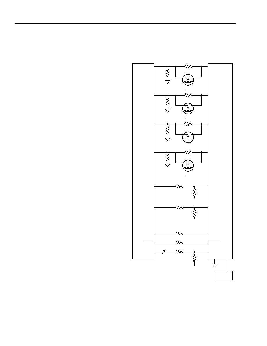
72
72
Lucent Technologies Inc.
Advance Data Sheet
November 1999
H.100/H.110 Interfaces and Time-Slot Interchangers
Ambassador T8100A, T8102, and T8105
3 Using the TSI Devices
(continued)
3.3 Basic Connections
(continued)
3.3.4 Physical Connections for H.100
All H.100 bus signals must adhere to the specification,
ECTF H.100 Hardware Compatibility Specification: CT
Bus
. The H.100 clock signals, CT_C8_A, CT_C8_B,
/CT_FRAME_A, /CT_FRAME_B, and CT_NETREF,
each require an individual external pull-up of 100 k
to
5 V or 50 k
to 3.3 V.
If CT_NETREF, CT_8A, CT_8B, CT_FRAME_A, or
CT_FRAME_B are not going to be used, they must be
tied to ground, V
CC
or a pull-up resistor. They cannot be
left floating, since they could oscillate.
3.3.5 Physical Connections for H.110
Figure 21 shows the physical connections required for
use in an H.110 environment. There are electrical dif-
ferences between H.100 and H.110. For H.110, exter-
nal components are required to meet specifications.
The specification is
ECTF H.110 Hardware Compatibil-
ity Specification: CT Bus
. Figure 21 shows the
NETREF terminations and the required terminations for
CT_C8A, CT_FRAMEA, CT_C8B, and CT_FRAMEB.
Each signal has a mechanism to short the 33
series
resistor and, in addition, a 10 k
pull-down resistor.
The 50 k
internal pull-ups on the CT data bus are
used for H.100. For H.110, the DPUE pin should be
tied low, disabling these internal pull-ups. H.110
requires the CT data bus to have pull-ups of 18 k
to
0.7 V. The control leads of the FET switches would typ-
ically go to the microprocessor.
3.3.6 PC Board BGA Considerations
There are no special requirements for the thermal balls
on the BGA package when designing a printed-circuit
board.
5-7142cF
* Switched low for insertion/removal.
Figure 21. Physical Connections for H.110
CT_NETREF2
CT_FRAMEA
CT_FRAMEB
CT_C8B
CT_NETREF2
CT_NETREF1
SCLKX2
CTD[0:31]
CT_C8B
SCLK
CT_FRAMEB
CT_FRAMEA
SCLK
33
CT_C8A
10 k
CTC8A_SRC
33
10 k
CTC8A_SRC
33
10 k
CTC8B_SRC
33
10 k
CTC8B_SRC
0
DEPOPULATE
CT_C8A
SCLKX2
0
DEPOPULATE
CTD[0:31]
24
DPUE
0.7 V
18 k
32
18 k
0.7 V
24
24
LUCENT
T8100A
T8102
T8105
18 k
0.7 V
CT_NETREF1
LPUE*
POWER
MANAGER

Lucent Technologies Inc.
73
Advance Data Sheet
November 1999
H.100/H.110 Interfaces and Time-Slot Interchangers
Ambassador T8100A, T8102, and T8105
3 Using the TSI Devices
(continued)
3.4 Using the LAR, AMR, and IDR for
Connections
3.4.1 Setting Up Local Connections (T8100A, T8105
Only)
Local connections require a physical location in the
local connection memory corresponding to the output
stream and time slot. The location contains a pointer to
a local data memory location which holds the actual
data that has come in or will be sent out. The local
memories are based on 1024 locations, so 10 bits are
required to specify the physical memory location where
a connection is placed or where data is stored. To sim-
plify the programming, the user supplies 11 bits in a
stream and time-slot format, which is converted by the
devices to the appropriate physical location. Relative to
describing a connection, a data memory location corre-
sponds with the FROM stream and time slot, and a
connection memory location corresponds with the TO
stream and time slot. To program a connection, the
user loads the data memory location into the connec-
tion memory location, effectively identifying where the
data resides.
The user programs 7 bits of the LAR for the time-slot
value (or 8 bits for pattern mode) and the lowest 4 bits
of the AMR for the stream value; these will then be con-
verted to the physical memory address. The upper bits
of the AMR select which field in the connection mem-
ory is being written into. Since the connection informa-
tion itself is 15 bits, two transfers (i.e., two fields) must
be made to the address in the connection memory.
In each case, the transfer is an indirect write of data to
the indirect data register, the IDR: The first transfer is
the lowest 7 bits (time-slot address) of the desired data
memory location. It is placed in the IDR after the LAR
and AMR have been set up with the appropriate con-
nection address.
Table 69 illustrates the decoding of the time-slot bits
(address value in the table refers to the hex value of the
7 bits comprising time slot).
When programming the registers for fallback, the CKS
and CKW registers should be programmed last.
Table 69. Time-Slot Bit Decoding
Address
Value
2 Mbits/s
Time Slot
4 Mbits/s
Time Slot
8 Mbits/s
Time Slot
0x00 0
0
0
0x01
1
1
1
0x02
2
2
2
0x03
3
3
3
0x04
4
4
4
0x05
5
5
5
0x06
6
6
6
0x07
7
7
7
0x08
8
8
8
0x09
9
9
9
0x0A
10
10
10
0x0B
11
11
11
0x0C
12
12
12
0x0D
13
13
13
0x0E
14
14
14
0x0F
15
15
15
0x10 16
16
16
0x11
17
17
17
:
:
:
:
0x1E
30
30
30
0x1F
31
31
31
0x20
NA
32
32
:
:
:
:
0x3E
NA
62
62
0x3F
NA
63
63
0x40
NA
NA
64
:
:
:
:
0x7E
NA
NA
126
0x7F
NA
NA
127
74
Lucent Technologies Inc.
Advance Data Sheet
November 1999
H.100/H.110 Interfaces and Time-Slot Interchangers
Ambassador T8100A, T8102, and T8105
3 Using the TSI Devices
(continued)
3.4 Using the LAR, AMR, and IDR for Connections
(continued)
3.4.1 Setting Up Local Connections (T8100A, T8105 Only) (continued)
Table 70. IDR: Indirect Data Register, Local Connections Only
The second transfer requires that data in the IDR be defined as follows.
After the second transfer is made, the entire 15 bits will be loaded into the connection memory; i.e., the second
transfer triggers the actual memory access. Figure 22 shows how the connections are made from the perspective
of the registers and memory contents.
If the user wishes to set up a pattern mode connection, then the first transfer is a full 8 bits (i.e., the pattern), rather
than the 7-bit time-slot value. This pattern byte will be stored in the lowest 8 bits of the selected connection memory
location. The pattern byte will be sent instead of a byte from local data memory during the output stream and time
slot which corresponds to the connection memory location.
5-6115aF
Figure 22. Local-to-Local Connection Programming (T8100A, T8105 Only)
Reg
R/W
Bit 7
Bit 6
Bit 5
Bit 4
Bit 3
Bit 2
Bit 1
Bit 0
IDR
R/W
Control
Address
XCS
PME
FME
CHE
Symbol
Bit
Description
XCS
7
A programmable bit which is routed to the XCS pin one time slot prior to the data to
which it relates.
PME
6
A high enables the pattern mode; the lower 8 bits of the connection address (time slot
and stream LSB) is routed to the time slot instead of data.
FME
5
A high enables the use of the alternate data buffer. (Refer to Appendix B for minimum
and constant delay settings.)
CHE
4
Enables the time-slot connection; a low in this bit forces 3-state during the time slot.
Address
3--0
All 4 bits are used for the stream address of the desired data memory location.
0000 0111
3, 27
3, 28
3, 29
3, 30
3, 31
CONNECTION
MEMORY
0100 0011
0001 1101
0000 0111
AMR
LAR
IDR
WRITE TO
TIME-SLOT
FIELD IN
FIRST TRANSFER:
0000 0111
0001
1110
3, 27
3, 28
3, 29
3, 30
3, 31
CONNECTION
MEMORY
0101 0011
0001 1101
0001 1110
AMR
LAR
IDR
WRITE TO
FIELD IN
MEMORY
SECOND TRANSFER:
LOCAL MEMORY PROGRAMMING EXAMPLE: CONNECT FROM 14, 7 TO 3, 29 (STREAM, TIME SLOT)
CONNECTION
MEMORY
CONNECTION
CONTROL/STREAM
Lucent Technologies Inc.
75
Advance Data Sheet
November 1999
H.100/H.110 Interfaces and Time-Slot Interchangers
Ambassador T8100A, T8102, and T8105
3 Using the TSI Devices
(continued)
3.4 Using the LAR, AMR, and IDR for Connections
(continued)
3.4.2 Setting Up H-Bus Connections
Table 71. IDR: Indirect Data Register, H-Bus Connections Only
The CAM blocks are 512 locations each (T8102, T8105 only) and the operations for the CAM blocks are selected
by AMR (see Section 2.1.3 Address Mode Register and Section 2.3.2 CAM Operation and Commands). Since the
block address is carried in the AMR, this reduces the number of bits that are necessary to establish a connection.
Eleven (11) address bits, i.e., bits for stream and time-slot identification, the 8-bit tag (pointer to the H-bus data
memory), and 3 control bits all need to be written into the selected CAM block for setting up a connection. (The
empty bit is a status bit that is changed internally as a result of operations on the CAM.) Four* transfers, indirect
writes through the IDR, are required to set up a connection in the CAM, though the method of transfer is different
than with the local memory. Since a specific physical address is not always necessary, the CAM will automatically
fill the first available slot. Thus, the LAR is not required for setting up the connection. (See the notes below.) The
first transfer after programming the AMR requires that the 7 bits which identify the time-slot number (refer to Sec-
tion 2.3.5 H-Bus Rate Selection and Connection Address Format for the proper format) be loaded into the IDR. The
second transfer uses a similar field description for the IDR as presented for local connections [Section 3.4.1 Setting
Up Local Connections (T8100A, T8105 Only) above]. The address field contains the stream number (5 bits), and
the control field contains only 3 control bits.
The third transfer for CAM connection setup is the transfer of the lower 8 bits of the tag field. The tag is loaded into
the IDR. The fourth transfer is the subrate control field and the TAG field MSB. The connection for the CAM is actu-
ally set up, (i.e., the memory access takes place) using a fifth write. It is an indirect write to the AMR (again through
the IDR) which corresponds with the specific command and blocks the user requests. All CAM commands require
that the IDR be loaded with the same command value as the AMR rather than a don't care or dummy value.
Notes: If an address is to be matched, such as the break connection command, then only the first two transfers
are required. The tag is unnecessary for identifying a connection.
The LAR is only used to read or query a specific location (i.e., 0--511) in a particular CAM block. Refer to
Section 2.1.3 Address Mode Register and Section 2.3.2 CAM Operation and Commands for details on
these commands.
For the CAMs, pattern mode is a 1/2 connection. Only the intended output to the H-bus (or to the local pins) needs
to be specified. The setup is the same as described above, four transfers to the holding registers followed by the
make connection command to the appropriate CAM block. When the address is matched, the tag value (from the
pipeline SRAM) will be sent as output to the bus
.
* Four transfers are required for the T8105 and T8102. For the T8100A, if subrate is enabled, then four transfers are also required. If subrate is
disabled, only three transfers are required and the T8100A follows the same programming model as the T8100.
Two subsequent IDR reads are required to retrieve the 9-bit physical address for the T8105 and T8102. Only one IDR read is required to
retrieve the 8-bit physical address for the T8100A.
Reg
R/W
Bit 7
Bit 6
Bit 5
Bit 4
Bit 3
Bit 2
Bit 1
Bit 0
IDR
--
Control
Address
R/W
PME
FME
--
--
--
--
--
Symbol
Bit
Description
R/W
7
Refers to the direction in the CAM data memory. A read sends data to the bus; a write loads
data from the bus.
PME
6
Pattern mode enable, similar to above, except the tag byte is output instead of the lower address
bits.
FME
5
Data buffer selection for setting delay type. (Refer to Appendix B for minimum and constant
delay settings.)
Address 4--0 All 5 bits are used for the stream address of the desired data memory location.
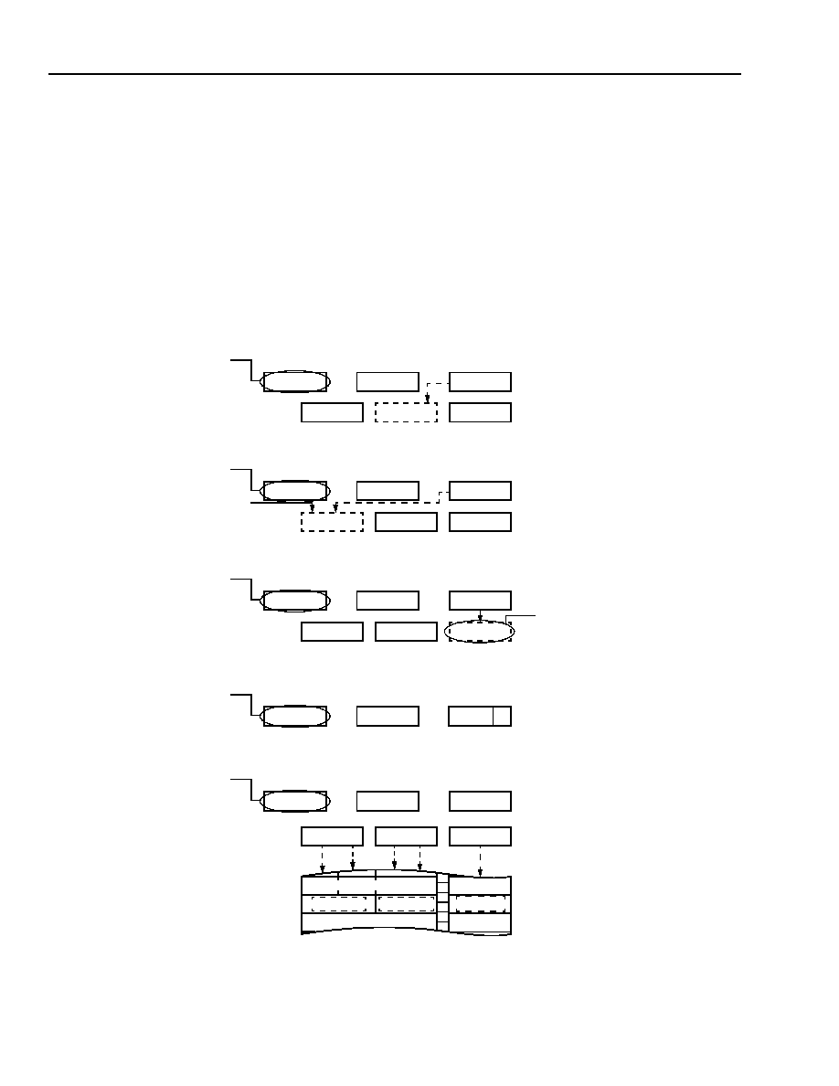
76
Lucent Technologies Inc.
Advance Data Sheet
November 1999
H.100/H.110 Interfaces and Time-Slot Interchangers
Ambassador T8100A, T8102, and T8105
3 Using the TSI Devices
(continued)
3.4 Using the LAR, AMR, and IDR for Connections
(continued)
3.4.2 Setting Up H-Bus Connections (continued)
Figure 23 illustrates how a CAM connection is made from the perspective of registers and the memory locations.
Note that each half of the connection (i.e., the FROM and the TO) requires a separate setup, though each half will
point to the same location in the H-bus data memory.
Following Figure 23, some simple programming examples are shown using pseudoassembler code. The local-to-
local and H-bus-to-local switching examples from Figure 22 and Figure 23 are reused in code examples #2 and #3.
The connections are referred to in stream, time-slot format.
5-6116aF
A. First Half of Connection, H-Bus Side
Figure 23. CAM Programming, H-Bus-to-Local Connection
0000 0111
1011 0000
XXXX XXXX
0000 0111
AMR
LAR (UNUSED)
IDR
WRITE TO TIME-SLOT
FIRST TRANSFER:
CAM PROGRAMMING EXAMPLE:
CTLS/STREAM
LOCATION USED--NOT EMPTY
HOLDING REGISTER
TIME SLOT
TAG
HOLDING REGISTERS
1011 0001
XXXX XXXX
000 01110
AMR
LAR (UNUSED)
IDR
WRITE TO CONTROL/STREAM
SECOND TRANSFER:
CTLS/STREAM
HOLDING REGISTER
TIME SLOT
TAG
HOLDING REGISTERS
1011 0010
XXXX XXXX
0011 0001
AMR
LAR (UNUSED)
IDR
WRITE TO TAG
THIRD TRANSFER:
CTLS/STREAM
HOLDING REGISTER
TIME SLOT
TAG
HOLDING REGISTERS
1110 0000
XXXX XXXX
1110 0000
AMR
LAR (UNUSED)
IDR (MUST = AMR)
TRANSFER HOLDING
LOAD CAM:
CTLS/STREAM
REGISTERS TO NEXT FREE
TIME SLOT
TAG
HOLDING REGISTERS
0000 0111
000 01110
0000 0111
DIRECTION BIT: FROM
BUS TO DATA MEMORY
000 01110
0000 0111
0011 0001
DATA LOCATION 49
LOCATION IN EVEN CAM
0011 0001
0000 0111
000 01110
(NOT EMPTY)
(EMPTY)
(LOCATION USED--NOT EMPTY)
(LOCATION NOT USED--EMPTY)
000 01110
0000 0111
EVEN CAM
PIPELINE SRAM
1011 0011
XXXX XXXX
AMR
LAR (UNUSED)
WRITE TO TAG
FOURTH TRANSFER:
HOLDING REGISTER
IDR
SUBRATE TAG
MSB
CONTROL
(BIT 0)
CONNECT FROM H-BUS 14, 7 TO LOCAL 3, 29, KEEP DATA IN LOCATION 49
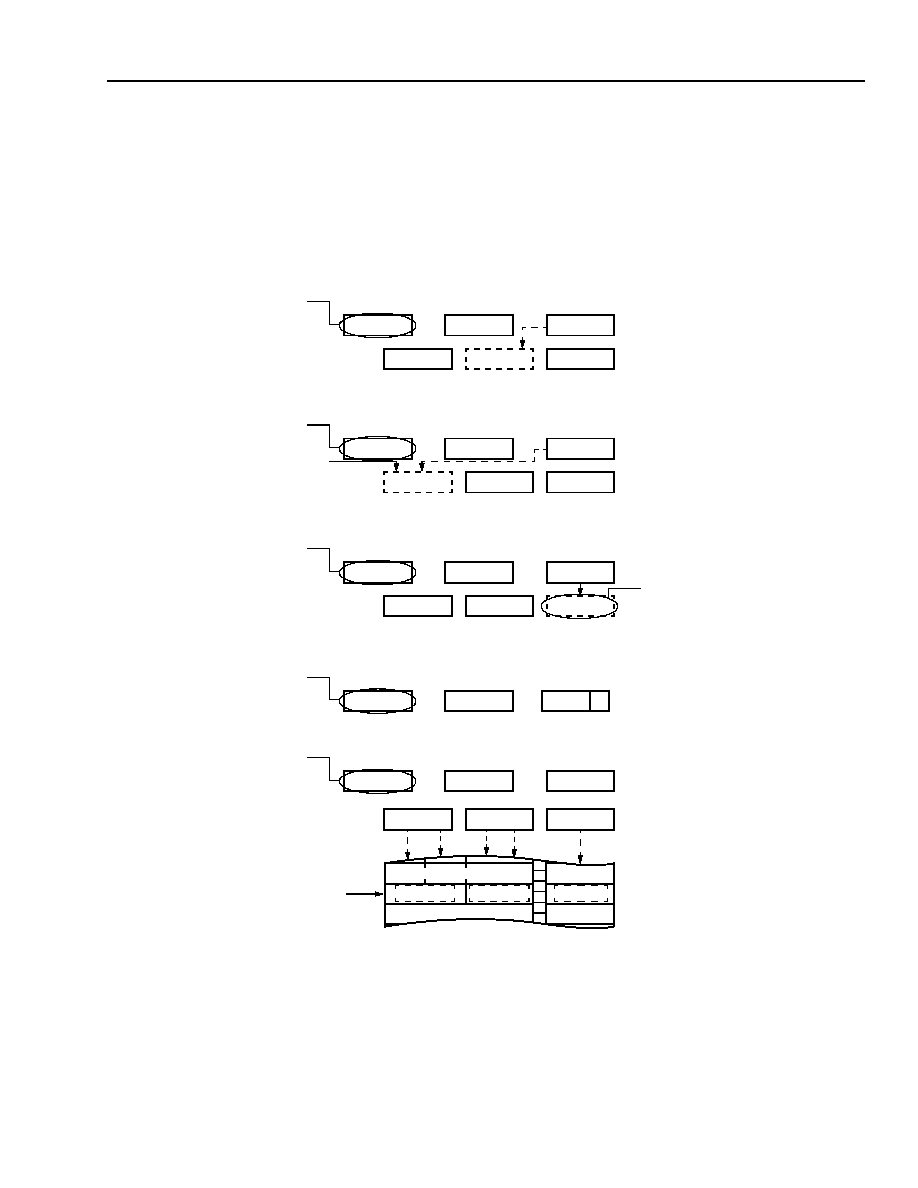
Lucent Technologies Inc.
77
Advance Data Sheet
November 1999
H.100/H.110 Interfaces and Time-Slot Interchangers
Ambassador T8100A, T8102, and T8105
3 Using the TSI Devices
(continued)
3.4 Using the LAR, AMR, and IDR for Connections
(continued)
3.4.2 Setting Up H-Bus Connections (continued)
5-6117aF
B. Second Half of Connection, Local Side
Figure 23. CAM Programming, H-Bus-to-Local Connection (continued)
0011 0001
1011 0000
XXXX XXXX
0001 1101
AMR
LAR (UNUSED)
IDR
WRITE TO TIME-SLOT
FIRST TRANSFER:
CAM PROGRAMMING EXAMPLE (CONTINUED):
CTLS/STREAM
LOCATION USED--NOT EMPTY
HOLDING REGISTER
TIME SLOT
TAG
HOLDING REGISTERS
1011 0001
XXXX XXXX
100 00011
AMR
LAR (UNUSED)
IDR
WRITE TO CONTROL/STREAM
SECOND TRANSFER:
CTLS/STREAM
HOLDING REGISTER
TIME SLOT
TAG
HOLDING REGISTERS
1011 0010
XXXX XXXX
0011 0001
AMR
LAR (UNUSED)
IDR
WRITE TO TAG
THIRD TRANSFER:
CTLS/STREAM
HOLDING REGISTER
TIME SLOT
TAG
HOLDING REGISTERS
1110 0011
XXXX XXXX
1110 0011
AMR
LAR (UNUSED)
IDR (MUST = AMR)
TRANSFER HOLDING
LOAD CAM:
CTLS/STREAM
REGISTERS TO NEXT FREE
TIME SLOT
TAG
HOLDING REGISTERS
0001 1101
100 00011
0001 1101
DIRECTION BIT: TO BUS
FROM DATA MEMORY
100 00011
0001 1101
0011 0001
DATA LOCATION 49
LOCATION IN LOCAL CAM
0011 0001
0001 1101
100 00011
(NOT EMPTY)
(EMPTY)
(LOCATION USED--NOT EMPTY)
(LOCATION NOT USED--EMPTY)
100 00011
0001 1101
NEXT FREE LOCATION
LOCAL CAM
PIPELINE SRAM
1011 0011
XXXX XXXX
AMR
LAR (UNUSED)
IDR
WRITE TO TAG
FOURTH TRANSFER:
HOLDING REGISTER
SUBRATE TAG
MSB
CONTROL
(BIT 0)
CONNECT FROM H-BUS 14, 7 TO LOCAL 3, 29, KEEP DATA IN LOCATION 49

78
Lucent Technologies Inc.
Advance Data Sheet
November 1999
H.100/H.110 Interfaces and Time-Slot Interchangers
Ambassador T8100A, T8102, and T8105
3 Using the TSI Devices
(continued)
3.4 Using the LAR, AMR, and IDR for Connections
(continued)
3.4.3 Programming Examples
;All programming examples included are in a pseudoassembler format.
;The basic commands used are the "move direct" and "move indirect."
;A move direct command is indicated by the letters "MD" followed by
;the register name, then the data. Similarly, a move indirect command
;is indicated by the letters "MI" followed by the register name, then by
;data or another register reference (the register may not be indirect).
;The semicolon delineates comments. Direct data is followed by the
;letter "h" for Hex and "b" for binary.
;*******EXAMPLE #1 - Set Up Clocks, Local Bus, H-Bus, and Framers
;
;*******Misc. Stuff
;
MD,AMR,00h
;Define control space
;all specific register names are equivalent
;to the LAR addresses (from Table 11)
;
;
;*******Set up Clocks
;**Main Clock Register
MD,IDR,0C2h
;Load IDR with values for bit slider on, slave mode,
;and synced to ECTF Bus A Clocks
MI,CKM,IDR
;The data in IDR is moved into CKM via the LAR register.
;
;**NETREF Registers
MD,IDR,88h
;Set up NETREF from Local Reference 0, 2.048 MHz bit clock
in, divided value
;value out (i.e., 8 kHz), enable the DJAT connections
MI,CKN,IDR
;Move the data to CKN
MD,IDR,0FFh
;Set up NETREF divider with divide-by-256
MI,CKND,IDR
;Move the data to CKND
;
;**Programmable Clocks
MD,IDR,26h
;This selects the oscillator for the TCLKOUT, A Clock
outputs off, and
;driving ECTF B Clocks
MI,CKP,IDR
;Move the data
;
;**Clock Resources
MD,IDR,40h
;Synced to bus so select Resource divider, x16 on PLL #1 &
x8 PLL #2, SC Clocks off
MI,CKR,IDR
;Make it so
MD,IDR,01h
;Set up Resource divider with divide-by-2 for 4 MHz signal
into PLL #1
MI,CKRD,IDR
;Move the data to divider
;

Lucent Technologies Inc.
79
Advance Data Sheet
November 1999
H.100/H.110 Interfaces and Time-Slot Interchangers
Ambassador T8100A, T8102, and T8105
3 Using the TSI Devices
(continued)
3.4 Using the LAR, AMR, and IDR for Connections
(continued)
3.4.3 Programming Examples (continued)
;**Secondary Controls (Fallback)
MD,IDR,35h
;Enable ECTF Fallback: Become the new A Clock master on A
Clock failure,
;synchronizes to a bit clock on local reference 1, but
requires the main divider
;with external input (assumes a CLAD is between the
divider and 4MHzIn).
MI,CKS,IDR
;Move the data to CKS
MD,IDR,0FFh
;Set up Main divider with divide-by-256
MI,CKMD,IDR
;Move the data to divider
;
;**Local Clocks
MD,IDR,0E4h
;Local Selected Clock 3 gets inverted 8.192 MHz, LSC2 gets
2.048 MHz
MI,CK32,IDR
;Move it to CK32
MD,IDR,80h
;LSC1 is high & LSC0 is low
MI,CK10,IDR
;Move it to CK10
;
;*******Set up Local Streams
;
MD,IDR,30h
;8 Streams at 8 Mbits/s
MI,LBS,IDR
;Define input streams per IDR
;
;*******Set up H Bus Streams
;
MD,IDR,0AAh
;Define H-Bus Streams 0 - 15 for 4 Mbits/s
MI,HSL,IDR
;Do it
;
MD,IDR,0FFh
;Define H-Bus Streams 16-31 for 8 Mbits/s
MI,HSH,IDR
;Engage
;*******Set up Framers
;
MD,IDR,00h
;This sequence sets up Group A
MI,FRLA,IDR
;
to start coincident
MI,FRLB,IDR
;
with the Frame
MI,FRPH,IDR
;
boundary and Group B
MD,IDR,0F0h
;
to start halfway through
MI,FRHA,IDR
;
the Frame. The Groups
MD,IDR,0F4h
;
operate in normal framing mode
MI,FRHB,IDR
;
at 8 Mbits/s and are Double Byte wide.
;Note: FRPH sets up the correct routing.
;
;*******Connect the devices to the outside world
;
MD,MCR,0Eh
;
Enable H-Bus Streams & Clock, Local Streams,
local
;
Clocks including Framers
;
;*******END OF EXAMPLE #1

80
Lucent Technologies Inc.
Advance Data Sheet
November 1999
H.100/H.110 Interfaces and Time-Slot Interchangers
Ambassador T8100A, T8102, and T8105
3 Using the TSI Devices
(continued)
3.4 Using the LAR, AMR, and IDR for Connections
(continued)
3.4.3 Programming Examples (continued)
;*******EXAMPLE #2 - Setting up Local Connections (T8100A, T8105 only)
;
;
Use 8 Mbits/s rate set up from Example #1...
;
Send data FROM Stream/Time Slot 14, 7 TO Stream/Time Slot 3, 29.
;
To transfer data the local input 14, 7 to the local
;
output 3, 29 the following programming steps are required.
;
MD,LAR,1Dh
;Set up lower address, i.e., Time Slot 29
MD,AMR,43h
;
Set up upper address bits (Stream 3), and
point to the
;
the Time Slot field of the connection memory
MI,IDR,07h
;Put a "7" in the Time Slot field of connection location
3,29
;
;Syntactically, "MI,IDR,data" is a special case since IDR is not the final recipient
of the data
;
MD,AMR,53h
;Maintain the same upper address, but get ready to load the
;
remaining connection info (upper bits +
control)
MI,IDR,0001_1110b
;This decodes as follows: XCS bit low, pattern mode off
;
(not set), frame bit low, time slot enabled,
and stream = 1110b (14)
;
;*******END OF EXAMPLE #2
;*******EXAMPLE #3 - Setting up H-Bus Connections, No Subrate
;
;
Use rate set up from Example #1...
;
Send data from Stream 14/Time Slot 7 of the H.100 bus to Stream 3/Time Slot 29
;
on the Local side. The data is coming in at 4 Mbits/s from E-CAM, and is sent
;
out at 8 Mbits/s to through L-CAM. We're using Data Memory location 49 to hold
;
the actual data. LAR is not used for the CAM connection setups; it is used for
;
reading specific CAM locations or writing and reading the associated Data
;
Memory Locations.
;
;******Set up the "from" connection
;
MD,AMR,0B0h
;Point to the Time-Slot holding register
MI,IDR,07h
;This is the Time-Slot value (7) for the H-Bus address
MD,AMR,0B1h
;Point to the upper bits of the connection
MI,IDR,000_01110b
:Set up a write into data memory from ECTF bus,
;
disable pattern mode, minimum delay,
;
and set stream number equal to 01110b (14).
MD,AMR,0B2h
;Point to tag field
MI,IDR,31h
;Use location 49 of the associated Data RAM to store the data
MD,AMR,0B3h
;Point to the subrate control and TAG MSB field;
MI,IDR,00h
;MSB of location 49 is 0;
;
MD,AMR,0E0h
;Write to next free location in the Even CAM
MI,IDR,0E0h
;The command is executed with the indirect to IDR which
;uses the same command value as in the AMR.

Lucent Technologies Inc.
81
Advance Data Sheet
November 1999
H.100/H.110 Interfaces and Time-Slot Interchangers
Ambassador T8100A, T8102, and T8105
3 Using the TSI Devices
(continued)
3.4 Using the LAR, AMR, and IDR for Connections
(continued)
3.4.3 Programming Examples (continued)
;
;**Optional: Test CAM Busy bit**
TEST:
MD,ACC,MCR
;Move MCR contents into (host's) accumulator (for example)
AND,01h
;Logical AND, i.e., mask off all but LSB of the MCR register
JNZ TEST
;If the LSB is zero (not busy), continue, else jump back and
;retest
;
CONTINUE:
;
;******Set up the "to" connection
;
MD,AMR,0B0h
;Point to the Time-Slot holding register
MI,IDR,1Dh
;This is the Time-Slot value (29) for the Local address
MD,AMR,0B1h
;Point to the upper bits of the connection
MI,IDR,100_00011b
:Set up a read from data memory to Local pins,
;
disable pattern mode, minimum delay, and set
;
stream number equal to 00011b (3).
MD,AMR,0B2h
;Point to tag field
MI,IDR,31h
;Use location 49 of the associated Data RAM to store the data
;
MD,AMR,0B3h;
MI,IDR,00h;
MD,AMR,0E3h
;Write to next free location in the Local CAM
MI,IDR,0E3h
;The command is executed with the indirect to IDR
;
;**CAM Busy bit can be tested here**
;
;
;*******END OF EXAMPLE #3
3.4.4 Miscellaneous Commands
These commands (i.e., 0x70, 0xF8, all reset commands in the AMR register) require two writes: first the value is
written to the AMR register; then the same value is written to the IDR register. After writing to the IDR register, the
command will be executed.
82
Lucent Technologies Inc.
Advance Data Sheet
November 1999
H.100/H.110 Interfaces and Time-Slot Interchangers
Ambassador T8100A, T8102, and T8105
4 Electrical Characteristics
4.1 Absolute Maximum Ratings
Stresses in excess of the absolute maximum ratings can cause permanent damage to the device. These are abso-
lute stress ratings only. Functional operation of the device is not implied at these or any other conditions in excess
of those given in the operational sections of this data sheet. Exposure to absolute maximum ratings for extended
periods can adversely affect device reliability.
4.2 Handling Precautions
Although protection circuitry has been designed into this device, proper precautions should be taken to avoid expo-
sure to electrostatic discharge (ESD) during handling and mounting. Lucent employs a human-body model (HBM)
and a charged-device model (CDM) for ESD-susceptibility testing and protection design evaluation. ESD voltage
thresholds are dependent on the circuit parameters used to define the model. No industry-wide standard has been
adopted for CDM. However, a standard HBM (resistance = 1500
, capacitance = 100 pF) is widely used and,
therefore, can be used for comparison purposes:
Description
Symbol
Min
Max
Unit
Supply Voltage
V
DD
--
3.6
V
XTALIN and XTALOUT Pins
--
V
SS
V
DD
V
Voltage Applied to I/O Pins
--
V
SS
≠ 0.5
V
DD
+ 3.4
V
Operating Temperature:
208-pin SQFP
217-ball BGA
--
--
0
-
40
70
85
∞C
∞C
Storage Temperature
T
stg
≠55
125
∞C
HBM ESD Threshold Voltage
Device
Rating
T8100A, T8102, T8105
2500 V
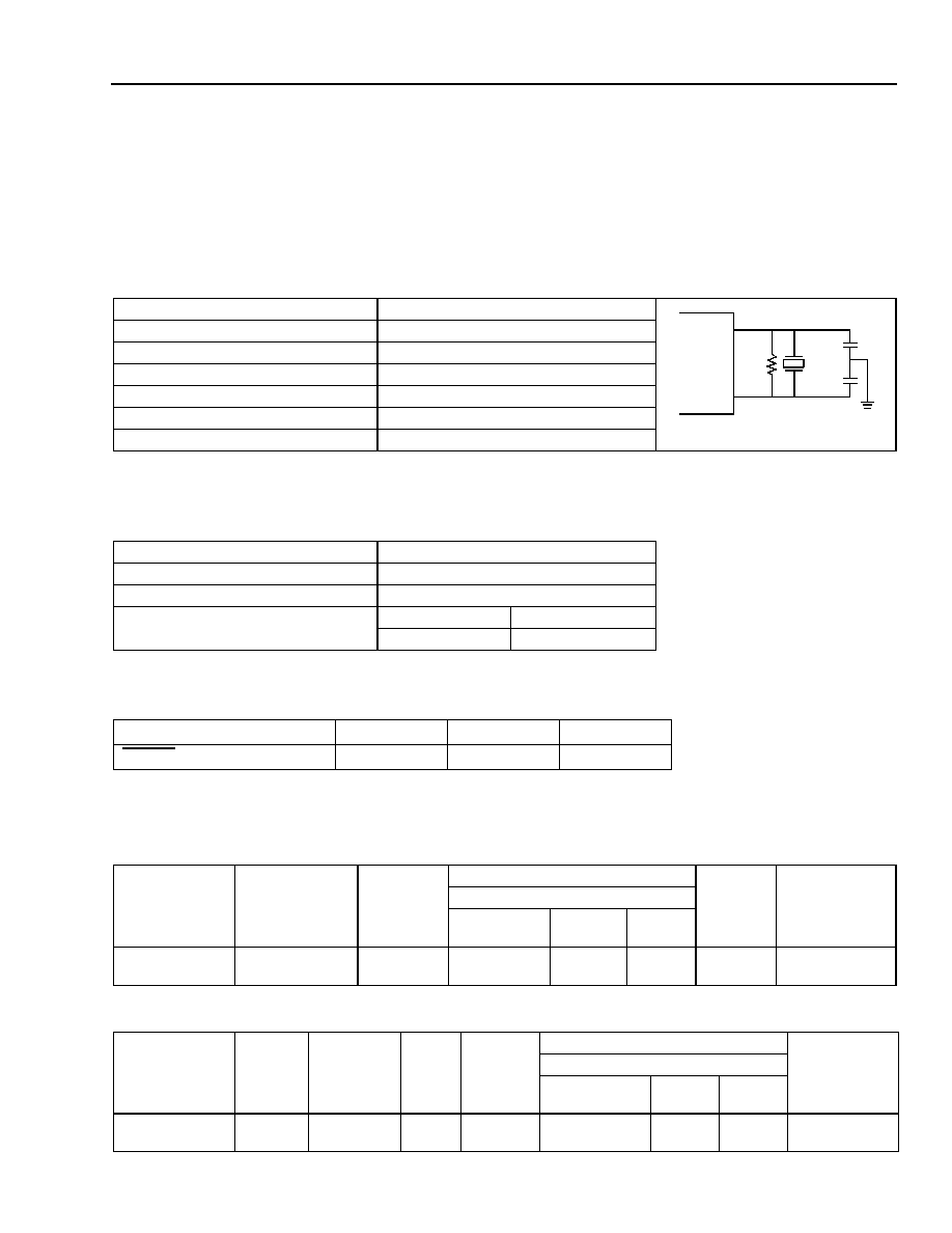
Lucent Technologies Inc.
83
Advance Data Sheet
November 1999
H.100/H.110 Interfaces and Time-Slot Interchangers
Ambassador T8100A, T8102, and T8105
4 Electrical Characteristics
(continued)
4.3 Crystal Information
Table 72. Crystal Specifications
The devices require a 16.384 MHz clock source. To supply this, a 16.384 MHz crystal can be connected between
the XTALIN and XTALOUT pins. External 18 pF, 5% capacitors must be connected from XTALIN and XTALOUT to
V
SS
. Crystal specifications are shown below. The
±
32 ppm tolerance is the suggested value if the oscillator is used
as the clocking source while mastering the bus. Otherwise, a crystal with a lesser tolerance can be used.
Table 73. Use of an Oscillator as an Alternative to Using a Crystal
XTALIN can be driven by a CMOS signal instead of a crystal. XTALIN and XTALOUT are not 5 V tolerant. The oscil-
lator must meet the requirements shown below.
4.4 Reset Pulse
4.5 Thermal Considerations
4.5.1 Thermal Considerations for the 208 SQFP
4.5.2 Thermal Considerations for the 217 PBGA
Parameter
Value
5-6390(F)
Frequency
16.384 MHz
Oscillation Mode
Fundamental, Parallel Resonant
Effective Series Resistance
40
maximum
Load Capacitance
14 pF
Shunt Capacitance
7 pF maximum
Frequency Tolerance and Stability
32 ppm
Parameter
Value
Frequency
16.384 MHz
Maximum Rise or Fall Time
10 ns, 10% to 90% V
DD
Minimum Pulse Width
Low
High
20 ns
20 ns
Parameter
Min
Max
Unit
RESET Minimum Pulse Width
61
--
ns
Parameter
Construction
Details
Body
Size
(mm sq.)
Thermal Numbers
Paddle
Size
(mil sq.)
Max. Power
(Natural
Convection)
(Watts)
Theta-JA (∞C/W)
Natural
Convection
200 fpm 500 fpm
4-Layer JEDEC
Test Board
Cu L.F.
20
26.5
23
21
433
2.1
Parameter
Body
Size
(mm sq.)
Array
Details
Ball
Pitch
(mm)
Number
of
Layers
Thermal Numbers
Max. Power
(Natural
Convection)
(Watts)
Theta-JA (∞C/W)
Natural
Convection
200 fpm 500 fpm
4-Layer JEDEC
Test Board
23
Peripheral
+ T.A.
1.27
2
32.5
29
27.5
1.7
V
SS
18 pF
18 pF
1 M
16.384 MH
Z
T8100A
XTALIN
XTALOUT
T8102
T8105
84
Lucent Technologies Inc.
Advance Data Sheet
November 1999
H.100/H.110 Interfaces and Time-Slot Interchangers
Ambassador T8100A, T8102, and T8105
4 Electrical Characteristics
(continued)
4.6 dc Electrical Characteristics, H-Bus (ECTF H.100 Spec., Rev. 1.0)
4.6.1 Electrical Drive Specifications--CT_C8 and /CT_FRAME
Table 74. Electrical Drive Specifications--CT_C8 and /CT_FRAME
V
DD
= 3.3 V and V
SS
= 0.0 V unless otherwise specified.
PCI-compliant data line I/O cells are used for the CT bus data lines. (See PCI Specification, Rev. 2.1, Chapter 4.)
/C16, /C4, C2, SCLK, SCLKX2, and /FR_COMP all use the same driver/receiver pairs as those specified for the
CT_C8 and /CT_FRAME signals, though this is not explicitly stated as a part of the H.100 Specification.
4.7 dc Electrical Characteristics, All Other Pins
Table 75. dc Electrical Characteristics, All Other Pins
V
DD
= 3.3 V and V
SS
= 0.0 V unless otherwise specified.
* Circuit simulation indicates a typical current of 175 mA and a worst-case current of 275 mA. This parameter is not tested in production.
Parameter
Symbol
Condition
Min
Max
Unit
Output High Voltage
V
OH
I
OUT
= ≠24 mA
2.4
3.3
V
Output Low Voltage
V
OL
I
OUT
= 24 mA
≠0.25
0.4
V
Positive-going Threshold
Vt+
--
1.2
2.0
V
Negative-going Threshold
Vt≠
--
0.6
1.6
V
Hysteresis (Vt+ ≠ Vt≠)
V
HYS
--
0.4
--
V
Input Pin Capacitance
C
IN
--
--
10
pF
Description
Symbol
Condition
Min
Typ
Max
Unit
Supply Current
I
DD
--
--
175*
275*
mA
Supply Voltage
V
DD
--
3.0
--
3.6
V
Input High Voltage
V
IH
--
2.0
--
--
V
Input Low Voltage
V
IL
--
--
--
0.8
V
Input Current
I
I
--
--
--
1
µA
Input Capacitance (input only)
C
I
--
--
--
5
pF
Input Capacitance (I/O pins)
C
IO
--
--
--
10
pF
Leakage Current (3-state)
I
LEAK
--
--
--
10
µA
Input Clamp Voltage
V
C
--
--
--
≠1.0
V
Output High Voltage
V
OH
--
2.4
--
--
V
Output Low Voltage
V
OL
--
--
--
0.4
V
Output Short-circuit Current
I
OS
V
OH
tied to GND
--
--
100
mA
Lucent Technologies Inc.
85
Advance Data Sheet
November 1999
H.100/H.110 Interfaces and Time-Slot Interchangers
Ambassador T8100A, T8102, and T8105
4 Electrical Characteristics
(continued)
4.8 H-Bus Timing (Extract from H.100 Spec., Rev. 1.0)
4.8.1 Clock Alignment
5-6119F
Figure 24. Clock Alignment
4.8.2 Frame Diagram
5-6120F
Note: Bit 1 is the MSB. Bit 8 is the LSB. MSB is always transmitted first in all transfers.
Figure 25. Frame Diagram
/CT_FRAME (A/B)
CT_C8 (A/B)
/FR_COMP
/C16
C2
/C4
SCLK
SCLK
SCLKX2
SCLKX2
SCLK
(2.048 MHz)
(2.048 MHz MODE)
(4.096 MHz MODE)
(4.096 MHz MODE)
(8.192 MHz MODE)
(8.192 MHz MODE)
SCLKX2
FRAME BOUNDARY
8
1
2
3
4
5
6
7
8
1
2
3
4
5
6
7
8
1
127
0
/CT_FRAME
CT_C8
CT_DX
TIME
SLOT
125
µ
s
FRAME BOUNDARY
86
Lucent Technologies Inc.
Advance Data Sheet
November 1999
H.100/H.110 Interfaces and Time-Slot Interchangers
Ambassador T8100A, T8102, and T8105
4 Electrical Characteristics
(continued)
4.8 H-Bus Timing (Extract from H.100 Spec., Rev. 1.0)
(continued)
4.8.3 Detailed Timing Diagram
5-6121F
Figure 26. Detailed Timing Diagram
/CT_FRAME
CT_C8
DATA OUT
DATA IN
2.0 V
0.6 V
2.0 V
0.6 V
2.4 V
0.4 V
1.4 V
tFS
tFH
1 BIT CELL
tFP
tC8H
tC8L
tC8P
tZDO
tDOD
tS127
BIT 8
tS0
BIT 1
tDOZ
tDV
tSAMP
tDIV
FRAME BOUNDARY

Lucent Technologies Inc.
87
Advance Data Sheet
November 1999
H.100/H.110 Interfaces and Time-Slot Interchangers
Ambassador T8100A, T8102, and T8105
4 Electrical Characteristics
(continued)
4.8 H-Bus Timing (Extract from H.100 Spec., Rev. 1.0)
(continued)
4.8.4 ac Electrical Characteristics, Timing, H-Bus (H.100 Spec., Rev. 1.0)
Table 76. ac Electrical Characteristics, Timing, H-Bus (H.100 Spec., Rev. 1.0)
Symbol
Parameter
Min
Typ
Max
Unit
Notes
--
Clock Edge Rate (all clocks)
0.25
--
2
V/ns
1, 2, 4
tC8P
Clock CT_C8 Period
122.066 ≠
--
122.074 +
ns
2, 4, 5
tC8H
Clock CT_C8 High Time
49 ≠
--
73 +
ns
2, 4, 6
tC8L
Clock CT_C8 Low Time
49 ≠
--
73 +
ns
2, 4, 6
tSAMP
Data Sample Point
--
90
--
ns
2, 4, 9
tDOZ
Data Output to HiZ Time
≠20
--
0
ns
2, 3, 4, 7, 11
tZDO
Data HiZ to Output Time
0
--
22
ns
2, 3, 4, 7, 11
tDOD
Data Output Delay Time
0
--
22
ns
2, 3, 4, 7
tDV
Data Valid Time
0
--
69
ns
2, 3, 4, 8, 10
tDIV
Data Invalid Time
102
--
112
ns
2, 4
tFP
/CT_FRAME Width
90
122
180
ns
2, 4
tFS
/CT_FRAME Setup Time
45
--
90
ns
2, 4
tFH
/CT_FRAME Hold Time
45
--
90
ns
2, 4
Phase Correction
0
--
10
ns
12
1. The rise and fall times are determined by the edge rate in V/ns. A maximum edge rate is the fastest rate at which a clock transitions.
CT_NETREF has a separate requirement. (See Section 2.5 Clocking Section.)
2. Measuring conditions, data lines: VTH (threshold voltage) = 1.4 V, VHI (test high voltage) = 2.4 V, VLO (test low voltage) = 0.4 V, input sig-
nal edge rate = 1 V/ns measuring conditions, clock and frame lines: Vt+ (test high voltage) = 2.0 V, Vt≠ (test low voltage) = 0.6 V, input sig-
nal edge rate = 1 V/ns.
3. Test load--200 pF.
4. When RESET is active, every output driver is 3-stated.
5. tC8P minimum and maximum are under free-run conditions assuming ±32 ppm clock accuracy.
6. Noncumulative, tC8P requirements still need to be met.
7. Measured at the transmitter.
8. Measured at the receiver.
9. For reference only.
10. tDV = maximum clock cable delay + maximum data cable delay + maximum data HiZ to output time = 12 ns + 35 ns + 22 ns = 69 ns. Maxi-
mum clock cable delay and maximum data cable delay are worst-case numbers based on electrical simulation.
11. tDOZ and tZDO apply at every time-slot boundary.
12. F (phase correction) results from PLL timing corrections.
88
Lucent Technologies Inc.
Advance Data Sheet
November 1999
H.100/H.110 Interfaces and Time-Slot Interchangers
Ambassador T8100A, T8102, and T8105
4 Electrical Characteristics
(continued)
4.8 H-Bus Timing (Extract from H.100 Spec., Rev. 1.0)
(continued)
4.8.5 Detailed Clock Skew Diagram
5-6122F
Figure 27. Detailed Clock Skew Diagram
4.8.6 ac Electrical Characteristics, Skew Timing, H-Bus (H.100 Spec., Rev. 1.0)
Table 77. ac Electrical Characteristics, Skew Timing, H-Bus (H.100 Spec., Rev. 1.0)
1. Test load--50 pF.
2. Assumes A and B masters in adjacent slots.
3. When static skew is 10 ns and, in the same clock cycle, each clock performs a 10 ns phase correction in opposite directions, a maximum
skew of 30 ns will occur during that clock cycle.
4. Meeting the skew requirements in Table 10 and the requirements of Section 2.3 H-Bus Section could require the PLLs generating CT_C8 to
have different time constants when acting as primary and secondary clock masters.
Symbol
Parameter
Min
Typ
Max
Unit
Notes
tSKC8
Maximum Skew Between CT_C8 A and B
--
--
±10, ±
ns
1, 2, 3, 4
tSKCOMP Maximum Skew Between CT_C8_A and Any
Compatibility Clock
--
--
±5
ns
1
--
Maximum Skew Between CT_C8_A and L_SCx Clock
--
--
±2
ns
1
Vt+
Vt+
CT_C8_A
CT_C8_B
tSKC8
Vt+
Vt+
CT_C8_A
COMPATIBILITY
tSKCOMP
CLOCKS
Vt≠
tSKCOMP
Lucent Technologies Inc.
89
Advance Data Sheet
November 1999
H.100/H.110 Interfaces and Time-Slot Interchangers
Ambassador T8100A, T8102, and T8105
4 Electrical Characteristics
(continued)
4.8 H-Bus Timing (Extract from H.100 Spec., Rev. 1.0)
(continued)
4.8.7 Reset and Power On
Table 78. Reset and Power On
4.9 ac Electrical Characteristics, Local Streams, and Frames
Table 79. ac Electrical Characteristics, Local Streams, and Frames
Table 80. L_SC[3:0] and Frame Group Rise and Fall Time
* Worst-case loading of 50 pF on all outputs except CT_D[31:0]. CT_D[31:0] drives 200 pF.
Symbol
Parameter
Min
Typ
Max
Unit
tRD
Output Float Delay from Reset Active
--
--
1
µs
tRS
Reset Active from Power Good
--
5
--
µs
Symbol
Description
Condition
Min
Max
Unit
tPD
Data Propagation Delay
Load = 50 pF
0
20
ns
tS
Data Setup Time
--
10
--
ns
tH
Data Hold Time
--
5
--
ns
tOFF
Data 3-state Off Time
--
--
20
ns
tD0
Data Bit 0 3-state
--
≠20
0
ns
Description
Min
Typ
Max
Unit*
L_SCx Rise Time
--
--
5
ns
L_SCx Fall Time
--
--
4
ns
Frame Group Rise Time
--
--
3
ns
Frame Group Fall Time
--
--
3
ns
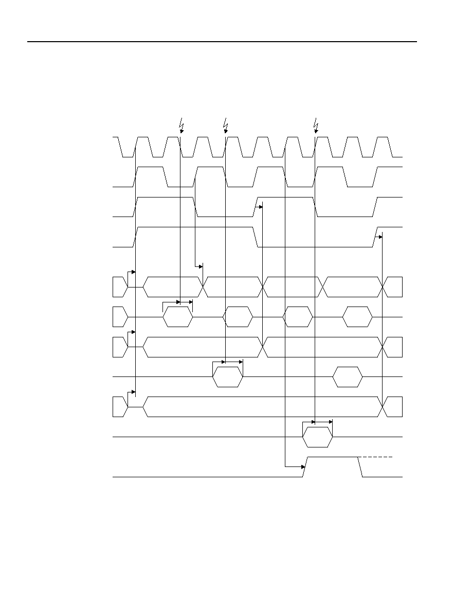
90
Lucent Technologies Inc.
Advance Data Sheet
November 1999
H.100/H.110 Interfaces and Time-Slot Interchangers
Ambassador T8100A, T8102, and T8105
4 Electrical Characteristics
(continued)
4.9 ac Electrical Characteristics, Local Streams, and Frames
(continued)
* Frame group is shown with an offset of four (4).
Note: LDO7 is the MSB, LDO0 is the LSB. MSB is always transmitted first in all transfers.
Figure 28. ac Electrical Characteristics, Local Streams, and Frames
L D O 6
L D O 7
L D O 5
L D O 4
L D O 3
LDI7
LDI
0
L D O 7
L D O 6
L D O 5
LDI6
LDI5
LDI4
LDI7
LDI6
L D O 7
L D O 6
LDI7
t P D
t P D
t P D
t D 0
tS
tH
tS
tH
tS
tH
1 6 . 3 8 4 M H z
8 . 1 9 2 M H z
4 . 0 9 6 M H z
2 . 0 4 8 M H z
8.192 Mbits/s
4.096 Mbits/s
2.048 Mbits/s
8.192 Mbits/s
4.096 Mbits/s
2.048 Mbits/s
t P D
FRAME GROUP:
L_SCn LOCAL CLOCKS
(NONINVERTED SHOWN):
t D 0
t D 0
LOCAL STREAMS:
3 / 4 P O I N T
3 / 4 P O I N T
3 / 4 P O I N T
L D O
0
L D O
0
L D O
0
*
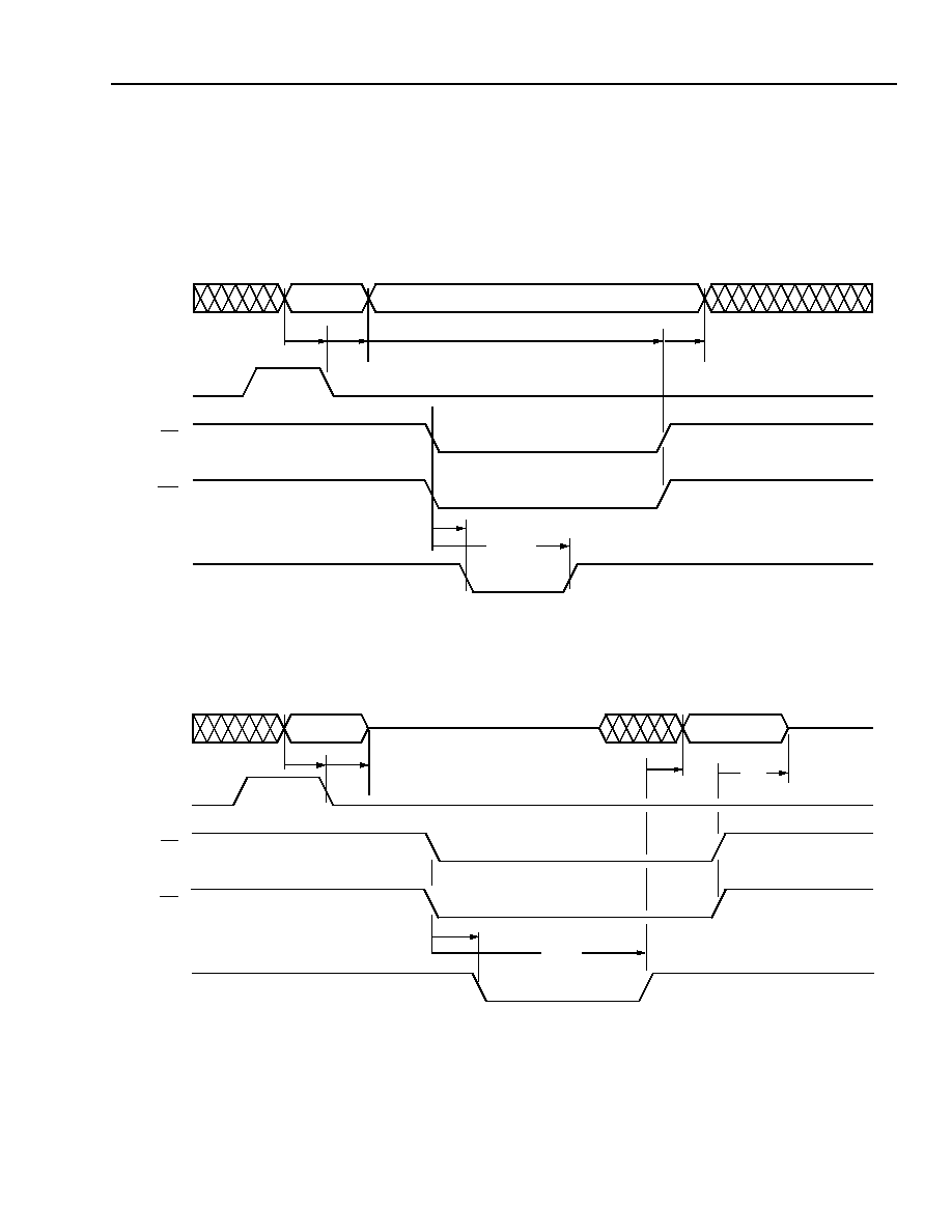
Lucent Technologies Inc.
91
Advance Data Sheet
November 1999
H.100/H.110 Interfaces and Time-Slot Interchangers
Ambassador T8100A, T8102, and T8105
4 Electrical Characteristics
(continued)
4.10 ac Electrical Characteristics, Microprocessor Timing
4.10.1 Microprocessor Access
Intel
Multiplexed Write and Read Cycles
For
Intel
write and read cycles, when RDY is low, wait-states are inserted. RDY is brought high when tIACC is met.
This is true for both read and write cycles.
5-6124.bF
Figure 29. Microprocessor Access
Intel
Multiplexed Write Cycle
5-6125.bF
Figure 30. Microprocessor Access
Intel
Multiplexed Read Cycle
tRDY
tIACC
A[1:0]
D[7:0]
AD[7:0]
ALE
CS
WR
RDY
tAS
tAH
tDS
tDH
(RDY DRIVEN LOW DURING
MEMORY ACCESSES ONLY)
tIACC
tRDY
A[1:0]
AD[7:0]
ALE
CS
RD
RDY
tAS
tAH
D[7:0]
tDI
tDV
(RDY DRIVEN LOW DURING
MEMORY ACCESSES ONLY)
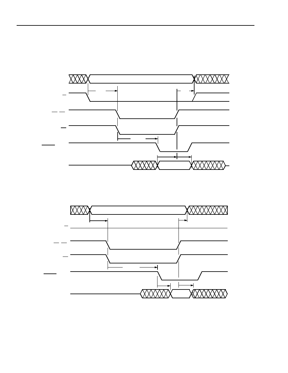
92
Lucent Technologies Inc.
Advance Data Sheet
November 1999
H.100/H.110 Interfaces and Time-Slot Interchangers
Ambassador T8100A, T8102, and T8105
4 Electrical Characteristics
(continued)
4.10 ac Electrical Characteristics, Microprocessor Timing
(continued)
4.10.2 Microprocessor Access
Motorola
Write and Read Cycles
5-6126.cF
Figure 31. Microprocessor Access
Motorola
Write Cycle
5-6127.bF
Figure 32. Microprocessor Access
Motorola
Read Cycle
A[1:0]
D[7:0]
R/W
DS (RD)
CS
DTACK (RDY)
tMACC
tDS
tDH
tAS
tAH
A[1:0]
D[7:0]
R/W
DS (RD)
CS
DTACK (RDY)
tMACC
tDV
tDI
tAH
tAS
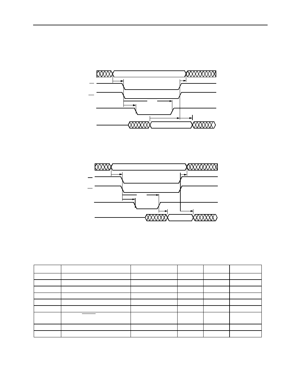
Lucent Technologies Inc.
93
Advance Data Sheet
November 1999
H.100/H.110 Interfaces and Time-Slot Interchangers
Ambassador T8100A, T8102, and T8105
4 Electrical Characteristics
(continued)
4.10 ac Electrical Characteristics, Microprocessor Timing
(continued)
4.10.3 Microprocessor Access
Intel
Demultiplexed Write and Read Cycles
5-6128.cF
Figure 33. Microprocessor Access
Intel
Demultiplexed Write Cycle
5-6128.bF
Figure 34. Microprocessor Access
Intel
Demultiplexed Read Cycle
Table 81. Microprocessor Access Timing
(See Figures 29 through 34.)
Symbol
Description
Condition
Min
Max
Unit
tAS
Address Setup Time
Load = 100 pF
7
--
ns
tAH
Address Hold Time
--
0
--
ns
tDV
Data Valid
--
--
13
ns
tDI
Data Invalid
--
0
11
ns
tRDY
Active to Ready Low (
Intel
)
Memory Access
--
14
ns
tIACC
Active to Ready High (
Intel
)
Memory Access
145
255
ns
tMACC
Active to
DTACK
Low (
Motorola
)
Register Access
Memory Access
--
130
14
255
ns
tDS
Data Setup Time
--
8
--
ns
tDH
Data Hold Time
--
0
--
ns
A[1:0]
CS
RDY
WR
D[7:0]
tAS
tDS
tDH
tAH
tRDY
tIACC
(RDY DRIVEN LOW
DURING MEMORY
ACCESSES ONLY)
A[1:0]
CS
RDY
RD
D[7:0]
tAS
tDV
tDI
tAH
tRDY
tIACC
(RDY DRIVEN LOW
DURING MEMORY
ACCESSES ONLY)
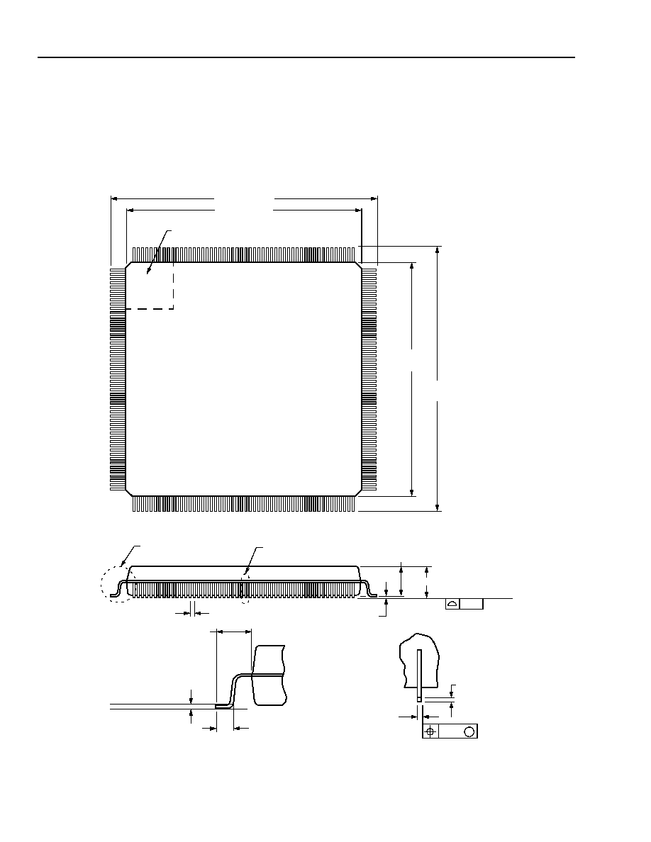
94
Lucent Technologies Inc.
Advance Data Sheet
November 1999
H.100/H.110 Interfaces and Time-Slot Interchangers
Ambassador T8100A, T8102, and T8105
5 Outline Diagrams
5.1 208-Pin Square Quad Flat Package (SQFP)
Dimensions are in millimeters.
Note:
The dimensions in this outline diagram are intended for informational purposes only. For detailed schemat-
ics to assist your design efforts, please contact your Lucent Technologies Microelectronics Group Account
Manager.
5-2196(F)
156
105
30.60 ± 0.20
157
208
1
52
53
104
28.00 ± 0.20
28.00
± 0.20
30.60
± 0.20
PIN #1 IDENTIFIER ZONE
4.10 MAX
0.08
3.40 ± 0.20
SEATING PLANE
0.25 MIN
0.50 TYP
DETAIL B
DETAIL A
0.50/0.75
GAGE PLANE
SEATING PLANE
1.30 REF
0.25
DETAIL A
DETAIL B
0.17/0.27
0.10
M
0.090/0.200
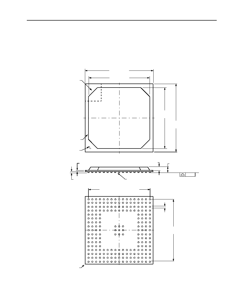
Lucent Technologies Inc.
95
Advance Data Sheet
November 1999
H.100/H.110 Interfaces and Time-Slot Interchangers
Ambassador T8100A, T8102, and T8105
5 Outline Diagrams
(continued)
5.2 217-Ball Plastic Ball Grid Array (PBGA)
Dimensions are in millimeters.
Note:
The dimensions in this outline diagram are intended for informational purposes only. For detailed schemat-
ics to assist your design efforts, please contact your Lucent Technologies Microelectronics Group Account
Manager.
5-6562(F)
0.36 ± 0.04
1.17 ± 0.05
2.13 ± 0.19
SEATING PLANE
SOLDER BALL
0.60 ± 0.10
0.20
A
B
C
D
E
F
G
H
J
K
L
M
N
P
R
T
U
1 2
3 4 5 6 7
8 9 10 11 12 13 14 15 16 17
16 SPACES @ 1.27 = 20.32
A1 BALL
CORNER
16 SPACES
@ 1.27 = 20.32
0.75 ± 0.15
PWB
MOLD
COMPOUND
23.00 ± 0.20
23.00
± 0.20
19.50
+0.70
≠0.00
19.50
+0.70
≠0.00
A1 BALL
IDENTIFIER ZONE
SIDE VIEW
BOTTOM VIEW
TOP VIEW

96
96
Lucent Technologies Inc.
Advance Data Sheet
November 1999
H.100/H.110 Interfaces and Time-Slot Interchangers
Ambassador T8100A, T8102, and T8105
6 Ordering Information
Version 1 and 2
Device Part Number
Package
Comcode
T8100A- - -SC-DB
208-Pin SQFP
108296146
T8100A- - -BAL-DB
217-Ball PBGA
108296138
T8102- - -SC-DB
208-Pin SQFP
108296161
T8102- - -BAL-DB
217-Ball PBGA
108296153
T8105- - -SC-DB
208-Pin SQFP
108296187
T8105- - -BAL-DB
217-Ball PBGA
108296179
Version 3
Device Part Number
Package
Comcode
T8105- - -BAL3-BB
217-Ball PBGA
108553397
T8105- - -SC3-DB
208-Pin SQFP
108553561
T8102- - -SC3-DB
208-Pin SQFP
108553587
T8102- - -BAL3-DB
217-Ball PBGA
108553579
T8100A- -BAL3-DB
217-Ball PBGA
108553595
T8100A- -SC3-DB
208-Pin SQFP
108553603

Lucent Technologies Inc.
97
Advance Data Sheet
November 1999
H.100/H.110 Interfaces and Time-Slot Interchangers
Ambassador T8100A, T8102, and T8105
Appendix A. Application of Clock
Modes
In the diagrams that follow, four clock modes are illus-
trated using Figure 16, the clocking diagram, as the
basis of each illustration. The key signal paths are
shown in solid lines, and unused paths with narrow
dashes. Two examples also indicate fallback paths. A
register profile (programming values) for all four exam-
ples is on the last page of the appendix.
Figure 35 shows the devices in bus master operation,
so they must link to either an 8 kHz recovered frame
reference or a 2.048 MHz recovered bit clock reference
from the E1 framers. In addition, the devices can pro-
vide one of the basic resource clocks to run the fram-
ers. In this case, the TCLKOUT is selecting the device's
16.384 MHz oscillator. The framers are returning a
2.048 MHz bit clock which is selected through the clock
selector. It is not divided, so the main divider is
bypassed (divide-by-1), the clock is smoothed
through an external DJAT, and the smooth 2.048 MHz
signal is routed to PLL #1 through the clock resource
selector. PLL #1 multiplies the 2.048 MHz input up to
65.536 MHz which, in turn, runs the rest of each
device, all bus clocks, and the local clocks (if desired).
If the devices are not providing NETREF generation,
then the NETREF from the bus is routed to the local
clocks via the NETREF internal/external selector. Since
the NETREF generation resources are not needed
here, the TODJAT and FROMDJAT pins are free for use
with the general-purpose register as bits GP6 and
GP7, respectively.
Figure 36 shows the T1 version of a bus master. In this
scenario, a 1.544 MHz recovered bit clock from the
framers is routed to a multiclock adapter (with built-in
jitter attenuation) which produces smooth 4.096 MHz
and 3.088 MHz outputs. The 4.096 MHz output is
routed up to PLL #1 for a times-16 rate multiplication to
65.536 MHz. This drives the bus clocks and the local
clocks. The smooth 3.088 MHz is also rate multiplied
times 8. This produces a 24.704 MHz clock. This is
divided back down to produce a smooth 12.352 MHz
which is fed back to the framers. (PLL outputs produce
one tightly bound edge and one with significant phase
jitter. Dividing a higher-frequency signal based on its
clean edge produces a lower frequency with two clean
edges.)
Figure 37 shows an H-
MVIP
slave arrangement for E1.
In this example, the C16 differential clocks provide the
main source for PLL #1. The 16.384 MHz signal is
divided down to 4.096 MHz and then rate multiplied up
to 65.536 MHz for driving the rest of each device. The
frame sync for the state machines is derived from the
/FRAME and C16 inputs as well as the state informa-
tion provided by C2 and /C4.
Note: The bit slider is enabled for a smooth phase
alignment between the internal frame and the
frame sync.
The bus clocks are not driven, but the local clocks are
available. A path for NETREF is shown as well, also
based on a 2.048 MHz input. The signal is smoothed
and then divided down to an 8 kHz signal via the
NETREF divider. The internal oscillator is again chosen
for routing to the framers via TCLKOUT.
Figure 38 shows an H-
MVIP
slave for T1. This is identi-
cal to the E1 case with regard to slaving, and a
NETREF path is illustrated in this example, too. The
NETREF divider has been changed to accommodate
the 1.544 MHz bit clock rate. The primary difference is
the use of the C16 clock through the main divider to
generate a 2.048 MHz signal which can be routed off-
chip and adapted to a 1.544 MHz signal using an exter-
nal device. The 1.544 MHz signal is returned to each
device via the 3MHzIN for rate multiplication up to
24.704 MHz and then division to a clean 12.352 MHz
signal which is routed to the framers via TCLKOUT.
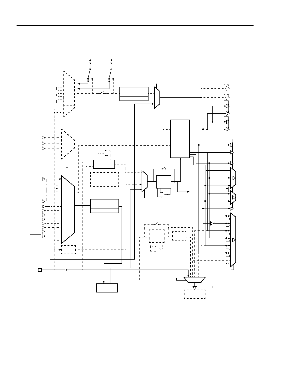
98
Lucent Technologies Inc.
Advance Data Sheet
November 1999
H.100/H.110 Interfaces and Time-Slot Interchangers
Ambassador T8100A, T8102, and T8105
Appendix A. Application of Clock Modes
(continued)
5-6129bF
Figure 35. E1, CT Bus Master, Compatibility Clock Master, Clock Source = 2.048 MHz from Trunk
FRAME
SEL.
x16
4 MHz
2 MHz
FRAME SYNC
DPLL
NETREF
DIVIDE-BY-N
DIVIDE REGISTER
CLOCK
RESOURCE
SELECT
DIVIDE-
BY-4
GP6
GP7
NETREF
INT/EXT
SELECT
BIT SLIDER
CONTROLS
BIT SLIDER
STATE
MACHINES
PLL #2
PLL #2 BYPASS
RATE SELECT
PRIREFOUT
4MHzIN
3MHzIN
TCLKOUT
TCLKOUT
ENABLE
TCLKOUT
SELECT
x8
NET-
˜
BY 8
NETREF
SELECT
/CT_FRAME_A
/CT_FRAME_B
/FR_COMP
CLOCK
SEL.
CLOCK
SEL.
AND
INPUT
STATE
MACH.
2.048 MHz
L_REF7
CT_C8
CLKB
/C16
±
/C4
C2
SCLK
SCLKX2
XTALIN
TODJAT/GP6 FROMDJAT/GP7
DJAT BYPASS
L_SC CTL
FRAME
FRAME
SEC8K
FRAME
FRAME
EN_B
C8
C8
EN_A
EN_NETREF1
CT_NETREF1
CT_C8_A
/CT_FRAME_A
CT_C8_B
/CT_FRAME_B
COMPATIBILITY
/CT16
±
C2
/C4
SCLK
SCLKX2
/FR_COMP
L_SC0
SCSEL
(1 OF 4
L_SC[1:3]
NOT SHOWN)
16.384 MHz
2.048 MHz
4.096 MHz
2.048 MHz
8.192 MHz
4.096 MHz
8.192 MHz
2.048 MHz
4.096 MHz
8.192 MHz
16.384 MHz
PLL#2
˜
2
(FALLBACK PATH)
4.096 MHz
CLOCKS DIRECTION
REF
SEL.
RESOURCE
DIVIDE-BY-N
DIVIDE REGISTER
MAIN
DIVIDE-BY-N
DIVIDE REGISTER
DIVIDE-
BY-2
CT_NETREF
FRAMERS
2 MHz DJAT
(AND GP6/7 ENABLE)
L_REF0
x16
x32
PLL #1
PLL #1
RATE SELECT
65.536 MHz
BYPASS
EN_NETREF2
CT_NETREF2
Lucent Technologies Inc.
99
Advance Data Sheet
November 1999
H.100/H.110 Interfaces and Time-Slot Interchangers
Ambassador T8100A, T8102, and T8105
Appendix A. Application of Clock Modes
(continued)
5-6130bF
Figure 36. T1, CT Bus Master, Compatibility Clock Master, Clock Source = 1.544 MHz from Trunk
FRAME
SEL.
x16
4 MHz
2 MHz
FRAME SYNC
DPLL
NETREF
DIVIDE-BY-N
DIVIDE REGISTER
CLOCK
RESOURCE
SELECT
DIVIDE-
BY-4
GP6
GP7
NETREF
INT/EXT
SELECT
BIT SLIDER
CONTROLS
BIT SLIDER
STATE
MACHINES
PLL #2
PLL #2 BYPASS
RATE SELECT
PRIREFOUT
4MHzIN
3MHzIN
TCLKOUT
TCLKOUT
ENABLE
TCLKOUT
SELECT
x8
NET-
˜
BY 8
NETREF
SELECT
/CT_FRAME_A
/CT_FRAME_B
/FR_COMP
CLOCK
SEL.
CLOCK
SEL.
AND
INPUT
STATE
MACH.
1.544 MHz
L_REF7
CT_C8
CLKB
/C16
±
/C4
C2
SCLK
SCLKX2
XTALIN
TODJAT/GP6 FROMDJAT/GP7
L_SC CTL
FRAME
FRAME
SEC8K
FRAME
FRAME
EN_B
C8
C8
EN_A
CT_NETREF1
CT_C8_A
/CT_FRAME_A
CT_C8_B
/CT_FRAME_B
COMPATIBILITY
/CT16
±
C2
/C4
SCLK
SCLKX2
/FR_COMP
L_SC0
SCSEL
(1 OF 4
L_SC[1:3]
NOT SHOWN)
16.384 MHz
2.048 MHz
4.096 MHz
2.048 MHz
8.192 MHz
4.096 MHz
8.192 MHz
2.048 MHz
4.096 MHz
8.192 MHz
16.384 MHz
PLL#2
˜
2
(FALLBACK PATH)
4.096 MHz
CLOCKS DIRECTION
REF
SEL.
RESOURCE
DIVIDE-BY-N
DIVIDE REGISTER
MAIN
DIVIDE-BY-N
DIVIDE REGISTER
DIVIDE-
BY-2
CT_NETREF
FRAMERS
JITTER ATTENUATED
MULTICLOCK ADAPTER
L_REF0
(XTALIN STILL DRIVES
OTHER INTERNALS.)
EN_NETREF1
CT_NETREF2
EN_NETREF2
x16
x32
PLL #1
PLL #1
RATE SELECT
65.536 MHz
BYPASS
100
Lucent Technologies Inc.
Advance Data Sheet
November 1999
H.100/H.110 Interfaces and Time-Slot Interchangers
Ambassador T8100A, T8102, and T8105
Appendix A. Application of Clock Modes
(continued)
5-6131bF
Figure 37. E1, Slave to CT Bus, Clock Source Is Either a 16 MHz or a 4 MHz or a 2 MHz and Frame, NETREF
Source = 2.048 MHz from Trunk
FRAME
SEL.
x16
4 MHz
2 MHz
FRAME SYNC
DPLL
NETREF
DIVIDE-BY-N
DIVIDE REGISTER
CLOCK
RESOURCE
SELECT
DIVIDE-
BY-4
GP6
GP7
NETREF
INT/EXT
SELECT
BIT SLIDER
CONTROLS
BIT SLIDER
STATE
MACHINES
PLL #2
PLL #2 BYPASS
RATE SELECT
PRIREFOUT
4MHzIN
3MHzIN
TCLKOUT
TCLKOUT
ENABLE
TCLKOUT
SELECT
x8
NET-
˜
BY 8
NETREF
SELECT
/CT_FRAME_A
/CT_FRAME_B
/FR_COMP
CLOCK
SEL.
CLOCK
SEL.
AND
INPUT
STATE
MACH.
2.048 MHz
CT_C8
CLKB
/C16
±
/C4
C2
SCLK
SCLKX2
XTALIN
TODJAT/GP6
FROMDJAT/GP7
L_SC CTL
FRAME
FRAME
SEC8K
FRAME
FRAME
EN_B
C8
C8
EN_A
CT_NETREF1
CT_C8_A
/CT_FRAME_A
CT_C8_B
/CT_FRAME_B
COMPATIBILITY
/CT16
±
C2
/C4
SCLK
SCLKX2
/FR_COMP
L_SC0
SCSEL
(1 OF 4
L_SC[1:3]
NOT SHOWN)
16.384 MHz
2.048 MHz
4.096 MHz
2.048 MHz
8.192 MHz
4.096 MHz
8.192 MHz
2.048 MHz
4.096 MHz
8.192 MHz
16.384 MHz
PLL#2
˜
2
(FALLBACK PATH)
4.096 MHz
CLOCKS DIRECTION
REF
SEL.
RESOURCE
DIVIDE-BY-N
DIVIDE REGISTER
MAIN
DIVIDE-BY-N
DIVIDE REGISTER
DIVIDE-
BY-2
CT_NETREF
FRAMERS
L_REF0
2 MHz DJAT
DJAT BYPASS
(AND GP6/7 ENABLE)
L_REF7
EN_NETREF1
CT_NETREF2
EN_NETREF2
x16
x32
PLL #1
PLL #1
RATE SELECT
65.536 MHz
BYPASS
Lucent Technologies Inc.
101
Advance Data Sheet
November 1999
H.100/H.110 Interfaces and Time-Slot Interchangers
Ambassador T8100A, T8102, and T8105
Appendix A. Application of Clock Modes
(continued)
5-6132bF
Figure 38. T1, Slave to CT Bus, Clock Source Is Either a 16 MHz or a 4 MHz or a 2 MHz and Frame, NETREF
Source = 1.544 MHz from Trunk
FRAME
SEL.
x16
4 MHz
2 MHz
FRAME SYNC
DPLL
NETREF
DIVIDE-BY-N
DIVIDE REGISTER
CLOCK
RESOURCE
SELECT
DIVIDE-
BY-4
GP6
GP7
NETREF
INT/EXT
SELECT
BIT SLIDER
CONTROLS
BIT SLIDER
STATE
MACHINES
PLL #2
PLL #2 BYPASS
RATE SELECT
PRIREFOUT
4MHzIN
3MHzIN
TCLKOUT
TCLKOUT
ENABLE
TCLKOUT
SELECT
x8
NET-
˜
BY 8
NETREF
SELECT
/CT_FRAME_A
/CT_FRAME_B
/FR_COMP
CLOCK
SEL.
CLOCK
SEL.
AND
INPUT
STATE
MACH.
1.544 MHz
CT_C8
CLKB
/C16
±
/C4
C2
SCLK
SCLKX2
XTALIN
TODJAT/GP6
FROMDJAT/GP7
L_SC CTL
FRAME
FRAME
SEC8K
FRAME
FRAME
EN_B
C8
C8
EN_A
CT_NETREF1
CT_C8_A
/CT_FRAME_A
CT_C8_B
/CT_FRAME_B
COMPATIBILITY
/CT16
±
C2
/C4
SCLK
SCLKX2
/FR_COMP
L_SC0
SCSEL
(1 OF 4
L_SC[1:3]
NOT SHOWN)
16.384 MHz
2.048 MHz
4.096 MHz
2.048 MHz
8.192 MHz
4.096 MHz
8.192 MHz
2.048 MHz
4.096 MHz
8.192 MHz
16.384 MHz
PLL#2
˜
2
(FALLBACK PATH)
4.096 MHz
CLOCKS DIRECTION
REF
SEL.
RESOURCE
DIVIDE-BY-N
DIVIDE REGISTER
MAIN
DIVIDE-BY-N
DIVIDE REGISTER
DIVIDE-
BY-2
CT_NETREF
FRAMERS
L_REF0
1.5 MHz DJAT
DJAT BYPASS
(AND GP6/7 ENABLE)
L_REF7
JITTER ATTENUATED
MULTICLOCK ADAPTER
EN_NETREF1
CT_NETREF2
EN_NETREF2
x16
x32
PLL #1
PLL #1
RATE SELECT
65.536 MHz
BYPASS

102
Lucent Technologies Inc.
Advance Data Sheet
November 1999
H.100/H.110 Interfaces and Time-Slot Interchangers
Ambassador T8100A, T8102, and T8105
Appendix A. Application of Clock Modes
(continued)
Table 82. Clock Register Programming Profile for the Four Previous Examples
The programming displays how similar the four basic modes of operation are. Local outputs (CK32 and CK10) are
obviously not constrained by the mode of operation. The primary difference between E1 and T1 is in the use of
PLL #2 (which is optional). The primary difference between master and slave is in the clock path to PLL #1, which
is covered by registers CKM, CKR, CKMD, and CKRD.
Note: CKR does include an example of running PLL #1 at X32 for E1 master and X16 for all other cases.
The watchdogs have been set up to monitor all CT bus signals, though fallback (to the oscillator) is shown as
enabled in all examples. It is recommended that the default condition, CKS = 0x00, be used for systems which do
not have specific fallback clocking schemes. Also, while programming the devices on powerup, it is recommended
that the watchdogs are disabled (CKW = 0x00) until the device is fully programmed to prevent false error conditions
(uninitialized clocks, for example) from changing the operating mode.
Register Name
CT Bus Master (E1) CT Bus Master (T1)
CT Bus Slave (E1)
CT Bus Slave (T1)
CKM
0010_1000b
0010_1000b
1100_0101b
1100_0101b
CKN
0110_0000b
0110_0000b
1000_1111b
1000_1111b
CKP
0010_0001b
0110_0001b
0010_0000b
0110_0000b
CKR
0001_0000b
0000_0000b
0100_0000b
0100_0000b
CKS
0000_0000b
0000_0000b
0000_0000b
0000_0000b
CK32
1001_0100b
1001_0100b
0010_0100b
0010_0100b
CK10
1101_1111b
1101_1111b
1000_0000b
1011_1101b
CKMD
0000_0000b
0000_0000b
0000_0000b
0000_0111b
CKND
0000_0000b
0000_0000b
1111_1111b
1100_0000b
CKRD
0000_0000b
0000_0000b
0000_0011b
0000_0011b
Watchdog: CKW
0011_1001b
0011_1001b
0011_1001b
0011_1001b

Lucent Technologies Inc.
103
Advance Data Sheet
November 1999
H.100/H.110 Interfaces and Time-Slot Interchangers
Ambassador T8100A, T8102, and T8105
Appendix B. Minimum Delay and
Constant Delay Connections
B.1 Connection Definitions
Forward
A forward connection is defined as one
Connection
in which the output (to) time slot has a
greater value than the input (from) time
slot, or put another way, the delta
between them is positive.
Reverse
A reverse connection is defined as one
Connection
in which the output (to) time slot has a
lesser value than the input (from) time
slot, and the delta between them is
negative.
So, for example, going from TS(1) to TS(38) is a for-
ward connection, and the TS
is +37, but going from
TS(38) to TS(1) is a reverse connection, with a TS
of
≠37:
where TS
= TS(to) ≠ TS(from).
Similarly, a delta can be introduced for streams which
will have a bearing in certain exceptions (discussed
later):
STR
= STR(to) ≠ STR(from)
There is only one combination which forms a TS
of
+127 or ≠127:
TS
= TS(127) ≠ TS(0) = +127, and
TS
= TS(0) ≠ TS(127) = ≠127,
but there are two combinations which form TS
s of
+126 or ≠126:
TS
= TS(127) ≠ TS(1) = TS(126) ≠ TS(0) = +126, and
TS
= TS(1) ≠ TS(127) = TS(0) ≠ TS(126) = ≠126,
there are three combinations which yield +125 or ≠125,
and so on.
The user can utilize the TS
to control the latency of
the resulting connection. In some cases, the latency
must be minimized. In other cases, such as a block of
connections which must maintain some relative integ-
rity while crossing a frame boundary, the required
latency of some of the connections may exceed one
frame (>128 time slots) to maintain the integrity of this
virtual frame.
Each device contains several bits for controlling
latency. Each connection has a bit which is used for
selecting one of two alternating data buffers. These bits
are set in the local connection memory (T8100A,
T8105 only) for local switching or in the tag register
field of the CAM section for H-bus switching. There are
also 2 bits in the CON register, address 0x0E, which
can control the buffer selection on a chip-wide basis.
Bit 1 of the register overrides the indiv idual FME bits.
Bit 0 becomes the global, chip-wide, FME setting.
104
104
Lucent Technologies Inc.
Advance Data Sheet
November 1999
H.100/H.110 Interfaces and Time-Slot Interchangers
Ambassador T8100A, T8102, and T8105
Appendix B. Minimum Delay and
Constant Delay Connections
(continued)
B.2 Delay Type Definitions
Constant Delay This is a well-defined, predictable, and
linear region of latency in which the to
time slot is at least 128 time slots after
the from time slot, but no more than
256 time slots after the from time slot.
Mathematically, constant delay latency is described as
follows*, with L denoting latency, and FME set to the
value indicated:
Forward Connections, FME = 1: L = 128 + TS
(0
TS
127)
Reverse Connections, FME = 0: L = 256 + TS
(≠127
TS
0)
* Since TS
= TS(to) ≠ TS(from), the user can modify the equations
to solve for either TS(to) or TS(from).
Minimum Delay This is the most common type of
switching, but has a shorter range than
constant delay, and the user must be
aware of exceptions caused by interac-
tions between the device's internal
pipeline and the dual buffering. The to
time slot is at least three time slots
after the from time slot, but no more
than 128 time slots after the from time
slot. Exceptions exist at TS
s of +1,
+2, ≠126, and ≠127.
Forward Connections, FME = 0: L = TS
(3
TS
127)
Reverse Connections, FME = 1: L = 128 + TS
(≠125
TS
0)
Example:
Switching from TS(37) to TS(1) as a con-
stant delay, the delta is ≠36, so FME is
set to 0 and the resulting latency is 256 ≠
36 = 220 time slots. Thus, the connec-
tion will be made from TS(37) of
Frame(n) to TS(1) of Frame(n + 2).
Simple
Summary:
Use constant delay for latencies of 128
to 256 time slots, set FME = 1 for forward
connections, set FME = 0 for reverse
connections.
Example:
Using the same switching from the
example above, TS(37) to TS(1), the
delta is ≠36, so FME is set to 1 to effect
the minimum delay (setting to 0 effects
constant delay), and the resulting
latency is 128 ≠ 36 = 92 time slots. The
relative positions of the end time slots
are the same in both minimum and con-
stant delay (i.e., they both switch to
TS[1]), but the actual data is delayed by
an additional frame in the constant delay
case.
Simple
Summary:
Use minimum delay for latencies of 3 to
128 time slots, set FME = 0 for forward
connections, set FME = 1 for reverse
connections.
5-6223 (F)
Figure 39. Constant Delay Connections, CON[1:0] = 0X
A
PPL
IED DE
L
T
A
(
T
I
M
E SL
O
T
S
)
RESULTING LATENCY
≠127
128
0
127
255
256
(TIME SLOTS)
FM
E
= 0
FM
E =
1
129
Lucent Technologies Inc.
105
Advance Data Sheet
November 1999
H.100/H.110 Interfaces and Time-Slot Interchangers
Ambassador T8100A, T8102, and T8105
Appendix B. Minimum Delay and
Constant Delay Connections
(continued)
B.2 Delay Type Definitions
(continued)
B.2.1 Exceptions to Minimum Delay
Up until this point in the discussion, the STRDs have
not been discussed because the to and from streams
have been irrelevant in the switching process*. Rather
than try to list the exceptions mathematically, a table is
provided. The latencies in these cases may exceed two
frames due to the interaction of the intrinsic pipeline
delays with the double buffering.
Table 83. Table of Special Cases (Exceptions)
Graphically, the minimum delay latency equations are
illustrated below. The exceptions to the minimum delay
have been included in the diagram, connected to the
main function by dashed lines.
FME Value
TS
Latency for
STR
< 0
Latency for
STR
0
0
+1
257
257
0
+2
258
2
1
≠126
258
2
1
≠127
257
257
B.2.2 Lower Stream Rates
The discussion has centered on 128 time-slot frames
which correspond to 8.192 Mbits/s data rates. How
does one make similar predictions for lower stream
rates?
For 4.096 Mbits/s, multiply the to and from time-slot
values by two (i.e., time slot 0 at 4.096 Mbits/s corre-
sponds to time slot 0 at 8.192 Mbits/s, and time slot
63 at 4.096 Mbits/s corresponds to time slot 126 at
8.192 Mbits/s). Similarly, multiply values by four to con-
vert 2.048 Mbits/s values. The latency equations can
then be applied directly.
* The one universally disallowed connection on the devices is a TS
of 0 and a STR
of 0. This is a stream and time-slot switching to
itself. Loopback on the local bus (e.g., LDO_0 to LDI_0) is permissi-
ble.
5-6224(F)
Figure 40. Minimum Delay Connections, CON[1:0] = 0X
A
PPL
IED DE
L
T
A
(
T
I
M
E SL
O
T
S
)
RESULTING LATENCY
≠127
0
127
127
128......256
(TIME SLOTS)
FM
E
= 1
FM
E =
0
0
≠126
258
257
2
2
2
SPECIAL LONG LATENCY
CONNECTIONS
(SEE TEXT)
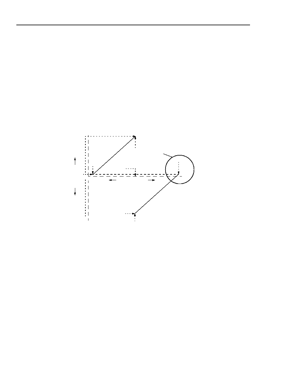
106
106
Lucent Technologies Inc.
Advance Data Sheet
November 1999
H.100/H.110 Interfaces and Time-Slot Interchangers
Ambassador T8100A, T8102, and T8105
Appendix B. Minimum Delay and Con-
stant Delay Connections
(continued)
B.2 Delay Type Definitions
(continued)
B.2.3 Mixed Minimum/Constant Delay
An interesting mix of delays occurs when the individual
FME bits are overridden and a chip-wide selection for
FME is used. In short, when these devices are placed
in this mode, and when register bits CON[1:0] = 10, for-
ward connections provide minimum delay, reverse con-
nections provide constant delay. When CON[1:0] = 11,
reverse connections provide minimum delay, forward
connections provide constant delay. The latter is inter-
esting because, graphically, the TS
to latency map-
ping appears as a linear monotonic function covering
255 time slots. (Graphs are in the section which fol-
lows.) The latency equations follow:
CON[1:0] = 10:
Forward Connections: L = TS
(3
TS
127).
Reverse Connections: L = 256 + TS
(≠127
TS
0).
CON[1:0] = 11:
Forward and Reverse: L = 128 + TS
(≠125
TS
127).
Table 83, Table of Special Cases (Exceptions), applies
to the mixed delays in a similar manner. Simply use bit
0 of CON for the FME value in Table 83.
5-6225(F)
Figure 41. Mixed Minimum/Constant Delay Connections, CON[1:0 = 10]
A
PPL
IED DE
L
T
A
(
T
I
M
E SL
O
T
S)
RESULTING LATENCY
≠127
0
127
127
256
(TIME SLOTS)
FM
E =
0
FM
E =
0
0
≠127
258
2
2
129
SPECIAL LONG LATENCY
CONNECTIONS
(SEE TEXT)
128
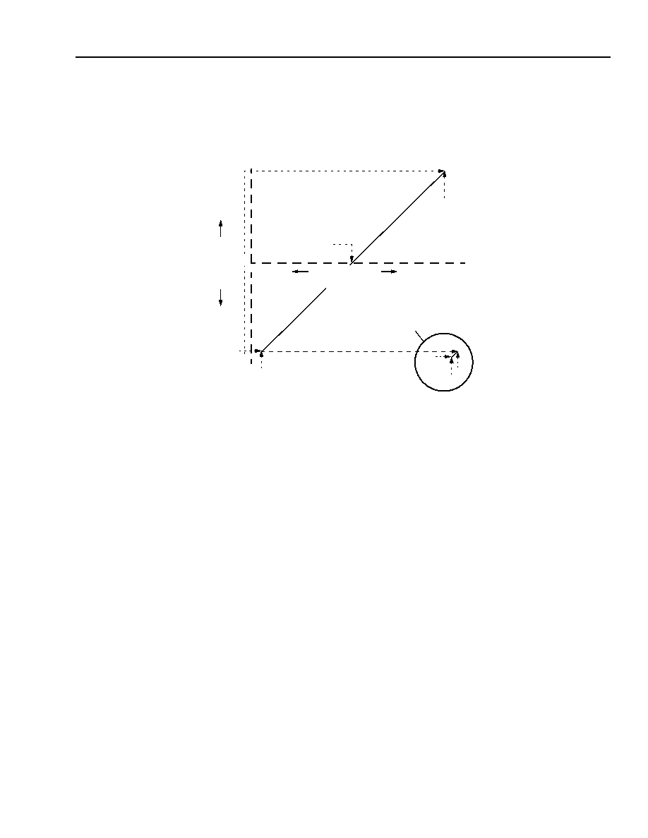
Lucent Technologies Inc.
107
Advance Data Sheet
November 1999
H.100/H.110 Interfaces and Time-Slot Interchangers
Ambassador T8100A, T8102, and T8105
Appendix B. Minimum Delay and Constant Delay Connections
(continued)
B.2 Delay Type Definitions
(continued)
B.2.3 Mixed Minimum/Constant Delay (continued)
5-6226(F)
Figure 42. Extended Linear (Mixed Minimum/Constant) Delay, CON[1:0] = 11
Appendix C. CAM Readback and Pattern Fill Mode
Reading back local data memories (AMR = 0x01, 0x02), local connection memory (AMR = 0x05), or H.100 data
memories (AMR = 0x90, 0xA0) simply yields whatever the expected pattern is. When reading back the CAM con-
tents, however, there is some bit manipulation involved.
AP
PL
I
E
D DEL
T
A
(
T
I
M
E SL
O
T
S
)
0
127
255
256
FM
E =
1
0
≠126
257
128
2
SPECIAL LONG LATENCY
CONNECTIONS
(SEE TEXT)
258
≠127
RESULTING LATENCY
(TIME SLOTS)

Lucent Technologies Inc. reserves the right to make changes to the product(s) or information contained herein without notice. No liability is assumed as a result of their use or application. No
rights under any patent accompany the sale of any such product(s) or information.
Ambassador is a trademark of Lucent Technologies Inc.
Copyright © 1999 Lucent Technologies Inc.
All Rights Reserved
November 1999
DS00-028CTI (Replaces DS98-387NTNB, DA99-002NTNB, DA99-003NTNB)
For additional information, contact your Microelectronics Group Account Manager or the following:
INTERNET: http://www.lucent.com/micro
E-MAIL: docmaster@micro.lucent.com
N. AMERICA:
Microelectronics Group, Lucent Technologies Inc., 555 Union Boulevard, Room 30L-15P-BA, Allentown, PA 18103
1-800-372-2447, FAX 610-712-4106 (In CANADA: 1-800-553-2448, FAX 610-712-4106)
ASIA PACIFIC: Microelectronics Group, Lucent Technologies Singapore Pte. Ltd., 77 Science Park Drive, #03-18 Cintech III, Singapore 118256
Tel. (65) 778 8833, FAX (65) 777 7495
CHINA: Microelectronics Group, Lucent Technologies (China) Co., Ltd., A-F2, 23/F, Zao Fong Universe Building, 1800 Zhong Shan Xi Road, Shanghai
200233 P. R. China Tel. (86) 21 6440 0468, ext. 316, FAX (86) 21 6440 0652
JAPAN: Microelectronics Group, Lucent Technologies Japan Ltd., 7-18, Higashi-Gotanda 2-chome, Shinagawa-ku, Tokyo 141, Japan
Tel. (81) 3 5421 1600, FAX (81) 3 5421 1700
EUROPE: Data Requests: MICROELECTRONICS GROUP DATALINE: Tel. (44) 7000 582 368, FAX (44) 1189 328 148
Technical Inquiries: GERMANY: (49) 89 95086 0 (Munich), UNITED KINGDOM: (44) 1344 865 900 (Ascot),
FRANCE: (33) 1 40 83 68 00 (Paris), SWEDEN: (46) 8 594 607 00 (Stockholm), FINLAND: (358) 9 4354 2800 (Helsinki),
ITALY: (39) 02 6608131 (Milan), SPAIN: (34) 1 807 1441 (Madrid)