 | –≠–ª–µ–∫—Ç—Ä–æ–Ω–Ω—ã–π –∫–æ–º–ø–æ–Ω–µ–Ω—Ç: T-8110L | –°–∫–∞—á–∞—Ç—å:  PDF PDF  ZIP ZIP |

Data Sheet
February 2004
Ambassador
Æ
T8110L H.100/H.110 Switch
1 Introduction
The T8110L is the newest addition to the Ambassa-
dor series of TDM switching and backlane intercon-
nect standard products. The T8110L can switch 4096
simultaneous time slots with 32 bidirectional local
streams and 32 bidirectional H.100/H.110 streams.
The T8110L has all the features of the T810X
devices. Additionally, the T8110L has more robust
clocking fallback abilities and is pin compatible with
the T8110. (The full version of the T8110 has a PCI
and minbridge interface.)
1.1 Features
!
4,096-connection unified switch
!
Full H.100/H.110 support (32 data lines, all clock
modes)
!
32 local I/O lines (2, 4, 8, or 16 Mbits/s)
!
Microprocessor interface: Motorola
Æ
/Intel
Æ
modes
!
Interrupt controller with external inputs
!
Eight independent general-purpose I/O lines
!
Eight independently programmed framing signals
!
Four local clocks
!
T1/E1 rate adaptation
!
Two clock-fallback modes
!
Stratum 4/4E and AT&T
Æ
62411 MTIE compliant
!
Incorporates 38 H.100 and 34 H.110 termination
resistors
!
Subrate switching of 4 bits, 2 bits, or 1 bit
!
Backward compatible to all T810x devices
!
Pin compatible with T8110
!
JTAG/boundary-scan testing support
!
BSDL files available
!
Assists H.110 hot swap
!
Single 3.3 V supply with 5 V tolerant inputs and
TTL compatible outputs
!
272 PBGA package
!
Evaluation boards available

Table of Contents
Contents
Page
2
Agere Systems Inc.
Data Sheet
February 2004
Ambassador T8110L H.100/H.110 Switch
1
Introduction ......................................................................................................................................................... 1
1.1
Features.................................................................................................................................................... 1
2
Pin Description ..................................................................................................................................................10
2.1
Interface Signals .....................................................................................................................................10
2.2
T8110L Pinout Information ..................................................................................................................... 12
2.3
Special Buffer Requirements .................................................................................................................. 20
2.3.1
H1x0 Bus Signal Internal Pull-Up/Pull-Down .............................................................................. 20
2.3.2
Local Bus Signal Internal Pull-Up ...............................................................................................20
3
Main Architectural Features .............................................................................................................................. 21
3.1
T8110L Architecture ............................................................................................................................... 21
4
Microprocessor Interface .................................................................................................................................. 22
4.1
Intel/Motorola Protocol Selector.............................................................................................................. 22
4.2
Word/Byte Addressing Selector.............................................................................................................. 22
4.3
Access Via the Microprocessor Bus ....................................................................................................... 23
4.3.1
Microprocessor Interface Register Map ...................................................................................... 24
4.3.2
Register Space Access ............................................................................................................... 28
4.3.3
Connection Memory Space Access ............................................................................................ 28
4.3.4
Data Memory Space Access....................................................................................................... 29
5
Operating Control and Status ........................................................................................................................... 30
5.1
Control Registers .................................................................................................................................... 30
5.1.1
Reset Registers .......................................................................................................................... 30
5.1.2
Master Output Enable Register................................................................................................... 31
5.1.3
Connection Control--Data Memory Selector Register ...............................................................32
5.1.4
General Clock Control (Phase Alignment, Fallback, Watchdogs) Register ................................ 33
5.1.5
Phase Alignment Select Register ...............................................................................................33
5.1.6
Fallback Control Register............................................................................................................33
5.1.7
Fallback Type Select Register .................................................................................................... 34
5.1.8
Fallback Trigger Registers .......................................................................................................... 35
5.1.9
Watchdog Select, C8, and NETREF Registers........................................................................... 36
5.1.10 Watchdog EN Register ............................................................................................................... 37
5.1.11 Failsafe Control Registers........................................................................................................... 38
5.2
Error and Status Registers ..................................................................................................................... 39
5.2.1
Clock Errors ................................................................................................................................ 40
5.2.1.1
Transient Clock Errors Registers................................................................................. 40
5.2.1.2
Latched Clock Error Register ...................................................................................... 41
5.2.2
System Status ............................................................................................................................. 42
5.2.2.1
Clock Fallback Status Register.................................................................................... 42
5.2.2.2
Device Identification Registers .................................................................................... 43
5.2.2.3
System Device Errors.................................................................................................. 43
6
Clock Architecture ............................................................................................................................................. 44
6.1
Clock Input Control Registers ................................................................................................................. 45
6.1.1
Main Input Selector Register....................................................................................................... 45
6.1.2
Main Divider Register.................................................................................................................. 46
6.1.3
Analog PLL1 (APLL1) Input Selector Register............................................................................46
6.1.4
APLL1 Rate Register .................................................................................................................. 47
6.1.5
Main Inversion Select Register ................................................................................................... 47
6.1.6
Resource Divider Register .......................................................................................................... 48
6.1.7
Analog PLL2 (APLL2) Rate Register .......................................................................................... 48
6.1.8
LREF Input Select Registers....................................................................................................... 49
6.1.9
DPLL1 Input Selector .................................................................................................................. 50

Table of Contents
(continued)
Contents
Page
Agere Systems Inc.
3
February 2004
Ambassador T8110L H.100/H.110 Switch
Data Sheet
6.1.9.1
DPLL1 Rate Register...................................................................................................50
6.1.10 DPLL2 Input Selector ..................................................................................................................50
6.1.10.1 DPLL2 Rate Register...................................................................................................51
6.1.11 NETREF1 Registers....................................................................................................................51
6.1.12 NETREF2 Registers....................................................................................................................52
6.2
Clock Output Control Registers ..............................................................................................................53
6.2.1
Master Output Enables Register .................................................................................................53
6.2.2
Clock Output Format Registers...................................................................................................54
6.2.3
TCLK and L_SCx Select Registers .............................................................................................55
6.3
Clock Register Access............................................................................................................................57
6.4
Clock Circuit Operation--APLL1 ............................................................................................................57
6.4.1
Main Clock Selection, Bit Clock, and Frame ...............................................................................57
6.4.1.1
Watchdog Timers ........................................................................................................58
6.4.1.2
Frame Center Sampling ..............................................................................................59
6.4.1.3
LREF Pair Polarity Configuration.................................................................................60
6.4.2
Main and Resource Dividers .......................................................................................................61
6.4.3
DPLL1 .........................................................................................................................................61
6.4.4
Reference Selector .....................................................................................................................61
6.4.5
Internal Clock Generation ...........................................................................................................61
6.4.5.1
Phase Alignment .........................................................................................................62
6.5
Clock Circuit Operation, APLL2 ..............................................................................................................63
6.5.1
DPLL2 .........................................................................................................................................63
6.6
Clock Circuit Operation, CT_NETREF Generation.................................................................................63
6.6.1
NETREF Source Select ..............................................................................................................63
6.6.2
NETREF Divider..........................................................................................................................63
6.7
Clock Circuit Operation--Fallback and Failsafe .....................................................................................64
6.7.1
Clock Fallback.............................................................................................................................64
6.7.1.1
Fallback Events ...........................................................................................................64
6.7.1.2
Fallback Scenarios--Fixed vs. Rotating Secondary....................................................65
6.7.1.3
H-Bus Clock Enable/Disable on Fallback ....................................................................68
6.7.2
Clock Failsafe .............................................................................................................................70
6.7.2.1
Failsafe Events ............................................................................................................70
7
Frame Group and FG I/O ..................................................................................................................................72
7.1
Frame Group Control Registers..............................................................................................................72
7.1.1
FGx Lower and Upper Start Registers ........................................................................................72
7.1.2
FGx Width Registers ...................................................................................................................73
7.1.3
FGx Rate Registers ....................................................................................................................73
7.2
FG7 Timer Option ...................................................................................................................................74
7.2.1
FG7 Counter (Low and High Byte) Registers..............................................................................74
7.3
FGIO Control Registers ..........................................................................................................................75
7.3.1
FGIO Data Register ....................................................................................................................75
7.3.2
FGIO Read Mask Register..........................................................................................................75
7.3.3
FGIO R/W Register .....................................................................................................................76
7.4
FG Circuit Operation...............................................................................................................................77
7.4.1
Frame Group 8 kHz Reference Generation ................................................................................78
7.4.2
FGIO General-Purpose Bits ........................................................................................................79
7.4.3
Programmable Timer (FG7 Only)................................................................................................79
7.4.4
FG External Interrupts.................................................................................................................79
7.4.5
FG Diagnostic Test Point Observation........................................................................................79
8
General-Purpose I/O .........................................................................................................................................80
8.1
GPIO Control Registers ..........................................................................................................................80

Table of Contents
(continued)
Contents
Page
4
Agere Systems Inc.
Data Sheet
February 2004
Ambassador T8110L H.100/H.110 Switch
8.1.1
GPIO Data Register .................................................................................................................... 80
8.1.2
GPIO Read Mask Register ......................................................................................................... 81
8.1.3
GPIO R/W Register..................................................................................................................... 81
8.1.4
GPIO Override Register .............................................................................................................. 82
8.2
GP Circuit Operation............................................................................................................................... 82
8.2.1
GPIO General-Purpose Bits........................................................................................................ 83
8.2.2
GP Dual-Purpose Bits GPIO (Override)...................................................................................... 83
8.2.2.1
GP H.110 Clock Master Indicators (GP0, GP1 Only) ..................................................83
8.2.3
GP External Interrupts ................................................................................................................ 83
8.2.4
GP Diagnostic Test Point Observation ....................................................................................... 83
9
Stream Rate Control ......................................................................................................................................... 84
9.1
H-Bus Stream Rate Control Registers.................................................................................................... 85
9.1.1
H-Bus Rate Registers ................................................................................................................. 85
9.2
L-Bus Stream Rate Control Registers .................................................................................................... 85
9.2.1
L-Bus Rate Registers .................................................................................................................. 85
9.2.2
L-Bus 16.384 Mbits/s Operation ................................................................................................. 86
9.2.3
16.384 Mbits/s Local I/O Superrate ............................................................................................ 88
9.2.4
16.384 Mbits/s Local I/O Superrate ............................................................................................ 89
10 Error Reporting and Interrupt Control ............................................................................................................... 90
10.1
Interrupt Control Registers...................................................................................................................... 90
10.1.1 Interrupts Via External FG[7:0] Registers ................................................................................... 90
10.1.1.1 FGIO Interrupt Pending Register................................................................................. 90
10.1.2 Interrupts Via External GP[7:0] ................................................................................................... 92
10.1.2.1 GPIO Interrupt Pending Register................................................................................. 92
10.1.2.2 GPIO Edge/Level and GPIO Polarity Registers .......................................................... 93
10.1.3 Interrupts Via Internal System Errors .......................................................................................... 93
10.1.4 System Interrupt Pending High/Low Registers ........................................................................... 94
10.1.5 System Interrupt Enable High/Low Registers ............................................................................. 95
10.1.6 Interrupts Via Internal Clock Errors ............................................................................................. 96
10.1.7 Clock Interrupt Pending High/Low Registers .............................................................................. 97
10.1.8 Clock Interrupt Enable High/Low Registers ................................................................................ 98
10.1.9 Interrupt Servicing Registers....................................................................................................... 99
10.1.9.1 Arbitration Control Register .........................................................................................99
10.1.9.2 SYSERR and CLKERR Output Select Register .......................................................... 99
10.1.9.3 Interrupt In-Service Registers.................................................................................... 101
10.2
Error Reporting and Interrupt Controller Circuit Operation ...................................................................103
10.2.1 Externally Sourced Interrupts Via FG[7:0], GP[7:0] .................................................................. 104
10.2.2 Internally Sourced System Error Interrupts ............................................................................... 104
10.2.3 Internally Sourced Clock Error Interrupts .................................................................................. 104
10.2.4 Arbitration of Pending Interrupts ............................................................................................... 104
10.2.4.1 Arbitration Off ............................................................................................................ 104
10.2.4.2 Flat Arbitration ........................................................................................................... 104
10.2.4.3 Tier Arbitration ........................................................................................................... 104
10.2.4.4 Pre-Empting Disabled................................................................................................ 105
10.2.4.5 Pre-Empting Enabled ................................................................................................ 105
10.2.5 CLKERR Output........................................................................................................................ 105
10.2.6 SYSERR Output .......................................................................................................................105
10.2.7 System Handling of Interrupts................................................................................................... 105
11 Test and Diagnostics ...................................................................................................................................... 106
11.1
Diagnostics Control Registers .............................................................................................................. 106
11.1.1 FG Testpoint Enable Register................................................................................................... 106

Table of Contents
(continued)
Contents
Page
Agere Systems Inc.
5
February 2004
Ambassador T8110L H.100/H.110 Switch
Data Sheet
11.1.2 GP Testpoint Enable Register ..................................................................................................108
11.1.3 State Counter Modes Registers ................................................................................................110
11.1.4 Miscellaneous Diagnostics Low Register..................................................................................110
11.1.5 Miscellaneous Diagnostic Registers .........................................................................................111
11.2
Diagnostic Circuit Operation .................................................................................................................112
12 Connection Control .........................................................................................................................................113
12.1
Programming Interface .........................................................................................................................113
12.1.1 Connection Memory Programming ...........................................................................................113
12.2
Switching Operation..............................................................................................................................115
12.2.1 Memory Architecture and Configuration....................................................................................115
12.2.1.1 Connection Memory ..................................................................................................115
12.2.1.2 Data Memory .............................................................................................................116
12.2.2 Standard Switching ...................................................................................................................117
12.2.2.1 Constant Delay and Minimum Delay Connections ....................................................117
12.2.2.2 Pattern Mode .............................................................................................................117
12.2.2.3 Subrate ......................................................................................................................117
13 Electrical Characteristics.................................................................................................................................124
13.1
Absolute Maximum Ratings ..................................................................................................................124
13.1.1 Handling Precautions ................................................................................................................124
13.2
Crystal Specifications ...........................................................................................................................124
13.2.1 XTAL1 Crystal ...........................................................................................................................124
13.2.2 XTAL2 Crystal ...........................................................................................................................125
13.2.3 Reset Pulse...............................................................................................................................126
13.3
Thermal Parameters (Definitions and Values)......................................................................................126
13.4
Reliability ..............................................................................................................................................127
13.5
dc Electrical Characteristics..................................................................................................................128
13.5.1 Electrical Drive Specifications, CT_C8 and /CT_FRAME .........................................................128
13.5.2 All Other Pins ............................................................................................................................129
13.6
H-Bus Timing ........................................................................................................................................129
13.6.1 Timing Diagrams .......................................................................................................................129
13.7
ac Electrical Characteristics..................................................................................................................130
13.7.1 Skew Timing, H-Bus..................................................................................................................130
13.8
Hot Swap ..............................................................................................................................................131
13.8.1 LPUE (Local Pull-Up Enable)....................................................................................................131
13.9
Decoupling............................................................................................................................................131
13.10 APLL V
DD
Filter ....................................................................................................................................132
13.11 PC Board PBGA Considerations ..........................................................................................................133
13.12 Unused Pins .........................................................................................................................................133
13.13 External Pull-Up Pins............................................................................................................................133
13.14 T8110L Evaluation Kits.........................................................................................................................133
13.15 T8110L Ordering Information................................................................................................................133
14 JTAG/Boundary Scan .....................................................................................................................................137
14.1
The Principle of Boundary-Scan Architecture.......................................................................................137
14.1.1 Instruction Register ...................................................................................................................138
14.2
Boundary-Scan Register.......................................................................................................................138
A
Constant and Minimum Delay Connections ....................................................................................................139
A.1
Connection Definitions..........................................................................................................................139
A.2
Delay Type Definitions..........................................................................................................................139
B
Register Bit Field Mnemonic Summary...........................................................................................................142
Significant Changes Between the June 2003 and November 2003 Release ........................................................163

List of Figures
Figure
Page
6
Agere Systems Inc.
Ambassador T8110L H.100/H.110 Switch
February 2004
Data Sheet
Figure 1.
T8110L Pull-Up/Pull-Down Arrangement for H1x0 Pins ....................................................................... 20
Figure 2.
T8110L Architecture Block Diagram ..................................................................................................... 21
Figure 3.
Microprocessor Access Timing, Intel Protocol ...................................................................................... 26
Figure 4.
Microprocessor Access Timing, Motorola Protocol ............................................................................... 27
Figure 5.
T8110L Main Clocking Paths ................................................................................................................ 44
Figure 6.
T8110L NETREF Paths ........................................................................................................................ 44
Figure 7.
T8110L Required Frame Pulse and Bit Clock with Polarities ............................................................... 60
Figure 8.
T8110L Phase Alignment, SNAP and SLIDE ....................................................................................... 62
Figure 9.
Fallback--Fixed vs. Rotating Secondary .............................................................................................. 65
Figure 10. T8110L Clock Fallback States .............................................................................................................. 66
Figure 11. T8110L H-Bus Clock Enable States ..................................................................................................... 68
Figure 12. T8110L Clock Failsafe States ............................................................................................................... 70
Figure 13. FG[7:0] Functional Paths ...................................................................................................................... 77
Figure 14. Frame Group 8 kHz Reference Timing ................................................................................................. 78
Figure 15. GP[7:0] Functional Paths ...................................................................................................................... 82
Figure 16. Local Stream 16.384 Mbits/s Timing..................................................................................................... 86
Figure 17. Local Stream 16.384 Mbits/s Circuit ..................................................................................................... 87
Figure 18. Superrate I/O Configuration .................................................................................................................. 88
Figure 19. Relationship Between 8.192 Mbits/s and 16.384 Mbits/s Time Slots ................................................... 89
Figure 20. Interrupt Controller .............................................................................................................................. 103
Figure 21. Microprocessor Programming--Reset Page Command ..................................................................... 114
Figure 22. Microprocessor Programming--Make/Break/Query Telephony Connections..................................... 114
Figure 23. T8110L Data Memory Map and Configurations .................................................................................. 116
Figure 24. TDM Data Stream Bit Rates ............................................................................................................... 118
Figure 25. Subrate Switching Example, Byte Packing ......................................................................................... 121
Figure 26. Subrate Switching Example, Byte Unpacking ..................................................................................... 123
Figure 27. Clock Alignment .................................................................................................................................. 129
Figure 28. Frame Timing Diagram ....................................................................................................................... 130
Figure 29. Detailed Clock Skew Timing Diagram................................................................................................. 130
Figure 30. APLL V
DD
Filtering .............................................................................................................................. 132
Figure 31. T8110L Pins by Functional Group ...................................................................................................... 134
Figure 32. IEEE
Æ
1149.1 Boundary-Scan Architecture ........................................................................................ 137
Figure 33. Constant Delay Connection Latency................................................................................................... 140
Figure 34. Minimum Delay Connection Latency .................................................................................................. 141

List of Tables
Table
Page
Agere Systems Inc.
7
February 2004
Ambassador T8110L H.100/H.110 Switch
Data Sheet
Table 1.
Microprocessor Interface Signals ..........................................................................................................10
Table 2.
H-Bus (H.100/H.110 Interface) Signals .................................................................................................10
Table 3.
L-Bus (Local) Interface Signals .............................................................................................................10
Table 4.
Clock Circuit Interface Signals ..............................................................................................................11
Table 5.
GPIO Interface Signals..........................................................................................................................11
Table 6.
Miscellaneous Interface Signals ............................................................................................................11
Table 7.
JTAG Signals ........................................................................................................................................11
Table 8.
T8110L Pinouts .....................................................................................................................................13
Table 9.
Intel/Motorola Protocol Selector ............................................................................................................22
Table 10. T8110L Memory Mapping to Microprocessor Space.............................................................................23
Table 11. Microprocessor Interface Register Map ................................................................................................24
Table 12. Register Space Access Timing .............................................................................................................28
Table 13. Connection Memory Space Access Timing...........................................................................................28
Table 14. Data Memory Space Access Timing .....................................................................................................29
Table 15. Control Register Map ............................................................................................................................30
Table 16. Reset Registers .....................................................................................................................................31
Table 17. Master Output Enable Register .............................................................................................................32
Table 18. Data Memory Mode Select Register .....................................................................................................32
Table 19. Clock Register Access Select Register .................................................................................................33
Table 20. Phase Alignment Select Register ..........................................................................................................33
Table 21. Fallback Control Register ......................................................................................................................34
Table 22. Fallback Type Select Register...............................................................................................................35
Table 23. Fallback Trigger Registers ....................................................................................................................35
Table 24. Watchdog Select, C8, NETREF Registers ............................................................................................36
Table 25. Watchdog EN Registers ........................................................................................................................37
Table 26. Failsafe Control Register .......................................................................................................................38
Table 27. Error and Status Register Map ..............................................................................................................39
Table 28. Clock Error Registers ............................................................................................................................40
Table 29. Latched Clock Error Registers ..............................................................................................................41
Table 30. Fallback and Failsafe Status Register ...................................................................................................42
Table 31. System Errors Registers .......................................................................................................................43
Table 32. Device Identification Registers ..............................................................................................................43
Table 33. Clock Input Control Register Map .........................................................................................................45
Table 34. Main Input Selector Register .................................................................................................................45
Table 35. Main Divider Register ............................................................................................................................46
Table 36. APLL1 Input Selector Register ..............................................................................................................46
Table 37. APLL1 Rate Register.............................................................................................................................47
Table 38. Main Inversion Select Register..............................................................................................................47
Table 39. Resource Divider Register ....................................................................................................................48
Table 40. APLL2 Rate Register.............................................................................................................................48
Table 41. LREF Input/Inversion Select Registers .................................................................................................49
Table 42. DPLL1 Input Selector Registers ............................................................................................................50
Table 43. DPLL2 Register .....................................................................................................................................51
Table 44. NETREF1 Registers ..............................................................................................................................51
Table 45. NETREF2 Registers ..............................................................................................................................52
Table 46. Clock Output Control Register Map.......................................................................................................53
Table 47. Master Output Enables Registers .........................................................................................................54
Table 48. Clock Output Format Registers .............................................................................................................55
Table 49. TCLK Select and L_SCx Select Registers ............................................................................................56
Table 50. Bit Clock and Frame ..............................................................................................................................57

List of Tables
(continued)
Table
Page
8
Agere Systems Inc.
Data Sheet
February 2004
Ambassador T8110L H.100/H.110 Switch
Table 51. Watchdog Timer Description ................................................................................................................. 58
Table 52. Frame Center Sampling ........................................................................................................................ 59
Table 53. Legacy Mode Fallback Event Triggers .................................................................................................. 65
Table 54. Clock Fallback State Description........................................................................................................... 67
Table 55. H-Bus Clock Enable State Description .................................................................................................. 69
Table 56. Clock Failsafe State Descriptions.......................................................................................................... 71
Table 57. Frame Group and FG I/O Register Map ................................................................................................ 72
Table 58. FGx Lower and Upper Start Registers .................................................................................................. 72
Table 59. FGx Width Registers ............................................................................................................................. 73
Table 60. FGx Rate Registers ............................................................................................................................... 73
Table 61. FG7 Counter (Low and High Byte) Registers ........................................................................................ 74
Table 62. FGIO Data Register............................................................................................................................... 75
Table 63. FGIO Read Mask Register .................................................................................................................... 75
Table 64. FGIO R/W Register ............................................................................................................................... 76
Table 65. GPIO Register ....................................................................................................................................... 80
Table 66. GPIO Data Register .............................................................................................................................. 80
Table 67. GPIO Read Mask Register.................................................................................................................... 81
Table 68. GPIO R/W Register ............................................................................................................................... 81
Table 69. GPIO Override Register ........................................................................................................................ 82
Table 70. T8110L Serial Stream Groupings.......................................................................................................... 84
Table 71. H-Bus Rate Registers............................................................................................................................ 85
Table 72. L-Bus Rate Registers ............................................................................................................................ 85
Table 73. Interrupt Control Register Map .............................................................................................................. 90
Table 74. FGIO Interrupt Pending Registers......................................................................................................... 90
Table 75. FGIO Edge/Level and Polarity Registers .............................................................................................. 91
Table 76. GPIO Interrupt Pending Register .......................................................................................................... 92
Table 77. GPIO Edge/Level and GPIO Polarity Registers .................................................................................... 93
Table 78. System Error Interrupt Assignments ..................................................................................................... 93
Table 79. System Interrupt Pending High/Low Registers...................................................................................... 94
Table 80. System Interrupt Enable High/Low Registers........................................................................................ 95
Table 81. Clock Error Interrupt Assignments ........................................................................................................ 96
Table 82. Clock Interrupt Pending High/Low Registers.........................................................................................97
Table 83. Clock Interrupt Enable High/Low Registers........................................................................................... 98
Table 84. Arbitration Control Register ...................................................................................................................99
Table 85. SYSERR Output Select Registers....................................................................................................... 100
Table 86. Interrupt In-Service Register ............................................................................................................... 101
Table 87. Diagnostics Control Register Map ....................................................................................................... 106
Table 88. FG Testpoint Enable Registers ........................................................................................................... 106
Table 89. FG[7:0] Internal Testpoint Assignments .............................................................................................. 107
Table 90. Testpoint Enable Registers .................................................................................................................108
Table 91. GP[7:0] Internal Testpoint Assignments.............................................................................................. 109
Table 92. State Counter Modes Registers ..........................................................................................................110
Table 93. Miscellaneous Diagnostics Low Register ............................................................................................ 110
Table 94. Miscellaneous Diagnostic Registers....................................................................................................111
Table 95. Microprocessor Programming, Connection Memory Access .............................................................. 113
Table 96. TDM Data Stream ............................................................................................................................... 118
Table 97. Subrate Switching, Data Propagation Rate vs. Channel Capacity ...................................................... 119
Table 98. Subrate Switching, Connection Memory Programming Setup ............................................................ 120
Table 99. Absolute Maximum Ratings.................................................................................................................124
Table 100. XTAL1 Specifications .......................................................................................................................... 124

List of Tables
(continued)
Table
Page
Agere Systems Inc.
9
February 2004
Ambassador T8110L H.100/H.110 Switch
Data Sheet
Table 101. 16.384 MHz Oscillator Requirements..................................................................................................125
Table 102. XTAL2 Specifications ..........................................................................................................................125
Table 103. 6.176 MHz/12.352 MHz Oscillator Requirements ...............................................................................125
Table 104. Reset Pulse .........................................................................................................................................126
Table 105. Thermal Parameter Values..................................................................................................................127
Table 106. Reliability Data.....................................................................................................................................127
Table 107. Electrical Drive Specifications, CT_C8 and /CT_FRAME....................................................................128
Table 108. dc Electrical Characteristics, All Other Pins ........................................................................................129
Table 109. Skew Timing, H-Bus ............................................................................................................................130
Table 110. L_SC[3:0] and Frame Group Rise and Fall Time ................................................................................131
Table 111. T8110L Ordering Information ..............................................................................................................133
Table 112. Instruction Register..............................................................................................................................138
Table 113. Special Cases (Exceptions).................................................................................................................141
Table 114. Mnemonic Summary, Sorted by Name................................................................................................143
Table 115. Mnemonic Summary, Sorted by Register............................................................................................153
Table 116. Changes ..............................................................................................................................................163
10
10
Agere Systems Inc.
Data Sheet
February 2004
Ambassador T8110L H.100/H.110 Switch
2 Pin Description
2.1 Interface Signals
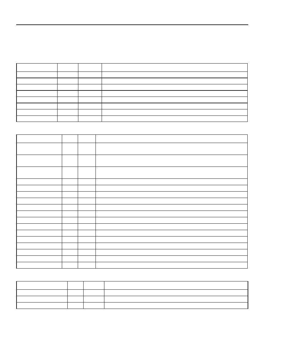
Table 1. Microprocessor Interface Signals
Signal
I/O
Width
Microprocessor Interface Function
A
I
20
Address[19:0] in.
D
I/O
16
Data bus in/out.
RD# (DS#)
I
1
RDn(DSn) in.
WR# (R/W#)
I
1
WRn(R/Wn) in.
CSN
I
1
CSn in.
WB_SEL
I
1
Word/byte select in.
RDY (DTACK#)
Out
1
RDY(DTACKn) out.
IM_SEL
I
1
Intel/Motorola select in.
Table 2. H-Bus (H.100/H.110 Interface) Signals
Signal
I/O
Width
Function
VPRECHARGE
In
1
Precharge voltage for pull-downs, H.110 bus signals:
CT_D, CT_NETREF1, CT_NETREF2.
H110_ENABLE
In
1
Pull-down enable for H.110 bus signals: CT_D, CT_NETREF1,
CT_NETREF2.
H100_ENABLE
In
1
Pull-up enable for H.100 bus signals: CT_D, CT_NETREF1,
CT_NETREF2, CT_C8_A, CT_C8_B, /CT_FRAME_A, /CT_FRAME_B.
CT_D
I/O
32
H.100/H.110 bus data.
CT_C8_A
I/O
1
H.100/H.110 bit clock A.
/CT_FRAME_A
I/O
1
H.100/H.110 frame reference A.
CT_C8_B
I/O
1
H.100/H.110 bit clock B.
/CT_FRAME_B
I/O
1
H.100/H.110 frame reference B.
CT_NETREF1
I/O
1
H.100/H.110 network reference 1.
CT_NETREF2
I/O
1
H.100/H.110 network reference 2.
/C16+
I/O
1
H-MVIPTM compatibility clock (16.384 MHz, differential).
/C16≠
I/O
1
H-MVIP compatibility clock (16.384 MHz, differential).
/C4
I/O
1
MVIP compatibility clock (4.096 MHz).
C2
I/O
1
MVIP compatibility clock (2.048 MHz).
SCLK
I/O
1
SC-bus compatibility clock.
/SCLKx2
I/O
1
SC-bus compatibility clock.
/FR_COMP
I/O
1
Compatibility frame reference.
Table 3. L-Bus (Local) Interface Signals
Signal
I/O
Width
Function
L_D
I/O
32
Local bus data.
L_SC
Out
4
Local bus clock outputs.
FG
I/O
8
Local frame groups.
Agere Systems Inc.
11
Data Sheet
February 2004
Ambassador T8110L H.100/H.110 Switch
2 Pin Description
(continued)
2.1 Interface Signals
(continued)
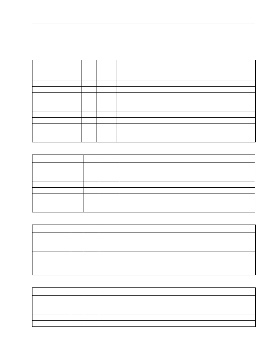
Table 4. Clock Circuit Interface Signals
Signal
I/O
Width
Function
XTAL1_IN
In
1
Crystal oscillator #1 input (16.384 MHz).
XTAL1_OUT
Out
1
Crystal oscillator #1 feedback.
XTAL2_IN
In
1
Crystal oscillator #2 input (6.176 MHz or 12.352 MHz).
XTAL2_OUT
Out
1
Crystal oscillator #2 feedback.
LREF
In
8
Local clock reference inputs.
TCLK_OUT
Out
1
Internal chip clock output.
PRI_REF_OUT
Out
1
Main divider reference out for CLAD/DJAT.
PRI_REF_IN
In
1
CLAD/DJAT reference in for APLL1.
NR1_SEL_OUT
Out
1
CT_NETREF1 selection out for CLAD/DJAT.
NR1_DIV_IN
In
1
CLAD/DJAT reference in for CT_NETREF1 divider.
NR2_SEL_OUT
Out
1
CT_NETREF2 selection out for CLAD/DJAT.
NR2_DIV_IN
In
1
CLAD/DJAT reference in for CT_NETREF2 divider.
Table 5. GPIO Interface Signals
Signal
I/O
Width
GPIO Function
Alternate Function
GP0
I/O
1
GPIO bit 0 I/O
A-master indicator out.
GP1
I/O
1
GPIO bit 1 I/O
B-master indicator out.
GP2
I/O
1
GPIO bit 2 I/O
--
GP3
I/O
1
GPIO bit 3 I/O
--
GP4
I/O
1
GPIO bit 4 I/O
--
GP5
I/O
1
GPIO bit 5 I/O
--
GP6
I/O
1
GPIO bit 6 I/O
--
GP7
I/O
1
GPIO bit 7 I/O
--
Table 6. Miscellaneous Interface Signals
Signal
I/O
Width
Function
RESET#
In
1
Chip reset.
SYSERR
Out
1
System error indicator.
CLKERR
Out
1
Clocking error indicator.
LPUE
In
1
Pull-up enable for signals: FG, GP, L_D, LREF, D, NR1_DIV_IN, NR2_DIV_IN,
PRI_REF_IN.
PEN
In
1
Reserved. Must be left unconnected.
TESTMODE
In
1
Reserved. Must be left unconnected.
Table 7. JTAG Signals
Signal
I/O
Width
Function
TRST#
In
1
JTAG reset.
TCK
In
1
JTAG clock.
TMS
In
1
JTAG mode select.
TDI
In
1
JTAG data in.
TDO
Out
1
JTAG data out.

12
Agere Systems Inc.
Data Sheet
February 2004
Ambassador T8110L H.100/H.110 Switch
2 Pin Description
(continued)
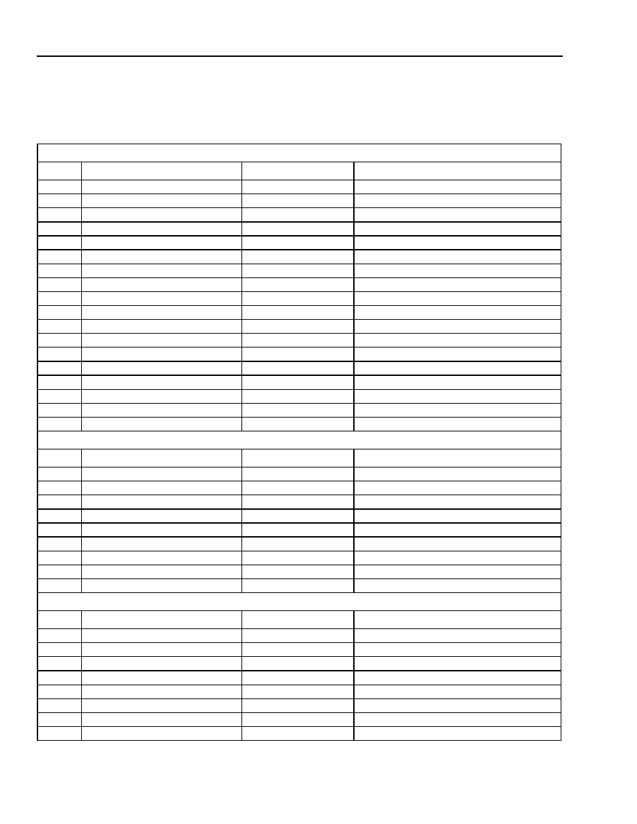
2.2 T8110L Pinout Information
The T8110L package is a 272-pin PBGA ball grid array. Refer to the table below for ball assignment, buffer type,
and pull-up/pull-down information.
Note: The pull-up/down column in the following table is defined as follows:
!
20 k
down--20 k
pull-down resistor is always in-circuit.
!
50 k
up--50 k
pull-up resistor is always in-circuit.
!
LPUE: 50 k
up--when LPUE = 1, a 50 k
pull-up resistor is in-circuit.
!
Enabled: 50 k
up/20 k
Vpre--when H100_ENABLE = 1, a 50 k
pull-up resistor is in-circuit (see Figure 1 on
page 20). When H110_ENABLE = 1, a 20 k
pull-down resistor from the VPRECHARGE input to this signal is in-
circuit.

Agere Systems Inc.
13
Data Sheet
February 2004
Ambassador T8110L H.100/H.110 Switch
2 Pin Description
(continued)
2.2 T8110L Pinout Information
(continued)
Table 8. T8110L Pinouts
Microprocessor Interface
Ball
Pin Name
Buffer Type
Pull-Up/Down (see note on page 12)
F1
A0
8 mA I/O-Schmitt
20 k
down
G1
A1
8 mA I/O-Schmitt
20 k
down
K3
A10
8 mA I/O-Schmitt
20 k
down
J3
A11
8 mA I/O-Schmitt
20 k
down
K1
A12
8 mA I/O-Schmitt
20 k
down
K2
A13
8 mA I/O-Schmitt
20 k
down
L3
A14
8 mA I/O-Schmitt
20 k
down
L4
A15
8 mA I/O-Schmitt
20 k
down
G2
A2
8 mA I/O-Schmitt
20 k
down
G3
A3
8 mA I/O-Schmitt
20 k
down
H1
A4
8 mA I/O-Schmitt
20 k
down
H2
A5
8 mA I/O-Schmitt
20 k
down
H3
A6
8 mA I/O-Schmitt
20 k
down
J4
A7
8 mA I/O-Schmitt
20 k
down
J1
A8
8 mA I/O-Schmitt
20 k
down
J2
A9
8 mA I/O-Schmitt
20 k
down
W1
D0
8 mA I/O-Schmitt
LPUE: 50 k
up
V1
D1
8 mA I/O-Schmitt
LPUE: 50 k
up
V2
D2
8 mA I/O-Schmitt
LPUE: 50 k
up
U3
D3
8 mA I/O-Schmitt
LPUE: 50 k
up
U1
D4
8 mA I/O-Schmitt
LPUE: 50 k
up
U2
D5
8 mA I/O-Schmitt
LPUE: 50 k
up
T3
D6
8 mA I/O-Schmitt
LPUE: 50 k
up
T4
D7
8 mA I/O-Schmitt
LPUE: 50 k
up
T1
D8
8 mA I/O-Schmitt
LPUE: 50 k
up
T2
D9
8 mA I/O-Schmitt
LPUE: 50 k
up
R3
D10
8 mA I/O-Schmitt
LPUE: 50 k
up
P4
D11
8 mA I/O-Schmitt
LPUE: 50 k
up
R1
D12
8 mA I/O-Schmitt
LPUE: 50 k
up
R2
D13
8 mA I/O-Schmitt
LPUE: 50 k
up
P2
D14
8 mA I/O-Schmitt
LPUE: 50 k
up
P3
D15
8 mA I/O-Schmitt
LPUE: 50 k
up
N1
RD#(DS#)
8 mA I/O-Schmitt
LPUE: 50 k
up
P1
WR#(R/W#)
8 mA I/O-Schmitt
LPUE: 50 k
up
L1
A16
8 mA I/O-Schmitt
20 k
down
L2
A17
8 mA I/O-Schmitt
20 k
down
M1
A18
8 mA I/O-Schmitt
20 k
down
M2
A19
8 mA I/O-Schmitt
20 k
down
M3
CSN
8 mA I/O-Schmitt
LPUE: 50 k
up
M4
WB_SEL
8 mA I/O-Schmitt
LPUE: 50 k
up
N2
RDY(DTACK#)
8 mA 3-state
External pull-up required
N3
IM_SEL
8 mA I/O-Schmitt
LPUE: 50 k
up

14
Agere Systems Inc.
Data Sheet
February 2004
Ambassador T8110L H.100/H.110 Switch
2 Pin Description
(continued)
2.2 T8110L Pinout Information
(continued)
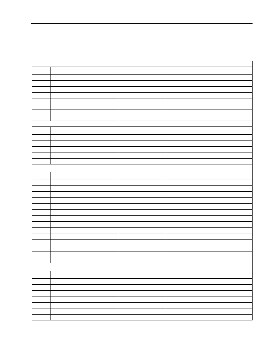
Table 8. T8110L Pinouts (continued)
H-Bus Interface
Ball
Pin Name
Buffer Type
Pull-Up/Down (see note on page 12)
C1
VPRECHARGE
Op amp noninvert
--
D5
H110_ENABLE
Input
20 k
down
D7
H100_ENABLE
Input
20 k
down
A11
CT_D0
PCI I/O
Enabled: 50 k
up/20 k
Vpre
B11
CT_D1
PCI I/O
Enabled: 50 k
up/20 k
Vpre
C10
CT_D2
PCI I/O
Enabled: 50 k
up/20 k
Vpre
C11
CT_D3
PCI I/O
Enabled: 50 k
up/20 k
Vpre
A10
CT_D4
PCI I/O
Enabled: 50 k
up/20 k
Vpre
B10
CT_D5
PCI I/O
Enabled: 50 k
up/20 k
Vpre
B9
CT_D6
PCI I/O
Enabled: 50 k
up/20 k
Vpre
C9
CT_D7
PCI I/O
Enabled: 50 k
up/20 k
Vpre
A9
CT_D8
PCI I/O
Enabled: 50 k
up/20 k
Vpre
B8
CT_D9
PCI I/O
Enabled: 50 k
up/20 k
Vpre
C8
CT_D10
PCI I/O
Enabled: 50 k
up/20 k
Vpre
A8
CT_D11
PCI I/O
Enabled: 50 k
up/20 k
Vpre
C7
CT_D12
PCI I/O
Enabled: 50 k
up/20 k
Vpre
A7
CT_D13
PCI I/O
Enabled: 50 k
up/20 k
Vpre
B7
CT_D14
PCI I/O
Enabled: 50 k
up/20 k
Vpre
C6
CT_D15
PCI I/O
Enabled: 50 k
up/20 k
Vpre
A6
CT_D16
PCI I/O
Enabled: 50 k
up/20 k
Vpre
B6
CT_D17
PCI I/O
Enabled: 50 k
up/20 k
Vpre
C5
CT_D18
PCI I/O
Enabled: 50 k
up/20 k
Vpre
A5
CT_D19
PCI I/O
Enabled: 50 k
up/20 k
Vpre
B5
CT_D20
PCI I/O
Enabled: 50 k
up/20 k
Vpre
A4
CT_D21
PCI I/O
Enabled: 50 k
up/20 k
Vpre
B4
CT_D22
PCI I/O
Enabled: 50 k
up/20 k
Vpre
C4
CT_D23
PCI I/O
Enabled: 50 k
up/20 k
Vpre
A3
CT_D24
PCI I/O
Enabled: 50 k
up/20 k
Vpre
B3
CT_D25
PCI I/O
Enabled: 50 k
up/20 k
Vpre
C3
CT_D26
PCI I/O
Enabled: 50 k
up/20 k
Vpre
A2
CT_D27
PCI I/O
Enabled: 50 k
up/20 k
Vpre
B2
CT_D28
PCI I/O
Enabled: 50 k
up/20 k
Vpre
B1
CT_D29
PCI I/O
Enabled: 50 k
up/20 k
Vpre
C2
CT_D30
PCI I/O
Enabled: 50 k
up/20 k
Vpre
D2
CT_D31
PCI I/O
Enabled: 50 k
up/20 k
Vpre
A13
CT_C8_A
24 mA I/O-Schmitt
Enabled: 50 k
up
A12
/CT_FRAME_A
24 mA I/O-Schmitt
Enabled: 50 k
up
B13
CT_C8_B
24 mA I/O-Schmitt
Enabled: 50 k
up
B12
/CT_FRAME_B
24 mA I/O-Schmitt
Enabled: 50 k
up
A14
CT_NETREF1
PCI I/O
Enabled: 50 k
up/20 k
Vpre
B14
CT_NETREF2
PCI I/O
Enabled: 50 k
up/20 k
Vpre
D9
/C16+
24 mA I/O-Schmitt
50 k
up

Agere Systems Inc.
15
Data Sheet
February 2004
Ambassador T8110L H.100/H.110 Switch
2 Pin Description
(continued)
2.2 T8110L Pinout Information
(continued)
Table 8. T8110L Pinouts (continued)
H-Bus Interface (continued)
Ball
Pin Name
Buffer Type
Pull-Up/Down (see note on page 12)
D10
/C16≠
24 mA I/O-Schmitt
50 k
up
D12
/C4
8 mA I/O-Schmitt
50 k
up
D14
C2
8 mA I/O-Schmitt
50 k
up
C14
SCLK
24 mA I/O-Schmitt
50 k
up
C13
/SCLKX2
24 mA I/O-Schmitt
50 k
up
C12
/FR_COMP
24 mA I/O-Schmitt
50 k
up
J20
LD0
8 mA I/O-Schmitt
LPUE: 50 k
up
J19
LD1
8 mA I/O-Schmitt
LPUE: 50 k
up
J18
LD2
8 mA I/O-Schmitt
LPUE: 50 k
up
K17
LD3
8 mA I/O-Schmitt
LPUE: 50 k
up
K20
LD4
8 mA I/O-Schmitt
LPUE: 50 k
up
K19
LD5
8 mA I/O-Schmitt
LPUE: 50 k
up
K18
LD6
8 mA I/O-Schmitt
LPUE: 50 k
up
L18
LD7
8 mA I/O-Schmitt
LPUE: 50 k
up
L20
LD8
8 mA I/O-Schmitt
LPUE: 50 k
up
L19
LD9
8 mA I/O-Schmitt
LPUE: 50 k
up
M18
LD10
8 mA I/O-Schmitt
LPUE: 50 k
up
M17
LD11
8 mA I/O-Schmitt
LPUE: 50 k
up
M20
LD12
8 mA I/O-Schmitt
LPUE: 50 k
up
M19
LD13
8 mA I/O-Schmitt
LPUE: 50 k
up
N19
LD14
8 mA I/O-Schmitt
LPUE: 50 k
up
N18
LD15
8 mA I/O-Schmitt
LPUE: 50 k
up
N20
LD16
8 mA I/O-Schmitt
LPUE: 50 k
up
P20
LD17
8 mA I/O-Schmitt
LPUE: 50 k
up
P19
LD18
8 mA I/O-Schmitt
LPUE: 50 k
up
P18
LD19
8 mA I/O-Schmitt
LPUE: 50 k
up
R20
LD20
8 mA I/O-Schmitt
LPUE: 50 k
up
R19
LD21
8 mA I/O-Schmitt
LPUE: 50 k
up
R18
LD22
8 mA I/O-Schmitt
LPUE: 50 k
up
P17
LD23
8 mA I/O-Schmitt
LPUE: 50 k
up
T20
LD24
8 mA I/O-Schmitt
LPUE: 50 k
up
T19
LD25
8 mA I/O-Schmitt
LPUE: 50 k
up
T18
LD26
8 mA I/O-Schmitt
LPUE: 50 k
up
U20
LD27
8 mA I/O-Schmitt
LPUE: 50 k
up
V20
LD28
8 mA I/O-Schmitt
LPUE: 50 k
up
U19
LD29
8 mA I/O-Schmitt
LPUE: 50 k
up
U18
LD30
8 mA I/O-Schmitt
LPUE: 50 k
up
T17
LD31
8 mA I/O-Schmitt
LPUE: 50 k
up
H20
L_SC0
8 mA 3-state
--
H19
L_SC1
8 mA 3-state
--
H18
L_SC2
8 mA 3-state
--
G19
L_SC3
8 mA 3-state
--
16
Agere Systems Inc.
Data Sheet
February 2004
Ambassador T8110L H.100/H.110 Switch
2 Pin Description
(continued)
2.2 T8110L Pinout Information
(continued)
Table 8. T8110L Pinouts (continued)
L-Bus Interface
Ball
Pin Name
Buffer Type
Pull Up/Down (see note on page 12)
Y20
FG0
8 mA I/O-Schmitt
LPUE: 50 k
up
Y19
FG1
8 mA I/O-Schmitt
LPUE: 50 k
up
W20
FG2
8 mA I/O-Schmitt
LPUE: 50 k
up
W19
FG3
8 mA I/O-Schmitt
LPUE: 50 k
up
W18
FG4
8 mA I/O-Schmitt
LPUE: 50 k
up
V19
FG5
8 mA I/O-Schmitt
LPUE: 50 k
up
V18
FG6
8 mA I/O-Schmitt
LPUE: 50 k
up
V17
FG7
8 mA I/O-Schmitt
LPUE: 50 k
up
B20
XTAL1_IN
Input
--
C19
XTAL1_OUT
Crystal feedback
--
E20
XTAL2_IN
Input
--
F19
XTAL2_OUT
Crystal feedback
--
A15
LREF0
Input-Schmitt
LPUE: 50 k
up
B15
LREF1
Input-Schmitt
LPUE: 50 k
up
C15
LREF2
Input-Schmitt
LPUE: 50 k
up
C16
LREF3
Input-Schmitt
LPUE: 50 k
up
A16
LREF4
Input-Schmitt
LPUE: 50 k
up
B16
LREF5
Input-Schmitt
LPUE: 50 k
up
Clock Circuit Interface
Ball
Pin Name
Buffer Type
Pull Up/Down (see note on page 12)
B17
LREF6
Input-Schmitt
LPUE: 50 k
up
C17
LREF7
Input-Schmitt
LPUE: 50 k
up
G20
TCLK_OUT
8 mA 3-state
--
A17
PRI_REF_OUT
8 mA 3-state
--
A18
PRI_REF_IN
Input-Schmitt
LPUE: 50 k
up
B18
NR1_SEL_OUT
8 mA 3-state
--
A19
NR1_DIV_IN
Input-Schmitt
LPUE: 50 k
up
D19
NR2_SEL_OUT
8 mA 3-state
--
C20
NR2_DIV_IN
Input-Schmitt
LPUE: 50 k
up
GPIO Interface
Ball
Pin Name
Buffer Type
Pull Up/Down (see note on page 12)
D1
GP0/AMASTER
8 mA I/O-Schmitt
LPUE: 50 k
up
E1
GP1/BMASTER
8 mA I/O-Schmitt
LPUE: 50 k
up
E2
GP2
8 mA I/O-Schmitt
LPUE: 50 k
up
F2
GP3
8 mA I/O-Schmitt
LPUE: 50 k
up
D3
GP4
8 mA I/O-Schmitt
LPUE: 50 k
up
F3
GP5
8 mA I/O-Schmitt
LPUE: 50 k
up
E3
GP6
8 mA I/O-Schmitt
LPUE: 50 k
up
E4
GP7
8 mA I/O-Schmitt
LPUE: 50 k
up
Agere Systems Inc.
17
Data Sheet
February 2004
Ambassador T8110L H.100/H.110 Switch
2 Pin Description
(continued)
2.2 T8110L Pinout Information
(continued)
Table 8. T8110L Pinouts (continued)
Miscellaneous Interfaces
Ball
Pin Name
Buffer Type
Pull Up/Down (see note on page 12)
Y1
RESET#
Input-Schmitt
50 k
up
V3
SYSERR
8 mA 3-state
--
W2
CLKERR
8 mA 3-state
--
J17
LPUE
Input
50 k
up
A20
PEN
Input
50 k
up. This pin is unused and must be
left unconnected.
F20
TESTMODE
Input
20 k
up. This pin is unused and must be
left unconnected.
JTAG Interface
Ball
Pin Name
Buffer Type
Pull Up/Down (see note on page 12)
C18
TRST#
Input-Schmitt
50 k
up
E18
TCK
Input-Schmitt
50 k
up
D18
TMS
Input-Schmitt
50 k
up
F18
TDI
Input-Schmitt
50 k
up
G18
TDO
4 mA 3-state
--
Power
Ball
Pin Name
Buffer Type
Pull Up/Down
B19
APLL1V
DD
Analog V
DD
--
E19
APLL2V
DD
Analog V
DD
--
D6
V
DD
--
--
D11
V
DD
--
--
D15
V
DD
--
--
F4
V
DD
--
--
F17
V
DD
--
--
K4
V
DD
--
--
L17
V
DD
--
--
R4
V
DD
--
--
R17
V
DD
--
--
U6
V
DD
--
--
U10
V
DD
--
--
U15
V
DD
--
--
Ground
Ball
Pin Name
Buffer Type
Pull Up/Down
A1
V
SS
--
--
D4
V
SS
--
--
D8
V
SS
--
--
D13
V
SS
--
--
D17
V
SS
--
--
H4
V
SS
--
--
H17
V
SS
--
--

18
Agere Systems Inc.
Data Sheet
February 2004
Ambassador T8110L H.100/H.110 Switch
2 Pin Description
(continued)
2.2 T8110L Pinout Information
(continued)
Table 8. T8110L Pinouts (continued)
Ground (continued)
Ball
Pin Name
Buffer Type
Pull Up/Down
N4
V
SS
--
--
N17
V
SS
--
--
U4
V
SS
--
--
U8
V
SS
--
--
U13
V
SS
--
--
U17
V
SS
--
--
U5
V
SS
--
--
U11
V
SS
--
--
U16
V
SS
--
--
W5--W9
V
SS
--
--
W10
V
SS
--
--
W13--W17
V
SS
--
--
V4--V9
V
SS
--
--
V13--V16
V
SS
--
--
Y5--Y9
V
SS
--
--
Y13--Y18
V
SS
--
--
Thermal Ground
J9--12
--
--
--
K9--12
--
--
--
L9--12
--
--
--
M9--12
--
--
--
No Connects
D16
No connects must be left unconnected.
D20
E17
G17
G4
W3
V12
Y4
Agere Systems Inc.
19
Data Sheet
February 2004
Ambassador T8110L H.100/H.110 Switch
2 Pin Description
(continued)
2.2 T8110L Pinout Information
(continued)
Note: The EPU pins must be tied to an exernal pull-up resistor. Multiple pins may share a common resistor. It is recommended that all EPU
pins be tied to a common 20 k
pull-up resistor.
Table 8. T8110L Pinouts (continued)
External Pull-Up
Ball
Pin Name
Buffer Type
Pull Up/Down
U7
EPU
--
--
U9
EPU
--
--
U12
EPU
--
--
U14
EPU
--
--
V10
EPU
--
--
V11
EPU
--
--
W4
EPU
--
--
W11
EPU
--
--
W12
EPU
--
--
Y2
EPU
--
--
Y3
EPU
--
--
Y10
EPU
--
--
Y11
EPU
--
--
Y12
EPU
--
--
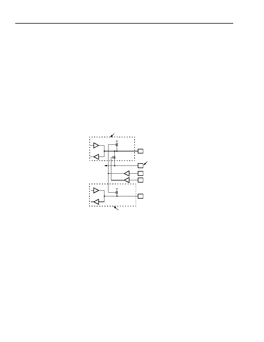
20
Agere Systems Inc.
Data Sheet
February 2004
Ambassador T8110L H.100/H.110 Switch
2 Pin Description
(continued)
2.3 Special Buffer Requirements
2.3.1 H1x0 Bus Signal Internal Pull-Up/Pull-Down
The H1x0 bus pins require special consideration for H.100 and H.110 usage. There are two control pins to select
between various internal bus pull-ups/pull-downs, as shown below:
!
H100_ENABLE. Enables internal 50 k
pull-ups on CT_Dn, CT_NETREF1, CT_NETREF2, CT_C8_A,
CT_C8_B, /CT_FRAME_A, and /CT_FRAME_B signals.
!
H110_ENABLE. Enables internal 20 k
pull-downs on all 32 CT_Dn signals, CT_NETREF1, and CT_NETREF2
to the VPRECHARGE signal.
Note: The two H1x0 enables are active-high. Only one or the other should ever be asserted.
Warning: Do not assert both at the same time.
Please refer to Figure 1 for more detail.
5-9611 (F)
Figure 1. T8110L Pull-Up/Pull-Down Arrangement for H1x0 Pins
2.3.2 Local Bus Signal Internal Pull-Up
The LPUE input is active-high; and is used to activate pull-ups on the following local signals: GP[7:0], FG[7:0],
D[15:0], LD[31:0], LREF[7:0], PRI_REF_IN, NR1_DIV_IN, and NR2_DIV_IN.
PAD
PAD
PAD
PAD
50 k
, MIN
PAD
20 k
, MIN
V
DD
V
DD
50 k
, MIN
CT_C8_A, CT_C8_B,
/CT_FRAME_A, /CT_FRAME_B
TO OTHER
CT_Dn
VPRECHARGE
H100_ENABLE
H110_ENABLE
CT_Dn, CT_NETREF1, CT_NETREF2
APPLY 0.7 V, NOMINAL
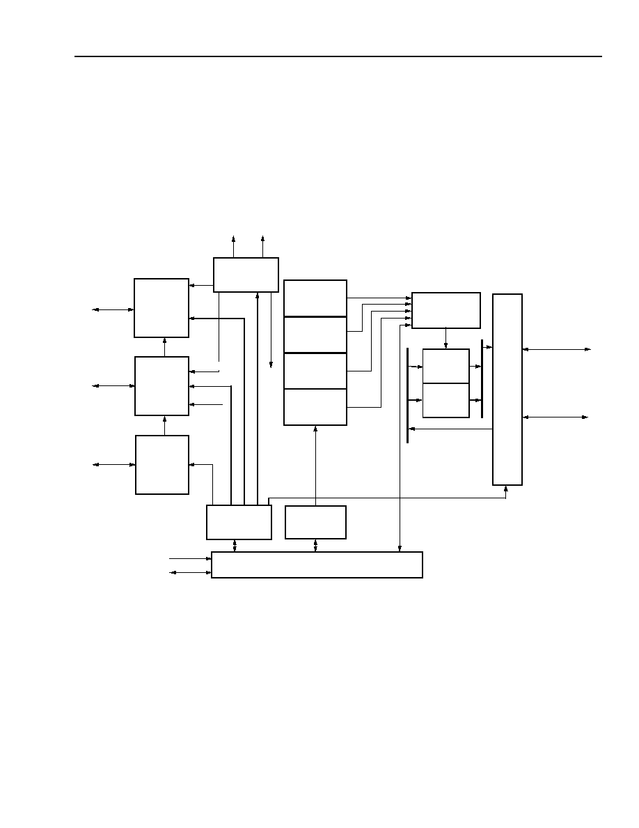
Agere Systems Inc.
21
Data Sheet
February 2004
Ambassador T8110L H.100/H.110 Switch
3 Main Architectural Features
3.1 T8110L Architecture
The T8110L includes all of the clocking and standard switching functions found on previous Ambassador devices,
plus additional functionalities that are described in the following sections. The T8110L interfaces to a controller via
a standard microprocessor interface which is described in Section 4. Note that the full version of the device, the
T8110, contains both microprocessor and PCI interfaces, allowing the device to attach directly to a PCI bus. The
T8110L and T8110 are pin compatible.
Figure 2. T8110L Architecture Block Diagram
ERROR
SIGNALS
GENERAL-
PURPOSE
I/O
FRAME
GROUPS
ADDITIONAL
I/O
INTERRUPT
AND
ERROR
CONTROL
GENERAL-
PURPOSE
I/O
CLOCKING
AND TIMING
CONTROL
H1x0 EVEN
CONNECTION
MEMORY
H1x0 ODD
CONNECTION
MEMORY
LOCAL HIGH
CONNECTION
MEMORY
LOCAL LOW
CONNECTION
MEMORY
CONNECTION
MEMORY
CONTROLLER
REGISTER
ACCESS
CONTROL
MICROPROCESSOR INTERFACE
SYSTEM
ERRORS
I
N
T
E
RNA
L
CL
O
C
K
S
LOCAL
CLOCKS
H1x0
CLOCKS
ERRORS
CLOCK
FG
TIMING
DATA
MEMORY
CONTROLLER
DATA
MEMORY
2K x 8
DATA
MEMORY
2K x 8
PAR
AL
LEL-T
O
-SER
I
A
L C
O
N
VER
SI
O
N
(OU
T
PU
T
)
S
E
R
I
AL-T
O-P
A
R
A
LL
EL C
O
N
VER
SI
ON
(I
N
P
U
T
)
H1x0
STREAMS
(BIDIRECTIONAL)
LOCAL
STREAMS
(BIDIRECTIONAL)
FRAME
GROUPS
AND GP I/O
ADDRESS
DATA
5-8920 (F)

22
Agere Systems Inc.
Data Sheet
February 2004
Ambassador T8110L H.100/H.110 Switch
4 Microprocessor Interface
4.1 Intel/Motorola Protocol Selector
IM_SEL = 1 is the default, if left unconnected, and selects an Intel handshake protocol.
IM_SEL = 0 selects a Motorola handshake protocol.
Note: The IM_SEL signal must be static (either pulled high or pulled low).
4.2 Word/Byte Addressing Selector
WB_SEL = 1 is the default, if left unconnected, and selects 16-bit word aligned addressing.
WB_SEL = 0 selects 8-bit byte aligned addressing.
Note: The WB_SEL signal may be static or dynamic in nature. If dynamic, WB_SEL must follow the same timing
requirements as the address bus.
Word-aligned addressing produces 16-bit data transfers via D[15:0]. Byte-aligned addressing produces 8-bit data
transfers via D[7:0] (D[15:8] is unused). The T8110L internal data bus is 32 bits, so A[1:0] address bits are decoded
along with WB_SEL to control a dword-to-word or dword-to-byte swap function back to the data bus.
Table 9. Intel/Motorola Protocol Selector
Intel/Motorola Protocol Selector
Signal
Intel Mnemonic
Motorola Mnemonic
D[15:0]
D[15:0]
D[15:0]
A[19:0]
A[15:0]
A[15:0]
CSN
CSn
CSn
RDY (DTACK#)
RDY
DTACKn
RD# (DS#)
RDn (read strobe)
DSn (data strobe)
WR# (R/W#)
WRn (write strobe)
R/Wn (read/write selector)
WB_SEL
Default
Default
IM_SEL
Default
Default

Agere Systems Inc.
23
Data Sheet
February 2004
Ambassador T8110L H.100/H.110 Switch
4 Microprocessor Interface
(continued)
4.3 Access Via the Microprocessor Bus
The T8110L microprocessor bus interface allows access to three internal regions: registers, connection memory,
and data memory. All microprocessor bus asynchronous strobes are synchronized to the T8110L's internal
65.536 MHz clock domain. There are 20 address bits provided to address the internal regions and these are
defined in Table 10.
Table 10. T8110L Memory Mapping to Microprocessor Space
Region
Subregion
Range (hex)
Registers
Reserved
0x00000--0x000FF
Operating control and status
0x00100--0x001FF
Clocks
0x00200--0x002FF
Rate control
0x00300--0x003FF
Frame group
0x00400--0x004FF
General-purpose I/O
0x00500--0x005FF
Interrupt control
0x00600--0x006FF
Reserved
0x00700--0x007FF
Reserved
0x00800--0x0FFFF
Reserved
--
0x10000--0x1FFFF
Data memory
--
0x20000--0x2FFFF
Reserved
--
0x30000--0x3FFFF
Connection memory
--
0x40000--0x4FFFF
Reserved
--
0x50000--0xFFFFF

24
Agere Systems Inc.
Data Sheet
February 2004
Ambassador T8110L H.100/H.110 Switch
4 Microprocessor Interface
(continued)
4.3 Access Via the Microprocessor Bus
(continued)
4.3.1 Microprocessor Interface Register Map
The T8110L registers map into the microprocessor bus space as follows.
Table 11. Microprocessor Interface Register Map
DWORD
Address
(20 bits)
Cross
Reference
Register
Byte 3
Byte 2
Byte 1
Byte 0
0x00100
5.1.1, 5.1.2
Master enable
Reserved
Reset select
Soft reset
0x00104
5.1.3, 5.1.4
Phase alignment
select
Clock register access
select
Data memory mode
select
Reserved
0x00108
5.1.4
Fallback trigger,
upper
Fallback trigger, lower Fallback type select
Fallback control
0x0010C
5.1.4
Watchdog EN, upper
Watchdog EN, lower
Watchdog select,
NETREF
Watchdog select, C8
0x00114
4.1.5
Reserved
Failsafe sensitivity
Failsafe enable
Failsafe control
0x00118
6.1.11
Reserved
OOL monitor
OOL threshold high
OOL threshold low
0x00120
5.2.1
Status 3, latched
clock errors, upper
Status 2, latched
clock errors, lower
Status 1, transient
clock errors, upper
Status 0, transient
clock errors, lower
0x00124
5.2.2
Status 7, system
errors
Reserved
Reserved
Status 4
0x00128
5.2.2.2
Device ID, upper
Device ID, lower
Reserved
Version ID
0x00140
11.1
Diag3
Diag2
Diag1
Diag0
0x00144
11.1
Diag7
Diag6
Diag5
Diag4
0x00148
11.1
Diag11
Diag10
Diag9
Diag8
0x00200
6.1
APLL1 rate
APLL1 input selector
Main divider
Main input selector
0x00204
6.1
APLL2 rate
Reserved
Resource divider
Main inversion select
0x00208
6.1
DPLL1 rate
DPLL1 input selector
Reserved
LREF input select
0x0020C
6.1
DPLL2 rate
DPLL2 input selector
Reserved
LREF inversion
select
0x00210
6.1
Reserved
NETREF1 LREF
select
NETREF1 divider
NETREF1 input
selector
0x00214
6.1
Reserved
NETREF2 LREF
select
NETREF2 divider
NETREF2 input
selector
0x00220
6.2
C8 output rate
/FR_COMP width
NETREF output
enables
Master output
enables
0x00224
6.2
SCLK output rate
TCLK select
Reserved
CCLK output
enables
0x00228
6.2
L_SC3 select
L_SC2 select
L_SC1 select
L_SC0 select
0x00300
9.1
H-bus rate H/G
H-bus rate F/E
H-bus rate D/C
H-bus rate B/A
0x00320
9.2
L-bus rate H/G
L-bus rate F/E
L-bus rate D/C
L-bus rate B/A
0x00400
7.1
FG0 rate
FG0 width
FG0 upper start
FG0 lower start

Agere Systems Inc.
25
Data Sheet
February 2004
Ambassador T8110L H.100/H.110 Switch
4 Microprocessor Interface
(continued)
4.3 Access Via the Microprocessor Bus
(continued)
4.3.1 Microprocessor Interface Register Map (continued)
Table 11. Microprocessor Interface Register Map (continued)
DWORD
Address
(20 bits)
Cross
Reference
Register
Byte 3
Byte 2
Byte 1
Byte 0
0x00410
7.1
FG1 rate
FG1 width
FG1 upper start
FG1 lower start
0x00420
7.1
FG2 rate
FG2 width
FG2 upper start
FG2 lower start
0x00430
7.1
FG3 rate
FG3 width
FG3 upper start
FG3 lower start
0x00440
7.1
FG4 rate
FG4 width
FG4 upper start
FG4 lower start
0x00450
7.1
FG5 rate
FG5 width
FG5 upper start
FG5 lower start
0x00460
7.1
FG6 rate
FG6 width
FG6 upper start
FG6 lower start
0x00470
7.1
FG7 rate
FG7 width
FG7 upper start
FG7 lower start
0x00474
7.2
FG7 mode upper
FG7 mode lower
FG7 counter high
byte
FG7 counter low
byte
0x00480
7.3
Reserved
FGIO R/W
FGIO read mask
FGIO data register
0x00500
8.1
GPIO override
GPIO R/W
GPIO read mask
GPIO data register
0x00600
12.1
FGIO interrupt
polarity
Reserved
FGIO interrupt
enable
FGIO interrupt pend-
ing
0x00604
10.1
GPIO interrupt
polarity
Reserved
GPIO interrupt
enable
GPIO interrupt pend-
ing
0x00608
10.1
System interrupt
enable, upper
System interrupt
enable, lower
System interrupt
pending, upper
System interrupt
pending, lower
0x0060C
10.1
Clock interrupt
enable, upper
Clock interrupt
enable, lower
Clock interrupt
pending, upper
Clock interrupt pend-
ing, lower
0x00610
10.1
CLKERR output
select
SYSERR output
select
Reserved
Arbitration control
0x00614
10.1
CLKERR pulse width
SYSERR pulse width
Reserved
Reserved
0x006FC
10.1
Reserved
Reserved
In-service, high
In-service, low
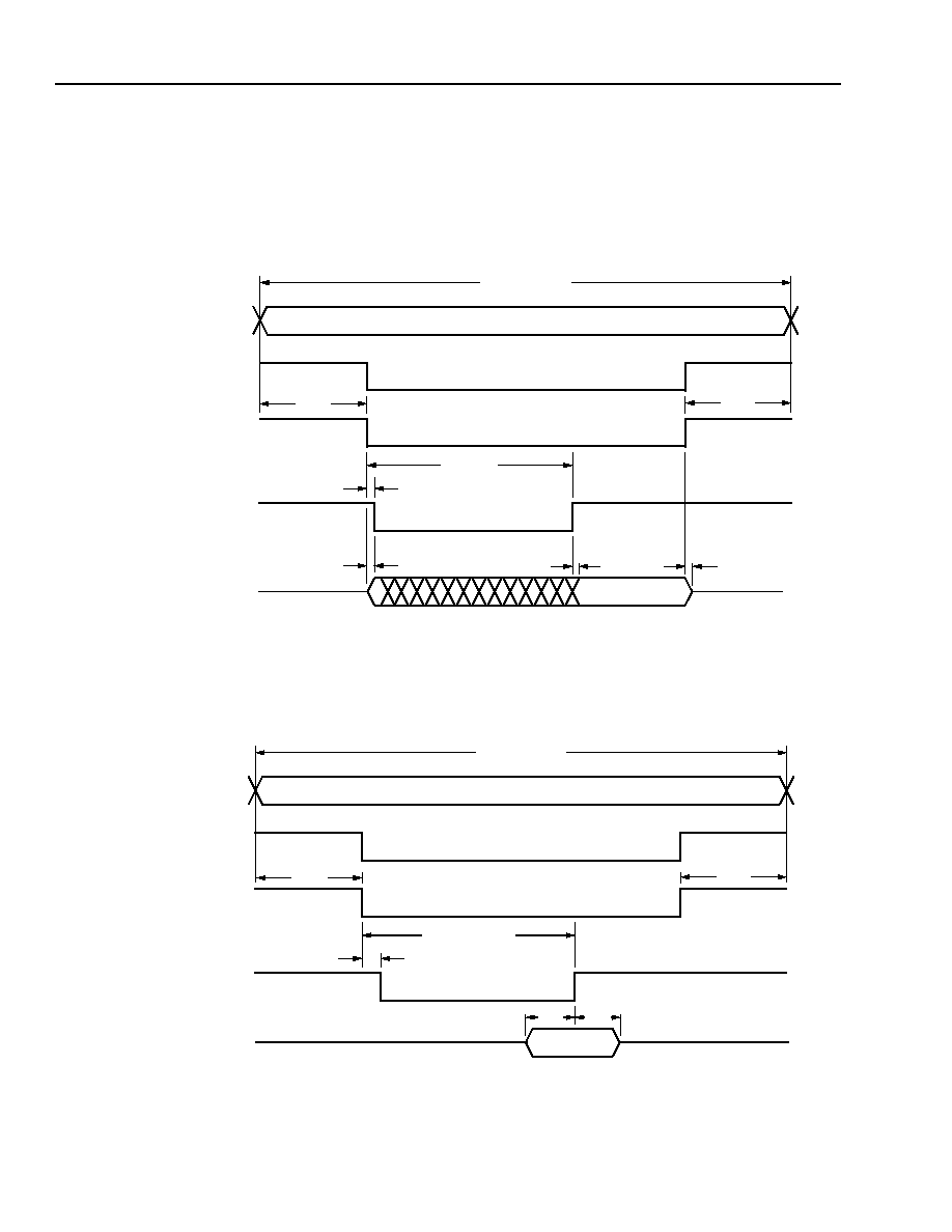
26
Agere Systems Inc.
Data Sheet
February 2004
Ambassador T8110L H.100/H.110 Switch
4 Microprocessor Interface
(continued)
4.3 Access Via the Microprocessor Bus
(continued)
4.3.1 Microprocessor Interface Register Map (continued)
5-9419 (F)
Figure 3. Microprocessor Access Timing, Intel Protocol
ADDRESS VALID
tah
tRDYhi
tas
taccess
WORD/BYTE SELECT,
A[19:0]
CSn
WRn
D[15:0], WRITE CYCLE
WR DATA
VALID
tds
tdh
RDY
tRDYlo
Microprocessor Access Write Cycle, Intel Protocol
ADDRESS VALID
tah
tRDYhi
tas
taccess
WORD/BYTE SELECT,
A[19:0]
CSn
RDn
RDY
tRDYlo
tdz
READ DATA VALID
D[15:0],
tde
tdv
READ CYCLE
Microprocessor Access Read Cycle, Intel Protocol
5-9418 (F)
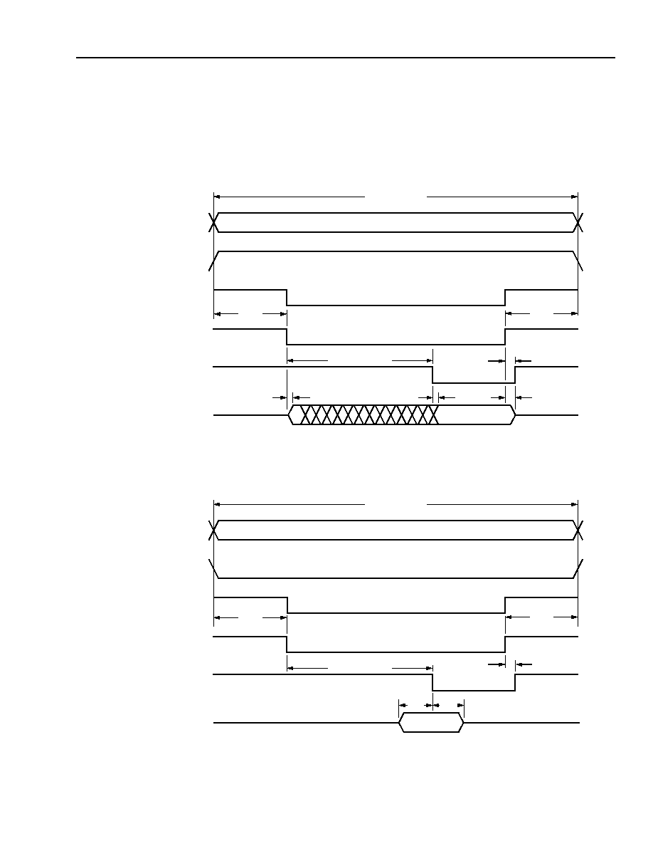
Agere Systems Inc.
27
Data Sheet
February 2004
Ambassador T8110L H.100/H.110 Switch
4 Microprocessor Interface
(continued)
4.3 Access Via the Microprocessor Bus
(continued)
4.3.1 Microprocessor Interface Register Map (continued)
5-9417 (F)
Figure 4. Microprocessor Access Timing, Motorola Protocol
ADDRESS VALID
tah
tDTACKhi
tDTACKlo
tde
tdv
tdz
tas
READ DATA VALID
taccess
WORD/BYTE SELECT,
A[19:0]
R/Wn
CSn
DSn
DTACKn
D[15:0], READ CYCLE
5-9416 (F)
Microprocessor Access Read Cycle, Motorola Protocol
ADDRESS VALID
tah
tDTACKhi
tDTACKlo
tas
taccess
WORD/BYTE SELECT,
A[19:0]
R/Wn
CSn
DSn
DTACKn
D[15:0], WRITE CYCLE
WR DATA
VALID
tds
tdh
Microprocessor Access Write Cycle, Motorola Protocol
28
Agere Systems Inc.
Data Sheet
February 2004
Ambassador T8110L H.100/H.110 Switch
4 Microprocessor Interface
(continued)
4.3 Access Via the Microprocessor Bus
(continued)
4.3.2 Register Space Access
The T8110L registers are always immediately available for access, providing low latency time to acknowledge the
transaction. Read access to [reserved] addresses returns 0x00. Register access timing for Figure 3 and Figure 4 is
shown below.
4.3.3 Connection Memory Space Access
The T8110L connection memory is always immediately available for access (via dedicated access times assigned for
microprocessor transactions) providing low latency time to acknowledge the transaction. Connection memory access
timing for Figure 3 and Figure 4 is shown below.
Table 12. Register Space Access Timing
Name
Parameter
Min (ns)
Max (ns)
taccess
Overall Access Time
41
--
tas
Address Setup Time
5
--
tah
Address Hold Time
0
--
tRDYlo
Intel Cycle, Time to RDY Deasserted
6
12
tRDYhi
Intel Cycle, Time to RDY Reasserted
36
72
tDTACKlo
Motorola Cycle, Time to DTACKn Asserted
36
70
tDTACKhi
Motorola Cycle, Time to DTACKn Deasserted
10
15
tde
Read Cycle, Time to Data Enabled
7
14
tdv
Read Cycle, Time to Data Valid
5
9
tdz
Read Cycle, Time to Data Invalid
10
16
tds
Write Cycle, Data Setup Time
25
--
tdh
Write Cycle, Data Hold Time
0
--
Table 13. Connection Memory Space Access Timing
Name
Parameter
Min (ns)
Max (ns)
taccess
Overall Access Time
41
--
tas
Address Setup Time
5
--
tah
Address Hold Time
0
--
tRDYlo
Intel Cycle, Time to RDY Deasserted
6
12
tRDYhi
Intel Cycle, Time to RDY Reasserted
36
72
tDTACKlo
Motorola Cycle, Time to DTACKn Asserted
36
70
tDTACKhi
Motorola Cycle, Time to DTACKn Deasserted
10
15
tde
Read Cycle, Time to Data Enabled
7
14
tdv
Read Cycle, Time to Data Valid
5
9
tdz
Read Cycle, Time to Data Invalid
10
16
tds
Write Cycle, Data Setup Time
25
--
tdh
Write Cycle, Data Hold Time
0
--

Agere Systems Inc.
29
Data Sheet
February 2004
Ambassador T8110L H.100/H.110 Switch
4 Microprocessor Interface
(continued)
4.3 Access Via the Microprocessor Bus
(continued)
4.3.4 Data Memory Space Access
The T8110L data memory is not guaranteed to be immediately available for access. Access to data memory is pri-
oritized for standard H-bus/L-bus switching, with microprocessor bus transaction access allowed as the lowest pri-
ority. The latency time to acknowledge these transactions is indeterminate and depends on the H-bus/L-bus
switching configuration. Data memory access timing for Figure 3 and Figure 4 is shown below.
* Max data memory space access time is indeterminate, and depends on how much of the data memory access bandwidth is being taken by
TDM switch connections.
Table 14. Data Memory Space Access Timing
Name
Parameter
Min (ns)
Max (ns)
taccess
Overall Access Time
41
--*
tas
Address Setup Time
5
--
tah
Address Hold Time
0
--
tRDYlo
Intel Cycle, Time to RDY Deasserted
6
12
tRDYhi
Intel Cycle, Time to RDY Reasserted
36
--*
tDTACKlo
Motorola Cycle, Time to DTACKn Asserted
36
--*
tDTACKhi
Motorola Cycle, Time to DTACKn Deasserted
10
15
tde
Read Cycle, Time to Data Enabled
7
14
tdv
Read Cycle, Time to Data Valid
5
9
tdz
Read Cycle, Time to Data Invalid
10
16
tds
Write Cycle, Data Setup Time
25
--
tdh
Write Cycle, Data Hold Time
0
--

30
Agere Systems Inc.
Data Sheet
February 2004
Ambassador T8110L H.100/H.110 Switch
5 Operating Control and Status
Overall T8110L operational control and status is configured via registers occupying 0x00100--0x001FC in the
address space.
5.1 Control Registers
General control functions are soft reset, reset configuration, overall master output enables, and data memory con-
figuration. Clocking-specific general control functions are clock register access configuration, phase alignment,
clock fallback, and clock watchdog configuration.
5.1.1 Reset Registers
The soft reset and reset select registers control soft reset functions and reset signal masking. Writes to the soft
reset register trigger the corresponding action, and the set bit(s) are automatically cleared.
!
Power-on reset: nonmaskable:
-- At power-on, initialize all T8110L registers (including reset select register) and connection valid flags. The
power-on reset cell test input is controlled via diagnostic register; see Section 11.
!
Hard reset: maskable via reset select register, HRBEB:
-- On assertion of RESET#, initialize all T8110L registers (excluding reset select register) and connection valid
flags.
Soft resets are maskable via reset select register, SRBEB, and selectable via soft reset register, SRESR.
!
Soft reset 1: Initialize all T8110L registers (excluding reset select register) and connection valid flags.
!
Soft reset 2: Initialize all T8110L registers (excluding reset select register).
!
Soft reset 3: Reset all interrupt pending registers and the interrupt in-service register.
!
Soft reset 4: Reset the interrupt in-service register only.
Table 15. Control Register Map
DWORD
Address
(20 Bits)
Register
Byte 3
Byte 2
Byte 1
Byte 0
0x00100
Master enable
Reserved
Reset select
Soft reset
0x00104 Phase alignment select
Clock register access
select
Data memory mode select
--
0x00108
Fallback trigger, upper
Fallback trigger, lower
Fallback type select
Fallback control
0x0010C
Watchdog EN, upper
Watchdog EN, lower
Watchdog select,
NETREF
Watchdog select, C8
0x00114
Reserved
Failsafe threshold low
Failsafe enable and status
Failsafe control

Agere Systems Inc.
31
Data Sheet
February 2004
Ambassador T8110L H.100/H.110 Switch
5 Operating Control and Status
(continued)
5.1 Control Registers
(continued)
5.1.2 Master Output Enable Register
The master output enable register is used to control master output enables to various groups of T8110L signals,
including the following:
L-bus data streams (L_D[31:0])
L-bus clocks (L_SC[3:0], FG[7:0] when used as frame group outputs)
H-bus data streams (CT_D[31:0])
H-bus clocks (CT_C8_A, /CT_FRAME_A, CT_C8_B, /CT_FRAME_B, CT_NETREF1,CT_NETREF2, /C16+,
/C16≠, /C4, C2, SCLK, /SCLKx2, /FR_COMP)
GPIO (GP[7:0])
FGIO (FG[7:0] when used as programmable register outputs)
T8110L outputs that are not programmatically enabled (i.e., always driven except during reset) include the follow-
ing:
CLKERR, SYSERR, PRI_REF_OUT, NR1_SEL_OUT, and NR2_SEL_OUT.
Table 16. Reset Registers
Byte
Address
Name
Bit(s) Mnemonic
Value
Function
0x00100
Soft Reset
7:0
SRESR
0000 0000
0000 0001
0000 0010
0001 0000
0010 0000
NOP (default value).
Reset all registers and connection valid flags.
Reset all registers.
Reset interrupt pending and in-service registers.
Reset interrupt in-service register only.
0x00101
Reset Select
7:2
Reserved
0000
NOP (default).
1
HRBEB
0
1
Disable hard reset to back end.
Enable hard reset to back end (default).
0
SRBEB
0
1
Disable soft resets to back end.
Enable soft resets to back end (default).
32
Agere Systems Inc.
Data Sheet
February 2004
Ambassador T8110L H.100/H.110 Switch
5 Operating Control and Status
(continued)
5.1 Control Registers
(continued)
5.1.3 Connection Control--Data Memory Selector Register
The data memory mode select register MSbit controls subrate switching enable. The lower 7 bits control the
T8110L data memory switching configuration. For more details, see Section 12.2.1.2 on page 116.
There are three data memory configurations as outlined below:
1. 4k single-buffered switch. Standard H-bus/L-bus switching only, up to 4096 simplex connections, all connections
are minimum delay due to single-buffer configuration.
2. 2k double-buffered switch. Standard H-bus/L-bus switching only, up to 2048 simplex connections, all connec-
tions are programmable for minimum or constant delay via the double-buffer configuration.
3. 2k single-buffered switch + 1k double-buffered switch. Standard H-bus/L-bus switching only, up to 2048 simplex
minimum delay connections (single buffer) and up to 1024 simplex minimum or constant delay connections
(double buffer).
Table 17. Master Output Enable Register
Byte
Address
Name
Bit(s)
Mnemonic
Value
Function
0x00103 Master Enable
7
AIOEB
0
1
Individual enables via bits [6:0] (default).
Enable all (same as bits [6:0] = 1111111).
6
Reserved
0
NOP.
5
FGREB
0
1
Disable FGIO (default).
Enable FGIO.
4
GPIEB
0
1
Disable GPIO (default).
Enable GPIO.
3
HCKEB
0
1
Disable H-bus clocks (default).
Enable H-bus clocks.
2
HDBEB
0
1
Disable H-bus data streams (default).
Enable H-bus data streams.
1
LCKEB
0
1
Disable L-bus clocks, L_SC, FG (default).
Enable L-bus clocks.
0
LDBEB
0
1
Disable L-bus data streams (default).
Enable L-bus data streams.
Table 18. Data Memory Mode Select Register
Byte
Address
Name
Bit(s) Mnemonic
Value
Function
0x00105 Data Memory Mode
Select
7
GSREB
0
1
Disable subrate switching (default).
Enable subrate switching.
6:0
DMMSP
100 0000
010 0000
011 0000
4k single-buffer switch (default).
2k double-buffer switch.
2k single-buffer, 1k double-buffer switch.

Agere Systems Inc.
33
Data Sheet
February 2004
Ambassador T8110L H.100/H.110 Switch
5 Operating Control and Status
(continued)
5.1 Control Registers
(continued)
5.1.4 General Clock Control (Phase Alignment, Fallback, Watchdogs) Register
The clock register access select register controls the selection between accessing the active vs. the inactive set of
T8110L clock registers. The T8110L contains two sets of clock registers, X and Y. The X and Y register sets are
comprised of the registers listed in Table 33 on page 45, Clock Input Control Register Map, and Table 46 on page
53, Clock Output Control Register Map. Only one set is used at a time. It is selected based on the clock fallback
setup. The clock register set that is currently in use is denoted as the active set; see Section 6.3 on page 57 for
more details.
5.1.5 Phase Alignment Select Register
The phase alignment select register selects the phase alignment configuration. For more details, see Section
6.4.5.1 on page 62. The T8110L internally generates an 8 kHz frame reference. Shown below are three configura-
tions to control phase alignment between this internally generated frame reference and a selected incoming frame
reference from the H-bus (/CT_FRAME_A, /CT_FRAME_B, or /FR_COMP) or local clock reference (LREF[4:7]).
!
Disable alignment, no realignment of unaligned frames
!
Snap alignment, immediate realignment of unaligned frames
!
Slide alignment, gradual realignment of unaligned frames
5.1.6 Fallback Control Register
The fallback control register allows user control over the active and inactive clock register sets. For more details,
see Section 6.7.1 on page 64. Writes to the fallback control register trigger the corresponding action, and the set
bit(s) are automatically cleared. The four commands are shown below:
!
GO_CLOCKS. At initialization, the clock register Y set is active, the X set is inactive, and access is enabled to
the X set. The GO_CLOCKS command transitions the Y set to inactive and the X set to active. This command
can either be performed immediately upon issue or can wait to be performed until the next 8 kHz frame refer-
ence (synchronized to frame).
!
CLEAR_FALLBACK. Forces a state transition for active/inactive assignment of the clock register X and Y sets
after a fallback event has occurred. This command can either be performed immediately upon issue or can wait
to be performed until the next 8 kHz frame reference (synchronized to frame).
Table 19. Clock Register Access Select Register
Byte
Address
Name
Bit(s) Mnemonic
Value
Function
0x00106 Clock Register Access
Select
7:0
CSASR
0000 0000
0000 0001
Access inactive clock registers (default).
Access active clock registers.
Table 20. Phase Alignment Select Register
Byte
Address
Name
Bit(s) Mnemonic
Value
Function
0x00107 Phase Alignment Select
7:0
PAFSR
0000 0000
0000 0001
0000 0010
Phase alignment is disabled (default).
Enable snap alignment.
Enable slide alignment.

34
Agere Systems Inc.
Data Sheet
February 2004
Ambassador T8110L H.100/H.110 Switch
5 Operating Control and Status
(continued)
5.1 Control Registers
(continued)
5.1.6 Fallback Control Register (continued)
!
FORCE_FALLBACK. Forces a state transition for active/inactive assignment of the clock register X and Y sets
by creating a fallback event. This command can either be performed immediately upon issue or can wait to be
performed until the next 8 kHz frame reference (synchronized to frame).
!
COPY ACTIVE TO INACTIVE SET. Copies all register values in the current active clock register set to the inac-
tive clock register set. This command is performed immediately upon issue.
* The synchronized to frame command also has a diagnostic element--instead of performing the command right at the frame boundary,
the user can elect to perform the command at a specified offset time from the frame boundary, by programming the Diag11 and Diag10
registers, 0x0014B--0x0014A.
5.1.7 Fallback Type Select Register
The upper nibble configures which H-bus clocks are selected to trigger a clock fallback event. Any of the legacy
modes have predetermined trigger enables and ignore the fallback trigger register settings. Nonlegacy modes
require the fallback trigger register settings. For more details, see Section 6.7.1 on page 64.
The lower nibble configures the state machine that controls clock register set active/inactive assignments. There
are three possible selections. For more details, see Section 6.7 on page 64.
!
Disabled. No transitions of clock register X and Y sets to active/inactive.
!
Fixed secondary. Swap the active/inactive sets on a fallback event; swap them back when fallback is cleared.
!
Rotating secondary. Swap the active/inactive sets on a fallback event; maintain this state when fallback is
cleared.
Table 21. Fallback Control Register
Byte
Address
Name
Bit(s) Mnemonic
Value
Function
0x00108 Fallback Control
7:0
FBCSR
0000 0000
0000 0001
0000 0010
0000 0100
0001 0001
0001 0010
0001 0100
0010 0000
NOP (default).
GO_CLOCKS command.
CLEAR_FALLBACK command.
FORCE_FALLBACK command.
GO_CLOCKS synchronized to frame*.
CLEAR_FALLBACK synchronized to frame*.
FORCE_FALLBACK synchronized to frame*.
COPY ACTIVE TO INACTIVE SET com-
mand.
Agere Systems Inc.
35
Data Sheet
February 2004
Ambassador T8110L H.100/H.110 Switch
5 Operating Control and Status
(continued)
5.1 Control Registers
(continued)
5.1.7 Fallback Type Select Register (continued)
5.1.8 Fallback Trigger Registers
The fallback trigger registers are used in conjunction with the fallback type select register and control which H-bus
clocks are enabled to trigger a clock fallback event in case of error. The sync reference inputs to DPLL1 and
DPLL2 can also trigger a clock fallback event upon detection of an error.
Table 22. Fallback Type Select Register
Byte
Address
Name
Bit(s) Mnemonic
Value
Function
0x00109 Fallback Type
Select
7:4
FTRSN
0000
0001
0010
0100
1000
1001
NOP (default).
Legacy, fallback to OSC/4 on main select failure.
Legacy, fallback X/Y set on main select failure.
Legacy, fallback X/Y set on H-bus A/B failure.
Fallback trigger registers control fallback.
Fallback trigger registers control fallback and
H-Bus clock enable state machine is enabled.
3:0
FSMSN
0000
0001
0010
Fallback is disabled (default).
Enable fixed secondary fallback.
Enable rotating secondary fallback.
Table 23. Fallback Trigger Registers
Byte
Address
Name
Bit(s) Mnemonic Value
Function
0x0010A Fallback
Trigger,
Lower
7
S2FEB
0
1
Disable /SCLKx2 trigger (default).
Enable /SCLKx2 trigger.
6
SCFEB
0
1
Disable SCLK trigger (default).
Enable SCLK trigger.
5
C2FEB
0
1
Disable C2 trigger (default).
Enable C2 trigger.
4
C4FEB
0
1
Disable /C4 trigger (default).
Enable /C4 trigger.
3
CMFEB
0
1
Disable /C16≠ trigger (default).
Enable /C16≠ trigger.
2
CPFEB
0
1
Disable /C16+ trigger (default).
Enable /C16+ trigger.
1
CBFEB
0
1
Disable CT_C8_B trigger (default).
Enable CT_C8_B trigger.
0
CAFEB
0
1
Disable CT_C8_A trigger (default).
Enable CT_C8_A trigger.

36
Agere Systems Inc.
Data Sheet
February 2004
Ambassador T8110L H.100/H.110 Switch
5 Operating Control and Status
(continued)
5.1 Control Registers
(continued)
5.1.8 Fallback Trigger Registers (continued)
5.1.9 Watchdog Select, C8, and NETREF Registers
The watchdog select, C8 register controls the watchdog circuits to monitor the proper frequency for the CT_C8_A
and CT_C8_B signals. These signals can take on two values, including 8.192 MHz (ECTF mode) and 4.096 MHz
(MC1 mode).
The watchdog select, NETREF register controls the watchdog circuits to monitor the proper frequency for the
CT_NETREF1 and CT_NETREF2 signals. These signals can take on three values depending on system-level
clocking architecture, including 8 kHz (frame reference), 1.544 MHz (T1 bit clock), and 2.048 MHz (E1 bit clock).
Table 23. Fallback Trigger Registers (continued)
Byte
Address
Name
Bit(s) Mnemonic Value
Function
0x0010B
Fallback Trigger, Upper
7
Reserved
0
NOP (default).
6
D2FEB
0
1
Disable DPLL2 sync trigger (default).
Enable DPLL2 sync trigger.
5
D1FEB
0
1
Disable DPLL1 sync trigger (default).
Enable DPLL1 sync trigger.
4
N2FEB
0
1
Disable CT_NETREF2 trigger (default).
Enable CT_NETREF2 trigger.
3
N1FEB
0
1
Disable CT_NETREF1 trigger (default).
Enable CT_NETREF1 trigger.
2
FCFEB
0
1
Disable /FR_COMP trigger (default).
Enable /FR_COMP trigger.
1
FBFEB
0
1
Disable /CT_FRAME_B trigger (default).
Enable /CT_FRAME_B trigger.
0
FAFEB
0
1
Disable /CT_FRAME_A trigger (default).
Enable /CT_FRAME_A trigger.
Table 24. Watchdog Select, C8, NETREF Registers
Byte
Address
Name
Bit(s) Mnemonic
Value
Function
0x0010C
Watchdog Select, C8
7:4
CBWSN
0000
0001
CT_C8_B watchdog at 8.192 MHz (default).
CT_C8_B watchdog at 4.096 MHz MC1mode.
3:0
CAWSN
0000
0001
CT_C8_A watchdog at 8.192 MHz (default).
CT_C8_A watchdog at 4.096 MHz MC1mode.
0x0010D
Watchdog Select,
NETREF
7:4
N2WSN
0000
0001
0010
CT_NETREF2 watchdog at 8 kHz (default).
CT_NETREF2 watchdog at 1.544 MHz.
CT_NETREF2 watchdog at 2.048 MHz.
3:0
N1WSN
0000
0001
0010
CT_NETREF1 watchdog at 8 kHz (default).
CT_NETREF1 watchdog at 1.544 MHz.
CT_NETREF1 watchdog at 2.048 MHz.
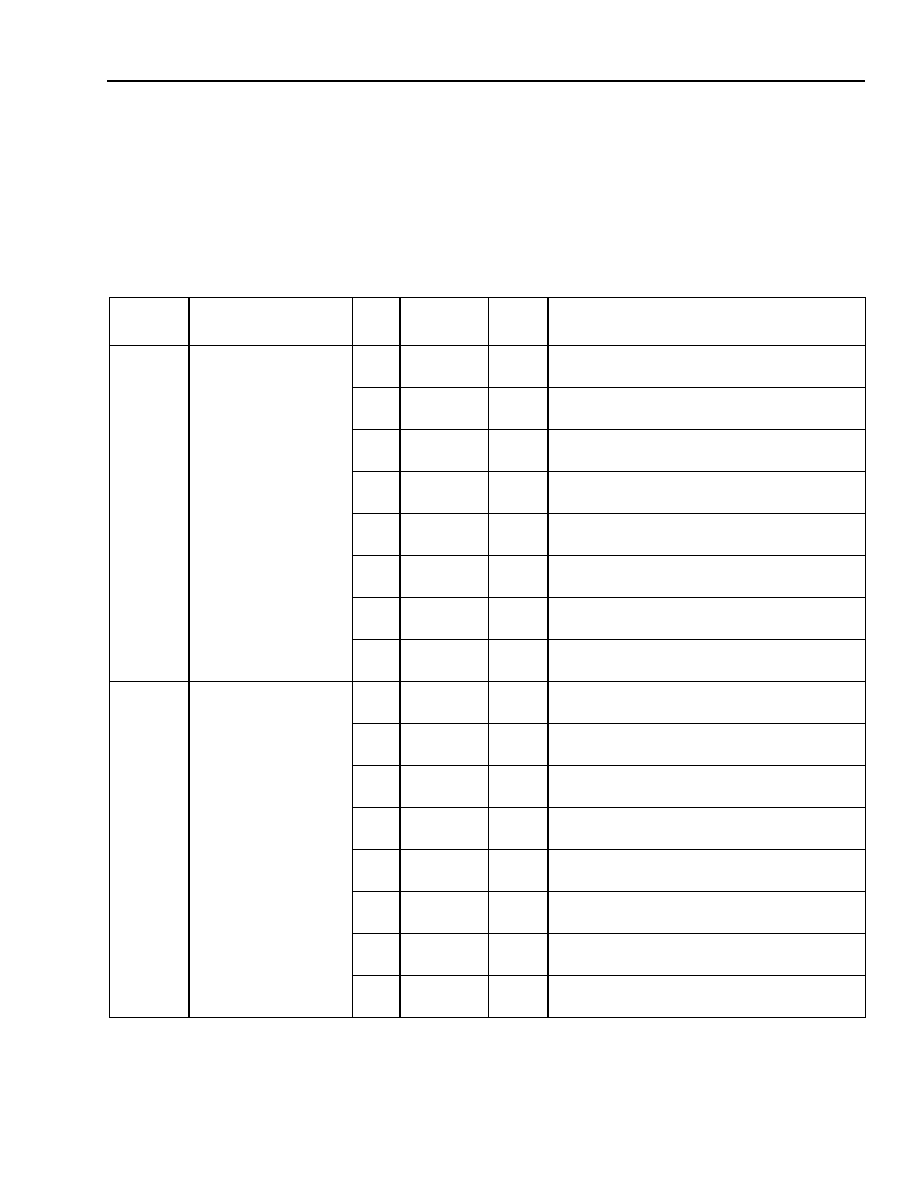
Agere Systems Inc.
37
Data Sheet
February 2004
Ambassador T8110L H.100/H.110 Switch
5 Operating Control and Status
(continued)
5.1 Control Registers
(continued)
5.1.10 Watchdog EN Register
The watchdog EN registers are used to enable/disable watchdogs on the individual H-bus clocks and the watch-
dogs on the sync inputs of DPLL1 and DPLL2.
Table 25. Watchdog EN Registers
Byte
Address
Name
Bit(s) Mnemonic
Value
Function
0x0010E
Watchdog EN, Lower
7
S2WEB
0
1
Disable /SCLKx2 watchdog (default).
Enable /SCLKx2 watchdog.
6
SCWEB
0
1
Disable SCLK watchdog (default).
Enable SCLK watchdog.
5
C2WEB
0
1
Disable C2 watchdog (default).
Enable C2 watchdog.
4
C4WEB
0
1
Disable/C4 watchdog (default).
Enable/C4 watchdog.
3
CMWEB
0
1
Disable/C16≠ watchdog (default).
Enable/C16≠ watchdog.
2
CPWEB
0
1
Disable/C16+ watchdog (default).
Enable/C16+ watchdog.
1
CBWEB
0
1
Disable CT_C8_B watchdog (default).
Enable CT_C8_B watchdog.
0
CAWEB
0
1
Disable CT_C8_A watchdog (default).
Enable CT_C8_A watchdog.
0x0010F
Watchdog EN, Upper
7
FSWEB
0
1
Disable FAILSAFE ref watchdog (default).
Enable FAILSAFE ref watchdog.
6
D2WEB
0
1
Disable DPLL2 sync watchdog (default).
Enable DPLL2 sync watchdog.
5
D1WEB
0
1
Disable DPLL1 sync watchdog (default).
Enable DPLL1 sync watchdog.
4
N2WEB
0
1
Disable CT_NETREF2 watchdog (default).
Enable CT_NETREF2 watchdog.
3
N1WEB
0
1
Disable CT_NETREF1 watchdog (default).
Enable CT_NETREF1 watchdog.
2
FCWEB
0
1
Disable /FR_COMP watchdog (default).
Enable /FR_COMP watchdog.
1
FBWEB
0
1
Disable /CT_FRAME_B watchdog (default).
Enable /CT_FRAME_B watchdog.
0
FAWEB
0
1
Disable /CT_FRAME_A watchdog (default).
Enable /CT_FRAME_A watchdog.
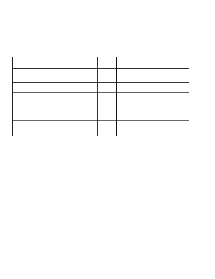
38
Agere Systems Inc.
Data Sheet
February 2004
Ambassador T8110L H.100/H.110 Switch
5 Operating Control and Status
(continued)
5.1 Control Registers
(continued)
5.1.11 Failsafe Control Registers
The failsafe control register controls a return from the failsafe state. Writes to the failsafe control register trigger the
corresponding action, and the set bit(s) are automatically cleared. From the failsafe state, the user can return to
either the primary or secondary clock register sets. For more on failsafe, please see Section 6.7.2 on page 70.
The failsafe enable register controls the enable/disable of failsafe operation. For more on failsafe operation, please
see Section 6.7.2 on page 70.
The failsafe sensitivity register allows the failsafe watchdog timer to be desensitized by either 1, 4, 8, or 16 watch-
dog sample clock periods.
The OOL threshold registers allow for programmable threshold times which indicate the APLL1 out-of-lock. Reso-
lution for the threshold value increments is one 32.768 MHz clock period (30.5 ns). The register contains
[count ≠ 1], a value of 0x0000 yields a 30.5 ns threshold. A value of 0xFFFF yields a 1.99 ms threshold. For more
on OOL operation, please see Section 6.7.2 on page 70.
The OOL monitor register allows the user to monitor either the raw APLL1 out-of-lock status, OR the status flag
that indicates that the APLL1 has been out-of-lock for more than the threshold defined in the OOL threshold regis-
ters.
Table 26. Failsafe Control Register
Byte
Address
Name
Bit(s) Mnemonic
Value
Function
0x00114
Failsafe Control
7:0
FSCSR
0000 0000
0000 0001
0000 0010
NOP (default).
Return from failsafe to nonfallback condition.
Return from failsafe to fallback condition.
0x00115
Failsafe Enable
7:0
FSEER
0000 0000
0000 0001
Failsafe disabled.
Failsafe enabled.
0x00116
Failsafe Sensitivity
7:0
FSSSR
0000 0000
0000 0001
0000 0010
0000 0100
0000 1000
Failsafe watchdog highest sensitivity.
Failsafe watchdog + 30.5 ns.
Failsafe watchdog + 121.0 ns.
Failsafe watchdog + 244.0 ns.
Failsafe watchdog + 488.0 ns.
0x00118
OOL Threshold Low
7:0
OLLLR
LLLL LLLL Failsafe threshold value, low byte.
0x00119
OOL Threshold High
7:0
OLHLR
LLLL LLLL Failsafe threshold value, high byte.
0x0011A
OOL Monitor
7:0
OOLER
0000 0000
0000 0001
Monitor direct APLL1 lock detect at PLOCK.
Monitor user threshold lock detect at PLOCK.
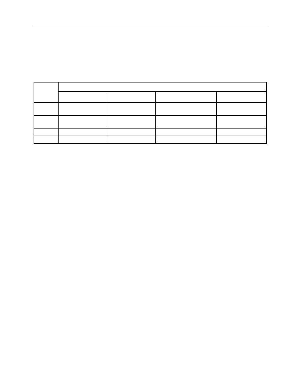
Agere Systems Inc.
39
Data Sheet
February 2004
Ambassador T8110L H.100/H.110 Switch
5 Operating Control and Status
(continued)
5.2 Error and Status Registers
Status 7, 6, and 3--0 registers are writable by the user for clearing specific error bits. Writing a 1 to any of the bits
of these registers will clear the corresponding error bit. The remaining error and status registers are read-only.
Table 27. Error and Status Register Map
DWORD
Address
(20 bits)
Register
Byte 3
Byte 2
Byte 1
Byte 0
0x00120
Status 3, latched clock
errors, upper
Status 2, latched clock
errors, lower
Status 1, transient clock
errors, upper
Status 0, transient
clock errors, lower
0x00124
Status 7, system
errors
Reserved
Reserved
Status 4 fallback and
failsafe status
0x00128
Device ID, upper
Device ID, lower
Reserved
Version ID
0x0012C
Reserved
Reserved
Reserved
Reserved

40
Agere Systems Inc.
Data Sheet
February 2004
Ambassador T8110L H.100/H.110 Switch
5 Operating Control and Status
(continued)
5.2 Error and Status Registers
(continued)
5.2.1 Clock Errors
5.2.1.1 Transient Clock Errors Registers
The transient clock error registers are used in conjunction with the watchdog EN registers and indicate error status
for H-bus clocks and DPLL1/DPLL2 sync inputs whose watchdogs are enabled. The transient indicators are
dynamic in nature; if a clock is in error only for a short time and then recovers, the error indication is deasserted
when the clock recovers. Additionally, an APLL1 out-of-lock indicator is provided, and used in conjunction with the
failsafe clocking mode. For more details, please see Section 6.7.1 on page 64 and Section 6.7.2 on page 70.
Table 28. Clock Error Registers
Byte Address
Name
Bit(s) Mnemonic
Value
Function
0x00120
Status 0, Transient
Clock Errors, Lower
7
S2TOB
0
1
/SCLKx2 no error (default).
/SCLKx2 error.
6
SCTOB
0
1
SCLK no error (default).
SCLK error.
5
C2TOB
0
1
C2 no error (default).
C2 error.
4
C4TOB
0
1
/C4 no error (default).
/C4 error.
3
CMTOB
0
1
/C16≠ no error (default).
/C16≠ error.
2
CPTOB
0
1
/C16+ no error (default).
/C16+ error.
1
CBTOB
0
1
CT_C8_B no error (default).
CT_C8_B error.
0
CATOB
0
1
CT_C8_A no error (default).
CT_C8_A error.
0x00121
Status 1, Transient
Clock Errors, Upper
7
FSTOB
0
1
Failsafe indicator: APLL1 reference no error.
APLL1 reference error.
6
D2TOB
0
1
DPLL2 sync no error (default).
DPLL2 sync error.
5
D1TOB
0
1
DPLL1 sync no error (default).
DPLL1 sync error.
4
N2TOB
0
1
CT_NETREF2 no error (default).
CT_NETREF2 error.
3
N1TOB
0
1
CT_NETREF1 no error (default).
CT_NETREF1 error.
2
FCTOB
0
1
/FR_COMP no error (default).
/FR_COMP error.
1
FBTOB
0
1
/CT_FRAME_B no error (default).
/CT_FRAME_B error.
0
FATOB
0
1
/CT_FRAME_A no error (default).
/CT_FRAME_A error.
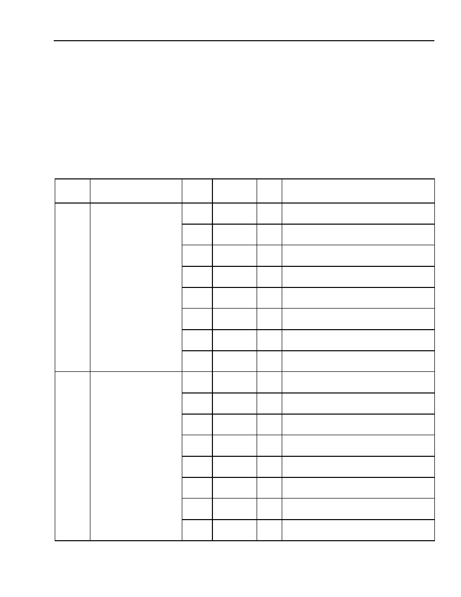
Agere Systems Inc.
41
Data Sheet
February 2004
Ambassador T8110L H.100/H.110 Switch
5 Operating Control and Status
(continued)
5.2 Error and Status Registers
(continued)
5.2.1 Clock Errors (continued)
5.2.1.2 Latched Clock Error Register
The latched clock error registers capture transient clock errors. The latched indicators capture and hold any tran-
sient error status and are used by the clock fallback logic. For more details, see Section 6.7 on page 64, and Sec-
tion 10 on page 90 for more details.
Table 29. Latched Clock Error Registers
Byte
Address
Name
Bit(s)
Mnemonic Value
Function
0x00122 Status 2, Latched Clock
Errors, Lower
7
S2LOB
0
1
/SCLKx2 no error (default).
/SCLKx2 error.
6
SCLOB
0
1
SCLK no error (default).
SCLK error.
5
C2LOB
0
1
C2 no error (default).
C2 error.
4
C4LOB
0
1
/C4 no error (default).
/C4 error.
3
CMLOB
0
1
/C16≠ no error (default).
/C16≠ error.
2
CPLOB
0
1
/C16+ no error (default).
/C16+ error.
1
CBLOB
0
1
CT_C8_B no error (default).
CT_C8_B error.
0
CALOB
0
1
CT_C8_A no error (default).
CT_C8_A error.
0x00123 Status 3, Latched Clock
Errors, Upper
7
FSLOB
0
1
Failsafe indicator: APLL1 reference no error.
APLL1 reference error.
6
D2LOB
0
1
DPLL2 sync no error (default).
DPLL2 sync error.
5
D1LOB
0
1
DPLL1 sync no error (default).
DPLL1 sync error.
4
N2LOB
0
1
CT_NETREF2 no error (default).
CT_NETREF2 error.
3
N1LOB
0
1
CT_NETREF1 no error (default).
CT_NETREF1 error.
2
FCLOB
0
1
/FR_COMP no error (default).
/FR_COMP error.
1
FBLOB
0
1
/CT_FRAME_B no error (default).
/CT_FRAME_B error.
0
FALOB
0
1
/CT_FRAME_A no error (default).
/CT_FRAME_A error.

42
Agere Systems Inc.
Data Sheet
February 2004
Ambassador T8110L H.100/H.110 Switch
5 Operating Control and Status
(continued)
5.2 Error and Status Registers
(continued)
5.2.2 System Status
5.2.2.1 Clock Fallback Status Register
The upper nibble provides status indicators for clock fallback. FBFOB indicates whether the circuit is in a clock fall-
back state. FBSOP indicates which of five possible states the circuit is in; see Section 6.7.1 on page 64 for more
details.
The lower nibble provides status indicators related to the X and Y clock register set active/inactive assignments.
XYSOB indicates which of the clock register sets is active. The remaining bits indicate a pending status for
GO_CLOCKS, CLEAR_FALLBACK, and FORCE_FALLBACK commands issued (via the fallback control register,
0x00108), which are waiting for a frame sync.
Table 30. Fallback and Failsafe Status Register
Byte
Address
Register Name
Bit(s) Mnemonic Value
Function
0x00124 Status 4, Clock Fallback
Status
7
FBFOB
0
1
Indicates not in fallback/failsafe state (default).
Indicates fallback/failsafe state.
6:4
FBSOP
111
000
001
010
011
100
101
Fallback state = INITIAL (default).
Fallback state = PRIMARY.
Fallback state = TO_PRIMARY.
Fallback state = SECONDARY.
Fallback state = TO_SECONDARY.
Failsafe state = FS_1.
Failsafe state = FS_2.
3
XYSOB
0
1
Clock register Y set is active, X is inactive.
Clock register X set is active, Y is inactive.
2
GOPOB
0
1
No GO_CLOCKS pending (default).
GO_CLOCKS pending, waiting for frame.
1
CFPOB
0
1
No CLEAR_FALLBACK pending (default).
CLEAR_FALLBACK pending, waiting for frame.
0
FFPOB
0
1
No FORCE_FALLBACK pending (default).
FORCE_FALLBACK pending, waiting for
frame.

Agere Systems Inc.
43
Data Sheet
February 2004
Ambassador T8110L H.100/H.110 Switch
5 Operating Control and Status
(continued)
5.2 Error and Status Registers
(continued)
5.2.2 System Status (continued)
5.2.2.2 Device Identification Registers
5.2.2.3 System Device Errors
These registers identify the device type and revision status, T8110L revision n.
Table 31. System Errors Registers
Byte
Address
Register Name
Bit(s) Mnemonic
Value
Function
0x00127 Status 7, System
Errors
7
CFSOB
0
1
No error.
Clock failsafe indicator.
6
CFBOB
0
1
No error.
Clock fallback indicator.
5:0
Reserved
0
NOP.
Table 32. Device Identification Registers
Byte
Address
Name
Bit(s) Mnemonic
Value
Function
0x00128 Version ID
7:0
VEROR
0000 0001
Revision status (value shown = REV1).
0x0012A Device ID, Lower
7:0
IDLOR
0001 0000
Device ID low status 0x10.
0x0012B Device ID, Upper
7:0
IDHOR
1000 0001
Device ID high status 0x81.
44
Agere Systems Inc.
Data Sheet
February 2004
Ambassador T8110L H.100/H.110 Switch
6 Clock Architecture
5-9432 (F)
Figure 5. T8110L Main Clocking Paths
5-9433 (F)
Figure 6. T8110L NETREF Paths
2.048 MHz
4.096 MHz
8.192 MHz
16.364 MHz
FRAME
32.768 MHz
(INTERNAL)
INTERNAL
CLOCK
PHASE
ALIGNMENT
BIT SLIDER
CONTROLS
MEMORIES
APLL1
65.536 MHz
APLL1
BYPASS
65.536 MHz
SAMPLED FRAME
DPLL1
CLOCK
SOURCE
SELECT
DPLL2
APLL2
49.408 MHz
TO
APLL2
BYPASS
OSC2
XTAL2 OUT
XTAL2 IN/
APLL2
RATE
SELECT
DPLL2
SOURCE
AND RATE
DIV
BY 4
PRI_REF_OUT
PRI_REF_IN
MAIN
DIVIDE-BY-n
DIVIDE REGISTER
RESOURCE
DIVIDE-BY-n
DIVIDE REGISTER
CLK
SEL
FRAME
SEL
DPLL1
SOURCE
AND RATE
OSC1
XTAL1 OUT
XTAL1 IN/
CLOCK
SELECT
/CT_FRAME_A
/CT_FRAME_B
/FR_COMP
LREF[4:7]
LREF[0:7]
CT_NETREF1
CT_NETREF2
CT_C8_A
CT_C8_B
MVIP (2 CLOCKS)
H-MVIP (4 CLOCKS)
SC-BUS (2 CLOCKS)
SCSA (2 CLOCKS)
2 OR
4 MHz
4
8
1, 5, 3, 6,
or 12 MHz
X8
X4
OSC2 IN
WA
T
CHDOGS
W
A
T
CHDOGS
PROGRAMMABLE
INVERSION
PROG.
INVERSION
MULT
BY 2
WA
T
CHDO
G
FAIL
SAFE
WA
T
C
H
D
O
G
FRAME
TCLK_OUT
GENERATION
SYNC
MUX
FRAME
OSC1 IN
NETREF2
DIVIDE-BY-n
DIVIDE REGISTER
NET-
REF1
SEL
NET-
REF2
SEL
DIV
BY 8
(FROM XTAL1)
LREF[0:7]
CT_NETREF2
CT_NETREF1
NR2_SEL_OUT
NR2_DIV_IN
NR2 SOURCE
SELECT
NR1 SOURCE
SELECT
NR2 DIV
SELECT
NR1 DIV
SELECT
NR1_SEL_OUT
NR1_DIV_IN
CT_NETREF2
8
(FROM XTAL2)
PROGRAMMABLE
INVERSION
CT_NETREF1
PROGRAMMABLE
INVERSION
PROGRAMMABLE
INVERSION
PROGRAMMABLE
INVERSION
NETREF1
DIVIDE-BY-n
DIVIDE REGISTER
Agere Systems Inc.
45
Data Sheet
February 2004
Ambassador T8110L H.100/H.110 Switch
6 Clock Architecture
(continued)
6.1 Clock Input Control Registers
The following registers control the T8110L main clocking paths and NETREF paths.
6.1.1 Main Input Selector Register
The main input selector register controls clock and frame input selection.
* C2 is allowed as the bit clock input.
Choices include the following:
Oscillator/crystal clock = XTAL1_IN (16.384 MHz), no frame
NETREF1 clock = CT_NETREF1 (8 kHz, 1.544 MHz, or 2.048 MHz), no frame
NETREF2 clock = CT_NETREF2 (8 kHz, 1.544 MHz, or 2.048 MHz), no frame
LREF individual clock = one of LREF[0:7]*, no frame
LREF paired clock = one of LREF[0:3] (2.048 MHz), frame = one of LREF[4:7]*
H-bus A-clocks clock = CT_C8_A (8.192 MHz), frame = /CT_FRAME_A (8 kHz)
*
Selection of which LREF is controlled at register 0x00208. Selection of LREF polarity is controlled at register 0x0020C.
Table 33. Clock Input Control Register Map
DWORD Address
(20 Bits)
Register
Byte 3
Byte 2
Byte 1
Byte 0
0x00200
APLL1 rate
APLL1 input selector
Main divider
Main input selector
0x00204
APLL2 rate
Reserved
Resource divider
Main inversion select
0x00208
DPLL1 rate
DPLL1 input selector
Reserved
LREF input select
0x0020C
DPLL2 rate
DPLL2 input selector
Reserved
LREF inversion select
0x00210
Reserved
NETREF1 LREF select
NETREF1 divider
NETREF1 input selector
0x00214
Reserved
NETREF2 LREF select
NETREF2 divider
NETREF2 input selector
Table 34. Main Input Selector Register
Byte Address
Name
Bit(s)
Mnemonic
Value
Function
0x00200
Main Input Selector
7:0
CKMSR
0000 0000
0001 0001
0001 0010
0010 0001
0010 0010
0100 0001
0100 0010
0100 0100
0100 1000
1000 0000
1000 0001
1000 0010
1000 0100
1000 1000
Select oscillator/crystal (default).
Select NETREF1.
Select NETREF2.
Select LREF[0:7] individually.
Select LREF[0:3, 4:7] paired.
Select H-bus A-clocks.
Select H-bus B-clocks.
Select MC1 R-clocks.
Select MC1 L-clocks.
Select MVIP clocks (C2 bit clock)*.
Select MVIP clocks (/C4 bit clock).
Select H-MVIP clocks (/C16± bit clock).
Select SC-bus clocks 2 MHz.
Select SC-bus clocks 4/8 MHz.
46
Agere Systems Inc.
Data Sheet
February 2004
Ambassador T8110L H.100/H.110 Switch
6 Clock Architecture
(continued)
6.1 Clock Input Control Registers
(continued)
H-bus B-clocks clock = CT_C8_B (8.192 MHz), frame = /CT_FRAME_B (8 kHz)
MC1 R-clocks clock = inverted CT_C8_A (4.096 MHz), frame = /CT_FRAME_A (8 kHz)
MC1 L-clocks clock = inverted CT_C8_B (4.096 MHz), frame = /CT_FRAME_B (8 kHz)
MVIP clocks clock = /C4 (4.096 MHz), frame = /FR_COMP (8 kHz)
MVIP clocks* clock = C2 (2.048 MHz), frame = /FR_COMP (8 kHz)
H-MVIP clocks clock = /C16± (16.384 MHz), frame = /FR_COMP (8 kHz)
SC-BUS 2 MHz clock = /SCLKx2, frame = /FR_COMP (8 kHz)
SC-BUS 4/8 MHz clock = SCLK, frame = /FR_COMP (8 kHz)
* C2 is allowed as the bit clock input.
6.1.2 Main Divider Register
The main divider register contains [divider value ≠ 1]. A value of 0x00 yields a divide-by-1 function.
A value of 0xFF yields a divide-by-256 function.
6.1.3 Analog PLL1 (APLL1) Input Selector Register
The APLL1 input selector register controls APLL1 reference input selection. The choices include the following:
!
APLL1 reference clock = oscillator/4 (4.096 MHz)
!
APLL1 reference clock = output of the main divider (4.096 MHz or 2.048 MHz)
!
APLL1 reference clock = output of the resource divider (4.096 MHz or 2.048 MHz)
!
APLL1 reference clock = output of DPLL1 (4.096 MHz or 2.048 MHz)
!
APLL1 reference clock = input from signal PRI_REF_IN (4.096 MHz or 2.048 MHz)
Table 35. Main Divider Register
Byte
Address
Name
Bit(s) Mnemonic
Value
Function
0x00201 Main Divider
7:0
CKMDR
LLLL LLLL
Divider value, {0x00 to 0xFF} = {div1 to div256},
respectively.
Table 36. APLL1 Input Selector Register
Byte
Address
Name
Bit(s) Mnemonic
Value
Function
0x00202 APLL1 Input Selector
7:0
P1ISR
0000 0000
0000 0001
0000 0010
0000 0100
0000 1000
Select oscillator/4 (default).
Select main divider output.
Select resource divider output.
Select DPLL1 output.
Select external input PRI_REF_IN.

Agere Systems Inc.
47
Data Sheet
February 2004
Ambassador T8110L H.100/H.110 Switch
6 Clock Architecture
(continued)
6.1 Clock Input Control Registers
(continued)
6.1.4 APLL1 Rate Register
The APLL1 rate register provides the rate multiplier value to APLL1. When APLL1 reference clock is at
4.096 MHz, the [x16 (multiplied by)] value must be selected. When APLL1 reference clock is at 2.048 MHz, the
[x32 (multiplied by)] value must be selected. A [x1 (multiplied by)] value is provided in order to bypass APLL1.
6.1.5 Main Inversion Select Register
The main inversion select register controls programmable inversions at various points within the T8110L main
clocking paths and NETREF paths. Internal points allowed for programmable inversion include the following:
!
Main clock selection CLK SEL MUX output; see Figure 5 on page 44.
!
NETREF2 divider output; see Figure 6 on page 44.
!
NETREF2 selection MUX output.
!
NETREF1 divider output.
!
NETREF1 selection MUX output.
Table 37. APLL1 Rate Register
Byte
Address
Name
Bit(s) Mnemonic
Value
Function
0x00203 APLL1 Rate
7:0
P1RSR
0000 0000
0000 0001
0001 xxxx
Times 16 (default).
Times 32.
Times 1 BYPASS (lower nibble is don't care).
Table 38. Main Inversion Select Register
Byte
Address
Name
Bit(s) Mnemonic
Value
Function
0x00204
Main Inversion Select
7:5
Reserved
000
NOP (default).
4
ICMSB
0
1
Don't invert main clock selection (default).
Invert main clock selection.
3
N2DSB
0
1
Don't invert NETREF2 divider output (default).
Invert NETREF2 divider output.
2
N2SSB
0
1
Don't invert NETREF2 selection (default).
Invert NETREF2 selection.
1
N1DSB
0
1
Don't invert NETREF1 divider output (default).
Invert NETREF1 divider output.
0
N1SSB
0
1
Don't invert NETREF1 selection (default).
Invert NETREF1 selection.
48
Agere Systems Inc.
Data Sheet
February 2004
Ambassador T8110L H.100/H.110 Switch
6 Clock Architecture
(continued)
6.1 Clock Input Control Registers
(continued)
6.1.6 Resource Divider Register
The resource divider register contains [divider value ≠ 1]. A value of 0x00 yields a divide-by-1 function. A value of
0xFF yields a divide-by-256 function.
6.1.7 Analog PLL2 (APLL2) Rate Register
The APLL2 rate register provides the rate multiplier value to APLL2. When the APLL2 reference clock is at
12.352 MHz, the (times 4) value must be selected. When the APLL2 reference clock is at 6.176 MHz, the
(times 8) value must be selected. A (times 1) value is provided in order to bypass APLL2.
Table 39. Resource Divider Register
Byte
Address
Name
Bit(s) Mnemonic
Value
Function
0x00205
Resource Divider
7:0
CKRDR
LLLL LLLL Divider value, {0x00 to 0xFF} = {div1 to div256},
respectively.
Table 40. APLL2 Rate Register
Byte
Address
Name
Bit(s) Mnemonic
Value
Function
0x00207 APLL2 Rate
7:0
P2RSR
0000 0000
0000 0001
0001 xxxx
Times 4 (default).
Times 8.
Times 1 BYPASS (lower nibble is don't care).

Agere Systems Inc.
49
Data Sheet
February 2004
Ambassador T8110L H.100/H.110 Switch
6 Clock Architecture
(continued)
6.1 Clock Input Control Registers
(continued)
6.1.8 LREF Input Select Registers
The LREF input select register is used in conjunction with the main input selector (0x00200) and provides the
selection control among the eight LREF inputs when the main selection is set for either individual or paired LREFs.
The LREF inversion select register allows programmable inversion for each LREF input. Please refer to
Section 6.4.1.3 on page 60 for further details.
Table 41. LREF Input/Inversion Select Registers
Byte
Address
Name
Bit(s) Mnemonic
Value
Function
0x00208 LREF Input
Select
7:0
LRISR
0000 0000
0000 0001
0000 0010
0000 0100
0000 1000
0001 0000
0010 0000
0100 0000
1000 0000
0001 0001
0010 0010
0100 0100
1000 1000
Select LREF0 (default).
Select LREF0.
Select LREF1.
Select LREF2.
Select LREF3.
Select LREF4.
Select LREF5.
Select LREF6.
Select LREF7.
Select paired, clock = LREF0, frame = LREF4.
Select paired, clock = LREF1, frame = LREF5.
Select paired, clock = LREF2, frame = LREF6.
Select paired, clock = LREF3, frame = LREF7.
0x0020C LREF Inversion
Select
7
IR7SB
0
1
Don't invert LREF7 (default).
Invert LREF7.
6
IR6SB
0
1
Don't invert LREF6 (default).
Invert LREF6.
5
IR5SB
0
1
Don't invert LREF5 (default).
Invert LREF5.
4
IR4SB
0
1
Don't invert LREF4 (default).
Invert LREF4.
3
IR3SB
0
1
Don't invert LREF3 (default).
Invert LREF3.
2
IR2SB
0
1
Don't invert LREF2 (default).
Invert LREF2.
1
IR1SB
0
1
Don't invert LREF1 (default).
Invert LREF1.
0
IR0SB
0
1
Don't invert LREF0 (default).
Invert LREF0.
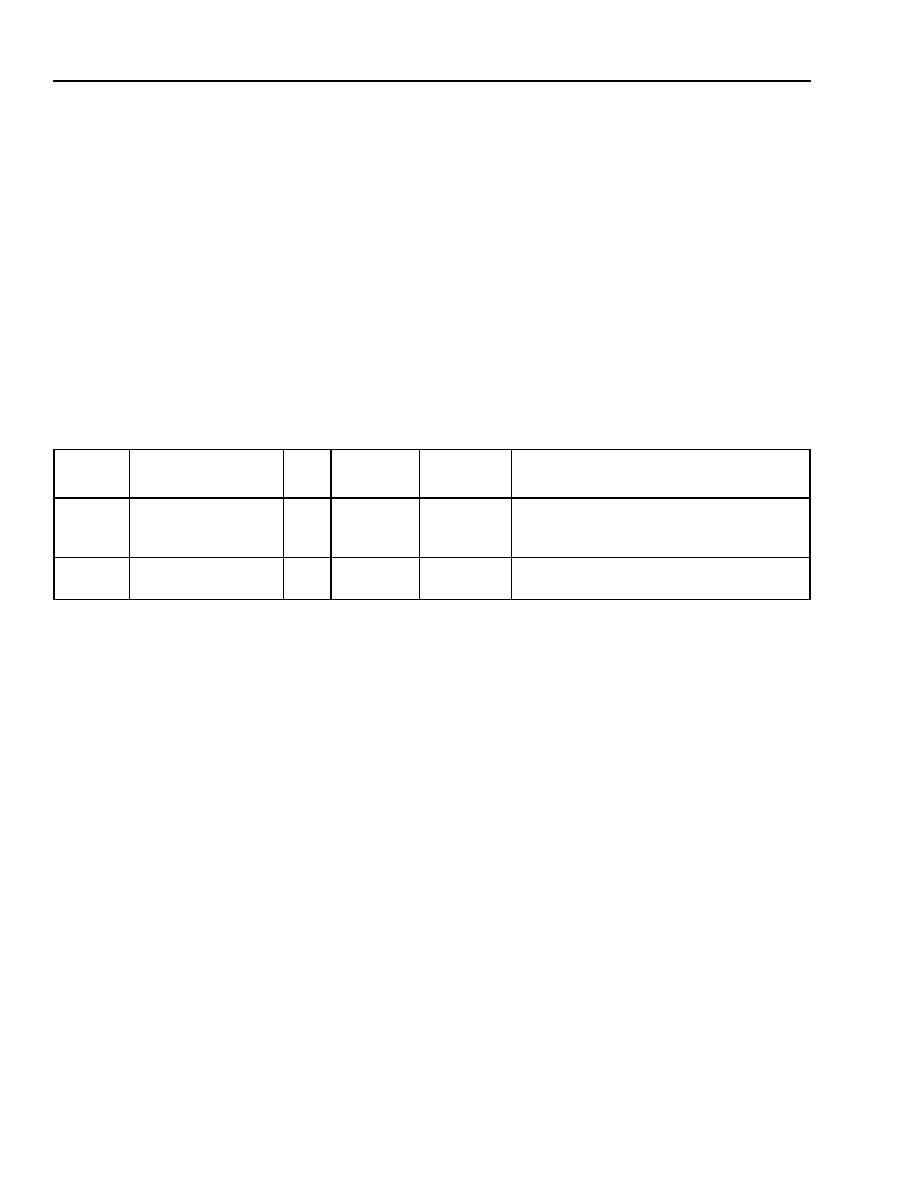
50
Agere Systems Inc.
Data Sheet
February 2004
Ambassador T8110L H.100/H.110 Switch
6 Clock Architecture
(continued)
6.1 Clock Input Control Registers
(continued)
6.1.9 DPLL1 Input Selector
The DPLL1 input selector selects one of three sources for DPLL1 synchronization input (see Section 6.4.2 on page
61), including the following:
!
Main clock selection CLK SEL MUX output
!
Main divider output
!
Resource divider output
6.1.9.1 DPLL1 Rate Register
The DPLL1 rate register controls the DPLL1 output frequency.
6.1.10 DPLL2 Input Selector
The DPLL2 input selector selects one of five sources for DPLL2 synchronization input (see Section 6.5.1 on page
63), including the following:
!
Main clock selection CLK SEL MUX output
!
Main divider output
!
Resource divider output
!
Internal frame
!
External input via PRI_REF_IN signal
Table 42. DPLL1 Input Selector Registers
Byte
Address
Name
Bit(s) Mnemonic
Value
Function
0x0020A DPLL1 Input Selector
7:0
D1ISR
0000 0000
0000 0001
0000 0010
Main selector (default).
Main divider.
Resource divider.
0x0020B DPLL1 Rate
7:0
D1RSR
0000 0000
0000 0001
DPLL1 output at 4.096 MHz (default).
DPLL1 output at 2.048 MHz.

Agere Systems Inc.
51
Data Sheet
February 2004
Ambassador T8110L H.100/H.110 Switch
6 Clock Architecture
(continued)
6.1 Clock Input Control Registers
(continued)
6.1.10 DPLL2 Input Selector (continued)
6.1.10.1 DPLL2 Rate Register
The DPLL2 rate register controls the DPLL2 output frequency.
6.1.11 NETREF1 Registers
The NETREF1 input selector, NETREF1 divider, and NETREF1 LREF select registers control the signal paths
used to generate CT_NETREF1 (see Figure 6 on page 44).
* Selection of which LREF is controlled at register 0x00212.
Table 43. DPLL2 Register
Byte
Address
Name
Bit(s) Mnemonic
Value
Function
0x0020E DPLL2 Input Selector
7:0
D2ISR
0000 0000
0000 0001
0000 0010
0000 0100
0000 1000
Main selector (default).
Main divider.
Resource divider.
T8110L internally generated frame.
External input PRI_REF_IN.
0x0020F DPLL2 Rate
7:0
D2RSR
0000 0000
0000 0001
0000 0010
0000 0100
0000 1000
DPLL2 output off (default).
DPLL2 output at 1.544 MHz.
DPLL2 output at 3.088 MHz.
DPLL2 output at 6.176 MHz.
DPLL2 output at 12.352 MHz.
Table 44. NETREF1 Registers
Byte
Address
Name
Bit(s) Mnemonic
Value
Function
0x00210
NETREF1 Input
Selector
7:4
N1DSN
0000
0001
Divider input = selector output (default).
Divider input = external input NR1_DIV_IN.
3:0
N1ISN
0000
0001
0010
0100
1000
Oscillator/XTAL1-div-8, 2.048 MHz (default).
Oscillator/XTAL1, 16.384 MHz.
CT_NETREF2 input.
LREF input*.
Oscillator/XTAL2, 6.176 MHz, or 12.352 MHz.
0x00211
NETREF1 Divider
7:0
NR1DR
LLLL LLLL Divider value, {0x00 to 0xFF} = {div1 to div256},
respectively.
0x00212
NETREF1 LREF
Select
7:0
N1LSR
0000 0000
0000 0001
0000 0010
0000 0100
0000 1000
0001 0000
0010 0000
0100 0000
1000 0000
Select LREF0 (default).
Select LREF0.
Select LREF1.
Select LREF2.
Select LREF3.
Select LREF4.
Select LREF5.
Select LREF6.
Select LREF7.

52
Agere Systems Inc.
Data Sheet
February 2004
Ambassador T8110L H.100/H.110 Switch
6 Clock Architecture
(continued)
6.1 Clock Input Control Registers
(continued)
6.1.12 NETREF2 Registers
The NETREF2 input selector, NETREF2 divider, and NETREF2 LREF select registers control the signal paths
used to generate CT_NETREF2 (see Figure 6 on page 44).
* Selection of which LREF is controlled at register 0x00216.
Table 45. NETREF2 Registers
Byte
Address
Name
Bit(s) Mnemonic
Value
Function
0x00214 NETREF2 Input
Selector
7:4
N2DSN
0000
0001
Divider input = selector output (default).
Divider input = external input NR1_DIV_IN.
3:0
N2ISN
0000
0001
0010
0100
1000
Oscillator/XTAL1-div-8, 2.048 MHz (default).
Oscillator/XTAL1, 16.384 MHz.
CT_NETREF1 input.
LREF input*.
Oscillator/XTAL2, 6.176 MHz, or 12.352 MHz.
0x00215 NETREF2 Divider
7:0
NR2DR
LLLL LLLL Divider value, {0x00 to 0xFF} = {div1 to div256},
respectively.
0x00216 NETREF2 LREF
Select
7:0
N2LSR
0000 0000
0000 0001
0000 0010
0000 0100
0000 1000
0001 0000
0010 0000
0100 0000
1000 0000
Select LREF0 (default).
Select LREF0.
Select LREF1.
Select LREF2.
Select LREF3.
Select LREF4.
Select LREF5.
Select LREF6.
Select LREF7.
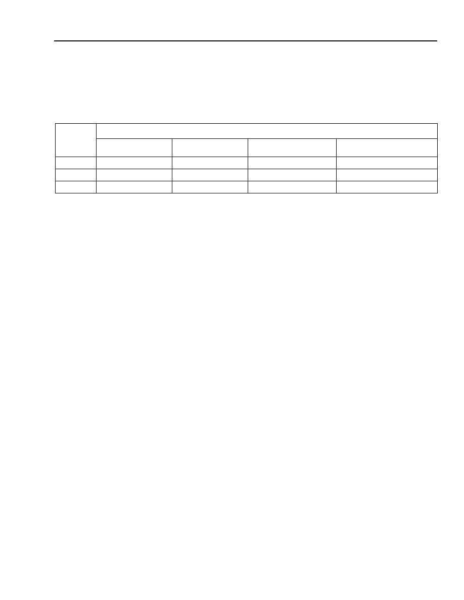
Agere Systems Inc.
53
Data Sheet
February 2004
Ambassador T8110L H.100/H.110 Switch
6 Clock Architecture
(continued)
6.2 Clock Output Control Registers
The registers listed below control output enable and rate selection of the T8110L clock path outputs.
6.2.1 Master Output Enables Register
The master output enables register controls the output enables for H-bus and compatibility clocks (CCLK) for
T8110L clock mastering. A-clocks refers to the combination of CT_C8_A bit clock and /CT_FRAME_A frame refer-
ence.
B-clocks refers to the CT_C8_B bit clock and /CT_FRAME_B frame reference.
These programmable enables are used in conjunction with master enable register 0x00103, H-bus clock enables,
HCKEB.
The NETREF output enables register controls the output enables for CT_NETREF1 and CT_NETREF2. These
programmable enables are used in conjunction with master enable register 0x00103, H-bus clock enables,
HCKEB.
The CCLK output enables register is used in conjunction with register 0x00220 and controls the output enables for
various groupings of compatibility clocks, including the following:
!
H-MVIP bit clock only(/C16±)
!
MVIP clocks (/C4, C2)
!
H-MVIP clocks (/C16±, /C4, C2)
!
SC-bus clocks (SCLK, /SCLKx2)
!
/FR_COMP compatibility frame reference
Table 46. Clock Output Control Register Map
DWORD
Address
(20 Bits)
Register
Byte 3
Byte 2
Byte 1
Byte 0
0x00220
C8 output rate
/FR_COMP width
NETREF output enables
Master output enables
0x00224
SCLK output rate
TCLK select
Reserved
CCLK output enables
0x00228
L_SC3 select
L_SC2 select
L_SC1 select
L_SC0 select

54
Agere Systems Inc.
Data Sheet
February 2004
Ambassador T8110L H.100/H.110 Switch
6 Clock Architecture
(continued)
6.2 Clock Output Control Registers
(continued)
6.2.1 Master Output Enables Register (continued)
* Overall selection includes all C clocks OFF, all C clocks ON, or select individual groups of C clocks to be enabled, in conjunction with register
0x00224.
6.2.2 Clock Output Format Registers
The clock output format registers select the pulse width of the /FR_COMP pulse width.
Note: When the T8110L is slowing to a compatibility bus, the /FR_COMP signal must be 122 ns. The T8110L can-
not phase align to a 244 ns /FR_COMP signal.
The C8 output rate register selects the CT_C8_A and CT_C8_B clock output frequency 8.192 MHz for ECTF
(H1x0) mode, or 4.096 MHz for MC1 mode.
The SCLK output rate register selects between three SC-Bus clock configurations, including the following:
!
SCLK = 2.048 MHz, /SCLKx2 = 4.096 MHz
!
SCLK = 4.096 MHz, /SCLKx2 = 8.192 MHz
!
SCLK = 8.192 MHz, /SCLKx2 = 8.192 MHz (phase shifted from SCLK)
Table 47. Master Output Enables Registers
Byte Address
Name
Bit(s) Mnemonic
Value
Function
0x00220
Master
Output
Enables
7:4
ABOEN
0000
0001
0010
0011
Disable A and B clock outputs (default).
Enable A clock outputs only.
Enable B clock outputs only.
Enable both A and B clock outputs.
3:0
CCOEN
0000
0001
0010
Disable compatibility (C clock) outputs (default).
Enable C clocks individually*.
Enable all C clocks.
0x00221
NETREF
Output
Enables
7:4
N2OEN
0000
0001
CT_NETREF2 disabled (default).
CT_NETREF2 enabled.
3:0
N1OEN
0000
0001
CT_NETREF1 disabled (default).
CT_NETREF1 enabled.
0x00224
CCLK
Output
Enables
7:4
FRSEN
0000
0001
/FR_COMP disabled (default).
/FR_COMP enabled.
3:0
CCSEN
0000
0001
0010
0011
0100
C-clock bit clocks disabled (default).
Enable H-MVIP bit clock.
Enable MVIP clocks.
Enable H-MVIP all clocks.
Enable SC-bus clocks.
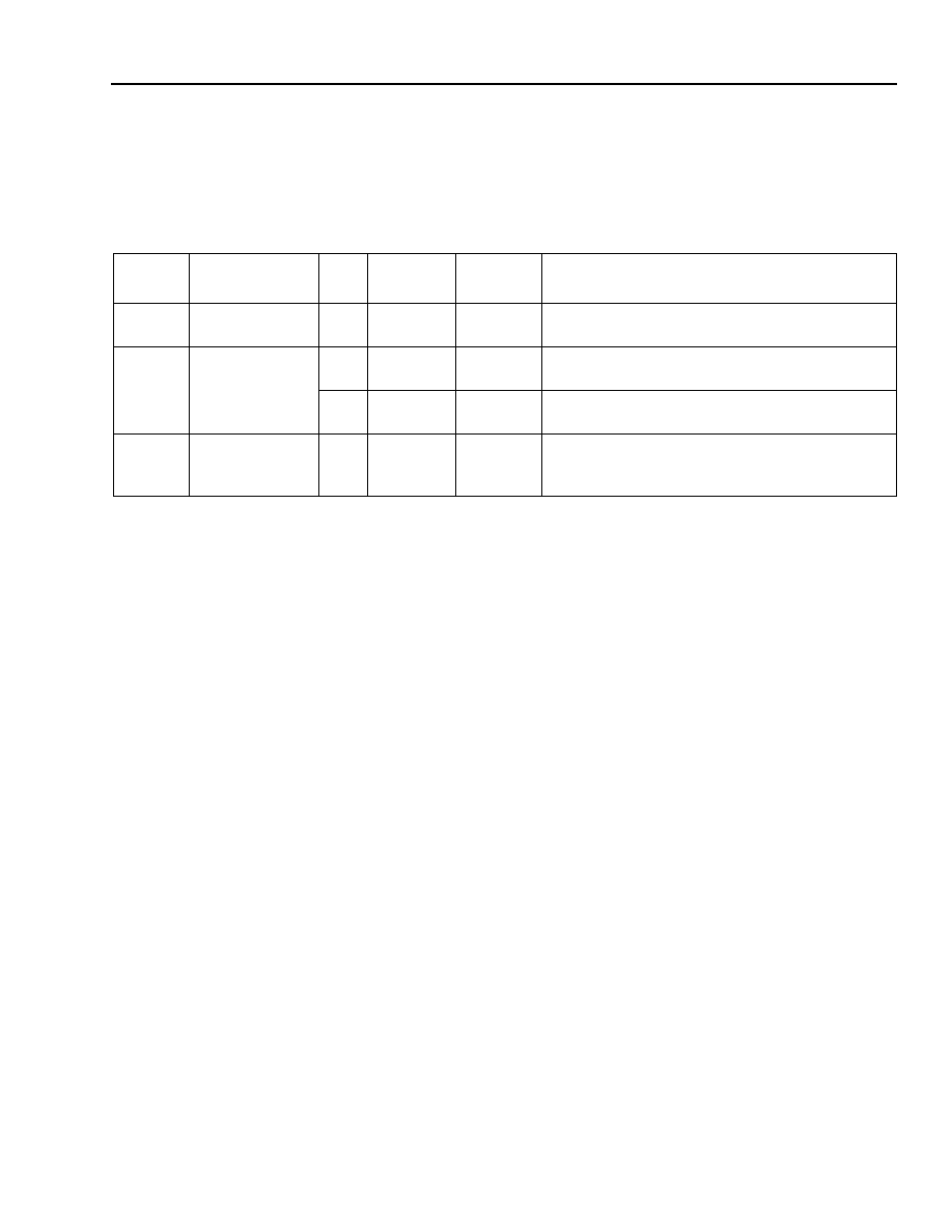
Agere Systems Inc.
55
Data Sheet
February 2004
Ambassador T8110L H.100/H.110 Switch
6 Clock Architecture
(continued)
6.2 Clock Output Control Registers
(continued)
6.2.2 Clock Output Format Registers (continued)
6.2.3 TCLK and L_SCx Select Registers
The TCLK select register controls the selection of various internally generated clocks for output to the TCLK_OUT
signal.
The L_SCx select registers control the selection of various internally generated clocks for output to the L_SC0,
L_SC1, L_SC2, and L_SC3 signals.
Table 48. Clock Output Format Registers
Byte
Address
Name
Bit(s) Mnemonic
Value
Function
0x00222 /FR_COMP
Width
7:0
FRWSR
0000 0000
0000 0001
/FR_COMP width is 122 ns (default).
/FR_COMP width is 244 ns.
0x00223 C8 Output Rate
7:4
BCRSN
0000
0001
CT_C8_B output at 8.192 MHz (default).
CT_C8_B output at 4.096 MHz, MC1 mode.
3:0
ACRSN
0000
0001
CT_C8_A output at 8.192 MHz (default).
CT_C8_A output at 4.096 MHz, MC1 mode.
0x00227 SCLK Output
Rate
7:0
SCRSR
0000 0000
0000 0001
0000 0010
SCLK = 2 MHz, /SCLKx2
= 4 MHz (default).
SCLK = 4 MHz, /SCLKx2 = 8 MHz.
SCLK = 8 MHz, /SCLKx2 = 8 MHz phase shifted.

56
Agere Systems Inc.
Data Sheet
February 2004
Ambassador T8110L H.100/H.110 Switch
6 Clock Architecture
(continued)
6.2 Clock Output Control Registers
(continued)
6.2.3 TCLK and L_SCx Select Registers (continued)
Table 49. TCLK Select and L_SCx Select Registers
Byte
Address
Name
Bit(s) Mnemonic
Value
Function
0x00226
TCLK Select
7:0
TCOSR
0000 0000
0000 0001
0000 0010
0001 0001
0001 0010
0010 0000
0010 0001
0010 0010
0011 0000
0011 0001
0011 0010
0100 0000
0100 0001
0100 0010
0100 0100
0100 1000
0101 0000
0101 0001
0101 0010
0101 0100
0101 1000
1000 0000
1000 0001
1000 0010
1001 0000
1001 0001
1001 0010
TCLK output disabled (default).
Select OSC1/XTAL1.
Select OSC2/XTAL2.
Select OSC1/XTAL1 inverted.
Select OSC2/XTAL2 inverted.
Select DPLL2 output.
Select APLL1 output, 65.536 MHz.
Select APLL2 output, 49.704 MHz.
Select DPLL2 output inverted.
Select APLL1 output inverted.
Select APLL2 output inverted.
Select generated 2.048 MHz.
Select generated 4.096 MHz.
Select generated 8.192 MHz.
Select generated 16.384 MHz.
Select generated 32.768 MHz.
Select generated 2.048 MHz inverted.
Select generated 4.096 MHz inverted.
Select generated 8.192 MHz inverted.
Select generated 16.384 MHz inverted.
select generated 32.768 MHz inverted.
Select generated frame.
Select generated CT_NETREF1.
Select generated CT_NETREF2.
Select generated frame inverted.
Select generated CT_NETREF1 inverted.
Select generated CT_NETREF2 inverted.
0x00228
(0x00229)
(0x0022A)
(0x0022B)
L_SC0 Select
L_SC1 Select
L_SC2 Select
L_SC3 Select
7:0
LC0SR
(LC1SR)
(LC2SR)
(LC3SR)
0000 0000
0000 0001
0001 0001
0100 0000
0100 0001
0100 0010
0100 0100
0100 1000
0101 0000
0101 0001
0101 0010
0101 0100
0101 1000
1000 0000
1000 0001
1000 0010
1001 0000
1001 0001
1001 0010
L_SCx output disabled (default).
Select OSC1/XTAL1.
Select OSC1/XTAL1 inverted.
Select generated 2.048 MHz.
Select generated 4.096 MHz.
Select generated 8.192 MHz.
Select generated 16.384 MHz.
Select generated 32.768 MHz.
Select generated 2.048 MHz inverted.
Select generated 4.096 MHz inverted.
Select generated 8.192 MHz inverted.
Select generated 16.384 MHz inverted.
Select generated 32.768 MHz inverted.
Select generated frame.
Select generated CT_NETREF1.
Select generated CT_NETREF2.
Select generated frame inverted.
Select generated CT_NETREF1 inverted.
Select generated CT_NETREF2 inverted.

Agere Systems Inc.
57
Data Sheet
February 2004
Ambassador T8110L H.100/H.110 Switch
6 Clock Architecture
(continued)
6.3 Clock Register Access
The T8110L clock control registers, 0x00200--0x002FF, consist of two identical sets of registers, X and Y. At any
given time, only one set is actually controlling the clocking (denoted as the active set), while the other is in a
standby state (inactive set). Either set, X or Y, may be the active set, as determined by a state machine that tracks
the clock fallback control and status and assigns either set to be active accordingly. For more details, see Section
6.7.1 on page 64. Users may only access one register set at a time. By default, access is allowed to the current
inactive set, but access to the active set is allowed via the clock register access select register, 0x00106; see Sec-
tion 5.1.4 on page 33.
6.4 Clock Circuit Operation--APLL1
APLL1 can accept either a 4.096 MHz or 2.048 MHz reference clock, and perform a corresponding multiplication
function to supply a 65.536 MHz operating clock for the T8110L. Additionally, APLL1 may be bypassed for circuit
diagnostic purposes. Please refer to Figure 5 on page 44.
6.4.1 Main Clock Selection, Bit Clock, and Frame
APLL1 clock references are selectable as stand-alone bit clocks, frames, or a pairing of bit clock and frame (see
main input selector register, 0x00200). The bit clock output of the main clock selection is available as input to the
main divider, resource divider, and DPLL1.
* MVIP, /C4 is typically the bit clock. C2 is selectable as the bit clock as well.
Used when LREF pairing is enabled. When using LREF pairing, the bit clock should be 2.048 MHz.
Table 50. Bit Clock and Frame
Bit Clock
Corresponding 8 kHz Frame
Value(s)
CT_NETREF1, CT_NETREF2
--
1.544 MHz (T1), 2.048 MHz (E1)
NA
CT_NETREF1, CT_NETREF2
8 kHz
CT_C8_A
/CT_FRAME_A
8.192 MHz (ECTF), 4.096 MHz (MC1)
CT_C8_B
/CT_FRAME_B
8.192 MHz (ECTF), 4.096 MHz (MC1)
/C16±
/FR_COMP
16.384 MHz (H-MVIP)
/C4
/FR_COMP
4.096 MHz (MVIP)
C2
/FR_COMP
2.048 MHz (MVIP*)
SCLK
/FR_COMP
2.048 MHz, 4.096 MHz, 8.192 MHz (SC-bus)
/SCLKx2
/FR_COMP
4.096 MHz, 8.192 MHz (SC-bus)
LREF[0]
LREF[4]
System-specific
LREF[1]
LREF[5]
System-specific
LREF[2]
LREF[6]
System-specific
LREF[3]
LREF[7]
System-specific
LREF[4]
--
System-specific
LREF[5]
--
System-specific
LREF[6]
--
System-specific
LREF[7]
--
System-specific

58
Agere Systems Inc.
Data Sheet
February 2004
Ambassador T8110L H.100/H.110 Switch
6 Clock Architecture
(continued)
6.4 Clock Circuit Operation--APLL1
(continued)
6.4.1 Main Clock Selection, Bit Clock, and Frame (continued)
6.4.1.1 Watchdog Timers
A set of watchdog timers is available for all H1x0, H-MVIP, MVIP, and SC-bus clocks. No watchdogs are available
for LREF[7:0] directly; however, the LREF inputs may be monitored indirectly via watchdogs on the DPLL1 and
DPLL2 sync inputs, or via the failsafe mechanism; see Section 6.7.2 on page 70. The watchdogs sample the
incoming clocks at 32.768 MHz (derived from the XTAL1 crystal) and monitor for loss of signal, as shown below.
Table 51. Watchdog Timer Description
Watchdog
Signal, Value
Description
H1x0 clock monitors*
CT_C8_A at 8.192 MHz
CT_C8_B at 8.192 MHz
ECTF mode. Checks for CT_C8 rising edge within a
35 ns window of its expected arrival.
CT_C8_A at 4.096 MHz
CT_C8_B at 4.096 MHz
MC1 mode. Monitors for loss of signal (falling edges).
FRAME monitors
/CT_FRAME_A
/CT_FRAME_B
/FR_COMP
Monitors for 8 kHz frequency. Detects frame overflow
(i.e., next frame pulse too late) and frame underflow
(i.e., next frame pulse too early).
NETREF monitors*
CT_NETREF1 at 1.544 MHz
CT_NETREF2 at 1.544 MHz
NETREF is T1 bit clock. Monitors for loss of signal
(rising or falling edges).
CT_NETREF1 at 2.048 MHz
CT_NETREF2 at 2.048 MHz
NETREF is E1 bit clock. Monitors for loss of signal
(rising or falling edges).
CT_NETREF1 at 8 kHz
CT_NETREF2 at 8 kHz
NETREF is 8 kHz frame reference. Monitors for
8 kHz frequency. Detects frame overflow
(i.e., next frame pulse too late) and frame underflow
(i.e., next frame pulse too early).
Compatibility clock monitors
/C16± at 16.384 MHz
/C4 at 4.096 MHz
C2 at 2.048 MHz
SCLK, /SCLKx2 at any of
their defined values.
Gross loss-of-signal detector--clocks are sampled
and normalized to 1.024 MHz. It can take up to
976 ns for these watchdog timers to detect loss of a
compatibility clock.
DPLL1, DPLL2 sync
monitors
Output of MUX selector to the
SYNC input of each
DPLL (8 kHz)
Monitors for 8 kHz frequency. Detects frame overflow
(i.e., next frame pulse too late) and frame underflow
(i.e., next frame pulse too early).
* User selects frequency at which to monitor the CT_C8 clocks via register 0x0010C, watchdog select, C8.
DPLL sync reference is expected to be 8 kHz.
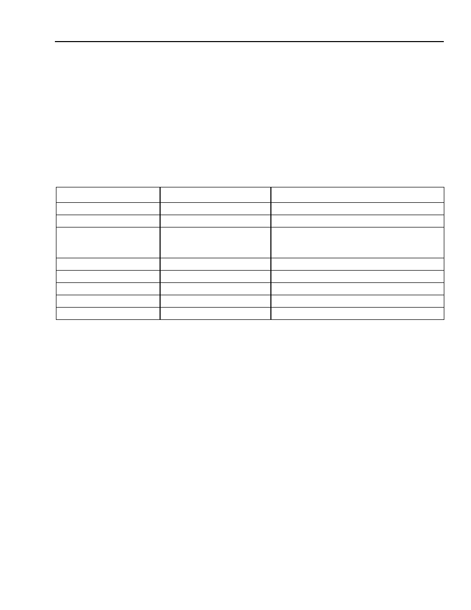
Agere Systems Inc.
59
Data Sheet
February 2004
Ambassador T8110L H.100/H.110 Switch
6 Clock Architecture
(continued)
6.4 Clock Circuit Operation--APLL1
(continued)
6.4.1 Main Clock Selection, Bit Clock, and Frame (continued)
6.4.1.2 Frame Center Sampling
Frame center samples are used in order to phase-align the incoming frame reference to the internally generated
frame reference; see Section 6.4.5.1 on page 62. The incoming frame reference signal is sampled with a recov-
ered clock (output of the APLL1 feedback divider) to determine the frame center. Frame center sampling is only
relevant when the main clock selection is based on a paired bit clock/frame reference, as follows.
Table 52. Frame Center Sampling
Frame Signal
Corresponding Bit Clock
Sample Clock
/CT_FRAME_A
CT_C8_A
Recovered 8.192 MHz, rising edge.
/CT_FRAME_B
CT_C8_B
Recovered 8.192 MHz, rising edge.
/FR_COMP
/C16± (H-MVIP)
or /C4 (MVIP)
or C2 (MVIP)
Recovered 4.096 MHz, falling edge.
/FR_COMP
SCLK or /SCLKx2 (SC-bus)
Recovered 2.048 MHz, rising edge.
LREF[4]
LREF[0]
Recovered 2.048 MHz, rising edge.
LREF[5]
LREF[1]
Recovered 2.048 MHz, rising edge.
LREF[6]
LREF[2]
Recovered 2.048 MHz, rising edge.
LREF[7]
LREF[3]
Recovered 2.048 MHz, rising edge.
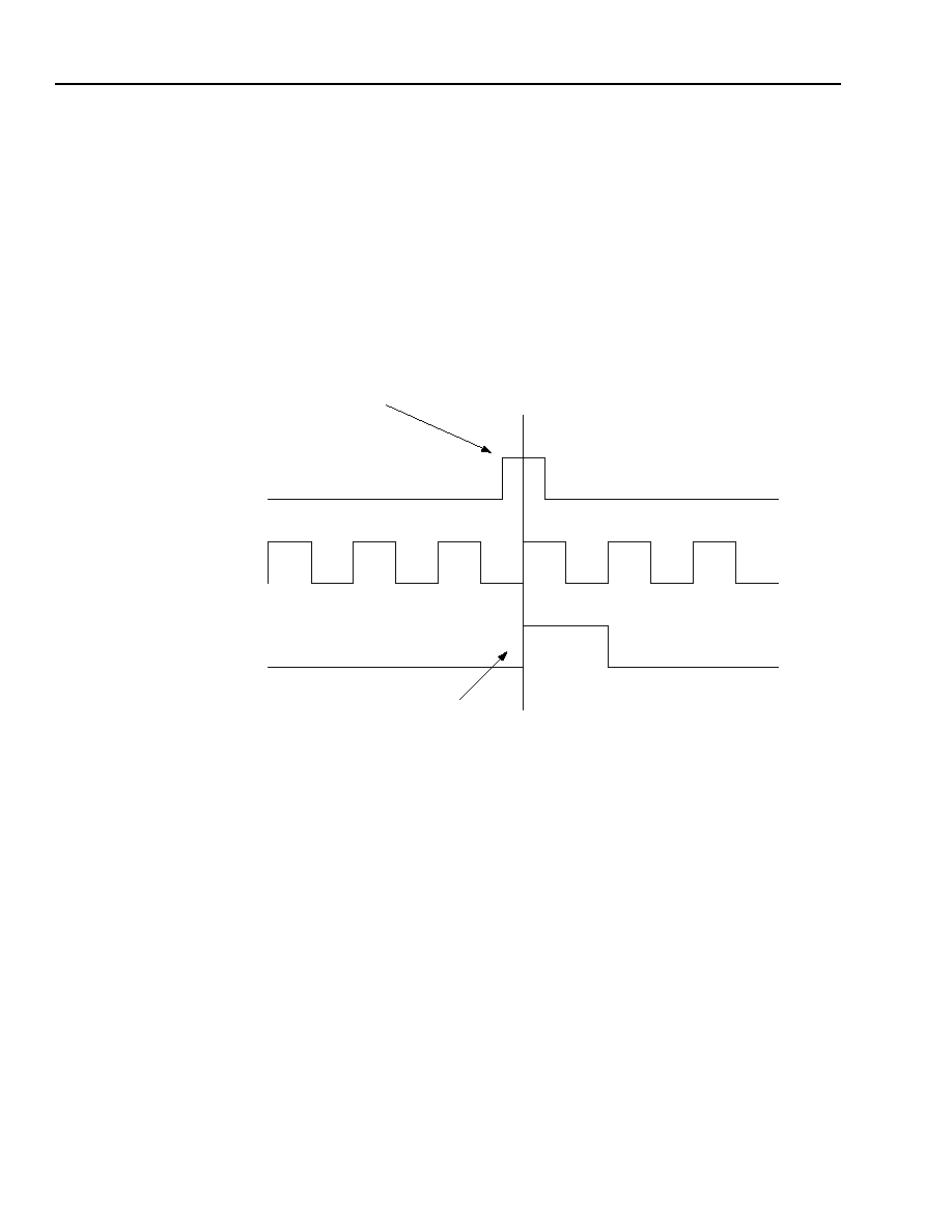
60
Agere Systems Inc.
Data Sheet
February 2004
Ambassador T8110L H.100/H.110 Switch
6 Clock Architecture
(continued)
6.4 Clock Circuit Operation--APLL1
(continued)
6.4.1 Main Clock Selection, Bit Clock, and Frame (continued)
6.4.1.3 LREF Pair Polarity Configuration
The T8110L may derive its clocking from an LREF pair, which is compromised of a frame pulse and a 2.048 MHz
bit clock. In order to achieve proper phase alignment when deriving clocking from LREF pairs, the T8110L must be
provided with a frame pulse and bit clock with polarities as shown below.
Figure 7. T8110L Required Frame Pulse and Bit Clock with Polarities
If the frame pulse and bit clock cannot be externally provided with the proper polarities, the polarities can be inter-
nally adjusted via the main inversion select register (0x204) and the LREF inversion select register (0x20C). The
main inversion select register will allow inversion of only the bit clock, while the LREF inversion select register
allows any LREF signal to be inverted.
Note: Once the frame pulse and bit clock polarity have been properly configured, they must not be changed while
the T8110L is deriving clocking from the LREF pair.
MASTER FRAME
(LREF 7/6/5/4)
MASTER BIT CLOCK
(LREF 3/2/1/0)
SLAVE FRAME
FRAME CENTER
MASTER FRAME SIGNAL
MAY BE EITHER 122 NS OR
244 NS WIDE.
THE OUTPUT FRAME SIGNAL LENGTH IS
PROGRAMMABLE. (SEE SECTION 8 OF THE
T8110 DATA SHEET.)

Agere Systems Inc.
61
Data Sheet
February 2004
Ambassador T8110L H.100/H.110 Switch
6 Clock Architecture
(continued)
6.4 Clock Circuit Operation--APLL1
(continued)
6.4.2 Main and Resource Dividers
Two independently programmable dividers are available to divide down the main clock selection signal. The func-
tion ranges from divide-by-1 (bypass) to divide-by-256.
!
For binary divider values of 1, 2, 4, 8, 16, 32, 64, 128, and 256, the output is 50% duty cycle.
!
For a divider value of 193, the output is almost 50% duty cycle (low-level duration is one clock cycle shorter than
high-level duration).
!
For all other divider values, the output is a pulse whose width is one full period of the main clock selection signal.
Output of both dividers is available to the DPLL1 and the APLL1 reference selector. The output of the main divider
is also available at the PRI_REF_OUT chip output.
Both dividers are reset whenever a changeover between X and Y clock register sets is detected; see Section 6.3
on page 57. This allows for immediate loading of the newly activated divider register values.
6.4.3 DPLL1
A digital phase-lock loop is provided to generate a 4.096 MHz or 2.048 MHz reference to APLL1, selectable via
register 0x0020B (DPLL1 rate). The DPLL1 operates at 32.768 MHz, derived from the XTAL1 crystal input. The
DPLL1 synchronization source is selectable (register 0x0020A, DPLL1 input selector) between the main clock
selection signal, the output of the resource divider, or the output of the main divider, and is intended to be pre-
sented as an 8 kHz frame reference. DPLL1 is determined to be in-lock or out-of-lock, based on the state of the
output clock when an edge transition is detected at the synchronization source. An out-of-lock condition results in a
DPLL1 correction, which can either lengthen or shorten its current output clock period by 30.5 ns.
6.4.4 Reference Selector
The APLL1 reference clock is selectable between five possible sources via register 0x00202, APLL1 input selector.
A 4.096 MHz or 2.048 MHz reference must be provided. The five possible sources are shown below:
!
XTAL1 crystal (16.384 MHz) divided-by-4
!
Main divider output
!
Resource divider output
!
DPLL1 output
!
PRI_REF_IN external chip input
6.4.5 Internal Clock Generation
The main internal functions of T8110L are synchronous to the 65.536 MHz output of APLL1. This clock is further
divided to generate 32.768 MHz, 16.384 MHz, and 8 kHz internal reference signals. Additional divide-down values
to 8.192 MHz, 4.096 MHz, and 2.048 MHz are generated. These generated clocks are the source for H1x0,
H-MVIP, MVIP, and SC-bus clocks when the T8110L is mastering the bus clocks; see Section 6.2 on page 53.
These internally generated clocks can either be free-running, or can be aligned to the incoming main selection
clock and frame, via a phase alignment circuit (see Section 7.4.5.1).

62
Agere Systems Inc.
Data Sheet
February 2004
Ambassador T8110L H.100/H.110 Switch
6 Clock Architecture
(continued)
6.4 Clock Circuit Operation--APLL1
(continued)
6.4.5 Internal Clock Generation (continued)
6.4.5.1 Phase Alignment
Phase alignment allows the free-running internally generated clocks to be forced into alignment with the incoming
main selection clock and frame, under the following conditions:
!
The main selection clock is based on a paired bit clock/frame reference (see Section 6.4.1.2 on page 59), and
the phase alignment circuit is enabled (via register 0x00107, phase alignment select).
The incoming frame center is monitored via the frame center samplers (see Section 6.4.1.2 on page 59) and com-
pared to the state of the internally generated frame. The circuit determines whether the frame centers are aligned.
If not, three possible actions take place as shown below:
!
NOP: no corrections when phase alignment is disabled.
!
Snap correction: the internally generated clocks and frame immediately snap into alignment with the incoming
frame center.
!
Slide correction: the internally generated clocks and frame gradually slide into alignment with the incoming frame
center, at a rate of one 65.536 MHz clock period per frame. The sliding occurs in one direction only and creates
frame periods that are 15.25 ns longer than 125
µ
s until the frames are aligned. Please refer to Figure 8.
5-9414 (F)
A. Phase Alignment--SNAP
5-9415 (F)
B. Phase Alignment--SLIDE
Figure 8. T8110L Phase Alignment, SNAP and SLIDE
INCOMING FRAME CENTER
INCOMING FRAME CENTER
MISALIGNED
INTERNAL
FRAME CENTER
SNAP
ALIGNMENT
REALIGNED INTERNAL
FRAME CENTER
125
µ
s
INCOMING BIT CLOCK
CT_C8_A
INCOMING FRAME
/CT_FRAME_A
INTERNAL CLOCK,
8.192 MHz
INTERNAL FRAME
REALIGNED INTERNAL
FRAME CENTER
MISALIGNED
INTERNAL
FRAME CENTER
MISALIGNED
INTERNAL
FRAME CENTER
MISALIGNED
INTERNAL
FRAME CENTER
INCOMING BIT CLOCK
CT_C8_A
INCOMING FRAME
/CT_FRAME_A
INTERNAL CLOCK,
8.192 MHz
INTERNAL FRAME
125
µ
s
125
µ
s
125
µ
s
45 ns
30 ns
15 ns
SLIDE ALIGNMENT
SLIDE ALIGNMENT
SLIDE ALIGNMENT

Agere Systems Inc.
63
Data Sheet
February 2004
Ambassador T8110L H.100/H.110 Switch
6 Clock Architecture
(continued)
6.5 Clock Circuit Operation, APLL2
APLL2 requires either a 6.176 MHz or 12.352 MHz reference clock to produce a 49.408 MHz clock for operating
DPLL2. A user-supplied rate multiplier (register 0x00207, APLL2 rate) provides either a times 8 function (when ref-
erence clock = 6.176 MHz) or a times 4 function (when reference clock = 12.352 MHz). Additionally, APLL2 may be
bypassed for circuit diagnostic purposes (see Figure 5 on page 44).
6.5.1 DPLL2
A second digital phase-lock loop is provided to generate various derivations of T1 operating frequencies, available
by selection via the TCLK_OUT output. The possible output frequencies are selectable via register 0x0020F
(DPLL2 rate) and include 1.544 MHz, 3.088 MHz, 6.176 MHz, and 12.352 MHz. The DPLL2 input clock operates at
49.408 MHz from the APLL2 output. Synchronization sources for DPLL2 include the same sources provided to
DPLL1 (selectable between the main clock selection signal, the output of the resource divider, or the output of the
main divider) and two additional sources, including the T8110L internally generated frame signal and the
PRI_REF_IN input. These selections are available via register 0x0020E, DPLL2 input selector. DPLL2 is deter-
mined to be in-lock or out-of-lock based on the state of its output when an edge transition is detected at the syn-
chronization source. An out-of-lock condition results in a DPLL2 correction, which can either lengthen or shorten its
current output clock period by 20.2 ns.
6.6 Clock Circuit Operation, CT_NETREF Generation
The T8110L provides two independently programmable paths to generate CT_NETREF1 and CT_NETREF2, via
registers 0x00210--0x00216. Each CT_NETREF is individually enabled with register 0x00221, NETREF output
enables. Each path consists of a source selector MUX and a divider circuit (see Figure 6 on page 44).
6.6.1 NETREF Source Select
XTAL1 input DIV 8 (2.048 MHz)
XTAL1 input (16.384 MHz)
XTAL2 input (6.176 MHz or 12.352 MHz)
LREF[7:0]
CT_NETREFx (the other NETREF--i.e., CT_NETREF1 can be derived from CT_NETREF2, and vise-versa).
The output of the source select MUX is made available directly to the NETREF divider, and also to chip output
(NR1_SEL_OUT, NR2_SEL_OUT).
6.6.2 NETREF Divider
Each NETREF path provides a divider from a divide-by-1 function up to a divide-by-256 function. The clock source
for the divider is selectable between the output of the source select MUX or from external chip input (NR1_DIV_IN,
NR2_DIV_IN).
!
For binary divider values of 1, 2, 4, 8, 16, 32, 64, and 128, output is 50% duty cycle.
!
For divider values of 256, 193, plus all other nonbinary values, output is a pulse whose width is one-half of a
clock period, asserted during the second half of the divider clock period.
The NETREF dividers are reset whenever a changeover between X and Y clock register sets is detected (see Sec-
tion 6.3 on page 57). This allows for immediate loading of the newly activated divider register values.

64
Agere Systems Inc.
Data Sheet
February 2004
Ambassador T8110L H.100/H.110 Switch
6 Clock Architecture
(continued)
6.7 Clock Circuit Operation--Fallback and Failsafe
Fallback is a means to alter the reference source to APLL1 by switching between two clock control register sets
upon detection of a fallback event. Failsafe is a feature to provide a safety net for the reference source to APLL1,
independent of clock fallback.
6.7.1 Clock Fallback
Clock fallback is a means to alter the APLL1 reference clock source upon detection of a fallback event and is con-
trolled by eight registers, 0x00108--0x0010F (refer to Section 5.1.4 on page 33). These registers enable and con-
trol the state transitions that determine which of two clock register sets is used to control the APLL1 reference clock
source (see Section 6.1 on page 45 through Section 6.3, Table 54 on page 67, and Figure 10 on page 66).
6.7.1.1 Fallback Events
Clock fallback (transition from primary to secondary clock sets) can only occur if the fallback mode is enabled (reg-
ister 0x00109, lower nibble) and a fallback event occurs. When enabled, there are three ways to trigger the fallback
event:
!
Software, via a FORCE_FALLBACK command. The user sets bit 2 of the fallback control register, 0x00108, cre-
ating a software-invoked fallback event.
!
Hardware via the fallback trigger enable registers, 0x0010A--0x0010B. User may enable specific watchdog tim-
ers and corresponding fallback trigger enable bits. If a watchdog timer indicates a clock error, and its correspond-
ing trigger enable bit is set, a hardware-invoked fallback event is produced.
!
Hardware, legacy modes, via the fallback type select register, 0x00109, upper nibble. The legacy modes are
included to maintain backwards compatibility with earlier Ambassador devices. User may enable specific watch-
dog timers, but the fallback trigger enable registers are ignored. Instead, the watchdogs which are allowed to
trigger a fallback event are automatically selected based on the state of the main input selector register, 0x00200
(refer to Table 53). If a watchdog timer indicates a clock error, and its corresponding trigger enable is selected via
the main input selector, a hardware-invoked fallback event is produced.
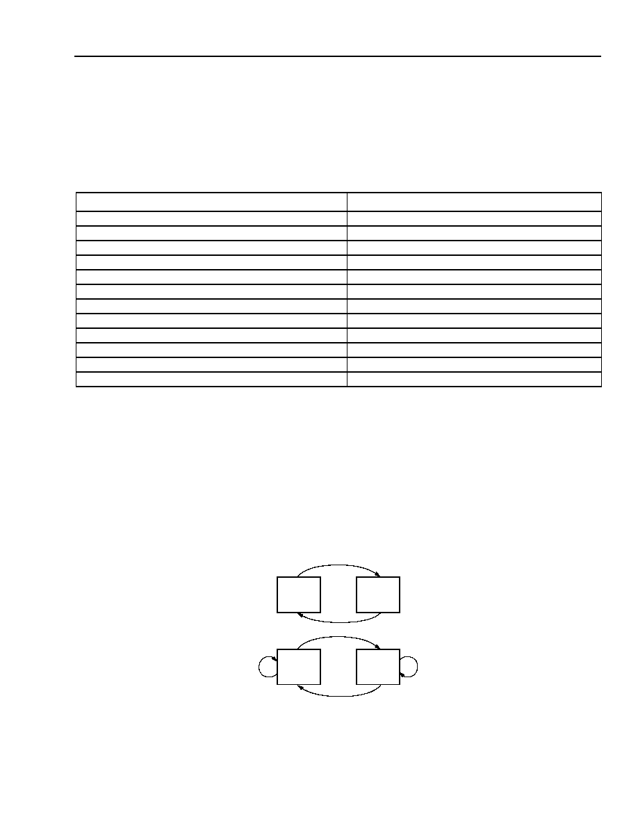
Agere Systems Inc.
65
Data Sheet
February 2004
Ambassador T8110L H.100/H.110 Switch
6 Clock Architecture
(continued)
6.7 Clock Circuit Operation--Fallback and Failsafe
(continued)
6.7.1 Clock Fallback (continued)
6.7.1.1 Fallback Events (continued)
6.7.1.2 Fallback Scenarios--Fixed vs. Rotating Secondary
When clock fallback is enabled (register 0x00109, lower nibble), there are two possible scenarios for transitioning
between the primary and secondary clock sets.
In a fixed secondary scheme, a fallback event switches the active clock set from primary to secondary. When the
fallback event is cleared (via user-invoked CLEAR_FALLBACK), the active clock set returns to primary.
In a rotating secondary scheme, a fallback event switches the active clock set from primary to secondary. When
the fallback event is cleared, the secondary remains as the new active clock set. In effect, the secondary becomes
the new primary, and the primary becomes the new secondary.
The concepts are illustrated in the figure below.
5-9420 (F)
Figure 9. Fallback--Fixed vs. Rotating Secondary
Table 53. Legacy Mode Fallback Event Triggers
Main Input Selector Function (Register 0x00200)
Selected Watchdog Triggers (Legacy Modes)
Oscillator/crystal
None
CT_NETREF1
NETREF1 watchdog
CT_NETREF
NETREF2 watchdog
LREF, individual
None
LREF, paired
None
H-bus, A clocks
CT_C8_A and /CT_FRAME_A watchdogs
H-bus, B clocks
CT_C8_B and /CT_FRAME_B watchdogs
MC1, R clocks
None
MC1, L clocks
None
MVIP clocks (/C4 or C2 bit clock)
/C4, C2, and /FR_COMP watchdogs
H-MVIP clocks
/C16±, /C4, C2, and /FR_COMP watchdogs
SC-bus clocks (2 MHz or 4/8 MHz)
SCLK, /SCLKx2, and /FR_COMP watchdogs
SECONDARY
REGISTER
SET
(X OR Y)
PRIMARY
REGISTER
SET
(X OR Y)
REGISTER
SET Y
REGISTER
SET X
ROTATING SECONDARY SCENARIO
FALLBACK
EVENT
FALLBACK
CLEARED
FALLBACK
EVENT
FALLBACK
EVENT
FIXED SECONDARY SCENARIO
FALLBACK
CLEARED
FALLBACK
CLEARED
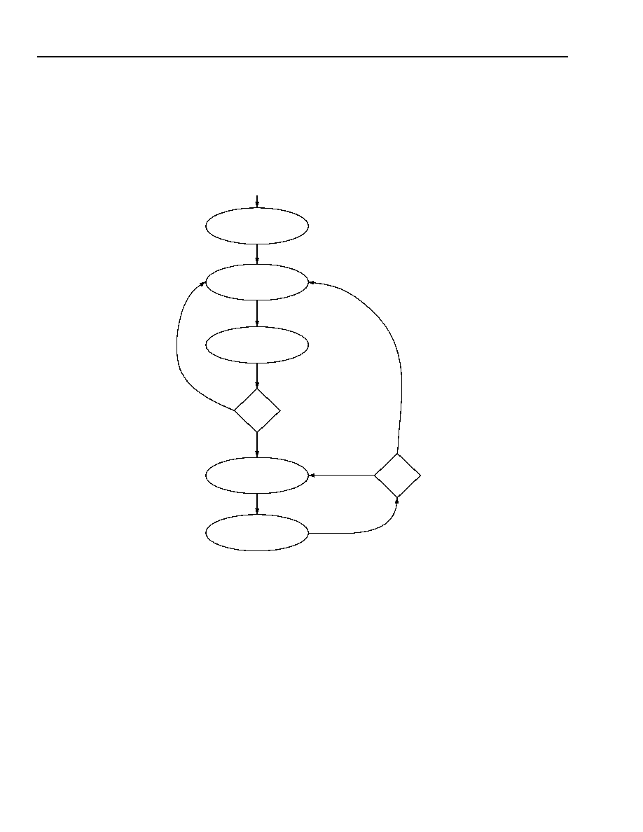
66
Agere Systems Inc.
Data Sheet
February 2004
Ambassador T8110L H.100/H.110 Switch
6 Clock Architecture
(continued)
6.7 Clock Circuit Operation--Fallback and Failsafe
(continued)
6.7.1 Clock Fallback (continued)
6.7.1.1 Fallback Scenarios--Fixed vs. Rotating Secondary (continued)
5-9422 (F)
Figure 10. T8110L Clock Fallback States
FALLBACK
TYPE
?
TO_PRIMARY
(X IS THE ACTIVE SET,
ASSERT FALLBACK FLAG)
SECONDARY
(Y IS THE ACTIVE SET)
TO_SECONDARY
(Y IS THE ACTIVE SET,
ASSERT FALLBACK FLAG)
PRIMARY
(X IS THE ACTIVE SET)
INITIAL
(Y IS THE ACTIVE SET)
RESET
USER COMMAND
GO_CLOCKS
FALLBACK ENABLED AND
FALLBACK EVENT
FALLBACK ENABLED AND
FALLBACK EVENT
USER COMMAND
CLEAR_FALLBACK
ROTATING
SECONDARY
FALLBACK
TYPE
?
MODE
FIXED
SECONDARY
MODE
USER COMMAND
CLEAR_FALLBACK
ROTATING
SECONDARY
MODE
FIXED
SECONDARY
MODE

Agere Systems Inc.
67
Data Sheet
February 2004
Ambassador T8110L H.100/H.110 Switch
6 Clock Architecture
(continued)
6.7 Clock Circuit Operation--Fallback and Failsafe
(continued)
6.7.1 Clock Fallback (continued)
6.7.1.1 Fallback Scenarios--Fixed vs. Rotating Secondary (continued)
* Fallback event; refer to Section 6.7.1.1 on page 64.
Fixed, rotating secondary; refer to Section 6.7.1.2 on page 65.
Table 54. Clock Fallback State Description
Clock Fallback
State
Description
Exit To
Exit Condition
INITIAL
Y is the active clock register
set. Default value provides
XTAL1-div-4 reference.
PRIMARY
User issues GO_CLOCKS command
(set register 0x00108 bit 0).
PRIMARY
X is the active clock register
set and controls APLL1
REFCLK.
TO_SECONDARY Fallback is enabled and fallback event*
occurs.
TO_SECONDARY Y is the active clock register
set and controls APLL1
REFCLK.
Fallback flag is asserted.
PRIMARY
User issues CLEAR_FALLBACK com-
mand (set register 0x00108 bit 1) and
fallback type = fixed secondary
.
SECONDARY
User issues CLEAR_FALLBACK com-
mand (set register 0x00108 bit 1) and
fallback type = rotating secondary
.
SECONDARY
Y is the active clock register
set and controls APLL1
REFCLK.
TO_PRIMARY
Fallback is enabled and fallback event*
occurs.
TO_PRIMARY
X is the active clock register
set and controls APLL1
REFCLK.
Fallback flag is asserted.
SECONDARY
User issues CLEAR_FALLBACK com-
mand (set register 0x00108 bit 1) and
fallback type = fixed secondary
.
PRIMARY
User issues CLEAR_FALLBACK com-
mand (set register 0x00108 bit 1) and
fallback type = rotating secondary
.
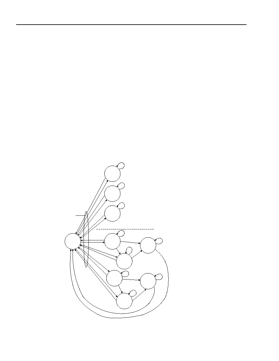
68
Agere Systems Inc.
Data Sheet
February 2004
Ambassador T8110L H.100/H.110 Switch
6 Clock Architecture
(continued)
6.7 Clock Circuit Operation--Fallback and Failsafe
(continued)
6.7.1 Clock Fallback (continued)
6.7.1.3 H-Bus Clock Enable/Disable on Fallback
The previous Ambassador devices allowed a fallback mode (A/B fallback) which automatically allowed an H1x0
bus clock master to detect an error in its own output clock and remove itself from the bus, or a clock slave to detect
an error on its incoming clock and promote itself to clock master. The H-bus clocks include:
!
A clocks: CT_C8_A, /CT_FRAME_A
!
B clocks: CT_C8_B, /CT_FRAME_B
!
C clocks: /C16±, /C4, C2, SCLK, /SCLKx2, /FR_COMP
Refer to Figure 11 and Table 55. The T8110L allows for this mode of operation in two ways:
Register 0x00109(7:4) = 0100: legacy mode, A/B fallback--when this mode is selected, the fallback triggers
allowed are predefined based on the main input clock selection, and the state machine which controls H-bus clock
enable/disable is activated.
Register 0x00109(7:4) = 1001: nonlegacy mode--when this mode is selected, the fallback trigger enable registers
determine what triggers a fallback, and the state machine which controls H-bus clock enable/disable is activated.
Figure 11. T8110L H-Bus Clock Enable States
The T8110
enters & leaves
these states
based on
Master Output
Enable clock
register
updates,
0x00220
Diag_ABC = Drives A
Clocks, B Clocks and
C Clocks, no fallback
permitted
Initial
Diag_ABC
Diag_AB
C_Only
A_Only
A_Master
B_Only
B_Master
A_Error
B_Error
A Clocks Fail
B Clocks Fail
A Clocks Fail
B Clocks Fail
B Clocks Fail
A Clocks Fail
Reprogram
B Clocks
Reprogram
A Clocks
Diagnostic/Forced Clocking
Fallback Clocking, assumes
Fallback enabled in CKS register
Diag_AB = Drives A
Clocks and B Clocks,
no fallback permitted
C_Only = Drives C
Clocks only, no
fallback permitted
B_Only = Drives B
Clocks, can be promoted
to master and drive C clocks
in fallbackcondition
A_Only = Drives A
Clocks, can be promoted
to master and drive C clocks
in fallbackcondition
B_Master = Drives B & C
Clocks, all clocks shut off
in fallbackcondition
A_Master = Drives A & C
Clocks, all clocks shut off
in fallbackcondition
B_Error = all clocks shut off,
waiting for B clocks to be
reprogrammed
A_Error = all clocks shut off,
waiting for A clocks to be
reprogrammed

Agere Systems Inc.
69
Data Sheet
February 2004
Ambassador T8110L H.100/H.110 Switch
6 Clock Architecture
(continued)
6.7 Clock Circuit Operation--Fallback and Failsafe
(continued)
6.7.1 Clock Fallback (continued)
6.7.1.1 H-Bus Clock Enable/Disable on Fallback (continued)
Table 55. H-Bus Clock Enable State Description
H-Bus Clock
Enable State
Description
Exit To
Exit Condition
INITIAL
Initial condition, waiting for clock
output control register program-
ming.
Any of the
other states
User update of the clock output control regis-
ter (0x00220, master output enables).
DIAG_ABC
T8110L is driving all H-bus clocks
(diagnostic mode).
INITIAL
User update of the clock output control regis-
ter (0x00220, master output enables).
DIAG_AB
T8110L is driving both the H-bus A
and B clocks (diagnostic mode).
INITIAL
User update of the clock output control regis-
ter (0x00220, master output enables).
C_ONLY
T8110L is driving only the
H-bus C clocks.
INITIAL
User update of the clock output control regis-
ter (0x00220, master output enables).
A_MASTER
T8110L clock output control regis-
ters are programmed to drive A
clocks and C clocks (T8110L is an
A clock master), or T8110L was
supplying a backup A clock and has
been promoted to A clock master.
A_ERROR A clock error on CT_C8_A or /CT_FRAME_A
is detected; disable clock outputs.
INITIAL
User update of the clock output control regis-
ter (0x00220, master output enables).
A_ONLY
T8110L clock output control regis-
ters are programmed to drive A
clocks only (T8110L is a B clock
slave, and supplies a backup A
clock).
A_MASTER A clock error on CT_C8_B or /CT_FRAME_B
is detected; promote to A clock master.
A_ERROR A clock error on CT_C8_A or /CT_FRAME_A
is detected; disable clock outputs.
INITIAL
User update of the clock output control regis-
ter (0x00220, master output enables).
A_ERROR
T8110L has detected a clock error
while driving the A clocks, and has
stopped driving any H bus clocks.
INITIAL
User update of the clock output control regis-
ter (0x00220, master output enables).
B_MASTER
T8110L clock output control regis-
ters are programmed to drive B
clocks and C clocks (T8110L is a B
clock master), or T8110L was sup-
plying a backup B clock and has
been promoted to B clock master.
B_ERROR A clock error on CT_C8_B or /CT_FRAME_B
is detected; disable clock outputs.
INITIAL
User update of the clock output control regis-
ter (0x00220, master output enables).
B_ONLY
T8110L clock output control regis-
ters are programmed to drive B
clocks only (T8110L is an A clock
slave, and supplies a backup B
clock).
B_MASTER A clock error on CT_C8_A or /CT_FRAME_A
is detected; promote to B clock master.
B_ERROR A clock error on CT_C8_B or /CT_FRAME_B
is detected; disable clock outputs.
INITIAL
User update of the clock output control regis-
ter (0x00220, master output enables).
B_ERROR
T8110L has detected a clock error
while driving the B clocks, and has
stopped driving any H bus clocks.
INITIAL
User update of the clock output control regis-
ter (0x00220, master output enables).
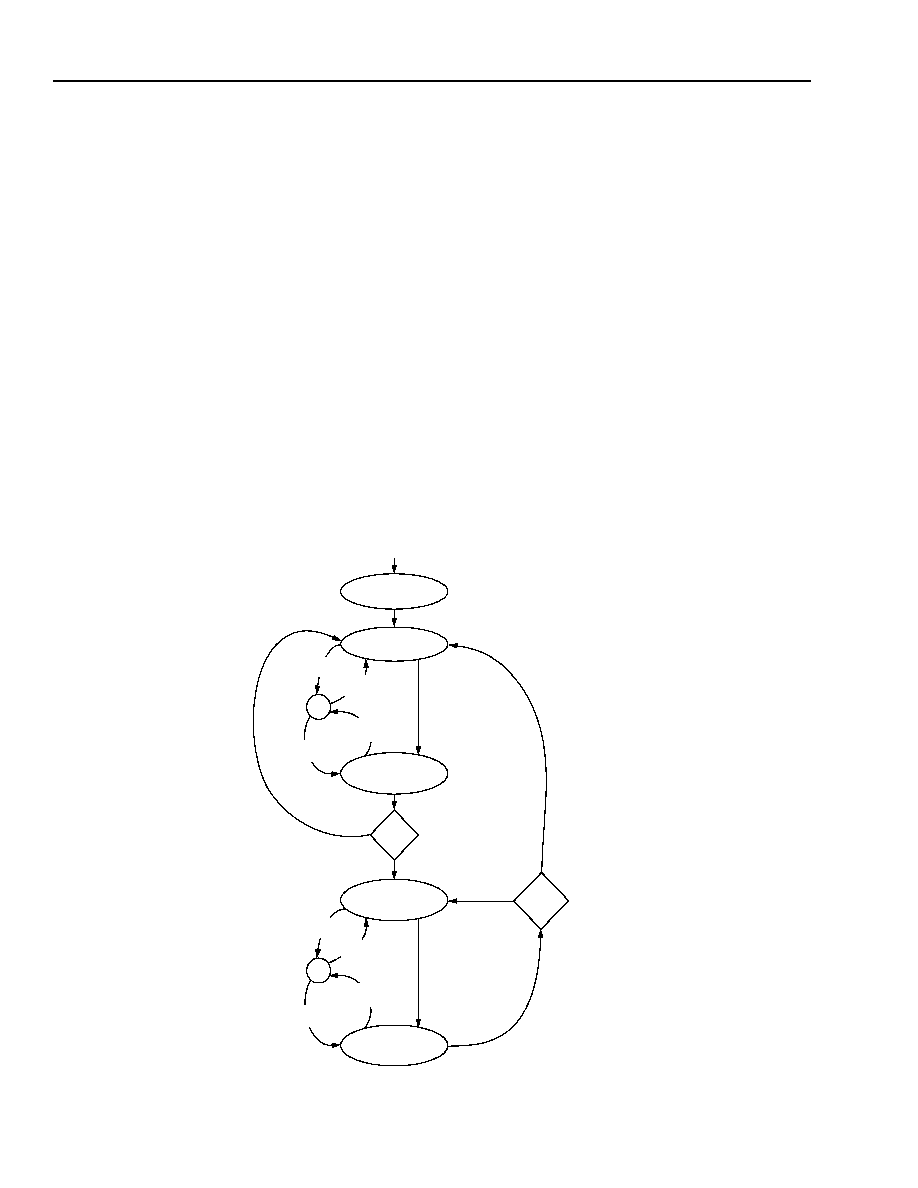
70
Agere Systems Inc.
Data Sheet
February 2004
Ambassador T8110L H.100/H.110 Switch
6 Clock Architecture
(continued)
6.7 Clock Circuit Operation--Fallback and Failsafe
(continued)
6.7.2 Clock Failsafe
Clock failsafe provides a safety net for the APLL1 reference clock source and is controlled by three registers,
0x00114--0x00116; see Section 5.1.11 on page 38. A failsafe event overrides the active clock control registers and
forces the APLL1 clock selection to be a fixed 4.096 MHz, derived from the XTAL1 crystal, divided by four. Transi-
tion into one of the failsafe states is independent of clock fallback (i.e., can enter from any state other than INI-
TIAL). Transitions out of the failsafe states are by user command and allow re-entry into either a nonfallback
(primary or secondary) or a fallback (TO_SECONDARY or TO_PRIMARY) state. Refer to Table 56 and Figure 12.
6.7.2.1 Failsafe Events
Clock failsafe (transition from either clock register set to a forced XTAL1-div-4 APLL1 reference clock) can only
occur if the failsafe mode is enabled (register 0x00115, lower nibble), and a failsafe event occurs. A failsafe event
is triggered by a watchdog error on the APLL1 reference clock (i.e., loss-of-reference).
Additionally, an out-of-lock (OOL) condition is provided for debug purposes. This does not trigger a failsafe event,
but does indicate potential difficulty with the APLL1. A lock status flag is provided out of APLL1, and the OOL is
defined by exceeding a user-defined threshold value (register 0x00116). The lock status is a flag indicating when
APLL1 is making a correction to maintain synchronization. The flag is continuously sampled. If enough active flags
are sampled in a row to exceed the user-defined threshold, this condition is reported via the system status register
(0x00125).
5-9421 (F)
Figure 12. T8110L Clock Failsafe States
FS_2
FAILSAFE RETURN TO
NONFALLBACK STATE
FAILSAFE ENABLED AND
FAILSAFE EVENT
FAILSAFE ENABLED AND
FAILSAFE EVENT
FAILSAFE RETURN TO
FALLBACK STATE
FALLBACK
TYPE
?
TO_PRIMARY
(X IS THE ACTIVE SET,
ASSERT FALLBACK FLAG)
SECONDARY
(Y IS THE ACTIVE SET)
TO_SECONDARY
(Y IS THE ACTIVE SET,
ASSERT FALLBACK FLAG)
INITIAL
(Y IS THE ACTIVE SET)
RESET
USER COMMAND
GO_CLOCKS
FALLBACK ENABLED AND
FALLBACK EVENT
FALLBACK ENABLED AND
FALLBACK EVENT
USER COMMAND
CLEAR_FALLBACK
ROTATING
SECONDARY
FALLBACK
TYPE
?
MODE
FIXED
SECONDARY
MODE
USER COMMAND
CLEAR_FALLBACK
ROTATING
SECONDARY
MODE
FIXED
SECONDARY
MODE
FS_1
FAILSAFE RETURN TO
NONFALLBACK STATE
FAILSAFE ENABLED AND
FAILSAFE EVENT
FAILSAFE ENABLED AND
FAILSAFE EVENT
FAILSAFE RETURN TO
FALLBACK STATE
PRIMARY
(X IS THE ACTIVE SET)

Agere Systems Inc.
71
Data Sheet
February 2004
Ambassador T8110L H.100/H.110 Switch
6 Clock Architecture
(continued)
6.7 Clock Circuit Operation--Fallback and Failsafe
(continued)
6.7.2 Clock Failsafe (continued)
6.7.2.1 Failsafe Events (continued)
Table 56. Clock Failsafe State Descriptions
Clock Failsafe
State
Description
Exit To
Exit Condition
FS_1
APLL1 REFCLK is forced to
XTAL1-div-4.
FAILSAFE FLAG is asserted.
PRIMARY
User issues FAILSAFE_RETURN to
nonfallback state command
(set register 0x00114 bit 0).
TO_SECONDARY User issues FAILSAFE_RETURN to
fallback state command
(set register 0x00114 bit 1).
FS_2
APLL1 REFCLK is forced to
XTAL1-div-4.
FAILSAFE FLAG is asserted.
SECONDARY
User issues FAILSAFE_RETURN to
non-fallback state command
(set register 0x00114 bit 0).
TO_PRIMARY
User issues FAILSAFE_RETURN to
fallback state command
(set register 0x00114 bit 1).

72
Agere Systems Inc.
Data Sheet
February 2004
Ambassador T8110L H.100/H.110 Switch
7 Frame Group and FG I/O
There are eight independently programmable T8110L frame group/FGIO signals, FG[7:0]. In the frame group
mode, the pin is an 8 kHz frame reference output, with programmable pulse width, polarity, and delay offset from
the internally generated frame reference. In the FGIO mode, the pin behaves as a general-purpose register bit,
with programmable direction (IN or OUT) and read masking. The FG7 signal allows for an additional mode of oper-
ation, providing a timer via a 16-bit programmable counter.
7.1 Frame Group Control Registers
7.1.1 FGx Lower and Upper Start Registers
The FGx lower and upper start registers provide a 12-bit delay offset value for the corresponding frame group bit.
Offsets are relative to the T8110L internally generated 8 kHz frame reference and have a resolution down to one
32.768 MHz clock period (30.5 ns increments).
Table 57. Frame Group and FG I/O Register Map
DWORD Address
(20 bits)
Register
Byte 3
Byte 2
Byte 1
Byte 0
0x00400
FG0 rate
FG0 width
FG0 upper start
FG0 lower start
0x00410
FG1 rate
FG1 width
FG1 upper start
FG1 lower start
0x00420
FG2 rate
FG2 width
FG2 upper start
FG2 lower start
0x00430
FG3 rate
FG3 width
FG3 upper start
FG3 lower start
0x00440
FG4 rate
FG4 width
FG4 upper start
FG4 lower start
0x00450
FG5 rate
FG5 width
FG5 upper start
FG5 lower start
0x00460
FG6 rate
FG6 width
FG6 upper start
FG6 lower start
0x00470
FG7 rate
FG7 width
FG7 upper start
FG7 lower start
0x00474
FG7 mode upper
FG7 mode lower
FG7 counter high byte
FG7 counter low byte
0x00480
Reserved
FGIO R/W
FGIO read mask
FGIO data register
Table 58. FGx Lower and Upper Start Registers
Byte Address
Name
Bit(s)
Mnemonic
Value
Function
0x00400
0x00410
0x00420
0x00430
0x00440
0x00450
0x00460
0x00470
FG0 Lower Start
(FG1 Lower Start)
(FG2 Lower Start)
(FG3 Lower Start)
(FG4 Lower Start)
(FG5 Lower Start)
(FG6 Lower Start)
(FG7 Lower Start)
7:0
F0LLR
(F1LLR)
(F2LLR)
(F3LLR)
(F4LLR)
(F5LLR)
(F6LLR)
(F7LLR)
LLLL LLLL Lower 8 bits of 12-bit start offset.
0x00401
(0x00411)
(0x00421)
(0x00431)
(0x00441)
(0x00451)
(0x00461)
(0x00471)
FG0 Upper Start
(FG1 Upper Start)
(FG2 Upper Start)
(FG3 Upper Start)
(FG4 Upper Start)
(FG5 Upper Start)
(FG6 Upper Start)
(FG7 Upper Start)
7:0
F0ULR
(F1ULR)
(F2ULR)
(F3ULR)
(F4ULR)
(F5ULR)
(F6ULR)
(F7ULR)
0000 LLLL Upper 4 bits of 12-bit start offset.

Agere Systems Inc.
73
Data Sheet
February 2004
Ambassador T8110L H.100/H.110 Switch
7 Frame Group and FG I/O
(continued)
7.1 Frame Group Control Registers
(continued)
7.1.2 FGx Width Registers
The FGx width registers control the polarity and the pulse widths generated for the corresponding frame group bit.
The pulse-width programming works in conjunction with the FGx rate registers to provide 1-bit, 2-bit, 4-bit,
1-byte, and 2-byte wide pulses for any of the available frame group rates (see Table 59).
7.1.3 FGx Rate Registers
The FGx rate registers either enable FGIO operation* or work in conjunction with FGx width registers to provide
various width frame group pulses at rates of 2.048 MHz, 4.096 MHz, 8.192 MHz, or 16.384 MHz.
* FGIO operation is controlled at registers 0x00480--482. Refer to Section 7.3 on page 75.
Table 59. FGx Width Registers
Byte
Address
Name
Bit(s) Mnemonic
Value
Function
0x00402
(0x00412)
(0x00422)
(0x00432)
(0x00442)
(0x00452)
(0x00462)
(0x00472)
FG0 Width
(FG1 Width)
(FG2 Width)
(FG3 Width)
(FG4 Width)
(FG5 Width)
(FG6 Width)
(FG7 Width)
7
F0ISB
(F1ISB)
(F2ISB)
(F3ISB)
(F4ISB)
(F5ISB)
(F6ISB)
(F7ISB)
0
1
Generate active-high pulse (default).
Generate active-low pulse.
6:0
F0WSP
(F1WSP)
(F2WSP)
(F3WSP)
(F4WSP)
(F5WSP)
(F6WSP)
(F7WSP)
000 0000
000 0001
000 0010
000 0100
001 0000
010 0000
1-bit wide pulse (default).
1-bit wide pulse.
2-bit wide pulse.
4-bit wide pulse.
1-byte wide pulse.
2-byte wide pulse.
Table 60. FGx Rate Registers
Byte Address
Name
Bit(s) Mnemonic
Value
Function
0x00403
(0x00413)
(0x00423)
(0x00433)
(0x00443)
(0x00453)
(0x00463)
(0x00473)
FG0 Rate
(FG1 Rate)
(FG2 Rate)
(FG3 Rate)
(FG4 Rate)
(FG5 Rate)
(FG6 Rate)
(FG7 Rate)
7:0
F0RSR
(F1RSR)
(F2RSR)
(F3RSR)
(F4RSR)
(F5RSR)
(F6RSR)
(F7RSR)
0000 0000
0000 0001
0000 0010
0000 0100
0000 1000
0000 1001
Off (default).
FGIO enabled* (not used as a frame group).
FGx rate = 2.048 MHz.
FGx rate = 4.096 MHz.
FGx rate = 8.192 MHz.
FGx rate = 16.384 MHz.
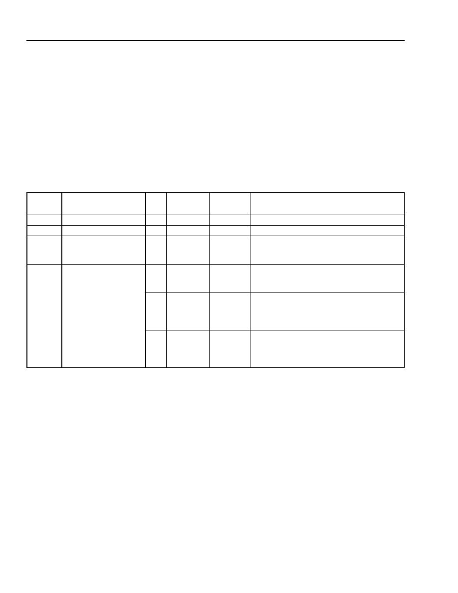
74
Agere Systems Inc.
Data Sheet
February 2004
Ambassador T8110L H.100/H.110 Switch
7 Frame Group and FG I/O
(continued)
7.2 FG7 Timer Option
The FG7 signal allows for an added function of a timer output, via a 16-bit programmable counter.
7.2.1 FG7 Counter (Low and High Byte) Registers
The FG7 counter (low and high byte) registers set the timer value. The timer is actually a divider, so the value
entered must be [divider value ≠ 1], i.e., 0000000000000011 would yield a div-by-4 operation. The FG7 mode lower
register enables the timer option, with two clock source options: T8110L internal frame or an external timer clock
via the FG6 signal. The FG7 mode upper register controls the shape of the timer pulse. For more details, see Sec-
tion 7.4.3 on page 79.
* Normal operation allows frame group or FGIO control via registers 0x00470--473. Enabling the counter overrides 0x00470--473 settings.
Square wave is only available when FG7 counter high/low value is a binary multiple 1, 2, 4, 8, 16, etc. Other values yield a carry out pulse
shape.
Carry out pulse is active for one FG7 timer clock period.
ß Programmable pulses are based on T8110L internal 32.768 MHz clock periods.
Table 61. FG7 Counter (Low and High Byte) Registers
Byte
Address
Name
Bit
Mnemonic
Value
Function
0x00474 FG7 Counter, Low Byte
7:0
FCLLR
LLLL LLLL Lower 8 bits of 16-bit counter value.
0x00475 FG7 Counter, High Byte
7:0
FCULR
LLLL LLLL Upper 8 bits of 16-bit counter value.
0x00476 FG7 Mode Lower
7:0
F7MSR
0000 0000
0000 0001
0000 0010
Normal operation* (default).
Enable timer, clock = internal frame.
Enable timer, clock = external FG6.
0x00477 FG7 Mode Upper
7
FCISB
0
1
Normal FG7 timer output, high pulses
(default).
Inverted FG7 timer output, low pulses.
6:4
F7SSP
000
001
010
100
FG7 timer output off (default).
FG7 timer output = square wave
.
FG7 timer output = carry out pulse
.
FG7 timer output = programmable pulse
ß
.
3:0
F7WSN
0001
0010
0100
1000
Programmable pulse width = 30.5 ns.
Programmable pulse width = 61.0 ns.
Programmable pulse width = 91.5 ns.
Programmable pulse width = 122 ns.
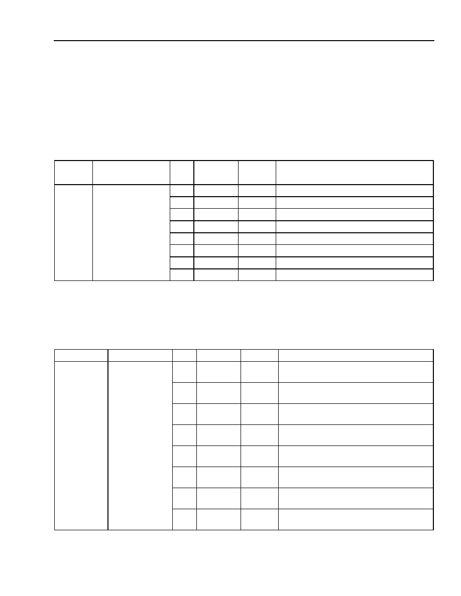
Agere Systems Inc.
75
Data Sheet
February 2004
Ambassador T8110L H.100/H.110 Switch
7 Frame Group and FG I/O
(continued)
7.3 FGIO Control Registers
7.3.1 FGIO Data Register
The FGIO data register provides read/write access and write storage to/from any FG signals being used as gen-
eral-purpose register bits. Writes to FGIO work in conjunction with the corresponding FGIO enabled settings in the
FGx rate registers. Reads are maskable, controlled via register 0x00481.
7.3.2 FGIO Read Mask Register
The FGIO read mask register controls the masking of any FG signals being used as general-purpose register bits
on a read access to the FGIO register.
Table 62. FGIO Data Register
Byte
Address
Name
Bit(s) Mnemonic
Value
Function
0x00480 FGIO Data Register
7
F7IOB
L
FGIO bit 7 value.
6
F6IOB
L
FGIO bit 6 value.
5
F5IOB
L
FGIO bit 5 value.
4
F4IOB
L
FGIO bit 4 value.
3
F3IOB
L
FGIO bit 3 value.
2
F2IOB
L
FGIO bit 2 value.
1
F1IOB
L
FGIO bit 1 value.
0
F0IOB
L
FGIO bit 0 value.
Table 63. FGIO Read Mask Register
Byte Address
Name
Bit(s) Mnemonic
Value
Function
0x00481
FGIO Read Mask
7
F7MEB
0
1
Unmask FGIO bit 7 (default).
Mask FGIO bit 7, return 0 on a read.
6
F6MEB
0
1
Unmask FGIO bit 6 (default).
Mask FGIO bit 6, return 0 on a read.
5
F5MEB
0
1
Unmask FGIO bit 5 (default).
Mask FGIO bit 5, return 0 on a read.
4
F4MEB
0
1
Unmask FGIO bit 4 (default).
Mask FGIO bit 4, return 0 on a read.
3
F3MEB
0
1
Unmask FGIO bit 3 (default).
Mask FGIO bit 3, return 0 on a read.
2
F2MEB
0
1
Unmask FGIO bit 2 (default).
Mask FGIO bit 2, return 0 on a read.
1
F1MEB
0
1
Unmask FGIO bit 1 (default).
Mask FGIO bit 1, return 0 on a read.
0
F0MEB
0
1
Unmask FGIO bit 0 (default).
Mask FGIO bit 0, return 0 on a read.
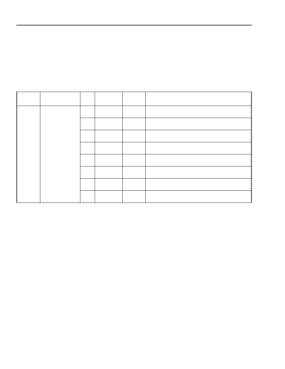
76
Agere Systems Inc.
Data Sheet
February 2004
Ambassador T8110L H.100/H.110 Switch
7 Frame Group and FG I/O
(continued)
7.3 FGIO Control Registers
(continued)
7.3.3 FGIO R/W Register
The FGIO R/W register provides direction control for any of the FG signals being used as general-purpose register
bits.
Table 64. FGIO R/W Register
Byte
Address
Name
Bit(s) Mnemonic
Value
Function
0x00482 FGIO R/W
7
F7DSB
0
1
FGIO bit 7 direction is input (default).
FGIO bit 7 direction is output.
6
F6DSB
0
1
FGIO bit 6 direction is input (default).
FGIO bit 6 direction is output.
5
F5DSB
0
1
FGIO bit 5 direction is input (default).
FGIO bit 5 direction is output.
4
F4DSB
0
1
FGIO bit 4 direction is input (default).
FGIO bit 4 direction is output.
3
F3DSB
0
1
FGIO bit 3 direction is input (default).
FGIO bit 3 direction is output.
2
F2DSB
0
1
FGIO bit 2 direction is input (default).
FGIO bit 2 direction is output.
1
F1DSB
0
1
FGIO bit 1 direction is input (default).
FGIO bit 1 direction is output.
0
F0DSB
0
1
FGIO bit 0 direction is input (default).
FGIO bit 0 direction is output.
Agere Systems Inc.
77
Data Sheet
February 2004
Ambassador T8110L H.100/H.110 Switch
7 Frame Group and FG I/O
(continued)
7.4 FG Circuit Operation
Each of the eight frame group signals FG[7:0] operate independently and have multiple uses. Refer to Figure 13
below.
!
As programmable 8 kHz frame reference outputs (frame group)
!
As general-purpose register I/O bits (FGIO)
!
As a programmable timer (FG7 only)
!
As external interrupt input signals
!
As diagnostic observation points for internal testpoints
5-9428a (F)
Figure 13. FG[7:0] Functional Paths
MASTER ENABLE REGISTER (0x00103)
FGx ENABLE
LOGIC
FG
X
RATE
FGIO
X
R/W
TESTPOINT DIAGNOSTIC CONTROL
T8110L TESTPOINTS
OUTPUT
ENABLE
PULSE
GENERATOR
FG
X
WIDTH
OFFSET
DETECT
FG
X
UPPER/
LOWER START
PROGRAMMABLE
TIMER
(FG7 ONLY)
T8110L
FROM FG6 INPUT
INTERNAL FRAME
ADDR
FG7 MODE
FG7 COUNTER
HI/LO BYTE
FGIO
X
DATA REG
FGIO DATA REGISTER
WRITES FROM REGISTER
FGIO DATA REGISTER
READS TO REGISTER
ACCESS INTERFACE
FG
X
FGIO
X
READ MASK
FG AS EXTERNAL INTERRUPT
TO INTERRUPT CONTROLLER
ACCESS INTERFACE
IF DIRECTION = OUTPUT,
RETURN THE DATA REG
CONTENTS ON A
READBACK, ELSE RETURN
THE I/O PIN VALUE.
FGIO
X
R/W

78
Agere Systems Inc.
Data Sheet
February 2004
Ambassador T8110L H.100/H.110 Switch
7 Frame Group and FG I/O
(continued)
7.4 FG Circuit Operation
(continued)
7.4.1 Frame Group 8 kHz Reference Generation
Any of the T8110L FG signals may be used as programmable 8 kHz frame reference outputs. There are two sets of
control required, an offset delay from internal frame center, and pulse shaping.
The offset delay is provided via the FGx upper/lower start address registers. The delay is relative to the T8110L
internal frame center, and the 12 bits used allow for 4096 different offsets, in increments of one 32.768 MHz clock
period (30.5 ns).
Pulse shaping is controlled via the FGx width and FGx rate registers. Pulses may be programmed to be active-high
or active-low. Pulse width can be either 1-bit, 2-bit, 4-bit, 1-byte or 2-byte wide (relative to the rate setting*), with
allowable rate settings of 2.048 MHz, 4.096 MHz, 8.192 MHz, and 16.384 MHz.
*Pulse widths are bit times or multiples of bit times, for each applicable rate:
RATE
BIT TIME
2.048 Mbits/s
488 ns
4.096 Mbits/s
244 ns
8.192 Mbits/s
122 ns
16.384 Mbits/s
61 ns
Notes:
Frame group signals shown with offset = 0 (default). At offset = 0, the pulse starts at frame center.
Nonzero offsets denote 32.768 MHz period increments (30.5 ns) from frame center. There are up to 4096 increments within an 8 kHz frame
period. Offsets may be programmed in the range from 0--4095.
Frame group signals are shown as active high pulses (default)--they may be programmed as active-low pulses.
Diagram shows frame group pulse widths relative to bit-clock rate and time-slot width. This is applicable for any of the four frame group data
rates (2 Mbits/s, 4 Mbits/s, 8 Mbits/s, or 16 Mbits/s).
Figure 14. Frame Group 8 kHz Reference Timing
4
3
2
1
0
31, 63, 127 or 255
bitclock rate
(2, 4, 8, or
16MHz)
timeslot
Frame
Center
T8110 internal
frame
FG(x),
1-bit width,
offset = 0
FG(x),
2-bit width,
offset = 0
FG(x),
1-byte width,
offset = 0
FG(x),
2-byte width,
offset = 0
FG(x),
4-bit width,
offset = 0

Agere Systems Inc.
79
Data Sheet
February 2004
Ambassador T8110L H.100/H.110 Switch
7 Frame Group and FG I/O
(continued)
7.4 FG Circuit Operation
(continued)
7.4.2 FGIO General-Purpose Bits
Any of the T8110L FG signals may be used as general-purpose I/O bits. Each FG bit used as FGIO is configured
by enabling the FGIO function via the FGx rate register(s) and setting the direction via the appropriate bits in the
FGIO R/W register. For write access to the FGIO, the FGIO data register is used to hold data for output to the FG
pin(s). Read accesses are maskable via the FGIO read mask register. For read access from the FGIO, the logical
state of the FG[7:0] signals is returned if unmasked. If an FGIO bit is masked, a read access returns 0.
7.4.3 Programmable Timer (FG7 Only)
The FG7 signal can be used as a programmable timer output, via the FG7 mode upper/lower, and FG7 counter
high and low byte registers. The FG7 timer is simply a clock divider. The FG7 counter high/low provides a 16-bit
[divider value ≠ 1].
Note: [divider value ≠ 1], i.e., a value of 0000000000000011 yields a div-by-4 operation.
The FG7 mode lower register enables the counter and selects between two clock sources into the counter: either
the T8110L internal frame (8 kHz) or an external clock via the FG6 input. The FG7 mode upper register controls
the output pulse shape. The output can be inverted or noninverted and shaped as either a square wave, a carryout
pulse, or a programmable-width pulse.
!
Square wave. This option is applicable only for divide operations that are binary multiples (i.e., div-by-2, div-by-
4, div-by-8, div-by-16, div-by-65536). Nonbinary divide operations while square wave is selected result in a car-
ryout pulse.
!
Carryout pulse. The output is a pulse, width = one FG7 timer clock period.
!
Programmable-width pulse. The timer output is synchronized to the T8110L 32.768 MHz clock domain and can
be programmed for 1, 2, 3, or 4, 32.768 MHz clock periods in width (30.5 ns, 61 ns, 91.5 ns, or 122 ns).
7.4.4 FG External Interrupts
All FG signals are internally connected as inputs to the interrupt controller logic. Any FG signal, whether an output
or an input, may be used to trigger interrupts. When a T8110L FG signal is used as an externally sourced input into
the interrupt controller logic, it must be in input mode (i.e., shut-off, FGx rate register(s) FxRSR = 0000 0000). An
FG signal in output mode may also be used for interrupts (i.e., an 8 kHz periodic signal, see Section 7.4.1 on page
78). The interrupt control registers (0x00600--603) control how the FG inputs are handled (for more details, refer
to Section 10.1 on page 90).
7.4.5 FG Diagnostic Test Point Observation
Any of the T8110L FG signals may be used to observe a predefined set of internal testpoints. Each FG bit used as
a testpoint output is enabled via diagnostic register 0x00140, FG testpoint enable. Settings in this register override
the FGx rate and FGIO R/W register, and force the selected bits to be testpoint outputs, see Section 11.1 on page
106 and Table 88 on page 106.
80
Agere Systems Inc.
Data Sheet
February 2004
Ambassador T8110L H.100/H.110 Switch
8 General-Purpose I/O
There are eight independent T8110L GPIO signals, GP[7:0]. These pins behave as general-purpose register bits,
with programmable direction (in or out) and read masking. The GP0 and GP1 signals allow for an additional mode
of operation, providing dedicated output signals to indicate A clock and B clock mastering for H.110 bus applica-
tions.
8.1 GPIO Control Registers
8.1.1 GPIO Data Register
The GPIO data register provides read/write access and write storage to/from any GP signals being used as gen-
eral-purpose register bits. Reads from GPIO are maskable, controlled via register 0x00501.
Table 65. GPIO Register
DWORD Address
(20 bits)
Register
Byte 3
Byte 2
Byte 1
Byte 0
0x00500
GPIO override
GPIO R/W
GPIO read mask
GPIO data register
Table 66. GPIO Data Register
Byte
Address
Name
Bit(s)
Mnemonic
Value
Function
0x00500 GPIO Data Register
7
G7IOB
L
GPIO bit 7 value.
6
G6IOB
L
GPIO bit 6 value.
5
G5IOB
L
GPIO bit 5 value.
4
G4IOB
L
GPIO bit 4 value.
3
G3IOB
L
GPIO bit 3 value.
2
G2IOB
L
GPIO bit 2 value.
1
G1IOB
L
GPIO bit 1 value.
0
G0IOB
L
GPIO bit 0 value.

Agere Systems Inc.
81
Data Sheet
February 2004
Ambassador T8110L H.100/H.110 Switch
8 General-Purpose I/O
(continued)
8.1 GPIO Control Registers
(continued)
8.1.2 GPIO Read Mask Register
The GPIO read mask register controls the masking of any GP signals being used as general-purpose register bits
on a read access to the GPIO register.
8.1.3 GPIO R/W Register
The GPIO R/W register provides direction control for any of the GP signals being used as general-purpose register
bits.
Table 67. GPIO Read Mask Register
Byte Address
Name
Bit(s)
Mnemonic
Value
Function
0x00501
GPIO Read Mask
7
G7MEB
0
1
Unmask GPIO bit 7 (default).
Mask GPIO bit 7, return 0 on a read.
6
G6MEB
0
1
Unmask GPIO bit 6 (default).
Mask GPIO bit 6, return 0 on a read.
5
G5MEB
0
1
Unmask GPIO bit 5 (default).
Mask GPIO bit 5, return 0 on a read.
4
G4MEB
0
1
Unmask GPIO bit 4 (default).
Mask GPIO bit 4, return 0 on a read.
3
G3MEB
0
1
Unmask GPIO bit 3 (default).
Mask GPIO bit 3, return 0 on a read.
2
G2MEB
0
1
Unmask GPIO bit 2 (default).
Mask GPIO bit 2, return 0 on a read.
1
G1MEB
0
1
Unmask GPIO bit 1 (default).
Mask GPIO bit 1, return 0 on a read.
0
G0MEB
0
1
Unmask GPIO bit 0 (default).
Mask GPIO bit 0, return 0 on a read.
Table 68. GPIO R/W Register
Byte Address
Name
Bit(s)
Mnemonic
Value
Function
0x00502
GPIO R/W
7
G7DSB
0
1
GPIO bit 7 direction is input (default).
GPIO bit 7 direction is output.
6
G6DSB
0
1
GPIO bit 6 direction is input (default).
GPIO bit 6 direction is output.
5
G5DSB
0
1
GPIO bit 5 direction is input (default).
GPIO bit 5 direction is output.
4
G4DSB
0
1
GPIO bit 4 direction is input (default).
GPIO bit 4 direction is output.
3
G3DSB
0
1
GPIO bit 3 direction is input (default).
GPIO bit 3 direction is output.
2
G2DSB
0
1
GPIO bit 2 direction is input (default).
GPIO bit 2 direction is output.
1
G1DSB
0
1
GPIO bit 1 direction is input (default).
GPIO bit 1 direction is output.
0
G0DSB
0
1
GPIO bit 0 direction is input (default).
GPIO bit 0 direction is output.
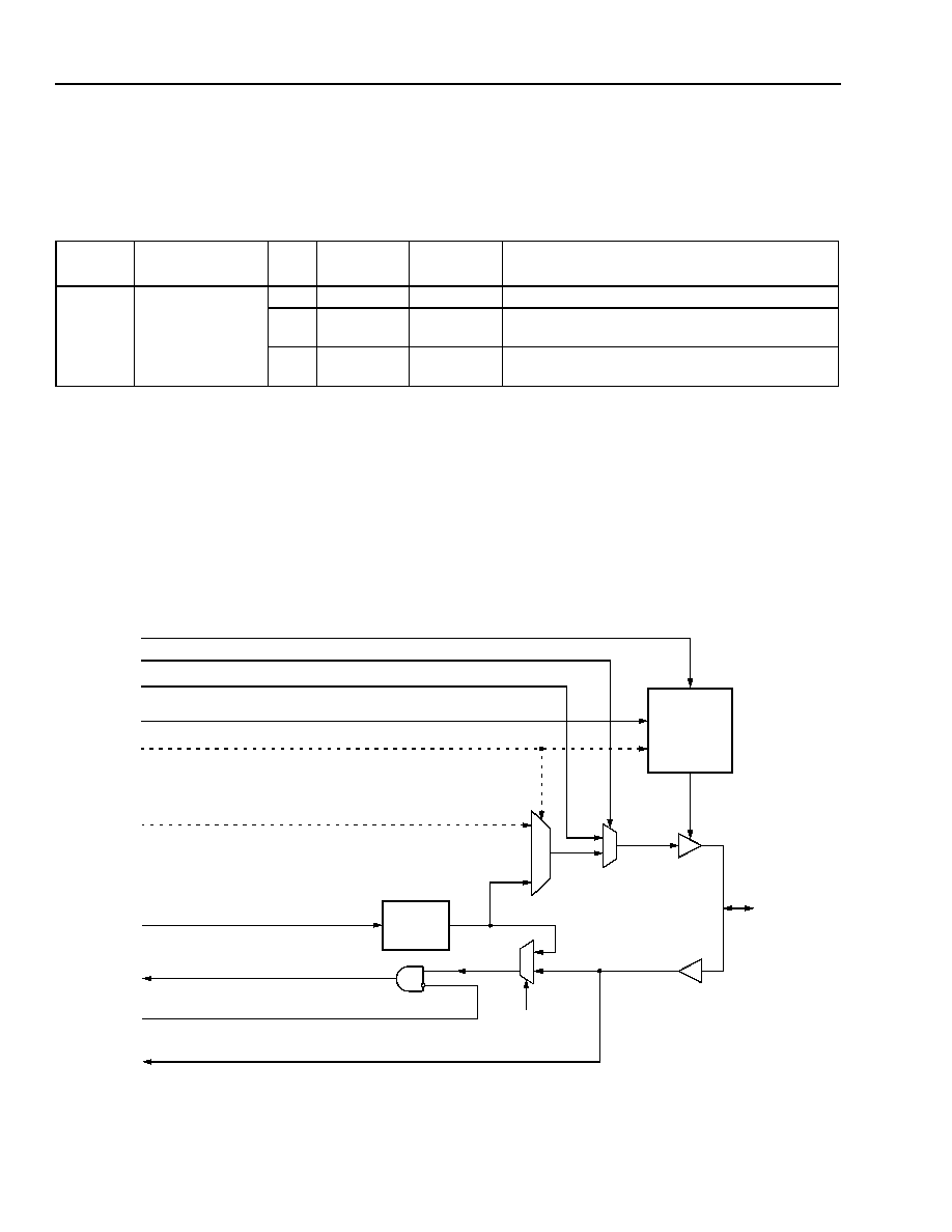
82
Agere Systems Inc.
Data Sheet
February 2004
Ambassador T8110L H.100/H.110 Switch
8 General-Purpose I/O
(continued)
8.1 GPIO Control Registers
(continued)
8.1.4 GPIO Override Register
8.2 GP Circuit Operation
The eight general-purpose I/O group signals GP[7:0] each operate independently and have multiple uses. Please
refer to Figure 15 on page 82.
!
As general-purpose register I/O bits (GPIO)
!
As H.110 bus clock master indicators (GP0, GP1 only)
!
As external interrupt input signals
!
As diagnostic observation points for internal testpoints
5-9427a (F)
Figure 15. GP[7:0] Functional Paths
Table 69. GPIO Override Register
Byte
Address
Name
Bit(s) Mnemonic
Value
Function
0x00503 GPIO Override
7:2
Reserved
0000 0
NOP (default).
1
G1OEB
0
1
GPIO bit 1 is GPIO (default).
GPIO bit 1 B-master indicator output.
0
G0OEB
0
1
GPIO bit 0 is GPIO (default).
GPIO bit 0 A-master indicator output.
MASTER ENABLE REGISTER (0x00103)
GPx ENABLE
LOGIC
GPIO OVERRIDE
GPIO
X
R/W
TESTPOINT DIAGNOSTIC CONTROL
T8110L TESTPOINTS
OUTPUT
ENABLE
GPIO
X
DATA REG
GPIO DATA REGISTER
WRITES FROM REGISTER
GPIO DATA REGISTER
READS TO REGISTER
ACCESS INTERFACE
GP
X
GPIO
X
READ MASK
GP AS EXTERNAL INTERRUPT
TO INTERRUPT CONTROLLER
ACCESS INTERFACE
GP0: A-CLOCK MASTER INDICATOR (0x00220 bit 4)
GP1: B-CLOCK MASTER INDICATOR (0x00220 bit 5)
IF DIRECTION = OUTPUT,
RETURN THE DATA REG
CONTENTS ON A
READBACK, ELSE RETURN
THE I/O PIN VALUE.
GPIO
X
R/W

Agere Systems Inc.
83
Data Sheet
February 2004
Ambassador T8110L H.100/H.110 Switch
8 General-Purpose I/O
(continued)
8.2 GP Circuit Operation
(continued)
8.2.1 GPIO General-Purpose Bits
Any of the T8110L GP signals may be used as general-purpose I/O bits. Each GP bit used as GPIO is configured
by setting the direction via the appropriate bits in the GPIO R/W register. For write access to the GPIO, the GPIO
data register is used to hold data for output to the GP pin(s). Read accesses are maskable via the GPIO read mask
register. For read access from the GPIO, the logical state of the GP[7:0] signals is returned if unmasked. If a GPIO
bit is masked, a read access returns 0.
8.2.2 GP Dual-Purpose Bits GPIO (Override)
8.2.2.1 GP H.110 Clock Master Indicators (GP0, GP1 Only)
An additional function is provided for GP0 and GP1 only, controlled via the GPIO override register.
GP0 may be used as a dedicated output (set GPIO override register bit 0), which transmits the state of the T8110L
A clock master enable (register 0x00220, bit 4). This output is intended to drive the external A clock FETs required
for H.110 bus mastering.
GP1 may be used as a dedicated output (set GPIO override register bit 1), which transmits the state of the T8110L
B clock master enable (register 0x00220, bit 5). This output is intended to drive the external B clock FETs required
for H.110 bus mastering.
8.2.3 GP External Interrupts
Any of the T8110L GP signals may be used as externally sourced inputs into the interrupt controller logic. Each GP
bit used as an interrupt input must be shut off by setting the appropriate GPIO R/W register bit to be input. The
interrupt control registers (0x00604--607) control how the GP inputs are handled. For more details, see Section
10.1 on page 90.
8.2.4 GP Diagnostic Test Point Observation
Any of the T8110L GP signals may be used to observe a predefined set of internal testpoints. Each GP bit used as
a testpoint output is enabled via diagnostic register 0x00142, GP testpoint enable. Settings in this register override
the GPIO R/W register and force the selected bits to be testpoint outputs (refer to Section 11.1 on page 106, and
Table 90 on page 108).

84
Agere Systems Inc.
Data Sheet
February 2004
Ambassador T8110L H.100/H.110 Switch
9 Stream Rate Control
There are a total of 64 data streams, divided into 16 stream groups of four streams each, as shown below.
The H-bus group operational frequencies are selectable between 2.048 MHz, 4.096 MHz, and 8.192 MHz.
The L-bus groups may operate at 2.048 MHz, 4.096 MHz, 8.192 MHz, and 16.384 MHz, which is implemented as
multiplexed 8.192 MHz streams. (For more details, see Section 9.2.2 on page 86).
Table 70. T8110L Serial Stream Groupings
Stream Group
Stream Bits
H-bus group A
CT_D[0:3]
H-bus group B
CT_D[4:7]
H-bus group C
CT_D[8:11]
H-bus group D
CT_D[12:15]
H-bus group E
CT_D[16:19]
H-bus group F
CT_D[20:23]
H-bus group G
CT_D[24:27]
H-bus group H
CT_D[28:31]
L-bus group A
LD[0:3]
L-bus group B
LD[4:7]
L-bus group C
LD[8:11]
L-bus group D
LD[12:15]
L-bus group E
LD[16:19]
L-bus group F
LD[20:23]
L-bus group G
LD[24:27]
L-bus group H
LD[28:31]
Agere Systems Inc.
85
Data Sheet
February 2004
Ambassador T8110L H.100/H.110 Switch
9 Stream Rate Control
(continued)
9.1 H-Bus Stream Rate Control Registers
9.1.1 H-Bus Rate Registers
The H-bus rate registers control the serial data stream rate of operation for each of the H-bus stream groups,
A--H. The upper nibble controls groups B, D, F, and H. The lower nibble controls groups A, C, E, and G.
9.2 L-Bus Stream Rate Control Registers
9.2.1 L-Bus Rate Registers
The L-bus rate registers control the serial data stream rate of operation for each of the L-bus stream groups,
A--H. The upper nibble controls groups B, D, F, and H. The lower nibble controls groups A, C, E, and G. Local
streams have a 16.384 MHz rate option (refer to Section 9.2.2 on page 86).
Table 71. H-Bus Rate Registers
DWORD Address (20 Bits)
Register
Byte 3
Byte 2
Byte 1
Byte 0
0x00300
H-bus rate H/G
H-bus rate F/E
H-bus rate D/C
H-bus rate B/A
Byte Address
Name
Bit(s) Mnemonic
Value
Function
0x00300
(0x00301)
(0x00302)
(0x00303)
H-bus Rate B/A
(H-bus Rate D/C)
(H-bus Rate F/E)
(H-bus Rate H/G)
7:4
HBRSN
(HDRSN)
(HFRSN)
(HHRSN)
0000
0010
0100
1000
H-bus group B(D, F, H) off (default).
H-bus group B(D, F, H) rate = 2.048 MHz.
H-bus group B(D, F, H) rate = 4.096 MHz.
H-bus group B(D, F, H) rate = 8.192 MHz.
3:0
HARSN
(HCRSN)
(HERSN)
(HGRSN)
0000
0010
0100
1000
H-bus group A(C, E, G) off (default).
H-bus group A(C, E, G) rate = 2.048 MHz.
H-bus group A(C, E, G) rate = 4.096 MHz.
H-bus group A(C, E, G) rate = 8.192 MHz.
Table 72. L-Bus Rate Registers
DWORD
Address (20 Bits)
Register
Byte 3
Byte 2
Byte 1
Byte 0
0x00320
L-bus rate H/G
L-bus rate F/E
L-bus rate D/C
L-bus rate B/A
Byte Address
Name
Bit(s) Mnemonic
Value
Function
0x00320
(0x00321)
(0x00322)
(0x00323)
L-bus Rate B/A
(L-bus Rate D/C)
(L-bus Rate F/E)
(L-bus Rate H/G)
7:4
LBRSN
(LDRSN)
(LFRSN)
(LHRSN)
0000
0010
0100
1000
1001
L-bus group B(D, F, H) off (default).
L-bus group B(D, F, H) rate = 2.048 MHz.
L-bus group B(D, F, H) rate = 4.096 MHz.
L-bus group B(D, F, H) rate = 8.192 MHz.
L-bus group B(D, F, H) rate = 16.384 MHz.
3:0
LARSN
(LCRSN)
(LERSN)
(LGRSN)
0000
0010
0100
1000
1001
L-bus group A(C, E, G) off (default).
L-bus group A(C, E, G) rate = 2.048 MHz.
L-bus group A(C, E, G) rate = 4.096 MHz.
L-bus group A(C, E, G) rate = 8.192 MHz.
L-bus group A(C, E, G) rate = 16.384 MHz.
86
Agere Systems Inc.
Data Sheet
February 2004
Ambassador T8110L H.100/H.110 Switch
9 Stream Rate Control
(continued)
9.2 L-Bus Stream Rate Control Registers
(continued)
9.2.2 L-Bus 16.384 Mbits/s Operation
Local stream 16.384 Mbits/s operation is implemented as two multiplexed 8.192 Mbits/s streams. Bits are shifted at
16.384 MHz, and 16 bits are shifted per 8.192 Mbits/s time slot (refer to Figure 16). This operation makes use of
adjacent pairs of the existing single-byte hold and shift registers for local stream operation, with the local even
stream assigned as the incoming stream, and the local odd stream assigned as the outgoing stream. Pairs are
assigned as LD[0,1], LD[2,3], . . . LD[30,31]. When an L-bus group is set to operate at rate of 16.384 Mbits/s, the
hold and shift circuitry is configured such that the serial output of the even stream shift register feeds the serial
input of the odd stream shift register (refer to Figure 17).
5-9411 (F)
Figure 16. Local Stream 16.384 Mbits/s Timing
15
6
976 ns (ONE 8 Mbits/s TIME-SLOT)
TIME-SLOT n
INCOMING BITS ARE SAMPLED AT
THE 3/4 POINT OF THE BIT TIME
14
13
12
11
10
9
8
7
5
4
3
2
1
0
8.192 MHz
16.384 MHz
SERIAL DATA:
L_D[EVEN] (INCOMING),
L_D[ODD] (OUTGOING)
OFFLOAD INCOMING
BYTES FROM TIME-SLOT n ≠ 1 TO HOLDING REGISTERS,
LOAD OUTGOING BYTES FOR
TIME-SLOT n TO SHIFT REGISTERS
OFFLOAD INCOMING
BYTES FROM TIME-SLOT n TO HOLDING REGISTERS,
LOAD OUTGOING BYTES FOR
TIME-SLOT n + 1 TO SHIFT REGISTERS

Agere Systems Inc.
87
Data Sheet
February 2004
Ambassador T8110L H.100/H.110 Switch
9 Stream Rate Control
(continued)
9.2 L-Bus Stream Rate Control Registers
(continued)
9.2.2 L-Bus 16.384 Mbits/s Operation (continued)
5-9426 (F)
Figure 17. Local Stream 16.384 Mbits/s Circuit
LOCAL
EVEN
STREAM
SHIFT
REGISTER
EVEN
STREAM
INCOMING
HOLDING
REGISTER
EVEN
STREAM
OUTGOING
HOLDING
REGISTER
ODD
STREAM
INCOMING
HOLDING
REGISTER
ODD
STREAM
OUTGOING
HOLDING
REGISTER
MS bit
LOCAL
ODD
STREAM
SHIFT
REGISTER
MS bit
8
8-bit BYTE TO
DATA MEMORY
8-bit BYTE FROM
DATA MEMORY
8
8
8-bit BYTE TO
DATA MEMORY
8-bit BYTE FROM
DATA MEMORY
8
(NO LOCAL EVEN
SERIAL OUTPUT
IF 16.384 Mbits/s
OPERATION)
OUTGOING
SERIAL DATA
OUTGOING SERIAL DATA (ODD)
INCOMING SERIAL DATA (EVEN)
(NO LOCAL ODD
SERIAL INPUT
IF 16.384 Mbits/s
OPERATION)
INCOMING
SERIAL DATA
16.384 Mbits/s
ENABLE
(ODD)
(EVEN)
88
Agere Systems Inc.
Data Sheet
February 2004
Ambassador T8110L H.100/H.110 Switch
9 Stream Rate Control
(continued)
9.2 L-Bus Stream Rate Control Registers
(continued)
9.2.3 16.384 Mbits/s Local I/O Superrate
This 16.384 Mbits/s rate option is available only on the local I/O streams (i.e., it is not supported as a part of the
H.100/H.110 specifications). When applying the superrate option to a local I/O group, the I/O for the group is rede-
fined and divided into two pairs of input and output. An input or an output can be selected from each pair, but both
can't be used simultaneously. This leads to four possible configurations for each group. Note that inputs are always
on even signals and outputs are always on odd signals. Thus, if all local groups are operated at the superrate, then
the application can have 16 lines, all at 16.384 Mbits/s, in contrast to the 32 I/O lines at normal rates.
Figure 18. Superrate I/O Configuration
LOCAL
I/O
PINS
LD0
LD1
LD2
LD3
GR
OU
P
A
GROUP A CONFIGURATION AT 2.048, 4.096,
OR 8.192 Mbits/s
LOCAL
I/O
PINS
LD0
LD1
LD2
LD3
GR
OU
P
A
GROUP A CONFIGURATION 1
AT 16.384 Mbits/s SUPERRATE
LOCAL
I/O
PINS
LD0
LD1
LD2
LD3
GR
OU
P
A
GROUP A CONFIGURATION 2
AT 16.384 Mbits/s SUPERRATE
LOCAL
I/O
PINS
LD0
LD1
LD2
LD3
GR
OU
P
A
GROUP A CONFIGURATION 3
AT 16.384 Mbits/s SUPERRATE
LOCAL
I/O
PINS
LD0
LD1
LD2
LD3
GR
OU
P
A
GROUP A CONFIGURATION 4
AT 16.384 Mbits/s SUPERRATE
Agere Systems Inc.
89
Data Sheet
February 2004
Ambassador T8110L H.100/H.110 Switch
9 Stream Rate Control
(continued)
9.2 L-Bus Stream Rate Control Registers
(continued)
9.2.4 16.384 Mbits/s Local I/O Superrate
The configurations are selected as a consequence of the connection programming. The data is inputted or output-
ted as a true 16-bit at 16.384 Mbits/s signal. Programming a 16-bit connection requires two separate byte connec-
tions, one for the MS-byte and the other for the LS-byte.
Note: n = even number, m = integer.
Figure 19. Relationship Between 8.192 Mbits/s and 16.384 Mbits/s Time Slots
Thus, programming a connection to stream n + 1 is programming a connection to the MS-byte on output pin n + 1
and programming a connection to stream n is programming a connection to the LS-byte on output pin n + 1. Simi-
larly, programming a connection from stream n + 1 is programming a connection from the MS-byte on input pin n
and programming a connection from stream n is programming a connection from the LS-byte on input pin n.
(An easier way to remember this is that the even/odd identifier becomes the MS-byte/LS-byte identifier.)
As a consequence of this arrangement, the T8110L permits byte-packing at the superrate in analogous manner to
subrate bit-packing.
15
14
13
12
11
10
9
8
7
6
5
4
3
2
1
0
PROGRAMMING A CONNECTION
FOR
STREAM n + 1, TIME SLOT m
WRITES TO/READS FROM HERE
PROGRAMMING A CONNECTION
FOR
STREAM n, TIME SLOT m
WRITES TO/READS FROM HERE
SUPERRATE STREAMPAIR n/n + 1, TIMESLOT m
IF INPUT USE STREAM n, IF OUTPUT USE STREAM n + 1
7
6
5
4
3
2
1
0
8.192 Mbits/s STREAM n, TIMESLOT m
AND
8.192 Mbits/s STREAM n + 1, TIMESLOT m
122 ns
61 ns
8.192 Mbits/s INPUT DATA BITS ARE SAMPLED AT 3/4 POINT (91 ns) OF THE 122 ns BIT TIME
16.384 Mbits/s INPUT DATA BITS ARE SAMPLED AT 3/4 POINT (45 ns) OF THE 61 ns BIT TIME
90
Agere Systems Inc.
Data Sheet
February 2004
Ambassador T8110L H.100/H.110 Switch
10 Error Reporting and Interrupt Control
10.1 Interrupt Control Registers
10.1.1 Interrupts Via External FG[7:0] Registers
10.1.1.1 FGIO Interrupt Pending Register
The FGIO interrupt pending register stores detected interrupts via the FG[7:0] signals. The user can clear specific
pending bits by writing 1 to that bit (write 1 to clear). Interrupts via these signals are maskable via the FGIO inter-
rupt enable register.
Table 73. Interrupt Control Register Map
DWORD
Address
(20 bits)
Register
Byte 3
Byte 2
Byte 1
Byte 0
0x00600
FGIO polarity
Reserved
FGIO interrupt enable
FGIO interrupt pending
0x00604
GPIO polarity
Reserved
GPIO interrupt enable
GPIO interrupt pending
0x00608
System interrupt enable
high
System interrupt enable
low
System interrupt
pending high
System interrupt
pending low
0x0060C
Clock interrupt enable
high
Clock interrupt enable
low
Clock interrupt pending
high
Clock interrupt pending
low
0x00610
CLKERR output select
SYSERR output select
Reserved
Arbitration control
0x00614
CLKERR pulse width
SYSERR pulse width
Reserved
Reserved
0x006FC
Reserved
Reserved
In-service, high
In-service, low
Table 74. FGIO Interrupt Pending Registers
Byte
Address
Name
Bit(s) Mnemonic
Value
Function
0x00600 FGIO Interrupt Pending
7
JF7OB
0
1
No pending interrupts via FG7 (default).
Pending interrupt via FG7.
6
JF6OB
0
1
No pending interrupts via FG6 (default).
Pending interrupt via FG6.
5
JF5OB
0
1
No pending interrupts via FG5 (default).
Pending interrupt via FG5.
4
JF4OB
0
1
No pending interrupts via FG4 (default).
Pending interrupt via FG4.
3
JF3OB
0
1
No pending interrupts via FG3 (default).
Pending interrupt via FG3.
2
JF2OB
0
1
No pending interrupts via FG2 (default).
Pending interrupt via FG2.
1
JF1OB
0
1
No pending interrupts via FG1 (default).
Pending interrupt via FG1.
0
JF0OB
0
1
No pending interrupts via FG0 (default).
Pending interrupt via FG0.
Agere Systems Inc.
91
Data Sheet
February 2004
Ambassador T8110L H.100/H.110 Switch
10 Error Reporting and Interrupt Control
(continued)
10.1 Interrupt Control Registers
(continued)
10.1.1 Interrupts Via External FG[7:0] Registers (continued)
10.1.1.1 FGIO Interrupt Pending Register (continued)
The FGIO edge/level and FGIO polarity registers control how interrupts are interpreted on the GP[7:0] signals
(negative edge, positive edge, low level, or high level).
Table 74. FGIO Interrupt Pending Registers (continued)
Byte
Address
Name
Bit(s) Mnemonic
Value
Function
0x00601 FGIO Interrupt Enable
7
JF7EB
0
1
Disable (mask) interrupts via FG7 (default).
Enable (unmask) interrupts via FG7.
6
JF6EB
0
1
Disable (mask) interrupts via FG6 (default).
Enable (unmask) interrupts via FG6.
5
JF5EB
0
1
Disable (mask) interrupts via FG5 (default).
Enable (unmask) interrupts via FG5.
4
JF4EB
0
1
Disable (mask) interrupts via FG4 (default).
Enable (unmask) interrupts via FG4.
3
JF3EB
0
1
Disable (mask) interrupts via FG3 (default).
Enable (unmask) interrupts via FG3.
2
JF2EB
0
1
Disable (mask) interrupts via FG2 (default).
Enable (unmask) interrupts via FG2.
1
JF1EB
0
1
Disable (mask) interrupts via FG1 (default).
Enable (unmask) interrupts via FG1.
0
JF0EB
0
1
Disable (mask) interrupts via FG0 (default).
Enable (unmask) interrupts via FG0.
Table 75. FGIO Edge/Level and Polarity Registers
Byte
Address
Name
Bit(s) Mnemonic
Value
Function
0x00603 FGIO Polarity
7
IF7SB
0
1
FG7 interrupts are negative edge or low level (default).
FG7 interrupts are positive edge or high level.
6
IF6SB
0
1
FG6 interrupts are negative edge or low level (default).
FG6 interrupts are positive edge or high level.
5
IF5SB
0
1
FG5 interrupts are negative edge or low level (default).
FG5 interrupts are positive edge or high level.
4
IF4SB
0
1
FG4 interrupts are negative edge or low level (default).
FG4 interrupts are positive edge or high level.
3
IF3SB
0
1
FG3 interrupts are negative edge or low level (default).
FG3 interrupts are positive edge or high level.
2
IF2SB
0
1
FG2 interrupts are negative edge or low level (default).
FG2 interrupts are positive edge or high level.
1
IF1SB
0
1
FG1 interrupts are negative edge or low level (default).
FG1 interrupts are positive edge or high level.
0
IF0SB
0
1
FG0 interrupts are negative edge or low level (default).
FG0 interrupts are positive edge or high level.
92
Agere Systems Inc.
Data Sheet
February 2004
Ambassador T8110L H.100/H.110 Switch
10 Error Reporting and Interrupt Control
(continued)
10.1 Interrupt Control Registers
(continued)
10.1.2 Interrupts Via External GP[7:0]
10.1.2.1 GPIO Interrupt Pending Register
The GPIO interrupt pending register stores detected interrupts via the GP[7:0] signals. The user can clear specific
pending bits by writing 1 to that bit (write 1 to clear). Interrupts via these signals are maskable via the GPIO inter-
rupt enable register.
Table 76. GPIO Interrupt Pending Register
Byte
Address
Name
Bit(s) Mnemonic
Value
Function
0x00604 GPIO Interrupt Pending
7
JG7OB
0
1
No pending interrupts via GP7 (default).
Pending interrupt via GP7.
6
JG6OB
0
1
No pending interrupts via GP6 (default).
Pending interrupt via GP6.
5
JG5OB
0
1
No pending interrupts via GP5 (default).
Pending interrupt via GP5.
4
JG4OB
0
1
No pending interrupts via GP4 (default).
Pending interrupt via GP4.
3
JG3OB
0
1
No pending interrupts via GP3 (default).
Pending interrupt via GP3.
2
JG2OB
0
1
No pending interrupts via GP2 (default).
Pending interrupt via GP2.
1
JG1OB
0
1
No pending interrupts via GP1 (default).
Pending interrupt via GP1.
0
JG0OB
0
1
No pending interrupts via GP0 (default).
Pending interrupt via GP0.
0x00605 GPIO Interrupt Enable
7
JG7EB
0
1
Disable (mask) interrupts via GP7 (default).
Enable (unmask) interrupts via GP7.
6
JG6EB
0
1
Disable (mask) interrupts via GP6 (default).
Enable (unmask) interrupts via GP6.
5
JG5EB
0
1
Disable (mask) interrupts via GP5 (default).
Enable (unmask) interrupts via GP5.
4
JG4EB
0
1
Disable (mask) interrupts via GP4 (default).
Enable (unmask) interrupts via GP4.
3
JG3EB
0
1
Disable (mask) interrupts via GP3 (default).
Enable (unmask) interrupts via GP3.
2
JG2EB
0
1
Disable (mask) interrupts via GP2 (default).
Enable (unmask) interrupts via GP2.
1
JG1EB
0
1
Disable (mask) interrupts via GP1 (default).
Enable (unmask) interrupts via GP1.
0
JG0EB
0
1
Disable (mask) interrupts via GP0 (default).
Enable (unmask) interrupts via GP0.

Agere Systems Inc.
93
Data Sheet
February 2004
Ambassador T8110L H.100/H.110 Switch
10 Error Reporting and Interrupt Control
(continued)
10.1 Interrupt Control Registers
(continued)
10.1.2 Interrupts Via External GP[7:0] (continued)
10.1.2.2 GPIO Edge/Level and GPIO Polarity Registers
The GPIO edge/level and GPIO polarity registers control how interrupts are interpreted on the GP[7:0] signals
(negative edge, positive edge, low level, or high level).
10.1.3 Interrupts Via Internal System Errors
Table 77. GPIO Edge/Level and GPIO Polarity Registers
Byte
Address
Name
Bit(s) Mnemonic
Value
Function
0x00607 GPIO Polar-
ity
7
IG7SB
0
1
GP7 interrupts are negative edge or low level (default).
GP7 interrupts are positive edge or high level.
6
IG6SB
0
1
GP6 interrupts are negative edge or low level (default).
GP6 interrupts are positive edge or high level.
5
IG5SB
0
1
GP5 interrupts are negative edge or low level (default).
GP5 interrupts are positive edge or high level.
4
IG4SB
0
1
GP4 interrupts are negative edge or low level (default).
GP4 interrupts are positive edge or high level.
3
IG3SB
0
1
GP3 interrupts are negative edge or low level (default).
GP3 interrupts are positive edge or high level.
2
IG2SB
0
1
GP2 interrupts are negative edge or low level (default).
GP2 interrupts are positive edge or high level.
1
IG1SB
0
1
GP1 interrupts are negative edge or low level (default).
GP1 interrupts are positive edge or high level.
0
IF0SB
0
1
GP0 interrupts are negative edge or low level (default).
GP0 interrupts are positive edge or high level.
Table 78. System Error Interrupt Assignments
System Interrupt Bit
Description
SYS15
Clock failsafe indicator.
SYS14
Clock fallback indicator.
SYS13
Reserved.
SYS12
Reserved.
SYS11
Reserved.
SYS10
Reserved.
SYS9
Reserved.
SYS8
Reserved.
SYS7
Reserved.
SYS6
Reserved.
SYS5
Reserved.
SYS4
Reserved.
SYS3
Reserved.
SYS2
Reserved.
SYS1
Reserved.
SYS0
Reserved.

94
Agere Systems Inc.
Data Sheet
February 2004
Ambassador T8110L H.100/H.110 Switch
10 Error Reporting and Interrupt Control
(continued)
10.1 Interrupt Control Registers
(continued)
10.1.4 System Interrupt Pending High/Low Registers
The system interrupt pending high/low registers store detected interrupts via the internal system error signals. The
user can clear specific bits by writing 1 to that bit (write 1 to clear).
Table 79. System Interrupt Pending High/Low Registers
Byte
Address
Name
Bit(s) Mnemonic Value
Function
0x00608 System Interrupt Pending Low
7
JS7OB
0
1
No pending interrupts via SYS7 (default).
Pending interrupt via SYS7.
6
JS6OB
0
1
No pending interrupts via SYS6 (default).
Pending interrupt via SYS6.
5
JS5OB
0
1
No pending interrupts via SYS5 (default).
Pending interrupt via SYS5.
4
JS4OB
0
1
No pending interrupts via SYS4 (default).
Pending interrupt via SYS4.
3
JS3OB
0
1
No pending interrupts via SYS3 (default).
Pending interrupt via SYS3.
2
JS2OB
0
1
No pending interrupts via SYS2 (default).
Pending interrupt via SYS2.
1
JS1OB
0
1
No pending interrupts via SYS1 (default).
Pending interrupt via SYS1.
0
JS0OB
0
1
No pending interrupts via SYS0 (default).
Pending interrupt via SYS0.
0x00609 System Interrupt Pending
High
7
JSFOB
0
1
No pending interrupts via SYS15 (default).
Pending interrupt via SYS15.
6
JSEOB
0
1
No pending interrupts via SYS14 (default).
Pending interrupt via SYS14.
5
JSDOB
0
1
No pending interrupts via SYS13 (default).
Pending interrupt via SYS13.
4
JSCOB
0
1
No pending interrupts via SYS12 (default).
Pending interrupt via SYS12.
3
JSBOB
0
1
No pending interrupts via SYS11 (default).
Pending interrupt via SYS11.
2
JSAOB
0
1
No pending interrupts via SYS10 (default).
Pending interrupt via SYS10.
1
JS9OB
0
1
No pending interrupts via SYS9 (default).
Pending interrupt via SYS9.
0
JS8OB
0
1
No pending interrupts via SYS8 (default).
Pending interrupt via SYS8.

Agere Systems Inc.
95
Data Sheet
February 2004
Ambassador T8110L H.100/H.110 Switch
10 Error Reporting and Interrupt Control
(continued)
10.1 Interrupt Control Registers
(continued)
10.1.5 System Interrupt Enable High/Low Registers
The system interrupt enable high/low registers allow for masking of interrupts via the internal system error signals.
Table 80. System Interrupt Enable High/Low Registers
Byte
Address
Name
Bit(s) Mnemonic Value
Function
0x0060A System Interrupt Enable
Low
7
JS7EB
0
1
Disable (mask) interrupts via SYS7 (default).
Enable (unmask) interrupts via SYS7.
6
JS6EB
0
1
Disable (mask) interrupts via SYS6 (default).
Enable (unmask) interrupts via SYS6.
5
JS5EB
0
1
Disable (mask) interrupts via SYS5 (default).
Enable (unmask) interrupts via SYS5.
4
JS4EB
0
1
Disable (mask) interrupts via SYS4 (default).
Enable (unmask) interrupts via SYS4.
3
JS3EB
0
1
Disable (mask) interrupts via SYS3 (default).
Enable (unmask) interrupts via SYS3.
2
JS2EB
0
1
Disable (mask) interrupts via SYS2 (default).
Enable (unmask) interrupts via SYS2.
1
JS1EB
0
1
Disable (mask) interrupts via SYS1 (default).
Enable (unmask) interrupts via SYS1.
0
JS0EB
0
1
Disable (mask) interrupts via SYS0 (default).
Enable (unmask) interrupts via SYS0.
0x0060B System Interrupt Enable
High
7
JSFEB
0
1
Disable (mask) interrupts via SYS15 (default).
Enable (unmask) interrupts via SYS15.
6
JSEEB
0
1
Disable (mask) interrupts via SYS14 (default).
Enable (unmask) interrupts via SYS14.
5
JSDEB
0
1
Disable (mask) interrupts via SYS13 (default).
Enable (unmask) interrupts via SYS13.
4
JSCEB
0
1
Disable (mask) interrupts via SYS12 (default).
Enable (unmask) interrupts via SYS12.
3
JSBEB
0
1
Disable (mask) interrupts via SYS11 (default).
Enable (unmask) interrupts via SYS11.
2
JSAEB
0
1
Disable (mask) interrupts via SYS10 (default).
Enable (unmask) interrupts via SYS10.
1
JS9EB
0
1
Disable (mask) interrupts via SYS9 (default).
Enable (unmask) interrupts via SYS9.
0
JS8EB
0
1
Disable (mask) interrupts via SYS8 (default).
Enable (unmask) interrupts via SYS8.

96
Agere Systems Inc.
Data Sheet
February 2004
Ambassador T8110L H.100/H.110 Switch
10 Error Reporting and Interrupt Control
(continued)
10.1 Interrupt Control Registers
(continued)
10.1.6 Interrupts Via Internal Clock Errors
Table 81. Clock Error Interrupt Assignments
Clock Interrupt Bit
Description
CLK15
Failsafe indicator--APLL1 reference error.
CLK14
DPLL2 sync input error.
CLK13
DPLL1 sync input error.
CLK12
CT_NETREF2 error.
CLK11
CT_NETREF1 error.
CLK10
/FR_COMP error.
CLK9
/CT_FRAME_B error.
CLK8
/CT_FRAME_A error.
CLK7
/SCLKx2 error.
CLK6
SCLK error.
CLK5
C2 error.
CLK4
/C4 error.
CLK3
/C16≠ error.
CLK2
/C16+ error.
CLK1
CT_C8_B error.
CLK0
CT_C8_A error.
Agere Systems Inc.
97
Data Sheet
February 2004
Ambassador T8110L H.100/H.110 Switch
10 Error Reporting and Interrupt Control
(continued)
10.1 Interrupt Control Registers
(continued)
10.1.7 Clock Interrupt Pending High/Low Registers
The clock interrupt pending high/low registers store detected interrupts via the internal clock error signals (refer to
Section 5.2.1 on page 40). The user can clear specific bits by writing 1 to that bit (write 1 to clear).
Table 82. Clock Interrupt Pending High/Low Registers
Byte
Address
Name
Bit(s) Mnemonic Value
Function
0x0060C Clock Interrupt Pending Low
7
JC7OB
0
1
No pending interrupts via CLK7 (default).
Pending interrupt via CLK7.
6
JC6OB
0
1
No pending interrupts via CLK6 (default).
Pending interrupt via CLK6.
5
JC5OB
0
1
No pending interrupts via CLK5 (default).
Pending interrupt via CLK5.
4
JC4OB
0
1
No pending interrupts via CLK4 (default).
Pending interrupt via CLK4.
3
JC3OB
0
1
No pending interrupts via CLK3 (default).
Pending interrupt via CLK3.
2
JC2OB
0
1
No pending interrupts via CLK2 (default).
Pending interrupt via CLK2.
1
JC1OB
0
1
No pending interrupts via CLK1 (default).
Pending interrupt via CLK1.
0
JC0OB
0
1
No pending interrupts via CLK0 (default).
Pending interrupt via CLK0.
0x0060D Clock Interrupt Pending
High
7
JCFOB
0
1
No pending interrupts via CLK15 (default).
Pending interrupt via CLK15.
6
JCEOB
0
1
No pending interrupts via CLK14 (default).
Pending interrupt via CLK14.
5
JCDOB
0
1
No pending interrupts via CLK13 (default).
Pending interrupt via CLK13.
4
JCCOB
0
1
No pending interrupts via CLK12 (default).
Pending interrupt via CLK12.
3
JCBOB
0
1
No pending interrupts via CLK11 (default).
Pending interrupt via CLK11.
2
JCAOB
0
1
No pending interrupts via CLK10 (default).
Pending interrupt via CLK10.
1
JC9OB
0
1
No pending interrupts via CLK9 (default).
Pending interrupt via CLK9.
0
JC8OB
0
1
No pending interrupts via CLK8 (default).
Pending interrupt via CLK8.

98
Agere Systems Inc.
Data Sheet
February 2004
Ambassador T8110L H.100/H.110 Switch
10 Error Reporting and Interrupt Control
(continued)
10.1 Interrupt Control Registers
(continued)
10.1.8 Clock Interrupt Enable High/Low Registers
The clock interrupt enable high/low registers allow for masking of interrupts via the internal clock error signals.
Table 83. Clock Interrupt Enable High/Low Registers
Byte
Address
Name
Bit(s) Mnemonic
Value
Function
0x0060E Clock Interrupt
Enable Low
7
JC7EB
0
1
Disable (mask) interrupts via
CLK7
(default).
Enable (unmask) interrupts via CLK7.
6
JC6EB
0
1
Disable (mask) interrupts via
CLK6
(default).
Enable (unmask) interrupts via CLK6.
5
JC5EB
0
1
Disable (mask) interrupts via
CLK5
(default).
Enable (unmask) interrupts via CLK5.
4
JC4EB
0
1
Disable (mask) interrupts via CLK4 (default).
Enable (unmask) interrupts via CLK4.
3
JC3EB
0
1
Disable (mask) interrupts via CLK3 (default).
Enable (unmask) interrupts via CLK3.
2
JC2EB
0
1
Disable (mask) interrupts via CLK2 (default).
Enable (unmask) interrupts via CLK2.
1
JC1EB
0
1
Disable (mask) interrupts via CLK1 (default).
Enable (unmask) interrupts via CLK1.
0
JC0EB
0
1
Disable (mask) interrupts via CLK0 (default).
Enable (unmask) interrupts via CLK0.
0x0060F Clock Interrupt
Enable High
7
JCFEB
0
1
Disable (mask) interrupts via CLK15 (default).
Enable (unmask) interrupts via CLK15.
6
JCEEB
0
1
Disable (mask) interrupts via CLK14 (default).
Enable (unmask) interrupts via CLK14.
5
JCDEB
0
1
Disable (mask) interrupts via CLK13 (default).
Enable (unmask) interrupts via CLK13.
4
JCCEB
0
1
Disable (mask) interrupts via CLK12 (default).
Enable (unmask) interrupts via CLK12.
3
JCBEB
0
1
Disable (mask) interrupts via CLK11 (default).
Enable (unmask) interrupts via CLK11.
2
JCAEB
0
1
Disable (mask) interrupts via CLK10 (default).
Enable (unmask) interrupts via CLK10.
1
JC9EB
0
1
Disable (mask) interrupts via CLK9 (default).
Enable (unmask) interrupts via CLK9.
0
JC8EB
0
1
Disable (mask) interrupts via CLK8 (default).
Enable (unmask) interrupts via CLK8.

Agere Systems Inc.
99
Data Sheet
February 2004
Ambassador T8110L H.100/H.110 Switch
10 Error Reporting and Interrupt Control
(continued)
10.1 Interrupt Control Registers
(continued)
10.1.9 Interrupt Servicing Registers
10.1.9.1 Arbitration Control Register
The arbitration control register allows for four modes of interrupt control operation as shown below:
!
Disabled. This mode bypasses any interrupt controller operation. No FG or GP inputs are allowed as external
interrupt inputs. SYSERR assertion is a simple logical OR of the internal system error bits. CLKERR assertion is
a simple logical OR of the internal clock error bits.
!
Flat. This mode treats all 48 possible inputs (eight from external FG[7:0], eight from external GP[7:0], 16 from
internal system errors, 16 from internal clock errors) with equal weight, and queues them for in-service via a
round-robin arbitration.
!
Tier, no pre-empting. This mode assigns three priority levels. The highest level is internal clock errors CLK[15:0];
next level is internal system errors SYS[15:0]; lowest level is external errors FG[7:0] and GP[7:0]. Arbitration pri-
ority encodes between the three levels. Multiple interrupts within a level are queued round-robin.
!
Tier, with pre-empting. This mode is the same as tier, with the added ability to pre-empt a current in-service inter-
rupt according to the three priority levels.
10.1.9.2 SYSERR and CLKERR Output Select Register
The SYSERR output select register controls how the SYSERR signal is asserted (active-high level, active-low
level, active-high pulse, or active-low pulse).
The SYSERR pulse-width register controls how wide the SYSERR pulse is (when selected output format = high or
low pulse). Value corresponds to the number of 32.768 MHz periods ≠ 1.
The CLKERR output select register controls how the CLKERR signal is asserted (active-high level, active-low
level, active-high pulse, or active-low pulse).
The CLKERR pulse-width register controls how wide the CLKERR pulse is (when selected output format = high or
low pulse). Value corresponds to the number of 32.768 MHz periods ≠ 1.
Table 84. Arbitration Control Register
Byte Address
Name
Bit(s) Mnemonic
Value
Function
0x00610
Arbitration
Control
7:0
JAMSR
0000 0000
0000 0001
0000 0010
0001 0010
Disable interrupt controller (default).
Flat structure (round-robin arbiter).
Tier structure (three levels), no pre-empting.
Tier structure (three levels), pre-empting.

100
Agere Systems Inc.
Data Sheet
February 2004
Ambassador T8110L H.100/H.110 Switch
10 Error Reporting and Interrupt Control
(continued)
10.1 Interrupt Control Registers
(continued)
10.1.9 Interrupt Servicing Registers (continued)
10.1.9.2 SYSERR and CLKERR Output Select Register (continued)
*
When the arbitration control is disabled (0x00610 = 0000 0000), SYSERR or CLKERR levels remain asserted until all the internal system (or
clock) pending bits are cleared.
Table 85. SYSERR Output Select Registers
Byte
Address
Name
Bit(s) Mnemonic
Value
Function
0x00612 SYSERR Output Select
7:0
JSOSR
0000 0000
0000 0001
0001 0000
0001 0001
SYSERR is active-high level* (default).
SYSERR is active-low level*.
SYSERR is active-high single pulse.
SYSERR is active-low single pulse.
0x00616 SYSERR Pulse Width
7:0
JSWSR
LLLL LLLL
SYSERR pulse-width value.
0x00613 CLKERR Output Select
7:0
JCOSR
0000 0000
0000 0001
0001 0000
0001 0001
CLKERR is active-high level* (default).
CLKERR is active-low level*.
CLKERR is active-high single pulse.
CLKERR is active-low single pulse.
0x00617 CLKERR Pulse Width
7:0
JCWSR
LLLL LLLL
CLKERR pulse-width value.

Agere Systems Inc.
101
Data Sheet
February 2004
Ambassador T8110L H.100/H.110 Switch
10 Error Reporting and Interrupt Control
(continued)
10.1 Interrupt Control Registers
(continued)
10.1.9 Interrupt Servicing Registers (continued)
10.1.9.3 Interrupt In-Service Registers
The interrupt in-service registers provide a 16-bit interrupt vector, with unique encoding to indicate which of the
48 possible interrupts is currently in-service.
Table 86. Interrupt In-Service Register
Byte Address
Register Name
Bit(s) Mnemonic
Value
Function
0x006FC
Interrupt In-service Low
7:0
Reserved
0000 000
Lower byte of in-service vector;
returns zero.
0x006FD
Interrupt In-service High
7:0
JISOR
0000 0000
0001 0000
0001 0001
0001 0010
0001 0011
0001 0100
0001 0101
0001 0110
0001 0111
0010 0000
0010 0001
0010 0010
0010 0011
0010 0100
0010 0101
0010 0110
0010 0111
0100 0000
0100 0001
0100 0010
0100 0011
0100 0100
0100 0101
No interrupt in-service (default).
FG0 interrupt in-service.
FG1 interrupt in-service.
FG2 interrupt in-service.
FG3 interrupt in-service.
FG4 interrupt in-service.
FG5 interrupt in-service.
FG6 interrupt in-service.
FG7 interrupt in-service.
GP0 interrupt in-service.
GP1 interrupt in-service.
GP2 interrupt in-service.
GP3 interrupt in-service.
GP4 interrupt in-service.
GP5 interrupt in-service.
GP6 interrupt in-service.
GP7 interrupt in-service.
SYS0 interrupt in-service.
SYS1 interrupt in-service.
SYS2 interrupt in-service.
SYS3 interrupt in-service.
SYS4 interrupt in-service.
SYS5 interrupt in-service.

102
Agere Systems Inc.
Data Sheet
February 2004
Ambassador T8110L H.100/H.110 Switch
10 Error Reporting and Interrupt Control
(continued)
10.1 Interrupt Control Registers
(continued)
10.1.9 Interrupt Servicing Registers (continued)
10.1.9.3 Interrupt In-Service Registers (continued)
The interrupt in-service registers provide a 16-bit interrupt vector, with unique encoding to indicate which of the
48 possible interrupts is currently in-service.
Table 86. Interrupt In-Service Register (continued)
Byte Address
Register Name
Bit(s) Mnemonic
Value
Function
0x006FD
Interrupt In-service High
7:0
0100 0110
0100 0111
0100 1000
0100 1001
0100 1010
0100 1011
0100 1100
0100 1101
0100 1110
0100 1111
1000 0000
1000 0001
1000 0010
1000 0011
1000 0100
1000 0101
1000 0110
1000 0111
1000 1000
1000 1001
1000 1010
1000 1011
1000 1100
1000 1101
1000 1110
1000 1111
SYS6 interrupt in-service.
SYS7 interrupt in-service.
SYS8 interrupt in-service.
SYS9 interrupt in-service.
SYS10 interrupt in-service.
SYS11 interrupt in-service.
SYS12 interrupt in-service.
SYS13 interrupt in-service.
SYS14 interrupt in-service.
SYS15 interrupt in-service.
CLK0 interrupt in-service.
CLK1 interrupt in-service.
CLK2 interrupt in-service.
CLK3 interrupt in-service.
CLK4 interrupt in-service.
CLK5 interrupt in-service.
CLK6 interrupt in-service.
CLK7 interrupt in-service.
CLK8 interrupt in-service.
CLK9 interrupt in-service.
CLK10 interrupt in-service.
CLK11 interrupt in-service.
CLK12 interrupt in-service.
CLK13 interrupt in-service.
CLK14 interrupt in-service.
CLK15 interrupt in-service.
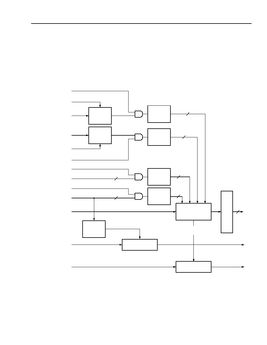
Agere Systems Inc.
103
Data Sheet
February 2004
Ambassador T8110L H.100/H.110 Switch
10 Error Reporting and Interrupt Control
(continued)
10.2 Error Reporting and Interrupt Controller Circuit Operation
T8110L errors are reported via two output signals, CLKERR and SYSERR. These outputs are generated by an
interrupt controller circuit; refer to Figure 20. The interrupt control circuit accepts 48 interrupt inputs in all. The way
in which these interrupts are arbitrated is selectable, and the means of reporting the interrupts out to the system is
also selectable.
5-9425 (F)
Figure 20. Interrupt Controller
FGIO INTERRUPT
ENABLE REGISTER
SYSERR OUTPUT
SELECT REGISTER
EDGE/LEVEL
SENSE GENERATION
SYSERR
CLKERR OUTPUT
SELECT REGISTER
EDGE/LEVEL
SENSE GENERATION
ARBITRATION
CONTROL REGISTER
LOGICAL OR
(UNMASKED
CLOCK
SOURCES)
CLKERR TRIGGER
CLKERR
ARBITRATION
CLOCK ERRORS
CLOCK
INTERRUPT
PENDING
REGISTERS
16
SYSTEM
INTERRUPT
PENDING
REGISTERS
GPIO
INTERRUPT
PENDING
REGISTER
FGIO
INTERRUPT
PENDING
REGISTER
CLOCK INTERRUPT
ENABLE REGISTERS
SYSTEM ERRORS
SYSTEM INTERRUPT
ENABLE REGISTERS
16
FG[7:0]
GPIO INTERRUPT
ENABLE REGISTER
GPIO POLARITY,
8
8
16
16
INT
E
RRUPT
IN-
SERVICE
RE
G
I
ST
ER
16
EDGE/LEVEL
SENSE
CONVERSION
GPIO EDGE/LEVEL
REGISTERS
GP[7:0]
EDGE/LEVEL
SENSE
CONVERSION
FGIO POLARITY,
FGIO EDGE/LEVEL
REGISTERS
SYSERR
TRIGGER

104
Agere Systems Inc.
Data Sheet
February 2004
Ambassador T8110L H.100/H.110 Switch
10 Error Reporting and Interrupt Control
(continued)
10.2 Error Reporting and Interrupt Controller Circuit Operation
(continued)
10.2.1 Externally Sourced Interrupts Via FG[7:0], GP[7:0]
Up to 16 of the 48 interrupt inputs are sourced external to the T8110L, via the FG[7:0] and GP[7:0] signals. Each
input is independently controlled via the interrupt control registers (refer to Section 10.1.1 on page 90 and Section
10.1.2 on page 92). Any externally sourced interrupt may be presented as active-high level, active-low level, posi-
tive edge, or negative edge sense. Each external interrupt is maskable. Any detected interrupt which is unmasked
is held in an interrupt pending register, and presented to the arbitration circuit for servicing.
10.2.2 Internally Sourced System Error Interrupts
Another set of 16 of the 48 interrupt inputs are sourced internally via the system error register bits (0x00126--127).
Each of these inputs is independently controlled via the interrupt control registers (refer to Section 10.1.3 on page
93). All internal system error bit interrupts are presented as active-high level sense. Each system error bit interrupt
is maskable. Any detected interrupt which is unmasked is held in an interrupt pending register and presented to the
arbitration circuit for servicing.
10.2.3 Internally Sourced Clock Error Interrupts
Another set of 16 of the 48 interrupt inputs are sourced internally via the latched clock error register bits
(0x00122--123; refer to Section 5.2.1 on page 40). Each of these inputs is independently controlled via the inter-
rupt control registers (refer to Section 10.1.6 on page 96). All internal clock error bit interrupts are presented as
active-high level sense. Each clock error bit interrupt is maskable. Any detected interrupt that is unmasked is held
in an interrupt pending register and presented to the arbitration circuit for servicing.
10.2.4 Arbitration of Pending Interrupts
The arbitration of the pending interrupts can be handled in one of four selectable modes: arbitration off, flat arbitra-
tion, tier arbitration with pre-empting disabled, and tier arbitration with pre-empting enabled. Interrupts are reported
to the system via the SYSERR signal.
10.2.4.1 Arbitration Off
This mode only allows the 16 internal system error register bits to generate interrupts, and no arbitration takes
place. The trigger for the SYSERR output is simply a logical OR of the internal system error register bits. All bits of
the internal system error register must be cleared in order to rearm the SYSERR trigger in this mode.
10.2.4.2 Flat Arbitration
The flat arbitration mode performs a round-robin arbitrations on all 48 interrupt sources. When a pending interrupt
wins the arbitration, the in-service register is loaded with its corresponding interrupt vector, SYSERR is triggered,
and that pending bit is cleared, removing it from the next round-robin arbitration cycle. The system must respond to
the current in-service interrupt (refer to Section 10.2.7 on page 105), after which the next arbitration cycle takes
place.
10.2.4.3 Tier Arbitration
The tier arbitration creates three prioritized groups as shown below:
!
Highest priority. The 16 internal latched clock error register bits.
!
Next highest priority. The 16 internal system error register bits.
!
Lowest priority. The 16 external FG[7:0] and GP[7:0] bits.

Agere Systems Inc.
105
Data Sheet
February 2004
Ambassador T8110L H.100/H.110 Switch
10 Error Reporting and Interrupt Control
(continued)
10.2 Error Reporting and Interrupt Controller Circuit Operation
(continued)
10.2.4 Arbitration of Pending Interrupts (continued)
10.2.4.3 Tier Arbitration (continued)
Arbitration assigns interrupt servicing priority to the three groups. Multiple pending interrupts within the same group
are arbitrated round-robin. When a pending interrupt wins the arbitration, the in-service register is loaded with its
corresponding interrupt vector, SYSERR is triggered, and that pending bit is cleared, removing it from the next
arbitration cycle.
10.2.4.4 Pre-Empting Disabled
With pre-empting disabled, once a pending interrupt wins the arbitration and the in-service register is loaded with
its corresponding interrupt vector, new incoming pending interrupts of higher priority must wait for the system to
respond to the current in-service interrupt (refer to Section 10.2.7 on page 105), at which time another arbitration
cycle takes place.
10.2.4.5 Pre-Empting Enabled
With pre-empting enabled, an interrupt that is in-service (i.e., its interrupt vector is loaded in the in-service register
and SYSERR has been triggered) can be overridden by new incoming pending interrupts of higher priority. The
current in-service interrupt is pushed onto a stack for storage; the higher-priority interrupt vector is loaded into the
in-service register and SYSERR is retriggered. Once all interrupts of higher priority have been serviced by the sys-
tem (refer to Section 10.2.7 on page 105), the stack is popped and the original lower-priority interrupt is reissued.
10.2.5 CLKERR Output
The CLKERR output signal is used to indicate any internal clocking errors. The trigger for the CLKERR output is
simply a logical OR of the internal latched clock error register bits. All bits of the internal clock error register must
be cleared in order to rearm the CLKERR trigger. The CLKERR trigger induces a state machine to generate the
CLKERR signal in one of four possible ways: active-high level, active-low level, active-high single pulse, or active-
low single pulse.
10.2.6 SYSERR Output
The T8110L SYSERR output signal is used to report interrupts. Internally, the arbitration circuit provides a
SYSERR trigger, which induces a state machine to generate the SYSERR signal in one of four possible ways:
active-high level, active-low level, active-high single pulse, or active-low single pulse.
10.2.7 System Handling of Interrupts
The T8110L interrupt controller presents an interrupt to the system by triggering the SYSERR output and providing
a predefined interrupt vector value at the interrupt in-service register (ISR). The system may acknowledge the
interrupt in three ways as shown below:
!
System reads the T8110L ISR register. This allows the arbiter to advance, and if more pending interrupts are
active, reloads the ISR with the winner of the arbitration and retriggers SYSERR.
!
System clears the T8110L ISR register (via register 0x00100, soft reset; write 0x20 clears the ISR). The arbiter
advances, and if more pending interrupts are active, reloads the ISR and retriggers SYSERR.
!
System resets the interrupt controller (via register 0x00100, soft reset, write 0x10 clears the ISR and all the
pending interrupt registers). All pending interrupts are cleared, and the arbiter is reset.
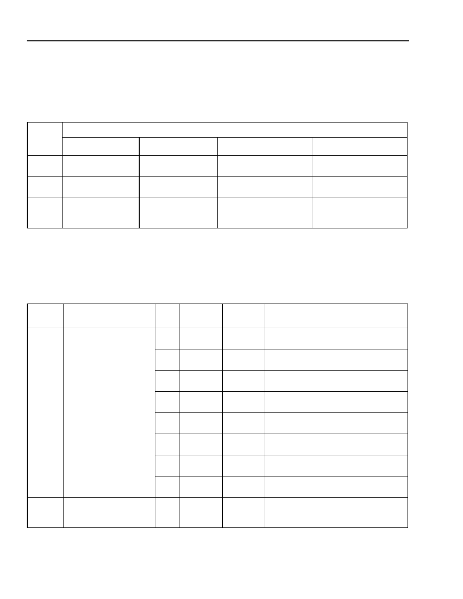
106
Agere Systems Inc.
Data Sheet
February 2004
Ambassador T8110L H.100/H.110 Switch
11 Test and Diagnostics
11.1 Diagnostics Control Registers
The diagnostic control registers allow for various diagnostic modes (refer to Section 11.2 on page 112).
11.1.1 FG Testpoint Enable Register
The FG testpoint enable register allows individual programming of FG[7:0] bits for either standard operation (as FG
or FGIO) or as testpoint outputs. FG testpoint select controls the MUX selection for which testpoints are selected.
Refer to Table 89 on page 107 for testpoint assignments for each FG bit.
Table 87. Diagnostics Control Register Map
DWORD
Address
(20 bits)
Register
Byte 3
Byte 2
Byte 1
Byte 0
0x00140 Diag3, GP testpoint
select
Diag2, GP testpoint
enable
Diag1, FG testpoint select
Diag0, FG testpoint enable
0x00144 Diag7, external buffer
RETRY timer
Diag6, miscellaneous
diagnostics low
Diag5, state counter
modes high
Diag4, state counter
modes low
0x00148 Diag11, sync-to-
frame command off-
set high
Diag10, sync-to-
frame command off-
set low
Diag9, interrupt controller
SYSERR delay
Diag8, interrupt controller
diagnostics
Table 88. FG Testpoint Enable Registers
Byte
Address
Name
Bit(s) Mnemonic
Value
Function
0x00140 Diag0, FG Testpoint
Enable
7
FT7EB
0
1
FG7 is standard FG or FGIO bit (default).
FG7 is a testpoint.
6
FT6EB
0
1
FG6 is standard FG or FGIO bit (default).
FG6 is a testpoint.
5
FT5EB
0
1
FG5 is standard FG or FGIO bit (default).
FG5 is a testpoint.
4
FT4EB
0
1
FG4 is standard FG or FGIO bit (default).
FG4 is a testpoint.
3
FT3EB
0
1
FG3 is standard FG or FGIO bit (default).
FG3 is a testpoint.
2
FT2EB
0
1
FG2 is standard FG or FGIO bit (default).
FG2 is a testpoint.
1
FT1EB
0
1
FG1 is standard FG or FGIO bit (default).
FG1 is a testpoint.
0
FT0EB
0
1
FG0 is standard FG or FGIO bit (default).
FG0 is a testpoint.
0x00141 Diag1, FG Testpoint
Select
7:0
FTPSR
LLLL LLLL Value for MUX selection of testpoints out-
put to FG[7:0]--see Table 88 on page
106.
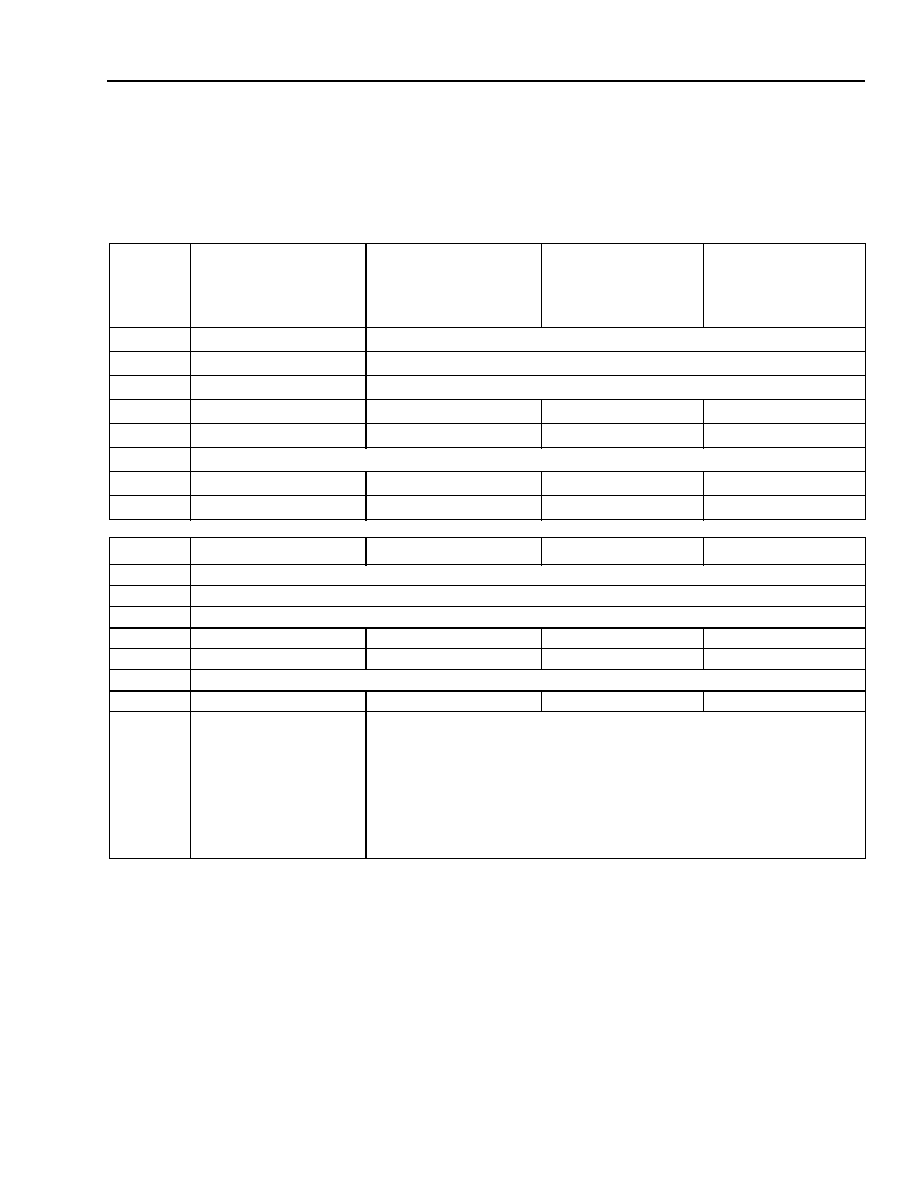
Agere Systems Inc.
107
Data Sheet
February 2004
Ambassador T8110L H.100/H.110 Switch
11 Test and Diagnostics
(continued)
11.1 Diagnostics Control Registers
(continued)
11.1.1 FG Testpoint Enable Register (continued)
Table 89. FG[7:0] Internal Testpoint Assignments
FG
Testpoint
Select
Value
FG7
FG6
FG5
FG4
0000 0001
i_FRAME
STATE_COUNT[10:4] (actual time slot)
0000 0010
i_FRAME
STATE_COUNT_LOOKAHEAD (lookahead time slot)
0000 0100
i_FRAME
STATE_COUNT_LOOKBEHIND (lookbehind time slot)
0000 1000
Reserved
Reserved
Reserved
Reserved
0001 0000
Reserved
Reserved
Reserved
Reserved
0010 0000
Reserved
0100 0000
P_S_SELECTOR
Reserved
OOL threshold flag
APLL1 lock indicator
1000 0000
Stalled
Snapping
C clock enable
B clock enable
--
FG3
FG2
FG1
FG0
0000 0001
STATE_COUNT[10:4] (actual time slot)
0000 0010
STATE_COUNT_LOOKAHEAD (lookahead time slot)
0000 0100
STATE_COUNT_LOOKBEHIND (lookbehind time slot)
0000 1000
Reserved
Reserved
Reserved
Reserved
0001 0000
Reserved
Reserved
Reserved
Reserved
0010 0000
Reserved
0100 0000
Failsafe flag
Force-to-OSC4 flag
Return from FS2 flag
Return from FS1 flag
1000 0000
A clock enable
Encoded ABC states:
000 or 100 = DIAGS
001 = A_ONLY
010 = A_MASTER
011 = A_ERROR
101 = B_ONLY
110 = B_MASTER
111 = B_ERROR
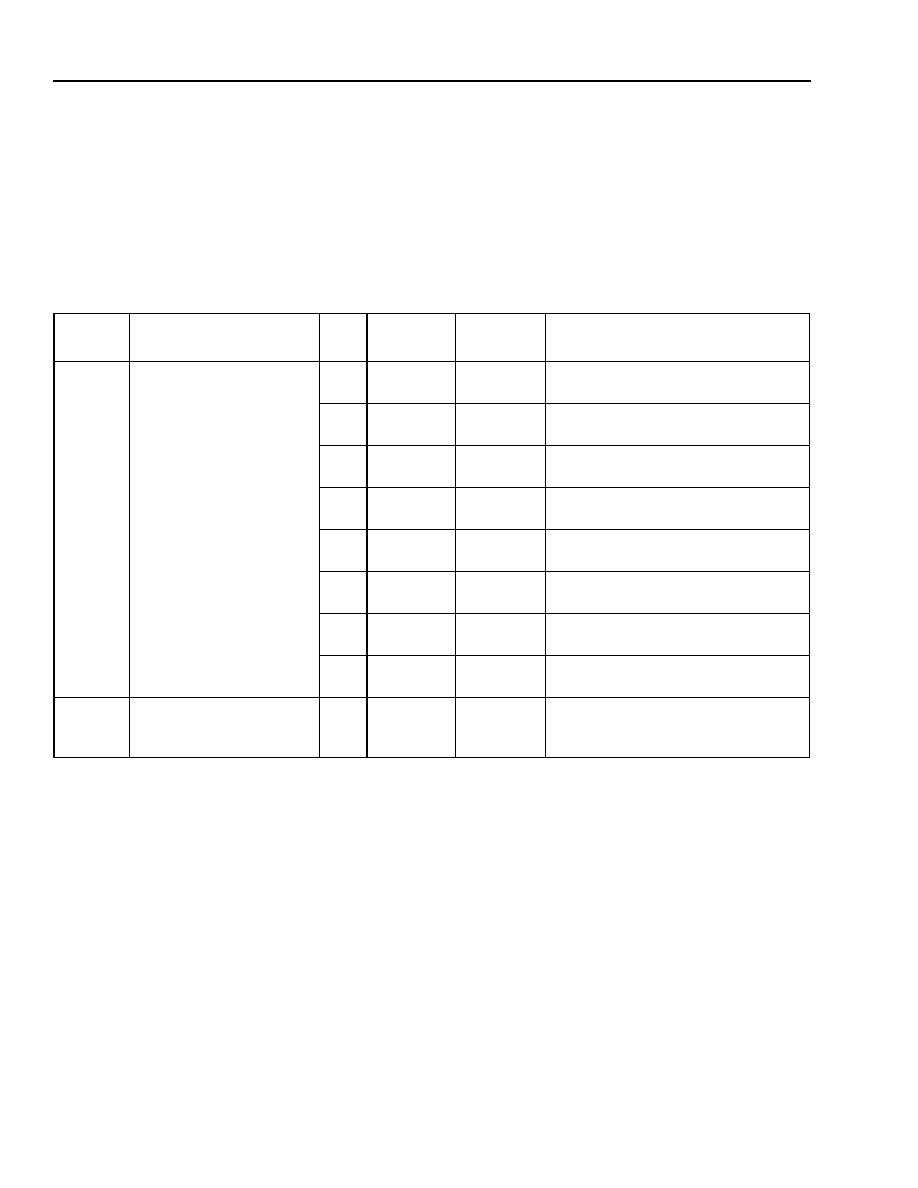
108
Agere Systems Inc.
Data Sheet
February 2004
Ambassador T8110L H.100/H.110 Switch
11 Test and Diagnostics
(continued)
11.1 Diagnostics Control Registers
(continued)
11.1.2 GP Testpoint Enable Register
The GP testpoint enable register allows individual programming of GP[7:0] bits for either standard operation (as
GPIO) or as testpoint outputs. GP testpoint select controls the MUX selection for which testpoints are selected.
Refer to Table 91 on page 109 for testpoint assignments for each GP bit.
Table 90. Testpoint Enable Registers
Byte
Address
Name
Bit(s) Mnemonic
Value
Function
0x00142 Diag2, GP Testpoint
Enable
7
GT7EB
0
1
GP7 is standard GPIO bit (default).
GP7 is a testpoint.
6
GT6EB
0
1
GP6 is standard GPIO bit (default).
GP6 is a testpoint.
5
GT5EB
0
1
GP5 is standard GPIO bit (default).
GP5 is a testpoint.
4
GT4EB
0
1
GP4 is standard GPIO bit (default).
GP4 is a testpoint.
3
GT3EB
0
1
GP3 is standard GPIO bit (default).
GP3 is a testpoint.
2
GT2EB
0
1
GP2 is standard GPIO bit (default).
GP2 is a testpoint.
1
GT1EB
0
1
GP1 is standard GPIO bit (default).
GP1 is a testpoint.
0
GT0EB
0
1
GP0 is standard GPIO bit (default).
GP0 is a testpoint.
0x00143 Diag3, GP Testpoint Select
7:0
GTPSR
LLLL LLLL
Value for MUX selection of testpoints
output to GP[7:0]--see Table 90 on
page 108.
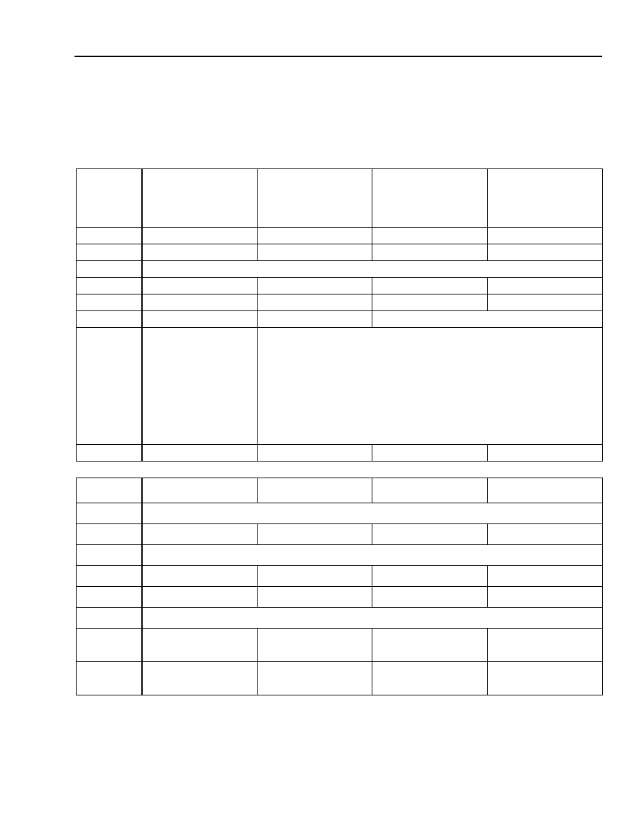
Agere Systems Inc.
109
Data Sheet
February 2004
Ambassador T8110L H.100/H.110 Switch
11 Test and Diagnostics
(continued)
11.1 Diagnostics Control Registers
(continued)
11.1.2 GP Testpoint Enable Register (continued)
Table 91. GP[7:0] Internal Testpoint Assignments
GP
Testpoint
Select
Value
GP7
GP6
GP5
GP4
0000 0001
BYTEREF_16
BYTEREF_8
BYTEREF_4
BYTEREF_2
0000 0010
i_FRAME
Reserved
CP8 read
CP8 write
0000 0100
Reserved
0000 1000
Reserved
Reserved
Reserved
Reserved
0001 0000
Reserved
Reserved
Reserved
Reserved
0010 0000
DPLL2 lock
DPLL1 lock
Reserved
0100 0000
P_S_SELECTOR
Fallback encoded states:
000 = PRIMARY
001 = TO_PRIMARY
010 = SECONDARY
011 = TO_SECONDARY
100 = FS1
101 = FS2
110 = [reserved]
111 = INITIAL
1000 0000
Stalled
Snapping
Reserved
Reserved
--
GP3
GP2
GP1
GP0
0000 0001
STATE_COUNT[3:0] (stream)
0000 0010
CP4 read
CP4 write
CP2 read
CP2 write
0000 0100
Reserved
0000 1000
Reserved
Reserved
Reserved
Reserved
0001 0000
Reserved
Reserved
Reserved
Reserved
0010 0000
Reserved
0100 0000
Fallback flag
Go_clocks
indicator
CLEAR_FALLBACK
indicator
FORCE_FALLBACK
indicator
1000 0000
Phase alignment
frame event
APLL1 feedback,
8 MHz tap
APLL1 feedback,
4 MHz tap
APLL1 feedback,
2 MHz tap
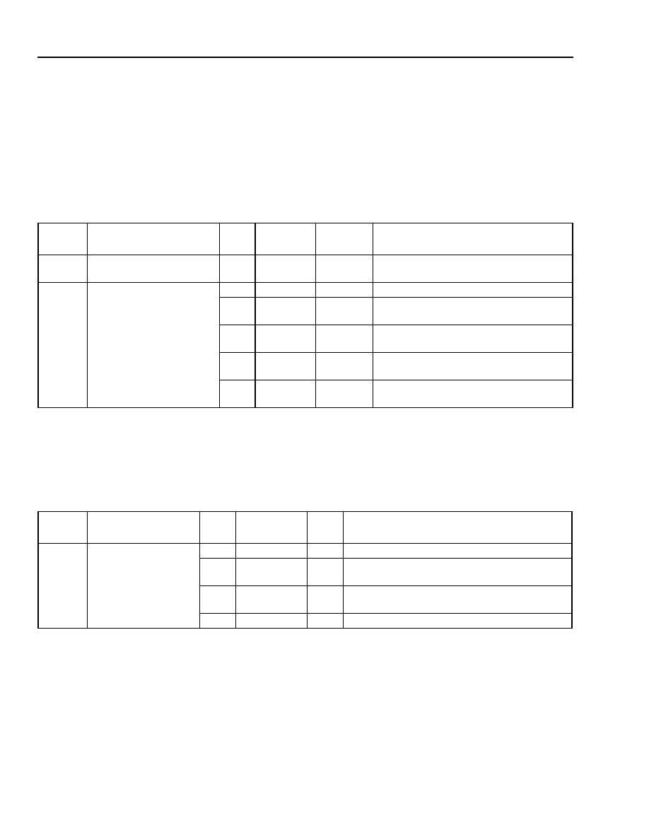
110
Agere Systems Inc.
Data Sheet
February 2004
Ambassador T8110L H.100/H.110 Switch
11 Test and Diagnostics
(continued)
11.1 Diagnostics Control Registers
(continued)
11.1.3 State Counter Modes Registers
The state counter modes registers control state counter diagnostics, including the breaking of state counter carry
chains, using /FR_COMP as the internal frame reference, and allowing the state counter to roll over early via a
modulo function. For more details, refer to Section 11.2 on page 112.
11.1.4 Miscellaneous Diagnostics Low Register
The miscellaneous diagnostics low register: bits 2 and 1 allow direct reset of the APLL2 and APLL1 feedback divid-
ers. Bit 0 controls the TST input of the power-on reset cell.
Table 92. State Counter Modes Registers
Byte
Address
Name
Bit(s) Mnemonic
Value
Function
0x00144 Diag4, State Counter
Modes Low
7:0
SCMLR
LLLL LLLL Lower 8 bits of state counter modulo load
value.
0x00145 Diag5, State Counter
Modes High
7:6
Reserved
00
NOP (default).
5
SCMSB
0
1
Normal carry chain operation (default).
Break state counter carry chains.
4
FRMSB
0
1
Normal internal frame operation (default).
Use /FR_COMP as internal frame.
3
SCLSB
0
1
Normal counting (default).
State counter modulo counting.
2:0
SCULP
LLL
Upper 3 bits of state counter modulo load
value.
Table 93. Miscellaneous Diagnostics Low Register
Byte
Address
Name
Bit(s)
Mnemonic
Value
Function
0x00146 Diag6, Miscellaneous
Diagnostics Low
7:3
Reserved
00
NOP (default).
2
FB2SB
0
1
APLL2 feedback divider reset inactive (default).
APLL2 feedback divider reset active.
1
FB1SB
0
1
APLL1 feedback divider reset inactive (default).
APLL1 feedback divider reset active.
0
Reserved
--
--
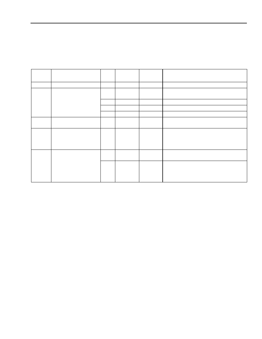
Agere Systems Inc.
111
Data Sheet
February 2004
Ambassador T8110L H.100/H.110 Switch
11 Test and Diagnostics
(continued)
11.1 Diagnostics Control Registers
(continued)
11.1.5 Miscellaneous Diagnostic Registers
Table 94. Miscellaneous Diagnostic Registers
Byte
Address
Name
Bit(s) Mnemonic
Value
Function
0x00147 Diag7
7:0
Reserved
--
NOP.
0x00148 Diag8, Interrupt
Controller Diagnostic
7:6
ICDSP
00
01
Interrupt controller, normal mode (default).
Interrupt controller, DIAG mode.
5:4
ICKLP
LL
DIAG mode, force CLK[1:0] errors.
3:2
ISYLP
LL
DIAG mode, force SYS[1:0] errors.
1:0
IEXLP
LL
DIAG mode, force EXT[8, 0] errors.
0x00149 Diag9, Interrupt Control-
ler Deassertion Delay
7:0
IASLR
LLLL LLLL Programmable delay to control the deas-
sertion time of SYSERR.
0x0014A Diag10, Sync-to-frame
Command Delay
(Lower)
7:0
CFLLR
LLLL LLLL Low byte of 12-bit offset value for sync-to-
frame clock commands (GO_CLOCKS,
CLEAR_FALLBACK,
FORCE_FALLBACK).
0x0014B Diag11, Sync-to-frame
Command Delay
(Upper)
7:4
CFSEN
0000
0001
Disable delay mode (default).
Enable delay mode.
3:0
CFHLN
LLLL
Upper 4 bits of 12-bit offset value for
sync-to-frame clock commands
(GO_CLOCKS, CLEAR_FALLBACK,
FORCE_FALLBACK).

112
Agere Systems Inc.
Data Sheet
February 2004
Ambassador T8110L H.100/H.110 Switch
11 Test and Diagnostics
(continued)
11.2 Diagnostic Circuit Operation
The T8110L internal diagnostic modes are intended primarily for chip manufacturing test. The diagnostic functions
include the following:
!
DIAG0--3, observability of internal testpoints via FG(7:0), GP(7:0):
-- Internal testpoints are brought to chip I/O at FG and GP signals. Refer to Table 89 on page 107 and Table 91
on page 109 for testpoint assignment.
!
DIAG4--5, internal state counter diagnostic modes:
-- Break counter carry chains--this is used in conjunction with monitoring of the state counter bits at FG and GP,
and breaks the 11-bit state counter into three separate pieces (bits [10:8], [7:4] and [3:0]).
-- Shorten frame operation--the internally generated 8 kHz frame is bypassed in favor of the /FR_COMP input.
The /FR_COMP input still denotes the frame center and may be presented at a higher frequency than 8 kHz.
This is used in conjunction with the state counter modulo function, which when properly programmed allows
the internal state counter to roll over coincident with the /FR_COMP frame center.
!
DIAG6, forced RESET of analog APLL1 feedback dividers:
-- The APLL1 feedback dividers are typically not reset. This diagnostic mode allows each feedback divider to be
held in a reset state.
!
DIAG7, reserved.
!
DIAG8, interrupt controller diagnostics:
-- When the diagnostic mode is enabled (DIAG8 register, bits 7:6 = 01), then bits 5:4 override the CLK error[1:0]
inputs, bits [3:2] override the SYS error[1:0] inputs, bit 1 overrides the GP[0] input, and bit 0 overrides the
FG[0] input to the interrupt controller. This allows for direct manipulation to set/clear a portion of interrupt bits
from each tier group. Please see Section 10.2 on page 103 for more details.
!
DIAG9, interrupt controller deassertion delay:
-- Allows a programmable deassertion time for the SYSERR signal in between back-to-back interrupts.
!
DIAG10--11, sync-to-frame command delay:
-- Allows a programmable delay time from the FRAME boundary for execution of the sync-to-frame clock com-
mands, GO_CLOCKS, CLEAR_FALLBACK, FORCE_FALLBACK.
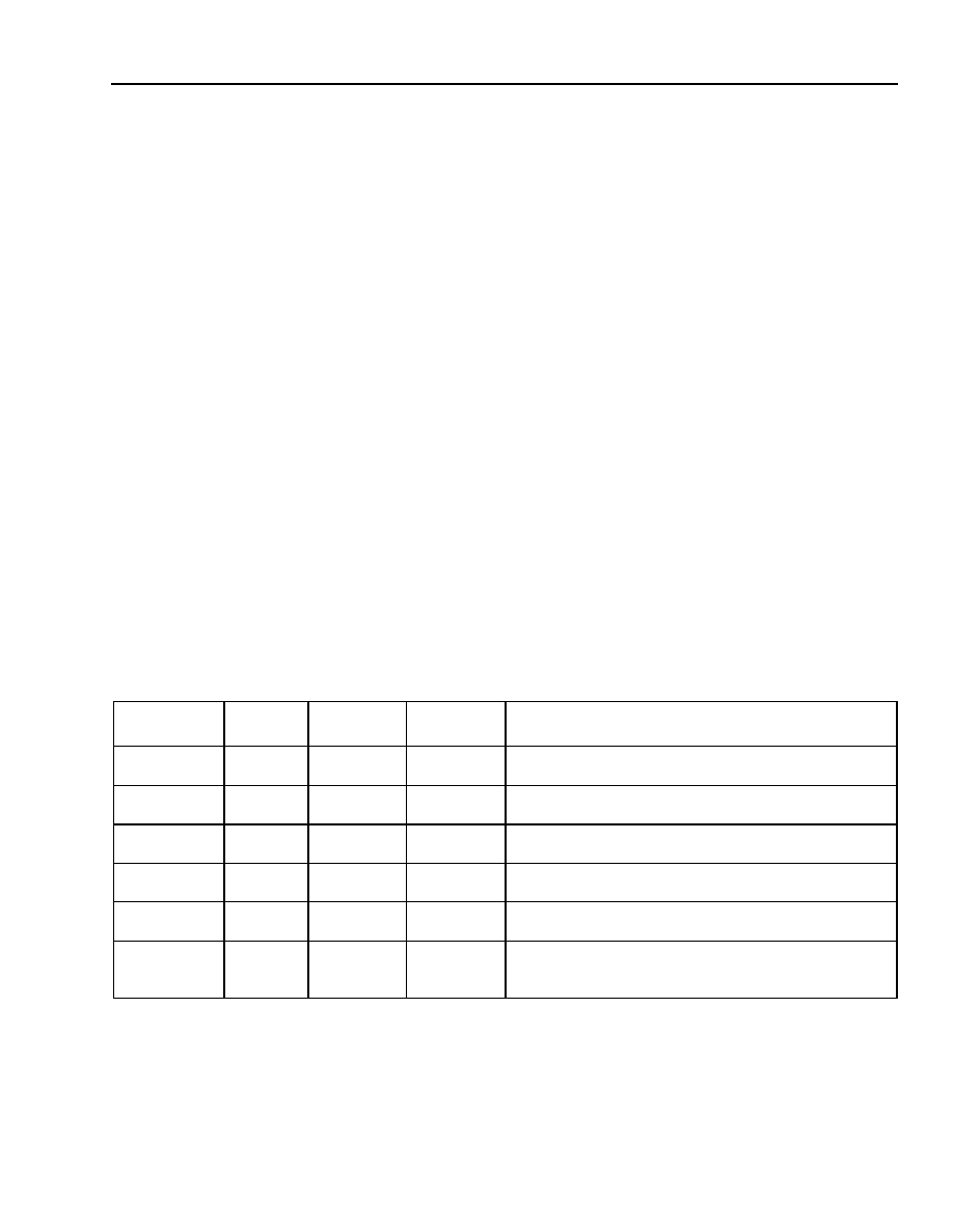
Agere Systems Inc.
113
Data Sheet
February 2004
Ambassador T8110L H.100/H.110 Switch
12 Connection Control
12.1 Programming Interface
Programming the T8110L for time-slot switching requires specific access cycles to the connection memory
regions. Access to other regions (data memory or registers) is made through a standard direct access via the inter-
face.
12.1.1 Connection Memory Programming
Because the microprocessor interface only allows word or byte accesses, multiple write accesses must occur. For
byte access, there are a total of three byte-wide holding registers. For word access, there is one word-wide holding
register. The user must load the holding registers with the proper information first, and then write to the upper byte
(or upper word) to actually move data into the connection memory; refer to Table 95.
The connection memory is divided into four 2K regions, each of which handles up to 128 time slots worth of con-
nectivity for each of 16 serial data streams. The regions include H1x0 even streams (CT_D[30, 28, . . . 0]), H1x0
odd streams (CT_D[31, 29, . . . 1]), local low streams (L_D[15:0]), and local high streams (L_D[31:16]). The con-
nection memory locations are addressed relative to time slot and stream.
Connection memory commands are as follows:
!
RESET PAGE resets any (up to all four) connection memory region (see Figure 21 on page 114). Address bit 15
determines whether or not it's a reset page command. The reset page command relies on a valid internal chip
clock and loops through all addresses within the connection memory region, resetting the VALID bit field. The
RESET PAGE command is presented as either two microprocessor WORD writes, or four microprocessor BYTE
writes, see Table 95.
!
MAKE/BREAK/QUERY, telephony connection (see Figure 22 on page 114).
The MAKE and BREAK commands are presented as multiple microprocessor write cycles. The QUERY command
is presented as multiple microprocessor read cycles; refer to Table 95.
Note: Data byte n required information is shown in Figure 22.
Table 95. Microprocessor Programming, Connection Memory Access
Word/Byte
(WB_SEL)
A[1:0]
D[15:8]
D[7:0]
Access Description
Byte
00
X
Data byte 0
Write data byte 0 to a holding register, or read data byte
0 information.
Byte
01
X
Data byte 1
Write data byte 1 to a holding register, or read data byte
1 information.
Byte
10
X
Data byte 2
Write data byte 2 to a holding register, or read data byte
2 information.
Byte
11
X
Data byte 3
Write data byte 3 plus the holding register data to con-
nection memory, or read data byte 3 information.
Word
0X
Data byte 1
Data byte 0
Write data bytes 1 and 0 to a holding register, or read
data bytes 1 and 0 information.
Word
1X
Data byte 3
Data byte 2
Write data bytes 3 and 2 plus the holding register data
to connection memory, or read data bytes 3 and 2 infor-
mation.
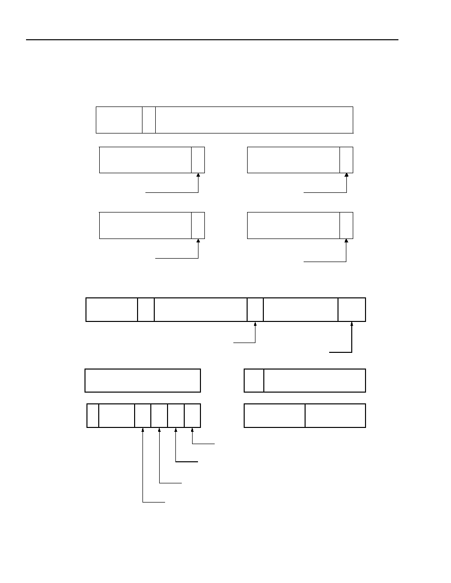
114
Agere Systems Inc.
Data Sheet
February 2004
Ambassador T8110L H.100/H.110 Switch
12 Connection Control
(continued)
12.1 Programming Interface
(continued)
12.1.1 Connection Memory Programming (continued)
Figure 21. Microprocessor Programming--Reset Page Command
5-9632 (F)
Figure 22. Microprocessor Programming--Make/Break/Query Telephony Connections
19:16
0100
15
1
14:0
000000000000000
A[19:0]
0 = NO ACTION
1 = RESET H-BUS
ODD REGION
0 = NO ACTION
1 = RESET H-BUS
EVEN REGION
0 = NO ACTION
1 = RESET LOCAL
HI REGION
0 = NO ACTION
1 = RESET LOCAL
LO REGION
RHO
RHE
RLH
RLL
7:1
0000000
DATA
BYTE 1
bit
0
7:1
0000000
DATA
BYTE 0
bit
0
7:1
0000000
DATA
BYTE 3
bit
0
7:1
0000000
DATA
BYTE 2
bit
0
A[19:0]
19:16
0100
15
0
14:8
TIME SLOT
7
6:2
STREAM
1:0
7:0
TAG (LOWER BITS)
7
6:0
SUBRATE
7:4
0000
3:0
0
DATA
BYTE 0
H-BUS/LOCAL SELECT:
0 = LOCAL STREAMS
1 = H.1x0 STREAMS
HLS
WORD/BYTE
ADDRESS LSBITS
TAG (UPPER BITS)
DATA
BYTE 2
0
1
2
3
6:4
7
000
0
DATA
BYTE 1
DATA
BYTE 3
MBS
0 = MAKE CONNECTION
1 = BREAK CONNECTION
0 = WRITE TO DATA MEMORY
1 = READ FROM DATA MEMORY
0 = PATTERN MODE DISABLED
1 = PATTERN MODE ENABLED
0 = USE CURRENT FRAME
1 = USE NEXT FRAME
RWS
VFC
PME

Agere Systems Inc.
115
Data Sheet
February 2004
Ambassador T8110L H.100/H.110 Switch
12 Connection Control
(continued)
12.2 Switching Operation
The basic building block of switching is one-half simplex connections loaded into the connection memory. Each
connection memory location controls data flow, either from a serial stream input to a location in data memory, or
from data memory to a serial stream output. A typical telephony simplex switch connection would use one from
and one to connection, each using the same data memory location.
12.2.1 Memory Architecture and Configuration
12.2.1.1 Connection Memory
The T8110L connection memory consists of 8192 locations, one location for each of the possible stream/time-slot
combinations, to provide a full nonblocking switch for up to 128 time slots on 32 H1x0 streams (CT_D[31:0]) and
32 local streams (L_D[31:0]). Connection memory is physically addressed by time slot (7 bits), H1x0/local select
(1 bit), and stream (5 bits).
The 8192 locations are divided into four pages of 2048, with each page dedicated to a set of 16 serial streams as
follows:
!
H1x0 even streams (CT_D[30, 28, . . . 0])
!
H1x0 odd streams (CT_D[31, 29, . . . 1])
!
Local high streams (L_D[31:16])
!
Local low streams (L_D[15:0])
Each of these connection memory pages are initialized at reset (valid bit entries are reset to invalid). Additionally,
each page may be initialized individually via software command, RESET PAGE (refer to Figure 21 on page 114).
Connection memory locations contain the following control information:
!
VALID bit indicates that a valid switch connection exists for this stream/time slot.
!
RWS indicates whether the connection is from (from serial stream to data memory) or to (from DATA memory to
serial stream).
!
VFC (virtual framing control) controls which data page is used in double-buffer scenarios.
Note: There are two data memory configurations that allow double-buffering of the data, in order to create con-
stant frame delay connections. Refer to Section 12.2.1.2 on page 116 and Section 12.2.2.1 on page 117.
!
PME indicates a pattern mode connection.
!
TAG is the data memory location used for this one-half simplex switch connection (or the data pattern sent to
serial output for pattern mode connections).
!
SUBRATE information is subrate switching control (bitswap).
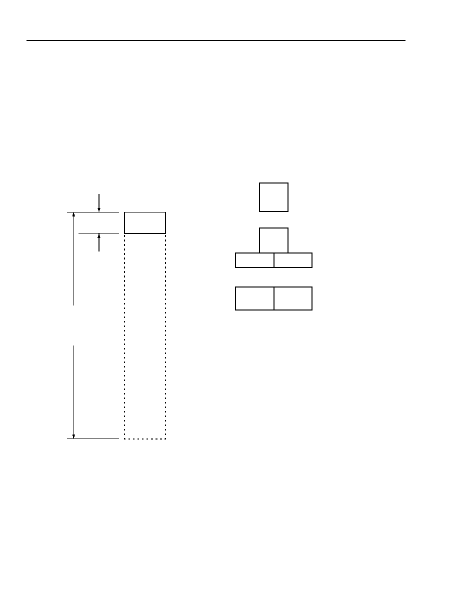
116
Agere Systems Inc.
Data Sheet
February 2004
Ambassador T8110L H.100/H.110 Switch
12 Connection Control
(continued)
12.2 Switching Operation
(continued)
12.2.1 Memory Architecture and Configuration (continued)
12.2.1.2 Data Memory
The T8110L data memory is 4096 bytes, which can be programmatically configured in three ways, via the data
memory mode select register (0x00105; refer to Section 5.1.3 on page 32).
5-9638 (F)
Figure 23. T8110L Data Memory Map and Configurations
TEL
DATA
MEMORY
MODES
TEL
TEL
TEL
TEL
TEL
0x20000
0x20FFF
0x20000
0x207FF
0x20800
0x20BFF
0x20000
0x207FF
(SET BY CONTROL
REGISTER 0x00105)
4K SINGLE-
BUFFERED
SWITCH
2K SINGLE
BUFFERED
+
1K DOUBLE
BUFFERED
2K DOUBLE-
BUFFERED
SWITCH
0x2FFFF
(RESERVED)
0x21000
0x20FFF
0x20000
4K
UTILIZED
TOTAL
ADDRESSED
SPACE IS 64K
DATA
MEMORY
ADDRESSING

Agere Systems Inc.
117
Data Sheet
February 2004
Ambassador T8110L H.100/H.110 Switch
12 Connection Control
(continued)
12.2 Switching Operation
(continued)
12.2.2 Standard Switching
Standard telephony switching is achieved by loading control fields into the connection memory for one-half simplex
connections (refer to Figure 22 on page 114, and Section 12.2.1.1 on page 115).
12.2.2.1 Constant Delay and Minimum Delay Connections
The VFC control bit in connection memory determines which of two data pages is accessed, when the data mem-
ory is configured to double-buffering for telephony connections (refer to Figure 23). This bit always affects to con-
nections (read the data memory, send it out to a serial stream output) in a double-buffer configuration. This bit can
control a from connection in a double-buffer configuration, only if it is a subrate connection; otherwise, the VFC bit
has no bearing on from connections.
The double-buffering configuration creates two data pages. During a particular frame (125
µ
s time boundary, parti-
tioned into time slots), one page is the active page, the other is the inactive page. The active/inactive page status
toggles at every frame boundary. For all from connections (except for subrate connections), incoming serial data is
always written to the active page. For all to connections, the VFC control bit indicates whether to read from the
active or inactive page. Manipulation of this bit affects the latency between the incoming from data and the outgo-
ing to data. This latency defines whether or not a connection is constant delay or minimum delay.
Please see Appendix A on page 139 for more details on constant and minimum delay connections.
12.2.2.2 Pattern Mode
The PME control bit in connection memory affects only to connections. Instead of reading a value out of the data
memory for subsequent output to a serial stream, the lower 8 bits of the TAG field provide a byte pattern for the
serial output.
12.2.2.3 Subrate
The subrate control bit field in connection memory is used only by from connections and controls how individual
bits or groups of bits of an incoming serial byte are shuffled prior to writing them to the data memory, in order to
achieve subrate switching.
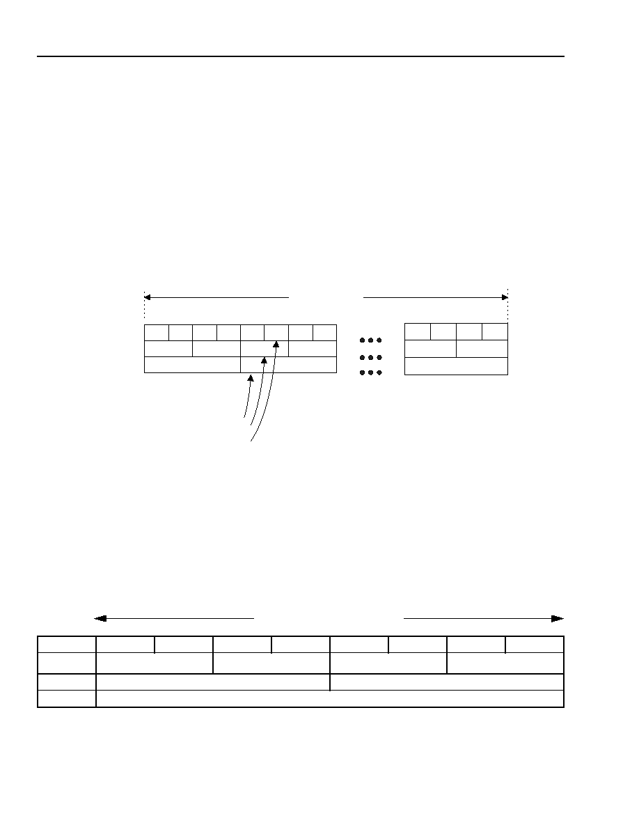
118
Agere Systems Inc.
Data Sheet
February 2004
Ambassador T8110L H.100/H.110 Switch
12 Connection Control
(continued)
12.2 Switching Operation
(continued)
12.2.2 Standard Switching (continued)
12.2.2.1 Subrate (continued)
Subrate Switching Overview
Traditional byte-oriented TDM data switching provides 8 bits of data per time slot, or channel, regardless of the
TDM stream bit rate. A particular channel occurs once every 8 kHz frame, and there are 8K
frames per second.
This allows for a channel data propagation rate of (8 bits/frame * 8K frames/s = 64 kbits/s).
Refer to Figure 24 and Table 97.
Figure 24. TDM Data Stream Bit Rates
Subrate refers to switching fractional portions of the byte-oriented TDM data streams. The T8110L allows the 8 bits
of a byte-oriented channel to be broken into multiple channels of fewer bits, either two 4-bit channels, four 2-bit
channels, or eight 1-bit channels. This lowers the data propagation rate per channel, but increases the overall
channel capacity for a given time slot. Refer to Table 96 and Table 97.
Notes:
Bit subrate = 8 channels per time slot, 1 bit per channel.
Di-bit = 4 channels per time slot, 2 bits per channel.
Nibble subrate = 2 channels per time slot, 4 bits per channel.
Byte (no subrate) = 1 channel per time slot, 8 bits per channel.
Table 96. TDM Data Stream
Bit
7
6
5
4
3
2
1
0
Di-Bit
7:6
5:4
3:2
1:0
Nibble
7:4
3:0
Byte
7:0
0
1
2
3
4
5
6
7
0
1
2
3
0
1
124
125
126
127
62
63
31
ONE FRAME (8 kHz)
TDM Stream Bit rate = 8MB/s: each stream has
128 timeslots (channels) per frame
TDM STREAM BIT RATE = 4 Mbits/s: EACH STREAM HAS
64 TIME SLOTS (CHANNELS) PER FRAME
TDM STREAM BIT RATE = 2 Mbits/s: EACH STREAM HAS
32 TIME SLOTS (CHANNELS) PER FRAME
EACH CHANNEL CONTAINS ONE 8-BIT
BYTE, REGARDLESS OF THE TDM
DATA STREAM BIT RATE
8 Mbits/s
4 Mbits/s
2 Mbits/s
TDM STREAM BIT RATE = 8 Mbits/s: EACH STREAM HAS
128 TIME SLOTS (CHANNELS) PER FRAME
One Time slot (or Channel)
Agere Systems Inc.
119
Data Sheet
February 2004
Ambassador T8110L H.100/H.110 Switch
12 Connection Control
(continued)
12.2 Switching Operation
(continued)
12.2.2 Standard Switching (continued)
12.2.2.1 Subrate (continued)
Subrate Switching Overview (continued)
Subrate Switching Using T8110L
The H1x0 bus and the local stream bus are based on byte-oriented TDM data streams--data is always switched
as whole bytes. The subrate data must be packed into these bytes prior to switching (refer to Sections and ). The
data bytes are not necessarily constrained to using fully packed bytes--any portion of a byte may be used. Sub-
rate switching using T8110L requires the following:
!
Overall subrate enable mode is activated (register 0x00105, data memory mode select bit 7 is set; see Section
5.1.3 on page 32).
!
The subrate field of the connection memory entry for that switch connection is set up. This field contains 7 bits
which control the type of subrate (i.e., bit, di-bit, nibble, or byte), and the data bit shuffling within the TDM byte
data, from and to (refer to Figure 22 on page 114, and Table 98).
!
The VFC connection memory bit for cases where a double-buffering configuration is set up in the data memory
(refer to Figure 22, and Sections 12.2.1.2, 12.2.2.1).
In order to program a subrate simplex connection, the subrate field is only required for the from half of that con-
nection. Incoming serial byte data has its bit positions rearranged based on the subrate field contents prior to being
written into the data memory. For double-buffered data memory configurations, the VFC bit controls which of two
data pages the rearranged byte is written to. The to half of a subrate simplex connection simply outputs the entire
byte found at the data memory location used for that connection, and its connection memory subrate field is
ignored.
Table 97. Subrate Switching, Data Propagation Rate vs. Channel Capacity
Subrate Type
Bits per Channel
Channel Data Propagation Rate
(Bits/Frame x 8K Frames/s)
Channel Capacity
(Relative to Byte Switching)
Bit
1
8 kbits/s
8X
Di-bit
2
16 kbits/s
4X
Nibble
4
32 kbits/s
2X
Byte (no subrate)
8
64 kbits/s
1X
120
Agere Systems Inc.
Data Sheet
February 2004
Ambassador T8110L H.100/H.110 Switch
12 Connection Control
(continued)
12.2 Switching Operation
(continued)
12.2.2 Standard Switching (continued)
12.2.2.1 Subrate (continued)
Subrate Switching Using T8110L (continued)
Subrate Packing of Outgoing Bytes
The output from subrate connections is always an entire byte so that it does not violate the H.100 or H.110 specifi-
cations. The output byte is composed of smaller, i.e., subrate pieces. The process of combining the incoming
pieces into a whole byte suitable for output is called packing. In the T8110L (and other subrate-capable Ambassa-
dor devices), packing is accomplished by making several from connections for each single to connection. For
example, in Figure 25, four from connections (of different stream/time-slot origins), all di-bits, are used to construct
a byte that will be output as defined by the to connection.
The outgoing to half of a simplex connection reads an entire byte from a data memory location. The packing of
separate incoming subrate pieces into this byte is achieved by setting up multiple from one-half simplex connec-
tions for one to one-half simplex connection, all using the same data memory location. An example is illustrated in
Figure 25. This example shows the packing of four separate incoming di-bits from four different channels into one
outgoing byte on one channel.
Note: Please note the limitation that multiple di-bits from the same time slot cannot be switched simultaneously.
This would require the byte of that time slot to be unpacked first, which is discussed in Section on page 122.
Table 98. Subrate Switching, Connection Memory Programming Setup
Subrate
Type
Subrate Connection Memory Bit Field (6:0)
6
5
4
3
2
1
0
Bit
1
000 = from bit 0
001 = from bit 1
010 = from bit 2
011 = from bit 3
100 = from bit 4
101 = from bit 5
110 = from bit 6
111 = from bit 7
000 = to bit 0
001 = to bit 1
010 = to bit 2
011 = to bit 3
100 = to bit 4
101 = to bit 5
110 = to bit 6
111 = to bit 7
Subrate Connection Memory Bit Field (6:0)
6
5
4
3
2
1
0
Di-Bit
01
00 = from bits[1:0]
01 = from bits[3:2]
10 = from bits [5:4]
11 = from bits[7:6]
Reserved
00 = to bits[1:0]
01 = to bits[3:2]
10 = to bits[5:4]
11 = to bits[7:6]
Subrate
Type
Subrate Connection Memory Bit Field (6:0)
6
5
4
3
2
1
0
Nibble
001
0 = from bits[3:0]
1 = from bits[7:4]
Reserved
0 = to bits[3:0]
1 = to bits[7:4]
Subrate Connection Memory Bit Field (6:0)
6
5
4
3
2
1
0
Byte
000
Reserved

Agere Systems Inc.
121
Data Sheet
February 2004
Ambassador T8110L H.100/H.110 Switch
12 Connection Control
(continued)
12.2 Switching Operation
(continued)
12.2.2 Standard Switching (continued)
12.2.2.1 Subrate (continued)
Subrate Packing of Outgoing Bytes (continued)
Notes:
Connectivity is as follows:
!
From
stream a, time slot n, bits[1:0] to stream e, time slot n + 10, bits[7:6].
!
From
stream b, time slot n + 1, bits[1:0] to stream e, time slot n + 10, bits[3:2].
!
From
stream c, time slot n + 2, bits[3:2] to stream e, time slot n + 10, bits[1:0].
!
From
stream d, time slot n + 3, bits[5:4] to stream e, time slot n + 10, bits[5:4].
Required connection memory programming is as follows:
Five 1/2 simplex connections are required to pack four incoming di-bits into an outgoing byte.
!
From
stream a, time slot n. Connection memory subrate field = 0100X11.
!
From
stream b, time slot n + 1. Connection memory subrate field = 0100X01.
!
From
stream c, time slot n + 2. Connection memory subrate field = 0101X00.
!
From
stream d, time slot n + 3. Connection memory subrate field = 0110X10.
!
To
stream e, time slot n + 10. Connection memory subrate field is don't care.
Figure 25. Subrate Switching Example, Byte Packing
FRAME (8 kHz)
TIME SLOT
STREAM a, DI-BIT CHANNELS IN
STREAM b, DI-BIT CHANNELS IN
STREAM c, DI-BIT CHANNELS IN
BIT POSTITIONS OF DI-BITS
WITHIN THE DATA BYTE
STREAM d, DI-BIT CHANNELS IN
STREAM e, DI-BIT CHANNELS OUT
n
n + 1
n + 2
n + 3
TIME SLOT
n + 10
7:
6
5:
4
3:
2
1:
0
a
1
a
2
a
3
a
4
b
1
b
2
b
3
b
4
a
4
d
2
b
4
c
3
c
1
c
2
c
3
c
4
d
1
d
2
d
3
d
4
7:
6
5:
4
3:
2
1:
0
7:
6
5:
4
3:
2
1:
0
7:
6
5:
4
3:
2
1:
0
7:
6
5:
4
3:
2
1:
0

122
Agere Systems Inc.
Data Sheet
February 2004
Ambassador T8110L H.100/H.110 Switch
12 Connection Control
(continued)
12.2 Switching Operation
(continued)
12.2.2 Standard Switching (continued)
12.2.2.1 Subrate (continued)
Subrate Unpacking of Incoming Bytes
Because the H1x0 bus and the local stream bus are based on byte-oriented TDM data streams, and the T8110L
architecture is geared towards standard byte switching, it is not possible to simultaneously switch subrate portions
of a single byte to different places. This limitation is overcome by application. To gain access to each subrate piece
contained in one incoming byte, that byte must be broadcast onto additional channels, one channel for each sub-
rate piece required. The means of broadcasting is up to the application--either the source device of the packed
subrate byte can broadcast it, or the device receiving that byte can broadcast it over unused channels and loop the
broadcast bytes back in. The example from Figure 25 is extended in Figure 26. This example shows the unpacking
of the packed byte created in Figure 25, output to four different channels.
Agere Systems Inc.
123
Data Sheet
February 2004
Ambassador T8110L H.100/H.110 Switch
12 Connection Control
(continued)
12.2 Switching Operation
(continued)
12.2.2 Standard Switching (continued)
12.2.2.1 Subrate (continued)
Subrate Unpacking of Incoming Bytes (continued)
Notes:
Connectivity is as follows:
From
stream e, time slot n + 3, bits[1:0] to stream j, time slot n + 8, bits[7:6].
From
stream f, time slot n + 5, bits[3:2] to stream i, time slot n + 8, bits[5:4].
From
stream f, time slot n + 6, bits[5:4] to stream h, time slot n + 8, bits[1:0].
From
stream f, time slot n + 7, bits[7:6] to stream g, time slot n + 8, bits[7:6].
Required connection memory programming is as follows:
Eight 1/2 simplex connections are required to unpack one incoming byte to four separate outgoing di-bits.
From
stream e, time slot n + 3. Connection memory subrate field = 0100X11.
From
stream f, time slot n + 5. Connection memory subrate field = 0101X10.
From
stream f, time slot n + 6. Connection memory subrate field = 0110X00.
From
stream f, time slot n + 7. Connection memory subrate field = 0111X11.
To
stream g, time slot n + 8. Connection memory subrate field is don't care.
To
stream h, time slot n + 8. Connection memory subrate field is don't care.
To
stream i, time slot n + 8. Connection memory subrate field is don't care.
To
stream j, time slot n + 8. Connection memory subrate field is don't care.
Figure 26. Subrate Switching Example, Byte Unpacking
n + 3
n + 4
n + 5
n + 6
FRAME (8 kHz)
TIME SLOT
TIME SLOT
BIT POSITIONS OF DI-BITS
WITHIN THE DATA BYTE
n + 7
7:
6
5:
4
3:
2
1:
0
STREAM e, DI-BIT CHANNELS IN
a
4
d
2
b
4
c
3
7:
6
5:
4
3:
2
1:
0
7:
6
5:
4
3:
2
1:
0
7:
6
5:
4
3:
2
1:
0
7:
6
5:
4
3:
2
1:
0
n + 8
a
4
d
2
b
4
c
3
a
4
d
2
b
4
c
3
a
4
d
2
b
4
c
3
STREAM f, DI-BIT CHANNELS IN
(BROADCASTS OF THE ORIGINAL INPUT)
STREAM g, DI-BIT CHANNELS OUT
STREAM h, DI-BIT CHANNELS OUT
STREAM i, DI-BIT CHANNELS OUT
STREAM j, DI-BIT CHANNELS OUT
a
4
X
X
X
X
X
X
d
2
X
b
4
X
X
c
3
X
X
X
BROADCASTED INCOMING BYTE
7:
6
5:
4
3:
2
1:
0

124
Agere Systems Inc.
Data Sheet
February 2004
Ambassador T8110L H.100/H.110 Switch
13 Electrical Characteristics
13.1 Absolute Maximum Ratings
Stresses in excess of the absolute maximum ratings can cause permanent damage; the table below shows abso-
lute stress ratings only. Functional operation of the device is not implied at these or any other conditions in excess
of those given in the operational sections of this data sheet. Exposure to absolute maximum ratings for extended
periods can adversely affect device reliability.
13.1.1 Handling Precautions
Although protection circuitry has been designed into this device, proper precautions should be taken to avoid expo-
sure to electrostatic discharge (ESD) during handling and mounting. Agere employs a human-body model (HBM)
and a charged-device model (CDM) for ESD-susceptibility testing and protection design evaluation. ESD voltage
thresholds are dependent on the circuit parameters used to define the model. No industry-wide standard has been
adopted for CDM. However, a standard HBM (resistance = 1500 W, capacitance = 100 pF) is widely used and,
therefore, can be used for comparison purposes. The T8110L has a HBM ESD threshold voltage rating of 1500 V
minimum.
13.2 Crystal Specifications
13.2.1 XTAL1 Crystal
The T8110L requires a 16.384 MHz clock source derived from an oscillator or a crystal. If a crystal is used it has to
be a 16.384 MHz crystal and must be connected between the XTAL1_IN and the XTAL1_OUT pins. External 24 pF,
5% capacitors must be connected from XTAL1_IN and XTAL1_OUT to Vss, as shown in the diagram below.
The ±32 ppm tolerance is the suggested value if the oscillator is used as the clocking source while mastering the
bus. Otherwise, a crystal with a lesser tolerance can be used. The crystal specifications are shown below.
Table 99. Absolute Maximum Ratings
Parameter
Symbol
Min
Max
Unit
Supply Voltage
V
DD
--
4.2
V
XTAL1_IN, XTAL2_IN, XTAL1_OUT, XTAL2_OUT pins
--
V
SS
V
DD
V
Voltage Applied to I/O Pins
--
V
SS
≠ 0.3
V
DD
5.5
V
Operating Temperature
--
≠40
85
∞C
Storage Temperature
T
stg
≠55
125
∞C
Table 100. XTAL1 Specifications
Parameter
Value
Frequency
16.384 MHz
Oscillation Mode
Fundamental, parallel resonance
Effective Series Resistance
50
maximum
Load Capacitance
18 pF
Shunt Capacitance
7 pF maximum
Frequency Tolerance and Stability
32 ppm
5-6390f(c)
V
SS
24 pF
24 pF
1 M
16.384 MH
Z
T8110L
XTAL1_IN
XTAL1_OUT
CRYSTAL
Agere Systems Inc.
125
Data Sheet
February 2004
Ambassador T8110L H.100/H.110 Switch
13 Electrical Characteristics
(continued)
13.2 Crystal Specifications
(continued)
13.2.1 XTAL1 Crystal (continued)
If an oscillator is used (see Section 6.4.4 on page 61), the signal has to be connected to the XTAL1_IN pin.
XTAL1_OUT must be left unconnected in this configuration. XTAL1_IN and XTAL1_OUT are not 5 V tolerant. The
oscillator must meet the requirements shown below.
13.2.2 XTAL2 Crystal
XTAL2 is an optional crystal oscillator input. If a crystal is used, it has to be a 6.176 MHz or a 12.352 MHz crystal
and must be connected between the XTAL2_IN and the XTAL2_OUT pins, as shown in the diagram below. Exter-
nal 24 pF, 5% capacitors must be connected from XTAL2_IN and XTAL2_OUT to Vss. The ±32 ppm tolerance is
the suggested value if the oscillator is used as the clocking source while mastering the bus. Otherwise, a crystal
with a lesser tolerance can be used (see Table 121).
If XTAL2 is not used, XTAL2_IN should be tied to V
DD
and XTAL2_OUT should be left unconnected.
* 120
maximum for 6.176 MHz crystal.
24 pF for 6.176 MHz crystal also.
18 pF for 6.176 MHz crystal also.
If an oscillator is used (see Section 6.5.1 on page 63), the signal has to be connected to the XTAL2_IN pin.
XTAL2_OUT must be left unconnected in this configuration. XTAL2_IN and XTAL2_OUT are not 5 V tolerant. The
oscillator must meet the requirements shown below.
Table 101. 16.384 MHz Oscillator Requirements
Parameter
Value
Frequency
16.384 MHz
Maximum Rise or Fall Time
10 ns, 10%--90% V
DD
Minimum Pulse Width
Low
High
20 ns
20 ns
Table 102. XTAL2 Specifications
Parameter
Value
Frequency
12.352 MHz
Oscillation Mode
Fundamental, parallel resonance
Effective Series Resistance
75*
maximum
Load Capacitance
18
pF
Shunt Capacitance
7 pF maximum
Frequency Tolerance and Stability
32 ppm
5-6390d
Table 103. 6.176 MHz/12.352 MHz Oscillator Requirements
Parameter
Value
Value
Frequency
6.176 MHz
12.352 MHz
Maximum Rise or Fall Time
10 ns, 10%--90% V
DD
10 ns, 10%--90% V
DD
Minimum Pulse Width
Low
High
Low
High
54 ns
54 ns
27 ns
27 ns
V
SS
24 pF
24 pF
1 M
T8110L
XTAL2_IN
XTAL2_OUT
12.352 MHz
CRYSTAL
126
Agere Systems Inc.
Data Sheet
February 2004
Ambassador T8110L H.100/H.110 Switch
13 Electrical Characteristics
(continued)
13.2 Crystal Specifications
(continued)
13.2.3 Reset Pulse
13.3 Thermal Parameters (Definitions and Values)
System and circuit board level performance depends not only on device electrical characteristics, but also on device
thermal characteristics. The thermal characteristics frequently determine the limits of circuit board or system perfor-
mance, and they can be a major cost adder or cost avoidance factor. When the die temperature is kept below 125
∞C, temperature activated failure mechanisms are minimized. The thermal parameters that Agere provides for its
packages help the chip and system designer choose the best package for their applications, including allowing the
system designer to thermally design and integrate their systems.
It should be noted that all the parameters listed below are affected, to varying degrees, by package design (including
paddle size) and choice of materials, the amount of copper in the test board or system board, and system airflow.
JA
--Junction to Air Thermal Resistance
JA
is a number used to express the thermal performance of a part under JEDEC standard natural convection con-
ditions.
JA
is calculated using the following formula:
JA
= (T
J
≠ T
amb
)/P; where P = power
JMA
--Junction to Moving Air Thermal Resistance
JMA
is effectively identical to
JA
but represents performance of a part mounted on a JEDEC four layer board inside
a wind tunnel with forced air convection.
JMA
is reported at airflows of 200 lft./min and 500 lft./min, which roughly
correspond to
1 m/s and 2.5 m/s (respectively).
JMA
is calculated using the following formula:
JMA
= (T
J
≠ T
amb
)/P
JC
--Junction to Case Thermal Resistance
JC
is the thermal resistance from junction to the top of the case. This number is determined by forcing nearly 100%
of the heat generated in the die out the top of the package by lowering the top case temperature. This is done by
placing the top of the package in contact with a copper slug kept at room temperature using a liquid refrigeration
unit.
JC
is calculated using the following formula:
JC
= (T
J
≠ T
C
)/P
Table 104. Reset Pulse
Parameter
Min
Max
Unit
RESET# Minimum Pulse Width
61
--
ns
Agere Systems Inc.
127
Data Sheet
February 2004
Ambassador T8110L H.100/H.110 Switch
13 Electrical Characteristics
(continued)
13.3 Thermal Parameters (Definitions and Values)
(continued)
JB
--Junction to Board Thermal Resistance
JB
is the thermal resistance from junction to board. This number is determined by forcing the heat generated in the
die out of the package through the leads or balls by lowering the board temperature and insulating the package top.
This is done using a special fixture, which keeps the board in contact with a water chilled copper slug around the
perimeter of the package while insulating the package top.
JB
is calculated using the following formula:
JB
= (T
J
≠ T
B
)/P
JT
JT
correlates the junction temperature to the case temperature. It is generally used by the customer to infer the
junction temperature while the part is operating in their system. It is not considered a true thermal resistance.
JT
is calculated using the following formula:
JT
= (T
J
≠ T
C
)/P
13.4 Reliability
Product reliability can be calculated as the probability that the product will perform under normal operating condi-
tions for a set period of time. Factors influencing the reliability of a product cover a range of variables, including de-
sign and manufacturing. The failure rate of a product is given as the number of units failing per unit time. This failure
rate is known as FIT, which is as follows:
1 FIT = 1 Failure/1x10e
9
hours.
Another unit used for failure rate is known as MTBF, which is 1/FIT. Many assumptions are made when calculating
the failure rate for a product, such as the average junction temperature and activation energy. The assumptions
made for calculating FIT and MTBF are shown in Table 106:
Table 105. Thermal Parameter Values
Parameter
Temperature ∞C/Watt
JA
22
JMA
(1 m/s)
19
JMA
(2.5 m/s)
17.5
JC
20
JB
TBD
JT
1.0
Table 106. Reliability Data
Junction Temperature
FIT (Per 10e
9
Device Hours
MTBF
Activation Energy
55 ∞C
10
1.0e
8
hours
.7eV
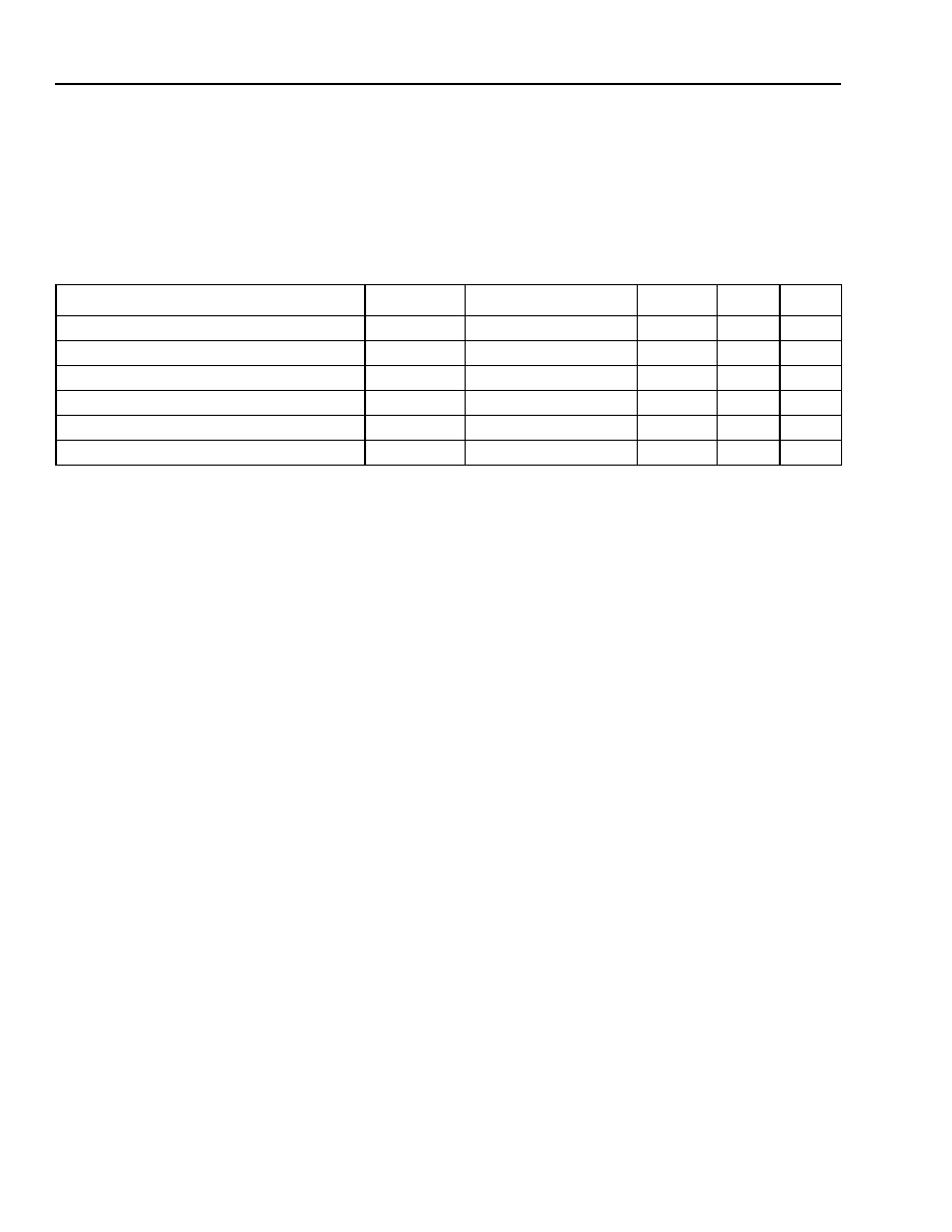
128
Agere Systems Inc.
Data Sheet
February 2004
Ambassador T8110L H.100/H.110 Switch
13 Electrical Characteristics
(continued)
13.5 dc Electrical Characteristics
13.5.1 Electrical Drive Specifications, CT_C8 and /CT_FRAME
V
DD
= 3.3 V and V
SS
= 0.0 V, unless otherwise specified.
PCI-compliant data line I/O cells are used for the CT bus data lines. (See PCI Specification, Rev. 2.2, Chapter 4.)
/C16, /C4, C2, SCLK, /SCLKx2, and /FR_COMP all use the same driver/receiver pairs as those specified for the
CT_C8 and /CT_FRAME signals, though this is not explicitly stated as a part of the H.1x0 specification.
Table 107. Electrical Drive Specifications, CT_C8 and /CT_FRAME
Parameter
Symbol
Condition
Min
Max
Unit
Output High Voltage
V
OH
I
OUT
= ≠24 mA
2.4
3.3
V
Output Low Voltage
V
OL
I
OUT
= 24 mA
≠0.25
0.4
V
Positive-going Threshold
Vt+
--
1.2
2.0
V
Negative-going Threshold
Vt≠
--
0.6
1.6
V
Hysteresis (Vt+--Vt≠)
V
HYS
--
0.4
--
V
Input Pin Capacitance
C
IN
--
--
10
pF
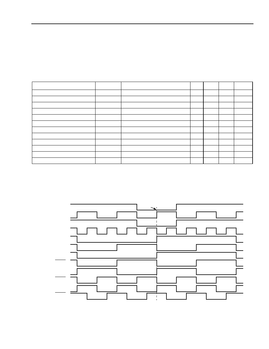
Agere Systems Inc.
129
Data Sheet
February 2004
Ambassador T8110L H.100/H.110 Switch
13 Electrical Characteristics
(continued)
13.5 dc Electrical Characteristics
(continued)
13.5.2 All Other Pins
V
DD
= 3.3 V and Vss = 0.0 V, unless otherwise specified.
13.6 H-Bus Timing
13.6.1 Timing Diagrams
5-6119F
Figure 27. Clock Alignment
Table 108. dc Electrical Characteristics, All Other Pins
Parameter
Symbol
Condition
Min
Typ
Max
Unit
Supply Current
I
DD
2000 H-bus/L-bus connections
--
300
--
mA
Supply Voltage
V
DD
--
3.0
--
3.6
V
Input High Voltage
V
IH
--
2.0
--
--
V
Input Low Voltage
V
IL
--
--
--
0.8
V
Input Current
I
I
--
--
--
1
µ
A
Input Capacitance (input only)
C
I
--
--
--
5
pF
Input Capacitance (I/O pins)
C
IO
--
--
--
10
pF
Leakage Current (3-state)
I
LEAK
--
--
--
10
µ
A
Input Clamp Voltage
V
C
--
--
--
≠1.0
V
Output High Voltage
V
OH
I = 8 mA
2.4
--
--
V
Output Low Voltage
V
OL
I = 8 mA
--
--
0.4
V
Output Short-circuit Current
I
OS
V
OH
tied to GND
--
--
100
mA
/CT_FRAME (A/B)
CT_C8 (A/B)
/FR_COMP
/C16
C2
/C4
SCLK
SCLK
/SCLKx2
/SCLKx2
SCLK
(2.048 MHz)
(2.048 MHz MODE)
(4.096 MHz MODE)
(4.096 MHz MODE)
(8.192 MHz MODE)
(8.192 MHz MODE)
/SCLKx2
FRAME BOUNDARY

130
Agere Systems Inc.
Data Sheet
February 2004
Ambassador T8110L H.100/H.110 Switch
13 Electrical Characteristics
(continued)
13.6 H-Bus Timing
(continued)
13.6.1 Timing Diagrams (continued)
Note: Bit 1 is the MSB and Bit 8 is the LSB. MSB is always transmitted first in all transfers.
5-6120F
Figure 28. Frame Timing Diagram
5-6122F
Figure 29. Detailed Clock Skew Timing Diagram
13.7 ac Electrical Characteristics
13.7.1 Skew Timing, H-Bus
* Test load--50 pF.
Assumes A and B masters in adjacent slots.
When static skew is 10 ns and in the same clock cycle, each clock performs a 10 ns phase correction in opposite directions, a maximum
skew of 30 ns will occur during that clock cycle.
ß Meeting the skew requirements in Table 109 and the requirements of Section 15.5 H-Bus Timing on page 129 could require the PLLs
generating CT_C8 to have different time constants when acting as primary and secondary clock masters.
Table 109. Skew Timing, H-Bus
Symbol
Parameter
Min
Typical
Max
Unit
tSKC8
Maximum Skew Between CT_C8_A and CT_C8_B*
ß
--
--
±10, ±
ns
TSKCOMP Maximum Skew Between CT_C8_A and any Compatibility Clock*
--
--
±5
ns
--
Maximum Skew Between CT_C8_A and L_SCx Clock*
--
--
±2
ns
8
1
2
3
4
5
6
7
8
1
2
3
4
5
6
7
8
1
127
0
/CT_FRAME
CT_C8
CT_DX
TIME
SLOT
125
µ
s
FRAME BOUNDARY
Vt+
Vt+
CT_C8_A
CT_C8_B
tSKC8
Vt+
Vt+
CT_C8_A
COMPATIBILITY
tSKCOMP
CLOCKS
Vt≠
tSKCOMP
Agere Systems Inc.
131
Data Sheet
February 2004
Ambassador T8110L H.100/H.110 Switch
13 Electrical Characteristics
(continued)
13.7 ac Electrical Characteristics
(continued)
13.7.1 Skew Timing, H-Bus (continued)
* Worst-case loading of 50 pF on all outputs.
13.8 Hot Swap
The T8110L has features which assist in H.110 hot swap applications. All H.110 bus signals are put in high imped-
ance (3-state and/or input) during the early power phase of board insertion/removal. The ECTF H.110 specification
requires that all CT data lines and CT_NETREF clocks have 0.7 V applied through 18 k
resistors before plugging
into and releasing from the H.110 bus. A feature on the T8110L incorporates all 34 18 k
precharge resistors inter-
nally (32 for the CT data signals, 2 for NETREFs). These resistors accept 0.7 V directly through the VPRE-
CHARGE input. The ECTF H.110 specification requires that the T8110L must be powered from early power in hot
swap applications. The circuit that generates the 0.7 V precharge voltage must also be powered from early power.
Refer to ECTF H.110 and PICMG CompactPCI
Æ
Hot Swap specifications for hot swap requirements.
13.8.1 LPUE (Local Pull-Up Enable)
LPUE is used as an assist in CompactPCI specifically for hot swap; see Section 2.3.2 on page 20. During live
board insertion/removal, the only devices which should be on early power are the power controller and interface
parts (PCI interface attached to J1, H.110 interface attached to J4). Without the LPUE, any device connected to the
T8110L would get current flow from the early power through the pull-up resistors. When late power parts power up,
they already have current flowing through the I/O and these devices could possibly latch up. The current flow is
eliminated by LPUE disabling the pull-up resistors. LPUE is typically controlled by the power controller. The power
controller will pull LPUE low during board insertion/removal and will release LPUE high so that the pull ups are re-
enabled with late power turning on. Signals that have pull-ups disabled by LPUE are GP[7:0], FG[7:0], D[15:0],
LD[31:0], LREF[7:0], PRI_REF_IN, NR1_DIV_IN, and NR2_DIV_IN.
13.9 Decoupling
Decoupling the T8110L V
DD
s with 0.1
µ
F capacitors is recommended. 1000 pF or 0.01
µ
F capacitors may be used
in addition to the 0.1
µ
F capacitors to provide additional decoupling.
Table 110. L_SC[3:0] and Frame Group Rise and Fall Time
Parameter
Min
Typ
Max
Unit*
L_SCx Rise Time
--
--
5
ns
L_SCx Fall Time
--
--
4
ns
Frame Group Rise Time
--
--
3
ns
Frame Group Fall Time
--
--
3
ns
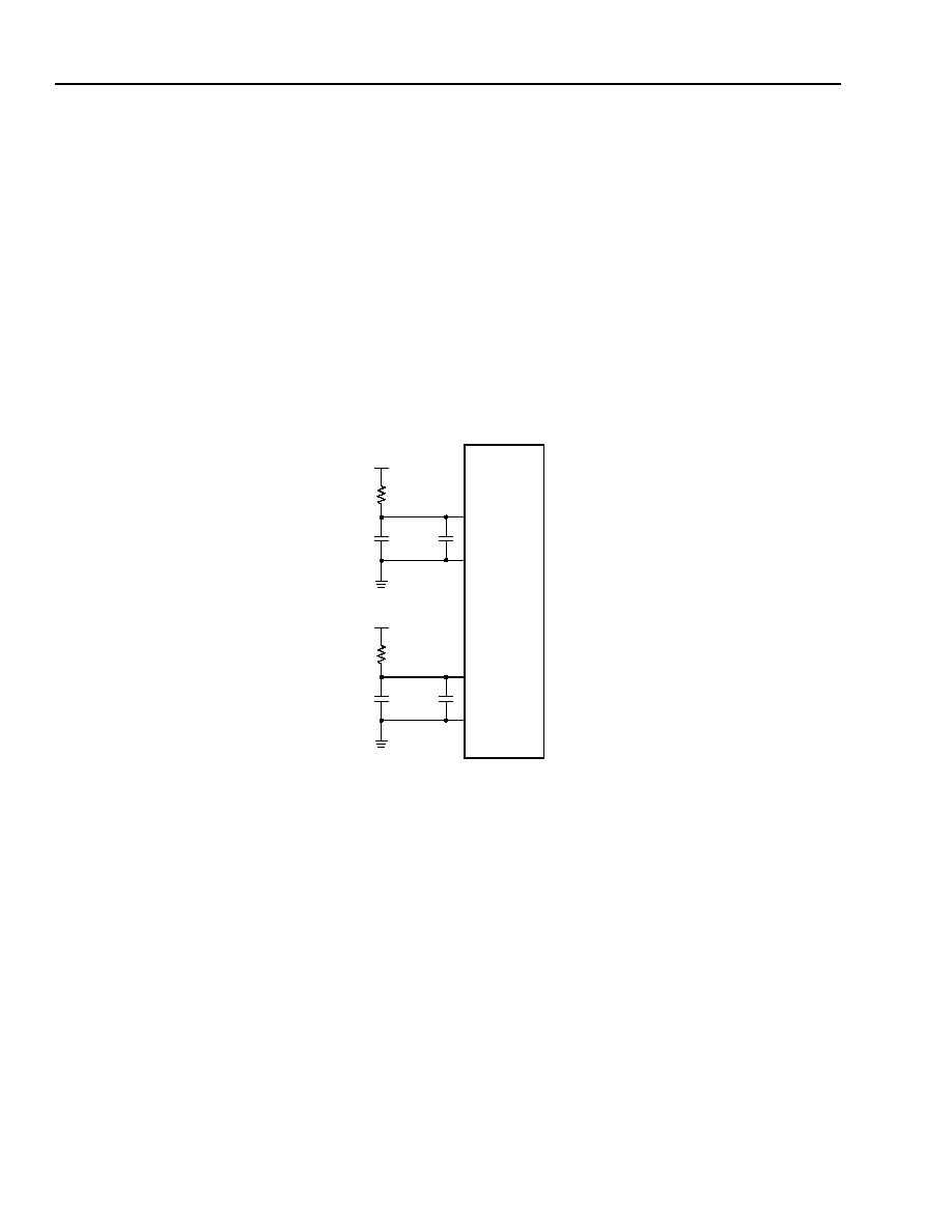
132
Agere Systems Inc.
Data Sheet
February 2004
Ambassador T8110L H.100/H.110 Switch
13 Electrical Characteristics
(continued)
13.10 APLL V
DD
Filter
Separate V
DD
s are provided for APLL1 and APLL2 for filtering purposes. V
DD
filtering will provide stability in the
APLL, primarily the VCOs. An R/C low pass filter should be applied to the PLL V
DD
s, see Figure 30. Depending on
the quality of V
DD
and board layout characteristics, the R/C values should be selected to filter out unwanted fre-
quencies above a targeted frequency. For example, a 25
resistor and 10
µ
F capacitor will have a cut-off
frequency of 636 Hz. Characterize the quality of your V
DD
and select component values accordingly. 25
is the
maximum recommended resistor value. At high frequencies the ESR of a bulk cap becomes a problem (no longer
effectively low passes) so a high-frequency cap of 0.1
µ
F or so is required to compensate for some of the higher
clocks and various harmonics. This needs to be placed as close to the T8110L device as possible to minimize the
radiational pick-up in the remaining trace length. APLL1 and APLL2 each draw approximately 7 mA at 3.3 V. Hot
swap applications can use late power to ensure the capacitance and in-rush current do not violate the PICMG Hot
Swap specification.
0995(F)
Figure 30. APLL V
DD
Filtering
V
SS
T8110L
APLL1V
DD
V
SS
APLL2V
DD
V
DD
= 3.3 V
V
DD
= 3.3 V
R
C
R
C
0.1
µ
F
0.1
µ
F

Agere Systems Inc.
133
Data Sheet
February 2004
Ambassador T8110L H.100/H.110 Switch
13 Electrical Characteristics
(continued)
13.11 PC Board PBGA Considerations
The T8110L is a 272-ball plastic ball grid array package. The 16 centrally located thermal balls should be con-
nected to board ground. While there are no special printed-circuit board requirements for the T8110L, there are
specification requirements for PC board layout that must be adhered to. For instance, per the ECTF H.110 specifi-
cation, all CT bus data signals must not exceed 4 inches in length from connector to I/O cell and all CT bus clock
signals must not exceed 2 inches in length from connector to I/O cell. We advise the customer to become familiar
with applicable specifications for any PC board requirements.
13.12 Unused Pins
Multiple pins may share a common resistor. Signals with pull-up/down resistors may be left unconnected if unused.
Unused 8 mA 3-state signals may be left unconnected. If XTAL1_IN and/or XTAL2_IN are being driven from an
oscillator, then XTAL1_OUT and/or XTAL2_OUT must be left unconnected. If XTAL2 is not used, XTAL2_IN should
be pulled-up or tied directly to V
DD
and XTAL2_OUT should be left unconnected. If VPRECHARGE is unused, this
signal may be left unconnected. All signals listed as no connect (D16, D20, E17, and G17) in Table 8 must be left
unconnected.
13.13 External Pull-Up Pins
The EPU pins must be tied to an external pull-up resistor. Multiple pins may share a common resistor. It is recom-
mended that all EPU pins be tied to a commmon 20 k
pull-up resistor.
13.14 T8110L Evaluation Kits
There is no T8110L-specific evaluation kit. If an evaluation kit is required, please purchase a T8110 PCI evaluation
kit, as the evaluation board allows the T8110 to be configured to be functionally identical to the T8110L. Each kit
contains an evaluation board, software, and documentation. The evaluation board is a full-length PCI board and it
includes the T8110 chip, a PCI-to-local bus bridge, a dual T1/E1 line interface, a dual codec, and a dual SLIC. The
software includes full source code, including rights to reuse. The documentation CD includes evaluation board
schematics (ORCAD and .pdf formats), evaluation board bill of material (BOM), and advisories. Please refer to the
website
http://www.agere.com/enterprise_metro_access/tdm_interconnect.html
for additional information.
13.15 T8110L Ordering Information
Table 111. T8110L Ordering Information
Device Part Number
Package
Comcode
T-8110L---BAL-DB
272-Ball PBGA
700052229
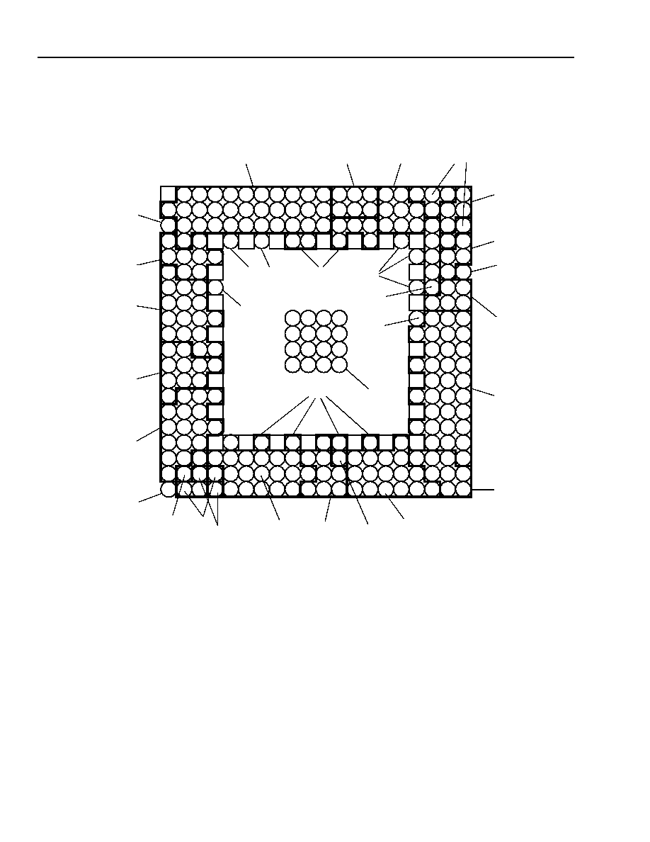
134
Agere Systems Inc.
Data Sheet
February 2004
Ambassador T8110L H.100/H.110 Switch
13 Package Outline
(continued)
13.15 Pin and Pad Assignments
(continued)
5-8906F(b).
Figure 31. T8110L Pins by Functional Group
VSS
VDD
VDD
VSS
VSS
VDD
VSS
VDD
VSS
VDD
VSS
VDD
VSS
VDD
VSS
VDD
VSS
VDD
VSS
VDD
VSS
VDD
VSS
VDD
VSS
A
B
C
D
E
F
G
H
J
K
L
M
N
P
R
T
U
V
W
Y
1
2
3
4
5
6
7
8
9
10
11
12
13
14
15
16
17
18
19
20
PRECHARGE
GPIO
µ
PROCESSOR
ADDRESS
µ
PROCESSOR
CONTROL
SIGNALS
µ
PROCESSOR
DATA
RESET
PLL
PLL
LOCAL
CLOCK
OUTPUTS
LOCAL
FRAME
ERROR
SIGNALS
(NO CONNECT)
GROUP
DATA
H-BUS DATA
H.110 CLOCKS
LOCAL
REFERENCE
INPUTS
EXTERNAL
CLADs/DJATs
COMPATIBILITY
CLOCKS
PLL
MLAC
JTAG
PORT
(XTAL#1)
(XTAL#2)
BIST
LOCAL
PE
H.100
PE
H.110
PE
THERMAL GROUND
(N/C)
VSS
EPU
EPU
V
SS
V
SS
VSS
(NO CONNECT)
EPU
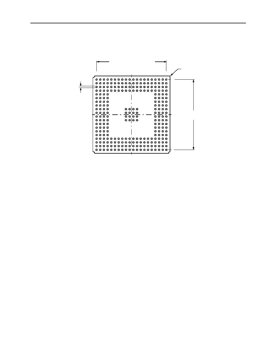
Agere Systems Inc.
135
Data Sheet
February 2004
Ambassador T8110L H.100/H.110 Switch
13 Package Outline
(continued)
13.15 Pin and Pad Assignments
(continued)
5-4406
BOTTOM VIEW
A
B
C
D
E
F
G
H
J
K
L
M
Y
N
P
R
T
U
V
W
1
2
3
4
5
6
7
8
9
10
11
12
13
14
15
16
17
18
20
19
19 SPACES @ 1.27 = 24.13
19 SPACES
@ 1.27 = 24.13
0.76
+0.14
≠0.16
A1 BALL
PAD CORNER
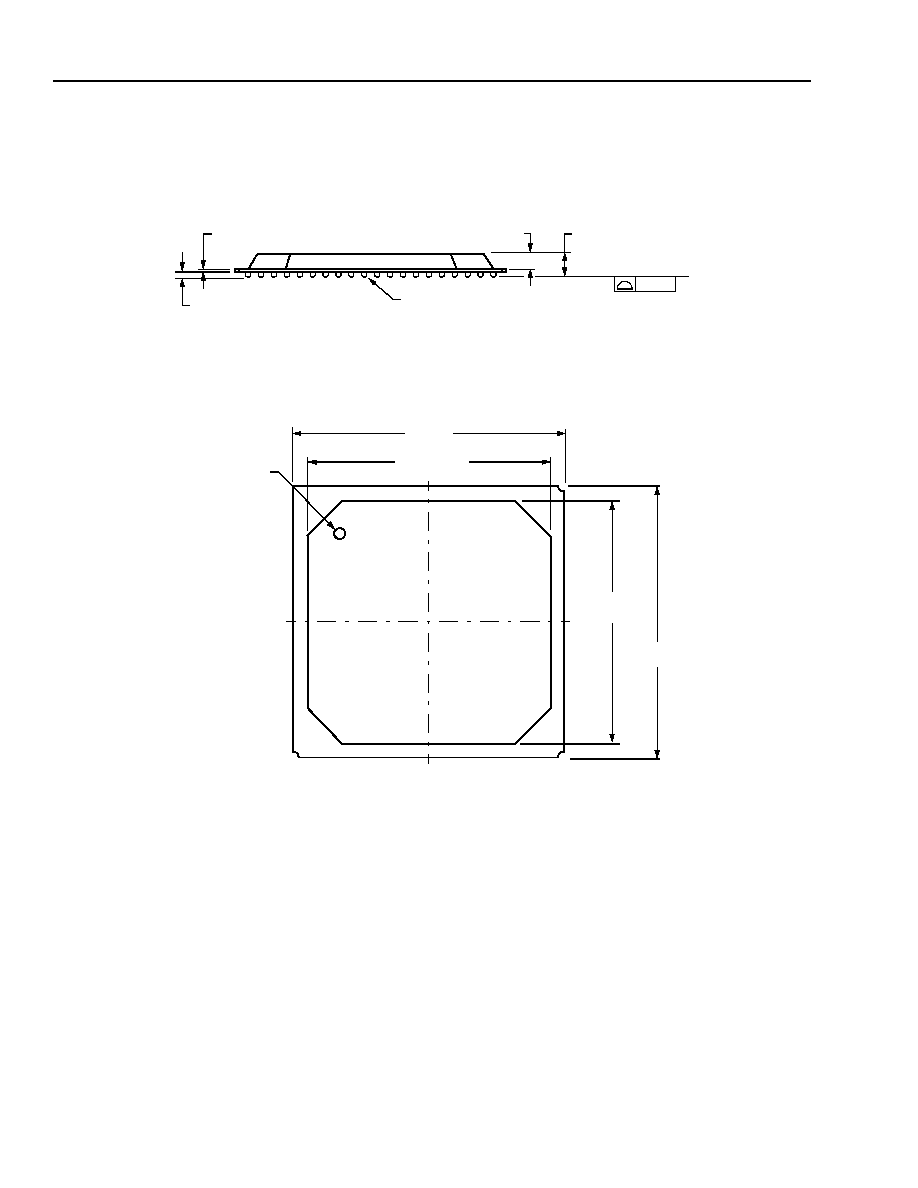
136
Agere Systems Inc.
Data Sheet
February 2004
Ambassador T8110L H.100/H.110 Switch
13 Package Outline
(continued)
13.15 Pin and Pad Assignments
(continued)
5-4406
SIDE VIEW
5-4406
TOP VIEW
1.17
±
0.05
SEATING PLANE
SOLDER BALL
0.60
±
0.10
0.20
0.36
+0.04
≠0.06
2.13
+0.19
≠0.21
27.00
24.00
+0.70
≠0.50
24.00
+0.70
≠0.50
A1 BALL PAD
CORNER
27.00
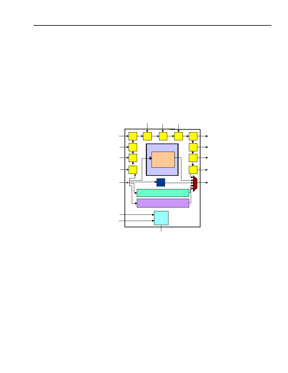
Agere Systems Inc.
137
Data Sheet
February 2004
Ambassador T8110L H.100/H.110 Switch
14 JTAG/Boundary Scan
14.1 The Principle of Boundary-Scan Architecture
Each primary input signal and primary output signal is supplemented with a multipurpose memory element called a
boundary-scan cell. Cells on device primary inputs are referred to as input cells and cells on primary outputs are
referred to as output cells. Input and output is relative to the core logic of the device.
At any time, only one register can be connected from TDI to TDO. For example, instruction register (IR), bypass,
boundary-scan, ident, or even some appropriate register internal to the core logic (see Figure 32). The selected
register is identified by the decoded output of the instruction register. Certain instructions are mandatory, such as
EXTEST (boundary-scan register selected), whereas others are optional, such as the IDCODE instruction (Ident
register selected).
Figure 32. IEEE
Æ
1149.1 Boundary-Scan Architecture
Figure 32 shows the following elements:
!
A set of four dedicated test pins, test data in (TDI), test mode select (TMS), test clock (TCK), test data out (TDO),
and one optional test pin test reset (TRSTN). These pins are collectively referred to as the test access port
(TAP).
!
A boundary-scan cell on each device's primary input and primary output pin, connected internally to form a serial
boundary-scan register (boundary scan).
!
A finite-state machine TAP controller with inputs TCK and TMS.
!
An n-bit (n = 3) instruction register (IR), holding the current instruction.
!
A 1-bit bypass register (BYPASS).
!
An optional 32-bit identification register (ident) capable of being loaded with a permanent device identification
code.
INTERNAL
CORE LOGIC
IDENTIFICATION REGISTER
INSTRUCTION REGISTER (IR)
TEST MODE SELECT
TEST CLOCK
TMS
TCK
TEST RESET (TRSTN)
TEST DATA OUT
TDO
TDI
TEST DATA IN
BYPASS
TAP
CONTROLLER
138
Agere Systems Inc.
Data Sheet
February 2004
Ambassador T8110L H.100/H.110 Switch
14 JTAG/Boundary Scan
(continued)
14.1.1 Instruction Register
The instruction register is 3 bits long and the capture value is 001.
14.2 Boundary-Scan Register
The T8110L boundary scan register is identical to that of the T8110 in the condition that the T8110's
VIO/uP_SELECT pin is tied to ground. The only difference is that for the T8110L, this pin (U5) is internally tied to
ground. Please refer to the T8110 datasheet for the bit-to-pin assignment.
Table 112. Instruction Register
Instruction
Binary Code
Description
EXTEST
000
Places the boundary-scan register in EXTEST mode.
SAMPLE
001
Places the boundary-scan register in sample mode.
IDCODE
101
Identification code.
BYPASS
110, 111
Places the bypass register in the scan chain.
HIGH Z
010
Places all outputs and I/Os in 3-state mode.

Agere Systems Inc.
139
Data Sheet
February 2004
Ambassador T8110L H.100/H.110 Switch
Appendix A. Constant and Minimum Delay Connections
A.1 Connection Definitions
A forward connection is defined as one in which the output to time slot has a greater value than the input from time
slot, or, put another way, the delta between them is positive.
A reverse connection is defined as one in which the output to time slot has a lesser value than the input from time
slot, and the delta between them is negative.
For example, going from TS(1) to TS(38) is a forward connection, and the TS
is +37, but going from TS(38) to
TS(1) is a reverse connection, with a TS
of ≠37:
where TS
= TS(to) ≠ TS(from).
Similarly, a delta can be introduced for streams which will have a bearing in certain exceptions (discussed later):
STR
= STR(to) ≠ STR(from).
There is only one combination which forms a TS
of +127 or ≠127:
TS
= TS(127) ≠ TS(0) = +127, and
TS
= TS(0) ≠ TS(127) = ≠127,
but there are two combinations which form TS
s of +126 or ≠126:
TS
= TS(127) ≠ TS(1) = TS(126) ≠ TS(0) = +126, and
TS
= TS(1) ≠ TS(127) = TS(0) ≠ TS(126) = ≠126,
there are three combinations which yield +125 or ≠125, and so on.
The user can utilize the TS
to control the latency of the resulting connection. In some cases, the latency must be
minimized. In other cases, such as a block of connections which must maintain some relative integrity while cross-
ing a frame boundary, the required latency of some of the connections may exceed a one frame (>128 time slots)
to maintain the integrity of this virtual frame.
The device uses a control bit at each connection memory location, VFC, for controlling latency, allowing each con-
nection to select one of two alternating data buffers.
A.2 Delay Type Definitions
Constant Delay--This is a well-defined, predictable, and linear region of latency in which the to time slot is at
least 128 time slots after the from time slot, but no more than 256 time slots after the from time slot.
Mathematically, constant delay latency is described as follows*, with L denoting latency, and VFC set to the value
indicated:
Forward connections, VFC = 1: L = 128 + TS
(0
TS
127)
Reverse connections, VFC = 0: L = 256 + TS
(≠127
TS
≠1)
Example:
Switching from TS(37) to TS(1) as a constant delay, the delta is ≠36, so FME is set to 0 and the result-
ing latency is 256 ≠ 36 = 220 time slots. Thus, the connection will be made from TS(37) of frame(n) to
TS(1) of frame(n + 2).
Simple summary:
Use constant delay for latencies of 128 to 256 time slots,
set VFC = 1 for forward connections,
set VFC = 0 for reverse connections.
* Since TS
= TS(to) ≠TS(from), the user can modify the equations to solve for either TS(to) or TS(from).

140
Agere Systems Inc.
Data Sheet
February 2004
Ambassador T8110L H.100/H.110 Switch
Appendix A. Constant and Minimum Delay Connections
(continued)
A.2 Delay Type Definitions
(continued)
Figure 33. Constant Delay Connection Latency
Minimum Delay--This is the most common type of switching, but has a shorter range than constant delay, and the
user must be aware of exceptions caused by interactions between the device's internal pipeline and the dual buff-
ering. The to time slot is at least 3 time slots after the from time slot, but no more than 128 time slots after the from
time slot. Exceptions exist at TS
s of +1, +2, ≠126, and ≠127.
Forward connections, VFC = 0: L = TS
(3
TS
127).
Reverse connections, VFC = 1: L = 128 + TS
(≠125
TS
0).
Example:
Using the same switching from the example above, TS(37) to TS(1), the delta is ≠36, so VFC is set
to 1 to effect the minimum delay (setting to 0 effects constant delay), and the resulting latency is
128 ≠ 36 = 92 time slots. The relative positions of the end time slots are the same in both minimum and
constant delay, i.e., they both switch to TS(1)], but the actual data is delayed by an additional frame in
the constant delay case.
Simple summary:
Use minimum delay for latencies of 3 to 128 time slots,
set VFC = 0 for forward connections,
set VFC = 1 for reverse connections.
Exceptions to Minimum Delay--Up until this point in the discussion, the STR
s have not been discussed
because the to and from streams have been irrelevant in the switching process.
Note: The one universally disallowed connection on the device is a TS
of 0 and a STR
of 0. This is, of course, a
stream + time-slot switching to itself!
Rather than try to list the exceptions mathematically, a table is provided. The latencies in these cases may exceed
two frames due to the interaction of the intrinsic pipeline delays with the double buffering.
A
PPL
I
E
D
DE
L
T
A
(
T
IM
E
S
L
OT
S
)
RESULTING LATENCY
≠127
128
0
127
255
256
(TIME SLOTS)
VF
C
= 0
VF
C
= 1
129
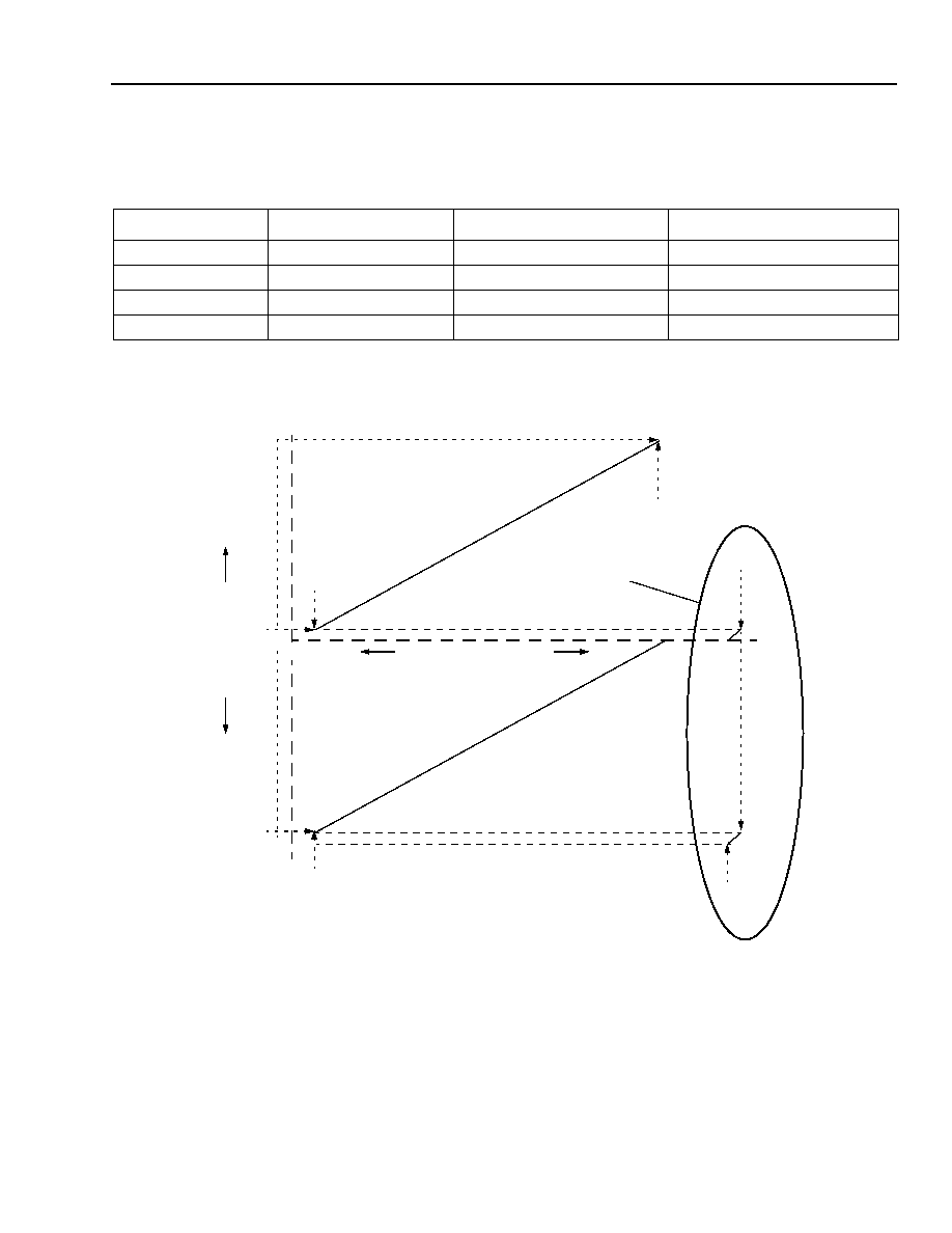
Agere Systems Inc.
141
Data Sheet
February 2004
Ambassador T8110L H.100/H.110 Switch
Appendix A. Constant and Minimum Delay Connections
(continued)
A.2 Delay Type Definitions
(continued)
Graphically, the minimum delay latency equations are illustrated below. The exceptions to the minimum delay have
been included in the diagram, connected to the main function by dashed lines.
5-6224
Figure 34. Minimum Delay Connection Latency
Lower Stream Rates--The discussion has centered on 128 time-slot frames which correspond to 8.192 Mbits/s
data rates. How does one make similar predictions for lower stream rates?
For 4.096 Mbits/s, multiply the to and from time-slot values by two, i.e., time slot 0 at 4.096 Mbits/s corresponds to
time slot 0 at 8.192 Mbits/s, and time slot 63 at 4.096 Mbits/s corresponds to time slot 126 at 8.192 Mbits/s. Simi-
larly, multiply values by four to convert 2.048 Mbits/s values. The latency equations can then be applied directly.
Table 113. Special Cases (Exceptions)
VFC Value
TS
Latency for STR
< 0
Latency for STR
0
0
+1
257
257
0
+2
258
2
1
≠126
258
2
1
≠127
257
257
AP
PLIE
D DELTA
(
T
IM
E SLO
T
S)
RESULTING LATENCY
≠127
0
127
127
128......256
(TIME SLOTS)
VF
C
= 1
VF
C
= 0
0
≠126
258
257
2
2
2
SPECIAL LONG LATENCY
CONNECTIONS
(SEE TEXT)

142
Agere Systems Inc.
Data Sheet
February 2004
Ambassador T8110L H.100/H.110 Switch
Appendix B. Register Bit Field Mnemonic Summary
Key to using the table below:
!
Five character alphanumeric designation
!
Character 4 indicates the general register type as follows:
-- Divide = load value for divider
-- Enable = bit or bits to enable a function
-- Load = load value, typically for counter
-- Output = output only
-- Select = bit or bits select multiple functions
!
Character 5 indicates the size as follows:
-- B = bit
-- N = nibble
-- P = partial register (2, 3, 5, 6, or 7 bits)
-- R = register
!
Position column identifies the bit position in the register:
-- 0, 1, 2, 3, 4, 5, 6, 7 for bits
-- L for lower nibble
-- U for upper nibble
-- n-m for bit positions in a partial register

Agere Systems Inc.
143
Data Sheet
February 2004
Ambassador T8110L H.100/H.110 Switch
Appendix B. Register Bit Field Mnemonic Summary
(continued)
Table 114. Mnemonic Summary, Sorted by Name
Mnemonic
Description
Type
Register
Bit Position
ABOEN
A and B clocks output
Enable
0x00220
U
ACRSN
A clocks rate
Select
0x00223
L
AIOEB
All I/O (master)
Enable
0x00103
7
BCRSN
B clocks rate
Select
0x00223
U
C2FEB
C2 fallback trigger
Enable
0x0010A
5
C2LOB
C2 latched error
Output
0x00122
5
C2TOB
C2 transient error
Output
0x00120
5
C2WEB
C2 watchdog
Enable
0x0010E
5
C4FEB
/C4 fallback trigger
Enable
0x0010A
4
C4LOB
C4 latched error
Output
0x00122
4
C4TOB
C4 transient error
Output
0x00120
4
C4WEB
/C4 watchdog
Enable
0x0010E
4
CAFEB
C8A fallback trigger
Enable
0x0010A
0
CALOB
C8A latched error
Output
0x00122
0
CATOB
C8A transient error
Output
0x00120
0
CAWEB
C8A watchdog
Enable
0x0010E
0
CAWSN
C8A watchdog
Select
0x0010C
L
CBFEB
C8B fallback trigger
Enable
0x0010A
1
CBLOB
C8B latched error
Output
0x00122
1
CBTOB
C8B transient error
Output
0x00120
1
CBWEB
C8B watchdog
Enable
0x0010E
1
CBWSN
C8B watchdog
Select
0x0010C
U
CCOEN
C clocks output
Enable
0x00220
L
CCSEN
C clocks separate
Enable
0x00224
L
CFBOB
Fallback status
Output
0x00127
6
CFHLN
Diag sync-to-frame high
Load
0x0014B
L
CFLLR
Diag sync-to-frame low
Load
0x0014A
--
CFPOB
CLEAR_FALLBACK pending
Output
0x00124
1
CFSEN
Diag sync-to-frame EN
Enable
0x0014B
U
CFSOB
Failsafe status
Output
0x00127
7
CKMDR
Clock main
Divide
0x00201
--
CKMSR
Clock main
Select
0x00200
--
CKRDR
Clock resource
Divide
0x00205
--
CMFEB
/C16≠ fallback trigger
Enable
0x0010A
3
CMLOB
/C16≠ latched error
Output
0x00122
3
CMTOB
/C16≠ transient error
Output
0x00120
3
CMWEB
/C16≠ watchdog
Enable
0x0010E
3
CPFEB
/C16+ fallback trigger
Enable
0x0010A
2
CPLOB
/C16+ latched error
Output
0x00122
2
CPTOB
/C16+ transient error
Output
0x00120
2
CPWEB
/C16+ watchdog
Enable
0x0010E
2
CSASR
Clock set access
Select
0x00106
--
D1FEB
DPLL1 sync trigger
Enable
0x0010B
5
D1ISR
DPLL1 input
Select
0x0020A
--

144
Agere Systems Inc.
Data Sheet
February 2004
Ambassador T8110L H.100/H.110 Switch
Appendix B. Register Bit Field Mnemonic Summary
(continued)
Table 114. Mnemonic Summary, Sorted by Name (continued)
Mnemonic
Description
Type
Register
Bit Position
D1LOB
DPLL1 sync latched error
Output
0x00123
5
D1RSR
DPLL1 rate
Select
0x0020B
--
D1TOB
DPLL1 sync transient error
Output
0x00121
5
D1WEB
DPLL1 sync watchdog
Enable
0x0010F
5
D2FEB
DPLL2 sync trigger
Enable
0x0010B
6
D2ISR
DPLL2 input
Select
0x0020E
--
D2LOP
DPLL2 lock status
Output
0x00125
3:2
D2RSR
DPLL2 rate
Select
0x0020F
--
D2TOB
DPLL2 sync transient error
Output
0x00121
6
D2WEB
DPLL2 sync watchdog
Enable
0x0010F
6
DMMSP
Data memory mode
Select
0x00105
6:0
F0DSB
FGIO 0 R/W direction
Select
0x00482
0
F0IOB
FGIO 0 data
Load
0x00480
0
F0ISB
Frame 0 pulse inversion
Enable
0x00402
7
F0LLR
Frame 0 lower start time
Load
0x00400
--
F0MEB
FGIO 0 read mask
Enable
0x00481
0
F0RSR
Frame 0 pulse width rate
Select
0x00403
--
F0ULR
Frame 0 upper start time
Load
0x00401
--
F0WSP
Frame 0 pulse width
Select
0x00402
6:0
F1DSB
FGIO 1 R/W direction
Select
0x00482
1
F1IOB
FGIO 1 data
Load
0x00480
1
F1ISB
Frame 1 pulse inversion
Enable
0x00412
7
F1LLR
Frame 1 lower start time
Load
0x00410
--
F1MEB
FGIO 1 read mask
Enable
0x00481
1
F1RSR
Frame 1 pulse width rate
Select
0x00413
--
F1ULR
Frame 1 upper start time
Load
0x00411
--
F1WSP
Frame 1 pulse width
Select
0x00412
6:0
F2DSB
FGIO 2 R/W direction
Select
0x00482
2
F2IOB
FGIO 2 data
Load
0x00480
2
F2ISB
Frame 2 pulse inversion
Enable
0x00422
7
F2LLR
Frame 2 lower start time
Load
0x00420
--
F2MEB
FGIO 2 read mask
Enable
0x00481
2
F2RSR
Frame 2 pulse width rate
Select
0x00423
--
F2ULR
Frame 2 upper start time
Load
0x00421
--
F2WSP
Frame 2 pulse width
Select
0x00422
6:0
F3DSB
FGIO 3 R/W direction
Select
0x00482
3
F3IOB
FGIO 3 data
Load
0x00480
3
F3ISB
Frame 3 pulse inversion
Enable
0x00432
7
F3LLR
Frame 3 lower start time
Load
0x00430
--
F3MEB
FGIO 3 read mask
Enable
0x00481
3
F3RSR
Frame 3 pulse width rate
Select
0x00433
--
F3ULR
Frame 3 upper start time
Load
0x00431
--
F3WSP
Frame 3 pulse width
Select
0x00432
6:0

Agere Systems Inc.
145
Data Sheet
February 2004
Ambassador T8110L H.100/H.110 Switch
Appendix B. Register Bit Field Mnemonic Summary
(continued)
Table 114. Mnemonic Summary, Sorted by Name (continued)
Mnemonic
Description
Type
Register
Bit Position
F4DSB
FGIO 4 R/W direction
Select
0x00482
4
F4IOB
FGIO 4 data
Load
0x00480
4
F4ISB
Frame 4 pulse inversion
Enable
0x00442
7
F4LLR
Frame 4 lower start time
Load
0x00440
--
F4MEB
FGIO 4 read mask
Enable
0x00481
4
F4RSR
Frame 4 pulse width rate
Select
0x00443
--
F4ULR
Frame 4 upper start time
Load
0x00441
--
F4WSP
Frame 4 pulse width
Select
0x00442
6:0
F5DSB
FGIO 5 R/W direction
Select
0x00482
5
F5IOB
FGIO 5 data
Load
0x00480
5
F5ISB
Frame 5 pulse inversion
Enable
0x00452
7
F5LLR
Frame 5 lower start time
Load
0x00450
--
F5MEB
FGIO 5 read mask
Enable
0x00481
5
F5RSR
Frame 5 pulse width rate
Select
0x00453
--
F5ULR
Frame 5 upper start time
Load
0x00451
--
F5WSP
Frame 5 pulse width
Select
0x00452
6:0
F6DSB
FGIO 6 R/W direction
Select
0x00482
6
F6IOB
FGIO 6 data
Load
0x00480
6
F6ISB
Frame 6 pulse inversion
Enable
0x00462
7
F6LLR
Frame 6 lower start time
Load
0x00460
--
F6MEB
FGIO 6 read mask
Enable
0x00481
6
F6RSR
Frame 6 pulse width rate
Select
0x00463
--
F6ULR
Frame 6 upper start time
Load
0x00461
--
F6WSP
Frame 6 pulse width
Select
0x00462
6:0
F7DSB
FGIO 7 R/W direction
Select
0x00482
7
F7IOB
FGIO 7 data
Load
0x00480
7
F7ISB
Frame 7 pulse inversion
Enable
0x00472
7
F7LLR
Frame 7 lower start time
Load
0x00470
--
F7MEB
FGIO 7 read mask
Enable
0x00481
7
F7MSR
Frame 7 mode
Select
0x00476
--
F7RSR
Frame 7 pulse width rate
Select
0x00473
--
F7SSP
FG7 timer pulse shape
Select
0x00477
--
F7ULR
Frame 7 upper start time
Load
0x00471
--
F7WSN
FG7 timer pulse width
Select
0x00477
L
F7WSP
Frame 7 pulse width
Select
0x00472
6:0
FAFEB
/FRAMEA fallback trigger
Enable
0x0010B
0
FALOB
/FRAMEA latched error
Output
0x00123
0
FATOB
/FRAMEA transient error
Output
0x00121
0
FAWEB
/FRAMEA watchdog
Enable
0x0010F
0
FB1SB
APLL1 feedback reset
Select
0x00146
1
FB2SB
APLL2 feedback reset
Select
0x00146
2
FBCSR
Fallback control
Select
0x00108
--
FBFEB
/FRAMEB fallback trigger
Enable
0x0010B
1

146
Agere Systems Inc.
Data Sheet
February 2004
Ambassador T8110L H.100/H.110 Switch
Appendix B. Register Bit Field Mnemonic Summary
(continued)
Table 114. Mnemonic Summary, Sorted by Name (continued)
Mnemonic
Description
Type
Register
Bit Position
FBFOB
Fallback enable status
Output
0x00124
7
FBLOB
/FRAMEB latched error
Output
0x00123
1
FBSOP
Fallback states
Output
0x00124
6:4
FBTOB
/FRAMEB transient error
Output
0x00121
1
FBWEB
/FRAMEB watchdog
Enable
0x0010F
1
FCFEB
/FR_COMP fallback trigger
Enable
0x0010B
2
FCISB
FG7 timer invert output
Select
0x00477
7
FCLLR
Frame group 7 lower count
Load
0x00474
--
FCLOB
/FR_COMP latched error
Output
0x00123
2
FCTOB
/FR_COMP transient error
Output
0x00121
2
FCULR
Frame group 7 upper count
Load
0x00475
--
FCWEB
/FR_COMP watchdog
Enable
0x0010F
2
FFPOB
FORCE_FALLBACK pending
Output
0x00124
0
FGREB
Frame group
Enable
0x00103
5
FPASR
Frame phase alignment
Select
0x00107
--
FRMSB
Diag /FR_COMP input
Select
0x00145
4
FRSEN
/FR_COMP separate
Enable
0x00224
U
FRWSR
/FR_COMP width
Select
0x00222
--
FSCSR
Failsafe return command
Select
0x00114
--
FSEER
Failsafe enable
Enable
0x00115
--
FSLOB
Failsafe latched error
Output
0x00123
7
FSMSN
Fallback secondary mode
Select
0x00109
L
FSSSR
Failsafe sensitivity
Select
0x00116
--
FSTOB
Failsafe transient error
Output
0x00121
7
FSWEB
Failsafe watchdog
Enable
0x0010F
7
FT0EB
FG0 testpoint
Enable
0x00140
0
FT1EB
FG1 testpoint
Enable
0x00140
1
FT2EB
FG2 testpoint
Enable
0x00140
2
FT3EB
FG3 testpoint
Enable
0x00140
3
FT4EB
FG4 testpoint
Enable
0x00140
4
FT5EB
FG5 testpoint
Enable
0x00140
5
FT6EB
FG6 testpoint
Enable
0x00140
6
FT7EB
FG7 testpoint
Enable
0x00140
7
FTPSR
FG testpoint MUX
Select
0x00141
--
FTRSN
Fallback type
Select
0x00109
U
G0DSB
GPIO 0 R/W direction
Select
0x00502
0
G0IOB
GPIO 0 data
Load
0x00500
0
G0MEB
GPIO 0 read mask
Enable
0x00501
0
G0OEB
GPIO 0 override
Enable
0x00503
0
G1DSB
GPIO 1 R/W direction
Select
0x00502
1
G1IOB
GPIO 1 data
Load
0x00500
1
G1MEB
GPIO 1 read mask
Enable
0x00501
1
G1OEB
GPIO 0 override
Enable
0x00503
1

Agere Systems Inc.
147
Data Sheet
February 2004
Ambassador T8110L H.100/H.110 Switch
Appendix B. Register Bit Field Mnemonic Summary
(continued)
Table 114. Mnemonic Summary, Sorted by Name (continued)
Mnemonic
Description
Type
Register
Bit Position
G2DSB
GPIO 2 R/W direction
Select
0x00502
2
G2IOB
GPIO 2 data
Load
0x00500
2
G2MEB
GPIO 2 read mask
Enable
0x00501
2
G3DSB
GPIO 3 R/W direction
Select
0x00502
3
G3IOB
GPIO 3 data
Load
0x00500
3
G3MEB
GPIO 3 read mask
Enable
0x00501
3
G4DSB
GPIO 4 R/W direction
Select
0x00502
4
G4IOB
GPIO 4 data
Load
0x00500
4
G4MEB
GPIO 4 read mask
Enable
0x00501
4
G5DSB
GPIO 5 R/W direction
Select
0x00502
5
G5IOB
GPIO 5 data
Load
0x00500
5
G5MEB
GPIO 5 read mask
Enable
0x00501
5
G6DSB
GPIO 6 R/W direction
Select
0x00502
6
G6IOB
GPIO 6 data
Load
0x00500
6
G6MEB
GPIO 6 read mask
Enable
0x00501
6
G7DSB
GPIO 7 R/W direction
Select
0x00502
7
G7IOB
GPIO 7 data
Load
0x00500
7
G7MEB
GPIO 7 read mask
Enable
0x00501
7
GOPOB
Go clocks pending
Output
0x00124
2
GPIEB
General purpose I/O
Enable
0x00103
4
GSREB
Global subrate
Enable
0x00105
7
GT0EB
GP0 testpoint
Enable
0x00142
0
GT1EB
GP1 testpoint
Enable
0x00142
1
GT2EB
GP2 testpoint
Enable
0x00142
2
GT3EB
GP3 testpoint
Enable
0x00142
3
GT4EB
GP4 testpoint
Enable
0x00142
4
GT5EB
GP5 testpoint
Enable
0x00142
5
GT6EB
GP6 testpoint
Enable
0x00142
6
GT7EB
GP7 testpoint
Enable
0x00142
7
GTPSR
GP testpoint MUX
Select
0x00143
--
HARSN
H1x0 group A rate
Select
0x00300
L
HBRSN
H1x0 group B rate
Select
0x00300
U
HCKEB
H1x0 clocks
Enable
0x00103
3
HCRSN
H1x0 group C rate
Select
0x00301
L
HDBEB
H1x0 data bus
Enable
0x00103
2
HDRSN
H1x0 group D rate
Select
0x00301
U
HERSN
H1x0 group E rate
Select
0x00302
L
HFRSN
H1x0 group F rate
Select
0x00302
U
HGRSN
H1x0 group G rate
Select
0x00303
L
HHRSN
H1x0 group H rate
Select
0x00303
U
HRBEB
Hard reset of back end
Enable
0x00101
1
IASLR
Diag, SYSERR assertion
Load
0x00149
--
ICDSP
Diag, internal control mode
Select
0x00148
7:6

148
Agere Systems Inc.
Data Sheet
February 2004
Ambassador T8110L H.100/H.110 Switch
Appendix B. Register Bit Field Mnemonic Summary
(continued)
Table 114. Mnemonic Summary, Sorted by Name (continued)
Mnemonic
Description
Type
Register
Bit Position
ICKLP
Diag, internal control CLKERR
Load
0x00148
5:4
ICMSB
Invert clock main
Select
0x00204
4
IDHOR
Device ID high
Output
0x0012B
--
IDLOR
Device ID low
Output
0x0012A
--
IEXLP
Diag, internal control EXTERR
Load
0x00148
1:0
IF0SB
Invert interrupt FGIO 0
Select
0x00603
0
IF1SB
Invert interrupt FGIO 1
Select
0x00603
1
IF2SB
Invert interrupt FGIO 2
Select
0x00603
2
IF3SB
Invert interrupt FGIO 3
Select
0x00603
3
IF4SB
Invert interrupt FGIO 4
Select
0x00603
4
IF5SB
Invert interrupt FGIO 5
Select
0x00603
5
IF6SB
Invert interrupt FGIO 6
Select
0x00603
6
IF7SB
Invert interrupt FGIO 7
Select
0x00603
7
IG0SB
Invert interrupt GPIO 0
Select
0x00607
0
IG1SB
Invert interrupt GPIO 1
Select
0x00607
1
IG2SB
Invert interrupt GPIO 2
Select
0x00607
2
IG3SB
Invert interrupt GPIO 3
Select
0x00607
3
IG4SB
Invert interrupt GPIO 4
Select
0x00607
4
IG5SB
Invert interrupt GPIO 5
Select
0x00607
5
IG6SB
Invert interrupt GPIO 6
Select
0x00607
6
IG7SB
Invert interrupt GPIO 7
Select
0x00607
7
IR0SB
Invert local reference 0
Select
0x0020C
0
IR1SB
Invert local reference 1
Select
0x0020C
1
IR2SB
Invert local reference 2
Select
0x0020C
2
IR3SB
Invert local reference 3
Select
0x0020C
3
IR4SB
Invert local reference 4
Select
0x0020C
4
IR5SB
Invert local reference 5
Select
0x0020C
5
IR6SB
Invert local reference 6
Select
0x0020C
6
IR7SB
Invert local reference 7
Select
0x0020C
7
ISYLP
Diag, internal control SYSERR
Load
0x00148
3:2
JAMSR
Interrupt arbitration mode
Select
0x00610
--
JC0EB
Interrupt from CLKERR 0
Enable
0x0060E
0
JC0OB
Interrupt pending CLKERR 0
Output
0x0060C
0
JC1EB
Interrupt from CLKERR 1
Enable
0x0060E
1
JC1OB
Interrupt pending CLKERR 1
Output
0x0060C
1
JC2EB
Interrupt from CLKERR 2
Enable
0x0060E
2
JC2OB
Interrupt pending CLKERR 2
Output
0x0060C
2
JC3EB
Interrupt from CLKERR 3
Enable
0x0060E
3
JC3OB
Interrupt pending CLKERR 3
Output
0x0060C
3
JC4EB
Interrupt from CLKERR 4
Enable
0x0060E
4
JC4OB
Interrupt pending CLKERR 4
Output
0x0060C
4
JC5EB
Interrupt from CLKERR 5
Enable
0x0060E
5

Agere Systems Inc.
149
Data Sheet
February 2004
Ambassador T8110L H.100/H.110 Switch
Appendix B. Register Bit Field Mnemonic Summary
(continued)
Table 114. Mnemonic Summary, Sorted by Name (continued)
Mnemonic
Description
Type
Register
Bit Position
JC5OB
Interrupt pending CLKERR 5
Output
0x0060C
5
JC6EB
Interrupt from CLKERR 6
Enable
0x0060E
6
JC6OB
Interrupt pending CLKERR 6
Output
0x0060C
6
JC7EB
Interrupt from CLKERR 7
Enable
0x0060E
7
JC7OB
Interrupt pending CLKERR 7
Output
0x0060C
7
JC8EB
Interrupt from CLKERR 8
Enable
0x0060F
0
JC8OB
Interrupt pending CLKERR 8
Output
0x0060D
0
JC9EB
Interrupt from CLKERR 9
Enable
0x0060F
1
JC9OB
Interrupt pending CLKERR 9
Output
0x0060D
1
JCAEB
Interrupt from CLKERR A
Enable
0x0060F
2
JCAOB
Interrupt pending CLKERR A
Output
0x0060D
2
JCBEB
Interrupt from CLKERR B
Enable
0x0060F
3
JCBOB
Interrupt pending CLKERR B
Output
0x0060D
3
JCCEB
Interrupt from CLKERR C
Enable
0x0060F
4
JCCOB
Interrupt pending CLKERR C
Output
0x0060D
4
JCDEB
Interrupt from CLKERR D
Enable
0x0060F
5
JCDOB
Interrupt pending CLKERR D
Output
0x0060D
5
JCEEB
Interrupt from CLKERR E
Enable
0x0060F
6
JCEOB
Interrupt pending CLKERR E
Output
0x0060D
6
JCFEB
Interrupt from CLKERR F
Enable
0x0060F
7
JCFOB
Interrupt pending CLKERR F
Output
0x0060D
7
JCOSR
Interrupt CLKERR output mode
Select
0x00613
--
JCWSR
Interrupt CLKERR pulse width
Select
0x00617
--
JF0EB
Interrupt from FGIO 0
Enable
0x00601
0
JF0OB
Interrupt pending FGIO 0
Output
0x00600
0
JF1EB
Interrupt from FGIO 1
Enable
0x00601
1
JF1OB
Interrupt pending FGIO 1
Output
0x00600
1
JF2EB
Interrupt from FGIO 2
Enable
0x00601
2
JF2OB
Interrupt pending FGIO 2
Output
0x00600
2
JF3EB
Interrupt from FGIO 3
Enable
0x00601
3
JF3OB
Interrupt pending FGIO 3
Output
0x00600
3
JF4EB
Interrupt from FGIO 4
Enable
0x00601
4
JF4OB
Interrupt pending FGIO 4
Output
0x00600
4
JF5EB
Interrupt from FGIO 5
Enable
0x00601
5
JF5OB
Interrupt pending FGIO 5
Output
0x00600
5
JF6EB
Interrupt from FGIO 6
Enable
0x00601
6
JF6OB
Interrupt pending FGIO 6
Output
0x00600
6
JF7EB
Interrupt from FGIO 7
Enable
0x00601
7
JF7OB
Interrupt pending FGIO 7
Output
0x00600
7
JG0EB
Interrupt from GPIO 0
Enable
0x00605
0
JG0OB
Interrupt pending GPIO 0
Output
0x00604
0
JG1EB
Interrupt from GPIO 1
Enable
0x00605
1
JG1OB
Interrupt pending GPIO 1
Output
0x00604
1
JG2EB
Interrupt from GPIO 2
Enable
0x00605
2

150
Agere Systems Inc.
Data Sheet
February 2004
Ambassador T8110L H.100/H.110 Switch
Appendix B. Register Bit Field Mnemonic Summary
(continued)
Table 114. Mnemonic Summary, Sorted by Name (continued)
Mnemonic
Description
Type
Register
Bit Position
JG2OB
Interrupt pending GPIO 2
Output
0x00604
2
JG3EB
Interrupt from GPIO 3
Enable
0x00605
3
JG3OB
Interrupt pending GPIO 3
Output
0x00604
3
JG4EB
Interrupt from GPIO 4
Enable
0x00605
4
JG4OB
Interrupt pending GPIO 4
Output
0x00604
4
JG5EB
Interrupt from GPIO 5
Enable
0x00605
5
JG5OB
Interrupt pending GPIO 5
Output
0x00604
5
JG6EB
Interrupt from GPIO 6
Enable
0x00605
6
JG6OB
Interrupt pending GPIO 6
Output
0x00604
6
JG7EB
Interrupt from GPIO 7
Enable
0x00605
7
JG7OB
Interrupt pending GPIO 7
Output
0x00604
7
JISOR
Interrupt in-service
Output
0x006FC
--
JS0EB
Interrupt from SYSERR 0
Enable
0x0060A
0
JS0OB
Interrupt pending SYSERR 0
Output
0x00608
0
JS1EB
Interrupt from SYSERR 1
Enable
0x0060A
1
JS1OB
Interrupt pending SYSERR 1
Output
0x00608
1
JS2EB
Interrupt from SYSERR 2
Enable
0x0060A
2
JS2OB
Interrupt pending SYSERR 2
Output
0x00608
2
JS3EB
Interrupt from SYSERR 3
Enable
0x0060A
3
JS3OB
Interrupt pending SYSERR 3
Output
0x00608
3
JS4EB
Interrupt from SYSERR 4
Enable
0x0060A
4
JS4OB
Interrupt pending SYSERR 4
Output
0x00608
4
JS5EB
Interrupt from SYSERR 5
Enable
0x0060A
5
JS5OB
Interrupt pending SYSERR 5
Output
0x00608
5
JS6EB
Interrupt from SYSERR 6
Enable
0x0060A
6
JS6OB
Interrupt pending SYSERR 6
Output
0x00608
6
JS7EB
Interrupt from SYSERR 7
Enable
0x0060A
7
JS7OB
Interrupt pending SYSERR 7
Output
0x00608
7
JS8EB
Interrupt from SYSERR 8
Enable
0x0060B
0
JS8OB
Interrupt pending SYSERR 8
Output
0x00609
0
JS9EB
Interrupt from SYSERR 9
Enable
0x0060B
1
JS9OB
Interrupt pending SYSERR 9
Output
0x00609
1
JSAEB
Interrupt from SYSERR A
Enable
0x0060B
2
JSAOB
Interrupt pending SYSERR A
Output
0x00609
2
JSBEB
Interrupt from SYSERR B
Enable
0x0060B
3
JSBOB
Interrupt pending SYSERR B
Output
0x00609
3
JSCEB
Interrupt from SYSERR C
Enable
0x0060B
4
JSCOB
Interrupt pending SYSERR C
Output
0x00609
4
JSDEB
Interrupt from SYSERR D
Enable
0x0060B
5
JSDOB
Interrupt pending SYSERR D
Output
0x00609
5
JSEEB
Interrupt from SYSERR E
Enable
0x0060B
6
JSEOB
Interrupt pending SYSERR E
Output
0x00609
6
JSFEB
Interrupt from SYSERR F
Enable
0x0060B
7

Agere Systems Inc.
151
Data Sheet
February 2004
Ambassador T8110L H.100/H.110 Switch
Appendix B. Register Bit Field Mnemonic Summary
(continued)
Table 114. Mnemonic Summary, Sorted by Name (continued)
Mnemonic
Description
Type
Register
Bit Position
JSFOB
Interrupt pending SYSERR F
Output
0x00609
7
JSOSR
Interrupt SYSERR output mode
Select
0x00612
--
JSWSR
Interrupt SYSERR pulse width
Select
0x00616
--
LARSN
Local group A rate
Select
0x00320
L
LBRSN
Local group B rate
Select
0x00320
U
LC0SR
Local clock 0 output
Select
0x00228
--
LC1SR
Local clock 1 output
Select
0x00229
--
LC2SR
Local clock 2 output
Select
0x0022A
--
LC3SR
Local clock 3 output
Select
0x0022B
--
LCKEB
Local clocks
Enable
0x00103
1
LCRSN
Local group C rate
Select
0x00321
L
LDBEB
Local data bus
Enable
0x00103
0
LDRSN
Local group D rate
Select
0x00321
U
LERSN
Local group E rate
Select
0x00322
L
LFRSN
Local group F rate
Select
0x00322
U
LGRSN
Local group G rate
Select
0x00323
L
LHRSN
Local group H rate
Select
0x00323
U
LRISR
Local reference input
Select
0x00208
--
N1DSB
NR1 divider inversion
Select
0x00204
1
N1DSN
NETREF1 divider input
Select
0x00210
U
N1FEB
NETREF1 fallback trigger
Enable
0x0010B
3
N1ISN
NETREF1 main input
Select
0x00210
L
N1LOB
NETREF1 latched error
Output
0x00123
3
N1LSR
NETREF1 local reference
Select
0x00212
--
N1OEN
NETREF1 output
Enable
0x00221
L
N1SSB
NR1 selector inversion
Select
0x00204
0
N1TOB
NETREF1 transient error
Output
0x00121
3
N1WEB
NETREF1 watchdog
Enable
0x0010F
3
N1WSN
NETREF1 watchdog
Select
0x0010D
L
N2DSB
NR2 divider inversion
Select
0x00204
3
N2DSN
NETREF1 divider input
Select
0x00214
U
N2FEB
NETREF2 fallback trigger
Enable
0x0010B
4
N2ISN
NETREF1 main input
Select
0x00214
L
N2LOB
NETREF2 latched error
Output
0x00123
4
N2LSR
NETREF1 local reference
Select
0x00216
--
N2OEN
NETREF1 output
Enable
0x00221
U
N2SSB
NR2 selector inversion
Select
0x00204
2
N2TOB
NETREF2 transient error
Output
0x00121
4
N2WEB
NETREF2 watchdog
Enable
0x0010F
4
N2WSN
NETREF2 watchdog
Select
0x0010D
U

152
Agere Systems Inc.
Data Sheet
February 2004
Ambassador T8110L H.100/H.110 Switch
Appendix B. Register Bit Field Mnemonic Summary
(continued)
Table 114. Mnemonic Summary, Sorted by Name (continued)
Mnemonic
Description
Type
Register
Bit Position
NR1DR
NETREF1 Divide
0x00211
--
NR2DR
NETREF2 Divide
0x00215
--
OLHLR
Out-of-lock threshold, high
Load
0x00119
--
OLLLR
Out-of-lock threshold, low
Load
0x00118
--
OOLER
Out-of-lock monitor
Enable
0x0011A
--
OOLOB
Out-of-lock status
Output
0x00125
6
P1ISR
APLL1 input
Select
0x00202
--
P1RSR
APLL1 rate
Select
0x00203
--
P2RSR
APLL2 rate
Select
0x00207
--
PAFSR
Phase align frame
Enable
0x00107
--
S2FEB
/SCLKx2 fallback trigger
Enable
0x0010A
7
S2LOB
/SCLKx2 latched error
Output
0x00122
7
S2TOB
/SCLKx2 transient error
Output
0x00120
7
S2WEB
/SCLKx2 watchdog
Enable
0x0010E
7
SCFEB
SCLK fallback trigger
Enable
0x0010A
6
SCLOB
SCLK latched error
Output
0x00122
6
SCLSB
Diag state counter mode EN
Select
0x00145
3
SCMLR
Diag state counter mode low
Load
0x00144
--
SCMSB
Diag state counter carry
Select
0x00145
5
SCRSR
SCLK/SCLKx2 rate
Select
0X00227
--
SCTOB
SCLK transient error
Output
0x00120
6
SCULP
Diag state counter mode high
Load
0x00145
2:0
SCWEB
SCLK watchdog
Enable
0x0010E
6
SRBEB
Soft reset of back end
Enable
0x00101
0
SRESR
Soft reset
Select
0x00100
--
TCOSR
T clock output
Select
0x00226
--
VEROR
Version ID register
Output
0x00128
--
XYSOB
Active clock set
Output
0x00124
3

Agere Systems Inc.
153
Data Sheet
February 2004
Ambassador T8110L H.100/H.110 Switch
Appendix B. Register Bit Field Mnemonic Summary
(continued)
Table 115. Mnemonic Summary, Sorted by Register
Mnemonic
Description
Type
Register
Bit Position
SRESR
Soft reset
Select
0x00100
--
SRBEB
Soft reset of back end
Enable
0x00101
0
HRBEB
Hard reset of back end
Enable
0x00101
1
LDBEB
Local data bus
Enable
0x00103
0
LCKEB
Local clocks
Enable
0x00103
1
HDBEB
H1x0 data bus
Enable
0x00103
2
HCKEB
H1x0 clocks
Enable
0x00103
3
GPIEB
General-purpose I/O
Enable
0x00103
4
FGREB
Frame group
Enable
0x00103
5
AIOEB
All I/O (master)
Enable
0x00103
7
GSREB
Global subrate
Enable
0x00105
7
DMMSP
Data memory mode
Select
0x00105
6:0
CSASR
Clock set access
Select
0x00106
--
FPASR
Frame phase alignment
Select
0x00107
--
PAFSR
Phase align frame
Enable
0x00107
--
FBCSR
Fallback control
Select
0x00108
--
FSMSN
Fallback secondary mode
Select
0x00109
L
FTRSN
Fallback type
Select
0x00109
U
CAFEB
C8A fallback trigger
Enable
0x0010A
0
CBFEB
C8B fallback trigger
Enable
0x0010A
1
CPFEB
/C16+ fallback trigger
Enable
0x0010A
2
CMFEB
/C16≠ fallback trigger
Enable
0x0010A
3
C4FEB
/C4 fallback trigger
Enable
0x0010A
4
C2FEB
C2 fallback trigger
Enable
0x0010A
5
SCFEB
SCLK fallback trigger
Enable
0x0010A
6
S2FEB
/SCLKx2 fallback trigger
Enable
0x0010A
7
FAFEB
/FRAMEA fallback trigger
Enable
0x0010B
0
FBFEB
/FRAMEB fallback trigger
Enable
0x0010B
1
FCFEB
/FR_COMP fallback trigger
Enable
0x0010B
2
N1FEB
NETREF1 fallback trigger
Enable
0x0010B
3
N2FEB
NETREF2 fallback trigger
Enable
0x0010B
4
D1FEB
DPLL1 sync trigger
Enable
0x0010B
5
D2FEB
DPLL2 sync trigger
Enable
0x0010B
6
CAWSN
C8A watchdog
Select
0x0010C
L
CBWSN
C8B watchdog
Select
0x0010C
U
N1WSN
NETREF1 watchdog
Select
0x0010D
L
N2WSN
NETREF2 watchdog
Select
0x0010D
U
CAWEB
C8A watchdog
Enable
0x0010E
0
CBWEB
C8B watchdog
Enable
0x0010E
1
CPWEB
/C16+ watchdog
Enable
0x0010E
2

154
Agere Systems Inc.
Data Sheet
February 2004
Ambassador T8110L H.100/H.110 Switch
Appendix B. Register Bit Field Mnemonic Summary
(continued)
Table 115. Mnemonic Summary, Sorted by Register (continued)
Mnemonic
Description
Type
Register
Bit Position
CMWEB
/C16≠ watchdog
Enable
0x0010E
3
C4WEB
/C4 watchdog
Enable
0x0010E
4
C2WEB
C2 watchdog
Enable
0x0010E
5
SCWEB
SCLK watchdog
Enable
0x0010E
6
S2WEB
/SCLKx2 watchdog
Enable
0x0010E
7
FAWEB
/FRAMEA watchdog
Enable
0x0010F
0
FBWEB
/FRAMEB watchdog
Enable
0x0010F
1
FCWEB
/FR_COMP watchdog
Enable
0x0010F
2
N1WEB
NETREF1 watchdog
Enable
0x0010F
3
N2WEB
NETREF2 watchdog
Enable
0x0010F
4
D1WEB
DPLL1 sync watchdog
Enable
0x0010F
5
D2WEB
DPLL2 sync watchdog
Enable
0x0010F
6
FSWEB
Failsafe watchdog
Enable
0x0010F
7
FSCSR
Failsafe return command
Select
0x00114
--
FSEER
Failsafe enable
Enable
0x00115
--
FSSSR
Failsafe sensitivity
Select
0x00116
--
OLLLR
Out-of-lock threshold, low
Load
0x00118
--
OLHLR
Out-of-lock threshold, high
Load
0x00119
--
OOLER
Out-of-lock monitor
Enable
0x0011A
--
CATOB
C8A transient error
Output
0x00120
0
CBTOB
C8B transient error
Output
0x00120
1
CPTOB
/C16+ transient error
Output
0x00120
2
CMTOB
/C16≠ transient error
Output
0x00120
3
C4TOB
C4 transient error
Output
0x00120
4
C2TOB
C2 transient error
Output
0x00120
5
SCTOB
SCLK transient error
Output
0x00120
6
S2TOB
/SCLKx2 transient error
Output
0x00120
7
FATOB
/FRAMEA transient error
Output
0x00121
0
FBTOB
/FRAMEB transient error
Output
0x00121
1
FCTOB
/FR_COMP transient error
Output
0x00121
2
N1TOB
NETREF1 transient error
Output
0x00121
3
N2TOB
NETREF2 transient error
Output
0x00121
4
D1TOB
DPLL1 sync transient error
Output
0x00121
5
D2TOB
DPLL2 sync transient error
Output
0x00121
6
FSTOB
Failsafe transient error
Output
0x00121
7
CALOB
C8A latched error
Output
0x00122
0
CBLOB
C8B latched error
Output
0x00122
1
CPLOB
/C16+ latched error
Output
0x00122
2
CMLOB
/C16≠ latched error
Output
0x00122
3
C4LOB
C4 latched error
Output
0x00122
4
C2LOB
C2 latched error
Output
0x00122
5
SCLOB
SCLK latched error
Output
0x00122
6
S2LOB
/SCLKx2 latched error
Output
0x00122
7
FALOB
/FRAMEA latched error
Output
0x00123
0

Agere Systems Inc.
155
Data Sheet
February 2004
Ambassador T8110L H.100/H.110 Switch
Appendix B. Register Bit Field Mnemonic Summary
(continued)
Table 115. Mnemonic Summary, Sorted by Register (continued)
Mnemonic
Description
Type
Register
Bit Position
FBLOB
/FRAMEB latched error
Output
0x00123
1
FCLOB
/FR_COMP latched error
Output
0x00123
2
N1LOB
NETREF1 latched error
Output
0x00123
3
N2LOB
NETREF2 latched error
Output
0x00123
4
D1LOB
DPLL1 sync latched error
Output
0x00123
5
D2LOB
DPLL2 sync latched error
Output
0x00123
6
FSLOB
Failsafe latched error
Output
0x00123
7
FFPOB
FORCE_FALLBACK pending
Output
0x00124
0
CFPOB
CLEAR_FALLBACK pending
Output
0x00124
1
GOPOB
Go clocks pending
Output
0x00124
2
XYSOB
Active clock set
Output
0x00124
3
FBFOB
Fallback enable status
Output
0x00124
7
FBSOP
Fallback states
Output
0x00124
6:4
CFBOB
Fallback status
Output
0x00127
6
CFSOB
Failsafe status
Output
0x00127
7
VEROR
Version ID register
Output
0x00128
--
IDLOR
Device ID low
Output
0x0012A
--
IDHOR
Device ID high
Output
0x0012B
--
FT0EB
FG0 testpoint
Enable
0x00140
0
FT1EB
FG1 testpoint
Enable
0x00140
1
FT2EB
FG2 testpoint
Enable
0x00140
2
FT3EB
FG3 testpoint
Enable
0x00140
3
FT4EB
FG4 testpoint
Enable
0x00140
4
FT5EB
FG5 testpoint
Enable
0x00140
5
FT6EB
FG6 testpoint
Enable
0x00140
6
FT7EB
FG7 testpoint
Enable
0x00140
7
FTPSR
FG testpoint MUX
Select
0x00141
--
GT0EB
GP0 testpoint
Enable
0x00142
0
GT1EB
GP1 testpoint
Enable
0x00142
1
GT2EB
GP2 testpoint
Enable
0x00142
2
GT3EB
GP3 testpoint
Enable
0x00142
3
GT4EB
GP4 testpoint
Enable
0x00142
4
GT5EB
GP5 testpoint
Enable
0x00142
5
GT6EB
GP6 testpoint
Enable
0x00142
6
GT7EB
GP7 testpoint
Enable
0x00142
7
GTPSR
GP testpoint MUX
Select
0x00143
--
SCMLR
Diagnostic, state counter mode low
Load
0x00144
--
SCLSB
Diagnostic, state counter mode EN
Select
0x00145
3
FRMSB
Diagnostic, /FR_COMP input
Select
0x00145
4
SCMSB
Diagnostic, state counter carry
Select
0x00145
5
SCULP
Diagnostic, state counter mode high
Load
0x00145
2:0
FB1SB
APLL1 feedback reset
Select
0x00146
1

156
Agere Systems Inc.
Data Sheet
February 2004
Ambassador T8110L H.100/H.110 Switch
Appendix B. Register Bit Field Mnemonic Summary
(continued)
Table 115. Mnemonic Summary, Sorted by Register (continued)
Mnemonic
Description
Type
Register
Bit Position
FB2SB
APLL2 feedback reset
Select
0x00146
2
IEXLP
Diagnostic, interrupt control EXTERR
Load
0x00148
1:0
ISYLP
Diagnostic, interrupt control SYSERR
Load
0x00148
3:2
ICKLP
Diagnostic, interrupt control CLKERR
Load
0x00148
5:4
ICDSP
Diagnostic, interrupt control mode
Select
0x00148
7:6
IASLR
Diagnostic, SYSERR assertion
Load
0x00149
--
CFLLR
Diagnostic sync-to-frame low
Load
0x0014A
--
CFHLN
Diagnostic sync-to-frame high
Load
0x0014B
L
CFSEN
Diagnostic sync-to-frame EN
Enable
0x0014B
U
CKMSR
Clock main
Select
0x00200
--
CKMDR
Clock main
Divide
0x00201
--
P1ISR
APLL1 input
Select
0x00202
--
P1RSR
APLL1 rate
Select
0x00203
--
N1SSB
NR1 selector inversion
Select
0x00204
0
N1DSB
NR1 divider inversion
Select
0x00204
1
N2SSB
NR2 selector inversion
Select
0x00204
2
N2DSB
NR2 divider inversion
Select
0x00204
3
ICMSB
Invert clock main
Select
0x00204
4
CKRDR
Clock resource
Divide
0x00205
--
P2RSR
APLL2 rate
Select
0x00207
--
LRISR
Local reference input
Select
0x00208
--
D1ISR
DPLL1 input
Select
0x0020A
--
D1RSR
DPLL1 rate
Select
0x0020B
--
IR0SB
Invert local reference 0
Select
0x0020C
0
IR1SB
Invert local reference 1
Select
0x0020C
1
IR2SB
Invert local reference 2
Select
0x0020C
2
IR3SB
Invert local reference 3
Select
0x0020C
3
IR4SB
Invert local reference 4
Select
0x0020C
4
IR5SB
Invert local reference 5
Select
0x0020C
5
IR6SB
Invert local reference 6
Select
0x0020C
6
IR7SB
Invert local reference 7
Select
0x0020C
7
D2ISR
DPLL2 input
Select
0x0020E
--
D2RSR
DPLL2 rate
Select
0x0020F
--
N1ISN
NETREF1 main input
Select
0x00210
L
N1DSN
NETREF1 divider input
Select
0x00210
U
NR1DR
NETREF1 Divide
0x00211
--
N1LSR
NETREF1 local reference
Select
0x00212
--
N2ISN
NETREF1 main input
Select
0x00214
L
N2DSN
NETREF1 divider input
Select
0x00214
U
NR2DR
NETREF2 Divide
0x00215
--
N2LSR
NETREF1 local reference
Select
0x00216
--
CCOEN
C clocks output
Enable
0x00220
L

Agere Systems Inc.
157
Data Sheet
February 2004
Ambassador T8110L H.100/H.110 Switch
Appendix B. Register Bit Field Mnemonic Summary
(continued)
Table 115. Mnemonic Summary, Sorted by Register (continued)
Mnemonic
Description
Type
Register
Bit Position
ABOEN
A and B clocks output
Enable
0x00220
U
N1OEN
NETREF1 output
Enable
0x00221
L
N2OEN
NETREF1 output
Enable
0x00221
U
FRWSR
/FR_COMP width
Select
0x00222
--
ACRSN
A clocks rate
Select
0x00223
L
BCRSN
B clocks rate
Select
0x00223
U
CCSEN
C clocks separate
Enable
0x00224
L
FRSEN
/FR_COMP separate
Enable
0x00224
U
TCOSR
T clock output
Select
0x00226
--
SCRSR
SCLK/SCLKx2 rate
Select
0x00227
--
LC0SR
Local clock 0 output
Select
0x00228
--
LC1SR
Local clock 1 output
Select
0x00229
--
LC2SR
Local clock 2 output
Select
0x0022A
--
LC3SR
Local clock 3 output
Select
0x0022B
--
HARSN
H1x0 group A rate
Select
0x00300
L
HBRSN
H1x0 group B rate
Select
0x00300
U
HCRSN
H1x0 group C rate
Select
0x00301
L
HDRSN
H1x0 group D rate
Select
0x00301
U
HERSN
H1x0 group E rate
Select
0x00302
L
HFRSN
H1x0 group F rate
Select
0x00302
U
HGRSN
H1x0 group G rate
Select
0x00303
L
HHRSN
H1x0 group H rate
Select
0x00303
U
LARSN
Local group A rate
Select
0x00320
L
LBRSN
Local group B rate
Select
0x00320
U
LCRSN
Local group C rate
Select
0x00321
L
LDRSN
Local group D rate
Select
0x00321
U
LERSN
Local group E rate
Select
0x00322
L
LFRSN
Local group F rate
Select
0x00322
U
LGRSN
Local group G rate
Select
0x00323
L
LHRSN
Local group H rate
Select
0x00323
U
F0LLR
Frame 0 lower start time
Load
0x00400
--
F0ULR
Frame 0 upper start time
Load
0x00401
--
F0ISB
Frame 0 pulse inversion
Enable
0x00402
7
F0WSP
Frame 0 pulse width
Select
0x00402
6:0
F0RSR
Frame 0 pulse width rate
Select
0x00403
--
F1LLR
Frame 1 lower start time
Load
0x00410
--
F1ULR
Frame 1 upper start time
Load
0x00411
--
F1ISB
Frame 1 pulse inversion
Enable
0x00412
7
F1WSP
Frame 1 pulse width
Select
0x00412
6:0
F1RSR
Frame 1 pulse width rate
Select
0x00413
--
F2LLR
Frame 2 lower start time
Load
0x00420
--
F2ULR
Frame 2 upper start time
Load
0x00421
--
F2ISB
Frame 2 pulse inversion
Enable
0x00422
7

158
Agere Systems Inc.
Data Sheet
February 2004
Ambassador T8110L H.100/H.110 Switch
Appendix B. Register Bit Field Mnemonic Summary
(continued)
Table 115. Mnemonic Summary, Sorted by Register (continued)
Mnemonic
Description
Type
Register
Bit Position
F2WSP
Frame 2 pulse width
Select
0x00422
6:0
F2RSR
Frame 2 pulse width rate
Select
0x00423
--
F3LLR
Frame 3 lower start time
Load
0x00430
--
F3ULR
Frame 3 upper start time
Load
0x00431
--
F3ISB
Frame 3 pulse inversion
Enable
0x00432
7
F3WSP
Frame 3 pulse width
Select
0x00432
6:0
F3RSR
Frame 3 pulse width rate
Select
0x00433
--
F4LLR
Frame 4 lower start time
Load
0x00440
--
F4ULR
Frame 4 upper start time
Load
0x00441
--
F4ISB
Frame 4 pulse inversion
Enable
0x00442
7
F4WSP
Frame 4 pulse width
Select
0x00442
6:0
F4RSR
Frame 4 pulse width rate
Select
0x00443
--
F5LLR
Frame 5 lower start time
Load
0x00450
--
F5ULR
Frame 5 upper start time
Load
0x00451
--
F5ISB
Frame 5 pulse inversion
Enable
0x00452
7
F5WSP
Frame 5 pulse width
Select
0x00452
6:0
F5RSR
Frame 5 pulse width rate
Select
0x00453
--
F6LLR
Frame 6 lower start time
Load
0x00460
--
F6ULR
Frame 6 upper start time
Load
0x00461
--
F6ISB
Frame 6 pulse inversion
Enable
0x00462
7
F6WSP
Frame 6 pulse width
Select
0x00462
6:0
F6RSR
Frame 6 pulse width rate
Select
0x00463
--
F7LLR
Frame 7 lower start time
Load
0x00470
--
F7ULR
Frame 7 upper start time
Load
0x00471
--
F7ISB
Frame 7 pulse inversion
Enable
0x00472
7
F7WSP
Frame 7 pulse width
Select
0x00472
6:0
F7RSR
Frame 7 pulse width rate
Select
0x00473
--
FCLLR
Frame group 7 lower count
Load
0x00474
--
FCULR
Frame group 7 upper count
Load
0x00475
--
F7MSR
Frame 7 mode
Select
0x00476
--
FCISB
FG7 timer invert output
Select
0x00477
7
F7WSN
FG7 timer pulse width
Select
0x00477
L
F7SSP
FG7 timer pulse shape
Select
0x00477
--
F0IOB
FGIO 0 data
Load
0x00480
0
F1IOB
FGIO 1 data
Load
0x00480
1
F2IOB
FGIO 2 data
Load
0x00480
2
F3IOB
FGIO 3 data
Load
0x00480
3
F4IOB
FGIO 4 data
Load
0x00480
4
F5IOB
FGIO 5 data
Load
0x00480
5
F6IOB
FGIO 6 data
Load
0x00480
6
F7IOB
FGIO 7 data
Load
0x00480
7
F0MEB
FGIO 0 read mask
Enable
0x00481
0
F1MEB
FGIO 1 read mask
Enable
0x00481
1
F2MEB
FGIO 2 read mask
Enable
0x00481
2

Agere Systems Inc.
159
Data Sheet
February 2004
Ambassador T8110L H.100/H.110 Switch
Appendix B. Register Bit Field Mnemonic Summary
(continued)
Table 115. Mnemonic Summary, Sorted by Register (continued)
Mnemonic
Description
Type
Register
Bit Position
F3MEB
FGIO 3 read mask
Enable
0x00481
3
F4MEB
FGIO 4 read mask
Enable
0x00481
4
F5MEB
FGIO 5 read mask
Enable
0x00481
5
F6MEB
FGIO 6 read mask
Enable
0x00481
6
F7MEB
FGIO 7 read mask
Enable
0x00481
7
F0DSB
FGIO 0 R/W direction
Select
0x00482
0
F1DSB
FGIO 1 R/W direction
Select
0x00482
1
F2DSB
FGIO 2 R/W direction
Select
0x00482
2
F3DSB
FGIO 3 R/W direction
Select
0x00482
3
F4DSB
FGIO 4 R/W direction
Select
0x00482
4
F5DSB
FGIO 5 R/W direction
Select
0x00482
5
F6DSB
FGIO 6 R/W direction
Select
0x00482
6
F7DSB
FGIO 7 R/W direction
Select
0x00482
7
G0IOB
GPIO 0 data
Load
0x00500
0
G1IOB
GPIO 1 data
Load
0x00500
1
G2IOB
GPIO 2 data
Load
0x00500
2
G3IOB
GPIO 3 data
Load
0x00500
3
G4IOB
GPIO 4 data
Load
0x00500
4
G5IOB
GPIO 5 data
Load
0x00500
5
G6IOB
GPIO 6 data
Load
0x00500
6
G7IOB
GPIO 7 data
Load
0x00500
7
G0MEB
PIO 0 read mask
Enable
0x00501
0
G1MEB
GPIO 1 read mask
Enable
0x00501
1
G2MEB
GPIO 2 read mask
Enable
0x00501
2
G3MEB
GPIO 3 read mask
Enable
0x00501
3
G4MEB
GPIO 4 read mask
Enable
0x00501
4
G5MEB
GPIO 5 read mask
Enable
0x00501
5
G6MEB
GPIO 6 read mask
Enable
0x00501
6
G7MEB
GPIO 7 read mask
Enable
0x00501
7
G0DSB
GPIO 0 R/W direction
Select
0x00502
0
G1DSB
GPIO 1 R/W direction
Select
0x00502
1
G2DSB
GPIO 2 R/W direction
Select
0x00502
2
G3DSB
GPIO 3 R/W direction
Select
0x00502
3
G4DSB
GPIO 4 R/W direction
Select
0x00502
4
G5DSB
GPIO 5 R/W direction
Select
0x00502
5
G6DSB
GPIO 6 R/W direction
Select
0x00502
6
G7DSB
GPIO 7 R/W direction
Select
0x00502
7
G0OEB
GPIO 0 override
Enable
0x00503
0
G1OEB
GPIO 1 override
Enable
0x00503
1
JF0OB
Interrupt pending FGIO 0
Output
0x00600
0
JF1OB
Interrupt pending FGIO 1
Output
0x00600
1
JF2OB
Interrupt pending FGIO 2
Output
0x00600
2
JF3OB
Interrupt pending FGIO 3
Output
0x00600
3
JF4OB
Interrupt pending FGIO 4
Output
0x00600
4

160
160
Agere Systems Inc.
Data Sheet
February 2004
Ambassador T8110L H.100/H.110 Switch
Appendix B. Register Bit Field Mnemonic Summary
(continued)
Table 115. Mnemonic Summary, Sorted by Register (continued)
Mnemonic
Description
Type
Register
Bit Position
JF5OB
Interrupt pending FGIO 5
Output
0x00600
5
JF6OB
Interrupt pending FGIO 6
Output
0x00600
6
JF7OB
Interrupt pending FGIO 7
Output
0x00600
7
JF0EB
Interrupt from FGIO 0
Enable
0x00601
0
JF1EB
Interrupt from FGIO 1
Enable
0x00601
1
JF2EB
Interrupt from FGIO 2
Enable
0x00601
2
JF3EB
Interrupt from FGIO 3
Enable
0x00601
3
JF4EB
Interrupt from FGIO 4
Enable
0x00601
4
JF5EB
Interrupt from FGIO 5
Enable
0x00601
5
JF6EB
Interrupt from FGIO 6
Enable
0x00601
6
JF7EB
Interrupt from FGIO 7
Enable
0x00601
7
IF0SB
Invert interrupt FGIO 0
Select
0x00603
0
IF1SB
Invert interrupt FGIO 1
Select
0x00603
1
IF2SB
Invert interrupt FGIO 2
Select
0x00603
2
IF3SB
Invert interrupt FGIO 3
Select
0x00603
3
IF4SB
Invert interrupt FGIO 4
Select
0x00603
4
IF5SB
Invert interrupt FGIO 5
Select
0x00603
5
IF6SB
Invert interrupt FGIO 6
Select
0x00603
6
IF7SB
Invert interrupt FGIO 7
Select
0x00603
7
JG0OB
Interrupt pending GPIO 0
Output
0x00604
0
JG1OB
Interrupt pending GPIO 1
Output
0x00604
1
JG2OB
Interrupt pending GPIO 2
Output
0x00604
2
JG3OB
Interrupt pending GPIO 3
Output
0x00604
3
JG4OB
Interrupt pending GPIO 4
Output
0x00604
4
JG5OB
Interrupt pending GPIO 5
Output
0x00604
5
JG6OB
Interrupt pending GPIO 6
Output
0x00604
6
JG7OB
Interrupt pending GPIO 7
Output
0x00604
7
JG0EB
Interrupt from GPIO 0
Enable
0x00605
0
JG1EB
Interrupt from GPIO 1
Enable
0x00605
1
JG2EB
Interrupt from GPIO 2
Enable
0x00605
2
JG3EB
Interrupt from GPIO 3
Enable
0x00605
3
JG4EB
Interrupt from GPIO 4
Enable
0x00605
4
JG5EB
Interrupt from GPIO 5
Enable
0x00605
5
JG6EB
Interrupt from GPIO 6
Enable
0x00605
6
JG7EB
Interrupt from GPIO 7
Enable
0x00605
7
IG0SB
Invert interrupt GPIO 0
Select
0x00607
0
IG1SB
Invert interrupt GPIO 1
Select
0x00607
1
IG2SB
Invert interrupt GPIO 2
Select
0x00607
2
IG3SB
Invert interrupt GPIO 3
Select
0x00607
3
IG4SB
Invert interrupt GPIO 4
Select
0x00607
4
IG5SB
Invert interrupt GPIO 5
Select
0x00607
5
IG6SB
Invert interrupt GPIO 6
Select
0x00607
6
IG7SB
Invert interrupt GPIO 7
Select
0x00607
7

Agere Systems Inc.
161
Data Sheet
February 2004
Ambassador T8110L H.100/H.110 Switch
Appendix B. Register Bit Field Mnemonic Summary
(continued)
Table 115. Mnemonic Summary, Sorted by Register (continued)
Mnemonic
Description
Type
Register
Bit Position
JS0OB
Interrupt pending SYSERR 0
Output
0x00608
0
JS1OB
Interrupt pending SYSERR 1
Output
0x00608
1
JS2OB
Interrupt pending SYSERR 2
Output
0x00608
2
JS3OB
Interrupt pending SYSERR 3
Output
0x00608
3
JS4OB
Interrupt pending SYSERR 4
Output
0x00608
4
JS5OB
Interrupt pending SYSERR 5
Output
0x00608
5
JS6OB
Interrupt pending SYSERR 6
Output
0x00608
6
JS7OB
Interrupt pending SYSERR 7
Output
0x00608
7
JS8OB
Interrupt pending SYSERR 8
Output
0x00609
0
JS9OB
Interrupt pending SYSERR 9
Output
0x00609
1
JSAOB
Interrupt pending SYSERR A
Output
0x00609
2
JSBOB
Interrupt pending SYSERR B
Output
0x00609
3
JSCOB
Interrupt pending SYSERR C
Output
0x00609
4
JSDOB
Interrupt pending SYSERR D
Output
0x00609
5
JSEOB
Interrupt pending SYSERR E
Output
0x00609
6
JSFOB
Interrupt pending SYSERR F
Output
0x00609
7
JS0EB
Interrupt from SYSERR 0
Enable
0x0060A
0
JS1EB
Interrupt from SYSERR 1
Enable
0x0060A
1
JS2EB
Interrupt from SYSERR 2
Enable
0x0060A
2
JS3EB
Interrupt from SYSERR 3
Enable
0x0060A
3
JS4EB
Interrupt from SYSERR 4
Enable
0x0060A
4
JS5EB
Interrupt from SYSERR 5
Enable
0x0060A
5
JS6EB
Interrupt from SYSERR 6
Enable
0x0060A
6
JS7EB
Interrupt from SYSERR 7
Enable
0x0060A
7
JS8EB
Interrupt from SYSERR 8
Enable
0x0060B
0
JS9EB
Interrupt from SYSERR 9
Enable
0x0060B
1
JSAEB
Interrupt from SYSERR A
Enable
0x0060B
2
JSBEB
Interrupt from SYSERR B
Enable
0x0060B
3
JSCEB
Interrupt from SYSERR C
Enable
0x0060B
4
JSDEB
Interrupt from SYSERR D
Enable
0x0060B
5
JSEEB
Interrupt from SYSERR E
Enable
0x0060B
6
JSFEB
Interrupt from SYSERR F
Enable
0x0060B
7
JC0OB
Interrupt pending CLKERR 0
Output
0x0060C
0
JC1OB
Interrupt pending CLKERR 1
Output
0x0060C
1
JC2OB
Interrupt pending CLKERR 2
Output
0x0060C
2
JC3OB
Interrupt pending CLKERR 3
Output
0x0060C
3
JC4OB
Interrupt pending CLKERR 4
Output
0x0060C
4
JC5OB
Interrupt pending CLKERR 5
Output
0x0060C
5
JC6OB
Interrupt pending CLKERR 6
Output
0x0060C
6
JC7OB
Interrupt pending CLKERR 7
Output
0x0060C
7
JC8OB
Interrupt pending CLKERR 8
Output
0x0060D
0
JC9OB
Interrupt pending CLKERR 9
Output
0x0060D
1
JCAOB
Interrupt pending CLKERR A
Output
0x0060D
2

162
162
Agere Systems Inc.
Data Sheet
February 2004
Ambassador T8110L H.100/H.110 Switch
Appendix B. Register Bit Field Mnemonic Summary
(continued)
Table 115. Mnemonic Summary, Sorted by Register (continued)
Mnemonic
Description
Type
Register
Bit Position
JCBOB
Interrupt pending CLKERR B
Output
0x0060D
3
JCCOB
Interrupt pending CLKERR C
Output
0x0060D
4
JCDOB
Interrupt pending CLKERR D
Output
0x0060D
5
JCEOB
Interrupt pending CLKERR E
Output
0x0060D
6
JCFOB
Interrupt pending CLKERR F
Output
0x0060D
7
JC0EB
Interrupt from CLKERR 0
Enable
0x0060E
0
JC1EB
Interrupt from CLKERR 1
Enable
0x0060E
1
JC2EB
Interrupt from CLKERR 2
Enable
0x0060E
2
JC3EB
Interrupt from CLKERR 3
Enable
0x0060E
3
JC4EB
Interrupt from CLKERR 4
Enable
0x0060E
4
JC5EB
Interrupt from CLKERR 5
Enable
0x0060E
5
JC6EB
Interrupt from CLKERR 6
Enable
0x0060E
6
JC7EB
Interrupt from CLKERR 7
Enable
0x0060E
7
JC8EB
Interrupt from CLKERR 8
Enable
0x0060F
0
JC9EB
Interrupt from CLKERR 9
Enable
0x0060F
1
JCAEB
Interrupt from CLKERR A
Enable
0x0060F
2
JCBEB
Interrupt from CLKERR B
Enable
0x0060F
3
JCCEB
Interrupt from CLKERR C
Enable
0x0060F
4
JCDEB
Interrupt from CLKERR D
Enable
0x0060F
5
JCEEB
Interrupt from CLKERR E
Enable
0x0060F
6
JCFEB
Interrupt from CLKERR F
Enable
0x0060F
7
JAMSR
Interrupt arbitration mode
Select
0x00610
--
JSOSR
Interrupt SYSERR output mode
Select
0x00612
--
JCOSR
Interrupt CLKERR output mode
Select
0x00613
--
JSWSR
Interrupt SYSERR pulse width
Select
0x00616
--
JCWSR
Interrupt CLKERR pulse width
Select
0x00617
--
JISOR
Interrupt in-service
Output
0x006FC
--
Agere Systems Inc.
163
Data Sheet
February 2004
Ambassador T8110L H.100/H.110 Switch
Significant Changes Between the June 2003 and November 2003 Release
Changes that were made to this document (since Revision 3) are listed below.
Table 116. Changes
Page
Description
page 11
Added PEN, TESTMODE Interface Signals to Table 6.
page 17
Added PEN, TESTMODE pins to Table 8.
page 126
Added Thermal Parameters definitions and values.
page 133
Removed signals listed as no connects.
page 141
Changed boundary of Constant Delay Rev Connections.

Copyright © 2004 Agere Systems Inc.
All Rights Reserved
February 2004
DS04-024SWCH (Replaces DS03-132SWCH and AY03-020SWCH)
Agere Systems Inc. reserves the right to make changes to the product(s) or information contained herein without notice. No liability is assumed as a result of their use or application.
Agere, Agere Systems, the Agere logo are trademarks and Ambassador is a registered trademark of Agere Systems Inc.
For additional information, contact your Agere Systems Account Manager or the following:
INTERNET:
http://www.agere.com
E-MAIL:
docmaster@agere.com
N. AMERICA:
Agere Systems Inc., Lehigh Valley Central Campus, Room 10A-301C, 1110 American Parkway NE, Allentown, PA 18109-91386
1-800-372-2447, FAX 610-712-4106 (In CANADA: 1-800-553-2448, FAX 610-712-4106)
ASIA:
Agere Systems Hong Kong Ltd., Suites 3201 & 3210-12, 32/F, Tower 2, The Gateway, Harbour City, Kowloon
Tel. (852) 3129-2000, FAX (852) 3129-2020
CHINA: (86) 21-54614688 (Shanghai), (86) 755-25881122 (Shenzhen)
JAPAN: (81) 3-5421-1600 (Tokyo), KOREA: (82) 2-767-1850 (Seoul), SINGAPORE: (65) 778-8833, TAIWAN: (886) 2-2725-5858 (Taipei)
EUROPE:
Tel. (44) 7000 624624, FAX (44) 1344 488 045
Motorola
is a registered trademark of Motorola, Inc.
Intel
is a registered trademark of Intel Corporation.
AT&T
is a registered trademark of AT&T Corporation.
CompactPCI
is a registered trademark of the PCI Industrial Computer Manufacturers Group.
MVIP
is a trademark of Natural MicroSystems Corporation.
IEEE
is a registered trademark of The Institute of Electrical and Electronic Engineers, Inc.