 | –≠–Ľ–Ķ–ļ—ā—Ä–ĺ–Ĺ–Ĺ—č–Ļ –ļ–ĺ–ľ–Ņ–ĺ–Ĺ–Ķ–Ĺ—ā: T8207 | –°–ļ–į—á–į—ā—Ć:  PDF PDF  ZIP ZIP |

Advance Data Sheet
September 2001
CelXpres
TM T8207
ATM Interconnect
1
Product Overview
1.1
Features
s
> OC-3 transport capability
s
UTOPIA level 1 and 2 (8-bit) cell-level handshake
interface (ATM or PHY layers)
s
32 multi-PHY (MPHY) operation
s
Shared UTOPIA mode
s
Egress SDRAM buffer support to expand UTOPIA
output priority queues for 32K to 512K cells:
-- 64 queues configurable up to four queues per
PHY with programmable sizes
-- Programmable number of UTOPIA output
queues with four levels of priority
s
Support of ATM traffic management via partial
packet discard (PPD), forward explicit congestion
notification (FECN), and the cell loss priority (CLP)
bit
s
Programmable slew rate GTL+ I/O:
-- 1.7 Gbits/s cell bus operation
-- Programmable as bus arbiter
s
Flexible per port cell counters
s
Cell header translation and insertion with virtual
path identifier (VPI) and virtual channel identifier
(VCI) via external SRAM (up to 64K entries)
s
Support of network node interface (NNI) and user
network interface (UNI) header types with optional
generic flow control (GFC) insertion
s
Programmable operations and maintenance and
resource management (OAM/RM) cell routing
s
Support of multicast and broadcast cells per PHY
s
Programmable priority for control/data cells trans-
mission onto cell bus
s
Eight GPIO pins
s
JTAG support
s
Optional monitoring of misrouted cells
s
Microprocessor interface, supporting both
Motor-
ola
ģ
and
Intel
ģ
modes (multiplexed and nonmulti-
plexed)
s
Control cell transmission and reception through
microprocessor port
s
Single 3.3 V power supply
s
3.3 V TTL I/O (5 V tolerant)
s
272-pin PBGA package
s
Industrial temperature range (≠40 įC to +85 įC)
s
Hot insertion capability
s
Compatible with
Transwitch
CellBus
ģ
1.2
Applications
s
Asymmetric digital subscriber line (ADSL) digital
subscriber line access multiplexer (DSLAMs)
s
Access gateways
s
Access multiplexers/concentrators
s
Multiservice access equipment platforms

2
Agere Systems Inc.
Advance Data Sheet
September 2001
ATM Interconnect
CelXpres T8207
Table of Contents
Contents
Page
1
Product Overview................................................................................................................................................1
1.1
Features ....................................................................................................................................................1
1.2
Applications ...............................................................................................................................................1
1.3
Description ................................................................................................................................................8
1.4
Conventions ............................................................................................................................................11
1.5
Glossary ..................................................................................................................................................12
2
Pin Description ..................................................................................................................................................13
3
Powerup/Reset Sequence ................................................................................................................................20
4
Hot Insertion......................................................................................................................................................21
5
PLL Configuration .............................................................................................................................................22
6
Microprocessor Interface ..................................................................................................................................23
6.1
Microprocessor Interface Configuration ..................................................................................................23
6.2
Microprocessor Interrupts........................................................................................................................23
6.3
Accessing the
CelXpres
T8207 via Microprocessor Interface.................................................................23
6.3.1
Accessing the Extended Memory Registers...............................................................................24
6.3.1.1 Extended Memory Writes.............................................................................................24
6.3.1.2 Extended Memory Reads.............................................................................................24
6.3.2
CelXpres
T8207 Access Performance .......................................................................................25
7
General-Purpose I/O (GPIO) ............................................................................................................................26
8
Look-Up Table ..................................................................................................................................................27
8.1
Look-Up Table RAM................................................................................................................................27
8.2
Organization ............................................................................................................................................28
8.3
Look-Up Procedure .................................................................................................................................33
8.4
Extended Records...................................................................................................................................36
8.5
Diagnostics..............................................................................................................................................41
8.6
Setup .......................................................................................................................................................41
9
UTOPIA Interface..............................................................................................................................................42
9.1
Incoming UTOPIA Cell Interface .............................................................................................................43
9.1.1
Incoming PHY Mode (Cells Received by T8207) .......................................................................43
9.1.2
Incoming ATM Mode (Cells Received by T8207).......................................................................43
9.2
Outgoing UTOPIA Cell Interface .............................................................................................................44
9.2.1
Outgoing PHY Mode (Cells Sent by T8207)...............................................................................44
9.2.2
Outgoing ATM Mode (Cells Sent by T8207) ..............................................................................45
9.3
Counters..................................................................................................................................................46
9.4
55-Byte UTOPIA Mode............................................................................................................................47
9.5
Shared UTOPIA Mode ............................................................................................................................48
9.6
UTOPIA Pin Modes .................................................................................................................................50
9.7
UTOPIA Clocking ....................................................................................................................................53
10 Cell Bus Interface..............................................................................................................................................54
10.1 General Architecture ...............................................................................................................................54
10.2 Cell Bus Frames......................................................................................................................................56
10.3 Cell Bus Routing Headers .......................................................................................................................59
10.3.1 Control Cells...............................................................................................................................59
10.3.2 Data Cells...................................................................................................................................60
10.3.3 Loopback Cells...........................................................................................................................60
10.3.4 Multicast Routing ........................................................................................................................60
10.3.5 Broadcast Routing......................................................................................................................61
10.4 Cell Bus Arbitration..................................................................................................................................61
10.5 Cell Bus Monitoring .................................................................................................................................62
10.6 GTL+ Logic..............................................................................................................................................62
10.7 Cell Bus Write and Read Clocks .............................................................................................................63

Agere Systems Inc.
3
Advance Data Sheet
September 2001
ATM Interconnect
CelXpres T8207
Table of Contents
(continued)
Contents
Page
11 SDRAM Interface.............................................................................................................................................. 64
11.1 Memory Configuration............................................................................................................................. 64
11.2 Powerup Sequence................................................................................................................................. 64
11.3 SDRAM Interface Timing ........................................................................................................................ 65
11.4 Queuing .................................................................................................................................................. 66
11.5 SDRAM Refresh ..................................................................................................................................... 72
11.6 SDRAM Throughput................................................................................................................................ 73
12 Traffic Management.......................................................................................................................................... 74
12.1 Cell Loss Priority (CLP)........................................................................................................................... 74
12.2 Forward Explicit Congestion Notification (FECN) ................................................................................... 74
12.3 Partial Packet Discard (PPD) .................................................................................................................. 74
13 JTAG Test Access Port .................................................................................................................................... 75
13.1 Instruction Register ................................................................................................................................. 75
13.2 Boundary-Scan Register ......................................................................................................................... 76
14 Registers........................................................................................................................................................... 79
14.1 Register Types........................................................................................................................................ 79
14.2 Direct Memory Access Registers ............................................................................................................ 82
14.2.1 Little-Endian Format (big_end = 0) for Extended Memory Access
Registers 30h--37h ................................................................................................................... 86
14.2.2 Big-Endian Format (big_end = 1) for Extended Memory Access
Registers 30h--37h ................................................................................................................... 88
14.2.3 General-Purpose I/O Control Registers ..................................................................................... 90
14.2.4 Control Cells .............................................................................................................................. 91
14.2.5 Multicast Memories .................................................................................................................... 92
14.3 Extended Memory Registers................................................................................................................... 93
14.3.1 Main Registers ........................................................................................................................... 93
14.3.2 UTOPIA Registers ................................................................................................................... 106
14.3.2.1 TX UTOPIA Configuration ......................................................................................... 108
14.3.2.2 TX UTOPIA Monitoring .............................................................................................. 125
14.3.2.3 RX UTOPIA Monitoring.............................................................................................. 126
14.3.3 SDRAM Registers .................................................................................................................... 128
14.3.3.1 SDRAM Control Memory ........................................................................................... 135
14.3.4 Various Internal Memories ....................................................................................................... 137
14.3.4.1 Control Cell Memories ............................................................................................... 137
14.3.4.2 Multicast Number Memories ...................................................................................... 138
14.3.4.3 PPD State Memory .................................................................................................... 140
14.3.5 External Memories ................................................................................................................... 141
14.3.5.1 Look-Up Translation Memory .................................................................................... 141
14.3.5.2 SDRAM Buffer Memory ............................................................................................. 141
15 Absolute Maximum Ratings ............................................................................................................................ 142
16 Recommended Operating Conditions............................................................................................................. 142
17 Handling Precautions...................................................................................................................................... 142
18 Electrical Requirements and Characteristics .................................................................................................. 143
18.1 Crystal Information ................................................................................................................................ 143
18.2 dc Electrical Characteristics .................................................................................................................. 144
19 Timing Requirements...................................................................................................................................... 145
19.1 Microprocessor Interface Timing........................................................................................................... 146
19.2 UTOPIA Timing ..................................................................................................................................... 152
19.3 External LUT Memory Timing ............................................................................................................... 153
19.4 Cell Bus Timing ..................................................................................................................................... 155
19.5 SDRAM Interface Timing ...................................................................................................................... 156
20 Outline Diagram.............................................................................................................................................. 157
21 Ordering Information....................................................................................................................................... 158

4
Agere Systems Inc.
Advance Data Sheet
September 2001
ATM Interconnect
CelXpres T8207
Table of Contents
(continued)
Figure
Page
Figure 1. Functional Block Diagram ......................................................................................................................... 9
Figure 2. Dual Bus Implementation ........................................................................................................................ 10
Figure 3. 272-Pin PBGA--Top View ...................................................................................................................... 19
Figure 4. Translation RAM Memory Map--8-Byte Records, for Up to 16 Ports ..................................................... 29
Figure 5. Translation RAM Memory Map--8-Byte Records, for Greater than 16 Ports...........................................30
Figure 6. Translation Record Types--8-Byte Records........................................................................................... 31
Figure 7. Translation RAM Flow Diagram .............................................................................................................. 35
Figure 8. Translation Record Types--Extended Mode .......................................................................................... 37
Figure 9. Translation RAM Memory Map--Extended Mode, for Up to 16 Ports..................................................... 38
Figure 10. Translation RAM Memory Map--Extended Mode, for Greater than 16 Ports ........................................39
Figure 11. Queue Priority Multiplexing ................................................................................................................... 46
Figure 12. TX UTOPIA Cell Handling ..................................................................................................................... 47
Figure 13. TX UTOPIA Bus Sharing....................................................................................................................... 49
Figure 14. Cell Bus Frame Format (Bit Positions for 16 User Mode) ..................................................................... 56
Figure 15. Cell Bus Frame Format (Bit Positions for 32 User Mode) ..................................................................... 57
Figure 16. Cell Bus Routing Headers ..................................................................................................................... 59
Figure 17. GTL+ External Circuitry ......................................................................................................................... 62
Figure 18. SDRAM Timing Parameters .................................................................................................................. 65
Figure 19. Crystal ................................................................................................................................................. 143
Figure 20. Negative Resistance Plot .................................................................................................................... 143
Figure 21. Nonmultiplexed
Intel
Mode Write Access Timing ................................................................................ 146
Figure 22. Nonmultiplexed
Intel
Mode Read Access Timing................................................................................ 146
Figure 23.
Motorola
Mode Write Access Timing................................................................................................... 148
Figure 24.
Motorola
Mode Read Access Timing .................................................................................................. 148
Figure 25. Multiplexed
Intel
Mode Write Access Timing....................................................................................... 150
Figure 26. Multiplexed
Intel
Mode Read Access Timing ...................................................................................... 150
Figure 27. External LUT Memory Read Timing (cyc_per_acc = 2 and cyc_per_acc = 3) .................................... 153
Figure 28. External LUT Memory Write Timing (cyc_per_acc = 2 and cyc_per_acc = 3) .................................... 153
Figure 29. Cell Bus Timing ................................................................................................................................... 155
Figure 30. SDRAM Interface Timing..................................................................................................................... 156

Agere Systems Inc.
5
Advance Data Sheet
September 2001
ATM Interconnect
CelXpres T8207
Table of Contents
(continued)
Table
Page
Table 1. UTOPIA Pins ........................................................................................................................................... 13
Table 2. Cell Bus Pins ........................................................................................................................................... 14
Table 3. SDRAM Interface Pins ............................................................................................................................ 15
Table 4. Microprocessor Interface Pins ................................................................................................................. 16
Table 5. Translation SRAM Interface ..................................................................................................................... 17
Table 6. JTAG Pins ............................................................................................................................................... 17
Table 7. General-Purpose Pins ............................................................................................................................. 18
Table 8. Power Pins .............................................................................................................................................. 18
Table 9. Loop Filter Register Settings .................................................................................................................... 22
Table 10. Access Times ........................................................................................................................................ 25
Table 11. Active and Ignore Truth Table ............................................................................................................... 31
Table 12. VPI Value Truth Table ........................................................................................................................... 32
Table 13. OAM Routing Control Truth Table ......................................................................................................... 32
Table 14. F5 Translation Record Addresses Table--8-Byte Records ................................................................... 33
Table 15. F5 Translation Record Addresses Table--Extended Mode ................................................................... 40
Table 16. Port Numbering for MPHY Configurations ............................................................................................ 51
Table 17. Supported Memory Configurations ....................................................................................................... 64
Table 18. Queue Organization and Port Group Address/Priority Bits for 16 Ports with T8207_sel = 1 ................. 67
Table 19. Queue Organization and Port Group Address/Priority Bits for 32 Ports ................................................ 69
Table 20. Queue Organization and Port Group Address/Priority Bits for 16 Ports with T8207_sel = 0................... 71
Table 21. Instruction Register ............................................................................................................................... 75
Table 22. Boundary-Scan Register Descriptions .................................................................................................. 76
Table 23. Register Map ........................................................................................................................................... 79
Table 24. Identification 0 (IDNT0) (00h) ................................................................................................................ 82
Table 25. Identification 1 (IDNT1) (01h) ................................................................................................................. 82
Table 26. Identification 2 (IDNT2) (02h) ................................................................................................................ 82
Table 27. Direct Configuration/Control Register (DCCR) (28h) ............................................................................. 83
Table 28. Interrupt Service Request (ISREQ) (29h) ............................................................................................. 84
Table 29. mclk PLL Configuration 0 (MPLLCF0) (2Ah) ......................................................................................... 84
Table 30. mclk PLL Configuration 1 (MPLLCF1) (2Bh) ......................................................................................... 85
Table 31. GTL+ Slew Rate Configuration (GTLSRCF) (2Eh) ................................................................................ 85
Table 32. GTL+ Control (GTLCNTRL) (2Fh)........................................................................................................... 85
Table 33. Extended Memory Address 1 (Little Endian) (EMA1_LE) (30h)............................................................. 86
Table 34. Extended Memory Address 2 (Little Endian) (EMA2_LE) (31h)............................................................. 86
Table 35. Extended Memory Address 3 (Little Endian) (EMA3_LE) (32h)............................................................. 86
Table 36. Extended Memory Address 4 (Little Endian) (EMA4_LE) (33h)............................................................. 86
Table 37. Extended Memory Access (Little Endian) (EMA_LE) (34h) ................................................................... 86
Table 38. Extended Memory Data Low (Little Endian) (EMDL_LE) (36h) ............................................................. 87
Table 39. Extended Memory Data High (Little Endian) (EMDH_LE) (37h) ............................................................ 87
Table 40. Extended Memory Address 4 (Big Endian) (EMA4_BE) (30h)............................................................... 88
Table 41. Extended Memory Address 3 (Big Endian) (EMA3_BE) (31h)............................................................... 88
Table 42. Extended Memory Address 2 (Big Endian) (EMA2_BE) (32h)............................................................... 88
Table 43. Extended Memory Address 1 (Big Endian) (EMA1_BE) (33h)............................................................... 88
Table 44. Extended Memory Access (Big Endian) (EMA_BE) (34h) ..................................................................... 89
Table 45. Extended Memory Data High (Big Endian) (EMDH_BE) (36h) .............................................................. 89
Table 46. Extended Memory Data Low (Big Endian) (EMDL_BE) (37h) ............................................................... 89
Table 47. GPIO Output Enable (GPIO_OE) (39h) ................................................................................................. 90
Table 48. GPIO Output Value (GPIO_OV) (3Bh) ................................................................................................... 90

6
Agere Systems Inc.
Advance Data Sheet
September 2001
ATM Interconnect
CelXpres T8207
Table of Contents
(continued)
Table
Page
Table 49. GPIO Input Value (GPIO_IV) (3Dh)........................................................................................................ 90
Table 50. Control Cell Receive Direct Memory (CCRXDM) (60h to 93h)............................................................... 91
Table 51. Control Cell Transmit Direct Memory (CCTXDM) (A0h to D7h) ............................................................. 91
Table 52. PHY Port 0 and Control Cells Multicast Direct Memory (PP0MDM) (E0h to FFh) ................................. 92
Table 53. Main Configuration 1 (MCF1) (0100h).................................................................................................... 93
Table 54. Main Interrupt Status 1 (MIS1) (0102h) ................................................................................................. 94
Table 55. Main Interrupt Enable 1 (MIE1) (0104h) ................................................................................................ 95
Table 56. TX UTOPIA Clock Configuration (TXUCCF) (010Ch) ............................................................................ 96
Table 57. RX UTOPIA Clock Configuration (RXUCCF) (010Eh)............................................................................ 97
Table 58. Main Configuration/Control (MCFCT) (0110h) ....................................................................................... 98
Table 59. Main Configuration 2 (MCF2) (0112h).................................................................................................... 98
Table 60. UTOPIA Configuration (UCF) (0114h) ................................................................................................. 100
Table 61. Main Configuration 3 (MCF3) (0116h) ................................................................................................. 100
Table 62. Loopback (LB) (0118h) ........................................................................................................................ 101
Table 63. UTOPIA Configuration 3 (UCF3) (011Ah)..............................................................................................101
Table 64. UTOPIA Configuration 2 (UCF2) (011Ch) ........................................................................................... 101
Table 65. Extended LUT Configuration (ELUTCF) (011Eh) ................................................................................. 101
Table 66. Extended LUT Control (ELUTCN) (0120h) .......................................................................................... 102
Table 67. Cell Bus Configuration/Status (CBCFS) (0130h) ................................................................................. 103
Table 68. Main Interrupt Status 2 (MIS2) (0132h) ................................................................................................ 103
Table 69. Main Interrupt Enable 2 (MIE2) (0134h) ............................................................................................... 104
Table 70. Misrouted LUT 1 (MLUT1) (0142h) ..................................................................................................... 105
Table 71. Misrouted LUT 2 (MLUT2) (0144h) ..................................................................................................... 105
Table 72. Misrouted Cell Header High (MCHH) (0146h) ..................................................................................... 105
Table 73. Misrouted Cell Header Low (MCHL) (0148h) ...................................................................................... 105
Table 74. HEC Interrupt Status 1 (HIS1) (0302h) ..................................................................................................106
Table 75. HEC Interrupt Enable 1 (HIE1) (0304h) .................................................................................................106
Table 76. HEC Interrupt Status (HIS) (0306h) ..................................................................................................... 106
Table 77. HEC Interrupt Enable (HIE) (0308h) .................................................................................................... 106
Table 78. LUT Interrupt Service Request (LUTISR) (030Eh) .............................................................................. 106
Table 79. LUT X Configuration/Status (LUTXCFS) (0320h to 033Eh) ................................................................. 107
Table 80. Master Queue 3 (MQ3) (0158h).............................................................................................................108
Table 81. Master Queue 2 (MQ2) (015Ah) ............................................................................................................108
Table 82. Master Queue 0 (MQ0) (015Ch)........................................................................................................... 109
Table 83. Master Queue 1 (MQ1) (015Eh) .......................................................................................................... 109
Table 84. Slave Queue 0 (SQ0) (016Ch) ............................................................................................................ 110
Table 85. Slave Queue 1 (SQ1) (016Eh) ............................................................................................................ 110
Table 86. TX PHY FIFO Routing 3 (TXPFR3) (0178h).......................................................................................... 111
Table 87. TX PHY FIFO Routing 2 (TXPFR2) (017Ah) ......................................................................................... 112
Table 88. TX PHY FIFO Routing 0 (TXPFR0) (017Ch)........................................................................................ 113
Table 89. TX PHY FIFO Routing 1 (TXPFR1) (017Eh) ....................................................................................... 114
Table 90. Routing Information 1 (RI1) (0200h) .................................................................................................... 115
Table 91. Routing Information 2 (RI2) (0202h) .................................................................................................... 116
Table 92. Routing Information 3 (RI3) (0204h) .................................................................................................... 117
Table 93. PPD Information 1 (PPDI1) (0206h) .................................................................................................... 118
Table 94. PPD Information 2 (PPDI2) (0208h) .................................................................................................... 119
Table 95. PPD Information 3 (PPDI3) (020Ah)..................................................................................................... 120
Table 96. PPD Information 4 (PPDI4) (020Ch) ................................................................................................... 121
Table 97. PPD Information 5 (PPDI5) (020Eh) .................................................................................................... 122
Table 98. PPD Information 6 (PPDI6) (0210h) .................................................................................................... 123
Table 99. PPD Information 7 (PPDI7) (0212h) .................................................................................................... 124

Agere Systems Inc.
7
Advance Data Sheet
September 2001
ATM Interconnect
CelXpres T8207
Table of Contents
(continued)
Table
Page
Table 100. PPD Memory Write (PPDMW) (0418h) ............................................................................................. 124
Table 101. PHY Port X Transmit Count Structure (PPXTXCNT) (0600h to 067Ch) ............................................ 125
Table 102. PHY Port X Receive Count Structure (PPXRXCNT) (0700h to 07F8h) ............................................. 126
Table 103. LUT X Configuration 1 Structure (LUTXCF1) (0704h to 077Ch)......................................................... 127
Table 104. SDRAM Control (SCT) (0400h) ......................................................................................................... 128
Table 105. SDRAM Interrupt Status (SIS) (0402h) ............................................................................................. 128
Table 106. SDRAM Interrupt Enable (SIE) (0404h) ............................................................................................ 128
Table 107. SDRAM Configuration (SCF) (0408h) ............................................................................................... 129
Table 108. Refresh (RFRSH) (0410h) ................................................................................................................ 130
Table 109. Refresh Lateness (RFRSHL) (0412h) ............................................................................................... 130
Table 110. Idle State 1 (IS1) (0420h) .................................................................................................................. 130
Table 111. Idle State 2 (IS2) (0422h) .................................................................................................................. 130
Table 112. Manual Access State 1 (MAS1) (0424h) ........................................................................................... 131
Table 113. Manual Access State 2 (MAS2) (0426h) ........................................................................................... 131
Table 114. SDRAM Interrupt Service Request 4 (SISR4) (0438h) ........................................................................ 132
Table 115. SDRAM Interrupt Service Request 3 (SISR3) (043Ah)........................................................................ 132
Table 116. SDRAM Interrupt Service Request 1 (SISR1) (043Ch) ..................................................................... 132
Table 117. SDRAM Interrupt Service Request 2 (SISR2) (043Eh) ..................................................................... 132
Table 118. Queue X (QX) (0440h to 04BEh) ....................................................................................................... 133
Table 119. Queue X Definition Structure (QXDEF) (2000h to 27E0h) ................................................................. 135
Table 120. Control Cell Receive Extended Memory (CCRXEM) (0800h to 0832h) ............................................. 137
Table 121. Control Cell Transmit Extended Memory (CCTXEM) (0900h to 0936h) ............................................ 137
Table 122. PHY Port 0 and Control Cells Multicast Extended Memory (PP0MEM) (0C00h to 0C1Eh)............... 138
Table 123. PHY Port X Multicast Memory (PPXMM) (0C20h to 0DE0h) ............................................................. 139
Table 124. PPD Memory (PPDM) (1000h to 13FEh) .......................................................................................... 140
Table 125. Translation RAM Memory (TRAM) (100000h to 17FFFEh) ............................................................... 141
Table 126. SDRAM (SDRAM) (2000000h to 3FFFFFEh) ................................................................................... 141
Table 127. Maximum Rating Parameters and Values.......................................................................................... 142
Table 128. Recommended Operating Conditions ................................................................................................ 142
Table 129. HBM ESD Threshold .......................................................................................................................... 142
Table 130. Crystal Specifications ........................................................................................................................ 143
Table 131. External Clock Requirements............................................................................................................. 143
Table 132. dc Electrical Characteristics .............................................................................................................. 144
Table 133. Input Clocks ...................................................................................................................................... 145
Table 134. Output Clocks .................................................................................................................................... 145
Table 135. Nonmultiplexed
Intel
Mode Write Access Timing .............................................................................. 147
Table 136. Nonmultiplexed
Intel
Mode Read Access Timing .............................................................................. 147
Table 137.
Motorola
Mode Write Access Timing ................................................................................................. 149
Table 138.
Motorola
Mode Read Access Timing ................................................................................................. 149
Table 139. Multiplexed
Intel
Mode Write Access Timing .................................................................................... 151
Table 140. Multiplexed
Intel
Mode Read Access Timing ..................................................................................... 151
Table 141. TX UTOPIA Timing (70 pF Load on Outputs) ................................................................................... 152
Table 142. RX UTOPIA Timing (70 pF Load on Outputs) ................................................................................... 152
Table 143. External LUT Memory Read Timing (cyc_per_acc = 2) .................................................................... 154
Table 144. External LUT Memory Read Timing (cyc_per_acc = 3) .................................................................... 154
Table 145. External LUT Memory Write Timing (cyc_per_acc = 2) .................................................................... 154
Table 146. External LUT Memory Write Timing (cyc_per_acc = 3) .................................................................... 154
Table 147. Cell Bus Timing ................................................................................................................................. 155
Table 148. SDRAM Interface Timing .................................................................................................................. 156

8
Agere Systems Inc.
Advance Data Sheet
September 2001
ATM Interconnect
CelXpres T8207
1
Product Overview
(continued)
1.3
Description
The
CelXpres
T8207 device integrates all of the required functionality to transport ATM cells across a backplane
architecture with high-speed cell traffic exceeding 1.5 Gbits/s to a maximum of 32 destinations. The management
of multiple service categories and monitoring of performance on ATM and PHY interfaces is incorporated in the
device's functionality. Traffic delivery to multi-PHYs (MPHYs) is managed through the UTOPIA interface.
The T8207 device meets the ATM Forum's universal test and operations PHY interface for ATM (UTOPIA) Level 1,
Version 2.01 and Level 2, Version 1.0 specifications for cell-level handshake and MPHY data path operation with
rates up to 353 Mbits/s. The T8207 supports the required MPHY operation as described in Sections 4.1 and 4.2 of
the ATM Forum's Level 2 specification. The T8207 supports MPHY operation with one transmit cell available
(TxCLAV) signal and one receive cell available (RxCLAV) signal for up to 16 PHY ports for an 8-bit UTOPIA 2 inter-
face configuration. With two transmit cells available/enable (TxCLAV/enb*) pairs of signals and receive cells avail-
able/enable (RxCLAV/enb*) pairs of signals, 32 MPHYs can be supported. In addition to the required UTOPIA
signals, the optional transmit parity (TxPRTY) and receive parity (RxPRTY) signals are provided.
The T8207 may be configured as an ATM or PHY level device providing cell routing between UTOPIA and a 32-bit
wide cell bus. In addition to the 32 data signals, the bus has the following signals:
s
Read clock
s
Write clock
s
Frame sync
s
Acknowledge
ATM cells arriving from the UTOPIA interface may get VPI and VCI translation and routing information from a look-
up table in external SRAM. An external synchronous dynamic random access memory (SDRAM) is used to extend
the buffering for ATM cells destined for the UTOPIA interface. This external SDRAM may be partitioned into four or
less independently sized queues per PHY for a configuration of 16 MPHYs and two queues per PHY or a program-
mable number of queues per PHY for a configuration of 32 MPHYs. The number of cells per queue per PHY is pro-
grammable. The four queues may be used to implement quality of service (QoS) using different priorities for each
queue.
The
CelXpres
T8207 provides a shared UTOPIA mode, which allows two devices on different cell buses to share
the same UTOPIA bus in ATM mode. Using a glueless interface, the two T8207 devices resolve queue priorities
and arbitrate the use of the UTOPIA bus. This shared mode can be used to provide redundancy or increase
UTOPIA traffic capacity by supporting traffic from multiple cell buses.
The
CelXpres
T8207 supports the transport of control and loopback cells with an external microprocessor. Control
or loopback cells may be sent or received through the microprocessor interface. The 8-bit microprocessor interface
may be configured to be
Motorola
or
Intel
compatible and is used to configure and monitor the device.
Agere Systems Inc.
9
Advance Data Sheet
September 2001
ATM Interconnect
CelXpres T8207
1
Product Overview
(continued)
5-7542E (F)
Figure 1. Functional Block Diagram
ONE OR TWO
32K TO 256K x 8
LOOK-UP
ENGINE
RX
UTOPIA
INTERFACE
RX PHY
FIFO
(16 CELLS)
CONTROL CELL
TX FIFO
(1 CELL)
LOOPBACK
FIFO
(1 CELL)
CONTROL CELL
RX FIFO
(16 CELLS)
TX PHY
FIFO
(128 CELLS)
SDRAM
INTERFACE
TX UTOPIA
1M TO 16M x 16
SDRAM
MICROPROCESSOR
INTERFACE
MICROPROCESSOR
CELL BUS
CELL BUS
ARBITER
CELL BUS
MONITORING
CELL BUS
INTERFACE
CELL BUS
TX
UTOPIA
INTERFACE
RX
UTOPIA
TX
UTOPIA
(4 CELLS)
INPUT FIFO
(128 CELLS)
CELL BUFFER
(LUT) SRAMs
RX UTOPIA
FIFO
(4 CELLS)
CELL BUS
OUTPUT FIFO
(4 CELLS)
10
Agere Systems Inc.
Advance Data Sheet
September 2001
ATM Interconnect
CelXpres T8207
1
Product Overview
(continued)
Figure 2 illustrates the use of the
CelXpres
T8207 in a system with dual backplane cell buses using shared
UTOPIA mode. In this configuration, both T8207 devices on each card receive cells from the UTOPIA bus, and
each device uses its translation table to determine if the cell should be transmitted on its backplane cell bus. In the
egress direction, each T8207 device receives cells from its cell bus to transmit on the UTOPIA bus. MPHY arbitra-
tion and queue priorities are resolved using a two-wire interface between the two devices. Although a single ATM
virtual connection is not typically established on both backplane cell buses simultaneously, no restrictions exist for
a single PHY utilizing both backplane cell buses for different virtual connections supporting higher throughput from
two bus interfaces. Redundant bus configurations can be supported in the event of a bus failure with T8207
devices by configuring one device to assume bus responsibility from the other.
0041
Figure 2. Dual Bus Implementation
DOWNSTREAM
BUFFERING
UPSTREAM
TRANSLATION
UTOPIA
T8207
DOWNSTREAM
BUFFERING
UPSTREAM
TRANSLATION
UTOPIA
PHYs
T8207
BACKPLANE
BUS
DOWNSTREAM
BUFFERING
UPSTREAM
TRANSLATION
UTOPIA
T8207
DOWNSTREAM
BUFFERING
UPSTREAM
TRANSLATION
UTOPIA
PHYs
T8207

Agere Systems Inc.
11
Advance Data Sheet
September 2001
ATM Interconnect
CelXpres T8207
1
Product Overview
(continued)
1.4
Conventions
s
All numbers in this document are decimals unless otherwise specified.
s
Hexadecimal numbers can be identified by the `h' suffix, e.g., A5h.
s
Binary numbers are either in double quotes for multiple bits or in single quotes for individual bits, e.g., "1001" and
`0.'
s
A byte is 8 bits, a word is 16 bits, and a double word (dword) is 32 bits.
s
A binary value of `1' is high, and a binary value of `0' is low.
s
To clear is to change one or multiple bit values to `0.'
s
To set is to change one or multiple bit values to `1.'
s
All memory addresses are specified in hexadecimal.
s
Addresses are converted from bytes to words or double words using the little-endian format, unless otherwise
specified.
s
A signal name with a trailing asterisk is active-low, e.g., sd_we*.
s
Bits y to x will be designated bits (y:x).

12
Agere Systems Inc.
Advance Data Sheet
September 2001
ATM Interconnect
CelXpres T8207
1
Product Overview
(continued)
1.5
Glossary
Bus Cell:
Major content of the cell bus frame consisting of
56 bytes, 4 bytes for routing options and 52 bytes
for the ATM cell content, which excludes the HEC.
The bus cell is preceded by the 4 bytes of request and
followed by the 4 bytes of grant and parity information.
CLP:
Cell loss priority. The CLP is a 1-bit field in the cell
header that becomes set when the cell violates the
negotiated quality of service parameters.
EFCI:
Explicit forward congestion indication. The EFCI is a
1-bit field in the PTI field of the cell header that
becomes set when the cell encounters congestion.
FECN:
Forward explicit congestion notification. FECN is a
method used by the network to signal to the destination
when congestion is encountered. The EFCI bit is used
to indicate the congestion.
GFC:
Generic flow control. The GFC is a 4-bit field in the cell
header that may be used by a UNI to support traffic and
congestion control. Typically, this field is programmed
to "0000" indicating that generic flow control is not sup-
ported. GFC may be used in priority protocols.
Grant Section:
Last 4 bytes of the cell bus frame. The grant section
occurs during the last clock cycle of the cell bus frame.
During this cycle, the cell bus arbiter indicates which
T8207 may transmit during the next bus cell unit of the
cell bus frame. A parity vector is also transmitted during
the grant section.
HEC:
Header error control. The HEC is a 1-byte field in the
cell header used for bit error detection and correction in
the header.
NNI:
Network node interface. The NNI is the interface
between nodes in the public network.
OAM Cell:
Operations and maintenance cell. An OAM cell carries
local management information.
PPD:
Partial packet discard. PPD is a technique to relieve
congestion. When one cell in a packet is lost, all
remaining cells in the packet, except the last, are dis-
carded.
PTI:
Payload type identifier. The PTI is a 3-bit field in the cell
header containing information about the type of data
(user, OAM, or traffic management) and about encoun-
tered congestion.
QoS:
Quality of service. Quality of service parameters define
the performance requirements and characteristics for
traffic on an assigned channel. Some parameters
include cell loss ratio, cell transfer delay, cell delay vari-
ation, peak cell rate, and sustained cell rate.
RM:
Resource management. RM is the local management
of network resources.
RxCLAV:
Receive cell available signal as described in the ATM
Forum's universal test and operations PHY interface
for ATM (UTOPIA) Level 1, Version 2.01 and Level 2,
Version 1.0 specifications.
RxENB:
Receive enable signal as described in the ATM
Forum's universal test and operations PHY interface
for ATM (UTOPIA) Level 1, Version 2.01 and Level 2,
Version 1.0 specifications.
TxCLAV:
Transmit cell available signal as described in the ATM
Forum's universal test and operations PHY interface
for ATM (UTOPIA) Level 1, Version 2.01 and Level 2,
Version 1.0 specifications.
TxENB:
Transmit enable signal as described in the ATM
Forum's universal test and operations PHY interface
for ATM (UTOPIA) Level 1, Version 2.01 and Level 2,
Version 1.0 specifications.
UNI:
User network interface. The UNI is the interface
between a private network node and a public network
node.
VCI:
Virtual channel identifier. The VCI is a 2-byte field in the
cell header that identifies the virtual channel used by
the cell.
VPI:
Virtual path identifier. The VPI is an 8-bit field in the
UNI cell header or a 12-bit field in the NNI cell header
that identifies the virtual path of the cell.

Agere Systems Inc.
13
Advance Data Sheet
September 2001
ATM Interconnect
CelXpres T8207
2
Pin Description
This section defines the
CelXpres
T8207 pins. All TTL compatible inputs or I/O are 5 V tolerant. No GTL+ inputs or
I/O are 5 V tolerant.
Table 1. UTOPIA Pins
Symbol
Ball
Reset
Value
Type
Name/Description
u_rxaddr[4:0]
R2, P3, R1, P2,
P1
Z
I/O
RX UTOPIA Address Lines. 10 mA drive, TTL compatible I/O,
5 V tolerant.
u_rxdata[7:0]
V2, U3, T4, V1,
U2, T3, U1, T2
--
I
RX UTOPIA Data Lines. TTL compatible input, 5 V tolerant.
u_rxclk
T1
Z
I/O
RX UTOPIA Clock. 10 mA drive, TTL compatible I/O, 5 V tolerant.
u_rxsoc
P4
--
I
RX UTOPIA Start of Cell (Active-High). TTL compatible input,
5 V tolerant.
u_rxclav[0]
L4
Z
I/O
RX UTOPIA PHY 0 Cell Available (Active-High). Main RX cell
available in single PHY mode. 10 mA drive, TTL compatible I/O, 5 V
tolerant. This pin has an internal 50 k
pull-up resistor.
u_rxclav[3:1]
M3, M2, M1
--
I
RX UTOPIA Cell Available Lines (Active-High). TTL compatible
input, 5 V tolerant. These pins have an internal 50 k
pull-up resis-
tor.
u_rxenb*[0]
M4
Z
I/O
RX UTOPIA PHY 0 Enable (Active-Low). Main RX enable in sin-
gle PHY mode. 10 mA drive, TTL compatible I/O, 5 V tolerant.
u_rxenb*[3:1]
N3, N2, N1
Z
I/O
RX UTOPIA PHY Enable Lines (Active-Low). 10 mA drive, TTL
compatible I/O, 5 V tolerant.
u_rxprty
R3
--
I
RX UTOPIA Odd Parity. TTL compatible input, 5 V tolerant. This
pin has an internal 50 k
pull-up resistor.
u_txaddr[4:0]
P17, R19, R20,
P18, P19
Z
I/O
TX UTOPIA Address Lines. 10 mA drive, TTL compatible I/O.
5 V tolerant.
u_txdata[7:0]
W20, V19, U19,
U18, T17, V20,
U20, T18
Z
O
TX UTOPIA Data Lines. 10 mA drive, TTL compatible output.
u_txclk
R18
Z
I/O
TX UTOPIA Clock. 10 mA drive, TTL compatible I/O, 5 V tolerant.
u_txsoc
T20
Z
O
TX UTOPIA Start of Cell (Active-High). 10 mA drive, TTL compat-
ible output.
u_txclav[0]
M20
Z
I/O
TX UTOPIA PHY 0 Cell Available (Active-High). Main TX cell
available in single PHY mode. 10 mA drive, TTL compatible I/O. 5 V
tolerant. This pin has an internal 50 k
pull-up resistor.
u_txclav[3:1]
M17, M18, M19
--
I
TX UTOPIA Cell Available Lines (Active-High). TTL compatible
input, 5 V tolerant. These pins have an internal 50 k
pull-up resis-
tor.
u_txenb*[0]
N20
Z
I/O
TX UTOPIA PHY 0 Enable (Active-Low). Main TX enable in single
PHY mode. 10 mA drive, TTL compatible I/O, 5 V tolerant.
u_txenb*[3:1]
P20, N18, N19
Z
O
TX UTOPIA Enable Lines (Active-Low). 10 mA drive, TTL com-
patible output.
u_txprty
T19
Z
O
TX UTOPIA Odd Parity. 10 mA drive, TTL compatible output.
u_shr_o
V16
1
O
Shared UTOPIA Output. Used as grant if device is shared
UTOPIA master or as request if device is shared UTOPIA slave.
4 mA drive, TTL compatible output. This pin has an internal 50 k
pull-up resistor.
u_shr_i
W17
--
I
Shared UTOPIA Input. Used as request if device is shared
UTOPIA master or as grant if chip is shared UTOPIA slave. TTL
compatible input, 5 V tolerant. This pin has an internal 50 k
pull-
up resistor.

14
Agere Systems Inc.
Advance Data Sheet
September 2001
ATM Interconnect
CelXpres T8207
2
Pin Description
(continued)
Table 2. Cell Bus Pins
Symbol
Ball
Reset
Value
Type
Name/Description
ua*[4:0]
B18, B17, C17,
D16, A18
--
I
Unit Address Lines (Active-Low). Address assigned to
device for cell bus identification. TTL compatible input, 5 V
tolerant.
cb_d*[31:0]
B5, C6, D7, A5,
B6, C7, A6, B7,
A7, C8, B8, A8,
D9, C9, B9, A9,
A11, C11, B11,
A12, B12, C12,
D12, A13, B13,
C13, A14, B14,
C14, A15, B15,
D14
Z
I/O
Cell Bus Data Lines (Active-Low). GTL+ I/O.
cb_wc*
A10
--
I
Cell Bus Write Clock (Active-Low). Uses falling edge to
output data on cell bus. Write and read clocks have the
same frequency but different phase. GTL+ input.
cb_rc*
B10 --
I
Cell Bus Read Clock (Active-Low). Uses falling edge to
latch data from cell bus. Write and read clocks have the
same frequency but different phase. GTL+ input.
cb_fs*
C15
Z
I/O
Cell Bus Frame Sync (Active-Low). GTL+ I/O.
cb_ack*
B16
Z
I/O
Cell Bus Acknowledge Signal (Active-Low). Driven low
on cycle 0 of the following frame when a valid cell is
received from the cell bus. This signal is not driven for
broadcast or multicast cells. GTL+ I/O.
arb_en*
A17
--
I
Cell Bus Arbiter Enable (Active-Low). Cell bus arbiter
enable. Only one device on the cell bus may be configured
as arbiter. TTL-compatible input, 5 V tolerant. This pin has
an internal 50 k
pull-up resistor.
cb_disable*
C16
--
I
Cell Bus Disable (Active-Low). CMOS input that 3-states
all GTL+ outputs when low, but GTL+ buffer inputs are
active. This pin has an internal 50 k
pull-up resistor.
cb_iref
A4
--
I
Cell Bus Current Reference. Precision current reference
for GTL+ buffers. A 1 k
, 1% resistor must be connected
between this pin and GND.
cb_vref
D10
--
I
Cell Bus Voltage Reference. GTL+ buffer threshold voltage
reference (1.0 V typical). This voltage reference is 2/3 V
TT
,
created using a voltage divider of three 1 k
, 1% resistors
between V
TT
and cb_vref_vss.
cb_vref_vss
C10
--
--
Cell Bus Voltage Reference Ground.

Agere Systems Inc.
15
Advance Data Sheet
September 2001
ATM Interconnect
CelXpres T8207
2
Pin Description
(continued)
Table 3. SDRAM Interface Pins
Symbol
Ball
Reset
Value
Type
Name/Description
sd_a[11:0]
L19, L18, L20,
K20, K19, K18,
K17, J20, J19,
J18, J17, H20
X
O
SDRAM Address Lines. 7 mA drive, TTL compatible out-
put. These buffers are 50
impedance matching buffers.
Long printed-wiring board traces should have 50
nominal
impedance.
sd_d[15:0]
F19, E20, G17,
F18, E19, D20,
E18, D19, C20
E17, D18, C19,
B20, C18, B19,
A20
Z
I/O
SDRAM Data Lines. 7 mA drive, TTL compatible I/O. These
buffers are 50
impedance matching buffers. Long printed-
wiring board traces should have 50
nominal impedance.
sd_bs[1:0]
H18, G20
X
O
SDRAM Bank Selects. 7 mA drive, TTL compatible output.
These buffers are 50
impedance matching buffers. Long
printed-wiring board traces should have 50
nominal
impedance.
sd_ras*
G19
1
O
SDRAM Row Address Select (Active-Low). 7 mA drive,
TTL compatible output. This buffer is a 50
impedance
matching buffer. Long printed-wiring board traces should
have 50
nominal impedance.
sd_cas*
F20
1
O
SDRAM Column Address Select (Active-Low). 7 mA
drive, TTL compatible output. This buffer is a 50
imped-
ance matching buffer. Long printed-wiring board traces
should have 50
nominal impedance.
sd_we*
G18
1
O
SDRAM Write Enable (Active-Low). 7 mA drive, TTL com-
patible output. This buffer is a 50
impedance matching
buffer. Long printed-wiring board traces should have 50
nominal impedance.
sd_clk
H19
Z
I/O
SDRAM Clock. 7 mA drive, TTL compatible output. This
buffer is a 50
impedance matching buffer. Long printed-
wiring board traces should have 50
nominal impedance.
sd_iref
A19
--
I
SDRAM Current Reference. Precision current reference for
SDRAM buffers. A 1 k
, 1% resistor must be connected
between this pin and GND.

16
Agere Systems Inc.
Advance Data Sheet
September 2001
ATM Interconnect
CelXpres T8207
2
Pin Description
(continued)
Table 4. Microprocessor Interface Pins
Symbol
Ball
Reset
Value
Type
Name/Description
a[7:1]
W6, Y6, V7, W7,
Y7, V8, W8
--
I
Microprocessor Port Address Lines. Most significant
7 bits of the address bus. TTL compatible input, 5 V tolerant.
a[0]/ale
Y8
--
I
Microprocessor Port Address 0/Address Latch Enable.
Least significant bit of the address bus in nonmultiplexed
mode or address latch enable in multiplexed mode.
d[7:0]
U9, V9 W9, Y9,
W10, V10, Y10,
Y11
Z
I/O
Microprocessor Port Data Lines. 6 mA drive, TTL compat-
ible I/O, 5 V tolerant.
sel*
W12
--
I
Microprocessor Chip Select (Active-Low). TTL compati-
ble input, 5 V tolerant.
wr*_ds*
V12
--
I
Microprocessor Write/Data Strobe. Active-low write
enable in
Intel
mode. Active-low data strobe in
Motorola
mode. TTL compatible input, 5 V tolerant.
rd*_rw*
U12
--
I
Microprocessor Read/Write. Active-low read enable in
Intel
mode, or read/write* enable in
Motorola
mode, where
read is active-high and write is active-low. TTL compatible
input, 5 V tolerant.
int_irq*
Y12
0/1
O
CPU Interrupt. Active-high in
Intel
mode and active-low in
Motorola
mode. 4 mA drive, TTL compatible output.
rdy_dtack*
U11
Z
O
Ready/Data Transfer Acknowledge. Active-high ready sig-
nal in
Intel
mode and active-low data transfer acknowledge
in
Motorola
mode. Indicates access complete. 6 mA drive,
TTL compatible output.
mot_sel
Y13
--
I
Intel
/
Motorola
Selection. `0' =
Intel
, `1' =
Motorola
. TTL
compatible input, 5 V tolerant.
mux
W13
--
I
Microprocessor Multiplex Select. Active-high for multiplex
mode. TTL compatible input, 5 V tolerant.

Agere Systems Inc.
17
Advance Data Sheet
September 2001
ATM Interconnect
CelXpres T8207
2
Pin Description
(continued)
Table 5. Translation SRAM Interface
Table 6. JTAG Pins
Symbol
Ball
Reset
Value
Type
Name/Description
tr_a[17:0]
L3, L2, L1, K1,
K3, K2, J1, J2,
J3, J4, H1, H2,
H3, G1, G2, G3,
F1, F2
X
O
Translation RAM Address Lines. 4 mA drive, TTL compat-
ible output.
tr_d[7:0]
E3, D1, C1, E4,
D3, D2, C2, B1
Z
I/O
Translation RAM Data Lines. 4 mA drive, TTL compatible
I/O, 5 V tolerant.
tr_cs*[1:0]
E1, E2
1
O
Translation RAM Chip Selects (Active-Low). Chip selects
to select one of two external SRAMs. For connection to one
external device, tr_cs*[0] is used. 4 mA drive, TTL compati-
ble output.
tr_oe*
F3
1
O
External RAM Output Enable (Active-Low). 4 mA drive,
TTL compatible output.
tr_we*
G4
1
O
External RAM Write Enable (Active-Low). 4 mA drive,
TTL compatible output.
Symbol
Ball
Reset
Value
Type
Name/Description
jtag_tdi
Y16
--
I
Test Data Input (JTAG). TTL compatible input, 5 V tolerant.
This pin has an internal 50 k
pull-up resistor.
jtag_tdo
W16
X
O
Test Data Output (JTAG). 4 mA drive, TTL compatible out-
put.
jtag_trst*
W15
--
I
Test Reset (JTAG) (Active-Low). Should be pulled low
when part is in normal operation. TTL compatible input, 5 V
tolerant. This pin has an internal 50 k
pull-up resistor.
jtag_tclk
V15
--
I
Test Clock (JTAG). TTL compatible input, 5 V tolerant. This
pin has an internal 50 k
pull-up resistor.
jtag_tms
U14
--
I
Test Mode Select (JTAG). TTL compatible input, 5 V toler-
ant. This pin has an internal 50 k
pull-up resistor.

18
Agere Systems Inc.
Advance Data Sheet
September 2001
ATM Interconnect
CelXpres T8207
2
Pin Description
(continued)
Table 7. General-Purpose Pins
Table 8. Power Pins
Symbol
Ball
Reset
Value
Type
Name/Description
gpio[7:0]
U5, Y3, Y4, V5,
W5, Y5, V6, U7
--
I/O
General-Purpose I/O. 4 mA drive, TTL compatible I/O, 5 V
tolerant.
reset*
V14
--
I
Reset (Active-Low). Schmitt trigger, TTL compatible input,
5 V tolerant.
xtalin
V13
--
I
Crystal Input (pclk). This input may be driven by either a
crystal or an external clock. If a crystal is used, connect it
between this pin and xtalout and connect the appropriately
valued capacitor from this pin to V
SS
.
If an external clock is used, this is a 5 V tolerant CMOS
input with 50 MHz max input frequency.
xtalout
Y14
--
O
Crystal Output Feedback. If a crystal is used, connect it
between this pin and xtalin and connect the appropriately
valued capacitor from this pin to V
SS
. If an external clock is
used to drive xtalin, this pin must be left unconnected.
cko
W11
--
O
Buffered Clock Output. If enabled, pclk is output on this
pin. 8 mA drive, TTL compatible output. This pin is high
impedance if not enabled.
cko_e
V11
--
I
CKO Enable. Enable for buffered clock output. If cko is not
used, tie this enable pin low. Active-high, TTL compatible
input, 5 V tolerant.
NC
A2, A3, A16, B2,
B3, B4, C3, C4,
C5, D5, U16, V3,
V4, V17, V18,
W1, W2, W3,
W4, W18, W19,
Y1, Y2, Y15,
Y17, Y18, Y19,
Y20
--
--
No Connection. Reserved.
Symbol
Ball
Name/Description
V
DD
D6, D11, D15, F4, F17, K4, L17, R4, R17, U6,
U10, U15
Power. 3.3 V. These pins should be properly
decoupled using 0.01
Ķ
F or 0.1
Ķ
F capacitors.
V
SS
A1, D4, D8, D13, D17, H4, H17, J9, J10, J11,
J12, K9, K10, K11, K12, L9, L10, L11, L12, M9,
M10, M11, M12, N4, N17, U4, U8, U13, U17
Ground.
V
DDA
W14
Clock Oscillator Power. 3.3 V. This pin should
be properly decoupled using 0.01
Ķ
F or 0.1
Ķ
F
capacitors.

Agere Systems Inc.
19
Advance Data Sheet
September 2001
ATM Interconnect
CelXpres T8207
2
Pin Description
(continued)
5-8013(f)
Figure 3. 272-Pin PBGA--Top View
VDD
VSS
VSS
VDD
VSS
VSS
VDD
VSS
VDD
VSS
VDD
VSS
VDD
VDD
VSS
VDD
VSS
VSS
VDD
VSS
VDD
VSS
VDD
VSS
VDD
A
B
C
D
E
F
G
H
J
K
L
M
N
P
R
T
U
V
W
Y
1
2
3
4
5
6
7
8
9
10
11
12
13
14
15
16
17
18
19
20
VSS VSS VSS VSS
VSS VSS VSS VSS
VSS VSS VSS VSS
VSS VSS VSS VSS

20
Agere Systems Inc.
Advance Data Sheet
September 2001
ATM Interconnect
CelXpres T8207
3
Powerup/Reset Sequence
One of the following two methods may be used to reset the T8207:
1.
Assert the reset* pin low for at least 5 pclk periods or 100 ns, whichever is longer, and then return it high for a
hardware reset. For a powerup reset, the reset* pin should be held low for at least 5 pclk periods or 100 ns,
whichever is longer, after the power supply ramps to its operating voltage and the crystal oscillator is stable.
2.
Write both the srst* and srst_reg* bits in the direct configuration/control register (address 28h) to `0,' and leave
them at that value for at least 1 Ķs to perform a software reset.
The device is now in the reset state, and the following start-up procedure must be executed to ensure proper oper-
ation:
1.
After pclk (xtalin) is provided to the T8207, and the device is in the reset state:
A. Write the mclk PLL configuration 0 and 1 registers at addresses 2Ah and 2Bh.
B. Continue after the PLL has stabilized in 100
Ķ
s.
2.
Set the srst_reg* bit (to take the main registers out of reset), and program the cyc_per_acc and big_end bits in
the direct configuration/control register (address 28h).
3.
Wait 1
Ķ
s for the circuit to stabilize.
Extended memory accesses may now be performed only to the main register group.
4.
Write the desired values to the main configuration 1 register (address 0100h), the TX UTOPIA clock configura-
tion register (address 010Ch), and the RX UTOPIA clock configuration register (address 010Eh) in the
extended memory registers. These bits should not be modified at a later time without returning to the reset
state.
5.
Program the main configuration 2 register (address 0112h) and the UTOPIA configuration register (address
0114h). These registers should not be modified at a later time without returning to the reset state.
6.
Program the cb_arb_sel and cb_usr_mode bits in the cell bus configuration/status register (address 0130h).
7.
Wait one clock period of the slowest clock (cell bus, UTOPIA, or pclk) for the circuit to stabilize.
8.
Set the srst* bit in the direct configuration/control register (address 28h).
9.
Wait three clock periods of the slowest clock (cell bus, UTOPIA, or pclk) for the circuit to stabilize.
The T8207 device is now out of reset state.
10. Initialize the SDRAM per the SDRAM specifications.
11. Enable the SDRAM by setting the sdram_en bit in the SDRAM control register (address 0400h).
12. Initialize the LUT to benign values (recommended).
13. Initialize the multicast memory to all '0' (recommended).
14. Program the three routing information registers (addresses 0200h through 0204h) and the seven PPD infor-
mation registers (addresses 0206h through 0212h).

Agere Systems Inc.
21
Advance Data Sheet
September 2001
ATM Interconnect
CelXpres T8207
4
Hot Insertion
When a connector with proper pin sequencing is used, the Agere Systems Inc. GTL+ buffers withstand hot inser-
tion into a backplane without corrupting the cell bus or damaging the device. The ground pins on the connector
should extend beyond all other pins so that the ground connections are made first. In addition, the power pins on
the connector should extend beyond the signal pins so that the power connections are made before the signal but
after the ground connections.
During hot insertion, the cell bus is not corrupted because the GTL+ outputs go to a high-impedance state during
the powerup reset. Therefore, proper timing should be met in the external powerup reset circuit.

22
Agere Systems Inc.
Advance Data Sheet
September 2001
ATM Interconnect
CelXpres T8207
5
PLL Configuration
The frequency of the device's main clock (mclk) is derived from the clock at the xtalin input (pclk) and is given by
the following equation when the PLL is engaged:
f
mclk
= f
pclk
x
Note: When the PLL is engaged, mclk is the output of the PLL.
M and N are the pll_m[4:0] and pll_n[2:0] counter values in the mclk PLL configuration 1 register (address 2Bh) and
must be set so that the voltage-controlled oscillator (VCO) operates in the appropriate range. The maximum value
for f
mclk
is 100 MHz. The valid range for M is between 2 and 22 inclusive, and the valid range for N is between 0
and 7 inclusive. When multiple sets of values can achieve the desired result, choose the lowest value of M and the
corresponding value for N.
Note: The output of the PLL must always be at least 50 MHz.
The loop filter must be set properly for correct operation of the PLL. The proper setting of the loop filter bits, lf[3:0],
in the mclk PLL configuration 0 register (address 2Ah) is determined by the chosen value for M. The following table
lists the lf[3:0] settings for given values of M. Typical PLL lock-in time is 50
Ķ
s.
Table 9. Loop Filter Register Settings
PLL Configuration Example:
Given a pclk frequency of 50 MHz and a desired mclk frequency of 100 MHz, the proper values of M, N, and lf[3:0]
are the following:
M = 2
N = 7
lf[3:0] = "0010"
The bypass PLL (bypb) and PLL enable (pllen) bits are used to select the source of mclk for the T8207. To select
the output of the PLL as the clock, both bits must be programmed to `1,' and to select pclk as the clock, both bits
must be programmed to `0.'
M
Mclk PLL Configuration 0
(2Ah) lf[3:0]
22
"0111"
16--21
"0110"
10--15
"0101"
6--9
"0100"
4--5
"0011"
2--3
"0010"
M
2
+
(
)
2
MOD8 N
1
+
(
)
1
+
(
)
◊
(
)
------------------------------------------------------------------

Agere Systems Inc.
23
Advance Data Sheet
September 2001
ATM Interconnect
CelXpres T8207
6
Microprocessor Interface
6.1
Microprocessor Interface Configuration
The microprocessor interface may be configured for either
Intel
or
Motorola
mode via the mot_sel input. Tie
mot_sel high to select
Motorola
mode and low to select
Intel
mode. In addition, the address and data buses may
be configured for multiplexed or nonmultiplexed mode using the mux input. To select multiplexed mode, tie mux
high, and to select nonmultiplexed mode, tie mux low. In multiplexed mode, d[7:0] are used for both the address
and the data bus, and the a[0] input becomes an address latch enable (ale) signal. In nonmultiplexed mode, sepa-
rate address, a[7:0], and data, d[7:0], buses are used. In both modes, the active-low sel* input selects the device
for microprocessor read or write accesses. The data leads are 3-stated when the sel*, wr*_ds*, or rd*_wr* signal is
high.
In
Motorola
mode, rd*_rw* is a read/write enable signal, which indicates the current access is a read when it is high
and a write when low. The wr*_ds* signal is data strobe in
Motorola
mode. The rdy_dtack* output is an active-low
data transfer acknowledge signal. The T8207 takes this signal low when the microprocessor access is complete.
The rdy_dtack* output returns high when the microprocessor acknowledges the access by taking the sel* or
wr*_ds* signal high. The rdy_dtack* output then goes high-impedance.
In
Intel
mode, the rd*_rw* input is an active-low read enable signal, and wr*_ds* is an active-low write enable sig-
nal. A logic low level on rd*_rw* indicates to the T8207 that the current access is a read, and a logic low level on
wr*_ds* indicates the access is a write. Finally, the rdy_dtack* output is an active-high ready signal. The T8207
asserts this signal high when a microprocessor access is complete. The rdy_dtack* output then goes high-imped-
ance when the sel*, wr*_ds*, or rd*_wr* signal goes high.
6.2
Microprocessor Interrupts
The int_irq* output is an active-high interrupt in
Intel
mode and an active-low interrupt request in
Motorola
mode. In
Intel
mode, int_irq* is normally low and goes high when an interrupt is generated. In
Motorola
mode, the interrupt
request signal is normally high and goes low during an interrupt. Interrupts are generated when an enabled inter-
rupt status bit becomes set. All interrupt status bits in the T8207 have a corresponding interrupt enable bit. When
the enable bit is cleared, the corresponding interrupt status bit is not enabled and will not generate an interrupt.
Several registers containing interrupt status bits exist in the three separate extended memory register groups
(main, UTOPIA, and SDRAM) of the T8207. The interrupt service request register at direct address 29h indicates
which register group is generating the interrupt. Only enabled interrupts will cause the int_serv_mainreg,
int_serv_sdramreg, and int_serv_utopiareg bits to become set. For the main register group, a special case exists.
The ctrl_cell_sent and the ctrl_cell_av interrupts (in the main interrupt status 1 register) do not cause the main
group indication bit to be set in the interrupt service request register. These interrupts have their own dedicated
service request bits to optimize sending and receiving control cells. The ctrl_cell_sent and ctrl_cell_av bits may
become set whether the corresponding interrupt is enabled or not.
6.3
Accessing the
CelXpres T8207 via Microprocessor Interface
The
CelXpres
T8207 has two distinct memory spaces, the direct memory access registers and the extended mem-
ory registers. The direct memory access registers are directly addressed 8-bit (byte) registers and are mapped
between addresses 00h and FFh. The extended memory registers are indirectly addressed and mapped between
addresses 0100h and 3FFFFFEh. The extended memory contains the SDRAM memory, the translation RAM,
internal memories, and the device's configuration, status, and control registers. Extended memory registers are
16 bits wide, and all accesses to the extended memory registers are executed internally as 16 bits. Direct memory
access registers are located in Section 14.2, Direct Memory Access Registers, and extended memory registers are
located in Section 14.3, Extended Memory Registers.

24
Agere Systems Inc.
Advance Data Sheet
September 2001
ATM Interconnect
CelXpres T8207
6
Microprocessor Interface
(continued)
6.3.1
Accessing the Extended Memory Registers
Before accessing the extended memory registers, the powerup sequence, as described in Section 3, Powerup/
Reset Sequence, must be completed. Accesses to extended memory are word accesses internally; therefore, the
least significant bit of the address is always `0.' Only the most significant 25 bits are supplied to the extended mem-
ory address registers (addresses 30h--34h). The following procedure outlines the steps needed for extended
memory accesses in the T8207 device.
6.3.1.1
Extended Memory Writes
1.
Write ext_a [25] bit to the extended memory address 4 register (little endian or big endian) (optional).
2.
Write ext_a [24:17] byte to the extended memory address register 3 (little endian or big endian) (optional).
3.
Write ext_a [16:9] byte to the extended memory address register 2 (little endian or big endian) (optional).
4.
Write ext_a [8:6] bits to the extended memory address register 1 (little endian or big endian) (optional).
5.
Write ext_d [15:8] byte to the extended memory data high register (little endian or big endian) (optional).
6.
Write ext_d [7:0] byte to the extended memory data low register (little endian or big endian) (optional).
7.
Write ext_a [5:1] bits; write "01," "10," or "11" to ext_we[1:0]; and write `1' to ext_strt_acc in the extended mem-
ory access register (little endian or big endian) (mandatory).
8.
Read the extended memory access register (little endian or big endian) to determine that the ext_strt_acc bit
has been cleared by hardware (mandatory).
6.3.1.2
Extended Memory Reads
1.
Write ext_a [25] bit to the extended memory address 4 register (little endian or big endian) (optional).
2.
Write ext_a [24:17] byte to the extended memory address register 3 (little endian or big endian) (optional).
3.
Write ext_a [16:9] byte to the extended memory address register 2 (little endian or big endian) (optional).
4.
Write ext_a [8:6] bits to the extended memory address register 1 (little endian or big endian) (optional).
5.
Write ext_a [5:1] bits; write "00" to ext_we[1:0]; and write `1' to ext_strt_acc in the extended memory access
register (little endian or big endian) (mandatory).
6.
Read the extended memory access register (little endian or big endian) to determine that the ext_strt_acc bit
has been cleared by hardware (mandatory).
7.
Read ext_d [15:8] byte from the extended memory data high register (little endian or big endian) (optional).
8.
Read ext_d [7:0] byte from the extended memory data low register (little endian or big endian) (optional).
Note:
Once the ext_strt_acc bit is set by software, only the extended memory access register should be
accessed until the ext_strt_acc bit is cleared by hardware.

Agere Systems Inc.
25
Advance Data Sheet
September 2001
ATM Interconnect
CelXpres T8207
6
Microprocessor Interface
(continued)
6.3.2
CelXpres
T8207 Access Performance
The times represented in the following table reflect access times for various microprocessor interface reads and
writes. For direct access registers, the values represent the time until the rdy_dtack signal transitions indicating the
data transfer portion of the access is complete. For accesses to extended memory, the values represent the time
from the completion of a write to register 34h until the ext_strt_acc bit is cleared.
The actual times are dependent on the frequency of the pclk and mclk clocks (see Section 5, PLL Configuration).
The terms pclkp and mclkp in the table represent the period of pclk and mclk, respectively, in ns.
Table 10. Access Times
Description
Min
Typ
Max
Unit
Read/Write to 28h--3Dh
4 x pclkp
5 x pclkp
5 x pclkp + 30
ns
Reads to:
60h--93h,
A0h--D7h,
E0h--FFh
(direct internal memory)
6 x pclkp + 3 x mclkp
8 x pclkp + 9 x mclkp
12 x pclkp + 15 x mclkp
ns
Writes to:
60h--93h,
A0h--D7h,
E0h--FFh
(direct internal memory)
6 x pclkp
8 x pclkp + 4 x mclkp
10 x pclkp + 9 x mclkp
ns
Reads to Extended Memory
Internal Structures
6 x pclkp + 6 x mclkp
8 x pclkp + 12 x mclkp
12 x pclkp + 18 x mclkp
ns
Writes to Extended Memory
Internal Structures
6 x pclkp
8 x pclkp + 7 x mclkp
10 x pclkp + 12 x mclkp
ns
Read from LUT SRAM
4 x pclkp + 11 x mclkp
--
10 x pclkp + 50 x mclkp
ns
Write to LUT SRAM
4 x pclkp
--
10 x pclkp + 50 x mclkp
ns

26
Agere Systems Inc.
Advance Data Sheet
September 2001
ATM Interconnect
CelXpres T8207
7
General-Purpose I/O (GPIO)
The T8207 has eight programmable general-purpose I/O pins called GPIO. These GPIO pins may be indepen-
dently programmed, via the GPIO_oe[7:0] bits in the GPIO output enable register (address 39h), to be inputs or
outputs. If a GPIO_oe bit is set to `1,' the corresponding GPIO pin is an output, or if cleared to `0,' the correspond-
ing GPIO pin is an input. Input values are read from the GPIO_in[7:0] bits in the GPIO input value register (address
3Dh), and output values are written to the GPIO_out[7:0] bits in the GPIO output value register (address 3Bh). The
GPIO[7:0] pins all have internal 50 k
pull-up resistors.

Agere Systems Inc.
27
Advance Data Sheet
September 2001
ATM Interconnect
CelXpres T8207
8
Look-Up Table
Cells arriving from the UTOPIA bus obtain information from the external static RAM look-up table (LUT), which is
divided among VPI, VCI, and OAM/RM records. Each of these records contains specific VPI or VPI/VCI translation
and cell bus routing information. The size of the records is programmable to 8 bytes or an extended 16 bytes. The
16-byte mode adds two 32-bit counters to each record. The 16-byte mode is discussed in Section 8.4, Extended
Records.
The VPI value in the header, in addition to the PHY port number, of the incoming cell points to a VPI record in the
look-up table. This VPI record is examined first. If the VPI record indicates OAM F4 routing, the OAM record, to
which the VPI record points, provides the OAM routing and VPI/VCI translation information. If OAM F4 routing is
not indicated, information about the type of translation, VPI only or VPI/VCI, is obtained from the original VPI
record. For VPI only translation, routing information is obtained from the VPI record, and full or partial VPI transla-
tion is performed.
For VPI/VCI translation, the VPI record points to the appropriate VCI record, where VPI/VCI translation and routing
information is stored. If the VCI record indicates OAM F5 routing, the OAM record, to which the VCI record points,
provides the OAM routing and VPI/VCI translation information. If no OAM F5 routing is indicated, VPI/VCI transla-
tion and cell routing is performed using the information in the VCI record.
8.1
Look-Up Table RAM
The number of memory devices (up to two) used for the look-up table and the size of the external SRAM are pro-
grammable. The tram_qnty_sel bit in the main configuration 1 register (address 0100h) specifies whether one or
two RAM chips are used. If two memory devices are used, separate chip select signals are generated. These chip
selects are created from the decoded RAM addresses. The tram_size configuration bits, also in the main configu-
ration 1 register, are used to select memory sizes of 32 Kbytes, 64 Kbytes, 128 Kbytes, or 256 Kbytes. Therefore,
the maximum look-up table size of 512 Kbytes is realized when two RAM chips of 256 Kbytes each are used.

28
Agere Systems Inc.
Advance Data Sheet
September 2001
ATM Interconnect
CelXpres T8207
8
Look-Up Table
(continued)
8.2
Organization
Organization is discussed in terms of 8-byte records. Differences in organization for 8-byte records and 16-byte
records will be discussed in Section 8.4, Extended Records. The look-up table may be configured to support up to
16 ports when multi-PHY mode is used, effectively creating a separate look-up table for each port.
For 32 ports, each even and odd pair of ports share a look-up table space.
All VPI, VCI, and OAM/RM records may be either 8 bytes or 16 bytes in length. (See Section 8.4, Extended
Records for information on 16-byte records.) Figure 4 shows the translation RAM memory map for 8-byte records
when the device is configured for 16 or less PHY ports. When greater than 16 PHY ports are used, the look-up
table is shared between even and odd ports. Figure 5 shows this translation RAM memory map. OAM/RM transla-
tion records are located at the bottom of the memory space with 64 OAM/RM records used by each port. If the
device is configured to support 16 to 32 ports, the first 1024 records will be used for OAM and RM translation
records. This translates to 8 Kbytes of memory for 8-byte records. The remaining memory is then used for VPI and
VCI records. For 8-byte records, when 16 ports or less are used, the base addresses of the OAM records are cal-
culated from the following equation:
OBA = PN
◊
8
◊
64
In this equation, OBA is the OAM base address, PN is the port number, 8 is the number of bytes per record, and 64
is the number of records per port. For example, the OAM/RM translation records for port 2 will have a base address
of 1024 or 400h.
For 8-byte records, when greater than 16 ports are used, the base addresses of the OAM records are calculated
from the following equation:
OBA = INT(PN/2)
◊
8
◊
64
In this equation, OBA is the OAM base address, PN is the port number; 8 is the number of bytes per record, and 64
is the number of records per port. The INT function specifies that the term within the parentheses is an integer, i.e.,
the fractional part is discarded. For example, the OAM/RM translation records for port 5 will have a base address of
1024 or 400h.
Note: If the device is configured to use less than 16 ports, the OAM/RM translation record memory space will be
allocated enough memory to handle ports 0 through the maximum port number used. For example, if the
device is configured to use ports 0, 2, 4, and 6 (see Section 9, UTOPIA Interface), the OAM/RM translation
record memory space will use 448 records (for ports 0 through 6). OAM/RM translation record memory
space for ports 1, 3, and 5 will be skipped even though the ports are not used.
Note: If the device is configured in PHY mode (see Section 9, UTOPIA Interface), the device supports only a single
PHY and the translation RAM memory will be addressed as port 0.
Separate VPI record base addresses may be set up for each port in multi-PHY mode (for up to 16 ports), and the
number of incoming VPI bits used as a pointer into the look-up table may be programmed. (See Section 14.3,
Extended Memory Registers, Table 103.) For 8-byte records, when 16 ports or less are used, the total memory
used by the VPI records is calculated using the following equation:
MS = NP x 2
NB
x 8
In this equation, MS is the memory size used for VPI records, NP is the number of ports used, 8 is the number of
bytes per record, and NB is the number of incoming VPI bits used to address the look-up table.
For 8-byte records, when greater than 16 ports are used, the total memory used by the VPI records is calculated
using the following equation:
MS = INT(NP/2) x 2
NB
x 8
In this equation, MS is the memory size used for VPI records, NP is the number of ports used (greater than 16),
8 is the number of bytes per record, and NB is the number of incoming VPI bits used to address the look-up table.
The INT function specifies that the term within the parentheses is an integer, i.e., the fractional part is discarded.
This calculated memory space must be reserved for VPI records.
Agere Systems Inc.
29
Advance Data Sheet
September 2001
ATM Interconnect
CelXpres T8207
8
Look-Up Table
(continued)
Figure 4. Translation RAM Memory Map--8-Byte Records, for Up to 16 Ports
The four translation record types (VCI, OAM/RM, VPI only, and VPI for VPI/VCI) for 8-byte records are illustrated in
Figure 6. There are two types of VPI translation records: one for VPI translation only and one for VPI/VCI transla-
tion. The VPI only translation record differs from other records in that it has the SH and SL bits which are used to
indicate full or partial VPI translation. (See Table 12, the VPI Value Truth Table.) The other VPI record is used when
VPI/VCI translation occurs. It has the VCI offset bits and max VCI value bits which are used to point to the VCI
record where translation and routing information reside. The maximum VCI offset is 19 bits in length; therefore,
only bits 3 through 18 are stored in the VPI record.
To address the appropriate VCI translation record, the VCI from the cell's header is multiplied by 8 and added to
bits 3 through 18 of the VCI offset which is obtained from the VPI record. This sum is the final offset into the look-
up table. This final offset should then be added to the translation RAM memory beginning address 100000h (Table
125) to obtain the final address. The max VCI value indicates the maximum number of VCI translation records in
the table. Therefore, if the VCI from the cell's header is greater than the max VCI value, the cell's VCI is out of
range and is counted as a misrouted cell. Note that VPI records from different ports may reference the same VCI
translation record. Other control bits in these records are described following Figure 6.
ROUTING LOOK-UP MEMORY MAP
OAM CELL ROUTING PORT X RECORD MAP
0000h
OAM CELL ROUTING PORT 0
+0000h
VP OAM VCI = 0 (F4)
0200h
OAM Cell Routing Port 1
∑
∑
∑
0400h
OAM CELL ROUTING PORT 2
0600h
OAM CELL ROUTING PORT 3
0800h
OAM CELL ROUTING PORT 4
+00F8h
VP OAM VCI = 31 (F4)
0A00h
OAM CELL ROUTING PORT 5
+0100h
VP OAM VCI = 6 & PT = "110" (F4) (RM-VPC)
0C00h
OAM CELL ROUTING PORT 6
+0108h
VC OAM PTI = "100" (F5)
0E00h
OAM CELL ROUTING PORT 7
+0110h
VC OAM PTI = "101" (F5)
1000h
OAM CELL ROUTING PORT 8
+0118h
VC OAM PTI = "110" (F5)
1200h
OAM CELL ROUTING PORT 9
+0120h
VC OAM PTI = "111" (F5)
1400h
OAM CELL ROUTING PORT 10
+0128h
RESERVED
1600h
OAM CELL ROUTING PORT 11
+0130h
RESERVED
1800h
OAM CELL ROUTING PORT 12
∑
∑
∑
1A00h
OAM CELL ROUTING PORT 13
1C00h
OAM CELL ROUTING PORT 14
1E00h
OAM CELL ROUTING PORT 15
+01F8h
RESERVED
2000h
ANY PURPOSE LOOK-UP MEMORY
SHARED BETWEEN EACH OF THE
16 PORTS
7FFFFh

30
Agere Systems Inc.
Advance Data Sheet
September 2001
ATM Interconnect
CelXpres T8207
8
Look-Up Table
(continued)
Figure 5. Translation RAM Memory Map--8-Byte Records, for Greater than 16 Ports
ROUTING LOOK-UP MEMORY MAP
OAM CELL ROUTING PORT X RECORD MAP
0000h
OAM CELL ROUTING PORT 0 AND 1
+0000h
VP OAM VCI = 0 (F4)
0200h
OAM CELL ROUTING PORT 2 AND 3
∑
∑
∑
0400h
OAM CELL ROUTING PORT 4 AND 5
0600h
OAM CELL ROUTING PORT 6 AND 7
0800h
OAM CELL ROUTING PORT 8 AND 9
+00F8h
VP OAM VCI = 31 (F4)
0A00h
OAM CELL ROUTING PORT 10 AND 11
+0100h
VP OAM VCI = 6 & PT = "110" (F4) (RM-VPC)
0C00h
OAM CELL ROUTING PORT 12 AND 13
+0108h
VC OAM PTI = "100" (F5)
0E00h
OAM CELL ROUTING PORT 14 AND 15
+0110h
VC OAM PTI = "101" (F5)
1000h
OAM CELL ROUTING PORT 16 AND 17
+0118h
VC OAM PTI = "110" (F5)
1200h
OAM CELL ROUTING PORT 18 AND 19
+0120h
VC OAM PTI = "111" (F5)
1400h
OAM CELL ROUTING PORT 20 AND 21
+0128h
RESERVED
1600h
OAM CELL ROUTING PORT 22 AND 23
+0130h
RESERVED
1800h
OAM CELL ROUTING PORT 24 AND 25
∑
∑
∑
1A00h
OAM CELL ROUTING PORT 26 AND 27
1C00h
OAM CELL ROUTING PORT 28 AND 29
1E00h
OAM CELL ROUTING PORT 30 AND 31
+01F8h
RESERVED
2000h
ANY PURPOSE LOOK-UP MEMORY
SHARED BETWEEN EACH OF THE
16 PAIRS OF PORTS
7FFFFh
Agere Systems Inc.
31
Advance Data Sheet
September 2001
ATM Interconnect
CelXpres T8207
8
Look-Up Table
(continued)
Figure 6. Translation Record Types--8-Byte Records
The routing control bits for VPI, VCI, and OAM/RM records are described below:
s
Active (A). This bit is one when the VPI or VCI is considered active. See the truth table (Table 11) below. This bit
is used in all types of records.
s
Ignore (I). When this bit is one, the VPI or VCI is ignored. See the truth table (Table 11) below. This bit is used in
all types of records.
Table 11. Active and Ignore Truth Table
VPI ONLY TRANSLATION RECORD
b15
b14
b13
b12
b11
b10
b9
b8
b7
b6
b5
b4
b3
b2
b1
b0
+0
A
P
E
I
VPI[11:0]
+2
SH
SL
RESERVED
+4
CELL BUS ROUTING HEADER[15:0]
+6
TANDEM ROUTING HEADER[15:0]
VPI for VPI/VCI Translation Record
b15
b14
b13
b12
b11
b10
b9
b8
b7
b6
b5
b4
b3
b2
b1
b0
+0
A
P
E
I
RESERVED
+2
BITS 3 THROUGH 18 OF VCI OFFSET[15:0]
+4
MAX VCI VALUE[15:0]
+6
RESERVED
VCI TRANSLATION RECORD
b15
b14
b13
b12
b11
b10
b9
b8
b7
b6
b5
b4
b3
b2
b1
b0
+0
A
--
E
I
VPI[11:0]
+2
VCI[15:0]
+4
CELL BUS ROUTING HEADER[15:0]
+6
TANDEM ROUTING HEADER[15:0]
OAM/RM TRANSLATION RECORD
b15
b14
b13
b12
b11
b10
b9
b8
b7
b6
b5
b4
b3
b2
b1
b0
+0
A
C1
C0
I
VPI[11:0]
+2
VCI[15:0]
+4
CELL BUS ROUTING HEADER[15:0]
+6
TANDEM ROUTING HEADER[15:0]
A
I
Action
0
0
The cell is discarded, considered misrouted, and counted as a received cell.
0
1
The cell is discarded, is not flagged as misrouted, and is not counted as a received cell.
1
0
The cell is valid and is counted as a received cell.
1
1
The cell is discarded, is not flagged as misrouted, and is not counted as a received cell.

32
Agere Systems Inc.
Advance Data Sheet
September 2001
ATM Interconnect
CelXpres T8207
8
Look-Up Table
(continued)
s
Enable OAM/RM Routing (E). When this bit is `1' in the VPI record and the VCI is less than 32, the routing and
translation information is obtained from the appropriate OAM/RM F4 record. If this bit is `1' in the VCI record and
the most significant bit of the PTI in the cell header is `1,' the routing and translation information is obtained from
the appropriate OAM/RM F5 record. This bit is used only in VPI and VCI records.
s
VPI Translation (P). When this bit is `1,' translation is on the VPI only. When this bit is `0,' VPI/VCI translation is
performed. This bit is used only in VPI records.
s
VPI Value High (SH). When this bit is `1,' bits 8 through 11 of the incoming VPI are replaced with the correspond-
ing bits in the VPI record. See the truth table (Table 12) below. This bit is used in VPI only translation records.
s
VPI Value Low (SL). When this bit is `1,' bits 0 through 7 of the incoming VPI are replaced with the corresponding
bits in the VPI record. See the truth table (Table 12) below. This bit is used in VPI only translation records.
Table 12. VPI Value Truth Table
s
OAM Routing Control (C1, C0). These 2 bits determine if the cell is routed as OAM/RM and if VPI/VCI translation
is performed. See the truth table (Table 13) below. These bits are used only in OAM/RM records.
Table 13. OAM Routing Control Truth Table
1. The most significant 4 bits of the VPI will only be substituted if the global rplc_gfc bit in the direct configuration/control register (address 28h)
is set in UNI mode or if the port is configured in NNI mode.
SH
SL
Action
0
0
No VPI translation is performed.
0
1
VPI translation is performed only on bits 0--7 of the incoming VPI.
1
0
VPI translation is performed only on bits 8--11 of the incoming VPI.
1
1
Complete VPI translation is performed.
C1
C0
Action
0
0
Both incoming VPI and VCI are substituted with the VPI
1
and VCI, respectively, in the OAM/RM
record, and the cell is routed according to the cell bus and tandem routing headers in the OAM/RM
record.
0
1
The cell is not routed as OAM/RM. If the record is OAM/RM F5, the cell is translated and routed
according to the cell bus and tandem routing headers in the original VCI record. If the record is OAM/
RM F4, the cell is translated and routed according to the cell bus and tandem routing headers in the
original VPI record.
1
0
The incoming VPI and VCI will be preserved, and the cell is routed according to the cell bus and tan-
dem routing headers in the OAM/RM record.
1
1
Reserved.
Agere Systems Inc.
33
Advance Data Sheet
September 2001
ATM Interconnect
CelXpres T8207
8
Look-Up Table
(continued)
8.3
Look-Up Procedure
Look-up procedure is discussed in terms of 8-byte records. Differences in look-up procedures for 8-byte records
and 16-byte records will be discussed in Section 8.4, Extended Records. When a cell is received, the set
lutX_vpi_mask bits in the LUT X configuration structure (Table 103) indicate which incoming VPI bits are used to
address the VPI record in the look-up table. The selected incoming VPI bits are concatenated and multiplied by
eight (for 8-byte records) to create an offset into the table. The sum of this offset and the VPI base address, found
in the LUT X configuration structure, creates the actual look-up table address for the VPI record associated with
the cell. Note that only bits 3 through 18 of the VPI base address are stored in the LUT X configuration structure. If
the lutX_vpi_chk bit is set, all unused VPI bits in the cell header must be `0,' or the cell will be considered out of
range. If the port is configured as UNI, the upper four VPI bits (GFC field) will be ignored in the verification. When
the cell is out of range, it is discarded and not counted as a received cell.
The validity of the accessed VPI record is determined by checking its active (A) and ignore (I) bits. If the cell is
valid, the enable OAM/RM routing (E) bit is consulted to determine if F4 type OAM cell treatment should occur.
(See the definition for these bits in Section 8.2, Organization.)
When the E bit is set and the incoming VCI is less than 32, the OAM record associated with the cell is read. To cal-
culate the translation record address for the OAM/RM cell, the incoming VCI is multiplied by eight (for 8-byte
records), and the resulting product is added to the port's OAM base address. (See Section 8.2, Organization.) A
special case exists when the incoming VCI is six and the PTI in the cell header is "110." For this case, the OAM
translation record address is the sum of the port's OAM base address and 100h.
Next, the validity of the F4 OAM record is determined by checking its A and I bits. If it is valid, the cell is routed as
described by the OAM routing control (C1, C0) bits. (See the definition for these bits in Section 8.2, Organization.)
If the E bit in the VPI record is not one or if the C1 and C0 bits in the OAM record are zero and one, respectively,
the cell does not receive OAM routing. If the cell is not routed OAM, the virtual path routing bit (P bit) in the original
VPI is checked to determine if the cell receives VPI only or VPI/VCI routing. If the P bit indicates VPI only routing,
the cell's VPI is replaced as indicated by the switch VPI high and low (SH, SL) bits in the VPI only translation
record. (See the definition for these bits in Section 8.2, Organization.) The cell bus routing header and tandem
routing header are then added to the cell, and the cell is transmitted on the cell bus.
If the P bit indicates VPI/VCI routing, the VCI translation record is accessed using the VCI offset and max VCI
value bits in the VPI for VPI/VCI translation record. (The VCI offset and max VCI value bits are described in Sec-
tion 8.2, Organization.) Again, the validity of the VCI translation record is determined by checking its A and I bits.
Next, if the cell is valid, the E bit in the VCI record and the most significant bit of the PTI value in the cell header are
examined to determine if F5 type OAM cell treatment should occur. The value of the incoming cell's PTI and port
number determines the address in the OAM/RM record space. The following table outlines the look-up table offsets
used for 8-byte records. The OAM translation record address is the sum of this offset and the port's OAM base
address.
Table 14. F5 Translation Record Addresses Table--8-Byte Records
PTI
OAM Translation Offset
"100"
Port's OAM base address plus 108h
"101"
Port's OAM base address plus 110h
"110"
Port's OAM base address plus 118h
"111"
Port's OAM base address plus 120h

34
Agere Systems Inc.
Advance Data Sheet
September 2001
ATM Interconnect
CelXpres T8207
8
Look-Up Table
(continued)
Next, the validity of the F5 OAM record is determined by checking its A and I bits. If it is valid, the cell is routed as
described by the OAM routing control (C1, C0) bits. (See the definition for these bits in Section 8.2, Organization.)
If the E bit in the VCI record is not one or if the C1 and C0 bits in the OAM record are zero and one, respectively,
the cell does not receive OAM routing. If the cell is not routed as an OAM cell, information in the VCI translation
record is used to route the cell. The cell's VPI and VCI are replaced with the VPI and VCI, respectively, in the VCI
record. The most significant 4 bits of the VPI will only be substituted if the global rplc_gfc bit in the direct configura-
tion/control register (address 28h) is set or if the port is configured in NNI mode. The cell bus routing header and
tandem routing header are then added to the cell, and the cell is transmitted on the cell bus.
Note: Unused OAM cell routing records in the LUT memory space can be used for other purposes.

Agere Systems Inc.
35
Advance Data Sheet
September 2001
ATM Interconnect
CelXpres T8207
8
Look-Up Table
(continued)
This look-up procedure is outlined in the flow diagram below.
5-7781F and 5-7782F
Figure 7. Translation RAM Flow Diagram
CELL IN
READ VPI
UNUSED
FROM ATM CELL
HEADER
VPI BITS ALL `0'
OR LUTX_VPI_CHECK
= `0'?
A bit = 1
AND
I bit = 0?
E bit = 1
AND
VCI < 32?
READ VP
OAM RECORD
A bit = 1
AND
I bit = 0?
C1 & C0
= "00" ?
C1 & C0
= "10" ?
P bit = 1 ?
VCI
CELL
DISCARDED
CELL
DISCARDED
NO
NO
YES
YES
YES
YES
CELL
DISCARDED
NO
YES
NO
YES
YES
NO
NO
VPI/VCI
TRANSLATION;
ROUTING FROM
OAM RECORD
VPI/VCI
PRESERVED;
ROUTING FROM
OAM RECORD
NO
VPI
TRANSLATION;
ROUTING FROM
VP RECORD
READ VPI
RECORD
VCI
READ VCI
FROM ATM CELL
HEADER
VCI IN
RANGE?
A bit = 1
AND
I bit = 0?
E bit = 1
AND
PTI[2] = `1'?
YES
NO
READ VC
OAM RECORD
A bit = 1
AND
I bit = 0?
YES
CELL
DISCARDED
NO
C1 & C0
= "00" ?
C1 & C0
= "10" ?
YES
NO
YES
NO
VPI/VCI
TRANSLATION;
ROUTING FROM
OAM RECORD
VPI/VCI
PRESERVED;
ROUTING FROM
OAM RECORD
VPI/VCI
TRANSLATION;
ROUTING FROM
VC RECORD
CELL
DISCARDED
CELL
DISCARDED
NO
NO
YES
YES
READ VCI
RECORD

36
Agere Systems Inc.
Advance Data Sheet
September 2001
ATM Interconnect
CelXpres T8207
8
Look-Up Table
(continued)
8.4
Extended Records
The length of the translation records may be extended to 16 bytes to support two cell counts for each translation
record. The lut_rec_form bits in the extended LUT configuration register (address 011Eh) are used to select this
extended mode. In extended (16-byte) mode, two 32-bit counters are appended to the 8-byte records.
The first counter in the translation record, total cell count, keeps a total count of all incoming cells received from the
UTOPIA bus and ultimately routed from this record. See the definition of the A and I bits in Section 8.2, Organiza-
tion.
The second counter, special cell count, is a subset of the total cell count counter. This counter counts only cells
whose PTI and CLP values in the cell header match the values specified in the extended LUT control register
(address 0120h). For example, this counter may be used to track specific F5 type OAM/RM cells and cells indicat-
ing forward congestion (EFCI = 1) or lower priority (CLP = 1).

Agere Systems Inc.
37
Advance Data Sheet
September 2001
ATM Interconnect
CelXpres T8207
8
Look-Up Table
(continued)
The four translation record types for extended mode are illustrated in Figure 8 below.
Figure 8. Translation Record Types--Extended Mode
EXTENDED VPI ONLY TRANSLATION RECORD
b15
b14
b13
b12
b11
b10
b9
b8
b7
b6
b5
b4
b3
b2
b1
b0
+0
A
P
E
I
VPI[11:0]
+2
SH
SL
RESERVED
+4
CELL BUS ROUTING HEADER[15:0]
+6
TANDEM ROUTING HEADER[15:0]
+8
TOTAL CELL COUNT[31:16]
+A
TOTAL CELL COUNT[15:0]
+C
SPECIAL CELL COUNT[31:16]
+E
SPECIAL CELL COUNT[15:0]
EXTENDED VPI FOR VPI/VCI TRANSLATION RECORD
b15
b14
b13
b12
b11
b10
b9
b8
b7
b6
b5
b4
b3
b2
b1
b0
+0
A
P
E
I
RESERVED
+2
BITS 3 THROUGH 18 OF VCI OFFSET[15:0]
+4
MAX VCI VALUE[15:0]
+6
RESERVED
+8
RESERVED
+A
RESERVED
+C
RESERVED
+E
RESERVED
EXTENDED VCI TRANSLATION RECORD
b15
b14
b13
b12
b11
b10
b9
b8
b7
b6
b5
b4
b3
b2
b1
b0
+0
A
--
E
I
VPI[11:0]
+2
VCI[15:0]
+4
CELL BUS ROUTING HEADER[15:0]
+6
TANDEM ROUTING HEADER[15:0]
+8
TOTAL CELL COUNT[31:16]
+A
TOTAL CELL COUNT[15:0]
+C
SPECIAL CELL COUNT[31:16]
+E
SPECIAL CELL COUNT[15:0]
EXTENDED OAM/RM TRANSLATION RECORD
b15
b14
b13
b12
b11
b10
b9
b8
b7
b6
b5
b4
b3
b2
b1
b0
+0
A
C1
C0
I
VPI[11:0]
+2
VCI[15:0]
+4
CELL BUS ROUTING HEADER[15:0]
+6
TANDEM ROUTING HEADER[15:0]
+8
TOTAL CELL COUNT[31:16]
+A
TOTAL CELL COUNT[15:0]
+C
SPECIAL CELL COUNT[31:16]
+E
SPECIAL CELL COUNT[15:0]

38
Agere Systems Inc.
Advance Data Sheet
September 2001
ATM Interconnect
CelXpres T8207
8
Look-Up Table
(continued)
Because the translation records are larger in extended mode, the look-up table memory map changes, the transla-
tion record address calculations change, and the memory size calculations change. Figure 9 shows the new trans-
lation RAM memory map for 16-byte records when the device is configured for 16 or less PHY ports. When greater
than 16 PHY ports are used, the look-up table is shared between even and odd ports. Figure 10 shows this trans-
lation RAM memory map.
Figure 9
.
Translation RAM Memory Map--Extended Mode, for Up to 16 Ports
ROUTING LOOK-UP MEMORY MAP
OAM CELL ROUTING PORT X RECORD MAP
0000h
OAM CELL ROUTING PORT 0
+0000h
VP OAM VCI = 0 (F4)
0400h
OAM CELL ROUTING PORT 1
∑
∑
∑
0800h
OAM CELL ROUTING PORT 2
0C00h
OAM CELL ROUTING PORT 3
1000h
OAM CELL ROUTING PORT 4
+01F0h
VP OAM VCI = 31 (F4)
1400h
OAM CELL ROUTING PORT 5
+0200h
VP OAM VCI = 6 & PT = "110" (F4) (RM-VPC)
1800h
OAM CELL ROUTING PORT 6
+0210h
VC OAM PTI = "100" (F5)
1C00h
OAM CELL ROUTING PORT 7
+0220h
VC OAM PTI = "101" (F5)
2000h
OAM CELL ROUTING PORT 8
+0230h
VC OAM PTI = "110" (F5)
2400h
OAM CELL ROUTING PORT 9
+0240h
VC OAM PTI = "111" (F5)
2800h
OAM CELL ROUTING PORT 10
+0250h
RESERVED
2C00h
OAM CELL ROUTING PORT 11
+0260h
RESERVED
3000h
OAM CELL ROUTING PORT 12
∑
∑
∑
3400h
OAM CELL ROUTING PORT 13
3800h
OAM CELL ROUTING PORT 14
3C00h
OAM CELL ROUTING PORT 15
+03F0h
RESERVED
4000h
ANY PURPOSE LOOK-UP MEMORY
SHARED BETWEEN EACH OF THE
16 PORTS
7FFFFh

Agere Systems Inc.
39
Advance Data Sheet
September 2001
ATM Interconnect
CelXpres T8207
8
Look-Up Table
(continued)
Figure 10
.
Translation RAM Memory Map--Extended Mode, for Greater than 16 Ports
The OAM/RM translation records at the bottom of the memory map now use 16 Kbytes of memory when the device
is configured to support 16 to 32 MPHY ports, and the base addresses for the OAM records are now calculated
using the following equation for 16 or less ports:
OBA = PN
◊
16
◊
64
In this equation, OBA is the OAM base address, PN is the port number (for up to 16 ports), 16 is the number of
bytes per record, and 64 is the number of records per port.
For 16-byte records, when greater than 16 ports are used, the base addresses of the OAM records are calculated
from the following equation:
OBA = INT(PN/2)
◊
16
◊
64
In this equation, OBA is the OAM base address, PN is the port number (for greater than 16 ports), 16 is the number
of bytes per record, and 64 is the number of records per port. The INT function specifies that the term within the
parentheses is an integer, i.e., the fractional part is discarded.
ROUTING LOOK-UP MEMORY MAP
OAM CELL ROUTING PORT X RECORD MAP
0000h
OAM CELL ROUTING PORT 0 AND 1
+0000h
VP OAM VCI = 0 (F4)
0400h
OAM CELL ROUTING PORT 2 AND 3
∑
∑
∑
0800h
OAM CELL ROUTING PORT 4 AND 5
0C00h
OAM CELL ROUTING PORT 6 AND 7
1000h
OAM CELL ROUTING PORT 8 AND 9
+01F0h
VP OAM VCI = 31 (F4)
1400h
OAM CELL ROUTING PORT 10 AND 11
+0200h
VP OAM VCI = 6 & PT = "110" (F4) (RM-VPC)
1800h
OAM CELL ROUTING PORT 12 AND 13
+0210h
VC OAM PTI = "100" (F5)
1C00h
OAM CELL ROUTING PORT 14 AND 15
+0220h
VC OAM PTI = "101" (F5)
2000h
OAM CELL ROUTING PORT 16 AND 17
+0230h
VC OAM PTI = "110" (F5)
2400h
OAM CELL ROUTING PORT 18 AND 19
+0240h
VC OAM PTI = "111" (F5)
2800h
OAM CELL ROUTING PORT 20 AND 21
+0250h
RESERVED
2C00h
OAM CELL ROUTING PORT 22 AND 23
+0260h
RESERVED
3000h
OAM CELL ROUTING PORT 24 AND 25
∑
∑
∑
3400h
OAM CELL ROUTING PORT 26 AND 27
3800h
OAM CELL ROUTING PORT 28 AND 29
3C00h
OAM CELL ROUTING PORT 30 AND 31
+03F0h
RESERVED
4000h
ANY PURPOSE LOOK-UP MEMORY
SHARED BETWEEN EACH OF THE
16 PAIRS OF PORTS
7FFFFh

40
Agere Systems Inc.
Advance Data Sheet
September 2001
ATM Interconnect
CelXpres T8207
8
Look-Up Table
(continued)
To calculate the 16-byte translation record address for the F4 type OAM cell, the incoming VCI is multiplied by 16,
and the resulting product is added to the port's OAM base address. For the special case when the incoming VCI is
six and the PTI in the cell header is "110," the OAM translation record address is the sum of the port's OAM base
address and 200h.
The 16-byte OAM type F5 translation record offset is determined from the incoming cell's PTI using the following
table. The OAM translation record address is the sum of this offset and the port's OAM base address.
Table 15. F5 Translation Record Addresses Table--Extended Mode
In extended mode, the memory space used by the VPI records also changes. The total memory now used by the
VPI records is calculated using the following equation for 16 or less ports:
MS = NP x 2
NB
x 16
In this equation, MS is the memory size used for VPI records, NP is the number of ports used, 16 is the number of
bytes per record, and NB is the number of incoming VPI bits used to address the look-up table.
For 16-byte records, when greater than 16 ports are used, the total memory used by the VPI records is calculated
using the following equation:
MS = INT(NP/2) x 2
NB
x 16
In this equation, MS is the memory size used for VPI records, NP is the number of ports used (for greater than
16 ports), 8 is the number of bytes per record, and NB is the number of incoming VPI bits used to address the look-
up table. The INT function specifies that the term within the parentheses is an integer, i.e., the fractional part is dis-
carded.
To address the 16-byte VPI translation record, the selected incoming VPI bits (see Section 8.3, Look-Up Proce-
dure) are concatenated and multiplied by 16 to create an offset into the look-up table. The sum of this offset and
the VPI base address creates the actual VPI translation record address associated with the incoming cell. Note
that only bits 3 through 18 of the VPI base address are stored in the LUT X configuration structure.
To address the 16-byte VCI translation record, the VCI from the cell's header is multiplied by 16 and added to bits 3
through 18 of the VCI offset which is obtained from the VPI record. This sum is the final offset into the look-up table.
This final offset should then be added to the translation RAM memory beginning address 100000h (Table 125) to
obtain the final address.
PTI
OAM Translation Offset
"100"
Port's OAM base address plus 210h
"101"
Port's OAM base address plus 220h
"110"
Port's OAM base address plus 230h
"111"
Port's OAM base address plus 240h

Agere Systems Inc.
41
Advance Data Sheet
September 2001
ATM Interconnect
CelXpres T8207
8
Look-Up Table
(continued)
8.5
Diagnostics
The T8207 also includes diagnostics to track misrouted cells. A cell is considered misrouted if its A and I bits are
"00," if its VCI is out of range, or if the lutX_vpi_chk bit is `1' and the unused VPI bits in the incoming cell header are
not all zero (see Section 8.3, Look-Up Procedure). When a misrouted cell is detected, the misrouted cell header
high and low registers (addresses 0146h and 0148h) may be updated. If enabled, the mis_cell interrupt, the vci_or
interrupt, or the vpi_or interrupt will be generated as appropriate (see Table 79 in Section 14.3, Extended Memory
Registers).
The misrouted cell header high and low registers contain the first four header bytes of selected misrouted cells.
Only a misrouted cell from a port whose mis_cell_lut_sel bit is set will update these registers, and this misrouted
cell will update the registers only if it is the first received after the mis_cell_clr bit is set. The lst_mis_cell_lut bits
indicate the port from which the header bytes in the misrouted cell header high and low registers were received.
The mis_cell_lut_sel bits are located in the misrouted LUT 1 register (address 0142h). The mis_cell_clr,
mis_cell_latch, and lst_mis_cell_lut bits are located in the misrouted LUT 2 register (address 0144h). (See Tables
70 and 71 in Section 14.3, Extended Memory Registers, for a complete description of the above bits.)
8.6
Setup
When configuring the lut_en bits in the LUT X configuration/status register (addresses 0320h through 033Eh), care
must be taken to ensure that the enabled ports' LUTs correspond to the ports chosen in UTOPIA mode. (See Sec-
tion 9.6, UTOPIA Pin Modes.) If a LUT is not enabled, corresponding bits in the LUT X configuration structure
(Section 14.3.2.3, RX UTOPIA Monitoring, Table 103) will be ignored. Also, when the device is configured for UTO-
PIA PHY mode (see Section 9, UTOPIA Interface), only port 0 entries in the external RAM look-up table are used;
therefore, the look-up table should be set up accordingly.

42
Agere Systems Inc.
Advance Data Sheet
September 2001
ATM Interconnect
CelXpres T8207
9
UTOPIA Interface
The
CelXpres
T8207 supports the ATM Forum's UTOPIA level 1 and level 2 specifications for cell-level handshake
and MPHY operation with rates up to 353 Mbits/s. The device may be configured as an ATM layer or as a PHY
layer by programming the phyen* bit in the main configuration 1 register (address 0100h).
As an ATM layer, the device may interface with a single PHY layer or multiple PHY layers (up to 32). Also as an
ATM layer, it may be configured for shared UTOPIA mode if 16 or less PHYs are used. (Note that if shared UTOPIA
mode is not used, the slave_en bit in the main configuration/control register (address 0110h) must be cleared at
device setup.)
In PHY mode, the T8207 functions as a single PHY device on the UTOPIA bus or as one of 31 PHY devices on the
UTOPIA level two bus.
In addition to the required UTOPIA signals, the T8207 supports an additional three transmit and three receive
enable (u_txenb*[3:1] and u_rxenb*[3:1]) signals, an additional three transmit and three receive cell available
(u_txclav[3:1] and u_rxclav[3:1]) signals, a transmit parity (u_txprty) signal, and a receive parity (u_rxprty) signal.
The T8207 UTOPIA signal names begin with u_tx, for UTOPIA transmit, or u_rx, for UTOPIA receive. Refer-
ences to transmit or receive are made relative to the UTOPIA data flow for the ATM layer UTOPIA interface.
Therefore, signals starting with u_rx, such as u_rxenb*[3:0] and u_rxdata[7:0], are receive UTOPIA signals
for devices in ATM mode but are transmit UTOPIA signals for devices in PHY mode. Furthermore, signals
such as u_txclav[3:0] and u_txaddr[4:0] are transmit UTOPIA signals for devices in ATM mode but are
receive UTOPIA signals for devices in PHY mode. The above ATM to PHY terminology will be used
throughout this UTOPIA Interface section.

Agere Systems Inc.
43
Advance Data Sheet
September 2001
ATM Interconnect
CelXpres T8207
9
UTOPIA Interface
(continued)
9.1
Incoming UTOPIA Cell Interface
9.1.1
Incoming PHY Mode (Cells Received by T8207)
In PHY mode, only one enable (u_rxenb*[0]) signal and one cell available (u_rxclav[0]) signal are used. The
u_rxenb*[0] signal is an input connected to the ATM layer's TxEnb* signal, and the u_rxclav[0] signal is an output
connected to the ATM layer's TxClav signal. As a PHY device, the T8207 uses only the LUT 0 configuration/status
register (address 0320h) and LUT 0 configuration 1 registers (addresses 0704h--0706h). For UTOPIA level 2
functionality, the PHY address is programmed in the addr_match bits of the UTOPIA configuration register
(address 0114h), and the addr_clav_en bits of the main configuration 2 register (address 0112h) can be pro-
grammed to any value mentioned in the register except "000." As specified in the UTOPIA level 2 specification,
during the polling process, the T8207 drives the u_rxclav[0] signal during the clock cycle following the cycle in
which its address appears on the u_rxaddr pins. The u_rxclav[0] pin goes high impedance when not selected to
support MPHY operation. In UTOPIA level 1, the above level 2 bits are not meaningful; therefore, the addr_clav_en
bits must be programmed to "000," the u_rxaddr pins must be grounded, and the addr_match bits cleared.
When the T8207 device is in PHY mode, if bit 5 (dont_inhibit_rxphy_clav) of register 0112h is cleared to `0,' the
rx_clav signal is deasserted if the RX UTOPIA FIFO is considered full. If this bit is set to `1,' the T8207 keeps the
rx_clav signal always asserted high indicating the capability to accept cells even if the RX UTOPIA FIFO could
overrun, or is actually overrun.
9.1.2
Incoming ATM Mode (Cells Received by T8207)
In ATM mode, the T8207 may connect to PHY devices that either meet level 1 or level 2 UTOPIA specifications. If
the connection is to devices that meet only UTOPIA level 1 specifications, the T8207 may access up to four of
these PHY devices using the four enable (u_rxenb*[3:0]) and cell available (u_rxclav[3:0]) signals. Connection to
more than one PHY device is possible only if the PHY's data, start of cell, and parity outputs go high impedance
when the device is not enabled. Polling of the cell available signals usually occurs while the current cell is received.
If the T8207 connects to PHY devices meeting level 2 UTOPIA specifications, one RxCLAV/RxENB pair supports
up to 16 PHY ports. For 32 PHY ports, two RxCLAV/RxENB pairs support two groups of 16 PHY ports for a total of
32 PHY ports. In ATM MPHY mode, the u_rxdata[7:0], u_rxaddr[4:0], u_rxsoc, and u_rxprty signals are connected
to each PHY port. In addition, the T8207 generates the address (u_rxaddr[4:0]) signals, permitting selection and
arbitration among the MPHY ports. The number of address lines used in the connection may vary from one to four,
giving a maximum address value of 15. (All five address lines must be connected to provide for the NULL address.)
Refer to Section 9.6, UTOPIA Pin Modes, for more information about the possible combinations of address, cell
available, and enable signals. The UTOPIA specification for operation with one TxClav and one RxClav is used
when the T8207 connects to multiple level 2 PHY devices.
Whether the T8207 is connected to several level 1 or level 2 PHY devices, a round-robin algorithm is implemented
that ensures that all PHY devices are serviced (accessed) in a timely manner. In addition, the number of clock
cycles wasted for bus arbitration is minimized because polling is performed during cell transfer.
In ATM mode, all unused u_rxclav inputs require connection to ground.
Note: The u_rxenb outputs are high impedance during powerup and reset. An attached PHY may interpret this
high-impedance state as an enable; however, the T8207 is not ready to properly handle input data during
this time. Attach pull-up resistors to these outputs if a problem is anticipated.
When the T8207 is in ATM mode, if bit 6 (inhibit_rxuto_fifo_overrun) of register 0112h is set to `1,' the T8207 pre-
vents the RX UTOPIA FIFO from overflowing by deasserting its rx_enb* signal even though the rx_clav signal is
high when polled, if the RX UTOPIA FIFO is considered full. If this bit is cleared to `0,' the rx_enb* signal is not
deasserted even if the RX UTOPIA FIFO is considered full.

44
Agere Systems Inc.
Advance Data Sheet
September 2001
ATM Interconnect
CelXpres T8207
9
UTOPIA Interface
(continued)
9.2
Outgoing UTOPIA Cell Interface
9.2.1
Outgoing PHY Mode (Cells Sent by T8207)
In PHY mode, only one enable (u_txenb*[0]) signal and one cell available (u_txclav[0]) signal are used. The
u_txenb*[0] signal is an input connected to the ATM layer's RxEnb* signal, and the u_txclav[0] signal is an output
connected to the ATM layer's RxClav signal. As a PHY device, the T8207 may use queue group 0 (queues 0, 1, 2,
and 3) in the SDRAM and TX UTOPIA cell buffer. The div_queue bits in the main configuration 2 register (address
0112h) may be programmed to "000" for 4 queues or "101" for 1 queue, and the port_rte[63:0] bits in the TX PHY
FIFO routing 0, 1, 2, and 3 registers (addresses 017Ch, 017Eh, 017Ah, and 0178h respectively) must be pro-
grammed to zero. If only queue 0 is used, configure and use only the queue 0 registers at addresses 0440h and
2000h through 2016h. Also, if only queue 0 is used, program the mphy_select bits and priority_select bits in the
routing information 1, 2, and 3 registers addresses 0200h, 0202h, and 0204h to the zero value of "110000." If
queues 0, 1, 2, and 3 are used, configure and use only the queue 0, 1, 2, and 3 registers at addresses 0440h
through 0446h and 2000h through 2076h. Also, if queues 0, 1, 2, and 3 are used, only the mphy_select bits in the
routing information 1 and 2 registers (addresses 0200h and 0202h) must all be programmed to the zero value of
"110000."
For UTOPIA level 2 functionality, the PHY address is programmed in the addr_match bits of UTOPIA configuration
register (address 0114h), and the addr_clav_en bits of the main configuration 2 register (address 0112h) can be
programmed to any value mentioned in the register except "000." As specified in the UTOPIA level 2 specification,
the T8207 drives the u_txclav[0] signal during the clock cycle following the one with its address on the u_txaddr
pins. The u_txclav[0] pin goes high impedance when not selected to support MPHY operation. When the
tx_utopia_hi_z bit in the main configuration 1 register (address 0100h) is cleared, the u_txsoc, u_txdata[7:0] and
u_txprty outputs go high impedance when not selected, allowing multiple PHYs to be connected on the same UTO-
PIA bus. In UTOPIA level 1, the above level 2 bits are not meaningful; therefore, the addr_clav_en bits must be
programmed to "000," the u_txaddr pins must be grounded, and the addr_match bits cleared.
Note: If the SDRAM is bypassed, the T8207 uses only queue 0 in the TX UTOPIA cell buffer.
Note: Even though the outgoing (egress) queues are 0--3, the egress port is determined by the address match
bits in register 0114h.

Agere Systems Inc.
45
Advance Data Sheet
September 2001
ATM Interconnect
CelXpres T8207
9
UTOPIA Interface
(continued)
9.2.2
Outgoing ATM Mode (Cells Sent by T8207)
In ATM mode, the T8207 may connect to PHY devices that either meet level 1 or level 2 UTOPIA specifications. If
connection is to devices that meet only UTOPIA level 1 specifications, the T8207 may access up to four of these
PHY devices using the four enable (u_txenb*[3:0]) and cell available (u_txclav[3:0]) signals. Polling of the cell
available signals occurs while the current cell is transmitted.
If the T8207 connects to PHY devices meeting level 2 UTOPIA specifications, one TxCLAV/TxENB pair supports
up to 16 PHY ports. For 32 PHY ports, two TxCLAV/TxENB pairs support two groups of 16 PHY ports for a total of
32 PHY ports.
In ATM MPHY mode, the u_txdata[7:0], u_txaddr[4:0], u_txsoc, and u_txprty outputs are connected to each PHY
port. In addition, the T8207 generates the address (u_txaddr[4:0]) signals, permitting selection and arbitration
among the ports. The number of address lines used in the connection may vary from one to four giving a maximum
address value of 15. (All five address lines must be connected to provide for the NULL address.) Refer to Section
9.6, UTOPIA Pin Modes, for more information about the possible combinations of address, cell available, and
enable signals. The UTOPIA specification for operation with one TxClav and one RxClav is used when the T8207
connects to multiple UTOPIA level 2 PHY devices.
In ATM mode, all unused u_txclav inputs require connection to ground.
Note: The u_txenb outputs are high impedance during powerup and reset. An attached PHY may interpret this
high-impedance state as an enable; however, the T8207 is not ready to send data during this time. Attach
pull-up resistors to these outputs if a problem is anticipated.
The TX UTOPIA cell buffer holds the next cells to be transmitted onto the UTOPIA bus. This TX UTOPIA cell
buffer, which holds 128 cells, may be divided into 1, 4, 8, 16, 32, or 64 queues using the div_queue bits in the main
configuration 2 register (address 0112h). The number of ports that the T8207 supports determines the number of
queues that should be chosen. (See Section 9.6, UTOPIA Pin Modes.) The number of cells per queue, held by the
buffer, is determined by dividing 128 (maximum number of cells that TX UTOPIA cell buffer holds) by the number of
queues selected (e.g., two cells per queue for 64 queues and 32 cells per queue for 4 queues).
If the T8207_sel bit in the main configuration 2 register, Table 59, is set, each port is assigned four queues in the
TX UTOPIA cell buffer except in the case of 32 ports. For 32 ports, each port is assigned two queues. Each group
of four queues is priority encoded where the lowest-numbered queue has the highest priority. Groups of four
queues are shared among two ports as follows:
s
Queues 0--3 are shared between ports 0 and 1.
s
Queues 4--7 are shared between ports 2 and 3.
s
Queues 8--11 are shared between ports 4 and 5.
s
Queues 12--15 are shared between ports 6 and 7.
s
Queues 16--19 are shared between ports 8 and 9.
s
Queues 20--23 are shared between ports 10 and 11.
s
Queues 24--27 are shared between ports 12 and 13.
s
Queues 28--31 are shared between ports 14 and 15.
s
Queues 32--35 are shared between ports 16 and 17.
s
Queues 36--39 are shared between ports 18 and 19.
s
Queues 40--43 are shared between ports 20 and 21.
s
Queues 44--47 are shared between ports 22 and 23.
s
Queues 48--51 are shared between ports 24 and 25.
s
Queues 52--55 are shared between ports 26 and 27.
s
Queues 56--59 are shared between ports 28 and 29.
s
Queues 60--63 are shared between ports 30 and 31.
46
Agere Systems Inc.
Advance Data Sheet
September 2001
ATM Interconnect
CelXpres T8207
9
UTOPIA Interface
(continued)
If the T8207_sel bit is set and 16 or less ports are used, then each port uses four queues with priorities from 0 to 3,
where 0 is the highest priority and 3 is the lowest priority. The lowest-numbered queue in the group of four is
assigned priority 0, and the highest-numbered queue in the group is assigned priority 3. For 32 PHY ports, any of
the four queues in each group may be assigned to either the even- or odd-numbered port. An example, which will
be called normal 32-port mode, assigns queues with priorities of 0 and 2 to the even-numbered ports and queues
with priorities of 1 and 3 to the odd-numbered ports. See the port_rte[63:48], port_rte[47:32], port_rte[31:16] and
port_rte[15:0] bits in the TX PHY FIFO routing 3, 2, 0, and 1 (addresses 0178h, 017Ah, 017Ch, and 017Eh) regis-
ters, respectively. Figure 11 illustrates the selection of ports when 32 are used.
If the T8207_sel bit in the main configuration 2 register (Table ) is cleared, the device cannot be configured to
access 32 PHY ports. Only 16 PHYs and 32 queues are available. For 16 PHY ports, any of the four queues in
each group may be assigned to either the even- or odd-numbered port. An example, which will be called normal
16-port mode, assigns queues with priorities of 0 and 2 to the even-numbered ports and queues with priorities of 1
and 3 to the odd-numbered ports.
5-7784.b F
Figure 11. Queue Priority Multiplexing
The TX UTOPIA cell buffer is kept full by cells transferred to it from the SDRAM. Each port has equal priority for
transmitting onto the UTOPIA bus. The cell transmitted by any one port is determined by the priority of its queues
with cells waiting to be transmitted. In addition, the number of clock cycles wasted for bus arbitration is minimized
because polling is performed during cell transfer.
Cells arriving from the cell bus have their header error check (HEC) bytes removed. Therefore, the T8207 calcu-
lates the HEC and inserts it into each cell before transmitting it onto the UTOPIA bus. See Figure 12.
9.3
Counters
For each port selected in MPHY mode, two 16-bit registers (in_cnt_phyX[31:16] and in_cnt_phyX[15:0] in Table
102) are used as a 32-bit free-running incoming cell counter. Each port's counter counts valid and misrouted
incoming cells. Incoming cells are not counted if they encounter an ignore (I) bit in their translation records that is
`1' or if their VPI and/or VCI are out of range. The counter for port 0 is found at addresses 0700h and 0702h. See
Table 102 in Section 14.3.2.3, RX UTOPIA Monitoring, for the addresses of other ports' incoming cell counters.
Also, for each port selected in MPHY mode, two 16-bit registers (out_cnt_phyX[31:16] and out_cnt_phyX[15:0] in
Table 101) are used as a 32-bit free-running outgoing cell counter. Each port's counter counts all outgoing cells to
the UTOPIA bus. The counter for port 0 is found at addresses 0600h and 0602h. See Table 101 in Section
14.3.2.2, TX UTOPIA Monitoring, for the addresses of other ports' outgoing cell counters.
CELL BUS
128
CELL
FIFO
QUEUE 0
QUEUE 1
QUEUE 2
QUEUE 3
P0
P1
P2
P3
P4
P5
P6
P7
P8
P9
P10
P30
P31
TX UTOPIA PORT
PRIORITY
DEMULTIPLEXER CONTROLLED BY
PORT_RTE[63:48], PORT_RTE[47:32],
PORT_RTE[31:16], PORT_RTE[15:0]
IN TX PHY FIFO ROUTING
3, 2, 0, AND 1 REGISTERS
(ADDRESSES 0178h, 017Ah, 017Ch, 017Eh)
QUEUE 60
QUEUE 61
QUEUE 62
QUEUE 63
HP
LP
Agere Systems Inc.
47
Advance Data Sheet
September 2001
ATM Interconnect
CelXpres T8207
9
UTOPIA Interface
(continued)
9.4
55-Byte UTOPIA Mode
In this special UTOPIA mode, the T8207 transmits a 55-byte cell, as opposed to 53 bytes, on the UTOPIA bus. The
extra 2 bytes are the tandem routing header received with the cell from the cell bus. These 2 bytes are appended
to the beginning of the cell with the tandem routing header [15:8] byte first, followed by the tandem routing header
[7:0] byte. Clearing the sp_utopia_sel* bit in the main configuration 1 register (address 0100h) enables this mode.
The start of cell signal (u_txsoc) is asserted only once with the first tandem routing header byte. The T8207 may be
configured for 55-byte UTOPIA mode whether it is an ATM or PHY device.
5-7783aF
Figure 12. TX UTOPIA Cell Handling
EXTERNAL
SDRAM
SDRAM
CONTROLLER
QUEUE FILL
MANAGER
EFCI
INSERTION
FECN ENA
QUEUE 0
TX UTOPIA
CELL BUFFER
(2 CELLS)
QUEUE 1
TX UTOPIA
CELL BUFFER
(2 CELLS)
QUEUE 62
TX UTOPIA
CELL BUFFER
(2 CELLS)
QUEUE 63
TX UTOPIA
CELL BUFFER
(2 CELLS)
HEC
INSERTION
53-byte CELL TO TX UTOPIA

48
Agere Systems Inc.
Advance Data Sheet
September 2001
ATM Interconnect
CelXpres T8207
9
UTOPIA Interface
(continued)
9.5
Shared UTOPIA Mode
The shared UTOPIA mode supports up to 16 PHY ports using only 32 queues, and it allows two T8207 devices on
different cell buses to share the same UTOPIA bus. This shared mode can be used to provide redundancy or to
increase the cell bus system capacity. One T8207 device is configured as master and the other as slave, using the
slave_en bit in the main configuration/control register (address 0110h). The master and the slave communicate to
each other through the shared UTOPIA output (u_shr_o) and input (u_shr_i) pins. For the master, u_shr_o func-
tions as the grant output, and u_shr_i, as the request input. For the slave, u_shr_o functions as the request output,
and u_shr_i, as the grant input. Only T8207 devices configured for ATM mode may be used in shared UTOPIA
mode. This configuration is supported for both UTOPIA level 1 and 2 configurations. The configuration for the
addr_clav_en bits must be the same in both devices in MCF2 (0112h) and port_rte (0178h to 017Eh) registers.
Note: The T8207 will support shared UTOPIA mode for only up to 32 queues. To use shared UTOPIA with 16 PHY
ports, only 32 queues, shared between even and odd ports can be used, which translates to a zero value for
the T8207_sel bit (Table 59).
The TX UTOPIA cell buffers in the master and the slave may be divided into the same number of queues or differ-
ent number of queues. The mast_queue_in[31:16], mast_queue_in[15:0], slav_queue_in[31:16], and
slav_queue_in[15:0] bits in the master queue 0 (address 015Ch), master queue 1 (address 015Eh), slave queue 0
(address 016Ch), and slave queue 1 (address 016Eh) registers, respectively, must be configured in the master
device. These bits indicate which queues in the master and which queues in the slave are enabled. The master's
priority algorithm uses this information to determine which waiting cell should be transmitted. The slave queue 0
and 1 registers are ignored in the slave.
The transmit operation in shared UTOPIA mode is illustrated in Figure 13. For the transmit interface, all enable,
start of cell, and data signals occur relative to the low-going start of grant signal from the master. The start of grant
signal occurs every 60 clock cycles and is always preceded by at least six clock cycles of ones.
Both devices transmit on the TX UTOPIA bus; the master arbitrates the bus and grants the slave access via its
u_shr_o pin. When the slave has cells waiting for transmission, it makes a request for each queue (up to 32) that
contains cells. To make this request, the slave pulls its request output low for one clock cycle during the queue's
request period. The request period for each queue is assigned relative to the master's start of grant signal. The
request period for queue zero occurs ten clock cycles after the start of grant and is followed by the request period
for queue one. The master uses the received queue number and a priority algorithm to determine if a slave's cell
should be transmitted before one of its own. Both master and slave have an equal chance to transmit cells if the
cells have equal priority. The master grants the slave's request by sending 8 bits of serial data, clocked at the rate
of the UTOPIA transmit clock, to its grant output. The first bit is the low-going grant signal. The next 5 bits desig-
nate the queue number of the cell to be transmitted. The queue number is sent most significant bit first. The next bit
is the valid bit; it is low if this grant is valid. Finally, the last bit (R[0]) is reserved for future use. The slave then has
53 cycles or 55 cycles to transmit its cell depending on the mode.
In UTOPIA receive mode, the master controls the UTOPIA bus, and the slave only monitors the bus. Both master
and slave receive all cells and use their individual look-up tables to determine which cells are destined for their cell
bus. The master controls the enable (u_rxenb[3:0]) and address (u_rxaddr[4:0]) signals to the UTOPIA bus. The
slave monitors these signals to determine when the cell starts and which port is sending the cell.
In shared UTOPIA mode, the master always drives the u_rxaddr[4:0], u_txaddr[4:0], u_txsoc, u_rxenb*[3:0], and
u_txenb*[3:0] signals. These signals become high impedance on the slave when the slave_en bit in the main con-
figuration/control register (address 0110h) is set. Both the master and slave drive the u_txprty and u_txdata[7:0]
signals when they transmit a cell; therefore, these signals must transition to a high-impedance state when not
active. Clear the tx_utopia_hi_z bit in the main configuration 1 register (address 0100h) to force the u_txprty and
u_txdata[7:0] signals to a high-impedance state when inactive.
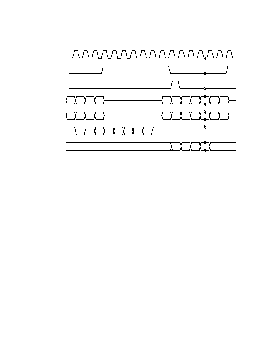
Agere Systems Inc.
49
Advance Data Sheet
September 2001
ATM Interconnect
CelXpres T8207
9
UTOPIA Interface
(continued)
5-7786aF
Figure 13. TX UTOPIA Bus Sharing
X
H0
H1
H2
P46
P47
P44
P46
P47
P45
X
QS[3]
VALID
QS[4]
QS[2] QS[1] QS[0]
R[0]
INVALID
INVALID
QR0
QR1
QR2
U_TXCLK
U_TXENB
*
U_TXSOC
U_TXDATA[7:0]
U_TXPRTY
GRANT
REQUEST

50
Agere Systems Inc.
Advance Data Sheet
September 2001
ATM Interconnect
CelXpres T8207
9
UTOPIA Interface
(continued)
9.6
UTOPIA Pin Modes
In multi-PHY mode, the T8207 interfaces with up to 32 PHY ports. Each port is numbered and accessed using a
certain combination of the cell available/enable (Clav/Enb*) and address (Addr) signals. The addr_clav_en bits in
the main configuration 2 register (address 0112h) are used to select this combination of cell available/enable and
address signals. Table 16 indicates the port numbering for each of the possible configurations.
The first selection of zero address and four cell available/enable signals (a value of "000" in bits 2:0 of register
0112h) is used for connection to UTOPIA level one devices. Use this selection to connect from one to four PHY
devices to the T8207 in ATM mode. If only one PHY is connected, any of the four cell available signals may be con-
nected to the PHY. For two PHY devices, connect any two (internal port number must be matched to the clav being
used). All unused u_rxclav inputs require connection to ground. Four queues are allocated per PHY in this configu-
ration.
The second selection of one address and four cell available/enable signals (a value of "010" in bits 2:0 of register
0112h) is used for connection to UTOPIA level two devices. The selection may be used for up to four PHY groups
of two ports each. (See Appendix 1 of The ATM Forum Technical Committee UTOPIA Level 2, Version 1.0 specifi-
cation.) All unused u_rxclav inputs require connection to ground. Four queues are allocated per PHY in this config-
uration.
The third selection of two address and four cell available/enable signals (a value of "101" in bits 2:0 of register
0112h) is used for connection to four UTOPIA level 2 PHY groups of four ports each. If the T8207_sel bit in register
0112h is set, four queues are allocated per PHY. If the T8207_sel bit is cleared, two queues are allocated per PHY
if the normal 16-port mode described in Section 11.4, Queuing is used or a programmable number of queues can
be allocated per PHY based on the settings in registers 017Ch--017Eh.
The fourth selection of two address and two cell available/enable signals (a value of "100" in bits 2:0 of register
0112h) is used for connection to two UTOPIA level 2 PHY groups of four ports each. All unused u_rxclav inputs
require connection to ground. Four queues are allocated per PHY in this configuration.
The fifth selection of three address and two cell available/enable signals (a value of "111" in bits 2:0 of register
0112h) is used for connection to two UTOPIA level 2 PHY groups of eight ports each. All unused u_rxclav inputs
require connection to ground. If the T8207_sel bit in register 0112h is set, four queues are allocated per PHY. If the
T8207_sel bit is cleared, two queues are allocated per PHY if the normal 16-port mode described in Section 11.4,
Queuing is used or a programmable number of queues can be allocated per PHY based on the settings in registers
017Ch--017Eh.
The sixth selection of three address and one cell available/enable signals (a value of "110" in bits 2:0 of register
0112h) is used for connection to eight UTOPIA level 2 PHY ports. All unused u_rxclav inputs require connection to
ground. Four queues are allocated per PHY in this configuration.
The seventh selection of four address and one cell available/enable signals (a value of "001" in bits 2:0 of register
0112h) is used for connection to sixteen UTOPIA level 2 PHY ports. All unused u_rxclav inputs require connection
to ground. If the T8207_sel bit in register 0112h is set, four queues are allocated per PHY. If the T8207_sel bit is
cleared, two queues are allocated per PHY if the normal 16-port mode described in Section 11.4, Queuing is used
or a programmable number of queues can be allocated per PHY based on the settings in registers 017Ch--017Eh.
Finally, the eighth selection of four address and two cell available/enable signals (a value of "011" in bits 2:0 of reg-
ister 0112h) is used for connection to two UTOPIA Level 2 PHY groups of 16 ports each. All unused u_rxclav inputs
require connection to ground. The T8207_sel bit in register 0112h must be set to `1' for this mode. Two queues are
allocated per PHY, if the normal 32-port mode described in Section 11.4, Queuing is used or a programmable
number of queues can be allocated per PHY based on the settings in registers 0178h--017Eh.

Agere Systems Inc.
51
Advance Data Sheet
September 2001
ATM Interconnect
CelXpres T8207
9
UTOPIA Interface
(continued)
Table 16. Port Numbering for MPHY Configurations
# of
addr
# of
clav/enb*
Ports 0--7
Port 0
Port 1
Port 2
Port 3
Port 4
Port 5
Port 6
Port 7
0
4
enb*[0],
clav[0],
addr = 0
--
enb*[1],
clav[1],
addr = 0
--
enb*[2],
clav[2],
addr = 0
--
enb*[3],
clav[3],
addr = 0
--
1
4
enb*[0],
clav[0],
addr = 0
--
enb*[0],
clav[0],
addr = 2
--
enb*[1],
clav[1],
addr = 0
--
enb*[1],
clav[1],
addr = 2
--
2
4
enb*[0],
clav[0],
addr = 0
enb*[0],
clav[0],
addr = 1
enb*[0],
clav[0],
addr = 2
enb*[0],
clav[0],
addr = 3
enb*[1],
clav[1],
addr0
enb*[1],
clav[1],
addr = 1
enb*[1],
clav[1],
addr = 2
enb*[1],
clav[1],
addr = 3
2
2
enb*[0],
clav[0],
addr = 0
--
enb*[0],
clav[0],
addr = 2
--
enb*[0],
clav[0],
addr = 4
--
enb*[0],
clav[0],
addr = 6
--
3
2
enb*[0],
clav[0],
addr = 0
enb*[0],
clav[0],
addr = 1
enb*[0],
clav[0],
addr = 2
enb*[0],
clav[0],
addr = 3
enb*[0],
clav[0],
addr = 4
enb*[0],
clav[0],
addr = 5
enb*[0],
clav[0],
addr = 6
enb*[0],
clav[0],
addr = 7
3
1
enb*[0],
clav[0],
addr = 0
--
enb*[0],
clav[0],
addr = 2
--
enb*[0],
clav[0],
addr = 4
--
enb*[0],
clav[0],
addr = 6
--
4
1
enb*[0],
clav[0],
addr = 0
enb*[0],
clav[0],
addr = 1
enb*[0],
clav[0],
addr = 2
enb*[0],
clav[0],
addr = 3
enb*[0],
clav[0],
addr = 4
enb*[0],
clav[0],
addr = 5
enb*[0],
clav[0],
addr = 6
enb*[0],
clav[0],
addr = 7
4
2
enb*[0],
clav[0],
addr = 0
enb*[0],
clav[0],
addr = 1
enb*[0],
clav[0],
addr = 2
enb*[0],
clav[0],
addr = 3
enb*[0],
clav[0],
addr = 4
enb*[0],
clav[0],
addr = 5
enb*[0],
clav[0],
addr = 6
enb*[0],
clav[0],
addr = 7
# of
addr
# of
clav/enb*
Ports 8--15
Port 8
Port 9
Port 10
Port 11
Port 12
Port 13
Port 14
Port 15
0
4
--
--
--
--
--
--
--
--
1
4
enb*[2],
clav[2],
addr = 0
--
enb*[2],
clav[2],
addr = 2
--
enb*[3],
clav[3],
addr = 0
--
enb*[3],
clav[3],
addr = 2
--
2
4
enb*[2],
clav[2],
addr = 0
enb*[2],
clav[2],
addr = 1
enb*[2],
clav[2],
addr = 2
enb*[2],
clav[2],
addr = 3
enb*[3],
clav[3],
addr = 0
enb*[3],
clav[3],
addr = 1
enb*[3],
clav[3],
addr = 2
enb*[3],
clav[3],
addr = 3
2
2
enb*[1],
clav[1],
addr = 0
--
enb*[1],
clav[1],
addr = 2
--
enb*[1],
clav[1],
addr = 4
--
enb*[1],
clav[1],
addr = 6
--
3
2
enb*[1],
clav[1],
addr = 0
enb*[1],
clav[1],
addr = 1
enb*[1],
clav[1],
addr = 2
enb*[1],
clav[1],
addr = 3
enb*[1],
clav[1],
addr = 4
enb*[1],
clav[1],
addr = 5
enb*[1],
clav[1],
addr = 6
enb*[1],
clav[1],
addr = 7
3
1
enb*[0],
clav[0],
addr = 8
--
enb*[0],
clav[0],
addr = 10
--
enb*[0],
clav[0],
addr = 12
--
enb*[0],
clav[0],
addr = 14
--
4
1
enb*[0],
clav[0],
addr = 8
enb*[0],
clav[0],
addr = 9
enb*[0],
clav[0],
addr = 10
enb*[0],
clav[0],
addr = 11
enb*[0],
clav[0],
addr = 12
enb*[0],
clav[0],
addr = 13
enb*[0],
clav[0],
addr = 14
enb*[0],
clav[0],
addr = 15
4
2
enb*[0],
clav[0],
addr = 8
enb*[0],
clav[0],
addr = 9
enb*[0],
clav[0],
addr = 10
enb*[0],
clav[0],
addr = 11
enb*[0],
clav[0],
addr = 12
enb*[0],
clav[0],
addr = 13
enb*[0],
clav[0],
addr = 14
enb*[0],
clav[0],
addr = 15

52
Agere Systems Inc.
Advance Data Sheet
September 2001
ATM Interconnect
CelXpres T8207
9
UTOPIA Interface
(continued)
Table 16. Port Numbering for MPHY Configurations (continued)
# of
addr
# of
clav/enb*
Ports 16--23
Port 16
Port 17
Port 18
Port 19
Port 20
Port 21
Port 22
Port 23
0
4
--
--
--
--
--
--
--
--
1
4
--
--
--
--
--
--
--
--
2
4
--
--
--
--
--
--
--
--
2
2
--
--
--
--
--
--
--
--
3
2
--
--
--
--
--
--
--
--
3
1
--
--
--
--
--
--
--
--
4
1
--
--
--
--
--
--
--
--
4
2
enb*[1],
clav[1],
addr = 0
enb*[1],
clav[1],
addr = 1
enb*[1],
clav[1],
addr = 2
enb*[1],
clav[1],
addr = 3
enb*[1],
clav[1],
addr = 4
enb*[1],
clav[1],
addr = 5
enb*[1],
clav[1],
addr = 6
enb*[1],
clav[1],
addr = 7
# of
addr
# of
clav/enb*
Ports 24--31
Port 24
Port 25
Port 26
Port 27
Port 28
Port 29
Port 30
Port 31
0
4
--
--
--
--
--
--
--
--
1
4
--
--
--
--
--
--
--
--
2
4
--
--
--
--
--
--
--
--
2
2
--
--
--
--
--
--
--
--
3
2
--
--
--
--
--
--
--
--
3
1
--
--
--
--
--
--
--
--
4
1
--
--
--
--
--
--
--
--
4
2
enb*[1],
clav[1],
addr = 8
enb*[1],
clav[1],
addr = 9
enb*[1],
clav[1],
addr = 10
enb*[1],
clav[1],
addr = 11
enb*[1],
clav[1],
addr = 12
enb*[1],
clav[1],
addr = 13
enb*[1],
clav[1],
addr = 14
enb*[1],
clav[1],
addr = 15

Agere Systems Inc.
53
Advance Data Sheet
September 2001
ATM Interconnect
CelXpres T8207
9
UTOPIA Interface
(continued)
9.7
UTOPIA Clocking
All TX UTOPIA signals in the T8207 are clocked on the rising edge of the TX UTOPIA clock, and all RX UTOPIA
signals are clocked on the rising edge of the RX UTOPIA clock.
The UTOPIA specifications state that the ATM layer supplies the transmit and receive UTOPIA interface clocks to
the PHY layers. The T8207 may be configured to drive these clocks or to be driven by them.
In the T8207, the clocks for transmit and receive UTOPIA interfaces may be independently derived from several
sources. In addition, each of these clocks may be independently configured. The TX UTOPIA clock configuration
(address 010Ch) and RX UTOPIA clock configuration (address 010Eh) registers are used to select and configure
the transmit UTOPIA interface and the receive UTOPIA interface clocks, respectively. See these register descrip-
tions for more information.

54
Agere Systems Inc.
Advance Data Sheet
September 2001
ATM Interconnect
CelXpres T8207
10
Cell Bus Interface
10.1 General Architecture
The high bandwidth, 32-bit cell bus is used to interconnect T8207 devices. Up to 32 devices may be connected to
the bus, and cell exchange may occur between any of these devices. Each cell bus frame is 16 clock cycles, and
during these 16 cycles, one cell is transmitted. The T8207 is designed to operate with a maximum cell bus fre-
quency of 66 MHz, which translates to a cell bandwidth of 1.7 Gbits/s. The maximum achievable frequency for a
given bus implementation is dependent on loading and other design considerations.
In addition to the 32 bits of data, the cell bus uses four additional control signals. The four signals include a read
clock, a write clock, a frame synchronization signal, and an acknowledge signal.
The read and write clocks (cb_rc* and cb_wc* pins, respectively) establish the timing for reading and writing cells
on the bus and are generated from an external clock source. The read clock is used to read the cell from the cell
bus, and the write clock is used to write the cell to the cell bus. Because all devices on the cell bus read and write
on the same clock edge, the write clock is delayed slightly, relative to the read clock, to ensure sufficient data hold
time.
The active-low frame sync (cb_fs*) is generated by the bus arbiter and indicates the first cycle of the cell bus frame
in 16 user mode or the first cycle of two cell bus frames for 32 user mode. This signal is generated every 16 clock
cycles for 16 user mode or every 32 clock cycles for 32 user mode.
The acknowledge (cb_ack*) signal is used to acknowledge the successful receipt of a cell. This signal is asserted
low during the next request cycle by the T8207 that receives the cell. This signal is not asserted for multicast or
broadcast cells. In the event of an overflow in the control cell RX FIFO, the loopback FIFO, the TX PHY FIFO, or
the cell bus input FIFO, the acknowledge signal will assert low. In the case of an overflow, this signal will not assert
low for multicast and broadcast cells.
When cb_disable* is asserted, the device can receive data on the cb_d*[31:0] but cannot transmit data. The device
cannot assert the cb_ack* even when a valid cell is received from the cell bus, if cb_disable* is asserted.
Several T8207 devices may reside on the cell bus, but one device must be configured as bus arbiter by clearing
the cb_arb_sel bit in the cell bus configuration/status register (address 0130h) or by pulling the arb_en* lead low.
The cell bus arbiter receives requests for access to the bus from all resident devices during the first cycle of the cell
bus frame and grants one of these requests during the last cycle of the cell bus frame. Before issuing the grant and
while a cell is transmitted on the cell bus, the arbiter executes its arbitration algorithm to determine the next device
to transmit on the bus. The arbiter also generates the frame synchronization signal. Software shall designate only
one device as cell bus arbiter, at any given time, to ensure proper operation of the bus.
A 5-bit unit address is assigned to each device (up to 32) on the bus. Each device uses this address to request cell
transmission and to identify incoming cells destined for them. Each device is given a unique unit address by indi-
vidually tying each address (ua*[4:0]) input high or low. The unit address inputs are active-low; therefore, a device
with its ua*[4:0] inputs tied to "10000" has address 15. The device makes a cell transmission request by driving the
two assigned bits during the request cycle, which is the first cycle of a frame. For example, device 15 uses bits 30
and 31 of the request cycle as its request bits. (See Section 10.2, Cell Bus Frames.) Also, each device uses its unit
address to determine if a received cell is destined for it. (See Section 10.3, Cell Bus Routing Headers.)

Agere Systems Inc.
55
Advance Data Sheet
September 2001
ATM Interconnect
CelXpres T8207
10
Cell Bus Interface
(continued)
The cell bus may be configured for 16-user or 32-user mode using the cb_usr_mode bit in the cell bus configura-
tion/status register (address 0130h). In 16-user mode, all 16 devices assert their transmission requests during the
first cycle of each frame, and the transmission grant for the next frame is given during the last cycle of the frame. In
32-user mode, the frame synchronization signal is asserted every two cell bus frames. The two frames are termed
the odd and even frames. The frame synchronization signal marks the beginning of the even frame, and the odd
frame starts 16 clock cycles later. During the request cycle of the even frame, devices zero through 15 assert their
transmission requests, and during the request cycle of the odd frame, devices 16 through 31 assert theirs.
Requests received from odd and even frames are serviced as a group, and grants are given in the order that the
requests are received with the highest priority serviced first with the same priority requests serviced using a round-
robin algorithm. Transmission grants for the next frame are always given at the end of the current frame.
Cells to be transmitted onto the cell bus come from three sources internal to the T8207. Data cells from the
UTOPIA bus are placed in the RX PHY FIFO to await transmission onto the cell bus. Control cells from the micro-
processor wait in the control cell TX FIFO, and loopback cells from the cell bus wait in the loopback FIFO. Cells
from these three FIFOs are priority multiplexed onto the cell bus output FIFO to be transmitted onto the cell bus.
Optional high priority can be established for data cells or control cells sent to the cell bus. If bit 9 in register 0130h
is cleared to `0' then cells from the RX PHY FIFO have the highest priority, cells from the control cell TX FIFO have
next highest, and finally, cells from the loopback FIFO have the lowest. If bit 9 in register 0130h is set to `1,' then
cells from the control cell TX FIFO have the highest priority, cells from the RX PHY FIFO have the next highest pri-
ority, and finally, cells from the loopback FIFO have the lowest priority. This bit on default is `0.'
Incoming cells may be broadcast, multicast, or single address types. The T8207 receiving device accepts single
address cells with an address field in the cell bus routing header that matches the device's unit address. In addi-
tion, the device accepts all broadcast cells and certain multicast cells that it is configured to accept. (See Section
10.3.4, Multicast Routing (continued).) Before a cell is accepted, a check is done on the previous grant to verify
whether it is a valid grant or not. The receiving device verifies the cell bus routing header cyclic redundancy check
(CRC-4) value in the least significant 4 bits of the cell bus routing header. It also verifies the bit interleave parity
(BIP-8) value from bits 24 to 31 of the last cell bus frame cycle. If either is corrupt, the cell is discarded. If kept, cells
are routed to the loopback FIFO, control FIFO, or TX PHY FIFO, based on the information in its cell bus routing
header. See Section 10.3, Cell Bus Routing Headers.
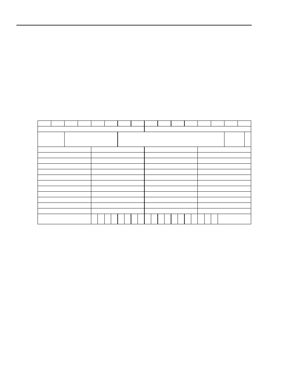
56
Agere Systems Inc.
Advance Data Sheet
September 2001
ATM Interconnect
CelXpres T8207
10
Cell Bus Interface
(continued)
10.2 Cell Bus Frames
A cell bus frame is always 16 clock cycles. The cell bus frame has three sections (request, bus cell, and grant).
During the request section, which is the first clock cycle of the frame, 16 devices assert their transmission requests
onto the bus. During the bus cell section, which is the next 14 clock cycles, a cell is transmitted on the cell bus. This
bus cell includes the cell bus routing header, the optional tandem routing header, and the 52-byte body of the cell.
During the grant section, which is the last clock cycle of the frame, the grant is asserted, indicating which device
may transmit its cell during the next frame. Also, during this last clock cycle, a parity vector is placed on the bus by
the transmitting device so that error detection can be performed on the cell. Figure 14 illustrates the format for the
cell bus frame.
Figure 14. Cell Bus Frame Format (Bit Positions for 16 User Mode)
31
16 15
0
CYCLE 0
U15
U14
U13
U12
U11
U10
U9
U8
U7
U6
U5
U4
U3
U2
U1
U0
CYCLE 1
CELL BUS ROUTING HEADER
TANDEM ROUTING HEADER
CYCLE 2
GFC/
VPI[11:8]
VPI[7:0]
VCI[15:0]
PTI
C
L
P
CYCLE 3
PAYLOAD BYTE 0
PAYLOAD BYTE 1
PAYLOAD BYTE 2
PAYLOAD BYTE 3
CYCLE 4
PAYLOAD BYTE 4
PAYLOAD BYTE 5
PAYLOAD BYTE 6
PAYLOAD BYTE 7
CYCLE 5
PAYLOAD BYTE 8
PAYLOAD BYTE 9
PAYLOAD BYTE 10
PAYLOAD BYTE 11
CYCLE 6
PAYLOAD BYTE 12
PAYLOAD BYTE 13
PAYLOAD BYTE 14
PAYLOAD BYTE 15
CYCLE 7
PAYLOAD BYTE 16
PAYLOAD BYTE 17
PAYLOAD BYTE 18
PAYLOAD BYTE 19
CYCLE 8
PAYLOAD BYTE 20
PAYLOAD BYTE 21
PAYLOAD BYTE 22
PAYLOAD BYTE 23
CYCLE 9
PAYLOAD BYTE 24
PAYLOAD BYTE 25
PAYLOAD BYTE 26
PAYLOAD BYTE 27
CYCLE 10
PAYLOAD BYTE 28
PAYLOAD BYTE 29
PAYLOAD BYTE 30
PAYLOAD BYTE 31
CYCLE 11
PAYLOAD BYTE 32
PAYLOAD BYTE 33
PAYLOAD BYTE 34
PAYLOAD BYTE 35
CYCLE 12
PAYLOAD BYTE 36
PAYLOAD BYTE 37
PAYLOAD BYTE 38
PAYLOAD BYTE 39
CYCLE 13
PAYLOAD BYTE 40
PAYLOAD BYTE 41
PAYLOAD BYTE 42
PAYLOAD BYTE 43
CYCLE 14
PAYLOAD BYTE 44
PAYLOAD BYTE 45
PAYLOAD BYTE 46
PAYLOAD BYTE 47
CYCLE 15
BIT INTERLEAVE PARITY
-- -- -- -- -- -- -- -- -- -- -- -- -- -- -- -- --
G
P
G
E
GRANT NUMBER

Agere Systems Inc.
57
Advance Data Sheet
September 2001
ATM Interconnect
CelXpres T8207
10
Cell Bus Interface
(continued)
Figure 15. Cell Bus Frame Format (Bit Positions for 32 User Mode)
31
16 15
0
CYCLE 0
U15
U14
U13
U12
U11
U10
U9
U8
U7
U6
U5
U4
U3
U2
U1
U0
CYCLE 1
CELL BUS ROUTING HEADER
TANDEM ROUTING HEADER
CYCLE 2
GFC/
VPI[11:8]
VPI[7:0]
VCI[15:0]
PTI
C
L
P
CYCLE 3
PAYLOAD BYTE 0
PAYLOAD BYTE 1
PAYLOAD BYTE 2
PAYLOAD BYTE 3
CYCLE 4
PAYLOAD BYTE 4
PAYLOAD BYTE 5
PAYLOAD BYTE 6
PAYLOAD BYTE 7
CYCLE 5
PAYLOAD BYTE 8
PAYLOAD BYTE 9
PAYLOAD BYTE 10
PAYLOAD BYTE 11
CYCLE 6
PAYLOAD BYTE 12
PAYLOAD BYTE 13
PAYLOAD BYTE 14
PAYLOAD BYTE 15
CYCLE 7
PAYLOAD BYTE 16
PAYLOAD BYTE 17
PAYLOAD BYTE 18
PAYLOAD BYTE 19
CYCLE 8
PAYLOAD BYTE 20
PAYLOAD BYTE 21
PAYLOAD BYTE 22
PAYLOAD BYTE 23
CYCLE 9
PAYLOAD BYTE 24
PAYLOAD BYTE 25
PAYLOAD BYTE 26
PAYLOAD BYTE 27
CYCLE 10
PAYLOAD BYTE 28
PAYLOAD BYTE 29
PAYLOAD BYTE 30
PAYLOAD BYTE 31
CYCLE 11
PAYLOAD BYTE 32
PAYLOAD BYTE 33
PAYLOAD BYTE 34
PAYLOAD BYTE 35
CYCLE 12
PAYLOAD BYTE 36
PAYLOAD BYTE 37
PAYLOAD BYTE 38
PAYLOAD BYTE 39
CYCLE 13
PAYLOAD BYTE 40
PAYLOAD BYTE 41
PAYLOAD BYTE 42
PAYLOAD BYTE 43
CYCLE 14
PAYLOAD BYTE 44
PAYLOAD BYTE 45
PAYLOAD BYTE 46
PAYLOAD BYTE 47
CYCLE 15
BIT INTERLEAVE PARITY
-- -- -- -- -- -- -- -- -- -- -- -- -- -- -- -- --
G
P
G
E
GRANT NUMBER
CYCLE 16
U31
U30
U29
U28
U27
U26
U25
U24
U23
U22
U21
U20
U19
U18
U17
U16
CYCLE 17
CELL BUS ROUTING HEADER
TANDEM ROUTING HEADER
CYCLE 18
GFC/
VPI[11:8]
VPI[7:0]
VCI[15:0]
PTI
C
L
P
CYCLE 19
PAYLOAD BYTE 0
PAYLOAD BYTE 1
PAYLOAD BYTE 2
PAYLOAD BYTE 3
CYCLE 20
PAYLOAD BYTE 4
PAYLOAD BYTE 5
PAYLOAD BYTE 6
PAYLOAD BYTE 7
CYCLE 21
PAYLOAD BYTE 8
PAYLOAD BYTE 9
PAYLOAD BYTE 10
PAYLOAD BYTE 11
CYCLE 22
PAYLOAD BYTE 12
PAYLOAD BYTE 13
PAYLOAD BYTE 14
PAYLOAD BYTE 15
CYCLE 23
PAYLOAD BYTE 16
PAYLOAD BYTE 17
PAYLOAD BYTE 18
PAYLOAD BYTE 19
CYCLE 24
PAYLOAD BYTE 20
PAYLOAD BYTE 21
PAYLOAD BYTE 22
PAYLOAD BYTE 23
CYCLE 25
PAYLOAD BYTE 24
PAYLOAD BYTE 25
PAYLOAD BYTE 26
PAYLOAD BYTE 27
CYCLE 26
PAYLOAD BYTE 28
PAYLOAD BYTE 29
PAYLOAD BYTE 30
PAYLOAD BYTE 31
CYCLE 27
PAYLOAD BYTE 32
PAYLOAD BYTE 33
PAYLOAD BYTE 34
PAYLOAD BYTE 35
CYCLE 28
PAYLOAD BYTE 36
PAYLOAD BYTE 37
PAYLOAD BYTE 38
PAYLOAD BYTE 39
CYCLE 29
PAYLOAD BYTE 40
PAYLOAD BYTE 41
PAYLOAD BYTE 42
PAYLOAD BYTE 43
CYCLE 30
PAYLOAD BYTE 44
PAYLOAD BYTE 45
PAYLOAD BYTE 46
PAYLOAD BYTE 47
CYCLE 31
BIT INTERLEAVE PARITY
-- -- -- -- -- -- -- -- -- -- -- -- -- -- -- -- --
G
P
G
E
GRANT NUMBER

58
Agere Systems Inc.
Advance Data Sheet
September 2001
ATM Interconnect
CelXpres T8207
10
Cell Bus Interface
(continued)
Devices on the cell bus make their requests during the first cycle of each frame. In 16-user mode, each device
asserts a request every frame. In 32-user mode, each device asserts a request every two frames. In 32-user mode,
devices with unit addresses 0 through 15 assert their requests during the even frames, and devices with unit
addresses 16 through 31 assert their requests during the odd frames. During cycle 0 of their assigned frame,
each device drives two of the 32 data bits available. The position of the two request bits for each device is based
on the device's unit address. The assigned bit positions for each device are illustrated in Figure 14 and Figure 15
for 16-user and 32-user modes, respectively. For example, in the figures, the device with unit address 0 makes
its requests using the 2 bits labeled as U0. Two bits, instead of one, are used for each device so the priority
of the request may be included. The priority of the request is set up using the cb_req_pr bits in the main configura-
tion/control register (address 0110h). See Table 58 in Section 14.3, Extended Memory Registers, for more informa-
tion.
During clock cycles 1 through 14, the device that was granted the bus at the end of the previous frame sends its
bus cell. The bus cell sent includes the cell bus routing header, the tandem routing header, and the original
UTOPIA cell with the header error check (HEC) byte removed. The HEC byte is removed because the cell bus
does its own error check over the complete cell using the bit interleave parity byte. The HEC byte is recreated and
inserted before the received cell is placed on the UTOPIA bus.
The cell bus routing header indicates the type of the cell (data, control, loopback) and its destination (single, multi-
cast, broadcast). See Section 10.3, Cell Bus Routing Headers, for more information on the cell bus routing header
structure. The optional tandem routing header is configured by the user.
The 32 bits of the grant section of the frame (clock cycle 15) includes the bit interleave parity (BIP-8) byte, the grant
parity bit, the grant enable bit, and the grant number. The most significant 8 bits of the grant section of the frame is
the BIP-8 byte. The BIP-8 byte is calculated over 54 bytes starting with the first tandem routing header byte and
ending with the last payload byte. To calculate this bit interleave parity, an exclusive-OR operation is performed on
the first byte of the tandem routing header and the value "11111111." The exclusive-OR operation then is performed
on this result and the following byte. The operation is then repeated with every successive byte through the last
data byte of the payload. The resulting byte becomes the BIP-8 byte of the grant section. The next 17 bits of the
grant section are unused. The least significant 7 bits of the grant section are used to grant transmission requests.
The grant number is located in the least significant 5 bits of the grant section and is the unit address of the device
that transmits a cell during the next frame. The grant enable, bit 5, is an active-high signal that indicates if the grant
is valid. Finally, the grant parity, bit 6, is the odd parity check calculated over the other six grant bits.
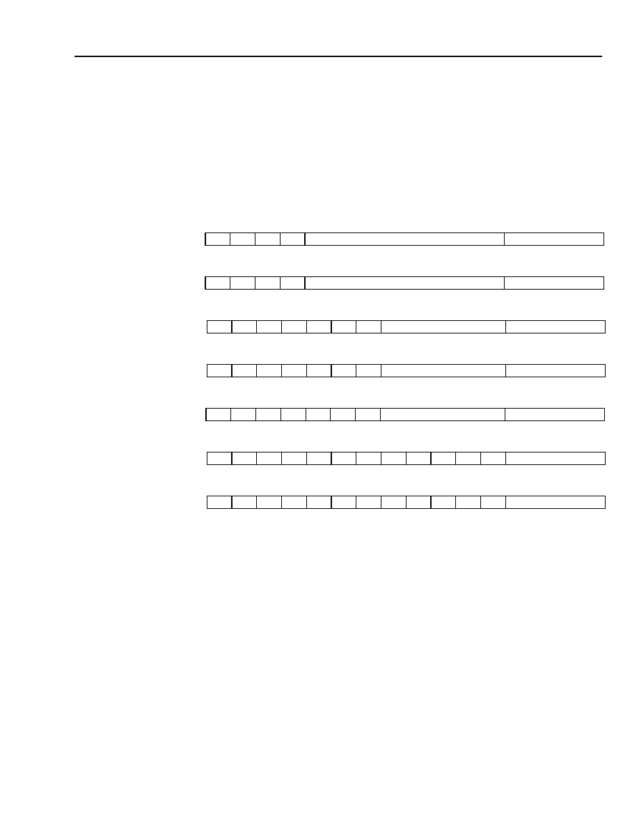
Agere Systems Inc.
59
Advance Data Sheet
September 2001
ATM Interconnect
CelXpres T8207
10
Cell Bus Interface
(continued)
10.3 Cell Bus Routing Headers
The cell bus routing header gives information about the cell and its routing. There are seven different formats for
cell bus routing headers. See Figure 16. These headers cover broadcast, multicast, and single address routing. A
T8207 device on the cell bus accepts all broadcast cells and certain multicast cells that it is configured to accept.
Broadcast or multicast routed cells may be data cells or control cells. The T8207 receiving device accepts single
address cells with an address field in its cell bus routing header that matches the device's unit address. Cells,
routed as single address, may be data, control, or loopback cells.
Figure 16. Cell Bus Routing Headers
The H field (b0 to b3) is the cell bus routing header cyclic redundancy check (CRC-4) calculated over the other
12 bits (b4 to b15) of the header. It is provided for cell bus routing header error detection. When cells arrive from
the cell bus, the receiving device calculates the CRC-4 over the most significant 12 bits of the cell bus routing
header and compares its calculation to the CRC-4 value stored in the H field of the cell bus routing header. If the
two do not match, the cell is discarded.
10.3.1 Control Cells
The microprocessor connected to the T8207 may send control cells to the cell bus by writing the cell to the control
cell transmit direct memory at addresses A0h to D7h (or extended memory at addresses 0900h to 0936h). After
the cell is written to memory, the microprocessor sets the cntl_cell_wr bit in the main configuration/control register
(address 0110h). This bit returns to zero when the cell is transmitted and memory is available to load a new control
cell into the device.
Control cells accepted from the cell bus are routed to the control cell RX FIFO. The microprocessor connected to
the T8207 reads the control cell at the head of the FIFO using the control cell receive direct memory at addresses
60h to 93h (or extended memory at addresses 0800h to 0832h). After the microprocessor reads the cell, it sets the
cntl_cell_rd bit in the main configuration/control register (address 0110h) to remove the cell from the head of the
FIFO.
MULTICAST
CONTROL CELL HEADER
b15
b14
b13
b12
b11
b10
b9
b8
b7
b6
b5
b4
b3
b2
b1
b0
1
1
--
--
MULTICAST NET NUMBER
H
MULTICAST
DATA CELL HEADER
b15
b14
b13
b12
b11
b10
b9
b8
b7
b6
b5
b4
b3
b2
b1
b0
1
0
--
--
MULTICAST NET NUMBER
H
SINGLE DESTINATION
DATA CELL HEADER
b15
b14
b13
b12
b11
b10
b9
b8
b7
b6
b5
b4
b3
b2
b1
b0
0
0
--
--
--
--
0
UNIT ADDRESS
H
SINGLE DESTINATION
CONTROL CELL HEADER
b15
b14
b13
b12
b11
b10
b9
b8
b7
b6
b5
b4
b3
b2
b1
b0
0
1
--
--
--
--
0
UNIT ADDRESS
H
SINGLE DESTINATION
LOOPBACK CELL HEADER
b15
b14
b13
b12
b11
b10
b9
b8
b7
b6
b5
b4
b3
b2
b1
b0
0
0
0
--
--
--
1
UNIT ADDRESS
H
BROADCAST
DATA CELL HEADER
b15
b14
b13
b12
b11
b10
b9
b8
b7
b6
b5
b4
b3
b2
b1
b0
0
0
1
--
--
--
1
--
--
--
--
--
H
BROADCAST
CONTROL CELL HEADER
b15
b14
b13
b12
b11
b10
b9
b8
b7
b6
b5
b4
b3
b2
b1
b0
0
1
1
--
--
--
1
--
--
--
--
--
H

60
Agere Systems Inc.
Advance Data Sheet
September 2001
ATM Interconnect
CelXpres T8207
10
Cell Bus Interface
(continued)
10.3.2 Data Cells
Data cells accepted from the cell bus are routed to the TX PHY FIFO. From the TX PHY FIFO, the cell is routed to
the appropriate transmit queue using the information about the cell's priority and the queue group to which it is des-
tined. The priority of the cell is indicated by 2 bits obtained from the first 64 bits of the bus cell (cell bus routing
header, tandem routing header, and ATM cell header). The position of these 2 bits in the cell are user programma-
ble during configuration using the prior0_sel[5:0] and prior1_sel[5:0] bits of the routing information 3 register
(address 0204h). The queue group to which the cell is destined is indicated by 4 bits obtained from the first 64 bits
of the bus cell (cell bus routing header, tandem routing header, and ATM cell header). The position of these 4 bits
in these headers are user programmable using the mphy1_sel[5:0] and mphy2_sel[5:0] bits of the routing informa-
tion 1 register (address 0200h) and the mphy3_sel[5:0] and mphy0_sel[5:0] bits of the routing information 2 regis-
ter (address 0202h). See Tables 90, 91, and 92 in Section 14.3, Extended Memory Registers. None of the priority
or MPHY bits are required to be adjacent. For more information on queue groups, see Section 11.4, Queuing.
If the T8207_sel bit (Table 59) is zero, the mphy3_sel[5:0] bits are not used.
10.3.3 Loopback Cells
A loopback cell may be sent to the cell bus for diagnostic purposes. Initially, the loopback cell is sent from one
T8207 (device 1) to a second T8207 (device 2). The second T8207 (device 2) returns the cell to the first T8207
(device 1), or, if desired, the second T8207 (device 2) may send the cell on to one or more entirely different T8207
devices. Device 2 accepts the loopback cell and replaces the most significant 12 bits of the cell bus routing header
with the routing_header bits in its loopback register (address 0118h). The 12 routing_header bits in the loopback
register correspond to the upper 12 bits of a single destination control cell header, a multicast control cell header, or
a broadcast control cell header. (See Figure 16.)
To create a loopback path from device 1 to device 2, and back to device 1, coordinated control of device 1 and
device 2 is needed. First, the microprocessor connected to device 2 sets up the loopback by writing the
routing_header bits in the loopback register of device 2. The routing_header bits indicate a single destination con-
trol cell with a unit address field for device 1. Second, the microprocessor connected to device 1 writes a loopback
cell to the control cell transmit direct memory (addresses A0h to D7h) of device 1. (See Section 10.3.1, Control
Cells of this document.) The cell bus routing header of this cell is the single destination loopback type, and the unit
address section of the header contains the address of device 2. To send the loopback cell, a `1' is then written to
the cntl_cell_wr bit of the main configuration/control register (address 0110h).
Care must be taken to ensure that the routing_header bits in a T8207 device are not changed until any previously
setup loopback cell has been received and retransmitted. If these bits are changed prematurely, misrouting will
occur.
10.3.4 Multicast Routing
The T8207 may be programmed to accept certain multicast data cells using the multicast memories at addresses
E0h through FFh (or 0C00h through 0C1Eh) and 0C20h through 0DFEh. The net numbers of accepted multicast
control cells are programmed in the memory space E0h through FFh (or 0C00h through 0C1Eh) and 0C20h
through 0DFEh. These memory spaces hold 256 bits each. Each bit represents a multicast net number from 0 to
255.
If the T8207_sel bit (Table 59) is cleared, the multicast memories at addresses 0D00h to 0DFEh are ignored.
Note: To prevent potential multicast memory errors, these memory spaces should be cleared during the initializa-
tion process.
For ATM mode, if the T8207_sel bit is cleared, the net numbers of accepted multicast data cells are programmed in
the multicast number memories, which are divided among eight PHY ports. If 16 ports are used in this mode, each
memory space is shared between two ports, e.g., ports zero and one use the memory assigned to PHY 0, ports two
and three use the memory assigned to PHY 1, and so on (see Section 9.2.2, Outgoing ATM Mode (Cells Sent by
T8207)).

Agere Systems Inc.
61
Advance Data Sheet
September 2001
ATM Interconnect
CelXpres T8207
10
Cell Bus Interface
(continued)
10.3.4 Multicast Routing (continued)
For ATM mode, if the T8207_sel bit is set, the net numbers of accepted multicast data cells are programmed in the
multicast number memories, which are divided among sixteen PHY ports. If 16 ports are used, each port has one
memory space. If 32 ports are used, each memory space is shared between two ports, e.g., ports zero and one
use the memory assigned to PHY 0, ports two and three use the memory assigned to PHY 1, and so on.
The cell priority bits select the specific queue in the queue group to which the cell is routed. (See Section 11.4,
Queuing.) Note that multicast control cells use the same multicast number memory as PHY 0 multicast data cells.
See Table 122 in Section 14.3, Extended Memory Registers and Table 52 in Section 14.2, Direct Memory Access
Registers, respectively.
For PHY mode, multicast cells are only transmitted to queue group 0, and only the PHY port 0 and control cell mul-
ticast direct memory at addresses E0h through FFh (or 0C00h through 0C1Eh) is used. The cell priority determines
the specific queue in queue group 0 to which the cell is routed. (See Section 10.3.2, Data Cells.)
10.3.5 Broadcast Routing
Broadcast control cells are transmitted and received as described in Section 10.3.1, Control Cells. The broadcast
control cell bus routing header has a broadcast control cell header type.
For ATM mode, if the T8207_sel bit (Table 59) is cleared and 8 PHY ports or less are being used, the broadcast
data cells are transmitted to all the ports. If 16 ports are used, the broadcast data cells are transmitted to only 8 of
the 16 ports depending on the cell priority bits that select the specific queue.
For ATM mode, if the T8207_sel bit (Table 59) is set, and 16 PHY ports or less are being used, the broadcast data
cells are transmitted to all the ports. If 32 ports are used, the broadcast data cells are transmitted to only 16 of the
32 ports depending on the cell priority bits that select the specific queue.
For PHY mode, if SDRAM is bypassed, broadcast data cells are only transmitted to queue 0. If the SDRAM is not
bypassed, broadcast data cells are only transmitted to queue group 0, and only PHY port 0 is used (although the
device will take the time to try to broadcast data cells to all the ports, cells will not be stored in queue groups other
than 0).
10.4
Cell Bus Arbitration
One of the T8207 devices sharing the cell bus must be configured as bus arbiter by clearing the cb_arb_sel bit in
the cell bus configuration/status register (address 0130h) or by pulling the arb_en* lead low. Using an arbitration
algorithm, the arbiter decides the next device to transmit on the cell bus and issues the grant signals at the end
of the cell bus frame. The arbiter also generates the active-low frame synchronization signal that occurs every
16 clock cycles in 16-user mode and every 32 clock cycles in 32-user mode.
To grant transmission requests, the arbiter must analyze requests received during the request section of the cur-
rent frame for 16-user mode or during two request cycles for 32-user mode. The arbitration algorithm used is
round-robin and based on the priority of the request and the last request granted.
The arbiter circuitry in all T8207 devices on the cell bus will synchronize to the active arbiter on the cell bus. So,
when an inactive device becomes the arbiter, it will begin sending frame synchronization signals that coincide to
the clock cycle that the original arbiter would have sent its next frame synchronization signal. This prevents the
new arbiter from misinterpreting random signals on its first request cycle as valid requests.
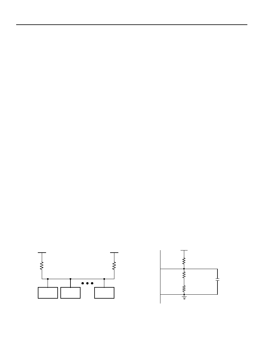
62
Agere Systems Inc.
Advance Data Sheet
September 2001
ATM Interconnect
CelXpres T8207
10
Cell Bus Interface
(continued)
10.5 Cell Bus Monitoring
Every T8207 device monitors the cell bus for proper operation. The monitoring section of the T8207 checks for the
presence of the read clock, the write clock, and the frame synchronization signal. The cb_wc_miss bit in the main
interrupt status 1 register (address 0102h) is set when the write clock is inactive for 32 mclk cycles. Likewise, the
cb_rc_miss bit in the main interrupt status 1 register is set when the read clock is inactive for 32 mclk cycles. In
addition, the cb_fs_miss bit in the main interrupt status 1 register is set when the frame synchronization signal is
inactive for greater than 16 cell bus read clock cycles for 16-user mode or for greater than 32 read clock cycles for
32-user mode. This bit is also set when the cell bus write clock is inactive for 32 mclk cycles.
When cells arrive from the cell bus, the cell bus monitoring section of the receiving device calculates the bit inter-
leave parity value over the 54-byte field from the first tandem routing header byte through the final payload byte. If
this calculated value does not match the value in bits 24 through 31 of the final clock cycle of the frame, the cell is
discarded.
The T8207 detects when a device asserts transmission requests and is not granted permission within a program-
mable time period. The cb_grnt_to bit in the main interrupt status 1 register (address 0102h) is set when a device
has not been granted permission to transmit within the number of frames programmed in the cb_req_to bits of the
main configuration 3 register (address 0116h).
10.6 GTL+ Logic
For the T8207, the cell bus data, frame sync, and acknowledge signals use onboard GTL+ transceivers, and the
cell bus clock signals use onboard GTL+ receivers. The GTL+ bus drivers are open drain and require terminating
resistors at both ends of each line. The terminating resistor (R) may be from 40
to 50
and should be pulled up
to 1.5 V
Ī
10% (V
TT
). The actual value of the terminating resistors should be chosen to match the bus line imped-
ance. Figure 17A below illustrates the terminating resistors and the configuration of one GTL+ bus line. The termi-
nation resistors are typically placed at the ends of the bus of the backplane.
The signal rise and fall times from the transceivers are carefully controlled to minimize out of band signals without
affecting the overall transmission rates. These controlled signal edges, in addition to proper resistive line termina-
tion, minimize noise and ringing. The slew rate of the GTL+ buffers can be programmed using bits [2:0] of register
2Eh.
The GTL+ receiver compares its input signal to a voltage reference, cb_vref, to determine the logic level of the
input. The value of the voltage reference is 2/3 V
TT
and is created using the voltage divider shown in Figure 17B.
The 1 k
resistors are 1% because the cb_vref voltage must track V
TT
by 1%. The 0.01
Ķ
F capacitor is a decou-
pling capacitor on the cb_vref input.
Figure 17. GTL+ External Circuitry
5-8011a (F)
5-8012a(F)
A. GTL+ Bus with Terminating Resistors
B. GTL+ Threshold Voltage Reference
R
R
V
TT
V
TT
CelXpres
T8207
CelXpres
T8207
CelXpres
T8207
1
k
Ī
1%
1
k
Ī
1%
V
TT
1
k
Ī
1%
cb_vref
0.01
Ķ
F
cb_vref_vss

Agere Systems Inc.
63
Advance Data Sheet
September 2001
ATM Interconnect
CelXpres T8207
10
Cell Bus Interface
(continued)
10.7 Cell Bus Write and Read Clocks
The read and write clocks (cb_wc* and cb_rc* pins) are supplied from an external source. The write clock should
be delayed 1.5 ns to 4 ns relative to the read clock to ensure sufficient data hold time. The position of the clock
source relative to the cell bus devices on the card or on connecting cards determines the actual delay that should
be used. When the clock source is centrally located among the cell bus devices, a longer delay may be used.
When the clock source is at either end of the cell bus devices, a shorter delay is needed. Also, a higher clock fre-
quency requires a shorter delay.

64
Agere Systems Inc.
Advance Data Sheet
September 2001
ATM Interconnect
CelXpres T8207
11
SDRAM Interface
For outgoing UTOPIA cells, the TX UTOPIA cell buffer supports 64 queues. These queues are separated into
16 queue groups, each consisting of four different priority queues as described in Section 9.2.2, Outgoing ATM
Mode (Cells Sent by T8207). This cell buffer holds 128 outgoing cells. Additional buffering is provided by an exter-
nal SDRAM. Connection to an external SDRAM is selected by clearing the sdram_bypass bit in the main configura-
tion 1 register (address 0100h).
If the SDRAM is not used, it is bypassed by setting the sdram_bypass bit in the main configuration 1 register at
start-up. When bypassed, only queue 0 of the 64 queues in the TX UTOPIA cell buffer is used. The only buffering
available in this mode is the 128-cell internal memory (TX PHY FIFO) and up to 128 cells from queue 0 of the TX
UTOPIA cell buffer. The TX PHY FIFO overflows only if the TX UTOPIA cell buffer is full, and as a result, the TX
PHY FIFO is also full. The setting of the div_queue bits in the main configuration 2 register (address 0112h) deter-
mines the number of cell locations allocated to queue 0 of the TX UTOPIA cell buffer. Be sure to program these bits
to "101" to maximize buffering.
11.1
Memory Configuration
The SDRAM interface supports from 2 Mbytes to 32 Mbytes of memory. This memory size is realized using 16 Mbit
or 64 Mbit devices. Table 17 below outlines the various memory configurations supported.
Table 17. Supported Memory Configurations
11.2
Powerup Sequence
The powerup sequence for the SDRAM must be performed manually before the SDRAM is enabled. Using the idle
state 1 and 2 registers (addresses 0420h and 0422h), the manual access state 1 and 2 registers (addresses 0424h
and 0426h), and the gen_man_acc bit in the SDRAM control register (address 0400h), follow the powerup com-
mand sequence prescribed by the SDRAM manufacturer. The T8207 does not control the chip select, the clock
enable, and the DQM inputs to the SDRAM. These signals should be externally tied to the appropriate logic level or
external control signal.
To manually execute SDRAM commands, first set up the idle values for CAS*, RAS*, WE*, bank select (BS), and
the address signals using the cas_idle, ras_idle, we_idle, bs_idle[1:0], and addr_idle[11:0] bits in the idle state 1
and 2 registers. Then manually set up the value of these signals for the first SDRAM command using the cas_man,
ras_man, we_man, bs_man[1:0], and addr_man[11:0] bits in the manual access state 1 and 2 registers. Finally,
write a `1' to the gen_man_acc bit in the SDRAM control register. Writing this `1' drives the CAS, RAS, WE*, BS,
and address values (in the manual access state 1 and 2 registers) onto the associated pins, for one SDRAM clock
cycle. After the one clock cycle, these signals return to their idle state. Repeat this process, making sure minimum
timing between commands is met, until the powerup process has been completed.
In the powerup sequence, configure the mode register of the SDRAM for a burst length of one and a CAS latency
of two or three. With a burst length of one, sequential and interleave addressing behave the same, so the SDRAM
may be configured for either addressing mode.
Number of
Devices
Device Memory Size and Data
Bus Organization
Number of
Columns
Number of
Banks
Number of
Rows
Total
Memory
1
16 Mbit, 16-bit data bus
256
2
2048
2 Mbyte
2
16 Mbit, 8-bit data bus
512
2
2048
4 Mbyte
4
16 Mbit, 4-bit data bus
1024
2
2048
8 Mbyte
1
64 Mbit, 16-bit data bus
256
4
4096
8 Mbyte
2
64 Mbit, 8-bit data bus
512
4
4096
16 Mbyte
4
64 Mbit, 4-bit data bus
1024
4
4096
32 Mbyte
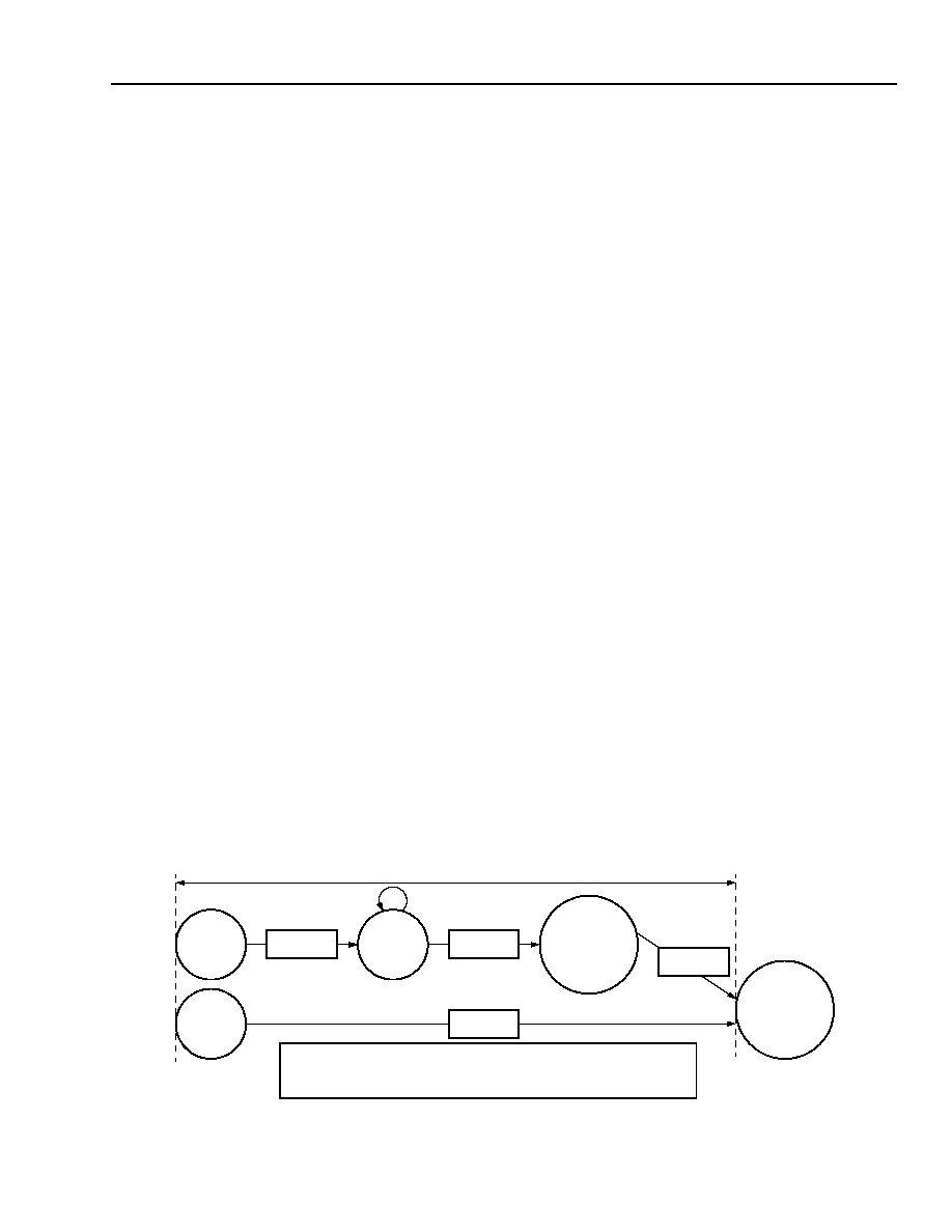
Agere Systems Inc.
65
Advance Data Sheet
September 2001
ATM Interconnect
CelXpres T8207
11
SDRAM Interface
(continued)
11.3
SDRAM Interface Timing
The mclk clock is the source of the SDRAM clock (sd_clk) from the T8207. Based on the frequency of the SDRAM
clock and the speed grade of the SDRAM, four timing parameters must be programmed into the SDRAM configu-
ration register at address 0408h. These timing parameters are specified in SDRAM (mclk) clock cycles and are
listed below:
s
RAS inactive to CAS active (ras2cas)--its value may be set from two to four SDRAM clock cycles.
s
CAS inactive to precharge command active (cas2pre)--its value may be set from one to four SDRAM clock
cycles.
s
Precharge command inactive to next command active (pre2cmd)--its value may be set from one to four SDRAM
clock cycles.
s
CAS before RAS (CBR) refresh command inactive to next CBR refresh command active (ref2cmd)--its value
may be set to 3, 7, or 15 SDRAM clock cycles.
Actual values for these parameters are obtained from the data sheet of the SDRAM used. For optimum perfor-
mance, these parameters should be programmed to the lowest acceptable values. The earliest time that a CAS
may be asserted after an RAS may be obtained from the data sheet parameter that describes the minimum time
from the activate command to the read/write command. Three parameters affect the earliest time that a precharge
command may follow a CAS. For read commands, a precharge command may be issued one clock earlier than the
last read data. The actual number of clock cycles depends on the CAS latency needed for the device. For write
commands, the earliest time that a precharge command may be issued following a CAS may be obtained from the
SDRAM data sheet parameter that describes the minimum time from the last data in to the precharge command. In
addition to these two parameters, the minimum time from the activate command to the precharge command may
need to be considered to obtain the value for cas2pre. If the SDRAM is only accessed for queuing purposes,
28 consecutive CAS commands will be executed between the activate command and the precharge command,
and the minimum time from the activate command to the precharge command does not need to be considered. If
the microprocessor reads and writes the SDRAM memory, only one CAS command will be executed between the
activate command and the precharge command. In this case, the minimum time from the activate command to the
precharge command is significant and must be considered. The minimum time from the precharge command to
the next command may be obtained from the data sheet parameter that describes the minimum time from the pre-
charge command to the activate command. The minimum time from the CBR refresh command to the next CBR
refresh command may be obtained from the data sheet. In the T8207, the minimum time from CBR refresh to any
other command is 15 SDRAM clock cycles. In the data sheet, the parameters may be specified in actual time units
rather than clock cycles. To determine the number of clock cycles, divide the parameter value by the SDRAM clock
period. Figure 18 below illustrates these timing parameters and the number of clock cycles needed to read or write
a cell using the default values for the parameters.
5-7785bF
Figure 18. SDRAM Timing Parameters
RAS
(1)
CBR
REFRESH
{2, 3, 4}
ras2cas
CAS
(1 TO 28)
{1, 2, 3, 4}
cas2pre
PRECHARGE
(1)
{3, 7, 15}
ref2cmd
{1, 2, 3, 4}
pre2cmd
NEXT
COMMAND
SINGLE COMMAND
THE BOXES REPRESENT THE NUMBER
OF IDLE CYCLES BETWEEN STATES. DEFAULT
VALUES ARE IN BOLD FOR ras2cas, cas2pre, pre2cmd, AND ref2cmd.
(1)

66
Agere Systems Inc.
Advance Data Sheet
September 2001
ATM Interconnect
CelXpres T8207
11
SDRAM Interface
(continued)
11.4
Queuing
Queuing is different for a T8207 device with its T8207_sel (Table 59) bit set than a T8207 device with its T8207_sel
bit cleared.
For a device configured in ATM mode with its T8207_sel bit set, up to 16 groups of queues with four priorities per
group may be configured in the SDRAM for a total of 64 queues. Therefore, the four port group address bits point
to one of 16 queue groups, and the two priority bits point to one of four queues in the group. (For a description of
the port group address and priority bits, see Section 10.3.2, Data Cells.) Priority bits with a value of zero represent
the highest priority, and those with a value of three, the lowest priority.
If the ATM is configured to support eight or less PHY ports, each port is mapped to one queue group using the
port_rte[31:0] bits in the TX PHY FIFO routing 0 and 1 registers (addresses 017Ch and 017Eh). For example, for a
configuration of eight PHY ports, which includes ports 0, 2, 4, 6, 8, 10, 12, and 14, PHY port 0 is assigned queue
group zero or queues zero, one, two, and three. Likewise, PHY port 2 is assigned group one or queues four, five,
six, and seven, and so on.
An ATM configured to support 16 PHY ports is a special case. When the T8207_sel bit is set and the ATM is con-
figured to support 16 PHY ports, each port (0--15) is assigned to its associated queue group as illustrated in Table
18, regardless of the value of the port_rte[63:0] bits. In this case, port 0 is assigned to queue group 0, port 1 to
queue group 1, and so on.
For an ATM configured to support 32 PHY ports, each queue group is shared between two ports as specified in
Section 9.2.2, Outgoing ATM Mode (Cells Sent by T8207), and the four queues may be split in any way between
the two ports using the port_rte[63:0] bits. Table 19 illustrates the relationship between the queue organization and
the port group address/priority bits for a device configured to support 32 PHY ports and whose port_rte[63:0] bits
are programmed to the normal 32-port mode as described in Section 9.2.2, Outgoing ATM Mode (Cells Sent by
T8207). See the TX PHY FIFO routing 3, 2, 0, and 1 registers at addresses 0178h, 017Ah, 017Ch, and 017Eh.
When the T8207_sel bit is cleared, 32 PHY ports are not supported. In this mode, eight or less PHY ports are each
mapped to one queue group using the port_rte[31:0] bits in the TX PHY FIFO routing 0 and 1 registers. For 16 PHY
ports, each queue group is shared between two ports, and the four queues may be split in any way between the
two ports using the port_rte[31:0] bits. Table 20 illustrates the relationship between the queue organization and the
port address/priority bits for a device configured to support 16 PHY ports and whose port_rte[31:0] bits are pro-
grammed to the normal 16-port mode as described in Section 9.2.2, Outgoing ATM Mode (Cells Sent by T8207).
See the TX PHY FIFO routing 0 and 1 registers at addresses 017Ch and 017Eh.

Agere Systems Inc.
67
Advance Data Sheet
September 2001
ATM Interconnect
CelXpres T8207
11
SDRAM Interface
(continued)
Table 18. Queue Organization and Port Group Address/Priority Bits for 16 Ports with T8207_sel = 1
Port Number
Queue Group
Queue Number
Priority
Port Group Address Bits
Priority Bits
0
0
0
Highest
"0000"
"00"
0
0
1
High
"0000"
"01"
0
0
2
Low
"0000"
"10"
0
0
3
Lowest
"0000"
"11"
1
1
4
Highest
"0001"
"00"
1
1
5
High
"0001"
"01"
1
1
6
Low
"0001"
"10"
1
1
7
Lowest
"0001"
"11"
2
2
8
Highest
"0010"
"00"
2
2
9
High
"0010"
"01"
2
2
10
Low
"0010"
"10"
2
2
11
Lowest
"0010"
"11"
3
3
12
Highest
"0011"
"00"
3
3
13
High
"0011"
"01"
3
3
14
Low
"0011"
"10"
3
3
15
Lowest
"0011"
"11"
4
4
16
Highest
"0100"
"00"
4
4
17
High
"0100"
"01"
4
4
18
Low
"0100"
"10"
4
4
19
Lowest
"0100"
"11"
5
5
20
Highest
"0101"
"00"
5
5
21
High
"0101"
"01"
5
5
22
Low
"0101"
"10"
5
5
23
Lowest
"0101"
"11"
6
6
24
Highest
"0110"
"00"
6
6
25
High
"0110"
"01"
6
6
26
Low
"0110"
"10"
6
6
27
Lowest
"0110"
"11"
7
7
28
Highest
"0111"
"00"
7
7
29
High
"0111"
"01"
7
7
30
Low
"0111"
"10"
7
7
31
Lowest
"0111"
"11"
8
8
32
Highest
"1000"
"00"
8
8
33
High
"1000"
"01"
8
8
34
Low
"1000"
"10"
8
8
35
Lowest
"1000"
"11"
9
9
36
Highest
"1001"
"00"
9
9
37
High
"1001"
"01"
9
9
38
Low
"1001"
"10"
9
9
39
Lowest
"1001"
"11"

68
Agere Systems Inc.
Advance Data Sheet
September 2001
ATM Interconnect
CelXpres T8207
11
SDRAM Interface
(continued)
Table 18. Queue Organization and Port Group Address/Priority Bits for 16 Ports with T8207_sel = 1
(continued)
Port Number
Queue Group
Queue Number
Priority
Port Group Address Bits
Priority Bits
10
10
40
Highest
"1010"
"00"
10
10
41
High
"1010"
"01"
10
10
42
Low
"1010"
"10"
10
10
43
Lowest
"1010"
"11"
11
11
44
Highest
"1011"
"00"
11
11
45
High
"1011"
"01"
11
11
46
Low
"1011"
"10"
11
11
47
Lowest
"1011"
"11"
12
12
48
Highest
"1100"
"00"
12
12
49
High
"1100"
"01"
12
12
50
Low
"1100"
"10"
12
12
51
Lowest
"1100"
"11"
13
13
52
Highest
"1101"
"00"
13
13
53
High
"1101"
"01"
13
13
54
Low
"1101"
"10"
13
13
55
Lowest
"1101"
"11"
14
14
56
Highest
"1110"
"00"
14
14
57
High
"1110"
"01"
14
14
58
Low
"1110"
"10"
14
14
59
Lowest
"1110"
"11"
15
15
60
Highest
"1111"
"00"
15
15
61
High
"1111"
"01"
15
15
62
Low
"1111"
"10"
15
15
63
Lowest
"1111"
"11"

Agere Systems Inc.
69
Advance Data Sheet
September 2001
ATM Interconnect
CelXpres T8207
11
SDRAM Interface
(continued)
Table 19. Queue Organization and Port Group Address/Priority Bits for 32 Ports
Port Number
Queue Group
Queue Number
Priority
Port Group Address Bits
Priority Bits
0
0
0
High
"0000"
"00"
0
0
2
Low
"0000"
"10"
1
0
1
High
"0000"
"01"
1
0
3
Low
"0000"
"11"
2
1
4
High
"0001"
"00"
2
1
6
Low
"0001"
"10"
3
1
5
High
"0001"
"01"
3
1
7
Low
"0001"
"11"
4
2
8
High
"0010"
"00"
4
2
10
Low
"0010"
"10"
5
2
9
High
"0010"
"01"
5
2
11
Low
"0010"
"11"
6
3
12
High
"0011"
"00"
6
3
14
Low
"0011"
"10"
7
3
13
High
"0011"
"01"
7
3
15
Low
"0011"
"11"
8
4
16
High
"0100"
"00"
8
4
18
Low
"0100"
"10"
9
4
17
High
"0100"
"01"
9
4
19
Low
"0100"
"11"
10
5
20
High
"0101"
"00"
10
5
22
Low
"0101"
"10"
11
5
21
High
"0101"
"01"
11
5
23
Low
"0101"
"11"
12
6
24
High
"0110"
"00"
12
6
26
Low
"0110"
"10"
13
6
25
High
"0110"
"01"
13
6
27
Low
"0110"
"11"
14
7
28
High
"0111"
"00"
14
7
30
Low
"0111"
"10"
15
7
29
High
"0111"
"01"
15
7
31
Low
"0111"
"11"
16
8
32
High
"1000"
"00"
16
8
34
Low
"1000"
"10"
17
8
33
High
"1000"
"01"
17
8
35
Low
"1000"
"11"
18
9
36
High
"1001"
"00"
18
9
38
Low
"1001"
"10"
19
9
37
High
"1001"
"01"
19
9
39
Low
"1001"
"11"
20
10
40
High
"1010"
"00"
20
10
42
Low
"1010"
"10"

70
Agere Systems Inc.
Advance Data Sheet
September 2001
ATM Interconnect
CelXpres T8207
11
SDRAM Interface
(continued)
Table 19. Queue Organization and Port Group Address/Priority Bits for 32 Ports (continued)
Port Number
Queue Group
Queue Number
Priority
Port Group Address Bits
Priority Bits
21
10
41
High
"1010"
"01"
21
10
43
Low
"1010"
"11"
22
11
44
High
"1011"
"00"
22
11
46
Low
"1011"
"10"
23
11
45
High
"1011"
"01"
23
11
47
Low
"1011"
"11"
24
12
48
High
"1100"
"00"
24
12
50
Low
"1100"
"10"
25
12
49
High
"1100"
"01"
25
12
51
Low
"1100"
"11"
26
13
52
High
"1101"
"00"
26
13
54
Low
"1101"
"10"
27
13
53
High
"1101"
"01"
27
13
55
Low
"1101"
"11"
28
14
56
High
"1110"
"00"
28
14
58
Low
"1110"
"10"
29
14
57
High
"1110"
"01"
29
14
59
Low
"1110"
"11"
30
15
60
High
"1111"
"00"
30
15
62
Low
"1111"
"10"
31
15
61
High
"1111"
"01"
31
15
63
Low
"1111"
"11"

Agere Systems Inc.
71
Advance Data Sheet
September 2001
ATM Interconnect
CelXpres T8207
11
SDRAM Interface
(continued)
Table 20. Queue Organization and Port Group Address/Priority Bits for 16 Ports with T8207_sel = 0
Port Number
Queue Group Queue Number
Priority
Port Group Address Bits
Priority Bits
0
0
0
High
"000"
"00"
0
0
2
Low
"000"
"10"
1
0
1
High
"000"
"01"
1
0
3
Low
"000"
"11"
2
1
4
High
"001"
"00"
2
1
6
Low
"001"
"10"
3
1
5
High
"001"
"01"
3
1
7
Low
"001"
"11"
4
2
8
High
"010"
"00"
4
2
10
Low
"010"
"10"
5
2
9
High
"010"
"01"
5
2
11
Low
"010"
"11"
6
3
12
High
"011"
"00"
6
3
14
Low
"011"
"10"
7
3
13
High
"011"
"01"
7
3
15
Low
"011"
"11"
8
4
16
High
"100"
"00"
8
4
18
Low
"100"
"10"
9
4
17
High
"100"
"01"
9
4
19
Low
"100"
"11"
10
5
20
High
"101"
"00"
10
5
22
Low
"101"
"10"
11
5
21
High
"101"
"01"
11
5
23
Low
"101"
"11"
12
6
24
High
"110"
"00"
12
6
26
Low
"110"
"10"
13
6
25
High
"110"
"01"
13
6
27
Low
"110"
"11"
14
7
28
High
"111"
"00"
14
7
30
Low
"111"
"10"
15
7
29
High
"111"
"01"
15
7
31
Low
"111"
"11"

72
Agere Systems Inc.
Advance Data Sheet
September 2001
ATM Interconnect
CelXpres T8207
11
SDRAM Interface
(continued)
Of the four priority queues, the highest-priority (priority zero), lowest-delay queue may be used for constant bit rate
(CBR) traffic. The other three queues, in descending order of priority, may be used for variable bit rate (VBR), avail-
able bit rate (ABR), and unspecified bit rate (UBR) traffic, respectively. Generally, as the priority becomes lower, the
queues become larger because lower-priority cells are likely to accumulate while higher-priority cells are transmit-
ted.
The size and location of each queue is programmable using the base_addressX[24:6] and end_addrX[24:6] bits in
the Queue X Definition Structure shown in Table 119. Using these base and end address registers, the size of each
queue may be programmed to a minimum of four cells and up to a maximum of 512K cells in one-cell increments.
Each queue must be disabled during queue configuration by clearing the queueX_rd_en and queueX_wr_en bits in
the queue X registers (addresses 0440h through 04BEh) (Table 118).
Cells sent to write-disabled queues will be discarded. Cells sent to read-disabled queues will be written into the
SDRAM but never transmitted to the TX UTOPIA port. Read-disabled queues may be used, as large external
memory, to store cells bound for the microprocessor. The microprocessor may use as many queues as required for
different type cells. Because the microprocessor reads only 2 bytes from the SDRAM per access, the cas2pre
value (see Section 11.3, SDRAM Interface Timing) may need to be larger than that required for the transferring of
cells only. Therefore, to maximize the bandwidth of the SDRAM for cell bus to UTOPIA traffic, restrict microproces-
sor access of the SDRAM to the initialization function (e.g., downloading microcode over the cell bus).
When the microprocessor increments the read pointer to read the SDRAM, it must first write the three least signifi-
cant bits (rd_pntX[8:6]) of the read pointer for the appropriate queue followed by the 16 most significant bits
(rd_pntX[24:9]). This order must be followed for proper operation. All queues used for microprocessor cell recep-
tion must be at least 32 cells long. (See the Queue X Definition Structure, Table 119, for more information on these
bits.)
11.5
SDRAM Refresh
The T8207 SDRAM interface performs CAS before RAS (CBR) refresh commands at a rate programmed in the
ref_cnt bits of the refresh register (address 0410h). The value in the refresh register represents refresh cycles in
SDRAM clock cycles. One refresh command is executed every ref_cnt clock cycles, on average, when the SDRAM
is idle. In addition, the value programmed in the refresh lateness register (address 0412h) represents the maximum
time, in programmed refresh cycles, between actual refresh cycles. If this limit is exceeded, the ref_late bit in the
SDRAM interrupt status register (address 0402h) will be set, and if the ref_late interrupt is enabled, an interrupt will
be generated. The ref_late indication is provided for diagnostic purposes and does not necessarily indicate a fatal
error. Bit errors in the actual cell are reported in the crc8_err_even and crc8_err_odd bits of the SDRAM interrupt
status register.

Agere Systems Inc.
73
Advance Data Sheet
September 2001
ATM Interconnect
CelXpres T8207
11
SDRAM Interface
(continued)
11.6
SDRAM Throughput
The SDRAM clock frequency must be fast enough for cell transfers, to and from the SDRAM, to occur without over-
runs to the TX PHY FIFO or underruns to the TX UTOPIA cell buffer. Using the default values for ras2cas, cas2pre,
and pre2cmd, thirty-five clock cycles are required to transfer one cell (56 bytes) into or out of the SDRAM. The
assumed efficiency rate is 90%. Therefore, the number of cells per second that can be read or written into the
SDRAM is calculated using the following equation:
Cell Rate = (f
mclk
/35 cycles per cell x 90%)
where f
mclk
is the frequency of the SDRAM clock.
The maximum UTOPIA and cell bus bandwidths must be calculated to ensure that the SDRAM clock frequency
supports these bandwidths. For example, assume that the total bandwidth on the UTOPIA bus is 64 Mbits/s and
that the cell bus clock rate is 33 MHz. The maximum number of cells per second that the cell bus can send is:
= 2.06 Mcells per second.
On the UTOPIA port, the total number of cells that can be sent is:
= 151 Kcells per second.
Thus, the total number of cells per second from the cell bus and to the UTOPIA bus is 2.21 Mcells per second. For
the cell rate equation above, the required SDRAM clock frequency is:
* 35 cycles per cell = 86 MHz.
This is a worst-case example and assumes that all potential cells on the cell bus are going to this one device. The
SDRAM frequency calculation produces a lower frequency if the actual system characteristics are considered and
if the distribution of cells is controlled.
33 MHz
16 cycles per cell
----------------------------------------------
64 Mbits/s
53 bytes per cell
8 bits per byte
◊
---------------------------------------------------------------------------------------
2.21 Mcells per second
0.9
-------------------------------------------------------------

74
Agere Systems Inc.
Advance Data Sheet
September 2001
ATM Interconnect
CelXpres T8207
12
Traffic Management
12.1 Cell Loss Priority (CLP)
To avoid congestion, cells with their CLP bit set may be automatically discarded upon reception at the TX PHY
FIFO or upon reception at a queue in the SDRAM. The cells are discarded if the TX PHY FIFO or SDRAM queue is
filled beyond the programmed limit and this feature is enabled.
For the TX PHY FIFO, this limit is programmed in the clp_fill_limit bits of the main configuration/control register
(address 0110h). The feature is enabled when the cell_drop_en bit in the main configuration/control register
(address 0110h) is set.
For the SDRAM queues, this limit is programmed for each queue (X) in the clp_fillX[24:9] and clp_fillX[8:6] bits in
Table 119. The feature is enabled when the queueX_clp_en bit in the queue X registers (address 0440h through
04BEh) is set. When a received cell exceeds the CLP fill level for a queue, the T8207 sets the corresponding
queueX_clp_lim status bit in the queue X registers. If the fill level is set to zero, the corresponding queueX_clp_lim
bit is set by the first received cell for the queue. Any fill greater than zero has an inherent inaccuracy of seven cells;
therefore, a fill limit of eight or less is not meaningful. The number of cells in each queue may be determined by
reading the value of the read and write pointers for the specific queue.
12.2 Forward Explicit Congestion Notification (FECN)
The T8207 supports FECN for data cells using the explicit forward congestion indication (EFCI) bit in the cell
header PTI. If enabled, FECN indicates cells that have encountered congestion by setting their EFCI bit. The
T8207 sets the EFCI bit in cells that leave a queue that is filled beyond the limit programmed in the fecn_fillX[24:9]
and fecn_fillX[8:6] bits in Table 119. (See Figure 12.) The T8207 only sets the EFCI bit in cells when the function is
enabled by the queueX_fecn_en bit in the queue X registers (address 0440h through 04BEh). When a received
cell exceeds the FECN fill level for a queue, the T8207 sets the corresponding queueX_fecn_lim status bit in the
queue X registers. If the fill level is set to zero, the corresponding queueX_fecn_lim bit is set by the first received
cell for the queue. Any fill greater than zero has an inherent inaccuracy of seven cells; therefore, a fill limit of eight
or less is not meaningful. The number of cells in each queue may be determined by reading the value of the read
and write pointers for the specific queue.
12.3 Partial Packet Discard (PPD)
Partial packet discard (PPD) is accomplished through the cooperation of the T8207 (source) that places the cell on
the cell bus and the T8207 (destination) that receives the cell from the bus. The source T8207 uses its translation
RAM to place a unique ID (PPD pointer) and PPD enable bit in the cell for each AAL5 connection. The PPD pointer
and PPD enable bit may consist of any bit in the first 64 bits of the bus cell (cell bus routing header, tandem routing
header, and ATM cell header) and are created at connection establishment.
The destination T8207 uses the PPD state memory (address 1000h to 13FEh) to track the state of AAL5 virtual
channels for partial packet discard. Each bit in the memory represents one of 8192 potential AAL5 virtual channels.
When the virtual channel connection is initially established, the bit in PPD state memory pointed to by the PPD
pointer is cleared. When a cell that has its PPD enabled is discarded, the bit pointed to by the PPD pointer
becomes set. Once this bit is set, successive cells with the same PPD pointer will be discarded until the last cell is
received. The last cell is identified using the SDU-type bit in the PTI of the cell header. When the last cell of the
packet is received, the virtual channel's corresponding bit in the PPD state memory is automatically cleared, and
the last cell is transmitted.
The ppd_en_sel[5:0] bits in the PPD information 1 register specify which of the bus cell's first 64 bits (cell bus rout-
ing header, tandem routing header, and ATM cell header) enable PPD. PPD is enabled when the associated bit in
the headers is one. The partial packet discard bits specify which of the bus cell's first 64 bits are used to create the
PPD pointer. These pointer bits are ppd_pnt0_sel[5:0] through ppd_pnt12_sel[5:0] in the PPD information 1
through 7 registers (addresses 0206h through 0212h). When an AAL5 virtual channel connection is initially estab-
lished, its PPD bit in the PPD state memory must be cleared using the write_pul, write_val, and write_addr bits in
the PPD memory write register at address 0418h.
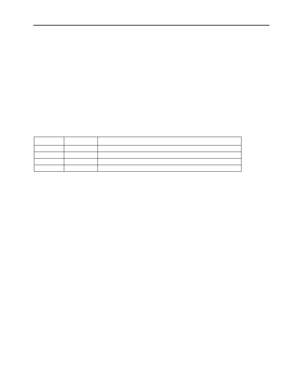
Agere Systems Inc.
75
Advance Data Sheet
September 2001
ATM Interconnect
CelXpres T8207
13
JTAG Test Access Port
A 5-pin test access port, consisting of the jtag_tclk, jtag_tms, jtag_tdi, jtag_tdo, and jtag_trst signals, provides the
standard interface to the test logic. The jtag_trst signal is active-low and resets the JTAG circuitry. When jtag_trst is
high, the JTAG interface is enabled. If the JTAG port is not used, jtag_trst should be tied low.
JTAG may be used only to test the inputs, outputs, and their connection to the printed-wiring board. In JTAG, serial
bit patterns are shifted into the device through the jtag_tdi pin, and the results can be observed at the I/O and at
the corresponding JTAG serial output, jtag_tdo. Since this JTAG conforms to the JTAG standard, the jtag_tdi and
jtag_tdo may be linked to the JTAG port of other devices for systemic testing. The boundary-scan description lan-
guage may be found on the Agere website.
13.1 Instruction Register
The instruction register (IR) is 3 bits in length. The instructions are defined in Table 21.
Table 21. Instruction Register
Instruction
Binary Code
Description
EXTEST
"000"
Places the boundary-scan register in extest mode.
SAMPLE
"001"
Places the boundary-scan register in sample mode.
Reserved
"010"--"110"
Reserved.
BYPASS
"111"
Places the bypass register in the scan chain.

76
Agere Systems Inc.
Advance Data Sheet
September 2001
ATM Interconnect
CelXpres T8207
13
JTAG Test Access Port
(continued)
13.2 Boundary-Scan Register
The boundary-scan register (BSR) is 222 bits in length. Table 22 gives descriptions of each cell in the boundary-
scan chain beginning with the least significant bit.
Table 22. Boundary-Scan Register Descriptions
Boundary-Scan
Register Bit
Name
Pin Name
Description
0--4
UA_N(0:4)
ua*[0:4]
Input.
5
ENARB_OE
--
ENARB is an input when ENARB_OE = 0.
6
ENARB
arb_enb*
Bidirectional.
7
CKOE_IN
--
CKO is high impedance when CKOE_IN = 0.
8
CKO
cko
3-statable output.
9
CKOE
cko_e
Input.
10
GPIO_OE(0)
--
GPIO(0) is an input when GPIO_OE(0) = 0.
11
GPIO(0)
gpio[0]
Bidirectional.
12
GPIO_OE(1)
--
GPIO(1) is an input when GPIO_OE(1) = 0.
13
GPIO(1)
gpio[1]
Bidirectional.
14
GPIO_OE(2)
--
GPIO(2) is an input when GPIO_OE(2) = 0.
15
GPIO(2)
gpio[2]
Bidirectional.
16
GPIO_OE(3)
--
GPIO(3) is an input when GPIO_OE(3) = 0.
17
GPIO(3)
gpio[3]
Bidirectional.
18
GPIO_OE(4)
--
GPIO(4) is an input when GPIO_OE(4) = 0.
19
GPIO(4)
gpio[4]
Bidirectional.
20
GPIO_OE(5)
--
GPIO(5) is an input when GPIO_OE(5) = 0.
21
GPIO(5)
gpio[5]
Bidirectional.
22
GPIO_OE(6)
--
GPIO(6) is an input when GPIO_OE(6) = 0.
23
GPIO(6)
gpio[6]
Bidirectional.
24
GPIO_OE(7)
--
GPIO(7) is an input when GPIO_OE(7) = 0.
25
GPIO(7)
gpio[7]
Bidirectional.
26
MUX
mux
Input.
27
RESET_N
reset*
Input.
28
CB_ACK_N
cb_ack*
Bidirectional.
29--60
CB_D_N(0:31)
cb_d*[0:31]
Bidirectional.
61
CB_F_N
cb_fs*
Bidirectional.
62
CB_DISBL
cb_disable* Input.
63
CB_RC_N
cb_rc*
Input.
64
CB_WC_N
cb_wc*
Input.
65--72
A(0:7)
a[0]/ale,
a[1:7]
Input.
73
D_OE
--
D(0:7) are inputs when D_OE = 0.
74--81
D(0:7)
d[0:7]
Bidirectional.
82
MOTO
mot_sel
Input.
83
RD_WR_N
rd*_rw*
Input.

Agere Systems Inc.
77
Advance Data Sheet
September 2001
ATM Interconnect
CelXpres T8207
13
JTAG Test Access Port
(continued)
Table 22
.
Boundary-Scan Register Descriptions (continued)
Boundary-Scan
Register Bit
Name
Pin Name
Description
84
RDY_DTACK_N_OE
--
RDYDTACK is high impedance when
RDY_DTACK_N_OE = 0.
85
RDYDTACK
rdy_dtack*
3-statable output.
86
SEL_N
sel*
Input.
87
WR_N
wr*_ds*
Input.
88
DEVHIZ_N_HIGH_DRIVE
--
INT_IRQ, SD_A(11:0), SD_BS(1:0), SD_CAS_N,
SD_RAS_N, and SD_WE_N are high impedance
when DEVHIZ_N_HIGH_DRIVE = 0.
89
INT_IRQ
int_irq*
3-statable output.
90--101
SD_A(0:11)
sd_a[0:11]
3-statable output.
102--103
SD_BS(0:1)
sd_bs[0:1]
3-statable output.
104
SD_CAS_N
sd_cas*
3-statable output.
105
SD_CLK_OE
--
SD_CLK is an input when SD_CLK_OE = 0.
106
SD_CLK
sd_clk
Bidirectional.
107
SD_D_OE
--
SD_D(15:0) are inputs when SD_D_OE = 0.
108--123
SD_D(0:15)
sd_d[0:15]
Bidirectional.
124
SD_RAS_N
sd_ras*
3-statable output.
125
SD_WE_N
sd_we*
3-statable output.
126
TR_CONT_OE
--
TR_OE_N, TR_WE_N, TR_A(17:0), and
TR_CS(1:0) are high impedance when
TR_CONT_OE = 0.
127
TR_OE_N
tr_oe*
3-statable output.
128
TR_WE_N
tr_we*
3-statable output.
129--146
TR_A(0:17)
tr_a[0:17]
3-statable output.
147--148
TR_CS(0:1)
tr_cs*[0:1]
3-statable output.
149
TR_D_OE
--
TR_D(7:0) are inputs when TR_D_OE = 0.
150--157
TR_D(0:7)
tr_d[0:7]
Bidirectional.
158
U_RXADDR_OE
--
U_RXADD(4:0) are inputs when U_RXADDR_OE
= 0.
159--163
U_RXADD(0:4)
u_rxaddr[0:4] Bidirectional.
164
U_RXCLAV0_OE
--
U_RXCLV0 is an input when U_RXCLAV0_OE =
0.
165
U_RXCLV0
u_rxclav[0]
Bidirectional.
166--168
U_RXCLV1--U_RXCLV3
u_rxclav[1:3] Input.
169
U_RXCLK_OE
--
U_RXCLK is an input when U_RXCLK_OE = 0.
170
U_RXCLK
T1
Bidirectional.
171--178
U_RXDAT(0:7)
u_rxdata[0:7] Input.
179
U_RXENB0_OE
--
U_RXENB(0) is an input when U_RXENB0_OE =
0.

78
Agere Systems Inc.
Advance Data Sheet
September 2001
ATM Interconnect
CelXpres T8207
13
JTAG Test Access Port
(continued)
Table 22
.
Boundary-Scan Register Descriptions (continued)
Boundary-Scan
Register Bit
Name
Pin Name
Description
180
U_RXENB(0)
u_rxenb*[0]
Bidirectional.
181
U_RXENB_OE
--
U_RXENB(3:1) are inputs when U_RXENB_OE =
0.
182--184
U_RXENB(1) ≠
U_RXENB(3)
u_rxenb*[1:3] Bidirectional.
185
U_RXPRTY
u_rxprty
Input.
186
U_RXSOC
u_rxsoc
Input.
187
U_SHR_I
u_shr_i
Input.
188
U_SHR_O_OE
--
U_SHR_O is an input when U_SHR_O_OE = 0.
189
U_SHR_O
u_shr_o
Bidirectional.
190
U_TXADDR_OE
--
U_TXADD(4:0) are inputs when U_TXADDR_OE
= 0.
191--195
U_TXADD(0:4)
u_txaddr[0:4]
Bidirectional.
196
U_TXCLAV0_OE
--
U_TXCLV0 is an input when U_TXCLAV0_OE =
0.
197
U_TXCLV0
u_txclav[0]
Bidirectional.
198--200
U_TXCLV1 ≠ U_TXCLV3
u_txclav[1:3]
Input.
201
U_TXCLK_OE
--
U_TXCLK is an input when U_TXCLK_OE = 0.
202
U_TXCLK
u_txclk
Bidirectional.
203
U_TXDATA_OE
--
U_TXDAT(7:0) are high impedance when
U_TXDATA_OE = 0.
204--211
U_TXDAT(0:7)
u_txdata[0:7]
3-statable output.
212
U_TXENB0_OE
--
U_TXENB0 is an input when U_TXENB0_OE = 0.
213
U_TXENB0
u_txenb*[0]
Bidirectional.
214
U_TXENB_OE
--
U_TXENB1, U_TXENB2, and U_TXENB3 are
high impedance when U_TXENB_OE = 0.
215--217
U_TXENB1 ≠ U_TXENB3
u_txenb*[1:3]
3-statable output.
218
U_TXPRTY_OE
--
U_TXPRTY is an input when U_TXPRTY_OE =
0.
219
U_TXPRTY
u_txprty
Bidirectional.
220
U_TXSOC_OE
--
U_TXSOC is high impedance when
U_TXSOC_OE = 0.
221
U_TXSOC
u_txsoc
3-statable output.

Agere Systems Inc.
79
Advance Data Sheet
September 2001
ATM Interconnect
CelXpres T8207
14
Registers
The T8207 has two distinct memory spaces, which are the direct memory access registers and the extended mem-
ory registers. The direct memory access registers are directly addressed 8-bit (byte) registers and are mapped
between addresses 00h and FFh. The extended memory registers are indirectly addressed and mapped between
addresses 0100h and 3FFFFFEh. The extended memory registers are mapped into three major blocks: the main
registers, the UTOPIA registers, and the SDRAM registers. They contain the SDRAM memory, the translation
RAM, internal memories, and the device's configuration, status, and control registers. Extended memory registers
are 16 bits wide. All accesses to the extended memory registers are executed internally as 16 bits. Direct memory
access registers are located in Section 14.2, Direct Memory Access Registers, and extended memory registers are
located in Section 14.3, Extended Memory Registers.
14.1 Register Types
Table 23. Register Map
Read/Write (RW):
These registers may be written or read.
Read Only (RO):
These registers may only be read.
Read-Only Latch (ROL):
The read-only latch is used for interrupt status registers. Reading a read-only latch
register has no effect on the contents. To clear a bit set in an ROL register, a one
must be written to the bit. Writing a zero to the bit has no effect. If the corresponding
interrupt enable bit is set, an interrupt will be continuously generated until the bit in
the ROL register is cleared.
Write Only (WO):
These registers may only be written. The write-only registers in the T8207 are a
pulse type. When they are written to one, they generate a pulse internally for one
clock cycle and then return to zero.
Register Name
Address (h)
Reference Page
Direct Configuration/Control Register (DCCR)
28h
83
Interrupt Service Request (ISREQ)
29h
84
mclk PLL Configuration 0 (MPLLCF0)
2Ah
84
mclk PLL Configuration 1 (MPLLCF1)
2Bh
85
GTL+ Slew Rate Configuration (GTLSRCF)
2Eh
85
GTL+ Control (GTLCNTRL)
2Fh
85
Extended Memory Address 1 (Little Endian) (EMA1_LE)
30h
86
Extended Memory Address 2 (Little Endian) (EMA2_LE)
31h
86
Extended Memory Address 3 (Little Endian) (EMA3_LE)
32h
86
Extended Memory Address 4 (Little Endian) (EMA4_LE)
33h
86
Extended Memory Access (Little Endian) (EMA_LE)
34h
86
Extended Memory Data Low (Little Endian) (EMDL_LE)
36h
87
Extended Memory Data High (Little Endian) (EMDH_LE)
37h
87
Extended Memory Address 4 (Big Endian) (EMA4_BE)
30h
88
Extended Memory Address 3 (Big Endian) (EMA3_BE)
31h
88
Extended Memory Address 2 (Big Endian) (EMA2_BE)
32h
88
Extended Memory Address 1 (Big Endian) (EMA1_BE)
33h
88
Extended Memory Access (Big Endian) (EMA_BE)
34h
89
Extended Memory Data High (Big Endian) (EMDH_BE)
36h
89
Extended Memory Data Low (Big Endian) (EMDL_BE)
37h
89
GPIO Output Enable (GPIO_OE)
39h
90
GPIO Output Value (GPIO_OV)
3Bh
90

80
Agere Systems Inc.
Advance Data Sheet
September 2001
ATM Interconnect
CelXpres T8207
14
Registers
(continued)
Table 23. Register Map (continued)
Register Name
Address (h)
Reference Page
GPIO Input Value (GPIO_IV)
3Dh
90
Control Cell Receive Direct Memory (CCRXDM)
60h to 93h
91
Control Cell Transmit Direct Memory (CCTXDM)
A0h to D7h
91
PHY Port 0 and Control Cells Multicast Direct Memory (PP0MDM)
E0h to FFh
92
Main Configuration 1 (MCF1)
0100h
93
Main Interrupt Status 1 (MIS1)
0102h
94
Main Interrupt Enable 1 (MIE1)
0104h
95
TX UTOPIA Clock Configuration (TXUCCF)
010Ch
96
RX UTOPIA Clock Configuration (RXUCCF)
010Eh
97
Main Configuration/Control (MCFCT)
0110h
98
Main Configuration 2 (MCF2)
0112h
99
UTOPIA Configuration (UCF)
0114h
100
Main Configuration 3 (MCF3)
0116h
100
Loopback
(LB) 0118h
101
UTOPIA Configuration 3 (UCF3)
011Ah
101
UTOPIA Configuration 2 (UCF2)
011Ch
101
Extended LUT Configuration (ELUTCF)
011Eh
101
Extended LUT Control (ELUTCN)
0120h
102
Cell Bus Configuration/Status (CBCFS)
0130h
103
Main Interrupt Status 2 (MIS2)
0132h
103
Main Interrupt Enable 2 (MIE2)
0134h
104
Misrouted LUT 1 (MLUT1)
0142h
105
Misrouted LUT 2 (MLUT2)
0144h
105
Misrouted Cell Header High (MCHH)
0146h
105
Misrouted Cell Header Low (MCHL)
0148h
105
Master Queue 3 (MQ3)
0158h
108
Master Queue 2 (MQ2)
015Ah
108
Master Queue 0 (MQ0)
015Ch
109
Master Queue 1 (MQ1)
015Eh
109
Slave Queue 0 (SQ0)
016Ch
110
Slave Queue 1 (SQ1)
016Eh
110
TX PHY FIFO Routing 3 (TXPFR3)
0178h
111
TX PHY FIFO Routing 2 (TXPFR2)
017Ah
112
TX PHY FIFO Routing 0 (TXPFR0)
017Ch
113
TX PHY FIFO Routing 1 (TXPFR1)
017Eh
114
Routing Information 1 (RI1)
0200h
115
Routing Information 2 (RI2)
0202h
116
Routing Information 3 (RI3)
0204h
117
PPD Information 1 (PPDI1)
0206h
118
PPD Information 2 (PPDI2)
0208h
119
PPD Information 3 (PPDI3)
020Ah
120
PPD Information 4 (PPDI4)
020Ch
121
PPD Information 5 (PPDI5)
020Eh
122

Agere Systems Inc.
81
Advance Data Sheet
September 2001
ATM Interconnect
CelXpres T8207
14
Registers
(continued)
Table 23. Register Map (continued)
Register Name
Address (h)
Reference Page
PPD Information 6 (PPDI6)
0210h
123
PPD Information 7 (PPDI7)
0212h
124
PPD Memory Write (PPDMW)
0418h
124
HEC Interrupt Status 1 (HIS1)
0302h
106
HEC Interrupt Enable 1 (HIE1)
0304h
106
HEC Interrupt Status (HIS)
0306h
106
HEC Interrupt Enable (HIE)
0308h
106
LUT Interrupt Service Request (LUTISR)
030Eh
106
LUT X Configuration/Status (LUTXCFS)
0320h to 033Eh
107
SDRAM Control (SCT)
0400h
128
SDRAM Interrupt Status (SIS)
0402h
128
SDRAM Interrupt Enable (SIE)
0404h
128
SDRAM Configuration (SCF)
0408h
129
Refresh (RFRSH)
0410h
130
Refresh Lateness (RFRSHL)
0412h
130
Idle State 1 (IS1)
0420h
130
Idle State 2 (IS2)
0422h
130
Manual Access State 1 (MAS1)
0424h
131
Manual Access State 2 (MAS2)
0426h
131
SDRAM Interrupt Service Request 4 (SISR4)
0438h
132
SDRAM Interrupt Service Request 3 (SISR3)
043Ah
132
SDRAM Interrupt Service Request 1 (SISR1)
043Ch
132
SDRAM Interrupt Service Request 2 (SISR2)
043Eh
132
Queue X (QX)
0440h to 04BEh
133
PHY Port X Transmit Count Structure (PPXTXCNT)
0600h to 067Ch
125
PHY Port X Receive Count Structure (PPXRXCNT)
0700h to 07F8h
126
LUT X Configuration 1 Structure (LUTXCF1)
0704h to 077Ch
127
Control Cell Receive Extended Memory (CCRXEM) 0
0800h to 0832h
137
Control Cell Transmit Extended Memory (CCTXEM)
0900h to 0936h
137
PHY Port 0 and Control Cells Multicast Extended Memory (PP0MEM)
0C00h to 0C1Eh
138
PHY Port X Multicast Memory (PPXMM)
0C20h to 0DE0h
139
PPD Memory (PPDM)
1000h to 13FEh
140
Queue X Definition Structure (QXDEF)
2000h to 27E0h
135
Translation RAM Memory (TRAM)
100000h to 17FFFEh
141
SDRAM (SDRAM)
2000000h to
3FFFFFEh
141
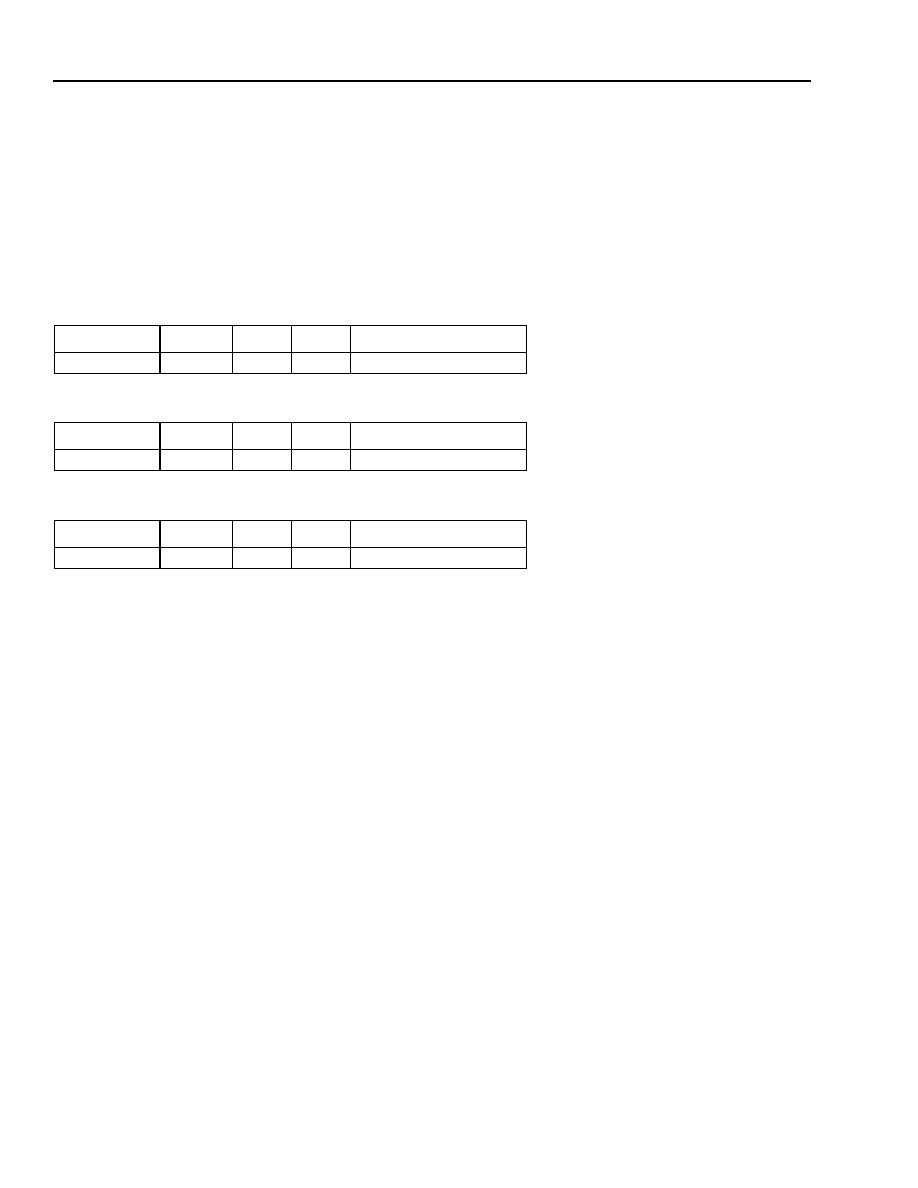
82
Agere Systems Inc.
Advance Data Sheet
September 2001
ATM Interconnect
CelXpres T8207
14
Registers
(continued)
14.2 Direct Memory Access Registers
The direct memory access registers are the only registers that can be directly addressed. These registers provide
some status and initial control of the device. In addition, the direct memory access register set includes some
extended memory access registers, which are used to indirectly access the extended memory registers. All unde-
fined addresses in the direct memory access registers' memory map, 00h to FFh, are reserved and should not be
accessed.
Table 24. Identification 0 (IDNT0) (00h)
Table 25. Identification 1 (IDNT1) (01h)
Table 26. Identification 2 (IDNT2) (02h)
1. RN represents the current revision number of the device.
Name
Bit Pos.
Type
Reset
Description
Device ID 0
7:0
RO
4Fh
Device Identification 0.
Name
Bit Pos.
Type
Reset
Description
Device ID 1
7:0
RO
07h
Device Identification 1.
Name
Bit Pos.
Type
Reset
Description
Device ID 2
7:0
RO
RN
1
Revision Number.

Agere Systems Inc.
83
Advance Data Sheet
September 2001
ATM Interconnect
CelXpres T8207
14
Registers
(continued)
Table 27. Direct Configuration/Control Register (DCCR) (28h)
Name
Bit Pos.
Type
Reset
Description
cyc_per_acc
0
RW
0
Cycles Per Access. This bit is used to indicate the number of cycles
per read/write to the translation RAM.
`0' = 2 mclk cycles.
`1' = 3 mclk cycles.
srst_reg*
1
RW
0
Software Reset Main Registers. A logic level zero on this bit resets
the main registers only. The direct memory access registers (including
this one) are not affected by this reset. This bit must be `0' while the
mclk PLL configuration 0 and 1 registers are being modified. Active-
low.
srst*
2
RW
0
Software Reset. A logic level zero on this bit resets the entire device
except the direct memory registers and the main registers. This bit
must be `0' while the mclk PLL configuration 0 and 1 registers are being
modified and clocks are not present. Active-low.
Reserved
3
RW
0
Reserved. This bit must be programmed to `1.'
rplc_gfc
4
RW
0
Replace GFC. If this bit is `1' and the device is in UNI mode, the GFC
field of incoming cells will be replaced during a VPI-VCI translation. If
this bit is `0' and the device is in UNI mode, the GFC field will be left
untouched. When the device is in NNI mode or when a VPI only trans-
lation is performed, this bit has no effect.
big_end
5
RW
0
Big Endian. If this bit is `0,' register fields in the direct address space,
30h to 37h, will be in little-endian format. If `1,' fields in the direct
address space, 30h to 37h, will be in big-endian format.
Reserved
7:6
RW
0
Reserved. These bits must be programmed to `0.'

84
Agere Systems Inc.
Advance Data Sheet
September 2001
ATM Interconnect
CelXpres T8207
14
Registers
(continued)
Table 28. Interrupt Service Request (ISREQ) (29h)
Table 29. mclk PLL Configuration 0 (MPLLCF0) (2Ah)
Name
Bit Pos.
Type
Reset
Description
Reserved
0
RO
0
Reserved.
int_serv_mainreg
1
RO
0
Interrupt Service Request for Main Registers. When this bit is
`1,' an interrupt in the main register group of the extended mem-
ory registers needs servicing. The control cell sent and control
cell available status bits do not affect this bit. Only enabled inter-
rupts will cause this bit to become set.
int_serv_sdramreg
2
RO
0
Interrupt Service Request for SDRAM Registers. When this bit
is `1,' an interrupt in the SDRAM register group of the extended
memory registers needs servicing. Only enabled interrupts will
cause this bit to become set.
int_serv_utopiareg
3
RO
0
Interrupt Service Request for UTOPIA Registers. When this bit
is `1,' an interrupt in the UTOPIA register group of the extended
memory registers needs servicing. Only enabled interrupts will
cause this bit to become set.
Reserved
4
RO
0
Reserved.
ctrl_cell_sent_sr
5
RO
0
Control Cell Sent Interrupt Service Request. When this bit is
`1,' the control cell sent interrupt in the main interrupt status 1
register needs servicing. The corresponding interrupt does not
need to be enabled for this bit to become set.
ctrl_cell_av_sr
6
RO
0
Control Cell Available Interrupt Service Request. When this
bit is `1,' the control cell available interrupt in the main interrupt
status 1 register needs servicing. The corresponding interrupt
does not need to be enabled for this bit to become set.
Reserved
7
RO
0
Reserved.
Name
Bit Pos.
Type
Reset
Description
lf[3:0]
3:0
RW
0
Loop Filter. See Section 5, PLL Configuration, for information on
these bits.
Reserved
5:4
RO
0
Reserved.
bypb
6
RW
0
Bypass PLL. If this bit is `0,' the PLL is bypassed. If `1,' the output
of the PLL supplies mclk.
pllen
7
RW
0
PLL Enable. If this bit is `1,' the PLL is enabled. If `0,' the PLL is
disabled.

Agere Systems Inc.
85
Advance Data Sheet
September 2001
ATM Interconnect
CelXpres T8207
14
Registers
(continued)
Table 30. mclk PLL Configuration 1 (MPLLCF1) (2Bh)
Table 31. GTL+ Slew Rate Configuration (GTLSRCF) (2Eh)
Table 32. GTL+ Control (GTLCNTRL) (2Fh)
Name
Bit Pos.
Type
Reset
Description
pll_m[4:0]
4:0
RW
0
PLL M Count Value. See Section 5, PLL Configuration, for informa-
tion on these bits.
pll_n[2:0]
7:5
RW
0
PLL N Count Value. See Section 5, PLL Configuration, for informa-
tion on these bits.
Name
Bit Pos.
Type
Reset
Description
slew_rate[2:0]
2:0
RW
4h
GTL+ Slew Rate Control [2:0]. The slew rates of the GTL+ (cell bus)
output signals are controlled by these bits. The minimum slew rate
time is 0.9 ns and the maximum slew rate time is 3.8 ns.
"000" = Fastest slew rate
"001"
"010"
"011" = Nominal slew rate (on fast side)
"100" = Nominal slew rate (on slow side)
"101"
"110"
"111" = Slowest slew rate
Reserved
3
RW
1
Reserved. Program to `1.'
Reserved
7:4
RW
0
Reserved. Program to `0.'
Name
Bit Pos.
Type
Reset
Description
Reserved
0
R
1
Reserved. Program to `1.'
GTLRPDN
1
RW
1
GTL+ Receive Powerdown. When this bit is cleared to `0,' the
GTL+ receivers on the cell bus pins are powered down. Under
this condition, no cells can be received from the backplane.
When this bit is set to `1,' the GTL+ receivers are powered up
and cells are received from the backplane.
GTLTPDN
2
RW
1
GTL+ Transmit Powerdown. When this bit is cleared to `0,'
the GTL+ transmitters on the cell bus pins are powered down.
Under this condition, no cells can be transmitted to the back-
plane.
When this bit is set to `1,' the GTL+ transmitters are powered
up and cells are transmitted to the backplane.
Reserved
4:3
R
0
Reserved. Program to `0.'
Reserved
5
R
1
Reserved. Program to `1.'
Reserved
7:6
R
0
Reserved. Program to `0.'

86
Agere Systems Inc.
Advance Data Sheet
September 2001
ATM Interconnect
CelXpres T8207
14
Registers
(continued)
14.2.1 Little-Endian Format (big_end = 0) for Extended Memory Access Registers 30h--37h
Table 33. Extended Memory Address 1 (Little Endian) (EMA1_LE) (30h)
Table 34. Extended Memory Address 2 (Little Endian) (EMA2_LE) (31h)
Table 35. Extended Memory Address 3 (Little Endian) (EMA3_LE) (32h)
Table 36. Extended Memory Address 4 (Little Endian) (EMA4_LE) (33h)
Table 37. Extended Memory Access (Little Endian) (EMA_LE) (34h)
Name
Bit Pos.
Type
Reset
Description
Reserved
4:0
RO
0
Reserved.
ext_a[8:6]
7:5
RW
0
Extended Access Address [8:6]. This extended access register
points to words.
Name
Bit Pos.
Type
Reset
Description
ext_a[16:9]
7:0
RW
0
Extended Access Address [16:9]. This extended access register
points to words.
Name
Bit Pos.
Type
Reset
Description
ext_a[24:17]
7:0
RW
0
Extended Access Address [24:17]. This extended access register
points to words.
Name
Bit Pos.
Type
Reset
Description
ext_a[25]
0
RW
0
Extended Access Address [25]. This extended access register
points to words.
Reserved
7:1
RO
0
Reserved.
Name
Bit Pos.
Type
Reset
Description
ext_a[5:1]
4:0
RW
0
Extended Access Address [5:1]. This extended access register
points to words. ext_a[0] is hardwired to `0.'
ext_we[1:0]
6:5
RW
0
Extended Access Write Enable. These bits are active-high write
enables for word accesses. If both bits are low, a read is performed. If
ext_we[1] is high, the contents of ext_d[15:8] are written, and if
ext_we[0] is high, the contents of ext_d[7:0] are written. If both bits are
high, both data bytes are written.
ext_strt_acc
7
RW
0
Start Access to Extended Memory. Write a `1' to this bit to start the
access to the extended memory registers. This bit is automatically
cleared when the access is complete.
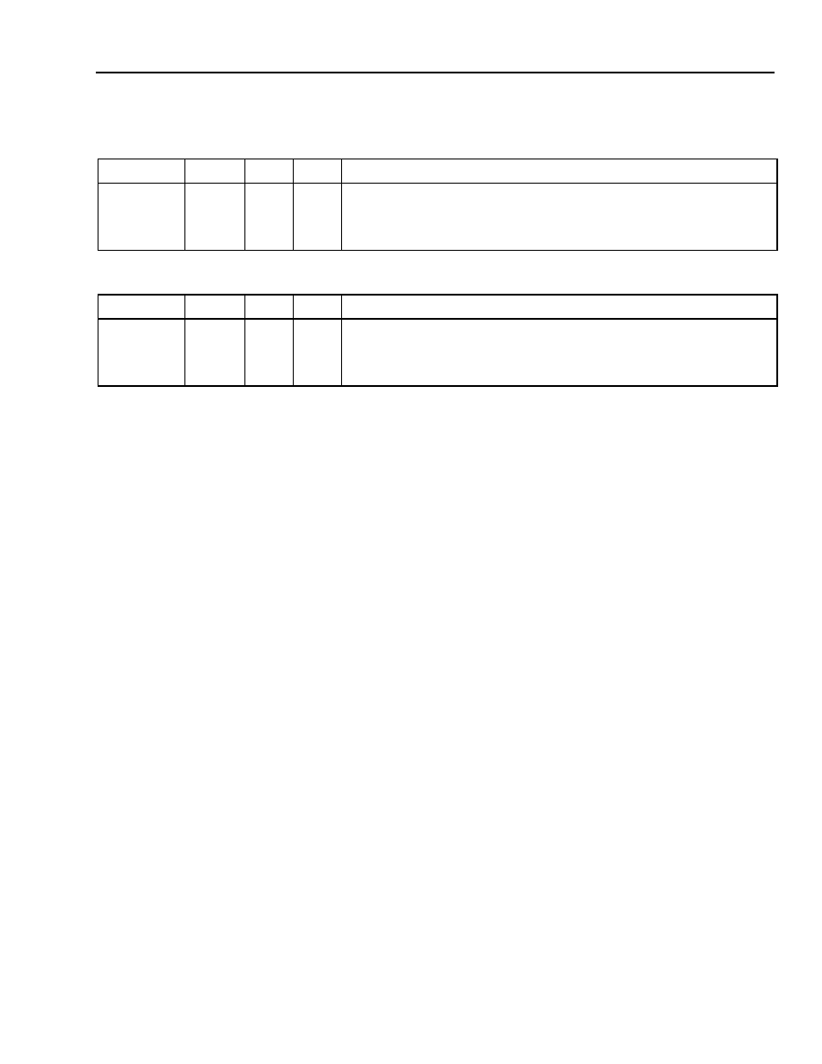
Agere Systems Inc.
87
Advance Data Sheet
September 2001
ATM Interconnect
CelXpres T8207
14
Registers
(continued)
Table 38. Extended Memory Data Low (Little Endian) (EMDL_LE) (36h)
Table 39. Extended Memory Data High (Little Endian) (EMDH_LE) (37h)
Name
Bit Pos.
Type
Reset
Description
ext_d[7:0]
7:0
RW
0
Extended Access Data Low. The least significant byte of data to be
written to extended memory is written here before the extended write
begins. The least significant byte of data read from extended memory is
available here after the extended read is complete.
Name
Bit Pos.
Type
Reset
Description
ext_d[15:8]
7:0
RW
0
Extended Access Data High. The most significant byte of data to be
written to extended memory is written here before the extended write
begins. The most significant byte of data read from extended memory is
available here after the extended read is complete.
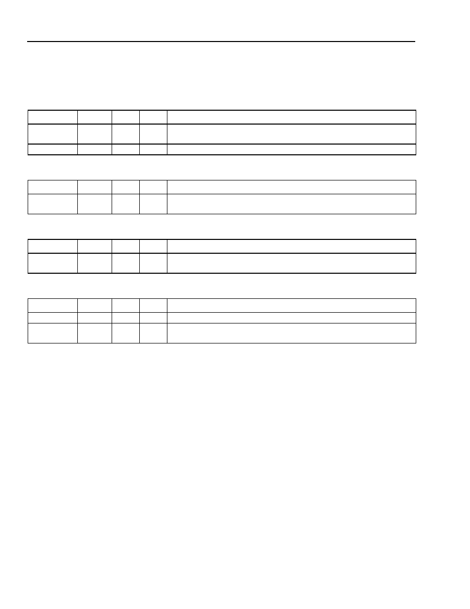
88
Agere Systems Inc.
Advance Data Sheet
September 2001
ATM Interconnect
CelXpres T8207
14
Registers
(continued)
14.2.2 Big-Endian Format (big_end = 1) for Extended Memory Access Registers 30h--37h
Table 40. Extended Memory Address 4 (Big Endian) (EMA4_BE) (30h)
Table 41. Extended Memory Address 3 (Big Endian) (EMA3_BE) (31h)
Table 42. Extended Memory Address 2 (Big Endian) (EMA2_BE) (32h)
Table 43. Extended Memory Address 1 (Big Endian) (EMA1_BE) (33h)
Name
Bit Pos.
Type
Reset
Description
ext_a[25]
0
RW
0
Extended Access Address [25]. This extended access register points
to words.
Reserved
7:1
RO
0
Reserved.
Name
Bit Pos.
Type
Reset
Description
ext_a[24:17]
7:0
RW
0
Extended Access Address [24:17]. This extended access register
points to words.
Name
Bit Pos.
Type
Reset
Description
ext_a[16:9]
7:0
RW
0
Extended Access Address [16:9]. This extended access register
points to words.
Name
Bit Pos.
Type
Reset
Description
Reserved
4:0
RO
0
Reserved.
ext_a[8:6]
7:5
RW
0
Extended Access Address [8:6]. This extended access register points
to words.
Agere Systems Inc.
89
Advance Data Sheet
September 2001
ATM Interconnect
CelXpres T8207
14
Registers
(continued)
Table 44. Extended Memory Access (Big Endian) (EMA_BE) (34h)
Table 45. Extended Memory Data High (Big Endian) (EMDH_BE) (36h)
Table 46. Extended Memory Data Low (Big Endian) (EMDL_BE) (37h)
Name
Bit Pos.
Type
Reset
Description
ext_a[5:1]
4:0
RW
0
Extended Access Address [5:1]. This extended access register points
to words. ext_a[0] is hardwired to `0.'
ext_we[1:0]
6:5
RW
0
Extended Access Write Enable. These bits are active-high write
enables for word accesses. If both bits are low, a read is performed. If
ext_we[1] is high, the contents of ext_d[15:8] are written, and if
ext_we[0] is high, the contents of ext_d[7:0] are written. If both bits are
high, both data bytes are written.
ext_strt_acc
7
RW
0
Start Access to Extended Memory. Write a `1' to this bit to start the
access to the extended memory registers. This bit is automatically
cleared when the access is complete.
Name
Bit Pos.
Type
Reset
Description
ext_d[15:8]
7:0
RW
0
Extended Access Data High. The most significant byte of data to be
written to extended memory is written here before the extended write
begins. The most significant byte of data read from extended memory is
available here after the extended read is complete.
Name
Bit
Pos.
Type
Reset
Description
ext_d[7:0]
7:0
RW
0
Extended Access Data Low. The least significant byte of data to be
written to extended memory is written here before the extended write
begins. The least significant byte of data read from extended memory is
available here after the extended read is complete.
90
Agere Systems Inc.
Advance Data Sheet
September 2001
ATM Interconnect
CelXpres T8207
14
Registers
(continued)
14.2.3 General-Purpose I/O Control Registers
Table 47. GPIO Output Enable (GPIO_OE) (39h)
Table 48. GPIO Output Value (GPIO_OV) (3Bh)
Table 49. GPIO Input Value (GPIO_IV) (3Dh)
Name
Bit Pos.
Type
Reset
Description
GPIO_oe[7:0]
7:0
RW
0
GPIO Output Enable. If this bit is set to `1,' the corresponding GPIO
pin is an output. If cleared to `0,' the corresponding GPIO pin is an
input.
Name
Bit Pos.
Type
Reset
Description
GPIO_out[7:0]
7:0
RW
0
GPIO Output Buffer. Output bits for the GPIO[7:0] pins are written to
this buffer. A bit in this buffer is only written to the pin if the corre-
sponding output enable bit is high.
Name
Bit Pos.
Type
Reset
Description
GPIO_in[7:0]
7:0
RO
0
GPIO Input Buffer. This buffer contains the values at the GPIO[7:0]
pins.

Agere Systems Inc.
91
Advance Data Sheet
September 2001
ATM Interconnect
CelXpres T8207
14
Registers
(continued)
14.2.4 Control Cells
Table 50. Control Cell Receive Direct Memory (CCRXDM) (60h to 93h)
The control cell receive memory may also be accessed from extended memory. See Table 120.
Table 51. Control Cell Transmit Direct Memory (CCTXDM) (A0h to D7h)
The control cell transmit memory may also be accessed from extended memory. See Table 121.
Name
Offset Type
Reset
Description
header[31:24]
00h
RO
X
These 52 bytes are the control cell received from the
cell bus. This memory space in direct memory is a
shadow of the control cell receive extended memory.
When present, the control cell should be read from
this direct memory space.
header[23:16]
01h
header[15:8]
02h
header[7:0]
03h
payload_byte0
04h
payload_byte1
05h
.
.
.
.
.
.
payload_byte46
32h
payload_byte47
33h
Name
Offset
Type Reset
Description
cell_bus_routing_header[15:8]
00h
RW
X
These 56 bytes are the cell routing header, the tan-
dem routing header, and the control cell to be trans-
mitted onto the cell bus. This memory space in direct
memory is a shadow of the control cell transmit
extended memory. A control cell to be transmitted
should be written to this direct memory space.
cell_bus_routing_header[7:0]
01h
tandem_routing_header[15:8]
02h
tandem_routing_header[7:0]
03h
header[31:24]
04h
header[23:16]
05h
header[15:8]
06h
header[7:0]
07h
payload_byte0
08h
payload_byte1
09h
.
.
.
.
.
.
payload_byte46
36h
payload_byte47
37h
92
Agere Systems Inc.
Advance Data Sheet
September 2001
ATM Interconnect
CelXpres T8207
14
Registers
(continued)
14.2.5 Multicast Memories
Table 52. PHY Port 0 and Control Cells Multicast Direct Memory (PP0MDM) (E0h to FFh)
The PHY port 0 and control cells multicast memory may also be accessed from extended memory (see Table 122).
Name
Offset Type Reset
Description
multicast_receive_enable[15:0]
00h
RW
X
This memory space contains 256 active-high
enable bits. Each bit represents a multicast net
number from 0 through 255. If a bit is set, the cor-
responding multicast addressed data cell is sent to
the queue group for PHY port 0, or the corre-
sponding multicast control cell is sent to the control
cell receive direct and extended memory. The
least significant bit is multicast net number 0. This
memory space in direct memory is a shadow of the
PHY port 0 and control cells multicast extended
memory space.
multicast_receive_enable[31:16]
02h
multicast_receive_enable[47:32]
04h
.
.
.
.
.
.
multicast_receive_enable[159:144]
12h
multicast_receive_enable[175:160]
14h
multicast_receive_enable[191:176]
16h
multicast_receive_enable[207:192]
18h
multicast_receive_enable[223:208]
1Ah
multicast_receive_enable[239:224]
1Ch
multicast_receive_enable[255:240]
1Eh

Agere Systems Inc. 93
Advance Data Sheet
September 2001
ATM Interconnect
CelXpres T8207
14
Registers
(continued)
14.3 Extended Memory Registers
The
CelXpres
T8207's extended memory registers are mapped into three major blocks: the main registers, the
UTOPIA registers, and the SDRAM registers.
14.3.1 Main Registers
Table 53. Main Configuration 1 (MCF1) (0100h)
Name Bit Pos.
Type Reset Description
Reserved 7:0 RO 00h Reserved.
tx_utopia_hi_z 8 RW 0 Transmit UTOPIA High Impedance. When the device is in ATM
and shared UTOPIA mode, this bit must be cleared to `0':
s
For the slave device, the u_txsoc output will always be high
impedance while the u_txdata[7:0] and u_txprty outputs go high
impedance when not active.
s
For the master device, the u_txdata[7:0] and u_txprty outputs go
high impedance when not active.
When the device is in ATM and nonshared UTOPIA mode and this
bit is cleared to `0,' the u_txdata[7:0] and u_txprty outputs go high
impedance when not active.
When the device is in PHY mode and this bit is cleared to `0,' the
u_txsoc, u_txdata[7:0], and u_txprty outputs go high impedance
when not active. If the device acts as one of the multi-PHY
devices, then this bit must be cleared to `0.'
When this bit is set to `1,' the u_txsoc, u_txdata[7:0], and u_txprty
outputs never go high impedance.
sdram_bypass 9
RW
0
SDRAM Bypass. When this bit is `1,' the T8207 will not use
SDRAM and will use only internal memory to buffer cell bus data.
Clear this bit to enable the SDRAM interface. Only queue 0 is used
when the SDRAM is bypassed.
phyen 10 RW 1 PHY Enable. When this bit is `1,' the UTOPIA bus is configured for
ATM mode. When `0,' the UTOPIA bus is configured for PHY
mode.
tram_qnty_sel 11 RW 0 Translation RAM Quantity Select. When two external SRAM
devices are used, this bit should be set. When this bit is cleared,
only one external SRAM will be accessed using tr_cs*[0].
sp_utopia_sel 12 RW 1 Special UTOPIA Mode Select. When this bit is `1,' the T8207 will
send 53-byte cells on the UTOPIA bus. When it is `0,' the 55-byte
UTOPIA mode is selected, and the tandem routing header bytes
will be appended to the beginning of each cell.
tram_size 14:13 RW 0 Translation RAM Size. These bits identify the size of the external
SRAM used for the look-up table RAM.
"00" = 32K bytes
"01" = 64K bytes
"10" = 128K bytes
"11" = 256K bytes
Reserved 15 RW 0 Reserved. Program to `0.'

94
Agere Systems Inc.
Advance Data Sheet
September 2001
ATM Interconnect
CelXpres T8207
14
Registers
(continued)
Table 54. Main Interrupt Status 1 (MIS1) (0102h)
Note: Immediately following device setup, write FFFFh to this register to clear erroneously set bits.
Name
Bit Pos.
Type
Reset
Description
cb_wc_miss
0
ROL
0
Cell Bus Write Clock Missing. This bit is set when the cell bus write
clock is inactive for 32 mclk cycles. An interrupt is generated if the cor-
responding enable bit is set.
cb_rc_miss
1
ROL
0
Cell Bus Read Clock Missing. This bit is set when the cell bus read
clock is inactive for 32 mclk cycles. An interrupt is generated if the cor-
responding enable bit is set.
cb_fs_miss
2
ROL
0
Cell Bus Frame Synchronization Signal Missing. This bit is set
when the cell bus frame sync is not asserted every 16 read clock
cycles in 16-user mode, or every 32 read clock cycles in 32-user
mode. It is also set when cell bus write clock is not present because
the frame synchronization signal is clocked onto the cell bus by the
write clock. An interrupt is generated if the corresponding enable bit is
set.
BIP8_err
3
ROL
0
Bit Interleave Parity Error. This bit is set when an error is detected in
the BIP-8 field of the last cell bus frame cycle. An interrupt is gener-
ated if the corresponding enable bit is set.
ctrl_cell_ack
4
ROL
0
Control Cell Acknowledged. This bit is set when a control cell is
sent on the cell bus and an acknowledge is received. This bit is not
set for broadcast or multicast cells. An interrupt is generated if the cor-
responding enable bit is set.
ctrl_cell_nack
5
ROL
0
Control Cell Not Acknowledged. This bit is set when a control cell is
sent on the cell bus and an acknowledge is not received. This bit is
not set for broadcast or multicast cells. An interrupt is generated if the
corresponding enable bit is set.
cb_grnt_to
6
ROL
0
Cell Bus Grant Time-Out. This bit is set when a cell bus request has
not been granted within the time programmed in the cb_req_to bits.
An interrupt is generated if the corresponding enable bit is set.
ctrl_cell_sent
7
ROL
0
Control Cell Sent. This bit is set when a control cell is sent onto the
cell bus. An interrupt is generated if the corresponding enable bit is
set.
ctrl_cell_av
8
ROL
0
Control Cell Available. This bit is set when a control cell is waiting to
be read by the microprocessor. An interrupt is generated if the corre-
sponding enable bit is set.
cb_rh_crc_err
9
ROL
0
Cell Bus Routing Header CRC Error. This bit is set when an error is
detected in the CRC field of the cell bus routing header. An interrupt is
generated if the corresponding enable bit is set.
rx_prty_err
10
ROL
0
Receive Parity Error. This bit is set when the odd parity calculated
over the data received on the RX UTOPIA port does not match the
u_rxprty signal. An interrupt is generated if the corresponding enable
bit is set. When a receive parity error occurs, the cell is still counted as
received and is translated and routed.
soc_err
11
ROL
0
Start of Cell Error. This bit is set when a SOC framing error is
detected on the RX UTOPIA port. An interrupt is generated if the cor-
responding enable bit is set. When a start of cell error occurs, the
received cells are dropped.
Reserved
15:12
RO
0
Reserved.

Agere Systems Inc.
95
Advance Data Sheet
September 2001
ATM Interconnect
CelXpres T8207
14
Registers
(continued)
Table 55. Main Interrupt Enable 1 (MIE1) (0104h)
Name
Bit Pos. Type Reset
Description
cb_wc_miss_ie
0
RW
0
Cell Bus Write Clock Missing Interrupt Enable. An interrupt is
generated if this bit and the corresponding status bit are set. The
interrupt is generated until this bit or the corresponding status bit is
reset.
cb_rc_miss_ie
1
RW
0
Cell Bus Read Clock Missing Interrupt Enable. An interrupt is
generated if this bit and the corresponding status bit are set. The
interrupt is generated until this bit or the corresponding status bit is
reset.
cb_fs_miss_ie
2
RW
0
Cell Bus Frame Synchronization Signal Missing Interrupt
Enable. An interrupt is generated if this bit and the corresponding
status bit are set. The interrupt is generated until this bit or the cor-
responding status bit is reset.
BIP8_err_ie
3
RW
0
Bit Interleave Parity Error Interrupt Enable. An interrupt is gener-
ated if this bit and the corresponding status bit are set. The interrupt
is generated until this bit or the corresponding status bit is reset.
ctrl_cell_ack_ie
4
RW
0
Control Cell Acknowledged Interrupt Enable. An interrupt is gen-
erated if this bit and the corresponding status bit are set. The inter-
rupt is generated until this bit or the corresponding status bit is reset.
ctrl_cell_nack_ie
5
RW
0
Control Cell Not Acknowledged Interrupt Enable. An interrupt is
generated if this bit and the corresponding status bit are set. The
interrupt is generated until this bit or the corresponding status bit is
reset.
cb_grnt_to_ie
6
RW
0
Cell Bus Grant Time-Out Interrupt Enable. An interrupt is gener-
ated if this bit and the corresponding status bit are set. The interrupt
is generated until this bit or the corresponding status bit is reset.
ctrl_cell_sent_ie
7
RW
0
Control Cell Sent Interrupt Enable. An interrupt is generated if this
bit and the corresponding status bit are set. The interrupt is gener-
ated until this bit or the corresponding status bit is reset.
ctrl_cell_av_ie
8
RW
0
Control Cell Available Interrupt Enable. An interrupt is generated
if this bit and the corresponding status bit are set. The interrupt is
generated until this bit or the corresponding status bit is reset.
cb_rh_crc_err_ie
9
RW
0
Cell Bus Routing Header CRC Error Interrupt Enable. An inter-
rupt is generated if this bit and the corresponding status bit are set.
The interrupt is generated until this bit or the corresponding status
bit is reset.
rx_prty_err_ie
10
RW
0
Receive Parity Error Interrupt Enable. An interrupt is generated if
this bit and the corresponding status bit are set. The interrupt is gen-
erated until this bit or the corresponding status bit is reset.
soc_err_ie
11
RW
0
Start of Cell Error Interrupt Enable. An interrupt is generated if
this bit and the corresponding status bit are set. The interrupt is gen-
erated until this bit or the corresponding status bit is reset.
Reserved
15:12
RO
0
Reserved.

96
Agere Systems Inc.
Advance Data Sheet
September 2001
ATM Interconnect
CelXpres T8207
14
Registers
(continued)
Table 56. TX UTOPIA Clock Configuration (TXUCCF) (010Ch)
Name
Bit Pos. Type Reset
Description
tx_utopia_clk_div
7:0
RW
01h
TX UTOPIA Clock Division. The selected TX UTOPIA clock
source is divided by the number programmed in these bits as
follows:
"00000000" = reserved
"00000001" = no division
"00000010" = divide by 2
"00000011" = divide by 3
.
.
.
"11111111" = divide by 255
These bits are meaningful only when the T8207 generates the
TX UTOPIA clock.
tx_utopia_clk_src_sel
9:8
RW
0
TX UTOPIA Clock Source Select. The source of the TX
UTOPIA clock is selected via these bits as follows:
"00" = cell bus write clock
"01" = reserved
"10" = pclk
"11" = mclk
These bits are meaningful only when the T8207 generates the
TX UTOPIA clock.
Reserved
10
RW
0
Reserved. Program to `0.'
tx_utopia_clk_en
11
RW
0
TX UTOPIA Clock Enable. If this bit is `1,' the T8207 gener-
ates the TX UTOPIA clock on the u_txclk pin. If this bit is `0,'
the u_txclk pin is configured as an input.
Reserved
15:12
RO
0
Reserved.

Agere Systems Inc.
97
Advance Data Sheet
September 2001
ATM Interconnect
CelXpres T8207
14
Registers
(continued)
Table 57. RX UTOPIA Clock Configuration (RXUCCF) (010Eh)
Name
Bit Pos. Type Reset
Description
rx_utopia_clk_div
7:0
RW
01h
RX UTOPIA Clock Division. The selected RX UTOPIA clock
source is divided by the number programmed in these bits as
follows:
"00000000" = reserved
"00000001" = no division
"00000010" = divide by 2
"00000011" = divide by 3
.
.
.
"11111111" = divide by 255
These bits are meaningful only when the T8207 generates the
RX UTOPIA clock.
rx_utopia_clk_src_sel
9:8
RW
0
RX UTOPIA Clock Source Select. The source of the RX
UTOPIA clock is selected via these bits as follows:
"00" = cell bus write clock
"01" = reserved
"10" = pclk
"11" = mclk
These bits are meaningful only when the T8207 generates the
RX UTOPIA clock.
Reserved
10
RW
0
Reserved. Program to `0.'
rx_utopia_clk_en
11
RW
0
RX UTOPIA Clock Enable. If this bit is `1,' the T8207 gener-
ates the RX UTOPIA clock on the u_rxclk pin. If this bit is `0,'
the u_rxclk pin is configured as an input.
Reserved
15:12
RO
0
Reserved.

98
Agere Systems Inc.
Advance Data Sheet
September 2001
ATM Interconnect
CelXpres T8207
14
Registers
(continued)
Table 58. Main Configuration/Control (MCFCT) (0110h)
Table 59. Main Configuration 2 (MCF2) (0112h)
Name
Bit Pos.
Type
Reset
Description
cntl_cell_rd
0
WO
0
Control Cell Has Been Read. Write `1' to this bit after a control
cell is read from the control cell FIFO. The `1' will pulse for one
clock cycle and will clear to `0' automatically.
cntl_cell_wr
1
RW
0
Control Cell Written in Control Cell Memory. Write `1' to this bit
after a control cell is written in the control cell memory. This bit is
automatically cleared when the cell is transmitted to the cell bus.
cb_req_pr
3:2
RW
0
Cell Bus Request Priority. These bits indicate the priority of stan-
dard requests sent on the cell bus as follows:
"00" = disabled, receives cells from cell bus but cannot transmit
"01" = low priority
"10" = medium priority
"11" = high priority
clp_fill_limit
10:4
RW
0
CLP Fill Limit. These bits indicate the TX PHY FIFO fill level at
which cells with their CLP bit set to one will be discarded.
cell_drop_en
11
RW
0
Cell Drop Enable. If this bit is one, incoming cells with their CLP
bit set to one will be discarded when the TX PHY FIFO fill limit pro-
grammed in the clp_fill_limit bits is reached.
inv_crc
12
RW
0
Invert CRC. If this bit is one, the CRC-4 in the routing header is
inverted before transmission to the cell bus. This bit is used to sim-
ulate errors.
cb_rx_en
13
RW
0
Cell Bus Receive Enable. If this bit is `1,' cells are received from
the cell bus. If `0,' cells are not accepted.
slave_en
14
RW
1
Slave Enable. If this bit is `1,' the T8207 is configured as a slave in
shared UTOPIA mode. The default value of this bit is `1.' Clear this
bit if shared UTOPIA is not used. For shared UTOPIA, only one of
the two devices may have this bit cleared. Dynamically changing
this bit will cause cell loss. When this bit is `1,' u_rxenb*[0] and
u_rxenb*[3:1] become inputs.
Reserved
15
RO
0
Reserved.
Name
Bit Pos.
Type
Reset
Description
addr_clav_en
2:0
RW
0
UTOPIA Address, Cell Available, and Enable Signals. These bits
configure the number of address, cell available, and enable signals
on the UTOPIA bus as follows (see Section 9.6 on page 50):
"000" = 0 ADDR, 4 CLAV, 4 ENB
"001" = 4 ADDR, 1 CLAV, 1 ENB
"010" = 1 ADDR, 4 CLAV, 4 ENB
"011" = 4 ADDR, 2 CLAV, 2 ENB
"100" = 2 ADDR, 2 CLAV, 2 ENB
"101" = 2 ADDR, 4 CLAV, 4 ENB
"110" = 3 ADDR, 1 CLAV, 1 ENB
"111" = 3 ADDR, 2 CLAV, 2 ENB
Reserved
3
RO
0
Reserved.

Agere Systems Inc.
99
Advance Data Sheet
September 2001
ATM Interconnect
CelXpres T8207
14
Registers
(continued)
Table 59. Main Configuration 2 (MCF2) (0112h) (continued)
Name
Bit Pos.
Type
Reset
Description
T8207_sel
4
RW
0
T8207 Select Bit. This bit should be programmed to `1' to obtain all of the
T8207 features. If this bit is programmed to `0,' the two additional div_queue
bit settings ("100" and "101") affect its operation. If div_queue is pro-
grammed to "100" and the T8207_sel bit is `0,' the TX UTOPIA cell buffer is
divided into 64 queues, but only 32 are used. In addition, if this bit is pro-
grammed to `0,' the UTOPIA Configuration 3 (011Ah) (Table 63), Master
Queue 3 (0158h) (Table 80), Master Queue 2 (015Ah) (Table 81), TX PHY
FIFO Routing 3 (0178h) (Table 86), and TX PHY FIFO Routing 2 (017Ah)
(Table 87) registers do not need to be programmed.
dont_inhibit_rxphy
_clav
5
RW
0
Don't Inhibit RX PHY_CLAV. This bit, when set to `1,' keeps the rx_clav sig-
nal always asserted high, indicating the capability to accept cells even if the
RX UTOPIA FIFO could overrun, or is actually overrun. This bit is valid only
when the RX UTOPIA is in PHY mode.
When this bit is cleared to `0,' the rx_clav signal is deasserted if the RX
UTOPIA FIFO is considered full.
inhibit_rxuto_fifo_
overrun
6
RW
0
Inhibit RX UTOPIA FIFO Overrun. This bit, when set to `1,' prevents the RX
UTOPIA FIFO from overflowing by deasserting its rx_enb* signal, even
though the rx_clav signal is high when polled, if the RX UTOPIA FIFO is
considered full. It is considered full when four cells are stored in it that have
not yet been read and processed by the T8207. This bit is valid when the RX
UTOPIA is in ATM mode.
When this bit is cleared to `0,' the rx_enb* signal is not deasserted even if
the RX UTOPIA FIFO is considered full.
Reserved
7:5
RO
0
Reserved.
div_queue
10:8
RW
0
Divide into Queues. These bits indicate the number of queues used in the
TX UTOPIA cell buffer as follows:
"000" = 4 queues--32 cells per queue
"001" = 8 queues--16 cells per queue
"010" = 16 queues--8 cells per queue
"011" = 32 queues--4 cells per queue
"100" = 64 queues--2 cells per queue
"101" = 1 queue--128 cells per queue
When the T8207 is configured to UTOPIA level 1 ATM mode or when it is
configured for PHY mode, the number of queues selected should be one to
maximize cell buffering.
T8207_sel = 1 (up to 32 PHYs are supported):
When the device is configured to UTOPIA level 2 ATM mode and is con-
nected to multiple PHY ports, each PHY port uses four queues unless 32
PHY ports are selected. If 32 PHY ports are selected, each PHY port uses
two queues. Therefore, for 16 or less PHY ports, selecting four queues will
provide only for PHY port 0, selecting eight queues will provide only for PHY
ports 0 and 1, and so on. For 32 PHY ports, selecting four queues will pro-
vide only for PHY ports 0 and 1, selecting eight queues will provide only for
PHY ports 0, 1, 2, and 3, and so on.
T8207_sel = 0 (up to 16 PHYs are supported):
When the device is configured to UTOPIA level 2 ATM mode and is con-
nected to multiple PHY ports, each PHY port uses four queues unless 16
PHY ports are selected. If 16 PHY ports are selected, each PHY port uses
two queues. Therefore, for 8 or less PHY ports, selecting four queues will
provide only for PHY port 0, selecting eight queues will provide only for PHY
ports 0 and 2, and so on. For 16 PHY ports, selecting four queues will pro-
vide only for PHY ports 0 and 1, selecting eight queues will provide only for
PHY ports 0, 1, 2, and 3, and so on.
Reserved
14:11
RO
0
Reserved.
Reserved
15
RW
0
Reserved. Program this bit to `1.'

100
Agere Systems Inc.
Advance Data Sheet
September 2001
ATM Interconnect
CelXpres T8207
14
Registers
(continued)
Table 60. UTOPIA Configuration (UCF) (0114h)
Table 61. Main Configuration 3 (MCF3) (0116h)
Name
Bit Pos.
Type
Reset
Description
hec_mask
7:0
RW
55h
Header Error Control (HEC) Mask. An exclusive-OR function is
performed on these bits and the HEC value received from the
UTOPIA bus before the HEC is checked for error. Also, an exclu-
sive-OR function is performed on these bits and the HEC value
calculated before it is transmitted on the UTOPIA bus. Note that a
value of zero will not change the HEC value, and a value of FFh
will invert the HEC value.
addr_match
12:8
RW
0
Address Match. These bits represent the UTOPIA address of the
T8207 in level 2 UTOPIA multi-PHY mode. These bits are only
used when the T8207 is configured as a PHY.
Reserved
15:13
RO
0
Reserved.
Name
Bit Pos.
Type
Reset
Description
cb_req_to
7:0
RW
0
Cell Bus Request Time-Out. These bits determine the number of
frames that a cell bus request may be present before the cell bus
grant time-out (cb_grnt_to) status bit is set.
gfc_value
11:8
RW
0
Generic Flow Control (GFC) Value. These are the bits inserted in
the GFC field of the TX UTOPIA outgoing cells when the GFC
insert feature is enabled.
gfc_insert_en
12
RW
0
GFC Insert Enable. If this bit is `1,' the gfc_value will be inserted
in all cells transmitted to the UTOPIA bus.
Reserved
15:13
RO
0
Reserved.

Agere Systems Inc.
101
Advance Data Sheet
September 2001
ATM Interconnect
CelXpres T8207
14
Registers
(continued)
Table 62. Loopback (LB) (0118h)
Table 63. UTOPIA Configuration 3 (UCF3) (011Ah)
Table 64. UTOPIA Configuration 2 (UCF2) (011Ch)
Table 65. Extended LUT Configuration (ELUTCF) (011Eh)
Name
Bit Pos.
Type
Reset
Description
Reserved
3:0
RO
0
Reserved.
routing_header
15:4
RW
0
Routing Header. These bits are substituted for cell bus routing
header bits, 15:4, of a received loopback cell before it is
retransmitted on the cell bus.
Name
Bit Pos.
Type
Reset
Description
rx_port_en[31:16]
15:0
RW
0
Receive Port Enable. Each bit in this field represents one of
the upper 16 PHY ports of 32 possible ports, where the most
significant bit is port 31 and the least significant bit is port 16. If
the corresponding bit is `1,' cells will be received on the desig-
nated UTOPIA port. This register is ignored if the T8207_sel bit
in the main configuration 2 register equals `0.'
Name
Bit Pos.
Type
Reset
Description
rx_port_en[15:0]
15:0
RW
0
Receive Port Enable. Each bit in this field represents one of
the lower 16 PHY ports of 32 possible ports, where the most
significant bit is port 15 and the least significant bit is port 0. If
the corresponding bit is `1,' cells will be received on the desig-
nated UTOPIA port.
Name
Bit Pos.
Type
Reset
Description
lut_rec_form
1:0
RW
0
LUT Record Format. These bits indicate the format of the LUT
records as follows:
"00" = 8-byte records
"01" = 16-byte record with extended monitoring
"10" = reserved
"11" = reserved
Reserved
15:2
RO
0
Reserved.

102
Agere Systems Inc.
Advance Data Sheet
September 2001
ATM Interconnect
CelXpres T8207
14
Registers
(continued)
Table 66. Extended LUT Control (ELUTCN) (0120h)
Name
Bit Pos.
Type Reset
Description
spc_cell_cnt_sel0
0
RW
0
Special Cell Count Select 0. When this bit is `1,' cells, whose four
least significant bits of their header are "0000," are counted in the
special cell count.
spc_cell_cnt_sel1
1
RW
0
Special Cell Count Select 1. When this bit is `1,' cells, whose four
least significant bits of their header are "0001," are counted in the
special cell count.
spc_cell_cnt_sel2
2
RW
0
Special Cell Count Select 2. When this bit is `1,' cells, whose four
least significant bits of their header are
"0
010," are counted in the
special cell count.
spc_cell_cnt_sel3
3
RW
0
Special Cell Count Select 3. When this bit is `1,' cells, whose four
least significant bits of their header are
"0
011," are counted in the
special cell count.
spc_cell_cnt_sel4
4
RW
0
Special Cell Count Select 4. When this bit is `1,' cells, whose four
least significant bits of their header are
"0
100," are counted in the
special cell count.
spc_cell_cnt_sel5
5
RW
0
Special Cell Count Select 5. When this bit is `1,' cells, whose four
least significant bits of their header are
"0
101," are counted in the
special cell count.
spc_cell_cnt_sel6
6
RW
0
Special Cell Count Select 6. When this bit is `1,' cells, whose four
least significant bits of their header are
"0
110," are counted in the
special cell count.
spc_cell_cnt_sel7
7
RW
0
Special Cell Count Select 7. When this bit is `1,' cells, whose four
least significant bits of their header are
"0
111," are counted in the
special cell count.
spc_cell_cnt_sel8
8
RW
0
Special Cell Count Select 8. When this bit is `1,' cells, whose four
least significant bits of their header are "1000," are counted in the
special cell count.
spc_cell_cnt_sel9
9
RW
0
Special Cell Count Select 9. When this bit is `1,' cells, whose four
least significant bits of their header are "1001," are counted in the
special cell count.
spc_cell_cnt_sel10
10
RW
0
Special Cell Count Select 10. When this bit is `1,' cells, whose four
least significant bits of their header are "1010," are counted in the
special cell count.
spc_cell_cnt_sel11
11
RW
0
Special Cell Count Select 11. When this bit is `1,' cells, whose four
least significant bits of their header are "1011," are counted in the
special cell count.
spc_cell_cnt_sel12
12
RW
0
Special Cell Count Select 12. When this bit is `1,' cells, whose four
least significant bits of their header are "1100," are counted in the
special cell count.
spc_cell_cnt_sel13
13
RW
0
Special Cell Count Select 13. When this bit is `1,' cells, whose four
least significant bits of their header are "1101," are counted in the
special cell count.
spc_cell_cnt_sel14
14
RW
0
Special Cell Count Select 14. When this bit is `1,' cells, whose four
least significant bits of their header are "1110," are counted in the
special cell count.
spc_cell_cnt_sel15
15
RW
0
Special Cell Count Select 15. When this bit is `1,' cells, whose four
least significant bits of their header are "1111," are counted in the
special cell count.

Agere Systems Inc.
103
Advance Data Sheet
September 2001
ATM Interconnect
CelXpres T8207
14
Registers
(continued)
Table 67. Cell Bus Configuration/Status (CBCFS) (0130h)
Table 68. Main Interrupt Status 2 (MIS2) (0132h)
Name
Bit Pos.
Type
Reset
Description
unit_addr*
4:0
RO ua*[4:0] Unit Address. These bits indicate the values at the ua*[4:0] inputs.
The inputs are active-low, so these bits will have a value of 1Fh for
device zero.
cb_arb_sel*
5
RW
1
Cell Bus Arbiter Select. If this bit is `0,' cell bus arbiter is selected.
Only one device on the cell bus may be configured as arbiter. All
other devices should set this bit to `1.'
cb_usr_mode
6
RW
0
Cell Bus User Mode. If this bit is `0,' 32-user mode is selected on
the cell bus. If `1,' 16-user mode is selected.
Reserved
8:7
RO
0
Reserved.
cntrl_cell_prio
9
RW
0
Control Cell Priority. If this bit is cleared to `0,' then cells from the
RX PHY FIFO have the highest priority, cells from the control cell
TX FIFO have next highest, and finally, cells from the loopback
FIFO have the lowest. If this bit is set to `1,' then cells from the con-
trol cell TX FIFO have the highest priority, cells from the RX PHY
FIFO have the next highest priority, and finally cells from the loop-
back FIFO have the lowest priority.
Note: It is recommended that this bit be set during the powerup/
reset sequence (Section 3), if necessary. It is strongly
advised not to set this bit during data flow.
Reserved
15:10
RO
0
Reserved.
Name
Bit Pos.
Type
Reset
Description
lb_cell_lost
0
ROL
0
Loopback Cell Lost. This bit is set if a loopback cell is
discarded when the loopback FIFO is full. An interrupt is
generated if the corresponding enable bit is set.
Reserved
1
ROL
0
Reserved.
cb_in_fifo_ovrn
2
ROL
0
Cell Bus Input FIFO Overrun. This bit is set if the four-
cell incoming cell bus input FIFO overflows. If this bit
becomes set, mclk may be too slow compared to the
cb_wc* input. An interrupt is generated if the correspond-
ing enable bit is set.
tx_phy_fifo_ovrn
3
ROL
0
TX PHY FIFO Overrun. This bit is set if the 128-cell TX
PHY FIFO overflows. If this bit becomes set, bandwidth to
the SDRAM may be insufficient. An interrupt is generated
if the corresponding enable bit is set.
cell_clp1_dis
4
ROL
0
Cell with CLP Set to One Discarded. This bit is set if
a cell with its CLP bit set to one is discarded when the
128-cell TX PHY FIFO goes over the clp_fill_limit. An inter-
rupt is generated if the corresponding enable bit is set.
rx_utopia_fifo_ovrn
5
ROL
0
RX UTOPIA FIFO Overrun. This bit is set if the RX
UTOPIA FIFO overflows. If this bit becomes set, band-
width to the translation RAM or the cell bus may be insuffi-
cient. An interrupt is generated if the corresponding enable
bit is set.
cntl_cell_rx_fifo_ovrn
6
ROL
0
Control Cell RX FIFO Overrun. This bit is set when the
control cell RX FIFO overflows. An interrupt is generated if
the corresponding enable bit is set.
Reserved
15:7
RO
0
Reserved.

104
Agere Systems Inc.
Advance Data Sheet
September 2001
ATM Interconnect
CelXpres T8207
14
Registers
(continued)
Table 69. Main Interrupt Enable 2 (MIE2) (0134h)
Name
Bit Pos.
Type Reset
Description
lb_cell_lost_ie
0
RW
0
Loopback Cell Lost Interrupt Enable. An interrupt is
generated if this bit and the corresponding status bit are
set. The interrupt is generated until this bit or the corre-
sponding status bit is reset.
Reserved
1
RW
0
Reserved. Program this bit to zero.
cb_in_fifo_ovrn_ie
2
RW
0
Cell Bus Input FIFO Overrun Interrupt Enable. An inter-
rupt is generated if this bit and the corresponding status bit
are set. The interrupt is generated until this bit or the corre-
sponding status bit is reset.
tx_phy_fifo_ovrn_ie
3
RW
0
TX PHY FIFO Overrun Interrupt Enable. An interrupt is
generated if this bit and the corresponding status bit are
set. The interrupt is generated until this bit or the corre-
sponding status bit is reset.
cell_clp1_dis_ie
4
RW
0
Cell with CLP Set to One Discarded Interrupt Enable.
An interrupt is generated if this bit and the corresponding
status bit are set. The interrupt is generated until this bit or
the corresponding status bit is reset.
rx_utopia_fifo_ovrn_ie
5
RW
0
RX UTOPIA FIFO Overrun Interrupt Enable. An interrupt
is generated if this bit and the corresponding status bit are
set. The interrupt is generated until this bit or the corre-
sponding status bit is reset.
cntl_cell_rx_fifo_ovrn_ie
6
RW
0
Control Cell RX FIFO Overrun Interrupt Enable. An
interrupt is generated if this bit and the corresponding sta-
tus bit are set. The interrupt is generated until this bit or the
corresponding status bit is reset.
Reserved
15:7
RO
0
Reserved.
Agere Systems Inc.
105
Advance Data Sheet
September 2001
ATM Interconnect
CelXpres T8207
14
Registers
(continued)
Table 70. Misrouted LUT 1 (MLUT1) (0142h)
Table 71. Misrouted LUT 2 (MLUT2) (0144h)
Table 72. Misrouted Cell Header High (MCHH) (0146h)
Table 73. Misrouted Cell Header Low (MCHL) (0148h)
Name
Bit Pos.
Type
Reset
Description
mis_cell_lut_sel
15:0
RW
FFFFh Misrouted Cell LUT Select. Each bit in this field repre-
sents one of 16 look-up table memory spaces. The least
significant bit is LUT memory space 0. If the correspond-
ing bit is `1,'
misrouted cells from the LUT memory space
are monitored.
Name
Bit Pos.
Type
Reset
Description
mis_cell_clr
0
WO
0
Misrouted Cell Header Clear. Write `1' to this bit to clear
the previously latched misrouted cell header. The `1' will
pulse for one clock cycle and will clear to `0' automatically.
mis_cell_latch
1
RO
0
Misrouted Cell Header Latched. If this bit is set to `1,' a
misrouted cell was detected and is stored to the
mis_cell_header bits.
Reserved
3:2
RO
0
Reserved.
lst_mis_cell_lut
7:4
RO
0
Last Misrouted Cell LUT. These bits indicate the LUT
memory space from which the last misrouted cell was
detected.
Reserved
15:8
RO
0
Reserved.
Name
Bit Pos.
Type
Reset
Description
mis_cell_header[31:16]
15:0
RO
0
Misrouted Cell Header Bits [31:16]. These bits are cell
header bits [31:16] from the first misrouted cell received
after the mis_cell_clr bit was set. A cell is considered mis-
routed if its A and I bits are "00," if its VCI is out of range,
or if the lutX_vpi_chk bit is `1' and the unused VPI bits in
the incoming cell header are not all zero.
Name
Bit Pos.
Type
Reset
Description
mis_cell_header[15:0]
15:0
RO
0
Misrouted Cell Header Bits [15:0]. These bits are cell
header bits [15:0] from the first misrouted cell received
after the mis_cell_clr bit was set. A cell is considered mis-
routed if its A and I bits are "00," if its VCI is out of range,
or if the lutX_vpi_chk bit is `1' and the unused VPI bits in
the incoming cell header are not all zero.

106
Agere Systems Inc.
Advance Data Sheet
September 2001
ATM Interconnect
CelXpres T8207
14
Registers
(continued)
14.3.2 UTOPIA Registers
Table 74. HEC Interrupt Status 1 (HIS1) (0302h)
Table 75. HEC Interrupt Enable 1 (HIE1) (0304h)
Table 76. HEC Interrupt Status (HIS) (0306h)
Table 77. HEC Interrupt Enable (HIE) (0308h)
Table 78. LUT Interrupt Service Request (LUTISR) (030Eh)
Name
Bit Pos.
Type
Reset
Description
hec_err[31:16]
15:0
RW
0
HEC Error. Each bit in this field represents one of the upper
16 PHY ports where the most significant bit is port 31 and the
least significant bit is port 16. The associated bit is set when an
HEC error is detected on the PHY port. An interrupt is gener-
ated if the corresponding enable bit is set. When a HEC error
occurs, the cell is still counted as received and is translated
and routed.
Name
Bit Pos.
Type
Reset
Description
hec_err_ie[31:16]
15:0
RW
0
HEC Error Interrupt Enable. An interrupt is generated if this
bit and the corresponding status bit are set. The interrupt is
generated until this bit or the corresponding status bit is reset.
Name
Bit Pos.
Type
Reset
Description
hec_err[15:0]
15:0
ROL
0
HEC Error. Each bit in this field represents one of the lower
16 PHY ports where the most significant bit is port 15 and the
least significant bit is port 0. The associated bit is set when an
HEC error is detected on the PHY port. An interrupt is gener-
ated if the corresponding enable bit is set. When a HEC error
occurs, the cell is still counted as received and is translated
and routed.
Name
Bit Pos.
Type
Reset
Description
hec_err_ie[15:0]
15:0
RW
0
HEC Error Interrupt Enable. An interrupt is generated if this
bit and the corresponding status bit are set. The interrupt is
generated until this bit or the corresponding status bit is reset.
Name
Bit Pos.
Type
Reset
Description
lut_int_serv[15:0]
15:0
RO
0
LUT Interrupt Service. Each bit in this field represents one of
16 LUT configuration/status registers. The least significant bit
represents LUT 0 configuration/status register. If the corre-
sponding bit is `1,' the specific LUT configuration/status register
has interrupt status bits that need servicing.

Agere Systems Inc.
107
Advance Data Sheet
September 2001
ATM Interconnect
CelXpres T8207
14
Registers
(continued)
Table 79. LUT X Configuration/Status (LUTXCFS) (0320h to 033Eh)
Name
Bit Pos.
Type
Reset
Description
lut_en
0
RW
0
LUT Memory Space Enable. If this bit is `1,' the LUT memory
space is enabled. When this bit is `0,' cells from the associated
PHY port are discarded, are not flagged as misrouted, and are
not counted as a received cell.
Note: When 16 or less PHY ports are used, each PHY port has
its own look-up table memory space. For 16 or less PHY
ports, PHY port 0 uses LUT 0 memory space, PHY port
1 uses LUT 1 memory space, and so on. When greater
than 16 PHY ports are used, even and odd PHY ports
must share the look-up memory space. For greater than
16 PHY ports, PHY ports 0 and 1 use LUT 0 memory
space, PHY ports 2 and 3 use LUT 1 memory space,
PHY ports 4 and 5 use LUT 2 memory space, and so on.
Reserved
3:1
RO
0
Reserved.
mis_cell
4
ROL
0
Misrouted Cell to LUT. This bit is set when a cell's translation
record has its A and I bits equal to `0.' An interrupt is generated
if the corresponding enable bit is set.
vci_or
5
ROL
0
VCI Out of Range. This bit is set when an incoming cell's VCI
is greater than the allowed range. An interrupt is generated if
the corresponding enable bit is set.
vpi_or
6
ROL
0
VPI Out of Range. This bit is set when one of the incoming
cell's unmasked VPI bits is not `0' and the lutX_vpi_chk bit
equals `1.' An interrupt is generated if the corresponding
enable bit is set.
Reserved
9:7
RO
0
Reserved.
mis_cell_ie
10
RW
0
Misrouted Cell to LUT Interrupt Enable. An interrupt is gen-
erated if this bit and the corresponding status bit are set. The
interrupt is generated until this bit or the corresponding status
bit is reset.
vci_or_ie
11
RW
0
VCI Out of Range Interrupt Enable. An interrupt is generated
if this bit and the corresponding status bit are set. The interrupt
is generated until this bit or the corresponding status bit is
reset.
vpi_or_ie
12
RW
0
VPI Out of Range Interrupt Enable. An interrupt is generated
if this bit and the corresponding status bit are set. The interrupt
is generated until this bit or the corresponding status bit is
reset.
Reserved
15:13
RO
0
Reserved.
The letter X in the register name represents the 16 PHY port look-up tables. The addresses of the 16 configuration/
status registers are shown below.
Register Name
Register
Address
Register Name
Register
Address
LUT 0 Configuration/Status
0320h
LUT 8 Configuration/Status
0330h
LUT 1 Configuration/Status
0322h
LUT 9 Configuration/Status
0332h
LUT 2 Configuration/Status
0324h
LUT 10 Configuration/Status
0334h
LUT 3 Configuration/Status
0326h
LUT 11 Configuration/Status
0336h
LUT 4 Configuration/Status
0328h
LUT 12 Configuration/Status
0338h
LUT 5 Configuration/Status
032Ah
LUT 13 Configuration/Status
033Ah
LUT 6 Configuration/Status
032Ch
LUT 14 Configuration/Status
033Ch
LUT 7 Configuration/Status
032Eh
LUT 15 Configuration/Status
033Eh

108
Agere Systems Inc.
Advance Data Sheet
September 2001
ATM Interconnect
CelXpres T8207
14
Registers
(continued)
14.3.2.1 TX UTOPIA Configuration
Table 80. Master Queue 3 (MQ3) (0158h)
Table 81. Master Queue 2 (MQ2) (015Ah)
Name
Bit Pos.
Type
Reset
Description
mast_queue_in[63:48]
15:0
RW
0
Master Queue Indication [63:48]. Each bit in this field rep-
resents one of 16 queues from the 64 queues in the T8207
device, where the least significant bit is queue 48, and the
most significant bit is queue 63. These bits must be set if
64 queues are used. This register is ignored if the T8207_sel
bit in the main configuration 2 register equals `0.'
Note: These bits must be programmed even when the
device is not used in shared UTOPIA mode.
Name
Bit Pos.
Type
Reset
Description
mast_queue_in[47:32]
15:0
RW
0
Master Queue Indication [47:32]. Each bit in this field rep-
resents one of 16 queues from the 64 queues in the T8207
device, where the least significant bit is queue 32, and the
most significant bit is queue 47. These bits must be set if
64 queues are used. This register is ignored if the T8207_sel
bit in the main configuration 2 register equals `0.'
Note: These bits must be programmed even when the
device is not used in shared UTOPIA mode.

Agere Systems Inc.
109
Advance Data Sheet
September 2001
ATM Interconnect
CelXpres T8207
14
Registers
(continued)
Table 82. Master Queue 0 (MQ0) (015Ch)
Table 83. Master Queue 1 (MQ1) (015Eh)
Name
Bit Pos.
Type
Reset
Description
mast_queue_in[31:16]
15:0
RW
0
Master Queue Indication [31:16]. Each bit in this field rep-
resents one of 16 queues from the 64 queues in the T8207
device, where the least significant bit is queue 16 and most
significant bit is queue 31. These bits indicate which queues
in the device are enabled for shared UTOPIA mode. If the
associated bit is `1,' it indicates that the queue is enabled.
These bits must be programmed in both the master and
slave devices.
Note: These bits must be programmed even when the
device is not used in shared UTOPIA mode.
Note: Shared UTOPIA mode supports up to 32 queues only.
Name
Bit Pos.
Type
Reset
Description
mast_queue_in[15:0]
15:0
RW
0
Master Queue Indication [15:0]. Each bit in this field repre-
sents one of 16 queues from the 64 queues in the T8207
device, where the least significant bit is queue 0, and most
significant bit is queue 15. These bits indicate which queues
in the device are enabled for shared UTOPIA mode. If the
associated bit is `1,' it indicates that the queue is enabled.
These bits must be programmed in both the master and
slave devices.
Note: These bits must be programmed even when the
device is not used in shared UTOPIA mode.
Note: Shared UTOPIA mode supports up to 32 queues only.

110
Agere Systems Inc.
Advance Data Sheet
September 2001
ATM Interconnect
CelXpres T8207
14
Registers
(continued)
Table 84. Slave Queue 0 (SQ0) (016Ch)
Table 85. Slave Queue 1 (SQ1) (016Eh)
Name
Bit Pos.
Type
Reset
Description
slav_queue_in[31:16]
15:0
RW
0
Slave Queue Indication [31:16]. The bits in this register are
used only in shared UTOPIA mode, and only 32 queues are
supported in shared UTOPIA mode. Each bit in this field rep-
resents one of the upper 16 queues from these 32 queues in
the slave device, where the least significant bit is queue 16,
and most significant bit is queue 31. These bits indicate
which queues in the slave device are enabled for shared
UTOPIA mode. If the associated bit is `1,' it indicates to the
master that the queue is enabled. These bits are only mean-
ingful in shared UTOPIA mode and must be programmed in
the master device.
Note: Shared UTOPIA mode supports up to 32 queues only.
Name
Bit Pos.
Type
Reset
Description
slav_queue_in[15:0]
15:0
RW
0
Slave Queue Indication [15:0]. The bits in this register are
used only in shared UTOPIA mode, and only 32 queues are
supported in shared UTOPIA mode. Each bit in this field rep-
resents one of the lower 16 queues from these 32 queues in
the slave device, where the least significant bit is queue 0,
and most significant bit is queue 15. These bits indicate
which queues in the slave device are enabled for shared
UTOPIA mode. If the associated bit is `1,' it indicates to the
master that the queue is enabled. These bits are only mean-
ingful in shared UTOPIA mode and must be programmed in
the master device.
Note: Shared UTOPIA mode supports up to 32 queues only.

Agere Systems Inc.
111
Advance Data Sheet
September 2001
ATM Interconnect
CelXpres T8207
14
Registers
(continued)
Table 86. TX PHY FIFO Routing 3 (TXPFR3) (0178h)
Name
Bit Pos.
Type
Reset
Description
port_rte[63:48]
15:0
RW
0
Port Route [63:48]. These port routing bits are only used when
32 PHY ports are used. Each bit in this field represents one of
16 queues from the 64 queues in the device, where the least sig-
nificant bit is queue 48, and the most significant bit is queue 63.
These 64 queues are divided into sixteen groups of four queues
each. The four queues of each group are divided between two
PHY ports, as follows:
Group 0--queues 0 to 3--ports 0 and 1
Group 1--queues 4 to 7--ports 2 and 3
Group 2--queues 8 to 11--ports 4 and 5
Group 3--queues 12 to 15--ports 6 and 7
Group 4--queues 16 to 19--ports 8 and 9
Group 5--queues 20 to 23--ports 10 and 11
Group 6--queues 24 to 27--ports 12 and 13
Group 7--queues 28 to 31--ports 14 and 15
Group 8--queues 32 to 35--ports 16 and 17
Group 9--queues 36 to 39--ports 18 and 19
Group 10--queues 40 to 43--ports 20 and 21
Group 11--queues 44 to 47--ports 22 and 23
Group 12--queues 48 to 51--ports 24 and 25
Group 13--queues 52 to 55--ports 26 and 27
Group 14--queues 56 to 59--ports 28 and 29
Group 15--queues 60 to 63--ports 30 and 31
The bits in this field assign each queue in the group to either the
odd- or even-numbered PHY port in the group. If a bit is cleared to
`0,' the corresponding queue is assigned to the even-numbered
port. If the bit is set to `1,' the corresponding queue is assigned to
the odd-numbered port. For 32 PHY ports, if the device is config-
ured in normal 32-port mode, as described in Section 9.2.2, Out-
going ATM Mode (Cells Sent by T8207), and in Section 11.4,
Queuing, this register is programmed to "1010101010101010."
With this setting, PHY port 24 is assigned queues 48 and 50, PHY
port 25 is assigned queues 49 and 51, PHY port 26 is assigned
queues 52 and 54, PHY port 27 is assigned queues 53 and 55,
and so on.

112
Agere Systems Inc.
Advance Data Sheet
September 2001
ATM Interconnect
CelXpres T8207
14
Registers
(continued)
Table 87. TX PHY FIFO Routing 2 (TXPFR2) (017Ah)
Name
Bit Pos.
Type
Reset
Description
port_rte[47:32]
15:0
RW
0
Port Route [47:32]. These port routing bits are only used when
32 PHY ports are used. Each bit in this field represents one of
16 queues from the 64 queues in the device, where the least sig-
nificant bit is queue 32, and the most significant bit is queue 47.
These 64 queues are divided into sixteen groups of four queues
each. The four queues of each group are divided between two
PHY ports, as follows:
Group 0--queues 0 to 3--ports 0 and 1
Group 1--queues 4 to 7--ports 2 and 3
Group 2--queues 8 to 11--ports 4 and 5
Group 3--queues 12 to 15--ports 6 and 7
Group 4--queues 16 to 19--ports 8 and 9
Group 5--queues 20 to 23--ports 10 and 11
Group 6--queues 24 to 27--ports 12 and 13
Group 7--queues 28 to 31--ports 14 and 15
Group 8--queues 32 to 35--ports 16 and 17
Group 9--queues 36 to 39--ports 18 and 19
Group 10--queues 40 to 43--ports 20 and 21
Group 11--queues 44 to 47--ports 22 and 23
Group 12--queues 48 to 51--ports 24 and 25
Group 13--queues 52 to 55--ports 26 and 27
Group 14--queues 56 to 59--ports 28 and 29
Group 15--queues 60 to 63--ports 30 and 31
The bits in this field assign each queue in the group to either the
odd- or even-numbered PHY port in the group. If a bit is cleared
to `0,' the corresponding queue is assigned to the even-num-
bered port. If the bit is set to `1,' the corresponding queue is
assigned to the odd-numbered port. For 32 PHY ports, if the
device is configured in normal 32-port mode, as described in
Section 9.2.2, Outgoing ATM Mode (Cells Sent by T8207), and in
Section 11.4, Queuing, this register is programmed to
"1010101010101010." With this setting, PHY port 16 is assigned
queues 32 and 34, PHY port 17 is assigned queues 33 and 35,
PHY port 18 is assigned queues 36 and 38, PHY port 19 is
assigned queues 37 and 39, and so on.
Agere Systems Inc.
113
Advance Data Sheet
September 2001
ATM Interconnect
CelXpres T8207
14
Registers
(continued)
Table 88. TX PHY FIFO Routing 0 (TXPFR0) (017Ch)
Name
Bit Pos.
Type
Reset
Description
port_rte[31:16]
15:0
RW
0
Port Route [31:16]. Each bit in this field represents one of
16 queues from the 64 queues in the device, where the least signifi-
cant bit is queue 16, and the most significant bit is queue 31. These
64 queues are divided into sixteen groups of four queues each.
Except in a special case of sixteen ports, the four queues of each
group are divided between two PHY ports, as follows:
Group 0--queues 0 to 3--ports 0 and 1
Group 1--queues 4 to 7--ports 2 and 3
Group 2--queues 8 to 11--ports 4 and 5
Group 3--queues 12 to 15--ports 6 and 7
Group 4--queues 16 to 19--ports 8 and 9
Group 5--queues 20 to 23--ports 10 and 11
Group 6--queues 24 to 27--ports 12 and 13
Group 7--queues 28 to 31--ports 14 and 15
Group 8--queues 32 to 35--ports 16 and 17
Group 9--queues 36 to 39--ports 18 and 19
Group 10--queues 40 to 43--ports 20 and 21
Group 11--queues 44 to 47--ports 22 and 23
Group 12--queues 48 to 51--ports 24 and 25
Group 13--queues 52 to 55--ports 26 and 27
Group 14--queues 56 to 59--ports 28 and 29
Group 15--queues 60 to 63--ports 30 and 31
The bits in this field assign each queue in the group to either the odd-
or even-numbered PHY port in the group. If a bit is cleared to `0,' the
corresponding queue is assigned to the even-numbered port. If the
bit is set to `1,' the corresponding queue is assigned to the odd-num-
bered port. For eight PHY ports, where ports 0, 2, 4, 6, 8, 10, and 14
are used, this register is set to "0000000000000000," ultimately
assigning 4 queues per port. For 32 PHY ports, if the device is con-
figured in normal 32-port mode, as described in Section 9.2.2, Out-
going ATM Mode (Cells Sent by T8207), and in Section 11.4,
Queuing, this register is programmed to "1010101010101010." With
this setting, PHY port 8 is assigned queues 16 and 18, PHY port 9 is
assigned queues 17 and 19, PHY port 10 is assigned queues 20 and
22, PHY port 11 is assigned queues 21 and 23, and so on.
For the special case of sixteen ports, if the T8207_sel bit is set,
these bits are ignored, and each port is assigned all four queues in
the group. PHY 0 is assigned queue group 0, or queues 0, 1, 2, and
3, PHY 1 is assigned queue group 1, or queues 4, 5, 6, and 7, and so
on.
For sixteen PHY ports, if the T8207_sel bit is cleared, the sixteen
ports can only use queues 0 to 31, and the queues are shared
between odd- and even-numbered ports. In the normal 16-port
mode, as described in Section 9.2.2, Outgoing ATM Mode (Cells
Sent by T8207), and in Section 11.4, Queuing, this register is pro-
grammed to "1010101010101010." With this setting, PHY port 8 is
assigned queues 16 and 18, PHY port 9 is assigned queues 17 and
19, PHY port 10 is assigned queues 20 and 22, PHY port 11 is
assigned queues 21 and 23, and so on.

114
Agere Systems Inc.
Advance Data Sheet
September 2001
ATM Interconnect
CelXpres T8207
14
Registers
(continued)
Table 89. TX PHY FIFO Routing 1 (TXPFR1) (017Eh)
Name
Bit Pos.
Type
Reset
Description
port_rte[15:0]
15:0
RW
0
Port Route [15:0]. Port Route [15:0]. Each bit in this field repre-
sents one of 16 queues from the 64 queues in the device, where the
least significant bit is queue 0, and the most significant bit is queue
15. These 64 queues are divided into sixteen groups of four queues
each. Except in a special case of sixteen ports, the four queues of
each group are divided between two PHY ports, as follows:
Group 0--queues 0 to 3--ports 0 and 1
Group 1--queues 4 to 7--ports 2 and 3
Group 2--queues 8 to 11--ports 4 and 5
Group 3--queues 12 to 15--ports 6 and 7
Group 4--queues 16 to 19--ports 8 and 9
Group 5--queues 20 to 23--ports 10 and 11
Group 6--queues 24 to 27--ports 12 and 13
Group 7--queues 28 to 31--ports 14 and 15
Group 8--queues 32 to 35--ports 16 and 17
Group 9--queues 36 to 39--ports 18 and 19
Group 10--queues 40 to 43--ports 20 and 21
Group 11--queues 44 to 47--ports 22 and 23
Group 12--queues 48 to 51--ports 24 and 25
Group 13--queues 52 to 55--ports 26 and 27
Group 14--queues 56 to 59--ports 28 and 29
Group 15--queues 60 to 63--ports 30 and 31
The bits in this field assign each queue in the group to either the
odd- or even-numbered PHY port in the group. If a bit is cleared to
`0,' the corresponding queue is assigned to the even-numbered
port. If the bit is set to `1,' the corresponding queue is assigned to
the odd-numbered port. For eight PHY ports, where ports 0, 2, 4, 6,
8, 10, and 14 are used, this register is set to "0000000000000000,"
ultimately assigning 4 queues per port. For 32 PHY ports, if the
device is configured in normal 32-port mode, as described in Sec-
tion 9.2.2, Outgoing ATM Mode (Cells Sent by T8207), and in Sec-
tion 11.4, Queuing, this register is programmed to
"1010101010101010." With this setting, PHY port 0 is assigned
queues 0 and 2, PHY port 1 is assigned queues 1 and 3, PHY port 2
is assigned queues 4 and 6, PHY port 3 is assigned queues 5 and
7, and so on.
For the special case of sixteen ports, if the T8207_sel bit is set,
these bits are ignored, and each port is assigned all four queues in
the group. PHY 0 is assigned queue group 0, or queues 0, 1, 2, and
3, PHY 1 is assigned queue group 1, or queues 4, 5, 6, and 7, and
so on.
For sixteen PHY ports, if the T8207_sel bit is cleared, the sixteen
ports can only use queues 0 to 31, and the queues are shared
between odd- and even-numbered ports. In the normal 16-port
mode, as described in Section 9.2.2, Outgoing ATM Mode (Cells
Sent by T8207), and in Section 11.4, Queuing, this register is pro-
grammed to "1010101010101010." With this setting, PHY port 0 is
assigned queues 0 and 2, PHY port 1 is assigned queues 1 and 3,
PHY port 2 is assigned queues 4 and 6, PHY port 3 is assigned
queues 5 and 7, and so on.

Agere Systems Inc.
115
Advance Data Sheet
September 2001
ATM Interconnect
CelXpres T8207
14
Registers
(continued)
Table 90. Routing Information 1 (RI1) (0200h)
Name
Bit Pos.
Type
Reset
Description
mphy1_sel[5:0]
5:0
RW
X
Multi-PHY 1 Select [5:0].
The mphy1_sel[5:0] bit field selects which bit of the cell header,
the cell bus routing header, or the tandem routing header is used
as this port group address bit.
mphy2_sel[5:0]
11:6
RW
X
Multi-PHY 2 Select [5:0].
The mphy2_sel[5:0] bit field selects which bit of the cell header,
the cell bus routing header, or the tandem routing header is used
as this port group address bit.
Multi-PHY 1 and 2 Select [5:0].
The port group address bits are used to determine the queue
group to which the cell is directed. The priority select bits are used
to determine the queue in the queue group to which the cell is
directed. The mphy3_sel[5:0] bits select the most significant bit of
the port group address, and the mphy0_sel[5:0] bits select the
least significant bit of the port group address. A value of zero to 31
selects bits in the cell header where zero is the CLP bit and 31 is
the most significant bit of the GFC/VPI field. A value of 32 to 47
selects bits in the tandem routing header where 32 is the least sig-
nificant bit and 47 is the most significant bit. A value of 48 to 63
selects bits in the cell bus routing header where 48 is the least sig-
nificant bit and 63 is the most significant bit. The value, "110000,"
is a special case and may be used to force the value of this bit to
`0.' If this bit is forced to zero, the bit position in the resultant
pointer is always `0' and is not extracted from the received cell.
Reserved
15:12
RO
0
Reserved.
116
Agere Systems Inc.
Advance Data Sheet
September 2001
ATM Interconnect
CelXpres T8207
14
Registers
(continued)
Table 91. Routing Information 2 (RI2) (0202h)
Name
Bit Pos. Type Reset
Description
mphy3_sel[5:0]
5:0
RW
X
Multi-PHY 3 Select [5:0].
The mphy3_sel[5:0] bit field selects which bit of the cell header,
the cell bus routing header, or the tandem routing header is used
as this port group address bit. These bits are ignored when the
T8207_sel bit equals `0.' These bits must be programmed if the
T8207_sel bit in the main configuration 2 register equals `1.'
mphy0_sel[5:0]
11:6
RW
X
Multi-PHY 0 Select [5:0].
The mphy0_sel[5:0] bit field selects which bit of the cell header,
the cell bus routing header, or the tandem routing header is used
as this port group address bit.
Multi-PHY 0 and 3 Select [5:0].
The port group address bits are used to determine the queue
group to which the cell is directed. The priority select bits are used
to determine the queue in the queue group to which the cell is
directed. The mphy3_sel[5:0] bits select the most significant bit of
the port group address, and the mphy0_sel[5:0] bits select the
least significant bit of the port group address. A value of zero to 31
selects bits in the cell header where zero is the CLP bit and 31 is
the most significant bit of the GFC/VPI field. A value of 32 to 47
selects bits in the tandem routing header where 32 is the least sig-
nificant bit and 47 is the most significant bit. A value of 48 to 63
selects bits in the cell bus routing header where 48 is the least sig-
nificant bit and 63 is the most significant bit. The value, "110000,"
is a special case and may be used to force the value of this bit to
`0.' If this bit is forced to zero, the bit position in the resultant
pointer is always `0' and is not extracted from the received cell.
Reserved
15:12
RO
0
Reserved.

Agere Systems Inc.
117
Advance Data Sheet
September 2001
ATM Interconnect
CelXpres T8207
14
Registers
(continued)
Table 92. Routing Information 3 (RI3) (0204h)
Name
Bit Pos.
Type
Reset
Description
prior0_sel[5:0]
5:0
RW
X
Priority 0 Select.
The prior0_sel[5:0] bit field selects which bit of the cell header, the
cell bus routing header, or the tandem routing header is used as
this priority bit.
prior1_sel[5:0]
11:6
RW
X
Priority 1 Select.
The prior1_sel[5:0] bit field selects which bit of the cell header, the
cell bus routing header, or the tandem routing header is used as
this priority bit.
Priority 0 and 1 Select.
The port group address bits are used to determine the queue
group to which the cell is directed. The priority select bits are used
to determine the queue in the queue group to which the cell is
directed. The prior1_sel[5:0] bits select the most significant bit of
the priority number in the specified group, and the prior0_sel[5:0]
bits select the least significant bit of the priority number. A value of
zero to 31 selects bits in the cell header where zero is the CLP bit
and 31 is the most significant bit of the GFC/VPI field. A value of
32 to 47 selects bits in the tandem routing header where 32 is the
least significant bit and 47 is the most significant bit. A value of 48
to 63 selects bits in the cell bus routing header where 48 is the
least significant bit and 63 is the most significant bit. The value,
"110000," is a special case and may be used to force the value of
this bit to `0.' If this bit is forced to zero, the bit position in the
resultant pointer is always `0' and is not extracted from the
received cell.
Reserved
15:12
RO
0
Reserved.

118
Agere Systems Inc.
Advance Data Sheet
September 2001
ATM Interconnect
CelXpres T8207
14
Registers
(continued)
Table 93. PPD Information 1 (PPDI1) (0206h)
Name
Bit Pos. Type Reset
Description
ppd_pnt12_sel[5:0]
5:0
RW
X
PPD Pointer 12 Select. The ppd_pnt12_sel[5:0] bit field selects
which bit of the cell header, the cell bus routing header, or the tan-
dem routing header is used as this offset bit.
The PPD pointer select bits are used to create an offset into the
PPD state memory. The PPD state memory is used to keep track
of AAL5 virtual channels for partial packet discard. Up to 8192 vir-
tual channels may be supported with these select fields. The
ppd_pnt12_sel[5:0] bits select the most significant bit of the PPD
state memory offset, and the ppd_pnt0_sel[5:0] bits select the
least significant bit of the offset. A value of zero to 31 selects bits
in the cell header where zero is the CLP bit and 31 is the most
significant bit of the GFC/VPI field. A value of 32 to 47 selects bits
in the tandem routing header where 32 is the least significant bit
and 47 is the most significant bit. A value of 48 to 63 selects bits
in the cell bus routing header where 48 is the least significant bit
and 63 is the most significant bit. The value, "110000," is a special
case and may be used to force the value of this bit to `0.' If this bit
is forced to zero, the bit position in the resultant pointer is always
`0' and is not extracted from the received cell.
ppd_en_sel[5:0]
11:6
RW
X
PPD Enable Select. The ppd_en_sel[5:0] bit field selects which
bit of the cell header, the cell bus routing header, or the tandem
routing header is used as this enable bit. The PPD enable select
bits are used to identify the AAL5 virtual channel and to enable
PPD. A value of zero to 31 selects bits in the cell header where
zero is the CLP bit and 31 is the most significant bit of the GFC/
VPI field. A value of 32 to 47 selects bits in the tandem routing
header where 32 is the least significant bit and 47 is the most sig-
nificant bit. A value of 48 to 63 selects bits in the cell bus routing
header where 48 is the least significant bit and 63 is the most sig-
nificant bit. The value, "110000," is a special case and may be
used to force the value of this bit to `0.' If this selected bit in the
received cell is one, the partial packet discard feature is enabled.
Reserved
15:12
RO
0
Reserved.
Agere Systems Inc.
119
Advance Data Sheet
September 2001
ATM Interconnect
CelXpres T8207
14
Registers
(continued)
Table 94. PPD Information 2 (PPDI2) (0208h)
Name
Bit Pos.
Type Reset
Description
ppd_pnt10_sel[5:0]
5:0
RW
X
PPD Pointer 10 Select.
The ppd_pnt10_sel[5:0] bit field selects which bit of the cell
header, the cell bus routing header, or the tandem routing
header is used as this offset bit.
ppd_pnt11_sel[5:0]
11:6
RW
X
PPD Pointer 11 Select.
The ppd_pnt11_sel[5:0] bit field selects which bit of the cell
header, the cell bus routing header, or the tandem routing
header is used as this offset bit.
PPD Pointer 10 and 11 Select.
The ppd pointer select bits are used to create an offset into the
PPD state memory. The PPD state memory is used to keep
track of AAL5 virtual channels for partial packet discard. Up to
8192 virtual channels may be supported with these select
fields. The ppd_pnt12_sel[5:0] bits select the most significant
bit of the PPD state memory offset, and the ppd_pnt0_sel[5:0]
bits select the least significant bit of the offset. A value of zero
to 31 selects bits in the cell header where zero is the CLP bit
and 31 is the most significant bit of the GFC/VPI field. A value
of 32 to 47 selects bits in the tandem routing header where 32
is the least significant bit and 47 is the most significant bit. A
value of 48 to 63 selects bits in the cell bus routing header
where 48 is the least significant bit and 63 is the most signifi-
cant bit. The value, "110000," is a special case and may be
used to force the value of this bit to `0.' If this bit is forced to
zero, the bit position in the resultant pointer is always `0' and is
not extracted from the received cell.
Reserved
15:12
RO
0
Reserved.
120
Agere Systems Inc.
Advance Data Sheet
September 2001
ATM Interconnect
CelXpres T8207
14
Registers
(continued)
Table 95. PPD Information 3 (PPDI3) (020Ah)
Name
Bit Pos.
Type Reset
Description
ppd_pnt8_sel[5:0]
5:0
RW
X
PPD Pointer 8 Select.
The ppd_pnt8_sel[5:0] bit field selects which bit of the cell
header, the cell bus routing header, or the tandem routing
header is used as this offset bit.
ppd_pnt9_sel[5:0]
11:6
RW
X
PPD Pointer 9 Select.
The ppd_pnt9_sel[5:0] bit field selects which bit of the cell
header, the cell bus routing header, or the tandem routing
header is used as this offset bit.
PPD Pointer 8 and 9 Select.
The ppd pointer select bits are used to create an offset into the
PPD state memory. The PPD state memory is used to keep
track of AAL5 virtual channels for partial packet discard. Up to
8192 virtual channels may be supported with these select
fields. The ppd_pnt12_sel[5:0] bits select the most significant
bit of the PPD state memory offset, and the ppd_pnt0_sel[5:0]
bits select the least significant bit of the offset. A value of zero
to 31 selects bits in the cell header where zero is the CLP bit
and 31 is the most significant bit of the GFC/VPI field. A value
of 32 to 47 selects bits in the tandem routing header where 32
is the least significant bit and 47 is the most significant bit. A
value of 48 to 63 selects bits in the cell bus routing header
where 48 is the least significant bit and 63 is the most signifi-
cant bit. The value, "110000," is a special case and may be
used to force the value of this bit to `0.' If this bit is forced to
zero, the bit position in the resultant pointer is always `0' and is
not extracted from the received cell.
Reserved
15:12
RO
0
Reserved.
Agere Systems Inc.
121
Advance Data Sheet
September 2001
ATM Interconnect
CelXpres T8207
14
Registers
(continued)
Table 96. PPD Information 4 (PPDI4) (020Ch)
Name
Bit Pos. Type Reset
Description
ppd_pnt6_sel[5:0]
5:0
RW
X
PPD Pointer 6 Select.
The ppd_pnt6_sel[5:0] bit field selects which bit of the cell header,
the cell bus routing header, or the tandem routing header is used
as this offset bit.
ppd_pnt7_sel[5:0]
11:6
RW
X
PPD Pointer 7 Select.
The ppd_pnt7_sel[5:0] bit field selects which bit of the cell header,
the cell bus routing header, or the tandem routing header is used
as this offset bit.
PPD Pointer 6 and 7 Select.
The ppd pointer select bits are used to create an offset into the
PPD state memory. The PPD state memory is used to keep track
of AAL5 virtual channels for partial packet discard. Up to 8192 vir-
tual channels may be supported with these select fields. The
ppd_pnt12_sel[5:0] bits select the most significant bit of the PPD
state memory offset, and the ppd_pnt0_sel[5:0] bits select the
least significant bit of the offset. A value of zero to 31 selects bits
in the cell header where zero is the CLP bit and 31 is the most
significant bit of the GFC/VPI field. A value of 32 to 47 selects bits
in the tandem routing header where 32 is the least significant bit
and 47 is the most significant bit. A value of 48 to 63 selects bits
in the cell bus routing header where 48 is the least significant bit
and 63 is the most significant bit. The value, "110000," is a special
case and may be used to force the value of this bit to `0.' If this bit
is forced to zero, the bit position in the resultant pointer is always
`0' and is not extracted from the received cell.
Reserved
15:12
RO
0
Reserved.
122
Agere Systems Inc.
Advance Data Sheet
September 2001
ATM Interconnect
CelXpres T8207
14
Registers
(continued)
Table 97. PPD Information 5 (PPDI5) (020Eh)
Name
Bit Pos. Type Reset
Description
ppd_pnt4_sel[5:0]
5:0
RW
X
PPD Pointer 4 Select.
The ppd_pnt4_sel[5:0] bit field selects which bit of the cell header,
the cell bus routing header, or the tandem routing header is used
as this offset bit.
ppd_pnt5_sel[5:0]
11:6
RW
X
PPD Pointer 5 Select.
The ppd_pnt5_sel[5:0] bit field selects which bit of the cell header,
the cell bus routing header, or the tandem routing header is used
as this offset bit.
PPD Pointer 4 and 5 Select.
The ppd pointer select bits are used to create an offset into the
PPD state memory. The PPD state memory is used to keep track
of AAL5 virtual channels for partial packet discard. Up to 8192 vir-
tual channels may be supported with these select fields. The
ppd_pnt12_sel[5:0] bits select the most significant bit of the PPD
state memory offset, and the ppd_pnt0_sel[5:0] bits select the
least significant bit of the offset. A value of zero to 31 selects bits
in the cell header where zero is the CLP bit and 31 is the most
significant bit of the GFC/VPI field. A value of 32 to 47 selects bits
in the tandem routing header where 32 is the least significant bit
and 47 is the most significant bit. A value of 48 to 63 selects bits
in the cell bus routing header where 48 is the least significant bit
and 63 is the most significant bit. The value, "110000," is a special
case and may be used to force the value of this bit to `0.' If this bit
is forced to zero, the bit position in the resultant pointer is always
`0' and is not extracted from the received cell.
Reserved
15:12
RO
0
Reserved.

Agere Systems Inc.
123
Advance Data Sheet
September 2001
ATM Interconnect
CelXpres T8207
14
Registers
(continued)
Table 98. PPD Information 6 (PPDI6) (0210h)
Name
Bit Pos.
Type Reset
Description
ppd_pnt2_sel[5:0]
5:0
RW
X
PPD Pointer 2 Select.
The ppd_pnt2_sel[5:0] bit field selects which bit of the cell
header, the cell bus routing header, or the tandem routing
header is used as this offset bit.
ppd_pnt3_sel[5:0]
11:6
RW
X
PPD Pointer 3 Select.
The ppd_pnt3_sel[5:0] bit field selects which bit of the cell
header, the cell bus routing header, or the tandem routing
header is used as this offset bit.
PPD Pointer 2 and 3 Select.
The ppd pointer select bits are used to create an offset into the
PPD state memory. The PPD state memory is used to keep
track of AAL5 virtual channels for partial packet discard. Up to
8192 virtual channels may be supported with these select
fields. The ppd_pnt12_sel[5:0] bits select the most significant
bit of the PPD state memory offset, and the ppd_pnt0_sel[5:0]
bits select the least significant bit of the offset. A value of zero
to 31 selects bits in the cell header where zero is the CLP bit
and 31 is the most significant bit of the GFC/VPI field. A value
of 32 to 47 selects bits in the tandem routing header where 32
is the least significant bit and 47 is the most significant bit. A
value of 48 to 63 selects bits in the cell bus routing header
where 48 is the least significant bit and 63 is the most signifi-
cant bit. The value, "110000," is a special case and may be
used to force the value of this bit to `0.' If this bit is forced to
zero, the bit position in the resultant pointer is always `0' and is
not extracted from the received cell.
Reserved
15:12
RO
0
Reserved.

124
Agere Systems Inc.
Advance Data Sheet
September 2001
ATM Interconnect
CelXpres T8207
14
Registers
(continued)
Table 99. PPD Information 7 (PPDI7) (0212h)
Table 100. PPD Memory Write (PPDMW) (0418h)
Name
Bit Pos.
Type
Reset
Description
ppd_pnt0_sel[5:0]
5:0
RW
X
PPD Pointer 0 Select.
The ppd_pnt0_sel[5:0] bit field selects which bit of the cell
header, the cell bus routing header, or the tandem routing header
is used as this offset bit.
ppd_pnt1_sel[5:0]
11:6
RW
X
PPD Pointer 1 Select.
The ppd_pnt1_sel[5:0] bit field selects which bit of the cell
header, the cell bus routing header, or the tandem routing header
is used as this offset bit.
PPD Pointer 0 and 1 Select.
The PPD pointer select bits are used to create an offset into the
PPD state memory. The PPD state memory is used to keep track
of AAL5 virtual channels for partial packet discard. Up to 8192 vir-
tual channels may be supported with these select fields. The
ppd_pnt12_sel[5:0] bits select the most significant bit of the PPD
state memory offset, and the ppd_pnt0_sel[5:0] bits select the
least significant bit of the offset. A value of zero to 31 selects bits
in the cell header where zero is the CLP bit and 31 is the most
significant bit of the GFC/VPI field. A value of 32 to 47 selects bits
in the tandem routing header where 32 is the least significant bit
and 47 is the most significant bit. A value of 48 to 63 selects bits
in the cell bus routing header where 48 is the least significant bit
and 63 is the most significant bit. The value, "110000," is a spe-
cial case and may be used to force the value of this bit to `0.' If
this bit is forced to zero, the bit position in the resultant pointer is
always `0' and is not extracted from the received cell.
Reserved
15:12
RO
0
Reserved.
Name
Bit Pos.
Type
Reset
Description
write_pul
0
RW
0
Write Pulse. If a '1' is written to this bit, a single bit will be written
to the PPD memory. The value of the bit is obtained from the
write_val bit, and the address in the PPD memory is obtained
from the write_addr bits. The write_pul bit is cleared by hardware
when the write is complete.
write_val
1
RW
0
Write Value. This bit contains the value to be written to the PPD
state memory bit.
write_addr
14:2
RW
0
Write Address. These bits contain the address of the bit in PPD
memory. This address will be used when a write is performed.
This address corresponds to the offset from the cell header, cell
bus header, and tandem routing header as determined from the
PPD point select bits. An address of all zeros will point to the
most significant bit of word 0, and an address of all ones will point
to the least significant bit of word1FF.
Reserved
15
RO
0
Reserved.
Agere Systems Inc.
125
Advance Data Sheet
September 2001
ATM Interconnect
CelXpres T8207
14
Registers
(continued)
14.3.2.2 TX UTOPIA Monitoring
Table 101. PHY Port X Transmit Count Structure (PPXTXCNT) (0600h to 067Ch)
Name
Offset
Type
Reset
Description
out_cnt_phyX[31:16]
00h
RW
X
Outgoing Cell Count for PHY Port X [31:16]. The
out_cnt_phyX[31:16] and out_cnt_phyX[15:0] fields together
are a free-running counter of cells transmitted on UTOPIA
PHY port X.
out_cnt_phyX[15:0]
02h
RW
X
Outgoing Cell Count for PHY Port X [15:0]. The
out_cnt_phyX[31:16] and out_cnt_phyX[15:0] fields together
are a free-running counter of cells transmitted on UTOPIA
PHY port X.
The letter X in the data structure name and in the bit names represents the values of 0 through 31 for the 32 PHY
ports. The base addresses of the 32 data structures and their associated PHY port number are shown below.
Data Structure
Base Address
Data Structure
Base Address
PHY Port 0 Transmit Count 0
0600h
PHY Port 16 Transmit Count 0
0640h
PHY Port 1 Transmit Count 0
0604h
PHY Port 17 Transmit Count 0
0644h
PHY Port 2 Transmit Count 0
0608h
PHY Port 18 Transmit Count 0
0648h
PHY Port 3 Transmit Count 0
060Ch
PHY Port 19 Transmit Count 0
064Ch
PHY Port 4 Transmit Count 0
0610h
PHY Port 20 Transmit Count 0
0650h
PHY Port 5 Transmit Count 0
0614h
PHY Port 21 Transmit Count 0
0654h
PHY Port 6 Transmit Count 0
0618h
PHY Port 22 Transmit Count 0
0658h
PHY Port 7 Transmit Count 0
061Ch
PHY Port 23 Transmit Count 0
065Ch
PHY Port 8 Transmit Count 0
0620h
PHY Port 24 Transmit Count 0
0660h
PHY Port 9 Transmit Count 0
0624h
PHY Port 25 Transmit Count 0
0664h
PHY Port 10 Transmit Count 0
0628h
PHY Port 26 Transmit Count 0
0668h
PHY Port 11 Transmit Count 0
062Ch
PHY Port 27 Transmit Count 0
066Ch
PHY Port 12 Transmit Count 0
0630h
PHY Port 28 Transmit Count 0
0670h
PHY Port 13 Transmit Count 0
0634h
PHY Port 29 Transmit Count 0
0674h
PHY Port 14 Transmit Count 0
0638h
PHY Port 30 Transmit Count 0
0678h
PHY Port 15 Transmit Count 0
063Ch
PHY Port 31 Transmit Count 0
067Ch
126
Agere Systems Inc.
Advance Data Sheet
September 2001
ATM Interconnect
CelXpres T8207
14
Registers
(continued)
14.3.2.3 RX UTOPIA Monitoring
Table 102. PHY Port X Receive Count Structure (PPXRXCNT) (0700h to 07F8h)
Name
Offset
Bit Pos.
Type
Reset
Description
in_cnt_phyX[31:16]
00h
15:0
RW
X
Incoming Cell Count for PHY Port X [31:16]. The
in_cnt_phyX[31:16] and in_cnt_phyX[15:0] fields
together are a free-running counter of cells from PHY
port X. Both valid and misrouted cells are counted.
Incoming cells are not counted if they encounter an
Ignore (I) bit in their translation records that is `1' or if
their VPI and/or VCI are out of range.
in_cnt_phyX[15:0]
02h
15:0
Incoming Cell Count for PHY Port X [15:0]. The
in_cnt_phyX[31:16] and in_cnt_phyX[15:0] fields
together are a free-running counter of cells from PHY
port X. Both valid and misrouted cells are counted.
Incoming cells are not counted if they encounter an
Ignore (I) bit in their translation records that is `1' or if
their VPI and/or VCI are out of range.
The letter X in the data structure name and in the bit names represents the values 0 through 31 for the 32 PHY
ports. The base addresses of the 32 data structures are shown below.
Structure Name
Base Address
Structure Name
Base Address
PHY port 0 receive count 0
0700h
PHY port 16 receive count 0
0780h
PHY port 1 receive count 0
0708h
PHY port 17 receive count 0
0788h
PHY port 2 receive count 0
0710h
PHY port 18 receive count 0
0790h
PHY port 3 receive count 0
0718h
PHY port 19 receive count 0
0798h
PHY port 4 receive count 0
0720h
PHY port 20 receive count 0
07A0h
PHY port 5 receive count 0
0728h
PHY port 21 receive count 0
07A8h
PHY port 6 receive count 0
0730h
PHY port 22 receive count 0
07B0h
PHY port 7 receive count 0
0738h
PHY port 23 receive count 0
07B8h
PHY port 8 receive count 0
0740h
PHY port 24 receive count 0
07C0h
PHY port 9 receive count 0
0748h
PHY port 25 receive count 0
07C8h
PHY port 10 receive count 0
0750h
PHY port 26 receive count 0
07D0h
PHY port 11 receive count 0
0758h
PHY port 27 receive count 0
07D8h
PHY port 12 receive count 0
0760h
PHY port 28 receive count 0
07E0h
PHY port 13 receive count 0
0768h
PHY port 29 receive count 0
07E8h
PHY port 14 receive count 0
0770h
PHY port 30 receive count 0
07F0h
PHY port 15 receive count 0
0778h
PHY port 31 receive count 0
07F8h
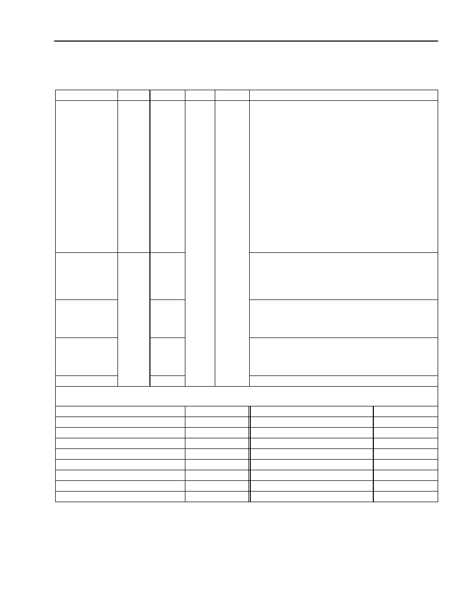
Agere Systems Inc.
127
Advance Data Sheet
September 2001
ATM Interconnect
CelXpres T8207
14
Registers
(continued)
Table 103. LUT X Configuration 1 Structure (LUTXCF1) (0704h to 077Ch)
Name
Offset
Bit Pos.
Type
Reset
Description
lutX_vpi_base
00h
15:0
RW
X
LUT X VPI Base Address. These bits define bits 3
through 18 of the VPI base address offset in look-up
table X. The offset may be a maximum of 19 bits. If
16-byte records are used, the least significant bit of this
word is ignored.
Note: When 16 or less PHY ports are used, each PHY
port has its own look-up table memory space.
For 16 or less PHY ports, PHY port 0 uses
LUT 0 memory space, PHY port 1 uses LUT 1
memory space, and so on. When greater than
16 PHY ports are used, even and odd PHY ports
must share the look-up memory space. For
greater than 16 PHY ports, PHY ports 0 and 1
use LUT 0 memory space, PHY ports 2 and 3
use LUT 1 memory space, PHY ports 4 and 5
use LUT 2 memory space, and so on.
lutX_vpi_mask
02h
11:0
LUT X VPI Mask. This 12-bit field is used to mask the
incoming VPI bits. If a bit in the field is set to `1,' the
corresponding incoming VPI bit will be used to address
the VPI record in the look-up table. All other incoming
VPI bits will be ignored.
lutX_vpi_chk
12
LUT X VPI Check. If this bit is set to `1,' the unused
incoming VPI bits must be `0,' or the cell will be
counted as misrouted. Unused bits are bits whose cor-
responding lutX_vpi_mask bit equal zero.
lutX_uni_en
13
LUT X User Network Interface (UNI) Enable. If this
bit is set to `1,' the port is identified as UNI, and the
GFC field of the cell header will not be used in the look-
up table. If this bit is `0,' the port is identified as NNI.
Reserved
15:14
Reserved.
The letter X in the data structure name and in the bit names represents the values 0 through 15 for the 16 look-up
table configurations. The base addresses of the 16 data structures are shown below.
Structure Name
Base Address
Structure Name
Base Address
LUT 0 configuration 1
0704h
LUT 8 configuration 1
0744h
LUT 1 configuration 1
070Ch
LUT 9 configuration 1
074Ch
LUT 2 configuration 1
0714h
LUT 10 configuration 1
0754h
LUT 3 configuration 1
071Ch
LUT 11 configuration 1
075Ch
LUT 4 configuration 1
0724h
LUT 12 configuration 1
0764h
LUT 5 configuration 1
072Ch
LUT 13 configuration 1
076Ch
LUT 6 configuration 1
0734h
LUT 14 configuration 1
0774h
LUT 7 configuration 1
073Ch
LUT 15 configuration 1
077Ch

128
Agere Systems Inc.
Advance Data Sheet
September 2001
ATM Interconnect
CelXpres T8207
14
Registers
(continued)
14.3.3 SDRAM Registers
Table 104. SDRAM Control (SCT) (0400h)
Table 105. SDRAM Interrupt Status (SIS) (0402h)
Table 106. SDRAM Interrupt Enable (SIE) (0404h)
Name
Bit Pos.
Type
Reset
Description
sdram_en
0
RW
0
SDRAM Enable. If this bit is set to `1,' the SDRAM becomes
active. If `0,' the SDRAM is in the idle state.
gen_man_acc
1
WO
0
Generate Manual Access. If the sdram_en bit is `0,' writing a `1'
to this bit will take the SDRAM out of its idle state and activate the
manual values programmed in the cas_man, ras_man, we_man,
bs_man, and addr_man bits. The `1' pulses for one clock cycle
and clears to `0' automatically. The SDRAM then returns to its
idle state. This special mode is used in the start-up sequence for
the SDRAM.
Reserved
14:2
RO
0
Reserved.
Reserved
15
RW
0
Reserved. Program this bit to `0.'
Name
Bit Pos.
Type
Reset
Description
ref_late
0
ROL
0
Refresh Late. This bit is set when the refresh cycle for the
SDRAM is greater than the value programmed in the late_lim
bits. An interrupt is generated if the corresponding enable bit is
set.
crc8_err_even
1
ROL
0
CRC-8 Error on Even Data Byte. This bit is set when an error is
detected on the even byte (sd_d[15:8]) of the SDRAM data bus.
An interrupt is generated if the corresponding enable bit is set.
crc8_err_odd
2
ROL
0
CRC-8 Error on Odd Data Byte. This bit is set when an error is
detected on the odd byte (sd_d[7:0]) of the SDRAM data bus. An
interrupt is generated if the corresponding enable bit is set.
Reserved
15:3
RO
0
Reserved.
Name
Bit Pos.
Type
Reset
Description
ref_late_ie
0
RW
0
Refresh Late Interrupt Enable. An interrupt is generated if this
bit and the corresponding status bit are set. The interrupt is gen-
erated until this bit or the corresponding status bit is reset.
crc8_err_even_ie
1
RW
0
CRC-8 Error on Even Data Byte Interrupt Enable. An interrupt
is generated if this bit and the corresponding status bit are set.
The interrupt is generated until this bit or the corresponding sta-
tus bit is reset.
crc8_err_odd_ie
2
RW
0
CRC-8 Error on Odd Data Byte Interrupt Enable. An interrupt
is generated if this bit and the corresponding status bit are set.
The interrupt is generated until this bit or the corresponding sta-
tus bit is reset.
Reserved
15:3
RO
0
Reserved.

Agere Systems Inc.
129
Advance Data Sheet
September 2001
ATM Interconnect
CelXpres T8207
14
Registers
(continued)
Table 107. SDRAM Configuration (SCF) (0408h)
Name
Bit Pos.
Type
Reset
Description
col_num
1:0
RW
0
Column Number. These bits are used to indicate the number of col-
umns in the SDRAM.
"100" = 256 columns
"01" = 512 columns
"10" = 1024 columns
"11" = reserved
cas_lat
2
RW
0
CAS Latency. This bit is used to indicate the CAS latency of the
SDRAM based on the clock frequency and speed grade of the device.
`0' = 2 cycles
`1' = 3 cycles
ras2cas
4:3
RW
2h
RAS Inactive to CAS Active Delay. These bits specify the minimum
time in SDRAM clock cycles from RAS going inactive to CAS going
active.
"01" = reserved
"10" = 2 clock cycles
"11" = 3 clock cycles
"00" = 4 clock cycles
cas2pre
6:5
RW
1
CAS Inactive to Precharge Active Delay. These bits specify the min-
imum time in SDRAM clock cycles from CAS going inactive to the pre-
charge command going active.
"01" = 1 clock cycles
"10" = 2 clock cycles
"11" = 3 clock cycles
"00" = 4 clock cycles
pre2cmd
8:7
RW
2h
Precharge Inactive to Next Command Active Delay. These bits
specify the minimum time in SDRAM clock cycles from the precharge
command going inactive to next command going active.
"01" = 1 clock cycles
"10" = 2 clock cycles
"11" = 3 clock cycles
"00" = 4 clock cycles
ref2cmd
10:9
RW
0
CBR Refresh Inactive to Next CBR Refresh Command Active
Delay. These bits specify the minimum time in SDRAM clock cycles
from the refresh command going inactive to next refresh command
going active. The minimum time from the refresh command to any
other command is 15 clock cycles.
"00" = 15 clock cycles
"01" = reserved
"10" = 3 clock cycles
"11" = 7 clock cycles
Reserved
15:11
RO
0
Reserved.

130
Agere Systems Inc.
Advance Data Sheet
September 2001
ATM Interconnect
CelXpres T8207
14
Registers
(continued)
Table 108. Refresh (RFRSH) (0410h)
Table 109. Refresh Lateness (RFRSHL) (0412h)
Table 110. Idle State 1 (IS1) (0420h)
Table 111. Idle State 2 (IS2) (0422h)
Name
Bit Pos.
Type
Reset
Description
ref_cnt 15:0
RW
0400h Refresh Count. These bits are used to program the refresh cycle in
SDRAM clock cycles. The number of clock cycles programmed in
this register should be less than one half the worst-case refresh
period.
Name
Bit Pos.
Type
Reset
Description
late_lim
15:0
RW
0400h Lateness Limit. These bits are used to program how late a refresh
cycle may occur. This limit is in refresh cycles. When this limit is
reached, the ref_late status bit will be set.
Name
Bit Pos.
Type
Reset
Description
cas_idle
0
RW
1
SDRAM CAS Idle Value. This is the value that will be placed on the
sd_cas* pin while the SDRAM is idle (sdram_en = `0').
ras_idle
1
RW
1
SDRAM RAS Idle Value. This is the value that will be placed on the
sd_ras* pin while the SDRAM is idle (sdram_en = `0').
we_idle
2
RW
1
SDRAM Write Enable Idle Value. This is the value that will be
placed on the sd_we* pin while the SDRAM is idle (sdram_en = `0').
bs_idle[1:0]
4:3
RW
3h
SDRAM Bank Select Idle Value. This is the value that will be
placed on the sd_bs[1:0] pins while the SDRAM is idle
(sdram_en = `0').
Reserved
15:5
RO
0
Reserved.
Name
Bit Pos.
Type
Reset
Description
addr_idle[11:0]
11:0
RW
0
SDRAM Address Idle Value. This is the value that will be placed on
the sd_a[11:0] pins while the SDRAM is idle (sdram_en = `0').
Reserved
15:12
RO
0
Reserved.

Agere Systems Inc.
131
Advance Data Sheet
September 2001
ATM Interconnect
CelXpres T8207
14
Registers
(continued)
Table 112. Manual Access State 1 (MAS1) (0424h)
Table 113. Manual Access State 2 (MAS2) (0426h)
Name
Bit Pos.
Type
Reset
Description
cas_ man
0
RW
1
SDRAM CAS Manual Value. This is the value that will be
placed on the sd_cas* pin for one clock cycle when the
gen_man_acc bit is written to `1.'
ras_ man
1
RW
1
SDRAM RAS Manual Value. This is the value that will be
placed on the sd_ras* pin for one clock cycle when the
gen_man_acc bit is written to `1.'
we_ man
2
RW
1
SDRAM Write Enable Manual Value. This is the value that
will be placed on the sd_we* pin for one clock cycle when the
gen_man_acc bit is written to `1.'
bs_ man[1:0]
4:3
RW
3h
SDRAM Band Select Manual Value. This is the value that will
be placed on the sd_bs[1:0] pins for one clock cycle when the
gen_man_acc bit is written to `1.'
Reserved
15:5
RO
0
Reserved.
Name
Bit Pos.
Type
Reset
Description
addr_man[11:0]
11:0
RW
0
SDRAM Address Manual Value. This is the value that will be
placed on the sd_a[11:0] pins for one clock cycle when the
gen_man_acc bit is written to `1.'
Reserved
15:12
RO
0
Reserved.

132
Agere Systems Inc.
Advance Data Sheet
September 2001
ATM Interconnect
CelXpres T8207
14
Registers
(continued)
Table 114. SDRAM Interrupt Service Request 4 (SISR4) (0438h)
Table 115. SDRAM Interrupt Service Request 3 (SISR3) (043Ah)
Table 116. SDRAM Interrupt Service Request 1 (SISR1) (043Ch)
Table 117. SDRAM Interrupt Service Request 2 (SISR2) (043Eh)
Name
Bit Pos.
Type
Reset
Description
queue_serv[63:48]
15:0
RO
0
Queue Service [63:48]. Each bit in this field represents one of
16 queue X registers from the 64 queue X registers. The least
significant bit represents the queue 48 register. The most sig-
nificant bit represents the queue 63 register. If the correspond-
ing bit is `1,' the specific queue X register has interrupt status
bits that need servicing (see Table 118).
Name
Bit Pos.
Type
Reset
Description
queue_serv[47:32]
15:0
RO
0
Queue Service [47:32]. Each bit in this field represents one of
16 queue X registers from the 64 queue X registers. The least
significant bit represents the queue 32 register. The most sig-
nificant bit represents the queue 47 register. If the correspond-
ing bit is `1,' the specific queue X register has interrupt status
bits that need servicing (see Table 118).
Name
Bit Pos.
Type
Reset
Description
queue_serv[31:16]
15:0
RO
0
Queue Service [31:16]. Each bit in this field represents one of
16 queue X registers from the 64 queue X registers. The least
significant bit represents the queue 16 register. The most sig-
nificant bit represents the queue 31 register. If the correspond-
ing bit is `1,' the specific queue X register has interrupt status
bits that need servicing (see Table 118).
Name
Bit Pos.
Type
Reset
Description
queue_serv[15:0]
15:0
RO
0
Queue Service [15:0]. Each bit in this field represents one of
16 queue X registers from the 64 queue X registers. The least
significant bit represents the queue 0 register. The most signif-
icant bit represents the queue 15 register. If the corresponding
bit is `1,' the specific queue X register has interrupt status bits
that need servicing (see Table 118).

Agere Systems Inc.
133
Advance Data Sheet
September 2001
ATM Interconnect
CelXpres T8207
14
Registers
(continued)
Table 118. Queue X (QX) (0440h to 04BEh)
Name
Bit Pos.
Type
Reset
Description
queueX_rd_en
0
RW
0
Queue X Read Enable. If this bit is `1,' the queue is enabled
for read operations. When any configuration bits are
changed, this bit must be `0.'
Note: To prevent corruption of data, this bit must be cleared
in unused queues.
queueX_wr_en
1
RW
0
Queue X Write Enable. If this bit is `1,' the queue is enabled
for write operations. When any configuration bits are
changed, this bit must be `0.'
Note: To prevent corruption of data, this bit must be cleared
in unused queues.
queueX_fecn_en
2
RW
0
Queue X FECN Enable. If this bit is `1,' the forward explicit
congestion notification (FECN) feature is enabled.
queueX_clp_en
3
RW
0
Queue X CLP Enable. If this bit is `1,' the cell loss priority
(CLP) feature is enabled.
Reserved
7:4
RO
0
Reserved.
queueX_fecn_lim
8
ROL
0
Queue X FECN Limit Reached. This bit is set when the
FECN limit has been reached in the queue. An interrupt is
generated if the corresponding enable bit is set.
queueX_clp_lim
9
ROL
0
Queue X CLP Limit Reached. This bit is set when the CLP
limit has been reached in the queue. An interrupt is gener-
ated if the corresponding enable bit is set.
queueX_ovrn
10
ROL
0
Queue X Overrun. This bit is set when the queue overruns.
An interrupt is generated if the corresponding enable bit is
set.
queueX_emp
11
ROL
0
Queue X Empty. This bit is set when the queue is empty. An
interrupt is generated if the corresponding enable bit is set.
queueX_fecn_lim_ie
12
RW
0
Queue X FECN Limit Reached Interrupt Enable. An inter-
rupt is generated if this bit and the corresponding status bit
are set. The interrupt is generated until this bit or the corre-
sponding status bit is reset.
queueX_clp_lim_ie
13
RW
0
Queue X CLP Limit Reached Interrupt Enable. An inter-
rupt is generated if this bit and the corresponding status bit
are set. The interrupt is generated until this bit or the corre-
sponding status bit is reset.
queueX_ovrn_ie
14
RW
0
Queue X Overrun Interrupt Enable. An interrupt is gener-
ated if this bit and the corresponding status bit are set. The
interrupt is generated until this bit or the corresponding sta-
tus bit is reset.
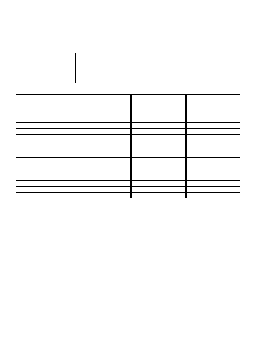
134
Agere Systems Inc.
Advance Data Sheet
September 2001
ATM Interconnect
CelXpres T8207
14
Registers
(continued)
Table 118. Queue X (QX) (0440h to 04BEh) (continued)
Note: When the T8207_sel bit = 0, queues 32--63 are disabled (default).
Name
Bit Pos.
Type
Reset
Description
queueX_emp_ie
15
RW
0
Queue X Empty Interrupt Enable. An interrupt is
generated if this bit and the corresponding status bit
are set. The interrupt is generated until this bit or the
corresponding status bit is reset.
The letter X in the register name and in the bit names represents the values of 0 through 63 for the 64 queues
shown below.
Register
Name
Register
Address
Register
Name
Register
Address
Register
Name
Register
Address
Register
Name
Register
Address
Queue 0 (Q0)
0440h
Queue 16 (Q16)
0460h
Queue 32 (Q32)
0480h
Queue 48 (Q48)
04A0h
Queue 1 (Q1)
0442h
Queue 17 (Q17)
0462h
Queue 33 (Q33)
0482h
Queue 49 (Q49)
04A2h
Queue 2 (Q2)
0444h
Queue 18 (Q18)
0464h
Queue 34 (Q34)
0484h
Queue 50 (Q50)
04A4h
Queue 3 (Q3)
0446h
Queue 19 (Q19)
0466h
Queue 35 (Q35)
0486h
Queue 51 (Q51)
04A6h
Queue 4 (Q4)
0448h
Queue 20 (Q20)
0468h
Queue 36 (Q36)
0488h
Queue 52 (Q52)
04A8h
Queue 5 (Q5)
044Ah
Queue 21 (Q21)
046Ah
Queue 37 (Q37)
048Ah
Queue 53 (Q53)
04AAh
Queue 6 (Q6)
044Ch
Queue 22 (Q22)
046Ch
Queue 38 (Q38)
048Ch
Queue 54 (Q54)
04ACh
Queue 7 (Q7)
044Eh
Queue 23 (Q23)
046Eh
Queue 39 (Q39)
048Eh
Queue 55 (Q55)
04AEh
Queue 8 (Q8)
0450h
Queue 24 (Q24)
0470h
Queue 40 (Q40)
0490h
Queue 56 (Q56)
04B0h
Queue 9 (Q9)
0452h
Queue 25 (Q25)
0472h
Queue 41 (Q41)
0492h
Queue 57 (Q57)
04B2h
Queue 10 (Q10)
0454h
Queue 26 (Q26)
0474h
Queue 42 (Q42)
0494h
Queue 58 (Q58)
04B4h
Queue 11 (Q11)
0456h
Queue 27 (Q27)
0476h
Queue 43 (Q43)
0496h
Queue 59 (Q59)
04B6h
Queue 12 (Q12)
0458h
Queue 28 (Q28)
0478h
Queue 44 (Q44)
0498h
Queue 60 (Q60)
04B8h
Queue 13 (Q13)
045Ah
Queue 29 (Q29)
047Ah
Queue 45 (Q45)
049Ah
Queue 61 (Q61)
04BAh
Queue 14 (Q14)
045Ch
Queue 30 (Q30)
047Ch
Queue 46 (Q46)
049Ch
Queue 62 (Q62)
04BCh
Queue 15 (Q15)
045Eh
Queue 31 (Q31)
047Eh
Queue 47 (Q47)
049Eh
Queue 63 (Q63)
04BEh
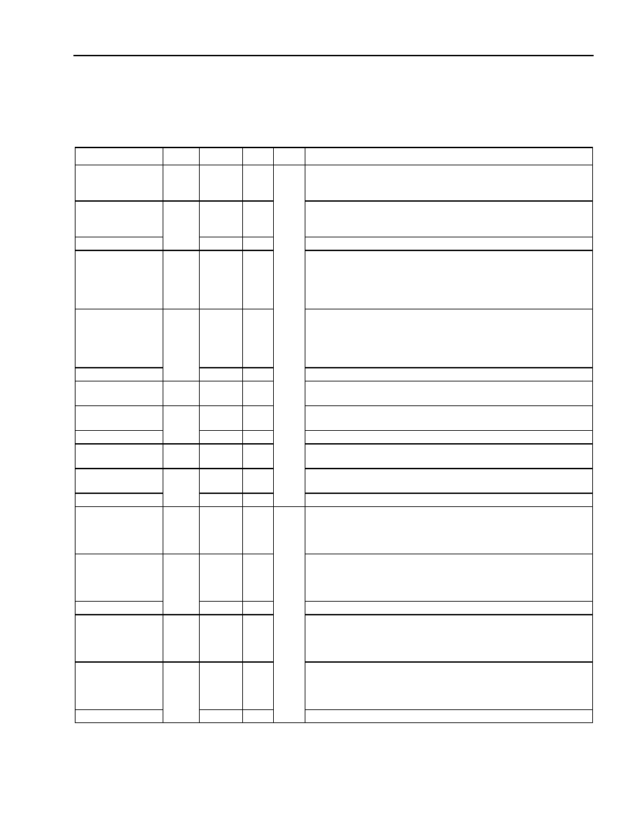
Agere Systems Inc.
135
Advance Data Sheet
September 2001
ATM Interconnect
CelXpres T8207
14
Registers
(continued)
14.3.3.1 SDRAM Control Memory
Table 119. Queue X Definition Structure (QXDEF) (2000h to 27E0h)
Name
Offset
Bit Pos.
Type Reset
Description
base_addrX[24:9]
00h
15:0
RW
X
Base Address Queue X [24:9]. These bits configure the upper
16 bits of the queue's base address offset in increments of one cell
(64 bytes).
base_addrX[8:6]
02h
15:13
RW
Base Address Queue X [8:6]. These bits configure bits 6 through
8 of the queue's base address offset in increments of one cell
(64 bytes).
Reserved
12:0
RO
Reserved.
end_addrX[24:9]
04h
15:0
RW
End Address Queue X [24:9]. These bits configure the upper
16 bits of the queue's end address offset in increments of one cell.
The total number of cells held by the queue may be calculated by
subtracting the base_addr from the end_addr and adding one to the
difference. The minimum size of any queue is four cells.
end_addrX[8:6]
06h
15:13
RW
End Address Queue X [8:6]. These bits configure bits 6 through 8 of
the queue's end address offset in increments of one cell. The total
number of cells held by the queue may be calculated by subtracting
the base_addr from the end_addr and adding one to the difference.
The minimum size of any queue is four cells.
Reserved
12:0
RO
Reserved.
wr_pntX[24:9]
08h
15:0
RW
Write Pointer for Queue X [24:9]. These bits must be initialized to
the base_addrX[24:9] before the queue is enabled.
wr_pntX[8:6]
0Ah
15:13
RW
Write Pointer for Queue X [8:6]. These bits must be initialized to the
base_addrX[8:6] before the queue is enabled.
Reserved
12:0
RO
Reserved.
rd_pntX[24:9]
0Ch
15:0
RW
Read Pointer for Queue X [24:9]. These bits must be initialized to
the base_addrX[24:9] before the queue is enabled.
rd_pntX[8:6]
0Eh
15:13
RW
Read Pointer for Queue X [8:6]. These bits must be initialized to the
base_addrX[8:6] before the queue is enabled.
Reserved
12:0
RO
Reserved.
fecn_fillX[24:9]
10h
15:0
RW
X
FECN Fill for Queue X [24:9]. These bits with fecn_fillX[8:6] deter-
mine the queue's fill level in cells (64 bytes) where the FECN bit is
set in outgoing cells. The FECN bit is set only when the
queueX_fecn_en bit is `1.'
fecn_fillX[8:6]
12h
15:13
RW
FECN Fill for Queue X [8:6]. These bits with fecn_fillX[24:9] deter-
mine the queue's fill level in cells (64 bytes) where the FECN bit is
set in outgoing cells. The FECN bit is set only when the
queueX_fecn_en bit is `1.'
Reserved
12:0
RO
Reserved.
clp_fillX[24:9]
14h
15:0
RW
CLP Fill for Queue X [24:9]. These bits with clp_fillX[8:6] determine
the queue's fill level in cells (64 bytes) where incoming cells with their
CLP bit set will be discarded. The incoming cell is dropped at this fill
level only when the queueX_clp_en bit is `1.'
clp_fillX[8:6]
16h
15:13
RW
CLP Fill for Queue X [8:6]. These bits with clp_fillX[24:9] determine
the queue's fill level in cells (64 bytes) where incoming cells with their
CLP bit set will be discarded. The incoming cell is dropped at this fill
level only when the queueX_clp_en bit is `1.'
Reserved
12:0
RO
Reserved.

136
Agere Systems Inc.
Advance Data Sheet
September 2001
ATM Interconnect
CelXpres T8207
14
Registers
(continued)
Table 119. Queue X Definition Structure (QXDEF) (2000h to 27E0h) (continued)
Name
Offset
Bit Pos.
Type
Reset
Description
The letter X in the data structure name and in the bit names represents the values of 0 through 63 for the 64
queues shown below.
Structure Name
Base Address
Structure Name
Base Address
Queue 0 base address high
2000h
Queue 32 base address high
2400h
Queue 1 base address high
2020h
Queue 33 base address high
2420h
Queue 2 base address high
2040h
Queue 34 base address high
2440h
Queue 3 base address high
2060h
Queue 35 base address high
2460h
Queue 4 base address high
2080h
Queue 36 base address high
2480h
Queue 5 base address high
20A0h
Queue 37 base address high
24A0h
Queue 6 base address high
20C0h
Queue 38 base address high
24C0h
Queue 7 base address high
20E0h
Queue 39 base address high
24E0h
Queue 8 base address high
2100h
Queue 40 base address high
2500h
Queue 9 base address high
2120h
Queue 41 base address high
2520h
Queue 10 base address high
2140h
Queue 42 base address high
2540h
Queue 11 base address high
2160h
Queue 43 base address high
2560h
Queue 12 base address high
2180h
Queue 44 base address high
2580h
Queue 13 base address high
21A0h
Queue 45 base address high
25A0h
Queue 14 base address high
21C0h
Queue 46 base address high
25C0h
Queue 15 base address high
21E0h
Queue 47 base address high
25E0h
Queue 16 base address high
2200h
Queue 48 base address high
2600h
Queue 17 base address high
2220h
Queue 49 base address high
2620h
Queue 18 base address high
2240h
Queue 50 base address high
2640h
Queue 19 base address high
2260h
Queue 51 base address high
2660h
Queue 20 base address high
2280h
Queue 52 base address high
2680h
Queue 21 base address high
22A0h
Queue 53 base address high
26A0h
Queue 22 base address high
22C0h
Queue 54 base address high
26C0h
Queue 23 base address high
22E0h
Queue 55 base address high
26E0h
Queue 24 base address high
2300h
Queue 56 base address high
2700h
Queue 25 base address high
2320h
Queue 57 base address high
2720h
Queue 26 base address high
2340h
Queue 58 base address high
2740h
Queue 27 base address high
2360h
Queue 59 base address high
2760h
Queue 28 base address high
2380h
Queue 60 base address high
2780h
Queue 29 base address high
23A0h
Queue 61 base address high
27A0h
Queue 30 base address high
23C0h
Queue 62 base address high
27C0h
Queue 31 base address high
23E0h
Queue 63 base address high
27E0h
Agere Systems Inc.
137
Advance Data Sheet
September 2001
ATM Interconnect
CelXpres T8207
14
Registers
(continued)
14.3.4 Various Internal Memories
14.3.4.1 Control Cell Memories
Table 120. Control Cell Receive Extended Memory (CCRXEM) (0800h to 0832h)
The control cell receive memory may also be accessed from direct memory. See Table 50.
Table 121. Control Cell Transmit Extended Memory (CCTXEM) (0900h to 0936h)
The control cell transmit memory may also be accessed from direct memory. See Table 51.
Name
Offset
Type
Reset
Description
header[31:16]
00h
RO
X
These 52 bytes are the control cell received from the cell
bus. When present, the control cell may be read from this
extended memory space.
header[15:0]
02h
payload_bytes 0--1
04h
.
.
.
.
.
.
payload_bytes 46--47
32h
Name
Offset
Type
Reset
Description
cell_bus_routing_header
0
RW
X
These 56 bytes are the cell routing header, the tandem rout-
ing header, and the control cell to be transmitted onto the cell
bus. A control cell to be transmitted may be written to this
extended memory space.
tandem_routing_header 2
header[31:16]
4
header[15:0]
6
payload_bytes 0--1
8
.
.
.
.
.
.
payload_bytes 46--47
36h
138
Agere Systems Inc.
Advance Data Sheet
September 2001
ATM Interconnect
CelXpres T8207
14
Registers
(continued)
14.3.4.2 Multicast Number Memories
Table 122. PHY Port 0 and Control Cells Multicast Extended Memory (PP0MEM) (0C00h to 0C1Eh)
The PHY port 0 and control cells multicast memory may also be accessed from direct memory (see Table 52).
Name
Offset Type Reset
Description
multicast_receive_enable[15:0]
00h
RW
X
This memory space contains 256 active-high
enable bits. Each bit represents a multicast net
number from 0 through 255. If a bit is set, the corre-
sponding multicast net number data cell is sent to
the queue group for PHY port 0, or the correspond-
ing multicast control cell is sent to the control cell
receive direct and extended memory. The least sig-
nificant bit is multicast net number 0.
multicast_receive_enable[31:16]
02h
multicast_receive_enable[47:32]
04h
.
.
.
.
.
.
multicast_receive_enable[191:176]
16h
multicast_receive_enable[207:192]
18h
multicast_receive_enable[223:208]
1Ah
multicast_receive_enable[239:224]
1Ch
multicast_receive_enable[255:240]
1Eh
Agere Systems Inc.
139
Advance Data Sheet
September 2001
ATM Interconnect
CelXpres T8207
14
Registers
(continued)
Table 123. PHY Port X Multicast Memory (PPXMM) (0C20h to 0DE0h)
Note: When the T8207_sel bit = `0' multicast memory at address 0D00h--0DECh are ignored.
Name
Offset Type Reset
Description
multicast_receive_enable[15:0]
00h
RW
X
This memory space contains 256 active-high enable
bits. Each bit represents a multicast net number from
0 through 255. If a bit is set, the corresponding multi-
cast net number data cell is sent to the queue group
for PHY port X. The least significant bit is multicast
net number 0.
multicast_receive_enable[31:16]
02h
multicast_receive_enable[47:32]
04h
.
.
.
.
.
.
multicast_receive_enable[239:224]
1Ch
multicast_receive_enable[255:240]
1Eh
The letter X in the data structure and in the bit names represents the values of 1 through 15 for 15 of the 16 PHY
ports. The base addresses of the 15 multicast memory locations are shown below.
Memory Name
Base Address
PHY Port 1 Multicast Memory
0C20h
PHY Port 2 Multicast Memory
0C40h
PHY Port 3 Multicast Memory
0C60h
PHY Port 4 Multicast Memory
0C80h
PHY Port 5 Multicast Memory
0CA0h
PHY Port 6 Multicast Memory
0CC0h
PHY Port 7 Multicast Memory
0CE0h
PHY Port 8 Multicast Memory
0D00h
PHY Port 9 Multicast Memory
0D20h
PHY Port 10 Multicast Memory
0D40h
PHY Port 11 Multicast Memory
0D60h
PHY Port 12 Multicast Memory
0D80h
PHY Port 13 Multicast Memory
0DA0h
PHY Port 14 Multicast Memory
0DC0h
PHY Port 15 Multicast Memory
0DE0h
140
Agere Systems Inc.
Advance Data Sheet
September 2001
ATM Interconnect
CelXpres T8207
14
Registers
(continued)
14.3.4.3 PPD State Memory
Table 124. PPD Memory (PPDM) (1000h to 13FEh)
Name
Offset
Type
Reset
Description
word0
00h
RW
X
This memory space contains 8192 AAL5 virtual channel PPD bits. The
PPD pointer bits in the cell header, cell bus routing header, and tandem
routing header, which are selected by the PPD pointer select bits, point
to a single bit in this memory space. If the bit for a corresponding AAL5
virtual channel is `0,' no cells are dropped. If the bit is `1,' all remaining
cells in the packet, except the last cell, are dropped. A PPD bit becomes
set when a cell in an AAL5 virtual channel packet is dropped. The last
cell of a packet is identified by the least significant bit of the PTI field in
the cell header, which is set to `1.' The most significant bit of the PTI field
is also checked to be `0' (user data). The final cell of the packet is sent,
and the corresponding PPD bit is cleared. The most significant bit of
word0 corresponds to AAL5 virtual channel zero, and the least signifi-
cant bit of word1FF corresponds to AAL5 virtual channel 8191.
word1
02h
word2
04h
word3
06h
word4
08h
word5
0Ah
word6
0Ch
word7
0Eh
.
.
.
.
.
.
word1F9
3F2h
word1FA
3F4h
word1FB
3F6h
word 1FC
3F8h
word1FD
3FAh
word1FE
3FCh
word1FF
3FEh
Agere Systems Inc.
141
Advance Data Sheet
September 2001
ATM Interconnect
CelXpres T8207
14
Registers
(continued)
14.3.5 External Memories
14.3.5.1 Look-Up Translation Memory
Table 125. Translation RAM Memory (TRAM) (100000h to 17FFFEh)
14.3.5.2 SDRAM Buffer Memory
Table 126. SDRAM (SDRAM) (2000000h to 3FFFFFEh)
Name
Offset
Type
Reset
Description
word0
00h
RW
X
This memory space is used to access the translation RAM memory.
.
.
.
.
.
.
word3FFFF
7FFFEh
Name
Offset
Type
Reset
Description
word0
00h
RW
X
This memory space is used to access the SDRAM memory.
.
.
.
.
.
.
wordFFFFFE
1FFFFFEh

142
Agere Systems Inc.
Advance Data Sheet
September 2001
ATM Interconnect
CelXpres T8207
15
Absolute Maximum Ratings
Stresses in excess of the absolute maximum ratings can cause permanent damage to the device. These are abso-
lute stress ratings only. Functional operation of the device is not implied at these or any other conditions in excess
of those given in the operational sections of the data sheet. Exposure to absolute maximum ratings for extended
periods can adversely affect device reliability.
Table 127. Maximum Rating Parameters and Values
1. Except for 5 V tolerant buffers where V
IHmax
= 5.5 V + 0.3 V.
2. Maximum power dissipation may be determined from the following equation: P
D
= (125
į
C ≠ T
A
)/22.5
į
C/W.
16
Recommended Operating Conditions
Table 128. Recommended Operating Conditions
17
Handling Precautions
Although protection circuitry has been designed into this device, proper precautions should be taken to avoid expo-
sure to electrostatic discharge (ESD) during handling and mounting. Agere employs a human-body model (HBM)
and a charged-device model (CDM) for ESD-susceptibility testing and protection design evaluation. ESD voltage
thresholds are dependent on the circuit parameters used to define the model. No industry-wide standard has been
adopted for the CDM. A standard HBM (resistance = 1500
, capacitance = 100 pF) is widely accepted and can be
used for comparison. The HBM ESD threshold presented here was obtained by using these circuit parameters.
Table 129. HBM ESD Threshold
Parameter
Symbol
Min
Typ
Max
Unit
dc Supply Voltage with Respect to Ground
V
DD
--
--
4.2
V
Input Voltage Range
1
V
I1
V
SS
≠ 0.3
--
V
DD
+ 0.3
V
Junction Temperature Range
T
J
≠40
--
125
į
C
Storage Temperature
T
stg
≠60
--
160
į
C
Maximum Power Dissipation (package limit)
2
P
D
--
--
2.44
W
Parameter
Symbol
Min
Typ
Max
Unit
dc Supply Voltage with Respect to Ground
V
DD
3.0
--
3.6
V
Ambient Operating Temperature Range
T
A
≠40
--
85
į
C
Device
Voltage (V)
T8207
2000

Agere Systems Inc.
143
Advance Data Sheet
September 2001
ATM Interconnect
CelXpres T8207
18
Electrical Requirements and Characteristics
18.1 Crystal Information
The
CelXpres
T8207 device requires a crystal or external clock source. The crystal may have a frequency from
5 MHz to 40 MHz and is connected between xtalin and xtalout. External 5% capacitors must be connected from
xtalin and xtalout to V
SS
. The value of the external capacitors is determined from the crystal data sheet using the
crystal specification requirements shown below.
Table 130. Crystal Specifications
The xtalin input may be driven by an external clock instead of a crystal. The frequency of the external source may
be 5 MHz to 50 MHz. The external clock must meet the requirements shown below.
Table 131. External Clock Requirements
The frequency of the T8207's main clock (mclk) is derived from the clock at the xtalin input (pclk). See Section 5,
PLL Configuration, for more information on these clocks.
Parameter
Value
Frequency
5 MHz to 40 MHz
Oscillation Mode
Fundamental parallel resonant
Effective Series Resistance
See Figure 20 below
Frequency Tolerance and Stability
5%
Figure 19. Crystal
Figure 20. Negative Resistance Plot
Parameter
Min
Max
Frequency
5 MHz
50 MHz
Maximum Rise or Fall Time
--
5 ns
Duty Cycle
40%
60%
CRYSTAL
XTALIN
XTALOUT
C
1
C
2
0
10
20
30
40
50
60
-1000
-800
-600
-400
-200
0
FREQUENCY (MHZ)
NEGATIVE RESISTANCE (ohms)
10p
20p
50p
FREQUENCY (MHz)
50 pF
20 pF
10 pF
NEGA
T
I
VE
RE
SIS
T
ANCE
(
)
= C1
= C2
= C1
= C2
= C1
= C2

144
Agere Systems Inc.
Advance Data Sheet
September 2001
ATM Interconnect
CelXpres T8207
18
Electrical Requirements and Characteristics
(continued)
18.2 dc Electrical Characteristics
The following conditions apply except where noted: T
A
= ≠40
į
C to +85
į
C, V
DD
= 3.3 V
Ī
10%, 15 pF each output.
Table 132. dc Electrical Characteristics
* This is the power consumed by the device under the following conditions: V
DD
= 3.3 V, pclk = 20 MHz, mclk = 100 MHz, UTOPIA clock =
20 MHz, cell bus clock = 30 MHz, nominal slew rate (register 2Eh).
Parameter
Symbol
Test Conditions
Min
Typ
Max
Unit
Supply Current
I
DD
--
--
--
--
mA
Input Voltage (TTL):
Low
High
V
IL
V
IH
--
--
--
2.0
--
--
0.8
--
V
V
Input Voltage (TTL 5 V tolerant):
Low
High
V
IL
V
IH
--
--
--
2.0
--
--
0.8
5.5
V
V
Input Voltage (GTL+):
Low
High
V
IL
V
IH
--
--
--
1.2
--
--
0.8
--
V
V
Input Voltage (xtalin):
Low
High
V
IL
V
IH
--
--
--
0.7 V
DD
--
--
0.2 V
DD
--
V
V
Output Voltage (TTL 4 mA):
Low
High
V
OL
V
OH
I
OL
= 4 mA
I
OH
= ≠4 mA
--
2.4
--
--
0.4
--
V
V
Output Voltage (TTL 6 mA):
Low
High
V
OL
V
OH
I
OL
= 6 mA
I
OH
= ≠6 mA
--
2.4
--
--
0.4
--
V
V
Output Voltage (TTL 7 mA):
Low
High
V
OL
V
OH
I
OL
= 7 mA
I
OH
= ≠7 mA
--
2.4
--
--
0.4
--
V
V
Output Voltage (TTL 10 mA):
Low
High
V
OL
V
OH
I
OL
= 10 mA
I
OH
= ≠10 mA
--
2.4
--
--
0.4
--
V
V
Output Current (GTL+)
I
OL
--
65
--
75
mA
Output Voltage (GTL+)
V
OL
--
--
0.3
0.5
V
Input Leakage Current (TTL)
--
--
--
--
1
Ķ
A
Input Leakage Current (TTL with pull-ups)
--
V
IL
= V
SS
--
--
67
Ķ
A
Input Leakage Current (cb_vref)
--
--
--
--
40
Ķ
A
Power Dissipation
P
D
--
--
--
1.5*
W
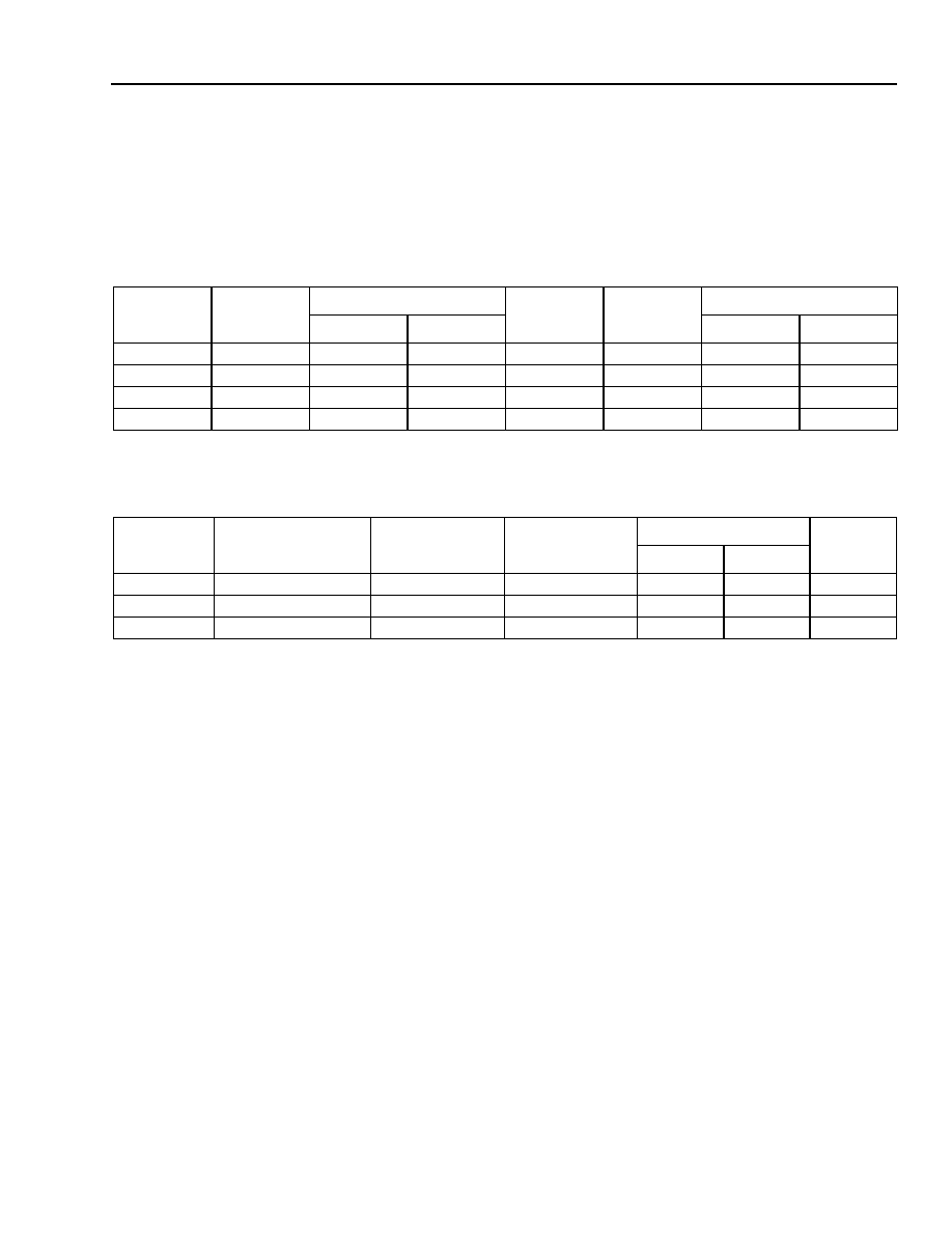
Agere Systems Inc.
145
Advance Data Sheet
September 2001
ATM Interconnect
CelXpres T8207
19
Timing Requirements
The following section describes the timing requirements. Capacitve loading is in the range of 10 pF to 50 pF,
unless otherwise specified.
Some timing requirements are dependent on the frequency of pclk or mclk. The terms mclkp and pclkp refer to the
period of their respective clocks in ns when used in the following tables.
Table 133. Input Clocks
Note: The cell bus write clock (cb_wc*) should be delayed 1.5 ns to 4 ns relative to the cell bus read clock (cb_rc*) to ensure sufficient data hold
time.
Table 134. Output Clocks
Clock Name
Frequency
(Max)
Voltage Level
Rise Time
(Max)
Fall Time
(Max)
Pulse Width (Min)
High
Low
High
Low
cb_wc*
66 MHz
--
--
--
--
6.06 ns
6.06 ns
cb_rc*
66 MHz
--
--
--
--
6.06 ns
6.06 ns
u_rxclk
50 MHz
2.0 V
0.8 V
4.0 ns
4.0 ns
8 ns
8 ns
u_txclk
50 MHz
2.0 V
0.8 V
4.0 ns
4.0 ns
8 ns
8 ns
Clock Name
Frequency (Max)
Rise Time (Max)
Fall Time (Max)
Pulse Width (Min)
Load
High
Low
sd_clk
100 MHz
1.0 ns
1.0 ns
4 ns
4 ns
15 pF
u_rxclk
50 MHz
2.0 ns
2.0 ns
8 ns
8 ns
40 pF
u_txclk
50 MHz
2.0 ns
2.0 ns
8 ns
8 ns
40 pF
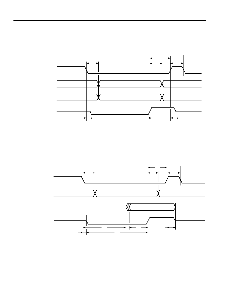
146
Agere Systems Inc.
Advance Data Sheet
September 2001
ATM Interconnect
CelXpres T8207
19
Timing Requirements
(continued)
19.1 Microprocessor Interface Timing
For access time information, see Section 6.3.2,
CelXpres
T8207 Access Performance.
5-7787bF
1. write_access_active is the logical OR function of sel* and wr*_ds*.
2. Load is 15 pF.
Note: sel* and wr*_ds* must not have coinciding edges in opposite directions to prevent glitches on the write_access_active signal.
Figure 21. Nonmultiplexed
Intel
Mode Write Access Timing
5-7788bF
1. read_access_active is the logical OR function of sel* and rd*_wr*.
2. Load is 15 pF.
Note: sel* and rd*_wr* must not have coinciding edges in opposite directions to prevent glitches on the read_access_active signals.
Figure 22. Nonmultiplexed
Intel
Mode Read Access Timing
WRITE_ACCESS_ACTIVE
1
A[7:0]
D[7:0]
RDY_DTACK*
2
t1
t3
t6
t4
t2
t5
t7
READ_ACCESS_ACTIVE
1
A[7:0]
D[7:0]
RDY_DTACK*
2
t1
t3
t6
t4
t2
t5
t8
t7
t9
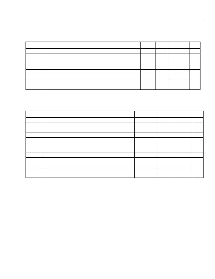
Agere Systems Inc.
147
Advance Data Sheet
September 2001
ATM Interconnect
CelXpres T8207
19
Timing Requirements
(continued)
Table 135. Nonmultiplexed
Intel
Mode Write Access Timing
1. See access times in Table 10.
Note: The term pclkp in the table represents the period of pclk in ns.
Table 136. Nonmultiplexed
Intel
Mode Read Access Timing
1. See access times in Table 10.
Note: The term pclkp in the table represents the period of pclk in ns.
Symbol
Parameter
Min
Typ
Max
Unit
t1
write_access_active Falling Edge to a[7:0] and d[7:0] Valid
--
--
2 x pclkp ≠ 4
ns
t2
rdy_dtack* Rising Edge to write_access_active Rising Edge
0
--
--
ns
t3
rdy_dtack* Rising Edge to a[7:0] and d[7:0] Invalid
0
--
--
ns
t4
write_access_active Falling Edge to rdy_dtack* Falling Edge
0
--
12
ns
t5
rdy_dtack* Low Pulse Width
1
--
--
--
--
t6
write_access_active Rising Edge to rdy_dtack* 3_state
0
--
5
ns
t7
write_access_active Rising Edge to write_access_active Fall-
ing Edge
25
--
--
ns
Symbol
Parameter
Min
Typ
Max
Unit
t1
read_access_active Falling Edge to a[7:0]
--
--
2 x pclkp ≠ 4
ns
t2
rdy_dtack* Rising Edge to read_access_active Rising
Edge
0
--
--
ns
t3
rdy_dtack* Rising Edge to a[7:0] Invalid
0
--
--
ns
t4
read_access_active Falling Edge to rdy_dtack* Falling
Edge
0
--
12
ns
t5
rdy_dtack* Low Pulse Width
1
--
--
--
--
t6
read_access_active Rising Edge to d[7:0] Invalid
0
--
5
ns
t7
d[7:0] Valid to rdy_dtack* Rising Edge
pclkp ≠ 4
--
--
ns
t8
read_access_active Falling Edge to d[7:0] Drive
3 x pclkp ≠ 4
--
--
ns
t9
read_access_active Rising Edge to read_access_active
Falling Edge
25
--
--
ns

148
Agere Systems Inc.
Advance Data Sheet
September 2001
ATM Interconnect
CelXpres T8207
19
Timing Requirements
(continued)
5-7789bF
1. write_access_active is the logical OR function of sel*, wr*_ds*, and rd*_wr*.
2. Load is 50 pF.
Notes:
sel* and wr*_ds* must not have coinciding edges in opposite directions to prevent glitches on the write_access_active signal.
rd*_wr* must be stable any time both sel* and wr*_ds* are low to prevent glitches on the write_access_active signals.
Figure 23.
Motorola
Mode Write Access Timing
5-7790bF
1. read_access_active is the logical OR function of sel*, wr*_ds*, and rd*_wr*.
2. Load is 50 pF.
Notes:
sel* and wr*_ds* must not have coinciding edges in opposite directions to prevent glitches on the read_access_active signal.
rd*_wr* must be stable any time both sel* and wr*_ds* are low to prevent glitches on the read_access_active signals.
Figure 24.
Motorola
Mode Read Access Timing
WRITE_ACCESS_ACTIVE
1
A[7:0]
D[7:0]
RDY_DTACK*
2
t1
t3
t4
t2
t5
t7
t6
t8
READ_ACCESS_ACTIVE
1
A[7:0]
D[7:0]
RDY_DTACK*
2
t1
t3
t4
t2
t5
t7
t6
t10
t8
t9
t11

Agere Systems Inc.
149
Advance Data Sheet
September 2001
ATM Interconnect
CelXpres T8207
19
Timing Requirements
(continued)
Table 137.
Motorola
Mode Write Access Timing
1. See access times in Table 10.
Note: The term pclkp in the table represents the period of pclk in ns.
Table 138.
Motorola
Mode Read Access Timing
1. See access times in Table 10.
Note: The term pclkp in the table represents the period of pclk in ns.
Symbol
Parameter
Min
Typ
Max
Unit
t1
write_access_active Falling Edge to a[7:0] and d[7:0] Valid
--
--
2 x pclkp ≠ 4
ns
t2
rdy_dtack* Falling Edge to write_access_active Rising
Edge
0
--
--
ns
t3
rdy_dtack* Falling Edge to a[7:0] and d[7:0] Invalid
0
--
--
ns
t4
write_access_active Falling Edge to rdy_dtack* Drive
0
--
12
ns
t5
write_access_active Falling Edge to rdy_dtack* Falling
Edge
1
--
--
--
--
t6
write_access_active Rising Edge to rdy_dtack* Rising Edge
0
--
5
ns
t7
rdy_dtack* Rising Edge to rdy_dtack* 3-state
1
--
5
ns
t8
write_access_active Rising Edge to write_access_active
Falling Edge
25
--
--
ns
Symbol
Parameter
Min
Typ
Max
Unit
t1
read_access_active Falling Edge to a[7:0] Valid
--
--
2 x pclkp ≠ 4
ns
t2
rdy_dtack* Falling Edge to read_access_active Rising
Edge
0
--
--
ns
t3
rdy_dtack* Falling Edge to a[7:0] Invalid
0
--
--
ns
t4
read_access_active Falling Edge to rdy_dtack* Drive
0
--
12
ns
t5
read_access_active Falling Edge to rdy_dtack* Falling
Edge
1
--
--
--
--
t6
read_access_active Rising Edge to rdy_dtack* Rising
Edge
0
--
5
ns
t7
rdy_dtack* Rising Edge to rdy_dtack* 3-state
1
--
5
ns
t8
d[7:0] Valid to rdy_dtack* Falling Edge
pclkp ≠ 4
--
--
ns
t9
read_access_active Rising Edge to d[7:0] Invalid
0
--
5
ns
t10
read_access_active Falling Edge to d[7:0] Drive
3 x pclkp ≠ 4
--
--
ns
t11
read_access_active Rising Edge to read_access_active
Falling Edge
25
--
--
ns
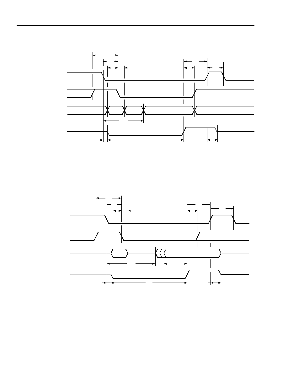
150
Agere Systems Inc.
Advance Data Sheet
September 2001
ATM Interconnect
CelXpres T8207
19
Timing Requirements
(continued)
5-7791bF
1. write_access_active is the logical OR function of sel* and wr*_ds*.
2. Load is 50 pF.
Note: sel* and wr*_ds* must not have coinciding edges in opposite directions to prevent glitches on the write_access_active signal.
Figure 25. Multiplexed
Intel
Mode Write Access Timing
5-7792bF
1. read_access_active is the logical OR function of sel* and rd*_wr*.
2. Load is 50 pF.
Note: sel* and rd*_wr* must not have coinciding edges in opposite directions prevent glitches on the read_access_active signals.
Figure 26. Multiplexed
Intel
Mode Read Access Timing
WRITE_ACCESS_ACTIVE
1
A[0]/ALE
D[7:0]
RDY_DTACK*
2
t2
t6
t9
t7
t5
t8
t10
t3
t4
t1
t11
READ_ACCESS_ACTIVE
1
A[0]/ALE
D[7:0]
RDY_DTACK*
2
t2
t6
t9
t7
t5
t8
t10
t3
t4
t1
t11
t12

Agere Systems Inc.
151
Advance Data Sheet
September 2001
ATM Interconnect
CelXpres T8207
19
Timing Requirements
(continued)
Table 139. Multiplexed
Intel
Mode Write Access Timing
1. See access times in Table 10.
Note: The term pclkp in the table represents the period of pclk in ns.
Table 140. Multiplexed
Intel
Mode Read Access Timing
1. See access times in Table 10.
Note: The term pclkp in the table represents the period of pclk in ns.
Symbol
Parameter
Min
Typ
Max
Unit
t1
a[0]/ale High Pulse Width
5
--
--
ns
t2
write_access_active Falling Edge to a[0]/ale Falling Edge
--
--
2 x pclkp ≠ 4
ns
t3
d[7:0] Valid to a[0]/ale Falling Edge
5
--
--
ns
t4
a[0]/ale Falling Edge to d[7:0] Invalid
0
--
--
ns
t5
rdy_dtack* Rising Edge to write_access_active Rising
Edge
0
--
--
ns
t6
rdy_dtack* Rising Edge to d[7:0] Invalid and a[0]/ale Ris-
ing Edge
0
--
--
ns
t7
write_access_active Falling Edge to rdy_dtack* Falling
Edge
0
--
12
ns
t8
rdy_dtack* Low Pulse Width
1
--
--
--
--
t9
write_access_active Rising Edge to rdy_dtack* 3-state
0
--
5
ns
t10
write_access_active Falling Edge to d[7:0] Valid
--
--
2 x pclkp ≠ 4
ns
t11
write_access_active Rising Edge to write_access_active
Falling Edge
25
--
--
ns
Symbol
Parameter
Min
Typ
Max
Unit
t1
a[0]/ale High Pulse Width
5
--
--
ns
t2
read_access_active Falling Edge to a[0]/ale Falling Edge
--
--
2 x pclkp ≠ 4
ns
t3
d[7:0] Valid to a[0]/ale Falling Edge
5
--
--
ns
t4
a[0]/ale Falling Edge to d[7:0] Invalid
0
--
--
ns
t5
rdy_dtack* Rising Edge to read_access_active Rising
Edge
0
--
--
ns
t6
rdy_dtack* Rising Edge to a[0]/ale Rising Edge
0
--
--
ns
t7
read_access_active Falling Edge to rdy_dtack* Falling
Edge
0
--
12
ns
t8
rdy_dtack* Low Pulse Width
1
--
--
--
--
t9
read_access_active Rising Edge to d[7:0] Invalid and
rdy_dtack* 3-state
0
--
5
ns
t10
read_access_active Falling Edge to d[7:0] Drive
3 x pclkp ≠ 4
--
--
ns
t11
d[7:0] Valid to rdy_dtack* Rising Edge
pclkp ≠ 4
--
--
ns
t12
read_access_active Rising Edge to read_access_active
Falling Edge
25
--
--
ns

152
Agere Systems Inc.
Advance Data Sheet
September 2001
ATM Interconnect
CelXpres T8207
19
Timing Requirements
(continued)
19.2 UTOPIA Timing
Table 141. TX UTOPIA Timing (70 pF Load on Outputs)
Table 142. RX UTOPIA Timing (70 pF Load on Outputs)
Parameter
Min
Typ
Max
Unit
u_txclk Frequency
0
--
50
MHz
u_txclk Duty Cycle
40
--
60
%
Output Delay from u_txclk, Applies to the Following Signals:
u_txaddr[4:0]
u_txdata[7:0]
u_txsoc
u_txprty
u_txenb*[3:0]
u_txclav[0],
u_shr_o
2.96
2.99
2.65
2.56
2.86
2.53
5.09
--
--
--
--
--
--
--
10.32
8.73
7.67
7.64
10.72
7.59
13.79
ns
ns
ns
ns
ns
ns
ns
Input Setup Time to u_txclk, Applies to the Following Signals:
u_shr_i, u_txclav[3:0], u_txenb*[0], u_txaddr[4:0]
4
--
--
ns
Input Hold Time from u_txclk, Applies to the Following Signals:
u_shr_i, u_txclav[3:0], u_txenb*[0], u_txaddr[4:0]
1
--
--
ns
Parameter
Min
Typ
Max
Unit
u_rxclk Frequency
0
--
50
MHz
u_rxclk Duty Cycle
40
--
60
%
Output Delay from u_rxclk, Applies to the Following Signals:
u_rxaddr[4:0],
u_rxenb*[3:0],
u_rxclav[0]
3.01
2.83
2.25
--
--
--
8.83
7.86
6.88
ns
ns
ns
Input Setup Time to u_rxclk, Applies to the Following Signals:
u_rxenb*[3:0], u_rxclav[3:0], u_rxdata[7:0], u_rxparity, u_rxsoc, u_rxaddr[4:0]
4
--
--
ns
Input Hold Time from u_rxclk, Applies to the Following Signals:
u_rxenb*[3:0], u_rxclav[3:0], u_rxdata[7:0], u_rxprty, u_rxsoc, u_rxaddr[4:0]
1
--
--
ns
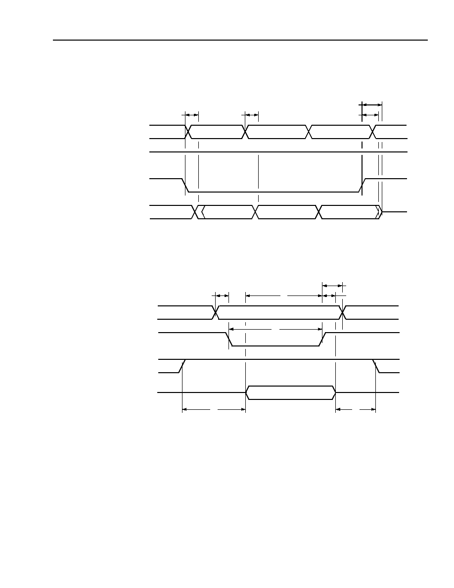
Agere Systems Inc.
153
Advance Data Sheet
September 2001
ATM Interconnect
CelXpres T8207
19
Timing Requirements
(continued)
19.3 External LUT Memory Timing
5-7795bF
Note: 30 pF load on outputs.
Figure 27. External LUT Memory Read Timing (cyc_per_acc = 2 and cyc_per_acc = 3)
5-7796aF
Note: 30 pF load on outputs.
Figure 28. External LUT Memory Write Timing (cyc_per_acc = 2 and cyc_per_acc = 3)
TR_A[17:0] & TR_CS*[1:0]
TR_WE*
TR_OE*
TR_D[7:0]
t1
t2
t3
t4
TR_A[17:0] & TR_CS*[1:0]
TR_WE*
TR_OE*
TR_D[7:0]
t2
t6
t4
t5
t7
t1
t3
t3

154
Agere Systems Inc.
Advance Data Sheet
September 2001
ATM Interconnect
CelXpres T8207
19
Timing Requirements
(continued)
The term mclkp in Tables 143, 144, 145, and 146, represents the period of mclk in ns.
Table 143. External LUT Memory Read Timing (cyc_per_acc = 2)
Table 144. External LUT Memory Read Timing (cyc_per_acc = 3)
Table 145. External LUT Memory Write Timing (cyc_per_acc = 2)
Table 146. External LUT Memory Write Timing (cyc_per_acc = 3)
Symbol
Parameter
Min
Typ
Max
Unit
t1
tr_oe* Low to tr_d[7:0] Driven by SRAM Chip
0
--
2 x mclkp ≠ 11
ns
t2
tr_a[17:0] & tr_cs*[1:0] Valid to tr_d[7:0] Valid
0
--
2 x mclkp ≠ 11
ns
t3
tr_oe* High to tr_d[7:0] Invalid
0
--
--
ns
t4
tr_oe* High to tr_d[7:0] 3-State
--
--
mclkp
ns
Symbol
Parameter
Min
Typ
Max
Unit
t1
tr_oe* Low to tr_d[7:0] Driven by SRAM Chip
0
--
3 x mclkp ≠ 11
ns
t2
tr_a[17:0] & tr_cs*[1:0] Valid to tr_d[7:0] Valid
0
--
3 x mclkp ≠ 11
ns
t3
tr_oe* High to tr_d[7:0] Invalid
0
--
--
ns
t4
tr_oe* High to tr_d[7:0] 3-State
--
--
mclkp
ns
Symbol
Parameter
Min
Typ
Max
Unit
t1
tr_oe* High to tr_d[7:0] Driven
mclkp ≠ 4
--
--
ns
t2
tr_a[17:0] Setup to tr_we* Falling Edge
2
--
--
ns
t3
tr_we* Low Pulse Width
mclkp ≠ 1
--
--
ns
t4
tr_d[7:0] Setup to tr_we* Rising Edge
mclkp
--
--
ns
t5
tr_d[7:0] Hold from tr_we* Rising Edge
2
--
--
ns
t6
tr_a[17:0] Hold from tr_we* Rising Edge
2
--
--
ns
t7
tr_d[7:0] 3-State to tr_oe* Low
0
--
--
ns
Symbol
Parameter
Min
Typ
Max
Unit
t1
tr_oe* High to tr_d[7:0] Driven
mclkp ≠ 4
--
--
ns
t2
tr_a[17:0] Setup to tr_we* Falling Edge
2
--
--
ns
t3
tr_we* Low Pulse Width
2 x mclkp ≠ 1
--
--
ns
t4
tr_d[7:0] Setup to tr_we* Rising Edge
2 x mclkp
--
--
ns
t5
tr_d[7:0] Hold from tr_we* Rising Edge
2
--
--
ns
t6
tr_a[17:0] Hold from tr_we* Rising Edge
2
--
--
ns
t7
tr_d[7:0] 3-State to tr_oe* Low
0
--
--
ns
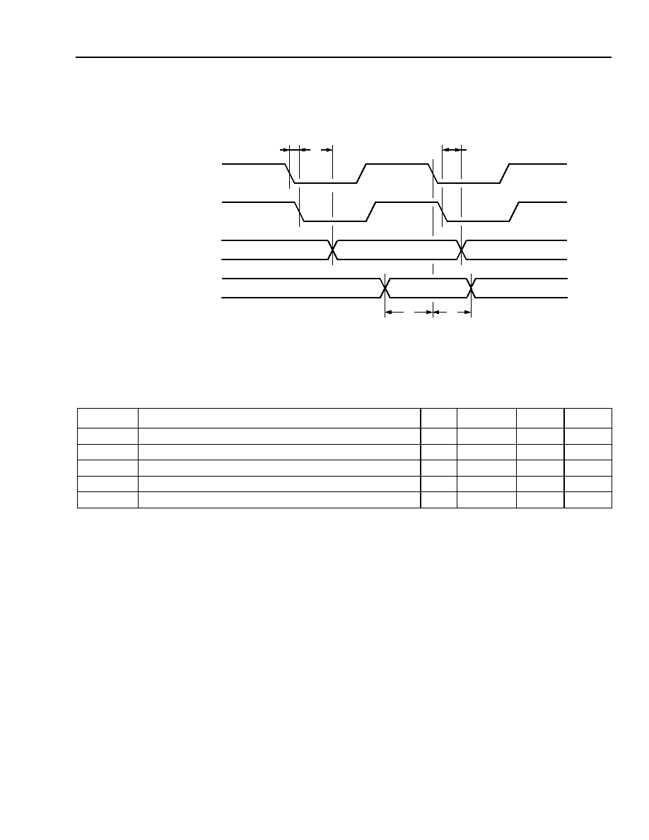
Agere Systems Inc.
155
Advance Data Sheet
September 2001
ATM Interconnect
CelXpres T8207
19
Timing Requirements
(continued)
19.4 Cell Bus Timing
5-7797bF
1. 25 pF load.
Figure 29. Cell Bus Timing
Table 147. Cell Bus Timing
1. Pin loading = 25 pF.
Symbol
Parameter
Min
Typ
Max
Unit
t1
cb_rc* Falling Edge to cb_wc* Falling Edge
1.5
--
4
ns
t2
cb_wc* Falling Edge to Output Valid
1
--
--
11.5
ns
t3
Input Setup to cb_rc* Falling Edge
1
--
--
ns
t4
Input Hold from cb_rc* Falling Edge
2
--
--
ns
t5
cb_wc* Falling Edge to Output Invalid
1
3
--
--
ns
CB_RC*
CB_WC*
CB_D*[31:0], CB_ACK*
1
,
CB_FS* (OUTPUT)
CB_D*[31:0], CB_ACK*,
CB_FS* (INPUT)
t1
t5
t2
t4
t3
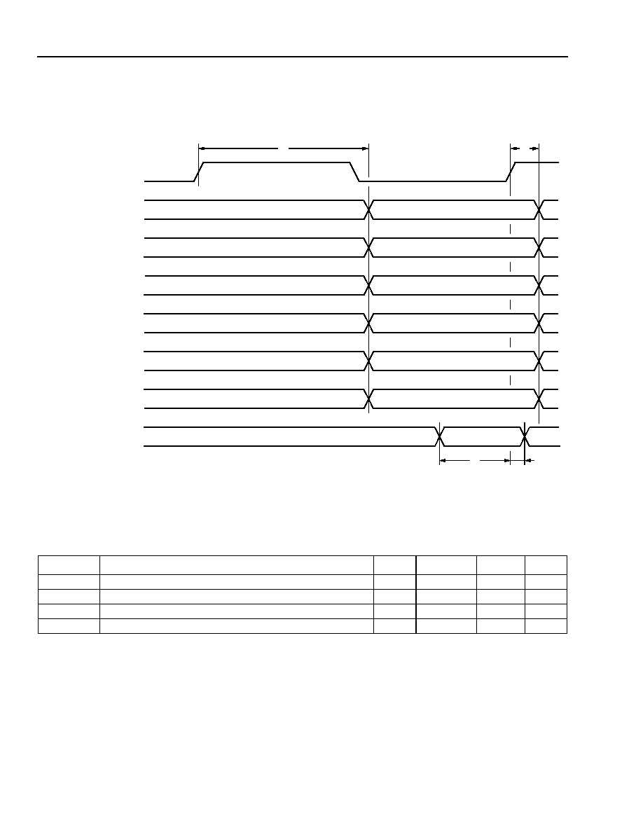
156
Agere Systems Inc.
Advance Data Sheet
September 2001
ATM Interconnect
CelXpres T8207
19
Timing Requirements
(continued)
19.5 SDRAM Interface Timing
5-7798BF
Note: 15 pF load on outputs.
Figure 30. SDRAM Interface Timing
Table 148. SDRAM Interface Timing
Symbol
Parameter
Min
Typ
Max
Unit
t1
sd_clk Rising to Outputs Valid
--
--
7
ns
t2
sd_clk Rising to Outputs Invalid
1.5
--
--
ns
t3
sd_d[15:0] Input Setup to sd_clk Rising Edge
3
--
--
ns
t4
sd_d[15:0] Input Hold from sd_clk Rising Edge
0
--
--
ns
SD_CLK*
SD_RAS*
SD_CAS*
SD_WE*
SD_BS[1:0]
SD_A[11:0]
SD_D[15:0]
SD_D[15:0]
(SOURCED BY T8207)
(SAMPLED BY T8207)
t4
t3
t1
t2
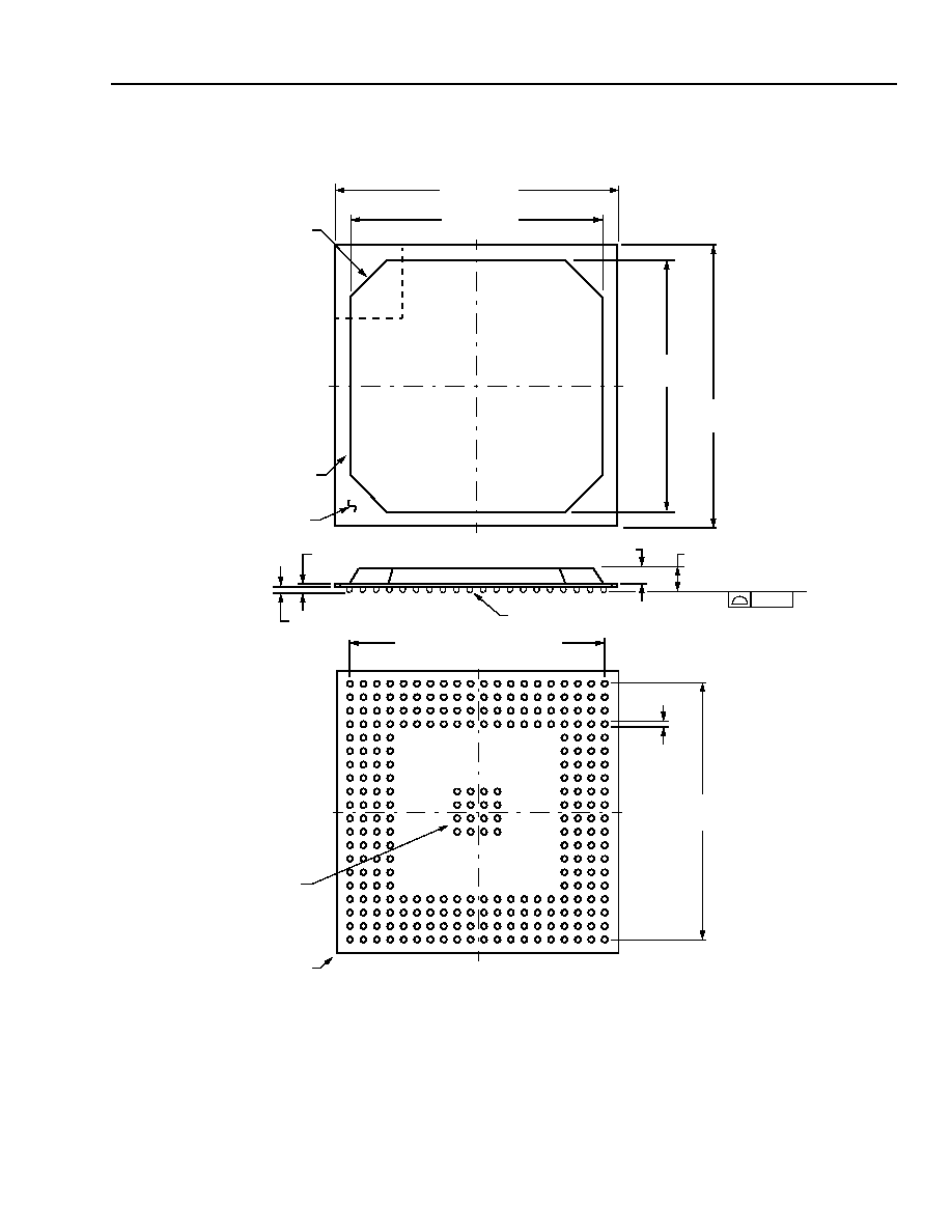
Agere Systems Inc.
157
Advance Data Sheet
September 2001
ATM Interconnect
CelXpres T8207
20
Outline Diagram
All dimensions shown are in millimeters.
5-4406.c
0.56
Ī
0.06
1.17
Ī
0.05
2.33
Ī
0.21
SEATING PLANE
SOLDER BALL
0.60
Ī
0.10
0.20
PWB
MOLD
COMPOUND
27.00
Ī
0.20
27.00
Ī
0.20
24.00
+0.70
≠0.00
24.00
+0.70
≠0.00
A1 BALL
IDENTIFIER ZONE
A
B
C
D
E
F
G
H
J
K
L
M
Y
N
P
R
T
U
V
W
1 2 3 4 5 6 7 8 9 10
11
12
13
14
15
16
17
18
20
19
CENTER ARRAY
FOR THERMAL
ENHANCEMENT
19 SPACES @ 1.27 = 24.13
A1 BALL
CORNER
19 SPACES
@ 1.27 = 24.13
0.75
Ī
0.15

Advance Data Sheet
September 2001
ATM Interconnect
CelXpres T8207
Agere Systems Inc. reserves the right to make changes to the product(s) or information contained herein without notice. No liab ility is assumed as a result of their use or application.
CelXpres is a trademark of Agere Systems Inc.
Copyright © 2001 Agere Systems Inc.
All Rights Reserved
September 2001
DS01-252DLC (Replaces DS00-211DLC)
For additional information, contact your Agere Systems Account Manager or the following:
INTERNET:
http://www.agere.com
E-MAIL:
docmaster@agere.com
N. AMERICA:
Agere Systems Inc., 555 Union Boulevard, Room 30L-15P-BA, Allentown, PA 18109-3286
1-800-372-2447, FAX 610-712-4106 (In CANADA: 1-800-553-2448, FAX 610-712-4106)
ASIA:
Agere Systems Hong Kong Ltd., Suites 3201 & 3210-12, 32/F, Tower 2, The Gateway, Harbour City, Kowloon
Tel. (852) 3129-2000, FAX (852) 3129-2020
CHINA: (86) 21-5047-1212 (Shanghai), (86) 10-6522-5566 (Beijing), (86) 755-695-7224 (Shenzhen)
JAPAN: (81) 3-5421-1600 (Tokyo), KOREA: (82) 2-767-1850 (Seoul), SINGAPORE: (65) 778-8833, TAIWAN: (886) 2-2725-5858 (Taipei)
EUROPE:
Tel. (44) 7000 624624, FAX (44) 1344 488 045
21
Ordering Information
Part Number
Package
Comcode
T-8207---BAL-DB
272-pin PBGAM, Dry Pack Tray
108698077
T-8207---BAL-DT
272-pin PBGAM Dry-bagged, Tape & Reel
108699265
Motorola
is a registered trademark of Motorola, Inc.
Intel
is a registered trademark of Intel Corporation.
Transwitch
and
CellBus
are registered trademarks of Transwitch Corp.