 | –≠–ª–µ–∫—Ç—Ä–æ–Ω–Ω—ã–π –∫–æ–º–ø–æ–Ω–µ–Ω—Ç: T8301 | –°–∫–∞—á–∞—Ç—å:  PDF PDF  ZIP ZIP |

Advance Data Sheet
December 2000
T8301 Internet Protocol Telephone
Phone-On-A-ChipTM IP Solution DSP
1 Introduction
Lucent Technologies' Phone-On-A-Chip IP Solution
is a highly integrated set of IC chips that form the
basic building blocks for an internet protocol tele-
phone (IPT), residing on a local area network (LAN).
The IPT presently consists of two ICs--the T8301
(IPT_DSP) and the T8302 (IPT_ARM*).
The T8301 provides the audio processing engine for
voice compression and decompression, speaker-
phone echo cancellation, digital-to-analog and ana-
log-to-digital converters, low-pass filters, and
amplifiers to drive standard business telephone
handsets and speakerphone hardware.
The general-purpose processor chip T8302 controls
system I/O (Ethernet, USB, IrDA, etc.) and provides
general telephone control features (LED control, key-
pad button scanning, LCD module interface, etc.).
A block diagram of the T8301 can be found in
Figure 3 on page 8.
Since the DSP1627 is an integral part of the T8301,
we will refer to the DSP1627 Digital Signal Processor
Data Sheet throughout this discussion.
1.1 Features
s
DSP1627 core with bit manipulation unit.
s
DSP clock speeds up to 80 MHz.
s
Instruction ROM, 32K x 16 (zero wait-state
at 80 MHz).
* ARM is a registered trademark of Advanced RISC Machines Lim-
ited.
s
Dual-port RAM, 6K x 16 (zero wait-state at
80 MHz).
s
Internal SRAM, 16K x 16 (single wait-state at
80 MHz).
s
16-bit analog-to-digital converter.
s
Programmable gain amplifier on audio input.
s
Fixed gain differential microphone input.
s
Analog input SRAM buffer, 512 x 16.
s
Timed DMA for analog input SRAM.
s
Two 16-bit digital-to-analog converters.
s
Independent simultaneous speaker and handset
outputs.
s
Two integrated differential speaker driver outputs.
s
Two analog output SRAM buffers, 512 x 16 each.
s
Two timed DMA outputs for simultaneous handset
and speaker audio output.
s
Low-pass filtering on audio inputs and outputs.
s
Serial I/O interface.
s
General-purpose timer counter.
s
Bit I/O interface.
s
JTAG test and debugging control.
s
Implementation in 0.35
µ
m, 5 V silicon technology.
s
Packaged in 100-pin TQFP.

Table of Contents
2
Lucent Technologies Inc.
Advance Data Sheet
December 2000
Phone-On-A-Chip IP Solution DSP
T8301 Internet Protocol Telephone
Contents
Page
Tables
Page
1 Introduction .............................................................. 1
1.1 Features ............................................................ 1
2 Pin Information ........................................................ 3
2.1 T8301 100-Pin TQFP Pin Diagram ................... 3
2.2 Pinout Information ............................................. 4
3 Overview .................................................................. 7
4 DSP1600 Core ........................................................ 9
4.1 Bit Manipulation Unit (BMU) .............................. 9
4.2 Timer ................................................................. 9
4.3 Clock PLL Control ............................................. 9
4.4 Bit Input/Output (BIO) ...................................... 10
4.5 Serial Input/Output (SIO) ................................. 10
4.6 Interrupts and Traps ........................................ 10
4.7 Power Management ........................................ 11
4.8 External Memory Interface (EMI) .................... 11
4.9 T8301 Memory Mapping ................................. 11
4.10 Y Space Memory Map ................................... 15
5 Audio Input/Output Circuitry .................................. 17
5.1 Analog Audio Input Channels .......................... 17
5.2 Programmable Gain Amplifier (PGA) .............. 17
5.3 Analog Audio Output Channels ....................... 18
5.4 Tone Ringer ..................................................... 18
5.5 Audio Codec Block .......................................... 20
5.6 Audio Codec Control Registers ....................... 21
6 DMA Input/Output Channels .................................. 23
6.1 DMA Operation ................................................ 23
6.2 DMA Registers ................................................ 23
7 Hardware Compander ........................................... 26
8 Electrical Specifications ......................................... 28
8.1 Operating Range Specifications ...................... 28
8.2 Analog and Codec Specifications .................... 28
8.3 Crystal Specification ........................................ 29
9 JTAG and Hardware
Development System (HDS) ................................. 30
9.1 TMODE Control for JCS/Boundary-Scan
Operation ........................................................ 30
9.1.1 Mode 7 Operation (TMODE = 7) ............ 30
9.1.2 Mode 6 operation (TMODE = 6) ............ 30
9.2 The Principle of Boundary-Scan
Architecture ..................................................... 30
9.2.1 Boundary-Scan
Instruction Register ................................ 32
Figures
Page
Figure 1. T8301 TQFP Pin Diagram ........................... 3
Figure 2. DSP/ARM Interface Block Diagram ............. 7
Figure 3. T8301 Block Diagram .................................. 8
Figure 4. Crystal Oscillator ......................................... 9
Figure 5. Audio Codec Block Diagram ..................... 20
Figure 6. Hardware Compander Block Diagram ....... 27
Figure 7. Boundary-Scan Architecture ..................... 31
Table 1. Pin Description ............................................. 4
Table 2. SIO Interface Signals .................................. 10
Table 3. DSP1627 INT0N and INT1N ...................... 11
Table 4. T8301 Instruction/Coefficient
Memory Map .............................................. 13
Table 5. T8301 Memory-Mapped Peripherals .......... 14
Table 6. Data Memory Area: I/O,
Register, and Memory ................................ 15
Table 7. Programmable Gain Amplifier Maximum .... 17
Table 8. Tone Ringer Control Register (trc_reg) ...... 18
Table 9. Tone Ringer Amplitude
Control Encoding ........................................ 19
Table 10. Tone Ringer Frequency Encoding ............ 19
Table 11. aioc_reg Analog Audio I/O Control ...........21
Table 12. Audio Codec Clock
Control Register (aclkc_reg) ..................... 22
Table 13. Audio Clock Encoding .............................. 22
Table 14. DMA Control Register dmac_reg .............. 24
Table 15. DMA Starting Address
Register setadr_reg .................................. 24
Table 16. DMA Transfer Count
Register setcnt_reg .................................. 24
Table 17. DMA Address Increment
Register adrinc_reg .................................. 25
Table 18. DMA Transfer Decrement Register
cntdec_reg ................................................ 25
Table 19. config_compander Register ...................... 26
Table 20. write_linear Register ................................. 26
Table 21. write_companded Register ....................... 26
Table 22. read_linear Register ................................. 26
Table 23. read_companded Register ....................... 26
Table 24. Operating Range Specifications ............... 28
Table 25. AINAN Specifications ...............................28
Table 26. AINCP, AINCN Specifications ..................28
Table 27. AOUTA Specifications .............................. 28
Table 28. Speaker#1, Speaker#2 Specifications ...... 29
Table 29. Digital Low-Pass Filters Specifications .....29
Table 30. Digital-to-Analog Converter
Specifications ........................................... 29
Table 31. Analog-to-Digital Converter
Specifications ........................................... 29
Table 32. Boundary-Scan Pin Functions ..................32
Table 33. Debug Mode .............................................. 32
Table 34. Boundary-Scan Instruction Register ......... 32
Table 35. Boundary-Scan Register Description ....... 33
Lucent Technologies Inc.
3
Advance Data Sheet
December 2000
T8301 Internet Protocol Telephone
Phone-On-A-Chip IP Solution DSP
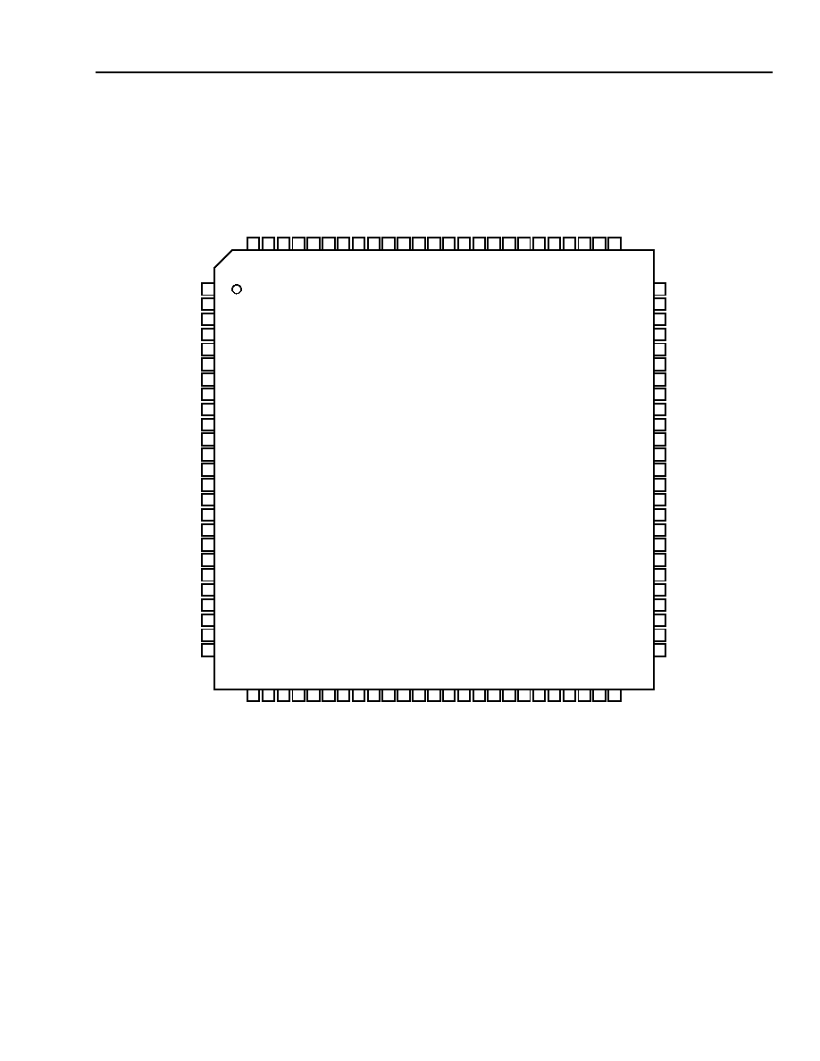
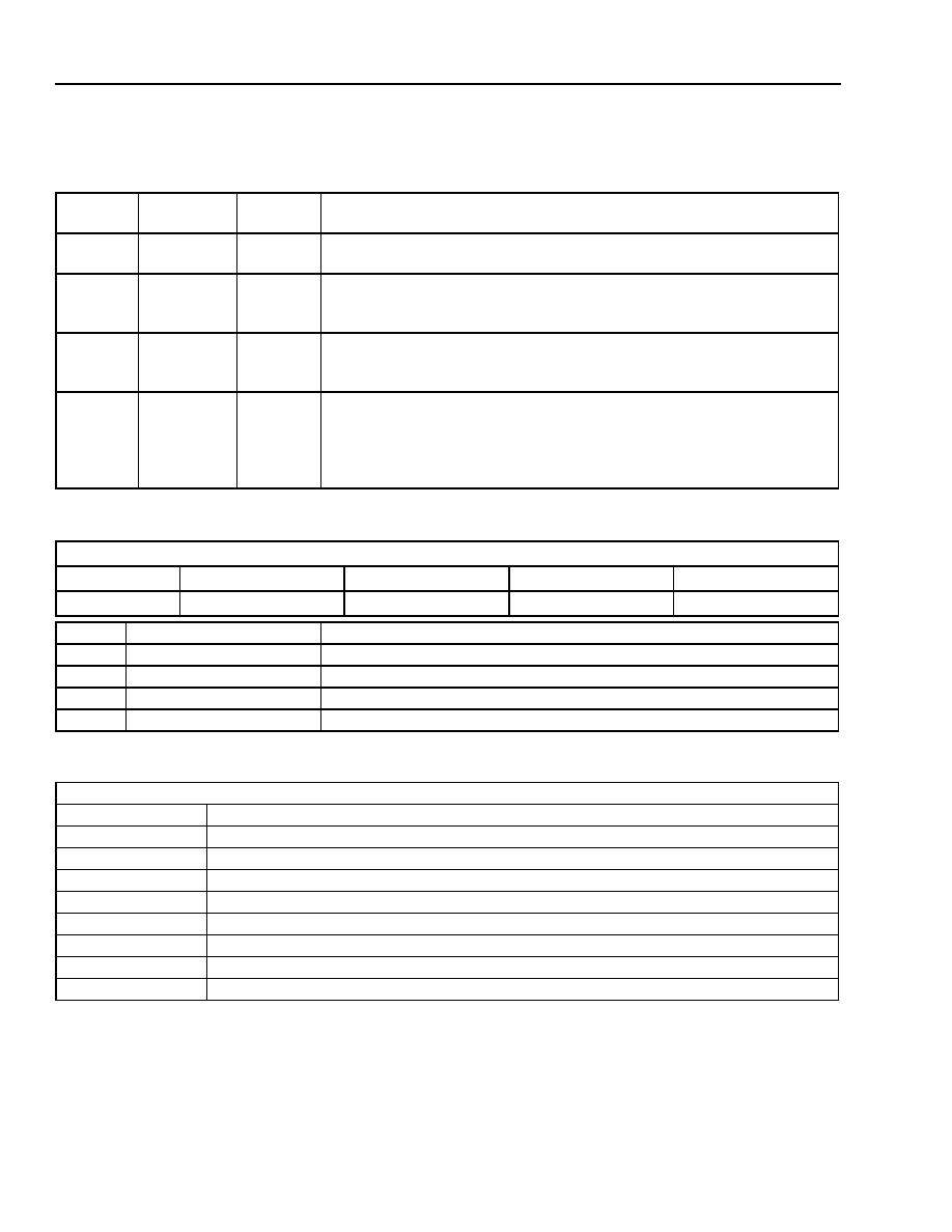
2 Pin Information
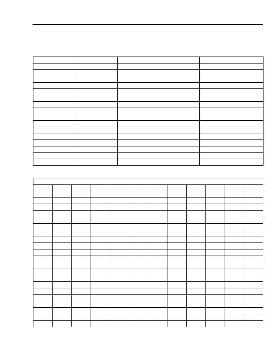
2.1 T8301 100-Pin TQFP Pin Diagram
5-8211(F)
Figure 1. T8301 TQFP Pin Diagram
V
DD
BIO0
BIO1
BIO2
BIO3
INT0N
INT1N
STOPN
DI1
V
SS
V
DD
DO1
SYNC
IOLD
IOCK
V
SS
V
DD
PLL
CKI1
CKI2
V
SS
PLL
A15
A14
A13
A12
V
SS
AINCP
AINCN
AINAN
V
SS
GB
V
DD
GB
STI1
STO1
STCK
CK8KHZ
V
DD
V
SS
D0
D1
D2
D3
D4
D5
D6
D7
V
DD
V
SS
D8
D9
D10
D11
V
SS
CK
O
CK
2MHZ
TDI
TM
S
TCK
TDO
RE
S
E
T
N
TM
ODEN2
TM
ODEN1
TM
ODEN0
TRS
T
N
V
DD
GB
V
SS
GB
SV
DD
S
PKD
R
V
2A
S
PKD
R
V
2B
SV
SS
SV
SS
S
PKD
R
V
1B
S
PKD
R
V
1A
SV
DD
V
DD
A
AO
U
T
A
GNDA
V
DD
A1
1
A1
0
A9
A8
A7
A6
A5
A4
V
SS
V
DD
A3
A2
A1
A0
I_
C
S
N
M_CS
N
X_C
S
N
RW
N
V
SS
V
DD
D15
D14
D13
D12
1
10
20
30
40
50
60
70
80
90
100
T8301
(100-pin TQFP)

4
Lucent Technologies Inc.
Phone-On-A-Chip IP Solution DSP
T8301 Internet Protocol Telephone
Advance Data Sheet
December 2000
2 Pin Information
(continued)
2.2 Pinout Information
In the following table, reference 1 refers to sections in the T8301 data sheet (this data sheet) and reference 2 refers
to sections in the DSP1627 data sheet.
Table 1. Pin Description
Pin #
Name
Description
Reference 1
Reference 2
1
V
DD
--
--
--
2
BIO0
BIT I/O 0
4.4
4.9
3
BIO1
BIT I/O 1
4.4
4.9
4
BIO2
BIT I/O 2
4.4
4.9
5
BIO3
BIT I/O 3
4.4
4.9
6
INT0N
DSP interrupt 0, active -low
4.6
4.3
7
INT1N
DSP interrupt 1, active -low
4.6
4.3
8
STOPN
Controls the internal processor clock, active -ow
--
4.13
9
DI1
Serial input/output unit (SIO) data in
4.5
4.7
10
V
SS
--
--
--
11
V
DD
--
--
--
12
DO1
Serial input/output unit (SIO) data out
4.5
4.7
13
SYNC
Serial input/output unit (SIO) sync
4.5
4.7
14
IOLD
Serial input/output unit (SIO) input load/output load
4.5
4.7
15
IOCK
Serial input/output unit (SIO) input clock/output clock
4.5
4.7
16
V
SS
--
--
--
17
V
DD
PLL
OSC and PLL V
DD
--
--
18
CKI1
XTL1 input/CMOS clock
4.3
4.12
19
CKI2
XTL2 input/CMOS clock
4.3
4.12
20
V
SS
PLL
OSC and PLL V
SS
--
--
21
A15
EMI address bus 15
4.9
--
22
A14
EMI address bus 14
4.9
4.5, 6.2
23
A13
EMI address bus 13
4.9
4.5, 6.2
24
A12
EMI address bus 12
4.9
4.5, 6.2
25
V
SS
--
--
--
26
V
DD
--
--
--
27
A11
EMI address bus 11
4.9
4.5, 6.2
28
A10
EMI address bus 10
4.9
4.5, 6.2
29
A9
EMI address bus 9
4.9
4.5, 6.2
30
A8
EMI address bus 8
4.9
4.5, 6.2
31
A7
EMI address bus 7
4.9
4.5, 6.2
32
A6
EMI address bus 6
4.9
4.5, 6.2
33
A5
EMI address bus 5
4.9
4.5, 6.2
34
A4
EMI address bus 4
4.9
4.5, 6.2
35
V
SS
--
--
--
36
V
DD
--
--
--
37
A3
EMI address bus 3
4.9
4.5, 6.2

Lucent Technologies Inc.
5
Advance Data Sheet
December 2000
Phone-On-A-Chip IP Solution DSP
T8301 Internet Protocol Telephone
2 Pin Information
(continued)
38
A2
EMI address bus 2
4.9
4.5, 6.2
39
A1
EMI address bus 1
4.9
4.5, 6.2
40
A0
EMI address bus 0
4.9
4.5, 6.2
41
I_CSN
ARM interrupt chip select, active-low
4.10, Table 6
--
42
M_CSN
ARM memory chip select, active-low
4.10, Table 6
--
43
X_CSN
External memory chip select, active-low
4.10, Table 6
--
44
RWN
Read/write, active-low
--
4.5, 6.2
45
V
SS
--
--
--
46
V
DD
--
--
--
47
D15
EMI data bus 15
3
4.5, 6.2
48
D14
EMI data bus 14
3
4.5, 6.2
49
D13
EMI data bus 13
3
4.5, 6.2
50
D12
EMI data bus 12
3
4.5, 6.2
51
D11
EMI data bus 11
3
4.5, 6.2
52
D10
EMI data bus 10
3
4.5, 6.2
53
D9
EMI data bus 9
3
4.5, 6.2
54
D8
EMI data bus 8
3
4.5, 6.2
55
V
SS
--
--
--
56
V
DD
--
--
--
57
D7
EMI data bus 7
3
4.5, 6.2
58
D6
EMI data bus 6
3
4.5, 6.2
59
D5
EMI data bus 5
3
4.5, 6.2
60
D4
EMI data bus 4
3
4.5, 6.2
61
D3
EMI data bus 3
3
4.5, 6.2
62
D2
EMI data bus 2
3
4.5, 6.2
63
D1
EMI data bus 1
3
4.5, 6.2
64
D0
EMI data bus 0
3
4.5, 6.2
65
V
SS
--
--
--
66
V
DD
--
--
--
67
CK8KHZ
Test clock
9.1
--
68
STCK
Serial test clock*
--
--
69
STO1
Serial test out 1*
--
--
70
STI1
Serial test in 1*
--
--
71
V
DD
GB
--
--
--
72
V
SS
GB
--
--
--
73
AINAN
(Handset) single-ended microphone input
5.1
--
74
AINCN
(Speakerphone) microphone differential input negative
5.1
--
75
AINCP
(Speakerphone) microphone differential input positive
5.1
--
76
GNDA
--
--
--
77
AOUTA
(Handset) single-ended speaker output
5.3
--
78
V
DD
A
--
--
--
* Leave open, this is for test purposes only.
Table 1. Pin Description (continued)
Pin #
Name
Description
Reference 1
Reference 2

6
Lucent Technologies Inc.
Phone-On-A-Chip IP Solution DSP
T8301 Internet Protocol Telephone
Advance Data Sheet
December 2000
2 Pin Information
(continued)
79
SV
DD
--
--
--
80
SPKDRV1A (Speakerphone) speaker#1 differential output driver A
5.3
--
81
SPKDRV1B (Speakerphone) speaker#1 differential output driver B
5.3
--
82
SV
SS
--
--
--
83
SV
SS
--
--
--
84
SPKDRV2B (Speakerphone) speaker#2 differential output driver B
5.3
--
85
SPKDRV2A (Speakerphone) speaker#2 differential output driver A
5.3
--
86
SV
DD
--
--
--
87
V
SS
GB
--
--
--
88
V
DD
GB
--
--
--
89
TRSTN
JTAG test reset input, active-low
9.2
--
90
TMODEN0
Test mode 0
9.1
--
91
TMODEN1
Test mode 1
9.1
--
92
TMODEN2
Test mode 2
9.1
--
93
RESETN
Chip reset, active-low
--
10.2
94
TDO
JTAG test data out
9.2
6.6
95
TCK
JTAG test clock
9.2
6.6
96
TMS
JTAG mode select
9.2
6.6
97
TDI
JTAG test data in
9.2
6.6
98
CK2MHZ
Clock out
9.1
--
99
CKO
DSP clock out
9.1
4.12
100
V
SS
--
--
--
Table 1. Pin Description (continued)
Pin #
Name
Description
Reference 1
Reference 2
Lucent Technologies Inc.
7
Advance Data Sheet
December 2000
T8301 Internet Protocol Telephone
Phone-On-A-Chip IP Solution DSP
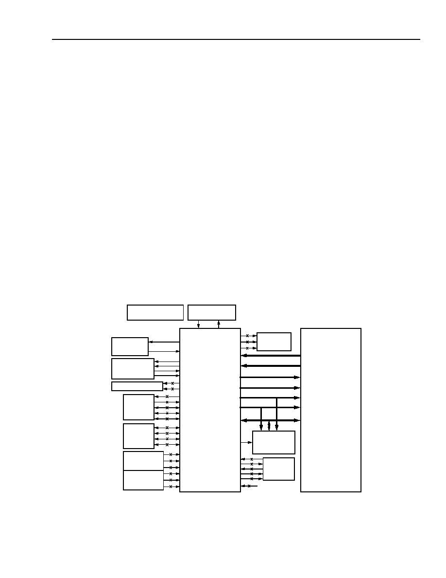
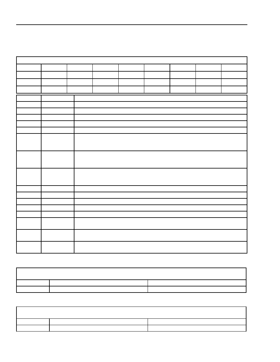
3 Overview
The T8301 (DSP) interfaces with the T8302 (ARM) to form the basic building blocks for an internet protocol tele-
phone (IPT), residing on a local area network (LAN); see Figure 2.
At the heart of the T8301 integrated circuit is the Lucent Technologies Microelectronics Group DSP1627 digital sig-
nal processor core. The DSP1627's high-performance (80 MIPS) and single-cycle multiply accumulate instruction
provide excellent support for execution of voice compression/decompression and echo cancellation algorithms.
The DSP1627 core and the analog audio circuitry included on the T8301 IC provide a low-cost silicon solution for
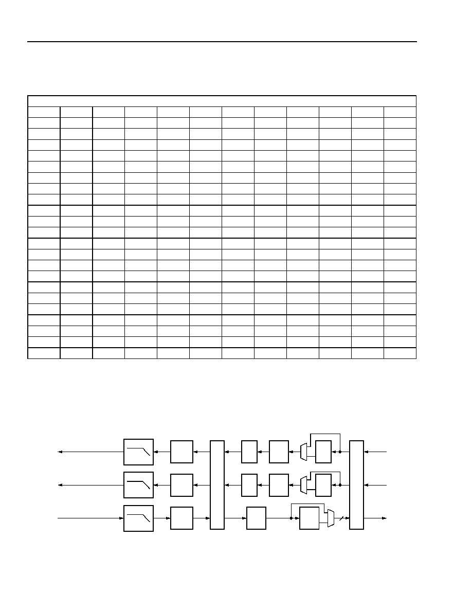
the IP exchange telephone's audio requirements. A block diagram of the T8301 integrated circuit is shown in
Figure 3.
The DSP1627 core contains the DSP1600 core processor, bit manipulation unit (BMU), dual-port RAM (DPRAM),
instruction/coefficient ROM (IROM), bit I/O (BIO), serial I/O (SIO), timer, clock PLL control, vectored interrupts and
traps, power management, external memory interface (EMI) with wait-state control, and a JTAG interface with inte-
gral hardware development system support.
The DSP1627 peripherals communicate with the DSP1627 core through the (D-IDB bus), which is 16 bits wide.
The DSP1627 core's Harvard architecture allows efficient memory utilization by supporting separate instruction
(XDB, XAB) and data (YDB, YAB) address spaces. The dual-port RAM (DPRAM) is connected to both address and
data buses XDB, YDB, XAB, and YAB, while the instruction ROM is only connected to the XDB and XAB memory
bus. The external memory interface provides a mechanism to access I/O devices and memories that are not part of
the core DSP1627 hardware.
For a complete description of the DSP1627 core and its peripherals, refer to the DSP1627 Digital Signal Processor
Data Sheet. A brief description of the functionality of the DSP1627 is provided in the following section. Where nec-
essary, comments are made which reflect differences between the operation of the DSP1627 and the T8301.
Please refer to the DSP1627 data sheet for further explanation.
Figure 2. DSP/ARM Interface Block Diagram
RESETN
DSP_INT0N
DSP_MCSN
DSP_ICSN
DSP_RWN
DSP_A0--DSP_A11
DSP_D0--DSP_D15
RESETN
INT0N
M_CS
I_CSN
RWN
A0--A11
D0--D15
X_CSN
TRSTN
TDO
TDI
TC
TMS
INT1N
BIO0
BIO1
BIO2
BIO3
STCK
STO1
STI1
TMODEN0
TMODEN1
TMODEN2
DO1
DI1
IOCK
IOLD
SYNC
SPKDRV1A
SPKDRV1B
AINCP
AINCN
SPKDRV2A
SPKDRV2B
AINAN
AOUTA
CKI1
CKI2
CKO
CK8KHZ
CK2MHZ
DSP
ARM
BOUNDARY
SCAN
AND/OR
JTAG
OPTIONAL
(MEMORY) DEVICE
ON 12K Y DATA
BUS
TEST MODE
SELECT PINS
ATE ANALOG
TEST PINS
OPTIONAL
BIT
INPUT
OUTPUT
OPTIONAL
EXTERNAL
SERIAL
CODEC
SPEAKERPHONE
SPEAKER AND
MIC
HANDSET
SPEAKER AND
MIC
HEADSET SPEAKER
X = LEAVE OPEN IF
UNUSED
12.288 MHz CLOCK
SOURCE
OPTIONAL
CLOCK
RESOURCES

8
Lucent Technologies Inc.
Phone-On-A-Chip IP Solution DSP
T8301 Internet Protocol Telephone
Advance Data Sheet
December 2000
3 Overview
(continued)
5-8210 (F)
Figure 3. T8301 Block Diagram
DMA
OUTPUT DMAS
COUNTER
ADDRESS
OUTPUT DMAH
COUNTER
ADDRESS
INPUT DMA
COUNTER
ADDRESS
dmac reg
trc_reg
TONE RINGER
aioc
AUDIO
CODEC
BLOCK
act1
act2
AUDIO CLOCK
GENERATOR
aclkc
SOUT SRAM
BUFFER
512 x 16
AOUTA SRAM
BUFFER
512 x 16
AIN SRAM
BUFFER
512 x 16
ADDRESS
DECODE
PGA
0--21 dB
IN 3 dB
`OR'
INTERNAL
SRAM
16K x 16
SIO
sdx(out)
srta
tdms
sdx(in)
sioc
saddx
TIMER
timerc
timer 0
BIO
sbit
cbit
YDB
YAB
DATA BUS
DSP 1600 CORE
XAB
XDB
INSTRUCTION/
COEFFICIENT BUS
I
N
T
E
R
R
D-IDB
BMU
aa0
aa1
ar1
ar2
ar0
ar3
U
P
T
DPRAM
6K x 16
IROM
32K x 16
EXTERNAL MEMORY INTERFACE
ioc
mwait
JTAG
jtag
JCON
ID
BYPASS
Breakpoint
Trace
HDS
CLOCK/PLL
pllc
& POWER
powerc
DSP1627
CORE
+
ER
O
M
ER
AMH
I
I/O
ER
AML
O
RW
N
A
[
15:
0]
D
[
15:
0]
STCK
STO1
STI1
SPKDRV1A
SPKDRV2A
SPKDRV2B
AOUTA
AINCP
AINCN
AINAN
TMODEN0
TMODEN1
TMODEN2
CKO
RESETN
STOPN
CK8kHz
CK2MHz
TDO
TDI
TCK
TMS
INT1N
INT0N
D(15:0)
A(15:0)
RWN
I_CSN
M_CSN
X_CSN
IOLD
IOCK
SYNC
DO1
DI1
BIO[3:0]
CKI2
CKI1
SPKDRV1B
OR
DMAINT
STEPS
TRSTN
30 dB
+
≠
12 dB
2.5 Vp-p
12 dB
1.5 dB
Lucent Technologies Inc.
9
Advance Data Sheet
December 2000
T8301 Internet Protocol Telephone
Phone-On-A-Chip IP Solution DSP
4 DSP1600 Core
The discussions in this section pertain to circuitry that is inside of the dotted outline in Figure 3. For additional
resources, please refer to the DSP1627 Digital Signal Processor Data Sheet.
The DSP1600 core includes a data arithmetic unit, memory addressing units, cache, and a control section. In com-
bination, these elements support a diverse instruction set for implementing users' algorithms.
4.1 Bit Manipulation Unit (BMU)
The BMU provides extensive bit manipulation capabilities that increase the DSP1627's efficiency in processing
data.
4.2 Timer
The DSP1627 core contains a programmable interrupt timer that can be configured to count over a wide range of
frequencies. This timer provides flexibility in timing events.
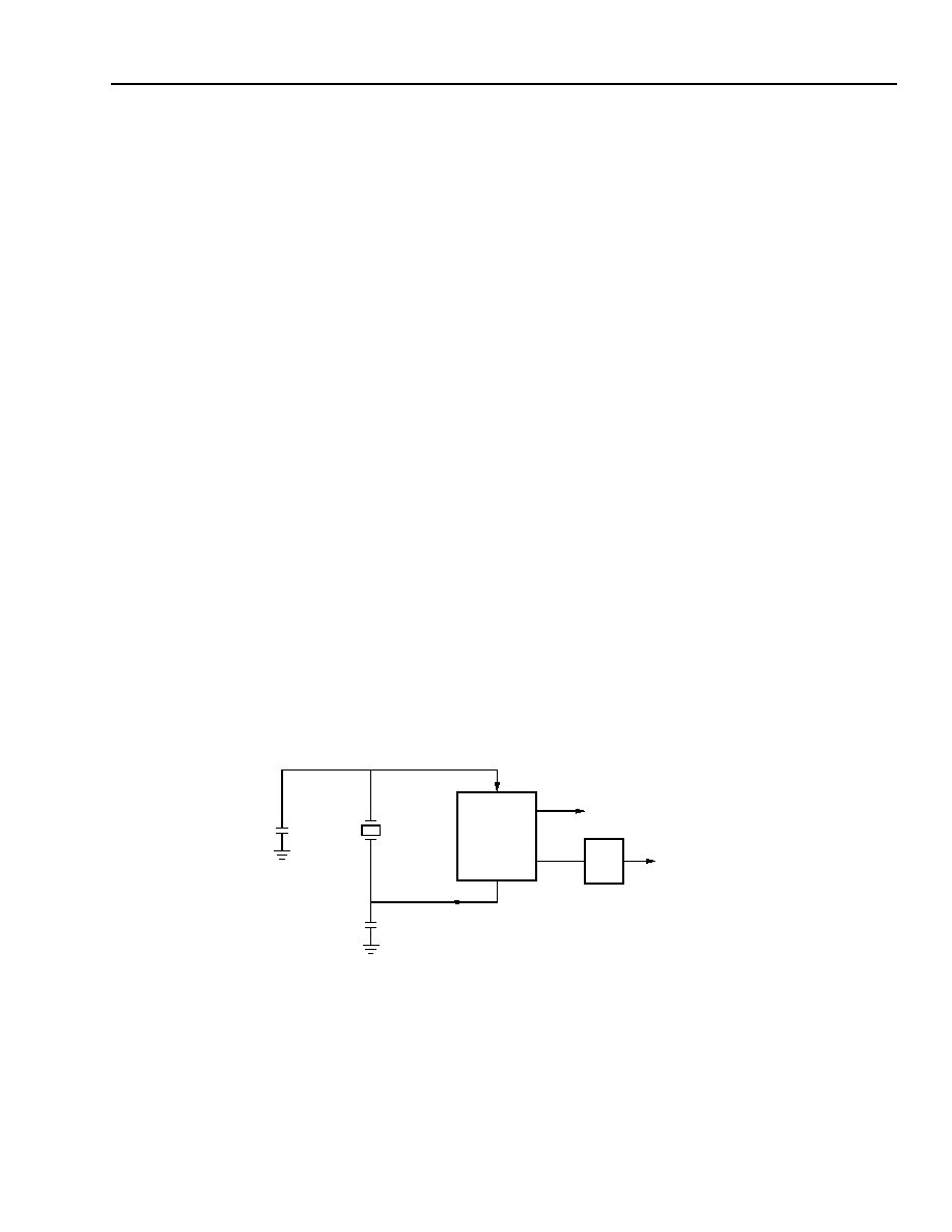
4.3 Clock PLL Control
The DSP1627 powers up with the input clock (CKI1/CKI2 in the T8301 IC) as the source for the processor clock.
An on-chip clock synthesizer (PLL) can also be used to generate the system clock for the DSP1627, which will run
at a frequency multiple of the input clock. The clock synthesizer is deselected and powered down on reset. For low-
power operation, an internally generated slow clock can be used to drive the DSP1627. If both the clock synthe-
sizer and the internally generated slow clock are selected, the slow clock will drive the DSP1627; however, the syn-
thesizer will continue to run.
The clock synthesizer and other programmable clock sources are discussed in the DSP1627 data sheet. The use
of these programmable clock sources for power management is also discussed in the DSP1627 data sheet. Board
designers should refer to the section on V
DDA
and V
SSA
connections in the data sheet for specific connection and
filtering requirements on the clock synthesizer power and ground leads.
Note: The 12,288 KHz is required as shown. Variations from this crystal frequency will cause detrimental effects to speech quality.
Figure 4. Crystal Oscillator
OSCILLATOR
TO PLL
˜
768
16 kHz
TO CODECS
CKI1
CKI2
LOAD
CAPACITOR
LOAD
CAPACITOR
12,288 kHz
CRYSTAL
10
Lucent Technologies Inc.
Phone-On-A-Chip IP Solution DSP
T8301 Internet Protocol Telephone
Advance Data Sheet
December 2000
4 DSP1600 Core
(continued)
4.4 Bit Input/Output (BIO)
The BIO provides convenient and efficient monitoring and control of four individually configurable pins. When con-
figured as outputs, the pins can be individually set, cleared, or toggled. When configured as inputs, individual pins
or combinations of pins can be tested for patterns. Flags returned by the BIO mesh seamlessly with conditional
instructions. Although the DSP1627 has eight BIOs available, the T8301 makes the four low-order BIOs available
on pins.
4.5 Serial Input/Output (SIO)
The serial I/O interface (SIO) of the T8301 closely follows the serial interface of the DSP1627. The T8301 multi-
plexes certain DSP1627 SIO pins and eliminates some others to reduce the total pin count. Hysteresis input buffers
are used for the SIO clocks on this device (IOLD, IOCK, and SYNC). The table below shows the signals that com-
prise the T8301 SIO interface.
* IOLD is comprised of the ILD1 and the OLD1 signals from the DSP1627 core tied together. By default, the IOLD signal is an input, which cor-
responds to the two DSP1627 load signals configured as passive. However, input load 1 (ILD1) may be configured as active, which then con-
figures the IOLD signal as an output. In this case, the internal input load 1 (ILD1) drives the output load signal (OLD1.)
IOCK is analogous to IOLD. Input clock 1 can be configured as an output, which would then drive IOCK and OCK1.
If the PLL is enabled, care should be taken if using IOCK as an output since there may be an unacceptable amount
of jitter on the clock.
The SYNC signal is intended to provide synchronization of the serial bus with an external 8 kHz frame clock. When
SYNC is configured as an input and asserted, the SIO load counter is reset and IOLD is asserted (if configured as
an output).
For typical applications, the SIO will be configured to have SYNC and IOCK as inputs and IOLD as an output (from
the DSP1627 core). In this configuration, there are thirty-two 8-bit (sixteen 16-bit) time slots for each SIO channel
and SYNC provides the 8 kHz SIO frame timing. The timing relationship for this configuration can be found in the
DSP1627 data sheet.
4.6 Interrupts and Traps
The DSP1627 supports prioritized, vectored interrupts, and a trap. There are eight internal hardware sources for
program interrupt and two external interrupt pins. Additionally, there is a trap signal from the hardware development
system (HDS). Each of the sources has a unique vector address and priority assigned to it. Refer to the DSP1627
data sheet for more information.
The use of the two external DSP1627 core interrupts is shown in Table 3 and in Figure 2.
Table 2. SIO Interface Signals
Symbol
Type
Function
DI1
I
Serial data in 1.
DO1
O
Serial data out 1.
IOLD*
I/O
Input/output load for SIO 1.
IOCK
I/O
Input/output clock for SIO 1.
SYNC
I/O
Sync for SIO 1 and 2.

Lucent Technologies Inc.
11
Advance Data Sheet
December 2000
Phone-On-A-Chip IP Solution DSP
T8301 Internet Protocol Telephone
4 DSP1600 Core
(continued)
INT0N is dedicated to the ARM DCC interrupts in the DSP's mask ROM. INT1N is internally ORed with the DMA
interrupt. The DSP's mask ROM for INT1 is dedicated to DMA servicing. It is recommended that INT1N float (inter-
nal pull up on pin).
4.7 Power Management
There are three different power management control mechanisms: the power control register (POWERC), the
stop pin (STOPN), and the AWAIT bit in the ALF register. Refer to the DSP1627 data sheet for more information
concerning these registers and their usage.
4.8 External Memory Interface (EMI)
The T8301 external memory interface is used to access the non-DSP1627 core features provided in the T8301
integrated circuit. The external memory interface is also used to access off-chip resources such as the interproces-
sor communication memories contained in the IPT_ARM integrated circuit.
The T8301 external memory interface requires one wait-state to access on-chip resources and two wait-states to
access 15 ns or faster off-chip resources when operating at 80 MHz.
4.9 T8301 Memory Mapping
The T8301 contains various types of memory modules, all with varying characteristics, aside from their memory
map location. As a Harvard architecture, the device has two address/data buses; these are referred to as X and Y.
The X system is used for program instructions and data, and the Y system is typically for data and memory
mapped I/O. Memory is 16 bits wide.
The DSP1627 can vary the X bus memory map based on the logic levels on two signals: EXM and LOWPR. How-
ever, the T8301 has EXM tied low internally, reducing the possibilities to two. The two memory maps are the
DSP1627's MAP1 and MAP3. LOWPR is software controllable. When using the DSP1627 software tools (with JCS
i.e., JTAG communications system) the tools will configure LOWPR automatically based upon the link time compile
options of the .if file. Map1 is the default map. The basic difference of the two maps is the type of memory at the
reset vector (0x0000). MAP1 has ROM at 0x0000, and MAP3 has RAM at 0x0000. The Y map is fixed.
The T8301 is a masked ROM-coded device and contains no flash memory. MAP 1 is typically used for production,
and Map 3 is typically used for code development. When used in conjunction to the T8302 ARM embedded proces-
sor, the ARM will be required to pass all code and data to the DSP's ram at power up reset. A hardware/software
protocol must be instituted to allow the ARM to successfully load code into the DSP.
Note: All X memory references are MAP 3.
s
Internal ROM, IROM--32K x 16:
-- Responds only to the X data bus, the X memory location is 0x4000--0xBFFF. This block will operate with zero
wait-states.
Table 3. DSP1627 INT0N and INT1N
Interrupt
Function
Interrupt Priority
INT1N
Interrupt from DMA block or external interrupt 1, active-low.
4 (higher)
INT0N
External interrupt input 0, active-low.
2

12
Lucent Technologies Inc.
Phone-On-A-Chip IP Solution DSP
T8301 Internet Protocol Telephone
Advance Data Sheet
December 2000
4 DSP1600 Core
(continued)
s
Dual-port (core) RAM, DPRAM--6K x 16:
-- This block is a true dual-port memory and is accessible simultaneously by both the X and Y bus system. Two
locations can be either read or written in the same instruction execution. This memory block resides at loca-
tions 0x0000--0x17FF on both the X and Y maps. This block will operate with zero wait states. The DPRAM
contains 6K x 16-bit words of zero wait-state memory, which is organized into six banks of 1K x 16-bit words.
Each bank has separate ports to the instruction/coefficient and data memory spaces. Dual accesses to both
memory spaces in separate banks incur no wait-states; however, accesses to the same bank from both
spaces will add one wait-state to the total access time.
s
Internal SRAM, ISRAM--16K x 16:
-- Although this is a dual-port RAM, there is only one bus system to the RAM itself. The X and Y bus is multi-
plexed before the RAM and is actually addressed via the external memory interface (EMI). Two locations can
be either read or written in the same instruction execution, but will require two clock cycles. The X memory
location is at 0xC000--0xFFFF and the Y memory location is at 0x8000--0xBFFF, and also at 0xC000--
0xFFFF. (Referred to as mirrored. A write to 0x8000 on the Y map will also write to 0xC000). There is only one
block of 16K; however, it appears twice on the Y map. There is one wait-state required for both the X and
Y bus to access this RAM.
s
External SRAM, XSRAM--12K x 16:
-- Responds only to the Y data bus. The T8301 generates a chip select called X_CSN (active-low), pin 43. It
uses the EMI to generate the address and data. There is one wait-state required for both the X and Y bus
to access this RAM.

Lucent Technologies Inc.
13
Advance Data Sheet
December 2000
Phone-On-A-Chip IP Solution DSP
T8301 Internet Protocol Telephone
4 DSP1600 Core
(continued)
Table 4. T8301 Instruction/Coefficient Memory Map
Address
X MAP1
X MAP3
Address
Y MAP
0x0000
0x0000
0x0800
Dual-port RAM 6K
0x0800
Dual-port RAM 6K
0x1000
(DPRAM)
0x1000
(DPRAM)
0x1800
0x1800
0x2000
Internal ROM 32K
0x2000
0x2800
(IROM)
Reserved 10K
0x2800
Reserved 10K
0x3000
0x3000
0x3800
0x3800
0x4000
(Instructions
0x4000
I/O and ERAMLO (See Table 5.)
0x4800
and constants)
0x4800
ERAMLO (See Table 5.)
0x5000
0x5000
0x5800
0x5800
ERAMLO External chip select
0x6000
Internal ROM 32K
0x6000
X_CSN (external SRAM) 12K
0x6800
(IROM)
0x6800
0x7000
0x7000
0x7800
0x7800
0x8000
(Instructions
0x8000
0x8800
and constants)
0x8800
0x9000
Internal SRAM 16K
0x9000
Internal SRAM 16K
0x9800
(ISRAM)
0x9800
(1K--16K block mirrored)
0xA000
0xA000
(ISRAM)
0xA800
0xA800
0xB000
0xB000
0xB800
0xB800
0xC000
0xC000
0xC800
Dual-port RAM 6K
0xC800
0xD000
(DPRAM)
Internal SRAM 16K
0xD000
Internal SRAM 16K
0xD800
(ISRAM)
0xD800
(1K--16K block mirrored)
0xE000
0xE000
(ISRAM)
0xE800
Reserved 10K
0xE800
0xF000
0xF000
0xF800
0xF800

14
Lucent Technologies Inc.
Phone-On-A-Chip IP Solution DSP
T8301 Internet Protocol Telephone
Advance Data Sheet
December 2000
4 DSP1600 Core
(continued)
Table 5. T8301 Memory-Mapped Peripherals
Address
Y MAP
0x4000
Analog I/O devices
0x4100
(I_CSN) DCC control interface
0x4200
Audio input, SRAM (512) read only
0x4300
0x4400
Handset audio output, SRAM (512) write only
0x4500
0x4600
Speaker audio output, SRAM (512) write only
0x4700
0x4800
M_CSN
0x4900
ARM-to-DSP
0x4A00
Buffer (1K)
0x4B00
0x4C00
M_CSN
0x4D00
DSP-to-ARM
0x4E00
Buffer (1K)
0x4F00

Lucent Technologies Inc.
15
Advance Data Sheet
December 2000
Phone-On-A-Chip IP Solution DSP
T8301 Internet Protocol Telephone
4 DSP1600 Core
(continued)
4.10 Y Space Memory Map
The table below shows the Y space memory map. This is the area can be addressed via the DSP1627's R0, R1,
R2, and R3 registers, and also by direct (Y-based) addressing.
Table 6. Data Memory Area: I/O, Register, and Memory
Address
R/W
DSP CS
Function
Description
Size
(words)
0x0:0x17FF
R/W
Internal
Internal RAM
--
6K
0x4000
R/W
I/O
aioc_reg
Analog audio I/O control register,
see Table 11.
1
0x4001
R/W
I/O
act1_reg
Audio codec test register 1.
1
0x4002
R/W
I/O
act2_reg
Audio codec test register 2.
1
0x4003
R/W
I/O
aclkc_reg
Audio codec clock control register,
see Table 12.
1
0x4008
R/W
I/O
trc_reg
Tone ringer control register, see Table 8.
1
0x4010
R/W
I/O
dmac_reg
DMA control register, see Table 14.
1
0x4014
R/W
I/O
AINsetadr_reg
Audio in DMA starting address register,
see Table 15.
1
0x4015
R/W
I/O
AINsetcnt_reg
Audio in DMA transfer count registers,
see Table 16.
1
0x4016
R/W
I/O
AINadrinc_reg
Audio in DMA address increment registers,
see Table 17.
1
0x4017
R/W
I/O
AINcntdec_reg
Audio in DMA transfer count decrement regis-
ter, see Table 18.
1
0x4018
R/W
I/O
HNDsetadr_reg
Handset DMA starting address register,
see Table 15.
1
0x4019
R/W
I/O
HNDsetcnt_reg
Handset DMA transfer count register,
see Table 16.
1
0x401A
R/W
I/O
HNDadrinc_reg
Handset DMA address increment register,
(see Table 17).
1
Ox401B
R/W
I/O
HNDcntdec_reg
Handset DMA transfer count decrement
register, see Table 18.
1
0x401C
R/W
I/O
SPKsetadr_reg
Speaker DMA starting address register,
see Table 15.
1
0x401D
R/W
I/O
SPKsetcnt_reg
Speaker DMA transfer count register,
see Table 16.
1
0x401E
R/W
I/O
SPKadrinc_reg
Speaker DMA address increment register,
see Table 17.
1
0x401F
R/W
I/O
SPKcntdec_reg
Speaker DMA transfer count decrement
register, see Table 18.
1
0x4040
R/W
I/O
config_compander Compander configuration register,
see Table 19.
1
0x4041
W
I/O
write_companded Write companded value register, see Table 21.
1
0x4041
R
I/O
read_linear
Read linear value register, see Table 22.
1
0x4042
W
I/O
write_linear
Write linear value register, see Table 20.
1

16
Lucent Technologies Inc.
Phone-On-A-Chip IP Solution DSP
T8301 Internet Protocol Telephone
Advance Data Sheet
December 2000
4 DSP1600 Core
(continued)
Address
R/W
DSP CS
Function
Description
Size
(words)
0x4042
R
I/O
read_companded Read companded value register,
see Table 23.
1
0x4100:0x4107
R/W
ERAMLO
I_CSN
External chip select to access token registers.
8
0x4108:x410B
R/W
ERAMLO
I_CSN
External chip select to access ARM interrupt
register.
4
0x410C:0x410F R/W
ERAMLO
I_CSN
External chip select to access DSP interrupt
register.
4
0x4110:0x41FF
R/W
ERAMLO
I_CSN
Reserved.
240
0x4200:0x43FF
R
ERAMLO
AIN SRAM
Audio input SRAM buffer.
512
0x4400:0x45FF
W
ERAMLO
AOUTA SRAM
Handset audio out SRAM buffer.
512
0x4600:0x47FF
W
ERAMLO
SOUT SRAM
Speaker audio out SRAM buffer.
512
0x4800:0x4BFF
R
ERAMLO
M_CSN
External chip select to access ARM to DSP
RAM (in the T8302 IPT_ARM chip).
1K
0x4C00:0x4FFF
W
ERAMLO
M_CSN
External chip select to access DSP to ARM
RAM (in the T8302 IPT_ARM chip).
1K
0x5000:0x7FFF R/W
ERAMLO
X_CSN
External spare chip select.
12K
0x8000:0xBFFF R/W
ERAMHI
ISRAM
Internal SRAM.
16K
Table 6. Data Memory Area: I/O, Register, and Memory (continued)
Lucent Technologies Inc.
17
Advance Data Sheet
December 2000
T8301 Internet Protocol Telephone
Phone-On-A-Chip IP Solution DSP
5 Audio Input/Output Circuitry
The discussions in this section pertain to circuitry that is outside of the dotted outline in Figure 3 on page 8.
5.1 Analog Audio Input Channels
The T8301 contains analog interfaces designed to support a 150
handset as well as an additional microphone
and two speakers.
The T8301 integrated circuit contains two audio analog inputs. There is a single-ended input (AINAN) to be con-
nected to a standard business telephone handset receiver. There is a differential input (AINCP, AINCN) to be con-
nected to a microphone. This provides the T8301 with the input circuitry to implement a speakerphone. The
differential input is directly connected to a 30 dB amplifier. The input select multiplexer routes AINAN or the output
of the fixed 30 dB amplifier to a programmable gain amplifier (PGA). The programmable gain amplifier is adjustable
from 0 dB to 21 dB in 3 dB steps. The signal output from the programmable gain amplifier is then routed to the
audio codec block to be digitized.
Each of the input signals AINAN, AINCP, and AINCN are ac-coupled to their T8301 inputs by a 0.2
µ
F capacitor.
The maximum signal input to the codec is 2.5 Vp-p. If the user sets the amplification to a value that would produce
a larger signal than 2.5 Vp-p, the audio codec will saturate and clip the input waveform.
The maximum input signal from the handset or from the microphone that can be supported for each gain setting is
listed in Table 7. Since the microphone amplifier has a maximum specified signal of 40 mV, the maximum micro-
phone input is not supported for PGA settings of 0 dB and 3 dB.
5.2 Programmable Gain Amplifier (PGA)
The programmable gain amplifier is using the PGAS[2:0] bits of the aioc_reg (see Table 11 on page 21). The set-
table gain values and their tolerances are shown below as well as the maximum allowed input signal voltage from
each of the input signals. Inputs greater than these values will saturate the input codec and produce clipped wave-
forms.
Table 7. Programmable Gain Amplifier Maximum
Bit Code
Gain
Max Input Signal
AINAN
AINCN, AINCP
000
0 dB ± 0.5 dB
2.500 Vp-p
Not supported
001
3 dB ± 0.5 dB
1.770 Vp-p
Not supported
010
6 dB ± 0.5 dB
1.250 Vp-p
40.0 mVp-p
011
9 dB ± 0.5 dB
0.844 Vp-p
28.3 mVp-p
100
12 dB ± 0.5 dB
0.625 Vp-p
20.0 mVp-p
101
15 dB ± 1.0 dB
0.442 Vp-p
14.2 mVp-p
110
18 dB ± 1.0 dB
0.313 Vp-p
10.0 mVp-p
111
21 dB ± 1.5 dB
0.221 Vp-p
7.1 mVp-p
18
Lucent Technologies Inc.
Phone-On-A-Chip IP Solution DSP
T8301 Internet Protocol Telephone
Advance Data Sheet
December 2000
5 Audio Input/Output Circuitry
(continued)
5.3 Analog Audio Output Channels
The T8301 contains two independent analog audio output ports. There is a single-ended output signal, AOUTA,
that can be connected to the speaker of a standard 150
business telephone handset or to a differential speaker
driver SPKDRV2. Differential speaker driver, SPKDRV1, can be set up to ring the phone by adding in the tone
ringer output into its audio path.
Differential speaker driver output pins (SPKDRV1A, SPKDRV1B and SPKDRV2A, SPKDRV2B) should be con-
nected to 45
speakers. Both outputs receive their analog signals from the audio codec block, which converts the
two digital input streams to analog signals.
The maximum signal from the codec is 2.5 Vp-p. The AOUTA signal has a maximum 2.5 Vp-p signal swing. It
should maintain a midlevel bias to prevent load noises when the driver is re-enabled. The speaker outputs
(SPKDRV1A, SPKDRV1B and SPKDRV2A, SPKDRV2B) each have 3 Vp-p signal swing. Since these outputs are
of opposite polarity, the differential signal output is 6 Vp-p. This is a 6 dB effective amplification of the codec output
signal. The signals should be biased such that, when power is re-enabled, no audible noises occur.
The differential speaker output driver does not have to produce a full 6 Vp-p signal without distortion. Signals above
5 Vp-p measured from SPKDRVxA to SPKDRVxB may be in the nonlinear range of the differential amplifier and
exhibit a flattening or clipping characteristic at the output.
AOUTA is ac coupled to the handset speaker using a 2
µ
F capacitor. The speaker driver outputs (SPKDRV1A,
SPKDRV1B and SPKDRV2A, SPKDRV2B) are direct coupled to 45
speakers.
5.4 Tone Ringer
The T8301 analog circuitry contains a tone ringer generator. When this circuit is powered up and enabled, the ring-
ing tone output is added to the current analog speaker signal and output through the differential speaker driver.
Custom tones may be generated by modifying the T8301 firmware.
Table 8. Tone Ringer Control Register (trc_reg)
Tone Ringer Control Register (trc_reg) Address (0x4008)
Bit #
15:13
12
11:8
7:0
Name
RSVD
TR_EN
TR_AC[3:0]
TR_FC[7:0]
Bit #
Name
Description
15:13
RSVD
Reserved.
12
TR_EN
Tone ringer output enable.
If 1, the tone ringer's output is added into the speaker output path.
If 0, the tone ringer's output is disconnected from the speaker output path.
11:8
TR_AC[3:0]
Tone ringer amplitude control, see Table 9.
7:0
TR_FC[7:0]
Tone ringer frequency control, see Table 10. (The tone ringer frequencies
are listed in hex format).
Lucent Technologies Inc.
19
Advance Data Sheet
December 2000
Phone-On-A-Chip IP Solution DSP
T8301 Internet Protocol Telephone
5 Audio Input/Output Circuitry
(continued)
Table 9. Tone Ringer Amplitude Control Encoding
Bit# TR_AC[3:0]
Volts Out (p-p)
dB Relative to Maximum Level
Tolerance (dB from Nominal)
0 0 0 0
Silent
dc to midvoltage reference
Not applicable
0 0 0 1
0.023 V
≠40.60
±0.75
0 0 1 0
0.032 V
≠37.74
±0.75
0 0 1 1
0.045 V
≠34.88
±0.75
0 1 0 0
0.063 V
≠32.02
±0.50
0 1 0 1
0.087 V
≠29.16
±0.50
0 1 1 0
0.120 V
≠26.30
±0.50
0 1 1 1
0.170 V
≠23.44
±0.25
1 0 0 0
0.230 V
≠20.58
±0.25
1 0 0 1
0.330 V
≠17.72
±0.25
1 0 1 0
0.460 V
≠14.86
±0.25
1 0 1 1
0.620 V
≠12.00
±0.25
1 1 0 0
0.880 V
≠9.00
±0.25
1 1 0 1
1.250 V
≠6.00
±0.25
1 1 1 0
1.770 V
≠3.00
±0.25
1 1 1 1
2.500 V
0
Not applicable
Table 10. Tone Ringer Frequency Encoding
Tone Ringer Frequency Encoding
Hz
Hex
Hz
Hex
Hz
Hex
Hz
Hex
Hz
Hex
Hz
Hex
24,000
3F
1,067
1D
545.5
35
366.4
6C
277.5
2A
223.3
C5
16,000
1F
1,043
0E
539.3
9A
363.6
36
275.9
95
222.2
62
12,000
0F
1,021
07
533.3
4D
360.9
1B
274.3
CA
221.2
31
9,600
87
1,000
03
527.5
A6
358.2
8D
272.7
E5
220.2
18
8,000
43
979.5
81
521.7
D3
355.5
C6
271.2
72
219.2
0C
6,857
A1
960.0
C0
516.1
69
352.9
E3
269.7
B9
218.2
06
6,000
D0
941.2
60
510.6
34
350.4
F1
268.2
DC
217.2
83
5,333
E8
923.1
30
505.3
1A
347.8
78
266.7
EE
216.2
C1
4,800
F4
905.6
98
500.0
0D
345.3
3C
265.2
77
215.3
E0
4,364
7A
888.9
4C
494.8
86
342.8
9E
263.7
BB
214.3
70
4,000
3D
872.7
26
489.8
C3
340.4
CF
262.3
DD
213.3
B8
3,692
1E
857.1
93
484.9
E1
338.0
E7
260.9
6E
212.4
5C
3,429
8F
842.1
49
480.0
F0
335.7
73
259.5
37
211.5
AE
3,200
C7
827.6
24
475.2
F8
333.3
39
258.1
9B
210.5
57
3,000
63
813.6
92
470.6
7C
331.0
9C
256.7
CD
209.6
AB
2,824
B1
800.0
C9
466.0
BE
328.8
CE
255.3
E6
208.7
55
2,667
58
786.9
64
461.5
DF
326.5
67
253.9
F3
207.8
AA
2,526
2C
774.2
B2
457.1
6F
324.3
33
252.6
79
206.9
D5
2,400
16
761.9
D9
452.8
B7
322.1
19
251.3
BC
206.0
EA
2,286
0B
750.0
EC
448.6
DB
320.0
8C
250.0
DE
205.1
F5
2,182
05
738.5
76
444.4
ED
317.9
46
248.7
EF
204.3
FA
20
Lucent Technologies Inc.
Phone-On-A-Chip IP Solution DSP
T8301 Internet Protocol Telephone
Advance Data Sheet
December 2000
5 Audio Input/Output Circuitry
(continued)
5.5 Audio Codec Block
The T8301 contains a 16-bit analog-to-digital converter and two 16-bit digital-to-audio converters. These convert-
ers each contain appropriate antialiasing or smoothing filters. A block diagram of the audio codec block is shown
below.
.
5-8212 (F)
Figure 5. Audio Codec Block Diagram
2,087
02
727.3
3B
440.4
F6
315.8
A3
247.4
F7
203.4
7D
2,000
01
716.4
9D
436.4
7B
313.7
D1
246.2
FB
202.5
3E
1,920
80
705.9
4E
432.4
BD
311.7
68
244.9
FD
201.7
9F
1,846
40
695.7
27
428.6
5E
309.7
B4
243.7
7E
200.8
4F
1,778
20
685.7
13
424.8
AF
307.7
5A
242.4
BF
200.0
A7
1,714
10
676.1
09
421.1
D7
305.7
2D
241.2
5F
199.2
53
1,655
88
666.7
04
417.4
EB
303.8
96
240.0
2F
198.3
29
1,600
C4
657.5
82
413.8
75
301.9
4B
238.8
97
197.5
14
1,548
E2
648.6
41
410.3
BA
300.0
25
237.6
CB
196.7
0A
1,500
71
640.0
A0
406.8
5D
298.1
12
236.5
65
195.9
85
1,455
38
631.6
50
403.4
2E
296.3
89
235.3
32
195.1
42
1,412
1C
623.4
A8
400.0
17
294.5
44
234.1
99
194.3
21
1,371
8E
615.4
D4
396.7
8B
292.7
A2
233.0
CC
193.5
90
1,333
47
607.6
6A
393.4
45
290.9
51
231.9
66
192.8
C8
1,297
23
600.0
B5
390.2
22
289.2
28
230.8
B3
192.0
E4
1,263
91
592.6
DA
387.1
11
287.4
94
229.7
59
191.2
F2
1,231
48
585.4
6D
384.0
08
285.7
4A
228.6
AC
190.5
F9
1,200
A4
578.3
B6
380.9
84
284.0
A5
227.5
56
189.7
FC
1,171
D2
571.4
5B
377.9
C2
282.4
52
226.4
2B
189.0
FE
1,143
E9
564.7
AD
375.0
61
280.7
A9
225.4
15
188.2
FF
1,116
74
558.2
D6
372.1
B0
279.1
54
224.3
8A
--
--
1,091
3A
551.7
6B
369.2
D8
--
--
--
--
--
--
Table 10. Tone Ringer Frequency Encoding (continued)
Tone Ringer Frequency Encoding
Hz
Hex
Hz
Hex
Hz
Hex
Hz
Hex
Hz
Hex
Hz
Hex
SDM
x 16
RCV
INTRP
x 4
RCV
LPF
x 2
SDM
x 16
RCV
INTRP
x 4
RCV
LPF
x 2
1 Mbit/s
64 kS/s
16 kS/s
8 kS/s
SINC3
DECM
/ 64
XMT
BPF
/ 2
1 Mbit/s
16 kS/s
8 kS/s
16
AMUX
DM
UX
FROM
TO
FROM
DAC
16-bit
DAC
16-bit
ADC
16-bit
LOW-PASS
RC FILTER
LOW-PASS
RC FILTER
LOW-PASS
RC FILTER
TO SPEAKER DRIVER
TO HANDSET OUTPUT
FROM AIN MUX
OR
SPEAKER DRIVER 2
DMAS
DMAH
DMAIN

Lucent Technologies Inc.
21
Advance Data Sheet
December 2000
Phone-On-A-Chip IP Solution DSP
T8301 Internet Protocol Telephone
5 Audio Input/Output Circuitry
(continued)
5.6 Audio Codec Control Registers
The analog audio input and output control register (aioc_reg) is used to select the active and enabled inputs
and outputs. Through this register the input and output channels can also have the clocks shut down to conserve
power.
Table 11. aioc_reg Analog Audio I/O Control
Analog Audio Input and Output Control Register (aioc_reg): Address (0x4000)
Bit #
15
14
13
12
11
10
9:8
Name
MPWRD
SPKFB
HNDFB
AINFB
SPK2EN
OLE
RSVD
Bit #
7
6
5
4
3
2
1:0
Name
RSVD
PGAS(2)
PGAS(1)
PGAS (0)
SPKEN
AOUTAEN
AINSS[1:0]
Bit #
Name
Value
at Reset
Description
15
MPWRD
1
Main powerdown.
If 1, powerdown.
If 0, powerup.
14
SPKFB
0*
Speaker #1 output filter bypass.
If 1, the transmit LPF is bypassed in the speaker path; set the correspond-
ing DMA clock to 16 kHz.
If 0, the transmit LPF is enabled in the speaker path.
Note: The SOC bits in the audio codec clock control register should
also be modified.
13
HNDFB
0*
Handset output filter bypass.
If 1, the transmit LPF is bypassed in the handset path; set the correspond-
ing DMA clock to 16 kHz.
If 0, the transmit LPF is enabled in the handset path.
Note: The HOC bits in the audio codec clock control register should
also be modified.
12
AINFB
0*
Analog input filter bypass.
If 1, the receive BPF is bypassed in the audio input path; set the corre-
sponding DMA clock to 16 kHz.
If 0, the receive BPF is enabled in the audio input path.
Note: The AINC bits in the audio codec clock control register should
also be modified.
11
SPK2EN
0
Enables speaker #2 output channel.
If 1, the speaker's output driver is enabled.
If 0, the output driver for the speaker output channel is disabled.
10
OLE
0
Output limit enable. When set, this bit causes the nominal full-scale output
for the analog outputs to be limited to approximately half the normal value
of 2.5 Vp-p Setting this bit has no effect on the receive gain.
9:7
RSVD
Reserved.
* If the BPF is bypassed, output from the decimator must be shifted right by 2 bits (6 dB attenuation) to avoid saturation going into the com-
pander. Similarly, if the LPF is bypassed in the speaker or handset path, input into the interpolator must be shifted left by 2 bits.
22
Lucent Technologies Inc.
Phone-On-A-Chip IP Solution DSP
T8301 Internet Protocol Telephone
Advance Data Sheet
December 2000
5 Audio Input/Output Circuitry
(continued)
Table 11. aioc_reg Analog Audio I/O Control
(
continued)
.
Bit #
Name
Value
at Reset
Description
6:4
PGAS[2:0]
000
PGA gain select. Selects the gain for the programmable gain amplifier.
See Table 7 on page 17 for an explanation of the coding.
3
SPKEN
0
Enables the speaker output channel.
If 1, the speaker's output driver is enabled.
If 0, the output driver for the speaker output channel is disabled.
2
AOUTAEN
0
Enables the handset output channel.
If 1, the handset output driver is enabled.
If 0, the output driver for the handset output channel is disabled.
1:0
AINSS
00
Analog input source select.
If 11, reserved.
If 10, analog input source is from the microphone (AINCN, AINCP).
If 01, analog input source is from the handset (AINAN).
If 00, mute (default after reset or powerup).
Table 12. Audio Codec Clock Control Register (aclkc_reg)
Audio Codec Clock Control Register (aclkc_reg) Address (0x4003)
Bit #
15:9
8:6
5:3
2:0
Name
RSVD
SOC(2:0)
HOC(2:0)
AINC(2:0)
Bit #
Name
Description
15:9
RSVD
Reserved.
8:6
SOC(2:0)
Please refer to Table 13 for bit field description.
5:3
HOC(2:0)
Please refer to Table 13 for bit field description.
2:0
AINC(2:0)
Please refer to Table 13 for bit field description.
Table 13. Audio Clock Encoding
Audio Clock Encoding SOC, HOC, AINC
Bit Code
Description
000
0 Hz. The clock for the channel is stopped.
001
8 kHz clock is used for all audio codes except G.722.
010
16 kHz clock is used for G.722 (must bypass filters).
011
Reserved.
100
Reserved.
101
Reserved.
110
Reserved.
111
Supplies 1 MHz clock to DMA. Reserved for testing only.

Lucent Technologies Inc.
23
Advance Data Sheet
December 2000
T8301 Internet Protocol Telephone
Phone-On-A-Chip IP Solution DSP
6 DMA Input/Output Channels
The discussions in this section pertain to circuitry that is outside of the dotted outline in Figure 3 on page 8.
There are three timed DMA transfer blocks, each of which transfers data to/from the audio codec block from/to a
512 x 16-bit SRAM. These SRAMs are two-port devices. One port is connected to the DSP1627 address and data
bus, and the other is accessed by the DMA controller. These memories transfer data to/from the audio codec block
or AOUTA, AIN, and SOUT. These DMA blocks are capable of transferring a 16-bit word to/from the device's A/D or
D/A at the following rates, which are set up by programming the audio codec clock control register:
s
8 kHz
s
16 kHz
Each channel initiates a transfer between the audio codec block and its respective SRAM on the rising edge of the
selected transfer clock.
6.1 DMA Operation
The T8301 has three timed DMA transfer channels. The DSP sets up a DMA channel by writing a starting address
and a transfer count into the setadr_reg (see Table 15) and setcnt_reg (see Table 16). The DSP then sets the
channel's GO bit in the dmac_reg (see Table 14). When the DMA finishes its current transfer operation, indicated
by the BSY bit in the dmac_reg going low, the DMA will transfer the contents of the setadr_reg (see Table 15) to
the adrinc_reg (see Table 17) and the cntdec_reg (see Table 18) respectively. The GO bit will be reset to zero and
the BSY bit will be set to one, in the dmac_reg on completion of this transfer. When the rising edge of the transfer
clock is detected, the DMA controller will transfer a single word to/from memory and the audio codec block. The
DMA channel will then increment its address pointer adrinc_reg and decrement its counter cntdec_reg. At the
completion of the number of transfers written into the transfer counter (cntdec_reg = 0), the DMA block will set its
ION bit in the dmac_reg to 1 and reset its BSY bit to zero. If its IEN bit is set, an interrupt to the DSP will occur. If
the DSP has set the GO bit which indicates that it has set up a new transfer or if the DSP responds (sets up a new
transfer count and re-enables transfers) before the next rising edge of the transfer clock, data can be continuously
transferred at the clocked rate.
If the DSP is reading or writing to the memory that a timed DMA is transferring to/from, the DMA can be delayed by
a clock cycle to allow the DSP to finish its access.
6.2 DMA Registers
Each DMA channel has the following four registers:
s
Starting address register
s
Transfer count register
s
Working address increment register (read only)
s
Working count decrement register (read only)
In addition, there is a control and status register that supports all three DMA channels.
24
Lucent Technologies Inc.
Phone-On-A-Chip IP Solution DSP
T8301 Internet Protocol Telephone
Advance Data Sheet
December 2000
6 DMA Input/Output Channels
(continued)
Table 14. DMA Control Register dmac_reg
DMA Control Register (dmac_reg) Address (0x4010)
Bit #
15
14
13
12
11
10
9
8
Name
RSVD
IENSPK
IENHND
IENAIN
RSVD
IONSPK
IONHND
IONAIN
Bit #
7
6
5
4
3
2
1
0
Name
RSVD
SPKBSY
HNDBSY
AINBSY
RSVD
SPKGO
HNDGO
AINGO
Bit #
Name
Description
15
RSVD Reserved.
14
IENSPK
Interrupt enable speaker output channel.
13
IENHND
Interrupt enable handset output channel.
12
IENAIN
Interrupt enable analog input channel.
11
RSVD Reserved.
10
IONSPK
Interrupt on speaker DMA channel. Indicates a transfer has completed. A physical
interrupt to the DSP will only occur if the IENSPK bit is also set. The interrupt is
cleared by a read operation.
9
IONHND
Interrupt on handset DMA channel. Indicates a transfer has completed. A physical
interrupt to the DSP will only occur if the IENHND bit is also set. The interrupt is
cleared by a read operation.
8
IONAIN
Interrupt on analog input DMA channel. Indicates a transfer has completed. A physi-
cal interrupt to the DSP will only occur if the IENAIN bit is also set. The interrupt is
cleared by a read operation.
7
RSVD
Reserved.
6
SPKBSY
Speaker DMA channel busy (read only).
5
HNDBSY
Handset DMA channel busy (read only).
4
AINBSY
Analog input DMA channel busy (read only).
3
RSVD
Reserved.
2
SPKGO
DMA start. Starts the DMA channel when set to 1, automatically reset to zero when a
count of zero is reached by the DMA transfer counter.
1
HNDGO
DMA start. Starts the DMA channel when set to 1, automatically reset to zero when a
count of zero is reached by the DMA transfer counter.
0
AINGO
DMA start. Starts the DMA channel when set to 1, automatically reset to zero when a
count of zero is reached by the DMA transfer counter.
Table 15. DMA Starting Address Register setadr_reg
Set DMA Address Registers [AINsetadr_reg Address (0x4014)] [HNDsetadr_reg Address (0x4018)]
[SPKsetadr_reg Address (0x401C)]
Bit #
15:9
8:0
Name
RSVD
DMA_ADDRESS_SET_UP[8:0]
Table 16. DMA Transfer Count Register setcnt_reg
Set DMA Count Registers [AINsetcnt_reg Address (0x4015)] [HNDsetcnt_reg Address (0x4019)]
[SPKsetcnt_reg Address (0x401D)]
Bit #
15:9
8:0
Name
RSVD
DMA_COUNT_SET_UP[8:0]
Lucent Technologies Inc.
25
Advance Data Sheet
December 2000
Phone-On-A-Chip IP Solution DSP
T8301 Internet Protocol Telephone
6 DMA Input/Output Channels
(continued)
Table 17. DMA Address Increment Register adrinc_reg
DMA Address Increment Registers (Read Only) [AINadrinc_reg Address (0x4016)]
[HNDadrinc_reg Address (0x401A)] [SPKadrinc_reg Address (0x401E)]
Bit #
15:9
8:0
Name
RSVD
DMA_ADDRESS[8:0]
Table 18. DMA Transfer Decrement Register cntdec_reg
DMA Count Decrement Registers (Read Only) [AINcntdec_reg Address (0x4017)]
[HNDcntdec_reg Address (0x401B)] [SPKcntdec_reg Address (0x401F)]
Bit #
15:9
8:0
Name
RSVD
DMA_COUNT[8:0]
26
Lucent Technologies Inc.
Phone-On-A-Chip IP Solution DSP
T8301 Internet Protocol Telephone
Advance Data Sheet
December 2000
7 Hardware Compander
The discussions in this section pertain to circuitry that is outside of the dotted outline in Figure 3 on page 8.
The hardware compander performs companded-to-linear and linear-to-companded conversions. This alleviates the
DSP from performing the functions in firmware. The compander supports both
µ
-law and A-law operations.
A block diagram of the compander is shown in Figure 6 on page 27. The compander consists of two write-only reg-
isters: write_linear and write_companded. A configuration register (config_compander) and two read registers
(read _linear and read_ companded) read the results. Config_compand configures the compander for either
µ
-law or A-law conversion. Upon reset, the register defaults to
µ
-law. The DSP performs a linear-to-companded
conversion by writing the write_linear register and then reading the read-companded buffer. The companded
value at the read buffer remains the same until a new linear value is written to the write_linear register. Similarly,
companded to linear is done by write_companded then read_linear.
Table 19. config_compander Register
Compander Configuration Register (config_compander)
Bit
15:1
0
Field
Reserved
µ-
Law
After Reset
X
1 =
µ-
Law
0 = A-Law
Table 20. write_linear Register
write_linear
Bit
15:0
--
Linear value
Table 21. write_companded Register
write_companded
Bit
15:0
--
Companded value
Table 22. read_linear Register
read_linear
Bit
15:0
--
Linear value
Table 23. read_companded Register
read_companded
Bit
15:0
--
Companded value

Lucent Technologies Inc.
27
Advance Data Sheet
December 2000
Phone-On-A-Chip IP Solution DSP
T8301 Internet Protocol Telephone
7 Hardware Compander
(continued)
5-8209(F)
Figure 6. Hardware Compander Block Diagram
The Config_compander register configures the compander for either
µ
-law or A-law conversion. Upon reset, the
register defaults to
µ
-law, see Table 19 on page 26.
CONFIG_COMPANDER
WRITE_LINEAR
READ_COMPANDED
WRITE_COMPANDED
READ_LINEAR
BUFFER
BUFFER
COMPANDER
COMBINATORIAL
LOGIC
µ
-
LAW
DSP_D[15:0]
DSP1627
28
Lucent Technologies Inc.
Phone-On-A-Chip IP Solution DSP
T8301 Internet Protocol Telephone
Advance Data Sheet
December 2000
8 Electrical Specifications
8.1 Operating Range Specifications
8.2 Analog and Codec Specifications
* Parameter supplied for reference purposes.
* Parameter supplied for reference purposes.
Table 24. Operating Range Specifications
Parameter
Symbol
Min
Max
Unit
Ambient Temperature Range
T
A
0
70
∞
C
Operating Supply Voltage
V
DD
4.75
5.25
V
Power Consumption
P
--
900
mW
Table 25. AINAN Specifications
Parameter
Conditions
Value
Source Impedance*
ac-coupled with a 0.2
µ
F capacitor
1 k
--3 k
Input Impedance
With ac-coupled +2.5 Vp-p input signal (max PGA gain)
6 k
--12 k
Total Harmonic Distortion
Input signals 100 mV--2.5 Vp-p
2%
Transmit Idle Channel Noise
PGA set 12 dB
20 dBrnC
Power Supply Rejection Ratio
--
50 dB
Table 26. AINCP, AINCN Specifications
Parameter
Conditions
Value
Source Impedance*
ac-coupled w/ 0.2
µ
F capacitor
1 k
-- 3 k
Input Impedance
With ac-coupled 40 mVp-p
12 k
--20 k
Total Gain
--
30 dB ± 1 dB
Total Harmonic Distortion
Input signals 1 mV--40 mV
2%
Total harmonic distortion input
signals 1 mV--40 mV
2%
Table 27. AOUTA Specifications
Parameter
Conditions
Value
V
OUT
0 dBm0
0.618 Vrms (±0.5 dB)
V
OUT
3.14 dBm0
2.50 Vp-p typical
Device impedance
--
150
Total harmonic distortion (3.0 dBm0)
≠35 dB max (
µ
A limit)
≠40 dB max
Total harmonic distortion (0.0 dBm0)
0.0 dB max (
µ
A limit)
≠65 dB max
Lucent Technologies Inc.
29
Advance Data Sheet
December 2000
Phone-On-A-Chip IP Solution DSP
T8301 Internet Protocol Telephone
8 Electrical Specifications
(continued)
Note: Maximum digital-to-analog converter range = 2.5 V. This translates into a peak-to-peak differential signal of 5.0 V. All signals measured
differentially.
.
.
8.3 Crystal Specification
See the DSP1627 Digital Signal Processor Data Sheet for further information.
Table 28. Speaker#1, Speaker#2 Specifications
Parameter
Conditions
Value
V
OUT
0 dBm0
1.236 Vrms (±0.5 dB)
V
OUT
3.14 dBm0
5.00 Vp-p typical
Device Impedance
--
45
Total Gain
--
6 dB ± 0.25 dB
Total Harmonic Distortion
≠35 dB max (
µ
A limit)
≠40 dB max
Total Harmonic Distortion
0.0 dB max (
µ
A limit)
≠65 dB max
Table 29. Digital Low-Pass Filters Specifications
Parameter
Conditions
Value
Maximum Ripple Pass-Band
300 Hz
signal frequency
3.0 kHz
3%
Minimum Attenuation
4 kHz
30 dB
Table 30. Digital-to-Analog Converter Specifications
Parameter
Conditions
Value
Range
--
16-bit
Monotonicity
Full operating range
Monotonic
Accuracy
Full operating range
TBD
Full Scale Output
--
2.5 Vp-p
Max Voltage Change 1-bit Change
--
1.5 LSB
Input Code
--
Two's complement
Table 31. Analog-to-Digital Converter Specifications
Parameter
Conditions
Value
Range
--
16-bit
Monotonicity
Full operating range
Monotonic
Accuracy
Full operating range
TBD
Max Step-to-step Size
--
1.5 LSB
Full Scale Input
--
2.5 Vp-p
Output Code
--
Two's complement

30
Lucent Technologies Inc.
Phone-On-A-Chip IP Solution DSP
T8301 Internet Protocol Telephone
Advance Data Sheet
December 2000
9 JTAG and Hardware Development System (HDS)
The JTAG block contains logic for implementing the JTAG/IEEE* P1149.1 standard. A four-signal test port provides
a mechanism for accessing the DSP1627 core from remote test equipment or a remote hardware development
system. The on-chip HDS performs instruction breakpointing and branch tracing at full speed. Using the JTAG port,
the breakpointing is set up and the trace history is read back.
9.1 TMODE Control for JCS/Boundary-Scan Operation
TMODEN0, TMODEN1, and TMODEN2 are inputs used to determine test mode operation. Of the eight possible
combinations, modes 6 and 7 are significant during the development and production phases.
9.1.1 Mode 7 Operation (TMODE = 7)
This is the production mode. Internal pull-up resistors (approximately 50 k
) will provide the logic level required.
The three pins can be left floating (no external resistors are required). In this mode, boundary-scan is active. The
CK8KHz (pin 67), the CK2MHz (pin 98), and the CKO (pin 99) are all dormant (high).
9.1.2 Mode 6 Operation (TMODE = 6)
The JCS tools (JTAG communications system) are used in this mode. TMODEN0 must be pulled low externally,
TMODEN1, and TMODEN2 can both be left floating to enter this mode. The CK8KHz (pin 67), the CK2MHz
(pin 98), and the CKO (pin 99) are active.
Should the user require access to any or all of the three clocks in production and still require boundary-scan capa-
bilities for production test, a strong (external) pull-down resistor would be required on TMODEN0 (1 k
). The pro-
duction test must be able to pull TMODEN0 high to allow access to the boundary-scan test. After the test is
complete, the pin would normally be low (TMODE 6) allowing the clocks to be active.
9.2 The Principle of Boundary-Scan Architecture
Each primary input signal and primary output signal is supplemented with a multipurpose memory element called a
boundary-scan cell. Cells on device primary inputs are referred to as input cells and cells on primary outputs are
referred to as output cells. Input and output is relative to the core logic of the device.
At any time, only one register can be connected from TDI to TDO, e.g., the instruction register (IR), BYPASS,
boundary-scan, IDENT, or even some appropriate register internal to the core logic; see Figure 7. The selected
register is identified by the decoded output of the instruction register. Certain instructions are mandatory, such as
EXTEST (boundary-scan register selected), whereas others are optional, such as the IDCODE instruction (IDENT
register selected).
* IEEE is a registered trademark of The Institute of Electrical and Electronics Engineers, Inc.
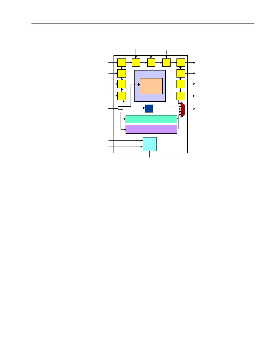
Lucent Technologies Inc.
31
Advance Data Sheet
December 2000
Phone-On-A-Chip IP Solution DSP
T8301 Internet Protocol Telephone
9 JTAG and Hardware Development System (HDS)
(continued)
Figure 7. Boundary-Scan Architecture
Figure 7 shows the following elements:
s
A set of four dedicated test pins, test data in (TDI), test mode select (TMS), test clock (TCK), test data out (TDO),
and one optional test pin test reset (TRSTN). These pins are collectively referred to as the test access port
(TAP).
s
A boundary-scan cell on each device's primary input and primary output pin, connected internally to form a serial
boundary-scan register (boundary-scan).
s
A finite-state machine TAP controller with inputs TCK and TMS.
s
An n-bit (n = 4) instruction register (IR), holding the current instruction.
s
A 1-bit bypass register (BYPASS).
s
An optional 32-bit identification register (IDENT) capable of being loaded with a permanent device identification
code.
INTERNAL
CORE LOGIC
IDENTIFICATION REGISTER
INSTRUCTION REGISTER (IR)
TEST MODE SELECT
TEST CLOCK
TMS
TCK
TEST RESET (TRSTN)
TEST DATA OUT
TDO
TDI
TEST DATA IN
BYPASS
TAP
CONTROLLER
IEEE 1149.1 CHIP ARCHITECTURE

32
Lucent Technologies Inc.
Phone-On-A-Chip IP Solution DSP
T8301 Internet Protocol Telephone
Advance Data Sheet
December 2000
9 JTAG and Hardware Development System (HDS)
(continued)
Access to JTAG (joint test action group) and boundary-scan will be initially provided through a single set of JTAG
pins. The pin definitions are as follows.
Debug mode, or boundary-scan mode is selected via the TMODE pins as shown below.
9.2.1 Boundary-Scan Instruction Register
The boundary-scan instruction register is 4 bits long and the capture value is 0001.
The idcode values are as follows:
Version = 0000 (0x0)
Part = 0011011101000110 (0x 3746)
Manufacturer = 00000011101 (0x1D)
Table 32. Boundary-Scan Pin Functions
Pin
Boundary-Scan
Debug
Comments
94
TDO (bscan)
TDO (debug)
--
95
TCK (bscan)
TCK (debug)
Pulled high internally
96
TMS (bscan)
TMS (debug)
Pulled high internally
97
TDI (bscan)
TDI (debug)
--
89
TRSTN (bscan)
TRSTN (debug)
Pulled high internally
Table 33. Debug Mode
Pin
Name
Description
Comments
90
TMODEN0
If 7 = boundary-scan
If 6 = debug
Pulled high internally
91
TMODEN1
Pulled high internally
92
TMODEN2
Pulled high internally
Table 34. Boundary-Scan Instruction Register
Instruction
Binary Code
Description
EXTEST
0000
Places the boundary-scan register in EXTEST mode.
SAMPLE
0001
Places the boundary-scan register in sample mode.
IDCODE
0101
Identification code.
BYPASS
1111
Places the bypass register in the scan chain.

Lucent Technologies Inc.
33
Advance Data Sheet
December 2000
Phone-On-A-Chip IP Solution DSP
T8301 Internet Protocol Telephone
9 JTAG and Hardware Development System (HDS)
(continued)
Table 35. Boundary-Scan Register Description
Boundary-Scan
Register Bit Pin
Pin Name
Ball
Enabled State
Pin Grouping
Control
Disable Value
0
BIO_E(0)
--
Controller
--
--
--
1
BIO(0)
2
I/O
BIO_E(0) 0
High
Impedance
2
BIO_E(1)
--
Controller
--
--
--
3
BIO(1)
3
I/O
BIO_E(1) 0
High
Impedance
4
BIO_E(2)
--
Controller
--
--
--
5
BIO(2)
4
I/O
BIO_E(2) 0
High
Impedance
6
BIO_E(3)
--
Controller
--
--
--
7
BIO(3)
5
I/O
BIO_E(3) 0
High
Impedance
8
INT0N
6
Input
--
--
--
9
INT1N
7
Input
--
--
--
10
STOPN
8
Input
--
--
--
11
DI1
9
Input
--
--
--
12
DO1_E
--
Controller
--
--
--
13
DO1
12
I/O
DO1_E
0
High Impedance
14
SYNC_E
--
Controller
--
--
--
15
SYNC
13
I/O
SYNC_E
0
High Impedance
16
IOLD_E
--
Controller
--
--
--
17
IOLD
14
I/O
IOLD_E
0
High Impedance
18
IOCK_E
--
Controller
--
--
--
19
IOCK
15
I/O
IOCK_E
0
High Impedance
20
DSP_A_E
--
Controller
--
--
--
21
A(15)
21
I/O
A_E
0
High Impedance
22
A(14)
22
I/O
A_E
0
High Impedance
23
A(13)
23
I/O
A_E
0
High Impedance
24
A(12)
24
I/O
A_E
0
High Impedance
25
A(11)
27
I/O
A_E
0
High Impedance
26
A(10)
28
I/O
A_E
0
High Impedance
27
A(9)
29
I/O
A_E
0
High Impedance
28
A(8)
30
I/O
A_E
0
High Impedance
29
A(7)
31
I/O
A_E
0
High Impedance
30
A(6)
32
I/O
A_E
0
High Impedance
31
A(5)
33
I/O
A_E
0
High Impedance
32
A(4)
34
I/O
A_E
0
High Impedance
33
A(3)
37
I/O
A_E
0
High Impedance
34
A(2)
38
I/O
A_E
0
High Impedance
35
A(1)
39
I/O
A_E
0
High Impedance
36
A(0)
40
I/O
A_E
0
High Impedance
37
I_CSN
41
I/O
A_E
0
High Impedance
38
M_CSN
42
I/O
A_E
0
High Impedance
39
X_CSN
43
I/O
A_E
0
High Impedance
40
RWN
44
I/O
A_E
0
High Impedance

34
Lucent Technologies Inc.
Phone-On-A-Chip IP Solution DSP
T8301 Internet Protocol Telephone
Advance Data Sheet
December 2000
9 JTAG and Hardware Development System (HDS)
(continued)
Boundary-Scan
Register Bit Pin
Pin Name
Ball
Enabled State
Pin Grouping
Control
Disable Value
41
D_E
--
Controller
--
--
--
42
D(15)
47
I/O
D_E
0
High Impedance
43
D(14)
48
I/O
D_E
0
High Impedance
44
D(13)
49
I/O
D_E
0
High Impedance
45
D(12)
50
I/O
D_E
0
High Impedance
46
D(11)
51
I/O
D_E
0
High Impedance
47
D(10)
52
I/O
D_E
0
High Impedance
48
D(9)
53
I/O
D_E
0
High Impedance
49
D(8)
54
I/O
D_E
0
High Impedance
50
D(7)
57
I/O
D_E
0
High Impedance
51
D(6)
58
I/O
D_E
0
High Impedance
52
D(5)
59
I/O
D_E
0
High Impedance
53
D(4)
60
I/O
D_E
0
High Impedance
54
D(3)
61
I/O
D_E
0
High Impedance
55
D(2)
62
I/O
D_E
0
High Impedance
56
D(1)
63
I/O
D_E
0
High Impedance
57
D(0)
64
I/O
D_E
0
High Impedance
58
CLK_E
--
Controller
--
--
--
59
CK8KHZ
67
I/O
CLK_E
0
High Impedance
60
STCK_E
--
Controller
--
--
--
61
STCK
68
I/O
STCK_E
0
High Impedance
62
STI_E
--
Controller
--
--
--
63
STI1
70
I/O
STI_E
0
High Impedance
64
STO_E
--
Controller
--
--
--
65
STO1
69
I/O
STO_E
0
High Impedance
66
RESETN_E
--
Controller
--
--
--
67
RESETN
93
I/O
RESETN_E
0
High Impedance
68
CK2MHZ
98
I/O
CLK_E
0
High Impedance
69
CKO
99
I/O
CLK_E
0
High Impedance
Table 35. Boundary-Scan Register Description (continued)

Lucent Technologies Inc.
35
Advance Data Sheet
December 2000
T8301 Internet Protocol Telephone
Phone-On-A-Chip IP Solution DSP
Notes

Lucent Technologies Inc. reserves the right to make changes to the product(s) or information contained herein without notice. No liability is assumed as a
result of their use or application. No rights under any patent accompany the sale of any such product(s) or information. Phone-On-A-Chip is a trademark of
Lucent Technologies Inc.
Copyright © 2000 Lucent Technologies Inc.
All Rights Reserved
Printed in U.S.A.
December 2000
DS01-025IPT (Replaces DS00-030IPT-3)
For additional information, contact your Microelectronics Group Account Manager or the following:
INTERNET:
http://www.lucent.com/micro
E-MAIL:
docmaster@micro.lucent.com
N. AMERICA: Microelectronics Group, Lucent Technologies Inc., 555 Union Boulevard, Room 30L-15P-BA, Allentown, PA 18109-3286
1-800-372-2447, FAX 610-712-4106 (In CANADA: 1-800-553-2448, FAX 610-712-4106)
ASIA PACIFIC: Microelectronics Group, Lucent Technologies Singapore Pte. Ltd., 77 Science Park Drive, #03-18 Cintech III, Singapore 118256
Tel. (65) 778 8833, FAX (65) 777 7495
CHINA:
Microelectronics Group, Lucent Technologies (China) Co., Ltd., A-F2, 23/F, Zao Fong Universe Building, 1800 Zhong Shan Xi Road, Shanghai
200233 P. R. China Tel. (86) 21 6440 0468, ext. 325, FAX (86) 21 6440 0652
JAPAN:
Microelectronics Group, Lucent Technologies Japan Ltd., 7-18, Higashi-Gotanda 2-chome, Shinagawa-ku, Tokyo 141, Japan
Tel. (81) 3 5421 1600, FAX (81) 3 5421 1700
EUROPE:
Data Requests: MICROELECTRONICS GROUP DATALINE: Tel. (44) 7000 582 368, FAX (44) 1189 328 148
Technical Inquiries: GERMANY: (49) 89 95086 0 (Munich), UNITED KINGDOM: (44) 1344 865 900 (Ascot),
FRANCE: (33) 1 40 83 68 00 (Paris), SWEDEN: (46) 8 594 607 00 (Stockholm), FINLAND: (358) 9 3507670 (Helsinki),
ITALY: (39) 02 6608131 (Milan), SPAIN: (34) 1 807 1441 (Madrid)

Data Sheet
March 2000
DSP1627 Digital Signal Processor
1 Features
s
Optimized for digital cellular applications with a bit manip-
ulation unit for higher coding efficiency.
s
On-chip, programmable, PLL clock synthesizer.
s
14 ns and 11 ns instruction cycle times at 5 V, 10 ns in-
struction cycle time at 3.0 V, and 20 ns and 12.5 ns in-
struction cycle times at 2.7 V, respectively.
s
Mask-programmable memory map option: The
DSP1627x36 features 36 Kwords on-chip ROM. The
DSP1627x32 features 32 Kwords on-chip ROM and ac-
cess to 16 Kwords external ROM in the same map. Both
feature 6 Kwords on-chip, dual-port RAM and a secure
option for on-chip ROM.
s
Low power consumption:
-- <5.5 mW/MIPS typical at 5 V.
-- <1.5 mW/MIPS typical at 2.7 V.
s
Flexible power management modes:
-- Standard sleep: 0.5 mW/MIPS at 5 V.
0.12 mW/MIPS at 2.7 V.
-- Sleep with slow internal clock: 1.4 mW at 5 V.
0.4 mW at 2.7 V.
-- Hardware STOP (pin halts DSP): <20
µ
A.
s
Mask-programmable clock options: crystal oscillator,
small signal, and CMOS.
s
Low-profile TQFP package (1.5 mm) available.
s
Sequenced accesses to X and Y external memory.
s
Object code compatible with the DSP1617.
s
Single-cycle squaring.
s
16 x 16-bit multiplication and 36-bit accumulation in one
instruction cycle.
s
Instruction cache for high-speed, program-efficient, zero-
overhead looping.
s
Dual 25 Mbits/s serial I/O ports with multiprocessor capa-
bility--16-bit data channel, 8-bit protocol channel.
s
8-bit parallel host interface:
-- Supports 8- or 16-bit transfers.
--
Motorola
*
or
Intel
compatible.
s
8-bit control I/O interface.
s
256 memory-mapped I/O ports.
s
IEEE
P1149.1 test port (JTAG boundary scan).
s
Full-speed in-circuit emulation hardware development
system on-chip.
s
Supported by DSP1627 software and hardware develop-
ment tools.
2 Description
The DSP1627 is Lucent Technologies Microelectronics
Group first digital signal processor offering 100 MIPS oper-
ation at 3.0 V and 80 MIPS operation at 2.7 V with a reduc-
tion in power consumption. Designed specifically for
applications requiring low power dissipation in digital cellu-
lar systems, the DSP1627 is a signal-coding device that can
be programmed to perform a wide variety of fixed-point sig-
nal processing functions. The device is based on the
DSP1600 core with a bit manipulation unit for enhanced sig-
nal coding efficiency. The DSP1627 includes a mix of pe-
ripherals specifically intended to support processing-
intensive but cost-sensitive applications in the area of digital
wireless communications.
The DSP1627x36 contains 36 Kwords of internal ROM
(IROM), but it doesn't support the use of IROM and external
ROM (EROM) in the same memory map. The DSP1627x32
supports the use of 32 Kwords of IROM with 16 Kwords of
EROM in the same map. Both devices contain 6 Kwords of
dual-port RAM (DPRAM), which allows simultaneous ac-
cess to two RAM locations in a single instruction cycle.
The DSP1627 is object code compatible with the DSP1617,
while providing more memory and architectural enhance-
ments including an on-chip clock synthesizer and an 8-bit
parallel host interface for hardware flexibility.
The DSP1627 supports 2.7 V, 3.0 V, and 5 V operation and
flexible power management modes required for portable
cellular terminals. Several control mechanisms achieve low-
power operation, including a STOP pin for placing the DSP
into a fully static, halted state and a programmable power
control register used to power down unused on-chip I/O
units. These power management modes allow for trade-offs
between power reduction and wake-up latency require-
ments. During system standby, power consumption is re-
duced to less than 20
µ
A.
The on-chip clock synthesizer can be driven by an external
clock whose frequency is a fraction of the instruction rate.
The device is packaged in a 100-pin BQFP or a 100-pin
TQFP and is available with 14 ns and 11 ns instruction cycle
times at 5 V, 10 ns instruction cycle times at 3.0 V, and
20 ns and 12.5 ns instruction cycle times at 2.7 V, respec-
tively.
*
Motorola
is a registered trademark of Motorola, Inc.
Intel
is a registered trademark of Intel Corp.
IEEE
is a registered trademark of The Institute of Electrical
and Electronics Engineers, Inc.

Data Sheet
DSP1627 Digital Signal Processor
March 2000
2
Lucent Technologies Inc.
Table of Contents
Contents
Page
Contents
Page
1
Features.............................................................. 1
2
Description .......................................................... 1
3
Pin Information.................................................... 3
4
Hardware Architecture ........................................ 7
4.1
DSP1627 Architectural Overview ............. 7
4.2
DSP1600 Core Architectural Overview .. 10
4.3
Interrupts and Trap ................................. 11
4.4
Memory Maps and Wait-States .............. 16
4.5
External Memory Interface (EMI)............ 18
4.6
Bit Manipulation Unit (BMU) ................... 19
4.7
Serial I/O Units (SIOs) ............................ 19
4.8
Parallel Host Interface (PHIF)................. 22
4.9
Bit Input/Output Unit (BIO)...................... 23
4.10
Timer ...................................................... 23
4.11
JTAG Test Port....................................... 24
4.12
Clock Synthesis ...................................... 26
4.13
Power Management ............................... 29
5
Software Architecture ....................................... 36
5.1
Instruction Set......................................... 36
5.2
Register Settings .................................... 45
5.3
Instruction Set Formats .......................... 55
6
Signal Descriptions ........................................... 61
6.1
System Interface..................................... 61
6.2
External Memory Interface ..................... 63
6.3
Serial Interface #1 .................................. 64
6.4
Parallel Host Interface or Serial
Interface #2 and Control I/O Interface .... 65
6.5
Control I/O Interface ............................... 65
6.6
JTAG Test Interface ............................... 66
7
Mask-Programmable Options ........................... 67
7.1
Input Clock Options ................................ 67
7.2
Memory Map Options ............................. 67
7.3
ROM Security Options............................ 67
8
Device Characteristics ...................................... 68
8.1
Absolute Maximum Ratings.................... 68
8.2
Handling Precautions ............................. 68
8.3
Recommended Operating Conditions .... 68
8.4
Package Thermal Considerations .......... 69
9
Electrical Characteristics and Requirements .... 70
9.1
Power Dissipation................................... 73
10 Timing Characteristics for 5 V Operation .......... 75
10.1
DSP Clock Generation ........................... 76
10.2
Reset Circuit ........................................... 77
10.3
Reset Synchronization............................ 78
10.4
JTAG I/O Specifications.......................... 79
10.5
Interrupt .................................................. 80
10.6
Bit Input/Output (BIO) ............................. 81
10.7
External Memory Interface...................... 82
10.8
PHIF Specifications ................................ 86
10.9
Serial I/O Specifications.......................... 92
10.10 Multiprocessor Communication .............. 97
11 Timing Characteristics for 3.0 V Operation ....... 98
11.1
DSP Clock Generation............................ 99
11.2
Reset Circuit ......................................... 100
11.3
Reset Synchronization.......................... 101
11.4
JTAG I/O Specifications........................ 102
11.5
Interrupt ................................................ 103
11.6
Bit Input/Output (BIO) ........................... 104
11.7
External Memory Interface.................... 105
11.8
PHIF Specifications .............................. 109
11.9
Serial I/O Specifications........................ 115
11.10 Multiprocessor Communication ............ 120
12 Timing Characteristics for 2.7 V Operation ..... 121
12.1
DSP Clock Generation.......................... 122
12.2
Reset Circuit ......................................... 123
12.3
Reset Synchronization.......................... 124
12.4
JTAG I/O Specifications........................ 125
12.5
Interrupt ................................................ 126
12.6
Bit Input/Output (BIO) ........................... 127
12.7
External Memory Interface.................... 128
12.8
PHIF Specifications .............................. 132
12.9
Serial I/O Specifications........................ 138
12.10 Multiprocessor Communication ............ 143
13 Crystal Electrical Characteristics and
Requirements.................................................. 144
13.1
External Components for the Crystal
Oscillator............................................... 144
13.2
Power Dissipation ................................. 144
13.3
LC Network Design for Third
Overtone Crystal Circuits...................... 147
13.4
Frequency Accuracy Considerations .... 149
14 Outline Diagrams ............................................ 152
14.1
100-Pin BQFP (Bumpered Quad
Flat Pack).............................................. 152
14.2
100-Pin TQFP (Thin Quad Flat Pack)... 153
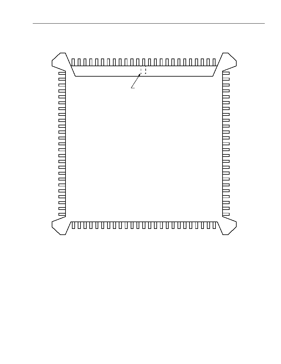
Data Sheet
March 2000
DSP1627 Digital Signal Processor
Lucent Technologies Inc.
3
3 Pin Information
Figure 1. DSP1627 BQFP Pin Diagram
DSP1627
20
10
30
90
80
70
V
SS
SY
NC1
DO1
OLD1
OCK
1
ICK
1
ILD1
V
SS
DI1
V
DD
IB
F1
OB
E1
DB
15
DB
14
DB
13
DB
12
DB
11
DB
10
DB
9
DB
8
DB
7
DB
6
DB
5
V
DD
V
SS
DB4
DB2
DB1
DB0
V
SS
IO
DB3
V
SS
V
DD
AB11
AB10
AB9
AB8
AB7
V
SS
ERAMHI
EROM
RWN
EXM
AB14
AB12
ERAMLO
V
DD
SADD1
DOEN1
OCK2/PCSN
DO2/PSTAT
SYNC2/PBSEL
ILD2/PIDS
OLD2/PODS
IBF2/PIBF
OBE2/POBE
DI2/PB1
V
SS
DOEN2/PB2
SADD2/PB3
V
DD
IOBIT0/PB4
IOBIT1/PB5
IOBIT2/PB6
IOBIT3/PB7
VEC3/IOBIT4
VEC2/IOBIT5
VEC1/IOBIT6
VEC0/IOBIT7
V
SS
ICK2/PB0
V
SS
A
CKI2
CKI
V
DD
A
TDO
TM
S
V
DD
CKO
TRA
P
STO
P
IA
CK
V
SS
IN
T
0
IN
T
1
AB
0
AB
1
AB
2
AB
3
AB
4
AB
5
AB
6
RS
T
B
TC
K
100
V
DD
60
50
40
PIN #1
IDENTIFIER
ZONE
TD
I
AB13
V
DD
AB15
5-4218 (F).b

Data Sheet
DSP1627 Digital Signal Processor
March 2000
4
Lucent Technologies Inc.
3 Pin Information
(continued)
Figure 2. DSP1627 TQFP Pin Diagram
V
DD
DB
5
DB
6
DB
7
DB
8
DB
9
DB
10
V
SS
DB
11
DB
12
DB
13
DB
14
DB
15
V
DD
OBE
1
IB
F1
V
SS
DI1
ILD1
ICK
1
OCK1
OLD1
DO1
S
Y
NC1
V
SS
100
90
80
V
DD
AB
6
AB
5
AB
4
AB
3
AB
2
AB
0
IN
T
1
IN
T
0
V
SS
IA
C
K
ST
O
P
TRAP
RSTB
CK
O
V
DD
TC
K
TM
S
TDO
TD
I
V
DD
A
CKI
CKI2
V
SS
A
AB
1
30
40
50
60
70
V
DD
SADD1
DOEN1
OCK2/PCSN
DO2/PSTAT
SYNC2/PBSEL
ILD2/PIDS
OLD2/PODS
IBF2/PIBF
OBE2/POBE
ICK2/PB0
V
SS
DOEN2/PB2
SADD2/PB3
V
DD
IOBIT0/PB4
IOBIT1/PB5
IOBIT2/PB6
IOBIT3/PB7
VEC3/IOBIT4
VEC2/IOBIT5
VEC1/IOBIT6
VEC0/IOBIT7
V
SS
DI2/PB1
V
SS
DB4
DB3
DB2
DB1
DB0
IO
ERAMHI
V
DD
ERAMLO
EROM
RWN
V
SS
EXM
AB15
AB14
V
DD
AB13
AB12
AB11
AB10
AB9
AB8
AB7
V
SS
1
10
20
DSP1627
5-4219 (F).b
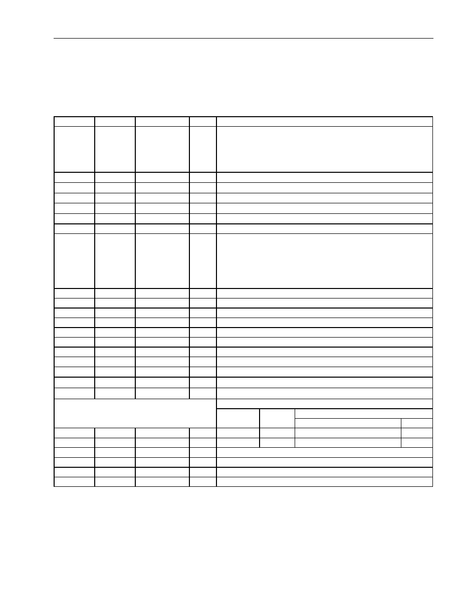
Data Sheet
March 2000
DSP1627 Digital Signal Processor
Lucent Technologies Inc.
5
3 Pin Information
(continued)
Functional descriptions of pins 1--100 are found in Section 6, Signal Descriptions. The functionality of pins 61 and
62 (TQFP pins 48 and 49) are mask-programmable (see Section 7, Mask-Programmable Options). Input levels on
all I and I/O type pins are designed to remain at full CMOS levels when not driven by the DSP.
*
3-states when RSTB = 0, or by JTAG control.
3-states when RSTB = 0 and INT0 = 1. Output = 1 when RSTB = 0 and INT0 = 0, except CKO which is free-running.
Pull-up devices on input.
ß 3-states by JTAG control.
** See Section 7, Mask-Programmable Options.
For SIO multiprocessor applications, add 5 k
external pull-up resistors to SADD1 and/or SADD2 for proper initialization.
Table 1. Pin Descriptions
BQFP Pin TQFP Pin
Symbol
Type
Name/Function
1, 2, 3, 4,
5, 7, 8, 9,
10, 11, 12,
15, 16, 17,
18, 19
88, 89, 90,
91, 92, 94,
95, 96, 97,
98, 99, 2,
3, 4, 5, 6
DB[15:0]
I/O*
External Memory Data Bus DB[15:0].
20
7
IO
O
Data Address 0x4000 to 0x40FF I/O Enable.
21
8
ERAMHI
O
Data Address 0x8000 to 0xFFFF External RAM Enable.
23
10
ERAMLO
O
Data Address 0x4100 to 0x7FFF External RAM Enable.
24
11
EROM
O
Program Address External ROM Enable.
25
12
RWN
O
Read/Write Not.
27
14
EXM
I
External ROM Enable.
28, 29, 31,
32, 33, 34,
35, 36, 37,
40, 41, 42,
43, 44, 45,
46
15, 16, 18,
19, 20, 21,
22, 23, 24,
27, 28, 29,
30, 31, 32,
33
AB[15:0]
O*
External Memory Address Bus 15--0.
47
34
INT1
I
Vectored Interrupt 1.
48
35
INT0
I
Vectored Interrupt 0.
50
37
IACK
O*
Interrupt Acknowledge.
51
38
STOP
I
STOP Input Clock.
52
39
TRAP
I/O*
Nonmaskable Program Trap/Breakpoint Indication.
53
40
RSTB
I
Reset Bar.
54
41
CKO
O
Processor Clock Output.
56
43
TCK
I
JTAG Text Clock.
57
44
TMS
I
JTAG Test Mode Select.
58
45
TDO
O
ß
JTAG Test Data Output.
59
46
TDI
I
JTAG Test Data Input.
Mask-Programmable Input Clock Option
CMOS
Small
Signal
Crystal
Oscillator
CMOS
61
48
CKI**
I
CKI
V
AC
XLO, 10 pF capacitor to V
SS
CKI
62
49
CKI2**
I
V
SSA
V
CM
XHI, 10 pF capacitor to V
SS
Open
65
52
VEC0/IOBIT7
I/O*
Vectored Interrupt Indication 0/Status/Control Bit 7.
66
53
VEC1/IOBIT6
I/O*
Vectored Interrupt Indication 1/Status/Control Bit 6.
67
54
VEC2/IOBIT5
I/O*
Vectored Interrupt Indication 2/Status/Control Bit 5.
68
55
VEC3/IOBIT4
I/O*
Vectored Interrupt Indication 3/Status/Control Bit 4.

Data Sheet
DSP1627 Digital Signal Processor
March 2000
6
Lucent Technologies Inc.
3 Pin Information
(continued)
Functional descriptions of pins 1--100 are found in Section 6, Signal Descriptions.
*
3-states when RSTB = 0, or by JTAG control.
3-states when RSTB = 0 and INT0 = 1. Output = 1 when RSTB = 0 and INT0 = 0.
ß Pull-up devices on input.
3-states by JTAG control.
** See Section 7, Mask-Programmable Options.
For SIO multiprocessor applications, add 5 k
external pull-up resistors to SADD1 and/or SADD2 for proper initialization.
Table 1. Pin Descriptions (continued)
BQFP Pin
TQFP Pin
Symbol
Type
Name/Function
69
56
IOBIT3/PB7
I/O*
Status/Control Bit 3/PHIF Data Bus Bit 7.
70
57
IOBIT2/PB6
I/O*
Status/Control Bit 2/PHIF Data Bus Bit 6.
71
58
IOBIT1/PB5
I/O*
Status/Control Bit 1/PHIF Data Bus Bit 5.
72
59
IOBIT0/PB4
I/O*
Status/Control Bit 0/PHIF Data Bus Bit 4.
74
61
SADD2/PB3
I/O*
SIO2 Multiprocessor Address/PHIF Data Bus Bit 3.
75
62
DOEN2/PB2
I/O*
SIO2 Data Output Enable/PHIF Data Bus Bit 2.
77
64
DI2/PB1
I/O*
SIO2 Data Input/PHIF Data Bus Bit 1.
78
65
ICK2/PB0
I/O*
SIO2 Input Clock/PHIF Data Bus Bit 0.
79
66
OBE2/POBE
O*
SIO2 Output Buffer Empty/PHIF Output Buffer Empty.
80
67
IBF2/PIBF
O*
SIO2 Input Buffer Full/PHIF Input Buffer Full.
81
68
OLD2/PODS
I/O*
SIO2 Output Load/PHIF Output Data Strobe.
82
69
ILD2/PIDS
I/O*
SIO2 Input Load/PHIF Input Data Strobe.
83
70
SYNC2/PBSEL
I/O*
SIO2 Multiprocessor Synchronization/PHIF Byte Select.
84
71
DO2/PSTAT
I/O*
SIO2 Data Output/PHIF Status Register Select.
85
72
OCK2/PCSN
I/O*
SIO2 Output Clock/PHIF Chip Select Not.
86
73
DOEN1
I/O*
SIO1 Data Output Enable.
87
74
SADD1
I/O*
SIO1 Multiprocessor Address.
90
77
SYNC1
I/O*
SIO1 Multiprocessor Synchronization.
91
78
DO1
O*
SIO1 Data Output.
92
79
OLD1
I/O*
SIO1 Output Load.
93
80
OCK1
I/O*
SIO1 Output Clock.
94
81
ICK1
I/O*
SIO1 Input Clock.
95
82
ILD1
I/O*
SIO1 Input Load.
96
83
DI1
I
SIO1 Data Input.
98
85
IBF1
O*
SIO1 Input Buffer Full.
99
86
OBE1
O*
SIO1 Output Buffer Empty.
6, 15, 26,
38, 49, 64,
76, 89, 97
93, 1, 13,
25, 36, 51,
63, 76, 84
V
SS
P
Ground.
14, 22, 30,
39, 55, 73,
88, 100
100, 9, 17,
26, 42, 60,
75, 87
V
DD
P
Power Supply.
60
47
V
DDA
P
Analog Power Supply.
63
50
V
SSA
P
Analog Ground.

Data Sheet
March 2000
DSP1627 Digital Signal Processor
Lucent Technologies Inc.
7
4 Hardware Architecture
The DSP1627 device is a 16-bit, fixed-point program-
mable digital signal processor (DSP). The DSP1627
consists of a DSP1600 core together with on-chip mem-
ory and peripherals. Added architectural features give
the DSP1627 high program efficiency for signal coding
applications.
4.1 DSP1627 Architectural Overview
Figure 3 shows a block diagram of the DSP1627. The fol-
lowing modules make up the DSP1627.
DSP1600 Core
The DSP1600 core is the heart of the DSP1627 chip. The
core contains data and address arithmetic units, and
control for on-chip memory and peripherals. The core
provides support for external memory wait-states and on-
chip, dual-port RAM and features vectored interrupts and
a trap mechanism.
Dual-Port RAM (DPRAM)
This module contains six banks of zero wait-state mem-
ory. Each bank consists of 1K 16-bit words and has sep-
arate address and data ports to the instruction/coefficient
and data memory spaces. A program can reference
memory from either space. The DSP1600 core automat-
ically performs the required multiplexing. If references to
both ports of a single bank are made simultaneously, the
DSP1600 core automatically inserts a wait-state and per-
forms the data port access first, followed by the instruc-
tion/coefficient port access.
A program can be downloaded from slow, off-chip mem-
ory into DPRAM, and then executed without wait-states.
DPRAM is also useful for improving convolution perfor-
mance in cases where the coefficients are adaptive.
Since DPRAM can be downloaded through the JTAG
port, full-speed remote in-circuit emulation is possible.
DPRAM can also be used for downloading self-test code
via the JTAG port.
Read-Only Memory (ROM)
The DSP1627x36 contains 36K 16-bit words of zero
wait-state mask-programmable ROM for program and
fixed coefficients. Similarly, the DSP1627x32 has 32K
16-bit words of ROM and access to 16 Kwords of exter-
nal ROM.
External Memory Multiplexer (EMUX)
The EMUX is used to connect the DSP1627 to external
memory and I/O devices. It supports read/write opera-
tions from/to instruction/coefficient memory (X memory
space) and data memory (Y memory space). The
DSP1600 core automatically controls the EMUX. Instruc-
tions can transparently reference external memory from
either set of internal buses. A sequencer allows a single
instruction to access both the X and the Y external mem-
ory spaces.
Clock Synthesis
The DSP powers up with a 1X input clock (CKI/CKI2) as
the source for the processor clock. An on-chip clock syn-
thesizer (PLL) can also be used to generate the system
clock for the DSP, which will run at a frequency multiple
of the input clock. The clock synthesizer is deselected
and powered down on reset. For low-power operation, an
internally generated slow clock can be used to drive the
DSP. If both the clock synthesizer and the internally gen-
erated slow clock are selected, the slow clock will drive
the DSP; however, the synthesizer will continue to run.
The clock synthesizer and other programmable clock
sources are discussed in Section 4.12. The use of these
programmable clock sources for power management is
discussed in Section 4.13.
Bit Manipulation Unit (BMU)
The BMU extends the DSP1600 core instruction set to
provide more efficient bit operations on accumulators.
The BMU contains logic for barrel shifting, normalization,
and bit field insertion/extraction. The unit also contains a
set of 36-bit alternate accumulators. The data in the al-
ternate accumulators can be shuffled with the data in the
main accumulators. Flags returned by the BMU mesh
seamlessly with the DSP1600 conditional instructions.
Bit Input/Output (BIO)
The BIO provides convenient and efficient monitoring
and control of eight individually configurable pins. When
configured as outputs, the pins can be individually set,
cleared, or toggled. When configured as inputs, individu-
al pins or combinations of pins can be tested for patterns.
Flags returned by the BIO mesh seamlessly with condi-
tional instructions.
Serial Input/Output Units (SIO and SIO2)
SIO and SIO2 offer asynchronous, full-duplex, double-
buffered channels that operate at up to 25 Mbits/s (for
20 ns instruction cycle in a nonmultiprocessor configura-
tion), and easily interface with other Lucent Technologies
fixed-point DSPs in a multiple-processor environment.
Commercially available codecs and time-division multi-
plex (TDM) channels can be interfaced to the serial I/O
ports with few, if any, additional components. SIO2 is
identical to SIO.
An 8-bit serial protocol channel may be transmitted in ad-
dition to the address of the called processor in multipro-
cessor mode. This feature is useful for transmitting high-
level framing information or for error detection and cor-
rection. SIO2 and BIO are pin-multiplexed with the PHIF.

Data Sheet
DSP1627 Digital Signal Processor
March 2000
8
Lucent Technologies Inc.
4 Hardware Architecture
(continued)
*
These registers are accessible through the pins only.
36K x 16 for the DSP1627x36; 32K x 16 for the DSP1627x32.
Figure 3. DSP1627 Block Diagram
TDO
TCK
TMS
M
U
X
DSP1600 CORE
RWN
EXM
EROM
ERAMHI
AB[15:0]
DB[15:0]
I/O
VEC[3:0] OR IOBIT[7:4]
DO2 OR PSTAT
OLD2 OR PODS
OCK2 OR PCSN
OBE2 OR POBE
SYNC2 OR PBSEL
ICK2 OR PB0
ILD2 OR PIDS
DI2 OR PB1
IBF2 OR PIBF
DOEN2 OR PB2
SADD2 OR PB3
IO BIT[3:0] OR PB[7:4]
CKI
CKI2
CKO
RSTB
STOP
TRAP
INT[1:0]
IACK
DI1
ICK1
ILD1
IBF1
DO1
OCK1
OLD1
OBE1
SYNC1
SADD1
DOEN1
EXTERNAL MEMORY INTERFACE & EMUX
ioc
DUAL-PORT
RAM
6K x 16
ROM
36K/32K x 16
ERAMLO
YAB
YDB
XDB
XAB
BMU
aa0
aa1
ar0
ar1
ar2
ar3
IDB
PHIF
phifc
PSTAT*
pdx0(IN)
pdx0(OUT)
BIO
sbit
cbit
SIO2
sdx2(OUT)
srta2
tdms2
sdx2(IN)
sioc2
saddx2
SIO
sdx(OUT)
srta
tdms
sdx(IN)
sioc
saddx
TIMER
timerc
timer0
HDS
BREAKPOINT*
JTAG
BOUNDARY SCAN
*
jtag
JCON*
ID*
BYPASS*
TRACE*
powerc
TDI
pllc
TRST
5-4142 (F).f

Data Sheet
March 2000
DSP1627 Digital Signal Processor
Lucent Technologies Inc.
9
4 Hardware Architecture
(continued)
Table 2. DSP1627 Block Diagram Legend
Symbol
Name
aa<0--1>
Alternate Accumulators.
ar<0--3>
Auxiliary BMU Registers.
BIO
Bit Input/Output Unit.
BMU
Bit Manipulation Unit.
BREAKPOINT
Four Instruction Breakpoint Registers.
BYPASS
JTAG Bypass Register.
cbit
Control Register for BIO.
EMUX
External Memory Multiplexer.
HDS
Hardware Development System.
ID
JTAG Device Identification Register.
IDB
Internal Data Bus.
ioc
I/O Configuration Register.
JCON
JTAG Configuration Registers.
jtag
16-bit Serial/Parallel Register.
pdx0(in)
Parallel Data Transmit Input Register 0.
pdx0(out)
Parallel Data Transmit Output Register 0.
PHIF
Parallel Host Interface.
phifc
Parallel Host Interface Control Register.
pllc
Phase-Locked Loop Control Register.
powerc
Power Control Register.
PSTAT
Parallel Host Interface Status Register.
ROM
Internal ROM (36 Kwords for DSP1627x36, 32 Kwords for DSP1627x32).
saddx
Multiprocessor Protocol Register.
saddx2
Multiprocessor Protocol Register for SIO2.
sbit
Status Register for BIO.
sdx(in)
Serial Data Transmit Input Register.
sdx2(in)
Serial Data Transmit Input Register for SIO2.
sdx(out)
Serial Data Transmit Output Register.
sdx2(out)
Serial Data Transmit Output Register for SIO2.
SIO
Serial Input/Output Unit.
SIO2
Serial Input/Output Unit #2.
sioc
Serial I/O Control Register.
sioc2
Serial I/O Control Register for SIO2.
srta
Serial Receive/Transmit Address Register.
srta2
Serial Receive/Transmit Address Register for SIO2.
tdms
Serial I/O Time-division Multiplex Signal Control Register.
tdms2
Serial I/O Time-division Multiplex Signal Control Register for SIO2.
TIMER
Programmable Timer.
timer0
Timer Running Count Register.
timerc
Timer Control Register.
TRACE
Program Discontinuity Trace Buffer.
XAB
Program Memory Address Bus.
XDB
Program Memory Data Bus.
YAB
Data Memory Address Bus.
YDB
Data Memory Data Bus.

Data Sheet
DSP1627 Digital Signal Processor
March 2000
10
Lucent Technologies Inc.
4 Hardware Architecture
(continued)
Parallel Host Interface (PHIF)
The PHIF is a passive, 8-bit parallel port which can in-
terface to an 8-bit bus containing other Lucent Technol-
ogies DSPs (e.g., DSP1620, DSP1627, DSP1628,
DSP1629, DSP1611, DSP1616, DSP1617, DSP1618),
microprocessors, or peripheral I/O devices. The PHIF
port supports either
Motorola
or
Intel
protocols, as well
as 8-bit or 16-bit transfers, configured in software. The
port data rate depends upon the instruction cycle rate.
A 25 ns instruction cycle allows the PHIF to support
data rates up to 11.85 Mbytes/s, assuming the external
host device can transfer 1 byte of data in 25 ns.
The PHIF is accessed in two basic modes: 8-bit or
16-bit mode. In 16-bit mode, the host determines an ac-
cess of the high or low byte. In 8-bit mode, only the low
byte is accessed. Software-programmable features al-
low for a glueless host interface to microprocessors
(see Section 4.8, Parallel Host Interface).
Timer
The timer can be used to provide an interrupt at the ex-
piration of a programmed interval. The interrupt may be
single or repetitive. More than nine orders of magnitude
of interval selection are provided. The timer may be
stopped and restarted at any time.
Hardware Development System (HDS) Module
The on-chip HDS performs instruction breakpointing
and branch tracing at full speed without additional off-
chip hardware. Using the JTAG port, the breakpointing
is set up, and the trace history is read back. The port
works in conjunction with the HDS code in the on-chip
ROM and the hardware and software in a remote com-
puter. The HDS code must be linked to the user's appli-
cation code and reside in the first 4 Kwords of ROM.
The on-chip HDS cannot be used with the secure ROM
masking option (see Section 7.3, ROM Security Op-
tions).
Four hardware breakpoints can be set on instruction ad-
dresses. A counter can be preset with the number of
breakpoints to receive before trapping the core. Break-
points can be set in interrupt service routines. Alternate-
ly, the counter can be preset with the number of cache
instructions to execute before trapping the core.
Every time the program branches instead of executing
the next sequential instruction, the addresses of the in-
structions executed before and after the branch are
caught in circular memory. The memory contains the
last four pairs of program discontinuities for hardware
tracing.
In systems with multiple processors, the processors
may be configured such that any processor reaching a
breakpoint will cause all the other processors to be
trapped (see Section 4.3, Interrupts and Trap).
Pin Multiplexing
In order to allow flexible device interfacing while main-
taining a low package pin count, the DSP1627 multi-
plexes 16 package pins between BIO, PHIF, VEC[3:0],
and SIO2.
Upon reset, the vectored interrupt indication signals,
VEC[3:0], are connected to the package pins while
IOBIT[4:7] are disconnected. Setting bit 12, EBIOH, of
the ioc register connects IOBIT[4:7] to the package pins
and disconnects VEC[3:0].
Upon reset, the parallel host interface (PHIF) is con-
nected to the package pins while the second serial port
(SIO2) and IOBIT[3:0] are disconnected. Setting bit 10,
ESIO2, of the ioc register connects the SIO2 and
IOBIT[3:0] and disconnects the PHIF.
Power Management
Many applications, such as portable cellular terminals,
require programmable sleep modes for power manage-
ment. There are three different control mechanisms for
achieving low-power operation: the powerc control reg-
ister, the STOP pin, and the AWAIT bit in the alf register.
The AWAIT bit in the alf register allows the processor to
go into a power-saving standby mode until an interrupt
occurs. The powerc register configures various power-
saving modes by controlling internal clocks and periph-
eral I/O units. The STOP pin controls the internal pro-
cessor clock. The various power management options
may be chosen based on power consumption and/or
wake-up latency requirements.
4.2 DSP1600 Core Architectural Overview
Figure 4 shows a block diagram of the DSP1600 core.
System Cache and Control Section (SYS)
This section of the core contains a 15-word cache mem-
ory and controls the instruction sequencing. It handles
vectored interrupts and traps, and also provides decod-
ing for registers outside of the DSP1600 core. SYS
stretches the processor cycle if wait-states are required
(wait-states are programmable for external memory ac-
cesses). SYS sequences downloading via JTAG of self-
test programs to on-chip, dual-port RAM.
The cache loop iteration count can be specified at run
time under program control as well as at assembly time.

Data Sheet
March 2000
DSP1627 Digital Signal Processor
Lucent Technologies Inc.
11
4 Hardware Architecture
(continued)
Data Arithmetic Unit (DAU)
The data arithmetic unit (DAU) contains a 16 x 16-bit
parallel multiplier that generates a full 32-bit product in
one instruction cycle. The product can be accumulated
with one of two 36-bit accumulators. The accumulator
data can be directly loaded from, or stored to, memory
in two 16-bit words with optional saturation on overflow.
The arithmetic logic unit (ALU) supports a full set of
arithmetic and logical operations on either 16- or 32-bit
data. A standard set of flags can be tested for condition-
al ALU operations, branches, and subroutine calls. This
procedure allows the processor to perform as a power-
ful 16- or 32-bit microprocessor for logical and control
applications. The available instruction set is fully com-
patible with the DSP1617 instruction set. See Section
5.1 for more information on the instruction set.
The user also has access to two additional DAU regis-
ters. The psw register contains status information from
the DAU (see Table 26, Processor Status Word Regis-
ter). The arithmetic control register, auc, is used to con-
figure some of the features of the DAU (see Table 27)
including single-cycle squaring. The auc register align-
ment field supports an arithmetic shift left by one and
left or right by two. The auc register is cleared by reset.
The counters c0 to c2 are signed, 8 bits wide, and may
be used to count events such as the number of times
the program has executed a sequence of code. They
are controlled by the conditional instructions and pro-
vide a convenient method of program looping.
Y Space Address Arithmetic Unit (YAAU)
The YAAU supports high-speed, register-indirect, com-
pound, and direct addressing of data (Y) memory. Four
general-purpose, 16-bit registers, r0 to r3, are available
in the YAAU. These registers can be used to supply the
read or write addresses for Y space data. The YAAU
also decodes the 16-bit data memory address and out-
puts individual memory enables for the data access.
The YAAU can address the six 1 Kword banks of on-
chip DPRAM or three external data memory segments.
Up to 48 Kwords of off-chip RAM are addressable, with
16K addresses reserved for internal RAM.
Two 16-bit registers, rb and re, allow zero-overhead
modulo addressing of data for efficient filter implemen-
tations. Two 16-bit signed registers, j and k, are used to
hold user-defined postmodification increments. Fixed
increments of +1, ≠1, and +2 are also available. Four
compound-addressing modes are provided to make
read/write operations more efficient.
The YAAU allows direct (or indexed) addressing of data
memory. In direct addressing, the 16-bit base register
(ybase) supplies the 11 most significant bits of the ad-
dress. The direct data instruction supplies the remaining
5 bits to form an address to Y memory space and also
specifies one of 16 registers for the source or destina-
tion.
X Space Address Arithmetic Unit (XAAU)
The XAAU supports high-speed, register-indirect, in-
struction/coefficient memory addressing with postmodi-
fication of the register. The 16-bit pt register is used for
addressing coefficients. The signed register i holds a
user-defined postincrement. A fixed postincrement of
+1 is also available. Register PC is the program
counter. Registers pr and pi hold the return address for
subroutine calls and interrupts, respectively.
The XAAU decodes the 16-bit instruction/coefficient ad-
dress and produces enable signals for the appropriate
X memory segment. The addressable X segments are
internal ROM (up to 36 Kwords for the DSP1627x36, up
to 32 Kwords for the DSP1627x32), six 1K banks of
DPRAM, and external ROM.
The locations of these memory segments depend upon
the memory map selected (see Table 5). A security
mode can be selected by mask option. This prevents
unauthorized access to the contents of on-chip ROM
(see Section 7, Mask-Programmable Options).
4.3 Interrupts and Trap
The DSP1627 supports prioritized, vectored interrupts
and a trap. The device has eight internal hardware
sources of program interrupt and two external interrupt
pins. Additionally, there is a trap pin and a trap signal
from the hardware development system (HDS). A soft-
ware interrupt is available through the icall instruction.
The icall instruction is reserved for use by the HDS.
Each of these sources of interrupt and trap has a unique
vector address and priority assigned to it. DSP16A in-
terrupt compatibility is not maintained.
The software interrupt and the traps are always enabled
and do not have a corresponding bit in the ins register.
Other vectored interrupts are enabled in the inc register
(see Table 29, Interrupt Control (inc) Register) and
monitored in the ins register (see Table 30, Interrupt
Status (ins) Register). When the DSP1627 goes into an
interrupt or trap service routine, the IACK pin is assert-
ed. In addition, pins VEC[3:0] encode which interrupt/
trap is being serviced. Table 4 details the encoding
used for VEC[3:0].
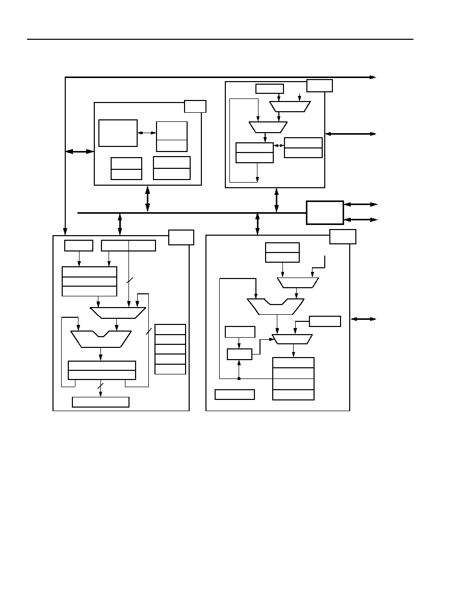
Data Sheet
DSP1627 Digital Signal Processor
March 2000
12
Lucent Technologies Inc.
4 Hardware Architecture
(continued)
Figure 4. DSP1600 Core Block Diagram
5-1741 (F).b
psw (16)
auc (16)
CONTROL
CACHE
cloop (7)
inc (16)
ins (16)
alf (16)
mwait (16)
SYS
XDB
XAB
IDB
YAB
YDB
r0 (16)
r1 (16)
r2 (16)
r3 (16)
j (16)
k (16)
re (16)
YAAU
rb (16)
ADDER
MUX
CMP
ybase (16)
pc (16)
pt (16)
pi (16)
i (16)
ADDER
XAAU
EXTRACT/SAT
x (16)
yh (16)
yl (16)
16 x 16 MPY
p (32)
SHIFT (≠2, 0, 1, 2)
c0 (8)
c2 (8)
c1 (8)
16
ALU/SHIFT
a0 (36)
a1 (36)
36
32
MUX
DAU
MUX
≠1, 0, 1, 2
BRIDGE
MUX
1
pr (16)

Data Sheet
March 2000
DSP1627 Digital Signal Processor
Lucent Technologies Inc.
13
4 Hardware Architecture
(continued)
Table 3. DSP1600 Core Block Diagram Legend
Symbol
Name
16 x 16 MPY
16-bit x 16-bit Multiplier.
a0--a1
Accumulators 0 and 1 (16-bit halves specified as a0, a0l, a1, and a1l)
*
.
*
F3 ALU instructions with immediates require specifying the high half of the accumulators as a0h and a1h.
alf
AWAIT, LOWPR, Flags.
ALU/SHIFT
Arithmetic Logic Unit/Shifter.
auc
Arithmetic Unit Control.
c0--c2
Counters 0--2.
cloop
Cache Loop Count.
CMP
Comparator.
DAU
Digital Arithmetic Unit.
i
Increment Register for the X Address Space.
IDB
Internal Data Bus.
inc
Interrupt Control.
ins
Interrupt Status.
j
Increment Register for the Y Address Space.
k
Increment Register for the Y Address Space.
MUX
Multiplexer.
mwait
External Memory Wait-states Register.
p
Product Register (16-bit halves specified as p, pl).
PC
Program Counter.
pi
Program Interrupt Return Register.
pr
Program Return Register.
psw
Processor Status Word.
pt
X Address Space Pointer.
r0--r3
Y Address Space Pointers.
rb
Modulo Addressing Register (begin address).
re
Modulo Addressing Register (end address).
SYS
System Cache and Control Section.
x
Multiplier Input Register.
XAAU
X Space Address Arithmetic Unit.
XAB
X Space Address Bus.
XDB
X Space Data Bus.
YAAU
Y Space Address Arithmetic Unit.
YAB
Y Space Address Bus.
YDB
Y Space Data Bus.
ybase
Direct Addressing Base Register.
y
DAU Register (16-bit halves specified as y, yl).

Data Sheet
DSP1627 Digital Signal Processor
March 2000
14
Lucent Technologies Inc.
4 Hardware Architecture
(continued)
Interruptibility
Vectored interrupts are serviced only after the execution
of an interruptible instruction. If more than one vectored
interrupt is asserted at the same time, the interrupts are
serviced sequentially according to their assigned priori-
ties. See Table 4 for the priorities assigned to the vec-
tored interrupts. Interrupt service routines, branch and
conditional branch instructions, cache loops, and in-
structions that only decrement one of the RAM pointers,
r0 to r3 (e.g., *r3
- -
), are not interruptible.
A trap is similar to an interrupt, but it gains control of the
processor by branching to the trap service routine even
when the current instruction is noninterruptible. It may
not be possible to return to normal instruction execution
from the trap service routine since the machine state
cannot always be saved. In particular, program execu-
tion cannot be continued from a trapped cache loop or
interrupt service routine. While in a trap service routine,
another trap is ignored.
When set to 1, the status bits in the ins register indicate
that an interrupt has occurred. The processor must
reach an interruptible state (completion of an interrupt-
ible instruction) before an enabled vectored interrupt will
be acted on. An interrupt will not be serviced if it is not
enabled. Polled interrupt service can be implemented
by disabling the interrupt in the inc register and then
polling the ins register for the expected event.
Vectored Interrupts
Tables 29 and 30 show the inc and ins registers. A logic
1 written to any bit of inc enables (or unmasks) the as-
sociated interrupt. If the bit is cleared to a logic 0, the in-
terrupt is masked. Note that neither the software
interrupt nor traps can be masked.
The occurrence of an interrupt that is not masked will
cause the program execution to transfer to the memory
location pointed to by that interrupt's vector address, as-
suming no other interrupt is being serviced (see Table
4, Interrupt Vector Table). The occurrence of an inter-
rupt that is masked causes no automatic processor ac-
tion, but will set the corresponding status bit in the ins
register. If a masked interrupt occurs, it is latched in the
ins register, but the interrupt is not taken. When un-
latched, this latched interrupt will initiate automatic pro-
cessor interrupt action. See the
DSP1611/17/18/27
Digital Signal Processor Information Manual
for a more
detailed description of the interrupts.
Signaling Interrupt Service Status
Five pins of DSP1627 are devoted to signaling interrupt
service status. The IACK pin goes high while any inter-
rupt or user trap is being serviced, and goes low when
the ireturn instruction from the service routine is issued.
Four pins, VEC[3:0], carry a code indicating which of the
interrupts or trap is being serviced. Table 4 contains the
encodings used by each interrupt.
Traps due to HDS breakpoints have no effect on either
the IACK or VEC[3:0] pins. Instead, they show the inter-
rupt state or interrupt source of the DSP when the trap
occurred.
Clearing Interrupts
The PHIF interrupts (PIBF and POBE) are cleared by
reading or writing the parallel host interface data trans-
mit registers pdx0[in] and pdx0[out], respectively. The
SIO and SIO2 interrupts (IBF, IBF2, OBE, and OBE2)
are cleared by reading or writing, as appropriate, the se-
rial data registers sdx[in], sdx2[in], sdx[out], and
sdx2[out]. The JTAG interrupt (JINT) is cleared by read-
ing the jtag register.
Three of the vectored interrupts are cleared by writing to
the ins register. Writing a 1 to the INT0, INT1, or TIME
bits in the ins will cause the corresponding interrupt sta-
tus bit to be cleared to a logic 0. The status bit for these
vectored interrupts is also cleared when the ireturn in-
struction is executed, leaving set any other vectored in-
terrupts that are pending.
Traps
The TRAP pin of the DSP1627 is a bidirectional signal.
At reset, it is configured as an input to the processor.
Asserting the TRAP pin will force a user trap. The trap
mechanism is used for two purposes. It can be used by
an application to rapidly gain control of the processor for
asynchronous time-critical event handling (typically for
catastrophic error recovery). It is also used by the HDS
for breakpointing and gaining control of the processor.
Separate vectors are provided for the user trap (0x46)
and the HDS trap (0x3). Traps are not maskable.

Data Sheet
March 2000
DSP1627 Digital Signal Processor
Lucent Technologies Inc.
15
4 Hardware Architecture
(continued)
Table 4. Interrupt Vector Table
Source
Vector
Priority
VEC[3:0]
Issued by
No Interrupt
--
--
0x0
--
Software Interrupt
0x2
1
0x1
icall
INT0
0x1
2
0x2
pin
JINT
0x42
3
0x8
jtag in
INT1
0x4
4
0x9
pin
TIME
0x10
7
0xc
timer
IBF2
0x14
8
0xd
SIO2 in
OBE2
0x18
9
0xe
SIO2 out
Reserved
0x1c
10
0x0
--
Reserved
0x20
11
0x1
--
Reserved
0x24
12
0x2
--
IBF
0x2c
14
0x3
SIO in
OBE
0x30
15
0x4
SIO out
PIBF
0x34
16
0x5
PHIF in
POBE
0x38
17
0x6
PHIF out
TRAP from HDS
0x3
18
--
*
*
Traps due to HDS breakpoints have no effect on VEC[3:0] pins.
breakpoint, jtag, or pin
TRAP from User
0x46
19 = highest
0x7
pin
A trap has four cycles of latency. At most, two instruc-
tions will execute from the time the trap is received at
the pin to when it gains control. An instruction that is ex-
ecuting when a trap occurs is allowed to complete be-
fore the trap service routine is entered. (Note that the
instruction could be lengthened by wait-states.) During
normal program execution, the pi register contains ei-
ther the address of the next instruction (two-cycle in-
struction executing) or the address following the next
instruction (one-cycle instruction executing). In an inter-
rupt service routine, pi contains the interrupt return ad-
dress. When a trap occurs during an interrupt service
routine, the value of the pi register may be overwritten.
Specifically, it is not possible to return to an interrupt
service routine from a user trap (0x46) service routine.
Continuing program execution when a trap occurs dur-
ing a cache loop is also not possible.
The HDS trap causes circuitry to force the program
memory map to MAP1 (with on-chip ROM starting at ad-
dress 0x0) when the trap is taken. The previous memo-
ry map is restored when the trap service routine exits by
issuing an ireturn. The map is forced to MAP1 because
the HDS code, if present, resides in the on-chip ROM.
Using the Lucent Technologies development tools, the
TRAP pin may be configured to be an output, or an input
vectoring to address 0x3. In a multiprocessor environ-
ment, the TRAP pins of all the DSPs present can be tied
together. During HDS operations, one DSP is selected
by the host software to be the master. The master pro-
cessor's TRAP pin is configured to be an output.
The TRAP pins of the slave processors are configured
as inputs. When the master processor reaches a break-
point, the master's TRAP pin is asserted. The slave pro-
cessors will respond to their TRAP input by beginning to
execute the HDS code.
AWAIT Interrupt (Standby or Sleep Mode)
Setting the AWAIT bit (bit 15) of the alf register
(alf = 0x8000) causes the processor to go into a power-
saving standby or sleep mode. Only the minimum cir-
cuitry on the chip required to process an incoming inter-
rupt remains active. After the AWAIT bit is set, one
additional instruction will be executed before the stand-
by power-saving mode is entered. A PHIF or SIO word
transfer will complete if already in progress. The AWAIT
bit is reset when the first interrupt occurs. The chip then
wakes up and continues executing.
Two nop instructions should be programmed after the
AWAIT bit is set. The first nop (one cycle) will be exe-
cuted before sleeping; the second will be executed after
the interrupt signal awakens the DSP and before the in-
terrupt service routine is executed.
The AWAIT bit should be set from within the cache if the
code which is executing resides in external ROM where
more than one wait-state has been programmed. This
ensures that an interrupt will not disturb the device from
completely entering the sleep state.

Data Sheet
DSP1627 Digital Signal Processor
March 2000
16
Lucent Technologies Inc.
4 Hardware Architecture
(continued)
For additional power savings, set ioc = 0x0180 and tim-
erc = 0x0040 in addition to setting alf = 0x8000. This will
hold the CKO pin low and shut down the timer and pres-
caler (see Table 38 and Table 31).
For a description of the control mechanisms for putting
the DSP into low-power modes, see Section 4.13, Pow-
er Management.
4.4 Memory Maps and Wait-States
The DSP1600 core implements a modified Harvard ar-
chitecture that has separate on-chip 16-bit address and
data buses for the instruction/coefficient (X) and data
(Y) memory spaces. Table 5 shows the instruction/coef-
ficient memory space maps for both the DSP1627x36
and DSP1627x32.
The differences between the x36 and x32 memory
maps can be seen by comparing the respective MAP1
and MAP3. For instance, MAP1 of the x36 provides for
36 Kwords of IROM and 6 Kwords of dual-port RAM
(DPRAM), whereas MAP1 of the x32 provides for
32 Kwords of IROM, 6 Kwords of DPRAM, and
16 Kwords of EROM.
The DSP1627 provides a multiplexed external bus
which accesses external RAM (ERAM) and ROM (ER-
OM). Programmable wait-states are provided for exter-
nal memory accesses. The instruction/coefficient
memory map is configurable to provide application flex-
ibility. Table 6 shows the data memory space, which
has one map.
Instruction/Coefficient Memory Map Selection
In determining which memory map to use, the proces-
sor evaluates the state of two parameters. The first is
the LOWPR bit (bit 14) of the alf register. The LOWPR
bit of the alf register is initialized to 0 automatically at re-
set. LOWPR controls the starting address in memory
assigned to the six 1K banks of dual-port RAM. If LOW-
PR is low, internal dual-port RAM begins at address
0xC000. If LOWPR is high, internal dual-port RAM be-
gins at address 0x0. LOWPR also moves IROM from
0x0 in MAP1 to 0x4000 in MAP3, and EROM from 0x0
in MAP2 to 0x4000 in MAP4.
The second parameter is the value at reset of the EXM
pin (pin 27 or pin 14, depending upon the package
type). EXM determines whether the internal 36 Kwords
ROM (IROM) will be addressable in the memory map.
The Lucent Technologies development system tools,
together with the on-chip HDS circuitry and the JTAG
port, can independently set the memory map. Specifi-
cally, during an HDS trap, the memory map is forced to
MAP1. The user's map selection is restored when the
trap service routine has completed execution.
MAP1
MAP1 has the IROM starting at 0x0 and six 1 Kword
banks of DPRAM starting at 0xC000. Additionally,
MAP1 for the x32 has 16 Kwords of EROM starting at
0x8000. MAP1 is used if DSP1627 has EXM low at re-
set and the LOWPR parameter is programmed to zero.
It is also used during an HDS trap.
MAP2
MAP2 differs from MAP1 in that the lowest 48 Kwords
reference external ROM (EROM). MAP2 is used if EXM
is high at reset, the LOWPR parameter is programmed
to zero, and an HDS trap is not in progress.
MAP3
MAP3 has the six 1 Kword banks of DPRAM starting at
address 0x0. In MAP3 of the x36, the 36 Kwords of
IROM start at 0x4000. Similarly, for the x32, 32 Kwords
of IROM start at 0x4000. Additionally, MAP3 for the x32
has 16 Kwords of EROM starting at 0xC000. MAP3 is
used if EXM is low at reset, the LOWPR bit is pro-
grammed to 1, and an HDS trap is not in progress. Note
that this map is not available if the secure mask-pro-
grammable option has been ordered.
MAP4
MAP4 differs from MAP3 in that addresses above
0x4000 reference external ROM (EROM). This map is
used if the LOWPR bit is programmed to 1, an HDS trap
is not in progress, and, either EXM is high during reset,
or the secure mask-programmable option has been or-
dered.
Whenever the chip is reset using the RSTB pin, the de-
fault memory map will be MAP1 or MAP2, depending
upon the state of the EXM pin at reset. A reset through
the HDS will not reinitialize the alf register, so the previ-
ous memory map is retained.
Boot from External ROM
After RSTB goes from low to high, the DSP1627 comes
out of reset and fetches an instruction from address
zero of the instruction/coefficient space. The physical
location of address zero is determined by the memory
map in effect. If EXM is high at the rising edge of RSTB,
MAP2 is selected. MAP2 has EROM at location zero;
thus, program execution begins from external memory.
If EXM is high and INT1 is low when RSTB rises, the
mwait register defaults to 15 wait-states for all external
memory segments. If INT1 is high, the mwait register
defaults to 0 wait-states.
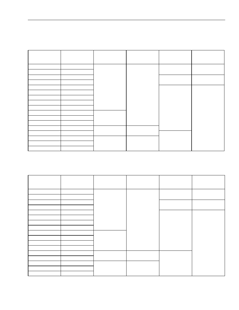
Data Sheet
March 2000
DSP1627 Digital Signal Processor
Lucent Technologies Inc.
17
4 Hardware Architecture
(continued)
Table 5. Instruction/Coefficient Memory Maps
*
MAP1 is set automatically during an HDS trap. The user-selected map is restored at the end of the HDS trap service routine.
LOWPR is an alf register bit. The Lucent Technologies development system tools can independently set the memory map.
MAP3 is not available if the secure mask-programmable option is selected.
DSP1627x36
X Address
AB[0:15]
MAP 1*
EXM = 0
LOWPR = 0
MAP 2
EXM = 1
LOWPR = 0
MAP 3
EXM = 0
LOWPR = 1
MAP 4
EXM = 1
LOWPR = 1
0
0x0000
IROM
(36K)
EROM
(48K)
DPRAM
(6K)
DPRAM
(6K)
4K
0x1000
6K
0x1800
Reserved
(10K)
Reserved
(10K)
12K
0x3000
16K
0x4000
IROM
(36K)
EROM
(48K)
20K
0x5000
24K
0x6000
28K
0x7000
32K
0x8000
36K
0x9000
Reserved
(12K)
40K
0xA000
44K
0xB000
48K
0xC000
DPRAM
(6K)
DPRAM
(6K)
52K
0xD000
Reserved
(12K)
54K
0xD800
Reserved
(10K)
Reserved
(10K)
56K
0xE000
60K--64K
0xFFFF
DSP1627x32
X Address
AB[0:15]
MAP 1*
EXM = 0
LOWPR = 0
MAP 2
EXM = 1
LOWPR = 0
MAP 3
EXM = 0
LOWPR = 1
MAP 4
EXM = 1
LOWPR = 1
0
0x0000
IROM
(32K)
EROM
(48K)
DPRAM
(6K)
DPRAM
(6K)
4K
0x1000
6K
0x1800
Reserved
(10K)
Reserved
(10K)
12K
0x3000
16K
0x4000
IROM
(32K)
EROM
(48K)
20K
0x5000
24K
0x6000
28K
0x7000
32K
0x8000
EROM
(16K)
36K
0x9000
40K
0xA000
44K
0xB000
48K
0xC000
DPRAM
(6K)
DPRAM
(6K)
EROM
(16K)
52K
0xD000
54K
0xD800
Reserved
(10K)
Reserved
(10K)
56K
0xE000
60K--64K
0xFFFF

Data Sheet
DSP1627 Digital Signal Processor
March 2000
18
Lucent Technologies Inc.
4 Hardware Architecture
(continued)
Data Memory Mapping
On the data memory side (see Table 6), the six 1K
banks of dual-port RAM are located starting at address
0. Addresses from 0x4000 to 0x40FF reference a 256-
word memory-mapped I/O segment (IO). Addresses
from 0x4100 to 0x7FFF reference the low external data
RAM segment (ERAMLO). Addresses above 0x8000
reference high external data RAM (ERAMHI).
Wait-States
The number of wait-states (from 0 to 15) used when ac-
cessing each of the four external memory segments
(ERAMLO, IO, ERAMHI, and EROM) is programmable
in the mwait register (see Table 36). When the program
references memory in one of the four external seg-
ments, the internal multiplexer is automatically switched
to the appropriate set of internal buses, and the associ-
ated external enable of ERAMLO, IO, ERAMHI, or
EROM is issued. The external memory cycle is auto-
matically stretched by the number of wait-states config-
ured in the appropriate field of the mwait register.
4.5 External Memory Interface (EMI)
The external memory interface supports read/write op-
erations from instruction/coefficient memory, data
memory, and memory-mapped I/O devices. The
DSP1627 provides a 16-bit external address bus,
AB[15:0], and a 16-bit external data bus, DB[15:0].
These buses are multiplexed between the internal bus-
es for the instruction/coefficient memory and the data
memory. Four external memory segment enables,
ERAMLO, IO, ERAMHI, and EROM, select the external
memory segment to be addressed.
If a data memory location with an address between
0x4100 and 0x7FFF is addressed, ERAMLO is asserted
low.
If one of the 256 external data memory locations, with
an address greater than or equal to 0x4000, and less
than or equal to 0x40FF, is addressed, IO is asserted
low. IO is intended for memory-mapped I/O.
If a data memory location with an address greater than
or equal to 0x8000 is addressed, ERAMHI is asserted
low. When the external instruction/coefficient memory is
addressed, EROM is asserted low.
The flexibility provided by the programmable options of
the external memory interface (see Table 36, mwait
Register and Table 38, ioc Register) allows the
DSP1627 to interface gluelessly with a variety of com-
mercial memory chips.
Each of the four external memory segments, ERAMLO,
IO, ERAMHI, and EROM, has a number of wait-states
that is programmable (from 0 to 15) by writing to the
mwait register. When the program references memory
in one of the four external segments, the internal multi-
plexer is automatically switched to the appropriate set of
internal buses, and the associated external enable of
ERAMLO, IO, ERAMHI, or EROM is issued. The exter-
nal memory cycle is automatically stretched by the num-
ber of wait-states in the appropriate field of the mwait
register.
When writing to external memory, the RWN pin goes
low for the external cycle. The external data bus,
DB[15:0], is driven by the DSP1627 starting halfway
through the cycle. The data driven on the external data
bus is automatically held after the cycle unless an exter-
nal read cycle immediately follows.
The DSP1627 has one external address bus and one
external data bus for both memory spaces. Since some
instructions provide the capability of simultaneous ac-
cess to both X space and Y space, some provision must
be made to avoid collisions for external accesses. The
DSP1627 has a sequencer that does the external X ac-
cess first, and then the external Y access, transparently
to the programmer. Wait-states are maintained as
Table 6. Data Memory Map (Not to Scale)
Decimal
Address
Address in
r0, r1, r2, r3
Segment
0
0x0000
DPRAM[1:6]
6K
0x1800
Reserved
(10K)
16K
0x4000
IO
16,640
0x4100
ERAMLO
32K
0x8000
ERAMHI
64K ≠ 1
0xFFFF

Data Sheet
March 2000
DSP1627 Digital Signal Processor
Lucent Technologies Inc.
19
4 Hardware Architecture
(continued)
programmed in the mwait register. For example, let two
instructions be executed: the first reads a coefficient
from EROM and writes data to ERAM; the second reads
a coefficient from EROM and reads data from ERAM.
The sequencer carries out the following steps at the ex-
ternal memory interface: read EROM, write ERAM, read
EROM, and read ERAM. Each step is done in sequen-
tial one-instruction cycle steps, assuming zero wait-
states are programmed. Note that the number of in-
struction cycles taken by the two instructions is four. Al-
so, in this case, the write hold time is zero.
The DSP1627 allows writing into external instruction/
coefficient memory. By setting bit 11, WEROM, of the
ioc register (see Table 38), writing to (or reading from)
data memory or memory-mapped I/O asserts the
EROM strobe instead of ERAMLO, IO, or ERAMHI.
Therefore, with WEROM set, EROM appears in both Y
space (replacing ERAM) and X space, in its normal po-
sition.
Bit 14 of the ioc register (see Table 38), EXTROM, may
be used with WEROM to download to a full 64K of ex-
ternal memory. When WEROM and EXTROM are both
asserted, address bit 15 (AB15) is held low, aliasing the
upper 32K of external memory into the lower 32K.
When an access to internal memory is made, the
AB[15:0] bus holds the last valid external memory ad-
dress. Asserting the RSTB pin low 3-states the AB[15:0]
bus. After reset, the AB[15:0] value is undefined.
The leading edge of the memory segment enables can
be delayed by approximately one-half a CKO period by
programming the ioc register (see Table 38). This is
used to avoid a situation in which two devices drive the
data bus simultaneously.
Bits 7, 8, and 13 of the ioc register select the mode of
operation for the CKO pin (see Table 38). Available op-
tions are a free-running unstretched clock, a wait-stated
sequenced clock (runs through two complete cycles
during a sequenced external memory access), and a
wait-stated clock based on the internal instruction cycle.
These clocks drop to the low-speed internal ring oscilla-
tor when SLOWCKI is enabled (see 4.13, Power Man-
agement). The high-to-low transitions of the wait-stated
clock are synchronized to the high-to-low transition of
the free-running clock. Also, the CKO pin provides ei-
ther a continuously high level, a continuously low level,
or changes at the rate of the internal processor clock.
This last option, only available with the crystal and
small-signal input clock options, enables the DSP1627
CKI input buffer to deliver a full-rate clock to other devic-
es while the DSP1627 itself is in one of the low-power
modes.
4.6 Bit Manipulation Unit (BMU)
The BMU interfaces directly to the main accumulators in
the DAU providing the following features:
s
Barrel shifting--logical and arithmetic, left and right
shift
s
Normalization and extraction of exponent
s
Bit-field extraction and insertion
These features increase the efficiency of the DSP in ap-
plications such as control or data encoding and decod-
ing. For example, data packing and unpacking, in which
short data words are packed into one 16-bit word for
more efficient memory storage, is very easy.
In addition, the BMU provides two auxiliary accumula-
tors, aa0 and aa1. In one instruction cycle, 36-bit data
can be shuffled, or swapped, between one of the main
accumulators and one of the alternate accumulators.
The ar<0--3> registers are 16-bit registers that control
the operations of the BMU. They store a value that de-
termines the amount of shift or the width and offset
fields for bit extraction or insertion. Certain operations in
the BMU set flags in the DAU psw register and the alf
register (see Table 26, Processor Status Word (psw)
Register, and Table 35, alf Register). The ar<0--3> reg-
isters can also be used as general-purpose registers.
The BMU instructions are detailed in Section 5.1. For a
thorough description of the BMU, see the
DSP1611/17/
18/27 Digital Signal Processor Information Manual
.
4.7 Serial I/O Units (SIOs)
The serial I/O ports on the DSP1627 device provide a
serial interface to many codecs and signal processors
with little, if any, external hardware required. Each high-
speed, double-buffered port (sdx and sdx2) supports
back-to-back transmissions of data. SIO and SIO2 are
identical. The output buffer empty (OBE and OBE2) and
input buffer full (IBF and IBF2) flags facilitate the read-
ing and/or writing of each serial I/O port by program-
or interrupt-driven I/O. There are four selectable active
clock speeds.
A bit-reversal mode provides compatibility with either
the most significant bit (MSB) first or least significant bit
(LSB) first serial I/O formats (see Table 22, Serial I/O
Control Registers (sioc and sioc2)). A multiprocessor
I/O configuration is supported. This feature allows up to
eight DSP161X devices to be connected together on an
SIO port without requiring external glue logic.

Data Sheet
DSP1627 Digital Signal Processor
March 2000
20
Lucent Technologies Inc.
4 Hardware Architecture
(continued)
The serial data may be internally looped back by setting
the SIO loopback control bit, SIOLBC, of the ioc regis-
ter. SIOLBC affects both the SIO and SIO2. The data
output signals are wrapped around internally from the
output to the input (DO1 to DI1 and DO2 to DI2). To ex-
ercise loopback, the SIO clocks (ICK1, ICK2, OCK1,
and OCK2) should either all be in the active mode,
16-bit condition, or each pair should be driven from one
external source in passive mode. Similarly, pins ILD1
(ILD2) and OLD1 (OLD2) must both be in active mode
or tied together and driven from one external frame
clock in passive mode. During loopback, DO1, DO2,
DI1, DI2, ICK1, ICK2, OCK1, OCK2, ILD1, ILD2, OLD1,
OLD2, SADD1, SADD2, SYNC1, SYNC2, DOEN1, and
DOEN2 are 3-stated.
Setting DODLY = 1 (sioc and sioc2) delays DO by one
phase of OCK so that DO changes on the falling edge
of OCK instead of the rising edge (DODLY = 0). This re-
duces the time available for DO to drive DI and to be val-
id for the rising edge of ICK, but increases the hold time
on DO by half a cycle on OCK.
Programmable Modes
Programmable modes of operation for the SIO and
SIO2 are controlled by the serial I/O control registers
(sioc and sioc2). These registers, shown in Table 22,
are used to set the ports into various configurations.
Both input and output operations can be independently
configured as either active or passive. When active, the
DSP1627 generates load and clock signals. When pas-
sive, load and clock signal pins are inputs.
Since input and output can be independently config-
ured, each SIO has four different modes of operation.
Each of the sioc registers is also used to select the fre-
quency of active clocks for that SIO. Finally, these reg-
isters are used to configure the serial I/O data formats.
The data can be 8 or 16 bits long, and can also be input/
output MSB first or LSB first. Input and output data for-
mats can be independently configured.
Multiprocessor Mode
The multiprocessor mode allows up to eight processors
(DSP1629, DSP1628, DSP1627, DSP1620, DSP1618,
DSP1617, DSP1616, DSP1611) to be connected to-
gether to provide data transmission among any of the
DSPs in the system. Either SIO port (SIO or SIO2) may
be independently used for the multiprocessor mode.
The multiprocessor interface is a four-wire interface,
consisting of a data channel, an address/protocol
channel, a transmit/receive clock, and a sync signal
(see Figure 5). The DI1 and DO1 pins of all the DSPs
are connected to transmit and receive the data channel.
The SADD1 pins of all the DSPs are connected to trans-
mit and receive the address/protocol channel. ICK1 and
OCK1 should be tied together and driven from one
source. The SYNC1 pins of all the DSPs are connected.
In the configuration shown in Figure 5, the master DSP
(DSP0) generates active SYNC1 and OCK1 signals
while the slave DSPs use the SYNC1 and OCK1 signals
in passive mode to synchronize operations. In addition,
all DSPs must have their ILD1 and OLD1 signals in ac-
tive mode.
While ILD1 and OLD1 are not required externally for
multiprocessor operation, they are used internally in the
DSP's SIO. Setting the LD field of the master's sioc reg-
ister to a logic level 1 will ensure that the active genera-
tion of SYNC1, ILD1, and OLD1 is derived from OCK1
(see Table 22). With this configuration, all DSPs should
use ICK1 (tied to OCK1) in passive mode to avoid con-
flicts on the clock (CK) line (see the
DSP1611/17/18/27
Digital Signal Processor Information Manual
for more
information).
Four registers (per SIO) configure the multiprocessor
mode: the time-division multiplexed slot register (tdms
or tdms2), the serial receive and transmit address reg-
ister (srta or srta2), the serial data transmit register (sdx
or sdx2), and the multiprocessor serial address/protocol
register (saddx or saddx2).
Multiprocessor mode requires no external logic and
uses a TDM interface with eight 16-bit time slots per
frame. The transmission in any time slot consists of
16 bits of serial data in the data channel and 16 bits of
address and protocol information in the address/proto-
col channel. The address information consists of the
transmit address field of the srta register of the transmit-
ting device. The address information is transmitted con-
currently with the transmission of the first 8 bits of data.
The protocol information consists of the transmit proto-
col field written to the saddx register and is transmitted
concurrently with the last 8 bits of data (see Table 25,
Multiprocessor Protocol Register). Data is received or
recognized by other DSP(s) whose receive address
matches the address in the address/protocol channel.
Each SIO port has a user-programmable receive ad-
dress and transmit address associated with it. The
transmit and receive addresses are programmed in the
srta register.
In multiprocessor mode, each device can send data in
a unique time slot designated by the tdms register trans-
mit slot field (bits 7--0). The tdms register has a fully de-
coded transmit slot field in order to allow one DSP1627
device to transmit in more than one time slot. This pro-
cedure is useful for multiprocessor systems with less
than eight DSP1627 devices when a higher bandwidth
is necessary between certain devices in that system.
The DSP operating during time slot 0 also drives
SYNC1.
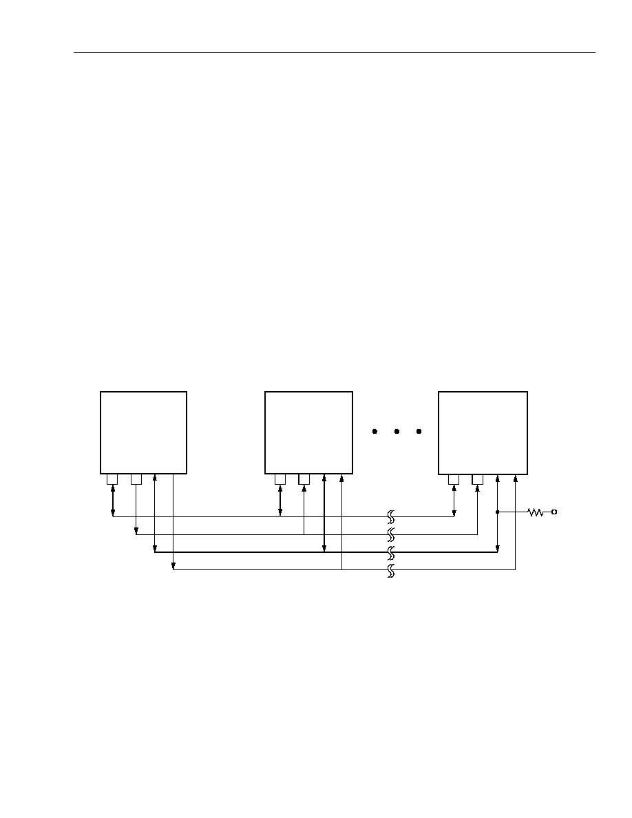
Data Sheet
March 2000
DSP1627 Digital Signal Processor
Lucent Technologies Inc.
21
4 Hardware Architecture
(continued)
In order to prevent multiple bus drivers, only one DSP
can be programmed to transmit in a particular time slot.
In addition, it is important to note that the address/pro-
tocol channel is 3-stated in any time slot that is not being
driven.
Therefore, to prevent spurious inputs, the address/pro-
tocol channel should be pulled up to V
DD
with a 5 k
re-
sistor, or it should be guaranteed that the bus is driven
in every time slot. (If the SYNC1 signal is externally gen-
erated, then this pull-up is required for correct initializa-
tion.)
Each SIO also has a fully decoded transmitting address
specified by the srta register transmit address field (bits
7--0). This is used to transmit information regarding the
destination(s) of the data. The fully decoded receive ad-
dress specified by the srta register receive address field
(bits 15--8) determines which data will be received.
The SIO protocol channel data is controlled via the sad-
dx register. When the saddx register is written, the
lower 8 bits contain the 8-bit protocol field. On a read,
the high-order 8 bits read from saddx are the most re-
cently received protocol field sent from the transmitting
DSP's saddx output register. The low-order 8 bits are
read as 0s.
An example use of the protocol channel is to use the top
3 bits of the saddx value as an encoded source address
for the DSPs on the multiprocessor bus. This leaves the
remaining 5 bits available to convey additional control
information, such as whether the associated field is an
opcode or data, or whether it is the last word in a trans-
fer, etc. These bits can also be used to transfer parity in-
formation about the data. Alternatively, the entire field
can be used for data transmission, boosting the band-
width of the port by 50%.
Using SIO2
The SIO2 functions the same as the SIO. Please refer
to Pin Multiplexing in Section 4.1 for a description of pin
multiplexing of BIO, PHIF, VEC[3:0], and SIO2.
Figure 5. Multiprocessor Communication and Connections
DSP 0
DO
IC
K
SA
DD
SY
NC
DSP 1
DSP 7
DATA CHANNEL
CLOCK
ADDRESS/PROTOCOL CHANNEL
SYNC SIGNAL
DI
OCK
DO
IC
K
SA
DD
SY
NC
DI
OCK
DO
IC
K
SAD
D
SYN
C
DI
OC
K
5 k
V
DD
5-4181 (F).a
Data Sheet
DSP1627 Digital Signal Processor
March 2000
22
Lucent Technologies Inc.
4 Hardware Architecture
(continued)
4.8 Parallel Host Interface (PHIF)
The DSP1627 has an 8-bit parallel host interface for rap-
id transfer of data with external devices. This parallel port
is passive (data strobes provided by an external device)
and supports either
Motorola or Intel microcontroller pro-
tocols. The PHIF also provides for 8-bit or 16-bit data
transfers. As a flexible host interface, it requires little or
no glue logic to interface to other devices (e.g., microcon-
trollers, microprocessors, or another DSP).
The data path of the PHIF consists of a 16-bit input buff-
er, pdx0(in), and a 16-bit output buffer, pdx0(out). Two
output pins, parallel input buffer full (PIBF) and parallel
output buffer empty (POBE), indicate the state of the
buffers. In addition, there are two registers used to con-
trol and monitor the PHIF's operation: the parallel host in-
terface control register (phifc, see Table 28), and the
PHIF status register (PSTAT, see Table 8). The PSTAT
register, which reflects the state of the PIBF and POBE
flags, can only be read by an external device when the
PSTAT input pin is asserted. The phifc register defines
the programmable options for this port.
The function of the pins, PIDS and PODS, is programma-
ble to support both the
Intel and Motorola protocols. The
pin, PCSN, is an input that, when low, enables PIDS and
PODS (or PRWN and PDS, depending on the protocol
used). While PCSN is high, the DSP1627 ignores any ac-
tivity on PIDS and/or PODS. If a DSP1627 is intended to
be continuously accessed through the PHIF port, PCSN
should be grounded. If PCSN is low and their respective
bits in the inc register are set, the assertion of PIDS and
PODS by an external device causes the DSP1627 de-
vice to recognize an interrupt.
Programmability
The parallel host interface can be programmed for 8-bit
or 16-bit data transfers using bit 0, PMODE, of the phifc
register. Setting PMODE selects 16-bit transfer mode.
An input pin controlled by the host, PBSEL, determines
an access of either the high or low bytes. The assertion
level of the PBSEL input pin is configurable in software
using bit 3 of the phifc register, PBSELF. Table 7 sum-
marizes the port's functionality as controlled by the
PSTAT and PBSEL pins and the PBSELF and PMODE
fields.
For 16-bit transfers, if PBSELF is zero, the PIBF and
POBE flags are set after the high byte is transferred. If
PBSELF is one, the flags are set after the low byte is
transferred. In 8-bit mode, only the low byte is accessed,
and every completion of an input or output access sets
PIBF or POBE.
Bit 1 of the phifc register, PSTROBE, configures the port
to operate either with an
Intel protocol where only the
chip select (PCSN) and either of the data strobes (PIDS
or PODS) are needed to make an access, or with a
Mo-
torola protocol where the chip select (PCSN), a data
strobe (PDS), and a read/write strobe (PRWN) are need-
ed. PIDS and PODS are negative assertion data strobes
while the assertion level of PDS is programmable
through bit 2, PSTRB, of the phifc register.
Finally, the assertion level of the output pins, PIBF and
POBE, is controlled through bit 4, PFLAG. When PFLAG
is set low, PIBF and POBE output pins have positive as-
sertion levels. By setting bit 5, PFLAGSEL, the logical
OR of PIBF and POBE flags (positive assertion) is seen
at the output pin PIBF. By setting bit 7 in phifc, PSOBEF,
the polarity of the POBE flag in the status register,
PSTAT, can be changed. PSOBEF has no effect on the
POBE pin.
Pin Multiplexing
Please refer to Pin Multiplexing in Section 4.1 for a de-
scription of BIO, PHIF, VEC[3:0], and SIO2 pins.
Table 7. PHIF Function (8-bit and 16-bit Modes)
PMODE Field
PSTAT Pin
PBSEL Pin
PBSELF Field = 0
PBSELF Field = 1
0 (8-bit)
0
0
pdx0 low byte
reserved
0
0
1
reserved
pdx0 low byte
0
1
0
PSTAT
reserved
0
1
1
reserved
PSTAT
1 (16-bit)
0
0
pdx0 low byte
pdx0 high byte
1
0
1
pdx0 high byte
pdx0 low byte
1
1
0
PSTAT
reserved
1
1
1
reserved
PSTAT
Table 8. pstat Register as Seen on PB[7:0]
Bit
7
6
5
4
3
2
1
0
Field
RESERVED
PIBF
POBE
Data Sheet
March 2000
DSP1627 Digital Signal Processor
Lucent Technologies Inc.
23
4 Hardware Architecture
(continued)
4.9 Bit Input/Output Unit (BIO)
The BIO controls the directions of eight bidirectional con-
trol I/O pins, IOBIT[7:0]. If a pin is configured as an output,
it can be individually set, cleared, or toggled. If a pin is
configured as an input, it can be read and/or tested.
The lower half of the sbit register (see Table 33) contains
current values (VALUE[7:0]) of the eight bidirectional pins
IOBIT[7:0]. The upper half of the sbit register (DI-
REC[7:0]) controls the direction of each of the pins. A log-
ic 1 configures the corresponding pin as an output; a logic
0 configures it as an input. The upper half of the sbit reg-
ister is cleared upon reset.
The cbit register (see Table 34) contains two 8-bit fields,
MODE/MASK[7:0] and DATA/PAT[7:0]. The values of
DATA/PAT[7:0] are cleared upon reset. The meaning of a
bit in either field depends on whether it has been config-
ured as an input or an output in sbit. If a pin has been con-
figured to be an output, the meanings are MODE and
DATA. For an input, the meanings are MASK and PAT
(pattern). Table 9 shows the functionality of the MODE/
MASK and DATA/PAT bits based on the direction select-
ed for the associated IOBIT pin.
Those bits that have been configured as inputs can be in-
dividually tested for 1 or 0. For those inputs that are being
tested, there are four flags produced: allt (all true), allf (all
false), somet (some true), and somef (some false). These
flags can be used for conditional branch or special in-
structions. The state of these flags can be saved and re-
stored by reading and writing bits 0 to 3 of the alf register
(see Table 35).
If a BIO pin is switched from being configured as an out-
put to being configured as an input and then back to be-
ing configured as an output, the pin retains the previous
output value.
Pin Multiplexing
Please refer to Pin Multiplexing in Section 4.1 for a
description of BIO, PHIF, VEC[3:0], and SIO2 pins.
4.10 Timer
The interrupt timer is composed of the timerc (control)
register, the timer0 register, the prescaler, and the
counter itself. The timer control register (see Table 31,
timerc Register) sets up the operational state of the timer
and prescaler. The timer0 register is used to hold the
counter reload value (or period register) and to set the
initial value of the counter. The prescaler slows the clock
to the timer by a number of binary divisors to allow for a
wide range of interrupt delay periods.
The counter is a 16-bit down counter that can be loaded
with an arbitrary number from software. It counts down
to 0 at the clock rate provided by the prescaler. Upon
reaching 0 count, a vectored interrupt to program ad-
dress 0x10 is issued to the DSP1627, providing the in-
terrupt is enabled (bit 8 of inc and ins registers). The
counter will then either wait in an inactive state for anoth-
er command from software, or will automatically repeat
the last interrupting period, depending upon the state of
the RELOAD bit in the timerc register.
When RELOAD is 0, the counter counts down from its
initial value to 0, interrupts the DSP1627, and then stops,
remaining inactive until another value is written to the
timer0 register. Writing to the timer0 register causes
both the counter and the period register to be written with
the specified 16-bit number. When RELOAD is 1, the
counter counts down from its initial value to 0, interrupts
the DSP1627, automatically reloads the specified initial
value from the period register into the counter, and re-
peats indefinitely. This provides for either a single timed
interrupt event or a regular interrupt clock of arbitrary pe-
riod.
The timer can be stopped and started by software, and
can be reloaded with a new period at any time. Its count
value, at the time of the read, can also be read by soft-
ware. Due to pipeline stages, stopping and starting the
timer may result in one inaccurate count or prescaled pe-
riod. When the DSP1627 is reset, the bottom 6 bits of the
timerc register and the timer0 register and counter are
initialized to 0. This sets the prescaler to CKO/2*, turns
off the reload feature, disables timer counting, and initial-
izes the timer to its inactive state. The act of resetting the
chip does not cause a timer interrupt. Note that the peri-
od register is not initialized on reset.
The T0EN bit of the timerc register enables the clock to
the timer. When T0EN is a 1, the timer counts down to-
wards 0. When T0EN is a 0, the timer holds its current
count.
*
Frequency of CKO/2 is equivalent to either CKI/2 for the PLL by-
passed or related to CKI by the PLL multiplying factors. See Section
4.12, Clock Synthesis.
Table 9. BIO Operations
DIREC[n]
*
*
0
n
7.
MODE/
MASK[n]
DATA/
PAT[n]
Action
1 (Output)
0
0
Clear
1 (Output)
0
1
Set
1 (Output)
1
0
No Change
1 (Output)
1
1
Toggle
0 (Input)
0
0
No Test
0 (Input)
0
1
No Test
0 (Input)
1
0
Test for Zero
0 (Input)
1
1
Test for One
Data Sheet
DSP1627 Digital Signal Processor
March 2000
24
Lucent Technologies Inc.
4 Hardware Architecture
(continued)
The PRESCALE field of the timerc register selects one
of 16 possible clock rates for the timer input clock (see
Table 31, timerc Register).
Setting the DISABLE bit of the timerc register to a logic
1 shuts down the timer and the prescaler for power sav-
ings. Setting the TIMERDIS, bit 4, in the powerc register
has the same effect of shutting down the timer. The
DISABLE bit and the TIMERDIS bit are cleared by writ-
ing a 0 to their respective registers to restore the normal
operating mode.
4.11 JTAG Test Port
The DSP1627 uses a JTAG/
IEEE
1149.1 standard four-
wire test port for self-test and hardware emulation.
There is no separate TRST input pin. An instruction reg-
ister, a boundary-scan register, a bypass register, and
a device identification register have been implemented.
The device identification register coding for the
DSP1627 is shown in Table 37. The instruction register
(IR) is 4 bits long. The instruction for accessing the de-
vice ID is 0xE (1110). The behavior of the instruction
register is summarized in Table 10. Cell 0 is the LSB
(closest to TDO).
The first line shows the cells in the IR that capture from
a parallel input in the capture-IR controller state. The
second line shows the cells that always load a logic 1 in
the capture-IR controller state. The third line shows the
cells that always load a logic 0 in the capture-IR control-
ler state. Cell 3 (MSB of IR) is tied to status signal PINT,
and cell 2 is tied to status signal JINT. The state of these
signals can therefore be captured during capture-IR and
shifted out during SHIFT-IR controller states.
Boundary-Scan Register
All of the chip's inputs and outputs are incorporated in a
JTAG scan path shown in Table 11. The types of
boundary-scan cells are as follows:
s
I = input cell
s
O = 3-state output cell
s
B = bidirectional (I/O) cell
s
OE = 3-state control cell
s
DC = bidirectional control cell
Table 10. JTAG Instruction Register
IR Cell #:
3
2
1
0
Parallel Input?
Y
Y
N
N
Always Logic 1?
N
N
N
Y
Always Logic 0?
N
N
Y
N

Data Sheet
March 2000
DSP1627 Digital Signal Processor
Lucent Technologies Inc.
25
4 Hardware Architecture
(continued)
Note that the direction of shifting is from TDI to cell 104 to cell 103 . . . to cell 0 of TDO.
*
Please refer to Pin Multiplexing in Section 4.1 for a description of pin multiplexing of BIO, PHIF, VEC[3:0], and SIO2.
Note that shifting a zero into this cell in the mode to scan a zero into the chip will disable the processor clocks just as the STOP pin will.
When the JTAG SAMPLE instruction is used, this cell will have a logic one regardless of the state of the pin.
Table 11. JTAG Boundary-Scan Register
Cell
Type
Signal Name/Function
Cell
Type
Signal Name/Function
0
OE
Controls cells 1, 27--31
69
B
OCK2/PCSN*
1
O
CKO
70
DC
Controls cell 71
2
I
RSTB
71
B
DO2/PSTAT*
3
DC
Controls cell 4
72
DC
Controls cell 73
4
B
TRAP 73
B
SYNC2/PBSEL*
5
I
STOP
74
DC
Controls cell 75
6
O
IACK 75
B
ILD2/PIDS*
7
I
INT0
76
DC
Controls cell 77
8
OE
Controls cells 6, 10--25, 49, 50, 78, 79
77
B
OLD2/PODS*
9
I
INT1
78
O
IBF2/PIBF*
10--25
O
AB[0:15]
79
O
OBE2/POBE*
26
I
EXM 80
DC
Controls
cell
81
27
O
RWN 81
B
ICK2/PB0*
28--31
O
EROM, ERAMLO, ERAMHI, IO
82
DC
Controls cell 83
32--36
B
DB[0:4] 83
B
DI2/PB1*
37
DC
Controls cells 32--36, 38--48
84
DC
Controls cell 85
38--48
B
DB[5:15]
85
B
DOEN2/PB2*
49
O
OBE1
86
DC
Controls cell 87
50
O
IBF1
87
B
SADD2/PB3*
51
I
DI1
88
DC
Controls cell 89
52
DC
Controls cell 53
89
B
IOBIT0/PB4*
53
B
ILD1
90
DC
Controls cell 91
54
DC
Controls cell 55
91
B
IOBIT1/PB5*
55
B
ICK1
92
DC
Controls cell 93
56
DC
Controls cell 57
93
B
IOBIT2/PB6*
57
B
OCK1
94
DC
Controls cell 95
58
DC
Controls cell 59
95
B
IOBIT3/PB7*
59
B
OLD1
96
DC
Controls cell 97
60
OE
Controls cell 61
97
B
VEC3/IOBIT4*
61
O
DO1
98
DC
Controls cell 99
62
DC
Controls cell 63
99
B
VEC2/IOBIT5*
63
B
SYNC1
100
DC
Controls cell 101
64
DC
Controls cell 65
101
B
VEC1/IOBIT6*
65
B
SADD1
102
DC
Controls cell 103
66
DC
Controls cell 67
103
B
VEC0/IOBIT7*
67
B
DOEN1
104
I
CKI
68
DC
Controls cell 69
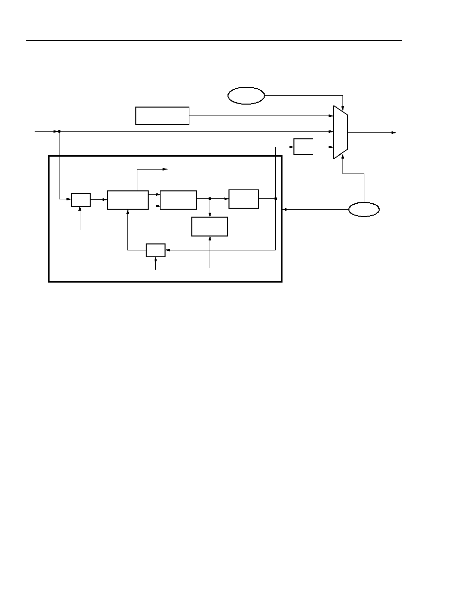
Data Sheet
DSP1627 Digital Signal Processor
March 2000
26
Lucent Technologies Inc.
4 Hardware Architecture
(continued)
4.12 Clock Synthesis
Figure 6. Clock Source Block Diagram
powerc
RING
OSCILLATOR
M
U
X
˜ 2
˜ N
PHASE
DETECTOR
CHARGE
PUMP
VCO
VCO CLOCK
f
VCO
LOOP
FILTER
˜ M
LF[3:0]
Mbits[4:0]
Nbits[2:0]
PLL/SYNTHESIZER
CKI INPUT CLOCK
LOCK
(FLAG TO INDICATE LOCK
CONDITION OF PLL)
f
CKI
f
SLOW CLOCK
SLOWCKI
pllc
PLLEN
INTERNAL
PROCESSOR
CLOCK
f
INTERNAL CLOCK
PLLSEL
f
CKI
5-4520 (F)
The DSP1627 provides an on-chip, programmable
clock synthesizer. Figure 6 is the clock source diagram.
The 1X CKI input clock, the output of the synthesizer, or
a slow internal ring oscillator can be used as the source
for the internal DSP clock. The clock synthesizer is
based on a phase-locked loop (PLL), and the terms
clock synthesizer and PLL are used interchangeably.
On powerup, CKI is used as the clock source for the
DSP. This clock is used to generate the internal proces-
sor clocks and CKO, where f
CKI
= f
CKO
. Setting the ap-
propriate bits in the pllc control register (described in
Table 32) will enable the clock synthesizer to become
the clock source. The powerc register, which is dis-
cussed in Section 4.13, can override the selection to
stop clocks or force the use of the slow clock for low-
power operation.
PLL Control Signals
The input to the PLL comes from one of the three mask-
programmable clock options: CMOS, crystal, or small-
signal. The PLL cannot operate without an external in-
put clock.
To use the PLL, the PLL must first be allowed to stabi-
lize and lock to the programmed frequency. After the
PLL has locked, the LOCK flag is set and the lock detect
circuitry is disabled. The synthesizer can then be used
as the clock source. Setting the PLLSEL bit in the pllc
register will switch sources from f
CKI
to f
VCO
/2 without
glitching. It is important to note that the setting of the pllc
register must be maintained. Otherwise, the PLL will
seek the new set point. Every time the pllc register is
written, the LOCK flag is reset.

Data Sheet
March 2000
DSP1627 Digital Signal Processor
Lucent Technologies Inc.
27
4 Hardware Architecture
(continued)
The frequency of the PLL output clock, f
VCO
, is deter-
mined by the values loaded into the 3-bit N divider and
the 5-bit M divider. When the PLL is selected and
locked, the frequency of the internal processor clock is
related to the frequency of CKI by the following equa-
tions:
f
VCO
= f
CKI
* M/N
f
INTERNAL CLOCK
= f
CKO
= f
VCO
˜
2
The frequency of the VCO, f
VCO
, must fall within the
range listed in Table 63. Also note that f
VCO
must be at
least twice f
CKI
.
The coding of the Mbits and Nbits is described as fol-
lows:
Mbits = M
-
2
if (N == 1)
Nbits = 0x7
else
Nbits = N
-
2
where N ranges from 1 to 8 and M ranges from 2 to 20.
The loop filter bits LF[3:0] should be programmed ac-
cording to Table 64.
Two other bits in the pllc register control the PLL. Clear-
ing the PLLEN bit powers down the PLL; setting this bit
powers up the PLL. Clearing the PLLSEL bit deselects
the PLL so that the DSP is clocked by a 1X version of
the CKI input; setting the PLLSEL bit selects the PLL-
generated clock for the source of the DSP internal pro-
cessor clock. The pllc register is cleared on reset and
powerup. Therefore, the DSP comes out of reset with
the PLL deselected and powered down. M and N should
be changed only while the PLL is deselected. The val-
ues of M and N should not be changed when powering
down or deselecting the PLL.
As previously mentioned, the PLL also provides a user
flag, LOCK, to indicate when the loop has locked. When
this flag is not asserted, the PLL output is unstable. The
DSP should not be switched to the PLL-based clock
without first checking that the lock flag is set. The lock
flag is cleared by writing to the pllc register. When the
PLL is deselected, it is necessary to wait for the PLL to
relock before the DSP can be switched to the PLL-
based clock. Before the input clock is stopped, the PLL
should be powered down. Otherwise, the LOCK flag will
not be reset and there may be no way to determine if the
PLL is stable, once the input clock is applied again.
The lock-in time depends on the frequency of operation
and the values programmed for M and N (see Table 64).

Data Sheet
DSP1627 Digital Signal Processor
March 2000
28
Lucent Technologies Inc.
4 Hardware Architecture
(continued)
PLL Programming Examples
The following section of code illustrates how the PLL would be initialized on powerup, assuming the following oper-
ating conditions:
s
CKI input frequency = 10 MHz
s
Internal clock and CKO frequency = 50 MHz
s
VCO frequency = 100 MHz
s
Input divide down count N = 2 (Set Nbits[2:0] = 000 to get N = 2, as described in Table 32.)
s
Feedback down count M = 20 (Set Mbits[4:0] = 10010 to get M = 18 + 2 = 20, as described in Table 32.)
The device would come out of reset with the PLL disabled and deselected.
pllinit: pllc = 0x2912
/* Running CKI input clock at 10 MHz, set up counters in PLL */
pllc = 0xA912 /* Power on PLL, but PLL remains deselected */
call pllwait
/* Loop to check for LOCK flag assertion */
pllc = 0xE912 /* Select high-speed, PLL clock */
goto start
/* User's code, now running at 50 MHz */
pllwait: if lock return
goto pllwait
Programming examples which illustrate how to use the PLL with the various power management modes are listed
in Section 4.13.
Latency
The switch between the CKI-based clock and the PLL-based clock is synchronous. This method results in the actual
switch taking place several cycles after the PLLSEL bit is changed. During this time, actual code can be executed,
but it will be at the previous clock rate. Table 12 shows the latency times for switching between CKI-based and PLL-
based clocks. In the example given, the delay to switch to the PLL source is 1--4 CKO cycles and to switch back is
11--31 CKO cycles.
Frequency Accuracy and Jitter
When using the PLL to multiply the input clock frequency up to the instruction clock rate, it is important to realize
that although the average frequency of the internal clock and CKO will have about the same relative accuracy as
the input clock, noise sources within the DSP will produce jitter on the PLL clock such that each individual clock
period will have some error associated with it. The PLL is guaranteed only to have sufficiently low jitter to operate
the DSP, and thus, this clock should not be used as an input to jitter-sensitive devices in the system.
V
DDA
and V
SSA
Connections
The PLL has its own power and ground pins, V
DDA
and V
SSA
. Additional filtering should be provided for V
DDA
in the
form of a ferrite bead connected from V
DDA
to V
DD
and two decoupling capacitors (4.7
µ
F tantalum in parallel with
a 0.01
µ
F ceramic) from V
DDA
to V
SS
. V
SSA
can be connected directly to the main ground plane. This recommen-
dation is subject to change and may need to be modified for specific applications depending on the characteristics
of the supply noise.
Note: For devices with the CMOS clock input option, the CKI2 pin should be connected to V
SSA
.
Table 12. Latency Times for Switching Between CKI and PLL-Based Clocks
Minimum Latency (Cycles)
Maximum Latency (Cycles)
Switch to PLL-based clock
1
N + 2
Switch from PLL-based clock
M/N + 1
M + M/N + 1

Data Sheet
March 2000
DSP1627 Digital Signal Processor
Lucent Technologies Inc.
29
4 Hardware Architecture
(continued)
4.13 Power Management
There are three different control mechanisms for putting
the DSP1627 into low-power modes: the powerc control
register, the STOP pin, and the AWAIT bit in the alf reg-
ister. The PLL can also be disabled with the PLLEN bit
of the pllc register for more power saving.
Powerc Control Register Bits
The powerc register has 10 bits that power down vari-
ous portions of the chip and select the clock source:
XTLOFF: Assertion of the XTLOFF bit powers down the
crystal oscillator or the small-signal input circuit, dis-
abling the internal processor clock. Assertion of the
XTLOFF bit to disable the crystal oscillator also pre-
vents its use as a noninverting buffer. Since the oscilla-
tor and the small-signal input circuits take many cycles
to stabilize, care must be taken with the turn-on se-
quence, as described later.
SLOWCKI: Assertion of the SLOWCKI bit selects the
ring oscillator as the clock source for the internal pro-
cessor clock instead of CKI or the PLL. When CKI or the
PLL is selected, the ring oscillator is powered down.
Switching of the clocks is synchronized so that no par-
tial or short clock pulses occur. Two nops should follow
the instruction that sets or clears SLOWCKI.
NOCK: Assertion of the NOCK bit synchronously turns
off the internal processor clock, regardless of whether
its source is provided by CKI, the PLL, or the ring oscil-
lator. The NOCK bit can be cleared by resetting the chip
with the RSTB pin, or asserting the INT0 or INT1 pins.
Two nops should follow the instruction that sets NOCK.
The PLL remains running, if enabled, while NOCK is
set.
INT0EN: This bit allows the INT0 pin to asynchronously
clear the NOCK bit, thereby allowing the device to con-
tinue program execution from where it left off without
any loss of state. No chip reset is required. It is recom-
mended that, when INT0EN is to be used, the INT0
interrupt be disabled in the inc register so that an unin-
tended interrupt does not occur. After the program re-
sumes, the INT0 interrupt in the ins register should be
cleared.
INT1EN: This bit enables the INT1 pin to be used as the
NOCK clear, exactly like INT0EN previously described.
The following control bits power down the peripheral
I/O units of the DSP. These bits can be used to further
reduce the power consumption during standard sleep
mode.
SIO1DIS: This is a powerdown signal to the SIO1 I/O
unit. It disables the clock input to the unit, thus eliminat-
ing any sleep power associated with the SIO1. Since
the gating of the clocks may result in incomplete trans-
actions, it is recommended that this option be used in
applications where the SIO1 is not used or when reset
may be used to reenable the SIO1 unit. Otherwise, the
first transaction after reenabling the unit may be corrupt-
ed.
SIO2DIS: This bit powers down the SIO2 in the same
way SIO1DIS powers down the SIO1.
PHIFDIS: This is a powerdown signal to the parallel
host interface. It disables the clock input to the unit, thus
eliminating any sleep power associated with the PHIF.
Since the gating of the clocks may result in incomplete
transactions, it is recommended that this option be used
in applications where the PHIF is not used, or when re-
set may be used to reenable the PHIF. Otherwise, the
first transaction after reenabling the unit may be corrupt-
ed.
TIMERDIS: This is a timer disable signal which disables
the clock input to the timer unit. Its function is identical
to the DISABLE field of the timerc control register. Writ-
ing a 0 to the TIMERDIS field will continue the timer op-
eration.
Figure 7 shows a functional view of the effect of the bits
of the powerc register on the clock circuitry. It shows
only the high-level operation of each bit. Not shown are
the bits that power down the peripheral units.
STOP Pin
Assertion (active-low) of the STOP pin has the same ef-
fect as setting the NOCK bit in the powerc register. The
internal processor clock is synchronously disabled until
the STOP pin is returned high. Once the STOP pin is re-
turned high, program execution will continue from
where it left off without any loss of state. No chip reset
is required. The PLL remains running, if enabled, during
STOP assertion.
The pllc Register Bits
The PLLEN bit of the pllc register can be used to power
down the clock synthesizer circuitry. Before shutting
down the clock synthesizer circuitry, the system clock
should be switched to either CKI using the PLLSEL bit
of pllc, or to the ring oscillator using the SLOWCKI bit of
powerc.
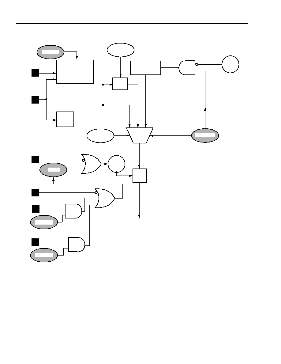
Data Sheet
DSP1627 Digital Signal Processor
March 2000
30
Lucent Technologies Inc.
4 Hardware Architecture
(continued)
Notes:
The functions in the shaded ovals are bits in the powerc control register. The functions in the nonshaded ovals are bits in the pllc control
register.
Deep sleep is the state arrived at either by a hardware or software stop of the internal processor clock.
The switching of the multiplexers and the synchronous gate is designed so that no partial clocks or glitching will occur.
When the deep sleep state is entered with the ring oscillator selected, the internal processor clock is turned off before the ring oscillator is pow-
ered down.
PLL select is the PLLSEL bit of pllc; PLL powerdown is the PLLEN bit of pllc.
Figure 7. Power Management Using the powerc and the pllc Registers
CKI2
CRYSTAL
OSCILLATOR,
OR
SMALL SIGNAL
CLOCK
RING
OSCILLATOR
STOP
XTLOFF
MASK-PROGRAMMABLE
OPTION
OFF
CKI
RSTB
CMOS
INPUT
CLOCK
SYNC.
GATE
SLOWCKI
SYNC.
MUX
INTERNAL
PROCESSOR
CLOCK
CLEAR NOCK
DISABLE
INT0
INT0EN
ON
INT1
INT1EN
DEEP
SLEEP
HW STOP
SW STOP
NOCK
PLLEN
PLLSEL
PLL
f
VCO/2
f
SLOW CLOCK
f
INTERNAL CLOCK
f
CKI
DEEP
SLEEP
5-4124 (F).h

Data Sheet
March 2000
DSP1627 Digital Signal Processor
Lucent Technologies Inc.
31
4 Hardware Architecture
(continued)
Await Bit of the alf Register
Setting the AWAIT bit of the alf register causes the pro-
cessor to go into the standard sleep state or power-sav-
ing standby mode. Operation of the AWAIT bit is the
same as in the DSP1610, DSP1611, DSP1616,
DSP1617, and DSP1618. In this mode, the minimum
circuitry required to process an incoming interrupt re-
mains active, and the PLL remains active if enabled. An
interrupt will return the processor to the previous state,
and program execution will continue. The action result-
ing from setting the AWAIT bit and the action resulting
from setting bits in the powerc register are mostly inde-
pendent. As long as the processor is receiving a clock,
whether slow or fast, the DSP may be put into standard
sleep mode with the AWAIT bit. Once the AWAIT bit is
set, the STOP pin can be used to stop and later restart
the processor clock, returning to the standard sleep
state. If the processor clock is not running, however, the
AWAIT bit cannot be set.
Power Management Sequencing
There are important considerations for sequencing the
power management modes. Both the crystal oscillator
and the small-signal clock input circuits have start-up
delays which must be taken into account, and the PLL
requires a delay to reach lock-in. Also, the chip may or
may not need to be reset following a return from a low-
power state.
Devices with a crystal oscillator or small-signal input
clocking option may use the XTLOFF bit in the powerc
register to power down the on-chip oscillator or small-
signal circuitry, thereby reducing the power dissipation.
When reenabling the oscillator or the small-signal cir-
cuitry, it is important to bear in mind that a start-up inter-
val exists during which time the clocks are not stable.
Two scenarios exist here:
1. Immediate Turn-Off, Turn-On with RSTB: This sce-
nario applies to situations where the target device is
not required to execute any code while the crystal os-
cillator or small-signal input circuit is powered down
and where restart from a reset state can be tolerated.
In this case, the processor clock derived from either
the oscillator or the small-signal input is running when
XTLOFF is asserted. This effectively stops the inter-
nal processor clock. When the system chooses to re-
enable the oscillator or small-signal input, a reset of
the device will be required. The reset pulse must be
of sufficient duration for the oscillator start-up interval
to be satisfied. A similar interval is required for the
small-signal input circuit to reach its dc operating
point. A minimum reset pulse of 20 ms will be ade-
quate. The falling edge of the reset signal, RSTB, will
asynchronously clear the XTLOFF field, thus re-en-
abling the power to the oscillator or small-signal cir-
cuitry. The target DSP will then start execution from a
reset state, following the rising edge of RSTB.
2. Running from Slow Clock While XTLOFF Active: The
second scenario applies to situations where the de-
vice needs to continue execution of its target code
when the crystal oscillator or small-signal input is
powered down. In this case, the device switches to
the slow ring oscillator clock first, by enabling the
SLOWCKI field before writing a 1 to the XTLOFF
field. Two nops are needed in between the two write
operations to the powerc register. The target device
will then continue execution of its code at slow speed,
while the crystal oscillator or small-signal input clock
is turned off. Switching from the slow clock back to
the high-speed crystal oscillator clock is then accom-
plished in three user steps. First, XTLOFF is cleared.
Then, a user-programmed routine sets the internal
timer to a delay to wait for the crystal's oscillations to
become stable. When the timer counts down to zero,
the high-speed clock is selected by clearing the
SLOWCKI field, either in the timer's interrupt service
routine or following a timer polling loop. If PLL opera-
tion is desired, then an additional routine is neces-
sary to enable the PLL and wait for it to lock.

Data Sheet
DSP1627 Digital Signal Processor
March 2000
32
Lucent Technologies Inc.
4 Hardware Architecture
(continued)
Power Management Examples Without the PLL
The following examples show the more significant options for reducing the power dissipation. These are valid only
if the pllc register is set to disable and deselect the PLL (PLLEN = 0, PLLSEL = 0).
Standard Sleep Mode. This is the standard sleep mode. While the processor is clocked with a high-speed clock,
CKI, the alf register's AWAIT bit is set. Peripheral units may be turned off to further reduce the sleep power.
powerc = 0X00F0
/* Turn off peripherals, core running with CKI */
sleep:a0 = 0x8000
/* Set alf register in cache loop if running from */
do 1 {
/* external memory with >1 wait state */
alf = a0
/* Stop internal processor clock, interrupt circuits */
nop
/* active */
}
nop
/* Needed for bedtime execution. Only sleep power */
nop
/* consumed here until.... interrupt wakes up the device */
cont: . . .
/* User code executes here */
powerc = 0x0
/* Turn peripheral units back on */
Sleep with Slow Internal Clock. In this case, the ring oscillator is selected to clock the processor before the device
is put to sleep. This will reduce the power dissipation while waiting for an interrupt to continue program execution.
powerc = 0x40F0
/* Turn off peripherals and select slow clock */
2*nop
/* Wait for it to take effect */
sleep:a0 = 0x8000
/* Set alf register in cache loop if running from */
do 1 {
/* external memory with >1 wait state */
alf = a0
/* Stop internal processor clock, interrupt circuits */
nop
/* active */
}
nop
/* Needed for bedtime execution. Reduced sleep power */
nop
/* consumed here.... Interrupt wakes up the device */
cont: . . .
/* User code executes here */
powerc = 0x00F0
/* Select high-speed clock */
2*nop
/* Wait for it to take effect */
powerc = 0x0000
/* Turn peripheral units back on */
Note that, in this case, the wake-up latency is determined by the period of the ring oscillator clock.
Sleep with Slow Internal Clock and Crystal Oscillator/Small-Signal Disabled. If the target device contains the
crystal oscillator or the small-signal clock option, the clock input circuitry can be powered down to further reduce
power. In this case, the slow clock must be selected first.
powerc = 0x40F0
/* Turn off peripherals and select slow clock */
2*nop
/* Wait for it to take effect */
powerc = 0xC0F0
/* Turn off the crystal oscillator */
sleep:a0 = 0x8000
/* Set alf register in cache loop if running from */
do 1 {
/* external memory with >1 wait state */
alf = a0
/* Stop internal processor clock, interrupt circuits */
nop
/* active */
}
nop
/* Needed for bedtime execution. Reduced sleep power */
nop
/* consumed here.... Interrupt wakes up the device */
powerc = 0x40F0
/* Clear XTLOFF, reenable oscillator/small-signal */
call xtlwait
/* Wait until oscillator/small-signal is stable */
cont: powerc = 0x00F0
/* Select high-speed clock */
2*nop
/* Wait for it to take effect */
powerc = 0x0000
/* Turn peripheral units back on */
Note that, in this case, the wake-up latency is dominated by the crystal oscillator or small-signal start-up period.

Data Sheet
March 2000
DSP1627 Digital Signal Processor
Lucent Technologies Inc.
33
4 Hardware Architecture
(continued)
Software Stop. In this case, all internal clocking is disabled. INT0, INT1, or RSTB may be used to reenable the
clocks. If the device uses the crystal oscillator or small-signal clock option, the power management must be done in
correct sequence.
powerc = 0x4000
/* SLOWCKI asserted */
2*nop
/* Wait for it to take effect */
powerc = 0xD000
/* XTLOFF asserted if applicable and INT0EN asserted */
inc = NOINT0
/* Disable the INT0 interrupt */
sopor:powerc = 0xF000
/* NOCK asserted, all clocks stop */
/* Minimum switching power consumed here */
3*nop
/* Some nops will be needed */
/* INT0 pin clears the NOCK field, clocking resumes */
cont: powerc = 0x4000
/* INT0EN cleared and XTLOFF cleared, if applicable*/
call waitxtl
/* Wait for the crystal oscillator/small-signal to */
/* stabilize, if applicable*/
powerc = 0x0
/* Clear SLOWCKI field, back to high speed */
2*nop
/* Wait for it to take effect */
ins = 0x0010
/* Clear the INT0 status bit */
In this case also, the wake-up latency is dominated by the crystal oscillator or small-signal start-up period.
The previous examples do not provide an exhaustive list of options available to the user. Many different clocking
possibilities exist for which the target device may be programmed, depending on:
s
The clock source to the processor.
s
Whether the user chooses to power down the peripheral units.
s
The operational state of the crystal oscillator/small-signal clock input, powered or unpowered.
s
Whether the internal processor clock is disabled through hardware or software.
s
The combination of power management modes the user chooses.
s
Whether or not the PLL is enabled.
An example subroutine for xtlwait follows:
xtlwait:
timer0 = 0x2710
/* Load a count of 10,000 into the timer
*/
timerc = 0x0010
/* Start the timer with a PRESCALE of two */
inc = 0x0000
/* Disable the interrupts
*/
loop1:
a0 = ins
/* Poll the ins register
*/
a0 = a0 & 0x0100
/* Check bit 8 (TIME) of the ins register */
if eq goto loop1
/* Loop if the bit is not set
*/
ins = 0x0100
/* Clear the TIME interrupt bit
*/
return
/* Return to the main program
*/

Data Sheet
DSP1627 Digital Signal Processor
March 2000
34
Lucent Technologies Inc.
4 Hardware Architecture
(continued)
Power Management Examples with the PLL
The following examples show the more significant options for reducing power dissipation if operation with the PLL
clock synthesizer is desired.
Standard Sleep Mode, PLL Running. This mode would be entered in the same manner as without the PLL. While
the input to the clock synthesizer, CKI, remains running, the alf register's AWAIT bit is set. The PLL will continue to
run and dissipate power. Peripheral units may be turned off to further reduce the sleep power.
powerc = 0x00F0
/* Turn off peripherals, core running with PLL */
sleep:a0 = 0x8000
/* Set alf register in cache loop if running from */
do 1 {
/* external memory with >1 wait state */
alf = a0
/* Stop internal processor clock, interrupt circuits */
nop
/* active */
}
nop
/* Needed for bedtime execution. Only sleep power plus PLL */
nop
/* power consumed here.... Interrupt wakes up the device */
cont: . . .
/* User code executes here */
powerc = 0x0
/* Turn peripheral units back on */
Sleep with Slow Internal Clock, PLL Running. In this case, the ring oscillator is selected to clock the processor
before the device is put to sleep. This will reduce power dissipation while waiting for an interrupt to continue program
execution.
powerc = 0x40F0
/* Turn off peripherals and select slow clock */
2*nop
/* Wait for slow clock to take effect */
sleep:a0 = 0x8000
/* Set alf register in cache loop if running from */
do 1 {
/* external memory with >1 wait state */
alf = a0
/* Stop internal processor clock, interrupt circuits */
nop
/* active */
}
nop
/* Needed for bedtime execution. Reduced sleep power, PLL */
nop
/* power, and ring oscillator power consumed here... */
/* Interrupt wakes up the device */
cont: . . .
/* User code executes here */
powerc = 0x00F0
/* Select high-speed PLL based clock */
2*nop
/* Wait for it to take effect */
powerc = 0x0000
/* Turn peripheral units back on */

Data Sheet
March 2000
DSP1627 Digital Signal Processor
Lucent Technologies Inc.
35
4 Hardware Architecture
(continued)
Sleep with Slow Internal Clock and Crystal Oscillator/Small-Signal Disabled, PLL Disabled. If the target de-
vice contains the crystal oscillator or the small-signal clock option, the clock input circuitry can be powered down to
further reduce power. In this case, the slow clock must be selected first, and then the PLL must be disabled, since
the PLL cannot run without the clock input circuitry being active.
powerc = 0x40F0
/* Turn off peripherals and select slow clock */
2*nop
/* Wait for slow clock to take effect */
pllc = 0x29F2
/* Disable PLL (assume N = 1,M = 20, LF = 1001) */
powerc = 0xC0F0
/* Disable crystal oscillator */
sleep:a0 = 0x8000
/* Set alf register in cache loop if running from */
do 1 {
/* external memory with >1 wait state */
alf = a0
/* Stop internal processor clock, interrupt circuits */
nop
/* active */
}
nop
/* Needed for bedtime execution. Reduced sleep power
nop
/* consumed here.... Interrupt wakes up device */
powerc = 0x40F0
/* Clear XTLOFF, leave PLL disabled */
call xtlwait
/* Wait until crystal oscillator/small-signal is stable */
pllc = 0xE9F2
/* Enable PLL, continue to run off slow clock */
call pllwait
/* Loop to check for LOCK flag assertion */
cont: powerc = 0x00F0
/* Select high-speed PLL based clock */
2*nop
/* Wait for it to take effect */
powerc = 0x0000
/* Turn peripherals back on */
Software Stop, PLL Disabled. In this case, all internal clocking is disabled. INT0, INT1, or RSTB may be used to
reenable the clocks. If the device uses the crystal oscillator or small-signal clock option, the power management
must be done in the correct sequence, with the PLL being disabled before shutting down the clock input buffer.
powerc = 0x4000
/* SLOWCKI asserted */
2*nop
/* Wait for slow clock to take effect */
pllc = 0x29F2
/* Disable PLL (assume N = 1, M = 20, LF = 1001) */
powerc = 0xD000
/* XTLOFF asserted, if applicable and INT0EN
/* asserted */
sopor:powerc = 0xF000
/* NOCK asserted, all clocks stop */
/* Minimum switching power consumed here */
3*nop
/* Some nops will be needed */
/* INT0 pin clears NOCK field, clocking resumes */
cont: powerc = 0x4000
/* INTOEN cleared and XTLOFF cleared, if applicable */
call xtlwait
/* Wait until crystal oscillator/small-signal is stable */
/* if applicable */
pllc = 0xE9F2
/* Enable PLL, continue to run off slow clock */
call pllwait
/* Loop to check for LOCK flag assertion */
powerc = 0x0
/* Select high-speed PLL based clock */
2*nop
/* Wait for it to take effect */
ins = 0x0010
/* Clear the INT0 status bit */

Data Sheet
DSP1627 Digital Signal Processor
March 2000
36
Lucent Technologies Inc.
5 Software Architecture
5.1 Instruction Set
The DSP1627 processor has seven types of instruc-
tions: multiply/ALU, special function, control, F3 ALU,
BMU, cache, and data move. The multiply/ALU instruc-
tions are the primary instructions used to implement sig-
nal processing algorithms. Statements from this group
can be combined to generate multiply/accumulate, log-
ical, and other ALU functions and to transfer data be-
tween memory and registers in the data arithmetic unit.
The special function instructions can be conditionally
executed based on flags from the previous ALU or BMU
operation, the condition of one of the counters, or the
value of a pseudorandom bit in the DSP1627 device.
Special function instructions perform shift, round, and
complement functions. The F3 ALU instructions enrich
the operations available on accumulators. The BMU in-
structions provide high-performance bit manipulation.
The control instructions implement the goto and call
commands. Control instructions can also be executed
conditionally. Cache instructions are used to implement
low-overhead loops, conserve program memory, and
decrease the execution time of certain multiply/ALU in-
structions. Data move instructions are used to transfer
data between memory and registers or between accu-
mulators and registers. See the
DSP1611/17/18/27
Digital Signal Processor Information Manual
for a de-
tailed description of the instruction set.
The following operators are used in describing the in-
struction set:
s
*
16 x 16-bit ≠> 32-bit multiplication or register-in-
direct addressing when used as a prefix to an ad-
dress register or denotes direct addressing
when used as a prefix to an immediate
s
+
36-bit addition
s
≠
36-bit subtraction
s
>>
Arithmetic right shift
s
>>>
Logical right shift
s
<<
Arithmetic left shift
s
<<<
Logical left shift
s
|
36-bit bitwise OR
s
&
36-bit bitwise AND
s
^
36-bit bitwise EXCLUSIVE OR
s
:
Compound address swapping, accumulator
shuffling
s
~
One's complement
These are 36-bit operations. One operand is 36-bit data in an ac-
cumulator; the other operand may be 16, 32, or 36 bits.
Multiply/ALU Instructions
Note that the function statements and transfer state-
ments in Table 13 are chosen independently. Any func-
tion statement (F1) can be combined with any transfer
statement to form a valid multiply/ALU instruction. If ei-
ther statement is not required, a single statement from
either column also constitutes a valid instruction. The
number of cycles to execute the instruction is a function
of the transfer column. (An instruction with no transfer
statement executes in one instruction cycle.) Whenever
PC, pt, or rM is used in the instruction and points to ex-
ternal memory, the programmed number of wait-states
must be added to the instruction cycle count. All multi-
ply/ALU instructions require one word of program mem-
ory. The no-operation (nop) instruction is a special-
case encoding of a multiply/ALU instruction and exe-
cutes in one cycle. The assembly-language representa-
tion of a nop is either nop or a single semicolon.
A single-cycle squaring function is provided in
DSP1627. By setting the X = Y = bit in the auc register,
any instruction that loads the high half of the y register
also loads the x register with the same value. A subse-
quent instruction to multiply the x register and y register
results in the square of the value being placed in the p
register. The instruction a0 = p p = x*y y = *r0++ with
the X = Y = bit set to one will read the value pointed to
by r0, load it to both x and y, multiply the previously
fetched value of x and y, and transfer the previous prod-
uct to a0. A table of values pointed to by r0 can thus be
squared in a pipeline with one instruction cycle per each
value. Multiply/ALU instructions that use x = X transfer
statements (such as a0 = p p = x*y y = *r0++ x = *pt++)
are not recommended for squaring because pt will be
incremented even though x is not loaded from the value
pointed to by pt. Also, the same conflict wait occurrenc-
es from reading the same bank of internal memory or
reading from external memory apply, since the X space
fetch occurs (even though its value is not used).
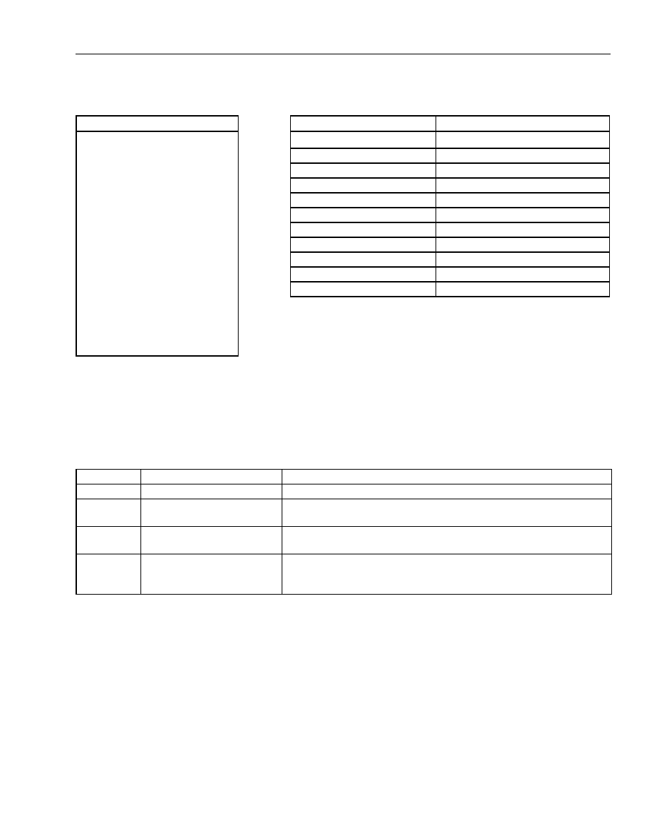
Data Sheet
March 2000
DSP1627 Digital Signal Processor
Lucent Technologies Inc.
37
5 Software Architecture
(continued)
The l in [ ] is an optional argument that specifies the low 16 bits of aT or y.
Add cycles for:
1. When an external memory access is made in X or Y space and wait-states are programmed, add the number of wait-states.
2. If an X space access and a Y space access are made to the same bank of DPRAM in one instruction, add one cycle.
Note: For transfer statements when loading the upper half of an accumulator, the lower half is cleared if the corre-
sponding CLR bit in the auc register is zero. auc is cleared by reset.
Table 13. Multiply/ALU Instructions
Function Statement
Transfer Statement
Cycles (Out/In Cache)
p = x * y
y = Y
x = X
2/1
aD = p
p = x * y
y = aT
x = X
2/1
aD = aS + p
p = x * y
y[l] = Y
1/1
aD = aS ≠ p
p = x * y
aT[l] = Y
1/1
aD = p
x = Y
1/1
aD = aS + p
Y
1/1
aD = aS ≠ p
Y = y[l]
2/2
aD = y
Y = aT[l]
2/2
aD = aS + y
Z:y
x = X
2/2
aD = aS ≠ y
Z:y[l]
2/2
aD = aS & y
Z:aT[l]
2/2
aD = aS | y
aD = aS ^ y
aS ≠ y
aS & y
Table 14. Replacement Table for Multiply/ALU Instructions
Replace
Value
Meaning
aD, aS, aT
a0, a1
One of two DAU accumulators.
X
*pt++, *pt++i
X memory space location pointed to by pt. pt is postmodified by +1 and
i, respectively.
Y
*rM, *rM++, *rM--, rM++j
RAM location pointed to by rM (M = 0, 1, 2, 3). rM is postmodified by
0, +1, ≠1, or j, respectively.
Z
*rMzp, *rMpz, *rMm2, *rMjk
Read/Write compound addressing. rM (M = 0, 1, 2, 3) is used twice.
First, postmodified by 0, +1, ≠1, or j, respectively; and, second, post-
modified by +1, 0, +2, or k, respectively.

Data Sheet
DSP1627 Digital Signal Processor
March 2000
38
Lucent Technologies Inc.
5 Software Architecture
(continued)
Special Function Instructions
All forms of the special function require one word of program memory and execute in one instruction cycle. (If PC
points to external memory, add programmed wait-states.)
aD = aS
--
Load destination accumulator from source accumulator
aD = ≠aS
--
2's complement
aD = ~aS
*
--
1's complement
aD = rnd(aS)
--
Round upper 20 bits of accumulator
aDh = aSh + 1 --
Increment upper half of accumulator (lower half cleared)
aD = aS + 1
--
Increment accumulator
aD = y
--
Load accumulator with 32-bit y register value with sign extend
aD = p
--
Load accumulator with 32-bit p register value with sign extend
The above special functions can be conditionally executed, as in:
if CON instruction
and with an event counter
ifc CON instruction
which means:
if CON is true then
c1 = c1 + 1
instruction
c2 = c1
else
c1 = c1 + 1
The above special function statements can be executed unconditionally by writing them directly, e.g., a0 = a1.
aD = aS >> 1
aD = aS >> 4
aD = aS >> 8
aD = aS >> 16
}
Arithmetic right shift (sign preserved) of 36-bit accumulators
*
This function is not available for the DSP16A.
aD = aS << 1
aD = aS << 4
aD = aS << 8
aD = aS << 16
}
Arithmetic left shift (sign not preserved) of the lower 32 bits of accumulators
(upper 4 bits are sign-bit-extended from bit 31 at the completion of the shift)
Table 15. Replacement Table for Special Function Instructions
Replace
Value
Meaning
aD
aS
a0, a1
One of two DAU accumulators.
CON
mi, pl, eq, ne, gt, le, lvs, lvc, mvs, mvc, c0ge,
c0lt, c1ge, c1lt, heads, tails, true, false, allt, allf,
somet, somef, oddp, evenp, mns1, nmns1, npint,
njint, lock
See Table 17 for definitions of mnemonics.

Data Sheet
March 2000
DSP1627 Digital Signal Processor
Lucent Technologies Inc.
39
5 Software Architecture
(continued)
Control Instructions
All control instructions executed unconditionally execute in two cycles, except icall which takes three cycles. Control
instructions executed conditionally execute in three instruction cycles. (If PC, pt, or pr point to external memory, add
programmed wait-states.) Control instructions executed unconditionally require one word of program memory, while
control instructions executed conditionally require two words. Control instructions cannot be executed from the
cache.
goto JA
goto pt
call JA
call pt
icall
return
(goto pr)
ireturn
(goto pi)
The goto JA and call JA instructions should not be placed in the last or next-to-last instruction before the boundary of a 4 Kwords page. If
the goto or call is placed there, the program counter will have incremented to the next page and the jump will be to the next page, rather than
to the desired current page.
The icall instruction is reserved for development system use.
The above control instructions, with the exception of ireturn and icall, can be conditionally executed. For example:
if le goto 0x0345
Table 16. Replacement Table for Control Instructions
Replace
Value
Meaning
CON
mi, pl, eq, ne, gt, le, nlvs, lvc, mvs, mvc, c0ge, c0lt,
c1ge, c1lt, heads, tails, true, false, allt, allf, somet,
somef, oddp, evenp, mns1, nmns1, npint, njint, lock
See Table 17 for definitions of mnemonics.
JA
12-bit value
Least significant 12 bits of absolute address
within the same 4 Kwords memory section.

Data Sheet
DSP1627 Digital Signal Processor
March 2000
40
Lucent Technologies Inc.
5 Software Architecture
(continued)
Conditional Mnemonics (Flags)
Table 17 lists mnemonics used in conditional execution of special function and control instructions.
Notes:
Testing the state of the counters (c0 or c1) automatically increments the counter by one.
The heads or tails condition is determined by a randomly set or cleared bit, respectively. The bit is randomly set with a probability of 0.5. A random
rounding function can be implemented with either heads or tails. The random bit is generated by a ten-stage pseudorandom sequence generator
(PSG) that is updated after either a heads or tails test. The pseudorandom sequence may be reset by writing any value to the pi register, except
during an interrupt service routine (ISR). While in an ISR, writing to the pi register updates the register and does not reset the PSG. If not in an
ISR, writing to the pi register resets the PSG. (The pi register is updated, but will be written with the contents of the PC on the next instruction.)
Interrupts must be disabled when writing to the pi register. If an interrupt is taken after the pi write, but before pi is updated with the PC
value, the ireturn instruction will not return to the correct location. If the RAND bit in the auc register is set, however, writing the pi register never
resets the PSG.
Table 17. DSP1627 Conditional Mnemonics
Test
Meaning
Test
Meaning
pl
Result is nonnegative (sign bit is bit 35).
0
mi
Result is negative. < 0
eq
Result is equal to 0. = 0
ne
Result is not equal to 0.
0
gt
Result is greater than 0. > 0
le
Result is less than or equal to 0.
0
lvs
Logical overflow set.
*
*
Result is not representable in the 36-bit accumulators (36-bit overflow).
lvc
Logical overflow clear.
mvs
Mathematical overflow set.
Bits 35--31 are not the same (32-bit overflow).
mvc
Mathematical overflow clear.
c0ge
Counter 0 greater than or equal to 0.
c0lt
Counter 0 less than 0.
c1ge
Counter 1 greater than or equal to 0.
c1lt
Counter 1 less than 0.
heads
Pseudorandom sequence bit set.
tails
Pseudorandom sequence bit clear.
true
The condition is always satisfied in an if in-
struction.
false
The condition is never satisfied in an if instruc-
tion.
allt
All True, all BIO input bits tested compared
successfully.
allf
All False, no BIO input bits tested compared
successfully.
somet
Some True, some BIO input bits tested com-
pared successfully.
somef
Some False, some BIO input bits tested did
not compare successfully.
oddp
Odd Parity, from BMU operation.
evenp
Even Parity, from BMU operation.
mns1
Minus 1, result of BMU operation.
nmns1
Not Minus 1, result of BMU operation.
npint
Not PINT, used by hardware development
system.
njint
Not JINT, used by hardware development
system.
lock
The PLL has achieved lock and is stable.

Data Sheet
March 2000
DSP1627 Digital Signal Processor
Lucent Technologies Inc.
41
5 Software Architecture
(continued)
F3 ALU Instructions
These instructions are implemented in the DSP1600 core. They allow accumulator two-operand operations with ei-
ther another accumulator, the p register, or a 16-bit immediate operand (IM16). The result is placed in a destination
accumulator that can be independently specified. All operations are done with the full 36 bits. For the accumulator
with accumulator operations, both inputs are 36 bits. For the accumulator with p register operations, the p register
is sign-extended into bits 35--32 before the operation. For the accumulator high with immediate operations, the im-
mediate is sign-extended into bits 35--32 and the lower bits 15--0 are filled with zeros, except for the AND opera-
tion, for which they are filled with ones. These conventions allow the user to do operations with 32-bit immediates
by programming two consecutive 16-bit immediate operations. The F3 ALU instructions are shown in Table 18.
Note: The F3 ALU instructions that do not have a destination accumulator are used to set flags for conditional
operations, i.e., bit test operations.
If PC points to external memory, add programmed wait-states.
The h and l are required notation in these instructions.
F4 BMU Instructions
The bit manipulation unit in the DSP1627 provides a set of efficient bit manipulation operations on accumulators. It
contains four auxiliary registers, ar<0--3> (arM, M = 0, 1, 2, 3), two alternate accumulators (aa0--aa1), which can
be shuffled with the working set, and four flags (oddp, evenp, mns1, and nmns1). The flags are testable by condi-
tional instructions and can be read and written via bits 4--7 of the alf register. The BMU also sets the LMI, LEQ,
LLV, and LMV flags in the psw register.
s
LMI = 1 if negative (i.e., bit 35 = 1)
s
LEQ = 1 if zero (i.e., bits 35--0 are 0)
s
LLV = 1 if (a) 36-bit overflow, or if (b) illegal shift on field width/offset condition
s
LMV = 1 if bits 31--35 are not the same (32-bit overflow)
The BMU instructions and cycle times follow. (If PC points to external memory, add programmed wait-states.) All
BMU instructions require 1 word of program memory unless otherwise noted. Please refer to the
DSP1611/17/18/
27 Digital Signal Processor Information Manual
for further discussion of the BMU instructions.
Table 18. F3 ALU Instructions
F3 ALU Instructions
Cachable (One-Cycle)
Not Cachable (Two-Cycle)
aD = aS + aT
aD = aS ≠ aT
aD = aS & aT
aD = aS | aT
aD =aS ^ aT
aS ≠ aT
aS & aT
aD = aS + p
aD = aS ≠ p
aD = aS & p
aD = aS | p
aD = aS ^ p
aS ≠ p
aS & p
aD = aSh + IM16
aD = aSh ≠ IM16
aD = aSh & IM16
aD = aSh | IM16
aD = aSh ^ IM16
aSh ≠ IM16
aSh & IM16
aD = aSl + IM16
aD = aSl ≠ IM16
aD = aSl & IM16
aD = aSl | IM16
aD = aSl ^ IM16
aSl ≠ IM16
aSl & IM16

Data Sheet
DSP1627 Digital Signal Processor
March 2000
42
Lucent Technologies Inc.
5 Software Architecture
(continued)
s
Barrel Shifter:
aD = aS >> IM16
Arithmetic right shift by immediate (36-bit, sign filled in); 2-cycle, 2-word.
aD = aS >> arM
Arithmetic right shift by arM (36-bit, sign filled in); 1-cycle.
aD = aS >> aS
Arithmetic right shift by aS (36-bit, sign filled in); 2-cycle.
aD = aS >>> IM16
Logical right shift by immediate (32-bit shift, 0s filled in); 2-cycle, 2-word.
aD = aS >>> arM
Logical right shift by arM (32-bit shift, 0s filled in); 1-cycle.
aD = aS >>> aS
Logical right shift by aS (32-bit shift, 0s filled in); 2-cycle.
aD = aS << IM16
Arithmetic left shift
by immediate (36-bit shift, 0s filled in); 2-cycle, 2-word.
aD = aS << arM
Arithmetic left shift
by arM (36-bit shift, 0s filled in); 1-cycle.
aD = aS << aS
Arithmetic left shift
by aS (36-bit shift, 0s filled in); 2-cycle.
aD = aS <<< IM16
Logical left shift by immediate (36-bit shift, 0s filled in); 2-cycle, 2-word.
aD = aS <<< arM
Logical left shift by arM (36-bit shift, 0s filled in); 1-cycle.
aD = aS <<< aS
Logical left shift by aS (36-bit shift, 0s filled in); 2-cycle.
Not the same as the special function arithmetic left shift. Here, the guard bits in the destination accumulator are shifted into, not sign-extended.
s
Normalization and Exponent Computation:
aD = exp(aS)
Detect the number of redundant sign bits in accumulator; 1-cycle.
aD = norm(aS, arM)
Normalize aS with respect to bit 31, with exponent in arM; 1-cycle.
s
Bit Field Extraction and Insertion:
aD = extracts(aS, IM16) Extraction with sign extension, field specified as immediate; 2-cycle, 2-word.
aD = extracts(aS, arM) Extraction with sign extension, field specified in arM; 1-cycle.
aD = extractz(aS, IM16) Extraction with zero extension, field specified as immediate; 2-cycle, 2-word.
aD = extractz(aS, arM) Extraction with zero extension, field specified in arM; 1-cycle.
aD = insert(aS, IM16)
Bit field insertion, field specified as immediate; 2-cycle, 2-word.
aD = insert(aS, arM)
Bit field insertion, field specified in arM; 2-cycle.
Note: The bit field to be inserted or extracted is specified as follows. The width (in bits) of the field is the upper byte
of the operand (immediate or arM), and the offset from the LSB is in the lower byte.
s
Alternate Accumulator Set:
aD = aS:aa0
Shuffle accumulators with alternate accumulator 0 (aa0); 1-cycle.
aD = aS:aa1
Shuffle accumulators with alternate accumulator 1 (aa1); 1-cycle.
Note: The alternate accumulator gets what was in aS. aD gets what was in the alternate accumulator.
Table 19. Replacement Table for F3 ALU Instructions and F4 BMU Instructions
Replace Value
Meaning
aD, aT, aS
a0 or a1
One of the two accumulators.
IM16
immediate
16-bit data, sign-, zero-, or one-extended as appropriate.
arM
ar<0--3>
One of the auxiliary BMU registers.
Data Sheet
March 2000
DSP1627 Digital Signal Processor
Lucent Technologies Inc.
43
5 Software Architecture
(continued)
Cache Instructions
Cache instructions require one word of program memory. The do instruction executes in one instruction cycle, and
the redo instruction executes in two instruction cycles. (If PC points to external memory, add programmed wait-
states.) Control instructions and long immediate values cannot be stored inside the cache. The instruction formats
are as follows:
s
do K {
s
instr1
s
instr2
s
.
s
.
s
.
s
instrN
s
}
s
redo K
The assembly-language statement, do cloop (or redo cloop), is used to specify that the number of iterations is to be taken from the cloop
register. K is encoded as 0 in the instruction encoding to select cloop.
When the cache is used to execute a block of instructions, the cycle timings of the instructions are as follows:
1. In the first pass, the instructions are fetched from program memory and the cycle times are the normal out-of-
cache values, except for the last instruction in the block of NI instructions. This instruction executes in two cycles.
2. During pass two through pass K ≠ 1, each instruction is fetched from cache and the in-cache timings apply.
3. During the last (Kth) pass, the block of instructions is fetched from cache and the in-cache timings apply, except
that the timing of the last instruction is the same as if it were out-of-cache.
4. If any of the instructions access external memory, programmed wait-states must be added to the cycle counts.
The redo instruction treats the instructions currently in the cache memory as another loop to be executed K times.
Using the redo instruction, instructions are reexecuted from the cache without reloading the cache.
The number of iterations, K, for a do or redo can be set at run time by first moving the number of iterations into the
cloop register (7 bits unsigned), and then issuing the do cloop or redo cloop. At the completion of the loop, the
value of cloop is decremented to 0; hence, cloop needs to be written before each do cloop or redo cloop.
Table 20. Replacement Table for Cache Instructions
Replace
Instruction
Encoding
Meaning
K
cloop
Number of times the instructions are to be executed taken from bits 0--6 of the cloop
register.
1 to 127
Number of times the instructions to be executed is encoded in the instruction.
N
1 to 15
1 to 15 instructions can be included.

Data Sheet
DSP1627 Digital Signal Processor
March 2000
44
Lucent Technologies Inc.
5 Software Architecture
(continued)
Data Move Instructions
Data move instructions normally execute in two instruction cycles. (If PC or rM point to external memory, any pro-
grammed wait-states must be added. In addition, if PC and rM point to the same bank of DPRAM, then one cycle
must be added.) Immediate data move instructions require two words of program memory; all other data move in-
structions require only one word. The only exception to these statements is a special case immediate load (short
immediate) instruction. If a YAAU register is loaded with a 9-bit short immediate value, the instruction requires only
one word of memory and executes in one instruction cycle. All data move instructions, except those doing long im-
mediate loads, can be executed from within the cache. The data move instructions are as follows:
s
R = IM16
s
aT[l] = R
s
SR = IM9
s
Y = R
s
R = Y
s
Z : R
s
R = aS[l]
s
DR = *(OFFSET)
s
*(OFFSET) = DR
Notes:
sioc, sioc2, tdms, tdms2, srta, and srta2 registers are not readable.
When signed registers less than 16 bits wide (c0, c1, c2) are read, their contents are sign-extended to 16 bits. When unsigned registers less than
16 bits wide are read, their contents are zero-extended to 16 bits.
Loading an accumulator with a data move instruction does not affect the flags.
Table 21. Replacement Table for Data Move Instructions
Replace
Value
Meaning
R
Any of the registers in Table 51
--
DR
r<0--3>, a0[l], a1[l], y[l], p, pl, x,
pt, pr, psw
Subset of registers accessible with direct addressing.
aS, aT
a0, a1
High half of accumulator.
Y
*rM, *rM++, *rM--, *rM++j
Same as in multiply/ALU instructions.
Z
*rMzp, *rMpz, *rMm2, *rMjk
Same as in multiply/ALU instructions.
IM16
16-bit value
Long immediate data.
IM9
9-bit value
Short immediate data for YAAU registers.
OFFSET
5-bit value from instruction
11-bit value in base register
Value in bits [15:5] of ybase register form the 11 most significant
bits of the base address. The 5-bit offset is concatenated to this
to form a 16-bit address.
SR
r<0--3>, rb, re, j, k
Subset of registers for short immediate.
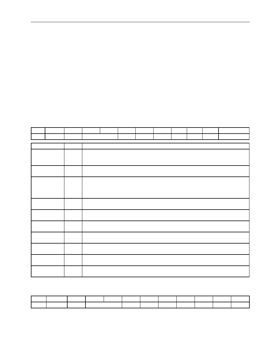
Data Sheet
March 2000
DSP1627 Digital Signal Processor
Lucent Technologies Inc.
45
5 Software Architecture
(continued)
5.2 Register Settings
Tables 22 through 38 describe the programmable registers of the DSP1627 device. Table 40 describes the register
settings after reset.
Note that the following abbreviations are used in the tables:
s
x = don't care
s
R = read only
s
W = read/write
The reserved (RSVD) bits in the tables should always be written with zeros to make the program compatible with
future chip versions.
Table 22. Serial I/O Control Registers
*
See tdms register, SYNC field.
See tdms register, SYNC field.
The bit definitions of the sioc2 register are identical to the sioc register bit definitions.
sioc
Bit
10
9
8
7
6
5
4
3
2
1
0
Field
DODLY
LD
CLK
MSB
OLD
ILD
OCK
ICK
OLEN
ILEN
Field
Value
Description
DODLY
0
1
DO changes on the rising edge of OCK.
DO changes on the falling edge of OCK. This delay in driving DO increases the hold
time on DO by half a cycle of OCK.
LD
0
1
In active mode, ILD1 and/or OLD1 = ICK1/16, active SYNC1 = ICK1/[128/256*].
In active mode, ILD1 and/or OLD1 = OCK1/16, active SYNC1 = OCK1/[128/256*].
CLK
00
01
10
11
Active clock = CKI/2 (1X).
Active clock = CKI/6 (1X).
Active clock = CKI/8 (1X).
Active clock = CKI/10 (1X).
MSB
0
1
LSB first.
MSB first.
OLD
0
1
OLD1 is an input (passive mode).
OLD1 is an output (active mode).
ILD
0
1
ILD1 is an input (passive mode).
ILD1 is an output (active mode).
OCK
0
1
OCK1 is an input (passive mode).
OCK1 is an output (active mode).
ICK
0
1
ICK1 is an input (passive mode).
ICK1 is an output (active mode).
OLEN
0
1
16-bit output.
8-bit output.
ILEN
0
1
16-bit input.
8-bit input.
sioc2
Bit
10
9
8
7
6
5
4
3
2
1
0
Field
DODLY2
LD2
CLK2
MSB2
OLD2
ILD2
OCK2
ICK2
OLEN2
ILEN2
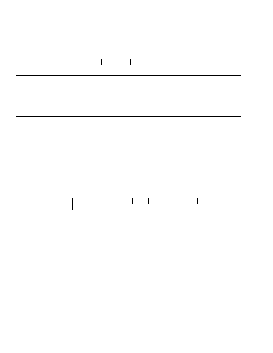
Data Sheet
DSP1627 Digital Signal Processor
March 2000
46
Lucent Technologies Inc.
5 Software Architecture
(continued)
Table 23. Time-Division Multiplex Slot Registers
See sioc register, LD field.
Select this mode when in multiprocessor mode.
ß The tdms2 register bit definitions are identical to the tdms register bit definitions.
tdms
Bit
9
8
7
6
5
4
3
2
1
0
Field
SYNCSP
MODE
TRANSMIT SLOT
SYNC
Field
Value
Description
SYNCSP
0
1
SYNC1 = ICK1/128 if LD = 0
*
.
SYNC1 = OCK1/128 if LD = 1*.
SYNC1 = ICK1/256 if LD = 0*.
SYNC1 = OCK1/256 if LD = 1*.
*
See sioc register, LD field.
Select this mode when in multiprocessor mode.
MODE
0
Multiprocessor mode off; DOEN1 is an input (passive mode).
1
Multiprocessor mode on; DOEN1 is an output (active mode).
TRANSMIT SLOT
1xxxxxx
Transmit slot 7.
x1xxxxx
Transmit slot 6.
xx1xxxx
Transmit slot 5.
xxx1xxx
Transmit slot 4.
xxxx1xx
Transmit slot 3.
xxxxx1x
Transmit slot 2.
xxxxxx1
Transmit slot 1.
SYNC
1
Transmit slot 0, SYNC1 is an output (active mode).
0
SYNC1 is an input (passive mode).
tdms2
ß
Bit
9
8
7
6
5
4
3
2
1
0
Field
SYNCSP2
MODE2
TRANSMIT SLOT2
SYNC2
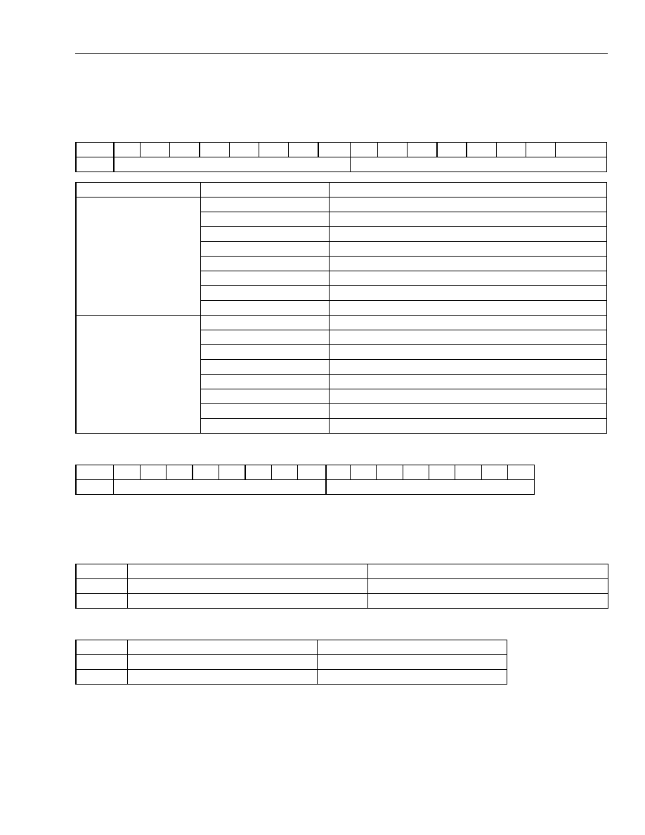
Data Sheet
March 2000
DSP1627 Digital Signal Processor
Lucent Technologies Inc.
47
5 Software Architecture
(continued)
Table 24. Serial Receive/Transmit Address Registers
The srta2 field definitions are identical to the srta register field definitions.
Table 25. Multiprocessor Protocol Registers
The saddx2 field definitions are identical to the saddx register field definitions.
srta
Bit
15
14
13
12
11
10
9
8
7
6
5
4
3
2
1
0
Field
RECEIVE ADDRESS
TRANSMIT ADDRESS
Field
Value
Description
RECEIVE ADDRESS
1xxxxxxx
Receive address 7.
x1xxxxxx
Receive address 6.
xx1xxxxx
Receive address 5.
xxx1xxxx
Receive address 4.
xxxx1xxx
Receive address 3.
xxxxx1xx
Receive address 2.
xxxxxx1x
Receive address 1.
xxxxxxx1
Receive address 0.
TRANSMIT ADDRESS
1xxxxxxx
Transmit address 7.
x1xxxxxx
Transmit address 6.
xx1xxxxx
Transmit address 5.
xxx1xxxx
Transmit address 4.
xxxx1xxx
Transmit address 3.
xxxxx1xx
Transmit address 2.
xxxxxx1x
Transmit address 1.
xxxxxxx1
Transmit address 0.
srta2
Bit
15
14
13
12
11
10
9
8
7
6
5
4
3
2
1
0
Field
RECEIVE ADDRESS2
TRANSMIT ADDRESS2
saddx
Bit Field
15--8
7--0
Write
X
Write Protocol Field [7:0]
Read
Read Protocol Field [7:0]
0
saddx2
Bit Field
15--8
7--0
Write
X
Write Protocol2 Field [7:0]
Read
Read Protocol2 Field [7:0]
0
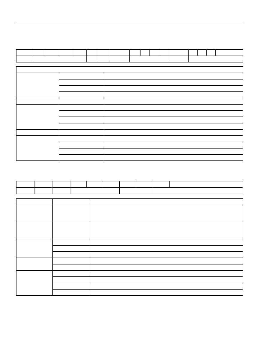
Data Sheet
DSP1627 Digital Signal Processor
March 2000
48
Lucent Technologies Inc.
5 Software Architecture
(continued)
The auc is 9 bits [8:0]. The upper 7 bits [15:9] are always zero when read and should always be written with zeros to make the program
compatible with future chip versions. The auc register is cleared at reset.
Table 26. Processor Status Word (psw) Register
Bit
15
14
13
12
11
10
9
8
7
6
5
4
3
2
1
0
Field
DAU FLAGS
X
X
a1[V]
a1[35:32]
a0[V]
a0[35:32]
Field
Value
Description
DAU FLAGS
*
*
The DAU flags can be set by either BMU or DAU operations.
Wxxx
LMI -- logical minus when set (bit 35 = 1).
xWxx
LEQ -- logical equal when set (bit [35:0] = 0).
xxWx
LLV -- logical overflow when set.
xxxW
LMV -- mathematical overflow when set.
a1[V]
W
Accumulator 1 (a1) overflow when set.
a1[35:32]
Wxxx
Accumulator 1 (a1) bit 35.
xWxx
Accumulator 1 (a1) bit 34.
xxWx
Accumulator 1 (a1) bit 33.
xxxW
Accumulator 1 (a1) bit 32.
a0[V]
W
Accumulator 0 (a0) overflow when set.
a0[35:32]
Wxxx
Accumulator 0 (a0) bit 35.
xWxx
Accumulator 0 (a0) bit 34.
xxWx
Accumulator 0 (a0) bit 33.
xxxW
Accumulator 0 (a0) bit 32.
Table 27. Arithmetic Unit Control (auc) Register
Bit
8
7
6
5
4
3
2
1
0
Field
RAND
X=Y=
CLR
SAT
ALIGN
Field
Value
Description
RAND
0
1
Pseudorandom sequence generator (PSG) reset by writing the pi register
only outside an interrupt service routine.
PSG never reset by writing the pi register.
X=Y=
0
1
Normal operation.
All instructions which load the high half of the y register also load the x regis-
ter, allowing single-cycle squaring with p = x * y.
CLR
1xx
Clearing yl is disabled (enabled when 0).
x1x
Clearing a1l is disabled (enabled when 0).
xx1
Clearing a0l is disabled (enabled when 0).
SAT
1x
a1 saturation on overflow is disabled (enabled when 0).
x1
a0 saturation on overflow is disabled (enabled when 0).
ALIGN
00
a0, a1
p.
01
a0, a1
p/4.
10
a0, a1
p x 4 (and zeros written to the two LSBs).
11
a0, a1
p x 2 (and zero written to the LSB).

Data Sheet
March 2000
DSP1627 Digital Signal Processor
Lucent Technologies Inc.
49
5 Software Architecture
(continued)
Encoding: A 0 disables an interrupt; a 1 enables an interrupt.
Encoding: A 0 indicates no interrupt. A 1 indicates an interrupt has been recognized and is pending or being serviced.
If a 1 is written to bits 4, 5, or 8 of ins, the corresponding interrupt is cleared.
Table 28. Parallel Host Interface Control (phifc) Register
Bit
15--7
6
5
4
3
2
1
0
Field
RSVD
PSOBEF
PFLAGSEL
PFLAG
PBSELF
PSTRB
PSTROBE
PMODE
Field
Value
Description
PMODE
0
1
8-bit data transfers.
16-bit data transfers.
PSTROBE
0
1
Intel
protocol: PIDS and PODS data strobes.
Motorola
protocol: PRWN and PDS data strobes.
PSTRB
0
1
When PSTROBE = 1, PODS pin (PDS) active-low.
When PSTROBE = 1, PODS pin (PDS) active-high.
PBSELF
0
1
In either mode, PBSEL pin = 0
pdx0 low byte. See Table 7.
If PMODE = 0, PBSEL pin = 1
pdx0 low byte.
If PMODE = 1, PBSEL pin = 0
pdx0 high byte.
PFLAG
0
1
PIBF and POBE pins active-high.
PIBF and POBE pins active-low.
PFLAGSEL
0
1
Normal.
PIBF flag ORed with POBE flag and output on PIBF pin; POBE pin un-
changed (output buffer empty).
PSOBEF
0
1
Normal.
POBE flag as read through PSTAT register is active-low.
Table 29. Interrupt Control (inc) Register
Bit
15
14--11
10
9
8
7--6
5--4
3
2
1
0
Field
JINT
*
*
JINT is a JTAG interrupt and is controlled by the HDS. It may be made unmaskable by the Lucent Technologies development system tools.
RSVD
OBE2
IBF2
TIME
RSVD
INT[1:0]
PIBF
POBE
OBE
IBF
Table 30. Interrupt Status (ins) Register
Bit
15
14--11
10
9
8
7--6
5--4
3
2
1
0
Field
JINT
RSVD
OBE2
IBF2
TIME
RSVD
INT[1:0]
PIBF
POBE
OBE
IBF
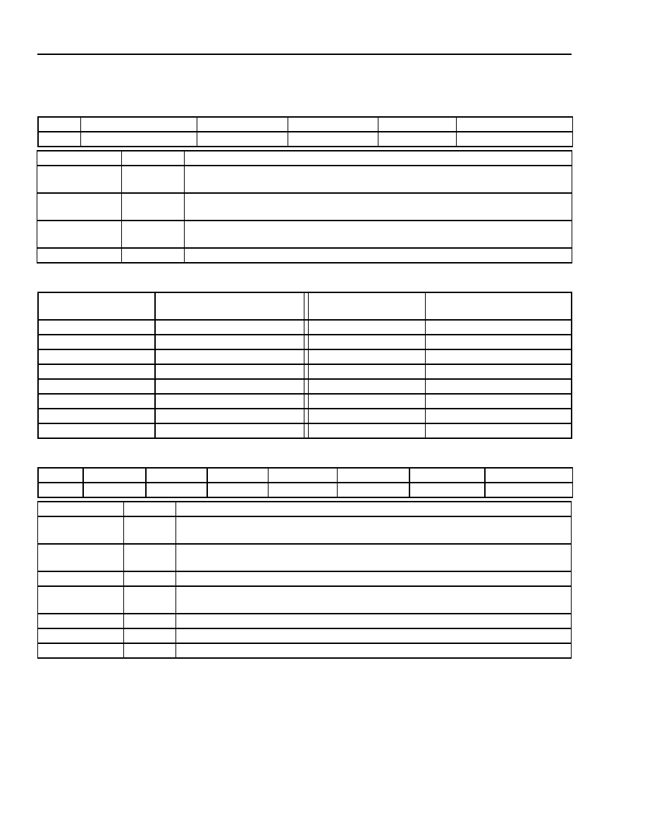
Data Sheet
DSP1627 Digital Signal Processor
March 2000
50
Lucent Technologies Inc.
5 Software Architecture
(continued)
Table 31. timerc Register
Bit
15--7
6
5
4
3--0
Field
RSVD
DISABLE
RELOAD
T0EN
PRESCALE
Field
Value
Description
DISABLE
0
1
Timer enabled.
Timer and prescaler disabled. The period register and timer0 are not reset.
RELOAD
0
1
Timer stops after counting down to 0.
Timer automatically reloads and repeats indefinitely.
T0EN
0
1
Timer holds current count.
Timer counts down to 0.
PRESCALE
--
See table below.
PRESCALE Field
PRESCALE
Frequency of
Timer Interrupts
PRESCALE
Frequency of
Timer Interrupts
0000
CKO/2
1000
CKO/512
0001
CKO/4
1001
CKO/1024
0010
CKO/8
1010
CKO/2048
0011
CKO/16
1011
CKO/4096
0100
CKO/32
1100
CKO/8192
0101
CKO/64
1101
CKO/16384
0110
CKO/128
1110
CKO/32768
0111
CKO/256
1111
CKO/65536
Table 32. Phase-Locked Loop Control (pllc) Register
Bit
15
14
13
12
11--8
7--5
4--0
Field
PLLEN
PLLSEL
ICP
SEL5V
LF[3:0]
Nbits[2:0]
Mbits[4:0]
Field
Value
Description
PLLEN
0
1
PLL powered down.
PLL powered up.
PLLSEL
0
1
DSP internal clock taken directly from CKI.
DSP internal clock taken from PLL.
ICP
--
Charge pump current selection (see Table 64 for proper value).
SEL5V
0
1
3 V operation (see Table 64 for proper value).
5 V operation (see Table 64 for proper value).
LF[3:0]
--
Loop filter setting (see Table 64 for proper value).
Nbits[2:0]
--
Encodes N, 1
N
8, where N = Nbits[2:0] + 2, unless Nbits[2:0] = 111, then N = 1.
Mbits[4:0]
--
Encodes M, 2
M
20, where M = Mbits[4:0] + 2, f
INTERNAL CLOCK
= f
CKI
x (M/(2N)).
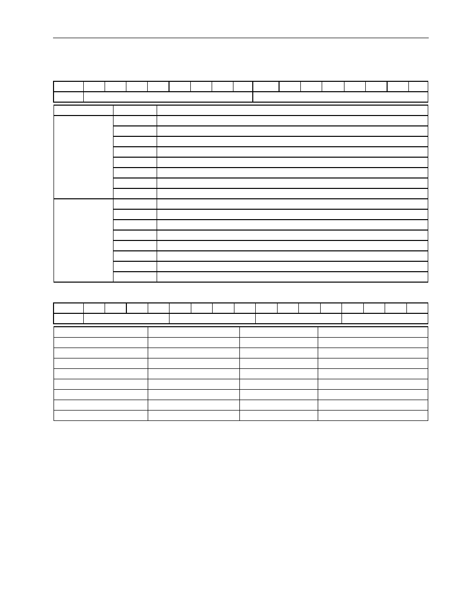
Data Sheet
March 2000
DSP1627 Digital Signal Processor
Lucent Technologies Inc.
51
5 Software Architecture
(continued)
Table 33. sbit Register
Bit
15
14
13
12
11
10
9
8
7
6
5
4
3
2
1
0
Field
DIREC[7:0]
VALUE[7:0]
Field
Value
Description
DIREC
1xxxxxxx
IOBIT7 is an output (input when 0).
x1xxxxxx
IOBIT6 is an output (input when 0).
xx1xxxxx
IOBIT5 is an output (input when 0).
xxx1xxxx
IOBIT4 is an output (input when 0).
xxxx1xxx
IOBIT3 is an output (input when 0).
xxxxx1xx
IOBIT2 is an output (input when 0).
xxxxxx1x
IOBIT1 is an output (input when 0).
xxxxxxx1
IOBIT0 is an output (input when 0).
VALUE
Rxxxxxxx
Reads the current value of IOBIT7.
xRxxxxxx
Reads the current value of IOBIT6.
xxRxxxxx
Reads the current value of IOBIT5.
xxxRxxxx
Reads the current value of IOBIT4.
xxxxRxxx
Reads the current value of IOBIT3.
xxxxxRxx
Reads the current value of IOBIT2.
xxxxxxRx
Reads the current value of IOBIT1.
xxxxxxxR
Reads the current value of IOBIT0.
Table 34. cbit Register
Bit
15
14
13
12
11
10
9
8
7
6
5
4
3
2
1
0
Field
MODE/MASK[7:4]
MODE/MASK[3:0]
DATA/PAT[7:4]
DATA/PAT[3:0]
DIREC[n]
*
*
0
n
7.
MODE/MASK[n]
DATA/PAT[n]
Action
1 (Output)
0
0
Clear
1 (Output)
0
1
Set
1 (Output)
1
0
No Change
1 (Output)
1
1
Toggle
0 (Input)
0
0
No Test
0 (Input)
0
1
No Test
0 (Input)
1
0
Test for Zero
0 (Input)
1
1
Test for One
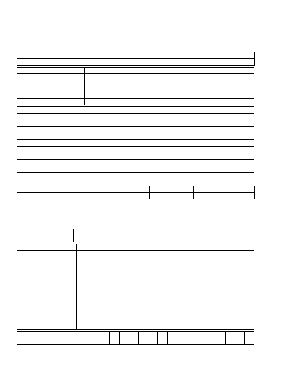
Data Sheet
DSP1627 Digital Signal Processor
March 2000
52
Lucent Technologies Inc.
5 Software Architecture
(continued)
If the EXM pin is high and the INT1 is low upon reset, the mwait register is initialized to all 1s (15 wait-states for all
external memory). Otherwise, the mwait register is initialized to all 0s (0 wait-states) upon reset.
Table 35. alf Register
Bit
15
14
13--0
Field
AWAIT
LOWPR
FLAGS
Field
Value
Action
AWAIT
1
0
Power-saving standby mode or standard sleep enabled.
Normal operation.
LOWPR
1
0
The internal DPRAM is addressed beginning at 0x0000 in X space.
The internal DPRAM is addressed beginning at 0xc000 in X space.
FLAGS
--
See table below.
Bit
Flag
Use
13--8
Reserved
--
7
nmns1
NOT-MINUS-ONE from BMU
6
mns1
MINUS-ONE from BMU
5
evenp
EVEN PARITY from BMU
4
oddp
ODD PARITY from BMU
3
somef
SOME FALSE from BIO
2
somet
SOME TRUE from BIO
1
allf
ALL FALSE from BIO
0
allt
ALL TRUE from BIO
Table 36. mwait Register
Bit
15--12
11--8
7--4
3--0
Field
EROM[3:0]
ERAMHI[3:0]
IO[3:0]
ERAMLO[3:0]
Table 37. DSP1627 32-Bit JTAG ID Register
Bit
31
30
29--28
27--19
18--12
11--0
Field
RESERVED
SECURE
CLOCK
ROMCODE
PART ID
0x03B
Field
Value
Mask-Programmable Features
RESERVED
0
--
SECURE
0
1
Nonsecure ROM option.
Secure ROM option.
CLOCK
01
10
11
Small-signal input clock option.
Crystal oscillator input clock option.
CMOS level input clock option.
ROMCODE
--
Users ROMCODE ID:
The ROMCODE ID is the 9-bit binary value of the following expression:
(20 x value for first letter) + (value of second letter), where the values of the letters are
in the following table. For example, ROMCODE GK is
(20 x 6) + (9) = 129 or 0 1000 0001.
PART ID
0x1C
DSP1627x36 with 36K IROM and no EROM in MAP1 or MAP3.
0x2C
DSP1627x32 with 32K IROM and 16K EROM in MAP1 and MAP3.
ROMCODE Letter
A
B
C
D
E
F
G
H
J
K
L
M
N
P
R
S
T
U
W
Y
Value
0
1
2
3
4
5
6
7
8
9
10
11
12
13
14
15
16
17
18
19
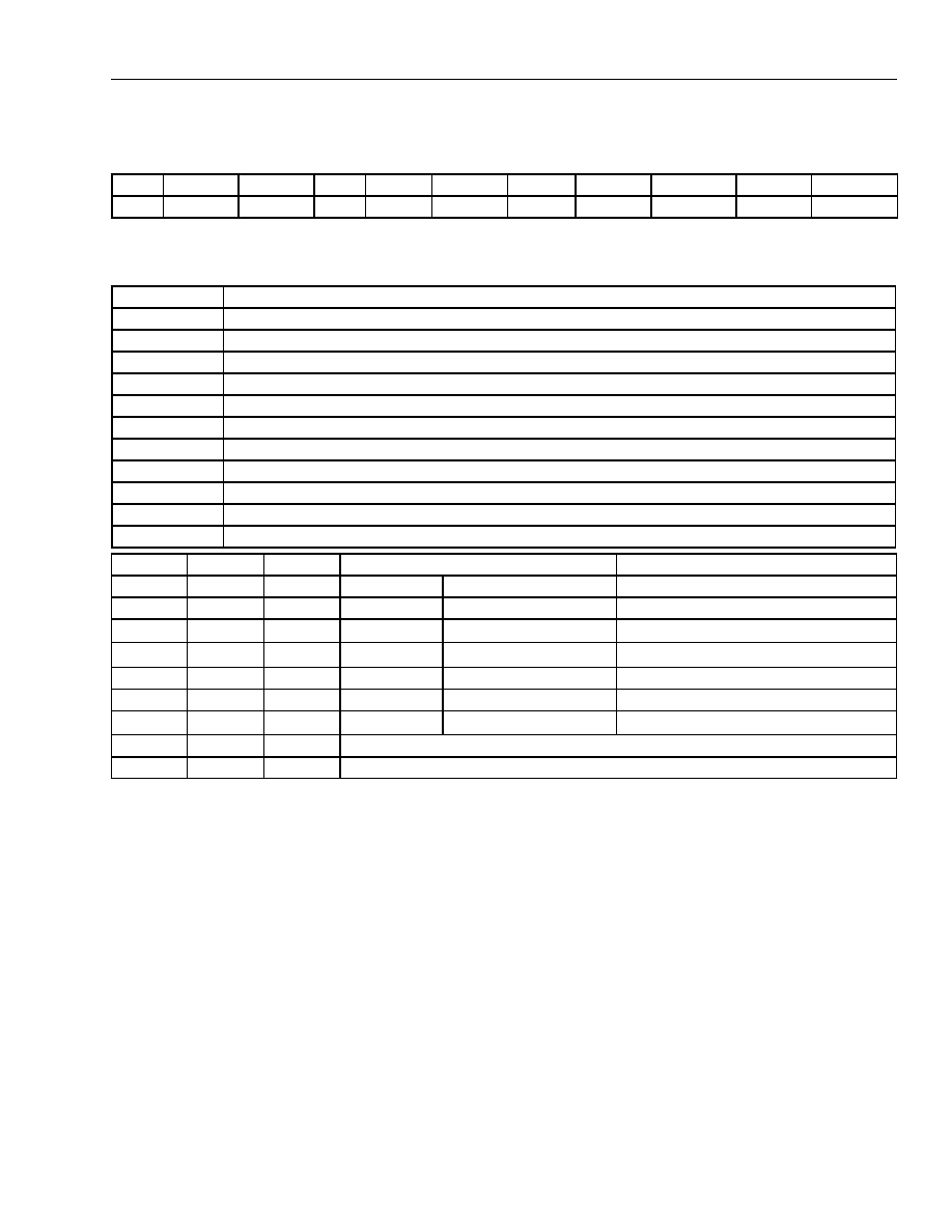
Data Sheet
March 2000
DSP1627 Digital Signal Processor
Lucent Technologies Inc.
53
5 Software Architecture
(continued)
Table 38. ioc Register
*
*
The field definitions for the ioc register are different from the DSP1610.
Bit
15
14
13
12
11
10
9
8--7
6--4
3--0
Field
RSVD
EXTROM CKO2 EBIOH
WEROM
ESIO2
SIOLBC
CKO[1:0]
RSVD
DENB[3:0]
ioc Fields
ioc Field
Description
EXTROM
If 1, sets AB15 low during external memory accesses when WEROM = 1.
CKO2
CKO configuration (see below).
EBIOH
If 1, enables high half of BIO, IOBIT[4:7], and disables VEC[3:0] from pins.
WEROM
If 1, allows writing into external program (X) memory.
ESIO2
If 1, enables SIO2 and low half of BIO, and disables PHIF from pins.
SIOLBC
If 1, DO1 and DO2 looped back to DI1 and DI2.
CKO[1:0]
CKO configuration (see below).
DENB3
If 1, delay EROM.
DENB2
If 1, delay ERAMHI.
DENB1
If 1, delay IO.
DENB0
If 1, delay ERAMLO.
CKO2
CKO1
CKO0
CKO Output
Description
1X
PLL
--
0
0
0
CKI
CKI x M/(2N)
Free-running clock.
0
0
1
CKI/(1 + W)
CKI x (M/(2N)) / [1 + W] Wait-stated clock.
*
,
*
The phase of CKI is synchronized by the rising edge of RSTB.
When SLOWCKI is enabled in the powerc register, these options reflect the low-speed internal ring oscillator.
0
1
0
1
1
Held high.*,
,
The wait-stated clock reflects the internal instruction cycle and may be stretched based on the mwait register setting (see Table 36). During
sequenced external memory accesses, it completes one cycle.
ß The sequenced wait-stated clock completes two cycles during a sequenced external memory access and may be stretched based on the
mwait register setting (see Table 36).
0
1
1
0
0
Held low.
1
0
0
CKI
CKI
Output of CKI buffer.
1
0
1
CKI/(1 + W)
CKI x (M/(2N)) / [1 + W] Sequenced, wait-stated clock.*,
,
,
ß
1
1
0
Reserved
1
1
1
Reserved

Data Sheet
DSP1627 Digital Signal Processor
March 2000
54
Lucent Technologies Inc.
5 Software Architecture
(continued)
Table 39. powerc Register
Note: The reserved (RSVD) bits should always be written with zeros to make the program compatible with future chip versions.
A
∑
indicates that this bit is unknown on powerup reset and unaffected on subsequent reset. An S indicates that this
bit shadows the PC. P indicates the value on an input pin, i.e., the bit in the register reflects the value on the corre-
sponding input pin.
If EXM is high and INT1 is low when RSTB goes high, mwait will contain all ones instead of all zeros.
The powerc register configures various power management modes.
Bit
15
14
13
12
11
10
9--8
7
6
5
4
3--0
Field
XTLOFF SLOWCKI NOCK INT0EN RSVD INT1EN RSVD SIO1DIS SIO2DIS PHIFDIS TIMERDIS RSVD
powerc fields
Field
Description
XTLOFF
1 = powerdown crystal oscillator or small-signal clock input.
SLOWCKI
1 = select ring oscillator clock (internal slow clock).
NOCK
1 = disable internal processor clock.
INT0EN
1 = INT0 clears NOCK field.
INT1EN
1 = INT1 clears NOCK field.
SIO1DIS
1 = disable SIO1.
SIO2DIS
1 = disable SIO2.
PHIFDIS
1 = disable PHIF.
TIMERDIS
1 = disable timer.
Table 40. Register Settings After Reset
Register
Bits 15--0
Register
Bits 15--0
r0
∑∑∑∑∑∑∑∑∑∑∑∑∑∑∑∑
inc
0000000000000000
r1
∑∑∑∑∑∑∑∑∑∑∑∑∑∑∑∑
ins
0000010000000110
r2
∑∑∑∑∑∑∑∑∑∑∑∑∑∑∑∑
sdx2
∑∑∑∑∑∑∑∑∑∑∑∑∑∑∑∑
r3
∑∑∑∑∑∑∑∑∑∑∑∑∑∑∑∑
saddx
∑∑∑∑∑∑∑∑∑∑∑∑∑∑∑∑
j
∑∑∑∑∑∑∑∑∑∑∑∑∑∑∑∑
cloop
000000000∑∑∑∑∑∑∑
k
∑∑∑∑∑∑∑∑∑∑∑∑∑∑∑∑
mwait
0000000000000000
rb
0000000000000000
saddx2
∑∑∑∑∑∑∑∑∑∑∑∑∑∑∑∑
re
0000000000000000
sioc2
∑∑∑∑∑∑0000000000
pt
∑∑∑∑∑∑∑∑∑∑∑∑∑∑∑∑
cbit
∑∑∑∑∑∑∑∑∑∑∑∑∑∑∑∑
pr
∑∑∑∑∑∑∑∑∑∑∑∑∑∑∑∑
sbit
00000000PPPPPPPP
pi
SSSSSSSSSSSSSSSS
ioc
0000000000000000
i
∑∑∑∑∑∑∑∑∑∑∑∑∑∑∑∑
jtag
∑∑∑∑∑∑∑∑∑∑∑∑∑∑∑∑
p
∑∑∑∑∑∑∑∑∑∑∑∑∑∑∑∑
pl
∑∑∑∑∑∑∑∑∑∑∑∑∑∑∑∑
a0
∑∑∑∑∑∑∑∑∑∑∑∑∑∑∑∑
x
∑∑∑∑∑∑∑∑∑∑∑∑∑∑∑∑
a0l
∑∑∑∑∑∑∑∑∑∑∑∑∑∑∑∑
y
∑∑∑∑∑∑∑∑∑∑∑∑∑∑∑∑
a1
∑∑∑∑∑∑∑∑∑∑∑∑∑∑∑∑
yl
∑∑∑∑∑∑∑∑∑∑∑∑∑∑∑∑
a1l
∑∑∑∑∑∑∑∑∑∑∑∑∑∑∑∑
auc
0000000000000000
timerc
∑∑∑∑∑∑∑∑00000000
psw
∑∑∑∑00∑∑∑∑∑∑∑∑∑∑
timer0
0000000000000000
c0
∑∑∑∑∑∑∑∑∑∑∑∑∑∑∑∑
tdms2
∑∑∑∑∑∑0000000000
c1
∑∑∑∑∑∑∑∑∑∑∑∑∑∑∑
srta2
∑∑∑∑∑∑∑∑∑∑∑∑∑∑∑∑
c2
∑∑∑∑∑∑∑∑∑∑∑∑∑∑∑∑
powerc
0000000000000000
sioc
∑∑∑∑∑∑0000000000
pllc
0000000000000000
srta
∑∑∑∑∑∑∑∑∑∑∑∑∑∑∑∑
ar0
∑∑∑∑∑∑∑∑∑∑∑∑∑∑∑∑
sdx
∑∑∑∑∑∑∑∑∑∑∑∑∑∑∑∑
ar1
∑∑∑∑∑∑∑∑∑∑∑∑∑∑∑∑
tdms
∑∑∑∑∑∑0000000000
ar2
∑∑∑∑∑∑∑∑∑∑∑∑∑∑∑∑
phifc
0000000000000000
ar3
∑∑∑∑∑∑∑∑∑∑∑∑∑∑∑∑
pdx0
0000000000000000
ybase
∑∑∑∑∑∑∑∑∑∑∑∑∑∑∑∑
alf
00000000∑∑∑∑∑∑∑∑
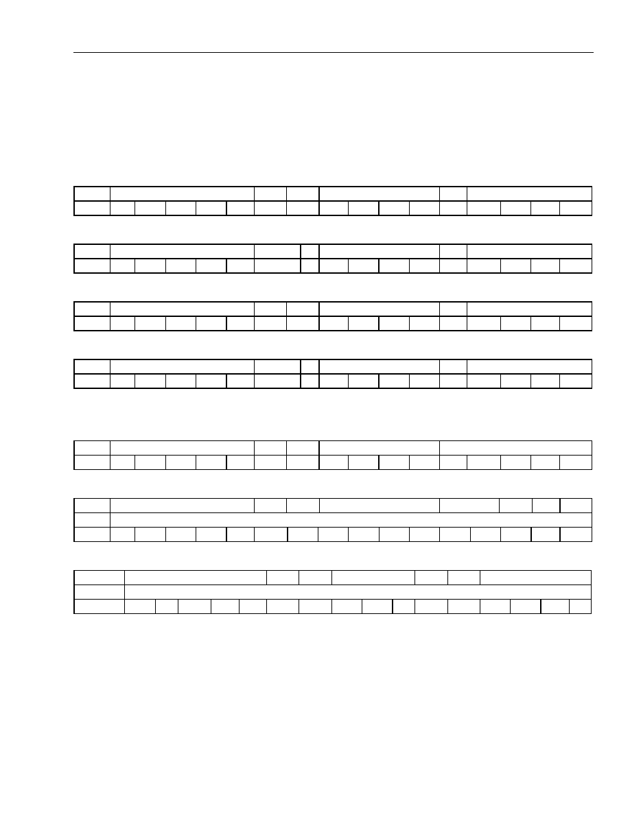
Data Sheet
March 2000
DSP1627 Digital Signal Processor
Lucent Technologies Inc.
55
5 Software Architecture
(continued)
5.3 Instruction Set Formats
This section defines the hardware-level encoding of the DSP1627 device instructions.
Multiply/ALU Instructions
Special Function Instructions
Format 1: Multiply/ALU Read/Write Group
Field
T
D
S
F1
X
Y
Bit
15
14
13
12
11
10
9
8
7
6
5
4
3
2
1
0
Format 1a: Multiply/ALU Read/Write Group
Field
T
aT
S
F1
X
Y
Bit
15
14
13
12
11
10
9
8
7
6
5
4
3
2
1
0
Format 2: Multiply/ALU Read/Write Group
Field
T
D
S
F1
X
Y
Bit
15
14
13
12
11
10
9
8
7
6
5
4
3
2
1
0
Format 2a: Multiply/ALU Read/Write Group
Field
T
aT
S
F1
X
Y
Bit
15
14
13
12
11
10
9
8
7
6
5
4
3
2
1
0
Format 3: F2 ALU Special Functions
Field
T
D
S
F2
CON
Bit
15
14
13
12
11
10
9
8
7
6
5
4
3
2
1
0
Format 3a: F3 ALU Operations
Field
T
D
S
F3
SRC2
aT
0
1
Immediate Operand (IM16)
Bit
15
14
13
12
11
10
9
8
7
6
5
4
3
2
1
0
Format 3b: BMU Operations
Field
T
D
S
F4[3--1]
0
F4[0]
AR
Immediate Operand (IM16)
Bit
15
14
13
12
11
10
9
8
7
6
5
4
3
2
1
0
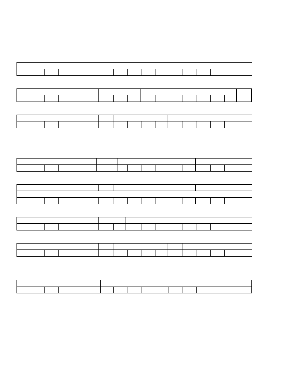
Data Sheet
DSP1627 Digital Signal Processor
March 2000
56
Lucent Technologies Inc.
5 Software Architecture
(continued)
Control Instructions
Note: A branch instruction immediately follows except for a software interrupt (icall).
Data Move Instructions
Cache Instructions
Format 4: Branch Direct Group
Field
T
JA
Bit
15
14
13
12
11
10
9
8
7
6
5
4
3
2
1
0
Format 5: Branch Indirect Group
Field
T
B
Reserved
0
Bit
15
14
13
12
11
10
9
8
7
6
5
4
3
2
1
0
Format 6: Conditional Branch Qualifier/Software Interrupt (icall)
Field
T
SI
Reserved
CON
Bit
15
14
13
12
11
10
9
8
7
6
5
4
3
2
1
0
Format 7: Data Move Group
Field
T
aT
R
Y/Z
Bit
15
14
13
12
11
10
9
8
7
6
5
4
3
2
1
0
Format 8: Data Move (immediate operand--2 words)
Field
T
D
R
Reserved
Immediate Operand (IM16)
Bit
15
14
13
12
11
10
9
8
7
6
5
4
3
2
1
0
Format 9: Short Immediate Group
Field
T
I
Short Immediate Operand (IM9)
Bit
15
14
13
12
11
10
9
8
7
6
5
4
3
2
1
0
Format 9a: Direct Addressing
Field
T
R/W
DR
1
OFFSET
Bit
15
14
13
12
11
10
9
8
7
6
5
4
3
2
1
0
Format 10: Do/Redo
Field
T
NI
K
Bit
15
14
13
12
11
10
9
8
7
6
5
4
3
2
1
0
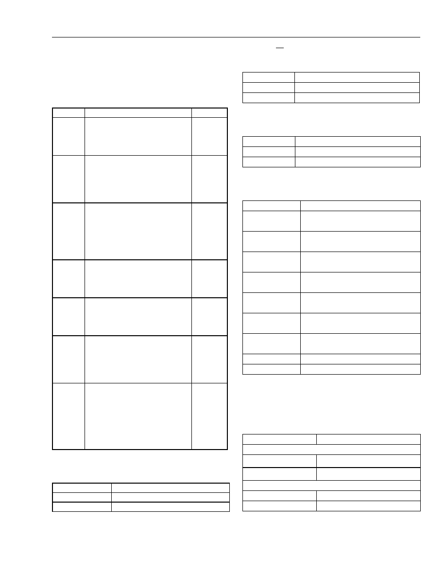
Data Sheet
March 2000
DSP1627 Digital Signal Processor
Lucent Technologies Inc.
57
5 Software Architecture
(continued)
Field Descriptions
Table 41. T Field
Table 42. D Field
Table 43.
aT
Field
Table 44. S Field
Table 45. F1 Field
Table 46. X Field
Specifies the type of instruction.
T
Operation
Format
0000x
goto JA
4
00010
Short imm j, k, rb, re
9
00011
Short imm r0, r1, r2, r3
9
00100
Y = a1[l]
F1
1
00101
Z : aT[l]
F1
2a
00110
Y
F1
1
00111
aT[l] = Y
F1
1a
01000
Bit 0 = 0, aT = R
7
01000
Bit 0 = 1, aTl = R
7
01001
Bit 10 = 0, R = a0
7
01001
Bit 10 = 1, R = a0l
7
01010
R = IM16
8
01011
Bit 10 = 0, R = a1
7
01011
Bit 10 = 1, R = a1l
7
01100
Y = R
7
01101
Z : R
7
01110
do, redo
10
01111
R = Y
7
1000x
call JA
4
10010
ifc CON
F2
3
10011
if CON
F2
3
10100
Y = y[l]
F1
1
10101
Z : y[l]
F1
2
10110
x = Y
F1
1
10111
y[l] = Y
F1
1
11000
Bit 0 = 0, branch indirect
5
11000
Bit 0 = 1, F3 ALU
3a
11001
y = a0 x = X
F1
1
11010
Cond. branch qualifier
6
11011
y = a1 x = X
F1
1
11100
Y = a0[l]
F1
1
11101
Z : y x = X
F1
2
11110
Bit 5 = 0, F4 ALU (BMU)
3b
11110
Bit 5 = 1, direct addressing
9a
11111
y = Y x = X
F1
1
Specifies a destination accumulator.
D
Register
0
Accumulator 0
1
Accumulator 1
Specifies transfer accumulator.
aT
Register
0
Accumulator 1
1
Accumulator 0
Specifies a source accumulator.
S
Register
0
Accumulator 0
1
Accumulator 1
Specifies the multiply/ALU function.
F1
Operation
0000
aD = pp = x * y
0001
aD = aS + pp = x * y
0010
p = x *
y
0011
aD = aS ≠ pp = x * y
0100
aD = p
0101
aD = aS + p
0110
nop
0111
aD = aS ≠ p
1000
aD = aS | y
1001
aD = aS ^ y
1010
aS & y
1011
aS ≠ y
1100
aD = y
1101
aD = aS + y
1110
aD = aS & y
1111
aD = aS ≠ y
Specifies the addressing of ROM data in two-operand
multiply/ALU instructions. Specifies the high or low half
of an accumulator or the y register in one-operand mul-
tiply/ALU instructions.
X
Operation
Two-Operand Multiply/ALU
0
*
pt++
1
*
pt++i
One-Operand Multiply/ALU
0
aTl, yl
1
aTh, yh

Data Sheet
DSP1627 Digital Signal Processor
March 2000
58
Lucent Technologies Inc.
5 Software Architecture
(continued)
Table 47. Y Field
Table 48. Z Field
Table 49. F2 Field
Table 50. CON Field
Specifies the form of register indirect addressing with
postmodification.
Y
Operation
0000
*r0
0001
*r0++
0010
*r0--
0011
*r0++j
0100
*r1
0101
*r1++
0110
*r1--
0111
*r1++j
1000
*r2
1001
*r2++
1010
*r2--
1011
*r2++j
1100
*r3
1101
*r3++
1110
*r3--
1111
*r3++j
Specifies the form of register indirect compound ad-
dressing with postmodification.
Z
Operation
0000
*
r0zp
0001
*
r0pz
0010
*
r0m2
0011
*
r0jk
0100
*
r1zp
0101
*
r1pz
0110
*
r1m2
0111
*
r1jk
1000
*
r2zp
1001
*
r2pz
1010
*
r2m2
1011
*
r2jk
1100
*
r3zp
1101
*
r3pz
1110
*
r3m2
1111
*
r3jk
Specifies the special function to be performed.
F2
Operation
0000
aD = aS >> 1
0001
aD = aS << 1
0010
aD = aS >> 4
0011
aD = aS << 4
0100
aD = aS >> 8
0101
aD = aS << 8
0110
aD = aS >> 16
0111
aD = aS << 16
1000
aD = p
1001
aDh = aSh + 1
1010
aD = ~aS
1011
aD = rnd(aS)
1100
aD = y
1101
aD = aS + 1
1110
aD = aS
1111
aD = ≠ aS
Specifies the condition for special functions and condi-
tional control instructions.
CON
Condition
CON
Condition
00000
mi
01110
true
00001
pl
01111
false
00010
eq
10000
gt
00011
ne
10001
le
00100
lvs
10010
allt
00101
lvc
10011
allf
00110
mvs
10100
somet
00111
mvc
10101
somef
01000
heads
10110
oddp
01001
tails
10111
evenp
01010
c0ge
11000
mns1
01011
c0lt
11001
nmns1
01100
c1ge
11010
npint
01101
c1lt
11011
njint
11100
lock
Other
codes
Reserved
--
--
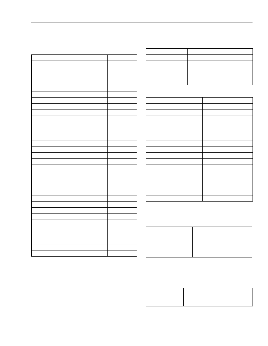
Data Sheet
March 2000
DSP1627 Digital Signal Processor
Lucent Technologies Inc.
59
5 Software Architecture
(continued)
Table 51. R Field
Table 52. B Field
Table 54. I Field
Table 55. SI Field
Specifies the register for data move instructions.
R
Register
R
Register
000000
r0
100000
inc
000001
r1
100001
ins
000010
r2
100010
sdx2
000011
r3
100011
saddx
000100
j
100100
cloop
000101
k
100101
mwait
000110
rb
100110
saddx2
000111
re
100111
sioc2
001000
pt
101000
cbit
001001
pr
101001
sbit
001010
pi
101010
ioc
001011
i
101011
jtag
001100
p
101100
Reserved
001101
pl
101101
Reserved
001110
pllc
101110
Reserved
001111
Reserved
101111
Reserved
010000
x
110000
a0
010001
y
110001
a0l
010010
yl
110010
a1
010011
auc
110011
a1l
010100
psw
110100
timerc
010101
c0
110101
timer0
010110
c1
110110
tdms2
010111
c2
110111
srta2
011000
sioc
111000
powerc
011001
srta
111001
Reserved
011010
sdx
111010
ar0
011011
tdms
111011
ar1
011100
phifc
111100
ar2
011101
pdx0
111101
ar3
011110
Reserved
111110
Reserved
011111
ybase
111111
alf
Specifies the type of branch instruction (except software
interrupt).
B
Operation
000
return
001
ireturn
010
goto pt
011
call pt
1xx
Reserved
Table 53. DR Field
DR Value
Register
0000
r0
0001
r1
0010
r2
0011
r3
0100
a0
0101
a0l
0110
a1
0111
a1l
1000
y
1001
yl
1010
p
1011
pl
1100
x
1101
pt
1110
pr
1111
psw
Specifies a register for short immediate data move in-
structions.
I
Register
00
r0/j
01
r1/k
10
r2/rb
11
r3/re
Specifies when the conditional branch qualifier instruc-
tion should be interpreted as a software interrupt in-
struction.
SI
Operation
0
Not a software interrupt
1
Software interrupt
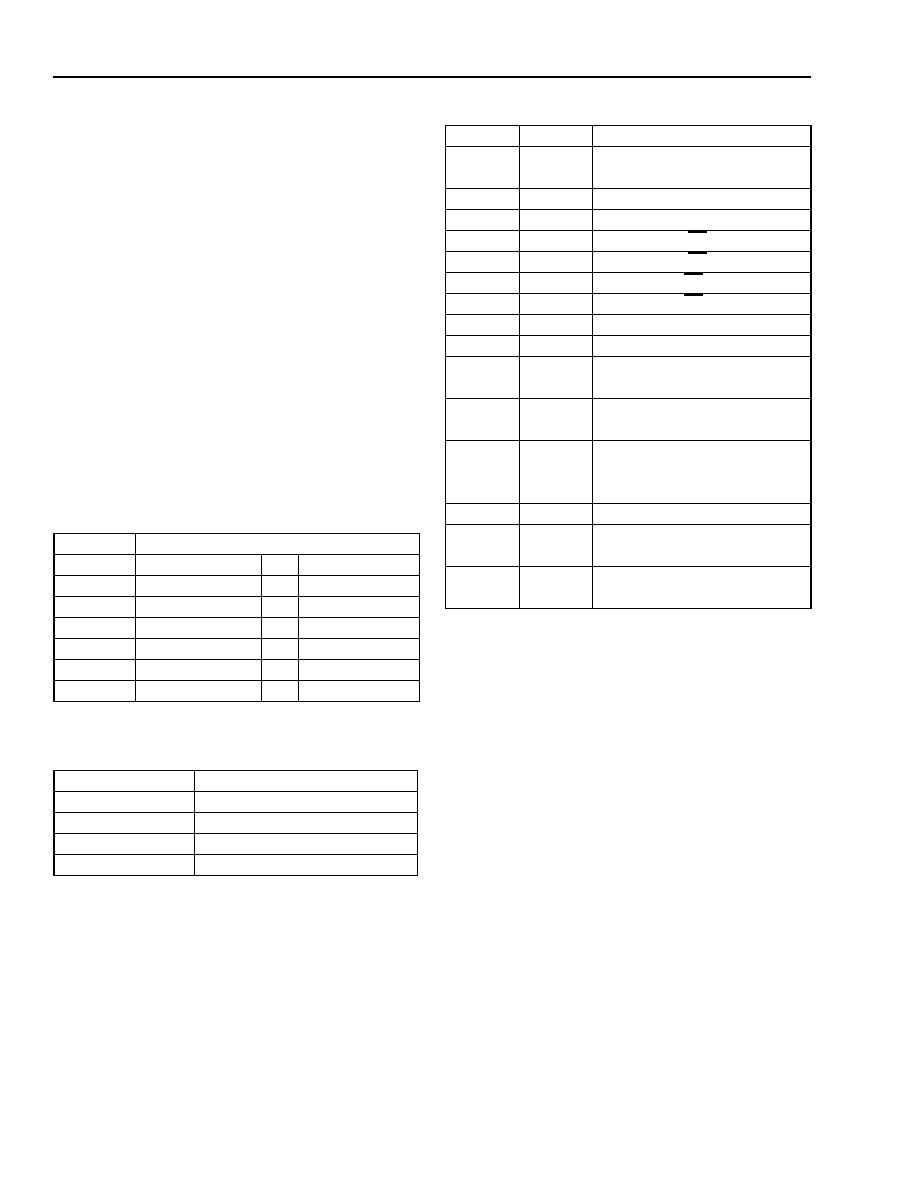
Data Sheet
DSP1627 Digital Signal Processor
March 2000
60
Lucent Technologies Inc.
5 Software Architecture
(continued)
NI Field
Number of instructions to be loaded into the cache. Zero
implies redo operation.
K Field
Number of times the NI instructions in cache are to be
executed. Zero specifies use of value in cloop register.
JA Field
12-bit jump address.
R/W Field
A zero specifies a write, *(O) = DR.
A one specifies a read, DR = *(O).
Table 56. F3 Field
Table 57. SRC2 Field
Note: xx encodes the auxiliary register to be used. 00 (ar0), 01(ar1),
10 (ar2), or 11(ar3).
Specifies the operation in an F3 ALU instruction.
F3
Operation
1000
aD = aS[h, l]
|
{aT, IM16, p}
1001
aD = aS[h, l]
^
{aT, IM16, p}
1010
aS[h, l]
&
{aT, IM16, p}
1011
aS[h, l]
≠
{aT, IM16, p}
1101
aD = aS[h, l]
+
{aT, IM16, p}
1110
aD = aS[h, l]
&
{aT, IM16, p}
1111
aD = aS[h, l]
≠
{aT, IM16, p}
Specifies operands in an F3 ALU instruction.
SRC2
Operands
00
aSl, IM16
10
aSh, IM16
01
aS, aT
11
aS, p
Table 58. BMU Encodings
F4
AR
Operation
0000
00xx
aD = aS >> arM
0001
00xx
aD = aS << arM
0000
10xx
aD = aS >>> arM
0001
10xx
aD = aS <<< arM
1000
0000
aD = aS >> aS
1001
0000
aD = aS << aS
1000
1000
aD = aS >>> aS
1001
1000
aD = aS <<< aS
1100
0000
aD = aS >> IM16
1101
0000
aD = aS << IM16
1100
1000
aD = aS >>> IM16
1101
1000
aD = aS <<< IM16
0000
1100
aD = exp(aS)
0001
11xx
aD = norm(aS, arM)
1110
0000
aD = extracts(aS, IM16)
0010
00xx
aD = extracts(aS, arM)
1110
0100
aD = extractz(aS, IM16)
0010
01xx
aD = extractz(aS, arM)
1110
1000
aD = insert(aS, IM16)
1010
10xx
aD = insert(aS, arM)
0111
0000
aD = aS:aa0
0111
0001
aD = aS:aa1

Data Sheet
March 2000
DSP1627 Digital Signal Processor
Lucent Technologies Inc.
61
6 Signal Descriptions
Figure 8. DSP1627 Pinout by Interface
EXTERNAL
MEMORY
INTERFACE
IO
ERAMHI
EROM
EXM
AB[15:0]
DB[15:0]
RWN
SYSTEM
INTERFACE
OR
CONTROL I/O
INTERFACE
OBE1
OLD1
OCK1
DO1
TDI
TDO
TCK
TMS
PODS OR OLD2
PSTAT OR DO2
PCSN OR OCK2
POBE OR OBE2
PBSEL OR SYNC2
PB2 OR DOEN2
PIBF OR IBF2
PIDS OR ILD2
PB0 OR ICK2
PB1 OR DI2
PB3 OR SADD2
PB[7:4] OR IOBIT[3:O]
DSP1627
RSTB
CKO
IACK
STOP
CKI2
VEC[3:0] OR IOBIT[4:7]
INT[1:0]
PARALLEL HOST
INTERFACE
OR
SERIAL INTERFACE #2
AND CONTROL I/O
INTERFACE
ILD1
DI1
TRAP
SERIAL
INTERFACE #1
ICK1
IBF1
SYNC1
ERAMLO
SADD1
DOEN1
JTAG TEST
INTERFACE
2
4
16
16
4
CKI
5-4006 (C)
Figure 8 shows the pinout for the DSP1627. The signals
can be separated into five interfaces as shown. These
interfaces and the signals that comprise them are de-
scribed below.
6.1 System Interface
The system interface consists of the clock, interrupt,
and reset signals for the processor.
RSTB
Reset: Negative assertion. A high-to-low transition
causes the processor to enter the reset state. The auc,
powerc, sioc, sioc2, phifc, pdx0, tdms, tdms2, timerc,
timer0, sbit (upper byte), inc, ins (except OBE, OBE2,
and PODS status bits set), alf (upper 2 bits, AWAIT and
LOWPR), ioc, rb, and re registers are cleared. The
mwait register is initialized to all 0s (zero wait-states)
unless the EXM pin is high and the INT1 pin is low. In
that case, the mwait register is initialized to all 1s (15
wait-states).
Reset clears IACK, VEC[3:0]/IOBIT[4:7], IBF, and IBF2.
The DAU condition flags are not affected by reset.
IOBIT[7:0] are initialized as inputs. If any of the IOBIT
pins are switched to outputs (by writing sbit), their initial
value will be logic zero (see Table 40, Register Settings
After Reset).
Upon negation of the signal, the processor begins exe-
cution at location 0x0000 in the active memory map
(see Section 4.4, Memory Maps and Wait-States).

Data Sheet
DSP1627 Digital Signal Processor
March 2000
62
Lucent Technologies Inc.
6 Signal Descriptions
(continued)
CKI
Input Clock: A mask-programmable option selects one
of three possible input buffers for the CKI pin (see Sec-
tion 7, Mask-Programmable Options, and Table 1, Pin
Descriptions). The internal CKI from the output of the
selected input buffer can then drive the internal proces-
sor clock directly (1X) or drive the on-chip PLL (see Sec-
tion 4.13). The PLL allows the CKI input clock to be at a
lower frequency than the internal processor clock.
CKI2
Input Clock 2: Used with mask-programmable input
clock options which require an external crystal or small
signal differential across CKI and CKI2 (see Table 1,
Pin Descriptions). When the CMOS option is selected,
this pin should be tied to V
SSA
.
STOP
Stop Input Clock: Negative assertion. A high-to-low
transition synchronously stops all of the internal proces-
sor clocks leaving the processor in a defined state. Re-
turning the pin high will synchronously restart the
processor clocks to continue program execution from
where it left off without any loss of state. This hardware
feature has the same effect as setting the NOCK bit in
the powerc register (see Table 39).
CKO
Clock Out: Buffered output clock with options program-
mable via the ioc register (see Table 38). The selectable
CKO options (see Tables 38 and 29) are as follows:
s
A free-running output clock at the frequency of the in-
ternal processor clock; runs at the internal ring oscilla-
tor frequency when SLOWCKI is enabled.
s
A wait-stated clock based on the internal instruction cy-
cle; runs at the internal ring oscillator frequency when
SLOWCKI is enabled.
s
A sequenced, wait-stated clock based on the EMI se-
quencer cycle; runs at the internal ring oscillator fre-
quency when SLOWCKI is enabled.
s
A free-running output clock that runs at the CKI rate, in-
dependent of the powerc register setting. This option
is only available with the crystal and small-signal clock
options. When the PLL is selected, the CKO frequency
equals the input CKI frequency regardless of how the
PLL is programmed.
s
A logic 0.
s
A logic 1.
INT[1:0]
Processor Interrupts 0 and 1: Positive assertion.
Hardware interrupt inputs to the DSP1627. Each is en-
abled via the inc register. When enabled and asserted,
each cause the processor to vector to the memory loca-
tion described in Table 4. INT1 is used in conjunction
with EXM to select the desired reset initialization of the
mwait register (see Table 36). When both INT0 and
RSTB are asserted, all output and bidirectional pins (ex-
cept TDO, which 3-states by JTAG control) are put in a
3-state condition.
VEC[3:0]
Interrupt Output Vector: These four pins indicate
which interrupt is currently being serviced by the device.
Table 4 shows the code associated with each interrupt
condition. VEC[3:0] are multiplexed with IOBIT[4:7].
IACK
Interrupt Acknowledge: Positive assertion. IACK
signals when an interrupt is being serviced by the
DSP1627. IACK remains asserted while in an interrupt
service routine, and is cleared when the ireturn instruc-
tion is executed.
TRAP
Trap Signal: Positive assertion. When asserted, the
processor is put into the trap condition, which normally
causes a branch to the location 0x0046. The hardware
development system (HDS) can configure the trap pin
to cause an HDS trap, which causes a branch to loca-
tion 0x0003. Although normally an input, the pin can be
configured as an output by the HDS. As an output, the
pin can be used to signal an HDS breakpoint in a multi-
ple processor environment.

Data Sheet
March 2000
DSP1627 Digital Signal Processor
Lucent Technologies Inc.
63
6 Signal Descriptions
(continued)
6.2 External Memory Interface
The external memory interface is used to interface the
DSP1627 to external memory and I/O devices. It sup-
ports read/write operations from/to program and data
memory spaces. The interface supports four external
memory segments. Each external memory segment
can have an independent number of software-program-
mable wait-states. One hardware address is decoded,
and an enable line is provided, to allow glueless I/O in-
terfacing.
AB[15:0]
External Memory Address Bus: Output only.
This 16-bit bus supplies the address for read or write
operations to the external memory or I/O. During exter-
nal memory accesses, AB[15:0] retain the value of the
last valid external access.
DB[15:0]
External Memory Data Bus: This 16-bit bidirectional
data bus is used for read or write operations to the ex-
ternal memory or I/O.
RWN
Read/Write Not: When a logic 1, the pin indicates that
the memory access is a read operation. When a logic 0,
the memory access is a write operation.
EXM
External Memory Select: Input only. This signal is
latched into the device on the rising edge of RSTB. The
value of EXM latched in determines whether the internal
ROM is addressable in the instruction/coefficient mem-
ory map. If EXM is low, internal ROM is addressable. If
EXM is high, only external ROM is addressable in the
instruction/coefficient memory map (see Table 5, In-
struction/Coefficient Memory Maps). EXM chooses be-
tween MAP1 or MAP2 and between MAP3 or MAP4.
EROM
External ROM Enable Signal: Negative assertion.
When asserted, the signal indicates an access to
external program memory (see Table 5, Instruction/Co-
efficient Memory Maps). This signal's leading edge can
be delayed via the ioc register (see Table 38).
ERAMHI
External RAM High Enable Signal: Negative asser-
tion. When asserted, the signal indicates an access to
external data memory addresses 0x8000 through
0xFFFF (see Table 6, Data Memory Map). This signal's
leading edge can be delayed via the ioc register (see
Table 38).
ERAMLO
External RAM Low Enable Signal: Negative asser-
tion. When asserted, the signal indicates an access to
external data memory addresses 0x4100 through
0x7FFF (see Table 6, Data Memory Map). This signal's
leading edge can be delayed via the ioc register (see
Table 38).
IO
External I/O Enable Signal: Negative assertion. When
asserted, the signal indicates an access to external data
memory addresses 0x4000 through 0x40FF (see
Table 6, Data Memory Map). This memory segment is
intended for memory-mapped I/O. This signal's leading
edge can be delayed via the ioc register (see Table 38).

Data Sheet
DSP1627 Digital Signal Processor
March 2000
64
Lucent Technologies Inc.
6 Signal Descriptions
(continued)
6.3 Serial Interface #1
The serial interface pins implement a full-featured syn-
chronous/asynchronous serial I/O channel. In addition,
several pins offer a glueless TDM interface for multipro-
cessing communication applications (see Figure 5, Mul-
tiprocessor Communications and Connections).
DI1
Data Input: Serial data is latched on the rising edge of
ICK1, either LSB or MSB first, according to the sioc reg-
ister MSB field (see Table 22).
ICK1
Input Clock: The clock for serial input data. In active
mode, ICK1 is an output; in passive mode, ICK1 is an
input, according to the sioc register ICK field (see
Table 22). Input has typically 0.7 V hysteresis.
ILD1
Input Load: The clock for loading the input buffer,
sdx[in], from the input shift register isr. A falling edge of
ILD1 indicates the beginning of a serial input word. In
active mode, ILD1 is an output; in passive mode, ILD1
is an input, according to the sioc register ILD field (see
Table 22). Input has typically 0.7 V hysteresis.
IBF1
Input Buffer Full: Positive assertion. IBF1 is asserted
when the input buffer, sdx[in], is filled. IBF1 is negated
by a read of the buffer, as in a0 = sdx. IBF1 is also ne-
gated by asserting RSTB.
DO1
Data Output: The serial data output from the output
shift register (osr), either LSB or MSB first (according to
the sioc register MSB field). DO1 changes on the rising
edges of OCK1. DO1 is 3-stated when DOEN1 is high.
DOEN1
Data Output Enable: Negative assertion. An input
when not in the multiprocessor mode. DO1 and SADD1
are enabled only if DOEN1 is low. DOEN1 is bidirection-
al when in the multiprocessor mode (tdms register
MODE field set). In the multiprocessor mode, DOEN1
indicates a valid time slot for a serial output.
OCK1
Output Clock: The clock for serial output data. In active
mode, OCK1 is an output; in passive mode, OCK1 is an
input, according to the sioc register OCK field (see Ta-
ble 22). Input has typically 0.7 V hysteresis.
OLD1
Output Load: The clock for loading the output shift reg-
ister, osr, from the output buffer sdx[out]. A falling edge
of OLD1 indicates the beginning of a serial output word.
In active mode, OLD1 is an output; in passive, OLD1 is
an input, according to the sioc register OLD field (see
Table 22). Input has typically 0.7 V hysteresis.
OBE1
Output Buffer Empty: Positive assertion. OBE1 is as-
serted when the output buffer, sdx[out], is emptied
(moved to the output shift register for transmission).
It is cleared with a write to the buffer, as in sdx = a0.
OBE1 is also set by asserting RSTB.
SADD1
Serial Address: Negative assertion. A 16-bit serial bit
stream typically used for addressing during multiproces-
sor communication between multiple DSP16xx devices.
In multiprocessor mode, SADD1 is an output when the
tdms time slot dictates a serial transmission; otherwise,
it is an input. Both the source and destination DSP can
be identified in the transmission. SADD1 is always an
output when not in multiprocessor mode and can be
used as a second 16-bit serial output. See the
DSP1611/17/18/27 Digital Signal Processor Informa-
tion Manual
for additional information. SADD1 is 3-stat-
ed when DOEN1 is high. When used on a bus, SADD1
should be pulled high through a 5 k
resistor.
SYNC1
Multiprocessor Synchronization: Typically used in
the multiprocessor mode, a falling edge of SYNC1 indi-
cates the first word (time slot 0) of a TDM I/O stream
and causes the resynchronization of the active ILD1
and OLD1 generators. SYNC1 is an output when the
tdms register SYNC field is set (i.e., selects the master
DSP and uses time slot 0 for transmit). As an input,
SYNC1 must be tied low unless part of a TDM interface.
When used as an output, SYNC1 = [ILD1/OLD1]/8 or
16, depending on the setting of the SYNCSP field of the
tdms register. When configured as described above,
SYNC1 can be used to generate a slow clock for SIO
operations. Input has typically 0.7 V hysteresis.

Data Sheet
March 2000
DSP1627 Digital Signal Processor
Lucent Technologies Inc.
65
6 Signal Descriptions
(continued)
6.4 Parallel Host Interface or Serial Interface
#2 and Control I/O Interface
This interface pin multiplexes a parallel host interface
with a second serial I/O interface and a 4-bit I/O inter-
face. The interface selection is made by writing the
ESIO2 bit in the ioc register (see Table 38 and
Section 4.1). The functions and signals for the second
SIO correspond exactly with those in SIO #1. Therefore,
the pin descriptions below discuss only PHIF and BIO
pin functionality.
PB[7:0]
Parallel I/O Data Bus: This 8-bit bidirectional bus is
used to input data to, or output data from, the PHIF.
Note that PB[3:0] are pin multiplexed with SIO2 func-
tionality, and PB[7:4] are pin multiplexed with BIO unit
pins IOBIT[3:0] (see Section 4.1).
PCSN
Peripheral Chip Select Not: Negative assertion.
PCSN is an input. While PCSN is low, the data strobes
PIDS and PODS are enabled. While PCSN is high, the
DSP1627 ignores any activity on PIDS and PODS.
PBSEL
Peripheral Byte Select: An input pin, configurable in
software. Selects the high or low byte of pdx0 available
for host accesses.
PSTAT
Peripheral Status Select: PSTAT is an input. When a
logic 0, the PHIF will output the pdx0[out] register on the
PB bus. When a logic 1, the PHIF will output the con-
tents of the PSTAT register on PB[7:0].
PIDS
Parallel Input Data Strobe: An input pin, software con-
figurable to support both
Intel
and
Motorola
protocols.
In
Intel
mode: Negative assertion. PIDS is pulled low by
an external device to indicate that data is available on
the PB bus. The DSP latches data on the PB bus on the
rising edge (low-to-high transition) of PIDS or PCSN,
whichever comes first.
In
Motorola
mode: PIDS(PRWN*) functions as a read/
write strobe. The external device sets PIDS(PRWN*) to
a logic 0 to indicate that data is available on the PB bus
(write operation by the external device). A logic 1 on
PIDS(PRWN*) indicates an external read operation by
the external device.
PODS
Parallel Output Data Strobe: An input pin, software
configurable to support both
Intel
and
Motorola
proto-
cols.
In
Intel
mode: Negative assertion. When PODS is pulled
low by an external device, the DSP1627 places the con-
tents of the parallel output register, pdx0, onto the PB
bus.
In
Motorola
mode: Software-configurable assertion
level. The external device uses PODS(PDS
*
) as its data
strobe for both read and write operations.
PIBF
Parallel Input Buffer Full: An output pin with positive
assertion; configurable in software. This flag is cleared
after reset, indicating an empty input buffer pdx0[in].
PIBF is set immediately after the rising edge of PIDS or
PCSN, indicating that data has been latched into the
pdx0[in] register. When the DSP1627 reads the con-
tents of this register, emptying the buffer, the flag is
cleared.
Configured in software, PIBF may become the logical
OR of the PIBF and POBE flags.
POBE
Parallel Output Buffer Empty: An output pin with pos-
itive assertion; configurable in software. This flag is set
after reset, indicating an empty output buffer pdx0[out].
POBE is set immediately after the rising edge of PODS
or PCSN, indicating that the data in pdx0[out] has been
driven onto the PB bus. When the DSP1627 writes to
pdx0[out], filling the buffer, this flag is cleared.
6.5 Control I/O Interface
This interface is used for status and control operations
provided by the bit I/O unit of the DSP1627. It is pin mul-
tiplexed with the PHIF and VEC[3:0] pins (see Section
4.1). Setting the ESIO2 and EBIOH bits in the ioc regis-
ter provides a full 8-bit BIO interface at the associated
pins.
IOBIT[7:0]
I/O Bits [7:0]: Each of these bits can be independently
configured as either an input or an output. As outputs,
they can be independently set, toggled, or cleared. As
inputs, they can be tested independently or in combina-
tions for various data patterns.
*
Motorola
mode signal name.

Data Sheet
DSP1627 Digital Signal Processor
March 2000
66
Lucent Technologies Inc.
6 Signal Descriptions
(continued)
6.6 JTAG Test Interface
The JTAG test interface has features that allow pro-
grams and data to be downloaded into the DSP via four
pins. This provides extensive test and diagnostic capa-
bility. In addition, internal circuitry allows the device to
be controlled through the JTAG port to provide on-chip
in-circuit emulation. Lucent Technologies provides
hardware and software tools to interface to the on-chip
HDS via the JTAG port.
Note: The DSP1627 provides all JTAG/
IEEE
1149.1
standard test capabilities including boundary
scan. See the
DSP1611/17/18/27 Digital Signal
Processor Information Manual
for additional in-
formation on the JTAG test interface.
TDI
Test Data Input: JTAG serial input signal. All serial-
scanned data and instructions are input on this pin. This
pin has an internal pull-up resistor.
TDO
Test Data Output: JTAG serial output signal. Serial-
scanned data and status bits are output on this pin.
TMS
Test Mode Select: JTAG mode control signal that,
when combined with TCK, controls the scan operations.
This pin has an internal pull-up resistor.
TCK
Test Clock: JTAG serial shift clock. This signal clocks
all data into the port through TDI, and out of the port
through TDO, and controls the port by latching the TMS
signal inside the state-machine controller.
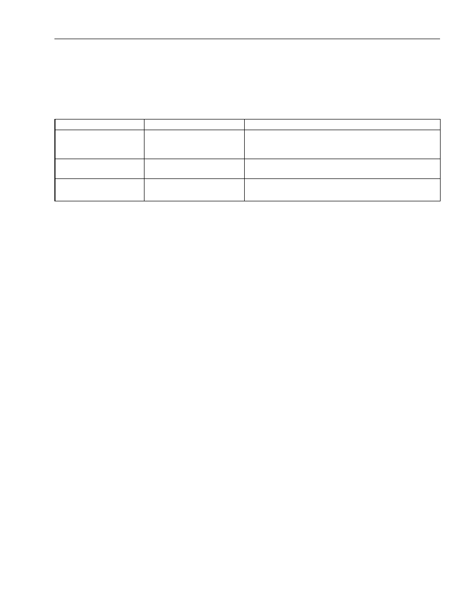
Data Sheet
March 2000
DSP1627 Digital Signal Processor
Lucent Technologies Inc.
67
7 Mask-Programmable Options
The DSP1627 contains a ROM that is mask-programmable. The selection of several programmable features is
made when a custom ROM is encoded. These features select the input clock options, the instruction/coefficient
memory map option, and the hardware emulation or ROM security option, as summarized in Table 59.
7.1 Input Clock Options
For all input options, the input clock CKI can run at some fraction of the internal clock frequency by setting the PLL
multiplication factors appropriately (see Section 4.12, Clock Synthesis). When the PLL is bypassed, the input clock
CKI frequency is the internal clock frequency.
If the mask option for using an external crystal is chosen, the internal oscillator may be used as a noninverting input
buffer by supplying a CMOS level to the CKI pin and leaving the CKI2 pin open.
7.2 Memory Map Options
The DSP1627 offers a DSP1627x36 or a DSP1627x32 where the difference is in the instruction/coefficient memory
maps. The DSP1627x36 contains 36 Kwords of internal ROM (IROM), but it doesn't support the use of IROM and
external ROM (EROM) in the same memory map. The DSP1627x32 supports the use of only 32 Kwords of IROM
with 16 Kwords of EROM in the same memory map. See Section 4.4 Memory Maps and Wait-States for further de-
scription.
7.3 ROM Security Options
The DSP1600 Hardware Development System (HDS) provides on-chip in-circuit emulation and requires that the re-
locatable HDS code be linked to the application code. This code's object file is called 1627hds.v
#
, where # is a
unique version identifier. Refer to the DSP1627-ST software tools release for more specific information. If on-chip
in-circuit emulation is desired, a nonsecure ROM must be chosen. If ROM security is desired with the DSP1627, the
HDS cannot be used. To provide testing of the internal ROM contents on a secure ROM device, a cyclic redundancy
check (CRC) program is called by and linked with the user's source code. The CRC code resides in the first
4 Kwords of ROM.
See the
DSP1600 Support Tools Manual
for more detailed information.
Table 59. DSP1627 ROM Options
Features
Options
Comments
Input Clock
CMOS Level
Small Signal
Crystal
2.7 V, 3.0 V, and 5.0 V.
2.7 V, 3.0 V, and 5.0 V.
2.7 V, 3.0 V, and 5.0 V.
Memory Map
DSP1627x36
DSP1627x32
36 Kwords IROM, no EROM in MAP1 or MAP3.
32 Kwords IROM, 16 Kwords EROM in MAP1 and MAP3.
ROM Security
Nonsecure
Secure
Specify and link 1627hds.v
#
*
, allows emulation.
Specify and link crc16.v
#
, no emulation capability.
*
1627hds.v
#
(# indicates the current version number) is the relocatable HDS object code. It uses approximately 140 words
and must reside in the first 4 Kwords of ROM.
crc16.v
#
is the cyclic redundancy check object code. It uses approximately 75 words and must reside in the first 4 Kwords
of ROM. See the
DSP1600 Support Tools Manual
for detailed information.

Data Sheet
DSP1627 Digital Signal Processor
March 2000
68
Lucent Technologies Inc.
8 Device Characteristics
8.1 Absolute Maximum Ratings
Stresses in excess of the absolute maximum ratings can cause permanent damage to the device. These are abso-
lute stress ratings only. Functional operation of the device is not implied at these or any other conditions in excess
of those given in the operational sections of the data sheet. Exposure to absolute maximum ratings for extended
periods can adversely affect device reliability.
External leads can be bonded and soldered safely at temperatures of up to 300
∞
C.
Voltage Range on V
DD
with Respect to Ground Using Devices Designed for 5 V Operation .............≠0.5 V to +7 V
Voltage Range on V
DD
with Respect to Ground Using Devices Designed for 3 V Operation ..........≠0.5 V to +4.6 V
Voltage Range on Any Pin ............................................................................................ .V
SS
≠ 0.5 V to V
DD
+ 0.5 V
Power Dissipation................................................................................................................................................ 1 W
Ambient Temperature Range ......................................................................................................... ≠40
∞
C to +85
∞
C
Storage Temperature Range
.................................................................................................................... ≠
65
∞
C to +150
∞
C
8.2 Handling Precautions
All MOS devices must be handled with certain precautions to avoid damage due to the accumulation of static
charge. Although input protection circuitry has been incorporated into the devices to minimize the effect of this static
buildup, proper precautions should be taken to avoid exposure to electrostatic discharge during handling and mount-
ing. Lucent Technologies employs a human-body model for ESD susceptibility testing. Since the failure voltage of
electronic devices is dependent on the current, voltage, and hence, the resistance and capacitance, it is important
that standard values be employed to establish a reference by which to compare test data. Values of 100 pF and
1500
are the most common and are the values used in the Lucent Technologies human-body model test circuit.
The breakdown voltage for the DSP1627 is greater than 2000 V.
8.3 Recommended Operating Conditions
The ratio of the instruction cycle rate to the input clock frequency is 1:1 without the PLL (referred to as 1X operation)
and M/(2N) with the PLL selected (see Section 4.12). Device speeds greater than 50 MIPS do not support 1X
operation; use the PLL.
Table 60. Recommended Operating Conditions
Maximum
Instruction Rate
(MIPS)
Device Speed
Input Clock
Package Supply Voltage
V
DD
(V)
Ambient Temperature
T
A
(
∞
∞
∞
∞
C)
Min
Max
Min
Max
50
20 ns
CMOS, small-signal,
crystal
BQFP
or TQFP
2.7
3.3
≠40
85
80
12.5 ns
CMOS, small-signal,
crystal
BQFP
or TQFP
2.7
3.3
≠40
85
100
10 ns
CMOS, small-signal,
crystal
BQFP
or TQFP
3.0
3.6
≠40
85
70
14 ns
CMOS, small-signal,
crystal
BQFP
or TQFP
4.75
5.25
≠40
85
90
11 ns
CMOS, small-signal,
crystal
BQFP
or TQFP
4.75
5.25
≠40
85

Data Sheet
March 2000
DSP1627 Digital Signal Processor
Lucent Technologies Inc.
69
8 Device Characteristics
(continued)
8.4 Package Thermal Considerations
The recommended operating temperature specified above is based on the maximum power, package type, and
maximum junction temperature. The following equations describe the relationship between these parameters. If the
applications' maximum power is less than the worst-case value, this relationship determines a higher maximum am-
bient temperature or the maximum temperature measured at top dead center of the package.
T
A
= T
J
≠ P x
JA
T
TDC
= T
J
≠ P x
J-TDC
where T
A
is the still-air ambient temperature and T
TDC
is the temperature measured by a thermocouple at the top
dead center of the package.
Maximum Junction Temperature (T
J
) in 100-Pin BQFP ................................................................................. 125
∞
C
100-pin BQFP Maximum Thermal Resistance in Still-Air-Ambient (
JA
) ..................................................... 55
∞
C/W
100-pin BQFP Maximum Thermal Resistance, Junction to Top Dead Center (
J-TDC
) ............................... 12
∞
C/W
Maximum Junction Temperature (T
J
) in 100-Pin TQFP ................................................................................. 125
∞
C
100-pin TQFP Maximum Thermal Resistance in Still-Air-Ambient (
JA
) ..................................................... 30
∞
C/W
100-pin TQFP Maximum Thermal Resistance, Junction to Top Dead Center (
J-TDC
) ................................. 6
∞
C/W
WARNING: Due to package thermal constraints, proper precautions in the user's application should be tak-
en to avoid exceeding the maximum junction temperature of 125
∞
C. Otherwise, the device will
be affected adversely.
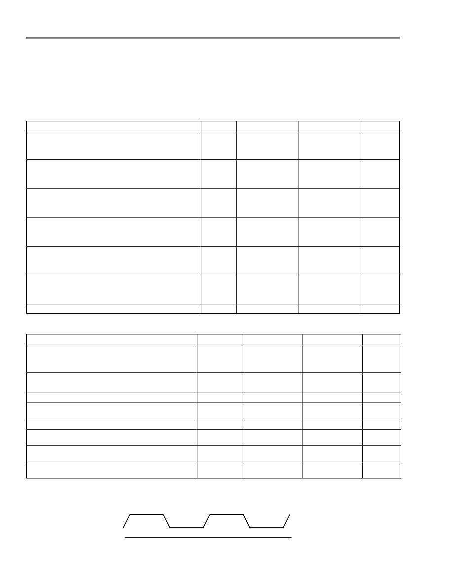
Data Sheet
DSP1627 Digital Signal Processor
March 2000
70
Lucent Technologies Inc.
9 Electrical Characteristics and Requirements
The following electrical characteristics are preliminary and are subject to change. Electrical characteristics refer to
the behavior of the device under specified conditions. Electrical requirements refer to conditions imposed on the
user for proper operation of the device. The parameters below are valid for the conditions described in Section 8.3,
Recommended Operating Conditions.
Table 61. Electrical Characteristics and Requirements
Parameter
Symbol
Min
Max
Unit
Input Voltage:
Low
V
IL
≠0.3
0.3 * V
DD
V
High
V
IH
0.7 * V
DD
V
DD
+ 0.3
V
Input Current (except TMS, TDI):
Low (V
IL
= 0 V, V
DD
= 5.25 V)
I
IL
≠5
--
µ
A
High (V
IH
= 5.25 V, V
DD
= 5.25 V)
I
IH
--
5
µ
A
Input Current (TMS, TDI):
Low (V
IL
= 0 V, V
DD
= 5.25 V)
I
IL
≠100
--
µ
A
High (V
IH
= 5.25 V, V
DD
= 5.25 V)
I
IH
--
5
µ
A
Output Low Voltage:
Low (I
OL
= 2.0 mA)
V
OL
--
0.4
V
Low (I
OL
= 50
µ
A)
V
OL
--
0.2
V
Output High Voltage:
High (I
OH
= ≠2.0 mA)
V
OH
V
DD
≠ 0.7
--
V
High (I
OH
= ≠50
µ
A)
V
OH
V
DD
≠ 0.2
--
V
Output 3-State Current:
Low (V
DD
= 5.25 V, V
IL
= 0 V)
I
OZL
≠10
--
µ
A
High (V
DD
= 5.25 V, V
IH
= 5.25 V)
I
OZH
--
10
µ
A
Input Capacitance
CI
--
5
pF
Table 62. Electrical Requirements for Mask-Programmable Input Clock Options
Parameter
Symbol
Min
Max
Unit
CKI CMOS Level Input Voltage:
Low
V
IL
≠0.3
0.3 * V
DD
V
High
V
IH
0.7 * V
DD
V
DD
+ 0.3
V
Small-signal Peak-to-peak Voltage
*
*
The small-signal buffer must be used in single-ended mode where an ac waveform (sine or square) is applied to CKI and a dc voltage approx-
imately equal to the average value of CKI is applied to CKI2, as shown in the figure below. The maximum allowable ripple on CKI2 is 100 mV.
Vpp
0.6
--
V
(on CKI)
Small-signal Input Duty Cycle
Duty cycle for a sine wave is defined as the percentage of time during each clock cycle that the voltage on CKI exceeds the voltage on CKI2.
DCyc
45
55
%
Small-signal Input Voltage Range
(pins: CKI, CKI2)
Vin
0.2 * V
DD
0.6 * V
DD
V
Small-signal Buffer Frequency Range
fss
--
35
MHz
Frequency Range of Fundamental Mode or Overtone
Crystal
fX
5
25
MHz
Series Resistance of Fundamental Mode or Overtone
Crystal (pins: CKI, CKI2)
RS
--
40
Mutual Capacitance of Crystal
(includes board stray capacitance)
C0
--
7
pF
CKI
CKI2
Data Sheet
March 2000
DSP1627 Digital Signal Processor
Lucent Technologies Inc.
71
9 Electrical Characteristics and Requirements
(continued)
Additional Electrical Requirements with Crystal Option: See Section 13, Crystal Electrical Characteristics and
Requirements.
Table 63. PLL Electrical Specifications, VCO Frequency Ranges
Parameter
Symbol
Min
Max
Unit
VCO frequency range (V
DD
= 3 V
±
10%)
*
*
The M and N counter values in the pllc register must be set so that the VCO will operate in the appropriate range (see Table 63). Choose the
lowest value of N and then the appropriate value of M for
f
INTERNAL CLOCK
=
f
CKI
x (M/(2N)) =
f
VCO
/2.
f
VCO
50
160
MHz
VCO frequency range (V
DD
= 3.0 V ≠
3.6 V)*
f
VCO
50
200
MHz
VCO frequency range (V
DD
= 5 V
±
5%)*
f
VCO
70
180
MHz
Input Jitter at CKI
--
--
200
ps-rms
Table 64. PLL Electrical Specifications and pllc Register Settings
M
V
DD
pllc13 (ICP)
pllc12
(SEL5V)
pllc[11:8]
(LF[3:0])
Typical Lock-in Time (
µ
µ
µ
µ
s)
*
*
Lock-in time represents the time following assertion of the PLLEN bit of the pllc register during which the PLL output clock is unstable. The
DSP must operate from the 1X CKI input clock or from the slow ring oscillator while the PLL is locking. Completion of the lock-in interval is
indicated by assertion of the LOCK flag.
23--24
2.7 V ≠ 3.6 V
1
0
1011
30
21--22
2.7 V ≠ 3.6 V
1
0
1010
30
19--20
2.7 V ≠ 3.6 V
1
0
1001
30
16--18
2.7 V ≠ 3.6 V
1
0
1000
30
12--15
2.7 V ≠ 3.6 V
1
0
0111
30
8--11
2.7 V ≠ 3.6 V
1
0
0110
30
2--7
2.7 V ≠ 3.6 V
1
0
0100
30
19--20
5 V
±
5%
1
1
1110
30
17--18
5 V
±
5%
1
1
1101
30
16
5 V
±
5%
1
1
1100
30
14--15
5 V
±
5%
1
1
1011
30
12--13
5 V
±
5%
1
1
1010
30
10--11
5 V
±
5%
1
1
1001
30
8--9
5 V
±
5%
1
1
1000
30
7
5 V
±
5%
1
1
0111
30
5--6
5 V
±
5%
1
1
0110
30
2--4
5 V
±
5%
1
1
0101
30
Data Sheet
DSP1627 Digital Signal Processor
March 2000
72
Lucent Technologies Inc.
9 Electrical Characteristics and Requirements
(continued)
Figure 9. Plot of V
OH
vs. I
OH
Under Typical Operating Conditions
Figure 10. Plot of V
OL
vs. I
OL
Under Typical Operating Conditions
0
10
20
30
40
5
15
25
35
45
50
DEVICE
UNDER
TEST
I
OH
(mA)
V
OH
(V)
V
DD
≠ 0.1
V
DD
≠ 0.2
V
DD
≠ 0.3
V
DD
≠ 0.4
V
DD
I
OH
V
OH
5-4007 (F).a
5-4008 (F).b
DEVICE
UNDER
TEST
I
OL
V
OL
0.4
0.3
0.2
0.1
0
V
OL
(V
)
0
5
10
15
20
25
30
35
40
45
50
I
OL
(mA)
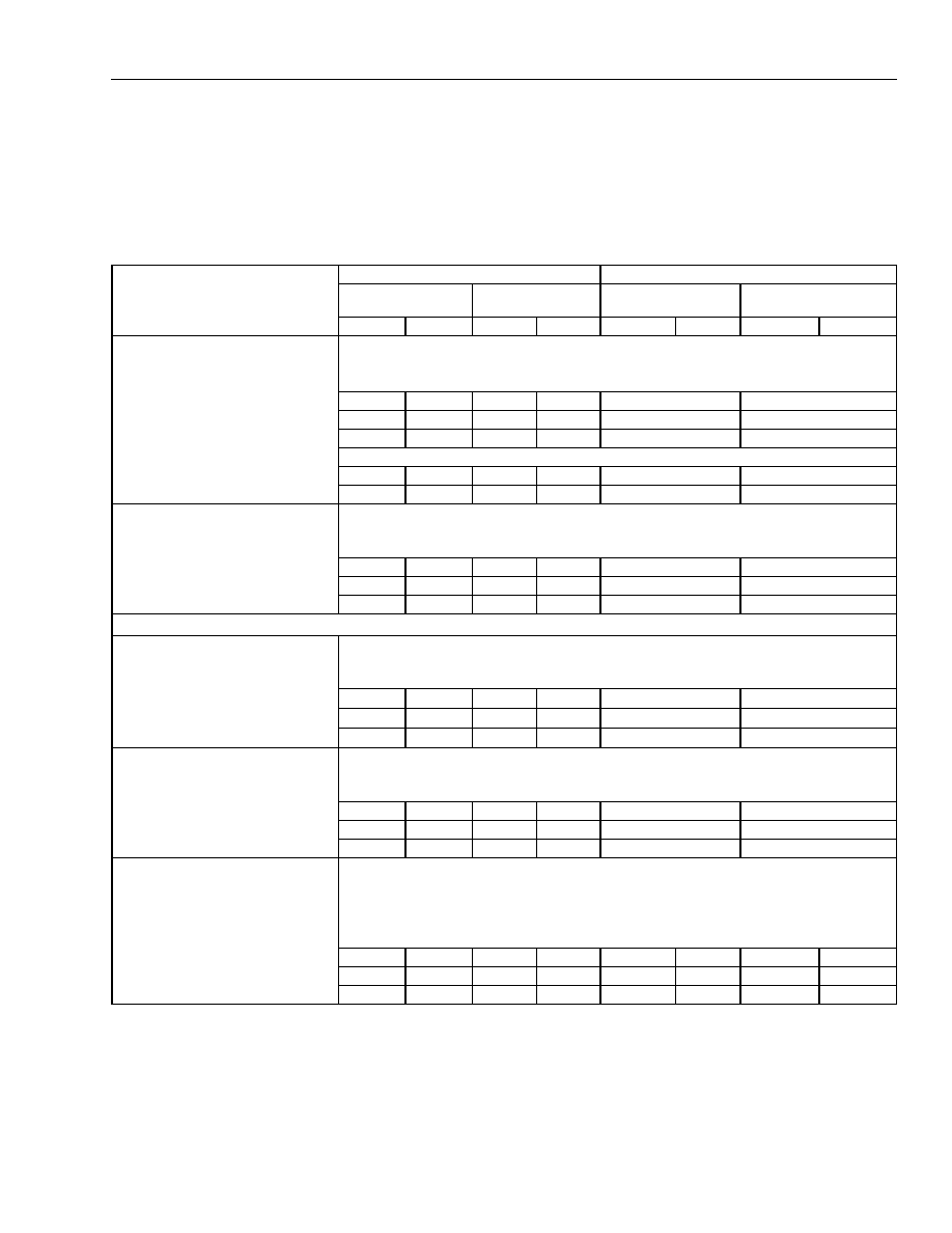
Data Sheet
March 2000
DSP1627 Digital Signal Processor
Lucent Technologies Inc.
73
9 Electrical Characteristics and Requirements
(continued)
9.1 Power Dissipation
Power dissipation is highly dependent on DSP program activity and the frequency of operation. The typical power
dissipation listed is for a selected application. The following electrical characteristics are preliminary and are subject
to change.
* T = CKI clock cycle for 1X input clock option or T = CKI clock cycle divided by M/(2N) for PLL clock option (see Section 4.12).
t
L
= PLL lock time (see Table 64).
Table 65. Power Dissipation and Wake-Up Latency
Operating Mode
(Unused Inputs at VDD or VSS)
Typical Power Dissipation (mW)
Wake-Up Latency
I/O Units ON
powerc[7:4] = 0x0
I/O Units OFF
powerc[7:4] = 0xf
(PLL Not Used
During Wake State)
(PLL Used
During Wake State)
5 V
3 V
5 V
3 V
5 V
3 V
5 V
3 V
Normal Operation ioc = 0x0180
PLL Disabled
CKI & CKO = 40 MHz
CMOS
220
74
214
72
--
--
Crystal Oscillator
241
80
235
78
--
--
Small Signal
223
76
217
74
--
--
CKI & CKO = 0 MHz
CMOS
0.19
0.067
0.19
0.067
--
--
Small Signal
3.0
1.1
3.0
1.1
--
--
Normal Operation ioc = 0x0180
PLL Enabled pllc = 0xFC0E
CKI = 10 MHz CKO = 40 MHz
CMOS
228
77
222
75
--
--
Crystal Oscillator
249
83
243
81
--
--
Small Signal
231
78
225
77
--
--
Power Management Modes CKO = 40 MHz
Standard Sleep, External Interrupt
alf[15] = 1, ioc = 0x0180
PLL Disabled During Sleep
CMOS
25.2
8.4
17.8
5.6
3T*
3T* + t
L
Crystal Oscillator
46.2
14.0
38.8
12.0
3T*
3T* + t
L
Small Signal
28.0
9.8
20.8
7.2
3T*
3T* + t
L
Standard Sleep, External Interrupt
alf[15] = 1, ioc = 0x0180
PLL Enabled During Sleep
CMOS
33.2
10.9
25.8
7.5
--
3T*
Crystal Oscillator
54.0
17.1
46.0
14.0
--
3T*
Small Signal
36.0
12.4
28.8
9.2
--
3T*
Sleep with Slow Internal Clock
Crystal/Small Signal Enabled
powerc[15:14] = 01,
alf[15] = 1, ioc = 0x0180
PLL Disabled During Sleep
CMOS
1.4
0.4
1.1
0.3
1.5
µ
s
5.0
µ
s
1.5
µ
s + t
L
5.0
µ
s + t
L
Crystal Oscillator
21.9
6.2
21.8
6.1
1.5
µ
s
5.0
µ
s
1.5
µ
s + t
L
5.0
µ
s + t
L
Small Signal
3.9
2.1
3.8
2.0
1.5
µ
s
5.0
µ
s
1.5
µ
s + t
L
5.0
µ
s + t
L
Data Sheet
DSP1627 Digital Signal Processor
March 2000
74
Lucent Technologies Inc.
9 Electrical Characteristics and Requirements
(continued)
*
T = CKI clock cycle for 1X input clock option or T = CKI clock cycle divided by M/(2N) for PLL clock option (see Section 4.12).
t
L
= PLL lock time (see Table 64).
The power dissipation listed is for internal power dissipation only. Total power dissipation can be calculated on the basis
of the application by adding C x V
DD
/2 x f for each output, where C is the additional load capacitance and f is the output
frequency.
Table 65. Power Dissipation and Wake-Up Latency (continued)
Operating Mode
(Unused inputs at VDD or VSS)
Typical Power Dissipation (mW)
Wake-Up Latency
I/O Units ON
powerc[7:4] = 0x0
I/O Units OFF
powerc[7:4] = 0xf
(PLL Not Used
During Wake State)
(PLL Used
During Wake State)
5 V
3 V
5 V
3 V
5 V
3 V
5 V
3 V
Sleep with Slow Internal Clock
Crystal/Small Signal Enabled
powerc[15:14] = 01,
alf[15] = 1, ioc = 0x0180
PLL Enabled During Sleep
CMOS
8.3
3.0
7.5
2.7
--
1.5
µ
s
5.0
µ
s
Crystal Oscillator
27.5
9.9
24.5
8.8
--
1.5
µ
s
5.0
µ
s
Small Signal
10.0
4.5
10.0
4.0
--
1.5
µ
s
5.0
µ
s
Sleep with Slow Internal Clock
Crystal/Small Signal Disabled
powerc[15:14] = 11,
alf[15] = 1, ioc = 0x0180
PLL Disabled During Sleep
Crystal Oscillator
0.67
0.24
0.56
0.16
20 ms
20 µs + t
L
Small Signal
0.67
0.24
0.56
0.16
20
µ
s
20 µs + t
L
Software Stop
powerc[15:12] = 0011
PLL Disabled During STOP
CMOS
0.19
0.067
0.19
0.067
3T*
3T* + t
L
Software Stop
powerc[15:12] = 1111
PLL Disabled During STOP
Crystal Oscillator
0.19
0.067
0.19
0.067
20 ms
20 µs +t
L
Small Signal
0.19
0.067
0.19
0.067
20
µ
s
20 µs + t
L
Hardware Stop (STOP = V
SS
)
powerc[15:12] = 0000
PLL Disabled During STOP
CMOS
0.19
0.067
0.19
0.067
3T*
--
Crystal Oscillator
20.0
6.0
20.0
6.0
3T*
--
Small Signal
3.0
1.1
3.0
1.1
3T*
--
Hardware Stop (STOP = V
SS
)
powerc[15:12] = 0000
PLL Enabled During STOP
CMOS
5.6
2.4
5.6
2.4
3T*
3T*
Crystal Oscillator
25.6
8.4
25.6
8.4
3T*
3T*
Small Signal
8.6
3.5
8.6
3.5
3T*
3T*

Data Sheet
March 2000
DSP1627 Digital Signal Processor
Lucent Technologies Inc.
75
9 Electrical Characteristics and Requirements
(continued)
Power dissipation due to the input buffers is highly dependent on the input voltage level. At full CMOS levels, es-
sentially no dc current is drawn. However, for levels between the power supply rails, especially at or near the thresh-
old of V
DD
/2, high currents can flow. Although input and I/O buffers may be left untied (since the input voltage levels
of the input and I/O buffers are designed to remain at full CMOS levels when not driven by the DSP), it is still rec-
ommended that unused input and I/O pins be tied to V
SS
or V
DD
through a 10 k
resistor to avoid application am-
biguities. Further, if I/O pins are tied high or low, they should be pulled fully to V
SS
or V
DD
.
WARNING: The device needs to be clocked for at least six CKI cycles during reset after powerup. Otherwise,
high currents may
flow.
10 Timing Characteristics for 5 V Operation
The following timing characteristics and requirements are preliminary information and are subject to change. Timing
characteristics refer to the behavior of the device under specified conditions. Timing requirements refer to conditions
imposed on the user for proper operation of the device. All timing data is valid for the following conditions:
T
A
= ≠40
∞
C to +85
∞
C (See Section 8.3.)
V
DD
= 5 V
±
5%, V
SS
= 0 V (See Section 8.3.)
Capacitance load on outputs (C
L
) = 50 pF, except for CKO, where C
L
= 20 pF.
Output characteristics can be derated as a function of load capacitance (C
L
).
All outputs: 0.03 ns/pF
dt/dC
L
0.06 ns/pF for 10
C
L
100 pF at V
IH
for rising edge and at V
IL
for falling edge.
For example, if the actual load capacitance is 30 pF instead of 50 pF, the derating for a rising edge is (30 ≠ 50) pF
x 0.06 ns/pF = 1.2 ns less than the specified rise time or delay that includes a rise time.
Test conditions for inputs:
s
Rise and fall times of 4 ns or less
s
Timing reference levels for delays = V
IH
, V
IL
Test conditions for outputs (unless noted otherwise):
s
C
LOAD
= 50 pF; except for CKO, where C
LOAD
= 20 pF
s
Timing reference levels for delays = V
IH
, V
IL
s
3-state delays measured to the high-impedance state of the output driver
For the timing diagrams, see Table 62 for input clock requirements.
Unless otherwise noted, CKO in the timing diagrams is the free-running CKO.

Data Sheet
DSP1627 Digital Signal Processor
March 2000
76
Lucent Technologies Inc.
10 Timing Characteristics for 5 V Operation
(continued)
10.1 DSP Clock Generation
*
See Table 62 for input clock electrical requirements.
Free-running clock.
Wait-stated clock (see Table 38).
ß
W = number of wait-states.
Figure 11. I/O Clock Timing Diagram
*
Device speeds greater than 50 MIPS do not support 1X operation. Use the PLL.
Device is fully static, t1 is tested at 100 ns for 1X input clock option, and memory hold time is tested at 0.1 s.
*
T = internal clock period, set by CKI or by CKI and the PLL parameters.
Table 66. Timing Requirements for Input Clock
Abbreviated Reference
Parameter
14 ns and 11 ns*
Min
Max
Unit
t1
Clock In Period (high to high)
20
--
ns
t2
Clock In Low Time (low to high)
10
--
ns
t3
Clock In High Time (high to low)
10
--
ns
Table 67. Timing Characteristics for Input Clock and Output Clock
Abbreviated Reference
Parameter
14 ns
11 ns
Unit
Min
Max
Min
Max
t4
Clock Out High Delay
--
10
--
8
ns
t5
Clock Out Low Delay (high to low)
--
10
--
8
ns
t6
Clock Out Period (low to low)
T*
--
T*
--
ns
t6a
Clock Out Period with SLOWCKI Bit
Set in powerc Register (low to low)
0.74
1.6
0.74
1.6
µ
s
5-4009 (F).a
t4
t1
t2
1X CKI*
t5
CKO
t3
t6, t6a
CKO
EXTERNAL MEMORY CYCLE
W = 1
ß
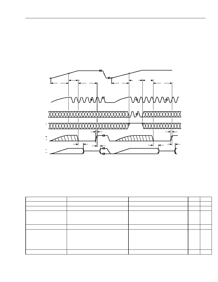
Data Sheet
March 2000
DSP1627 Digital Signal Processor
Lucent Technologies Inc.
77
10 Timing Characteristics for 5 V Operation
(continued)
10.2 Reset Circuit
The DSP1627 has a powerup reset circuit that automatically clears the JTAG controller upon powerup. If the supply
voltage falls below V
DD
MIN* and a reset is required, the JTAG controller must be reset--even if the JTAG port isn't
being used--by applying six low-to-high clock edges on TCK with TMS held high, followed by the usual RSTB and
CKI reset sequence. Figure 12 shows two separate events: an initial powerup and a powerup following a drop in the
power supply voltage.
*
See Table 60, Recommended Operating Condiitons.
Notes:
See Table 62 for CKI electrical requirements and Table 71 for TCK timing requirements.
When both INT0 and RSTB are asserted, all output and bidirectional pins (except TDO, which 3-states by JTAG control) are put in a 3-state
condition. With RSTB asserted and INT0 not asserted, EROM, ERAMHI, ERAMLO, IO, DSEL, and RWN outputs remain high, and CKO remains
a free-running clock.
TMS and TDI signals have internal pull-up devices.
Figure 12. Powerup Reset and Chip Reset Timing Diagram
*
With external components as specified in Table 62.
T
TCK
= t12 = TCK period. See Table 71 for TCK timing requirements.
Table 68. Timing Requirements for Powerup Reset and Chip Reset
Abbreviated Reference
Parameter
Min
Max
Unit
t8
Reset Pulse (low to high)
6T
--
ns
t9
V
DD
Ramp
--
10
ms
t146
V
DD
MIN to RSTB Low CMOS
Crystal*
Small-signal
2T
20
20
--
--
--
ns
ms
µ
s
t151
TMS High
6 * T
TCK
--
ns
t152
JTAG Reset to
CMOS
RSTB Low
Crystal*
Small-Signal
2T
20 ms ≠ 6 * T
TCK
if 6 * T
TCK
< 20 ms
0 if 6 * T
TCK
20 ms
20 µs ≠ 6 * T
TCK
if 6 * T
TCK
< 20 µs
0 if 6 * T
TCK
20 µs
--
--
--
--
--
ns
t153
RSTB Rise (low to high)
--
95
ns
5-2253 (F).a
t10
t11
t10
t11
t9
t146
t8
t9
t151
t152
t8
V
DD
RAMP
CKI
TCK
TMS
RSTB
PINS V
OH
V
OL
V
IH
V
IL
V
IH
0.4 V
V
DD
MIN
V
DD
MIN
0.4 V
t153
t153
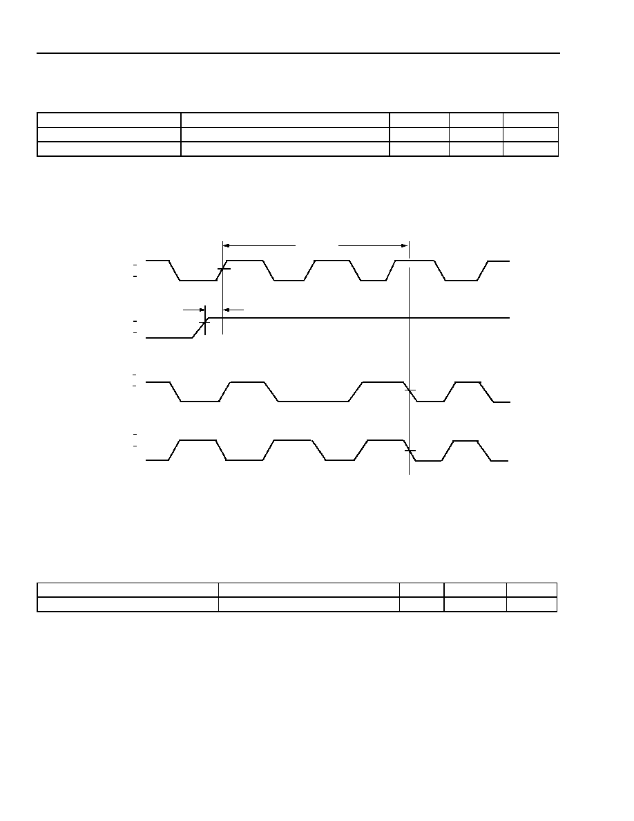
Data Sheet
DSP1627 Digital Signal Processor
March 2000
78
Lucent Technologies Inc.
10 Timing Characteristics for 5 V Operation
(continued)
Note: The device needs to be clocked for at least six CKI cycles during reset after powerup. Otherwise, high cur-
rents may flow.
10.3 Reset Synchronization
*
See Table 62 for input clock electrical requirements.
Note: CKO
1
and CKO
2
are two possible CKO states before reset. CKO is free-running.
Figure 13. Reset Synchronization Timing
Table 69. Timing Characteristics for Powerup Reset and Chip Reset
Abbreviated Reference
Parameter
Min
Max
Unit
t10
RSTB Disable Time (low to 3-state)
--
100
ns
t11
RSTB Enable Time (high to valid)
--
100
ns
Table 70. Timing Requirements for Reset Synchronization Timing
Abbreviated Reference
Parameter
Min
Max
Unit
t126
Reset Setup (high to high)
1.5
T/2 ≠ 5
ns
5-4011 (F).a
CKI
*
V
IH
V
IL
t126
t5 + 2 x t6
RSTB
V
IH
V
IL
V
IH
V
IL
CKO
V
IH
V
IL
CKO
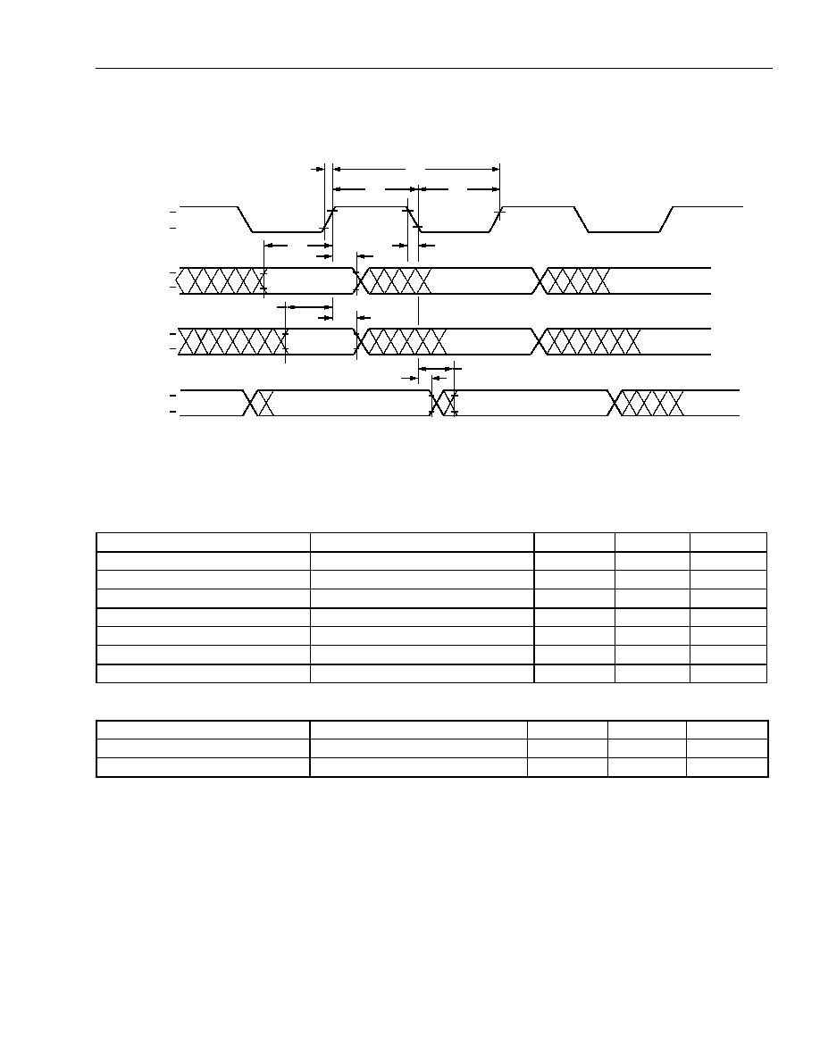
Data Sheet
March 2000
DSP1627 Digital Signal Processor
Lucent Technologies Inc.
79
10 Timing Characteristics for 5 V Operation
(continued)
10.4 JTAG I/O Specifications
Figure 14. JTAG Timing Diagram
Table 71. Timing Requirements for JTAG Input/Output
Abbreviated Reference
Parameter
Min
Max
Unit
t12
TCK Period (high to high)
50
--
ns
t13
TCK High Time (high to low)
22.5
--
ns
t14
TCK Low Time (low to high)
22.5
--
ns
t15
TMS Setup Time (valid to high)
7.5
--
ns
t16
TMS Hold Time (high to invalid)
2
--
ns
t17
TDI Setup Time (valid to high)
7.5
--
ns
t18
TDI Hold Time (high to invalid)
2
--
ns
Table 72. Timing Characteristics for JTAG Input/Output
Abbreviated Reference
Parameter
Min
Max
Unit
t19
TDO Delay (low to valid)
--
19
ns
t20
TDO Hold (low to invalid)
0
--
ns
t12
t14
t13
t15
t16
t17
t18
t19
t20
TCK
TMS
TDI
TDO
V
IH
V
IL
V
IH
V
IL
V
IH
V
IL
V
OH
V
OL
t155
t156
5-4017 (F)
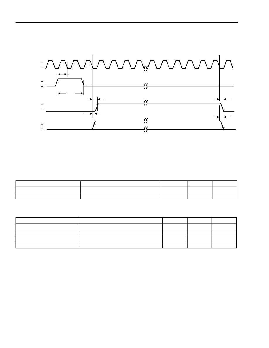
Data Sheet
DSP1627 Digital Signal Processor
March 2000
80
Lucent Technologies Inc.
10 Timing Characteristics for 5 V Operation
(continued)
10.5 Interrupt
*
CKO is free-running.
IACK assertion is guaranteed to be enclosed by VEC[3:0] assertion.
Figure 15. Interrupt Timing Diagram
Note: Interrupt is asserted during an interruptible instruction and no other pending interrupts.
Note: Interrupt is asserted during an interruptible instruction and no other pending interrupts.
Table 73. Timing Requirements for Interrupt
Abbreviated Reference
Parameter
Min
Max
Unit
t21
Interrupt Setup (high to low)
15
--
ns
t22
INT Assertion Time (high to low)
2T
--
ns
Table 74. Timing Characteristics for Interrupt
Abbreviated Reference
Parameter
Min
Max
Unit
t23
IACK Assertion Time (low to high)
--
T/2 + 7.5
ns
t24
VEC Assertion Time (low to high)
--
9.5
ns
t25
IACK Invalid Time (low to low)
--
7.5
ns
t26
VEC Invalid Time (low to low)
--
9.5
ns
5-4018 (F)
CKO
*
INT[1:0]
t21
V
OH
V
OL
V
IH
V
IL
t22
IACK
V
OH
V
OL
VEC[3:0]
V
OH
V
OL
t23
t24
t25
t26
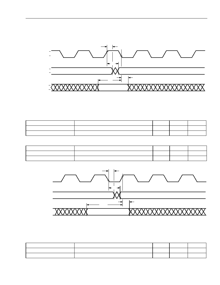
Data Sheet
March 2000
DSP1627 Digital Signal Processor
Lucent Technologies Inc.
81
10 Timing Characteristics for 5 V Operation
(continued)
10.6 Bit Input/Output (BIO)
Figure 16. Write Outputs Followed by Read Inputs (cbit = Immediate; a1 = sbit)
Figure 17. Write Outputs and Test Inputs (cbit = Immediate)
Table 75. Timing Requirements for BIO Input Read
Abbreviated Reference
Parameter
Min
Max
Unit
t27
IOBIT Input Setup Time (valid to high)
12
--
ns
t28
IOBIT Input Hold Time (high to invalid)
0
--
ns
Table 76. Timing Characteristics for BIO Output
Abbreviated Reference
Parameter
Min
Max
Unit
t29
IOBIT Output Valid Time (low to valid)
--
7.5
ns
t144
IOBIT Output Hold Time (low to invalid)
1
--
ns
Table 77. Timing Requirements for BIO Input Test
Abbreviated Reference
Parameter
Min
Max
Unit
t141
IOBIT Input Setup Time (valid to low)
12
--
ns
t142
IOBIT Input Hold Time (low to invalid)
0
--
ns
CKO
IOBIT
(INPUT)
t28
t27
VALID OUTPUT
V
I
H
V
I
L
V
O
H
V
O
L
V
O
H
V
O
L
DATA INPUT
t29
t144
IOBIT
(OUTPUT)
5-4019 (F).a
CKO
IOBIT
(INPUT)
t142
t141
VALID OUTPUT
V
OH
≠
V
O
L≠
TEST INPUT
t29
t144
IOBIT
(OUTPUT)
V
OH
≠
V
O
L≠
V
IH
≠
V
I
L≠
5-4019 (F).b
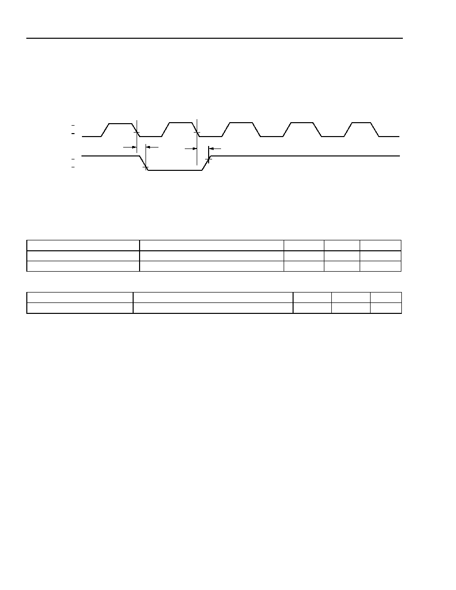
Data Sheet
DSP1627 Digital Signal Processor
March 2000
82
Lucent Technologies Inc.
10 Timing Characteristics for 5 V Operation
(continued)
10.7 External Memory Interface
The following timing diagrams, characteristics, and requirements do not apply to interactions with delayed external
memory enables unless so stated. See the
DSP1611/17/18/27 Digital Signal Processor Information Manual
for a
detailed description of the external memory interface including other functional diagrams.
*
W = number of wait-states.
Figure 18. Enable Transition Timing
Table 78. Timing Characteristics for External Memory Enables (EROM, ERAMHI, IO, ERAMLO)
Abbreviated Reference
Parameter
Min
Max
Unit
t33
CKO to ENABLE Active (low to low)
0
7
ns
t34
CKO to ENABLE Inactive (low to high)
≠1
6
ns
Table 79. Timing Characteristics for Delayed External Memory Enables (ioc = 0x000F)
Abbreviated Reference
Parameter
Min
Max
Unit
t33
CKO to Delayed ENABLE Active (low to low)
T/2 ≠ 2
T/2 + 7
ns
CKO
ENABLE
t34
t33
W
*
= 0
V
OH
V
OL
V
OH
V
OL
5-4020 (F).b
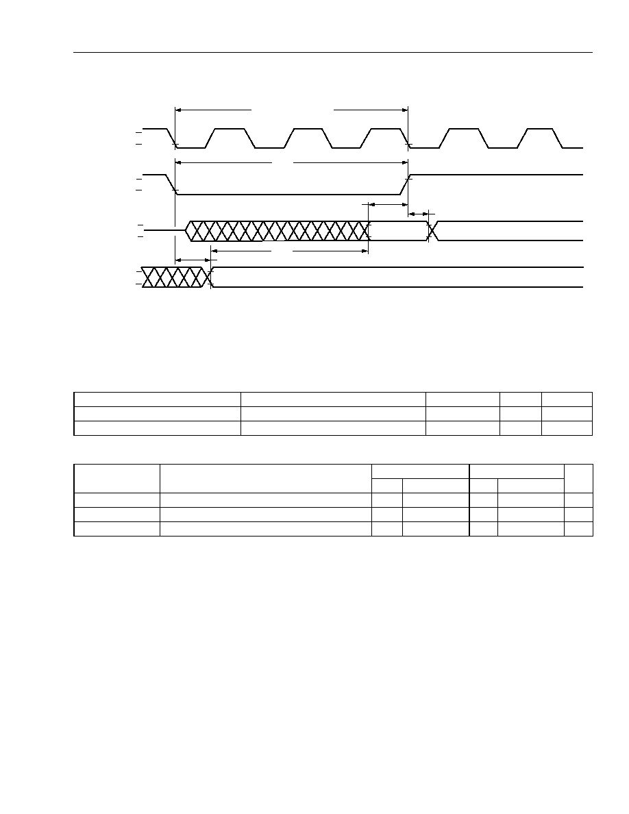
Data Sheet
March 2000
DSP1627 Digital Signal Processor
Lucent Technologies Inc.
83
10 Timing Characteristics for 5 V Operation
(continued)
*
W = number of wait-states.
Figure 19. External Memory Data Read Timing Diagram
Table 80. Timing Characteristics for External Memory Access
Abbreviated Reference
Parameter
Min
Max
Unit
t127
Enable Width (low to high)
T(1 + W) ≠ 4
--
ns
t128
Address Valid (enable low to valid)
--
2
ns
Table 81. Timing Requirements for External Memory Read (EROM, ERAMHI, IO, ERAMLO)
Abbreviated
Reference
Parameter
14 ns
11 ns
Unit
Min
Max
Min
Max
t129
Read Data Setup (valid to enable high)
12
--
11
--
ns
t130
Read Data Hold (enable high to hold)
0
--
0
--
ns
t150
External Memory Access Time (valid to valid)
--
T(1 + W) ≠ 13
--
T(1 + W) ≠ 12
ns
V
IH
V
IL
DB
CKO
AB
V
OH
V
OL
t128
READ ADDRESS
ENABLE
V
OH
V
OL
V
OH
V
OL
(MWAIT = 0 x 2222)
W* = 2
t127
t129
t130
READ DATA
t150
5-4021 (F).a
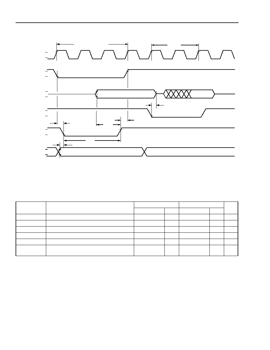
Data Sheet
DSP1627 Digital Signal Processor
March 2000
84
Lucent Technologies Inc.
10 Timing Characteristics for 5 V Operation
(continued)
* W = number of wait-states.
Figure 20. External Memory Data Write Timing Diagram
Table 82. Timing Characteristics for External Memory Data Write (All Enables)
Abbreviated
Reference
Parameter
14 ns
11 ns
Unit
Min
Max
Min
Max
t131
Write Overlap (enable low to 3-state)
--
0
--
0
ns
t132
RWN Advance (RWN high to enable high)
0
--
0
--
ns
t133
RWN Delay (enable low to RWN low)
0
--
0
--
ns
t134
Write Data Setup (data valid to RWN high)
T(1 + W)/2 ≠ 3
--
T(1 + W)/2 ≠ 2
--
ns
t135
RWN Width (low to high)
T(1 + W) ≠ 5.5
--
T(1 + W) ≠ 5.5
--
ns
t136
Write Address Setup (address valid to RWN
low)
0
--
0
--
ns
ERAMLO
EROM
CKO
AB
RWN
DB
WRITE ADDRESS
READ ADDRESS
V
OH
V
OL
V
OH
V
OL
V
OH
V
OL
V
OH
V
OL
V
OH
V
OL
WRITE DATA
READ
W* = 1
t131
t132
t134
t133
t135
t136
(MWAIT = 0x1002)
W* = 2
V
OH
V
OL
5-4022 (F).a

Data Sheet
March 2000
DSP1627 Digital Signal Processor
Lucent Technologies Inc.
85
10 Timing Characteristics for 5 V Operation
(continued)
*
W = number of wait-states.
Figure 21. Write Cycle Followed by Read Cycle
Table 83. Timing Characteristics for Write Cycle Followed by Read Cycle
Abbreviated Reference
Parameter
Min
Max
Unit
t131
Write Overlap (enable low to 3-state)
--
0
ns
t137
Write Data 3-state (RWN high to 3-state)
--
2
ns
t138
Write Data Hold (RWN high to data hold)
0
--
ns
t139
Write Address Hold (RWN high to address hold)
0
--
ns
ERAMLO
CKO
AB
RWN
WRITE ADDRESS
READ ADDRESS
V
OH
V
OL
V
OH
V
OL
V
OH
V
OL
V
OH
V
OL
W* = 1
t137
(MWAIT = 0x1002)
W* = 2
EROM
V
OH
V
OL
DB
WRITE
READ
V
OH
V
OL
t138
t139
t131
5-4023 (F).a
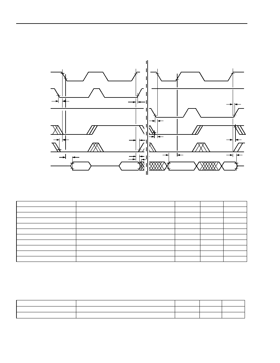
Data Sheet
DSP1627 Digital Signal Processor
March 2000
86
Lucent Technologies Inc.
10 Timing Characteristics for 5 V Operation
(continued)
10.8 PHIF Specifications
For the PHIF, "READ" means read by the external user (output by the DSP); "WRITE" is similarly defined. The 8-bit reads/
writes are identical to one-half of a 16-bit access.
Figure 22. PHIF
Intel
Mode Signaling (Read and Write) Timing Diagram
*
This timing diagram for the PHIF port shows accesses using the PCSN signal to initiate and complete a transaction. The transactions can also be initiated
and completed with the PIDS and PODS signals. An output transaction (read) is initiated by PCSN or PODS going low, whichever comes last. For example,
the timing requirements referenced to PCSN going low, t45 and t49, should be referenced to PODS going low, if PODS goes low after PCSN. An output
transaction is completed by PCSN or PODS going high, whichever comes first. An input transaction is initiated by PCSN or PIDS going low, whichever
comes last. An input transaction is completed by PCSN or PIDS going high, whichever comes first. All requirements referenced to PCSN apply to PIDS or
PODS, if PIDS or PODS is the controlling signal.
Table 84. Timing Requirements for PHIF
Intel Mode Signaling
Abbreviated Reference
Parameter
Min
Max
Unit
t41
PODS to PCSN Setup (low to low)
0
--
ns
t42
PCSN to PODS Hold (high to high)
0
--
ns
t43
PIDS to PCSN Setup (low to low)
0
--
ns
t44
PCSN to PIDS Hold (high to high)
0
--
ns
t45*
PSTAT to PCSN Setup (valid to low)
4.5
--
ns
t46*
PCSN to PSTAT Hold (high to invalid)
0
--
ns
t47*
PBSEL to PCSN Setup (valid to low)
4.5
--
ns
t48*
PCSN to PBSEL Hold (high to invalid)
0
--
ns
t51*
PB Write to PCSN Setup (valid to high)
7.5
--
ns
t52*
PCSN to PB Write Hold (high to invalid)
4
--
ns
Table 85. Timing Characteristics for PHIF
Intel Mode Signaling
Abbreviated Reference
Parameter
Min
Max
Unit
t49*
PCSN to PB Read (low to valid)
--
13
ns
t50*
PCSN to PB Read Hold (high to invalid)
3
--
ns
PCSN
t41
t42
t43
t45
t46
t49
t50
16-bit READ
16-bit WRITE
PODS
PIDS
PBSEL
PSTAT
PB[7:0]
t47
t51
t52
t48
t44
5-4036 (F)
t154
V
IH≠
V
IL≠
V
IH≠
V
IL≠
V
IH≠
V
IL≠
V
IH≠
V
IL≠
V
IH≠
V
IL≠
V
IH≠
V
IL≠

Data Sheet
March 2000
DSP1627 Digital Signal Processor
Lucent Technologies Inc.
87
10 Timing Characteristics for 5 V Operation
(continued)
Figure 23. PHIF
Intel
Mode Signaling (Pulse Period and Flags) Timing Diagram
*
t53 should be referenced to the rising edge of PCSN or PODS, whichever comes first.
t54 should be referenced to the rising edge of PCSN
or PIDS, whichever comes first.
POBE and PIBF may be programmed to be the opposite logic levels shown in the diagram (positive assertion levels shown). t53 and t54 apply
to the inverted levels as well as those shown.
Table 86. Timing Requirements for PHIF
Intel
Mode Signaling
Abbreviated Reference
Parameter
Min
Max
Unit
t55
PCSN/PODS/PIDS Pulse Width (high to low)
15
--
ns
t56
PCSN/PODS/PIDS Pulse Width (low to high)
15
--
ns
Table 87. Timing Characteristics for PHIF
Intel
Mode Signaling
Abbreviated Reference
Parameter
Min
Max
Unit
t53*
PCSN/PODS to POBE
(high to high)
--
15
ns
t54*
PCSN/PIDS to PIBF
(high to high)
--
15
ns
PODS
PIDS
V
IH
V
IL
V
IH
V
IL
V
IH
V
IL
t55
t56
t55
t56
t55
t56
PCSN
t53
t54
16-bit READ
8-bit WRITE
PBSEL
POBE
PIBF
t54
V
OH
V
OL
V
OH
V
OL
V
OH
V
OL
t56
t56
t55
t53
8-bit READ
16-bit WRITE
5-4037 (F).a

Data Sheet
DSP1627 Digital Signal Processor
March 2000
88
Lucent Technologies Inc.
10 Timing Characteristics for 5 V Operation
(continued)
Figure 24. PHIF
Motorola
Mode Signaling (Read and Write) Timing Diagram
*
This timing diagram for the PHIF port shows accesses using the PCSN signal to initiate and complete a transaction. The transactions can also
be initiated and completed with the PDS signal. An input/output transaction is initiated by PCSN or PDS going low, whichever comes last. For
example, the timing requirements referenced to PCSN going low, t45 and t49, should be referenced to PDS going low, if PDS goes low after
PCSN. An input/output transaction is completed by PCSN or PDS going high, whichever comes first. All requirements referenced to PCSN
should be referenced to PDS, if PDS is the controlling signal. PRWN should never be used to initiate or complete a transaction.
PDS is programmable to be active-high or active-low. It is shown active-low in Figures 24 and 25. POBE and PIBF may be programmed to be
the opposite logic levels shown in the diagram. t53 and t54 apply to the inverted levels as well as those shown.
Table 88. Timing Requirements for PHIF
Motorola Mode Signaling
Abbreviated Reference
Parameter
Min
Max
Unit
t41
PDS
to PCSN Setup (valid to low)
0
--
ns
t42
PCSN to PDS
Hold (high to invalid)
0
--
ns
t43
PRWN to PCSN Setup (valid to low)
4.5
--
ns
t44
PCSN to PRWN Hold (high to invalid)
0
--
ns
t45*
PSTAT to PCSN Setup (valid to low)
4.5
--
ns
t46*
PCSN to PSTAT Hold (high to invalid)
0
--
ns
t47*
PBSEL to PCSN Setup (valid to low)
4.5
--
ns
t48*
PCSN to PBSEL Hold (high to invalid)
0
--
ns
t51*
PB Write to PCSN Setup (valid to high)
8
--
ns
t52*
PCSN to PB Write Hold (high to invalid)
4
--
ns
Table 89. Timing Characteristics for PHIF
Motorola Mode Signaling
Abbreviated Reference
Parameter
Min
Max
Unit
t49*
PCSN to PB Read (low to valid)
--
13
ns
t50*
PCSN to PB Read (high to invalid)
3
--
ns
5-4038 (F).a
PCSN
PDS
PRWN
PBSEL
PSTAT
PB[7:0]
t41
t42
t43
t44
t45
t46
t47
t48
t52
t51
t50
t49
16-bit READ
16-bit WRITE
t43
t44
V
I H
V
IL
V
I H
V
IL
V
I H
V
IL
V
I H
V
IL
V
I H
V
IL
t154
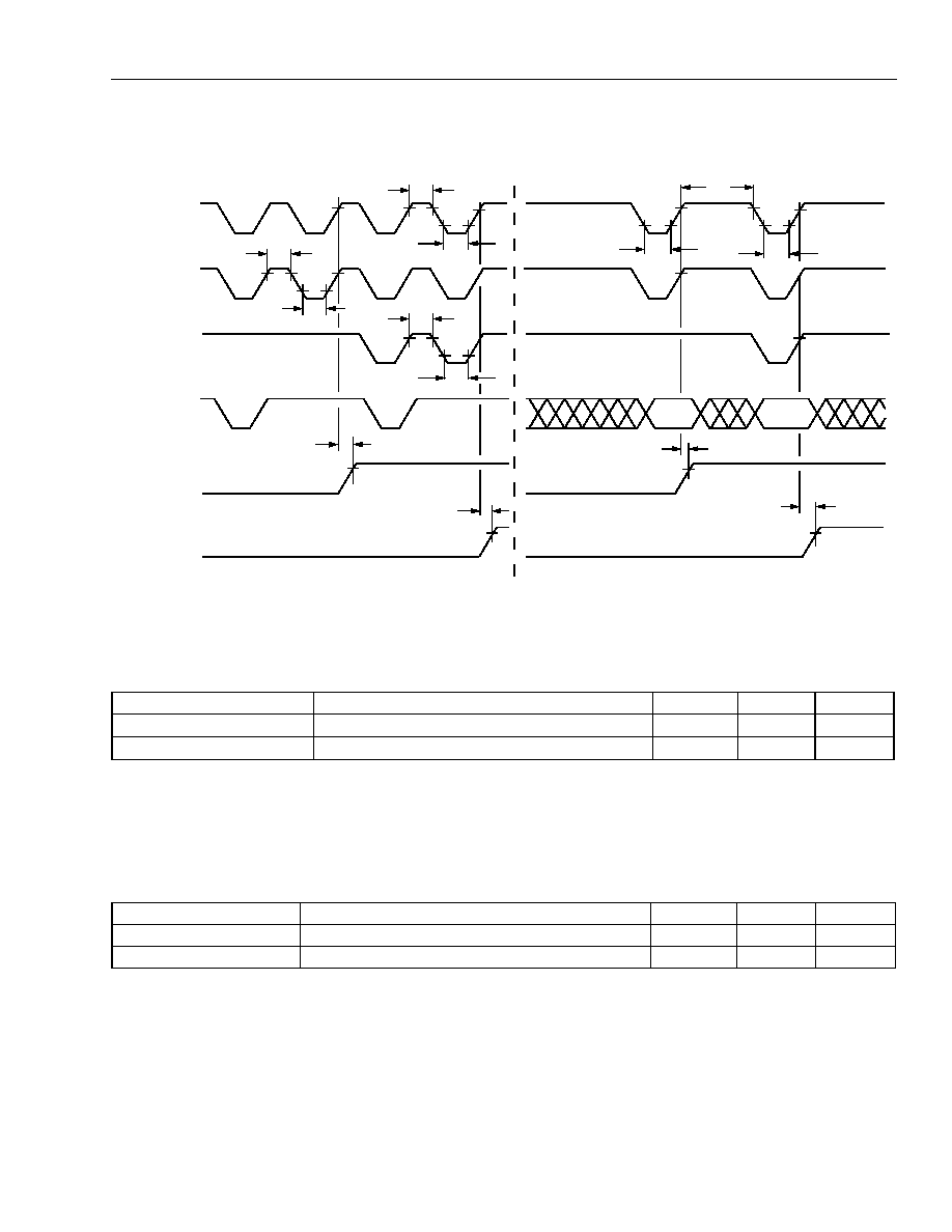
Data Sheet
March 2000
DSP1627 Digital Signal Processor
Lucent Technologies Inc.
89
10 Timing Characteristics for 5 V Operation
(continued)
Figure 25. PHIF
Motorola
Mode Signaling (Pulse Period and Flags) Timing Diagram
*
An input/output transaction is initiated by PCSN or PDS going low, whichever comes last. For example, t53 and t54 should be referenced to
PDS going low, if PDS goes low after PCSN. An input/output transaction is completed by PCSN or PDS going high, whichever comes first.
All requirements referenced to PCSN should be referenced to PDS, if PDS is the controlling signal. PRWN should never be used to initiate or
complete a transaction.
PDS is programmable to be active-high or active-low. It is shown active-low in Figures 24 and 25. POBE and PIBF may be programmed to
be the opposite logic levels shown in the diagram. t53 and t54 apply to the inverted levels as well as those shown.
Table 90. Timing Characteristics for PHIF
Motorola
Mode Signaling
Abbreviated Reference
Parameter
Min
Max
Unit
t53*
PCSN/PDS
to POBE
(high to high)
--
15
ns
t54*
PCSN/PDS
to PIBF
(high to high)
--
15
ns
Table 91. Timing Requirements for PHIF
Motorola
Mode Signaling
Abbreviated Reference
Parameter
Min
Max
Unit
t55
PCSN/PDS/PRWN Pulse Width (high to low)
15
--
ns
t56
PCSN/PDS/PRWN Pulse Width (low to high)
15
--
ns
PDS
PRWN
V
IH
≠
t55
t56
t55
t56
t55
t56
PCSN
t53
t54
16-bit READ
8-bit WRITE
PBSEL
POBE
PIBF
t54
t56
t56
t55
t53
8-bit READ
16-bit WRITE
V
IL
≠
V
IH
≠
V
IL
≠
V
IH
≠
V
IL
≠
V
OH
≠
V
OL
≠
V
OH
≠
V
OL
≠
V
OH
≠
V
OL
≠
5-4039 (F).a
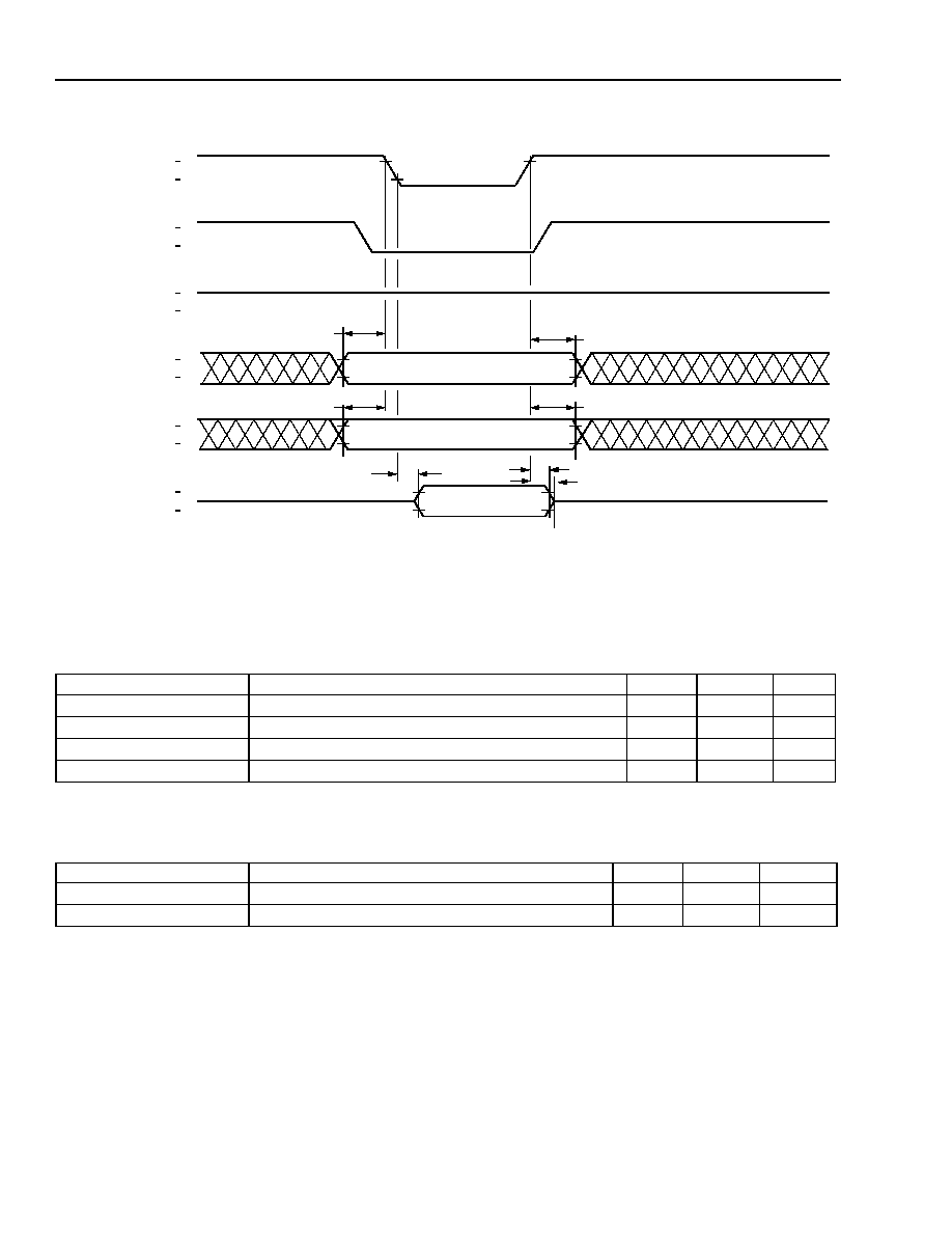
Data Sheet
DSP1627 Digital Signal Processor
March 2000
90
Lucent Technologies Inc.
10 Timing Characteristics for 5 V Operation
(continued)
*
Motorola
mode signal name.
Figure 26. PHIF
Intel
or
Motorola
Mode Signaling (Status Register Read) Timing Diagram
t45, t47, and t49 are referenced to the falling edge of PCSN or PODS(PDS), whichever occurs last.
t46, t48, and t50 are referenced to the rising edge of PCSN or PODS(PDS), whichever occurs first.
t45, t47, and t49 are referenced to the falling edge of PCSN or PODS(PDS), whichever occurs last.
t46, t48, and t50 are referenced to the rising edge of PCSN or PODS(PDS), whichever occurs first.
Table 92. Timing Requirements for
Intel
and
Motorola
Mode Signaling (Status Register Read)
Abbreviated Reference
Parameter
Min
Max
Unit
t45
PSTAT to PCSN Setup (valid to low)
4.5
--
ns
t46
PCSN to PSTAT Hold (high to invalid)
0
--
ns
t47
PBSEL to PCSN Setup (valid to low)
4.5
--
ns
t48
PCSN to PBSEL Hold (high to invalid)
0
--
ns
Table 93. Timing Characteristics for
Intel
and
Motorola
Mode Signaling (Status Register Read)
Abbreviated Reference
Parameter
Min
Max
Unit
t49
PCSN to PB Read (low to valid)
--
13
ns
t50
PCSN to PB Read Hold (high to invalid)
3
--
ns
PCSN
PODS (PDS*)
PIDS (PRWN*)
PBSEL
PSTAT
PB[7:0]
t47
t48
t45
t46
t49
t50
V
IH
V
IL
V
OH
V
OL
V
IH
V
IL
V
IH
V
IL
V
IH
V
IL
V
IH
V
IL
5-4040 (F).a
t154

Data Sheet
March 2000
DSP1627 Digital Signal Processor
Lucent Technologies Inc.
91
10 Timing Characteristics for 5 V Operation
(continued)
Figure 27. PHIF, PIBF, and POBE Reset Timing Diagram
*
After reset, POBE and PIBF always go to the levels shown, indicating output buffer empty and input buffer empty. The DSP program, however,
may later invert the definition of the logic levels for POBE and PIBF. t57 and t58 continue to apply.
POBE and PIBF can be programmed to be active-high or active-low. They are shown active-high. The timing characteristic for active-low is
the same as for active-high
.
Figure 28. PHIF, PIBF, and POBE Disable Timing Diagram
Table 94. PHIF Timing Characteristics for PHIF, PIBF, and POBE Reset
Abbreviated Reference
Parameter
Min
Max
Unit
t57
RSTB Disable to POBE/PIBF* (high to valid)
--
19
ns
t58
RSTB Enable to POBE/PIBF* (low to invalid)
3
19
ns
Table 95. PHIF Timing Characteristics for POBE and PIBF Disable
Abbreviated Reference
Parameter
Min
Max
Unit
t59
CKO to POBE/PIBF Disable (high/low to disable)
--
15
ns
RSTB
V
IH
≠
t58
t57
V
IL
≠
POBE
V
OH
≠
V
OL
≠
PIBF
V
OH
≠
V
OL
≠
5-4775 (F)
CKO
V
IH
≠
V
IL
≠
t59
t59
POBE
V
OH
≠
V
OL
≠
PIBF
V
OH
≠
V
OL
≠
5-4776 (F)
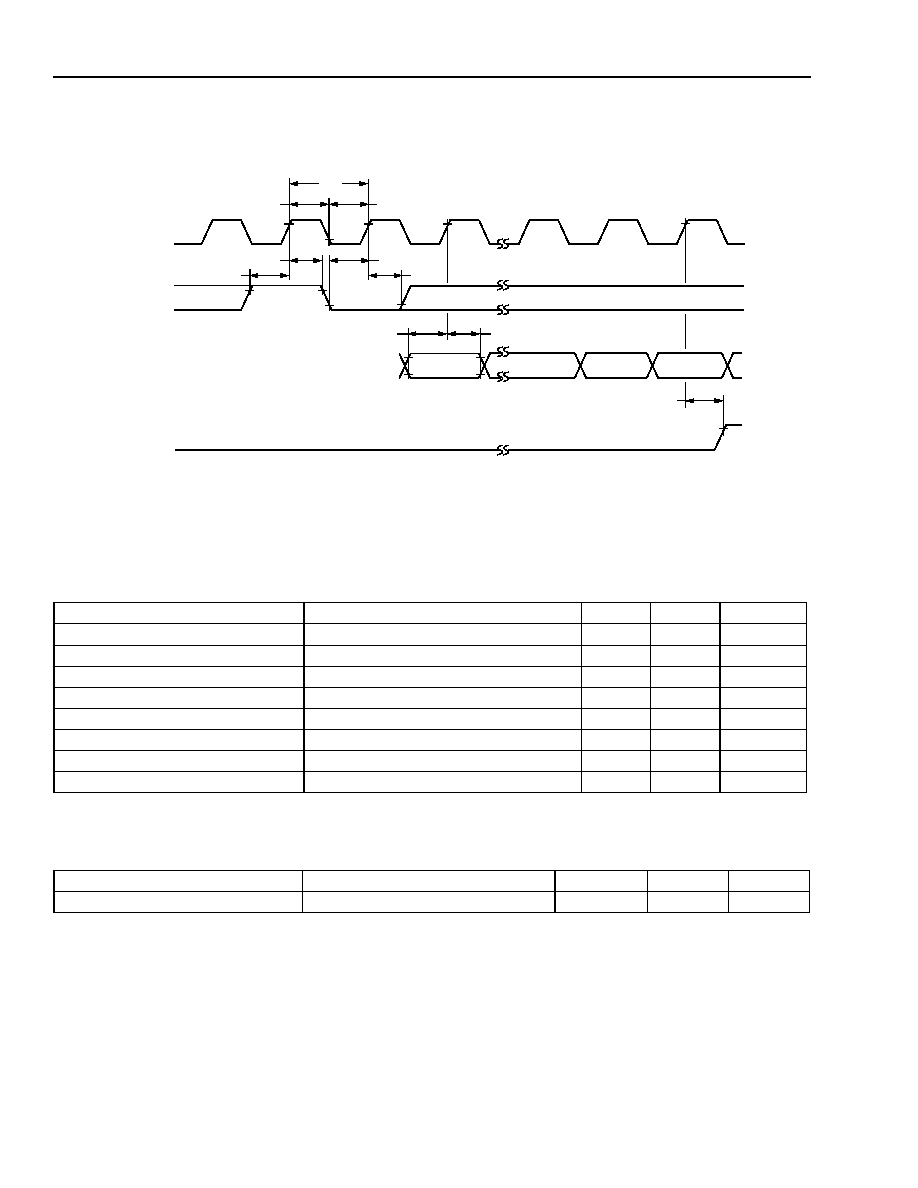
Data Sheet
DSP1627 Digital Signal Processor
March 2000
92
Lucent Technologies Inc.
10 Timing Characteristics for 5 V Operation
(continued)
10.9 Serial I/O Specifications
*
N = 16 or 8 bits.
Figure 29. SIO Passive Mode Input Timing Diagram
Device is fully static; t70 is tested at 200 ns.
For Multiprocessor mode, see note in Section 10.10.
Table 96. Timing Requirements for Serial Inputs
Abbreviated Reference
Parameter
Min
Max
Unit
t70
Clock Period (high to high)
40
--
ns
t71
Clock Low Time (low to high)
18
--
ns
t72
Clock High Time (high to low)
18
--
ns
t73
Load High Setup (high to high)
6
--
ns
t74
Load Low Setup (low to high)
6
--
ns
t75
Load High Hold (high to invalid)
0
--
ns
t77
Data Setup (valid to high)
5
--
ns
t78
Data Hold (high to invalid)
0
--
ns
Table 97. Timing Characteristics for Serial Outputs
Abbreviated Reference
Parameter
Min
Max
Unit
t79
IBF Delay (high to high)
--
22
ns
IBF
V
OH
≠
V
OL
≠
DI
V
IH
≠
V
IL
≠
ILD
V
IH
≠
V
IL
≠
ICK
V
IH
≠
V
IL
≠
BN ≠ 1*
B0
t77
t78
B0
B1
t79
t72
t71
t70
t75
t74
t75
t73
5-4777 (F)

Data Sheet
March 2000
DSP1627 Digital Signal Processor
Lucent Technologies Inc.
93
10 Timing Characteristics for 5 V Operation
(continued)
*
ILD goes high during bit 6 (of 0:15), N = 8 or 16.
Figure 30. SIO Active Mode Input Timing Diagram
Table 98. Timing Requirements for Serial Inputs
Abbreviated Reference
Parameter
Min
Max
Unit
t77
Data Setup (valid to high)
5
--
ns
t78
Data Hold (high to invalid)
0
--
ns
Table 99. Timing Characteristics for Serial Outputs
Abbreviated Reference
Parameter
Min
Max
Unit
t76a
ILD Delay (high to low)
--
22
ns
t101
ILD Hold (high to invalid)
4
--
ns
t79
IBF Delay (high to high)
--
22
ns
IBF
V
OH
≠
V
OL
≠
DI
V
IH
≠
V
IL
≠
ILD
V
OH
≠
V
OL
≠
ICK
V
OH
≠
V
OL
≠
BN ≠ 1
B0
t77
t78
B0
B1
t79
t101
t76a
*
5-4778 (F)
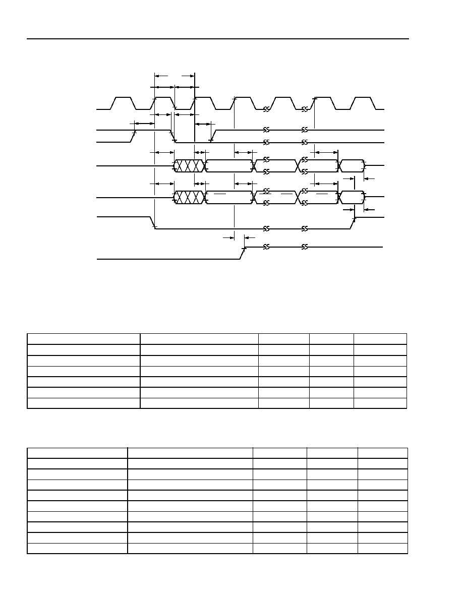
Data Sheet
DSP1627 Digital Signal Processor
March 2000
94
Lucent Technologies Inc.
10 Timing Characteristics for 5 V Operation
(continued)
*
See sioc register, MSB field to determine if B0 is the MSB or LSB. See sioc register, ILEN field to determine if the DO word length is 8 bits or
16 bits.
Figure 31. SIO Passive Mode Output Timing Diagram
Device is fully static; t80 is tested at 200 ns.
For multiprocessor mode, see note in Section 10.10.
Table 100. Timing Requirements for Serial Inputs
Abbreviated Reference
Parameter
Min
Max
Unit
t80
Clock Period (high to high)
40
--
ns
t81
Clock Low Time (low to high)
18
--
ns
t82
Clock High Time (high to low)
18
--
ns
t83
Load High Setup (high to high)
6
--
ns
t84
Load Low Setup (low to high)
6
--
ns
t85
Load Hold (high to invalid)
0
--
ns
Table 101. Timing Characteristics for Serial Outputs
Abbreviated Reference
Parameter
Min
Max
Unit
t87
Data Delay (high to valid)
--
22
ns
t88
Enable Data Delay (low to active)
--
22
ns
t89
Disable Data Delay (high to 3-state)
--
22
ns
t90
Data Hold (high to invalid)
4
--
ns
t92
Address Delay (high to valid)
--
22
ns
t93
Address Hold (high to invalid)
4
--
ns
t94
Enable Delay (low to active)
--
22
ns
t95
Disable Delay (high to 3-state)
--
22
ns
t96
OBE Delay (high to high)
--
22
ns
DOEN
V
IH
≠
V
IL
≠
SADD
V
OH
≠
V
OL
≠
OLD
V
IH
≠
V
IL
≠
OCK
V
IH
≠
V
IL
≠
t85
t80
t81
t82
t84
t83
t85
t88
B0
B1
B7
BN ≠ 1
t90
t90
t87
t94
AD0
AD1
AD7
t93
t93
t92
AS7
t89
t95
OBE
V
OH
≠
V
OL
≠
DO*
V
OH
≠
V
OL
≠
t96
5-4796 (F)
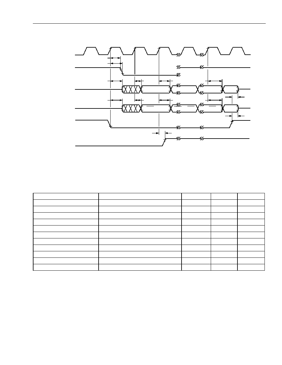
Data Sheet
March 2000
DSP1627 Digital Signal Processor
Lucent Technologies Inc.
95
10 Timing Characteristics for 5 V Operation
(continued)
*
OLD goes high at the end of bit 6 of 0:15.
Figure 32. SIO Active Mode Output Timing Diagram
Table 102. Timing Characteristics for Serial Outputs
Abbreviated Reference
Parameter
Min
Max
Unit
t86a
OLD Delay (high to low)
--
22
ns
t102
OLD Hold (high to invalid)
4
--
ns
t87
Data Delay (high to valid)
--
22
ns
t88
Enable Data Delay (low to active)
--
22
ns
t89
Disable Data Delay (high to 3-state)
--
22
ns
t90
Data Hold (high to invalid)
4
--
ns
t92
Address Delay (high to valid)
--
22
ns
t93
Address Hold (high to invalid)
4
--
ns
t94
Enable Delay (low to active)
--
22
ns
t95
Disable Delay (high to 3-state)
--
22
ns
t96
OBE Delay (high to high)
--
22
ns
DOEN
V
IH
≠
V
IL
≠
SADD
V
OH
≠
V
OL
≠
OLD
V
OH
≠
V
OL
≠
OCK
V
OH
≠
V
OL
≠
t102
t86a
t88
B0
B1
B7
BN ≠ 1
t90
t90
t87
t94
AD0
AD1
AD7
t93
t93
t92
AS7
t89
t95
OBE
V
OH
≠
V
OL
≠
DO
V
OH
≠
V
OL
≠
t96
*
5-4797 (F)
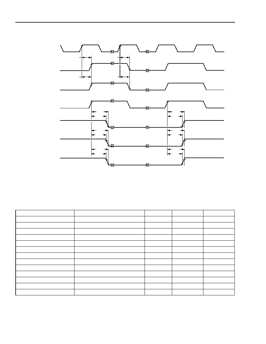
Data Sheet
DSP1627 Digital Signal Processor
March 2000
96
Lucent Technologies Inc.
10 Timing Characteristics for 5 V Operation
(continued)
*
See sioc register, LD field.
Figure 33. Serial I/O Active Mode Clock Timing
Table 103. Timing Characteristics for Signal Generation
Abbreviated Reference
Parameter
Min
Max
Unit
t97
ICK Delay (high to high)
--
15
ns
t98
ICK Delay (high to low)
--
15
ns
t99
OCK Delay (high to high)
--
15
ns
t100
OCK Delay (high to low)
--
15
ns
t76a
ILD Delay (high to low)
--
22
ns
t76b
ILD Delay (high to high)
--
22
ns
t101
ILD Hold (high to invalid)
4
--
ns
t86a
OLD Delay (high to low)
--
22
ns
t86b
OLD Delay (high to high)
--
22
ns
t102
OLD Hold (high to invalid)
4
--
ns
t103
SYNC Delay (high to low)
--
22
ns
t104
SYNC Delay (high to high)
--
22
ns
t105
SYNC Hold (high to invalid)
4
--
ns
ICK
V
OH
≠
V
OL
≠
CKO
V
OH
≠
V
OL
≠
t97
OCK
V
OH
≠
V
OL
≠
ICK/OCK*
V
OH
≠
ILD
V
OH
≠
V
OL
≠
OLD
V
OH
≠
V
OL
≠
SYNC
V
OH
≠
V
OL
≠
t99
t98
t100
t101
t76a
t101
t76b
t102
t86a
t102
t86b
t105
t103
t105
t104
5-4798 (F)

Data Sheet
March 2000
DSP1627 Digital Signal Processor
Lucent Technologies Inc.
97
10 Timing Characteristics for 5 V Operation
(continued)
10.10 Multiprocessor Communication
*
Negative edge initiates time slot 0.
Figure 34. SIO Multiprocessor Timing Diagram
Note: All serial I/O timing requirements and characteristics still apply, but the minimum clock period in passive
multiprocessor mode, assuming 50% duty cycle, is calculated as (t77 + t116) x 2.
* With capacitance load on ICK, OCK, DO, SYNC, and SADD = 100 pF, add 4 ns to t116--t122.
Table 104. Timing Requirements for SIO Multiprocessor Communication
Abbreviated Reference
Parameter
Min
Max
Unit
t112
Sync Setup (high/low to high)
22
--
ns
t113
Sync Hold (high to high/low)
0
--
ns
t114
Address Setup (valid to high)
9
--
ns
t115
Address Hold (high to invalid)
0
--
ns
Table 105. Timing Characteristics for SIO Multiprocessor Communication
Abbreviated Reference*
Parameter
Min
Max
Unit
t116
Data Delay (bit 0 only) (low to valid)
--
22
ns
t117
Data Disable Delay (high to 3-state)
--
20
ns
t120
DOEN Valid Delay (high to valid)
--
16
ns
t121
Address Delay (bit 0 only) (low to valid)
--
22
ns
t122
Address Disable Delay (high to 3-state)
--
20
ns
OCK/ICK
B0
B15
B8
B7
B1
B0
B15
SYNC
V
IH
≠
V
IL
≠
DO/D1
V
OH
≠
V
OL
≠
DOEN
V
OH
≠
V
OL
≠
t112
t113
t112
t113
TIME SLOT 1
TIME SLOT 2
t117
t116
AD0
AS7
AS0
AD7
AD1
AD0
SADD
t122
t121
t114
t115
t120
t120
*
5-4799 (F)

Data Sheet
DSP1627 Digital Signal Processor
March 2000
98
Lucent Technologies Inc.
11 Timing Characteristics for 3.0 V Operation
The following timing characteristics and requirements are preliminary information and are subject to change. Timing
characteristics refer to the behavior of the device under specified conditions. Timing requirements refer to conditions
imposed on the user for proper operation of the device. All timing data is valid for the following conditions:
T
A
= ≠40
∞
C to +85
∞
C (See Section 8.3.)
V
DD
= 3.0 V to 3.6 V, V
SS
= 0 V (See Section 8.3.)
Capacitance load on outputs (C
L
) = 50 pF, except for CKO, where C
L
= 20 pF.
Output characteristics can be derated as a function of load capacitance (C
L
).
All outputs: 0.03 ns/pF
dt/dC
L
0.07 ns/pF for 10
C
L
100 pF at V
IH
for rising edge and at V
IL
for falling edge.
For example, if the actual load capacitance is 30 pF instead of 50 pF, the derating for a rising edge is (30 ≠ 50) pF
x 0.06 ns/pF = 1.2 ns less than the specified rise time or delay that includes a rise time.
Test conditions for inputs:
s
Rise and fall times of 4 ns or less
s
Timing reference levels for delays = V
IH
, V
IL
Test conditions for outputs (unless noted otherwise):
s
C
LOAD
= 50 pF; except for CKO, where C
LOAD
= 20 pF
s
Timing reference levels for delays = V
IH
, V
IL
s
3-state delays measured to the high-impedance state of the output driver
For the timing diagrams, see Table 62 for input clock requirements.
Unless otherwise noted, CKO in the timing diagrams is the free-running CKO.
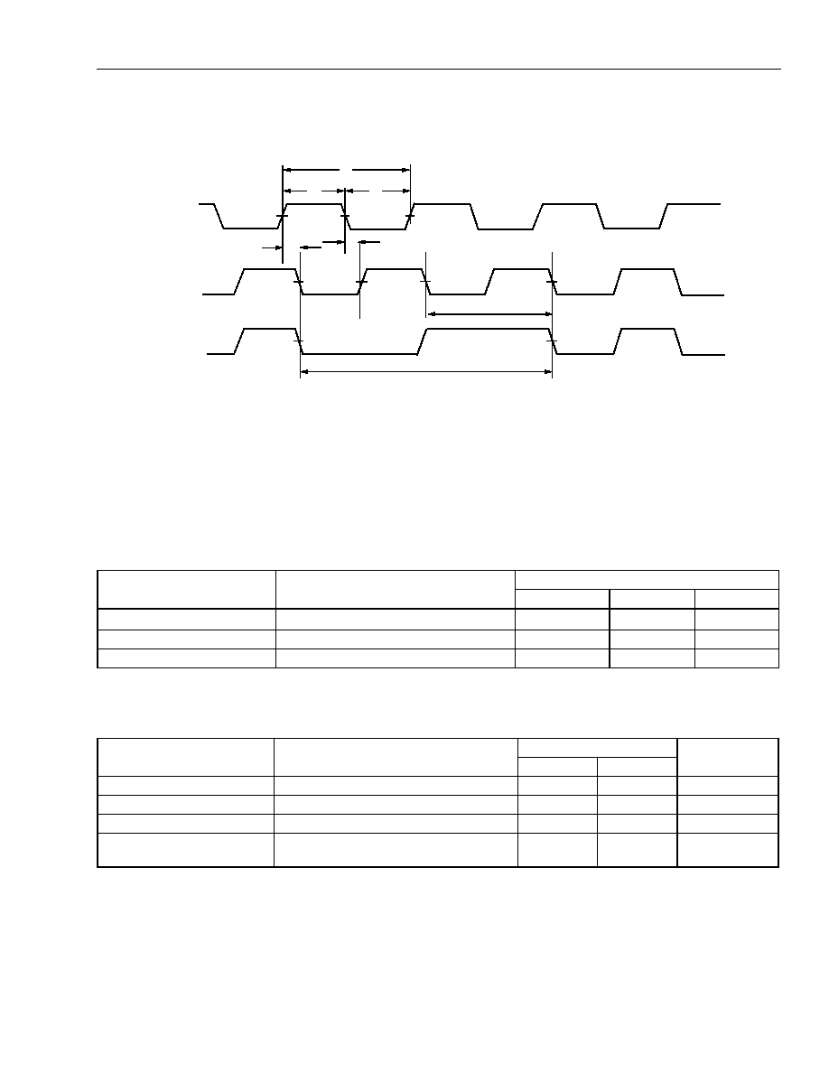
Data Sheet
March 2000
DSP1627 Digital Signal Processor
Lucent Technologies Inc.
99
11 Timing Characteristics for 3.0 V Operation
(continued)
11.1 DSP Clock Generation
* See Table 62 for input clock electrical requirements.
Free-running clock.
Wait-stated clock (see Table 38).
ß W = number of wait-states.
Figure 35. I/O Clock Timing Diagram
*
Device speeds greater than 50 MIPS do not support 1X operation. Use the PLL.
Device is fully static, t1 is tested at 100 ns for 1X input clock option, and memory hold time is tested at 0.1 s.
*
T = internal clock period, set by CKI or by CKI and the PLL parameters.
Table 106. Timing Requirements for Input Clock
Abbreviated Reference
Parameter
10 ns*
Min
Max
Unit
t1
Clock In Period (high to high)
20
--
ns
t2
Clock In Low Time (low to high)
10
--
ns
t3
Clock In High Time (high to low)
10
--
ns
Table 107. Timing Characteristics for Input Clock and Output Clock
Abbreviated Reference
Parameter
10 ns
Unit
Min
Max
t4
Clock Out High Delay
--
10
ns
t5
Clock Out Low Delay (high to low)
--
10
ns
t6
Clock Out Period (low to low)
T*
--
ns
t6a
Clock Out Period with SLOWCKI Bit Set
in powerc Register (low to low)
0.74
3.8
µ
s
5-4009 (F).a
t4
t1
t2
1X CKI*
t5
CKO
t3
t6, t6a
CKO
EXTERNAL MEMORY CYCLE
W = 1
ß
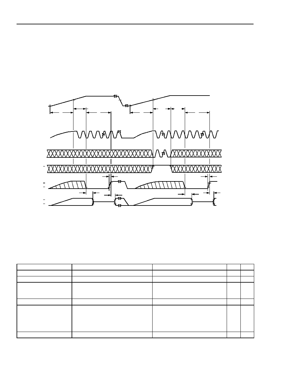
Data Sheet
DSP1627 Digital Signal Processor
March 2000
100
Lucent Technologies Inc.
11 Timing Characteristics for 3.0 V Operation
(continued)
11.2 Reset Circuit
The DSP1627 has a powerup reset circuit that automatically clears the JTAG controller upon powerup. If the supply
voltage falls below V
DD
MIN* and a reset is required, the JTAG controller must be reset--even if the JTAG port isn't
being used--by applying six low-to-high clock edges on TCK with TMS held high, followed by the usual RSTB and
CKI reset sequence. Figure 60 shows two separate events: an initial powerup and a powerup following a drop in the
power supply voltage.
*
See Table 60, Recommended Operating Condiitons.
Notes:
See Table 62 for CKI electrical requirements and Table 151 for TCK timing requirements.
When both INT0 and RSTB are asserted, all output and bidirectional pins (except TDO, which 3-states by JTAG control) are put in a 3-state
condition. With RSTB asserted and INT0 not asserted, EROM, ERAMHI, ERAMLO, IO, DSEL, and RWN outputs remain high, and CKO remains
a free-running clock.
TMS and TDI signals have internal pull-up devices.
Figure 36. Powerup Reset and Chip Reset Timing Diagram
* With external components as specified in Table 62.
T
TCK
= t12 = TCK period. See Table 151 for TCK timing requirements.
Table 108. Timing Requirements for Powerup Reset and Chip Reset
Abbreviated Reference
Parameter
Min
Max
Unit
t8
Reset Pulse (low to high)
6T
--
ns
t9
V
DD
Ramp
--
10
ms
t146
V
DD
MIN to RSTB Low CMOS
Crystal*
Small-Signal
2T
20
20
--
--
--
ns
ms
µ
s
t151
TMS High
6 * T
TCK
--
ns
t152
JTAG Reset to
CMOS
RSTB Low
Crystal*
Small-Signal
2T
20 ms ≠ 6 * T
TCK
if 6 * T
TCK
< 20 ms
0 if 6 * T
TCK
20 ms
20 µs ≠ 6 * T
TCK
if 6 * T
TCK
< 20 µs
0 if 6 * T
TCK
20 µs
--
--
--
--
--
ns
t153
RSTB (low to high)
--
54
ns
5-2253 (F).a
t10
t11
t10
t11
t9
t146
t8
t9
t151
t152
t8
V
DD
RAMP
CKI
TCK
TMS
RSTB
PINS V
OH
V
OL
V
IH
V
IL
V
IH
0.4 V
V
DD
MIN
V
DD
MIN
0.4 V
t153
t153

Data Sheet
March 2000
DSP1627 Digital Signal Processor
Lucent Technologies Inc.
101
11 Timing Characteristics for 3.0 V Operation
(continued)
Note: The device needs to be clocked for at least six CKI cycles during reset after powerup. Otherwise, high cur-
rents may flow.
11.3 Reset Synchronization
*
See Table 62 for input clock electrical requirements.
Note: CKO
1
and CKO
2
are two possible CKO states before reset. CKO is free-running.
Figure 37. Reset Synchronization Timing
Table 109. Timing Characteristics for Powerup Reset and Chip Reset
Abbreviated Reference
Parameter
Min
Max
Unit
t10
RSTB Disable Time (low to 3-state)
--
100
ns
t11
RSTB Enable Time (high to valid)
--
100
ns
Table 110. Timing Requirements for Reset Synchronization Timing
Abbreviated Reference
Parameter
Min
Max
Unit
t126
Reset Setup (high to high)
3
T/2 ≠ 5
ns
5-4011 (F).a
CKI
*
V
IH
V
IL
t126
t5 + 2 x t6
RSTB
V
IH
V
IL
V
IH
V
IL
CKO
V
IH
V
IL
CKO
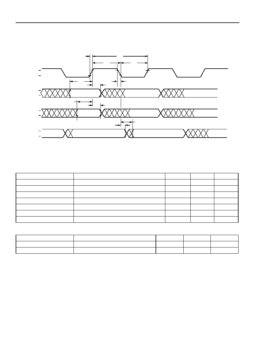
Data Sheet
DSP1627 Digital Signal Processor
March 2000
102
Lucent Technologies Inc.
11 Timing Characteristics for 3.0 V Operation
(continued)
11.4 JTAG I/O Specifications
Figure 38. JTAG Timing Diagram
Table 111. Timing Requirements for JTAG Input/Output
Abbreviated Reference
Parameter
Min
Max
Unit
t12
TCK Period (high to high)
50
--
ns
t13
TCK High Time (high to low)
22.5
--
ns
t14
TCK Low Time (low to high)
22.5
--
ns
t15
TMS Setup Time (valid to high)
7.5
--
ns
t16
TMS Hold Time (high to invalid)
2
--
ns
t17
TDI Setup Time (valid to high)
7.5
--
ns
t18
TDI Hold Time (high to invalid)
2
--
ns
Table 112. Timing Characteristics for JTAG Input/Output
Abbreviated Reference
Parameter
Min
Max
Unit
t19
TDO Delay (low to valid)
--
19
ns
t20
TDO Hold (low to invalid)
0
--
ns
t12
t14
t13
t15
t16
t17
t18
t19
t20
TCK
TMS
TDI
TDO
V
IH
V
IL
V
IH
V
IL
V
IH
V
IL
V
OH
V
OL
t155
5-4017 (F)
t156

Data Sheet
March 2000
DSP1627 Digital Signal Processor
Lucent Technologies Inc.
103
11 Timing Characteristics for 3.0 V Operation
(continued)
11.5 Interrupt
* CKO is free-running.
IACK assertion is guaranteed to be enclosed by VEC[3:0] assertion.
Figure 39. Interrupt Timing Diagram
Note: Interrupt is asserted during an interruptible instruction and no other pending interrupts.
Note: Interrupt is asserted during an interruptible instruction and no other pending interrupts.
Table 113. Timing Requirements for Interrupt
Abbreviated Reference
Parameter
Min
Max
Unit
t21
Interrupt Setup (high to low)
19
--
ns
t22
INT Assertion Time (high to low)
2T
--
ns
Table 114. Timing Characteristics for Interrupt
Abbreviated Reference
Parameter
Min
Max
Unit
t23
IACK Assertion Time (low to high)
--
T/2 + 10
ns
t24
VEC Assertion Time (low to high)
--
12.5
ns
t25
IACK Invalid Time (low to low)
--
10
ns
t26
VEC Invalid Time (low to low)
--
12.5
ns
5-4018 (F)
CKO
*
INT[1:0]
t21
V
OH
V
OL
V
IH
V
IL
t22
IACK
V
OH
V
OL
VEC[3:0]
V
OH
V
OL
t23
t24
t25
t26

Data Sheet
DSP1627 Digital Signal Processor
March 2000
104
Lucent Technologies Inc.
11 Timing Characteristics for 3.0 V Operation
(continued)
11.6 Bit Input/Output (BIO)
Figure 40. Write Outputs Followed by Read Inputs (cbit = Immediate; a1 = sbit)
Figure 41. Write Outputs and Test Inputs (cbit = Immediate)
Table 115. Timing Requirements for BIO Input Read
Abbreviated Reference
Parameter
Min
Max
Unit
t27
IOBIT Input Setup Time (valid to high)
15
--
ns
t28
IOBIT Input Hold Time (high to invalid)
0
--
ns
Table 116. Timing Characteristics for BIO Output
Abbreviated Reference
Parameter
Min
Max
Unit
t29
IOBIT Output Valid Time (low to valid)
--
9
ns
t144
IOBIT Output Hold Time (low to invalid)
1
--
ns
Table 117. Timing Requirements for BIO Input Test
Abbreviated Reference
Parameter
Min
Max
Unit
t141
IOBIT Input Setup Time (valid to low)
15
--
ns
t142
IOBIT Input Hold Time (low to invalid)
0
--
ns
5-4019 (F).a
CKO
IOBIT
(INPUT)
t28
t27
VALID OUTPUT
V
I
H
V
I
L
V
O
H
V
O
L
V
O
H
V
O
L
DATA INPUT
t29
t144
IOBIT
(OUTPUT)
5-4019 (F).b
CKO
IOBIT
(INPUT)
t142
t141
VALID OUTPUT
V
OH
≠
V
O
L≠
TEST INPUT
t29
t144
IOBIT
(OUTPUT)
V
OH
≠
V
O
L≠
V
IH
≠
V
I
L≠

Data Sheet
March 2000
DSP1627 Digital Signal Processor
Lucent Technologies Inc.
105
11 Timing Characteristics for 3.0 V Operation
(continued)
11.7 External Memory Interface
The following timing diagrams, characteristics, and requirements do not apply to interactions with delayed external
memory enables unless so stated. See the
DSP1611/17/18/27 Digital Signal Processor Information Manual
for a
detailed description of the external memory interface including other functional diagrams.
*
W = number of wait-states.
Figure 42. Enable Transition Timing
Table 118. Timing Characteristics for External Memory Enables (EROM, ERAMHI, IO, ERAMLO)
Abbreviated Reference
Parameter
Min
Max
Unit
t33
CKO to ENABLE Active (low to low)
0
5
ns
t34
CKO to ENABLE Inactive (low to high)
≠1
4.5
ns
Table 119. Timing Characteristics for Delayed External Memory Enables (ioc = 0x000F)
Abbreviated Reference
Parameter
Min
Max
Unit
t33
CKO to Delayed ENABLE Active (low to low)
T/2 ≠ 2
T/2 + 7
ns
CKO
ENABLE
t34
t33
W
*
= 0
V
OH
V
OL
V
OH
V
OL
5-4020 (F).b
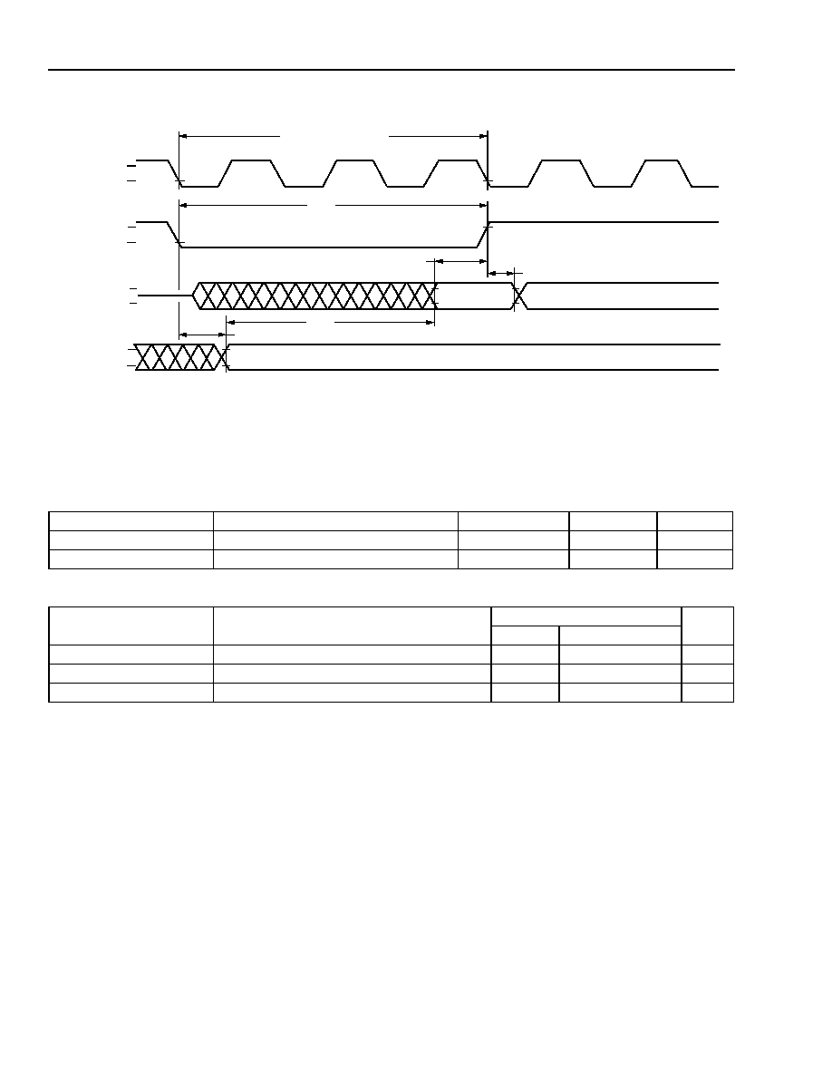
Data Sheet
DSP1627 Digital Signal Processor
March 2000
106
Lucent Technologies Inc.
11 Timing Characteristics for 3.0 V Operation
(continued)
*
W = number of wait-states.
Figure 43. External Memory Data Read Timing Diagram
Table 120. Timing Characteristics for External Memory Access
Abbreviated Reference
Parameter
Min
Max
Unit
t127
Enable Width (low to high)
T(1 + W) ≠ 1.5
--
ns
t128
Address Valid (enable low to valid)
--
2
ns
Table 121. Timing Requirements for External Memory Read (EROM, ERAMHI, IO, ERAMLO)
Abbreviated Reference
Parameter
10 ns
Unit
Min
Max
t129
Read Data Setup (valid to enable high)
13
--
ns
t130
Read Data Hold (enable high to hold)
0
--
ns
t150
External Memory Access Time (valid to valid)
--
T(1 + W) ≠ 13
ns
V
IH
V
IL
DB
CKO
AB
V
OH
V
OL
t128
READ ADDRESS
ENABLE
V
OH
V
OL
V
OH
V
OL
(MWAIT = 0 x 2222)
W* = 2
t127
t129
t130
READ DATA
t150
5-4021 (F).a
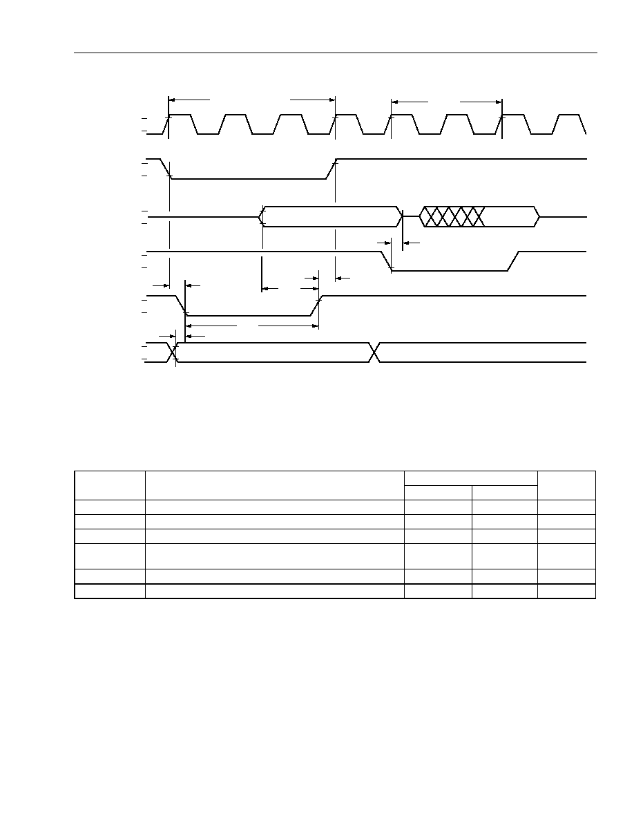
Data Sheet
March 2000
DSP1627 Digital Signal Processor
Lucent Technologies Inc.
107
11 Timing Characteristics for 3.0 V Operation
(continued)
* W = number of wait-states.
Figure 44. External Memory Data Write Timing Diagram
Table 122. Timing Characteristics for External Memory Data Write (All Enables)
Abbreviated
Reference
Parameter
10 ns
Unit
Min
Max
t131
Write Overlap (enable low to 3-state)
--
0
ns
t132
RWN Advance (RWN high to enable high)
0
--
ns
t133
RWN Delay (enable low to RWN low)
0
--
ns
t134
Write Data Setup (data valid to RWN high)
T(1 + W)/2 ≠
3
--
ns
t135
RWN Width (low to high)
T(1 + W) ≠ 4
--
ns
t136
Write Address Setup (address valid to RWN low)
0
--
ns
ERAMLO
EROM
CKO
AB
RWN
DB
WRITE ADDRESS
READ ADDRESS
V
OH
V
OL
V
OH
V
OL
V
OH
V
OL
V
OH
V
OL
V
OH
V
OL
WRITE DATA
READ
W* = 1
t131
t132
t134
t133
t135
t136
(MWAIT = 0x1002)
W* = 2
V
OH
V
OL
5-4022 (F).a
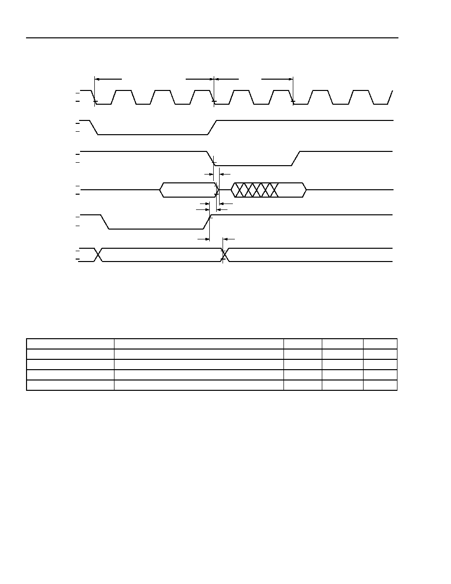
Data Sheet
DSP1627 Digital Signal Processor
March 2000
108
Lucent Technologies Inc.
11 Timing Characteristics for 3.0 V Operation
(continued)
*
W = number of wait-states.
Figure 45. Write Cycle Followed by Read Cycle
Table 123. Timing Characteristics for Write Cycle Followed by Read Cycle
Abbreviated Reference
Parameter
Min
Max
Unit
t131
Write Overlap (enable low to 3-state)
--
0
ns
t137
Write Data 3-state (RWN high to 3-state)
--
2
ns
t138
Write Data Hold (RWN high to data hold)
0
--
ns
t139
Write Address Hold (RWN high to address hold)
0
--
ns
ERAMLO
CKO
AB
RWN
WRITE ADDRESS
READ ADDRESS
V
OH
V
OL
V
OH
V
OL
V
OH
V
OL
V
OH
V
OL
W* = 1
t137
(MWAIT = 0x1002)
W* = 2
EROM
V
OH
V
OL
DB
WRITE
READ
V
OH
V
OL
t138
t139
t131
5-4023 (F).a

Data Sheet
March 2000
DSP1627 Digital Signal Processor
Lucent Technologies Inc.
109
11 Timing Characteristics for 3.0 V Operation
(continued)
11.8 PHIF Specifications
For the PHIF, "READ" means read by the external user (output by the DSP); "WRITE" is similarly defined. The 8-bit reads/
writes are identical to one-half of a 16-bit access.
Figure 46. PHIF
Intel
Mode Signaling (Read and Write) Timing Diagram
*
This timing diagram for the PHIF port shows accesses using the PCSN signal to initiate and complete a transaction. The transactions can also be
initiated and completed with the PIDS and PODS signals. An output transaction (read) is initiated by PCSN or PODS going low, whichever comes
last. For example, the timing requirements referenced to PCSN going low, t45 and t49, should be referenced to PODS going low, if PODS goes
low after PCSN. An output transaction is completed by PCSN or PODS going high, whichever comes first. An input transaction is initiated by PCSN
or PIDS going low, whichever comes last. An input transaction is completed by PCSN or PIDS going high, whichever comes first. All requirements
referenced to PCSN apply to PIDS or PODS, if PIDS or PODS is the controlling signal.
Table 124. Timing Requirements for PHIF
Intel Mode Signaling
Abbreviated Reference
Parameter
Min
Max
Unit
t41
PODS to PCSN Setup (low to low)
0
--
ns
t42
PCSN to PODS Hold (high to high)
0
--
ns
t43
PIDS to PCSN Setup (low to low)
0
--
ns
t44
PCSN to PIDS Hold (high to high)
0
--
ns
t45*
PSTAT to PCSN Setup (valid to low)
6
--
ns
t46*
PCSN to PSTAT Hold (high to invalid)
0
--
ns
t47*
PBSEL to PCSN Setup (valid to low)
6
--
ns
t48*
PCSN to PBSEL Hold (high to invalid)
0
--
ns
t51*
PB Write to PCSN Setup (valid to high)
10
--
ns
t52*
PCSN to PB Write Hold (high to invalid)
5
--
ns
Table 125. Timing Characteristics for PHIF
Intel Mode Signaling
Abbreviated Reference
Parameter
Min
Max
Unit
t49*
PCSN to PB Read (low to valid)
--
17
ns
t50*
PCSN to PB Read Hold (high to invalid)
3
--
ns
5-4036 (F)
PCSN
t41
t42
t43
t45
t46
t49
t50
16-bit READ
16-bit WRITE
PODS
PIDS
PBSEL
PSTAT
PB[7:0]
t47
t51
t52
t48
t44
t154
V
IH≠
V
IL≠
V
IH≠
V
IL≠
V
IH≠
V
IL≠
V
IH≠
V
IL≠
V
IH≠
V
IL≠
V
IH≠
V
IL≠

Data Sheet
DSP1627 Digital Signal Processor
March 2000
110
Lucent Technologies Inc.
11 Timing Characteristics for 3.0 V Operation
(continued)
Figure 47. PHIF
Intel
Mode Signaling (Pulse Period and Flags) Timing Diagram
*
t53 should be referenced to the rising edge of PCSN or PODS, whichever comes first.
t54 should be referenced to the rising edge of PCSN
or PIDS, whichever comes first.
POBE and PIBF may be programmed to be the opposite logic levels shown in the diagram (positive assertion levels shown). t53 and t54 apply
to the inverted levels as well as those shown.
Table 126. Timing Requirements for PHIF
Intel
Mode Signaling
Abbreviated Reference
Parameter
Min
Max
Unit
t55
PCSN/PODS/PIDS Pulse Width (high to low)
20.5
--
ns
t56
PCSN/PODS/PIDS Pulse Width (low to high)
20.5
--
ns
Table 127. Timing Characteristics for PHIF
Intel
Mode Signaling
Abbreviated Reference
Parameter
Min
Max
Unit
t53*
PCSN/PODS to POBE
(high to high)
--
20
ns
t54*
PCSN/PIDS to PIBF
(high to high)
--
20
ns
PODS
PIDS
V
IH
V
IL
V
IH
V
IL
V
IH
V
IL
t55
t56
t55
t56
t55
t56
PCSN
t53
t54
16-bit READ
8-bit WRITE
PBSEL
POBE
PIBF
t54
V
OH
V
OL
V
OH
V
OL
V
OH
V
OL
t56
t56
t55
t53
8-bit READ
16-bit WRITE
5-4037 (F).a
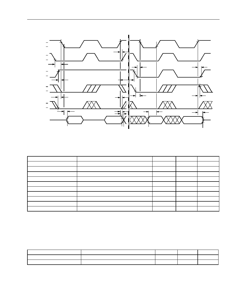
Data Sheet
March 2000
DSP1627 Digital Signal Processor
Lucent Technologies Inc.
111
11 Timing Characteristics for 3.0 V Operation
(continued)
Figure 48. PHIF
Motorola
Mode Signaling (Read and Write) Timing Diagram
*
This timing diagram for the PHIF port shows accesses using the PCSN signal to initiate and complete a transaction. The transactions can
also be initiated and completed with the PDS signal. An input/output transaction is initiated by PCSN or PDS going low, whichever comes last.
For example, the timing requirements referenced to PCSN going low, t45 and t49, should be referenced to PDS going low, if PDS goes low
after PCSN. An input/output transaction is completed by PCSN or PDS going high, whichever comes first. All requirements referenced to
PCSN should be referenced to PDS, if PDS is the controlling signal. PRWN should never be used to initiate or complete a transaction.
PDS is programmable to be active-high or active-low. It is shown active-low in Figures 72 and 73. POBE and PIBF may be programmed to
be the opposite logic levels shown in the diagram. t53 and t54 apply to the inverted levels as well as those shown.
*
This timing diagram for the PHIF port shows accesses using the PCSN signal to initiate and complete a transaction. The transactions can
also be initiated and completed with the PDS signal. An input/output transaction is initiated by PCSN or PDS going low, whichever comes last.
For example, the timing requirements referenced to PCSN going low, t45 and t49, should be referenced to PDS going low, if PDS goes low
after PCSN. An input/output transaction is completed by PCSN or PDS going high, whichever comes first. All requirements referenced to
PCSN should be referenced to PDS, if PDS is the controlling signal. PRWN should never be used to initiate or complete a transaction.
Table 128. Timing Requirements for PHIF
Motorola Mode Signaling
Abbreviated Reference
Parameter
Min
Max
Unit
t41
PDS
to PCSN Setup (valid to low)
0
--
ns
t42
PCSN to PDS
Hold (high to invalid)
0
--
ns
t43
PRWN to PCSN Setup (valid to low)
6
--
ns
t44
PCSN to PRWN Hold (high to invalid)
0
--
ns
t45*
PSTAT to PCSN Setup (valid to low)
6
--
ns
t46*
PCSN to PSTAT Hold (high to invalid)
0
--
ns
t47*
PBSEL to PCSN Setup (valid to low)
6
--
ns
t48*
PCSN to PBSEL Hold (high to invalid)
0
--
ns
t51*
PB Write to PCSN Setup (valid to high)
10
--
ns
t52*
PCSN to PB Write Hold (high to invalid)
5
--
ns
Table 129. Timing Characteristics for PHIF
Motorola Mode Signaling
Abbreviated Reference
Parameter
Min
Max
Unit
t49*
PCSN to PB Read (low to valid)
--
17
ns
t50*
PCSN to PB Read (high to invalid)
3
--
ns
PCSN
PDS
PRWN
PBSEL
PSTAT
PB[7:0]
t41
t42
t43
t44
t45
t46
t47
t48
t52
t51
t50
t49
16-bit READ
16-bit WRITE
t43
t44
V
I H
V
IL
V
I H
V
IL
V
I H
V
IL
V
I H
V
IL
V
I H
V
IL
5-4038 (F).a
t154
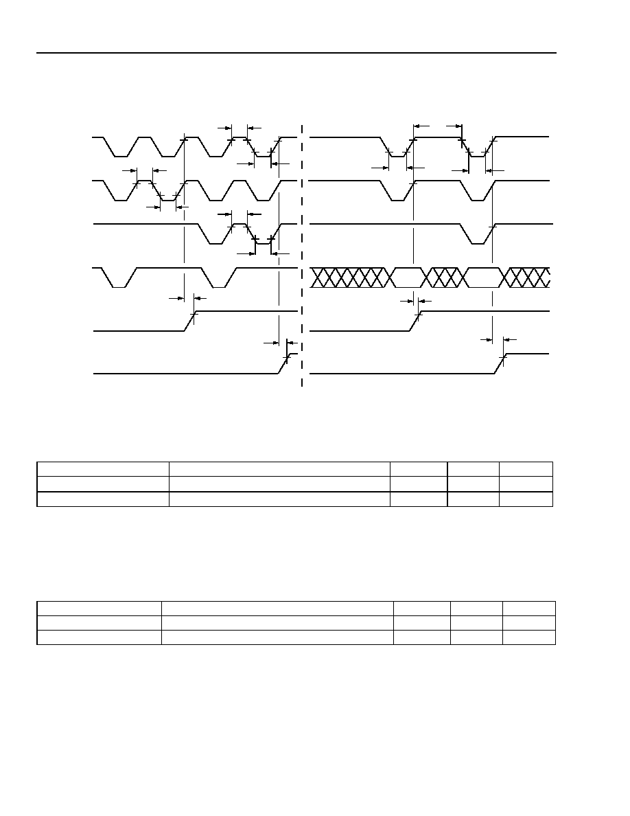
Data Sheet
DSP1627 Digital Signal Processor
March 2000
112
Lucent Technologies Inc.
11 Timing Characteristics for 3.0 V Operation
(continued)
Figure 49. PHIF
Motorola
Mode Signaling (Pulse Period and Flags) Timing Diagram
* An input/output transaction is initiated by PCSN or PDS going low, whichever comes last. For example, t53 and t54 should be referenced to
PDS going low, if PDS goes low after PCSN. An input/output transaction is completed by PCSN or PDS going high, whichever comes first.
All requirements referenced to PCSN should be referenced to PDS, if PDS is the controlling signal. PRWN should never be used to initiate or
complete a transaction.
PDS is programmable to be active-high or active-low. It is shown active-low in Figures 48 and 49. POBE and PIBF may be programmed to
be the opposite logic levels shown in the diagram. t53 and t54 apply to the inverted levels as well as those shown.
Table 130. Timing Characteristics for PHIF
Motorola
Mode Signaling
Abbreviated Reference
Parameter
Min
Max
Unit
t53*
PCSN/PDS
to POBE
(high to high)
--
20
ns
t54*
PCSN/PDS
to PIBF
(high to high)
--
20
ns
Table 131. Timing Requirements for PHIF
Motorola
Mode Signaling
Abbreviated Reference
Parameter
Min
Max
Unit
t55
PCSN/PDS/PRWN Pulse Width (high to low)
20
--
ns
t56
PCSN/PDS/PRWN Pulse Width (low to high)
20
--
ns
PDS
PRWN
V
IH
≠
t55
t56
t55
t56
t55
t56
PCSN
t53
t54
16-bit READ
8-bit WRITE
PBSEL
POBE
PIBF
t54
t56
t56
t55
t53
8-bit READ
16-bit WRITE
V
IL
≠
V
IH
≠
V
IL
≠
V
IH
≠
V
IL
≠
V
OH
≠
V
OL
≠
V
OH
≠
V
OL
≠
V
OH
≠
V
OL
≠
5-4039 (F).a
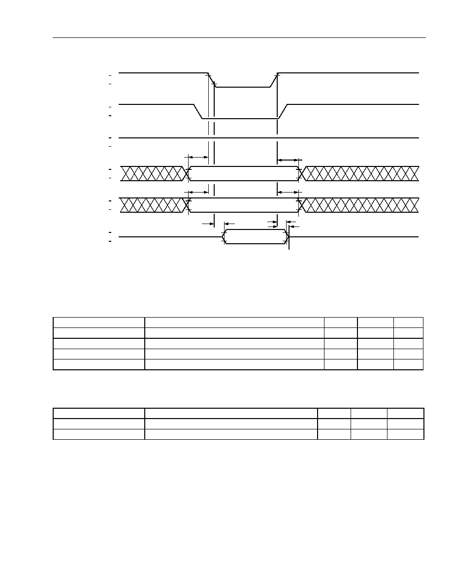
Data Sheet
March 2000
DSP1627 Digital Signal Processor
Lucent Technologies Inc.
113
11 Timing Characteristics for 3.0 V Operation
(continued)
*
Motorola
mode signal name.
Figure 50. PHIF
Intel
or
Motorola
Mode Signaling (Status Register Read) Timing Diagram
t45, t47, and t49 are referenced to the falling edge of PCSN or PODS(PDS), whichever occurs last.
t46, t48, and t50 are referenced to the rising edge of PCSN or PODS(PDS), whichever occurs first.
t45, t47, and t49 are referenced to the falling edge of PCSN or PODS(PDS), whichever occurs last.
t46, t48, and t50 are referenced to the rising edge of PCSN or PODS(PDS), whichever occurs first.
Table 132. Timing Requirements for
Intel
and
Motorola
Mode Signaling (Status Register Read)
Abbreviated Reference
Parameter
Min
Max
Unit
t45
PSTAT to PCSN Setup (valid to low)
6
--
ns
t46
PCSN to PSTAT Hold (high to invalid)
0
--
ns
t47
PBSEL to PCSN Setup (valid to low)
6
--
ns
t48
PCSN to PBSEL Hold (high to invalid)
0
--
ns
Table 133. Timing Characteristics for
Intel
and
Motorola
Mode Signaling (Status Register Read)
Abbreviated Reference
Parameter
Min
Max
Unit
t49
PCSN to PB Read (low to valid)
--
17
ns
t50
PCSN to PB Read Hold (high to invalid)
3
--
ns
PCSN
PODS (PDS*)
PIDS (PRWN*)
PBSEL
PSTAT
PB[7:0]
t47
t48
t45
t46
t49
t50
V
IH
V
IL
V
OH
V
OL
V
IH
V
IL
V
IH
V
IL
V
IH
V
IL
V
IH
V
IL
5-4040 (F).a
t154
Data Sheet
DSP1627 Digital Signal Processor
March 2000
114
Lucent Technologies Inc.
11 Timing Characteristics for 3.0 V Operation
(continued)
Figure 51. PHIF, PIBF, and POBE Reset Timing Diagram
POBE and PIBF can be programed to be active-high or active-low. They are shown active-high. The timing characteristic for active-low is the
same as for active-high.
Figure 52. PHIF, PIBF, and POBE Disable Timing Diagram
Table 134. PHIF Timing Characteristics for PHIF, PIBF, and POBE Reset
Abbreviated Reference
Parameter
Min
Max
Unit
t57
RSTB Disable to POBE/PIBF
*
(high to valid)
*
After reset, POBE and PIBF always go to the levels shown, indicating output buffer empty and input buffer empty. The DSP program, however,
may later invert the definition of the logic levels for POBE and PIBF. t57 and t58 continue to apply.
--
25
ns
t58
RSTB Enable to POBE/PIBF* (low to invalid)
3
25
ns
Table 135. PHIF Timing Characteristics for POBE and PIBF Disable
Abbreviated Reference
Parameter
Min
Max
Unit
t59
CKO to POBE/PIBF
*
Disable (high/low to disable)
*
POBE and PIBF can be programmed to be active-high or active-low. They are shown active-high. The timing characteristic for active-low is
the same as for active-high.
--
20
ns
RSTB
V
IH
≠
t58
t57
V
IL
≠
POBE
V
OH
≠
V
OL
≠
PIBF
V
OH
≠
V
OL
≠
5-4775 (F)
CKO
V
IH
≠
V
IL
≠
t59
t59
POBE
V
OH
≠
V
OL
≠
PIBF
V
OH
≠
V
OL
≠
5-4776 (F)
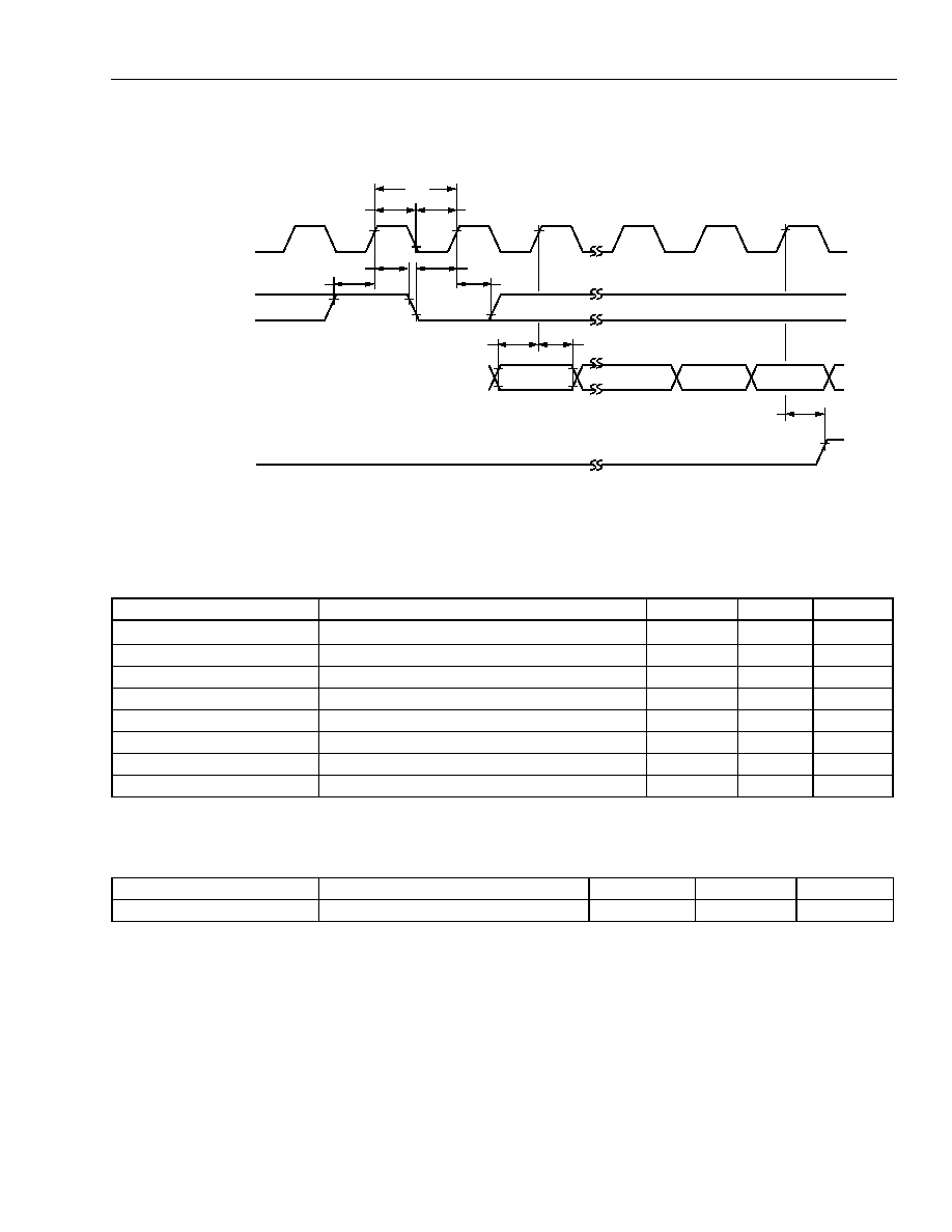
Data Sheet
March 2000
DSP1627 Digital Signal Processor
Lucent Technologies Inc.
115
11 Timing Characteristics for 3.0 V Operation
(continued)
11.9 Serial I/O Specifications
*
N = 16 or 8 bits.
Figure 53. SIO Passive Mode Input Timing Diagram
Device is fully static; t70 is tested at 200 ns.
For multiprocessor mode, see note in Section 12.10.
Table 136. Timing Requirements for Serial Inputs
Abbreviated Reference
Parameter
Min
Max
Unit
t70
Clock Period (high to high)
40
--
ns
t71
Clock Low Time (low to high)
18
--
ns
t72
Clock High Time (high to low)
18
--
ns
t73
Load High Setup (high to high)
8
--
ns
t74
Load Low Setup (low to high)
8
--
ns
t75
Load High Hold (high to invalid)
0
--
ns
t77
Data Setup (valid to high)
7
--
ns
t78
Data Hold (high to invalid)
0
--
ns
Table 137. Timing Characteristics for Serial Outputs
Abbreviated Reference
Parameter
Min
Max
Unit
t79
IBF Delay (high to high)
--
35
ns
IBF
V
OH
≠
V
OL
≠
DI
V
IH
≠
V
IL
≠
ILD
V
IH
≠
V
IL
≠
ICK
V
IH
≠
V
IL
≠
BN ≠ 1*
B0
t77
t78
B0
B1
t79
t72
t71
t70
t75
t74
t75
t73
5-4777 (F)
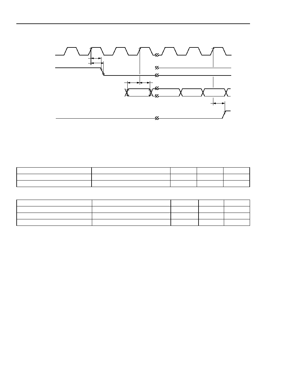
Data Sheet
DSP1627 Digital Signal Processor
March 2000
116
Lucent Technologies Inc.
11 Timing Characteristics for 3.0 V Operation
(continued)
*
ILD goes high during bit 6 (of 0:15), N = 8 or 16.
Figure 54. SIO Active Mode Input Timing Diagram
Table 138. Timing Requirements for Serial Inputs
Abbreviated Reference
Parameter
Min
Max
Unit
t77
Data Setup (valid to high)
7
--
ns
t78
Data Hold (high to invalid)
0
--
ns
Table 139. Timing Characteristics for Serial Outputs
Abbreviated Reference
Parameter
Min
Max
Unit
t76a
ILD Delay (high to low)
--
35
ns
t101
ILD Hold (high to invalid)
5
--
ns
t79
IBF Delay (high to high)
--
35
ns
IBF
V
OH
≠
V
OL
≠
DI
V
IH
≠
V
IL
≠
ILD
V
OH
≠
V
OL
≠
ICK
V
OH
≠
V
OL
≠
BN ≠ 1
B0
t77
t78
B0
B1
t79
t101
t76a
*
5-4778 (F)
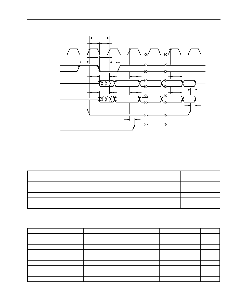
Data Sheet
March 2000
DSP1627 Digital Signal Processor
Lucent Technologies Inc.
117
11 Timing Characteristics for 3.0 V Operation
(continued)
*
See sioc register, MSB field, to determine if B0 is the MSB or LSB. See sioc register, ILEN field, to determine if the DO word length is 8 bits
or 16 bits.
Figure 55. SIO Passive Mode Output Timing Diagram
Device is fully static; t80 is tested at 200 ns.
For multiprocessor mode, see note in Section 12.10.
Table 140. Timing Requirements for Serial Inputs
Abbreviated Reference
Parameter
Min
Max
Unit
t80
Clock Period (high to high)
40
--
ns
t81
Clock Low Time (low to high)
18
--
ns
t82
Clock High Time (high to low)
18
--
ns
t83
Load High Setup (high to high)
8
--
ns
t84
Load Low Setup (low to high)
8
--
ns
t85
Load Hold (high to invalid)
0
--
ns
Table 141. Timing Characteristics for Serial Outputs
Abbreviated Reference
Parameter
Min
Max
Unit
t87
Data Delay (high to valid)
--
35
ns
t88
Enable Data Delay (low to active)
--
35
ns
t89
Disable Data Delay (high to 3-state)
--
35
ns
t90
Data Hold (high to invalid)
5
--
ns
t92
Address Delay (high to valid)
--
35
ns
t93
Address Hold (high to invalid)
5
--
ns
t94
Enable Delay (low to active)
--
35
ns
t95
Disable Delay (high to 3-state)
--
35
ns
t96
OBE Delay (high to high)
--
35
ns
DOEN
V
IH
≠
V
IL
≠
SADD
V
OH
≠
V
OL
≠
OLD
V
IH
≠
V
IL
≠
OCK
V
IH
≠
V
IL
≠
t85
t80
t81
t82
t84
t83
t85
t88
B0
B1
B7
BN ≠ 1
t90
t90
t87
t94
AD0
AD1
AD7
t93
t93
t92
AS7
t89
t95
OBE
V
OH
≠
V
OL
≠
DO*
V
OH
≠
V
OL
≠
t96
5-4796 (F)
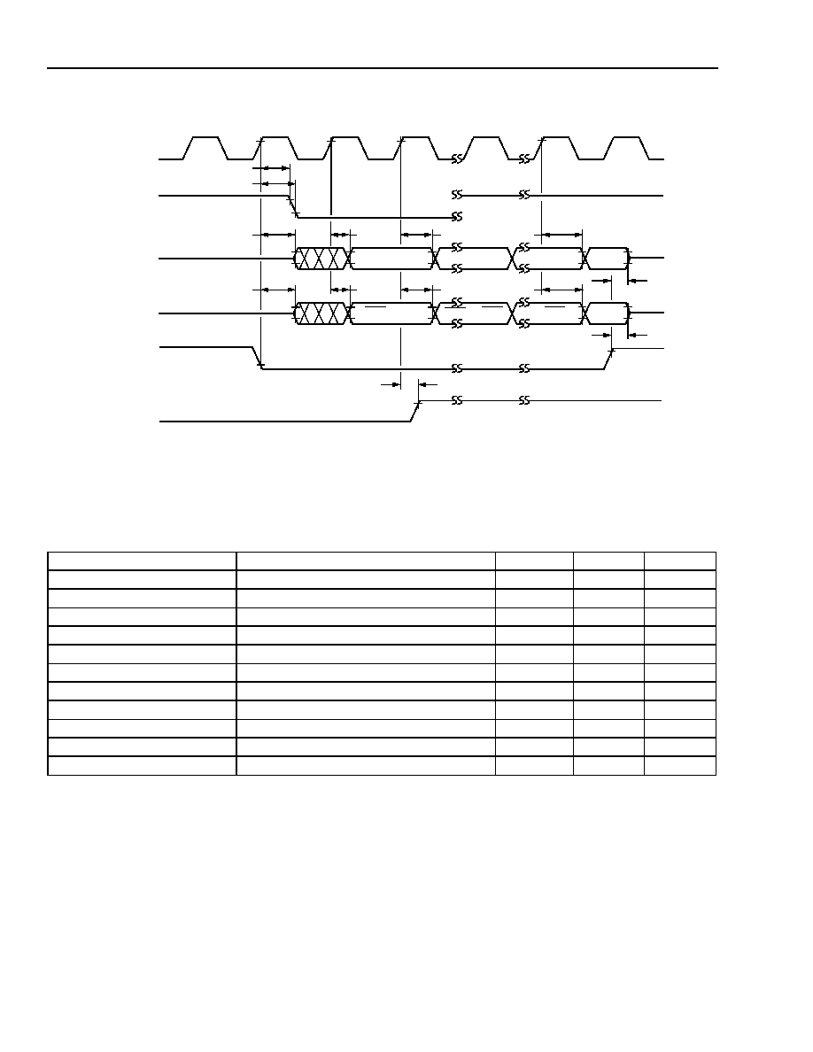
Data Sheet
DSP1627 Digital Signal Processor
March 2000
118
Lucent Technologies Inc.
11 Timing Characteristics for 3.0 V Operation
(continued)
*
OLD goes high at the end of bit 6 of 0:15.
Figure 56. SIO Active Mode Output Timing Diagram
Table 142. Timing Characteristics for Serial Output
Abbreviated Reference
Parameter
Min
Max
Unit
t86a
OLD Delay (high to low)
--
35
ns
t102
OLD Hold (high to invalid)
5
--
ns
t87
Data Delay (high to valid)
--
35
ns
t88
Enable Data Delay (low to active)
--
35
ns
t89
Disable Data Delay (high to 3-state)
--
35
ns
t90
Data Hold (high to invalid)
5
--
ns
t92
Address Delay (high to valid)
--
35
ns
t93
Address Hold (high to invalid)
5
--
ns
t94
Enable Delay (low to active)
--
35
ns
t95
Disable Delay (high to 3-state)
--
35
ns
t96
OBE Delay (high to high)
--
35
ns
DOEN
V
IH
≠
V
IL
≠
SADD
V
OH
≠
V
OL
≠
OLD
V
OH
≠
V
OL
≠
OCK
V
OH
≠
V
OL
≠
t102
t86a
t88
B0
B1
B7
BN ≠ 1
t90
t90
t87
t94
AD0
AD1
AD7
t93
t93
t92
AS7
t89
t95
OBE
V
OH
≠
V
OL
≠
DO
V
OH
≠
V
OL
≠
t96
*
5-4797 (F)
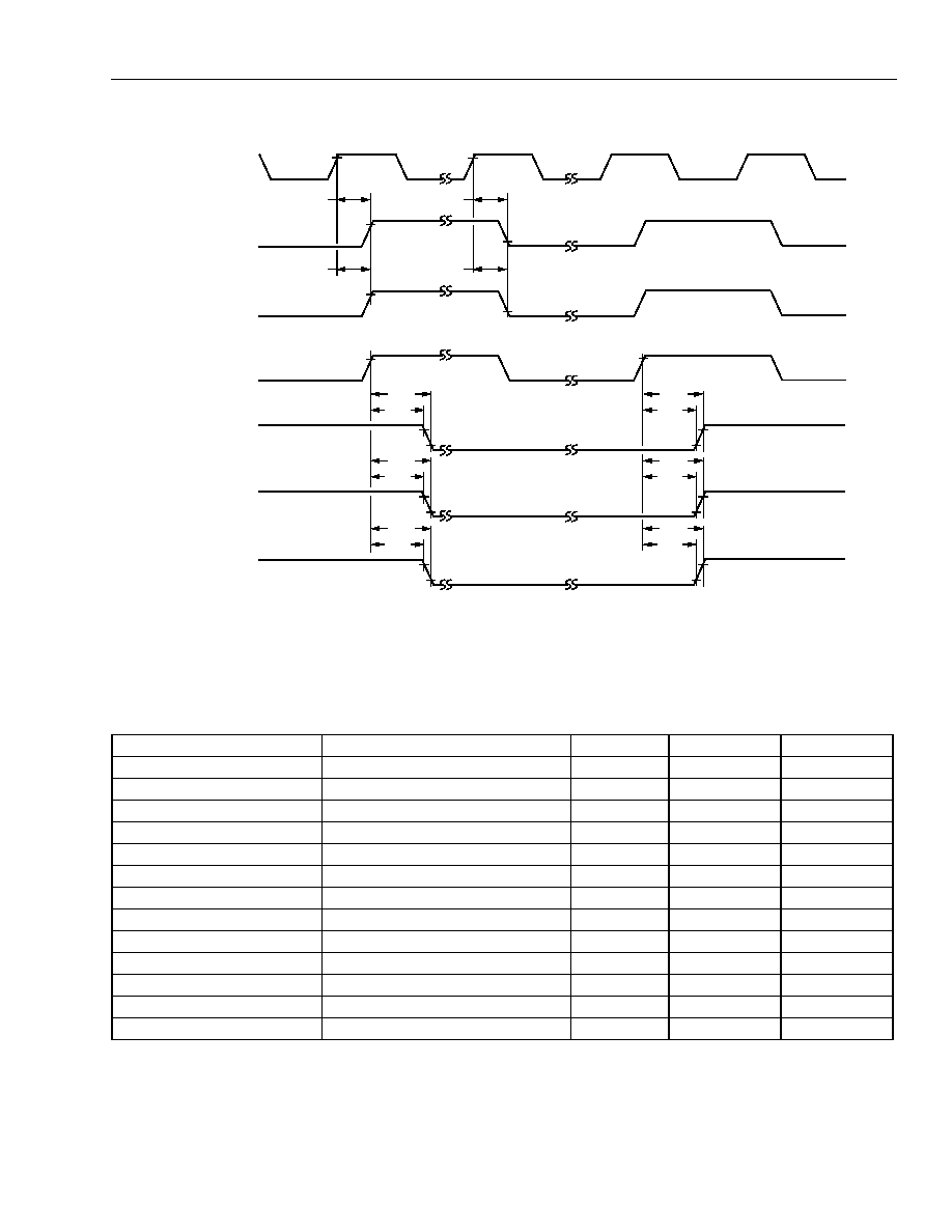
Data Sheet
March 2000
DSP1627 Digital Signal Processor
Lucent Technologies Inc.
119
11 Timing Characteristics for 3.0 V Operation
(continued)
*
See sioc register, LD field.
Figure 57. Serial I/O Active Mode Clock Timing
Table 143. Timing Characteristics for Signal Generation
Abbreviated Reference
Parameter
Min
Max
Unit
t97
ICK Delay (high to high)
--
18
ns
t98
ICK Delay (high to low)
--
18
ns
t99
OCK Delay (high to high)
--
18
ns
t100
OCK Delay (high to low)
--
18
ns
t76a
ILD Delay (high to low)
--
35
ns
t76b
ILD Delay (high to high)
--
35
ns
t101
ILD Hold (high to invalid)
5
--
ns
t86a
OLD Delay (high to low)
--
35
ns
t86b
OLD Delay (high to high)
--
35
ns
t102
OLD Hold (high to invalid)
5
--
ns
t103
SYNC Delay (high to low)
--
35
ns
t104
SYNC Delay (high to high)
--
35
ns
t105
SYNC Hold (high to invalid)
5
--
ns
ICK
V
OH
≠
V
OL
≠
CKO
V
OH
≠
V
OL
≠
t97
OCK
V
OH
≠
V
OL
≠
ICK/OCK*
V
OH
≠
ILD
V
OH
≠
V
OL
≠
OLD
V
OH
≠
V
OL
≠
SYNC
V
OH
≠
V
OL
≠
t99
t98
t100
t101
t76a
t101
t76b
t102
t86a
t102
t86b
t105
t103
t105
t104
5-4798 (F)
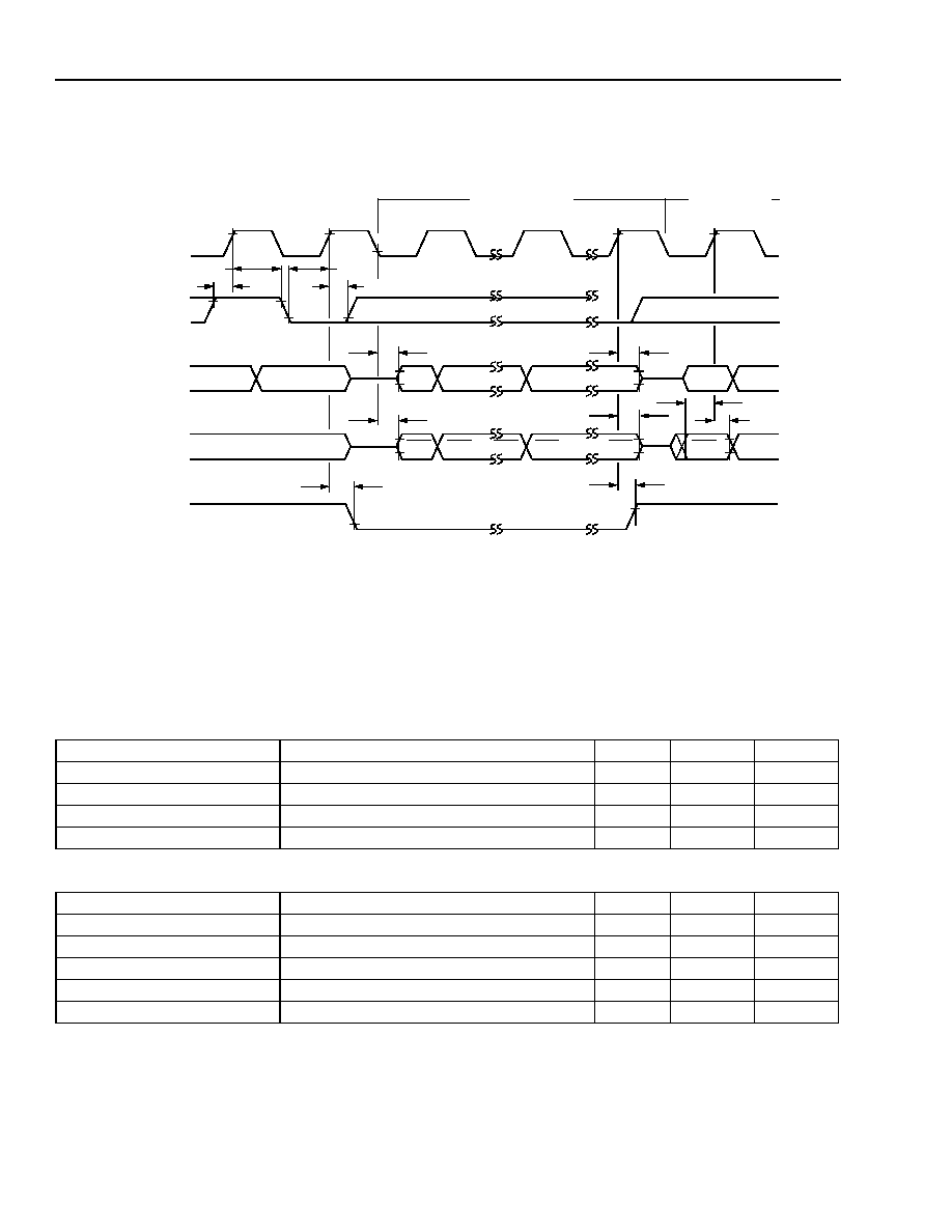
Data Sheet
DSP1627 Digital Signal Processor
March 2000
120
Lucent Technologies Inc.
11 Timing Characteristics for 3.0 V Operation
(continued)
11.10 Multiprocessor Communication
*
Negative edge initiates time slot 0.
Figure 58. SIO Multiprocessor Timing Diagram
Note: All serial I/O timing requirements and characteristics still apply, but the minimum clock period in passive
multiprocessor mode, assuming 50% duty cycle, is calculated as (t77 + t116) x 2.
* With capacitance load on ICK, OCK, DO, SYNC, and SADD = 100 pF, add 4 ns to t116--t122.
Table 144. Timing Requirements for SIO Multiprocessor Communication
Abbreviated Reference
Parameter
Min
Max
Unit
t112
Sync Setup (high/low to high)
35
--
ns
t113
Sync Hold (high to high/low)
0
--
ns
t114
Address Setup (valid to high)
12
--
ns
t115
Address Hold (high to invalid)
0
--
ns
Table 145. Timing Characteristics for SIO Multiprocessor Communication
Abbreviated Reference*
Parameter
Min
Max
Unit
t116
Data Delay (bit 0 only) (low to valid)
--
35
ns
t117
Data Disable Delay (high to 3-state)
--
30
ns
t120
DOEN Valid Delay (high to valid)
--
25
ns
t121
Address Delay (bit 0 only) (low to valid)
--
35
ns
t122
Address Disable Delay (high to 3-state)
--
30
ns
OCK/ICK
B0
B15
B8
B7
B1
B0
B15
SYNC
V
IH
≠
V
IL
≠
DO/D1
V
OH
≠
V
OL
≠
DOEN
V
OH
≠
V
OL
≠
t112
t113
t112
t113
TIME SLOT 1
TIME SLOT 2
t117
t116
AD0
AS7
AS0
AD7
AD1
AD0
SADD
t122
t121
t114
t115
t120
t120
*
5-4799 (F)

Data Sheet
March 2000
DSP1627 Digital Signal Processor
Lucent Technologies Inc.
121
12 Timing Characteristics for 2.7 V Operation
The following timing characteristics and requirements are preliminary information and are subject to change. Timing
characteristics refer to the behavior of the device under specified conditions. Timing requirements refer to conditions
imposed on the user for proper operation of the device. All timing data is valid for the following conditions:
T
A
= ≠40
∞
C to +85
∞
C (See Section 8.3.)
V
DD
= 3 V
±
10%, V
SS
= 0 V (See Section 8.3.)
Capacitance load on outputs (C
L
) = 50 pF, except for CKO, where C
L
= 20 pF.
Output characteristics can be derated as a function of load capacitance (C
L
).
All outputs: 0.03 ns/pF
dt/dC
L
0.07 ns/pF for 10
C
L
100 pF at V
IH
for rising edge and at V
IL
for falling edge.
For example, if the actual load capacitance is 30 pF instead of 50 pF, the derating for a rising edge is (30 ≠ 50) pF
x 0.06 ns/pF = 1.2 ns less than the specified rise time or delay that includes a rise time.
Test conditions for inputs:
s
Rise and fall times of 4 ns or less
s
Timing reference levels for delays = V
IH
, V
IL
Test conditions for outputs (unless noted otherwise):
s
C
LOAD
= 50 pF; except for CKO, where C
LOAD
= 20 pF
s
Timing reference levels for delays = V
IH
, V
IL
s
3-state delays measured to the high-impedance state of the output driver
For the timing diagrams, see Table 62 for input clock requirements.
Unless otherwise noted, CKO in the timing diagrams is the free-running CKO.

Data Sheet
DSP1627 Digital Signal Processor
March 2000
122
Lucent Technologies Inc.
12 Timing Characteristics for 2.7 V Operation
(continued)
12.1 DSP Clock Generation
*
See Table 62 for input clock electrical requirements.
Free-running clock.
Wait-stated clock (see Table 38).
ß W = number of wait-states.
Figure 59. I/O Clock Timing Diagram
* Device speeds greater than 50 MIPS do not support 1 X operation. Use the PLL.
Device is fully static, t1 is tested at 100 ns for 1X input clock option, and memory hold time is tested at 0.1 s.
*
T = internal clock period, set by CKI or by CKI and the PLL parameters.
Table 146. Timing Requirements for Input Clock
Abbreviated Reference
Parameter
20 ns and 12.5 ns
*
Min
Max
Unit
t1
Clock In Period (high to high)
20
--
ns
t2
Clock In Low Time (low to high)
10
--
ns
t3
Clock In High Time (high to low)
10
--
ns
Table 147. Timing Characteristics for Input Clock and Output Clock
Abbreviated Reference
Parameter
20 ns
12.5 ns
Unit
Min
Max
Min
Max
t4
Clock Out High Delay
--
14
--
10
ns
t5
Clock Out Low Delay (high to low)
--
14
--
10
ns
t6
Clock Out Period (low to low)
T*
--
T*
--
ns
t6a
Clock Out Period with SLOWCKI Bit Set in
powerc Register (low to low)
0.74
3.8
0.74
3.8
µ
s
5-4009 (F).a
t4
t1
t2
1X CKI*
t5
CKO
t3
t6, t6a
CKO
EXTERNAL MEMORY CYCLE
W = 1
ß
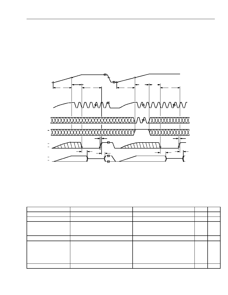
Data Sheet
March 2000
DSP1627 Digital Signal Processor
Lucent Technologies Inc.
123
12 Timing Characteristics for 2.7 V Operation
(continued)
12.2 Reset Circuit
The DSP1627 has a powerup reset circuit that automatically clears the JTAG controller upon powerup. If the supply
voltage falls below V
DD
MIN* and a reset is required, the JTAG controller must be reset--even if the JTAG port isn't
being used--by applying six low-to-high clock edges on TCK with TMS held high, followed by the usual RSTB and
CKI reset sequence. Figure 60 shows two separate events: an initial powerup and a powerup following a drop in the
power supply voltage.
*
See Table 60, Recommended Operating Condiitons.
Notes:
See Table 62 for CKI electrical requirements and Table 151 for TCK timing requirements.
When both INT0 and RSTB are asserted, all output and bidirectional pins (except TDO, which 3-states by JTAG control) are put in a 3-state
condition. With RSTB asserted and INT0 not asserted, EROM, ERAMHI, ERAMLO, IO, DSEL, and RWN outputs remain high, and CKO remains
a free-running clock.
TMS and TDI signals have internal pull-up devices.
Figure 60. Powerup Reset and Chip Reset Timing Diagram
* With external components as specified in Table 62.
T
TCK
= t12 = TCK period. See Table 151 for TCK timing requirements.
Table 148. Timing Requirements for Powerup Reset and Chip Reset
Abbreviated Reference
Parameter
Min
Max
Unit
t8
Reset Pulse (low to high)
6T
--
ns
t9
V
DD
Ramp
--
10
ms
t146
V
DD
MIN to RSTB Low CMOS
Crystal*
Small-signal
2T
20
20
--
--
--
ns
ms
µ
s
t151
TMS High
6 * T
TCK
--
ns
t152
JTAG Reset to
CMOS
RSTB Low
Crystal*
Small-Signal
2T
20 ms ≠ 6 * T
TCK
if 6 * T
TCK
< 20 ms
0 if 6 * T
TCK
20 ms
20 µs ≠ 6 * T
TCK
if 6 * T
TCK
< 20 µs
0 if 6 * T
TCK
20 µs
--
--
--
--
--
ns
t153
RSTB (low to high)
--
54
ns
5-2253 (F).a
t10
t11
t10
t11
t9
t146
t8
t9
t151
t152
t8
V
DD
RAMP
CKI
TCK
TMS
RSTB
PINS V
OH
V
OL
V
IH
V
IL
V
IH
0.4 V
V
DD
MIN
V
DD
MIN
0.4 V
t153
t153
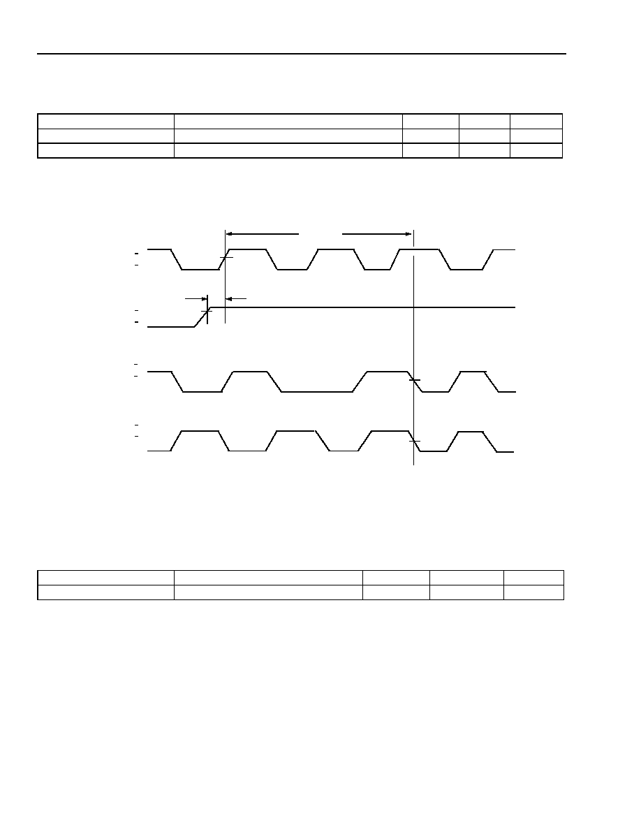
Data Sheet
DSP1627 Digital Signal Processor
March 2000
124
Lucent Technologies Inc.
12 Timing Characteristics for 2.7 V Operation
(continued)
Note: The device needs to be clocked for at least six CKI cycles during reset after powerup. Otherwise, high cur-
rents may flow.
12.3 Reset Synchronization
*
See Table 62 for input clock electrical requirements.
Note: CKO
1
and CKO
2
are two possible CKO states before reset. CKO is free-running.
Figure 61. Reset Synchronization Timing
Table 149. Timing Characteristics for Powerup Reset and Chip Reset
Abbreviated Reference
Parameter
Min
Max
Unit
t10
RSTB Disable Time (low to 3-state)
--
100
ns
t11
RSTB Enable Time (high to valid)
--
100
ns
Table 150. Timing Requirements for Reset Synchronization Timing
Abbreviated Reference
Parameter
Min
Max
Unit
t126
Reset Setup (high to high)
3
T/2 ≠ 5
ns
5-4011 (F).a
CKI
*
V
IH
V
IL
t126
t5 + 2 x t6
RSTB
V
IH
V
IL
V
IH
V
IL
CKO
V
IH
V
IL
CKO
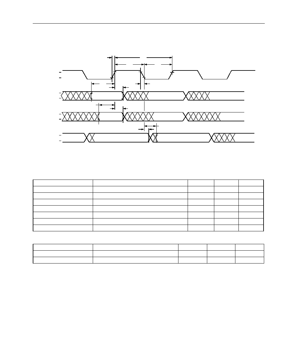
Data Sheet
March 2000
DSP1627 Digital Signal Processor
Lucent Technologies Inc.
125
12 Timing Characteristics for 2.7 V Operation
(continued)
12.4 JTAG I/O Specifications
Figure 62. JTAG Timing Diagram
Table 151. Timing Requirements for JTAG Input/Output
Abbreviated Reference
Parameter
Min
Max
Unit
t12
TCK Period (high to high)
50
--
ns
t13
TCK High Time (high to low)
22.5
--
ns
t14
TCK Low Time (low to high)
22.5
--
ns
t15
TMS Setup Time (valid to high)
7.5
--
ns
t16
TMS Hold Time (high to invalid)
2
--
ns
t17
TDI Setup Time (valid to high)
7.5
--
ns
t18
TDI Hold Time (high to invalid)
2
--
ns
Table 152. Timing Characteristics for JTAG Input/Output
Abbreviated Reference
Parameter
Min
Max
Unit
t19
TDO Delay (low to valid)
--
19
ns
t20
TDO Hold (low to invalid)
0
--
ns
t12
t14
t13
t15
t16
t17
t18
t19
t20
TCK
TMS
TDI
TDO
V
IH
V
IL
V
IH
V
IL
V
IH
V
IL
V
OH
V
OL
t155
t156
5-4017 (F)
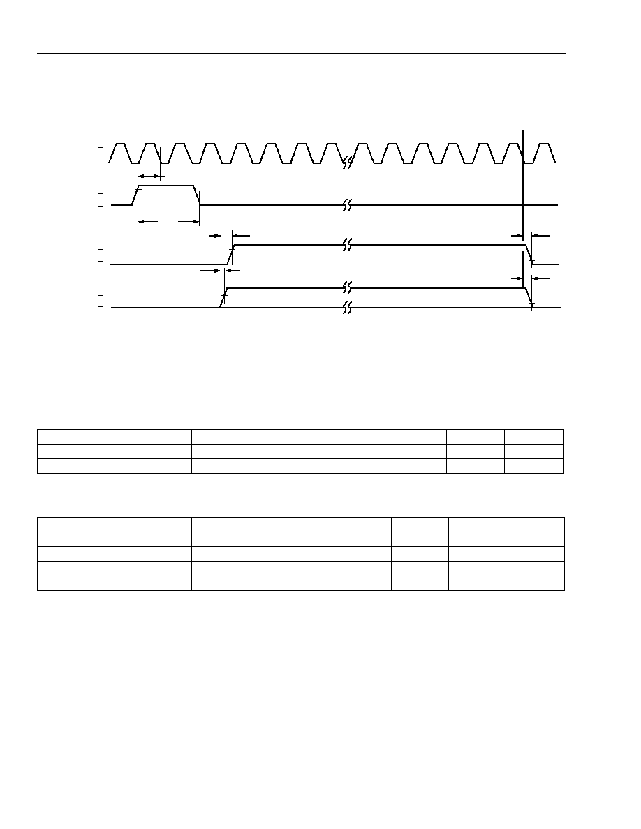
Data Sheet
DSP1627 Digital Signal Processor
March 2000
126
Lucent Technologies Inc.
12 Timing Characteristics for 2.7 V Operation
(continued)
12.5 Interrupt
*
CKO is free-running.
IACK assertion is guaranteed to be enclosed by VEC[3:0] assertion.
Figure 63. Interrupt Timing Diagram
Note: Interrupt is asserted during an interruptible instruction and no other pending interrupts.
Note: Interrupt is asserted during an interruptible instruction and no other pending interrupts.
Table 153. Timing Requirements for Interrupt
Abbreviated Reference
Parameter
Min
Max
Unit
t21
Interrupt Setup (high to low)
19
--
ns
t22
INT Assertion Time (high to low)
2T
--
ns
Table 154. Timing Characteristics for Interrupt
Abbreviated Reference
Parameter
Min
Max
Unit
t23
IACK Assertion Time (low to high)
--
T/2 + 10
ns
t24
VEC Assertion Time (low to high)
--
12.5
ns
t25
IACK Invalid Time (low to low)
--
10
ns
t26
VEC Invalid Time (low to low)
--
12.5
ns
5-4018 (F)
CKO
*
INT[1:0]
t21
V
OH
V
OL
V
IH
V
IL
t22
IACK
V
OH
V
OL
VEC[3:0]
V
OH
V
OL
t23
t24
t25
t26

Data Sheet
March 2000
DSP1627 Digital Signal Processor
Lucent Technologies Inc.
127
12 Timing Characteristics for 2.7 V Operation
(continued)
12.6 Bit Input/Output (BIO)
Figure 64. Write Outputs Followed by Read Inputs (cbit = Immediate; a1 = sbit)
Figure 65. Write Outputs and Test Inputs (cbit = Immediate)
Table 155. Timing Requirements for BIO Input Read
Abbreviated Reference
Parameter
Min
Max
Unit
t27
IOBIT Input Setup Time (valid to high)
15
--
ns
t28
IOBIT Input Hold Time (high to invalid)
0
--
ns
Table 156. Timing Characteristics for BIO Output
Abbreviated Reference
Parameter
Min
Max
Unit
t29
IOBIT Output Valid Time (low to valid)
--
9
ns
t144
IOBIT Output Hold Time (low to invalid)
1
--
ns
Table 157. Timing Requirements for BIO Input Test
Abbreviated Reference
Parameter
Min
Max
Unit
t141
IOBIT Input Setup Time (valid to low)
15
--
ns
t142
IOBIT Input Hold Time (low to invalid)
0
--
ns
CKO
IOBIT
(INPUT)
t28
t27
VALID OUTPUT
V
I
H
V
I
L
V
O
H
V
O
L
V
O
H
V
O
L
DATA INPUT
t29
t144
IOBIT
(OUTPUT)
5-4019 (F).a
CKO
IOBIT
(INPUT)
t142
t141
VALID OUTPUT
V
OH
≠
V
O
L≠
TEST INPUT
t29
t144
IOBIT
(OUTPUT)
V
OH
≠
V
O
L≠
V
IH
≠
V
I
L≠
5-4019 (F).b

Data Sheet
DSP1627 Digital Signal Processor
March 2000
128
Lucent Technologies Inc.
12 Timing Characteristics for 2.7 V Operation
(continued)
12.7 External Memory Interface
The following timing diagrams, characteristics, and requirements do not apply to interactions with delayed external
memory enables unless so stated. See the
DSP1611/17/18/27 Digital Signal Processor Information Manual
for a
detailed description of the external memory interface including other functional diagrams.
*
W = number of wait-states.
Figure 66. Enable Transition Timing
Table 158. Timing Characteristics for External Memory Enables (EROM, ERAMHI, IO, ERAMLO)
Abbreviated Reference
Parameter
Min
Max
Unit
t33
CKO to ENABLE Active (low to low)
0
5
ns
t34
CKO to ENABLE Inactive (low to high)
≠1
4.5
ns
Table 159. Timing Characteristics for Delayed External Memory Enables (ioc = 0x000F)
Abbreviated Reference
Parameter
Min
Max
Unit
t33
CKO to Delayed ENABLE Active (low to low)
T/2 ≠ 2
T/2 + 7
ns
CKO
ENABLE
t34
t33
W
*
= 0
V
OH
V
OL
V
OH
V
OL
5-4020 (F).b
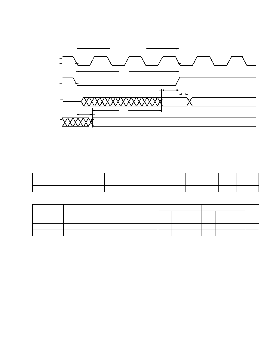
Data Sheet
March 2000
DSP1627 Digital Signal Processor
Lucent Technologies Inc.
129
12 Timing Characteristics for 2.7 V Operation
(continued)
*
W = number of wait-states.
Figure 67. External Memory Data Read Timing Diagram
Table 160. Timing Characteristics for External Memory Access
Abbreviated Reference
Parameter
Min
Max
Unit
t127
Enable Width (low to high)
T(1 + W) ≠ 1.5
--
ns
t128
Address Valid (enable low to valid)
--
2
ns
Table 161. Timing Requirements for External Memory Read (EROM, ERAMHI, IO, ERAMLO)
Abbreviated
Reference
Parameter
20 ns
12.5 ns
Unit
Min
Max
Min
Max
t129
Read Data Setup (valid to enable high)
15
--
13
--
ns
t130
Read Data Hold (enable high to hold)
0
--
0
--
ns
t150
External Memory Access Time (valid to valid)
--
T(1 + W) ≠ 15
--
T(1 + W) ≠ 14
ns
V
IH
V
IL
DB
CKO
AB
V
OH
V
OL
t128
READ ADDRESS
ENABLE
V
OH
V
OL
V
OH
V
OL
(MWAIT = 0 x 2222)
W* = 2
t127
t129
t130
READ DATA
t150
5-4021 (F).a
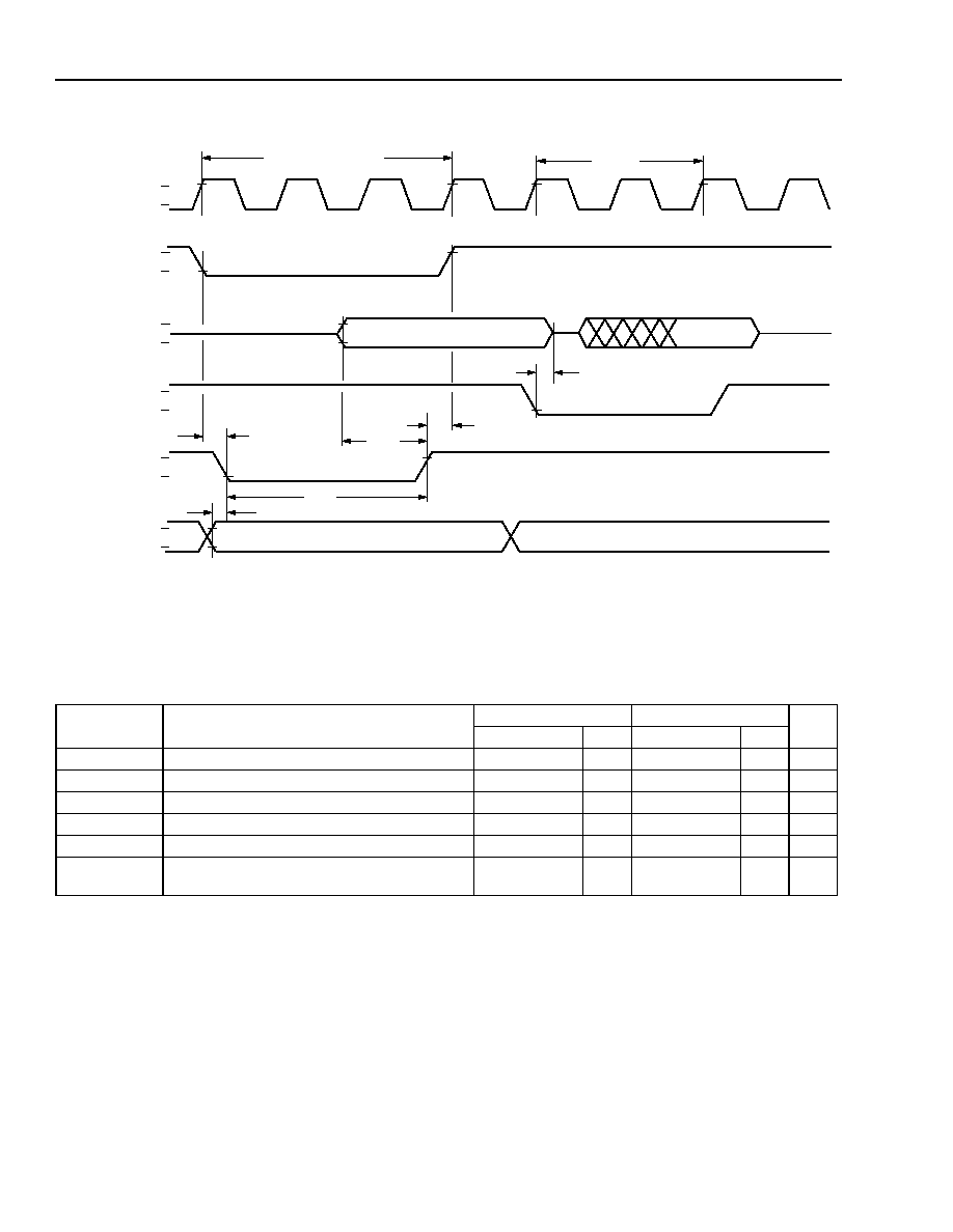
Data Sheet
DSP1627 Digital Signal Processor
March 2000
130
Lucent Technologies Inc.
12 Timing Characteristics for 2.7 V Operation
(continued)
*
W = number of wait-states.
Figure 68. External Memory Data Write Timing Diagram
Table 162. Timing Characteristics for External Memory Data Write (All Enables)
Abbreviated
Reference
Parameter
20 ns
12.5 ns
Unit
Min
Max
Min
Max
t131
Write Overlap (enable low to 3-state)
--
0
--
0
ns
t132
RWN Advance (RWN high to enable high)
0
--
0
--
ns
t133
RWN Delay (enable low to RWN low)
0
--
0
--
ns
t134
Write Data Setup (data valid to RWN high)
T(1 + W)/2 ≠ 4
--
T(1 + W)/2 ≠ 3
--
ns
t135
RWN Width (low to high)
T(1 + W) ≠ 5
--
T(1 + W) ≠ 4
--
ns
t136
Write Address Setup (address valid to RWN
low)
0
--
0
--
ns
ERAMLO
EROM
CKO
AB
RWN
DB
WRITE ADDRESS
READ ADDRESS
V
OH
V
OL
V
OH
V
OL
V
OH
V
OL
V
OH
V
OL
V
OH
V
OL
WRITE DATA
READ
W* = 1
t131
t132
t134
t133
t135
t136
(MWAIT = 0x1002)
W* = 2
V
OH
V
OL
5-4022 (F).a
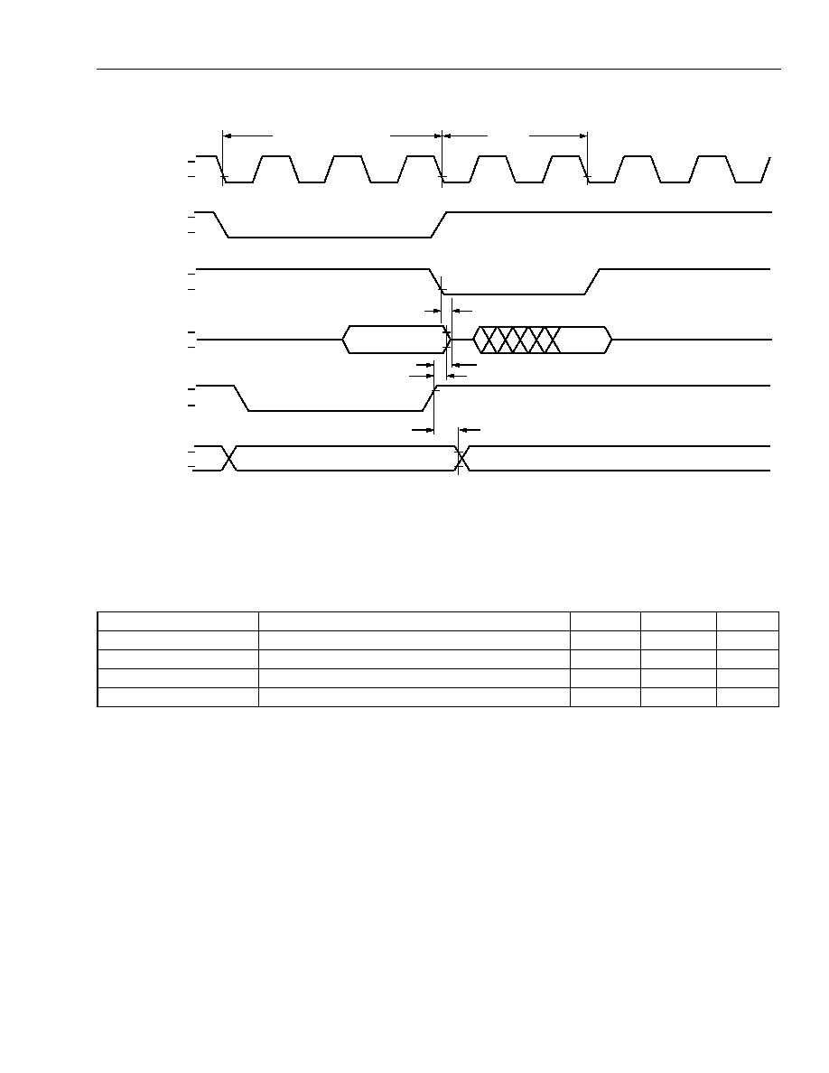
Data Sheet
March 2000
DSP1627 Digital Signal Processor
Lucent Technologies Inc.
131
12 Timing Characteristics for 2.7 V Operation
(continued)
*
W = number of wait-states.
Figure 69. Write Cycle Followed by Read Cycle
Table 163. Timing Characteristics for Write Cycle Followed by Read Cycle
Abbreviated Reference
Parameter
Min
Max
Unit
t131
Write Overlap (enable low to 3-state)
--
0
ns
t137
Write Data 3-state (RWN high to 3-state)
--
2
ns
t138
Write Data Hold (RWN high to data hold)
0
--
ns
t139
Write Address Hold (RWN high to address hold)
0
--
ns
5-4023 (F).a
ERAMLO
CKO
AB
RWN
WRITE ADDRESS
READ ADDRESS
V
OH
V
OL
V
OH
V
OL
V
OH
V
OL
V
OH
V
OL
W* = 1
t137
(MWAIT = 0x1002)
W* = 2
EROM
V
OH
V
OL
DB
WRITE
READ
V
OH
V
OL
t138
t139
t131
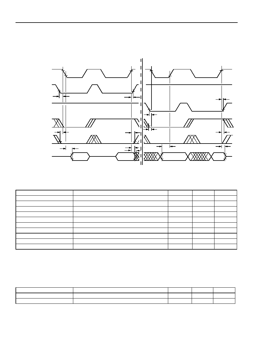
Data Sheet
DSP1627 Digital Signal Processor
March 2000
132
Lucent Technologies Inc.
12 Timing Characteristics for 2.7 V Operation
(continued)
12.8 PHIF Specifications
For the PHIF, "READ" means read by the external user (output by the DSP); "WRITE" is similarly defined. The 8-bit reads/
writes are identical to one-half of a 16-bit access.
Figure 70. PHIF
Intel
Mode Signaling (Read and Write) Timing Diagram
*
This timing diagram for the PHIF port shows accesses using the PCSN signal to initiate and complete a transaction. The transactions can also be
initiated and completed with the PIDS and PODS signals. An output transaction (read) is initiated by PCSN or PODS going low, whichever comes
last. For example, the timing requirements referenced to PCSN going low, t45 and t49, should be referenced to PODS going low, if PODS goes
low after PCSN. An output transaction is completed by PCSN or PODS going high, whichever comes first. An input transaction is initiated by PCSN
or PIDS going low, whichever comes last. An input transaction is completed by PCSN or PIDS going high, whichever comes first. All requirements
referenced to PCSN apply to PIDS or PODS, if PIDS or PODS is the controlling signal.
Table 164. Timing Requirements for PHIF
Intel Mode Signaling
Abbreviated Reference
Parameter
Min
Max
Unit
t41
PODS to PCSN Setup (low to low)
0
--
ns
t42
PCSN to PODS Hold (high to high)
0
--
ns
t43
PIDS to PCSN Setup (low to low)
0
--
ns
t44
PCSN to PIDS Hold (high to high)
0
--
ns
t45*
PSTAT to PCSN Setup (valid to low)
6
--
ns
t46*
PCSN to PSTAT Hold (high to invalid)
0
--
ns
t47*
PBSEL to PCSN Setup (valid to low)
6
--
ns
t48*
PCSN to PBSEL Hold (high to invalid)
0
--
ns
t51*
PB Write to PCSN Setup (valid to high)
10
--
ns
t52*
PCSN to PB Write Hold (high to invalid)
5
--
ns
Table 165. Timing Characteristics for PHIF
Intel Mode Signaling
Abbreviated Reference
Parameter
Min
Max
Unit
t49*
PCSN to PB Read (low to valid)
--
17
ns
t50*
PCSN to PB Read Hold (high to invalid)
3
--
ns
5-4036 (F)
PCSN
t41
t42
t43
t45
t46
t49
t50
16-bit READ
16-bit WRITE
PODS
PIDS
PBSEL
PSTAT
PB[7:0]
t47
t51
t52
t48
t44
t154
V
IH≠
V
IL≠
V
IH≠
V
IL≠
V
IH≠
V
IL≠
V
IH≠
V
IL≠
V
IH≠
V
IL≠
V
IH≠
V
IL≠
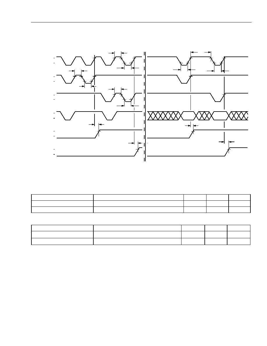
Data Sheet
March 2000
DSP1627 Digital Signal Processor
Lucent Technologies Inc.
133
12 Timing Characteristics for 2.7 V Operation
(continued)
Figure 71. PHIF
Intel
Mode Signaling (Pulse Period and Flags) Timing Diagram
*
t53 should be referenced to the rising edge of PCSN or PODS, whichever comes first.
t54 should be referenced to the rising edge of PCSN
or PIDS, whichever comes first.
POBE and PIBF may be programmed to be the opposite logic levels shown in the diagram (positive assertion levels shown). t53 and t54 apply
to the inverted levels as well as those shown.
Table 166. Timing Requirements for PHIF
Intel
Mode Signaling
Abbreviated Reference
Parameter
Min
Max
Unit
t55
PCSN/PODS/PIDS Pulse Width (high to low)
20.5
--
ns
t56
PCSN/PODS/PIDS Pulse Width (low to high)
20.5
--
ns
Table 167. Timing Characteristics for PHIF
Intel
Mode Signaling
Abbreviated Reference
Parameter
Min
Max
Unit
t53*
PCSN/PODS to POBE
(high to high)
--
20
ns
t54*
PCSN/PIDS to PIBF
(high to high)
--
20
ns
PODS
PIDS
V
IH
V
IL
V
IH
V
IL
V
IH
V
IL
t55
t56
t55
t56
t55
t56
PCSN
t53
t54
16-bit READ
8-bit WRITE
PBSEL
POBE
PIBF
t54
V
OH
V
OL
V
OH
V
OL
V
OH
V
OL
t56
t56
t55
t53
8-bit READ
16-bit WRITE
5-4037 (F).a
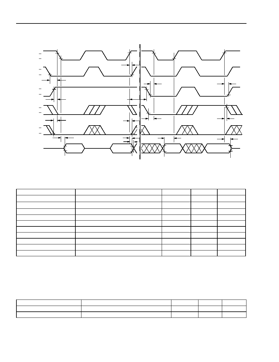
Data Sheet
DSP1627 Digital Signal Processor
March 2000
134
Lucent Technologies Inc.
12 Timing Characteristics for 2.7 V Operation
(continued)
Figure 72. PHIF
Motorola
Mode Signaling (Read and Write) Timing Diagram
*
This timing diagram for the PHIF port shows accesses using the PCSN signal to initiate and complete a transaction. The transactions can
also be initiated and completed with the PDS signal. An input/output transaction is initiated by PCSN or PDS going low, whichever comes last.
For example, the timing requirements referenced to PCSN going low, t45 and t49, should be referenced to PDS going low, if PDS goes low
after PCSN. An input/output transaction is completed by PCSN or PDS going high, whichever comes first. All requirements referenced to
PCSN should be referenced to PDS, if PDS is the controlling signal. PRWN should never be used to initiate or complete a transaction.
PDS is programmable to be active-high or active-low. It is shown active-low in Figures 72 and 73. POBE and PIBF may be programmed to
be the opposite logic levels shown in the diagram. t53 and t54 apply to the inverted levels as well as those shown.
*
This timing diagram for the PHIF port shows accesses using the PCSN signal to initiate and complete a transaction. The transactions can
also be initiated and completed with the PDS signal. An input/output transaction is initiated by PCSN or PDS going low, whichever comes last.
For example, the timing requirements referenced to PCSN going low, t45 and t49, should be referenced to PDS going low, if PDS goes low
after PCSN. An input/output transaction is completed by PCSN or PDS going high, whichever comes first. All requirements referenced to
PCSN should be referenced to PDS, if PDS is the controlling signal. PRWN should never be used to initiate or complete a transaction.
Table 168. Timing Requirements for PHIF
Motorola
Mode Signaling
Abbreviated Reference
Parameter
Min
Max
Unit
t41
PDS
to PCSN Setup (valid to low)
0
--
ns
t42
PCSN to PDS
Hold (high to invalid)
0
--
ns
t43
PRWN to PCSN Setup (valid to low)
6
--
ns
t44
PCSN to PRWN Hold (high to invalid)
0
--
ns
t45*
PSTAT to PCSN Setup (valid to low)
6
--
ns
t46*
PCSN to PSTAT Hold (high to invalid)
0
--
ns
t47*
PBSEL to PCSN Setup (valid to low)
6
--
ns
t48*
PCSN to PBSEL Hold (high to invalid)
0
--
ns
t51*
PB Write to PCSN Setup (valid to high)
10
--
ns
t52*
PCSN to PB Write Hold (high to invalid)
5
--
ns
Table 169. Timing Characteristics for PHIF
Motorola
Mode Signaling
Abbreviated Reference
Parameter
Min
Max
Unit
t49*
PCSN to PB Read (low to valid)
--
17
ns
t50*
PCSN to PB Read (high to invalid)
3
--
ns
PCSN
PDS
PRWN
PBSEL
PSTAT
PB[7:0]
t41
t42
t43
t44
t45
t46
t47
t48
t52
t51
t50
t49
16-bit READ
16-bit WRITE
t43
t44
V
I H
V
IL
V
I H
V
IL
V
I H
V
IL
V
I H
V
IL
V
I H
V
IL
5-4038 (F).a
t154
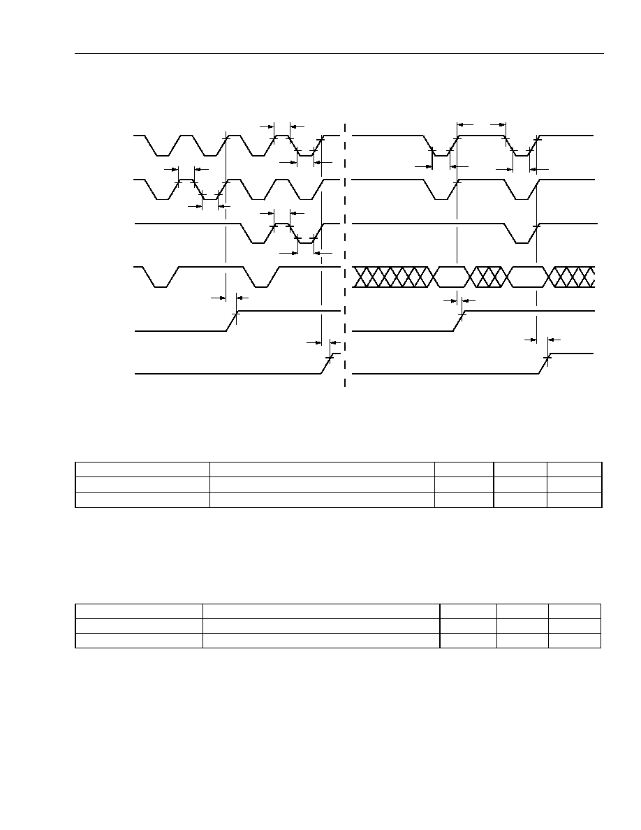
Data Sheet
March 2000
DSP1627 Digital Signal Processor
Lucent Technologies Inc.
135
12 Timing Characteristics for 2.7 V Operation
(continued)
Figure 73. PHIF
Motorola
Mode Signaling (Pulse Period and Flags) Timing Diagram
* An input/output transaction is initiated by PCSN or PDS going low, whichever comes last. For example, t53 and t54 should be referenced to
PDS going low, if PDS goes low after PCSN. An input/output transaction is completed by PCSN or PDS going high, whichever comes first.
All requirements referenced to PCSN should be referenced to PDS, if PDS is the controlling signal. PRWN should never be used to initiate or
complete a transaction.
PDS is programmable to be active-high or active-low. It is shown active-low in Figures 72 and 73. POBE and PIBF may be programmed to
be the opposite logic levels shown in the diagram. t53 and t54 apply to the inverted levels as well as those shown.
Table 170. Timing Characteristics for PHIF
Motorola
Mode Signaling
Abbreviated Reference
Parameter
Min
Max
Unit
t53*
PCSN/PDS
to POBE
(high to high)
--
20
ns
t54*
PCSN/PDS
to PIBF
(high to high)
--
20
ns
Table 171. Timing Requirements for PHIF
Motorola
Mode Signaling
Abbreviated Reference
Parameter
Min
Max
Unit
t55
PCSN/PDS/PRWN Pulse Width (high to low)
20
--
ns
t56
PCSN/PDS/PRWN Pulse Width (low to high)
20
--
ns
PDS
PRWN
V
IH
≠
t55
t56
t55
t56
t55
t56
PCSN
t53
t54
16-bit READ
8-bit WRITE
PBSEL
POBE
PIBF
t54
t56
t56
t55
t53
8-bit READ
16-bit WRITE
V
IL
≠
V
IH
≠
V
IL
≠
V
IH
≠
V
IL
≠
V
OH
≠
V
OL
≠
V
OH
≠
V
OL
≠
V
OH
≠
V
OL
≠
5-4039 (F).a

Data Sheet
DSP1627 Digital Signal Processor
March 2000
136
Lucent Technologies Inc.
12 Timing Characteristics for 2.7 V Operation
(continued)
*
Motorola
mode signal name.
Figure 74. PHIF
Intel
or
Motorola
Mode Signaling (Status Register Read) Timing Diagram
t45, t47, and t49 are referenced to the falling edge of PCSN or PODS(PDS), whichever occurs last.
t46, t48, and t50 are referenced to the rising edge of PCSN or PODS(PDS), whichever occurs first.
t45, t47, and t49 are referenced to the falling edge of PCSN or PODS(PDS), whichever occurs last.
t46, t48, and t50 are referenced to the rising edge of PCSN or PODS(PDS), whichever occurs first.
Table 172. Timing Requirements for
Intel
and
Motorola
Mode Signaling (Status Register Read)
Abbreviated Reference
Parameter
Min
Max
Unit
t45
PSTAT to PCSN Setup (valid to low)
6
--
ns
t46
PCSN to PSTAT Hold (high to invalid)
0
--
ns
t475
PBSEL to PCSN Setup (valid to low)
6
--
ns
t48
PCSN to PBSEL Hold (high to invalid)
0
--
ns
Table 173. Timing Characteristics for
Intel
and
Motorola
Mode Signaling (Status Register Read)
Abbreviated Reference
Parameter
Min
Max
Unit
t49
PCSN to PB Read (low to valid)
--
17
ns
t50
PCSN to PB Read Hold (high to invalid)
3
--
ns
PCSN
PODS (PDS*)
PIDS (PRWN*)
PBSEL
PSTAT
PB[7:0]
t47
t48
t45
t46
t49
t50
V
IH
V
IL
V
OH
V
OL
V
IH
V
IL
V
IH
V
IL
V
IH
V
IL
V
IH
V
IL
5-4040 (F).a
t154

Data Sheet
March 2000
DSP1627 Digital Signal Processor
Lucent Technologies Inc.
137
12 Timing Characteristics for 2.7 V Operation
(continued)
Figure 75. PHIF, PIBF, and POBE Reset Timing Diagram
POBE and PIBF can be programmed to be active-high or active-low. They are shown active-high. The timing characteristic for active-low is
the same as for active-high.
Figure 76. PHIF, PIBF, and POBE Disable Timing Diagram
*
POBE and PIBF can be programmed to be active-high or active-low. They are shown active-high. The timing characteristic for active-low is
the same as for active-high.
Table 174. PHIF Timing Characteristics for PHIF, PIBF, and POBE Reset
Abbreviated Reference
Parameter
Min
Max
Unit
t57
RSTB Disable to POBE/PIBF
*
(high to valid)
*
After reset, POBE and PIBF always go to the levels shown, indicating output buffer empty and input buffer empty. The DSP program,
however, may later invert the definition of the logic levels for POBE and PIBF. t57 and t58 continue to apply.
--
25
ns
t58
RSTB Enable to POBE/PIBF* (low to invalid)
3
25
ns
Table 175. PHIF Timing Characteristics for POBE and PIBF Disable
Abbreviated Reference
Parameter
Min
Max
Unit
t59
CKO to POBE/PIBF Disable (high/low to disable)
--
20
ns
RSTB
V
IH
≠
t58
t57
V
IL
≠
POBE
V
OH
≠
V
OL
≠
PIBF
V
OH
≠
V
OL
≠
5-4775 (F)
CKO
V
IH
≠
V
IL
≠
t59
t59
POBE
V
OH
≠
V
OL
≠
PIBF
V
OH
≠
V
OL
≠
5-4776 (F)
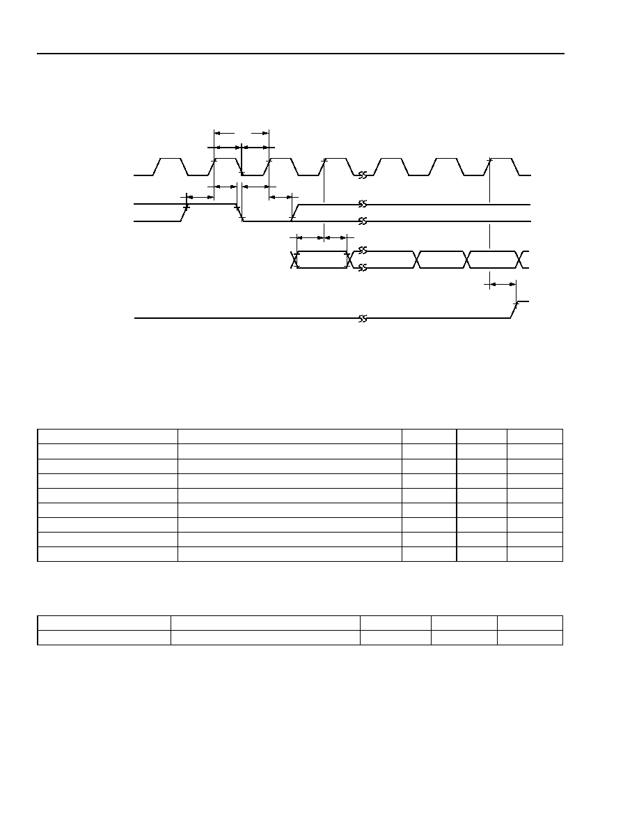
Data Sheet
DSP1627 Digital Signal Processor
March 2000
138
Lucent Technologies Inc.
12 Timing Characteristics for 2.7 V Operation
(continued)
12.9 Serial I/O Specifications
*
N = 16 or 8 bits.
Figure 77. SIO Passive Mode Input Timing Diagram
Device is fully static; t70 is tested at 200 ns.
For multiprocessor mode, see note in Section 12.10.
Table 176. Timing Requirements for Serial Inputs
Abbreviated Reference
Parameter
Min
Max
Unit
t70
Clock Period (high to high)
40
--
ns
t71
Clock Low Time (low to high)
18
--
ns
t72
Clock High Time (high to low)
18
--
ns
t73
Load High Setup (high to high)
8
--
ns
t74
Load Low Setup (low to high)
8
--
ns
t75
Load High Hold (high to invalid)
0
--
ns
t77
Data Setup (valid to high)
7
--
ns
t78
Data Hold (high to invalid)
0
--
ns
Table 177. Timing Characteristics for Serial Outputs
Abbreviated Reference
Parameter
Min
Max
Unit
t79
IBF Delay (high to high)
--
35
ns
IBF
V
OH
≠
V
OL
≠
DI
V
IH
≠
V
IL
≠
ILD
V
IH
≠
V
IL
≠
ICK
V
IH
≠
V
IL
≠
BN ≠ 1*
B0
t77
t78
B0
B1
t79
t72
t71
t70
t75
t74
t75
t73
5-4777 (F)
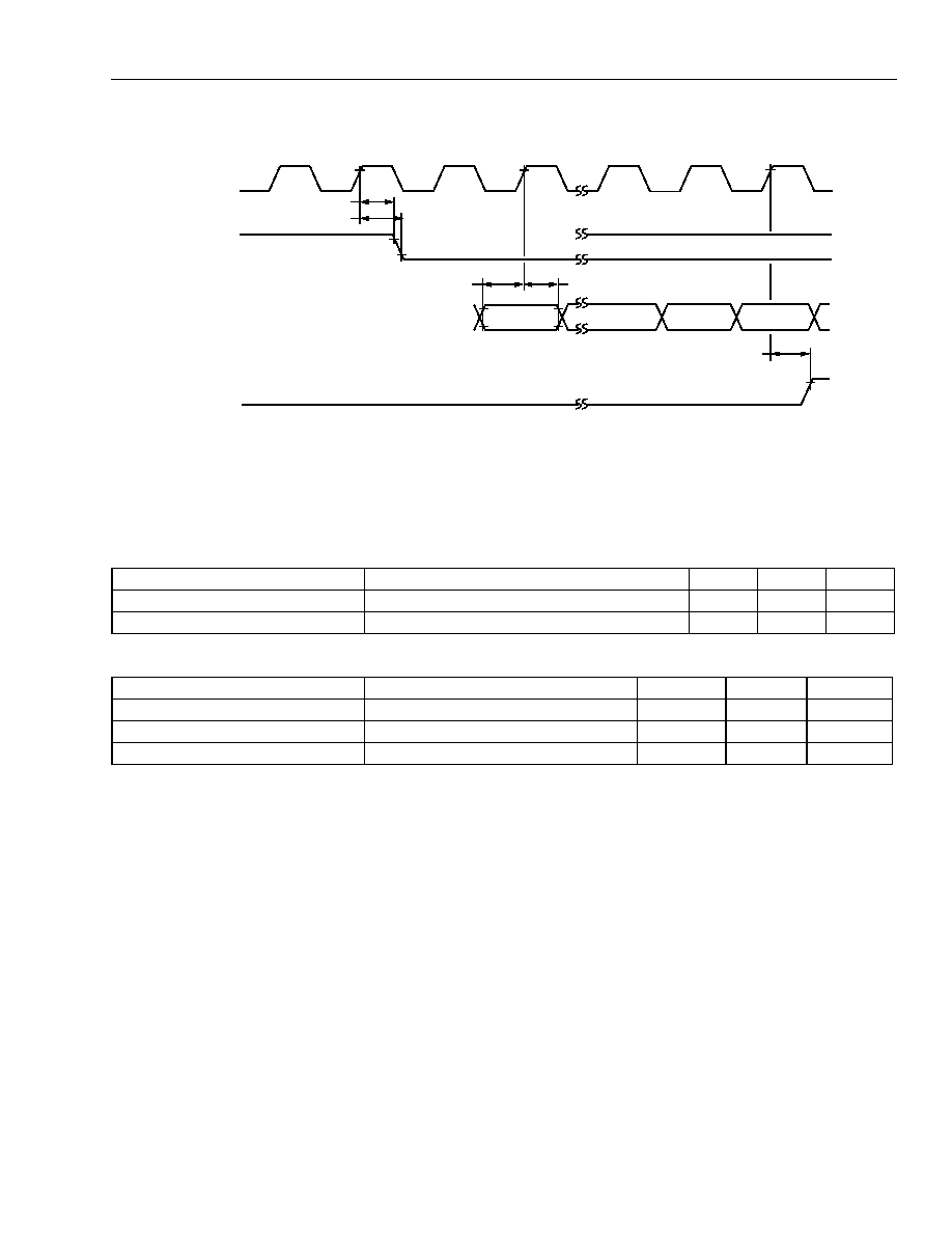
Data Sheet
March 2000
DSP1627 Digital Signal Processor
Lucent Technologies Inc.
139
12 Timing Characteristics for 2.7 V Operation
(continued)
*
ILD goes high during bit 6 (of 0:15), N = 8 or 16.
Figure 78. SIO Active Mode Input Timing Diagram
Table 178. Timing Requirements for Serial Inputs
Abbreviated Reference
Parameter
Min
Max
Unit
t77
Data Setup (valid to high)
7
--
ns
t78
Data Hold (high to invalid)
0
--
ns
Table 179. Timing Characteristics for Serial Outputs
Abbreviated Reference
Parameter
Min
Max
Unit
t76a
ILD Delay (high to low)
--
35
ns
t101
ILD Hold (high to invalid)
5
--
ns
t79
IBF Delay (high to high)
--
35
ns
IBF
V
OH
≠
V
OL
≠
DI
V
IH
≠
V
IL
≠
ILD
V
OH
≠
V
OL
≠
ICK
V
OH
≠
V
OL
≠
BN ≠ 1
B0
t77
t78
B0
B1
t79
t101
t76a
*
5-4778 (F)
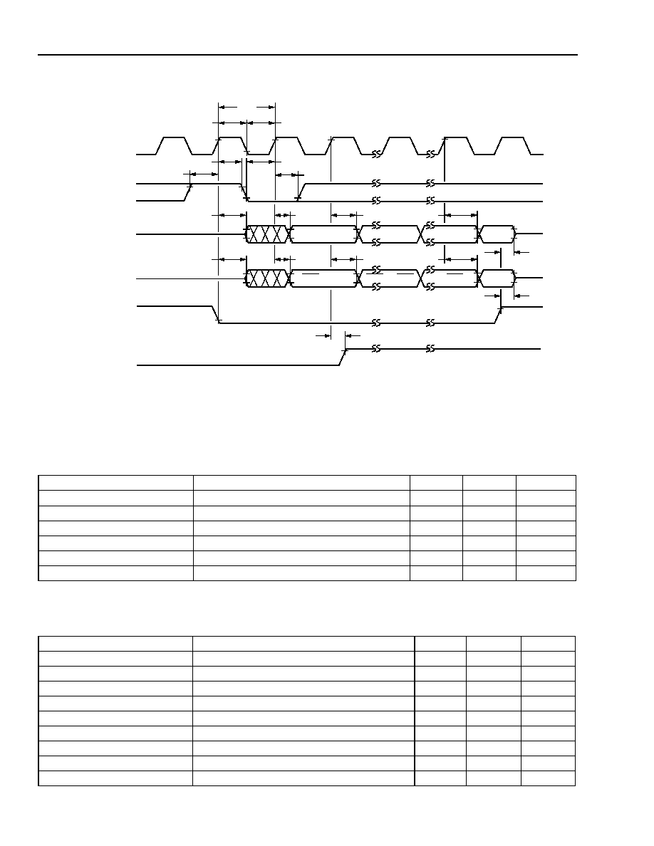
Data Sheet
DSP1627 Digital Signal Processor
March 2000
140
Lucent Technologies Inc.
12 Timing Characteristics for 2.7 V Operation
(continued)
*
See sioc register, MSB field, to determine if B0 is the MSB or LSB. See sioc register, ILEN field, to determine if the DO word length is 8 bits
or 16 bits.
Figure 79. SIO Passive Mode Output Timing Diagram
Device is fully static; t80 is tested at 200 ns.
For multiprocessor mode, see note in Section 12.10.
Table 180. Timing Requirements for Serial Inputs
Abbreviated Reference
Parameter
Min
Max
Unit
t80
Clock Period (high to high)
40
--
ns
t81
Clock Low Time (low to high)
18
--
ns
t82
Clock High Time (high to low)
18
--
ns
t83
Load High Setup (high to high)
8
--
ns
t84
Load Low Setup (low to high)
8
--
ns
t85
Load Hold (high to invalid)
0
--
ns
Table 181. Timing Characteristics for Serial Outputs
Abbreviated Reference
Parameter
Min
Max
Unit
t87
Data Delay (high to valid)
--
35
ns
t88
Enable Data Delay (low to active)
--
35
ns
t89
Disable Data Delay (high to 3-state)
--
35
ns
t90
Data Hold (high to invalid)
5
--
ns
t92
Address Delay (high to valid)
--
35
ns
t93
Address Hold (high to invalid)
5
--
ns
t94
Enable Delay (low to active)
--
35
ns
t95
Disable Delay (high to 3-state)
--
35
ns
t96
OBE Delay (high to high)
--
35
ns
DOEN
V
IH
≠
V
IL
≠
SADD
V
OH
≠
V
OL
≠
OLD
V
IH
≠
V
IL
≠
OCK
V
IH
≠
V
IL
≠
t85
t80
t81
t82
t84
t83
t85
t88
B0
B1
B7
BN ≠ 1
t90
t90
t87
t94
AD0
AD1
AD7
t93
t93
t92
AS7
t89
t95
OBE
V
OH
≠
V
OL
≠
DO*
V
OH
≠
V
OL
≠
t96
5-4796 (F)
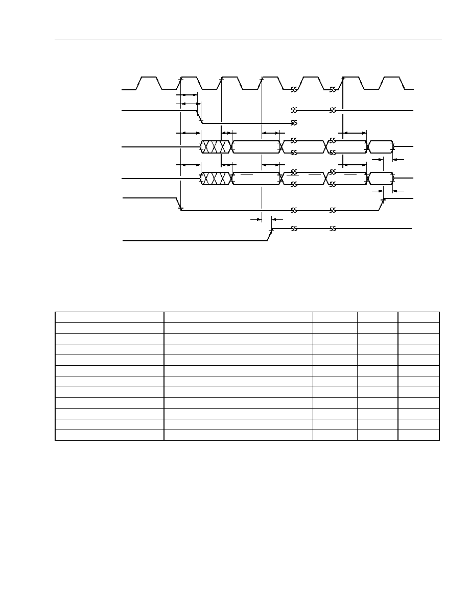
Data Sheet
March 2000
DSP1627 Digital Signal Processor
Lucent Technologies Inc.
141
12 Timing Characteristics for 2.7 V Operation
(continued)
*
OLD goes high at the end of bit 6 of 0:15.
Figure 80. SIO Active Mode Output Timing Diagram
Table 182. Timing Characteristics for Serial Output
Abbreviated Reference
Parameter
Min
Max
Unit
t86a
OLD Delay (high to low)
--
35
ns
t102
OLD Hold (high to invalid)
5
--
ns
t87
Data Delay (high to valid)
--
35
ns
t88
Enable Data Delay (low to active)
--
35
ns
t89
Disable Data Delay (high to 3-state)
--
35
ns
t90
Data Hold (high to invalid)
5
--
ns
t92
Address Delay (high to valid)
--
35
ns
t93
Address Hold (high to invalid)
5
--
ns
t94
Enable Delay (low to active)
--
35
ns
t95
Disable Delay (high to 3-state)
--
35
ns
t96
OBE Delay (high to high)
--
35
ns
5-4797 (F)
DOEN
V
IH
≠
V
IL
≠
SADD
V
OH
≠
V
OL
≠
OLD
V
OH
≠
V
OL
≠
OCK
V
OH
≠
V
OL
≠
t102
t86a
t88
B0
B1
B7
BN ≠ 1
t90
t90
t87
t94
AD0
AD1
AD7
t93
t93
t92
AS7
t89
t95
OBE
V
OH
≠
V
OL
≠
DO
V
OH
≠
V
OL
≠
t96
*
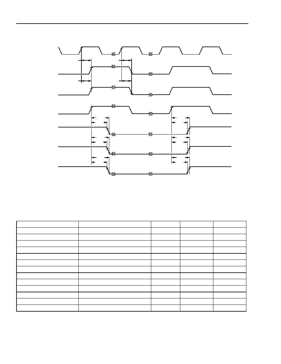
Data Sheet
DSP1627 Digital Signal Processor
March 2000
142
Lucent Technologies Inc.
12 Timing Characteristics for 2.7 V Operation
(continued)
*
See sioc register, LD field.
Figure 81. Serial I/O Active Mode Clock Timing
Table 183. Timing Characteristics for Signal Generation
Abbreviated Reference
Parameter
Min
Max
Unit
t97
ICK Delay (high to high)
--
18
ns
t98
ICK Delay (high to low)
--
18
ns
t99
OCK Delay (high to high)
--
18
ns
t100
OCK Delay (high to low)
--
18
ns
t76a
ILD Delay (high to low)
--
35
ns
t76b
ILD Delay (high to high)
--
35
ns
t101
ILD Hold (high to invalid)
5
--
ns
t86a
OLD Delay (high to low)
--
35
ns
t86b
OLD Delay (high to high)
--
35
ns
t102
OLD Hold (high to invalid)
5
--
ns
t103
SYNC Delay (high to low)
--
35
ns
t104
SYNC Delay (high to high)
--
35
ns
t105
SYNC Hold (high to invalid)
5
--
ns
ICK
V
OH
≠
V
OL
≠
CKO
V
OH
≠
V
OL
≠
t97
OCK
V
OH
≠
V
OL
≠
ICK/OCK*
V
OH
≠
ILD
V
OH
≠
V
OL
≠
OLD
V
OH
≠
V
OL
≠
SYNC
V
OH
≠
V
OL
≠
t99
t98
t100
t101
t76a
t101
t76b
t102
t86a
t102
t86b
t105
t103
t105
t104
5-4798 (F)
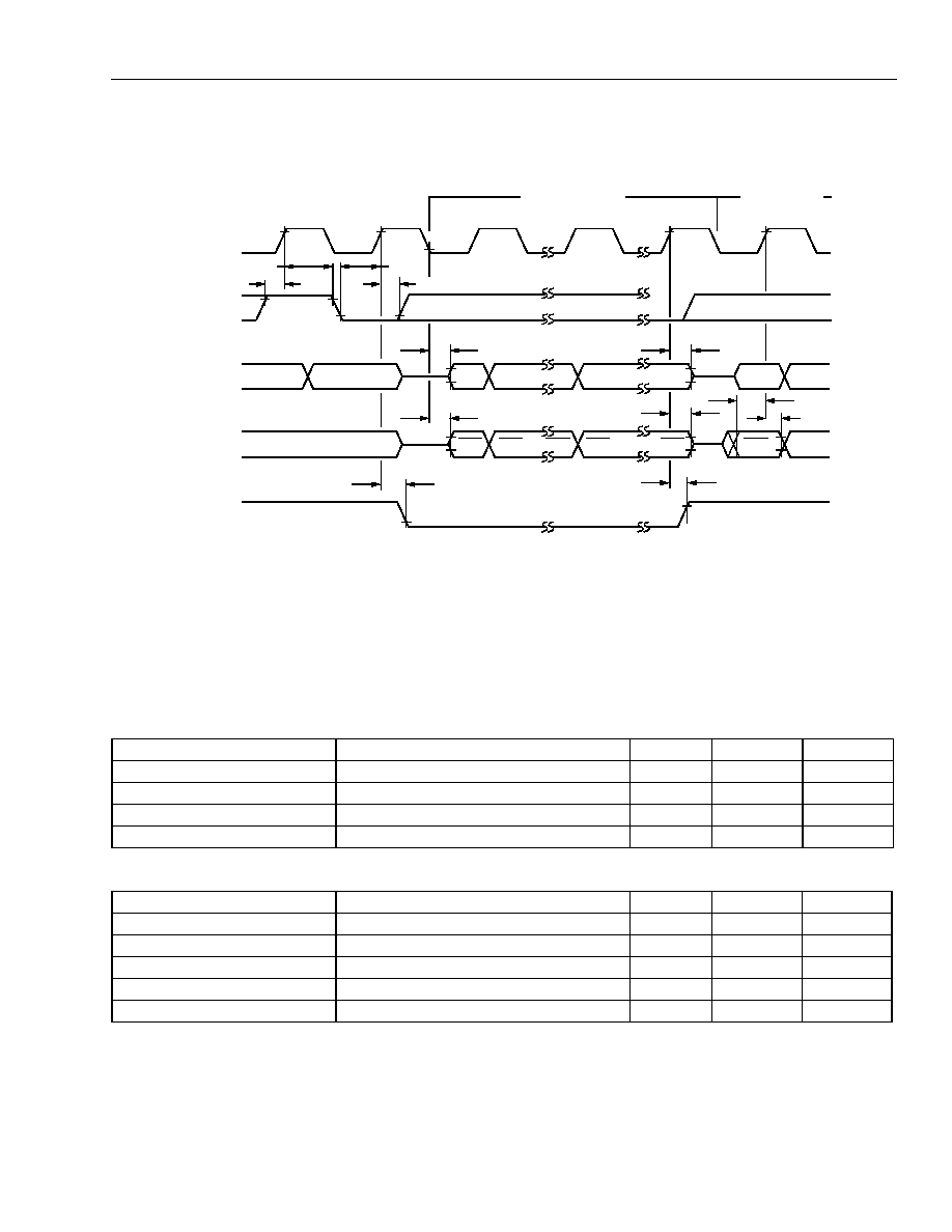
Data Sheet
March 2000
DSP1627 Digital Signal Processor
Lucent Technologies Inc.
143
12 Timing Characteristics for 2.7 V Operation
(continued)
12.10 Multiprocessor Communication
*
Negative edge initiates time slot 0.
Figure 82. SIO Multiprocessor Timing Diagram
Note: All serial I/O timing requirements and characteristics still apply, but the minimum clock period in passive
multiprocessor mode, assuming 50% duty cycle, is calculated as (t77 + t116) x 2.
* With capacitance load on ICK, OCK, DO, SYNC, and SADD = 100 pF, add 4 ns to t116--t122.
Table 184. Timing Requirements for SIO Multiprocessor Communication
Abbreviated Reference
Parameter
Min
Max
Unit
t112
Sync Setup (high/low to high)
35
--
ns
t113
Sync Hold (high to high/low)
0
--
ns
t114
Address Setup (valid to high)
12
--
ns
t115
Address Hold (high to invalid)
0
--
ns
Table 185. Timing Characteristics for SIO Multiprocessor Communication
Abbreviated Reference*
Parameter
Min
Max
Unit
t116
Data Delay (bit 0 only) (low to valid)
--
35
ns
t117
Data Disable Delay (high to 3-state)
--
30
ns
t120
DOEN Valid Delay (high to valid)
--
25
ns
t121
Address Delay (bit 0 only) (low to valid)
--
35
ns
t122
Address Disable Delay (high to 3-state)
--
30
ns
OCK/ICK
B0
B15
B8
B7
B1
B0
B15
SYNC
V
IH
≠
V
IL
≠
DO/D1
V
OH
≠
V
OL
≠
DOEN
V
OH
≠
V
OL
≠
t112
t113
t112
t113
TIME SLOT 1
TIME SLOT 2
t117
t116
AD0
AS7
AS0
AD7
AD1
AD0
SADD
t122
t121
t114
t115
t120
t120
*
5-4799 (F)
Data Sheet
DSP1627 Digital Signal Processor
March 2000
144
Lucent Technologies Inc.
13 Crystal Electrical Characteristics and Requirements
If the option for using the external crystal is chosen, the following electrical characteristics and requirements apply.
13.1 External Components for the Crystal Oscillator
The crystal oscillator is enabled by connecting a crystal across CKI and CKI2, along with one external capacitor from
each of these pins to ground (see Figure 83). For most applications, 10 pF external capacitors are recommended;
however, larger values allow for better frequency precision (see Section 13.4, Frequency Accuracy Considerations).
The crystal should be either fundamental or overtone mode, parallel resonant, with a rated power (drive level) of at
least 1 mW, and specified at a load capacitance equal to the total capacitance seen by the crystal (including external
capacitors and strays). The series resistance of the crystal should be specified to be less than half the absolute
value of the negative resistance shown in Figure 84 or Figure 85 for the crystal frequency. The frequency of the
signal at the CKI input pin is equal to the crystal frequency.
Figure 83. Fundamental Crystal Configuration
The following guidelines should be followed when designing the printed-circuit board layout for a crystal-based ap-
plication:
1. Keep crystal and external capacitors as close to CKI and CKI2 pins as possible to minimize board stray capaci-
tance.
2. Keep high-frequency digital signals such as CKO away from CKI and CKI2 traces to avoid coupling.
13.2 Power Dissipation
Figures 86 and 87 indicate the typical power dissipation of the on-chip crystal oscillator circuit versus frequency.
Note that these curves are intended to show the relative effects of load capacitance on supply current and that the
actual supply current measured depends on crystal resistance. For typical crystals, measured supply current at the
V
DDA
pin should be less than that shown in the figures.
5-4041 (F).a
CKI
CKI2
XTAL
C
1
C
2
Data Sheet
March 2000
DSP1627 Digital Signal Processor
Lucent Technologies Inc.
145
13 Crystal Electrical Characteristics and Requirements
(continued)
Figure 84. Negative Resistance of Crystal Oscillator
Circuit, V
DD
= 4.75 V
Figure 85. Negative Resistance of Crystal Oscillator
Circuit, V
DD
= 2.7 V
CKI
CKI2
C
1
C
2
C
0
Z(
)
C
1
= C
2
= C
EXT
C
0
= PARASITIC CAPACITANCE OF
CRYSTAL (7 pF MAXIMUM)
5-3529 (F).b
0
≠40
≠80
≠120
≠160
≠200
0
5
10
15
20
25
40
FREQUENCY (MHz)
R
e
[Z
]
(
)
30
35
≠240
≠280
≠320
≠360
≠400
≠440
≠480
≠520
≠560
≠600
≠640
≠680
≠720
≠760
≠800
C
1
, C
2
= 10 pF
C
1
, C
2
= 50 pF
C
1
, C
2
= 20 pF
5-3527 (F).b
0
≠40
≠80
≠120
≠160
≠200
0
5
10
15
20
25
40
FREQUENCY (MHz)
R
e
{Z
} (
)
30
35
≠240
≠280
≠320
≠360
≠400
≠440
≠480
≠520
≠560
≠600
≠640
≠680
≠720
≠760
≠800
C
1
, C
2
= 20 pF
C
1
, C
2
= 10 pF
C
1
, C
2
= 50 pF

Data Sheet
DSP1627 Digital Signal Processor
March 2000
146
Lucent Technologies Inc.
13 Crystal Electrical Characteristics and Requirements
(continued)
Figure 86. Typical Supply Current of Crystal Oscillator Circuit, V
DD
= 5.0 V, 25
∞
C
Figure 87. Typical Supply Current of Crystal Oscillator Circuit, V
DD
= 2.7 V, 25
∞
C
5-5188 (F)
6.5
6.0
5.5
5.0
4.5
3.0
2
8
14
18
22
26
30
34
38
FREQUENCY (MHz)
AVERA
G
E O
S
CI
L
L
AT
O
R
CURRENT
(
m
A)
4.0
3.5
4
12
16
20
24
28
32
36
40
10
6
7.0
C
1
= C
2
= 10 pF
C
1
= C
2
= 50 pF
5-5189 (F)
1.5
0.0
2
8
14
18
22
26
30
FREQUENCY (MHz)
AVERAG
E O
S
CI
L
L
A
T
O
R CURR
E
N
T
(
m
A)
1.0
0.5
4
12
16
20
24
28
10
6
2.0
0
C
1
= C
2
= 10 pF
C
1
= C
2
= 50 pF
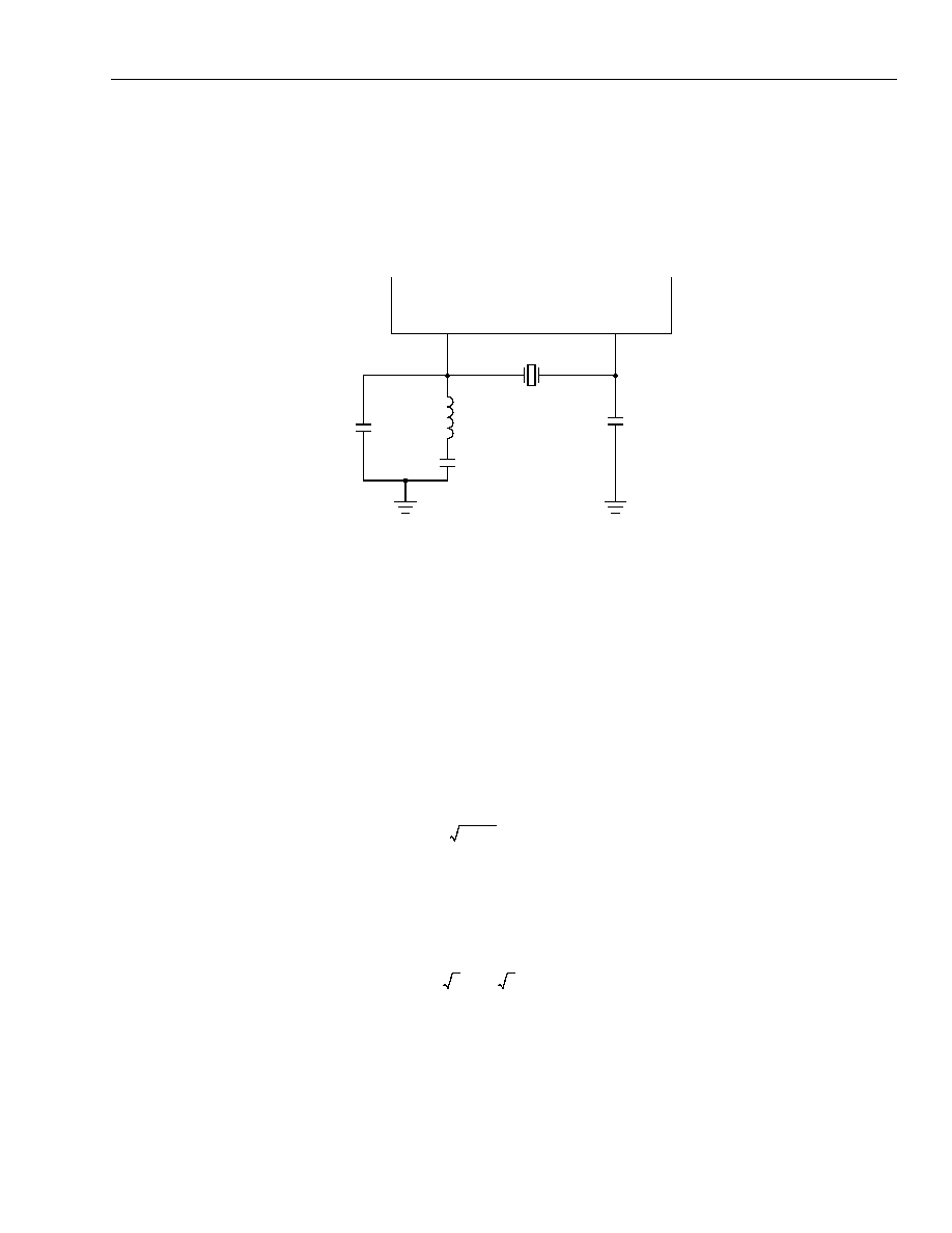
Data Sheet
March 2000
DSP1627 Digital Signal Processor
Lucent Technologies Inc.
147
13 Crystal Electrical Characteristics and Requirements
(continued)
13.3 LC Network Design for Third Overtone Crystal Circuits
For certain crystal applications, it is cheaper to use a third overtone crystal instead of a fundamental mode crystal.
When using third overtone crystals, it is necessary, however, to filter out the fundamental frequency so that the cir-
cuit will oscillate only at the third overtone. There are several techniques that will accomplish this; one of these is
described below. Figure 88 shows the basic setup for third overtone operation.
Figure 88. Third Overtone Crystal Configuration
The parallel combination of L
1
and C
1
forms a resonant circuit with a resonant frequency between the first and third
harmonic of the crystal such that the LC network appears inductive at the fundamental frequency and capacitive at
the third harmonic. This ensures that a 360
∞
phase shift around the oscillator loop will occur at the third overtone
frequency but not at the fundamental. The blocking capacitor, C
3
, provides dc isolation for the trap circuit and should
be chosen to be large compared to C
1
.
For example, suppose it is desired to operate with a 40 MHz, third overtone, crystal:
Let:
f
3
=
operating frequency of third overtone crystal (40 MHz in this example)
f
1
=
fundamental frequency of third overtone crystal, or f
3
/3 (13.3 MHz in this example)
f
T
=
resonant frequency of trap =
C
2
=
external load capacitor (10 pF in this example)
C
3
=
dc blocking capacitor (0.1
µ
F in this example)
Arbitrarily, set trap resonance to geometric mean of f
1
and f
3
. Since f
1
= f
3
/3, the geometric mean would be:
5-4043 (F).a
CKI
CKI2
XTAL
C
1
C
2
C
3
L
1
1
2
L
1
C
1
--------------------------
f
T
f
3
3
-------
40 MHz
3
--------------------
23 MHz
=
=
=

Data Sheet
DSP1627 Digital Signal Processor
March 2000
148
Lucent Technologies Inc.
13 Crystal Electrical Characteristics and Requirements
(continued)
At the third overtone frequency, f
3
, it is desirable to have the net impedance of the trap circuit (X
T
) equal to the im-
pedance of C
2
(X
C2
), i.e.,
Selecting C
3
so that X
C3
<< X
L1
yields,
For a capacitor,
For an inductor,
Solving for C
1
, and realizing that L
1
C
1
= 3/
3
2
yields,
Hence, for C
2
= 10 pF, C
1
= 15 pF. Since the impedance of the trap circuit in this example would be equal to the
impedance of a 10 pF capacitor, the negative resistance and supply current curves for C
1
= C
2
= 10 pF at 40 MHz
would apply to this example.
Finally, solving for the inductor value,
For the above example, L
1
is 3.2
µ
H.
X
T
X
C2
X
C1
X
C3
X
L1
+
(
)
||
=
=
X
T
X
C2
X
C1
X
L1
||
=
=
X
C
j
≠
C
-------- where
2
f
=
=
X
L
j
L
=
C
1
3
2
---
C
2
=
L
1
1
4
2
f
T
2
C
1
---------------------------
=
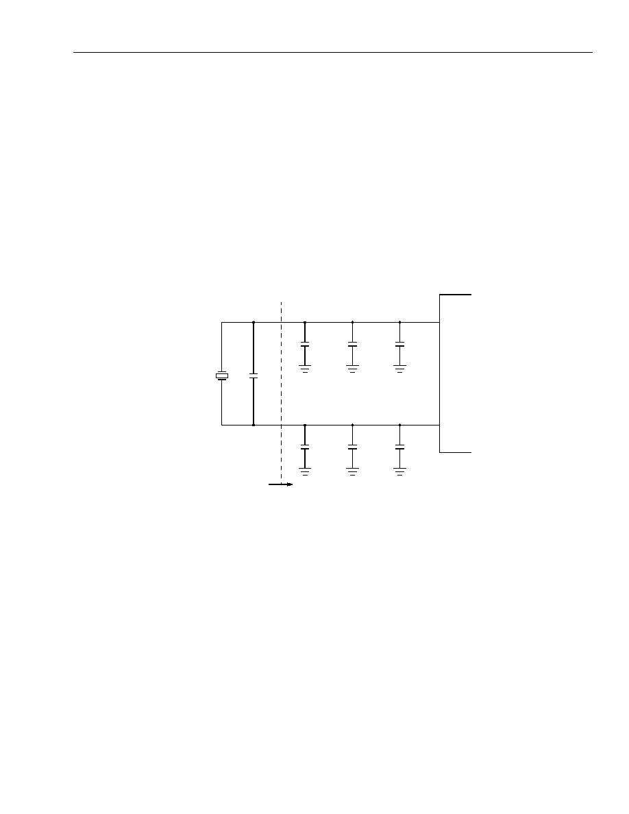
Data Sheet
March 2000
DSP1627 Digital Signal Processor
Lucent Technologies Inc.
149
13 Crystal Electrical Characteristics and Requirements
(continued)
13.4 Frequency Accuracy Considerations
For frequency accuracy implications of using the PLL, see Section 4.12, Clock Synthesis.
For most applications, clock frequency errors in the hundreds of parts per million can be tolerated with no adverse
effects. However, for applications where precise average frequency tolerance on the order of 100 ppm is required,
care must be taken in the choice of external components (crystal and capacitors) as well as in the layout of the
printed-circuit board. Several factors determine the frequency accuracy of a crystal-based oscillator circuit. Some of
these factors are determined by the properties of the crystal itself. Generally, a low-cost, standard crystal will not be
sufficient for a high-accuracy application, and a custom crystal must be specified. Most crystal manufacturers provide
extensive information concerning the accuracy of their crystals, and an applications engineer from the crystal vendor
should be consulted prior to specifying a crystal for a given application.
In addition to absolute, temperature, and aging tolerances of a crystal, the operating frequency of a crystal is also de-
termined by the total load capacitance seen by the crystal. When ordering a crystal from a vendor, it is necessary to
specify a load capacitance at which the operating frequency of the crystal will be measured. Variations in this load
capacitance due to temperature and manufacturing variations will cause variations in the operating frequency of the
oscillator. Figure 89 illustrates some of the sources of this variation.
Notes:
C
ext
= External load capacitor (one each required for CKI and CKI2).
C
D
= Parasitic capacitance of the DSP1627 itself.
C
B
= Parasitic capacitance of the printed-wiring board.
C
O
= Parasitic capacitance of crystal (not part of C
L
,
but still a source of frequency variation).
Figure 89. Components of Load Capacitance for Crystal Oscillator
The load capacitance, CL, must be specified to the crystal vendor. The crystal manufacturer will cut the crystal so
that the frequency of oscillation will be correct when the crystal sees this load capacitance. Note that C
L
refers to a
capacitance seen across the crystal leads, meaning that for the circuit shown in Figure 89, C
L
is the series combi-
nation of the two external capacitors (C
ext
/2) plus the equivalent board and device strays (C
B
/2 + C
D
/2). For exam-
ple, if 10 pF external capacitors were used and parasitic capacitance is neglected, then the crystal should be
specified for a load capacitance of 5 pF. If the load capacitance deviates from this value due to the tolerance on the
external capacitors or the presence of strays, then the frequency will also deviate. This change in frequency as func-
tion of load capacitance is known as pullability and is expressed in units of ppm/pF. For small deviations of a few
pF, pullability can be determined by the equation below:
where C
0
= parasitic capacitance of crystal in pF.
C
1
= motional capacitance of crystal in pF (usually between 1 fF to 25 fF, value available from crystal vendor).
C
L
= total load capacitance in pF seen by crystal.
5-4045 (F).a
CKI
CKI2
XTAL
C
D
C
B
C
EXT
C
D
C
B
C
EXT
C
L
C
O
pullability (ppm/pF)
C
1
(
)
10
6
(
)
2
C
0
C
L
+
(
)
2
--------------------------------
=

Data Sheet
DSP1627 Digital Signal Processor
March 2000
150
Lucent Technologies Inc.
13 Crystal Electrical Characteristics and Requirements
(continued)
Note that for a given crystal, the pullability can be reduced, and, hence, the frequency stability improved, by making
CL as large as possible while still maintaining sufficient negative resistance to ensure start-up per the curves shown
in Figures 86 and 87.
Since it is not possible to know the exact values of the parasitic capacitance in a crystal-based oscillator system, the
external capacitors are usually selected empirically to null out the frequency offset on a typical prototype board.
Thus, if a crystal is specified to operate with a load capacitance of 10 pF, the external capacitors would have to be
made slightly less than 20 pF each in order to account for strays. Suppose, for instance, that a crystal for which
C
L
= 10 pF is specified is plugged into the system and it is determined empirical that the best frequency accuracy
occurs with Cext = 18 pF. This would mean that the equivalent board and device strays from each leac to ground
would be 2 pF.
As an example, suppose it is desired to design a 23 MHz, 3.3 V system with
±
100 ppm frequency accuracy. The
parameters for a typical high-accuracy, custom, 23 MHz fundamental mode crystal are as follows:
Initial Tolerance
10 ppm
Temperature Tolerance
25 ppm
Aging Tolerance
6 ppm
Series Resistance
20
max.
Motional Capacitance (C
1
)
15 fF max.
Parasitic Capacitance (C
0
)
7 pF max.
In order to ensure oscillator start-up, the negative resistance of the oscillator with load and parasitic capacitance
must be at least twice the series resistance of the crystal, or 40
. Interpolating from Figure 89, external capacitors
plus strays can be made as large as 30 pF while still achieving 40
of negative resistance. Assume for this example
that external capacitors are chosen so that the total load capacitance including strays is 30 pF per lead, or 15 pF
total. Thus, a load capacitance, C
L
= 15 pF would be specified to the crystal manufacturer.
From the above equation, the pullability would be calculated as follows:
If 2% external capacitors are used, the frequency deviation due to capacitor tolerance is equal to:
(0.02)(15 pF)(15.5 ppm/pF) = 4.7 ppm
Note: To simplify analysis, C
ext
is considered to be 30 pF. In practice, it would be slightly less than this value to
account for strays. Also, temperature and aging tolerances on the capacitors have been neglected.
Typical capacitance variation of the oscillator circuit in the DSP1627 itself across process, temperature, and supply
voltage is
±
1 pF. Thus, the expected frequency variation due to the DSP1627 is:
(1 pF)(15.5 ppm/pF) = 15.5 ppm
Approximate variation in parasitic capacitance of crystal =
±
0.5 pF.
Frequency shift due to variation in C
0
= (0.5 pF)(15.5 ppm/pF) = 7.75 ppm
Approximate variation in parasitic capacitance of printed-circuit board =
±
1.5 pF.
Frequency shift due to variation in board capacitance = (1.5 pF)(15.5 ppm/pF) = 23.25 ppm
pullability
C
1
(
)
10
6
(
)
2 C
0
C
L
+
(
)
2
--------------------------------
0.015
(
)
10
6
(
)
2 7
15
+
(
)
2
----------------------------------
15.5 ppm/pF
=
=
=

Data Sheet
March 2000
DSP1627 Digital Signal Processor
Lucent Technologies Inc.
151
13 Crystal Electrical Characteristics and Requirements
(continued)
Thus, the contributions to frequency variation add up as follows:
Initial Tolerance of Crystal
10.0 ppm
Temperature Tolerance of Crystal
25.0
Aging Tolerance of Crystal
6.0
Load Capacitor Variation
4.7
DSP1627 Circuit Variation1
5.5
C
0
Variation
7.8
Board Variation
23.3
Total
92.3 ppm
This type of detailed analysis should be performed for any crystal-based application where frequency accuracy is
critical.
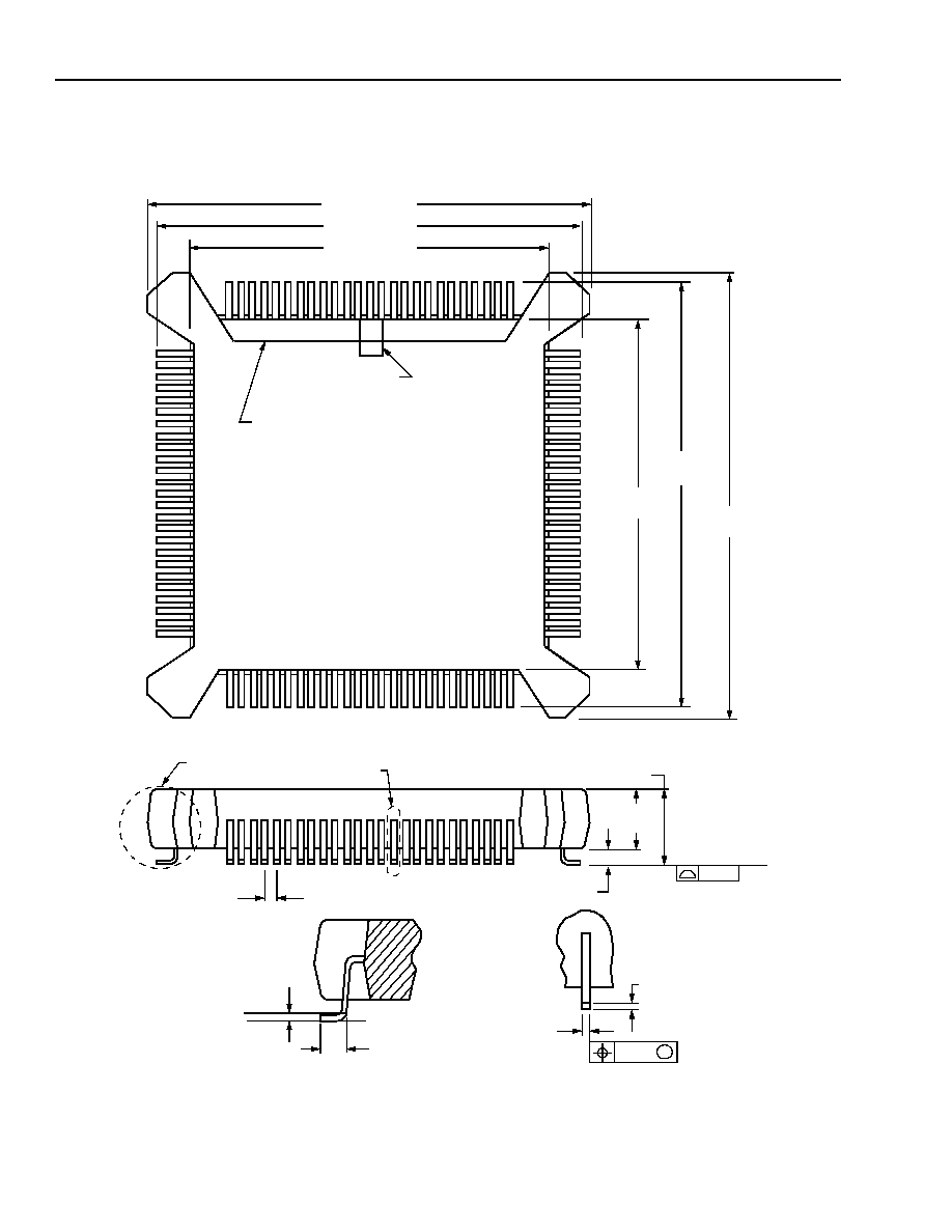
Data Sheet
DSP1627 Digital Signal Processor
March 2000
152
Lucent Technologies Inc.
14 Outline Diagrams
14.1 100-Pin BQFP (Bumpered Quad Flat Pack)
All dimensions are in millimeters.
5-1970 (F)r.10
PIN #1
IDENTIFIER
ZONE
89
1
13
1 4
3 8
39
6 3
64
88
19.050 ± 0.405
22.350 ± 0.255
22.860 ± 0.305
22.350
± 0.255
19.050
± 0.405
22.860
± 0.305
EDGE CHAMFER
DETAIL A
4.570 MAX
DETAIL B
0.760 ± 0.255
0.635 TYP
0.10
SEATING PLANE
3.555
± 0.255
DETAIL B
0.280 ± 0.075
0.150
M
0.175 ± 0.025
DETAIL A
0.255
0.91/1.17
GAGE PLANE
SEATING PLANE
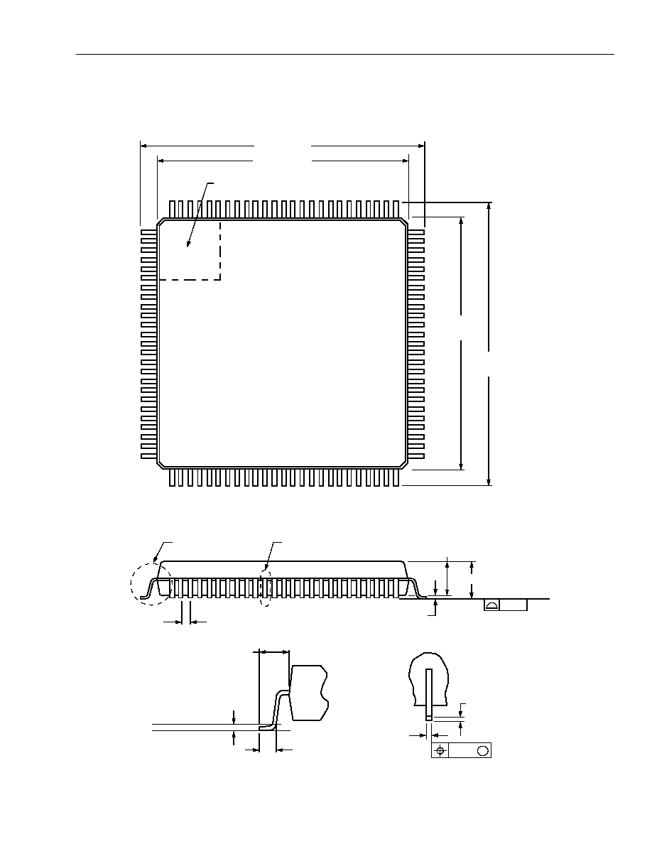
Data Sheet
March 2000
DSP1627 Digital Signal Processor
Lucent Technologies Inc.
153
14 Outline Diagrams
(continued)
14.2 100-Pin TQFP (Thin Quad Flat Pack)
All dimensions are in millimeters.
0.50 TYP
1.60 MAX
SEATING PLANE
0.08
1.40
±
0.05
0.05/0.15
DETAIL A
DETAIL B
14.00
±
0.20
16.00
±
0.20
76
100
1
25
26
50
51
75
14.00
±
0.20
16.00
±
0.20
PIN #1 IDENTIFIER ZONE
DETAIL B
0.19/0.27
0.08
M
0.106/0.200
DETAIL A
0.45/0.75
GAGE PLANE
SEATING PLANE
1.00 REF
0.25
5-2146 (F)r.14

Lucent Technologies Inc. reserves the right to make changes to the product(s) or information contained herein without notice. No liability is assumed as a result of their use or application. No
rights under any patent accompany the sale of any such product(s) or information.
Copyright © 2000 Lucent Technologies Inc.
All Rights Reserved
March 2000
DS00-205WTEC (Replaces DS00-061WTEC)
For additional information, contact your Microelectronics Group Account Manager or the following:
INTERNET:
http://www.lucent.com/micro
E-MAIL:
docmaster@micro.lucent.com
N. AMERICA: Microelectronics Group, Lucent Technologies Inc., 555 Union Boulevard, Room 30L-15P-BA, Allentown, PA 18103
1-800-372-2447, FAX 610-712-4106 (In CANADA: 1-800-553-2448, FAX 610-712-4106)
ASIA PACIFIC: Microelectronics Group, Lucent Technologies Singapore Pte. Ltd., 77 Science Park Drive, #03-18 Cintech III, Singapore 118256
Tel. (65) 778 8833, FAX (65) 777 7495
CHINA:
Microelectronics Group, Lucent Technologies (China) Co., Ltd., A-F2, 23/F, Zao Fong Universe Building, 1800 Zhong Shan Xi Road, Shanghai
200233 P. R. China Tel. (86) 21 6440 0468, ext. 316, FAX (86) 21 6440 0652
JAPAN:
Microelectronics Group, Lucent Technologies Japan Ltd., 7-18, Higashi-Gotanda 2-chome, Shinagawa-ku, Tokyo 141, Japan
Tel. (81) 3 5421 1600, FAX (81) 3 5421 1700
EUROPE:
Data Requests: MICROELECTRONICS GROUP DATALINE: Tel. (44) 7000 582 368, FAX (44) 1189 328 148
Technical Inquiries:GERMANY: (49) 89 95086 0 (Munich), UNITED KINGDOM: (44) 1344 865 900 (Ascot),
FRANCE: (33) 1 40 83 68 00 (Paris), SWEDEN: (46) 8 594 607 00 (Stockholm), FINLAND: (358) 9 4354 2800 (Helsinki),
ITALY: (39) 02 6608131 (Milan), SPAIN: (34) 1 807 1441 (Madrid)