 | –≠–Ľ–Ķ–ļ—ā—Ä–ĺ–Ĺ–Ĺ—č–Ļ –ļ–ĺ–ľ–Ņ–ĺ–Ĺ–Ķ–Ĺ—ā: T8532 | –°–ļ–į—á–į—ā—Ć:  PDF PDF  ZIP ZIP |
Preliminary Data Sheet
September 2001
T8531A/T8532 Multichannel Programmable
Codec Chip Set
Features
s
Per-channel programmable gain and hybrid bal-
ance
s
Programmable termination impedances
s
Programmable
Ķ
-law, A-law, or linear PCM output
s
Tone plant:
-- DTMF generator
-- DTMF receiver
-- Caller ID generator
-- Call progress tones generator
s
Test utilities:
-- Automatic gain calibration
-- Tone generation
-- dc generation
-- dc measurement
-- Variance computation
-- Peak detection
s
Analog and digital loopbacks
s
Programmable time-slot assignment with bit offset
s
Low-noise, balanced, receive SLIC interface
s
Few or no SLIC/codec interface components
required
s
Sigma-delta converters with dither noise reduction
s
Serial microcontroller control interface
s
Meets or exceeds ITU-T G.711--G.712 and rele-
vant
Telcordia Technologies
TM
requirements
s
Available in 64-pin MQFP and TQFP packages
General Description
The multichannel programmable codec chip set is
comprised of the T8531A 16-channel line card signal
processor and one or two custom T8532 octal A/D
and D/A converters. A ROM-coded tone plant, with
line-test and self-test utilities, is included on the sig-
nal processor. Together these devices achieve a
highly integrated and highly programmable multi-
channel voice codec solution.
Software is provided to compute the gain and filter
coefficients required to program the codec.
5-3793i (F)
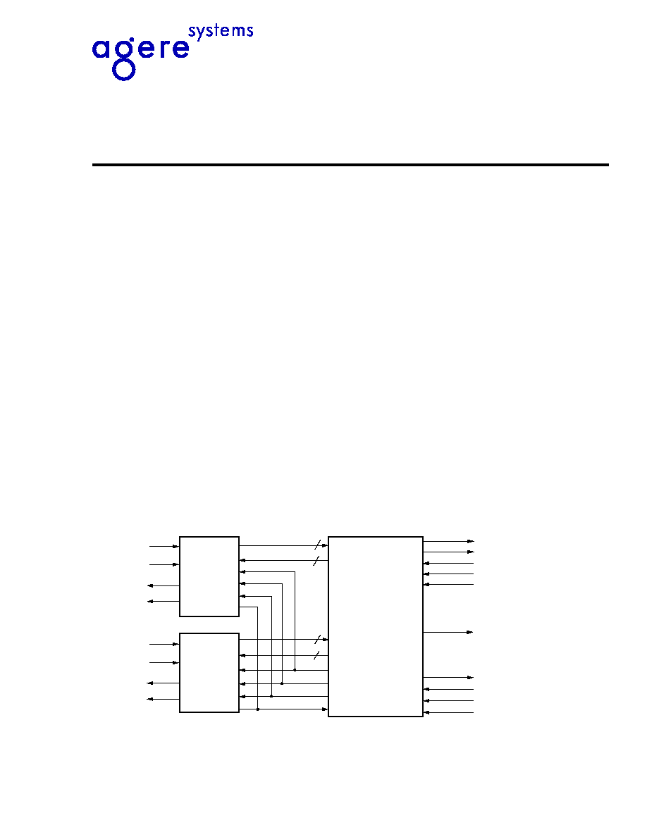
Figure 1. System Block Diagram
T8532
OCTAL
A/D
D/A
T8532
OCTAL
A/D
D/A
T8531A
DIGITAL
SIGNAL
PROCESSOR
VTX (8)
VRP (8)
VRN (8)
VTX (8)
VRP (8)
VRN (8)
2
3
2
3
CK16
VRTX (8)
VRTX (8)
PCM
INTERFACE
MICROPROCESSOR
INTERFACE
ASIC

2
Agere Systems Inc.
Preliminary Data Sheet
September 2001
Codec Chip Set
T8531A/T8532 Multichannel Programmable
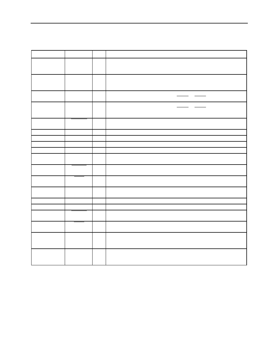
Table of Contents
Contents
Page
Features ..................................................................... 1
General Description.................................................... 1
T8532 Description.................................................... 4
T8531A Description ................................................. 5
Pin Information ........................................................... 7
Chip Set Functional Description ............................... 12
Transmit Path......................................................... 12
Antialias Filter and
-
Converter ...................... 12
Decimator ........................................................... 12
Digital Transmit Gain Adjustment........................ 12
Band Filtering ...................................................... 12
Ķ
-Law, A-Law, and Linear PCM Modes............... 12
Receive Path ......................................................... 13
Receive Path Filtering ......................................... 13
Digital Receive Gain............................................ 13
Interpolator and Digital Sigma-Delta
Modulator.......................................................... 13
Decoder, Filters, and Receive Amplifier ............. 13
Other Chip Set Functions....................................... 13
Voltage Reference............................................... 13
Hybrid Balance .................................................... 13
Analog Termination Impedance Synthesis.......... 13
Digital Termination Impedance Synthesis ........... 14
Loopback Modes ................................................. 14
Interchip Control Interface ................................... 14
T8531A Functional Blocks ..................................... 14
Clock Synthesizer................................................ 14
T8531A System Interface ................................... 15
T8531A Microprocessor Interface ....................... 15
T8532 Octal Control Interface ............................. 16
T8531A Time-Slot Assignment (TSA) ................. 16
DSP Engine Timing................................................ 16
T8531A Program Structure ................................. 16
Control of the DSP Engine via the
Microprocessor Interface .................................. 17
The DSP Engine Time-Slot Information
Tables ............................................................... 17
The DSP Engine ac Path Coefficient Table ........ 17
The Time-Slot Control Word................................ 18
Operations Performed by the DSP Engine at
T8531A Start-Up............................................... 18
Microprocessor Start-Up of the DSP Engine ....... 19
Powering Up a Time Slot in the T8531................ 19
Disabling a Time Slot in the T8531 ..................... 19
T8532 Powerup/Powerdown ............................... 19
Changing DSP RAM Space of an Active
Time Slot........................................................... 20
DSP Engine Memory Requirements ................... 20
Contents
Page
T8531A Reset and Start-Up................................... 20
Hardware Reset .................................................. 20
Internal Reset ...................................................... 21
Reset of the T8532 Devices ................................ 21
Start-Up After Internal Reset.................................. 21
Autocalibration..................................................... 22
User Test Features ................................................ 22
Off-Line Programmable System Test
Capability .......................................................... 22
On-Line Per-Channel Test Capability.................. 22
Inactive Mode with Loopback .............................. 22
Self-Test and Line-Test Routines .......................... 22
Tone Generation ................................................. 22
Tone Detection .................................................... 23
dc Generation ...................................................... 23
dc Measurement.................................................. 23
Variance Computation ......................................... 23
Peak Detection .................................................... 23
Tone Plant.............................................................. 23
DTMF Transceiver............................................... 23
Caller Line Identification ...................................... 23
Call Progress Tones............................................ 23
Absolute Maximum Ratings...................................... 24
Handling Precautions ............................................... 24
Electrical Characteristics .......................................... 25
dc Characteristics .................................................. 25
Transmission Characteristics ................................... 26
Timing Characteristics .............................................. 30
Software Interface .................................................... 33
Applications .............................................................. 44
Common Voltage Reference.................................. 47
Outline Diagrams...................................................... 48
64-Pin MQFP ......................................................... 48
64-Pin TQFP .......................................................... 49
Ordering Information................................................. 50
Appendix A. Transmit Path Group Delay vs. Bit
Offset ................................................................ 50

Preliminary Data Sheet
September 2001
Agere Systems Inc.
3
Codec Chip Set
T8531A/T8532 Multichannel Programmable
Table of Contents
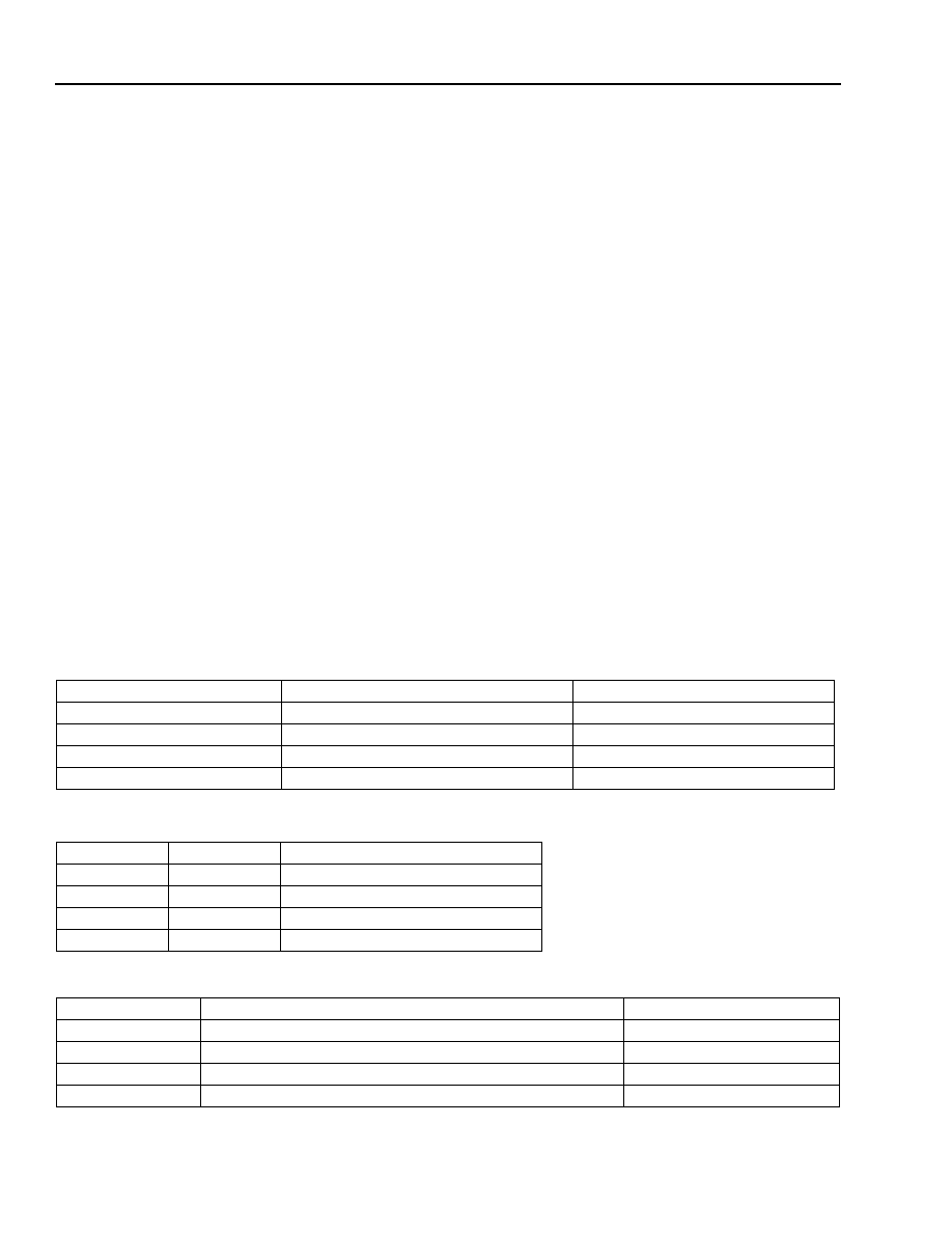
(continued)
Figures
Page
Figure 1. System Block Diagram .................................1
Figure 2. Block Diagram of T8532 Octal Converter.....4
Figure 3. Block Diagram of One T8532 Analog
Channel........................................................4
Figure 4. T8531A Block Diagram ................................5
Figure 5. T8531A Digital ac Path.................................6
Figure 6. Control, PCM, and Octal Interfaces..............6
Figure 7. T8532 64-Pin MQFP ....................................7
Figure 8. T8531A 64-Pin TQFP...................................9
Figure 9. Timing Characteristics of PCM Interface
Assuming 2.048 MHz SCK Rate ................31
Figure 10. Timing Diagram for Microprocessor
Write/Read to/from the DSP on the
Control Interface.......................................32
Figure 11. Line Card Solution Using the L7585
SLIC .........................................................44
Figure 12. Line Card Solution Using the L9215G
SLIC .........................................................45
Figure 13. Line Card Solution Using the L9310G
SLIC .........................................................46
Figure 14. Common 2.4 V Voltage Reference...........47
Tables
Page
Table 1. T8532 Pin Descriptions ................................. 8
Table 2. T8531A Pin Descriptions ............................. 10
Table 3. Active Time-Slot Spacing in a PCM
Bus Frame ................................................... 15
Table 4. DSP Engine RAM Map for Channel_0 ac
Path Coefficients ......................................... 17
Table 5A. Bit Map for DSP Engine Time-Slot
Control Word............................................. 18
Table 5B. Bit Map for Default Per-Board
Coefficient Tables...................................... 18
Table 6. DSP Engine RAM Map for Time-Slot
Information Table 0...................................... 18
Table 7. Summary of Microprocessor Commands
for Control of T8531A Data Processing ....... 20
Table 8. Digital Interface............................................ 25
Table 9. Analog Interface .......................................... 25
Table 10. T8532 Power Dissipation........................... 26
Table 11. T8531A Power Dissipation ........................ 26
Table 12. Gain and Dynamic Range ......................... 26
Table 13. Noise (per Channel) .................................. 28
Table 14. Distortion and Group Delay ....................... 29
Table 15. Crosstalk.................................................... 29
Table 16. PCM Interface Timing ............................... 30
Table 17. Serial Control Port Timing ........................ 32
Table 18. DSP Engine RAM Memory Map ................33
Table 19. T8531A Time-Slot Assignment Memory
Map ...........................................................35
Table 20A. Bit Map for T8531A Time-Slot Assignment
Registers at 0x1400--0x140F.................35
Table 20B. Bit Map for CTZ Disable and Null
Channel...................................................35
Table 21. T8531A Channel Register Memory Map
for T8532 Device 0 ...................................36
Table 22. T8531A Channel Register Memory Map
for T8532 Device 1 ...................................36
Table 23. Bit Map for T8532 Powerup/Powerdown
Registers at 0x1500--0x1507 and
0x1540--0x1547 .......................................37
Table 24. Bit Map for T8532 Channel Control
Register 1 at 0x1508--0x150F and
0x1548--0x154F .......................................37
Table 25. T8532 Control Register 1: Transmit
Gain ...........................................................37
Table 26. T8532 Control Register 1: Analog
Termination Impedance .............................37
Table 27. T8532 Control Register 1: Digital
Loopback ...................................................38
Table 28. Bit Map for T8532 All Channel Test
Register at 0x1510 and 0x1550.................38
Table 29. Bits 3:0 of T8532 All Channel Test
Register at 0x1510 and 0x1550.................38
Table 30. Bit Map for T8532 Channel Control
Register 2 at 0x1518--0x151F and
0x1558--0x155F .......................................39
Table 31. T8532 Control Register 2: Receive Gain ...39
Table 32. T8531A Control Register Map ...................39
Table 33. Bits 15:8 of T8531A Board Control Word 1
at 0x1FFE ..................................................40
Table 34. Bits 7:0 of T8531A Board Control Word 1
at 0x1FFE ..................................................40
Table 35. Bits 15:9 of T8531A Board Control Word 2
at 0x1FFC..................................................41
Table 36. Bits 8:0 of T8531A Board Control Word 2
at 0x1FFC..................................................41
Table 37. Bits 15:0 of T8531A Board Control Word 3
at 0x1FFA ..................................................41
Table 38. Bits 15:0 of T8531A Board Control Word 4
at 0x1FF8 ..................................................41
Table 39. Bits 15:0 of T8531A Board Control Word 5
at 0x1FF6 ..................................................41
Table 40. Bits 15:0 of T8531A Reset of
Microprocessor Commands at 0x7FFF .....41
Table 41. DSP Engine ROM Memory Map................42
Table 42. Transmit Path Group Delay vs. Bit Offset ..50
4
Agere Systems Inc.
Preliminary Data Sheet
September 2001
Codec Chip Set
T8531A/T8532 Multichannel Programmable
General Description
(continued)
T8532 Description
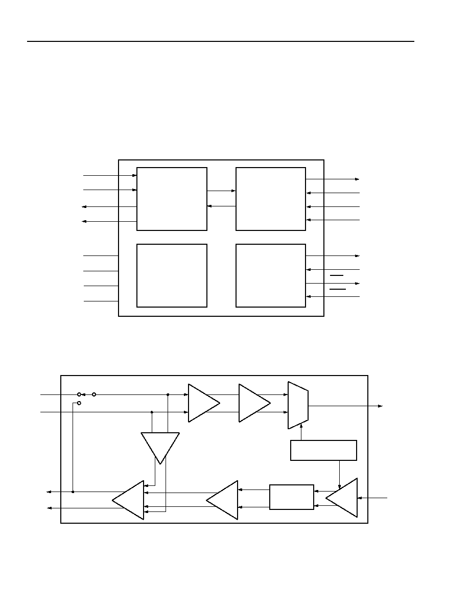
The T8532 block diagram is shown in Figure 2. Each of its eight channels consists of an antialias filter, sigma-delta
A/D and D/A converters, reconstruction and smoothing filters, termination impedance synthesis, and selectable
gain. The digital oversampled data is multiplexed onto a serial data port designed to interface with the T8531A
Another serial interface accepts control data from the T8531A for activating the various gain settings, self-test, and
powerdown modes. This chip also contains a precision voltage reference.
5-3794.b (F)
Figure 2. Block Diagram of T8532 Octal Converter
5-3796.d (F)
* Antialiasing filter.
Figure 3. Block Diagram of One T8532 Analog Channel
8-CHANNEL
A/D D/A
ANALOG HYBRID
&
TERMINATION
VOLTAGE
REFERENCE
OVERSAMPLED
DATA
INTERFACE
CONTROL
INTERFACE
VTX[7:0]
VRTX[7:0]
VRP[7:0]
VRN[7:0]
V
DDA
V
SSA
V
DD
V
SS
OSDX[1:0]
OSDR[1:0]
OSCK
OSFS
CDO
CDI
CCS
RSTB
GAIN
AAF*
-
A/D
A
T
GAIN
SUM
GAIN
V REFERENCES
RECEIVE
FILTER
D/A
D/A
VTX
VRP
VRN
1.024 MHz
1.024 MHz
VRTX
DIGITAL LOOPBACK
Agere Systems Inc.
5
Preliminary Data Sheet
September 2001
Codec Chip Set
T8531A/T8532 Multichannel Programmable
General Description
(continued)
T8531A Description
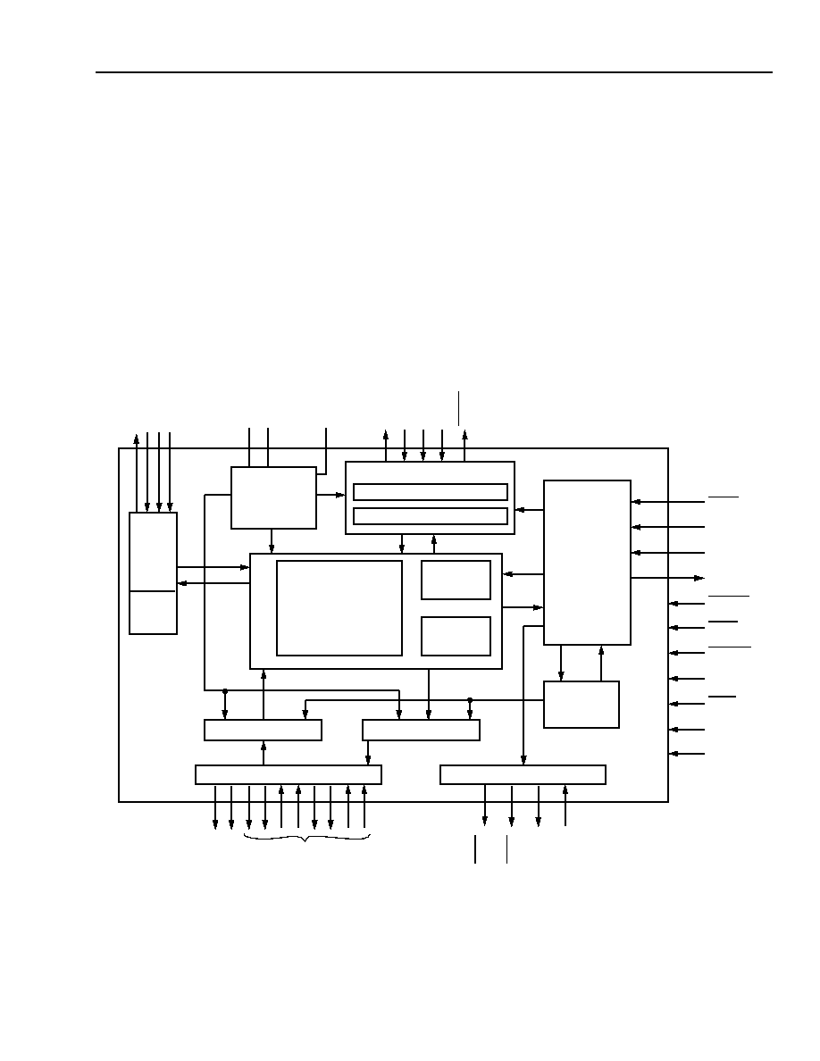
As shown in Figure 4, the
T8531A contains a digital signal processor (DSP) engine surrounded by a customized
input/output (I/O) frame. The I/O frame performs the
Ķ
-law or A-law conversion as well as the decimation and inter-
polation functions needed to interface the sigma-delta bit streams to the digital signal processor engine. The
sigma-delta converters operate at a 1.024 MHz sample rate, while the signal processor operates at 16 ksamples/s.
A key function of the I/O frame is to control the timing of the digital data going to the signal processor so that group
delay is minimized.
The I/O frame also contains an integrated phase-locked loop which synthesizes all the required internal clocks for
the chip set.
The microcontroller interface is used to run the ROM routines and to download the gain, filter, and balance network
settings, powerup/powerdown commands, time-slot assignments, digital loopback settings, and commands for the
T8532 octal chips.
0505(F)
Figure 4. T8531A Block Diagram
PLL
CLOCK
SYNTHESIZER
JTAG
SYSTEM PCM INTERFACE
DATA TRANSFER
Ķ
/A-LAW CONVERTER
MICRO-
PROCESSOR
CONTROL
INTERFACE
DSP
ROM
DSP
RAM
DIGITAL
SIGNAL
PROCESSING
ENGINE
DECIMATOR
INTERPOLATOR
TSA
T8532 CONTROL INTERFACE
T8532 OVERSAMPLED INTERFACE
UPCK
UPDI
UPDO
TSTCLK
V
DD
V
SS
HDS
UPCS
HIGHZB
RSTB
T_SYNC
TEST
OSDX/R[3:0]
OS
CK
OSF
S
CDO
CCS
0
CCS
1
CDI
TDI
TCK
TMS
TDO
S
T
SX
B
SD
X
SD
R
SC
K
SFS
V
DDA
V
SSA
CK
16

6
Agere Systems Inc.
Preliminary Data Sheet
September 2001
Codec Chip Set
T8531A/T8532 Multichannel Programmable
General Description
(continued)
T8531A Description
(continued)
0498 (F)
Figure 5. T8531A Digital ac Path
5-4229.F (F)
Figure 6. Control, PCM, and Octal Interfaces
Ķ
/A-LAW
TO
LINEAR
RECV
FILTER
REL
RDG
INTER-
POLATOR
DIGITAL
-
BALANCE
FILTER
LINEAR
TO
Ķ
/A-LAW
XMT FILTER
REL
TDG
DECIMATOR
ų
64
1.024 MHz
8 kHz
PCMRX
8 kHz
PCMTX
1.024 MHz
ABS
RDG
ABS
CTZ
FILTER
Ķ
/A-LAW
TO
LINEAR
RECV
FILTER
REL
RDG
INTER-
POLATOR
DIGITAL
-
BALANCE
FILTER
LINEAR
TO
Ķ
/A-LAW
XMT FILTER
DECIMATOR
ų
64
1.024 MHz
8 kHz
PCMRX
8 kHz
PCMTX
1.024 MHz
ABS
RDG
TDG
CTZ
FILTER
OSFS
OSCK
OSDR0
OSDR1
OSDX0
OSDX1
CDO
CDI
CODEC 0
T8532
DSP
T8531A
8 kHz SYNC
4 MHz CLOCK
4 CH RX DATA
4 CH RX DATA
4 CH TX DATA
4 CH TX DATA
CHIP SELECT
CONTROL REGISTER
CONTROL REGISTER
UPCK
UPCS
UPDI
UPDO
CLOCK
CHIP SELECT
CONTROL REGISTER IN
CONTROL REGISTER OUT
SCK
SFS
SDR
SDX
STSXB
DATA TRANSMIT
CLOCK
FRAME SYNC
DATA RECEIVE
BACKPLANE
CODEC 1
T8532
CHIP SELECT
OSDX2
OSDR2
OSDR3
OSDX3
PCM
INTERFACE
CONTROL
INTERFACE
OCTAL
INTERFACE
OSDX2
OSDR2
OSDR3
OSDX3
CDO
CDI
OSCK
OSFS
4 CH RX DATA
4 CH RX DATA
4 CH TX DATA
4 CH TX DATA
OSFS
OSCK
OSDR0
OSDR1
OSDX0
OSDX1
CDI
CDO
CCS0
CCS1
CCS0
CCS1
DRIVER ENABLE
MICRO-
PROCESSOR
PCM
BUS
Agere Systems Inc.
7
Preliminary Data Sheet
September 2001
Codec Chip Set
T8531A/T8532 Multichannel Programmable
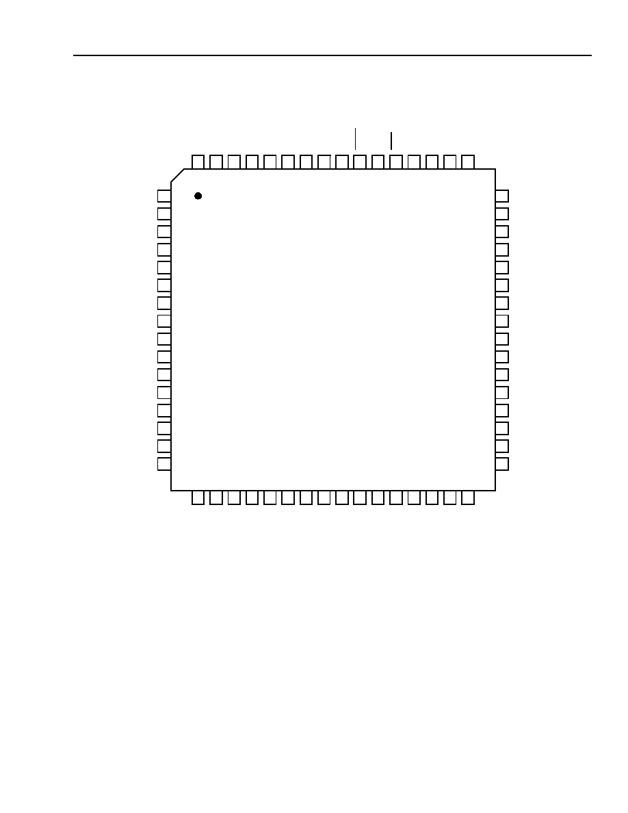
Pin Information
5-9214 (F)
Figure 7. T8532 64-Pin MQFP
60
59
58
57
56
55
54
53
52
61
RS
T
B
OSDX
0
VTX
0
V
DDD
CC
S
OS
DR1
V
SS
D
VTX
7
OSCK
62
63
64
51
50
49
CD
I
OS
DR0
V
DDA
CD
O
OSDX
1
V
DDA
OSF
S
30
28
27
26
25
24
23
22
21
20
29
NC
V
DDA
VRT
X
4
V
DDA
V
SSA
NC
VT
X
3
VRT
X
3
NC
31
32
19
18
17
NC
NC
VT
X
4
NC
NC
V
DDA
NC
13
12
11
10
9
8
7
6
5
4
VRTX6
VRTX5
VRTX7
VRN7
VRN6
V
SSA
VRP4
V
DDA
14
15
16
3
2
1
VRP6
VTX5
VRP7
V
SSA
VRP5
VRN5
VRN4
VTX6
36
38
39
40
41
42
43
44
45
46
37
VRP1
VTX2
VRTX0
VRP0
V
SSA
VRP2
V
SSA
VRP3
VTX1
35
34
33
47
48
VRN1
V
DDA
VRN0
VRTX2
VRN2
VRN3
VRTX1
T8532
OSDX
0

8
Agere Systems Inc.
Preliminary Data Sheet
September 2001
Codec Chip Set
T8531A/T8532 Multichannel Programmable
Pin Information
(continued)
Table 1. T8532 Pin Descriptions
Note: TI = TTL input, TO = TTL output; CI = CMOS input, CO = CMOS output; AI = analog input, AO = analog output; I
u
indicates a pull-up
device is included on this lead, I
d
indicates a pull-down device is included on this lead.
Number
Name
Type
Name/Function
64, 8, 10, 18,
31, 39, 41, 49
VTX[7:0]
AI
Analog Input. Transmit signal voltage to be encoded.
1, 7, 11, 17, 32,
38, 42, 48
VRTX[7:0]
AI
Transmit Reference Voltage. 2.4 V reference. Each pin must have a sep-
arate supply associated with the corresponding VTX pin.
2, 6, 12, 16, 33,
37, 43, 47
VRP[7:0]
AO
Noninverting Receive Output. This pin can drive high-impedance loads
either differentially or single ended. It is the complement of the VRN output.
3, 5, 13, 15, 34,
36, 44, 46
VRN[7:0]
AO
Inverting Receive Output. This pin can drive high-impedance loads either
differentially or single ended. It is the complement of the VRP output.
9, 19, 27, 30,
40, 50, 63
V
DDA
--
5 V Analog Power Supply. Power supply decoupling capacitor (0.1
Ķ
F)
should be connected from each V
DDA
pin to analog ground. Capacitors
should be located as close as possible to the device pins.
4, 14, 21,
35, 45
V
SSA
--
Analog Ground.
51
V
DDD
--
5 V Digital Power Supply. Decouple with a 0.1
Ķ
F capacitor to digital
ground.
62
V
SSD
--
Digital Ground.
60, 59
OSDX[1:0]
CO
Oversampled Transmit Data. Four channels of 1.024 MHz
-
transmit
data is transmitted to the T8531A through each of these pins. The data rate
is 4.096 MHz.
61, 58
OSDR[1:0]
CI
Oversampled Receive Data. Four channels of 1.024 MHz
-
receive
data is received from the T8531A on each of these pins. The data rate is
4.096 MHz.
57
OSCK
CI
Interface Clock. The 4.096 MHz clock that enters this pin from the T8531A
serves as the bit clock for all the oversampled data transmission between
this chip and the T8531A This is the master clock input for the T8532.
56
OSFS
CI
Interface Frame Sync. This signal serves as the frame sync for the over-
sampled data interface between the T8532 and the T8531A
54
CDI
CI
Control Data Interface Input. The T8531A sends control register address
and data to the T8532 through this pin. One address byte and one data
byte are accepted each time CCS is toggled.
52
CDO
CO
Control Data Interface Output. Control register contents are clocked out
through this pin.
53
CCS
CI
Control Interface Chip Select (Active-Low). This active-low input
enables the control interface.
55
RSTB
TI
u
Reset (Active-Low). This input must be pulled high for normal operation.
When pulled momentarily low (at least 1
Ķ
s) while OSCK is active, all pro-
grammable registers in the device are reset to the states specified under
powerup initialization. This pin has an internal pull-up resistor.
20, 22--26,
28, 29
NC
--
No Connect. No connection to chip. These pins can be used as logic level
tie points.

Agere Systems Inc.
9
Preliminary Data Sheet
September 2001
Codec Chip Set
T8531A/T8532 Multichannel Programmable
Pin Information
(continued)
5-9213a (F)
Figure 8. T8531A 64-Pin TQFP
60
59
58
57
56
55
54
53
52
61
T_SY
NC
H
I
GHZB
V
SS
CD
I
CC
S
1
CK
1
6
V
DD
NC
V
SS
62
63
64
51
50
49
CD
O
RS
T
B
V
DD
CC
S
0
TES
T
V
SS
V
DD
30
28
27
26
25
24
23
22
21
20
29
SD
X
UP
CK
S
C
KS
EL
V
DD
SF
S
UP
DI
V
DD
V
SS
V
DD
31
32
19
18
17
SDR
V
SS
V
SS
SC
K
UP
CS
UPDO
ST
SX
B
13
12
11
10
9
8
7
6
5
4
TCK
V
DDA
NC
V
DD
TDO
NC
V
DD
V
SS
14
15
16
3
2
1
TMS
V
DD
V
SS
TDI
NC
V
SSA
V
SS
TSTCLK
36
38
39
40
41
42
43
44
45
46
37
OSDX3
OSCK
JTESTB
V
SS
OSDX2
OSDR0
OSDR1
V
SS
V
SS
35
34
33
47
48
OSDR2
OSFS
V
DD
OSDX0
OSDX1
V
DD
OSDR3
T8531A

10
Agere Systems Inc.
Preliminary Data Sheet
September 2001
Codec Chip Set
T8531A/T8532 Multichannel Programmable
Pin Information
(continued)
Table 2. T8531A Pin Descriptions
Note: TI = TTL input, TO = TTL output; CI = CMOS input, CO = CMOS output; AI = analog input, AO = analog output; I
u
indicates a pull-up
device is included on this lead.
Number
Name
Type
Name/Function
29
UPDI
TI
Control Data Interface Input. The microcontroller sends control register
address and data to the T8531A through this pin.
30
UPDO
TO
Control Data Interface Output. The microcontroller receives control regis-
ter contents from this pin. Inactive state is high impedance.
27
UPCK
TI
Control Data Interface Clock. Bit clock for the control interface. Speed is
limited to 4.096 MHz.
28
UPCS
TI
Control Interface Chip Select (Active-Low). This active-low input enables
the control interface.
43, 45,
36, 38
OSDX[3:0]
CI
Oversampled Transmit Data. Four channels of 1 Msamples/s
-
transmit
data are received from the T8532 chips through each of these pins. The data
rate is 4.096 MHz.
42, 44,
35, 37
OSDR[3:0]
CO
Oversampled Receive Data. Four channels of 1 Msamples/s
-
receive
data is transmitted to the T8532 chips on each of these pins. The data rate is
4.096 MHz.
39
OSCK
CO
4.096 MHz Clock. Clock for data transfer to/from T8532 chips.
40
OSFS
CO
Oversampling Sync. 8 kHz synchronization pulse for data transfer
to/from T8532 chips.
11
V
DDA
--
Synthesizer V
DD
. Power supply for clock synthesizer block.
13
V
SSA
--
Synthesizer Ground. Ground connection for the clock synthesizer block.
24
STSXB
TO
Backplane Drive Enable (Active-Low). Active when SDX is transmitting
valid data; high impedance otherwise. This pin provides an enable signal for
a backplane line driver.
20
SCK
TI
Master Clock Input. This is the bit clock used to shift data into and out of the
SDR and SDX pins. It is the input to the clock synthesizer and is used to
generate all internal clocks. Rate is 4.096 MHz.
17
SCKSEL
TI
u
Master Clock Select Input. A logic low selects the 2.048 MHz SCK. A logic
high selects the 4.096 MHz SCK. An internal pull-up device is included, pro-
viding 4.096 MHz SCK operation with no external connections.
22
SDR
TI
Receive PCM Input. The data on this pin is shifted into the T8531A on the
falling edges of SCK. Data is only entered for valid time slots as defined in
the TSA registers.
Agere Systems Inc.
11
Preliminary Data Sheet
September 2001
Codec Chip Set
T8531A/T8532 Multichannel Programmable
Pin Information
(continued)
Table 2. T8531A Pin Descriptions (continued)
* The DSP is not configured for boundary scan operation.
Note: TI = TTL input, TO = TTL output; CI = CMOS input, CO = CMOS output; AI = analog input, AO = analog output; I
u
indicates that a pull-
up device is included on this lead, I
d
indicates that a pull-down device is included on this lead.
Number
Name
Type
Name/Function
23
SDX
TO
Transmit PCM Output. This pin remains in the high-impedance state
except during the transmit time slots as defined in the TSA registers.
Data is shifted out on the rising edge of SCK.
21
SFS
TI
Frame Sync. Active-high pulse or square wave with an 8 kHz pulse
repetition rate. The rising edge defines the start of the transmit and
receive frames.
54
CDO
CO
T8532 Control Data Output. Control register information for the T8532
chips. Data is valid only when either CCS0 or CCS1 is low.
51
CDI
TI
u
T8532 Control Data Input. Control register information from the T8532
chips. Data is valid only when either CCS0 or CCS1 is low. An internal
pull-up device is provided.
53, 52
CCS[1:0]
CO
Control Interface Chip Select (Active-Low). These active-low outputs
select one of the associated T8532 chips.
7
TCK
TI
JTAG Test Port*-Common Test Clock. Rate
20 MHz.
4
TDI
TI
u
JTAG Test Port*-Serial Data Input. A pull-up device is provided.
5
TDO
TO
JTAG Test Port*-Serial Data Output.
6
TMS
TI
u
JTAG Test Port*-Mode Select. A pull-up device is provided.
48
JTESTB
TI
u
JTAG Test. Used for factory testing. Do not make any connection to this
pin. A pull-up device is provided.
59
HIGHZB
TI
u
3-State Control Pin (Active-Low). When pulled low, the device output
pins go into a high-impedance state. A pull-up device is provided.
60
TEST
CI
u
Test Mode Input (Active-Low). This input allows bypass of clock synthe-
sizer and uses TSTCLK to drive the chip. A pull-up device is provided.
61
CK16
CO
16 MHz Clock Output. 16.384 MHz clock output (50% duty cycle). This
clock is present at all times and can be used to drive a host processor.
8
TSTCLK
CI
Test Clock.
1, 12, 14, 64
NC
--
No Connect. This pin may be used as a tie point.
55
T_SYNC
CI
u
Test Sync (Active-Low). Used for factory testing. Do not make any con-
nection to this pin. A pull-up device is provided.
58
RSTB
TI
u
Reset (Active-Low). A logic low initiates reset. A pull-up device is pro-
vided.
3, 10, 16, 19,
25, 31, 34, 46,
50, 56, 62
V
DD
--
5 V Digital Power Supply. Power supply decoupling capacitors (0.1
Ķ
F)
should be connected from each V
DD
pin to ground. Capacitors should be
located as close as possible to the device pins.
2, 9, 15, 18, 26,
32, 33, 41, 47,
49, 57, 63
V
SS
--
Digital Ground.

12
12
Agere Systems Inc.
Preliminary Data Sheet
September 2001
Codec Chip Set
T8531A/T8532 Multichannel Programmable
Chip Set Functional Description
Transmit Path
Antialias Filter and
-
Converter
The line interface circuit must provide a transmit signal
(VTX), and a reference voltage (VRTX) which is the dc
voltage of the VTX signal for that channel.
The input signal goes into a programmable-gain ampli-
fier. The signal is then passed through an antialias filter
followed by a
-
A/D converter. The
-
converter
operates at 1.024 MHz. The processed output signals
are multiplexed into two groups of four channels each
onto output pins OSDX[1:0], each of which operates at
4.096 MHz.
A precision, on-chip voltage reference helps ensure
accurate and highly stable transmission levels.
It is important to understand the difference between
how the gain levels should be set in the T8532 and
how these levels would be set in a standard codec.
The T8532 is best thought of as a data acquisition sys-
tem, not a codec. Hybrid balance, fine gain adjust,
Ķ
- or A-law coding, filtering, and equalization are done
after the A/D in the T8532 and by the DSP processor in
the T8531A The analog gain adjust taps should not be
used to set the absolute level at the PCM output. This
can be done using the DSP gain adjust taps. The ana-
log taps should be set so the signal at the input to the
A/D converter is as close as possible to the full-scale
input level of the A/D for the largest signal level that will
be present at the VTX input. This optimizes the
dynamic range of the A/D. The 0 dB gain tap should
thus be used if the maximum signal level is in the range
between 2.25 Vp-p and 3.2 Vp-p. The 3 dB tap should
be used for signals with a maximum signal level in the
range of 1.6 Vp-p and 2.25 Vp-p. The 6 dB tap should
be used for signals with a maximum signal level in the
range between 1.1 Vp-p and 1.6 Vp-p. Higher gain lev-
els should be used for signals with smaller absolute
levels.
The signal level to produce a 0 dBm0 level at the digital
transmit output of the T8531A is not a fixed quantity as
explained above. For a line with a complex impedance
or an RX echo signal, extra headroom must be allowed
and the TX signal level must be set to account for the
headroom. In this specification, the largest possible
0 dBm0 level for the TX signal is assumed. This guar-
antees that the distortion specification will not be
exceeded for all practical 0 dBm signal levels. The larg-
est possible 0 dBm signal is one that has no headroom
for TX gain equalization. For the case of 0 dB transmit
gain, this level is found as the following:
(3.2 V/log
≠1
(3.15/20)) = 2.23 Vp-p.
This level is the worst-case 0 dBm0 level.
Decimator
The decimator filters out the high-frequency compo-
nents and down-samples to 16 kHz. It also reorders the
16 channels of transmit signals into a sequence that is
determined by the time-slot assignment.
Digital Transmit Gain Adjustment
The transmit absolute and relative gains are specified
as 15-bit binary numbers representing their linear
magnitude. These gains default to 4000 hex. This
equates to a 0 dB gain for the relative gain but equates
to a 1.65 dB gain for the absolute gain. For a 0 dB gain,
program the absolute gain for 34ED hex. Gain can be
varied from minus infinity dB (off) (0000 hex) to 6 dB for
relative gain or to 7.65 dB for absolute gain (7FFF hex).
The relative gain control allows for TLP adjustment
without hybrid balance or termination coefficient modifi-
cation.
Band Filtering
The bandpass filter in the transmit path removes
power-line and ringing frequencies, and eliminates
most of the signal energy at 4 kHz and above. This
allows the encoder to transmit the filtered signal at 8
ksamples/s, the worldwide standard.
The transmit filtering is implemented with a low-pass
filter, followed by a high-pass filter. The data samples
enter the filter at 16 ksamples/s. They are first low-pass
filtered to 3.4 kHz. After low-pass filtering, the sampling
rate is reduced to 8 ksamples/s. The samples are then
high-pass filtered to 300 Hz.
The low-pass filter also serves as an equalizer for fre-
quency response alterations. A set of equalizer coeffi-
cients that modify this filter are required for each
complex termination impedance when using a voltage
feed, current-sensed SLIC.
Ķ
-Law, A-Law, and Linear PCM Modes
In the transmit path, the 8 ksamples/s PCM signal out-
put from the filter is processed prior to transmission
over the system interface. The 16-bit linear PCM signal
may be compressed according to either
Ķ
-law or A-law,
or transmitted as two consecutive 8-bit words. The
selection is programmable via the microprocessor
interface. Please note, when using A-law, a linear value
of 0 is always encoded as 7F.

Agere Systems Inc.
13
Preliminary Data Sheet
September 2001
Codec Chip Set
T8531A/T8532 Multichannel Programmable
Chip Set Functional Description
(continued)
Receive Path
In the receive direction, the signal received from the
system interface is converted to a 16-bit linear PCM sig-
nal.
Receive Path Filtering
The 16-bit linear PCM signal is filtered and interpolated
to 16 ksamples/s to meet the receive signal loss charac-
teristics. This filter smooths the data following interpola-
tion from 8 ksamples/s to 16 ksamples/s. The filter can
also serve as an equalizer for frequency response alter-
ation. This is required for complex termination imped-
ance cases when using a current feed, voltage-sensed
SLIC.
One of two receive filters can be used, the receive filter
and the extended receive filter. The receive filter has
two poles and three zeros. This filter can be used to
minimize downloadable code (to use this receive filter,
select the T7531x codec in the Aquarium coefficient
software). The extended receive filter provides more
flexibility in coefficient optimization by providing three
poles and three zeros. The Aquarium coefficient soft-
ware defaults to the extended receive filter when the
T8531x codec is selected.
Digital Receive Gain
The receive absolute and relative gains are specified as
15-bit binary numbers representing their linear magni-
tude. These gains default to 4000 hex. This equates to a
0 dB gain for the relative gain but equates to a
≠0.211 dB gain for the absolute gain. For a 0 dB gain,
program the absolute gain for 4193 hex. Gain can be
varied from minus infinity dB (0) (0000 hex) to 6 dB for
relative gain or to 5.8 dB for absolute gain (7FFF hex).
The relative gain control allows for TLP adjustment with-
out hybrid balance or termination coefficient modifica-
tion.
Interpolator and Digital Sigma-Delta Modulator
The sampling frequency of the receive signal from the
digital gain adjustment is increased from 16 kHz to
64 kHz by the interpolator, which removes most of the
high-frequency signal images above 8 kHz. The interpo-
lator also maps each of 16 time slots to the appropriate
line channel through the digital sigma-delta modulator.
The digital sigma-delta modulator converts the interpo-
lated signal to a 1.024 MHz bit stream which is then sent
to the T8532 device.
Decoder, Filters, and Receive Amplifier
Receive data enters the T8532 on pins OSDR[1:0] at
4.096 MHz; four channels are time-division multiplexed
onto each pin. The data is demultiplexed into eight indi-
vidual channels. The processed signal for each chan-
nel passes through switched-capacitor D/A and
reconstruct filters, followed by a smoothing filter. A pro-
grammable gain amplifier is included, followed by an
output amplifier capable of driving a 50 k
load to
Ī
1.58 V single-ended (relative to VOS) or
Ī
3.16 V dif-
ferential at peak overload. For single-ended operation,
the load must be ac coupled to VRP (or VRN).
Other Chip Set Functions
Voltage Reference
The T8532 has a precision on-chip voltage reference
which ensures accurate and highly stable transmission
levels.
Hybrid Balance
The hybrid balance function is provided as a digital
block in the T8531A
The T8531A implements a 9-tap FIR and a single-pole
IIR digital balance filter in which a replica of the echo is
digitally subtracted from the transmit plus near-end
echo signal. The coefficients are user programmable
on a per-line basis via the microprocessor interface.
Analog Termination Impedance Synthesis
Termination impedance matching is implemented to
maximize the power transfer capability at the loop inter-
face and to minimize signal reflections between the
transmit and receive paths.
The resistive component, implemented in the T8532
device, comprises a variable attenuated path between
VTX and VRP. The capacitive component is imple-
mented in the digital domain.
Analog termination impedance (ATI) is provided with 16
gain settings to match a voltage drive/current sense
line interface circuit with the following characteristics:
Z
T
= 2R
P
+ G
TX
* G
RX
* A
T
where Z
T
is the termination impedance in ohms, R
P
is
the resistance of each protection resistor (for stability
R
P
50
), G
TX
is the SLIC transmit gain, G
RX
is the
SLIC receive gain, and A
T
is the T8532 feedback gain.
The polarity of the A
T
gain is positive (positive voltage
swing on VTX gives a positive voltage swing on VRP).
The gain values are shown in Table 26; gain tolerances
are
Ī
2%. Differential receive output is assumed.

14
14
Agere Systems Inc.
Preliminary Data Sheet
September 2001
Codec Chip Set
T8531A/T8532 Multichannel Programmable
Chip Set Functional Description
(continued)
Other Chip Set Functions
(continued)
Digital Termination Impedance Synthesis
The CTZ filter in the T8531A synthesizes complex ter-
mination impedances. The CTZ filter utilizes alpha and
beta coefficients (board control words 4 and 5, respec-
tively) to perform the synthesis. One set of alpha beta
coefficients is required for each termination impedance
and balance network.
Alpha bits [9:0] represent the RC time constant of the
impedance that the filter is going to synthesize. The
bits are formatted as two's complement. Alpha bits
must be a nonzero value. Beta bits [7:0] represent the
dc gain of the filter. Beta coefficients are also formatted
as two's complement. Setting beta equal to zero turns
off the CTZ function.
There is a constraint on the value of the protection
resistor with regard to termination impedance synthesis
and hybrid balance. For synthesis to operate properly,
the combined series resistance of the tip protection
resistor and the ring protection resistor must be 100
or greater.
Loopback Modes
There are four loopback modes in the T8532.
The first two loopback modes are controlled by the all-
channel test (ACT) register. ACT bits 0 and 1 place all
eight channels into loopback mode. Analog and digital
loopback are described and shown in block diagram
form in Table 29. Analog loopback allows one to check
functionality from Tip/Ring up to and including the
T8532. Digital loopback allows the T8531A to check
T8532 functionality.
The third loopback mode is used in the autocalibration
sequence (control register 2). This mode provides a
loopback between a selected channel and channel four
of a given T8532. The channel to be calibrated is
selected via control register 1 (see Table 27). Channel
four is the only channel in the T8532 that is trimmed for
gain accuracy. Every other channel uses channel four
as a reference and is calibrated to it during the autocal-
ibration sequence.
The fourth loopback mode is a digital loopback mode
located in control register 1. This operates like the digi-
tal loopback mode described in the notes for the ACT
register (table 29). Unlike the ACT register, this digital
loopback mode is selectable per channel. This loop-
back mode can be used to check T8532 functionality
from the T8531A device. It is also used during the cali-
bration sequence.
There is one loopback mode in the T8531A Loopback
at the oversampled data interface is controlled by
board control word 1. This mode allows the T8531A to
test itself. When bit 0 of 0x1FFE is selected, all 16
channels of octal interface receive data (OSDRn) are
looped back to the T8531A transmit inputs (OSDXn).
Interchip Control Interface
The control interface is a 4-pin interface used to send
control information to the T8532 from the T8531, and to
read back the control register contents. The pins con-
sist of a chip select input (CCS0/CCS1), a data input
(CDI), and a data output (CDO). The transfer of control
data is synchronous with the 4.096 MHz OSCK, which
is also used for oversampled data transfer.
T8531A Functional Blocks
Clock Synthesizer
The clock synthesizer block is a phase-lock loop (PLL)
circuit which takes SCK supplied by the backplane and
uses it to produce the 81.92 MHz DSP engine clock.
The input clock, SCK, can be 2.048 MHz or 4.096 MHz.
An on-chip clock synthesizer has the advantages
shown below:
s
Precludes the need for extra clocks to be fed over
the backplane.
s
Constrains the high-speed DSP engine clock within
the device.
s
Synchronizes all clocks used on the line card to the
backplane clock, thus reducing board noise due to
beat frequencies.
A clock generator block takes the PLL output and
divides it down to produce all the lower-frequency
clocks used by the T8531A and T8532.

Agere Systems Inc.
15
Preliminary Data Sheet
September 2001
Codec Chip Set
T8531A/T8532 Multichannel Programmable
Chip Set Functional Description
(continued)
T8531A Functional Blocks
(continued)
T8531A System Interface
The system interface is a full-duplex interface used for
the exchange of PCM data with the system. The sys-
tem is the master of this bus. No control information is
transmitted over the system interface; all control
instructions are routed over the microprocessor inter-
face.
The system interface is used for all 16 lines serviced by
the T8531A The PCM data rate is 8 ksamples/s/line,
so the total required channel capacity is 16 x 8 =
128 Kwords/s in each direction. At the 4.096 MHz rate,
each word takes 1.95
Ķ
s to transmit interleaved with
5.86
Ķ
s of dead time. The frame sync, SFS, is pre-
sented to the system interface at an 8 kHz rate.
A single bit clock and frame sync are used to control
both the transmit and receive directions. The beginning
of the first time slot in a frame is identified from the SFS
input (see Figure 9). In nondelayed mode, SFS is
active coincident with bit 0 of time slot 0 of the RX
frame (and the TX frame if the programmed offset
between TX and RX is 0). In delayed mode, SFS is
active one cycle earlier.
The amount of skew or offset between the transmit and
receive frames and time slots is programmable via
board control word 2, 0x1FFC. The bit offset is up to a
frame, i.e., up to 511 bits in 4 MHz mode. The bit offset
skew takes place in the system PCM interface block.
The active transmit and receive time slots are deter-
mined by the card address. The number of time slots
within a frame varies according to the rate of SCK. Only
16 time slots are ever active in a frame, as shown in
Table 3.
The T8531A obtains its card address in board control
word 1, 0x1FFE.
In
Ķ
-law or A-law mode, each PCM word is only 8 bits
long and occupies one time slot. In linear mode, the
PCM word is 16 bits long and occupies two adjacent
time slots. The MSB is the first bit clocked out in the
valid time slot, and the LSB is the last bit of the follow-
ing (invalid) time slot.
T8531A Microprocessor Interface
This interface between the microprocessor (or other
external controller) and the T8531A device carries
user-supplied program variables and control and test
instructions to both the T8531A and the T8532 octal
converters. The external device is the master of the
microprocessor interface. The interface is serial and
asynchronous, and consists of four pins (UPCK,
UPCS, UPDI, UPDO). The data rate is determined by
the customer's choice of external device, but may not
exceed 4.096 MHz. Microprocessor interface com-
mands consist of two words, address and data.
Address and data are 16 bits wide. The T8531A
expects an address first. The first bit of the address
word is the R/W flag, which tells the T8531A whether it
must receive or send data (receive, R/W = 0; send, R/
W = 1).
Addresses less than 0x1400 refer to the DSP engine
RAM space. If a read from the DSP engine is required,
the microprocessor interface issues a read interrupt to
the DSP engine. If it's a write to the DSP engine, the
microprocessor interface shifts in the data word and
saves it into the data register before sending a write
interrupt to the DSP engine. Once in every 7.8
Ķ
s time
segment, the DSP engine checks whether an interrupt
is outstanding from the microprocessor interface block.
If so, the DSP engine reads the address register. If it's
a read, the DSP engine fetches the word from RAM,
places it in the data register, and shifts it out to the
microprocessor. If it's a write, it puts the contents of the
data register into RAM.
Table 3. Active Time-Slot Spacing in a PCM Bus Frame
SCK Rate (MHz)
Total # of Time Slots
Card Address
Valid Time Slots
Invalid Time Slots
2.048
32
0
1
0, 2, 4, . . . 30
1, 3, 5, . . . 31
1, 3, 5, . . . 31
0, 2, 4, . . . 30
4.096
64
0
1
2
3
0, 4, 8, . . . 60
1, 5, 9, . . . 61
2, 6, 10, . . . 62
3, 7, 11, . . . 63
1--3, 5--7, . . . 61--63
0, 2--4, 6--8, . . . 62--63
0--1, 3--5, 7--9, . . . 63
0--2, 4--6, 8--10, . . . 60--62

16
16
Agere Systems Inc.
Preliminary Data Sheet
September 2001
Codec Chip Set
T8531A/T8532 Multichannel Programmable
Chip Set Functional Description
(continued)
T8531A Functional Blocks
(continued)
A pause therefore exists between the external control-
ler issuing an address and receiving a data read back.
The data rate of 2.048 MHz allows 256 SCK cycles in a
frame, i.e., eight address/data pairs with no pause
between words. Since the DSP engine can process
only one interrupt every 7.8
Ķ
s, the T8531A requires a
separation between address and data on read and
write instructions to the microprocessor interrupt (see
Figure 10). This, in effect, requires UPCK to be
gapped. Addresses
0x1400 refer to registers or TSA
RAM external to the DSP engine. If the address word
from the microprocessor is 0x1400 through 0x140F, it
activates the TSA state machine. If the address word
from the microprocessor is 0x1500 through 0x15FF, it
activates the T8532 control state machine.
Microprocessor data and address words can be
flushed out of the T8531A by addressing 0x7FFF with
data word 0xFFFF (see Table 40).
T8532 Octal Control Interface
The two T8532 chips cannot be accessed by the micro-
controller directly; the T8532's registers are all
accessed via the T8531A microprocessor interface.
The microprocessor communicates serially with the
T8532 by simply writing or reading 16-bit address and
16-bit data. The octal control interface block translates
this address and data into 8-bit address and 8-bit data
needed by the T8532. The octal control interface block
waits until the microprocessor interface block receives
all 16 bits of the address word and determines whether
this is a read or write operation by looking at bit 15. If
this is a write operation for a T8532 chip, it receives
another 16-bit data word.
T8531A Time-Slot Assignment (TSA)
The TSA block contains a 16 x 6 dual-port RAM which
is readable or writable via the microprocessor inter-
face. Table 18 gives the bit map for TSA RAM words.
The TSA RAM is in time-slot order, i.e., location
0x1400 is for time slot 0 and 0x1401 for time slot 1 and
so on. The low 4 bits (B3--B0) indicate which of the 16
possible channel numbers is assigned to this time slot.
The time-slot assignment is controlled by the micropro-
cessor writing to address 0x1400 through 0x140F.
The TSA block also generates the control signals and
flags used to synchronize the TSA, interpolator and
decimator, and T8532 interface blocks. The TSA RAM
is not preinitialized, so the microprocessor is required
to write to all 16 locations of the TSA RAM at start-up to
ensure proper operation. Twice a frame, the TSA state
machine reads the entire TSA RAM from top to bottom
in sequence and sends the contents of each RAM loca-
tion to the interpolator as channel numbers for RX
channels. The TSA state machine performs the same
procedure for the decimator to provide it with the TX
channel numbers. By performing TSA at the oversam-
pled sigma-delta rate, round trip group delay is signifi-
cantly minimized.
DSP Engine Timing
The DSP engine processes all 16 lines every frame. In
order to simplify synchronization of data exchanges,
the processing frame is broken into 16 equal time seg-
ments of 7.8
Ķ
s each. The ROM code is identical for
each time segment.
Synchronization between the engine and the rest of the
chip is enforced by the system interface block, which
issues an interrupt every 7.8
Ķ
s. This interrupt is the
only unmasked interrupt processed by the engine. The
interrupt service routine forces the ROM code to
branch to the start of the processing loop.
T8531A Program Structure
The DSP engine firmware performs three types of
operations:
1. Signal processing of the ac path data.
2. RAM accesses initiated by the microprocessor
interface.
3. Data and program flow operations.
The signal processing algorithms performed by the
T8531A are implemented in firmware and are held in
ROM.
Many firmware parameters are user programmable via
the microprocessor interface. Interrupts from the micro-
processor interface are handled once every time seg-
ment (7.8
Ķ
s), and the appropriate accesses are made
to the DSP engine RAM registers.

Agere Systems Inc.
17
Preliminary Data Sheet
September 2001
Codec Chip Set
T8531A/T8532 Multichannel Programmable
Chip Set Functional Description
(continued)
DSP Engine Timing
(continued)
Control of the DSP Engine via the Microprocessor
Interface
There are four types of commands that the external
controlling device may issue to the DSP engine:
1. Downloading data to RAM.
2. Activating and deactivating lines.
3. Changing the RX and TX routine to be run.
4. Periodic read and/or refresh of RAM space.
All of these commands must only involve reading and
writing to the DSP RAM so that the DSP engine does
not have to perform test- and branch-type operations
when a microprocessor interface command is received.
The complete memory map for the DSP engine RAM is
given in Table 18. The microprocessor interface is
allowed to read any RAM location in the DSP engine
and to write to specified addresses.
The DSP Engine Time-Slot Information Tables
In the T8531, the DSP engine RAM has been set up to
contain 16 tables which hold the pointers to the ac
coefficients and data buffers required to process each
time slot. Each table starts on a 32-word boundary and
is accessed in the firmware using direct addressing
instructions. Each table has an RX part and a TX part
(see Table 18).
The tables are labeled 0 through 15 and are in time-slot
order, i.e., table 0 is used when processing data for
time slot 0. Time-slot number can vary between 0 and
15 and is used in conjunction with the card address to
provide up to 64 time-slot positions on the PCM bus
(see Table 3).
The DSP Engine ac Path Coefficient Table
The microprocessor interface can control the DSP
coefficients, shown in Table 4. The DSP engine RAM
contains space to hold separate sets of coefficients for
each channel, labeled channel_0 through channel_15.
The coefficients are held in channel order, since they
hold information that is channel specific and does not
change with the time slot (see Table 18).
Table 4 shows the ac path coefficient space for
channel_0.
Table 4. DSP Engine RAM Map for Channel_0 ac
Path Coefficients
RAM
Address
Purpose
Number
of Words
Initial
Value
rgain_rel_0
RX path
relative gain
1
1 (4000 H)
Reserved
Data storage
1
--
rgain_abs_0
RX path
absolute gain
1
1 (4000 H)
tgain_abs_0
TX path
absolute gain
1
1 (4000 H)
bf_coef_0
Balance filter
coefficients
10
Not
initialized
Reserved
Data storage
1
--
tgain_rel_0
TX path
relative gain
1
1 (4000 H)
18
18
Agere Systems Inc.
Preliminary Data Sheet
September 2001
Codec Chip Set
T8531A/T8532 Multichannel Programmable
Chip Set Functional Description
(continued)
DSP Engine Timing
(continued)
The Time-Slot Control Word
The DSP engine works in time-slot order. The TSA
function is performed by the decimator/interpolator.
The DSP engine is not required to reorder the data in
any way. The advantages of this approach are that the
group delay introduced by the TSA function is very
small, and the DSP code needed for context switching
is small. When the microprocessor assigns a time slot
via the TSA RAM, it also has to issue a new time-slot
control word (TCW) instruction to the DSP engine to
enable the time slot to link to the correct ac coefficients.
The TCW contains the information shown in Tables 5A
and 5B. The TCW is only looked at when a time slot is
inactive. The initial setup of the TCWs assumes chan-
nel-order time-slot assignment.
Operations Performed by the DSP Engine at
T8531A Start-Up
The DSP engine performs its start-up code after it has
been reset. All interrupts are disabled. First, the DSP
engine computes the checksum for its ROM and RAM
to verify their integrity. Next, the DSP engine walks
through each time-slot information table and sets the
data buffer and coefficient pointers. The DSP engine
RAM is set up for channel-order time-slot assignment,
i.e., table 0 points to channel_0 and so on. The start-up
settings for the Time-Slot Information Table (i.e., for
time slot 0) are shown in Table 6.
The first 16 locations of RAM bank 1 hold the channel
address table, where pointers to the start of the coeffi-
cient space for each channel are held. These pointers
are set up during the start-up routine. Pointers to the
three sets of default coefficients are also set up. The
DSP engine then walks through all 16 ac coefficient
tables and sets them to their initial values as shown in
the previous section. The RX and TX filter coefficients
(one set for all 16 lines) are taken from ROM and writ-
ten to their RAM locations.
The DSP engine takes about 3 ms to execute the start-
up code. At the end of the code, the interrupt system is
enabled and the DSP engine enters sleep mode.
Table 5A. Bit Map for DSP Engine Time-Slot Control Word
Table 5B. Bit Map for Default Per-Board Coefficient Tables
Table 6. DSP Engine RAM Map for Time-Slot Information Table 0
Register Bit
Function
Initial Value
0--3
Channel Number
channel_(time-slot number)
4
Go to Powerup
0
5
Modify Coefficients
0
6--7
Use Default Per-Board Coefficient Tables
0
Bit 7
Bit 6
Mode
0
0
Do Not Select Default Tables
0
1
Default Table 1 Coefficient Set
1
0
Default Table 2 Coefficient Set
1
1
Default Table 2 Coefficient Set
Variable
Function
Initialized Address
tcw_0
Time-slot Control Word
See above
rx_rtn_0
Address of Receive ac Routine
rpath_inactive
tx_rtn_0
Address of Transmit ac Routine
tpath_inactive
data storage
Reserved
NA

Agere Systems Inc.
19
Preliminary Data Sheet
September 2001
Codec Chip Set
T8531A/T8532 Multichannel Programmable
Chip Set Functional Description
(continued)
DSP Engine Timing
(continued)
Microprocessor Start-Up of the DSP Engine
Once the interrupt system is enabled, the DSP engine
looks for a read or write interrupt from the microproces-
sor interface once every time segment, i.e., 16 times a
frame.
If the ac coefficients for every channel are to be inde-
pendently controlled, the microprocessor can write
directly to the addresses of the 16 ac coefficient tables.
This requires a total of 16 microprocessor commands
to set up each channel, i.e., 16 frames to set up all
16 channels. Prior to activating any time slots, the
microprocessor has the option of bulk downloading the
coefficients to set up the ac coefficient tables.
When a channel needs to be set up and linked to its
time slot, the microprocessor must send the TCW for
that time slot with the modify coefficient (MC) bit (see
Table 5A). The MC bit causes the inactive routine for
that time slot to set pointers from that time-slot space to
the channel space in RAM. The MC bit also causes the
inactive routine to check the default coefficient bits of
the TCW. If set, the appropriate default table coeffi-
cients are copied over to the RAM space for the chan-
nel. This mechanism allows the microprocessor to
download a set of coefficients that can be used by mul-
tiple channels.
A mix-and-match approach can be used, i.e., some
channels are set up with independent sets of coeffi-
cients, while other channels get a default setting.
During start-up, the microprocessor must also down-
load the 16 TSA commands used by the TSA block to
map physical channels to time slots. This is required to
initialize the TSA RAM to known values. When all 16
locations have been set up, the microprocessor must
send BCW2 (0x1FFC). This flags the TSA control to
start normal operation.
Powering Up a Time Slot in the T8531
Depending on the application, the microprocessor may
choose to set up the ac coefficients for a channel just
prior to enabling it for use. This requires 16 micropro-
cessor commands if the coefficients must be set up
from scratch, or no commands if an appropriate default
set has already been set up. In either case, the micro-
processor must ensure that all the TX and RX parts of
a channel are set up prior to enabling the time slot.
If dynamic time-slot assignment is used, the micropro-
cessor must next download a TSA command, which
the TSA block uses to map the time slot to the required
channel number.
The microprocessor must enable the time slot by set-
ting the go to powerup bit of the TCW. This causes the
DSP engine to change the TX and RX ac routine
addresses to active.
A maximum of 17 commands or a minimum of one
command is therefore needed to power up a channel.
Disabling a Time Slot in the T8531
To disable a time slot, the microprocessor must send a
command that sets the address of either the TX or RX
ac routine to TX_inactive and RX_inactive, respec-
tively.
The inactive routines come into use in the next TX or
RX time segment for this time slot. Upon returning from
the inactive routine, the DSP engine checks for a
microprocessor interrupt and then enters sleep mode
for the rest of the time segment.
T8532 Powerup/Powerdown
Each channel can be powered up independently. There
are two control register addresses that can be used to
control the power for each channel. In both cases, the
first bit of the address word controls the power. P = 1
for powerup, and P = 0 for powerdown.
One address is provided for each channel which
controls the power (0x1508--0x150F and
0x1548--0x154F), and the address is followed by a
data word which controls the other programmable
functions for the same channel. A second address
(0x1500--0x1507 and 0x1540--0x1547) is provided
for each channel that controls only the power.

20
20
Agere Systems Inc.
Preliminary Data Sheet
September 2001
Codec Chip Set
T8531A/T8532 Multichannel Programmable
Chip Set Functional Description
(continued)
DSP Engine Timing
(continued)
Changing DSP RAM Space of an Active Time Slot
The microprocessor is only allowed to change four
RAM locations for an active time slot:
s
Relative transmit gain
s
Relative receive gain
s
Address of receive ac routine
s
Address of transmit ac routine
Absolute gains and time-slot assignment can only be
altered when the time slot is inactive. Note that the
DSP engine does not check the TCW of active time
slots.
Following the initial powerup, the line card is likely to be
in service without being reset for as long as it continues
to operate trouble-free. Therefore, the microprocessor
has the option of continuously monitoring the variables
it has programmed by reading them back from the DSP
engine/microprocessor interface and rewriting them.
DSP Engine Memory Requirements
The size of the DSP engine internal dual-port RAM is
4K x 16-bit words per DSP engine. RAM storage is
used for user-programmable variables and for interme-
diate storage of the data being processed by the
device. The RAM memory map is given in Table 18.
The on-chip ROM is used for both program and data.
The DSP engine firmware is ROM based. The hard-
ware development system code is also ROM based.
The DSP engine ROM memory map is given in
Table 41.
T8531A Reset and Start-Up
The chips support both hardware and software reset.
Hardware Reset
The T8531A reset functions are handled by the reset
control block. Hardware reset occurs if the board is
powered up with RSTB low. Since RSTB has a Schmitt
trigger buffer with an internal pull-up, a capacitor
attached external to the RSTB pin causes the pin to
pull high after a specified period of time. For power-on
reset, the T8531A requires that this period of time be
>1 ms to give the on-chip clock synthesizer block time
to start producing clock edges for the T8531A and
T8532 chips (although it may not have reached its final
accuracy yet). Successful hardware reset of the device
requires that:
1. The PCM bus signals SCK and SFS should be valid
at the start of the 1 ms power-on reset period.
2. V
DD
(and therefore RSTB) should have been low for
at least 200 ms prior to commencing power-on reset
to ensure that the JTAG controller powerup reset cir-
cuit has had time to clear the JTAG controller.
If, during normal operation, V
DD
falls below the defined
minimum value, V
DD
min, the power-on reset procedure
described above must be repeated.
Hardware reset occurs if RSTB is pulsed high-low-high
for 1 ms during normal operation (i.e., no loss of
power).
Table 7. Summary of Microprocessor Commands for Control of T8531A Data Processing
Function Required
Number of Commands
When Issued
Bulk TSA register download & BCW2
17
Start-up
Individual TSA register download
1
Prior to activating a time slot via the TCW
Coefficient download
16 per channel
Start-up or when time slot is inactive
Set TCW to use/share coefficients
already downloaded to default tables
1
Start-up or when time slot is inactive
Enable time slot via TCW (fixed TSA)
1
When time slot is inactive
Enable time slot via TCW (dynamic TSA)
2
When time slot is inactive
Disable time slot
1
When time slot is active
Change gain value
1 per gain
Any time

Agere Systems Inc.
21
Preliminary Data Sheet
September 2001
Codec Chip Set
T8531A/T8532 Multichannel Programmable
Chip Set Functional Description
(continued)
T8531A Reset and Start-Up
(continued)
Internal Reset
Internal reset is defined as the process that starts when
the internal reset line is brought low. This happens as a
consequence of hardware (RTSB) or software (BCW1)
reset. The internal reset process performs the following
functions:
1. The frequency synthesizer does not receive any
reset signal, and is thus unaffected by reset. Follow-
ing power-on reset of the T8531, the frequency syn-
thesizer takes the mode determined by the
SCKSEL pin.
2. The T8531A custom logic jams all resettable
latches, counters, and registers to their default val-
ues. No data is latched on any of the T8531A inter-
faces during internal reset.
3. The DSP engine is held in reset state.
4. The internal reset line is held low for a minimum of
18 ms to allow the frequency synthesizer to reach its
final accuracy. An internal counter is started when
the internal reset line goes low. It counts 80 frame
sync pulses on SFS before releasing the internal
reset line.
5. When the internal reset line goes high and the EXM
(internal) signal is held low, the DSP engine begins
its start-up routine by fetching the first instruction
from location 0 of the internal ROM.
6. At the rising edge of the internal reset line, all the
T8531A custom logic blocks commence their normal
operation.
Reset of the T8532 Devices
There are two options for reset of the T8532 chips.
The T8532s can make use of the same hardware reset
pulse as the T8531A The T8531A supplies OSCK to
the T8532s as soon as it is available, i.e., before the
hardware reset has gone away. It is recommended that
hardware reset be applied to all chips simultaneously.
Alternatively, the T8532s can be reset through software
reset (Tables 21 and 22), which is generated by the
external controlling device and routed to the T8532s
via the T8531A This can only occur when OSCK is
guaranteed to be valid, i.e., not within 10 ms of power-
on hardware reset.
Start-Up After Internal Reset
There is a specific sequence of microprocessor inter-
face instructions that must be followed after internal
reset in order to properly configure the T8531A and
T8532s for normal operation.
1. If nondefault values are required, the T8531A board
control word 1 (address 0x1FFE) must be updated.
2. The 16 TSA RAM locations must be written before
0x1FFC. CTZ must be disabled (see Table 20B).
3. The all channel test register must be set for normal
operation (addresses 0x1510 and 0x1550 set to
0x0004).
4. The T8531A control registers must be set. All 16
channels must be powered up (addresses
0x1500--0x1507 and 0x1540--0x1547 must be set
to 0x8000).
5. The amplitude of the calibration sine wave must be
set by writing address 0x0580 to coefficient
0xAA20, and address 0x0581 to coefficient
0xF49D.
6. All 16 channels must be put into initialization mode
(addresses 0x1518--0x151F and 0x1558--0x155F
must be set to 0x0080).
7. The DSP engine RAM address 0x0002 must be set
to 0x0700 to begin the first part of the T8532 cali-
bration start-up sequence.
8. After 70 ms, all 16 T8532 channels must be put into
loopback mode (addresses 0x1508--0x151F and
0x1548--0x154F must be set to 0x8001).
9. The DSP engine RAM address 0x0002 must be set
to 0x0720 to begin the second part of the T8532
calibration start-up sequence.
10. After 70 ms, both T8532s should be sent a soft
reset (addresses 0x1517 and 0x1557 set to
0x8000) and the all channel test register should be
set for normal operation (addresses 0x1510 and
0x1550 set to 0x0004). Normal T8531A operation
commences with the next SFS frame sync. The
chips are now ready for channels to be enabled and
filter coefficients to be set.

22
22
Agere Systems Inc.
Preliminary Data Sheet
September 2001
Codec Chip Set
T8531A/T8532 Multichannel Programmable
Chip Set Functional Description
(continued)
Start-Up After Internal Reset
(continued)
Autocalibration
Autocalibration is an analog self-test and trimming pro-
cedure controlled by the DSP core. Sine wave signals
are generated in the receive direction. These signals
are looped back at the analog side of the T8532, and
the return signal amplitudes are measured in the trans-
mit path. This procedure provides on-the-spot fault
coverage of the transmit and receive paths. It also cali-
brates the octal devices by modifying the gain on each
channel. Channel four of the T8532 is the only channel
trimmed at the factory for absolute gain accuracy.
When autocalibration is run, all channels are trimmed
with reference to channel four. That is, the gain on
each channel is adjusted so that its absolute gain is
equivalent to that of the trimmed channel. Performing
trimming in this manner provides channel-to-channel
gain matching of better than 0.01 dB. This is a much
better performance than could be achieved using con-
ventional trimming. Trimmed values are placed in data
storage, and absolute gain values are then modified
accordingly any time the absolute gain register is
changed.
The calibration sequence measures the looped-back
power result and compares it to the calibrated channel.
The trim window is
Ī
0.2 dB. If any channel exhibits a
power value which is greater than
Ī
0.2 dB, the calibra-
tion procedure sets a failure flag for that channel. Trim-
ming will not be performed on the failed channel, and
the channel's trimmed gain will be left at 0 dB. The
failed channel, therefore, is left in its previous state and
can still be used. The results of calibration are held in
RAM address 0x07F4 for transmit (pass 1) and 0x07F5
for receive (pass 2). A bit is set high for every failed
channel.
The preceding section discussed the sequence of
instructions that must be followed in order to properly
configure the T8531A for normal operation. The auto-
calibration procedure is mandatory after hardware
reset.
User Test Features
This section outlines the T8531A test features and
architecture. For more information on the line-test
capabilities, see the
T8531A/T8532 User Manual
and
the
T8531A ROM Routines User Manual
.
Off-Line Programmable System Test Capability
The T8531A has a standard 4-pin test access port
known as JTAG that can be used for testing and
debugging. The user has the option of downloading
custom firmware to the DSP engine RAM via the JTAG
port, and running it in the DSP engine in place of the
normal ROM-based code. The DSP16 hardware devel-
opment tool provides a powerful user interface for real-
time code development and debug. The user can also
execute the self-test ROM routine which exercises sig-
nificant portions of the T8531A and T8532 devices.
On-Line Per-Channel Test Capability
In addition to the active (i.e., normal voice processing
functions) and inactive routines, the user can select the
routines listed in Table 41 by altering the TX and RX
routines address in the time-slot information table (see
Table 6).
Inactive Mode with Loopback
This is a pair of routines that are used for the TX and
RX parts of the channel. Data from SDR is looped back
without modification to SDX.
Self-Test and Line-Test Routines
The following routines can be used to test the codec,
SLIC, relays, discretes, and line functionality.
Tone Generation
In tone generation mode, the RX part of the channel is
used to send a sine wave signal out to the line. The
sine wave can be up to 4 kHz in frequency, and up to
1024 points long. The RX filter is not implemented in
tone generation.

Agere Systems Inc.
23
Preliminary Data Sheet
September 2001
Codec Chip Set
T8531A/T8532 Multichannel Programmable
Chip Set Functional Description
(continued)
Self-Test and Line-Test Routines
(continued)
Tone Detection
In tone detection mode, the TX part of the channel can
be used to detect signal energy from the line at a given
frequency up to 4 kHz. This routine performs discrete
Fourier transform (DFT) to capture and analyze the
reflected tone. The routine does not employ the trans-
mit bandpass filters. The number of frames to sample
the reflected tone must be defined. The number of
frames that DFT is run must be a power of 2 and
should be complete cycles of tone value.
dc Generation
This routine generates a dc signal (value defined by
user) in the RX path.
dc Measurement
Provides average dc value and difference between two
average values.
Variance Computation
The variance routine computes the variance of small
noise signals from the TX path around the computed
mean level. This routine employs the transmit band-
pass filters for out-of-band noise reduction.
Peak Detection
This routine examines the incoming TX signal and
saves the maximum and minimum signal values. Two
versions are provided. The peak detection routine
scales the result by the TX absolute gain. The alternate
peak detection routine does not.
Tone Plant
The following tone plant functions are provided in ROM
code in the T8531A device. Refer to the
T8531 and
T8531A Tone Processing
manual for more information
DTMF Transceiver
DTMF generation and detection satisfies LSSGR Sig-
naling for Analog Interfaces GR-506 CORE, section
15.
Caller Line Identification
Called ID transmission is performed as specified in TR-
NWT-000031 (CLASS feature: calling number deliv-
ery).
Call Progress Tones
A call progress tone generator is provided. This tone
generator complies with
Telcordia
GR-506-CORE
requirements.

24
Agere Systems Inc.
Preliminary Data Sheet
September 2001
Codec Chip Set
T8531A/T8532 Multichannel Programmable
Absolute Maximum Ratings
Stresses in excess of the absolute maximum ratings can cause permanent damage to the device. These are abso-
lute stress ratings only. Functional operation of the device is not implied at these or any other conditions in excess
of those given in the operational section of the data sheet. Exposure to absolute maximum ratings for extended
periods can adversely affect device reliability.
Handling Precautions
Although protection circuitry has been designed into this device, proper precautions should be taken to avoid expo-
sure to electrostatic discharge (ESD) during handling and mounting. Agere Systems Inc. employs a human-body
model (HBM) and a charged-device model (CDM) for ESD-susceptibility testing and protection design evaluation.
ESD voltage thresholds are dependent on the circuit parameters used to define the model. No industry-wide stan-
dard has been adopted for the CDM. A standard HBM (resistance = 1500
, capacitance = 100 pF) is widely
accepted and can be used for comparison. The HBM ESD threshold presented here was obtained by using these
circuit parameters:
Parameter
Symbol
Min
Max
Unit
Ambient Operating Temperature
T
A
≠40
85
į
C
Operating Junction Temperature
T
J
≠40
125
į
C
Thermal Resistance, Junction to Case
R
JC
--
35
į
C/W
Storage Temperature Range
T
stg
≠55
150
į
C
Power Supply Voltage
V
DD
4.75
5.25
V
Voltage on Any Pin with Respect to Ground
V
SS
≠0.25
5.25
V
Package Power Dissipation
P
D
--
1
W
HBM ESD Threshold
Device
Voltage (V)
T8531
>1000
T8532
>1000
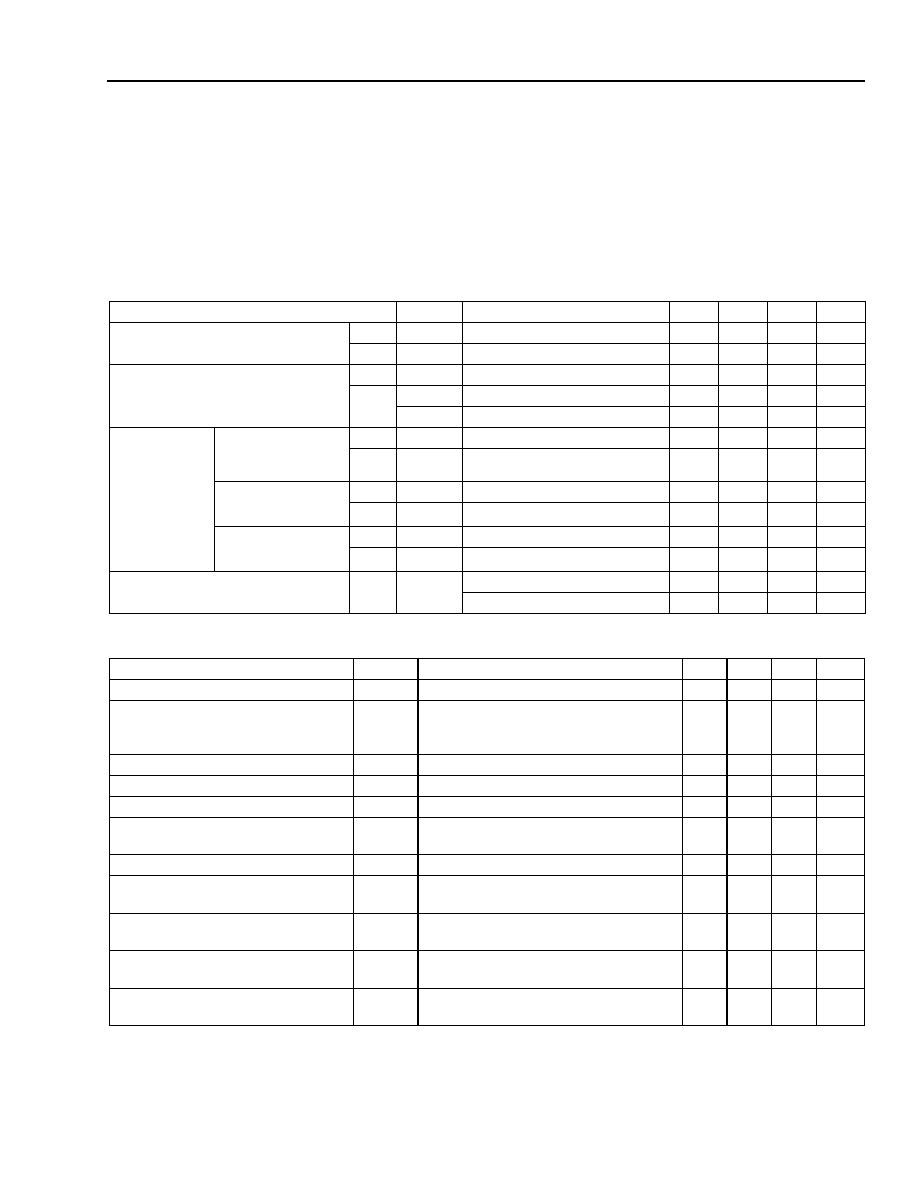
Agere Systems Inc.
25
Preliminary Data Sheet
September 2001
Codec Chip Set
T8531A/T8532 Multichannel Programmable
Electrical Characteristics
For all specifications: T
A
= ≠40
į
C to +85
į
C, V
DD
= 5 V
Ī
5%, unless otherwise noted. Typical values are for
T
A
= 25
į
C and V
DD
= 5 V. Input signal frequency is 1020 Hz, unless otherwise noted. DSP clock frequency is
49.152 MHz.
dc Characteristics
Table 8. Digital Interface
Table 9. Analog Interface
Parameter
Symbol
Test Conditions
Min
Typ
Max
Unit
Input Voltage
Low
V
IL
TTL-compatible inputs
--
--
0.7
V
High
V
IH
TTL-compatible inputs
2.0
--
--
V
Output Voltage
Low
V
OL
I
L
= 10 mA
--
--
0.4
V
High
V
OH
I
L
= ≠10 mA
2.4
--
--
V
V
OHC
I
L
= ≠320
Ķ
A
3.5
--
--
V
Input Current
Pins Without a
Pull-up or
Pull-down
Low
I
IL
GND < V
IN
< V
IL
≠10
--
--
Ķ
A
High
I
IH
V
IH
< V
IN
< V
DD
--
--
10
Ķ
A
Pins with a
Pull-up
Low
I
IL
GND < V
IN
< V
IL
≠120
--
≠2
Ķ
A
High
I
IH
V
IH
< V
IN
< V
DD
--
--
10
Ķ
A
Pins with a
Pull-down
Low
I
IL
GND < V
IN
< V
IL
≠10
--
--
Ķ
A
High
I
IH
V
IH
< V
IN
< V
DD
2
--
120
Ķ
A
Output Current in High-impedance
State
--
I
OZ
UPDO, SDX ≠40
į
C to 0
į
C
≠30
--
30
Ķ
A
UPDO, SDX 0
į
C to 85
į
C
≠10
--
10
Ķ
A
Parameter
Symbol
Test Conditions
Min
Typ
Max
Unit
Input Resistance
RVTX
0.25 V < VTX < 4.75 V
10
--
--
M
Input Resistance
(dependent on the setting
of the termination impedance)
RVRTX
2.3 V < VRTX < 2.5 V
7
--
--
k
Common-mode Reference Voltage
VVRTX
--
2.2
2.4
2.6
V
CMT Input Sink Current
IVRTX
2.3 V < VRTX < 2.5 V
--
--
400
Ķ
A
Input Voltage Swing
VVTX
--
--
--
3.2
Vp-p
Load Resistance at VRP and VRN
(differential)
RL
--
4.0
--
--
k
Load Capacitance
CL
CL from VRP or VRN to V
SSA
--
--
100
pF
Output Resistance
RO
Digital input code corresponding to
0 dBm PCM code at 1.02 kHz
--
2
10
Output Offset Voltage Between
VRP and VRN
VOS
Digital pattern corresponding to idle
PCM code (
Ķ
-law)
≠100
0
100
mV
Output Offset Voltage Between
VRP and VRN, Powerdown
VOSPD
Channel powered down
10
Ķ
A max dc load
≠20
0
20
mV
Output Voltage Swing (differential)
VRSW
RL = 100 k
differential maximum
receive gain
5.28
--
--
Vp-p

26
Agere Systems Inc.
Preliminary Data Sheet
September 2001
Codec Chip Set
T8531A/T8532 Multichannel Programmable
Electrical Characteristics
(continued)
dc Characteristics
(continued)
Table 10. T8532 Power Dissipation
Table 11. T8531A Power Dissipation
* Powerup current exhibits a negative temperature coefficient.
Transmission Characteristics
Table 12. Gain and Dynamic Range
Parameter
Symbol
Test Conditions
Min
Typ
Max
Unit
Powerdown Current
IDD0
OSCK and OSFS present, 8 channels powered down
--
9
12
mA
Powerup Current
IDD1
OSCK and OSFS present, 8 channels powered up,
normal operation
--
61
88
mA
Parameter
Symbol
Test Conditions
Min
Typ
Max
Unit
Powerdown Current
IDD0
SCK and SFS present, 16 channels powered down
and inactive
--
50
60
mA
Powerup Current
IDD1
SCK and SFS present, 16 channels powered up and
active
--
85*
100
mA
Parameter
Symbol
Test Conditions
Min
Typ
Max
Unit
Absolute
Levels
GAL
Maximum 0 dBm0 levels (1.02 kHz):
VTX (encoder milliwatt)
(T8532 TX gain = 0 dB; T8531A gain = ≠1.65 dB)
VRP--VRN (decoder milliwatt)
(T8532 RX gain = 6.02 dB; T8531A gain = 0.21 dB)
Termination impedance off
--
--
2.23
4.38
--
--
Vp-p
Vp-p
Minimum 0 dBm0 levels (1.02 kHz):
VTX
(T8532 TX gain =12.04 dB; T8531A gain = ≠1.65 dB)
VRP--VRN
(T8532 RX gain = ≠12.04 dB; T8531A gain = 0.21 dB)
Termination impedance off
--
--
557.0
548.0
--
--
mVp-p
mVp-p
Transmit Gain
Absolute
Accuracy
GXA
Transmit gain programmed for maximum
0 dBm0 test level, measured deviation of digital code
from ideal 0 dBm0 level at OSDX[1:0] digital outputs,
with transmit gain set to 0 dB:
0
į
C to 85
į
C
≠40
į
C to +85
į
C
≠0.25
≠0.30
--
--
0.25
0.30
dB
dB
Transmit Gain
Variation with
Programmed
Gain
GXAG
Measured transmit gain over the range from maxi-
mum to minimum, calculated deviation from the pro-
grammed gain relative to GXA at 0 dB:
V
DD
= 5 V
≠0.1
--
0.1
dB

Agere Systems Inc.
27
Preliminary Data Sheet
September 2001
Codec Chip Set
T8531A/T8532 Multichannel Programmable
Transmission Characteristics
(continued)
Table 12. Gain and Dynamic Range (continued)
Parameter
Symbol
Test Conditions
Min
Typ
Max
Unit
Transmit Gain Variation
with Frequency
GXAF
Relative to 1016 Hz, minimum gain < GX <
maximum gain, VTX = 0 dBm0 signal,
T
Z
= 600
,
path gain set to 0 dB:
f = 16.67 Hz
f = 40 Hz
f = 50 Hz
f = 60 Hz
f = 200 Hz
f = 300 Hz to 3000 Hz
f = 3140 Hz
f = 3380 Hz
f = 3860 Hz
f = 4600 Hz and above
--
--
--
--
≠1.8
≠0.125
≠0.57
≠0.735
--
--
≠50
≠38
≠44
≠45
≠0.5
Ī
0.04
0.01
≠0.550
≠9.9
--
≠30
≠26
≠30
≠30
0
0.125
0.125
0.015
≠8.98
≠32
dB
dB
dB
dB
dB
dB
dB
dB
dB
dB
Transmit Gain Variation
with Signal Level
GXAL
Sinusoidal test method reference
level = 0 dBm0:
VTX = ≠37 dBm0 to +3 dBm0
VTX = ≠50 dBm0 to ≠37 dBm0
VTX = ≠55 dBm0 to ≠50 dBm0
≠0.25
≠0.50
≠1.4
--
--
--
0.25
0.50
1.4
dB
dB
dB
Receive Gain Absolute
Accuracy
GRA
Receive gain programmed to 0 dB, apply
0 dBm0 oversampled data to OSDR0 or
OSDR1, measure VRP,
RL = 100 k
differential:
0 to 85
į
C
≠40
į
C to +85
į
C
≠0.25
≠0.30
--
--
0.25
0.30
dB
dB
Relative Gain:
VRP to VRN
--
Digital input 0 dBm0 signal
f = 300 Hz to 3400 Hz
≠0.01
--
0.01
dB
Relative Phase:
VRP to VRN
--
Digital input 0 dBm0 signal
f = 300 Hz to 3400 Hz
≠0.25
--
0.25
Deg
Receive Gain Variation
with Programmed
Gain
GRAG
Measure receive gain over the range from
maximum to minimum setting, calculated
deviation from the programmed gain relative
to GRA at 0 dB, V
DD
= 5 V
≠0.1
--
0.1
dB
Receive Gain Variation
with Frequency
GRAF
Relative to 1016 Hz, digital input = 0 dBm0
code, minimum gain < GR < maximum gain:
0 dB path gain
f = below 3000 Hz
f = 3140 Hz
f = 3380 Hz
f = 3860 Hz
f = 4600 Hz and above
≠0.125
≠0.57
≠0.735
--
--
Ī
0.04
Ī
0.04
≠0.550
≠10.7
--
0.125
0.125
0.015
≠8.98
≠28
dB
dB
dB
dB
dB
Receive Gain Variation
with Signal Level
GRAL
Sinusoidal test method, reference
level = 0 dBm0:
OSDR = ≠37 dBm0 to +3 dBm0
OSDR = ≠50 dBm0 to ≠37 dBm0
OSDR = ≠55 dBm0 to ≠50 dBm0
≠0.25
≠0.50
≠1.4
--
--
--
0.25
0.50
1.4
dB
dB
dB
Relative Termination
Impedance Gain
A
T
--
≠0.2
--
0.2
dB

28
Agere Systems Inc.
Preliminary Data Sheet
September 2001
Codec Chip Set
T8531A/T8532 Multichannel Programmable
Transmission Characteristics
(continued)
Table 13. Noise (per Channel)
* Measured with a ≠50 dBm0 activation signal applied to VF
X
I input of channel under test.
Parameter
Symbol
Test Conditions
Min
Typ
Max
Unit
Transmit Noise,
C-message Weighted
N
XC
0 dB transmit gain
--
--
18
dBrnC0
Transmit Noise,
P-message Weighted
N
XP
0 dB transmit gain
--
--
≠68
dBm0p
Receive Noise,
C-message Weighted
N
RC
0 dB receive gain, digital pattern corre-
sponding to idle PCM code,
Ķ
-law
--
--
13
dBrnC0
Receive Noise,
P-message Weighted
N
RP
0 dB receive gain, digital pattern corre-
sponding to idle PCM code, A-law
--
--
≠75
dBm0p
Noise, Single Frequency
N
RS
f = 0 kHz to 100 kHz, loop around measure-
ment, VTX = 0 Vrms
--
--
≠53
dBm0
Power Supply Rejection,
Transmit
PSR
X
V
DD
= 5.0 Vdc + 100 mVrms
f = 0 kHz to 4 kHz
f = 4 kHz to 50 kHz*
C-message weighted
36
30
--
--
--
--
dBC
dBC
Power Supply Rejection,
Receive
PSR
R
Measured on VRP
V
DD
= 5.0 Vdc + 100 mVrms
f = 0 kHz to 4 kHz
f = 4 kHz to 25 kHz
f = 25 kHz to 50 kHz
Digital pattern corresponding to idle PCM
code,
Ķ
-law, C-message weighted
36
40
36
--
--
--
--
--
--
dBC
dBC
dBC
Spurious Out-of-band
Signals at the Channel
Outputs
SOS
0 dBm0, 300 Hz to 3400 Hz input
oversampled data code applied at OSDR0
(or OSDR1):
4600 Hz to 7600 Hz
7600 Hz to 8400 Hz
8400 Hz to 50 kHz
--
--
--
--
--
--
≠30
≠40
≠30
dB
dB
dB

Agere Systems Inc.
29
Preliminary Data Sheet
September 2001
Codec Chip Set
T8531A/T8532 Multichannel Programmable
Transmission Characteristics
(continued)
Table 14. Distortion and Group Delay
* Varies as a function of bit offset. See Appendix A.
Table 15. Crosstalk
Parameter
Symbol
Test Conditions
Min
Typ
Max
Unit
Signal to Total Distortion
Transmit or Receive
C-message Weighted
STD
X
STD
R
Sinusoidal test method level:
3.0 dBm0
0 dBm0
33
36
--
--
--
--
dB
dB
Single Frequency Distortion,
Transmit
SFD
X
0 dBm0 single frequency input,
200 Hz
f
IN
3400 Hz; measure at
any other single frequency
--
--
≠46
dB
Single Frequency Distortion,
Receive
SFD
R
0 dBm0 single frequency input,
200 Hz
f
IN
3400 Hz; measure at
any other single frequency
--
--
≠46
dB
Intermodulation Distortion
IMD
Transmit or receive, two frequencies
in the range (300 Hz to 3400 Hz)
--
≠55
≠41
dB
TX Group Delay, Absolute
D
XA
f = 1600 Hz, SCK = 4.096 MHz,
bit offset = 419
--
250*
300
Ķ
s
RX Group Delay, Absolute
D
RA
f = 1600 Hz
--
250
300
Ķ
s
Parameter
Symbol
Test Conditions
Min
Typ
Max
Unit
Transmit to Transmit Crosstalk,
0 dBm0 Level
CT
X-X
f = 300 Hz to 3400 Hz,
Any channel to any channel
--
--
≠75
dB
Transmit to Receive Crosstalk,
0 dBm0 Level
CT
X-R
f = 300 Hz to 3400 Hz,
Any channel to any other channel
In-channel
--
--
--
--
≠75
≠50
dB
dB
Receive to Transmit Crosstalk,
0 dBm0 Level
CT
R-X
f = 300 Hz to 3400 Hz,
Any channel to any other channel
In-channel
--
--
--
--
≠75
≠50
dB
dB
Receive to Receive Crosstalk,
0 dBm0 Level
CT
R-R
f = 300 Hz to 3400 Hz,
Any channel to any channel
--
--
≠75
dB
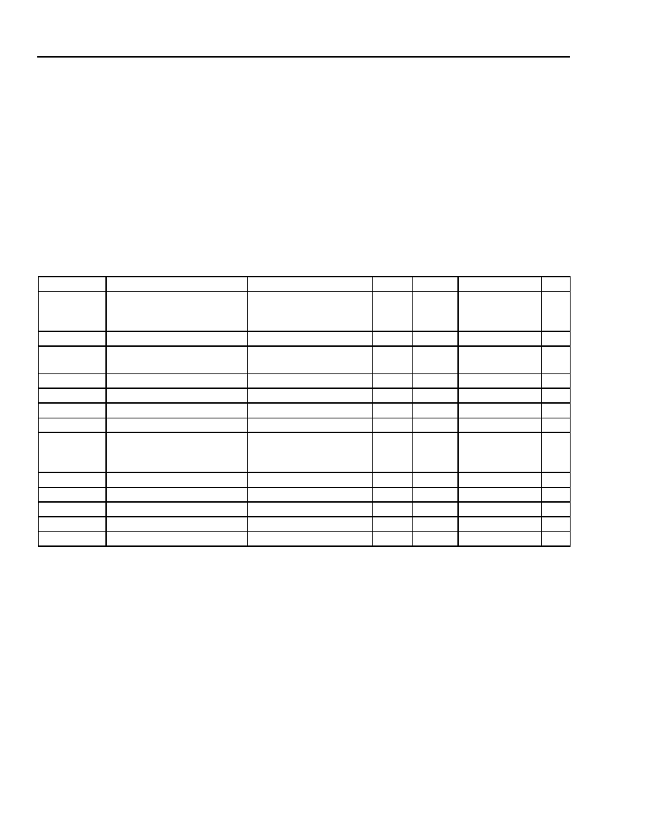
30
Agere Systems Inc.
Preliminary Data Sheet
September 2001
Codec Chip Set
T8531A/T8532 Multichannel Programmable
Timing Characteristics
A signal is valid if it is above V
IH
or below V
IL
and invalid if it is between V
IL
and V
IH
. For the purposes of this speci-
fication, the following conditions apply:
s
All input signals are defined as V
IL
= 0.4 V, V
IH
= 2.7 V, tR < 10 ns, tF < 10 ns.
s
tR is measured from V
IL
to V
IH
. tF is measured from V
IH
to V
IL
.
s
Delay times are measured from the input signal valid to the output signal valid.
s
Setup times are measured from the data input valid to the clock input invalid.
s
Hold times are measured from the clock signal valid to the data input invalid.
s
Pulse widths are measured from V
IL
to V
IL
or from V
IH
to V
IH
.
Table 16. PCM Interface Timing (See Figure 9.)
Symbol
Parameter
Test Conditions
Min
Typ
Max
Unit
fSCK
Frequency of SCK (Selection
frequency is pin-strap
programmable.)
--
--
--
2.048
4.096
--
--
MHz
MHz
tSCK
Period of SCK
Measured from V
IL
to V
IL
--
1/fSCK
--
ns
--
Jitter of SCK
--
--
--
100 ns in
100 ms = 1 ppm
--
tSCHSCL
Period of SCK High
Measured from V
IH
to V
IH
80
--
--
ns
tSCLSCH
Period of SCK Low
Measured from V
IL
to V
IL
80
--
--
ns
tSCH1SCH2 Rise Time of SCK
Measured from V
IL
to V
IH
--
--
15
ns
tSCL2SCL1 Fall Time of SCK
Measured from V
IH
to V
IL
--
--
15
ns
tFSHFSL
Period of SFS High
Measured from V
IH
to V
IL
:
2.048 MHz
4.096 MHz
0.488
0.244
--
--
62.5
62.5
Ķ
s
Ķ
s
tSFHSCL
Frame Sync High Setup
--
30
--
--
ns
tSCLSFL
Frame Sync Hold Time
--
30
--
--
ns
tSCHDXV
Data Enabled on TS Entry
0 < C
LOAD
< 100 pF
0
9
90
ns
tDRVSCL
Receive Data Setup
--
30
--
--
ns
tSCLDRX
Receive Data Hold
--
30
--
--
ns
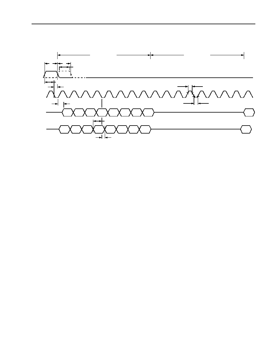
Agere Systems Inc.
31
Preliminary Data Sheet
September 2001
Codec Chip Set
T8531A/T8532 Multichannel Programmable
Timing Characteristics
(continued)
5-4233.a (F)
* Card address 0, bit offset 0 assumed.
Card address 0 assumed.
Notes:
A is the position of the frame sync pulse in the delayed mode.
B is the position of the frame sync pulse in the nondelayed mode.
Figure 9. Timing Characteristics of PCM Interface Assuming 2.048 MHz SCK Rate
SFS
B
A
tFSHFSL
SCK
1
2
3
4
5
6
7
8
9
10
11
12
13
14
15
16
1
1
2
3
4
5
6
7
8
SDX
*
1
SDR
1
2
3
4
5
6
7
8
1
tSCLSFL
tSFHSCL
tSCHDXV
tDRVSCL
tSCLDRX
TIME SLOT 0
TIME SLOT 1
tSCHSCL
tSCLSCH
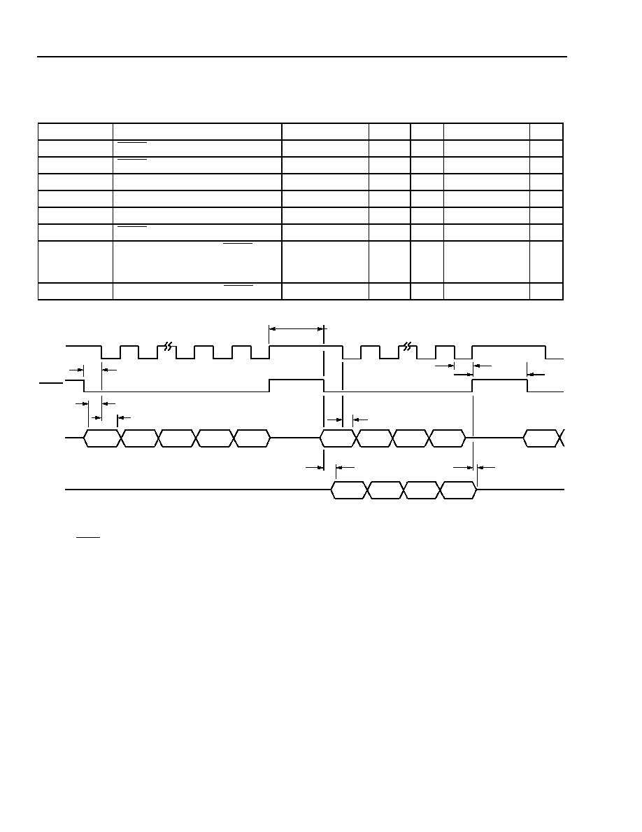
32
Agere Systems Inc.
Preliminary Data Sheet
September 2001
Codec Chip Set
T8531A/T8532 Multichannel Programmable
Timing Characteristics
(continued)
Table 17. Serial Control Port Timing (See Figure 10.)
5-4232a (F)
Notes:
UPDI and UPCS change at the rising edge of UPCK by the microprocessor and are sampled at the falling edge of UPCK by the DSP.
UPDO changes at the rising edge of UPCK by the DSP and is sampled at the falling edge of UPCK by the microprocessor.
Figure 10. Timing Diagram for Microprocessor Write/Read to/from the DSP on the Control Interface
Symbol
Parameter
Test Conditions
Min
Typ
Max
Unit
tCSHLSET
UPCS to UPCK Setup
--
25
--
--
ns
tCSLHHOD
UPCS to UPCK Hold
--
20 ns
--
UPCK Period/2
--
tUPDIST
UPDI to UPCK Setup
--
25
--
--
ns
tUPDIHD
UPDI to UPCK Hold
--
20
--
--
ns
tUPDODEL
UPCK to UPDO Delay
C
L
= 50 pF
--
--
42
ns
tUPDOHZDL
UPCS to UPDO High-Z
C
L
= 50 pF
--
--
34
ns
tCKCSH
Duration of UPCK and UPCS High:
Write Cycle
Read Cycle
--
--
1
9
--
--
--
--
Ķ
s
Ķ
s
tCKCSH1
Duration of UPCK and UPCS High
--
9
--
--
Ķ
s
tCSHLSET
tCSLHHOD
tUPDOHZDL
0
13--1
14
15
0
13--1
14
15
tUPDIHD
DATA (16 bits)
tUPDODEL
0
1
13--2
14
15
tUPDIST
tUPDIHD
ADDRESS (16 bits)
UPDI
UPDO
UPCS
UPCK
HIGH-Z STATE
DATA (16 bits)
tCKCSH
ADDRESS
tCKCSH1

Agere Systems Inc.
33
Preliminary Data Sheet
September 2001
Codec Chip Set
T8531A/T8532 Multichannel Programmable
Software Interface
Table 18 lists the RAM data space for the DSP engine. Space for up to 16 channels is allocated. The total T8531A
RAM size is 4 Kwords, arranged as 4 x 1 Kbanks. Address bit 15 is used as a read/write flag (1 = read). The micro-
processor interface can read any address in the DSP engine RAM space.
Table 18. DSP Engine RAM Memory Map
1. This address can address ROM code.
2. For time slots 1--15, the address shown is the first address. Refer to time slot 0 for range information.
3. For channels 1--15, the address shown is the first address. Refer to channel 0 for range information.
Address Range
Memory Contents
Write by Microprocessor Interface
RAM Bank 0
Time-Slot Information Tables (See page 18.)
0x0000
Time-slot control word (time slot 0)
Y
0x0001
1
Receive ac routine address (time slot 0)
Y
0x0002
1
Transmit ac routine address (time slot 0)
Y
0x0003--0x003F
Data storage (time slot 0)
Selected locations
0x0040
2
Time slot 1 information table
As shown for time slot 0
0x0080
Time slot 2 information table
As shown for time slot 0
0x00C0
Time slot 3 information table
As shown for time slot 0
0x0100
Time slot 4 information table
As shown for time slot 0
0x0140
Time slot 5 information table
As shown for time slot 0
0x0180
Time slot 6 information table
As shown for time slot 0
0x01C0
Time slot 7 information table
As shown for time slot 0
0x0200
Time slot 8 information table
As shown for time slot 0
0x0240
Time slot 9 information table
As shown for time slot 0
0x0280
Time slot 10 information table
As shown for time slot 0
0x02C0
Time slot 11 information table
As shown for time slot 0
0x0300
Time slot 12 information table
As shown for time slot 0
0x0340
Time slot 13 information table
As shown for time slot 0
0x0380
Time slot 14 information table
As shown for time slot 0
0x03C0
Time slot 15 information table
As shown for time slot 0
RAM Bank 1
ac Coefficient Reference Tables
0x0400--0x040F
Channel coefficient address table
N
0x0410--0x0413
Default coefficient address table
N
0x0414--0x0434
Reserved
N
ac Per-Channel Coefficients (See page 17.)
0x0435
Receive path relative gain (channel 0)
Y
0x0436
Data storage (channel 0)
N
0x0437
Receive path absolute gain (channel 0)
Y
0x0438
Transmit path absolute gain (channel 0)
Y
0x0439--0x0442
Balance filter coefficients (channel 0)
Y
0x0443
Data storage (channel 0)
N
0x0444
Transmit path relative gain (channel 0)
Y
0x0445
3
Channel 1 ac filter coefficients
As shown for channel 0
0x0455
Channel 2 ac filter coefficients
As shown for channel 0
0x0465
Channel 3 ac filter coefficients
As shown for channel 0
0x0475
Channel 4 ac filter coefficients
As shown for channel 0
0x0485
Channel 5 ac filter coefficients
As shown for channel 0
0x0495
Channel 6 ac filter coefficients
As shown for channel 0
0x04A5
Channel 7 ac filter coefficients
As shown for channel 0

34
Agere Systems Inc.
Preliminary Data Sheet
September 2001
Codec Chip Set
T8531A/T8532 Multichannel Programmable
Software Interface
(continued)
Table 18. DSP Engine RAM Memory Map (continued)
1. This address can address ROM code.
2. For time slots 1--15, the address shown is the first address. Refer to time slot 0 for range information.
3. For channels 1--15, the address shown is the first address. Refer to channel 0 for range information.
4. Per-board refers to a function that is common to all 16 channels in a single chip set.
Address Range
Memory Contents
Write by Microprocessor Interface
ac Per-Channel Coefficients (See page 17.) (continued)
0x04B5
Channel 8 ac filter coefficients
As shown for channel 0
0x04C5
Channel 9 ac filter coefficients
As shown for channel 0
0x04D5
Channel 10 ac filter coefficients
As shown for channel 0
0x04E5
Channel 11 ac filter coefficients
As shown for channel 0
0x04F5
Channel 12 ac filter coefficients
As shown for channel 0
0x0505
Channel 13 ac filter coefficients
As shown for channel 0
0x0515
Channel 14 ac filter coefficients
As shown for channel 0
0x0525
Channel 15 ac filter coefficients
As shown for channel 0
ac Per-Board
4
Coefficients
0x0535--0x053E
Receive (equalizer) filter coefficients
Y
0x053F--0x0552
Transmit (equalizer) filter coefficients
Y
0x0553
Transmit gain coefficients for filter compensation
Y
0x0554--0x055E
Extended receive (equalizer) filter coefficients
Y
0x055F--0x0560
Unused
Y
Default Per-Board
4
Coefficient Tables
0x0561
Default Table 1 receive path relative gain
Y
0x0562
Default Table 1 receive path absolute gain
Y
0x0563
Default Table 1 transmit path absolute gain
Y
0x0564--0x056D
Default Table 1 balance filter coefficients
Y
0x056E
Default Table 1 transmit path relative gain
Y
0x056F--0x057C
Default Table 2 coefficient set
Y
Self-Test Flags and Tone Processing
0x057D--0x05EE
Temporary storage for self-test routines
Y
0x05EF--0x05F3
Call progress tone generation control words
Y
0x05F4--0x05FC
Caller ID control words
Y
0x05FD--0x05FF
Tone processing data storage
Y
0x0600--0x06FF
Tone processing time-slot tables
Y
0x0700--0x071C
Tone processing data storage
Y
0x071D--0x0724
Dial tone filter coefficients
Y
0x0725--0x0754
Tone processing data storage
Y
0x0755
1
Receive active routine filter address
Y
0x0756
1
Receive inactive routine address
Y
0x0757
1
Transmit inactive routine address
Y
0x0758--0x07EF
Unused
Y
0x07F0
Result of ROM checksum test
N
0x07F2
Result of RAM checksum test
N
0x07F4
Result of TX path self-test
N
0x07F5
Result of RX path self-test
N
0x07F6
ROM code version number
N
0x07F7--0x07FF
Unused
Y
0x0800--0x0FFF
Caller ID and DTMF data storage
Y
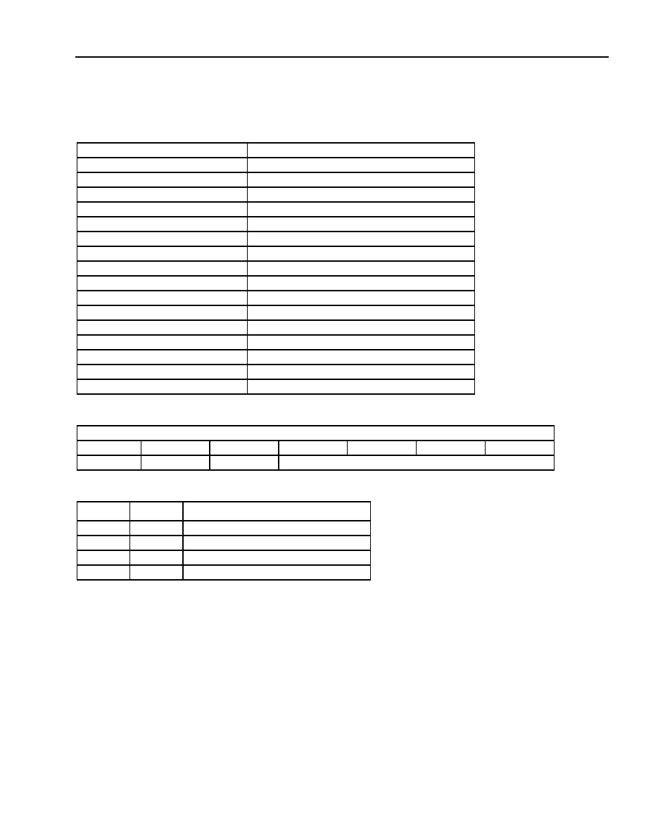
Agere Systems Inc.
35
Preliminary Data Sheet
September 2001
Codec Chip Set
T8531A/T8532 Multichannel Programmable
Software Interface
(continued)
Table 19. T8531A Time-Slot Assignment Memory Map
All registers can be written by the microprocessor interface.
Table 20A. Bit Map for T8531A Time-Slot Assignment Registers at 0x1400--0x140F
Table 20B. Bit Map for CTZ Disable and Null Channel
Notes:
X = Don't care.
Bits 4 and 5 default to 1 upon reset.
Address Range
Memory Contents
0x1400
Time slot 0 channel assignment
0x1401
Time slot 1 channel assignment
0x1402
Time slot 2 channel assignment
0x1403
Time slot 3 channel assignment
0x1404
Time slot 4 channel assignment
0x1405
Time slot 5 channel assignment
0x1406
Time slot 6 channel assignment
0x1407
Time slot 7 channel assignment
0x1408
Time slot 8 channel assignment
0x1409
Time slot 9 channel assignment
0x140A
Time slot 10 channel assignment
0x140B
Time slot 11 channel assignment
0x140C
Time slot 12 channel assignment
0x140D
Time slot 13 channel assignment
0x140E
Time slot 14 channel assignment
0x140F
Time slot 15 channel assignment
Bit Number and Function
15--6
5
4
3
2
1
0
Not used
CTZ disable
Null channel
Binary-coded channel number 0--15
Bit 5
Bit 4
Function
X
0
Disables null pointer
X
1
Nulls channel
0
X
Enables CTZ
1
X
Disables CTZ
36
Agere Systems Inc.
Preliminary Data Sheet
September 2001
Codec Chip Set
T8531A/T8532 Multichannel Programmable
Software Interface
(continued)
Table 21. T8531A Channel Register Memory Map
for T8532 Device 0
All registers can be written by the microprocessor
interface.
Table 22. T8531A Channel Register Memory Map
for T8532 Device 1
All registers can be written by the microprocessor
interface.
Address
Range
Memory
Contents
0x1500
Channel 0 powerup/powerdown register
0x1501
Channel 1 powerup/powerdown register
0x1502
Channel 2 powerup/powerdown register
0x1503
Channel 3 powerup/powerdown register
0x1504
Channel 4 powerup/powerdown register
0x1505
Channel 5 powerup/powerdown register
0x1506
Channel 6 powerup/powerdown register
0x1507
Channel 7 powerup/powerdown register
0x1508
Channel 0 control register 1
0x1509
Channel 1 control register 1
0x150A
Channel 2 control register 1
0x150B
Channel 3 control register 1
0x150C
Channel 4 control register 1
0x150D
Channel 5 control register 1
0x150E
Channel 6 control register 1
0x150F
Channel 7 control register 1
0x1510
All channel test register
0x1517
Single-byte soft reset (no data word)
0x1518
Channel 0 control register 2
0x1519
Channel 1 control register 2
0x151A
Channel 2 control register 2
0x151B
Channel 3 control register 2
0x151C
Channel 4 control register 2
0x151D
Channel 5 control register 2
0x151E
Channel 6 control register 2
0x151F
Channel 7 control register 2
Address
Range
Memory
Contents
0x1540
Channel 8 powerup/powerdown register
0x1541
Channel 9 powerup/powerdown register
0x1542
Channel 10 powerup/powerdown register
0x1543
Channel 11 powerup/powerdown register
0x1544
Channel 12 powerup/powerdown register
0x1545
Channel 13 powerup/powerdown register
0x1546
Channel 14 powerup/powerdown register
0x1547
Channel 15 powerup/powerdown register
0x1548
Channel 8 control register 1
0x1549
Channel 9 control register 1
0x154A
Channel 10 control register 1
0x154B
Channel 11 control register 1
0x154C
Channel 12 control register 1
0x154D
Channel 13 control register 1
0x154E
Channel 14 control register 1
0x154F
Channel 15 control register 1
0x1550
All channel test register
0x1557
Single-byte soft reset (no data word)
0x1558
Channel 8 control register 2
0x1559
Channel 9 control register 2
0x155A
Channel 10 control register 2
0x155B
Channel 11 control register 2
0x155C
Channel 12 control register 2
0x155D
Channel 13 control register 2
0x155E
Channel 14 control register 2
0x155F
Channel 15 control register 2

Agere Systems Inc.
37
Preliminary Data Sheet
September 2001
Codec Chip Set
T8531A/T8532 Multichannel Programmable
Software Interface
(continued)
Table 23. Bit Map for T8532 Powerup/Powerdown Registers at 0x1500--0x1507 and 0x1540--0x1547
Notes:
PWR = 0: powerdown.
PWR = 1: powerup--normal operation.
Table 24. Bit Map for T8532 Channel Control Register 1 at 0x1508--0x150F and 0x1548--0x154F
Table 25. T8532 Control Register 1: Transmit Gain
Table 26. T8532 Control Register 1: Analog Termination Impedance
Bit Number and Function
15
14--0
PWR
Not used
Bit Number and Function
15
14--8
7
6
5
4
3
2
1
0
PWR
Not used
TX gain
Termination impedance
LPBK
Bit 7
Bit 6
Bit 5
Mode
TXGAIN2
TXGAIN1
TXGAIN0
0
0
0
0 dB transmit gain
0
0
1
3.01 dB transmit gain
0
1
0
6.02 dB transmit gain
0
1
1
9.03 dB transmit gain
1
0
0
12.04 dB transmit gain
1
0
1
12.04 dB transmit gain
1
1
0
12.04 dB transmit gain
1
1
1
12.04 dB transmit gain
Bit 4
Bit 3
Bit 2
Bit 1
Gain (See equation on page 13.)
TI3
TI2
TI1
TI0
0
0
0
0
0.0000
0
0
0
1
0.0583
0
0
1
0
0.1417
0
0
1
1
0.2250
0
1
0
0
0.3083
0
1
0
1
0.3917
0
1
1
0
0.5000
0
1
1
1
0.5583
1
0
0
0
0.6417
1
0
0
1
0.7083
1
0
1
0
0.8083
1
0
1
1
0.8917
1
1
0
0
0.9750
1
1
0
1
1.0583
1
1
1
0
1.2167
1
1
1
1
2.0000

38
Agere Systems Inc.
Preliminary Data Sheet
September 2001
Codec Chip Set
T8531A/T8532 Multichannel Programmable
Software Interface
(continued)
Table 27. T8532 Control Register 1: Digital Loopback
Table 28. Bit Map for T8532 All Channel Test Register at 0x1510 and 0x1550
Table 29. Bits 3:0 of T8532 All Channel Test Register at 0x1510 and 0x1550
Notes:
Read out address provides the previous read or write address to CDO whenever a new address is being written into the register.
When analog loopback is high, data that enters the analog transmit path (VTX) is converted to a 1.024 MHz digital bit stream and routed back to
the analog receive path (VRP, VRN). The output of the transmit path is available on the oversampled data interface, but receive path oversam-
pled data is ignored.
5-5134 (F)
When digital loopback is high, oversampled data receive (OSDR) is routed to oversampled data transmit (OSDX). The receive signal is propa-
gated to VRN/VRP, but any transmit signal from VTX is disconnected. A reference voltage on VRTX is still required in this mode.
5-5135 (F)
Bit 0
Mode
LPBK
0
Normal operation
1
Digital loopback
Bit Number and Function
15--4
3
2
1
0
Not used
Read out address
Reserved
Analog loopback
Digital loopback
Bit Number
Function
3
2
1
0
0
--
--
--
Normal operation
1
--
--
--
Read out address
--
0
--
--
Reserved
--
1
--
--
Normal operation
--
--
0
--
Normal operation
--
--
1
--
Analog loopback
--
--
--
0
Normal operation
--
--
--
1
Digital loopback
OVERSAMPLED
DATA
INTERFACE
A/D, D/A
VTX
VRP
OSDX
OSDR
OVERSAMPLED
DATA
INTERFACE
A/D, D/A
VTX
VRP
OSDX
OSDR
Agere Systems Inc.
39
Preliminary Data Sheet
September 2001
Codec Chip Set
T8531A/T8532 Multichannel Programmable
Software Interface
(continued)
Table 30. Bit Map for T8532 Channel Control Register 2 at 0x1518--0x151F and 0x1558--0x155F
Notes:
SUSEQ = 0: normal operation.
SUSEQ = 1: start-up calibration sequence.
Table 31. T8532 Control Register 2: Receive Gain
Table 32. T8531A Control Register Map
Note: A board control word controls a function that is common to all 16 channels of a given chip set.
Bit Number and Function
15--8
7
6--3
2
1
0
Not used
SUSEQ
Not used
Receive gain
Bit 2
Bit 1
Bit 0
Mode TLP Levels,
Termination Impedance Is On
RXGAIN2
RXGAIN1
RXGAIN0
0
0
0
6.02 dB receive gain
0
0
1
3.01 dB receive gain
0
1
0
0.0 dB receive gain
0
1
1
≠3.01 dB receive gain
1
0
0
≠6.02 dB receive gain
1
0
1
≠9.03 dB receive gain
1
1
0
≠12.04 dB receive gain
1
1
1
≠12.04 dB receive gain
Address Range
Register Contents
Write by Microprocessor Interface
0x1FFE
Board control word 1
Y
0x1FFC
Board control word 2
Y
0x1FFA
Board control word 3
Y
0x1FF8
Board control word 4
Y
0x1FF6
Board control word 5
Y
40
Agere Systems Inc.
Preliminary Data Sheet
September 2001
Codec Chip Set
T8531A/T8532 Multichannel Programmable
Software Interface
(continued)
Table 33. Bits 15:8 of T8531A Board Control Word 1 at 0x1FFE
Table 34. Bits 7:0 of T8531A Board Control Word 1 at 0x1FFE
Notes:
All bits in board control register 1 will be zeros upon hardware reset.
In OSD loopback mode, OSDR0, OSDR1, OSDR2, and OSDR3 are looped back with a delay of two OSCLK clock cycles to OSDX0, OSDX1,
OSDX2, and OSDX3, respectively.
Test modes are for production testing only.
Ķ
-law/A-law companding mode provides 8 bits of PCM data with the first bit (bit 1) defined as the MSB and the last bit (bit 8) as the LSB. Bit 1 is
the sign bit, bits 2 through 4 are the chord bits, and bits 5 through 8 are the interval bits. In linear mode, the
Ķ
-law/A-law conversion in the PCM
interface block is disabled and 16 bits of linear PCM data are provided. In linear mode, bit 1 is the MSB and the sign bit, bits 2 through 14 are
the intervals, and bits 15 and 16 are insignificant. Each interval represents 0.0001362745 Vrms with 8031 intervals being the maximum signal
output of 3 dBm0. Negative values are two's complement of positive values.
X = don't care.
Bit Number
Function
15
14
13
12
11
10
9
8
0
--
--
--
--
--
--
--
Normal operation
1
--
--
--
--
--
--
--
Soft reset
--
--
--
--
0
--
--
--
Normal operation
--
--
--
--
1
--
--
--
TZ test mode
--
--
--
--
--
0
--
--
Normal operation
--
--
--
--
--
1
--
--
RX dither circuit off
--
--
--
--
--
--
0
--
Normal operation
--
--
--
--
--
--
1
--
Nodecim test mode
--
--
--
--
--
--
--
0
Normal operation
--
--
--
--
--
--
--
1
Linear mode
Bit Number
Function
7
6
5
4
3
2
1
0
0
X
--
--
--
--
--
--
Delayed data timing
1
X
--
--
--
--
--
--
Nondelayed data timing
--
X
0
x
--
--
--
--
Ķ
-law
--
X
1
0
--
--
--
--
A-law, including even bit inversion
--
X
1
1
--
--
--
--
A-law, no even bit inversion
--
X
--
--
C1
C0
--
--
C1C0 = card address in binary
--
X
--
--
--
--
0
--
Reserved
--
X
--
--
--
--
1
--
Normal operation
--
X
--
--
--
--
--
0
Normal operation
--
X
--
--
--
--
--
1
Loopback at OSD
Agere Systems Inc.
41
Preliminary Data Sheet
September 2001
Codec Chip Set
T8531A/T8532 Multichannel Programmable
Software Interface
(continued)
Table 35. Bits 15:9 of T8531A Board Control Word 2 at 0x1FFC
Table 36. Bits 8:0 of T8531A Board Control Word 2 at 0x1FFC
Note: Bits 15 through 9 are not used; assumed to be zeros. BOF[8:0] provide a fixed offset, relative to the frame synchronization strobe (SFS),
for the first bit transmitted in each time slot. The offset is the number of data periods by which transmission of the first bit on SDX is
delayed. All subsequent transmissions also follow this offset. The default value after hardware reset or powerup is 1A3; however, this reg-
ister must still be written after reset.
Table 37. Bits 15:0 of T8531A Board Control Word 3 at 0x1FFA
Note: For test use only, do not use in normal operation. The default value after hardware reset or powerup is 0.
Table 38. Bits 15:0 of T8531A Board Control Word 4 at 0x1FF8
Note: The default value after hardware reset or powerup is A4.
Table 39. Bits 15:0 of T8531A Board Control Word 5 at 0x1FF6
Note: The default value after hardware reset or powerup is 0.
Table 40. Bits 15:0 of T8531A Reset of Microprocessor Commands at 0x7FFF
Bit Number and Function
15--9
Not used
Bit Number
Function
8
7
6
5, 4, 3
2
1
0
BOF8
BOF7
BOF6
BOF5--3
BOF2
BOF1
BOF0
BOF8--0 = Bit offset in binary
Bit Number and Function
15--5
4--0
Not used
TZ test bits
Bit Number and Function
15--10
9--0
Not used
CTZ alpha coefficients
Bit Number and Function
15--8
7--0
Not used
CTZ beta coefficients
Bit Number
Function
15
14
13
12
11
10
9
8
7
6
5
4
3
2
1
0
1
1
1
1
1
1
1
1
1
1
1
1
1
1
1
1
Clear address and data words
in T8531

42
Agere Systems Inc.
Preliminary Data Sheet
September 2001
Codec Chip Set
T8531A/T8532 Multichannel Programmable
Software Interface
(continued)
Table 41 shows the memory map for the DSP engine ROM. The ROM information is not accessible via the micro-
processor. The total ROM size is 8 Kwords.
Table 41. DSP Engine ROM Memory Map
Address Range
Memory Contents
0x0003
HDS interrupt service routine
0x0008
Time-slot sync interrupt service routine
0x000B
Start-up routine
0x0380
Time segment controller (ts_proc)
0x03B0
Double precision multiply routine
0x03B8
Double precision multiply routine
0x0400
Transmit path active routine
0x0500
Receive path active routine
0x0503
RX path active without reading from the system interface
0x0600
Transmit path inactive/loopback routine
0x0610
Transmit path inactive routine
0x0680
Receive path inactive/loopback routine
0x0690
Receive path inactive routine
0x0700
Self-test pass 1 setup (TX)
0x0720
Self-test pass 2 setup (RX)
0x07A0
Tone generation start-up
0x0860
Tone detection start-up
0x0A80
Variance calculation
0x0B00
Peak detection routine
0x0B60
dc generation
0x0B80
ROM checker
0x0C00
RAM checker
0x0E00
Variance calculation with TX filters
0x0F00
Simultaneous start-up of tone generator and DFT routine
0x0F10
Simultaneous start-up of tone generator and original variance routine
0x0F20
Routine places TX and RX halves of a time slot into inactive loopback
0x0F30
Places TX and RX halves of a time slot into inactive routine
0x0F40
Routine for copying values in channel coefficient table 0 to all 16-channel tables
0x0F60
Approximate location of HDS code
0x0FFE
Checksum for ROM 0x0000 : 0x07FF

Agere Systems Inc.
43
Preliminary Data Sheet
September 2001
Codec Chip Set
T8531A/T8532 Multichannel Programmable
Software Interface
(continued)
Table 41. DSP Engine ROM Memory Map
Address Range
Memory Contents
0x0FFF
Checksum for ROM 0x0800 : 0x0FFD
0x1000
Call progress tone generation start
0x102B
Call progress tone generation during operation
0x105A
Call progress tone generator initialization
0x1070--0x146F
Sine-wave lookup table
0x1470
Caller ID generation start
0x14C8
Caller ID generation during operation, TX path
0x1604
Caller ID generation during operation, RX path
0x160E
Caller ID generator initialization
0x1650
DTMF detector start
0x16AA
DTMF detector during operation subroutine
0x16FE
DTMF detector during operation subroutine
0x1B3C
DTMF detector initialization
0x1BD0
Extended receive path active routine
0x1BD3
Extended receive path active without reading from the system interface
0x1C30
Extended transmit path inactive/loopback routine
0x1C37
Extended transmit path inactive routine
0x1CA6
Extended receive path inactive with data loopback
0x1CAD
Extended receive path inactive routine
0x1CD0
Tone processing initialization
0x1D00
Reserved
0x1D60
dc measurement routine
0x1DBC--0x1FFF Not used
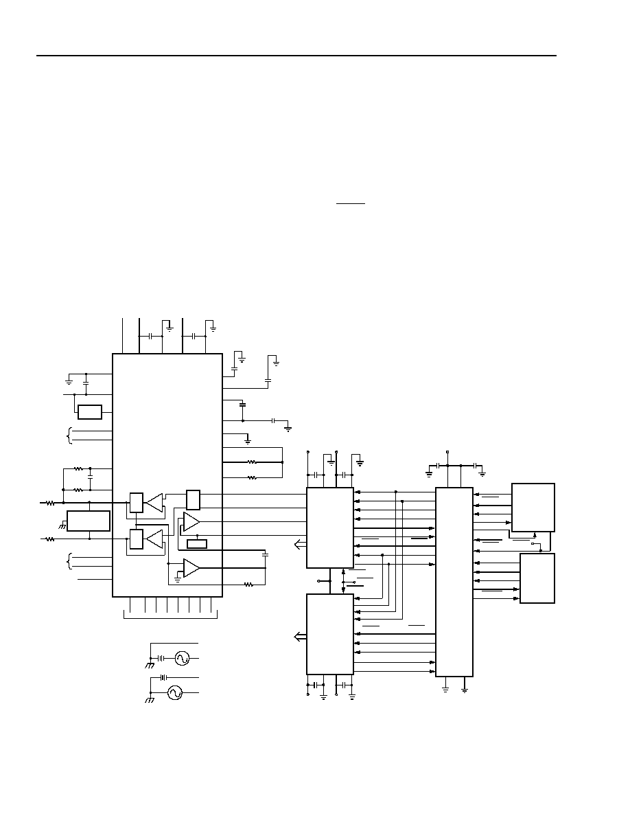
44
Agere Systems Inc.
Preliminary Data Sheet
September 2001
Codec Chip Set
T8531A/T8532 Multichannel Programmable
Applications
Figure 11 shows a full line card implementation using the T8531/T8532 codec and the L7585 SLIC with integrated
relays. One T8531A and two T8532 devices support 16 SLIC devices (only one L7585 SLIC is illustrated). Figure
11 portrays only the transmission paths inside the L7585 SLIC. L7585 functionality includes eight solid-state relays,
performing ring, test, and break functions, a ring-trip detector, quiet polarity reversal, 14 operating states, and
more. For complete functionality of this SLIC, refer to the L7585 data sheet.
The analog connection between the SLIC and the codec is direct; no external components are required. The trans-
fer of control data on the octal interface between the T8531A and T8532 devices is also direct. Data is synchro-
nous with OSCK and transmits at a 4.096 MHz rate. The microprocessor control interface is a standard 4-wire
serial port connection, microprocessor clock (UPCK), chip select (UPCS), data input (UPDI), and output (UPDO).
The T8531A generates a 16 MHz clock for microprocessor use. This clock is always present. The PCM interface
consists of a system clock (SCK) input of either 2.048 MHz or 4.096 MHz, an 8 kHz system frame sync (SFS)
input, a system data transmit port (DX), and a system data receive (DR) port.
The only external components required by the codec chip set are the power supply decoupling. Decouple as many
power supply pins as possible, at a minimum, use one capacitor per device side. Analog and digital grounds should
be tied together into one low-impedance ground plane.
12-3351p(F)
* Optional for quiet reverse battery.
4.096 MHz operation; for 2.048 MHz operation, tie SCKSEL to V
SS
.
Figure 11. Line Card Solution Using the L7585 SLIC
OSFS
OSCK
OSDR0
OSDR1
OSDX0
OSDX1
CDO
CDI
CODEC 0
T8532
DSP
UPCK
UPCS
UPDI
UPDO
SCK
SFS
SDR
SDX
STSXB
PCM
CODEC 1
T8532
OSDX2
OSDR2
OSDR3
OSDX3
PCM
INTERFACE
CONTROL
INTERFACE
OCTAL
INTERFACE
OSDX2
OSDR2
OSDR3
OSDX3
CDO
CDI
OSCK
OSFS
OSFS
OSCK
OSDR0
OSDR1
OSDX0
OSDX1
CDI
CDO
CCS0
CCS1
CCS0
CCS1
DGND
VCCD
RDO
RSW
RTS
PR
PT
RTI
TTI
CLK
VSP VBAT
BGND VCCA AGND
NDET NCS B5 B4 B3 B2 B1 B0
FB1
FB2
CF1
CF2
DCR
DCOUT
IPROG
LCTH
RCVN
RCVP
VTX
VRTX
TXI
VITR
ITR
RELAY
K1
CVD
0.1
Ķ
F
CRTF
0.1
Ķ
F
RS1
500
RRTF
1 M
260 V
SURGE
PROTECTOR
RPR
82.5
RPT
82.5
TEST-IN
BUS
1 MHz
CLOCK
BATTERY BACK
RINGING
CVB
0.1
Ķ
F
≠48 V
CVA
0.1
Ķ
F
+5 V
+10 V
FB2*
CF1
0.22
Ķ
F
CF2
0.1
Ķ
F
RPROG 64.9 k
RLCTH 24.9 k
+5 V
CB1
0.1
Ķ
F
SLIC 0
L7585
PARALLEL DATA BUS TO MICROPROCESSOR
0.1
Ķ
F
+5 V
0.1
Ķ
F
+5 V
RSTB
SCKSEL
RSTB
0.1
Ķ
F
0.1
Ķ
F
CHANNELS
8--15
CHANNELS
1--7
+5 V
+5 V
CHANNEL
0
VRN0
VRP0
VTX0
VRTX0
TEST
TEST
VDDD
RSTB
RSTB
RSTB
CK16
VSS
VSSA
0.1
Ķ
F
+5 V
0.1
Ķ
F
VDD
2.4 V
RGX1
8.25 k
TIP
RING
0.047
Ķ
F
FB1*
0.047
Ķ
F
VDDA
VSS
A
VDDD
VSS
D
VDDA
V
SSA
VDDD
V
SSD
VDDA
MICRO-
PROCESSOR
T8531A
100 V
100 V
100 V
100 V
10 V
50 V
100 V
TRNG
RRNG
EARTH BACK
RINGING
TRNG
RRNG
TRNG
RRNG
RINGING
BUS
(SEE BELOW)
100 V
ASIC
BUS
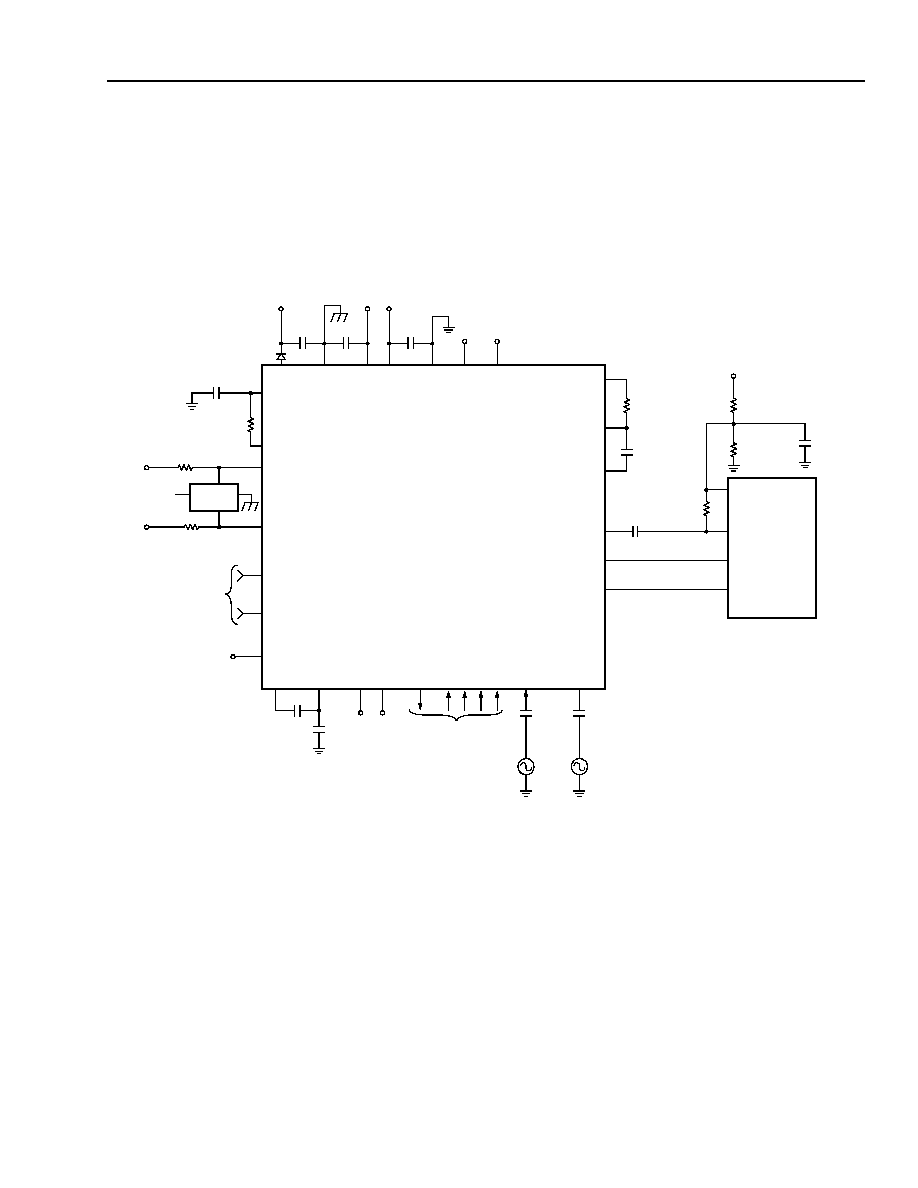
Agere Systems Inc.
45
Preliminary Data Sheet
September 2001
Codec Chip Set
T8531A/T8532 Multichannel Programmable
Applications
(continued)
Figure 12 shows the complete SLIC schematic for interfacing to the Agere L9215G short-loop, sine wave, ringing
SLIC. All ac parameters are programmed by the codec. Note, this codec differentiates itself in that no external
components are required in the ac interface to provide a dc termination impedance or for stability. For illustration
purposes, 0.5 Vrms PPM injection was assumed in this example and no meter pulse rejection is used. Also, this
example illustrates the device using programmable overhead and current limit. The components associated with
V
REF
can be replaced by a common voltage reference circuit (see Figure 14).
12-3534C (F)
Figure 12. Line Card Solution Using the L9215G SLIC
V
BAT1
BGND
V
BAT2
V
CC
AGND ICM TRGDET
ground key
not used
C
BAT1
0.1
Ķ
F
C
BAT2
0.1
Ķ
F
C
CC
0.1
Ķ
F
RTFLT
DCOUT
PR
PT
OVH
V
PROG
V
REF
C
RT
0.1
Ķ
F
R
RT
383
k
AGERE
L7591
V
BAT2
FUSIBLE OR PTC
50
50
CF1
CF2
rate of battery
reversal not
ramped
FB1 FB2
NSTAT BR B2 B1 B0
C
F1
0.47
Ķ
F
C
F2
0.1
Ķ
F
PPM
0.5 Vrms
C
PPM
10 nF
RING
IN
PPM
IN
VITR
R
CVP
R
CVN
ITR
VTX
TXI
R
GX
4750
V
BAT1
D
BAT1
V
BAT2
V
CC
C
TX
0.1
Ķ
F
C
RING
0.47
Ķ
F
not
used
FROM
PROGRAMMABLE
D/A VOLTAGE
SOURCE
C
C1
T8532
VTX
VRP
VRN
L9215G
FROM/TO
CONTROL
0.1
Ķ
F
FUSIBLE OR PTC
C
VREF
VRTX
V
CC
R
VREF2
4.32 k
R
VREF1
4.02 k
301 k
R
VREF3
10 V
10
Ķ
F

46
Agere Systems Inc.
Preliminary Data Sheet
September 2001
Codec Chip Set
T8531A/T8532 Multichannel Programmable
Applications
(continued)
Figure 13 shows the complete SLIC schematic for interfacing to the Agere L9310G Line Interface and Line Access
circuit. All ac parameters are programmed by the codec. Note, this codec differentiates itself in that no external
components are required in the ac interface to provide a dc termination impedance or for stability. For illustration
purposes, 2.2 Vrms PPM injection was assumed in this example and hybrid meter pulse rejection is used. Also, this
example illustrates the device using the battery switch with multiple battery operation and programmable overhead,
current limit and loop closure threshold.
0500 (F)
Figure 13. Line Card Solution Using the L9310G SLIC
R
S1
FUSIBLE
50
CV
BAT1
0.1
Ķ
F
V
BAT1
RTS
V
PROG
(I
LIMIT
= 25 mA)
LCTH (THRESHOLD = 11 mA)
V
BAT
C
F2
0.1
Ķ
F
FB2
CF1
VTX
ITR
PPMOUT
C
RTS
0.1
Ķ
F
PPMIN
AGND V
DD
1 M
50
R
RING
100 V--130 V
SECONDARY
OR PTC
FUSIBLE
OR PTC
R
RTF
400
RINGING
SOURCE
C
CC
0.1
Ķ
F
V
CC
C
DD
0.1
Ķ
F
V
DD
A
D
C
TX
0.1
Ķ
F
R
GX
6.49 k
RSW
PT
V
BAT2
/
V
CC
BGND
V
BAT1
TRGDET
ICM
DGND
TXI
TXN
PROTECTOR
180 V--330 V
SECONDARY
PROTECTOR
FB1
V
REF
TESTLEV
TESTSIG
CF2
PER-LINE
TO/FROM
MICROPROCESSOR
V
BAT2
CV
BAT2
0.1
Ķ
F
C
PPM
0.01
Ķ
F
R
PPM
17.4 k
RAMPED
PPM
GENERATION
0.7 Vrms for
2.2 Vrms at T/R
OVH (OVERHEAD = 9.2 V for 2.2 Vrms PPM)
FROM
PROGRAMMABLE
VOLTAGE
SOURCE
PWR
T
RING
L9310G
(GAIN OF 2)
LCF
PR
RESET
R
LCTH
VITR
R
CVP
R
CVN
C
C1
T8532
VTX
VRP
VRN
0.1
Ķ
F
VRTX
301 k
R
VREF
V
REF
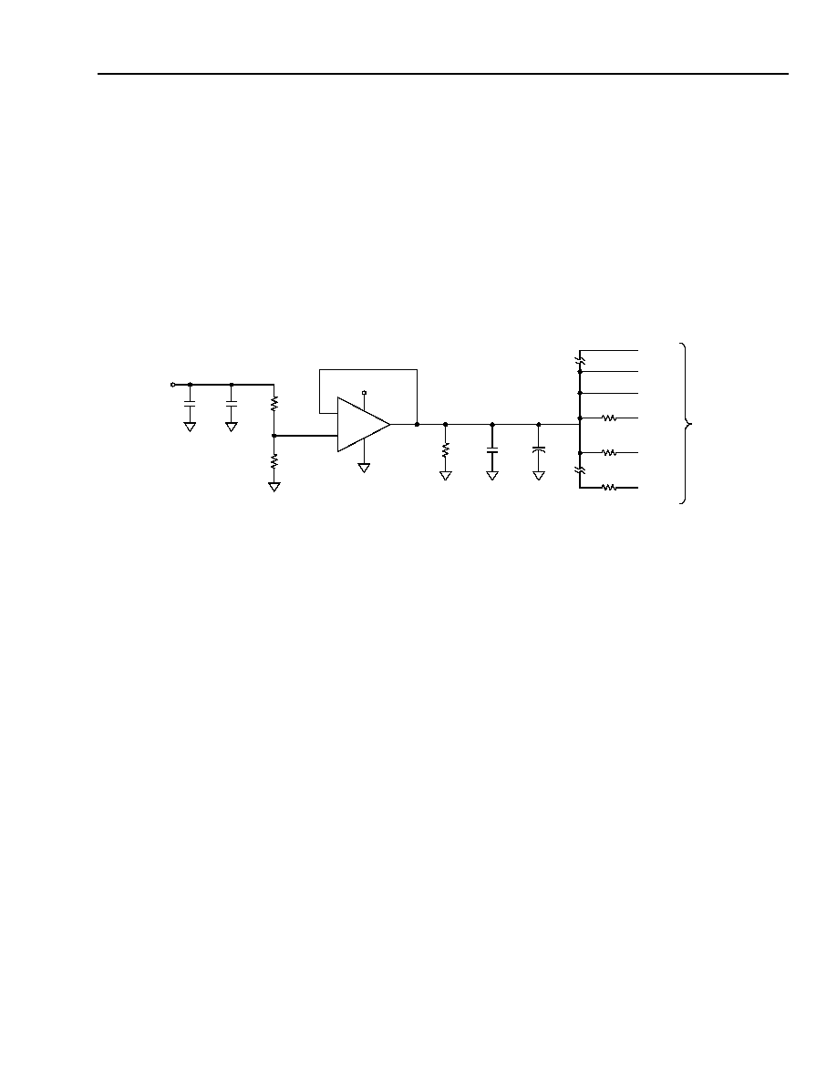
Agere Systems Inc.
47
Preliminary Data Sheet
September 2001
Codec Chip Set
T8531A/T8532 Multichannel Programmable
Applications
(continued)
Common Voltage Reference
Every channel of the T8532 codec requires a 2.4 V reference (VRTX) for operation. Some SLICs provide this refer-
ence for the codec. An external circuit is required for SLICs without the reference voltage.
Figure 14 shows a circuit that can provide the 2.4 V reference for 16 or more channels. Even with the common ref-
erence voltage, interchannel crosstalk remains insignificant. The circuit employs a single supply op amp as a volt-
age follower. R1 and R2 set up the reference voltage. RL provides a reference bias when all channels are
programmed off and provides a discharge path for the reference filtering. The op amp supplies an ample minimum
of 20 mA. Each channel's VRTX node only requires a maximum of 340
Ķ
A and VTX is a high-impedance input.
The R
VREFx
resistors provide the necessary bias for the VTX inputs.
12-3570a (F)
Figure 14. Common 2.4 V Voltage Reference
2.15 k
R2
2.37 k
R1
0.1
Ķ
F
10
Ķ
F
5 V
3
2
≠
+
5 V
8
4
1
1/2 LM2904
OR
1.91 k
RL
0.1
Ķ
F
10
Ķ
F
EQUIVALENT
VRTX15
VRTX1
VRTX0
VTX0
VTX1
VTX15
TO
T8531A/2
R
VREF15
301 k
R
VREF1
301 k
R
VREF0
301 k
+
+

48
Agere Systems Inc.
Preliminary Data Sheet
September 2001
Codec Chip Set
T8531A/T8532 Multichannel Programmable
Outline Diagrams
64-Pin MQFP
5-5202(F)
33
48
14.00
Ī
0.20
17.20
Ī
0.25
DETAIL A
DETAIL B
3.00 MAX
0.80 TYP
SEATING PLANE
0.10
2.55/2.75
0.25 MAX
1
16
49
64
PIN #1 IDENTIFIER ZONE
17.20
Ī
0.25
14.00
Ī
0.20
32
17
0.30/0.45
0.16
M
0.13/0.23
DETAIL B
0.25
0.73/1.03
1.60 REF
GAGE PLANE
SEATING PLANE
DETAIL A

Agere Systems Inc.
49
Preliminary Data Sheet
September 2001
Codec Chip Set
T8531A/T8532 Multichannel Programmable
Outline Diagrams
(continued)
64-Pin TQFP
5-3080 (F)
DETAIL A
0.50 TYP
1.60 MAX
SEATING PLANE
0.08
DETAIL B
0.05/0.15
1.40
Ī
0.05
10.00
Ī
0.20
12.00
Ī
0.20
1
64
49
16
17
32
48
33
10.00
Ī
0.20
12.00
Ī
0.20
PIN #1
IDENTIFIER ZONE
DETAIL A
0.45/0.75
GAGE PLANE
SEATING PLANE
1.00 REF
0.25
DETAIL B
0.19/0.27
0.08
M
0.106/0.200

Preliminary Data Sheet
September 2001
Codec Chip Set
T8531A/T8532 Multichannel Programmable
Agere Systems Inc. reserves the right to make changes to the product(s) or information contained herein without notice. No liability is assumed as a result of their use or application.
Copyright © 2001 Agere Systems Inc.
All Rights Reserved
September 2001
DS01-320ALC (Replaces DS01-030ALC)
For additional information, contact your Agere Systems Account Manager or the following:
INTERNET:
http://www.agere.com
E-MAIL:
docmaster@agere.com
N. AMERICA:
Agere Systems Inc., 555 Union Boulevard, Room 30L-15P-BA, Allentown, PA 18109-3286
1-800-372-2447, FAX 610-712-4106 (In CANADA: 1-800-553-2448, FAX 610-712-4106)
ASIA:
Agere Systems Hong Kong Ltd., Suites 3201 & 3210-12, 32/F, Tower 2, The Gateway, Harbour City, Kowloon
Tel. (852) 3129-2000, FAX (852) 3129-2020
CHINA: (86) 21-5047-1212 (Shanghai), (86) 10-6522-5566 (Beijing), (86) 755-695-7224 (Shenzhen)
JAPAN: (81) 3-5421-1600 (Tokyo), KOREA: (82) 2-767-1850 (Seoul), SINGAPORE: (65) 778-8833, TAIWAN: (886) 2-2725-5858 (Taipei)
EUROPE:
Tel. (44) 7000 624624, FAX (44) 1344 488 045
Ordering Information
Appendix A. Transmit Path Group Delay vs. Bit Offset
Receive path group delay is a fixed value and is specified in the data sheet.
Note: Bit offset values for partial time segments would incrementally add to the base data delay value by 488 ns
per bit offset for an SCK of 2.048 MHz and in increments of 244 ns per bit offset for an SCK of 4.096 MHz.
Table 42. Transmit Path Group Delay vs. Bit Offset
Telcordia Technologies
is a trademark of Telcordia Technologies, Inc.
Device Code
Package
Temperature
Comcode
T-8531A - - - TL-DB
64-Pin TQFP, Dry pack tray
≠40
į
C to +85
į
C
108888272
T-8531A - - - TL-DT
64-Pin TQFP, Dry-bagged, Tape & Reel
≠40
į
C to +85
į
C
108888678
T-8532 - - - JL-DB
64-Pin MQFP, Dry pack tray
≠40
į
C to +85
į
C
108697301
T-8532 - - - JL-DT
64-Pin MQFP, Dry-bagged, Tape & Reel
≠40
į
C to +85
į
C
700005740
Bit Offset in Whole Time
Segments
Bit Offset
SCK = 2.048 MHz
Bit Offset
SCK = 4.096 MHz
T
X
Data Delay (Ķs)
f = 1600 Hz
0
0
0
273.4
1
16
32
281.2
2
32
64
289.0
3
48
96
296.8
4
64
128
304.6
5
80
160
312.4
6
96
192
320.2
7
112
224
328.0
8
128
256
335.8
9
144
288
343.6
10
160
320
351.4
11
176
352
359.2
12
192
384
367.0
13
208
416
250.0
14
224
448
257.8
15
240
480
265.6