 | –≠–ª–µ–∫—Ç—Ä–æ–Ω–Ω—ã–π –∫–æ–º–ø–æ–Ω–µ–Ω—Ç: T8535B | –°–∫–∞—á–∞—Ç—å:  PDF PDF  ZIP ZIP |
Document Outline
- Features
- Description
- List of Figures
- Figure 1. Functional Block Diagram, Each Section
- Figure 2. 44-Pin PLCC Pin Diagram
- Figure 3. 68-Pin PLCC Pin Diagram
- Figure 4. 100-Pin TQFP Pin Diagram
- Figure 5. 64-Pin TQFP Pin Diagram
- Figure 6. Command Frame Format, Master to Slave, Read or Write Commands
- Figure 7. Command Frame Format, Slave to Master, Read Commands
- Figure 8. Write Operation, Normal Mode (Continuous DCLK)
- Figure 9. Write Operation, Normal Mode (Gapped DCLK)
- Figure 10. Write Operation, Byte-by-Byte Mode (Gapped DCLK)
- Figure 11. Write Operation, Byte-by-Byte Mode (Continuous DCLK)
- Figure 12. Read Operation, Normal Mode (Continuous DCLK)
- Figure 13. Read Operation, Normal Mode (Gapped DCLK)
- Figure 14. Read Operation, Byte-by-Byte Mode (Gapped DCLK)
- Figure 15. Read Operation, Byte-by-Byte Mode (Continuous DCLK)
- Figure 16. Fast Scan, Normal Mode (Continuous DCLK)
- Figure 17. Fast Scan, Normal Mode (Gapped DCLK)
- Figure 18. Fast Scan, Byte-by-Byte Mode (Gapped DCLK)
- Figure 19. Fast Scan, Byte-by-Byte Mode (Continuous DCLK)
- Figure 20. Hardware Reset Procedure
- Figure 21. Internal Signal Processing
- Figure 22. Serial Interface Timing, Normal Mode (One Byte Transfer and Continuous DCLK Shown)
- Figure 23. Byte-by-Byte Mode Timing (Gapped DCLK Shown)
- Figure 24. Single-Clocking Mode (TXBITOFF = 0, RXBITOFF = 0, PCMCTRL2 = 0x00)
- Figure 25. Single-Clocking Mode (TXBITOFF = 1, RXBITOFF = 2, PCMCTRL2 = 0x01)
- Figure 26. Double-Clocking Mode (Bit Offset = 0, PCMCTRL2 = 0x00)
- Figure 27. POTS Interface
- List of Tables
- Table 1. Pin Assignments, 44-Pin PLCC, Per-Channel Functions
- Table 2. Pin Assignments, 44-Pin PLCC, Common Functions
- Table 3. Pin Assignments, 68-Pin PLCC, Per-Channel Functions
- Table 4. Pin Assignments, 68-Pin PLCC, Common Functions
- Table 5. Pin Assignments, 100-Pin TQFP, Per-Channel Functions
- Table 6. Pin Assignments, 100-Pin TQFP, Common Functions
- Table 7. Pin Assignments 64-Pin TQFP, Per-Channel Functions
- Table 8. Pin Assignments 64-Pin TQFP, Common Functions
- Table 9. Bit Assignments for Fast Scan Mode
- Table 10. dc Characteristics
- Table 11. Analog Interface
- Table 12. Power Dissipation
- Table 13. Gain and Dynamic Range
- Table 14. Per-Channel Noise Characteristics
- Table 15. Distortion and Group Delay
- Table 16. Crosstalk
- Table 17. Serial Control Port Timing (See Figures 22 and 23.)
- Table 18. PCM Interface Timing: Single-Clocking Mode (See Figures 24 and 25.)
- Table 19. PCM Interface Timing: Double-Clocking Mode (See Figure 26.)
- Table 20. Memory Mapping
- Table 21. Control Bit Definition
- General Description
- Pin Information
- Functional Description
- Absolute Maximum Ratings
- Operating Ranges
- Handling Precautions
- Electrical Characteristics
- Timing Characteristics
- Software Interface
- Applications
- Outline Diagrams
- Ordering Information
- Contact Us

Preliminary Data Sheet
September 2001
T8535B/T8536B Quad Programmable Codec
Features
s
5 V operation
s
Per-channel programmable gains, equalization,
termination impedance, and hybrid balance
s
Programmable
µ
-law, linear, or A-law modes:
-- Up to 256 time slots per frame
-- Supports PCM data rates of 512 kbits/s to
16.384 Mbits/s
-- Double-clock mode timing compatible with
ISDN standard interfaces
s
Fully programmable time-slot assignment with bit
offset
s
Analog and digital loopback test modes
s
Serial microprocessor interface:
-- Normal and byte-by-byte control modes
-- Fast scan mode
s
Six bidirectional control leads per channel, for
SLIC and line card function control
s
Differential analog output:
-- Mates directly to SLICs, eliminating external
components
s
Sigma-delta converters with dither noise reduction
s
Quad design to minimize package count on dense
line card applications
s
Meets or exceeds ITU-T G.711--G.712 and rele-
vant
Telcordia Technologies
TM
requirements
Description
The device consists of four independent channels of
codec and digital signal processing functions on one
chip. In addition to the classic A-to-D and D-to-A con-
version, each channel provides termination imped-
ance synthesis and a hybrid balance network.
The device is controlled by a serial microprocessor
interface, and a series of bidirectional I/O leads are
provided so that this control mechanism can be uti-
lized to operate the battery feed device, ringing volt-
age switches, etc. Common data and clock paths can
be shared over any number of devices. All the filter
coefficients, signal processing, SLIC, and test fea-
tures are accessible through this interface. This
serial interface can be operated at speeds up to
4.096 Mbits/s.
The choice of a PCM bus is also programmable, with
any channel capable of being assigned to any time
slot. The PCM bus can be operated at speeds up to
16.384 Mbits/s, allowing for a maximum of 256 time
slots. Separate transmit and receive interfaces are
available for 4-wire bus designs, or they can be
strapped together for a 2-wire PCM bus.
The device is available in four packages:
The T8536B 64-pin TQFP features five data latches
per channel and the 100-pin TQFP features six-data
latches per channel. Both devices have two PCM
ports and are pin-compatible with the T8538B 3.3 V
Quad Programmable Codec.
The T8536B 68-pin PLCC features six data latches
per channel and has one PCM port. This device is
pin-compatible with the T8534 Quad Programmable
Echo Canceller Codec.
The T8535B 44-pin PLCC has no data latches and
has one PCM port. This device is pin-compatible with
the T8533 Quad Programmable Echo Canceller
Codec.

2
Agere Systems Inc.
Preliminary Data Sheet
September 2001
T8535B/T8536B Quad Programmable Codec
Table of Contents
Contents
Page
Features .................................................................................................................................................................... 1
Description................................................................................................................................................................. 1
General Description................................................................................................................................................... 4
Pin Information .......................................................................................................................................................... 5
Functional Description ............................................................................................................................................. 13
Clocking Considerations ....................................................................................................................................... 13
The Control Interface ............................................................................................................................................ 13
Modes ................................................................................................................................................................ 13
Protocol .............................................................................................................................................................. 14
Write Command ................................................................................................................................................. 16
Read Command ................................................................................................................................................. 18
Fast Scan Mode ................................................................................................................................................. 20
Write All Channels.............................................................................................................................................. 23
Reset Functionality ............................................................................................................................................... 23
Memory Control Mapping ................................................................................................................................... 24
Standby Mode ....................................................................................................................................................... 24
Test Capabilities ................................................................................................................................................... 24
SLIC Control Capabilities ...................................................................................................................................... 24
Suggested Initialization Procedures...................................................................................................................... 25
Signal Processing ................................................................................................................................................. 25
Absolute Maximum Ratings.....................................................................................................................................26
Operating Ranges ................................................................................................................................................... 26
Handling Precautions .............................................................................................................................................. 26
Electrical Characteristics ......................................................................................................................................... 27
dc Characteristics ................................................................................................................................................. 27
Analog Interface .................................................................................................................................................... 28
Gain and Dynamic Range .....................................................................................................................................29
Noise Characteristics ............................................................................................................................................ 31
Distortion and Group Delay................................................................................................................................... 32
Crosstalk ...............................................................................................................................................................33
Timing Characteristics ............................................................................................................................................. 34
Control Interface Timing........................................................................................................................................ 34
Serial Control Port Timing .................................................................................................................................. 34
Normal Mode...................................................................................................................................................... 35
Byte-by-Byte Mode............................................................................................................................................. 35
PCM Interface Timing ...........................................................................................................................................36
Single-Clocking Mode ........................................................................................................................................ 36
Double-Clocking Mode ....................................................................................................................................... 38
Software Interface ................................................................................................................................................... 40
Applications ............................................................................................................................................................. 44
Outline Diagrams..................................................................................................................................................... 45
100-Pin TQFP ....................................................................................................................................................... 45
68-Pin PLCC ......................................................................................................................................................... 46
64-Pin TQFP ......................................................................................................................................................... 47
44-Pin PLCC ......................................................................................................................................................... 48
Ordering Information................................................................................................................................................ 49

Agere Systems Inc.
3
Preliminary Data Sheet
September 2001
T8535B/T8536B Quad Programmable Codec
Table of Contents
(continued)
Figures
Page
Figure 1. Functional Block Diagram, Each Section ................................................................................................... 4
Figure 2. 44-Pin PLCC Pin Diagram ......................................................................................................................... 5
Figure 3. 68-Pin PLCC Pin Diagram ......................................................................................................................... 7
Figure 4. 100-Pin TQFP Pin Diagram ....................................................................................................................... 9
Figure 5. 64-Pin TQFP Pin Diagram .......................................................................................................................11
Figure 6. Command Frame Format, Master to Slave, Read or Write Commands ..................................................15
Figure 7. Command Frame Format, Slave to Master, Read Commands................................................................15
Figure 8. Write Operation, Normal Mode (Continuous DCLK) ................................................................................16
Figure 9. Write Operation, Normal Mode (Gapped DCLK) .....................................................................................16
Figure 10. Write Operation, Byte-by-Byte Mode (Gapped DCLK)...........................................................................17
Figure 11. Write Operation, Byte-by-Byte Mode (Continuous DCLK) .....................................................................17
Figure 12. Read Operation, Normal Mode (Continuous DCLK) ..............................................................................18
Figure 13. Read Operation, Normal Mode (Gapped DCLK) ...................................................................................19
Figure 14. Read Operation, Byte-by-Byte Mode (Gapped DCLK) ..........................................................................19
Figure 15. Read Operation, Byte-by-Byte Mode (Continuous DCLK) .....................................................................20
Figure 16. Fast Scan, Normal Mode (Continuous DCLK) .......................................................................................21
Figure 17. Fast Scan, Normal Mode (Gapped DCLK) ............................................................................................21
Figure 18. Fast Scan, Byte-by-Byte Mode (Gapped DCLK) ...................................................................................22
Figure 19. Fast Scan, Byte-by-Byte Mode (Continuous DCLK) ..............................................................................22
Figure 20. Hardware Reset Procedure ...................................................................................................................23
Figure 21. Internal Signal Processing .....................................................................................................................25
Figure 22. Serial Interface Timing, Normal Mode (One Byte Transfer and Continuous DCLK Shown) ..................35
Figure 23. Serial Interface Timing, Byte-by-Byte Mode (One Byte Transfer and Gapped DCLK Shown)...............35
Figure 24. Single-Clocking Mode (TXBITOFF = 0, RXBITOFF = 0, PCMCTRL2 = 0x00) ......................................37
Figure 25. Single-Clocking Mode (TXBITOFF = 1, RXBITOFF = 2, PCMCTRL2 = 0x01) ......................................37
Figure 26. Double-Clocking Mode (RXBITOFF = 0x20, PCMCTRL2 = 0x00) ........................................................39
Figure 27. POTS Interface ......................................................................................................................................44
Tables
Page
Table 1. Pin Assignments, 44-Pin PLCC, Per-Channel Functions............................................................................5
Table 2. Pin Assignments, 44-Pin PLCC, Common Functions .................................................................................6
Table 3. Pin Assignments, 68-Pin PLCC, Per-Channel Functions............................................................................7
Table 4. Pin Assignments, 68-Pin PLCC, Common Functions .................................................................................8
Table 5. Pin Assignments, 100-Pin TQFP, Per-Channel Functions..........................................................................9
Table 6. Pin Assignments, 100-Pin TQFP, Common Functions .............................................................................10
Table 7. Pin Assignments, 64-Pin TQFP, Per-Channel Functions..........................................................................11
Table 8. Pin Assignments, 64-Pin TQFP, Common Functions ...............................................................................12
Table 9. Bit Assignments for Fast Scan Mode ........................................................................................................20
Table 10. dc Characteristics....................................................................................................................................27
Table 11. Analog Interface ......................................................................................................................................28
Table 12. Power Dissipation ...................................................................................................................................28
Table 13. Gain and Dynamic Range .......................................................................................................................29
Table 14. Per-Channel Noise Characteristics .........................................................................................................31
Table 15. Distortion and Group Delay .....................................................................................................................32
Table 16. Crosstalk .................................................................................................................................................33
Table 17. Serial Control Port Timing .......................................................................................................................34
Table 18. PCM Interface Timing: Single-Clocking Mode ........................................................................................36
Table 19. PCM Interface Timing: Double-Clocking Mode .......................................................................................38
Table 20. Memory Mapping ....................................................................................................................................40
Table 21. Control Bit Definition ...............................................................................................................................41
4
Agere Systems Inc.
Preliminary Data Sheet
September 2001
T8535B/T8536B Quad Programmable Codec
General Description
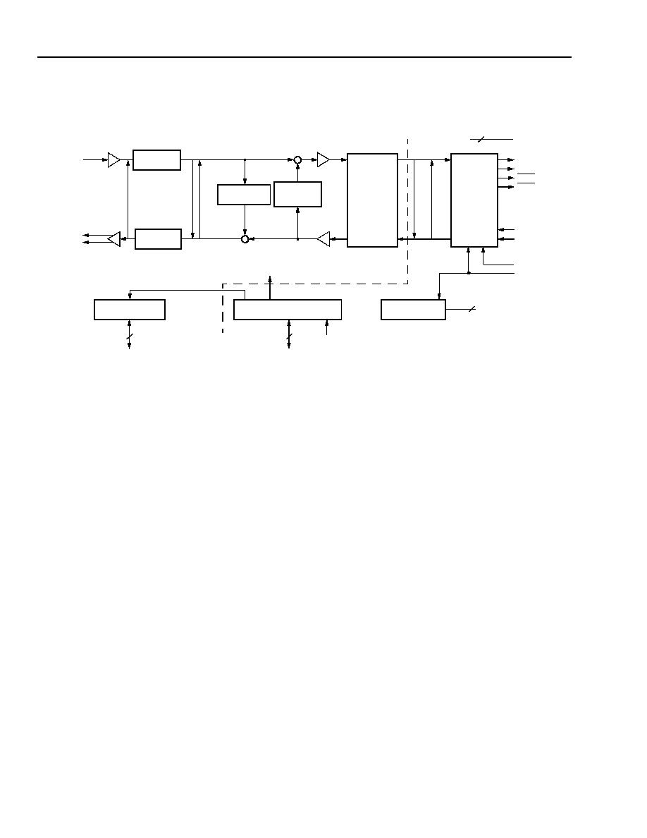
Refer to Figure 1 for the following discussion.
5-8125aF
* Second PCM port not available in all package types.
Figure 1. Functional Block Diagram, Each Section
RST
SLIC
TO/FROM
ANALOG
GAIN
A/D
CONVERTER
ANALOG
BUFFER
D/A
CONVERTER
DI
G
I
T
A
L
L
O
OPBACK 3
ANA
L
O
G
LOOPBA
CK 1
DI
GIT
AL
LOOPBA
CK 2
TERMINATION
IMPEDANCE
HYBRID
BALANCE
NETWORK
DIGITAL GAIN
(GAIN TRANSFER)
µ
-LAW
PER
CHANNEL
COMMON
ANA
L
O
G
LOOPB
ACK 2
DIGI
TAL
LOOPB
ACK 1
PCM BUS
INTERFACE
DX0
DR1*
TO/FROM
PCM BUS
POWER AND
GROUND
18
FS
BCLK
SLIC
CONTROL LATCHES
MICROPROCESSOR CONTROL
CONTROL AND DATA SIGNALS
4
SERIAL CONTROL INTERFACE
PER
CHANNEL
COMMON
0 TO 6
FREQUENCY
SYNTHESIZER
0 TO 3
FILTER
OR
CONVERSION
A-LAW
DIGITAL GAIN
(GAIN TRANSFER)
DX1*
TSX0*
TSX1*
DR0
VF
R
OPn
VF
R
ONn
VF
X
In
This device performs virtually all the signal processing
functions associated with a central office line termina-
tion. Functionality includes line termination impedance
synthesis, fixed hybrid balance impedance synthesis,
and level conversion both in the analog sense to
accommodate various subscriber line interface circuits
(SLICs) and in the digital sense for adjustment of the
levels on the PCM bus. In general, the termination
impedance synthesis generates the equivalent of a cir-
cuit with the parallel combination of a capacitor and a
resistor in series with a resistor, or the parallel combi-
nation of a resistor and the series combination of a
resistor and capacitor. These general forms of imped-
ance characteristics will satisfy most of the require-
ments specified throughout the world. Programmable
selection of either
µ
-law or A-law encoding further aids
worldwide deployment. All coefficients used in the filter-
ing algorithms can be computed off-line in advance and
downloaded to the device at the time of powerup. All
signal processing is contained within the device, and
there are only three interfaces of consequence to the
system designer: the SLIC interface, the PCM inter-
face, and the control interface.
The SLIC interface is designed to be flexible and con-
venient to use with a variety of SLIC circuits. With an
appropriate choice of SLIC, no external components
are required in the interface, with the exception of a dc
blocking capacitor in the transmit direction. In some
cases, dc blocking capacitors in the receive direction
may be necessary as well, since the device operates
from a single low-voltage supply.
The PCM bus interface is flexible in that it allows, inde-
pendently, the transmit and receive data for any chan-
nel to be placed in any time slot. The bus can be
operated at a maximum 16.384 Mbits/s rate to accom-
modate a maximum 256 time slots. Separate pins
are provided for each direction of transmission to
allow 4-wire bus operation. The frame strobe signal is
an 8 kHz signal that defines the beginning of the frame
structure for all four channels. The interface will count
8 bits per time slot and insert or read the data for each
channel as programmed. Lower speeds of the PCM
bus are allowed. The PCM clock must be synchronous
with the frame strobe signal.
The microprocessor control interface is a serial inter-
face that uses the classical chip select type of opera-
tion. The interface controls the device by writing or
reading various internal addresses. The command set
consists of simple read and write operations, with the
address determining the effect. All the memory loca-
tions, including the per-chip functions, are organized by
channel.
There are several test modes included to facilitate con-
firmation of correct operation. In the signal path, two
analog and three digital loopback tests are available,
while in the microprocessor interface, there is a write/
read test mode that tests the operation of the memory.
Use of external test access switches allows a complete
test of the signal path through the line card so that cor-
rect operation of various operational modes can be ver-
ified.
Agere Systems Inc.
5
Preliminary Data Sheet
September 2001
T8535B/T8536B Quad Programmable Codec
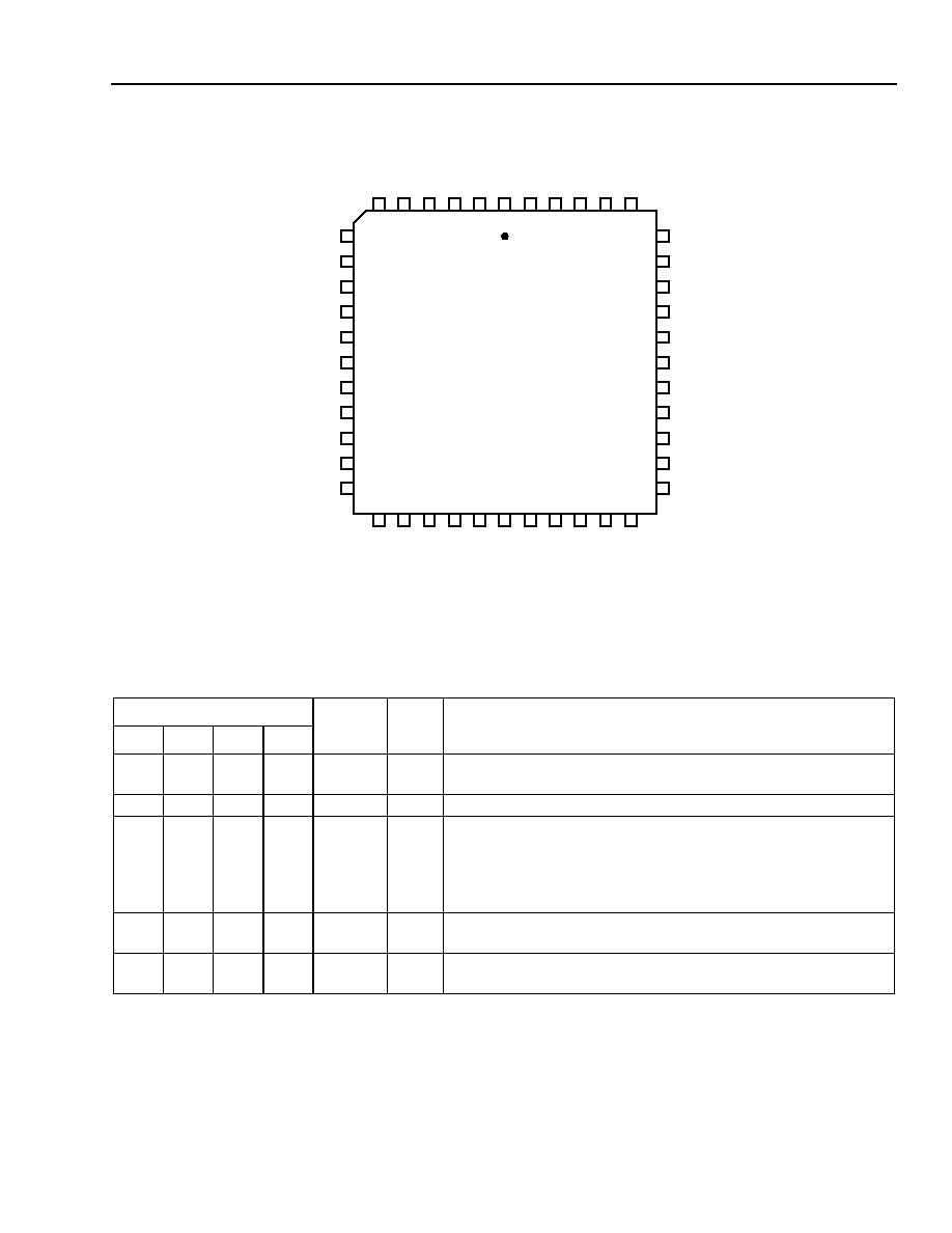
Pin Information
5-7187.b(F)
Figure 2. 44-Pin PLCC Pin Diagram
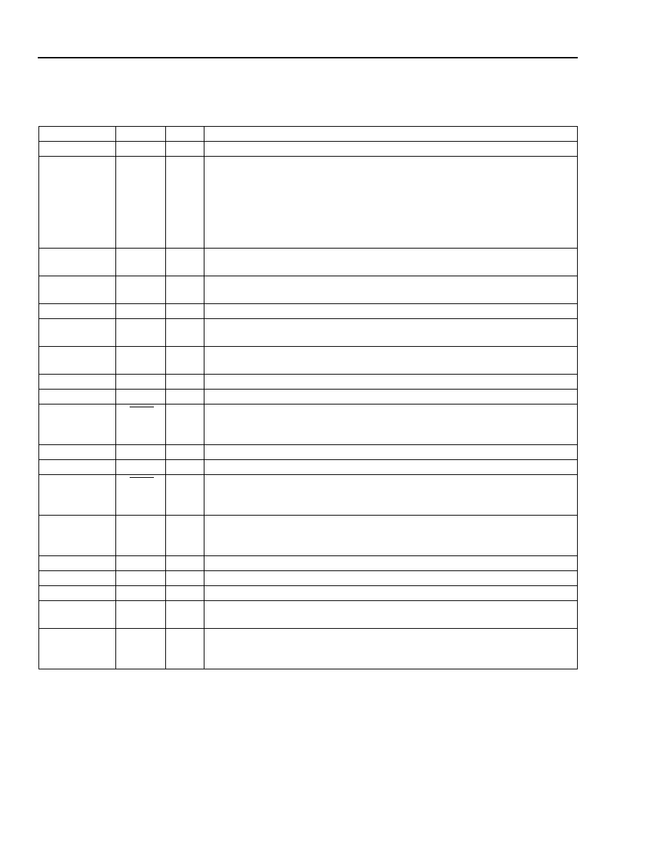
Table 1. Pin Assignments, 44-Pin PLCC, Per-Channel Functions
Ckt
Name
Type
Name/Description
a
b
c
d
15
22
23
30
AGND
GND
Analog Ground. A common AGND, DGND, SGND plane is
highly recommended.
14
21
24
31
V
DD
PWR
Analog Power Supply.
13
20
25
32
VF
X
I
I
Voice Frequency Transmit Input. This node requires a 10 M
or 20 M
resistance to AGND. The value is dependent upon the
gain of the XAG amplifier (register 146). 20 M
can be used for
any gain setting, 10 M
can only be used for XAG gain settings
of 0 dB and +6.02 dB.
12
19
26
33
VF
R
OP
O
Voice Frequency Receive Output, Positive Polarity. This pin
can drive 2000
(or greater) loads.
11
18
27
34
VF
R
ON
O
Voice Frequency Receive Output, Negative Polarity. This pin
can drive 2000
(or greater) loads.
5
4
3
2
1
44
43
42
NC
DC
L
K
DR
RS
T
FI
L
T
V
DO
6
41
40
V
DD
DI
IN
T
S
DG
N
D
26
25
24
23
22
21
20
19
27
V
DD
b
VF
X
Ic
VF
R
ON
b
VF
R
OP
b
VF
R
ON
c
V
DD
A
G
NDc
28
18
VF
X
Ib
V
DD
c
VF
R
OP
c
A
G
NDb
15
14
13
12
11
10
9
V
DD
a
PVCOIN
PVCO
SGND
DGND
V
DD
VF
R
OPa
16
17
8
7
VF
X
Ia
PLLT
AGNDa
VF
R
ONa
32
34
35
36
38
33
VF
X
Id
DX
DGND
FS
AGNDd
DGND
VF
R
ONd
31
30
29
39
V
DD
VF
R
OPd
BCLK
V
DD
d
37
CS

6
Agere Systems Inc.
Preliminary Data Sheet
September 2001
T8535B/T8536B Quad Programmable Codec
Pin Information
(continued)
Table 2. Pin Assignments, 44-Pin PLCC, Common Functions
Pin
Name
Type
Name/Description
1
DO
O
Serial Data Output. This is a 3-state output.
2
DI
I
Serial Data Input.
3
DCLK
I
Serial Data Clock Input.
4
CS
I
Chip Select Input. This lead determines the interval that the serial interface is
active.
5
INTS
I
Serial Interface Select. Leaving this lead open places the serial interface in the nor-
mal mode; grounding it places the interface into the byte-by-byte mode. This lead
has an internal pull-up.
6
FILTV
PWR
Frequency Synthesizer Power (5 V). This pin must be tied to V
DD
.
7
PVCOIN
--
Internal Test Point. Do not connect to this lead.
8
PVCO
--
Internal Test Point. Do not connect to this lead.
9
PLLT
--
Synthesizer Test Point. Do not connect to this lead.
10
SGND
GND
Synthesizer Ground. Connect to digital ground. A common AGND, DGND, SGND
plane is highly recommended.
16, 29,
38, 44
DGND
GND
Digital Ground. Logic ground and return for logic power supply. A common AGND,
DGND, SGND plane is highly recommended.
17, 28,
35, 42
V
DD
PWR
Digital Power Supply (5 V).
36
FS
I
PCM Frame Strobe Input. This 8 kHz clock must be derived from the same source
as BCLK.
37
BCLK
I
PCM Bit Clock Input. This lead is used to develop internal clocks for certain clock
rates.
39 DX
O
PCM Transmit Data Output. This is a 3-state output.
40
DR
I
PCM Receive Data Input.
41
RST
I
Power-On Reset. A low causes a reset of the entire chip. This pin may be con-
nected to DGND with a 0.1
µ
F capacitor for a power-on reset function, or it may be
driven by external logic. This lead has an internal pull-up.
43
NC
--
No Connect. This pin may be used as a tie point.
Agere Systems Inc.
7
Preliminary Data Sheet
September 2001
T8535B/T8536B Quad Programmable Codec
Pin Information
(continued)
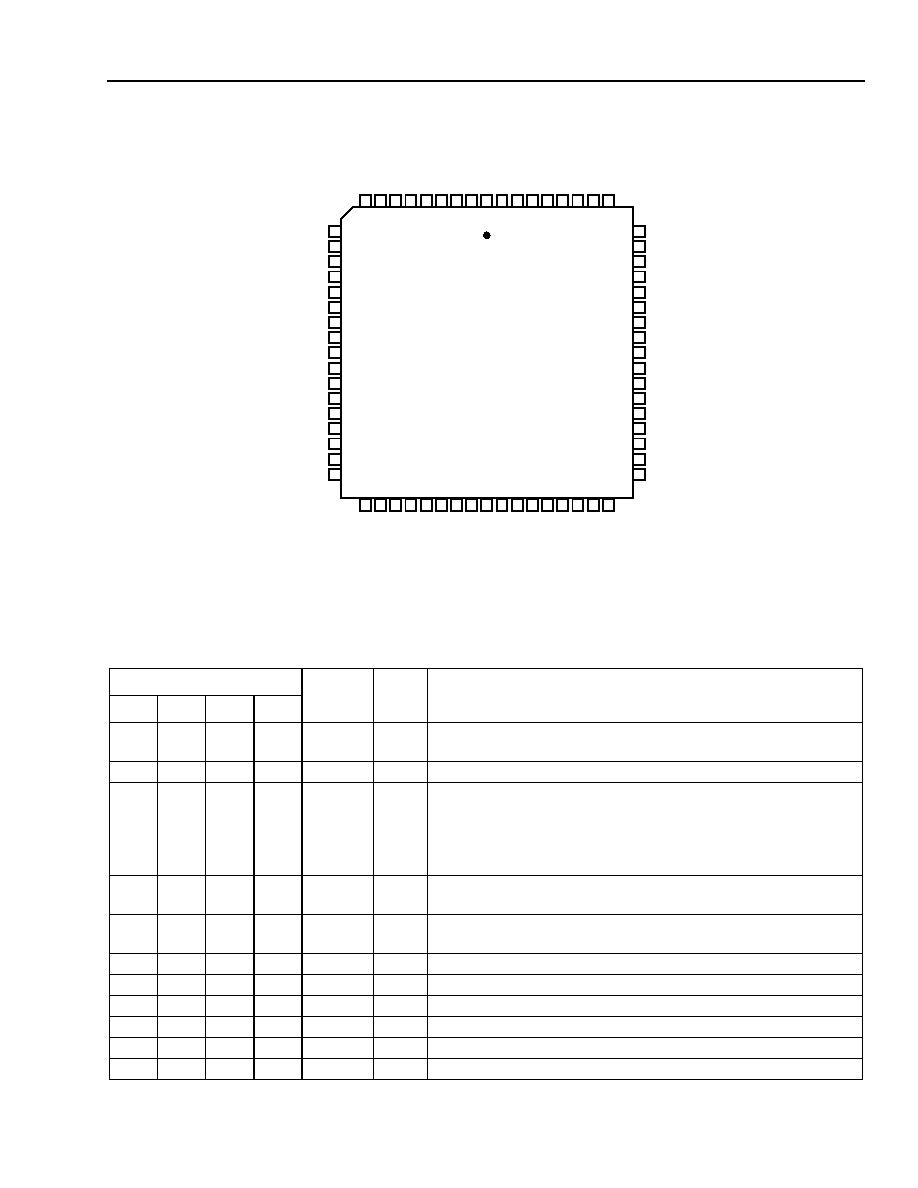
5-8126 (F)
Figure 3. 68-Pin PLCC Pin Diagram
Table 3. Pin Assignments, 68-Pin PLCC, Per-Channel Functions
Ckt
Name
Type
Name/Description
a
b
c
d
21
34
35
48
AGND
GND
Analog Ground. A common AGND, DGND, SGND plane is
highly recommended.
20
33
36
49
V
DD
PWR
Analog Power Supply.
19
32
37
50
VF
X
I
I
Voice Frequency Transmit Input. This node requires a 10 M
or 20 M
resistance to AGND. The value is dependent upon the
gain of the XAG amplifier (register 146). 20 M
can be used for
any gain setting, 10 M
can only be used for XAG gain settings
of 0 dB and +6.02 dB.
18
31
38
51
VF
R
OP
O
Voice Frequency Receive Output, Positive Polarity. This pin
can drive 2000
(or greater) loads.
17
30
39
52
VF
R
ON
O
Voice Frequency Receive Output, Negative Polarity. This pin
can drive 2000
(or greater) loads.
16
29
41
53
SLIC0
I/O
SLIC Control 0.
15
27
42
54
SLIC1
I/O
SLIC Control 1.
9
26
43
61
SLIC2
I/O
SLIC Control 2.
8
25
44
63
SLIC3
I/O
SLIC Control 3.
7
23
46
64
SLIC4
I/O
SLIC Control 4.
6
22
47
62
SLIC5
I/O
SLIC Control 5.
6
4
3
2
1 68 67 66 65 64
5
NC
DCL
K
SL
I
C
2
d
SL
I
C
3
d
RS
T
INT
S
SL
I
C
4
a
SL
I
C
2
a
DO
7
8
9
63 62 61
VD
D
DI
SL
I
C
5
d
SL
I
C
4
d
CS
SL
I
C
5
a
SL
I
C
3
a
DGND
40
38
37
36
35
34
33
32
31
30
39
VDDb
VF
XI
c
SL
I
C
1
b
SL
I
C
0
b
VF
RO
Pb
VF
RONc
SL
I
C
0
c
SL
I
C
2
c
AGNDc
41 42 43
29
28
27
VF
XI
b
VDDc
VDD
V
F
RONb
VF
RO
Pc
VDD
SL
I
C
1
c
AGNDb
23
21
20
19
18
17
16
15
14
13
22
SLIC0a
VDDa
FILTV
PVCO
SGND
SLIC5b
DGND
SLIC2b
VFROPa
24
25
26
12
11
10
SLIC1a
VFXIa
PVCOIN
PLLT
AGNDa
SLIC4b
SLIC3b
VFRONa
47
49
50
51
52
53
54
55
56
57
48
SLIC1d
VFXId
DR
DGND
FS
AGNDd
SLIC4c
SLIC3c
VFRONd
46
45
44
58
59
60
VDD
VFROPd
DX
BCLK
VDDd
SLIC5c
DGND
SLIC0d

8
Agere Systems Inc.
Preliminary Data Sheet
September 2001
T8535B/T8536B Quad Programmable Codec
Pin Information
(continued)
Table 4. Pin Assignments, 68-Pin PLCC, Common Functions
Pin
Name
Type
Name/Description
1
DO
O
Serial Data Output. This is a 3-state output.
2
DI
I
Serial Data Input.
3
DCLK
I
Serial Data Clock Input.
4
CS
I
Chip Select Input. This lead determines the interval that the serial interface is
active.
5
INTS
I
Serial Interface Select. Leaving this lead open places the serial interface in the nor-
mal mode; grounding it places the interface into the byte-by-byte mode. This lead
has an internal pull-up.
10
FILTV
PWR
Frequency Synthesizer Power (5 V). This pin must be tied to V
DD
.
11
PVCOIN
--
Internal Test Point. Do not connect to this lead.
12
PVCO
--
Internal Test Point. Do not connect to this lead.
13
PLLT
--
Synthesizer Test Point. Do not connect to this lead.
14
SGND
GND
Synthesizer Ground. Connect to digital ground. A common AGND, DGND, SGND
plane is highly recommended.
24, 45,
58, 68
DGND
GND
Digital Ground. Logic ground and return for logic power supply. A common AGND,
DGND, SGND plane is highly recommended.
28, 40,
55, 66
V
DD
PWR
Digital Power Supply (5 V).
56
FS
I
PCM Frame Strobe Input. This 8 kHz clock must be derived from the same source
as BCLK.
57
BCLK
I
PCM Bit Clock Input. This lead is used to develop internal clocks for certain clock
rates.
59 DX
O
PCM Transmit Data Output. This is a 3-state output.
60
DR
I
PCM Receive Data Input.
65
RST
I
Power-On Reset. A low causes a reset of the entire chip. This pin may be con-
nected to DGND with a 0.1
µ
F capacitor for a power-on reset function, or it may be
driven by external logic. This lead has an internal pull-up.
67
NC
--
No Connect. This pin may be used as a tie point.
Agere Systems Inc.
9
Preliminary Data Sheet
September 2001
T8535B/T8536B Quad Programmable Codec
Pin Information
(continued)
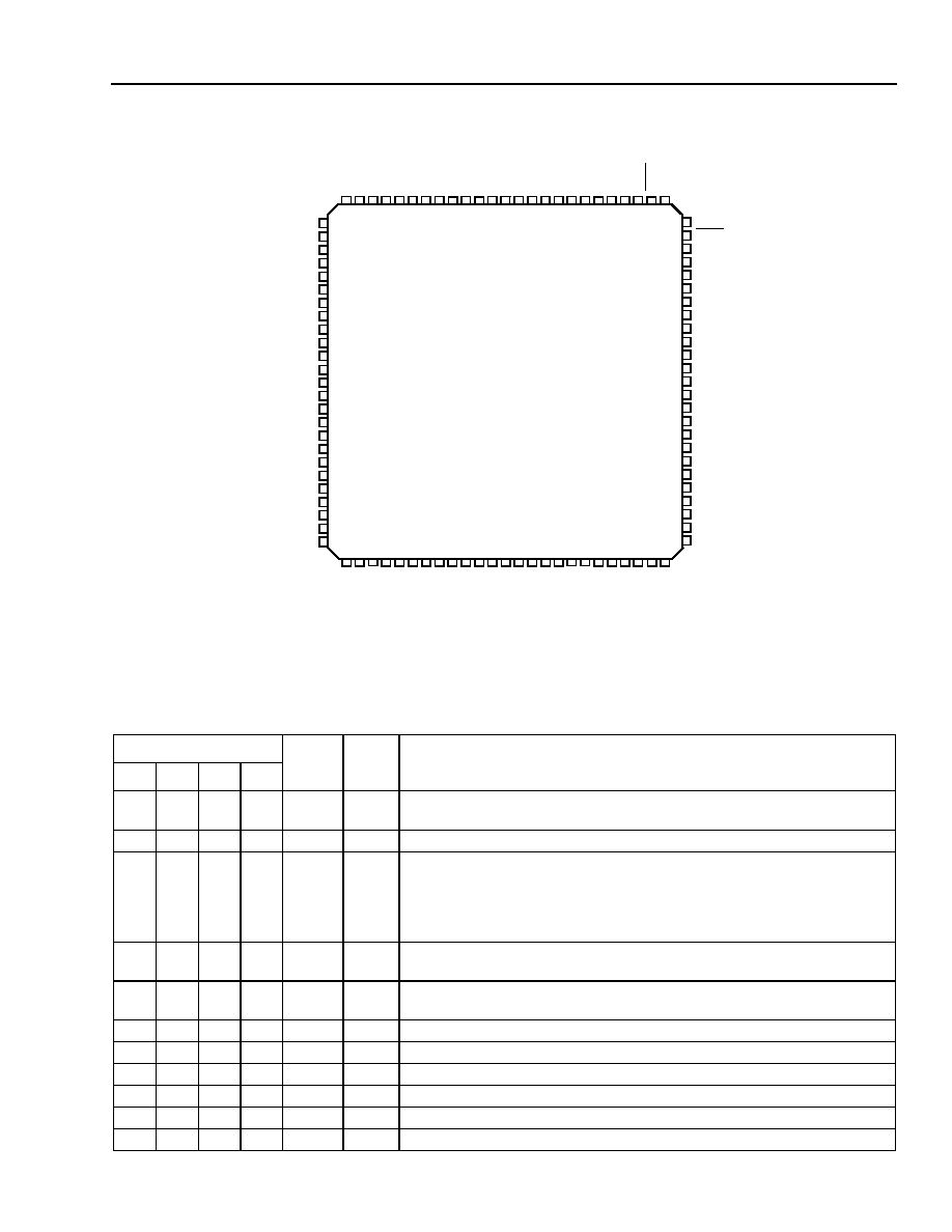
5-8885 (F)
Figure 4. 100-Pin TQFP Pin Diagram
Table 5. Pin Assignments, 100-Pin TQFP, Per-Channel Functions
Ckt
Name
Type
Name/Description
a
b
c
d
17
31
34
54
AGND
GND
Analog Ground. A common AGND, DGND, SGND plane is highly rec-
ommended.
16
30
36
55
V
DD
PWR
Analog Power Supply.
14
29
41
56
VF
X
I
I
Voice Frequency Transmit Input. This node requires a 10 M
or
20 M
resistance to AGND. The value is dependent upon the gain of
the XAG amplifier (register 146). 20 M
can be used for any gain
setting, 10 M
can only be used for XAG gain settings of 0 dB and
+6.02 dB.
13
28
42
57
VF
R
OP
O
Voice Frequency Receive Output, Positive Polarity. This pin can
drive 2000
(or greater) loads.
11
27
43
58
VF
R
ON
O
Voice Frequency Receive Output, Negative Polarity. This pin can
drive 2000
(or greater) loads.
6
26
46
65
SLIC0
I/O
SLIC Control 0.
5
24
47
66
SLIC1
I/O
SLIC Control 1.
100
23
48
78
SLIC2
I/O
SLIC Control 2.
99
21
49
80
SLIC3
I/O
SLIC Control 3.
98
19
52
81
SLIC4
I/O
SLIC Control 4.
97
18
53
79
SLIC5
I/O
SLIC Control 5.
FILTV
DX1
DCL
K
CS
INT
S
NC
NC
NC
NC
NC
SL
I
C
5
a
SL
I
C
4
a
SL
I
C
3
a
SL
I
C
2
a
NC
NC
SGND
SLIC1a
SLIC0a
NC
NC
NC
NC
VF
R
ONa
NC
VF
R
OPa
VF
X
Ia
NC
V
DD
a
AGNDa
SLIC5b
SLIC4b
DGND
SLIC3b
NC
SLIC2b
SLIC1b
V
DD
SL
I
C
0
b
VF
R
ONb
VF
X
Ib
VDDb
AGNDb
NC
NC
AGNDc
NC
V
DD
c
NC
NC
NC
NC
VF
X
Ic
VF
R
OP
c
VF
R
ONc
NC
V
DD
SL
I
C
0
c
SL
I
C
1
c
SL
I
C
2
c
SL
I
C
3
c
TSX0
DR0
DX0
DGND
NC
BCLK
FS
V
DD
SLIC1d
SLIC0d
NC
NC
NC
NC
NC
NC
VF
R
ONd
VF
R
OPd
VF
X
Id
V
DD
d
AGNDd
SLIC5c
DGND
DI
DO
NC
DGND
V
DD
RST
SL
I
C
4
d
SL
I
C
3
d
SL
I
C
5
d
SL
I
C
2
d
TSX
1
DR1
NC
88
89
90
91
92
93
95
96
97
98
99
10
0
87
86
85
84
83
82
81
80
79
78
77
76
94
38
37
36
35
34
33
31
30
29
28
27
26
39
40
41
42
43
44
45
46
47
48
49
50
32
13
12
11
10
9
8
6
5
4
3
2
1
14
15
16
17
18
19
20
21
22
23
24
25
7
63
64
65
66
67
68
70
71
72
73
74
75
62
61
60
59
58
57
56
55
54
53
52
51
69
SLIC4c
NC
VF
R
OP
b
10
Agere Systems Inc.
Preliminary Data Sheet
September 2001
T8535B/T8536B Quad Programmable Codec
Pin Information
(continued)
Table 6. Pin Assignments, 100-Pin TQFP, Common Functions
Pin
Name
Type
Name/Description
1
FILTV
PWR
Frequency Synthesizer Power (5 V). This pin must be tied to V
DD
.
2, 3, 7--10,
12, 15, 22, 32,
33, 35,
37--40,
44, 50,
59--64, 70,
85, 91--96
NC
--
No Connect. This pin may be used as a tie point.
4
SGND
GND
Synthesizer Ground. Connect to digital ground. A common AGND, DGND,
SGND plane is highly recommended.
20, 51, 71, 84
DGND
GND
Digital Ground. Logic ground and return for logic power supply. A common
AGND, DGND, SGND plane is highly recommended.
25, 45, 67, 83
V
DD
PWR
Digital Power Supply (5 V).
68
FS
I
PCM Frame Strobe Input. This 8 kHz clock must be derived from the same
source as BCLK.
69
BCLK
I
PCM Bit Clock Input. This lead is used to develop internal clocks for certain
clock rates.
72 DX0
O
PCM Transmit Data Output 0. This is a 3-state output.
73
DR0
I
PCM Receive Data Input 0.
74
TSX0
O
Backplane Line Driver Enable 0 (Active-Low). Normally, these open-drain
outputs are floating in a high-impedance state. When a time slot is active on
DX0, this output pulls low to enable a backplane line driver.
75
DX1
O
PCM Transmit Data Output 1. This is a 3-state output.
76
DR1
I
PCM Receive Data Input 1.
77
TSX1
O
Backplane Line Driver Enable 1 (Active-Low). Normally, these open-drain
outputs are floating in a high-impedance state. When a time slot is active on
DX1, this output pulls low to enable a backplane line driver.
82
RST
I
Power-On Reset. A low causes a reset of the entire chip. This pin may be
connected to DGND with a 0.1
µ
F capacitor for a power-on reset function, or it
may be driven by external logic. This lead has an internal pull-up.
86
DO
O
Serial Data Output. This is a 3-state output.
87
DI
I
Serial Data Input.
88
DCLK
I
Serial Data Clock Input.
89
CS
I
Chip Select Input. This lead determines the interval that the serial interface is
active.
90
INTS
I
Serial Interface Select. Leaving this lead open places the serial interface in
the normal mode; grounding it places the interface into the byte-by-byte mode.
This lead has an internal pull-up.

Agere Systems Inc.
11
Preliminary Data Sheet
September 2001
T8535B/T8536B Quad Programmable Codec
Pin Information
(continued)
5-7187dF
Figure 5. 64-Pin TQFP Pin Diagram
Table 7. Pin Assignments, 64-Pin TQFP, Per-Channel Functions
Ckt
Name
Type
Name/Description
a
b
c
d
9
21
22
34
AGND
GND
Analog Ground. A common AGND, DGND, SGND plane is
highly recommended.
8
20
23
35
V
DD
PWR
Analog Power Supply.
7
19
24
36
VF
X
I
I
Voice Frequency Transmit Input. This node requires a
10 M
or 20 M
resistance to AGND. The value is dependent
upon the gain of the XAG amplifier (register 146). 20 M
can
be used for any gain setting, 10 M
can only be used for XAG
gain settings of 0 dB and +6.02 dB.
6
18
25
37
VF
R
OP
O
Voice Frequency Receive Output, Positive Polarity. This
pin can drive 2000
(or greater) loads.
5
17
26
38
VF
R
ON
O
Voice Frequency Receive Output, Negative Polarity. This
pin can drive 2000
(or greater) loads.
4
16
28
39
SLIC0
I/O
SLIC Control 0.
3
14
29
40
SLIC1
I/O
SLIC Control 1.
64
13
30
51
SLIC2
I/O
SLIC Control 2.
63
12
31
52
SLIC3
I/O
SLIC Control 3.
62
10
33
53
SLIC4
I/O
SLIC Control 4.
60 59 58 57 56 55 54 53 52
61
DCLK
DR1
SL
I
C
3d
RS
T
IN
T
S
SL
I
C
4a
SL
I
C
2a
DO
62
63
64
51 50 49
V
DD
DI
SL
I
C
2d
SL
I
C
4d
CS
SL
I
C
3a
DG
N
D
30
28
27
26
25
24
23
22
21
20
29
V
DD
b
VF
X
Ic
V
DD
SLIC0b
VF
R
OP
b
VF
R
ON
c
SL
I
C
0c
SL
I
C
1c
A
G
NDc
31 32
19
18
17
VF
X
Ib
V
DD
c
SLIC1b
VF
R
ON
b
VF
R
OP
c
V
DD
A
G
NDb
13
12
11
10
9
8
7
6
5
4
SLIC0a
V
DD
a
FILTV
SGND
DGND
SLIC2b
VF
R
OPa
14
15
16
3
2
1
SLIC1a
VF
X
Ia
AGNDa
SLIC4b
SLIC3b
VF
R
ONa
36
38
39
40
41
42
43
44
45
46
37
SLIC1d
VF
X
Id
DX0
DGND
FS
AGNDd
DG
ND
SL
IC
2
c
VF
R
ONd
35
34
33
47
48
V
DD
VF
R
OPd
BCLK
V
DD
d
SLIC4c
SL
IC
3
c
SLIC0d
DX1
TSX0
DR0
T
S
X
1

12
Agere Systems Inc.
Preliminary Data Sheet
September 2001
T8535B/T8536B Quad Programmable Codec
Pin Information
(continued)
Table 8. Pin Assignments, 64-Pin TQFP, Common Functions
Pin
Name
Type
Name/Description
1
FILTV
PWR
Frequency Synthesizer Power (5 V). This pin must be tied to V
DD
.
2
SGND
GND
Synthesizer Ground. Connect to digital ground. A common AGND, DGND, SGND
plane is highly recommended.
11, 32,
44, 56
DGND
GND
Digital Ground. Logic ground and return for logic power supply. A common AGND,
DGND, SGND plane is highly recommended.
15, 27,
41, 55
V
DD
PWR
Digital Power Supply (5 V).
42
FS
I
PCM Frame Strobe Input. This 8 kHz clock must be derived from the same source
as BCLK.
43
BCLK
I
PCM Bit Clock Input. This lead is used to develop internal clocks for certain clock
rates.
45 DX0
O
PCM Transmit Data Output 0. This is a 3-state output.
46
DR0
I
PCM Receive Data Input 0.
47
TSX0
O
Backplane Line Driver Enable 0 (Active-Low). Normally, these open-drain outputs
are floating in a high-impedance state. When a time slot is active on DX0, this output
pulls low to enable a backplane line driver.
48
DX1
O
PCM Transmit Data Output 1. This a 3-state output.
49
DR1
I
PCM Receive Data Input 1.
50
TSX1
O
Backplane Line Driver Enable 1 (Active-Low). Normally, these open-drain outputs
are floating in a high-impedance state. When a time slot is active on DX1, this output
pulls low to enable a backplane line driver.
54
RST
I
Power-On Reset. A low causes a reset of the entire chip. This pin may be con-
nected to DGND with a 0.1
µ
F capacitor for a power-on reset function, or it may be
driven by external logic. This lead has an internal pull-up.
57
DO
O
Serial Data Output. This is a 3-state output.
58
DI
I
Serial Data Input.
59
DCLK
I
Serial Data Clock Input.
60
CS
I
Chip Select Input. This lead determines the interval that the serial interface is
active.
61
INTS
I
Serial Interface Select. Leaving this lead open places the serial interface in the nor-
mal mode; grounding it places the interface into the byte-by-byte mode. This lead
has an internal pull-up.

Agere Systems Inc.
13
Preliminary Data Sheet
September 2001
T8535B/T8536B Quad Programmable Codec
Functional Description
Clocking Considerations
The PCM bus uses BCLK as the bit clock and the one-
going edge of FS to determine the location of the
beginning of a frame. These two clocks must be
derived from the same source. Internally, the device
develops all the internal clocks with a phase-locked
loop that uses BCLK as the timing source. BCLK and
FS must be continuously present and without gaps in
order for the device to operate correctly.
DCLK is used to clock the internal serial interface and
may be asynchronous to the other clocks. There is no
need to derive this clock from the same source as the
other clocks. The serial bus may be operated at any
speed up to 4.096 Mbits/s. DCLK can be gapped.
There is no limit on the number of devices on the same
serial bus.
The Control Interface
The device is controlled via a series of memory loca-
tions accessed by a serial data connection to the exter-
nal master controller. This interface operates using the
chip select lead to enable transmission of information.
All chip functions are enabled or disabled by setting or
clearing bits in the control memory. Filter coefficients
and gain adjustments are also stored in this memory.
The codec has both a serial input lead and a serial out-
put lead. These may be used individually for a 4-wire
serial interface, or tied together for a 2-wire interface.
The line driver circuitry is capable of driving relatively
high currents so that in the event that the line is long
enough to show significant transmission line effects, it
can be terminated in the characteristic impedance at
each end with resistors to V
CC
and ground.
All data transfers on the serial bus are byte oriented
with the least significant bit (shown in this data sheet as
bit 0) transmitted first, followed by the more significant
bits. For data fields, the least significant byte of the first
data byte is transmitted first, followed by the more sig-
nificant bytes, each byte transmitted LSB first. This for-
mat is compatible with the serial port on most
microcontrollers.
Modes
There are two different modes of operation for the
serial interface: the normal mode and the byte-by-byte
mode. These two modes differ in the data clocking and
the manner in which CS is used to control the transfer.
Note that the CS lead is used to control the transfer of
serial data from master controller to slave codec and in
the reverse direction.
In normal mode (INTS pin open), the CS lead must go
low for the duration of the transfer. CS is latched by
DCLK on a positive-going clock edge. DI is latched by
DCLK on a negative-going clock edge. DCLK may be
continuous, but only needs to be present to clock data
when CS is low (gapped clock). When using gapped
clock, DCLK can remain high or low when CS is high.
The only error check performed by the codec is to
verify that CS is low for an integral number of bytes.
Detection of an active chip select for other than an
integral multiple of 8 bits results in the operation being
terminated. The next active excursion of chip select will
be interpreted as a new command; hence, the serial
I/O interface can always be initialized by asserting CS
for a number of clock periods that is not an integral
multiple of 8. CS is captured using DCLK, so DCLK
must be transitioned to perform this initialization.
The byte-by-byte mode (INTS pin tied to ground) uses
CS to control each byte of the transfer. In this mode,
CS goes low for exactly 8 bits at a time, corresponding
to a 1-byte transfer either to or from the codec chip.
DCLK can be continuous or gapped. When using a
gapped clock, DCLK can remain high or low when CS
is high. CS and DI are latched on a positive-going clock
edge. Repeated transitions of CS are used to control
subsequent bytes of data to/from the codec. For a write
command in this mode, CS must go low for each byte
of the transfer until the transfer is complete. For a read
command, CS will go low for each of the 3 bytes of the
read command transferred to the device, then low
again for each byte to be read. Notice that the total
number of bytes transferred (and excursions on CS) is
N + 3, where N is the number of bytes to be read in the
command. This mode of operation is useful in cases
where the master is a microprocessor with a built-in
UART that transfers 1 byte at a time. Error detection is
limited to detection of an active CS for other than an
integral multiple of 8 bits. Recovery is the same as nor-
mal mode.
Flow control can be accomplished by suspending the
transitions on DCLK by holding either state. During the
data transfer, CS must remain low while clock transi-
tions are suspended with DCLK in either state.

14
14
Agere Systems Inc.
Preliminary Data Sheet
September 2001
T8535B/T8536B Quad Programmable Codec
Functional Description
(continued)
The Control Interface
(continued)
Protocol
The format of the command protocol is shown in Fig-
ures 6 and 7.
The control interface operates with one external master
controller and multiple slave codec devices. Each
transfer is initiated by the master, and the slave
responds for either read operations or the fast scan
mode. The slave does not check the bus for activity
prior to transmitting; it only checks for an active CS.
The master should allow for a wait between the end of
a read command until CS becomes active for the read
data. The master must refrain from sending additional
commands to the slave chip until the response is
received. On a 4-wire bus, commands to other devices
may be initiated before the response is received, but
care in generating the CS function is needed to ensure
that the multiple responses do not interfere. It should
be noted that multiple memory locations can be
accessed in the same command by setting the data
field length field to the desired number of bytes to be
transferred. If flow control is desired, it must be per-
formed by using separate commands, each transfer-
ring smaller blocks of information, or by controlling the
serial clock (gapping the serial clock), or with CS in the
case of byte-by-byte mode.
There is no response from the slave to the master for a
write operation. The response to a read operation sim-
ply includes the data to be read in the data field. Com-
mands from the master controller include data for write
operations, but not for read operations.
All data is transmitted in a byte-oriented fashion with
the least significant bit of each byte transferred first.
Multibyte fields are transferred least significant byte
first in both directions. The data field will contain the
first addressed data location first, with subsequent data
locations transmitted in ascending order.
Since the coefficients and gains are stored in volatile
memory, all the coefficients and gains must be loaded
after powerup. There is, however, no need to reload
them when switching from active to standby modes, or
vice versa.
Agere Systems Inc.
15
Preliminary Data Sheet
September 2001
T8535B/T8536B Quad Programmable Codec
Functional Description
(continued)
The Control Interface
(continued)
Protocol (continued)
* Location of memory bank selection. All user controls are in memory bank 0; other memory banks contain internal state information for the
device.
Note: Data field length is in bytes for all operations. All data is transmitted in bytes with the LSB for each byte transmitted first. For 16-bit mem-
ory operations, the least significant byte of the first memory location is transmitted first, followed by the most significant byte; each byte is
transmitted LSB first. Additional memory locations are loaded in ascending sequence.
Figure 6. Command Frame Format, Master to Slave, Read or Write Commands
Note: All data is transmitted in bytes with the LSB for each byte transmitted first. For memory operations, the least significant byte of the first
memory location is transmitted first, followed by the most significant byte, each byte transmitted LSB first. Additional memory locations
are loaded in ascending sequence.
Figure 7. Command Frame Format, Slave to Master, Read Commands
LSB
MSB LSB
MSB LSB
MSB LSB
COMMAND (8 bits)
START ADDRESS (8 bits)
DATA FIELD LENGTH (8 bits)
DATA FIELD (VARIABLE LENGTH) WRITE OPERATIONS ONLY
TIME
7
6
5
4
3
2
1
0
MSB
LSB
START ADDRESS:
7
6
5
4
3
2
1
0
MSB
LSB
DATA FIELD LENGTH:
7
6
5
4
3
2
1
0
MSB
LSB
COMMAND:
0*
0*
CKT
SELECT
0
0
COMMAND
CKT SELECT:
CKT a:
CKT b:
CKT c:
CKT d:
00
01
10
11
COMMANDS: FAST SCAN MODE:
WRITE MEMORY:
WRITE ALL CHANNELS:
READ MEMORY:
10
01
11
00
LSB
DATA FIELD (VARIABLE LENGTH) READ OPERATIONS ONLY
16
Agere Systems Inc.
Preliminary Data Sheet
September 2001
T8535B/T8536B Quad Programmable Codec
Functional Description
(continued)
The Control Interface
(continued)
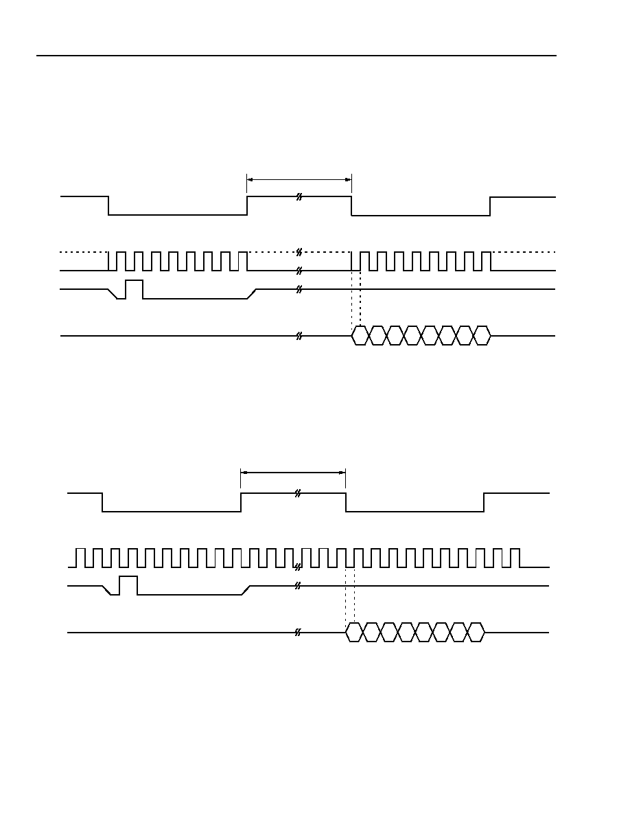
Write Command
A write command is used to write to the memory addresses. Figures 8--11 illustrate normal or byte-by-byte opera-
tion with continuous or gapped DCLKs. For gapped DCLK operation, transitions, not frequency, are critical (as long
as the transitions do not exceed the maximum DCLK frequencies).
0078B
* Allow a minimum of 244 ns before the next command frame.
Note: Data field length of 1 shown.
Figure 8. Write Operation, Normal Mode (Continuous DCLK)
0078C
* Allow a minimum of 244 ns before the next command frame.
Note: Data field length of 1 shown.
Figure 9. Write Operation, Normal Mode (Gapped DCLK)
COMMAND FRAME
0
1
7
0
1
7
CS
DCLK
DI
COMMAND
START ADDRESS
DATA
0
1
7
0
1
7
0
1
7
0
1
7
LENGTH
0
1
7
0
1
7
*
COMMAND FRAME
0
1
7
0
1
7
CS
DCLK
DI
COMMAND
START ADDRESS
DATA
0
1
7
0
1
7
0
1
7
0
1
7
LENGTH
0
1
7
0
1
7
*
Agere Systems Inc.
17
Preliminary Data Sheet
September 2001
T8535B/T8536B Quad Programmable Codec
Functional Description
(continued)
The Control Interface
(continued)
Write Command (continued)
0072C
* Shows customary usage, CS not required to go high between bytes.
Allow a minimum of 244 ns before the next command frame.
Note: Data field length of 1 shown.
Figure 10. Write Operation, Byte-by-Byte Mode (Gapped DCLK)
0074B
* Shows customary usage, CS not required to go high between bytes.
Allow a minimum of 244 ns before the next command frame.
Note: Data field length of 1 shown.
Figure 11. Write Operation, Byte-by-Byte Mode (Continuous DCLK)
0
1
7
0
1
7
CS
DCLK
DI
COMMAND
START ADDRESS
LENGTH
DATA
COMMAND FRAME
0
1
7
0
1
7
0
1
7
0
1
7
0
1
7
0
1
7
*
*
*
0
1
7
0
1
7
CS
DCLK
DI
COMMAND
START ADDRESS
LENGTH
DATA
0
1
7
0
1
7
0
1
7
0
1
7
0
1
7
0
1
7
COMMAND FRAME
*
*
*
18
Agere Systems Inc.
Preliminary Data Sheet
September 2001
T8535B/T8536B Quad Programmable Codec
Functional Description
(continued)
The Control Interface
(continued)
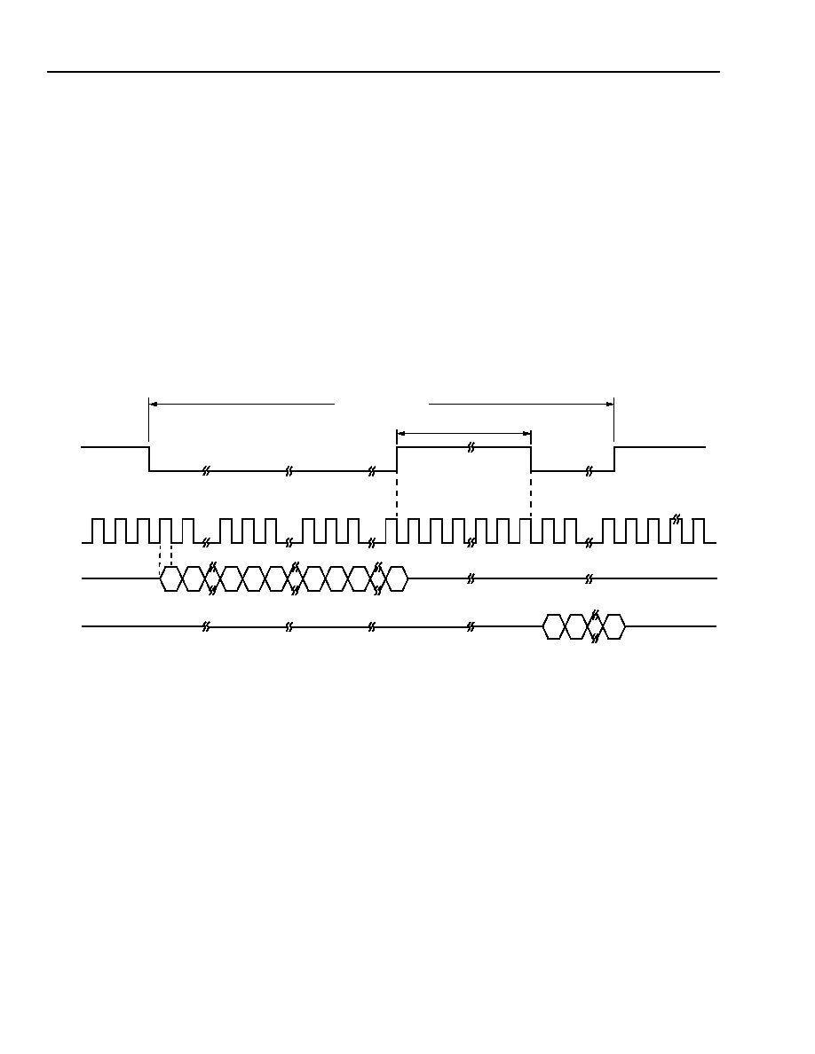
Read Command
The normal flow of information to the master controller is always in response to a read command. All control mem-
ory locations are accessed in 8-bit bytes. All read commands from the master controller require a response from
the addressed codec. It is the responsibility of the master controller to ensure that only one device is transmitting
on the serial interface line at any one time. The master controller also must ensure that the CS lead goes high after
transferring the 3-byte sequence used to initiate the read, and then it goes low again for the response. In this case,
it should be noted that the device expects that the second time CS goes low the data is to be sent to the master;
thus, it does not interpret the DI lead as containing a valid instruction during that CS excursion and a write during
this time is not recommended. Note also that the CS lead must allow the number of bytes sent in a read command
to be transferred before a subsequent command can be received by the codec. Figures 12--15 illustrate normal or
byte-by-byte operation with continuous or gapped DCLKs. Like a write command, transitions, not frequency, are
critical with regard to gapped DCLK operation.
0079B
* Provides sufficient wait time to access read data.
Allow a minimum of 244 ns before the next command frame.
Note: Data field length of 1 shown.
Figure 12. Read Operation, Normal Mode (Continuous DCLK)
COMMAND FRAME
0
1
7
0
1
7
CS
DCLK
DI
COMMAND
START ADDRESS
DATA
0
1
7
0
1
7
0
1
7
LENGTH
0
1
7
0
1
7
0
1
7
DO
WAIT
1.5
µ
s
*
Agere Systems Inc.
19
Preliminary Data Sheet
September 2001
T8535B/T8536B Quad Programmable Codec
Functional Description
(continued)
The Control Interface
(continued)
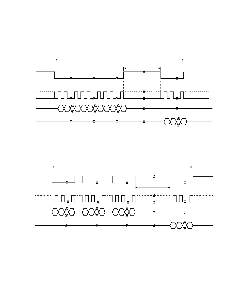
Read Command (continued)
0079C
* Provides sufficient wait time to access read data.
Allow a minimum of 244 ns before the next command frame.
Figure 13. Read Operation, Normal Mode (Gapped DCLK)
0073C
* Shows customary usage, CS not required to go high between bytes.
Provides sufficient wait time to access read data.
Allow a minimum of 244 ns before the next command frame.
Note: Data field length of 1 shown.
Figure 14. Read Operation, Byte-by-Byte Mode (Gapped DCLK)
COMMAND FRAME
0
1
7
0
1
7
CS
DCLK
DI
COMMAND
START ADDRESS
DATA
0
1
7
0
1
7
0
1
7
LENGTH
0
1
7
0
1
7
0
1
7
DO
WAIT
1.5
µ
s
*
0
1
7
DATA
0
1
7
0
1
7
COMMAND
START
LENGTH
CS
DCLK
DI
D0
COMMAND FRAME
0
1
7
0
1
7
0
1
7
0
1
7
0
1
7
WAIT
1.5
µ
s
ADDRESS
*
*
20
Agere Systems Inc.
Preliminary Data Sheet
September 2001
T8535B/T8536B Quad Programmable Codec
Functional Description
(continued)
The Control Interface
(continued)
Read Command (continued)
0075B
* Shows customary usage, CS not required to go high between bytes.
Provides sufficient wait time to access read data.
Allow a minimum of 244 ns before the next command frame.
Note: Data field length of 1 shown.
Figure 15. Read Operation, Byte-by-Byte Mode (Continuous DCLK)
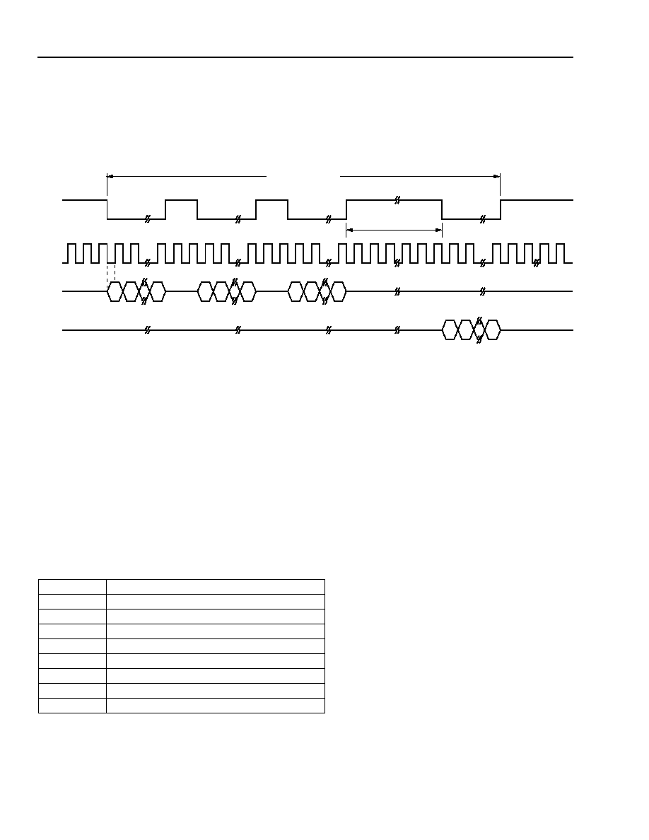
Fast Scan Mode
The fast scan mode allows a single byte command to read two SLIC control leads for all four channels with a
1-byte reply. This mode significantly speeds up the normal scanning for off-hook, ring trip, and ring ground detec-
tion. This special command sequence allows the controlling microprocessor to fast scan 2 bits in the SLIC control
byte of each of the four channels. The command code is (00000010)
2
; there are no start address or length fields.
The command returns only a single byte of data, formatted as shown in Table 9.
Table 9. Bit Assignments for Fast Scan Mode
Bit
Reported Status
0 (LSB)
Channel 0, bit 0 (ckt a, address 160, bit 0)
1
Channel 0, bit 1 (ckt a, address 160, bit 1)
2
Channel 1, bit 0 (ckt b, address 160, bit 0)
3
Channel 1, bit 1 (ckt b, address 160, bit 1)
4
Channel 2, bit 0 (ckt c, address 160, bit 0)
5
Channel 2, bit 1 (ckt c, address 160, bit 1)
6
Channel 3, bit 0 (ckt d, address 160, bit 0)
7 (MSB)
Channel 3, bit 1 (ckt d, address 160, bit 1)
0
1
7
0
1
7
CS
DCLK
DI
COMMAND
START
LENGTH
DATA
0
1
7
0
1
7
0
1
7
0
1
7
0
1
7
COMMAND FRAME
D0
0
1
7
WAIT
1.5
µ
s
ADDRESS
*
*
Agere Systems Inc.
21
Preliminary Data Sheet
September 2001
T8535B/T8536B Quad Programmable Codec
Functional Description
(continued)
The Control Interface
(continued)
Fast Scan Mode (continued)
The circuit select in the command structure (Figure 6) is not used for this special single-byte command. The rules
for toggling chip select apply as for the read command. Figures 16--19 illustrate normal or byte-by-byte operation
with continuous or gapped DCLKs.
0125B
* Provides sufficient wait time to access read data.
Allow a minimum of 244 ns between bytes.
Figure 16. Fast Scan, Normal Mode (Continuous DCLK)
0125C
* Provides sufficient wait time to access read data.
Allow a minimum of 244 ns between bytes.
Figure 17. Fast Scan, Normal Mode (Gapped DCLK)
1
2
3
CS
DCLK
DI
COMMAND
DATA
4
5
DO
WAIT
1.5
µ
s
*
0
1
2
3
4
5
6
7
6
7
0
1
2
3
4
5
6
7
0
1
2
3
CS
DCLK
DI
COMMAND
DATA
4
5
DO
WAIT
1.5
µ
s
*
0
1
2
3
4
5
6
7
6
7
0
1
2
3
4
5
6
7
0
22
Agere Systems Inc.
Preliminary Data Sheet
September 2001
T8535B/T8536B Quad Programmable Codec
Functional Description
(continued)
The Control Interface
(continued)
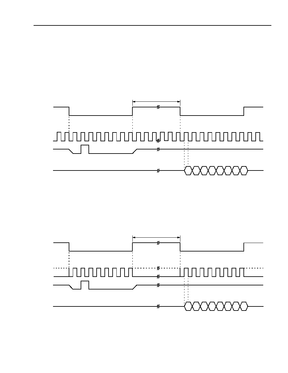
Fast Scan Mode (continued)
0126D
* Provides sufficient wait time to access read data.
Allow a minimum of 244 ns between bytes.
Figure 18. Fast Scan, Byte-by-Byte Mode (Gapped DCLK)
0124C
* Provides sufficient wait time to access read data.
Allow a minimum of 244 ns between bytes.
Figure 19. Fast Scan, Byte-by-Byte Mode (Continuous DCLK)
1
2
3
CS
DCLK
DI
COMMAND
DATA
4
5
DO
WAIT
1.5
µ
s
*
0
1
2
3
4
5
6
7
6
7
0
1
2
3
4
5
6
7
0
1
2
3
CS
DCLK
DI
COMMAND
DATA*
4
5
DO
WAIT
1.5
µ
s*
0
1
2
3
4
5
6
7
6
7
0
1
2
3
4
5
6
7
0
Agere Systems Inc.
23
Preliminary Data Sheet
September 2001
T8535B/T8536B Quad Programmable Codec
Functional Description
(continued)
The Control Interface
(continued)
Write All Channels
The write all channels command causes all four channels to be loaded with the same coefficients with a single data
transfer from the master controller. This allows for a faster initialization of the device after a powerup. This com-
mand should be used with caution since it affects all four channels. The normal memory write and read commands
affect only one channel.
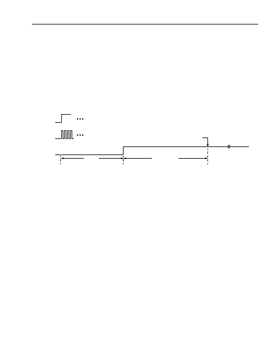
Reset Functionality
0071c
Figure 20. Hardware Reset Procedure
The reset function allows the internal logic of the device to be set to a known initial condition, either externally by
activating the reset lead, or on a per-channel basis through the microprocessor interface by setting and then clear-
ing bits, if required, in address RESCTRL (address 128). These two reset functions have different effects, and
each of the software reset functions is a subset of the hardware reset functionality. The primary difference is in the
treatment of the internal memory. The hardware reset is assumed to be a result of a catastrophic hardware event,
such as a loss of power, loss of BCLK, or an initial powerup. Accordingly, the assumption is made that the internal
memory does not contain valid data, and default values for all memory locations are loaded. A software reset, how-
ever, can only be initiated if the device is operational (at least the microprocessor interface), so the contents of the
memory may indeed be valid; thus, the resets may be more specific. Additionally, software resets only affect the
selected channel.
FS
BCLK
RST
DEVICE
CAN NOW BE PROGRAMMED
RUNS CONTINUOUSLY
RUNS CONTINUOUSLY
WAIT
5 ms
1 ms

24
24
Agere Systems Inc.
Preliminary Data Sheet
September 2001
T8535B/T8536B Quad Programmable Codec
Functional Description
(continued)
Reset Functionality
(continued)
A 0.1
µ
F capacitor between the RST lead and ground
will effectively hold the lead low long enough to reset
the device on powerup, allowing for a cost-effective
power-on reset function. Notice that the memory must
be reloaded through the serial interface after a hard-
ware reset function. For proper operation, it is neces-
sary for FS and BCLK to be present and stable during
a reset. A wait period for the internal PLL to stabilize is
required after reset goes high. See the timing diagram
shown in Figure 20 for the proper hardware or power-
on reset procedure.
For a software reset, the control memory should not be
accessed for a minimum of 256
µ
s following the reset.
Memory Control Mapping
Several memory locations are used to control the
device. The software interface tables (Table 20, Mem-
ory Mapping, and Table 21, Control Bit Definition) show
the memory assignments that are useful in call pro-
cessing and system testing. It should be noted that
other memory locations are used by the device to hold
intermediate results and other device state information.
Writing to these other locations can cause serious dis-
ruptions in the operation of the device and should be
avoided.
Standby Mode
The device enters a low-power standby mode with
powerup or software reset, or by programming the
CHACTIVE register 129, bit 0. In standby mode, the
control interface is active, capable of writing or reading
registers. SLIC read and write data latches are also
active. Analog signals at VF
X
I and PCM signals at D
R
are ignored in this mode. BCLK must be present for
proper standby mode operation.
Test Capabilities
The device has several built-in test capabilities that can
be used to verify correct operation of the signal pro-
cessing of the line card. These test functions are
accessed in several different control addresses. Five
loopback modes are employed: the first for the digital
signal from the PCM bus to be looped back to the PCM
bus. This loopback facility can be used to verify correct
operation of the PCM bus interface logic, as well as
operation of the PCM bus. The second digital loopback
function allows complete testing of the digital process-
ing capability of the codec by looping the data back at
the analog/digital conversion interface. The third loop-
back function can be used to check the operation of all
the signal processing performed in the device, includ-
ing the conversions to/from analog. These digital loop-
back functions can be used with tone generation and
reception via the PCM bus.
The first analog loopback facility is at the digital side of
the delta-sigma converters and loops analog transmit
data back to the analog receive path. The second ana-
log loopback is at the PCM bus interface and loops the
transmit data from the line back to the receive path.
By assigning the transmit and receive time slots identi-
cally, a loopback arrangement at the PCM bus can be
effectively programmed for signals generated on the
line side of the codec. This mode is useful for testing
from the line side through the entire device.
SLIC Control Capabilities
Memory locations 158, 159, and 160 are used to con-
trol six bidirectional latches that are intended to allow
the serial interface to control other line card devices,
such as ringing/test switches, telecom electromechani-
cal relays, and SLIC devices. When the TTL latches
are configured as outputs, external devices should be
set up to sink current from the latch. Location 158 sets
the operational mode of these latches as either inputs
or outputs. Location 159 specifies what is to be written
on the latch leads driven by the device. Location 160
reports the actual state of these leads. It should be
noted that a channel control reset forces all of these
external leads, except those corresponding to bits 2
and 3, to the high-impedance state, so any inputs con-
nected to bits 0, 1, 4, and 5 should have appropriate
pull-up or pull-down resistors (off-chip, if required) to
force the external device into a known state at power-
up or in the event of a reset. Bits 2 and 3 will reset to
outputs with a value of zero.
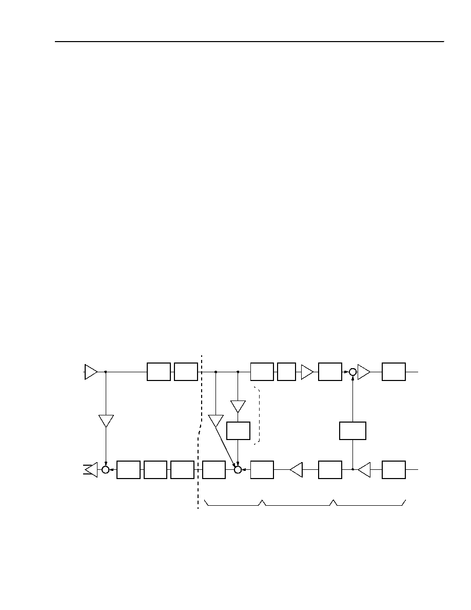
Agere Systems Inc.
25
Preliminary Data Sheet
September 2001
T8535B/T8536B Quad Programmable Codec
Functional Description
(continued)
SLIC Control Capabilities
(continued)
The fast scan mode allows for a minimal data transfer
on the serial bus to monitor bits 0 and 1 of the SLIC
data memory location (159). If these two bits are wired
as inputs to the off-hook and/or ring ground detection
circuits, a convenient method of rapidly scanning for
these two functions is obtained. Bits 2 and 3 default to
outputs; thus, they are convenient to provide control of
the SLIC state. In any event, all six leads are program-
mable for maximum flexibility.
Suggested Initialization Procedures
It is suggested that upon powerup, a hardware reset be
used to set the device into a known state. The serial
interface should then be used to load the memory
addresses that differ from the default values (the write
all channels command is convenient for this function). If
other devices are controlled by the SLIC data memory
location, then it also should be loaded with a known
configuration. After the completion of this sequence,
the device is ready to be activated. Depending on the
application, the next step may either be normal opera-
tion or a set of test sequences. After the initialization of
the memory, the device and associated line card
devices can be controlled by using memory locations
130, 131, 145, 155, 156, 157, 158, 159, and 129; that
is, by supplying the PCM bus time-slot addresses,
switching the SLIC into the proper mode, and activat-
ing the codec. Within memory location 129, the codec
would normally be placed into active mode, with both
directions of the PCM bus enabled at the start of a call.
At the completion of a call, the codec should be placed
into standby mode and the PCM bus disabled. Great
caution should be used when changing the memory
while the codec is in active mode, since termination
impedances, balance impedances, and gains may
change. These changes are likely to yield undesirable
system effects. It is safe to refresh coefficients that are
known to be unchanging in the application. It is always
possible to read the memory to verify its contents with-
out deleterious effects on codec operation. Normal
operation would load the memory and perform all gain
adjustments while the codec is in standby mode.
Under no circumstances should memory above
address 162 be written, since this section of memory is
used for state data and intermediate results. Also, all
reserved addresses should not be written. Changing
this information may have deleterious effects on sys-
tem operation.
Signal Processing
Figure 21 details the signal processing functional
blocks of one channel of the codec.
0497F
* Programmable blocks.
Figure 21. Internal Signal Processing
SPEED
FROM
PCM
BUS
*
GRX1
GAIN
8 kHz
COMP
TO LIN.
TRANSFER
XLPF
GAIN
TWEAKING
GRX2
SINC
3
-
D/A
1-bit
D/A
RCF
SMF
TO
0 dB
BAL
*
32 kHz
4096 kHz
LPF
*
DIGITAL
*
*
SLIC
TO
PCM
BUS
*
GAIN
GTX2
LIN.TO
COMP
YLPF
*
GAIN
TWEAKING
GTX1
SINC
3
*
FROM
0 dB TO 24 dB
SLIC
TRANSFER
TEQ
-
A/D
LPF
*
RTZ
8 STEPS
IN 5 STEPS
XAG
ANALOG
CTZ
*
26
Agere Systems Inc.
Preliminary Data Sheet
September 2001
T8535B/T8536B Quad Programmable Codec
Absolute Maximum Ratings
Stresses in excess of the absolute maximum ratings can cause permanent damage to the device. These are abso-
lute stress ratings only. Functional operation of the device is not implied at these or any other conditions in excess
of those given in the operational section of the data sheet. Exposure to absolute maximum ratings for extended
periods can adversely affect device reliability.
1. Sparse copper, one layer test board.
2. Four layer, JEDEC test board.
Operating Ranges
Handling Precautions
Although protection circuitry has been designed into this device, proper precautions should be taken to avoid expo-
sure to electrostatic discharge (ESD) during handling and mounting. Agere Systems Inc. employs a human-body
model (HBM) and a charged-device model (CDM) for ESD-susceptibility testing and protection design evaluation.
ESD voltage thresholds are dependent on the circuit parameters used to define the model. No industry-wide stan-
dard has been adopted for the CDM. A standard HBM (resistance = 1500
, capacitance = 100 pF) is widely
accepted and can be used for comparison.
Parameter
Symbol
Min Max
Unit
Storage Temperature Range
T
stg
-
55
150
∞C
Power Supply Voltage (all leads designated power)
V
DDX
--
6.5
V
Negative Voltage on Any Lead with Respect to Ground
V
SS
-
0.25
--
V
Thermal Resistance, Junction to Ambient:
68-Pin PLCC
1
44-Pin PLCC
1
64-Pin TQFP
2
100-Pin TQFP
2
R
JA
R
JA
R
JA
R
JA
--
--
--
--
43
49
40
30
∞C/W
∞C/W
∞C/W
∞C/W
Package Power Dissipation
P
D
--
1
W
SLIC Control Interface Latches, Current per Device
I
L
--
160
mA
Parameter
Symbol
Min Max
Unit
Ambient Operating Temperature
T
A
-
40
85
∞C
Operating Junction Temperature
T
J
-
40
125
∞C
Power Supply Voltage (all leads designated power)
V
DDX
4.75
5.25
V
HBM ESD Threshold Voltage
Device
Voltage
T8535B/T8536B
>2000
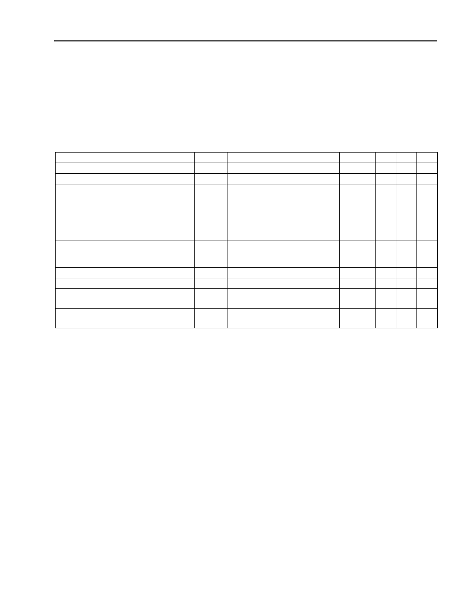
Agere Systems Inc.
27
Preliminary Data Sheet
September 2001
T8535B/T8536B Quad Programmable Codec
Electrical Characteristics
For all specifications: T
A
=
-
40 ∞C to +85 ∞C, V
DD
= 5 V ± 5%, unless otherwise noted. Typical values are for
T
A
= 25 ∞C and V
DD
= 5 V. Input signal frequency is 1004 Hz, BCLK = 16.384 MHz, DCLK = 4.096 MHz, and coef-
ficients are at default values, unless otherwise noted.
dc Characteristics
Table 10. dc Characteristics
Parameter
Symbol
Test Conditions
Min
Typ Max Unit
Input Voltage Low
V
IL
All inputs
--
--
0.8
V
Input Voltage High
V
IH
All inputs
2.0
--
--
V
Input Current
I
IL
Digital, without pull-up, inputs,
GND < V
IN
< V
DD
With internal pull-up, V
IN
= GND
(INTS and RST leads)
With internal pull-up, V
IN
= V
DD
(INTS and RST leads)
-
10
-
240
-
10
--
--
--
10
10
10
µ
A
µ
A
µ
A
Output Voltage Low:
All Outputs
V
OL
I
L
= 3.2 mA
--
--
0.4
V
SLIC Controls, Configured as Outputs
V
OL
I
L
= 24 mA
--
--
1.0
V
Output Voltage High
V
OH
I
L
=
-
320
µ
A
3.5
--
--
V
Output Current in High-impedance State
I
OZ
--
-
30
--
30
µ
A
Line Driver (DX and DO leads) Output
Voltage High
V
OH
I
L
=
-
10 mA
V
DD
-
0.5
--
--
V
Line Driver (DX and DO leads) Output
Voltage Low
V
OL
I
L
= 10 mA
--
--
1.0
V
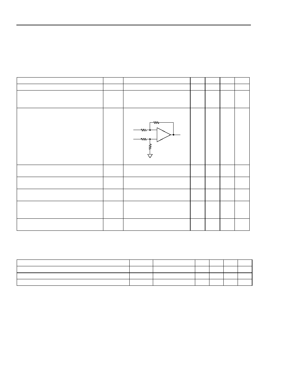
28
Agere Systems Inc.
Preliminary Data Sheet
September 2001
T8535B/T8536B Quad Programmable Codec
Electrical Characteristics
(continued)
Analog Interface
The following specifications pertain to the analog SLIC interface for each channel.
Table 11. Analog Interface
Table 12. Power Dissipation
Power measurements are made at BCLK = 2.048 MHz, DCLK = 2.048 MHz, no inputs from serial interface, inter-
face latches set as outputs, and outputs unloaded.
Parameter
Symbol
Test Conditions
Min
Typ
Max
Unit
Input Resistance
R
VFxI
0.25 < V
IN
< (V
DDX
-
0.25) V.
100
--
300
k
dc Input Voltage
V
VFxI
Relative to ground.
Signal should be capacitively
coupled to VF
X
I.
1.8
2.0
2.2
V
Load Resistance at VF
R
OP and VF
R
ON
(differential)
R
L
5-8881F
7.5
--
--
k
Output Resistance
R
O
Digital input code correspond-
ing to idle PCM code (
µ
-law).
--
2
10
Output Offset Voltage Between VF
R
OP
and VF
R
ON
V
OS
Digital input code correspond-
ing to idle PCM code (
µ
-law).
-
100
0
100
mV
Output Offset Voltage Between VF
R
OP
and VF
R
ON, Standby Mode
V
OSS
R
L
= 100 k
.
-
20
0
20
mV
Common-mode Output Voltage, Active
Mode
V
OCM
Digital input code correspond-
ing to alternating ± zero
µ
-law
PCM code.
--
2.0
--
V
Common-mode Output Voltage, Standby
Mode
V
OCMS
--
1.7
2.0
2.3
V
Parameter
Symbol
Test Conditions
Min
Typ
Max
Unit
All Channels in Standby, Dissipation for One Channel
I
DDS
--
--
22
28
mW
One Channel Active, Dissipation for Active Channel
I
DD1
--
--
225
--
mW
Four Channels Active, Dissipation for One Channel
I
DD1
--
--
90
125
mW
R
L
R
L
R
L
R
L

Agere Systems Inc.
29
Preliminary Data Sheet
September 2001
T8535B/T8536B Quad Programmable Codec
Electrical Characteristics
(continued)
Gain and Dynamic Range
Table 13. Gain and Dynamic Range
Parameter
Symbol
Test Conditions
Min
Typ
Max
Unit
Absolute Levels
GAL
Maximum 0 dBm0 levels (1004 Hz):
VF
X
I (encoder milliwatt), all programma-
ble transmit gains set to 0 dB.
RCV (decoder milliwatt), termination
impedance off, all programmable
receive gains set to 0 dB.
--
--
2.80
5.29
--
--
Vp-p
Vp-p
Absolute Levels
GAL
Minimum 0 dBm0 levels (1004 Hz):
VF
X
I (encoder milliwatt),
XAG = 24 dB, GTX1 = 6 dB,
GTX2 = 0 dB.
RCV (decoder milliwatt), termination
impedance off, GRX1
= 0 dB,
GRX2
=
-
6 dB.
--
--
87.5
2.63
--
--
mVp-p
Vp-p
Absolute Maximum Volt-
age Swings
GAL
VF
X
I
VF
R
OP to VF
R
ON (differential).
--
--
--
--
3.2
5.28
Vp-p
Vp-p
Transmit Gain Absolute
Accuracy
GXA
Transmit gain programmed for maxi-
mum 0 dBm0 test level, measured devi-
ation of digital code from ideal
0 dBm0 level at DX digital outputs, with
transmit gain set to 0 dB:
20 ∞C to 70 ∞C
0 ∞C to 85 ∞C
-
40 ∞C to +85 ∞C.
--
-
0.25
-
0.30
±0.15
--
--
--
0.25
0.30
dB
dB
dB
Transmit Gain Variation
with Programmed Gain
GXAG
Measured transmit gain over the range
from maximum to minimum, calculated
deviation from the programmed gain rel-
ative to GXA at 0 dB, V
DD
= 5 V.
-
0.1
--
0.1
dB
Transmit Gain Variation
with Frequency, 600
Resistive Source
Impedance and Syn-
thesized Termination
Impedance
GXAF
Relative to 1004 Hz, minimum
gain < GX < maximum gain,
VF
X
I = 0 dBm0 signal, path gain
set to 0 dB:
f = 16.67 Hz
f = 40 Hz
f = 50 Hz
f = 60 Hz
f = 200 Hz
f = 300 Hz to 3000 Hz
f = 3140 Hz
f = 3380 Hz
f = 3860 Hz
f = 4600 Hz and above.
--
--
--
--
-
3.0
-
0.125
-
0.57
-
0.735
--
--
-
50
-
40
-
40
-
55
-
2.0
±0.04
0.01
-
0.03
-
8.8
--
-
30
-
26
-
30
-
30
0
0.135
0.125
0.015
-
8.98
-
32
dB
dB
dB
dB
dB
dB
dB
dB
dB
dB

30
Agere Systems Inc.
Preliminary Data Sheet
September 2001
T8535B/T8536B Quad Programmable Codec
Electrical Characteristics
(continued)
Gain and Dynamic Range
(continued)
Table 13. Gain and Dynamic Range (continued)
* Applied to all four channels.
RTZ
and CTZ paths open.
Parameter
Symbol
Test Conditions
Min
Typ
Max
Unit
Transmit Gain Variation
with Signal Level
GXAL
Sinusoidal test method*,
reference level = 0 dBm0
:
VF
X
I =
-
40 dBm0 to +3 dBm0
VF
X
I =
-
50 dBm0 to
-
40 dBm0
VF
X
I =
-
55 dBm0 to
-
50 dBm0.
-
0.25
-
0.50
-
1.40
--
--
--
0.25
0.50
1.40
dB
dB
dB
Receive Gain Absolute
Accuracy
GRA
Receive gain programmed to
-
6 dB,
apply 0 dBm0 signal to IPCM, mea-
sure V
RCV
, R
L
= 100 k
differential:
20 ∞C to 70 ∞C
0 ∞C to 85 ∞C
-
40 ∞C to +85 ∞C.
--
-
0.25
-
0.30
±0.15
--
--
--
0.25
0.30
dB
dB
dB
Relative Gain, VF
R
OP to
VF
R
ON
--
Digital input 0 dBm0 signal,
f = 300 Hz to 3400 Hz.
-
0.01
--
0.01
dB
Relative Phase, VF
R
OP
to VF
R
ON
--
Digital input 0 dBm0 signal,
f = 300 Hz to 3400 Hz.
-
0.25
--
0.25
Degrees
Receive Gain Variation
with Programmed Gain
GRAG
Measure receive gain over the range
from maximum to minimum setting,
calculated deviation from the pro-
grammed gain relative to GRA at
0 dB, V
DD
= 5 V.
-
0.1
--
-
0.1
dB
Receive Gain Variation
with Frequency, 600
Resistive Termination
GRAF
Relative to 1004 Hz, digital input =
0 dBm0 code, minimum gain < GR <
maximum gain, 0 dB path gain:
f = below 3000 Hz
f = 3140 Hz
f = 3380 Hz
f = 3860 Hz
f = 4600 Hz and above.
-
0.125
-
0.57
-
0.735
--
--
±0.04
±0.04
-
0.550
-
10.7
--
0.125
0.125
0.015
-
8.98
-
28
dB
dB
dB
dB
dB
Receive Gain Variation
with Signal Level
GRAL
Sinusoidal test method*,
reference level = 0 dBm0:
IPCM digital level =
-
40 dBm0 to +3 dBm0
IPCM digital level =
-
50 dBm0 to
-
40 dBm0
IPCM digital level =
-
55 dBm0 to
-
50 dBm0.
-
0.25
-
0.50
-
1.40
--
--
--
0.25
0.50
1.40
dB
dB
dB

Agere Systems Inc.
31
Preliminary Data Sheet
September 2001
T8535B/T8536B Quad Programmable Codec
Electrical Characteristics
(continued)
Noise Characteristics
Table 14. Per-Channel Noise Characteristics
* R
VFXI
= 25 M
.
Parameter
Symbol
Test Conditions
Min
Typ
Max
Unit
Transmit Noise,
C-Message Weighted
N
XC
0 dB transmit gain*.
--
7
18
dBrnC0
Transmit Noise,
P-Message Weighted
N
XP
0 dB transmit gain*.
--
--
-
68
dBm0p
Receive Noise,
C-Message Weighted
N
RC
0 dB receive gain, digital pattern
corresponding to idle PCM code,
µ
-law*.
--
0
13
dBrnC0
Receive Noise,
P-Message Weighted
N
RP
0 dB receive gain, digital pattern
corresponding to idle PCM code, A-law*.
--
--
-
75
dBm0p
Noise, Single Frequency
N
RS
f = 0 kHz to 100 kHz, loop around
measurement, V
VFxI
= 0 Vrms.
--
--
-
53
dBm0
Power Supply Rejection,
Transmit
PSR
X
V
DD
= 5.0 V
DC
+ 100 mVrms:
f = 0 kHz to 4 kHz
f = 4 kHz to 50 kHz
C-message weighted.
36
30
--
--
--
--
dBC
dBC
Power Supply Rejection,
Receive
PSR
R
Measured on VF
R
OP,
V
DD
= 5.0 V
DC
+ 100 mVrms:
f = 0 kHz to 4 kHz
f = 4 kHz to 25 kHz
f = 25 kHz to 50 kHz.
36
40
36
--
--
--
--
--
--
dBC
dBC
dBC
Spurious Out-of-Band
Signals at the Chan-
nel Outputs
SOS
0 dBm0, 300 Hz to 3400 Hz signal applied
to V
VFxI
, transmit gain set to 0 dB:
4600 Hz to 7600 Hz
7600 Hz to 8400 Hz
8.4 kHz to 50 kHz.
--
--
--
--
--
--
-
30
-
40
-
30
dB
dB
dB
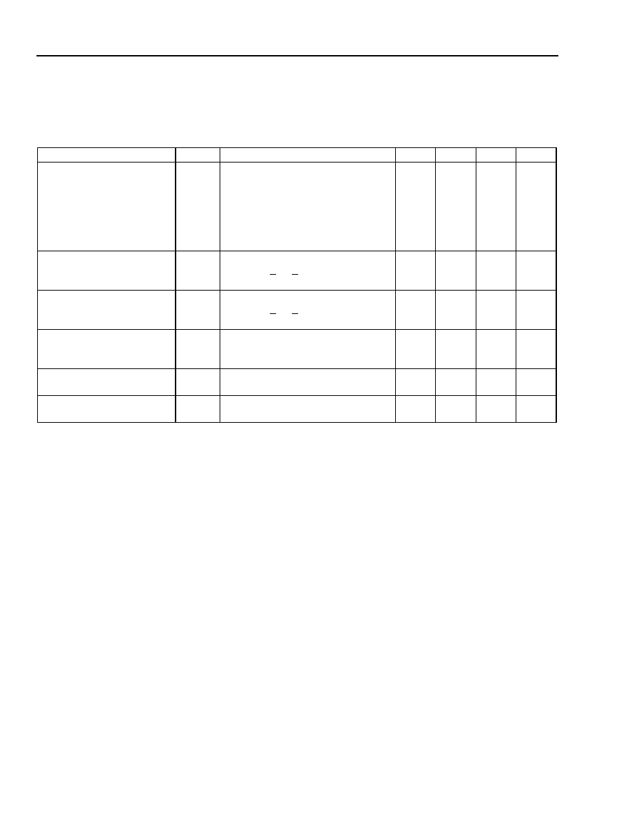
32
Agere Systems Inc.
Preliminary Data Sheet
September 2001
T8535B/T8536B Quad Programmable Codec
Electrical Characteristics
(continued)
Distortion and Group Delay
Table 15. Distortion and Group Delay
* Absolute group delay is a function of time-slot assignment, and the maximum in this table refers to the optimal (minimum group delay) time-
slot assignment.
Parameter
Symbol
Test Conditions
Min
Typ
Max
Unit
Signal to Total Distortion,
Transmit or Receive
STD
X
STD
R
Sinusoidal test method level:
µ
-law
-
30 dBm0 to +3 dBm0
A-law
-
30 dBm0 to +3 dBm0
µ
-law
-
40 dBm0 to
-
30 dBm0
A-law
-
40 dBm0 to
-
30 dBm0
µ
-law
-
45 dBm0 to
-
40 dBm0
A-law
-
45 dBm0 to
-
40 dBm0.
36
35
31
30
27
25
--
--
--
--
--
--
--
--
--
--
--
--
dB
dB
dB
dB
dB
dB
Single Frequency Distortion,
Transmit
SFD
X
0 dBm0 single frequency input,
200 Hz < f
IN
< 3400 Hz; measured
at any other single frequency.
--
--
-
46
dB
Single Frequency Distortion,
Receive
SFD
R
0 dBm0 single frequency input,
200 Hz < f
IN
< 3400 Hz; measured
at any other single frequency.
--
--
-
46
dB
Intermodulation Distortion
IMD
Transmit or receive, two
frequencies in the range of
300 Hz to 3400 Hz.
--
-
55
-
49
dB
TX Group Delay, Absolute*
D
XA
f = 1600 Hz, 600
resistive termination.
--
--
475
µ
s
RX Group Delay, Absolute*
D
RA
f = 1600 Hz, 600
resistive termination.
--
--
260
µ
s
Agere Systems Inc.
33
Preliminary Data Sheet
September 2001
T8535B/T8536B Quad Programmable Codec
Electrical Characteristics
(continued)
Crosstalk
Table 16. Crosstalk
Parameter
Symbol
Test Conditions
Min
Typ
Max
Unit
Transmit to Transmit Crosstalk,
0 dBm0 Level
CT
X-X
f = 300 Hz to 3400 Hz,
any channel to any channel.
--
-
100
-
80
dB
Transmit to Receive Crosstalk,
0 dBm0 Level
CT
X-R
f = 300 Hz to 3400 Hz,
any channel to any other channel.
In-channel.
--
--
-
100
-
80
-
80
-
50
dB
dB
Receive to Transmit Crosstalk,
0 dBm0 Level
CT
R-X
f = 300 Hz to 3400 Hz,
any channel to any other channel.
In-channel.
--
--
-
100
-
70
-
80
-
50
dB
dB
Receive to Receive Crosstalk,
0 dBm0 Level
CT
R-R
f = 300 Hz to 3400 Hz,
any channel to any channel.
--
-
100
-
80
dB

34
Agere Systems Inc.
Preliminary Data Sheet
September 2001
T8535B/T8536B Quad Programmable Codec
Timing Characteristics
Control Interface Timing
Serial Control Port Timing
Table 17. Serial Control Port Timing (See Figures 22 and 23.)
* The t
SXBDLY
delay is from either DCLK or CS, whichever transition is later, for the first bit of the byte.
Symbol
Parameter
Test Conditions
Min
Typ
Max
Unit
f
DCLK
Clock Frequency (all commands)
--
--
--
4096
kHz
t
CSSETUP
Chip Select Setup Time, Normal Mode
D
CLK
= 4.096 MHz
7
--
--
ns
t
CSHOLD
Chip Select Hold Time, Normal Mode
D
CLK
= 4.096 MHz
4
--
--
ns
t
SXDLY
Output Data Delay, Normal Mode
D
CLK
= 4.096 MHz
--
--
9
ns
t
SDHOLD
Input Data Hold Time, Normal Mode
D
CLK
= 4.096 MHz
4
--
--
ns
t
SDSETUP
Input Data Setup Time, Normal Mode
D
CLK
= 4.096 MHz
7
--
--
ns
t
SDZ
Output Data, High Impedance
D
CLK
= 4.096 MHz
100
--
--
ns
t
RISE
Clock Edge Rise Time
D
CLK
= 4.096 MHz
--
--
12
ns
t
FALL
Clock Edge Fall Time
D
CLK
= 4.096 MHz
--
--
12
ns
t
RISE
,
t
FALL
Line Driver Rise/Fall Time (DO output)
I
L
= 15 mA,
C
LOAD
= 100 pF
--
--
30 ns
t
CSBHOLD
Chip Select Hold Time, Byte-by-Byte Mode
D
CLK
= 4.096 MHz
4
--
--
ns
t
SXBDLY
Output Data Delay, Byte-by-Byte Mode
D
CLK
= 4.096 MHz*
--
--
9
ns
t
CSBSETUP
Chip Select Setup Time, Byte-by-Byte Mode
D
CLK
= 4.096 MHz
7
--
--
ns
t
SDBHOLD
Data Hold Time, Byte-by-Byte Mode
D
CLK
= 4.096 MHz
4
--
--
ns
t
SDBSETUP
Data Setup Time, Byte-by-Byte Mode
D
CLK
= 4.096 MHz
7
--
--
ns
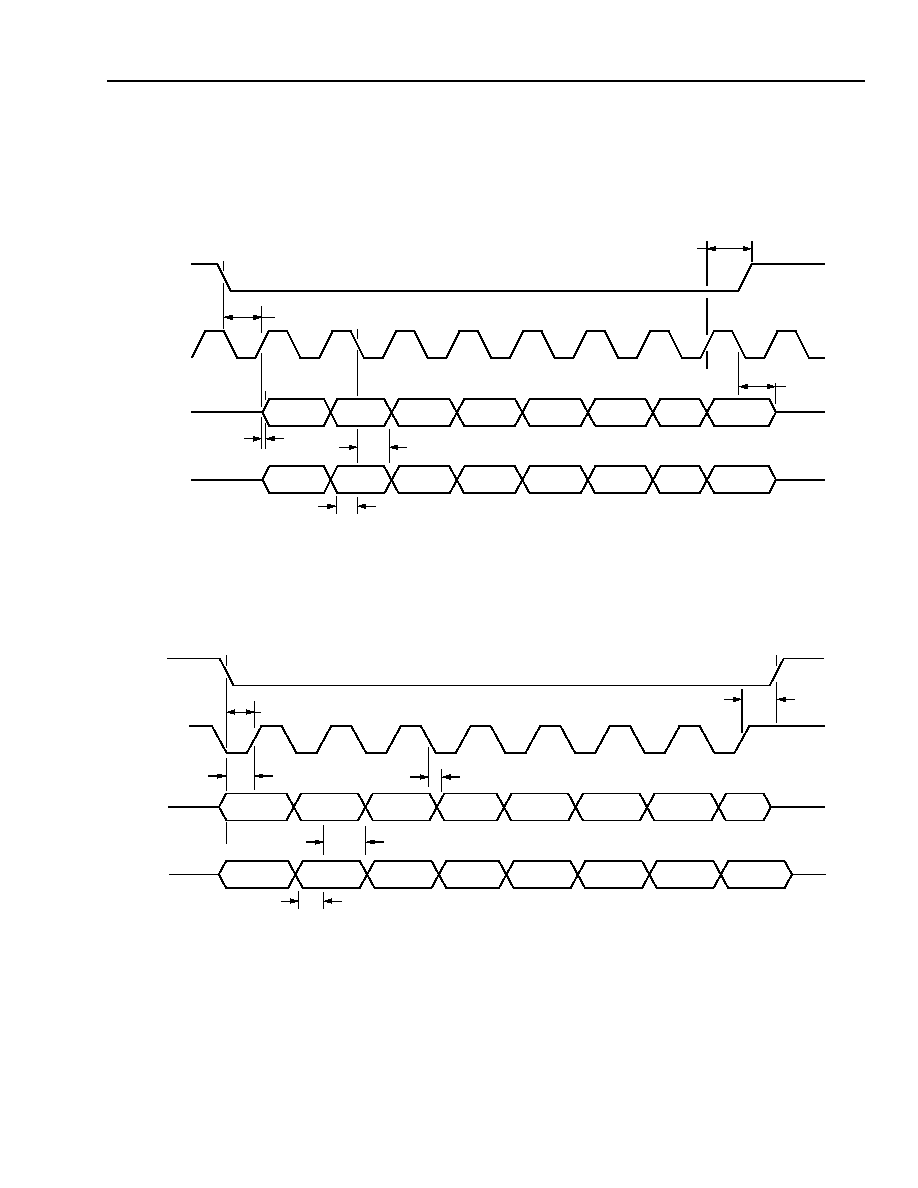
Agere Systems Inc.
35
Preliminary Data Sheet
September 2001
T8535B/T8536B Quad Programmable Codec
Timing Characteristics
(continued)
Control Interface Timing
(continued)
Normal Mode
5-7185.f(F)
Figure 22. Serial Interface Timing, Normal Mode (One Byte Transfer and Continuous DCLK Shown)
Byte-by-Byte Mode
5-7186e (F)
Figure 23. Serial Interface Timing, Byte-by-Byte Mode (One Byte Transfer and Gapped DCLK Shown)
0
1
2
3
4
5
6
7
0
1
2
3
4
5
6
7
0
1
2
3
4
5
6
7
CS
DCLK
DO
DI
LSB
t
CSSETUP
t
SXDLY
t
SDHOLD
t
SDSETUP
t
CSHOLD
t
SDZ
0
1
2
3
4
5
6
7
0
1
2
3
4
5
6
7
0
1
2
3
4
5
6
7
CS
DCLK
DO
DI
LSB
MSB
t
CSBSETUP
t
SDBSETUP
t
SXBDLY
t
CSBHOLD
t
SDBHOLD
t
SDBSETUP
36
36
Agere Systems Inc.
Preliminary Data Sheet
September 2001
T8535B/T8536B Quad Programmable Codec
Timing Characteristics
(continued)
PCM Interface Timing
Single-Clocking Mode
Frame sync (FS) signifies the start of frame on the
PCM bus for all four channels. FS occurs every 125
µ
s
at an 8 kHz rate. FS must be synchronous with the
PCM bus clock (BCLK) and must be high for a mini-
mum of one BCLK period. The PCM interface operates
using fixed data rate timing, data timing for both trans-
mit and receive are controlled by BCLK. BCLK can
be any value from 512 kHz (eight time slots) to
16.384 MHz (256 time slots) as defined by Table 18.
The PCM bus transfers the most significant bit of the
time slot first, consistent with normal telephony prac-
tice. Figure 24 shows FS, DX, and DR beginning on the
rising edge of BCLK and being latched on the falling
edge of BCLK. Figure 25 shows DX and DR beginning,
and FS being latched on the rising edge of BCLK, and
DX and DR being latched on the falling edge of BCLK.
Figure 24 portrays a bit offset of zero, and Figure 25
portrays a transmit bit offset of one and a receive bit
offset of two. Bit offset skews the PCM transmit and/or
receive data independently from the FS reference. Up
to seven BCLK cycles of bit offset can be employed on
a per-channel basis. This flexibility can accommodate
special timing requirements.
Linear coding is transmitted and received in two con-
secutive 8-bit time slots. TSX0 or TSX1 is active (low)
when DX data is transmitting (8 bits for companded
code, 16 bits for linear code).
Table 18. PCM Interface Timing: Single-Clocking Mode (See Figures 24 and 25.)
Symbol
Parameter
Test Conditions
Min
Typ
Max
Unit
f
BCLK
Allowable BCLK Frequencies
--
--
--
--
--
--
--
--
--
--
--
--
--
--
--
--
512
1024
1536
2048
3072
4096
8192
16384
--
--
--
--
--
--
--
--
kHz
kHz
kHz
kHz
kHz
kHz
kHz
kHz
--
Jitter of BCLK
--
--
--
100 ns in
100 ms =
1 ppm
--
--
BCLK Duty Cycle
--
40
50
60
%
t
FSSETUP
Frame Strobe Setup Time
B
CLK
= 16.384 MHz
7
--
--
ns
t
FSHOLD
Frame Strobe Hold Time
B
CLK
= 16.384 MHz
4
--
--
ns
t
FSWIDTH
Frame Strobe Width
FS synchronous with
BCLK
t
BCLK
--
125
µ
s
-
t
BCLK
--
t
XDLY
Output Data Delay
B
CLK
= 16.384 MHz
--
--
9
ns
t
IDHOLD
Input Data Hold Time
B
CLK
= 16.384 MHz
4
--
--
ns
t
IDSETUP
Input Data Setup Time
B
CLK
= 16.384 MHz
7
--
--
ns
t
RISE
Clock Edge Rise Time
B
CLK
= 16.384 MHz
--
--
8
ns
t
FALL
Clock Edge Fall Time
B
CLK
= 16.384 MHz
--
--
8
ns
t
RISE
,
t
FALL
DX Output Rise/Fall Time
I
L
= 15 mA,
C
LOAD
= 100 pF
--
--
30
ns
t
DXHIGHZ
DX Output Data Float on TS Exit
C
LOAD
= 0
--
--
5
ns
t
TSXDELAY
Line Driver Enable Delay
--
--
--
5
ns
t
TSXHIGHZ
Line Driver Enable Float on TS Exit
--
--
--
5
ns
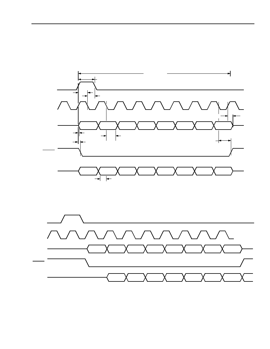
Agere Systems Inc.
37
Preliminary Data Sheet
September 2001
T8535B/T8536B Quad Programmable Codec
Timing Characteristics
(continued)
PCM Interface Timing
(continued)
Single-Clocking Mode (continued)
5-7188d F
Figure 24. Single-Clocking Mode (TXBITOFF = 0, RXBITOFF = 0, PCMCTRL2 = 0x00)
5-7185.g F
Figure 25. Single-Clocking Mode (TXBITOFF = 1, RXBITOFF = 2, PCMCTRL2 = 0x01)
1
2
3
4
5
6
7
8
9
1
2
3
4
5
6
7
8
FS
BCLK
DX0/1
DR0/1
LSB
1
2
3
4
5
6
7
8
TIME SLOT 0
SIGN BIT
t
FSHOLD
t
FSSETUP
t
XDLY
t
IDHOLD
t
IDSETUP
t
FSWIDTH
TSX0/1
t
TSXDELAY
t
DXHIGHZ
t
TSXHIGHZ
1
2
3
4
5
6
7
8
9
1
2
3
4
5
6
7
8
1
2
3
4
5
6
7
FS
BCLK
DX0/1
DR0/1
8
TSX0/1
38
38
Agere Systems Inc.
Preliminary Data Sheet
September 2001
T8535B/T8536B Quad Programmable Codec
Timing Characteristics
(continued)
PCM Interface Timing
(continued)
Double-Clocking Mode
As with the single-clocking mode, FS signifies the start
of frame on the PCM bus for all four channels and
occurs every 125
µ
s at an 8 kHz rate. FS must be
synchronous with BCLK and must be high for a mini-
mum of one BCLK period. The PCM interface operates
using fixed data rate timing; data timing for both trans-
mit and receive are controlled by BCLK. In double-
clocking mode, however, BCLK runs at twice the PCM
data rate. BCLK can be any value from 512 kHz (data
rate of 256 kbits/s, 4 time slots) to 16.384 MHz (data
rate of 8192 kbits/s, 128 time slots) as defined by Table
19.
In Figure 26, detail A, the falling edge of the first BCLK
latches FS. The falling edge of the second BCLK
latches DR (receive bit offset of 1). DX starts on the ris-
ing edge of the first BCLK. The PCM bus transfers the
most significant bit of the data first.
The codec defaults to FS and DR being latched on the
first BCLK cycle. To latch DR on the second BCLK
cycle, program receive bit offset for 1 (RXBITOFF =
0x20). For every bit programmed (0 to 7), bit offset
shifts transmit or receive data by one BCLK cycle.
Therefore, in double-clock mode, the time-slot assign-
ment and bit offset registers need to be used in tandem
in order to achieve a full range of bit offset values. For
instance, in time-slot 0, bit offset will shift data up to
four bits. To shift data 5 to 8 bits, time slot 1 needs to
be selected.
Linear coding is not allowed in double-clocking mode.
TSX0 or TSX1 (not shown in Figure 26) is active (low)
when DX data is transmitting.
Note that the device reverts back to single-clock mode
if reset (address 128, bit 0). Internal states of the codec
can be reset without going out of double-clock mode
(address 128, bit 1).
Table 19. PCM Interface Timing: Double-Clocking Mode (See Figure 26.)
Note: DX load = 150 pF.
Symbol
Parameter
Signal
Min
Typ
Max
Unit
fBCLK
Allowable BCLK Frequencies
BCLK
--
--
--
--
--
--
--
--
512
1024
1536
2048
3072
4096
8192
16384
--
--
--
--
--
--
--
--
kHz
kHz
kHz
kHz
kHz
kHz
kHz
kHz
--
Jitter of BCLK
BCLK
--
--
100 ns in
100 ms =
1 ppm
--
tBCL
Clock Period
BCLK
61
--
1953
ns
tR, tF
Clock Rise/Fall
BCLK
--
--
8
ns
tWL, tWH
Pulse Width
BCLK
tBCL x 0.4
--
tBCL x 0.6
ns
tR, tF
Frame Rise/Fall
FS
--
--
15
ns
tWFH
Frame Width High
FS
tBCL
--
--
ns
tWFL
Frame Width Low
FS
tBCL
--
--
ns
tSF
Frame Setup
FS
7
--
tBCL
-
50
ns
tHF
Frame Hold
FS
4
--
--
ns
tDDC
Data Delay Clock
DX
--
--
9
ns
tDDF
Data Delay Frame
DX
--
--
9
ns
tSD
Data Setup
DR
7
--
--
ns
tHD
Data Hold
DR
4
--
--
ns
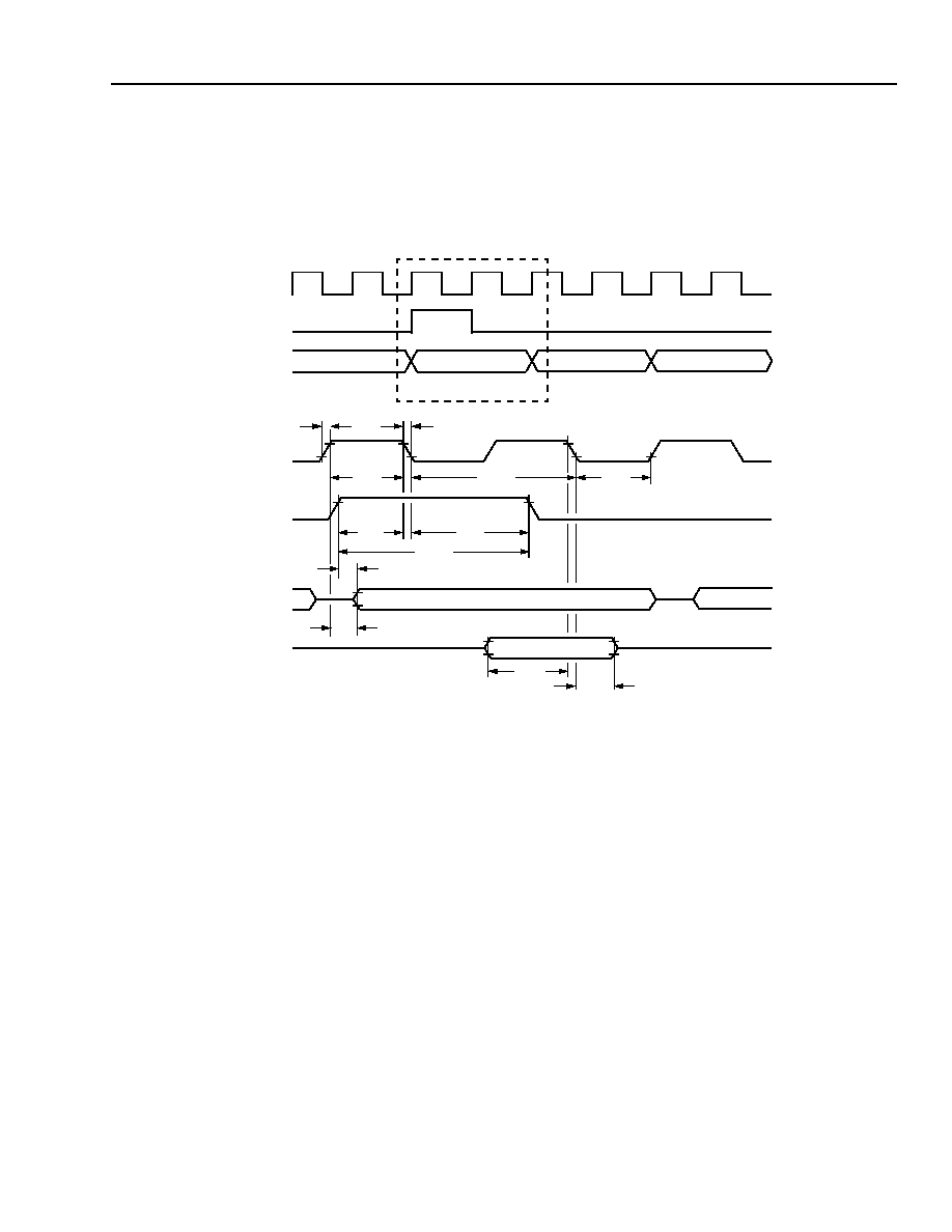
Agere Systems Inc.
39
Preliminary Data Sheet
September 2001
T8535B/T8536B Quad Programmable Codec
Timing Characteristics
(continued)
PCM Interface Timing
(continued)
Double-Clocking Mode (continued)
5-7173F
Figure 26. Double-Clocking Mode (RXBITOFF = 0x20, PCMCTRL2 = 0x00)
BCLK
FS
DX/DR
bit 0
bit 1
bit 2
DETAIL A
BCLK
tR
tF
tWL
tBCL
tWH
tSF
tHF
tWFH
tDDF
tDDC
tHD
tSD
FS
DX
DR
DETAIL A

40
Agere Systems Inc.
Preliminary Data Sheet
September 2001
T8535B/T8536B Quad Programmable Codec
Software Interface
Table 20. Memory Mapping
With the exceptions noted, all of these memory locations may be read to determine the state of the controls con-
tained therein. In the following table, bit 0 is the LSB (transmitted first on the serial interface) and bit 7 is the most
significant bit of the byte. Unused bits in an address or multibyte address should be loaded as zero. All of the mem-
ory locations can be programmed on a per-channel basis.
Note that the entire coefficient set for a channel (or all four channels) may be loaded with one command.
Control
Name
Address
(Decimal)
# of
Bits
Used
Default
Value
Description
HBALTAPS
0--27
64--91
448
See Table 21
Balance impedance tap coefficients.
Reserved
28--63
92--127
--
--
These addresses have no function.
RESCTRL
128
2
0x00
Reset address. Writing a one in the used positions causes a
reset as defined by the bit definition. This reset remains in
force until the bit is written as a zero.
CHACTIVE
129
1
0x00
Standby/active control.
RXBITOFF
130
4
0x00
Bit offset for receive direction.
RXOFF
131
8
16 * channel # Time-slot assignment for receive direction.
GRX1
132--133
11
0x0400
Gain transfer for receive direction.
GRX2
134--135
11
0x01ac
Gain tweaking. Control of gain sensitive to impedance and
SLIC parameter choices, receive direction.
Reserved
136--139
--
--
This address has no function.
CTZCTRL
140--143
31
07ed0000
CTZ bleed coefficients.
Reserved
144
--
--
This address has no function.
PCMCTRL2
145
6
0x00
PCM transmission and sampling edge control.
SDCTRL
146
7
0x19
RTZ, transmit analog gain (XAG), and digital loopback 3
controls.
SDTSI
147
7
17 * channel # Internal time-slot interchanger and loopback controls.
Default sets external pins to state referenced in this data
sheet.
GTX2
148--149
12
0x0400
Gain transfer for transmit direction.
ZEQTX
150--152
21
0x000000
Transmit line equalization.
GTX1
153--154
12
0x051a
Gain tweaking. Control of gain sensitive to impedance and
SLIC parameter choices, transmit direction.
TXBITOFF
155
4 or 5
0x00
Bit offset for transmit direction.
TXOFF
156
8
16 * channel # Time-slot assignment for transmit direction.
PCMCTRL1
157
7
0x00
PCM, companding, and loopback controls.
SLICTS
158
6
0x0c
SLIC 3-state control. Latch I/O.
SLICWR
159
6
0x00
Data to be written to the SLIC latches if the corresponding
bit is set in the SLICTS control word.
SLICRD
160
6
--
Current actual state of the SLIC leads. This will be the same
as SLICWR for those leads configured as outputs. All other
positions will reflect the actual state of the external lead. A
write operation to this word will be ignored, and within one
PCM frame (125
µ
s), the data will be overwritten.
Reserved
161
--
--
This address has no function.
VERIFY
162
8
0x00
Test address for serial interface verification.

Agere Systems Inc.
41
Preliminary Data Sheet
September 2001
T8535B/T8536B Quad Programmable Codec
Software Interface
(continued)
The following table shows the control bit assignments in the memory control addresses. In all control bit cases, the
bit being set places the function into the active mode as defined in the function column.
Table 21. Control Bit Definition
Control Name
(Address, Decimal)
[Address, Hex]
Bit
Assignment(s)
Function
HBALTAPS
(0--27, 64--91)
[0x00--0x1b,
0x40--0x5b]
448
Balance impedance coefficients. Default value is 0x00 for all bytes except
for addresses 3 and 5, which are 0x80, and address 69, which is 0x88.
RESCTRL
(128)
[0x80]
2--7
Not used, load as zeros.
1
A one resets all other internal states. Control addresses are not reset.
0
A one resets all control addresses to default values. Note that setting this
bit will result in it and all others of this word becoming cleared on the next
PCM frame as a normal part of the reset functionality. Alternatively, hard-
ware reset can be used to reset all control and state functions. It is neces-
sary to wait at least 256
µ
s after asserting this bit before initiating any
other serial I/O transactions.
CHACTIVE
(129)
[0x81]
1--7
Load as zeros.
0
Active/standby mode. A zero causes the channel to enter standby (low-
power) mode and disables the PCM interface for this channel. A one acti-
vates the channel and the corresponding PCM bus interface. Default is
zero.
RXBITOFF
(130)
[0x82]
5--7
Receive direction bit offset for the FS signal. Defaults to zero. These
3 bits can be thought of as the least significant bits (RXOFF contains the
more significant bits) of a bit counter that determines the location of the
first bit of the PCM data from FS.
0--4
Load as zeros.
RXOFF
(131)
[0x83]
0--7
Receive time-slot assignment. Defaults to (16 * channel number). Each
time slot represents 8 bits; allow for two time slots when using linear
mode or double-clock mode.
GRX1
(132--133)
[0x84--0x85]
0--10
Gain adjustment for gain transfer stage in receive direction. Defaults to
0x0400 (0 dB). This is an 11-bit multiply operation with a maximum gain of
two (6 dB). 0 dB is the maximum recommended setting.
GRX2
(134--135)
[0x86--0x87]
0--10
Gain adjustment for tweak gain stage in receive direction. Defaults to
0x01ac (
-
7.58 dB). This is an 11-bit multiply operation with a maximum
gain of two (6 dB). 0 dB is the maximum recommended setting.
CTZCTRL
(140--143)
[0x8c--0x8f]
0--30
Coefficients for the CTZ termination bleed. Defaults to 0x07ed0000.
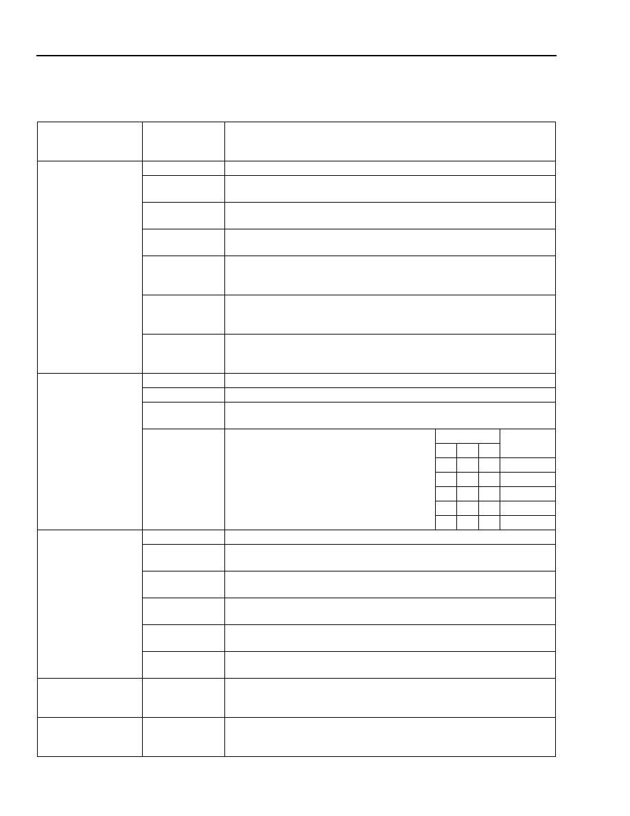
42
Agere Systems Inc.
Preliminary Data Sheet
September 2001
T8535B/T8536B Quad Programmable Codec
Software Interface
(continued)
Table 21. Control Bit Definition (continued)
Control Name
(Address, Decimal)
[Address, Hex]
Bit
Assignment(s)
Function
PCMCTRL2
(145)
[0x91]
6--7
Load as zeros.
5
A one selects DX PCM port 1. A zero selects DX PCM port 0. Defaults
to zero. PCM port 1 is not available in all package types.
4
A one selects DR PCM port 1. A zero selects DR PCM port 0. Defaults
to zero. PCM port 1 is not available in all package types.
3
A one selects double-clocking mode. Defaults to zero (single-clocking
mode). A write to any channel affects all four channels.
2
A one starts transmit data on a falling BCLK edge. A zero starts transmit
data on a rising BCLK edge. Defaults to zero. A write to any channel
affects all four channels.
1
A one latches receive data on a rising BCLK edge. A zero latches
receive data on a falling BCLK edge. Defaults to zero. A write to any
channel affects all four channels.
0
A one latches FS on a rising BCLK edge. A zero latches FS on a
falling BCLK edge. Defaults to zero. A write to any channel affects all
four channels.
SDCTRL
(146)
[0x92]
7
Load as zero.
6
Enable digital loopback 3. Defaults to zero (no loopback).
3--5
RTZ gain. Defaults to 3 (equal level point value of 3 * 0.075 = 0.225).
Turn off by writing to zero.
0--2
Transmit analog gain (XAG). Defaults to
1 (6 dB) gain.
Bit Number
Function
(dB)
2
1
0
0
0
0
0.0
0
0
1
6.02
0
1
0
12.04
0
1
1
18.06
1
0
0
24.08
SDTSI
(147)
[0x93]
7
Load as zero.
6
Digital loopback, receive to transmit at the sigma-delta converters
(digital loopback 2). Defaults to zero (no loopback).
4--5
Analog channel feeding this digital channel in the transmit direction.
Defaults to channel number.
3
Send idle-channel code (alternating bits) to this analog receive path.
Defaults to zero (off).
2
Loopback from transmit to receive at the sigma-delta converters
(analog loopback 1). Defaults to zero (no loopback).
0--1
Digital channel feeding this analog receive channel. Defaults to channel
number.
GTX2
(148--149)
[0x94--0x95]
0--11
Gain control for gain transfer stage in transmit direction. Defaults to
0x0400 (0 dB). This is a 12-bit multiply operation with a maximum gain
of four (12 dB).
ZEQTX
(150--152)
[0x96--0x98]
0--20
Coefficients for the transmit equalization stage. Varies frequency
response and accommodates current-sensing SLICs. Defaults to
0x000000.

Agere Systems Inc.
43
Preliminary Data Sheet
September 2001
T8535B/T8536B Quad Programmable Codec
Software Interface
(continued)
Table 21. Control Bit Definition (continued)
Control Name
(Address, Decimal)
[Address, Hex]
Bit
Assignment(s)
Function
GTX1
(153--154)
[0x99--0x9a]
0--11
Gain control for tweak gain stage in transmit direction. Defaults to
0x051a (2.11 dB). This is a 12-bit multiply operation with a maximum
gain of four (12 dB).
TXBITOFF
(155)
[0x9b]
5--7
Transmit direction bit offset for the FS signal. Defaults to zero. These
3 bits can be thought of as the least significant bits (TXOFF contains the
more significant bits) of a bit counter that determines the location of the
first bit of the PCM data from FS.
0--4
Load as zeros.
TXOFF
(156)
[0x9c]
0--7
Transmit time-slot assignment. Defaults to (16 * channel number). Each
time slot represents 8 bits; allow for two time slots when using linear
mode or double-clock mode.
PCMCTRL1
(157)
[0x9d]
7
3-state transmit PCM interface. Defaults to zero. A one forces the PCM
interface into a high-impedance state during its assigned time-slot on
the PCM bus. Placing the channel in standby mode also forces a high-
impedance condition on the transmit interface.
6
Transmit zeros instead of data. Defaults to zero (off).
5
Linear mode significant bit. A one sets MSB first for both PCM transmit
data output and for PCM receive data input. A zero sets both PCM
paths to LSB first. Defaults to zero, LSB first.
4
Place idle-channel code on receive path. Defaults to zero (off).
3
Loopback receive to transmit at PCM conversion interface (digital
loopback 1). Defaults to zero (no loopback).
2
Loopback transmit to receive at PCM conversion interface (analog
loopback 2). Defaults to zero (no loopback).
1
Linear/companded mode. A one sets 16-bit linear mode with two adja-
cent time slots used. Linear data is in two's complement form. Linear
mode is only available when using single-clocking mode. A zero sets
companded mode with only one time slot used. Defaults to zero. Linear
mode is programmed as LSB or MSB first using bit 5 of this word.
0
µ
-law or A-law. A one sets A-law mode, and a zero sets
µ
-law mode.
Defaults to zero (
µ
-law).
SLICTS
(158)
[0x9e]
6--7
Load as zeros.
0--5
Controls the drivers for the corresponding SLIC latches. A one enables
the lead as an output. Defaults to 0x0C (bits 2 and 3 set, the rest
cleared).
SLICWR
(159)
[0x9f]
6--7
Load as zeros.
0--5
SLIC data latches. If the corresponding bit in the SLICTS address is set
for an output, the device will drive the corresponding bit according to the
contents of this address. Writes are performed within 125
µ
s. Wait
125
µ
s before a subsequent write to the same channel or between write
all channel commands. Default is zero.
SLICRD
(160)
[0xa0]
6--7
Not used, ignore on read.
0--5
Reports the actual state of the SLIC leads. Anything written to this
address is ignored. Updates within 125
µ
s.
VERIFY
(162)
[0xa2]
0--7
Test location for serial interface. This location has no internal use, but
merely latches write data for the purpose of testing the serial interface.
This register does not clear with reset.
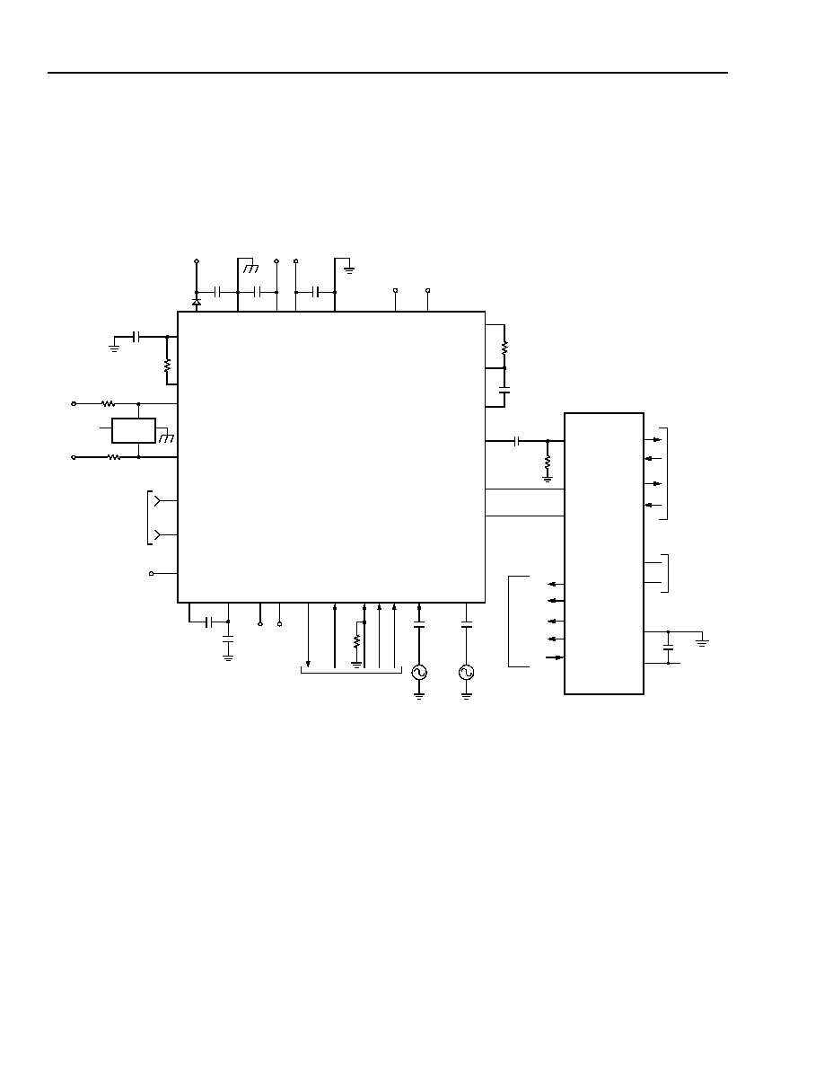
44
Agere Systems Inc.
Preliminary Data Sheet
September 2001
T8535B/T8536B Quad Programmable Codec
Applications
The following reference circuit shows a complete schematic for interfacing to the Agere L9215G SLIC. All ac
parameters are programmed by the T8536B. Note that this implementation differentiates itself in that no external
components are required in the ac interface to provide a dc termination impedance or for stability. For illustration
purposes, 0.5 Vrms PPM injection was assumed in this example and no meter pulse rejection is used. Also, this
example illustrates the device using programmable overhead and current limit.
12-3534.y (F)
Figure 27. POTS Interface
V
BAT1
BGND
V
BAT2
V
CC
AGND
ICM
TRGDET
ground key
not used
C
BAT1
0.1
µ
F
C
BAT2
0.1
µ
F
C
CC
0.1
µ
F
RTFLT
DCOUT
PR
PT
OVH
V
PROG
V
REF
C
RT
0.1
µ
F
R
RT
383
k
AGERE
L7591
V
BAT1
FUSIBLE OR PTC
50
50
CF1
CF2
rate of battery
reversal not
ramped
FB1 FB2 NSTAT BR
B2 B1 B0
C
F1
0.22
µ
F
C
F2
0.1
µ
F
PPM
0.5 Vrms
C
PPM
10 nF
RING
IN
PPM
IN
VITR
RCVP
RCVN
ITR
VTX
TXI
R
GX
4750
V
BAT1
D
BAT1
V
BAT2
V
CC
C
TX
0.1
µ
F
C
RING
0.47
µ
F
FROM
PROGRAMMABLE
D/A VOLTAGE
SOURCE
C
C1
PCM
HIGHWAY
DX0
DR0
DX1
DR1
FS
BCLK
DGND
V
DD
SYNC
AND
V
DD
VFXI
VFROP
VFRON
SLIC4a
SLIC3a
SLIC2a
SLIC1a
SLIC0a
CLOCK
L9215G
FROM/TO
CONTROL
B2
B1
BR
NSTAT
B0
0.1
µ
F
FUSIBLE OR PTC
T8536B
R
PD
1
10
k
R
VFXI
20 M
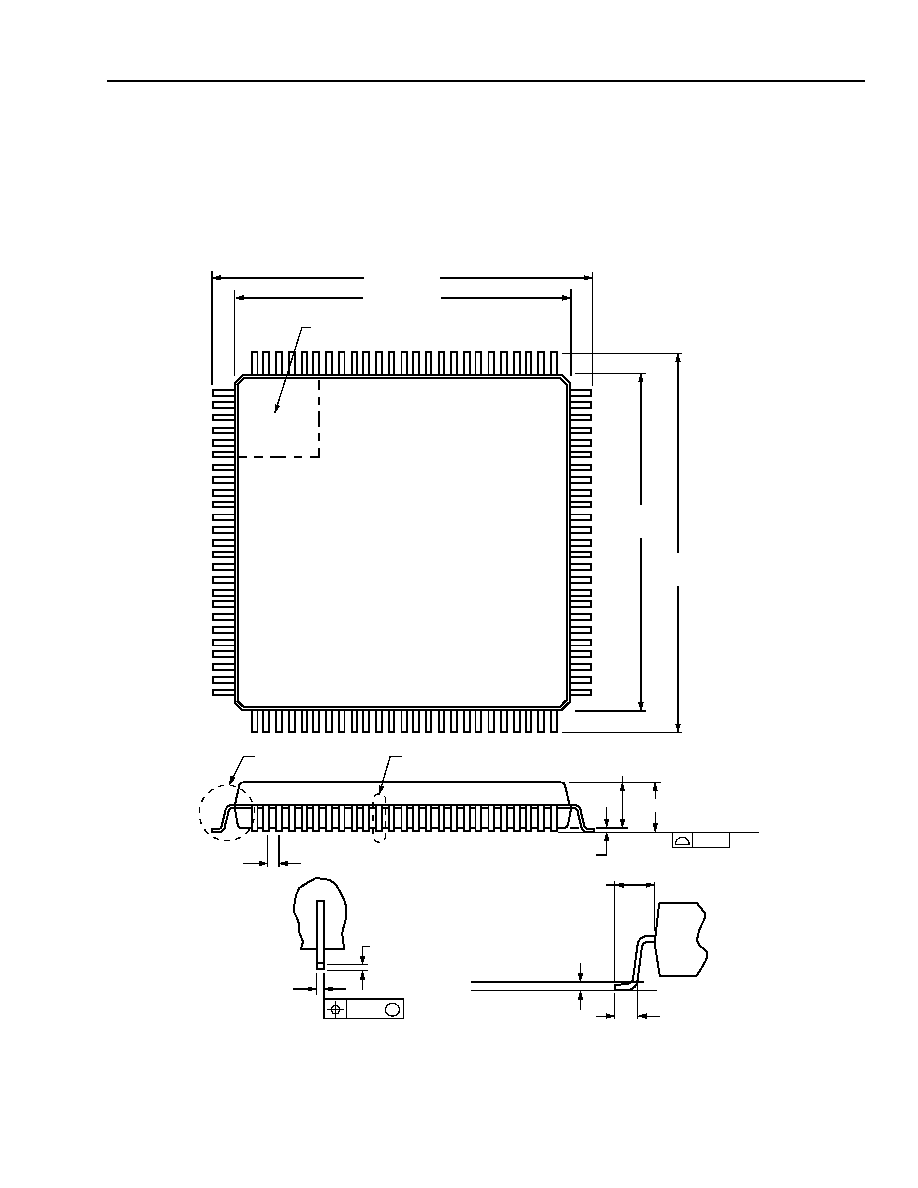
Agere Systems Inc.
45
Preliminary Data Sheet
September 2001
T8535B/T8536B Quad Programmable Codec
Outline Diagrams
100-Pin TQFP
Dimensions shown are in millimeters.
Note: The dimensions in this outline diagram are intended for informational purposes only.
For detailed schematics to assist your design efforts, please contact your Agere Sales Representative.
5-2146F
0.50 TYP
1.60 MAX
SEATING PLANE
0.08
1.40
±
0.05
0.05/0.15
DETAIL A
DETAIL B
14.00
±
0.20
16.00
±
0.20
76
100
1
25
26
50
51
75
14.00
±
0.20
16.00
±
0.20
PIN #1 IDENTIFIER ZONE
DETAIL B
0.19/0.27
0.08
M
0.106/0.200
DETAIL A
0.45/0.75
GAGE PLANE
SEATING PLANE
1.00 REF
0.25
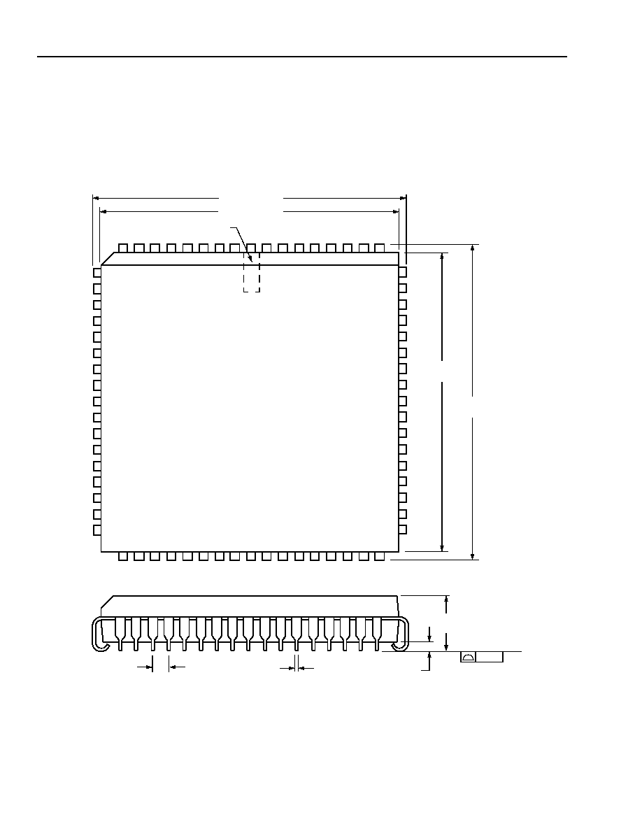
46
Agere Systems Inc.
Preliminary Data Sheet
September 2001
T8535B/T8536B Quad Programmable Codec
Outline Diagrams
(continued)
68-Pin PLCC
Dimensions shown are in millimeters.
Note: The dimensions in this outline diagram are intended for informational purposes only.
For detailed schematics to assist your design efforts, please contact your Agere Sales Representative.
5-2139
1
9
10
26
27
43
44
60
61
PIN #1 IDENTIFIER ZONE
25.146
±
0.127
24.231
±
0.102
25.146
±
0.127
24.231
±
0.102
1.27 TYP
0.330/0.533
5.080
MAX
0.51 MIN,
TYP
SEATING PLANE
0.10
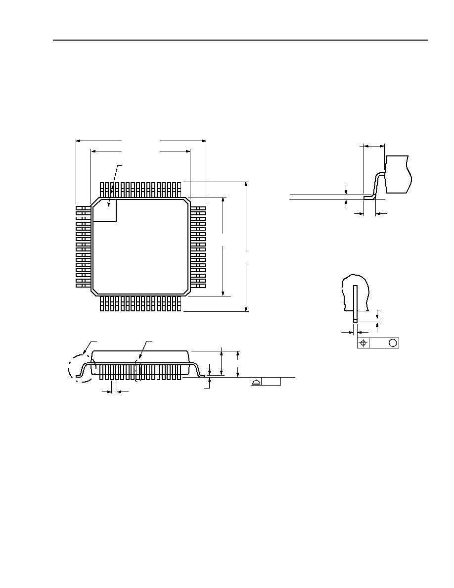
Agere Systems Inc.
47
Preliminary Data Sheet
September 2001
T8535B/T8536B Quad Programmable Codec
Outline Diagrams
(continued)
64-Pin TQFP
Dimensions shown are in millimeters.
Note: The dimensions in this outline diagram are intended for informational purposes only.
For detailed schematics to assist your design efforts, please contact your Agere Sales Representative.
5-3080
DETAIL A
0.50 TYP
1.60 MAX
SEATING PLANE
0.08
DETAIL B
0.05/0.15
1.40
±
0.05
10.00
±
0.20
12.00
±
0.20
1
64
49
16
17
32
48
33
10.00
±
0.20
12.00
±
0.20
PIN #1
IDENTIFIER ZONE
DETAIL A
0.45/0.75
GAGE PLANE
SEATING PLANE
1.00 REF
0.25
DETAIL B
0.19/0.27
0.08
M
0.106/0.200
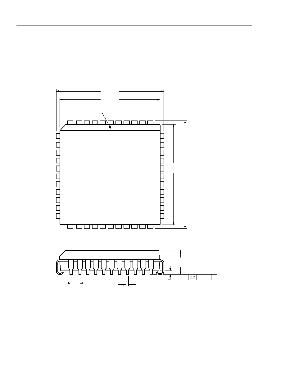
48
Agere Systems Inc.
Preliminary Data Sheet
September 2001
T8535B/T8536B Quad Programmable Codec
Outline Diagrams
(continued)
44-Pin PLCC
Dimensions are in millimeters.
Note: The dimensions in this outline diagram are intended for informational purposes only.
For detailed schematics to assist your design efforts, please contact your Agere Sales Representative.
5-2506(F)
4.57
MAX
1.27 TYP
0.53
MAX
0.10
SEATING PLANE
0.51 MIN
TYP
1
6
40
7
17
29
39
18
28
PIN #1 IDENTIFIER
ZONE
16.66 MAX
17.65 MAX
16.66
MAX
17.65
MAX

Agere Systems Inc.
49
Preliminary Data Sheet
September 2001
T8535B/T8536B Quad Programmable Codec
Ordering Information
Device Code
Package
Temperature
Comcode
T8535B - - - ML-D
44-Pin PLCC
Dry-bagged
-
40 ∞C to +85 ∞C
109059824
T8536B - - - ML-D
68-Pin PLCC
Dry-bagged
-
40 ∞C to +85 ∞C
109059816
T8536B - - 1TL-DB
100-Pin TQFP
Dry Pack Tray
-
40 ∞C to +85 ∞C
109059790
T8536B - - - TL-DB
64-Pin TQFP
Dry Pack Tray
-
40 ∞C to +85 ∞C
109059808

Agere Systems Inc. reserves the right to make changes to the product(s) or information contained herein without notice. No liability is assumed as a result of their use or application.
Copyright © 2001 Agere Systems Inc.
All Rights Reserved
September 2001
DS01-315ALC (Replaces DS01-251ALC)
For additional information, contact your Agere Systems Account Manager or the following:
INTERNET:
http://www.agere.com
E-MAIL:
docmaster@agere.com
N. AMERICA:
Agere Systems Inc., 555 Union Boulevard, Room 30L-15P-BA, Allentown, PA 18109-3286
1-800-372-2447, FAX 610-712-4106 (In CANADA: 1-800-553-2448, FAX 610-712-4106)
ASIA:
Agere Systems Hong Kong Ltd., Suites 3201 & 3210-12, 32/F, Tower 2, The Gateway, Harbour City, Kowloon
Tel. (852) 3129-2000, FAX (852) 3129-2020
CHINA: (86) 21-5047-1212 (Shanghai), (86) 10-6522-5566 (Beijing), (86) 755-695-7224 (Shenzhen)
JAPAN: (81) 3-5421-1600 (Tokyo), KOREA: (82) 2-767-1850 (Seoul), SINGAPORE: (65) 778-8833, TAIWAN: (886) 2-2725-5858 (Taipei)
EUROPE:
Tel. (44) 7000 624624, FAX (44) 1344 488 045
Telcordia Technologies
is a trademark of Telcordia Technologies, Inc.