 | –≠–ª–µ–∫—Ç—Ä–æ–Ω–Ω—ã–π –∫–æ–º–ø–æ–Ω–µ–Ω—Ç: T9000 | –°–∫–∞—á–∞—Ç—å:  PDF PDF  ZIP ZIP |

Preliminary Data Sheet
November 2000
T9000
ISDN Network Termination Node (NTN) Device
1 Description
The T9000 is an ISDN network termination node
device that is highly integrated and provides a low-
cost solution to support the following:
s
All standard NT1 functions required to attach an
S/T interface device to an ISDN network. In addi-
tion, the T9000 also supports attachment of two
standard analog (POTS) telephones for communi-
cations over an ISDN network.
s
Intelligent network termination (INT/Smart NT1)
functions, with its built-in controller and support for
attachment of two analog phones for communica-
tions over an ISDN network.
s
A variation of the V5.1 signaling protocol called
narrowband multiservice delivery system (NMDS)
adopted by countries using the V5 signaling proto-
col (e.g., United Kingdom)
In addition, the T9000 can also be used for pair-gain
applications where support for more than one tele-
phone line is required without the installation of an
additional pair of wires from the telephone central
office to the customer premises.
2 Features
s
Complete interface to basic rate ISDN networks at
the S/T-interface and U-interface reference points.
s
U-interface (LT or NT operation) conforms to
ANSI
* T1.601 and ETSI TS 080 standards.
s
S/T-interface conforms to
ANSI
T1.605 standard,
ITU-T I.430 recommendation, and ETSI ETS 300
012 standard for the network termination (NT) side
of the network.
s
Low power consumption.
s
D-channel HDLC formatter with address recogni-
tion and integrated contention resolution scheme.
s
64-byte D-channel FIFOs.
s
GCI+ interface supporting GCI and generic TDM
modes for interfacing to a wide variety of POTS cir-
cuits.
s
General-purpose I/O (GPIO) ports with interrupt
capability for interfacing to SLICs, codecs, DTMF
decoders, and other peripheral devices.
s
Three low-power, general-purpose comparators.
s
Two 100 kHz programmable PWM outputs with an
automatic sine wave generation mode to support
ringing, pulse metering, etc.
s
20 kHz--200 kHz programmable dc/dc converter
synchronization output.
s
JTAG boundary scan on all digital pins.
s
Power-saving mode.
-- In this mode, the unused interfaces of the
T9000, such as, microcontroller, PWMs, and
comparator can remain in powerdown mode,
thus resulting in significant reduction in power
consumption (see Section 20.2, Power Con-
sumption).
s
Packaged in a 100-pin TQFP (thin quad flat pkg).
s
5 V power supply.
s
Operating temperature range: ≠40 ∞C to +85 ∞C.
s
Integrated 80C32 microcontroller with the following
features:
-- Programmable clock rates (MHz): 15.36, 7.68,
3.84, 1.92, 0.96.
-- 4K internal SRAM.
-- 64K internal ROM.
-- Supports external ROM/RAM.
-- Can be disabled via pin strap (sleep mode) for
use with an external emulator.
-- Programmable watchdog timer.
External ROM and RAM (64K x 8 maximum each)
are accessed through an external data/address bus.
Support for ROM and RAM space above the 64K
limit can be accomplished by memory paging using
one or more GPIO signals as an external chip select.
Power management routines may be implemented
through the microcontroller to power down most of
the internal submodules, including the microcontrol-
ler itself. An autosleep mode is also included, allow-
ing the microcontroller to stop its internal clock and
be automatically restarted (microcontroller wake-up)
whenever any interrupt is triggered.
*
ANSI
is a registered trademark of American National Standards
Institute, Inc.

Table of Contents
Contents
Page
Contents
Page
2
Lucent Technologies Inc.
Preliminary Data Sheet
November 2000
ISDN Network Termination Node (NTN) Device
T9000
1 Description................................................................1
2 Features ...................................................................1
3 Block Diagram ..........................................................6
4 Pin Information .........................................................7
5 Control Register Memory Space ............................15
6 Functional Modules ................................................17
6.1 80C32 Microcontroller Module (80C32 Block) ..17
6.2 Program Address Space ...................................17
6.3 Data Address Space .........................................17
6.4 Timers ...............................................................17
6.5 Interrupts ...........................................................17
6.6 Interrupt Register Set ........................................18
6.7 Clock Generator................................................21
6.8 Watchdog Timer................................................22
6.9 On-Circuit Emulation (ONCE) Mode .................23
6.10 Emulation ........................................................23
6.11 Module I/O ......................................................23
6.12 Special Instructions for Using the Lucent
80C32 Block....................................................24
6.12.1 Port Configuration .....................................24
6.12.1.1 Ports 0 and 2 .......................................24
6.12.1.2 Port 1 ...................................................24
6.12.1.3 Port 3 ...................................................24
6.13 Serial Port Timing ...........................................25
6.14 External Program Memory Characteristics .....26
7 Transmission Superblock .......................................29
7.1 U-Interface Block (U Block)...............................29
7.2 S/T-Interface Block (S Block) ............................29
7.3 Data Flow/Activation Control Module (DFAC)...30
7.3.1 EOC State Machine (EOCSM) ....................30
7.3.2 Automatic EOC (AUTOEOC) Mode ............30
7.3.3 Manual EOC Mode......................................30
7.3.4 Data Flow Control........................................32
7.4 Microcontroller Access to Upstream and
Downstream B1 and B2 Channels....................32
7.5 LT Mode ............................................................32
7.6 DFAC Register Set ...........................................33
8 Device Operation Control .......................................47
8.1 Device Operation Register ................................47
9 HDLC with FIFO Module ........................................52
9.1 HDLC Transmitter .............................................52
9.1.1 HDLC Transmitter Initialization....................52
9.2 HDLC Transmitter D-Channel Access ..............53
9.3 HDLC Receiver .................................................54
9.3.1 HDLC Receiver Initialization........................54
9.3.1.1 Overrun Condition..................................56
9.4 Address Recognition .........................................56
9.5 HDLC Register Set ...........................................58
10 GCI+ Interface Module ........................................ 69
10.1 TDM Mode (GCCF, GMODE[1:0] = 1x) ......... 69
10.2 GCI Modes (GCCF[GMODE(1:0)] = 0x) ........ 73
10.3 GCI-NT Mode (GCCF[GMODE(1:0)] = 00) .... 73
10.3.1 GCI-SCIT Mode (GCCF,
GMODE[1:0] = 01) ..................................... 75
10.3.2 Monitor Message Transfer ....................... 77
10.4 C/I Message Transfer..................................... 77
10.5 GCI+ Powerdown Mode................................. 77
10.6 GCI+ Loopbacks ............................................ 78
10.7 GCI+ Register Set .......................................... 79
11 GPIO Ports .......................................................... 85
11.1 GPIO Register Set ......................................... 86
12 PWM Module ....................................................... 93
12.1 PWM Manual/Timer Operation Mode............. 94
12.2 PWM Auto Operation (Sine) Mode................. 94
12.3 PWSM ROM................................................... 96
12.4 PWM Auto Mode Example ............................. 97
12.5 PWM Powerdown Mode............................... 100
12.6 PWM Module Register Set........................... 100
13 dc/dc Control Generator .................................... 104
13.1 dc/dc Control Generator Register Set .......... 104
14 Comparators...................................................... 105
14.1 Comparators Register Set............................ 106
14.2 Configuration Sequence .............................. 107
15 Test Mode.......................................................... 108
16 Loopbacks ......................................................... 109
17 Absolute Maximum Ratings............................... 110
18 Handling Precautions ........................................ 110
19 Recommended Operating Conditions ............... 110
20 Electrical Characteristics .................................... 111
20.1 Power Supply ................................................ 111
20.2 Power Consumption..................................... 111
20.3 S/T-Interface Receiver Common-Mode
Rejection ...................................................... 111
20.4 Pin Electrical Characteristics........................ 112
21 Crystal Characteristics....................................... 113
22 Timing Characteristics ....................................... 113
23 Application Diagrams......................................... 114
24 Outline Diagram................................................. 116
24.1 100-Pin TQFP .............................................. 116
25 Ordering Information.......................................... 117
26 Register Set Summary ...................................... 118

Preliminary Data Sheet
November 2000
Lucent Technologies Inc.
3
ISDN Network Termination Node (NTN) Device
T9000
Table of Contents
(continued)
Tables
Page
Table 1. S/T-Interface Pins (6) ..................................8
Table 2. U-Interface Pins (7) .....................................8
Table 3. GCI+ Pins (5) ...............................................9
Table 4. GPIO Pins (24) ..........................................10
Table 5. 80C32 External Access Pins (27) ...............11
Table 6. Comparators (6) ........................................13
Table 7. JTAG Pins (4) ............................................13
Table 8. Miscellaneous Pins (2) ..............................14
Table 9. Oscillator Pins (2) ......................................14
Table 10. Power and Ground Pins ..........................14
Table 11. Control Register Memory Space ...............15
Table 12. GIR0: Global Interrupt Register 0
(0x00) ....................................................................18
Table 13. GIR1: Global Interrupt Register 1
(0x01) ....................................................................19
Table 14. GIE: Global Interrupt Enable Register
(0x02) .....................................................................20
Table 15. UPCK: Microcontroller Clock Control
Register (0x03) .....................................................21
Table 16. WDT: Microcontroller Watchdog Timer
Control (0x04) .......................................................22
Table 17. Port Direction Registers ...........................24
Table 18. Standard 80C32 RCLK/TCLK Options ....25
Table 19. Lucent 80C32 RCLK/TCLK Options ........25
Table 20. External Program Memory
Characteristics ........................................................26
Table 21. AUTOEOC = 1 Messages
(Data/Messages = 1) That Initiate Actions ............31
Table 22. DFCF: DFAC Configuration Register
(0x05) ....................................................................33
Table 23. DFR: Data Flow Register
(0x06) ....................................................................34
Table 24. UCR0: U-Interface Control Register #0
(0x07) ....................................................................35
Table 25. UCR1: U-Interface Control Register #1
(0x08) ....................................................................36
Table 26. USR0: U-Interface Status Register #0
(0x09) ....................................................................37
Table 27. USR1: U-Interface Status Register #1
(0x0A) ...................................................................37
Table 28. ECR0: EOC Control Register 0--Command
and Address (0x0B) ..............................................38
Table 29. ECR1: EOC Control Register 1--Message
(0x0C) ...................................................................39
Table 30. ESR0: EOC Status Register 0--Command
and Address (0x0D) ..............................................39
Table 31. ESR1: EOC Status Register 1--Message
(0x0E) ...................................................................39
Table 32. SCR0: S-Interface Control Register #0
(0x0F) ....................................................................40
Table 33. SCR1: S-Interface Control Register #1
(0x10) ....................................................................41
Tables
Page
Table 34. SSR: S-Interface Status Register
(0x11) ................................................................... 42
Table 35. MFR0: Multiframe Register, Q-Chan-
nel Data (0x12) .................................................... 43
Table 36. MFR1: Multiframe Register, S-Sub-
channel Data (0x13) ............................................. 43
Table 37. UIR: U-Interface Interrupt Register
(0x14) ................................................................... 44
Table 38. UIE: U-Interface Interrupt Enable
(0x15) .................................................................... 45
Table 39. SIR: S-Interface Interrupt Register
(0x16) ................................................................... 46
Table 40. SIE: S-Interface Interrupt Enable Register
(0x17) .................................................................... 46
Table 41. DOCR: Device Operation Control
Register (0x50) ...................................................... 47
Table 42. B1UP: B1-Channel Upstream Data
from GCI to U-interface (0x51)............................... 47
Table 43. B2UP: B2-Channel Upstream Data
from GCI to U-interface (0x52)............................... 48
Table 44. B1DN: B1-Channel Downstream Data
from U-Interface to GCI (0x53) .............................. 48
Table 45. B2DN: B2-Channel Downstream Data
from U-Interface to GCI (0x54) .............................. 48
Table 46. Reserved 1: Reserved Register for
Internal Use (0x55) ................................................ 49
Table 47. Reserved 2: Reserved Register for
Internal Use (0x56) ................................................ 49
Table 48. Reserved 3: Reserved Register for
Internal Use (0x57) ................................................ 49
Table 49. Reserved 4: Reserved Register for
Internal Use (0x58) ................................................ 50
Table 50. Reserved 5: Reserved Register for
Internal Use (0x59) ................................................ 50
Table 51. Reserved 6: Reserved Register for
Internal Use (0x5A) ................................................ 50
Table 52. Reserved 7: Reserved Register for
Internal Use (0x5B) ................................................ 50
Table 53. Reserved 8: Reserved Register for
Internal Use (0x5C) ................................................ 51
Table 54. Reserved 9: Reserved Register for
Internal Use (0x5D) ................................................ 51
Table 55. HTCF: HDLC Transmitter Configuration
Register (0x18) .................................................... 58
Table 56. HRCF: HDLC Receiver Configuration
Register (0x19) .................................................... 59
Table 57. HTTH: HDLC Transmit FIFO Threshold
(0x1A) .................................................................. 60
Table 58. HRTH: HDLC Receive FIFO Threshold
(0x1B) .................................................................. 60
Table 59. HTSA: HDLC Transmit FIFO Space
Available (0x1C) ................................................... 61

4
Lucent Technologies Inc.
Preliminary Data Sheet
November 2000
ISDN Network Termination Node (NTN) Device
T9000
Table of Contents
(continued)
Tables
Page
Table 60. HRDA: HDLC Receive FIFO Data
Available (0x1D) ....................................................61
Table 61. HTX: HDLC Transmit Data (0x1E) ..........61
Table 62. HTXL: HDLC Transmit Data Last Byte
(0x1F) ....................................................................62
Table 63. HRX: HDLC Receive Data (0x20) ...........62
Table 64. HSCR: HDLC SAPI C/R Bit Mask
(0x21) ....................................................................62
Table 65. HSM0: HDLC SAPI Match Pattern 0
(0x22) ....................................................................63
Table 66. HTM0: HDLC TEI Match Pattern 0
(0x23) ....................................................................63
Table 67. HSM1: HDLC SAPI Match Pattern 1
(0x24) ....................................................................63
Table 68. HTM1: HDLC TEI Match Pattern 1
(0x25) ....................................................................64
Table 69. HSM2: HDLC SAPI Match Pattern 2
(0x26) ....................................................................64
Table 70. HTM2: HDLC TEI Match Pattern 2
(0x27) ....................................................................64
Table 71. HSM3: HDLC SAPI Match Pattern 3
(0x28) ....................................................................64
Table 72. HTM3: HDLC TEI Match Pattern 3
(0x29) ....................................................................65
Table 73. HSMOD: HDLC SAPI Modifier Register
(0x2A) ....................................................................65
Table 74. HTMOD: HDLC TEI Modifier Register
(0x2B) ....................................................................66
Table 75. HIR: HDLC Interrupt Register (0x2C) ......67
Table 76. HIE: HDLC Interrupt Enable 15 (0x2D) ...68
Table 77. GCI+ Interface Signals ............................69
Table 78. TDM Data Rate and Clock Options ..........70
Table 79. GCI-TE Data-Slot Association ..................76
Table 80. GCCF: GCI+ Configuration Register
(0x2E) ...................................................................79
Table 81. GCOF1: GCI PFS1 Offset Select
(0x2F) ....................................................................80
Table 82. GCOF2: GCI PFS2 Offset Select
(0x30) ....................................................................80
Table 83. GCDMD: GCI Downstream (Transmit)
Monitor Data (0x31) ..............................................81
Table 84. GCDML: GCI Downstream (Transmit)
Monitor Data Last (0x32) ......................................81
Table 85. GCUMD: GCI Upstream (Receive) Monitor
Data (0x33) ...........................................................81
Table 86. GCDCI: GCI Downstream (Transmit) C/I
Data (0x34) ...........................................................82
Table 87. GCUCI: GCI Upstream (Receive) C/I
Data (0x35) ...........................................................82
Table 88. GCIR: GCI Interrupt Register (0x36) .......83
Table 89. GCIE: GCI Interrupt Enable (0x37) ..........84
Table 90. GPDIR0: GPIO Port 0 Pin Direction
(0x38) ....................................................................86
Tables
Page
Table 91. GPDIR1: GPIO Port 1 Pin Direction
(0x39) ................................................................... 87
Table 92. GPDIR2: GPIO Port 2 Pin Direction
(0x3A) .................................................................. 87
Table 93. GPAF0: GPIO Alternate Function
Register #0 (0x3B) ............................................... 88
Table 94. GPAF1: GPIO Alternate Function
Register #1 (0x3C) ............................................... 89
Table 95. GPD0: GPIO Port 0 Data Register
(0x3D) .................................................................. 89
Table 96. GPD1: GPIO Port 1 Data Register
(0x3E) .................................................................. 90
Table 97. GPD2: GPIO Port 2 Data Register
(0x3F) ................................................................... 90
Table 98. GPLEI: GPIO Level-Edge-Triggered
Interrupt Control (0x40) ........................................ 90
Table 99. GPPOL: GPIO Interrupt Polarity
Control (0x41) ...................................................... 91
Table 100. GPIR: GPIO Interrupt Register
(0x42) ................................................................... 91
Table 101. GPIE: GPIO Interrupt Enable
(0x43) ................................................................... 92
Table 102. ROM Code ............................................. 96
Table 103. PWM Sine Modulator Programming
Example ............................................................... 98
Table 104. PW0CF: Pulse-Width Modulator 0
Configuration (0x44) .......................................... 100
Table 105. PW0VH: Pulse-Width Modulator 0
Pulse-Width Value, High Byte (0x45) ................. 101
Table 106. PW0VL: Pulse-Width Modulator 0
Pulse-Width Value, Low Byte (0x46) ................. 101
Table 107. PW1CF: Pulse-Width Modulator 1
Configuration (0x47) .......................................... 102
Table 108. PW1VH: Pulse-Width Modulator 1
Pulse-Width Value, High Byte (0x48) ................. 103
Table 109. PW1VL: Pulse-Width Modulator 1
Pulse-Width Value, Low Byte (0x49) ................. 103
Table 110. PWIR: Pulse-Width Modulator Interrupt
Register (0x4A) .................................................. 103
Table 111. DCCF: dc/dc Configuration Register
(0x4B) ................................................................ 104
Table 112. Comparator Characteristics ................ 106
Table 113. CME: Comparator Enable (0x4C) ....... 106
Table 114. CMT: Comparator Transition Polarity
(0x4D) ................................................................ 106
Table 115. CMIR: Comparator Interrupt Register
(0x4E) ................................................................ 107
Table 116. CMIE: Comparator Interrupt Enable
(0x4F) ................................................................. 107

Preliminary Data Sheet
November 2000
Lucent Technologies Inc.
5
ISDN Network Termination Node (NTN) Device
T9000
Table of Contents
(continued)
Tables
Page
Table 117. Absolute Maximum Ratings ..................110
Table 118. ESD Threshold Voltage ........................110
Table 119. Recommended Operating Conditions .110
Table 120. Power Consumption ............................111
Table 121. S/T-Interface Receiver Common-Mode
Rejection ...............................................................111
Table 123. Digital dc Characteristics (Over
Operating Ranges)................................................112
Table 123. Fundamental Mode Crystal
Characteristics ......................................................113
Table 124. Internal PLL Characteristics ..................113
Table 126. MTC (Master Timing Clock)
Requirements and Characteristics (LT Mode) ......113
Table 126. Register Set Summary Global
Registers .............................................................118
Table 127. Register Set Summary DFAC
Registers .............................................................118
Table 128. Register Set Summary U-Interface
Control Registers ..................................................118
Table 129. Register Set Summary EOC
Control Registers ................................................119
Table 130. Register Set Summary S-Interface
Registers ..............................................................119
Table 131. Register Set Summary Multiframe
Registers .............................................................119
Table 132. Register Set Summary U-Interface
Interrupt Registers ..............................................119
Table 133. Register Set Summary S-Interface
Interrupt Registers ...............................................120
Table 134. Register Set Summary HDLC
Registers ..............................................................121
Table 135. Register Set Summary GCI+
Registers ..............................................................123
Table 136. Register Set Summary GPIO
Registers ..............................................................124
Table 137. Register Set Summary PWM
Registers ..............................................................125
Table 138. Register Set Summary dc/dc
Register ................................................................125
Table 139. Register Set Summary Comparator
Registers ..............................................................126
Figures
Page
Figure 1. NTN Block Diagram..................................... 6
Figure 2. T9000 Pinout ............................................... 7
Figure 3. NTN Data Memory Address Space ........... 18
Figure 4. External Program Memory Read Cycle ..... 27
Figure 5. External Data Memory Read Cycle ........... 27
Figure 6. External Data Memory Write Cycle ........... 28
Figure 7. Downstream EOC Analysis (AUTOEOC = 1)
and Upstream EOC Processing ............................. 31
Figure 8. 2B+D Data Flow Block Diagram................ 32
Figure 9. HDLC Transmitter FIFO ............................ 53
Figure 10. HDLC Receiver Status Word................... 54
Figure 11. HDLC Receiver FIFO Snapshot
Sequence ............................................................... 55
Figure 12. DLCI Extension and Function of
SAPI0M-TEI0M Bits ............................................... 57
Figure 13. GCI+ Interface, TDM Mode Timing,
Double Clock Mode: GCCF[CKMODE] = 0,
GCCF[GMODE(1:0)] = 1x ...................................... 71
Figure 14. GCI+ Interface, TDM Mode Timing,
Single Clock Mode: GCCF[CKMODE] = 1,
GCCF[GMODE(1)] = 1........................................... 72
Figure 15. NTN/T8503 Glueless TDM
Interconnection ...................................................... 72
Figure 16. GCI-NT Frame Structure ......................... 74
Figure 17. GCI-NT Timing Diagram.......................... 74
Figure 18. GCI-TE Mode Frame Structure ............... 76
Figure 19. GCI Loopback Logic ................................ 78
Figure 20. GPIO Pin Capabilities Summary ............. 86
Figure 21. Pulse-Width Modulated Output Signal .... 93
Figure 22. PWMCNTRL Architecture ....................... 95
Figure 23. Widths of PWM Pulses Generated with
a 2.5%--97.5% Modulation Width ......................... 99
Figure 24. (A) CMV When CME Is a Periodic
Pulse and (B) CMV When CMV Is Static ............. 105
Figure 25. Location of the Loopback
Configurations ...................................................... 109
Figure 26. NT1 Application ..................................... 114
Figure 27. NT1+ Application ................................... 114
Figure 28. Pair Gain Application ............................. 115

6
Lucent Technologies Inc.
Preliminary Data Sheet
November 2000
ISDN Network Termination Node (NTN) Device
T9000
3 Block Diagram
Figure 1 shows the architecture of the NTN device.
5-6494aF
Figure 1. NTN Block Diagram
LEGEND:
dc/dc:
Square wave signal generator with programmable period
COMP:
Comparator
DFAC:
Data flow/activation control
GCI+:
General control interface
GPIO:
General-purpose input/output
HDLC:
High-level datalink controller
JTAG:
Boundary-scan interface
PWM:
Pulse-width modulator
UCI:
Microcontroller interface
DFAC
U
GCI+
S/T
HDLC
ROM
RAM
80C32
CORE
UCI
CLOCK/
RESET
dc/dc
GPIO
PWM
COMP
JT
AG
24 GPIO PINS
S/T-INTERFACE
U-INTERFACE
GCI+ INTERFACE
TRANSMISSION SUPERBLOCK

Lucent Technologies Inc.
7
Preliminary Data Sheet
November 2000
ISDN Network Termination Node (NTN) Device
T9000
4 Pin Information
5-6495.bF
Note: Alternate pin functions, shown in parentheses (), are selected when the TEST pin is asserted.
Alternate pin functions, shown in brackets [], are selected when the corresponding register bits are set.
Figure 2. T9000 Pinout
GP
IO0.
7
[P
WM
O11]
DCL (
K
2_512)
FS1 (K
2_F
)
RE
SE
T
DD (RCLK
EN)
FS2 (ILO
S
S
)
JT
DO
(TD
O
)
GND
D
XT
AL1
XT
AL0
V
DDD
DU
RXD
RD
JT
DI (T
DI)
JTCK (C1536)
JT
MS
(
T
C
I
)
GP
IO0.
4
[P
WM
O00]
GPIO0.3
GPIO0.2
GPIO0.1
GPIO0.0
FT
GND
D
LOP
GND
A
LON
SDINN
XI
N
T
1
XI
N
T
0
GND
D
GP
IO2.
7
(
P
T
L
B_S
)
GP
IO2.
6
[M
TC]
GP
IO2.
5
GP
IO2.
4
GP
IO2.
3
[S
Y
N
CO
]
GP
IO2.
2
[F
SC]
GP
IO1.
7
[T
2]
AD2
AD5
AD6
AD7
GND
D
A8
A9
A10
A11
A12
A13
GP
IO2.
1
[B
CLK]
GP
IO2.
0
GND
D
GP
IO1.
6
[T
1]
GP
IO0.
6
[P
WM
O10]
GP
IO0.
5
[P
WM
O01]
SDINP
VRCM
PSEN
AD1
A14
A15
5
1
65
60
55
50
45
40
35
30
25
20
15
10
T9000
EA
V
DDA
AD4
AD3
2
3
4
6
7
8
9
11
12
13
14
16
17
18
19
21
22
23
24
26 27 28 29
31 32 33 34
36 37 38 39
41 42 43 44
46 47 48 49
51
52
53
54
56
57
58
59
61
62
63
64
66
67
68
GP
IO1.
5
[T
0]
GP
IO1.
4
(
U
SS
P_E
)
GP
IO1.
3
GP
IO1.
2
GP
IO1.
1
GP
IO1.
0
V
DDD
TE
ST
GND
D
I
NN0
INP
0
I
NN1
INP
1
I
NN2
INP
2
TXD
ALE
V
DDD
AD0
SLP
V
DDD
GND
D
CLKO
VRP
VRN
CSENS
V
DDA
RNR
RPR
TPR
GND
A
69
70
71
72
73
74
75
76
81
86
91
96
100 99 98 97
95 94 93 92
90 89 88 87
85 84 83 82
80 79 78 77
WR
V
DDA
GND
A
TNR

8
Lucent Technologies Inc.
Preliminary Data Sheet
November 2000
ISDN Network Termination Node (NTN) Device
T9000
4 Pin Information
(continued)
Table 1. S/T-Interface Pins (6)
Table 2. U-Interface Pins (7)
Pin Name Pin #
Type
Pin Description
CSENS
58
--
Current Sense. Connect an 11.5 k
, 1%, resistor from this pin to GND
A
.
FT
71
I
Fixed Timing Control. Upon exiting from RESET, the state of this pin is sampled
internally and written to register SCR0[FT] to control whether the S-block receiver
uses fixed or adaptive timing (note that the 80C32 is free to overwrite register bit
SCR0[FT] subsequent to this). Internal 50 k
pull-down.
0: Adaptive Timing. Incoming data at S/T-interface is sampled at a point defined by
an adaptive timing algorithm.
1: Fixed Timing. Incoming data at the S/T-interface is sampled with a fixed delay
relative to the S/T transmitter clock.
TPR
54
O
Transmit Positive Rail for S/T-Interface. Positive output of S/T-interface analog
transmitter. Connect to transformer through a 121
, 1% resistor.
TNR
51
O
Transmit Negative Rail for S/T-Interface. Negative output of S/T-interface analog
transmitter. Connect to transformer through a 121
, 1% resistor.
RPR
55
I
Receive Positive Rail for S/T-Interface. Positive input of S/T-interface analog
receiver. Connect to transformer through a 10 k
, 10% resistor.
RNR
56
I
Receive Negative Rail for S/T-Interface. Negative input of S/T-interface analog
receiver. Connect to transformer through a 10 k
, 10% resistor.
Pin Name Pin #
Type
Pin Description
LOP
68
O
Line Driver Positive Output for U-Interface. Connect to U-interface transformer
through a 16.9
,
1% resistor.
LON
65
O
Line Driver Negative Output for U-Interface. Connect to U-interface transformer
through a 16.9
,
1% resistor.
VRP
61
--
Positive Voltage Reference for U-Interface Circuits. Connect a 0.1
µ
F, 20% capac-
itor to GND
A
(as close to the device pins as possible).
VRN
60
--
Negative Voltage Reference for U-Interface Circuits. Connect a 0.1
µ
F, 20%
capacitor to GND
A
(as close to the device pins as possible).
VRCM
62
--
Common-Mode Voltage Reference for U-Interface Circuits. Connect a 0.1
µ
F,
20% capacitor to GND
A
(as close to the device pins as possible).
SDINN
64
I
Sigma-Delta A/D Negative Input for U-Interface. Connect via an 820 pF, 20%
capacitor to SDINP.
SDINP
63
I
Sigma-Delta A/D Positive Input for U-Interface. Connect via an 820 pF, 20%
capacitor to SDINN.

Lucent Technologies Inc.
9
Preliminary Data Sheet
November 2000
ISDN Network Termination Node (NTN) Device
T9000
4 Pin Information
(continued)
Table 3. GCI+ Pins (5)
* OD = open-drain output, I
d
= input with an internal 50 k
pull-down.
Depending on the setting of register bit GCCF[GDRIVER], this output can be programmed to either open drain or push-pull.
Pin Name
Pin #
Type*
Pin Description
DU
33
I
Data Upstream. GCI+ data input.
DD
(RCLKEN)
32
OD
(O)
Data Downstream. GCI+ data output. Open-drain
output (typical).
80 kHz Receive Clock. When the TEST pin is asserted, this pin assumes the
alternate function RCLKEN. This output is a buffered version of the internal
80 kHz baud clock that is locked to the received data on the U-interface (or free-
running if the U-interface is inactive).
DCL
(K2_512)
29
O
(O)
GCI Data Clock. Rate defined by GCCF[GRATE(1:0)].
K2_512K Clock. When the TEST pin is asserted, this pin assumes the alternate
function K2_512. This is the 512 kHz internal data clock from the U block, and is
synchronous to the received data on the U-interface.
FS1
(K2_F)
30
O
(O)
Programmable Frame Sync 1. Envelope of channel #0 (GCI mode) or frame
sync pulse for B1 channel (TDM mode). See Table 28.
K2_Frame Clock. When the TEST pin is asserted, this pin assumes the alter-
nate function K2_F. This is the 8 kHz frame clock from the U block, and is syn-
chronous to the received data on the U-interface.
FS2
(ILOSS)
34
O
(I
d
)
Programmable Frame Sync 2. Frame sync pulse for B2 channel. See Table 28.
Insertion Loss. When the TEST pin is asserted, this pin assumes the alternate
function ILOSS. The ILOSS pin causes the device to continuously transmit an
SN1 pattern. This is useful for performing certain tests such as power spectral
density. Internal 50 k
pull-down.
0: No effect on device operation.
1: U transmitter sends SN1 tone continuously.

10
Lucent Technologies Inc.
Preliminary Data Sheet
November 2000
ISDN Network Termination Node (NTN) Device
T9000
4 Pin Information
(continued)
Table 4. GPIO Pins (24)
* I = input, O = output, I
d
= input with an internal 50 k
pull-down, I
U
= input with an internal 100 k
pull-up.
Pin Name
Pin # Type*
Pin Description
GPIO0.0
GPIO0.1
GPIO0.2
GPIO0.3
GPIO0.4 [PWMO00]
GPIO0.5 [PWMO01]
GPIO0.6 [PWMO10]
GPIO0.7 [PWMO11]
72
73
74
75
76
77
78
79
I
U
/O
I
U
/O
I
U
/O
I
U
/O
I
U
/O
I
U
/O
I
U
/O
I
U
/O
General-Purpose Programmable I/O Port 0. All of these pins may be con-
figured as inputs or outputs (see register GPDIR0). When programmed as
inputs, GPIO0.[3:0] may be configured as level or edge-triggered interrupt
sources for the 80C32 block (see register GPLEI). GPIO0.[3:0] have
Schmitt trigger input buffers. Internal 100 k
pull-up.
GPIO0.[7:6] and [5:4] may be alternatively configured (see register GPAF0)
as outputs from PWM modules 1 and 0, respectively.
GPIO1.0
GPIO1.1
GPIO1.2
GPIO1.3
GPIO1.4 (USSP_E)
GPIO1.5 [T0]
GPIO1.6 [T1]
GPIO1.7 [T2]
81
82
83
84
85
86
87
88
I
U
/O
I
U
/O
I
U
/O
I
U
/O
I
d
/O
I
U
/O
I
U
/O
I
U
/O
General-Purpose Programmable I/O Port 1. All of these pins may be con-
figured as inputs or outputs (see register GPDIR1). When programmed as
inputs, GPIO1.[3:0] may be configured as level- or edge-triggered interrupt
sources for the 80C32 block (see register GPLEI). GPIO1.[3:0] have
Schmitt trigger input buffers. Internal 100 k
pull-up.
GPIO1.[7:5] may be alternatively configured (see register GPAF1) as the
external trigger sources, T2, T1, and T0, respectively, for timers 2:0 on the
80C32 block.
U-Interface Send Single Pulses--Enable. When the TEST pin is
asserted, this pin assumes the alternate function USSP_E. This function is
identical to that controlled by bit UCR1[USSP_E]. This input causes the
U-interface to continuously transmit single 2B1Q pulses on the U-interface.
The pulses occur at a rate of 1 pulse per 125
µ
s and alternate between pos-
itive and negative polarity. The magnitude of the pulses is controlled by bit
UCR1[USPMAG].
0: No effect on device operation.
1: U transmitter sends single pulses continuously.
GPIO2.0
GPIO2.1 [BCLK]
GPIO2.2 [FSC]
GPIO2.3 [SYNCO]
GPIO2.4
GPIO2.5
GPIO2.6 [MTC]
GPIO2.7 (PTLB_S)
90
91
92
93
94
95
96
97
I
U
/O
I
U
/O
I
U
/O
I
U
/O
I
U
/O
I
U
/O
I
U
/O
I
U
/O
General-Purpose Programmable I/O Port 2. All of these pins may be con-
figured as inputs or outputs (see register GPDIR2). Internal 100 k
pull-up.
When programmed as an output, GPIO2.0 has a 6 mA current sinking
capability.
GPIO2.6 becomes an input to the 8 kHz MTC signal when DOCR[NT-LT] bit
is set to 1 (register 0x50).
GPIO2.3 may be alternatively configured (see register GPAF1) as the dc/dc
output signal SYNCO (see Section 13.1, dc/dc Control Generator Register
Set).
GPIO2.2 may be alternatively configured (see register GPAF1) as the GCI+
signal FSC (see Section 10, GCI+ Interface Module).
GPIO2.1 may be alternatively configured (see register GPAF1) as the GCI+
signal BCLK (see Section 10, GCI+ Interface Module).
Pulse Template/Loopback, S-Interface. When the TEST pin is asserted,
this pin assumes the alternate function PTLB_S. This input causes the
device to perform an S/T-only activation (equivalent to setting SCR0[STOA]
= 1), and enables a remote loopback towards the TE on the 2B+D channels
(equivalent to setting SCR1[RLB_D, RLB_B2, RLB_B1] = 1). This is useful
for performing pulse template and other tests on the S/T-interface. The U-
interface should be maintained inactive while this function is enabled.

Lucent Technologies Inc.
11
Preliminary Data Sheet
November 2000
ISDN Network Termination Node (NTN) Device
T9000
4 Pin Information
(continued)
Table 5. 80C32 External Access Pins (27)
The 80C32 external access pins change function when the 80C32 block is placed in on-circuit emulation (ONCE)
mode (see Section 6.9, On-Circuit Emulation (ONCE) Mode). The following table lists the normal function for each
pin or group of pins first, followed by the function when in ONCE mode.
* I = input, O = output, HZ = high-impedance, OD = open-drain output, I
d
= input with an internal 50 k
pull-down, I
U
= input with an internal
100 k
pull-up.
Pin Name
Pin #
Type*
Pin Description
AD[7:0]
11--4
I/O
Multiplexed Low-Order Address/Data Bus. Used when accessing external mem-
ory. AD[7:0] are open-drain bidirectional I/O ports requiring external pull-ups.
--
I/O
ONCE mode
. AD[7:0] are inputs in all cases except during the read phase of an
internal RAM access, where they become outputs to allow the internal RAM to
drive data onto the bus to be read by the emulator.
A[15:8]
20--13
O
Upper Address Bus. Used when accessing external memory. A[15:8] are open-
drain, bidirectional I/O ports requiring external pull-ups. In normal mode, they are
outputs.
--
I
ONCE mode
. A[15:8] are inputs. If the address is within the range 0K--4K, the chip
will execute the read/write operation on the address indicated. The NTN will not
respond to addresses above 4K.
ALE
2
O
Address Latch Enable. Output pulse for latching the low byte of the address dur-
ing an access to external memory. In normal operation, ALE is emitted at a con-
stant rate of 1/6 the oscillator frequency, and can be used for external timing or
clocking. Note that one ALE pulse is skipped during each access to external data
memory.
--
I
ONCE mode
. ALE is an input that is driven directly by the emulator's ALE signal
and is used to latch the address applied on A[15:7], AD[7:0].
PSEN
1
O
Program Store Enable (Active-Low). Read strobe output to external program
memory. When the 80C32 is executing code from external program memory, PSEN
is activated twice each machine cycle, except that two PSEN activations are
skipped during each access to external data memory. PSEN is not activated during
fetches from internal program memory.
--
HZ
ONCE mode
.
PSEN
is 3-stated.
RD
27
O
Read Strobe (Active-Low). External data memory read strobe output.
--
I
ONCE mode
.
RD
is an input that is driven directly by the emulator's ALE signal and
used to access internal memory locations from 0K--4K. The NTN will not respond
to addresses above 4K.
WR
28
O
Write Strobe (Active-Low). External data memory write strobe output.
--
I
ONCE mode
.
WR
is an input that is driven directly by the emulator's ALE signal and
used to access internal memory locations from 0K--4K. The NTN will not respond
to addresses above 4K.
XINT0
99
I
External Interrupt 0 (Active-Low). Input for driving external interrupt #0 signal on
80C32. This signal is fed to the UCI module where it is combined with the rest of
the type 0 interrupts from the internal NTN circuitry (i.e., those in register GIR0),
and the result is presented to the 80C32 INT0_B input.
--
OD
ONCE mode
. Interrupt source 0 output. Open-drain output. The UCI module drives
this signal low whenever an internal interrupt type 0 condition occurs.

12
Lucent Technologies Inc.
Preliminary Data Sheet
November 2000
ISDN Network Termination Node (NTN) Device
T9000
4 Pin Information
(continued)
Table 5. 80C32 External Access Pins (27) (continued)
* I = input, O = output, HZ = high-impedance, OD = open-drain output, I
d
= input with an internal 50 k
pull-down, I
U
= input with an internal
100 k
pull-up.
Pin Name
Pin #
Type*
Pin Description
XINT1
100
I
External Interrupt 1 (Active-Low). Input for driving external interrupt #1 signal on
80C32. This signal is fed to the UCI module where it is collapsed with the rest of the
type 1 interrupts from the internal NTN circuitry (i.e., those in register GIR1), and the
result is presented to the 80C32 INT1_B input.
--
OD
ONCE mode
. Interrupt source 1 output. Open-drain output. The UCI module drives
this signal low whenever an internal interrupt type 1 condition occurs.
CLKO
24
O
Microcontroller Clock Output. Outputs clock based on settings in register UPCK
(see Section 6.7, Clock Generator).
--
O
ONCE mode
. Same behavior as in normal mode. Can be used to supply clock to
external emulator.
SLP
21
I
U
Internal Microsleep Input (Active-Low). Activates ONCE mode when
SLP
is low
upon an exit from RESET. Internal 100 k
pull-up.
--
I
U
ONCE mode
. Same behavior as in normal mode. Internal pull-up.
RXD
26
I
d
80C32 Serial Input Port. Connected directly to P3.0 of 80C32 block. Can also be
used as a programmable I/O by appropriate programming of the SFR direction
register DIR3 and the SFR port register P3. Internal 50 k
pull-down.
--
HZ
ONCE mode
. RXD is 3-stated.
TXD
23
I
d
80C32 Serial Output Port. Connected directly to P3.1 of 80C32 block. Can also
be used as a programmable I/O by appropriate programming of the SFR direction
register DIR3 and the SFR port register P3 (see Section 6.12, Special Instructions
for Using the Lucent 80C32 Block). Internal 50 k
pull-down.
--
HZ
ONCE mode
. TXD is 3-stated.
EA
70
I
External Access (Active-Low). When
EA
is held high, the microcontroller executes
instructions from the internal program memory. Holding
EA
low forces the microcon-
troller to execute instructions from external program memory. Internal 100 k
pull-
up.
--
I
ONCE mode
. Holding
EA
low disables access to the internal memory in the NTN
device.

Lucent Technologies Inc.
13
Preliminary Data Sheet
November 2000
ISDN Network Termination Node (NTN) Device
T9000
4 Pin Information
(continued)
Table 6. Comparators (6)
* I = input.
Table 7. JTAG Pins (4)
* I = input, O = output, I
U
= input with an internal 100 k
pull-up.
Pin Name
Pin #
Type*
Pin Description
INP0
46
I
Input Positive, Comparator 0. Connect to 5 V via 1 k
.
INN0
45
I
Input Negative, Comparator 0. Connect to GND via 1 k
.
INP1
48
I
Input Positive, Comparator 1. Connect to 5 V via 1 k
.
INN1
47
I
Input Negative, Comparator 1. Connect to GND via 1 k
.
INP2
50
I
Input Positive, Comparator 2. Connect to 5 V via 1 k
.
INN2
49
I
Input Negative, Comparator 2. Connect to GND via 1 k
.
Pin Name
Pin #
Type*
Pin Description
JTCK
(C1536)
41
I
U
(O)
JTAG TAP Clock. It is recommended that this pin be externally pulled to V
DD
during normal operation. Internal 100 k
pull-up.
15.36 MHz System Clock. When the TEST pin is asserted, this pin assumes
the alternate function C1536. This output is a buffered version of the internal
15.36 MHz system clock that is used by the NTN device.
JTMS
(TCI)
42
I
U
(O)
JTAG TAP Mode Select. This pin is externally pulled to V
DD
through approxi-
mately 20 k
. Internal 100 k
pull-up.
Test Control In. When the TEST pin is asserted, this pin assumes the alternate
function TCI. This pin is used for factory testing.
Note: When in test mode, TCI must not be pulled low by the user when not being
actively driven.
JTDI
(TDI)
40
I
U
JTAG Serial Data Input. This pin is internally pulled to V
DD
through approxi-
mately 20 k
. Internal 100 k
pull-up.
Test Data In. When the TEST pin is asserted, the GPIO1.7 pin assumes the
alternate function TDI. This pin is used for factory testing.
JTDO
(TDO)
35
O
JTAG Serial Data Output.
Test Data Out. When the TEST pin is asserted, this pin assumes the alternate
function TDO. This pin is used for factory testing.

14
Lucent Technologies Inc.
Preliminary Data Sheet
November 2000
ISDN Network Termination Node (NTN) Device
T9000
4 Pin Information
(continued)
Table 8. Miscellaneous Pins (2)
* I = input, O = output, I
d
= input with an internal 50 k
pull-down.
Table 9. Oscillator Pins (2)
* I = input, O = output.
Table 10. Power and Ground Pins
Pin Name
Pin #
Type*
Pin Description
RESET
31
I
d
Reset Input (Active-High). This signal resets the entire device. During RESET,
the U transmitter produces 0 V. This puts the U-interface in the QUIET mainte-
nance mode as described in
ANSI
T1.601 Section 6.5. RESET should be
asserted whenever return loss and longitudinal balance measurements are being
made on the U-interface. Internal 50 k
pull-down.
TEST
43
I
d
Test Input (Active-High). During normal operation, this signal should be main-
tained high. Internal 50 k
pull-down. Please see Section 15, Test Mode for more
details.
Pin Name
Pin #
Type*
Pin Description
XTAL1
37
I
Crystal In. 15.36 MHz oscillator input. When using an external crystal, one of the
crystal pins is connected to this pin. This pin may also be driven by an external
oscillator with CMOS output levels.
XTAL0
38
O
Crystal Out. 15.36 MHz oscillator output. When using an external crystal, one of
the crystal pins is connected to this pin. When using an external oscillator, this
pin is left unconnected.
Pin Name
Pin #
Type
Pin Description
V
DDD
3, 22, 39, 80
--
Digital Power. 5 V
±
5% power supply pins for digital circuitry.
GND
D
12, 25, 36, 44, 69,
89, 98
--
Digital Ground. Ground leads for digital circuitry.
V
DDA
53, 57, 67
--
Analog Power. 5 V
±
5% power supply lead for the analog circuitry.
GND
A
52, 59, 66
--
Analog Ground. Ground leads for analog circuitry.

Lucent Technologies Inc.
15
Preliminary Data Sheet
November 2000
ISDN Network Termination Node (NTN) Device
T9000
5 Control Register Memory Space
Table 11. Control Register Memory Space
Register Address Register Mnemonic
Description
Refer To
0x00
GIR0
Global Interrupt Register 0
Table 12 on page 18
0x01
GIR1
Global Interrupt Register 1
Table 13 on page 19
0x02
GIE
Global Interrupt Enable Register
Table 14 on page 20
0x03
UPCK
Microcontroller Clock Control Register
Table 15 on page 21
0x04
WDT
Microcontroller Watchdog Timer Control
Table 16 on page 22
0x05
DFCF
DFAC Configuration Register
Table 22 on page 33
0x06
DFR
Data Flow Register
Table 23 on page 34
0x07
UCR0
U-Interface Control Register #0
Table 24 on page 35
0x08
UCR1
U-Interface Control Register #1
Table 25 on page 36
0x09
USR0
U-Interface Status Register #0
Table 26 on page 37
0x0A
USR1
U-Interface Status Register #1
Table 27 on page 37
0x0B
ECR0
EOC Control Register 0--Command and Address
Table 28 on page 38
0x0C
ECR1
EOC Control Register 1--Message
Table 29 on page 39
0x0D
ESR0
EOC Status Register 0--Command and Address
Table 30 on page 39
0x0E
ESR1
EOC Status Register 1--Message
Table 31 on page 39
0x0F
SCR0
S-Interface Control Register #0
Table 32 on page 40
0x10
SCR1
S-Interface Control Register #1
Table 33 on page 41
0x11
SSR
S-Interface Status Register
Table 34 on page 42
0x12
MFR0
Multiframe Register, Q-Channel Data
Table 35 on page 43
0x13
MFR1
Multiframe Register, S-Subchannel Data
Table 36 on page 43
0x14
UIR
U-Interface Interrupt Register
Table 37 on page 44
0x15
UIE
U-Interface Enable Register
Table 38 on page 45
0x16
SIR
S-Interface Interrupt Register
Table 39 on page 46
0x17
SIE
S-Interface Enable Register
Table 40 on page 46
0x18
HTCF
HDLC Transmitter Configuration Register
Table 55 on page 58
0x19
HRCF
HDLC Receiver Configuration Register
Table 56 on page 59
0x1A
HTTH
HDLC Transmit FIFO Threshold
Table 57 on page 60
0x1B
HRTH
HDLC Receive FIFO Threshold
Table 58 on page 60
0x1C
HTSA
HDLC Transmit FIFO Space Available
Table 59 on page 61
0x1D
HRDA
HDLC Receive FIFO Data Available
Table 60 on page 61
0x1E
HTX
HDLC Transmit Data
Table 61 on page 61
0x1F
HTXL
HDLC Transmit Data Last Byte
Table 62 on page 62
0x20
HRX
HDLC Receive Data
Table 63 on page 62
0x21
HSCR
HDLC SAPI C/R Bit Mask
Table 64 on page 62
0x22
HSM0
HDLC SAPI Match Pattern 0
Table 65 on page 63
0x23
HTM0
HDLC TEI Match Pattern 0
Table 66 on page 63
0x24
HSM1
HDLC SAPI Match Pattern 1
Table 67 on page 63
0x25
HTM1
HDLC TEI Match Pattern 1
Table 68 on page 64
0x26
HSM2
HDLC SAPI Match Pattern 2
Table 69 on page 64
0x27
HTM2
HDLC TEI Match Pattern 2
Table 70 on page 64
0x28
HSM3
HDLC SAPI Match Pattern 3
Table 71 on page 64
0x29
HTM3
HDLC TEI Match Pattern 3
Table 72 on page 65
0x2A
HSMOD
HDLC SAPI Modifier Register
Table 73 on page 65
0x2B
HTMOD
HDLC TEI Modifier Register
Table 74 on page 66
0x2C
HIR
HDLC Interrupt Register
Table 75 on page 67
0x2D
HIE
HDLC Interrupt Enable 15
Table 76 on page 68
0x2E
GCCF
GCI+ Configuration Register
Table 80 on page 79

16
Lucent Technologies Inc.
Preliminary Data Sheet
November 2000
ISDN Network Termination Node (NTN) Device
T9000
5 Control Register Memory Space
(continued)
Table 11. Control Register Memory Space (continued)
Register Address
Register Mnemonic
Description
Refer To
0x2F
GCOF1
GCI PFS1 Offset Select
Table 81 on page 80
0x30
GCOF2
GCI PFS2 Offset Select
Table 82 on page 80
0x31
GCDMD
GCI Downstream (Transmit) Monitor Data
Table 83 on page 81
0x32
GCDML
GCI Downstream (Transmit) Monitor Data Last
Table 84 on page 81
0x33
GCUMD
GCI Upstream (Receive) Monitor Data
Table 85 on page 81
0x34
GCDCI
GCI Downstream (Transmit) C/I Data
Table 86 on page 82
0x35
GCUCI
GCI Upstream (Receive) C/I Data
Table 87 on page 82
0x36
GCIR
GCI Interrupt Register
Table 88 on page 83
0x37
GCIE
GCI Interrupt Enable
Table 89 on page 84
0x38
GPDIR0
GPIO Port 0 Pin Direction
Table 90 on page 86
0x39
GPDIR1
GPIO Port 1 Pin Direction
Table 91 on page 87
0x3A
GPDIR2
GPIO Port 2 Pin Direction
Table 92 on page 87
0x3B
GPAF0
GPIO Alternate Function Register #0
Table 93 on page 88
0x3C
GPAF1
GPIO Alternate Function Register #1
Table 94 on page 89
0x3D
GPD0
GPIO Port 0 Data Register
Table 95 on page 89
0x3E
GPD1
GPIO Port 1 Data Register
Table 96 on page 90
0x3F
GPD2
GPIO Port 2 Data Register
Table 97 on page 90
0x40
GPLEI
GPIO Level-Edge-Triggered Interrupt Control
Table 98 on page 90
0x41
GPPOL
GPIO Interrupt Polarity Control
Table 99 on page 91
0x42
GPIR
GPIO Interrupt Register
Table 100 on page 91
0x43
GPIE
GPIO Interrupt Enable
Table 101 on page 92
0x44
PW0CF
Pulse-Width Modulator 0 Configuration
Table 104 on page 100
0x45
PW0VH
Pulse-Width Modulator 0 Pulse-Width Value, High Byte
Table 105 on page 101
0x46
PW0VL
Pulse-Width Modulator 0 Pulse-Width Value, Low Byte
Table 106 on page 101
0x47
PW1CF
Pulse-Width Modulator 1 Configuration
Table 107 on page 102
0x48
PW1VH
Pulse-Width Modulator 1 Pulse-Width Value, High Byte
Table 108 on page 103
0x49
PW1VL
Pulse-Width Modulator 1 Pulse-Width Value, Low Byte
Table 109 on page 103
0x4A
PWIR
Pulse-Width Modulator Interrupt Register
Table 110 on page 103
0x4B
DCCF
dc/dc Configuration Register
Table 111 on page 104
0x4C
CME
Comparator Enable
Table 113 on page 106
0x4D
CMT
Comparator Transition Polarity
Table 114 on page 106
0x4E
CMIR
Comparator Interrupt Register
Table 115 on page 107
0x4F
CMIE
Comparator Interrupt Enable
Table 116 on page 107
0x50
DOCR
Device Operation Control Register
Table 41 on page 47
0x51
B1UP
B1-Channel Upstream Data from GCI to U-Interface
Table 42 on page 47
0x52
B2UP
B2-Channel Upstream Data from GCI to U-Interface
Table 43 on page 48
0x53
B1DN
B1-Channel Downstream Data from GCI to U-Interface
Table 44 on page 48
0x54
B2DN
B2-Channel Downstream Data from GCI to U-Interface
Table 45 on page 48
0x55
Reserved1
Reserved Register for Internal Use
Table 46 on page 49
0x56
Reserved2
Table 47 on page 49
0x57
Reserved3
Table 48 on page 49
0x58
Reserved4
Table 49 on page 50
0x59
Reserved5
Table 50 on page 50
0x5A
Reserved6
Table 51 on page 50
0x5B
Reserved7
Table 52 on page 50
0x5C
Reserved8
Table 53 on page 51
0x5D
Reserved9
Table 54 on page 51

Lucent Technologies Inc.
17
Preliminary Data Sheet
November 2000
ISDN Network Termination Node (NTN) Device
T9000
6 Functional Modules
This section covers the functionality of the NTN core
modules.
6.1 80C32 Microcontroller Module (80C32
Block)
The NTN IC includes an embedded 80C32 microcon-
troller, incorporating a 256-byte internal RAM, three
16-bit timer/counters, six interrupt sources, and one
serial port I/O.
Typical functions of the microcontroller module are as
follows:
s
Definition of operation modes for all other NTN mod-
ules (U-interface, S/T-interface, etc.)
s
Configuration of the 2B+D data flow paths in the
DFAC module
s
Layer 2 and layer 3 processing of the D channel for
POTS calls
s
Supervision of the POTS circuitry
s
Device power management
6.2 Program Address Space
The on-chip 64K x 8 mask-programmable ROM occu-
pies the full program memory space addressable by
the 80C32. The 80C32 addresses this memory via the
microcontroller interface (UCI) module.
The internal ROM can be disabled so that code from an
external ROM can be executed by tying the EA pin low.
The microcontroller then fetches the program instruc-
tions through its external access port (see Table 5).
Applications requiring a larger program space than the
64K x 8 available with the standard 80C32 may use
GPIO ports to extend the address space using a pag-
ing scheme.
6.3 Data Address Space
The NTN data address space is comprised of several
distinct regions as shown in Figure 3.
The 80C32 internal RAM is an integral part of the
80C32 architecture and is accessed using the 80C32
MOV instruction (see any standard 80C32 data sheet
for details on the internal memory space).
The NTN has on-chip registers and SRAM that occupy
the lowest 4 Kbytes of the 80C32's external data mem-
ory address space and is accessed using the 80C32
MOVX instruction. The on-chip read and write signals
from the 80C32 (shown in Figure 3 as RDi and WRi)
are asserted during access to this memory space.
The lowest 94 bytes of the 80C32 external space
(00--5Dh) are comprised of the device configuration
and control registers, and the remaining (4002) bytes
(5Eh--0FFFh) are comprised of SRAM.
The NTN can also access off-chip RAM up to the 64K
address space limit through the external access port
(see Table 5). When accessing the 4K on-chip RAM at
the bottom of the address space, the on-chip external
qualifier function shown in Figure 3 prevents the RDi
and WRi signals from propagating to the NTN pins RD
and WR (the pins remain 3-stated). When accessing
an address outside the 4K range of the on-chip mem-
ory space, the RD and WR signals appear on the NTN
pins RD and WR. The external qualifier function elimi-
nates the need for any external decoding (chip-select)
logic when an external RAM is being used. In this
scheme, the lowest 4K of any external RAM is not
usable. External address decoding logic may be used if
it is desirable to use the lowest 4K of the external RAM.
6.4 Timers
Timer 0 and timer 1 can be configured as either inde-
pendent timers or counters as specified in the 80C32
data sheet. In counter mode, GPIO ports 1.5 and 1.6
may be configured to generate timer 0's and timer 1's
trigger sources, respectively (see Section 11, GPIO
Ports). Timer 2 can be configured as a timer, a counter,
or as a serial baud rate generator. In counter and baud
generator mode, GPIO 1.7 may be configured as timer
2's trigger source.
6.5 Interrupts
The 80C32 accepts six interrupts sources. These inter-
rupt sources are interrupt lines INT0 and INT1 (the
80C32 block external interrupts); timer 0, timer 1, and
timer 2; and a serial port interrupt.
The NTN has an embedded interrupt controller which
collapses a large number of interrupt sources (GPIR,
UIR, SIR, PWIR, CMIR, GCIR, and HIR) into the two
80C32 interrupt inputs INT0 and INT1. Since the inter-
rupt controller can be viewed as an AND function of the
NTN interrupt sources, the 80C32 interrupts should be
programmed as level-triggered interrupts (TCON.IT0
and TCON.IT1, cleared to 0, the reset default condi-
tion).
If external edge-triggered interrupts sources must be
interfaces to the NTN, ports GPIO0[3:0] and
GPIO1[3:0] can be used.
18
Lucent Technologies Inc.
Preliminary Data Sheet
November 2000
ISDN Network Termination Node (NTN) Device
T9000
6 Functional Modules
(continued)
6.5 Interrupts
(continued)
External pins XINT0 and XINT1 are also collapsed in the UCI module. XINT0 is collapsed into register GIR0 in bit
XI0I. XINT1 is collapsed into register GIR1 in bit XI1I. These interrupts are maskable via the corresponding inter-
rupt enable bits (see register GIE).
5-6710F.a
Figure 3. NTN Data Memory Address Space
6.6 Interrupt Register Set
Table 12. GIR0: Global Interrupt Register 0 (0x00)
Note: All bits in this register are set to 1 upon occurrence of the corresponding interrupt condition, and remain set
until the interrupt condition causing the interrupt goes away.
Reg
R/W
Bit 7
Bit 6
Bit 5
Bit 4
Bit 3
Bit 2
Bit 1
Bit 0
GIR0
R
--
--
--
XI0I
125I
UII
SII
GPIOI
RESET
Default
--
--
--
0
0
0
0
0
Bit
Symbol
Name/Description
7--5
--
Reserved.
4
XI0I
External
XINT0
Interrupt. This interrupt follows the level on the NTN external interrupt pin
XINT0.
3
125I
125
µ
s Interrupt. This interrupt occurs every 125
µ
s. This can be used to program the timing
of the microcontroller to access the B-channel data.
2
UII
U-Interface Interrupt. This interrupt occurs when any of the interrupt bits in the U interrupt
register (UIR) are active, i.e., all of the U-interface interrupts are collapsed into this bit.
1
SII
S-Interface Interrupt. This interrupt occurs when any of the interrupt bits in the S interrupt
register (SIR) are active, i.e., all of the S-interface interrupts are collapsed into this bit.
0
GPIOI
GPIO Interrupt. This interrupt occurs when any of the interrupt bits in the GPIO interrupt
register (GPIR) are active, i.e., all of the GPIO interrupts are collapsed into this bit.
ACCESSIBLE
BY INDIRECT
ADDRESSING
ONLY
ACCESSIBLE
BY DIRECT
ADDRESSING
ONLY
ACCESSIBLE
BY DIRECT
AND
INDIRECT
SPECIAL
FUNCTION
REGISTERS
ADDRESSING
80C32
INTERNAL RAM
FFh
80h
PORTS,
STATUS AND CONTROL BITS,
TIMER, REGISTERS,
STACK POINTER, ACCUMULATOR
FFh
80h
UPPER
7Fh
128
LOWER
128
0
NTN ON-CHIP RAM
(80C32 EXTERNAL SPACE)
NTN OFF-CHIP RAM
(80C32 EXTERNAL SPACE)
UP TO 60K
ACCESSIBLE
EXTERNAL
MEMORY
NTN
ON-CHIP
SRAM
NTN
DEVICE
REGISTERS
LOWEST 4K
NOT
ACCESSIBLE
EXTERNAL
QUALIFIER
RDi
WRi
5Dh
0FFFh
(4K)
0FFFh
(4K)
RD
WR
FFFFh
(64K)
0
0
ON-CHIP

Lucent Technologies Inc.
19
Preliminary Data Sheet
November 2000
ISDN Network Termination Node (NTN) Device
T9000
6 Functional Modules
(continued)
6.6 Interrupt Register Set
(continued)
Table 13. GIR1: Global Interrupt Register 1 (0x01)
Note: All bits in this register are set to 1 upon occurrence of the corresponding interrupt condition, and remain set
until the interrupt condition causing the interrupt goes away.
Reg
R/W
Bit 7
Bit 6
Bit 5
Bit 4
Bit 3
Bit 2
Bit 1
Bit 0
GIR1
R
--
--
--
XI1I
HDLCI
GCII
CMPI
PWMI
RESET
Default
--
--
--
0
0
0
0
0
Bit
Symbol
Name/Description
7--5
--
Reserved.
4
XI1I
External
XINT1
Interrupt. This interrupt follows the level on the NTN external interrupt pin
XINT1.
3
HDLCI
HDLC Interrupt. This interrupt occurs when any of the interrupt bits in the HDLC interrupt
register (HIR) are active, i.e., all of the HDLC interrupts are collapsed into this bit.
2
GCII
GCI Interrupt. This interrupt occurs when any of the interrupt bits in the GCI interrupt
register (GCIR) are active, i.e., all of the GCI interrupts are collapsed into this bit.
1
CMPI
Comparator Interrupt. This interrupt occurs when any of the interrupt bits in the comparator
interrupt register (CIR) are active, i.e., all of the comparator interrupts are collapsed into this
bit.
0
PWMI
PWM Interrupt. This interrupt occurs when any of the interrupt bits in the PWM interrupt
register (PWIR) are active, i.e., all of the PWM interrupts are collapsed into this bit.

20
Lucent Technologies Inc.
Preliminary Data Sheet
November 2000
ISDN Network Termination Node (NTN) Device
T9000
6 Functional Modules
(continued)
6.6 Interrupt Register Set
(continued)
Table 14. GIE: Global Interrupt Enable Register (0x02)
This register contains enable bits for the interrupts in registers GIR0 and GIR1.
Reg
R/W
Bit 7
Bit 6
Bit 5
Bit 4
Bit 3
Bit 2
Bit 1
Bit 0
GIE
R/W
--
--
--
125IE
II1E
XI1E
II0E
XI0E
RESET
Default 0
0
0
0
0
0
0
0
Bit
Symbol
Name/Description
7--5
--
Reserved.
Program to 0.
4
125IE
125
µ
s Interrupt Enable. Enables the 125
µ
s interrupt.
0: Interrupt disabled.
1: Interrupt enabled.
3
II1E
Internal Interrupt #1 Enable. Enables internal interrupt #1 bits (HDLCI, GCII, CMPI, PWMI).
0: Interrupt disabled.
1: Interrupt enabled.
2
XI1E
External Interrupt #1 Enable. Enables external interrupt XI1I.
0: Interrupt disabled.
1: Interrupt enabled.
1
II0E
Internal Interrupt #0 Enable. Enables internal interrupt #0 bits (BODI, UII, SII, GPIOI).
0: Interrupt disabled.
1: Interrupt enabled.
0
XI0E
External Interrupt #0 Enable. Enables external interrupt XI0I.
0: Interrupt disabled.
1: Interrupt enabled.

Lucent Technologies Inc.
21
Preliminary Data Sheet
November 2000
ISDN Network Termination Node (NTN) Device
T9000
6 Functional Modules
(continued)
6.7 Clock Generator
This module contains the crystal oscillator, from which it derives clocks to drive the rest of the modules. The micro-
controller can execute a self-powerdown by selecting the clock it receives. At powerup, the microcontroller clock
defaults to 15.36 MHz. The microcontroller can slow down its own clock by writing to the UPCK register. When the
microcontroller is stopped (UPCK[2:0] = 000), any interrupt will immediately set UPCK = 15.36 MHz.
Table 15. UPCK: Microcontroller Clock Control Register (0x03)
Reg
R/W
Bit 7
Bit 6
Bit 5
Bit 4
Bit 3
Bit 2
Bit 1
Bit 0
UPCK
R/W
CLKOE
--
--
--
--
UPCK2
UPCK1
UPCK0
RESET
Default
1
0
0
0
0
1
1
1
Bit #
Symbol
Name/Description
7
CLKOE
External Microcontroller Clock Output Enable. Controls the output driver for the CLKO
signal.
0: Output driver is 3-stated.
1: Output driver is enabled.
6--3
--
Reserved. Program to 0.
2--0
UPCK[2:0] Microcontroller Clock Value. Programs the frequency of the microcontroller clock as
follows:
000: Stops clock (clock is restarted on detection of interrupt).
001: 0.96 MHz.
010: 1.92 MHz.
011: 3.84 MHz.
100: 7.68 MHz.
101: 15.36 MHz.
110: 15.36 MHz.
111: 15.36 MHz.

22
22
Lucent Technologies Inc.
Preliminary Data Sheet
November 2000
ISDN Network Termination Node (NTN) Device
T9000
6 Functional Modules
(continued)
6.8 Watchdog Timer
A watchdog timer is implemented using a 16-bit pre-
scaler clocked by the 80C32 microcontroller clock. The
prescaler drives a programmable up-counter that pro-
vides an additional count multiplication selection and is
programmable from 1 to 127. Upon overflow of the up-
counter, the entire chip is reset (including the 80C32).
Given the 16-bit prescaler (65536 count) and a 1 to 127
multiplication selection, the watchdog time-out ranges
can be calculated as follows:
960 kHz 80C32 clock:
Longest: 1/960 k x 65536 x 127 = 8.670 s
Shortest: 1/960 k x 65536 x 1 = 68.27 ms
15.36 MHz 80C32 clock:
Longest: 1/15.36 M x 65536 x 127 = 541.9 ms
Shortest: 1/15.36 M x 65536 x 1 = 4.267 ms
Note that programming the count multiplication register
to 0 initiates an immediate reset of the chip. This is a
convenient way to get the 80C32 to do a full system
reset.
Table 16 lists the watchdog timer control register bits.
Table 16. WDT: Microcontroller Watchdog Timer Control (0x04)
Reg
R/W
Bit 7
Bit 6
Bit 5
Bit 4
Bit 3
Bit 2
Bit 1
Bit 0
WDT
R/W
WDTE
WDT6
WDT5
WDT4
WDT3
WDT2
WDT1
WDT0
RESET
Default
0
1
1
1
1
1
1
1
Bit #
Symbol
Name/Description
7
WDTE
Watchdog Timer Enable. Enables the watchdog timer function.
0: Watchdog timer disabled.
1: Watchdog timer enabled.
6:0
WDT[6:0]
Watchdog Timer Value. Multiplication selection for the watchdog timer.

Lucent Technologies Inc.
23
Preliminary Data Sheet
November 2000
ISDN Network Termination Node (NTN) Device
T9000
6 Functional Modules
(continued)
6.9 On-Circuit Emulation (ONCE) Mode
The external access port pin SLP is used to put the
device under the control of an external microcontroller.
The ONCE mode is invoked by the following two steps:
s
Pulling SLP and RESET low.
s
Holding SLP low while releasing RESET.
Table 5 lists the functions of the microcontroller's exter-
nal access pins during ONCE mode.
6.10 Emulation
When using ONCE mode, some special provisions
must be made on the target system to ensure accurate
emulation as follows:
s
If the target system's NTN uses external RAM, a
memory decoder must be added to the board to sup-
port emulation. This decoder must select the external
RAM only during accesses to addresses above the
lowest 4K of memory. This is not necessary during
normal operation because the NTN disables the RD
and WR strobes that are routed to the external mem-
ory whenever an access is being made to the inter-
nal 4K of RAM. However, during emulation mode,
the signals are being driven by the external emulator
and will be presented to the external RAM for all
external data accesses, including the lowest 4K. This
will create contention between the internal 4K of
RAM and the lowest 4K of external RAM. As a simple
example of required decoding logic, if using an exter-
nal 4K RAM, the A12 address line could be inverted
and used to drive the RAM's CS signal. For an exter-
nal 8K RAM, the NOR of the A12 and A13 lines could
be used to drive CS. For an external 16K RAM, the
NOR of A12 through A14 could be used to drive CS,
etc. This logic is not required when using the system
in normal (nonemulation) mode.
s
If any of the GPIO1.[7:5] pins are being used as
inputs to trigger internal timers T2, T1, and T0 (see
register GPAF1), these signals must also be routed
to the 80C32 emulator's port pins P1.0, P3.5, and
P3.4, respectively, in order to trigger the correspond-
ing timers on the emulator.
s
External interrupt sources that normally drive XINT0
and XINT1 should be open-drain drivers to avoid
contention with the XINT0 and XINT1 pins during
ONCE mode. In normal operation, XINT0 and XINT1
pins on the NTN are inputs with internal pull-ups
(thus an external open-drain driver does not require
a pull-up). In ONCE mode, the XINT0 and XINT1
pins become open-drain outputs (with internal pull-
ups) so that the NTN can drive the internal status of
the XINT0 and XINT1 signals onto the corresponding
emulator pins. Note that this means that, in ONCE
mode, the interrupt service routine (ISR) for INT0
and INT1 will need to be modified to reflect this differ-
ence. This is because in normal mode, the microcon-
troller will see X|0| or X|1| go high in registers GR0
and GR1, respectively, when an external interrupt
occurs. However, in ONCE mode, the occurrence of
an external interrupt will change the level on the
emulator's INT0 and INT1 pins, but this change will
not show up in the X|0| or X|1| interrupt bits in the
NTN. Therefore, the ISR will need to assume that, if
no bits in GIR0 (for an XINT0 interrupt) or GIR1 (for
an XINT1 interrupt) are set and an interrupt has
occurred, then the ISR for the corresponding exter-
nal interrupt should be invoked.
6.11 Module I/O
The I/O interface for this module is identical to that doc-
umented in the Lucent 80C31/32/51/52 data sheet,
with the exception of the ALE signal. ALE is also
an input to the 80C32 block. This is required to allow
an external microcontroller to access the internal
4 Kbytes address space during ONCE mode.
During ONCE mode, there is a direct connection
between the external access port signals and their
associated signals on the microcontroller interface. For
this purpose, a shell was created around the original
block. This shell is essentially a set of multiplexers that,
during ONCE mode, allows the external port access
signals to drive the XDBALE, XDBTI, IOLAD, IOHAD,
WR, and RD signals on the internal microcontroller
interface.

24
24
Lucent Technologies Inc.
Preliminary Data Sheet
November 2000
ISDN Network Termination Node (NTN) Device
T9000
6 Functional Modules
(continued)
6.12 Special Instructions for Using the
Lucent 80C32 Block
There are some differences in operation between the
Lucent 80C32 block and a standard 80C32. Attention
must be paid to these differences in order to ensure
trouble-free operation.
6.12.1 Port Configuration
The Lucent Technologies 80C32 I/O ports are con-
trolled by a direction register that determines whether
the port is an input or output. Normal instruction and
data accesses will operate properly without writing to
the direction registers. However, in order to use the
ports as inputs or outputs, the direction registers must
be set accordingly. Writing a 0 to the corresponding bit
of the direction register will configure the pin as an out-
put, and the content of the port latch will be driven onto
the pin. Writing a 1 to the corresponding bit of the direc-
tion register will configure the pin as an input.
The direction registers reside in an unused area of the
SFR address space of the 80C32 at the addresses
shown in Table 17.
6.12.1.1 Ports 0 and 2
In the NTN, ports 0 and 2 are dedicated to accessing
memory, and therefore, no action is required with
regard to the setting of the direction control registers.
6.12.1.2 Port 1
Port 1 is not available on the NTN device, with the
exception of P1.0, which is used as the timer 2 input
when bit GPAF1[GPAF1.7] is set. This is the only
allowed use for P1.0 on the NTN device, and therefore,
bit 0 in the port 1 direction register must be set to 1 to
configure this bit as an input. This is the default on the
80C32 block.
Note that P1.1 is not available on the 80C32 block.
Normally, this pin can be used as the T2EX signal for
timer 2 on an 80C32. Since this input is not available
on the NTN, the timer 2 functions that are normally
controlled by the T2EX input are not accessible on the
NTN.
Also note that on a standard 80C32, timer 2 has a pro-
grammable clock out mode in which P1.0 is used to
output a square wave whose frequency is controlled by
timer 2. Since P1.0 can only be used as the timer 2
input on the NTN, this mode is not allowed.
6.12.1.3 Port 3
All of the pins on port 3 are used by the NTN device.
The following is a summary of the usage requirements
for the pins of port 3:
s
P3.1, P3.0. The NTN device allows P3.1 and P3.0 to
be used as general-purpose I/O in addition to their
primary purpose of supporting UART connections via
the RXD and TXD functions. In this case, the corre-
sponding bits in the port 3 direction register must be
set according to the use of the pins.
s
P3.3, P3.2. The NTN device uses P3.3 and P3.2 as
general external interrupt sources XINT1 and XINT0.
Therefore, bits 3 and 2 in the port 3 direction register
must be set to 1 to configure these bits as inputs.
s
P3.5, P3.4. The only allowed use for these bits on
the NTN device is as the timer 1 and timer 0 inputs
(when bits GPAF1[GPAF1.6] and GPAF1[GPAF1.5]
are set, respectively). Therefore, bits 5 and 4 in the
port 3 direction register must be set to 1 to configure
these bits as inputs. This is the default state on the
80C32 block.
s
P3.7, P3.6. The only allowed use for these bits on
the NTN device is as the WR and RD outputs. Since
normal instruction and data accesses will operate
properly without writing to the direction registers, bits
7 and 6 in port 3 direction register are don't cares.
Table 17. Port Direction Registers
Direction Control Register Port #
SFR Address
Default Value
Default State
Port 0
0xa4
FFh
Input
Port 1
0xa5
FFh
Input
Port 2
0xa6
00h
Output
Port 3
0xa7
FFh
Input

Lucent Technologies Inc.
25
Preliminary Data Sheet
November 2000
ISDN Network Termination Node (NTN) Device
T9000
6 Functional Modules
(continued)
6.13 Serial Port Timing
As per the
Intel
* 80C32 data book, there are two inputs to the UART module, TXclock and RXclock, which control
the transmission and reception of serial data, respectively. For each of these inputs, it is possible to independently
select either timer 1 or timer 2 as the source. This selection is controlled by the RCLK and TCLK bits in the SFR
register T2CON, which controls the mode of operation of timer 2. The RCLK/TCLK options are shown in Table 18.
Table 18. Standard 80C32 RCLK/TCLK Options
The UART module in the Lucent 80C32 has only one clock input, which is used to control both reception and trans-
mission. This limitation results in the following truth table (Table 19), which illustrates that both RXclock and
TXclock must be drawn from the same source, either timer 1 or timer 2, depending on the value selected for TCLK.
Table 19. Lucent 80C32 RCLK/TCLK Options
The only cases impacted are cases where the UART transmission and reception functions have to be performed
with different clocks. Completely independent selection of RXclock and TXclock is not possible, as is seen by com-
paring Table 18 and Table 19.
*
Intel
is a registered trademark of Intel Corporation.
RCLK
TCLK
RXclock
TXclock
0
0
timer 1
timer 1
0
1
timer 1
timer 2
1
0
timer 2
timer 1
1
1
timer 2
timer 2
RCLK
TCLK
RXclock
TXclock
0
0
timer 1
timer 1
1
1
timer 2
timer 2

26
Lucent Technologies Inc.
Preliminary Data Sheet
November 2000
ISDN Network Termination Node (NTN) Device
T9000
6 Functional Modules
(continued)
6.14 External Program Memory Characteristics
Table 20. External Program Memory Characteristics (Use with Figure 4 through Figure 6.)
Each timing symbol has five characters. The first character is always a T (time). The other characters, depending
on their positions, stand for the name of a signal or the logical status of that signal. The following list identifies each
character:
T
A
= 0 ∞C to 70 ∞C, V
CC
= 5 V
±
10%; V
SS
= 0 V; load capacitance for port 0, ALE, and PSEN = 100 pF; load capac-
itance for all other outputs = 80 pF.
Character
Meaning
Character
Meaning
A
Address
Q
Output data
C
Clock
R
RD
signal
D
Input data
T
Time
H
Logic level high
V
Valid
I
Instruction (program memory contents)
W
WR
signal
L
Logic level low, or ALE
X
No longer a valid logic level
P
PSEN
Z
Float
Symbol
Parameter
Min
Max
Unit
1/TCLCL
Oscillator Frequency
--
15.36
MHz
TAVDV
Address Valid to Valid Data In
--
9TCLCL ≠ 100
ns
TAVIV
Address Valid to Valid Instruction In
--
3TCLCL ≠ 100
ns
TAVLL
Address Valid to ALE Low
TCLCL ≠ 40
--
ns
TAVWL
Address to
RD
or
WR
Low
4TCLCL ≠ 40
--
ns
TLHLL
ALE Pulse Width
2TCLCL ≠ 40
--
ns
TLLAX
Address Hold After ALE Low
TCLCL ≠ 35
--
ns
TLLDV
ALE Low to Valid Data In
--
8TCLCL ≠ 100
ns
TLLIV
ALE Low to Valid Instruction In
--
4TCLCL ≠ 100
ns
TLLPL
ALE Low to
PSEN
Low
TCLCL ≠ 25
--
ns
TLLWL
ALE Low to
RD
or
WR
Low
3TCLCL ≠ 50
3TCLCL + 50
ns
TPLAZ
PSEN
Low to Address Float
--
20
ns
TPLIV
PSEN
Low to Valid Instruction In
--
3TCLCL ≠ 100
ns
TPLPH
PSEN
Pulse Width
3TCLCL ≠ 40
--
ns
TPXAV
PSEN
to Address Valid
TCLCL ≠ 8
--
ns
TPXIX
Instruction Hold After
PSEN
0
--
ns
TPXIZ
Instruction Float After
PSEN
--
TCLCL ≠ 20
ns
TQVWH
Data Valid to Write High
7TCLCL ≠ 100
--
ns
TQVWX
Data Valid to Write Transition
TCLCL ≠ 50
--
ns
TRHDX
Data Hold After
RD
0
--
ns
TRHDZ
Data Float After
RD
--
2TCLCL ≠ 50
ns
TRLAZ
RD
Low to Address Float
--
20
ns
TRLDV
RD
Low to Valid Data In
--
5TCLCL ≠ 100
ns
TRLRH
RD
Pulse Low
6TCLCL ≠ 50
--
ns
TWHLH
RD
or WR High to ALE High
TCLCL ≠ 40
TCLCL + 40
ns
TWHQX
Data Hold After
WR
TCLCL ≠ 50
--
ns
TWLWH
WR
Pulse Low
6TCLCL ≠ 50
--
ns

Lucent Technologies Inc.
27
Preliminary Data Sheet
November 2000
ISDN Network Termination Node (NTN) Device
T9000
6 Functional Modules
(continued)
6.14 External Program Memory Characteristics
(continued)--
5-8335(F)
Figure 4. External Program Memory Read Cycle
5-8336(F)
Figure 5. External Data Memory Read Cycle
A0--A7
INSTR
A0--A7
A8--A15
ALE
PSEN
PORT0
PORT2
TLHLL
TPLPH
TLLIV
TAVIV
TLLAX
TPLAZ
TPXAV
TPXIX
TPXIZ
TAVLL
TPLIV
TLLPL
ALE
PORT0
PORT2
A0--A7
DATA-IN
A0--A7
P2.0--P2.7
TLHLL
TWHLH
TLLWL
TRLRH
TRLDV
TLLAX
TAVWL
TRHDX
TAVLL
TRLAZ
TRHDZ
TLLDV
TAVDV
PSEN
RD

28
Lucent Technologies Inc.
Preliminary Data Sheet
November 2000
ISDN Network Termination Node (NTN) Device
T9000
6 Functional Modules
(continued)
6.14 External Program Memory Characteristics
(continued)
5-8334(F)
Figure 6. External Data Memory Write Cycle
ALE
PORT0
PORT2
A0--A7
DATA-OUT
A0--A7
P2.0--P2.7
TLHLL
TWHLH
TLLWL
TWLWH
TQVWH
TLLAX
TAVWL
TWHQX
TAVLL
TQVWX
PSEN
WR

Lucent Technologies Inc.
29
Preliminary Data Sheet
November 2000
ISDN Network Termination Node (NTN) Device
T9000
7 Transmission Superblock
The transmission superblock (TSB) contains all the
modules that are directly involved in the transmission
of data to/from the S, U, HDLC, or GCI+ interfaces. It is
comprised of the following modules (contained in a box
labeled Transmission Superblock in Figure 1).
s
U block--This module provides the NT-mode and
LT-mode U-interface function.
s
S block--This module provides the NT-mode
S/T-interface function.
s
Data Flow/Activation Control (DFAC)--This module
manages the data flow between the U, S, HDLC, and
GCI+ interfaces. In addition, it serves as the central
control element for activation/deactivation of the
S and U blocks, and implements the embedded
operation channel (EOC) processing state machine.
s
HDLC--This module provides the HDLC controller
function for D-channel access.
s
GCI+--This module provides the GCI+ interface for
external components such as codecs.
7.1 U-Interface Block (U Block)
The ISDN U-interface block offers the following
features:
s
Conforms to ETSI TS 080 and
ANSI
T1.601 stan-
dards in both LT and NT operation.
s
Meets loop range requirement per the
British Tele-
com
*
specification BT RC7355D.
s
Single pulse and ILOSS output modes for test sup-
port.
s
Manual/auto activation, manual/auto dying gasp
(power status indication), and manual/auto activation
of the EOC control.
s
M4 control and status bits incorporate 3x (trinal) bit
filtering.
The primary interface to this block is provided via the
DFAC module (see Section 7.3, Data Flow/Activation
Control Module (DFAC)). A bank of registers contained
in the DFAC module defines the operation of the U-
interface.
*
British Telecom
is a trademark of British Telecommunications plc.
7.2 S/T-Interface Block (S Block)
The ISDN S/T-interface block offers the following fea-
tures:
s
Conforms to ITU-T I.430, ETSI 300-012, and
ANSI
T1.605 standards for the network termination (NT)
side of the network.
s
Fixed/adaptive timing modes under microcontrol, or
pin control, defaulting to adaptive timing from a reset
state.
s
Provides knowledge of the S/T-interface activation
state to the microcontroller by supplying INFO-1 and
INFO-3 state information.
s
Manual/auto activation, multiframing (S and Q chan-
nels), and POTS D-channel contention resolution.
s
Microcontrolled powerdown feature supports a scan
mode that looks for activity on the S/T-interface.
s
Supports point-to-point and multipoint arrangement.
Data to/from this block is provided by/to the DFAC. A
bank of registers contained in the DFAC module
defines the operation of the S/T-interface.

30
30
Lucent Technologies Inc.
Preliminary Data Sheet
November 2000
ISDN Network Termination Node (NTN) Device
T9000
7 Transmission Superblock
(continued)
7.3 Data Flow/Activation Control Module
(DFAC)
This module provides the following functions:
s
S/T-interface and U-interface activation/deactivation
control.
s
U-interface management.
-- M4 bit filtering.
-- Automatic/manual EOC channel control.
-- Register interface.
-- Activation/deactivation management.
s
S/T-interface management.
-- Register interface.
-- Activation/deactivation management.
s
Data flow functions:
-- Mapping of B1-, B2-, and D-channel data between
S/T bus and U bus.
-- Mapping of D-channel data between the HDLC
transmitter module and the U bus.
-- Mapping of B1- and B2-channel data between the
GCI+ interface and the U bus.
7.3.1 EOC State Machine (EOCSM)
EOCSM module processes the downstream EOC. The
received EOC data/message is transferred to the
microcontroller. The upstream EOC channel may
be directly controlled by the microcontroller
(DFCF[AUTOEOC = 0]) or automatically generated
by the EOCSM as shown in Figure 7.
7.3.2 Automatic EOC (AUTOEOC) Mode
In the automatic EOC (AUTOEOC) mode, the down-
stream EOC messages are interpreted and acted upon
by the NTN with no need for microcontroller interven-
tion. The appropriate upstream response is automati-
cally generated.
The set of EOC messages supported by the NTN are
those defined in ETSI TS 080 and
ANSI
T1.601, and
are shown in Table 21.
7.3.3 Manual EOC Mode
In the manual EOC mode, the microcontroller is
responsible for interpreting the downstream EOC mes-
sage, taking the appropriate action, and responding
correctly in the upstream direction.
In both manual and AUTOEOC modes, the NTN stores
the most recent downstream EOC contents in registers
ESR0 and ESR1. The microcontroller can be inter-
rupted on either a single change in the EOC contents
(see bit UIR[EOCSC]) or a trinal-checked change in the
EOC contents (see bit UIR[EOC3SC]). Actions in
response to the standard set of messages shown in
Table 21 can be taken by writing to register ECR0[7:4].
The microcontroller writes the upstream EOC response
to registers ECR0[3:0] and ECR1[7:0]. The half-super-
frame interrupt UIR[RHSF] can be used to determine
the correct EOC message timing.
All actions are latched, permitting multiple EOC-initi-
ated actions to be in effect simultaneously. The transi-
tion of transmission system through either receiver
reset or full reset states releases all the outstanding
EOC-controlled operations, and resets the EOC pro-
cessor to return-to-normal.

Lucent Technologies Inc.
31
Preliminary Data Sheet
November 2000
ISDN Network Termination Node (NTN) Device
T9000
7 Transmission Superblock
(continued)
7.3 Data Flow/Activation Control Module (DFAC)
(continued)
7.3.3 Manual EOC Mode (continued)
Table 21. AUTOEOC = 1 Messages (Data/Messages = 1) That Initiate Actions
Note: EOC_UP = EOC upstream contents. EOC_DN = EOC downstream contents.
5-6505bF
Figure 7. Downstream EOC Analysis (AUTOEOC = 1) and Upstream EOC Processing
Message Code
Message
0101 0000
Operate 2B+D Loopback
0101 0001
Operate B1 Loopback
0101 0010
Operate B2 Loopback
0101 0011
Request Corrupted CRC
0101 0100
Notify of Corrupted CRC
1111 1111
Return to Normal
0000 0000
Hold State
THREE CONSECUTIVE
IDENTICAL MESSAGES
ADDRESS
= 000 OR 111
MESSAGE
AUTOEOC = 0
EOC_UP =
MICROCONTROLLER_EOC
EOC_UP =
ECHO
EOC_UP =
UNABLE_TO_COMPLY
EOC_UP =
ECHO
Y
N
Y
N
Y
N
INITIATE
ACTIONS
N
SUPPORTED
EOC_UP =
HOLD_STATE
Y

32
32
Lucent Technologies Inc.
Preliminary Data Sheet
November 2000
ISDN Network Termination Node (NTN) Device
T9000
7 Transmission Superblock
(continued)
7.3 Data Flow/Activation Control Module
(DFAC)
(continued)
7.3.4 Data Flow Control
Figure 8 shows the high-level view of the 2B+D data
flow. The downstream buffer (DB) and upstream buffer
(UB) submodules control the downstream and
upstream paths, respectively.
When the B-channel data flow is configured to be
between the U-interface and the GCI interface, the cor-
responding S/T-interface channel is disabled. The con-
verse is also true, i.e., when the data flow is between
the S- and U-interfaces, the corresponding GCI+ inter-
face channel is disabled. The D-channel packets are
never passed to the GCI interfaces.
All D-channel packets are passed to the S/T-interface.
The packets are passed to the HDLC module depend-
ing on the address recognition configuration, see Sec-
tion 9.3, HDLC Receiver.
5-6507F
Figure 8. 2B+D Data Flow Block Diagram
7.4 Microcontroller Access to Upstream and
Downstream B1 and B2 Channels
The microcontroller can write into B1UP register 51h
the content it wants to be transferred on the U-interface
upstream B1 channel (assuming
DFR[U_FORCE_B1UP] = DFR[B1_SEL] = 1 and
ECR0[LB1] = 0). In this way, the microcontroller can
process the upstream GCI information (such as imple-
menting a bit-robbing algorithm on pair-gain applica-
tions).
Similarly, the content of the U-interface downstream B1
channel is available to the microcontroller by reading
B1DN register 53h. The microcontroller can break the
normal data flow from U-interface to GCI, by writing
into the B1DN register the content it wants to be sent to
the GCI downstream B1 channel (assuming that
GCOF2[U_FORCE_B1DN] = DFR[B1_SEL] = 1 and
ECR0[LB1] = 0).
The B1UP register (51h) and B1DN register (53h) are
both read/write registers. Hence, data can be read from
these registers and also written into them for transmit-
ting in the proper direction.
The microcontroller can write into B2UP register 52h
the content it wants to be transferred on the U-interface
upstream B2 channel (assuming
DFR[U_FORCE_B2UP] = DFR[B2_SEL] = 1 and
ECR0[LB2] = 0).
Similarly, the content of the U-interface downstream B2
channel is available to the microcontroller by reading
B2DN register 54h. The microcontroller can break the
normal data flow from U-interface to GCI, by writing
into the B2DN register the content it wants to be sent to
the GCI downstream B2 channel (assuming that
GCOF2[U_FORCE_B2DN] = DFR[B2_SEL] = 1 and
ECR0[LB2] = 0).
The following table summarizes the microcontroller
access to upstream and downstream B1 and B2 chan-
nels:
DFR[PFSx_ACT] and DFR[Bx_SEL] need to be set to
1 and ECR0[LBx] needs to be set to 0 in order to acti-
vate these functions.
7.5 LT Mode
The T9000 device can also be operated in LT mode.
Setting the register bit DOCR[NT_LT] to 1 changes the
T9000 from NT operational mode to LT operational
mode.
When the device is operating in LT mode, an 8 kHz
master transmit clock (MTC) must be provided as an
input on GPIO2.6.
RX
TX
TX
RX
RX
TX
RX
TX
DB
UB
GCI BLOCK
S/T BLOCK
U BLOCK
2B
2B
2B+D
2B+D
2B+D
2B+D
D
D
LOOPBACK
HDLC BLOCK
BxUP
W
R
BxDN
R
W
U_FORCE
_BxUP
1
0
U_FORCE
_BxDN
0
1
Action
B-channels on the
U-interface are
accessed. Upstream
registers are write
only, downstream reg-
isters are read only.
B-channels on the GCI/
TDM registers are
accessed. Upstream
registers are read only,
downstream registers
are write only.

Lucent Technologies Inc.
33
Preliminary Data Sheet
November 2000
ISDN Network Termination Node (NTN) Device
T9000
7 Transmission Superblock
(continued)
7.6 DFAC Register Set
Table 22. DFCF: DFAC Configuration Register (0x05)
Reg
R/W
Bit 7
Bit 6
Bit 5
Bit 4
Bit 3
Bit 2
Bit 1
Bit 0
DFCF
R/W
ILOSS
USIMRST
URESET
--
UOADS
ACT_ANSI
AUTOEOC
GRESET
RESET
Default 0
0
0
0
1
0
1
0
Bit
Symbol
Name/Description
7
ILOSS
Insertion Loss Test Control. Causes the U-interface transmitter to continuously transmit the sequence
SN1. The U-interface transceiver remains reset during this mode.
0: No effect on device operation.
1: U transmitter sends SN1 tone continuously.
6
USIMRST
Special Simulation Reset for U-Block. This signal causes assertion of a special reset that is used for fac-
tory testing of the U block. This bit should always be programmed to 0.
0: No effect on device operation.
1: U-block simulation reset (nonlatching-value readback will always be 0).
5
URESET
U Transceiver Reset. Assertion of this bit halts U-interface data transmission and clears adaptive filter
coefficients. During URESET, the U transmitter produces 0 V. The microcontroller may use this bit to put
the U-interface in a quiet mode for maintenance as described in
ANSI T1.601 Section 6.5. In addition, this bit
should be asserted whenever return loss and longitudinal balance measurements are being made on the
U-interface.
0: No effect on device operation.
1: U block is held in reset (nonlatching-value readback will always be 0).
4
--
Reserved. Program to 0.
3
UOADS
UOA Default State. During activation, the bits UOA_n and OOF_n become transparent at the same time (at
U-interface synchronization time), but UOA_n is filtered for three occurrences before being acted upon, and
hence, a direct transition to the UOA state is not possible. To satisfy this ETSI ETR 080 requirement, the
UOADS bit allows the NTN to default to the presynchronization value of UOA_n to 0. Upon synchronization,
if UOADS = 0 is received, a transition to the UOA state occurs, because the 3-time filtering criteria is satis-
fied. UOADS defaults to 1, meaning that U-only activation, at start-up, causes the U-interface to fully syn-
chronize and then a transition to the UOA state occurs. It is recommended that UOADS be programmed to 1.
2
ACT_ANSI
ACT Mode Select. Controls the state of the transmitted ACT bit when an EOC loopback 2 (2B+D) is re-
quested. The loopback occurs automatically if AUTOEOC bit is set. Otherwise, bit U2BDLT must be set to 0.
0: ACT = 1 during loopback 2 after INFO3 is recognized at the S/T-interface (per ETSI ETR 080). The
data received by the NT is not looped back towards the LT until after ACT = 1 is received from the LT.
Prior to this time, 2B+D data toward the LT is all 1s.
1: ACT = 0 during loopback 2 (per
ANSI T1.601). The data received at the NT is looped back towards the
LT as soon as the 2B+D loopback is enabled.
1
AUTOEOC
Automatic EOC Processor Enable. Enables EOC state machine which implements EOC processing per
ETSI ETR 080 (see Section 7.3.1, EOC State Machine (EOCSM) for details on the EOC state machine oper-
ation). The EOC state machine only responds to the addresses 000 and 111 as valid addresses.
0: EOC state machine disabled.
1: EOC state machine enabled.
0
GRESET
Global Software Reset. Assertion of this bit resets all internal modules except the 80C32 to their default
states. U-macro adaptive filter coefficients are cleared. Since performing a GRESET also resets this bit to its
default state, it is not necessary to write it back to a 0 after writing a 1.
0: No effect on device operation.
1: Reset all circuitry except internal 80C32.

34
Lucent Technologies Inc.
Preliminary Data Sheet
November 2000
ISDN Network Termination Node (NTN) Device
T9000
7 Transmission Superblock
(continued)
7.6 DFAC Register Set
(continued)
Table 23. DFR: Data Flow Register (0x06)
Reg
R/W
Bit 7
Bit 6
Bit 5
Bit 4
Bit 3
Bit 2
Bit 1
Bit 0
DFR
R/W
U_FORCE_B2UP
U_FORCE_B1UP FORCE_D
PFS2_ACT
PFS1_ACT
B2_SEL B1_SEL BSWAP
RESET
Default 0
0
0
0
0
0
0
0
Bit #
Symbol
Name/Description
7
U_FORCE_B2UP
Microcontroller Access to Upstream B2 Channel. When this bit is set, the microcontroller can
access the upstream B2-channel data from the GCI to the U-interface via the register B2UP (0x52)
assuming that DFR[B2_SEL] = 1 and ECR0[LB2] = 0.
6
U_FORCE_B1UP
Microcontroller Access to Upstream B1 Channel. When this bit is set, the microcontroller can
access the upstream B1-channel data from the GCI to the U-interface via the register B1UP (0x51)
assuming that DFR[B1_SEL] = 1 and ECR0[LB1] = 0.
5
FORCE_D
Force Local D-Channel Access. When this bit is asserted, D-channel arbitration is disabled
and upstream access to the D channel is granted exclusively to the local HDLC controller.
0: Normal operation. Upstream D-channel arbitration is automatically provided (with an
equal priority) between the local HDLC controller and the upstream D channel from the
S/T-interface.
1: Upstream D-channel access is granted exclusively to the HDLC controller.
4
PFS2_ACT
Programmable Frame Strobe-2 Output Enable on GCI+ Interface. See Section 10, GCI+ Inter-
face Module for detailed information.
0: Function PFS2 is disabled. FS2 output drives a zero level. Data downstream (DD) pin is
3-stated during the corresponding time slot.
1: PFS2 is enabled.
3
PFS1_ACT
Programmable Frame Strobe-1 Output Enable on GCI+ Interface. See GCI+ section for detailed
information.
0: Function PFS1 is disabled. In TDM mode, FS1 output drives a zero level. In GCI mode,
GPIO2.2 drives a zero level (assuming GPAF1[GPAF2.2] = 1). Data downstream (DD) pin
is 3-stated during the corresponding time slot.
1: PFS1 is enabled and will be output on pin FS1 (in TDM mode) or GPIO2.2 (in GCI mode,
assuming GPAF1[GPAF2.2] = 1).
2
B2_SEL
U-Interface B2-Channel Source/Destination.
0: U-interface B2 channel to/from S/T-interface.
1: U-interface B2 channel to/from GCI+ interface (or microcontroller if U_FORCE_B2UP is set).
1
B1_SEL
U-Interface B1-Channel Source/Destination.
0: U-interface B1 channel to/from S/T-interface.
1: U-interface B1 channel to/from GCI+ interface (or microcontroller if U_FORCE_B1UP is set).
0
BSWAP
B-Channel Swap on GCI+ Interface. No effect on device operation unless either B1_SEL = 1
or B2_SEL = 1. See GCI+ interface section for details on the assignment of B channels to GCI+
time slots.
0: Normal operation.
1: When B1_SEL = 1, the U-interface B1 channel source/destination is the channel on which
the B2 channel is assigned on the GCI+ interface. When B2_SEL = 1, the U-interface
B2-channel source/destination is the channel on which the B1 channel is assigned on
the GCI+ interface.

Lucent Technologies Inc.
35
Preliminary Data Sheet
November 2000
ISDN Network Termination Node (NTN) Device
T9000
7 Transmission Superblock
(continued)
7.6 DFAC Register Set
(continued)
Table 24. UCR0: U-Interface Control Register #0 (0x07)
Reg
R/W
Bit 7
Bit 6
Bit 5
Bit 4
Bit 3
Bit 2
Bit 1
Bit 0
UCR0
R/W
NTM_n
PS1
PS2
SAI
XPCY
F_ACTUP
ACTUP
ISTP
DEA
UOA
F_ACTDN
ACTDN
RESET
Default 1
1
1
0
0
0
0
0
Bit #
Symbol
Name/Description
7
NTM_n
NT Test Mode. Controls upstream U-interface overhead bit NTM.
0: NTM = 0, Indicates the NT is in test mode.
1: NTM = 1, Normal operation.
6
PS1
Power Status 1. Controls upstream U-interface overhead bit PS1. (See PS2 below.)
DEA
Deactivate. When the T9000 device is put in LT mode (DOCR[NT_LT] = 1), this bit becomes the DEA
(turn-off) bit.
5
PS2
Power Status 2. Controls upstream U-interface overhead bit PS2. According to ETSI ETR 080, PS1 and
PS2 indicate the NT power status as follows:
PS1
PS2
Power Status
0
0
Dying gasp.
0
1
Primary power out.
1
0
Secondary power out.
1
1
All power normal.
4
SAI
S/T-Interface Activity Indicator Control. Controls upstream U-interface overhead bit SAI. According to
ETSI ETR 080, the SAI bit is set to 1 to indicate to the network that there is activity (INFO 1 or INFO 3) at
the S/T reference point. Otherwise, it is set to 0.
0: SAI follows activity on S/T-interface per ETR 080.
1: Forces SAI = 1 on the U-interface.
UOA
U-Interface Only Activation. When the T9000 device is put in LT mode (DOCR[NT_LT] = 1), this bit
becomes the UOA (U-only-activation) bit. This bit needs to be set to 1 to allow S/T activation at the NT.
3
XPCY
Force U-Block Upstream Data Transparency. Asserts U-block XPCY bit, forcing U-block upstream 2B+D
data transparency.
0: No effect on device operation.
1: Forces U-block data transparency.
2
F_ACTUP
Force U-Interface Upstream ACT Bit. Normally, the state of the upstream ACT bit tracks the received
INFO3 state on the S-interface. However, in cases where there is no TE attached, this bit allows manual
control of the upstream ACT bit (via the ACTUP bit, below).
0: ACT bit follows INFO 3.
1: ACT bit follows ACTUP bit (see ACTUP below).
F_ACTDN
Force U-Interface Downstream ACT Bit. When the T9000 device is put in LT mode (DOCR[NT_LT] = 1),
this bit controls the downstream ACT bit (via the ACTDN bit, described below).
0: Downstream ACT bit is zero.
1: Forces the value of ACTDN bit (described below) to be transferred downstream.
1
ACTUP
ACT Upstream. Only valid when F_ACTUP bit is set (see F_ACTUP above). It controls the state of the
upstream U-interface ACT bit.
0: Forces upstream ACT bit = 0.
1: Forces upstream ACT bit = 1.
ACTDN
ACT Downstream Bit. When the T9000 device is put in LT mode (DOCR[NT_LT] = 1), this bit controls the
state of the downstream U-interface ACT bit.
0: Forces downstream ACT bit = 0.
1: Forces downstream ACT bit = 1.

36
Lucent Technologies Inc.
Preliminary Data Sheet
November 2000
ISDN Network Termination Node (NTN) Device
T9000
7 Transmission Superblock
(continued)
7.6 DFAC Register Set
(continued)
Table 24. UCR0: U-Interface Control Register #0 (0x07) (continued)
Table 25. UCR1: U-Interface Control Register #1 (0x08)
Bit #
Symbol
Name/Description
0
ISTP
Initiate Start-Up. Setting this bit to 1 initiates a start-up sequence on the U-interface. After the activation
attempt, this bit is internally cleared to 0, automatically.
0: No effect on device operation.
1: Attempt one U activation.
Reg
R/W
Bit 7
Bit 6
Bit 5
Bit 4
Bit 3
Bit 2
Bit 1
Bit 0
UCR1
R/W
R64T
R25T
R16T
R15T
ULBKMUX
ULLBK
USPMAG
USSP_E
RESET
Default 1
1
1
1
0
0
0
0
Bit #
Symbol
Name/Description
7
R64T
Transmit Reserved Bit. Controls upstream U-interface overhead bit R64.
6
R25T
Transmit Reserved Bit. Controls upstream U-interface overhead bit R25.
5--4
R[16:15]T
Transmit Reserved Bits. Controls upstream U-interface overhead bits R16 and R15.
3
ULBKMUX
U-Interface Local Loopback MUX. Controls the point at which the U-interface local
loopback takes place when the ULLBK bit (see below) is asserted.
0: U local loopback occurs at the line interface (line must be disconnected during this
operation).
1: U local loopback occurs at the interface between the digital and analog section
of the U block. Line need not be disconnected during this operation.
2
ULLBK
U-Interface Local Loopback. Controls loopback of U-interface data stream at either the
line interface or the digital-to-analog boundary in the U block, depending on the ULBK-
MUX bit (see above). ULLBK turns off the echo canceller and reconfigures the receive
scrambler to match the transmit scrambler. If ULBKMUX = 0, the line should be discon-
nected prior to asserting ULLBK. This ensures that a sufficiently large echo is generated
so that the device can detect the echo as received data and synchronize to it.
0: No effect on device operation.
1: U-interface local loopback.
1
USPMAG
U Single Pulse Magnitude. Controls the magnitude of the pulse transmitted on the
U-interface when the device is in the U send single pulse test mode (see USSP_E bit
below).
0: Transmit ±3 pulses.
1: Transmit ±1 pulses.
0
USSP_E
U Send Single Pulse Enable. Test mode that causes the U-interface to continuously
transmit single 2B1Q pulses on the U-interface. The pulses occur at a rate of 1 pulse per
125
µ
s and alternate between positive and negative polarity. The magnitude of the
pulses is controlled by USPMAG (see above).
0: No effect on device operation.
1: Send single pulses on the U-interface.

Lucent Technologies Inc.
37
Preliminary Data Sheet
November 2000
ISDN Network Termination Node (NTN) Device
T9000
7 Transmission Superblock
(continued)
7.6 DFAC Register Set
(continued)
Table 26. USR0: U-Interface Status Register #0 (0x09)
Table 27. USR1: U-Interface Status Register #1 (0x0A)
Reg
R/W
Bit 7
Bit 6
Bit 5
Bit 4
Bit 3
Bit 2
Bit 1
Bit 0
USR0
R
AIB_n
FEBE_n
NEBE_n
UOA_n
DEA_n
OOF_n
XACT
ACTDN
RESET
Default
1
1
1
1
1
0
0
0
Bit #
Symbol
Name/Description
7
AIB_n
Alarm Indication Bit. Filtered (3x) version of downstream U-interface overhead bit AIB.
6
FEBE_n
Far-End Block Error. Indicates whether a CRC error was detected in the most recent
U-interface received superframe at the far end.
0: CRC error in most recent far-end U superframe.
1: No CRC error detected at far end.
5
NEBE_n
Near-End Block Error. Indicates whether a CRC error was detected in the most recent
U-interface received superframe.
0: CRC error in most recent received U superframe.
1: No CRC error detected in most recent received U superframe.
4
UOA_n
U-Interface Only Activation. Filtered (3x) version of downstream U-interface overhead bit
UOA.
3
DEA_n
Deactivation Indication Bit. Filtered (2x) version of downstream U-interface overhead bit
DEA.
2
OOF_n
Out of Frame. Indicates whether synchronization has been achieved on the U-interface.
0: U-interface out of frame.
1: U-interface is synchronized (SWs and ISWs are being properly detected).
1
XACT
U-Transceiver Active.
0: Transceiver is IDLE. No start-up requests are active. U block is in a low-power mode,
and line driver is in a high-impedance power-saving mode.
1: Transceiver starting up or active.
0
ACTDN
Downstream Activation Bit. Filtered (3x) version of downstream U-interface overhead bit
ACT.
Reg
R/W
Bit 7
Bit 6
Bit 5
Bit 4
Bit 3
Bit 2
Bit 1
Bit 0
USR1
R
--
R64R
R54R
R44R
R34R
R25R
R16R
R15R
RESET
Default
--
1
1
1
1
1
1
1
Bit #
Symbol
Name/Description
7
--
Reserved.
6--3
R[6:3]4R
Receive U Bits. Filtered (3x) version of downstream U-interface overhead bits R64, R54,
R44, and R34.
2
R25R
Receive U Bit. Filtered (3x) version of downstream U-interface overhead bit R25.
1--0
R[16:15]R
Receive U Bits. Filtered (3x) version of downstream U-interface overhead bits R16 and
R15.

38
Lucent Technologies Inc.
Preliminary Data Sheet
November 2000
ISDN Network Termination Node (NTN) Device
T9000
7 Transmission Superblock
(continued)
7.6 DFAC Register Set
(continued)
Table 28. ECR0: EOC Control Register 0--Command and Address (0x0B)
Reg
R/W
Bit 7
Bit 6
Bit 5
Bit 4
Bit 3
Bit 2
Bit 1
Bit 0
ECR0
R/W
CCRC
LD
LB2
LB1
A1T
A2T
A3T
DMT
RESET
Default
0
0
0
0
0
0
0
1
Bit #
Symbol
Name/Description
7
CCRC
Corrupt Cyclic Redundancy Check. Used to corrupt the CRC information transmitted to the
far end. This value is ORed with the CCRC control output generated by the EOC state machine
(see ECCRC bit in register ESR0).
0: CRC is generated correctly.
1: CRC is corrupted.
6
LD
U-Interface D-Channel Loopback Control. Implements a D-channel loopback. This value is
ORed with the 2B+D loopback control output generated by the EOC state machine (see
ELBK2 bit in register ESR0).
0: No loopback.
1: D-channel transparent loopback from U-interface receiver to transmitter.
5
LB2
U-Interface B2-Channel Loopback Control. Implements a B2-channel loopback. This value
is ORed with the 2B+D and B2 loopback control outputs generated by the EOC state machine
(see ELBK2 and ELB2 bits in register ESR0).
0: No loopback.
1: B2-channel transparent loopback from U-interface receiver to transmitter.
4
LB1
U-Interface B1-Channel Loopback Control. Implements a B1-channel loopback. This value
is ORed with the 2B+D and B1 loopback control outputs generated by the EOC state machine
(see ELBK2 and ELB1 bits in register ESR0).
0: No loopback.
1: B1-channel transparent loopback from U-interface receiver to transmitter.
3--1
A[1:3]T
Transmit EOC Address. These bits are transmitted as the EOC channel address when in
manual EOC mode. They have no effect when in AUTOEOC mode. A1T is the first bit
transmitted.
000: NT address.
111: Broadcast address.
0
DMT
Transmit EOC Data or Message Indicator. This bit is transmitted as the EOC channel
data/message indicator when in manual EOC mode. It has no effect when in AUTOEOC mode.
I1T is the first bit transmitted.
0: Data.
1: Message.

Lucent Technologies Inc.
39
Preliminary Data Sheet
November 2000
ISDN Network Termination Node (NTN) Device
T9000
7 Transmission Superblock
(continued)
7.6 DFAC Register Set
(continued)
Table 29. ECR1: EOC Control Register 1--Message (0x0C)
Table 30. ESR0: EOC Status Register 0--Command and Address (0x0D)
Table 31. ESR1: EOC Status Register 1--Message (0x0E)
Reg
R/W
Bit 7
Bit 6
Bit 5
Bit 4
Bit 3
Bit 2
Bit 1
Bit 0
ECR1
R/W
I1T
I2T
I3T
I4T
I5T
I6T
I7T
I8T
RESET
Default
1
1
1
1
1
1
1
1
Bit #
Symbol
Name/Description
7--0
I[1:8]T
Transmit EOC Information. These bits are transmitted as the EOC channel message
when in manual EOC mode. They have no effect when in AUTOEOC mode. I1T is the
first bit transmitted.
Reg
R/W
Bit 7
Bit 6
Bit 5
Bit 4
Bit 3
Bit 2
Bit 1
Bit 0
ESR0
R
ECCRC
ELBK2
ELB2
ELB1
A1R
A2R
A3R
DMR
RESET
Default
0
0
0
0
1
1
1
1
Bit #
Symbol
Name/Description
7
ECCRC
EOCSM CCRC Bit. This bit contains the value of the CCRC output from the EOC state
machine (EOCSM), and is valid in both auto and manual EOC modes. It provides a way to
monitor the current output of the EOCSM.
6
ELBK2
EOCSM LBK2 Bit. This bit contains the value of the loopback-2 (2B+D) output from the
EOCSM, and is valid in both auto and manual EOC modes. It provides a way to monitor the
current output of the EOCSM.
5
ELB2
EOCSM LB2 Bit. This bit contains the value of the B2 output from the EOCSM, and is valid in
both auto and manual EOC modes. It provides a way to monitor the current output of the
EOCSM.
4
ELB1
EOCSM LB1 Bit. This bit contains the value of the B1 output from the EOCSM, and is valid in
both auto and manual EOC modes. It provides a way to monitor the current output of the
EOCSM.
3--1
A[1:3]R
Receive EOC Address. These bits contain the most recently received EOC address and are
valid in both auto and manual EOC modes.
0
DMR
Receive EOC Data/Message Indicator. This bit contains the most recently received EOC
data/message bit and is valid in both auto and manual EOC modes.
Reg
R/W
Bit 7
Bit 6
Bit 5
Bit 4
Bit 3
Bit 2
Bit 1
Bit 0
ESR1
R
I1R
I2R
I3R
I4R
I5R
I6R
I7R
I8R
RESET
Default
1
1
1
1
1
1
1
1
Bit #
Symbol
Name/Description
7--0
I[1:8]R
Receive EOC Information. These bits contain the most recently received EOC channel
message or data and are valid in both auto and manual EOC modes.

40
Lucent Technologies Inc.
Preliminary Data Sheet
November 2000
ISDN Network Termination Node (NTN) Device
T9000
7 Transmission Superblock
(continued)
7.6 DFAC Register Set
(continued)
Table 32. SCR0: S-Interface Control Register #0 (0x0F)
Reg
R/W
Bit 7
Bit 6
Bit 5
Bit 4
Bit 3
Bit 2
Bit 1
Bit 0
SCR0
R/W
--
--
STOA
FACT
FT
MF_E
ST_E
SRESET
RESET
Default
0
0
0
0
0
0
1
0
Bit #
Symbol
Name/Description
7--6
--
Reserved. Program to 0.
5
STOA
S/T-Only Activation. This bit allows the S/T-interface to perform a normal activation independent of the
state of the U-interface. The S block will behave as if synchronization has been achieved on the U-inter-
face and the downstream U-interface ACT bit has been received. It will reach its full activation state (G3,
transmitting INFO4) only if a TE is attached. Note the difference in function between this bit and FACT,
below.
0: Normal operation.
1: Allows S/T activation independent of the U-interface state.
When STOA is cleared to zero, the SRESET bit must be asserted. If a U-interface activation occurs
while STOA is active, STOA must be deasserted before any further U-activation attempts will be recog-
nized by the device.
4
FACT
S/T Force Activation. This bit forces the S/T-interface to proceed directly to its full activation state (G3,
transmitting INFO4) regardless of whether a TE is attached or what the state of the U-interface is. This
may be useful for test purposes. Note the difference in function between this bit and STOA, above. In
order for this bit to have any effect, the S/T-interface must be enabled.
0: Normal operation.
1: Forces S block to transmit INFO4.
If a U-interface activation occurs while FACT is active, FACT must be deasserted before any further U-
activation attempts will be recognized by the device.
3
FT
Fixed/Adaptive Timing Selection. Determines whether the S/T-interface receiver uses fixed or adap-
tive timing.
0: Adaptive timing. When this bit is set to 0, incoming data at the S/T-interface is sampled at a point
defined by an adaptive timing algorithm. This mode is used in point-to-point configuration (only 1
TE) or a multi-TE configuration on an extended passive bus, where the round-trip delay can vary
from 10
µ
s to 42
µ
s, but the differential delay between various TEs is less than 2
µ
s.
1: Fixed timing. When this bit is set to 1, incoming data at the S/T-interface is sampled with a fixed
delay relative to the S/T transmitter clock. This mode is used in a multi-TE configuration with a
short passive bus, where the round-trip delay variations are 10
µ
s to 14
µ
s.
2
MF_E
S/T-Interface Multiframing Enable. Enables the multiframing controller and allows the microcontroller
to access the S and Q channels. When disabled, multiframing is not implemented (the device transmits
all 0s in the FA and M bit positions and all 1s in the S bit positions to the TE). Also register bits
MFR0(3:0) are forced to 1 and MFR1(3:0) are forced to 0 when multiframing is disabled.
0: Disable multiframing controller.
1: Enable multiframing controller.
1
ST_E
S/T-Interface Enable. This signal enables the S/T-interface.
0: S/T-interface is powered down and disabled.
1: S/T-interface is enabled and can respond to activation attempts.
0
SRESET
S/T-Interface Reset. Writing a one to this bit causes a reset of the S/T-interface, initializing the interface
in the same manner as the external RESET pin.
0: Normal operation.
1: Reset S/T-interface (nonlatching--this bit clears itself and will always be read back as 0).

Lucent Technologies Inc.
41
Preliminary Data Sheet
November 2000
ISDN Network Termination Node (NTN) Device
T9000
7 Transmission Superblock
(continued)
7.6 DFAC Register Set
(continued)
Table 33. SCR1: S-Interface Control Register #1 (0x10)
Reg
R/W
Bit 7
Bit 6
Bit 5
Bit 4
Bit 3
Bit 2
Bit 1
Bit 0
SCR1
R/W
--
--
--
RLB_D
RLB_B2
RLB_B1
TE_DA
--
RESET
Default
0
0
0
0
0
0
0
0
Bit #
Symbol
Name/Description
7--5
--
Reserved. Program to 0.
4
RLB_D
S/T Remote Loopback--D Channel.
0: Normal operation.
1: D-channel data received at the S/T-interface is transmitted back to the TE.
3
RLB_B2
S/T Remote Loopback--B2 Channel.
0: Normal operation.
1: B2-channel data received at the S/T-interface is transmitted back to the TE.
2
RLB_B1
S/T Remote Loopback--B1 Channel.
0: Normal operation.
1: B1-channel data received at the S/T-interface is transmitted back to the TE.
1
TE_DA
Timer Expired/Deactivate. This signal is used to inform the S-block activation state
machine that an external timer (normally activation timer T1) has expired or that deacti-
vation is requested. It will force deactivation of the S-interface.
0: Normal operation.
1: Force deactivation of S/T-interface.
0
--
Reserved. Program to 0.

42
Lucent Technologies Inc.
Preliminary Data Sheet
November 2000
ISDN Network Termination Node (NTN) Device
T9000
7 Transmission Superblock
(continued)
7.6 DFAC Register Set
(continued)
Table 34. SSR: S-Interface Status Register (0x11)
Reg
R/W
Bit 7
Bit 6
Bit 5
Bit 4
Bit 3
Bit 2
Bit 1
Bit 0
SSR
R
FSERR
--
--
RXINFO3 RXINFO1
ASI2
ASI1
ASI0
RESET
Default
0
--
--
0
0
0
0
0
Bit #
Symbol
Name/Description
7
FSERR
S/T-Block Receiver Frame Synchronization Error. This bit reflects the current state of
the FSERR bit from the S/T-block. FSERR indicates that a framing error has occurred on
the S/T-interface. Any type of frame error (including a transition from INFO2 or INFO4 to
INFO0) immediately sets FSERR = 1. FSERR is reset to zero upon completion of an
error-free frame. Note that bit SIR[FSERRL] is a latched version of this signal.
6--5
--
Reserved.
4
RXINFO3
Receiving INFO3. This bit tracks the reception of INFO3 on the S/T-interface.
0: INFO3 not detected.
1: INFO3 present.
3
RXINFO1
Receiving INFO1. This bit tracks the reception of INFO1 on the S/T-interface.
0: INFO1 not detected.
1: INFO1 present.
2--0
ASI[2:0]
S-Block G State. These 3 bits reflect the current state of the S/T-block activation state
machine.
000: S/T-interface disabled. Sending INFO0.
001: (I.430 G1 State) deactivated. NT and TE are deactivated; both are sending
INFO0.
010: (I.430 G2 State) pending activation. NT is transmitting INFO2 to initiate activation
(ACT bit = 1) and is receiving INFO0.
011: (I.430 G3 State) activated. NT and TE are fully activated; i.e., NT transmitting
INFO4 and receiving INFO3.
100: (I.430 G4 State) pending deactivation. S/T-interface is sending INFO0.
101: S/T-interface is receiving INFO1 and waiting for synchronization on the U-interface
before transmitting INFO2 (i.e., the S/T block has exited state G1 but not yet
entered state G2). This is not an I.430-defined state, but is required for NT1 imple-
mentation.
110: S/T-interface is receiving INFO3 and waiting for activation indication (U-interface
downstream ACT = 1) on the U-interface before transmitting INFO4 (i.e., the S/T
block has exited state G2 but not yet entered state G3). This is not an I.430 state,
but is required for NT1 implementation.
111: Not used.

Lucent Technologies Inc.
43
Preliminary Data Sheet
November 2000
ISDN Network Termination Node (NTN) Device
T9000
7 Transmission Superblock
(continued)
7.6 DFAC Register Set
(continued)
Table 35. MFR0: Multiframe Register, Q-Channel Data (0x12)
Table 36. MFR1: Multiframe Register, S-Subchannel Data (0x13)
Reg
R/W
Bit 7
Bit 6
Bit 5
Bit 4
Bit 3
Bit 2
Bit 1
Bit 0
MFR0
R
--
--
--
--
QD1
QD2
QD3
QD4
RESET
Default --
--
--
--
1
1
1
1
Bit #
Symbol
Name/Description
7--4
--
Reserved.
3--0
QD[1:4]
Q-Channel Data. When multiframing is enabled (SCR0[MF_E] = 1), these bits contain the
Q-channel bits of the most recent complete multiframe. When multiframing is disabled, these
bits are set to 1. The interrupt bit SIR0[QSC] can be used to notify the microcontroller of the
reception of a new Q-channel message. In order to avoid having the existing Q-channel data
overwritten by a new Q-channel message, the read operation must be complete within 20
S/T-interface frames of when QSC becomes asserted, that is 5 ms. The order of transmission
is Q1 first to Q4 last.
Reg
R/W
Bit 7
Bit 6
Bit 5
Bit 4
Bit 3
Bit 2
Bit 1
Bit 0
MFR1
W
--
--
--
--
SSD1
SSD2
SSD3
SSD4
RESET
Default
0
0
0
0
0
0
0
0
Bit #
Symbol
Name/Description
7--4
--
Reserved. Program to 0.
3--0
SSD[1:4]
S-Subchannel Data, Subchannels 1 to 5. When multiframing is enabled (SCR0[MF_E] = 1),
these bits can be written to transmit data onto the five S subchannels SC1--SC5. When mul-
tiframing is disabled, these bits are set to 0. The interrupt bit SIR[SSRDY] can be used to
notify the microcontroller that this register is ready to accept a new set of S-subchannel data.
Up to 5 nibbles may be written to this register upon reception of the SSRDY interrupt. Each
successive nibble written will be transmitted on the next available subchannel, and if less
than 5 nibbles are written, the remaining subchannels will transmit all 1s. For example, if two
nibbles are written, the first nibble will be transmitted on subchannel SC1, the second nibble
will be transmitted on subchannel SC2, and all 1s will be transmitted on the remaining sub-
channels, SC3--SC5. The write operation must be complete within five S/T-interface frames
of when SSRDY becomes asserted (1.25 ms). The order of transmission is SSD1 first to
SSD4 last.

44
Lucent Technologies Inc.
Preliminary Data Sheet
November 2000
ISDN Network Termination Node (NTN) Device
T9000
7 Transmission Superblock
(continued)
7.6 DFAC Register Set
(continued)
Table 37. UIR: U-Interface Interrupt Register (0x14)
Note: All bits in this register are set to 1 upon occurrence of the corresponding interrupt condition, and are cleared
to 0 when the register is read.
Reg
R/W
Bit 7
Bit 6
Bit 5
Bit 4
Bit 3
Bit 2
Bit 1
Bit 0
UIR
R
RSF
RHSF
BERR
ACTSC
OUSC
EOC3SC
EOCSC
ECNFY
RESET
Default
0
0
0
0
0
0
0
0
Bit #
Symbol
Name/Description
7
RSF
Receive Superframe. This interrupt occurs at the beginning of each downstream U-inter-
face superframe, and signifies that a new group of U-overhead bits is available.
6
RHSF
Receive Half Superframe. This interrupt occurs just after processing the downstream EOC
data/message on the U-interface, i.e., every half superframe (6 ms). This can be useful in
the case of any nonstandard use of the EOC channel where it is required to know when new
data has arrived. If a response to the incoming EOC message is required (for example, in
the case of manual EOC processing), the microcontroller has approximately 1.5 ms to write
the response data to registers ECR0 and ECR1 before it is transmitted.
5
BERR
Block Error. This interrupt occurs on U-superframe boundaries whenever a NEBE or FEBE
error has been detected in the previous superframe. The most recent NEBE and FEBE val-
ues are available in register USR0.
4
ACTSC
Downstream Activation State Change. This interrupt occurs whenever any of the follow-
ing bits (found in register USR0) change state: ACTDN, XACT, OOF_n, DEA_n, UOA_n,
AIB_n.
3
OUSC
Other U-Interface State Change. This interrupt occurs whenever any of the following bits
(found in register USR1) change state: R15R, R16R, R25R, R34R, R44R, R54R, R64R.
2
EOC3SC
New Trinal-Checked EOC Message Received. This interrupt occurs when a trinal-
checked EOC message has been received that is different than the most recent trinal-
checked EOC message.
1
EOCSC
New EOC Message Received. This interrupt occurs whenever the current EOC message
is different from the previous EOC message (no trinal-checking is performed).
0
ECNFY
EOC Corrupt CRC Notify State Change. This is a status bit only. It will not cause an inter-
rupt (so it has no corresponding enable bit in register UIE); it is for polling only. It is only valid
when in AUTOEOC mode. It provides a way to monitor the current output of the EOCSM,
and is logically part of the group of bits ECCRC, ELBK2, ELB2, ELB1 found in ESR0.

Lucent Technologies Inc.
45
Preliminary Data Sheet
November 2000
ISDN Network Termination Node (NTN) Device
T9000
7 Transmission Superblock
(continued)
7.6 DFAC Register Set
(continued)
Table 38. UIE: U-Interface Interrupt Enable (0x15)
This register contains enable bits for the interrupts in register UIR.
Reg
R/W
Bit 7
Bit 6
Bit 5
Bit 4
Bit 3
Bit 2
Bit 1
Bit 0
UIE
R/W
RSFE
RHSFE
BERRE
ACTSCE
OUSCE
EOC3SCE EOCSCE
--
RESET
Default 0
0
0
0
0
0
0
--
Bit #
Symbol
Name/Description
7
RSFE
RSF Interrupt Enable.
0: Interrupt disabled.
1: Interrupt enabled.
6
RHSFE
RHSF Interrupt Enable.
0: Interrupt disabled.
1: Interrupt enabled.
5
BERRE
BERR Interrupt Enable.
0: Interrupt disabled.
1: Interrupt enabled.
4
ACTSCE
ACTSC Interrupt Enable.
0: Interrupt disabled.
1: Interrupt enabled.
3
OUSCE
OUSC Interrupt Enable.
0: Interrupt disabled.
1: Interrupt enabled.
2
EOC3SCE
EOC3SC Interrupt Enable.
0: Interrupt disabled.
1: Interrupt enabled.
1
EOCSCE
EOCSC Interrupt Enable.
0: Interrupt disabled.
1: Interrupt enabled.
0
--
--

46
Lucent Technologies Inc.
Preliminary Data Sheet
November 2000
ISDN Network Termination Node (NTN) Device
T9000
7 Transmission Superblock
(continued)
7.6 DFAC Register Set
(continued)
Table 39. SIR: S-Interface Interrupt Register (0x16)
Note: All defined bits in this register are set to 1 upon occurrence of the corresponding interrupt condition, and are
cleared to 0 when the register is read.
Table 40. SIE: S-Interface Interrupt Enable Register (0x17)
This register contains enable bits for the interrupts in register SIR.
Reg
R/W
Bit 7
Bit 6
Bit 5
Bit 4
Bit 3
Bit 2
Bit 1
Bit 0
SIR
R
--
--
--
--
SSC
FSERRL
QSC
SSRDY
RESET
Default
--
--
--
--
0
0
0
0
Bit #
Symbol
Name/Description
7--4
--
Reserved.
3
SSC
S-Interface Activation State Change. This interrupt occurs whenever any one of the
RXINFO3, RXINFO1, and ASI[2:0] bits in register SSR changes state.
2
FSERRL S-Interface Receiver Frame Synchronization Error, Latched. This interrupt occurs on the
rising edge of the FSERR signal from the S block (see bit SSR[FSERR]), and is reset when
read. Note that this interrupt will occur only when FSERR transitions from 0 to 1. If the FSERR
condition persists after reading this bit, it will not cause this bit to be set again until FSERR
goes away, and then transitions to 1 again. To poll the current state of FSERR, bit
SSR[FSERR] can be used.
1
QSC
S-Interface Q Bit Change. This interrupt occurs to signal that a complete Q-channel nibble
has been received and is available in register MFR0.
0
SSRDY
S-Interface Ready to Accept New S-Channel Nibble. This interrupt occurs to signal that the
current S-subchannel nibbles have been transmitted and a new set may be written to register
MFR1.
Reg
R/W
Bit 7
Bit 6
Bit 5
Bit 4
Bit 3
Bit 2
Bit 1
Bit 0
SIE
R/W
--
--
--
--
SSCE
FSERRLE
QSCE
SSRDYE
RESET
Default
0
0
0
0
0
0
0
0
Bit #
Symbol
Name/Description
7--4
--
Reserved. Program to 0.
3
SSCE
SSC Interrupt Enable.
0: Interrupt disabled.
1: Interrupt enabled.
2
FSERRLE FSERRL Interrupt Enable.
0: Interrupt disabled.
1: Interrupt enabled.
1
QSCE
QSC Interrupt Enable.
0: Interrupt disabled.
1: Interrupt enabled.
0
SSRDYE
SSRDY Interrupt Enable.
0: Interrupt disabled.
1: Interrupt enabled.

Lucent Technologies Inc.
47
Preliminary Data Sheet
November 2000
ISDN Network Termination Node (NTN) Device
T9000
8 Device Operation Control
8.1 Device Operation Register
Table 41. DOCR: Device Operation Control Register (0x50)
*
Siemens
is a trademark of Siemens Aktiengesellschaft.
Table 42. B1UP: B1-Channel Upstream Data from GCI to U-Interface (0x51)
Reg
R/W
Bit 7
Bit 6
Bit 5
Bit 4
Bit 3
Bit 2
Bit 1
Bit 0
DOCR
R/W
FORCE_SAI_STD
BS_E
--
--
NT_LT
--
--
--
RESET
Default
0
0
0
0
0
0
0
0
Bit #
Symbol
Name/Description
7
FORCE_SAI_STD
FORCE SAI Bit to Follow ETSI Standard. Controls the value of the upstream SAI
bit, as may be required when conformance testing with a
Siemens
* K1404 U-inter-
face tester.
0: When this bit is set to 0, the SAI bit upstream remains high during the period
from RXINFO1 going low to RXINFO3 going high, so the
Siemens
K1404 will
not initiate U-only activation when TE-initiated activation is being tested.
1: When this bit is set to 1, the SAI bit remains low conforming to the ETSI ETR
080 standard.
6
BS_E
Backswing Suppression Enable. This bit enables the backswing suppression
feature on the S/T-interface. It is recommended that this bit be programmed to 0.
0: Backswing suppression enabled.
1: Backswing suppression not used.
5--4
--
Reserved. Program to 0.
3
NT_LT
NT or LT Operation of the NTN Device. This bit selects the NT or LT operation of
the device. This bit defaults to 0, selecting NT mode. When programmed to 1, the
NTN device is in LT mode. When set to LT mode, GPIO2.6 is the input (regardless
of the GPDIR2 value) for the 8 kHz MTC signal.
2--0
--
Reserved. Program to 0.
Reg
R/W
Bit 7
Bit 6
Bit 5
Bit 4
Bit 3
Bit 2
Bit 1
Bit 0
B1UP
R/W
B1UP7
B1UP6
B1UP5
B1UP4
B1UP3
B1UP2
B1UP1
B1UP0
RESET
Default
--
--
--
--
--
--
--
--
Bit #
Symbol
Name/Description
7--0
B1UP[7:0]
B1-Channel Upstream Data. When DFR[U_FORCE_B1UP] = 1, DFR[B1_SEL] = 1, and
ECR0[LB1] = 0, the microcontroller can write into this register the content that the user
wants to be transferred on the upstream B1 channel from GCI to the U-interface.

48
Lucent Technologies Inc.
Preliminary Data Sheet
November 2000
ISDN Network Termination Node (NTN) Device
T9000
8 Device Operation Control
(continued)
8.1 Device Operation Register
(continued)
Table 43. B2UP: B2-Channel Upstream Data from GCI to U-Interface (0x52)
Table 44. B1DN: B1-Channel Downstream Data from U-Interface to GCI (0x53)
Table 45. B2DN: B2-Channel Downstream Data from U-Interface to GCI (0x54)
Reg
R/W
Bit 7
Bit 6
Bit 5
Bit 4
Bit 3
Bit 2
Bit 1
Bit 0
B2UP
R/W
B2UP7
B2UP6
B2UP5
B2UP4
B2UP3
B2UP2
B2UP1
B2UP0
RESET
Default
--
--
--
--
--
--
--
--
Bit #
Symbol
Name/Description
7--0
B2UP[7:0]
B2-Channel Upstream Data. When DFR[U_FORCE_B2UP] = 1, DFR[B2_SEL] = 1, and
ECR0[LB2] = 0, the microcontroller can write into this register the content that the user
wants to be transferred on the upstream B2 channel from GCI to the U-interface.
Reg
R/W
Bit 7
Bit 6
Bit 5
Bit 4
Bit 3
Bit 2
Bit 1
Bit 0
B1DN
R/W
B1DN7
B1DN6
B1DN5
B1DN4
B1DN3
B1DN2
B1DN1
B1DN0
RESET
Default
--
--
--
--
--
--
--
--
Bit #
Symbol
Name/Description
7--0
B1DN[7:0]
B1-Channel Downstream Data. When GCOF1[U_FORCE_B1DN] = 1, DFR[B1_SEL] =
1, and ECR0[LB1] = 0, the microcontroller can write into this register the content that the
user wants to be transferred on the downstream B1 channel from GCI to the U-interface.
Reg
R/W
Bit 7
Bit 6
Bit 5
Bit 4
Bit 3
Bit 2
Bit 1
Bit 0
B2DN
R/W
B2DN7
B2DN6
B2DN5
B2DN4
B2DN3
B2DN2
B2DN1
B2DN0
RESET
Default
--
--
--
--
--
--
--
--
Bit #
Symbol
Name/Description
7--0
B2DN[7:0]
B2-Channel Downstream Data. When GCOF2[U_FORCE_B2DN] = 1, DFR[B2_SEL] =
1, and ECR0[LB2] = 0, the microcontroller can write into this register the content that the
user wants to be transferred on the downstream B2 channel from GCI to the U-interface.

Lucent Technologies Inc.
49
Preliminary Data Sheet
November 2000
ISDN Network Termination Node (NTN) Device
T9000
8 Device Operation Control
(continued)
8.1 Device Operation Register
(continued)
Table 46. Reserved 1: Reserved Register for Internal Use (0x55)
Table 47. Reserved 2: Reserved Register for Internal Use (0x56)
Table 48. Reserved 3: Reserved Register for Internal Use (0x57)
Reg
R/W
Bit 7
Bit 6
Bit 5
Bit 4
Bit 3
Bit 2
Bit 1
Bit 0
Reserved1
R
--
--
--
--
--
--
--
--
RESET
Default
--
--
--
--
--
--
--
--
Bit #
Symbol
Name/Description
7--0
--
Reserved Register for Internal Use.
Reg
R/W
Bit 7
Bit 6
Bit 5
Bit 4
Bit 3
Bit 2
Bit 1
Bit 0
Reserved2
R/W
--
--
U_FDEACT
U_R54T
MLSE_POWER_DN
--
--
--
RESET
Default --
--
0
1
0
--
--
--
Bit #
Symbol
Name/Description
7--6
--
Reserved for Internal Use.
5
U_FDEACT
U-Interface Force Deactivation. When the NTN device is in LT mode
[DOCR(NT_LT=1)], setting this bit to 1 forces the NTN device to send three or
four U superframes of dea = 0 and then switch the transceiver off.
When the NTN device is in NT mode, this bit has no effect.
4
U_R54T
Transmit Reserved Bit. When the NTN device is in LT mode [DOCR(NT_LT=1)],
this bit is sent as the R54 reserved bit.
When the NTN device is in NT mode, this bit has no effect.
3
MLSE_POWER_DN
Maximum Likelihood Sequence Estimation, Powerdown. This bit, when set to
1, powers down the MLSE algorithm in the T9000 device, thereby providing a
power savings of approximately 15 mW, but the T9000 device does not pass the
ETSI performance test on loop3 (and loop3 reversed) with +2.5 dB noise level,
when this bit is set to 1.
Thus, this bit needs to be set to 0 to pass the ETSI performance test on loop3
(and loop3 reversed) with +2.5 dB noise level.
Note: When setting this bit to 1, care must be taken to not change the other bit
values in this register. The user must perform a read, modify, and write
operation when changing this bit value, to make sure other bit values are
unchanged.
2--0
--
Reserved for Internal Use.
Reg
R/W
Bit 7
Bit 6
Bit 5
Bit 4
Bit 3
Bit 2
Bit 1
Bit 0
Reserved3
R
--
--
--
--
--
--
--
--
RESET
Default
--
--
--
--
--
--
--
--
Bit #
Symbol
Name/Description
7--0
--
Reserved Register for Internal Use.

50
Lucent Technologies Inc.
Preliminary Data Sheet
November 2000
ISDN Network Termination Node (NTN) Device
T9000
8 Device Operation Control
(continued)
8.1 Device Operation Register
(continued)
Table 49. Reserved 4: Reserved Register for Internal Use (0x58)
Table 50. Reserved 5: Reserved Register for Internal Use (0x59)
Table 51. Reserved 6: Reserved Register for Internal Use (0x5A)
Table 52. Reserved 7: Reserved Register for Internal Use (0x5B)
Reg
R/W
Bit 7
Bit 6
Bit 5
Bit 4
Bit 3
Bit 2
Bit 1
Bit 0
Reserved4
R
--
--
--
--
--
--
--
--
RESET
Default
--
--
--
--
--
--
--
--
Bit #
Symbol
Name/Description
7--0
--
Reserved for Internal Use.
Reg
R/W
Bit 7
Bit 6
Bit 5
Bit 4
Bit 3
Bit 2
Bit 1
Bit 0
Reserved5
R
--
--
--
--
--
--
--
--
RESET
Default
--
--
--
--
--
--
--
--
Bit #
Symbol
Name/Description
7--0
--
Reserved for Internal Use.
Reg
R/W
Bit 7
Bit 6
Bit 5
Bit 4
Bit 3
Bit 2
Bit 1
Bit 0
Reserved6
R
--
--
--
--
--
--
--
--
RESET
Default
--
--
--
--
--
--
--
--
Bit #
Symbol
Name/Description
7--0
--
Reserved for Internal Use.
Reg
R/W
Bit 7
Bit 6
Bit 5
Bit 4
Bit 3
Bit 2
Bit 1
Bit 0
Reserved7
R
--
--
--
--
--
--
--
--
RESET
Default
--
--
--
--
--
--
--
--
Bit #
Symbol
Name/Description
7--0
--
Reserved for Internal Use.

Lucent Technologies Inc.
51
Preliminary Data Sheet
November 2000
ISDN Network Termination Node (NTN) Device
T9000
8 Device Operation Control
(continued)
8.1 Device Operation Register
(continued)
Table 53. Reserved 8: Reserved Register for Internal Use (0x5C)
Table 54. Reserved 9: Reserved Register for Internal Use (0x5D)
Reg
R/W
Bit 7
Bit 6
Bit 5
Bit 4
Bit 3
Bit 2
Bit 1
Bit 0
Reserved8
R
--
--
--
--
--
--
--
--
RESET
Default
--
--
--
--
--
--
--
--
Bit #
Symbol
Name/Description
7--0
--
Reserved for Internal Use.
Reg
R/W
Bit 7
Bit 6
Bit 5
Bit 4
Bit 3
Bit 2
Bit 1
Bit 0
Reserved9
R
--
--
--
--
--
--
--
--
RESET
Default
--
--
--
--
--
--
--
--
Bit #
Symbol
Name/Description
7--0
--
Reserved for Internal Use.

52
52
Lucent Technologies Inc.
Preliminary Data Sheet
November 2000
ISDN Network Termination Node (NTN) Device
T9000
9 HDLC with FIFO Module
The HDLC (high-level data link) module supports stan-
dard HDLC framing and deframing functionality on the
D channel of the NTN. Two 64 x 9 register files are
used to implement transmitter and receiver FIFOs, and
address recognition is performed on the incoming
frames.
Data/parameter exchange between the microcontroller
and the HDLC module is done by reading/writing a set
of registers. Interrupts are used to request microcon-
troller intervention.
Data to be framed and transmitted is written into the
FIFO by the microcontroller via registers HTX and
HTXL. All bytes of a packet, except the last one, are
written to HTX. The last byte is written to HTXL. HTX
and HTXL occupy the same physical space (the trans-
mit FIFO).
The microcontroller reads data from the receive FIFO
via register HRX.
9.1 HDLC Transmitter
The HDLC transmitter automatically frames user data
packets (UDPs) by inserting starting and closing flags,
inserting (if requested) the frame check sequence (cal-
culated according to the ITU-16 polynomial cyclic
redundancy check [CRC]) and performing zero-bit
insertion on the user data and frame check sequence
(FCS).
Packets to be framed are transferred by the microcon-
troller into the transmitter FIFO by writing to the HTX
and HTXL registers. Multiple HDLC packets can be
written into the transmitter FIFO. For all bytes of a
packet, except the last one, the microcontroller should
write the data byte into the HTX register. The last byte
of a packet is written into the HTXL register. Figure 9
shows the transmitter FIFO contents in the case where
the microcontroller has written two complete 9-byte
packets into the transmitter FIFO and partially written a
third packet. For packets #1 and #2, bytes 0 to 7 are
written to register HTX and byte 8 is written to register
HTXL. The HDLC transmitter FIFO manager indicates
the number of free bytes currently in the transmitter
FIFO via read-only register HTSA. At the snapshot in
time represented by the figure, the HDLC transmitter is
ready to accept byte P3-B2. Also, the microcontroller
can write up to 48 bytes before the FIFO is filled,
because the first four bytes of the first packet have
been transmitted.
9.1.1 HDLC Transmitter Initialization
On powerup, the HDLC transmitter is initialized auto-
matically. After powerup, whenever there is any change
to the HTCF[MANCRC] or HTCF[TXMODE] configura-
tion bits, the bit HTCF[TX_INIT] needs to be set to 1 to
reinitialize the HDLC transmitter. Once the initialization
is completed, the HTCF[TX_INIT] bit returns to 0.
During initialization, register bit HTCF[MANCRC] is
sampled. If it is zero (the default), the FCS will be cal-
culated automatically, according to the ITU 16 polyno-
mial cyclic redundancy check (CRC-16) and inserted at
the end of the user data. If HTCF[MANCRC] = 1, no
FCS automatic insertion is done; it is the responsibility
of the user software to perform the FCS insertion if
desired. This feature may be useful in cases where it is
necessary to use an FCS other than that in the ITU
standard.
Users may abort the current frame transmission by
asserting register bit HTCF[ABRT_RQ]. When this
occurs, the transmitter FIFO manager will flush the
contents of the transmitter FIFO. This bit automatically
returns to 0 once the abort sequence has been initi-
ated.
Register bit HTCF[IDL] determines the idle pattern to
be sent by the HDLC transmitter when there are no
packets to be framed. If set to 0, flags (01111110) will
be inserted between the closing flag of a frame and the
opening flag of the next frame. If set to 1, idles
(11111111) will be inserted.
In certain applications where buffer overloading at the
far-end receiver can occur, there may be a requirement
to add a minimum number of extra interframe fill bytes
at the end of each frame. HTCF[FCNT(2:0)] deter-
mines the number of fill bytes to be sent at the end of a
packet. For FCNT(2:0) = n (where n > 0), n ≠ 1 inter-
frame flags are padded after the closing flag of one
frame and the opening flag of the next frame. For the
case of n = 0, the closing flag of one frame acts as the
opening flag of the next frame (i.e., back-to-back
frames are supported).
The HTTH[TFAE] register bits determine the threshold
that the queue manager uses to control assertion of the
HIR[TTHR] interrupt register bit. This bit is asserted
when, as a consequence of a read of the transmitter
FIFO by the HDLC framer, the available space of the
FIFO exceeds the number in the HTTH[TFAE].
Interrupt register bit HIR[TFC] is asserted at the end of
the closing flag of a transmitted frame.
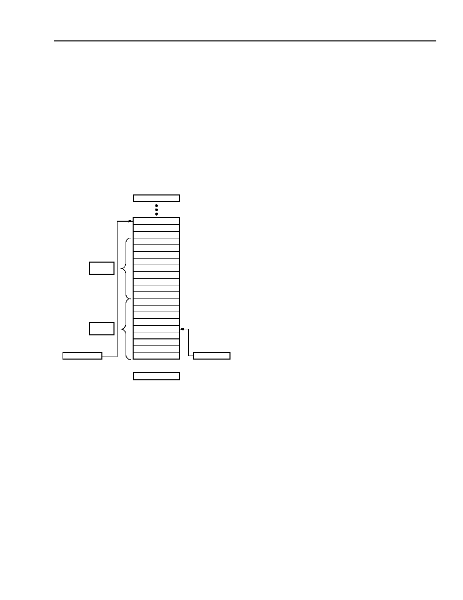
Lucent Technologies Inc.
53
Preliminary Data Sheet
November 2000
ISDN Network Termination Node (NTN) Device
T9000
9 HDLC with FIFO Module
(continued)
9.1 HDLC Transmitter
(continued)
9.1.1 HDLC Transmitter Initialization (continued)
Interrupt register bit HIR[TUNDR] is asserted to indi-
cate that an underrun error has occurred during the
transmission of a frame. An underrun error occurs
when the transmitter has completed the transmission
of a user byte that is not the last of a packet and
detects that the transmitter FIFO is empty. In this case,
the frame is completed by inserting the abort pattern,
01111111.
5-7099F
Note: RPTR = read pointer, WPTR = write pointer.
Figure 9. HDLC Transmitter FIFO
9.2 HDLC Transmitter D-Channel Access
The HDLC transmitter accesses the upstream D chan-
nel using a priority mechanism (implemented via an
arbitration circuit) equivalent to that specified in the
ITU-I.430 standard for TEs on the S/T bus. The arbiter
automatically grants control to the HDLC module if one
of these conditions occurs:
s
S/T-interface is not fully active (no INFO 3 is being
received on the S/T-interface).
s
SCR0[FACT] register bit is set to 1.
s
DFR[FORCE_D] register bit is set to 1.
When none of the above conditions are true and INFO
3 is being received on the S/T-interface, the priority cir-
cuit determines when the HDLC module is granted
access to the upstream D channel. The arbiter will
grant access to the HDLC module when 8 or 9 (for pri-
ority class 1) or 10 or 11 (for priority class 2) consecu-
tive ones are received on the upstream S/T D channel.
The priority class is controlled via register bit
HTTH[PCLASS]. Within a priority class, the priority
level (i.e., 8/9 or 10/11) is automatically managed.
Once the packet has been transmitted, the HDLC mod-
ule releases control to the internal arbiter for a new
arbitration.
When the S/T-interface is active, the microcontroller
may force access to the upstream D channel to be
granted to the HDLC module by asserting register bit
DFR[FORCE_D]. Normally, the upstream (received) D-
channel bit (D bit) from the TEs is echoed downstream
in the E-bit position. When FORCE_D is asserted, the
inverted version of the D bit is echoed. This has the
effect of guaranteeing that all active TEs will cease
transmission (due to a collision error) and no new
transmissions will be initiated. In this way, upstream
access to the D channel is granted exclusively to the
local HDLC controller.
When the S/T-interface is disabled (SCR0[ST_E] = 0)
or in force activate mode (SCR0[FACT] = 1), the HDLC
transmitter will be granted immediate access to the
upstream D channel. If the HDLC module is granted
access to the D channel and does not have any data to
transmit, it will transmit the idle pattern determined by
HTCF[IDL]. For operation with TEs running the LAPD
protocol, HTCF[IDL] should be set to 1.
RPTR = 04h
P1-B0 (SAPI)
PI-B1 (TEI)
P1-B2
P1-B3
P1-B4
P1-B5
P1-B6
P1-B7
P1-LASTBYTE
P2-B0 (SAPI)
P2-B1 (TEI)
P2-B2
P2-B3
P2-B4
P2-B5
P2-B6
UDP #2
UDP #1
P2-B7
P2-LASTBYTE
P3-B0 (SAPI)
P3-B1 (TEI)
WPTR = 14h
HTSA = 30h

54
54
Lucent Technologies Inc.
Preliminary Data Sheet
November 2000
ISDN Network Termination Node (NTN) Device
T9000
9 HDLC with FIFO Module
(continued)
9.3 HDLC Receiver
Downstream D channel is always transferred to the
HDLC receiver. The HDLC receiver removes flags,
does zero bit deletion, and calculates the FCS for the
downstream D-channel information. Deframed data is
converted from serial to parallel (byte delimited) and
passed to the microcontroller through the receiver
FIFO HRX register.
9.3.1 HDLC Receiver Initialization
On powerup, the HDLC receiver is initialized automati-
cally. After powerup, whenever there is any change to
the HRCF[DROPCRC], HRCF[RXMODE],
HRCF[BAE], or HSM0[BAP(7:0)] configuration bits, the
bit HRCF[RX_INIT] must be set to 1 to reinitialize the
HDLC receiver. Once the initialization is completed, the
HRCF[RX_INIT] bit automatically returns to 0.
During initialization, register bit HRCF[DROPCRC] is
sampled. If it is one (the default), the FCS will be
dropped (not stored in the receiver FIFO). If
HRCF[DROPCRC] = 0, the complete deframed packet,
including its FCS, will be stored in the receiver FIFO.
If the device is programmed for address matching, then
prior to storing a packet in the receiver FIFO, its
address is checked against a set of patterns (see Sec-
tion 9.4, Address Recognition). Only packets with an
address field matching one of the programmed
address values are transferred to the receiver FIFO, all
others are rejected. At the end of a frame, a status byte
is transferred to the HDLC receiver FIFO that provides
information about the following events: frame-overrun,
frame-complete, frame-error, and frame-abort.
Figure 10 shows the structure of the status byte. Each
bit is set to one when the corresponding condition is
active.
Bit 7 (OVR). The overrun bit indicates that the frame
has been closed by a receive FIFO overrun condition
(see section 9.3.1.1 Overrun Condition ).
Bit 6 (EOF). The end of frame bit indicates that the
packet has been properly terminated with a closing
flag.
Bit 5 (FERR). The FCS error bit indicates that the
results of comparing the incoming FCS with internally
calculated FCS on the received data (according to the
ITU CRC-16 polynomial) did not match.
Bit 4 (FABRT). The frame abort bit indicates that the
frame has been closed with an abort pattern
(01111111).
Bits 2--0 (CBIT). The check error bit provides an extra
error check. In most HDLC based protocols, the packet
length is an exact multiple number of bytes. When this
is the case, CBIT = 111. Otherwise, CBIT
111.
The above definitions for the status bits imply that cor-
rectly received frames will have 47h as the status byte.
Bit 3 is reserved and is set to 0.
Figure 10. HDLC Receiver Status Word
Multiple packets may be stored in the receiver FIFO at
a given time. The HRDA[NBNSW] register bits indicate
the number of bytes until the next status word in the
FIFO. If there are no status words in the FIFO, it indi-
cates the number of bytes of an unfinished packet cur-
rently stored into the FIFO.
Packets less than 2 bytes in length (4 bytes if
HRCF[DROPCRC] = 1) are automatically rejected.
7
6
5
4
3
2:0
OVR
EOF
FERR
FABRT
--
CBIT

Lucent Technologies Inc.
55
Preliminary Data Sheet
November 2000
ISDN Network Termination Node (NTN) Device
T9000
9 HDLC with FIFO Module
(continued)
9.3 HDLC Receiver
(continued)
9.3.1 HDLC Receiver Initialization (continued)
Figure 11 represents a sequence of snapshots in time of the receiver FIFO.
In Figure 11 (a), the FIFO is empty, so HRDA = 00h.
In Figure 11 (b), the first five bytes of a packet have been loaded into the FIFO; register HRDA indicates that there
is no status byte in the FIFO (HRDA[SWRF] = 0) and also indicates the number of bytes currently in the FIFO
(HRDA[NBNSW] = 05h).
In Figure 11 (c), a complete packet has been loaded into the FIFO and part of a second packet has been loaded. In
this case, HDRA[SWRF] = 1, which indicates that there is a status byte in the receiver FIFO. HRDA[NBNSW] =
09h
indicates that the status byte is the ninth byte in the FIFO.
In Figure 11 (d), the second packet has been completely loaded into the receiver FIFO, part of a third packet has
been received, and some bytes of the first packet have been read by the microcontroller.
Figure 11 (e) represents the case in which the microcontroller has read all bytes of the first packet except its status
byte. A new read of the FIFO (HRX register) will cause the HRDA register to point to the status byte of the second
packet, as shown in Figure 11 (f).
5-7098F
Figure 11. HDLC Receiver FIFO Snapshot Sequence
FREE
(a)
HRDA = 00h
SPACE
FREE
(b)
HRDA = 05h
SPACE
FREE
(c)
HRDA = 89h
SPACE
UDP #1
P1-SAPI
P1-TEI
P1-B2
P1-B3
P1-B4
P1-SAPI
P1-TEI
P1-B2
P1-B3
P1-B4
P1-B5
P1-B6
P1-B7
P1-STATUS
P2-SAPI
P2-TEI
P2-B2
UDP #2
UDP #1
(d)
HRDA = 86h
(e)
HRDA = 81h
FREE
(f)
HRDA = 89h
SPACE
P2-SAPI
P2-TEI
P2-B2
P2-B3
P2-B4
P2-B5
P2-B6
P2-B7
P2-STATUS
P3-SAPI
P3-TEI
P3-B2
UDP #3
UDP #2
P2-SAPI
P2-TEI
P2-B2
P2-B3
P2-B4
P2-B5
P2-B6
P2-B7
P2-STATUS
P3-SAPI
P3-TEI
P3-B2
UDP #3
UDP #2
UDP #1
P1-B3
P1-B4
P1-B5
P1-B6
P1-B7
P1-STATUS
P2-SAPI
P2-TEI
P2-B2
P2-B3
P2-B4
P2-B5
P2-B6
P2-B7
P2-STATUS
P3-SAPI
FREE
SPACE
UDP #2
UDP #1
FREE
SPACE
UDP #3
P1-STATUS

56
56
Lucent Technologies Inc.
Preliminary Data Sheet
November 2000
ISDN Network Termination Node (NTN) Device
T9000
9 HDLC with FIFO Module
(continued)
9.3 HDLC Receiver
(continued)
9.3.1 HDLC Receiver Initialization (continued)
Up to 16 status bytes can be stored in the receiver
FIFO at a given time. Once this condition is reached, it
is indicated by assertion of the HIR[RSTF] interrupt
register bit and the FIFO is considered full. In the worst
case, the microcontroller has approximately 2 ms from
the time HIR[RSTF] is asserted to read data from the
FIFO and avoid overrun errors (an overrun error is indi-
cated by assertion of the HIR[ROVR] interrupt bit).
When a status word with its EOF bit set is loaded into
the FIFO, interrupt bit HIR[REOF] is set. Similarly,
when a status word with its ABRT bit set is loaded into
the FIFO, interrupt bit HIR[RABT] is set.
When the receive FIFO is filled at or above the level
programmed in register HRTH, an interrupt is asserted
by enabling the bit HIR[RTHR]. The interrupt should
clear when the interrupt status register is read, and
should not be asserted again until the receive FIFO is
emptied to the point that more spaces remain in the
FIFO than the value programmed in the HRTH register,
and then enough bytes are received to again cause the
delay FIFO fill level to reach the HRTH register value.
9.3.1.1 Overrun Condition
An overrun condition occurs when the receiver is
unable to download a processed byte into the FIFO
because the FIFO is full or contains 16 status words.
Interrupt bit HIR[ROVR] is set when an overrun occurs.
If the overrun condition occurs during the reception of a
packet with a matching address field, the current frame
will be closed and its status word's OVR bit will be set.
The remainder of the frame will be dropped even if the
overrun condition has been removed. The receiver
must be reinitialized after the overrun condition, before
new packets can be properly received.
9.4 Address Recognition
A very flexible address comparison scheme is imple-
mented in the NTN device. Eight registers are used for
storing SAPI or TEI patterns for comparison with the
incoming address. The registers are grouped logically
into the pairs HSM0/HTM0, HSM1/HTM1, HSM2/
HTM2, HSM3/HTM3 to define a total of four DLCI (data
link connection identifier) address matching patterns. If
HSMOD and HTMOD are programmed for address
matching, only frames with an address field matching
one of the programmed address values (or special
addresses) are transferred to the receive FIFO. All oth-
ers are ignored. If an address match occurs, the
address field is also loaded into the HDLC receive
FIFO.
The address modifier registers, HSMOD and HTMOD,
are used to control the address recognition modes and
can be used to extend the DLCIs defined in the four
HSMx/HTMx register pairs. Figure 12 shows an exam-
ple of this for the SAPI0/TEI0 pair (i.e., bits
SAPI0M[1:0] and TEI0M[1:0] in HSMOD and HTMOD,
respectively).
Consider the default setting of TEI0M = 00 and
SAPI0M = 00 on powerup. In this case, TEIM0 = 00
causes rejection of all packets for a given DLCI pair,
independent of the state of SAPI0M. This means that
on powerup, the HDLC receiver is disabled and will not
receive any packets. Now consider the effect of setting
TEI0M to the other three possible values while leaving
SAPI0M set to 00.
Setting TEI0M = 01 enables the recognition of the
DLCI0 address programmed in the HSM0/HTM0 pair.
Setting TEI0M = 10 extends the definition of DLCI0 to
include the broadcast TEI value, 127. Setting TEI0M =
11 extends the definition of DLCI0 to include all TEI val-
ues.
In a similar way, setting SAPI0M to the values 01, 10,
or 11 will extend the existing definition of DLCI0 to
include SAPI0 = 0, SAPI = 63, or all SAPI values,
respectively. Note, then, that when SAPI0M/TEI0M =
1111, any packet more than 2 bytes in length (4 bytes if
HRCF[DROPCRC] = 1) will be downloaded to the
receiver FIFO, regardless of its address. This effec-
tively disables address recognition for all four DLCI
pairs, since the values programmed into the other three
pairs become irrelevant in this case.
One further level of address recognition control is avail-
able via the HSCR register, which provides a means for
enabling/disabling comparison of the command
response (C/R) bit for each SAPI. When
HSCR[SxCRE] = 0, no comparison is done on the C/R
bit of the SAPI defined by HSMx register. When
HSCR[SXCRE] = 1, the C/R bit is included in compari-
son. However, for extended SAPI values of 0 or 63
(HSMOD[SAPIxM] = 01 or = 10), no comparison is ever
done on the C/R bit.
In the transmit direction, no automatic address inser-
tion is performed.
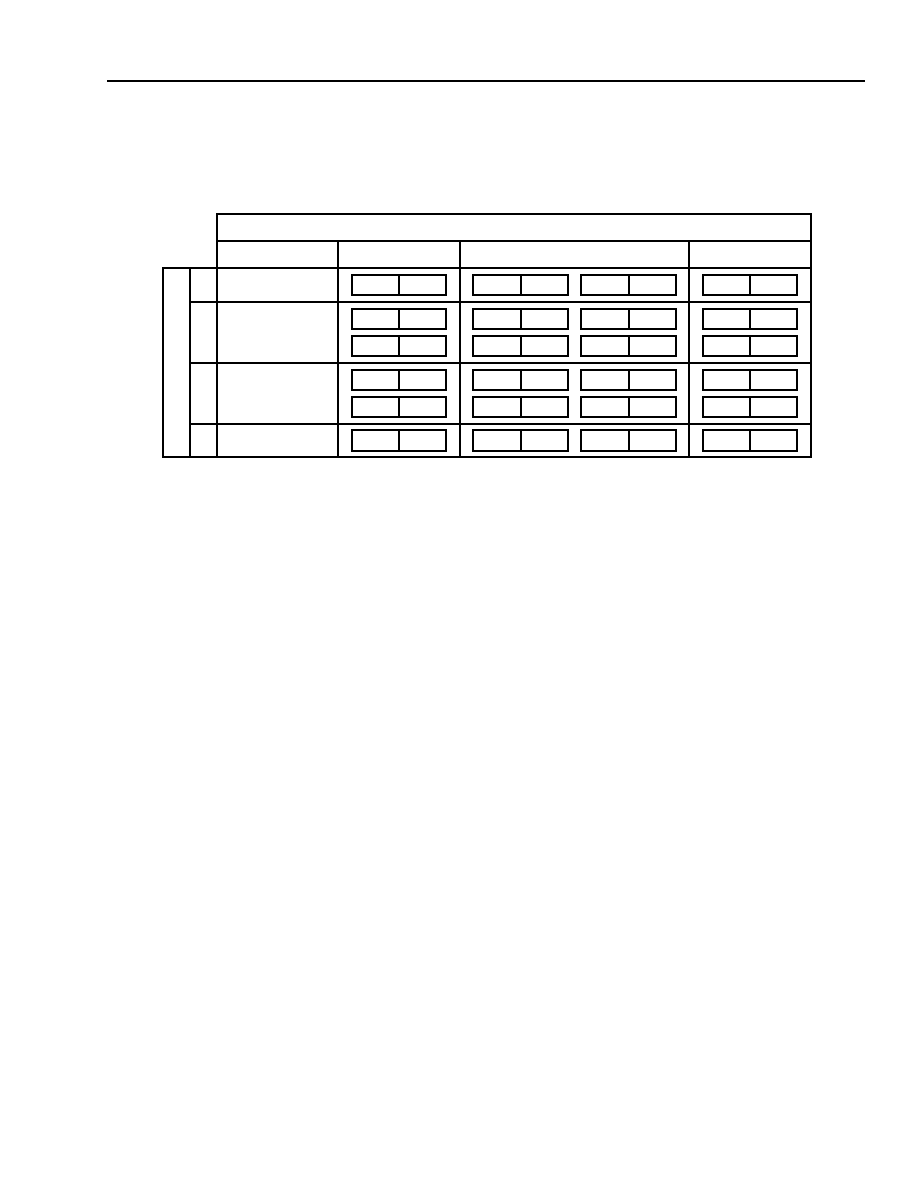
Lucent Technologies Inc.
57
Preliminary Data Sheet
November 2000
ISDN Network Termination Node (NTN) Device
T9000
9 HDLC with FIFO Module
(continued)
9.4 Address Recognition
(continued)
5-6514F
* Indicates any SAPI value.
Indicates any TEI value.
Figure 12. DLCI Extension and Function of SAPI0M-TEI0M Bits
SAPI0
TEI0
SAPI0
TEI0
0
TEI0
SAPI0
TEI0
63
TEI0
*
TEI0
SAPI0
TEI0
SAPI0
127
SAPI0
00
SAPI0
TEI0
0
TEI0
SAPI0
TEI0
63
TEI0
*
TEI0
SAPI0
127
0
127
SAPI0
127
63
127
*
127
SAPI0
0
SAPI0
63
*
01
10
11
00
01
10
11
TEI0M
S
A
P
I
0
M

58
Lucent Technologies Inc.
Preliminary Data Sheet
November 2000
ISDN Network Termination Node (NTN) Device
T9000
9 HDLC with FIFO Module
(continued)
9.5 HDLC Register Set
Table 55. HTCF: HDLC Transmitter Configuration Register (0x18)
Reg
R/W
Bit 7
Bit 6
Bit 5
Bit 4
Bit 3
Bit 2
Bit 1
Bit 0
HTCF
R/W
FCNT2
FCNT1
FCNT0
IDL
TXMODE ABRT_RQ MANCRC
TX_INIT
RESET
Default 0
0
0
1
0
0
0
0
Bit #
Symbol
Name/Description
7--5
FCNT[2:0]
Interframe Fill Count. Sets the number of fill bytes to be transmitted between each
HDLC frame. The number of fill bytes inserted between the closing flag of one frame and
the opening flag of another is FCNT[2:0]
-
1, except for the case of FCNT[2:0] = 0, which
causes sharing of the closing flag of one frame with the opening flag of the next.
000: Back-to-back frames (closing/opening flag is shared).
001: No fill bytes are inserted.
. . .
111: Insert 6 fill bytes.
Back-to-back frames can only occur if the priority mechanism is disabled by setting
DFR[FORCE_D] = 1. See DFR[FORCE_D] description.
4
IDL
Idle/Interframe Fill Value. Sets the value of the transmitter's idle and interframe fill
bytes.
0: 01111110 (flags)
1: 11111111 (idles)
Flags can only be used as idle or interframe fill bytes if the priority mechanism is disabled
by setting DFR[FORCE_D] = 1. See DFR[FORCE_D] description.
3
TXMODE
Transmitter Mode. Determines whether the transmitter is in standard HDLC mode or
transparent mode. The transmitter must be reinitialized after changing this bit.
0: Standard HDLC mode.
1: Transparent mode.
2
ABRT_RQ
HDLC Transmitter Abort Request. When this signal is written to 1, the frame
currently being transmitted is aborted and the transmit FIFO will be flushed. This bit
automatically returns to 0 once the abort sequence has been set.
1
MANCRC
HDLC Transmitter Manual/Auto CRC Insertion. Controls whether the transmit FCS
(CRC) will be inserted automatically by the HDLC controller or whether it must be manu-
ally loaded into the transmit FIFO. The transmitter must be reinitialized after changing
this bit.
0: Auto insertion.
1: Manual insertion.
0
TX_INIT
HDLC Transmitter Initialize. Writing this bit to 1 will cause initialization of the HDLC
transmitter. On powerup, the HDLC transmitter is initialized automatically. After powerup,
whenever the MANCRC or TXMODE configuration bits are changed, this bit needs to be
set to reinitialize the HDLC transmitter. Prior to programming any of the transmitter regis-
ters, this bit must be written to 1. The microcontroller must then poll this bit and wait until
it returns to 0 (signaling that transmitter initialization is complete) before programming
any of the other transmitter registers.

Lucent Technologies Inc.
59
Preliminary Data Sheet
November 2000
ISDN Network Termination Node (NTN) Device
T9000
9 HDLC with FIFO Module
(continued)
9.5 HDLC Register Set
(continued)
Table 56. HRCF: HDLC Receiver Configuration Register (0x19)
Reg
R/W
Bit 7
Bit 6
Bit 5
Bit 4
Bit 3
Bit 2
Bit 1
Bit 0
HRCF
R/W
--
--
--
--
RXMODE
BAE
DROPCRC
RX_INIT
RESET
Default
0
0
0
0
0
0
1
0
Bit #
Symbol
Name/Description
7--4
--
Reserved. Program to 0.
3
RXMODE
Receiver Mode. Determines whether the receiver is in standard HDLC mode or transparent
mode. The receiver must be reinitialized after changing this bit.
0: Standard HDLC mode.
1: Transparent mode.
2
BAE
Byte Alignment Enable. This bit enables the byte alignment feature for the HDLC receiver
when operating in transparent mode. When this feature is enabled, register HSM0 (22h) pro-
vides the byte alignment pattern. The receiver must be reinitialized after changing this bit.
0: Byte alignment mechanism is disabled.
1: Byte alignment mechanism is enabled.
1
DROPCRC Drop Receive CRC. Controls whether the CRC bytes (last 2 bytes of an HDLC frame) are
loaded into the receive FIFO. The receiver must be reinitialized after changing this bit.
0: Load 2 CRC bytes into receive FIFO.
1: Drop CRC (CRC bytes are not loaded into the receive FIFO).
0
RX_INIT
HDLC Receiver Initialize. Writing this bit to 1 will cause initialization of the HDLC receiver.
On powerup, the HDLC receiver is initialized automatically. After powerup, whenever there
is any change in the DROPCRC, RXMODE, BAE, or HSM0[BAP(7:0)] configuration bits, this
bit needs to be set to reinitialize the HDLC receiver. Prior to programming any of the receiver
registers, this bit must be written to 1. The microcontroller must then poll this bit and wait
until it returns to 0 (signaling that receiver initialization is complete) before programming any
of the other receiver registers. During initialization, DROPCRC is latched. Any change to
DROPCRC after initialization is disregarded.

60
Lucent Technologies Inc.
Preliminary Data Sheet
November 2000
ISDN Network Termination Node (NTN) Device
T9000
9 HDLC with FIFO Module
(continued)
9.5 HDLC Register Set
(continued)
Table 57. HTTH: HDLC Transmit FIFO Threshold (0x1A)
Table 58. HRTH: HDLC Receive FIFO Threshold (0x1B)
Reg
R/W
Bit 7
Bit 6
Bit 5
Bit 4
Bit 3
Bit 2
Bit 1
Bit 0
HTTH
R/W
P_CLASS
--
TFAE5
TFAE4
TFAE3
TFAE2
TFAE1
TFAE0
RESET
Default
1
0
1
0
0
0
0
0
Bit #
Symbol
Name/Description
7
P_CLASS Priority Class. This bit is used during arbitration to the upstream D-channel access. It indi-
cates the number of consecutive ones the NTN has to receive on the upstream S/T D chan-
nel in order to grant D-channel access to the HDLC transmitter.
0: Priority class 2 (data) as defined in ITU-I.430.
1: Priority class 1 (signaling) as defined in ITU-I.430.
Within a class, priority levels are automatically managed.
6
--
Reserved. Program to 0.
5--0
TFAE[5:0] HDLC Transmitter FIFO Almost Empty Threshold. The HDLC transmitter will issue an
interrupt (if enabled) when the number of empty bytes in the transmit FIFO exceeds the
threshold level programmed in this register. The interrupt will clear when the interrupt status
register is read. The interrupt will not be asserted again until the number of empty bytes in the
transmit FIFO is equal to or less than the value programmed in TFAE[5:0], and then enough
bytes are transmitted to again cause the FIFO empty level to exceed the TFAE[5:0] value.
Reg
R/W
Bit 7
Bit 6
Bit 5
Bit 4
Bit 3
Bit 2
Bit 1
Bit 0
HRTH
R/W
--
--
RFAF5
RFAF4
RFAF3
RFAF2
RFAF1
RFAF0
RESET
Default
0
0
1
0
0
0
0
0
Bit #
Symbol
Name/Description
7--6
--
Reserved. Program to 0.
5--0
RFAF[5:0]
HDLC Receiver FIFO Almost Full Threshold. The HDLC receiver will issue an interrupt
(if enabled) when the number of bytes in the receive FIFO exceeds the threshold level
programmed in this register. The interrupt will clear when the interrupt status register is
read. The interrupt will not be asserted again until the number of bytes in the receive
FIFO is equal to or less than the value programmed in RFAF[5:0], and enough bytes are
received to again cause the FIFO fill level to exceed the RFAF[5:0] value.

Lucent Technologies Inc.
61
Preliminary Data Sheet
November 2000
ISDN Network Termination Node (NTN) Device
T9000
9 HDLC with FIFO Module
(continued)
9.5 HDLC Register Set
(continued)
Table 59. HTSA: HDLC Transmit FIFO Space Available (0x1C)
Table 60. HRDA: HDLC Receive FIFO Data Available (0x1D)
Table 61. HTX: HDLC Transmit Data (0x1E)
Reg
R/W
Bit 7
Bit 6
Bit 5
Bit 4
Bit 3
Bit 2
Bit 1
Bit 0
HTSA
R
--
TSP6
TSP5
TSP4
TSP3
TSP2
TSP1
TSP0
RESET
Default
--
1
0
0
0
0
0
0
Bit #
Symbol
Name/Description
7
--
Reserved.
6--0
TSP[6:0]
Transmitter Space. This register contains the number of empty positions in the transmit-
ter FIFO.
Reg
R/W
Bit 7
Bit 6
Bit 5
Bit 4
Bit 3
Bit 2
Bit 1
Bit 0
HRDA
R
SWRF
NBNSW6
NBNSW5 NBNSW4 NBNSW3
NBNSW2 NBNSW1 NBNSW0
RESET
Default
--
--
--
--
--
--
--
--
Bit #
Symbol
Name/Description
7
SWRF
Status Word on Receive FIFO. The HDLC receiver module asserts this bit whenever
there is a status word in the receive FIFO.
0: No status word.
1: Status word.
6--0
NBNSW[6:0]
Number of Bytes Until Next Status Word. These bits indicate how many bytes are
present in the receive FIFO. If SWRF (bit 7) is equal to 1, indicating that a status word is
available in the FIFO, then NBNSW[6:0] indicates the number of bytes in the receive
FIFO up to and including the status byte. If SWRF is equal to 0, indicating that no status
words are available in the FIFO, then NBNSW[6:0] indicates the total number of data
bytes in the receive FIFO.
Reg
R/W
Bit 7
Bit 6
Bit 5
Bit 4
Bit 3
Bit 2
Bit 1
Bit 0
HTX
W
TXD7
TXD6
TXD5
TXD4
TXD3
TXD2
TXD1
TXD0
RESET
Default
--
--
--
--
--
--
--
--
Bit #
Symbol
Name/Description
7--0
TXD[7:0]
HDLC Transmit Data. Data to be transmitted is written to this register, which maps into
the transmit FIFO. The last byte of each packet must be written to register HTXL (see
Table 62).

62
Lucent Technologies Inc.
Preliminary Data Sheet
November 2000
ISDN Network Termination Node (NTN) Device
T9000
9 HDLC with FIFO Module
(continued)
9.5 HDLC Register Set
(continued)
Table 62. HTXL: HDLC Transmit Data Last Byte (0x1F)
Table 63. HRX: HDLC Receive Data (0x20)
Table 64. HSCR: HDLC SAPI C/R Bit Mask (0x21)
Reg
R/W
Bit 7
Bit 6
Bit 5
Bit 4
Bit 3
Bit 2
Bit 1
Bit 0
HTXL
W
TXDL7
TXDL6
TXDL5
TXDL4
TXDL3
TXDL2
TXDL1
TXDL0
RESET
Default
--
--
--
--
--
--
--
--
Bit #
Symbol
Name/Description
7--0
TXDL[7:0]
HDLC Transmit Data--Last Byte. The last data byte of each transmitted packet is writ-
ten to this register (rather than HTX) to indicate to the transmitter that this is the end of
the packet. This register occupies the same physical space as HTX (i.e., it maps to the
transmit FIFO).
Reg
R/W
Bit 7
Bit 6
Bit 5
Bit 4
Bit 3
Bit 2
Bit 1
Bit 0
HRX
R
RXD7
RXD6
RXD5
RXD4
RXD3
RXD2
RXD1
RXD0
RESET
Default
--
--
--
--
--
--
--
--
Bit #
Symbol
Name/Description
7--0
RXD[7:0]
Received Data/Status. The content of the FIFO is read when addressing this register.
The first received bit is the least significant bit of this byte.
Reg
R/W
Bit 7
Bit 6
Bit 5
Bit 4
Bit 3
Bit 2
Bit 1
Bit 0
HSCR
R/W
--
--
--
--
S3CRE
S2CRE
S1CRE
S0CRE
RESET
Default
0
0
0
0
0
0
0
0
Bit #
Symbol
Name/Description
7--4
--
Reserved. Program to 0.
3
S3CRE
SAPI3 Command/Response Bit Comparison Enable.
0: SAPI3 C/R bit is ignored.
1: SAPI3 comparison includes C/R bit (HSM3.1).
2
S2CRE
SAPI2 Command/Response Bit Comparison Enable.
0: SAPI2 C/R bit is ignored.
1: SAPI2 comparison includes C/R bit (HSM2.1).
1
S1CRE
SAPI1 Command/Response Bit Comparison Enable.
0: SAPI1 C/R bit is ignored.
1: SAPI1 comparison includes C/R bit (HSM1.1).
0
S0CRE
SAPI0 Command/Response Bit Comparison Enable.
0: SAPI0 C/R bit is ignored.
1: SAPI0 comparison includes C/R bit (HSM0.1).

Lucent Technologies Inc.
63
Preliminary Data Sheet
November 2000
ISDN Network Termination Node (NTN) Device
T9000
9 HDLC with FIFO Module
(continued)
9.5 HDLC Register Set
(continued)
Table 65. HSM0: HDLC SAPI Match Pattern 0 (0x22)
Table 66. HTM0: HDLC TEI Match Pattern 0 (0x23)
Table 67. HSM1: HDLC SAPI Match Pattern 1 (0x24)
Reg
R/W
Bit 7
Bit 6
Bit 5
Bit 4
Bit 3
Bit 2
Bit 1
Bit 0
HSM0
R/W
SAPI05
SAPI04
SAPI03
SAPI02
SAPI01
SAPI00
C/R0
EA00
BAP7
BAP6
BAP5
BAP4
BAP3
BAP2
BAP1
BAP0
RESET
Default
--
--
--
--
--
--
--
--
Bit #
Symbol
Name/Description
7--2
SAPI0[5:0]
Match Pattern 0 for SAPI. When in the HDLC mode, this register provides the match
pattern for SAPI. See Section 9.4, Address Recognition for details.
BAP[7:2]
Byte Alignment Pattern. When in transparent mode, this register provides the byte
alignment pattern if HRCF[BAE] = 1.
1
C/R0
Command/Response Bit. Set according to the Q.920 standard.
BAP1
Byte Alignment Pattern. When in transparent mode, this register provides the byte
alignment pattern if HRCF[BAE] = 1.
0
EA00
Address Field Extension Bit (0 or 1). This bit has to be 0 for recognizing SAPI0 and
SAPI63 addresses.
BAP0
Byte Alignment Pattern. When in transparent mode, this register provides the byte
alignment pattern if HRCF[BAE] = 1.
Reg
R/W
Bit 7
Bit 6
Bit 5
Bit 4
Bit 3
Bit 2
Bit 1
Bit 0
HTM0
R/W
TEI06
TEI05
TEI04
TEI03
TEI02
TEI01
TEI00
EA10
RESET
Default
--
--
--
--
--
--
--
--
Bit #
Symbol
Name/Description
7--1
TEI0[6:0]
Match Pattern 0 for TEI. See Section 9.4, Address Recognition for details.
0
EA10
Address Field Extension Bit (0 or 1). This bit has to be 1 for recognizing the special TEI127
value of 127.
Reg
R/W
Bit 7
Bit 6
Bit 5
Bit 4
Bit 3
Bit 2
Bit 1
Bit 0
HSM1
R/W
SAPI15
SAPI14
SAPI13
SAPI12
SAPI11
SAPI10
C/R1
EA01
RESET
Default
--
--
--
--
--
--
--
--
Bit #
Symbol
Name/Description
7--2
SAPI1[5:0] Match Pattern 1 for SAPI. When in the HDLC mode, this register provides the match pat-
tern for SAPI. See Section 9.4, Address Recognition for details.
1
C/R1
Command/Response Bit. Set according to the Q.920 standard.
0
EA01
Address Field Extension Bit (0 or 1). This bit has to be 0 for recognizing SAPI0 and
SAPI63 addresses.

64
Lucent Technologies Inc.
Preliminary Data Sheet
November 2000
ISDN Network Termination Node (NTN) Device
T9000
9 HDLC with FIFO Module
(continued)
9.5 HDLC Register Set
(continued)
Table 68. HTM1: HDLC TEI Match Pattern 1 (0x25)
Table 69. HSM2: HDLC SAPI Match Pattern 2 (0x26)
Table 70. HTM2: HDLC TEI Match Pattern 2 (0x27)
Table 71. HSM3: HDLC SAPI Match Pattern 3 (0x28)
Reg
R/W
Bit 7
Bit 6
Bit 5
Bit 4
Bit 3
Bit 2
Bit 1
Bit 0
HTM1
R/W
TEI16
TEI15
TEI14
TEI13
TEI12
TEI11
TEI10
EA11
RESET
Default
--
--
--
--
--
--
--
--
Bit #
Symbol
Name/Description
7--1
TEI1[6:0] Match Pattern 1 for TEI. See Section 9.4, Address Recognition for details.
0
EA11
Address Field Extension Bit (0 or 1). This bit has to be 1 for recognizing the special TEI value
of 127.
Reg
R/W
Bit 7
Bit 6
Bit 5
Bit 4
Bit 3
Bit 2
Bit 1
Bit 0
HSM2
R/W
SAPI25
SAPI24
SAPI23
SAPI22
SAPI21
SAPI20
C/R2
EA02
RESET
Default
--
--
--
--
--
--
--
--
Bit #
Symbol
Name/Description
7--2
SAPI2[5:0]
Match Pattern 2 for SAPI. When in the HDLC mode, this register provides the match
pattern for SAPI. See Section 9.4, Address Recognition for details.
1
C/R2
Command/Response Bit. Set according to the Q.920 standard.
0
EA02
Address Field Extension Bit (0 or 1). This bit has to be 0 for recognizing special SAPI
values of 0 or 63.
Reg
R/W
Bit 7
Bit 6
Bit 5
Bit 4
Bit 3
Bit 2
Bit 1
Bit 0
HTM2
R/W
TEI26
TEI25
TEI24
TEI23
TEI22
TEI21
TEI20
EA12
RESET
Default
--
--
--
--
--
--
--
--
Bit #
Symbol
Name/Description
7--1
TEI2[6:0] Match Pattern 2 for TEI. See Section 9.4, Address Recognition for details.
0
EA12
Address Field Extension Bit (0 or 1). This bit has to be 1 for recognizing the special TEI
value of 127.
Reg
R/W
Bit 7
Bit 6
Bit 5
Bit 4
Bit 3
Bit 2
Bit 1
Bit 0
HSM3
R/W
SAPI35
SAPI34
SAPI33
SAPI32
SAPI31
SAPI30
C/R3
EA03
RESET
Default
--
--
--
--
--
--
--
--
Bit #
Symbol
Name/Description
7--2
SAPI3[5:0]
Match Pattern 3 for SAPI. When in the HDLC mode, this register provides the match
pattern for SAPI. See Section 9.4, Address Recognition for details.
1
C/R3
Command/Response Bit. Set according to the Q.920 standard.
0
EA03
Address Field Extension Bit (0 or 1). This bit has to be 0 for recognizing special SAPI
values of 0 or 63.

Lucent Technologies Inc.
65
Preliminary Data Sheet
November 2000
ISDN Network Termination Node (NTN) Device
T9000
9 HDLC with FIFO Module
(continued)
9.5 HDLC Register Set
(continued)
Table 72. HTM3: HDLC TEI Match Pattern 3 (0x29)
Table 73. HSMOD: HDLC SAPI Modifier Register (0x2A)
See Section 9.4, Address Recognition for details on the function of this register.
Reg
R/W
Bit 7
Bit 6
Bit 5
Bit 4
Bit 3
Bit 2
Bit 1
Bit 0
HTM3
R/W
TEI36
TEI35
TEI34
TEI33
TEI32
TEI31
TEI30
EA13
RESET
Default
--
--
--
--
--
--
--
--
Bit #
Symbol
Name/Description
7--1
TEI3(6--0)
Match Pattern 3 for TEI. See Section 9.4, Address Recognition for details.
0
EA13
Address Field Extension Bit (0 or 1). This bit has to be 1 for recognizing the special
TEI value of 127.
Reg
R/W
Bit 7
Bit 6
Bit 5
Bit 4
Bit 3
Bit 2
Bit 1
Bit 0
HSMOD
R/W
SAPI3M1
SAPI3M0
SAPI2M1
SAPI2M0
SAPI1M1
SAPI1M0
SAPI0M1
SAPI0M0
RESET
Default
0
0
0
0
0
0
0
0
Bit #
Symbol
Name/Description
7--6
SAPI3M[1:0]
SAPI3 Modifier. This field indicates the value(s) for the SAPI of DLCI3.
00: SAPI3 = value of HSM3.
01: SAPI3 = value of HSM3 or 0.
10: SAPI3 = value of HSM3 or 63.
11: SAPI3 = any value.
5--4
SAPI2M[1:0]
SAPI2 Modifier. This field indicates the value(s) for the SAPI of the DLCI2.
00: SAPI2 = value of HSM2.
01: SAPI2 = value of HSM2 or 0.
10: SAPI2 = value of HSM2 or 63.
11: SAPI2 = any value.
3--2
SAPI1M[1:0]
SAPI1 Modifier. This field indicates the value(s) for the SAPI of the DLCI1.
00: SAPI1 = value of HSM1.
01: SAPI1 = value of HSM1 or 0.
10: SAPI1 = value of HSM1 or 63.
11: SAPI1 = any value.
1--0
SAPI0M[1:0]
SAPI0 Modifier. This field indicates the value(s) for the SAPI of the DLCI0.
00: SAPI0 = value of HSM0.
01: SAPI0 = value of HSM0 or 0.
10: SAPI0 = value of HSM0 or 63.
11: SAPI0 = any value.

66
Lucent Technologies Inc.
Preliminary Data Sheet
November 2000
ISDN Network Termination Node (NTN) Device
T9000
9 HDLC with FIFO Module
(continued)
9.5 HDLC Register Set
(continued)
Table 74. HTMOD: HDLC TEI Modifier Register (0x2B)
See Section 9.4, Address Recognition for details on the function of this register.
Reg
R/W
Bit 7
Bit 6
Bit 5
Bit 4
Bit 3
Bit 2
Bit 1
Bit 0
HTMOD
R/W
TEI3M1
TEI3M0
TEI2M1
TEI2M0
TEI1M1
TEI1M0
TEI0M1
TEI0M0
RESET
Default
0
0
0
0
0
0
0
0
Bit #
Symbol
Name/Description
7--6
TEI3M[1:0]
TEI3 Modifier. This field indicates the value(s) for the TEI of DLCI3.
00: DLCI3 not defined.
01: TEI3 = value of HTM3.
10: TEI3 = value of HTM3 or broadcast TEI (127).
11: TEI3 = any value.
5--4
TEI2M[1:0]
TEI2 Modifier. This field indicates the value(s) for the TEI of DLCI2.
00: DLCI2 not defined.
01: TEI2 = value of HTM2.
10: TEI2 = value of HTM2 or broadcast TEI (127).
11: TEI2 = any value.
3--2
TEI1M[1:0]
TEI1 Modifier. This field indicates the value(s) for the TEI of DLCI1.
00: DLCI1 not defined.
01: TEI1 = value of HTM1.
10: TEI1 = value of HTM1 or broadcast TEI (127).
11: TEI1 = any value.
1--0
TEI0M[1:0]
TEI0 Modifier. This field indicates the value(s) for the TEI of DLCI0.
00: DLCI0 not defined.
01: TEI0 = value of HTM0.
10: TEI0 = value of HTM0 or broadcast TEI (127).
11: TEI0 = any value.

Lucent Technologies Inc.
67
Preliminary Data Sheet
November 2000
ISDN Network Termination Node (NTN) Device
T9000
9 HDLC with FIFO Module
(continued)
9.5 HDLC Register Set
(continued)
Table 75. HIR: HDLC Interrupt Register (0x2C)
Note: All bits in this register are set to 1 upon occurrence of the corresponding interrupt condition, and are cleared
to 0 when the register is read.
Reg
R/W
Bit 7
Bit 6
Bit 5
Bit 4
Bit 3
Bit 2
Bit 1
Bit 0
HIR
R
RSTF
ROVR
REOF
RABT
RTHR
TUNDR
TFC
TTHR
RESET
Default
--
--
--
--
--
--
--
--
Bit #
Symbol
Name/Description
7
RSTF
Receiver Status Full Interrupt. This interrupt occurs when the receiver FIFO is filled
with 16 status bytes.
6
ROVR
Receive FIFO Overrun Interrupt. This interrupt occurs when a received byte is written
to a full receive FIFO.
5
REOF
Receive End of Frame Interrupt. This interrupt occurs when an end of frame (EOF)
status byte is written to the receive FIFO.
4
RABT
Receive Abort Detect Interrupt. This interrupt occurs when the receiver detects an
abort condition.
3
RTHR
Receive FIFO Threshold Interrupt. This interrupt occurs when the receiver almost full
threshold is exceeded.
2
TUNDR
Transmit FIFO Underrun Interrupt. This interrupt occurs when the transmitter attempts
to transmit a byte from an empty transmit FIFO.
1
TFC
Transmit Frame Complete Interrupt. This interrupt occurs when the transmitter has
successfully transmitted a frame.
0
TTHR
Transmit FIFO Threshold Interrupt. This interrupt occurs when the transmitter almost
empty threshold is exceeded.

68
Lucent Technologies Inc.
Preliminary Data Sheet
November 2000
ISDN Network Termination Node (NTN) Device
T9000
9 HDLC with FIFO Module
(continued)
9.5 HDLC Register Set
(continued)
Table 76. HIE: HDLC Interrupt Enable 15 (0x2D)
Reg
R/W
Bit 7
Bit 6
Bit 5
Bit 4
Bit 3
Bit 2
Bit 1
Bit 0
HIE
R/W
RSTFE
ROVRE
REOFE
RABTE
RTHRE
TUNDRE
TFCE
TTHRE
RESET
Default
0
0
0
0
0
0
0
0
Bit #
Symbol
Name/Description
7
RSTFE
RSTFE Interrupt Enable.
0: Interrupt disabled.
1: Interrupt enabled.
6
ROVRE
ROVR Interrupt Enable.
0: Interrupt disabled.
1: Interrupt enabled.
5
REOFE
REOF Interrupt Enable.
0: Interrupt disabled.
1: Interrupt enabled.
4
RABTE
RABT Interrupt Enable.
0: Interrupt disabled.
1: Interrupt enabled.
3
RTHRE
RTHR Interrupt Enable.
0: Interrupt disabled.
1: Interrupt enabled.
2
TUNDRE
TUNDR Interrupt Enable.
0: Interrupt disabled.
1: Interrupt enabled.
1
TFCE
TFC Interrupt Enable.
0: Interrupt disabled.
1: Interrupt enabled.
0
TTHRE
TTHR Interrupt Enable.
0: Interrupt disabled.
1: Interrupt enabled.

Lucent Technologies Inc.
69
Preliminary Data Sheet
November 2000
ISDN Network Termination Node (NTN) Device
T9000
10 GCI+ Interface Module
The programmable GCI+ interface supports a large variety of codec interfaces, including GCI, long-frame sync
(LFS) TDM, and short-frame sync (SFS) TDM; hence, the + attribute. These interfaces cover most available
codecs on the marketplace (Lucent,
Siemens
,
National
*, and
Motorola
).
The GCI+ interface is comprised of seven signals as shown in Table 77. The pin routing of the FSC and PFS1 sig-
nals changes slightly depending on whether the device is in TDM or GCI mode. This was done in order to place the
signal most likely to be used in each mode on the FS1 pin rather than the GPIO2.2 pin. This allows the GPIO2.2
signal to be available for other uses in most cases.
Table 77. GCI+ Interface Signals
The GCI+ interface behavior depends on the operational mode defined by its configuration register, GCCF. Three
modes are supported by the GCI+ interface:
s
GCI-NT mode (GCCF[GMODE(1:0)] = 00).
s
GCI-TE mode (GCCF[GMODE(1:0)] = 01).
s
TDM mode (GCCF[GMODE(1:0)] = 1x).
10.1 TDM Mode (GCCF, GMODE[1:0] = 1x)
TDM mode is for use with codecs having a simple TDM interface. Figure 13 and Figure 14 show the timing for the
GCI+ interface when programmed in TDM mode.
There are two clock modes for the data clock, DCL: single clock and double clock mode. In single clock mode
(GCCF[CKMODE] = 1), there is one DCL cycle per bit. In double clock mode (GCCF[CKMODE] = 0), there are two
DCL cycles per bit. The DCL clock rate is programmed via the GCCF[GRATE(1:0)] register bits. The DCL rates
supported in TDM mode are 512 kHz, 1536 kHz, or 2048 kHz. Since there can be either one or two DCL cycles per
data bit, depending on whether the GCI+ is in single or double clock mode, there are six possible data rates, as
shown in Table 78. In addition, a powerdown mode is available in which DCL is stopped (see Section 10.5, GCI+
Powerdown Mode).
In double clock mode, a bit clock (BCLK) signal is available on the GPIO2.1 pin when GPAF1[GPAF2.1] = 1. BCLK
occurs once per bit time and is a divide-by-two version of the DCL signal. BCLK is always 0 in single clock mode.
*
National
is a registered trademark of National Semiconductor Corporation.
Motorola
is a registered trademark of Motorola, Inc.
Function
Name
GCI Pin
TDM Pin
I/O
Meaning
FSC
FS1
GPIO2.2
O
Reference frame sync (marks start of frame).
PFS1
GPIO2.2
FS1
O
Programmable frame sync 1 (marks location of B1 channel).
PFS2
FS2
FS2
O
Programmable frame sync 2 (marks location of B2 channel).
DCL
DCL
DCL
O
Data clock (defined with GRATE bits).
BCLK
GPIO2.1
GPIO2.1
O
Bit clock (only active during 2 times data clock mode).
DU
DU
DU
I
Data upstream (U transmit data).
DD
DD
DD
O
Data downstream (U receive data).

70
Lucent Technologies Inc.
Preliminary Data Sheet
November 2000
ISDN Network Termination Node (NTN) Device
T9000
10 GCI+ Interface Module
(continued)
10.1 TDM Mode (GCCF, GMODE[1:0] = 1x)
(continued)
Table 78. TDM Data Rate and Clock Options
In TDM mode, the FSC signal can provide an envelope of time slot #0 (the first time slot of a frame) via the
GPIO2.2 pin by setting GPAF1[GPAF2.2] = 1. The PFS1 and PFS2 signals mark the location of the B1 and B2 time
slots on the TDM highway and are output on the FS1 and FS2 pins, respectively (see Table 78).
The PFS1 and PFS2 (programmable frame sync) signals may be programmed to be a pulse (duration of one bit
period, sometimes referred to as short frame sync) or envelope (duration of one time slot minus one-half of a DCL
period, sometimes referred to as long frame sync). Register bit GCCF[PFSPE] sets the short or long frame sync
mode.
The B1 and B2 time slots may be programmed to be at any offset from the start of the frame (in time-slot incre-
ments) by programming the GCOF1 and GCOF2 registers with the desired offset.
The U-interface B1 and B2 channels are normally transferred to/from the codec on the time slots marked by PFS1
and PFS2, respectively. This ordering can be switched by setting the DFAC[BSWAP] register bit to 1.
Register bit GCCF[PFSPE] = 1 controls the relative delay between PFSx (x = 1 or x = 2) and the first data bit of the
time slot associated with PFSx. When GCCF[PFSDEL] = 0, the PFSx rising edge is coincident with the start of the
first data bit of the corresponding time slot. When GCCF[PFSDEL] = 1, the PFSx rising edge occurs one data bit
prior to the first data bit of the corresponding time slot.
Generation of the PFSx signals and data transfer to/from the corresponding time slots may be disabled by setting
DFR[PFSx_ACT] = 0.
CKMODE
GRATE
DCL Rate (kHz)
BCLK Rate (kHz)
Data Rate (kHz)
Number of 8-bit
Time Slots
0
00
0
0
0
0
0
01
512
256
256
4
0
10
1536
768
768
12
0
11
2048
1024
1024
16
1
00
0
0
0
0
1
01
512
0
512
8
1
10
1536
0
1536
24
1
11
2048
0
2048
32
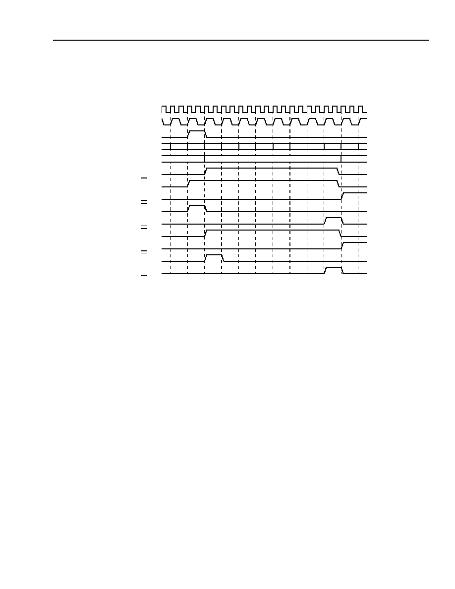
Lucent Technologies Inc.
71
Preliminary Data Sheet
November 2000
ISDN Network Termination Node (NTN) Device
T9000
10 GCI+ Interface Module
(continued)
10.1 TDM Mode (GCCF, GMODE[1:0] = 1x)
(continued)
5-6722 (F)
1. Only present if programmed on GPAF1 register.
2. Not outputs. Shown only for reference.
Note: GKMODE = 0; OFF1 = 0; OFF2 = 1.
Key:
A: PFSDEL = 0 and PFSPE = 0.
B: PFSDEL = 0 and PFSPE = 1.
C: PFSDEL = 1 and PFSPE = 0.
D: PFSDEL = 1 and PFSPE = 1.
?: Don't care.
Figure 13. GCI+ Interface, TDM Mode Timing, Double Clock Mode: GCCF[CKMODE] = 0,
GCCF[GMODE(1:0)] = 1x
DCL
?
?
0
1
2
3
4
5
6
7
0
1
?
0
BCLK
1
SYNC
2
BITSLOT
2
CHANNELSLOT
2
FSC
1
PFS1
PFS2
PFS1
PFS2
PFS1
PFS2
PFS1
PFS2
A
B
C
D
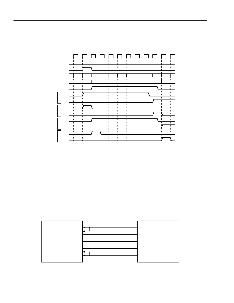
72
Lucent Technologies Inc.
Preliminary Data Sheet
November 2000
ISDN Network Termination Node (NTN) Device
T9000
10 GCI+ Interface Module
(continued)
10.1 TDM Mode (GCCF, GMODE[1:0] = 1x)
(continued)
5-6719 (F)
1. Only present if programmed on GPAF1 register.
2. Not outputs. Shown only for reference.
Note: GKMODE = 1; OFF1 = 0; OFF2 = 1.
Key:
A: PFSDEL = 0 and PFSPE = 0.
B: PFSDEL = 0 and PFSPE = 1.
C: PFSDEL = 1 and PFSPE = 0.
D: PFSDEL = 1 and PFSPE = 1.
?: Don't care.
Figure 14. GCI+ Interface, TDM Mode Timing, Single Clock Mode: GCCF[CKMODE] = 1, GCCF[GMODE(1)] = 1
The figure below shows an example of how a codec with a TDM interface would be connected to an NTN device.
The codec shown is the Lucent T8503 dual codec. The correct register settings are shown in the NTN block.
5-6720 (F)
Figure 15. NTN/T8503 Glueless TDM Interconnection
DCL
PFS1
PFS2
PFS1
PFS2
PFS1
PFS2
PFS1
PFS2
?
?
0
1
2
3
4
5
6
7
0
1
?
0
BCLK
1
SYNC
2
BITSLOT
2
CHANNELSLOT
2
FSC
1
A
B
C
D
T8503
DUAL CODEC
NTN
(GMODE = 1x)
(GRATE = 11)
(CKMODE = 1)
(PFSPE = 1)
(PFSDEL = 0)
(GDRIVER = 1)
FSX0
FSR0
DR
MCLK
DX
FSR1
FSX1
PFS1
DD
DCL
DU
PFS2

Lucent Technologies Inc.
73
Preliminary Data Sheet
November 2000
ISDN Network Termination Node (NTN) Device
T9000
10 GCI+ Interface Module
(continued)
10.2 GCI Modes (GCCF[GMODE(1:0)] = 0x)
GCI mode is for use with codecs having a GCI inter-
face. Two GCI modes are supported by the NTN
device:
s
GCI-NT mode with a GCI frame structure of only one
GCI channel.
s
GCI-SCIT mode with a GCI frame structure of three
GCI channels.
In both modes, the circuit operates as a GCI master
device, i.e., the DCL output pin provides the GCI clock
signal (512 kHz or 1536 kHz). A BCLK signal is avail-
able on the GPIO2.1 pin when GPAF1[GPAF2.1] = 1.
BCLK occurs once per bit time and is a divide-by-two
version of the DCL signal.
The FS1 output pin provides the frame synchronization
clock (FSC) signal as defined by the GCI standard (see
Figure 17). The internal PFS1 and PFS2 signals mark
the location of the B1 and B2 time slots on the TDM
highway. PFS2 is output on the FS2 pin (see Table 77).
PFS1 can be made available on the GPIO2.2 pin by
setting GPAF1[GPAF2.2] = 1.
The PFS1 and PFS2 (programmable frame sync) sig-
nals may be programmed to be a pulse (duration of
one bit period, sometimes referred to as short frame
sync) or envelope (duration of one time slot, some-
times referred to as long frame sync). Register bit
GCCF[PFSPE] sets the short or long frame sync mode.
The U-interface B1 and B2 channels are normally
transferred to/from the codec on the time slots marked
by PFS1 and PFS2, respectively. This ordering can be
switched by setting the DFAC[BSWAP] register bit to 1.
Register bit GCCF[PFSDEL] controls the relative
delay between PFSx (x = 1 or x = 2) and the first
data bit of the time slot associated with PFSx. When
GCCF[PFSDEL] = 0, the PFSx rising edge is coinci-
dent with the start of the first data bit of the correspond-
ing time slot. When GCCF[PFSDEL] = 1, the PFSx
rising edge occurs one data bit prior to the first data bit
of the corresponding time slot.
Generation of the PFSx signals and data transfer
to/from the corresponding time slots may be disabled
by setting DFR[PFSx_ACT] = 0.
10.3 GCI-NT Mode (GCCF[GMODE(1:0)] = 00)
Figure 16 shows the frame structure for the GCI-NT
mode. The DCL clock rate is automatically set to
512 kHz, overriding the value defined by
GCCF[GRATE(1:0)]. In addition, a powerdown mode is
available in which DCL is stopped (see Section 10.5,
GCI+ Powerdown Mode).
The data rate in GCI-NT mode is automatically set to
256 kHz, overriding the value defined by
GCCF[CKMODE]. A total of four 8-bit time slots are
contained in each frame. Time slots 0 and 1 carry user
data, time slot 2 is the GCI monitor (MON) channel,
and time slot 3 is the GCI signaling and control chan-
nel.
The FS1 output pin provides the frame synchronization
clock (FSC) as defined by the GCI standard. It
becomes active with the rising edge of DCL at the start
of time slot 0 and is turned off one-half of a DCL period
prior to the start of time slot 1.
In this mode, the NTN device:
s
May transfer upstream/downstream data on time-
slots 0 and 1.
s
Manages the MON channel's operation, mainte-
nance, and data transfer (see Section 10.3.2, Moni-
tor Message Transfer for more details).
s
Provides control of the C/I subchannel (see Section
10.4, C/I Message Transfer for more details).
Register bit GCOF1[OFF10] controls the time slots to
which PFS1 and PFS2 are associated. If
GCOF1[OFF10] = 0 PFS1 occurs during time slot 0
(GCI-B1 channel) and PFS2 occurs during time slot 1
(GCI-B2 channel). If GCOF1[OFF10] = 1 the associa-
tion is reversed, PFS1 occurs during time slot 1
(GCI-B2 channel) and the PFS2 occurs during time slot
0 (GCI-B1 channel). Note that the GCOF1(OFF1[4:1])
bits are ignored in GCI-NT mode, as is the entire
GCOF2 register.
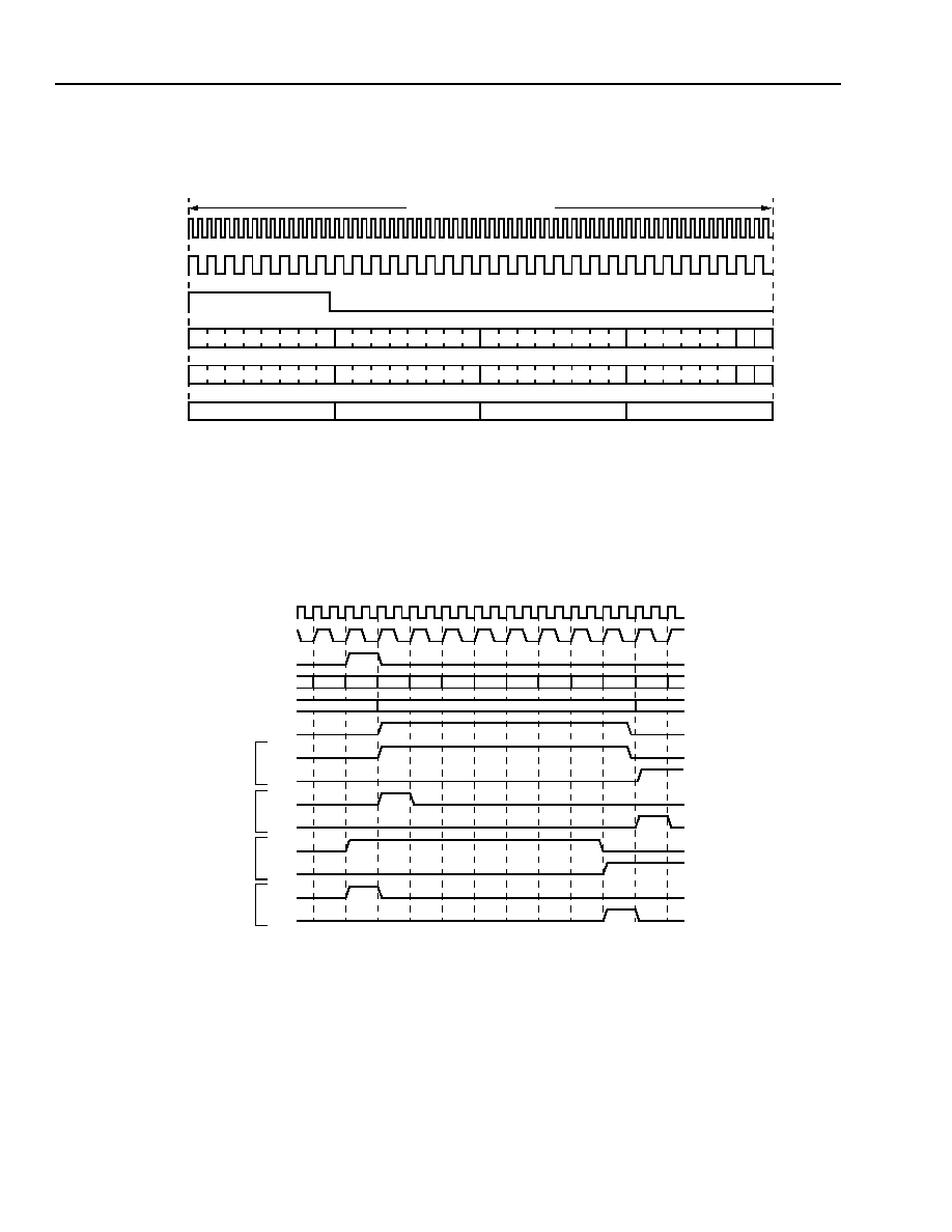
74
Lucent Technologies Inc.
Preliminary Data Sheet
November 2000
ISDN Network Termination Node (NTN) Device
T9000
10 GCI+ Interface Module
(continued)
10.3 GCI-NT Mode (GCCF[GMODE(1:0)] = 00)
(continued)
5-6721 (F)
1. Not an output. Shown only for reference.
Note: GCCF[GMODE] = 00 (GCI-NT); DCL = 512 kHz; data rate = 256 kHz.
Figure 16. GCI-NT Frame Structure
Figure 17 shows the generation of PFS1/PFS2 signals, assuming GCOF1[OFF10] = 0.
5-6718 (F)
1. Only present if programmed on GPAF1 register.
2. Not outputs. Shown only for reference.
Note: GMODE = 00; CKRATE
00; GKMODE = X; OFF1 (0) = 0.
Key:
A: PFSDEL = 0 and PFSPE = 0
B: PFSDEL = 0 and PFSPE = 1
C: PFSDEL = 1 and PFSPE = 0
D: PFSDEL = 1 and PFSPE = 1
?: Don't care
Figure 17. GCI-NT Timing Diagram
DCL
BCLK
FS1(FSC)
DD
DU
TIMESLOT
1
GCI-NT FRAME (125
µ
s)
B1
B2
MON (OUT)
C/I
A E
B1
B2
MON (IN)
C/I
A E
0
1
2
3
DCL
BCLK
1
SYNC
2
BITSLOT
2
CHANNELSLOT
2
FSC
PFS1
1
PFS2
PFS1
1
PFS2
PFS1
1
PFS2
PFS1
1
PFS2
A
B
C
D
?
?
0
1
2
3
4
5
6
7
0
1
?
0

Lucent Technologies Inc.
75
Preliminary Data Sheet
November 2000
ISDN Network Termination Node (NTN) Device
T9000
10 GCI+ Interface Module
(continued)
10.3 GCI-NT Mode (GCCF[GMODE(1:0)] = 00)
(continued)
10.3.1 GCI-SCIT Mode (GCCF, GMODE[1:0] = 01)
Figure 18 shows the frame structure for GCI-SCIT
(Special Circuit Interface-T) mode, also known as GCI-
TE mode. In this mode, the DCL clock rate is automati-
cally set to 1536 kHz, overriding the value defined by
GCCF[GRATE]. In addition, a powerdown mode is
available in which DCL is stopped (see Section 10.5,
GCI+ Powerdown Mode).
The data rate in GCI-SCIT mode is automatically set to
768 kHz, ignoring the value defined by
GCCF[CKMODE]. A total of twelve 8-bit time slots are
contained in each frame comprising three GCI chan-
nels of four time slots each. Time slots 0 and 1 carry
user data, time slot 2 is the GCI monitor (MON) chan-
nel, and time slot 3 is the GCI signaling and control
channel.
The FS1 output pin provides the frame synchronization
clock (FSC) as defined by the GCI standard. It
becomes active with the rising edge of DCL at the start
of time slot 0 and is turned off one-half of a DCL period
prior to the start of time slot 1.
In this mode, the NTN device:
s
May transfer upstream/downstream data on time
slots 0 (B1), 1 (B2), 4 (IC1), and 5 (IC2).
s
Does not provide control over MON-0 (time slot 2)
because layer-1 transceiver control is done through
the internal microcontroller bus. The downstream
monitor code will be FFh. Downstream A and E bits
for GCI channel 0 will be set to 1. Upstream data in
time slot 2 will be ignored.
s
Does not support external layer-2 devices. This
implies:
-- No data transfer is provided over GCI-D channel
(time slot 3, first and second data bits) as the
internal HDLC controller and microcontroller pro-
vide this service. Downstream data during these
2 bits will be set to 1.
-- There is no need to support GCI subchannel C/I
control on channel 0 (C/I-0). The downstream C/I
code will be Fh. The upstream C/I code will be
ignored.
-- There is no need for terminal IC (TIC) subchannel
control. The downstream TIC code will be Fh. The
upstream TIC code will be ignored.
s
Automatically manages the MON-1 channel's opera-
tion, maintenance, and data transfer (see Section
10.3.2, Monitor Message Transfer, for more details).
s
Provides control of the C/I-1 subchannel (see Sec-
tion 10.4, C/I Message Transfer, for more details).
Register GCOF1[OFF1(4:0)] controls the time slots to
which PFS1 and PFS2 are assigned. Table 79 illus-
trates the relationship between the value of
GCOF1[OFF1(4:0)] and the time-slot assignment of the
PFS1 and PFS2 signals. Note that the GCOF2 register
is ignored in GCI-NT mode.
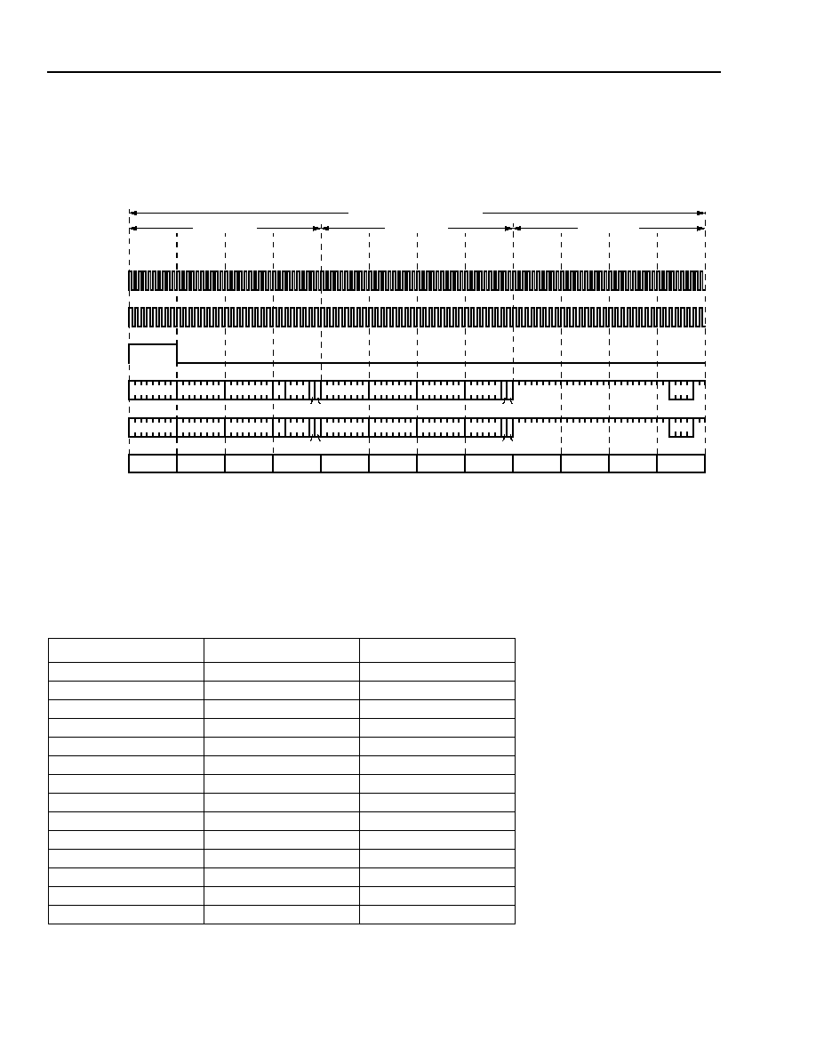
76
Lucent Technologies Inc.
Preliminary Data Sheet
November 2000
ISDN Network Termination Node (NTN) Device
T9000
10 GCI+ Interface Module
(continued)
10.3 GCI-NT Mode (GCCF[GMODE(1:0)] = 00)
(continued)
10.3.1 GCI-SCIT Mode (GCCF, GMODE[1:0] = 01) (continued)
5-6723 (F)
1. Not output. Shown only for reference.
Notes:
GCCF[GMODE] = 01 (GCI-TE)
DCL = 1536 kHz.
Data rate = 768 kHz.
Figure 18. GCI-TE Mode Frame Structure
Table 79. GCI-TE Data-Slot Association
GCOF1[OFF1(4:0)]
PFS1 Time Slot
PFS2 Time Slot
X0000
0
1
X0001
1
0
X0010
0
4
X0011
4
0
X0100
0
5
X0101
5
0
X0110
1
4
X0111
4
1
X1000
1
5
X1001
5
1
X1010
4
5
X1011
5
4
X11X0
0
1
X11X1
1
0
0
1
2
3
4
5
6
7
8
9
10
11
DCL
BCLK
PFSI(FSC)
DD
DU
CHANNEL SLOT
1
GCI-CH0
GCI-CH1
GCI-CH2
GCI-TE FRAME (125
µ
s)
B1
B2
MON-0
(OUT)
D C/I-0
A
E
IC1
IC2
MON-1
(OUT)
C/I-1
TIC
B1
B2
MON-0
(IN)
D C/I-0
A
E
IC1
IC2
MON-1
(IN)
C/I-1
TIC
A
E
A
E

Lucent Technologies Inc.
77
Preliminary Data Sheet
November 2000
ISDN Network Termination Node (NTN) Device
T9000
10 GCI+ Interface Module
(continued)
10.3 GCI-NT Mode (GCCF[GMODE(1:0)] = 00)
(continued)
10.3.2 Monitor Message Transfer
For both GCI-NT and GCI-TE modes, the NTN man-
ages the monitor channel (MON) protocol as defined
by the GCI standard. In GCI-NT mode, monitor data
transfer occurs in time slot 2 (MON-0) using the A&E
bit pair in time slot 3. In GCI-TE mode, monitor data
transfer occurs in time slot 6 (MON-1) using the A&E
bit pair in time slot 7.
Monitor messages may be one or more bytes in length.
To transmit a single byte message downstream, the
microcontroller writes the monitor byte into the GCDML
register. Once this byte is internally loaded, the GCI-
controller asserts the interrupt bit GCIR[DMRDY] indi-
cating to the microcontroller that it is ready to accept a
new message to be transmitted. If the transmission is
successfully completed, the GCI controller asserts
interrupt bit GCIR[DMEOM]. Otherwise, if the transmis-
sion has been aborted, it will assert interrupt bit
GCIR(DMABRT). Downstream monitor message
aborts may occur as a consequence of an abort
request by the downstream device or an expiration of
the GCI controller downstream timer (if
GCOF1[GTMODE] = 1).
Multibyte monitor messages operate in a similar man-
ner to single-byte messages, except that for an N-byte
message, bytes 1 to N ≠ 1 are written into register
GCDMD, and the last monitor byte is written into regis-
ter GCDML. The interrupt bit GCIR[DMRDY] is used in
both cases to signify when new downstream data may
be written to either GCDMD or GCDML.
Upstream monitor bytes, when confirmed, are trans-
ferred to the GCUMD register. Interrupt bit
GCIR[UMRDY] is asserted to indicate a new monitor
byte has been successfully received. At the completion
of an upstream message, interrupt bit GCIR[UMEOM]
is asserted. If the upstream message is aborted, the
interrupt bit GCIR [UMABRT] is asserted. Upstream
monitor message aborts may occur as a consequence
of an implicit abort produced by an invalid upstream
A&E bit pair sequence (normally produced by the
downstream device) or an expiration of the GCI con-
troller upstream timer (if GCOF1[GTMODE] = 1).
The embedded GCI controller has one timer associ-
ated with each monitor direction to avoid deadlock situ-
ations. Both timers may be enabled by setting
GCOF1[GTMODE] = 1. The downstream timer will be
started each time the transfer of a downstream monitor
byte is initiated. If the byte is not acknowledged within
four frames, the timer will expire and generate an abort
request. The upstream timer will be started upon the
detection of a new byte. If this byte is not confirmed by
the far end (because it did not detect identical bytes in
two consecutive frames--upstream RNR event) or the
byte cannot be transferred to the GCUMD register
(because the microcontroller has not yet read the previ-
ous byte--upstream RNR event), the timer will expire.
10.4 C/I Message Transfer
For both GCI-NT and GCI-TE modes, the NTN man-
ages data transfer over the command/indication chan-
nel as defined by the GCI standard. In GCI-NT mode,
C/I data transfer occurs in the first 6 bits of time slot 3
(C/I-0). In GCI-TE mode, C/I data transfer occurs in the
first 6 bits of time slot 7 (C/I-1).
To transmit a downstream C/I code, the microcontroller
writes the code into the GCDCI register. This code will
be continuously transmitted until a new code is written
to GCDCI. The internal GCI controller will not read the
new code from GCDCI until the current code has been
transferred in at least two consecutive frames.
Upstream command/indication codes are first filtered
before they are transferred to the GCUCI register. A
double last look criterion is used to validate a new C/I
code, i.e., a new code is transferred to the GCUCI reg-
ister only if it is different from the previously loaded
value and is received in two consecutive GCI frames.
Whenever this happens, the GCIR[UCIC] interrupt is
asserted.
10.5 GCI+ Powerdown Mode
The GCI+ may be placed in a powerdown mode by set-
ting GCCF[GRATE(1:0)] = 00). Prior to enabling power-
down mode, the user must set DFR[PFS1_ACT] = 0
and DFR[PFS2_ACT] = 0. While in powerdown mode,
the DCL clock signal is stopped (held low), the PFS1
and PFS2 signals are held low, and the DD signal is
3-stated.
When in powerdown, a falling edge on the DU signal
causes an assertion of the interrupt bit GCIR[GWUP].
This allows the user to write a powerup routine for the
GCI+ interface.
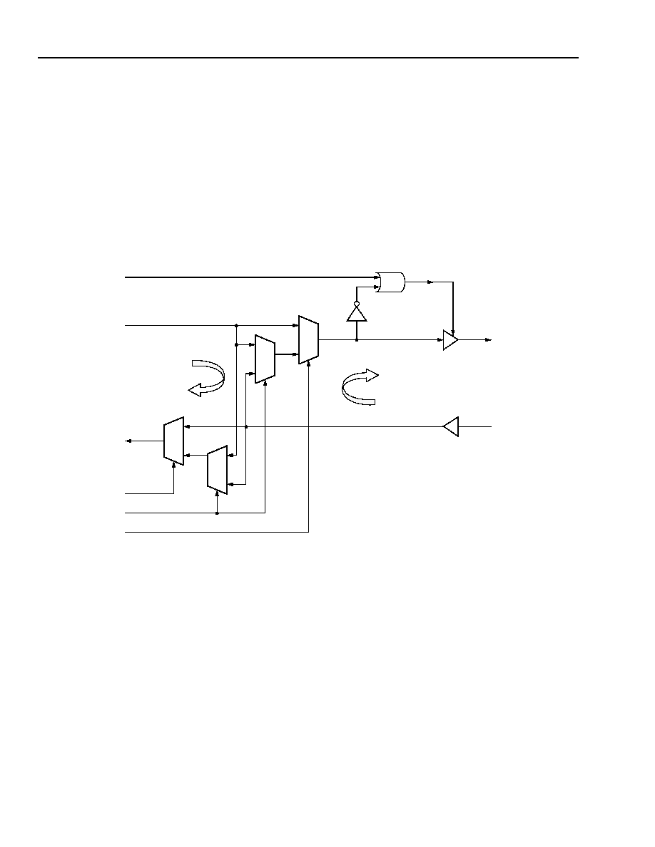
78
Lucent Technologies Inc.
Preliminary Data Sheet
November 2000
ISDN Network Termination Node (NTN) Device
T9000
10 GCI+ Interface Module
(continued)
10.6 GCI+ Loopbacks
DFR (G_L_LBK) and DFR (G_R_LBK) register bits control the loopback mode of the GCI interface.
When the DFR (G_L_LBK) register bit is set, downstream B1/B2 channel is fed back to the upstream B1/B2
channel.
When the DFR (G_R_LBK) register bit is set, upstream B1/B2 channel is fed back to the downstream B1/B2
channel.
Both loopbacks may be set at the same time. Loopbacks are transparent, except in the case when both are active
at the same time. Note that loopbacks only operate over data channels; no other channels will be looped back.
5-6724 (F)
Figure 19. GCI Loopback Logic
0
1
0
1
0
1
0
1
REMOTE LOOPBACK
LOCAL LOOPBACK
GDRIVER
DD_I
DU_I
G_L_LBK
DATA CHANNEL
G_R_LBK
DD_OE
DD
DU

Lucent Technologies Inc.
79
Preliminary Data Sheet
November 2000
ISDN Network Termination Node (NTN) Device
T9000
10 GCI+ Interface Module
(continued)
10.7 GCI+ Register Set
Table 80. GCCF: GCI+ Configuration Register (0x2E)
Reg
R/W
Bit 7
Bit 6
Bit 5
Bit 4
Bit 3
Bit 2
Bit 1
Bit 0
GCCF
R/W
GDRIVER
PFSDEL
PFSPE
CKMODE
GRATE1
GRATE0
GMODE1 GMODE0
RESET
Default
0
0
0
0
0
0
0
0
Bit #
Symbol
Name/Description
7
GDRIVER
GCI+ Driver Type. Sets the type of output driver to be used for the GCI+ signal DD.
0: Open-drain driver.
1: Push-pull driver.
6
PFSDEL
PFS Delay. Sets the relative delay between PFSx (x = 1 or x = 2) and the first data bit of
the time slot associated with PFSx.
0: PFSx rising edge is coincident with the start of the corresponding time slot.
1: PFSx rising edge occurs one bit time before the start of the corresponding time
slot.
5
PFSPE
PFS Pulse (Short Frame Sync) or Envelope (Long Frame Sync) Mode. Sets the
duration of the PFSx (x = 1 or x = 2) pulse.
0: PFS is an 8-bit envelope lasting from one time slot minus one-half of a DCL period.
1: PFS lasts for one data bit time.
4
CKMODE
GCI+ Data Clock Mode. Sets the clock mode of the GCI+ DCL clock to single or double
clock mode when in TDM mode. This bit is ignored in GCI mode.
0: DCL set to double clock mode (two clocks per data bit).
1: DCL set to single clock mode (one clock per data bit).
3--2
GRATE[1:0]
GCI+ Clock Rate. Sets the DCL clock rate when in TDM mode. In GCI mode
(GMODE[1:0] = 0x), these bits are ignored, unless they are equal to 00.
00: Clock disabled.
01: 512 kHz.
10: 1.536 MHz.
11: 2.048 MHz.
1--0
GMODE[1:0]
GCI+ Operation Mode. Sets the mode of operation of the GCI+ Interface. When in either
of the GCI modes (GMODE[1:0] = 0x), these bits override the GRATE[1:0] values, unless
GRATE[1:0] = 00.
00: GCI-NT mode.
01: GCI-TE mode.
1x: TDM mode.

80
Lucent Technologies Inc.
Preliminary Data Sheet
November 2000
ISDN Network Termination Node (NTN) Device
T9000
10 GCI+ Interface Module
(continued)
10.7 GCI+ Register Set
(continued)
Table 81. GCOF1: GCI PFS1 Offset Select (0x2F)
Table 82. GCOF2: GCI PFS2 Offset Select (0x30)
Reg
R/W
Bit 7
Bit 6
Bit 5
Bit 4
Bit 3
Bit 2
Bit 1
Bit 0
GCOF1
R/W
GTMODE G_R_LBK G_L_LBK
OFF14
OFF13
OFF12
OFF11
OFF10
RESET
Default
0
0
0
0
0
0
0
0
Bit #
Symbol
Name/Description
7
GTMODE
GCI Time-Out Mode. (Only Applicable on GCI-NT and GCI-TE Operation Modes.)
Enables the GCI time-out mechanism.
0: Time-out mechanism disabled.
1: Time-out mechanism enabled (abort after three TNR or RNRs), (0.5 ms since the
beginning of transmission).
6
G_R_LBK
GCI Remote Loopback.
0: Normal operation.
1: Upstream B1- and B2-channel data on the GCI is internally looped back to the
downstream GCI. Loopback is transparent, except when G_L_LBK is asserted at
the same time.
5
G_L_LBK
GCI Local Loopback.
0: Normal operation.
1: Downstream B1- and B2-channel data on the GCI is internally looped back to the
upstream GCI. Loopback is transparent, except when G_R_LBK is asserted at the
same time.
4--0
OFF1[4:0]
Offset of PS1. Determines the number of channel slots by which PFS1 (B1 channel) is
offset from the first time slot of the frame.
Reg
R/W
Bit 7
Bit 6
Bit 5
Bit 4
Bit 3
Bit 2
Bit 1
Bit 0
GCOF2
R/W
U_FORCE_B2DN U_FORCE_B1DN
--
OFF24 OFF23 OFF22 OFF21 OFF20
RESET
Default
0
0
0
0
0
0
0
0
Bit #
Symbol
Name/Description
7
U_FORCE_B2DN Microcontroller Access to Downstream B2 Channel. When this bit is set, the
microcontroller can access the downstream B2-channel data from the U-interface to
the GCI via the register B2DN (0x54) assuming that DFR[B2_SEL] = 1 and
ECR0[LB2] = 0.
6
U_FORCE_B1DN Microcontroller Access to Downstream B1 Channel. When this bit is set, the
microcontroller can access the downstream B1-channel data from the U-interface to
the GCI via the register B1DN (0x53) assuming that DFR[B1_SEL] = 1 and
ECR0[LB1] = 0.
5
--
Reserved. Program to 0.
4--0
OFF2[4:0]
OFFSET of PFS2. Determines the number of time slots by which PFS2 (B2-channel)
is offset from the first time slot of the frame.

Lucent Technologies Inc.
81
Preliminary Data Sheet
November 2000
ISDN Network Termination Node (NTN) Device
T9000
10 GCI+ Interface Module
(continued)
10.7 GCI+ Register Set
(continued)
The following registers are only relevant in GCI mode, with the exception of GCIR[GWUP] and GCIE[GWUPE].
Table 83. GCDMD: GCI Downstream (Transmit) Monitor Data (0x31)
Table 84. GCDML: GCI Downstream (Transmit) Monitor Data Last (0x32)
Table 85. GCUMD: GCI Upstream (Receive) Monitor Data (0x33)
Reg
R/W
Bit 7
Bit 6
Bit 5
Bit 4
Bit 3
Bit 2
Bit 1
Bit 0
GCDMD
W
DMD7
DMD6
DMD5
DMD4
DMD3
DMD2
DMD1
DMD0
RESET
Default
1
1
1
1
1
1
1
1
Bit #
Symbol
Name/Description
7--0
DMD[7:0] Downstream Monitor Data. For any multibyte monitor message, all message bytes except
the last one are written to this register for transmission on the downstream monitor channel
(see Section 10.3.2, Monitor Message Transfer). The DMRDY interrupt bit provides an indica-
tion that a new byte may be loaded.
Reg
R/W
Bit 7
Bit 6
Bit 5
Bit 4
Bit 3
Bit 2
Bit 1
Bit 0
GCDML
W
DML7
DML6
DML5
DML4
DML3
DML2
DML1
DML0
RESET
Default
1
1
1
1
1
1
1
1
Bit #
Symbol
Name/Description
7--0
DML[7:0] Downstream Monitor Last. The last byte of a downstream monitor message is written to this
register for transmission on downstream monitor channel (see Section 10.3.2, Monitor Mes-
sage Transfer). The DMRDY interrupt bit provides an indication that a new byte may be
loaded.
Reg
R/W
Bit 7
Bit 6
Bit 5
Bit 4
Bit 3
Bit 2
Bit 1
Bit 0
GCUMD
W
UMD7
UMD6
UMD5
UMD4
UMD3
UMD2
UMD1
UMD0
RESET
Default
--
--
--
--
--
--
--
--
Bit #
Symbol
Name/Description
7--0
UMD[7:0]
Upstream Monitor Channel Received Data. The most recent successfully received byte
of an upstream monitor message is made available in this register (see Section 10.3.2,
Monitor Message Transfer). The UMRDY interrupt bit provides an indication that a new
byte has been received.

82
Lucent Technologies Inc.
Preliminary Data Sheet
November 2000
ISDN Network Termination Node (NTN) Device
T9000
10 GCI+ Interface Module
(continued)
10.7 GCI+ Register Set
(continued)
Table 86. GCDCI: GCI Downstream (Transmit) C/I Data (0x34)
Table 87. GCUCI: GCI Upstream (Receive) C/I Data (0x35)
Reg
R/W
Bit 7
Bit 6
Bit 5
Bit 4
Bit 3
Bit 2
Bit 1
Bit 0
GCDCI
R/W
--
--
DCI6
DCI5
DCI4
DCI3
DCI2
DCI1
RESET
Default
0
0
--
--
--
--
--
--
Bit #
Symbol
Name/Description
7--6
--
Reserved. Program to 0.
5--0
DCI[6:1] Downstream Command/Indication Code. The microcontroller writes the desired down-
stream (transmit) C/I code to this register. The code will be continuously transmitted until a new
code is written. The internal GCI controller will not read the new code from the GCDCI until the
current code has been transferred in at least two consecutive frames (see Section 10.4, C/I
Message Transfer).
Reg
R/W
Bit 7
Bit 6
Bit 5
Bit 4
Bit 3
Bit 2
Bit 1
Bit 0
GCUCI
R/W
--
--
UCI6
UCI5
UCI4
UCI3
UCI2
UCI1
RESET
Default
0
0
--
--
--
--
--
--
Bit #
Symbol
Name/Description
7--6
--
Reserved. Program to 0.
5--0
UCI[6:1]
Upstream Command/Indication Code. Validated upstream (receive) C/I codes are stored
here. The validation circuit employs a double last look criterion, i.e., a new code is transferred
to the GCUCI register only if it is different from the previously loaded value and is received in
two consecutive GCI frames. The UCIC interrupt bit provides an indication that a new vali-
dated byte has been received.

Lucent Technologies Inc.
83
Preliminary Data Sheet
November 2000
ISDN Network Termination Node (NTN) Device
T9000
10 GCI+ Interface Module
(continued)
10.7 GCI+ Register Set
(continued)
Table 88. GCIR: GCI Interrupt Register (0x36)
Note: All bits in this register are set to 1 upon occurrence of the corresponding interrupt condition, and are cleared
to 0 when the register is read.
Reg
R/W
Bit 7
Bit 6
Bit 5
Bit 4
Bit 3
Bit 2
Bit 1
Bit 0
GCIR
R
GWUP
UCIC
UMRDY
UMEOM
UMABRT
DMRDY
DMEOM
DMABRT
RESET
Default
0
0
0
0
0
0
0
0
Bit #
Symbol
Name/Description
7
GWUP
GCI Wake-Up Interrupt. This interrupt occurs when the following two conditions are true:
1. GCI clocks are stopped (GCCF[GRATE(1:0)] = 00).
2. A falling edge of DU occurs.
6
UCIC
Upstream Command/Indication Change. This interrupt occurs upon the reception of a
new, validated C/I code in register GCUCI. At reset, the internal C/I code is set to 111111.
5
UMRDY
Upstream Monitor Byte Ready. This interrupt occurs when a newly received monitor byte
is available in register GCUMD.
4
UMEOM
Upstream Monitor End of Message. This interrupt occurs when the last byte of a monitor
message has been successfully received.
3
UMABRT
Upstream Monitor Aborted. This interrupt occurs when an abort has been detected in the
received monitor message.
2
DMRDY
Downstream Monitor Ready. This interrupt occurs to indicate that the downstream monitor
buffer is empty and a new byte may be loaded into GCDMD or GCDML.
1
DMEOM
Downstream End of Message. This interrupt occurs when the far end acknowledges the
successful reception of the last byte of a downstream message.
0
DMABRT
Downstream Monitor Aborted. This signal is asserted when, during the transmission of a
downstream monitor message, a request to abort has been received from the downstream
device.

84
Lucent Technologies Inc.
Preliminary Data Sheet
November 2000
ISDN Network Termination Node (NTN) Device
T9000
10 GCI+ Interface Module
(continued)
10.7 GCI+ Register Set
(continued)
Table 89. GCIE: GCI Interrupt Enable (0x37)
Reg
R/W
Bit 7
Bit 6
Bit 5
Bit 4
Bit 3
Bit 2
Bit 1
Bit 0
GCIE
R
GWUPE
UCICE
UMRDYE UMEOME UMABRTE DMRDYE DMEOME DMABRTE
RESET
Default
0
0
0
0
0
0
0
0
Bit #
Symbol
Name/Description
7
GWUPE
GCI Wake-Up Interrupt Enable.
0: Interrupt disabled.
1: Interrupt enabled.
6
UCICE
UCIC Interrupt Enable.
0: Interrupt disabled.
1: Interrupt enabled.
5
UMRDYE
UMRDY Interrupt Enable.
0: Interrupt disabled.
1: Interrupt enabled.
4
UMEOME
UMEOM Interrupt Enable.
0: Interrupt disabled.
1: Interrupt enabled.
3
UMABRTE
UMABRT Interrupt Enable.
0: Interrupt disabled.
1: Interrupt enabled.
2
DMRDYE
DMRDY Interrupt Enable.
0: Interrupt disabled.
1: Interrupt enabled.
1
DMEOME
DMEOM Interrupt Enable.
0: Interrupt disabled.
1: Interrupt enabled.
0
DMABRTE
DMABRT Interrupt Enable.
0: Interrupt disabled.
1: Interrupt enabled.

Lucent Technologies Inc.
85
Preliminary Data Sheet
November 2000
ISDN Network Termination Node (NTN) Device
T9000
11 GPIO Ports
Three general-purpose input/output ports are available
on the T9000 device with each port being 8 bits wide.
For any port, each signal may be individually config-
ured as an input or as an output by proper program-
ming of registers GPDIR[0:2]. On reset, all ports are
configured as inputs.
All GPIO signals have a weak pull-up resistor of
100 k
(nominal value). Unneeded GPIO signals
should be configured as inputs, and may be left uncon-
nected. If connected on the board, it is recommended
that they be tied to V
DD
to avoid power consumption.
Registers GPD[0:2] contain the value on the GPIO pin.
For GPIO pins configured as inputs, the microcontroller
accesses the port value by reading its corresponding
GPD register. For GPIO pins configured as outputs, the
microcontroller writes the desired value into its corre-
sponding GPD register.
GPIO0.[3:0] and GPIO1.[3:0] pins, when configured as
inputs (see registers GPDIR0 and GPDIR1), may also
be configured as level-activated or transition-activated
external interrupt sources for the microcontroller (see
registers GPPOL and GPLEI). Any of these eight exter-
nal interrupt sources may be masked by proper pro-
gramming of register GPIE. On module reset, all
interrupts are disabled. GPIO interrupt register (GPIR)
is cleared when read by the microcontroller.
GPIO0.[3:0] and GPIO1.[3:0] pins, when configured as
inputs, present a Schmitt trigger buffer for better noise
immunity.
GPAF0 and GPAF1 registers define alternate functional
modes for some GPIO pins.
s
GPAF0[GPAF0.(7:6)] register bits, when set, override
GPDIR0 [DIR0.(7:6)] and configure GPIO0.[7:6] as
the PWM 1 output.
s
GPAF0[GPAF0.(5:4)] register bits, when set, override
GPDIR0[DIR0.(5:4)] and configure GPIO0.[5:4] as
PWM0 outputs.
s
GPAF1[GPAF1.(7:5)] register bits, when set, override
GPDIR[DIR1.(7:5)] and configure GPIO1.[7:5] as
input trigger sources for timers 2, 1, and 0 (for proper
timer operation, the microcontroller should also con-
figure the associated SFR register bit for each timer).
s
GPAF1[GPAF2.3] register bit, when set, overrides
the GPDIR2[DIR2.3] register bit and configures
GPIO2.3 as a SYNCO output from the dc/dc module
(see Section 13, dc/dc Control Generator).
s
GPAF1[GPAF2.2] register bit, when set, overrides
the GPDIR2[DIR2.2] register bit and configures
GPIO2.2 as the reference frame sync clock (FSC)
output as specified in Section 10, GCI+ Interface
Module.
s
GPAF1[GPAF2.1] register bit, when set, overrides
the GPDIR2[DIR2.1] register bit and configures
GPIO2.1 as the GCI bit clock (BCLK) output (as
specified in Section 10, GCI+ Interface Module).
s
GPAF1[GPRESET] provides a nonlatching software
reset of the GPIO module. It has the same effect as a
global reset or a global software reset.
s
DOCR[LT_NT] register bit, when set, ignores
GPDIR2[DIR2.6] and configures GPIO2.6 as the
input for 8 kHz master transmit clock (MTC) signal.
s
When the test pin (pin 43) is asserted, GPIO1.4 and
GPIO2.7 change their functions to USSP_E and
PTLB_S, respectively, as explained in Table 4.
All registers are read/write to allow read-modify-write
operations by the microcontroller. Transition activated
interrupt sources may be individually reset by writing a
1 to the associated bits of GPPOL register.
All GPIO port signals are TTL levels. Driving capability
is 6 mA for GPIO2.0 signal and 1 mA for all others.
Figure 20 summarizes features available for all GPIO
signals.
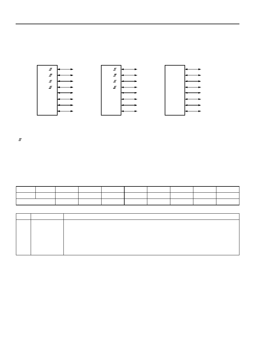
86
Lucent Technologies Inc.
Preliminary Data Sheet
November 2000
ISDN Network Termination Node (NTN) Device
T9000
11 GPIO Ports
(continued)
Note: Alternate pin functions, shown in parentheses (), are selected when the TEST pin is asserted.
Alternate pin functions, shown in brackets [], are selected when the corresponding register bits are set.
5-6529F.c
Figure 20. GPIO Pin Capabilities Summary
11.1 GPIO Register Set
Table 90. GPDIR0: GPIO Port 0 Pin Direction (0x38)
Reg
R/W
Bit 7
Bit 6
Bit 5
Bit 4
Bit 3
Bit 2
Bit 1
Bit 0
GPDIR0
R/W
DIR0.7
DIR0.6
DIR0.5
DIR0.4
DIR0.3
DIR0.2
DIR0.1
DIR0.0
RESET
Default
1
1
1
1
1
1
1
1
Bit #
Symbol
Name/Description
7--0
DIR0.[7:0]
GPIO0.[7:0] Pin Direction.
0: Output.
1: Input.
Note: When any of bits 7:4 in register GPAF0 are set, the corresponding DIR0.x value in
this register is ignored and the pin function is determined according to the GPAF0
register function.
.0
.1
.2
.3
.4
.5
.6
.7
[PWMO00]
[PWMO01]
[PWMO10]
[PWMO11]
GPIO0
.0
.1
.2
.3
.4
.5
.6
.7
[T0]
[T1]
[T2]
GPIO1
.0
.1
.2
.3
.4
.5
.6
[BCLK]
[FSC]
[SYNCO]
GPIO2 .7
(USSP_E)
[MTC]
(PTLB_S)
: External interrupt capability.
: Optional trigger sources for timers.
: 6 mA sink capability.
: Schmitt trigger when inputs.
LEGEND:

Lucent Technologies Inc.
87
Preliminary Data Sheet
November 2000
ISDN Network Termination Node (NTN) Device
T9000
11 GPIO Ports
(continued)
11.1 GPIO Register Set
(continued)
Table 91. GPDIR1: GPIO Port 1 Pin Direction (0x39)
Table 92. GPDIR2: GPIO Port 2 Pin Direction (0x3A)
Reg
R/W
Bit 7
Bit 6
Bit 5
Bit 4
Bit 3
Bit 2
Bit 1
Bit 0
GPDIR1
R/W
DIR1.7
DIR1.6
DIR1.5
DIR1.4
DIR1.3
DIR1.2
DIR1.1
DIR1.0
RESET
Default
1
1
1
1
1
1
1
1
Bit #
Symbol
Name/Description
7--0
DIR1.[7:0]
GPIO1.[7:0] Pin Direction.
0: Output.
1: Input.
Note: When any of bits 7:5 in register GPAF1 are set, the corresponding DIR1.x value in
this register is ignored and the pin function is determined according to the GPAF1
register function.
Reg
R/W
Bit 7
Bit 6
Bit 5
Bit 4
Bit 3
Bit 2
Bit 1
Bit 0
GPDIR2
R/W
DIR2.7
DIR2.6
DIR2.5
DIR2.4
DIR2.3
DIR2.2
DIR2.1
DIR2.0
RESET
Default
1
1
1
1
1
1
1
1
Bit #
Symbol
Name/Description
7--0
DIR2.[7:0]
GPIO2.[7:0] Pin Direction. DIR2.x defines the pin direction for GPIO2.x.
0: Output.
1: Input.
Notes: When any of bits 3:1 in register GPAF1 are set, the corresponding DIR2.x value
in this register is ignored and the pin function is determined according to the
GPAF1 register function.
When DOCR[LT_NT] bit is set to 1 (NTN device is in LT mode), the DIR2.6 value
is ignored and pin GPIO2.6 becomes an input to the 8 kHz MTC signal.

88
Lucent Technologies Inc.
Preliminary Data Sheet
November 2000
ISDN Network Termination Node (NTN) Device
T9000
11 GPIO Ports
(continued)
11.1 GPIO Register Set
(continued)
Table 93. GPAF0: GPIO Alternate Function Register #0 (0x3B)
Reg
R/W
Bit 7
Bit 6
Bit 5
Bit 4
Bit 3
Bit 2
Bit 1
Bit 0
GPAF0
R/W
GPAF0.7
GPAF0.6
GPAF0.5
GPAF0.4
--
--
--
--
RESET
Default
0
0
0
0
0
0
0
0
Bit #
Symbol
Name/Description
7
GPAF0.7
GPIO0.7 Alternate Function Selection.
0: No effect on device operation.
1: Overrides GPDIR[DIR0.7]. GPIO0.7 is configured as output #1 of the PWM
module #1.
6
GPAF0.6
GPIO0.6 Alternate Function Selection.
0: No effect on device operation.
1: Overrides GPDIR0[DIR0.6]. GPIO0.6 is configured as output #0 of the PWM
module #1.
5
GPAF0.5
GPIO0.5 Alternate Function Selection.
0: No effect on device operation.
1: Overrides GPDIR0[DIR0.5]. GPIO0.5 is configured as output #1 of the PWM
module #0.
4
GPAF0.4
GPIO0.4 Alternate Function Selection.
0: No effect on device operation.
1: Overrides GPDIR0[DIR0.4]. GPIO0.4 is configured as output #0 of the PWM
module #0.
3--0
--
Reserved. Program to 0.

Lucent Technologies Inc.
89
Preliminary Data Sheet
November 2000
ISDN Network Termination Node (NTN) Device
T9000
11 GPIO Ports
(continued)
11.1 GPIO Register Set
(continued)
Table 94. GPAF1: GPIO Alternate Function Register #1 (0x3C)
Table 95. GPD0: GPIO Port 0 Data Register (0x3D)
Reg
R/W
Bit 7
Bit 6
Bit 5
Bit 4
Bit 3
Bit 2
Bit 1
Bit 0
GPAF1
R/W
GPAF1.7 GPAF1.6 GPAF1.5
--
GPAF2.3
GPAF2.2
GPAF2.1
GPRESET
RESET
Default
0
0
0
0
0
0
0
0
Bit #
Symbol
Name/Description
7
GPAF1.7
GPIO1.7 Alternate Function Selection.
0: No effect on device operation.
1: Overrides GPDIR1[DIR1.7] value. GPIO1.7 is configured as the timer 2 external
input (connects directly to P1.0 of the microcontroller module).
6
GPAF1.6
GPIO1.6 Alternate Function Selection.
0: No effect on device operation.
1: Overrides GPDIR1[DIR1.6] value. GPIO1.6 is configured as the timer 1 external
input (connects directly to P3.5 of the microcontroller module).
5
GPAF1.5
GPIO1.5 Alternate Function Selection.
0: No effect on device operation.
1: Overrides GPDIR1[DIR1.5] value. GPIO1.5 is configured as the timer 0 external
input (connects directly to P3.4 of the microcontroller module).
4
--
Reserved. Program to 0.
3
GPAF2.3
GPIO2.3 Alternate Function Selection.
0: No effect on device operation.
1: Overrides GPDIR2[DIR2.3] value. GPIO2.3 is configured as the SYNCO output from
the dc/dc module.
2
GPAF2.2
GPIO2.2 Alternate Function Selection.
0: No effect on device operation.
1: Overrides GPDIR2[DIR2.2] value. GPIO2.2 is configured as the FSC output from the
GCI module.
1
GPAF2.1
GPIO2.1 Alternate Function Selection.
0: No effect on device operation.
1: Overrides GPDIR2[DIR2.1] value. GPIO2.1 is configured as the BCLK output from
the GCI module.
0
GPRESET
GPIO Reset. Resets all the GPIO bits.
Reg
R/W
Bit 7
Bit 6
Bit 5
Bit 4
Bit 3
Bit 2
Bit 1
Bit 0
GPD0
R/W
GPD0.7
GPD0.6
GPD0.5
GPD0.4
GPD0.3
GPD0.2
GPD0.1
GPD0.0
RESET
Default
0
0
0
0
0
0
0
0
Bit #
Symbol
Name/Description
7--0
GPD0.[7:0]
I/O Data on GPIO Port 0.

90
Lucent Technologies Inc.
Preliminary Data Sheet
November 2000
ISDN Network Termination Node (NTN) Device
T9000
11 GPIO Ports
(continued)
11.1 GPIO Register Set
(continued)
Table 96. GPD1: GPIO Port 1 Data Register (0x3E)
Table 97. GPD2: GPIO Port 2 Data Register (0x3F)
Table 98. GPLEI: GPIO Level-Edge-Triggered Interrupt Control (0x40)
Reg
R/W
Bit 7
Bit 6
Bit 5
Bit 4
Bit 3
Bit 2
Bit 1
Bit 0
GPD1
R/W
GPD1.7
GPD1.6
GPD1.5
GPD1.4
GPD1.3
GPD1.2
GPD1.1
GPD1.0
RESET
Default
0
0
0
0
0
0
0
0
Bit #
Symbol
Name/Description
7--0
GPD1.[7:0]
I/O Data on GPIO Port 1.
Reg
R/W
Bit 7
Bit 6
Bit 5
Bit 4
Bit 3
Bit 2
Bit 1
Bit 0
GPD2
R/W
GPD2.7
GPD2.6
GPD2.5
GPD2.4
GPD2.3
GPD2.2
GPD2.1
GPD2.0
RESET
Default
0
0
0
0
0
0
0
0
Bit #
Symbol
Name/Description
7--0
GPD2.[7:0]
I/O Data on GPIO Port 2.
Reg
R/W
Bit 7
Bit 6
Bit 5
Bit 4
Bit 3
Bit 2
Bit 1
Bit 0
GPLEI
R/W
ILE1.3
ILE1.2
ILE1.1
ILE1.0
ILE0.3
ILE0.2
ILE0.1
ILE0.0
RESET
Default
1
1
1
1
1
1
1
1
Bit #
Symbol
Name/Description
7--4
ILE1.[3:0]
Level/Edge Interrupt Control for GPIO1.[3:0]. Only applicable when pin is in input
mode (see register GPDIR1). ILE1.x defines the interrupt mechanism for GPIO1.x pin.
0: Level-triggered.
1: Edge-triggered.
3--0
ILE0.[3:0]
Level/Transition Interrupt Control for GPIO0.[3:0]. Only applicable when pin is in input
mode (see register GPDIR0). ILE0.x defines the interrupt mechanism for GPIO0.x.
0: Level-triggered.
1: Edge-triggered.

Lucent Technologies Inc.
91
Preliminary Data Sheet
November 2000
ISDN Network Termination Node (NTN) Device
T9000
11 GPIO Ports
(continued)
11.1 GPIO Register Set
(continued)
Table 99. GPPOL: GPIO Interrupt Polarity Control (0x41)
Table 100. GPIR: GPIO Interrupt Register (0x42)
Note: All bits in this register are set to 1 upon occurrence of the corresponding interrupt condition and are cleared
to 0 when the register is read, except in level-triggering mode. When in level-triggering mode, this register is
cleared when read only if the source of the interrupt has been taken away. They are also cleared upon writ-
ing a one to the corresponding bits in GPPOL registers.
Reg
R/W
Bit 7
Bit 6
Bit 5
Bit 4
Bit 3
Bit 2
Bit 1
Bit 0
GPPOL
R/W
IPOL1.3
IPOL1.2
IPOL1.1
IPOL1.0
IPOL0.3
IPOL0.2
IPOL0.1
IPOL0.0
RESET
Default
1
1
1
1
1
1
1
1
Bit #
Symbol
Name/Description
7--4
IPOL1.[3:0]
Interrupt Polarity for GPIO1.[3:0] Pins. Only applicable when pin is an input (see regis-
ter GPDIR1). IPOL1.x specifies value of GPIO1.x that generates an interrupt.
0: Level-triggered => Interrupt when level is 0.
Edge-triggered => Interrupt on falling edge.
1: Level-triggered => Interrupt when level is 1.
Edge-triggered => Interrupt on rising edge.
3--0
IPOL0.[3:0]
Interrupt Polarity for GPIO0.[3:0] Pins. Only applicable when pin is an input (see regis-
ter GPDIR0). IPOL0.x specifies value of GPIO0.x that generates an interrupt.
0: Level-triggered => Interrupt when level is 0.
Edge-triggered => Interrupt on falling edge.
1: Level-triggered => Interrupt when level is 1.
Edge-triggered => Interrupt on rising edge.
Reg
R/W
Bit 7
Bit 6
Bit 5
Bit 4
Bit 3
Bit 2
Bit 1
Bit 0
GPIR
R/W
GPI1.3
GPI1.2
GPI1.1
GPI1.0
GPI0.3
GPI0.2
GPI0.1
GPI0.0
RESET
Default
--
--
--
--
--
--
--
--
Bit #
Symbol
Name/Description
7--4
GPIx.[3:0]
GPIO1.x Interrupt. This interrupt occurs when the appropriate edge or level, as deter-
mined by the GPLEI and GPPOL registers, has been sensed on the corresponding GPIO
pin.
3--0
GPIx.[3:0]
GPIO0.x Interrupt. This interrupt occurs when the appropriate edge or level, as deter-
mined by the GPLEI and GPPOL registers, has been sensed on the corresponding GPIO
pin.

92
Lucent Technologies Inc.
Preliminary Data Sheet
November 2000
ISDN Network Termination Node (NTN) Device
T9000
11 GPIO Ports
(continued)
11.1 GPIO Register Set
(continued)
Table 101. GPIE: GPIO Interrupt Enable (0x43)
Reg
R/W
Bit 7
Bit 6
Bit 5
Bit 4
Bit 3
Bit 2
Bit 1
Bit 0
GPIE
R/W
GPIE13
GPIE12
GPIE11
GPIE10
GPIE03
GPIE02
GPIE01
GPIE00
RESET
Default
0
0
0
0
0
0
0
0
Bit #
Symbol
Name/Description
7--4
GPIE1.[3:0]
GPIO1.x Interrupt Enable.
0: Interrupt disabled.
1: Interrupt enabled.
3--0
GPIE0.[3:0]
GPIO0.x Interrupt Enable.
0: Interrupt disabled.
1: Interrupt enabled.
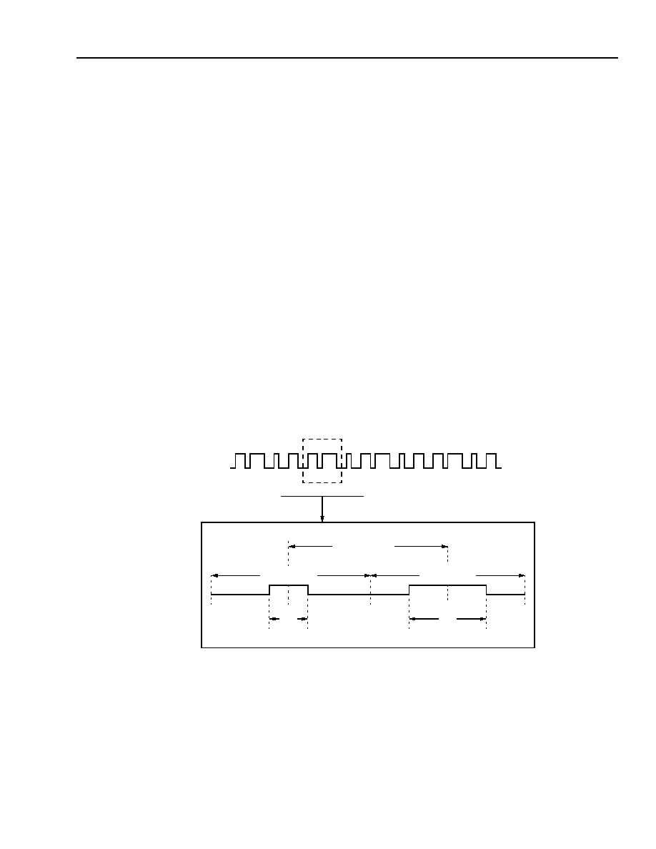
Lucent Technologies Inc.
93
Preliminary Data Sheet
November 2000
ISDN Network Termination Node (NTN) Device
T9000
12 PWM Module
The PWM module is comprised of a general-purpose dual pulse-width modulator with sine modulation capability.
Each module is capable of generating a sequence of pulses of programmable width and period. The generated
pulses are centered in the programmed period. Figure 21 illustrates a general case of the PWM output signal for
the two PWM generators. Normally, the pulse period is determined ahead of time and does not change during the
pulse train generation. Pulse-width values change according to the user's desired algorithm.
In POTS applications, pulse-width modulated signals are typically used for generation of:
s
Call alert signals (20 Hz to 30 Hz typical)
s
Billing signals (50 Hz and 12 kHz typical)
s
Answering machine control signals (2 kHz typical)
s
Identification tones (697 Hz to 2 kHz)
In these applications, the width of the PWM signal is modulated according to the amplitude of a sine wave sampled
at pulse period intervals. The PWM signal is then low-pass filtered with a simple RC integrator.
There are three configuration registers per PWM generator: PWxCF, PWxVH, and PWxVL, where x = 0 or 1. In
addition, there is a common PWM interrupt register (PWIR) shared by both generators. Both generators are identi-
cal, so references to these registers in the explanation that follows will simply use x in place of 0 or 1 in the register
names.
Each PWM output can be made available on two separate GPIO pins according to the programming of register bits
GPAF0.[7:4]. This allows the same PWMO to drive two different external devices by proper programming of regis-
ter GPAF0.[7:4]. For example, the outputs of PWMO (PWMO00 and PWMO01) can drive two external devices and
the outputs of PWM1 (PWMO10 and PWMO11) can also drive 2 different external devices.
5-6522F
Figure 21. Pulse-Width Modulated Output Signal
PWM
SEE DETAIL BELOW
RANGE
◊
TICK
RANGE
◊
TICK
RANGE
◊
TICK
PW
PWM
PW

94
94
Lucent Technologies Inc.
Preliminary Data Sheet
November 2000
ISDN Network Termination Node (NTN) Device
T9000
12 PWM Module
(continued)
For low-frequency tones (Hz range), the algorithm that
defines the width of the pulse is easily accomplished
with microcontroller routines (manual mode). However,
implementing higher frequency tones (kHz range)
requires a large degree of microcontroller intervention.
To address this issue, the PWM generators were
designed to operate in two different modes: manual/
timer mode and auto mode.
12.1 PWM Manual/Timer Operation Mode
In manual mode, the user may implement any desired
algorithm to define the width of the pulses. Two impor-
tant parameters that are controlled via the PWxCF reg-
ister are pulse-width granularity and pulse-width range.
Pulse-width granularity defines the minimum duration
(or tick) of a pulse width. Pulse-width range denotes
the number of possible ticks in a pulse period or, in
other words, the number of different width values with
which the pulse can be modulated. The tick size and
pulse period may be expressed as:
Tick = Granularity x 65 ns
(1)
PP = Range x Tick = Range x Granularity x 65 ns
(2)
Concerning the above relationships, note the following:
s
A small granularity allows for a finer resolution of the
resulting output signal in time, and therefore requires
less filtering.
s
A large range allows for a finer resolution, in ampli-
tude, of the resulting output signal.
s
Power consumption is roughly inversely proportional
to the granularity value, so the larger the granularity,
the less power the circuit will consume.
s
As granularity and range are increased, the equiva-
lent oversampling rate is decreased (i.e., the pulse
period, PP, increases as shown in equation 2 above).
At the start of a pulse period, the controller loads the
value contained in register PWxVH and generates a
pulse with a width PWxVH multiplied by the tick value
(where only the appropriate MSBs of PWxVH are used
according to the tick value, see register PWxVH). The
value in PWxVL determines the rate at which the
PWIR[PWxI] interrupt register bit will be asserted. The
module asserts the PWIR (PWxI) interrupt register bit
every PWxVL + 1 pulse period intervals. The interrupt
is generated only if the PWxCF (PWxIE) bit is set. The
interrupt is asserted even if GPIO pin is not assigned to
the PWMx generator. The interrupt register is reset
upon a register read operation.
12.2 PWM Auto Operation (Sine) Mode
The auto mode uses a sine modulator controller
(PWSM) to substantially reduce the overhead require-
ment of the microcontroller. In this mode, the width of
the pulses automatically follows the amplitude of a sine
wave of frequency Fs. A 256-byte ROM is used to store
discrete values of amplitude for one period of a sine
wave, where each successive ROM location, n,
represents the sine amplitude at a normalized time
of t = n/256.
Figure 22 shows a simplified architecture of the PWM
block (the shaded areas indicate the extra logic
required for implementing the sine wave functionality).
The 8-bit ROM address is derived from the upper 8 bits
of the 16-bit accumulator output. The accumulator sim-
ply adds the 16-bit value formed by the PWxVH and
PWxVL registers (PWV) to its output every cycle,
where the cycle time is determined by the pulse period,
PP. Consider then, how PWV and PP affect the output.
When PWV is <2
8
, each ROM value will be output for a
least one cycle, and possibly even more (depending on
how far below 2
8
the PWV value is). Conversely, when
PWV is >2
8
, some ROM values will be skipped. Thus,
as the value of PWV drops below 2
8
, it has the effect
of increasing the quantization error in the amplitude of
the sinewave output. PWV, then, can be thought of as
controlling the ROM step size (where the step size can
be <1).
When PP is large, the rate at which each newly formed
ROM address is output is slower than when PP is
small. Therefore, if all other factors are equal, a larger
PP will result in a lower frequency sinewave output. PP,
then, can be thought of as controlling the ROM step
rate.
In auto mode, range and granularity take on a some-
what different meaning than in manual mode. In auto
mode, Equations (1) and (2) still hold with respect to
range and granularity, but tick does not play a direct
role in this case. Rather, it is the combination of range
and granularity that determines the frequency and
amplitude resolution of the output waveform as
explained above.
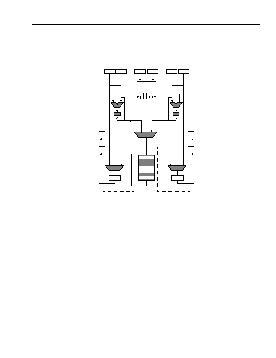
Lucent Technologies Inc.
95
Preliminary Data Sheet
November 2000
ISDN Network Termination Node (NTN) Device
T9000
12 PWM Module
(continued)
12.2 PWM Auto Operation (Sine) Mode
(continued)
5-7204F
Figure 22. PWMCNTRL Architecture
INTERFACE
WITH
PWSM1
PW1VH PW1VL
PW1CF
PW0CF
TIME BASE
GENERATOR
WIDTH1
ACCUM1[15:8]
INTERFACE
WITH
PWSM0
PW0VL PW0VH
WIDTH0
ACCUM0[15:8]
ACCUM1[15:0]
ACCUM0[15:0]
ADDRESS
PWMROM
(256 x 8)
DATA_OUT
PW1V
PW0V

96
Lucent Technologies Inc.
Preliminary Data Sheet
November 2000
ISDN Network Termination Node (NTN) Device
T9000
12 PWM Module
(continued)
12.3 PWSM ROM
As mentioned previously, the ROM shown in Figure 22 is used to store the amplitude values of one complete cycle
of a sine wave. The ROM address generated by the accumulator determines the current ROM output value. The
sine amplitudes in the ROM represent a sine wave with a 2.5%--97.5% scale and a dc offset of 128 (out of 256).
The values can be expressed by the following formula:
W(A) = ROUND (128 x [1 + 0.95 x SIN {2 x
x A/256}])
Table 102 illustrates the resulting value W(A) at each ROM address A.
Table 102. ROM Code
Values in decimal (A = address; W = width).
A
W
A
W
A
W
A
W
A
W
A
W
A
W
A
W
0
128
32
214
64
250
96
214
128
128
160
42
192
6
224
42
1
131
33
216
65
250
97
212
129
125
161
40
193
6
225
44
2
134
34
218
66
249
98
210
130
122
162
38
194
7
226
46
3
137
35
220
67
249
99
207
131
119
163
36
195
7
227
49
4
140
36
222
68
249
100
205
132
116
164
34
196
7
228
51
5
143
37
224
69
249
101
203
133
113
165
32
197
7
229
53
6
146
38
226
70
248
102
200
134
110
166
30
198
8
230
56
7
149
39
227
71
248
103
198
135
107
167
29
199
8
231
58
8
152
40
229
72
247
104
196
136
104
168
27
200
9
232
60
9
155
41
232
73
247
105
193
137
101
169
25
201
9
233
63
10
158
42
231
74
246
106
191
138
98
170
24
202
10
234
65
11
160
43
234
75
245
107
188
139
96
171
22
203
11
235
68
12
163
44
235
76
244
108
185
140
93
172
21
204
12
236
71
13
166
45
237
77
243
109
183
141
90
173
19
205
13
237
73
14
169
46
238
78
242
110
180
142
87
174
18
206
14
238
76
15
172
47
239
79
241
111
177
143
84
175
17
207
15
239
79
16
175
48
240
80
240
112
175
144
81
176
16
208
16
240
81
17
177
49
241
81
239
113
172
145
79
177
15
209
17
241
84
18
180
50
242
82
238
114
169
146
76
178
14
210
18
242
87
19
183
51
243
83
237
115
166
147
73
179
13
211
19
243
90
20
185
52
244
84
235
116
163
148
71
180
12
212
21
244
93
21
188
53
245
85
234
117
160
149
68
181
11
213
22
245
96
22
191
54
246
86
232
118
158
150
65
182
10
214
24
246
98
23
193
55
247
87
231
119
155
151
63
183
9
215
25
247
101
24
196
56
247
88
229
120
152
152
60
184
9
216
27
248
104
25
198
57
248
89
227
121
149
153
58
185
8
217
29
249
107
26
200
58
248
90
226
122
146
154
56
186
8
218
30
250
110
27
203
59
248
91
224
123
143
155
53
187
7
219
32
251
113
28
205
60
249
92
222
124
140
156
51
188
7
220
34
252
116
29
207
61
249
93
220
125
137
157
49
189
7
221
36
253
119
30
210
62
249
94
218
126
134
158
46
190
7
222
38
254
122
31
212
63
250
95
216
127
131
159
44
191
6
223
40
255
125

Lucent Technologies Inc.
97
Preliminary Data Sheet
November 2000
ISDN Network Termination Node (NTN) Device
T9000
12 PWM Module
(continued)
12.4 PWM Auto Mode Example
Consider an example of how to set up the PWM mod-
ule in auto mode. Suppose we want to generate a sine
wave of frequency Fs. First select the values of range
and granularity, and then compute the appropriate
value of PWxVH/L. To accomplish this, the procedure
is as follows:
Calculate the pulse period, PP, (from equation 2)
PP = Range x Granularity x 65 ns
(3)
Calculate the sine period, SP:
SP =
(4)
Based on PP and SP, we can calculate the number of
samples (Ks) per sine period:
Ks =
=
(5)
Now calculate the 16-bit quantity PWV (i.e., PWVxH/L,
the amount by which the accumulator will increment
each time as shown in Figure 22). There are 2
16
total
addresses in one sine period, SP. Since there are Ks
samples in one sine period, 2
16
must be divided by Ks
so that exactly one cycle of all 2
16
addresses has been
completed in one sine period, SP. The rounded result is
PWV, which gets written into the PWxVH and PWxVL
registers:
PWV = ROUND
=
ROUND (6)
Now, back-calculate the actual number of samples (Ka)
based on the rounded result:
Ka =
(7)
To find the error in frequency due to rounding, first
back-calculate the actual frequency of the sine modula-
tor output by taking the inverse of the pulse period
times the actual number of samples, as follows:
Fa =
(8)
Then calculate the error in frequency as:
Ferr =
x 100%
(9)
To further understand the operation of the PWSM mod-
ule, consider the math behind the operation. The sine
wave being generated can be described by the follow-
ing equation:
f(t) = Asin (2
x Fa x t)
(10)
where Fa is computed per equation 8. A new value for
this equation is computed every pulse period, PP.
Therefore, in the
n
th pulse period (where
n
is an inte-
ger representing the current sample number, beginning
with sample 0), the time (t) in the above equation is:
t = n x PP
(11)
Substituting equation 11 into equation 10 yields:
f(t) = Asin (2
x Fa x n x PP)
(12)
Now rearranging equation 8,
PP =
(13)
and substituting the value of Ka computed in equation
7 results in:
PP =
(14)
Substituting equation 14 into equation 12 yields:
f(t) = Asin (2
)
(15)
From equation 15, it is evident that the argument gen-
erated sine wave is n x PWV. This term is generated at
the output of the accumulator shown in Figure 22 by
clocking the accumulator at PP intervals. The maxi-
mum value of n x PWV is 2
16
because the accumulator
will roll over after it reaches 2
16
. Therefore, the factor of
2
16
in the denominator is the normalization factor,
which is equal to the maximum value of n x PWM.
1
F
S
-------
SP
PP
---------
SP
Range
Granularity
◊
65 ns
◊
---------------------------------------------------------------------------------------
2
16
K
S
---------
2
16
Range
◊
Granularity
◊
65 ns
◊
SP
-------------------------------------------------------------------------------------------------------
2
16
PWV
----------------
1
PP
Ka
◊
------------------------
Fa F
S
≠
F
S
---------------------
1
Fa
Ka
◊
-----------------------
PWV
Fa
2
16
◊
------------------------
n
PWV
◊
2
16
------------------------

98
Lucent Technologies Inc.
Preliminary Data Sheet
November 2000
ISDN Network Termination Node (NTN) Device
T9000
12 PWM Module
(continued)
12.4 PWM Auto Mode Example
(continued)
In the physical circuit implementation, the width of the pulse follows a 2.5%--97.5% modulation scheme and
depends on the granularity and tick values as described in the following equation:
W(n) = FLOOR
x tick
(16)
Note that, in step 1 of the above procedure (equation 3), it is assumed that range and granularity have already
been chosen. It is useful to look at the effects of selecting different values for range and granularity in order to
guide the selection of these values for a particular application. Consider an example using real numbers.
Suppose it is desired to generate a sine wave of frequency Fs = 697 Hz. Table 103 shows the resulting values of
PWV, Ka, Fa, and frequency error (Ferr) for all possible values of range and granularity.
Table 103. PWM Sine Modulator Programming Example
One interesting result in Table 103 is that, for different combinations of granularity (G) and range (R) whose prod-
ucts are equal, the resulting parameters for the sine wave output in each case are identical. For example, the pairs
(G = 1, R = 256), (G = 2, R = 128), (G = 4, R = 64), and (G = 8, R = 32) all yield identical values of PWV, Ka, Fa,
and Ferr. However, note from equation 16 that larger values of granularity will produce more rounding error for a
given W(n).
Granularity
Range
PP (
µ
s)
Ks (Fs = 697)
PWV
Ka
Fa
Ferr (%)
1
32
2.08
688.666
95
689.85
695.80
0.17
1
64
4.17
344.333
190
344.93
695.80
0.17
1
128
8.33
172.166
381
172.01
697.63
-
0.09
1
256
16.67
86.083
761
86.12
696.72
0.04
2
32
4.17
344.333
190
344.93
695.80
0.17
2
64
8.33
172.166
381
172.01
697.63
-
0.09
2
128
16.67
86.083
761
86.12
696.72
0.04
2
256
33.33
43.042
1523
43.03
697.17
-
0.02
4
32
8.33
172.166
381
172.01
697.63
-
0.09
4
64
16.67
86.083
761
86.12
696.72
0.04
4
128
33.33
43.042
1523
43.03
697.17
-
0.02
4
256
66.67
21.521
3045
21.52
696.95
0.01
8
32
16.67
86.083
761
86.12
696.72
0.04
8
64
33.33
43.042
1523
43.03
697.17
-
0.02
8
128
66.67
21.521
3045
21.52
696.95
0.01
8
256
133.33
10.760
6090
10.76
696.95
0.01
16
32
33.33
43.042
1523
43.03
697.17
-
0.02
16
64
66.67
21.521
3045
21.52
696.95
0.01
16
128
133.33
10.760
6090
10.76
696.95
0.01
16
256
266.67
5.380
12181
5.38
697.00
0.00
ROUND 128
1
0.95
+
2
n
PWV
◊
2
16
------------------------
◊
sin
◊
◊
Granularity
-----------------------------------------------------------------------------------------------------------------------------------------
Lucent Technologies Inc.
99
Preliminary Data Sheet
November 2000
ISDN Network Termination Node (NTN) Device
T9000
12 PWM Module
(continued)
12.4 PWM Auto Mode Example
(continued)
As mentioned earlier, when PWV is greater than 2
8
, some ROM values will be skipped. Another way of stating this
is that, when Ka is less than 2
8
, some ROM values will be skipped. This is true by definition, since Ka represents
the number of samples output during one period of a sine wave, and there are 2
8
ROM samples. If one criterion of
the generated sinewave is that the amplitude be as accurate as possible (i.e., no ROM values are skipped), then
the choice of entries in Table 103 is limited to those with values of Ka that are greater than or equal to 256. Note
that only three of the entries meet this requirement in this example.
This example is provided to illustrate some of the considerations when selecting values for range and granularity. It
may be useful to construct a spreadsheet that reproduces Table 103 (which itself was generated using a spread-
sheet) for the frequency value of interest. Other engineering trade-offs, such as low-pass filter complexity vs. PWM
output accuracy, are beyond the scope of this document but may be important to consider depending on the spe-
cific system requirements.
5-6524F
Figure 23. Widths of PWM Pulses Generated with a 2.5%--97.5% Modulation Width
35
30
25
20
15
10
5
0
0
2
4
6
8
10
12
14
16
18
20
22
SAMPLE (PERIOD) #
PULS
E W
I
DTH
2.5%--97.5% SINE MODULATION SAMPLES
24
26
28
30

100
Lucent Technologies Inc.
Preliminary Data Sheet
November 2000
ISDN Network Termination Node (NTN) Device
T9000
12 PWM Module
(continued)
12.5 PWM Powerdown Mode
Each PWM generator can be powered down by setting PWxCF (PwxE) register bit to 0.
12.6 PWM Module Register Set
Table 104. PW0CF: Pulse-Width Modulator 0 Configuration (0x44)
Reg
R/W
Bit 7
Bit 6
Bit 5
Bit 4
Bit 3
Bit 2
Bit 1
Bit 0
PW0CF
R/W
PW0_E
PW0AUTO
PW0IE
PW0G.2
PW0G.1
PW0G.0
PW0R.1
PW0R.0
RESET
Default
0
--
0
--
--
--
--
--
Bit #
Symbol
Name/Description
7
PW0_E
PWM
0 Enable.
0: Powerdown mode. PWMO0 output is maintained at 0.
1: Pulse-width modulator enabled. In a normal operation, this register should be set
after defining PP0.
6
PW0AUTO
PWM
0 Auto/Manual Operation Mode.
0: Manual/timer operation mode.
1: Sine modulator activated.
5
PW0IE
PWM
0 Interrupt Enable.
0: Interrupt disabled.
1: Interrupt enabled.
4--2
PW0G.[2:0]
PWM
0 Granularity. This parameter defines the granularity of the output pulse; i.e., the
minimum pulse width at high (tick0). Pulse period and pulse width are multiples of the
tick0 value (see pulse-width range below).
000: Granularity = 1
001: Granularity = 2
010: Granularity = 4
011: Granularity = 8
1XX: Granularity = 16
tick0 = 65 ns.
tick0 = 130 ns.
tick0 = 260 ns.
tick0 = 521 ns.
tick0 = 1042 ns.
1--0
PW0R.[1:0]
PWM
0 Range. This parameter defines the number of different values the pulse width can
take. Pulse period (PP0) is a function of the pulse-width granularity and the pulse-width
range, as follows:
00: Range = 32
01: Range = 64
10: Range = 128
11: Range = 256
PP0 = 32 * tick ns.
PP0 = 64 * tick ns.
PP0 = 128 * tick ns.
PP0 = 256 * tick ns.

Lucent Technologies Inc.
101
Preliminary Data Sheet
November 2000
ISDN Network Termination Node (NTN) Device
T9000
12 PWM Module
(continued)
12.6 PWM Module Register Set
(continued)
Table 105. PW0VH: Pulse-Width Modulator 0 Pulse-Width Value, High Byte (0x45)
Table 106. PW0VL: Pulse-Width Modulator 0 Pulse-Width Value, Low Byte (0x46)
Reg
R/W
Bit 7
Bit 6
Bit 5
Bit 4
Bit 3
Bit 2
Bit 1
Bit 0
PW0VH
R/W
PW0VH7
PW0VH6
PW0VH5
PW0VH4
PW0VH3
PW0VH2
PW0VH1
PW0VH0
RESET
Default
--
--
--
--
--
--
--
--
Bit #
Symbol
Name/Description
7--0
PW0VH[7:0]
PWM
0 Pulse-Width Value, High Byte. When manual pulse-width control is pro-
grammed, the pulse-width high can be expressed as:
PW0 = PW0VH[7:0] * tick when PW0R.[1:0] = 11.
PW0 = PW0VH[7:1] * tick when PW0R.[1:0] = 10.
PW0 = PW0VH[7:2] * tick when PW0R.[1:0] = 01.
PW0 = PW0VH[7:3] * tick when PW0R.[1:0] = 00.
If auto mode is selected, it contains the high-order byte of the programmed sine fre-
quency (Fs).
Reg
R/W
Bit 7
Bit 6
Bit 5
Bit 4
Bit 3
Bit 2
Bit 1
Bit 0
PW0VL
R/W
PW0VL7
PW0VL6
PW0VL5
PW0VL4
PW0VL3
PW0VL2
PW0VL1
PW0VL0
RESET
Default
--
--
--
--
--
--
--
--
Bit #
Symbol
Name/Description
7--0
PW0VL[7:0]
PWM
0 Pulse-Width Value, Low Byte. Its function depends on the operation mode
selected.
When auto operation mode is selected (PW0CF[PW0AUTO] = 1), it contains the low-
order byte of the programmed sine frequency (Fs).
When manual/timer operation mode is selected (PW0CF[PW0AUTO] = 0), it defines the
rate at which PWIR[PW0I] interrupt register bit will be asserted:
PWIR[PW0I] assertion rate = PP0 x (PW0VL + 1).

102
Lucent Technologies Inc.
Preliminary Data Sheet
November 2000
ISDN Network Termination Node (NTN) Device
T9000
12 PWM Module
(continued)
12.6 PWM Module Register Set
(continued)
Table 107. PW1CF: Pulse-Width Modulator 1 Configuration (0x47)
Reg
R/W
Bit 7
Bit 6
Bit 5
Bit 4
Bit 3
Bit 2
Bit 1
Bit 0
PW1CF
R/W
PW1_E PW1AUTO
PW1IE
PW1G.2
PW1G.1
PW1G.0
PW1R.1
PW1R.0
RESET
Default
0
--
0
--
--
--
--
--
Bit #
Symbol
Name/Description
7
PW1_E
PWM
1 Enable.
0: Powerdown mode. PWMO1 output is maintained at 0.
1: Pulse-width modulator enabled. In a normal operation, this register should be set
after defining PP1 (see pulse-width range below).
6
PW1AUTO
PWM
1 Auto/Manual Operation Mode.
0: Manual programming.
1: Sine modulator activated.
5
PW1IE
PWM
1 Interrupt Enable.
0: Interrupt disabled.
1: Interrupt enabled.
4--2
PW1G.[2:0]
PWM 1 Granularity. This parameter defines the granularity of the output pulse; i.e., the
minimum pulse width at high (tick1). Pulse period and pulse width are multiples of the
tick1 value (see pulse-width range below).
000: Granularity = 1
001: Granularity = 2
010: Granularity = 4
011: Granularity = 8
1XX: Granularity = 16
tick1 = 65 ns.
tick1 = 130 ns.
tick1 = 260 ns.
tick1 = 521 ns.
tick1 = 1042 ns.
1--0
PW1R.[1:0]
PWM
1 Range. This parameter defines the number of different values the pulse width can
take. Pulse period (PP1) is a function of the pulse width granularity and the pulse width
range, as follows:
00: Range = 32
01: Range = 64
10: Range = 128
11: Range = 256
PP1 = 32 * tick1 ns.
PP1 = 64 * tick1 ns.
PP1 = 128 * tick1 ns.
PP1 = 256 * tick1 ns.

Lucent Technologies Inc.
103
Preliminary Data Sheet
November 2000
ISDN Network Termination Node (NTN) Device
T9000
12 PWM Module
(continued)
12.6 PWM Module Register Set
(continued)
Table 108. PW1VH: Pulse-Width Modulator 1 Pulse-Width Value, High Byte (0x48)
Table 109. PW1VL: Pulse-Width Modulator 1 Pulse-Width Value, Low Byte (0x49)
Table 110. PWIR: Pulse-Width Modulator Interrupt Register (0x4A)
Note: All bits in this register are set to 1 upon occurrence of the corresponding interrupt condition, and are cleared
to 0 when the register is read.
Reg
R/W
Bit 7
Bit 6
Bit 5
Bit 4
Bit 3
Bit 2
Bit 1
Bit 0
PW1VH
R/W
PW1VH7
PW1VH6
PW1VH5
PW1VH4
PW1VH3
PW1VH2
PW1VH1
PW1VH0
RESET
Default
--
--
--
--
--
--
--
--
Bit #
Symbol
Name/Description
7--0
PW1VH[7:0]
PWM
1 Pulse-Width Value, High Byte. When manual pulse-width control is pro-
grammed, the pulse-width high can be expressed as follows:
PW1 = PW1VH[7:0] * tick when PW1R.[1:0] = 11.
PW1 = PW1VH[7:1] * tick when PW1R.[1:0] = 10.
PW1 = PW1VH[7:2] * tick when PW1R.[1:0] = 01.
PW1 = PW1VH[7:3] * tick when PW1R.[1:0] = 00.
If auto mode is selected, it contains the high-order byte of the programmed sine fre-
quency (Fs).
Reg
R/W
Bit 7
Bit 6
Bit 5
Bit 4
Bit 3
Bit 2
Bit 1
Bit 0
PW1VL
R/W
PW1VL7
PW1VL6
PW1VL5
PW1VL4
PW1VL3
PW1VL2
PW1VL1
PW1VL0
RESET
Default
--
--
--
--
--
--
--
--
Bit #
Symbol
Name/Description
7--0
PW1VL[7:0]
PWM
#
1 Pulse-Width Value, Low Byte. Its function depends on the operation mode
selected.
When auto operation mode is selected (PW1CF[PW1AUTO] = 1), it contains the low-
order byte of the programmed sine frequency (Fs).
When manual/timer operation mode is selected (PW1CF[PW1AUTO] = 0), it defines the
rate at which PWIR[PW1I] interrupt register bit will be asserted:
PWIR[PW1I] assertion rate = PP1 x (PW1VL + 1).
Reg
R/W
Bit 7
Bit 6
Bit 5
Bit 4
Bit 3
Bit 2
Bit 1
Bit 0
PWIR
R
--
--
--
--
--
--
PW1I
PW0I
RESET
Default
--
--
--
--
--
--
0
0
Bit #
Symbol
Name/Description
7--2
--
Reserved.
1--0
PWxI
PWM
x Interrupt. This interrupt occurs only in manual/timer mode (PWxAUTO = 0).
Once the current PWV value initiates the PWM output waveform, this interrupt is
asserted to indicate to the microcontroller that it should load a new value within
PPx * (PWxVL + 1) ns. If the microcontroller does not load a new value within this win-
dow, the previously loaded value will be used to generate the new pulse. PWxCF[PWxIE]
is the enable bit for this interrupt.

104
Lucent Technologies Inc.
Preliminary Data Sheet
November 2000
ISDN Network Termination Node (NTN) Device
T9000
13 dc/dc Control Generator
This module generates a square wave signal (50% duty cycle) with a programmable period. The output frequency
is controlled by register DCCF and ranges from 15 kHz to 480 kHz. It can be expressed by:
F
dc/dc
= 960/(2 * (DCV + 1)) kHz.
As an example, DCV = 14 generates a 32 kHz square wave output signal.
This module can be disabled by setting DCCF[DC_E] to 0.
The output of this module, SYNCO, is available on pin GPIO2.3 when GPAF1[GPAF2.3] is set. If GPAF1[GPAF2.3]
= 0, it is recommended that the dc/dc module be disabled to minimize power consumption (see DC_E bit in DCR0
register).
13.1 dc/dc Control Generator Register Set
Table 111. DCCF: dc/dc Configuration Register (0x4B)
DCCF may be read by the microcontroller, allowing a read-modify-write operation.
Reg
R/W
Bit 7
Bit 6
Bit 5
Bit 4
Bit 3
Bit 2
Bit 1
Bit 0
DCCF
R/W
--
--
DC_E
DCV4
DCV3
DCV2
DCV1
DCV0
RESET
Default
0
0
0
--
--
--
--
--
Bit #
Symbol
Name/Description
7--6
--
Reserved. Program to 0.
5
DC_E
dc/dc Controller Enable. When disabled, SYNCO = 0.
0: Powerdown.
1: Enabled.
4--0
DCV[4:0]
dc Prescale Value.
SYNCO Frequency = 960/(2 * (DCV + 1)) kHz.
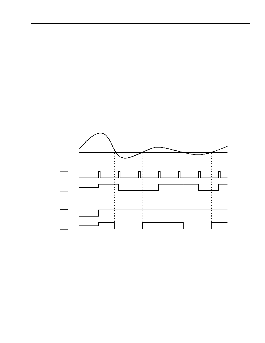
Lucent Technologies Inc.
105
Preliminary Data Sheet
November 2000
ISDN Network Termination Node (NTN) Device
T9000
14 Comparators
The comparator module consists of three low-power, general-purpose comparators. Each comparator has an inde-
pendent powerdown mode (CME register). Each comparator can generate a separate interrupt (CMIR[CMI(2:0)]),
when a transition occurs on its output. Each interrupt can be programmed to trigger on a 0 to 1 or 1 to 0 output
change (CMT register) and may be individually enabled via register CMIE. All interrupts are cleared when the
CMIR register is read.
The current output of each comparator (CMV) is available by reading any of the comparator register. When a com-
parator is powered down, it retains its current output CMV(i) as illustrated in Figure 24, where it is assumed that
INN(i) input has a fixed reference voltage. The CMV bits are useful for situations in which it is desirable to poll the
state of a comparator; for example, in verifying that a comparator that triggered an interrupt by transitioning
through a threshold in a particular direction has not returned to its preceding state. The ability to poll the state of
the comparators also allows the use of the comparators without having to enable any of the corresponding inter-
rupts. In many applications, analog input signals change at a very low rate. Users may implement interrupt-based
or polling-based algorithms where the comparator is powered up for a very small fraction of time. In this case, the
power consumption is minimized.
5-6726 (F)
Key:
A: Interrupt generated (CMI[i] = 1), if enabled (CMIE[i] = 1) and falling transition (CMT[i] = 0).
B: Interrupt generated (CMI[i] = 1), if enabled (CMIE[i] = 1) and falling transition (CMT[i] = 1).
Figure 24. (A) CMV When CME Is a Periodic Pulse and (B) CMV When CME Is Static
INP(i)
INN(i)
CME(i)
CMV(i)
CME(i)
CMV(i)
(1)
(2)
(1)
(2)
(1)
(2)
(1)
(2)
A
B

106
Lucent Technologies Inc.
Preliminary Data Sheet
November 2000
ISDN Network Termination Node (NTN) Device
T9000
14 Comparators
(continued)
Table 112 shows the major characteristics of the comparators.
Table 112. Comparator Characteristics
14.1 Comparators Register Set
Table 113. CME: Comparator Enable (0x4C)
Table 114. CMT: Comparator Transition Polarity (0x4D)
Parameter
Conditions
Min
Nom
Max
Unit
Input Common Mode (VCM)
--
0
--
3.2
V
Input Offset Voltage
0 < VCM < 3.2
-
15
--
15
mV
Gain
VCM = 1, f = 10 kHz
--
124
--
dB
CMRR
VCM = 1, f = 10 kHz
--
85
--
dB
PSRR
VCM = 1, f = 10 kHz
--
79
--
dB
dc Power Dissipation
--
--
0.8
1.5
mW
Standby Power Dissipation
--
--
--
3
µ
W
Reg
R/W
Bit 7
Bit 6
Bit 5
Bit 4
Bit 3
Bit 2
Bit 1
Bit 0
CME
R/W
--
CMV.2
CMV.1
CMV.0
--
CME.2
CME.1
CME.0
RESET
Default
0
--
--
--
0
0
0
0
Bit #
Symbol
Name/Description
7
--
Reserved. Program to 0.
6--4
CMV.[2:0]
Comparator [2:0] Value (Read-Only Field). These status bits indicate the current state
of the corresponding comparator output.
3
--
Reserved. Program to 0.
2--0
CME.[2:0]
Comparator [2:0] Enable.
0: Comparator disabled (powerdown mode).
1: Comparator active.
Note: On powerdown, any pending interrupts are reset.
Reg
R/W
Bit 7
Bit 6
Bit 5
Bit 4
Bit 3
Bit 2
Bit 1
Bit 0
CMT
R/W
--
CMV.2
CMV.1
CMV.0
--
CMT.2
CMT.1
CMT.0
RESET
Default
0
--
--
--
0
1
1
1
Bit #
Symbol
Name/Description
7
--
Reserved. Program to 0.
6--4
CMV.[2:0]
Comparator [2:0] Value (Read-Only Field). These status bits indicate the current state
of the corresponding comparator output.
3
--
Reserved. Program to 0.
2--0
CMT.[2:0]
Comparator [2:0] Transition Polarity.
0: Interrupt on 1-to-0 transition.
1: Interrupt on 0-to-1 transition.

Lucent Technologies Inc.
107
Preliminary Data Sheet
November 2000
ISDN Network Termination Node (NTN) Device
T9000
14 Comparators
(continued)
14.1 Comparators Register Set
(continued)
Table 115. CMIR: Comparator Interrupt Register (0x4E)
Note: Bits CMI.[2:0] in this register are set to 1 upon occurrence of the corresponding interrupt condition, and are
cleared to 0 when the register is read.
Table 116. CMIE: Comparator Interrupt Enable (0x4F)
14.2 Configuration Sequence
In order to avoid unwanted interrupts when changing the CMT value, the user should satisfy at least one of the fol-
lowing two conditions:
s
The comparator interrupt is disabled.
s
The comparator is powered down.
Reg
R/W
Bit 7
Bit 6
Bit 5
Bit 4
Bit 3
Bit 2
Bit 1
Bit 0
CMIR
R
--
CMV.2
CMV.1
CMV.0
--
CMI.2
CMI.1
CMI.0
RESET
Default
--
--
--
--
--
--
--
--
Bit #
Symbol
Name/Description
7
--
Reserved.
6--4
CMV.[2:0]
Comparator [2:0] Value. These status bits indicate the current state of the correspond-
ing comparator output. No interrupt is generated in response to the value in these bits.
3
--
Reserved.
2--0
CMI.[2:0]
Comparator [2:0] Interrupt. This interrupt indicates that the comparator output has tog-
gled in the direction specified in register CMT.
Reg
R/W
Bit 7
Bit 6
Bit 5
Bit 4
Bit 3
Bit 2
Bit 1
Bit 0
CMIE
R/W
--
CMV.2
CMV.1
CMV.0
--
CMIE.2
CMIE.1
CMIE.0
RESET
Default
0
--
--
--
0
0
0
0
Bit #
Symbol
Name/Description
7
--
Reserved. Program to 0.
6--4
CMV.[2:0]
Comparator [2:0] Value (Read-Only Field). These status bits indicate the current state
of the corresponding comparator output.
3
--
Reserved. Program to 0.
2--0
CMIE.[2:0]
Comparator [2:0] Interrupt Enable.
0: Interrupt disabled (masked).
1: Interrupt enabled.
Masked interrupts are not latched.

108
Lucent Technologies Inc.
Preliminary Data Sheet
November 2000
ISDN Network Termination Node (NTN) Device
T9000
15 Test Mode
When the TEST pin (pin 43) is asserted, pins 34, 85, and 97 change their existing functions so that the customer
can put the device in ILOSS, single pulses on the U-interface, and pulse template/loopback on S/T-interface test
modes, respectively.
When the TEST pin (pin 43) is asserted, pins 29, 30, 32, 35, 40, 41, and 42 also change their existing functions to
enable factory testing of the device as explained in Table 3 and Table 7.
Note: The existing functions on the above pins will not be available when the TEST pin is asserted.
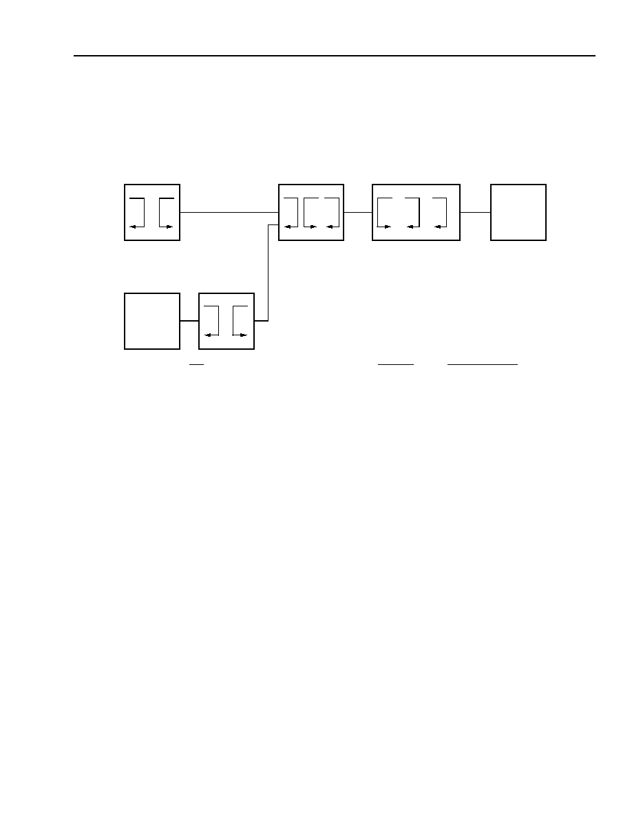
Lucent Technologies Inc.
109
Preliminary Data Sheet
November 2000
ISDN Network Termination Node (NTN) Device
T9000
16 Loopbacks
Following is a description of the loopbacks supported by the NTN.
The figure below shows the Layer-1 loopbacks that are defined in ITU-T I.430, Appendix I and
ANSI
Specification
T1.605, Appendix G. A complete discussion of these loopbacks is presented in ITU-T I.430, Appendix I.
5-2482.b (F)
Figure 25. Location of the Loopback Configurations
Key
Loopback
Channel(s) Looped
TE1 = ISDN terminal.
R = R reference point.
2
2B+D channels
TE2 = non-ISDN terminal.
S = S reference point.
3
2B+D channels
TA = terminal adapter.
T = T reference point.
4
B1, B2
NT2 = network termination 2.
U = U reference point.
C
B1, B2
NT1 = network termination 1.
B1 or B2
2B+D, B1, B2
LT = line termination.
A
2B+D, B1, B2
TE1
S
NT2
NT1
T
U
LT
2
C
B1
3
B2
TA
TE2
R
4
S
4
A
A
U

110
Lucent Technologies Inc.
Preliminary Data Sheet
November 2000
ISDN Network Termination Node (NTN) Device
T9000
17 Absolute Maximum Ratings
Stresses in excess of the absolute maximum ratings can cause permanent or latent damage to the device. These
are absolute stress ratings only. Functional operation of the device is not implied at these or any other conditions in
excess of those given in the operation sections of the data sheet. Exposure to absolute maximum ratings for
extended periods can adversely affect device reliability.
External leads can be soldered safely at temperatures up to 300 ∞C.
Table 117. Absolute Maximum Ratings
18 Handling Precautions
Although protection circuitry has been designed into this device, proper precautions should be taken to avoid expo-
sure to electrostatic discharge (ESD) during handling and mounting. Lucent employs a human-body model (HBM)
and charged-device model (CDM) for ESD-susceptibility testing and protection design evaluation. ESD voltage
thresholds are dependent on the circuit parameters used to define the model. No industry-wide standard has been
adopted for the CDM. However, a standard HBM (resistance = 1500
,
capacitance = 100 pF) is widely used and,
therefore, can be used for comparison. The HBM ESD threshold presented here was obtained by using the circuit
parameters shown below.
Table 118. ESD Threshold Voltage
19 Recommended Operating Conditions
Table 119. Recommended Operating Conditions
* To meet ANSI T1.601 free-run line rate requirement, NT tolerance is 100 ppm.
x = tolerance of MTC.
Parameter
Symbol
Min
Max
Unit
dc Supply Voltage Range
V
DD
≠0.5
6.5
V
Storage Temperature
T
stg
≠55
150
∞C
Voltage (any pin) with Respect to GND
--
≠0.5
6.5
V
Device
Voltage
T9000
>500
Parameter
Symbol
Test Condition
Min
Typ
Max
Unit
Ambient Temperature
T
A
V
DD
= 5 V
±
5%
≠40
--
85
∞C
Any V
DD
V
DD
--
4.75
5.0
5.25
V
GND to GND
V
GG
--
≠10
--
10
mV
Voltage Ref Capacitor
CVR
--
0.08
0.1
0.2
µF
Master Clock Frequency
MCLK
--
--
15.36
--
MHz
Master Clock Tolerance
MCLK
NT Mode
LT Mode
≠225*
≠225 + x*
--
--
≠225*
≠225 + x*
ppm
ppm
Master Clock Duty Cycle
MCLK
--
47
--
53
%

Lucent Technologies Inc.
111
Preliminary Data Sheet
November 2000
ISDN Network Termination Node (NTN) Device
T9000
20 Electrical Characteristics
20.1 Power Supply
The NTN operates from one power supply: the digital section from a 5.0 V
±
5% supply and the analog section
from a 5.0 V
±
5% supply.
20.2 Power Consumption
Table 120. Power Consumption
20.3 S/T-Interface Receiver Common-Mode Rejection
Table 121. S/T-Interface Receiver Common-Mode Rejection
Conditions
Loop Length
0 kft
18 kft
Unit
NT1 Mode
U-interface and S/T-interface powered up, microcontroller, and MLSE (see Table 47 for
MLSE description) powered down
365
330
mW
Restricted NT1 Power Mode
U-interface powered up, S/T-interface, microcontroller, and MLSE powered down
335
300
mW
Intelligent NT1 (INT1) Mode
U-interface, S/T-interface, and microcontroller powered up, and MLSE powered down
415
380
mW
Restricted INT1 Power Mode
U-interface and microcontroller powered up, S/T-interface, and MLSE powered down
385
350
mW
Parameter
Symbol
Specifications
Unit
Common-mode Rejection (at device pins)
CMR
400
mV

112
Lucent Technologies Inc.
Preliminary Data Sheet
November 2000
ISDN Network Termination Node (NTN) Device
T9000
20 Electrical Characteristics
(continued)
20.4 Pin Electrical Characteristics
Table 122. Digital dc Characteristics (Over Operating Ranges)
Parameter
Symbol
Test Condition
Min
Typ
Max
Unit
Input Leakage Current:
Low
High
Low
High
I
ILPU
I
IHPU
I
ILPD
I
IHPD
V
IL
= 0
V
IH
= V
DD
V
IL
= 0
V
IH
= V
DD
≠50
--
≠10
≠10
--
--
--
--
≠10
≠10
--
≠100
µA
µA
µA
µA
Input Voltage:
Low
V
IL
Pins 2, 4--11, 13--21, 23,
26--28, 33--34, 37--38, 40,
43, 45--50, 70, 72--79,
81--88, 90--97, 99--100
--
--
0.9
V
High
V
IH
Pins 2, 4--11, 13--21, 23,
26--28, 33--34, 37--38, 40,
43, 45--50, 70, 72--79,
81--88, 90--97, 99--100
3.5
--
--
V
Reset
V
ILS
V
IHS
V
H
(Hysteresis)
Pin 31
0.5
--
--
--
--
1.7
--
V
DD
≠ 0.5
--
V
V
V
Output Leakage Current:
Low
High
I
OZL
I
OZH
V
OL
= 0 (pins 1, 24, 35)
V
OH
= V
DD
(pins 1, 24, 35)
--
≠10
--
--
10
--
µA
µA
Output Voltage:
Low, TTL
V
OL
I
OL
= 1.6 mA (pins 40, 42)
--
--
0.4
V
I
OL
= 3.2 mA (pins 2,
4--11,
13--20, 23,
26--30, 32,
34, 41,
71--79,
81--88, 91,
93--97, 99,
100)
I
OL
= 4.8 mA (pins 1, 24,
35, 90, 92)
High, TTL
V
OH
I
OH
= 1.6 mA (pins 40, 42)
2.4
--
--
--
I
OH
= 3.2 mA (pins 2,
4--11,
13--20, 23,
26--30, 32,
34, 41,
71--79,
81--88, 91,
93--97, 99,
100)
I
OH
= 4.8 mA (pins 1, 24,
35, 90, 92)

Lucent Technologies Inc.
113
Preliminary Data Sheet
November 2000
ISDN Network Termination Node (NTN) Device
T9000
21 Crystal Characteristics
Table 123. Fundamental Mode Crystal Characteristics
These are the characteristics of a parallel resonant crystal for meeting the
±
100 ppm requirements of T1.601 for
NT operation. The parasitic capacitance of the PC board to which the T9000 crystal is mounted must be kept within
the range of 0.6 pF
±
0.4 pF.
Table 124. Internal PLL Characteristics
* Set by digital PLL; therefore, variations track MTC (LT mode) or U-interface line rate (NT mode).
22 Timing Characteristics
Table 125. MTC (Master Timing Clock) Requirements and Characteristics* (LT Mode)
* To meet ANSI T1.601-1992, see not for Recommended Operating Conditions.
One UI = 12.5 µs.
Parameter
Symbol
Test Conditions
Specifications
Unit
Center Frequency
F
O
With 25.0 pF of loading
15.36
MHz
Tolerance Including Calibration, Tempera-
ture Stability, and Aging
TOL
--
±
70
ppm
Drive Level
DL
Maximum
0.5
mW
Series Resistance
R
S
Maximum
20
Shunt Capacitance
C
O
--
3.0
±
20%
pF
Motional Capacitance
C
M
--
12
±
20%
fF
Parameter
Test Conditions
Min
Typ
Max
Unit
Total Pull Range
--
±
250
--
--
ppm
Jitter Transfer Function
≠3 dB point (LT)
≠3 dB point (NT), 18 kft 26 AWG
--
--
0.45*
5*
--
--
Hz
Hz
Jitter Peaking
at 0.15 Hz typical (LT)
at 1.5 Hz typical (NT)
--
--
0.4*
1.0*
--
--
dB
dB
Parameter
Min
Typ
Max
Unit
MTC Clock Period
125 ≠ 32 ppm
125
125 + 32 ppm
µs
MTC High/Low Time
8
--
--
MCLKs
MTC Rise/Fall Time
--
--
60
ns
MTC Jitter
--
--
0.259
UI

114
Lucent Technologies Inc.
Preliminary Data Sheet
November 2000
ISDN Network Termination Node (NTN) Device
T9000
23 Application Diagrams
12-3564
Figure 26. NT1 Application
12-3565
Figure 27. NT1+ Application
TERMINAL
EQUIPMENT
S/T-INTERFACE
U-INTERFACE
NT1
T9000
LT
CUSTOMER PREMISES
CENTRAL OFFICE
TERMINAL
EQUIPMENT
ANALOG
PHONE 1
ANALOG
PHONE 2
CODECs/
SLICs
S/T-INTERFACE
U-INTERFACE
NT1
T9000
LT
CUSTOMER PREMISES
CENTRAL OFFICE

Lucent Technologies Inc.
115
Preliminary Data Sheet
November 2000
ISDN Network Termination Node (NTN) Device
T9000
23 Application Diagrams
(continued)
12-3566
Figure 28. Pair Gain Application
LEGEND:
ALC:
Analog line card
FS1:
Frame sync 1
FS2:
Frame sync 2
SLIC:
Subscriber loop interface circuit
B1, B2: Voice channels
CODEC
CODEC
CODEC
ALC
SLIC
U
U
B2
FS1 TDM
T9000
TDM
B2
B1
CODEC
FS2
B1
SLIC
ANALOG
PHONE 2
ANALOG
PHONE 1
MICRO-
PROCESSOR
MEMORY
DUAL
SINE WAVE
GENERATOR
MICRO-
PROCESSOR
MEMORY
DUAL
SINE WAVE
GENERATOR
T9000
CUSTOMER PREMISES
CENTRAL OFFICE
2B1Q
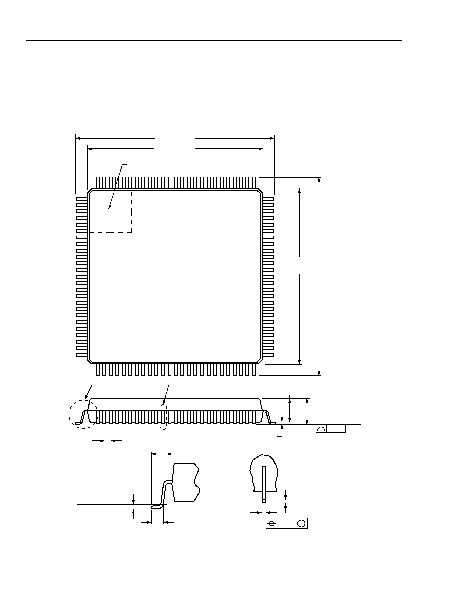
116
Lucent Technologies Inc.
Preliminary Data Sheet
November 2000
ISDN Network Termination Node (NTN) Device
T9000
24 Outline Diagram
24.1 100-Pin TQFP
Dimensions are in millimeters.
Note: The dimensions in this outline diagram are intended for informational purposes only. For detailed schematics
to assist your design efforts, please contact your Lucent Technologies Account Manager.
5-2146C
0.50 TYP
1.60 MAX
SEATING PLANE
0.08
1.40 ± 0.05
0.05/0.15
DETAIL A
DETAIL B
14.00 ± 0.20
16.00 ± 0.20
76
100
1
25
26
50
51
75
14.00
± 0.20
16.00
± 0.20
PIN #1 IDENTIFIER ZONE
DETAIL B
0.19/0.27
0.08
M
0.106/0.200
DETAIL A
0.45/0.75
GAGE PLANE
SEATING PLANE
1.00 REF
0.25

Lucent Technologies Inc.
117
Preliminary Data Sheet
November 2000
ISDN Network Termination Node (NTN) Device
T9000
25 Ordering Information
Device Code
Package
Temperature
Comcode
T-9000- - -TL
100-pin TQFP
≠40 ∞C to +85 ∞C
108556523

118
Lucent Technologies Inc.
Preliminary Data Sheet
November 2000
ISDN Network Termination Node (NTN) Device
T9000
26 Register Set Summary
The following section contains tables that list a summary of the entire register set for the T9000.
Table 126. Register Set Summary Global Registers
Table 127. Register Set Summary DFAC Registers
Table 128
.
Register Set Summary U-Interface Control Registers
Reg
R/W
Bit 7
Bit 6
Bit 5
Bit 4
Bit 3
Bit 2
Bit 1
Bit 0
0x00, Global Interrupt Register 0
GIR0
R
--
--
--
XI0I
125I
UII
SII
GPIOI
RESET
Default --
--
--
0
0
0
0
0
0x01, Global Interrupt Register 1
GIR1
R
--
--
--
XI1I
HDLCI
GCII
CMPI
PWMI
RESET
Default 0
0
0
0
0
0
0
0
0x02, Global Interrupt Enable Register
GIE
R/W
--
--
--
125IE
II1E
XI1E
II0E
XI0E
RESET
Default 0
0
0
0
0
0
0
0
0x03, Microcontroller Clock Control Register
UPCK
R/W
CLKOE
--
--
--
--
UPCK2
UPCK1
UPCK0
RESET
Default 1
0
0
0
0
1
1
1
0x04, Watchdog Timer
WDT
R/W
WDTE
WDT6
WDT5
WDT4
WDT3
WDT2
WDT1
WDT0
RESET
Default 0
1
1
1
1
1
1
1
0x05, DFAC Configuration Register
DFCF
R/W
ILOSS
USIMRST
URESET
--
UOADS
ACT_ANSI
AUTOEOC
GRESET
RESET Default 0
0
0
0
1
0
1
0
0x06, Data Flow Register
DFR
R/W
U_FORCE_B2UP
U_FORCE_B1UP
FORCE_D
PFS2_ACT
PFS1_ACT
B2_SEL
B1_SEL
BSWAP
RESET Default 0
0
0
0
0
0
0
0
0x07, U-Interface Control Register #0
UCR0
R/W
NTM_n
PS1
PS2
SAI
XPCY
F_ACTUP
ACTUP
ISTP
RESET
Default
1
1
1
0
0
0
0
0
0x08, U-Interface Control Register #1
UCR1
R/W
R64T
R25T
R16T
R15T
ULBKMUX
ULLBK
USPMAG
USSP_E
RESET
Default
1
1
1
1
0
0
0
0
0x09, U-Interface Status Register #0
USR0
R
AIB_n
FEBE_n
NEBE_n
UOA_n
DEA_n
OOF_n
XACT
ACTDN
RESET
Default
1
1
1
1
1
0
0
0
0x0A, U-Interface Status Register #1
USR1
R
--
R64R
R54R
R44R
R34R
R25R
R16R
R15R
RESET
Default
--
1
1
1
1
1
1
1
Lucent Technologies Inc.
119
Preliminary Data Sheet
November 2000
ISDN Network Termination Node (NTN) Device
T9000
26 Register Set Summary
(continued)
Table 129. Register Set Summary EOC Control Registers
Table 130. Register Set Summary S-Interface Registers
Table 131. Register Set Summary Multiframe Registers
Table 132. Register Set Summary U-Interface Interrupt Registers
0x0B, EOC Control Register 0--Command and Address
Reg
R/W
Bit 7
Bit 6
Bit 5
Bit 4
Bit 3
Bit 2
Bit 1
Bit 0
ECR0
R/W
CCRC
LD
LB2
LB1
A1T
A2T
A3T
DMT
RESET
Default
0
0
0
0
0
0
0
1
0x0C, EOC Control Register 1--Message
ECR1
R/W
I1T
I2T
I3T
I4T
I5T
I6T
I7T
I8T
RESET
Default
1
1
1
1
1
1
1
1
0x0D, EOC Status Register 0--Command and Address
ESR0
R
ECCRC
ELD
ELB2
ELB1
A1R
A2R
A3R
DMR
RESET
Default
0
0
0
0
1
1
1
1
0x0E, EOC Status Register 1--Message
ESR1
R
I1R
I2R
I3R
I4R
I5R
I6R
I7R
I8R
RESET
Default
1
1
1
1
1
1
1
1
0x0F, S-Interface Control Register #0
SCR0
R/W
--
--
STOA
FACT
FT
MF_E
ST_E
SRESET
RESET
Default
0
0
0
0
0
0
1
0
0x10, S-Interface Control Register #1
SCR1
R/W
--
--
--
RLB_D
RLB_B2
RLB_B1
TE_DA
--
RESET
Default
0
0
0
0
0
0
0
0
0x11, S-Interface Status Register
SSR
R
FSERR
--
--
RXINFO3 RXINFO1
ASI2
ASI1
ASI0
RESET
Default 0
--
--
0
0
0
0
0
0x12, Multiframe Register, Q-Channel Data
MFR0
R
--
--
--
--
QD1
QD2
QD3
QD4
RESET
Default --
--
--
--
1
1
1
1
0x13, Multiframe Register, S-Subchannel Data
MFR1
W
--
--
--
--
SSD1
SSD2
SSD3
SSD4
RESET
Default
0
0
0
0
0
0
0
0
0x14, U-Interface Interrupt Register
UIR
R
RSF
RHSF
BERR
ACTSC
OUSC
EOC3SC
EOCSC
ECNFY
RESET
Default
0
0
0
0
0
0
0
0
0x15, U-Interface Interrupt Enable
UIE
R/W
RSFE
RHSFE
BERRE
ACTSCE
OUSCE
EOC3SCE
EOCSCE
--
RESET
Default
0
0
0
0
0
0
0
--

120
Lucent Technologies Inc.
Preliminary Data Sheet
November 2000
ISDN Network Termination Node (NTN) Device
T9000
26 Register Set Summary
(continued)
Table 133. Register Set Summary S-Interface Interrupt Registers
0x16, S-Interface Interrupt Register
SIR
R
--
--
--
--
SSC
FSERR
QSC
SSRDY
RESET
Default --
--
--
--
0
0
0
0
0x17, S-Interface Interrupt Enable
SIE
R/W
--
--
--
--
SSCE
FSERRE
QSCE
SSRDYE
RESET
Default 0
0
0
0
0
0
0
0
0x50, Device Operation Control Register
DOCR
R/W
FORCE_SAI
_STD
BS_E
--
--
NT_LT
--
--
--
RESET
Default
0
0
0
0
0
0
0
0
0x51, B1-Channel Upstream Data from GCI to U-Interface
B1UP
R/W
B1UP7
B1UP6
B1UP5
B1UP4
B1UP3
B1UP2
B1UP1
B1UP0
RESET
Default
--
--
--
--
--
--
--
--
0x52, B2-Channel Upstream Data from GCI to U-Interface
B2UP
R/W
B2UP7
B2UP6
B2UP5
B2UP4
B2UP3
B2UP2
B2UP1
B2UP0
RESET
Default
--
--
--
--
--
--
--
--
0x53, B1-Channel Downstream Data from GCI to U-Interface
B1DN
R/W
B1DN7
B1DN6
B1DN5
B1DN4
B1DN3
B1DN2
B1DN1
B1DN0
RESET
Default
--
--
--
--
--
--
--
--
0x54, B2-Channel Downstream Data from GCI to U-Interface
B2DN
R/W
B2DN7
B2DN6
B2DN5
B2DN4
B2DN3
B2DN2
B2DN1
B2DN0
RESET
Default
--
--
--
--
--
--
--
--
0x55, Reserved Register for Internal Use
Reserved1
R
--
--
--
--
--
--
--
--
RESET
Default --
--
--
--
--
--
--
--
0x56, Reserved Register for Internal Use
Reserved2
R/W
--
--
U_FDEACT
U_R54T
MLSE_POWER
_DN
--
--
--
RESET
Default --
--
0
1
0
--
--
--
0x57, Reserved Register for Internal Use
Reserved3
R
--
--
--
--
--
--
--
--
RESET
Default --
--
--
--
--
--
--
--
0x58, Reserved Register for Internal Use
Reserved4
R
--
--
--
--
--
--
--
--
RESET
Default --
--
--
--
--
--
--
--
0x59, Reserved Register for Internal Use
Reserved5
R
--
--
--
--
--
--
--
--
RESET
Default --
--
--
--
--
--
--
--
0x5A, Reserved Register for Internal Use
Reserved6
R
--
--
--
--
--
--
--
--
RESET
Default --
--
--
--
--
--
--
--
0x5B, Reserved Register for Internal Use
Reserved7
R
--
--
--
--
--
--
--
--
RESET
Default --
--
--
--
--
--
--
--
0x5C, Reserved Register for Internal Use
Reserved8
R
--
--
--
--
--
--
--
--
RESET
Default --
--
--
--
--
--
--
--
0x5D, Reserved Register for Internal Use
Reserved8
R
--
--
--
--
--
--
--
--
RESET
Default --
--
--
--
--
--
--
--

Lucent Technologies Inc.
121
Preliminary Data Sheet
November 2000
ISDN Network Termination Node (NTN) Device
T9000
26 Register Set Summary
(continued)
Table 134. Register Set Summary HDLC Registers
Reg
R/W
Bit 7
Bit 6
Bit 5
Bit 4
Bit 3
Bit 2
Bit 1
Bit 0
0x18, HDLC Transmitter Configuration Register
HTCF
R/W
FCNT2
FCNT1
FCNT0
IDL
TXMODE
ABRT_RQ
MANCRC
TX_INIT
RESET
Default 0
0
0
1
0
0
0
0
0x19, HDLC Receiver Configuration Register
HRCF
R/W
--
--
--
--
RXMODE
BAE
DROPCRC
RX_INIT
RESET
Default
0
0
0
0
--
0
1
0
0x1A, HDLC Transmit FIFO Threshold
HTTH
R/W
P_CLASS
--
TFAE5
TFAE4
TFAE3
TFAE2
TFAE1
TFAE0
RESET
Default
1
0
1
0
0
0
0
0
0x1B, HDLC Receive FIFO Threshold
HRTH
R/W
--
--
RFAF5
RFAF4
RFAF3
RFAF2
RFAF1
RFAF0
RESET
Default
0
0
1
0
0
0
0
0
0x1C, HDLC Transmit FIFO Space Available
HTSA
R
--
TSP6
TSP5
TSP4
TSP3
TSP2
TSP1
TSP0
RESET
Default
--
1
0
0
0
0
0
0
0x1D, HDLC Receive FIFO Data Available
HRDA
R
SWRF
NBNSW6 NBNSW5 NBNSW4
NBNSW3
NBNSW2
NBNSW1
NBNSW0
RESET
Default
--
--
--
--
--
--
--
--
0x1E, HDLC Transmit Data
HTX
W
TXD7
TXD6
TXD5
TXD4
TXD3
TXD2
TXD1
TXD0
RESET
Default
--
--
--
--
--
--
--
--
0x1F, HDLC Transmit Data Last Byte
HTXL
W
TXDL7
TXDL6
TXDL5
TXDL4
TXDL3
TXDL2
TXDL1
TXDL0
RESET
Default
--
--
--
--
--
--
--
--
0x20, HDLC Receive Data
HRX
R
RXD7
RXD6
RXD5
RXD4
RXD3
RXD2
RXD1
RXD0
RESET
Default
--
--
--
--
--
--
--
--
0x21, HDLC SAPI C/R Bit Mask Register
HSCR
R/W
--
--
--
--
S3CRE
S2CRE
S1CRE
S0CRE
RESET
Default
0
0
0
0
0
0
0
0
0x22, HDLC SAPI Match Pattern 0
HSM0
R/W
SAPI05
SAPI04
SAPI03
SAPI02
SAPI01
SAPI00
C/R0
EA00
BAP7
BAP6
BAP5
BAP4
BAP3
BAP2
BAP1
BAP0
RESET
Default
--
--
--
--
--
--
--
--

122
Lucent Technologies Inc.
Preliminary Data Sheet
November 2000
ISDN Network Termination Node (NTN) Device
T9000
26 Register Set Summary
(continued)
Table 134. Register Set Summary HDLC Registers (continued)
Reg
R/W
Bit 7
Bit 6
Bit 5
Bit 4
Bit 3
Bit 2
Bit 1
Bit 0
0x23, HDLC TEI Match Pattern 0
HTM0
R/W
TEI06
TEI05
TEI04
TEI03
TEI02
TEI01
TEI00
EA10
RESET
Default
--
--
--
--
--
--
--
--
0x24, HDLC SAPI Match Pattern 1
HSM1
R/W
SAPI15
SAPI14
SAPI13
SAPI12
SAPI11
SAPI10
C/R1
EA01
RESET
Default
--
--
--
--
--
--
--
--
0x25, HDLC TEI Match Pattern 1
HTM1
R/W
TEI16
TEI15
TEI14
TEI13
TEI12
TEI11
TEI10
EA11
RESET
Default
--
--
--
--
--
--
--
--
0x26, HDLC SAPI Match Pattern 2
HSM2
R/W
SAPI25
SAPI24
SAPI23
SAPI22
SAPI21
SAPI20
C/R2
EA02
RESET
Default
--
--
--
--
--
--
--
--
0x27, HDLC TEI Match Pattern 2
HTM2
R/W
TEI26
TEI25
TEI24
TEI23
TEI22
TEI21
TEI20
EA12
RESET
Default
--
--
--
--
--
--
--
--
0x28, HDLC SAPI Match Pattern 3
HSM3
R/W
SAPI35
SAPI34
SAPI33
SAPI32
SAPI31
SAPI30
C/R3
EA03
RESET
Default
--
--
--
--
--
--
--
--
0x29, HDLC TEI Match Pattern 3
HTM3
R/W
TEI36
TEI35
TEI34
TEI33
TEI32
TEI31
TEI30
EA13
RESET
Default
--
--
--
--
--
--
--
--
0x2A, HDLC SAPI Modifier Register
HSMOD
R/W
SAPI3M1
SAPI3M0
SAPI2M1
SAPI2M0
SAPI1M1
SAPI1M0
SAPI0M1
SAPI0M0
RESET
Default
0
0
0
0
0
0
0
0
0x2B, HDLC TEI Modifier Register
HTMOD
R/W
TEI3M1
TEI3M0
TEI2M1
TEI2M0
TEI1M1
TEI1M0
TEI0M1
TEI0M0
RESET
Default
0
0
0
0
0
0
0
0
0x2C, HDLC Interrupt Register
HDIR
R
RSTF
ROVR
REOF
RABT
RTHR
TUNDR
TFC
TTHR
RESET
Default
--
--
--
--
--
--
--
--
0x2D, HDLC Interrupt Enable Register
HDIE
R
RSTFE
ROVRE
REOFE
RABTE
RTHRE
TUNDRE
TFCE
TTHRE
RESET
Default
0
0
0
0
0
0
0
0

Lucent Technologies Inc.
123
Preliminary Data Sheet
November 2000
ISDN Network Termination Node (NTN) Device
T9000
26 Register Set Summary
(continued)
Table 135. Register Set Summary GCI+ Registers
Reg
R/W
Bit 7
Bit 6
Bit 5
Bit 4
Bit 3
Bit 2
Bit 1
Bit 0
0x2E, GCI+ Configuration Register
GCCF
R/W
GDRIVER
PFSDEL
PFSPE
CKMODE
GRATE1
GRATE0
GMODE1 GMODE0
RESET
Default
0
0
0
0
0
0
0
0
0x2F, GCI+ PFS1 Offset Select
GCOF1
R/W
GTMODE
G_R_LBK G_L_LBK
OFF14
OFF13
OFF12
OFF11
OFF10
RESET
Default
0
0
0
0
0
0
0
0
0x30, GCI+ PFS2 Offset Select
GCOF2
R/W
U_FORCE
_B2DN
U_FORC
E_B1DN
--
OFF24
OFF23
OFF22
OFF21
OFF20
RESET
Default
0
0
0
0
0
0
0
0
0x31, GCI Downstream (Transmit) Monitor Data
GCDMD
W
DMD7
DMD6
DMD5
DMD4
DMD3
DMD2
DMD1
DMD0
RESET
Default
1
1
1
1
1
1
1
1
0x32, GCI Downstream (Transmit) Monitor Data Last
GCDML
W
DML7
DML6
DML5
DML4
DML3
DML2
DML1
DML0
RESET
Default
1
1
1
1
1
1
1
1
0x33, GCI Upstream (Receive) Monitor Data
GCUMD
R
UMD7
UMD6
UMD5
UMD4
UMD3
UMD2
UMD1
UMD0
RESET
Default
--
--
--
--
--
--
--
--
0x34, GCI Downstream (Transmit) C/I Data
GCDCI
R/W
--
--
DCI6
DCI5
DCI4
DCI3
DCI2
DCI1
RESET
Default
0
0
--
--
--
--
--
--
0x35, GCI Upstream (Receive) C/I Data
GCUCI
R/W
--
--
UCI6
UCI5
UCI4
UCI3
UCI2
UCI1
RESET
Default
0
0
--
--
--
--
--
--
0x36, GCI Interrupt Register
GCIR
R
GWUP
UCIC
UMRDY
UMEOM
UMABRT
DMRDY
DMEOM
DMABRT
RESET
Default
0
0
0
0
0
0
0
0
0x37, GCI Interrupt Enable
GCIE
R
GWUPE
UCICE
UMRDYE UMEOME UMABRT
E
DMRDYE DMEOME DMABRT
E
RESET
Default
0
0
0
0
0
0
0
0

124
Lucent Technologies Inc.
Preliminary Data Sheet
November 2000
ISDN Network Termination Node (NTN) Device
T9000
26 Register Set Summary
(continued)
Table 136. Register Set Summary GPIO Registers
Reg
R/W
Bit 7
Bit 6
Bit 5
Bit 4
Bit 3
Bit 2
Bit 1
Bit 0
0x38, GPIO Port 0 Pin Direction
GPDIR0
R/W
DIR0.7
DIR0.6
DIR0.5
DIR0.4
DIR0.3
DIR0.2
DIR0.1
DIR0.0
RESET
Default
1
1
1
1
1
1
1
1
0x39, GPIO Port 1 Pin Direction
GPDIR1
R/W
DIR1.7
DIR1.6
DIR1.5
DIR1.4
DIR1.3
DIR1.2
DIR1.1
DIR1.0
RESET
Default
1
1
1
1
1
1
1
1
0x3A, GPIO Port 2 Pin Direction
GPDIR2
R/W
DIR2.7
DIR2.6
DIR2.5
DIR2.4
DIR2.3
DIR2.2
DIR2.1
DIR2.0
RESET
Default
1
1
1
1
1
1
1
1
0x3B, GPIO Alternate Function Register #0
GPAF0
R/W
GPAF0.7
GPAF0.6
GPAF0.5
GPAF0.4
--
--
--
--
RESET
Default
0
0
0
0
0
0
0
0
0x3C, GPIO Alternate Function Register #1
GPAF1
R/W
GPAF1.7
GPAF1.6
GPAF1.5
--
GPAF2.3
GPAF2.2
GPAF2.1 GPRESET
RESET
Default
0
0
0
0
0
0
0
0
0x3D, GPIO Port 0 Data Register
GPD0
R/W
GPD0.7
GPD0.6
GPD0.5
GPD0.4
GPD0.3
GPD0.2
GPD0.1
GPD0.0
RESET
Default
0
0
0
0
0
0
0
0
0x3E, GPIO Port 1 Data Register
GPD1
R/W
GPD1.7
GPD1.6
GPD1.5
GPD1.4
GPD1.3
GPD1.2
GPD1.1
GPD1.0
RESET
Default
0
0
0
0
0
0
0
0
0x3F, GPIO Port 2 Data Register
GPD2
R/W
GPD2.7
GPD2.6
GPD2.5
GPD2.4
GPD2.3
GPD2.2
GPD2.1
GPD2.0
RESET
Default
0
0
0
0
0
0
0
0
0x40, GPIO Level-Edge-Triggered Interrupt Control
GPLEI
R/W
ILE1.3
ILE1.2
ILE1.1
ILE1.0
ILE0.3
ILE0.2
ILE0.1
ILE0.0
RESET
Default
1
1
1
1
1
1
1
1
0x41, GPIO Interrupt Polarity Control
GPPOL
R/W
IPOL1.3
IPOL1.2
IPOL1.1
IPOL1.0
IPOL0.3
IPOL0.2
IPOL0.1
IPOL0.0
RESET
Default
1
1
1
1
1
1
1
1
0x42, GPIO Interrupt Register
GPIR
R/W
GPI1.3
GPI1.2
GPI1.1
GPI1.0
GPI0.3
GPI0.2
GPI0.1
GPI0.0
RESET
Default
--
--
--
--
--
--
--
--
0x43, GPIO Interrupt Enable
GPIE
R/W
GPIE13
GPIE12
GPIE11
GPIE10
GPIE03
GPIE02
GPIE01
GPIE00
RESET
Default
--
--
--
--
--
--
--
--

Lucent Technologies Inc.
125
Preliminary Data Sheet
November 2000
ISDN Network Termination Node (NTN) Device
T9000
26 Register Set Summary
(continued)
Table 137. Register Set Summary PWM Registers
Table 138. Register Set Summary dc/dc Register
Reg
R/W
Bit 7
Bit 6
Bit 5
Bit 4
Bit 3
Bit 2
Bit 1
Bit 0
0x44, Pulse-Width Modulator
#
0 Configuration
PW0CF
R/W
PW0_E
PW0AUTO
PW0IE
PW0G.2
PW0G.1
PW0G.0
PW0R.1
PW0R.0
RESET
Default
0
--
0
--
--
--
--
--
0x45, Pulse-Width Modulator
#
0 Pulse-Width Value, High Byte
PW0VH
R/W
PW0VH7
PW0VH6
PW0VH5
PW0VH4
PW0VH3
PW0VH2
PW0VH1
PW0VH0
RESET
Default
--
--
--
--
--
--
--
--
0x46, Pulse-Width Modulator
#
0 Pulse-Width Value, Low Byte
PW0VL
R/W
PW0VL7
PW0VL6
PW0VL5
PW0VL4
PW0VL3
PW0VL2
PW0VL1
PW0VL0
RESET
Default
--
--
--
--
--
--
--
--
0x47, Pulse-Width Modulator
#
1 Configuration
PW1CF
R/W
PW1_E
PW1AUTO
PW1IE
PW1G.2
PW1G.1
PW1G.0
PW1R.1
PW1R.0
RESET
Default
0
--
0
--
--
--
--
--
0x48, Pulse-Width Modulator
#
1 Pulse-Width Value, High Byte
PW1VH
R/W
PW1VH7
PW1VH6
PW1VH5
PW1VH4
PW1VH3
PW1VH2
PW1VH1
PW1VH0
RESET
Default
--
--
--
--
--
--
--
--
0x49, Pulse-Width Modulator
#
1 Pulse-Width Value, Low Byte
PW1VL
R/W
PW1VL7
PW1VL6
PW1VL5
PW1VL4
PW1VL3
PW1VL2
PW1VL1
PW1VL0
RESET
Default
--
--
--
--
--
--
--
--
0x4A, Pulse-Width Modulator Interrupt Register
PWIR
R
--
--
--
--
--
--
PW1I
PW0I
RESET
Default
--
--
--
--
--
--
0
0
0x4B, dc/dc Configuration Register
DCCF
R/W
--
--
DC_E
DCV4
DCV3
DCV2
DCV1
DCV0
RESET
Default
0
0
0
--
--
--
--
--

Preliminary Data Sheet
November 2000
ISDN Network Termination Node (NTN) Device
T9000
Lucent Technologies Inc. reserves the right to make changes to the product(s) or information contained herein without notice. N o liability is assumed as a result of their use or application. No
rights under any patent accompany the sale of any such product(s) or information.
Copyright © 2000 Lucent Technologies Inc.
All Rights Reserved
November 2000
DS01-037ISDN (Replaces DS00-181ISDN)
For additional information, contact your Microelectronics Group Account Manager or the following:
INTERNET: http://www.lucent.com/micro
E-MAIL: docmaster@micro.lucent.com
N. AMERICA:
Microelectronics Group, Lucent Technologies Inc., 555 Union Boulevard, Room 30L-15P-BA, Allentown, PA 18103
1-800-372-2447, FAX 610-712-4106 (In CANADA: 1-800-553-2448, FAX 610-712-4106)
ASIA PACIFIC: Microelectronics Group, Lucent Technologies Singapore Pte. Ltd., 77 Science Park Drive, #03-18 Cintech III, Singapore 118256
Tel. (65) 778 8833, FAX (65) 777 7495
CHINA: Microelectronics Group, Lucent Technologies (China) Co., Ltd., A-F2, 23/F, Zao Fong Universe Building, 1800 Zhong Shan Xi Road, Shanghai
200233 P. R. China Tel. (86) 21 6440 0468, ext. 316, FAX (86) 21 6440 0652
JAPAN: Microelectronics Group, Lucent Technologies Japan Ltd., 7-18, Higashi-Gotanda 2-chome, Shinagawa-ku, Tokyo 141, Japan
Tel. (81) 3 5421 1600, FAX (81) 3 5421 1700
EUROPE: Data Requests: MICROELECTRONICS GROUP DATALINE: Tel. (44) 7000 582 368, FAX (44) 1189 328 148
Technical Inquiries: GERMANY: (49) 89 95086 0 (Munich), UNITED KINGDOM: (44) 1344 865 900 (Ascot),
FRANCE: (33) 1 40 83 68 00 (Paris), SWEDEN: (46) 8 594 607 00 (Stockholm), FINLAND: (358) 9 4354 2800 (Helsinki),
ITALY: (39) 02 6608131 (Milan), SPAIN: (34) 1 807 1441 (Madrid)
26 Register Set Summary
(continued)
Table 139. Register Set Summary Comparator Registers
0x4C, Comparator Enable
CME R/W -- CMV.2 CMV.1 CMV.0 -- CME.2 CME.1 CME.0
RESET Default 0 -- -- -- 0 0 0 0
0x4D, Comparator Transition Polarity
CMT R/W -- CMV.2 CMV.1 CMV.0 -- CMT.2 CMT.1 CMT.0
RESET Default 0 -- -- -- 0 1 1 1
0x4E, Comparator Interrupt Register
CMIR R -- CMV.2 CMV.1 CMV.0 -- CMI.2 CMI.1 CMI.0
RESET Default -- -- -- -- -- 1 1 1
0x4F, Comparator Interrupt Enable
CMIE R/W -- CMV.2 CMV.1 CMV.0 -- CMIE.2 CMIE.1 CMIE.0
RESET Default 0 -- -- -- 0 0 0 0