 | –≠–ª–µ–∫—Ç—Ä–æ–Ω–Ω—ã–π –∫–æ–º–ø–æ–Ω–µ–Ω—Ç: TAAD08JU2 | –°–∫–∞—á–∞—Ç—å:  PDF PDF  ZIP ZIP |

Preliminary Data Sheet
August 18, 2003
TAAD08JU2
T1/E1/J1 ATM Processor, Versions 2.1 and 3.1
1 Features
s
System-on-a-chip integrated circuit supports low-
speed ATM access for next-generation wireless
base transmission station (BTS), base station con-
troller (BSC), node-B, radio network controller
(RNC), and remote access concentrator (RAC)
applications.
s
IC provides an integrated octal framer that sup-
ports T1/E1/J1 formats.
s
Supports inverse multiplexing for ATM (IMA) over
selected group and link mappings ranging from
four two-link groups up to one eight-link group per
ATM Forum AF-PHY-0086.001.
s
Integrates an ATM adaptation layer 2 (AAL2) seg-
mentation and reassembly (SAR) function for sup-
port of low-speed data or voice traffic per ITU
I.363.2.
s
Provides AAL5 SAR functionality per ITU I.363.5.
s
Provides quality of service (QoS) connection iden-
tifier (CID) multiplexing per ITU I.366.1.
s
Enables ATM layer user network interface (UNI) or
IMA mode, selectable on a per-link basis for flexi-
ble transport of delay critical voice and data traffic.
s
Guarantees QoS for a variety of traffic types
(including delay-sensitive voice, real-time data,
non-real-time data, and signaling information)
through an advanced hierarchical three-level prior-
ity scheduler and per-VC queueing.
s
Supports 2032 bidirectional AAL2 CIDs.
s
Supports 2032 bidirectional high-speed data con-
nections or virtual circuits (VCs) via embedded
context memory; filters control cells and accepts
control cells via a host microprocessor interface.
s
On-board memory is used for connection manage-
ment and queue data storage. No external memory
is needed.
s
Software package includes the following:
-- Device manager source code (C-based device
manager ready-to-use with host RTOS).
-- Setup file utility to provision TAAD08JU2.
-- Firmware for embedded controller (executable
binary).
-- API reference manual available for device man-
ager software.
s
Designed in 0.16 µm, low-power CMOS
technology.
2 Physical
s
3.3 V digital I/O compatibility; 1.5 V core power
s
520 enhanced ball-grid array (EBGA) package
s
≠40
o
C to +85
o
C temperature range
3 Standards
ITU I.363.2, ITU I.363.5, ITU I.366.1, ITU I.366.2,
ITU I.432, ITU I.361, ITU I.371, ITU G.703, ITU
G.704, ITU G.804, ITU G.732, ITU G.706, ITU I.610,
ITU G.775, ITU G.733, ITU G.735, ITU G.965,
ITU O.162, ANSI
Æ
T1.403, ANSI T1.231,
ATM Forum AF-PHY-0086.001
ATM Forum AF-PHY-0039.000
ATM Forum AF-TM-0121.000
ETS 300.417-1-1

Table of Contents
2
Agere Systems - Proprietary
Agere Systems Inc.
Preliminary Data Sheet
August 18, 2003
T1/E1/J1 ATM Processor, Versions 2.1 and 3.1
TAAD08JU2
Contents
Page
1
Features .............................................................................................................................................................1
2
Physical ..............................................................................................................................................................1
3
Standards ...........................................................................................................................................................1
4
Description ....................................................................................................................................................... 11
5
Pin Definitions ..................................................................................................................................................12
6
Pin Description .................................................................................................................................................12
7
Package Pin Layout .........................................................................................................................................21
8
Block Diagram ..................................................................................................................................................27
9
Software Components ......................................................................................................................................28
9.1
Firmware.................................................................................................................................................29
9.2
Device Manager......................................................................................................................................29
9.3
Setup File Utility (SFU) ...........................................................................................................................30
9.4
TAAD08JU2 Application Code................................................................................................................31
9.5
System Software.....................................................................................................................................32
9.6
Software Development Environment ......................................................................................................32
9.7
Notes ......................................................................................................................................................33
10 Functional Overview.........................................................................................................................................34
10.1 Receive Direction Data Flow ..................................................................................................................34
10.1.1
PHY Layer ................................................................................................................................34
10.1.2
Low-Speed PHY Links ..............................................................................................................34
10.1.3
High-Speed PHY Links .............................................................................................................35
10.1.4
TC and IMA Layers...................................................................................................................35
10.1.5
ATM Layer ................................................................................................................................36
10.1.6
AAL Engine...............................................................................................................................36
10.1.7
Embedded Device Controller....................................................................................................37
10.2 Transmit Direction Data Flow..................................................................................................................37
10.2.1
SSCS/AAL Layer Interaction ....................................................................................................37
10.2.2
ATM Layer ................................................................................................................................37
10.2.3
IMA/TC Layer............................................................................................................................38
10.2.4
PHY Layer ................................................................................................................................38
11 Modes of Operation..........................................................................................................................................39
11.1 Interface Modes ......................................................................................................................................39
11.1.1
UTOPIA-2 Expansion Port Multiplexing Modes ........................................................................39
11.1.2
System Interface Port Multiplexing Modes ...............................................................................39
11.1.3
Line-Interface Modes ................................................................................................................40
11.2 Device Operating Modes ........................................................................................................................40
11.2.1
Operating Mode 1: Internal PHY Mode.....................................................................................40
11.2.2
Operating Mode 2: External PHY Mode ...................................................................................42
11.2.3
Operating Mode 3: SAR-Only Mode .........................................................................................43
11.2.4
Operating Mode Summary........................................................................................................43
12 Applications ......................................................................................................................................................44
12.1 BTS Network Interface Termination ........................................................................................................44
12.2 VToA Trunking Application......................................................................................................................46
12.3 Low-Speed ATM Access.........................................................................................................................47
12.4 AAL2 Cross Connect ..............................................................................................................................47
13 Embedded Device Controller (EDC) ................................................................................................................48
13.1 Introduction.............................................................................................................................................48
13.2 Features..................................................................................................................................................48
13.3 EDC Functional Description....................................................................................................................48
13.4 Host Interface .........................................................................................................................................48
13.5 Host Interface Signals and Timing..........................................................................................................49

Table of Contents
(continued)
Contents
Page
Data Sheet
TAAD08JU2
August 18, 2003
T1/E1/J1 ATM Processor, Versions 2.1 and 3.1
Agere Systems Inc.
Agere Systems - Proprietary
3
Use pursuant to Company instructions
13.6 Host Interactions.....................................................................................................................................49
14 Framer Block ....................................................................................................................................................53
14.1 Introduction .............................................................................................................................................53
14.2 Features..................................................................................................................................................53
14.3 Framer-to-Line Interface Unit Physical Interface ....................................................................................54
14.3.1
Line Interface References/Standards .......................................................................................54
14.3.2
Clocking Modes ........................................................................................................................54
14.3.3
Frame Formats .........................................................................................................................55
14.3.4
Transmit Framer Functions.......................................................................................................55
14.4 DS1 Transparent Framing Format ..........................................................................................................55
14.5 CEPT 2.048 Basic Frame Structure Transparent Framing Format.........................................................56
14.6 Receive Framer Nonalignment Mode (DS1/E1) .....................................................................................57
14.6.1
Loss of Frame Alignment Criteria .............................................................................................57
14.6.1.1 Frame Bit Errors.........................................................................................................57
14.6.1.2 CRC Errors.................................................................................................................57
14.7 Frame Alignment Criteria........................................................................................................................57
14.8 Performance-Monitoring Functional Integration Into Framer ..................................................................58
14.9 Performance Report Message................................................................................................................61
14.10 ESF Data Link.........................................................................................................................................62
14.11 Facility Data Link ....................................................................................................................................62
14.11.1 Facility Data Link References/Standards ..................................................................................62
14.11.2 Receive Data Link Functional Description ................................................................................63
14.11.3 SLC-96 Superframe Receive Data Link....................................................................................63
14.11.4 DDS Receive Data Link Stack ..................................................................................................63
14.11.5 CEPT; CEPT CRC-4 (100 ms); CEPT CRC-4 (400 ms) Multiframe Sa Bits Receive Stack .....63
14.11.6 Receive Data Link Stack Idle Modes ........................................................................................64
14.11.7 Transmit Facility Data Link Functional Description ...................................................................64
14.11.8 SLC-96 Superframe Transmit Data Link...................................................................................64
14.11.9 DDS Transmit Data Link Stack .................................................................................................64
14.11.10 Transmit ESF Data Link Bit-Oriented Messages ......................................................................64
14.11.11 CEPT, CEPT Multiframe Transmit Data Link Sa Bits Stack ......................................................65
14.11.12 Transmit Data Link Stack Idle Modes .......................................................................................66
14.11.13 SLC-96, DDS, or CEPT ESF Frame Alignment ........................................................................66
14.12 Concentration Highway Interface (CHI) ..................................................................................................66
14.12.1 CHI References/Standards .......................................................................................................66
14.12.2 Transmit/Receive CHI Features................................................................................................66
14.12.3 Double NOTFAS System Time-Slot Mode................................................................................67
14.12.4 Transparent Mode.....................................................................................................................67
14.12.5 Loopbacks ................................................................................................................................67
14.12.6 Nominal CHI Timing..................................................................................................................68
14.12.7 CHI Timing with CHI Double Time-Slot Timing (CHIDTS) Mode Enabled ................................69
14.12.8 Clocking Scheme......................................................................................................................69
15 Transmission Convergence (TC) Block............................................................................................................70
15.1 Introduction .............................................................................................................................................70
15.2 Features..................................................................................................................................................70
15.3 TC--Receive Direction ...........................................................................................................................71
15.4 TC--Transmit Direction ..........................................................................................................................71
15.4.1
HEC Generation/Checking .......................................................................................................72
15.5 Cell Delineation.......................................................................................................................................72
15.6 Cell Payload Scrambling/Descrambling..................................................................................................72
15.7 Cell Mapping...........................................................................................................................................72
15.8 Facility Maintenance ...............................................................................................................................72

Table of Contents
(continued)
Contents
Page
TAAD08JU2 Data
Sheet
T1/E1/J1 ATM Processor, Versions 2.1 and 3.1
August 18, 2003
4
Agere Systems - Proprietary
Agere Systems Inc.
Use pursuant to Company instructions
15.9 Cell Rate Decoupling ..............................................................................................................................73
15.10 Functionality............................................................................................................................................73
16 Inverse Multiplexing for ATM (IMA) Block.........................................................................................................74
16.1 Introduction.............................................................................................................................................74
16.2 Features..................................................................................................................................................75
16.3 Multi-PHY UTOPIA Slave Interface ........................................................................................................76
16.4 Link Processor ........................................................................................................................................76
16.5 Group Processor.....................................................................................................................................77
16.6 Delay Compensation Buffer (DCB).........................................................................................................78
16.7 Programming the DCB............................................................................................................................85
16.7.1
Link Start-Up Guardband Field .................................................................................................85
16.7.2
Link Maximum Operational Delay.............................................................................................85
16.8 Features Not Supported in IMA ..............................................................................................................85
17 ATM Port Controller (APC) Block .....................................................................................................................87
17.1 Introduction.............................................................................................................................................87
17.2 Architecture.............................................................................................................................................88
17.3 Features..................................................................................................................................................89
17.4 Summary of Commands .........................................................................................................................90
17.5 Buffer Management ................................................................................................................................90
17.6 Scheduling..............................................................................................................................................92
17.6.1
Ingress Scheduling ...................................................................................................................92
17.6.2
Fabric Backpressure.................................................................................................................93
17.6.3
Egress Scheduling....................................................................................................................93
17.7 ABR Flow Control ...................................................................................................................................93
17.8 Control Plane Functions .........................................................................................................................94
17.8.1
APC Support for Control Plane Functions ................................................................................94
17.9 Management Plane Functions ................................................................................................................94
17.9.1
Operation Administration and Maintenance (OAM) ..................................................................94
17.10 Statistics Counters ..................................................................................................................................95
17.11 Ingress Enqueue Operations ..................................................................................................................95
17.11.1 Connection Look-Up .................................................................................................................96
17.11.2 OAM Processing.......................................................................................................................97
17.11.3 Policing .....................................................................................................................................98
17.11.4 Buffer Thresholding ..................................................................................................................98
17.11.5 Egress--APC VC Queueing Structure......................................................................................98
17.12 Connection Management........................................................................................................................99
17.12.1 Connection Admission Control .................................................................................................99
17.12.1.1 CBR............................................................................................................................99
17.12.1.2 rt-VBR ........................................................................................................................99
17.12.1.3 nrt-VBR ......................................................................................................................99
17.12.1.4 ABR............................................................................................................................99
17.12.1.5 UBR............................................................................................................................99
18 ATM Adaptation Layer (AAL) Block ................................................................................................................100
18.1 Introduction...........................................................................................................................................100
18.2 Features................................................................................................................................................100
18.3 Definitions .............................................................................................................................................101
18.4 Architecture...........................................................................................................................................102
18.4.1
Datapath Flows .......................................................................................................................102
18.4.2
Subblock Architecture.............................................................................................................105
18.4.3
Subblock Definition .................................................................................................................106
18.4.4
Subblock Flows.......................................................................................................................107
18.4.5
Address Translation ................................................................................................................108

Table of Contents
(continued)
Contents
Page
Data Sheet
TAAD08JU2
August 18, 2003
T1/E1/J1 ATM Processor, Versions 2.1 and 3.1
Agere Systems Inc.
Agere Systems - Proprietary
5
Use pursuant to Company instructions
18.4.6
Queueing and Scheduling ......................................................................................................109
18.4.7
Modes .....................................................................................................................................109
18.4.8
User Data Types (UDT) and AAL Types................................................................................. 110
18.4.9
UDT: ATM Cell ........................................................................................................................ 111
18.4.10 AAL Type: AAL0 ..................................................................................................................... 111
18.4.11 AAL Type: AAL2 ..................................................................................................................... 111
18.4.12 AAL2 Subtype: SPAAL2 (Single-Packet AAL2) ...................................................................... 112
18.4.13 CPS-AAL0 .............................................................................................................................. 113
18.4.14 AAL Type: AAL5 ..................................................................................................................... 113
18.4.15 UDT: Packet ATM (PATM)....................................................................................................... 114
18.4.16 UDT: HPF................................................................................................................................ 115
18.4.17 AAL Type: NPAAL (No Particular AAL)................................................................................... 116
18.4.18 Nonuser Data Types: ESI Messages ...................................................................................... 116
18.4.18.1 ESI Message Format ............................................................................................... 116
18.4.18.2 ESI Violation Code ................................................................................................... 117
18.4.18.3 ESI Packet Length ................................................................................................... 117
18.4.19 Service Types ......................................................................................................................... 117
18.4.20 CPS_SERVICE....................................................................................................................... 118
18.4.21 SEG_AAL2_SSSAR_SERVICE ............................................................................................. 119
18.4.22 SEG_AAL2_SSTED_SERVICE.............................................................................................. 119
18.4.23 SEG_AAL5_SERVICE............................................................................................................ 119
18.4.24 TRANSPARENT_SERVICE....................................................................................................120
18.4.25 REASS_AAL2_SSSAR_SERVICE .........................................................................................120
18.4.26 REASS_AAL2_SSTED_SERVICE .........................................................................................120
18.4.27 REASS_AAL5_SERVICE .......................................................................................................120
18.5 Provisioning ..........................................................................................................................................122
18.5.1
Some Notes on Terminology and Command Referencing......................................................122
18.5.2
System Interface.....................................................................................................................122
18.5.3
Port Table................................................................................................................................123
18.5.4
MEMI Shared Memory............................................................................................................124
18.5.4.1 MEMI-SM Provisioning Constraints..........................................................................125
18.5.4.2 VC Table...................................................................................................................125
18.5.4.3 AAL2 VC Table.........................................................................................................126
18.5.4.4 Connection Table .....................................................................................................127
18.5.4.5 Level 0 Queue Descriptor ........................................................................................129
18.5.4.6 ICID Table ................................................................................................................129
18.5.5
SQASE Shared Memory.........................................................................................................129
18.6 Configuration ........................................................................................................................................130
18.6.1
Connection and Channel Setup..............................................................................................130
18.6.1.1 AAL2 Data Flow (CPS/SSSAR/SSTED) ..................................................................133
18.6.1.2 CPS-AAL0 Data Flow...............................................................................................133
18.6.1.3 AAL0/AAL5 Data Flow..............................................................................................133
18.6.1.4 HPF Data Flow .........................................................................................................133
18.6.2
Configuration for QoS .............................................................................................................134
18.6.2.1 Packet Scheduling ...................................................................................................134
18.6.2.2 IL1Q Scheduler Algorithm ........................................................................................134
18.6.2.3 IL2Q Scheduler Algorithm ........................................................................................134
18.6.2.4 Latency Policing .......................................................................................................136
18.6.2.5 Latency-Sensitive Data Discard ...............................................................................136
18.6.2.6 Internal Queue Housekeeping .................................................................................136
18.6.2.7 Reference Clock Generation....................................................................................136
18.6.2.8 Latency Timer Enable/Disable Functions.................................................................137

Table of Contents
(continued)
Contents
Page
TAAD08JU2 Data
Sheet
T1/E1/J1 ATM Processor, Versions 2.1 and 3.1
August 18, 2003
6
Agere Systems - Proprietary
Agere Systems Inc.
Use pursuant to Company instructions
18.6.2.9 Queue Length Policing.............................................................................................137
18.6.2.10 Connection Queue Length Policing..........................................................................138
18.6.2.11 IL1Q and L1Q Length Policing .................................................................................139
18.6.2.12 IL2Q Length Policing................................................................................................140
18.6.3
Configuration for Exceptions...................................................................................................140
18.7 Interface Timing Diagrams....................................................................................................................143
18.7.1
SIF UT2/UT2+ Interface .........................................................................................................143
18.7.2
Polling Algorithms for UTOPIA 2 and UT2+ Modes................................................................152
18.7.2.1 Receive Interface Polling .........................................................................................152
18.7.2.2 Transmit Interface Polling.........................................................................................153
18.7.3
NIF ..........................................................................................................................................153
18.7.4
ESI ..........................................................................................................................................153
19 Absolute Maximum Ratings............................................................................................................................154
20 Power Requirements......................................................................................................................................154
21 Handling Precautions .....................................................................................................................................155
22 Electrical Characteristics ................................................................................................................................155
22.1 Logical Interface Electrical Characteristics, Version 2.1 .......................................................................155
22.2 Logical Interface Electrical Characteristics, Version 3.1 .......................................................................156
23 Timing Characteristics ....................................................................................................................................157
23.1 Input Clocks, Versions 2.1 and 3.1 .......................................................................................................157
23.2 Host Interface Timing............................................................................................................................158
23.3 Reset Timing.........................................................................................................................................160
23.4 Concentration Highway (CHI) Timing, Versions 2.1 and 3.1 ................................................................161
23.5 Fabric Interface--Ports A and B, Versions 2.1 and 3.1 ........................................................................162
23.6 Expansion UTOPIA2 Interface..............................................................................................................164
23.6.1
Receive Interface Timing ........................................................................................................164
23.6.2
Transmit Interface Timing .......................................................................................................164
23.7 Enhanced Services Interface (ESI), Versions 2.1 and 3.1....................................................................164
23.8 JTAG.....................................................................................................................................................165
23.9 System Interface, Version 2.1...............................................................................................................165
23.9.1
Receive Interface Timing, Version 2.1 ....................................................................................165
23.9.2
Transmit Interface Timing, Version 2.1 ...................................................................................165
23.10 System Interface, Version 3.1...............................................................................................................166
23.10.1 Receive Interface Timing, Version 3.1 (SUCLK Is an Input.) ..................................................166
23.10.2 Transmit Interface Timing, Version 3.1 (SUCLK Is an Input.) .................................................166
24 Referenced Documents..................................................................................................................................167
25 Glossary .........................................................................................................................................................169
Appendix A. Revision History ................................................................................................................................172

List of Figures
Figure
Page
Data Sheet
TAAD08JU2
August 18, 2003
T1/E1/J1 ATM Processor, Versions 2.1 and 3.1
Agere Systems Inc.
Agere Systems - Proprietary
7
Use pursuant to Company instructions
Figure 1.
Pin Configuration Diagram ................................................................................................................21
Figure 2.
Architecture of the TAAD08JU2 Device ............................................................................................27
Figure 3.
Software Components .......................................................................................................................28
Figure 4.
Device Manager APIs and TAAD08JU2 Communications ................................................................30
Figure 5.
TAAD08JU2 Software Development Environment ............................................................................32
Figure 6.
TAAD08JU2 Interfaces......................................................................................................................39
Figure 7.
Mode 1: Internal PHY Mode Operation .............................................................................................40
Figure 8.
Example of Sharing Span Line with TDM and ATM Data..................................................................41
Figure 9.
Mode 2: External PHY Mode .............................................................................................................42
Figure 10.
Mode 3: SAR-Only Mode...................................................................................................................43
Figure 11.
BTS Application .................................................................................................................................44
Figure 12.
BTSs Require ADM Functions...........................................................................................................45
Figure 13.
Gateway Controller............................................................................................................................45
Figure 14.
Remote Access Concentrator Application .........................................................................................46
Figure 15.
Edge/Access Switch Application .......................................................................................................46
Figure 16.
AAL2 Cross Connect .........................................................................................................................47
Figure 17.
Stand-Alone AAL2 Cross Connect ....................................................................................................47
Figure 18.
Standard Host Interface Timing.........................................................................................................49
Figure 19.
DS1 Transparent Frame Structure ....................................................................................................56
Figure 20.
CEPT Transparent Frame Structure..................................................................................................56
Figure 21.
System Loopbacks ............................................................................................................................67
Figure 22.
Nominal Concentration Highway Interface Timing ............................................................................68
Figure 23.
CHIDTS Mode Concentration Highway Interface Timing ..................................................................69
Figure 24.
IMA Application..................................................................................................................................74
Figure 25.
IMA High-Level Interconnect Block Diagram.....................................................................................75
Figure 26.
Logical View of Three-Link Group's DCB Shortly After Starting to Receive Data from the Line .......78
Figure 27.
Logical View of Three-Link Group's DCB When It Starts Reading DCB ...........................................79
Figure 28.
Logical View of Three-Link Group's DCB After It Starts Reading DCB .............................................80
Figure 29.
DCB During Normal Operation ..........................................................................................................81
Figure 30.
Starting to Add a Link to a Group ......................................................................................................82
Figure 31.
Link Now Being Read ........................................................................................................................83
Figure 32.
Effects of Link #3 and Link #4 Faults.................................................................................................84
Figure 33.
APC Block Integrated Memory Configuration....................................................................................87
Figure 34.
Switch Fabric Connections for Dual TAAD08JU2 Switch Mode........................................................88
Figure 35.
AAL Engine Block Diagram .............................................................................................................100
Figure 36.
SIF-to-NIF, NIF-to-SIF .....................................................................................................................102
Figure 37.
SIF Loopback, NIF Loopback ..........................................................................................................103
Figure 38.
NIF Adaptation Loopback ................................................................................................................103
Figure 39.
Host-to-SIF, SIF-to-Host..................................................................................................................104
Figure 40.
Host-to-NIF, NIF-to-Host .................................................................................................................104
Figure 41.
SAR Subblock Diagram...................................................................................................................105
Figure 42.
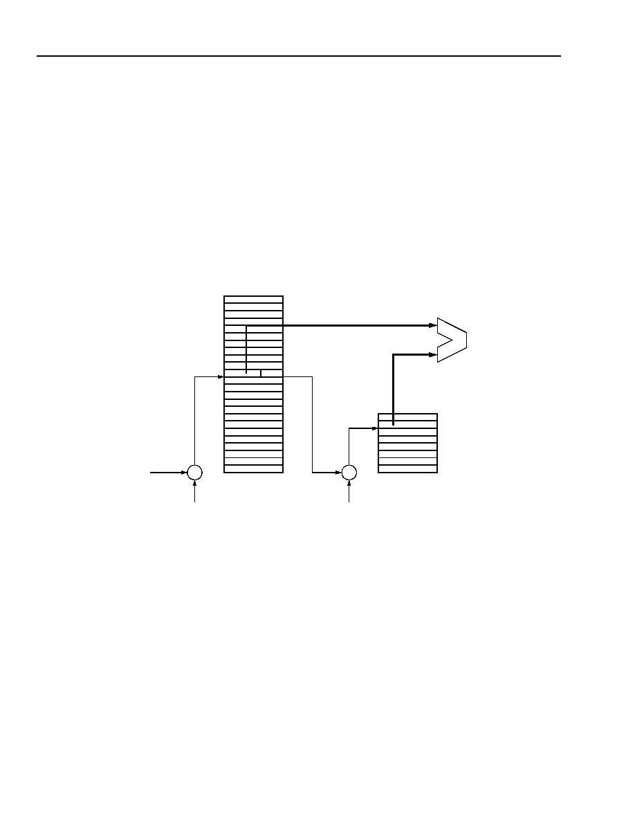
Logical View of the Enqueue (Left) and Dequeue (Right) Address Translation Procedure.............108
Figure 43.
Simplified Diagram of SQASE Queueing Structure.........................................................................109
Figure 44.
User Data Types and AAL Types at the Interfaces .........................................................................110
Figure 45.
User Data Type (UDT) vs. AAL Type Mapping ...............................................................................111
Figure 46.
SPAAL2 Data Format ......................................................................................................................112
Figure 47.
CPS-AAL0 Data Format ..................................................................................................................113
Figure 48.
PATM Format ..................................................................................................................................114
Figure 49.
HPF Format .....................................................................................................................................115
Figure 50.
Transferring an HPF Packet over the Host Interface Example........................................................118
Figure 51.
Port Table ........................................................................................................................................123
Figure 52.
VC Table..........................................................................................................................................125

List of Figures
(continued)
TAAD08JU2 Data
Sheet
T1/E1/J1 ATM Processor, Versions 2.1 and 3.1
August 18, 2003
Figures
Page
8
Agere Systems - Proprietary
Agere Systems Inc.
Use pursuant to Company instructions
Figure 53.
AAL2 VC Table................................................................................................................................126
Figure 54.
Connection Table ............................................................................................................................127
Figure 55.
SQASE Queueing Structure ............................................................................................................131
Figure 56.
Connection Queue Length Policing .................................................................................................138
Figure 57.
IL1Q/L1Q Length Policing ...............................................................................................................139
Figure 58.
IL2Q Length Policing .......................................................................................................................140
Figure 59.
UT2/UT2+ Header at the SIF Interface ...........................................................................................143
Figure 60.
Cell Transmission on the SIF Interface ...........................................................................................144
Figure 61.
Packet Transmission on the SIF Interface with No Stalls................................................................145
Figure 62.
Packet Transmission on the SIF Interface with the PHY Stalling ....................................................146
Figure 63.
Packet Transmission on the SIF Interface with the Master Stalling ................................................147
Figure 64.
Reception of a Cell on the SIF Interface..........................................................................................148
Figure 65.
Reception of a Packet on the SIF Interface with No Stalls ..............................................................149
Figure 66.
Reception of a Packet on the SIF Interface with the PHY Stalling ..................................................150
Figure 67.
Reception of a Packet on the SIF Interface with the Master Stalling...............................................151
Figure 68.
ESI Functional Timing Diagram.......................................................................................................153
Figure 69.
Data Read from TAAD08JU21 ........................................................................................................158
Figure 70.
Data Written to TAAD08JU2............................................................................................................159
Figure 71.
Power-On Reset ..............................................................................................................................160
Figure 72.
Stable Reset ....................................................................................................................................160
Figure 73.
CHI Transmit I/O Timing..................................................................................................................161
Figure 74.
CHI Receive I/O Timing...................................................................................................................162

List of Tables
Table
Page
Agere Systems Inc.
Agere Systems - Proprietary
9
Use pursuant to Company instructions
Data Sheet
TAAD08JU2
August 18, 2003
T1/E1/J1 ATM Processor, Versions 2.1 and 3.1
Table 1.
Pin Definitions................................................................................................................................... 12
Table 2.
Transmission Line Interface Signals (48 Signals) ............................................................................ 13
Table 3.
CHI Interface Signals (20 Signals) ................................................................................................... 14
Table 4.
UTOPIA 2 Expansion Interface Signals (52 Signals) ....................................................................... 14
Table 5.
System Interface Signals (62 Signals).............................................................................................. 15
Table 6.
Switch Fabric Interface Signals (50 Pins)......................................................................................... 17
Table 7.
APC External Statistics Interface Signals (18 Signals) .................................................................... 18
Table 8.
SAR External Statistics Interface Signals (18 Signals)..................................................................... 18
Table 9.
Host Interface Signals (49 Signals) .................................................................................................. 19
Table 10.
JTAG Interface Pins (6 Signals) ...................................................................................................... 19
Table 11.
Global/Miscellaneous Signal Pins (10 Signals) ................................................................................ 19
Table 12.
Power Supply Pins (4 Analog Power Pins, 120 Digital Power Pins) ............................................... 20
Table 13.
Signal-to-Ball Mapping ..................................................................................................................... 22
Table 14.
Host Registers .................................................................................................................................. 50
Table 15.
Frame Alignment Criteria.................................................................................................................. 58
Table 16.
Performance Monitor Functional Descriptions.................................................................................. 59
Table 17.
Performance Report Message Format ............................................................................................. 61
Table 18.
Performance Report Message Field Definition................................................................................. 62
Table 19.
Shared Tx Stack Format for CEPT Frame ....................................................................................... 65
Table 20.
Cell Headers of Idle, Unassigned, and Invalid Cells......................................................................... 73
Table 21.
TC Functionality................................................................................................................................ 73
Table 22.
TAAD08JU2 Exceptions to the IMA PICS Proforma ........................................................................ 85
Table 23.
PATM Fields ................................................................................................................................... 114
Table 24.
HPF Fields...................................................................................................................................... 115
Table 25.
ESI Message Format (AALXDATA[15:0])....................................................................................... 116
Table 26.
ESI Violation Codings..................................................................................................................... 117
Table 27.
AAL Type vs. Service Type Compatibility....................................................................................... 118
Table 28.
Transport of Congestion Indication and Loss Priority..................................................................... 121
Table 29.
PortIndex to Enqueue Block Port Mapping..................................................................................... 123
Table 30.
MEMI-SM Resources ..................................................................................................................... 124
Table 31.
SQASE-SM Resources .................................................................................................................. 130
Table 32.
L1Q and IL2Q Scheduling .............................................................................................................. 135
Table 33.
Example Stage-Two Divider Settings ............................................................................................. 137
Table 34.
Exceptions ...................................................................................................................................... 141
Table 35.
Absolute Maximum Ratings............................................................................................................ 154
Table 36.
Power Requirements ...................................................................................................................... 154
Table 37.
Operating Conditions...................................................................................................................... 154
Table 38.
Handling Precautions ..................................................................................................................... 155
Table 39.
Version 2.1 Logic Interface Characteristics .................................................................................... 155
Table 40.
Version 3.1 Logic Interface Characteristics .................................................................................... 156
Table 41.
Versions 2.1 and 3.1 Main System Clock (GCLK) Timing Specifications....................................... 157
Table 42.
Version 2.1 UTOPIA Input Clocks (UCLK) Timing Specifications .................................................. 157
Table 43.
Version 3.1 UTOPIA Input Clocks (UCLK_A[B]) Timing Specifications ......................................... 157
Table 44.
Host Read Timing Characteristics .................................................................................................. 158
Table 45.
Host Write Timing Characteristics .................................................................................................. 159
Table 46.
Version 2.1 CHI Transmit Timing Characteristics........................................................................... 161
Table 47.
Version 3.1 CHI Transmit Timing Characteristics........................................................................... 161
Table 48.
CHI Receive Timing Characteristics............................................................................................... 162
Table 49.
Version 2.1 Fabric Interface Timing Specifications (Transmit Interface) ........................................ 162
Table 50.
Version 3.1 Fabric Interface Timing Specifications (Transmit Interface) ........................................ 163
Table 51.
Version 2.1 Fabric Interface Timing Specifications (Receive Interface) ......................................... 163
Table 52.
Version 3.1 Fabric Interface Timing Specifications (Receive Interface) ......................................... 163

List of Tables
(continued)
Table
Page
TAAD08JU2 Data
Sheet
T1/E1/J1 ATM Processor, Versions 2.1 and 3.1
August 18, 2003
10
Agere Systems - Proprietary
Agere Systems Inc.
Use pursuant to Company instructions
Table 53.
Expansion UTOPIA2 Receive Interface Timing Specifications: 50 MHz ........................................ 164
Table 54.
UTOPIA2 Transmit Interface Timing Specifications: 50 MHz......................................................... 164
Table 55.
Version 2.1 ESI Interface Timing Specifications............................................................................. 164
Table 56.
Version 3.1 ESI Interface Timing Specifications (SAR and APC) .................................................. 164
Table 57.
JTAG Timing Specifications ........................................................................................................... 165
Table 58.
Version 2.1 Receive Interface Timing............................................................................................. 165
Table 59.
Version 2.1 Transmit Interface Timing............................................................................................ 165
Table 60.
Version 3.1 Receive Interface Timing (SUCLK Input) .................................................................... 166
Table 61.
Version 3.1 Transmit Interface Timing (SUCLK Input) ................................................................... 166
Table A-1.
Revision History.............................................................................................................................. 172

Data Sheet
August 18, 2003
T1/E1/J1 ATM Processor, Versions 2.1 and 3.1
TAAD08JU2
Agere Systems Inc.
Agere Systems - Proprietary
11
4 Description
TAAD08JU2 provides a flexible network-interface solution for next-generation applications in which efficient trans-
port of narrowband voice and broadband data information is critical to guaranteeing network QoS for the user and
transmission efficiency for the network operator. Constructed using Agere's 0.16 µm CMOS technology, the chip
has an integrated octal framer, IMA processor, cell scheduler and router, and AAL2/5 SAR functions.
TAAD08JU2 operates in either UNI or IMA mode (selectable on a per-span line basis). The complete AF-PHY-
0086.001 management information base (MIB) is supported. Flexible provisioning of link and group combinations
enables a mix of IMA and UNI mappings to various AAL services.
Support for AAL2 is provided via an AAL/CPS function that maps/demaps variable-sized CPS packets to/from
ATM-SDU. A total of 2032 bidirectional CIDs are supported. These CIDs can be transported within a programma-
ble number of VCs per direction. TAAD08JU2 supports up to 124 AAL2 VCs, which may be allocated between
ingress and egress traffic.
Support for high-speed data switching is provided whereby AAL5 VCs are routed through to the system interface
toward their destinations. TAAD08JU2 provides support for up to 2032 bidirectional AAL5 VCs via an internal con-
text memory.
TAAD08JU2 provides the following:
!
Integrated policing
!
F4/F5 operations, administration, and maintenance (OAM)
!
Cell processing
!
Statistics collection for performance monitoring
Communication with TAAD08JU2 is accomplished through a 32-bit microprocessor interface. The system interface
is through two choices: a UTOPIA 2 interface with support for both 8-bit and 16-bit data bus width and a UTOPIA-
derived packet interface with support for both 8-bit and 16-bit data bus widths.
TAAD08JU2 provides a complete ATM access function from AAL/CPS mapping functions (for AAL2 and 5) through
ATM/TC/PHY layers. The highly integrated, flexible architecture results in unified OAM features, simpler operation,
and best-in-class operation with respect to area, power, and function.

12
Agere Systems - Proprietary
Agere Systems Inc.
Data Sheet
August 18, 2003
T1/E1/J1 ATM Processor, Versions 2.1 and 3.1
TAAD08JU2
5 Pin Definitions
6 Pin Description
Many of the pins of the TAAD08JU2 device are multiplexed for different functions. In these cases, both functions
are shown in the same row of Table 2.
Table 1. Pin Definitions
Type
Description
I
Input only. All 3.3 V inputs are designed to be TTL compatible.
I
u
Input with high-value pull-up resistor internal to TAAD08JU2.
I
d
Input with high-value pull-down resistor internal to TAAD08JU2.
O
Output only. These outputs have I
OL
/I
OH
= 10 mA.
O-6
Output only. These outputs have I
OL
/I
OH
= 6 mA.
I/O
Bidirectional input and output.
P
Power or ground.

Agere Systems Inc.
Agere Systems - Proprietary
13
Data Sheet
August 18, 2003
T1/E1/J1 ATM Processor, Versions 2.1 and 3.1
TAAD08JU2
6 Pin Description
(continued)
Table 2. Transmission Line Interface Signals (48 Signals)
Signal
Type
Description
LRXCLK(0:7)
I
d
Line Interface Receive Clocks. Receive path clock from the LIU.
LRXPDATA(0:7)/
LRXDATA(0:7)
I
d
Line Interface Receive Positive Rail Data/Line Interface Receive Data. When
the TAAD08JU2 device is configured to operate in a dual-rail line interface mode,
this pin is the positive receive data from the external LIU. When the TAAD08JU2
device is configured to operate in a single-rail line interface mode, this pin is the
receive data from the external LIU.
LRXNDATA(0:7)/
LRXBPV(0:7)
I
d
Line Interface Receive Negative Rail Data/Line Interface Receive Bipolar Vio-
lations. When the TAAD08JU2 device is configured to operate in a dual-rail line
interface mode, this pin is the negative receive data from the external LIU. When
the TAAD08JU2 device is configured to operate in a single-rail line interface mode,
this pin is the receive bipolar violations signal from the external LIU.
LTXCLK(0:7)
I
d
/O
Line Interface Transmit Clock. These pins can be individually programmed as
either a clock input or output in one of three modes:
1. Global clock mode. All the LTXCLK signals are outputs derived from a global
clock input signal (see CHI interface CRXCLK in Table 3).
2. All of the LTXCLK signals are outputs of the corresponding LRXCLK signals
looped back internally.
3. Independent transmit clock mode. Each LTXCLK pin is an input from the line
interface.
The clock rates, when used as either inputs or outputs, are 1.544 MHz or
2.048 MHz. When the CHI interface is active, these pins must be configured in the
global clock mode.
LTXPDATA(0:7)/
LTXDATA(0:7)
O
Line Interface Transmit Positive Rail Data/Line Interface Transmit Data. When
the TAAD08JU2 device operates in a dual-rail line interface mode, this pin is the
positive transmit data sent to the external LIU. When the TAAD08JU2 device oper-
ates in a single-rail line interface mode, this pin is the transmit data sent to the
external LIU.
LTXNDATA(0:7)
O
Line Interface Transmit Negative Rail Data. When the TAAD08JU2 device oper-
ates in a dual-rail line interface mode, this pin is the negative transmit data sent to
external LIU. When the TAAD08JU2 device operates in a single-rail line interface
mode, this pin outputs an 8 kHz frame sync pulse.

14
Agere Systems - Proprietary
Agere Systems Inc.
Data Sheet
August 18, 2003
T1/E1/J1 ATM Processor, Versions 2.1 and 3.1
TAAD08JU2
6 Pin Description
(continued)
Table 3. CHI Interface Signals (20 Signals)
Signal
Type
Description
CRXCLK
I
CHI Receive Clock. This signal is used to perform two basic functions: 1) this
pin is used to clock the CHI receive interface; 2) depending on transmit line
clock mode, the clock on this pin can be used to drive the Tx line clock (of
which there are several suboptions). These suboptions are as follows:
!
When the receive CHI interface is used, then 2.048 MHz, 4.096 MHz,
8.192 MHz, or 16.384 MHz can be supplied. Internally, TAAD08JU2 will
derive 1.544 MHz and 2.048 MHz to support T1, E1, or a mix of T1 and E1
lines.
!
If the CHI is not used, this pin can be used to drive the line clocks in two sub-
modes, as follows:
-- This pin would directly drive the Tx interface. In this mode, 1.544 MHz (T1)
or 2.048 MHz (E1) is applied to CRXCLK, and all eights links run at this
line rate.
-- A 2.048 MHz reference is applied to CRXCLK and TAAD08JU2 internally
derives 1.544 MHz and 2.048 MHz to support either T1, E1, or a mix of
T1/E1 transmit lines. This mode is essentially a subset of option 1 above,
except the CHI is not used.
!
This pin is not used when the TAAD08JU2 is programmed into independent
transmit clock mode or receive loop timing mode.
!
The CRXCLK pin does not require a clock to be connected if that pin is not
being used for any framer or CHI clocking modes. However, if a clock is
required, this can be easily accommodated by connecting GCLK to this pin.
CRXDATA(0:7)
I
CHI Receive Data. These are the received CHI data inputs at 2.048 Mbits/s,
4.096 Mbits/s, or 8.192 Mbits/s.
CRXFS
I
CHI Receive Frame Sync. Global 8 kHz frame sync for the receive CHI ports.
CTXCLK
I
CHI Transmit Clock. Global system clock for transmit defined as a 2.048 MHz,
4.096 MHz, 8.192 MHz, or 16.384 MHz global input clock.
CTXDATA(0:7)
O
CHI Transmit Data. These are the transmitted CHI data outputs clocked by the
CTXCLK at 2.048 Mbits/s, 4.096 Mbits/s, or 8.192 Mbits/s.
CTXFS
I
CHI Transmit Frame Sync. Input global 8 kHz frame sync for the transmit sys-
tem.
Table 4. UTOPIA 2 Expansion Interface Signals (52 Signals)
Signal
Type
Description
UMODE
I
UTOPIA Expansion Interface Mode. This pin sets the mode of operation for
this interface. The modes are described below:
0: Master Mode: This signal is set low when TAAD08JU2 is programmed to
operate in either internal or external PHY mode. In this case, the internal
APC block controls the expansion interface pins as a UTOPIA master.
1: Slave Mode: This is set high when the TAAD08JU2 is programmed into
SAR-only mode. In this mode, this interface connects to the SAR block as a
UTOPIA slave.
UCLK
I
UTOPIA Expansion Clock. This is the UTOPIA clock input for both the trans-
mit and receive UTOPIA. The clock frequency applied to this pin should be less
than or equal to GCLK. A clock must be supplied on this pin at all times. Even if
this interface is not otherwise used, a clock must still be provided. Typically, this
can be easily accommodated by connecting GCLK to this pin.

Agere Systems Inc.
Agere Systems - Proprietary
15
Data Sheet
August 18, 2003
T1/E1/J1 ATM Processor, Versions 2.1 and 3.1
TAAD08JU2
6 Pin Description
(continued)
URXDATA[15:0]
Master: I
d
Slave: O
UTOPIA Expansion Receive Data. In master mode, these signals are the par-
allel 16-bit data input bus from an external PHY device. In slave mode, these
signals are a data output bus to an external PHY device. These signals are
clocked in/out on the rising edge of UCLK. Bit URXDATA[15] is the MSB.
URXPRTY
Master: I
d
Slave: O
UTOPIA Expansion Receive Data Parity. This signal either receives (master
mode) or sends (slave mode) the receive data parity signal. When a master,
TAAD08JU2's APC block can be configured to check for odd parity or can be
disabled. When a slave, this can be configured to odd, even, or no parity.
URXSOC Master:
I
d
Slave: O
UTOPIA Expansion Receive Start of Cell. Active-high signal asserted when
U
RXDATA
contains the first word of a cell.
URXENB Master:
O
Slave: I
u
UTOPIA Expansion Receive Enable. Active-low signal asserted by the ATM
layer to signal that a transfer will occur at the next rising edge of
UCLK.
URXADDR[4:0]
Master: O
Slave: I
d
UTOPIA Expansion Receive Address. 5-bit address used by the UTOPIA
master to select the UTOPIA slave for the receive signal path. Bit 4 is the MSB.
URXCLAV
Master: I
Slave: O
UTOPIA Expansion Receive Cell Available. Active-high signal asserted when
a complete cell is available in the FIFO of the device selected by U
RXADDR
.
UTXDATA[15:0]
Master: O
Slave: I
d
UTOPIA Expansion Transmit Data. In master mode, these signals are a paral-
lel 16-bit data output bus to an external PHY device. In slave mode, these sig-
nals are a parallel 16-bit data input bus from an external PHY device. Data is
clocked out/in on the rising edge of UCLK. Bit UTXDATA[15] is the MSB.
UTXPRTY
Master: O
Slave: I
d
UTOPIA Expansion Transmit Data Parity. This signal either sends (master
mode) or receives (slave mode) the transmit data parity signal. In slave mode,
this can be configured to odd, even, or no parity on UTXDATA bus. In master
mode, transmit parity can be either odd or disabled. The default is odd.
UTXSOC Master:
O
Slave: I
d
UTOPIA Expansion Transmit Start of Cell. Active-high signal asserted when
U
TXDATA
contains the first word of a cell.
UTXENB Master:
O
Slave: I
u
UTOPIA Expansion Transmit Enable. Active-low signal asserted by the ATM
layer to signal that U
TXDATA
and U
TXSOC
contain valid data.
UTXADDR[4:0]
Master: O
Slave: I
d
UTOPIA Expansion Transmit Address. 5-bit address used by the master to
select the UTOPIA slave for the transmit signal path. Bit 4 is the MSB.
UTXCLAV
Master: I
d
Slave: O
UTOPIA Expansion Transmit Cell Available. Active-high signal asserted
when the polled slave is ready to receive complete cell can be stored in the
FIFO of the device selected by U
TXADDR
.
Table 5. System Interface Signals (62 Signals)
Signal
Type
Description
SMODE[2:0]
I
d
System Interface Mode. The two LSBs (SMODE[1:0]) determine the operating
mode of the interface, while SMODE[2] determines the clock mode in UTOPIA
cell and packet modes.
SMODE[1:0] Description
00: UTOPIA mode
01: Packet (UT2+) mode
10: Unused
11: Unused
SMODE[2] sets the clock mode for the system interface. A low on this pin
causes TAAD08JU2 to input SUCLK, and a high sets TAAD08JU2 to generate
SUCLK.
Table 4. UTOPIA 2 Expansion Interface Signals (52 Signals) (continued)
Signal
Type
Description

16
Agere Systems - Proprietary
Agere Systems Inc.
Data Sheet
August 18, 2003
T1/E1/J1 ATM Processor, Versions 2.1 and 3.1
TAAD08JU2
6 Pin Description
(continued)
SUCLK
I
d
/O
System Interface Clock. Pin programmable to be an input or output. The clock
frequency applied to this pin should be less than or equal to GCLK.
STXDATA[15:0]
O
System Interface Transmit Data. Parallel data bus to the ATM layer clocked
out on the rising edge of SUCLK. Bit 15 is the MSB.
STXADDR[4:0]
O
System Transmit Address. 5-bit address used to select the external UTOPIA
slave for the transmit signal path.
STXSOC/STXSOP
O
System Transmit Start of Cell/Packet. In cell or packet mode, when STXSOC
is high, the first word of the packet is present on the STXDATA bus. STXSOC is
considered valid only when STXENB is asserted and is updated on the rising
edge of SUCLK.
STXPRTY
O
System Transmit Data Parity. This signal sends the parity bits for the STX-
DATA bus.
STXENB
O
System Transmit Enable. Active-low signal asserted by the ATM layer to sig-
nal that STXDATA contains valid data.
STXEOP
O
System UT2+ Transmit End of Packet. This signal is high when the last word
of a packet is on the STXDATA bus. STXEOP is valid only when STXENB is
asserted and is updated on the rising edge of SUCLK (UT2+ mode only).
STXSIZ
O
System UT2+ Transmit Size. This signal indicates the size of the current word
on STXDATA. STXSIZ is valid only when STXEOP is asserted. If the last word
contains two valid bytes, STXSIZ is high while that word is on the STXDATA
bus (16-bit UT2+ mode only).
STXERR
I
d
System UT2+ Transmit Error. SRXERR is an active-high signal that indicates
when the current packet is to be aborted and discarded, if possible. STXERR is
valid only when STXEOP and STXENB are asserted and is sampled on the ris-
ing edge of SUCLK (UT2+ mode only).
STXCLAV/STXPA
I
d
System Transmit Cell/Packet Available. Active-high signal asserted when a
complete cell/packet can be stored in the FIFO of the external device selected
by STXADDR.
STXSPA
I
d
System UT2+ Transmit Selected Multi-PHY Packet Available. While STX-
CLAV shows the polled status of the external UTOPIA slave, this signal indi-
cates the status of the current selected external slave. When asserted, this
signal indicates that the current selected slave has more space than the pre-
defined space in its FIFO (UT2+ mode only).
SRXDATA[15:0]
I
d
System Receive Data. This signal is the parallel 16-bit data bus to the ATM
layer clocked out on the rising edge of SUCLK. Bit SRXDATA[15] is the MSB.
SRXADDR[4:0]
O
System Receive Address. 5-bit address used to select the external UTOPIA
slave for the receive signal path. SRXADDR[4] is the MSB.
SRXSOC/SRXSOP
I
d
System Receive Start of Cell/Packet. Active-high signal asserted when SRX-
DATA
contains the first word of a cell or packet.
SRXPRTY
I
d
System Receive Data Parity. Programmable for odd, even, or no parity over
SRXDATA.
SRXENB
O
System Receive Enable. Active-low signal asserted by the ATM layer to signal
that a transfer will occur at the next rising edge of SUCLK
.
SRXEOP
I
d
System UT2+ Receive End of Packet. This signal is active-high, and it indi-
cates that the last word of a packet is on the SRXDATA bus. SRXEOP is valid
when SRXENB is asserted and is sampled on the rising edge of SUCLK. (UT2+
mode only.)
Table 5. System Interface Signals (62 Signals) (continued)
Signal
Type
Description

Agere Systems Inc.
Agere Systems - Proprietary
17
Data Sheet
August 18, 2003
T1/E1/J1 ATM Processor, Versions 2.1 and 3.1
TAAD08JU2
6 Pin Description
(continued)
SRXSIZ
I
d
System UT2+ Receive Size. This signal indicates the size of the current word
on SRXDATA. SRXSIZ is valid when SRXEOP is asserted. A logic one indi-
cates that SRXDATA[15:0] are valid, and a logic zero indicates that SRX-
DATA[15:8] are valid. (UT2+ mode only.)
SRXERR
I
d
System UT2+ Receive Error. This is an active-high signal that indicates that
the current packet is to be aborted and discarded, if possible. SRXERR is only
valid when SRXEOP and SRXENB are asserted and is sampled on the rising
edge of SUCLK. (UT2+ mode only.)
SRXCLAV/SRXPA
I
d
System Receive Cell/Packet Available. In cell mode, when asserted, this sig-
nal indicates that a subsequent cell is available after the current transfer. In
packet mode, when asserted, it indicates that more data than the predefined
amount is available.
SRXVAL
I
d
System UT2+ Receive Data Valid. This is an active-high signal asserted by a
slave device when in UT2+ mode to indicate that data is valid on the current
clock cycle. This signal allows for the slave device to control data flow by deas-
serting this signal, thus pausing the current packet transmission. When the
slave has valid data to put on the data bus, it will resume transmission of the
current packet by asserting SRXVAL. For every clock cycle that there is valid
data on the data bus, SRXVAL must be asserted. SRXVAL is a shared 3-state
signal between all active MPHYs and only the currently selected MPHY may
drive this signal.
Table 6. Switch Fabric Interface Signals (50 Pins)
Signal
Type
Description
Switch Fabric A Port
AATXDATA[7:0]
O-6
APC Port A Transmit Data. Parallel data bus used to transfer cells from
TAAD08JU2 to the switch fabric.
AATXPRTY
O-6
APC Port A Transmit Parity. Odd parity calculated over
AATXDATA
. Odd parity
means an odd number of ones including the parity bit.
AATXSOC
O-6
APC Port A Transmit Start of Cell. Active-high signal asserted when AATX-
DATA contains the first word of a cell.
AATXCLKP
O-6
APC Port A Transmit Differential Clock Positive. This clock is the reference
that is sent with the AATXDATA and is used by the receiving APC or switch fab-
ric to clock in the data. This clock is derived from GCLK and is twice the GCLK
frequency.
AATXCLKN
O-6
APC Port A Transmit Differential Clock Negative. This clock is the reference
that is sent with the AATXDATA and is used by the receiving APC or switch fab-
ric to clock in the data. This clock is derived from GCLK and is twice the GCLK
frequency.
AARXDATA[7:0]
I
d
APC Port A Receive Data. Parallel data bus used to transfer cells from the
switch fabric to TAAD08JU2.
AARXPRTY
I
d
APC Port A Receive Parity. Odd parity calculated over AARXDATA. Odd parity
means an odd number of ones including the parity bit.
AARXSOC
I
d
APC Port A Receive Start of Cell. Active-high signal asserted when AARX-
DATA contains the first word of a cell.
AARXCLKP
I
d
APC Port A Receive Differential Clock Positive. This clock is used by
TAAD08JU2 to clock AARXDATA into the device. This clock is typically twice
GCLK.
Table 5. System Interface Signals (62 Signals) (continued)
Signal
Type
Description

18
Agere Systems - Proprietary
Agere Systems Inc.
Data Sheet
August 18, 2003
T1/E1/J1 ATM Processor, Versions 2.1 and 3.1
TAAD08JU2
6 Pin Description
(continued)
Table 7. APC External Statistics Interface Signals (18 Signals)
AARXCLKN
I
d
APC Port A Receive Differential Clock Negative. This clock is used by
TAAD08JU2 to clock AARXDATA into the device. This clock is typically twice
GCLK.
Switch Fabric B Port
ABTXDATA[7:0]
O-6
APC Port B Transmit Data. Parallel data bus used to transfer cells from
TAAD08JU2 to the switch fabric.
ABTXPRTY
O-6
APC Port B Transmit Parity. Odd parity calculated over ABTXDATA. Odd parity
means an odd number of ones including the parity bit.
ABTXSOC
O-6
APC Port B Transmit Start of Cell. Active-high signal asserted when ABTX-
DATA contains the first word of a cell.
ABTXCLKP
O-6
APC Port B Transmit Differential Clock Positive. The frequency is derived
from GCLK. Maximum frequency is 100 MHz.
ABTXCLKN
O-6
APC Port B Transmit Differential Clock Negative. The frequency is derived
from GCLK. Maximum frequency is 100 MHz.
ABRXDATA[7:0]
I
d
APC Port B Receive, bits 7:0. Parallel data bus used to transfer cells from the
switch fabric to TAAD08JU2.
ABRXPRTY
I
d
APC Port B Receive Parity. Odd parity calculated over ABRXDATA. Odd parity
means an odd number of ones, including the parity bit.
ABRXSOC
I
d
APC Port B Receive Start of Cell. Active-high signal asserted when ABRX-
DATA contains the first word of a cell.
ABRXCLKP
I
d
APC Port B Receive Clock Positive. This clock is used by TAAD08JU2 to clock
the ABRXDATA into the device. This clock is typically twice GCLK.
ABRXCLKN
I
d
APC Port B Receive Clock Negative. This clock is used by TAAD08JU2 to
clock the ABRXDATA into the device. This clock is typically twice GCLK.
Switch Fabric Miscellaneous Signals
AGTSYNC
O
Global Time-Slot (Cell Time) Synchronization Pulse. Asserted high once
every 68 cycles of internal APC clock (which is 2 x GCLK).
AHPSWF
I
d
Agere Test Mode Pin. Should be tied to ground.
Signal
Type
Description
AEDATA[15:0]
O
APC External Statistics Data. A 16-bit data bus used to transfer data between
the APC and an optional external adjunct device.
AECLK
O
APC External Statistics Clock. Used as a reference to transfer data between
the APC and an external adjunct.
AESYNC
O
APC External Statistics Sync. A single-cycle pulse signaling the beginning of
the 34 clock cycle (AECLK) external statistics interface time slot. The absence
of this synchronization pulse indicates that cell processing is disabled.
Table 8. SAR External Statistics Interface Signals (18 Signals)
Signal
Type
Description
REDATA[15:0]
O
SAR External Statistics Data. A 16-bit data bus used to transfer data between
the SAR and an optional external adjunct device.
RECLK
O
SAR External Statistics Clock. Used as reference to transfer data between the
SAR and an external adjunct.
Table 6. Switch Fabric Interface Signals (50 Pins) (continued)
Signal
Type
Description

Agere Systems Inc.
Agere Systems - Proprietary
19
Data Sheet
August 18, 2003
T1/E1/J1 ATM Processor, Versions 2.1 and 3.1
TAAD08JU2
6 Pin Description
(continued)
Table 10. JTAG Interface Pins (6 Signals)
RESYNC
O
SAR External Statistics Sync. A single-cycle pulse signaling the beginning of
the (RECLK) SAR statistics interface time slot. The absence of this synchroniza-
tion pulse indicates that cell processing is disabled.
Table 9. Host Interface Signals (49 Signals)
Signal
Type
Description
HMODE[1:0]
I
d
Host Interface Mode Select. Selects the mode of operation of the microprocessor
interface. These pins must be connected to ground.
HCLK
I
Host Interface Clock. This interface is rising edge clocked. Data written to
TAAD08JU2 is latched on the rising edge of clock, and address information and data
outputs on the rising edge of clock. The maximum speed for this clock is 66 MHz.
HD[31:0]
I/O
Host Data Bus. This is a bidirectional 32-bit data bus used to transfer data to/from
TAAD08JU2.
HA[9:0]
I
d
Host Address Inputs. 10-bit address for register read or write operations. This
addressing is by 32-bit word.
HCEN
I
u
Host Chip Select. The active-low signal validates HA[9:0] for read and write transfers.
HWEN
I
u
Host Write Enable. 0 causes an active-low write, and 1 causes a read.
HADV
I
d
Host Advance. A high signal on this pin causes TAAD08JU2 to increment a previous
host address by one.
HIRQ
O
Host Slave Mode Interrupt. Active-low interrupt request signal from TAAD08JU2.
Signal
Type
Description
TMODE
I
d
JTAG Test Mode. This pin is an input with an internal pull-down. TMODE = 1 is
reserved for Agere testing.
TMS
I
u
Test Mode Select. This pin enables JTAG test mode. Pin has an internal pull-up.
TDI
I
u
Test Data Input. Serial test input during JTAG testing.
TRSTN
I
u
Test Reset. This signal must be asserted low on powerup.
TDO
O
Test Data Output. Serial test output during JTAG testing.
TCK
I
u
Test Clock. An internal pull-up exists on this pin. This pin is used to clock state and
test data into and out of the TAAD08JU2 during JTAG testing.
Table 11. Global/Miscellaneous Signal Pins (10 Signals)
Signal
Type
Description
GOE
I
u
Global Output Enable. When GOE is 0, all TAAD08JU2 outputs assume a high-
impedance state except TDO. When GOE is 1, all outputs operate normally. An
internal pull-up is provided on this pin.
GCLK
I
Global Clock. Maximum clock frequency is 52 MHz. All output clocks are derived
from this clock. GCLK should have a minimum 60/40 duty cycle and a maximum
frequency tolerance of ±0.05%. GCLKs frequency can range from 25 MHz to
50 MHz. When running slower than 50 MHz, the maximum throughput of
TAAD08JU2 (which is 155 Mbits/s at 50 MHz) is degraded proportionately.
Table 8. SAR External Statistics Interface Signals (18 Signals)
Signal
Type
Description

20
Agere Systems - Proprietary
Agere Systems Inc.
Data Sheet
August 18, 2003
T1/E1/J1 ATM Processor, Versions 2.1 and 3.1
TAAD08JU2
6 Pin Description
(continued)
Table 12. Power Supply Pins (4 Analog Power Pins, 120 Digital Power Pins)
GRESET
I
u
Global Reset. Active-low reset signal. On initial powerup, GRESET must be
asserted for at least 250 µs after stable clocks are provided to TAAD08JU2, in
order to allow the internal PLLs to stabilize. GCLK and HCLK must be continu-
ously applied during reset. When asserted, all internal circuity is reset to its
default condition. If TAAD08JU2 has already been powered on and operating, the
device can be reset by asserting GRESET for at least 8 clock cycles of GCLK and
8 clock cycles of HCLK. Note that both of these clock signals must be applied for
TAAD08JU2 to be properly reset. GRESET must be inactive for 2 ms before boot
sequence can commence.
GPLLBYP
I
d
Global PLL Bypass. This pin is used to bypass the operation of the global clock
synthesizer PLL. This pin is intended for Agere manufacturing testing, and must
be tied low for normal operation.
GPLLOUT
O
Global PLL Output. A reference clock output of the PLL used only for Agere test
purposes.
FPLLOUT
O
Framer PLL Output. A reference clock output of the PLL used only for Agere test
purposes.
SCANMODE
I
d
Scan Mode. This pin is used by Agere to scan test this device.
SCANCLK1
I
d
Scan Clock 1. This pin enables Agere internal scan testing, and should be tied
low for normal operation.
SCANCLK2
I
d
Scan Clock 2. This pin enables Agere internal scan testing, and should be tied
low for normal operation.
IDDQ
I
IDDQ Test Mode Enable. This pin should be tied high for normal operation.
When tied low, this pin is used for IDDQ testing.
Signal
Type
Description
GV
DD
A
P
Global PLL Power Supply. Separate dedicated 3.3 V power supply to power the
global clock synthesizer PLL. This power supply should be a low-noise supply.
GV
SS
A
P
Global PLL Ground. Separate 3.3 V ground to power the global clock synthe-
sizer PLL. This should be a low-noise ground.
FV
DD
A
P
Framer PLL Power Supply. Separate dedicated 3.3 V power supply to power the
framer PLL. This power supply should be a low-noise supply.
FV
SS
A
P
Framer PLL Ground. Separate dedicated 3.3 V ground to power the framer PLL.
This should be a low-noise ground.
V
DD
33
P
3.3 V Digital Power Pins.
V
DD
15
P
1.5 V Digital Power Pins.
V
SS
P
Digital Ground Pins.
Table 11. Global/Miscellaneous Signal Pins (10 Signals) (continued)
Signal
Type
Description

Data Sheet
August 18, 2003
T1/E1/J1 ATM Processor, Versions 2.1 and 3.1
TAAD08JU2
Agere Systems Inc.
Agere Systems - Proprietary
21
7 Package Pin Layout
TAAD08JU2 uses the SuperBGA
TM
EBGA-520 package (1.27 mm. pitch).
!
Body size: 40 x 40 x 0.78 mm
!
Maximum height off-board: 1.67 mm
!
Solder ball pitch: 1.27 mm
!
Thermal,
JA
: 11
o
C/W
5-9957(F)
Figure 1. Pin Configuration Diagram
399
2
3
4
5
6
7
8
9
10 11 12 13 14 15 16 17 18 19 20 21 22 23 24 25 26 27 28 29 30 31
A
B
C
D
E
F
G
H
J
K
L
M
N
P
R
T
U
V
W
Y
AA
AB
AC
AD
AE
AF
AG
AH
AJ
AK
AL
TOP VIEW
V
SS
V
DD
15 (1.5 V)
V
DD
33 (3.3 V)
SIGNAL PIN/SPECIAL V
DD
-V
SS
400
396
398
394
397
393
395
391
VSS
VSS
VSS
VSS
VSS
VSS
VSS
VSS
VSS
VSS
VSS
392
389
390
388
386
18
10
13
5
2
22
12
17
8
3
21
11
16
6
1
24
14
19
9
4
27
20
25
15
7
23
26
387
384
385
383
381
382
379
380
378
376
370
368
369
367
366
365
363
364
362
361
360
358
359
357
356
355
353
354
352
351
377
375
374
VSS
VSS
372
373
371
346
348
347
349
350
341
343
342
344
345
336
338
337
339
340
331
333
332
334
335
319
322
321
323
325
314
317
316
318
320
309
312
311
313
315
304
308
306
310
329
328
330
324
326
327
VSS
VSS
VSS VSS
VSS
VSS
VSS VSS
VSS
VSS
303
301
305
307
302
277
287
282
292
297
275
285
280
290
295
279
289
284
293
298
278
288
283
291
296
300
299
294
274
281
276
286
260
255
265
270
259
254
264
269
253
263
258
268
272
252
262
257
267
271
273
256
251
261
266
VSS
VSS
VSS
30
33
29
32
28
31
35 34
44
39
45
50
40
49
42
37
43
48
38
47
41
36
46
1.5
1.5
1.5
51 52 53 54 55
56 57 58 59 60
61 62 63 64 65
66 67 68 69 70
71 72 73
1.5
76 78 79 80 82
81 83 84 85 87
86 88 89 90 92
91 93 95 97
94 96 98 100
74
75 77
99
VSS
VSS
VSS
VSS
VSS
VSS
VSS VSS
VSS
VSS
VSS
1.5
1.5
1.5
1.5
1.5
104 109 114 119 124
106 111 116 121 126
103 108 112 117 122
105 110 113 118 123
128 132 137 142 147
129 133 138 143 148
130 134 139 144 149
115 120 125 127
101
107
102
131 136 141 146
135 140 145 150
VSS
152 157 162 167 171
156 161 166
151
153 158 163 168 172
154 159 164 169 173
155 160 165 170
VSS
VSS
VSS
VSS
VSS
1.5
1.5
1.5
180 185 190 195 200
182 187 192 197
179 184 189 193 198
178 183 188 191 196
174 176 181 186
175
177
199
194
VSS
VSS
VSS
VSS
VSS
VSS
VSS
1.5
1.5
1.5
1.5
1.5
VSS
246 247 248 249 250
241 242 243 244 245
236 237 238 239 240
231 232 233 234 235
228 229 230
224 226
227
219 221 222 223 225
214 216 217 218 220
209 211 212 213 215
204 206 208 210
201 203 205 207
202
VSS
VSS
VSS
VSS
1.5 1.5 1.5
1.5
1.5
1.5
1.5
1.5
1.5
1.5
1.5
1.5
1.5
1.5
1.5
3.3
3.3
3.3
3.3
3.3
3.3
3.3
3.3
3.3
3.3
3.3
3.3
3.3
3.3
3.3
3.3
3.3
3.3
3.3
3.3
3.3
3.3
3.3
3.3
3.3
3.3
3.3
3.3
3.3
3.3
3.3
3.3
1
VSS

TAAD08JU2
Preliminary Data Sheet
T1/E1/J1 ATM Processor, Versions 2.1 and 3.1
August 18, 2003
7 Package Pin Layout
(continued)
22
Agere Systems Inc.
(Pins shown as Reserved must be left unconnected).
Table 13. Signal-to-Ball Mapping
Ball
Pad
Number
Data Sheet Ball Name
E4
1
AEDATA[15]
D2
2
AEDATA[14]
E3
3
AEDATA[13]
F5
4
AEDATA[12]
E2
5
AEDATA[11]
F4
6
AEDATA[10]
E1
7
AEDATA[9]
F3
8
AEDATA[8]
G5
9
AEDATA[7]
F2
10
AEDATA[6]
G4
11
AEDATA[5]
G3
12
AEDATA[4]
G2
13
AEDATA[3]
H5
14
AEDATA[2]
G1
15
AEDATA[1]
H4
16
AEDATA[0]
H3
17
URXDATA[15]
H2
18
URXDATA[14]
J5
19
URXDATA[13]
H1
20
URXDATA[12]
J4
21
URXDATA[11]
J3
22
URXDATA[10]
J2
23
URXDATA[9]
K5
24
URXDATA[8]
J1
25
URXDATA[7]
K4
26
URXDATA[6]
K1
27
URXDATA[5]
L4
28
URXDATA[4]
L3
29
URXDATA[3]
L2
30
URXDATA[2]
M5
31
URXDATA[1]
M4
32
URXDATA[0]
M3
33
URXENB
M2
34
URXPRTY
M1
35
URXSOC
N5
36
URXCLAV
N4
37
URXADDR[0]
N3
38
URXADDR[1]
N2
39
URXADDR[2]
N1
40
URXADDR[3]
P5
41
URXADDR[4]
P4
42
UCLK
P3
43
UTXADDR[4]
P2
44
UTXADDR[3]
P1
45
UTXADDR[2]
R5
46
UTXADDR[1]
R4
47
UTXADDR[0]
R3
48
UTXCLAV
R2
49
UTXSOC
R1
50
UTXPRTY
U1
51
UTXENB
U2
52
UTXDATA[15]
U3
53
UTXDATA[14]
U4
54
UTXDATA[13]
U5
55
UTXDATA[12]
V1
56
UTXDATA[11]
V2
57
UTXDATA[10]
V3
58
UTXDATA[9]
V4
59
UTXDATA[8]
V5
60
UTXDATA[7]
W1
61
UTXDATA[6]
W2
62
UTXDATA[5]
W3
63
UTXDATA[4]
W4
64
UTXDATA[3]
W5
65
UTXDATA[2]
Y1
66
UTXDATA[1]
Y2
67
UTXDATA[0]
Y3
68
UMODE
Y4
69
STXDATA[15]
Y5
70
STXDATA[14]
AA2
71
STXDATA[13]
AA3
72
STXDATA[12]
AA4
73
STXDATA[11]
AB1
74
STXDATA[10]
AB4
75
STXDATA[9]
AC1
76
STXDATA[8]
AB5
77
STXDATA[7]
AC2
78
STXDATA[6]
Table 13. Signal-to-Ball Mapping (continued)
Ball
Pad
Number
Data Sheet Ball Name

Preliminary Data Sheet
TAAD08JU2
August 18, 2003
T1/E1/J1 ATM Processor, Versions 2.1 and 3.1
7 Package Pin Layout
(continued)
<10pt>Agere Systems - Proprietary
23
AC3
79
STXDATA[5]
AC4
80
STXDATA[4]
AD1
81
STXDATA[3]
AC5
82
STXDATA[2]
AD2
83
STXDATA[1]
AD3
84
STXDATA[0]
AD4
85
STXCLAV/STXPA/
AE1
86
STXSPA
AD5
87
STXSOC/STXSOP
AE2
88
STXPRTY
AE3
89
STXSIZ
AE4
90
STXENB
AF2
91
STXERR
AE5
92
STXEOP
AF3
93
RESERVED
AG1
94
STXADDR[0]
AF4
95
STXADDR[1]
AG2
96
STXADDR[2]
AF5
97
STXADDR[3]
AG3
98
STXADDR[4]
AH2
99
SRXADDR[4]
AG4
100
SRXADDR[3]
AH5
101
SRXADDR[2]
AK4
102
SRXADDR[1]
AJ5
103
SRXADDR[0]
AG6
104
SUCLK
AK5
105
SRXVAL
AH6
106
SRXCLAV
AL5
107
SRXSOC
AJ6
108
SRXPRTY
AG7
109
SRXEOP
AK6
110
SRXERR
AH7
111
SRXENB
AJ7
112
SRXSIZ
AK7
113
SRXDATA[15]
AG8
114
SRXDATA[14]
AL7
115
SRXDATA[13]
AH8
116
SRXDATA[12]
AJ8
117
SRXDATA[11]
AK8
118
SRXDATA[10]
Table 13. Signal-to-Ball Mapping (continued)
Ball
Pad
Number
Data Sheet Ball Name
AG9
119
SRXDATA[9]
AL8
120
SRXDATA[8]
AH9
121
SRXDATA[7]7
AJ9
122
SRXDATA[6]
AK9
123
SRXDATA[5]
AG10
124
SRXDATA[4]
AL9
125
SRXDATA[3]
AH10
126
SRXDATA[2]
AL10
127
SRXDATA[1]
AH11
128
SRXDATA[0]
AJ11
129
SMODE2
AK11
130
SMODE1
AG12
131
SMODE0
AH12
132
REDATA[15]
AJ12
133
REDATA[14]
AK12
134
REDATA[13]
AL12
135
REDATA[12]
AG13
136
REDATA[11]
AH13
137
REDATA[10]
AJ13
138
REDATA[9]
AK13
139
REDATA[8]
AL13
140
REDATA[7]
AG14
141
REDATA[6]
AH14
142
REDATA[5]
AJ14
143
REDATA[4]
AK14
144
REDATA[3]
AL14
145
REDATA[2]
AG15
146
REDATA[1]
AH15
147
REDATA[0]
AJ15
148
RESYNC
AK15
149
RECLK
AL15
150
HIRQ
AL17
151
HADV
AK17
152
HWEN
AJ17
153
HCEN
AH17
154
HCLK
AG17
155
HA[9]
AL18
156
HA[8]
AK18
157
HA[7]
AJ18
158
HA[6]
Table 13. Signal-to-Ball Mapping (continued)
Ball
Pad
Number
Data Sheet Ball Name

TAAD08JU2
Preliminary Data Sheet
T1/E1/J1 ATM Processor, Versions 2.1 and 3.1
August 18, 2003
7 Package Pin Layout
(continued)
24
Agere Systems Inc.
AH18
159
HA[5]
AG18
160
HA[4]
AL19
161
HA[3]
AK19
162
HA[2]
AJ19
163
HA[1]
AH19
164
HA[0]
AG19
165
HMODE1
AL20
166
HMODE0
AK20
167
HD[31]
AJ20
168
HD[30]
AH20
169
HD[29]
AG20
170
HD[28]
AK21
171
HD[27]
AJ21
172
HD[26]
AH21
173
HD[25]
AL22
174
HD[24]
AH22
175
HD[23]
AL23
176
HD[22]
AG22
177
HD[21]
AK23
178
HD[20]
AJ23
179
HD[19]
AH23
180
HD[18]
AL24
181
HD[17]
AG23
182
HD[16]
AK24
183
HD[15]
AJ24
184
HD[14]
AH24
185
HD[13]
AL25
186
HD[12]
AG24
187
HD[11]
AK25
188
HD[10]
AJ25
189
HD[9]
AH25
190
HD[8]
AK26
191
HD[7]
AG25
192
HD[6]
AJ26
193
HD[5]
AL27
194
HD[4]
AH26
195
HD[3]
AK27
196
HD[2]
AG26
197
HD[1]
AJ27
198
HD[0]
Table 13. Signal-to-Ball Mapping (continued)
Ball
Pad
Number
Data Sheet Ball Name
AK28
199
RESERVED
AH27
200
RESERVED
AG28
201
RESERVED
AH30
202
RESERVED
AG29
203
RESERVED
AF27
204
RESERVED
AG30
205
RESERVED
AF28
206
RESERVED
AG31
207
RESERVED
AF29
208
RESERVED
AE27
209
RESERVED
AF30
210
RESERVED
AE28
211
RESERVED
AE29
212
RESERVED
AE30
213
RESERVED
AD27
214
RESERVED
AE31
215
RESERVED
AD28
216
RESERVED
AD29
217
RESERVED
AD30
218
RESERVED
AC27
219
RESERVED
AD31
220
TCK
AC28
221
TDO
AC29
222
TRSTN
AC30
223
TDI
AB27
224
TMS
AC31
225
TMODE
AB28
226
GOE
AB31
227
IDDQ
AA28
228
SCANMODE
AA29
229
SCANCLK2
AA30
230
SCANCLK1
Y27
231
GPLLOUT
Y28
232
GRESET
Y29
233
GCLK
Y30
234
GPLLBYP
Y31
235
GVSSA
W27
236
GVDDA
W28
237
FPLLOUT
W29
238
FVSSA
W30
239
FVDDA
W31
240
RESERVED
Table 13. Signal-to-Ball Mapping (continued)
Ball
Pad
Number
Data Sheet Ball Name

Preliminary Data Sheet
TAAD08JU2
August 18, 2003
T1/E1/J1 ATM Processor, Versions 2.1 and 3.1
7 Package Pin Layout
(continued)
<10pt>Agere Systems - Proprietary
25
V27
241
RESERVED
V28
242
RESERVED
V29
243
RESERVED
V30
244
RESERVED
V31
245
RESERVED
U27
246
RESERVED
U28
247
RESERVED
U29
248
RESERVED
U30
249
RESERVED
U31
250
RESERVED
R31
251
RESERVED
R30
252
RESERVED
R29
253
RESERVED
R28
254
RESERVED
R27
255
RESERVED
P31
256
RESERVED
P30
257
RESERVED
P29
258
RESERVED
P28
259
RESERVED
P27
260
RESERVED
N31
261
RESERVED
N30
262
RESERVED
N29
263
RESERVED
N28
264
RESERVED
N27
265
RESERVED
M31
266
RESERVED
M30
267
RESERVED
M29
268
RESERVED
M28
269
RESERVED
M27
270
RESERVED
L30
271
RESERVED
L29
272
RESERVED
L28
273
RESERVED
K31
274
RESERVED
K28
275
RESERVED
J31
276
RESERVED
K27
277
RESERVED
J30
278
RESERVED
J29
279
RESERVED
J28
280
RESERVED
Table 13. Signal-to-Ball Mapping (continued)
Ball
Pad
Number
Data Sheet Ball Name
H31
281
LRXNDATA7/LRXBPV7
J27
282
LRXNDATA6/LRXBPV6
H30
283
LRXNDATA5/LRXBPV5
H29
284
LRXNDATA4/LRXBPV4
H28
285
LRXNDATA3/LRXBPV3
G31
286
LRXNDATA2/LRXBPV2
H27
287
LRXNDATA1/LRXBPV1
G30
288
LRXNDATA0/LRXBPV0
G29
289
LRXPDATA7/LRXDATA7
G28
290
LRXPDATA6/LRXDATA6
F30
291
LRXPDATA5/LRXDATA5
G27
292
LRXPDATA4/LRXDATA4
F29
293
LRXPDATA3/LRXDATA3
E31
294
LRXPDATA2/LRXDATA2
F28
295
LRXPDATA1/LRXDATA1
E30
296
LRXPDATA0/LRXDATA0
F27
297
LRXCLK7
E29
298
LRXCLK6
D30
299
LRXCLK5
E28
300
LRXCLK4
D27
301
LRXCLK3
B28
302
LRXCLK2
C27
303
LRXCLK1
E26
304
LRXCLK0
B27
305
LTXNDATA7
D26
306
LTXNDATA6
A27
307
LTXNDATA5
C26
308
LTXNDATA4
E25
309
LTXNDATA3
B26
310
LTXNDATA2
D25
311
LTXNDATA1
C25
312
LTXNDATA0
B25
313
LTXPDATA7/LTXDATA7
E24
314
LTXPDATA6/LTXDATA6
A25
315
LTXPDATA5/LTXDATA5
D24
316
LTXPDATA4/LTXDATA4
C24
317
LTXPDATA3/LTXDATA3
B24
318
LTXPDATA2/LTXDATA2
E23
319
LTXPDATA1/LTXDATA1
A24
320
LTXPDATA0/LTXDATA0
Table 13. Signal-to-Ball Mapping (continued)
Ball
Pad
Number
Data Sheet Ball Name

TAAD08JU2
Preliminary Data Sheet
T1/E1/J1 ATM Processor, Versions 2.1 and 3.1
August 18, 2003
7 Package Pin Layout
(continued)
26
Agere Systems Inc.
D23
321
LTXCLK7
C23
322
LTXCLK6
B23
323
LTXCLK5
E22
324
LTXCLK4
A23
325
LTXCLK3
D22
326
LTXCLK2
A22
327
LTXCLK1
D21
328
LTXCLK0
C21
329
CTXDATA7
B21
330
CTXDATA6
E20
331
CTXDATA5
D20
332
CTXDATA4
C20
333
CTXDATA3
B20
334
CTXDATA2
A20
335
CTXDATA1
E19
336
CTXDATA0
D19
337
CTXFS
C19
338
CTXCLK
B19
339
CRXDATA7
A19
340
CRXDATA6
E18
341
CRXDATA5
D18
342
CRXDATA4
C18
343
CRXDATA3
B18
344
CRXDATA2
A18
345
CRXDATA1
E17
346
CRXDATA0
D17
347
CRXFS
C17
348
CRXCLK
B17
349
ABRXDATA[7]
A17
350
ABRXDATA[6]
A15
351
ABRXDATA[5]
B15
352
ABRXDATA[4]
C15
353
ABRXDATA[3]
D15
354
ABRXDATA[2]
E15
355
ABRXDATA[1]
A14
356
ABRXDATA[0]
B14
357
ABRXCLKN
C14
358
ABRXCLKP
D14
359
ABRXSOC
E14
360
ABRXPRTY
Table 13. Signal-to-Ball Mapping (continued)
Ball
Pad
Number
Data Sheet Ball Name
A13
361
ABTXDATA[7]
B13
362
ABTXDATA[6]
C13
363
ABTXDATA[5]
D13
364
ABTXDATA[4]
E13
365
ABTXDATA[3]
A12
366
ABTXDATA[2]
B12
367
ABTXDATA[1]
C12
368
ABTXDATA[0]
D12
369
ABTXCLKN
E12
370
ABTXCLKP
B11
371
ABTXSOC
C11
372
ABTXPRTY
D11
373
AARXDATA[7]
A10
374
AARXDATA[6]
D10
375
AARXDATA[5]
A9
376
AARXDATA[4]
E10
377
AARXDATA[3]
B9
378
AARXDATA[2]
C9
379
AARXDATA[1]
D9
380
AARXDATA[0]
A8
381
AARXCLKN
E9
382
AARXCLKP
B8
383
AARXSOC
C8
384
AARXPRTY
D8
385
AATXDATA[7]
A7
386
AATXDATA[6]
E8
387
AATXDATA[5]
B7
388
AATXDATA[4]
C7
389
AATXDATA[3]
D7
390
AATXDATA[2]
B6
391
AATXDATA[1]
E7
392
AATXDATA[0]
C6
393
AATXCLKN
A5
394
AATXCLKP
D6
395
AATXSOC
B5
396
AATXPRTY
E6
397
AGTSYNC
C5
398
AHPSWF
B4
399
AESYNC
D5
400
AECLK
Table 13. Signal-to-Ball Mapping (continued)
Ball
Pad
Number
Data Sheet Ball Name

Data Sheet
August 18, 2003
T1/E1/J1 ATM Processor, Versions 2.1 and 3.1
TAAD08JU2
Agere Systems Inc.
Agere Systems - Proprietary
27
8 Block Diagram
0145(F)
Figure 2. Architecture of the TAAD08JU2 Device
As seen in Figure 2, TAAD08JU2 provides a complete ATM low-speed access function. In comparison to current
alternative devices, TAAD08JU2 provides framing, transmission convergence, inverse multiplexing for ATM, ATM
port management, and AAL SARing functions in a single, highly integrated device. Furthermore, TAAD08JU2 is
architected to be flexible and scalable to effectively handle alternative higher-rate physical interfaces.
TAAD08JU2 provides the following features as a highly integrated system on a chip (SOC):
!
A complete, integrated, low-speed ATM access device solution.
!
Flexible solution for transporting mixed traffic classes with QoS guarantees.
!
System-on-a-chip performance with a simpler OAMP API to enhance time-to-market.
TAAD08JU2 terminates a variety of low-speed physical link protocols (T1/E1/J1) via an integrated framer. Each
link can carry ATM cell streams corresponding to multiple connections.
Transmission convergence (TC) provides cell delineation through HEC generation and checking. TC also provides
cell rate decoupling between the ATM and PHY layers through insertion/discard of idle ATM cells.
The IMA block provides for inverse multiplexing over ATM using one to four groups with two to eight links per
group.
The ATM port controller (APC) block provides all of the functionality of the Agere APC device, such as switching,
traffic shaping, and policing.
The AAL engine provides a number of segmentation and reassembly options based on AAL2 and AAL5 standards
while maintaining multiple traffic classes and qualities of service.
FRAMER
TC
IMA
EDC
TAAD08JU2
AAL
APC
B
A
INTERFACE
UTOPIA EXPANSION
ENGINE
INTERFACE
HOST PROCESSOR
SY
STEM
I
N
TE
R
F
AC
E
SWI
T
CH
F
ABRI
C
B
U
S
CHI
T
D
M
IN
T
E
R
F
A
C
E
LIN
E
I
N
TE
R
F
AC
E

28
Agere Systems - Proprietary
Agere Systems Inc.
Data Sheet
August 18, 2003
T1/E1/J1 ATM Processor, Versions 2.1 and 3.1
TAAD08JU2
9 Software Components
This section discusses the software that is used to initialize, configure, and operate TAAD08JU2. The purpose of
this section is to introduce these important software components, to familiarize the user with them, and to provide
links to the appropriate documentation.
TAAD08JU2 is a highly integrated SOC. The numerous functional blocks (see chapter 8) that the system com-
prises are connected together and controlled by an internal 32 bit ARM
Æ
processor. This processor runs software
(known as firmware) that controls all the internal workings of TAAD08JU2 and all the external communications with
the user's system. Control of the TAAD08JU2 system occurs via a communications protocol between the firmware
running on the internal ARM and software running on an external microprocessor (host processor). Commands are
sent to the firmware and responses are returned using this protocol. A library of C functions translates high-level
API function calls into the command format expected by firmware and implements the communications protocol.
This library of software is known as device manager (DevMan for short). A separate utility is also used to create a
binary setup file that configures TAAD08JU2's operating modes and initializes tables. This utility is the TAAD08JU2
setup file utility (formerly known as Newport Setup File Utility, NSFU for short). End users of TAAD08JU2 write
application code that, through the device manager, controls the TAAD08JU2 in their systems.
Many levels of software are used to abstract the user from the internal details of the hardware in TAAD08JU2.
(There is no direct access to the internal registers in TAAD08JU2. Control is strictly through firmware commands
and indications.) The user's view of TAAD08JU2 is through the high-level device manager API calls.
Figure 3 shows the scope of software components surrounding the TAAD08JU2 device.
Figure 3. Software Components
The rectangular block at the center of the figure refers to the physical TAAD08JU2 (formerly known as Newport,
NP for short) hardware device. The physical device has a set of control registers, an input buffer, and an output
buffer. These registers and buffers are known as the embedded device controller (EDC) registers. All control and
data transfer is done through these registers and buffers. From the software point of view, TAAD08JU2 is a mem-
ory-mapped device with interface registers used to send commands and exchange data with the internal devices.
See chapter 13 for details on the TAAD08JU2 registers that are visible to the host processor.
SYSTEM SOFTWARE
APPLICATION CODE
SFU
DEVICE
MANAGER
FIRMWARE
NP

Agere Systems Inc.
Agere Systems - Proprietary
29
Data Sheet
August 18, 2003
T1/E1/J1 ATM Processor, Versions 2.1 and 3.1
TAAD08JU2
9 Software Components
(continued)
9.1 Firmware
The TAAD08JU2 chip contains an embedded ARM processor to manage the internal devices and communicate
with the host processor. The ARM processor has no software permanently stored in TAAD08JU2. The user's host
processor must load the ARM's instructions into RAM located inside the TAAD08JU2 before the TAAD08JU2 can
operate. These instructions are known as firmware. The ARM firmware files are supplied with the TAAD08JU2 soft-
ware release.
The firmware can be viewed as the assembly language of TAAD08JU2. All user-controllable functions of
TAAD08JU2 are implemented as firmware commands (i.e., assembly-language statements in a microprocessor).
To execute a command, the binary parameters of the command are loaded into the TAAD08JU2 EDC input buffer
by the host processor. The command word is then written to the EDC command register. The ARM receives an
interrupt, and the firmware then reads the command word from the command register and interprets the command
parameters. The firmware executes the command. The firmware places the results of executing the command into
the EDC output buffer and writes an indication word into the EDC indication register. TAAD08JU2 hardware then
generates an external interrupt to the host processor notifying it that firmware has made data available. This is the
handshaking that occurs to exchange commands and data between the external processor and TAAD08JU2 firm-
ware.
In summary, the key points of the TAAD08JU2 ARM firmware are:
!
TAAD08JU2 contains an embedded ARM processor--a true SOC.
!
Two binary files contain the ARM instruction code and data.
!
The instruction code for the ARM processor is not permanently stored in TAAD08JU2, and thus must be down-
loaded into TAAD08JU2 every time the device is powered on or reset.
!
Application software never talks directly to the ARM. Only the device manager sends firmware commands and
receives indications from the ARM.
9.2 Device Manager
The device manager for TAAD08JU2 is an applications programming interface (API) written in C. This software is
referred to as device manager software or simply the device manager, and the interface is called the device man-
ager API. Programmers use this interface to access and control TAAD08JU2 from their applications. The device
manager is coded using ANSI C and is compiled into a library of functions for the host platform.
TAAD08JU2 is a very complex device. Communication with the ARM processor firmware in TAAD08JU2 is some-
what complicated. The API is designed to provide programmers with a level of abstraction that hides the complex-
ity of this device. Figure 4 illustrates how the device manager API is used to communicate with TAAD08JU2.

30
Agere Systems - Proprietary
Agere Systems Inc.
Data Sheet
August 18, 2003
T1/E1/J1 ATM Processor, Versions 2.1 and 3.1
TAAD08JU2
9 Software Components
(continued)
Figure 4. Device Manager APIs and TAAD08JU2 Communications
As shown in Figure 4, the host application code (typically high-level management software) is linked with the
device manager library. It uses the C functions exported by the library to access and control TAAD08JU2.
TAAD08JU2's host interface provides for the hardware registers that are used to pass information to and from the
firmware software. The device manager layer sends commands to the firmware for services. The firmware uses
indications to inform the device manager about events that occur on TAAD08JU2. The device manager interprets
the indications and, if required, conveys the results to the application.
The device manager hides the details of the hardware from the application. The device manager API deals in high-
level functionality, not device registers. It also hides device-specific details where possible. Applications use the
device manager's C function interface to request services provided by the device manager. The return value of the
C function indicates whether the called function was successful or not.
Refer to the TAAD08JU2 device manager API document for more details on device manager implementation and
the available API functions.
In summary, the key points of the TAAD08JU2 device manager are as follows:
!
The device manager is a set of C functions that applications use to configure, control, and monitor TAAD08JU2.
!
The device manager library is called by the application code. It is not a separate, stand-alone application.
!
The device manager is the interface between application code and the TAAD08JU2 device. Application code
never accesses TAAD08JU2 registers directly. Application code never sends firmware commands or receives
firmware indications.
!
The device manager translates application calls into firmware commands, which then are sent to the ARM in
TAAD08JU2.
!
The device manager handles alarm recording and statistics reported by TAAD08JU2.
!
The device manager handles downloading the ARM firmware into TAAD08JU2 during start-up.
9.3 Setup File Utility (SFU)
The TAAD08JU2 setup file utility (also known as Newport Setup File Utility, NSFU for short) runs on a Windows
Æ
PC and guides the user through the initial configuration of TAAD08JU2. The NSFU software package creates a
binary setup file containing configuration commands, which are downloaded to TAAD08JU2 using a device man-
ager API.
EDC REGISTERS
HOST PROCESSOR
APPLICATION CODE
DEVICE MANAGER API
ARM--FIRMWARE
TAAD08JU2

Agere Systems Inc.
Agere Systems - Proprietary
31
Data Sheet
August 18, 2003
T1/E1/J1 ATM Processor, Versions 2.1 and 3.1
TAAD08JU2
9 Software Components
(continued)
The user is encouraged to use the setup file utility to generate the sequence of setup commands and store them in
a setup file. The setup utility allows the user to choose the mode information by simply clicking on the GUI to select
options. It ensures that the user selects a valid combination of options by providing appropriate error messages
and, where possible, by restricting the available options to the appropriate ones. This methodology brings the great
advantage that the firmware is freed from having to perform error checking on all the provisioning parameters,
which reduces the embedded code size. In addition, the GUI handles the translation of provisioning parameters
into per-block provisioning parameters, also reducing the complexity of the initialization code.
Once the host via device manager has downloaded the setup file to TAAD08JU2, the provisioning of the device is
complete. The TAAD08JU2 waits for the next command from the host or provides an indication to the host if an
interrupt occurs or an alarm goes off.
See the TAAD08JU2 setup file utility software for more details on using this utility.
9.4 TAAD08JU2 Application Code
The TAAD08JU2 application code performs the actual initialization, configuration, control, and monitoring of
TAAD08JU2 through device manager API function calls (configuration that is done by the NSFU can also be
accomplished via the application code). This software is written by users to implement TAAD08JU2 in their system.
The device manager is not an autonomous program. It is only an interpreter between the user's application code
and TAAD08JU2. It is up to the application code to instruct device manager to initialize TAAD08JU2, download the
firmware, download the setup file, add connections, monitor alarms and statistics, etc. Therefore, the programmer
of TAAD08JU2 should be very familiar with all of the API functions and data types listed in the TAAD08JU2 device
manager API document.
The following application pseudocode demonstrates control of TAAD08JU2 using device manager API calls:
/* Reset the TAAD08JU2 chip - board specific */
lapiInitialize(..); /* Initialize DevMan */
/* User must allocate all memory used by DevMan *.
npGetNewportDeviceMemoryRequirement(..);
pDev1Handle = malloc(MemoryRequired);
lapiInitializeDevice(pDev1Handle, ..);
npLoadFirmware(..); /* download the 2 ARM firmware binary files */
lapiSetupDevice(..); /* Download NSFU file */
/* Now add connections, monitor stats, etc. etc. */
npAddConnection(..);
...
...
...
/* When all done, shutdown TAAD08JU2 and DevMan */
lapiFinalizeDevice(..);
/* Users must free memory they allocated for Device Manager */
free(pDev1Handle);
lapiFinalize();
Complete example applications illustrating the proper use of device manager API functions are provided in the
TAAD08JU2 software release documentation.

32
Agere Systems - Proprietary
Agere Systems Inc.
Data Sheet
August 18, 2003
T1/E1/J1 ATM Processor, Versions 2.1 and 3.1
TAAD08JU2
9 Software Components
(continued)
9.5 System Software
The system software is the customer's software controlling the entire system in which a TAAD08JU2 device oper-
ates. This software is responsible for configuring peripheral devices around TAAD08JU2 and determining the oper-
ating modes of TAAD08JU2.
Working examples of system software, running on the Agere TAAD08JU2 evaluation board set, are provided in the
Agere software release.
9.6 Software Development Environment
Figure 5 is an example of a TAAD08JU2 software development environment. The TAAD08JU2 SOC is totally con-
trolled by software. TAAD08JU2's internal functional blocks are controlled by software (firmware) running on the
embedded ARM processor. The firmware must be downloaded by host software into TAAD08JU2 in order for the
ARM to boot. Even then, there are no specific directives in the firmware to configure TAAD08JU2 and have it begin
executing autonomously. TAAD08JU2 must be initialized, configured, and controlled by an external microproces-
sor; hence, some form of a software development effort is required in order to use the TAAD08JU2 device.
Figure 5. TAAD08JU2 Software Development Environment
Figure 5 details a typical TAAD08JU2 software development environment. The hardware components in the exam-
ple are the following:
!
TAAD08JU2: the TAAD08JU2 device.
!
CPU: the external host CPU to which TAAD08JU2 is connected. TAAD08JU2 is usually a memory mapped
device on the processor's bus.
!
Target Board: a stand-alone, embedded, single-board computer. The board usually has a real-time operating
system (RTOS) running on it to provide resource management (processor start-up, serial communications, net-
working, etc.). The target board has RAM to hold the TAAD08JU2 DevMan and application code and possibly
nonvolatile storage for the firmware and setup file(s).
!
Development PC: a Windows-based PC used for developing the TAAD08JU2 software that will run on the target
board. The PC is connected to the target board by some means (serial, network, or other).
APPLICATION
CODE
NSFU
TAAD08JU2
SOFTWARE
(DEVMAN
LIBRARY &
FIRMWARE
COMPILER
DEBUGGER
RTOS
DEVELOPMENT PC
TARGET BOARD
& DEVMAN
SETUP
FILE
FIRMWARE
CPU
TAAD08JU2
APPLICATION

Agere Systems Inc.
Agere Systems - Proprietary
33
Data Sheet
August 18, 2003
T1/E1/J1 ATM Processor, Versions 2.1 and 3.1
TAAD08JU2
9 Software Components
(continued)
The software components are the following:
!
Application and DevMan: the executable application and TAAD08JU2 device manager code, linked together to
run in the target board's environment and access the TAAD08JU2 EDC registers and interrupt.
!
Firmware: the ARM binary files that must be downloaded into TAAD08JU2 by the application using DevMan
calls.
!
Setup file: the binary configuration file created by the NSFU, loaded into TAAD08JU2 by the application using
DevMan calls.
!
Compiler/debugger/RTOS: a software development tool kit to compile C code into executable form that will run
on the target board CPU. A real-time operating system would probably be included with these tools to manage
the target board. A source-level debugger would also assist in debugging application code running on the target
board.
!
TAAD08JU2 software: the device manager source code ported to the particular compiler and RTOS being used
on the target board. The two binary firmware files that need to be downloaded into TAAD08JU2 are also pro-
vided in the software package.
!
NSFU: the TAAD08JU2 setup file utility that runs on a Windows PC and generates the setup file.
!
Application code: the user's code. This code is responsible for initializing DevMan, making the firmware and
setup files available to DevMan, and calling DevMan functions to configure and control TAAD08JU2. It is usually
linked with DevMan and downloaded to the target board where it runs.
9.7 Notes
The following notes apply to initializing, configuring, and operating TAAD08JU2 Version 3.1 only:
1. A minimum number of static queues must be allocated in each of the two enqueue blocks of the SAR (ISIA and
ECA). Assuming a default configuration, the minimum number is three.
2. When AAL5/SSSAR/SSTED packet data is reassembled to the host, the user must allocate an IL2Q for each
direction in which data is sent to the host. Both of these queues are in the 2--7 range; therefore, they are both
ingress queues. Then the user must allocate level 1 queues for egress and ingress to the host. The egress to
the host queue must have a source direction of egress. The ID of the egress to host queue is in the 2--7 range.
The IL2Q for egress to host traffic is still associated with portID 31.

34
Agere Systems - Proprietary
Agere Systems Inc.
Data Sheet
August 18, 2003
T1/E1/J1 ATM Processor, Versions 2.1 and 3.1
TAAD08JU2
10 Functional Overview
Depending upon the provisioned mode of operation, the cell stream associated with a link may be treated as an
ATM user network interface (UNI) or combined along with several other links associated with an inverse multiplex-
ing over ATM (IMA) group. The IMA block is provided to terminate the IMA protocol.
An ATM service access point (SAP) is effectively provided between the TC and the ATM layers via an internal
UTOPIA-2 multi-PHY (MPHY) interface and associated control logic. The ATM layer functions such that connection
management, QoS scheduling, buffer management, and statistics gathering are provided by an ATM port controller
(APC) block, a modified version of the Agere ATLANTA
Æ
APC device.
An ATM-SAP is also provided between the ATM and AAL layers via an internal UTOPIA interface and associated
control logic. The AAL engine adapts service-specific convergence sublayer (SSCS) packets into ATM cells, sup-
porting both AAL2 and AAL5 protocols. The AAL engine includes class-of-service multiplexing to enable a single
AAL2 VC to transport connections of different traffic types.
Finally, the SSCS packet is exchanged with the destination SSCS entity via the system interface operating in one
of two modes. TAAD08JU2's system interface supports the following:
!
Standard UTOPIA level 2 (also known as UT2) cell-based MPHY master port.
!
UTOPIA level 2 plus packet-over-SONET (also known as UT2+) MPHY master port.
Underlying this system-on-chip implementation is an embedded device controller (EDC) that provides an intelligent
higher-level interface for provisioning and monitoring as well as alarm correlation and statistics gathering. This
higher-level, command-based interface simplifies integration of TAAD08JU2 into end systems by reducing firm-
ware development efforts.
10.1 Receive Direction Data Flow
This section describes the basic operation of TAAD08JU2 as data is received from the T1/E1/J1 line interface
(shown on the left side of Figure 2) and is processed by TAAD08JU2.
10.1.1 PHY Layer
TAAD08JU2 may receive cells from either low-speed interfaces (T1, E1, or J1) or high-speed interfaces
(155 Mbits/s) via the following:
!
Eight T1/E1/J1 span line interface ports
!
One UTOPIA-2 16- or 8-bit MPHY port that bypasses the framer, TC, and IMA functions.
10.1.2 Low-Speed PHY Links
In the case of low-speed interfaces, TAAD08JU2 enables flexible link assignments for either IMA or UNI mode on a
per-link basis. This provisioning capability enables users to isolate delay-sensitive traffic from delay-insensitive traf-
fic by steering time-critical traffic flows onto UNI mode links while carrying other data on IMA mode links.
TAAD08JU2's scheduler views each logical link independently, whether the logical link consists of a single physical
link (UNI mode) or multiple physical links (IMA mode group). If IMA mode is selected, the link is also assigned to an
IMA group. TAAD08JU2's scheduler may also guarantee bandwidth to real-time-critical traffic while in IMA mode
(since ATM layer processing is independent of the TC and PHY layers). TAAD08JU2's eight physical ports may be
configured in any configuration of links and groups with up to four IMA groups.
TAAD08JU2 also provides the capability to switch nxDS0 channels to/from the span lines from/to a concentrated
highway interface (CHI) time-division multiplexed (TDM) bus for legacy applications. This provides the ability to
share bandwidth on a span line between ATM and TDM traffic.

Agere Systems Inc.
Agere Systems - Proprietary
35
Data Sheet
August 18, 2003
T1/E1/J1 ATM Processor, Versions 2.1 and 3.1
TAAD08JU2
10 Functional Overview
(continued)
10.1.3 High-Speed PHY Links
TAAD08JU2 provides the ability to connect a high-speed external PHY/TC framer device directly to the ATM layer
functions via the UTOPIA expansion port. This port can operate at up to 50 MHz. For this path, the internal framer
engine, TC, and IMA blocks are bypassed. This high-speed PHY expansion port can be used in combination with
the low- and medium-speed PHY links.
Note: This expansion port can also be used as an ATM service access point for connections to AAL and system
devices.
The UTOPIA expansion bus operates at up to 50 MHz and 16-bit data bus widths.
10.1.4 TC and IMA Layers
As data is received by the framer, it delineates the data into time slots and bytes and then passes the data to the
TC and IMA blocks. The TC determines the proper ATM cell boundaries. The cells are then passed to the IMA
block.
When receiving data from the TC/IMA blocks, the APC determines which logical link data is received based on the
MPHY addressing presented by the IMA block.
The IMA block provides the ability to group multiple physical low-speed links into a single logical high-speed link,
approximately equal in bandwidth to the sum of individual low-speed links (less IMA protocol overhead). One to
four IMA groups may be specified for TAAD08JU2, ranging from a minimum of two links per IMA group to a maxi-
mum of eight links per IMA group. The effect of an IMA group is to reduce the transmission latency of long packets
(corresponding to high-speed bursts) by increasing the apparent bandwidth available to the data flow. IMA enables
a network operator to scale transport capacity for higher bandwidth flows in a more granular way without having to
buy more expensive excess capacity. That is, multiple T1/E1 links may be added as demand grows, rather than
T3.
In the receive direction, the IMA block detects link failures and automatically rebalances the offered load (in the
transmit direction) across the remaining good links. The IMA block provides an indication of a failed link to the APC
block as a type of backpressure to redistribute the offered load over the smaller bandwidth of the remaining good
links. Any data (cells) currently being transmitted over the bad link may necessarily be lost and cannot be retrans-
mitted across the other links.
The IMA block removes IMA-protocol-specific cells from the cell stream (in the receive direction) and verifies the
IMA protocol across each group's links. Thus, only data stream cells are transferred between the IMA and APC
blocks. TAAD08JU2 provides these protocol checking functions autonomously (via the EDC block) without requir-
ing intervention by an external host device.

36
Agere Systems - Proprietary
Agere Systems Inc.
Data Sheet
August 18, 2003
T1/E1/J1 ATM Processor, Versions 2.1 and 3.1
TAAD08JU2
10 Functional Overview
(continued)
10.1.5 ATM Layer
Receive ATM layer functions such as connection management, header look-up translation, ingress queueing,
OAM, and performance-monitoring processing are provided by the APC block, which is derived from the standard-
product Agere APC device.
In the APC receive direction, cells are transferred from the IMA via a UTOPIA-2 interface. In this case, the APC
block provides a UTOPIA-2 master function to poll cells from the PHYs. The APC block buffers the cells (so as to
prevent cell loss due to buffer overrun in the TC block) and determines the egress destination port for the cell. The
APC block may switch the cell to any of several destinations, as follows:
!
Any of 31 APC egress ports
!
The EDC block to be processed or sent out the host interface
!
Any of 40 ATLANTA switch fabric ports connected to the switch fabric interface
Within TAAD08JU2, the APC block provides a novel architecture in which ingress and egress internal data buffer
space is shared across PHY links and the AAL engine. This enables TAAD08JU2 to route cells from one span line
to another span line based on the ATM cell header for an add/drop multiplexer-like ATM-based switch function.
The destination port is determined via a header look-up into internal context memory.
10.1.6 AAL Engine
The AAL engine receives cells from the ATM layer (APC block) via the UTOPIA-2 bus. The APC is the bus master.
Data is transferred from the TC block, the IMA block, or an external source via the UTOPIA expansion interface,
into the APC via the UTOPIA-2 bus. Cells are then transferred to the AAL engine. Following AAL processing, cells
or packets are forwarded to their destination via the system interface.
Alternatively, cells could be received via the switch fabric interface. In this mode, the data enters the APC block via
the switch fabric port and then exits via the UTOPIA-2 bus to the AAL engine. From there it is processed and sent
out the system interface via the Rx egress system bus as packets, just as in the previously illustrated flow.
The AAL engine provides the following types of services, based upon the SSCS entity pertaining to the connection:
!
AAL5 reassembly
!
AAL2/I.366.1 frame reassembly from AAL2 CPS packets
!
AAL2 demultiplexing (in the case of short CPS packets)
In addition, if the system interface is the cell-based UTOPIA-2 MPHY, the AAL engine may demultiplex CPS pack-
ets from an AAL2 VC into AAL0 cells so that the AAL2 connections can be routed to different destinations within
the system.
The packets or cells are forwarded to the system interface port operating in one of two modes:
!
UTOPIA-2 (cell transfer)
!
UTOPIA-2+ (packet transfer)
The AAL engine provides class-of-service packet scheduling onto the system interface port to distribute service to
different types of traffic via a weighted round-robin scheduler. The AAL engine provides quality-of-service schedul-
ing onto both system and network interfaces to distribute service to different types of traffic via a hierarchy of
schedulers.
The AAL engine may also detect that certain packets (CPS-SDUs or reassembled AAL5 packets) are destined for
the external host device. In this case, the AAL engine transfers the packet to a buffer for access by the external
host via TAAD08JU2's device manager.

Agere Systems Inc.
Agere Systems - Proprietary
37
Data Sheet
August 18, 2003
T1/E1/J1 ATM Processor, Versions 2.1 and 3.1
TAAD08JU2
10 Functional Overview
(continued)
10.1.7 Embedded Device Controller
The embedded device controller (EDC) consists of a microcontroller that manages the general operation of the
other blocks and communicates with an external CPU via the host interface.
10.2 Transmit Direction Data Flow
The transmit direction refers to data transfer from the system interface/switch fabric interface/host microprocessor,
through TAAD08JU2, and out through the network interface.
10.2.1 SSCS/AAL Layer Interaction
Data to be exchanged with the PHY link may be received from one of the following four sources:
!
System interface
!
ATLANTA switch fabric interface
!
External host microprocessor
!
UTOPIA expansion port
Data from the system interface may be formatted as cells or packets. In the case of a cell stream, TAAD08JU2's
AAL engine may provide AAL0 CPS-packet or AAL2 VC multiplexing; AAL5 cells are passed directly to the ATM
layer.
In the case of a packet stream, TAAD08JU2's AAL engine may be programmed to provide the following processing
(via the AAL engine):
!
AAL5 segmentation
!
AAL2/I.366.1 frame SARing into AAL2 CPS packets
!
AAL2 multiplexing (in the case of short CPS packets)
!
AAL2 class-of-service scheduling (when multiple traffic classes share a common AAL2 VC)
Data from the ATLANTA switch fabric may be switched to the AAL engine (for AAL0 to AAL2 multiplexing or AAL2
to AAL0 demultiplexing) and then to a PHY link. Also, data may be transferred from the system interface through
the AAL engine and routed by the APC to the switch fabric interface.
Data from the external host microprocessor may undergo either of the following:
!
AAL5 SARing for an SSCOP service
!
AAL2 multiplexing as a CPS packet
!
AAL2/I.366.1 SARing
10.2.2 ATM Layer
The APC block performs normal queue management and scheduling (on a VC basis) corresponding to destination
PHY link speed. The APC block moves cells to the IMA block via the APC_TX_Egress UTOPIA bus where the
MPHY ID determines the destination for the cell as either one of four IMA group PHYs or one of eight UNI PHYs.
The APC UTOPIA-2 bus block acts as a master, while the IMA UTOPIA-2 bus block acts as a slave.
Alternatively, the APC block may schedule delivery to an external PHY/TC via the expansion UTOPIA-2 MPHY
port. Again, the APC is the UTOPIA master.

38
Agere Systems - Proprietary
Agere Systems Inc.
Data Sheet
August 18, 2003
T1/E1/J1 ATM Processor, Versions 2.1 and 3.1
TAAD08JU2
10 Functional Overview
(continued)
10.2.3 IMA/TC Layer
The IMA block receives a cell from the APC block via the internal UTOPIA bus and determines the destination port
from the MPHY address. If the MPHY address indicates an IMA group, the IMA block routes the cell stream to the
appropriate group state machine, which distributes cells in a round-robin fashion across the subtending links. ICP
and filler cells are inserted under control of the IMA block, based on IMA frame synchronization and ATM layer traf-
fic rates.
In the case of a UNI link, the cells are routed from the ATM layer (APC macrocell) to the TC directly by bypassing
the IMA processing.
In the IMA transmit direction, the APC block views IMA groups and UNI links as independent logical paths. Thus,
the APC block schedules traffic onto the j-th logical PHY as an n x 1.5 Mbits/s (n x 2 Mbits/s) link; n = 1 in the case
of a UNI link. Data is transferred between the IMA/TC block and the APC via a UTOPIA-2 MPHY bus where each
IMA group or UNI link constitutes a single-destination PHY. The APC block schedules flows onto a maximum of
eight PHYs (corresponding to the eight links) or a minimum of one PHY (corresponding to a single eight-link IMA
group).
The IMA block to framer block interface is via a TC function. Thus, the IMA block provides the ability for the APC
block to issue/receive cells directly to/from the framer when links are not provisioned in IMA mode. In this case,
each such link is provisioned in UNI mode.
10.2.4 PHY Layer
Cells are mapped onto the associated PHY link based on the frame type (T1, E1, or J1). Direct mapping is used to
map cells in an octet-aligned fashion into the frame payload.

Data Sheet
August 18, 2003
T1/E1/J1 ATM Processor, Versions 2.1 and 3.1
TAAD08JU2
Agere Systems Inc.
Agere Systems - Proprietary
39
11 Modes of Operation
This section provides a high-level description of TAAD08JU2's device operating modes, as well as its interface
operating modes.
The first section describes the various modes for each interface. The sections following the interface mode section
describe the basic modes of operation for TAAD08JU2.
11.1 Interface Modes
To provide flexibility, the line interface port, UTOPIA expansion port, and the system interface port pins are multi-
plexed interfaces sharing different functions that are programmed during device configuration.
5-9963(F)
Figure 6. TAAD08JU2 Interfaces
11.1.1 UTOPIA-2 Expansion Port Multiplexing Modes
The UTOPIA-2 expansion port may be configured in one of the following two operating modes:
!
UTOPIA-2 MPHY master, 16-bit mode, 25 MHz or 50 MHz:
-- Internal or external PHY mode
!
UTOPIA-2 MPHY slave, 16-bit mode, 50 MHz:
-- SAR-only mode
11.1.2 System Interface Port Multiplexing Modes
The system interface port may be configured in one of two operating modes:
!
UTOPIA-2 MPHY master, 8-bit or 16-bit mode, 25 MHz or 50 MHz
!
UT2+ MPHY master, 8-bit or 16-bit mode, 25 MHz or 50 MHz
TAAD08JU2
LINE
INTERFACE
HOST PROCESSOR
INTERFACE
CHI TDM
INTERFACE
SYSTEM
INTERFACE
SWITCH FABRIC
BUS
UTOPIA
EXPANSION
INTERFACE

40
Agere Systems - Proprietary
Agere Systems Inc.
Data Sheet
August 18, 2003
T1/E1/J1 ATM Processor, Versions 2.1 and 3.1
TAAD08JU2
11 Modes of Operation
(continued)
11.1.3 Line-Interface Modes
The following two line-interface modes of TAAD08JU2 can each be configured in three different areas:
!
Line-formatting modes:
-- T1, E1, or J1
-- T1 and E1 can be mixed
-- IMA groups must be composed of links with the same protocol
!
Transmit-clocking modes:
-- Loop timing
-- Common transmit clock (CTC)
-- Independent transmit clock (ITC)
11.2 Device Operating Modes
By configuring TAAD08JU2 via pin settings and commands, TAAD08JU2 can be enabled to operate in several
modes, as follows:
!
Internal PHY mode
!
External PHY mode
!
SAR-only mode
These device operating modes are briefly illustrated on the following pages.
11.2.1 Operating Mode 1: Internal PHY Mode
0146(F)
Figure 7. Mode 1: Internal PHY Mode Operation
The internal PHY mode provides termination of low- or medium-speed span lines carrying ATM cell traffic. Each
PHY link may be individually configured as either UNI or IMA mode. In the case of IMA operation, TAAD08JU2 sup-
ports up to four IMA groups. A group may comprise two to eight IMA links.
LIU
FRAMER
TC
IMA
EDC
ROM, ETC.
HOST CPU/RAM/
INTERFACE
HOST PROCESSOR
ATM
SYSTEM
AAL
APC
SWI
T
CH
FABRI
C
BUS
CHI T
D
M
I
N
TERF
ACE
B
A
INTERFACE
UTOPIA EXPANSION
CHI
FRAMER
DEVICE
SWITCH
FABRIC
TAAD08JU2
LIN
E
I
N
TE
R
F
AC
E
S
YSTEM
I
N
T
E
RFACE

Agere Systems Inc.
Agere Systems - Proprietary
41
Data Sheet
August 18, 2003
T1/E1/J1 ATM Processor, Versions 2.1 and 3.1
TAAD08JU2
11 Modes of Operation
(continued)
TAAD08JU2 implements all IMA group and link state machine behavior within the device with no real-time inter-
vention required by an external host processor. This includes differential delay measurement and mitigation, link
synchronization, IMA frame synchronization, and insertion/checking of IMA control protocol (ICP) and filler cells.
The IMA virtual link and UNI link cell streams are provided to the ATM layer function within TAAD08JU2 for con-
nection management, buffer management, OAM and PM cell processing, and QoS scheduling. The ATM layer
function provides the capability to switch cells from one span line to a different span line for ATM-based grooming.
The ATM layer function may also forward cells to the AAL engine function for further processing.
If the UTOPIA-2 cell-based system interface is used, the AAL engine may pass AAL5 cells directly to the system
interface, while demultiplexing individual packets from AAL2 VCs into individual AAL0 cells. In this mode,
TAAD08JU2 provides the ability to route cells onto a cell-based backplane to provide an access function for an
ATM switch. The AAL0 and AAL5 cells may be routed through the switch fabric to an egress port, where converg-
ing AAL0 cells are remultiplexed into AAL2 VCs.
If the UT2+ packet-based system interface is used, the AAL engine provides AAL5 reassembly and AAL2 SARing
before forwarding the packet onto the system interface. AAL2 VCs are decomposed into individual CPS packets,
prepended with a simple layer 2 packet header, and transmitted over the packet system interface. TAAD08JU2
provides the ability to reassemble frames from multiple AAL2 SDUs in support of ITU I.366.1 SSSAR functionality.
TAAD08JU2 also provides the ability to schedule packet transmission onto the system interface via traffic class
scheduling to share service across different traffic types.
An additional function in the internal framer mode capabilities provides the capability to map ATM traffic into frac-
tional (nx64) logical channels and TDM traffic into the remaining (mx64) logical channels for simultaneous trans-
port of ATM and TDM traffic. This is an enhancement to the internal framer mode in which the CHI interface is
enabled.
One example of an application where this feature is useful is colocated 2G and 3G base transmission sites (BTS).
In this case, the 2G traffic is backhauled on a separate logical channel within a shared physical channel (span
line). TAAD08JU2 enables multiplexing (on an nxDS0 basis) of TDM traffic onto a span line along with ATM traffic
via logical pipes.
5-9966(F)
Figure 8. Example of Sharing Span Line with TDM and ATM Data
ATM CELL MAPPING, 1-n OCTETS TDM CELL MAPPING, n-24/31 OCTETS
T1 OR E1 FRAME
SPAN LINE
BSC
LIU
ANALOG
BTS
TAAD08JU2
3G BTS
CHI TDM INTERFACE

42
Agere Systems - Proprietary
Agere Systems Inc.
Data Sheet
August 18, 2003
T1/E1/J1 ATM Processor, Versions 2.1 and 3.1
TAAD08JU2
11 Modes of Operation
(continued)
In Figure 8, the DS0 time slots designated as TDM are multiplexed to/from the CHI bus interface, through the
framer block, to/from the T1 or E1 span line. The size of the TDM logical pipe may vary from 0 to N, where N is the
number of time slots in the PHY frame structure. The CHI bus is a 32-DS0 frame structure.
Regardless of the size of the ATM channel, only 64 kbits/s clear channel span lines are supported. Also, only a sin-
gle ATM logical channel is supported per span line port; i.e., the logical channel must be composed of consecutive
time slots and cannot be split among time slots within a frame. Due to the capacity of the CHI buses, this mode is
only available for T1/E1/J1 line interface modes.
Other optional traffic routing in this mode includes the use of the switch fabric interface via the APC block instead of
the system interface and use of the UTOPIA expansion port in conjunction with the network interface. MPHY
addresses not used for the internal connections can be configured for use by the UTOPIA expansion interface.
11.2.2 Operating Mode 2: External PHY Mode
0147(F)
Figure 9. Mode 2: External PHY Mode
TAAD08JU2 also supports bypass of the low-speed framer/TC and IMA blocks for direct access to the ATM layer
and AAL engine functions via a high-speed UTOPIA-2 MPHY interface. In this mode, an external high-speed
PHY/TC function may be used to provide access to an OC-3 ring. The ATM layer can filter and process only drop
cells. A typical application may be any RAC or BTS that requires access to a high-speed ring, yet terminates only a
portion of the total traffic at any particular node.
In this mode, TAAD08JU2 may provide SARing or cell switching onto the corresponding system interface.
TAAD08JU2 supports up to 155 Mbits/s of data traffic on this interface when operating with a 50 MHz global clock.
Even though the switch fabric would not typically be used in this mode, TAAD08JU2 allows full use of this interface.
NOT USED
FRAMER
TC
IMA
EDC
ROM, ETC.
HOST CPU/RAM/
INTERFACE
HOST PROCESSOR
SYSTEM
AAL
APC
SWI
T
C
H
FA
B
R
I
C
BU
S
LIN
E
I
N
T
E
RFACE
CHI T
D
M
I
N
TERF
ACE
B
A
INTERFACE
UTOPIA EXPANSION
NOT USED
TAAD08JU2
OC3/
155 Mbits/s
STS-3
LINK
ATM PHY
INTERFACE
ATM
SWITCH
FABRIC
SYSTE
M
I
N
TERF
ACE

Agere Systems Inc.
Agere Systems - Proprietary
43
Data Sheet
August 18, 2003
T1/E1/J1 ATM Processor, Versions 2.1 and 3.1
TAAD08JU2
11 Modes of Operation
(continued)
11.2.3 Operating Mode 3: SAR-Only Mode
5-9968(F)
Figure 10. Mode 3: SAR-Only Mode
The SAR-only mode refers to the capability in which TAAD08JU2 is used as a SAR device only. In this mode, the
AAL2 cells entering the UTOPIA expansion interface, which is operating in slave mode, are sent to the AAL
engine, bypassing the APC. The AAL engine would provide SARing functions for the supported AAL processing.
In this mode, all blocks except SAR and EDC are disabled.
When instructed to do so, the AAL engine processes data received on AAL2 connections at the CPS layer. For
VCs received from the expansion port, the CPS packets may be queued for either the system interface or looped
back to the expansion port. This capability enables the SAR to implement a CID switching capability where data on
a given terminated VC/CID may be demultiplexed from the source VC and remultiplexed into a new destination
AAL2 VC with a configurable CID.
11.2.4 Operating Mode Summary
TAAD08JU2's flexible architecture readily accommodates many ATM access termination challenges while provid-
ing open, telecom application-friendly interfaces. The basic modes covered in this document do not represent the
only possible operating configurations. The ability to route traffic is not limited to these configurations, and many
other combinations are possible by using loopbacks in various blocks and the switching capabilities of the APC.
Complementing its APC-based ATM layer architecture with powerful PHY/TC and AAL layer functions,
TAAD08JU2 offers a powerful solution to address the convergence of voice and data traffic through a system-on-
chip approach that minimizes time to market.
NOT USED
FRAMER
TC
IMA
EDC
ROM, ETC.
HOST CPU/RAM/
INTERFACE
HOST PROCESSOR
SSCS
AAL
APC
SWI
T
CH
F
ABRI
C
B
U
S
SY
STEM
IN
T
E
R
F
A
C
E
LI
N
E
I
N
T
E
RFACE
CHI T
D
M
I
N
TERF
ACE
B
A
INTERFACE
UTOPIA EXPANSION
NOT USED
TAAD08JU2
FUNCTION
UTOPIA
MASTER
DEVICE

44
Agere Systems - Proprietary
Agere Systems Inc.
Data Sheet
August 18, 2003
T1/E1/J1 ATM Processor, Versions 2.1 and 3.1
TAAD08JU2
12 Applications
TAAD08JU2 can be used in several applications where low-speed ATM access is required. Target applications
include the following:
!
BTS network interface termination
!
Voice traffic over ATM (VToA) trunking application
!
Low-speed ATM access
!
AAL2 crossconnect
The following subsections describe TAAD08JU2 in each of these applications.
12.1 BTS Network Interface Termination
In the BTS network interface termination, TAAD08JU2 provides several useful features. First, third-generation sys-
tems require ATM transport for a variety of traffic types, including compressed speech, video, data, and signaling
information. TAAD08JU2 supports this through features such as AAL2 and AAL5 transport, AAL2 multiplex-
ing/demultiplexing, and QoS scheduling. AAL2 is especially useful for these wireless systems because most
speech packets are short packets, and AAL2 enables multiplexing of several such packets into a single ATM cell,
realizing efficient transmission to the BSC. For example, assuming a CDMA-based EVRC speech compression
algorithm, from 160 to 200 user connections may be supported on a single T1/E1 span line. Moreover, each of the
user connections pertain to a unique channel element (within the BTS) and must be demultiplexed from the ATM
VC into individual packets. TAAD08JU2 provides this function by mapping AAL-CIDs into AAL0 cells and forward-
ing the cells to the destination modem channel card.
Third-generation wireless systems also anticipate higher user access speeds, ranging up to 2 Mbits/s. For a 20 ms
air frame, this corresponds to ~5000 octets per user. Typically, such data will be transported as ATM/AAL5 flows
with different QoS requirements, depending on the source data.
5-9971(F)
Figure 11. BTS Application
TAAD08JU2 supports this data traffic by passing through AAL5 cells (which will be reassembled at their destina-
tion) with corresponding egress QoS scheduling utilizing the APC scheduling services. Moreover, such traffic tends
to be bursty, yet has maximum latency requirements to ensure delivery in time for soft-hand-off diversity combining.
TAAD08JU2 supports this need by the use of the IMA block, which reduces the transport latency of long packets
while allowing reduced operating costs by not requiring migration to higher-speed transport links (since such traffic
is bursty and such pipes may tend to be underutilized).
IWF
BSC
BTS
TAAD08JU2
BTS
LOW-SPEED NIC
SAR
CE
MODEM
CARD
CE
CE
CE
CE
CE
RF
N = 8
SPANS

Agere Systems Inc.
Agere Systems - Proprietary
45
Data Sheet
August 18, 2003
T1/E1/J1 ATM Processor, Versions 2.1 and 3.1
TAAD08JU2
12 Applications
(continued)
Finally, the wireless application necessitates economic and efficient interconnection of microcell or picocell sites so
that overall transport costs are minimized. Typically, this may be ensured either by daisy-chaining BTSs or by con-
centrating traffic in a gateway application. TAAD08JU2 supports this need through the internal prioritizing of pass-
through traffic and switching (in the daisy-chain application) through an ATM drop-and-insert feature utilizing the
APC's switching capabilities. TAAD08JU2 further supports such topologies with an egress system interface UTO-
PIA-2 MPHY bus that enables routing traffic to multiple destinations (in the gateway application).
5-9972(F)
Figure 12. BTSs Require ADM Functions
5-9973(F)
Figure 13. Gateway Controller
PSTN
MSC
BSC
BSC
8-T1/E1
SPAN
LINES
GATEWAY
CONTROLLER
TAAD08JU2S
UTOPIA
IN-BUILDING PICOCELL
CONFIGURATION
HDLS
RP
RP
RP
RP

46
Agere Systems - Proprietary
Agere Systems Inc.
Data Sheet
August 18, 2003
T1/E1/J1 ATM Processor, Versions 2.1 and 3.1
TAAD08JU2
12 Applications
(continued)
12.2 VToA Trunking Application
Typically, ATM is used to transport CBR services such as voice services via AAL1. However, for low-speed access
and PCM traffic, AAL1 is inefficient due to cell header and AAL overhead. ATM/AAL1 may map either multiple sam-
ples (n x 64 kbits/s) pertaining to a single connection (with up to 5.875 ms worth of speech) or multiple samples
pertaining to multiple connections in a single ATM cell.
However, efficient VToA is provided by efficiently transporting compressed speech. In this application, speech is
first compressed, possibly utilizing silence-interval suppression. Then the speech packet is multiplexed into an
ATM VC utilizing AAL2. TAAD08JU2 supports this application in its normal AAL2 cross connect mode, in which
cells are forwarded to TAAD08JU2 from DSPs and compressed into AAL2 by TAAD08JU2. This relieves the DSP
from having to provide transport protocol processing.
Note: An interworking function may be provided between the DSP and TAAD08JU2 to map the speech packets
into ATM. For example, a SAR could be used. However, concentration of the voice packets into a VC should
be performed as close to the egress port as possible for maximum statistical multiplexing across many
sources. This is why TAAD08JU2 provides an advantage over localized stat-MUXing on a single DSP card.
Also, most SARs do not provide AAL2 support.
5-9974(F)
Figure 14. Remote Access Concentrator Application
5-9975(F)
Figure 15. Edge/Access Switch Application
T1/E1
FRAMER
DSP
FRAMER
FRAMER
DSP
DSP
IWF
TAAD08JU2
UTOPIA
VARIABLE LENGTH PACKETS
OR AAL0 CELLS
PSTN
RAC
CO
64 Kbits/s
PCM
MUX
N = 8 T1/E1
ATM/AAL2
COMPRESSED VOICE
LOW-SPEED NIC
HIGH-
C-ATM
TAAD08JU2
EDGE SWITCH
ATM
SWITCH
SPEED NIC
C-ATM
C-ATM
CPE
N = B
SPANS

Agere Systems Inc.
Agere Systems - Proprietary
47
Data Sheet
August 18, 2003
T1/E1/J1 ATM Processor, Versions 2.1 and 3.1
TAAD08JU2
12 Applications
(continued)
12.3 Low-Speed ATM Access
In this application, data from a variety of sources are multiplexed into AAL2 using I.366.1 QoS MUXing. I.366.1
pertains only to the AAL type 2 and defines SSCS, CPCS, and SAR services necessary for mapping larger packets
(e.g., >64 octets) to/from AAL2 VCs. TAAD08JU2 provides support for I.366.1 concentration to enable ATM trans-
port of a variety of low-speed services.
12.4 AAL2 Cross Connect
CID switching is provided by the following architecture. One (west) TAAD08JU2 device terminates an AAL2 VC,
demultiplexes CIDs from the CID into AAL0 cells, and routes the AAL0 cells through a space switch fabric to a sec-
ond (east) TAAD08JU2 device. The east TAAD08JU2 device accepts the AAL0 cells, relates them to specific AAL2
VCs, and maps the SSCS into CIDs and subsequently into an AAL2 VC and onto the physical transmission link. In
this fashion, TAAD08JU2 may function as a scalable AAL2 cross connect by expansion in ports and (cell) switch-
ing fabric.
Note: East CIDs need not match west CIDs.
5-9976(F)
Figure 16. AAL2 Cross Connect
In a fashion similar to the APC stand-alone ATM switching configuration, TAAD08JU2 may provide a stand-alone
AAL2 cross connect, as illustrated in Figure 17.
5-9977(F)
Figure 17. Stand-Alone AAL2 Cross Connect
AAL2 VC_1
CIDs: A, C, B
AAL2 VC_2
CIDs: E, F, G
AAL2 VC_3
CIDs: A, E, B
AAL2 VC_4
CIDs: F, G, B
TAAD08JU2
(WEST)
TAAD08JU2
(WEST)
(SWITCH FABRIC/
TAAD08JU2
(EAST)
TAAD08JU2
(EAST)
AAL0 VC_E
AAL0 VC_F
AAL0 VC_G
ASE)
AAL2 V C_1
CIDs: A, C, B
AAL2 V C_2
CIDs: E, F, G
TAAD08JU2

48
Agere Systems - Proprietary
Agere Systems Inc.
Data Sheet
August 18, 2003
T1/E1/J1 ATM Processor, Versions 2.1 and 3.1
TAAD08JU2
13 Embedded Device Controller (EDC)
(continued)
13 Embedded Device Controller (EDC)
13.1 Introduction
The embedded device controller is based on an ARM9 RISC architecture. The EDC is responsible for the control
functions of TAAD08JU2 and is responsible for configuration, on-chip resource management, and compilation of
statistical information for performance monitoring. The EDC also provides alarm correlation among the blocks for
faster fault detection and isolation.
The EDC enables TAAD08JU2 to be controlled via high-level, simple, device-specific commands issued from the
external host device. The commands and associated parameters are converted into a series of register-level trans-
actions for OAMP of blocks within the device.
The EDC also decouples host signaling insertion/extraction from the dataflow to enable scheduling of service to the
external device.
Through the use of embedded application code running on the EDC and APIs running on the external host device,
the TAAD08JU2 user achieves faster time to market with a powerful software architecture to control the highly inte-
grated system-on-a-chip device.
13.2 Features
!
Enables an abstract command/indication interface to TAAD08JU2.
!
Performs alarm correlation and fault isolation without requiring external host intervention to minimize data loss.
!
Contains all necessary application code to provide its functions.
!
Allows data transfers between the host interface and the APC and SAR blocks to support implementation of
OAM functions on the host processor.
13.3 EDC Functional Description
The EDC contains an ARMT core and a number of peripherals:
!
The arbiter and decoder.
!
Interfaces to embedded memories including two 32K x 32 SRAMs.
!
A programmable interrupt controller (PIC).
!
A timer block that provides a watchdog timer and seven additional general-purpose timers.
!
The host controller that can transfer between the ARM bus and its own data buffers.
13.4 Host Interface
The host interface controller provides the interface between TAAD08JU2 and a host processor. This interface
implements the host signal interface and registers through which the host communicates with TAAD08JU2. The
interface also provides the synchronization between the host clock (HCLK) and the chips global clock (GCLK).
The host registers are located in the HCLK domain to allow for very fast access reads. The input buffer is also writ-
ten using this clock. Any other signals that must pass to TAAD08JU2's global clock are appropriately synchronized.
The synchronization scheme allows the global chip clock to be completely independent of HCLK.

Agere Systems Inc.
Agere Systems - Proprietary
49
Data Sheet
August 18, 2003
T1/E1/J1 ATM Processor, Versions 2.1 and 3.1
TAAD08JU2
13 Embedded Device Controller (EDC)
(continued)
13.5 Host Interface Signals and Timing
The host interface mimics the timing of a sync-burst SRAM. All inputs and outputs are timed relative to the rising
edge of the host interface clock (HCLK). The data is delayed (by two clock cycles) relative to the corresponding
address so that reads and writes have exactly the same timing. This allows the user to easily interleave reads and
writes to TAAD08JU2.
Another feature of the host interface is the HADV input, which allows the user to autoincrement the previously pro-
vided address rather than specifying a new address. This may be useful for users who wish to use the input and
output buffers in their linearly addressed mode.
1417 (F)
Figure 18. Standard Host Interface Timing
13.6 Host Interactions
The host interface controller has several registers and two data buffers that are used for all external host communi-
cation. Addresses are shown per 32-bit word.
The host registers are shown in Table 14.
RA2
WA2
WA1
RA1
W1
R1
R2
W2A
W2B
W2C
W2D
R3
RA3
HCLK
HCEN
HADV
HA
HWEN
HD(31:0)
R3A

50
Agere Systems - Proprietary
Agere Systems Inc.
Data Sheet
August 18, 2003
T1/E1/J1 ATM Processor, Versions 2.1 and 3.1
TAAD08JU2
13 Embedded Device Controller (EDC)
(continued)
Table 14. Host Registers
Register Name
HA(9:0)
Bits
Reset
Value
Description
CONF (configuration)
0x000
0
0
SOFT_RESET. Places entire TAAD08JU2 device
(except for the host interface) into a reset state.
1
0
ARM_ENABLE. Allows the embedded ARM processor
to come out of reset. This bit should remain 0 until the
ARM's firmware has been loaded.
2
0
DCLK_RATE. Sets the rate of the clock to the framer,
TC, and IMA blocks (called DCLK):
0 = DCLK is equal to GCLK.
1 = DCLK is 1/2 of GCLK.
Normally, this bit is sent to 0.
3
0
DCLK_DISABLE. 1 disables the clock to the framer, TC,
and IMA blocks.
4
0
Reserved; should be set to 0.
31:5
0
Reserved.
IS (interrupt status)
0x001
0
0
IBRI (input buffer ready interrupt). Becomes active
when the host can write to the input buffer and the com-
mand register.
1
0
OBRI (output buffer ready interrupt). Becomes active
when the output buffer and/or the indication register has
data for the host.
3:2
0
Reserved.
4
0
ASI0 (application-specific interrupt). Becomes active
when the ARM sets the register. Application-specific
interrupts are reserved for future use by the firmware.
5
0
ASI1 (application-specific interrupt). Becomes active
when the ARM sets the register.
31:6
0
Reserved.
QIS (qualified interrupt
status)
0x002
31:0
0
This register contains the same bits as the interrupt sta-
tus register, after they have been qualified (ANDed) by
the corresponding bits in the interrupt enable register.
IE (interrupt enable)
0x003
31:0
0
Each bit in this register is an enable for the correspond-
ing bit in the IS register. The IRQN signal becomes
active if the OR of each bit of (IS AND IE) is active.
IES (interrupt enable set)
(write only)
0x004
31:0
--
During a write, a 1 in any data bit will cause the corre-
sponding bit in the interrupt enable register to be set.
IEC (interrupt enable
clear) (write only)
0x005
31:0
--
During a write, a 1 in any data bit will cause the corre-
sponding bit in the interrupt enable register to be
cleared.
CMD (command
register)
0x006
31:0
0
The host should write commands to this register, which
will cause an interrupt to the ARM.

Agere Systems Inc.
Agere Systems - Proprietary
51
Data Sheet
August 18, 2003
T1/E1/J1 ATM Processor, Versions 2.1 and 3.1
TAAD08JU2
13 Embedded Device Controller (EDC)
(continued)
AIB (autoincrement input
buffer)
0x007
31:0
0
This address provides an autoincrementing addressing
of the input buffer. This can be used in place of the
HADV external signal to write multiple 32-bit words to
TAAD08JU2's host input buffer. The first write to this
location (after reset and after the input buffer ready
interrupt has been sent) will be equivalent to a write-to
location 0x100. Subsequent writes will be to subsequent
word addresses.
AWA (ARM processor
bus write address)
0x008
31:0
0
This register is used for downloading EDC firmware to
the ARM processor. A write to this register initiates a
write transfer from the host buffer to the address speci-
fied. The AWP register should be programmed before
writing to this location.
AWP (ARM processor
bus write
parameters)
0x009
8:0
0
This register is used for downloading EDC firmware to
the ARM processor. ARM processor bus transfer size:
specifies amount of data (in words) that should be trans-
ferred to the ARM processor bus.
16:9
0
Input buffer start location. Starting location (in words) of
the input buffer from where the transfer should originate.
31:17
0
Reserved.
IBL (input buffer level)
0x00A
8:0
0
Read-only. The host can read this register to determine
how much data is present in the input buffer. This is only
updated when the host is writing data and after the
entire buffer of data has been transferred out of the
buffer.
31:9
0
Reserved.
IR (indication register)
0x00B
31:0
0
Read-only. The host can read this register after the
ARM has set the output buffer ready interrupt.
AOB (autoincrement out-
put buffer)
0x00C
31:0
0
Read-only. This location provides an autoincrementing
addressing of the output buffer. This can be used in
place of the HADV external signal to read multiple 32-bit
words from TAAD08JU2's host output buffer. The first
read from this location (after reset and after the output
buffer ready interrupt has been set) will be equivalent to
a read from location 0x200. Subsequent reads will be
from subsequent word addresses.
ARA (ARM processor
bus read address)
0x00D
31:0
0
This register is a diagnostic register that allows the host
to read back the contents of the ARM processor memo-
ries. A write to this register initiates an ARM processor
bus read transfer from the ARM processor bus address
specified to the host output buffer. The AWP register
should be programmed before writing to this location.
Table 14. Host Registers (continued)
Register Name
HA(9:0)
Bits
Reset
Value
Description

52
Agere Systems - Proprietary
Agere Systems Inc.
Data Sheet
August 18, 2003
T1/E1/J1 ATM Processor, Versions 2.1 and 3.1
TAAD08JU2
13 Embedded Device Controller (EDC)
(continued)
ARP (ARM processor
bus read parameters)
0x00E
8:0
0
This register is a diagnostic register that allows the host
to read back the contents of the ARM processor memo-
ries. ARM processor bus transfer size: specifies amount
of data (in words) that should be transferred from the
ARM processor bus.
16:9
0
Output buffer start location. Starting location (in words)
of the output buffer to where the transfer should go.
31:17
0
Reserved.
OBL (output buffer level)
0x00F
8:0
0
Read-only. The host can read this register to determine
how much data is present in the output buffer. This is
only updated after the entire transfer of data into the
buffer.
31:9
0
Reserved.
VR (version register)
(This entire 32-bit regis-
ter provides the same
value as the device ID
accessible through the
JTAG.)
0x010
11:0
--
ID number + LSB of 1. This field value represents the
device version ID. The field value is 0x321 (ID number
0x190) for version 3.1 and 0x03B (ID number 0x01D)
for version 2.1.
27:12 0x5A94 Part number.
31:28
X
Version number. Varies with each mask set.
BIST_INPUT_BUFFER
0x011
31:0
0
Reserved; must be set to 0.
IB (0:255) (input buffer)
0x100--
0x1FF
31:0
--
Linearly addressed input buffer.
OB (0:255) (output
buffer)
0x200--
0x2FF
31:0
--
Linearly addressed output buffer.
Table 14. Host Registers (continued)
Register Name
HA(9:0)
Bits
Reset
Value
Description

Data Sheet
August 18, 2003
T1/E1/J1 ATM Processor, Versions 2.1 and 3.1
TAAD08JU2
Agere Systems Inc.
Agere Systems - Proprietary
53
14 Framer Block
14.1 Introduction
The framer block implements the physical layer function in the ATM protocol stack. The block interfaces with the
T1/E1/J1 lines on the line side and the TC block on the system side. It also has a CHI interface for carrying TDM
traffic. The block receives and transmits data traffic available from the ATM or TDM interfaces over the physical
line. It also receives and transmits data link information over the line.
The framer block is a flexible framer engine that enables integration of a feature-rich, yet power-efficient framer
function into TAAD08JU2.
14.2 Features
!
Framer features:
-- T1 framing modes: ESF, D4, SLC
Æ
-96, T1 DM DDS, SF (F
T
-only)
-- E1 framing modes: G.704 basic and CRC-4 multiframe consistent with G.706
-- J1 framing modes: JESF (Japan)
-- E1 signaling modes:
∑ Transparent
∑ Register and system access for entire TS16 multiframe structure per ITU G.732
∑ Alarm reporting and performance monitoring per AT&T, ANSI, ITU-T, NTT, TTC, and ETSI standards
!
Facility data link features:
-- HDLC or transparent access for either ESF or DDS+ FDL frame formats
-- Register/stack access for SLC-96 transmit and receive data
-- Extended superframe (ESF)
-- Automatic transmission of the ESF performance report messages (PRM)
-- Automatic transmission of the ANSI T1.403 ESF performance report messages
-- Automatic detection and transmission of ANSI T1.403 ESF FDL bit-oriented codes
-- Register/stack access for all CEPT Sa-bits transmit and receive data
!
Framer interface:
-- Concentration highway interface:
∑ Single clock and frame sync signals
∑ Programmable clock rates at 2.048 MHz, 4.096 MHz, 8.192 MHz, and 16.384 MHz
∑ Programmable data rates at 2.048 Mbits/s, 4.096 Mbits/s, and 8.192 Mbits/s
∑ Programmable clock edges and bit/byte offsets
-- LIU interface:
∑ Eight T1/E1/J1 channels
∑ Line coding: B8ZS, HDB3, AMI, and CMI (JJ20-11)

54
Agere Systems - Proprietary
Agere Systems Inc.
Data Sheet
August 18, 2003
T1/E1/J1 ATM Processor, Versions 2.1 and 3.1
TAAD08JU2
14 Framer Block
(continued)
14.3 Framer-to-Line Interface Unit Physical Interface
The network interface of the framer consists of eight groups of six connections. The six connections for each
framer are LTXNDATA, LTXPDATA, and LTXCLK, driven from the transmit framer (receive path), and LRXPDATA,
LRXNDATA, and LRXCLK (transmit path), sourced from the external line interface device. The line interface may
operate in single-rail or dual-rail mode. The default mode of the line encoder is single-rail. In this mode, the input
signals are passed transparently through the line encoder.
In single-rail mode, the link's framer internal bipolar line encoder/decoder is disabled and monitoring of received
line format violation is accomplished with the use of the LRXNDATA input. When LRXNDATA = 1 on the rising edge
of LRXCLK, the line format violation counter increments by one. The link's transmit framer transmits data via the
LTXPDATA output pin while LTXNDATA is forced to a 0 state.
In dual-rail mode, the internal line encoder/decoder and monitoring are enabled. The line code may be selected
from the following choices:
!
Alternate mark inversion (AMI).
!
High-density bipolar of order 3--G.703, A.1 (HDB3).
!
Binary 8 zero code suppression--G.703, A.2 (B8ZS).
Line format violations due to excessive zeros will be optionally monitored as follows:
!
B8ZS--eight consecutive zeros cause a violation.
!
HDB3--four consecutive zeros cause a violation.
14.3.1 Line Interface References/Standards
1. ITU-T Recommendation G.703, Physical/Electrical Characteristics of Hierarchical Digital Interfaces, 1991.
2. ANSI T1.403-1995, Network-to-Customer Installation--DS1 Metallic Interface, March 21, 1995.
14.3.2 Clocking Modes
This section lists all the Tx line clocking modes for framer.
!
Mode A1: either all E1s or all T1s running off a single clock (just ATM traffic). In this mode, the CRXCLK input will
be used to drive the Tx line clocks. The CRXCLK input can be 1.544 MHz (T1) or 2.048 MHz (E1). Only ATM
traffic is supported in this mode.
!
Mode A2: a mix of E1s and T1s--all E1s running off a single clock, all T1s running off another single clock (just
ATM traffic). In this mode, a reference 2.048 MHz clock input on CRXCLK is used to feed into a PLL that gener-
ates 1.544 MHz and 2.048 MHz. The two clocks will then be selected on a per-link basis to run the line at either
E1 or T1 rate. Only ATM traffic is supported in this mode.
!
Mode A3: independent timing--eight independent clock inputs will be used to drive the eight lines (just ATM traf-
fic). In this mode, eight independent (mutually asynchronous) clocks will be input to the framer. These clocks will
be used to drive the Tx line clocks for each line (LTXCLK).
Note: In this mode, LTXCLK is an input. Only ATM traffic is supported in this mode.
!
Mode A4: loop timing--the Rx line clock will be used to drive the Tx line clocks (just ATM traffic). In this mode,
the Rx line clocks (LRXCLK) get internally looped to the Tx line clock (LTXCLK). Only ATM traffic is supported in
this mode.
!
Mode B1: either all E1s or all T1s running of a single clock or a mix of E1s and T1s--all E1s running off a single
clock, all T1s running off another single clock (ATM plus CHI traffic). In this mode, the receive CHI clock (CRX-
CLK) is used to feed in to the PLL, which generates a 1.544 MHz clock and a 2.048 MHz clock. These clocks are
then selected on a per-link basis to run the line at either E1 or T1 rate. Both ATM and CHI traffic are supported.

Data Sheet
August 18, 2003
T1/E1/J1 ATM Processor, Versions 2.1 and 3.1
TAAD08JU2
Agere Systems Inc.
Agere Systems - Proprietary
55
14 Framer Block
(continued)
14.3.3 Frame Formats
The eight framers support the following frame formats:
!
DS1 superframe D4.
!
DS1 superframe J-D4 with Japanese Remote Alarm.
!
DS1 superframe DDS.
!
DS1 superframe SLC-96.
!
DS1 extended superframe (ESF).
!
Japanese extended superframe J-ESF (J1 standard with different CRC-6 algorithm).
!
Nonaligned DS1 (transparent 193 bits).
!
CEPT basic frame {ITU G.706}.
!
CEPT CRC-4 multiframe with 100 ms timer (ITU G.706).
!
CEPT CRC-4 multiframe with 400 ms timer (automatic CRC-4/non-CRC-4 equipment interworking) (ITU G.706
Annex B).
!
Nonalign E1 (transparent 256 bits).
!
2.048 coded mark inversion (CMI) coded interface (TTC Standards JJ-20.11).
!
DS1 superframe (F
T
bits only).
14.3.4 Transmit Framer Functions
!
Transmits alarm indication signal (AIS) to the line automatically and on demand.
!
Transmits remote alarm indication (RAI) to the line automatically and on demand. Conditions for transmitting RAI
include loss of received-frame alignment, CEPT loss of received-time slot 0 multiframe alignment, CEPT CRC-4
timer expiration, CEPT loss of received-time slot 16 signaling multiframe alignment, CEPT received Sa6 = 8, and
received Sa6 = C.
!
Transmits auxiliary test pattern (AUXP) to the line automatically and on demand.
!
Transmits CEPT E bits based received CRC-4 errors.
!
Support the CEPT double not-FAS system mode.
!
Transmits line loopback on and off codes to the line on demand (T1.403 Section 9.3.1).
!
When not in frame alignment, to optionally send AIS or transparently pass data.
14.4 DS1 Transparent Framing Format
The transmit framer can be programmed to transparently transmit 193 bits of CHI data to the line.
When configured for transparent framing, the transmit framer extracts bit 8 of time slot 1 from the receive CHI data
and inserts this bit into the framing bit position of the transmit line data. The other 7 bits of the receive system time
slot 1 are ignored by the transmit framer. The receive framer will insert every 193rd bit of the receive line data into
bit 8 of time slot 1 of the CHI data. The other bits of time slot 1 are set to 0.
Frame integrity is maintained in both the transmit and receive framer sections.

56
Agere Systems - Proprietary
Agere Systems Inc.
Data Sheet
August 18, 2003
T1/E1/J1 ATM Processor, Versions 2.1 and 3.1
TAAD08JU2
14 Framer Block
(continued)
5-5989(F).ar.1
Figure 19. DS1 Transparent Frame Structure
In transparent framing mode 1, the receive framer is forced not to reframe on the receive line data. Other than bipo-
lar violations and unframed AIS monitoring, there is no processing of the receive line data. The receive framer will
insert the 193rd bit of the receive line data into bit 8 of time slot 1 of the transmit system data.
Bit 8 of time slot 1 of the receive system interface is inserted as the 193rd data bit into the transmit line data.
In transparent framing mode 2, the receive framer functions normally on receive line data. All normal monitoring of
receive line data is performed, and data is passed to the transmit CHI as programmed. The receive framer inserts
the extracted framing bit of the receive line data into bit 8 of time slot 1 of the transmit system data. The remaining
bits in time slot 1 are set to 0.
Bit 8 of time slot 1 of the receive system interface is inserted in the transmit line framing bit position.
14.5 CEPT 2.048 Basic Frame Structure Transparent Framing Format
The transmit framer can be programmed to transparently transmit 256 bits of CHI data to the line. The transmit
framer must be programmed to transparent framing mode 1.
In transparent mode, the transmit framer transmits all 256 bits of the system payload unmodified to the line. Time
slot 1 of the CHI interface, determined by the system frame sync signal, is inserted into the FAS/NOTFAS time slot
of the transmit line interface.
Frame integrity is maintained in both the transmit and receive framer sections.
5-5988(F)
Figure 20. CEPT Transparent Frame Structure
TIME SLOT 1
(STUFF TIME SLOT)
32 TIME-SLOT CHI FRAME
TIME SLOT 2 TIME SLOT 3
TIME SLOT 31 TIME SLOT 32
0
0
0
0
0
0
0
F BIT
TRAMSMIT FRAMER'S
193-bit FRAME
DS1 = 125
µ
s
TIME SLOT 1 TIME SLOT 2
TIME SLOT 24
F BIT
TIME SLOT 1
32 TIME-SLOT CHI FRAME
TIME SLOT 2 TIME SLOT 3
TIME SLOT 31 TIME SLOT 32
TIME SLOT 1
32 TIME-SLOT LINE FRAME
TIME SLOT 2 TIME SLOT 3
TIME SLOT 31 TIME SLOT 32

Data Sheet
August 18, 2003
T1/E1/J1 ATM Processor, Versions 2.1 and 3.1
TAAD08JU2
Agere Systems Inc.
Agere Systems - Proprietary
57
14 Framer Block
(continued)
In transparent framing mode 1, the receive framer is forced not to reframe on the receive line data. Other than
bipolar violations and unframed AIS monitoring, there is no processing of the receive line data. The entire receive
line payload is transmitted unmodified to the CHI.
In transparent framing mode 2, the receive framer functions normally on the receive line data. All normal monitor-
ing of receive line data is performed, and data is transmitted to the CHI as programmed.
14.6 Receive Framer Nonalignment Mode (DS1/E1)
In the nonalign framing modes, the receive frame aligner does not frame to the receive line data. Other than bipolar
violations, AIS, and AUXP monitoring, there is no processing of the receive line data. The entire receive line frame
is given unmodified to the system interface.
14.6.1 Loss of Frame Alignment Criteria
There are two criteria for declaring loss of frame: frame bit errors and CRC errors.
14.6.1.1 Frame Bit Errors
!
T1: two frame bit errors out of 4 frame bits (F
T
and F
S
bits checked).
!
T1: two frame bit errors out of 5 frame bits (F
T
and F
S
bits checked).
!
T1: two frame bit errors out of 6 frame bits (F
T
and F
S
bits checked).
!
T1: three frame bit errors out of 12 frame bits--DDS only (F
T
, F
S
, and time slot 24 F bits).
!
T1: two frame bit errors out of 4 frame bits (only F
T
bits checked).
!
T1: two frame bit errors out of 5 frame bits (only F
T
bits checked).
!
T1: two frame bit errors out of 6 frame bits (only F
T
bits checked).
!
T1: four frame bit errors out of 12 frame bits--DDS only (F
T
, F
S
, and time slot 24 FAS pattern).
!
E1: three consecutive incorrect frame alignment signals.
!
E1: three consecutive incorrect frame alignment signals or three consecutive incorrect non-FAS frames as indi-
cated by bit 2 in time slot 0 in frames not containing the frame alignment signal.
!
E1: three consecutive incorrect FAS or non-FAS frames.
!
2.048 Mbits/s CMI: two consecutive missing code rule violations (CRVs).
14.6.1.2 CRC Errors
!
The use of CRC errors to declare loss of frame is optional. CRC errors are monitored in the performance monitor
block.
!
In DS1 mode, ESF and J-ESF formats only, N or more CRC-6 errors in a 1 second interval results in loss-of-
frame alignment. N is provisionable. N defaults to 320 in DS1 mode.
!
In CEPT mode, N or more CRC-4 errors in a 1 second interval results in loss-of-frame alignment. N is provision-
able. N defaults to 915 in CEPT modes.
14.7 Frame Alignment Criteria
Table 15 describes the frame alignment criteria for the formats supported by the framer.

58
Agere Systems - Proprietary
Agere Systems Inc.
Data Sheet
August 18, 2003
T1/E1/J1 ATM Processor, Versions 2.1 and 3.1
TAAD08JU2
14 Framer Block
(continued)
Table 15. Frame Alignment Criteria
14.8 Performance-Monitoring Functional Integration Into Framer
The framer monitors the recovered line data for alarm conditions and errored events. To a lesser degree of impor-
tance, the framer also monitors the receive system data when in the switching mode and presents the information
to the system through the embedded device controller.
In the transport mode, both directions are monitored for alarm conditions and error events.
Table 16 shows the functions provided by the performance monitor and establishes the functions' validity in partic-
ular framing modes.
Frame Format
Alignment Procedure
SF
Frame alignment is established when six consecutive error-free superframes are
received. Only the F
T
framing bits are checked (36 bits checked).
D4 and J-D4
Frame alignment is established when six consecutive error-free superframes are
received (72 bits checked in D4, 66 bits checked in J-D4).
DDS
Frame alignment is established when six consecutive error-free frames are
received (42 bits checked: F
T
, F
S
, and time slot 24).
SLC-96
The F
T
frame position is established when four consecutive error-free super-
frames are received (24 F
T
bits checked). After establishing the F
T
frame posi-
tion, SLC-96 superframe alignment is established on the first valid F
S
sequence
of 000111000111. All the while, the F
T
frame position must remain error-free.
ESF and J-ESF
Frame alignment is established when three consecutive error-free superframes
are received (18 bits checked).
CEPT Basic
Frame
Uses the strategy outlined in G.706 paragraph 4.1.2.
CEPT CRC-4
100 ms Timer
Uses the strategy outlined in G.706 paragraphs 4.1.2 and 4.2.
CEPT CRC-4
400 ms Timer
Uses the strategy outlined in G.706 paragraph 4.1.2 and Annex B.
2.048 Mbits/s CMI
Coded Interface
Frame alignment is established on the first detection of the CRV violation. Multi-
frame alignment is achieved the first time the 01111111 multiframe alignment pat-
tern is detected.

Data Sheet
August 18, 2003
T1/E1/J1 ATM Processor, Versions 2.1 and 3.1
TAAD08JU2
Agere Systems Inc.
Agere Systems - Proprietary
59
14 Framer Block
(continued)
Table 16. Performance Monitor Functional Descriptions
Function
Description
Valid Framing Modes for
Functions
1
Performance report messages (PRMs) as per G.704 Section
2.1.3.1.3.3, G.963, T1.231 Section 6.3, and T1.403 Section 9.4.2.
ESF and J-ESF only
2
Provides status for errored seconds, bursty errored seconds,
severely errored seconds, and unavailable seconds at ET, ET-RE,
NT, and NT-RE.
All modes
3
Maintains a count of errored seconds, bursty errored seconds,
severely errored seconds, and unavailable seconds at the ET.
All modes
4
Provides a status indication for a loss of signaling frame alignment
condition.
All modes
5
Provides a status indication for an out-of-frame condition.
All modes
6
Provides a status indication for a loss of time slot 0 CRC-4 multi-
frame alignment.
CEPT CRC-4 only
7
Provides a status indication for a time slot 0 CRC-4 multiframe
alignment signal bit error.
CEPT CRC-4 only
8
Provides a status indication for auxiliary pattern detection.
CEPT CRC-4 only
9
Provides a status indication for detection of the DS1 idle signal.
All modes except CEPT CRC-4
10
Provides a status indication for detection of an alarm indication sig-
nal.
All modes
11
Provides a status indication for detection of remote alarm indica-
tion.
All modes
12
Provides a status indication for detection of time slot 16 AIS.
CEPT CRC-4 only
13
Provides a status indication for detection of remote multiframe
alarm in time slot 16 (RTS16MFA).
CEPT CRC-4 only
14
Provides a status indication for the loss of CEPT biframe alignment
(LBFA).
CEPT CRC-4 only
15
Provides a status indication for detection of remote Japanese yel-
low alarm (RJYA).
J-D4 only
16
Provides a status indication for continuous E-bit reception.
CEPT CRC-4 only
17
Provides a status indication for detection of Sa6 states.
CEPT CRC-4 only
18
Provides a status indication for detection of line format violations.
All modes
19
Provides a status indication for detection of frame bit errors.
All modes
20
Provides a status indication for detection of CRC errors.
ESF, J-ESF, and CEPT CRC-4
only
21
Provides a status indication for detection of excessive CRC errors. ESF, J-ESF, and CEPT CRC-4
only
22
Provides a status indication for detection of an E bit equal to 0.
CEPT CRC-4 only
23
Provides a status indication for expiration of CRC-4 multiframe
alignment timer.
CEPT CRC-4 only
24
Provides a status indication for new frame alignment.
All modes
25
Provides a status indication for detection of Sa7 link identification
code.
CEPT CRC-4 only
26
Provides a status indication for detection of an SF line loopback on
code.
SF only
27
Provides a status indication for detection of an SF line loopback off
code.
SF only

60
Agere Systems - Proprietary
Agere Systems Inc.
Data Sheet
August 18, 2003
T1/E1/J1 ATM Processor, Versions 2.1 and 3.1
TAAD08JU2
14 Framer Block
(continued)
28
Provides a status indication for detection of an overflow in the
receive elastic store.
All modes
29
Provides a status indication for detection of an underflow in the
receive elastic store.
All modes
30
Provides a status indication for detection of loss of signal.
All modes
31
Maintains a count of received CRC errors.
ESF/J-ESF and CEPT CRC-4
only
32
Maintains a count of received bipolar violations, line code viola-
tions, and excessive zeros.
All modes
33
Provides a status indication for detection of a bit-oriented message
in the ESF data link bits.
ESF only
34
Provides a status indication of a test pattern detector lock.
All modes
35
Provides a status indication for detection of a test-pattern bit error. All modes
36
Provides a status indication for detection of an ESF-FDL RAI/yel-
low alarm code.
ESF only
37
Provides a status indication for detection of the ESF-FDL payload
loopback enable code.
ESF only
38
Provides a status indication for detection of the ESF-FDL payload
loopback disable code.
ESF only
39
Provides a status indication for detection of the ESF-FDL line loop-
back enable code.
ESF only
40
Provides a status indication for detection of the ESF-FDL line loop-
back disable code.
ESF only
41
Maintains a 16-bit count of received framing bit errors.
All modes
42
Maintains a 16-bit count of received E bit = 0 events.
CEPT CRC-4 only
43
Maintains a 16-bit count of received Sa6 = 00x1 events.
CEPT CRC-4 only
44
Maintains a 16-bit count of received Sa6 = 001x events.
CEPT CRC-4 only
45
Provides a status indication for detection of an (A, Sa5, Sa6[1:4]) =
(x, x, AIS).
CEPT CRC-4 only
46
Provides a status indication for detection of an (A, Sa5, Sa6[1:4]) =
(0, 1, 1111).
CEPT CRC-4 only
47
Provides a status indication for detection of an (A, Sa5, Sa6[1:4]) =
(1, 1, 1111).
CEPT CRC-4 only
48
Provides a status indication for detection of an (A, Sa5, Sa6[1:4]) =
(x, x, AUXP).
CEPT CRC-4 only
49
Provides a status indication for detection of an (A, Sa5, Sa6[1:4]) =
(1, 1, 1000).
CEPT CRC-4 only
50
Provides a status indication for detection of an (A, Sa5, Sa6[1:4]) =
(0, 1, 1000).
CEPT CRC-4 only
51
Provides a status indication for detection of an (A, Sa5, Sa6[1:4]) =
(0, 1, 1110).
CEPT CRC-4 only
52
Provides a status indication for detection of an (A, Sa5, Sa6[1:4]) =
(0, 1, 1100).
CEPT CRC-4 only
53
Provides a status indication for detection of an (A, Sa5, Sa6[1:4]) =
(1, 0, 0000).
CEPT CRC-4 only
Table 16. Performance Monitor Functional Descriptions (continued)
Function
Description
Valid Framing Modes for
Functions

Agere Systems Inc.
Agere Systems - Proprietary
61
Data Sheet
August 18, 2003
T1/E1/J1 ATM Processor, Versions 2.1 and 3.1
TAAD08JU2
14 Framer Block
(continued)
14.9 Performance Report Message
A performance report message is assembled by the performance monitoring block in the framer. This message
can be either sent automatically in the ESF data link or sent as a result of a command. The performance monitor
block monitors for errored second events and generates the one-second data for the extended superframe (ESF)
performance report message (PRM) (G.704 Section 2.1.3.1.3.3, G.963, T1.231 Section 6.3, and T1.403 Section
9.4.2). The form of the PRM message is shown in Table 17 below. The definition of the fields is given in Table 18.
A severely errored frame (SEF) defect is determined by examining contiguous time windows for frame bit errors. In
ESF, the window size is 3 ms, and only the frame pattern sequence bits are checked. An SEF defect occurs when
two or more frame bit errors in a window are detected. An SEF defect is terminated when the signal is in frame and
there are less than two frame bit errors in a window.
Table 17. Performance Report Message Format
54
Provides a status indication for detection of an (A, Sa5, Sa6[1:4]) =
(1, 1, 1110).
CEPT CRC-4 only
55
Provides a status indication for detection of an (A, Sa5, Sa6[1:4]) =
(1, 1, 00xx).
CEPT CRC-4 only
56
Provides a status indication for detection of an (A, Sa5, Sa6[1:4]) =
(x, 0, xxxx).
CEPT CRC-4 only
Octet Number
PRM B7 PRM B6 PRM B5 PRM B4 PRM B3 PRM B2 PRM B1 PRM B0
1
Flag
2
SAPI
C/R
EA
3
TEI
EA
4
Control
5
G3
LV
G4
U1
U2
G5
SL
G6
6
FE
SE
LB
G1
R
G2
Nm
NI
7
G3
LV
G4
U1
U2
G5
SL
G6
8
FE
SE
LB
G1
R
G2
Nm
NI
9
G3
LV
G4
U1
U2
G5
SL
G6
10
FE
SE
LB
G1
R
G2
Nm
NI
11
G3
LV
G4
U1
U2
G5
SL
G6
12
FE
SE
LB
G1
R
G2
Nm
NI
13--14
FCS
15
Flag
Table 16. Performance Monitor Functional Descriptions (continued)
Function
Description
Valid Framing Modes for
Functions

62
Agere Systems - Proprietary
Agere Systems Inc.
Data Sheet
August 18, 2003
T1/E1/J1 ATM Processor, Versions 2.1 and 3.1
TAAD08JU2
14 Framer Block
(continued)
.
14.10 ESF Data Link
When the framer is in ESF mode, several options are available for use of the 4 kbits/s data link that is part of the SF
framing structure. The npSetLineAutoPrmConfig
1
device manager API allows for the enabling and disabling of
automatic sending of the PRM and the selection of threshold levels for the receive and transmit ESF data link
FIFOs from two choices programmed using the npSetDataLinkThresholds. If the PRM is set to be transmitted
automatically, then the data link cannot be used for other types of messages. If the automatic PRM is disabled, the
ESF data link channel can be used to send bit-oriented messages (BOMs), PRM, and any other data message the
user wishes to send. Messages to be sent are specified using the npSendData in the case of non-BOM or the
npSetLineAutoBomConfig for BOM. Non-BOM messages can be up to 128 bytes long. Received messages can
be generated by npGetData for the host to extract the data.
14.11 Facility Data Link
The facility data link is available in SLC-96, DDS and CEPT framing formats. FDL messages are sent using the
npSendData and received using the npGetData.
14.11.1 Facility Data Link References/Standards
ANSI T1.403-1995-Bit-Oriented Messages (BOM).
Table 18. Performance Report Message Field Definition
Field
Definition
G1 = 1
CRC Error Event = 1
G2 = 1
1 < CRC Error Event
5
G3 = 1
5 < CRC Error Event
10
G4 = 1
10 < CRC Error Event
100
G5 = 1
100 < CRC Error Event
319
G6 = 1
CRC Error Event
320
SE = 1
Severely Errored Framing Event
1 (FE will = 0)
FE = 1
Frame Synchronization Bit Error Event
1 (SE will = 0)
LV = 1
Line Code Violation Event
1 (BPV
1 or EXZ
1)
SL = 1
Slip Event
1
LB = 1
Payload Loopback Activated
U1, U2 = 0
Reserved
R = 0
Reserved (default value = 0)
Nm, NI = 00, 01, 10, 11
One Second Report Modulo 4 Counter
1. Device manager function calls throughout this document are indicated by boldface type.

Agere Systems Inc.
Agere Systems - Proprietary
63
Data Sheet
August 18, 2003
T1/E1/J1 ATM Processor, Versions 2.1 and 3.1
TAAD08JU2
14 Framer Block
(continued)
14.11.2 Receive Data Link Functional Description
This block extracts facility data links bits, as follows:
!
D bits from the SLC-96 multi-superframe.
!
Sa bits from time slot 0 in CEPT basic and CRC-4 multiframes.
!
Data link bits from DDS frames.
The respective bits will always be extracted from the framed-aligned receive line payload and stored in the facility
data link stack regardless of other configuration bits.
All frame types support clear-on-read status and interrupt bits based on the setting of the input select signal.
14.11.3 SLC-96 Superframe Receive Data Link
!
Delineates the SLC-96 data link in the Fs signaling frame, extracts the 24 D bits, and stores them in word 1 of
npGetData.
!
Provides interrupt for stack ready.
!
Provides host access to stack using processor clock.
!
Supports loss-of-frame status.
Both basic frame alignment and multiframe alignment must be established before the data can be assumed valid.
14.11.4 DDS Receive Data Link Stack
!
Extracts data link bit (bit 6) from time slot 24 and stores it in words 1 and 2 of npGetData.
!
Provides interrupt via indication processing.
!
Provides host access to stack using npGetData.
!
Supports loss-of-frame status.
DDS frames are numbered 1 through 12 with the data link bits located in bit 6 of time slot 24 in every frame. Only
basic frame alignment must be established for the data link bits to be extracted.
14.11.5 CEPT; CEPT CRC-4 (100 ms); CEPT CRC-4 (400 ms) Multiframe Sa Bits Receive Stack
!
Extracts two multiframes of Sa bits from CEPT links and stores them in words 1 through 3 of npGetData.
!
Supports loss-of-frame status.
!
Provides host access to the stack using npGetData.
!
Provides interrupt via indication processing.
CEPT frames are numbered 0 through 15 with the Sa bits located in time slot 0 of the odd numbered frames. The
Sa bits can only be extracted from CEPT links when the proper alignment has been established.
For basic CEPT frames, the Sa bits will be extracted given the arbitrary alignment selected by the frame aligner
block when basic frame alignment is established. For CEPT CRC-4 links the Sa bits will be extracted based on the
alignment determined by the frame aligner block when multiframe frame alignment is established.
Optionally, the Sa bits will be extracted from CEPT CRC-4 links only after basic frame alignment is established
(RxCRCSM).

64
Agere Systems - Proprietary
Agere Systems Inc.
Data Sheet
August 18, 2003
T1/E1/J1 ATM Processor, Versions 2.1 and 3.1
TAAD08JU2
14 Framer Block
(continued)
14.11.6 Receive Data Link Stack Idle Modes
!
No data link stack features for the following frame formats:
-- D4
-- J-D4
-- ESF
-- J-ESF
-- CMI
14.11.7 Transmit Facility Data Link Functional Description
This block performs the transmission of D bits into SLC-96 superframes, Sa bits into CEPT multiframes, and data-
link bits into DDS frames using npSendData.
14.11.8 SLC-96 Superframe Transmit Data Link
!
Provides for sending D bits and delineator bits on SLC-96 bits via npSendData.
!
Provides interrupt and initiates npGetData process using a Tx threshold.
!
Performs retransmission of stack when update is yet to be performed.
The 12 frame SLC-96 superframe is composed of a terminal frame (F
T
) alternating with a subframe that consists of
a combined signaling (F
S
) frame and data link. The subframe shares establishing the signaling frame (F
S
) and
SLC-96 data link. The FDL stack bits are inserted into the signaling and data link subframe position in the super-
frame. Seventy-two frames (six superframes) are required to deliver the 24 D bits and 12-bit delineator. The front-
end delineator is 00111, which is followed by 24 D bits and trailed by 0001110. The alignment of the F
S
bits within
the superframe is determined and indicated by the frame aligner block.
The transmission of the SLC-96 stack will take 9 ms to complete, during which time the host should refill the stack
using the npSendData if the D bits need to change.
14.11.9 DDS Transmit Data Link Stack
!
Provides for sending three superframes of data link bits via npSendData.
!
Provides interrupt and initiates npGetData process using a Tx threshold.
!
Performs retransmission of stack when update has yet to be performed.
!
Provides host access to stack using npSendData.
The transmission of the SLC-96 stack will take 9 ms to complete, during which time the host should refill the stack
using the npSendData if the D bits need to change.
14.11.10 Transmit ESF Data Link Bit-Oriented Messages
!
Provides capability to transmit bit-oriented messages.
When enabled, bit-oriented messages will be transmitted on the data link channel of the frame bit for ESF links.
The ESF superframe is numbered 1 through 24 with the data link channel transmitted in the odd numbered frames
(4 kbits/s).
The BOM is a 16-bit message defining an alarm or command and response action, and sent repeatedly for a
period of time determined by the event. The message consists of eight 1s, a 0, a 6-bit code to identify the alarm or
action, and a 0 (1111_1111_0 in front and 0 behind the 6-bit code).

Agere Systems Inc.
Agere Systems - Proprietary
65
Data Sheet
August 18, 2003
T1/E1/J1 ATM Processor, Versions 2.1 and 3.1
TAAD08JU2
14 Framer Block
(continued)
The message can occur at any point in the extended superframe without respect to boundaries. The BOM format
is as follows:
0 X X X _ X X X 0 _ 1111_1111 (right-most bit being transmitted first).
When the BOM pattern is enabled, it will be transmitted until disabled. When disabled, the pattern will cease to be
transmitted immediately.
When enabled, the BOMs should only be inserted when the proper alignment has been reached. For ESF links,
both BFA and MFA are required for insertion. This condition affects the insertion of BOMs bits and the reporting of
stack empty to the host.
14.11.11 CEPT, CEPT Multiframe Transmit Data Link Sa Bits Stack
!
Provides two multiframes of Sa-bit storage for transmission on CEPT links.
!
Provides interrupt for stack empty.
!
Performs retransmission of stack when update has yet to be performed.
!
Provides capability to source Sa bits from blocks other than the data link block.
This block will always present the Sa bits stored in the Tx stack to the TDM data stream. In CEPT, the Sa bits are
located in time slot 0 of the NOTFAS frames (odd-numbered frames). CEPT multiframe format frames are num-
bered 0 through 15 with the Sa bits located in time slot 0 of the odd-numbered frames (NOTFAS frames).
The Sa bits are stored in the Tx stack as follows.
Table 19. Shared Tx Stack Format for CEPT Frame
Transmission of the Sa stack will take 4 ms, during which time the host should refill the system stack if the Sa bits
need to change.
Near the beginning of each CEPT double multiframe, the Tx data link block will determine whether a new set of Sa
bits is available to be transmitted. If this is the case, the new Sa bits will be transmitted; otherwise, the previous Sa
bits will be retransmitted.
When enabled, the Sa bits will only be inserted when the proper alignment has been reached. For CEPT with no
CRC-4 links, only biframe alignment (BFA) is required for insertion. For CEPT with CRC-4 links, both biframe align-
ment (BFA) and CRC-4 multiframe alignment (MFA) are required for insertion for the insertion of Sa bits.
Before enabling a link for CEPT format, the host should initialize the stack. If not, the data link block will transmit
the reset state of the stack, which is arbitrary.
Word 15
14
13
12
11
10
9
8
7
6
5
4
3
2
1
0
0
SA41 SA43 SA45 SA47 SA49 SA411 SA413 SA415 SA41 SA43 SA45 SA47 SA49 SA411 SA413 SA415
1
SA51 SA53 SA55 SA57 SA59 SA511 SA513 SA515 SA51 SA53 SA55 SA57 SA59 SA511 SA513 SA515
2
SA61 SA63 SA65 SA67 SA69 SA611 SA613 SA615 SA61 SA63 SA65 SA67 SA69 SA611 SA613 SA615
3
SA71 SA73 SA75 SA77 SA79 SA711 SA713 SA715 SA71 SA73 SA75 SA77 SA79 SA711 SA713 SA715
4
SA81 SA83 SA85 SA87 SA89 SA811 SA813 SA815 SA81 SA83 SA85 SA87 SA89 SA811 SA813 SA815

66
Agere Systems - Proprietary
Agere Systems Inc.
Data Sheet
August 18, 2003
T1/E1/J1 ATM Processor, Versions 2.1 and 3.1
TAAD08JU2
14 Framer Block
(continued)
14.11.12 Transmit Data Link Stack Idle Modes
!
D4
!
J-D4
!
CMI
!
No data link features
14.11.13 SLC-96, DDS, or CEPT ESF Frame Alignment
For CEPT, DDS, or SLC-96 frames, loss-of-frame alignment is not an issue since the framer is the source of time-
slot 0 or the F bits. Once a link is enabled, the frame sequence always starts at the beginning.
In the case of the system being the source of multiframe alignment, the data link block will simply deliver what is
requested.
14.12 Concentration Highway Interface (CHI)
The CHI can be programmed to operate at 2.048 MHz, 4.096 MHz, 8.192 MHz, or 16.384 MHz clock rates (data
rates up to 8.192 Mbits/s only). A pair of global system clock and system frame sync (one for the transmit and one
for the receive direction) are required. The offset between the frame sync and bit 0 of time slot 0 is programmable.
This interface can be used, for example, to interface with the Agere TSI devices.
14.12.1 CHI References/Standards
1. ITU G.783 Characteristics of Synchronous Digital Hierarchy (SDH) Equipment Functional Blocks.
2. ITU Q.511 Exchange Interfaces Towards Other Exchanges.
14.12.2 Transmit/Receive CHI Features
The features supported on the CHI are summarized below:
!
Data rates of 2.048 Mbits/s, 4.096 Mbits/s, 8.192 Mbits/s.
!
Clock rates of 2.048 MHz, 4.096 MHz, 8.192 MHz, 16.384 MHz.
!
A global input clock and frame sync.
!
Byte offset--2.048 Mbits/s, 0--31 bytes.
!
Byte offset--4.096 Mbits/s, 0--63 bytes.
!
Byte offset--8.192 Mbits/s, 0--127 bytes.
!
Bit offset.
!
1/2-bit offset.
!
1/4-bit offset.
!
Clock mode select.
!
Double time-slot mode, CHIDTS.
!
Double NOTFAS system time slot, FRM_DNOTFAS.
!
Sampled clock edge for transmit system frame sync.
!
Global programmable stuffed time-slot position in DS1 mode.
!
Global programmable stuffed byte in DS1 mode.

Agere Systems Inc.
Agere Systems - Proprietary
67
Data Sheet
August 18, 2003
T1/E1/J1 ATM Processor, Versions 2.1 and 3.1
TAAD08JU2
14 Framer Block
(continued)
!
Global single time-slot loopback address for system or line.
!
Programmable automatic system AIS (loss-of-frame alignment).
!
Programmable automatic system AIS (CEPT CRC-4 multiframe alignment timer expiration).
!
On-demand transmission of system AIS.
14.12.3 Double NOTFAS System Time-Slot Mode
In the default case (FRM_DNOTFAS = 0), both the FAS and NOTFAS time slots are transmitted by the transmit
system interface and expected by the receive system interface. Setting FRM_DNOTFAS to 1 enables the NOTFAS
time slot to be transmitted twice on the transmit system interface in the NOTFAS and FAS time-slot (TS0) posi-
tions. Similarly, the receive system interface assumes time slot 0 to carry NOTFAS data that is repeated twice.
14.12.4 Transparent Mode
In the transparent DS1 mode, the transmit system interface inserts the 193rd bit of the DS1 frame in bit 7 (LSB) of
the first stuffed time slot. The receive system interface takes bit 7 of the first stuffed time slot and inserts it into the
framing bit position (193rd bit on the TDM data bus).
In the transparent E1 mode, the transmit system maps 32 received time slots into the CHI time slots. Similarly, the
receive system maps the CHI time slots into the TDM bus time slots. The transmit frame formatter inserts TS0 of
the CHI (FAS/NOTFAS) into the TS0 of the frame based on the biframe alignment.
14.12.5 Loopbacks
Two forms of loopbacks are supported: single time-slot system loopback and single time-slot line loopback, as
shown in Figure 21. When in single time-slot system loopback, a single time slot from the receive system interface
is looped back to the system. An idle code is transmitted to the line in place of the looped-back time slot.
When in single time-slot line loopback, a single time slot from the transmit system interface is looped back to the
line. The programmable idle code is transmitted to the system in place of the looped-back time slot.
5-9030(F)r.1
Figure 21. System Loopbacks
SYSTEM
LINE
ES
SINGLE TIME-SLOT SYSTEM LOOPBACK
SYSTEM
LINE
ES
SINGLE TIME-SLOT LINE LOOPBACK
ES = ELASTIC STORE

68
Agere Systems - Proprietary
Agere Systems Inc.
Data Sheet
August 18, 2003
T1/E1/J1 ATM Processor, Versions 2.1 and 3.1
TAAD08JU2
14 Framer Block
(continued)
14.12.6 Nominal CHI Timing
Figure 22 illustrates nominal CHI frame timing. Double time-slot mode (CHIDTS) is disabled. The frames are
125 µs long and consist of 32 contiguous time slots when the 2.048 MHz data rate mode is selected.
In DS1 frame modes, the CHI frame consists of 24 payload time slots and eight stuffed (unused) time slots. In
CEPT frame modes, the CHI frame consists of 32 payload time slots.
!
CTXDATA: output data to system.
!
CRXDATA: input data to system.
!
CTXFS: transmit CHI frame sync.
!
CRXFS: receive CHI frame sync.
5-8978(F)
* The position of the stuffed time is controlled by register bit FRM_STUFFL. FRM_STUFF = 1 is shown.
Figure 22. Nominal Concentration Highway Interface Timing
CTXFS/
125
µ
s
CTXDATA
FRAME 1
FRAME 1
FRAME 2
CRXDATA
FRAME 2
8.192 Mbits/s CHI:
FRAME 1
FRAME 2
CRXDATA
4.096 Mbits/s CHI:
2.048 Mbits/s CHI:
CTXDATA
FRAME 1
FRAME 2
HIGH IMPEDANCE
HIGH IMPEDANCE
24 VALID TIME SLOTS
FRAME 2
CTXDATA
FRAME 2
CRXDATA
DS1 FORMAT
FRAME 1
FRAME 2
2.048 Mbits/s CHI:
CRXDATA
CTXDATA
or
CEPT FORMAT
32 VALID TIME SLOTS
24 VALID TIME SLOTS
7 STUFFED
SLOTS*
FRAME 1
CRXFS
1 STUFFED SLOT

Agere Systems Inc.
Agere Systems - Proprietary
69
Data Sheet
August 18, 2003
T1/E1/J1 ATM Processor, Versions 2.1 and 3.1
TAAD08JU2
14 Framer Block
(continued)
14.12.7 CHI Timing with CHI Double Time-Slot Timing (CHIDTS) Mode Enabled
Figure 23 illustrates the CHI frame timing when CHIDTS is enabled. In the CHIDTS mode, valid CHI payload time
slots are alternated with high-impedance intervals of one time-slot duration. This mode is valid only for
4.096 Mbits/s and 8.192 Mbits/s CHI data transfer rates.
5-8979(F)
Figure 23. CHIDTS Mode Concentration Highway Interface Timing
14.12.8 Clocking Scheme
LTXCLK--Line Transmit Clock. This can be either input or output. When programmed as output, it is used to
generate line clock for each tx line. The clock source for this clock is either the LRXCLK when lines are set in Rx
CLK loop mode, or the CRXCLK pin. When programmed as input, the system designer must provide the Tx line
clocks to . It is assumed that these clocks will also drive the Tx LIUs. Typically, LTXCLK is set as an input to imple-
ment independent transmit clock (ITC) mode. This pin either inputs or outputs 1.544 MHz or 2.048 MHz.
CRXCLK--CHI Receive Clock. This pin is an input, but also has multiple functions as listed below:
!
It can be set up as a CHI clock in which 2.048 MHz, 4.096 MHz, 8.192 MHz, or 16.384 MHz can be applied. In
this case, transmit clock must be generated either by line Rx clock in loop timing mode, or LTXCLK in input
mode.
!
This pin can also be set to REF2M048 mode. In this mode, a fixed 2.048 MHz is applied and generates both
1.544 MHz and 2.048 MHz clocks that drive the various framer ports based on user-programmed setup. This pin
can be set as a common transmit clock (CTC) for all lines. In this mode, this pin could have 1.544 MHz or 2.048
MHz, and this will be the clock reference for all eight lines.
The LRXCLK and the CTXCLK each have the one function as defined in the pinout.
CTXFS/
125
µ
s
CTXDATA
TS0
CRXDATA
8.192 Mbits/s CHI
CRXDATA
4.096 Mbits/s CHI
CTXDATA
HIGH IMPEDANCE
TS1
TS2
TS3
TS0
TS1
TS2
TS3
TS31
TS0
TS31
TS0
FRAME 1
TIME
SLOT
8 bits
TIME
SLOT
FRAME 2
TS0
TS1
TS31
TS31
TS0
TS0
TS1
TS0
TS4
TS30
TS4
T30
TS2
TS30
TS2
TS30
CRXFS

70
Agere Systems - Proprietary
Agere Systems Inc.
Data Sheet
August 18, 2003
T1/E1/J1 ATM Processor, Versions 2.1 and 3.1
TAAD08JU2
15 Transmission Convergence (TC) Block
15.1 Introduction
The transmission convergence (TC) block provides the cell delineation function and physical layer mapping of ATM
cells to/from the PHY link.
In the receive direction, the TC receives cells as a byte-aligned payload from the framer. The TC locates the ATM
cell boundary via the common I.432-based cell delineation technique. The TC then passes ATM cells to the ATM
layer for subsequent processing and routing.
In the transmit direction, the TC receives cells from the ATM layer via an internal UTOPIA-2 MPHY interconnection.
The TC inserts a correct HEC in the ATM cell header and maps the cell in a byte-aligned fashion into a data stream
toward the framer.
If the link is configured for ATM UNI mode, the TC performs cell rate decoupling between the physical layer and the
ATM layer by discarding idle cells in the receive direction and by inserting idle cells in the transmit direction. The
TC also discards ATM cells with uncorrectable HEC errors.
If the link is configured for ATM IMA mode, the TC does not discard any cells for rate decoupling. ATM cells with a
bad header are discarded and an indication is provided to the IMA sublayer in order to preserve IMA frame syn-
chronization.
15.2 Features
!
Supports up to eight PHY channels.
!
Provides cell delineation per ITU I.432.
!
ATM UNI mode support for idle cell discard.
!
ATM IMA mode support by detecting and/or discarding errored cells.
!
Performs ATM cell HEC checking in the receive direction.
!
Optional support for error detect/correct mode.
!
Performs ATM cell HEC generation in the transmit direction.
!
Optional support for x55 coset addition to ATM header.
!
Optional support for cell payload scrambling.
!
Supports TC onto T1, E1, and J1 PHY links.
!
Supports fractional ATM logical channels on T1, E1, and J1 links.
!
Mapping of ATM cells onto DS1 per direct mapping scheme of G.804.
!
Mapping of ATM cells onto E1 per G.704 and G.804.

Data Sheet
August 18, 2003
T1/E1/J1 ATM Processor, Versions 2.1 and 3.1
TAAD08JU2
Agere Systems Inc.
Agere Systems - Proprietary
71
15 Transmission Convergence (TC) Block
(continued)
15.3 TC--Receive Direction
The receive section consists of the following blocks:
!
Receive line interface. This block interfaces to the framer. It determines which channel is to be processed next
and provides the receive cell delineator with the data word to process.
!
Receive cell delineator. This block implements the cell delineation state machine and generates the loss of cell
delineation event.
!
Receive cell processor. This block implements the header error control state machine, includes a self-synchro-
nizing descrambler, and writes passed (unfiltered) cells into the receive data buffer.
!
Transmit IMA interface. This implements the interface to the IMA block. Cell data is written into the transmit data
buffer from the IMA block.
!
Receive IMA interface. This block implements the interface to the IMA block. Cell data is read from the receive
data buffer and output to the IMA block from this interface. Parity is generated for each byte read out of the
receive data buffer.
!
Receive line side context RAM. This block, indexed by the channel number from the receive line interface block,
stores the state variables (generated on the line clock) for the receive cell delineator, receive processor, and
receive buffer manager.
!
Receive UTOPIA side context RAM. This block, which is indexed by the port number from the receive UTOPIA
slave interface block, stores the state variables (generated on the UTOPIA clock) for the buffer manager.
!
Receive data buffer. This block stores received ATM cells together with the start-of-cell (SOC) signal.
15.4 TC--Transmit Direction
The transmit section consists of the following blocks:
!
Transmit line interface. This block interfaces to the framer; it determines which channel is to be processed next
and gets the data from the transmit cell processor.
!
Transmit cell processor. This block reads cells from the transmit data buffer and performs the payload scram-
bling and HEC generation. If no cells are available in the buffer, the transmit cell processor generates idle cells.
!
Transmit buffer manager. This block manages the read and write pointers for each channel (which are generated
on separate clocks), as well as the various FIFO flags.
!
Transmit UTOPIA slave interface. This block implements the MPHY transmit UTOPIA-2 interface. Cell data and
the SOC bit from the UTOPIA interface are written into the transmit data buffer and output on the UTOPIA inter-
face. Parity is checked for each byte input from the UTOPIA interface.
!
Transmit line-side context RAM. This block, which is indexed by the channel number from the transmit line inter-
face block, stores the state variables (generated on the line clock) for the transmit cell processor and buffer man-
ager.
!
Transmit UTOPIA side context RAM. This block, which is indexed by the port number from the transmit UTOPIA
slave interface block, stores the state variables (generated on the UTOPIA clock) for the buffer manager.
!
Transmit data buffer. This block stores transmit ATM cells together with the start-of-cell (SOC) signal.

72
Agere Systems - Proprietary
Agere Systems Inc.
Data Sheet
August 18, 2003
T1/E1/J1 ATM Processor, Versions 2.1 and 3.1
TAAD08JU2
15 Transmission Convergence (TC) Block
(continued)
15.4.1 HEC Generation/Checking
The HEC octet is generated in the transmit direction by calculating a CRC with the polynomial x
8
+ x
2
+ x + 1 over
the first four header octets and then adding the coset 01010101.
In the receive direction, the HEC is checked by calculating the CRC according to the above method on the
received header octets and subsequently adding the received HEC. The syndrome thus generated is equal to 0 if
no errors are in the header. The CRC provides the capability of single error correction and multiple error detection.
The error control mechanism can be in one of two states: correction or detection. When an error occurs, a cell may
be corrected or discarded depending on the state of operation.
15.5 Cell Delineation
Cell delineation means finding the cell boundaries in a cell stream with a good degree of confidence. The TC imple-
ments HEC-based cell delineation.
Initially, the cell delineation state machine is in hunt. When a correct HEC is found, it is assumed that a candidate
cell delineation is found and the state machine goes to presync. In presync, if an incorrect HEC occurs, the hunt
state is resumed. Otherwise, if delta (normally = 6) consecutive correct HECs occur, it is assumed that the cell
delineation is correct and the state machine goes to the sync state. The state machine remains in sync unless
alpha (normally = 7) consecutive incorrect HECs are found--in which case the state machine goes back to the hunt
state.
15.6 Cell Payload Scrambling/Descrambling
In the transmit direction, each cell payload is scrambled by a self-synchronizing scrambler using the polynomial
x
43
+ 1. Cell payloads are scrambled in order to avoid repeating fixed bit patterns and improve the robustness of
the cell delineation algorithm. In the receive direction, the cell payload is descrambled by a descrambler using the
same polynomial (x
43
+ 1). The descrambler is only active when the cell delineation state machine is in presync or
sync.
15.7 Cell Mapping
The direct cell mapping method is used with most line framing formats. In this method, cells are octet aligned (with
respect to the line framing and overhead) and consecutive with no gaps between cells.
15.8 Facility Maintenance
Two maintenance functions are defined: detection of the out-of-cell delineation (OCD) condition and detection of
the loss-of-cell delineation (LCD) condition. OCD is declared when hunt state is entered and it is cleared when
sync state is entered.
!
LCD is declared when OCD persists continuously for a time greater than that set in a programmable timer. The
timer can be programmed for up to 1 s. The default timer setting is 4 ms. LCD is cleared when OCD is cleared
continuously for the same programmed time.

Data Sheet
August 18, 2003
T1/E1/J1 ATM Processor, Versions 2.1 and 3.1
TAAD08JU2
Agere Systems Inc.
Agere Systems - Proprietary
73
15 Transmission Convergence (TC) Block
(continued)
15.9 Cell Rate Decoupling
Cell rate decoupling, in the transmit direction, means inserting idle or unassigned cells to keep the cell stream con-
tinuous when no other cells are available for transmission. In the receive direction, it means discarding idle, unas-
signed, or invalid cells. These types of cells are defined in Table 20.
Cell rate decoupling is a physical layer function according to the International Telecommunication Union (ITU) I.432
standard and an ATM layer function according to the ATM Forum's User-Network Interface (UNI) Specification Ver-
sion 3.1*.
*
When transmitting idle or unassigned cells, the correct HEC must be generated. In addition, I.432 requires that the payload of an idle cell be
48 octets equal to 01101010.
Note: X means don't care.
15.10 Functionality
Table 21 lists the functions and requirements met by the TC block.
.
Table 20. Cell Headers of Idle, Unassigned, and Invalid Cells
Cell Type
Cell Header Definition
Idle (ITU I.432)
00000000 00000000 00000000 00000001
Unassigned (ATM Forum UNI 3.1) 00000000 00000000 00000000 0000XXX0
Invalid (ATM Forum UNI 3.1)
XXXX0000 00000000 00000000 0000XXX1
Table 21. TC Functionality
Function
Subfunction
Specification
HEC Generation/
Verification
Error detection
Multiple-bit, cell optionally discarded.
Error correction
Single-bit, cell header corrected and
accepted if in correction mode. Cell dis-
carded if in detection mode.
HEC generator polynomial
x
8
+ x
2
+ x + 1.
Coset
01010101. Programmable on/off.
Cell Delineation
HEC-based
ATMF and ITU state diagram.
State transition to hunt after loss of cell
delineation
<7 cell times.
State transition to sync after presync
<6 cell times.
State transition to presync from hunt
1 valid HEC.
Cell Scrambling/
Descrambling
Self-synchronizing scrambler/descrambler
x
43
+ 1, active only in presync and sync
state and on ATM payload bytes.
Programmable ON/OFF.
Cell Mapping
--
Direct mapping.
Maintenance Functions
Out-of-cell delineation (OCD, LOC for ITU) On = Transition out of sync state.
OFF = Transition to sync state.
Loss-of-cell delineation (LCD)
On = OCD persisting for 4 ms.
OFF = OCD not present for 4 ms.
Cell Rate Decoupling
Idle cell insertion
Programmable on/off.
Idle cell pattern
Programmable header and payload.

74
Agere Systems - Proprietary
Agere Systems Inc.
Data Sheet
August 18, 2003
T1/E1/J1 ATM Processor, Versions 2.1 and 3.1
TAAD08JU2
16 Inverse Multiplexing for ATM (IMA) Block
16.1 Introduction
IMA provides modular bandwidth, using existing physical links (e.g., DS1/E1), to access ATM networks and to
interconnect ATM network elements. Inverse multiplexing groups a number of physical links to form a logical link
whose bandwidth is approximately the sum of the bandwidth of the individual links. In the transmit direction, a sin-
gle stream of ATM cells is inverse multiplexed across physical links in a group, in a round-robin fashion. In the
receive direction, ATM cells are inverse demultiplexed from the various links in a group, in a round-robin fashion, in
order to reconstruct the original cell stream. An IMA example is illustrated in Figure 24 for a single group of three
links.
5-9980(F)
Figure 24. IMA Application
IMA GROUP
PHY
PHY
PHY
PHY
PHY
PHY
PHY
CELL STREAM
ATM LAYER
PHYSICAL LINK
PHYSICAL LINK
PHYSICAL LINK
IMA VIRTUAL LINK
IMA GROUP
ORIGINAL CELL
TO ATM LAYER

Data Sheet
August 18, 2003
T1/E1/J1 ATM Processor, Versions 2.1 and 3.1
TAAD08JU2
Agere Systems Inc.
Agere Systems - Proprietary
75
16 Inverse Multiplexing for ATM (IMA) Block
(continued)
16.2 Features
!
Supports up to four IMA groups.
!
Supports from two to eight links per IMA group within TAAD08JU2.
!
Provides IMA group and link state machine behavior per ATM Forum AF-PHY-0086.001, version 1.1.
!
Provides ICP cell insertion and filtering.
!
Provides enhanced alarm correlation and fault isolation to rapidly react to link losses.
!
Performs rate decoupling between the PHY and ATM layers to maintain IMA frame synchronization.
!
Supports link differential delay compensation for up to 25 ms via internal memory buffer.
!
Default mode is UNI mode, which will transparently transfer cells between the TC and the APC.
All of the IMA functions (state machines, link addition and deletion, ICP cell processing, etc.) are implemented in
hardware, thus requiring microprocessor support only in non-real-time critical operations such as configuration,
error handling, and performance parameter accumulation. The IMA is divided into a link section and a group sec-
tion, each handling a configurable number of links and groups, respectively.
The IMA layer interfaces to the ATM layer via a UTOPIA Level 2 interface.
The IMA functionality is divided between the link and group processors, which are interconnected via an internal
UTOPIA level 2 interface on which the link processor is the slave and the group processor the master. The micro-
processor interface provides access to the IMA cores internal registers.
Communication between the link processor and the group processor occurs in-band by overwriting fixed fields of
ICP and filler cells. In the transmit direction, the link processor restores the fixed information in the ICP and filler
cells before transmitting them to the physical layer.
5-9981.a (F)
Figure 25. IMA High-Level Interconnect Block Diagram
LINK
PROCESSOR
GROUP
PROCESSOR
MPHY
UTOPIA
SLAVE
DELAY
COMPENSATION
BUFFER
UTOPIA-2
TO
APC
TO TC

76
Agere Systems - Proprietary
Agere Systems Inc.
Data Sheet
August 18, 2003
T1/E1/J1 ATM Processor, Versions 2.1 and 3.1
TAAD08JU2
16 Inverse Multiplexing for ATM (IMA) Block
(continued)
16.3 Multi-PHY UTOPIA Slave Interface
The multi-PHY UTOPIA slave interface performs the following two functions:
!
It monitors the fill level of all of its port FIFOs, and reports the cell available status of the ports polled by the multi-
PHY UTOPIA master.
!
It transfers cells to/from the port selected by the APC, which is the multi-PHY UTOPIA master.
The multi-PHY UTOPIA slave interface monitors the fill level of each group's receive and transmit FIFO, and
reports the cell available status of the link polled by the ATM layer.
When a port is selected, the multi-PHY UTOPIA slave interface controls the reading/writing of cells from/to the port
receive/transmit FIFO.
16.4 Link Processor
The receive and transmit link state machines, the IMA frame synchronization mechanism, and the IMA error/main-
tenance state machine are driven by events triggered by changes in the link configuration, by the reception of ICP
cells, and by faults detected by the link processor.
The link control section selects the link to receive or transmit cells. In reception, a link is selected if the status from
the TC indicates that it has a cell available in its FIFO and if the delay compensation buffer (DCB) can hold one
more cell. In transmission, a link is selected if the status from the TC indicates that its FIFO can hold one more cell,
and if the Tx FIFO in the link processor has one cell to transmit.
The Rx cell processor section monitors incoming cells, determines with the CRC monitor section the validity of ICP
cells, and processes the ICP cell information. It computes the initial value of the DCB write pointer, reports the
reception of ICP cells to the IMA frame synchronization section, and informs the Rx LSM and Tx LSM sections of
the far-end link status.
The DCB control and the DCB constitute a FIFO that is large enough to absorb the required link differential delay
(approximately 8 Kbytes per T1/E1 link). All received cells are written into the DCB, except for stuffed ICP cells that
are used by the IMA frame synchronization section and then discarded.

Data Sheet
August 18, 2003
T1/E1/J1 ATM Processor, Versions 2.1 and 3.1
TAAD08JU2
Agere Systems Inc.
Agere Systems - Proprietary
77
16 Inverse Multiplexing for ATM (IMA) Block
(continued)
16.5 Group Processor
The group and group traffic state machines are implemented in the group state machine section. These state
machines are driven by events triggered by changes in the group configuration, by the reception of ICP and filler
cells (which contain in-band information from the link), and by faults detected by the group processor.
The Rx FIFO section implements multiple independent receive FIFOs for each group, using a contiguous section
of memory. The FIFO depth is 128 bytes (2.4 cells) for each receive FIFO. The receive FIFO stores the group's
reconstructed cell stream that is passed to the ATM layer via the multi-PHY UTOPIA slave interface. The receive
FIFO also serves as a smoothing buffer for removing the cell delay variation attributed to ICP and stuff ICP cells.
The Rx cell processor receives cells from the link and performs the following functions:
!
It monitors incoming ICP cells and processes the group-related ICP cell information.
!
It informs the group state machine of the acceptance/rejection of the group parameters and the far-end group
status.
!
It extracts in-band information sent by the link processor, computes the DCB read pointer, and checks the link
difference delay.
!
It passes the read pointer to the Tx cell processor for transmission back to the link processor.
!
It writes ATM cells into the group's receive FIFO and discards ICP and filler cells.

78
Agere Systems - Proprietary
Agere Systems Inc.
Data Sheet
August 18, 2003
T1/E1/J1 ATM Processor, Versions 2.1 and 3.1
TAAD08JU2
16 Inverse Multiplexing for ATM (IMA) Block
(continued)
16.6 Delay Compensation Buffer (DCB)
Figure 26 through Figure 32 illustrate the logical operation of the IMA's DCB. The DCB for each link is represented
as an individual memory in which data is stored sequentially in an upward direction, starting near the bottom and
incrementing toward the top. The data storage is handled by a set of pointers that effectively make the RAM oper-
ate as a FIFO. Once the data storage hits the top of the memory, it wraps back around to the bottom (circular
store). Read and write pointers keep track of where data is read or written for each DCB, and also whether the
memory is near full or near empty.
Figure 26 shows an example just after a three-link group has been started. Once started, the IMA looks at incoming
cells. When it encounters an ICP cell on each link, it uses the frame addressing in the cell to calculate where to
start loading data into the DCB the subsequent cells. Once all three links have received ICP cells, all three links will
be storing data in the DCB. At this point, however, no data will be read out and forwarded to the ATM layer.
1609 (F)
Figure 26. Logical View of Three-Link Group's DCB Shortly After Starting to Receive Data from the Line
INITIAL DCB WRITE
POINTER BASED ON
INCOMING ICP CELLS
PER LINK.
THE INITIAL READ
POINTER IS SET BASED
ON WHERE THE EARLIEST
LINK'S STARTING
WRITE POINTER
WAS ORIGINALLY SET.
DIFFERENCE BETWEEN
THESE ADDRESSES
CORRESPONDS TO
DELAY OF READING
OUT DATA,
E.G., COULD BE 5 ms.
LINK START
START READING
SET BY
DETERMINING THE
PROGRAMMABLE
DELAY.
e.
g.
,
5
m
s
DCB FOR
LINK #3
DCB FOR
LINK #2
DCB FOR
LINK #1
TOTAL SIZE OF
TOTAL RANGE
OF LINK DELAY
THAT CAN BE
TOLERATED
BY IMA.
DCB DETERMINES
CURRENT WRITE
POINTERS
(AFTER SOME
DATA HAS COME
IN FROM LINES).
SHADING
REPRESENTS
DATA WRITTEN
TO DCB.
INCREASING
ADDRESS
EARLIEST LINK
(LEAST DELAY)
MIDDLE
DELAY LINK
LATEST LINK
(LONGEST DELAY)
THRESHOLD TO
DICB_GUARDBAND

Data Sheet
August 18, 2003
T1/E1/J1 ATM Processor, Versions 2.1 and 3.1
TAAD08JU2
Agere Systems Inc.
Agere Systems - Proprietary
79
16 Inverse Multiplexing for ATM (IMA) Block
(continued)
Data is sent to the ATM layer once enough data has been received on all three links, which is determined by the
programmable threshold, as illustrated in Figure 27. The threshold is programmable via a register and is an offset
from the starting point of the slowest link. Once all three links in Figure 27 pass this threshold, the DCB starts to be
read beginning at the starting read pointer of the earliest link.
1610 (F)
Figure 27. Logical View of Three-Link Group's DCB When It Starts Reading DCB
The reason for this programmable offset value is that it determines two operating behaviors of the DCB. First, it
sets the range of link delays that the DCB can tolerate, both for earlier links and later ones. Second, it sets the
latency of the DCB. For example, in Figure 27, the latency is 5 ms minimum. With this delay of 5 ms set, the DCB
can add links that are up to 5 ms later than the current latest link. It can add links earlier by (total DCB delay) ≠
5 ms.
DCB FOR
LINK #3
DCB FOR
LINK #2
DCB FOR
LINK #1
EARLIEST LINK
(LEAST DELAY)
MIDDLE
DELAY LINK
LATEST LINK
(LONGEST DELAY)
INCREASING
ADDRESS
CURRENT
WRITE
POINTERS
e.g., 5 ms
INITIAL DCB WRITE
POINTER. DARKER
SHADED DATA
WILL EVENTUALLY
BE DISCARDED.
ONCE LINK #1 HAS
PASSED THE START
READING THRESHOLD,
THE DCB IS READ
STARTING AT
INITIAL READ POINTER.
WHEN LATEST LINK
PASSES THIS
THRESHOLD,
READING OF DCB
IS STARTED.

80
Agere Systems - Proprietary
Agere Systems Inc.
Data Sheet
August 18, 2003
T1/E1/J1 ATM Processor, Versions 2.1 and 3.1
TAAD08JU2
16 Inverse Multiplexing for ATM (IMA) Block
(continued)
As can be seen in Figure 28, the DCB is read by reading across each link. In this example, link #1 is followed by
link #2, etc. Because data is read out at the IDCC rate (the sum total of the line rates minus overhead), as the write
pointers advance the read pointers follow, and the difference between them remains constant.
1611 (F)
Figure 28. Logical View of Three-Link Group's DCB After It Starts Reading DCB
INITIAL DCB WRITE
POINTER. DARKER
SHADED DATA
WILL EVENTUALLY
BE DISCARDED.
INCREASING
ADDRESS
DCB FOR
LINK #3
DCB FOR
LINK #2
DCB FOR
LINK #1
EARLIEST LINK
(LEAST DELAY)
MIDDLE
DELAY LINK
LATEST LINK
(LONGEST DELAY)
CURRENT
WRITE
POINTERS.
THRESHOLD TO START
READING SET BY
DETERMINING THE
PROGRAMMABLE
DELAY.
CURRENT READ
POINTER--READS
LINKS IN
ROUND-ROBIN
FASHION.
INITIAL READ
POINTER.
e.g., 5 ms

Data Sheet
August 18, 2003
T1/E1/J1 ATM Processor, Versions 2.1 and 3.1
TAAD08JU2
Agere Systems Inc.
Agere Systems - Proprietary
81
16 Inverse Multiplexing for ATM (IMA) Block
(continued)
In Figure 29, during normal operation, the DCB pointers are just following each other. As they reach the top of
memory, the pointer just wraps around to the bottom.
1612 (F)
Figure 29. DCB During Normal Operation
In Figure 30, a new link is about to be added. Prior to adding a link to the group, the link is enabled and data is
received. Once an ICP cell has been received on this new link, the IMA calculates where in the DCB the data is to
be stored. In Figure 30, a fourth link has been enabled, an ICP has been found, and data reception and storage
into the DCB has started. This link will not be added to the round-robin reading until the read pointer has moved to
an area memory containing valid data. This is shown in Figure 31.
DCB FOR
LINK #3
DCB FOR
LINK #2
DCB FOR
LINK #1
EARLIEST LINK
(LEAST DELAY)
MIDDLE
DELAY LINK
LATEST LINK
(LONGEST DELAY)
INCREASING
ADDRESS
CURRENT
WRITE
POINTERS
e.g., 5 ms
CURRENT READ POINTER:
READS LINKS IN
ROUND-ROBIN FASHION.
DATA IS READ AT
THE IDCC RATE.

82
Agere Systems - Proprietary
Agere Systems Inc.
Data Sheet
August 18, 2003
T1/E1/J1 ATM Processor, Versions 2.1 and 3.1
TAAD08JU2
16 Inverse Multiplexing for ATM (IMA) Block
(continued)
1613 (F)
Figure 30. Starting to Add a Link to a Group
DCB FOR
LINK #3
DCB FOR
LINK #2
DCB FOR
LINK #1
INCREASING
ADDRESS
EARLIEST LINK
(LEAST DELAY)
MIDDLE
DELAY LINK
LATEST LINK
(LONGEST DELAY)
DCB FOR
LINK #4
THIS AREA OF
MEMORY, FROM THE
FASTEST LINK'S
WRITE POINTER TO
THE READ POINTER,
DETERMINES
EARLIEST LINK
THAT CAN BE ADDED.
LINK #4 ICP CELL
FOUND, DATA
STARTING TO BE
WRITTEN INTO
BUFFER.
THE AMOUNT
OF MEMORY
BETWEEN THE
SLOWEST LINES
READ AND WRITE
POINTER
DETERMINES
THE LATEST LINE
THAT CAN BE
ADDED.
E.G., 5 ms
CURRENT READ
POINTER.
SLIGHTLY LATER
THAN LINK #1
THE DATA WILL
WRAP AROUND
ONCE THE WRITE
POINTER REACHES
THE END OF THE
BUFFER.

Data Sheet
August 18, 2003
T1/E1/J1 ATM Processor, Versions 2.1 and 3.1
TAAD08JU2
Agere Systems Inc.
Agere Systems - Proprietary
83
16 Inverse Multiplexing for ATM (IMA) Block
(continued)
1614 (F)
Figure 31. Link Now Being Read
DCB FOR
LINK #3
DCB FOR
LINK #2
DCB FOR
LINK #1
EARLIEST LINK
(LEAST DELAY)
MIDDLE
DELAY LINK
LATEST LINK
(LONGEST DELAY)
DCB FOR
LINK #4
SLIGHTLY LATER
THAN LINK #1
INCREASING
ADDRESS
CURRENT WRITE
POINTERS
CURRENT READ
POINTER
THE READ POINTER
HAS CAUGHT UP
TO THE STARTING
WRITE PONTER
OF LINK #4, AND
THE FOURTH LINK
NOW JOINS THE GROUP.

84
Agere Systems - Proprietary
Agere Systems Inc.
Data Sheet
August 18, 2003
T1/E1/J1 ATM Processor, Versions 2.1 and 3.1
TAAD08JU2
16 Inverse Multiplexing for ATM (IMA) Block
(continued)
Figure 32 illustrates what happens in the DCB when the links fall out of their delay window. A fault on link #3
causes it to nearly catch up to the read pointer. A fault on link #4 causes it to run too slow. The faults shown in this
figure are not yet causing a loss of delay synchronization (LODS). If either link #3 catches the read pointer or if link
#4 is caught by the read point, a LODS condition will occur.
1615 (F)
Figure 32. Effects of Link #3 and Link #4 Faults
DCB FOR
LINK #3
DCB FOR
LINK #2
DCB FOR
LINK #1
EARLIEST LINK
(LEAST DELAY)
MIDDLE
DELAY LINK
LATEST LINK
(LONGEST DELAY)
DCB FOR
LINK #4
SLIGHTLY LATER
THAN LINK #1
INCREASING
ADDRESS
CURRENT WRITE
POINTERS
CURRENT READ
POINTER:
INCREMENTING AT
THE IDCC RATE.
LINK #4's DCB IS
NEARLY EMPTY. IF
THE READ POINT
CATCHES UP WITHIN
4 CELLS OF THE
WRITE POINT, THEN
THE LINK WILL
BE CONSIDERED
OUT OF DELAY
SYNCHRONIZATION.
LINK #3's DCB IS
NEARLY FULL. OUT OF
DELAY SYNCHRONIZATION
IS DETERMINED WHEN
THE DIFFERENCE
BETWEEN THE
WRITE POINTER AND
READ POINTER AND
READ POINTER GROWS
TO A PROGRAMMED
AMOUNT.

Data Sheet
August 18, 2003
T1/E1/J1 ATM Processor, Versions 2.1 and 3.1
TAAD08JU2
Agere Systems Inc.
Agere Systems - Proprietary
85
16 Inverse Multiplexing for ATM (IMA) Block
(continued)
16.7 Programming the DCB
16.7.1 Link Start-Up Guardband Field
This value is set in the setup file utility and is the number of cells in the DCB of the slowest link (i.e., the link with
the most transport delay) before the IMA round robin is started. It must be greater than four.
This value should be kept as small as possible, since all links will incur the delay programmed into this field. When
adding a link, the value programmed here also corresponds to the value of the slowest link that can be added. For
example, if the guardband delay is 5 ms, a link can be added up to 5 ms slower than the slowest link.
When programming the delay for these fields: delay = guardband value * cell rate (53 bytes in one ATM cell).
If a delay of 5 ms is desired:
!
T1 cell rate 276 µs: 18 * 276 µs = 4.96 ms. Program the guardband field to 18.
!
E1 cell rate 221 µs: 23 * 221 µs = 5.083 ms. Program the guardband field to 23. (Two of the 32 time slots in E1
are used for signaling. 30 bytes arrive at a rate of 125 µs.)
16.7.2 Link Maximum Operational Delay
This value is called LddSpread in npIMAGroupParameters.
This field is the threshold in the number of cells above which a loss of delay synchronization is declared: the total
window of time allowed between the slowest and fastest link.
A link can be added that is the link maximum operational delay field: link start-up guardband delay. If the link maxi-
mum operational delay is 25 ms and the link start-up guardband is 5 ms, a link can be added that is up to 20 ms
faster than the current slowest link.
The formula for determining the value in this field is the same as the link start-up guardband fields.
16.8 Features Not Supported in IMA
Table 22 lists the ways in which the TAAD08JU2 device differs from the IMA PICS Proforma, as given in IMA spec-
ification AF-PHY-0086.001, dated April 1999.
Table 22. TAAD08JU2 Exceptions to the IMA PICS Proforma
PICS
Proforma
Mandatory/
Optional
Comment
BIP 21,
R-15
M
The TAAD08JU2 IMA implementation complies with BIP 21. The IMA can be pro-
grammed to operate either in a v1.1 or a v1.0 operating mode. When programmed
to operate as a v1.1 IMA controller, the TAAD08JU2 IMA follows the definitions for
bytes 18 and 19 outlined in Figure 36 of the IMA specification (AF-PHY-0086-001).
When programmed to operate in v1.0 IMA mode, TAAD08JU2 will follow the defini-
tions noted in Figure 37 of the IMA specification.
BIP 70-71,
O-5 and 6
O
TAAD08JU2 supports two of the three symmetry modes:
!
Symmetrical configuration and operation mode
!
Symmetrical configuration and asymmetrical operation mode
Asymmetrical configuration and operation mode is not supported.

86
Agere Systems - Proprietary
Agere Systems Inc.
Data Sheet
August 18, 2003
T1/E1/J1 ATM Processor, Versions 2.1 and 3.1
TAAD08JU2
IDC.2,
IDC.7
R-64,
R-69
M
IDCC is not implemented in the TX direction. The rate at which cells are played out
is governed by the line clock.
Further, a caveat to TAAD08JU2's computation of cell rate in the RX direction
assumes the use of nonfractional T1, J1, or E1 links in the IMA group. This also
means that fractional formats such as T1-DDS cannot be used for IMA.
LDD.2,
R-75
M
The TAAD08JU2 buffer has a depth of 128 cells. At E1 operation, the buffer size is
128 cells x 221 µs = 28.29 ms, and at T1 the buffer size is 128 cells x 276 µs =
35.33 ms. Therefore, if the number of cells in the DCB of the slowest link
(dcbGuardband) is set to 5 cells, at E1 operation the LDD is equal to 28.29 ms ≠
(5 cells x 221 µs) = 27.19 ms; for T1 operation with the same dcbGuardband set-
ting, the link differential delay (LDD) is equal to 33.95 ms. It is possible to have an
LDD less than 25 ms if the dcbGuardband is set to a higher value or the
LDD_SPREAD (number of cells above which a loss-of-delay synchronization is
declared) is set to a lower value.
OAM.52-53
O-26, O-27
O
TAAD08JU2 performance parameters are only accumulated over a 1 s interval.
OAM.76-77,
O-30
O
Only the default value of 2.5 s is supported by TAAD08JU2.
IPM.4
R-158
M
The TAAD08JU2 IMA does not supply the host processor with cell rate information.
TAAD08JU2 does notify the host when links have been added or deleted. The host
can then compute the impact on cell rate. This satisfies R-158.
MIB.1-3, O-
32, O-33,
CR-17
O
The IMA MIB structure is not built or populated by TAAD08JU2.
CIT.14
M
If a timing mismatch occurs during startup of an IMA group, the IMA state machine
will go to the Startup state. It should go to the Insufficient-Links state. This vio-
lates R-63 of the IMA specification.
OAM.32--33
M
If an IMA link is pulled at the hub (i.e., both Rx and Tx at the same time), the
FELSR1 register for that link is not updated (it shows Active when it should be
Unusable). When the link is reconnected to the hub, the RX_UUS_FE alarm is
quickly set and cleared. Likewise, no far-end IMA_RDI indication is given until the
link is plugged back in. This violates the IMA specifications R-132, R-133, R-143,
and R-144.
OAM.40,42
O
Table 22. TAAD08JU2 Exceptions to the IMA PICS Proforma (continued)
PICS
Proforma
Mandatory/
Optional
Comment

Data Sheet
August 18, 2003
T1/E1/J1 ATM Processor, Versions 2.1 and 3.1
TAAD08JU2
Agere Systems Inc.
Agere Systems - Proprietary
87
17 ATM Port Controller (APC) Block
17.1 Introduction
The APC block is a highly integrated module that provides the ATM layer functions of an ATM switching system.
The block is based upon Agere's ATM port controller (APC) IC, which is a part of the ATLANTA R2 chip set. The
core of the APC is integrated along with the memories to store connection tables, cells, pointers, and control infor-
mation in the APC block. The APC block can support 2K VCs and has a cell buffer capacity of 4K cells.
There are three distinct differences between the APC block in TAAD08JU2 and the APC device, as follows:
!
The smaller number of connections supported by TAAD08JU2 due to the smaller on-chip memories compared to
the external memories used with the APC device (see Figure 33).
1940 (F)
Figure 33. APC Block Integrated Memory Configuration
!
The presence of the on-chip ARM processor and associated firmware that allow the user to interact with the APC
block through commands and indications rather than direct register reads and writes.
!
Only the APC's UTOPIA B interface is available externally. UTOPIA B connects to TAAD08JU2's expansion
interface and to the SAR. UTOPIA A connects internally to the IMA block. Also note that because the SAR's
UTOPIA is 16-bit only, the APC's UTOPIA B is limited to 16-bit only.
The APC block operates in one of three distinct modes:
!
Single APC switch mode. This mode corresponds to the case in which the switch fabric interface is not con-
nected to anything. In this mode, all connections in the APC are between MPHYs.
!
Dual APC switch mode. In this mode, the switch fabric interface on TAAD08JU2 is connected back-to-back with
the switch fabric interface on either another TAAD08JU2 or an APC device. Connections in this mode can either
be between an MPHY and the fabric (in which case the cells are destined for the other TAAD08JU2/APC) or
between two MPHYs (indicating that the cells on this connection enter and leave the same TAAD08JU2 device
by its MPHYs).
!
Port card mode. In port card mode, the switch fabric interface is connected to a switch fabric device. In this
mode, all connections in the APC are between an MPHY and the fabric.
These modes are set via the setup file utility.
Note: Advisories are issued as needed to update product information. When using this data sheet for design pur-
poses, please contact your Agere Account Manager to obtain the latest advisory on this product.
APC BLOCK
UTOPIA B
INTERFACE
UTOPIA A
INTERFACE
VCRAM
64K x 64 bits
BRAM
64K x 32 bits
CRAM
32K x 32 bits
PRAM
16K x 8 bits
APC EXTERNAL
STATISTICS
SWITCH FABRIC
INTERFACE
INTERFACE

88
Agere Systems - Proprietary
Agere Systems Inc.
Data Sheet
August 18, 2003
T1/E1/J1 ATM Processor, Versions 2.1 and 3.1
TAAD08JU2
17 ATM Port Controller (APC) Block
(continued)
In both port card mode and dual APC switch mode, setting up a complete unidirectional connection requires issu-
ing two device manager function calls, as follows:
!
First, the npAddConnection() is given to one TAAD08JU2/APC to set up a connection in the fabric-to-MPHY
direction (set by the ConnDir field). This command returns a 64-bit connection tag in an indication if successful.
!
Second, the npAddConnection() is sent to a different TAAD08JU2/APC to set up a connection in the MPHY-to-
fabric direction. This is the second half of the complete connection, and the command takes as a parameter the
connection tag returned by the command issued to the first TAAD08JU2/APC.
1616 (F)
Figure 34. Switch Fabric Connections for Dual TAAD08JU2 Switch Mode
17.2 Architecture
Refer to the ATLANTA ATM Port Controller Advance Data Sheet, the APC User Manual, or the ATLANTA architec-
ture specification for detailed information about the APC architecture. Except where required for essential
TAAD08JU2 implementation-specific details of the APC block, only short descriptions will be provided in this docu-
ment, or references will be made to appropriate ATLANTA
APC documentation. Since the entire APC block is
imported into TAAD08JU2, the subblock level descriptions are not documented here. The APC block provides sup-
port for ATM layer functions including connection management, buffer management, class-of-service VC schedul-
ing, and VP or VC switching. The APC also provides considerable statistics gathering functions.
TRANSMIT PORT A
TRANSMIT PORT B
RECEIVE PORT B
RECEIVE PORT A
TAAD08JU2 1
TAAD08JU2 2
FABRIC SIDE
PHY SIDE
TRANSMIT PORT A
TRANSMIT PORT B
RECEIVE PORT B
RECEIVE PORT A

Data Sheet
August 18, 2003
T1/E1/J1 ATM Processor, Versions 2.1 and 3.1
TAAD08JU2
Agere Systems Inc.
Agere Systems - Proprietary
89
17 ATM Port Controller (APC) Block
(continued)
17.3 Features
!
Supports up to 2k connections with no external memory required.
!
Supports multiple traffic classes:
-- CBR (up to 32 rates per port).
-- rt-VBR (up to 16 rates per port).
-- nrt-VBR.
-- ABR.
-- UBR.
!
Provides I.610 and ATM TM4.1 traffic management.
!
Supports per-VC dual leaky bucket UPC policing per generic cell rate algorithm (GCRA).
!
Provides performance monitoring and OAM cell processing (end-segment behavior):
-- Up to 128 flows may be monitored.
!
Buffer management per adaptive threshold algorithm:
-- Per-VC thresholds for optimum buffer utilization.
-- Adapts excess buffer allocation to current buffer occupancy.
!
Provides per-port hierarchical scheduler.
!
Enables support for up to 155 Mbits/s PHY links (bypassing the low-speed framer and IMA).
!
Provides a comprehensive single-chip solution for implementing all ATM layer functions needed at an ATM
switch port.
!
Can be configured in a variety of switching modes for flexible operation:
-- Performs as an ATM switch port card by supporting linear aggregation of up to 311 Mbits/s of ATM traffic at
the physical layer interface (full duplex).
-- Operates as a stand-alone single-chip 32 x 32 shared memory switch or a N:1 concentrator.
-- Operates in conjunction with the Agere APC (ATM port controller device) or with another TAAD08JU2 as a
2 x 2 dual APC-based switch (no separate external switch fabric needed).
!
Performs ATM layer user network interface (UNI) and network node interface (NNI) management functions:
-- Controls up to 31 full-duplex MPHY (multiple physical layer) ports on the physical layer side.
-- Allows any MPHY to be configured as a UNI or an NNI.
-- Optionally, translates or passes the generic flow control (GFC) field of the egress ATM cell header for NNI or
UNI applications.
-- Performs virtual path identifier (VPI)/virtual channel identifier (VCI) translation for up to 4K connections on
egress while allowing reusability of same VPI/VCI on different UNIs.
!
Maintains a variety of optional per-connection, per-port, and per-device statistics counters in external memory
and on-chip.
!
Provides dual interfaces to ATLANTA switch fabrics to facilitate construction of redundant systems for fault toler-
ance.
!
Implements a flexible, efficient buffer/congestion management scheme based on a novel Bell Labs patented
adaptive dynamic thresholding (ADT) algorithm:
-- Supports selective cell discard and early/partial packet discard (EPD/PPD).
-- Provides capability for minimum buffer reservations on per-connection, per-class, and per-port basis.
!
Performs ATM forum-compliant available bit rate (ABR) explicit rate flow control using the highly efficient and
sophisticated Bell Labs patented ALBERTA
algorithm. Provides optional support for EFCI marking as well.

90
Agere Systems - Proprietary
Agere Systems Inc.
Data Sheet
August 18, 2003
T1/E1/J1 ATM Processor, Versions 2.1 and 3.1
TAAD08JU2
17 ATM Port Controller (APC) Block
(continued)
!
Provides OAM fault management functions for loopback, continuity check, defect indication on all connections,
and performance monitoring for up to 127 processes.
!
Provides an enhanced services interface (ESI) to support operation of an optional external adjunct device for
comprehensive statistical data collection and virtual source/virtual destination (VS/VD) ABR functionality sup-
port.
!
Queues up to 4096 cells in on-chip memory.
17.4 Summary of Commands
The commands associated with the APC block fall into the following categories:
!
Initialization: used only at device initialization to set modes, enable features, configure ports, and set identifier
ranges and scheduler limits.
!
Configuration: used to configure the schedulers at initialization and dynamically.
!
Masks: masks alarm interrupts and statistics reporting.
!
Connection: used to set up and tear down individual connections and set their associated parameters, statistics
gathering, fault state, and OAM behavior.
!
Cell insertion: used to insert cells onto bidirectional connections.
!
Statistics: used to retrieve global or per-connection statistics.
17.5 Buffer Management
The following buffer management thresholds exist in the APC:
!
CLP1 discard threshold
!
CLP0+1 discard threshold
!
Partial packet discard (PPD)
!
Early packet discard (EPD) threshold
!
Selective EFCI (SEFCI) marking threshold
!
Ingress fabric backpressure (IFBP) alarm threshold
These thresholds, with the exception of SEFCI and IFBP, are dynamic and provided per-VC for each traffic class.
Except for IFBP, which exists only on the ingress, all other thresholds are provided both on the ingress and egress
sides. Furthermore, SEFCI and IFBP are provided per-port, per-traffic-class on the ingress, and per-subport and
per-traffic-class on the egress.
The per-VC thresholds are dynamic because they change depending on the amount of free buffer space available.
The larger the free buffer space, the higher the threshold. The APC provides the option to configure the per-VC
dynamic thresholds as static thresholds, as well as the capability to partition the buffer space between the five traf-
fic classes. Thus, there is flexibility for using the buffer space differently for different traffic classes. For example,
large buffers can be used for nrt-VBR traffic class, implying smaller effective bandwidths for given traffic descrip-
tors. For CBR and rt-VBR traffic classes, CDV and CTD constraints dictate smaller buffer requirements.
The APC also provides the facility to limit the buffer usage per-port, per-traffic-class on the ingress, and per-sub-
port and per-traffic-class on the egress. The APC buffer management scheme makes use of the concepts of effec-
tive scheduling bandwidths and buffer allocations to guarantee (to a given statistical probability) delay and cell loss
ratios for connections admitted on the condition of their conformance to leak-bucket traffic regulation, and it pro-
vides those effective bandwidth and buffer values on a per-VC basis within the VC parameter table entry.

Data Sheet
August 18, 2003
T1/E1/J1 ATM Processor, Versions 2.1 and 3.1
TAAD08JU2
Agere Systems Inc.
Agere Systems - Proprietary
91
17 ATM Port Controller (APC) Block
(continued)
The effective buffer allocation for a VC is not used immediately as the discard threshold, but conditioned on the
available reserve of the common buffer pool relative to a congestion threshold established for the traffic class to
which the VC belongs. The overall reserve and specific congestion conditions add to and subtract from the value of
the buffer allocation, to continuously adjust the threshold to balance the losses of the given connection against the
overall state of the system. This concept is elaborated for use in APC with its multiple classes of service.
Additional supported objectives and features include the following:
!
A VC that is not being policed and is violating its leaky bucket regulator contract is prevented from consuming
excessive buffer space.
!
Different traffic classes support buffer reservation independent of other classes. The reservation mechanism
supports partial or complete partitioning of the total buffer space.
!
Within a traffic class, different ports/subports support buffer reservation independent of other ports/subports.
!
For a given VC, different kinds of loss determinations (e.g., CLP1, CLP0+1, EPD) are provided, as well as
thresholds for other purposes such as SEFCI.
!
Within a class, it is possible to provide different loss priorities to different VCs and to provide any or all VCs a
guaranteed minimum buffer space during periods of heavy buffer use.
!
The APC supports 64 per-VC guaranteed levels per traffic class and threshold type.
SEFCI and IFBP thresholds are based on static thresholds.
The CLP1 and CLP0+1 thresholds trigger cell discarding based on the value of the CLP1 field in the ATM header.
CLP1 thresholding operates on CLP1 cells only, while CLP0+1 thresholding operates on both CLP0 and CLP1
cells. CLP transparent mode is also supported.
PPD occurs if a user cell is discarded because of a policing violation, a CLP1 threshold violation, a CLP0+1 thresh-
old violation, or no free buffer space available. The remaining user cells are dropped (up to but not including the
next end-of-frame cell).
EPD threshold is only evaluated on the first user cell of a VC after the (AAL5) end of frame is detected using the
PTI field of the cell header. All user cells are dropped (up to and including the next end-of-frame cell).
The ingress fabric backpressure (IFBP) alarm threshold does not explicitly cause cell discard. It is used to set an
interrupt indicating that the ingress buffer is being congested by cells for a particular destination fabric port and traf-
fic class. When the threshold is exceeded, status information is generated to indicate the congested destination
fabric port and traffic class.
Selective explicit forward congestion indication threshold (SEFCI) marking occurs only if enabled. If the SEFCI
threshold is violated and the cell's ATM header PTI field indicates a user data cell, it is marked to indicate conges-
tion was experienced. SEFCI is supported only for NVBR, ABR, and UBR classes.
Dynamic threshold function permits allocation of buffers to individually overloaded connections when there are
large reserves of unoccupied buffers, avoiding losses that would be incurred by the overloaded circuits under a
static threshold policy. Conversely, as overall class occupancy approaches a preconfigured trigger point (B), the
extra allocation is withdrawn, supporting the cell loss probability (CLP) performance associated with using the
effective buffer (b_e) requirement for each connection. Similarly, between B and a second preconfigured trigger
point (R), the slope of the dynamic threshold function moves the threshold toward each connection's guaranteed
value (b_g), providing a controlled reduction of all connections to their guaranteed values for those cases where
general system overload peaks make it impossible to support the b_e values for all connections.

92
Agere Systems - Proprietary
Agere Systems Inc.
Data Sheet
August 18, 2003
T1/E1/J1 ATM Processor, Versions 2.1 and 3.1
TAAD08JU2
17 ATM Port Controller (APC) Block
(continued)
17.6 Scheduling
Cells that arrive and are not dropped by the APC are stored in memory while they await transmission. The stored
cells are organized into FIFO linked lists called virtual connection (VC) queues. There is one VC queue for each
VC. The virtual connection could be a virtual channel connection (VCC) or a virtual path connection (VPC). Empty
memory locations available for cell storage are contained in the free cell queue. The free cell queue is organized as
a LIFO stack. All memory configured for cell storage belongs either to a VC queue or the free cell queue.
When a cell arrives after VC table look-up, and if the cell is admissible (e.g., by the policer at the ingress only), it is
passed for enqueueing to the VC queue structure that is part of the associated VC table entry. If necessary, that VC
is then scheduled in the flow queue for the associated traffic class.
A flow queue is a collection of VCs organized as a queue for the purpose of scheduling. A flow is characterized by
the parameters output port, traffic class, and bit rate (or weight).
17.6.1 Ingress Scheduling
APC's scheduling mechanism selects which VC queue to service at each cell dispatch time, thus enabling it to
meet the QoS requirements of different VCs while simultaneously promoting high utilization of both bandwidth and
buffers in the switch.
APC scheduling functions support five traffic classes: CBR, rt-VBR, nrt-VBR, ABR, and UBR. VCs are configured
at call setup to belong to one of the five traffic classes.
Service is divided into three levels of priority, as follows:
!
The highest priority is accorded to CBR traffic.
!
The second priority level is for guaranteed traffic services (GTS), which include the rt-VBR, nrt-VBR, ABR, and
UBR classes. Within GTS, the different services are shaped according to programmable rates.
!
The lowest priority level is called excess bandwidth service (EBS) and is available in weighted shares for rt-VBR,
nrt-VBR, ABR, and UBR, as determined by programmable weights.
Scheduling is implemented in a hierarchy of three tiers. At the first level, VCs within a traffic class are scheduled
among each other. At the second level, traffic classes within a priority are scheduled. At the third level, service is
scheduled among the three priorities.
Within a traffic class, VCs are grouped into flows that are organized with queues. Algorithms used to schedule ser-
vice to VCs depend on the traffic class to which the VC belongs. These scheduling algorithms are based on manip-
ulating the flow queues belonging to the traffic class. The state of the flow queues is kept in flow tables managed by
the scheduling algorithms.
CBR is scheduled in a non-work-conserving manner by a shaper algorithm according to the rate assigned to each
VC. rt-VBR is scheduled in a work-conserving manner by a starting potential fair queueing (SPFQ) algorithm
according to the rate assigned to each VC. nrt-VBR is scheduled in a work-conserving manner by a weighted
round-robin (WRR) algorithm according to the weights assigned to each VC. ABR (UBR) is scheduled in a work-
conserving manner by a weighted round-robin scheduler and is provided bandwidth proportional to MCR above
MCR. GTS provides non-work-conserving service via a shaper algorithm to its four associated VC schedulers
according to the rate assigned for the aggregate of all VCs in the class associated with each of those first-level
schedulers. EBS provides work-conserving service via self-clocked fair queueing (SCFQ) to its four associated VC
schedulers according to the weight assigned for the aggregate of all VCs in the class associated with each of those
first-level schedulers.

Data Sheet
August 18, 2003
T1/E1/J1 ATM Processor, Versions 2.1 and 3.1
TAAD08JU2
Agere Systems Inc.
Agere Systems - Proprietary
93
17 ATM Port Controller (APC) Block
(continued)
17.6.2 Fabric Backpressure
Ingress scheduling is augmented by backpressure from the fabric. For each of the fabric ports, there are 5 bits of
backpressure status that apply to the traffic classes CBR, rt-VBR, nrt-VBR, ABR, and UBR. When backpressure is
asserted for a particular traffic class and port, no traffic of that flow is transmitted by the APC. Backpressure status
is continuously updated via the egress cell stream from the fabric to the APC. The APC provides a mechanism to
map the four classes in the fabrics to the five classes used by the APC.
Backpressure controls the effects of output congestion in the fabric. This functionality offers the important advan-
tage of having a completely lossless switching fabric. Furthermore, it precludes the necessity of large and expen-
sive buffering in the switch fabric by shifting the congestion to the ingress port where there is sufficient buffering.
That is, only a small amount of buffering is provided per fabric element and shared by all input ports, and there are
three orders of magnitude more buffers in the port that can be shared between the ingress and egress.
17.6.3 Egress Scheduling
The APC provides 32 independent schedulers that can be individually mapped to any of the 31 subports and the
microprocessor subport. There are two different scheduling arrangements, based on the subport number.
The first 16 subports (0 through 15) are provided with scheduling structures similar to that used at ingress (Type 1
subports), with some modifications. The remaining subports (16 through 31) are provided with a somewhat simpler
configuration, using weighted round robin (WRR) for all classes at the first level (Type 2 subports).
However, at the egress there is an additional level of scheduling (common to both Type 1 and Type 2 subports)
that governs the distribution of service to the 32 subports. It consists of a UTOPIA rate scheduler (URS) and UTO-
PIA excess bandwidth scheduler (UES) and the associated priority selector policy. The URS provides guaranteed
bandwidth to fixed rate UTOPIA subports, while the UES offers unused bandwidth, leftover from URS, in a work-
conserving manner to the MPI (address 31) and to one other specially designated
subport (e.g., one occupied by a
SAR). The MPI has strict priority over the specially designated UTOPIA subport.
The URS/UES can be operated in two alternative modes: one applicable to direct connections to the UTOPIA
MPHY devices; the other applicable to operation with an external port inverse multiplexer (PI-MUX) device. In the
direct connection case, multiple subport schedulers may be logically mapped to a single MPHY subport destina-
tion, thus providing what is called a virtual PHY partitioning of one physical link into separate, rate-controlled flows
(for example, to construct multiple virtual paths, each with guaranteed bandwidth, within a physical link).
17.7 ABR Flow Control
The APC supports an ABR flow-control mechanism based on adaptive load/buffer explicit rate algorithm
(ALBERTA). ALBERTA is fully compliant with the ATM Forum standards, has fast transient response, provides fast
convergence, supports two types of fairness criterion (proportional to MCR and MCR plus equal share), requires
few parameters, and allows high link utilization. In addition, the APC's ABR solution provides the flexibility to sup-
port two kinds of switch behavior: explicit rate (ER) marking and selective EFCI. ALBERTA measures both traffic
load and queue length to control the rate of an ABR connection. RM cells are marked with congestion information
both in the forward and backward directions; bidirectional ER marking improves convergence time. On ingress,
congestion is per-APC based, and on the egress, congestion is per-subport based.
The APC supports ABR point-to-multipoint connections and provides consolidation of RM cells in the backward
direction.

94
Agere Systems - Proprietary
Agere Systems Inc.
Data Sheet
August 18, 2003
T1/E1/J1 ATM Processor, Versions 2.1 and 3.1
TAAD08JU2
17 ATM Port Controller (APC) Block
(continued)
17.8 Control Plane Functions
Control plane functions are triggered during the connection setup phase and are composed of the following func-
tions: generic call admission control (GCAC) and call admission control (CAC).
Working in conjunction with the PNNI routing protocol, select a path through the network from the source to the
destination that has a high likelihood of meeting the network resource requirements of the connection. GCAC is an
important part of this functionality.
Because the path selected during connection setup phase is only a best guess due to the latencies and periodicity
involved in the PNNI routing protocol, and also because it is based on a limited set of advertised nodal and link
state attributes and metrics, GCAC alone is not enough to guarantee the QoS for the connection. The switching
system also performs local CAC upon receipt of a connection setup request. The decision to accept or reject the
connection is the fundamental objective of CAC and is based on the connection's traffic descriptors, QoS require-
ments, and the currently available resources (buffer and bandwidth) in the switch after accounting for resources
already committed to guarantee QoS of existing connections. In addition, CAC must satisfy conflicting require-
ments of promoting efficient use of switch resources while making its decisions on-the-fly. This imposes severe lim-
itations on the computational complexity of the algorithm.
17.8.1 APC Support for Control Plane Functions
The APC provides the necessary functions to configure connections and establish connection records. Its built-in
hardware counters provide a set of statistic collections that can be used to support PNNI functions (routing topol-
ogy update) and CAC, precluding the need for reliance on any particular traffic model. The APC facilitates the
design of an admissible region that is coupled to its shared memory buffer management, leading to fair, efficient,
and robust algorithms. Furthermore, opportunity is provided to integrate the CAC with the measured state of buffer
and bandwidth obtained from the measurement function, leading to another degree of enhancement.
17.9 Management Plane Functions
17.9.1 Operation Administration and Maintenance (OAM)
The APC supports the following OAM functions:
!
Connections can be configured independently for either F4 or F5 flows as connection endpoints, segment end-
points, and intermediate points.
!
The detection of OAM cells is used to identify end-to-end and segment OAM cells for F4/F5 flows, recognize
OAM cell type and function type, and optionally discard/capture (under microprocessor control) OAM cells with
invalid or nonsupported functions.
!
The error detection and protection are done by CRC-10 error-detection code check on incoming OAM cell pay-
loads, discarding OAM cells with payload errors, and CRC-10 generation on transmitted OAM cells.
!
Alarm indication signal (AIS) and remote defect indication (RDI) are used to support fault management. End-to-
end VP and VC AIS/RDI defect indication cell generation and processing are supported on a per-connection
basis.
!
Continuity check is supported on all VCs, configured as either a source, a sink, or a combination thereof, with a
continuity check cell insertion performed in the absence of user traffic. Activation and deactivation functions are
performed by cell insertion/extraction through the microprocessor interface.

Data Sheet
August 18, 2003
T1/E1/J1 ATM Processor, Versions 2.1 and 3.1
TAAD08JU2
Agere Systems Inc.
Agere Systems - Proprietary
95
17 ATM Port Controller (APC) Block
(continued)
!
Detection and looping back of end-to-end and segment loopback cells at the corresponding endpoints and
optional loopback cell detection and looping back at the intermediate points (i.e., neither connection nor segment
endpoints) based on loopback location ID for all virtual connections at the rate of up to 100 cells per second is
supported in the APC. The generation and insertion of the loopback cells is performed via the microprocessor
interface.
!
The APC provides performance monitoring support through automatic generation, insertion, and capture of for-
ward monitoring and backward reporting cells for VP/VC segment or end-to-end flows. Performance monitoring
support is provided for up to 127 flows. Standard block sizes of 1024, 512, 256, and 128 user cells are used.
!
The APC supports generation of forward monitoring flow at the connection or segment endpoint, and receipt of
the associated backward reporting flow with optional data collection, where the connection or segment endpoint
is configured as PM source.
!
The APC supports receipt of forward monitoring flow at a connection or segment endpoint with data collection,
receipt of forward monitoring flow at the connection or segment endpoint, and generation of associated back-
ward reporting flow with optional data collection.
17.10 Statistics Counters
The APC provides the unique capability for on-line estimation of the QoS parameters such as CDV and CLR for
different traffic classes on a VC/port/subport basis. This capability is made possible by measurements based on
built-in hardware counters that APC provides for statistics collection.
APC's measurement capability does not need to rely on any particular traffic model because it is based on contin-
uously monitoring the cell flow intensities and queue occupancies to infer desired information on target parame-
ters. By supporting novel concepts of effective buffer occupancy and effective service rate, this unique capability
overcomes the fundamental limitations of real-time, in-service performance monitoring in complex switching archi-
tectures with multistage queuing, backpressure, adaptive dynamic thresholding, and WFQ scheduling.
APC's collection of on-chip statistics counters also supports thresholding for buffer management, ABR explicit rate
calculation, and performance management.
On the ingress, counters are provided per VC, per destination fabric port, per traffic class, and per APC.
On the egress, counters are provided per VC, per egress subport, per traffic class, and per APC.
17.11 Ingress Enqueue Operations
The APC performs ingress enqueue operations on the cell path that begins from the ingress PHY side interfaces
and ends at the APC ingress cell buffer. These ingress enqueue operations include the following:
!
PHY interface termination
!
Connection look-up
!
OAM processing
!
Policing
!
Buffer thresholding
!
Cell and VC enqueue
Cells traverse the ingress enqueue path in a serial manner. Cells removed from the cell stream by a function are
generally not processed by downstream functions except where noted. Modifications to the cell by upstream func-
tions are seen by downstream functions. If an upstream function captures or turns around the cell, subsequent
downstream functions will use the capture or turnaround VC information.The APC supports two UTOPIA II inter-
faces (A and B) and a microprocessor cell insertion capability.

96
Agere Systems - Proprietary
Agere Systems Inc.
Data Sheet
August 18, 2003
T1/E1/J1 ATM Processor, Versions 2.1 and 3.1
TAAD08JU2
17 ATM Port Controller (APC) Block
(continued)
Each of the UTOPIA II interfaces can control up to a maximum of 31 physical layer devices (MPHYs). Each physi-
cal layer device feeds into an internal FIFO that is used to synchronize cell arrivals to the time slot. In each time
slot, a cell may be selected from one of the three FIFOs to produce a single stream of cells. Selection of a cell is
based on the status of these three FIFOs, the status of the ingress OAM insertion request, and the selection mode
as indicated by the value of uservice.
FIFOs are classified as either high priority or low priority. High-priority FIFOs are always served before low-priority
FIFOs. FIFOs at a given priority are served in a work-conserving, round-robin fashion. The UTOPIA II interface A
FIFO is always high priority, and the microprocessor insertion FIFO is always low priority. The UTOPIA II interface
B FIFO can be configured as high or low priority by the value of uservice.
In addition, ingress OAM insertion requests preempt low-priority cells. If no high-priority cells are available when
the OAM insertion is pending, no cell will be selected for processing (idle ingress enqueue time slot).
In order to insert ingress OAM cells, an idle ingress enqueue time slot is required. Naturally occurring idle time slots
are expected in an ingress cell stream consisting of high-priority cells (e.g., the ATM rate resulting from an OC-12c
PHY). OAM ingress cell insertions are performed during these idle time slots. When ingress OAM cell insertions
are being supported, it is required that a sufficient idle time-slot rate occur in the high-priority ingress cell stream.
The resulting ingress cell stream is processed by subsequent downstream operations. The effect of interface termi-
nation on the cell is either of the following:
!
Pass (P). The cell is accepted into the cell stream.
!
Discard (D). A protocol or parity error occurred, and the cell is not accepted into the ingress cell stream. Cells
discarded at this point are not seen by any downstream function.
17.11.1 Connection Look-Up
Look-up is performed at the arrival time of the cell. The ingress cell stream received from the PHY interface termi-
nation function is mapped to an ingress virtual-connection table (IVT) entry using user configured look-up tables
and ATM header and additional extended header information received with the cell. The extended header contains
additional fields to enable special features used in connection look-up. Cells received from the microprocessor
insertion FIFO always use the extended cell format. Cell type recognition is also performed.
A three-level look-up is performed. Look-up table 1 (LUT1) is accessed using the MPHY port number. It contains
32 entries to support 31 external MPHY ports and the microprocessor insertion FIFO. Look-up table 2 (LUT2) is
accessed using virtual path information from the ATM header. It supports up to 4096 entries. Look-up table 3
(LUT3) is accessed using virtual channel information from the ATM header. It also supports up to 4096 entries.
An additional look-up compression table (LUCT) is used between LUT2 and LUT3. This table allows the APC to
globally handle selected VCI values less than 32 without allocating LUT3 and VC table entries for them. This saves
CRAM and VCRAM memory. For example, if only three VCI values are supported below 32, the LUCT can be con-
figured to compress the VCI range from 0 to 31 into only three LUT3 entries. This saves 29 LUT3 entries for each
VP supported. LUCT is not used if the cell's VCI value is >31. If the cell's VCI value is <32, the LUCT offset value is
used instead of VCI when computing the index into LUT3.
As a prelude to accessing the ingress VC table (IVT), located in VC RAM, a VC index (VCX) is obtained as a result
of LUT3 look-up. The VCX is used to map the cell to one of 64K entries in IVT corresponding to 2048 ingress virtual
connections that are supported by APC. The resulting VC entry contains connection information used to complete
the look-up process and support other operations performed on the cell. The effect of the connection look-up func-
tion is one of the following:
!
Pass (P). The cell is successfully mapped into an enabled VC entry.

Data Sheet
August 18, 2003
T1/E1/J1 ATM Processor, Versions 2.1 and 3.1
TAAD08JU2
Agere Systems Inc.
Agere Systems - Proprietary
97
17 ATM Port Controller (APC) Block
(continued)
!
Discard (D). The cell is removed from the cell stream. Reasons for discard include:
-- Idle/unassigned cell
-- Invalid PTI field: VPI/VCI out-of-range
-- Look-up compression table (LUCT) entry invalid
-- Connection inactive
-- OAM or RM cell payload CRC error
!
Turnaround (T). The cell is mapped to a special turnaround VC entry for subsequent processing. Turnaround is
initiated by a bit in the cell's extended header.
!
Capture (C). The cell is mapped to a special capture VC entry for subsequent downstream processing. Capture
is initiated by a bit in the cell's extended header. Reasons for capture include:
-- Cell capture flag set
-- Invalid PTI field
-- VPI/VCI out-of-range
-- LUCT entry invalid
-- Connection inactive
-- OAM or RM cell payload CRC error
17.11.2 OAM Processing
Cells recognized by the connection look-up function as ATM OAM cells are processed by this function. The type of
processing depends on the OAM cell type, whether or not the particular cell is supported, and whether or not the
on-chip OAM processing is enabled. The disposition of OAM cells is determined prior to VC table access based on
APC configuration, and look-up table information. The effect of the OAM function is one of the following:
!
Pass (P). The cell is not an OAM cell or should not be terminated at this APC. OAM state information in the look-
up or VC table may be updated.
!
Discard (D). The terminated OAM cell is removed from the cell stream. OAM state information in the look-up or
VC table may be updated. Reasons for discard include:
-- Unsupported OAM cell
-- Undefined OAM cell/function type
-- Terminated sink point for OAM flow
!
Insert (I). The OAM function has inserted a new cell into the cell stream (downstream of PHY interface termina-
tion and connection look-up) during an idle time slot.
!
Turnaround (T). The terminated and supported OAM cell is removed from the cell stream, and another OAM cell
is generated for the upstream path (using the turnaround VC).
!
Capture (C). The OAM cell must be rerouted using the capture VC for processing. Reasons for capture include
the following:
-- Unsupported OAM cell
-- Undefined OAM cell/function type
-- Supported by capture for processing external to APC
Cells discarded or captured by the connection look-up function are not seen by the OAM function. On-chip OAM
processing can be disabled by a configuration register bit.

98
Agere Systems - Proprietary
Agere Systems Inc.
Data Sheet
August 18, 2003
T1/E1/J1 ATM Processor, Versions 2.1 and 3.1
TAAD08JU2
17 ATM Port Controller (APC) Block
(continued)
17.11.3 Policing
APC uses the VC table information to perform policing if necessary. The policing function is used to monitor a con-
nection to ensure that it conforms to the negotiated traffic contract, established at call setup. The policing function
provided by the algorithms implemented in the APC fully meets the requirements and recommendations of the ATM
Forum Traffic Management Specification Version 4.0 and ITU-T I.317. The effect of policing function is one of the
following:
!
Pass or Tag (PT). Policing is not enabled for the connection, or the cell is accepted or tagged as conforming by
the policing function.
!
Discard (D). Policing is enabled for the connection and the nonconforming cell is removed from the cell stream.
17.11.4 Buffer Thresholding
The buffer thresholding function uses VC table and buffer state information to manage congestion. The following
thresholds exist:
!
CLP1 discard threshold
!
CLP0+1 discard threshold
!
Partial packet discard (PPD) (triggered by either of the above thresholds)
!
Early packet discard (EPD) threshold
!
Selective EFCI (SEFCI) marking threshold
!
Ingress fabric backpressure (IFBP) alarm threshold
The effect of the thresholding function is one of the following:
!
Pass (P). The cell is admitted to the buffer.
!
Discard (D). The cell is not admitted and is removed from the cell stream.
!
Notice (N). The cell was discarded upstream but packet discard state in the VC table must be updated.
17.11.5 Egress--APC VC Queueing Structure
Cells that arrive and are not dropped by the APC are stored in memory while they await transmission. The stored
cells are organized into FIFO linked lists called VC queues. There is one VC queue for each VC. Empty memory
locations available for cell storage are contained in the free cell queue. The free cell queue is organized as a LIFO
stack. All memory that is configured for cell storage belongs either to a VC queue or the free cell queue.
A logical element of a VC queue contains cell data and a pointer to the next element off the queue. An element of
the free cell queue contains a pointer to the next cell but no cell data. For each VC queue, a HeadCellPtr contains
a pointer to the head element of the queue and a TailCellPtr points to the tail element. The HeadCellPtr and Tail-
CellPtr are stored in the VC table entry of each VC. A FreeCellPtr contains a pointer to the head of the free cell
queue. Operations applied to VC queues are initialize, enqueue, and dequeue.
An active VC is one whose VC queue is not empty, i.e., it contains cells that are awaiting service. A VC session
begins when the VC queue goes from empty to nonempty and ends when the VC queue returns to empty.
To summarize, when a cell arrives at ingress, after VC table look-up, and if the cell is admissible by the policing on
that VC, it is passed for enqueuing to the VCQ structure that is part of the associated VC table entry, and, if neces-
sary, that VC is then scheduled in the flow queue for the associated traffic class.

Data Sheet
August 18, 2003
T1/E1/J1 ATM Processor, Versions 2.1 and 3.1
TAAD08JU2
Agere Systems Inc.
Agere Systems - Proprietary
99
17 ATM Port Controller (APC) Block
(continued)
17.12 Connection Management
17.12.1 Connection Admission Control
17.12.1.1 CBR
A CBR connection is characterized by the traffic descriptor (PCR) and the QoS requirements CLR and CDV. Gen-
erally, the CDV constraint dominates.
This can be transformed to a queue length constraint as follows: a simple CBR effective bandwidth that is PCR of
the connection.
17.12.1.2 rt-VBR
The rt-VBR connections are characterized from their traffic descriptor (PCR, SCR, MBS) and QoS objectives CLR
and CDV. The computation of the effective bandwidth for the rt-VBR and nrt-VBR connections is based on the the-
ory of effective bandwidth of leaky-bucket regulated and extremal periodic on-off sources.
17.12.1.3 nrt-VBR
The nrt-VBR is treated like rt-VBR, with the exception that there is no CDV QoS metric defined.
17.12.1.4 ABR
The ABR connections provide guarantees only for MCR (minimum cell rate). ABR sources will adjust their rates
based on feedback they obtain from the ABR flow control algorithm.
17.12.1.5 UBR
UBR connections do not provide any QoS guarantees. Thus, there is no need for any bandwidth or buffer alloca-
tion for a UBR connection.

100
Agere Systems - Proprietary
Agere Systems Inc.
Data Sheet
August 18, 2003
T1/E1/J1 ATM Processor, Versions 2.1 and 3.1
TAAD08JU2
18 ATM Adaptation Layer (AAL) Block
18.1 Introduction
The AAL engine block provides ATM adaptation layer (AAL) services as listed in Section 18.2. The AAL engine
also provides enhanced AAL-derived services, as well as QoS functions, including latency and bandwidth guaran-
tees.
Figure 35 shows the interfaces to the AAL engine. Three interfaces are provided for user data transport. The NIF is
a UTOPIA 2 slave interface to the network. The AAL engine implements a single Rx slave PHY and four Tx PHYs.
The system interface (SIF) is a UTOPIA 2+ master interface to the system. This interface is configurable either as
a standard UTOPIA 2 or as a UTOPIA-derived packet interface. The AAL engine implements all 31 Rx and Tx mas-
ter PHYs. Finally, the host interface provides an interface to the AAL engine for command and control as provided
by the EDC block. The host interface can also be used to extract/insert packets from/to the AAL engine for adapta-
tion. In this respect, the host operates as an additional PHY. A fourth interface--the external statistics interface
(ESI)--is provided for statistics reporting, and may be utilized for tariffing applications. Note that Figure 35 does not
detail flows through the data path; this is done later.
1641 (F) R.01
Figure 35. AAL Engine Block Diagram
18.2 Features
!
Adaptation support for AAL5, AAL2 (including SSSAR and SSTED).
!
VC switching support for ATM; CID switching support for AAL2; VC MUX-deMUX support for AAL2.
!
Support for up to 4064 unidirectional connections
1
or 2032 bidirectional connections.
!
Reassembly service support for up to 64 AAL2 VCs per direction
2
up to a maximum of 124 VCs for both direc-
tions.
1. See Connection: Section 18.3 on page 101.
2. Reassembly services are limited to flows sourced at the NIF (or at the SIF when SIF is in cell mode). See Section 18.4.7 on page 109, Sec-
tion 18.4.8 on page 110, and Section 18.4.19 on page 117.
4
31
1
UT2/UT2+ T
X
UT2 R
X
UT2/UT2+ R
X
UT2 T
X
HOST
DATA PATH
NETWORK
INTERFACE
SYSTEM
NETWORK
HOST
SYSTEM
(SIF)
MASTER
SLAVE
SLAVE
MASTER
EXTERNAL
E G R E S S
31
I N G R E S S
INTERFACE
INTERFACE
(NIF)
STATISTICS
INTERFACE
(ESI)

Data Sheet
August 18, 2003
T1/E1/J1 ATM Processor, Versions 2.1 and 3.1
TAAD08JU2
Agere Systems Inc.
Agere Systems - Proprietary
101
18 ATM Adaptation Layer (AAL) Block
(continued)
!
Segmentation service support for up to 2032 layer-2 bidirectional VCs into as many as 124 destination AAL2
VCs
1
.
!
Reassembly service support for multiple AAL5 VCs
2
.
!
Segmentation service support for multiple AAL5 ingress VCs
3
.
!
Support for insertion/extraction of flows from/to host from/to any service
4
.
!
Support for QoS across four classes of service within each AAL2 formatted ATM connection.
!
Bidirectional 155 Mbits/s average throughput.
!
Latency and discard guarantees.
18.3 Definitions
!
SAR: the AAL engine is also called the SAR. SAR and AAL engine will be used interchangeably in this docu-
ment.
!
Connection: a unidirectional stream of data identified with a VCI.
!
Channel: a bidirectional stream of data identified with an AAL2 CID.
!
Flow: a unidirectional stream of data as configured in the SAR, at its lowest level of abstraction. For instance, if
the SAR is configured to demultiplex an AAL2 VC into its constituent CPS packets, the CIDs within the AAL2 VC
are the flows; on the other hand, if the SAR is configured to route the AAL2 VC as ATM with no demultiplexing,
the VC itself is the flow. The SAR provides for up to 4094 flows. Internally, there are 4096 possible flows; how-
ever, two flows are set aside for SAR internal configuration. A bidirectional stream of data would consume two
flows.
!
ICID: internal connection identifier is a unique number (0--4095) that identifies a flow. Note that ICID 0 and 1 are
used for configuration purposes.
!
Ingress: (loosely) the direction from terminal to TAAD08JU2 (SIF to NIF). See Section 18.4.4 on page 107.
!
Egress: (loosely) the direction from network to terminal (NIF to SIF). See Section 18.4.4.
!
Enqueue: the direction (for either an ingress or egress flow) from flow source to deposit into the SQASE shared
memory (SM). See Section 18.4.4.
!
Dequeue: the direction (for either an ingress or egress flow) from SQASE SM to flow destination. See Section
18.4.4.
!
Enqueue block, dequeue block, adaptation block: See Section 18.4.3 on page 106.
!
Rx: same as ingress. Typically used when describing the physical interface (SIF or NIF). The usage of Rx is con-
sistent with its definition in the ATM Forum Technical Committee, UTOPIA Level 2, Version 1.0, AF-PHY-
0039.000.
!
Tx: same as egress. Typically used when describing the physical interface (SIF or NIF). The usage of Tx is con-
sistent with its definition in the ATM Forum Technical Committee, UTOPIA Level 2, Version 1.0, AF-PHY-
0039.000.
1. Segmentation services are limited to flows sourced at the SIF (when SIF is in packet mode) or at the host. See Section 18.4.7 on page 109,
Section 18.4.8 on page 110, and Section 18.4.19 on page 117.
2. Roughly limited by the maximum number of flows across all services, 4k unidirectional or 2k bidirectional. See Section 18.5 on page 122.
Reassembly services are limited to flows sourced at the NIF, or at the SIF (when SIF is in cell mode). See Section 18.4.7, Section 18.4.8, and
Section 18.4.19.
3. Roughly limited by the maximum number of flows across all services, 4k unidirectional or 2k bidirectional. See Section 18.5 on page 122.
Segmentation services are limited to flows sourced at the SIF (when SIF is in packet mode) or at the host. See Section 18.4.7, Section
18.4.8, and Section 18.4.19.
4. Roughly limited by the maximum number of flows across all services, 4k unidirectional or 2k bidirectional. See Section 18.5.

102
Agere Systems - Proprietary
Agere Systems Inc.
Data Sheet
August 18, 2003
T1/E1/J1 ATM Processor, Versions 2.1 and 3.1
TAAD08JU2
18 ATM Adaptation Layer (AAL) Block
(continued)
!
Provisioning: configuration of SAR parameters for allocation of buffer space, routing for Il2Qs, etc., as distin-
guished from configuration for specific flows.
!
User data: (loosely) any data provisioned by the user for adaptation/transport through the AAL engine via any of
the ports, as distinguished from, for example, control data or ESI messages.
!
Management data: (loosely) any user data that is inserted from or extracted to the host.
!
Layer 2: packets arriving as NPAAL or HPF contain a header VCI. This VCI in combination with the source PHY
is termed the layer-2 address.
!
Subpacket: a 12-octet unit of data, plus descriptor. This is the basic unit of data manipulated by SQASE.
!
Message mode: when a flow is configured to be in message mode, an entire SDU is enqueued from the source
into the SAR's subpacket buffer before it can be dequeued to the destination.
!
Streaming mode: when a flow is configured to be in streaming mode, an entire IDU is enqueued from the
source into the SAR's subpacket buffer before it can be dequeued to the destination.
!
PPD: partial packet discard. When a flow is configured to be in streaming mode, it may happen that the head
portion of an SDU is dequeued to its destination, whereas the tail is dropped. This is called partial packet discard
(PPD).
18.4 Architecture
To correctly provision and configure the SAR, an understanding of the SAR subblock architecture is required.
18.4.1 Datapath Flows
Figure 36 through Figure 40 build on Figure 35 to illustrate the various datapath flows for which the AAL engine
(SAR) may be configured.
1642 (F) R.01
Figure 36. SIF-to-NIF, NIF-to-SIF
The bold arrow from SIF to NIF in Figure 36 indicates a single ingress flow. The arrow from NIF to SIF indicates an
egress flow.
UT2/UT2+ R
X
UT2 R
X
UT2/UT2+ T
X
UT2 T
X
DATA PATH
SIF
SYSTEM
NETWORK
NIF
E G R E S S
I N G R E S S

Data Sheet
August 18, 2003
T1/E1/J1 ATM Processor, Versions 2.1 and 3.1
TAAD08JU2
Agere Systems Inc.
Agere Systems - Proprietary
103
18 ATM Adaptation Layer (AAL) Block
(continued)
1643 (F) R.01
Figure 37. SIF Loopback, NIF Loopback
The arrow from SIF to SIF in Figure 37 indicates a SIF loopback flow. The arrow from NIF to NIF indicates an NIF
loopback flow.
1644 (F) R.01
Figure 38. NIF Adaptation Loopback
The arrow in Figure 38 indicates adaptation loopback. Adaptation loopback is a service whereby, for instance, an
AAL5 service at NIF Tx is readapted into AAL2-SSTED at the NIF Rx. This service is available at both the NIF and
the SIF, and requires two flows; Figure 38 thus illustrates two flows: one ingress and one egress.
UT2/UT2+ R
X
UT2/UT2+ T
X
UT2 T
X
DATA PATH
SIF
SYSTEM
NETWORK
NIF
E G R E S S
I N G R E S S
UT2 R
X
DATA PATH
SIF
SYSTEM
NETWORK
NIF
E G R E S S
I N G R E S S
UT2 T
X
UT2 R
X

104
Agere Systems - Proprietary
Agere Systems Inc.
Data Sheet
August 18, 2003
T1/E1/J1 ATM Processor, Versions 2.1 and 3.1
TAAD08JU2
18 ATM Adaptation Layer (AAL) Block
(continued)
1646 (F) R.01
Figure 39. Host-to-SIF, SIF-to-Host
The arrow from SIF to host in Figure 39 indicates a single ingress flow; in other words, this flow is extracted to the
host. The arrow from host to SIF indicates an egress flow; in other words, this flow is inserted from the host.
1645 (F) R.01
Figure 40. Host-to-NIF, NIF-to-Host
The arrow from NIF to host in Figure 40 indicates a single egress flow. Again, this is an extracted flow. The arrow
from host to NIF indicates an ingress flow. Again, this is an inserted flow.
UT2/UT2+ T
X
UT2/UT2+ R
X
HOST INTERFACE
DATA PATH
SIF
SYSTEM
NETWORK
HOST
NIF
E G R E S S
I N G R E S S
UT2 T
X
UT2 R
X
HOST INTERFACE
DATA PATH
SIF
SYSTEM
NETWORK
HOST
NIF
E G R E S S
I N G R E S S

Data Sheet
August 18, 2003
T1/E1/J1 ATM Processor, Versions 2.1 and 3.1
TAAD08JU2
Agere Systems Inc.
Agere Systems - Proprietary
105
18 ATM Adaptation Layer (AAL) Block
(continued)
18.4.2 Subblock Architecture
Datapath flows are summarized in Figure 41. Now the SAR subblocks are shown. Subblocks are labeled with acro-
nyms, which are described in Section 18.4.3.
1418 (F)
Figure 41. SAR Subblock Diagram
STAT
ISIA
SQASE
ECA
PI
MEMI
ESIA
ICA
SIF
NIF
(A)
(A)
(B)
(B)
(C)
(C)
(D)
(D)
(G)
(F)
(H)
SM
(E)

106
Agere Systems - Proprietary
Agere Systems Inc.
Data Sheet
August 18, 2003
T1/E1/J1 ATM Processor, Versions 2.1 and 3.1
TAAD08JU2
18 ATM Adaptation Layer (AAL) Block
(continued)
18.4.3 Subblock Definition
!
SIF is the system interface subblock. SIF implements the UTOPIA 2 and UTOPIA 2+ master for all 31 Rx and Tx
PHYs.
!
NIF is the network interface subblock. NIF implements the UTOPIA 2 slave for a single Rx PHY and up to 4 Tx
PHYs.
!
ISIA is the ingress system interface adaptation subblock. ISIA performs the address translation and adaptation
functions on data arriving from the SIF, PI, or ESIA. ISIA enqueues this data as subpackets to SQASE. ISIA is an
enqueue block.
!
ECA is the egress cell adaptation subblock. ECA performs the address translation and adaptation functions on
data arriving from the NIF or PI. ECA enqueues this data as subpackets to SQASE. ECA is an enqueue block.
!
SQASE is the subpacket queueing and scheduling engine. SQASE buffers subpackets from the enqueue blocks
in the shared memory (SM), a 18k x 128 bit memory, and schedules subpackets for dequeue to the dequeue
blocks.
!
ICA is the ingress cell adaptation subblock. ICA gets subpackets dequeued from SQASE and sends data to NIF
or PI. ICA is a dequeue block.
!
ESIA is the egress system interface adaptation subblock. ESIA gets subpackets dequeued from SQASE and
sends data to SIF, PI, or ISIA. ESIA is a dequeue block.
!
PI is the processor interface. PI provides an interface between each of the subblocks and the TAAD08JU2 EDC
for control and host user data purposes.
!
MEMI is the adaptation blocks' shared memory and interface. MEMI contains a 9k x 64 bit memory (MEMI-SM)
used by ISIA, ECA, ICA, and ESIA for LUTs and state variables.
!
STAT is the statistics manager. STAT accumulates exception information in internal memories and collects and
writes out ESI messages from ISIA, ECA, ICA, and ESIA to the ESI interface.

Data Sheet
August 18, 2003
T1/E1/J1 ATM Processor, Versions 2.1 and 3.1
TAAD08JU2
Agere Systems Inc.
Agere Systems - Proprietary
107
18 ATM Adaptation Layer (AAL) Block
(continued)
18.4.4 Subblock Flows
Figure 41 illustrates the fundamental behavior of the SAR, as follows:
1. Cells or packets are sourced at an interface subblock (SIF or NIF) (A). The interface subblock checks and
removes the cell/packet HEC and forwards the cell/packet to the enqueue block (ISIA or ECA).
2. The enqueue block extracts the cell/packet header (B). The enqueue block then uses the header information to
perform a series of look-ups in tables set up in MEMI-SM by the various configuration commands: {PHY, VCI}
determines the adaptation and {PHY, VCI, (CID)} determines the service and the unique internal connection
identifier (ICID) of the flow. This procedure is called address translation and is overviewed in Section 18.4.5.
3. The enqueue block performs the configured adaptation on the flow data and enqueues the data to the SQASE in
a proprietary internal packet format. This internal packet format contains an internal connection identifier (ICID),
other information relating to how the data is to be queued, and the packet payload. The packet payload is physi-
cally transferred to the SQASE in packet fragments called subpackets, where a subpacket is a 12-byte block of
a packet.
4. SQASE queues the subpackets into the shared memory (SQASE-SM) (E). The shared memory permits SQASE
to adhere to QoS constraints when queueing and scheduling subpackets. It also allows SAR to handle source
and destination burstiness.
5. The SQASE scheduler determines the dequeue of subpackets. Subpackets are formatted according to destina-
tion adaptation and dequeued to the dequeue subblock (ICA or ESIA) (C).
6. The dequeue block converts the subpackets into the proper cell/packet format, prepending the cell/packet
header according to a look-up in MEMI-SM.
7. The dequeue block sends the constructed cells/packets to the interface block (NIF or SIF) (D).
In addition, as shown, data may be sourced (inserted) (F)/destined (extracted) (G) from/to the host via PI. Also,
data may be looped back from ESIA to ISIA (H). Note that additional loopback paths are possible within SQASE.
For instance, a data flow may be enqueued from ECA to SQASE, which then dequeues that flow to ISIA, forming a
NIF loopback path.

108
Agere Systems - Proprietary
Agere Systems Inc.
Data Sheet
August 18, 2003
T1/E1/J1 ATM Processor, Versions 2.1 and 3.1
TAAD08JU2
18 ATM Adaptation Layer (AAL) Block
(continued)
18.4.5 Address Translation
The enqueue blocks (ISIA and ECA) each contain a 2048-entry VC table and a 2048-entry Connection Table
(ConnTable). Address translation is performed so that incoming data units index to the correct VC and Connection
Table entries.
The address translation procedures are shown graphically in Figure 42. On the left side of the figure, the enqueue
procedure is described. It uses a three-level look-up process.
1. The port table is indexed by the source PHY. The look-up verifies VPI and VCI range (minimum VCI, maximum
VCI) and produces a VC base address.
2. The VC base address is added to the normalized source VCI (the source VCI minus the minimum VCI config-
ured for this PHY). The resulting address indexes the VC table.
3. The VC table indicates the AAL type (page 110). It also contains the Conn Base. For non-AAL2 services, the
Conn Base is used directly to index the Connection Table. For AAL2-services, the Conn Base is added to the
normalized CID (the source CID minus the minimum CID configured for this VC). The resulting address indexes
the Connection Table.
The Connection Table contains the ICID plus other information relating to how the data is to be queued and sched-
uled.
On the right side of Figure 42, the dequeue address translation procedure is described. The ICID is carried with the
queued subpackets through the SQASE. On dequeue, it is used to look up the destination PHY, VPI, VCI, and (for
AAL2 services) CID.
1673 (F)
Figure 42. Logical View of the Enqueue (Left) and Dequeue (Right) Address Translation Procedure
+
+
NORMALIZED (VCI)
NORMALIZED (CID)
ENQUEUE ADDRESS TRANSLATION
ICID
CONN BASE
VC BASE
PHY
CONNECTION
TABLE
VC
TABLE
PORT
TABLE
ICID
DESTINATION
MPHY, VPI,
VCI
(CID)
DEQUEUE
ADAPTATION
TABLE
DEQUEUE ADDRESS TRANSLATION

Data Sheet
August 18, 2003
T1/E1/J1 ATM Processor, Versions 2.1 and 3.1
TAAD08JU2
Agere Systems Inc.
Agere Systems - Proprietary
109
18 ATM Adaptation Layer (AAL) Block
(continued)
18.4.6 Queueing and Scheduling
A simplified architecture of the SQASE is shown in Figure 43. The input queueing stage consists of level 0 queues
(L0Qs). Incoming data from a particular flow is held in an L0Q until a full SDU/IDU unit has been assembled. Once
complete, it is transferred from the input queues to the output queues based on its connection information. Once
placed into the output queues, it becomes eligible for dequeue scheduling.
The output queues are composed of three stages. The three stages are intralevel 1 queues (IL1Q), level 1 queues
(L1Qs) and intralevel 2 queues (IL2Qs). There are four IL1Qs permanently associated with each L1Q. These
IL1Qs enable four different classes of scheduling within each L1Q. Each L1Q is configured to route to a single
IL2Q. In turn, the IL2Qs are configured to send data to a specific system interface or network interface PHY
address. Multiple IL2Qs can be configured to drive a specific PHY.
1674 (F)
Figure 43. Simplified Diagram of SQASE Queueing Structure
18.4.7 Modes
The SAR has only one true mode configuration. The system interface (SIF) subblock must be configured to sup-
port either standard UTOPIA 2 (SIF cell mode) or nonstandard UTOPIA 2+ (SIF packet mode). UTOPIA 2 (SIF cell
mode) supports transport of ATM cells. UTOPIA 2+ (SIF packet mode) supports transport of packet ATM (PATM)
packets.
DESTINATION
DATA
IL2Q
L1Q
L0Q
SOURCE
DATA
OUTPUT QUEUES
ROUTING
INPUT
QUEUE
IL1Q

110
Agere Systems - Proprietary
Agere Systems Inc.
Data Sheet
August 18, 2003
T1/E1/J1 ATM Processor, Versions 2.1 and 3.1
TAAD08JU2
18 ATM Adaptation Layer (AAL) Block
(continued)
18.4.8 User Data Types (UDT) and AAL Types
Discussion of SIF mode leads to a discussion of data types at the interfaces. Figure 44 illustrates data types avail-
able at all the interfaces for both SIF cell mode and SIF packet mode.
1675 (F) R.01
Figure 44. User Data Types and AAL Types at the Interfaces
HOST INTERFACE
DATA PATH
SIF
NIF
INGRESS
AT THE NIF
USER DATA TYPE:
AAL TYPE:
AAL0
ATM CELL
AAL2
CPS-AAL0
AAL5
AT THE SIF (PACKET MODE)
USER DATA TYPE:
AAL TYPE:
NPAAL
PATM
AT THE HOST
USER DATA TYPE:
AAL TYPE:
NPAAL
HPF
EGRESS
ATM CELL
AT THE SIF (CELL MODE)
USER DATA TYPE:
AAL TYPE:
CPS-AAL0
AAL2
AAL5
AAL0

Data Sheet
August 18, 2003
T1/E1/J1 ATM Processor, Versions 2.1 and 3.1
TAAD08JU2
Agere Systems Inc.
Agere Systems - Proprietary
111
18 ATM Adaptation Layer (AAL) Block
(continued)
As illustrated in Figure 45, three user data types (UDTs) are provided for transport of user data to/from the SAR:
ATM cell, packet ATM (PATM), and host packet format (HPF). These UDTs are visible to the user at the interfaces
of the SAR.
Five AAL types are provided for SAR provisioning/configuration. The AAL type determines how a sourced data unit
of data type is interpreted by SAR.
As previously defined, UDT is one of ATM cell, PATM, or HPF. The ATM cell type is further split into AAL types
AAL0, AAL2, CPS-AAL0, and AAL5. Conversely, UDTs PATM and HPF both map to a single AAL type: NPAAL.
Figure 45 shows the mapping between UDT and AAL type.
1676 (F)
Figure 45. User Data Type (UDT) vs. AAL Type Mapping
18.4.9 UDT: ATM Cell
Cells as specified in ITU-T Recommendation I.361, B-ISDN ATM Layer Specification are transported across the
NIF UTOPIA 2 interface. Cells are also transported across the SIF UTOPIA 2 interface when that interface is con-
figured as cell mode. (See Section 18.4.7 on page 109.)
An ATM cell data stream may be used to carry user data adapted according to the AAL types indicated in
Figure 44. The ATM cell header VCI determines the AAL type, according to SAR configuration. Interrogation of the
ATM VCI is a component of address translation. (See Section 18.4.5, Address Translation, on page 108 and Sec-
tion 18.5, Provisioning, on page 122.)
The following treatment of ATM cell AAL types may be viewed as a summary of AAL support provided by the SAR
at the ATM service access point (SAP).
18.4.10 AAL Type: AAL0
The SAR is configurable to switch the VCI, and to route ATM cells from any source PHY (including the host), to any
destination PHY (including the host), with no interrogation of the ATM cell payload. AAL0 cells sourced onto flows
configured for transparent service are treated in this manner, regardless of any adaptation the cells may carry.
(See Section 18.4.19, Service Types, on page 117.) Other services types are not applicable to AAL0.
18.4.11 AAL Type: AAL2
AAL2 support at the ATM layer is fully compliant with ITU-T Recommendation I.363.2, B-ISDN ATM Adaptation
Layer Specification: Type 2 AAL.
ATM CELL
UDT
AAL TYPE
AAL0
PATM
HPF
AAL2
CPS-AAL0
AAL5
NPAAL
SPAAL2
AAL2 SUBTYPE

112
Agere Systems - Proprietary
Agere Systems Inc.
Data Sheet
August 18, 2003
T1/E1/J1 ATM Processor, Versions 2.1 and 3.1
TAAD08JU2
18 ATM Adaptation Layer (AAL) Block
(continued)
18.4.12 AAL2 Subtype: SPAAL2 (Single-Packet AAL2)
Cells generated with the single-packet AAL2 mode are compliant with ITU Recommendation I.363.2. Within the
TAAD08JU2 context, it describes an AAL2 style adaptation that will only ever contain a single CPS packet. This is
guaranteed by appropriate configuration of the scheduler mode within the SAR. To an AAL2 compliant receiver, the
SPAAL2 format will appear as a cell containing a single packet aligned to the front of the cell that is packed to the
end of the cell with pad octets. The length of an SPAAL2 packet (header and payload) may be in the range of 4 to
47 octets. Packets may not be multiplexed in the cells. See Figure 46.
1419 (F) R.01
Figure 46. SPAAL2 Data Format
UUI
CPS
CPS SDU
2
8
2
9
3
0
3
1
2
4
2
5
2
6
2
7
1
8
1
9
2
0
2
1
1
4
1
5
1
6
1
7
2
2
2
3
8
9
1
0
1
1
1
2
1
3
0
5
6
7
3
4
1
2
VCI
LP
PTI
GFC
VPI
1
8
1
9
2
0
2
1
1
4
1
5
1
6
1
7
2
2
2
3
8
9
1
0
1
1
1
2
1
3
0
5
6
7
3
4
1
2
ATM
48 OCTETS
PAD
START
FIELD
CPS PDU LAYER
CPS PACKET
HEADER
CPS SDU
LAYER
LAYER
CELL
HEADER
CID
LI
UUI
HEC

Data Sheet
August 18, 2003
T1/E1/J1 ATM Processor, Versions 2.1 and 3.1
TAAD08JU2
Agere Systems Inc.
Agere Systems - Proprietary
113
18 ATM Adaptation Layer (AAL) Block
(continued)
18.4.13 CPS-AAL0
CPS-AAL0 is a nonstandard type used to transfer CPS connections across the ATM layer in a manner uniquely
identified by the ATM layer VCI. A CPS-AAL0 VC can contain one, and only one, CID throughout its life. The format
of a CPS-AAL0 cell is shown in Figure 47.
1422 (F) R.01
Figure 47. CPS-AAL0 Data Format
Note that there is no start field (STF) in the CPS-AAL0 CPS-PDU. As a result, the CPS-SDU can be up to 45 octets
in length and still fit into a single ATM-SDU; however, the length of a CPS packet (header and payload) may be in
the range of 4 to 48 octets.
18.4.14 AAL Type: AAL5
AAL5 support at the ATM layer is fully compliant with ITU-T Recommendation I.363.5, B-ISDN ATM Adaptation
Layer Specification: Type 5 AAL, with the exception of support for Annex E, corrupted data delivery option.
UUI
CPS
CPS SDU
2
8
2
9
3
0
3
1
2
4
2
5
2
6
2
7
1
8
1
9
2
0
2
1
1
4
1
5
1
6
1
7
2
2
2
3
8
9
1
0
1
1
1
2
1
3
0
5
6
7
3
4
1
2
VCI
LP
PTI
GFC
VPI
1
8
1
9
2
0
2
1
1
4
1
5
1
6
1
7
2
2
2
3
8
9
1
0
1
1
1
2
1
3
0
5
6
7
3
4
1
2
ATM
PAD
LAYER
LAYER
CELL
HEADER
CID
LI
UUI
HEC
48 OCTETS
CPS PACKET
HEADER
CPS SDU

114
Agere Systems - Proprietary
Agere Systems Inc.
Data Sheet
August 18, 2003
T1/E1/J1 ATM Processor, Versions 2.1 and 3.1
TAAD08JU2
18 ATM Adaptation Layer (AAL) Block
(continued)
18.4.15 UDT: Packet ATM (PATM)
Packets transported across the SIF UTOPIA 2+ interface when that interface is configured as packet mode (see
Section 18.4.7 on page 109) are formatted as PATM. The PATM packet consists of an ATM-like header identifying
the connection, a variable-length payload for transporting the payload, and a 1-octet trailer for transporting the UUI.
PATM is used to transport packet data to be adapted into one of the AAL services supported by SAR.
Note: During segmentation services, the user should allow for the fact that the UUI byte is stripped from the last
byte of the packet payload and is incorporated as the user-to-user indication for the segmented frame. Like-
wise, during reassembly services the UUI gets appended as the last byte of the packet payload.
1647 (F)
Figure 48. PATM Format
Table 23 describes field usage for the PATM format where it differs from the ATM header field descriptions.
Table 23. PATM Fields
Field
Description
PATM Payload 1--65536 octets in length.
UUI
For adaptation into the following:
!
AAL2 CPS or SSSAR: bits 4--0 carry the CPS-UUI or SSSAR-UUI. Bits 7--5
are reserved.
!
SSTED: bits 7--0 carry the SSTED-UUI.
!
AAL5: bits 7--0 carry the CPCS-UUI.
0
5
6
7
3
4
1
2
UUI
PATM
HEADER
2
8
2
9
3
0
3
1
2
4
2
5
2
6
2
7
1
8
1
9
2
0
2
1
1
4
1
5
1
6
1
7
2
2
2
3
8
9
1
0
1
1
1
2
1
3
0
5
6
7
3
4
1
2
VCI
LP
PTI
GFC
VPI
PATM PAYLOAD
PATM
TRAILER

Data Sheet
August 18, 2003
T1/E1/J1 ATM Processor, Versions 2.1 and 3.1
TAAD08JU2
Agere Systems Inc.
Agere Systems - Proprietary
115
18 ATM Adaptation Layer (AAL) Block
(continued)
18.4.16 UDT: HPF
Packets/cells transported across the host interface are formatted as host packet format (HPF). It is possible for the
host to extract/insert packets or cells from/to the SAR. Packets may be adapted to any of the AAL services sup-
ported by SAR; cells may be transported without adaptation from/to either the NIF or the SIF (cell mode).
Note: During segmentation services, the user should allow for the fact that the UUI byte is stripped from the last
byte of the packet payload and is incorporated as the user-to-user indication for the segmented frame. Like-
wise, during reassembly services, the UUI gets appended as the last byte of the packet payload. The HPF
does not contain a trailing UUI field in the case of AAL0 service (transparent service).
1421 (F)
Figure 49. HPF Format
Table 24 describes field usage for the HPF format where it differs from the ATM header field descriptions.
Table 24. HPF Fields
Field
Description
D
Direction: 0 = ingress; 1 = egress.
R
Reserved.
HPF Payload
48 octets for ATM cell transport, 1k--64k octets for packet transport.
LEN
Length: length of packet payload in octets, including the UUI if present.
ICID
ICID: internal connection identifier for this packet.
3
0
5
6
7
3
4
1
2
4
6
4
7
4
8
4
9
4
2
4
3
4
4
4
5
4
0
4
1
3
6
3
7
3
8
3
9
3
0
3
1
3
2
3
3
2
9
3
4
3
5
1
6
HPF
HEADER
HPF PAYLOAD
D
VCI
LP
PTI
LEN
R
VPI
5
6
5
7
5
8
5
9
5
2
5
3
5
4
5
5
5
5
1
6
0
6
1
6
2
6
3
1
4
1
5
1
3
0
ICID
UUI
NPAAL
TRAILER
HPF USED FOR PACKET TRANSPORT
4
6
4
7
4
8
4
9
4
2
4
3
4
4
4
5
4
0
4
1
3
6
3
7
3
8
3
9
3
0
3
1
3
2
3
3
2
9
3
4
3
5
1
6
HPF
HEADER
HPF PAYLOAD
D
VCI
PTI
LEN
R
VPI
5
6
5
7
5
8
5
9
5
2
5
3
5
4
5
5
5
0
5
1
6
0
6
1
6
2
6
3
1
4
1
5
1
0
ICID
HPF USED FOR CELL TRANSPORT
48 OCTETS
LP
1
1
0
1
RSVD
1
1
0
1
2
1
RSVD
2
1

116
Agere Systems - Proprietary
Agere Systems Inc.
Data Sheet
August 18, 2003
T1/E1/J1 ATM Processor, Versions 2.1 and 3.1
TAAD08JU2
18 ATM Adaptation Layer (AAL) Block
(continued)
Packets to the host will have LEN values no larger than the programmed maximum SAR IDU length. Packets from
the host must not have LEN values larger than the lesser of 1 Kbyte and programmed maximum SAR IDU length,
which is set using the device manager function call npAddConnection()/npAAL2AddChannel(). The maximum
SAR IDU length is programmed using a combination of the IDU/SDU table in the setup file utility and the device
manager function call npAddConnection/npAAL2AddChannel. The host must partition frames larger than this
into multiple HPF packets and indicate frame continuation using the PTI field. Likewise, the SAR issues large
frames to the host in the form of multiple HPF packets, wherein the PTI field indicates frame continuation. The HPF
format is identical to PATM, except for the extended header shown in Figure 49.
18.4.17 AAL Type: NPAAL (No Particular AAL)
NPAAL (loosely, no particular AAL) type simply refers to a type recognized by the SAR for provisioning and config-
uration purposes, to which data types PATM and HPF map.
18.4.18 Nonuser Data Types: ESI Messages
The SAR exports a single nonuser data type for reporting external statistics interface (ESI) messages. The SAR
reports enqueue and dequeue operations--both successful and unsuccessful--as statistics messages on the ESI.
In general, the enqueue, dequeue, or discard of an entire SDU is reported on the ESI, so that a user may keep
track of all traffic put through the SAR. This may be done for a tariffing application or simply for debug.
18.4.18.1 ESI Message Format
Messages reported on the ESI are formatted as shown in Table 25.
See page 153 for a functional timing diagram.
Table 25. ESI Message Format (AALXDATA[15:0])
Word
AALXDATA bit
15
14
13
12
11
10
9
8
7
6
5
4
3
2
1
0
0
Reserved
ICID
1
Reserved
Violation Code
1
1.
1. Violation Code: See Section 18.4.18.2 , ESI Violation Code, on page 117.
SQ
2
2. SQ: SQASE operation. 0 => enqueue. 1 => dequeue.
DR
3
3. DR: Data Direction. 0 => ingress, 1 => egress.
ST
4
4. ST: Status. 0 => successful enqueue/dequeue operation. 1 => operation not successful.
2
Packet Length
5
5. Packet Length: SDU length of enqueued data unit. The dequeue operation reports PDU length for AAL5 and NPAAL and CPS packet
length for AAL2.

Data Sheet
August 18, 2003
T1/E1/J1 ATM Processor, Versions 2.1 and 3.1
TAAD08JU2
Agere Systems Inc.
Agere Systems - Proprietary
117
18 ATM Adaptation Layer (AAL) Block
(continued)
18.4.18.2 ESI Violation Code
The status and violation code field in the ESI message is coded as shown in Table 26. Possible violation codes for
ingress and egress are identical, distinguished by the DR field.
1. Reserved for silicon revisions prior to TAAD08JU2 2K V2.0 (revision register 0000 0011).
2. SIF packet mode only.
18.4.18.3 ESI Packet Length
The packet length reported in the ESI message is defined in Note 5 of Table 25. In this case, because the SAR
could not allocate an L0Q descriptor, there is no ability to report length information to the ESI. For a frame-based
service that fails to get an L0Q, multiple ESI messages are reported per frame. In all other cases, just one mes-
sage is reported, and the packet length is the SDU length.
18.4.19 Service Types
Sourced VCs are configured with an AAL type. Sourced flows are configured with a service type. Table 27 defines
permissible service types for the AAL types. Service types are described in the following sections.
Table 26. ESI Violation Codings
SQ ST
Operation
Violation
Code
Description
0
0
Enqueue Success
Reserved
Operation Successful.
0
1
Enqueue Failure
000001
1
Connection Queue Error.
000010
1
Intralevel 1 Queue Error.
000011
1
Level 1 Queue Error.
000100
1
Intralevel 2 Queue Error.
000101
1
Level 2 Queue Error.
000110
1
Enqueue Subpacket Error.
101011
1
Exception #11. See Table 34.
101100
1
Exception #12. See Table 34.
101101
1
Exception #13. See Table 34.
101110
1
Exception #14. See Table 34.
101111
1
Exception #15. See Table 34.
110000
1
Exception #16. See Table 34.
110001
1
Exception #17. See Table 34.
110010
1
Exception #18. See Table 34.
111000
1
Exception #24. See Section 18.4.18.3 and Table 34.
111001
1
Exception #25. See Table 34.
1
0
Dequeue Success
Reserved
Operation Successful.
1
1
Dequeue Failure
Reserved
Dequeue Packet Abort
2
.

118
Agere Systems - Proprietary
Agere Systems Inc.
Data Sheet
August 18, 2003
T1/E1/J1 ATM Processor, Versions 2.1 and 3.1
TAAD08JU2
18 ATM Adaptation Layer (AAL) Block
(continued)
Figure 50 shows an example of how an HPF packet is read/written from the host interface. In this example, the
packet has a length of 62 bytes.
1941 (F)
Figure 50. Transferring an HPF Packet over the Host Interface Example
Note: When reading an HPF packet from the host, this field will contain the ICID from the AAL engine. When writ-
ing an HPF packet to the host, this field is ignored.
18.4.20 CPS_SERVICE
CPS_SERVICE offers a CPS layer segmentation and reassembly process. Management and reserved UUI code-
points are observed, but no attempt is made to perform any SEG-SSCS (segmentation service specific conver-
gence sublayer) related functions.
CPS_SERVICE may be selected for processing of received AAL2 cells destined for cell-based interfaces.
CPS_SERVICE may also be selected for flows destined for the host.
Data units requiring CPS_SERVICE are configured to use static L0Qs (see Section 18.5.4.5 ).
Table 27. AAL Type vs. Service Type Compatibility
AAL Type
Service Type
AAL0
AAL2
CPS-AAL0
AAL5
NPAAL
CPS_SERVICE
Invalid
Valid
Valid
Invalid
Invalid
SEG_AAL2_SSSAR_SERVICE
Invalid
Invalid
Invalid
Invalid
Valid
SEG_AAL2_SSTED_SERVICE
Invalid
Invalid
Invalid
Invalid
Valid
SEG_AAL5_SERVICE
Invalid
Invalid
Invalid
Invalid
Valid
TRANSPARENT_SERVICE
Valid
Invalid
Invalid
Invalid
Valid
REASS_AAL2_SSSAR_SERVICE
Invalid
Valid
Valid
Invalid
Invalid
REASS_AAL2_SSTED_SERVICE
Invalid
Valid
Valid
Invalid
Invalid
REASS_AAL5_SERVICE
Invalid
Invalid
Invalid
Valid
Invalid
1ST
2ND
3RD
18TH
D
R
VPI
VCI
PTI
LP
ICD (NOTE)
LEN
DATA--byte 1
DATA--byte 2
DATA--byte 3
DATA--byte 4
DATA--byte 61
DATA--byte 62
UUI
WRITES
31 30 29 28 27 26 25 24 23 22 21 20 19 18 17 16 15 14 13 12 11 10 9 8 7 6 5 4 3 2 1 0

Data Sheet
August 18, 2003
T1/E1/J1 ATM Processor, Versions 2.1 and 3.1
TAAD08JU2
Agere Systems Inc.
Agere Systems - Proprietary
119
18 ATM Adaptation Layer (AAL) Block
(continued)
18.4.21 SEG_AAL2_SSSAR_SERVICE
SEG_AAL2_SSSAR_SERVICE represents the SSSAR segmentation process defined in ITU-T Recommendation
I.366.1, Segmentation and Reassembly Service Specific Convergence Sublayer for the AAL Type 2.
Data units requiring the SEG_AAL2_SSSAR_SERVICE may be sourced from a packet-based SIF, the host, or the
adaptation loopback path.
Connections using SEG_AAL2_SSSAR_SERVICE are configured to use dynamic L0Qs (Section 18.5.4.5 on
page 129).
Connections using SEG_AAL2_SSSAR_SERVICE may be configured to operate in streaming mode with or with-
out partial packet discard (PPD) behavior.
Management or reserved data units received on message mode connections using
SEG_AAL2_SSSAR_SERVICE, as defined in ITU-T Recommendation I.366.2, AAL Type 2 Service Specific Con-
vergence Sublayer for Narrow-Band Services, may be redirected to the processor.
18.4.22 SEG_AAL2_SSTED_SERVICE
SEG_AAL2_SSTED_SERVICE represents the SSTED segmentation process defined in ITU-T Recommendation
I.366.1, Segmentation and Reassembly Service Specific Convergence Sublayer for the AAL Type 2. The
SEG_AAL2_SSTED_SERVICE incorporates the SSSAR SSCS.
Data units requiring the SEG_AAL2_SSTED_SERVICE may be sourced from a packet-based SIF, the host, or the
adaptation loopback path.
Connections using SEG_AAL2_SSTED_SERVICE are configured to use dynamic L0Qs (Section 18.5.4.5 on
page 129).
Connections using SEG_AAL2_SSTED_SERVICE may be configured to operate in streaming mode with or with-
out PPD behavior.
Management or reserved data units received on message mode connections using
SEG_AAL2_SSTED_SERVICE, as defined in ITU-T Recommendation I.366.2, AAL Type 2 Service Specific Con-
vergence Sublayer for Narrow-Band Services, may be redirected to the processor.
18.4.23 SEG_AAL5_SERVICE
SEG_AAL5_SERVICE represents the AAL5 segmentation process defined in ITU-T Recommendation I.363.5, B-
ISDN ATM Adaptation Layer Specification: Type 5 AAL.
Data units requiring the SEG_AAL5_SERVICE may be sourced from a packet-based SIF, the host, or the adapta-
tion loopback path.
Connections using SEG_AAL5_SERVICE are configured to use dynamic L0Qs (Section 18.5.4.5 on page 129).
Connections using SEG_AAL5_SERVICE may be configured to operate in streaming mode with or without PPD
behavior.

120
Agere Systems - Proprietary
Agere Systems Inc.
Data Sheet
August 18, 2003
T1/E1/J1 ATM Processor, Versions 2.1 and 3.1
TAAD08JU2
18 ATM Adaptation Layer (AAL) Block
(continued)
18.4.24 TRANSPARENT_SERVICE
The transparent service provides no adaptation-layer processing. In-band indications received on connections
(UUI, PTI) that use this service are propagated but otherwise ignored. No accumulation of multiple data units or
segmentation of a data unit occurs.
For appropriately sized data units, this service may be used to transfer cells transparently between the NIF and a
cell based SIF. The host may inject datagrams destined for a packet-based SIF using this service.
Data units requiring TRANSPARENT_SERVICE will typically be configured to use dynamic L0Qs (Section
18.5.4.5 on page 129).
18.4.25 REASS_AAL2_SSSAR_SERVICE
REASS_AAL2_SSSAR_SERVICE represents the SSSAR reassembly process defined in ITU-T Recommendation
I.366.1, Segmentation and Reassembly Service Specific Convergence Sublayer for the AAL Type 2.
Data units requiring the REASS_AAL2_SSSAR_SERVICE may be sourced from a cell-based SIF or the NIF.
Connections using REASS_AAL2_SSSAR_SERVICE are configured to use dynamic L0Qs (Section 18.5.4.5 on
page 129).
Connections using REASS_AAL2_SSSAR_SERVICE may be configured to operate in streaming mode with or
without PPD behavior.
Management or reserved data units received on message mode connections using
REASS_AAL2_SSSAR_SERVICE, as defined in ITU-T Recommendation I.366.2, AAL Type 2 Service Specific
Convergence Sublayer for Narrow-Band Services, may be redirected to the processor.
18.4.26 REASS_AAL2_SSTED_SERVICE
REASS_AAL2_SSTED_SERVICE represents the SSTED reassembly process defined in ITU-T Recommendation
I.366.2, AAL Type 2 Service Specific Convergence Sublayer for Narrow-Band Services. The
REASS_AAL2_SSTED_SERVICE incorporates the SSSAR SSCS.
Data units requiring the REASS_AAL2_SSTED_SERVICE may be sourced from a cell-based SIF or the NIF.
Connections using REASS_AAL2_SSTED_SERVICE are configured to use dynamic L0Qs (Section 18.5.4.5 on
page 129).
Connections using REASS_AAL2_SSTED_SERVICE may be configured to operate in streaming mode with or
without PPD behavior.
Management or reserved data units received on message mode connections using
REASS_AAL2_SSTED_SERVICE, as defined in ITU-T Recommendation I.366.2, AAL Type 2 Service Specific
Convergence Sublayer for Narrow-Band Services may be redirected to the processor.
18.4.27 REASS_AAL5_SERVICE
REASS_AAL5_SERVICE represents the AAL5 reassembly process defined in ITU-T Recommendation I.363.5, B-
ISDN ATM Adaptation Layer Specification: Type 5 AAL.
Data units requiring the REASS_AAL5_SERVICE may be sourced from a cell-based SIF or the NIF.
Connections using REASS_AAL5_SERVICE are configured to use dynamic L0Qs (Section 18.5.4.5 on page 129).
Connections using REASS_AAL5_SERVICE may be configured to operate in streaming mode with or without PPD
behavior.

Data Sheet
August 18, 2003
T1/E1/J1 ATM Processor, Versions 2.1 and 3.1
TAAD08JU2
Agere Systems Inc.
Agere Systems - Proprietary
121
18 ATM Adaptation Layer (AAL) Block
(continued)
Table 28. Transport of Congestion Indication and Loss Priority
Destination Service
Source
Service
AAL0
CPS
SSSAR
SSTED
AAL5
NPAAL
AAL0
dst.LP = src.LP
dst.PTI = src.PTI
--
--
--
--
dst.UUI = 0
dst.LP = src.LP
dst.PTI = src.PTI
CPS
--
dst.UUI = src.UUI
--
--
--
dst.UUI = src.UUI
dst.LP = 0
dst.PTI = 1
SSSAR
--
--
--
--
--
dst.UUI =
src.UUI
1
dst.LP = 0
dst.PTI = 0/1
2
1. As derived from the final CPS packet comprising the SSSAR PDU (valid on the final IDU of an SSSAR-PDU only).
2. According to streaming status, note that CI portion of the PTI is always clear.
SSTED
--
--
--
--
--
dst.UUI =
src.UUI
3
dst.LP = src.LP
4
dst.PTI = 0/1/2/3
5
3. As derived from the SSTED trailer UUI field (valid on the final IDU of an NPAAL-PDU only).
4. As derived from the SSTED trailer CPI LP field (valid on the final IDU of an NPAAL-PDU only).
5. According to streaming status, note that CI portion of the PTI is derived from the SSTED trailer CPI CI field (CI is valid on the final IDU of an
NPAAL-PDU only).
AAL5
--
--
--
--
--
dst.UUI =
src.UUI
6
dst.LP = src.LP
7
dst.PTI = 0/1/2/3
8
6. As derived from the CPCS trailer UUI field (valid on the final IDU of a NPAAL-PDU only).
7. As derived from a rolling OR of the current loss priority and the received loss priority of each cell comprising an AAL5 PDU.
8. According to streaming status, note that CI portion of the PTI is derived from the PTI of the cell immediately prior to a streaming/message
mode packet operation.
NPAAL
dst.LP = src.LP
dst.PTI = src.PTI
dst.UUI =
src.UUI
9
9. The CPS packet UUI is a truncated version of the NPAAL UUI.
dst.UUI = src.UUI dst.UUI = src.UUI
dst.LP = src.LP
10
dst.CI = src.CI
11
10. As derived from a rolling OR of the current loss priority and the received loss priority of each IDU comprising an NPAAL PDU.
11. As derived from the received congestion indication of the last IDU comprising an NPAAL PDU.
12. As derived from a rolling OR of the current loss priority and the received loss priority of each IDU comprising an NPAAL PDU.
13. According to streaming status, note that CI portion of the PTI is derived from the PTI of the final IDU prior to a streaming/message mode
packet operation.
14. As derived from a rolling OR of the current loss priority and the received loss priority of each IDU comprising an NPAAL PDU.
15. According to streaming status, note that CI portion of the PTI is derived from the PTI of the final IDU prior to a streaming/message mode
packet operation.
dst.UUI = src.UUI
dst.LP = src.LP
12
dst.PTI = 0,1,2,3
13
dst.UUI = src.UUI
dst.LP = src.LP
14
dst.PTI = 0/1/2/3
15

122
Agere Systems - Proprietary
Agere Systems Inc.
Data Sheet
August 18, 2003
T1/E1/J1 ATM Processor, Versions 2.1 and 3.1
TAAD08JU2
18 ATM Adaptation Layer (AAL) Block
(continued)
18.5 Provisioning
Resources within the SAR must be allocated before flows can be configured. This is termed provisioning. Provi-
sioning is static: it is expected to be done once, before connections are set up.
Provisioning is done from the source to the destination--the direction of the datapath. Source provisioning is per-
formed first to allocate resources to reflect an expected mix of AAL types, VC ranges, etc., as they will appear at
the source ports. Within the SAR, queueing and scheduling resources are then provisioned to provide desired lev-
els of QoS. Finally, destination provisioning is performed to compose outgoing AAL types, and map flows to outgo-
ing ports, VCs, and CIDs.
This data sheet refers to a sourced AAL2 VC, for instance, to describe AAL2 adapted ATM cells at the source inter-
face, as distinct from an AAL2 VC being composed for a destination interface.
18.5.1 Some Notes on Terminology and Command Referencing
Provisioning is described in terms of the firmware commands issued to perform it. All commands begin with the
NPT string. The firmware commands mentioned in Section 18.5.1 through Section 18.5.4.6 are implemented by
the initialization of the AAL in the device manager and the setup file utility.
Just as SAR datapaths for ingress and egress are very symmetric, there exist many command pairs: one for
ingress, one for egress. Such pairs are occasionally identified with a composite term, e.g.,
NPT_AAL_NIF(SIF)_TRANSMIT(RECEIVE)_CONFIG instead of NPT_AAL_NIF_TRANSMIT_CONFIG/
NPT_AAL_SIF_RECEIVE_CONFIG.
18.5.2 System Interface
The system interface block (SIF) will allow the SAR engine to communicate with the external systems in two differ-
ent ways:
!
UTOPIA cell mode (UT2)
!
Enhanced UTOPIA packet mode (UT2+)
Both interfaces support a maximum of 31 MPHYs. Upon configuration, all MPHYs work in one and only one
selected mode.
Packet and cell mode may be run as an 8-bit or 16-bit data bus interface (software selectable). Either of the data
bus widths can be run at speeds between 25 MHz and 50 MHz.
The SIF is a UTOPIA master. When operating in cell mode, the SIF does not support octet-level handshake. The
SIF supports an octet-level flow control in packet mode.

Data Sheet
August 18, 2003
T1/E1/J1 ATM Processor, Versions 2.1 and 3.1
TAAD08JU2
Agere Systems Inc.
Agere Systems - Proprietary
123
18 ATM Adaptation Layer (AAL) Block
(continued)
In egress direction, the SIF throttles data from the SAR on different MPHYs using the DUAV(30:0) (data unit avail-
able) signal. In ingress direction, the SAR will use a single DUAV signal to backpressure data from the SIF.
18.5.3 Port Table
A port table exists for both the ECA and ISIA. For either block, there is a table entry for each port, where a port is
one of the following: a PHY from the interface (SIF or NIF), the management port (the host), or the loopback port
(for adaptation loopback--ISIA only). Figure 51 illustrates the port table fields relevant to provisioning.
Note: For ECA, M = 5. For ISIA, M = 33.
1648 (F)
Figure 51. Port Table
The port table is indexed by the PortIndex. The NPT_AAL_NIF_TRANSMIT_CONFIG(PortIndex) in each
NPT_AAL_NIF_TRANSMIT_CONFIG command word is mapped to an ECA port. The
NPT_AAL_SIF_RECEIVE_CONFIG(PortIndex) in each command word is mapped to an ISIA port, as shown in
Table 29.
Note that NPT_AAL_SIF_RECEIVE_CONFIG(PortIndex) = [0--30] is hard-mapped to an ISIA PHY, whereas
NPT_AAL_NIF_TRANSMIT_CONFIG(PortIndex) = [0--3] is hard-mapped to a normalized PHY, reflecting the fact
that NIF Tx PHYs may begin at any multiple of 4 within [0, 4, 8, 12, 16, 20, 24, 28], as indicated by
NPT_AAL_NIF_TRANSMIT_CONFIG(UtopiaStrtAdd).
The VPI is set by programming VPI and PortIndex appropriately within each even word of
NPT_AAL_NIF(SIF)_TRANSMIT(RECEIVE)_CONFIG. Note that the VPI is fixed per port. Data units sourced with
a VPI other than NPT_AAL_NIF(SIF)_TRANSMIT(RECEIVE)_CONFIG(VPI) are discarded with an exception.
Table 29. PortIndex to Enqueue Block Port Mapping
PortIndex
ECA Port
ISIA Port
0
PHY[UtopiaStrtAdd]
PHY[0]
1
PHY[UtopiaStrtAdd+1]
PHY[1]
2
PHY[UtopiaStrtAdd+2]
PHY[2]
3
PHY[UtopiaStrtAdd+3]
PHY[3]
4
Management Port
PHY[4]
5
NA
PHY[5]
6--30
NA
PHY[6-30]
31
NA
Management Port
32
NA
Loopback Port
PortIndex
PORT TABLE
VCIMinOffset
VCIMaxOffset
NumAal2VCs
VPI
.
.
.
0
1
2
M ≠ 1
[NOTE 1]

124
Agere Systems - Proprietary
Agere Systems Inc.
Data Sheet
August 18, 2003
T1/E1/J1 ATM Processor, Versions 2.1 and 3.1
TAAD08JU2
18 ATM Adaptation Layer (AAL) Block
(continued)
Since the VPI is fixed per port, flow identification at the source is referred to as {port, VCI, (CID)}.
The total number of VCs sourced on the PortIndex is VCIMaxOffset-VCIMinOffset+1, and the VCIs begin at VCIM-
inOffset. NumAal2VCs is the number of AAL2 VCs on the PortIndex, where AAL2 VCs must begin at VCIMinOffset,
and must fall within a contiguous range. This is discussed further in Section 18.5.4.
18.5.4 MEMI Shared Memory
The SAR contains two large memories, each of which contains multiple resources (tables or state). These memo-
ries are the adaptation blocks shared memory (MEMI-SM) and the SQASE shared memory (SQASE-SM). The
number of resources in each memory is fixed, but the memory allocation given to the resources is programmable.
MEMI-SM is a 9K deep (0x2400 entries) memory. Each entry is 64 bits wide. MEMI-SM contains resources as
listed in Table 30. Resources have different widths and are packed into MEMI-SM as efficiently as possible. This is
illustrated by the width indicator in Table 30. The impact of packing on the user is explained on a case-by-case
basis.
1. Indicates for each resource the number of resource entries that fit into each MEMI-SM entry. 0.5 indicates that 2 MEMI-SM entries are
required for each resource entry.
2. An SSTED trailer pipe entry is required for each allocated dynamic L0Q.
3. The number of entries is the number of resource indices available within the default allocated region, not the number of memory words.
4. MEMI-SM is 9K deep: 0x2400--0x2260 = 0x1a0 = (decimal) 416. Strictly, the SSTED trailer pipe needs to be no larger than the number of
allocated dynamic L0Qs.
The command NPT_AAL_ADAPBLK_MEM_ALLC is executed once to provision MEMI-SM. There are a number of
constraints regarding MEMI-SM provisioning, as listed below. See Section 18.5.4.2 through Section 18.5.4.6 for
explanations.
Table 30. MEMI-SM Resources
SAR
Subblock
Resource Name
Width
Indicator
1
Description
Default
Base
#Entries
3
ISIA
VC Table
2
Section 18.5.4.2 on page 125.
0x00
2048
ISIA
AAL2 VC Table
2
Section 18.5.4.3 on page 126.
0x400
64
ISIA
Connection Table
1
Section 18.5.4.4 on page 127.
0x420
2048
ISIA
Level 0 Queue Descriptor
0.5
Section 18.5.4.5 on page 129.
0xC20
128
ISIA
SSTED Trailer Pipe
2
1
State for sourced AAL2-SSTED VCs.
0xD20
64
ECA
VC Table
2
Section 18.5.4.2 on page 125.
0x1560
2048
ECA
AAL2 VC Table
2
Section 18.5.4.3 on page 126.
0x1960
64
ECA
Connection Table/Descriptor
1
Section 18.5.4.4 on page 127.
0x1980
2048
ECA
Level 0 Queue Descriptor
0.5
Section 18.5.4.5 on page 129.
0x2160
128
ECA
SSTED Trailer Pipe
2
1
State for sourced AAL2-SSTED VCs.
0x2260
416
4
ICA & ESIA Dequeue Adaptation Table
2
Section 18.5.4.6 on page 129.
0xD60
4096

Data Sheet
August 18, 2003
T1/E1/J1 ATM Processor, Versions 2.1 and 3.1
TAAD08JU2
Agere Systems Inc.
Agere Systems - Proprietary
125
18 ATM Adaptation Layer (AAL) Block
(continued)
18.5.4.1 MEMI-SM Provisioning Constraints
!
NifVcCnt + SifVcCnt may not exceed the overall user flow limit of 4064.
!
The AAL2 VCs within a port are constrained to occupy the lowermost VC table addresses.
!
Neither NifAal2VcCnt nor SifAal2VcCnt may exceed the per-direction AAL2 VC limit of 64.
!
NifVcPlusChanCnt + SifVcPlusChanCnt may not exceed the overall user flow limit of 4064.
18.5.4.2 VC Table
The VC table contains parameters relating to sourced VCs. Both AAL2 and non-AAL2 sourced VCs require a VC
table entry, where AAL2 VCs are constrained to occupy the lower VC table entries. This table is carved up across
the ports as illustrated in Figure 52.
1649 (F)
Figure 52. VC Table
Notes:
1. For ECA, N = NPT_AAL_ADAPBLK_MEM_ALLC(NifVcCnt), which in turn, must be set to at least:
2. For ISIA, N = NPT_AAL_ADAPBLK_MEM_ALLC(SifVcCnt), which in turn, must be set to at least:
PortIndex
PORT TABLE
0
1
2
M ≠ 1
VC TABLE
VCIMaxOffset
0
≠ VCIMinOffset
0
+ 1
*
*
0
N ≠ 1
1
[NOTE 1]
[NOTE 1][NOTE 2]
NumAal2VCs
0
NumAal2VCs
2
VCIMaxOffset
2
≠ VCIMinOffset
2
+ 1
Active
(NPT_AAL_NIF_TRANSMIT_CONFIG(VCIMaxOffset) ≠ NPT_AAL_NIF_TRANSMIT_CONFIG(VCIMinOffset) + 1)
Egress
Ports
Active
(NPT_AAL_SIF_RECEIVE_CONFIG(VCIMaxOffset) ≠ NPT_AAL_SIF_RECEIVE_CONFIG(VCIMinOffset) + 1)
Ingress
Ports

126
Agere Systems - Proprietary
Agere Systems Inc.
Data Sheet
August 18, 2003
T1/E1/J1 ATM Processor, Versions 2.1 and 3.1
TAAD08JU2
18 ATM Adaptation Layer (AAL) Block
(continued)
MEMI-SM can fit two VC table entries per memory word. For example, in the default initialization of resource bases
shown in Table 30, the ISIA VC table is given a range of 0x400 words, which provides an allocation of 2048 VCs
sourced to ISIA. The provisioning constraints are as follows:
!
NifVcCnt + SifVcCnt may not exceed the overall VC limit of 4064 (4096--32). There are 32 entries reserved for
internal use.
!
AAL2 VCs are constrained to occupy the lowermost addresses within the VC range.
The VC table is discussed further below.
18.5.4.3 AAL2 VC Table
The AAL2 VC table contains parameters and state relating to sourced AAL2 VCs. This table is carved up across
the ports as illustrated in Figure 53.
1650 (F)
Notes:
1. The AAL2 VC count is set to 64 and cannot be changed.
2. MEMI-SM can fit two VC table entries per memory word. For example, in the default initialization of resource bases shown in Table 30, the
ISIA AAL2 VC table is given a range of 0x20 words, which provides an allocation of 64 AAL2 VCs sourced to ISIA.
Figure 53. AAL2 VC Table
PortIndex
PORT TABLE
0
1
2
M ≠ 1
AAL2 VC TABLE
0
N ≠ 1
1
NumAal2VCs
2
[NOTE 1]
NumAal2VCs
0
*
*

Data Sheet
August 18, 2003
T1/E1/J1 ATM Processor, Versions 2.1 and 3.1
TAAD08JU2
Agere Systems Inc.
Agere Systems - Proprietary
127
18 ATM Adaptation Layer (AAL) Block
(continued)
18.5.4.4 Connection Table
The Connection Table contains parameters and state relating to sourced flows. For sourced AAL2 VCs, a flow is
identified as {Port, VCI, CID}. For sourced non-AAL2 VCs, a flow is identified as {Port, VCI}. The Connection Table
is carved up across the port, VCs as illustrated in Figure 54.
1651 (F)
Figure 54. Connection Table
AAL2 VC Table
VC TABLE
PortIndex
0
VCTableBase
2
+ i
VCTableBase
2
+ j
VCTableBase
2
+ p
VCTableBase
2
+ r
VCTableBase
2
+ q
Aal2VCTableBase
0
+ i
Aal2VCTableBase
0
+ p
Aal2VCTableBase
0
+ q
2
0
2
CONNECTION TABLE
N ≠ 1
[NOTE 1]
AAL2 SOURCE:
NON-AAL2 SOURCE:
2, q
2, p
0, i
2, r
2, q
2, p
0, j
0, i
NumCIDs
(2, q)
NumCIDs
(0, i)
NumCIDs
(2, p)

128
Agere Systems - Proprietary
Agere Systems Inc.
Data Sheet
August 18, 2003
T1/E1/J1 ATM Processor, Versions 2.1 and 3.1
TAAD08JU2
18 ATM Adaptation Layer (AAL) Block
(continued)
Notes:
1. For ECA, N = NPT_AAL_ADAPBLK_MEM_ALLC(NifVcPlusChanCnt), which in turn, must be set to at least:
For ISIA, N = NPT_AAL_ADAPBLK_MEM_ALLC(SifVcPlusChanCnt), which in turn, must be set to at least:
The Connection Table must be sized for one entry per non-AAL2 VC, plus an entry for every used CID within each
AAL2 VCs. NumCIDs indicates a contiguous range of used CIDs. NumCIDs is programmed during connection con-
figuration, not provisioning (and thus is not a NPT_AAL_ADAPBLK_MEM_ALLC command field). However, the
user must predict the total expected number of CIDs across all sourced AAL2 VCs before any connection configu-
ration is done. Since AAL2 VCs may be sourced from both SIF and NIF, a prediction must be made for both ingress
and egress.
Note that the AAL2 allocation within the Connection Table is a contiguous range of entries: one per CID.
MEMI-SM can fit one Connection Table per memory word. For example, in the default initialization of resource
bases shown in Table 30, the ISIA Connection Table is given a range of 0x800 words, which provides an allocation
of 2048 flows sourced to ISIA. Recall, the provisioning constraints are that NifVcPlusChanCnt + SifVcPlusChanCnt
may not exceed the overall limit of 4064 (4096--32) flows. There are 32 entries reserved for internal use.
The total number of entries in the connection table is divided evenly between channels and non-AAL2 VCs since
every bidirectional AAL2 channel--CPSAAL0 flow will require a channel entry and connection entry in the connec-
tion table. So a Connection Table entry is needed for each channel and each non-AAL2 VC at a given interface.
NPT_ADAPTBLK_MEM_ALLC(NifVCCnt) ≠ NPT_ADAPTBLK_MEM_ALLC(NifAal2VcCnt
)
+
Expected Number of CIDs on VC
Active
Egress
Ports
(
Active
Egress
Ports
AAL2
VCs
on Port
(
)
.
)
+
Expected Number of CIDs on VC
Active
Ingress
Ports
(
Active
Ingress
Ports
AAL2
VCs
on Port
(
)
.
NPT_ADAPTBLK_MEM_ALLC(SifVCCnt) ≠ NPT_ADAPTBLK_MEM_ALLC(SifAal2VcCnt)
)

Data Sheet
August 18, 2003
T1/E1/J1 ATM Processor, Versions 2.1 and 3.1
TAAD08JU2
Agere Systems Inc.
Agere Systems - Proprietary
129
18 ATM Adaptation Layer (AAL) Block
(continued)
18.5.4.5 Level 0 Queue Descriptor
An overview of the SAR queueing structure is presented in Section 18.4.6 on page 109. Level 0 queueing is the
first queueing step, whereby data is obtained from an interface (SIF, NIF, host, or loopback), and sent to the
SQASE for buffering in the SQASE shared memory (SQASE-SM).
An L0Q is active when the SAR is in the process of accumulating a data unit (for instance, accumulating an PATM
packet for segmentation, reassembling a packet from a sequence of ATM-SDUs, etc.). A data unit is the lowest
level packet of information associated with a flow/service (a 48-octet cell for AAL0; a CPS packet for AAL2; a
PATM packet for PATM; etc.). An L0Q is active during accumulation of a data unit; once the data unit is queued into
the SQASE-SM, the L0Q is freed up to be used to accumulate another data unit.
L0Qs are a global resource but must also be divided between ingress and egress. The user must specify how
many L0Qs are required for the SIF (ingress) and NIF (egress).
The general rule that follows is that, for a given interface, the user needs to allocate an L0Q for each simulta-
neously accumulating service. CPS packets within a sourced AAL2 VC arrive one at a time, so an L0Q is required
for each sourced AAL2 VC. The same rule applies for sourced AAL5 VCs. Sourced AAL0 and CPS-AAL0 packets
are contained within an ATM cell, so just a single L0Q is required for all such services per direction. If the source
user data type (UDT) is PATM or HPF, an L0Q is required for each MPHY.
The TAAD08JU2 firmware allocates a static L0Q for each sourced AAL2 VC, and the balance of the L0Qs are
dynamically allocated by the SAR to the remaining services.
The default allocation of L0Qs is as follows:
!
Total L0Qs = 164.
!
Reserved L0Qs = 2.
!
Egress static L0Qs = 32.
!
Ingress static L0Qs = 32.
!
Egress dynamic L0Qs = 49.
!
Ingress dynamic L0Qs = 49.
Dynamic L0Qing can be used to overallocate. The user may configure more non-AAL2 services at the source inter-
face than there are dynamic L0Qs. If the SAR gets sourced data for which there is no L0Q, the data will be dis-
carded.
18.5.4.6 ICID Table
Once queued, each user data flow is identified within the SAR with an ICID. The ICID is used to look up destination
parameters VPI, VCI, CID, PHY. The ICID table is shared across the destination interfaces (SIF, NIF, host, adapta-
tion loopback). NPT_ADAPTBLK_MEM_ALLC(SifVcPlusChanCnt) + NPT_ADAPTBLK_MEM_ALLC(NifVcPlus-
ChanCnt) must be <= 4064.
18.5.5 SQASE Shared Memory
SQASE-SM is an 18K deep (0x4800 entries) memory. Each entry is 128 bits wide. SQASE-SM contains resources
as listed in Table 31. Resources have different widths and are packed into SQASE-SM as efficiently as possible.
This is illustrated by the width indicator in Table 31. The impact of packing on the user is explained on a case-by-
case basis.
Each resource in SQASE-SM occupies contiguously incrementing address space starting at a resource base
address. Resource base addresses are expressed in memory pages where a SQASE-SM memory page is
64 words, and each word is 128 bits. This allocation is fixed in SQASE_SM.

130
Agere Systems - Proprietary
Agere Systems Inc.
Data Sheet
August 18, 2003
T1/E1/J1 ATM Processor, Versions 2.1 and 3.1
TAAD08JU2
18 ATM Adaptation Layer (AAL) Block
(continued)
18.6 Configuration
18.6.1 Connection and Channel Setup
The SQASE queueing structure consists of input and output queues. Input queues are used to hold partially con-
structed data packets. Output queues are used to hold complete data packets pending dequeue. The queueing
structure was initially described in Section 18.4.6 and illustrated in Figure 43. This section builds upon this over-
view to show how connections are set up within this queueing structure.
The input queueing stage consists of L0Qs. Each L0Q may hold a single partially constructed IDU. When an IDU is
complete, it is transferred from the SQASE input queues to the SQASE output queues where it becomes eligible
for dequeue scheduling. After a completed IDU is transferred to the output queues, the previously occupied L0Q is
released and may be reused. The selection of L0Q usage and subsequent transferal to output queueing hierarchy
is under the control of the adaptation enqueue blocks (ISIA, ECA).
The SQASE output queues consist of three stages of hierarchy. The three stages are IL1Qs, L1Qs, and IL2Qs.
Each L1Q contains four IL1Qs, which are permanently associated. Each L1Q may be routed via user configuration
to a single IL2Q during connection setup. Each IL2Q defines an MPHY/adaptation pairing.
Figure 55 illustrates the SQASE queueing hierarchy. The vertical columns indicate levels within the queueing hier-
archy; the horizontal flows indicate data paths across the SQASE. The queuing hierarchy is symmetrical between
data directions; however, the specific usage of the queue resources varies according to the adaptation type of the
transported data. The figure illustrates data flows for the supported adaptation types.
Consider the NIF UT2 flows described by the diagram. These are depicted at the lower end of the illustration as
horizontal flows from left to right across the queueing structure. All the NIF UT2 flows terminate in the IL2Qs
labelled NIF UT2 - MPHY 0x0. All of these data flows will be dequeued from the SAR through the network interface
(NIF) on UTOPIA MPHY zero. The text descriptions of these flows (adjacent to the IL2Q column) indicate that there
are multiple adaptation types being merged into this single UTOPIA port.
Table 31. SQASE-SM Resources
SAR Subblock
Resource Name
Width
Indicator
1
Description
Default
Base
2
SQASE
Connection Queue Length Polic-
ing Table
4
Per-connection queue lengths.
0x00
SQASE
Policing Table
4
Maximum queue lengths, refer-
enced for queue length policing.
0x400
SQASE
L0Q Descriptor
1
Input queueing stage descriptors.
0x420
SQASE
IL1Q Descriptor
0.5
Output queueing stage descriptors.
0xC20
SQASE
L1Q Descriptor
0.5
Output queueing stage descriptors.
0xD20
SQASE
Subpacket Data Buffer
1
Internal data storage.
0x1560
1. Indicates, for each resource, the number of resource entries that fit into each SQASE-SM entry. 0.5 indicates that 2
SQASE-SM entries are required for each resource entry.
2. Base address is expressed in SQASE-SM memory pages, single memory page is 64 words, each word is 128 bits.

Data Sheet
August 18, 2003
T1/E1/J1 ATM Processor, Versions 2.1 and 3.1
TAAD08JU2
Agere Systems Inc.
Agere Systems - Proprietary
131
18 ATM Adaptation Layer (AAL) Block
(continued)
1652 (F)
Figure 55. SQASE Queueing Structure
IL2Q
L1Q
IL1Q
L0Q
INPUT QUEUEING
OUTPUT QUEUEING
= INGRESS TRAFFIC
= EGRESS TRAFFIC
= IDLE RESOURCE
AAL2 VCI = 0x0
CID = 0x08 TO 0x27
CID = 0xF8 TO 0xFF
CID = 0x08 TO 0x0F
CID = 0x08
CID = 0x28 TO 0x47
CID = 0x08 TO 0x27
CID = 0x08 TO 0x0F
AAL2 VCI 0 (CID 0x08)
AAL2 VCI 1 (CID 0x08 TO 0x0F)
AAL2 VCI 2 (CID 0x08 TO 0x0F)
AAL2 VCI 3 (CID 0x08 TO 0x47)
AAL2 VCI 4 (CID 0x08 TO 0x27
AND 0xF8 TO 0xFF)
VCI = 0x20 TO 0x3F
VCI = 0x40 TO 0x7F
AAL0/5 VCI 0x20 TO 0x7F
NIF UT2
--
MP
HY
0
x
0
AAL 0/5
VCI = 0x80 TO 0xBF
VCI = 0xC0 TO 0xFF
CPS AAL0
CPS-AAL0 VC 0x80 TO 0xFF
AAL2 VCI = 0x1
AAL2 VCI = 0x2
AAL2 VCI = 0x3
AAL2 VCI = 0x4
AAL2 VCI = 0x0
AAL2 VCI = 0x1
CPS AAL0
AAL 0/5
VCI = 0x20 TO 0x3F
VCI = 0x40 TO 0x7F
VCI = 0x80 TO 0xBF
VCI = 0xC0 TO 0xFF
CID = 0x08
CID = 0x08
S
I
F UT2
--
MP
HY
0
X
C
AAL2 VCI 0 (CID 0x08)
AAL2 VCI 1 (CID 0x08)
CPS-AAL0 (VCI 0x20 TO 0x7F)
AAL0/5 (VCI 0x80 TO 0xFF)
AAL2 VCI = 0x0
AAL2 VCI = 0x1
CPS AAL0
AAL 0/5
VCI = 0x20 TO 0x3F
VCI = 0x40 TO 0x7F
VCI = 0x80 TO 0xBF
VCI = 0xC0 TO 0xFF
CID = 0x08 TO 0x20
CID = 0x08 TO 0x20
S
I
F UT2
--
MP
HY
0
X
D
AAL2 VCI 0 (CID 0x08 TO 0x20)
AAL2 VCI 1 (CID 0x08 TO 0x20)
CPS-AAL0 (VCI 0x20 TO 0x7F)
AAL0/5 (VCI 0x80 TO 0xFF)
HOST
HPF PACKETS
H
O
ST
-
E
G
R
ES
S
HPF PACKETS
HOST
HPF PACKETS
HO
S
T
-
I
NG
RE
S
S
HPF PACKETS

132
Agere Systems - Proprietary
Agere Systems Inc.
Data Sheet
August 18, 2003
T1/E1/J1 ATM Processor, Versions 2.1 and 3.1
TAAD08JU2
18 ATM Adaptation Layer (AAL) Block
(continued)
These flows are individually explained as follows:
!
CPS-AAL0 VC 0x80 to 0xFF. All data carried over these flows is emitted from the SAR as CPS-AAL0-formatted
ATM cells. The diagrammed flow shows data destined for VCs in the range 0x80 to 0xFF being split into one of
two IL1Qs according to the indicated VCI. There are four IL1Q groups available, but in the indicated example
only two are utilized. This is done to permit QoS scheduling between the two VCI groups where each VCI group
represents a traffic class such as video, voice, or data.
!
AAL0/5 VCI 0x20 to 0x7F. All data carried over these flows is emitted from the SAR as AAL0/5-formatted ATM
cells. The diagrammatic flow shows data destined for VCs in the range 0x20 to 0x7F being split into one of two
IL1Qs according to the indicated VCI. There are four IL1Q groups available, but in the indicated example only
two are utilized. As in the CPS-AAL0 flows described above, the grouping is performed to permit QoS scheduling
between the two VCI groups where each VCI group represents a traffic class.
!
AAL2 VCI 0, 1, 2. All data carried over these flows is emitted from the SAR as AAL2-formatted ATM cells. This
description refers to a set of three AAL2 flows that all route into the same IL2Q. Each of the three VCIs is allo-
cated its own L1Q and will be scheduled with equal fairness. Within each of the three VCIs, data is grouped
according to its CPS-layer addressing (channel index (CID)). In the example, each VC carries a single channel
and thus requires a single IL1Q.
!
AAL2 VCI 3, 4. All data carried over these flows is emitted from the SAR as AAL2-formatted ATM cells. This
description refers to a set of two AAL2 flows that both route into the same IL2Q. Like the previous description,
each of the two VCIs is allocated its own L1Q and will be scheduled with equal fairness. However, the SAR is
able to allocate scheduler bandwidth between the IL2Qs so that a user can control the relative service given to
the VCI group 0, 1, 2 vs. the VCI group 3, 4. This is done to permit QoS scheduling between the groups of VCIs
where each VCI group represents a traffic class. Each individual flow within each of these VCI's flows is routed
into IL1Qs according to the CID. By grouping the packets according to CID within IL1Qs, the SAR is able to per-
form QoS scheduling between groups of CIDs within a VC.
All of these flow groups terminate within a single IL2Q. The SAR is able to configure the scheduler service given to
each IL2Q so that the profile of traffic sourced from each IL2Q is controllable within this single UTOPIA MPHY.
The diagram shows additional flow groups for egress and host traffic. These additional examples use the same
principles described above with varied configurations of traffic sources. The following sections describe in more
detail the capabilities of the SQASE for each adaptation type.

Data Sheet
August 18, 2003
T1/E1/J1 ATM Processor, Versions 2.1 and 3.1
TAAD08JU2
Agere Systems Inc.
Agere Systems - Proprietary
133
18 ATM Adaptation Layer (AAL) Block
(continued)
18.6.1.1 AAL2 Data Flow (CPS/SSSAR/SSTED)
AAL2 flows utilize all queueing levels within the SQASE queueing hierarchy. For an AAL2 flow, the L1Q is analo-
gous to the ATM layer VCI. All AAL2 data queued through each L1Q will be emitted on a single (programmable)
VCI.
The simplest implementation of an AAL2 datapath routes all incoming CPS-layer data connections into a single
IL1Q within the L1Q. All CPS-layer data will then be packed (in order of arrival) into the ATM cell with packet strad-
dling and TimerCU support where required. If a configurable quality of service (QoS) is required at the CPS layer,
the incoming CPS-layer connections may be grouped, according to required QoS, into four groups (classes) of
connections. These are then mapped to the four IL1Qs permanently associated with the L1Q. This allows the
scheduler to perform AAL layer scheduling within the VC by extraction of data packets in parallel from the four
IL1Qs. Within each of the IL1Qs, the data will still be presented in the order of arrival.
Each L1Q (VCI) is then routed into an IL2Q. In the example illustrated in Figure 55, the egress AAL2 VCIs are
routed into either MPHY 0xC or MPHY 0xD. This indicates that, within the MPHY, the AAL2 sources will receive
equal ATM layer bandwidth. Where the user requires configurable ATM layer bandwidth, a rudimentary ATM layer
scheduling function is provided. L1Qs (ATM VCIs) may be grouped and routed into different IL2Qs per group. This
is illustrated in Figure 55 for ingress AAL2 data flow where the 5 AAL2 VCIs are split into two groups that are then
routed separately to IL2Qs. By manipulation of the IL2Q data scheduling, the user is able to control the proportion
of data sourced from each of the groups of VCs.
The restriction is that there are only 124 (128 ≠ 4) L1Qs. Four L1Qs are reserved for internal usage. Each AAL2
VC must have a dedicated L1Q. Thus, the maximum AAL2 VCs for both directions is 124, and there are 62 bidirec-
tional AAL2 VCs. In the AAL2 VC table, either egress or ingress interface cannot have more than 64 AAL2 VCs.
So, for example, if one interface has 64 AAL2 VCs, the other interface can only have a maximum of 60 AAL2 VCs.
18.6.1.2 CPS-AAL0 Data Flow
CPS-AAL0 flows pack a single CPS packet into each ATM cell. While the outgoing VC and CID within the produced
cell may be individually configured, there is only one effective addressing level since there is only one CID carried
over each ATM layer VC. This translates to a single layer of queueing required within the SQASE.
As previously defined for an AAL2 flow, incoming CPS-layer connections are grouped into four classes and stored in
the corresponding IL1Qs. However, since there is no further addressing required, only a single L1Q is utilized within
an MPHY. Additional MPHYs carrying CPS-AAL0 will each require an additional L1Q. The L1Q is routed directly into
a single IL2Q for each MPHY.
18.6.1.3 AAL0/AAL5 Data Flow
Similarly to CPS-AAL0, AAL0/5 requires a single (ATM) layer of addressing, which translates to a single layer of
queueing required within the SQASE.
As previously defined for an AAL2 flow, incoming AAL0/5 connections are grouped into four classes and stored in
the corresponding IL1Qs. However, since there is no further addressing required, only a single L1Q is utilized within
an MPHY. Additional MPHYs carrying AAL0/5 will each require an additional L1Q. The L1Q is routed directly into a
single IL2Q for each MPHY.
18.6.1.4 HPF Data Flow
HPF packets are routed to and from the host processor. These require a single (ATM) layer of addressing, which
translates to a single layer of queueing within the SQASE. All data destined for the host is queued into one of four
IL1Qs according to its incoming address. These four groups are then scheduled into the host. Four IL1Qs provide
support for provisioning QoS onto the data sent to the host, where data sent to the host represents multiple traffic
classes.

134
Agere Systems - Proprietary
Agere Systems Inc.
Data Sheet
August 18, 2003
T1/E1/J1 ATM Processor, Versions 2.1 and 3.1
TAAD08JU2
18 ATM Adaptation Layer (AAL) Block
(continued)
18.6.2 Configuration for QoS
18.6.2.1 Packet Scheduling
Packet scheduling is executed within the SQASE. There are two scheduler functions: the IL1Q scheduler and the
IL2Q scheduler. The application of these schedulers varies according to transported adaptation type and is listed in
Table 32.
18.6.2.2 IL1Q Scheduler Algorithm
The IL1Q scheduler allows configuration of the relative service given to each of the four IL1Qs within each L1Q. The
scheduler does not support rate guarantees or explicit bandwidth controls. The operation of the scheduler is as fol-
lows.
The four IL1Qs within the L1Q are assessed for eligibility. Eligibility is based on the following factors:
!
Queue credit counter
!
Queue occupancy
The queue credit counter maintains a history that reflects the service previously given to each IL1Q. The queue
occupancy indicates whether an IL1Q contains data or is empty. The most eligible queue is indicated by the queue
that currently shows the lowest queue credit value and also contains data. A packet is extracted from the queue
selected as most eligible and dequeued from the SAR. The queue credit counter is updated to reflect the length of
the packet that was dequeued, and the scheduling process is repeated.
The user may configure a credit weight parameter that is used to moderate the update of the credit counter. This
parameter directly controls the proportion of data emitted from each of the four IL1Qs within each L1Q. For example,
a set of four IL1Qs with credit weights of 64, 64, 64, 32, respectively, for queues 0, 1, 2, 3 will see an equal quantity
of data emitted from each of queues 0, 1, and 2 and twice as much data emitted from queue 3.
Note the following:
!
The relation between credit weight and service is reciprocal.
!
Empty queues do not accrue credit within the scheduler.
18.6.2.3 IL2Q Scheduler Algorithm
The IL2Q scheduler allows configuration of the relative services given to each IL2Q (i.e., each adaptation type/PHY
combination) within the device. The scheduler does not support rate guarantees or explicit bandwidth controls. The
operation of the scheduler is as follows.
Each IL2Q within the device is assessed for eligibility. Eligibility is based on the following factors:
!
Queue credit counter
!
Queue occupancy
!
Flow control.

Data Sheet
August 18, 2003
T1/E1/J1 ATM Processor, Versions 2.1 and 3.1
TAAD08JU2
Agere Systems Inc.
Agere Systems - Proprietary
135
18 ATM Adaptation Layer (AAL) Block
(continued)
The queue credit counter maintains a history that reflects the service previously given to each IL2Q. The queue
occupancy indicates whether an IL2Q contains data or is empty. The flow control indicates the ability of the destina-
tion PHY to accept data. UTOPIA PHYs may flow control the dequeue of data via deassertion of DUAV clav
responses, host PHY and adaptation loopback flow control is managed internally. The most eligible queue is indi-
cated by the queue that currently shows the lowest queue credit value and also contains data and is not currently
flow controlled by the destination PHY. A unit of service (equivalent size to an ATM PDU) is extracted from the most
eligible queue and dequeued from the SAR. The queue credit counter is updated to reflect the data extraction.
The user may configure a credit weight parameter that is used to moderate the update of the credit counter. This
parameter directly controls the proportion of data emitted from each IL2Q.
Note the following:
!
The relationship between credit weight and service is reciprocal.
!
Empty queues do not accrue credit within the scheduler.
!
Specification of the credit weight used exponent mantissa representation to counter loss of accuracy at extremes
of range caused by reciprocal relationship. This causes requested values to be aligned to the closest available
value within the constraints of the number representation scheme.
!
Queues that are eligible for service but flow-controlled by the destination PHY are deemed to surrender that ser-
vice slot and will experience a lower server rate than requests by the credit weight configuration.
!
IL2Q service is logically divided into ingress and egress service groups that will receive a fair split of the overall
service.
.I
Table 32. L1Q and IL2Q Scheduling
Adaptation Type
IL1Q Scheduler
IL2Q Scheduler
CPS-AAL0
Provision QoS between groups of CPS-AAL0
connections sharing a single common desti-
nation PHY. Outgoing CPS-layer and ATM-
layer addressing are not affected.
Provision service of CPS-AAL0 traffic within a
PHY carrying multiple adaptation types. Provi-
sion service between multiple MPHYs.
AAL0
Provision QoS between groups of AAL0 con-
nections sharing a single common destina-
tion PHY.
Provision service of AAL0 traffic within a PHY
carrying multiple adaptation types. Provision
service between multiple MPHYs.
AAL2
Provision QoS between groups of AAL2 con-
nections sharing a single common destina-
tion PHY and a single common destination
ATM layer address.
Provision service of AAL2 traffic within a PHY
carrying multiple adaptation types. Provision
service between multiple MPHYS. Additional
IL2Qs may be added to support provision of
QoS between groups of AAL2 formatted ATM
layer connections sharing a single common des-
tination PHY.
AAL5
Provision QoS between groups of AAL5 con-
nections sharing a single common destina-
tion PHY.
Provision service of AAL5 traffic within a PHY
carrying multiple adaptation types. Provision
service between multiple MPHYs.
HPF
Provision QoS between groups of connec-
tions destined for the host PHY.
Provision service of HPF traffic to the host.

136
Agere Systems - Proprietary
Agere Systems Inc.
Data Sheet
August 18, 2003
T1/E1/J1 ATM Processor, Versions 2.1 and 3.1
TAAD08JU2
18 ATM Adaptation Layer (AAL) Block
(continued)
18.6.2.4 Latency Policing
TAAD08JU2 provides a mechanism to remove cells that have been stored in the queues longer than a programmed
amount of time. This is called latency policing, and it has the following features within
TAAD08JU2:
!
Two latency policing periods.
!
Configurable latency period from 10 µs to 10 s in 10 µs steps.
!
Hierarchical selection mechanism to allow per L1Q enable/disable with minimum performance overhead.
!
Per IL1Q enable/disable within an enabled L1Q.
The
TAAD08JU2 SAR supports a traffic discard method that derives eligibility for discard from the age of the trans-
ported data (latency policing). No external references, either in-band or out-of-band, are required or supported by
this function. The latency policing method is implemented using latency timers. A latency timer may be configured at
any time. Two latency timers are instanced within the SQASE subblock. The two timers are identical and inter-
changeable but are intended to be used to support the following two functional variants of latency policing. These
two variants are called latency-sensitive data discard and internal queue housekeeping and are described in the fol-
lowing document sections.
18.6.2.5 Latency-Sensitive Data Discard
The SAR transports traffic classes that are sensitive to transmission latency (e.g., transmission of voice packets).
User-configurable QoS provisioning supports relative bandwidth controls per traffic class. This mechanism does not
include specific delivery latency guarantees, and during periods of high network congestion traffic may experience
transmission delays above the maximum permissible for the class. In this circumstance, the correct behavior is to
discard aged data that retains no usefulness to the end application. This alleviates congestion within the network.
The SAR supports this feature in both egress and ingress data directions.
18.6.2.6 Internal Queue Housekeeping
The SAR operation depends on efficient use of its fixed on-chip buffers. Under exceptional circumstances, such as
downstream device failure, it is possible for the SAR to be left with a residual fill that is never dequeued. Internal
queue housekeeping is supported to allow the SAR to discard this traffic after a configurable period of time.
18.6.2.7 Reference Clock Generation
The latency monitor action is triggered by a reference clock signal. The reference clock signal is generated by a two-
stage divider chain.
Stage One Divider
Stage one of the timing reference is a clock-compensation circuit that is used to modulate the incoming system clock
frequency into a 10 µs reference signal period. The DividerRatio is set during initialization to a value that yields a
ReferencePeriod of 10 µs.
ReferencePeriod
1
SystemClockFrequency
---------------------------------------------------------------------- x DividerRatio
=

Data Sheet
August 18, 2003
T1/E1/J1 ATM Processor, Versions 2.1 and 3.1
TAAD08JU2
Agere Systems Inc.
Agere Systems - Proprietary
137
18 ATM Adaptation Layer (AAL) Block
(continued)
Stage Two Divider
The clock-compensated 10 µs reference signal period is divided down into the required latency period for the use
within the latency timers. This parameter defines the latency policing period irrespective of the number of enabled
queues, as follows:
LatencyPeriod = StageOneReferencePeriod x StageTwoDividerRatio
Note that each of the stage-two dividers has an independent enable. This allows a single latency timer to be opera-
tional while the second timer is globally disabled by removing its reference clock input. Further configuration of a dis-
abled latency timer is not required.
18.6.2.8 Latency Timer Enable/Disable Functions
Latency policing is performed on the IL1Qs within the SQASE. A three-stage enable hierarchy is used to control
which queues are policed. Enabling latency policing on a single IL1Q requires that all of the enable stages within
the enable/disable hierarchy above that IL1Q are configured correctly. The enable hierarchy for latency policing is
as follows:
!
Global Latency Timer Enable. Each of the two latency-timer reference signals is independently enabled. If nei-
ther latency-timer reference signal is enabled, no latency policing will be performed within the SAR.
!
L1Q Range Configuration. Each of the two latency timers performs latency policing over a defined range of
L1Qs. The range must be contiguous and is fully defined by a start and end pointer. Note that inclusion in the
defined L1Q range does not necessarily force latency policing onto all constituent IL1Qs because a further stage
of the enable hierarchy is still applicable.
!
IL1Q Latency Monitor Enable Mask. Each of the L1Qs is configured using a descriptor word stored in the main
SQASE memory. A 4-bit field defines a bit mask of enables for each of the IL1Q w.r.t latency policing. Any com-
bination of this mask is legal, including all disabled. (All disabled is applicable where the configuration of the SAR
forces inclusion of nonlatency policed queues within the start/end L1Q defined in the second stage of the
enabling hierarchy.)
18.6.2.9 Queue Length Policing
All queue levels within the SQASE queueing hierarchy are independently policed against programmable maximum
length parameters. A policing table housed in the SQASE-SM is used to hold a set of maximum queue lengths that
are then referenced by policing operations. Length policing can be programmed on each of the queues referencing
the table. This allows configuration of policing for the connection queues IL1Q, L1Q, and IL2Q. Each of these is
described in the following document sections.
Table 33. Example Stage-Two Divider Settings
ReferencePeriod
DividerRatio
npAalTimerConfig
(nExpirePeriodMultiple)
LatencyPeriod
10.000 µs
10:1
10
100 µs
10.000 µs
1000:1
1000
10 ms
10.000 µs
100000:1
100000
1 s

138
Agere Systems - Proprietary
Agere Systems Inc.
Data Sheet
August 18, 2003
T1/E1/J1 ATM Processor, Versions 2.1 and 3.1
TAAD08JU2
18 ATM Adaptation Layer (AAL) Block
(continued)
18.6.2.10 Connection Queue Length Policing
Each internal connection within the SAR, identifiable by an internal connection identifier (ICID), may be optionally
policed to a user-definable length. The policed length is expressed in octets of subpacket data buffer fill. Attempted
violation of the defined maximum length will result in data discard and exception generation. The connection queue
length policing table and policing table SQASE-SM resources are used as indicated in Figure 56.
The incoming ICID is used to reference into a connection queue descriptor. The referenced connection queue
descriptor contains a pointer into the policing table and a current queue length. The pointer into the policing table is
used to look up the allowed maximum queue length. The maximum queue length and the actual queue length are
compared to evaluate pass or fail for any attempted enqueue operation. If the policing check indicates failure, the
enqueue attempt is rejected and the enqueueing data is discarded. The current contents of the queue are unaf-
fected
.
1653 (F)
Figure 56. Connection Queue Length Policing
+
+
A
B
{A < B}? PASS: FAIL
SQASE-SM RESOURCE
SQASE-SM RESOURCE
ICID
#00
#00
QUEUE LENGTH
MAX LENGTH
#00
#00
THRESHOLD
POINTER
POLICING TABLE
CONNECTION QUEUE
DESCRIPTORS

Data Sheet
August 18, 2003
T1/E1/J1 ATM Processor, Versions 2.1 and 3.1
TAAD08JU2
Agere Systems Inc.
Agere Systems - Proprietary
139
18 ATM Adaptation Layer (AAL) Block
(continued)
18.6.2.11 IL1Q and L1Q Length Policing
Each L1Q and its constituent IL1Qs is policed against user-definable lengths. The policed length is expressed in
octets of subpacket data buffer fill. Attempted violation of the defined maximum length will result in data discard and
exception generation. The IL1Q descriptor and level 1 descriptor SQASE-SM resources are used as indicated in
Figure 57.
!
IL1Q Policing. The incoming L1Q identifier is used to reference into an IL1Q descriptor. The referenced IL1Q
descriptor contains a pointer into the policing table and a current queue length. The pointer into the policing table
is used to lookup the allowed maximum queue length. The maximum queue length and the actual queue length
are compared to evaluate pass or fail for any attempted enqueue operation.
!
L1Q Policing. The incoming L1Q and IL1Q identifiers are used to reference into an L1Q descriptor. The refer-
enced L1Q descriptor contains a pointer into the policing table and a current queue length. The pointer into the
policing table is used to look up the allowed maximum queue length. The maximum queue length and the actual
queue length are compared to evaluate pass or fail for any attempted enqueue operation.
If either of these policing checks indicates failure, the enqueue attempt is rejected and the enqueueing data is dis-
carded. The current contents of the queue are unaffected.
1654 (F)
Figure 57. IL1Q/L1Q Length Policing
+
+
A
B
#00
#00
C
D
+
#00
{(A < B) AND (C < D)}? PASS: FAIL
+
#00
SQASE-SM
L1QID
4xL1QID
+
IL1QID
SQASE-SM
QUEUE LENGTH
QUEUE LENGTH
MAX LENGTH
MAX LENGTH
THRESHOLD
THRESHOLD
POINTER
POINTER
RESOURCE
POLICING TABLE
RESOURCE
L1Q
DESCRIPTORS
SQASE-SM
RESOURCE
DESCRIPTORS
IL1Q

140
Agere Systems - Proprietary
Agere Systems Inc.
Data Sheet
August 18, 2003
T1/E1/J1 ATM Processor, Versions 2.1 and 3.1
TAAD08JU2
18 ATM Adaptation Layer (AAL) Block
(continued)
18.6.2.12 IL2Q Length Policing
Each IL2Q is policed against user-definable lengths. The policed length is expressed in octets of subpacket data
buffer fill. Attempted violation of the defined maximum length will result in data discard and exception generation.
Unlike all other policing operations within the SQASE, IL2Q policing does not use the SQASE-SM policing table
resource. The maximum values against which the queue lengths are policed are held in the shared IL2Q descrip-
tors.
The destination IL2Q (read from the L1Q descriptor) is used to select an IL2Q descriptor from the IL2Q private
descriptors. This IL2Q descriptor contains a queue length and a reference to a shared Il2Q descriptor. The refer-
ence to the shared Il2Q descriptor is used to read a maximum queue length from an entry in the IL2Q shared
descriptor table. This referenced maximum length and the actual queue length are compared to assess pass/fail for
the enqueue attempt. If the policing check indicates failure, the enqueue attempt is rejected and the enqueueing
data is discarded. The current contents of the queue are unaffected.
1655 (F)
Figure 58. IL2Q Length Policing
18.6.3 Configuration for Exceptions
Subblocks issue exceptions when an error or exceptional condition is encountered. A 5-bit exception code (EXC-
CODE) indicates the nature of the exception, and a 15-bit exception parameter (EXCPARAM) identifies the con-
nection. SM prepends a 2-bit exception ID (EXCID) to the EXCCODE to distinguish identical EXCCODEs from
different subblocks (an EXCCODE carries a unique meaning, depending on which subblock has issued it). Table
34 shows the subblock and EXCID, along with its EXCCODEs and EXCPARAMs, plus a name and description.
Note that the entries given for EXCPARAM in Table 34 show only valid bits; all other bits are reserved and are
always 0.
Note that enqueue block exceptions, as well as SIF and NIF exceptions, are produced per data unit (SDU or IDU).
SQASE exceptions are produced per subpacket.
+
+
A
B
{A < B}? PASS: FAIL
SQASE-SM RESOURCE
DEST IL2Q
#00
#00
QUEUE LENGTH
#00
#00
THRESHOLD
SQASE-SM RESOURCE
SHARED
IL2Q
PRIVATE
DESCRIPTORS
IL2Q
SHARED DESCRIPTORS
POINTER

Data Sheet
August 18, 2003
T1/E1/J1 ATM Processor, Versions 2.1 and 3.1
TAAD08JU2
Agere Systems Inc.
Agere Systems - Proprietary
141
18 ATM Adaptation Layer (AAL) Block
(continued)
Table 34. Exceptions
Subblock
(EXCID)
EXCCODE
EXCPARAM
Name
Description
ISIA
(01)
and
ECA
(10)
19
6:0 = MPHY
ENQ_IF_PROTOCOL_VIOLATION
Interface protocol violation. An
unexpected PSI indication has
been received.
20
1
1. For silicon revisions prior to TAAD08JU2 V2.0 (revision register 0000 0011), these exceptions are subject to errata 6.22 and should not be
programmed without masking.
ENQ_DU_RX_DISABLED_PORT
Received data unit on disabled
port.
21
1
ENQ_DU_VPI_DISPARITY
Disparate VPI received.
22
1
ENQ_DU_VCI_OUT_OF_RANGE
VC out of range.
23
1
ENQ_DU_RX_DISABLED_VCI
Received data unit on disabled VC.
1
5:0 =
AAL2_VC_INDEX
ENQ_AAL2 MAAL-ERROR_0
AAL2 MAAL-ERROR(0).
2
ENQ_AAL2_MAAL_ERROR_1
AAL2 MAAL-ERROR(1).
3
ENQ_AAL2_MAAL_ERROR_2
AAL2 MAAL-ERROR(2).
4
ENQ_AAL2_MAAL_ERROR_3
AAL2 MAAL-ERROR(3).
5
ENQ_AAL2_MAAL_ERROR_4
AAL2 MAAL-ERROR(4).
6
11:0 = ICID
ENQ_AAL2_MAAL_ERROR_5
AAL2 MAAL-ERROR(5).
7
5:0 = AAL2_VC_NDEX
ENQ_AAL2_MAAL_ERROR_6
AAL2 MAAL-ERROR(6).
8
ENQ_AAL2_MAAL_ERROR_7
AAL2 MAAL-ERROR(7).
9
11:0 = ICID
ENQ_AAL2_MAAL_ERROR_8
AAL2 MAAL-ERROR(8)/Received
data unit on codepoint (UUI/PTI
according to service type) flagged
for discard.
10
ENQ_AAL2_MAAL_ERROR_9
AAL2 MAAL-ERROR(9). Data
received on a disabled connection.
29
Reserved
Reserved.
25
ENQ_0_LEN_MUP
Received 0 length map unit data
primitive (abort frame).
26
1
ENQ_PKT_ENQ_FAILURE
Packet enqueue failure.
27
1
ENQ_PP_EPH_FAILURE
Partial packet EPH enqueue fail-
ure.
28
1
ENQ_PP_ENQ_FAILURE
Enqueue partial packet failure.
30
ENQ_PD_ENQ_FAILURE
Enqueue PD failure.
11
ENQ_AAL2_MAAL_ERROR_10
AAL2 MAAL-ERROR(5)/
SSSAR MAAL-ERROR(10)/
SDU length policing violation.
17
ENQ_AAL5_ERR_C
Received 0 length AAL5 frame
(Err_C).
18
ENQ_AAL5_ERR_D
Received illegal pad length in AAL5
frame (Err_D).
16
ENQ_AAL5_ERR_B
Received illegal CPI in AAL5 frame
(Err_B).
13
ENQ_AAL2_MAAL_ERROR_20
AAL2 MAAL-ERROR(20).
14
ENQ_AAL2_MAAL_ERROR_21
AAL2 MAAL-ERROR(21).

142
Agere Systems - Proprietary
Agere Systems Inc.
Data Sheet
August 18, 2003
T1/E1/J1 ATM Processor, Versions 2.1 and 3.1
TAAD08JU2
18 ATM Adaptation Layer (AAL) Block
(continued)
Table 34. Exceptions (continued)
Subblock
(EXCID)
EXCCODE
EXCPARAM
Name
Description
ISIA
(01)
and
ECA
(10)
15
11:0 = ICID
ENQ_AAL2_MAAL_ERROR_22_A
AL5_ERR_A
AAL5/SSTED CRC verification
error (AAL5: Err_A; SSTED:
MAAL-ERROR(22).
12
ENQ_AAL2_MAAL_ERROR_11_A
AL5_ERR_G
RAS timer expiry (AAL5 Err_G;
AAL2 MAAL-ERROR(11).
24
ENQ_L0Q_LL_EXHAUSTED
L0Q linked list exhaustion.
SQASE
(00)
00XX1
2
9:8 = IL1QID
7:0 = L0QID
SQASE_FLERR
Free list global error.
00X1X
2
SQASE_FLDIRERR
Free list direction error.
001XX
2
SQASE_FLQOSERR
Free list quality of service error.
9
11:0 = ICID
SQASE_VCONNQ
Connection queue length violation
10
SQASE_VIL1Q
IL1Q length violation.
11
SQASE_VL1Q
L1Q length violation.
12
SQASE_VIL2Q
Intra-Level 2 queue (IL2Q) length
violation.
24
8:2 = L1QID
1:0 = IL1QID
SQASE_LATMON
Latency monitor discard.
25
8:2 = L1QID
SQASE_TCU
TimerCU scheduler action.
SIF
(11)
2
3
4:0 = MPHY
SIF_TXPKTERR
Packet signaling error on SAR Tx
(egress).
1
3
SIF_TXUT2ERR
Protocol error on UTOPIA Tx
(egress).
0
3
SIF_RXUT2ERR
Protocol error on UTOPIA Rx
(ingress).
NIF
(11)
24
3
4:0 = MPHY
NIF_PRTYERR
Parity error on UT2 Tx (egress).
25
NIF_CRCERR
ATM HEC error on UT2 Tx
(egress).
26
3
NIF_TXUT2ERR
Protocol error on UT2 Tx (egress).
27
3
NIF_RXUT2ERR
Protocol error on UT2 Rx (ingress).
1. For silicon revisions prior to TAAD08JU2
V2.0 (revision register 0000 0011), these exceptions are subject to errata 6.22 and should not be
programmed without masking.
2. Free list exceptions are identified by 00 in the leading 2 bits of the exception code. The remaining 3 bits are used to interpret the exception
type, which is defined according to the number of bits set in the code.
One bit set: the corresponding error (FLERR, FLDIRERR, FLQOSERR) has occurred.
Two bits set: the exception code is now viewed as a mask. Each of the set bits corresponds to an exception that has occurred. For example:
code 00011 indicates that a direction error has occurred at the same time as a free list QoS error.
Three bits set: When all three bits are set in the exception mask, this can mean one of two things:
(a) All three free list errors have occurred simultaneously.
(b) The enqueue primitive was rejected due to a previous free list exception on the same L0Q. This is an optimization within the SQASE
that chooses not to incur cycles enqueueing a subpacket into a queue that is already corrupt due to a prior failure to enqueue a subpacket.
Under these circumstances, the exception code indicates that one or more of the three errors occurred but the SQASE is unable to define
which. The cause should be assumed to be identical to the previously received exception code on this L0Q. This discarding state is reset on
reception of an EPM primitive on this L0Q.
3. Not supported for silicon revisions prior to Rev 3.

Data Sheet
August 18, 2003
T1/E1/J1 ATM Processor, Versions 2.1 and 3.1
TAAD08JU2
Agere Systems Inc.
Agere Systems - Proprietary
143
18 ATM Adaptation Layer (AAL) Block
(continued)
18.7 Interface Timing Diagrams
18.7.1 SIF UT2/UT2+ Interface
The SIF UT2 interface complies with the ATM Forum standard AF-PHY-0039.000. The UT2+ is an extension of the
UT2 interface. The interfaces is a master and can operate both in 8-bit and 16-bit modes. Data on this interface is
always accompanied by a header as shown in Figure 59. Note that this header is identical to the ATM cell header
at the user-network interface.
Figure 59. UT2/UT2+ Header at the SIF Interface
The interface is initially configured to work in either UT2 or UT2+ mode. The selection of 8-bit or 16-bit data at the
interface is also programmable.
In the ingress direction, the SIF polls the PHYs to check for data availability. Once it detects that a particular PHY
has data (based on the SRXCLAV/SRXPA signal), it selects it for data reception. While it is receiving data on a par-
ticular PHY, it continues to poll the other PHYs to check if they have data. The SIF interface is capable of accepting
back-to-back cells and packets. A start-of-packet (SRXSOP) signal identifies the start of a cell or a packet. The end
of a packet is identified by a end-of-packet (SRXEOP) signal. This signal is valid only in UT2+ mode. The data is
also accompanied by a parity signal that can be programmed to be either odd or even. When the interface is in
8-bit UT2+ mode, a size signal identifies whether the end of the packet is contained in bits 7--0 or 15--8. The valid
signal is used by the PHY to stall in the middle of data transmission. This signal is applicable only in UT2+ mode.
In UT2 mode, the interface expects to receive an entire cell from the selected PHY. There is also an error (SRX-
ERR) signal that is applicable only in UT2+ mode. When this signal is asserted along with the SRXEOP signal, it
implies that the received packet is corrupted and needs to be aborted.
In egress direction, the SIF polls the PHYs to check if they can accept data. Once it detects that a particular PHY
can accept data, based on the STXCLAV/STXPA signal, it selects that PHY and starts to transmit data. The size,
STXSOP, STXEOP, STXERR, and parity signals have the same definitions as in the ingress direction. In UT2
mode, the SIF transmits an entire cell without stalling. In UT2+ mode, the SIF can stall in the middle of a packet if it
runs out of data. The PHY can stall the SIF too, using the STXSPA signal if it has no room to accept more data.
In UT2+ mode, the SIF interface does not permit multiplexing of packets in both ingress and egress directions.
Once a packet is started in either direction, it has to be completed before starting a new packet. Therefore, STX-
SPA and SRXSPA signals should reflect the status of the current selected PHY once the packet transmission/
reception has started. These signals should be driven independent of the STXENB/SRXENB signals once the PHY
has been selected.
8-bit MODE
GFC
7
6
5
4
3
2
1
0
VPI
VPI(7:4)
VCI(15:12)
VCI(11:4)
VCI(3:0)
PTI
CLP
48 OCTET CELL IN CELL MODE OR
VARIABLE LENGTH PACKET
7
6
5
4
3
2
1
0
15
14
13
12
11
10
9
8
GFC
VCI(15:12)
VCI(11:0)
HEC
PTI
CLP
HEC
UNUSED
48 OCTET (24 WORD) CELL IN CELL MODE OR
VARIABLE LENGTH PACKET IN PACKET MODE.
VPI(3:0)
16-bit MODE
IN PACKET MODE.
PAYLOAD 1
PAYLOAD 3
PAYLOAD 2
PAYLOAD 4

144
Agere Systems - Proprietary
Agere Systems Inc.
Data Sheet
August 18, 2003
T1/E1/J1 ATM Processor, Versions 2.1 and 3.1
TAAD08JU2
18 ATM Adaptation Layer (AAL) Block
(continued)
1603 (F)
Figure 60. Cell Transmission on the SIF Interface
00
1F
1F
00
1F
01
1F
02
1F
0004
0003
0002
0001
0000
STXADDR
STXPA
STXENB
STXDATA
STXPRTY
STXSOP
SUCLK

Data Sheet
August 18, 2003
T1/E1/J1 ATM Processor, Versions 2.1 and 3.1
TAAD08JU2
Agere Systems Inc.
Agere Systems - Proprietary
145
18 ATM Adaptation Layer (AAL) Block
(continued)
1604 (F)
Figure 61. Packet Transmission on the SIF Interface with No Stalls
00
1F
1F
00
1F
01
1F
02
1F
0000
0001
0002
0003
0004
STXENB
STXPA
TXADDR
SUCLK
STXDATA
STXPRTY
STXSOP
STXSPA
STXEOP
STXERR
STXSIZ

146
Agere Systems - Proprietary
Agere Systems Inc.
Data Sheet
August 18, 2003
T1/E1/J1 ATM Processor, Versions 2.1 and 3.1
TAAD08JU2
18 ATM Adaptation Layer (AAL) Block
(continued)
1605 (F)
Figure 62. Packet Transmission on the SIF Interface with the PHY Stalling
0000
0001
0002
0003
0004
0005
0006
0007
04
1F
03
1F
02
1F
01
1F
01
1F
00
1F
00
1F
SUCLK
STXADDR
STXPA
STXENB
STXDATA
STXPRTY
STXSOP
STXSPA
STXEOP
STXERR
STXSIZ

Data Sheet
August 18, 2003
T1/E1/J1 ATM Processor, Versions 2.1 and 3.1
TAAD08JU2
Agere Systems Inc.
Agere Systems - Proprietary
147
18 ATM Adaptation Layer (AAL) Block
(continued)
1606 (F)
Figure 63. Packet Transmission on the SIF Interface with the Master Stalling
04
1F
00
1F
03
1F
02
1F
01
1F
00
1F
00
1F
0004
0003
0002
0001
0000
0006
0005
SUCLK
STXADDR
STXPA
STXENB
STXDATA
STXPRTY
STXSOP
STXSPA
STXEOP
STXERR
STXSIZ

148
Agere Systems - Proprietary
Agere Systems Inc.
Data Sheet
August 18, 2003
T1/E1/J1 ATM Processor, Versions 2.1 and 3.1
TAAD08JU2
18 ATM Adaptation Layer (AAL) Block
(continued)
1607 (F)
Figure 64. Reception of a Cell on the SIF Interface
SR
X
SOP
SRXDATA
SR
X
ENB
SRXCLAV
SRXADDR
SUCLK
SR
X
PRTY
0003
1F
02
1F
01
1F
00
1F
00
1F
0000
0001
0002

Data Sheet
August 18, 2003
T1/E1/J1 ATM Processor, Versions 2.1 and 3.1
TAAD08JU2
Agere Systems Inc.
Agere Systems - Proprietary
149
18 ATM Adaptation Layer (AAL) Block
(continued)
1608 (F)
Figure 65. Reception of a Packet on the SIF Interface with No Stalls
SRXSOP
SRXDATA
SRXENB
SRXPA
SRXADDR
SUCLK
SRXPRTY
0003
1F
02
1F
01
1F
00
1F
00
1F
0000
0001
0002
SRXVAL
SRXEOP
SRXERR
SRXSIZ

150
Agere Systems - Proprietary
Agere Systems Inc.
Data Sheet
August 18, 2003
T1/E1/J1 ATM Processor, Versions 2.1 and 3.1
TAAD08JU2
18 ATM Adaptation Layer (AAL) Block
(continued)
1639 (F)
Figure 66. Reception of a Packet on the SIF Interface with the PHY Stalling
05
1F
04
1F
03
1F
02
1F
01
1F
00
1F
00
1F
SUCLK
SRXADDR
SRXPA
SRXENB
SRXDATA
SRXPRTY
SRXSOP
SRXVAL
SRXEOP
SRXERR
SRXSIZ
0001
0000
0002
0003
0004
0005
0006

Data Sheet
August 18, 2003
T1/E1/J1 ATM Processor, Versions 2.1 and 3.1
TAAD08JU2
Agere Systems Inc.
Agere Systems - Proprietary
151
18 ATM Adaptation Layer (AAL) Block
(continued)
1640 (F)
Figure 67. Reception of a Packet on the SIF Interface with the Master Stalling
04
1F
03
1F
00
1F
02
1F
01
1F
00
1F
00
1F
SUCLK
SRXADDR
SRXPA
SRXENB
SRXDATA
SRXPRTY
SRXSOP
SRXVAL
SRXEOP
SRXERR
SRXSIZ
0001
0000
0002
0003
0004
0005

152
Agere Systems - Proprietary
Agere Systems Inc.
Data Sheet
August 18, 2003
T1/E1/J1 ATM Processor, Versions 2.1 and 3.1
TAAD08JU2
18 ATM Adaptation Layer (AAL) Block
(continued)
18.7.2 Polling Algorithms for UTOPIA 2 and UT2+ Modes
18.7.2.1 Receive Interface Polling
The polling sequence is governed by the following rules:
!
It starts at the MPHY address, the minimum address configured after being enabled.
!
It increments the PHY address by 1 for each successive poll.
!
After reaching the maximum configured address, it wraps back to the minimum. These first three rules define the
basic PHY address polling sequence. When the cell/packet available signal is detected in response to a poll, the
SIF polls one more PHY address and suspends polling. The response to the second polled address is ignored.
Immediately after the first PHY address is selected, polling resumes. The next poll address will be the PHY
address that was ignored.
!
In UTOPIA 2 mode, it skips the active PHY address without delay during the first 27 cycles (53 cycles in 8-bit
mode) of a cell transfer (SRXENB asserted). In UT2+ mode, it skips the active PHY address without delay until
SRXEOP is received from the active PHY device.
!
If, after the 27th cycle (53rd cycle in 8-bit mode) of a cell transfer in UTOPIA 2 mode or after SRXEOP is
detected in UT2+ mode, the round-robin PHY address is not the (previously) active PHY address and polling is
not stopped, it preempts the round-robin sequence for one poll slot, and polls the (previously) active PHY
address. After preemption, the next poll address will be the PHY address that was preempted. Each device
should indicate its status by asserting the SRXPA/SRXCLAV signal low (no packets/cells to transfer) or high
(packets/cells available) after sampling its address on SRXADRR.
A receive cell transfer occurs when the following conditions are all met:
!
A physical device is detected with a packet/cell available.
!
A transfer is not currently active.
!
There is space in the internal FIFO for a new cell.
Cell transfers occur as soon as the transfer conditions are met. The SIF selects the device by placing the device
address on the address bus SRXADRR, and subsequently bringing down the receive enable signal SRXENB.
Selection preempts the polling sequence if it is active.
In UTOPIA 2 mode, the SIF then reads 27 words (53 words in 8-bit mode) without pausing, starting from when the
receive start of cell/packet signal is asserted. The transfer proceeds in open-loop fashion until all the words are
read. In UT2+ mode, the SIF reads words from the selected PHY, pausing if the slave deasserts SRXVAL, until
SRXEOP is received from the slave.

Data Sheet
August 18, 2003
T1/E1/J1 ATM Processor, Versions 2.1 and 3.1
TAAD08JU2
Agere Systems Inc.
Agere Systems - Proprietary
153
18 ATM Adaptation Layer (AAL) Block
(continued)
18.7.2.2 Transmit Interface Polling
The polling sequence is governed by the following rules:
!
It starts at the minimum configured PHY address after being enabled.
!
It increments the PHY address by 1 for each successive poll.
!
After reaching the maximum configured PHY address, it wraps back to the minimum. These first three rules
define the basic PHY address polling sequence.
!
In UTOPIA 2 mode, it skips the active PHY address (without delay) during the first N ≠ 4 cycles (N is 27 and 53
for 16-bit mode and 8-bit mode, respectively) of a cell transfer (STXENB asserted). In UT2+ mode, it skips the
active PHY address (without delay) until it sends out an STXEOP.
!
If, after the N ≠ 3 cycle of a cell transfer in UTOPIA 2 mode or STXEOP assertion in UT2+ mode, the round-robin
PHY address is not the active PHY address, it preempts the round-robin sequence for one poll slot, and polls the
active PHY address. After preemption, the next poll address will be the PHY address that was preempted.
Each device should indicate its status by asserting the STXPA/STXCLAV signal low (no packets/cells to transfer)
or high (packets/cells available) after sampling its address on the transmit address bus STXADDR. If the device
responds with packet/cell available asserted, the SIF then transmits to it 27 or 53 words (corresponding to 16-bit
mode and 8-bit mode), without pausing in UTOPIA 2 mode. In UT2+ mode, it transmits words, pausing for the
slave's assertion of STXPA/STXCLAV, until STXEOP assertion. The SIF asserts the transmit start-of-cell signal
only for the duration of the first word being transmitted.
If an MPHY unexpectedly changes status after being polled (for instance, if it responds it is available when polled
but unavailable when selected), the SIF sets a status bit indicating a protocol error but continues to send a com-
plete packet/cell.
18.7.3 NIF
The NIF UTOPIA 2 interface is fully compliant with ATM Forum Technical Committee, UTOPIA Level 2, Version
1.0, AF-PHY-039.000. NIF implements up to four Tx slave PHYs and a single Rx slave PHY. NIF is a 16-bit device
only; 8-bit mode is not supported. NIF implements cell-level handshaking only; octet-level handshaking is not sup-
ported.
18.7.4 ESI
Figure 68 shows the functional timing diagram for message reporting on the ESI. The beginning of the message is
marked by a synchronization pulse RESYNC. Message data REDATA[16:0] arrives on three consecutive clock
cycles. Output RECLK is produced so that RESYNC and REDATA may be captured by an off-chip message gath-
erer on the positive edge of RECLK with plenty of setup time. RECLK runs at the same frequency as the GCLK
pin, but is not phase-aligned with GLCK.
1656 (F)
Figure 68. ESI Functional Timing Diagram
RECLK
REDATA
RESYNC
MESSAGE-A
MESSAGE-A
WORD 1
MESSAGE-A
WORD 2
MESSAGE-B
WORD 0
MESSAGE-B
WORD 1
MESSAGE-B
WORD 2
MESSAGE-C
WORD 0
MESSAGE-C
WORD 1
MESSAGE-C
WORD 2
WORD 0

154
Agere Systems - Proprietary
Agere Systems Inc.
Data Sheet
August 18, 2003
T1/E1/J1 ATM Processor, Versions 2.1 and 3.1
TAAD08JU2
19 Absolute Maximum Ratings
Stresses in excess of the absolute maximum ratings can cause permanent damage to the device. These are abso-
lute stress ratings only. Functional operation of the device is not implied at these or any other conditions in excess
of those given in the operational sections of the data sheet. Exposure to absolute maximum ratings for extended
periods can adversely affect device reliability.
* This maximum rating only applies when the device is powered up with V
DD
.
20 Power Requirements
The power used by TAAD08JU2 varies according to the operating mode; therefore, a number of power figures are
supplied here for reference.
.
* The power numbers listed in this table are worst-case estimates based on characterization in a typical system
environment. These values are not 100% production tested.
Table 37. Operating Conditions
Table 35. Absolute Maximum Ratings
Parameter
Symbol Min Max Unit
Supply Voltage Range
V
DD33
≠0.5 3.6
V
Supply Voltage Range
V
DD15
≠0.5 1.8
V
Maximum Voltage (digital pins)
--
--
5.5*
V
Minimum Voltage (digital pins) with Respect to GND
--
≠0.5
--
V
Storage Temperature Range
T
stg
≠65 125
∞C
Ambient Temperature
T
A
≠40
85
∞C
Table 36. Power Requirements
Operating Mode*
GCLK
V
DD33
Power
V
DD15
Power
Total Power
Unit
Internal PHY Mode
50 MHz
1.0
2.0
3.0
W
External PHY Mode
50 MHz
1.0
1.5
2.5
W
Internal PHY Mode
25 MHz
0.7
1.5
2.2
W
External PHY Mode
25 MHz
0.5
1.0
1.5
W
SAR-only Mode
50 MHz
1.0
1.2
2.2
W
Parameter
Symbol
Min
Typ
Max
Unit
Power Supply
V
DD33
3.14
3.3
3.47
V
Power Supply
V
DD15
1.4
1.5
1.6
V

Data Sheet
August 18, 2003
T1/E1/J1 ATM Processor, Versions 2.1 and 3.1
TAAD08JU2
Agere Systems Inc.
Agere Systems - Proprietary
155
21 Handling Precautions
Although protection circuitry has been designed into this device, proper precautions should be taken to avoid expo-
sure to electrostatic discharge (ESD) during handling and mounting. Agere employs a human-body model (HBM)
and charged-device model (CDM) for ESD-susceptibility testing and protection design evaluation. ESD voltage
thresholds are dependent on the circuit parameters used in the defined model. No industry-wide standard has
been adopted for the CDM. However, a standard HBM (resistance = 1500
, capacitance = 100 pF) is widely used
and, therefore, can be used for comparison purposes. The HBM ESD threshold presented here was obtained by
using these circuit parameters.
22 Electrical Characteristics
The following specifications apply to both versions 2.1 and 3.1 unless otherwise indicated.
22.1 Logical Interface Electrical Characteristics, Version 2.1
T
A
= 0
∞
C to 70
∞
C; V
DD
= 3.3 V
±
10%; V
SS
= 0 V.
Table 38. Handling Precautions
Device
Voltage
TAAD08JU2
2000
Table 39. Version 2.1 Logic Interface Characteristics
Parameter
Symbol
Test Conditions
Min
Typ
Max
Unit
Input Leakage Current:
Nonpull-up Pins
Pull-up Pins
Nonpull-up I/O Pins
Pull-down Pins
I
IL
I
IL
I
IL
I
IL
V
SS
< V
IN
< V
DD
±
10%
V
IN
= V
SS
V
SS
< V
IN
< V
DD
±
10%
V
IN
= V
DD
±
10%
--
--
--
--
--
--
--
--
10
60
70
300
µ
A
µ
A
µ
A
µ
A
Output Voltage:
Low
High
V
OL
V
OH
I
OL
= ≠10 mA
I
OH
= 10 mA
1
1. All outputs or bidirectional pins except switch fabric interface outputs.
--
2.4
--
--
0.4
--
V
V
Output Voltage:
Low
High
V
OL
V
OH
I
OL
= ≠6 mA
I
OH
= 6 mA
2
2. Switch fabric outputs: AATXDATA, AATXPARITY, AATXSOC, AATXCLKP, AATXCLKN, ABTXDATA, ABTXPARITY, ABTXSOC,
ABTXCLKP, ABTXCLKN.
--
2.4
--
--
0.4
--
V
V
AARXCLKN, AARXCLKP,
ABRXCLKN, ABRXCLKP
Common-mode Input Voltage
V
IC
--
1.4 V
DD33
/2
1.9
V
AARXCLKN, AARXCLKP,
ABRXCLKN, ABRXCLKP
Differential Input Voltage
V
DIFF
--
0.4
0.5
V
DD33
≠V
IC
V
Input Capacitance
C
in
--
--
2.5
--
pF
Bidirectional/Output Capacitance
C
in
--
--
5.0
--
pF
Load Capacitance
C
L
--
--
--
70
pF
High-level Input Voltage
V
IH
--
2.0
--
V
DD
V
Low-level Input Voltage
V
IL
--
0
--
0.8
V

156
Agere Systems - Proprietary
Agere Systems Inc.
Data Sheet
August 18, 2003
T1/E1/J1 ATM Processor, Versions 2.1 and 3.1
TAAD08JU2
22 Electrical Characteristics
(continued)
22.2 Logical Interface Electrical Characteristics, Version 3.1
T
A
= 0
∞
C to 70
∞
C; V
DD33
= 3.14 V(min) ≠3.47 V(max); V
DD15
= 1.5 V
±
100 mV; V
SS
= 0 V.
Table 40. Version 3.1 Logic Interface Characteristics
Parameter
Symbol
Test Conditions
Min
Typ
Max
Unit
Input Leakage Current:
Nonpull-up Pins
Pull-up Pins
Nonpull-up I/O Pins
Pull-down Pins
I
IL
I
IL
I
IL
I
IL
V
SS
< V
IN
< V
DD33
±
10%
V
IN
= V
SS
V
SS
< V
IN
< V
DD33
±
10%
V
IN
= V
DD
±
10%
--
--
--
--
--
--
--
--
10
60
70
300
µ
A
µ
A
µ
A
µ
A
Output Voltage:
Low
High
V
OL
V
OH
I
OL
= ≠10 mA
I
OH
= 10 mA
1
1. All outputs or bidirectional pins except switch fabric interface outputs.
--
2.4
--
--
0.4
--
V
V
Output Voltage:
Low
High
V
OL
V
OH
I
OL
= ≠6 mA
I
OH
= 6 mA
2
2. Switch fabric outputs: AATXDATA, AATXPARITY, AATXSOC, AATXCLKP, AATXCLKN, ABTXDATA, ABTXPARITY, ABTXSOC, ABTXCLKP,
ABTXCLKN.
--
2.4
--
--
0.4
--
V
V
Input Capacitance
C
IN
--
--
2.5
--
pF
Bidirectional/Output Capacitance
C
IN
--
--
5.0
--
pF
Load Capacitance
C
L
--
--
--
70
pF
High-level Input Voltage
V
IH
--
V
DD1
≠ 0.5
--
V
DD1
V
Low-level Input Voltage
V
IL
--
0
--
1.0
V
Common-mode Input Voltage
V
IC
--
1.4
V
DD33
/2
1.9
V
Differential Input Voltage
V
DIFF
--
0.4
0.5
V
DD33
≠ V
IC
V

Data Sheet
August 18, 2003
T1/E1/J1 ATM Processor, Versions 2.1 and 3.1
TAAD08JU2
Agere Systems Inc.
Agere Systems - Proprietary
157
23 Timing Characteristics
23.1 Input Clocks, Versions 2.1 and 3.1
Table 42. Version 2.1 UTOPIA Input Clocks (UCLK) Timing Specifications
Table 41. Versions 2.1 and 3.1 Main System Clock (GCLK) Timing Specifications
Signal Name
Description
Min
Max
Unit
GCLK
GCLK Frequency (nominal)
25
52
MHz
GCLK Duty Cycle
40
60
%
GCLK Frequency Tolerance
--
0.05
%
GCLK Rise/Fall Time
0.4
2
ns
Signal Name
Description
Min
Max
Unit
UCLK
UCLK Frequency (nominal)
10
52
MHz
UCLK Duty Cycle
40
60
%
UCLK Frequency Tolerance
--
0.05
%
UCLK Rise/Fall Time
0.4
2
ns
Table 43. Version 3.1 UTOPIA Input Clocks (UCLK_A[B]) Timing Specifications
Signal Name
Description
Min
Max
Unit
UCLK_A[B]
UCLK_A[B] Frequency (nominal)
10
52
MHz
UCLK_A[B] Duty Cycle
40
60
%
UCLK_A[B] Frequency Tolerance
--
0.05
%
UCLK_A[B] Rise/Fall Time
0.4
2
ns

158
Agere Systems Inc.
Data Sheet
August 18, 2003
T1/E1/J1 ATM Processor, Versions 2.1 and 3.1
TAAD08JU2
23 Timing Characteristics
(continued)
23.2 Host Interface Timing
0506 (F)
Figure 69. Data Read from TAAD08JU21
Table 44. Host Read Timing Characteristics
Symbol
Parameter
Min
Max
Unit
tASET
Address Setup Time
3
--
ns
tAHD
Address Hold Time
1
--
ns
tRDEL
Read Data Delay
--
10
ns
tRSET
Read Data Setup Time
tCYC ≠ 10
--
ns
tRHD
Read Data Hold Time
1
--
ns
HCLK
Host Interface Clock Frequency
--
66
MHz
--
Host Interface Clock Duty Cycle
40
60
%
tHR
Host Interface Clock Rise Time
--
3
ns
tHF
Host Interface Clock Fall Time
--
3
ns
HCLK
HCEN
HDATA
HWEN
HA
tASET
VALID
tRDEL
DATA VALID
tAHD
tCYC
tRSET
tRHD
OUT

Data Sheet
August 18, 2003
T1/E1/J1 ATM Processor, Versions 2.1 and 3.1
TAAD08JU2
Agere Systems Inc.
Agere Systems - Proprietary
159
23 Timing Characteristics
(continued)
0507 (F)
Figure 70. Data Written to TAAD08JU2
Table 45. Host Write Timing Characteristics
Symbol
Parameter
Min
Max
Unit
t
ASET
Address Setup Time
3
--
ns
t
AHD
Address Hold Time
1
--
ns
t
WSET
Write Data Setup Time
3
--
ns
t
WHD
Write Data Hold Time
1
--
ns
HCLK
Host Interface Clock Frequency
--
66
MHz
--
Host Interface Clock Duty Cycle
40
60
%
t
HR
Host Interface Clock Rise Time
--
3
ns
t
HF
Host Interface Clock Fall Time
--
3
ns
HCLK
HCEN
HDATA
HWEN
HA
DATA VALID
tWHD
tASET
tWHD
tWSET
tCYC
VALID
IN

160
Agere Systems - Proprietary
Agere Systems Inc.
Data Sheet
August 18, 2003
T1/E1/J1 ATM Processor, Versions 2.1 and 3.1
TAAD08JU2
23 Timing Characteristics
(continued)
23.3 Reset Timing
.
1671 (F)
Figure 71. Power-On Reset
1672 (F)
Figure 72. Stable Reset
250
µ
s
CLOCKS UNSTABLE
HCLK
GCLK
GRESET
HCLK
GCLK
GRESET
AT LEAST EIGHT HCLK AND GCLK CYCLES

Data Sheet
August 18, 2003
T1/E1/J1 ATM Processor, Versions 2.1 and 3.1
TAAD08JU2
Agere Systems Inc.
Agere Systems - Proprietary
161
23 Timing Characteristics
(continued)
23.4 Concentration Highway (CHI) Timing, Versions 2.1 and 3.1
Table 46 and Table 48, with Figure 73 and Figure 74, respectively, illustrate the detailed CHI timing for clock, data,
and frame synchronization.
Table 46. Version 2.1 CHI Transmit Timing Characteristics
*
f
CK
can be either 2.048 MHz, 4.096 MHz, 8.192 MHz, or 16.384 MHz.
Table 47. Version 3.1 CHI Transmit Timing Characteristics
*
f
CK
can be either 2.048 MHz, 4.096 MHz, 8.192 MHz, or 16.384 MHz.
5-9080(F)
Figure 73. CHI Transmit I/O Timing
Symbol
Parameter
Min
Max
Unit
f
CK
Clock Frequency*
2.048
16.384
MHz
t
CK
Clock Period
61.04
488.2
ns
t
R
Clock Rise Time
0
3
ns
t
F
Clock Fall Time
0
3
ns
t
S
Frame Sync Setup Time
35
--
ns
t
H
Frame Sync Hold Time
0
--
ns
t
PD
Clock to CHI Data Delay
--
25
ns
Symbol
Parameter
Min
Max
Unit
f
CK
Clock Frequency*
2.048
16.384
MHz
t
CK
Clock Period
61.04
488.2
ns
t
R
Clock Rise Time
0
3
ns
t
F
Clock Fall Time
0
3
ns
t
S
Frame Sync Setup Time
35
--
ns
t
H
Frame Sync Hold Time
5
--
ns
t
PD
Clock to CHI Data Delay
--
25
ns
CTXCLK
CTXFS
CTXDATA
t
S
CLOCK
FRAME SYNC
DATA
t
H
t
CK
t
PD

162
Agere Systems - Proprietary
Agere Systems Inc.
Data Sheet
August 18, 2003
T1/E1/J1 ATM Processor, Versions 2.1 and 3.1
TAAD08JU2
23 Timing Characteristics
(continued)
*
f
CK
can be either 2.048 MHz, 4.096 MHz, 8.192 MHz, or 16.384 MHz.
5-9081(F)
Figure 74. CHI Receive I/O Timing
23.5 Fabric Interface--Ports A and B, Versions 2.1 and 3.1
Table 48. CHI Receive Timing Characteristics
Symbol
Parameter
Min
Max
Unit
f
CK
Clock Frequency*
2.048
16.384
MHz
t
CK
Clock Period
61.04
488.2
ns
t
R
Clock Rise Time
0
3
ns
t
F
Clock Fall Time
0
3
ns
t
SSYNC
Frame Sync Setup Time
30
--
ns
t
HSYNC
Frame Sync Hold Time
5
--
ns
t
SDATA
CHI Data Setup Time
25
--
ns
t
HDATA
CHI Data Hold Time
5
--
ns
Table 49. Version 2.1 Fabric Interface Timing Specifications (Transmit Interface)
Signal Name
Description
Min
Max
Unit
AATXCLKP, AATXCLKN, ABTXCLKP,
ABTXCLKN
Frequency
0
104
MHz
Duty Cycle
40
60
%
Frequency Tolerance
--
1
%
Rise/Fall Time
0.2
3
ns
AATXDATA[7:0], AATXPRTY, AATX-
SOC, ABTXDATA[7:0], ABTXPRTY,
ABTXSOC
Valid from the Crossing Point of
AA[B]TXCLKP Rising Edge and
AA[B]TXCLKN Falling Edge
≠1
2
ns
t
HDATA
CRXCLK
CRXFS
CRXDATA
CLOCK
FRAME SYNC
DATA
t
SSYNC
t
HSYNC
t
SDATA
t
CK

Data Sheet
August 18, 2003
T1/E1/J1 ATM Processor, Versions 2.1 and 3.1
TAAD08JU2
Agere Systems Inc.
Agere Systems - Proprietary
163
23 Timing Characteristics
(continued)
Table 50. Version 3.1 Fabric Interface Timing Specifications (Transmit Interface)
Signal Name
Description
Min
Max
Unit
AATXCLKP, AATXCLKN, ABTXCLKP,
ABTXCLKN
Frequency
0
100
MHz
Duty Cycle
40
60
%
Frequency Tolerance
--
1
%
Rise/Fall Time
0.2
3
ns
AATXDATA[7:0], AATXPRTY, AATX-
SOC, ABTXDATA[7:0], ABTXPRTY,
ABTXSOC
Valid from the Crossing Point of
AA[B]TXCLKP Rising Edge and
AA[B]TXCLKN Falling Edge
(10 pF spec)
0.75
3
ns
Table 51. Version 2.1 Fabric Interface Timing Specifications (Receive Interface)
Signal Name
Description
Min
Max
Unit
AARXCLKP, AARX-
CLKN, ABRXCLKP,
ABRXCLKN
Frequency
--
104
MHz
Duty Cycle
35
65
%
Frequency Tolerance
--
1
%
Rise/Fall Time
0.4
2
ns
AARXDATA[7:0], AARX-
PRTY, AARXSOC,
ABRXDATA[7:0], ABRX-
PRTY, ABRXSOC
Input Setup to the Crossing Point of
AA[B]RXCLKP Rising Edge and AA[B]RXCLKN
Falling Edge
4
--
ns
Input Hold to the Crossing Point of AA[B]RXCLKP
Rising Edge and AA[B]RXCLKN Falling Edge
0
--
ns
Table 52. Version 3.1 Fabric Interface Timing Specifications (Receive Interface)
Signal Name
Description
Min
Max
Unit
AARXCLKP,
AARXCLKN,
ABRXCLKP, ABRXCLKN
Frequency
--
100
MHz
Duty Cycle
35
65
%
Frequency Tolerance
--
1
%
Rise/Fall Time
0.4
2
ns
AARXDATA[7:0],
AARXPRTY, AARXSOC,
ABRXDATA[7:0],
ABRXPRTY, ABRXSOC
Input Setup to the Crossing Point of
AA[B]RXCLKP Rising Edge and AA[B]RXCLKN
Falling Edge
2.5
--
ns
Input Hold to the Crossing Point of AA[B]RXCLKP
Rising Edge and AA[B]RXCLKN Falling Edge
0
--
ns

164
Agere Systems Inc.
Data Sheet
August 18, 2003
T1/E1/J1 ATM Processor, Versions 2.1 and 3.1
TAAD08JU2
23 Timing Characteristics
(continued)
23.6 Expansion UTOPIA2 Interface
23.6.1 Receive Interface Timing
Table 53. Expansion UTOPIA2 Receive Interface Timing Specifications: 50 MHz
23.6.2 Transmit Interface Timing
Table 54. UTOPIA2 Transmit Interface Timing Specifications: 50 MHz
23.7 Enhanced Services Interface (ESI), Versions 2.1 and 3.1
Signal Name
Description
Min
Max
Unit
URXDATA[15:0]
URXPRTY, URXSOC, URXCLAV
Input Setup to UCLK Rising Edge
4
--
ns
Input Hold from UCLK Rising Edge
1
--
ns
URXENB, URXADDR[4:0]
Valid from UCLK Rising Edge
2
10
ns
Signal Name
Description
Min
Max
Unit
UTXCLAV
Input Setup to UCLK Rising Edge
4
--
ns
Input Hold from UCLK Rising Edge
1
--
ns
UTXDATA[15:0]
UTXPRTY, UTXSOC, UTXENB,
UTXADDR[4:0]
Valid from UCLK Rising Edge
2
10
ns
Table 55. Version 2.1 ESI Interface Timing Specifications
Signal Name
Description
Min
Max
Unit
AECLK
Frequency (nominal)
25
52
MHz
Duty Cycle
40
60
%
Frequency Tolerance
--
0.5
%
Rise/Fall Time
0.5
3
ns
AEDATA[15:0], AESYNC
Valid from A[S]ECLK Rising Edge
2
10
ns
Table 56. Version 3.1 ESI Interface Timing Specifications (SAR and APC)
Signal Name
Description
Min
Max
Unit
AECLK/RECLK
Frequency (nominal)
25
50
MHz
Duty Cycle
40
60
%
Frequency Tolerance
--
0.5
%
Rise/Fall Time
0.5
2
ns
AEDATA[15:0], AESYNC,
REDATA[15:0], RESYNC
Valid from A[R]ECLK Falling Edge
--
3
ns

Data Sheet
August 18, 2003
T1/E1/J1 ATM Processor, Versions 2.1 and 3.1
TAAD08JU2
Agere Systems Inc.
Agere Systems - Proprietary
165
23 Timing Characteristics
(continued)
23.8 JTAG
Table 57. JTAG Timing Specifications
23.9 System Interface, Version 2.1
23.9.1 Receive Interface Timing, Version 2.1
23.9.2 Transmit Interface Timing, Version 2.1
Signal Name
Description
Min
Max
Unit
TCK
TCK Frequency (nominal)
--
10
MHz
TCK Duty Cycle
40
60
%
TCK Rise/Fall Time
--
5
ns
TDI
Input Setup to TCK Rising Edge
20
--
ns
Input Hold from TCK Rising Edge
20
--
ns
TDO
Valid from TCK Falling Edge
--
40
ns
TRSTN
Asynchronous Reset
--
--
--
Table 58. Version 2.1 Receive Interface Timing
Signal Name
Description
Min
Max
Unit
SRXDATA[15:0],
SRXPRTY,
SRXSOC,
SRXCLAV,
SRXEOP,
SRXERR,
SRXSIZ,
SRXVAL
Input Setup to SCLK Rising Edge
Input Hold from SCLK Rising
Edge
4
1
--
--
ns
ns
SRXENB,
SRXADDR[4:0]
Valid from UCLK Rising Edge
2
10
ns
Table 59. Version 2.1 Transmit Interface Timing
Signal Name
Description
Min
Max
Unit
SRXCLV
STXERR
STXSPA
Input Setup to SCLK Rising Edge
Input Hold from SCLK Rising
Edge
4
1
--
--
ns
ns
STXDATA[15:0]
STXPRTY
STXSOC
STXENB
STXADDR[4:0],
STXEOP
STXSIZ
Valid from UCLK Rising Edge
2
10
ns

166
Agere Systems - Proprietary
Agere Systems Inc.
Data Sheet
August 18, 2003
T1/E1/J1 ATM Processor, Versions 2.1 and 3.1
TAAD08JU2
23 Timing Characteristics
(continued)
23.10 System Interface, Version 3.1
23.10.1 Receive Interface Timing, Version 3.1 (SUCLK Is an Input.)
23.10.2 Transmit Interface Timing, Version 3.1 (SUCLK Is an Input.)
Table 60. Version 3.1 Receive Interface Timing (SUCLK Input)
Signal Name
Description
Min
Max
Unit
SRXDATA[15:0], SRXPRTY,
SRXSOC, SRXCLAV SRXEOP,
SRXERR, SRXSIZ, SRXVAL
Input Setup to SCLK Rising Edge
Input Hold from SCLK Rising Edge
4
1
--
--
ns
ns
SRXENB
SRXADDR[4:0]
Valid from SUCLK Rising Edge
2
10
ns
Table 61. Version 3.1 Transmit Interface Timing (SUCLK Input)
Signal Name
Description
Min
Max
Unit
SRXCLV
STXERR
STXSPA
Input Setup to SCLK Rising Edge
Input Hold from SCLK Rising Edge
4
1
--
--
ns
ns
STXDATA[15:0], STXPRTY, STXSOC,
STXENB, STXADDR[4:0], STXEOP,
STXSIZ
Valid from SUCLK Rising Edge
2
10
ns

Data Sheet
August 18, 2003
T1/E1/J1 ATM Processor, Versions 2.1 and 3.1
TAAD08JU2
Agere Systems Inc.
Agere Systems - Proprietary
167
24 Referenced Documents
1. Inverse Multiplexing for ATM (IMA) Specification, Version 1.0, July, 1997, AF-PHY-0086.00
2. ANSI T1.231-1997, Digital Hierarchy--Layer 1 In-Service Digital Transmission Performance Monitoring
3. ANSI T1.403, 1995, Bit-Oriented Messages (BOM)
4. ANSI T1.403, 1995, Network-to-Customer Installation--DS1 Metallic Interface; March 21, 1995
5. ANSI T1.403, 1999, Network and Customer Installation Interfaces--DS1 Electrical Interface
6. APC Version 3e Data Sheet
7. ATM Forum Technical Committee, UTOPIA Level 2, Version 1.0, AF-PHY-039.000
8. ETS 300 233 Integrated Services Digital Network (ISDN); Access Digital Section for ISDN Primary Rate, May
1994
9. ETS 300 417-1-1 Transmission and Multiplexing (TM); Generic Functional Requirement for Synchronous Digi-
tal Hierarchy (SDH) Equipment; Part 1-1: Generic Processes and Performance; January 1996
10. ITU-T Recommendation G.703, Physical/Electrical Characteristics of Hierarchical Digital Interfaces, 1991
11. ITU-T Recommendation G.732, Characteristics of Primary PCM Multiplex Equipment Operating at
2048 kbits/s; 1993
12. ITU-T Recommendation G.733, Characteristics of Primary PCM Multiplex Equipment Operating at
1544 kbits/s; 1993
13. ITU-T Recommendation G.775, Loss of Signal (LOS) and Alarm Indication Signal (AIS) Defect Detection and
Clearance Criteria; November 1994
14. ITU-T Recommendation G.826, Error Performance Parameters and Objectives for International, Constant Bit
Rate Digital Paths at or above the Primary Rate, February 1999
15. ITU-T Recommendation G.963, Access Digital Section for ISDN Primary Rate at 1544 kbits/s, March 1993
16. ITU-T Recommendation I.361, B-ISDN ATM Layer Specification
17. ITU-T Recommendation I.363.1, B-ISDN ATM Adaptation Layer Specification: Type 1 AAL
18. ITU-T Recommendation I.363.2, B-ISDN ATM Adaptation Layer Specification: Type 2 AAL
19. ITU-T Recommendation I.363.5, B-ISDN ATM Adaptation Layer Specification: Type 5 AAL
20. ITU-T Recommendation I.366.1, Segmentation and Reassembly Service Specific Convergence Sublayer for
the AAL Type 2
1
21. ITU-T Recommendation I.366.2, AAL Type 2 Service Specific Convergence Sublayer for Narrow-Band Ser-
vices
22. ITU-T Recommendation O.151, Error Performance Measuring Equipment Operating at the Primary Rate and
Above; October, 1992
23. ITU-T Recommendation O.152, Error Performance Measuring Equipment for Bit Rates of 64 kbits/s
24. ITU-T Recommendation O.153, Basic Parameters for the Measurement of Error Performance at Bit Rates
Below the Primary Rate; October, 1992
25. ITU-T Recommendation O.161, In-Service Code Violation Monitors for Digital Systems; 1993
26. ITU-T Recommendation O.162, Equipment to Perform In-Service Monitoring on 2048, 8448, 34,368, and N x
64 kbits/s; October, 1992
27. ITU-T Recommendation O.163, Equipment to Perform In-Service Monitoring on 1544 kbit/s Signals; October,
1992
28. TTC Standard JT-G704, Synchronous Frame Structures used at 1554, 6312, 2048, 8488 and 44736 kbits/s
Hierarchical Levels; July 1995
1. TAAD08JU2 does not support the Service Specific Assured Data Transmission portion of the Segmentation and Reassembly Service specific
Convergence Sublayer for the AAL type 2 included in the ITU-T Recommendation I.366.1. The AAL engine can provide limited functionality
in support of an external host-software-based SSADT solution.

168
Agere Systems Inc.
Data Sheet
August 18, 2003
T1/E1/J1 ATM Processor, Versions 2.1 and 3.1
TAAD08JU2
24 Referenced Documents
(continued)
29. UTOPIA Level 2 Specification (AF-PHY-0039.000):
-- I.371, Traffic Control and Congestion Control in B-ISDN
-- I.610, B-ISDN Operation and Maintenance Principles and Functions
-- ITU-T Recommendation G.804, ATM Cell Mapping into Plesiochronous Digital Hierarchy (PDH)
-- ITU-T Recommendation G.704, Synchronous Frame Structures used at 1554, 6312, 2048, 8488 and
139,264 kbit/s Signals; October, 1992
-- ITU-T Recommendation G.706, Frame Alignment and Cyclic Redundancy Check (CRC) Procedures Relat-
ing to Basic Frame Structures defined in Recommendation G.704; 1991

Data Sheet
August 18, 2003
T1/E1/J1 ATM Processor, Versions 2.1 and 3.1
TAAD08JU2
Agere Systems Inc.
Agere Systems - Proprietary
169
25 Glossary
AAL
ATM Adaptation Layer
AFE
Analog Front End
AHB
Advanced High-Performance Bus
AIS
Alarm Indication Signal
API
Application Programming Interface
ARM
Advanced RISC Machine
ATMF
ATM Forum
BAPI
Board-Level Application Programming Interface
BSC
Base Station Controller
BTS
Base Transmission Station
CAC
Call Admission Control
CBR
Constant Bit Rate
CD
Context (or Connection) Descriptor
CID
Connection Identifier
CHI
Concentrated Highway Interface
CLP
Cell Loss Priority
COS
Class of Service
CPE
Customer-Provided Equipment
CPCS
Common Part Convergence Sublayer
CPS
Common Part Sublayer
CRC
Cyclic Redundancy Check
DAPI
Device Application Programming Interface
DMAC
Direct Memory Access Controller
FE
Far-End
FEBE
Far-End Bit Error
FERF
Far-End Reporting Function
GCRA
Generic Cell Rate Algorithm
GFC
Generic Flow Control
HEC
Header Error Control
HOL
Head of Line
HSD
High-Speed Data
ICP
IMA Control Protocol
IMA
Inverse Multiplexing over ATM
IWF
Interworking Function
LAPI
Low-Level Application Programming Interface
LI
Length Indication

170
Agere Systems - Proprietary
Agere Systems Inc.
Data Sheet
August 18, 2003
T1/E1/J1 ATM Processor, Versions 2.1 and 3.1
TAAD08JU2
25 Glossary
(continued)
LIU
Line Interface Unit
LLC
Logical Link Controller
LOC
Loss of Cell Delineation
LUT
Look-Up Table
MIB
Management Information Base
MPHY
Multiphysical Layer
NE
Near End
OAM
Operations, Administration, and Maintenance
OAMP
Operations, Administration, Maintenance, and Provisioning
OSF
Offset Flag
PDU
Protocol Data Unit
PH
Packet Header
PHY
Physical Interface
PM
Performance Monitoring
PMD
Physical Medium Dependent
POS
Packet over SONET
PTI
Payload Type Indicator
PVC
Permanent Virtual Circuit
QoS
Quality of Service
RAC
Remote Access Concentrator
RTOS
Real-time Operating System
SAP
Service Access Point
SAR
Segmentation and Reassembly
SCFQ
Self-Clocking Fair Queueing
SDU
Service Data Unit
SN
Sequence Number
SSCS
Service-Specific Convergence Sublayer
SEG-SSCS Segmentation and Reassembly Service-Specific Convergence Sublayer
SSCOP
Service-Specific Connection Oriented Protocol
SSSAR
Service-Specific Segmentation and Reassembly
SSTED
Service-Specific Transmission Error Detection
SSADT
Service-Specific Assured Data Transfer
STF
Start Flag
SVC
Switched Virtual Circuit
TC
Transmission Convergence
TDM
Time-Division Multiplexed

Data Sheet
August 18, 2003
T1/E1/J1 ATM Processor, Versions 2.1 and 3.1
TAAD08JU2
Agere Systems Inc.
Agere Systems - Proprietary
171
25 Glossary
(continued)
UNI
User-to-Network Interface
UPC
Usage Parameter Control
UUI
User-to-User Indication
UT2+
Enhanced UTOPIA or Packet over SONET (POS)
UTOPIA
Universal Test and Operations Port Interface for ATM
VC
Virtual Circuit
VCI
Virtual Channel Identifier
VPI
Virtual Path Identifier
VCC
Virtual Channel Connection
VToA
Voice Traffic over ATM
VPC
Virtual Path Connection

172
Agere Systems - Proprietary
Agere Systems Inc.
Data Sheet
August 18, 2003
T1/E1/J1 ATM Processor, Versions 2.1 and 3.1
TAAD08JU2
Appendix A. Revision History
This version of the data sheet covers both Versions 2.1 and 3.1. Table A-1 lists revisions to this data sheet made
since the August 2001 release. Any change to the document since the last release is marked by change bars; the
substantive changes are listed below.
Table A-1. Revision History
No.
Page
Date
Description
1
page 1, page 11
1/25/02 Change from support of 2047 AAL2 CIDs and 2048 high-speed VCs to
2032 AAL2 CIDs and 2032 high-speed VCs.
2
page 13
Description of LTXNDATA pin changed to read "Line Interface Transmit
Negative Rail Data. When the TAAD08JU2 device operates in a dual-rail
line interface mode, this pin is the negative transmit data sent to external
LIU. When the TAAD08JU2 device operates in a single-rail line interface
mode, this pin outputs an 8 kHz frame sync pulse."
3
page 14
CRXCLK pin description revised to indicate that the pin does not require a
clock to be connected if that pin is not being used for any framer or CHI
clocking modes.
4
page 34
"Packet-over-SONET (UT2+) MPHY master port compatible with Agere
TDAT and TADM parts" replaced with "Packet-over-SONET (UT2+) MPHY
master port."
5
page 37
"AAL2/13bb.1 SARing" changed to "AAL2/I.366.1 SARing."
6
page 89
Spatial multicasting support removed from APC block features.
7
Table 39, page 155
High-level input voltage minimum changed to 2.0; maximum to V
DD.
Low-
level input voltage minimum changed to 0; max to 0.8.
8
page 1
4/8/02
Features list expanded to include setup file utility to provision TAAD08JU2
and API reference manual available for device manager software.
9
page 1
ATM Forum AF-PHY-0029.000 and TR-NWT-000170 removed from stan-
dards list. ATM Forum AF-TM-0121.000 replaces ATM Forum Traffic Man-
agement.
10
page 19
TMODE = 0 changed to TMODE = 1.
11
page 19, page 157
GCLK maximum frequency tolerance revised to 0.05%.
12
page 48
Reference to firmware section removed.
13
page 50
In ARP register, 0X00E* changed to 0X00E.
14
page 85
Change to Table 22, TAAD08JU2 Exceptions to the IMA PICS Proforma,
on page 85.
15
page 85
Reference to NPT_PHY_IMA_CONFIG_GROUP firmware command
changed to npIMAGroupParameter.
16 page 100--page 153
ATM Adaptation Layer block chapter revised throughout.
17
page 100
Rx and Tx labels transposed.
18
page 100
"Flow" changed to "connection."
19
page 101
Bullet changed from "Segmentation service support for up to 2k layer-2
ingress VCs into as many as 62 destination AAL-2 VCs" to "Segmentation
service support for up to 2032 layer-2 bidirectional VCs into as many as
124 destination AAL2 VCs."
20
page 133
Paragraph added regarding restriction to number of L1Qs and resultant
maximum numbers of AAL2 VCs.
21
page 138
SQASE-SM replaces SQASE-SRB in Figure 56.

Agere Systems Inc.
173
Data Sheet
August 18, 2003
T1/E1/J1 ATM Processor, Versions 2.1 and 3.1
TAAD08JU2
Appendix A. Revision History
(continued)
22 page 143--page 153
4/8/02
Signal names changed throughout, e.g., PPA changed to SRX-
CLAV/SRXPA or STXCLAV/STXPA. SOP changed to SRXSOP or STX-
SOP; err changed to SRXERR; spa changed to STXSPA. TxSPA changed
to STXSPA; RxSPA changed to SRXSPA; TxEnb/RxEnb changed to STX-
ENB/SRXENB. SUCLK added as first signal in Figure 60--Figure 67.
23
page 155
Old Recommended Operating Conditions table incorporated into Table 39.
24
page 157
Change to description column in Table 42.
25
page 159
Figure 70 revised to show t
CYC
begins halfway up rising ramp of HCLK.
26
page 162
Change to maximum rating for Frame Sync Hold Time and CHI Data Hold
Time.
27
--
Commands and Indications chapters deleted.
28
--
References to the J2 mode removed throughout.
29
page 154
Table 36, Power Requirements, updated.
30 page 158--page 159
HADDR changed to HA and HDATAOUT changed to HD in Figure 69 and
Figure 70.
31
page 165
Test load information removed from Table 57.
32
page 154
4/16/02 Change to Table 40.
33
page 162
4/22/02 Change to Frame Sync Hold Time and CHI Data Hold Time ratings in
Table 49.
34
--
5/20/02 Chapters 18, Firmware Flows, 19, Embedded Device Controller, and 20,
Device Manager deleted.
35
page 28
5/20/02 Chapter 9, Software Components, added.
36
page 55, page 59
5/30/02 References to AIS-CI removed from Framer chapter.
37
page 14--page 17
6/12/02 Changes to Tables 4 and 5.
38
page 40, page 154
6/12/02 Change to designations of operating modes.
39
page 17--page 37,
page 87.
6/17/02 References to "ASX" changed to "switch fabric."
40
page 39--page 43
6/17/02 References to "framer mode" changed to "PHY mode." References to "SAR
slave mode" changed to "SAR-only mode."
41
page 19
6/26/02 Change to description of HCEN signal.
42
page 54
8/19/02 Changed TND to LTXNDATA, TPD to LTXPDATA, TLCK to LTXCLK, RPD
to LRXPDATA, RND to LRXNDATA, and RCLK to LRXCLK.
43
page 68
8/19/02 Changed TCHIDATA TO CTXDATA, RCHIDATA to CRXDATA, TCHIFS to
CTXFS, and RCHIFS to CRXFS.
44
page 85
8/19/22 Changed the comment regarding LDD.2, R-75.
45
page 53, page 55
9/11/02 Textual changes: e.g., changed F1 to F
T;
deleted HDLC features.
46
page 54
9/11/02 Added Section 14.3.1, Line Interface References/Standards; renumbered
following sections.
47
page 138, page 172
9/11/02 SAR supports latency-sensitive data discard in both ingress and egress
directions
48
page 33
11/19/02 Added a list of actions that a Device Manager user needs to perform under
certain conditions.
49 page 155--page 166 11/19/02 Version 3.1 electrical and timing characteristics added.
50
page 85 ff.
4/28/03 Additional exceptions to IMA PICS Proforma in Table 22.
Table A-1. Revision History (continued)
No.
Page
Date
Description

TAAD08JU2
Data Sheet
August 2003
T1/E1/J1 ATM Processor, Versions 2.1 and 3.1
Appendix A. Revision History
(continued)
Agere Systems Inc. reserves the right to make changes to the product(s) or information contained herein without notice. No liability is assumed as a result of their use or application. Agere is a
registered trademark of Agere Systems Inc. Agere Systems and the Agere Logo are trademarks of Agere Systems Inc.
Copyright © 2003 Agere Systems Inc.
All Rights Reserved
August 2003
DS03-198ATM
For additional information, contact your Agere Systems Account Manager or the following:
INTERNET:
http://www.agere.com
E-MAIL:
docmaster@agere.com
N. AMERICA: Agere Systems Inc., Lehigh Valley Central Campus, Room 10A-301C, 1110 American Parkway NE, Allentown, PA 18109-9138
1-800-372-2447, FAX 610-712-4106 (In CANADA: 1-800-553-2448, FAX 610-712-4106)
ASIA:
Agere Systems Hong Kong Ltd., Suites 3201 & 3210-12, 32/F, Tower 2, The Gateway, Harbour City, Kowloon
Tel. (852) 3129-2000, FAX (852) 3129-2020
CHINA: (86) 21-5047-1212 (Shanghai), (86) 755-25881122 (Shenzhen)
JAPAN: (81) 3-5421-1600 (Tokyo), KOREA: (82) 2-767-1850 (Seoul), SINGAPORE: (65) 6778-8833, TAIWAN: (886) 2-2725-5858 (Taipei)
EUROPE:
Tel. (44) 1344 296 400
51
page 52
8/11/03 Change to description of version register.
52
throughout
8/11/03 Document type changed from Preliminary Data Sheet to Data Sheet.
Table A-1. Revision History (continued)
No.
Page
Date
Description
