 | –≠–ª–µ–∫—Ç—Ä–æ–Ω–Ω—ã–π –∫–æ–º–ø–æ–Ω–µ–Ω—Ç: TDAT04622 | –°–∫–∞—á–∞—Ç—å:  PDF PDF  ZIP ZIP |
Document Outline
- DA01-010SONT.pdf
- Introduction
- TDAT04622
- TDAT021G2
- TDAT042G5
- Table 1. TDAT Device Product Line
- Contact Us
- AY01015.pdf
- System Programming (SP)
- SP1. Required Provisioning Sequence and Clocks
- SP2. Behavior During Loss of Receive Line Clock
- SP3. PT Register Addressing
- Microprocessor Interface (MPU)
- MPU1. Interface to Motorola* MC68360 Processor Is Not Glueless
- MPU2. Synchronous Microprocessor Interface Mode Is Nonfunctional
- Core Registers (CR)
- CR1. Clear on Read/Clear on Write Behavior
- Line Interface (LI)
- LI1. STS-48/STM-16 Mode Lacks Facility Loopback
- Path Terminator (PT)
- PT1. Signal Degrade (SD) and Signal Fail (SF) Bit Behavior
- PT2. Clear-After-Write Behavior of Signal Degrade Clear Bits
- PT3. Remote Defect Indicator (RDI) Behavior
- PT4. SS Pointer Interpretation Algorithm
- PT5. Delta/Event Registers in COR Mode
- Data Engine (DE)
- DE1. SDL ModeÑHeader Error Correction in LSB
- DE2. Incorrect ATM Loss of Cell Delineation (LCD) Implementation
- DE3. ATM Transmit Count of Idle Cells
- DE4. Channel Provisioning
- DE5. Packet Behavior in POS/SDL ModeÑDry Mode
- DE6. Incorrect ATM Out of Cell Delineation (OCD) Implementation
- DE7. Incorrect Frame State of ATM Data Streams
- DE8. Clearing DE Interrupt Register (0x1002)
- DE9. Single Packet Transmission in HDLC-CRC, SDL-CRC, and PPP Modes
- DE10. Excessive HDLC Flag Characters
- UTOPIA (UT)
- UT1. Polling in Multidevice MPHY Mode
- UT2. UTOPIA Clock Limitations
- UT3. PMRST Register Value Invalid After Reset
- UT4. FIFO Overflow and Error Reporting
- UT5. Timing Difference Between Direct and Polled Status Modes
- UT6. UTOPIA Interface D Nonfunctional in Some Mixed MPHY and Point-to-Point Configurations
- UT7. Response to 0x1F MPHY Address
- UT8. Far-End Loopback Bandwidth Limitations
- UT9. Clock Requirements for MPHY Modes
- UT10. Egress Packet Mode Overflows
- UT11. Clearing UT Interrupt Register
- UT12. Incorrect Implementation of POS Multi-PHY Mode
- UT13. Invalid Extra Cycle Between EOP and SOP in CRC-16/32 Mode
- UT14. Nonfunctional RxPA Signal for Channels B and D in Packet Direct Status MPHY Mode
- Overhead Processor (OHP)
- OHP1. Maximum BER Count
- OHP2. RDI-L Reporting
- OHP3. M1 Error Counter in STS-48/STM-16 Mode
- Packaging and Pinouts (P)
- P1. Pin F5 (Previously JTEST) Is No Connect (NC)
- P2. Modified Pinout and Power Supply ConfigurationÑFuture Versions
- P3. Change to TDAT042G5 Version 1 Pinout
- P4. Power Dissipation
- Data Addenda
- DA1. Incorrect PT Control Register Mapping
- DA2. Variable Change
- AY99-013SONT-2 Replaces AY99-013SONT to Incorporate the Following Updates
- AY99-013SONT-3 Replaces AY99-013SONT-2 to Incorporate the Following Updates
- AY99-013SONT-4 Replaces AY99-013SONT-3 to Incorporate the Following Updates
- AY01-015SONT (Replaces AY99-013SONT-4 and Must Accompany DS98-193SONT-4) Replaces AY99-013SONT-4 ...
- Change List
- 1/25/01
- 1/29/01
- 2/13/01
- 3/1/01
- List of Figures
- Figure 1. Receive-Side UTOPIA Interface and Channel FIFOs
- Figure 2. Master Control Flow Chart
- List of Tables
- Table 1. COR/W Settings of Register 0x0010, Bit 6
- Table 2. Transmit DE Egress and Sequencer Cell State Registers
- Table 3. Required UTOPIA Clock (TxCLK) Rates
- Table 4. Register 0x1002: DE Interrupt (COR/W)
- Table 5. Cell/Packet Corruption Rates
- Table 6. Settings at Which Overflows Reported in Error
- Table 7. Settings to Prevent Overflows Reported in Error
- Table 8. Signal Degrade and Signal Fail Algorithm OHP Registers [6:3]
- Table 9. Power Dissipation and Relative Package Thermal Characteristics
- Contact Us
- Features
- Description
- Pin Information
- Overview
- Functional Description
- Line Interface
- Interface Description
- Register Access Description
- Register Maps
- Register Descriptions
- Absolute Maximum Ratings
- Handling Precautions
- Operating Conditions
- Electrical Characteristics
- Interface Timing Specifications
- Reference of SONET/SDH Terms and Comparisons
- Outline Diagram
- Ordering Information
- DS98-193SONT-4 Replaces DS98-193SONT-3 to Incorporate the Following Updates
- List of Figures
- List of Tables
- Table 1. Pin Assignments for 600-Pin LBGA by Pin Number Order
- Table 2. Pin Assignments for 600-Pin LBGA by Signal Name
- Table 3. Pin DescriptionsÑLine Interface Signals
- Table 4. Pin DescriptionsÑTOH Interface Signals
- Table 5. Pin DescriptionsÑEnhanced UTOPIA Interface Signals
- Table 6. Pin DescriptionsÑMicroprocessor Interface Signals
- Table 7. Pin DescriptionsÑGeneral-Purpose I/O Signals: Interface Signals
- Table 8. Pin DescriptionsÑJTAG Interface Signals
- Table 9. Pin DescriptionsÑPower Signals
- Table 10. Pin DescriptionsÑNo Connect Pins
- Table 11. Optional Offset Field
- Table 12. Line Interface Modes
- Table 13. Clock Settings for CLKDIV Pin
- Table 14. R/T TOH Interface Rates
- Table 15. TOAC Byte Insertion: An STS-3/STM-1 Example
- Table 16. Ns, L, M, and B Values to Set the BER Indicator
- Table 17. Ns, L, M, and B Values to Clear the BER Indicator
- Table 18. TOAC Channel I/O vs. STS Number/Time Slot
- Table 19. Types of Signal Labels
- Table 20. 1-bit Mode
- Table 21. 3-bit Mode (Enhanced RDI)
- Table 22. Valid Concatenation Starting Locations: STS-Mc into an STS-48c
- Table 23. Packet Length Field
- Table 24. UTOPIA Traffic Types
- Table 25. Standard 53-byte ATM Cell Structure
- Table 26. Bus Format for 16-bit Interface
- Table 27. Bus Format for 8-bit Interface
- Table 28. Bus Format for 32-bit Interface
- Table 29. Egress High Watermark Thresholds
- Table 30. Nominal dc Power for Suggested Terminations
- Table 31. MPU Modes
- Table 32. PMRST Provisioning
- Table 33. Quad ATM UTOPIA 3 Interface
- Table 34. Quad POS UTOPIA 3 Interface
- Table 35. Register Address Space
- Table 36. Map of Core Registers
- Table 37. Map of UT Registers
- Table 38. Map of OHP Registers
- Table 39. Map of Path Terminator Registers
- Table 40. Map of DE Registers
- Table 41. Register 0x0000: Device Version (RO)
- Table 42. Registers 0x0001Ñ0x0005: Device Name (RO)
- Table 43. Register 0x0008: Composite Interrupts (RO or COR/W)
- Table 44. Register 0x000A: GPIO Input (RO)
- Table 45. Register 0x000C: Block Interrupt Masks (R/W)
- Table 46. Register 0x000E: Core Resets (WO)
- Table 47. Register 0x000F: GPIO Output (R/W)
- Table 48. Register 0x0010: Line Provisioning/Mode (R/W)
- Table 49. Register 0x0011: Channel (AÑD) Control (R/W)
- Table 50. Register 0x0012: Loopback Control (R/W)
- Table 51. Register 0x0013: GPIO Mode (R/W)
- Table 52. Registers 0x0014, 0x0015: GPIO Output Configuration
- Table 53. Register 0x001F: Scratch (R/W)
- Table 54. Register 0x0200: UT Macrocell Version Number (RO)
- Table 55. Register 0x0201: UT Interrupt (RO)
- Table 56. Registers 0x0202, 0x0203, 0x0204, 0x0205: Channel [AÑD] (COR)
- Table 57. Register 0x0206: Interrupt Mask (R/W)
- Table 58. Registers 0x0207, 0x0208, 0x0209, 0x020A: Interrupt MaskÑChannel [AÑD] (R/W)
- Table 59. Register 0x020B: Channel [AÑD] Error Count in PMRST Mode (RO)
- Table 60. Fields of the Provisioning Registers
- Table 61. Registers 0x020F, 0x0213, 0x0217, 0x021B: Channel [AÑD] Receive Provisioning Register (...
- Table 62. Registers 0x0210, 0x0214, 0x0218, 0x021C: Channel [AÑD] Transmit Provisioning Register ...
- Table 63. Registers 0x0211, 0x0215, 0x0219, 0x021D: Channel [AÑD] Ingress Provisioning Register (...
- Table 64. Registers 0x0212, 0x0216, 0x021A, 0x021E: Channel [AÑD] Egress Provisioning Register (R/W)
- Table 65. Register 0x021F: Reset Register (R/W)
- Table 66. Register 0x0220: Channel [AÑD] Error Count (RO)
- Table 67. Register 0x0224: UT_Scratch Register (R/W)
- Table 68. Register 0x0225: PA Response Register (R/W)
- Table 69. Register 0x0226: Size Mode Register (R/W)
- Table 70. Register 0x0400: OHP Macrocell Version Number (RO)
- Table 71. Register 0x0401: OHP Interrupt (RO)
- Table 72. Registers 0x0402Ñ0x0409: Delta/Event (COR/W)
- Table 73. Registers 0x040AÑ0x040D: Receive/Transmit State (RO)
- Table 74. Registers 0x040E, 0x0410, 0x0412, 0x0414: Mask Bits (R/W)
- Table 75. Registers 0x040F, 0x0411, 0x0413, 0x0415: Mask Bits (R/W)
- Table 76. Registers 0x0416Ñ0x0419: Toggles (R/W)
- Table 77. Registers 0x041A, 0x041C, 0x041E, 0x0420: Continuous N Times Detect (CNTD) Values (R/W)
- Table 78. Registers 0x041B, 0x041D, 0x041F, 0x0421: Continuous N Times Detect (CNTD) Values (R/W)
- Table 79. Registers 0x0422Ñ0x042D: Receive Control (R/W)
- Table 80. Registers 0x042E: Transmit Control Port A (R/W)
- Table 81. Registers 0x042F, 0x0431, 0x0433, 0x0435: Transmit Control (R/W)
- Table 82. Registers 0x0430, 0x0432, 0x0434: Transmit Control Port [BÑD] (R/W)
- Table 83. Registers 0x0436Ñ0x0439: Transmit Control (R/W)
- Table 84. Registers 0x043AÑ0x0451: OHP Signal Degrade BER Algorithm Parameters (R/W)
- Table 85. Registers 0x0452Ñ0x0469: OHP Signal Fail BER Algorithm Parameters (R/W)
- Table 86. Ns, L, M, and B Values to Set the BER Indicator
- Table 87. Ns, L, M, and B Values to Clear the BER Indicator
- Table 88. Registers 0x046AÑ0x047D: B1, B2, M1 Error Count (RO)
- Table 89. Registers 0x047EÑ0x0485: Transmit F1, S1, K2, K1 OH Insert Value (R/W)
- Table 90. Registers 0x0486Ñ0x0491: Receive F1, S1, K2, K1 Monitor Value (RO)
- Table 91. Registers 0x0492Ñ0x04F9: Receive J0 Monitor Value (RO)
- Table 92. Registers 0x0512Ñ0x0579: Transmit J0 Insert Value (R/W)
- Table 93. Registers 0x05AAÑ0x05C1: Transmit Z0 Insert Value (R/W)
- Table 94. Register 0x05C2: Scratch Register (R/W)
- Table 95. Register 0x0800: PT Macrocell Version Number (RO)
- Table 96. Register 0x0801: PT Interrupt (RO)
- Table 97. Registers 0x0802, 0x080F, 0x081C, 0x0829 and 0x0803, 0x0810, 0x081D, 0x082A: PT Delta/E...
- Table 98. Registers 0x0836Ñ0x083B, 0x0868Ñ0x0887, 0x0888Ñ0x088D, 0x08BAÑ0x08D9, 0x08DAÑ0x08DF, 0x...
- Table 99. Register 0x097E: PT Interrupt Mask Control (R/W)
- Table 100. Registers 0x097FÑ0x0980, 0x098CÑ0x098D, 0x0999Ñ0x099A, 0x09A6Ñ0x09A7: PT Interrupt Mas...
- Table 101. Registers (0x09B3, 0x09BF, 0x09CB, 0x09D7, 0x09E3), (0x09EF, 0x09FB, 0x0A07, 0x0A14, 0...
- Table 102. Register 0x0AA4: PT One-Shot Control Parameters (WO)
- Table 103. Registers 0x0AA6Ñ0x0AAD, 0x0AAE, 0x0AB5, 0x0AB6Ñ0x0ABD, 0x0ABEÑ0x0AC5: PT Control Para...
- Table 104. Registers 0x0AC6Ñ0x0AF7: PT Provisioning (R/W)
- Table 105. Registers 0x0ACCÑ0x0AD1: PT Signal Fail BER Algorithm Parameters (R/W)
- Table 106. Registers 0x0AD2Ñ0x0AD7: PT Signal Degrade BER Algorithm Parameters (R/W)
- Table 107. Ns, L, M, and B Values to Set the BER Indicator
- Table 108. Ns, L, M, and B Values to Clear the BER Indicator
- Table 109. Registers 0x0AD8Ñ0x0AF7: Transmit J1 Data Insert (R/W)
- Table 110. Register 0x0AF8: Scratch Register (R/W)
- Table 111. Register 0x1000: DE Macrocell Version Number (RO)
- Table 112. Register 0x1001, 0x1002: DE Interrupts (0x1001 is RO, 0x1002 is RO and COR/W)
- Table 113. Register 0x1004: Dry Escape Marker (R/W)
- Table 114. Registers 0x1010Ñ0x1015: Sequencer Provisioning Registers (R/W) (continued)
- Table 115. Registers 0x1016Ñ0x1021: Egress Configuration (R/W)
- Table 116. Registers 0x1022Ñ0x102D: Ingress Configuration (R/W)
- Table 117. Registers 0x102EÑ0x1031: Over-Fiber Mode (Packet-Over-Fiber or POF) Control (R/W)
- Table 118. Registers 0x1032Ñ0x1036: Sequencer Cell State Registers (R/W)
- Table 119. Registers 0x1040Ñ0x1043: Ingress Payload Type and Mode Control (R/W)
- Table 120. Receive Type and Mode Control Summary Table (Registers 0x1040Ñ0x1043)
- Table 121. Registers 0x1080Ñ0x1087: ATM Framer Idle Cell Match Mask (R/W)
- Table 122. Registers 0x1088Ñ0x108F: ATM Idle Cell Registers (R/W)
- Table 123. Registers 0x1090Ñ0x1097: ATM Unassigned Cell Match Mask (R/W)
- Table 124. Registers 0x1098Ñ0x109F: ATM Unassigned Cell Registers (R/W)
- Table 125. Registers 0x10A0Ñ0x10A3: ATM Framer State Registers (RO)
- Table 126. Register 0x10A4: ATM X43 Frame Control (R/W)
- Table 127. Register 0x10A5: ATM X31 Frame Control (R/W)
- Table 128. Register 0x10A6: ATM X31 V/W Values (R/W)
- Table 129. Register 0x10A7: ATM X31 X/Y Values (R/W)
- Table 130. Register 0x10A8: ATM X31 Z Value (R/W)
- Table 131. Register 0x10A9: Frame State Interrupt Mask (R/W)
- Table 132. Register 0x10AA: Scrambler State Interrupt Mask (R/W)
- Table 133. Register 0x10AB: ATM Receive Debug Register (R/W)
- Table 134. Registers 0x10B0Ñ0x10B3: PPP Attach (R/W)
- Table 135. Registers 0x10E0Ñ0x10E3: Egress Payload Type and Mode Control (R/W)
- Table 136. Transmit Type and Mode Control Summary Table (Registers 0x10E0Ñ0x10E3)
- Table 137. Registers 0x10F0Ñ10FB: PPP Header Value Detach (R/W)
- Table 138. Registers 0x10FCÑ0x10FF: PPP Header Detach Search (R/W)
- Table 139. Registers 0x1100Ñ0x1107: ATM/HDLC/SDL FramerÑCondition Counter 1 (PMRST Update) (RO)
- Table 140. Registers 0x1108Ñ0x110F: ATM/HDLC/SDL FramerÑCondition Counter 2 (PMRST Update) (RO)
- Table 141. Registers 0x1110Ñ0x1117: CRC CheckerÑBad Packet Counter (PMRST Update) (RO)
- Table 142. Registers 0x1118Ñ0x111F: PPP DetachÑMismatched Header Counter (PMRST Update) (RO)
- Table 143. Registers 0x1120Ñ0x1127: Receive Good Packet/Cell Counter (PMRST Update) (RO)
- Table 144. Registers 0x1128Ñ0x112F: Transmit Good Packet/Cell Counter (PMRST Update) (RO)
- Table 145. Registers 0x1180Ñ0x1186: Interrupt Masks for Packet Counters (R/W)
- Table 146. Registers 0x1181Ñ0x1187: Interrupts for Packet Counters (COR/W)
- Table 147. Registers 0x1200Ñ0x1213, 0x12F0: ATM Transmit Registers (R/W)
- Table 148. Registers 0x1400Ñ0x1403: SDL State Registers (RO)
- Table 149. Registers 0x1470Ñ0x1473: A Message Mailbox Registers (RO)
- Table 150. Registers 0x1480Ñ0x1483: A Message Mailbox Registers (RO)
- Table 151. Registers 0x1490Ñ0x1493: A Message Mailbox Registers (RO)
- Table 152. Registers 0x14A0Ñ0x14A3: B Message Mailbox Registers (RO)
- Table 153. Registers 0x14B0Ñ0x14B3: B Message Mailbox Registers (RO)
- Table 154. Registers 0x14C0Ñ0x14C3: B Message Mailbox Registers (RO)
- Table 155. Registers 0x14D0Ñ0x14D3: SDL Interrupt Masks (R/W)
- Table 156. Registers 0x14E0Ñ0x14E3: SDL Interrupts (COR/W)
- Table 157. Register 0x14F0: SDL Receive Configuration Registers (R/W)
- Table 158. Registers 0x1600Ñ0x1607: SDL Transmit Registers (R/W)
- Table 159. Recommended Operating Conditions
- Table 160. 3.3 V Logic Interface Characteristics
- Table 161. LVPECL Interface Characteristics
- Table 162. LVPECL 3.3 V Logic Interface Characteristics
- Table 163. Microprocessor Interface Synchronous Write Cycle Specifications
- Table 164. Microprocessor Interface Synchronous Read Cycle Specifications
- Table 165. Microprocessor Interface Asynchronous Write Cycle Specifications
- Table 166. Microprocessor Interface Asynchronous Read Cycle Specifications
- Table 167. Receive Line-Side Timing Specifications
- Table 168. Transmit Line-Side Timing Specifications
- Table 169. Transmit UTOPIA Interface Timing Specifications
- Table 170. Receive UTOPIA Interface Timing Specifications
- Table 171. UTOPIA Interface Clock Specifications
- Table 172. Transmit TOAC Interface Timing Specifications
- Table 173. Receive TOAC Interface Timing Specifications
- Table 174. SONET/SDH Comparisons
- Table 175. SONET/SDH New Terminology
- Contact Us
Data Addendum
May 2001
TDAT SONET/SDH
155/622/2488 Mbits/s Data Interfaces
Introduction
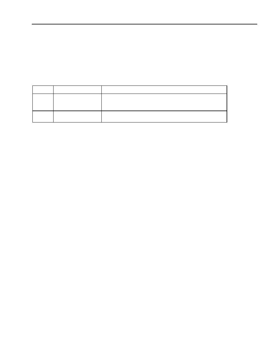
The TDAT data interface is available in three different configurations as summarized in Table 1.
TDAT04622
The TDAT04622 device contains a subset of the TDAT042G5 device. The TDAT04622 device functions as
described in the TDAT042G5 SONET/SDH 155/622/2488 Mbits/s Data Interface Data Sheet
(DS98-193SONT-4) with the following limitations:
s
Quad OC-3 operation only or single OC-12 operation only.
s
Single UTOPIA port.
TDAT021G2
The TDAT021G2 device contains a subset of the TDAT042G5 device. The TDAT021G2 device functions as
described in the TDAT042G5 SONET/SDH 155/622/2488 Mbits/s Data Interface Data Sheet
(DS98-193SONT-4) with the following limitations:
s
Quad OC-3 operation only or dual OC-12 operation only.
s
Two UTOPIA ports.
TDAT042G5
The TDAT042G5 device contains all functionality as described in the TDAT042G5 SONET/SDH 155/622/2488
Mbits/s Data Interface Data Sheet (DS98-193SONT-4).
Table 1. TDAT Device Product Line
Device
Line Ports
UTOPIA Ports
OC-3
OC-12
OC-48
Ports Present
Modes
TDAT04622
4
(A, B, C, D)
1
(A)
NA
1
(A)
U2, U2+, U3, U3+
s
8-bit
s
16-bit
TDAT021G2
4
(A, B, C, D)
2
(A, B)
NA
2
(A, B)
U2, U2+, U3, U3+
s
8-bit
s
16-bit
s
32-bit
TDAT042G5
4
(A, B, C, D)
4
(A, B, C, D)
1
(16-bit parallel
multiplexed/
demultiplexed)
4
(A, B, C, D)
U2, U2+, U3, U3+
s
8-bit
s
16-bit
s
32-bit

Data Addendum
May 2001
155/622/2488 Mbits/s Data Interfaces
TDAT SONET/SDH
Agere Systems Inc. reserves the right to make changes to the product(s) or information contained herein without notice. No liability is assumed as a result of their use or application.
Copyright © 2001 Agere Systems Inc.
All Rights Reserved
Printed in U.S.A.
May 2001
DA01-010SONT (Replaces DA00-001SONT and must accompany DS98-193SONT-4)
For additional information, contact your Agere Systems Account Manager or the following:
INTERNET:
http://www.agere.com
E-MAIL:
docmaster@micro.lucent.com
N. AMERICA: Agere Systems Inc., 555 Union Boulevard, Room 30L-15P-BA, Allentown, PA 18109-3286
1-800-372-2447, FAX 610-712-4106 (In CANADA: 1-800-553-2448, FAX 610-712-4106)
ASIA PACIFIC: Agere Systems Singapore Pte. Ltd., 77 Science Park Drive, #03-18 Cintech III, Singapore 118256
Tel. (65) 778 8833, FAX (65) 777 7495
CHINA:
Agere Systems (Shanghai) Co., Ltd., 33/F Jin Mao Tower, 88 Century Boulevard Pudong, Shanghai 200121 PRC
Tel. (86) 21 50471212, FAX (86) 21 50472266
JAPAN:
Agere Systems Japan Ltd., 7-18, Higashi-Gotanda 2-chome, Shinagawa-ku, Tokyo 141, Japan
Tel. (81) 3 5421 1600, FAX (81) 3 5421 1700
EUROPE:
Data Requests: DATALINE: Tel. (44) 7000 582 368, FAX (44) 1189 328 148
Technical Inquiries: GERMANY: (49) 89 95086 0 (Munich), UNITED KINGDOM: (44) 1344 865 900 (Ascot),
FRANCE: (33) 1 40 83 68 00 (Paris), SWEDEN: (46) 8 594 607 00 (Stockholm), FINLAND: (358) 9 3507670 (Helsinki),
ITALY: (39) 02 6608131 (Milan), SPAIN: (34) 1 807 1441 (Madrid)

Advisory
May 2001
TDAT042G5 Device Advisory
for Version 1 and 1A of the Device
System Programming (SP)
SP1. Required Provisioning Sequence and Clocks
The core registers must be written prior to provisioning any other registers (1) to establish the internal clock
rates for the device, and (2) because writing to certain core registers resets the remainder of the device. Cer-
tain clocks must be present to read/write registers prior to provisioning the device.
One of the following clocks must be present prior to provisioning to enable register access:
I
TxCKP and TxCKN
I
MPU clock (microprocessor interface synchronous mode only)
Provisioning must be implemented in the following sequence:
I
Core register 0x0010 (mode) must be provisioned first
I
Core register 0x0011 (channel [A--D] control) second
I
Remainder of the core registers must then be provisioned (order does not matter)
It is recommended, but not required, that the remainder of the device be provisioned in the following order:
I
OHP, PT, and DE blocks (order does not matter)
I
UT block to turn on the data source to the master and slave
Workaround
Provisioning must be implemented in the following sequence:
I
Apply either TxCKP and TxCKN or MPU clock.
I
Provision core:
-- Mode, register 0x0010
-- Channel [A--D] control, register 0x0011
-- Remainder of the core
Corrective Action
Not applicable. Use above procedure in provisioning the device.

2
Agere Systems Inc.
Advisory
May 2001
for Version 1 and 1A of the Device
TDAT042G5 Device Advisory
System Programming (SP)
(continued)
SP2. Behavior During Loss of Receive Line Clock
All state and counter values will be held at their current values when Rx line clock has been lost. The device will not
automatically multiplex in the Tx line clock when the Rx line clock is lost.
Workaround
System software should monitor loss of line clock bits in the receive/transmit state register (addresses 0x040A--
0x040D) and ignore all other alarms. This condition must be serviced as a major failure event.
Corrective Action
This is informational only. No corrective action is required for this condition.
SP3. PT Register Addressing
Addresses for the PT error counter registers are as follows:
I
Channel A: 0x09B3 to 0x09E3
I
Channel B: 0x09EF to 0x0A20
I
Channel C: 0x0A2C to 0x0A5C
I
Channel D: 0x0A68 to 0x0A98
Note: The reserved address space between the error counter registers is not symmetric. (The reserved space
between channels B and C is 0x003D, and the reserved space between channels A and B and channels
C and D is 0x003C.)
Workaround
This is informational only. No workaround is available for this condition.
Corrective Action
No corrective action is required for this condition.

Agere Systems Inc.
3
Advisory
May 2001
for Version 1 and 1A of the Device
TDAT042G5 Device Advisory
Microprocessor Interface (MPU)
MPU1. Interface to Motorola* MC68360 Processor Is Not Glueless
The interface between the Motorola MC68360 processor and TDAT042G5 requires intervening logic because of
the following incompatibilities in the specifications of these two devices. For a 33 MHz microprocessor clock rate,
the Motorola MC68360 series processors can be interfaced to TDAT042G5 without intervening glue logic, if used
without DT and if programmed for six wait-states. If a user wishes not to use the wait-states, then the chip select
applied to TDAT042G5 must be held low until the address changes. Details are given below.
Chip Select Timing
The TDAT042G5 CS input signal requirements are not compatible with the Motorola MC68360 series processor
CSx output signals. TDAT042G5 timing does not allow simultaneous deassertion of CS and ADS signals. Chip
select applied to TDAT042G5 must be held low for at least 5 ns after the MC68360 deasserts ADS.
Workaround: Use external glue logic to decode the address to generate CS, or provide microprocessor interface
signals meeting the requirements of TDAT042G5.
DT Timing
If the Motorola MC68360 processor CSx signal is used to drive the TDAT042G5 CS, then TDAT042G5 DT output
does not satisfy the MC68360 processor DSACK timing requirement. DT is not pulled to 1 before it is placed in a
high-impedance state. This causes the next MPU cycle to be terminated early.
Workaround: Place a 1 k
resistor from DT to V
DDD
.
Corrective Action
Corrective action for MPU1 has not been determined.
MPU2. Synchronous Microprocessor Interface Mode Is Nonfunctional
The synchronous microprocessor interface mode, MPMODE = 1 (pin D8), functions as described in the advance
data sheet, but causes data errors. Placing TDAT042G5 in the synchronous mode and placing a clock on MPCLK
(pin C8) will cause the data passing through the device to be corrupted. Data errors are generated at a rate of 1%
or less of corrupted packets.
Workaround
Use the TDAT042G5 in the asynchronous microprocessor mode, MPMODE = 0, with no clock applied to MPCLK.
Corrective Action
This condition will be resolved in version 1A of the device.
* Motorola is a registered trademark of Motorola, Inc.
4
Agere Systems Inc.
Advisory
May 2001
for Version 1 and 1A of the Device
TDAT042G5 Device Advisory
Core Registers (CR)
CR1. Clear on Read/Clear on Write Behavior
Bit 6 of line provisioning register 0x0010 sets the functionality of the COR/W registers.
Table 1. COR/W Settings of Register 0x0010, Bit 6
Workaround
This is informational only. No workaround is available for this condition.
Corrective Action
This condition will be described in revision 4 of the advance data sheet.
Line Interface (LI)
LI1. STS-48/STM-16 Mode Lacks Facility Loopback
There is no facility loopback function (line input to line output) available in STS-48/STM-16 mode. Facility loopback
is available only in STS-12/STM-4 and STS-3/STM-1 modes as described in the advance data sheet.
Workaround
This function is not a feature of TDAT042G5.
Corrective Action
No corrective action is required for this condition.
Bit 6
Mode
Bit Clear Behavior of Accessed Registers
1
COR
After COR has been set (address 0x0010, bit 6 = 1), all registers that are accessed
are cleared when read.
0
COW
After COW has been set (address 0x0010, bit 6 = 0), a 1 must be written to a given bit
in a given register to clear that bit. Writing a 0 to a bit in a given register does not clear
that bit.

Agere Systems Inc.
5
Advisory
May 2001
for Version 1 and 1A of the Device
TDAT042G5 Device Advisory
Path Terminator (PT)
PT1. Signal Degrade (SD) and Signal Fail (SF) Bit Behavior
Receive signal degrade and receive signal fail bits in the PT state registers (addresses 0x0838, 0x088A, 0x08DC,
and 0x092E, bits [1:0]) do not function as described. Until the signal degrade (SD) and signal fail (SF) thresholds
are programmed, the SD and SF bits will toggle on a frame-by-frame basis.
Workaround
Program thresholds during system software initialization.
Corrective Action
This functionality will be retained in its current state in future versions of the device. The advance data sheet will be
corrected to reflect the actual function of the registers.
PT2. Clear-After-Write Behavior of Signal Degrade Clear Bits
Signal degrade clear (bits 15--12) of the PT one-shot control parameters register (address 0x0AA4) are described
as one-shot, clear-after-write bits. Writing these bits should automatically set and then clear the bits. This one-shot
behavior is not observed.
Workaround
The bits must be set to 1 and then explicitly set to 0 to clear these signal degrade bits.
Corrective Action
This functionality will be retained in its current state in future versions of the device. The advance data sheet will be
corrected to reflect the actual function of the registers.

6
Agere Systems Inc.
Advisory
May 2001
for Version 1 and 1A of the Device
TDAT042G5 Device Advisory
Path Terminator (PT)
(continued)
PT3. Remote Defect Indicator (RDI) Behavior
The SONET standards require that when an RDI changes value, it should hold the value for a minimum of
20 frames. This applies to a no error state, which should be maintained for at least 20 consecutive frames.
However, it is also intended by the SONET standard that the occurrence of an error state should be reported
immediately.
TDAT042G5 responds to error conditions within 100 ms (ANSI
*
T1.105 which states only that RDI-L must be gen-
erated or removed within 100 ms of detecting or terminating an incoming defect), in which case the two require-
ments become functionally the same.
Single-bit and enhanced RDI behave differently under the following conditions:
I
Transition from error state to no error state.
I
While in the error state, a subsequent error occurs.
The single-bit error RDI does not hold the no error state for 20 frames. However, the enhanced RDI does hold the
no error state for 20 consecutive frames.
Workaround
No workaround is available for this condition.
Corrective Action
The enhanced RDI indicator in future versions of the device will behave the same as the single-bit error indicator.
PT4. SS Pointer Interpretation Algorithm
The SDH standards do not require that the SS bits are set to binary 10 for SDH equipment. The SS bit values are
not used in determining a valid pointer value. Because of this, the SS pointer interpretation algorithm is not imple-
mented in the device. Bit 5 (RSSPTRNORM[A--D]) of PT control registers 0x0AA6, 0xAAE, 0x0AB6, and 0x0ABE
is not used. Bits 1 and 0 (RSSEXP[1:0]) of PT provisioning register 0x0AC7 are not used.
Workaround
No workaround is available for this condition.
Corrective Action
These bits will be removed from the PT registers in future revisions of the advance data sheet.
* ANSI is a registered trademark of American National Standards Institute, Inc.

Agere Systems Inc.
7
Advisory
May 2001
for Version 1 and 1A of the Device
TDAT042G5 Device Advisory
Path Terminator (PT)
(continued)
PT5. Delta/Event Registers in COR Mode
Because there is a one-cycle delay before the PT delta event registers (0x802, 0x080F, 0x081C, 0x0829) are
cleared after being read in COR mode, new interrupts may be lost.
Workaround
No workaround is available for this condition.
Corrective Action
This condition will be addressed in future versions of the device.
Data Engine (DE)
DE1. SDL Mode--Header Error Correction in LSB
In SDL mode, the header error correction process is susceptible to single-bit errors in the least significant bit (LSB)
of the special payload.
Workaround
No workaround is available for this condition.
Corrective Action
This condition will be addressed in future versions of the device.
DE2. Incorrect ATM Loss of Cell Delineation (LCD) Implementation
Currently, the LCD is implemented in the same way that out of cell delineation (OCD) is implemented. This is not in
accordance with the ITU-TI.432-2 February 1999 standard.
Workaround
No workaround is available for this condition.
Corrective Action
A software workaround will be available with version 1A of the device.
8
Agere Systems Inc.
Advisory
May 2001
for Version 1 and 1A of the Device
TDAT042G5 Device Advisory
Data Engine (DE)
(continued)
DE3. ATM Transmit Count of Idle Cells
For ATM mode in the transmit direction, all cells are currently counted, including the idle cells. Only the cells con-
taining data should be counted.
Workaround
No workaround is available for this condition.
Corrective Action
This condition will be addressed in version 1A of the device.
DE4. Channel Provisioning
When using the device in STS-3/STM-1 and STS-12/STM-4 modes with either PPP, CRC, or HDLC, egress config-
uration registers 0x1016, 0x1017, 0x1018, and sequencer cell state register 0x1036 of all four channels must be
provisioned, even if a channel is not being used.
Workaround
Provision all four transmit DE channels. Set DE egress configuration registers and the sequencer cell state register
as shown in Table 2.
Table 2. Transmit DE Egress and Sequencer Cell State Registers
Corrective Action
This condition will be addressed in future versions of the device.
Address
Value
STS-3/STM-1
STS-12/STM-4
0x1016
0x4567
0x4567
0x1017 0x4567
0x4567
0x1018
0x4567
0x4567
0x1019--0x1021
--
0x4567
0x1036 0x0000
0x0000
Agere Systems Inc.
9
Advisory
May 2001
for Version 1 and 1A of the Device
TDAT042G5 Device Advisory
Data Engine (DE)
(continued)
DE5. Packet Behavior in POS/SDL Mode--Dry Mode
When the device is configured in POS mode with dry mode enabled, the following conditions may persist:
I
PPP mode; STS-48/STS-12/STS-3.
When running in PPP mode, the PPP header--0xFF03 0x0021 (provisionable)--may be incorrectly inserted at
any point in a packet within the outgoing data stream when the FIFO runs dry, thereby corrupting the packet.
Packets being sent are corrupted if the FIFO runs dry.
I
PPP and CRC modes; STS-48/STS-12/STS-3.
CRC, PPP, and HDLC modes; STS-48/STS-12/STS-3.
In PPP, CRC, and HDLC dry modes, some of the packet data may be corrupted when the packet length is above
a certain size where size is dependent upon UT clock rate and low watermark setting. Either sections of the
packet may be lost or additional packets may be inserted.
Workaround
Several workarounds are possible:
I
Do not provision dry mode for this device.
I
If dry mode is provisioned:
-- Do not allow the FIFO to be emptied.
-- Run the UTOPIA clock fast enough, as shown in Table 3, so that the FIFO is never empty.
-- Use a larger external FIFO to buffer the data.
-- Do not allow the packet size to exceed the low watermark.
Table 3. Required UTOPIA Clock (TxCLK) Rates
Corrective Action
This condition will be corrected in version 1A of the device.
Mode
TxCLK and Rate
STS-48/STM-16
TxCLK > 77 MHz (U3+, 32-bit mode)
STS-12/STM-4
TxCLK > 40 MHz
STS-3/STM-1
TxCLK > 10 MHz

10
Agere Systems Inc.
Advisory
May 2001
for Version 1 and 1A of the Device
TDAT042G5 Device Advisory
Data Engine (DE)
(continued)
DE6. Incorrect ATM Out of Cell Delineation (OCD) Implementation
In ATM mode, the OCD reporting for channels B, C, and D is incorrect. The OCD state of channel A is reported for
channels B, C, and D. The OCD reporting is correct for channel A.
Workaround
No workaround is available for this condition.
Corrective Action
This condition will be corrected in version 1A of the device.
DE7. Incorrect Frame State of ATM Data Streams
When sending a single ATM data stream to channel A, the frame states of channels B, C, and D are incorrectly set
to sync mode. This prevents LCD errors from being reported on channel A as well. In addition, when sending a sin-
gle ATM data stream to channels B, C, or D, the frame states always remain in hunt mode. This results in LCD
errors on those channels.
Workaround
No workaround is available for this condition.
Corrective Action
A software workaround will be available with version 1A of the device.
Agere Systems Inc.
11
Advisory
May 2001
for Version 1 and 1A of the Device
TDAT042G5 Device Advisory
Data Engine (DE)
(continued)
DE8. Clearing DE Interrupt Register (0x1002)
DE interrupt register 0x1002 is incorrectly defined in the revision 3 of the data sheet as RO. DE interrupt register
0x1002 is correctly defined as a COR/W register. However, register 0x1002 must be used in the COR mode (regis-
ter 0x0010 bit 6 set to 1). The bits of register 0x1002 are explained in detail in Table 4.
Table 4. Register 0x1002: DE Interrupt (COR/W)
Workaround
This is informational only. No workaround is available for this condition.
Corrective Action
This behavior will be described in future revisions of the advance data sheet.
DE9. Single Packet Transmission in HDLC-CRC, SDL-CRC, and PPP Modes
When receiving in either PPP or CRC mode, a single packet may not pass through the device. This occurs when
the end of packet (which contains the CRC) never reaches the UT FIFO. The ingress channel suspends transfer to
the UT when there is no end of packet in the FIFO. These bytes are transferred to the UT when the next packet is
received. This problem will affect HDLC-CRC, SDL-CRC, and PPP modes.
Workaround
There are two possible workarounds:
I
Set ingress payload type and mode control registers (0x1040--0x1043) to CRC strip mode. However, in CRC-16
mode, single packets may still get stuck if CRC ends on bytes A or B.
I
Send a minimum 4-byte dummy packet after each packet.
Corrective Action
This condition will be addressed in future versions of the device.
Bits
Mode
Clear Behavior of Register 0x1002
15--12
RO
To clear these SDL Rx frame state interrupt bits, read and
clear their associated interrupt source registers
(addresses 0x14E0--0x14E3).
11--0
COR or COW
(address 0x0010, bit 6)
To properly clear these bits, device must be in COR mode
(address 0x0010, bit 6 = 1).

12
Agere Systems Inc.
Advisory
May 2001
for Version 1 and 1A of the Device
TDAT042G5 Device Advisory
Data Engine (DE)
(continued)
DE10. Excessive HDLC Flag Characters
The following three issues refer to HDLC flag character (0x7E) problems in the data engine:
I
An excessive number of HDLC flag characters (0x7Es) may be inserted between packets on the transmit side if
the UTOPIA low watermark value is set above 2. This will have the effect of reducing the bandwidth of the device.
I
The data engine operates on 32-bit boundaries. Egress packets that are not multiples of four will be filled with
0x7Es.
I
Egress packets consisting of all 0x7Es as data will be corrupted.
Workaround
Set the UTOPIA egress low watermark value in the UTOPIA egress provisioning registers (0x0212, 0x0216,
0x021A, 0x021E) to either 1 or 2 to prevent excessive 0x7Es from being inserted between packets.
Corrective Action
This condition will be addressed in future versions of the device.
UTOPIA (UT)
UT1. Polling in Multidevice MPHY Mode
When the TDAT042G5 is polled and responds, the data bus becomes enabled. In a multidevice MPHY configura-
tion, if the data bus is active from a different PHY device, response to a poll from the device will corrupt a data
transfer already in progress. TDAT042G5 MPHY always functions without data corruption in a single-device
(slave), multiple-channel configuration (point-to-point).
Workaround
No workaround is available for this condition.
Corrective Action
This condition will be addressed in future versions of the device.

Agere Systems Inc.
13
Advisory
May 2001
for Version 1 and 1A of the Device
TDAT042G5 Device Advisory
UTOPIA (UT)
(continued)
UT2. UTOPIA Clock Limitations
The maximum speed of the UTOPIA interface is 104 MHz. When operating at clock speeds greater than 52 MHz,
RxCLK[D:A] must be placed in source mode and will use the same external clock as the corresponding
TxCLK[D:A] clock. RxCLK[D:A] source mode is set by provisioning bit 6 (CLOCK_MODE_Rx) for channel A of the
UTOPIA receive provisioning registers (address 0x020F).
When operating at speeds less than 52 MHz, separate external clocks for RxCLK[D:A] and TxCLK[D:A] may be
used.
Workaround
This is informational only. No workaround is available for this condition.
Corrective Action
This condition will be addressed in future versions of the device. Design modifications will be directed towards
allowing a maximum interface speed of 104 MHz in all cases. Note that UTOPIA Level 3 clock architecture has
changed in the ATM Forum's UTOPIA Level 3 specification as of the July 1998 version.
UT3. PMRST Register Value Invalid After Reset
The value in PMRST_PECTx[A--D] (addresses 0x020B through 0x020E) is invalid after reset until the second
PMRST clock period is completed. After the second PMRST, the register value is valid.
Workaround
Always have the system software execute a read of PMRST_PECTx as part of the system initialization following a
reset.
Corrective Action
This condition will be addressed in future versions of the device.

14
Agere Systems Inc.
Advisory
May 2001
for Version 1 and 1A of the Device
TDAT042G5 Device Advisory
UTOPIA (UT)
(continued)
UT4. FIFO Overflow and Error Reporting
If the RxFIFO overflows, RxEOP is not asserted as expected. Therefore, when errors occur, two packets will be
corrupted instead of one because two start of packets (SOPs) occurred without an end of packet (EOP). RxERR is
not asserted when the above overflow condition occurs. No effect is noticeable in the ATM mode. Channel A works
as expected; this problem occurs in channels B, C, and D.
Workaround
This error is detectable in the status registers. No workaround is available for this condition.
Corrective Action
This condition will be addressed in future versions of the device.
UT5. Timing Difference Between Direct and Polled Status Modes
In the receive direction of the MPHY mode, RxPA[A] shows the polled packet (or ATM) available status for all four
slices, while the RxPA[B], RxPA[C], and RxPA[D] show the direct status states of their respective FIFOs. In some
cases, the status of RxPA[A] does not agree with the status of RxPA[D:B]. The direct status indication has one
additional cycle of pipeline delay from that of the polled status.
Workaround
This is informational only. No workaround is available for this condition.
Corrective Action
No corrective action is required for this condition.
UT6. UTOPIA Interface D Nonfunctional in Some Mixed MPHY and Point-to-Point
Configurations
When TDAT042G5 is configured with slice D in a point-to-point mode, slice D is nonfunctional in one special case.
If UTOPIA interfaces A and B are configured for 32-bit MPHY operation with slice C as part of the polled channels,
interface D will be nonfunctional and cannot be independently configured in a UTOPIA Level 2 point-to-point mode.
This condition does not occur in 16-bit MPHY operation.
Workaround
For mixed MPHY and point-to-point configuration, use UTOPIA slice D for MPHY mode instead of slice C.
UTOPIA slice C will then be available for normal point-to point mode.
Corrective Action
This condition will be addressed in future versions of the device.
Agere Systems Inc.
15
Advisory
May 2001
for Version 1 and 1A of the Device
TDAT042G5 Device Advisory
UTOPIA (UT)
(continued)
UT7. Response to 0x1F MPHY Address
TDAT042G5 MPHY currently generates a polled status response to the address 0x1F (the null address), which is
not compliant with the UTOPIA Level 2 standard. The address 0x1F is valid for UTOPIA Level 3 operation.
Workaround
No workaround is available for this condition.
Corrective Action
This condition will be addressed in future versions of the device.
UT8. Far-End Loopback Bandwidth Limitations
In the STS-48/STM-16 mode (U3, U3+), looping back data at the far end (UTOPIA interface) can only be accom-
plished without cell/packet corruption at rates below the following, as shown in Table 5.
Table 5. Cell/Packet Corruption Rates
When cell/packet corruption occurs, the device reports transmit FIFO underflow.
Workaround
No workaround is available for this condition.
Corrective Action
This condition will be addressed in future versions of the device.
Mode
ATM
Packet
STS-48/STM-16
300 Mbits/s
Rate not yet determined
STS-12/STM-4
70 Mbits/s
Rate not yet determined
STS-3/STM-1
30 Mbits/s
Rate not yet determined
16
Agere Systems Inc.
Advisory
May 2001
for Version 1 and 1A of the Device
TDAT042G5 Device Advisory
UTOPIA (UT)
(continued)
UT9. Clock Requirements for MPHY Modes
When using the TDAT042G5 in MPHY mode, receive and transmit clocks must be provided for all channels (A, B,
C, and D). Also, the packet available (PA) signal for each channel must be provided on each channel's associated
PA pin.
Workaround
It is possible to place RxCLK[D:A] into source mode by provisioning bit 6 (CLOCK_MODE_Rx) of the UTOPIA
receive provisioning registers (addresses 0x020F, 0x0213, 0x0217, 0x021B). This will eliminate the need to supply
separate receive and transmit clocks.
Corrective Action
This is informational only. No corrective action is required for this condition.
UT10. Egress Packet Mode Overflows
In the UTOPIA modes listed below, the device will report transmit packet overflow errors when no overflows have
occurred. This occurs when the egress high watermark is set for the UTOPIA modes as shown in Table 6.
Table 6. Settings at Which Overflows Reported in Error
Workaround
Set the egress high watermark threshold as shown in Table 7. If there is a delay between TxPA deassertion and
TxENB deassertion, the additional cycles should also be accounted for when setting the threshold.
Table 7. Settings to Prevent Overflows Reported in Error
Corrective Action
This condition will be addressed in future versions of the device.
UTOPIA Modes
Egress High Watermark Thresholds
8-bit, U3+
0x3D
16-bit, U2+
0x3B
32-bit, U3+
0x37
UTOPIA Modes
Egress High Watermark Thresholds
8-bit, U3+
<
0x3D
16-bit, U2+
<
0x3B
32-bit, U3+
<
0x37

Agere Systems Inc.
17
Advisory
May 2001
for Version 1 and 1A of the Device
TDAT042G5 Device Advisory
UTOPIA (UT)
(continued)
UT11. Clearing UT Interrupt Register
When a UT interrupt event occurs and COW mode is enabled, writing to UT interrupt register 0x0201 does not
clear the register (this register is read-only). The interrupt is cleared by writing to the UT delta and event registers
(addresses 0x0202--0x0205).
Workaround
This is informational only. No workaround is available for this condition.
Corrective Action
No corrective action is required for this condition.
UT12. Incorrect Implementation of POS Multi-PHY Mode
Because the TDAT042G5 lacks a selected PA signal (SPA), the status of a channel that is transmitting data in POS
MPHY mode is not known during polling. Therefore, the PA signal cannot be used as a data valid signal. If the
channel transmitting data runs dry, the master side may receive invalid data.
Workaround
Use direct status polling mode only and ensure that the address of channel A is applied to the address bus at all
times, except during the clock cycle when another channel is being selected.
Corrective Action
No corrective action is required for this condition.
UT13. Invalid Extra Cycle Between EOP and SOP in CRC-16/32 Mode
When using the device in CRC-16 or CRC-32 mode, there is always an extra cycle between the end of packet
(EOP) of the previous packet and the start of packet (SOP) of the following packet.
Workaround
This is informational only. No workaround is available for this condition.
Corrective Action
This is condition will be addressed in the future version of the device.
18
Agere Systems Inc.
Advisory
May 2001
for Version 1 and 1A of the Device
TDAT042G5 Device Advisory
UTOPIA (UT)
(continued)
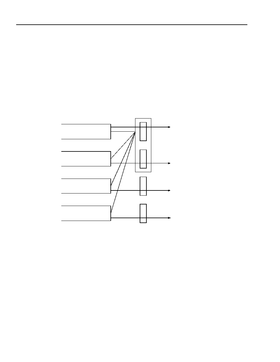
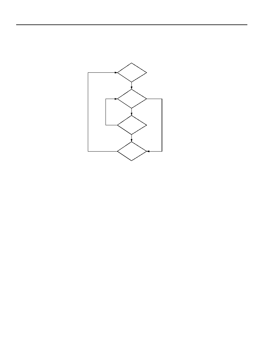
UT14. Nonfunctional RxPA Signal for Channels B and D in Packet Direct Status MPHY Mode
When using MPHY direct status for all operational modes (8-bit, 16-bit, and 32-bit), the RxPA signal for channels B
and D is not functional. The RxPA signal is functional only for channels A and C.
Workaround
The TDAT UTOPIA interface currently has nonfunctioning RxPAB and RxPAD output signals when used in four-
channel Multi-PHY mode as shown in Figure 1. The result of this problem is the unavailability of direct status polling
on the receive-side UTOPIA interface. To work around this problem, the following analysis is done to aid the user in
doing a round-robin data extraction procedure.
1664 (F)
Figure 1. Receive-Side UTOPIA Interface and Channel FIFOs
The rate at which data fills and drains the receive-side UTOPIA FIFOs is calculated as follows:
I
The data enters each UTOPIA FIFO from the data engine bytewise running on a 77.76 MHz system clock.
I
If we assume each channel (worst case) is filled with an STS-12c rate signal, then the amount of data (excluding
SONET overhead, both section/line, path, and three stuff columns) per second is
(87 x12 x 9 x 8000) ≠ (4 x 9 x 8000) = 74.88 Mbytes/STS-12c/s or 599.040 Mbits/STS-12c/s.
I
Since each FIFO contains a maximum of 256 bytes/FIFO, it takes on average
(256/74,880,000) = 3.4188
µ
s to fill a FIFO, and with a clock cycle of 77.76 MHz, it requires as a worst case,
3.2922
µ
s to fill the FIFO.
I
Since there are four FIFOs all receiving data at 74.88 Mbytes/s, then the total bandwidth requirements of all four
channels combined is (4 x 74,880,000) = 299.52 Mbytes/s.
I
The servicing rate on each FIFO is based on the UTOPIA interface width and frequency. If we assume a
32-bit A/B UTOPIA interface operating at 100 MHz, then the service rate is 400 Mbytes/s to service all the
channels.
INGRESS CHANNEL A FIFO
256 bytes DEEP
INGRESS CHANNEL B FIFO
256 bytes DEEP
INGRESS CHANNEL C FIFO
256 bytes DEEP
A
B
R
X
PAA
32-bit INTERFACE (A AND B)
R
X
PAB
C
R
X
PAC
INGRESS CHANNEL D FIFO
256 bytes DEEP
D
R
X
PAD
X
X

Agere Systems Inc.
19
Advisory
May 2001
for Version 1 and 1A of the Device
TDAT042G5 Device Advisory
UTOPIA (UT)
(continued)
I
The interface can drain an entire FIFO at a rate of 400 Mbytes/s. To drain 256 bytes, it requires a maximum of
(256 / 400,000,000) = 0.64
µ
s to drain a FIFO that is completely full. To drain all four FIFOs, it requires
(0.64 x 4) = 2.56
µ
s total
.
For data to be efficiently removed from each of the Rx FIFOs, a round-robin extraction method must be employed
since the RxPAB and RxPAD signals are not available for direct status polling. Since it requires a worst case total of
3.2922
µ
s to fill a FIFO, the master must service all FIFOs in a manner such that it does not allow any particular
FIFO to fill and hence overflow. Assuming equal servicing of each FIFO, the master must therefore not service any
particular FIFO for longer than (3.2922 / 4) = 0.8231
µ
s. This also must account for any dead cycles in a cycling
between channels and any dead cycles on a particular channel (single dead cycle between EOP and SOP).
When servicing four FIFOs, there is a maximum clock cycle penalty for switching between channels. For two-cycle
mode, this penalty is a maximum of four UTOPIA master clock cycles; so to switch between all four channels, a
total of up to sixteen master clock cycles may be required to perform all the switching. The value of four is worst
case, and in some cases this can be as low as one cycle. The value of four results from the case where the FIFO
drains while servicing that channel, which will be common when draining at the 100 MHz frequency. In that case,
the master must first see that the FIFO has drained by observing that RxPAA is invalid on the last cycle while drain-
ing the FIFO (best case is one cycle lost). It must then deactivate RxENB and place a new channel address on the
address bus on the following cycle (best case is one cycle lost). It must then activate RxENB for the new channel
on the following cycle and have TDAT sample RxENB low (best case is one cycle lost). The TDAT will then output
data two cycles later when using a PA response mode of two cycles (one cycle lost with data output on second
cycle). Any additional delays by the master must be added to these to calculate a worst-case condition. The best-
case condition occurs when the master stops the data flow when there are still more than two data items contained
within the FIFO. In this case, the master deactivates RxENB at some predetermined maximum 32-bit word drain
value, where the PA response on the cycle prior to deactivation had valid data. For two-cycle mode, two additional
data items will be output from the FIFO for that particular channel, if available. The master deactivates RxENB,
places the new channel address on the FIFO, and activates RxENB. On the cycle where RxENB is activated, the
last valid data item from the previous channel may be output (best case), and one dead cycle will follow this before
data for the following selected channel is output.
Given the information above, assume the worst case of four cycles between channel switching. Also assume the
FIFOs are filling at a worst-case rate, 3.2922
µ
s/FIFO. Assume the master is draining each FIFO using the 32-bit,
100 MHz, A/B, UTOPIA interface. Assume the master extracts a maximum of thirty 32-bit words (120 bytes) from
each FIFO before switching to an alternate channel. This requires (30 x 10) = 300 ns/FIFO, and assume that it
takes the worst-case four clock cycles to switch to alternate channels. Therefore, the total servicing time per FIFO
is (300 + 4 x 10) = 340 ns/channel, and the total servicing time per four channels is (4 x 340) = 1.36
µ
s per round
robin servicing of all four channels. At this round-robin rate, a maximum of 120 bytes are serviced per channel per
1.360
µ
s interval; so to service the total bytes per channel (74.88 Mbytes/s), it requires a total of 0.849 seconds,
which is sufficient bandwidth to service all channels.
Since the FIFOs fill at the maximum rate of 1 byte/13.355 ns, each FIFO will fill to a depth of 102 bytes in the
1.360
µ
s interval between channel servicing. This is well below the overflow threshold, which is set by the user to a
value near the top of the FIFO (high watermark, 0x36 (216 bytes) default) and is below the number of bytes ser-
viced by the master per channel per round-robin servicing (120 bytes). Each customer's servicing characteristics
will depend on the master's behavior and how fast it performs the channel switching. If it cannot switch in the worst-
case, four-cycle manner described above, performance will degrade.
One item not accounted for in the above analysis is the fact that TDAT may place a dead cycle between packets (in
CRC and PPP modes, not in HDLC mode). In this case, there can be a maximum of three dead cycles per FIFO
(assuming 40-byte packets worst case and 102 bytes in FIFO between round-robin cycle). This will be taken up by
the slack provided above, where (102 bytes + 4 bytes/dead cycle x 3 dead cycles) = 114 bytes, which still falls
below the servicing rate of 120 bytes per round-robin servicing.
20
Agere Systems Inc.
Advisory
May 2001
for Version 1 and 1A of the Device
TDAT042G5 Device Advisory
UTOPIA (UT)
(continued)
The logical flow of the above procedure is shown in Figure 2 below:
1665 (F)
Figure 2. Master Control Flow Chart
Select channel
If PA = 1 continue
If count = 30 words, then deactivate RxENB and switch to new channel
Else continue with current channel
Else deactivate RxENB and switch to next channel
Return to selection of new channel
Corrective Action
This is condition will be addressed in the future version of the device.
SELECT NEXT
PA = 1
CHANNEL
COUNT
<
30
DEACTIVATE
R
X
ENB
YES
NO
YES
HOLD ADDRESS OF SELECTED
CHANNEL ON ADDRESS BUS
NO
Agere Systems Inc.
21
Advisory
May 2001
for Version 1 and 1A of the Device
TDAT042G5 Device Advisory
Overhead Processor (OHP)
OHP1. Maximum BER Count
The maximum number of errors the device can report is limited to 5.00E-04 in STS-12/STM-4 mode and 1.00E-04
in STS-48/STM-16 mode. This applies to the SDLSET, SDLCLEAR, SFLSET, and SFLCLEAR bits of the signal
degrade and signal fail BER algorithm OHP registers. These bits are shown in Table 8.
Table 8. Signal Degrade and Signal Fail Algorithm OHP Registers [6:3]
* The OHP prefix shown here will be added to the current bit names in revision 4 of the advance data
sheet.
Workaround
This is informational only. No workaround is available for this condition.
Corrective Action
No corrective action is required for this condition.
OHP2. RDI-L Reporting
When the device is initially powered up, it defaults to STS-48/STM-16 mode. This locks a counter value into trans-
mit control registers for channels B, C, and D. When the device is configured for STS-3/STM-1 mode, the counter
does not automatically clear.
Workaround
During STS-3/STM-1 OHP configuration in the system code, manually clear transmit control registers 0x0431,
0x0433, and 0x0435 for channels B, C, and D. In order to clear these transmit control registers, the bits must be
toggled. The following pseudocode shows how to clear the bits on channels B, C, and D:
Set address 0x0431 to 0x007F # set bits on channel B
Set address 0x0431 to 0x0000 # clear bits on channel B
Set address 0x0433 to 0x007F # set bits on channel C
Set address 0x0433 to 0x0000 # clear bits on channel C
Set address 0x0435 to 0x007F # set bits on channel D
Set address 0x0435 to 0x0000 # clear bits on channel D
Corrective Action
This is informational only. No corrective action is required for this condition.
OHP Bits*
Addresses
OHP_SDLSET[A--D][3:0]
0x043B, 0x043D, 0x043F, 0x0441
OHP_SDLCLEAR[A--D][3:0]
0x0447, 0x0449, 0x044B, 0x044D
OHP_SFLSET[A--D][3:0]
0x0453, 0x0455, 0x0457, 0x0459
OHP_SFLCLEAR[A--D][3:0]
0x045F, 0x0461, 0x0463, 0x0465

22
Agere Systems Inc.
Advisory
May 2001
for Version 1 and 1A of the Device
TDAT042G5 Device Advisory
Overhead Processor (OHP)
(continued)
OHP3. M1 Error Counter in STS-48/STM-16 Mode
When the device receives REI-L errors in the STS-48/STM-16 mode, no M1 errors are reported.
Workaround
There are several workarounds for this problem:
I
Pass the B2 error count value to the far end through system software.
I
Process the M1 byte from the receive TOAC with an external FPGA.
I
Pass the B2 error count from the receive to the transmit direction using transmit TOAC capability. The error count
must be inserted into the eleventh Z2 byte in an STS-48/STM-16 transmit signal. The transmit TOAC signal is
driven by an external device with software insert capability.
I
Pass the B2 error count from the receive to the transmit direction in the section overhead byte. The device has F1
and S1 monitor capability; the protocol for sending the error message to the far end with F1 or S1 bytes is user-
defined.
Corrective Action
This condition will be addressed in future versions of the device.
Packaging and Pinouts (P)
P1. Pin F5 (Previously JTEST) Is No Connect (NC)
Item deleted. Corrected in the advance data sheet.
P2. Modified Pinout and Power Supply Configuration--Future Versions
Item deleted. No modifications to the power supply configuration will be made.
P3. Change to TDAT042G5 Version 1 Pinout
Item deleted. All devices conform to power pin assignments as listed in the advance data sheet.

Agere Systems Inc.
23
Advisory
May 2001
for Version 1 and 1A of the Device
TDAT042G5 Device Advisory
Packaging and Pinouts (P)
(continued)
P4. Power Dissipation
The worst-case power dissipation of TDAT042G5 is currently estimated to be 7.5 W. The minimum and maximum
power dissipation is listed in Table 9, as well as the relative package thermal characteristics.
Table 9. Power Dissipation and Relative Package Thermal Characteristics
*
JA
= (T
J
≠ T
A
)/P
D
: T
J
= junction temperature, T
A
= ambient temperature of medium surrounding the package, P
D
= electrical power dissipated
by the device.
JC
= (T
J
≠ T
C
)/P
D
: T
J
= junction temperature, T
C
= package temperature (top, dead-center), P
D
= electrical power dissipated by the device.
Maximum junction temperature of TDAT042G5 is 125 ∞C. Therefore, maximum case temperature under natural
convection conditions must be less than approximately 50 ∞C, and in this case, an external heat sink is required.
References
Jeff Weiss, 600 LBGA Thermal Test Report, February 25, 1999.
HL250C 3.3 Volt 0.25
µ
m CMOS Standard-Cell Library (MN98-060ASIC-02), pages 2-2 and 2-3.
Workaround
An external heat sink is required.
Corrective Action
Power consumption will be addressed in future versions of the device.
Parameter
Symbol
Test Conditions
Min
Typ
Max
Unit
Power Dissipation:
Minimum
Maximum
P
D
STS-3/STM-1 line rate
STS-12/STM-4 and STS-48/
STM-16 line rates
--
--
3
6
--
--
W
W
Thermal Performance
(JEDEC standard
conditions)*
JA
Standard JEDEC 4-layer PWB:
I
Standard natural convection
I
200 LFPM airflow
I
800 LFPM airflow
--
--
--
9
6.5
5
--
--
--
∞C/W
∞C/W
∞C/W
Correlation Factor
Between Die and Case
Temperatures
JC
Standard JEDEC 4-layer PWB:
I
Standard natural convection
I
200 LFPM airflow
I
800 LFPM airflow
--
--
--
0.3
0.4
0.5
--
--
--
∞C/W
∞C/W
∞C/W

24
Agere Systems Inc.
Advisory
May 2001
for Version 1 and 1A of the Device
TDAT042G5 Device Advisory
Data Addenda
DA1. Incorrect PT Control Register Mapping
TDAT042G5 SONET/SDH 155/622/2488 Mbits/s Data Interface Advance Data Sheet, Rev. 3 lists the following bit
mapping for PT control registers 0x0AAA, 0x0AB2, 0x0ABA, and 0x0AC2:
bit #9 TRDIP_PLMPINH[A--D]
bit #8 TRDIP_UNEQUIPINH[A--D]
bit #7 TRDIP_LCDINH[A--D]
The correct bit mapping is the following:
bit #9 TRDIP_LCDINH[A--D]
bit #8 TRDIP_PLMPINH[A--D]
bit #7 TRDIP_UNEQUIPINH[A--D]
Workaround
No workaround is available for this condition.
Corrective Action
This correct bit mapping will be included in July 2000 of the advance data sheet.
DA2. Variable Change
TDAT042G5 SONET/SDH 155/622/2488 Mbits/s Data Interface Advance Data Sheet, Rev. 3 lists the variable
TRD_LCDINH[A--D], which has been changed to TRD_LCD[A--D] in the January 2001 revision.
Workaround
No workaround is available for this condition.
Corrective Action
This correction will be included in January 2001 of the advance data sheet.

Agere Systems Inc.
25
Advisory
May 2001
for Version 1 and 1A of the Device
TDAT042G5 Device Advisory
AY99-013SONT-2 Replaces AY99-013SONT to Incorporate the Following Updates
1. Page 1, SP1. Required Provisioning Sequence and Clocks, added new issue.
2. Page 8, DE4. Channel Provisioning, added new issue.
3. Page 9, DE5. Packet Behavior in POS/SDL Mode--Dry Mode, added new issue.
4. Page 15, UT8. Far-End Loopback Bandwidth Limitations, added new issue.
5. Page 16, advance data sheet document number corrected.
AY99-013SONT-3 Replaces AY99-013SONT-2 to Incorporate the Following Updates
1. Page 1, notice that the advisory issues still apply to the advance data sheet which has just been updated.
AY99-013SONT-4 Replaces AY99-013SONT-3 to Incorporate the Following Updates
1. Replaced OC- designation with STS- and STM- throughout advisory.
2. Page 2, SP2. Behavior During Loss of Receive Line Clock, added new issue.
3. Page 2, SP3. PT Register Addressing, added new issue.
4. Page 4, CR1. Clear on Read/Clear on Write Behavior, added new issue.
5. Page 5, PT2. Clear-After-Write Behavior of Signal Degrade Clear Bits, corrected description.
6. Page 6, PT4. SS Pointer Interpretation Algorithm, added new issue.
7. Page 7, PT5. Delta/Event Registers in COR Mode, added new issue.
8. Page 7, DE2. Incorrect ATM Loss of Cell Delineation (LCD) Implementation, identified the specific ITU stan-
dard with which the LCD implementation does not comply.
9. Page 8, DE4. Channel Provisioning, Table Transmit DE Egress and Sequencer Cell State Registers, corrected
register 0x102D to 0x1021.
10. Page 9, DE5. Packet Behavior in POS/SDL Mode--Dry Mode, identified dry mode issues.
11. Page 10, DE6. Incorrect ATM Out of Cell Delineation (OCD) Implementation, added new issue.
12. Page 10, DE7. Incorrect Frame State of ATM Data Streams, added new issue.
13. Page 11, DE8. Clearing DE Interrupt Register (0x1002), added new issue.
14. Page 11, DE9. Single Packet Transmission in HDLC-CRC, SDL-CRC, and PPP Modes, added new issue.
15. Page 12, DE10. Excessive HDLC Flag Characters, added new issue.
16. Page 13, UT2. UTOPIA Clock Limitations, clarified wording.
17. Page 14, UT4. FIFO Overflow and Error Reporting, clarified wording.
18. Page 16, UT9. Clock Requirements for MPHY Modes, added new issue.
19. Page 16, UT10. Egress Packet Mode Overflows, added new issue.
20. Page 17, UT11. Clearing UT Interrupt Register, added new issue.
21. Page 17, UT12. Incorrect Implementation of POS Multi-PHY Mode, added new issue.
22. Page 21, OHP1. Maximum BER Count, added new issue. In addition, differentiated OHP bits from PT bits with
the same name; the names will be corrected in revision 4 of the advance data sheet.

26
Agere Systems Inc.
Advisory
May 2001
for Version 1 and 1A of the Device
TDAT042G5 Device Advisory
AY99-013SONT-4 Replaces AY99-013SONT-3 to Incorporate the Following Updates
(continued)
23. Page 21, OHP2. RDI-L Reporting, added new issue.
24. Page 22, OHP3. M1 Error Counter in STS-48/STM-16 Mode, added new issue.
25. Page 22, removed issue P1. Pin 5 (Previously JTEST) Is No Connect (NC). Pin F5 was corrected to NC in the
accompanying advance data sheet, DS98-193SONT-3.
26. Page 22, removed issue P2. Modified Pinout and Power Supply Configuration--Future Versions. Plans for 2.5 V
power ring implementation considered, but no schedule available at this time.
27. Page 22, removed issue P3. Change to TDAT042G5 Version 1 Pinout. Listed pins have been corrected to NC in
the accompanying advance data sheet, DS98-193SONT-3.
28. Page 24, DA1. Incorrect PT Control Register Mapping, added new issue.
AY01-015SONT (Replaces AY99-013SONT-4 and Must Accompany
DS98-193SONT-4) Replaces AY99-013SONT-4 to Incorporate the Following
Updates
Change List
This change list summarizes changes across the various versions of this document starting with the version dated
1/25/01.
1/25/01
1. Page 6, PT3. Remote Defect Indicator (RDI) Behavior, clarified wording.
2. Page 12, DE 11. ATM Header Error Correction (HEC) Behavior, added entire section to document.
1/29/01
1. Page 24, DA1. Incorrect PT Control Register Mapping, changed corrective action description to include the July
2000 date.
2. Page 24, DA2. Variable Change, added entire section to document.
2/13/01
1. Page 12, updated issue on DE 11. ATM Header Error Correction (HEC) Behavior, to include more information.
2. Page 17, added issue UT13. Invalid Extra Cycle Between EOP and SOP in CRC-16/32 Mode.
3. Page 18, added issue UT14. Nonfunctional RxPA Signal for Channels B and D in Packet Direct Status MPHY
Mode.
3/1/01
1. Page 12, removed DE 11 from document.
2. Page 18, UT14. Nonfunctional RxPA Signal for Channels B and D in Packet Direct Status MPHY Mode, added
workaround to document.

Agere Systems Inc.
27
Advisory
May 2001
for Version 1 and 1A of the Device
TDAT042G5 Device Advisory
Notes

Advisory
May 2001
for Version 1 and 1A of the Device
TDAT042G5 Device Advisory
Agere Systems Inc. reserves the right to make changes to the product(s) or information contained herein without notice. No liability is assumed as a result of their use or application.
Copyright © 2001 Agere Systems Inc.
All Rights Reserved
Printed in U.S.A.
May 2001
AY01-015SONT (Replaces AY99-013SONT-4 and Must Accompany DS98-193SONT-4)
For additional information, contact your Agere Systems Account Manager or the following:
INTERNET:
http://www.agere.com
E-MAIL:
docmaster@micro.lucent.com
N. AMERICA:
Agere Systems Inc., 555 Union Boulevard, Room 30L-15P-BA, Allentown, PA 18109-3286
1-800-372-2447, FAX 610-712-4106 (In CANADA: 1-800-553-2448, FAX 610-712-4106)
ASIA PACIFIC: Agere Systems Singapore Pte. Ltd., 77 Science Park Drive, #03-18 Cintech III, Singapore 118256
Tel. (65) 778 8833, FAX (65) 777 7495
CHINA:
Agere Systems (Shanghai) Co., Ltd., 33/F Jin Mao Tower, 88 Century Boulevard Pudong, Shanghai 200121 PRC
Tel. (86) 21 50471212, FAX (86) 21 50472266
JAPAN:
Agere Systems Japan Ltd., 7-18, Higashi-Gotanda 2-chome, Shinagawa-ku, Tokyo 141, Japan
Tel. (81) 3 5421 1600, FAX (81) 3 5421 1700
EUROPE:
Data Requests: DATALINE: Tel. (44) 7000 582 368, FAX (44) 1189 328 148
Technical Inquiries:GERMANY: (49) 89 95086 0 (Munich), UNITED KINGDOM: (44) 1344 865 900 (Ascot),
FRANCE: (33) 1 40 83 68 00 (Paris), SWEDEN: (46) 8 594 607 00 (Stockholm), FINLAND: (358) 9 3507670 (Helsinki),
ITALY: (39) 02 6608131 (Milan), SPAIN: (34) 1 807 1441 (Madrid)

Data Sheet
May 2001
TDAT042G5 SONET/SDH
155/622/2488 Mbits/s Data Interface
Features
I
Point-to-point path termination device for interface
termination.
I
Versatile IC supports 155/622/2488 Mbits/s
SONET/SDH interface solutions for packet over
SONET (POS), asynchronous transfer mode
(ATM), or simplified data link (SDL) for data over
fiber applications.
I
Supports point-to-point and multi-PHY UTOPIA.
I
Low-power 3.3 V operation, CMOS technology.
I
High-speed I/O is LVPECL. All other logic has 5 V
tolerant TTL-level inputs.
I
≠40 ∞C to +85 ∞C temperature range.
I
600 LBGA package.
SONET/SDH Interface
I
Termination of quad STS-3/STM-1, quad STS-12/
STM-4, or single STS-48/STM-16.
I
Supports overhead processing for transport and
path overhead bytes.
I
Optional insertion and extraction of overhead bytes
via serial overhead interface.
I
Full path termination and SPE extraction/insertion.
I
SONET/SDH compliant condition and alarm
reporting.
I
Handles all concatenation levels of STS-3c
through STS-48c (in multiples of 3; i.e., 3c, 6c, 9c,
etc.), STM-1 through STM-16.
I
Built-in diagnostic loopback modes.
I
Compliant with the following Telcordia
(Bellcore),
ANSI*, and ITU standards:
-- GR-253 CORE: SONET Transport Systems:
Common Generic Criteria.
*ANSI is a registered trademark of American National Standards
Institute, Inc.
Telcordia is a registered trademark of Bell Communications
Research, Inc.
-- ITU-T G.707: Network Node Interface for the
Synchronous Digital Hierarchy.
-- ITU-T G.803: Architecture of Transport Net-
works Based on the Synchronous Digital Hier-
archy.
-- T1.105: SONET-Basic Description including
Multiplex Structure, Rates, and Formats.
-- T1.105.02 SONET-Payload Mappings.
-- T1.105.03 SONET-Jitter at Network Interfaces.
-- T1.105.06 SONET Physical Layer Specifica-
tions.
-- T1.105.07 SONET-Sub-STS-1 Interface Rates
and Formats Specification.
-- ITU-T I.432: B-ISDN User-Network Interface-
Physical Layer Specification.
-- IETF RFC 2615 (June 1999): PPP over
SONET/SDH.
-- IETF RFC 1661: The Point-to-Point Protocol
(PPP).
-- IETF RFC 1662: PPP in HDLC-like Framing.
Data Processing
I
Provisionable data engine supports payload inser-
tion/extraction and CRC-16/-32 generation/verifica-
tion for ATM cell or PPP, SDL, or HDLC streams.
I
Maintains counts for cell/packet traffic (e.g., total
number of cells, number of discarded cells).
I
Integrated UTOPIA Level 2- and UTOPIA Level 3-
compatible ATM physical layer interface with
packet extensions for all test and operations.
I
Insertion and extraction of up to four separate data
channels.
I
Compliant with 1998: ATM Forum, ITU standards,
and IETF standards.
Microprocessor Interface
I
16-bit address and 16-bit data interface with up to
66 MHz read and write access.
I
Compatible with most industry-standard proces-
sors.
Please see the Description section, page 11, for
details.

Table of Contents
Contents
Page
4
Agere Systems Inc.
Data Sheet
May 2001
155/622/2488 Mbits/s Data Interface
TDAT042G5 SONET/SDH
Features ................................................................................................................................................................... 3
SONET/SDH Interface ........................................................................................................................................... 3
Data Processing ..................................................................................................................................................... 3
Microprocessor Interface ....................................................................................................................................... 3
Description .............................................................................................................................................................. 11
Pin Information ....................................................................................................................................................... 11
Overview ................................................................................................................................................................. 45
ATM/HDLC/HDLC-CRC/PPP Support ................................................................................................................. 47
SDL Support ........................................................................................................................................................48
Over-Fiber Mode ..................................................................................................................................................49
Test and General-Purpose I/O Support ............................................................................................................... 49
External Interfaces ............................................................................................................................................... 49
Functional Description ............................................................................................................................................ 50
Line Interface Block ............................................................................................................................................. 51
SONET Framer .................................................................................................................................................... 53
Overhead Processor (OHP) Block ....................................................................................................................... 53
Path Terminator (PT) Block ................................................................................................................................. 62
Data Engine (DE) Block ....................................................................................................................................... 70
UTOPIA (UT) Interface Block ............................................................................................................................... 84
JTAG (Boundary-Scan) Test Block .................................................................................................................... 100
Line Interface ........................................................................................................................................................ 100
LVPECL I/O Termination and Load Specifications ............................................................................................ 100
Interface Description ............................................................................................................................................. 101
Microprocessor Interface ...................................................................................................................................101
General-Purpose I/O Bus (GPIO) ...................................................................................................................... 102
Interrupts ............................................................................................................................................................ 103
Reset .................................................................................................................................................................. 104
Performance Monitor Reset (PMRST) ............................................................................................................... 104
Loopback Operation ........................................................................................................................................... 106
System Interfaces .............................................................................................................................................. 107
Register Access Description ................................................................................................................................. 111
Register Maps ......................................................................................................................................................112
Core Registers ................................................................................................................................................... 112
UT Registers ......................................................................................................................................................113
OHP Registers ................................................................................................................................................... 116
PT Registers ......................................................................................................................................................126
DE Registers ......................................................................................................................................................138
Register Descriptions ........................................................................................................................................... 147
Core Registers ................................................................................................................................................... 147
UT Registers ......................................................................................................................................................154
OHP Registers ................................................................................................................................................... 165
PT Registers ......................................................................................................................................................192
DE Registers ......................................................................................................................................................211
Absolute Maximum Ratings .................................................................................................................................. 253
Handling Precautions ........................................................................................................................................... 253
Operating Conditions ............................................................................................................................................ 254
Electrical Characteristics ...................................................................................................................................... 254

Table of Contents
(continued)
Contents
Page
Agere Systems Inc.
5
Data Sheet
May 2001
155/622/2488 Mbits/s Data Interface
TDAT042G5 SONET/SDH
Interface Timing Specifications .............................................................................................................................255
Microprocessor Interface Timing ........................................................................................................................255
Line Interface I/O Timing ....................................................................................................................................264
UTOPIA Interface Timing ...................................................................................................................................268
Transport Overhead Access Channel (TOAC) Interface Timing ........................................................................271
Reference of SONET/SDH Terms and Comparisons ...........................................................................................273
Definitions of SONET/SDH Bytes ......................................................................................................................273
SONET/SDH Comparisons ................................................................................................................................274
SONET/SDH New Terminology .........................................................................................................................274
Outline Diagram ....................................................................................................................................................275
600-Pin LBGA ....................................................................................................................................................275
Ordering Information .............................................................................................................................................276
DS98-193SONT-4 Replaces DS98-193SONT-3 to Incorporate the Following Updates ......................................276

List of Figures
Contents
Page
6
Agere Systems Inc.
Data Sheet
May 2001
155/622/2488 Mbits/s Data Interface
TDAT042G5 SONET/SDH
Figure 1. Pin Diagram of 600-Pin LBGA (Bottom View) .........................................................................................11
Figure 2. Overview Block Diagram .........................................................................................................................45
Figure 3. Interface Block Diagram .......................................................................................................................... 46
Figure 4. External Interface Summary Diagram ..................................................................................................... 49
Figure 5. Functional Block Diagram ....................................................................................................................... 50
Figure 6. Signal Degrade and Failure Parameters for BER ................................................................................... 56
Figure 7. Pointer Interpreter State Diagram ........................................................................................................... 62
Figure 8. STS-48 Signal Carrying One STS-48c Frame ........................................................................................ 65
Figure 9. STS-48 Signal Carrying Four STS-12c Frames ...................................................................................... 66
Figure 10. Quad STS-12 Configuration With Each STS-12 Signal Carrying One STS-3c Frame .......................... 66
Figure 11. Quad STS-12 Configuration With Each STS-12 Signal Carrying One STS-12c Frame (Channel A), One
STS-9c Frame (Channel B), One STS-6c Frame (Channel C), and One STS-3c Frame (Channel D) . 67
Figure 12. Quad STS-3 Configuration With Each STS-3 Signal Carrying One STS-2c Frame .............................. 67
Figure 13. Block Diagram of Date Engine (DE) ......................................................................................................70
Figure 14. State Diagram for the X31 Scrambler Synchronization Process ........................................................... 72
Figure 15. General Structure of SDL Packets ........................................................................................................ 72
Figure 16. Uncompressed and Compressed PPP Packets .................................................................................... 75
Figure 17. Example of Tx/Rx Sequencer Configuration: STS-48c into Single OC-48 Signal ................................. 78
Figure 18. Example of Tx/Rx Sequencer Configuration: 4xSTS-12c into Four Independent OC-12 Signals ......... 79
Figure 19. SONET Multiplexing: 2-Stage Byte Interleaving Example .....................................................................80
Figure 20. Example of Tx/Rx Sequencer Configuration: 4xSTS-3c into Four Independent OC-3 Signals ............. 81
Figure 21. TDAT042G5 Over-Fiber Modes: SDL, ATM (X31) ................................................................................ 82
Figure 22. UT Block Diagram ................................................................................................................................. 84
Figure 23. Receive-Side Interface Handshaking in Point-to-Point, Single Cycle Mode ......................................... 91
Figure 24. Receive-Side Interface Handshaking in Point-to-Point, Two-Cycle Mode ............................................92
Figure 25. Transmit-Side Interface Handshaking in Point-to-Point, Single Cycle Mode ........................................ 95
Figure 26. Multi-PHY Configuration of All Four Channels ...................................................................................... 96
Figure 27. TxPA Two-Cycle Responses of a Multi-PHY for All Four Channels ...................................................... 98
Figure 28. RxPA Responses of a Multi-PHY for All Four Channels (PA Response Configured for One Cycle) .... 99
Figure 29. GPIO Functionality .............................................................................................................................. 102
Figure 30. Interrupt Functionality .......................................................................................................................... 103
Figure 31. Miscellaneous Functionality ................................................................................................................ 104
Figure 32. Loopback Operation ............................................................................................................................ 106
Figure 33. Quad ATM UTOPIA 2 .......................................................................................................................... 107
Figure 34. Single ATM UTOPIA 3 ........................................................................................................................ 108
Figure 35. Quad POS UTOPIA 2 .......................................................................................................................... 109
Figure 36. Single POS UTOPIA 3 ........................................................................................................................ 110
Figure 37. 32-bit MPHY UTOPIA 3 .......................................................................................................................110
Figure 38. Microprocessor Interface Synchronous Write Cycle (MPMODE (Pin D8) = 1) .................................... 256
Figure 39. Microprocessor Interface Synchronous Read Cycle (MPMODE (Pin D8) = 1) ...................................258
Figure 40. Microprocessor Interface Asynchronous Write Cycle Description (MPMODE (Pin D8) = 0) ............... 260
Figure 41. Microprocessor Interface Asynchronous Read Cycle (MPMODE (Pin D8) = 0) .................................. 262
Figure 42. Receive Line-Side Timing Waveform .................................................................................................. 264
Figure 43. Transmit Line-Side Timing Waveform--STS-48/STM-16 Contraclocking ........................................... 265
Figure 44. Transmit Line-Side Timing Waveform--Frame Synch ........................................................................ 265
Figure 45. Transmit Line-Side Timing Waveform--STS-48/STM-16 Forward Clocking ...................................... 265
Figure 46. Transmit UTOPIA Interface Timing ..................................................................................................... 268
Figure 47. Receive UTOPIA Interface Timing ...................................................................................................... 269
Figure 48. Transmit TOAC Interface Timing ......................................................................................................... 271
Figure 49. STS-12/STM-4 and STS-48/STM-16 Receive TOAC Interface Timing ............................................... 272
Figure 50. STS-3/STM-1 Receive TOAC Interface Timing ................................................................................... 272

List of Tables
Contents
Page
Agere Systems Inc.
7
Data Sheet
May 2001
155/622/2488 Mbits/s Data Interface
TDAT042G5 SONET/SDH
Table 1. Pin Assignments for 600-Pin LBGA by Pin Number Order .......................................................................12
Table 2. Pin Assignments for 600-Pin LBGA by Signal Name ...............................................................................17
Table 3. Pin Descriptions--Line Interface Signals .................................................................................................22
Table 4. Pin Descriptions--TOH Interface Signals .................................................................................................27
Table 5. Pin Descriptions--Enhanced UTOPIA Interface Signals ..........................................................................28
Table 6. Pin Descriptions--Microprocessor Interface Signals ................................................................................40
Table 7. Pin Descriptions--General-Purpose I/O Signals: Interface Signals .........................................................41
Table 8. Pin Descriptions--JTAG Interface Signals ...............................................................................................42
Table 9. Pin Descriptions--Power Signals .............................................................................................................43
Table 10. Pin Descriptions--No Connect Pins .......................................................................................................44
Table 11. Optional Offset Field ...............................................................................................................................48
Table 12. Line Interface Modes ..............................................................................................................................51
Table 13. Clock Settings for CLKDIV Pin ...............................................................................................................52
Table 14. R/T TOH Interface Rates ........................................................................................................................53
Table 15. TOAC Byte Insertion: An STS-3/STM-1 Example ..................................................................................53
Table 16. Ns, L, M, and B Values to Set the BER Indicator ...................................................................................57
Table 17. Ns, L, M, and B Values to Clear the BER Indicator ................................................................................58
Table 18. TOAC Channel I/O vs. STS Number/Time Slot ......................................................................................59
Table 19. Types of Signal Labels ...........................................................................................................................64
Table 20. 1-bit Mode ...............................................................................................................................................64
Table 21. 3-bit Mode (Enhanced RDI) ....................................................................................................................64
Table 22. Valid Concatenation Starting Locations: STS-Mc into an STS-48c ........................................................68
Table 23. Packet Length Field ................................................................................................................................73
Table 24. UTOPIA Traffic Types ............................................................................................................................85
Table 25. Standard 53-byte ATM Cell Structure .....................................................................................................86
Table 26. Bus Format for 16-bit Interface ...............................................................................................................86
Table 27. Bus Format for 8-bit Interface .................................................................................................................87
Table 28. Bus Format for 32-bit Interface ...............................................................................................................87
Table 29. Egress High Watermark Thresholds .......................................................................................................94
Table 30. Nominal dc Power for Suggested Terminations ...................................................................................100
Table 31. MPU Modes ..........................................................................................................................................101
Table 32. PMRST Provisioning ............................................................................................................................105
Table 33. Quad ATM UTOPIA 3 Interface ............................................................................................................107
Table 34. Quad POS UTOPIA 3 Interface ............................................................................................................109
Table 35. Register Address Space .......................................................................................................................111
Table 36. Map of Core Registers ..........................................................................................................................112
Table 37. Map of UT Registers .............................................................................................................................113
Table 38. Map of OHP Registers ..........................................................................................................................116
Table 39. Map of Path Terminator Registers ........................................................................................................126
Table 40. Map of DE Registers ............................................................................................................................138
Table 41. Register 0x0000: Device Version (RO) ................................................................................................147
Table 42. Registers 0x0001--0x0005: Device Name (RO) ..................................................................................147
Table 43. Register 0x0008: Composite Interrupts (RO or COR/W) ......................................................................148
Table 44. Register 0x000A: GPIO Input (RO) ......................................................................................................148
Table 45. Register 0x000C: Block Interrupt Masks (R/W) ....................................................................................149
Table 46. Register 0x000E: Core Resets (WO) ...................................................................................................149
Table 47. Register 0x000F: GPIO Output (R/W) ..................................................................................................150
Table 48. Register 0x0010: Line Provisioning/Mode (R/W) ..................................................................................150
Table 49. Register 0x0011: Channel (A--D) Control (R/W) .................................................................................151
Table 50. Register 0x0012: Loopback Control (R/W) ...........................................................................................151
Table 51. Register 0x0013: GPIO Mode (R/W) ....................................................................................................152

List of Tables
(continued)
Contents
Page
8
Agere Systems Inc.
Data Sheet
May 2001
155/622/2488 Mbits/s Data Interface
TDAT042G5 SONET/SDH
Table 52. Registers 0x0014, 0x0015: GPIO Output Configuration ....................................................................... 152
Table 53. Register 0x001F: Scratch (R/W) ........................................................................................................... 153
Table 54. Register 0x0200: UT Macrocell Version Number (RO) ........................................................................ 154
Table 55. Register 0x0201: UT Interrupt (RO) ..................................................................................................... 154
Table 56. Registers 0x0202, 0x0203, 0x0204, 0x0205: Channel [A--D] (COR) .................................................. 155
Table 57. Register 0x0206: Interrupt Mask (R/W) ................................................................................................ 156
Table 58. Registers 0x0207, 0x0208, 0x0209, 0x020A: Interrupt Mask--Channel [A--D] (R/W) ........................ 156
Table 59. Register 0x020B: Channel [A--D] Error Count in PMRST Mode (RO) ................................................156
Table 60. Fields of the Provisioning Registers ..................................................................................................... 157
Table 61. Registers 0x020F, 0x0213, 0x0217, 0x021B: Channel [A--D] Receive Provisioning Register (R/W) . 158
Table 62. Registers 0x0210, 0x0214, 0x0218, 0x021C: Channel [A--D] Transmit Provisioning Register (R/W) 159
Table 63. Registers 0x0211, 0x0215, 0x0219, 0x021D: Channel [A--D] Ingress Provisioning Register (R/W) .. 161
Table 64. Registers 0x0212, 0x0216, 0x021A, 0x021E: Channel [A--D] Egress Provisioning Register (R/W) ...161
Table 65. Register 0x021F: Reset Register (R/W) ............................................................................................... 162
Table 66. Register 0x0220: Channel [A--D] Error Count (RO) ............................................................................ 162
Table 67. Register 0x0224: UT_Scratch Register (R/W) ...................................................................................... 162
Table 68. Register 0x0225: PA Response Register (R/W) ................................................................................... 163
Table 69. Register 0x0226: Size Mode Register (R/W) ........................................................................................ 164
Table 70. Register 0x0400: OHP Macrocell Version Number (RO) ..................................................................... 165
Table 71. Register 0x0401: OHP Interrupt (RO) .................................................................................................. 165
Table 72. Registers 0x0402--0x0409: Delta/Event (COR/W) .............................................................................. 165
Table 73. Registers 0x040A--0x040D: Receive/Transmit State (RO) ................................................................. 168
Table 74. Registers 0x040E, 0x0410, 0x0412, 0x0414: Mask Bits (R/W) ............................................................ 169
Table 75. Registers 0x040F, 0x0411, 0x0413, 0x0415: Mask Bits (R/W) ............................................................ 170
Table 76. Registers 0x0416--0x0419: Toggles (R/W) ......................................................................................... 171
Table 77. Registers 0x041A, 0x041C, 0x041E, 0x0420: Continuous N Times Detect (CNTD) Values (R/W) ..... 171
Table 78. Registers 0x041B, 0x041D, 0x041F, 0x0421: Continuous N Times Detect (CNTD) Values (R/W) ..... 172
Table 79. Registers 0x0422--0x042D: Receive Control (R/W) ............................................................................ 173
Table 80. Registers 0x042E: Transmit Control Port A (R/W) ............................................................................... 177
Table 81. Registers 0x042F, 0x0431, 0x0433, 0x0435: Transmit Control (R/W) ................................................. 180
Table 82. Registers 0x0430, 0x0432, 0x0434: Transmit Control Port [B--D] (R/W) ............................................ 181
Table 83. Registers 0x0436--0x0439: Transmit Control (R/W) ........................................................................... 184
Table 84. Registers 0x043A--0x0451: OHP Signal Degrade BER Algorithm Parameters (R/W) ........................ 185
Table 85. Registers 0x0452--0x0469: OHP Signal Fail BER Algorithm Parameters (R/W) ................................ 186
Table 86. Ns, L, M, and B Values to Set the BER Indicator ................................................................................. 187
Table 87. Ns, L, M, and B Values to Clear the BER Indicator .............................................................................. 188
Table 88. Registers 0x046A--0x047D: B1, B2, M1 Error Count (RO) ................................................................. 189
Table 89. Registers 0x047E--0x0485: Transmit F1, S1, K2, K1 OH Insert Value (R/W) .................................... 189
Table 90. Registers 0x0486--0x0491: Receive F1, S1, K2, K1 Monitor Value (RO) ........................................... 190
Table 91. Registers 0x0492--0x04F9: Receive J0 Monitor Value (RO) .............................................................. 190
Table 92. Registers 0x0512--0x0579: Transmit J0 Insert Value (R/W) ............................................................... 190
Table 93. Registers 0x05AA--0x05C1: Transmit Z0 Insert Value (R/W) .............................................................191
Table 94. Register 0x05C2: Scratch Register (R/W) ............................................................................................ 191
Table 95. Register 0x0800: PT Macrocell Version Number (RO) ......................................................................... 192
Table 96. Register 0x0801: PT Interrupt (RO) ...................................................................................................... 192
Table 97. Registers 0x0802, 0x080F, 0x081C, 0x0829 and 0x0803, 0x0810, 0x081D, 0x082A:
PT Delta/Event Parameters (COR/W) .................................................................................................. 192
Table 98. Registers 0x0836--0x083B, 0x0868--0x0887, 0x0888--0x088D, 0x08BA--0x08D9,
0x08DA--0x08DF, 0x090C--0x092B, 0x092C--0x0931, 0x095E--0x097D:
PT State Registers (RO) ...................................................................................................................... 194
Table 99. Register 0x097E: PT Interrupt Mask Control (R/W) ............................................................................. 195

List of Tables
(continued)
Contents
Page
Agere Systems Inc.
9
Data Sheet
May 2001
155/622/2488 Mbits/s Data Interface
TDAT042G5 SONET/SDH
Table 100. Registers 0x097F--0x0980, 0x098C--0x098D, 0x0999--0x099A, 0x09A6--0x09A7: PT Interrupt
Mask Control (R/W) ............................................................................................................................196
Table 101. Registers (0x09B3, 0x09BF, 0x09CB, 0x09D7, 0x09E3), (0x09EF, 0x09FB, 0x0A07, 0x0A14, 0x0A20),
(0x0A2C, 0x0A38, 0x0A44, 0x0A50, 0x0A5C), (0x0A68, 0x0A74, 0x0A80, 0x0A8C, 0x0A98):
Error Counters (RO) ...........................................................................................................................198
Table 102. Register 0x0AA4: PT One-Shot Control Parameters (WO) ................................................................198
Table 103. Registers 0x0AA6--0x0AAD, 0x0AAE, 0x0AB5, 0x0AB6--0x0ABD, 0x0ABE--0x0AC5:
PT Control Parameters (R/W) ............................................................................................................199
Table 104. Registers 0x0AC6--0x0AF7: PT Provisioning (R/W) .........................................................................205
Table 105. Registers 0x0ACC--0x0AD1: PT Signal Fail BER Algorithm Parameters (R/W) ...............................206
Table 106. Registers 0x0AD2--0x0AD7: PT Signal Degrade BER Algorithm Parameters (R/W) .......................207
Table 107. Ns, L, M, and B Values to Set the BER Indicator ...............................................................................208
Table 108. Ns, L, M, and B Values to Clear the BER Indicator ............................................................................209
Table 109. Registers 0x0AD8--0x0AF7: Transmit J1 Data Insert (R/W) .............................................................210
Table 110. Register 0x0AF8: Scratch Register (R/W) ..........................................................................................210
Table 111. Register 0x1000: DE Macrocell Version Number (RO) ......................................................................211
Table 112. Register 0x1001, 0x1002: DE Interrupts (0x1001 is RO, 0x1002 is RO and COR/W) .......................211
Table 113. Register 0x1004: Dry Escape Marker (R/W) ......................................................................................213
Table 114. Registers 0x1010--0x1015: Sequencer Provisioning Registers (R/W) ..............................................214
Table 115. Registers 0x1016--0x1021: Egress Configuration (R/W) ..................................................................215
Table 116. Registers 0x1022--0x102D: Ingress Configuration (R/W) .................................................................219
Table 117. Registers 0x102E--0x1031: Over-Fiber Mode (Packet-Over-Fiber or POF) Control (R/W) ..............223
Table 118. Registers 0x1032--0x1036: Sequencer Cell State Registers (R/W) ..................................................225
Table 119. Registers 0x1040--0x1043: Ingress Payload Type and Mode Control (R/W) ...................................225
Table 120. Receive Type and Mode Control Summary Table (Registers 0x1040--0x1043) ...............................226
Table 121. Registers 0x1080--0x1087: ATM Framer Idle Cell Match Mask (R/W) .............................................227
Table 122. Registers 0x1088--0x108F: ATM Idle Cell Registers (R/W) ..............................................................227
Table 123. Registers 0x1090--0x1097: ATM Unassigned Cell Match Mask (R/W) .............................................228
Table 124. Registers 0x1098--0x109F: ATM Unassigned Cell Registers (R/W) .................................................228
Table 125. Registers 0x10A0--0x10A3: ATM Framer State Registers (RO) .......................................................229
Table 126. Register 0x10A4: ATM X43 Frame Control (R/W) ..............................................................................229
Table 127. Register 0x10A5: ATM X31 Frame Control (R/W) ..............................................................................230
Table 128. Register 0x10A6: ATM X31 V/W Values (R/W) ..................................................................................230
Table 129. Register 0x10A7: ATM X31 X/Y Values (R/W) ...................................................................................231
Table 130. Register 0x10A8: ATM X31 Z Value (R/W) ........................................................................................231
Table 131. Register 0x10A9: Frame State Interrupt Mask (R/W) .........................................................................232
Table 132. Register 0x10AA: Scrambler State Interrupt Mask (R/W) ..................................................................232
Table 133. Register 0x10AB: ATM Receive Debug Register (R/W) .....................................................................233
Table 134. Registers 0x10B0--0x10B3: PPP Attach (R/W) .................................................................................234
Table 135. Registers 0x10E0--0x10E3: Egress Payload Type and Mode Control (R/W) ...................................234
Table 136. Transmit Type and Mode Control Summary Table (Registers 0x10E0--0x10E3) .............................235
Table 137. Registers 0x10F0--10FB: PPP Header Value Detach (R/W) ............................................................235
Table 138. Registers 0x10FC--0x10FF: PPP Header Detach Search (R/W) ......................................................236
Table 139. Registers 0x1100--0x1107: ATM/HDLC/SDL Framer--Condition Counter 1
(PMRST Update) (RO) .......................................................................................................................238
Table 140. Registers 0x1108--0x110F: ATM/HDLC/SDL Framer--Condition Counter 2
(PMRST Update) (RO) .......................................................................................................................239
Table 141. Registers 0x1110--0x1117: CRC Checker--Bad Packet Counter (PMRST Update) (RO) ...............240
Table 142. Registers 0x1118--0x111F: PPP Detach--Mismatched Header Counter (PMRST Update) (RO) ...241
Table 143. Registers 0x1120--0x1127: Receive Good Packet/Cell Counter (PMRST Update) (RO) .................242
Table 144. Registers 0x1128--0x112F: Transmit Good Packet/Cell Counter (PMRST Update) (RO) ................243

List of Tables
(continued)
Contents
Page
10
Agere Systems Inc.
Data Sheet
May 2001
155/622/2488 Mbits/s Data Interface
TDAT042G5 SONET/SDH
Table 145. Registers 0x1180--0x1186: Interrupt Masks for Packet Counters (R/W) ..........................................243
Table 146. Registers 0x1181--0x1187: Interrupts for Packet Counters (COR/W) .............................................. 244
Table 147. Registers 0x1200--0x1213, 0x12F0: ATM Transmit Registers (R/W) ............................................... 244
Table 148. Registers 0x1400--0x1403: SDL State Registers (RO) ..................................................................... 246
Table 149. Registers 0x1470--0x1473: A Message Mailbox Registers (RO) ...................................................... 247
Table 150. Registers 0x1480--0x1483: A Message Mailbox Registers (RO) ...................................................... 247
Table 151. Registers 0x1490--0x1493: A Message Mailbox Registers (RO) ...................................................... 247
Table 152. Registers 0x14A0--0x14A3: B Message Mailbox Registers (RO) ..................................................... 247
Table 153. Registers 0x14B0--0x14B3: B Message Mailbox Registers (RO) ..................................................... 248
Table 154. Registers 0x14C0--0x14C3: B Message Mailbox Registers (RO) ..................................................... 248
Table 155. Registers 0x14D0--0x14D3: SDL Interrupt Masks (R/W) .................................................................. 248
Table 156. Registers 0x14E0--0x14E3: SDL Interrupts (COR/W) ...................................................................... 249
Table 157. Register 0x14F0: SDL Receive Configuration Registers (R/W) ......................................................... 249
Table 158. Registers 0x1600--0x1607: SDL Transmit Registers (R/W) .............................................................. 250
Table 159. Recommended Operating Conditions ................................................................................................ 254
Table 160. 3.3 V Logic Interface Characteristics .................................................................................................. 254
Table 161. LVPECL Interface Characteristics ...................................................................................................... 254
Table 162. LVPECL 3.3 V Logic Interface Characteristics ................................................................................... 255
Table 163. Microprocessor Interface Synchronous Write Cycle Specifications ................................................... 257
Table 164. Microprocessor Interface Synchronous Read Cycle Specifications ................................................... 259
Table 165. Microprocessor Interface Asynchronous Write Cycle Specifications .................................................. 261
Table 166. Microprocessor Interface Asynchronous Read Cycle Specifications ................................................. 263
Table 167. Receive Line-Side Timing Specifications ........................................................................................... 266
Table 168. Transmit Line-Side Timing Specifications .......................................................................................... 267
Table 169. Transmit UTOPIA Interface Timing Specifications ............................................................................. 268
Table 170. Receive UTOPIA Interface Timing Specifications .............................................................................. 269
Table 171. UTOPIA Interface Clock Specifications .............................................................................................. 270
Table 172. Transmit TOAC Interface Timing Specifications ................................................................................. 271
Table 173. Receive TOAC Interface Timing Specifications .................................................................................. 272
Table 174. SONET/SDH Comparisons ................................................................................................................ 274
Table 175. SONET/SDH New Terminology ..........................................................................................................274
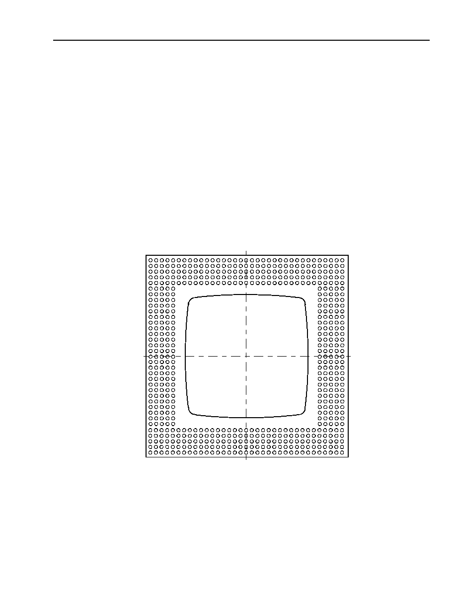
Agere Systems Inc.
11
Data Sheet
May 2001
155/622/2488 Mbits/s Data Interface
TDAT042G5 SONET/SDH
Description
The TDAT042G5 SONET/SDH interface device provides a versatile solution for quad STS-3/STM-1,
quad STS-12/STM-4, and for single STS-48/STM-16 point-to-point datacom/telecom applications. Constructed
using Agere Systems Inc.'s state-of-the-art CMOS technology, this device incorporates integrated SONET/SDH
framing, section and line overhead insertion and extraction, path termination, and generation.
The integrated circuit provides complete encapsulation and decapsulation for packet and ATM streams into and
out of SONET/SDH payloads.
Communication with the device is accomplished through a generic microprocessor interface. The device supports
separate address and data buses.
With the device, construction of all types of point-to-point STS-3/STS-12/STS-48 (STM-1/STM-4/
STM-16) data equipment is simplified and cost-reduced, allowing extremely efficient solutions.
Pin Information
TDAT042G5 is available in a 600-pin LBGA package. The pin diagram is shown in Figure 1. For convenience, pin
assignments are listed by pin order in Table 1 and by signal name in Table 2. The pin descriptions as well as the
pin assignments are listed in Table 3--Table 10 and are grouped by interface type.
5-7175(F)
Figure 1. Pin Diagram of 600-Pin LBGA (Bottom View)
T
D
H
AL
F
K
B
P
M
L
J
AH
R
C
E
Y
N
U
AN
G
AD
V
AM
AJ
AG
AE
AC
AA
W
AP
AK
AF
AB
AR
A
19
30
26
28
24
32
22
20
18
4
6
8
10
12
14
16
2
34
5
23
25
7
31
29
15
21
3
27
11
17
9
13
1
35
33

12
Agere Systems Inc.
Data Sheet
May 2001
155/622/2488 Mbits/s Data Interface
TDAT042G5 SONET/SDH
Pin Information
(continued)
Table 1. Pin Assignments for 600-Pin LBGA by Pin Number Order
Note: NC refers to no connect. Do not connect pins so designated.
Pin
Signal Name
Pin
Signal Name
Pin
Signal Name
Pin
Signal Name
A1
V
DDD
B1
V
DDD
C1
GND
D
D1
GND
D
A2
V
DDD
B2
V
DDD
C2
GND
D
D2
GND
D
A3
GND
D
B3
GND
D
C3
V
DDD
D3
GND
D
A4
GND
D
B4
GND
D
C4
GND
D
D4
V
DDD
A5
V
DDD
B5
NC
C5
NC
D5
NC
A6
V
DDD
B6
V
DDA
C6
GND
A
D6
NC
A7
GND
D
B7
INT
C7
RST
D7
PMRST
A8
GND
D
B8
CS
C8
MPCLK
D8
MPMODE
A9
DATA[1]
B9
DATA[0]
C9
DS
D9
R/W
A10
DATA[6]
B10
DATA[5]
C10
DATA[4]
D10
DATA[3]
A11
DATA[10]
B11
DATA[9]
C11
DATA[8]
D11
DATA[7]
A12
DATA[15]
B12
DATA[14]
C12
DATA[13]
D12
DATA[12]
A13
GND
D
B13
ADDR[3]
C13
ADDR[2]
D13
ADDR[1]
A14
ADDR[8]
B14
ADDR[7]
C14
ADDR[6]
D14
ADDR[5]
A15
ADDR[12]
B15
ADDR[11]
C15
ADDR[10]
D15
NC
A16
GND
D
B16
ADDR[15]
C16
ADDR[14]
D16
ADDR[13]
A17
V
DDD
B17
NC
C17
NC
D17
NC
A18
V
DDD
B18
NC
C18
NC
D18
NC
A19
NC
B19
NC
C19
NC
D19
NC
A20
GND
D
B20
NC
C20
NC
D20
NC
A21
NC
B21
NC
C21
NC
D21
NC
A22
NC
B22
NC
C22
NC
D22
NC
A23
GND
D
B23
NC
C23
NC
D23
NC
A24
NC
B24
NC
C24
NC
D24
NC
A25
NC
B25
NC
C25
NC
D25
NC
A26
NC
B26
NC
C26
NC
D26
NC
A27
GND
D
B27
NC
C27
NC
D27
V
DDD
A28
GND
D
B28
NC
C28
NC
D28
NC
A29
GND
D
B29
NC
C29
NC
D29
NC
A30
V
DDD
B30
NC
C30
NC
D30
NC
A31
V
DDD
B31
NC
C31
NC
D31
NC
A32
GND
D
B32
GND
D
C32
GND
D
D32
V
DDD
A33
GND
D
B33
GND
D
C33
V
DDD
D33
GND
D
A34
V
DDD
B34
V
DDD
C34
GND
D
D34
GND
D
A35
V
DDD
B35
V
DDD
C35
GND
D
D35
GND
D

Agere Systems Inc.
13
Data Sheet
May 2001
155/622/2488 Mbits/s Data Interface
TDAT042G5 SONET/SDH
Pin Information
(continued)
Table 1.
Pin Assignments for 600-Pin LBGA by Pin Number Order (continued)
Note: NC refers to no connect. Do not connect pins so designated.
Pin
Signal Name
Pin
Signal Name
Pin
Signal Name
Pin
Signal Name
E1
V
DDD
F1
V
DDD
J31
TxEOP[A]
N1
GND
D
E2
NC
F2
TCK
J32
TxSOP/C[A]
N2
TxD[6]N
E3
V
DDD
PLL
F3
GND
D
J33
TxPRTY[A]
N3
TxD[6]P
E4
GND
D
PLL
F4
TMS
J34
TxDATA[A][15]
N4
TxD[7]N
E5
V
DDD
F5
NC
J35
TxDATA[A][14]
N5
TxD[7]P
E6
NC
F31
NC
K1
TxD[12]N
N31
RxDATA[A][15]
E7
ICT
F32
NC
K2
TxD[12]P
N32
RxDATA[A][14]
E8
DT
F33
NC
K3
TxD[13]N
N33
RxDATA[A][13]
E9
ADS
F34
NC
K4
TxD[13]P
N34
RxDATA[A][12]
E10
DATA[2]
F35
V
DDD
K5
V
DDD
N35
GND
D
E11
V
DDD
G1
GND
D
K31
TxDATA[A][13]
P1
TxD[4]N
E12
DATA[11]
G2
TDO
K32
TxDATA[A][12]
P2
TxD[4]P
E13
ADDR[0]
G3
TRST
K33
TxDATA[A][11]
P3
TxD[5]N
E14
ADDR[4]
G4
NC
K34
TxDATA[A][10]
P4
V
DDD
E15
ADDR[9]
G5
TDI
K35
TxDATA[A][9]
P5
TxD[5]P
E16
V
DDD
G31
NC
L1
TxD[10]N
P31
RxDATA[A][11]
E17
NC
G32
TxADDR[0]
L2
TxD[10]P
P32
RxDATA[A][10]
E18
NC
G33
TxADDR[1]
L3
TxD[11]N
P33
RxDATA[A][9]
E19
NC
G34
TxCLK[A]
L4
TxD[11]P
P34
RxDATA[A][8]
E20
V
DDD
G35
GND
D
L5
V
DDD
P35
RxDATA[A][7]
E21
NC
H1
GND
D
L31
V
DDD
R1
V
DDD
E22
NC
H2
TxCKQP
L32
TxDATA[A][8]
R2
TxD[2]N/TxD[B]N
E23
NC
H3
GND
D
L33
TxDATA[A][7]
R3
TxD[2]P/TxD[B]P
E24
NC
H4
CLKDIV
L34
TxDATA[A][6]
R4
TxD[3]P/TxD[A]P
E25
V
DDD
H5
GND
D
L35
TxDATA[A][5]
R5
TxD[3]N/TxD[A]N
E26
NC
H31
TxSZ[A]
M1
TxD[8]N
R31
RxDATA[A][6]
E27
NC
H32
TxERR[A]
M2
TxD[8]P
R32
RxDATA[A][5]
E28
NC
H33
TxPA[A]
M3
TxD[9]N
R33
RxDATA[A][4]
E29
NC
H34
TxENB[A]
M4
TxD[9]P
R34
RxDATA[A][3]
E30
NC
H35
GND
D
M5
V
DDD
R35
RxDATA[A][2]
E31
V
DDD
J1
TxD[14]N
M31
TxDATA[A][4]
T1
GND
D
E32
NC
J2
TxD[14]P
M32
TxDATA[A][3]
T2
TxD[0]P/TxD[D]P
E33
NC
J3
TxD[15]N
M33
TxDATA[A][2]
T3
TxD[1]N/TxD[C]N
E34
NC
J4
TxD[15]P
M34
TxDATA[A][1]
T4
TxD[1]P/TxD[C]P
E35
V
DDD
J5
TxCKQN
M35
TxDATA[A][0]
T5
V
DDD

14
Agere Systems Inc.
Data Sheet
May 2001
155/622/2488 Mbits/s Data Interface
TDAT042G5 SONET/SDH
Pin Information
(continued)
Table 1.
Pin Assignments for 600-Pin LBGA by Pin Number Order (continued)
Note: NC refers to no connect. Do not connect pins so designated.
Pin
Signal Name
Pin
Signal Name
Pin
Signal Name
Pin
Signal Name
T31
V
DDD
Y1
GND
D
AC31 TxDATA[B][8]
AG1
RxD[0]N
T32
RxDATA[A][1]
Y2
RxD[13]N/
RxCLK[B]N
AC32 TxDATA[B][9]
AG2
RxD[0]P
T33
RxDATA[A][0]
Y3
RxD[13]P/
RxCLK[B]P
AC33 TxDATA[B][10]
AG3
ECLREFLO
T34
RxPRTY[A]
Y4
GND
D
AC34 TxDATA[B][11]
AG4
ECLREFHI
T35
GND
D
Y5
V
DDD
AC35 GND
D
AG5
GPIO[3]
U1
TxFSYNCN
Y31
V
DDD
AD1
RxD[5]N
AG31 RxDATA[B][5]
U2
TxD[0]N/
TxD[D]N
Y32
TxSZ[B]
AD2
RxD[5]P
AG32 RxDATA[B][6]
U3
TxFSYNCP
Y33
TxCLK[B]
AD3
RxD[6]N
AG33 RxDATA[B][7]
U4
TxCKP
Y34
TxADDR[3]
AD4
RxD[6]P
AG34 RxDATA[B][8]
U5
TxCKN
Y35
GND
D
AD5
V
DDD
AG35 RxDATA[B][9]
U31
RxSOP/C[A]
AA1
RxD[11]N/
RxCLK[C]N
AD31 TxDATA[B][3]
AH1
GND
D
U32
RxEOP[A]
AA2
RxD[11]P/RxCLK[C]P
AD32 TxDATA[B][4]
AH2
GPIO[2]
U33
NC
AA3
RxD[12]N/RxD[C]N
AD33 TxDATA[B][5]
AH3
GPIO[1]
U34
RxENB[A]
AA4
RxD[12]P/RxD[C]P
AD34 TxDATA[B][6]
AH4
GPIO[0]
U35
V
DDD
AA5
GND
D
AD35 TxDATA[B][7]
AH5
TxTOHF
V1
V
DDD
AA31 TxEOP[B]
AE1
RxD[3]N
AH31 RxDATA[B][1]
V2
V
DDD
AA32 TxSOP/C[B]
AE2
RxD[3]P
AH32 RxDATA[B][2]
V3
GND
D
AA33 TxENB[B]
AE3
RxD[4]N
AH33 RxDATA[B][3]
V4
R
x
CKN/R
x
D
[A]
N
AA34 TxPA[B]
AE4
RxD[4]P
AH34 RxDATA[B][4]
V5
R
x
CKP/R
x
D
[A]
P
AA35 TxERR[B]
AE5
V
DDD
AH35 GND
D
V31
GND
D
AB1
R
x
D[9]N/R
x
CLK[D]N
AE31 V
DDD
AJ1
GND
D
V32
RxERR[A]
AB2
R
x
D[9]P/R
x
CLK[D]P
AE32 RxDATA[B][15]
AJ2
TxTOHCK
V33
RxPA[A]
AB3
RxD[10]N/RxD[D]N
AE33 TxDATA[B][0]
AJ3
TxTOHD[A]
V34
NC
AB4
RxD[10]P/RxD[D]P
AE34 TxDATA[B][1]
AJ4
TxTOHD[B]
V35
V
DDD
AB5
V
DDD
AE35 TxDATA[B][2]
AJ5
TxTOHD[C]
W1
V
DDD
AB31 TxDATA[B][13]
AF1
RxD[1]N
AJ31
RxEOP[B]
W2
RxD[14]N
/
RxCLK[A]N
AB32 TxDATA[B][12]
AF2
RxD[1]P
AJ32
RxSOP/C[B]
W3
RxD[14]P
/
RxCLK[A]P
AB33 TxDATA[B][14]
AF3
RxD[2]N
AJ33
RxPRTY[B]
W4
RxD[15]N/
RxD[B]N
AB34 TxDATA[B][15]
AF4
RxD[2]P
AJ34
RxDATA[B][0]
W5
RxD[15]P/
RxD[B]P
AB35 TxPRTY[B]
AF5
V
DDD
AJ35
GND
D
W31
RxADDR[0]
AC1
GND
D
AF31 RxDATA[B][10]
AK1
V
DDD
W32
RxADDR[1]
AC2
RxD[7]N
AF32 RxDATA[B][11]
AK2
TxTOHD[D]
W33
RxCLK[A]
AC3
RxD[7]P
AF33 RxDATA[B][12]
AK3
RxREF
W34
TxADDR[2]
AC4
RxD[8]N
AF34 RxDATA[B][13]
AK4
RxTOHF[A]
W35
RxSZ[A]
AC5
RxD[8]P
AF35 RxDATA[B][14]
AK5
RxTOHCK[A]

Agere Systems Inc.
15
Data Sheet
May 2001
155/622/2488 Mbits/s Data Interface
TDAT042G5 SONET/SDH
Pin Information
(continued)
Table 1.
Pin Assignments for 600-Pin LBGA by Pin Number Order (continued)
Note: NC refers to no connect. Do not connect pins so designated.
Pin
Signal Name
Pin
Signal Name
Pin
Signal Name
Pin
Signal Name
AK31 RxSZ[B]
AL31
V
DDD
AM31 TxADDR[4]
AN31 NC
AK32 RxERR[B]
AL32
RxADDR[3]
AM32 V
DDD
AN32 GND
D
AK33 RxPA[B]
AL33
RxADDR[2]
AM33 GND
D
AN33 V
DDD
AK34 RxENB[B]
AL34
RxCLK[B]
AM34 GND
D
AN34 GND
D
AK35 V
DDD
AL35
V
DDD
AM35 GND
D
AN35 GND
D
AL1
V
DDD
AM1
GND
D
AN1
GND
D
AP1
V
DDD
AL2
RxTOHD[A]
AM2
GND
D
AN2
GND
D
AP2
V
DDD
AL3
RxTOHF[B]
AM3
GND
D
AN3
V
DDD
AP3
GND
D
AL4
RxTOHCK[B]
AM4
V
DDD
AN4
GND
D
AP4
GND
D
AL5
V
DDD
AM5
RxTOHD[B]
AN5
RxTOHF[C]
AP5
NC
AL6
RxTOHCK[C]
AM6
RxTOHD[C]
AN6
GND
D
AP6
RxTOHF[D]
AL7
RxTOHCK[D]
AM7
NC
AN7
RxTOHD[D]
AP7
NC
AL8
NC
AM8
RxCLK[D]
AN8
RxSZ[D]
AP8
RxERR[D]
AL9
RxPA[D]
AM9
RxENB[D]
AN9
RxEOP[D]
AP9
RxSOP/C[D]
AL10
RxDATA[D][0]
AM10 RxDATA[D][1]
AN10 RxDATA[D][2]
AP10 RxDATA[D][3]
AL11
V
DDD
AM11 RxDATA[D][5]
AN11 RxDATA[D][6]
AP11 RxDATA[D][7]
AL12
RxDATA[D][9]
AM12 RxDATA[D][10]
AN12 RxDATA[D][11]
AP12 RxDATA[D][12]
AL13
RxDATA[D][14]
AM13 RxDATA[D][15]
AN13 TxDATA[D][0]
AP13 TxDATA[D][1]
AL14
TxDATA[D][3]
AM14 TxDATA[D][2]
AN14 TxDATA[D][4]
AP14 TxDATA[D][5]
AL15
TxDATA[D][8]
AM15 TxDATA[D][7]
AN15 TxDATA[D][9]
AP15 TxDATA[D][10]
AL16
V
DDD
AM16 TxDATA[D][12]
AN16 TxDATA[D][13]
AP16 TxDATA[D][14]
AL17
TxSOP/C[D]
AM17 TxPRTY[D]
AN17 TxEOP[D]
AP17 TxDATA[D][15]
AL18
V
DDD
AM18 TxERR[D]
AN18 TxSZ[D]
AP18 TxPA[D]
AL19
NC
AM19 NC
AN19 NC
AP19 TxCLK[D]
AL20
V
DDD
AM20 RxSZ[C]
AN20 RxCLK[C]
AP20 RxADDR[4]
AL21
RxSOP/C[C]
AM21 RxEOP[C]
AN21 RxENB[C]
AP21 RxPA[C]
AL22
RxDATA[C][3]
AM22 RxDATA[C][2]
AN22 RxDATA[C][1]
AP22 RxDATA[C][0]
AL23
RxDATA[C][7]
AM23 RxDATA[C][6]
AN23 RxDATA[C][5]
AP23 RxDATA[C][4]
AL24
RxDATA[C][12]
AM24 RxDATA[C][11]
AN24 RxDATA[C][10]
AP24 RxDATA[C][9]
AL25
V
DDD
AM25 TxDATA[C][0]
AN25 RxDATA[C][15]
AP25 RxDATA[C][14]
AL26
TxDATA[C][5]
AM26 TxDATA[C][4]
AN26 TxDATA[C][3]
AP26 TxDATA[C][2]
AL27
TxDATA[C][10]
AM27 TxDATA[C][9]
AN27 TxDATA[C][8]
AP27 TxDATA[C][7]
AL28
TxDATA[C][14]
AM28 TxDATA[C][13]
AN28 TxDATA[C][12]
AP28 TxDATA[C][11]
AL29
TxEOP[C]
AM29 TxSOP/C[C]
AN29 TxPRTY[C]
AP29 TxDATA[C][15]
AL30
TxSZ[C]
AM30 TxERR[C]
AN30 TxPA[C]
AP30 TxENB[C]
16
Agere Systems Inc.
Data Sheet
May 2001
155/622/2488 Mbits/s Data Interface
TDAT042G5 SONET/SDH
Pin Information
(continued)
Table 1.
Pin Assignments for 600-Pin LBGA by Pin Number Order (continued)
Note: NC refers to no connect. Do not connect pins so designated.
Pin
Signal Name
Pin
Signal Name
Pin
Signal Name
Pin
Signal Name
AP31 TxCLK[C]
AR6
V
DDD
AR16 GND
D
AR26 TxDATA[C][1]
AP32 GND
D
AR7
GND
D
AR17 TxENB[D]
AR27 TxDATA[C][6]
AP33 GND
D
AR8
GND
D
AR18 V
DDD
AR28 GND
D
AP34 V
DDD
AR9
RxPRTY[D]
AR19 V
DDD
AR29 GND
D
AP35 V
DDD
AR10 RxDATA[D][4]
AR20 GND
D
AR30 V
DDD
AR1
V
DDD
AR11 RxDATA[D][8]
AR21 RxERR[C]
AR31 V
DDD
AR2
V
DDD
AR12 RxDATA[D][13]
AR22 RxPRTY[C]
AR32 GND
D
AR3
GND
D
AR13 GND
D
AR23 GND
D
AR33 GND
D
AR4
GND
D
AR14 TxDATA[D][6]
AR24 RxDATA[C][8]
AR34 V
DDD
AR5
V
DDD
AR15 TxDATA[D][11]
AR25 RxDATA[C][13]
AR35 V
DDD

Agere Systems Inc.
17
Data Sheet
May 2001
155/622/2488 Mbits/s Data Interface
TDAT042G5 SONET/SDH
Pin Information
(continued)
Table 2. Pin Assignments for 600-Pin LBGA by Signal Name
Note: NC refers to no connect. Do not connect pins so designated.
Signal Name
Pin
Signal Name
Pin
Signal Name
Pin
Signal Name
Pin
ADDR[0]
E13
DS
C9
GND
D
G1
GND
D
AP3
ADDR[1]
D13
DT
E8
GND
D
G35
GND
D
AP32
ADDR[2]
C13
ECLREFHI
AG4
GND
D
H1
GND
D
AP33
ADDR[3]
B13
ECLREFLO
AG3
GND
D
H3
GND
D
AP4
ADDR[4]
E14
GND
A
C6
GND
D
H5
GND
D
AR3
ADDR[5]
D14
GND
D
A3
GND
D
H35
GND
D
AR4
ADDR[6]
C14
GND
D
A4
GND
D
N1
GND
D
AR7
ADDR[7]
B14
GND
D
A7
GND
D
N35
GND
D
AR8
ADDR[8]
A14
GND
D
A8
GND
D
T1
GND
D
AR13
ADDR[9]
E15
GND
D
A13
GND
D
T35
GND
D
AR16
ADDR[10]
C15
GND
D
A16
GND
D
V3
GND
D
AR20
ADDR[11]
B15
GND
D
A20
GND
D
V31
GND
D
AR23
ADDR[12]
A15
GND
D
A23
GND
D
Y1
GND
D
AR28
ADDR[13]
D16
GND
D
A27
GND
D
Y4
GND
D
AR29
ADDR[14]
C16
GND
D
A28
GND
D
Y35
GND
D
AR32
ADDR[15]
B16
GND
D
A29
GND
D
AA5
GND
D
AR33
ADS
E9
GND
D
A32
GND
D
AC1
GND
D
PLL
E4
CLKDIV
H4
GND
D
A33
GND
D
AC35
GPIO[0]
AH4
CS
B8
GND
D
B3
GND
D
AH1
GPIO[1]
AH3
DATA[0]
B9
GND
D
B4
GND
D
AH35
GPIO[2]
AH2
DATA[1]
A9
GND
D
B32
GND
D
AJ1
GPIO[3]
AG5
DATA[2]
E10
GND
D
B33
GND
D
AJ35
ICT
E7
DATA[3]
D10
GND
D
C1
GND
D
AM1
INT
B7
DATA[4]
C10
GND
D
C2
GND
D
AM2
MPCLK
C8
DATA[5]
B10
GND
D
C4
GND
D
AM3
MPMODE
D8
DATA[6]
A10
GND
D
C32
GND
D
AM33
NC
A19
DATA[7]
D11
GND
D
C34
GND
D
AM34
NC
A21
DATA[8]
C11
GND
D
C35
GND
D
AM35
NC
A22
DATA[9]
B11
GND
D
D1
GND
D
AN1
NC
A24
DATA[10]
A11
GND
D
D2
GND
D
AN2
NC
A25
DATA[11]
E12
GND
D
D3
GND
D
AN4
NC
A26
DATA[12]
D12
GND
D
D33
GND
D
AN6
NC
B5
DATA[13]
C12
GND
D
D34
GND
D
AN32
NC
B17
DATA[14]
B12
GND
D
D35
GND
D
AN34
NC
B18
DATA[15]
A12
GND
D
F3
GND
D
AN35
NC
B19

18
Agere Systems Inc.
Data Sheet
May 2001
155/622/2488 Mbits/s Data Interface
TDAT042G5 SONET/SDH
Pin Information
(continued)
Table 2.
Pin Assignments for 600-Pin LBGA by Signal Name (continued)
Note: NC refers to no connect. Do not connect pins so designated.
Signal Name
Pin
Signal Name
Pin
Signal Name
Pin
Signal Name
Pin
NC
B20
NC
D21
NC
V34
RxD[6]N
AD3
NC
B21
NC
D22
NC
AL8
RxD[6]P
AD4
NC
B22
NC
D23
NC
AL19
RxD[7]N
AC2
NC
B23
NC
D24
NC
AM7
RxD[7]P
AC3
NC
B24
NC
D25
NC
AM19
RxD[8]N
AC4
NC
B25
NC
D26
NC
AN19
RxD[8]P
AC5
NC
B26
NC
D28
NC
AN31
R
x
D[9]N/R
x
CLK[D]N
AB1
NC
B27
NC
D29
NC
AP5
R
x
D[9]P/R
x
CLK[D]P
AB2
NC
B28
NC
D30
NC
AP7
RxD[10]N/RxD[D]N
AB3
NC
B29
NC
D31
PMRST
D7
RxD[10]P/RxD[D]P
AB4
NC
B30
NC
E2
R/W
D9
RxD[11]N/RxCLK[C]N
AA1
NC
B31
NC
E6
RST
C7
RxD[11]P/RxCLK[C]P
AA2
NC
C5
NC
E17
RxADDR[0]
W31
RxD[12]N/RxD[C]N
AA3
NC
C17
NC
E18
RxADDR[1]
W32
RxD[12]P/RxD[C]P
AA4
NC
C18
NC
E19
RxADDR[2]
AL33
RxD[13]N/RxCLK[B]N
Y2
NC
C19
NC
E21
RxADDR[3]
AL32
RxD[13]P/RxCLK[B]P
Y3
NC
C20
NC
E22
RxADDR[4]
AP20
RxD[14]N/RxCLK[A]N
W2
NC
C21
NC
E23
R
x
CKN/R
x
D
[A]
N
V4
RxD[14]P/RxCLK[A]P
W3
NC
C22
NC
E24
R
x
CKP/R
x
D
[A]
P
V5
RxD[15]N/RxD[B]N
W4
NC
C23
NC
E26
RxCLK[A]
W33
RxD[15]P/RxD[B]P
W5
NC
C24
NC
E27
RxCLK[B]
AL34
RxDATA[A][0]
T33
NC
C25
NC
E28
RxCLK[C]
AN20
RxDATA[A][1]
T32
NC
C26
NC
E29
RxCLK[D]
AM8
RxDATA[A][2]
R35
NC
C27
NC
E30
RxD[0]N
AG1
RxDATA[A][3]
R34
NC
C28
NC
E32
RxD[0]P
AG2
RxDATA[A][4]
R33
NC
C29
NC
E33
RxD[1]N
AF1
RxDATA[A][5]
R32
NC
C30
NC
E34
RxD[1]P
AF2
RxDATA[A][6]
R31
NC
C31
NC
F5
RxD[2]N
AF3
RxDATA[A][7]
P35
NC
D5
NC
F31
RxD[2]P
AF4
RxDATA[A][8]
P34
NC
D6
NC
F32
RxD[3]N
AE1
RxDATA[A][9]
P33
NC
D15
NC
F33
RxD[3]P
AE2
RxDATA[A][10]
P32
NC
D17
NC
F34
RxD[4]N
AE3
RxDATA[A][11]
P31
NC
D18
NC
G4
RxD[4]P
AE4
RxDATA[A][12]
N34
NC
D19
NC
G31
RxD[5]N
AD1
RxDATA[A][13]
N33
NC
D20
NC
U33
RxD[5]P
AD2
RxDATA[A][14]
N32

Agere Systems Inc.
19
Data Sheet
May 2001
155/622/2488 Mbits/s Data Interface
TDAT042G5 SONET/SDH
Pin Information
(continued)
Table 2.
Pin Assignments for 600-Pin LBGA by Signal Name (continued)
Note: NC refers to no connect. Do not connect pins so designated.
Signal Name
Pin
Signal Name
Pin
Signal Name
Pin
Signal Name
Pin
RxDATA[A][15]
N31
RxDATA[D][2]
AN10
RxSOP/C[A]
U31
TxCLK[B]
Y33
RxDATA[B][0]
AJ34
RxDATA[D][3]
AP10
RxSOP/C[B]
AJ32
TxCLK[C]
AP31
RxDATA[B][1]
AH31
RxDATA[D][4]
AR10
RxSOP/C[C]
AL21
TxCLK[D]
AP19
RxDATA[B][2]
AH32
RxDATA[D][5]
AM11
RxSOP/C[D]
AP9
TxD[0]N/TxD[D]N
U2
RxDATA[B][3]
AH33
RxDATA[D][6]
AN11
RxSZ[A]
W35
TxD[0]P/TxD[D]P
T2
RxDATA[B][4]
AH34
RxDATA[D][7]
AP11
RxSZ[B]
AK31
TxD[1]N/TxD[C]N
T3
RxDATA[B][5]
AG31
RxDATA[D][8]
AR11
RxSZ[C]
AM20
TxD[1]P/TxD[C]P
T4
RxDATA[B][6]
AG32
RxDATA[D][9]
AL12
RxSZ[D]
AN8
TxD[2]N/TxD[B]N
R2
RxDATA[B][7]
AG33
RxDATA[D][10]
AM12
RxTOHCK[A]
AK5
TxD[2]P/TxD[B]P
R3
RxDATA[B][8]
AG34
RxDATA[D][11]
AN12
RxTOHCK[B]
AL4
TxD[3]N/TxD[A]N
R5
RxDATA[B][9]
AG35
RxDATA[D][12]
AP12
RxTOHCK[C]
AL6
TxD[3]P/TxD[A]P
R4
RxDATA[B][10]
AF31
RxDATA[D][13]
AR12
RxTOHCK[D]
AL7
TxD[4]N
P1
RxDATA[B][11]
AF32
RxDATA[D][14]
AL13
RxTOHD[A]
AL2
TxD[4]P
P2
RxDATA[B][12]
AF33
RxDATA[D][15]
AM13
RxTOHD[B]
AM5
TxD[5]N
P3
RxDATA[B][13]
AF34
RxENB[A]
U34
RxTOHD[C]
AM6
TxD[5]P
P5
RxDATA[B][14]
AF35
RxENB[B]
AK34
RxTOHD[D]
AN7
TxD[6]N
N2
RxDATA[B][15]
AE32
RxENB[C]
AN21
RxTOHF[A]
AK4
TxD[6]P
N3
RxDATA[C][0]
AP22
RxENB[D]
AM9
RxTOHF[B]
AL3
TxD[7]N
N4
RxDATA[C][1]
AN22
RxEOP[A]
U32
RxTOHF[C]
AN5
TxD[7]P
N5
RxDATA[C][2]
AM22
RxEOP[B]
AJ31
RxTOHF[D]
AP6
TxD[8]N
M1
RxDATA[C][3]
AL22
RxEOP[C]
AM21
TCK
F2
TxD[8]P
M2
RxDATA[C][4]
AP23
RxEOP[D]
AN9
TDI
G5
TxD[9]N
M3
RxDATA[C][5]
AN23
RxERR[A]
V32
TDO
G2
TxD[9]P
M4
RxDATA[C][6]
AM23
RxERR[B]
AK32
TMS
F4
TxD[10]N
L1
RxDATA[C][7]
AL23
RxERR[C]
AR21
TRST
G3
TxD[10]P
L2
RxDATA[C][8]
AR24
RxERR[D]
AP8
TxADDR[0]
G32
TxD[11]N
L3
RxDATA[C][9]
AP24
RxPA[A]
V33
TxADDR[1]
G33
TxD[11]P
L4
RxDATA[C][10]
AN24
RxPA[B]
AK33
TxADDR[2]
W34
TxD[12]N
K1
RxDATA[C][11]
AM24
RxPA[C]
AP21
TxADDR[3]
Y34
TxD[12]P
K2
RxDATA[C][12]
AL24
RxPA[D]
AL9
TxADDR[4]
AM31
TxD[13]N
K3
RxDATA[C][13]
AR25
RxPRTY[A]
T34
TxCKN
U5
TxD[13]P
K4
RxDATA[C][14]
AP25
RxPRTY[B]
AJ33
TxCKP
U4
TxD[14]N
J1
RxDATA[C][15]
AN25
RxPRTY[C]
AR22
TxCKQN
J5
TxD[14]P
J2
RxDATA[D][0]
AL10
RxPRTY[D]
AR9
TxCKQP
H2
TxD[15]N
J3
RxDATA[D][1]
AM10
RxREF
AK3
TxCLK[A]
G34
TxD[15]P
J4

20
Agere Systems Inc.
Data Sheet
May 2001
155/622/2488 Mbits/s Data Interface
TDAT042G5 SONET/SDH
Pin Information
(continued)
Table 2.
Pin Assignments for 600-Pin LBGA by Signal Name (continued)
Note: NC refers to no connect. Do not connect pins so designated.
Signal Name
Pin
Signal Name
Pin
Signal Name
Pin
Signal Name
Pin
TxDATA[A][0]
M35
TxDATA[C][3]
AN26
TxEOP[C]
AL29
V
DDD
A17
TxDATA[A][1]
M34
TxDATA[C][4]
AM26
TxEOP[D]
AN17
V
DDD
A18
TxDATA[A][2]
M33
TxDATA[C][5]
AL26
TxERR[A]
H32
V
DDD
A30
TxDATA[A][3]
M32
TxDATA[C][6]
AR27
TxERR[B]
AA35
V
DDD
A31
TxDATA[A][4]
M31
TxDATA[C][7]
AP27
TxERR[C]
AM30
V
DDD
A34
TxDATA[A][5]
L35
TxDATA[C][8]
AN27
TxERR[D]
AM18
V
DDD
A35
TxDATA[A][6]
L34
TxDATA[C][9]
AM27
TxFSYNCN
U1
V
DDD
B1
TxDATA[A][7]
L33
TxDATA[C][10]
AL27
TxFSYNCP
U3
V
DDD
B2
TxDATA[A][8]
L32
TxDATA[C][11]
AP28
TxPA[A]
H33
V
DDD
B34
TxDATA[A][9]
K35
TxDATA[C][12]
AN28
TxPA[B]
AA34
V
DDD
B35
TxDATA[A][10]
K34
TxDATA[C][13]
AM28
TxPA[C]
AN30
V
DDD
C3
TxDATA[A][11]
K33
TxDATA[C][14]
AL28
TxPA[D]
AP18
V
DDD
C33
TxDATA[A][12]
K32
TxDATA[C][15]
AP29
TxPRTY[A]
J33
V
DDD
D4
TxDATA[A][13]
K31
TxDATA[D][0]
AN13
TxPRTY[B]
AB35
V
DDD
D27
TxDATA[A][14]
J35
TxDATA[D][1]
AP13
TxPRTY[C]
AN29
V
DDD
D32
TxDATA[A][15]
J34
TxDATA[D][2]
AM14
TxPRTY[D]
AM17
V
DDD
E1
TxDATA[B][0]
AE33
TxDATA[D][3]
AL14
TxSOP/C[A]
J32
V
DDD
E5
TxDATA[B][1]
AE34
TxDATA[D][4]
AN14
TxSOP/C[B]
AA32
V
DDD
E11
TxDATA[B][2]
AE35
TxDATA[D][5]
AP14
TxSOP/C[C]
AM29
V
DDD
E16
TxDATA[B][3]
AD31
TxDATA[D][6]
AR14
TxSOP/C[D]
AL17
V
DDD
E20
TxDATA[B][4]
AD32
TxDATA[D][7]
AM15
TxSZ[A]
H31
V
DDD
E25
TxDATA[B][5]
AD33
TxDATA[D][8]
AL15
TxSZ[B]
Y32
V
DDD
E31
TxDATA[B][6]
AD34
TxDATA[D][9]
AN15
TxSZ[C]
AL30
V
DDD
E35
TxDATA[B][7]
AD35
TxDATA[D][10]
AP15
TxSZ[D]
AN18
V
DDD
F1
TxDATA[B][8]
AC31
TxDATA[D][11]
AR15
TxTOHCK
AJ2
V
DDD
F35
TxDATA[B][9]
AC32
TxDATA[D][12]
AM16
TxTOHD[A]
AJ3
V
DDD
K5
TxDATA[B][10]
AC33
TxDATA[D][13]
AN16
TxTOHD[B]
AJ4
V
DDD
L5
TxDATA[B][11]
AC34
TxDATA[D][14]
AP16
TxTOHD[C]
AJ5
V
DDD
L31
TxDATA[B][12]
AB32
TxDATA[D][15]
AP17
TxTOHD[D]
AK2
V
DDD
M5
TxDATA[B][13]
AB31
TxENB[A]
H34
TxTOHF
AH5
V
DDD
P4
TxDATA[B][14]
AB33
TxENB[B]
AA33
V
DDA
B6
V
DDD
R1
TxDATA[B][15]
AB34
TxENB[C]
AP30
V
DDD
A1
V
DDD
T5
TxDATA[C][0]
AM25
TxENB[D]
AR17
V
DDD
A2
V
DDD
T31
TxDATA[C][1]
AR26
TxEOP[A]
J31
V
DDD
A5
V
DDD
U35
TxDATA[C][2]
AP26
TxEOP[B]
AA31
V
DDD
A6
V
DDD
V1
Agere Systems Inc.
21
Data Sheet
May 2001
155/622/2488 Mbits/s Data Interface
TDAT042G5 SONET/SDH
Pin Information
(continued)
Table 2.
Pin Assignments for 600-Pin LBGA by Signal Name (continued)
Note: NC refers to no connect. Do not connect pins so designated.
Signal Name
Pin
Signal Name
Pin
Signal Name
Pin
Signal Name
Pin
V
DDD
V2
V
DDD
AK1
V
DDD
AL35
V
DDD
AR2
V
DDD
V35
V
DDD
AK35
V
DDD
AM4
V
DDD
AR5
V
DDD
W1
V
DDD
AL1
V
DDD
AM32
V
DDD
AR6
V
DDD
Y5
V
DDD
AL5
V
DDD
AN3
V
DDD
AR18
V
DDD
Y31
V
DDD
AL11
V
DDD
AN33
V
DDD
AR19
V
DDD
AB5
V
DDD
AL16
V
DDD
AP1
V
DDD
AR30
V
DDD
AD5
V
DDD
AL18
V
DDD
AP2
V
DDD
AR31
V
DDD
AE5
V
DDD
AL20
V
DDD
AP34
V
DDD
AR34
V
DDD
AE31
V
DDD
AL25
V
DDD
AP35
V
DDD
AR35
V
DDD
AF5
V
DDD
AL31
V
DDD
AR1
V
DDD
PLL
E3

22
Agere Systems Inc.
Data Sheet
May 2001
155/622/2488 Mbits/s Data Interface
TDAT042G5 SONET/SDH
Pin Information
(continued)
Note: 3.3 V CMOS logic inputs are 5 V tolerant. Logic inputs can be driven from standard TTL levels, and logic out-
puts can drive standard TTL inputs. All LVPECL buffers are differential. LVPECL is compliant with low-volt-
age (3.3 V) pseudo-emitter-coupled logic interface levels. All PECL outputs, including ECLREFHI and
ECLREFLO require terminating resistors. The required termination for the PECL buffers is 50
to a termi-
nating voltage of V
DDD
≠ 2 V. The Thevenin equivalent is also acceptable (130
to V
DDD
and 82
to
GND
D
). Other termination styles are not recommended. LVPECL inputs with a / in the name indicate multiple
functionality. The name preceding the / is the function in STS-48/STM-16 mode. The name after the / is the
function in STS-3/STM-1 or STS-12/STM-4 mode.
Table 3. Pin Descriptions--Line Interface Signals
Unused LVPECL outputs should not be terminated to minimize power consumption. Unused inputs are internally
disabled whenever core registers 0x0010 and 0x0011 are properly provisioned. The unused inputs can be consid-
ered to be NC (no connect).
Pin
Symbol
Type
I/O
Name/Description
V5
RxCKP/
RxD[A]P
LVPECL
I
Receive Line Clock (STS-48/STM-16)/Receive Line Data Input Channel
A. In STS-48/STM-16 mode, these pins function as receive line clock. This
155.52 MHz clock comes from an external clock data recovery circuit. This
clock is used to clock in the RxD[15:0] receive line data inputs.
In STS-3/STM-1 or STS-12/STM-4 mode, these pins function as receive
data input channel A at 155.52 Mbits/s or 622.08 Mbits/s, respectively.
This buffer is internally disabled when not in STS-48/STM-16 mode and
channel A is disabled. This buffer is internally disabled through proper pro-
visioning when the input is not active.
V4
RxCKN/
RxD[A]N
AG2
RxD[0]P
LVPECL
I
Receive Line Data Inputs (STS-48/STM-16). In STS-48/STM-16 mode,
these pins function as receive line data inputs [0:8]. The remaining receive
line data inputs [9:15] are listed below and are multiplexed for use in the
STS-3/STM-1 or STS-12/STM-4 modes.
The 2.488 Gbits/s STS-48/STM-16 serial data stream is converted to a
155.52 Mbits/s parallel 16-bit word external to TDAT042G5 by a demulti-
plexer.
All 32 differential data input pins, RxD[15:0]P/N, are used as the parallel
data input bus in the STS-48/STM-16 mode. These pins constitute a
155.52 Mbits/s parallel 16-bit word-aligned to the RxCKP/N 155.52 MHz
receive line clock. RxD[15] is the most significant bit and is the first bit
received. RxD[0] is the least significant bit and is the last bit received.
This buffer is internally disabled through proper provisioning when the input
is not active.
AG1
RxD[0]N
AF2
RxD[1]P
LVPECL
AF1
RxD[1]N
AF4
RxD[2]P
LVPECL
AF3
RxD[2]N
AE2
RxD[3]P
LVPECL
AE1
RxD[3]N
AE4
RxD[4]P
LVPECL
AE3
RxD[4]N
AD2
RxD[5]P
LVPECL
AD1
RxD[5]N
AD4
RxD[6]P
LVPECL
AD3
RxD[6]N
AC3
RxD[7]P
LVPECL
AC2
RxD[7]N
AC5
RxD[8]P
LVPECL
AC4
RxD[8]N
AB2
RxD[9]P/
RxCLK[D]P
LVPECL
I
Receive Line Data Input [9]/Receive Line Clock Channel D. In STS-48/
STM-16 mode, these pins function as receive line data input [9] at
155.52 Mbits/s.
In STS-3/STM-1 or STS-12/STM-4 mode, these pins function as receive
line clock channel D at either 155.52 MHz (STS-3/STM-1) or 622.08 MHz
(STS-12/STM-4).
This buffer is internally disabled when not in STS-48/STM-16 mode and
channel D is disabled. This buffer is internally disabled through proper pro-
visioning when the input is not active.
AB1
RxD[9]N/
RxCLK[D]N

Agere Systems Inc.
23
Data Sheet
May 2001
155/622/2488 Mbits/s Data Interface
TDAT042G5 SONET/SDH
Pin Information
(continued)
Table 3. Pin Descriptions--Line Interface Signals (continued)
Unused LVPECL outputs should not be terminated to minimize power consumption. Unused inputs are internally
disabled whenever core registers 0x0010 and 0x0011 are properly provisioned. The unused inputs can be consid-
ered to be NC (no connect).
Pin
Symbol
Type
I/O
Name/Description
AB4
RxD[10]P/
RxD[D]P
LVPECL
I
Receive Line Data Input [10]/Receive Line Data Input
Channel D. In STS-48/STM-16 mode, these pins function as
receive line data input [10] at 155.52 Mbits/s.
In STS-3/STM-1 or STS-12/STM-4 mode, these pins function as
receive line data input channel D at either 155.52 Mbits/s (STS-3/
STM-1) or 622.08 Mbits/s (STS-12/STM-4).
This buffer is internally disabled when not in STS-48/STM-16
mode and channel D is disabled. This buffer is internally disabled
through proper provisioning when the input is not active.
AB3
RxD[10]N/
RxD[D]N
AA2
RxD[11]P/
RxCLK[C]P
LVPECL
I
Receive Line Data Input [11]/Receive Line Clock Channel C.
In STS-48/STM-16 mode, these pins function as receive line data
input [11] at 155.52 Mbits/s.
In STS-3/STM-1 or STS-12/STM-4 mode, these pins function as
receive line clock channel C at either 155.52 MHz (STS-3/STM-1)
or 622.08 MHz (STS-12/STM-4).
This buffer is internally disabled when not in STS-48/STM-16
mode and channel C is disabled. This buffer is internally disabled
through proper provisioning when the input is not active.
AA1
RxD[11]N/
RxCLK[C]N
AA4
RxD[12]P/
RxD[C]P
LVPECL
I
Receive Line Data Input [12]/Receive Line Data Input
Channel C. In STS-48/STM-16 mode, these pins function as
receive line data input [12] at 155.52 Mbits/s.
In STS-3/STM-1 or STS-12/STM-4 mode, these pins function as
receive line data input channel C at either 155.52 Mbits/s (STS-3/
STM-1) or 622.08 Mbits/s (STS-12/STM-4).
This buffer is internally disabled when not in STS-48/STM-16
mode and channel C is disabled. This buffer is internally disabled
through proper provisioning when the input is not active.
AA3
RxD[12]N/
RxD[C]N
Y3
RxD[13]P/
RxCLK[B]P
LVPECL
I
Receive Line Data Input [13]/Receive Line Clock Channel B.
In STS-48/STM-16 mode, these pins function as receive line data
input [13] at 155.52 Mbits/s.
In STS-3/STM-1 or STS-12/STM-4 mode, these pins function as
receive line clock channel B at either 155.52 MHz (STS-3/STM-1)
or 622.08 MHz (STS-12/STM-4).
This buffer is internally disabled when not in STS-48/STM-16
mode and channel B is disabled. This buffer is internally disabled
through proper provisioning when the input is not active.
Y2
RxD[13]N/
RxCLK[B]N
W3
RxD[14]P/
RxCLK[A]P
LVPECL
I
Receive Line Data Input [14]/Receive Line Clock Channel A.
In STS-48/STM-16 mode, these pins function as receive line data
input [14] at 155.52 Mbits/s.
In STS-3/STM-1 or STS-12/STM-4 mode, these pins function as
receive line clock channel A at either 155.52 MHz (STS-3/STM-1)
or 622.08 MHz (STS-12/STM-4).
This buffer is internally disabled when not in STS-48/STM-16
mode and channel A is disabled. This buffer is internally disabled
through proper provisioning when the input is not active.
W2
RxD[14]N/
RxCLK[A]N

24
Agere Systems Inc.
Data Sheet
May 2001
155/622/2488 Mbits/s Data Interface
TDAT042G5 SONET/SDH
Pin Information
(continued)
Table 3. Pin Descriptions--Line Interface Signals (continued)
Unused LVPECL outputs should not be terminated to minimize power consumption. Unused inputs are internally
disabled whenever core registers 0x0010 and 0x0011 are properly provisioned. The unused inputs can be consid-
ered to be NC (no connect).
* I
u
= I
d
= 50 k
, where I
u
= internal pull-up resistance and I
d
= internal pull-down resistance.
This may be obtained from a passive voltage divider of a 130
resistor connected from V
DDD
to one end of an 82
resistor, the other end of
which is connected to GND
D
.
Pin
Symbol
Type
I/O*
Name/Description
W5
RxD[15]P/
RxD[B]P
LVPECL
I
Receive Line Data Input [15]/Receive Line Data Input
Channel B. In STS-48/STM-16 mode, these pins function as
receive line data input [15] at 155.52 Mbits/s.
In STS-3/STM-1 or STS-12/STM-4 mode, these pins function as
receive line data input channel B at either 155.52 Mbits/s
(STS-3/STM-1) or 622.08 Mbits/s (STS-12/STM-4).
This buffer is internally disabled when not in STS-48/STM-16
mode and channel B is disabled. This buffer is internally disabled
through proper provisioning when the input is not active.
W4
RxD[15]N/
RxD[B]N
H4
CLKDIV
3.3 V
(5 V tolerant)
I
u
Clock Division. This pin controls a divider in the line transmit
block to create a 77.76 MHz clock from either the 155.52 MHz
STS-3/STM-1 or STS-48/STM-16 transmit line clock, or the
622.08 MHz STS-12/STM-4 transmit line clock, TxCKP/N.
CLKDIV = 1 for STS-12/STM-4 (divide by 8).
CLKDIV = 0 for STS-3/STM-1 and STS-48 /STM-16 (divide by 2).
AG3
ECLREFLO
--
O
Reference Voltage for LVPECL I/O Buffers. ECLREFLO and
ECLREFHI are buffer outputs which provide the reference for the
output level of the LVPECL output buffers. ECLREFLO and ECL-
REFHI must be connected to a 50
source of V
DDD
≠ 2 V.
No
user-accessible signal is present on these pins.
AG4
ECLREFHI
--
O
Note: The TDAT042G5 has internal circuitry that is associated with the buffer section of the chip. This section
monitors the voltage levels of REFLO and REFHI. A very low frequency calibration process, during which
the values at the ECLREFLO and ECLREFHI pins are continuously monitored, is performed to allow the
drive capactity of remaining buffers to be adjusted within true PECL levels. Therefore, it is important to ter-
minate the ECLREFLO and ECLREFHI outputs in exactly the same way as you would terminate LVPECL
outputs.

Agere Systems Inc.
25
Data Sheet
May 2001
155/622/2488 Mbits/s Data Interface
TDAT042G5 SONET/SDH
Pin Information
(continued)
Table 3. Pin Descriptions--Line Interface Signals (continued)
Unused LVPECL outputs should not be terminated to minimize power consumption. Unused inputs are internally
disabled whenever core registers 0x0010 and 0x0011 are properly provisioned. The unused inputs can be consid-
ered to be NC (no connect).
* I
u
= I
d
= 50 k
, where I
u
= internal pull-up resistance and I
d
= internal pull-down resistance.
Pin
Symbol
Type
I/O*
Name/Description
U4
TxCKP
LVPECL
I
Transmit Line Clock. When in STS-48/STM-16 mode, this clock
is a 155.52 MHz input and clocks out TxD[15:0]P/N or TxD[D:A].
When in STS-12/STM-4 mode, this clock is a 622.08 MHz input
and clocks out TxD[D:A]P/N.
When in STS-3/STM-1 mode, this clock is a 155.52 MHz input
and clocks out TxD[D:A]P/N.
U5
TxCKN
U3
TxFSYNCP
LVPECL
I
d
Transmit Line Frame Sync. This input is the external 8 kHz
transmit line frame sync. Driving this input is optional. If undriven
from an external source, these pins must be no connects. When
this input is used, it must be (1) synchronized to TxCKP/N, and (2)
at least one TxCKP/N cycle wide, up to a maximum of 1 frame
period minus 2 TxCKP/N cycles wide.
U1
TxFSYNCN
I
u
T2
TxD[0]P/
TxD[D]P
LVPECL
O
Transmit Line Data Output [0]/Transmit Line Data Output
Channel D. In STS-48/STM-16 mode, the pins function as trans-
mit line data output [0] at 155.52 Mbits/s.
In STS-3/STM-1 or STS-12/STM-4 mode, the pins function as
transmit data output channel D at either 155.52 Mbits/s or
622.08 Mbits/s.
This buffer is internally disabled through proper provisioning when
the input is not active.
U2
TxD[0]N/
TxD[D]N
T4
TxD[1]P/
TxD[C]P
LVPECL
O
Transmit Line Data Output [1]/Transmit Line Data Output
Channel C. In STS-48/STM-16 mode, the pins function as trans-
mit line data output [1] at 155.52 Mbits/s.
In STS-3/STM-1 or STS-12/STM-4 mode, the pins function as
transmit data output channel C at either 155.52 Mbits/s or
622.08 Mbits/s.
This buffer is internally disabled through proper provisioning when
the input is not active.
T3
TxD[1]N/
TxD[C]N
R3
TxD[2]P/
TxD[B]P
LVPECL
O
Transmit Line Data Output [2]/Transmit Line Data Output
Channel B. In STS-48/STM-16 mode, the pins function as trans-
mit line data output [2] at 155.52 Mbits/s.
In STS-3/STM-1 or STS-12/STM-4 mode, the pins function as
transmit data output channel B at either 155.52 Mbits/s or
622.08 Mbits/s.
This buffer is internally disabled through proper provisioning when
the input is not active.
R2
TxD[2]N/
TxD[B]N
R4
TxD[3]P/
TxD[A]P
LVPECL
O
Transmit Line Data Output [3]/Transmit Line Data Output
Channel A. In STS-48/STM-16 mode, the pins function as trans-
mit line data output [3] at 155.52 Mbits/s.
In STS-3/STM-1 or STS-12/STM-4 mode, the pins function as
transmit data output channel A at either 155.52 Mbits/s or
622.08 Mbits/s.
This buffer is internally disabled through proper provisioning when
the input is not active.
R5
TxD[3]N/
TxD[A]N
26
Agere Systems Inc.
Data Sheet
May 2001
155/622/2488 Mbits/s Data Interface
TDAT042G5 SONET/SDH
Pin Information
(continued)
Table 3. Pin Descriptions--Line Interface Signals (continued)
Unused LVPECL outputs should not be terminated to minimize power consumption. Unused inputs are internally
disabled whenever core registers 0x0010 and 0x0011 are properly provisioned. The unused inputs can be consid-
ered to be NC (no connect).
Pin
Symbol
Type
I/O
Name/Description
H2
TxCKQP
LVPECL
O
Transmit Line Clock Q. This 155.52 MHz clock is used to clock
out the data in the STS-48/STM-16 mode for forward-directional
timing with the 155 Mbits/s 16-bit parallel-to-2.5 Gbits/s serial
MUX.
For an STS-48/STM-16 contra-clocking interface with the
155 Mbits/s parallel-to-2.5 Gbits/s serial MUX, this clock is not
used. In the contra-clocking mode, a phase-locked version of
TxCKP/N is used to clock out the data. In the contra-clocking
mode, the transmit line clock PLL must be active (see core regis-
ter map 0x0010, bit 5 (PLL_ MODE) on page 112).
This clock is not used in the STS-3/STM-1 or STS-12/STM-4
modes.
J5
TxCKQN
P2
TxD[4]P
LVPECL
O
Transmit Line Data Outputs (STS-48/STM-16). In STS-48/
STM-16 mode, these pins function as transmit line data outputs
[4:15]. The remaining transmit line data outputs [0:3] are listed
below and are multiplexed for use in the STS-3/STM-1 or STS-12/
STM-4 modes.
The 155.52 Mbits/s 16-bit word parallel bus is converted to a
2.488 Gbits/s serial data stream external to TDAT042G5 by a mul-
tiplexer.
All 32 differential data output pins, TxD[15:0]P/N, are used as the
parallel data output bus in the STS-48/STM-16 mode. These pins
constitute a 155.52 Mbyte/s parallel 16-bit word-aligned to the
TxCKP/N and TxCKQP/N 155.52 MHz transmit line clock.
TxD[15] is the most significant bit and is the first bit transmitted.
TxD[0] is the least significant bit and is the last bit transmitted.
This buffer is internally disabled through proper provisioning when
the input is not active.
P1
TxD[4]N
P5
TxD[5]P
LVPECL
P3
TxD[5]N
N3
TxD[6]P
LVPECL
N2
TxD[6]N
N5
TxD[7]P
LVPECL
N4
TxD[7]N
M2
TxD[8]P
LVPECL
M1
TxD[8]N
M4
TxD[9]P
LVPECL
M3
TxD[9]N
L2
TxD[10]P
LVPECL
L1
TxD[10]N
L4
TxD[11]P
LVPECL
L3
TxD[11]N
K2
TxD[12]P
LVPECL
K1
TxD[12]N
K4
TxD[13]P
LVPECL
K3
TxD[13]N
J2
TxD[14]P
LVPECL
J1
TxD[14]N
J4
TxD[15]P
LVPECL
J3
TxD[15]N

Agere Systems Inc.
27
Data Sheet
May 2001
155/622/2488 Mbits/s Data Interface
TDAT042G5 SONET/SDH
Pin Information
(continued)
Table 4. Pin Descriptions--TOH Interface Signals
* I
u
= I
d
= 50 k
, where I
u
= internal pull-up resistance and I
d
= internal pull-down resistance.
Pin
Symbol
Type
I/O*
Name/Description
AK3
RxREF
3.3 V
O
Receive Line Frame. This output provides the receive 8 kHz
frame reference for external timing needs. RxREF is derived from
one of the received line clocks (user-selectable). It is a 50% duty
cycle clock when TDAT042G5 is in frame. This signal may be
used to implement line timing on a SONET ring. When not provi-
sioned, this signal must not be used. RxREF is valid only when
the SONET framer is in frame. Upon LOC or LOF, RxREF is
present but is free running. Because jitter may be present on this
signal when the device goes into and out of an LOC or LOF state,
it should not be used as a reference for TxFSYNCP/N.
AL7
AL6
AL4
AK5
RxTOHCK[D]
RxTOHCK[C]
RxTOHCK[B]
RxTOHCK[A]
3.3 V
O
Receive TOH Interface Clock. This clock is nominally a
5.184 MHz (STS-3/STM-1) or 20.736 MHz (STS-12/STM-4,
STS-48/STM-16) clock which provides timing for circuitry that
receives and externally processes the receive transport overhead
bytes. The duty cycle of the clock is not 50% (see Figure 49 and
Figure 50, page 272). In STS-48/STM-16 mode, all four of these
clocks are active.
AN7
AM6
AM5
AL2
RxTOHD[D]
RxTOHD[C]
RxTOHD[B]
RxTOHD[A]
3.3 V
O
Receive TOH Interface Data. This 5.184 Mbits/s or
20.736 Mbits/s signal contains all the receive transport overhead
bytes (A1, A2, J0/Z0, B1, E1, F1, D1--D3, H1--H3, K1, K2,
D4--D12, S1/Z1, M0, and E2) for all 3/12/48 STS-1s. This signal
can be used by external circuitry to process the TOH bytes.
RxTOHD is updated on the falling edge of RxTOHCK. In STS-48/
STM-16 mode, RxTOHD[A] contains all currently defined TOH
bits except for M1, which is located in RxTOHD[C].
AP6
AN5
AL3
AK4
RxTOHF[D]
RxTOHF[C]
RxTOHF[B]
RxTOHF[A]
3.3 V
O
Receive TOH Interface Frame. This 8 kHz framing signal is used
to locate the individual receive transport overhead bits in the
RxTOHD bit stream. RxTOHF is only high while bit 1 (MSB) of the
first framing byte (A1 during parity time in first byte) is present on
the RxTOHD output. RxTOHF is updated on the falling edge of
RxTOHCK.
AJ2
TxTOHCK
3.3 V
O
Transmit TOH Interface Clock. This clock is nominally a
5.184 MHz (STS-3/STM-1), 20.736 MHz (STS-12/STM-4,
STS-48/STM-16) clock which provides timing for circuitry that
externally generates and transmits the transmit transport over-
head bytes for inclusion in the transmit data stream. The duty
cycle of the clock is not 50% (see Figure 48, pag e271).
AK2
AJ5
AJ4
AJ3
TxTOHD[D]
TxTOHD[C]
TxTOHD[B]
TxTOHD[A]
3.3 V
(5 V tolerant)
I
u
Transmit TOH Interface Data. This 5.184 Mbits/s or
20.736 Mbits/s signal contains all the transmit transport overhead
bytes (A1, A2, J0/Z0, B1, E1, F1, D1--D3, H1--H3, K1, K2,
D4--D12, S1/Z1, M0, and E2) for all 3/12/48 STS-1s. This signal
is generated by external circuitry for custom TOH byte definitions.
TxTOHD is sampled on the rising edge of TxTOHCK.
AH5
TxTOHF
3.3 V
O
Transmit TOH Interface Frame. This 8 kHz framing signal is
used to align the individual transmit transport overhead bits in the
TxTOHD bit stream. TxTOHF is only high while bit 1 (MSB) of the
first framing byte (A1 during parity time in first byte) is expected
on the TxTOHD input. TxTOHF is updated on the falling edge of
TxTOHCK.

28
Agere Systems Inc.
Data Sheet
May 2001
155/622/2488 Mbits/s Data Interface
TDAT042G5 SONET/SDH
Pin Information
(continued)
Note: An external pull-up resistor of 50 k
--100 k
is required on all input pins of a disabled UTOPIA port. Either
an external pull-up resistor of 50 k
--100 k
or an external pull-down resistor of 0
--1 k
is required on all
unused inputs of an enabled UTOPIA port. Use of either a pull-up or pull-down resistor is selected to place
the unused input pin into the inactive state.
Table 5. Pin Descriptions--Enhanced UTOPIA Interface Signals
Pin
Symbol
Type
I/O
Name/Description
AM31
Y34
W34
G33
G32
TxADDR[4]
TxADDR[3]
TxADDR[2]
TxADDR[1]
TxADDR[0]
3.3 V
(5 V tolerant)
I
Transmit Address. The TxADDR is driven by the UTOPIA mas-
ter to poll and select the appropriate PHY channel of
TDAT042G5 to transmit data.
Note: The PHY address (0x00 to 0x1E) for each of the four
channels in TDAT042G5 is configured via software
provisioning.
J34
J35
K31
K32
K33
K34
K35
L32
L33
L34
L35
M31
M32
M33
M34
M35
TxDATA[A][15]
TxDATA[A][14]
TxDATA[A][13]
TxDATA[A][12]
TxDATA[A][11]
TxDATA[A][10]
TxDATA[A][9]
TxDATA[A][8]
TxDATA[A][7]
TxDATA[A][6]
TxDATA[A][5]
TxDATA[A][4]
TxDATA[A][3]
TxDATA[A][2]
TxDATA[A][1]
TxDATA[A][0]
3.3 V
(5 V tolerant)
I
Transmit Data Channel A. Used to transport data into the
UTOPIA PHY Tx block. TxDATA[A] is only valid when TxENB[A]
is asserted, and is sampled on the rising edge of TxCLK[A].
Note that TxDATA[A] is used in various UTOPIA modes. In U2 or
U2+, all 16 bits are valid. In U3 or U3+ (8-bit mode), only bits 15
to 8 are valid.
In U3 or U3+ (32-bit mode), TxDATA[A][15:0] forms the most
significant 16 bits of the combined data bus (bits 31 to 16), and
TxDATA[B][15:0] forms the least significant 16 bits of the com-
bined data bus (bits 15 to 0).
Note: [15:0] refers to a 16-bit data bus (15 = MSB, 0 = LSB).
AB34
AB33
AB31
AB32
AC34
AC33
AC32
AC31
AD35
AD34
AD33
AD32
AD31
AE35
AE34
AE33
TxDATA[B][15]
TxDATA[B][14]
TxDATA[B][13]
TxDATA[B][12]
TxDATA[B][11]
TxDATA[B][10]
TxDATA[B][9]
TxDATA[B][8]
TxDATA[B][7]
TxDATA[B][6]
TxDATA[B][5]
TxDATA[B][4]
TxDATA[B][3]
TxDATA[B][2]
TxDATA[B][1]
TxDATA[B][0]
3.3 V
(5 V tolerant)
I
Transmit Data Channel B. Used to transport data into the
UTOPIA PHY Tx block. TxDATA[B] is only valid when TxENB[B]
is asserted (TxENB[A] for U3 or U3+ (32-bit mode)), and is sam-
pled on the rising edge of TxCLK[B] (TxCLK[A] for U3 or U3+
(32-bit mode). Note that TxDATA[B] is used in various UTOPIA
modes. In U2 or U2+, all 16 bits are valid. In U3 or U3+ (8-bit
mode), only bits 15 to 8 are valid.
In U3 or U3+ (32-bit mode), TxDATA[B][15:0] forms the least sig-
nificant 16 bits of the combined data bus (bits 15 to 0), and
TxDATA[A][15:0] forms the most significant 16 bits of the com-
bined data bus (bits 31 to 16). In this mode, channel B port must
be provisioned to the idle (default) state.
Note: [15:0] refers to a 16-bit data bus (15 = MSB, 0 = LSB).

Agere Systems Inc.
29
Data Sheet
May 2001
155/622/2488 Mbits/s Data Interface
TDAT042G5 SONET/SDH
Pin Information
(continued)
Table 5. Pin Descriptions--Enhanced UTOPIA Interface Signals
(continued)
Pin
Symbol
Type
I/O
Name/Description
AP29
AL28
AM28
AN28
AP28
AL27
AM27
AN27
AP27
AR27
AL26
AM26
AN26
AP26
AR26
AM25
TxDATA[C][15]
TxDATA[C][14]
TxDATA[C][13]
TxDATA[C][12]
TxDATA[C][11]
TxDATA[C][10]
TxDATA[C][9]
TxDATA[C][8]
TxDATA[C][7]
TxDATA[C][6]
TxDATA[C][5]
TxDATA[C][4]
TxDATA[C][3]
TxDATA[C][2]
TxDATA[C][1]
TxDATA[C][0]
3.3 V
(5 V tolerant)
I
Transmit Data Channel C. Used to transport data into the
UTOPIA PHY Tx block. TxDATA[C] is only valid when TxENB[C]
is asserted, and is sampled on the rising edge of TxCLK[C].
Note that TxDATA[C] is used in various UTOPIA modes. In U2
or U2+, all 16 bits are valid. In U3 or U3+ (8-bit mode), only bits
15 to 8 are valid.
In U3 or U3+ (32-bit mode), channel C port is considered dis-
abled, and must be provisioned to the idle (default) state.
Note: [15:0] refers to a 16-bit data bus (15 = MSB, 0 = LSB).
AP17
AP16
AN16
AM16
AR15
AP15
AN15
AL15
AM15
AR14
AP14
AN14
AL14
AM14
AP13
AN13
TxDATA[D][15]
TxDATA[D][14]
TxDATA[D][13]
TxDATA[D][12]
TxDATA[D][11]
TxDATA[D][10]
TxDATA[D][9]
TxDATA[D][8]
TxDATA[D][7]
TxDATA[D][6]
TxDATA[D][5]
TxDATA[D][4]
TxDATA[D][3]
TxDATA[D][2]
TxDATA[D][1]
TxDATA[D][0]
3.3 V
(5 V tolerant)
I
Transmit Data Channel D. Used to transport data into the UTO-
PIA PHY Tx block. TxDATA[D] is only valid when TxENB[D] is
asserted, and is sampled on the rising edge of TxCLK[D]
(TxCLK[A] for U3+, 32-bit mode). Note that TxDATA[D] is used in
various UTOPIA modes. In U2 or U2+, all 16 bits are valid. In U3
or U3+ (8-bit mode), only bits 15 to 8 are valid.
In U3 or U3+ (32-bit mode), channel D port is considered dis-
abled, and must be provisioned to the idle (default) state.
Note: [15:0] refers to a 16-bit data bus (15 = MSB, 0 = LSB).
AM17
AN29
AB35
J33
TxPRTY[D]
TxPRTY[C]
TxPRTY[B]
TxPRTY[A]
3.3 V
(5 V tolerant)
I
Transmit Parity. This signal indicates the parity on the
TxDATA[D:A][15:0] bus. A parity error raises an alarm but does
not cause the cell/packet to be dropped. Odd or even parity may
be provisioned through a software register. TxPRTY[D:A] is con-
sidered valid only when TxENB[D:A] is asserted, and is sam-
pled on the rising edge of TxCLK[D:A].
In U3 or U3+ (32-bit mode), the TxPRTY[A] parity pin of port A
indicates the parity for the entire 32-bit data input.

30
Agere Systems Inc.
Data Sheet
May 2001
155/622/2488 Mbits/s Data Interface
TDAT042G5 SONET/SDH
Pin Information
(continued)
Table 5
.
Pin Descriptions--Enhanced UTOPIA Interface Signals (continued)
Pin
Symbol
Type
I/O
Name/Description
AL17
AM29
AA32
J32
TxSOP/C[D]
TxSOP/C[C]
TxSOP/C[B]
TxSOP/C[A]
3.3 V
(5 V tolerant)
I
Transmit Start of Packet/Cell. In ATM mode, the TxSOP/C[D:A]
signal marks the start of a cell on the TxDATA[D:A][15:0] bus.
When TxSOP/C[D:A] is active, the first word of the cell is present
on the TxDATA[D:A][15:0] bus.
In packet modes, the TxSOP/C[D:A] signal marks the start of a
packet on the TxDATA[D:A][15:0] bus. When TxSOP/C[D:A] is
active, the first word of the packet is present on the
TxDATA[D:A][15:0] bus.
TxSOP/C[D:A] is considered valid only when TxENB[D:A] is
asserted, and is sampled on the rising edge of TxCLK[D:A].
In U3 or U3+ (32-bit mode), only the TxSOP/C[A] pin of port A is
used to indicate a start of packet/cell for the 32-bit data input.
AP18
AN30
AA34
H33
TxPA[D]
TxPA[C]
TxPA[B]
TxPA[A]
3.3 V
O
Transmit Cell/Packet Available. This signal indicates when the
TDAT042G5 transmit FIFO can accept data from the master
device. If the FIFO is empty or more than the provisioned space is
available in the FIFO, TxPA[D:A] is set active.
I
One-Cycle Delay Mode. This mode follows the UTOPIA Level
2 Standard. The TxPA response occurs one cycle after the
address is polled.
I
Two-Cycle Delay Mode. This mode follows the UTOPIA Level
3 baselined text*. The TxPA response occurs two cycles after
the address is polled.
I
TxPA[D:A] Assertion. The TxPA[D:A] signal behavior relies on
the UTOPIA provisionable watermarks. In packet mode,
TxPA[D:A] goes high when the amount of data in the FIFO is
less than the high watermark setting. In ATM mode, TxPA[D:A]
goes high when the FIFO has space to receive a complete ATM
cell from the master. (This requires the high threshold to be set
appropriately by the user, i.e., set so that an entire cell can be
received once TxPA[D:A] goes active.)
* ATM Forum Technical Committee, UTOPIA Level 3, STR-PHY-UL3-01.00, July
1999.
(See further description on next page.)

Agere Systems Inc.
31
Data Sheet
May 2001
155/622/2488 Mbits/s Data Interface
TDAT042G5 SONET/SDH
Pin Information
(continued)
Table 5
.
Pin Descriptions--Enhanced UTOPIA Interface Signals (continued)
Pin
Symbol
Type
I/O
Name/Description
AP18
AN30
AA34
H33
TxPA[D]
TxPA[C]
TxPA[B]
TxPA[A]
3.3 V
O
Transmit Cell/Packet Available. (continued)
I
TxPA[D:A] Deassertion. In packet mode, TxPA[D:A] goes low
when the amount of data in the FIFO reaches or exceeds the
high watermark. In ATM mode, TxPA[D:A] goes low when there
is not enough space in the FIFO to receive an entire ATM cell.
(This requires the threshold values to be provisioned properly,
i.e., set low enough such that when the high watermark is
reached, the transmission of the current cell can be completed
without overflowing the FIFO). In ATM mode, TxPA[D:A] will be
deasserted four cycles before the end of the current cell trans-
fer if the FIFO cannot accept a complete ATM cell on the follow-
ing transmission.
TxPA[D:A] is updated on the rising edge of TxCLK[D:A].
In 32-bit mode, only the TxPA[A] pin of port A is used to indicate
the packet/cell available status.
I
MPHY Support. When the TxPA signals are used for multi-PHY
(MPHY) direct status, the corresponding TxCLK[B, C, and/or D]
must be provided. This clock will be the same as TxCLK[A].
AP19
AP31
Y33
G34
TxCLK[D]
TxCLK[C]
TxCLK[B]
TxCLK[A]
3.3 V
(5 V tolerant)
I
Transmit Clock. This clock is used to write cells or packets into
the transmit FIFO. TxCLK[D:A] can operate at speeds from dc to
104 MHz.
In U3 or U3+ (32-bit mode), only the TxCLK[A] input pin of port A
is used to clock the data input.
If MPHY direct status is used, then all clocks TxCLK[D:A] must be
provided.
AR17
AP30
AA33
H34
TxENB[D]
TxENB[C]
TxENB[B]
TxENB[A]
3.3 V
(5 V tolerant)
I
Transmit Data Enable (Active-Low). This signal is used to trans-
fer data on the TxDATA[D:A][15:0] bus into the transmit FIFOs. If
TxENB[D:A] is high, no operation is performed. If TxENB[D:A] is
low, a write occurs.
TxENB[D:A] is sampled on the rising edge of TxCLK[D:A].
TxENB[D:A] has the same meaning as data valid.
In U3 or U3+ (32-bit mode), only the TxENB[A] input pin of port A
is used to enable the transfer of data.
32
Agere Systems Inc.
Data Sheet
May 2001
155/622/2488 Mbits/s Data Interface
TDAT042G5 SONET/SDH
Pin Information
(continued)
Table 5
.
Pin Descriptions--Enhanced UTOPIA Interface Signals
(continued)
Pin
Symbol
Type
I/O
Name/Description
AN18
AL30
Y32
H31
TxSZ[D]
TxSZ[C]
TxSZ[B]
TxSZ[A]
3.3 V
(5 V tolerant)
I
Transmit Size. These pins are used only in U2+ and U3+
(packet) modes. This signal defines the valid bytes transmitted
and their packing within (1) TxDATA[D:A][15:0] for U2+ 16-bit
mode, and (2) TxDATA[A][15:0] and TxDATA[B][15:0] for the U3+
(32-bit mode). The meaning of these bits may be inverted
through UT register 0x0226 TxSIZE/RxSIZE mode, page 164.
In U3+ (8-bit mode), TxSZ[D:A] are unused.
For U2+ 16-bit mode,
TxSZ[D:A] = 0 defines the MSByte of TxDATA[D:A][15:0], i.e.,
TxDATA[D:A][15:8], to be the last byte of the packet transmit-
ted when using the default configuration.
TxSZ[D:A] = 1 defines the LSByte of TxDATA[D:A][15:0], i.e.
TxDATA[D:A][7:0], to be the last byte of the packet transmit-
ted when using the default configuration.
For U3+ (32-bit mode), TxSZ[A] and TxSZ[B] are combined to
define four states of the transmitted data stream. TxSZ[C] and
TxSZ[D] are unused. The following states are assigned by
TxSZ[A] and TxSZ[B] when TxEOP[A] is asserted when using
the default configuration. TxSZ[D:A] is ignored when
TxEOP[D:A] is not present.
TxDATA[A]
TxDATA[B]
TxDATA[A][15:8] TxDATA[A][7:0]
TxDATA[B][15:8] TxDATA[B][7:0]
TxSZ[A] TxSZ[B] DATA[31:24] DATA[23:16]
DATA[15:8]
DATA[7:0]
0
0
Valid
Not valid
Not valid
Not valid
0
1
Valid
Valid
Not valid
Not valid
1
0
Valid
Valid
Valid
Not valid
1
1
Valid
Valid
Valid
Valid
There is no byte swapping and the data bytes are packed into
the upper transmitted bytes first.

Agere Systems Inc.
33
Data Sheet
May 2001
155/622/2488 Mbits/s Data Interface
TDAT042G5 SONET/SDH
Pin Information
(continued)
Table 5
.
Pin Descriptions--Enhanced UTOPIA Interface Signals (continued)
Pin
Symbol
Type
I/O
Name/Description
AN17
AL29
AA31
J31
TxEOP[D]
TxEOP[C]
TxEOP[B]
TxEOP[A]
3.3 V
(5 V tolerant)
I
Transmit End of Packet. These pins are used only in U2+
and U3+ (packet) modes. This signal indicates that the last
word of a packet is on the TxDATA[D:A][15:0] bus.
TxEOP[D:A] is valid only when TxENB[D:A] is asserted, and
is sampled on the rising edge of TxCLK[D:A].
In U3+ (32-bit mode), only the TxEOP[A] input pin of port A
is used to indicate the end of the incoming packet.
AM18
AM30
AA35
H32
TxERR[D]
TxERR[C]
TxERR[B]
TxERR[A]
3.3 V
(5 V tolerant)
I
Transmit Error. These pins are used only in U2+ and U3+
(packet) modes. TxERR[D:A] is only used in packet modes,
and indicates that the current packet is to be aborted and
discarded, if possible. TxERR[D:A] is only valid when
TxEOP[D:A] and TxENB[D:A] are asserted, and is sampled
on the rising edge of TxCLK[D:A].
In U3+ (32-bit mode), the TxERR[A] and the TxERR[B] input
pin of port A is used to indicate an error on the incoming
packet.
AP20
AL32
AL33
W32
W31
RxADDR[4]
RxADDR[3]
RxADDR[2]
RxADDR[1]
RxADDR[0]
3.3 V
(5 V tolerant)
I
Receive Address. Receive address is driven to the MPHY
to poll and select the appropriate MPHY channel.
Note: The address for each channel is configured by the
microprocessor.
N31
N32
N33
N34
P31
P32
P33
P34
P35
R31
R32
R33
R34
R35
T32
T33
RxDATA[A][15]
RxDATA[A][14]
RxDATA[A][13]
RxDATA[A][12]
RxDATA[A][11]
RxDATA[A][10]
RxDATA[A][9]
RxDATA[A][8]
RxDATA[A][7]
RxDATA[A][6]
RxDATA[A][5]
RxDATA[A][4]
RxDATA[A][3]
RxDATA[A][2]
RxDATA[A][1]
RxDATA[A][0]
3.3 V
O
Receive Data Channel A. Used to transport data out of the
UTOPIA PHY Rx block. RxDATA[A][15:0] is only valid when
RxENB[A] is asserted, and is updated on the rising edge of
RxCLK[A]. Note that RxDATA[A][15:0] is used in various
UTOPIA modes. In U2 or U2+, all 16 bits are valid. In U3 or
U3+ (8-bit mode), only bits 15 to 8 are valid.
In U3 or U3+ (32-bit mode), RxDATA[A][15:0] forms the most
significant 16 bits of the combined data bus (bits 31 to 16),
and RxDATA[B][15:0] forms the least significant 16 bits of the
combined data bus (bits 15 to 0).
Note: [15:0] refers to a 16-bit data bus (15 = MSB, 0 = LSB).

34
Agere Systems Inc.
Data Sheet
May 2001
155/622/2488 Mbits/s Data Interface
TDAT042G5 SONET/SDH
Pin Information
(continued)
Table 5
.
Pin Descriptions--Enhanced UTOPIA Interface Signals (continued)
Pin
Symbol
Type
I/O
Name/Description
AE32
AF35
AF34
AF33
AF32
AF31
AG35
AG34
AG33
AG32
AG31
AH34
AH33
AH32
AH31
AJ34
RxDATA[B][15]
RxDATA[B][14]
RxDATA[B][13]
RxDATA[B][12]
RxDATA[B][11]
RxDATA[B][10]
RxDATA[B][9]
RxDATA[B][8]
RxDATA[B][7]
RxDATA[B][6]
RxDATA[B][5]
RxDATA[B][4]
RxDATA[B][3]
RxDATA[B][2]
RxDATA[B][1]
RxDATA[B][0]
3.3 V
O
Receive Data Channel B. Used to transport data out of the
UTOPIA PHY Rx block. RxDATA[B][15:0] is only valid when
RxENB[B] is asserted, and is updated on the rising edge of
RxCLK[B]. Note that RxDATA[B][15:0] is used in various UTO-
PIA modes. In U2 or U2+, all 16 bits are valid. In U3 or U3+ (8-
bit mode), only bits 15 to 8 are valid.
In U3 or U3+ (32-bit mode), RxDATA[B][15:0] forms the least sig-
nificant 16 bits of the combined data bus (bits 15 to 0), and
RxDATA[A][15:0] forms the most significant 16 bits of the com-
bined data bus (bits 31 to 16). In this mode, channel B port must
be provisioned to idle.
In this mode, RxDATA[B][15:0] is valid when RxENB[A] is
asserted, and RxDATA[B][15:0] is updated on the rising edge of
RxCLK[A].
Note: [15:0] refers to a 16-bit data bus (15 = MSB, 0 = LSB).
AN25
AP25
AR25
AL24
AM24
AN24
AP24
AR24
AL23
AM23
AN23
AP23
AL22
AM22
AN22
AP22
RxDATA[C][15]
RxDATA[C][14]
RxDATA[C][13]
RxDATA[C][12]
RxDATA[C][11]
RxDATA[C][10]
RxDATA[C][9]
RxDATA[C][8]
RxDATA[C][7]
RxDATA[C][6]
RxDATA[C][5]
RxDATA[C][4]
RxDATA[C][3]
RxDATA[C][2]
RxDATA[C][1]
RxDATA[C][0]
3.3 V
O
Receive Data Channel C. Used to transport data out of the
UTOPIA PHY Rx block. RxDATA[C][15:0] is only valid when
RxENB[C] is asserted, and is updated on the rising edge of
RxCLK[C]. Note that RxDATA[C][15:0] is used in various UTO-
PIA modes. In U2 or U2+, all 16 bits are valid. In U3+ (8-bit
mode), only bits 15 to 8 are valid.
In U3 or U3+ (32-bit mode), channel C port must be provisioned
to idle mode.
Note: [15:0] refers to a 16-bit data bus (15 = MSB, 0 = LSB).

Agere Systems Inc.
35
Data Sheet
May 2001
155/622/2488 Mbits/s Data Interface
TDAT042G5 SONET/SDH
Pin Information
(continued)
Table 5
.
Pin Descriptions--Enhanced UTOPIA Interface Signals (continued)
Pin
Symbol
Type
I/O
Name/Description
AM13
AL13
AR12
AP12
AN12
AM12
AL12
AR11
AP11
AN11
AM11
AR10
AP10
AN10
AM10
AL10
RxDATA[D][15]
RxDATA[D][14]
RxDATA[D][13]
RxDATA[D][12]
RxDATA[D][11]
RxDATA[D][10]
RxDATA[D][9]
RxDATA[D][8]
RxDATA[D][7]
RxDATA[D][6]
RxDATA[D][5]
RxDATA[D][4]
RxDATA[D][3]
RxDATA[D][2]
RxDATA[D][1]
RxDATA[D][0]
3.3 V
O
Receive Data Channel D. Used to transport data out of the
UTOPIA PHY Rx block. RxDATA[D][15:0] is only valid when
RxENB[D] is asserted, and is updated on the rising edge of
RxCLK[D]. Note that RxDATA[D][15:0] is used in various UTO-
PIA modes. In U2 or U2+, all 16 bits are valid. In U3+ (8-bit
mode), only bits 15 to 8 are valid.
In U3 or U3+ (32-bit mode), channel D port must be provisioned
to idle mode.
Note: [15:0] refers to a 16-bit data bus (15 = MSB, 0 = LSB).
AR9
AR22
AJ33
T34
RxPRTY[D]
RxPRTY[C]
RxPRTY[B]
RxPRTY[A]
3.3 V
O
Receive Parity. This signal indicates the parity on the
RxDATA[D:A][15:0]. Odd or even parity may be provisioned
through a software register. RxPRTY[D:A] is considered valid
only when RxENB[D:A] is asserted, and is updated on the rising
edge of RxCLK[D:A].
In U3 or U3+ (32-bit mode), the RxPRTY[A] parity pin of port A
indicates the parity for the entire 32-bit data output.
AP9
AL21
AJ32
U31
RxSOP/C[D]
RxSOP/C[C]
RxSOP/C[B]
RxSOP/C[A]
3.3 V
O
Receive Start of Packet/Cell. In ATM mode, RxSOP/C[D:A]
signal marks the start of a cell on the RxDATA[D:A][15:0] bus.
When RxSOP/C[D:A] is high on the clock cycle following the
latching of an active RxENB[D:A] signal, the first word of the cell
structure is present on the RxDATA[D:A][15:0] bus.
In packet modes, the RxSOP/C[D:A] signal marks the start of a
packet on the RxDATA[D:A][15:0] bus. When RxSOP/C[D:A] is
high, the first word of the packet is present on the
RxDATA[D:A][15:0] bus.
RxSOP/C[D:A] is considered valid only when RxENB[D:A] is
asserted, and is updated on the rising edge of RxCLK[D:A].
In U3 or U3+ (32-bit mode), only the RxSOP/C[A] pin of port A is
used to indicate a start of packet/cell for the 32-bit data output.

36
Agere Systems Inc.
Data Sheet
May 2001
155/622/2488 Mbits/s Data Interface
TDAT042G5 SONET/SDH
Pin Information
(continued)
Table 5
.
Pin Descriptions--Enhanced UTOPIA Interface Signals (continued)
Pin
Symbol
Type
I/O
Name/Description
AL9
AP21
AK33
V33
RxPA[D]
RxPA[C]
RxPA[B]
RxPA[A]
3.3 V
O
Receive Cell/Packet Available. This signal indicates when the
TDAT042G5 receive FIFO can send data to the master device.
The RxPA[D:A] signal behavior depends on the provisioned low
watermark in the UTOPIA interface.
I
One-Cycle Delay Mode. This mode follows the UTOPIA Level
2 Standard. The RxPA response occurs one cycle after the
address is polled. RxENB is asserted to activate the selected
PHY. RxDATA and RxSOP are output one cycle after RxENB is
sampled active by the PHY device.
I
Two-Cycle Delay Mode. This mode follows the UTOPIA Level
3 baselined text*. The RxPA response occurs two cycles after
the address is polled. RxENB is asserted to activate the
selected PHY. RxDATA and RxSOP are output two cycles after
RxENB is sampled active by the PHY device.
I
RxPA[D:A] Assertion. RxPA[D:A] goes high (is asserted)
when the amount of data in the receive FIFO has reached or
exceeded the low watermark or there is end of packet (EOP)
resident in the FIFO.
I
RxPA[D:A] Deassertion. In ATM mode, the RxPA[D:A] signal
goes low (is deasserted) when the FIFO has less than the low
threshold amount of data and there is no EOP inside the FIFO
(i.e., part of an ATM cell). Once the last byte of the current cell
is transmitted, and if the amount of data within the FIFO is still
less than the low threshold, RxPA[D:A] is deasserted.
In packet mode, the RxPA[D:A] signal goes low (is deasserted)
when the FIFO has less than the low threshold amount of data
and there is no EOP inside the FIFO.
Once the data transfer begins (since the amount of data has
reached or exceeded the low watermark), and if there is no
EOP below the low threshold (i.e., a long packet), the RxPA
signal is deasserted when the FIFO is drained by the UTOPIA
master device. In this case, the master must closely monitor the
RxPA[D:A] signals and use these signals as data valid indica-
tors to ensure that bad data is not read from the TDAT042G5.
TDAT042G5 will deassert the RxPA[D:A] signal immediately
when the FIFO is drained.
* ATM Forum Technical Committee, UTOPIA Level 3, STR-PHY-UL3-01.00, July
1999.
(See further description on next page.)

Agere Systems Inc.
37
Data Sheet
May 2001
155/622/2488 Mbits/s Data Interface
TDAT042G5 SONET/SDH
Pin Information
(continued)
Table 5
.
Pin Descriptions--Enhanced UTOPIA Interface Signals (continued)
Pin
Symbol
Type
I/O
Name/Description
AL9
AP21
AK33
V33
RxPA[D]
RxPA[C]
RxPA[B]
RxPA[A]
3.3 V
O
Receive Cell/Packet Available. (continued)
I
Data Transfer. A TDAT042G5 ingress channel sends data
when it has asserted RxPA[D:A] and the master device
requests data (via RxENB[D:A]). In ATM mode, if the master
device requests data using RxENB[D:A] and if the TDAT042G5
has less than the low watermark amount of data to send and
there is no end of cell in the FIFO (RxPA[D:A] is deasserted),
then the TDAT042G5 UTOPIA interface will send out data that
should be ignored by the master, i.e., it does not send data from
its internal FIFO.
In ATM mode, once an ATM cell transfer starts, the Tx or Rx
side must complete the transfer. If the transfer is not com-
pleted, then the cell will be corrupted. The transfer continues
until either (1) the end of cell is reached, when the end of cell
exists below the low watermark, or (2) the end of the FIFO is
reached. If the end of the FIFO is reached, no underflow is
flagged on the receive side. In ATM mode, the low watermark
should be set so that at least one entire cell is in the FIFO prior
to asserting RxPA[D:A].
In packet mode, once the data transfer begins, the RxPA[D:A]
signal will remain asserted until the FIFO is drained if there is
no EOP below the low watermark. During the time RxPA[D:A] is
asserted, valid data is being transferred.
RxPA[D:A] is updated on the rising edge of RxCLK[D:A].
In 32-bit mode, only the RxPA[A] pin of port A is used to indi-
cate the packet/cell available status.
I
MPHY Support. When the RxPA signals are used for MPHY
direct status, the corresponding RxCLK[B, C, and/or D] must be
provided. This clock will be the same as RxCLK[A].
AM9
AN21
AK34
U34
RxENB[D]
RxENB[C]
RxENB[B]
RxENB[A]
3.3 V
(5 V tolerant)
I
Receive Data Enable (Active-Low). This signal is used to indi-
cate to the UTOPIA PHY Rx block that it is selected. If
RxENB[D:A] is high, no operation is performed. If RxENB[D:A] is
low, the UTOPIA PHY Rx block sends data (not necessarily valid
data).
In U3 or U3+ (32-bit mode), only the RxENB[A] input pin of port A
is used to enable the transfer of data.

38
Agere Systems Inc.
Data Sheet
May 2001
155/622/2488 Mbits/s Data Interface
TDAT042G5 SONET/SDH
Pin Information
(continued)
Table 5
.
Pin Descriptions--Enhanced UTOPIA Interface Signals (continued)
* I
u
= I
d
= 50 k
, where I
u
= internal pull-up resistance and I
d
= internal pull-down resistance.
Pin
Symbol
Type
I/O*
Name/Description
AM8
AN20
AL34
W33
RxCLK[D]
RxCLK[C]
RxCLK[B]
RxCLK[A]
3.3 V
(5 V tolerant)
I
u
/O
Receive Clock. This clock is used to read cells or packets from
the receive FIFO. RxCLK[D:A] can operate at speeds from dc to
104 MHz. For clock rates above 52 MHz, the receive clock must
be placed in source mode.
RxCLK[D:A] sourcing from the respective TxCLK[D:A] may be
provisioned by CLOCK_MODE_Rx (see registers 0x020F,
0x0213, 0x0217, 0x021B on pages 114--115).
In U3 or U3+ (32-bit mode), only the RxCLK[A] input/output pin of
port A is used to clock the data output.
If MPHY mode is used, then all clocks RxCLK[D:A] must be pro-
vided.
AN8
AM20
AK31
W35
RxSZ[D]
RxSZ[C]
RxSZ[B]
RxSZ[A]
3.3 V
O
Receive Size. These pins are used only in U2+ and U3+ (packet)
modes. This signal defines the valid bytes received and their
packing within (1) RxDATA[D:A][15:0] for U2+ 16-bit mode, and (2)
RxDATA[A][15:0] and RxDATA[B][15:0] for the U3+ (32-bit mode).
The meaning of these bits may be inverted through UT register
0x0226 TxSIZE/RxSIZE mode, page 164.
In U3+ (8-bit mode), RxSZ[D:A] are unused.
For U2+ 16-bit mode,
RxSZ[D:A] = 0 defines the MSByte of RxDATA[D:A][15:0], i.e.,
RxDATA[D:A][15:8], to be the last byte of the packet received
when using the default configuration.
RxSZ[D:A] = 1 defines the LSByte of RxDATA[D:A][15:0], i.e.,
RxDATA[D:A][7:0], to be the last byte of the packet received
when using the default configuration.
In U3+ (32-bit mode), the MSByte will be placed on RxDATA[A],
bits 15 to 8. In the 16-bit mode, the MSByte will be placed on
RxDATA[D:A], bits 15 to 8.
For U3+ (32-bit mode), RxSZ[A] and RxSZ[B] are combined to
define four states of the received data stream. RxSZ[C] and
RxSZ[D] are unused. The following states are assigned by
RxSZ[A] and RxSZ[B] when RxEOP[A] is asserted and the
default configuration is provisioned.
RxDATA[A] RxDATA[B]
RxDATA[A][15:8] RxDATA[A][7:0]
RxDATA[B][15:8] RxDATA[B][7:0]
RxSZ[A] RxSZ[B]DATA[31:24] DATA[23:16]
DATA[15:8]
DATA[7:0]
0
0
Valid
Not valid
Not valid
Not valid
0
1
Valid
Valid
Not valid
Not valid
1
0
Valid
Valid
Valid
Not valid
1
1
Valid
Valid
Valid
Valid
The data bytes are packed into the upper transmitted bytes first.

Agere Systems Inc.
39
Data Sheet
May 2001
155/622/2488 Mbits/s Data Interface
TDAT042G5 SONET/SDH
Pin Information
(continued)
Table 5
.
Pin Descriptions--Enhanced UTOPIA Interface Signals (continued)
* I
u
= I
d
= 50 k
, where I
u
= internal pull-up resistance and I
d
= internal pull-down resistance.
Pin
Symbol
Type
I/O*
Name/Description
AN9
AM21
AJ31
U32
RxEOP[D]
RxEOP[C]
RxEOP[B]
RxEOP[A]
3.3 V
O
Receive End of Packet. These pins are used only in U2+ and
U3+ (packet) modes. This signal indicates that the last word of a
packet is on the RxDATA[D:A][15:0] bus. RxEOP[D:A] is valid only
when RxENB[D:A] is asserted, and is updated on the rising edge
of RxCLK[D:A].
In U3+ (32-bit mode), only the RxEOP[A] output pin of port A is
used to indicate the end of the outgoing packet.
AP8
AR21
AK32
V32
RxERR[D]
RxERR[C]
RxERR[B]
RxERR[A]
3.3 V
O
Receive Error. These pins are used only in U2+ and U3+
(packet) modes. RxERR[D:A] is only used in POS mode, and indi-
cates that the current packet is to be aborted and discarded, if
possible. RxERR[D:A] is only valid when RxEOP[D:A] and
RxENB[D:A] are asserted, and is updated on the rising edge of
RxCLK[D:A].
If the Rx FIFO overflows, RxERR[D:A] and RxEOP[D:A] are
asserted to indicate a corrupted packet.
RxERR is asserted when a CRC error occurs in any packet mode
using CRC-16 or CRC-32. RxERR is asserted when an incoming
packet has an abort flag at the end of its stream. In both of these
cases, an RxEOP is asserted with the RxERR.
RxERR is not asserted when a header does not match in PPP
header attaching mode. In that case, no data is sent to the UTO-
PIA interface.
In U3+ (32-bit mode), only the RxERR[A] output pin of port A is
used to indicate an error on the outgoing packet.
40
Agere Systems Inc.
Data Sheet
May 2001
155/622/2488 Mbits/s Data Interface
TDAT042G5 SONET/SDH
Pin Information
(continued)
Table 6. Pin Descriptions--Microprocessor Interface Signals
* I
u
= I
d
= 50 k
, where I
u
= internal pull-up resistance and I
d
= internal pull-down resistance.
Pin
Symbol
Type
I/O*
Name/Description
C7
RST
3.3 V
(5 V tolerant)
I
u
Reset (Asynchronous) (Active-Low). Reset must be held
active-low for a minimum of 100 ns. After deassertion of reset, the
device is reset and available for use after 8
µ
s.
E7
ICT
3.3 V
(5 V tolerant)
I
u
3-State Control (Active-Low). ICT has an internal 100 k
pull-
up. This control 3-states the digital outputs. It does not control the
LVPECL outputs.
D7
PMRST
3.3 V
(5 V tolerant)
I/O
1-Second Performance Monitor (PM) Clock. PM clock can be
generated on-chip. This signal will have a 50% duty cycle.
PMRST clock may be programmed by core register 0x0013,
bit 15 (PMRST_I/O_CTRL) to be either an output or input. As an
output clock, it is derived from the transmit line clock, TxCKP/N.
This clock is divided to produce a 1 second, 50% duty cycle clock
output. As an input, PMRST is under software control and can be
activated longer or shorter than once per second. In the software
control mode with PMRST an input, the minimum pulse width of
the external PMRST signal is 10 ms.
D8
MPMODE
3.3 V
(5 V tolerant)
I
u
MPU Mode Select. This signal is set high for a synchronous
microprocessor, or low for an asynchronous microprocessor.
C8
MPCLK
3.3 V
(5 V tolerant)
I
u
MPU Clock. This clock can operate from 1 Hz to 66 MHz when in
synchronous mode.
B8
CS
3.3 V
(5 V tolerant)
I
u
Chip Select (Active-Low). This signal must be low during regis-
ter access.
B7
INT
3.3 V
(open drain)
O
Interrupt (Active-Low). This signal goes low when the device
generates an unmasked interrupt.
A12
B12
C12
D12
E12
A11
B11
C11
D11
A10
B10
C10
D10
E10
A9
B9
DATA[15]
DATA[14]
DATA[13]
DATA[12]
DATA[11]
DATA[10]
DATA[9]
DATA[8]
DATA[7]
DATA[6]
DATA[5]
DATA[4]
DATA[3]
DATA[2]
DATA[1]
DATA[0]
3.3 V
(5 V tolerant)
I
u
/O
Data Bus. This bus is a bidirectional data bus for writing and
reading software registers. [15:0] refers to a 16-bit data bus
(15 = MSB, 0 = LSB).
Agere Systems Inc.
41
Data Sheet
May 2001
155/622/2488 Mbits/s Data Interface
TDAT042G5 SONET/SDH
Pin Information
(continued)
Table 6. Pin Descriptions--Microprocessor Interface Signals
(continued)
* I
u
= I
d
= 50 k
, where I
u
= internal pull-up resistance and I
d
= internal pull-down resistance.
Table 7. Pin Descriptions--General-Purpose I/O Signals: Interface Signals
* I
u
= I
d
= 50 k
, where I
u
= internal pull-up resistance and I
d
= internal pull-down resistance.
Pin
Symbol
Type
I/O*
Name/Description
B16
C16
D16
A15
B15
C15
E15
A14
B14
C14
D14
E14
B13
C13
D13
E13
ADDR[15]
ADDR[14]
ADDR[13]
ADDR[12]
ADDR[11]
ADDR[10]
ADDR[9]
ADDR[8]
ADDR[7]
ADDR[6]
ADDR[5]
ADDR[4]
ADDR[3]
ADDR[2]
ADDR[1]
ADDR[0]
3.3 V
(5 V tolerant)
I
u
Address Bus. This bus is used to address registers. [15:0] refers
to a 16-bit data bus (15 = MSB, 0 = LSB).
E9
ADS
3.3 V
(5 V tolerant)
I
u
Address Strobe (Active-Low). This signal indicates the address
is valid for MPU access in the asynchronous mode, and transfer
start for the synchronous mode.
D9
R/W
3.3 V
(5 V tolerant)
I
u
Read/Write. This signal is low to indicate a write operation and is
high to indicate a read operation.
C9
DS
3.3 V
(5 V tolerant)
I
u
Data Strobe (Active-Low). This signal used in the asynchronous
mode (MPMODE = 0) indicates that the data is valid for MPU
writes.
E8
DT
3.3 V
O
Data Transfer Acknowledge (Active-Low). This signal acknowl-
edges the data transfer cycle.
Pin
Symbol
Type
I/O*
Name/Description
AG5
AH2
AH3
AH4
GPIO[3]
GPIO[2]
GPIO[1]
GPIO[0]
3.3 V
(5 V tolerant)
I
u
/O
General-Purpose I/O. These programmable I/O pins may be
used to monitor or control external circuitry. These pins may also
be provisioned to cause an interrupt upon a change in their val-
ues.
42
Agere Systems Inc.
Data Sheet
May 2001
155/622/2488 Mbits/s Data Interface
TDAT042G5 SONET/SDH
Pin Information
(continued)
Table 8. Pin Descriptions--JTAG Interface Signals
* I
u
= I
d
= 50 k
, where I
u
= internal pull-up resistance and I
d
= internal pull-down resistance.
Note: JTAG interface signals are used for test operations that are carried out using the IEEE P1149.1 test access port. IEEE is a registered
trademark of The Institute of Electrical and Electronics Engineers, Inc.
Pin
Symbol
Type
I/O*
Name/Description
F2
TCK
3.3 V
(5 V tolerant)
I
u
JTAG Test Clock. This 10 MHz signal provides timing for test
operations.
F4
TMS
3.3 V
(5 V tolerant)
I
u
JTAG Test Mode Select. Controls test operations. TMS is sam-
pled on the rising edge of TCK.
G5
TDI
3.3 V
(5 V tolerant)
I
u
JTAG Test Data In. Provides a 10 Mbits/s test data input signal.
TDI is sampled on the rising edge of TCK.
G2
TDO
3.3 V
O
JTAG Test Data Out. This 10 Mbits/s data output signal is
updated on the falling edge of TCK. The TDO output is 3-stated
except when scanning out test data.
G3
TRST
3.3 V
(5 V tolerant)
I
u
JTAG Test Reset (Active-Low). This signal provides an asyn-
chronous reset for the TAP. Under normal device operations,
TRST should be pulled low. TRST is a Schmitt-triggered input.

Agere Systems Inc.
43
Data Sheet
May 2001
155/622/2488 Mbits/s Data Interface
TDAT042G5 SONET/SDH
Pin Information
(continued)
Table 9. Pin Descriptions--Power Signals
* P = power.
Pin
Symbol
Type*
I/O
Name/Description
B6
V
DDA
P
--
Analog Power Supply.
A1, A2, A5, A6, A17,
A18, A30, A31, A34,
A35, B1, B2, B34, B35,
C3, C33, D4, D27, D32,
E1, E5, E11, E16, E20,
E25, E31, E35, F1, F35,
K5, L5, L31, M5, P4, R1,
T5, T31, U35, V1, V2,
V35, W1, Y5, Y31, AB5,
AD5, AE5, AE31, AF5,
AK1, AK35, AL1, AL5,
AL11, AL16, AL18,
AL20, AL25, AL31,
AL35, AM4, AM32, AN3,
AN33, AP1, AP2, AP34,
AP35, AR1, AR2, AR5,
AR6, AR18, AR19,
AR30, AR31, AR34,
AR35
V
DDD
P
--
Digital Power Supply.
E3
V
DDD
PLL
P
--
Digital Power Supply PLL.
C6
GND
A
P
--
Analog Ground.
A3, A4, A7, A8, A13,
A16, A20, A23,
A27, A28, A29, A32,
A33, B3, B4, B32, B33,
C1, C2, C4, C32, C34,
C35, D1, D2, D3, D33,
D34, D35, F3, G1, G35,
H1, H3, H5, H35, N1,
N35, T1, T35, V3, V31,
Y1, Y4, Y35, AA5, AC1,
AC35, AH1, AH35, AJ1,
AJ35, AM1, AM2, AM3,
AM33, AM34, AM35,
AN1, AN2, AN4, AN6,
AN32, AN34, AN35,
AP3, AP4, AP32, AP33,
AR3, AR4, AR7, AR8,
AR13, AR16, AR20,
AR23, AR28, AR29,
AR32, AR33
GND
D
P
--
Digital Ground.
E4
GND
D
PLL
P
--
Digital Ground PLL.

44
Agere Systems Inc.
Data Sheet
May 2001
155/622/2488 Mbits/s Data Interface
TDAT042G5 SONET/SDH
Pin Information
(continued)
Table 10. Pin Descriptions--No Connect Pins
Pin
Symbol
Type
I/O
Name/Description
E6, D6
NC
--
--
No Connection. Has internal pull-up resistor.
Do not connect to these pins.
A19, A21, A22, A24,
A25, A26, B5, B17, B18,
B19, B20, B21, B22,
B23, B24, B25, B26,
B27, B28, B29, B30,
B31, C5, C17, C18, C19,
C20, C21, C22, C23,
C24, C25, C26, C27,
C28, C29, C30, C31, D5,
D15, D17, D18, D19,
D20, D21, D22, D23,
D24, D25, D26, D28,
D29, D30, D31, E2, E17,
E18, E19, E21, E22,
E23, E24, E26, E27,
E28, E29, E30, E32,
E33, E34, F5, F31, F32,
F33, F34, G4, G31, U33,
V34, AL8, AL19, AM7,
AM19, AN19, AN31,
AP5, AP7
NC
--
--
No Connection. Do not connect to these pins.
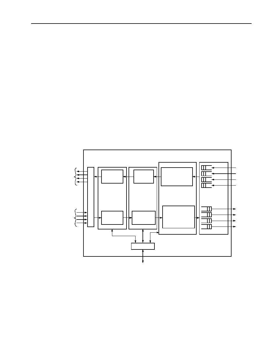
Agere Systems Inc.
45
Data Sheet
May 2001
155/622/2488 Mbits/s Data Interface
TDAT042G5 SONET/SDH
Overview
This device integrates the SONET/SDH interface termination functions with a generic cell/packet delineation cir-
cuit. It supports STS-48/STM-16, quad STS-12/STM-4, and quad STS-3/STM-1 interface rates. Up to four data
channels transported within an STS-N payload are processed via the SONET/SDH termination blocks and the on-
chip data encapsulation/decapsulation engine. Packet or ATM data are transmitted/received by this device on the
equipment side via the enhanced UTOPIA interface. SONET/SDH streams are transmitted/received by this device
on the network side via the line interface.
Concatenation levels supported by this device range from STS-1 to STS-48c. Valid standard concatenated
SONET frame configurations for this device are STS-3c, STS6c, STS-9c, STS-12c, STS-15c, STS-18c, and STS-
48c. Non-standard concatenation levels (such as STS-4c, STS-5c, STS-7c, etc.) are supported as well. In STS-48
mode, four pointer processors are available. This allows an STS-48 frame to carry up to four concatenated sub-
frames (for example, mapping of four STS-12c payloads into an STS-48 frame). In quad STS-3 and STS-12
modes, only one pointer processor is available. Therefore, only a single subframe may be mapped into an STS-3
or STS-12 frame (mapping a single STS-3c payload into an STS-12 frame, for instance). For details, see Table 22
on page 68.
This device supports mapping for ATM cells into SONET/SDH, mapping for packet data via all existing or currently
proposed standards (e.g., PPP, SDL) into SONET/SDH streams. Via SDL mapping, this device also supports
packet over fiber or ATM over fiber, respectively. Figure 2 shows the overview block diagram, and Figure 3 shows
the interface block diagram for this device.
5-6680(F).ar.15
Figure 2. Overview Block Diagram
OVERHEAD
PROCESSOR
OVERHEAD
PROCESSOR
SPE
MAPPER
POINTER
INTERPRETER
L
I
NE I
N
TERF
ACE BL
O
C
K
LINE
TERMINATION
PATH
TERMINATION
PAYLOAD
TERMINATION
PACKET/CELL
PROCESSOR
-DELINEATION
-DECAPSULATION
-UNSCRAMBLING
SINGLE STM-16/STS-48
OR QUAD STM-4/STS-12
ENHANCED
OR QUAD STM-1/STS-3
SINGLE STM-16/STS-48
OR QUAD STM-4/STS-12
OR QUAD STM-1/STS-3
CONTROL
µ
P INTERFACE
UTOPIA
INSERT
MONITOR
-CRC VERIFICATION
ENHANCED
UTOPIA
COMPATIBLE
INTERFACE
PACKET/CELL
PROCESSOR
-ENCAPSULATION
-SCRAMBLING
-CRC GENERATION
L
I
NE INT
E
RF
ACE
(U2, U2+, U3, U3+)
INTERFACE

46
Agere Systems Inc.
Data Sheet
May 2001
155/622/2488 Mbits/s Data Interface
TDAT042G5 SONET/SDH
Overview
(continued)
Figure 3 shows the interface diagram of the IC.
5-6746(F)r.11
Figure 3. Interface Block Diagram
The receive path terminates and processes section, line, and path overhead. It performs framing (A1, A2),
descrambling, detects alarm conditions, and monitors section, line, and path BIP-Ns (B1, B2, B3), accumulating
error counts for each level for performance monitoring purposes. Line and path remote error indications (M1, G1)
are also accumulated. The payload pointers (H1, H2) are interpreted, and the synchronous payload envelope
(SPE) is extracted.
The transmit path inserts section, line, and path overhead. It inserts the framing pattern (A1, A2), performs scram-
bling, inserts AIS (optionally), and calculates and inserts section, line, and path BIP-8s (B1, B2, B3). Line and path
remote failure indications (M1, G1) are inserted based on received BIP-8 errors. The payload pointers (H1, H2) are
generated, and the SPE is inserted.
When used to implement an ATM UNI, ATM cells are written into an internal 4-cell FIFO buffer using a generic
8-/16-/32-bit wide UTOPIA 2/3 compliant interface. Idle/unassigned cells are automatically inserted when the inter-
nal FIFO is empty. The device provides generation of the header check sequence and optionally scrambles the
ATM payload.
SPE
MAPPER
STS-3/STM-1
STS-12/STM-4
STS-48/STM-16
RECEIVE
OVERHEAD
PROCESSOR
OVERHEAD
INTERFACE
TRANSMIT
OVERHEAD
PROCESSOR
POINTER
INTERPRETER
ATM/HDLC/SDL
FRAME
UNSCRAMBLING
DECAPSULATION
UTOPIA
ENHANCED
ATM/HDLC/SDL
FRAME INSERTION
SCRAMBLING
ENCAPSULATION
UTOPIA
TOH
INTERFACE
MPU
INTERFACE
JTAG
INTERFACE
Rx
Tx
UTOPIA
L
I
NE INT
E
RF
ACE
INTERFACE
STS-3/STM-1
STS-12/STM-4
STS-48/STM-16

Agere Systems Inc.
47
Data Sheet
May 2001
155/622/2488 Mbits/s Data Interface
TDAT042G5 SONET/SDH
Overview
(continued)
When used to implement a POS UNI, the device writes packets into an internal 256-byte FIFO buffer using a
generic 8-/16-/32-bit wide enhanced UTOPIA 2/3 compliant interface. HDLC framing performs the insertion of
flags, control escape characters, and the FCS fields. Either the CRC-ITU or CRC-32 (in regular or reversed mode)
can be computed and added to the frame. Counts of transmitted packets and errored/dropped packets are accu-
mulated for performance monitoring purposes.
ATM/HDLC/HDLC-CRC/PPP Support
TDAT042G5 supports the transfer of ATM cells or variable-length packets. Support for 52- or 53-byte cell sizes is
provided at the UTOPIA interface through register provisioning. The following three types of packet data can be
sent and received with HLDC-like framing: transparent HDLC, CRC, and PPP. Transparent HDLC contains 0x7E
framing but no CRC. CRC mode is HDLC with an attached CRC. PPP has 0x7E framing with provisionable
attached header information and CRC.
When used to implement an ATM UNI, the device performs cell delineation on the SPE. HEC error correction is
provided. Idle/unassigned cells may be dropped according to a programmable filter. Cells are also dropped upon
detection of an uncorrectable header check sequence error. The ATM cell payloads are descrambled before being
passed to a 4-cell FIFO buffer. The received cells are read from the FIFO using a generic 8-/16-/32-bit wide
UTOPIA 2/3 compliant interface. Counts of received ATM cells, uncorrectable HEC errors, and correctable HEC
errors are accumulated independently for performance monitoring purposes.
When used to implement a POS UNI, the device descrambles the SPE before extracting HDLC frames. The con-
trol escape characters are removed. Descrambling can be performed after control escape byte destuffing (or
before to control malicious HDLC expansion)
.
The optional 16- or 32-bit error check sequence is verified for cor-
rectness. The packets are placed into a 256-byte FIFO buffer.* The received packets are read from the FIFO using
a generic 8-/16-/32-bit wide enhanced UTOPIA 2/3 compliant interface. Counts of received packets and errored/
dropped packets are accumulated independently for performance monitoring purposes. The device POS imple-
mentation also allows the optional attach/detach of a per-channel provisionable PPP header.
* FIFOs are 256 bytes per channel and cannot be reallocated.

48
Agere Systems Inc.
Data Sheet
May 2001
155/622/2488 Mbits/s Data Interface
TDAT042G5 SONET/SDH
Overview
(continued)
SDL Support
Supports the simplified data link (SDL) protocol, which is currently being reviewed in standards bodies. The imple-
mentation supports 4-byte modified SDL UNI including the following:
I
CRC-16 based frame delineation with 2-byte packet field length
I
Forty-eighth order scrambler
I
No HDLC-like packet expansion
I
Optional CRC-16/-32 payload check
I
Capable of packet-over-fiber operation (i.e., no SONET frame)
I
Two user-programmable 6-byte OAM messages
I
Optional offset field from 0 to 32 bytes
TDAT042G5 provides support for a provisionable offset to the packet to allow for the attachment of layer 2 routing
information (e.g., MPLS tags). Table 11 defines the provisioned value for each offset.
Table 11. Optional Offset Field
The packet length value (header value that CRC is calculated over) will account for the total length of the packet
datagram as well as the associated route tags.
Provisioned
Value
Route Tag Length
(Bytes)
0x0
0
0x1
1
0x2
2
0x3
3
0x4
4
0x5
5
0x6
6
0x7
7
0x8
8
0x9
10
0xA
12
0xB
14
0xC
16
0xD
20
0xE
24
0xF
32
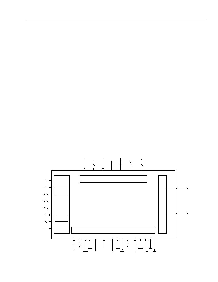
Agere Systems Inc.
49
Data Sheet
May 2001
155/622/2488 Mbits/s Data Interface
TDAT042G5 SONET/SDH
Overview
(continued)
Over-Fiber Mode
Over-fiber mode is used for packet delivery over fiber. No SONET overhead is added in this mode. Since no
SONET overhead is added, the OHP and PT blocks must be configured for the bypass mode.
In transmitting from the TDAT042G5 to the line, the data engine maps the data payload into a full SONET frame
starting at what normally would be the first A1 byte. The data engine continues to map payload into the full SONET
frame until an end of packet or end of frame is reached, at which time the data engine halts the mapping of the
incoming data stream into the SONET frame until the next start of frame.
When TDAT042G5 is receiving from the line, the data engine must be provisioned to receive the maximum packet
size, unless the location of the last byte of the packet is known in advance. If the size of the packet is not known,
one must program the data engine to receive the entire SONET frame. The external UTOPIA interface device must
then be capable of extracting the variable length packets from the full SONET frame.
Details of the over-fiber mode are given in the Data Engine (DE) Block section, page 82.
Test and General-Purpose I/O Support
The device is provisioned, controlled, and monitored using a generic 16-bit microprocessor interface. A standard
five-signal IEEE -1149.1 compliant JTAG test port is also provided for boundary-scan purposes.
A 4-bit GPIO (general-purpose input/output) interface is provided to control and/or monitor other onboard devices.
External Interfaces
Figure 4 shows the external interfaces.
5-6745(F).br.3
Figure 4. External Interface Summary Diagram
MPU AND TEST INTERFACE
TxD
ECLREF
2
RxD
RxCLK
4 x 24 Rx UTOPIA
4 x 24 Tx UTOPIA
UT
OP
IA
INT
E
RF
A
C
E
OHP
+5 MPHY ADDRESS
+5 MPHY ADDRESS
4
GPIO
T
X
LINE
R
X
LINE
TxFSYNC
TxCK
TxCKQ
CLKDIV
5
JTAG
RST
ICT
PMRST
MPMODE
MPCLK
CS
INT
16
DATA
ADDR
ADS
R/W
DS
16
DT
T
X
TOHF
4
T
X
TOHD
T
X
TOHCK
R
X
REF
R
X
TOHF
R
X
TOHCK
4
R
X
TOHD
4
348 SIGNAL PINS
4
2
2
2
32
32
2
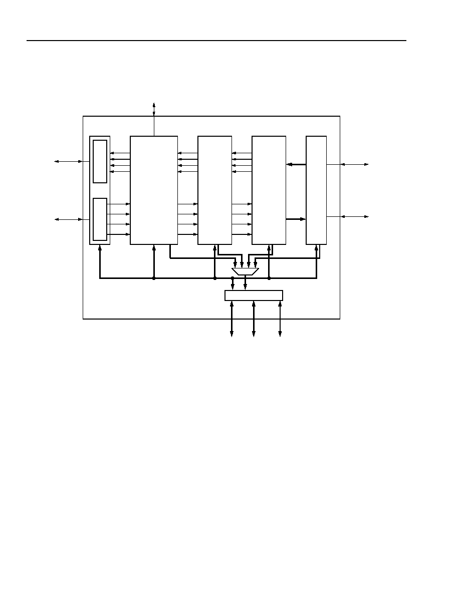
50
Agere Systems Inc.
Data Sheet
May 2001
155/622/2488 Mbits/s Data Interface
TDAT042G5 SONET/SDH
Functional Description
The block diagram for this device can be seen in Figure 5.
5-7055(F).br.2
Figure 5. Functional Block Diagram
OHP
TX
L
I
N
E
RX
LINE
PT
DE
CTRL
UTOP
IA
IF
TOH I/O
MP
JTAG
GPIO
Rx UTOPIA I/O
Tx UTOPIA I/O
Rx LINE I/O
Tx LINE I/O

Agere Systems Inc.
51
Data Sheet
May 2001
155/622/2488 Mbits/s Data Interface
TDAT042G5 SONET/SDH
Functional Description
(continued)
Line Interface Block
This device is designed to work with commonly available optoelectronic converters for OC-3, OC-12, and OC-48
line rates. It will also work with available multiplexer and demultiplexer chip sets for an STS-48/STM-16 line inter-
face rate. The line interface will operate in one of three possible modes, and is provisioned through core register
0x0010 (mode), bits 4--0. These three values of the mode register are the only values allowed.
This block provides the interface between the external SONET/SDH line components and the overhead processor
(OHP) block. The line interface must provide transmit/receive functions for quad STS-3/STM-1, quad STS-12/
STM-4, and STS-48/STM-16 applications. All external inputs and outputs for the TDAT042G5 line I/O block are ref-
erenced to the positive edge of the clock. When the external devices are referenced to the negative edge, the dif-
ferential input clock will need to be reversed at the TDAT042G5 input.
Receive Line Interface Summary
The following list summarizes the receive line interface operations for each STS mode:
I
In quad STS-3/STM-1 mode, the receive line interface provides four separate STS-3/STM-1 input pin groups.
Each input group comprises a differential LVPECL 155.52 Mbits/s data input and a differential 155.52 MHz clock.
Each input group provides data to only one of four (A, B, C, or D) OHP blocks. This interface is synchronous and
requires an external CDR.
I
In quad STS-12/STM-4 mode, the receive line interface provides four separate STS-12/STM-4 input pin groups.
Each input group comprises a differential LVPECL 622.08 Mbits/s data input and a differential 622.08 MHz clock.
Each input group provides data to only one of four (A, B, C, or D) OHP blocks. This interface is synchronous and
requires an external CDR.
I
In the STS-48/STM-16 mode, the device provides 16 differential LVPECL data inputs at 155.52 Mbits/s with a dif-
ferential LVPECL 155.52 MHz clock. In this mode, an external 1:16 data demultiplexer with a 1/16 clock divider is
required. External barrel shifter circuitry to byte align the data is not required.
I
Multiplexers select between the terminal loopback data, the 32-bit parallel STS-48/STM-16 data bus, and the
four STS-12/STM-4 or STS-3/STM-1 8-bit parallel data buses. The controls for these MUXes are mode (register
0x0010) and loopback (register 0x0012) provided by the control block (see Table 48 and Table 50 on pages
150--151).
I
For STS-48 mode, the 155.52 MHz input clock is divided by two to 77.76 MHz and distributed to all four multi-
plexers. For the STS-12/STM-4 mode, each 622.08 MHz input clock is divided by eight to 77.76 MHz. Each
77.76 MHz clock is distributed to the appropriate clock multiplexer (A, B, C, or D). For the STS-3/STM-1 mode,
each 155.52 MHz input clock is divided by eight to 19.44 MHz. Each 19.44 MHz clock is distributed to the appro-
priate clock multiplexer (A, B, C, or D).
Table 12. Line Interface Modes
Mode[4:0]
Core Register
0x0010
Interfaces
Line Interface Signals
10000
STS-48/STM-16
RxCKP/N, RxD[15:0]P/N,
TxCKP/N, TxD[15:0]P/N
01111
STS-12/STM-4
RxCLK[D]P/N, RxD[D]P/N, TxCKP/N, TxD[D]P/N
RxCLK[C]P/N, RxD[C]P/N, TxCKP/N, TxD[C]P/N
RxCLK[B]P/N, RxD[B]P/N, TxCKP/N, TxD[B]P/N
RxCLK[A]P/N, RxD[A]P/N, TxCKP/N, TxD[A]P/N
00000
STS-3/STM-1
RxCLK[D]P/N, RxD[DP/N, TxCKP/N, TxD[D]P/N
RxCLK[C]P/N, RxD[C]P/N, TxCKP/N, TxD[C]P/N
RxCLK[B]P/N, RxD[B]P/N, TxCKP/N, TxD[B]P/N
RxCLK[A]P/N, RxD[A]P/N, TxCKP/N, TxD[A]P/N
52
Agere Systems Inc.
Data Sheet
May 2001
155/622/2488 Mbits/s Data Interface
TDAT042G5 SONET/SDH
Functional Description
(continued)
Line Interface Block
(continued)
Transmit Line Interface Summary
The following list summarizes the transmit line interface operations for each STS mode.
I
In quad STS-3/STM-1 and STS-12/STM-4 modes, the transmit line interface receives 8 bits of data from each
OHP block (A, B, C, and D) at 19.44 Mbits/s and 77.76 Mbits/s, respectively. An 8-to-1 parallel-to-serial conver-
sion produces output data at 155.52 Mbits/s for STS-3/STM-1 mode and 622.08 Mbits/s for STS-12/STM-4
mode. For facility loopback, the outputs are multiplexed with the corresponding data from the STS-12/STS-3
(STM-4/STM-1) receive block and sent to four differential LVPECL buffers.
I
In STS-48/STM-16 mode, a 32-bit data word at 77.76 Mbits/s is received from the OHP. Then a 2-to-1 parallel-to-
parallel conversion is performed producing a 16-bit word at 155.52 Mbits/s. In this mode, an external 16:1 data
demultiplexer is required. Facility loopback is not available for the STS-48/STM-16 mode.
I
There is a single clock input, TxCKP/N, in the transmit case. The clock source rates are 622.08 MHz (STS-12/
STM-4), 155.52 MHz (STS-3/STM-1), or 155.52 MHz (STS-48/STM-16).
In the STS-48/STM-16 case, two transmit clock modes are available, contra* and forward clocking. In the contra-
clocking mode, the transmit data is sent out as commanded by TxCKP/N; in addition, an internal PLL must be
activated, core register 0x0010 bit 5, to minimize the phase delay between TxCKP/N and the transmitted data. In
the forward clocking mode, the transmit data and the clock, TxCKQ (used to clock out the data), are sent in par-
allel to the transmit multiplexer.
In STS-12/STM-4 and STS-3/STM-1 modes, the input clock is divided by eight producing the internal clock at
77.76 MHz and 19.44 MHz, respectively. In STS-48/STM-16 mode, the input clock is divided by eight to produce
an internal clock at 77.76 MHz. The CLKDIV pin (H4) controls this division. Table 13 shows the required value of
CLKDIV.
Table 13. Clock Settings for CLKDIV Pin
I
TxFSYNCP/N is an optional external frame sync. This 8 kHz frame sync pulse must be synchronous with
TxCKP/N. It is, at minimum, a one TxCKP/N clock cycle wide pulse that is latched in at the system rate
(622.08 MHz or 155.52 MHz). TOH interface signal RxREF should not be used as a source to TxFSYNCP/N.
I
The active edge of the transmit clock is the positive edge.
I
When TDAT042G5 operates in asynchronous mode (MPMODE = 0), the line block provides the microprocessor
clock to the microprocessor interface block. The CLKDIV pin must be set to ensure that the clock is always
77.76 MHz.
Line interface timing is given in the Interface Timing Specifications section (see Table 168, page 267).
* Contra refers to a type of data transmission whereby a clock signal is received by a register before the register sends data.
CLKDIV Pin
Description
CLKDIV = 1
When in STS-12/STM-4 (622.08 MHz divide by 8).
CLKDIV = 0
When in STS-3/STM-1, STS-48/STM-16 (155.52 MHz divide by 2).
Agere Systems Inc.
53
Data Sheet
May 2001
155/622/2488 Mbits/s Data Interface
TDAT042G5 SONET/SDH
Functional Description
(continued)
SONET Framer
The SONET framer consists of the overhead processor (OHP) and path terminator (PT) blocks. The receive
SONET framer requires 625
µ
s to drop frame after the line input signal is lost. Once a valid receive line input is
restored, the maximum average reframe time (MART) is 250
µ
s.
Overhead Processor (OHP) Block
The OHP block terminates/generates the section and line overhead bytes of the line. The data rate of the TOH
interface is given in Table 14. Timing for the TOH interface is given in the Interface Timing Specifications section
(see Table 172 and Table 173, page 271).
Table 14. R/T TOH Interface Rates
* This STS-48/STM-16 interface is a four-line interface resulting in an effective interface rate
of 82.944 Mbits/s.
All receive transport overhead bytes are output on the RTOH interface for external processing. Transmit transport
overhead bytes can optionally be inserted from the TTOH interface.
The transmit transport overhead bytes can be inserted in one of three ways selected through software provision-
ing: (1) automatically by hardware, (2) via software provisioning, or (3) through the TOAC. Table 15 defines those
overhead bytes that can be inserted via each of the three paths. In some cases, the user has the choice to insert
the byte via software registers or through the TOAC. Superscripts in the table reference these insertion methods
which are described in the footnotes.
Table 15. TOAC Byte Insertion: An STS-3/STM-1 Example
1.Inserted via TOAC, but not part of SONET standard.
2.Inserted via software or automatically via hardware.
3.Inserted via TOAC only.
4.Inserted via software register only.
5.Inserted via TOAC or software register.
6.Inserted via TOAC hardware; should be included in TOAC interface timing.
Mode
R/T TOH Interface Rate
STS-48/STM-16
20.736* Mbits/s
STS-12/STM-4
20.736 Mbits/s
STS-3/STM-1
5.184 Mbits/s
OH Parity
3
(1st bit of
1st byte)
X
6
X
6
X
6
X
6
X
6
J0
5
Z0
4
Z0
4
X
6
B1-2
1
B1-3
1
E1
5
E1-2
1
E1-3
1
F1
5
F1-2
1
F1-3
1
D1
3
D1-2
1
D2-3
1
D2
3
D2-2
1
D2-3
1
D3
3
D3-2
1
D3-3
1
X
6
X
6
X
6
X
6
X
6
X
6
X
6
X
6
X
6
X
6
X
6
X
6
K1
2
K1-2
1
K1-3
1
K2
2
K2-2
1
K2-3
1
D4
3
D4-2
1
D4-3
1
D5
3
D5-2
1
D5-3
1
D6
3
D6-2
1
D6-3
1
D7
3
D7-2
1
D7-3
1
D8
3
D8-2
1
D8-3
1
D9
3
D9-2
1
D9-3
1
D10
3
D10-2
1
D10-3
1
D11
3
D11-2
1
D11-3
1
D12
3
D12-2
1
D12-3
1
S1
5
Z1-2
3
Z1-3
3
Z2
3
Z2-2
3
X
6
E2
3
E2-2
1
E2-3
1

54
Agere Systems Inc.
Data Sheet
May 2001
155/622/2488 Mbits/s Data Interface
TDAT042G5 SONET/SDH
Functional Description
(continued)
Overhead Processor (OHP) Block
(continued)
The TOAC inserter must insert the first bit of A1 at the TOAC input, TxTOHD[D:A], during the first clock cycle when
TxTOHF = 1. The TOAC has a built-in parity checker. For the parity check, the value of the first inserted bit of A1
must be set to the parity value of the previous frame. The remainder of the inserted bits of the A1, A2 bytes are
ignored by the transmit framer.
Receive OHP
Loss-of-Signal. The loss-of-signal block monitors the incoming scrambled data for the absence of transitions.
When an absence of transitions is detected for a programmable length of time, a loss-of-signal (LOS) is declared.
LOS is cleared when two valid framing patterns are detected, and during the intervening time, no LOS condition is
detected.
Framer. The frame block finds and locks onto the incoming A1 and A2 bytes of the SONET transport overhead.
Loss-of-frame (LOF) is declared when a defect persists for more than 3 ms. LOF is cleared when the defect is
absent for more than 3 ms. To prevent intermittent out-of-frame/in-frame conditions, the 3 ms timer is not reset to
zero until an in-frame (or out-of-frame) condition persists for 3 ms. The framer is also responsible for performing bit
rotations on the incoming data stream to ensure that the rest of the IC receives byte-aligned data.
While in-frame, the A1/A2 framing bytes in each frame are compared against the expected pattern. Out-of-frame
(OOF) is declared when five consecutive frames containing one or more framing pattern errors have been
received.
While out-of-frame, this block will monitor the receive data stream for an occurrence of the framing pattern. When a
framing pattern has been recognized, the framer performs the necessary bit rotation and verifies that an error-free
framing pattern is present in the next frame before declaring in-frame.
J0 Section Trace. The section trace message is extracted and stored in a 16-byte memory for access by software.
The first byte of the message can be provisioned to be either:
I
The byte with the most significant bit (MSB) set high (for SDH), or
I
The byte following a carriage return (0x0D) and line feed (0x0A) sequence (for SONET).
J0 mismatch detection is provided using one of four methods (provisionable via J0MONMODE[A--D][1:0]; see reg-
ister description, page 173).
Descrambler. The descrambler block implements the frame synchronous SONET descrambler with a generating
polynomial of 1 + x
6
+ x
7
. The framing bytes (A1, A2), the section trace bytes (J0), and the growth bytes (Z0) are
not descrambled. The descrambler may be disabled through a software register.

Agere Systems Inc.
55
Data Sheet
May 2001
155/622/2488 Mbits/s Data Interface
TDAT042G5 SONET/SDH
Functional Description
(continued)
Overhead Processor (OHP) Block
(continued)
Receive OHP (continued)
B1 BIP-8 Check. The SBIP block counts section BIP-8 (B1) errors. The SBIP value is calculated over the scram-
bled data of the complete previous frame. The calculated value is compared against the received B1 byte and dif-
ferences (errors) are counted. A theoretical maximum of 64,000 errors may be detected per second. The SBIP
block accumulates these errors in a 16-bit saturating counter. This counter operates in latch and clear mode to
ensure Bellcore and ITU compliance with regard to not missing any events (bit errors). It is intended that this
counter be polled at least once per second so that no error events are missed. Optionally, a maximum of only
one SBIP error per frame can be counted (provisionable via B1BITBLKCNT[A--D]; see register description,
page 174). This causes the error counter to only increment by one when one or more errors are detected.
B2 BIP-N Check. The LBIP block counts line BIP-N errors. The LBIP value is calculated over the incoming frame
and is compared to the received B2 bytes received in the next frame. The errors are counted. Optionally, a maxi-
mum of only one LBIP error per frame can be counted (B2BITBLKCNT[A--D]; see register description, page 174).
This causes the block error counter to only increment by one when one or more errors are detected. A theoretical
maximum of 3,072,000 errors may be detected per second. The LBIP block accumulates these errors in a 22-bit
saturating counter. This counter is operated in latch and clear mode to ensure Bellcore and ITU compliance with
regard to not missing any events (bit errors). It is intended that this counter be polled at least once per second so
that no error events are missed.
BER Check. The OHP block also detects provisionable signal fail (SF) and signal degrade (SD) conditions. The
SF and SD values are provisioned through a group of software registers (SF addresses 0x0452--0x0469,
SD addresses 0x043A--0x0451). The SF alarm can be provisioned for a bit error rate (BER) of between 10
≠3
to
10
≠5
; the SD alarm can be provisioned for a bit error rate (BER) of between 10
≠5
to 10
≠9
(see Table 86, page 187).

56
Agere Systems Inc.
Data Sheet
May 2001
155/622/2488 Mbits/s Data Interface
TDAT042G5 SONET/SDH
Functional Description
(continued)
Overhead Processor (OHP) Block
(continued)
Receive OHP (continued)
Figure 6 illustrates the parameters used in determining the bit error detection rate.
5-7934(F)
Figure 6. Signal Degrade and Failure Parameters for BER
TDAT042G5 provides a method to monitor the BER at the line and path layers. The following explains the algo-
rithm for this method to set and clear the BER. The algorithm for this method is the same for setting and clearing
the BER, the only difference is the programmed values. TDAT042G5 includes two complete sets of identical
counters, one used to determine signal fail (SF) and one used to determine signal degrade (SD). The only differ-
ence between SF and SD is the provisioned values. The same algorithm is used for both the line and path layers of
SONET.
The algorithm uses four sets of counters: labelled Ns (number of frames), L (number of errors), M (number of
errored blocks), and B (total number of blocks). Each of these counters has different values that are provisioned to
either set the BER high or clear the BER indication. The algorithm works by counting blocks, i.e., a preset number
of SONET/SDH frames (Ns). If the number of errors in the block exceeds the provisioned level (L), then the errored
block counter is incremented by 1; otherwise, the number of blocks in error stays at its current level. At this point,
the frame counter and the error counter are reset back to 0 and start counting again. At the end of a preset number
of blocks (B), the count in the errored block counter is compared against a provisioned threshold (M). If the total
number of blocks in error equals or exceeds the provisioned threshold (M), then the BER alarm is raised. If the total
number of blocks in error is less than the provisioned amount (M), then the BER alarm is cleared.
The values used by the counters are determined by the state of the algorithm. If the BER state is low, then the SET
parameters are used. If the BER state is high, then the CLEAR parameters are used.
NUMBER OF MONITORING BLOCKS SFBSET[A--D] OR SDBSET[A--D] (IN THIS CASE, 3)
NUMBER OF FRAMES IN A MONITORING BLOCK SFNSSET[A--D] OR SDNSSET[A--D],
BLOCK
BOUNDARY
ACCUMULATED BIP ERROR COUNT:
B1 OR B2 FOR LINE
B3 FOR PATH
FRAME
BOUNDARY
BLOCK GOOD/BAD COUNT
SFNSCLEAR[A--D] OR SDNSCLEAR[A--D]
SFLSET[A--D] OR SDLSET[A--D]
SFLCLEAR[A--D] OR SDLCLEAR[A--D]
SFMSET[A--D] OR SDMSET[A--D]
SFMCLEAR[A--D] OR SDMCLEAR[A--D]
(IN THIS CASE, 7)
Agere Systems Inc.
57
Data Sheet
May 2001
155/622/2488 Mbits/s Data Interface
TDAT042G5 SONET/SDH
Functional Description
(continued)
Overhead Processor (OHP) Block
(continued)
Receive OHP (continued)
Table 16 and Table 17 show values of Ns, L, M, and B for STS-3/STM-1, STS-12/STM-4, and STS-48/STM-16 to
set and clear the BER indicator. SF registers are 0x0452--0x0469 and SD registers are 0x043A--0x0451. All
SF/SD set and clear values are hexadecimal.
Table 16. Ns, L, M, and B Values to Set the BER Indicator
* These are the numbers to be provisioned in TDAT042G5. The actual values of the BER algorithm are 1 greater than the actual values shown.
These BER values cannot be provisioned because the maximum value of L is 0xF (i.e., L is a 4-bit register).
Mode
BER
SF/SD Set Values
Actual
Number of
Frames
Probability of
Detecting L
Errors (%)
Probability of
Declaring
SF/SD (%)
Integra-
tion
Time
(s)
Max-
imum
Number
of Frames
Ns*
L*
M*
B*
@BER
@BER/2
@BER
@BER/2
STS-3/
STM-1
1.00E-03
1
6
3D
3D
62
99.96
85.13
97.68
0.00
0.008
64
1.00E-04
6
9
3
7
48
72.70
7.28
96.06
0.16
0.013
104
1.00E-05
30
7
3
7
384
71.34
10.08
95.19
0.52
0.1
800
1.00E-06
1E0
7
3
7
3840
71.34
10.09
95.19
0.52
1
8000
1.00E-07
1275
7
4
9
47250
69.74
9.44
95.07
0.13
10
80000
1.00E-08
B5A4
7
3
9
465000
68.07
8.82
98.47
0.82
83
664000
1.00E-09
3F7A0
4
5
F
4160000
56.90
11.25
96.52
0.60
667
5336000
1.00E-10
--
--
--
--
--
--
--
--
--
--
--
STS-12/
STM-4
1.00E-03
--
--
--
--
64
100.00
88.43
100.00
0.04
0.008
64
1.00E-04
2
B
6
A
22
84.92
9.64
98.38
0.00
0.008
64
1.00E-05
D
8
3
8
117
67.93
7.17
96.48
0.25
0.025
200
1.00E-06
80
8
3
8
1152
66.19
6.66
95.46
0.19
0.25
2000
1.00E-07
4FB
8
3
8
11475
65.75
6.53
95.16
0.18
2.5
20000
1.00E-08
31CE
8
3
8
114750
65.75
6.53
95.16
0.18
21
168000
1.00E-09
1F20C
8
3
8
1147500
65.75
6.53
95.16
0.18
167
1336000
1.00E-10
--
--
--
--
--
--
--
--
--
--
--
STS-48/
STM-16
1.00E-03
--
--
--
--
64
100.00
100.00
100.00
100.00
0.008
64
1.00E-04
1
E
3F
3F
64
99.95
58.97
96.89
0.00
0.008
64
1.00E-05
5
A
35
3F
320
90.60
16.25
96.47
0.00
0.008
64
1.00E-06
20
7
8
E
480
77.55
13.09
96.69
0.00
0.0625
500
1.00E-07
13A
7
8
E
4710
75.80
12.15
95.17
0.00
0.625
5000
1.00E-08
C1C
7
7
E
46500
74.58
11.54
98.09
0.01
5.2
41600
1.00E-09
765C
6
6
A
333300
82.92
19.71
97.29
0.18
42
336000
1.00E-10
--
--
--
--
--
--
--
--
--
--
--
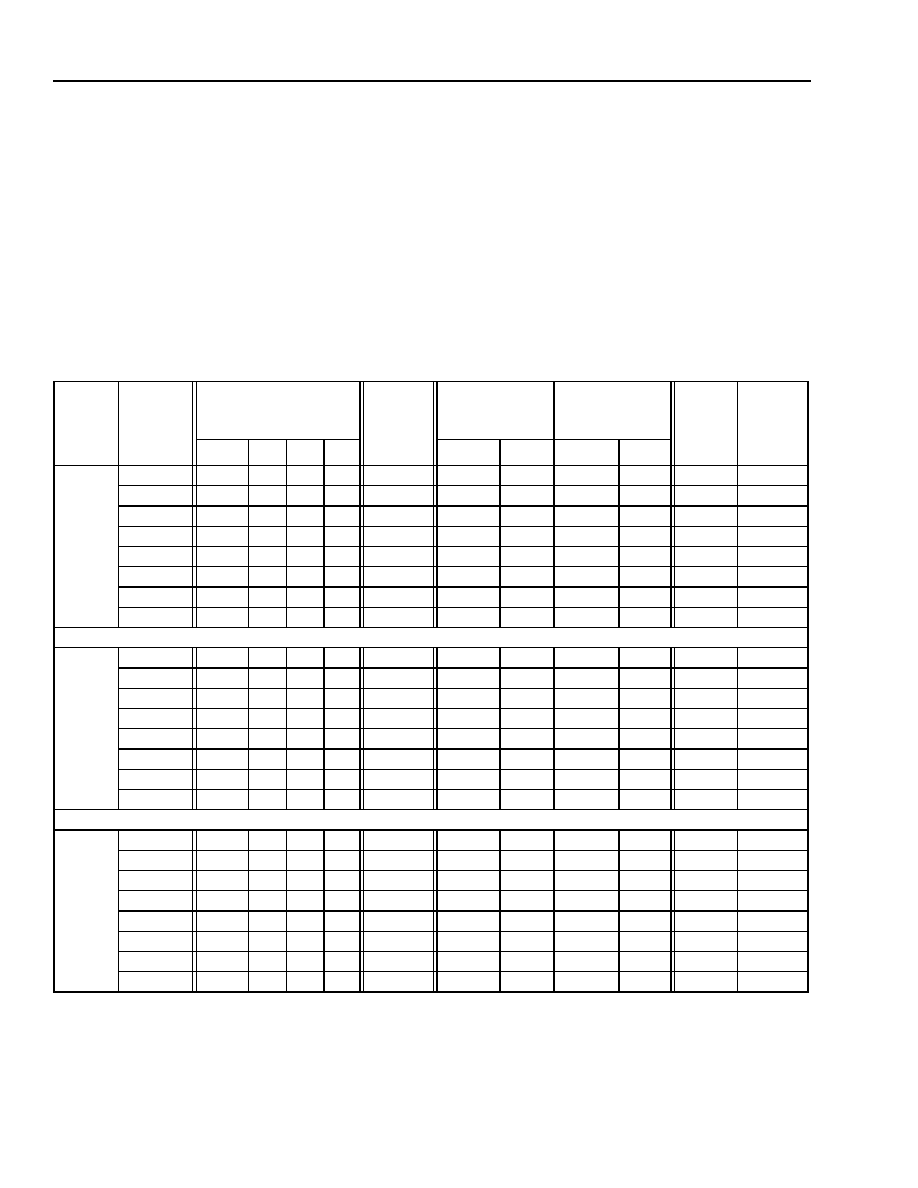
58
Agere Systems Inc.
Data Sheet
May 2001
155/622/2488 Mbits/s Data Interface
TDAT042G5 SONET/SDH
Functional Description
(continued)
Overhead Processor (OHP) Block
(continued)
Receive OHP (continued)
Overhead (OH) Extract. All transport overhead (TOH) bytes are extracted and sent over the RxTOH interface for
possible external processing. The number of bits sent are as follows:
I
STS-3/STM-1: 5,184,000 bits/s per interface
I
STS-12/STM-4: 20,736,000 bits/s per interface
I
STS-48/STM-16: 82,944,000 bits/s (over 4 serial lines (20,736 kbits/s each))
Table 17. Ns, L, M, and B Values to Clear the BER Indicator
* These are the numbers to be provisioned in TDAT042G5. The actual values of the BER algorithm are 1 greater than the actual values shown.
These BER values cannot be provisioned because the maximum value of L is 0xF (i.e., L is a 4-bit register).
Mode
BER
SF/SD Set Values
Actual
Number of
Frames
Probability of
Detecting L
Errors (%)
Probability of
Clearing
SF/SD (%)
Integra-
tion
Time
(s)
Max-
imum
Number
of Frames
Ns*
L*
M*
B*
@BER*5
@BER
@BER*5
@BER
STS-3/
STM-1
1.00E-03
--
--
--
--
--
--
--
--
--
--
--
1.00E-04
1
6
3
7
8
85.13
0.39
0.27
100.00
0.013
104
1.00E-05
6
2
3
7
48
93.01
11.33
0.01
99.21
0.1
800
1.00E-06
30
2
3
7
384
84.42
6.84
0.34
99.88
1
8000
1.00E-07
1E05
2
3
7
3840
84.42
6.84
0.34
99.88
10
80000
1.00E-08
1275
2
4
9
47250
83.66
6.59
0.22
99.98
83
664000
1.00E-09
B5A4
2
3
9
465000
82.86
6.35
0.03
99.75
667
5336000
1.00E-10
3F7A0
2
2
F
4160000
46.31
1.48
0.50
99.84
6670
53360000
STS-12/
STM-4
1.00E-03
--
--
--
--
--
--
--
--
--
--
--
1.00E-04
1
7
6
6
7
100.00
51.54
0.00
99.03
0.008
64
1.00E-05
2
2
8
A
22
98.36
20.51
0.07
100.00
0.025
200
1.00E-06
D
2
3
8
117
87.99
8.23
0.02
99.59
0.25
2000
1.00E-07
80
2
3
8
1152
87.34
7.94
0.02
99.64
2.5
20000
1.00E-08
4FB
2
3
8
11475
87.17
7.87
0.03
99.65
21
168000
1.00E-09
31CE
2
3
8
114750
87.17
7.87
0.03
99.65
167
1336000
1.00E-10
1F20C
2
3
8
1147500
87.17
7.87
0.03
99.65
1670
13360000
STS-48/
STM-16
1.00E-03
--
--
--
--
--
--
--
--
--
--
--
1.00E-04
64
100.00
45.99
0.00
99.42
0.008
64
1.00E-05
1
2
D
E
15
100.00
60.11
0.00
99.47
0.008
64
1.00E-06
5
3
D
3F
320
95.07
7.28
0.00
99.98
0.0625
500
1.00E-07
20
2
6
13
640
87.34
7.94
0.00
99.94
0.625
5000
1.00E-08
13A
2
6
13
6280
86.52
7.61
0.00
99.95
5.2
41600
1.00E-09
C1C
2
6
13
62000
85.95
7.38
0.00
99.96
42
336000
1.00E-10
765C
2
4
A
333300
84.89
7.00
0.03
99.95
420
3360000
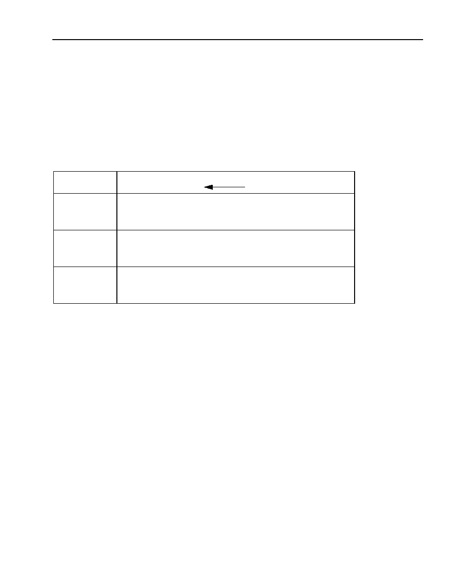
Agere Systems Inc.
59
Data Sheet
May 2001
155/622/2488 Mbits/s Data Interface
TDAT042G5 SONET/SDH
Functional Description
(continued)
Overhead Processor (OHP) Block
(continued)
Receive OHP (continued)
The OH interface consists of clock, data, and frame. The data and frame signals update on the falling edge of the
clock. The frame pulse is high for the most significant bit (MSB) of the first bit of the frame. Bytes J0, Z0, and F1
(current and previous), K1, K2, and S1 can also be extracted via software registers.
Table 18 shows the ordering of the bytes for the allowed TOAC configurations.
Table 18. TOAC Channel I/O vs. STS Number/Time Slot
The overhead extract block also performs the following functions:
I
Error Monitors. The REI_L block counts remote error indication block errors. The M1 byte is extracted and
counted. This represents the number of LBIP errors detected by the far-end equipment. Optionally, a maximum
of only one REI-L error per frame may be counted (provisionable via M1BITBLKCNT[A--D]; register description,
page 175). This causes the block error counter to only increment by one when one or more errors are detected.
I
Automatic Protection Switch Signaling. The APS block filters the K1 and K2 bytes (automatic protection
switching channel) and stores the validated message in software-accessible registers. The K bytes are validated
after a programmable number of consecutive frames contain identical K1 (and K2[7:3] or K2[7:0]) values. APS
protection switching byte failure is detected within this block when a programmable number of frames have
passed without valid K bytes. The protection switching byte failure is removed upon detection of a programmable
number of frames with identical K1 (and K2[7:3] or K2[7:0]) bytes. The use of K2[7:3] or K2[7:0] is provisionable
via the K1K2_2_OR_1 register bit (see register description, page 169).
I
Line Remote Defect Indicator. Bits 2, 1, and 0 of the K2 byte are monitored for the pattern 110. If this pattern
appears for 3--15 (provisionable by OHP register CNTDK2) consecutive frames, RDI-L is asserted. RDI-L is
removed when any pattern other than 110 is detected for 3--15 (provisionable by OHP register CNTDK2) con-
secutive frames. (See page 171 for register description of CNTDK2[A--D][3:0].)
I
Line Alarm Indication Signal. Bits 6, 7, and 8 of the K2 byte are monitored for the pattern 111. If this pattern
appears for 3--15 (provisionable by OHP register CNTDK2) consecutive frames, AIS-L is asserted. AIS-L is
removed when any pattern other than 111 is detected for 3--15 (provisionable by OHP register CNTDK2) con-
secutive frames. (See page 171 for register description of CNTDK2[A--D][3:0].)
Output Rate
TOAC Channel Input vs. Input STS Number/Time Slot
Time
STS-3/STM-1
3 2 1 (Channel A)
3 2 1 (Channel B)
3 2 1 (Channel C)
3 2 1 (Channel D)
STS-12/STM-4
12 9 6 3 11 8 5 2 10 7 4 1 (Channel A)
12 9 6 3 11 8 5 2 10 7 4 1 (Channel B)
12 9 6 3 11 8 5 2 10 7 4 1 (Channel C)
12 9 6 3 11 8 5 2 10 7 4 1 (Channel D)
STS-48/STM-16
39 27
15
3
38 26
14
2
37
25
13
1
(Channel A)
42 30
18
6
41 29
17
5
40
28
16
4
(Channel B)
45 33
21
9
44 32
20
8
43
31
19
7
(Channel C)
48 36
24 12
47 35
23 11 46
34
22 10 (Channel D)

60
Agere Systems Inc.
Data Sheet
May 2001
155/622/2488 Mbits/s Data Interface
TDAT042G5 SONET/SDH
Functional Description
(continued)
Overhead Processor (OHP) Block
(continued)
Receive OHP (continued)
I
Rx Synchronization Message. The S1 block filters the synchronization message (S1) byte and stores the vali-
dated message in a software-accessible register. The synchronization message will be validated if a programma-
ble number (in OHP register CNTDS1) of consecutive frames contain identical S1 values. An inconsistent
synchronization message alarm will be reported if a provisional number (by OHP register CNTDS1FRAME) of
consecutive frames pass without a validated message occurring. (See page 172 for register descriptions of
CNTDS1[A--D][3:0] and CNTDS1FRAME [A--D][3:0].)
I
F1 User Channel. The F1 byte is extracted by the OHP. The F1 user channel is monitored for change of state
using OHP registers 0x0402, 0x0404, 0x0406, 0x0408 (see register map, page 116). The previous and current
F1 values are stored in F1DMON1[A--D][7:0] and F1DMON0[A--D][7:0], respectively (see page 122 for register
map, page 190 for register descriptions).
I
DCC and Orderwire Bytes. The data communication channel (D1--D3, D4--D12) and orderwire bytes (E1, E2)
can only be extracted via the TOAC.
I
D1/D2/D3 Section Data Communications Channels (DCC). DCC outputs are taken from the TOAC.
I
D4--D12 Line Data Communications Channels (DCC). DCC outputs are taken from the TOAC.
I
M1 REI-L. REI-L is extracted by the OHP.
I
Support for ATM/Packet-Over-Fiber. The transport overhead must be bypassed when operating in data-over-
fiber mode. In this mode, the TOH_BYPASS and ROH_BYPASS register bits must be set to 1. No overhead
insertion/extraction is done when in bypass mode.
Transmit OHP
Overhead Insertion. Some transport overhead (TOH) bytes can optionally be inserted via the TxTOH interface
and inserted into the TOH bytes (see Table 15, page 53). Certain bytes can be either inserted from values stored in
registers or automatically generated. The TxTOH interface controls the insertion mechanism. Software insertion
takes precedence over TOAC insertion. The number of bits received are as follows:
I
STS-3/STM-1: 5,184,000 bits/s per interface
I
STS-12/STM-4: 20,736,000 bits/s per interface
I
STS-48/STM-16: 82,944,000 bits/s (over 4 serial lines (20,736 kbits/s each))
S1 Synchronization Message. The S1 block controls the insertion of the S1 byte. The byte ordering is the same
as the RxTOAC and is shown in Table 18 (see pa ge59). The S1 byte can be provisioned to come from the TxTOH
interface or from a software-settable register. Control for message insertion is from software control register
TS1INS[A--D] (see register description, page 179 and page 183).
K1K2 APS Signaling. The APS block controls the insertion of the K bytes based on software provisioned K bytes,
and alarm conditions (AIS-L, RDI-L). Inconsistent APS bytes can be inserted via register provisioning by
TAPSBABBLEINS[A--D] (see register description, page 178 and page 183).
RDI_L Generation. The following six alarms contribute to RDI_L generation: LOF, OOF, LOS, LOC, AIS_L, and
SF. They can be inhibited from contributing to RDI-L via transmit control registers (addresses 0x042F, 0x0431,
0x0433, 0x0435; see register description, page 180).

Agere Systems Inc.
61
Data Sheet
May 2001
155/622/2488 Mbits/s Data Interface
TDAT042G5 SONET/SDH
Functional Description
(continued)
Overhead Processor (OHP) Block
(continued)
Transmit OHP (continued)
BIP-8 Generation. The SBIP block calculates the B1 value according to Bellcore and ITU standards. Insertion of
SBIP errors is possible through the use of software control register TB1ERRINS[A--D] (see register description,
page 180).
The LBIP block calculates the B2 values according to Bellcore and ITU standards. Insertion of LBIP errors is pos-
sible through the use of software control register TB2ERRINS[A--D] (see register description, page 180).
The REI_L block controls the insertion of the remote error indication block error count.
J0 Section Trace. The section trace message is inserted either from the TxTOH interface or from a message
stored in a 16-byte software-accessible memory. Control for message insertion is from software control register
TJ0INS[A--D] (see register description, page 177 and page 181).
SONET Scrambler. The scrambler block implements the frame synchronous SONET scrambler with a generating
polynomial of 1 + x
6
+ x
7
. The scrambler may be disabled through a software register.
A1/A2 Framing Bytes. A1 and A2 are automatically placed on the line. Errors can be inserted into A2 by setting
OHP register TA1A2ERRINS[A--D][4:0] (see register description, page 180).
E1/E2 Orderwire Bytes. The orderwire bytes for section and line are taken from the TOAC.
D1/D2/D3 Section Data Communications Channels (DCC). DCC inputs are taken from the TOAC.
D4--D12 Line Data Communications Channels (DCC). DCC inputs are taken from the TOAC.
F1 User Channel. The F1 byte can be optionally inserted from stored values in OHP register TF1INS[A--D]
(addresses 0x047E, 0x0480, 0x0482, 0x0484; see register description, page 179 and page 183).
M1 REI-L. REI-L can be automatically generated and inserted into the outgoing SONET frame, or can optionally
be inhibited. Errors can be inserted into M1 via OHP register TM1_ERR_INS[A--D] (addresses 0x042E, 0x0430,
0x0432, 0x0434; see register description, page 179 and page 183).
Support for ATM/Packet-Over-Fiber. The transport overhead must be bypassed when operating in data-over-
fiber mode. In this mode, the TOH_BYPASS and ROH_BYPASS register bits must be set to 1. No overhead inser-
tion/extraction is done when in bypass mode.
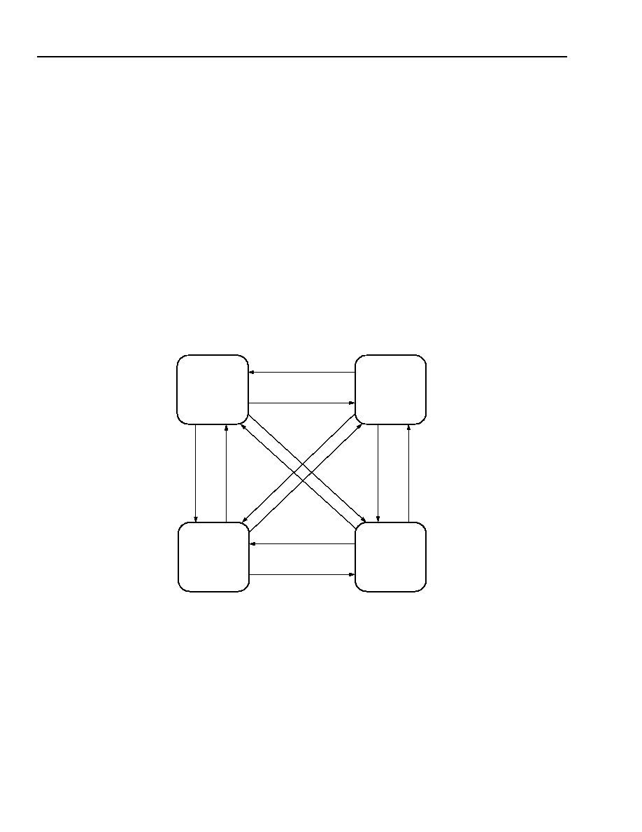
62
Agere Systems Inc.
Data Sheet
May 2001
155/622/2488 Mbits/s Data Interface
TDAT042G5 SONET/SDH
Functional Description
(continued)
Path Terminator (PT) Block
The path terminator performs path overhead (POH) termination and extracts the payload for further processing by
the downstream circuitry. The path terminator block interprets the incoming H1/H2 pointer of each incoming STS
channel. The pointer interpreter supports up to four channels and performs path overhead termination on each
channel. Each channel may be either an STS-1, STS-3c, STS-6c, STS-9c, . . . , STS-45c, or STS-48c.
The pointer is validated according to Bellcore and ITU specifications. The H1/H2 pointers are used to determine
the location of the first path overhead (POH) byte (J1). The pointer interpreter consists of a finite state machine
(FSM) with four steady states. These states are defined as follows:
I
Normal state
I
Loss-of-pointer (LOP)
I
Alarm indication signal (AIS)
I
Concatenation
The transition between states will require several consecutive events to protect against transient conditions caused
by bit errors during high BER conditions. The state machine is shown below in Figure 7.
5-7935(F)
Figure 7. Pointer Interpreter State Diagram
The PT block monitors for the following conditions and takes appropriate actions:
I
Pointer Increment. TDAT042G5 uses an 11-bit counter to count the number of pointer increments and updates
the associated counter holding register on the occurrence of PMRST (RPI_INC[A--D][10:0]; see register
description, page 198). A pointer increment can occur when in the normal pointer mode. The following two meth-
ods can be used to determine if the pointer increment operation should be performed: 6-of-10 or 8-of-10 majority
matching (selectable via software provisioning of register RINCDEC_6OR8MAJ [A--D]; see register description,
page 200).
NORMAL
AIS
CONC
LOP
8
NDF
POINT
E
RS
OR 8 INV
A
L
ID P
OINT
E
RS
3
NO
RM
A
L
PO
I
N
T
E
R
S
3
CO
N
C
I
N
DI
C
A
T
IONS
3
AIS INDICA
T
IONS
1 NDF POINTER OR
3 NORMAL POINTERS
3 AIS INDICATIONS
8 INVALID POINTERS
3 CONC INDICATIONS
3
AI
S
IN
D
IC
AT
IO
N
S
8
IN
VA
LI
D
P
O
IN
TE
R
S
3 N
O
R
M
AL
P
O
IN
TE
R
S
3 C
O
N
C
IN
D
IC
AT
IO
N
S

Agere Systems Inc.
63
Data Sheet
May 2001
155/622/2488 Mbits/s Data Interface
TDAT042G5 SONET/SDH
Functional Description
(continued)
Path Terminator (PT) Block
(continued)
I
Pointer Decrement. TDAT042G5 uses an 11-bit counter to count the number of pointer decrements and
updates the associated counter holding register on the occurrence of PMRST (RPI_DEC[A--D][10:0]; see regis-
ter description, page 198). A pointer decrement can occur when in the normal pointer mode. The following two
methods can be used to determine if the pointer decrement operation should be performed: 6-of-10 or 8-of-10
majority matching (selectable via software provisioning of register RINCDEC_6OR8MAJ [A--D]; see register
description, page 200).
I
Loss-of-Pointer. LOP-P is declared as shown in the above state diagram. In an LOP-P state, none of the path
overhead bytes are extracted.
I
AIS-P. The AIS-P is declared when the H1 and H2 bytes are set to all ones. In an AIS-P state, none of the path
overhead bytes are extracted.
I
Concatenated Pointer. A concatenated pointer is detected when the new data flag is set and the pointer offset
value is all ones.
I
New Pointer. TDAT042G5 uses a 13-bit counter to count the number of new data flags that occur and updates
the associated counter holding register on the occurrence of PMRST (RNDFCNT[A--D][12:0]; see register
description, page 198). TDAT042G5 uses a 3-of-4 majority voting scheme to determine if the new data flag is
set. Valid new data flags occur when the NDF bits are either 1001, 0001, 1101, 1011, or 1000.
I
Normal Pointer. A normal pointer occurs when all of the following conditions are true simultaneously:
1. NDF is not set (NDF bits are either 0110, 0111, 0100, or 0010),
2. There is no invalid pointer value,
3. There is a valid offset (0 to 782)
I
Invalid Pointer. An invalid pointer is declared when neither a new data flag nor a normal pointer is detected.
SPE Terminate
Receive Path Trace. The path trace message is extracted and stored in a 16-byte (SDH) or 64-byte (SONET)
memory for access by software. The first byte of the message can be provisioned to be either of the following:
I
For SDH mode, the byte with the most significant bit (MSB) set high (for SDH)
I
For SONET mode, the byte following a carriage return (0x0D) and line feed (0x0A) sequence
The framing can also be disabled.
Receive Error Monitor. The PBIP block counts path BIP-8 errors. A theoretical maximum of 64,000 errors may be
detected per second. The PBIP block accumulates these errors in a 16-bit saturating counter. This counter is oper-
ated in latch and clear mode to ensure Bellcore and ITU compliance with regard to not missing any events (bit
errors). It is intended that this counter be polled at least once per second in order that no error events are missed.
The REI_P block counts remote error indication block errors.
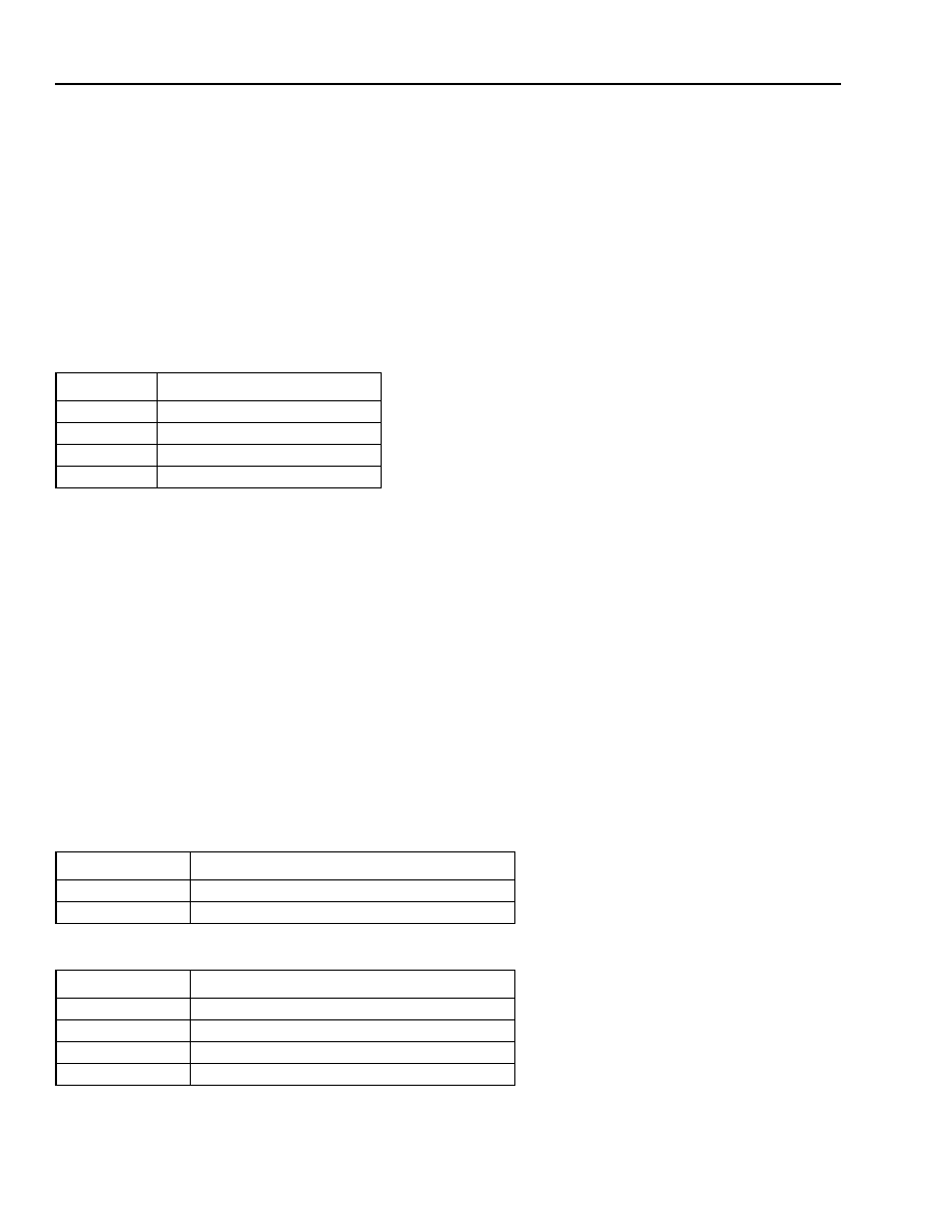
64
Agere Systems Inc.
Data Sheet
May 2001
155/622/2488 Mbits/s Data Interface
TDAT042G5 SONET/SDH
Functional Description
(continued)
Path Terminator (PT) Block
(continued)
SPE Terminate (continued)
Receive Signal Label. The C2 block will extract and validate the signal label byte (C2) and store it in a software-
accessible register. The signal label is updated when a provisionable number of consecutive detections of a new
C2 value occur (CNTDC2[A--D][3:0]; see register description, page 204). All monitoring is disabled when the
pointer is in an LOP-P or an AIS-P state. Commonly used values of C2 with their signal labels are listed below in
Table 19.
Table 19. Types of Signal Labels
Any value of C2 may be provisioned. If the provisioned value is not matched by the detected value, then data is not
passed to the DE. If the provisioned value does match the detected value, then data is passed to the DE.
TDAT042G5 will detect unequipped payloads (UNEQ-P) when a provisionable number of consecutive monitored
C2 bytes match the 0x00 unequipped STS SPE state. TDAT042G5 will detect mismatched payloads (PLM-P)
when a provisionable number of consecutive monitored C2 bytes do not match the provisioned expected payload
label (RC2EXPVAL[7:0]; see register description, page 205).
Receive Path Status. The G1 block extracts the path remote error indication (REI-P) bits of G1[7:4] and accumu-
lates the REI-P errors in a 16-bit saturating counter. This counter is operated in latch and clear mode to ensure
Bellcore and ITU compliance. It is intended that this counter be polled at least once per second in order that no
error events are missed.
RDI-P. This block will also validate the path remote defect indication (RDI-P) bits and store the result in a software-
accessible register. The receive path can monitor remote defect indications in either enhanced or single bit RDI-P
modes (provisionable via software bit RDIPMON_ENH_OR1B [A--D]; see register description, page 200). The
interpretation of the G1 byte is as follows.
Table 20. 1-bit Mode
Table 21. 3-bit Mode (Enhanced RDI)
* TIM-P must be accomplished through (microprocessor) software by reading the
transmit RDI-P state and inserting the G1 bit.
C2 Value
Signal Label
0x00
Unequipped STS SPE
0x01
Equipped nonspecific payload
0x13
Mapping for ATM
0x16
Mapping for HDLC-PPP
G1 Bytes
Description
G1[3:1] = 0xx
No RDI-P defects
G1[3:1] = 1xx
AIS-P, LOP-P
G1 Bytes
Description
G1[3:1] = 001
No RDI-P defects
G1[3:1] = 010
PLM-P or LCD-P
G1[3:1] = 101
AIS-P or LOP-P
G1[3:1] = 110
UNEQ-P or TIM-P (TIM-P is J1 mismatch*)
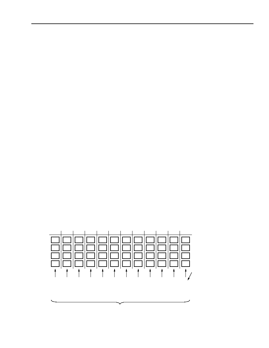
Agere Systems Inc.
65
Data Sheet
May 2001
155/622/2488 Mbits/s Data Interface
TDAT042G5 SONET/SDH
Functional Description
(continued)
Path Terminator (PT) Block
(continued)
Z5/N1, Z4/K4, Z3/F3, H4, F2 Monitoring. TDAT042G5 monitors the F2 user channel byte, the H4 VT multiframe
indicator byte, Z3/F3 growth/user byte, Z4/K4 growth/APS path byte, and the Z5/N1 tandem connection byte.
These bytes are stored in software registers. These registers are updated when a provisionable number of detec-
tions of new values occur on the associated incoming byte. All monitoring is disabled when the pointer is in an
LOP-P or an AIS-P state.
Signal Failure and Signal Degrade Monitoring. The path overhead processor also detects/clears provisionable
signal fail (SF) and signal degrade (SD) conditions. The SF and SD values are provisionable through a group of
software registers in the PT register map. The provisioning is the same as that shown in Table 16, page 57 of the
Overhead Processor (OHP) Block section.
SPE Generate
Transmit Pointer Generation. The pointer generation block generates the outgoing H1 and H2 pointer values.
Each of the four PT channels can generate one normal (valid) pointer. Therefore, in STS-3/STM-1 and STS-12/
STM-4 modes, only one normal pointer (and only one SPE) may be inserted into the transmitted SONET/SDH
frame. In STS-48/STM-12 mode, all four PT channels are used. Therefore, up to four normal pointers (and four
SPEs) may be inserted into the transmitted SONET/SDH frame.
When inserting concatenated frames, only the first H1 and H2 bytes will contain a valid pointer value. The remain-
ing H1 and H2 bytes of the channel will be set to indicate concatenation. The remaining unequipped channels will
have their H1 and H2 pointers set to a fixed pointer value.
For proper pointer generation, the appropriate values must be provisioned in the H-byte transmit state register
THx_STATE (see register description, page 203).
The following examples illustrate how the device may be configured to transmit various sub-rates and concate-
nated payloads. Each block in the following diagrams represents one STS-1 frame. Figure 8 illustrates how to pro-
vision the THx_STATE registers to transmit an STS-48c frame within an STS-48 signal. In this example, the pointer
to the first STS-1 is provisioned as a normal pointer value while the pointers to the remaining STS-1 signals are
provisioned as concatenated pointers. Figure 9 illustrates how to provision the THx_STATE registers to transmit
four STS-12c frames within an STS-48 signal. The concatenated STS-Mc frames that may be mapped into STS-N
signals (where M
N) are restricted to those listed in Table 22 (see page 68).
0351(F)
Figure 8. STS-48 Signal Carrying One STS-48c Frame
12
11
10
9
8
7
6
5
4
3
2
1
01
01
01
01
01
01
01
01
01
01
01
00
01
01
01
01
01
01
01
01
01
01
01
01
01
01
01
01
01
01
01
01
01
01
01
01
01
01
01
01
01
01
01
01
01
01
01
01
TIME-SLOT NUMBER
TH
X
_STATE[A][12--1][1:0]
TH
X
_STATE[B][12--1][1:0]
TH
X
_STATE[D][12--1][1:0]
TH
X
_STATE[C][12--1][1:0]
47 CONCATENATED POINTERS
NORMAL POINTER
39
42
45
48
27
30
33
36
15
18
21
24
3
6
9
12
38
41
44
47
26
29
32
35
14
17
20
23
2
5
8
11
37
40
43
46
25
28
31
34
13
16
19
22
1
4
7
10
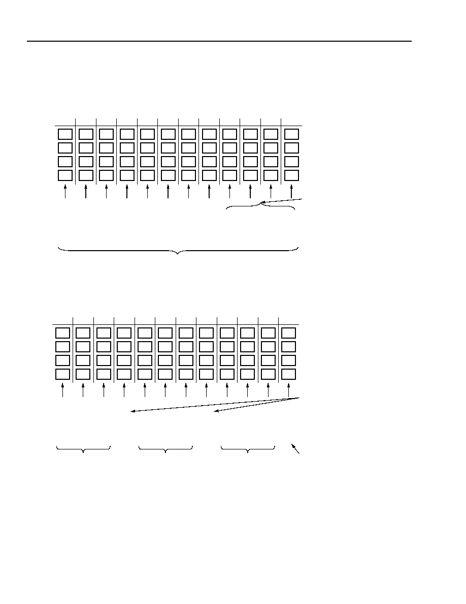
66
Agere Systems Inc.
Data Sheet
May 2001
155/622/2488 Mbits/s Data Interface
TDAT042G5 SONET/SDH
Functional Description
(continued)
Path Terminator (PT) Block
(continued)
SPE Generate (continued)
0352(F)
Figure 9. STS-48 Signal Carrying Four STS-12c Frames
0353(F)
Figure 10. Quad STS-12 Configuration With Each STS-12 Signal Carrying One STS-3c Frame
12
11
10
9
8
7
6
5
4
3
2
1
01
01
01
01
01
01
01
01
00
00
00
00
01
01
01
01
01
01
01
01
01
01
01
01
01
01
01
01
01
01
01
01
01
01
01
01
01
01
01
01
01
01
01
01
01
01
01
01
TIME-SLOT NUMBER
TH
X
_STATE[A][12--1][1:0]
TH
X
_STATE[B][12--1][1:0]
TH
X
_STATE[D][12--1][1:0]
TH
X
_STATE[C][12--1][1:0]
44 CONCATENATED POINTERS
FOUR NORMAL POINTERS
39
42
45
48
27
30
33
36
15
18
21
24
3
6
9
12
38
41
44
47
26
29
32
35
14
17
20
23
2
5
8
11
37
40
43
46
25
28
31
34
13
16
19
22
1
4
7
10
12
11
10
9
8
7
6
5
4
3
2
1
10
10
10
01
10
10
10
01
10
10
10
00
10
10
10
01
10
10
10
01
10
10
10
00
10
10
10
01
10
10
10
01
10
10
10
00
10
10
10
01
10
10
10
01
10
10
10
00
TIME-SLOT NUMBER
TH
X
_STATE[A][12--1][1:0]
TH
X
_STATE[B][12--1][1:0]
TH
X
_STATE[D][12--1][1:0]
TH
X
_STATE[C][12--1][1:0]
UNEQUIPPED
CONCATENATED POINTERS
12a
12b
12c
12d
9a
9b
9c
9d
6a
6b
6c
6d
3a
3b
3c
3d
11a
11b
11c
11d
8a
8b
8c
8d
5a
5b
5c
5d
2a
2b
2c
2d
10a
10b
10c
10d
7a
7b
7c
7d
4a
4b
4c
4d
1a
1b
1c
1d
POINTERS
UNEQUIPPED
POINTERS
UNEQUIPPED
POINTERS
NORMAL POINTERS
Agere Systems Inc.
67
Data Sheet
May 2001
155/622/2488 Mbits/s Data Interface
TDAT042G5 SONET/SDH
Functional Description
(continued)
Path Terminator (PT) Block
(continued)
SPE Generate (continued)
0354(F)
Figure 11. Quad STS-12 Configuration With Each STS-12 Signal Carrying One STS-12c Frame
(Channel A), One STS-9c Frame (Channel B), One STS-6c Frame (Channel C), and
One STS-3c Frame (Channel D)
0355(F)r.1
Figure 12. Quad STS-3 Configuration With Each STS-3 Signal Carrying One STS-2c Frame
12
11
10
9
8
7
6
5
4
3
2
1
01
01
01
01
01
01
01
01
01
01
01
00
10
01
01
01
10
01
01
01
10
01
01
00
10
10
01
01
10
10
01
01
10
10
01
00
01
10
10
01
10
10
10
01
10
10
10
00
TIME-SLOT NUMBER
TH
X
_STATE[A][12--1][1:0]
TH
X
_STATE[B][12--1][1:0]
TH
X
_STATE[D][12--1][1:0]
TH
X
_STATE[C][12--1][1:0]
NORMAL POINTERS
12a
12b
12c
12d
9a
9b
9c
9d
6a
6b
6c
6d
3a
3b
3c
3d
11a
11b
11c
11d
8a
8b
8c
8d
5a
5b
5c
5d
2a
2b
2c
2d
10a
10b
10c
10d
7a
7b
7c
7d
4a
4b
4c
4d
1a
1b
1c
1d
12
11
10
9
8
7
6
5
4
3
2
1
10
10
10
10
10
10
10
10
10
10
10
00
10
10
10
10
10
10
10
10
10
10
10
00
10
10
10
10
10
10
10
10
10
10
10
00
10
10
10
10
10
10
10
10
10
10
10
00
TIME-SLOT NUMBER
TH
X
_STATE[A][12--1][1:0]
TH
X
_STATE[B][12--1][1:0]
TH
X
_STATE[D][12--1][1:0]
TH
X
_STATE[C][12--1][1:0]
UNEQUIPPED POINTERS
CONCATENATED POINTERS
3a
3b
3c
3d
2a
2b
2c
2d
1a
1b
1c
1d
3a
3b
3c
3d
2a
2b
2c
2d
1a
1b
1c
1d
3a
3b
3c
3d
2a
2b
2c
2d
1a
1b
1c
1d
3a
3b
3c
3d
2a
2b
2c
2d
1a
1b
1c
1d
NORMAL POINTERS
68
Agere Systems Inc.
Data Sheet
May 2001
155/622/2488 Mbits/s Data Interface
TDAT042G5 SONET/SDH
Functional Description
(continued)
Path Terminator (PT) Block
(continued)
SPE Generate (continued)
The general rule for mapping STS-Mc frames in STS-N signals (M
N) is that the TDAT042G5 can have a maxi-
mum of four normal pointers in STS-48 mode. For M
12, the valid starting locations for mapping into an STS-48
signal are 1, 13, 25, and 37. For M >12, only one normal pointer is permitted and it must start at the first location
(the first STS-1). The TDAT042G5 allows only one normal pointer in STS-3 or STS-12 modes. The only valid start-
ing location for mapping concatenated frames into an STS-3 or STS-12 signal is 1.
Table 22. Valid Concatenation Starting Locations: STS-Mc into an STS-48c
STS-1 Number
STS-3c
STS-6c
STS-9c
STS-12c
STS-15c
STS-18c
STS-48c
1
Y
Y
Y
Y
Y
Y
Y
4
No
No
No
No
No
No
No
7
No
No
No
No
No
No
No
10
No
No
No
No
No
No
No
13
Y
Y
Y
Y
No
No
No
16
No
No
No
No
No
No
No
19
No
No
No
No
No
No
No
22
No
No
No
No
No
No
No
25
Y
Y
Y
Y
No
No
No
28
No
No
No
No
No
No
No
31
No
No
No
No
No
No
No
34
No
No
No
No
No
No
No
37
Y
Y
Y
Y
No
No
No
40
No
No
No
No
No
No
No
43
No
No
No
No
No
No
No
46
No
No
No
No
No
No
No

Agere Systems Inc.
69
Data Sheet
May 2001
155/622/2488 Mbits/s Data Interface
TDAT042G5 SONET/SDH
Functional Description
(continued)
Path Terminator (PT) Block
(continued)
SPE Generate (continued)
BIP-8. The PBIP block calculates the B3 value according to Bellcore and ITU standards. Insertion of PBIP errors is
possible through the use of a software control register.
REI Generation. The REI_P block controls the insertion of the remote error indication block error count. The
received PBIP error counts are inserted into the path status (G1) byte.
RDI-P Generation. The transmit path can insert remote defect indications using either single-bit or enhanced
RDI-P modes (provisionable via software register bit TRDIP_ENH_OR1B[A--D]; see register description, page
202). The highest to lowest priority of the defect code insertion is as follows:
1. AIS-P, LOP-P (applies only to the single-bit version of RDI-P),
2. UNEQ-P,
3. PLM-P, LCD-P,
4. No defects
TIM-P can be inserted using software through TRDIPSINS (registers 0x0AAA, 0x0AB2, 0x0ABA, or 0x0AC2,
bits 15--11; see register description, page 201). The LCD-P defect is observed in the data engine and passed to
the pointer block for transmission. Each particular defect can be inhibited from contributing to the transmitted
RDI-P insertion value via software registers 0x0AAA, 0x0AB2, 0x0ABA, and 0x0AC2. RDI_P can either be inserted
by software or automatically through hardware.
Z5/N1, Z4/K4, Z3/F3, H4, F2 Insertion. TDAT042G5 inserts the F2 user channel byte, the H4 VT multiframe indi-
cator byte, Z3/F3 growth/user byte, Z4/K4 growth/APS path byte, and the Z5/N1 tandem connection byte via soft-
ware provisioning.
Error Insertion Mechanisms. TDAT042G5 provides a method to inject via software REI-P
(TREIPERRINS[A--D]) and B3 (TB3ERRINS[A--D]) errors into the transmitted SONET frame (see register
descriptions, page 202).
Insertion of J1, F2, C2, Z3, H4, Z4, Z5, SS Values. TDAT042G5 provides paged provisionable registers to insert
the path overhead bytes into the outgoing SONET frame. The paging is done by first writing to the page provision-
ing register at location 0x0AC6 to set the port number and time slot to be provisioned, and then writing to the
appropriate insertion registers. Available time-slot values for TDAT042G5 are time slot 1 for STS-48c mode; time
slots 1, 2, 3, and 4 for STS-48 consisting of four STS-Mc (M
12) signals; and time slot 1 for quad STS-12c and
quad STS-3c modes (ports A, B, C, and D configured for quad STS-3c and quad STS-12c).

70
Agere Systems Inc.
Data Sheet
May 2001
155/622/2488 Mbits/s Data Interface
TDAT042G5 SONET/SDH
Functional Description
(continued)
Data Engine (DE) Block
The DE block processes ATM, SDL, PPP, and HDLC cells/packets at rates up to 2.488 Gbits/s. The DE block
behaves like four independent logical data channels, one for each of the four STS-12/STM-4 or STS-3/STM-1
channels, or like a separate single channel for STS-48/STM-16. The following description is for each one of these
data engines. Each of the functional elements to be described are independently provisioned.
The data engine supports both ATM cells and packet data formats.
I
The ATM processor functions with 52-byte, 53-byte, and 56-byte ATM cells.
I
The packet processor has three packet modes: HDLC, CRC, and PPP. All three modes use HDLC framing, i.e.,
0x7E delineates the packets. In HDLC mode, the 0x7E framing bytes are inserted or detected by the data
engine. In the CRC mode, a user-selectable 16-bit or 32-bit CRC word is appended or detected at the end of the
packet. The PPP mode places or detects a PPP header on the front of the packet as well as uses the CRC word.
The block diagram for the data engine is shown in Figure 13.
5-8385(F)r.2
Figure 13. Block Diagram of Date Engine (DE)
CBINT
SDL
INSERTER
ATM
INSERTER
HDLC
INSERTER
X43
POST-
TX
SEQUENCER
SCRAMBLER
CRC
GENERATOR
PPP
ATTACH
PT
INTERFACE
X43
PRESCRAMBLER
UT
INTERFACE
CBINT
SDL
FRAMER
ATM
FRAMER
HDLC
FRAMER
X43
POST-
RX
SEQUENCER
UNSCRAMBLER
CRC
CHECKER
PPP
DETACH
PT
INTERFACE
X43
PRE-
UT
INTERFACE
UNSCRAMBLER
RECEIVE-SIDE DE BLOCK
TRANSMIT-SIDE DE BLOCK

Agere Systems Inc.
71
Data Sheet
May 2001
155/622/2488 Mbits/s Data Interface
TDAT042G5 SONET/SDH
Functional Description
(continued)
Data Engine (DE) Block
(continued)
Receive Data Engine
Receive Sequencer. The receive sequencer demaps SONET framing to four logical channels, performs the phys-
ical channel byte alignment and packing, and performs appropriate payload clock domain transfer. The receive
sequencer must be provisioned properly for correct operation. There are six registers that are fixed for each partic-
ular mode of operation (STS-3/STM-1, STS-12/STM-4, or STS-48/STM-16) and must not be modified
(SEQ_CTRL, INIT_CNTS, OH_MARKER_LO, OH_MARKER_HI, SOH_MARKER_LO, SOH_MARKER_HI). See
the register descriptions for details, page 214. Also, the appropriate time slots must be provisioned for the rate of
the payload expected for each channel. This is done via the registers Rx_TS[1--12] (see register descriptions,
page 219). An example of how to configure this for STS-48c mode is shown in the section on configuring the trans-
mit/receive sequencer (see Transmit Data Engine section, page 78).
ATM Cell Processor. The cell processor performs ATM cell delineation using the ATM header error correction
(HEC) field found in the cell header. The HEC is a CRC-8 calculation over the first four octets (total of 32 bits) of
the ATM cell header. If the TDAT042G5 is in bit-synchronous mode (data is not byte-aligned), 32 separate HEC
calculations are performed to delineate an ATM cell. If the TDAT042G5 is in byte-synchronous mode (data is byte-
aligned), four separate HEC calculations are performed to delineate an ATM cell. An alpha-delta counter is used to
track the processor's ability to frame the ATM cells consistently. When a certain level of confidence is reached
(defined by the programmable delta counter threshold), the frame is declared in sync state, and data is passed to
subsequent blocks. If the framer is unable to frame ATM cells over a few cell periods (defined by the programma-
ble delta counter threshold), the framer resumes hunt state.
In SONET mode, the processor performs optional X
43
unscrambling of the payload. Because the X
43
scrambler is
self-synchronizing, the framer needs no assistance from the data in order to synchronize the scrambler. The
TDAT042G5 also supports an X
31
scrambler, compliant with I.432, which is mainly used for packet-over-fiber
applications. The state diagram for the X
31
scrambler is shown in Figure 14 on page 72. The X
31
scrambler uses
an x
31
+ x
28
+ 1 polynomial to scramble the data. Unlike the X
43
scrambler, the X
31
scrambler does not self-
synchronize based upon the data it receives. Thus, one-bit samples of the scrambler output are sent on the trans-
mit side and compared with the scrambler samples on the receive side every 212 bits. If the samples do not match,
the receive-side scrambler is adjusted to converge with the transmit-side scrambler. This process continues until a
certain level of confidence in the scrambler synchronization is achieved. In the X
31
mode, the ATM cell processor
does not send out any output until both the framer and the scrambler are synchronized, whereas in X
31
mode, only
the framer needs to be synchronized.
Idle ATM cells, which contain no real data, can be either left in or removed from the bit stream. The idle cell header
description can be configured, though it is set to a default value (0x00000001). ATM cells can also be filtered if the
header contents match a provisioned match register after masking with a provisionable mask register. This allows
filtering based on the contents of the GFC, PTI, and CLP fields of the header. Optionally, ATM cells may be
dropped if uncorrectable HEC errors are detected. Incoming single-bit ATM header errors can be corrected and the
cells may be passed through or dropped, depending on the software configuration.
The data engine processes only standard 53-byte ATM cells. However, the UTOPIA block processes 52-byte, 53-
byte, 54-byte, and 56-byte cells, and interfaces these to the data engine. (See UTOPIA (UT) Interface Block,
page 86, for details).
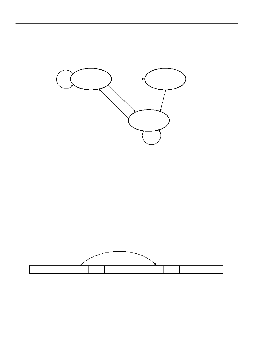
72
Agere Systems Inc.
Data Sheet
May 2001
155/622/2488 Mbits/s Data Interface
TDAT042G5 SONET/SDH
Functional Description
(continued)
Data Engine (DE) Block
(continued)
Receive Data Engine (continued)
5-8388(F)
Note: Even in synchronized mode, the confidence counter can continue to increase up to the Z value.
Figure 14. State Diagram for the X
31
Scrambler Synchronization Process
SDL Frame Processor. The SDL frame processor consists of an SDL framer, which detects the start of SDL pack-
ets, and an (optional) X
48
unscrambler, which is used to unscramble payload data. SDL packets can also arrive
unscrambled, in which case the unscrambler is disabled. The SDL frame processor can frame packets in SDL form
which contain a data length between 4 and 65,535 bytes.
The SDL framer uses a CRC-16 check upon 2 bytes sequences used to determine packet length in order to frame
SDL packets. Since the framer is designed to support data that is not byte-aligned, 32 separate framers may be
used to search for the CRC-16 pattern. If the data is byte-synchronized, only four framers are needed. A confi-
dence counter is used to gauge the framer's ability to frame SDL packets consistently. When the confidence
counters reaches a certain level (defined by the programmable SDL delta counter register), the framer is in sync
state. Single-bit error correction for the SDL headers is also supported. Shown below in Figure 15 is the general
structure of the SDL packets. In this figure, there is no interpacket fill.
5-8386(F)r.2
Figure 15. General Structure of SDL Packets
VERIFICATION
SYNCHRONIZED
ACQUISITION
COUNTER EQUALS Y
COUNTER LESS
COUNTER DROPS
THAN Y
BELOW V
COUNTER EQUALS X
COUNTER DROPS
BELOW W
COUNTER LESS
THAN X
PACKET PAYLOAD
PACKET
LENGTH
CRC-16
PACKET PAYLOAD
PACKET
LENGTH
PACKET PAYLOAD
CRC-16
Agere Systems Inc.
73
Data Sheet
May 2001
155/622/2488 Mbits/s Data Interface
TDAT042G5 SONET/SDH
Functional Description
(continued)
Data Engine (DE) Block
(continued)
Receive Data Engine (continued)
Interpacket fill separating packets always contains a multiple of 4 bytes. The SDL framer is able to detect inter-
packet fill since its value is fixed. (It has 4 bytes equal to 0x0000000, i.e., a packet length of 0x0000 with a CRC-16
of 0x0000.) Since the framer knows the length of a particular packet and can detect interpacket fill, it will predict the
start of the next frame and frame on it. The SDL frame processor supports SDL and SDL CRC modes. When oper-
ating in SDL CRC mode, a 2-byte or 4-byte CRC for the packet payload is attached to the end of the packet pay-
load prior to the next packet length. When operating in SDL mode, there is no 2-byte or 4-byte CRC for the packet
payload.
The SDL frame processor supports X
48
scrambling of the packet payload, which is accomplished by using a primi-
tive polynomial of x
48
+ x
28
+ x
27
+ x + 1. The X
48
scrambler is not self-synchronizing. Thus, the side transmitting
SDL packets will periodically send its 48-bit scrambler state within the data stream such that the receive side can
synchronize its scrambler. Whenever the SDL frame processor receives a scrambler state, it is immediately put
into sync state, which allows it to send data out. Upon receiving additional scrambler states, the scrambler will
compare its own state with the state received. If the scrambler states match, then the scrambler remains in sync
state. However, if there is a mismatch, the scrambler is put into postsync state. In postsync state, if an additional
scrambler state mismatch occurs, the X
48
scrambler is resynchronized with the scrambler state it has received.
The SDL frame processor detects scrambler state data since the packet length field of 0x001 and the length of
time separating scrambler state transmissions is programmable. Single-bit error correction for the SDL scrambler
state is incorporated within the TDAT042G5.
Both the SDL framer and the X
48
scrambler must be synchronized before the SDL frame processor will send data.
Besides the SDL scrambler state being transmitted, the SDL framer will also extract special A and B messages
used by the upstream device to send link layer 1 messages to the downstream hardware. The packet length field
used to detect A and B messages are 0x0002 and 0x0003, respectively.
In addition to scrambling the data, the SDL data stream coming into the SDL frame processor is dc balanced with
the 32-bit value 0xB6AB31E0.
Table 23 below is used to describe the packet length field.
Table 23. Packet Length Field
Pre-descrambler. The pre-descrambler block descrambles the payload using a self-synchronous descrambler
with a generator polynomial of 1 + x
43
. For ATM cell traffic, only the 48-byte cell payload (and not the cell over-
head) is descrambled. For HDLC and PPP packets, the entire frame (including header and trailer) is descrambled.
Predescrambling, post-descrambling, or no descrambling may be selected through a provisionable register.
Packet Length
Field
SDL Data Type
0x0000
Interpacket fill
0x0001
SDL scrambler state
0x0002
A message
0x0003
B message
0x0004--
0xFFFF
Length of payload region for current
packets (in bytes)

74
Agere Systems Inc.
Data Sheet
May 2001
155/622/2488 Mbits/s Data Interface
TDAT042G5 SONET/SDH
Functional Description
(continued)
Data Engine (DE) Block
(continued)
Receive Data Engine (continued)
HDLC Framer. The packet processor frame aligns to HDLC packets using the HDLC flag character (0x7E). Flags
are also used to fill interpacket spaces. The flags are removed and control escape destuffing is performed. The
control escape character (0x7D) is searched for and when it is found, the control escape character is removed, i.e.,
0x7D5D is unescaped to 0x7D and 0x7D5E is unescaped to 0x7E. If dry mode is enabled, then 0x7D20 is unes-
caped to a value of 0x00, which represents dry data (FIFO underflow in the middle of a packet). Any other unes-
caped sequence of 0x7D results in an errored packet.
CRC Check. An optional CRC-ITU or CRC-32 calculation on the whole POS frame is performed after byte destuff-
ing and data descrambling. The CRC-ITU generating polynomial is 1 + x
5
+ x
12
+ x
16
. The CRC-32 generating
polynomial is 1 + x + x
2
+ x
4
+ x
5
+ x
7
+ x
8
+ x
10
+ x
11
+ x
12
+ x
16
+ x
22
+ x
23
+ x
26
+ x
32
. The computation over
the whole packet, including the FCS field, should result in all zeros. A different value indicates an error. Packets
with FCS errors are marked as such and are discarded. CRC field stripping is optional. Both normal and reversed
CRC modes are supported.
Post-descrambler. The descrambler block descrambles the payload using a self-synchronous descrambler with a
generator polynomial of 1 + x
43
. For ATM cell traffic, this block is bypassed. For HDLC frames, the entire frame
(including header and trailer) is descrambled. The descrambler may be disabled through the use of a software reg-
ister.
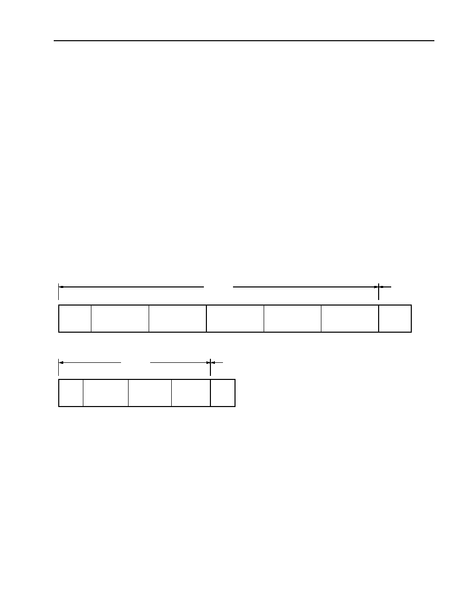
Agere Systems Inc.
75
Data Sheet
May 2001
155/622/2488 Mbits/s Data Interface
TDAT042G5 SONET/SDH
Functional Description
(continued)
Data Engine (DE) Block
(continued)
Receive Data Engine
(continued)
PPP Header Detach. The PPP detach function matches the PPP header (corresponding to the first 4 bytes of the
PPP uncompressed frame or first 2 bytes of the PPP compressed frame) to a set of fixed or provisionable values
for each channel and outputs frames in accordance with payload control register settings. The address and control
field bytes are assumed to be 0xFF03. The block supports two fixed protocol fields (0x0021 corresponding to the
IP protocol field, and 0x8021 corresponding to the IP control protocol). Additionally, 12 provisionable registers,
PPP_Rx_HDR [0--11][15:0] (addresses 0x10F0--0x10FB), are supported on-chip to allow a large number of pro-
tocols to be recognized in the receive (ingress) data path of the chip.
The PPP detach function supports compressed or uncompressed header fields, optionally matching two fixed (one
corresponding to IP protocol) 16-bit protocol fields. This optional PPP header check allows PPP (normal or com-
pressed (i.e., no FF03)) to be checked and the header optionally stripped. Packets that fail to match one of the pro-
visioned headers or the two default headers can optionally be discarded. This function supports optionally
matching 12 programmable 16-bit protocol fields. The PPP detach function provides mismatched PPP header
count on a per-channel basis through four 28-bit counters, PM_MHC_[0--3][27:0] (addresses 0x1118--0x111F).
The function can optionally discard frames if header fields do not match on a per-channel basis. It can also option-
ally strip header fields only if they do match on a per-channel basis.
A PPP packet has the following two formats:
5-9642 (F)
* TDAT042G5 is verified to handle packets of up to 64 Kbytes. Larger packets may be processed, but no upper bound or packet size
has been determined. Packets of less than 4 bytes are discarded by the DE.
Figure 16. Uncompressed and Compressed PPP Packets
Each channel has a 16-bit register, PPP_Rx_CHK_CH [0--3][15:0] (addresses 0x10FC--0x10FF), that can be
provisioned.
If the header bytes do not match and payload control bit 7 = 0, the entire PPP packet is discarded for a given chan-
nel. Otherwise, if the header bytes do not match and payload control bit 7 = 1, the PPP packet is marked as bad
and not discarded for a given channel.
If payload control bit 6 = 0, the header is stripped, provided it matches a provisionable value; otherwise, it is left on
for a given channel.
0x7E
0x7E
0x7E
0x7E
PROTOCOL
DATA
CRC FIELD
FIELD
1 byte
2 bytes
1 byte
64 Kbytes*
2 OR 4 bytes
PACKET
COMPRESSED PPP PACKET
NEXT PACKET
1 byte
1 byte
64 Kbytes*
PACKET
UNCOMPRESSED PPP PACKET
NEXT PACKET
ADDRESS FIELD
CONTROL FIELD
0xFF
CRC FIELD
DATA
0x03
PROTOCOL
FIELD
2 OR 4 bytes
2 bytes
1 byte
1 byte

76
Agere Systems Inc.
Data Sheet
May 2001
155/622/2488 Mbits/s Data Interface
TDAT042G5 SONET/SDH
Functional Description
(continued)
Data Engine (DE) Block
(continued)
Receive Data Engine
(continued)
The bad packet counting is based upon the following criteria:
I
Header Fields. The PPP mismatched header counter, PM_MHC_[0--3][27:0] (addresses 0x1118--0x111F),
counts for PPP packets with various header errors/mismatches as provisioned in the registers.
I
CRC Field. The CRC bad packet counter, PM_BPC_n (n = 0, 1, 2, 3), increments if a CRC error is found in
channel n.
Each PPP packet not counted as a bad packet in PM_MHC_n (n = 0, 1, 2, 3) counter or PM_BPC_n counter incre-
ments the PPP good packet counter, PM_GPC_n (n = 0, 1, 2, 3), for channel n. (See register descriptions,
page 241.)
Note that each channel only has a single pair of good and bad packet counters.
Transmit Data Engine
ATM Cell Inserter. The ATM cell inserter provides X
43
or X
31
scrambling of the payload for transport of ATM cells
over SONET. X
31
scrambling is suitable for the transport of ATM cells over fiber where bit-level cell delineation is
required. The state diagram for the X
31
scrambler is shown in Figure 14, page72. The ATM cell inserter will gener-
ate idle cells/bytes to fill the SONET/SDH payload when cells/packets are not available in the transmit direction
FIFO of the UTOPIA block. For ATM cells, the GFC, PTI, and CLP fields of the idle cell header and the idle cell pay-
load are provisionable via software registers. The idle generator generates idle cells/bytes to fill the SONET/SDH
payload when cells/packets are not available in the transmit FIFO. Idle cell HCS is automatically calculated and
inserted.
Header Check Sequence (HCS) Generator. The HCS generator performs a CRC-8 calculation over the first four
header octets of the ATM cell. The generator inserts the result into the fifth octet of the ATM header.
SDL Frame Inserter. The SDL inserter performs SDL frame generation and X
48
scrambling of the payload field.
An optional CRC-16/32 field can be attached (SDL-CRC mode) and is calculated over the payload. The SDL
inserter also periodically transmits scrambler state updates through a special 6-byte message. The time between
scrambler state updates can be provisioned by software using register SDLFI_INT (see register description, page
250). The packet length header of scrambler state updates is the 16-bit word, 0x0001. Special A and B messages
can be software-provisioned to send link layer 1 messages to downstream hardware. The packet length headers
for the special A and B messages are 0x0002 and 0x0003, respectively.

Agere Systems Inc.
77
Data Sheet
May 2001
155/622/2488 Mbits/s Data Interface
TDAT042G5 SONET/SDH
Functional Description
(continued)
Data Engine (DE) Block
(continued)
Transmit Data Engine (continued)
Prescrambler. The prescrambler block optionally scrambles the payload using a self-synchronizing scrambler with
a generator polynomial of 1 + x
43
for HDLC and PPP packets. For HDLC frames, the entire frame, including
header and trailer, is scrambled; however, HDLC flags are not scrambled. The scrambler may be disabled through
the use of a software register. This scrambler removes excessive 0x7D and 0x7E bytes. For ATM cell and SDL
packet traffic, this block is not used. (By randomizing the data, the scrambler prevents malicious use of the channel
due to escaping 7D and 7E sequences.)
CRC-16/-32 Generator. An optional CRC-16/-32 generator on the whole packet frame can be performed. The gen-
erating polynomial for CRC-16 is 1+ x
5
+ x
12
+ x
16
. The generating polynomial for CRC-32 is 1+ x + x
2
+ x
4
+ x
5
+
x
7
+ x
8
+ x
10
+ x
11
+ x
12
+ x
16
+ x
22
+ x
23
+ x
26
+ x
32
.
HDLC Inserter. The HDLC framer provides frame check sequence (FCS) generation and insertion using either the
CRC-ITU or CRC-32 generation polynomials. After optional CRC generation, the HDLC framer performs control
escape (0x7D) stuffing, flag character (0x7E) or abort character (0x7D7E) insertion, and dry mode insertion
(0x7D20, where the last two bytes (the 20 bytes of the default value of 0x7D20) are provisionable).
Postscrambler. The postscrambler block optionally scrambles the payload using a self-synchronizing scrambler
with a generator polynomial of 1 + x
43
for HDLC and PPP packets, in accordance with RFC1619. For HDLC and
PPP packets, the entire frame, including header and trailer, is scrambled. The scrambler may be disabled through
the use of a software register. For ATM cell and SDL packet traffic, this block is not used.*
PPP Header Attach. The PPP attach function inserts the provisionable 4-byte PPP header if payload control
bit 7 = 1 (addresses 0x10E0--0x10E3). The first and second bytes are set to 0xFF03, and the third and fourth
bytes are set to a value defined by a software register in PPP_Tx_CHAN[0--3] (see register descriptions,
page 234).
If payload control bit 7 = 0 (addresses 0x10E0--0x10E3) (compressed PPP header mode), only the two provision-
able bytes defined by the software register PPP_Tx_CHAN[0--3] can be attached. Note that there is only one soft-
ware register-defined protocol value for each channel.
The PPP attach function provides good packet count on a per-channel basis through four 28-bit counters,
PM_GPC_TX_[0--3] [27:0] (addresses 0x1128--112F).
* The ATM and SDL framer inserters have their own dedicated scramblers.
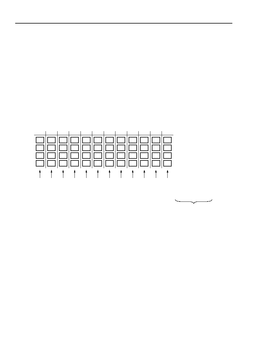
78
Agere Systems Inc.
Data Sheet
May 2001
155/622/2488 Mbits/s Data Interface
TDAT042G5 SONET/SDH
Functional Description
(continued)
Data Engine (DE) Block
(continued)
Transmit Data Engine (continued)
Tx Sequencer. The transmit sequencer maps logical channels into SONET frames, and must be provisioned prop-
erly for correct operation. The appropriate time slots must be provisioned for the rate of the payload expected for
each channel. This is done via the registers Tx_TS[1--12] (see register descriptions, page 215).
TDAT042G5 provides 12 time slots and four channels to define how data is mapped into the 48 synchronous trans-
port signals (STS-1) of an STS-48 frame or into the 12/3 STS signals of an STS-12/3 SONET frame.
Figure 17 illustrates the mapping of the 48 STS-1 signals into an STS-48 signal and their assigned time slots. Each
STS-1 block in the figure represents a byte of data for the specific STS-1 signal. The STS signals within the 12 time
slots are ordered such that the SONET multiplexing requirements of lower rate signals into higher rate signals are
satisfied. A value of 0x4 indicates that valid data is contained in the specific byte (STS) and the data is being
received/transmitted from/to channel 0.
5-7936(F)r.3
Figure 17. Example of Tx/Rx Sequencer Configuration: STS-48c into Single OC-48 Signal
39
42
45
48
27
30
33
36
15
18
21
24
3
6
9
12
38
41
44
47
26
29
32
35
14
17
20
23
2
5
8
11
37
40
43
46
25
28
31
34
13
16
19
22
1
4
7
10
12
11
10
9
8
7
6
5
4
3
2
1
0 x 4
0 x 4
0 x 4
0 x 4
0 x 4
0 x 4
0 x 4
0 x 4
0 x 4
0 x 4
0 x 4
0 x 4
0 x 4
0 x 4
0 x 4
0 x 4
0 x 4
0 x 4
0 x 4
0 x 4
0 x 4
0 x 4
0 x 4
0 x 4
0 x 4
0 x 4
0 x 4
0 x 4
0 x 4
0 x 4
0 x 4
0 x 4
0 x 4
0 x 4
0 x 4
0 x 4
0 x 4
0 x 4
0 x 4
0 x 4
0 x 4
0 x 4
0 x 4
0 x 4
0 x 4
0 x 4
0 x 4
0 x 4
TIME-SLOT NUMBER
T
X
_TS[12--1][15:12]
T
X
_TS[12--1][11:8]
T
X
_TS[12--1][3:0]
T
X
_TS[12--1][7:4]
CONFIGURE SIMILARLY
FOR R
X
SEQUENCER
REGISTER
0 x 4
PAYLOAD LOCATIONS
VALID AND DIRECTED TO CHANNEL 0
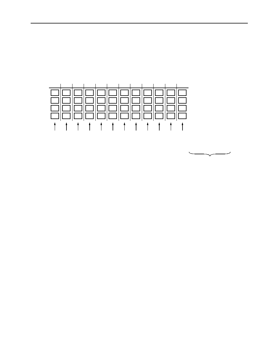
Agere Systems Inc.
79
Data Sheet
May 2001
155/622/2488 Mbits/s Data Interface
TDAT042G5 SONET/SDH
Functional Description
(continued)
Data Engine (DE) Block
(continued)
Transmit Data Engine (continued)
Figure 18 illustrates the configuration of the time-slot registers for four independent STS-12 signals. In this case,
there are 12 STS-1 signals that comprise each STS-12 signal.
5-7937(F)r.3
Figure 18. Example of Tx/Rx Sequencer Configuration: 4xSTS-12c into Four Independent OC-12 Signals
12a
12b
12c
12d
9a
9b
9c
9d
6a
6b
6c
6d
3a
3b
3c
3d
11a
11b
11c
11d
8a
8b
8c
8d
5a
5b
5c
5d
2a
2b
2c
2d
10a
10b
10c
10d
7a
7b
7c
7d
4a
4b
4c
4d
1a
1b
1c
1d
12
11
10
9
8
7
6
5
4
3
2
1
0 x 4
0 x 4
0 x 4
0 x 4
0 x 4
0 x 4
0 x 4
0 x 4
0 x 4
0 x 4
0 x 4
0 x 4
0 x 5
0 x 5
0 x 5
0 x 5
0 x 5
0 x 5
0 x 5
0 x 5
0 x 5
0 x 5
0 x 5
0 x 5
0 x 6
0 x 6
0 x 6
0 x 6
0 x 6
0 x 6
0 x 6
0 x 6
0 x 6
0 x 6
0 x 6
0 x 6
0 x 7
0 x 7
0 x 7
0 x 7
0 x 7
0 x 7
0 x 7
0 x 7
0 x 7
0 x 7
0 x 7
0 x 7
TIME-SLOT NUMBER
T
X
_TS[12--1][15:12]
T
X
_TS[12--1][11:8]
T
X
_TS[12--1][3:0]
T
X
_TS[12--1][7:4]
CONFIGURE SIMILARLY
FOR R
X
SEQUENCER
REGISTER
0 x 4
PAYLOAD VALID TO CHANNEL 0
0 x 5
PAYLOAD VALID TO CHANNEL 1
0 x 6
PAYLOAD VALID TO CHANNEL 2
0 x 7
PAYLOAD VALID TO CHANNEL 3
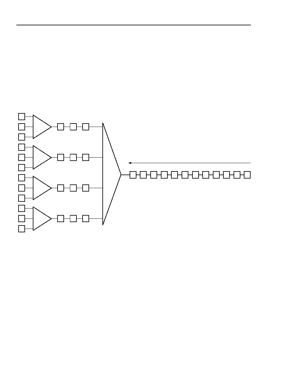
80
Agere Systems Inc.
Data Sheet
May 2001
155/622/2488 Mbits/s Data Interface
TDAT042G5 SONET/SDH
Functional Description
(continued)
Data Engine (DE) Block
(continued)
Transmit Data Engine (continued)
The multiplexing rules of SONET are illustrated in Figure 19, and are shown for the case of two-stage byte inter-
leaving of 12 STS-1 signals into an STS-12 signal. The values provisioned in the time-slot registers should obey
the SONET multiplexing rules. In Figure 18, time slots 1 through 12 of channel A represent the interleaved bytes of
the multiplexed STS-12 signal being received/transmitted in logical channel 0 (0x4). Channels B, C, and D are con-
figured similarly; however, data is being received/transmitted from logical channels 1, 2, and 3, respectively.
5-8387(F)
Figure 19. SONET Multiplexing: 2-Stage Byte Interleaving Example
3
2
1
3:1
1
2
3
STS#
6
5
4
3:1
4
5
6
9
8
7
3:1
7
8
9
12
11
10
3:1
10
11
12
12
9
6
3
11
8
5
2
10
7
4
1
12TH BYTE
1ST BYTE
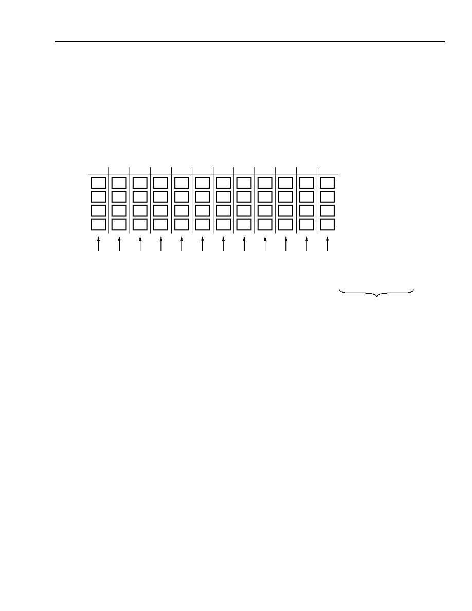
Agere Systems Inc.
81
Data Sheet
May 2001
155/622/2488 Mbits/s Data Interface
TDAT042G5 SONET/SDH
Functional Description
(continued)
Data Engine (DE) Block
(continued)
Transmit Data Engine (continued)
Figure 20 illustrates the configuration of the time-slot registers for four independent STS-3 signals. In this case,
there are three STS-1 signals that comprise each STS-3 signal. Since there are 12 time slots and only three are
actually required, the values in time slots 4--12 can be repetitively configured as shown in the figure or can be
configured as invalid, i.e., 0x0, 0x1, 0x2, and 0x3 for channels A, B, C, and D, respectively.
5-7937(F).ar2
Figure 20. Example of Tx/Rx Sequencer Configuration: 4xSTS-3c into Four Independent OC-3 Signals
Performance Monitoring
This block contains several cell/packet counters for receive/transmit data traffic. Two 28-bit saturating counters
count the number of good packets/cells that are sent out and received by the enhanced UTOPIA interface. There
are 28-bit counters used to count the number of corrected ATM HCS single bit errors, HDLC invalid sequences,
and SDL corrected headers. Also, 28-bit counters are used to count the number of uncorrectable HCS errored
ATM cells (discarded cells), HDLC short packets, SDL errored headers, packets with bad CRC checks, and mis-
matched PPP headers. These counters are operated in latch and clear mode (using PMRST) to ensure GR-256
standards compliance. It is intended that these counters be polled at least once per second so that no error events
are missed.
3a
3b
3c
3d
2a
2b
2c
2d
1a
1b
1c
1d
3a
3b
3c
3d
2a
2b
2c
2d
1a
1b
1c
1d
3a
3b
3c
3d
2a
2b
2c
2d
1a
1b
1c
1d
3a
3b
3c
3d
2a
2b
2c
2d
1a
1b
1c
1d
12
11
10
9
8
7
6
5
4
3
2
1
0 x 4
0 x 4
0 x 4
0 x 4
0 x 4
0 x 4
0 x 4
0 x 4
0 x 4
0 x 4
0 x 4
0 x 4
0 x 5
0 x 5
0 x 5
0 x 5
0 x 5
0 x 5
0 x 5
0 x 5
0 x 5
0 x 5
0 x 5
0 x 5
0 x 6
0 x 6
0 x 6
0 x 6
0 x 6
0 x 6
0 x 6
0 x 6
0 x 6
0 x 6
0 x 6
0 x 6
0 x 7
0 x 7
0 x 7
0 x 7
0 x 7
0 x 7
0 x 7
0 x 7
0 x 7
0 x 7
0 x 7
0 x 7
TIME-SLOT NUMBER
T
X
_TS[12--1][15:12]
T
X
_TS[12--1][11:8]
T
X
_TS[12--1][3:0]
T
X
_TS[12--1][7:4]
CONFIGURE SIMILARLY
FOR R
X
SEQUENCER
REGISTER
0 x 4
PAYLOAD VALID TO CHANNEL 0
0 x 5
PAYLOAD VALID TO CHANNEL 1
0 x 6
PAYLOAD VALID TO CHANNEL 2
0 x 7
PAYLOAD VALID TO CHANNEL 3
82
Agere Systems Inc.
Data Sheet
May 2001
155/622/2488 Mbits/s Data Interface
TDAT042G5 SONET/SDH
Functional Description
(continued)
Data Engine (DE) Block
(continued)
Over-Fiber Modes
In addition to the support of the normal SONET/SDH modes for different payload types such as HDLC, PPP, ATM
(X
43
or X
31
), and SDL as shown in Figure 2 on pa ge45, this device is capable of supporting the over-fiber modes
for two payload types, SDL or ATM (X
31
). In the over-fiber mode, a 3% payload increase can be realized because
the data stream contains no SONET/SDH overhead bytes.
In the over-fiber modes, it is possible to utilize the whole bandwidth (155 Mbits/s for OC-3, 622 Mbits/s for OC-12,
or 2.5 Gbits/s for OC-48) of the optical fiber for SDL packets or ATM cells.
As can be seen in Figure 21, for over-fiber modes the device is provisioned as follows:
I
The line termination (OHP) and path termination (PT) blocks of the device need to be provisioned in the
passthrough mode.
I
The payload termination (DE) block needs to be set to the bit synchronization mode in the payload control regis-
ter.
I
The transparent mode in the transmit and receive sequencers (addresses 0x102E and 0x102F; see register
description, page 223).
I
Bit 12 of the mode register (address 0x0010) needs to be set to 0 so that the received clock drives the entire
receive data path. In this way, there is no need to cross the clock domain boundary. As a result, only a single
channel is allowed for OC-3, OC-12, or OC-48 when the device is operated in the over-fiber modes. In contrast,
the device is capable of supporting four OC-3/OC-12 channels or one OC-8 channel in the SONET/SDH modes.
5-6680(F).cr.1
Figure 21. TDAT042G5 Over-Fiber Modes: SDL, ATM (X
31
)
PASSTHROUGH
L
I
NE I
N
T
E
RF
ACE
B
L
OCK
LINE
TERMINATION
PATH
TERMINATION
PAYLOAD
TERMINATION
PACKET/CELL
PROCESSOR
-BIT SYNC
-DECAPSULATION
-UNSCRAMBLING
SINGLE OC-48
SINGLE OC-12
SINGLE OC-3
CONTROL
µ
P INTERFACE
-CRC VERIFICATION
ENHANCED
UTOPIA I/O
PACKET/CELL
PROCESSOR
-ENCAPSULATION
-SCRAMBLING
-CRC GENERATION
PASSTHROUGH
PASSTHROUGH
PASSTHROUGH

Agere Systems Inc.
83
Data Sheet
May 2001
155/622/2488 Mbits/s Data Interface
TDAT042G5 SONET/SDH
Functional Description
(continued)
Data Engine (DE) Block
(continued)
Transparent Payload Mode
The transparent payload mode in the payload termination data engine (DE) block is one of seven basic payload
type modes in the payload control registers and allows data to pass directly through the DE. In this mode, no fram-
ing is done on the data, and the data in the SONET frame is treated as raw data. The transparent payload mode
basically disables all the functions of the framers. In contrast, the transparent mode of the sequencer (over-fiber
mode) disables the conversion function of the sequencer between the SONET/SDH framing structure and the log-
ical channel structure.
In the transparent payload mode, the data engine processes the entire payload as a single packet with no J1 byte
or other POH. An RxSOP is generated on the UTOPIA interface on the first byte following the J1 byte. The last
byte of payload occurs at an RxEOP.
If the device is set in both the transparent payload mode in the payload control registers and the transparent mode
in the sequencer, then the whole SONET/SDH frame (overhead bytes will be overwritten with zeros) will appear at
the receive UTOPIA interface as one packet. At the transmit UTOPIA side, the whole SONET/SDH frame needs to
be supplied.
Transparent Receive Mode Control. In receiving from the line, provisioning must specify the time slot and
SONET frame byte location where the last byte in the packet will occur. The following registers are used to indicate
this location.
I
Rx_CHCD_FM (address 0x1030; see register description, page 224) specifies the time slot where the last byte
of a packet exists in channels C and D.
I
Rx_CHAB_FM (address 0x1031; see register description, page 224) specifies the time slot where the last byte
of a packet exists in channels A and B.
I
Rx_CELLA_FM (address 0x1032), Rx_CELLB_FM (address 0x1033), Rx_CELLC_FM (address 0x1034), and
Rx_CELLD_FM (address 0x1035) specify in which SONET location (0 to 809) the last byte in a packet exists in
channel A, B, C, or D, respectively. (See register descriptions, page 225.)
In the case where the location of the last byte in the frame is not known, the last byte should be provisioned for
location 809 and time slot 12, and external UTOPIA hardware must perform packet delineation on the data
stream.
Transparent Transmit Mode Control. In transmitting to the line, provisioning must specify the time slot and
SONET frame alignment. This is done through Tx_TRANS_CTRL (address 0x102F; see register description,
page 223) used in conjunction with Tx_TS[1--12] (addresses 0x1016--0x1021; see register descriptions,
page 215).
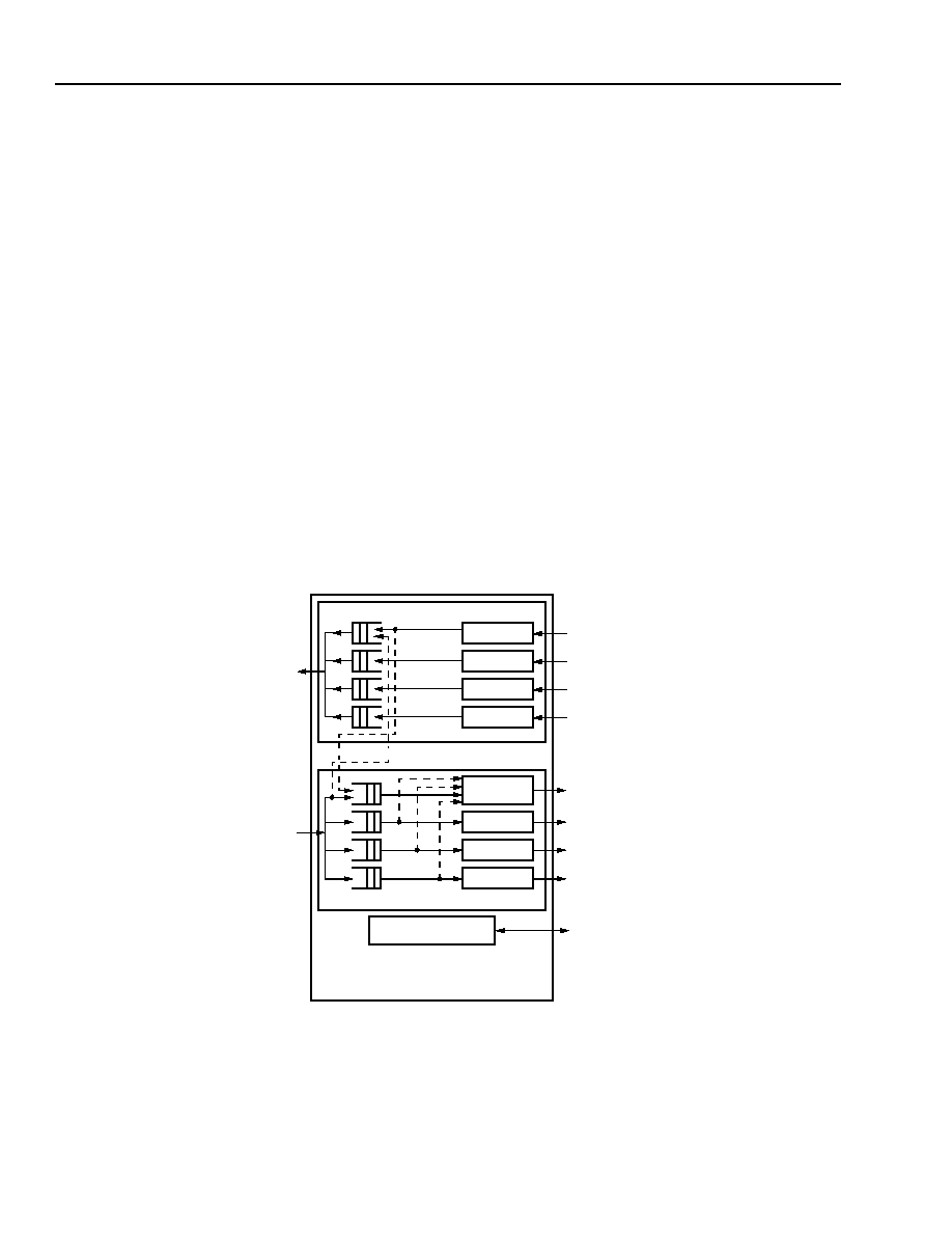
84
Agere Systems Inc.
Data Sheet
May 2001
155/622/2488 Mbits/s Data Interface
TDAT042G5 SONET/SDH
Functional Description
(continued)
UTOPIA (UT) Interface Block
The UT core provides buffering and UTOPIA interface functionality. This enhanced UTOPIA interface will pass U2,
U2+, U3, and U3+ protocols. In the receive direction, data is buffered from the line side, and sent out of the device
via a UTOPIA/packet-over-SONET-PHY interface. In the transmit direction, data is received by the device via a
UTOPIA/packet-over-SONET-PHY interface, and buffered before being sent to the line side. Data that is sent or
received can be either packet or ATM traffic, and is configurable on a per-channel basis. The UTOPIA slave inter-
face is designed to accommodate back-to-back ATM cell and packet data transfers in point-to-point or multi-PHY
modes.
Level-2 physical interfaces (transmit and receive) support four logical data channels as shown in Figure 22. Each
of these interfaces is independently configurable for cell or packet transfers, and can support up to STS-12/STM-4
bandwidth. Optionally, two of the interfaces, specifically A and B, can be grouped together to support a 32-bit
UTOPIA level-3 interface supporting up to STS-48/STM-16 of bandwidth. The aggregate traffic that can be carried
over these interfaces is limited to STS-48/STM-16 bandwidth.
In addition to operating as separate point-to-point streams, MPHY capabilities for up to four channels can be pro-
vided from the A interface in either 16-bit or 32-bit modes. For example, when operating as a 32-bit interface, the A
interface can support either a single STS-48c channel or four STS-12c channels. As a 16-bit interface, the MPHY
interface can support either a single STS-12c channel or four STS-3c channels.
Since each channel can be configured independently, each one can carry different traffic types at different rates,
provided that the capabilities of the active interfaces and the data engine are not exceeded.
There are two basic data paths: receive side, defined to be data going from the line side to the UTOPIA side, and
transmit side, defined to be data going from the UTOPIA side to the line side as shown in Figure 22.
5-7056(F)r.5
Note: For MPHY support, channels are mapped to interface A only.
Figure 22. UT Block Diagram
EGRESS SIDE
INTERFACE A
INTERFACE B
INTERFACE C
INTERFACE D
INGRESS SIDE
INTERFACE D
INTERFACE C
INTERFACE B
INTERFACE A
SOFTWARE REGISTERS
UTOPIA 2/3 INTERFACE
NOTE: UTOPIA 32-bit MODE
COMBINES CHANNELS A & B
INTERNAL
CONTROL
BUS
UT
OP
IA
I
N
T
E
R
F
A
C
E
Tx
Rx
L
I
NE
S
I
DE
IN BOTH DIRECTIONS (Tx & Rx)
LOOPBACKS
MP
H
Y

Agere Systems Inc.
85
Data Sheet
May 2001
155/622/2488 Mbits/s Data Interface
TDAT042G5 SONET/SDH
Functional Description
(continued)
UTOPIA (UT) Interface Block
(continued)
Enhanced refers to the extensions that have been added to support packet transfers. These extensions are indica-
tions of the following: (1) an end of packet (TxEOP/RxEOP), (2) the byte on which packet ends in last word (TxSZ/
RxSZ), and (3) the signal to abort a packet early (TxERR/RxERR). An abort occurs, for example, if the check sum
at the end of a packet is bad, or the end of a packet is reached prematurely. If the receive FIFO overflows because
the master cannot process packet data fast enough, an RxERR will also be generated.
UTOPIA Loopbacks
TDAT042G5 can be placed in loopback on a channel-by-channel basis. When the TDAT042G5 is placed in far-end
loopback (FELB), data from the DE is sent to and processed by the UTOPIA interface. Instead of sending it to the
UTOPIA master, however, the data is sent to the corresponding egress channel and back to the line interface.
When the TDAT042G5 is placed in near-end loopback (NELB), data from the egress channel is transferred to the
corresponding ingress channel, instead of the DE. This data is then processed by the ingress channel and is
returned to the UTOPIA master.
UTOPIA Modes
Each UTOPIA interface mode is capable of supporting various types of traffic with different bandwidth capabilities
as summarized in Table 24. In a point-to-point operational mode, any interface can be configured independently in
any of the defined modes (e.g., channel A passes ATM cells using STS-12c, channel B passes packets, etc.).
It should be noted that the U3 or U3+ (32-bit mode) can only be supported by overloading channel A and B inter-
face pins. Only the control signals from channel A are used. The channel B size and data bits are combined with
the channel A size and data bits to form the 2-bit size and the 32-bit data words. When 32-bit mode is selected,
channels B, C, and D must be configured to be idle (so that channel B will be under the control of channel A in
32-bit mode).
Multichannel multi-PHY (MPHY) capabilities are only supported on interface A by grouping the internal FIFOs and
data paths of channels B, C, and D as needed. This operational mode is described in a later section.
Table 24. UTOPIA Traffic Types
* Maximum speed may be exceeded if nonstandard load conditions are used and the clock is sourced. See CLOCK_MODE_Rx [A--D]
(registers 0x020F, 0x0213, 0x0217, 0x021B), pages 158--159 for details.
UTOPIA Name
Interface
Width
Maximum
Speed
Aggregate
Bandwidth
Traffic Type
Maximum
Number of
Interfaces
U2
16 bits
52 MHz*
622 Mbits/s (STS-12)
ATM cells only
4
U2+
16 bits
52 MHz*
622 Mbits/s (STS-12)
ATM cells/packets
4
U3, 8-bit mode
8 bits
104 MHz
622 Mbits/s (STS-12)
ATM cells only
4
U3+, 8-bit mode
8 bits
104 MHz
622 Mbits/s (STS-12)
ATM cells/packets
4
U3, 32-bit mode
32 bits
104 MHz
2.5 Gbits/s (STS-48)
ATM cells only
1
U3+, 32-bit mode
32 bits
104 MHz
2.5 Gbits/s (STS-48)
ATM cells/packets
1
86
Agere Systems Inc.
Data Sheet
May 2001
155/622/2488 Mbits/s Data Interface
TDAT042G5 SONET/SDH
Functional Description
(continued)
UTOPIA (UT) Interface Block
(continued)
UTOPIA ATM Cell Processing
The UTOPIA block will process ATM packets of 52, 53, 54, or 56 bytes. The standard 53-byte ATM cell structure is
shown in Table 25.
Table 25. Standard 53-byte ATM Cell Structure
In the receive path, TDAT042G5 automatically calculates the HEC (byte 5) and overwrites this byte of the ATM cell.
It is therefore possible to transfer only 52-byte packets through the UTOPIA I/O to increase interface efficiency.
This mode will be referred to as the 52-byte mode. The 52-byte or 53-byte ATM mode is provisioned through
ATM_SIZE_Rx[A--D] (bit 4 of registers 0x020F, 0x0213, 0x0217, and 0x021B) and ATM_SIZE_Tx[A--D]
(
bit 4 of
registers 0x0210, 0x0214, 0x0218, and 0x021C).
U2 Modes. For U2 and U2+, both the 52-byte and 53-byte, 16-bit UTOPIA interface modes are supported for ATM
cells as shown in Table 26.
Table 26. Bus Format for 16-bit Interface
* UDF refers to the undefined H5 byte.
This option is also called the 54-byte mode.
H1
H2
H3
H4
H5 (HEC)
D1
D2
. . .
D48
8 bits
8 bits
8 bits
8 bits
8 bits
8 bits
8 bits
8 bits
53 bytes
53-byte Option
52-byte Option (HEC Omitted)
TxD[15:8] or RxD[15:8]
TxD[7:0] or RxD[7:0]
TxD[15:8] or RxD[15:8]
TxD[7:0] or RxD[7:0]
H1
H2
H1 H2
H3 H4
H3 H4
H5 (HEC)
H5 (UDF*)
D1
D2
D1
D2
D3 D4
D3
D4
.
.
.
.
.
.
.
.
.
.
.
.
D47
D48
D47
D48
Agere Systems Inc.
87
Data Sheet
May 2001
155/622/2488 Mbits/s Data Interface
TDAT042G5 SONET/SDH
Functional Description
(continued)
UTOPIA (UT) Interface Block
(continued)
UTOPIA ATM Cell Processing (continued)
U3 Modes. For U3 and U3+, both the 52-byte and 53-byte, and either 8-bit or 32-bit modes are supported for ATM
cells as shown below.
For the case of an 8-bit UTOPIA interface, data is placed on the UTOPIA port as shown in Table 27.
Table 27. Bus Format for 8-bit Interface
For the case of a 32-bit UTOPIA interface, parallel data is placed on the UTOPIA port as shown in Table 28.
Table 28. Bus Format for 32-bit Interface
* UDF refers to undefined H5 bytes.
This option is also called the 56-byte mode.
53-byte Option
52-byte Option (HEC Omitted)
TxD[15:8] or RxD[15:8]
TxD[7:0] or RxD[7:0]
TxD[15:8] or RxD[15:8]
TxD[7:0] or RxD[7:0]
H1
Not used
H1
Not used
H2
Not used
H2
Not used
H3 Not
used
H3 Not
used
H4
Not used
H4
Not used
H5 (HEC)
Not used
D1
Not used
D1
Not used
D2
Not used
D2
Not used
.
.
.
.
.
.
.
.
.
.
.
.
D48
Not used
D48
Not used
53-byte Option
52-byte Option (HEC Omitted)
TxD[31:24]
or
RxD[31:24]
TxD[23:16]
or
RxD[23:16]
TxD[15:8]
or
RxD[15:8]
TxD[7:0]
or
RxD[7:0]
TxD[31:24]
or
RxD[31:24]
TxD[23:16]
or
RxD[23:16]
TxD[15:8]
or
RxD[15:8]
TxD[7:0]
or
RxD[7:0]
H1
H2
H3 H4
H1
H2
H3 H4
H5 (HEC)
H5-UDF1
H5-UDF2
H5-UDF3
D1
D2
D3
D4
D1
D2
D3
D4
D5
D6
D7 D8
D5
D6
D7 D8
.
.
.
.
.
.
.
.
.
.
.
.
.
.
.
.
.
.
.
.
.
.
.
.
D45
D46
D47
D48
D45
D46
D47
D48

88
Agere Systems Inc.
Data Sheet
May 2001
155/622/2488 Mbits/s Data Interface
TDAT042G5 SONET/SDH
Functional Description
(continued)
UTOPIA (UT) Interface Block
(continued)
UT Clocking
TDAT042G5 is compliant with the U2 standard
1
and several versions of the proposed U3 specification
2--6
as a UT
slave device. The U2 standard and proposed U3 specifications define the slave device transmit path (egress) clock
as an input clock. For the U2 case, the slave transmit path clock is generated by the UT master device. For the cur-
rent version of the U3 specification
6
, the transmit path clock for both slave and master devices is generated by the
same external clock source
7
. The U2 standard and current U3 proposed specification
6
define the slave device
receive path (ingress) clock as an input clock. In the U2 case, the slave device receive path (ingress) clock is gen-
erated by the UT master device. In the U3 case, the receive clock for both the master and slave devices is gener-
ated by same external clock source. Previous proposed versions of the U3 specification provided for the case
where the receive path clock could be generated by the slave device. TDAT042G5 can be provisioned in the con-
figuration where it sources the receive path (ingress) clock.
The timing specification for the UT clock is given in the UTOPIA Interface Timing section, pages 268--270.
UT Transmit Path (Egress) Clock
In all UTOPIA modes, the transmit path clock must be provided to TxCLK[D:A] pins as described in Table 5, page
page 31.
UT Receive Path (Ingress) Clock
The receive path clock RxCLK[D:A] pins can be provisioned to be either clock inputs or outputs as described in
Table 5, page 38. Provisioning as either an input or output is done on a per-channel basis through registers
0x020F, 0x0213, 0x0217, and 0x021B (CLOCK_MODE_Rx). In the U2 mode, RxCLK is always provisioned to be
an input. To meet the latest proposed U3 specification, RxCLK is provisioned as an input. To meet special UT
requirements, RxCLK may be provisioned to be a clock output signal. When provisioned as a clock output, the
RxCLK[D:A] is derived from the corresponding TxCLK[D:A] input.
For RxCLK rates greater than 52 MHz, RxCLK must be provisioned to be an output.
1. UTOPIA Level 2, Version 1.0, AF-PHY-0039.000, June 1995.
2. UTOPIA Level 3 Baseline Text, UL3-01.04, February 1999.
3. UTOPIA Level 3 Living List, UL3-01.04, February 1999.
4. UTOPIA Level 3 Living List, LTD-PHY-UL3-01.05, April 1999.
5. UTOPIA Level 3, STR-PHY-UL3-01.00, July 1999.
6.UTOPIA Level 3, AF-PHY-136.00, October 1999.
7.Previous proposed versions of the U3 specification were similar to the U2 standard where the slave device transmit clock was gen erated by
the UT master device.

Agere Systems Inc.
89
Data Sheet
May 2001
155/622/2488 Mbits/s Data Interface
TDAT042G5 SONET/SDH
Functional Description
(continued)
UTOPIA (UT) Interface Block
(continued)
UT Receive Input Path (Ingress)
The UTOPIA Rx interface is designed to accommodate ATM cells as well as packet traffic. While the standard
UTOPIA interface transmits and receives ATM cells, this interface has been enhanced to carry non-ATM traffic.
The interfaces supported include the following: UTOPIA Level 2 (U2), enhanced UTOPIA Level 2 (U2+), UTOPIA
Level 3 (U3) in 8-bit mode or 32-bit mode, and enhanced UTOPIA Level 3 (U3+) in 8-bit mode or 32-bit mode.
In the receive direction, data arrives and is sent to one of four channels (A through D). Each channel buffers data
independently and, when sufficient data has been stored in its FIFO, sends the data out of the channel via its UTO-
PIA interface. There are four paths inside the UT core, corresponding to one path per channel. These paths are
labeled A to D. When using 32-bit modes, only the control signals of interface A and size signals of interfaces A
and B are used.
Note: 32-bit mode is supported using channels A and B only. When 32-bit mode is selected, channels B, C, and D
must be configured to be idle (channel B will be under the control of channel A in 32-bit mode).
In normal mode, data arrives into the ingress channel, and control and data information are written into the FIFO.
The data is extracted from the FIFO, and word-aligned on the first byte of data. After word alignment, the data is
sent out of the device via the UTOPIA interface.
Note: The start of packets must be word-aligned, and there can only be one packet per word (required by the defi-
nition of the UTOPIA interface).
FIFO. The 256-byte UTOPIA Rx FIFO is responsible for buffering data from the DE block to be sent to the UTOPIA
interface. The FIFO accommodates four ATM cells or 256 bytes of packet data. In STS-48/STM-16, only one
256-byte FIFO is used. The FIFO is required to manage the asynchronous nature of the UTOPIA interface. Over-
flow will only occur if the master device connected to the UTOPIA interface is having congestion problems. When
overflow occurs and head of line discard is performed, it is possible that part of one packet may be appended to
another (if, for example, an end of packet is discarded along with the data at the head of the FIFO). Because this is
not a desirable operation, it is necessary to discard until the start of the next packet is observed. Data is read from
the FIFO when there is sufficient data in the FIFO. Upon overflow, the RxERR and RxEOP signals are asserted to
indicate to the master the corruption of the current packet.
Sufficient data is defined to be a minimum amount of data in the FIFO (a programmable threshold, low watermark),
or at least one end of packet stored in the FIFO. If the FIFO overflows, the block is responsible for discarding data
until the next start of packet. When this occurs, an alarm is raised. Underflow in the receive direction can occur
when there is no data, or if only part of a packet has arrived and has been transmitted, and is normal behavior.

90
Agere Systems Inc.
Data Sheet
May 2001
155/622/2488 Mbits/s Data Interface
TDAT042G5 SONET/SDH
Functional Description
(continued)
UTOPIA (UT) Interface Block
(continued)
UT Receive Input Path (Ingress) (continued)
Receive Cell/Packet Available (RxPA). This signal indicates when the TDAT042G5 receive FIFO can send data
to the master device. The RxPA[D:A] signal behavior depends on the provisioned low watermark in the UTOPIA
interface.
I
One-Cycle Delay Mode. This mode follows the UTOPIA Level 2 Standard. The RxPA response occurs one cycle
after the address is polled. RxENB is asserted to activate the selected PHY. RxDATA and RxSOP are output one
cycle after RxENB is sampled active by the PHY device.
I
Two-Cycle Delay Mode. This mode follows the UTOPIA Level 3 baselined text*. The RxPA response occurs two
cycles after the address is polled. RxENB is asserted to activate the selected PHY. RxDATA and RxSOP are out-
put two cycles after RxENB is sampled active by the PHY device.
I
RxPA[D:A] Assertion. RxPA[D:A] goes high (is asserted) when the amount of data in the receive FIFO has
reached or exceeded the low watermark or there is end of packet (EOP) resident in the FIFO.
I
RxPA[D:A] Deassertion. In ATM mode, the RxPA[D:A] signal goes low (is deasserted) when the FIFO has less
than the low threshold amount of data and there is no EOP inside the FIFO (i.e., part of an ATM cell). Once the
last byte of the current cell is transmitted, and if the amount of data within the FIFO is still less than the low
threshold, RxPA[D:A] is deasserted.
In packet mode, the RxPA[D:A] signal goes low (is deasserted) when the FIFO has less than the low threshold
amount of data and there is no EOP inside the FIFO.
Once the data transfer begins (since the amount of data has reached or exceeded the low watermark), and if
there is no EOP below the low threshold (i.e., a long packet), the RxPA signal is deasserted when the FIFO is
drained by the UTOPIA master device. In this case, the master must closely monitor the RxPA[D:A] signals and
use these signals as data valid indicators to ensure that bad data is not read from the TDAT042G5. TDAT042G5
will deassert the RxPA[D:A] signal immediately when the FIFO is drained.
I
Data Transfer. A TDAT042G5 ingress channel sends data when it has asserted RxPA[D:A] and the master
device requests data (via RxENB[D:A]). In ATM mode, if the master device requests data using RxENB[D:A] and
if the TDAT042G5 has less than the low watermark amount of data to send and there is no end of cell in the FIFO
(RxPA[D:A] is deasserted), then the TDAT042G5 UTOPIA interface will send out data that should be ignored by
the master, i.e., it does not send data from its internal FIFO.
In ATM mode, once an ATM cell transfer starts, the Tx or Rx side must complete the transfer. If the transfer is not
completed, then the cell will be corrupted. The transfer continues until either (1) the end of cell is reached, when
the end of cell exists below the low watermark, or (2) the end of the FIFO is reached. If the end of the FIFO is
reached, no underflow is flagged on the receive side. In ATM mode, the low watermark should be set so that at
least one entire cell is in the FIFO prior to asserting RxPA[D:A].
In packet mode, once the data transfer begins, the RxPA[D:A] signal will remain asserted until the FIFO is
drained if there is no EOP below the low watermark. During the time RxPA[D:A] is asserted, valid data is being
transferred.
RxPA[D:A] is updated on the rising edge of RxCLK[D:A].
In 32-bit mode, only the RxPA[A] pin of port A is used to indicate the packet/cell available status.
I
MPHY Support. When the RxPA signals are used for MPHY direct status, the corresponding
RxCLK[B, C, and/or D] must be provided. This clock will be the same as RxCLK[A].
* ATM Forum Technical Committee, UTOPIA Level 3, STR-PHY-UL3-01.00, July 1999.
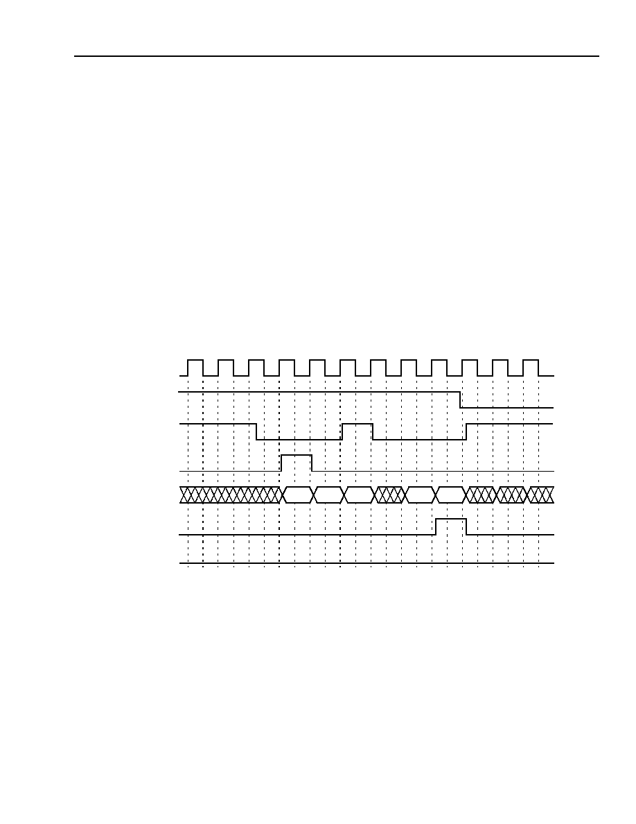
Agere Systems Inc.
91
Data Sheet
May 2001
155/622/2488 Mbits/s Data Interface
TDAT042G5 SONET/SDH
Functional Description
(continued)
UTOPIA (UT) Interface Block
(continued)
UT Receive Input Path (Ingress) (continued)
Figure 23 illustrates the receive-side interface handshaking when operating in point-to-point mode with the RxPA
response provisioned to be a single cycle. In two-cycle mode, the RxSOP, RxDATA, and RxPA signals are
delayed an additional cycle. In the figure, the master device initiates the transfer after observing an asserted
packet available for the channel. The TDAT042G5 samples RxENB low on the first cycle and then asserts
RxSOP/C and RxDATA on the second cycle. RxDATA is sampled on the rising edge of the second cycle by the
master device. Figure 24 illustrates receive-side interface handshaking when operating in two-cycle mode. When
operating in U3+ mode, two-cycle mode must be used.
In this example, the master stops transfer in the middle of the packet. Data with value c is valid on the cycle that
RxENB goes inactive, and when RxENB returns, data is again valid on the first cycle after the slave observes an
active RxENB (data value d).
The packet transfer is complete when the slave asserts the RxEOP signal. If an error occurs in the packet, then the
RxERR signal is asserted simultaneously with the RxEOP. RxERR is ignored if it is not asserted when RxEOP is
active.
5-7450(F).ar.2
Figure 23. Receive-Side Interface Handshaking in Point-to-Point, Single Cycle Mode
The packet transfer is complete when the slave asserts the RxEOP signal. If an error occurs in the packet, then the
RxERR signal is asserted simultaneously with the RxEOP. RxERR is ignored if it is not asserted when RxEOP is
active.
RxCLK
1
2
3
4
5
6
7
8
9
10
11
12
a
b
c
d
e
RxPA
RxENB
RxSOP/C
RxDATA[15:0]
RxEOP
RxERR
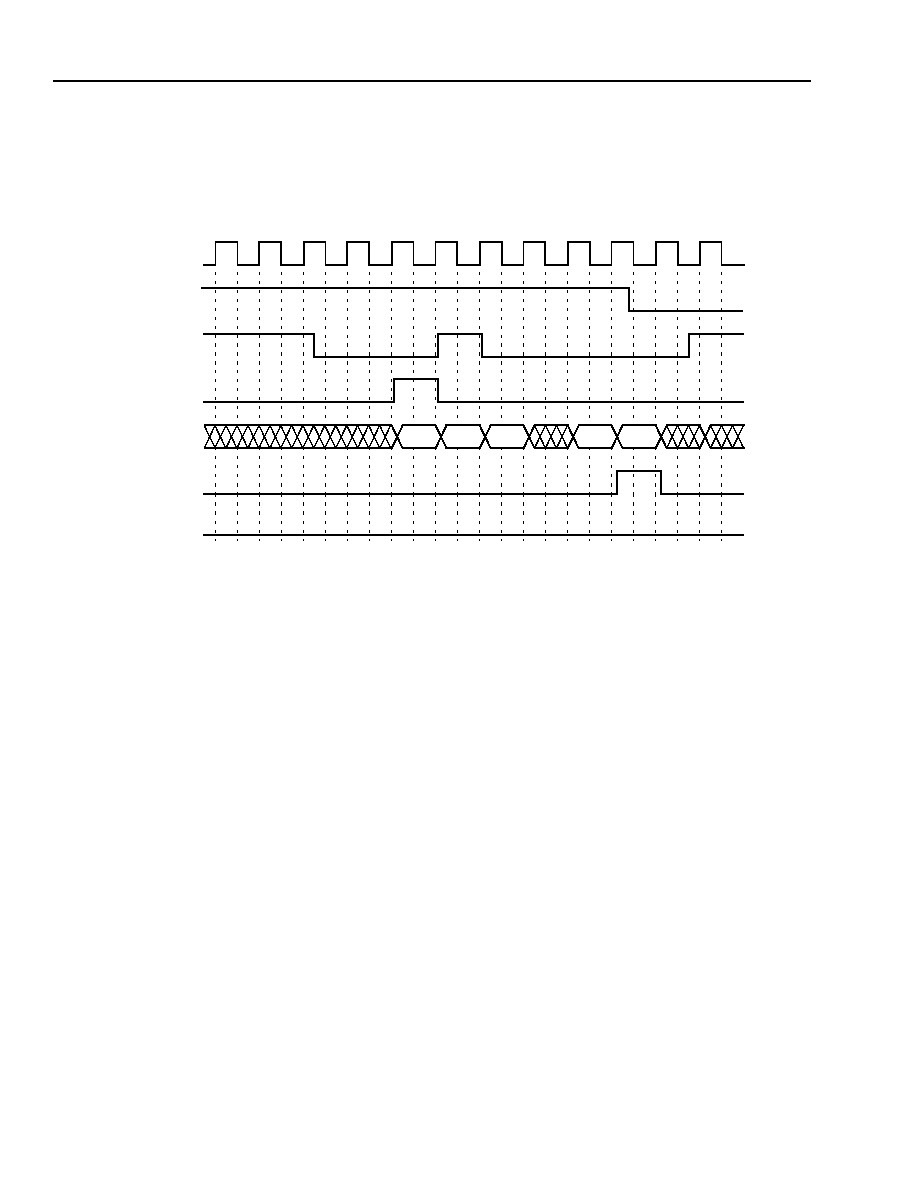
92
Agere Systems Inc.
Data Sheet
May 2001
155/622/2488 Mbits/s Data Interface
TDAT042G5 SONET/SDH
Functional Description
(continued)
UTOPIA (UT) Interface Block
(continued)
UT Receive Input Path (Ingress) (continued)
5-7450(F)br.1
Figure 24. Receive-Side Interface Handshaking in Point-to-Point, Two-Cycle Mode
RxCLK
1
2
3
4
5
6
7
8
9
10
11
12
a
b
d
RxPA
RxENB
RxSOP/C
RxDATA[15:0]
RxEOP
RxERR
c
e

Agere Systems Inc.
93
Data Sheet
May 2001
155/622/2488 Mbits/s Data Interface
TDAT042G5 SONET/SDH
Functional Description
(continued)
UTOPIA (UT) Interface Block
(continued)
UT Transmit Input Path (Egress)
In the transmit direction, data arrives from the various UTOPIA interfaces, and is stored in a 256-byte FIFO, one
per channel. After sufficient data has been stored into the FIFO, it is made available to be sent to the DE.
Like the UTOPIA Rx interface, the UTOPIA Tx interface is designed to accommodate ATM cells as well as packet
traffic. While the traditional UTOPIA interface only transfers ATM cells, this interface has been enhanced to carry
packet traffic. The interfaces supported include the following: UTOPIA Level 2 (U2), enhanced UTOPIA Level 2
(U2+), UTOPIA Level 3 (U3) in 4 x 8-bit mode or 32-bit mode, and enhanced UTOPIA Level 3 (U3+) in 4 x 8-bit
mode or 32-bit mode.
The UTOPIA Tx side can indicate to the ATM side to suspend the transfer, by deasserting TxPA, when necessary.
When the amount of data in the FIFO exceeds its programmable high watermark, it deasserts TxPA. This signal
causes the deassertion of TxPA on the next clock. At this point, the ATM side knows that the UTOPIA Tx block can
only accept a limited number of words, after which it will overflow. In this case, the ATM device must not exceed
writing this limited number of words before suspending the transfer. Transfer is resumed once again when the
FIFO falls below the high watermark. When transferring ATM cells, TxPA must be deasserted four clocks before
the end of cell, or else it must be prepared to accept an entire new cell. When transferring ATM cells, deasserting
TxPA does not immediately suspend the transfer of the current cell because the entire cell can be transmitted with-
out interruption.
Transmit Cell/Packet Available (TxPA). This signal indicates when the TDAT042G5 transmit FIFO can accept
data from the master device. If the FIFO is empty or more than the provisioned space is available in the FIFO,
TxPA[D:A] is set active.
I
One-Cycle Delay Mode. This mode follows the UTOPIA Level 2 Standard. The TxPA response occurs one cycle
after the address is polled.
I
Two-Cycle Delay Mode. This mode follows the UTOPIA Level 3 baselined text*. The TxPA response occurs two
cycles after the address is polled.
I
TxPA[D:A] Assertion. The TxPA[D:A] signal behavior relies on the UTOPIA provisionable watermarks. In
packet mode, TxPA[D:A] goes high when the amount of data in the FIFO is less than the high watermark setting.
In ATM mode, TxPA[D:A] goes high when the FIFO has space to receive a complete ATM cell from the master.
(This requires the high threshold to be set appropriately by the user, i.e., set so that an entire cell can be
received once TxPA[D:A] goes active.)
I
TxPA[D:A] Deassertion. In packet mode, TxPA[D:A] goes low when the amount of data in the FIFO reaches or
exceeds the high watermark. In ATM mode, TxPA[D:A] goes low when there is not enough space in the FIFO to
receive an entire ATM cell. (This requires the threshold values to be provisioned properly, i.e., set low enough
such that when the high watermark is reached, the transmission of the current cell can be completed without
overflowing the FIFO). In ATM mode, TxPA[D:A] will be deasserted four cycles before the end of the current cell
transfer if the FIFO cannot accept a complete ATM cell on the following transmission.
TxPA[D:A] is updated on the rising edge of TxCLK[D:A].
In 32-bit mode, only the TxPA[A] pin of port A is used to indicate the packet/cell available status.
I
MPHY Support. When the TxPA signals are used for multi-PHY (MPHY) direct status, the corresponding
TxCLK[B, C, and/or D] must be provided. This clock will be the same as TxCLK[A].
* ATM Forum Technical Committee, UTOPIA Level 3, STR-PHY-UL3-01.00, July 1999.
94
Agere Systems Inc.
Data Sheet
May 2001
155/622/2488 Mbits/s Data Interface
TDAT042G5 SONET/SDH
Functional Description
(continued)
UTOPIA (UT) Interface Block
(continued)
UT Transmit Input Path (Egress) (continued)
FIFO. The UTOPIA Tx FIFO is used to create an elastic store that can buffer bursts of data received via the UTO-
PIA Tx, faster than can be transmitted out of the path. After the FIFO exceeds a programmable watermark, it indi-
cates to the UTOPIA Tx master to stop sending data. The master can choose to ignore this request causing the
risk of an overflow. The FIFO block buffers 256 bytes of cell/packet data. The FIFO accommodates four ATM cells
or 256 bytes of packet data. The FIFO is required to manage the asynchronous nature of the UTOPIA interface.
Optionally, in the case of FIFO underflow, a 0x7D207D207D20 . . . will be inserted by the data engine into the mid-
dle of the packet if dry mode is provisioned and the default dry escape sequence is used (0x7D20, where the last
two bytes (the 20 bytes of the default value of 0x7D20) are provisionable). This will be removed at the far end by
the device (provided the link is comprised of two devices and both sides of the link support dry mode).
I
FIFO Watermark Threshold. When carrying ATM cell traffic, this threshold, while measured in words, should be
set at least one cell's length from end of FIFO. The UTOPIA Tx interface, by definition, must be able to accept an
entire ATM cell after the current ATM cell, unless TxPA is deasserted at least four clock cycles before the end of
the current cell transfer.
When carrying packet traffic, however, the threshold can be set higher, as the UTOPIA Tx interface only needs
to accept a limited number of words after deasserting TxPA. The number of words is a programmable value for
the sender, and should be assumed to be at least 2 words for the purposes of setting the threshold.
FIFO high watermark threshold, EGRESS_WATERMARK_HIGH_[A--D][6:0] (addresses 0x0212, 0x0216,
0x021A, 0x021E), should be set as follows.
Table 29. Egress High Watermark Thresholds
Note: The high watermark threshold should be set less than the values in the above table assuming there is no
delay between TxPA deassertion and TxENB deassertion. Then the threshold values may be changed to
optimize UT egress performance and to avoid FIFO overflow.
UTOPIA Mode
Maximum Threshold Value
8-bit, U3+
0x3D
16-bit, U2+
0x3B
32-bit, U3+
0x37
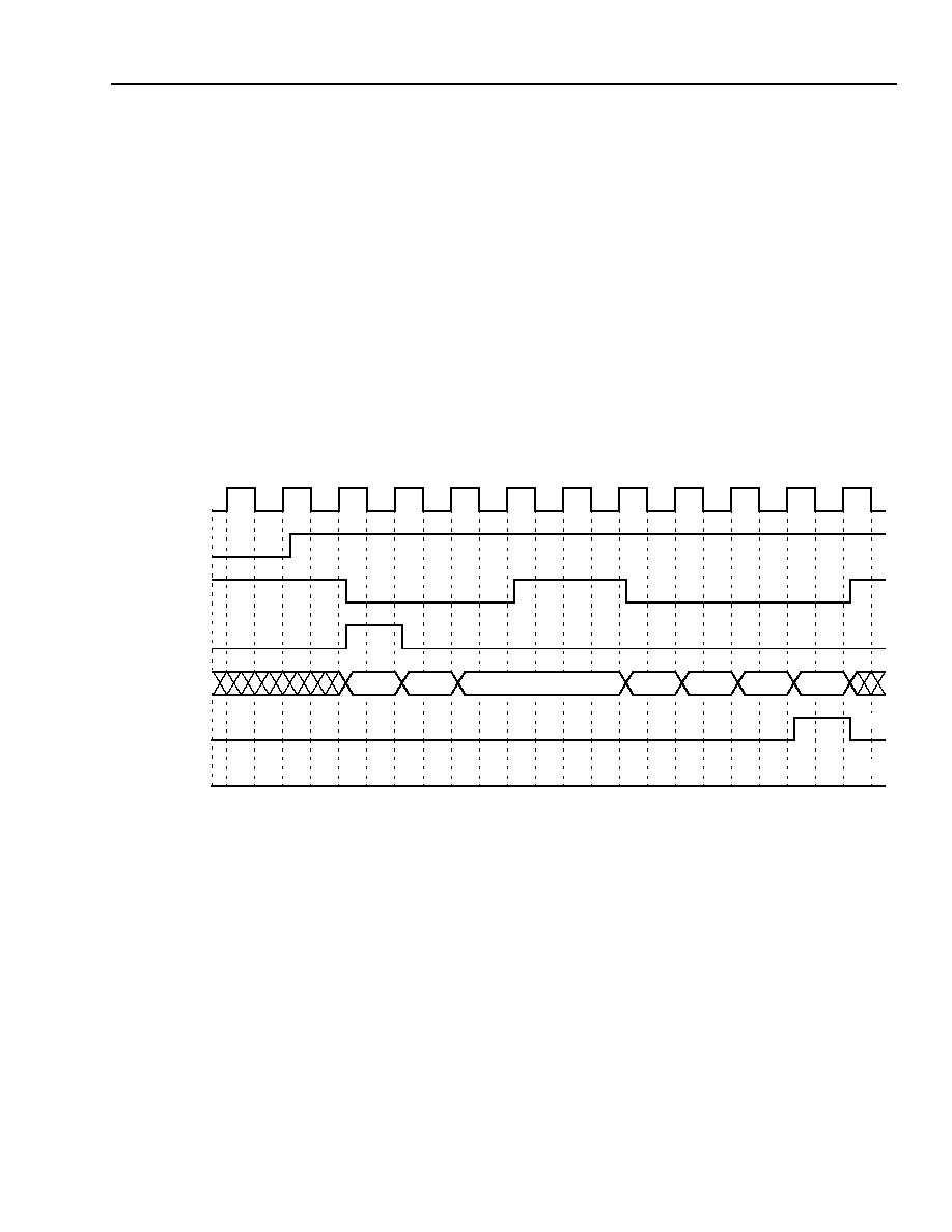
Agere Systems Inc.
95
Data Sheet
May 2001
155/622/2488 Mbits/s Data Interface
TDAT042G5 SONET/SDH
Functional Description
(continued)
UTOPIA (UT) Interface Block
(continued)
UT Transmit Path (Egress) (continued)
Figure 25 illustrates the transmit-side interface handshaking when operating in point-to-point mode with the TxPA
response provisioned to be a single cycle. In two-cycle mode, the TxPA signal is delayed an additional cycle. In the
figure, the master device initiates the transfer after observing an asserted packet available for the channel by
asserting the TxENB signal. The master places data and start of packet on the bus the same cycle as TxENB, and
the TDAT042G5 samples the TxSOP and TxDATA on the following clock cycle (rising edge).
In this example, the master stops transfer in the middle of the packet. Data with value c is valid on the cycle that
TxENB goes inactive, and when TxENB returns, data is again valid on the first cycle (data value d).
The packet transfer is complete when the master asserts the TxEOP signal. If an error occurs in the packet, then
the TxERR signal is asserted simultaneously with the TxEOP. TxERR is ignored if it is not asserted when TxEOP
is active.
5-7457(F).ar.2
Figure 25. Transmit-Side Interface Handshaking in Point-to-Point, Single Cycle Mode
TxCLK
1
2
3
4
5
6
7
8
9
10
11
12
a
b
c
d
e
f
g
TxPA
TxENB
TxSOP/C
TxDATA[15:8]
TxEOP
TxERR
96
Agere Systems Inc.
Data Sheet
May 2001
155/622/2488 Mbits/s Data Interface
TDAT042G5 SONET/SDH
Functional Description
(continued)
UTOPIA (UT) Interface Block
(continued)
Multi-PHY Support
In addition to point-to-point UTOPIA mode, the TDAT042G5, as the slave device, can also be configured to support
the polled multi-PHY mode. To operate in multi-PHY mode, channel A must be configured in the polling mode,
since the control signals of channel A are used for all channels. Any combination of B, C, or D can be included in
the polling group, in which case they provide control information to channel A. Channels B, C, and D also can be
configured in any of the UTOPIA modes. In this case, the output is transferred through the channel A interface
(channel A and B interfaces for 32-bit mode). Channels not configured for polling can be operated as point-to-point
connections. If channel A is in 32-bit polling mode, channel B cannot be in point-to- point mode since its interface is
controlled by channel A, while channels C and D may be provisioned as point-to-point connections.
Figure 26 shows a multi-PHY mode when all four channels of the UT are in polling mode.
5-7349(F)r.2
Figure 26. Multi-PHY Configuration of All Four Channels
Mixed mode polling is also possible. For example, for those channels operated in polling mode, it is legitimate for
some of the channels to be in packet mode while others are in ATM mode. However, if one or more of the channels
are in packet mode, channel A should be configured as packet mode to activate control signals for packet transfer.
Multi-PHY operation can be configured by asserting the polling mode enable bit and Tx/Rx address in the respec-
tive port provisioning registers (see port provisioning registers, pages 158--161). Microprocessor provisionable
registers in each channel include a polling mode enable bit and 5-bit Rx address or 5-bit Tx address. The value for
the Tx and Rx address of an MPHY channel must be identical. Both the Rx and Tx directions have a 5-pin address
input to poll and select the appropriate PHY.
INGRESS CHANNEL A
UTOPIA _PHY_Rx
UTOPIA _PHY_Rx
UTOPIA _PHY_Rx
UTOPIA _PHY_Rx
UTOPIA _PHY_Tx
UTOPIA _PHY_Tx
UTOPIA _PHY_Tx
UTOPIA _PHY_Tx
µ
P
RxPA[A]/RxDATA[A]
RxENB[A]/RxADDR
RxPA[B]
RxPA[C]
RxPA[D]
TxPA[A]
TxENB[A]/TxDATA[A]/TxADDR
TxPA[B]
TxPA[C]
TxPA[D]
INGRESS CHANNEL B
INGRESS CHANNEL C
INGRESS CHANNEL D
EGRESS CHANNEL A
EGRESS CHANNEL B
EGRESS CHANNEL C
EGRESS CHANNEL D

Agere Systems Inc.
97
Data Sheet
May 2001
155/622/2488 Mbits/s Data Interface
TDAT042G5 SONET/SDH
Functional Description
(continued)
UTOPIA (UT) Interface Block
(continued)
Multi-PHY Support (continued)
In 8-bit or 16-bit multi-PHY mode, only the data bus and the control signals (except the RxPA or TxPA signal) of
channel A are active for the polled group. RxPA[A] indicates the packet/cell availability of the selected or polled
channel. Similarly, TxPA[A] indicates transmit FIFO availability for a selected or polled channel. The remaining
RxPA/TxPA signals for the polled channels are activated and indicate instantaneous or direct status of the particu-
lar channel. In 32-bit multi-PHY mode, the data bus and size control signals of channel B are also active.
TDAT042G5 does not provide a selected packet available (SPA) signal to monitor the status of the current channel
sending/receiving data to or from the master. To prevent the FIFOs from running dry or overflowing in the middle of
a packet transfer, the user must design the UT TDAT042G5 slave-to-master interface with direct status mode
rather than address polling. The direct status of each channel is provided on the associated SPA pin for that chan-
nel. In this mode, the user must guarantee that when channels are switched to receive data from a channel other
than channel A, they immediately reapply the address of channel A to the address bus after the new channel is
selected. The user then gets the direct status SPA signal from channel A. Channels B, C, and D are always directly
sent out of the TDAT042G5. In either receive or transmit, when direct status is used in addition to the direct status
pin for a given interface, its corresponding interface clock pin must be driven by the clock of the A interface.
During the cycle when the selected channel is being changed, the address of the new channel is placed on the
address bus. The user must ignore the RxPA response of the initial channel during the expected response time
(one or two cycles later, depending on the PA response bit when the address of the newly selected channel was
applied).
Figure 27 illustrates the transmit interface timing for the case when the direct status of packet available of channels
A, B, C, and D is present. In this example, channels A and C indicate they can receive data. When the SPA signal
for C is observed, a channel switch is performed by the master by deasserting TxENB and placing the address of
channel C on the address bus. On the following cycle, data is placed on the bus along with the start of packet. In
this example, the TxPA response is configured for two cycles so that the PA response of address 02 results in the
PA of channel C to appear on channel A's output two clock cycles later. Subsequent data sent to the slave will go
to channel C (i.e., data values I, J, etc.).
When the RxPA signals are used for multi-PHY (MPHY) direct status, the corresponding RxCLK[B, C, and/or D]
must be provided. They may be provided via an external UT master, or they may be sourced from the correspond-
ing TxCLK[D:A] pin by using the UT clock source mode (see UT Clocking, page 88).
98
Agere Systems Inc.
Data Sheet
May 2001
155/622/2488 Mbits/s Data Interface
TDAT042G5 SONET/SDH
Functional Description
(continued)
UTOPIA (UT) Interface Block
(continued)
Multi-PHY Support (continued)
5-7933(F).ar.3
Figure 27. TxPA Two-Cycle Responses of a Multi-PHY for All Four Channels
A
C
E
G
I
K
M
O
Q
B
D
F
H
J
L
N
P
R
11
00
02
00
00
00
00
02
00
1
2
3
4
5
6
7
8
9
10
11
T
X
CLK[A]
T
X
ADDR
T
X
PA[A]
T
X
PA[B]
T
X
PA[C]
T
X
PA[D]
T
X
ENB[A]
T
X
SOP/C[A]
T
X
DATA[A][15:0]
T
X
EOP[A]
T
X
DATA[B][15:0]
T
X
SIZE[A, B]
HIGH Z
HIGH Z
HIGH Z
HIGH Z
HIGH Z
HIGH Z
Agere Systems Inc.
99
Data Sheet
May 2001
155/622/2488 Mbits/s Data Interface
TDAT042G5 SONET/SDH
Functional Description
(continued)
UTOPIA (UT) Interface Block
(continued)
Multi-PHY Support (continued)
The ATM side sends one RxENB (TxENB) signal to channel A for the grouped channels to select a channel which
has ATM cells/packets (or room) available. An MPHY channel is selected using the following procedures.
1.The ATM layer polls the RxPA[D:A] (TxPA[D:A]) status of a channel by placing its address on the RxADDR[4:0]
(TxADDR[4:0]) lines.
2.In the following cycle, the MPHY channel gives its status by driving RxPA[D:A] (TxPA[D:A]) of channel A.
3.The ATM side selects the MPHY channel by placing the desired MPHY address on the address bus
RxADDR[4:0] (TxADDR[4:0]) during this cycle; RxENB[D:A] (TxENB[D:A]) is deasserted.
4.During the next cycle, the ATM side asserts RxENB[D:A] (TxENB[D:A]), and the selection of an MPHY channel is
made.
Only one MPHY channel at a time is selected for a cell/packet transfer when ATM drives RxENB (TxENB) for
channel A from high to low. However, another MPHY channel can be polled for its RxPA (TxPA) status while the
selected channel transfers data.
Figure 28 shows an example of the single-cycle RxPA response of each channel. In this figure, channels A, B, C,
and D have Rx addresses 00, 01, 02, and 03, respectively. RxPA[A] shows the packet availability of all four chan-
nels. Channels A and C have available packets to send, and channels B and D do not have packets to send. By
driving RxENB[A] low at clock edge 1, the ATM side selects channel A, and packet transfer is started at
clock edge 2. The master samples this data at clock edge 3. At clock edge 4, RxPA[C] shows that channel C also
has a packet to send, and this is reflected to RxPA[A] at clock edge 5. RxPA[B] and RxPA[D] show the direct status
of channels B and D, indicating that they do not have packets to send.
5-7348(F)r.2
Figure 28. RxPA Responses of a Multi-PHY for All Four Channels
(PA Response Configured for One Cycle)
1
2
3
4
5
6
7
8
9
10
11
00
P1P2
P17P18
01
1F
01
1F
02
1F
03
1F
00
1F
P3P4
P5P6
P7P8
P9P10
P11P12
P13P14
P15P16
00
01
02
03
00
R
X
CLK[A]
R
X
ADDR
R
X
DATA[A]
R
X
SOP/C[A]
R
X
EOP[A]
R
X
SZ[A]
R
X
ENB[A]
R
X
PA[C]
R
X
PA[B]
R
X
PA[A]
R
X
PA[D]
HIGH Z
HIGH Z
HIGH Z
HIGH Z
HIGH Z
HIGH Z
HIGH Z
HIGH Z
HIGH Z

100
Agere Systems Inc.
Data Sheet
May 2001
155/622/2488 Mbits/s Data Interface
TDAT042G5 SONET/SDH
Functional Description
(continued)
JTAG (Boundary-Scan) Test Block
The JTAG test block provides an IEEE 1149.1 JTAG controller interface for memory BIST, boundary scan, and
32-bit ID register instructions. Details about JTAG (boundary-scan) functionality and interface timing specifications
can be found in MN98-060ASIC-02, HL250C 3.3 Volt 0.25
µ
m CMOS Standard-Cell Library Manual, page 8-1
through page 8-31.
The instruction register length is 3 bits.
Reset of JTAG Logic
There are two events that will reset the JTAG logic:
I
Pulse or pull the TRST pin signal low with no TCK pin signal present. TRST is pulled high on-chip.
I
The TMS pin signal is driven high for five cycles of TCK. TMS is pulled high on-chip.
TRST can be held high during normal device operation only if TRST is pulled low upon powerup.
Line Interface
LVPECL I/O Termination and Load Specifications
The LVPECL buffers are compatible with the temperature independent ECL 100K levels, but the output levels that
are guaranteed are relaxed 30 mV from the actual 100K levels allowing for noise and variations in the power sup-
ply and process.
All LVPECL output buffers require a terminating resistor. These terminating resistors, which must also be con-
nected to both LVPECLREFHI and LVPECLREFLO, go to a common terminating voltage. All of the terminating
resistors used with a chip must be identical precision (1%) resistors. The value of these terminating resistors is
usually chosen to match the characteristic impedance of the board. To save on power, a terminating voltage equal
to V
DDD
≠ 2 V is available in most ECL systems. The minimum value of the terminating resistor that can be used on
these bufers is 50
. This is also the standard termination used in most ECL systems. Larger values of resistance
will save power, but will also slow down the high-to-low transition of the output, since it is RC limited.
if no V
DDD
≠ 2 V supply is available, a larger value resistor may be connected directly to GND. It should be chosen
such that the current through it does not exceed the current through a 50
resistor to V
DDD
≠ 2 V (21 mA in the
high state). This large resistor will most likely be a poor match to the board impedance. The match can be
improved by the user of a Thevenin equivalent resistor pair. Such a Thevenin equivalent resistor will burn much
more system power (but not on-chip power) than would a single resistor, but it does allow for impedance matching
in the absence of aV
DDD
≠ 2 V supply. Termination resistor options are shown in Table 30.
Experienced ECL designers sometimes use the (bipolar) ECL output buffers in a tied-OR configuration. Unfortu-
nately, this cannot be done with these LVPECL buffers.
Table 30. Nominal dc Power for Suggested Terminations
Note: The value is the average of the high and low states in LVPECL output buffer and external terminating resis-
tors, for a single-ended output. The values double for double-ended outputs.
Terminating Resistor and Voltage
Output Transistor (on-chip)
Power (mW)
Terminating Resistor (off-chip)
Power (mW)
50
to V
DDD
≠ 2 V
1
1.
Standard ECL termination (parallel).
15
13
125
to V
DDD
and 83
to GND
2
2.
Thevenin equivalent or 50
to V
DDD
≠ 2 V.
15
52
Agere Systems Inc.
101
Data Sheet
May 2001
155/622/2488 Mbits/s Data Interface
TDAT042G5 SONET/SDH
Line Interface
(continued)
LVPECL I/O Termination and Load Specifications
(continued)
The input common mode range for LVPECL differential buffers is from 1 V to 2.75 V; and the swing needs to be at
least 300 mV. So basically what it means is the lowest voltage on the input should be no lower than (1 V ≠ 0.150 V)
and the highest voltage on the input shouldn't be more than (2.75 V + 0.150 V). So if the differential swing is
800 mV, then the common mode range would be 2.5 V down to 1.25 V. This is all for 3 V buffers.
Interface Description
Microprocessor Interface
This device is equipped with a generic 16-bit microprocessor interface that allows operation with most commer-
cially available microprocessors. Input MPMODE is used to configure this interface into one of two possible modes
(synchronous or asynchronous). In synchronous mode, the microprocessor interface can operate at speeds from
1 MHz up to 66 MHz.* In asynchronous mode, the internal 78 MHz system clock is used to operate this interface.
Table 31. MPU Modes
The host interface is designed to connect directly to a commonly used asynchronous or synchronous host bus.
The interface to this block includes a separate clock, MPCLK, which is used in the synchronous interface mode.
The interface is only a slave on the host bus. There is no posting of writes in the host interface; all registers are
directly accessible. The microprocessor interface pins use 3.3 V (5 V, TTL-tolerant) CMOS I/O levels. The micro-
processor interface timing specifications are given in the Interface Timing Specifications section (see Table 163--
Table 166, pages 257--263).
* All status counters must be read within the 1-second time window of the PMRST. If this is not the case, counter values will be l ost.
MPMODE
Mode
Microprocessor Interface Signals
0
Async
CS, INT, D[15:0], A[15:0], ADS, R/W, DS, DT
1
Sync
MPCLK, CS, INT, D[15:0], A[15:0], ADS, R/W, DT
102
Agere Systems Inc.
Data Sheet
May 2001
155/622/2488 Mbits/s Data Interface
TDAT042G5 SONET/SDH
Interface Description
(continued)
General-Purpose I/O Bus (GPIO)
GPIO[3:0] are bidirectional pins. They can be configured individually as input or output by writing to the GPIO mode
and GPIO output configuration registers (addresses 0x0013, 0x0014, 0015; see register descriptions, page 152).
The value to be output is written into the GPIO output register (address 0x000F; see register descriptions,
page 150). To use the GPIO pins as outputs, set the GPIO output configuration bits (bits 8 and 0) to 1, and set the
GPIO mode bits GPIO[3:0]_DIRECTION_ I/O (address 0x0013, bits [3:0]) to 1.
The input value is read from the GPIO input register (address 0x000A; see register description, page148). GPIO
pins can also be used to generate an interrupt upon a change in value. An interrupt can be generated on either the
input level or edge, depending on the GPIO mode register. Figure 29 shows how the GPIO functions.
5-7058(F)r.6
Figure 29. GPIO Functionality
If a GPIO pin is an input, the logic value on the pin can be read from a software register. The GPIO pin can also be
programmed to generate a level-sensitive interrupt or a positive edge-triggered interrupt contributing to the external
interrupt pin.
If a GPIO pin is an output, the value provisioned will appear on the device pin immediately.
0000
DEVICE VERSION
0001
0002
0003
DEVICE NAME =
0004
0005
0008
COMPOSITE INTERRUPTS
000A
GPIO INPUTS
000C BLOCK INTERRUPT MASKS
000E
CORE RESETS
000F
GPIO OUTPUTS
0010
LINE PROVISIONING
0011
CHANNEL CONTROL
0012
LOOPBACK CONTROL
0013
GPIO MODE
001F
SCRATCH
3 2 1 0
3 2 1 0
2 1 0
3 2 1 0
3 2 1 0
3 2 1 0
3
INTERRUPTS
GPIO INPUTS
GPIO OUTPUTS
GPIO MODE
POS.
EDGE
DET.
0
1
2
3
+
GPIO[3:0]
ACTIVE
LEVEL EDGE
DIRECTION
TDAT042G5
CORE REGISTERS
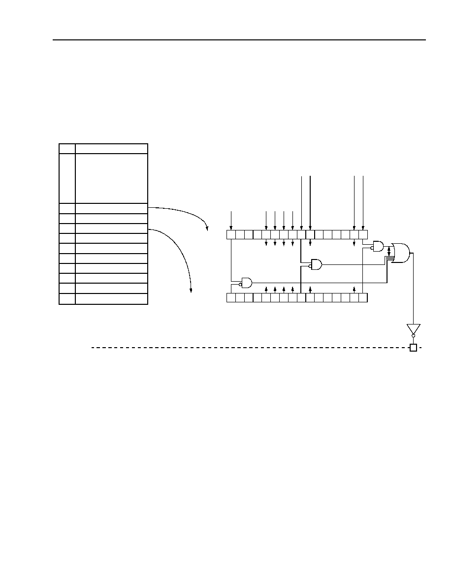
Agere Systems Inc.
103
Data Sheet
May 2001
155/622/2488 Mbits/s Data Interface
TDAT042G5 SONET/SDH
Interface Description
(continued)
Interrupts
Interrupt requests can be read from the composite interrupts register (0x0008; see register description, page 148).
There is also a corresponding block interrupt masks register (0x000C; see register description, page 149). Any
unmasked request will cause the INT pin to go low. GPIO interrupt functionality is shown in Figure 30.
5-7059(F)r.5
Figure 30. Interrupt Functionality
INTERRUPTS
BLOCK INTERRUPT MASKS
INT
3
2
1
0
3
2
1
0
PM
UT DE
OH
PT
PM INTERRUPT
(GPIO)
INT
E
RRUPT
(
U
T
)
INT
E
RRUPT
(
D
E)
INT
E
RRUPT
(
O
HP)
INT
E
RRUPT
(
P
T
)
0000
DEVICE VERSION
0001
0002
0003
DEVICE NAME =
0004
0005
0008
COMPOSITE INTERRUPTS
000A
GPIO INPUTS
000C BLOCK INTERRUPT MASKS
000E
CORE RESETS
000F
GPIO OUTPUTS
0010
LINE PROVISIONING
0011
CHANNEL CONTROL
0012
LOOPBACK CONTROL
0013
GPIO MODE
001F
SCRATCH
TDAT042G5
CORE REGISTERS
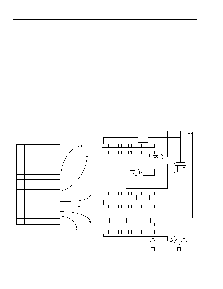
104
Agere Systems Inc.
Data Sheet
May 2001
155/622/2488 Mbits/s Data Interface
TDAT042G5 SONET/SDH
Interface Description
(continued)
Reset
If the reset pin RST (C7) is forced low, the software registers will be placed in their default powerup state. The
device will lose its previous state, and data path continuity will be lost. An internal 100 k
pull-up and a Schmitt-
trigger input is provided for this pin. Reset can be generated from software by writing 0x0005 to the core resets reg-
ister (0x000E; see register description on page 149 and timing on page 263).
Performance Monitor Reset (PMRST)
A 1 Hz clock (PMRST) is provided to all internal macrocells. This clock is used to control the 1-second binning of
coding violations (CVs) and alarms. The source of this clock is selectable from one of the three following sources:
I
The PMRST pin (D7)
I
A software controllable register (0x000E; see register description on page 149)
I
An internal 1-second counter (sourced from the 77.76 MHz transmit clock).
This is configured by the line provisioning register (address 0x0010). When under software control, writing 0x0080
to core resets register (address 0x000E) will generate a PMRSTX pulse.
5-7060(F)r.4
Figure 31. Miscellaneous Functionality
R R R
12 12 12
D
C
B
D
L B
B
B
L
12
INTERRUPTS
CORE RESETS
LINE PROVISIONING
LINE EQ./UNEQ.
LOOPBACKS
RST
DELTA
POS.
EDGE
DET.
C
B
L
A
B
L
A
15 14 13 12 11 10 9 8 7 6 5 4 3 2 1 0
11
10
9
8
7 6 5 4 3 2 1 0
P M S
48
PM
ARST
PMRST
1 SEC.
COUNT
PM
RS
TX
MO
D
E
[
1
1:
0
]
L
B
[
11:
0]
0000
DEVICE VERSION
0001
0002
0003
DEVICE NAME =
0004
0005
0008 COMPOSITE INTERRUPTS
000A
GPIO INPUTS
000C BLOCK INTERRUPT MASKS
000E
CORE RESETS
000F
GPIO OUTPUTS
0010
LINE PROVISIONING
0011
CHANNEL CONTROL
0012
LOOPBACK CONTROL
0013
GPIO MODE
001F
SCRATCH
TDAT042G5
CORE REGISTERS
15
PMRST I/O CONTROL

Agere Systems Inc.
105
Data Sheet
May 2001
155/622/2488 Mbits/s Data Interface
TDAT042G5 SONET/SDH
Interface Description
(continued)
Performance Monitor Reset (PMRST)
(continued)
Address 0x0010, bits 8 and 9 of the core register set defines the mode of operation for PMRST. Address 0x000E,
bit 7 provides the software-controllable reset function (see Register Maps section, page 112). When this bit is set
to 1, the PMRST signal goes high. The register will automatically be reset to 0, and the PMRST signal will go low
after 500 ms.
Table 32. PMRST Provisioning
Core Register
ADDR 0x0010, Bits 9, 8
Description
00
PMRST comes from external pin (1 Hz, 50% duty cycle signal).
01
PMRST comes from internal 1-second counter (1 Hz, 50% duty cycle signal).
Writing a logic 1 to the PMRST bit (core register 0x000E, bit 7) in this mode will
reset the counter so that a 0
1 transition occurs on the PMRST within 10 clock
cycles of the 77.76 MHz clock.
11
PMRST is software controlled. Writing a logic 1 to the PMRST bit (core register
0x000E, bit 7) will cause a 0
1 transition on the internal PMRST signal. This
pulse will be high for 100 cycles of the 77.76 MHz clock and low for 100 cycles of
the 77.76 MHz clock. Writing the PMRST bit to a logic 1 during this 200 clock
cycle interval will have no effect (2.57
µ
s). The PMRST rising edge must occur
within 10 clock cycles of writing the PMRST bit.
106
Agere Systems Inc.
Data Sheet
May 2001
155/622/2488 Mbits/s Data Interface
TDAT042G5 SONET/SDH
Interface Description
(continued)
Loopback Operation
Figure 32 illustrates the different types of loopback provided in the device. Loopback is controlled by core register
0x0012, loopback control (see register description on page 151).
5-7061(F)r.4
Figure 32. Loopback Operation
In the following description, only the data path from Terminal A to B is discussed, but the same terms apply to the
reverse direction.
Near-End Loopback
The packet/cell payload is looped back to the data source (Layer 2 device) as soon as it crosses the Layer 1 to
Layer 2 boundary (UTOPIA block).
Far-End Loopback
The packet/cell payload is looped back to the facility (optical) data source as soon as it enters the UTOPIA block of
Terminal B. The data does not enter the Layer 2 device. The total delay from receive data input to transmit data
output in far-end loopback (FELB) mode is approximately 2
µ
s.
Terminal Loopback
The SONET/SDH signal is looped back at the terminal (line interface) block, and is returned to the Layer 2 device.
For terminal loopback of UTOPIA ports B, C, or D to function, UTOPIA port A must be provisioned for terminal loop-
back. This is because only the Tx clock from port A is used in terminal loopback mode.
Facility Loopback
The facility (optical) data signal is looped back to the facility as soon as it enters the Terminal B line interface block.
SONET facility loopback is only available in STS-3/STM-1 and STS-12/STM-4 modes.
LAY
E
R 2
UT
DE
PT
OHP
LI
NE
CONT
OP
T
I
C
S
TERMINAL B
LAY
E
R 2
UT
DE
PT
OHP
LI
NE
CONT
OP
TI
CS
TERMINAL A
S
O
URC
E
FAR
END
SINK
FACILITY
TERMINAL
NEAR
END
FACILITY
(OPTICS)
IN
T
E
R
F
A
C
E
IN
T
E
R
F
A
C
E
Agere Systems Inc.
107
Data Sheet
May 2001
155/622/2488 Mbits/s Data Interface
TDAT042G5 SONET/SDH
Interface Description
(continued)
System Interfaces
ATM Interfaces
5-6750(F)r.3
* RxCLK may be either sunk or sourced, depending upon the application.
The transmit and receive signals for channels B, C, and D of the TDAT042G5 device are mapped to the remaining three ATM devices as
shown above.
Figure 33. Quad ATM UTOPIA 2
For the quad ATM UTOPIA 3 eight-bit interface mode, where the ATM device has only an 8-bit interface, the
RxDATA[15:0] and TxDATA[15:0] words are replaced with RxDATA[15:8] and TxDATA[15:8] in each channel of the
TDAT042G5. This is shown in the following table.
Table 33. Quad ATM UTOPIA 3 Interface
TDAT042G5 Channel
ATM Device
TxDATA[15:8][A]
RxDATA[15:8][A]
TxDATA[7:0]
RxDATA[7:0]
Same signals for channel [B]
Same signals for device #2
Same signals for channel [C]
Same signals for device #3
Same signals for channel [D]
Same signals for device #4
DEVICE #2
DEVICE #3
DEVICE #4
TxCLK
ATM DEVICE
TxENB
TxCLAV
RxCLK
TxPRTY
TxSOC
RxENB
RxCLAV
RxDATA[15:0]
RxPRTY
RxSOC
TxDATA[15:0]
TxCLK[A]
TxENB[A]
TxPA[A]
RxCLK[A]*
TxPRTY[A]
TxSOP/C[A]
RxENB[A]
RxPA[A]
RxSZ[A]
RxPRTY[A]
RxSOP/C[A]
TxDATA[15:0][A]
[B]
[B]
[C]
[C]
[D]
[D]
TDAT042G5
TxSZ[A]
TxEOP[A]
TxERR[A]
RxDATA[15:0][A]
RxEOP[A]
RxERR[A]
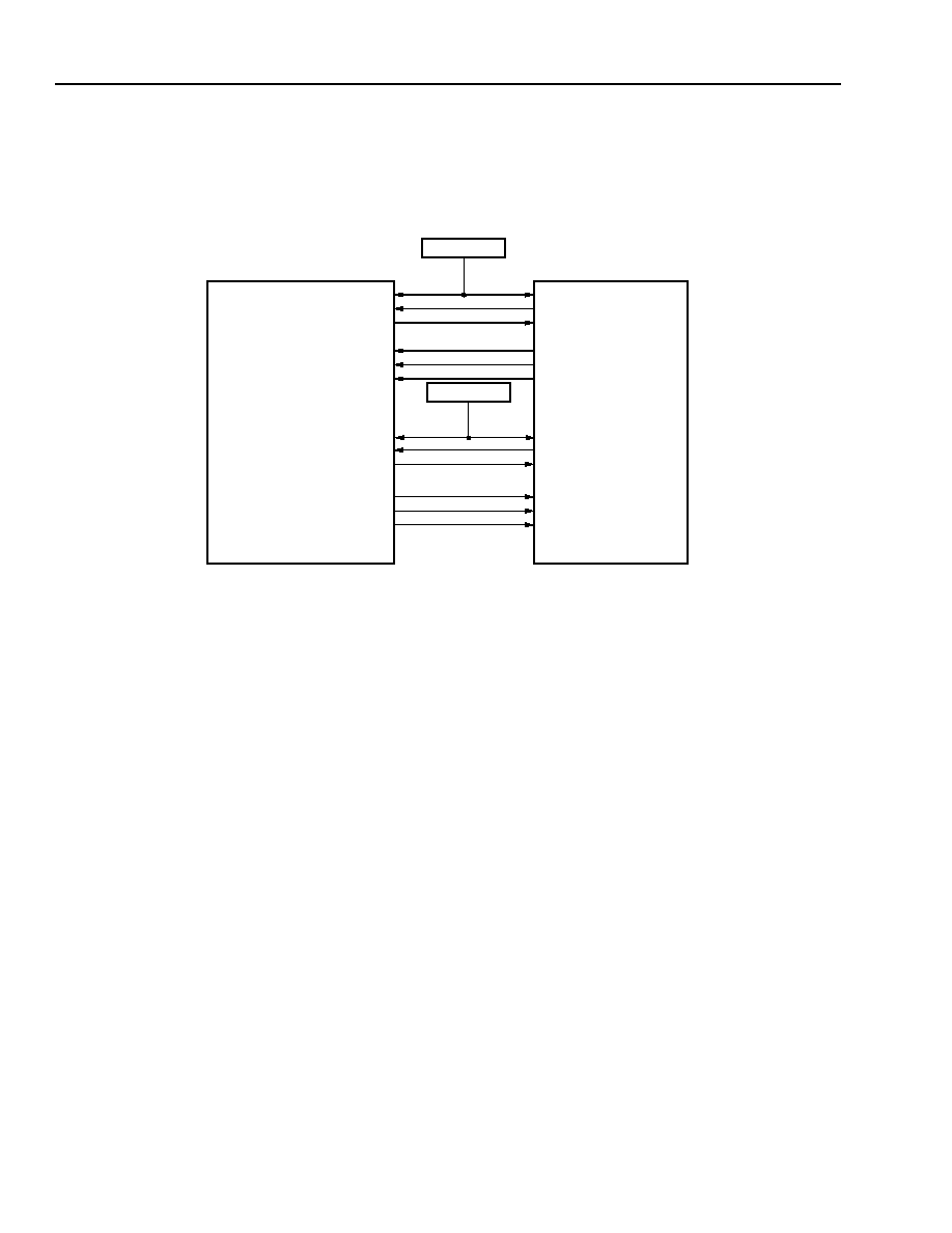
108
Agere Systems Inc.
Data Sheet
May 2001
155/622/2488 Mbits/s Data Interface
TDAT042G5 SONET/SDH
Interface Description
(continued)
System Interfaces
(continued)
ATM Interfaces (continued)
5-6740(F)r.5
* RxCLK may be either sunk or sourced, depending upon the application.
Figure 34. Single ATM UTOPIA 3
TxCLK
ATM DEVICE
TxENB
TxCLAV
RxCLK
TxPRTY
TxSOC
RxENB
RxCLAV
RxDATA[31:0]
RxPRTY
RxSOC
TxDATA[31:0]
TxCLK[A]
TxENB[A]
TxPA[A]
RxCLK[A]*
TxPRTY[A]
TxSOP/C[A]
RxENB[A]
RxPA[A]
RxSZ[A]
RxPRTY[A]
RxSOP/C[A]
TxDATA[15:0][A:B]
TDAT042G5
TxSZ[A:B]
TxEOP[A]
TxERR[A]
RxDATA[15:0][A:B]
RxEOP[A]
RxERR[A]
T
X
CLOCK
R
X
CLOCK

Agere Systems Inc.
109
Data Sheet
May 2001
155/622/2488 Mbits/s Data Interface
TDAT042G5 SONET/SDH
Interface Description
(continued)
System Interfaces
(continued)
POS Interfaces
5-6741(F)r.7
* RxCLK may be either sunk or sourced, depending upon the application.
The transmit and receive signals for channels B, C, and D of the TDAT042G5 device are mapped to the remaining three POS devices as
shown above.
Figure 35. Quad POS UTOPIA 2
For the quad POS UTOPIA 3 eight-bit interface mode, where the POS device has only an 8-bit interface, the
RxDATA and TxDATA words are replaced with RxDATA[15:8] and TxDATA[15:8] in each channel of the
TDAT042G5. This is shown in the following table.
Table 34. Quad POS UTOPIA 3 Interface
TDAT042G5 Channel
POS Device
TxDATA[15:8][A]
RxDATA[15:8][A]
TxDATA[7:0]
RxDATA[7:0]
Same signals for channel [B]
Same signals for device #2
Same signals for channel [C]
Same signals for device #3
Same signals for channel [D]
Same signals for device #4
DEVICE #2
DEVICE #3
DEVICE #4
TFCLK
POS DEVICE
TENB
TPA
RFCLK
TEOP
TERR
RENB
RPA
RDAT[15:0]
RPRTY
RSOP
TSOP
TMOD
TDAT[15:0]
TPRTY
RMOD
REOP
RERR
TxCLK[A]
TxENB[A]
TxPA[A]
RxCLK[A]*
TxPRTY[A]
TxSOP/C[A]
RxENB[A]
RxPA[A]
RxSZ[A]
RxPRTY[A]
RxSOP/C[A]
TxDATA[15:0][A]
[B]
[B]
[C]
[C]
[D]
[D]
TDAT042G5
TxSZ[A]
TxEOP[A]
TxERR[A]
RxDATA[15:0][A]
RxEOP[A]
RxERR[A]
110
Agere Systems Inc.
Data Sheet
May 2001
155/622/2488 Mbits/s Data Interface
TDAT042G5 SONET/SDH
Interface Description
(continued)
System Interfaces
(continued)
POS Interfaces (continued)
5-6743(F)r.7
* RxCLK may be either sunk or sourced, depending upon the application.
Figure 36. Single POS UTOPIA 3
5-6743(F).br.2
* RxCLK may be either sunk or sourced, depending upon the application.
Figure 37. 32-bit MPHY UTOPIA 3
TFCLK
POS DEVICE
TENB
TPA
RFCLK
TEOP
TERR
RENB
RPA
RDAT[31:0]
RPRTY
RSOP
TSOP
TMOD[1:0]
TDAT[31:0]
TPRTY
RMOD[1:0]
REOP
RERR
TxCLK[A]
TxENB[A]
TxPA[A]
RxCLK[A/B]*
TxPRTY[A]
TxSOP/C[A]
RxENB[A]
RxPA[A]
RxSZ[A]
RxPRTY[A]
RxSOP/C[A]
TxDATA[15:0][A:B]
TDAT042G5
TxSZ[A:B]
TxEOP[A]
TxERR[A]
RxDATA[15:0][A:B]
RxEOP[A]
RxERR[A]
T
X
CLOCK
R
X
CLOCK
T
X
CLK
LAYER DEVICE
T
X
ENB
T
X
CLAV[0]
R
X
CLK
T
X
EOP
T
X
ERR
R
X
ENB
R
X
CLAV[0]
R
X
DAT[31:0]
R
X
PRTY
R
X
SOP
T
X
SOP
T
X
MOD[1:0]
T
X
DAT[31:0]
T
X
PRTY
R
X
MOD[1:0]
R
X
EOP
R
X
ERR
TxCLK[A]
TxENB[A]
TxPA[A]
RxCLK[A:B]*
TxPRTY[A]
TxSOP/C[A]
RxENB[A]
RxPA[A]
RxSZ[A]
RxPRTY[A]
RxSOP/C[A]
TxDATA[15:0][A:B]
TDAT042G5
TxSZ[A:B]
TxEOP[A]
TxERR[A]
RxDATA[15:0][A:B]
RxEOP[A]
RxERR[A]
TxADDR[12:0]
TxCLAV[3:1]
TxADDR[4:0]
TxPA[B:D]
R
X
ADDR[12:0]
R
X
CLAV[3:1]
RxADDR[4:0]
RxPA[B:D]
T
X
CLOCK
R
X
CLOCK
Agere Systems Inc.
111
Data Sheet
May 2001
155/622/2488 Mbits/s Data Interface
TDAT042G5 SONET/SDH
Register Access Description
Register address space is defined by the 16-bit address word of ADDR[15:0] (see Table 6, page 41). Bits 15
through 13 must be 0. Bits 12 through 9 map to the major functional blocks as shown in Table 35. The usable
address space is also shown in Table 35.
Register addresses outside of the space defined in Table 35 must not be addressed, i.e., written or read.
Table 36--Table 40 are the register maps. Details of the register functions are given in the following register
description tables. Note that the usable register address space is not contiguous. Register addresses not specifi-
cally identified in the following tables are reserved and must not be addressed, i.e., written or read. Registers and
bits that are reserved must not be written or must be written to the indicated default value. In Table 36--Table 40,
the registers may be read only (RO), read/write (R/W), write only (WO), or clear-on-read or clear-on-write
(COR/W).
The core registers must be written prior to provisioning any other registers (1) to establish the internal clock rates
for the device, and (2) because writing to certain core registers resets the remainder of the device. Certain clocks
must be present to read/write registers prior to provisioning the device.
One of the following clocks must be present prior to provisioning to enable register access.
I
TxCKP and TxCKN
I
MPU clock (microprocessor interface synchronous mode only)
Provisioning must be implemented in the following sequence.
I
Core register 0x0010 (mode) must be provisioned first
I
Core register 0x0011 (channel [A--D] control) second
I
Remainder of the core registers must then be provisioned (order does not matter)
It is recommended, but not required, that the remainder of the device be provisioned in the following order.
I
OHP, PT, and DE blocks (order does not matter)
I
UT block to turn on the data source to the master and slave
Table 35. Register Address Space
Functional Block
Address Range (Hex)
Core
0x0000--0x001F
UT
0x0200--0x0226
OHP
0x0400--0x05C2
PT
0x0800--0x0AF8
DE
0x1000--0x1607
TDAT042G5 SONET/SDH
Data Sheet
155/622/2488 Mbits/s Data Interface
May 2001
112
Agere Systems Inc.
Regis
t
er Maps
Co
re Reg
i
ster
s
T
a
b
l
e
36.
Map
o
f
Co
r
e
Reg
i
st
er
s
Ad
d
r
ess
(H
ex
)
(R
O),
(R/W),
(W
O),
(COR/W)
Bi
t Num
b
er
D
e
faul
t
Va
l
u
e
(He
x
)
1
5
1
4
1
3
1
2
1
1
1
0
9
8
7
6
5432
1
0
V
e
r
s
i
on Contr
o
l
0
000
R
O
D
EVI
C
E
_
VER
S
I
O
N
[7:
0
]
R
e
s
er
v
e
d
0
1
0
0
0
001
R
O
A
S
CI
I
_
NA
ME
_TD
54
44
0
002
R
O
A
S
C
II_
N
A
M
E
_
A
T
41
54
0
003
R
O
A
S
CI
I
_
NA
ME
_04
30
34
0
004
R
O
A
S
CI
I
_
NA
ME
_2G
32
47
0
005
R
O
ASC
I
I
_
N
A
ME
_5C
R
3
50D
0006
--
0
007
--
Reser
v
e
d
00
00
C
o
m
p
o
s
it
e In
t
e
rr
u
p
t
s
0
008
R
O
or
CO
R/
W
PM
R
S
T
(CO
R
/
W
)
R
e
se
r
v
e
d
GP
IO
[3
:0
]I
(CO
R
/
W
)
UTI
(R
O
)
DE
I
(R
O
)
R
e
se
r
v
e
d
P
T
I
(R
O
)
OH
P
I
(R
O
)
00
00
G
e
ne
ra
l
-
P
u
rpos
e
I
n
put
0
009
--
Reser
v
e
d
00
00
000
A
R
O
R
es
er
v
e
d
G
PI
O[
3:
0]
_I
NPUT
_V
A
L
UE
--
Bl
oc
k
I
n
ter
r
u
p
t
Ma
sks
000
B
Reser
v
e
d
00
00
000C
R/
W
P
MR
S
T
M
R
es
er
v
e
d
G
P
I
O
[
3:
0]
I
M
UTI
M
DE
I
M
R
e
s
e
r
v
e
d
P
T
I
M
O
H
P
I
M
FFFF
Cor
e
Re
sets
000D
Reser
v
e
d
00
00
000
E
W
O
R
es
er
v
e
d
P
MRS
T
R
e
s
e
r
v
e
d
S
W
RST
--
G
e
ne
ra
l
-
P
u
rpos
e
O
u
tput
00
0F
R/W
R
es
er
v
e
d
G
PI
O[
3:
0]_
O
UT
PUT
_
V
A
LUE
0
0
0
0
P
r
o
v
is
io
n
i
n
g
0
010
R/W
R
es
er
v
e
d
P
OF
_
PO
S
Reser
v
ed
P
MMO
DE
[
1
:
0
]
S
DH/
SO
N
E
T
CO
R/
CO
W
PLL
_
MO
DE
ST
S4
8
S
T
S1
2
[
A]
S
T
S1
2
[
B]
ST
S1
2
[
C]
ST
S1
2
[
D]
10
70
0
011
R/W
EQ_CH_A
Reser
v
ed
EQ_CH_B
Reser
v
ed
EQ_CH_C
Re
s
e
r
v
e
d
EQ_CH_D
R
e
s
e
r
v
e
d
00
00
0
012
R/
W
L
O
O
P
B
A
C
K
[
3
:
0]
_CH_
A
L
O
O
P
B
A
C
K
[
3:
0]
_CH_B
L
O
O
P
B
A
CK
[
3
:
0
]
_
CH_C
L
O
O
P
B
A
CK
[
3
:
0
]
_
CH_D
0
0
0
0
0
013
R/W
PM
RST_
IO
_CT
R
L
R
e
se
r
v
e
d
GP
IO
[3
:0
]_
I
N
T
E
R
R
U
P
T
_
A
C
T
I
V
E
_
H
/
L
G
PI
O[
3:
0]
_I
N
T
E
R
R
U
P
T
_
L
E
V
E
L
/
E
D
G
E
G
P
IO
[3
:0
]_
D
I
R
E
C
T
IO
N
_
I/
O
0
00
0
0
014
R/W
R
es
er
v
e
d
GP
IO
[1]_
OC
Re
s
e
r
v
e
d
G
P
IO
[
0
]_
O
C
00
00
0
015
R/W
R
es
er
v
e
d
GP
IO
[3]_
OC
Re
s
e
r
v
e
d
G
P
IO
[
2
]_
O
C
00
00
0016
--
001
E
--
Reser
v
e
d
00
00
00
1F
R/W
CO
RE
_S
CRA
TCH[
1
5
:
0
]
00
00

Data Sheet
TDAT042G5 SONET/SDH
May 2001
155/622/2488 Mbits/s Data Interface
113
Agere Systems Inc.
Regis
t
er Maps
(
c
on
tin
ued
)
UT
Re
gister
s
T
a
b
l
e
37.
Map
o
f
UT
Re
g
i
st
er
s
A
ddr
es
s
(H
ex)
(R
O),
(R/W),
(W
O),
(COR/W)
Bi
t Num
b
er
D
e
faul
t
Va
l
u
e
(He
x
)
1
5
1
4
1
3
1
2
1
1
1
0
98765432
10
UT Ma
c
r
oc
e
l
l
V
e
r
s
i
on
Num
b
e
r
0
200
R
O
Res
e
r
v
ed
U
T
_
V
ER
S
I
O
N
[7
:0
]
0
00
0
U
T
In
te
rr
u
p
t
0
201
R
O
Res
e
r
v
ed
UT
_
I
NT
[D]
UT
_
I
NT
[C]
UT
_
I
NT
[B
]
UT
_
I
NT
[A
]
00
00
Del
t
a & E
v
e
n
t
P
a
r
a
m
e
ter
s
Cha
nne
l
A
0
202
CO
R/W
R
es
er
v
e
d
FI
F
O
_
OV
E
R
-
FL
O
W
Tx
A
FI
F
O
_
UNDER-
FL
O
W
_
Tx
A
FI
F
O
_
OV
E
R
-
FL
O
W
RxA
PA
R
I
T
Y
_
E
RR
OR_
Tx
A
00
00
Cha
nne
l
B
0
203
CO
R/W
R
es
er
v
e
d
FI
F
O
_
OV
E
R
-
FL
O
W
Tx
B
FI
F
O
_
UNDER-
FL
O
W
_
Tx
B
FI
F
O
_
OV
E
R
-
FL
O
W
RxB
PA
R
I
T
Y
_
E
RR
OR_
Tx
B
00
00
Cha
nne
l
C
0
204
CO
R/W
R
es
er
v
e
d
FI
F
O
_
OV
E
R
-
FL
O
W
Tx
C
FI
F
O
_
UNDER-
FL
O
W
_
Tx
C
FI
F
O
_
OV
E
R
-
FL
O
W
RxC
PA
R
I
T
Y
_
E
RR
OR_
Tx
C
00
00
Cha
nne
l
D
0
205
CO
R/W
R
es
er
v
e
d
FI
F
O
_
OV
E
R
-
FL
O
W
Tx
D
FI
F
O
_
UNDER-
FL
O
W
_
Tx
D
FI
F
O
_
OV
E
R
-
FL
O
W
RxD
PA
R
I
T
Y
_
E
RR
OR_
Tx
D
00
00
In
te
rr
u
p
t Ma
s
k
P
a
r
a
me
te
rs
0
206
R/W
R
es
er
v
e
d
I
NT
M[
D]
I
N
T
M
[
C
]
I
NT
M[B
]
I
N
T
M
[A
]
000
F
Cha
nne
l
A
0
207
R/W
R
es
er
v
e
d
FI
F
O
_
OV
E
R
-
FL
O
W
_T
x
_
M
AS
K[
A
]
FI
F
O
_
UNDER-
FL
O
W
_T
x
_
M
AS
K[
A
]
FI
F
O
_
OV
E
R
-
FL
O
W
_
R
x
_
M
ASK
[
A
]
PA
R
I
T
Y
_
E
RR
O
R
_
T
x
_
M
A
SK[
A]
000
F
Cha
nne
l
B
0
208
R/W
R
es
er
v
e
d
FI
FO
_
OV
E
R
-
FL
O
W
_T
x
_
M
AS
K[
B
]
FI
F
O
_
UNDER-
FL
O
W
_T
x
_
M
AS
K[
B
]
FI
F
O
_
OV
E
R
-
FL
O
W
_
R
x
_
M
ASK
[
B
]
PA
R
I
T
Y
_
E
RR
O
R
_
T
x
_
M
A
SK[
B]
000
F
TDAT042G5 SONET/SDH
Data Sheet
155/622/2488 Mbits/s Data Interface
May 2001
114
Agere Systems Inc.
Regis
t
er Maps
(
c
on
tin
ued
)
UT
Re
gisters
(
c
o
n
ti
nue
d)
Ta
ble
3
7
.
M
a
p of UT Re
gis
t
e
r
s
(
c
o
n
ti
nue
d)
A
ddr
es
s
(H
ex)
(R
O),
(R/W),
(W
O),
(COR/W)
Bi
t Num
b
er
D
e
faul
t
Va
l
u
e
(He
x
)
1
5
1
4
1
3
1
2
1
1
1
0
98765432
10
Cha
nne
l
C
0
209
R/W
R
es
er
v
e
d
FI
F
O
_
OV
E
R
-
FL
O
W
_T
x
_
M
ASK[
C]
FI
F
O
_
UNDER-
FL
O
W
_T
x
_
M
ASK[
C]
FI
F
O
_
OV
E
R
-
FL
O
W
_
R
x
_
M
ASK[
C]
PA
R
I
T
Y
_
E
RR
O
R
_
T
x
_
M
ASK[
C]
000
F
Cha
nne
l
D
020
A
R
/W
Res
e
r
v
ed
FI
F
O
_
OV
E
R
-
FL
O
W
_T
x
_
M
ASK[
D]
FI
F
O
_
UNDER-
FL
O
W
_T
x
_
M
ASK[
D]
FI
F
O
_
OV
E
R
-
FL
O
W
_
R
x
_
M
ASK[
D]
PA
R
I
T
Y
_
E
RR
O
R
_
T
x
_
M
ASK[
D]
000
F
E
r
r
o
r
Co
unt
er
s
i
n
P
M
RS
T M
ode
Cha
nne
l
A
020
B
R
O
PMR
S
T
_
PE
C
T
x
A
00
00
Cha
nne
l
B
020C
R
O
PMR
S
T
_
PE
C
T
x
B
00
00
Cha
nne
l
C
020D
R
O
PMR
S
T
_
PEC
T
x
C
00
00
Cha
nne
l
D
020
E
R
O
PMR
S
T
_
PEC
T
x
D
00
00
UT
P
r
ov
i
s
io
ni
ng
Re
gi
s
t
er
s
Cha
nne
l
A
02
0F
R/W
P
O
LLIN
G
_
ENB_
Rx
A
Reser
v
ed
RxA
DDR_A
[
4
:
0
]
Re
se
r
v
e
d
CLO
C
K
_
MO
DE
_
Rx
A
PA
R
I
T
Y
_
Rx
A
AT
M
_
SI
Z
E
_
Rx
A
TR
AF
FI
C
_
TYPE
_
RxA
UT
O
P
I
A
_MO
D
E_Rx
A[
2:
0]
00
20
0
210
R/W
P
O
LLIN
G
_
EN
B
_
T
x
A
Reser
v
ed
TxA
DDR_A
[
4:
0]
Reser
v
e
d
P
A
RI
T
Y
_
TxA
AT
M
_
SI
Z
E
_
TxA
TR
AF
FI
C
_
TYPE
_
Tx
A
U
T
OP
IA
_M
OD
E
_
T
x
A
[
2
:
0
]
00
00
0
211
R/W
R
es
er
v
e
d
I
NG
RESS
_W
A
T
ERMARK
_HIG
H_A[
6:
0]
Res
e
r
v
e
d
ING
R
ESS
_W
A
T
ERMARK_
L
O
W
_A[
6
:
0
]
361
F
0
212
R/W
R
es
er
v
e
d
E
GRES
S_W
A
T
E
RMA
R
K_HI
GH_A
[6
:0
]
R
es
er
v
e
d
E
GRES
S_W
A
T
E
RMA
R
K
_LO
W_A
[
6
:
0
]
361
F
Cha
nne
l
B
0
213
R/W
P
O
LLIN
G
_
ENB_
Rx
B
Reser
v
ed
RxA
DDR_B
[
4
:
0
]
Re
se
r
v
e
d
CLO
C
K
_
MO
DE
_
Rx
B
PA
R
I
T
Y
_
Rx
B
AT
M
_
SI
Z
E
_
Rx
B
TR
AF
FI
C
_
TYPE
_
RxB
UT
O
P
I
A
_MO
D
E_Rx
B[
2:
0]
01
20
0
214
R/W
P
O
LLIN
G
_
EN
B
_
T
x
B
Reser
v
ed
TxA
DDR_B
[
4:
0]
Reser
v
e
d
P
A
RI
T
Y
_
TxB
AT
M
_
SI
Z
E
_
TxB
TR
AF
FI
C
_
TYPE
_
Tx
B
U
T
OP
IA
_M
OD
E
_
T
x
B
[
2
:
0
]
01
20
0
215
R/W
R
es
er
v
e
d
I
NG
RESS
_W
A
T
ERMARK
_HIG
H_B[
6:
0]
Res
e
r
v
e
d
ING
R
ESS
_W
A
T
ERMARK_
L
O
W
_B[
6
:
0
]
361
F
0
216
R/W
R
es
er
v
e
d
E
GRES
S_W
A
T
E
RMA
R
K_HI
GH_B
[6
:0
]
R
es
er
v
e
d
E
GRES
S_W
A
T
E
RMA
R
K
_LO
W_B
[
6
:
0
]
361
F
Data Sheet
TDAT042G5 SONET/SDH
May 2001
155/622/2488 Mbits/s Data Interface
115
Agere Systems Inc.
Regis
t
er Maps
(
c
on
tin
ued
)
UT
Re
gisters
(
c
o
n
ti
nue
d)
Ta
ble
3
7
.
M
a
p of UT Re
gis
t
e
r
s
(
c
o
n
ti
nue
d)
A
ddr
es
s
(H
ex)
(R
O),
(R/W),
(W
O),
(COR/W)
Bi
t Num
b
er
D
e
faul
t
Va
l
u
e
(He
x
)
1
5
1
4
1
3
1
2
1
1
1
0
98765432
10
0
217
R/W
P
O
LLIN
G
_
EN
B
_
R
x
C
Reser
v
ed
RxA
DDR_C[
4:
0]
Re
se
r
v
e
d
CLO
C
K
_
MO
DE
_
RxC
PA
R
I
T
Y
_
RxC
AT
M
_
SI
Z
E
_
RxC
TR
AF
FI
C
_
TYPE
_
RxC
U
T
OP
IA
_M
OD
E
_
R
x
C
[
2
:
0
]
02
20
0
218
R/W
P
O
LLIN
G
_
ENB
_
Tx
C
Res
e
r
v
ed
T
x
A
D
D
R
_
C
[4
:0]
R
es
er
v
e
d
P
ARI
T
Y
_
TxC
AT
M
_
SI
Z
E
_
TxC
TR
AF
FI
C
_
TYPE
_
Tx
C
UT
OPI
A
_
M
ODE_
T
x
C[
2:
0]
02
20
0
219
R/W
R
es
er
v
e
d
I
NG
R
E
SS
_W
A
T
E
R
MARK_
H
I
G
H
_
C
[6
:0
]
R
es
er
v
e
d
I
NGRE
SS_
W
A
T
E
RMARK_L
O
W_
C[6
:
0]
361
F
021
A
R
/W
Res
e
r
v
ed
E
G
RES
S
_W
A
T
ERMARK
_HI
G
H_C[
6:
0]
Res
e
r
v
e
d
EG
RESS
_W
A
T
ERMARK
_LO
W_C[
6:
0]
361
F
Cha
nne
l
D
021
B
R
/W
P
O
LLIN
G
_
EN
B
_
R
x
D
Reser
v
ed
RxA
DDR_D[
4:
0]
Re
se
r
v
e
d
CLO
C
K
_
MO
DE
_
RxD
PA
R
I
T
Y
_
RxD
AT
M
_
SI
Z
E
_
RxD
TR
AF
FI
C
_
TYPE
_
RxD
U
T
OP
IA
_M
OD
E
_
R
x
D
[
2
:
0
]
03
20
021C
R/W
P
O
LLIN
G
_
ENB
_
Tx
D
Res
e
r
v
ed
T
x
A
D
D
R
_
D
[4
:0]
R
es
er
v
e
d
P
ARI
T
Y
_
TxD
AT
M
_
SI
Z
E
_
TxD
TR
AF
FI
C
_
TYPE
_
Tx
D
UT
OPI
A
_
M
ODE_
T
x
D[
2:
0]
03
20
021D
R/W
R
es
er
v
e
d
I
NG
R
E
SS
_W
A
T
E
R
MARK_
H
I
G
H
_
D
[6
:0
]
R
es
er
v
e
d
I
NGRE
SS_
W
A
T
E
RMARK_L
O
W_
D[6
:
0]
361
F
021
E
R
/W
Res
e
r
v
ed
E
G
RES
S
_W
A
T
ERMARK
_HI
G
H_D[
6:
0]
Res
e
r
v
e
d
EG
RESS
_W
A
T
ERMARK
_LO
W_D[
6:
0]
361
F
Re
set Reg
i
ste
r
02
1F
R/W
R
es
er
v
e
d
U
T
_
T
x
AR
S
T
_
D
UT_
T
x
AR
S
T
_
C
UT_
T
x
AR
S
T
_
B
UT_Tx
AR
S
T
_
A
UT_Rx
AR
S
T
_
D
UT_Rx
AR
S
T
_
C
UT_Rx
AR
ST
_
B
UT_Rx
AR
ST
_
A
00F
F
E
r
r
o
r
Co
unt
er
s
Cha
nne
l
A
0
220
R
O
PEC
T
x
A
00
00
Cha
nne
l
B
0
221
R
O
PEC
T
x
B
00
00
Cha
nne
l
C
0
222
R
O
PE
C
T
x
C
00
00
Cha
nne
l
D
0
223
R
O
PE
C
T
x
D
00
00
S
c
ra
tc
h Re
gi
s
t
e
r
0
224
R/W
UT_
S
CRA
TCH
[
15
:
0
]
00
00
P
A
R
e
sp
o
n
se
R
e
g
i
st
e
r
0
225
R/W
R
es
er
v
e
d
TxP
A
D
T
xP
A
C
TxP
A
B
T
xP
A
A
RxP
A
D/
RxD
A
T
A
D/
RxSOP/CD
RxP
A
C/
RxD
A
T
A
C/
RxSOP/CC
RxP
AB/
RxD
A
T
AB/
RxSOP/CB
RxP
AA/
RxD
A
T
AA/
RxSOP/CA
00
00
S
i
z
e
Mode
Re
gi
s
t
e
r
0
226
R/W
R
es
er
v
e
d
T
x
S
I
Z
E_
D
TxS
I
ZE
_
C
TxS
I
ZE
_
B
TxS
I
ZE
_
A
Rx
S
I
ZE
_
D
Rx
S
I
ZE
_
C
Rx
S
I
ZE
_
B
Rx
S
I
ZE
_
A
00
00
TDAT042G5 SONET/SDH
Data Sheet
155/622/2488 Mbits/s Data Interface
May 2001
116
Agere Systems Inc.
Regis
t
er Maps
(
c
on
tin
ued
)
OH
P Reg
i
s
t
er
s
T
a
b
l
e
3
8
.
M
a
p of OHP Re
gis
t
e
r
s
Addre
s
s
(
H
ex)
(R
O),
(R/W),
(W
O),
(COR/W)
Bi
t
N
u
m
b
e
r
Defa
ul
t
Va
l
u
e
(
H
ex)
1
5
1
4
1
3
1
2
1
1
1
0
9876
5432
10
O
H
P Macr
o
c
ell
V
e
r
s
i
o
n
Nu
m
b
e
r
040
0
R
O
OHP
_
VE
RSI
O
N[
15:
0]
000
0
O
H
P
I
n
te
r
r
upts
040
1
R
O
R
es
er
v
e
d
OHP
_
INT
[D]
OH
P
_
I
N
T
[
C]
OH
P
_
I
N
T
[
B]
OH
P
_
I
N
T
[
A]
000
0
Delt
a &
E
ven
t P
a
r
a
m
e
t
e
r
s
040
2
C
OR/
W
L
RDI-
M
O
ND[A]
LA
IS
-
M
O
ND[A]
R
APS
-
BA
BLE
E
[A
]
S1
D
M
O
N
4D
[
A
]
S1
D
M
O
N
8D
[
A
]
K2
D
M
O
N
D[
A
]
K1
K
2
D
M
O
ND[
A
]
F1
DMO
N
D[
A
]
TT
O
A
C
_
P
ERRE
[A
]
S1B
ABB
L
EE[
A]
S
F
D[
A
]
S
DD[
A
]
OO
F
D
[A
]
LOF
D
[
A
]
L
OS
D
[
A]
LO
CD[A
]
000
0
040
3
C
OR/
W
00
000000
0
000
0
00
J
0
M
I
S
E
[A
]
000
0
040
4
C
OR/
W
L
RDI-
M
O
ND[B]
LA
IS
-
M
O
ND[B]
R
APS
-
BA
BLE
E
[B
]
S1
D
M
O
N
4D
[
B
]
S1
D
M
O
N
8D
[
B
]
K2
D
M
O
N
D[
B
]
K1
K
2
D
M
O
ND[
B
]
F1
DMO
N
D[
B
]
TT
O
A
C
_
P
ERRE
[B
]
S1B
ABB
L
EE[
B]
S
F
D[
B
]
S
DD[
B
]
OO
F
D
[B
]
LOF
D
[
B
]
L
OS
D
[
B]
LO
CD[B
]
000
0
040
5
C
OR/
W
00
000000
0
000
0
00
J
0
M
I
S
E
[B
]
000
0
040
6
C
OR/
W
L
RDI-
M
O
ND[
C]
LA
IS
-
M
O
ND[
C]
R
APS
-
BA
BLE
E
[C
]
S1
D
M
O
N
4D[
C
]
S1
D
M
O
N
8D[
C
]
K2
D
M
O
N
D[
C]
K1
K
2
D
M
O
ND[
C
]
F1
DMO
N
D[
C]
TT
O
A
C
_
P
ERRE
[C
]
S1B
ABB
LE
E[
C]
S
F
D[
C]
S
DD[
C]
OO
F
D
[
C
]
LO
F
D
[C
]
L
OS
D
[
C
]
L
O
C
D
[C
]
0
0
0
0
040
7
C
OR/
W
00
000000
0
000
0
00
J
0
M
I
S
E
[C
]
000
0
040
8
C
OR/
W
L
RDI-
M
O
ND[
D]
LA
IS
-
M
O
ND[
D]
R
APS
-
BA
BLE
E
[D
]
S1
D
M
O
N
4D[
D
]
S1
D
M
O
N
8D[
D
]
K2
D
M
O
N
D[
D]
K1
K
2
D
M
O
ND[
D
]
F1
DMO
N
D[
D]
TT
O
A
C
_
P
ERRE
[D
]
S1B
ABB
LE
E[
D]
S
F
D[
D]
S
DD[
D]
OO
F
D
[
D
]
LO
F
D
[D
]
L
OS
D
[
D
]
L
O
C
D
[D
]
0
0
0
0
0
4
0
9
C
O
R
/
W
000000000000000
J
0
M
I
S
E
[D
]
000
0
Rece
iv
e/
T
r
an
sm
i
t
S
t
ate
&
V
a
l
u
e P
a
r
a
m
e
te
r
s
0
40A
R
O
LRDI
-
MO
N[
A
]
LA
IS
-
MO
N[
A
]
Reser
v
ed
TLRDI
-
IN
T
[
A]
S
F
[A
]
S
D[
A]
O
O
F
[
A
]
LO
F
[
A
]
LO
S[
A]
LOC[
A]
000
C
0
40B
R
O
LRDI
-
MO
N[
B
]
LA
IS
-
MO
N[
B
]
Reser
v
ed
TLRDI
-
IN
T
[
B]
S
F
[B
]
S
D[
B]
O
O
F
[
B
]
LO
F
[
B
]
LO
S[
B]
LOC[
B]
000
C
04
0C
R
O
LRDI
-
MO
N
[
C]
LA
IS
-
MO
N
[
C]
Reser
v
ed
TLRDI
-
IN
T
[
C
]
S
F
[
C
]
S
D[
C]
O
O
F[
C]
LO
F
[
C]
LO
S
[
C]
L
O
C[
C]
000
C
04
0D
R
O
LRDI
-
MO
N
[
D]
LA
IS
-
MO
N
[
D]
Reser
v
ed
TLRDI
-
IN
T
[
D
]
S
F
[
D
]
S
D[
D]
O
O
F[
D]
LO
F
[
D]
LO
S
[
D]
L
O
C[
D]
000
C
I
n
ter
r
upt Ma
sk
P
a
r
a
m
e
ter
s
0
40E
R/
W
L
RDI-
MO
N
M
[A
]
LA
IS
-
MO
N
M
[A
]
R
APS
-
BA
BLE
M
[A
]
S1
D
M
O
N
4M[
A
]
S1
D
M
O
N
8M[
A
]
K2
D
M
O
N
M[
A
]
K1
K
2
D
M
ON
M
[
A]
F1
DMO
N
M[
A
]
TT
O
A
C
_
P
ERRM
[A
]
S1B
ABB
LEM[
A]
SF
M
[
A]
S
D
M
[
A
]
OOF
M[
A
]
LO
F
M
[A
]
L
O
SM
[
A
]
L
O
C
M
[
A]
F
FFF
040F
R/
W
INT
M
[A
]
0
000000
0
000
0
0
0J
0
M
I
S
M
[A
]
800
1
Data Sheet
TDAT042G5 SONET/SDH
May 2001
155/622/2488 Mbits/s Data Interface
117
Agere Systems Inc.
Regis
t
er Maps
(
c
on
tin
ued
)
OH
P
Reg
i
s
t
ers
(
c
o
n
ti
nue
d)
Ta
ble
3
8
.
M
a
p of OHP Re
gis
t
e
r
s
(
c
ont
inu
ed)
Addre
s
s
(
H
ex)
(R
O),
(R/W),
(W
O),
(COR/W)
Bi
t
N
u
m
b
e
r
Defa
ul
t
Va
l
u
e
(
H
ex)
1
5
1
4
1
3
1
2
1
1
1
0
9876
5432
10
041
0
R
/
W
L
RDI-
MO
N
M
[B
]
LA
IS
-
MO
N
M
[B
]
R
APS
-
BA
BLE
M
[B
]
S1
D
M
O
N
4M[
B
]
S1
D
M
O
N
8M[
B
]
K2
D
M
O
N
M[
B
]
K1
K
2
D
M
ON
M
[
B]
F1
DMO
N
M[
B
]
TT
O
A
C
_
P
ERRM
[B
]
S1B
ABB
LEM[
B]
SF
M
[
B]
S
D
M
[
B
]
OOF
M[
B
]
LO
F
M
[B
]
L
O
SM
[
B
]
L
O
C
M
[
B]
F
FFF
041
1
R
/
W
INT
M
[B
]
0
000000
0
000
0
0
0J
0
M
I
S
M
[B
]
800
1
041
2
R
/
W
L
RDI-
MO
N
M
[
C
]
LA
IS
-
MO
N
M
[
C
]
R
APS
-
BA
BLE
M
[C
]
S1
D
M
O
N
4M[
C
]
S1
D
M
O
N
8M[
C
]
K2
D
M
O
N
M[
C]
K1
K
2
D
M
ON
M
[
C
]
F1
DMO
N
M[
C]
TT
O
A
C
_
P
ERRM
[C
]
S1B
ABB
LE
M
[
C
]
SF
M[
C
]
SD
M[C
]
OO
F
M
[C]
LO
F
M
[
C
]
LO
S
M
[C]
L
OCM
[
C]
F
FFF
041
3
R
/
W
INT
M
[C]
0
000000
0
000
0
0
0J
0
M
I
S
M
[C]
800
1
041
4
R
/
W
L
RDI-
M
O
NM
D]
LA
IS
-
MO
N
M
[
D
]
R
APS
-
BA
BLE
M
[D
]
S1
D
M
O
N
4M[
D
]
S1
D
M
O
N
8M[
D
]
K2
D
M
O
N
M[
D]
K1
K
2
D
M
ON
M
[
D
]
F1
DMO
N
M[
D]
TT
O
A
C
_
P
ERRM
[D
]
S1B
ABB
LE
M
[
D
]
SF
M[
D
]
SD
M[D
]
OO
F
M
[D]
LO
F
M
[
D
]
LO
S
M
[D]
L
OCM
[
D]
F
FFF
0
4
1
5
R
/
W
I
N
T
M
[
D
]
00000000000000
J
0
M
I
S
M
[D
]
800
1
To
g
g
l
e
s
041
6
R
/
W
Res
e
r
v
ed
T
A
1A
2E
R
REN[A]
SF
CLEAR[A]
SFSET
[A]
SD
CLEAR[A]
SDSET
[A]
--
041
7
R
/
W
Res
e
r
v
ed
T
A
1A
2E
R
REN[B]
SF
CLEAR[B]
SFSET
[B]
SD
CLEAR[B]
SDSET
[B]
--
041
8
R
/
W
Res
e
r
v
ed
T
A
1A
2E
R
REN[C]
SF
CLEAR[C]
SFSET
[C]
SD
CLEAR[C]
SDSET
[C]
--
041
9
R
/
W
Res
e
r
v
ed
T
A
1A
2E
R
REN[D]
SF
CLEAR[D]
SFSET
[D]
SD
CLEAR[D]
SDSET
[D]
--
Co
nt
i
n
uo
us
N Ti
me
s
De
te
c
t
V
a
l
u
e
s
0
41A
R/
W
CNTDK
2[
A
]
[
3
:
0
]
CNTDK
1
K
2[
A
]
[
3
:
0
]
CNTDF1[
A
]
[
3
:
0
]
CNTDJ0Z0[
A
]
[
3
:
0
]
333
3
0
41B
R/
W
R
eser
v
e
d
CNTDS
1
F
R
A
ME
[
A
]
[
3
:
0
]
CNTDS
1[
A
]
[
3
:
0
]
C
NTDK
1
K
2FRA
ME
[
A
]
[
3:
0]
053
C
04
1C
R/
W
CNTDK
2[
B
]
[
3
:
0
]
CNTDK
1
K
2[
B
]
[
3
:
0
]
CNTDF1[
B
]
[
3
:
0
]
CNTDJ0Z0[
B
]
[
3
:
0
]
333
3
04
1D
R/
W
R
eser
v
e
d
CNTDS
1
F
R
A
ME
[
B
]
[
3
:
0
]
CNTDS
1
[
B
]
3
:
0
]
C
N
TDK
1
K
2
FRA
M
E
[
B
]
[
3
:
0
]
053
C
0
41E
R/
W
CNTDK
2[
C]
[
3
:
0
]
CNTDK
1K
2[
C]
[
3
:
0
]
CNTDF1[
C]
[
3
:
0
]
CNTDJ
0
Z
0[
C]
[
3
:
0
]
333
3
041F
R/
W
R
es
er
v
e
d
CNT
DS1F
RA
ME[
C
]
[
3
:
0
]
CNT
DS1[
C]
3:
0]
CNT
DK1K
2F
RAME
[C]
[
3
:
0
]
053
C
042
0
R
/
W
CNTDK
2[
D]
[
3
:
0
]
CNTDK
1K
2[
D]
[
3
:
0
]
CNTDF1[
D]
[
3
:
0
]
CNTDJ
0
Z
0[
D]
[
3
:
0
]
333
3
042
1
R
/
W
Reser
v
ed
CNTDS
1FRA
ME
[
D
]
[
3
:
0
]
CNTDS
1[
D]
3:
0]
CNTDK
1K
2FRA
ME
[
D
]
[
3
:
0
]
053
C
R
e
c
e
i
v
e
C
o
n
t
ro
l
P
a
r
a
m
e
t
e
rs
0
4
2
2
R
/W
J0
M
O
N
M
OD
E
[
A
]
[1
:0
]
M1
B
7
IGN
O
R
E[
A]
LA
IS
IN
S
[A
]
LO
F
_
AI
SI
NH
[
A
]
OO
F
_
AI
S
I
NH[
A
]
LO
S_
A
I
S
I
NH[
A
]
SF
B
1
B2
S
EL[
A
]
SD
B
1
B2
SEL
[A]
CNTDB
1
SE
L
[
A
]
S1MO
N
8
_OR_
4C
TL
[
A
]
K1
K
2
_
2
_O
R_1
[A
]
B2
B
I
T
B
L
K
CNT
[
A
]
DS
CRI
N
H[
A
]
B1
B
I
T
B
L
K
CNT
[
A
]
RO
H
_
B
Y
P
ASS[
A]
000
0
042
3
R
/
W
M1BITBLK
CNT[A]
Res
e
r
v
ed
LOS
D
ET
CNT
[A
][
12:
0]
000
0

TDAT042G5 SONET/SDH
Data Sheet
155/622/2488 Mbits/s Data Interface
May 2001
118
Agere Systems Inc.
Regis
t
er Maps
(
c
on
tin
ued
)
OH
P
Reg
i
s
t
ers
(
c
o
n
ti
nue
d)
Ta
ble
3
8
.
M
a
p of OHP Re
gis
t
e
r
s
(
c
ont
inu
ed)
Addre
s
s
(
H
ex)
(R
O),
(R/W),
(W
O),
(COR/W)
Bi
t
N
u
m
b
e
r
Defa
ul
t
Va
l
u
e
(
H
ex)
1
5
1
4
1
3
1
2
1
1
1
0
9876
5432
10
0
4
2
4
R
/W
J0
M
O
N
M
OD
E
[
B
]
[1
:0
]
M1
B
7
IGN
O
R
E[
B]
LA
IS
IN
S
[B
]
LO
F
_
AI
SI
NH
[
B
]
OO
F
_
AI
S
I
NH[
B
]
LO
S_
A
I
S
I
NH[
B
]
SF
B
1
B2
S
EL[
B
]
SD
B
1
B2
SEL
[B]
CNTDB
1
SE
L
[
B
]
S1MO
N
8
_OR_
4C
TL
[
B
]
K1
K
2
_
2
_O
R_1
[B
]
B2
B
I
T
B
L
K
CNT
[
B
]
DS
CRI
N
H[
B
]
B1
B
I
T
B
L
K
CNT
[
B
]
RO
H
_
B
Y
P
ASS[
B]
000
0
042
5
R
/
W
M1BITBLK
CNT[B]
Res
e
r
v
ed
LOS
D
ET
CNT
[B
][
12:
0]
000
0
0
4
2
6
R
/W
J0
M
O
N
M
OD
E
[
C
]
[1
:0
]
M1
B
7
IGN
OR
E
[
C
]
LA
IS
IN
S
[C
]
LO
F
_
AI
SI
NH[
C]
OO
F
_
AI
S
IN
H
[
C
]
LO
S_
A
I
S
IN
H
[
C
]
SF
B
1
B2
S
EL
[C
]
SD
B
1
B2
SE
L
[
C
]
CNTDB
1
SE
L
[
C
]
S1MO
N
8
_OR_
4C
TL
[
C
]
K1
K
2
_
2
_O
R_1
[C
]
B2
B
I
T
B
L
KC
N
T
[C
]
DS
CRI
N
H[
C]
B1
B
I
T
B
L
K
CNT[
C
]
RO
H
_
B
Y
P
A
SS[
C]
000
0
042
7
R
/
W
M1BITBLK
CNT[C]
R
e
s
e
r
v
e
d
LO
S
D
ET
C
N
T
[
C
]
[1
2:
0]
0
0
0
0
0
4
2
8
R
/W
J0
M
O
N
M
OD
E
[
D
]
[1
:0
]
M1
B
7
IGN
OR
E
[
D
]
LA
IS
IN
S
[D
]
LO
F
_
AI
SI
NH[
D]
OO
F
_
AI
S
IN
H
[
D
]
LO
S_
A
I
S
IN
H
[
D
]
SF
B
1
B2
S
EL
[D
]
SD
B
1
B2
SE
L
[
D
]
CNTDB
1
SE
L
[
D
]
S1MO
N
8
_OR_
4C
TL
[
D
]
K1
K
2
_
2
_O
R_1
[D
]
B2
B
I
T
B
L
KC
N
T
[D
]
DS
CRI
N
H[
D]
B1
B
I
T
B
L
K
CNT[
D
]
RO
H
_
B
Y
P
A
SS[
D]
000
0
042
9
R
/
W
M1BITBLK
CNT[D]
R
e
s
e
r
v
e
d
LO
S
D
ET
C
N
T
[
D
]
[1
2:
0]
0
0
0
0
0
42A
R/
W
RRE
FS
E
L
[
1
:
0
]
RRE
F_
EN
Reser
v
ed
R
T
O
A
CS
-
I
NH[
A
]
RTO
A
C
-
CI
NH[
A
]
RT
O
A
C
D
I
NH
[
A
]
RTO
A
C
_
O
EPI
N
S
[A
]
000
0
0
42B
R/
W
R
es
er
v
e
d
R
T
O
A
C
S-
I
NH[
B
]
RTO
A
C
-
CI
NH[
B
]
RT
O
A
C
D
I
NH
[
B
]
RTO
A
C
_
O
EPI
N
S
[B
]
000
0
04
2C
R/
W
R
es
er
v
e
d
R
T
O
A
C
S-
I
N
H[
C]
RTO
A
C
-
CI
NH[
C
]
RT
O
A
C
D
I
NH[
C]
RTO
A
C
_
O
EPI
N
S
[C
]
000
0
04
2D
R/
W
R
es
er
v
e
d
R
T
O
A
C
S-
I
N
H[
D]
RTO
A
C
-
CI
NH[
D
]
RT
O
A
C
D
I
NH[
D]
RTO
A
C
_
O
EPI
N
S
[D
]
000
0
T
r
an
sm
it Co
n
t
r
o
l
P
a
r
a
m
e
ter
s
0
42E
R/
W
T
T
O
A
C
I
N
H
TJ0
I
NS
[A
]
TT
O
A
C_
J
0[
A]
TT
O
A
C
_
O
EPM
O
N
[A
]
TT
O
A
C_
I
N
S[
A]
TT
O
A
C_
E2[
A
]
TT
O
A
C_
S1[
A
]
TT
O
A
C_
D4T
O
1
2
[A
]
TT
O
A
C
_
D
1T
O3
[A
]
TT
O
A
C_
F1
[
A
]
TT
O
A
C_
E1[
A
]
T
A
PS-
B
AB-
BL
E
I
N
S
[A
]
TM
1_
E
R
R
_I
N
S
[
A
]
TM
1_
R
E
I
L_I
N
H
[
A
]
TF1
I
N
S
[A
]
TS
1
I
N
S
[A
]
000
3
042F
R/
W
T
A1
A2E
R
RI
NS[
A
]
[
4
:0
]
T
OH_B
Y
P
ASS
[A
]
S
CRI
NH
[A
]
TB
1
E
RR
IN
S[
A]
TB
2
E
RR
IN
S[
A]
TI
ME
R_
L
RDI
I
N
H
[A
]
T
S
F
_LR
DI
I
NH[
A
]
T
L
AI
SM
O
N_LRDI
I
NH
[
A
]
T
L
O
F
_LR
DI
I
N
H
[A
]
TO
O
F
_
L
RDI
I
N
H
[A
]
TL
O
S
_
L
RDI
I
N
H
[A
]
TL
O
C
_
L
RDI
I
N
H
[A
]
000
0
043
0
R
/
W
Re
se
r
v
e
d
TJ0
I
NS
[B
]
TT
O
A
C_
J
0[
B]
TT
O
A
C
_
O
EPM
O
N
[B
]
TT
O
A
C_
I
N
S[
B]
TT
O
A
C_
E2[
B
]
TT
O
A
C_
S1[
B
]
TT
O
A
C_
D4T
O
1
2
[B
]
TT
O
A
C
_
D
1T
O3
[B
]
TT
O
A
C_
F1
[
B
]
TT
O
A
C_
E1[
B
]
T
APS-
BA
B-
BL
EI
NS
[B
]
TM
1_
E
R
R
_I
N
S
[
B
]
TM
1_
R
E
I
L_I
N
H
[
B
]
TF1
I
N
S
[B
]
TS
1
I
N
S
[B
]
000
3
Data Sheet
TDAT042G5 SONET/SDH
May 2001
155/622/2488 Mbits/s Data Interface
119
Agere Systems Inc.
Regis
t
er Maps
(
c
on
tin
ued
)
OH
P
Reg
i
s
t
ers
(
c
o
n
ti
nue
d)
Ta
ble
3
8
.
M
a
p of OHP Re
gis
t
e
r
s
(
c
ont
inu
ed)
Addre
s
s
(
H
ex)
(R
O),
(R/W),
(W
O),
(COR/W)
Bi
t
N
u
m
b
e
r
Defa
ul
t
Va
l
u
e
(
H
ex)
1
5
1
4
1
3
1
2
1
1
1
0
9876
5432
10
0
4
3
1
R
/W
T
A
1A
2
E
R
R
IN
S
[
B
][4
:
0
]
T
O
H
_
B
Y
P
ASS
[B
]
S
CRI
NH
[B
]
TB
1
E
RR
IN
S[
B]
TB
2
E
RR
IN
S[
B]
TI
ME
R_
L
RDI
I
N
H
[B
]
T
S
F
_LR
DI
I
NH[
B
]
T
L
AI
SM
O
N_LRDI
I
NH
[
B
]
T
L
O
F
_LR
DI
I
N
H
[B
]
TO
O
F
_
L
RDI
I
N
H
[B
]
TL
O
S
_
L
RDI
I
N
H
[B
]
TL
O
C
_
L
RDI
I
N
H
[B
]
000
0
043
2
R
/
W
Re
se
r
v
e
d
TJ0
I
NS
[C
]
TT
O
A
C_
J
0[
C
]
TT
O
A
C
_
O
EPM
O
N
[C
]
TT
O
A
C_
IN
S
[
C
]
TT
O
A
C_
E2
[C
]
TT
O
A
C_
S1
[C
]
TT
O
A
C_
D4T
O
1
2
[C
]
TT
O
A
C
_
D
1T
O
3
[C
]
TT
O
A
C_
F1
[
C
]
TT
O
A
C_
E1
[C
]
T
A
PS-
B
AB-
BL
E
I
N
S
[C
]
TM
1_
E
R
R
_IN
S
[C
]
TM
1_
R
E
I
L
_
INH[C]
TF1
I
N
S
[C]
TS
1
I
N
S
[C
]
000
3
043
3
R
/
W
T
A
1A
2ERRI
NS[
C
][
4:
0]
T
O
H_B
Y
P
A
SS[
C
]
S
CRI
NH
[C
]
TB
1
E
RR
IN
S
[
C
]
TB
2
E
RR
IN
S
[
C
]
TI
ME
R_
L
RDI
I
N
H
[C
]
T
S
F
_LR
DI
I
NH[
C]
T
L
AI
SM
O
N_LRDI
I
NH[
C]
T
L
O
F
_LR
DI
I
N
H
[C
]
TO
O
F
_
L
RDI
I
N
H
[C
]
TL
O
S
_
L
RDI
I
N
H
[C
]
TL
O
C
_
L
RDI
I
N
H
[C
]
000
0
043
4
R
/
W
Re
se
r
v
e
d
TJ
0
I
N
S[
D
]
TT
O
A
C_
J
0[
D
]
TT
O
A
C
_
O
EPM
O
N
[D
]
TT
O
A
C_
IN
S
[
D
]
TT
O
A
C_
E2
[D
]
TT
O
A
C_
S1
[D
]
TT
O
A
C_
D4T
O
1
2
[D
]
TT
O
A
C
_
D
1T
O
3
[D
]
TT
O
A
C_
F1
[
D
]
TT
O
A
C_
E1
[D
]
T
A
PS-
B
AB-
BL
E
I
N
S
[D
]
TM
1_
E
R
R
_IN
S
[D
]
TM
1_
R
E
I
L
_
INH[D]
TF1
I
N
S
[D]
TS
1
I
N
S
[D]
000
3
043
5
R
/
W
T
A
1A
2ERRI
NS[
D
][
4:
0]
T
O
H_B
Y
P
A
SS[
D
]
S
CRI
NH
[D
]
TB
1
E
RR
IN
S
[
D
]
TB
2
E
RR
IN
S
[
D
]
TI
ME
R_
L
RDI
I
N
H
[D
]
T
S
F
_LR
DI
I
NH[
D]
T
L
AI
SM
O
N_LRDI
I
NH[
D]
T
L
O
F
_LR
DI
I
N
H
[D
]
TO
O
F
_
L
RDI
I
N
H
[D
]
TL
O
S
_
L
RDI
I
N
H
[D
]
TL
O
C
_
L
RDI
I
N
H
[D
]
000
0
043
6
R
/
W
T
A
PSI
NS
[A
]
TK2
S
I
N
S
[A
]
Re
se
r
v
e
d
T
A
IS
L
I
N
S
[A
][
11
:0
]
C
0
0
0
043
7
R
/
W
T
A
PSI
NS
[B
]
TK2
S
I
N
S
[B
]
Re
se
r
v
e
d
T
A
IS
L
I
N
S
[B
][
11
:0
]
C
0
0
0
043
8
R
/
W
T
A
PSI
NS
[C
]
TK2
S
I
N
S
[C
]
Re
se
r
v
e
d
T
A
IS
LI
N
S
[C]
[
11:
0]
C000
043
9
R
/
W
T
A
PSI
NS
[D
]
TK2
S
I
N
S
[D
]
Re
se
r
v
e
d
T
A
IS
LI
N
S
[D]
[
11:
0]
C000
S
i
gna
l
De
gr
a
d
e
BE
R Al
gor
i
t
hm
P
a
ra
m
e
te
r
s
0
43A
R/
W
O
H
P_
S
D
N
S
S
E
T
[A
][
18
:3
]
000
0
0
43B
R/
W
Re
se
r
v
e
d
O
H
P_S
D
MSET
[
A
]
[
7
:
0
]
OH
P_
SD
LS
ET
[A
][
3:
0]
OH
P_
SD
N
S
S
E
T
[
A
]
[
2
:
0
]
000
0
04
3C
R/
W
O
H
P_
S
D
N
S
S
E
T
[B
][
18
:3
]
000
0
04
3D
R/
W
Re
se
r
v
e
d
O
H
P_S
D
MSET
[
B
]
[
7
:
0
]
OH
P_
SD
LS
ET
[B
][
3:
0]
OH
P_
SD
N
S
S
E
T
[
B
]
[
2
:
0
]
000
0
0
43E
R/
W
OHP_
SDNSS
E
T
[
C
]
[
18:
3]
000
0
043F
R/
W
Re
se
r
v
e
d
O
H
P
_
S
D
MS
E
T
[
C
]
[
7
:
0
]
O
HP
_S
DLS
E
T
[
C]
[
3
:
0
]
O
HP
_S
DNS
S
E
T
[
C]
[
2
:
0
]
000
0
044
0
R
/
W
OHP_
SDNSS
E
T
[
D
]
[
18:
3]
000
0
044
1
R
/
W
Re
se
r
v
e
d
O
H
P
_
S
D
MS
E
T
[
D
]
[
7
:
0
]
O
HP
_S
DLS
E
T
[
D]
[
3
:
0
]
O
HP
_S
DNS
S
E
T
[
D]
[
2
:
0
]
000
0
044
2
R
/
W
OH
P_
SD
BSE
T
[
A
]
[
1
5
:
0]
000
0
044
3
R
/
W
OH
P_
SD
BSE
T
[
B
]
[
1
5
:
0]
000
0
044
4
R
/
W
O
H
P_S
D
BSE
T
[
C
]
[1
5:0
]
000
0
TDAT042G5 SONET/SDH
Data Sheet
155/622/2488 Mbits/s Data Interface
May 2001
120
Agere Systems Inc.
Regis
t
er Maps
(
c
on
tin
ued
)
OH
P
Reg
i
s
t
ers
(
c
o
n
ti
nue
d)
Ta
ble
3
8
.
M
a
p of OHP Re
gis
t
e
r
s
(
c
ont
inu
ed)
Addre
s
s
(
H
ex)
(R
O),
(R/W),
(W
O),
(COR/W)
Bi
t
N
u
m
b
e
r
Defa
ul
t
Va
l
u
e
(
H
ex)
1
5
1
4
1
3
1
2
1
1
1
0
9876
5432
10
044
5
R
/
W
O
H
P_S
D
BSE
T
[
D
]
[1
5:0
]
000
0
044
6
R
/
W
O
H
P
_
S
DNS
CLE
A
R[
A
]
[
1
8
:
3
]
000
0
044
7
R
/
W
Re
se
r
v
e
d
OH
P_
SD
MC
LE
AR
[A
][
7:
0]
OH
P
_
SD
L
C
L
EAR
[
A
]
[
3
:
0
]
O
H
P
_SD
N
S
C
L
EAR
[
A
]
[
2
:
0
]
000
0
044
8
R
/
W
O
H
P
_
S
DNS
CLE
A
R[
B
]
[
1
8
:
3
]
000
0
044
9
R
/
W
Re
se
r
v
e
d
OH
P_
SD
MC
LE
AR
[B
][
7:
0]
OH
P
_
SD
L
C
L
EAR
[
B
]
[
3
:
0
]
O
H
P
_SD
N
S
C
L
EAR
[
B
]
[
2
:
0
]
000
0
0
44A
R/
W
O
H
P
_
S
DNS
CLE
A
R[
C]
[
1
8:
3]
000
0
0
44B
R/
W
Re
se
r
v
e
d
O
H
P_S
D
MC
LEA
R
[C
]
[
7
:
0
]
OH
P_
SD
LC
L
EAR
[
C
][
3:
0]
OH
P_
SD
N
S
C
L
E
A
R
[
C
]
[
2
:
0
]
000
0
04
4C
R/
W
O
H
P
_
S
DNS
CLE
A
R[
D]
[
1
8:
3]
000
0
04
4D
R/
W
Re
se
r
v
e
d
O
H
P_S
D
MC
LEA
R
[D
]
[
7
:
0
]
OH
P_
SD
LC
L
EAR
[
D
][
3:
0]
OH
P_
SD
N
S
C
L
E
A
R
[
D
]
[
2
:
0
]
000
0
0
44E
R/
W
OH
P
_
SD
B
C
L
EAR
[
A
]
[
15:
0]
000
0
044F
R/
W
OH
P
_
SD
B
C
L
EAR
[
B
]
[
15:
0]
000
0
045
0
R
/
W
OH
P_
SD
BC
LE
AR
[
C
][
15:
0]
000
0
045
1
R
/
W
OH
P_
SD
BC
LE
AR
[
D
][
15:
0]
000
0
Si
g
n
a
l F
a
il
B
E
R
A
l
g
o
rit
h
m
P
a
ra
m
e
t
e
r
s
045
2
R
/
W
OH
P_
SF
N
SSE
T
[
A
]
[
18:
3]
000
0
045
3
R
/
W
Re
se
r
v
e
d
O
H
P_
S
F
M
S
ET
[
A
]
[
7
:
0
]
OH
P
_
SF
LS
E
T
[A
][3
:
0
]
O
H
P
_
S
F
N
SS
E
T
[A
][
2:
0]
0
0
0
0
045
4
R
/
W
OH
P_
SF
N
SSE
T
[
B
]
[
18:
3]
000
0
045
5
R
/
W
Re
se
r
v
e
d
O
H
P_
S
F
M
S
ET
[
B
]
[
7
:
0
]
OH
P
_
SF
LS
E
T
[B
][3
:
0
]
O
H
P
_
S
F
N
SS
E
T
[B
][
2:
0]
0
0
0
0
045
6
R
/
W
OH
P
_
SF
N
S
S
E
T
[C
][
1
8
:
3
]
000
0
045
7
R
/
W
Re
se
r
v
e
d
O
H
P
_
S
F
M
S
ET
[C
][
7:
0
]
O
H
P_
S
F
L
S
E
T
[C
]
[
3
:
0
]
O
H
P_
S
F
N
S
SE
T
[
C
][2
:0
]
0
0
0
0
045
8
R
/
W
OH
P
_
SF
N
S
S
E
T
[D
][
1
8
:
3
]
000
0
045
9
R
/
W
Re
se
r
v
e
d
O
H
P
_
S
F
M
S
ET
[D
][
7:
0
]
O
H
P_
S
F
L
S
E
T
[D
]
[
3
:
0
]
O
H
P_
S
F
N
S
SE
T
[
D
][2
:0
]
0
0
0
0
0
45A
R/
W
O
H
P_
S
F
BS
E
T
[A
][
15
:0
]
000
0
0
45B
R/
W
O
H
P_
S
F
BS
E
T
[B
][
15
:0
]
000
0
04
5C
R/
W
OH
P_
SF
BS
ET
[
C
]
[
15:
0]
000
0
04
5D
R/
W
OH
P_
SF
BS
ET
[
D
]
[
15:
0]
000
0
0
45E
R/
W
OH
P
_
SF
N
S
C
L
EAR
[
A
]
[
18:
3]
000
0
045F
R/
W
Re
se
r
v
e
d
OH
P
_
SF
M
C
LE
A
R
[A
][7
:0
]
O
H
P
_S
F
L
C
L
EA
R
[
A
]
[
3
:0
]
O
H
P
_S
F
N
S
C
L
E
A
R
[
A
]
[
2
:
0
]
0
0
0
0
046
0
R
/
W
OH
P
_
SF
N
S
C
L
EAR
[
B
]
[
18:
3]
000
0
046
1
R
/
W
Re
se
r
v
e
d
OH
P
_
SF
M
C
LE
A
R
[B
][7
:0
]
O
H
P
_S
F
L
C
L
EA
R
[
B
]
[
3
:0
]
O
H
P
_S
F
N
S
C
L
E
A
R
[
B
]
[
2
:
0
]
0
0
0
0
046
2
R
/
W
O
H
P
_
S
F
NS
CLE
A
R[
C]
[
18:
3]
000
0
046
3
R
/
W
Re
se
r
v
e
d
OHP
_
SF
MCLE
AR[
C
][
7:
0]
O
H
P_S
F
L
C
LEA
R
[C]
[
3
:
0
]
O
H
P_S
F
NS
CLEA
R[C]
[2
:0
]
000
0
046
4
R
/
W
O
H
P
_
S
F
NS
CLE
A
R[
D]
[
18:
3]
000
0
046
5
R
/
W
Re
se
r
v
e
d
OHP
_
SF
MCLE
AR[
D
][
7:
0]
O
H
P_S
F
L
C
LEA
R
[D]
[
3
:
0
]
O
H
P_S
F
NS
CLEA
R[D]
[2
:0
]
000
0
Data Sheet
TDAT042G5 SONET/SDH
May 2001
155/622/2488 Mbits/s Data Interface
121
Agere Systems Inc.
Regis
t
er Maps
(
c
on
tin
ued
)
OH
P
Reg
i
s
t
ers
(
c
o
n
ti
nue
d)
Ta
ble
3
8
.
M
a
p of OHP Re
gis
t
e
r
s
(
c
ont
inu
ed)
Addre
s
s
(
H
ex)
(R
O),
(R/W),
(W
O),
(COR/W)
Bi
t
N
u
m
b
e
r
Defa
ul
t
Va
l
u
e
(
H
ex)
1
5
1
4
1
3
1
2
1
1
1
0
9876
5432
10
046
6
R
/
W
O
H
P_S
F
BC
LE
AR
[A
][
15
:0
]
000
0
046
7
R
/
W
O
H
P_S
F
BC
LE
AR
[B
][
15
:0
]
000
0
046
8
R
/
W
OH
P_
S
F
BC
L
E
AR
[
C
][
15
:0
]
000
0
046
9
R
/
W
OH
P_
S
F
BC
L
E
AR
[
D
][
15
:0
]
000
0
B1,
B2
,
and M1
E
r
r
o
r
Cou
n
t
s
0
46A
R
O
B1E
CNT
[
A
]
[
15:
0]
000
0
0
46B
R
O
B1E
CNT
[
B
]
[
15:
0]
000
0
04
6C
R
O
B
1
EC
N
T
[
C
][
15
:0
]
000
0
04
6D
R
O
B
1
EC
N
T
[
D
][
15
:0
]
000
0
0
46E
R
O
Res
e
r
v
ed
B2
ECNT
[A
][
21
:1
6]
000
0
046F
R
O
B2E
CNT
[
A
]
[
15:
0]
000
0
047
0
R
O
R
es
er
v
e
d
B2
ECNT
[B
][
21
:1
6]
000
0
047
1
R
O
B2E
CNT
[
B
]
[
15:
0]
000
0
047
2
R
O
R
es
er
v
e
d
B2E
CNT
[
C
]
[
2
1
:
16]
000
0
047
3
R
O
B
2
EC
N
T
[
C
][
15
:0
]
000
0
047
4
R
O
R
es
er
v
e
d
B2E
CNT
[
D
]
[
2
1
:
16]
000
0
047
5
R
O
B
2
EC
N
T
[
D
][
15
:0
]
000
0
047
6
R
O
R
es
er
v
e
d
M1
ECNT
[A
][
20:
16
]
000
0
047
7
R
O
M1E
C
N
T
[
A
]
[
15:
0]
000
0
047
8
R
O
R
es
er
v
e
d
M1
ECNT
[B
][
20:
16
]
000
0
047
9
R
O
M1E
C
N
T
[
B
]
[
15:
0]
000
0
0
47A
R
O
Res
e
r
v
ed
M1E
C
N
T
[
C
][
20
:1
6]
000
0
0
47B
R
O
M1ECNT
[
C
][
15:
0]
000
0
04
7C
R
O
Res
e
r
v
ed
M1E
C
N
T
[
D
][
20
:1
6]
000
0
04
7D
R
O
M1ECNT
[
D
][
15:
0]
000
0
T
r
a
n
s
m
it
F
1
,
S1
,
K
2
,
K
1
O
H
I
n
s
e
r
t
V
a
l
u
e
04
7
E
R
/
W
T
F
1
D
I
N
S
[A
][7
:
0
]
T
S
1
D
I
N
S
[A
][7
:0
]
0
0
0
0
047F
R/
W
T
K2
DINS[
A
]
[
7
:
0
]
T
K1
D
I
NS[
A
]
[
7
:
0
]
000
0
0
4
8
0
R
/W
T
F
1
D
I
N
S
[B
][7
:
0
]
T
S
1
D
I
N
S
[B
][7
:0
]
0
0
0
0
0
4
8
1
R
/W
T
K
2D
I
N
S
[
B
][7
:0
]
T
K
1
D
I
N
S
[B
][7
:0
]
0
0
0
0
048
2
R
/
W
T
F
1
DI
NS[
C
][
7:
0]
T
S
1DI
N
S[
C][
7
:
0
]
000
0
048
3
R
/
W
T
K
2DI
N
S[
C][
7
:
0
]
T
K1DI
NS[
C
][
7:
0]
000
0
048
4
R
/
W
T
F
1
DI
NS[
D
][
7:
0]
T
S
1DI
N
S[
D][
7
:
0
]
000
0
048
5
R
/
W
T
K
2DI
N
S[
D][
7
:
0
]
T
K1DI
NS[
D
][
7:
0]
000
0

TDAT042G5 SONET/SDH
Data Sheet
155/622/2488 Mbits/s Data Interface
May 2001
122
Agere Systems Inc.
Regis
t
er Maps
(
c
on
tin
ued
)
OH
P
Reg
i
s
t
ers
(
c
o
n
ti
nue
d)
Ta
ble
3
8
.
M
a
p of OHP Re
gis
t
e
r
s
(
c
ont
inu
ed)
Addre
s
s
(
H
ex)
(R
O),
(R/W),
(W
O),
(COR/W)
Bi
t
N
u
m
b
e
r
Defa
ul
t
Va
l
u
e
(
H
ex)
1
5
1
4
1
3
1
2
1
1
1
0
9876
5432
10
Re
cei
ve F
1
,
S
1
,
K2
, K1 Mo
n
i
to
r
V
a
lu
e
048
6
R
O
F
1
D
MON1[
A
]
[
7
:
0
]
F
1
D
M
O
N
0[
A]
[7
:0
]
000
0
048
7
R
O
K
2DMO
N[A
]
[
7
:
0
]
K
1DMO
N[A
]
[
7
:
0
]
000
0
048
8
R
O
R
es
er
v
e
d
S1DMO
N
[A
][
7:
0]
000
0
048
9
R
O
F
1
D
MON1[
B
]
[
7
:
0
]
F
1
D
M
O
N
0[
B]
[7
:0
]
000
0
0
48A
R
O
K2DMO
N
[B
][
7:
0]
K1DMO
N
[B
][
7:
0]
000
0
0
48B
R
O
Res
e
r
v
ed
S1DMO
N
[B
][
7:
0]
000
0
0
4
8
C
R
O
F
1
D
M
ON
1
[
C
][7
:0
]
F
1
D
M
O
N
0
[
C
][7
:0
]
0
0
0
0
0
4
8
D
R
O
K
2
D
M
ON
[C
][
7:
0]
K1
D
M
O
N
[C
][
7:
0
]
0
0
0
0
0
48E
R
O
Res
e
r
v
ed
S
1
DMON[
C
]
[
7
:
0]
000
0
048F
R
O
F
1
DMO
N
1[
D
]
[
7
:
0
]
F
1DMO
N
0
[D]
[
7
:
0
]
000
0
049
0
R
O
K
2DMO
N
[
D]
[7
:0
]
K
1DMON[
D]
[7
:0]
000
0
049
1
R
O
R
es
er
v
e
d
S
1
DMON[
D
]
[
7
:
0]
000
0
Recei
ve
J
0
Mo
n
i
to
r
V
a
l
u
e
0
4
9
2
R
O
R
J0
D
M
O
N
[A
][
2]
[7
:0
]
R
J0
D
M
O
N
[A
][
1]
[7
:0
]
0
0
0
0
0
4
9
3
R
O
R
J0
D
M
O
N
[A
][
4]
[7
:0
]
R
J0
D
M
O
N
[A
][
3]
[7
:0
]
0
0
0
0
0
4
9
4
R
O
R
J0
D
M
O
N
[A
][
6]
[7
:0
]
R
J0
D
M
O
N
[A
][
5]
[7
:0
]
0
0
0
0
0
4
9
5
R
O
R
J0
D
M
O
N
[A
][
8]
[7
:0
]
R
J0
D
M
O
N
[A
][
7]
[7
:0
]
0
0
0
0
0
4
9
6
R
O
R
J0
D
M
ON
[
A
][1
0
][7
:0
]
R
J0
D
M
O
N
[A
][
9]
[7
:0
]
0
0
0
0
0
4
9
7
R
O
R
J0
D
M
ON
[
A
][1
2
][7
:0
]
R
J0
D
M
O
N
[A
][1
1
][7
:
0
]
0
0
0
0
0
4
9
8
R
O
R
J0
D
M
ON
[
A
][1
4
][7
:0
]
R
J0
D
M
O
N
[A
][1
3
][7
:
0
]
0
0
0
0
0
4
9
9
R
O
R
J0
D
M
ON
[
A
][1
6
][7
:0
]
R
J0
D
M
O
N
[A
][1
5
][7
:
0
]
0
0
0
0
049A
--
04
B
1
--
Reser
v
ed
000
0
0
4
B2
R
O
RJ
0DMON[
B]
[2
][
7:
0]
RJ
0DMON[
B]
[1
][
7:
0]
000
0
0
4
B3
R
O
RJ
0DMON[
B]
[4
][
7:
0]
RJ
0DMON[
B]
[3
][
7:
0]
000
0
0
4
B4
R
O
RJ
0DMON[
B]
[6
][
7:
0]
RJ
0DMON[
B]
[5
][
7:
0]
000
0
0
4
B5
R
O
RJ
0DMON[
B]
[8
][
7:
0]
RJ
0DMON[
B]
[7
][
7:
0]
000
0
04
B
6
R
O
R
J
0
D
M
O
N
[
B
][1
0
][7
:0
]
R
J0
D
M
O
N
[B
][
9]
[7
:0
]
0
0
0
0
04
B
7
R
O
R
J
0
D
M
O
N
[
B
][1
2
][7
:0
]
R
J0
D
M
O
N
[B
][1
1
][7
:
0
]
0
0
0
0
04
B
8
R
O
R
J
0
D
M
O
N
[
B
][1
4
][7
:0
]
R
J0
D
M
O
N
[B
][1
3
][7
:
0
]
0
0
0
0
04
B
9
R
O
R
J
0
D
M
O
N
[
B
][1
6
][7
:0
]
R
J0
D
M
O
N
[B
][1
5
][7
:
0
]
0
0
0
0
04
BA
--
04
D1
--
Reser
v
ed
000
0
Data Sheet
TDAT042G5 SONET/SDH
May 2001
155/622/2488 Mbits/s Data Interface
123
Agere Systems Inc.
Regis
t
er Maps
(
c
on
tin
ued
)
OH
P
Reg
i
s
t
ers
(
c
o
n
ti
nue
d)
Ta
ble
3
8
.
M
a
p of OHP Re
gis
t
e
r
s
(
c
ont
inu
ed)
Addre
s
s
(
H
ex)
(R
O),
(R/W),
(W
O),
(COR/W)
Bi
t
N
u
m
b
e
r
Defa
ul
t
Va
l
u
e
(
H
ex)
1
5
1
4
1
3
1
2
1
1
1
0
9876
5432
10
04
D2
R
O
RJ
0
D
MON[
C
]
[
2
]
[
7
:
0]
R
J
0
D
MO
N[C]
[
1
]
[
7:
0]
000
0
04
D3
R
O
RJ
0
D
MON[
C
]
[
4
]
[
7
:
0]
R
J
0
D
MO
N[C]
[
3
]
[
7:
0]
000
0
04
D4
R
O
RJ
0
D
MON[
C
]
[
6
]
[
7
:
0]
R
J
0
D
MO
N[C]
[
5
]
[
7:
0]
000
0
04
D5
R
O
RJ
0
D
MON[
C
]
[
8
]
[
7
:
0]
R
J
0
D
MO
N[C]
[
7
]
[
7:
0]
000
0
0
4
D
6
R
O
R
J
0
D
M
O
N
[
C
]
[1
0]
[7
:0
]
R
J0D
M
ON
[
C
][9
][
7
:
0
]
0
0
0
0
04
D7
R
O
RJ
0DMON[
C][
1
2
]
[
7
:
0
]
R
J
0
DMON[
C
][
11
][
7:
0]
000
0
04
D8
R
O
RJ
0DMON[
C][
1
4
]
[
7
:
0
]
R
J
0
DMON[
C
][
13
][
7:
0]
000
0
04
D9
R
O
RJ
0DMO
N[C]
16]
[
7
:
0
]
R
J
0
DMON[
C
][
15
][
7:
0]
000
0
04
D
A
--
04F
1
--
Reser
v
ed
000
0
0
4
F
2
R
O
R
J
0
D
M
O
N
[D
][2
][
7:
0
]
R
J
0D
M
O
N
[
D
][1
][
7
:
0
]
0
0
0
0
0
4
F
3
R
O
R
J
0
D
M
O
N
[D
][4
][
7:
0
]
R
J
0D
M
O
N
[
D
][3
][
7
:
0
]
0
0
0
0
0
4
F
4
R
O
R
J
0
D
M
O
N
[D
][6
][
7:
0
]
R
J
0D
M
O
N
[
D
][5
][
7
:
0
]
0
0
0
0
0
4
F
5
R
O
R
J
0
D
M
O
N
[D
][8
][
7:
0
]
R
J
0D
M
O
N
[
D
][7
][
7
:
0
]
0
0
0
0
04F
6
R
O
R
J
0
DMON[
D
][
10
][
7:
0]
R
J
0
D
MO
N[D]
[
9
]
[
7:
0]
000
0
04F
7
R
O
R
J
0
DMON[
D
][
12
][
7:
0]
RJ
0DMON[
D][
1
1
]
[
7
:
0
]
000
0
04F
8
R
O
R
J
0
DMON[
D
][
14
][
7:
0]
RJ
0DMON[
D][
1
3
]
[
7
:
0
]
000
0
04F
9
R
O
R
J
0
DMO
N
[D]
16]
[
7
:
0
]
R
J
0
DMON[
D
][
15
][
7:
0]
000
0
04
F
A
--
051
1
--
Reser
v
ed
000
0
J0
B
y
t
e
T
r
an
sm
it
I
n
s
e
r
t
(
1
6
B
y
te
s
)
0
5
1
2
R
/W
T
J
0D
IN
S
[
A
][2
][
7:
0
]
T
J
0
D
IN
S
[
A
][1
][
7
:
0
]
0
0
0
0
0
5
1
3
R
/W
T
J
0D
IN
S
[
A
][4
][
7:
0
]
T
J
0
D
IN
S
[
A
][3
][
7
:
0
]
0
0
0
0
0
5
1
4
R
/W
T
J
0D
IN
S
[
A
][6
][
7:
0
]
T
J
0
D
IN
S
[
A
][5
][
7
:
0
]
0
0
0
0
0
5
1
5
R
/W
T
J
0D
IN
S
[
A
][8
][
7:
0
]
T
J
0
D
IN
S
[
A
][7
][
7
:
0
]
0
0
0
0
0
5
1
6
R
/W
T
J
0
D
I
N
S[
A]
[1
0]
[7
:0
]
T
J0
D
I
N
S
[A
][9
][
7
:
0
]
0
0
0
0
051
7
R
/
W
T
J
0DINS
[
A
]
[
1
2
]
[
7
:
0
]
T
J
0
DINS
[A
][
11
][
7:
0]
000
0
051
8
R
/
W
T
J
0DINS
[
A
]
[
1
4
]
[
7
:
0
]
T
J
0
DINS
[A
][
13
][
7:
0]
000
0
051
9
R
/
W
T
J
0DINS
[
A
]
[
1
6
]
[
7
:
0
]
T
J
0
DINS
[A
][
15
][
7:
0]
000
0
051A
--
053
1
--
Reser
v
ed
000
0
0
5
3
2
R
/W
T
J
0D
IN
S
[
B
][2
][
7:
0
]
T
J
0
D
IN
S
[
B
][1
][
7
:
0
]
0
0
0
0
0
5
3
3
R
/W
T
J
0D
IN
S
[
B
][4
][
7:
0
]
T
J
0
D
IN
S
[
B
][3
][
7
:
0
]
0
0
0
0
0
5
3
4
R
/W
T
J
0D
IN
S
[
B
][6
][
7:
0
]
T
J
0
D
IN
S
[
B
][5
][
7
:
0
]
0
0
0
0
TDAT042G5 SONET/SDH
Data Sheet
155/622/2488 Mbits/s Data Interface
May 2001
124
Agere Systems Inc.
Regis
t
er Maps
(
c
on
tin
ued
)
OH
P
Reg
i
s
t
ers
(
c
o
n
ti
nue
d)
Ta
ble
3
8
.
M
a
p of OHP Re
gis
t
e
r
s
(
c
ont
inu
ed)
Addre
s
s
(
H
ex)
(R
O),
(R/W),
(W
O),
(COR/W)
Bi
t
N
u
m
b
e
r
Defa
ul
t
Va
l
u
e
(
H
ex)
1
5
1
4
1
3
1
2
1
1
1
0
9876
5432
10
0
5
3
5
R
/W
T
J
0D
IN
S
[
B
][8
][
7:
0
]
T
J
0
D
IN
S
[
B
][7
][
7
:
0
]
0
0
0
0
0
5
3
6
R
/W
T
J
0
D
I
N
S[
B]
[1
0]
[7
:0
]
T
J0
D
I
N
S
[B
][9
][
7
:
0
]
0
0
0
0
053
7
R
/
W
T
J
0DINS
[
B
]
[
1
2
]
[
7
:
0
]
T
J
0
DINS
[B
][
11
][
7:
0]
000
0
053
8
R
/
W
T
J
0DINS
[
B
]
[
1
4
]
[
7
:
0
]
T
J
0
DINS
[B
][
13
][
7:
0]
000
0
053
9
R
/
W
T
J
0DINS
[
B
]
[
1
6
]
[
7
:
0
]
T
J
0
DINS
[B
][
15
][
7:
0]
000
0
053A
--
055
1
--
Reser
v
ed
000
0
0
5
5
2
R
/W
T
J
0
D
IN
S
[
C
]
[2
][7
:
0
]
T
J0
D
I
N
S
[C
]
[
1
]
[
7
:
0
]
0
0
0
0
0
5
5
3
R
/W
T
J
0
D
IN
S
[
C
]
[4
][7
:
0
]
T
J0
D
I
N
S
[C
]
[
3
]
[
7
:
0
]
0
0
0
0
0
5
5
4
R
/W
T
J
0
D
IN
S
[
C
]
[6
][7
:
0
]
T
J0
D
I
N
S
[C
]
[
5
]
[
7
:
0
]
0
0
0
0
0
5
5
5
R
/W
T
J
0
D
IN
S
[
C
]
[8
][7
:
0
]
T
J0
D
I
N
S
[C
]
[
7
]
[
7
:
0
]
0
0
0
0
055
6
R
/
W
T
J
0
D
IN
S[
C
]
[1
0]
[7:
0
]
T
J
0
D
I
N
S
[
C
][
9]
[7
:0
]
000
0
055
7
R
/
W
T
J
0
D
INS[
C]
[1
2]
[7:
0
]
T
J
0
D
I
NS[
C
]
[
1
1
][
7:
0]
000
0
055
8
R
/
W
T
J
0
D
INS[
C]
[1
4]
[7:
0
]
T
J
0
D
I
NS[
C
]
[
1
3
][
7:
0]
000
0
055
9
R
/
W
T
J
0
D
INS[
C]
[1
6]
[7:
0
]
T
J
0
D
I
NS[
C
]
[
1
5
][
7:
0]
000
0
055A
--
057
1
--
Reser
v
ed
000
0
0
5
7
2
R
/W
T
J
0
D
IN
S
[
D
]
[2
][7
:
0
]
T
J0
D
I
N
S
[D
]
[
1
]
[
7
:
0
]
0
0
0
0
0
5
7
3
R
/W
T
J
0
D
IN
S
[
D
]
[4
][7
:
0
]
T
J0
D
I
N
S
[D
]
[
3
]
[
7
:
0
]
0
0
0
0
0
5
7
4
R
/W
T
J
0
D
IN
S
[
D
]
[6
][7
:
0
]
T
J0
D
I
N
S
[D
]
[
5
]
[
7
:
0
]
0
0
0
0
0
5
7
5
R
/W
T
J
0
D
IN
S
[
D
]
[8
][7
:
0
]
T
J0
D
I
N
S
[D
]
[
7
]
[
7
:
0
]
0
0
0
0
057
6
R
/
W
T
J
0
D
IN
S[
D
]
[1
0]
[7:
0
]
T
J
0
D
I
N
S
[
D
][
9]
[7
:0
]
000
0
057
7
R
/
W
T
J
0
D
INS[
D]
[1
2]
[7:
0
]
T
J
0
D
I
NS[
D
]
[
1
1
][
7:
0]
000
0
057
8
R
/
W
T
J
0
D
INS[
D]
[1
4]
[7:
0
]
T
J
0
D
I
NS[
D
]
[
1
3
][
7:
0]
000
0
057
9
R
/
W
T
J
0
D
INS[
D]
[1
6]
[7:
0
]
T
J
0
D
I
NS[
D
]
[
1
5
][
7:
0]
000
0
057A
--
05
A
9
--
Reser
v
ed
000
0
Z
0
Byte
T
r
an
sm
it I
n
ser
t
0
5
A
A
R
/W
T
Z
0
D
I
N
S
[A
][
2]
[7
:0
]
Res
e
r
v
ed
000
0
0
5
A
B
R
/W
T
Z
0
D
I
N
S
[A
][
4]
[7
:0
]
T
Z
0
D
I
N
S
[
A
]
[
3
][7
:0
]
0
0
0
0
05
A
C
R
/
W
T
Z
0
D
I
N
S
[A
][
6]
[7
:0
]
T
Z
0
D
I
N
S
[
A
]
[
5
][7
:0
]
0
0
0
0
0
5
A
D
R
/W
T
Z
0
D
I
N
S
[A
][
8]
[7
:0
]
T
Z
0
D
I
N
S
[
A
]
[
7
][7
:0
]
0
0
0
0
0
5
A
E
R
/W
T
Z
0
D
I
N
S
[A
][1
0
]
[
7
:
0
]
T
Z
0
D
I
N
S
[
A
]
[
9
][7
:0
]
0
0
0
0
05
A
F
R/
W
TZ0DI
NS
[
A
]
[
12]
[
7
:
0
]
TZ0DI
NS
[
A
]
[
1
1
]
[
7
:
0
]
000
0
Data Sheet
TDAT042G5 SONET/SDH
May 2001
155/622/2488 Mbits/s Data Interface
125
Agere Systems Inc.
Regis
t
er Maps
(
c
on
tin
ued
)
OH
P
Reg
i
s
t
ers
(
c
o
n
ti
nue
d)
Ta
ble
3
8
.
M
a
p of OHP Re
gis
t
e
r
s
(
c
ont
inu
ed)
Addre
s
s
(
H
ex)
(R
O),
(R/W),
(W
O),
(COR/W)
Bi
t
N
u
m
b
e
r
Defa
ul
t
Va
l
u
e
(
H
ex)
1
5
1
4
1
3
1
2
1
1
1
0
9876
5432
10
05
B
0
R
/
W
T
Z
0
D
I
N
S
[B
][
2]
[7
:0
]
Res
e
r
v
ed
000
0
05
B
1
R
/
W
T
Z
0
D
I
N
S
[B
][
4]
[7
:0
]
T
Z
0
D
I
N
S
[
B
]
[
3
][7
:0
]
0
0
0
0
05
B
2
R
/
W
T
Z
0
D
I
N
S
[B
][
6]
[7
:0
]
T
Z
0
D
I
N
S
[
B
]
[
5
][7
:0
]
0
0
0
0
05
B
3
R
/
W
T
Z
0
D
I
N
S
[B
][
8]
[7
:0
]
T
Z
0
D
I
N
S
[
B
]
[
7
][7
:0
]
0
0
0
0
05
B
4
R
/
W
T
Z
0
D
I
N
S
[B
][1
0
]
[
7
:
0
]
T
Z
0
D
I
N
S
[
B
]
[
9
][7
:0
]
0
0
0
0
0
5
B
5
R/
W
TZ0DI
NS
[
B
]
[
12]
[
7
:
0
]
TZ0DI
NS
[
B
]
[
1
1
]
[
7
:
0
]
000
0
0
5
B
6
R/
W
TZ0DI
NS
[
C
]
[
2
]
[
7:
0]
Res
e
r
v
ed
000
0
0
5
B7
R/
W
T
Z
0
DINS
[C]
[
4
][
7:
0]
T
Z
0
D
INS
[
C]
[3
][
7:
0]
000
0
0
5
B8
R/
W
T
Z
0
DINS
[C]
[
6
][
7:
0]
T
Z
0
D
INS
[
C]
[5
][
7:
0]
000
0
0
5
B9
R/
W
T
Z
0
DINS
[C]
[
8
][
7:
0]
T
Z
0
D
INS
[
C]
[7
][
7:
0]
000
0
0
5
B
A
R
/W
T
Z
0
D
I
N
S
[C
]
[
1
0
][7
:0
]
T
Z
0
D
I
N
S
[
C
][
9]
[7
:0
]
0
0
0
0
0
5
B
B
R
/W
T
Z
0
D
I
N
S
[C
]
[
1
2
][7
:0
]
T
Z
0
D
I
N
S
[C
][1
1
][7
:0
]
0
0
0
0
05BC
R
/
W
T
Z
0
DINS
[D]
[
2
][
7:
0]
Res
e
r
v
ed
000
0
05BD
R
/
W
T
Z
0
DINS
[D]
[
4
][
7:
0]
T
Z
0
D
INS
[
D]
[3
][
7:
0]
000
0
05B
E
R
/
W
T
Z
0
DINS
[D]
[
6
][
7:
0]
T
Z
0
D
INS
[
D]
[5
][
7:
0]
000
0
05
BF
R/
W
T
Z
0
DINS
[D]
[
8
][
7:
0]
T
Z
0
D
INS
[
D]
[7
][
7:
0]
000
0
0
5
C
0
R
/
W
T
Z
0
D
I
N
S
[D
]
[
1
0
][7
:0
]
T
Z
0
D
I
N
S
[
D
][
9]
[7
:0
]
0
0
0
0
0
5
C
1
R
/
W
T
Z
0
D
I
N
S
[D
]
[
1
2
][7
:0
]
T
Z
0
D
I
N
S
[D
][1
1
][7
:0
]
0
0
0
0
O
H
P Scr
a
t
c
h
R
e
g
i
ste
r
05
C2
R/
W
O
H
P
_
S
CRA
TCH[
15:
0]
000
0
TDAT042G5 SONET/SDH
Data Sheet
155/622/2488 Mbits/s Data Interface
May 2001
126
Agere Systems Inc.
Regis
t
er Maps
(
c
on
tin
ued
)
P
T
R
e
gi
st
er
s
T
a
b
l
e
39.
Map
o
f
P
a
t
h
T
e
rm
in
at
o
r
Reg
i
st
er
s
Addre
s
s
(
H
ex)
(R
O),
(R/W),
(W
O),
(COR/W)
Bi
t
N
u
m
b
e
r
Defa
ul
t
Va
l
u
e
(
H
ex)
1
5
1
4
1
3
1
2
1
1
1
0
9876
5432
10
P
T
M
a
c
r
o
c
el
l V
e
r
s
io
n
N
u
m
b
e
r
080
0
R
O
R
es
er
v
e
d
PT
_V
ER
SI
ON
[
7
:
0
]
000
0
P
T
I
n
te
r
r
u
p
t
080
1
R
O
R
es
er
v
e
d
PT_
I
NT[
D
]
PT_
I
NT[
C
]
P
T
_
I
N
T
[
B
]
P
T_
I
N
T[
A
]
000
0
P
T
Del
t
a & E
v
e
n
t
P
a
r
a
m
e
ter
s
Po
r
t
A
080
2
C
OR/
W
RJ1DMON
MI
S[A]E
Reser
v
ed
RP
I
HD[
A
]
[
1
--
12
]
000
0
080
3
C
OR/
W
T
RDI
PD
[A
]
Reser
v
ed
RZ5DMO
ND
[
A
]
RZ4DMO
ND
[
A
]
RZ3DMO
ND
[
A
]
RH
4
D
MO
ND
[
A
]
RF2DMO
ND
[
A
]
RRDIPD
M
O
ND[A]
RC
2
D
M
O
ND
[
A
]
R
UC2D
[A
]
RP
P
L
MD
[A
]
RSDD[A]
RSF
D
[
A
]
000
0
08
04
--
0
80E
--
Reser
v
ed
000
0
Po
r
t
B
080F
COR/
W
RJ1DMON
MI
S[B]E
Reser
v
ed
RP
I
HD[
B
]
[
1
--
12
]
000
0
081
0
C
OR/
W
T
RDI
PD
[B
]
Reser
v
ed
RZ5DMO
ND
[
B
]
RZ4DMO
ND
[
B
]
RZ3DMO
ND
[
B
]
RH
4
D
MO
ND
[
B
]
RF2DMO
ND
[
B
]
RRDIPD
M
O
ND[B]
RC
2
D
M
O
ND
[
B
]
R
UC2D
[B
]
RP
P
L
MD
[B
]
RSDD[B]
RSF
D
[
B
]
000
0
08
11
--
0
81B
--
Reser
v
ed
000
0
Po
r
t
C
08
1C
COR/
W
RJ1DMON
MIS[C]E
Reser
v
ed
RP
I
HD[
C]
[
1
--
1
2
]
000
0
08
1D
CO
R/
W
T
RDI
P
D
[C
]
Reser
v
ed
RZ5DMO
ND[
C]
RZ4DMO
ND[
C]
RZ3DMO
ND[
C]
RH
4
D
MO
ND[
C]
RF2DMO
ND[
C]
RRDIPD
MON
D
[
C]
RC
2
D
M
O
ND[
C]
R
UC2D
[C
]
RP
P
L
MD
[C
]
RSDD[C]
RSF
D
[C]
000
0
081E
--
082
8
--
Reser
v
ed
000
0
Po
r
t
D
082
9
C
OR/
W
RJ1DMON
MIS[D]E
Reser
v
ed
RP
I
HD[
D]
[
1
--
1
2
]
000
0
0
82A
CO
R/
W
T
RDI
P
D
[D
]
Reser
v
ed
RZ5DMO
ND[
D]
RZ4DMO
ND[
D]
RZ3DMO
ND[
D]
RH
4
D
MO
ND[
D]
RF2DMO
ND[
D]
RRDIP
D
MOND[D]
RC
2
D
M
O
ND[
D]
R
UC2D
[D
]
RP
P
L
MD
[D
]
RSDD[D]
RSF
D
[D]
000
0
082B
--
083
5
--
Reser
v
ed
000
0
PT
S
t
at
e Re
g
i
st
er
s
P
o
r
t
A S
t
at
e Re
g
i
st
er
s
083
6
R
O
R
S
S
DRP[
A
]
[
1
:0
]
R
es
er
v
e
d
RP
IH_
S
T
A
T
E
[A
][
1]
[1
:0]
RP
IH_
S
T
A
T
E
[A
][
2]
[1
:0]
RP
IH_
S
T
A
T
E
[A
][
3]
[1
:0]
RP
IH_
S
T
A
T
E
[A
][
4]
[1
:0]
RP
IH_
S
T
A
T
E
[A
][
5]
[1
:0]
RP
IH_
S
T
A
T
E
[A
]
[
6]
[1
:0]
0A
AA
Data Sheet
TDAT042G5 SONET/SDH
May 2001
155/622/2488 Mbits/s Data Interface
127
Agere Systems Inc.
Regis
t
er Maps
(
c
on
tin
ued
)
P
T
R
e
gi
st
er
s
(
c
on
t
i
nu
e
d
)
Ta
ble
3
9
.
M
a
p of Pa
th Te
r
m
ina
t
or
Re
gis
t
e
r
s
(
c
on
tin
ued)
Addre
s
s
(
H
ex)
(R
O),
(R/W),
(W
O),
(COR/W)
Bi
t
N
u
m
b
e
r
Defa
ul
t
Va
l
u
e
(
H
ex)
1
5
1
4
1
3
1
2
1
1
1
0
9876
5432
10
083
7
R
O
R
es
er
v
e
d
RP
IH_
S
T
A
T
E
[A
][
7]
[1
:0]
RP
IH_
S
T
A
T
E
[A
][
8]
[1
:0]
RP
IH_
S
T
A
T
E
[A
][
9]
[1
:0]
RP
IH_
S
T
A
T
E
[A
][1
0]
[1
:0]
RP
IH_
S
T
A
T
E
[A
][1
1]
[1
:0]
RP
IH_
S
T
A
T
E
[A
][
12]
[1
:0]
0A
AA
0
8
3
8
R
O
T
R
D
I
P
I
N
T
[A
][2
:0
]
R
e
s
e
r
v
e
d
R
R
D
IP
D
M
ON
[
A
]
[
2
:
0
]
R
UC2
VS
[A
]
RPPL
M
S
[A
]
RSDS[A]
R
SF
[
A
]
000
0
0
8
3
9
R
O
R
F
2
D
M
O
N
[A
][
7:
0
]
R
C
2
D
M
O
N
[A
][7
:0
]
0
0
0
0
0
83A
R
O
RZ
3
D
MO
N[
A
]
[
7
:
0
]
RH4DMO
N
[
A
]
[
7
:
0
]
000
0
0
83B
R
O
RZ
5
D
MON[
A]
[7
:0]
R
Z
4
DMON[
A
]
[
7:
0]
000
0
0
83C
--
086
7
--
Reser
v
ed
000
0
0
8
6
8
R
O
R
J1
D
M
O
N
[A
][
1]
[7
:0
]
R
J1
D
M
O
N
[A
][
2]
[7
:0
]
0
0
0
0
0
8
6
9
R
O
R
J1
D
M
O
N
[A
][
3]
[7
:0
]
R
J1
D
M
O
N
[A
][
4]
[7
:0
]
0
0
0
0
0
86A
R
O
RJ
1DMON[
A]
[5
][
7:
0]
RJ
1DMON[
A]
[6
][
7:
0]
000
0
0
86B
R
O
RJ
1DMON[
A]
[7
][
7:
0]
RJ
1DMON[
A]
[8
][
7:
0]
000
0
08
6C
R
O
RJ
1DMON[
A]
[9
][
7:
0]
RJ
1DMON[
A]
[
10]
[
7
:0
]
000
0
0
8
6
D
R
O
R
J
1
D
M
O
N
[
A
][1
1
][7
:0
]
R
J1
D
M
O
N
[A
][1
2
][7
:
0
]
0
0
0
0
08
6
E
R
O
R
J
1
D
M
O
N
[
A
][1
3
][7
:0
]
R
J1
D
M
O
N
[A
][1
4
][7
:
0
]
0
0
0
0
086F
R
O
RJ
1DMO
N[A]
[
15]
[
7
:
0
]
R
J
1
DMON[
A
]
[
16]
[
7
:0
]
000
0
0
8
7
0
R
O
R
J1
D
M
ON
[
A
][1
7
][7
:0
]
R
J1
D
M
O
N
[A
][1
8
][7
:
0
]
0
0
0
0
0
8
7
1
R
O
R
J1
D
M
ON
[
A
][1
9
][7
:0
]
R
J1
D
M
O
N
[A
][2
0
][7
:
0
]
0
0
0
0
0
8
7
2
R
O
R
J1
D
M
ON
[
A
][2
1
][7
:0
]
R
J1
D
M
O
N
[A
][2
2
][7
:
0
]
0
0
0
0
0
8
7
3
R
O
R
J1
D
M
ON
[
A
][2
3
][7
:0
]
R
J1
D
M
O
N
[A
][2
4
][7
:
0
]
0
0
0
0
0
8
7
4
R
O
R
J1
D
M
ON
[
A
][2
5
][7
:0
]
R
J1
D
M
O
N
[A
][2
6
][7
:
0
]
0
0
0
0
0
8
7
5
R
O
R
J1
D
M
ON
[
A
][2
7
][7
:0
]
R
J1
D
M
O
N
[A
][2
8
][7
:
0
]
0
0
0
0
0
8
7
6
R
O
R
J1
D
M
ON
[
A
][2
9
][7
:0
]
R
J1
D
M
O
N
[A
][3
0
][7
:
0
]
0
0
0
0
0
8
7
7
R
O
R
J1
D
M
ON
[
A
][3
1
][7
:0
]
R
J1
D
M
O
N
[A
][3
2
][7
:
0
]
0
0
0
0
0
8
7
8
R
O
R
J1
D
M
ON
[
A
][3
3
][7
:0
]
R
J1
D
M
O
N
[A
][3
4
][7
:
0
]
0
0
0
0
0
8
7
9
R
O
R
J1
D
M
ON
[
A
][3
5
][7
:0
]
R
J1
D
M
O
N
[A
][3
6
][7
:
0
]
0
0
0
0
08
7
A
R
O
R
J
1
D
M
O
N
[
A
][3
7
][7
:0
]
R
J1
D
M
O
N
[A
][3
8
][7
:
0
]
0
0
0
0
08
7
B
R
O
R
J
1
D
M
O
N
[
A
][3
9
][7
:0
]
R
J1
D
M
O
N
[A
][4
0
][7
:
0
]
0
0
0
0
0
8
7
C
R
O
R
J
1
D
M
O
N
[
A
][4
1
][7
:0
]
R
J1
D
M
O
N
[A
][4
2
][7
:
0
]
0
0
0
0
0
8
7
D
R
O
R
J
1
D
M
O
N
[
A
][4
3
][7
:0
]
R
J1
D
M
O
N
[A
][4
4
][7
:
0
]
0
0
0
0
08
7
E
R
O
R
J
1
D
M
O
N
[
A
][4
5
][7
:0
]
R
J1
D
M
O
N
[A
][4
6
][7
:
0
]
0
0
0
0
087F
R
O
RJ
1DMO
N[A]
[
47]
[
7
:
0
]
R
J
1
DMON[
A
]
[
48]
[
7
:0
]
000
0
0
8
8
0
R
O
R
J1
D
M
ON
[
A
][4
9
][7
:0
]
R
J1
D
M
O
N
[A
][5
0
][7
:
0
]
0
0
0
0
0
8
8
1
R
O
R
J1
D
M
ON
[
A
][5
1
][7
:0
]
R
J1
D
M
O
N
[A
][5
2
][7
:
0
]
0
0
0
0
TDAT042G5 SONET/SDH
Data Sheet
155/622/2488 Mbits/s Data Interface
May 2001
128
Agere Systems Inc.
Regis
t
er Maps
(
c
on
tin
ued
)
P
T
R
e
gi
st
er
s
(
c
on
t
i
nu
e
d
)
Ta
ble
3
9
.
M
a
p of Pa
th Te
r
m
ina
t
or
Re
gis
t
e
r
s
(
c
on
tin
ued)
Addre
s
s
(
H
ex)
(R
O),
(R/W),
(W
O),
(COR/W)
Bi
t
N
u
m
b
e
r
Defa
ul
t
Va
l
u
e
(
H
ex)
1
5
1
4
1
3
1
2
1
1
1
0
9876
5432
10
0
8
8
2
R
O
R
J1
D
M
ON
[
A
][5
3
][7
:0
]
R
J1
D
M
O
N
[A
][5
4
][7
:
0
]
0
0
0
0
0
8
8
3
R
O
R
J1
D
M
ON
[
A
][5
5
][7
:0
]
R
J1
D
M
O
N
[A
][5
6
][7
:
0
]
0
0
0
0
0
8
8
4
R
O
R
J1
D
M
ON
[
A
][5
7
][7
:0
]
R
J1
D
M
O
N
[A
][5
8
][7
:
0
]
0
0
0
0
0
8
8
5
R
O
R
J1
D
M
ON
[
A
][5
9
][7
:0
]
R
J1
D
M
O
N
[A
][6
0
][7
:
0
]
0
0
0
0
0
8
8
6
R
O
R
J1
D
M
ON
[
A
][6
1
][7
:0
]
R
J1
D
M
O
N
[A
][6
2
][7
:
0
]
0
0
0
0
0
8
8
7
R
O
R
J1
D
M
ON
[
A
][6
3
][7
:0
]
R
J1
D
M
O
N
[A
][6
4
][7
:
0
]
0
0
0
0
P
o
r
t
B S
t
at
e Re
g
i
st
er
s
088
8
R
O
R
S
S
DRP[
B
]
[
1
:0
]
R
es
er
v
e
d
RP
IH_
S
T
A
T
E
[B
][
1]
[1
:0]
RP
IH_
S
T
A
T
E
[B
][
2]
[1
:0]
RP
IH_
S
T
A
T
E
[B
][
3]
[1
:0]
RP
IH_
S
T
A
T
E
[B
][
4]
[1
:0]
RP
IH_
S
T
A
T
E
[B
][
5]
[1
:0]
RP
IH_
S
T
A
T
E
[B
]
[
6]
[1
:0]
0A
AA
088
9
R
O
R
es
er
v
e
d
RP
IH_
S
T
A
T
E
[B
][
7]
[1
:0]
RP
IH_
S
T
A
T
E
[B
][
8]
[1
:0]
RP
IH_
S
T
A
T
E
[B
][
9]
[1
:0]
RP
IH_
S
T
A
T
E
[B
][1
0]
[1
:0]
RP
IH_
S
T
A
T
E
[B
][1
1]
[1
:0]
RP
IH_
S
T
A
T
E
[B
][
12]
[1
:0]
0A
AA
08
8
A
R
O
T
R
D
I
P
I
N
T
[B
][2
:0
]
R
e
s
e
r
v
e
d
R
R
D
IP
D
M
ON
[
B
]
[
2
:
0
]
R
UC2
VS
[B
]
RPPL
M
S
[B
]
RSDS[B]
R
SF
[
B
]
000
0
0
88B
R
O
RF
2
D
MO
N[
B
]
[
7
:
0
]
RC2DMO
N
[
B
]
[
7
:
0
]
000
0
08
8C
R
O
RZ
3
D
MO
N[
B
]
[
7
:
0
]
RH4DMO
N
[
B
]
[
7
:
0
]
000
0
08
8D
R
O
RZ
5
D
MON[
B]
[7
:0]
R
Z
4
DMON[
B
]
[
7:
0]
000
0
088E
--
08
B
9
--
Reser
v
ed
000
0
0
8
B
A
R
O
R
J1
D
M
O
N
[B
][
1]
[7
:0
]
R
J1
D
M
O
N
[B
][
2]
[7
:0
]
0
0
0
0
0
8
B
B
R
O
R
J1
D
M
O
N
[B
][
3]
[7
:0
]
R
J1
D
M
O
N
[B
][
4]
[7
:0
]
0
0
0
0
0
8
B
C
R
O
R
J1
D
M
O
N
[B
][
5]
[7
:0
]
R
J1
D
M
O
N
[B
][
6]
[7
:0
]
0
0
0
0
0
8
B
D
R
O
R
J1
D
M
O
N
[B
][
7]
[7
:0
]
R
J1
D
M
O
N
[B
][
8]
[7
:0
]
0
0
0
0
0
8
B
E
R
O
R
J1
D
M
O
N
[B
][
9]
[7
:0
]
R
J1
D
M
O
N
[B
][1
0
][7
:
0
]
0
0
0
0
0
8
B
F
R
O
R
J
1
D
M
O
N
[
B
][1
1
][7
:0
]
R
J1
D
M
O
N
[B
][1
2
][7
:
0
]
0
0
0
0
0
8
C
0
R
O
R
J
1
D
M
O
N
[
B
][1
3
][7
:0
]
R
J1
D
M
O
N
[B
][1
4
][7
:
0
]
0
0
0
0
0
8
C
1
R
O
R
J
1
D
M
O
N
[
B
][1
5
][7
:0
]
R
J1
D
M
O
N
[B
][1
6
][7
:
0
]
0
0
0
0
0
8
C
2
R
O
R
J
1
D
M
O
N
[
B
][1
7
][7
:0
]
R
J1
D
M
O
N
[B
][1
8
][7
:
0
]
0
0
0
0
0
8
C
3
R
O
R
J
1
D
M
O
N
[
B
][1
9
][7
:0
]
R
J1
D
M
O
N
[B
][2
0
][7
:
0
]
0
0
0
0
0
8
C
4
R
O
R
J
1
D
M
O
N
[
B
][2
1
][7
:0
]
R
J1
D
M
O
N
[B
][2
2
][7
:
0
]
0
0
0
0
0
8
C
5
R
O
R
J
1
D
M
O
N
[
B
][2
3
][7
:0
]
R
J1
D
M
O
N
[B
][2
4
][7
:
0
]
0
0
0
0
0
8
C
6
R
O
R
J
1
D
M
O
N
[
B
][2
5
][7
:0
]
R
J1
D
M
O
N
[B
][2
6
][7
:
0
]
0
0
0
0
0
8
C
7
R
O
R
J
1
D
M
O
N
[
B
][2
7
][7
:0
]
R
J1
D
M
O
N
[B
][2
8
][7
:
0
]
0
0
0
0
0
8
C
8
R
O
R
J
1
D
M
O
N
[
B
][2
9
][7
:0
]
R
J1
D
M
O
N
[B
][3
0
][7
:
0
]
0
0
0
0
0
8
C
9
R
O
R
J
1
D
M
O
N
[
B
][3
1
][7
:0
]
R
J1
D
M
O
N
[B
][3
2
][7
:
0
]
0
0
0
0
0
8
C
A
R
O
R
J1
D
M
ON
[
B
][3
3
][7
:0
]
R
J1
D
M
O
N
[B
][3
4
][7
:
0
]
0
0
0
0
Data Sheet
TDAT042G5 SONET/SDH
May 2001
155/622/2488 Mbits/s Data Interface
129
Agere Systems Inc.
Regis
t
er Maps
(
c
on
tin
ued
)
P
T
R
e
gi
st
er
s
(
c
on
t
i
nu
e
d
)
Ta
ble
3
9
.
M
a
p of Pa
th Te
r
m
ina
t
or
Re
gis
t
e
r
s
(
c
on
tin
ued)
Addre
s
s
(
H
ex)
(R
O),
(R/W),
(W
O),
(COR/W)
Bi
t
N
u
m
b
e
r
Defa
ul
t
Va
l
u
e
(
H
ex)
1
5
1
4
1
3
1
2
1
1
1
0
9876
5432
10
0
8
C
B
R
O
R
J1
D
M
ON
[
B
][3
5
][7
:0
]
R
J1
D
M
O
N
[B
][3
6
][7
:
0
]
0
0
0
0
08
C
C
R
O
R
J
1
D
M
O
N
[
B
][3
7
][7
:0
]
R
J1
D
M
O
N
[B
][3
8
][7
:
0
]
0
0
0
0
08
C
D
R
O
R
J
1
D
M
O
N
[
B
][3
9
][7
:0
]
R
J1
D
M
O
N
[B
][4
0
][7
:
0
]
0
0
0
0
0
8
C
E
R
O
R
J1
D
M
ON
[
B
][4
1
][7
:0
]
R
J1
D
M
O
N
[B
][4
2
][7
:
0
]
0
0
0
0
0
8
C
F
R
O
R
J1
D
M
ON
[
B
][4
3
][7
:0
]
R
J1
D
M
O
N
[B
][4
4
][7
:
0
]
0
0
0
0
0
8
D
0
R
O
R
J
1
D
M
O
N
[
B
][4
5
][7
:0
]
R
J1
D
M
O
N
[B
][4
6
][7
:
0
]
0
0
0
0
0
8
D
1
R
O
R
J
1
D
M
O
N
[
B
][4
7
][7
:0
]
R
J1
D
M
O
N
[B
][4
8
][7
:
0
]
0
0
0
0
0
8
D
2
R
O
R
J
1
D
M
O
N
[
B
][4
9
][7
:0
]
R
J1
D
M
O
N
[B
][5
0
][7
:
0
]
0
0
0
0
0
8
D
3
R
O
R
J
1
D
M
O
N
[
B
][5
1
][7
:0
]
R
J1
D
M
O
N
[B
][5
2
][7
:
0
]
0
0
0
0
0
8
D
4
R
O
R
J
1
D
M
O
N
[
B
][5
3
][7
:0
]
R
J1
D
M
O
N
[B
][5
4
][7
:
0
]
0
0
0
0
0
8
D
5
R
O
R
J
1
D
M
O
N
[
B
][5
5
][7
:0
]
R
J1
D
M
O
N
[B
][5
6
][7
:
0
]
0
0
0
0
0
8
D
6
R
O
R
J
1
D
M
O
N
[
B
][5
7
][7
:0
]
R
J1
D
M
O
N
[B
][5
8
][7
:
0
]
0
0
0
0
0
8
D
7
R
O
R
J
1
D
M
O
N
[
B
][5
9
][7
:0
]
R
J1
D
M
O
N
[B
][6
0
][7
:
0
]
0
0
0
0
0
8
D
8
R
O
R
J
1
D
M
O
N
[
B
][6
1
][7
:0
]
R
J1
D
M
O
N
[B
][6
2
][7
:
0
]
0
0
0
0
0
8
D
9
R
O
R
J
1
D
M
O
N
[
B
][6
3
][7
:0
]
R
J1
D
M
O
N
[B
][6
4
][7
:
0
]
0
0
0
0
P
o
r
t
C S
t
at
e Re
g
i
st
er
s
08
D
A
R
O
RSS
DRP[
C
][
1:
0]
Res
e
r
v
ed
RP
I
H
_S
T
A
T
E
[C][1
]
[1
:0]
RP
I
H
_S
T
A
T
E
[C][2
]
[1
:0]
RP
I
H
_S
T
A
T
E
[C][3
]
[1
:0]
RP
I
H
_S
T
A
T
E
[C][4
]
[1
:0]
RP
IH_S
T
A
T
E
[C][5
]
[1
:0]
RP
IH_S
T
A
T
E
[C][6
]
[1
:0]
0A
AA
08DB
R
O
R
es
er
v
e
d
RP
I
H
_S
T
A
T
E
[C][7
]
[1
:0]
RP
I
H
_S
T
A
T
E
[C][8
]
[1
:0]
RP
I
H
_S
T
A
T
E
[C][9
]
[1
:0]
RP
IH
_S
T
A
T
E
[
C
][10
]
[1
:0]
R
P
IH
_
S
T
A
T
E
[C
]
[
1
1]
[1
:0]
R
P
IH
_
S
T
A
T
E
[C
]
[
1
2]
[1
:0]
0A
AA
0
8
DC
R
O
TRDI
P
I
NT[
C
]
[
2:
0]
Reser
v
ed
RRDI
P
D
MO
N
[
C]
[
2
:
0
]
R
UC2
VS
[C]
RPPL
M
S
[C]
RSDS
[
C
]
R
SF
[C]
000
0
0
8
DD
R
O
RF2DMO
N[
C]
[
7
:
0
]
RC2DMO
N
[
C
]
[
7:
0]
000
0
08DE
R
O
R
Z
3
DMO
N
[C]
[
7
:0
]
RH4DMON[
C
][
7:
0]
000
0
0
8
D
F
R
O
R
Z
5
D
M
ON
[
C
][7
:
0
]
R
Z
4
D
M
ON
[
C
][
7:
0]
0
0
0
0
08E0
--
0
90B
--
Reser
v
ed
000
0
09
0C
R
O
RJ
1
D
MON[
C
]
[
1
]
[
7
:
0]
R
J
1
D
MO
N[C]
[
2
]
[
7:
0]
000
0
09
0D
R
O
RJ
1
D
MON[
C
]
[
3
]
[
7
:
0]
R
J
1
D
MO
N[C]
[
4
]
[
7:
0]
000
0
0
90E
R
O
RJ
1
D
MON[
C
]
[
5
]
[
7
:
0]
R
J
1
D
MO
N[C]
[
6
]
[
7:
0]
000
0
090F
R
O
RJ
1
D
MON[
C
]
[
7
]
[
7
:
0]
R
J
1
D
MO
N[C]
[
8
]
[
7:
0]
000
0
0
9
1
0
R
O
R
J
1
D
M
O
N
[C
][9
][
7:
0
]
R
J
1
D
M
O
N
[
C
]
[1
0]
[7
:0
]
0
0
0
0
091
1
R
O
R
J
1
DMON[
C
][
11
][
7:
0]
RJ
1DMON[
C][
1
2
]
[
7
:
0
]
000
0
091
2
R
O
R
J
1
DMON[
C
][
13
][
7:
0]
RJ
1DMON[
C][
1
4
]
[
7
:
0
]
000
0
091
3
R
O
R
J
1
DMON[
C
][
15
][
7:
0]
RJ
1DMON[
C][
1
6
]
[
7
:
0
]
000
0
TDAT042G5 SONET/SDH
Data Sheet
155/622/2488 Mbits/s Data Interface
May 2001
130
Agere Systems Inc.
Regis
t
er Maps
(
c
on
tin
ued
)
P
T
R
e
gi
st
er
s
(
c
on
t
i
nu
e
d
)
Ta
ble
3
9
.
M
a
p of Pa
th Te
r
m
ina
t
or
Re
gis
t
e
r
s
(
c
on
tin
ued)
Addre
s
s
(
H
ex)
(R
O),
(R/W),
(W
O),
(COR/W)
Bi
t
N
u
m
b
e
r
Defa
ul
t
Va
l
u
e
(
H
ex)
1
5
1
4
1
3
1
2
1
1
1
0
9876
5432
10
091
4
R
O
R
J
1
DMON[
C
][
17
][
7:
0]
RJ
1DMON[
C][
1
8
]
[
7
:
0
]
000
0
091
5
R
O
R
J
1
DMON[
C
][
19
][
7:
0]
RJ
1DMON[
C][
2
0
]
[
7
:
0
]
000
0
091
6
R
O
R
J
1
DMON[
C
][
21
][
7:
0]
RJ
1DMON[
C][
2
2
]
[
7
:
0
]
000
0
091
7
R
O
R
J
1
DMON[
C
][
23
][
7:
0]
RJ
1DMON[
C][
2
4
]
[
7
:
0
]
000
0
091
8
R
O
R
J
1
DMON[
C
][
25
][
7:
0]
RJ
1DMON[
C][
2
6
]
[
7
:
0
]
000
0
091
9
R
O
R
J
1
DMON[
C
][
27
][
7:
0]
RJ
1DMON[
C][
2
8
]
[
7
:
0
]
000
0
0
91A
R
O
RJ
1DMON[
C][
2
9
]
[
7
:
0
]
R
J
1
DMON[
C
][
30
][
7:
0]
000
0
0
91B
R
O
RJ
1DMON[
C][
3
1
]
[
7
:
0
]
R
J
1
DMON[
C
][
32
][
7:
0]
000
0
09
1C
R
O
RJ
1DMON[
C][
3
3
]
[
7
:
0
]
R
J
1
DMON[
C
][
34
][
7:
0]
000
0
09
1D
R
O
RJ
1DMON[
C][
3
5
]
[
7
:
0
]
R
J
1
DMON[
C
][
36
][
7:
0]
000
0
0
91E
R
O
RJ
1DMON[
C][
3
7
]
[
7
:
0
]
R
J
1
DMON[
C
][
38
][
7:
0]
000
0
091F
R
O
RJ
1DMON[
C][
3
9
]
[
7
:
0
]
R
J
1
DMON[
C
][
40
][
7:
0]
000
0
092
0
R
O
R
J
1
DMON[
C
][
41
][
7:
0]
RJ
1DMON[
C][
4
2
]
[
7
:
0
]
000
0
092
1
R
O
R
J
1
DMON[
C
][
43
][
7:
0]
RJ
1DMON[
C][
4
4
]
[
7
:
0
]
000
0
092
2
R
O
R
J
1
DMON[
C
][
45
][
7:
0]
RJ
1DMON[
C][
4
6
]
[
7
:
0
]
000
0
092
3
R
O
R
J
1
DMON[
C
][
47
][
7:
0]
RJ
1DMON[
C][
4
8
]
[
7
:
0
]
000
0
092
4
R
O
R
J
1
DMON[
C
][
49
][
7:
0]
RJ
1DMON[
C][
5
0
]
[
7
:
0
]
000
0
092
5
R
O
R
J
1
DMON[
C
][
51
][
7:
0]
RJ
1DMON[
C][
5
2
]
[
7
:
0
]
000
0
092
6
R
O
R
J
1
DMON[
C
][
53
][
7:
0]
RJ
1DMON[
C][
5
4
]
[
7
:
0
]
000
0
092
7
R
O
R
J
1
DMON[
C
][
55
][
7:
0]
RJ
1DMON[
C][
5
6
]
[
7
:
0
]
000
0
092
8
R
O
R
J
1
DMON[
C
][
57
][
7:
0]
RJ
1DMON[
C][
5
8
]
[
7
:
0
]
000
0
092
9
R
O
R
J
1
DMON[
C
][
59
][
7:
0]
RJ
1DMON[
C][
6
0
]
[
7
:
0
]
000
0
0
92A
R
O
RJ
1DMON[
C][
6
1
]
[
7
:
0
]
R
J
1
DMON[
C
][
62
][
7:
0]
000
0
0
92B
R
O
RJ
1DMON[
C][
6
3
]
[
7
:
0
]
R
J
1
DMON[
C
][
64
][
7:
0]
000
0
P
o
r
t
D S
t
at
e Re
g
i
st
er
s
09
2C
R
O
RSS
DRP[
D
][
1:
0]
Res
e
r
v
ed
RPI
H
_ST
A
T
E
[
D
][
1]
[1
:0
]
R
P
IH
_
S
T
A
T
E
[D
]
[
2
]
[1
:0
]
R
P
IH
_
S
T
A
T
E
[D
]
[
3
]
[1
:0
]
R
P
IH
_
S
T
A
T
E
[D
]
[
4
]
[1
:0
]
R
P
IH
_
S
T
A
T
E
[D
]
[
5
]
[1
:0
]
R
P
IH
_
S
T
A
T
E
[D
]
[
6
]
[1
:0
]
0A
AA
09
2D
R
O
Res
e
r
v
ed
RPI
H
_ST
A
T
E
[
D
][
7]
[1
:0
]
R
P
IH
_
S
T
A
T
E
[D
]
[
8
]
[1
:0
]
R
P
IH
_
S
T
A
T
E
[D
]
[
9
]
[1
:0
]
R
P
IH
_
S
T
A
T
E
[D
][
10
]
[1
:0
]
R
P
IH
_
S
T
A
T
E
[D
][
1
1
]
[1
:0
]
R
P
IH
_
S
T
A
T
E
[D
][
1
2
]
[1
:0
]
0A
AA
0
92E
R
O
TRDI
P
I
NT[
D
]
[
2:
0]
Reser
v
ed
RRDI
P
D
MO
N
[
D]
[
2
:
0
]
R
UC2V
S
[D
]
R
PPL
MS
[D
]
RS
DS
[
D
]
R
S
F
[
D
]
000
0
092F
R
O
RF
2DMO
N[D]
[
7
:0
]
RC2DMON[
D
][
7:
0]
000
0
093
0
R
O
R
Z
3
DMO
N
[D]
[
7
:0
]
RH4DMON[
D
][
7:
0]
000
0
0
9
3
1
R
O
R
Z
5
D
M
ON
[
D
][7
:
0
]
R
Z
4
D
M
ON
[
D
][
7:
0]
0
0
0
0
Data Sheet
TDAT042G5 SONET/SDH
May 2001
155/622/2488 Mbits/s Data Interface
131
Agere Systems Inc.
Regis
t
er Maps
(
c
on
tin
ued
)
P
T
R
e
gi
st
er
s
(
c
on
t
i
nu
e
d
)
Ta
ble
3
9
.
M
a
p of Pa
th Te
r
m
ina
t
or
Re
gis
t
e
r
s
(
c
on
tin
ued)
Addre
s
s
(
H
ex)
(R
O),
(R/W),
(W
O),
(COR/W)
Bi
t
N
u
m
b
e
r
Defa
ul
t
Va
l
u
e
(
H
ex)
1
5
1
4
1
3
1
2
1
1
1
0
9876
5432
10
09
32
--
09
5D
--
Reser
v
ed
000
0
0
95E
R
O
RJ
1
D
MON[
D
]
[
1
]
[
7
:
0]
R
J
1
D
MO
N[D]
[
2
]
[
7:
0]
000
0
095F
R
O
RJ
1
D
MON[
D
]
[
3
]
[
7
:
0]
R
J
1
D
MO
N[D]
[
4
]
[
7:
0]
000
0
0
9
6
0
R
O
R
J
1
D
M
O
N
[D
][5
][
7:
0
]
R
J
1D
M
O
N
[
D
][6
][
7
:
0
]
0
0
0
0
0
9
6
1
R
O
R
J
1
D
M
O
N
[D
][7
][
7:
0
]
R
J
1D
M
O
N
[
D
][8
][
7
:
0
]
0
0
0
0
0
9
6
2
R
O
R
J
1
D
M
O
N
[D
][9
][
7:
0
]
R
J
1
D
M
O
N
[
D
]
[1
0]
[7
:0
]
0
0
0
0
096
3
R
O
R
J
1
DMON[
D
][
11
][
7:
0]
RJ
1DMON[
D][
1
2
]
[
7
:
0
]
000
0
096
4
R
O
R
J
1
DMON[
D
][
13
][
7:
0]
RJ
1DMON[
D][
1
4
]
[
7
:
0
]
000
0
096
5
R
O
R
J
1
DMON[
D
][
15
][
7:
0]
RJ
1DMON[
D][
1
6
]
[
7
:
0
]
000
0
096
6
R
O
R
J
1
DMON[
D
][
17
][
7:
0]
RJ
1DMON[
D][
1
8
]
[
7
:
0
]
000
0
096
7
R
O
R
J
1
DMON[
D
][
19
][
7:
0]
RJ
1DMON[
D][
2
0
]
[
7
:
0
]
000
0
096
8
R
O
R
J
1
DMON[
D
][
21
][
7:
0]
RJ
1DMON[
D][
2
2
]
[
7
:
0
]
000
0
096
9
R
O
R
J
1
DMON[
D
][
23
][
7:
0]
RJ
1DMON[
D][
2
4
]
[
7
:
0
]
000
0
0
96A
R
O
RJ
1DMON[
D][
2
5
]
[
7
:
0
]
R
J
1
DMON[
D
][
26
][
7:
0]
000
0
0
96B
R
O
RJ
1DMON[
D][
2
7
]
[
7
:
0
]
R
J
1
DMON[
D
][
28
][
7:
0]
000
0
09
6C
R
O
RJ
1DMON[
D][
2
9
]
[
7
:
0
]
R
J
1
DMON[
D
][
30
][
7:
0]
000
0
09
6D
R
O
RJ
1DMON[
D][
3
1
]
[
7
:
0
]
R
J
1
DMON[
D
][
32
][
7:
0]
000
0
0
96E
R
O
RJ
1DMON[
D][
3
3
]
[
7
:
0
]
R
J
1
DMON[
D
][
34
][
7:
0]
000
0
096F
R
O
RJ
1DMON[
D][
3
5
]
[
7
:
0
]
R
J
1
DMON[
D
][
36
][
7:
0]
000
0
097
0
R
O
R
J
1
DMON[
D
][
37
][
7:
0]
RJ
1DMON[
D][
3
8
]
[
7
:
0
]
000
0
097
1
R
O
R
J
1
DMON[
D
][
39
][
7:
0]
RJ
1DMON[
D][
4
0
]
[
7
:
0
]
000
0
097
2
R
O
R
J
1
DMON[
D
][
41
][
7:
0]
RJ
1DMON[
D][
4
2
]
[
7
:
0
]
000
0
097
3
R
O
R
J
1
DMON[
D
][
43
][
7:
0]
RJ
1DMON[
D][
4
4
]
[
7
:
0
]
000
0
097
4
R
O
R
J
1
DMON[
D
][
45
][
7:
0]
RJ
1DMON[
D][
4
6
]
[
7
:
0
]
000
0
097
5
R
O
R
J
1
DMON[
D
][
47
][
7:
0]
RJ
1DMON[
D][
4
8
]
[
7
:
0
]
000
0
097
6
R
O
R
J
1
DMON[
D
][
49
][
7:
0]
RJ
1DMON[
D][
5
0
]
[
7
:
0
]
000
0
097
7
R
O
R
J
1
DMON[
D
][
51
][
7:
0]
RJ
1DMON[
D][
5
2
]
[
7
:
0
]
000
0
097
8
R
O
R
J
1
DMON[
D
][
53
][
7:
0]
RJ
1DMON[
D][
5
4
]
[
7
:
0
]
000
0
097
9
R
O
R
J
1
DMON[
D
][
55
][
7:
0]
RJ
1DMON[
D][
5
6
]
[
7
:
0
]
000
0
0
97A
R
O
RJ
1DMON[
D][
5
7
]
[
7
:
0
]
R
J
1
DMON[
D
][
58
][
7:
0]
000
0
0
97B
R
O
RJ
1DMON[
D][
5
9
]
[
7
:
0
]
R
J
1
DMON[
D
][
60
][
7:
0]
000
0
09
7C
R
O
RJ
1DMON[
D][
6
1
]
[
7
:
0
]
R
J
1
DMON[
D
][
62
][
7:
0]
000
0
09
7D
R
O
RJ
1DMON[
D][
6
3
]
[
7
:
0
]
R
J
1
DMON[
D
][
64
][
7:
0]
000
0

TDAT042G5 SONET/SDH
Data Sheet
155/622/2488 Mbits/s Data Interface
May 2001
132
Agere Systems Inc.
Regis
t
er Maps
(
c
on
tin
ued
)
P
T
R
e
gi
st
er
s
(
c
on
t
i
nu
e
d
)
Ta
ble
3
9
.
M
a
p of Pa
th Te
r
m
ina
t
or
Re
gis
t
e
r
s
(
c
on
tin
ued)
Addre
s
s
(
H
ex)
(R
O),
(R/W),
(W
O),
(COR/W)
Bi
t
N
u
m
b
e
r
Defa
ul
t
Va
l
u
e
(
H
ex)
1
5
1
4
1
3
1
2
1
1
1
0
9876
5432
10
P
T
I
n
te
r
r
upt Ma
s
k
Contr
o
l
0
97E
R/
W
P
T_
F
UNCMO
D
E
R
eser
v
e
d
P
TI
NTM[
D
--
A]
0
00F
P
o
r
t
A I
n
te
r
r
upt Ma
s
k
Contr
o
l
097F
R/
W
RJ1DMON
MISM[A]
R
e
se
r
v
e
d
R
P
IH
_
S
T
A
T
E
M
[
A
][1
--
1
2
]
8
FFF
098
0
R
/
W
T
RDI
P-
IN
T
M
[A
]
Reser
v
ed
RZ5DMO
NM[
A
]
RZ4DMO
NM[
A
]
RZ3DMO
NM[
A
]
RH
4
D
MO
NM[
A
]
RF2DMO
NM[
A
]
RRDIPD-
MONM[A]
RC
2
M
O
N
M[
A]
R
UC2
V
M
[A
]
R
PPL
MM
[A
]
RSDM
[A]
R
SF
M
[
A]
F
FFF
09
81
--
0
98B
--
Reser
v
ed
000
0
P
o
r
t
B I
n
te
r
r
upt Ma
s
k
Contr
o
l
09
8C
R/
W
RJ1DMON
MISM[B]
R
e
se
r
v
e
d
R
P
IH
_
S
T
A
T
E
M
[
B
][1
--
1
2
]
8
FFF
09
8D
R/
W
T
RDI
P
-
IN
T
M
[B
]
Reser
v
ed
RZ5DMO
NM[
B
]
RZ4DMO
NM[
B
]
RZ3DMO
NM[
B
]
RH
4
D
MO
NM[
B
]
RF2DMO
NM[
B
]
RRDIPD-
MONM[B]
RC
2
M
O
N
M[
B]
R
UC2
V
M
[B
]
R
PPL
MM
[B
]
RSDM
[B]
R
SF
M
[
B]
F
FFF
098E
--
099
8
R/
W
Reser
v
ed
000
0
P
o
r
t
C I
n
te
r
r
upt Ma
s
k
Contr
o
l
099
9
R
/
W
RJ1DMON
MI
S
M
[
C
]
Reser
v
ed
RP
I
H
_S
T
A
TE
M[
C]
[
1
--
12]
8F
F
F
0
99A
R/
W
T
RDI
P
-
IN
T
M
[
C
]
Reser
v
ed
RZ5DMO
NM[
C
]
RZ4DMO
NM[
C
]
RZ3DMO
NM[
C
]
RH
4
D
MO
NM[
C
]
RF2DMO
NM[
C
]
RRDIPD-
MONM[C]
RC
2
M
O
N
M[
C]
R
UC2
V
M
[C
]
R
PPL
MM
[C
]
RSDM
[C
]
R
SF
M
[
C]
F
FFF
099B
--
09
A
5
--
Reser
v
ed
000
0
P
o
r
t
D I
n
te
r
r
upt Ma
s
k
Contr
o
l
09
A
6
R
/
W
RJ1DMON
MI
S
M
[
D
]
Reser
v
ed
RP
I
H
_S
T
A
TE
M[
D]
[
1
--
12]
8F
F
F
0
9
A
7
R/
W
T
RDI
P
-
IN
T
M
[
D
]
Reser
v
ed
RZ5DMO
NM[
D
]
RZ4DMO
NM[
D
]
RZ3DMO
NM[
D
]
RH
4
D
MO
NM[
D
]
RF2DMO
NM[
D
]
RRDIPD-
MONM[D]
RC
2
M
O
N
M[
D]
R
UC2
V
M
[D
]
R
PPL
MM
[D
]
RSDM
[D
]
R
SF
M
[
D]
F
FFF
09A8
--
09
B
2
--
Reser
v
ed
000
0
E
r
r
o
r C
ounte
r
s
Po
r
t
A
09
B
3
RO
R
e
s
e
r
v
e
d
RPI
_
I
N
C
[
A]
[
10:
0]
000
0
09B4
--
09B
E
--
Reser
v
ed
000
0
09
BF
R
O
Res
e
r
v
ed
RPI
_
DEC[
A]
[
10:
0]
000
0
09
C
0
--
09CA
--
Reser
v
ed
000
0
Data Sheet
TDAT042G5 SONET/SDH
May 2001
155/622/2488 Mbits/s Data Interface
133
Agere Systems Inc.
Regis
t
er Maps
(
c
on
tin
ued
)
P
T
R
e
gi
st
er
s
(
c
on
t
i
nu
e
d
)
Ta
ble
3
9
.
M
a
p of Pa
th Te
r
m
ina
t
or
Re
gis
t
e
r
s
(
c
on
tin
ued)
Addre
s
s
(
H
ex)
(R
O),
(R/W),
(W
O),
(COR/W)
Bi
t
N
u
m
b
e
r
Defa
ul
t
Va
l
u
e
(
H
ex)
1
5
1
4
1
3
1
2
1
1
1
0
9876
5432
10
09CB
R
O
R
es
er
v
e
d
RNDFCNT[
A
]
[
12
:
0
]
000
0
09
C
C
--
09
D6
--
Reser
v
ed
000
0
09
D7
R
O
RB
3E
RRCNT[
A
]
[
15
:
0
]
000
0
09
D
8
--
09
E
2
--
Reser
v
ed
000
0
09
E
3
RO
R
R
E
IP
ER
R
C
N
T
[A
][
15
:0
]
000
0
09E4
--
09E
E
--
Reser
v
ed
000
0
Po
r
t
B
09
EF
R
O
Res
e
r
v
ed
RPI
_
I
N
C
[
B]
[
10:
0]
000
0
09F
0
--
09
F
A
--
Reser
v
ed
000
0
09
F
B
R
O
Res
e
r
v
ed
RPI
_
DEC[
B]
[
10:
0]
000
0
09
F
C
--
0A
0
6
--
Reser
v
ed
000
0
0
A
07
R
O
Res
e
r
v
ed
RNDFCNT[
B
]
[
12
:
0
]
000
0
0A08
--
0A
1
3
--
Reser
v
ed
000
0
0A
1
4
RO
RB
3E
RRCNT[
B
]
[
15
:
0
]
000
0
0A15
--
0A
1F
--
Reser
v
ed
000
0
0A
2
0
RO
R
R
E
IP
ER
R
C
N
T
[B
][
15
:0
]
000
0
0A21
--
0A2
B
--
Reser
v
ed
000
0
Po
r
t
C
0A2C
R
O
Res
e
r
v
ed
RP
I
_
I
NC[
C]
[
1
0
:
0]
000
0
0A2
D
--
0A
3
7
--
Reser
v
ed
000
0
0
A
38
R
O
Res
e
r
v
ed
RP
I
_
DE
C[
C]
[
10:
0]
000
0
0A39
--
0A
4
3
--
Reser
v
ed
000
0
0
A
44
R
O
Res
e
r
v
ed
RNDFCNT
[
C
]
[
1
2
:
0
]
000
0
0A45
--
0A
4F
--
Reser
v
ed
000
0
0A
5
0
RO
RB
3
E
RRCNT[
C
]
[
1
5
:
0
]
000
0
TDAT042G5 SONET/SDH
Data Sheet
155/622/2488 Mbits/s Data Interface
May 2001
134
Agere Systems Inc.
Regis
t
er Maps
(
c
on
tin
ued
)
P
T
R
e
gi
st
er
s
(
c
on
t
i
nu
e
d
)
Ta
ble
3
9
.
M
a
p of Pa
th Te
r
m
ina
t
or
Re
gis
t
e
r
s
(
c
on
tin
ued)
Addre
s
s
(
H
ex)
(R
O),
(R/W),
(W
O),
(COR/W)
Bi
t
N
u
m
b
e
r
Defa
ul
t
Va
l
u
e
(
H
ex)
1
5
1
4
1
3
1
2
1
1
1
0
9876
5432
1
0
0A51
--
0A5
B
--
Reser
v
ed
000
0
0A5C
R
O
RRE
I
P
E
RRCNT[
C
]
[
15:
0]
000
0
0A5
D
--
0A
6
7
--
Reser
v
ed
000
0
Po
r
t
D
0
A
68
R
O
Res
e
r
v
ed
RP
I
_
I
NC[
D]
[
1
0
:
0]
000
0
0A69
--
0A
7
3
--
Reser
v
ed
000
0
0
A
74
R
O
Res
e
r
v
ed
RP
I
_
DE
C[
D]
[
10:
0]
000
0
0A75
--
0A
7F
--
Reser
v
ed
000
0
0
A
80
R
O
Res
e
r
v
ed
RNDFCNT
[
D
]
[
1
2
:
0
]
000
0
0A81
--
0A8
B
--
Reser
v
ed
000
0
0A8C
R
O
RB
3
E
RRCNT[
D
]
[
1
5
:
0
]
000
0
0A8
D
--
0A
9
7
--
Reser
v
ed
000
0
0A
9
8
RO
RRE
I
P
E
RRCNT[
D
]
[
15:
0]
000
0
0A99
--
0AA
3
--
Reser
v
ed
000
0
P
T
One
-
S
h
o
t
C
ontr
o
l
0A
A
4
W
O
S
DCLE
A
R[
A
--
D
]
SD
SE
T
[
A
--
D]
S
F
CLE
A
R[
A
--
D]
S
F
S
E
T[
A
--
D]
--
0AA
5
--
Reser
v
ed
000
0
P
T
Co
n
t
r
o
l
P
a
ra
me
t
e
r
s
Po
r
t
A
0A
A
6
R/
W
R
P
O
HMO
N
S
E
L[
A
]
[
3
:
0
]
R
e
s
e
r
v
e
d
RCO
NC_
AL
LOR
FI
R
S
T[
A
]
RJ1FRA
ME
A
[
A
]
[
1
:
0
]
R
J1
D
M
P
C[
A
]
Re
s
e
r
v
e
d
RB
3B
I
T
B
LK
CN
T
[A
]
RI
I
NCDE
C_6
O
R8
MA
J
[
A]
Reser
v
ed
RD
I
P
M
O
N_E
N
H
_
O
R
1
B[
A]
120
0
0A
A
7
R/
W
R
FO
RCE
_LO
P
[
A
]
[
1
--
4
]
CO
NCA
TI
_E
X
P
E
C
TE
D[
A
]
[
1
--
1
2
]
000
0
0A
A
8
R/
W
R
FO
RCE
_LO
P
[
A
]
[
5
--
8
]
MA
S
K
_
CO
NCA
T[
A
]
[
1
--
1
2
]
0
FFF
0AA
9
R
/
W
R
F
O
R
C
E
_
L
OP
[A
][
9
--
12]
R
F
O
R
C
E
_A
IS
[A
][
1
--
12]
000
0
0
A
A
A
R/
W
T
x_RE
I
P
_
V
A
L
UE
[
A
]
[
3:
0]
TR
D
I
P
S
I
N
S[
A]
Re
s
e
r
v
e
d
T
R
DI
P
_
P
LM
P
-
IN
H
[
A
]
TR
D
I
P
_
UN
EQ
U
I
P
IN
H
[
A
]
TR
D
I
P
_
L
CD
[
A
]
TR
D
I
P
_
L
O
PPI
N
H
[A
]
T
RDI
P_
AI
SI
NH[
A]
TR
D
I
P
_
EN
H
_O
R1
B
[
A
]
T
R
EI
PE
R
RI
N
S
[
A
]
TB
3E
R
R
I
N
S[
A]
TJ
1I
N
S
[A
]
Res
e
r
v
ed
000
0
0
AAB
R
/
W
T
PO
H
I
N
S
SEL
[A
][
3:
0]
T
H
x
_
ST
A
T
E[
A]
[1
--
6
][1
:0
]
1
AA
A
Data Sheet
TDAT042G5 SONET/SDH
May 2001
155/622/2488 Mbits/s Data Interface
135
Agere Systems Inc.
LCDRe
gister Ma
ps
(
c
o
n
ti
nue
d)
P
T
R
e
gi
st
er
s
(
c
on
t
i
nu
e
d
)
Ta
ble
3
9
.
M
a
p of Pa
th Te
r
m
ina
t
or
Re
gis
t
e
r
s
(
c
on
tin
ued)
Addre
s
s
(
H
ex)
(R
O),
(R/W),
(W
O),
(COR/W)
Bi
t
N
u
m
b
e
r
Defa
ul
t
Va
l
u
e
(
H
ex)
1
5
1
4
1
3
1
2
1
1
1
0
9876
5432
10
0A
A
C
R/
W
CNT
DH4
Z
3
Z4[
A
]
[
3:
0]
THx_S
T
A
T
E
[
A
]
[
7
--
12
][
1:
0]
3
A
A
A
0A
A
D
R/
W
CNT
DZ5
[
A
]
[
3
:
0
]
CNTDF2[
A
]
[
3
:
0
]
C
NTDRDI
P
[
A
]
[
3
:
0
]
CNT
DC2
[
A
]
[
3:
0]
333
3
Po
r
t
B
0
AAE
R/
W
R
P
O
HMONS
E
L[
B]
[
3
:
0
]
R
es
er
v
e
d
RCONC_
AL
L
O
R
FI
R
S
T[
B
]
RJ1
F
RA
M
E
A
[
B
][1:0
]
RJ1DMP
C[
B
]
Reser
v
ed
RB
3B
I
T
B
LK
CNT
[B
]
RI
I
NCDE
C_6O
R8
MAJ
[
B]
Reser
v
ed
RDIPMON
_ENH
_OR1B[B]
120
0
0A
A
F
R/
W
R
FO
RCE
_LO
P
[
B
]
[
1
--
4
]
CO
NCA
TI
_E
X
P
E
C
TE
D[
B
]
[
1
--
1
2
]
000
0
0A
B
0
R/
W
R
FO
RCE
_LO
P
[
B
]
[
5
--
8
]
MA
S
K
_
CO
NCA
T[
B
]
[
1
--
1
2
]
0
FFF
0AB
1
R
/
W
R
F
O
R
C
E
_
L
OP
[B
][
9
--
12]
R
F
O
R
C
E
_A
IS
[B
][
1
--
12]
000
0
0A
B
2
R/
W
T
x_RE
I
P
_
V
A
L
UE
[
B
]
[
3:
0]
T
RDI
P
S
I
NS
[
B
]
Re
se
r
v
e
d
TRDI
P
_
P
LMP
-
I
NH[
B
]
TRDIP_
UNEQ
U
IP
INH[B]
TRDIP_LC
D[B]
T
RDIP_
L
O
PPI
NH
[B
]
T
RDI
P
_
AI
S
I
NH[B]
TRDIP_
ENH
_OR1B[B]
TREIPER-
RINS[B]
TB
3
E
RRI
NS
[
B
]
TJ1INS[B]
Re
s
e
r
v
e
d
000
0
0AB
3
R
/
W
T
PO
H
I
N
S
SEL
[B
][
3:
0]
T
H
x
_
ST
A
T
E[
B]
[1
--
6
][1
:0
]
1
AA
A
0A
B
4
R/
W
CNT
DH4
Z
3
Z4[
B
]
[
3:
0]
THx_S
T
A
T
E
[
B
]
[
7
--
12
][
1:
0]
3
A
A
A
0A
B
5
R/
W
CNT
DZ5
[
B
]
[
3
:
0
]
CNTDF2[
B
]
[
3
:
0
]
C
NTDRDI
P
[
B
]
[
3
:
0
]
CNT
DC2
[
B
]
[
3:
0]
333
3
Po
r
t
C
0
A
B6
R/
W
R
PO
H
M
O
N
SEL
[
C
]
[
3
:
0
]
R
e
s
e
r
v
e
d
R
CO
N
C
_
AL
L
O
R
FIR
S
T[C
]
R
J
1
F
R
A
ME
A
[
C
][1
:0
]
R
J
1
D
M
P
C[
C
]
Re
s
e
r
v
ed
R
B
3
B
I
T
B
LK
CN
T
[C
]
R
IIN
C
D
E
C_
6O
R8
MAJ
[
C
]
Res
e
r
v
ed
RD
I
P
M
O
N_E
N
H
_O
R
1
[
C
]
12
00
0
A
B7
R/
W
R
F
O
R
C
E
_
L
O
P[
C
]
[
1
--
4
]
C
O
N
C
A
T
I_
E
X
P
E
C
T
E
D
[C
][1
--
12
]
0
00
0
0
A
B8
R/
W
R
F
O
R
C
E
_
L
O
P[
C
]
[
5
--
8]
M
A
S
K
_
C
O
NCA
T
[
C]
[
1
--
12]
0
FFF
0
A
B
9
R
/
W
R
F
O
R
C
E
_
L
OP
[C
][
9
--
1
2
]
R
F
OR
C
E
_
A
I
S
[C
][1
--
12
]
0
0
0
0
0A
B
A
R
/
W
T
x
_
RE
I
P
_V
A
L
UE
[
C
]
[
3:
0]
TR
DI
P
S
IN
S
[
C
]
Re
s
e
r
v
e
d
T
R
D
I
P
_
P
LM
P
-
IN
H
[
C
]
TR
D
I
P
_
UNE
Q
U
I
P
IN
H
[
C
]
T
RDI
P_
L
C
D
[C
][C
]
T
RDIP_
L
O
PPI
NH
[C
]
T
RDI
P
_
AI
SINH[C]
T
RDIP_
ENH
_
O
R1
B[C]
T
R
EI
PER-
RINS[C]
TB
3
E
R
R
INS
[
C]
TJ
1I
N
S
[
C
]
R
e
s
e
r
v
e
d
00
00
0
A
B
B
R
/
W
T
P
O
H
I
N
S
S
E
L
[
C
][3
:0
]
T
H
x
_
S
T
A
TE
[C
][1
--
6
][1
:
0
]
1
A
A
A
0
A
B
C
R
/
W
C
N
T
D
H
4
Z3Z4
[C
]
[
3:0
]
TH
x
_
S
T
A
T
E
[
C
][7
--
1
2
][1
:0
]
3
A
A
A
0
A
B
D
R
/
W
C
N
TD
Z5
[C
][3
:0
]
C
N
T
D
F
2
[
C
]
[
3
:0
]
C
N
T
D
R
D
IP
[C
][
3
:
0
]
C
N
TD
C
2
[C
][3
:0
]
3
3
3
3
Po
r
t
D
0
A
B
E
R/
W
R
P
O
HMO
N
S
E
L[
D]
[
3
:
0
]
R
eser
v
e
d
RCO
NC_
ALL
O
R
FI
RS
T[
D]
R
J
1
F
RA
ME
A
[
D]
[
1
:
0
]
R
J1DMP
C[
D]
Reser
v
ed
RB
3B
I
T
B
LK
CNT
[D
]
RI
I
NCDE
C_6O
R8
MAJ
[
D]
Reser
v
ed
RDI
P
M
O
N_E
N
H
_OR1
[D]
120
0
0A
B
F
R/
W
R
FO
RCE
_LO
P
[
D]
[
1
--
4]
CO
NCA
TI
_
E
X
P
E
C
TE
D[
D]
[
1
--
12]
000
0
0
A
C0
R/
W
R
FO
RCE
_LO
P
[
D]
[
5
--
8]
MA
S
K
_CO
NCA
T[
D]
[
1
--
1
2
]
0
FFF
0
A
C1
R/
W
R
FO
RCE
_L
O
P
[
D
]
[
9
--
12
]
R
F
O
R
C
E
_
AI
S[
D
]
[1
--
12
]
000
0
TDAT042G5 SONET/SDH
Data Sheet
155/622/2488 Mbits/s Data Interface
May 2001
136
Agere Systems Inc.
Regis
t
er Maps
(
c
on
tin
ued
)
P
T
R
e
gi
st
er
s
(
c
on
t
i
nu
e
d
)
Ta
ble
3
9
.
M
a
p of Pa
th Te
r
m
ina
t
or
Re
gis
t
e
r
s
(
c
on
tin
ued)
Addre
s
s
(
H
ex)
(R
O),
(R/W),
(W
O),
(COR/W)
Bi
t
N
u
m
b
e
r
Defa
ul
t
Va
l
u
e
(
H
ex)
1
5
1
4
1
3
1
2
1
1
1
0
9876
5432
10
0
A
C2
R/
W
T
x
_
RE
I
P
_V
A
L
UE
[
D
]
[
3:
0]
TRDI
P
S
IN
S
[
D
]
Re
se
r
v
e
d
TRDI
P
_
P
LMP
-
IN
H
[
D
]
TRDIP_
UNEQ
U
IP
INH[D]
TRDIP_LC
D[D]
TR
DI
P
_
L
O
P
P
I
NH[
D]
T
RDI
P
_
AI
SINH[D]
TRDIP_
ENH
_OR1B[D]
T
R
EI
PE
R
RI
NS
[D
]
TB
3
E
RRI
NS
[
D
]
TJ1
I
NS
[D
]
Re
s
e
r
v
e
d
000
0
0
A
C3
R/
W
T
P
O
HI
NS
S
E
L[
D]
[
3
:
0
]
T
Hx
_
S
T
A
T
E
[
D
]
[
1
--
6]
[1
:0
]
1
AA
A
0
A
C4
R/
W
C
NTDH4Z3Z4
[
D
]
[
3
:
0
]
THx_S
T
A
T
E
[
D]
[
7
--
1
2
][1
:0
]
3
AA
A
0
A
C5
R/
W
CNTDZ5[
D]
[
3
:
0
]
CNTDF2[
D
]
[
3
:
0
]
CNTDRDI
P
[
D]
[
3
:
0
]
CNTDC2[
D
]
[
3:
0]
333
3
P
T
P
r
ov
is
io
ni
ng
R
e
gi
s
t
er
s
0
A
C6
R/
W
R
eser
v
e
d
PG
_
P
R
O
V_
P
N
UM
[1
:0]
PG
_PR
O
V_T
NUM[
3
:
0
]
000
1
0
A
C7
R/
W
T
RDI
PDI
N
S[
2:0
]
T
SS[
1:
0]
Res
e
r
v
ed
Res
e
r
v
ed
000
0
0
A
C8
R/
W
R
eser
v
e
d
R
C
2
EX
P
V
AL
[7
:0
]
0
0
0
0
0
A
C9
R/
W
TF2DI
NS
[
7
:
0
]
T
C
2
D
INS[
7:
0]
000
0
0A
CA
R/
W
TZ3DI
NS
[
7
:
0
]
T
H
4
D
INS[
7:
0]
000
0
0A
CB
R/
W
TZ5DI
NS
[
7
:
0
]
TZ4DI
NS
[
7
:
0
]
000
0
Si
g
n
a
l
F
a
il (S
F
)
B
3
BE
R Al
g
o
r
i
t
h
m C
o
n
t
r
o
l
S
i
g
n
a
l
s
000
0
0A
CC
R/
W
P
T
_
S
F
MSET
[
7
:
0
]
R
es
er
v
e
d
P
T
_
SF
LS
ET
[3
:0
]
000
0
0A
CD
R/
W
P
T_
S
F
NS
S
E
T[
1
8
:
1
6]
Re
se
r
v
e
d
P
T
_
S
FB
S
E
T[
1
1
:
0
]
0
0
0
0
0A
CE
R/
W
PT
_S
F
N
S
SET
[
15:
0]
000
0
0A
CF
R/
W
P
T
_
SF
MCLE
AR[
7
:0
]
R
es
er
v
e
d
P
T
_
SF
L
C
LEAR[
3
:
0
]
000
0
0A
D0
R/
W
P
T_S
F
NS
CL
E
A
R
[
18:
16
]
Re
se
r
v
e
d
P
T
_SF
B
C
L
EAR[
1
1
:
0]
000
0
0A
D1
R/
W
PT
_
S
F
N
SC
LE
AR
[1
5:
0]
000
0
S
i
gn
al
De
g
r
ade
(
S
D)
B
3
B
E
R
A
l
go
r
i
t
h
m
Con
t
r
o
l
S
i
g
n
a
l
s
000
0
0AD2
R/
W
P
T
_
SDMS
ET
[7
:0
]
R
es
er
v
e
d
P
T
_
S
D
L
SET
[
3
:
0
]
000
0
0A
D3
R/
W
P
T_S
DNS
S
E
T
[
18:
16
]
Re
se
r
v
e
d
PT
_SDB
SET
[
11:
0]
000
0
0A
D4
R/
W
P
T
_S
D
N
S
SE
T
[
15
:0
]
000
0
0AD5
R/
W
P
T
_
S
D
MCLEA
R
[
7
:
0
]
R
es
er
v
e
d
P
T
_
SDLCLE
AR[
3
:
0
]
000
0
0A
D6
R/
W
P
T_S
DNS
CLE
A
R[
1
8
:
16]
Re
se
r
v
e
d
PT
_S
DBCLE
A
R[
11:
0]
000
0
0A
D7
R/
W
PT
_
S
D
N
S
C
L
E
A
R
[1
5:
0]
000
0
T
r
a
n
s
m
i
t
J1 Data
I
n
ser
t
Re
g
i
st
er
s
0AD8
R/
W
T
J
1
DI
NS[
1
]
[
7
:
0
]
T
J
1DI
N
S[
2]
[7
:0
]
000
0
0AD9
R/
W
T
J
1
DI
NS[
3
]
[
7
:
0
]
T
J
1DI
N
S[
4]
[7
:0
]
000
0
0AD
A
R/
W
T
J
1
DI
NS[
5
]
[
7
:
0
]
T
J
1DI
N
S[
6]
[7
:0
]
000
0
0A
DB
R/
W
T
J
1
DI
NS[
7
]
[
7
:
0
]
T
J
1DI
N
S[
8]
[7
:0
]
000
0
0ADC
R/
W
T
J
1
DI
NS[
9
]
[
7
:
0
]
T
J
1
D
INS[
10
][
7:
0]
000
0
0A
DD
R/
W
T
J
1
DI
NS
[
1
1]
[
7
:
0
]
T
J
1
DI
NS
[
1
2
]
[
7
:
0
]
000
0
Data Sheet
TDAT042G5 SONET/SDH
May 2001
155/622/2488 Mbits/s Data Interface
137
Agere Systems Inc.
Regis
t
er Maps
(
c
on
tin
ued
)
P
T
R
e
gi
st
er
s
(
c
on
t
i
nu
e
d
)
Ta
ble
3
9
.
M
a
p of Pa
th Te
r
m
ina
t
or
Re
gis
t
e
r
s
(
c
on
tin
ued)
Addre
s
s
(
H
ex)
(R
O),
(R/W),
(W
O),
(COR/W)
Bi
t
N
u
m
b
e
r
Defa
ul
t
Va
l
u
e
(
H
ex)
1
5
1
4
1
3
1
2
1
1
1
0
9876
5432
10
0A
DE
R/
W
T
J
1
DI
NS
[
1
3]
[
7
:
0
]
T
J
1
DI
NS
[
1
4
]
[
7
:
0
]
000
0
0
A
DF
R/
W
T
J
1
DI
NS
[
1
5]
[
7
:
0
]
T
J
1
DI
NS
[
1
6
]
[
7
:
0
]
000
0
0A
E
0
R/
W
T
J
1
DI
NS
[
1
7]
[
7
:
0
]
T
J
1
DI
NS
[
1
8
]
[
7
:
0
]
000
0
0A
E
1
R/
W
T
J
1
DI
NS
[
1
9]
[
7
:
0
]
T
J
1
DI
NS
[
2
0
]
[
7
:
0
]
000
0
0A
E
2
R/
W
T
J
1
DI
NS
[
2
1]
[
7
:
0
]
T
J
1
DI
NS
[
2
2
]
[
7
:
0
]
000
0
0A
E
3
R/
W
T
J
1
DI
NS
[
2
3]
[
7
:
0
]
T
J
1
DI
NS
[
2
4
]
[
7
:
0
]
000
0
0A
E
4
R/
W
T
J
1
DI
NS
[
2
5]
[
7
:
0
]
T
J
1
DI
NS
[
2
6
]
[
7
:
0
]
000
0
0A
E
5
R/
W
T
J
1
DI
NS
[
2
7]
[
7
:
0
]
T
J
1
DI
NS
[
2
8
]
[
7
:
0
]
000
0
0A
E
6
R/
W
T
J
1
DI
NS
[
2
9]
[
7
:
0
]
T
J
1
DI
NS
[
3
0
]
[
7
:
0
]
000
0
0A
E
7
R/
W
T
J
1
DI
NS
[
3
1]
[
7
:
0
]
T
J
1
DI
NS
[
3
2
]
[
7
:
0
]
000
0
0A
E
8
R/
W
T
J
1
DI
NS
[
3
3]
[
7
:
0
]
T
J
1
DI
NS
[
3
4
]
[
7
:
0
]
000
0
0A
E
9
R/
W
T
J
1
DI
NS
[
3
5]
[
7
:
0
]
T
J
1
DI
NS
[
3
6
]
[
7
:
0
]
000
0
0
A
E
A
R/
W
T
J
1
DI
NS
[
3
7]
[
7
:
0
]
T
J
1
DI
NS
[
3
8
]
[
7
:
0
]
000
0
0
A
E
B
R/
W
T
J
1
DI
NS
[
3
9]
[
7
:
0
]
T
J
1
DI
NS
[
4
0
]
[
7
:
0
]
000
0
0A
E
C
R/
W
T
J
1
DI
NS
[
4
1]
[
7
:
0
]
T
J
1
DI
NS
[
4
2
]
[
7
:
0
]
000
0
0A
E
D
R/
W
T
J
1
DI
NS
[
4
3]
[
7
:
0
]
T
J
1
DI
NS
[
4
4
]
[
7
:
0
]
000
0
0
A
E
E
R/
W
T
J
1
DI
NS
[
4
5]
[
7
:
0
]
T
J
1
DI
NS
[
4
6
]
[
7
:
0
]
000
0
0A
E
F
R/
W
T
J
1
DI
NS
[
4
7]
[
7
:
0
]
T
J
1
DI
NS
[
4
8
]
[
7
:
0
]
000
0
0A
F0
R/
W
T
J
1
DI
NS
[
4
9]
[
7
:
0
]
T
J
1
DI
NS
[
5
0
]
[
7
:
0
]
000
0
0A
F1
R/
W
T
J
1
DI
NS
[
5
1]
[
7
:
0
]
T
J
1
DI
NS
[
5
2
]
[
7
:
0
]
000
0
0A
F2
R/
W
T
J
1
DI
NS
[
5
3]
[
7
:
0
]
T
J
1
DI
NS
[
5
4
]
[
7
:
0
]
000
0
0A
F3
R/
W
T
J
1
DI
NS
[
5
5]
[
7
:
0
]
T
J
1
DI
NS
[
5
6
]
[
7
:
0
]
000
0
0A
F4
R/
W
T
J
1
DI
NS
[
5
7]
[
7
:
0
]
T
J
1
DI
NS
[
5
8
]
[
7
:
0
]
000
0
0A
F5
R/
W
T
J
1
DI
NS
[
5
9]
[
7
:
0
]
T
J
1
DI
NS
[
6
0
]
[
7
:
0
]
000
0
0A
F6
R/
W
T
J
1
DI
NS
[
6
1]
[
7
:
0
]
T
J
1
DI
NS
[
6
2
]
[
7
:
0
]
000
0
0A
F7
R/
W
T
J
1
DI
NS
[
6
3]
[
7
:
0
]
T
J
1
DI
NS
[
6
4
]
[
7
:
0
]
000
0
S
c
r
a
t
c
h
Re
gi
s
t
er
0A
F
8
R/
W
P
T
_
S
CRA
TCH[
1
5
:
0
]
000
0
TDAT042G5 SONET/SDH
Data Sheet
155/622/2488 Mbits/s Data Interface
May 2001
138
Agere Systems Inc.
Regis
t
er Maps
(
c
on
tin
ued
)
DE Register
s
T
a
b
l
e
4
0
.
M
a
p of DE Re
gis
t
e
r
s
Addre
s
s
(
H
ex)
(R
O),
(R/W),
(W
O),
(COR/W)
Bi
t
N
u
m
b
e
r
Defa
ul
t
Va
l
u
e
(
H
ex)
1
5
1
4
1
3
1
2
1
1
1
0
9876
5432
10
DE Macr
o
cel
l V
e
r
s
io
n
N
u
m
b
er
100
0
R
O
DE_V
ERSI
ON[
15:
0]
000
1
D
E
In
t
e
rr
u
p
t
s
100
1
R
O
R
es
er
v
e
d
D
EI
NT
_S
DLMS
DEI
N
T
CH[
3:
0]
000
0
100
2
R
O an
d
CO
R/
W
DE
I
N
T_S
D
L
R
x
F
S
D
E
I
NT_A
TMRxA
C
DE
I
N
T_A
T
MRx
S
DE
I
N
T_A
T
MRxF
000
0
100
3
--
Reser
v
ed
000
0
Mi
sce
ll
an
eo
u
s
Reg
i
ster
s
100
4
R
/
W
Res
e
r
v
ed
DR
Y
ESCA
PE[
7:
0]
002
0
10
05
--
100F
--
Reser
v
ed
000
0
S
e
que
nc
e
r
P
r
o
v
i
s
i
oni
ng Re
gi
s
t
e
r
s
(R/
W
)
101
0
R
/
W
Reser
v
ed
SEQ
_
RA
TE
SEQ
_
MO
DE
000
2
101
1
R
/
W
I
N
I
T
_CNTS
221
0
101
2
R
/
W
OH
_
M
AR
KE
R
_LO
043
5
101
3
R
/
W
OH_MA
R
KER_HI
002
5
101
4
R
/
W
S
O
H_MA
RK
E
R
_LO
043
5
101
5
R
/
W
S
O
H_MA
RK
E
R
_
H
I
002
5
E
g
r
e
s
s
/
I
n
g
r
es
s
C
o
n
f
ig
ur
at
i
o
n
(
R
/
W
)
101
6
R
/
W
T
x
_T
S0
[1
5:0
]
(B
its
15,
11,
7, 3 ar
e
r
e
s
e
r
v
ed)
444
4
101
7
R
/
W
T
x
_T
S1
[1
5:0
]
(B
its
15,
11,
7, 3 ar
e
r
e
s
e
r
v
ed)
555
5
101
8
R
/
W
T
x
_T
S2
[1
5:0
]
(B
its
15,
11,
7, 3 ar
e
r
e
s
e
r
v
ed)
666
6
101
9
R
/
W
T
x
_T
S3
[1
5:0
]
(B
its
15,
11,
7, 3 ar
e
r
e
s
e
r
v
ed)
777
7
1
01A
R/
W
T
x
_
T
S
4
[
1
5
:0
] (B
its
15,
11,
7, 3 ar
e
r
e
s
e
r
v
ed)
444
4
1
01B
R/
W
T
x
_
T
S
5
[
1
5
:0
] (B
its
15,
11,
7, 3 ar
e
r
e
s
e
r
v
ed)
555
5
10
1C
R/
W
T
x
_
T
S
6
[
1
5
:0
] (B
its
15,
11,
7, 3 ar
e
r
e
s
e
r
v
ed)
666
6
10
1D
R/
W
T
x
_
T
S
7
[
1
5
:0
] (B
its
15,
11,
7, 3 ar
e
r
e
s
e
r
v
ed)
777
7
1
01E
R/
W
T
x
_
T
S
8
[
1
5
:0
] (B
its
15,
11,
7, 3 ar
e
r
e
s
e
r
v
ed)
444
4
101F
R/
W
T
x
_
T
S
9
[
1
5
:0
] (B
its
15,
11,
7, 3 ar
e
r
e
s
e
r
v
ed)
555
5
102
0
R
/
W
T
x
_
T
S
10[
15:
0]
(Bit
s
1
5
,
1
1
,
7,
3 are re
s
e
r
v
e
d
)
666
6
102
1
R
/
W
T
x
_
T
S
11[
15:
0]
(Bit
s
1
5
,
1
1
,
7,
3 are re
s
e
r
v
e
d
)
777
7
102
2
R
/
W
Rx
_
T
S0[
15:
0]
(Bit
s
1
5
,
1
1
, 7,
3 are res
e
r
v
ed
)
444
4
Data Sheet
TDAT042G5 SONET/SDH
May 2001
155/622/2488 Mbits/s Data Interface
139
Agere Systems Inc.
Regis
t
er Maps
(
c
on
tin
ued
)
DE Register
s
(
c
ont
inu
ed)
Ta
ble
4
0
.
M
a
p of DE Re
gis
t
e
r
s
(
c
on
tin
ued)
Addre
s
s
(
H
ex)
(R
O),
(R/W),
(W
O),
(COR/W)
Bi
t
N
u
m
b
e
r
Defa
ul
t
Va
l
u
e
(
H
ex)
1
5
1
4
1
3
1
2
1
1
1
0
9876
5432
10
102
3
R
/
W
Rx
_
T
S1[
15:
0]
(Bit
s
1
5
,
1
1
, 7,
3 are res
e
r
v
ed
)
555
5
102
4
R
/
W
Rx
_
T
S2[
15:
0]
(Bit
s
1
5
,
1
1
, 7,
3 are res
e
r
v
ed
)
666
6
102
5
R
/
W
Rx
_
T
S3[
15:
0]
(Bit
s
1
5
,
1
1
, 7,
3 are res
e
r
v
ed
)
777
7
102
6
R
/
W
Rx
_
T
S4[
15:
0]
(Bit
s
1
5
,
1
1
, 7,
3 are res
e
r
v
ed
)
444
4
102
7
R
/
W
Rx
_
T
S5[
15:
0]
(Bit
s
1
5
,
1
1
, 7,
3 are res
e
r
v
ed
)
555
5
102
8
R
/
W
Rx
_
T
S6[
15:
0]
(Bit
s
1
5
,
1
1
, 7,
3 are res
e
r
v
ed
)
666
6
102
9
R
/
W
Rx
_
T
S7[
15:
0]
(Bit
s
1
5
,
1
1
, 7,
3 are res
e
r
v
ed
)
777
7
1
02A
R/
W
R
x
_
T
S
8[
15:
0]
(Bit
s
1
5
,
1
1
, 7,
3 are res
e
r
v
ed
)
444
4
1
02B
R/
W
R
x
_
T
S
9[
15:
0]
(Bit
s
1
5
,
1
1
, 7,
3 are res
e
r
v
ed
)
555
5
10
2C
R/
W
R
x
_
T
S
1
0
[1
5:
0]
(B
it
s
15
, 11,
7,
3
a
r
e res
e
r
v
ed)
666
6
10
2D
R/
W
R
x
_
T
S
1
1
[1
5:
0]
(B
it
s
15
, 11,
7,
3
a
r
e res
e
r
v
ed)
777
7
T
r
a
n
sp
ar
en
t Mo
d
e
Co
n
t
r
o
l
1
02E
R/
W
R
x
_
OF
_CT
R
L[
15:
0]
(Bit
s
1
5
,
1
3
, 12
, 11
, 9,
8
,
7,
5, 4,
3 are re
s
e
r
v
ed
)
000
0
102F
R/
W
T
x
_
O
F
_
C
T
R
L
[
1
5
:
0
] (B
its
15,
13,
12,
1
1
,
9
,
8,
7
,
5,
4, 3 ar
e
r
e
s
e
r
v
ed)
000
0
103
0
R
/
W
Rx_CHCD_FM[
15:
0]
(B
it
s
1
5
,
14
,
7 6 are
r
e
ser
v
ed)
000
0
103
1
R
/
W
Rx
_CHAB_
F
M
[1
5:0
]
(B
its
15,
14,
7
6
a
r
e res
e
r
v
ed
)
000
0
S
e
q
u
en
ce
r
C
e
l
l
St
a
t
e
103
2
R
/
W
Res
e
r
v
ed
Rx
_CE
LL[
A]
_F
M[9
:
0
]
000
0
103
3
R
/
W
Res
e
r
v
ed
Rx
_CE
LL[
B]
_F
M[9
:
0
]
000
0
103
4
R
/
W
Res
e
r
v
ed
Rx
_CEL
L[C]
_F
M[
9:
0]
000
0
103
5
R
/
W
Res
e
r
v
ed
Rx
_CEL
L[D]
_F
M[
9:
0]
000
0
103
6
R
/
W
Res
e
r
v
ed
T
x
_SE
Q
_
D
I
S
A
B
LE
[3
:0
]
0
00F
10
37
--
103F
--
Reser
v
ed
000
0
In
g
r
ess P
a
y
l
o
a
d
T
y
p
e
a
n
d
Mo
d
e
Co
n
t
r
o
l
104
0
R
/
W
Res
e
r
v
ed
Rx
_P
CT
L_0[
10
:0
]
070
0
104
1
R
/
W
Res
e
r
v
ed
Rx
_P
CT
L_1[
10
:0
]
070
0
104
2
R
/
W
Res
e
r
v
ed
Rx
_P
CT
L_2[
10
:0
]
070
0
104
3
R
/
W
Res
e
r
v
ed
Rx
_P
CT
L_3[
10
:0
]
070
0
10
44
--
107F
--
Reser
v
ed
000
0

TDAT042G5 SONET/SDH
Data Sheet
155/622/2488 Mbits/s Data Interface
May 2001
140
Agere Systems Inc.
Regis
t
er Maps
(
c
on
tin
ued
)
DE Register
s
(
c
ont
inu
ed)
Ta
ble
4
0
.
M
a
p of DE Re
gis
t
e
r
s
(
c
on
tin
ued)
Addre
s
s
(
H
ex)
(R
O),
(R/W),
(W
O),
(COR/W)
Bi
t
N
u
m
b
e
r
Defa
ul
t
Va
l
u
e
(
H
ex)
1
5
1
4
1
3
1
2
1
1
1
0
9876
5432
10
A
T
M F
r
am
er
R
e
g
i
s
t
er
s
I
d
le
C
e
ll
M
a
t
c
h
M
ask
108
0
R
/
W
A
T
M_IDM_
0[
31:
16]
F
FFF
108
1
R
/
W
A
T
M_I
D
M_0
[
1
5
:
0
]
F
FFF
108
2
R
/
W
A
T
M_IDM_
1[
31:
16]
F
FFF
108
3
R
/
W
A
T
M_I
D
M_1
[
1
5
:
0
]
F
FFF
108
4
R
/
W
A
T
M_IDM_
2[
31:
16]
F
FFF
108
5
R
/
W
A
T
M_I
D
M_2
[
1
5
:
0
]
F
FFF
108
6
R
/
W
A
T
M_IDM_
3[
31:
16]
F
FFF
108
7
R
/
W
A
T
M_I
D
M_3
[
1
5
:
0
]
F
FFF
I
d
le
C
e
ll
R
e
g
i
s
t
e
r
108
8
R
/
W
A
T
M_I
DC_0[
31
:1
6]
000
0
108
9
R
/
W
A
T
M_I
D
C
_
0[
15:
0]
000
1
1
08A
R/
W
A
T
M_I
DC_1[
31
:1
6]
000
0
1
08B
R/
W
A
T
M_I
D
C
_
1[
15:
0]
000
1
10
8C
R/
W
A
T
M_I
DC_2[
31
:1
6]
000
0
10
8D
R/
W
A
T
M_I
D
C
_
2[
15:
0]
000
1
1
08E
R/
W
A
T
M_I
DC_3[
31
:1
6]
000
0
108F
R/
W
A
T
M_I
D
C
_
3[
15:
0]
000
1
Una
ssi
gn
e
d
Cel
l
Ma
tc
h Ma
sk
109
0
R
/
W
A
T
M_USM_
0[3
1
:
16]
F
FFF
109
1
R
/
W
A
T
M_
USM_0[
15
:0
]
F
FFF
109
2
R
/
W
A
T
M_USM_
1[3
1
:
16]
F
FFF
109
3
R
/
W
A
T
M_
USM_1[
15
:0
]
F
FFF
109
4
R
/
W
A
T
M_USM_
2[3
1
:
16]
F
FFF
109
5
R
/
W
A
T
M_
USM_2[
15
:0
]
F
FFF
109
6
R
/
W
A
T
M_USM_
3[3
1
:
16]
F
FFF
109
7
R
/
W
A
T
M_
USM_3[
15
:0
]
F
FFF
Un
assi
g
n
e
d
C
e
ll
Reg
i
s
t
er
109
8
R
/
W
A
T
M
_
U
S
G_0
[
31
:1
6]
000
0
109
9
R
/
W
A
T
M_USG
_0[
15:
0]
000
0
1
09A
R/
W
A
T
M
_
U
S
G_1
[
31
:1
6]
000
0
1
09B
R/
W
A
T
M_USG
_1[
15:
0]
000
0
10
9C
R/
W
A
T
M
_
U
S
G_2
[
31
:1
6]
000
0
Data Sheet
TDAT042G5 SONET/SDH
May 2001
155/622/2488 Mbits/s Data Interface
141
Agere Systems Inc.
Regis
t
er Maps
(
c
on
tin
ued
)
DE Register
s
(
c
ont
inu
ed)
Ta
ble
4
0
.
M
a
p of DE Re
gis
t
e
r
s
(
c
on
tin
ued)
Addre
s
s
(
H
ex)
(R
O),
(R/W),
(W
O),
(COR/W)
Bi
t
N
u
m
b
e
r
Defa
ul
t
Va
l
u
e
(
H
ex)
1
5
1
4
1
3
1
2
1
1
1
0
9876
5432
10
10
9D
R/
W
A
T
M_USG
_2[
15:
0]
000
0
1
09E
R/
W
A
T
M
_
U
S
G_3
[
31
:1
6]
000
0
109F
R/
W
A
T
M_USG
_3[
15:
0]
000
0
A
T
M S
c
r
a
m
b
l
e
r
F
r
am
er
S
t
ate
10
A
0
RO
R
e
s
e
r
v
e
d
A
T
M_
ST
_0[
3:
0]
000
0
10
A
1
RO
R
e
s
e
r
v
e
d
A
T
M_
ST
_1[
3:
0]
000
0
10
A
2
RO
R
e
s
e
r
v
e
d
A
T
M_
ST
_2[
3:
0]
000
0
10
A
3
RO
R
e
s
e
r
v
e
d
A
T
M_
ST
_3[
3:
0]
000
0
A
T
M
F
r
am
e Co
n
t
r
o
l Reg
i
ster
s
A
T
M Recei
ve
Co
n
f
i
g
u
r
a
t
io
n
1
0
A4
R/
W
R
es
er
v
e
d
A
T
M_X4
3[
11:
0]
01C6
1
0
A5
R/
W
R
es
er
v
e
d
A
T
M_X3
1[
11:
0]
01C8
1
0
A6
R/
W
R
es
er
v
e
d
A
T
M_X
31V
W[1
1
:
0
]
021
0
1
0
A7
R/
W
R
es
er
v
e
d
A
T
M_
X31
XY[
11
:0]
041
8
1
0
A8
R/
W
R
es
er
v
e
d
A
T
M
_
X
3
1Z
[5
:0
]
0
0
1
8
1
0
A9
R/
W
R
es
er
v
e
d
F
S
_I
N
T
_
M
ASK
[3
:0]
0
00F
10A
A
R
/
W
Res
e
r
v
ed
SS
_I
NT
_MAS
K[
3:0
]
0
00F
10A
B
R
/
W
Res
e
r
v
ed
A
T
M_Rx
_DE
B
U
G_RE
G[
5:
0]
003
C
10A
C
--
10
AF
--
Reser
v
ed
000
0
A
T
M T
r
an
sm
i
t
Co
n
t
r
o
l
Reg
i
s
t
er
s
P
PP A
tta
c
h
10
B
0
R
/
W
PP
P_
T
x
_C
H
A
N
[
0]
[1
5:
0]
000
0
10
B
1
R
/
W
PP
P_
T
x
_C
H
A
N
[
1]
[1
5:
0]
000
0
10
B
2
R
/
W
PP
P_
T
x
_C
H
A
N
[
2]
[1
5:
0]
000
0
10
B
3
R
/
W
PP
P_
T
x
_C
H
A
N
[
3]
[1
5:
0]
000
0
10B4
--
10DF
--
Reser
v
ed
000
0
Eg
r
ess P
a
y
l
o
a
d
T
y
p
e
a
n
d
Mo
d
e
C
o
n
t
r
o
l
1
0
E0
R/
W
R
es
er
v
e
d
T
x
_P
CT
L
_
[
0
]
[
10
:0
]
070
0
1
0
E1
R/
W
R
es
er
v
e
d
T
x
_P
CT
L
_
[
1
]
[
10
:0
]
070
0
1
0
E2
R/
W
R
es
er
v
e
d
T
x
_P
CT
L
_
[
2
]
[
10
:0
]
070
0
1
0
E3
R/
W
R
es
er
v
e
d
T
x
_P
CT
L
_
[
3
]
[
10
:0
]
070
0
10E4
--
10
EF
--
Reser
v
ed
000
0
TDAT042G5 SONET/SDH
Data Sheet
155/622/2488 Mbits/s Data Interface
May 2001
142
Agere Systems Inc.
Regis
t
er Maps
(
c
on
tin
ued
)
DE Register
s
(
c
ont
inu
ed)
Ta
ble
4
0
.
M
a
p of DE Re
gis
t
e
r
s
(
c
on
tin
ued)
Addre
s
s
(
H
ex)
(R
O),
(R/W),
(W
O),
(COR/W)
Bi
t
N
u
m
b
e
r
Defa
ul
t
Va
l
u
e
(
H
ex)
1
5
1
4
1
3
1
2
1
1
1
0
9876
5432
10
P
PP D
e
ta
c
h
10F
0
R
/
W
P
P
P
_
Rx_HDR0[
0
]
[
15
:
0
]
000
0
10F
1
R
/
W
P
P
P
_
Rx_HDR0[
1
]
[
15
:
0
]
000
0
10F
2
R
/
W
P
P
P
_
Rx_HDR0[
2
]
[
15
:
0
]
000
0
10F
3
R
/
W
P
P
P
_
Rx_HDR0[
3
]
[
15
:
0
]
000
0
10F
4
R
/
W
P
P
P
_
Rx_HDR0[
4
]
[
15
:
0
]
000
0
10F
5
R
/
W
P
P
P
_
Rx_HDR0[
5
]
[
15
:
0
]
000
0
10F
6
R
/
W
P
P
P
_
Rx_HDR0[
6
]
[
15
:
0
]
000
0
10F
7
R
/
W
P
P
P
_
Rx_HDR0[
7
]
[
15
:
0
]
000
0
10F
8
R
/
W
P
P
P
_
Rx_HDR0[
8
]
[
15
:
0
]
000
0
10F
9
R
/
W
P
P
P
_
Rx_HDR0[
9
]
[
15
:
0
]
000
0
10
F
A
R/
W
P
P
P
_
Rx_HDR0[
10]
[
15:
0]
000
0
10
F
B
R/
W
P
P
P
_
Rx_HDR0[
11]
[
15:
0]
000
0
10F
C
R
/
W
PP
P_Rx
_CHK_
C
H
[
0]
[
15:
0]
C001
10F
D
R
/
W
PP
P_Rx
_CHK_
C
H
[
1]
[
15:
0]
C002
10
F
E
R/
W
PP
P_Rx
_CHK_
C
H
[
2]
[
15:
0]
C004
10
F
F
R
/
W
PP
P_Rx
_CHK_
C
H
[
3]
[
15:
0]
C008
A
T
M/
HDLC/
S
D
L Fra
m
e
r
Condi
ti
on
--
Counte
r
1
(P
MRS
T
Upda
te
)
110
0
R
O
R
es
er
v
e
d
PM_F
C1_
0
[
27:
16]
000
0
110
1
R
O
P
M
_F
C1_0
[15
:
0
]
000
0
110
2
R
O
R
es
er
v
e
d
PM_F
C1_
1
[
27:
16]
000
0
110
3
R
O
P
M
_F
C1_1
[15
:
0
]
000
0
110
4
R
O
R
es
er
v
e
d
PM_F
C1_
2
[
27:
16]
000
0
110
5
R
O
P
M
_F
C1_2
[15
:
0
]
000
0
110
6
R
O
R
es
er
v
e
d
PM_F
C1_
3
[
27:
16]
000
0
110
7
R
O
P
M
_F
C1_3
[15
:
0
]
000
0
A
T
M/
HDLC/
S
D
L Fra
m
e
r
Condi
ti
on
--
Counte
r
2
(P
MRS
T
Upda
te
)
110
8
R
O
R
es
er
v
e
d
PM_F
C2_
0
[
27:
16]
000
0
110
9
R
O
P
M
_F
C2_0
[15
:
0
]
000
0
1
10A
R
O
Res
e
r
v
ed
PM_F
C2_
1
[
27:
16]
000
0
1
10B
R
O
P
M
_F
C2_1
[15
:
0
]
000
0
11
0C
R
O
Res
e
r
v
ed
PM_F
C2_
2
[
27:
16]
000
0
11
0D
R
O
P
M
_F
C2_2
[15
:
0
]
000
0
1
10E
R
O
Res
e
r
v
ed
PM_F
C2_
3
[
27:
16]
000
0
Data Sheet
TDAT042G5 SONET/SDH
May 2001
155/622/2488 Mbits/s Data Interface
143
Agere Systems Inc.
Regis
t
er Maps
(
c
on
tin
ued
)
DE Register
s
(
c
ont
inu
ed)
Ta
ble
4
0
.
M
a
p of DE Re
gis
t
e
r
s
(
c
on
tin
ued)
Addre
s
s
(
H
ex)
(R
O),
(R/W),
(W
O),
(COR/W)
Bi
t
N
u
m
b
e
r
Defa
ul
t
Va
l
u
e
(
H
ex)
1
5
1
4
1
3
1
2
1
1
1
0
9876
543210
110F
R
O
P
M
_F
C2_3
[15
:
0
]
000
0
CRC Ch
e
c
ker
--
Ba
d
P
a
c
k
e
t
Counte
r
(
P
MRS
T
Upd
a
te
)
111
0
R
O
R
es
er
v
e
d
PM_B
PC_0
[2
7:
16]
000
0
111
1
R
O
PM_B
PC_0[
15
:0]
000
0
111
2
R
O
R
es
er
v
e
d
PM_B
PC_1
[2
7:
16]
000
0
111
3
R
O
PM_B
PC_1[
15
:0]
000
0
111
4
R
O
R
es
er
v
e
d
PM_B
PC_2
[2
7:
16]
000
0
111
5
R
O
PM_B
PC_2[
15
:0]
000
0
111
6
R
O
R
es
er
v
e
d
PM_B
PC_3
[2
7:
16]
000
0
111
7
R
O
PM_B
PC_3[
15
:0]
000
0
PP
P D
e
ta
ch
--
Mi
sm
atc
h
ed
Head
e
r
Co
u
n
t
e
r
(P
MRST
U
p
d
a
t
e
)
111
8
R
O
R
es
er
v
e
d
PM_MHC_
0[2
7
:
16]
000
0
111
9
R
O
P
M
_MHC_0[
15
:0
]
000
0
1
11A
R
O
Res
e
r
v
ed
PM_MHC_
1[2
7
:
16]
000
0
1
11B
R
O
P
M
_MHC_1[
15
:0
]
000
0
11
1C
R
O
Res
e
r
v
ed
PM_MHC_
2[2
7
:
16]
000
0
11
1D
R
O
P
M
_MHC_2[
15
:0
]
000
0
1
11E
R
O
Res
e
r
v
ed
PM_MHC_
3[2
7
:
16]
000
0
111F
R
O
P
M
_MHC_3[
15
:0
]
000
0
R
e
c
e
i
v
e
Go
o
d
P
acke
t
/
C
e
ll
C
o
u
n
te
r
(
P
M
R
S
T
U
p
d
a
t
e
)
112
0
R
O
R
es
er
v
e
d
P
M_G
P
C_Rx
_0
[2
7:
16]
000
0
112
1
R
O
P
M
_G
PC_Rx
_0[
15
:0
]
000
0
112
2
R
O
R
es
er
v
e
d
P
M_G
P
C_Rx
_1
[2
7:
16]
000
0
112
3
R
O
P
M
_G
PC_Rx
_1[
15
:0
]
000
0
112
4
R
O
R
es
er
v
e
d
P
M_G
P
C_Rx
_2
[2
7:
16]
000
0
112
5
R
O
P
M
_G
PC_Rx
_2[
15
:0
]
000
0
112
6
R
O
R
es
er
v
e
d
P
M_G
P
C_Rx
_3
[2
7:
16]
000
0
112
7
R
O
P
M
_G
PC_Rx
_3[
15
:0
]
000
0
T
r
a
n
s
m
i
t
G
o
o
d
P
a
c
k
e
t
/
C
e
l
l
Counte
r
(
P
MRS
T
Upd
a
te
)
112
8
R
O
R
es
er
v
e
d
P
M_GP
C_T
x
_0[
27:
16
]
000
0
112
9
R
O
P
M
_G
P
C
_T
x
_
0
[
15
:0
]
000
0
1
12A
R
O
Res
e
r
v
ed
P
M
_GP
C
_T
x
_1[
27:
16
]
000
0
1
12B
R
O
P
M
_G
P
C
_T
x
_
1
[
15
:0
]
000
0
11
2C
R
O
Res
e
r
v
ed
P
M
_GP
C
_T
x
_2[
27:
16
]
000
0
TDAT042G5 SONET/SDH
Data Sheet
155/622/2488 Mbits/s Data Interface
May 2001
144
Agere Systems Inc.
Regis
t
er Maps
(
c
on
tin
ued
)
DE Register
s
(
c
ont
inu
ed)
Ta
ble
4
0
.
M
a
p of DE Re
gis
t
e
r
s
(
c
on
tin
ued)
Addre
s
s
(
H
ex)
(R
O),
(R/W),
(W
O),
(COR/W)
Bi
t
N
u
m
b
e
r
Defa
ul
t
Va
l
u
e
(
H
ex)
1
5
1
4
1
3
1
2
1
1
1
0
9876
5432
10
11
2D
R
O
P
M
_G
P
C
_T
x
_
2
[
15
:0
]
000
0
1
12E
R
O
Res
e
r
v
ed
P
M
_GP
C
_T
x
_3[
27:
16
]
000
0
112F
R
O
P
M
_G
P
C
_T
x
_
3
[
15
:0
]
000
0
11
30
--
117F
RO
Reser
v
ed
000
0
I
n
ter
r
upts and
Ma
sks f
o
r
P
a
c
ket Counter
s
118
0
R
/
W
Res
e
r
v
ed
DE
DI
NTM[
0
]
0
01F
118
1
C
OR/
W
Res
e
r
v
ed
DE
DI
NT[
0
]
000
0
118
2
R
/
W
Res
e
r
v
ed
DE
DI
NTM[
1
]
0
01F
118
3
C
OR/
W
Res
e
r
v
ed
DE
DI
NT[
1
]
000
0
118
4
R
/
W
Res
e
r
v
ed
DE
DI
NTM[
2
]
0
01F
118
5
C
OR/
W
Res
e
r
v
ed
DE
DI
NT[
2
]
000
0
118
6
R
/
W
Res
e
r
v
ed
DE
DI
NTM[
3
]
0
01F
118
7
C
OR/
W
Res
e
r
v
ed
DE
DI
NT[
3
]
000
0
11
88
--
11
F
F
--
Reser
v
ed
000
0
A
T
M
T
r
an
s
m
i
t
R
e
gi
s
t
er
s
120
0
R
/
W
NUL
LCELL
1
[
0
][
15
:0
]
000
0
120
1
R
/
W
NUL
LCELL
1
[
1
][
15
:0
]
000
0
120
2
R
/
W
NUL
LCELL
1
[
2
][
15
:0
]
000
0
120
3
R
/
W
NUL
LCELL
1
[
3
][
15
:0
]
000
0
12
04
--
120F
--
Reser
v
ed
000
0
121
0
R
/
W
NUL
LCELL
2
[
0
][
15
:0
]
000
1
121
1
R
/
W
NUL
LCELL
2
[
1
][
15
:0
]
000
1
121
2
R
/
W
NUL
LCELL
2
[
2
][
15
:0
]
000
1
121
3
R
/
W
NUL
LCELL
2
[
3
][
15
:0
]
000
1
12
14
--
12
EF
--
Reser
v
ed
000
0
12F
0
R
/
W
Res
e
r
v
ed
A
T
M_
H
E
ADER_
E
RR
O
R
[7
:0
]
000
0
12F
1
--
13
F
F
--
Reser
v
ed
000
0
Data Sheet
TDAT042G5 SONET/SDH
May 2001
155/622/2488 Mbits/s Data Interface
145
Agere Systems Inc.
Regis
t
er Maps
(
c
on
tin
ued
)
DE Register
s
(
c
ont
inu
ed)
Ta
ble
4
0
.
M
a
p of DE Re
gis
t
e
r
s
(
c
on
tin
ued)
Addre
s
s
(
H
ex)
(R
O),
(R/W),
(W
O),
(COR/W)
Bi
t
N
u
m
b
e
r
Defa
ul
t
Va
l
u
e
(
H
ex)
1
5
1
4
1
3
1
2
1
1
1
0
9876
5432
10
S
D
L R
e
c
e
i
v
e
R
egi
s
t
er
s
140
0
R
O
R
es
er
v
e
d
SDL_
ST
[0
][
3:
0]
000
0
140
1
R
O
R
es
er
v
e
d
SDL_
ST
[1
][
3:
0]
000
0
140
2
R
O
R
es
er
v
e
d
SDL_
ST
[2
][
3:
0]
000
0
140
3
R
O
R
es
er
v
e
d
SDL_
ST
[3
][
3:
0]
000
0
14
04
--
146F
--
Reser
v
ed
000
0
147
0
R
O
S
D
L_A
MM1[
0
][
15
:0
]
000
0
147
1
R
O
S
D
L_A
MM1[
1
][
15
:0
]
000
0
147
2
R
O
S
D
L_A
MM1[
2
][
15
:0
]
000
0
147
3
R
O
S
D
L_A
MM1[
3
][
15
:0
]
000
0
14
74
--
147F
--
Reser
v
ed
000
0
148
0
R
O
S
D
L_A
MM2[
0
][
15
:0
]
000
0
148
1
R
O
S
D
L_A
MM2[
1
][
15
:0
]
000
0
148
2
R
O
S
D
L_A
MM2[
2
][
15
:0
]
000
0
148
3
R
O
S
D
L_A
MM2[
3
][
15
:0
]
000
0
14
84
--
148F
--
Reser
v
ed
000
0
149
0
R
O
S
D
L_A
MM3[
0
][
15
:0
]
000
0
149
1
R
O
S
D
L_A
MM3[
1
][
15
:0
]
000
0
149
2
R
O
S
D
L_A
MM3[
2
][
15
:0
]
000
0
149
3
R
O
S
D
L_A
MM3[
3
][
15
:0
]
000
0
14
94
--
149F
--
Reser
v
ed
000
0
14
A
0
RO
S
D
L_B
MM1[
0
][
15
:0
]
000
0
14
A
1
RO
S
D
L_B
MM1[
1
][
15
:0
]
000
0
14
A
2
RO
S
D
L_B
MM1[
2
][
15
:0
]
000
0
14
A
3
RO
S
D
L_B
MM1[
3
][
15
:0
]
000
0
14A4
--
14
AF
--
Reser
v
ed
000
0
14
B
0
RO
S
D
L_B
MM2[
0
][
15
:0
]
000
0
14
B
1
RO
S
D
L_B
MM2[
1
][
15
:0
]
000
0
14
B
2
RO
S
D
L_B
MM2[
2
][
15
:0
]
000
0
14
B
3
RO
S
D
L_B
MM2[
3
][
15
:0
]
000
0
TDAT042G5 SONET/SDH
Data Sheet
155/622/2488 Mbits/s Data Interface
May 2001
146
Agere Systems Inc.
Regis
t
er Maps
(
c
on
tin
ued
)
DE Register
s
(
c
ont
inu
ed)
Ta
ble
4
0
.
M
a
p of DE Re
gis
t
e
r
s
(
c
on
tin
ued)
Addre
s
s
(
H
ex)
(R
O),
(R/W),
(W
O),
(COR/W)
Bi
t
N
u
m
b
e
r
Defa
ul
t
Va
l
u
e
(
H
ex)
1
5
1
4
1
3
1
2
1
1
1
0
9876
5432
10
14B4
--
14
BF
--
Reser
v
ed
000
0
14
C0
R
O
SDL_
BMM[
0]
_3[
15:
0]
000
0
14
C1
R
O
SDL_
BMM[
1]
_3[
15:
0]
000
0
14
C2
R
O
SDL_
BMM[
2]
_3[
15:
0]
000
0
14
C3
R
O
SDL_
BMM[
3]
_3[
15:
0]
000
0
14
C
4
--
14CF
--
Reser
v
ed
000
0
14
D0
R/
W
R
es
er
v
e
d
S
D
L
INT
M
[
0
]
[
7
:
0
]
(Bi
t
3 is
r
e
s
e
r
v
ed)
00
F
F
14
D1
R/
W
R
es
er
v
e
d
S
D
L
INT
M
[
1
]
[
7
:
0
]
(Bi
t
3 is
r
e
s
e
r
v
ed)
00
F
F
14
D2
R/
W
R
es
er
v
e
d
S
D
L
INT
M
[
2
]
[
7
:
0
]
(Bi
t
3 is
r
e
s
e
r
v
ed)
00
F
F
14
D3
R/
W
R
es
er
v
e
d
S
D
L
INT
M
[
3
]
[
7
:
0
]
(Bi
t
3 is
r
e
s
e
r
v
ed)
00
F
F
14
D
4
--
14DF
--
Reser
v
ed
000
0
1
4
E0
R/
W
R
es
er
v
e
d
S
D
L
INT
[
0]
[7
:0
] (Bi
t
3 is
r
e
s
e
r
v
ed)
000
0
1
4
E1
R/
W
R
es
er
v
e
d
S
D
L
INT
[
1]
[7
:0
] (Bi
t
3 is
r
e
s
e
r
v
ed)
000
0
1
4
E2
R/
W
R
es
er
v
e
d
S
D
L
INT
[
2]
[7
:0
] (Bi
t
3 is
r
e
s
e
r
v
ed)
000
0
1
4
E3
R/
W
R
es
er
v
e
d
S
D
L
INT
[
3]
[7
:0
] (Bi
t
3 is
r
e
s
e
r
v
ed)
000
0
14E4
--
14
EF
--
Reser
v
ed
000
0
14F
0
R
/
W
Res
e
r
v
ed
S
D
L_DE
L
T
A
[6
:0]
000
1
14F
1
--
15
F
F
--
Reser
v
ed
000
0
S
D
L T
r
an
s
m
it
Re
gi
s
t
er
s
160
0
R
/
W
SDLF
I
_
MSG
1
[
15:
0]
000
0
160
1
R
/
W
SDLF
I
_
MSG
2
[
15:
0]
000
0
160
2
R
/
W
SDLF
I
_
MSG
3
[
15:
0]
000
0
160
3
R
/
W
SDL
M
TB
Reser
v
ed
SDL
CHID[1
:
0
]
000
0
160
4
R
/
W
S
D
L
F
I_
IN
T
[
1
5
:
0
]
000
8
160
5
R
/
W
SDLSMIE
Res
e
r
v
ed
S
D
LSC
SDL
S
S
T
MS
800
0
160
6
R
/
W
Reser
v
ed
S
D
L
F
D
O
SDL
M
SI
000
0
160
7
R
/
W
Res
e
r
v
ed
SDL
H
E[
1:
0]
S
D
LPE
[
1
:
0
]
S
D
LECI
D[1
:
0
]
000
0
Agere Systems Inc.
147
Data Sheet
May 2001
155/622/2488 Mbits/s Data Interface
TDAT042G5 SONET/SDH
Register Descriptions
Core Registers
This section gives a brief description of each register bit and its functionality. All algorithms are described in the
main text of the document. The abbreviations after each register indicate if the register is read only (RO), read/
write (R/W), write only (WO), or clear-on-read or clear-on-write (COR/W).
Required Provisioning Sequence and Clocks
0x indicates a hexadecimal value in the Reset Default column. Otherwise, the entry is binary. This is true for every
register table in the document.
Table 41. Register 0x0000: Device Version (RO)
Reset default of register = 0x0100.
Table 42. Registers 0x0001--0x0005: Device Name (RO)
Reset default of each register is shown below.
Address
(Hex)
Bit #
Name
Function
Reset
Default
0000
15--8
DEVICE_VERSION[7:0] Device Version Number. Device version register will
change each time the device is changed.
0x01
1
1. 0x02 for version 1A.
7--0
--
Reserved.
0x00
Address
(Hex)
Bit #
Name
Function
Reset
Default
0001
15--0
ASCII_NAME_TD
Device ASCII Name. Value = T, D.
0x5444
0002
15--0
ASCII_NAME_AT
Device ASCII Name. Value = A, T.
0x4154
0003
15--0
ASCII_NAME_04
Device ASCII Name. Value = 0, 4.
0x3034
0004
15--0
ASCII_NAME_2G
Device ASCII Name. Value = 2, G.
0x3247
0005
15--0
ASCII_NAME_5CR
Device ASCII Name. Value = 5, CR.
0x350D

148
Agere Systems Inc.
Data Sheet
May 2001
155/622/2488 Mbits/s Data Interface
TDAT042G5 SONET/SDH
Register Descriptions
(continued)
Core Registers
(continued)
Table 43. Register 0x0008: Composite Interrupts (RO or COR/W)
Reset default of register = 0x0000.
Table 44. Register 0x000A: GPIO Input (RO)
Reset default of register = 0x000x (x not determined).
Address
(Hex)
Bit #
Name
Function
Reset
Default
0008
15
PMRSTI
Performance Monitor Reset Interrupt. Active-high
signal indicating a 1 second event has occurred.
This bit is COR/W.
0
14--12
--
Reserved. These bits must be written to their reset
default value (000).
000
11--8
GPIO[3:0]I
General-Purpose Interrupt. Signal indicating the
associated input is active. When the GPIO are out-
puts, this signal will be forced low. These interrupts
are COR/W when the interrupt is programmed to
the positive edge mode; otherwise, this is a read-
only (RO) location.
0x0
7
UTI
UTOPIA Composite Interrupt. Active-high signal
indicating an unmasked delta or event is active in
the UTOPIA block. This bit is RO.
0
6
DEI
Data Engine Composite Interrupt. Active-high
signal indicating an unmasked delta or event is
active in the data engine block. This bit is RO.
0
5--2
--
Reserved. These bits must be written to their reset
default value (0000).
0000
1
PTI
Path Terminator Composite Interrupt. Active-high
signal indicating an unmasked delta or event is
active in the path terminator block. This bit is RO.
0
0
OHPI
Overhead Processor Composite Interrupt.
Active-high signal indicating an unmasked delta or
event is active in the overhead processor block.
This bit is RO.
0
Address
(Hex)
Bit #
Name
Function
Reset
Default
000A
15--4
--
Reserved. These bits must be written to their reset
default value (0x000).
0x000
3--0
GPIO[3:0]_INPUT_VALUE General-Purpose Input Value. These are the logi-
cal values of the GPIO[3:0] I/O pins.
Pin
Value
Agere Systems Inc.
149
Data Sheet
May 2001
155/622/2488 Mbits/s Data Interface
TDAT042G5 SONET/SDH
Register Descriptions
(continued)
Core Registers
(continued)
Table 45. Register 0x000C: Block Interrupt Masks (R/W)
Reset default of register = 0xFFFF.
Table 46. Register 0x000E: Core Resets (WO)
Address
(Hex)
Bit #
Name
Function
Reset
Default
000C
15
PMRSTM
Performance Monitor Reset Mask. When set to 1,
the associated composite interrupt bit will be inhib-
ited (masked) from contributing to the interrupt pin
(INT).
1
14--12
--
Reserved. These bits must be written to their reset
default value (111).
111
11--8
GPIO[3:0]IM
General-Purpose Interrupt Mask. When set to 1,
the associated composite interrupt bits will be inhib-
ited (masked) from contributing to the interrupt pin
(INT).
0xF
7
UTIM
UTOPIA Composite Interrupt Mask. When set to
1, the associated composite interrupt bit will be
inhibited (masked) from contributing to the interrupt
pin (INT).
1
6
DEIM
Data Engine Composite Interrupt Mask. When
set to 1, the associated composite interrupt bit will
be inhibited (masked) from contributing to the inter-
rupt pin (INT).
1
5--2
--
Reserved. These bits must be written to their reset
default value (1111).
1111
1
PTIM
Path Terminator Composite Interrupt Mask.
When set to 1, the associated composite interrupt
bit will be inhibited (masked) from contributing to
the interrupt pin (INT).
1
0
OHPIM
Overhead Processor Composite Interrupt Mask.
When set to 1, the associated composite interrupt
bit will be inhibited (masked) from contributing to
the interrupt pin (INT).
1
Address
(Hex)
Bit #
Name
Function
Reset
Default
000E
15--8
--
Reserved.
NA
7
PMRST
Performance Monitor Reset. When this bit is set
to 1, the PMRST signal goes high. The register will
automatically be reset to 0, and the PMRST signal
will go low after 500 ms.
NA
6--3
--
Reserved.
NA
2--0
SWRST
Software Reset. When a binary value of 101 is
written to this register, it will create a software reset
of the device. This reset has the same effect as the
hardware reset. All microprocessor registers are
reset to their default states, and all internal data
path state machines are reset.
NA

150
Agere Systems Inc.
Data Sheet
May 2001
155/622/2488 Mbits/s Data Interface
TDAT042G5 SONET/SDH
Register Descriptions
(continued)
Core Registers
(continued)
Table 47. Register 0x000F: GPIO Output (R/W)
Reset default of register = 0x0000.
Provisioning Registers
Table 48. Register 0x0010: Line Provisioning/Mode (R/W)
Reset default of register = 0x1070.
Address
(Hex)
Bit #
Name
Function
Reset
Default
000F
15--4
--
Reserved. These bits must be written to their reset
default value (0x000).
0x000
3--0
GPIO[3:0]_OUTPUT_VALUE General-Purpose Output Values. The value writ-
ten into these bits will appear on the GPIO[3:0] pins.
0x0
Address
(Hex)
Bit #
Name
Function
Reset
Default
0010
15--13
--
Reserved. These bits must be written to their reset
default value (000).
000
12
POF_POS
Packet/ATM Over Fiber/SONET. 0 = packet or ATM
over fiber (POF); 1 = packet or ATM over SONET
(POS).
1
11--10
--
Reserved. These bits must be written to their reset
default value (00).
00
9--8
PMMODE[1:0]
Performance Monitoring Mode.
00 or 10 = PMRST comes from external pin.
01 = PMRST comes from internal 1-second counter.
11 = PMRST is software controlled.
00
7
SDH/SONET
SDH or SONET Mode. 1 = SDH; 0 = SONET.
0
6
COR/W
Clear-on-Read or Clear-on-Write Control. This bit
sets the functionality of the COR/W registers.
1 = COR. Clear on read; read register to clear.
0 = COW. Clear on write; write 1 to clear.
COW mode will clear bits to which a 1 is written. Bits
written to 0 are not cleared.
1
5
PLL_MODE
PLL Mode. Control for STS-48/STM-16 mode only.
This bit controls the transmit line clock PLL. For
STS-48/STM-16 contra-clocking mode, this PLL
must be active, i.e., the bit = 0.
1 = PLL off (inactive)
0 = PLL on (active)
1
4
STS48
STS-48/STM-16 Control. 1 = STS-48/STM-16
mode; 0 = STS-3/STS-12 (STM-1/STM-4) mode.
1
3--0
STS12[A--D]
STS-12/STS-3 (STM-4/STM-1) Mode Control.
The only values permitted are the following:
1111 = STS-12/STM-4
0000 = STS-3/STM-1
0x0

Agere Systems Inc.
151
Data Sheet
May 2001
155/622/2488 Mbits/s Data Interface
TDAT042G5 SONET/SDH
Register Descriptions
(continued)
Core Registers
(continued)
Provisioning Registers (continued)
Table 49. Register 0x0011: Channel (A--D) Control (R/W)
Reset default of register = 0x0000.
Table 50. Register 0x0012: Loopback Control (R/W)
Reset default of register = 0x0000.
Address
(Hex)
Bit #
Name
Function
Reset
Default
0011
15
EQ_CH_A
Equip Channel A. 1 = enable; 0 = disable, i.e., turns off
clock in Rx direction, except in the STS-48/STM-16
mode. This function is valid only for STS-12/STM-4 and
STS-3/STM-1 modes (no effect in Tx direction).
0
14--12
--
Reserved. These bits must be written to their reset
default value (000).
000
11
EQ_CH_B
Equip Channel B. 1 = enable; 0 = disable, i.e., turns off
clock in Rx direction, except in the STS-48/STM-16
mode. This function is valid only for STS-12/STM-4 and
STS-3/STM-1 modes (no effect in Tx direction).
0
10--8
--
Reserved. These bits must be written to their reset
default value (000).
000
7
EQ_CH_C
Equip Channel C. 1 = enable; 0 = disable, i.e., turns off
clock in Rx direction, except in the STS-48/STM-16
mode. This function is valid only for STS-12/STM-4 and
STS-3/STM-1 modes (no effect in Tx direction).
0
6--4
--
Reserved. These bits must be written to their reset
default value (000).
000
3
EQ_CH_D
Equip Channel D. 1 = enable; 0 = disable, i.e., turns off
clock in Rx direction, except in the STS-48/STM-16
mode. This function is valid only for STS-12/STM-4 and
OSTS-3/STM-1 modes (no effect in Tx direction).
0
2--0
--
Reserved. These bits must be written to their reset
default value (000).
000
Address
(Hex)
Bit #
Name
Function
Reset
Default
0012
15--12
LOOPBACK[3:0]_
CH_A
Loopback Control. Only the following combinations
are valid:
0000 = no loopbacks
0001 = SONET facility loopback
0010 = SONET terminal loopback
0100 = UTOPIA far-end loopback
1000 = UTOPIA near-end loopback
SONET facility loopback is only available in STS-3/
STM-1 and STS-12/STM-4 modes.
0x0
11--8
LOOPBACK[3:0]_
CH_B
0x0
7--4
LOOPBACK[3:0]_
CH_C
0x0
3--0
LOOPBACK[3:0]_
CH_D
0x0

152
Agere Systems Inc.
Data Sheet
May 2001
155/622/2488 Mbits/s Data Interface
TDAT042G5 SONET/SDH
Register Descriptions
(continued)
Core Registers
(continued)
Provisioning Registers (continued)
Table 51. Register 0x0013: GPIO Mode (R/W)
Reset default of register = 0x0000.
Table 52. Registers 0x0014, 0x0015: GPIO Output Configuration
Reset default of registers = 0x0000.
Address
(Hex)
Bit #
Name
Function
Reset
Default
0013
15
PMRST_I/O_CTRL
PMRST I/O Control. This bit is set to 1 to make
PMRST an output.
0
14--12
--
Reserved. These bits must be written to their reset
default value (000).
000
11--8
GPIO[3:0]_INTERRUPT_
ACTIVE_H/L
GPIO Interrupt Active State.
0 = report received value unchanged (level = input pin
value, positive edge = 1 when signal rises).
1 = invert received value (level = invert input pin value,
positive edge = 0 when detected).
0x0
7--4
GPIO[3:0]_INTERRUPT_
LEVEL/EDGE
GPIO Interrupt Type. 0 = positive edge; 1 = level.
0x0
3--0
GPIO[3:0]_DIRECTION_
I/O
GPIO Direction Control. 0 = input; 1 = output.
0x0
Address
(Hex)
Bit #
Name
Function
Reset
Default
0014
--
GPIO[1:0]_OC
GPIO[1:0] Output Configuration.
0x0000
15--9
--
Reserved. These bits must be written to their reset
default value (0000000).
0000
000
8
GPIO[1]_OC
GPIO[1] Output Configuration. Set this bit to 1 to
activate the output of the corresponding GPIO pin.
0
7--1
--
Reserved. These bits must be written to their reset
default value (0000000).
0000
000
0
GPIO[0]_OC
GPIO[0] Output Configuration. Set this bit to 1 to
activate the output of the corresponding GPIO pin.
0
0015
--
GPIO[3:2]_OC
GPIO[3:2] Output Configuration.
0x0000
15--9
--
Reserved. These bits must be written to their reset
default value (0000000).
0000
000
8
GPIO[3]_OC
GPIO[3] Output Configuration. Set this bit to 1 to
activate the output of the corresponding GPIO pin.
0
7--1
--
Reserved. These bits must be written to their reset
default value (0000000).
0000
000
0
GPIO[2]_OC
GPIO[2] Output Configuration. Set this bit to 1 to
activate the output of the corresponding GPIO pin.
0
Agere Systems Inc.
153
Data Sheet
May 2001
155/622/2488 Mbits/s Data Interface
TDAT042G5 SONET/SDH
Register Descriptions
(continued)
Core Registers
(continued)
Provisioning Registers (continued)
Table 53. Register 0x001F: Scratch (R/W)
Reset default of register = 0x0000.
Address
(Hex)
Bit #
Name
Function
Reset
Default
001F
15--0
CORE_SCRATCH[15:0] Core Scratch Register. A read/write register used to
verify functionality of the microprocessor interface. No
internal action will occur when written data is written to
this location.
0x0000

154
Agere Systems Inc.
Data Sheet
May 2001
155/622/2488 Mbits/s Data Interface
TDAT042G5 SONET/SDH
Register Descriptions
(continued)
UT Registers
This section gives a brief description of each register bit and its functionality. All algorithms are described in the
main text of the document. The abbreviations after each register indicate if the register is read only (RO), read/write
(R/W), write only (WO), or clear-on-read or clear-on-write (COR/W).
0x indicates a hexadecimal value in the Reset Default column. Otherwise, the entry is binary. This is true for every
register table in the document.
Version Control
Table 54. Register 0x0200: UT Macrocell Version Number (RO)
Reset default of register = 0x0000.
Interrupt
Table 55. Register 0x0201: UT Interrupt (RO)
Reset default of register = 0x0000.
Note: These registers are cleared by accessing registers 0x0202, 0x0203, 0x0204, 0x0205.
Address
(Hex)
Bit #
Name
Function
Reset
Default
0200
15--8
--
Reserved. These bits must be written to their
reset default value (0x00).
0x00
7--0
UT_VERSION[7:0]
UT Macrocell Version Number. The version of
the macrocell will increment each time a
change occurs to the macrocell functionality.
0x00
Address
(Hex)
Bit #
Name
Function
Reset
Default
0201
15--4
--
Reserved. These bits must be written to their
reset default value (0x000).
0x000
3
UT_INT[D]
UT Interrupt for Channel D. If this bit is set to
1, it indicates one of the interrupt conditions for
channel D occurred.
0x0
2
UT_INT[C]
UT Interrupt for Channel C. If this bit is set to
1, it indicates one of the interrupt conditions for
channel C occurred.
1
UT_INT[B]
UT Interrupt for Channel B. If this bit is set to
1, it indicates one of the interrupt conditions for
channel B occurred.
0
UT_INT[A]
UT Interrupt for Channel A. If this bit is set to
1, it indicates one of the interrupt conditions for
channel A occurred.

Agere Systems Inc.
155
Data Sheet
May 2001
155/622/2488 Mbits/s Data Interface
TDAT042G5 SONET/SDH
Register Descriptions
(continued)
UT Registers
(continued)
Delta and Event Parameters (COR)
Table 56. Registers 0x0202, 0x0203, 0x0204, 0x0205: Channel [A--D] (COR)
Reset default of registers = 0x0000.
Address
(Hex)
Bit #
Name
Function
Reset
Default
0202, 0203,
0204, 0205
15--4
--
Reserved. These bits must be written to their
reset default value (0x000).
0x000
3
FIFO_OVERFLOW_
Tx[A--D]
FIFO Overflow Transmit Channel [A--D]. If
set, indicates that an overflow occurred in the
Tx FIFO of channel [A--D].
0x0
2
FIFO_UNDERFLOW_
Tx[A--D]
FIFO Underflow Transmit Channel [A--D]. If
set, indicates that an underflow occurred in the
Tx FIFO of channel [A--D].
1
FIFO_OVERFLOW_
Rx[A--D]
FIFO Overflow Receive Channel [A--D]. If
set, indicates that an overflow occurred in the
Rx FIFO of channel [A--D].
0
PARITY_ERROR_
Tx[A--D]
Parity Error Transmit Channel [A--D]. If set,
indicates that a parity error was detected on the
Tx channel of channel [A--D].

156
Agere Systems Inc.
Data Sheet
May 2001
155/622/2488 Mbits/s Data Interface
TDAT042G5 SONET/SDH
Register Descriptions
(continued)
UT Registers
(continued)
Interrupt Mask Parameters (R/W)
Table 57. Register 0x0206: Interrupt Mask (R/W)
Reset default of register = 0x000F.
Table 58. Registers 0x0207, 0x0208, 0x0209, 0x020A: Interrupt Mask--Channel [A--D] (R/W)
Reset default of registers = 0x000F.
Error Counters in PMRST Mode (RO)
Table 59. Register 0x020B: Channel [A--D] Error Count in PMRST Mode (RO)
Reset default of register = 0x0000.
Address
(Hex)
Bit #
Name
Function
Reset
Default
0206
15--4
--
Reserved. These bits must be written to their
reset default value (0x000).
0x000
3
INTM[D]
Interrupt Mask D. If set to 1, masks any inter-
rupts from channel D.
0xF
2
INTM[C]
Interrupt Mask C. If set to 1, masks any inter-
rupts from channel C.
1
INTM[B]
Interrupt Mask B. If set to 1, masks any inter-
rupts from channel B.
0
INTM[A]
Interrupt Mask A. If set to 1, masks any inter-
rupts from channel A.
Address
(Hex)
Bit #
Name
Function
Reset
Default
0207, 0208,
0209, 020A
15--4
--
Reserved. These bits must be written to their
reset default value (0x000).
0x000
3
FIFO_OVERFLOW_Tx_
MASK[A
--D]
FIFO Overflow Transmit Mask [A--D]. If set,
masks this interrupt from setting Int[A--D].
0xF
2
FIFO_UNDERFLOW_Tx_
MASK[A
--D]
FIFO Underflow Transmit Mask [A--D]. If set,
masks this interrupt from setting Int[A--D].
1
FIFO_OVERFLOW_Rx_
MASK[A
--D]
FIFO Overflow Receive Mask [A--D]. If set,
masks this interrupt from setting Int[A--D].
0
PARITY_ERROR_Tx_
MASK[A--D]
Parity Error Transmit Mask [A--D]. If set,
masks this interrupt from setting Int[A--D].
Address
(Hex)
Bit #
Name
Function
Reset
Default
020B--020E
15--0
PMRST_PECTx[A--D]
PMRST Parity Error Count Transmit
Channel [A--D]. Counts the number of parity
errors that occur for Tx channel [A--D], based
upon the PMRST interval.
0x0000
Agere Systems Inc.
157
Data Sheet
May 2001
155/622/2488 Mbits/s Data Interface
TDAT042G5 SONET/SDH
Register Descriptions
(continued)
UT Registers
(continued)
UT Provisioning Registers (R/W)
The fields of the UT provisioning registers in Table 61--Table 64 are summarized in Table 60. Following the table
are the provisioning registers for the four channels.
Note: The default value depends on the channel. Defaults are as follows:
Channel A = 00000
Channel B = 00001
Channel C = 00010
Channel D = 00011
Table 60. Fields of the Provisioning Registers
*The value 000 for UTOPIA_MODE_Rx bits places the corresponding UTOPIA outputs in the high-impedance state.
Field Name
Function
Bit Value
Default
POLLING_ENB_Rx
POLLING_ENB_Tx
Enabled
Bit 15 = 1
0
Disabled
Bit 15 = 0
RxADDR_[4:0]
TxADDR_[4:0]
MPHY Address Value
Bits [12:8]
See note above.
CLOCK_MODE_Rx
Source
Bit 6 = 1
0
Sink
Bit 6 =0
PARITY_Rx
PARITY_Tx
Odd
Bit 5 = 1
1
Even
Bit 5 = 0
ATM_SIZE_Rx
ATM_SIZE_Tx
52 Bytes
Bit 4 = 1
0
53 Bytes
Bit 4 = 0
TRAFFIC_TYPE_Rx
TRAFFIC_TYPE_Tx
ATM Cells
Bit 3 = 1
0
Packets
Bit 3 = 0
UTOPIA_MODE_Rx
UTOPIA_MODE_Tx
Disabled (Idle)*
Bits[2:0] = 000
000
U2
Bits[2:0] = 001
U2+
Bits[2:0] = 010
U3, 8-bit
Bits[2:0] = 011
U3, 32-bit
Bits[2:0] = 100
U3+, 8-bit
Bits[2:0] = 101
U3+, 32-bit
Bits[2:0] = 110
Invalid
Bits[2:0] = 111
158
Agere Systems Inc.
Data Sheet
May 2001
155/622/2488 Mbits/s Data Interface
TDAT042G5 SONET/SDH
Register Descriptions
(continued)
UT Registers
(continued)
UT Provisioning Registers (R/W) (continued)
Table 61. Registers 0x020F, 0x0213, 0x0217, 0x021B: Channel [A--D] Receive Provisioning Register (R/W)
Reset default of register 0x020F = 0x0020.
Reset default of register 0x0213 = 0x0120.
Reset default of register 0x0217 = 0x0220.
Reset default of register 0x021B = 0x0320.
Address
(Hex)
Bit #
Name
Function
Reset
Default
020F, 0213,
0217, 021B
15
POLLING_ENB_Rx
[A--D]
Polling Enable Receive Channel [A--D]. If
set to 1, receive polling mode is enabled.
0
14--13
--
Reserved. These bits must be written to their
reset default value (00).
00
12--8
RxADDR_A[4:0]
Polling Receive Address Channel [A--D].
Receive polling address.
00000
RxADDR_B[4:0]
00001
RxADDR_C[4:0]
00010
RxADDR_D[4:0]
00011
7
--
Reserved. This bit must be written to its reset
default value (0).
0
6
CLOCK_MODE_Rx
[A--D]
Clock Mode Receive Channel [A--D].
Defines if the RxCLK[A--D] is sourced or sunk.
If this bit = 1, the clock is sourced, and then
(1) the corresponding Tx clock is used as
RxCLK[A--D], and (2) this clock is also sent out
of the device via RxCLK[A--D].
If this bit = 0, CLOCK_MODE_Rx[A--D] is
sunk, and then RxCLK[A--D] acts as an input.
Default is sink.
0
5
PARITY_Rx[A--D]
Parity Receive Channel [A--D]. Defines if odd
(bit = 1) or even (bit = 0) parity is generated for
the data transmitted across the UTOPIA PHY
Rx interface. Default is odd.
1
4
ATM_SIZE_Rx[A--D]
ATM Packet Size Receive Channel [A--D].
Defines how many bytes are received per ATM
cell. Default is 53 bytes. Valid only when traffic
type is ATM cells.
Page 86 and page 87 give details of the func-
tion of this bit.
0 = standard 53-byte (also 54-byte and 56-byte)
ATM cell modes.
1 = 52-byte ATM cell mode (HEC omitted).
0
3
TRAFFIC_TYPE_Rx
[A--D]
Traffic Type Receive Channel [A--D]. Config-
ures channel to receive either ATM cells or
packets.
Bit Value
Traffic Type
0
packets (default)
1
ATM cells
0
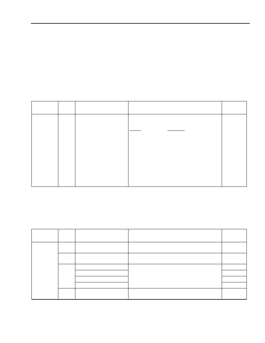
Agere Systems Inc.
159
Data Sheet
May 2001
155/622/2488 Mbits/s Data Interface
TDAT042G5 SONET/SDH
Register Descriptions
(continued)
UT Registers
(continued)
UT Provisioning Registers (R/W) (continued)
Table 61. Registers 0x020F, 0x0213, 0x0217, 0x021B: Channel [A--D] Receive Provisioning Register (R/W)
(continued)
Reset default of register 0x020F = 0x0020.
Reset default of register 0x0213 = 0x0120.
Reset default of register 0x0217 = 0x0220.
Reset default of register 0x021B = 0x0320.
*The value 000 for these bits places the corresponding UTOPIA outputs in the high-impedance state.
Table 62. Registers 0x0210, 0x0214, 0x0218, 0x021C: Channel [A--D] Transmit Provisioning Register (R/W)
Reset default of register 0x0210 = 0x0000.
Reset default of register 0x0214 = 0x0120.
Reset default of register 0x0218 = 0x0220.
Reset default of register 0x021C = 0x0320.
Address
(Hex)
Bit #
Name
Function
Reset
Default
020F, 0213,
0217, 021B
2--0
UTOPIA_MODE_Rx
[A--D][2:0]
UTOPIA Mode Receive Channel [A--D]. Con-
figures the Rx channel mode.
Mode
Bit Value
disabled (idle)* bits[2:0] = 000
U2
bits[2:0] = 001
U2+
bits[2:0] = 010
U3, 8-bit
bits[2:0] = 011
U3, 32-bit
bits[2:0] = 100
U3+, 8-bit
bits[2:0] = 101
U3+, 32-bit
bits[2:0] = 110
invalid
bits[2:0] = 111
U3 configuration also requires the appropriate
setting of register 0x0225 (PA response) to be
set for a two-cycle response.
000
Address
(Hex)
Bit #
Name
Function
Reset
Default
0210, 0214,
0218, 021C
15
POLLING_ENB_Tx
[A--D]
Polling Enable Transmit Channel [A--D]. If
set, transmit polling mode is enabled.
0
14--13
--
Reserved. These bits must be written to their
reset default value (00).
00
12--8
TxADDR_A[4:0]
Polling Transmit Address Channel [A--D].
Transmit polling address.
00000
TxADDR_B[4:0]
00001
TxADDR_C[4:0]
00010
TxADDR_D[4:0]
00011
7--6
--
Reserved. These bits must be written to their
reset default value (00).
00

160
Agere Systems Inc.
Data Sheet
May 2001
155/622/2488 Mbits/s Data Interface
TDAT042G5 SONET/SDH
Register Descriptions
(continued)
UT Registers
(continued)
UT Provisioning Registers (R/W) (continued)
Table 62. Registers 0x0210, 0x0214, 0x0218, 0x021C: Channel [A--D] Transmit Provisioning Register (R/W)
(continued)
Reset default of register 0x0210 = 0x0000.
Reset default of register 0x0214 = 0x0120.
Reset default of register 0x0218 = 0x0220.
Reset default of register 0x021C = 0x0320.
Address
(Hex)
Bit #
Name
Function
Reset
Default
0210, 0214,
0218, 021C
5
PARITY_Tx[A]
Parity Transmit Channel [A--D]. Defines if
odd (bit = 1) or even (bit = 0) parity is generated
for the data transmitted across the UTOPIA
PHY Tx interface. Default is even for channel A
and odd for channels B, C, and D.
0
PARITY_Tx[B--D]
1
4
ATM_SIZE_Tx[A--D]
ATM Packet Size Transmit Channel [A--D].
Defines how many bytes are transmitted per
ATM cell. Default is 53 bytes. Valid only when
traffic type is ATM cells.
Page 86 and page 87 give details of the func-
tion of this bit.
0 = standard 53-byte (also 54-byte and 56-byte)
ATM cell modes.
1 = 52-byte ATM cell mode (HEC omitted).
0
3
TRAFFIC_TYPE_Tx
[A--D]
Traffic Type Transmit Channel [A--D]. Con-
figures channel to transmit either ATM cells or
packets.
Bit Value
Traffic Type
0
packets (default)
1
ATM cells
0
2--0
UTOPIA_MODE_Tx
[A--D][2:0]
UTOPIA Mode Transmit Channel [A--D].
Configures the Tx channel mode.
Mode
Bit Value
disabled (idle)
bits[2:0] = 000
U2
bits[2:0] = 001
U2+
bits[2:0] = 010
U3, 8-bit
bits[2:0] = 011
U3, 32-bit
bits[2:0] = 100
U3+, 8-bit
bits[2:0] = 101
U3+, 32-bit
bits[2:0] = 110
invalid
bits[2:0] = 111
U3 configuration also requires appropriate set-
ting of register 0x0225 (PA response) to be set
for a two-cycle response.
000

Agere Systems Inc.
161
Data Sheet
May 2001
155/622/2488 Mbits/s Data Interface
TDAT042G5 SONET/SDH
Register Descriptions
(continued)
UT Registers
(continued)
UT Provisioning Registers (R/W) (continued)
Table 63. Registers 0x0211, 0x0215, 0x0219, 0x021D: Channel [A--D] Ingress Provisioning Register (R/W)
Reset default of registers = 0x361F.
Table 64. Registers 0x0212, 0x0216, 0x021A, 0x021E: Channel [A--D] Egress Provisioning Register (R/W)
Reset default of registers = 0x361F.
Address
(Hex)
Bit #
Name
Function
Reset
Default
0211, 0215,
0219, 021D
15--14
--
Reserved. These bits must be written to their
reset default value (00).
00
13--8
INGRESS_WATERMARK
_HIGH_[A--D][6:0]
Ingress Watermark High for Channel
[A--D]. Defines threshold before which over-
flow is detected causing a head of FIFO dis-
card; data in the receive FIFO will be discarded
down to the next start of packet/cell.
110110
7--6
--
Reserved. These bits must be written to their
reset default value (00).
00
5--0
INGRESS_WATERMARK
_LOW_[A--D][6:0]
Ingress Watermark Low for Channel [A--D].
Defines how many words must be stored in the
ingress FIFO before transmission out of the
UTOPIA port, if an end of packet is not
received.
011111
Address
(Hex)
Bit #
Name
Function
Reset
Default
0212, 0216,
021A, 021E
15--14
--
Reserved. These bits must be written to their
reset default value (00).
00
13--8
EGRESS_WATERMARK_
HIGH_[A--D][6:0]
Egress Watermark High for Channel [A--D].
Defines how many words can be stored into the
egress FIFO before backpressure is applied to
the UTOPIA PHY Tx port to stop acceptance of
more traffic. Default value is set for packet
transfer. For ATM transfer, the value should be
configured as 0x29. For packet mode, this value
depends upon the specific user-interface char-
acteristics. The default value (110110) will work
for packet mode.
110110
7--6
--
Reserved. These bits must be written to their
reset default value (00).
00
5--0
EGRESS_WATERMARK_
LOW_[A--D][6:0]
Egress Watermark Low for Channel [A--D].
Defines how many words must be stored in the
egress FIFO before transmission to the data
engine, if an end of packet is not received.
011111

162
Agere Systems Inc.
Data Sheet
May 2001
155/622/2488 Mbits/s Data Interface
TDAT042G5 SONET/SDH
Register Descriptions
(continued)
UT Registers
(continued)
Reset Register (R/W)
Table 65. Register 0x021F: Reset Register (R/W)
Reset default of register = 0x00FF.
Error Count Registers (RO)
Table 66. Register 0x0220: Channel [A--D] Error Count (RO)
Reset default of register = 0x0000.
Scratch Register (R/W)
Table 67. Register 0x0224: UT_Scratch Register (R/W)
Reset default of register = 0x0000.
Address
(Hex)
Bit #
Name
Function
Reset
Default
021F
--
UT_ARST
UTOPIA Asynchronous Reset. Active-high
signal. This must be the last signal written to
the UTOPIA interface during configuration and
must be written to the value 0x00 to enable the
particular channels.
0x00FF
15--8
--
Reserved. These bits must be written to their
reset default value (0x00).
0x00
7
UT_TxARST_D
Transmit ARST for Transmit Channel D.
1
6
UT_TxARST_C
Transmit ARST for Transmit Channel C.
1
5
UT_TxARST_B
Transmit ARST for Transmit Channel B.
1
4
UT_TxARST_A
Transmit ARST for Transmit Channel A.
1
3
UT_RxARST_D
Receive ARST for Receive Channel D.
1
2
UT_RxARST_C
Receive ARST for Receive Channel C.
1
1
UT_RxARST_B
Receive ARST for Receive Channel B.
1
0
UT_RxARST_A
Receive ARST for Receive Channel A.
1
Address
(Hex)
Bit #
Name
Function
Reset
Default
0220--0223
15--0
PECTx[A--D]
Parity Error Count Transmit Channel [A--D].
Counts the instantaneous (real-time) number of
parity errors that occur for Tx channel [A--D].
0x0000
Address
(Hex)
Bit #
Name
Function
Reset
Default
0224
15--0
UT_SCRATCH
UT Scratch Register. Read/write register with
no other internal UT connections.
0x0000

Agere Systems Inc.
163
Data Sheet
May 2001
155/622/2488 Mbits/s Data Interface
TDAT042G5 SONET/SDH
Register Descriptions
(continued)
UT Registers
(continued)
PA Response Register (R/W)
Table 68. Register 0x0225: PA Response Register (R/W)
Reset default of register = 0x0000.
Address
(Hex)
Bit #
Name
Function
Reset
Default
0225
--
PA/DATA
Packet Available (PA). In MPHY mode, when
this bit is 0, the PA response follows placement
of a valid address on the address bus by the
ATM master device by one UTOPIA interface
clock period. The RxDATA response follows the
RxENB assertion.
If this bit is 1, then the PA response and
RxDATA response follow the address by two
clock periods. Two-cycle response is provided
for U3-compatible operation.
0x0000
15--8
--
Reserved. These bits must be written to their
reset default value (0x00).
0x00
7
TxPAD
TxPA Response for Transmit Channel D.
0
6
TxPAC
TxPA Response for Transmit Channel C.
0
5
TxPAB
TxPA Response for Transmit Channel B.
0
4
TxPAA
TxPA Response for Transmit Channel A.
0
3
RxPAD/RxDATAD/RxSOP/
CD
RxPA Response for Receive Channel D.
0
2
RxPAC/RxDATAC/RxSOP/
CC
RxPA Response for Receive Channel C.
0
1
RxPAB/RxDATAB/RxSOP/
CB
RxPA Response for Receive Channel B.
0
0
RxPAA/RxDATAA/RxSOP/
CA
RxPA Response for Receive Channel A.
0

164
Agere Systems Inc.
Data Sheet
May 2001
155/622/2488 Mbits/s Data Interface
TDAT042G5 SONET/SDH
Register Descriptions
(continued)
UT Registers
(continued)
Size Mode Register (R/W)
Table 69. Register 0x0226: Size Mode Register (R/W)
Reset default of register = 0x0000.
Address
(Hex)
Bit #
Name
Function
Reset
Default
0226
--
--
Size Mode. Size mode for each channel. These
bits define the size mode for the TxSZ[D--A]
and RxSZ[D--A] pins (see Table 5, page 32
and page 38).
If this mode bit = 0 (default mode):
I
TxSIZE_[D--A] (or RxSIZE_[D--A]) set to 0
means the most significant byte is the last
byte of the current packet, and
I
TxSIZE_[D--A] (or RxSIZE_[D--A]) set to 1
means the least significant byte is the last
byte.
If this mode bit = 1:
I
TxSIZE_[D--A] (or RxSIZE_[D--A]) set to 1
means the most significant byte is the last
byte of the current packet, and
I
TxSIZE_[D--A] (or RxSIZE_[D--A]) set to 0
means the least significant byte is the last
byte.
0x0000
15--8
--
Reserved. These bits must be written to their
reset default value (0x00).
0x00
7
TxSIZE_D
TxSIZE_MODE for Transmit Channel D.
0
6
TxSIZE_C
TxSIZE_MODE for Transmit Channel C.
0
5
TxSIZE_B
TxSIZE_MODE for Transmit Channel B.
0
4
TxSIZE_A
TxSIZE_MODE for Transmit Channel A.
0
3
RxSIZE_D
RxSIZE_MODE for Receive Channel D.
0
2
RxSIZE_C
RxSIZE_MODE for Receive Channel C.
0
1
RxSIZE_B
RxSIZE_MODE for Receive Channel B.
0
0
RxSIZE_A
RxSIZE_MODE for Receive Channel A.
0

Agere Systems Inc.
165
Data Sheet
May 2001
155/622/2488 Mbits/s Data Interface
TDAT042G5 SONET/SDH
Register Descriptions
(continued)
OHP Registers
This section gives a brief description of each register bit and its functionality. All algorithms are described in the
main text of the document. The abbreviations after each register indicate if the register is read only (RO), read/
write (R/W), write only (WO), or clear-on-read or clear-on-write (COR/W).
0x indicates a hexadecimal value in the Reset Default column. Otherwise, the entry is binary. This is true for every
register table in the document.
Table 70. Register 0x0400: OHP Macrocell Version Number (RO)
Reset default of register = 0x0000.
Table 71. Register 0x0401: OHP Interrupt (RO)
Reset default of register = 0x0000.
Table 72. Registers 0x0402--0x0409: Delta/Event (COR/W)
Reset default of registers = 0x0000.
Address
(Hex)
Bit #
Name
Function
Reset
Default
0400
15--0
OHP_VERSION[15:0]
OHP Macrocell Version Number. The version
of the macrocell will increment each time a
change occurs to the macrocell functionality.
0x0000
Address
(Hex)
Bit #
Name
Function
Reset
Default
0401
15--4
--
Reserved. These bits must be written to their
reset default value (0x000).
0x000
3
OHP_INT[D]
OHP Interrupt. Active-high interrupt bits for
channels D to A. Each bit is the ORing of all
event and delta bits of that channel. In STS-48/
STM-16 mode, INT[A] is valid.
0x0
2
OHP_INT[C]
0x0
1
OHP_INT[B]
0x0
0
OHP_INT[A]
0x0
Address
(Hex)
Bit #
Name
Function
Reset
Default
0402, 0404,
0406, 0408
15
LRDIMOND[A--D]
Line/Multiplex RDI Delta. Delta bits indicate a
change of state for the line/multiplex RDI state
bits (LRDIMON[A--D]). Their mask bits are
LRDIMONM[A--D]. Only LRDIMOND[A] is
valid for STS-48/STM-16.
0
14
LAISMOND[A--D]
Line/Multiplex AIS Delta. Delta bits indicate a
change of state for the line/multiplex AIS state
bits (LAISMON[A--D]). Their mask bits are
LAISMONM[A--D]. Only LAISMOND[A] is valid
for STS-48/STM-16.
0
13
RAPSBABLEE[A--D]
APS Babble Event. Each bit is active-high to
indicate the inconsistence in K1 byte of that
channel. Their mask bits are
RAPSBABLEM[A--D]. Only RAPSBABLEE[A]
is valid for STS-48/STM-16.
0

166
Agere Systems Inc.
Data Sheet
May 2001
155/622/2488 Mbits/s Data Interface
TDAT042G5 SONET/SDH
Register Descriptions
(continued)
OHP Registers
(continued)
Table 72. Registers 0x0402--0x0409: Delta/Event (COR/W) (continued)
Reset default of registers = 0x0000.
Address
(Hex)
Bit #
Name
Function
Reset
Default
0402, 0404,
0406, 0408
12
S1DMON4D[A--D]
Delta Register for S1DMON[3:0] When
S1MON8or4CTL = 1. Each delta bit indicates a
change of state for S1DMON[3:0] in its channel.
Their mask bits are S1DMON4M[A--D]. In
STS-48/STM-16 mode, S1DMON4D[A] is valid.
0
11
S1DMON8D[A--D]
Delta Register for S1DMON[7:4] When
S1MON8or4CTL = 1 or S1DMON[7:0] When
S1MON8or4CTL = 0. Each delta bit indicates a
change of state for S1DMON[7:4]/
S1DMON[7:0] in its channel. Their mask bits
are S1DMON8M[A--D]. In STS-48/STM-16
mode, S1DMON8D[A] is valid.
0
10
K2DMOND[A--D]
K2[2:0] Data Monitor Delta. Each bit is active-
high to indicate a change in K2DMON[A--D]
for that channel. Their mask bits are
K2DMONM[A--D]. Only K2DMOND[A] is valid
for STS-48/STM-16.
0
9
K1K2DMOND[A--D]
K1K2 Data Monitor Delta. Each bit is active-
high to indicate a change in (K1[7:0] and
K2[7:3]) or (K1[7:0] and K2[7:0]) for that chan-
nel depending on K1K2_2_OR_1. Their mask
bits are K1K2DMONM[A--D]. Only
K1K2DMOND[A] is valid for STS-48/STM-16.
0
8
F1DMOND[A--D]
F1 Data Monitor Delta. Their mask bits are
F1DMONM[A--D]. Only F1DMOND[A] is valid
for STS-48/STM-16.
0
7
TTOAC_PERRE[A--D]
Transmit TOAC Parity Error Event. Event bit
indicates a parity error was detected on the
incoming TOAC.
0
6
S1BABBLEE[A--D]
Receive S1 Byte Babbling Event. Event bit
will be set if CNTDS1FRAME[A--D][3:0] con-
secutive frames pass without a validated S1
byte.
0
5
SFD[A--D]
Signal Fail BER Algorithm Delta. Delta bits
indicate a change of state for the signal fail BER
algorithm state bits (SF[A--D]). Their mask bits
are SFM[A--D]. Only SFD[A] is valid for STS-
48/STM-16.
0

Agere Systems Inc.
167
Data Sheet
May 2001
155/622/2488 Mbits/s Data Interface
TDAT042G5 SONET/SDH
Register Descriptions
(continued)
OHP Registers
(continued)
Table 72. Registers 0x0402--0x0409: Delta/Event (COR/W) (continued)
Reset default of registers = 0x0000.
Address
(Hex)
Bit #
Name
Function
Reset
Default
0402, 0404,
0406, 0408
4
SDD[A--D]
Signal Degrade BER Algorithm Delta. Delta
bit indicates a change of state for the signal
degrade BER algorithm state bits (SD[A--D]).
Their mask bits are SDM[A--D]. Only SDD[A] is
valid for STS-48/STM-16.
0
3
OOFD[A--D]
Receive Out-of-Frame Delta. Delta bit indi-
cates a change of state for the out-of-frame
(OOF[A--D]). Their mask bits are
OOFM[A--D]. In STS-48/STM-16 mode, only
OOFD[A] is valid.
0
2
LOFD[A--D]
Receive Loss-of-Frame Delta. Delta bit indi-
cates a change of state for the loss-of-frame
(LOF[A--D]) . Their mask bits are LOFM[A--D].
In STS-48/STM-16 mode, only LOFD[A] is
valid.
0
1
LOSD[A--D]
Receive Loss-of-Signal Delta. Delta bit indi-
cates a change of state for the loss-of-signal
(LOS[A--D]). Their mask bits are LOSM[A--D].
In STS-48/STM-16 mode, only LOSD[A] is
valid.
0
0
LOCD[A--D]
Receive Loss-of-Clock Delta. Delta bit indi-
cates a change of state for the loss-of-clock
(LOC[A--D]). Their mask bits are LOCM[A--D].
In STS-48/STM-16 mode, only LOCD[A] is
valid.
0
0403, 0405,
0407, 0409
15--1
--
Reserved. These bits must be written to their
reset default value (000000000000000).
000
0000
0000
0000
0
J0MISE[A--D]
J0 Mismatch Event. Their mask bits are
J0MISM[A--D]. In STS-48/STM-16 mode, only
J0MISE[A] is valid for J0 byte while J0MISE[B--
D] are used for Z0 bytes.
0

168
Agere Systems Inc.
Data Sheet
May 2001
155/622/2488 Mbits/s Data Interface
TDAT042G5 SONET/SDH
Register Descriptions
(continued)
OHP Registers
(continued)
Table 73. Registers 0x040A--0x040D: Receive/Transmit State (RO)
Reset default of registers = 0x000C.
Address
(Hex)
Bit #
Name
Function
Reset
Default
040A--040D
15
LRDIMON[A--D]
Line/Multiplex RDI State. In STS-48/
STM-16 mode, only LRDIMON[A] is valid.
0
14
LAISMON[A--D]
Line/Multiplex AIS State. In STS-48/
STM-16 mode, only LAISMON[A] is valid.
0
13--7
--
Reserved. These bits must be written to their
reset default value (0000000).
000
0000
6
TLRDIINT[A--D]
Transmit Line RDI Insert State. State bits for
inserting line RDI value into the K2[2:0] bits. In
STS-48/STM-16 mode, only TLRDIINT[A] is
valid.
0
5
SF[A--D]
Signal Fail State. In STS-48/STM-16 mode,
only SF[A] is valid.
0
4
SD[A--D]
Signal Degrade State. In STS-48/STM-16
mode, only SD[A] is valid.
0
3
OOF[A--D]
Out-of-Frame. Active-high out-of-frame state
bits. In STS-48/STM-16 mode, only OOF[A] is
valid.
1
2
LOF[A--D]
Loss-of-Frame. Active-high loss-of-frame state
bits. In STS-48/STM-16 mode, only LOF[A] is
valid.
1
1
LOS[A--D]
Loss-of-Signal. Active-high loss-of-signal state
bits. In STS-48/STM-16 mode, only LOS[A] is
valid.
0
0
LOC[A--D]
Loss-of-Clock. Active-high loss-of-clock state
bits. In STS-48/STM-16 mode, only LOC[A] is
valid.
0

Agere Systems Inc.
169
Data Sheet
May 2001
155/622/2488 Mbits/s Data Interface
TDAT042G5 SONET/SDH
Register Descriptions
(continued)
OHP Registers
(continued)
Table 74. Registers 0x040E, 0x0410, 0x0412, 0x0414: Mask Bits (R/W)
Reset default of registers = 0xFFFF.
Address
(Hex)
Bit #
Name
Function
Reset
Default
040E, 0410,
0412, 0414
15
LRDIMONM[A--D]
Line/Multiplex RDI Mask. A 1 masks the cor-
responding occurrence of the alarm to the inter-
rupt. In STS-48/STM-16 mode, only
LRDIMONM[A] is valid.
1
14
LAISMONM[A--D]
Line/Multiplex AIS Mask. A 1 masks the corre-
sponding occurrence of the alarm to the inter-
rupt. In STS-48/STM-16 mode, only
LAISMONM[A] is valid.
1
13
RAPSBABLEM[A--D]
APS Babble Mask. A 1 masks the correspond-
ing occurrence of the alarm to the interrupt. In
STS-48/STM-16 mode, only
RAPSBABLEM[A] is valid.
1
12
S1DMON4M[A--D]
Mask Bits for S1DMON4D When S1MON8
or 4CTL = 1. A 1 masks the corresponding
occurrence of the alarm to the interrupt. In
STS-48/STM-16 mode, only
S1DMON4LSNM[A] is valid.
1
11
S1DMON8M[A--D]
Mask Bits for S1DMON8D. A 1 masks the cor-
responding occurrence of the alarm to the inter-
rupt. In STS-48/STM-16 mode, only
S1DMON8M[A] is valid.
1
10
K2DMONM[A--D]
K2[2:0] Data Monitor Mask. A 1 masks the
corresponding occurrence of the alarm to the
interrupt. In STS-48/STM-16 mode, only
K2DMONM[A] is valid.
1
9
K1K2DMONM[A--D]
K1K2 Data Monitor Mask. A 1 masks the cor-
responding occurrence of the alarm to the inter-
rupt. In STS-48/STM-16 mode, only
K1K2DMONM[A] is valid.
1
8
F1DMONM[A--D]
F1 Data Monitor Mask. A 1 masks the corre-
sponding occurrence of the alarm to the inter-
rupt. In STS-48/STM-16 mode, only
F1DMONM[A] is valid.
1
7
TTOAC_PERRM[A--D]
Transmit TOAC Parity Error Mask. A 1 masks
the corresponding occurrence of the alarm to
the interrupt. All 4 bits are valid in every mode.
1

170
Agere Systems Inc.
Data Sheet
May 2001
155/622/2488 Mbits/s Data Interface
TDAT042G5 SONET/SDH
Register Descriptions
(continued)
OHP Registers
(continued)
Table 74. Registers 0x040E, 0x0410, 0x0412, 0x0414: Mask Bits (R/W)
(continued)
Reset default of registers = 0xFFFF.
Table 75. Registers 0x040F, 0x0411, 0x0413, 0x0415: Mask Bits (R/W)
Reset default of registers = 0x8001.
Address
(Hex)
Bit #
Name
Function
Reset
Default
040E, 0410,
0412, 0414
6
S1BABBLEM[A--D]
S1 Babbling Mask. A 1 masks the correspond-
ing occurrence of the alarm to the interrupt. In
STS-48/STM-16 mode, only S1BABBLEM[A] is
valid.
1
5
SFM[A--D]
Signal Fail Mask. A 1 masks the correspond-
ing occurrence of the alarm to the interrupt. In
STS-48/STM-16 mode, only SFM[A] is valid.
1
4
SDM[A--D]
Signal Degrade Mask. A 1 masks the corre-
sponding occurrence of the alarm to the inter-
rupt. In STS-48/STM-16 mode, only SDM[A] is
valid.
1
3
OOFM[A--D]
Out-of-Frame Mask. A 1 masks the corre-
sponding occurrence of the alarm to the inter-
rupt. In STS-48/STM-16 mode, only OOFM[A]
is valid.
1
2
LOFM[A--D]
Loss-of-Frame Mask. A 1 masks the corre-
sponding occurrence of the alarm to the inter-
rupt. In STS-48/STM-16 mode, only LOFM[A] is
valid.
1
1
LOSM[A--D]
Loss-of-Signal Mask. A 1 masks the corre-
sponding occurrence of the alarm to the inter-
rupt. In STS-48/STM-16 mode, only LOSM[A] is
valid.
1
0
LOCM[A--D]
Loss-of-Clock Mask. A 1 masks the corre-
sponding occurrence of the alarm to the inter-
rupt. In STS-48/STM-16 mode, only LOCM[A] is
valid.
1
Address
(Hex)
Bit #
Name
Function
Reset
Default
040F, 0411,
0413, 0415
15
INTM[A--D]
Interrupt Mask. The corresponding occurrence
of a 1 masks the alarm to the interrupt.
1
14--1
--
Reserved. These bits must be written to their
reset default value (00000000000000).
00
0000
0000
0000
0
J0MISM[A--D]
J0 Mismatch Mask. The corresponding occur-
rence of a 1 masks the alarm to the interrupt.
1

Agere Systems Inc.
171
Data Sheet
May 2001
155/622/2488 Mbits/s Data Interface
TDAT042G5 SONET/SDH
Register Descriptions
(continued)
OHP Registers
(continued)
Table 76. Registers 0x0416--0x0419: Toggles (R/W)
Reset default of registers = 0x0000.
Note: These registers are one-shot type registers. They are enabled by writing a 0-to-1 transition to a bit. After
being enabled, the registers must be cleared by writing all bits to 0 following access.
Table 77. Registers 0x041A, 0x041C, 0x041E, 0x0420: Continuous N Times Detect (CNTD) Values (R/W)
Reset default of registers = 0x3333.
Address
(Hex)
Bit #
Name
Function
Reset
Default
0416--0419
15--5
--
Reserved. These bits must be written to their
reset default value (00000000000).
000
0000
0000
4
TA1A2ERREN[A--D]
Transmit A1/A2 Error Enable. Enable signal to
start the insertion of A2 errors in the outgoing
frame. The number of consecutive errors is
controlled by TA1A2ERRINS[4:0].
TA1A2ERREN[A] is valid in STS-48/STM-16
mode.
0
3
SFCLEAR[A--D]
Signal Fail Clear. Allows the signal fail algo-
rithm to be forced into the normal state.
0
2
SFSET[A--D]
Signal Fail Set. Allows the signal fail algorithm
to be forced into the failed state.
0
1
SDCLEAR[A--D]
Signal Degrade Clear. Allows the signal
degrade algorithm to be forced into the normal
state.
0
0
SDSET[A--D]
Signal Degrade Set. Allows the signal degrade
algorithm to be forced into the degraded state.
0
Address
(Hex)
Bit #
Name
Function
Reset
Default
041A, 041C,
041E, 0420
15--12
CNTDK2[A--D][3:0]
Continuous N Times Detect for K2[2:0] Byte.
The valid range for these bits is 0x2--0xF.
Invalid values will be mapped to a value of 0x1.
In STS-48/STM-16 mode, CNTDK2[A] is valid.
0x3
11--8
CNTDK1K2[A--D][3:0]
Continuous N Times Detect for APS (K1,
K2[7:3]) Byte. The valid range for these bits is
0x2--0xF. Invalid values will be mapped to a
value of 0x1. In STS-48/STM-16 mode,
CNTDK1K2[A] is valid.
0x3
7--4
CNTDF1[A--D][3:0]
Continuous N Times Detect for F1 Byte. The
valid range for these bits is 0x2--0xF. Invalid
values will be mapped to a value of 0x1. In
STS-48/STM-16 mode, CNTDF1[A] is valid.
0x3
3--0
CNTDJ0Z0[A--D][3:0]
Continuous N Times Detect for J0Z0 Bytes.
The valid range for these bits is 0x2--0xF.
Invalid values will be mapped to a value of 0x1.
In STS-48/STM-16 mode, CNTDJ0Z0[A] is
valid.
0x3

172
Agere Systems Inc.
Data Sheet
May 2001
155/622/2488 Mbits/s Data Interface
TDAT042G5 SONET/SDH
Register Descriptions
(continued)
OHP Registers
(continued)
Table 78. Registers 0x041B, 0x041D, 0x041F, 0x0421: Continuous N Times Detect (CNTD) Values (R/W)
Reset default of registers = 0x053C.
Address
(Hex)
Bit #
Name
Function
Reset
Default
041B, 041D,
041F, 0421
15--12
--
Reserved. These bits must be written to their reset
default value (0x0).
0x0
11--8
CNTDS1FRAME
[A--D][3:0]
Continuous N Times Detect for S1 Byte Bab-
bling. The valid range for these bits is 0x2--0xF.
Invalid values will be mapped to a value of 0x1. In
STS-48/STM-16 mode, CNTDS1FRAME[A] is
valid.
0x5
7--4
CNTDS1[A--D][3:0]
Continuous N Times Detect for S1 Byte. The
valid range for these bits is 0x2--0xF. Invalid val-
ues will be mapped to a value of 0x1. In
STS-48/STM-16 mode, CNTDS1[A] is valid.
0x3
3--0
CNTDK1K2FRAME
[A--D][3:0]
Continuous N Times Detect for APS Frame. The
valid range for these bits is 0x2--0xF. Invalid val-
ues will be mapped to a value of 0x1. In STS-48/
STM-16 mode, CNTDK1K2FRAME[A] is valid.
0xC

Agere Systems Inc.
173
Data Sheet
May 2001
155/622/2488 Mbits/s Data Interface
TDAT042G5 SONET/SDH
Register Descriptions
(continued)
OHP Registers
(continued)
Table 79. Registers 0x0422--0x042D: Receive Control (R/W)
Reset default of registers = 0x0000.
Address
(Hex)
Bit #
Name
Function
Reset
Default
0422, 0424,
0426, 0428
15--14
J0MONMODE[A--D][1:0]
J0 Monitoring Mode. The four modes are,
00 = The OHP will latch the value of the J0 byte
every frame for a total of 16 bytes. The OHP will
compare the incoming J0 byte with the next
expected value (the expected value is obtained
by cycling through the previously stored 16
received bytes in round-robin fashion) and set
the event bit if different.
01 = This is the SONET framing mode. The
hardware looks for 0x0D followed by 0x0A to
indicate that the next byte is the first byte of the
path trace message. The J0 byte is continu-
ously written into J0DMON with the first byte
residing at the first address. If any received byte
does not match the previously received byte for
its location, then the event bit is set.
10 = This is the SDH framing mode. The hard-
ware looks for the byte with the MSB set to 1,
which indicates that the next byte is the second
byte of the message. The rest of the operation
is the same as the SONET framing mode.
11 = A new J0 byte J0DMON[0][7:0] will be
detected after CNTDJ0Z0[3:0] consecutive con-
sistent occurrences of a new pattern in the J0
overhead byte. Any changes to this byte are
reported to J0MISE and J0MISM. These event
bits will act as delta bits indicating a change of
state for the J0DMON[0][7:0].
00
13
M1B7IGNORE[A--D]
Bit 7 of M1 Byte Ignore. Bit 7 of M1 byte will
be ignored if M1B7IGNORE is set to 1 for that
channel. Only M1B7IGNORE[A] is valid for
STS-48/STM-16.
0
12
LAISINS[A--D]
AIS Software Insertion. Active-high for AIS
insertion. In STS-48/STM-16 mode, only LAI-
SINS[A] is valid.
0
11
LOF_AISINH[A--D]
Loss-of-Frame AIS Inhibit. When set to logic
1, the AIS insertion will be inhibited in case of
loss-of-frame.
0
10
OOF_AISINH[A--D]
Out-of-Frame AIS Inhibit. When set to logic 1,
the AIS insertion will be inhibited in case of out-
of-frame.
0

174
Agere Systems Inc.
Data Sheet
May 2001
155/622/2488 Mbits/s Data Interface
TDAT042G5 SONET/SDH
Register Descriptions
(continued)
OHP Registers
(continued)
Table 79. Registers 0x0422--0x042D: Receive Control (R/W) (continued)
Reset default of registers = 0x0000.
Address
(Hex)
Bit #
Name
Function
Reset
Default
0422, 0424,
0426, 0428
9
LOS_AISINH[A--D]
Loss-of-Signal AIS Inhibit. When set to logic
1, the line AIS insertion will be inhibited in case
of loss-of-signal.
0
8
SFB1B2SEL[A--D]
Signal Fail B1/B2 Error Count Select. When
set to logic 0, the B1 errors will be used by the
signal fail error rate algorithm; otherwise, B2
errors are used.
0
7
SDB1B2SEL[A--D]
Signal Degrade B1/B2 Error Count Select.
When set to logic 0, the B1 errors will be used
by the signal degrade error rate algorithm; oth-
erwise, B2 errors are used.
0
6
CNTDB1SEL[A--D]
Reset CNTD Counters on B1 Error. Active-
high control bits to reset continuous N time
detect counters upon received B1 errors. Only
CNTDB1SEL[0] is valid for STS-48/STM-16.
0
5
S1MON8_OR_4CTL[A--D] S1 Byte or Nibble. When set to logic 1, the S1
byte will be monitored as two nibbles. Other-
wise, it is treated as a byte. Only
S1MON8or4CTL[A] is valid for STS-48/STM-
16.
0
4
K1K2_2_OR_1[A--D]
K1 and K2 Treated as 2 Registers or 1. When
a bit is set to 1, the K1 and K2 bytes will be
treated as one 16-bit register. Otherwise, they
will be treated as two registers of size 13
(K1[7:0] and K2[7:3]) and 3 (K2[2:0]).
K1K2_2_OR_1[A] is valid for STS-48/STM-16.
0
3
B2BITBLKCNT[A--D]
B2 Error Count in Bit or Block. When set to 0,
B2 check logic will count bit errors; otherwise, it
counts block errors. Only B2BITBLKCNT[A] is
valid for STS-48/STM-16.
0
2
DSCRINH[A--D]
Descramble Inhibit Control. When a bit is set
to 1, the descrambler for that is disabled. In
STS-48/STM-16 mode, all 4 bits need to be set
to same value.
0
1
B1BITBLKCNT[A--D]
B1 Error Count in Bit or Block. When set to 0,
B1 check logic will count bit errors; otherwise, it
counts block errors. Only B1BITBLKCNT[A] is
valid for STS-48/STM-16.
0
0
ROH_BYPASS[A--D]
Receive Overhead Bypass. Control bit, when
set to 1, causes the received data to pass
through the block retimed. In STS-48/STM-16
mode, all 4 bits need to be set to same value.
0

Agere Systems Inc.
175
Data Sheet
May 2001
155/622/2488 Mbits/s Data Interface
TDAT042G5 SONET/SDH
Register Descriptions
(continued)
OHP Registers
(continued)
Table 79. Registers 0x0422--0x042D: Receive Control (R/W) (continued)
Reset default of registers = 0x0000.
Address
(Hex)
Bit #
Name
Function
Reset
Default
0423, 0425,
0427, 0429
15
M1BITBLKCNT[A--D]
M1 Error Count in Bit or Block. When set to
0, M1 check logic will count bit errors. When set
to 1, block errors are counted. Only
M1BITBLKCNT[C] is valid for STS-48/STM-16.
0
14--13
--
Reserved. These bits must be written to their
reset default value (00).
00
12--0
LOSDETCNT[A--D][12:0]
Loss-of-Signal Detection Count. Set the
number of consecutive all-zeros/-ones pattern
detected to declare receive LOS state for each
channel. The time scale is in steps of 8 (for
STS-3/STM-1 and STS-12/STM-4) or 32
(STS-48/STM-16) bits at a time. Only
LOSDETCNT[A][12:0] is valid for STS-48/
STM-16.
0
0000
0000
0000
042A
15--14
RREFSEL[1:0]
Receive Reference Sync Select. Select refer-
ence output from channel A (00), B (01), C (10),
and D (11).
00
13
RREF_EN
Receive Reference Sync Enable. When set to
0, the receive 8 kHz (50% duty cycle) sync out-
put, RxREF (pin AK3), is placed in the high-
impedance state.
0
12--4
--
Reserved. These bits must be written to their
reset default value (000000000).
0000
00000
3
RTOACSINH[A]
Receive TOAC Frame (Sync) Inhibit Channel
A. When set to 1, the TOAC sync output,
RxTOHF (pin AK4), is placed in the high-imped-
ance state.
0
2
RTOACCINH[A]
Receive TOAC Clock Inhibit Channel A.
When set to 1, the TOAC clock output,
RxTOHCK (pin AK5), is placed in the high-
impedance state.
0
1
RTOACDINH[A]
Receive TOAC Data Inhibit Channel A. When
set to 1, the TOAC data output, RxTOHD (pin
AL2), is placed in the high-impedance state.
0
0
RTOAC_OEPINS[A]
Receive TOAC Odd or Even Parity Insert
Channel A. When set to 1, the output TOAC
parity bit is even. When set to 0, the parity is
odd.
0

176
Agere Systems Inc.
Data Sheet
May 2001
155/622/2488 Mbits/s Data Interface
TDAT042G5 SONET/SDH
Register Descriptions
(continued)
OHP Registers
(continued)
Table 79. Registers 0x0422--0x042D: Receive Control (R/W) (continued)
Reset default of registers = 0x0000.
Address
(Hex)
Bit #
Name
Function
Reset
Default
042B--042D
15--4
--
Reserved. These bits must be written to their
reset default value (0x000).
0x000
3
RTOACSINH[B--D]
Receive TOAC Frame (Sync) Inhibit Channel
[B--D]. When set to 1, the TOAC sync output,
RxTOHF (pins AL3, AN5, AP6), is placed in the
high-impedance state.
0
2
RTOACCINH[B--D]
Receive TOAC Clock Inhibit Channel [B--D].
When set to 1, the TOAC clock output,
RxTOHCK (pins AL4, AL6, AL7), is placed in
the high-impedance state.
0
1
RTOACDINH[B--D]
Receive TOAC Data Inhibit Channel [B--D].
When set to 1, the TOAC data output, RxTOHD
(pins AM5, AM6, AN7), is placed in the high-
impedance state.
0
0
RTOAC_OEPINS[B--D]
Receive TOAC Odd or Even Parity Insert
Channel [B--D]. When set to 1, the output
TOAC parity bit is even. When set to 0, the par-
ity is odd.
0

Agere Systems Inc.
177
Data Sheet
May 2001
155/622/2488 Mbits/s Data Interface
TDAT042G5 SONET/SDH
Register Descriptions
(continued)
OHP Registers
(continued)
Table 80. Registers 0x042E: Transmit Control Port A (R/W)
Reset default of registers = 0x0003.
* TJ0INS = 1 always sets J0 to the TJ0DINS values regardless of the value of TTOAC_J0.
Address
(Hex)
Bit #
Name
Function
Reset
Default
042E
15
TTOACINH
Transmit TOAC Clock and Sync Inhibit Chan-
nel A. When set to 1, the transmit TOAC clock
and sync are placed in the high-impedance
state.
0
14
TJ0INS[A]
Transmit J0 Insert Control Channel A. Con-
trol bit, when set to a logic 1, inserts the value in
TJ0DINS[A--D][16:1][7:0] into the outgoing J0
bytes; otherwise, the insert value depends on
TTOAC_J0[A--D] registers. TJ0INS[A] is valid
in STS-48/STM-16 mode.*
0
13
TTOAC_J0[A]
Transmit TOAC J0 Byte Control Channel A.
Control bit, when set to logic 0, causes the
default value 00000000 for SONET or
11111111 for SDH to be inserted into the J0
byte in the transmit frame. Setting this bit to
logic 1 causes the TTOAC value to be inserted
into the J0 byte. TTOAC_J0[A] is valid for STS-
48/STM-16 mode.*
0
12
TTOAC_OEPMON[A]
Transmit TOAC Odd or Even Parity Monitor
Channel A. When set to 1, even parity is
checked for transmit TOAC channels; other-
wise, odd parity is checked.
0
11
TTOAC_INS[A]
Transmit TOAC Byte Control Channel A.
Control bit, when set to logic 0, causes the
default value 00000000 for SONET or
11111111 for SDH to be inserted into those
overhead bytes within the transmit frame that
do not have all specific insert control bits. Set-
ting these bits to logic 1 causes the TTOAC
value to be inserted into those overhead bytes
not having specific insert control bits.
TTOAC_INS[A] is valid for STS-48/STM-16
mode.
0
10
TTOAC_E2[A]
Transmit TOAC E2 Byte Control Channel A.
Control bit, when set to logic 0, causes the
default value to be inserted into the E2 byte in
the transmit frame. Setting these bits to logic 1
causes the TTOAC value to be inserted into the
E2 byte. TTOAC_E2[A] is valid for STS-48/
STM-16 mode.
0

178
Agere Systems Inc.
Data Sheet
May 2001
155/622/2488 Mbits/s Data Interface
TDAT042G5 SONET/SDH
Register Descriptions
(continued)
OHP Registers
(continued)
Table 80. Registers 0x042E: Transmit Control Port A (R/W) (continued)
Reset default of registers = 0x0003.
Address
(Hex)
Bit #
Name
Function
Reset
Default
042E
9
TTOAC_S1[A]
Transmit TOAC S1 Byte Control Channel A.
Control bit, when set to logic 0, causes the
default value to be inserted into the S1 byte in
the transmit frame. Setting these bits to logic 1
causes the TTOAC value to be inserted into the
S1 byte. TTOAC_S1[A] is valid for STS-48/
STM-16 mode.
0
8
TTOAC_D4TO12[A]
Transmit TOAC D4 to D12 Byte Control
Channel A. Control bit, when set to logic 0,
causes the default value to be inserted into the
D4 to D12 bytes in the transmit frame. Setting
these bits to logic 1 causes the TTOAC value to
be inserted into the D4 to D12 bytes.
TTOAC_D4TO12[A] is valid for STS-48/
STM-16 mode.
0
7
TTOAC_D1TO3[A]
Transmit TOAC D1 to D3 Byte Control Chan-
nel A. Control bit, when set to logic 0, causes
the default value to be inserted into the D1 to
D3 bytes in the transmit frame. Setting these
bits to logic 1 causes the TTOAC value to be
inserted into the D1 to D3 bytes.
TTOAC_D1TO3[A] is valid for STS-48/STM-16
mode.
0
6
TTOAC_F1[A]
Transmit TOAC F1 Byte Control Channel A.
Control bit, when set to logic 0, causes the
default value to be inserted into the F1 byte in
the transmit frame. Setting these bits to logic 1
causes the TTOAC value to be inserted into the
F1 byte. TTOAC_F1[A] is valid for STS-48/
STM-16 mode.
0
5
TTOAC_E1[A]
Transmit TOAC E1 Byte Control Channel A.
Control bit, when set to logic 0, causes the
default value to be inserted into the E1 byte in
the transmit frame. Setting this bit to logic 1
causes the TTOAC value to be inserted into the
E1 byte. TTOAC_E1[A] is valid for STS-48/
STM-16 mode.
0
4
TAPSBABBLEINS[A]
Transmit APS Babble Insert Channel A. Con-
trol bit, when set to 1, causes an inconsistent
APS byte (K1[7:0], K2[7:3]) to be inserted into
the outgoing STS-M frame until this register is
reset to 0.
0

Agere Systems Inc.
179
Data Sheet
May 2001
155/622/2488 Mbits/s Data Interface
TDAT042G5 SONET/SDH
Register Descriptions
(continued)
OHP Registers
(continued)
Table 80. Registers 0x042E: Transmit Control Port A (R/W) (continued)
Reset default of registers = 0x0003.
Address
(Hex)
Bit #
Name
Function
Reset
Default
042E
3
TM1_ERR_INS[A]
Transmit M1 Error Insert Channel A. Once
this register is set to 1, an error will be inserted
continuously into the outgoing M1 byte until this
register is reset to 0. In STS-48/STM-16 mode,
only TM1_ERR_INS is valid.
0
2
TM1_REIL_INH[A]
Transmit M1 REI-L Inhibit Channel A. Active-
high to inhibit automatic insertion of REI-L
(MS-REI). In STS-48/STM-16 mode, only
TM1_REIL_INH is valid.
0
1
TF1INS[A]
Transmit F1 Insert Control Channel A. Con-
trol bit, when set to a logic 1, inserts the value in
TF1DINS[7:0] into the outgoing F1 byte in the
STS-M frame; otherwise, the insert value
depends on TTOAC_F1 register. TF1INS[A] is
valid in STS-48/STM-16 mode.
1
0
TS1INS[A]
Transmit S1 Insert Control Channel A. Con-
trol bit, when set to a logic 1, inserts the value in
TS1DINS[7:0] into the outgoing S1 byte in the
STS-M frame; otherwise, the insert value
depends on TTOAC_S1 register. TS1INS[A] is
valid in STS-48/STM-16 mode.
1

180
Agere Systems Inc.
Data Sheet
May 2001
155/622/2488 Mbits/s Data Interface
TDAT042G5 SONET/SDH
Register Descriptions
(continued)
OHP Registers
(continued)
Table 81. Registers 0x042F, 0x0431, 0x0433, 0x0435: Transmit Control (R/W)
Reset default of registers = 0x0000.
Address
(Hex)
Bit #
Name
Function
Reset
Default
042F, 0431,
0433, 0435
15--11
TA1A2ERRINS[A--D][4:0] Number of Consecutive Frames with A2
Error Insertion. These bits specify the number
of consecutive frames to be inserted with a
frame error of the first A2 byte.
0x00
10
TOH_BYPASS[A--D]
Transmit Overhead Bypass. Control bit, when
set to 1, causes the frame from PT pass
through untouched. In STS-48/STM-16 mode,
all 4 bits need to be set to same value.
0
9
SCRINH[A--D]
Scramble Inhibit. When set to high, the scram-
bling is inhibited. In STS-48/STM-16 mode, all
4 bits need to be set to same value.
0
8
TB1ERRINS[A--D]
Transmit B1 Error Insertion. When set to
high, the B1 output will be inverted. For
STS-48/STM-16, only TB1ERRINS[A] is valid.
0
7
TB2ERRINS[A--D]
Transmit B2 Error Insertion. When set to
high, all B2 bytes in that channel will be
inverted. All 4 bits are valid in STS-48/STM-16
mode.
0
6
TIMER_LRDIINH[A--D]
Transmit 20-Frame Line RDI Inhibit. Control
bit, when set to logic high, inhibits the require-
ment of minimum 20 frame RDI insertion.
0
5
TSF_LRDIINH[A--D]
Transmit Signal Fail Line RDI Inhibit. Active-
high.
0
4
TLAISMON_LRDIINH
[A--D]
Transmit Line-AIS-Monitored Line RDI
Inhibit. Active-high.
0
3
TLOF_LRDIINH[A--D]
Transmit Loss-of-Frame Line RDI Inhibit.
Active-high.
0
2
TOOF_LRDIINH[A--D]
Transmit Out-of-Frame Line RDI Inhibit.
Active-high.
0
1
TLOS_LRDIINH[A--D]
Transmit Loss-of-Signal Line RDI Inhibit.
Active-high.
0
0
TLOC_LRDIINH[A--D]
Transmit Loss-of-Clock Line RDI Inhibit.
Control bit, when set to a logic 1, causes the
associated failure not to contribute to the auto-
matic insertion of RDI-L; otherwise, the associ-
ated alarm contributes to the generation of
RDI-L.
0

Agere Systems Inc.
181
Data Sheet
May 2001
155/622/2488 Mbits/s Data Interface
TDAT042G5 SONET/SDH
Register Descriptions
(continued)
OHP Registers
(continued)
Table 82. Registers 0x0430, 0x0432, 0x0434: Transmit Control Port [B--D] (R/W)
Reset default of registers = 0x0003.
* TJ0INS = 1 always sets J0 to the TJ0DINS values regardless of the value of TTOAC_J0.
Address
(Hex)
Bit #
Name
Function
Reset
Default
0430, 0432,
0434
15
--
Reserved. This bit must be written to its reset
default value (0).
0
14
TJ0INS[B--D]
Transmit J0 Insert Control Channel [B--D].
Control bit, when set to a logic 1, insert the
value in TJ0DINS[A--D][16:1][7:0] into the out-
going J0 bytes; otherwise, the insert value
depends on TTOAC_J0[A--D] registers.
TJ0INS[A] is valid in STS-48/STM-16 mode.*
0
13
TTOAC_J0[B--D]
Transmit TOAC J0 Byte Control Channel
[B--D]. Control bit, when set to logic 0, causes
the default value 00000000 for SONET or
11111111 for SDH to be inserted into the J0
byte in the transmit frame. Setting this bit to
logic 1 causes the TTOAC value to be inserted
into the J0 byte. TTOAC_J0[A] is valid for STS-
48/
STM-16 mode.*
0
12
TTOAC_OEPMON[B--D]
Transmit TOAC Odd or Even Parity Monitor
Channel [B--D]. When set to 1, even parity is
checked for transmit TOAC channels; other-
wise, odd parity is checked.
0
11
TTOAC_INS[B--D]
Transmit TOAC Byte Control Channel
[B--D]. Control bit, when set to logic 0, causes
the default value 00000000 for SONET or
11111111 for SDH to be inserted into those
overhead bytes within the transmit frame that
do not have all specific insert control bits. Set-
ting this bit to logic 1 causes the TTOAC value
to be inserted into those overhead bytes not
having specific insert control bits.
TTOAC_INS[A] is valid for STS-48/STM-16
mode.
0
10
TTOAC_E2[B--D]
Transmit TOAC E2 Byte Control Channel
[B--D]. Control bit, when set to logic 0, causes
the default value to be inserted into the E2 byte
in the transmit frame. Setting this bit to logic 1
causes the TTOAC value to be inserted into the
E2 byte. TTOAC_E2[A] is valid for STS-48/
STM-16 mode.
0

182
Agere Systems Inc.
Data Sheet
May 2001
155/622/2488 Mbits/s Data Interface
TDAT042G5 SONET/SDH
Register Descriptions
(continued)
OHP Registers
(continued)
Table 82. Registers 0x0430, 0x0432, 0x0434: Transmit Control Port [B--D] (R/W) (continued)
Reset default of registers = 0x0003.
Address
(Hex)
Bit #
Name
Function
Reset
Default
0430, 0432,
0434
9
TTOAC_S1[B--D]
Transmit TOAC S1 Byte Control Channel
[B--D]. Control bit, when set to logic 0, causes
the default value to be inserted into the S1 byte
in the transmit frame. Setting this bit to logic 1
causes the TTOAC value to be inserted into the
S1 byte. TTOAC_S1[A] is valid for STS-48/
STM-16 mode.
0
8
TTOAC_D4TO12[B--D]
Transmit TOAC D4 to D12 Byte Control
Channel [B--D]. Control bit, when set to logic
0, causes the default value to be inserted into
the D4 to D12 bytes in the transmit frame. Set-
ting this bit to logic 1 causes the TTOAC value
to be inserted into the D4 to D12 bytes.
TTOAC_D4TO12[A] is valid for STS-48/STM-16
mode.
0
7
TTOAC_D1TO3[B--D]
Transmit TOAC D1 to D3 Byte Control Chan-
nel [B--D]. Control bit, when set to logic 0,
causes the default value to be inserted into the
D1 to D3 bytes in the transmit frame. Setting
this bit to logic 1 causes the TTOAC value to be
inserted into the D1 to D3 bytes.
TTOAC_D1TO3[A] is valid for STS-48/STM-16
mode.
0
6
TTOAC_F1[B--D]
Transmit TOAC F1 Byte Control Channel
[B--D]. Control bit, when set to logic 0, causes
the default value to be inserted into the F1 byte
in the transmit frame. Setting this bit to logic 1
causes the TTOAC value to be inserted into the
F1 byte. TTOAC_F1[A] is valid for STS-48/
STM-16 mode.
0
5
TTOAC_E1[B--D]
Transmit TOAC E1 Byte Control Channel
[B--D]. Control bit, when set to logic 0, causes
the default value to be inserted into the E1 byte
in the transmit frame. Setting this bit to logic 1
causes the TTOAC value to be inserted into the
E1 byte. TTOAC_E1[A] is valid for STS-48/
STM-16 mode.
0

Agere Systems Inc.
183
Data Sheet
May 2001
155/622/2488 Mbits/s Data Interface
TDAT042G5 SONET/SDH
Register Descriptions
(continued)
OHP Registers
(continued)
Table 82. Registers 0x0430, 0x0432, 0x0434: Transmit Control Port [B--D] (R/W) (continued)
Reset default of registers = 0x0003.
Address
(Hex)
Bit #
Name
Function
Reset
Default
0430, 0432,
0434
4
TAPSBABBLEINS[B--D]
Transmit APS Babble Insert Channel
[B--D]. Control bit, when set to 1, causes an
inconsistent APS byte (K1[7:0], K2[7:3]) to be
inserted into the outgoing STS-M frame until
this register is reset to 0.
0
3
TM1_ERR_INS[B--D]
Transmit M1 Error Insert [B--D]. Once this
register is set to 1, an error will be inserted con-
tinuously into the outgoing M1 byte until this
register is reset to 0. In STS-48/STM-16 mode,
only TM1_ERR_INS is valid.
0
2
TM1_REIL_INH[B--D]
Transmit M1 REI-L Inhibit Channel [B--D].
Active-high to inhibit automatic insertion of
REI-L (MS-REI). In STS-48/STM-16 mode, only
TM1_REIL_INH is valid.
0
1
TF1INS[B--D]
Transmit F1 Insert Control Channel [B--D].
Control bit, when set to a logic 1, inserts the
value in TF1DINS[7:0] into the outgoing F1 byte
in the STS-M frame; otherwise, the insert value
depends on TTOAC_F1 register. TF1INS[A] is
valid in STS-48/STM-16 mode.
1
0
TS1INS[B--D]
Transmit S1 Insert Control Channel [B--D].
Control bit, when set to a logic 1, inserts the
value in TS1DINS[7:0] into the outgoing S1 byte
in the STS-M frame; otherwise, the insert value
depends on TTOAC_S1 register. TS1INS[A] is
valid in STS-48/STM-16 mode.
1

184
Agere Systems Inc.
Data Sheet
May 2001
155/622/2488 Mbits/s Data Interface
TDAT042G5 SONET/SDH
Register Descriptions
(continued)
OHP Registers
(continued)
Table 83. Registers 0x0436--0x0439: Transmit Control (R/W)
Reset default of registers = 0xC000.
Address
(Hex)
Bit #
Name
Function
Reset
Default
0436--0439
15
TAPSINS[A--D]
Transmit APS Software Insert. When set to 1,
the value in registers TK1DINS[7:0] and
TK2DINS[7:3] will be inserted into K1[7:0] and
K2[7:3] in the transmit frame. When set to 0, a
value of all zeros will be inserted.
1
14
TK2SINS[A--D]
Transmit K2 Software Insert. When set to
logic 1, the value in registers TK2DINS[2:0] will
be inserted into K2[2:0] in the transmit frame;
otherwise, hardware insert is enabled for RDI-L
(110) insertion.
1
13--12
--
Reserved. These bits must be written to their
reset default value (00).
00
11--0
TAISLINS[A--D][11:0]
Force Line AIS in the Selected Output Time
Slot. Active-high. For STS-3/STM-1, the index
[0:2] corresponds to time slot 1-2-3; for STS-12/
STM-4, the index[0:11] corresponds to time slot
1-4-7-10-2-5-8-11-3-6-9-12; and for STS-48/
STM-16, the index [A][0:11] is for time slot 1-13-
25-37-2-14-26-38-3-15-27-39, [B][0:11] for 4-
16-28-40-5-17-29-41-6-18-30-42, [C][0:11] for
7-19-31-43-8-20-32-44-9-21-33-45, and
[D][0:11] for 10-22-34-46-11-23-35-47-12-24-
36-48.
0x000

Agere Systems Inc.
185
Data Sheet
May 2001
155/622/2488 Mbits/s Data Interface
TDAT042G5 SONET/SDH
Register Descriptions
(continued)
OHP Registers
(continued)
Table 84. Registers 0x043A--0x0451: OHP Signal Degrade BER Algorithm Parameters (R/W)
Reset default of registers = 0x0000.
Notes: OHP_SDNSSET[A--D][2:0] are located in registers 0x043B, 0x043D, 0x043F, and 0x0441, respectively.
OHP_SDNSCLEAR[A--D][2:0] are located in registers 0x0447, 0x0449, 0x044B, and 0x044D, respec-
tively.
Address
(Hex)
Bit #
Name
Function
Reset
Default
043A, 043C,
043E, 0440
15--0
OHP_SDNSSET
[A--D][18:3]
Signal Degrade Ns Set [18:3]. Number of
frames in a monitoring block for SD.
0x0000
043B, 043D,
043F, 0441
15
--
Reserved. This bit must be written to its reset
default value (0).
0
14--7
OHP_SDMSET[A--D][7:0] Signal Degrade M Set. Threshold of the num-
ber of bad monitoring blocks in an observation
interval. If the number of bad blocks is above
this threshold, then signal degrade (SD) is set.
0000
0000
6--3
OHP_SDLSET[A--D][3:0]
Signal Degrade L Set. Error threshold for
determining if a monitoring block is bad.
0x0
2--0
OHP_SDNSSET[A--D][2:0] Signal Degrade Ns Set [2:0]. Number of
frames in a monitoring block for SD.
000
0442--0445
15--0 OHP_SDBSET[A--D][15:0] Signal Degrade B Set. Number of monitoring
blocks.
0x0000
0446, 0448,
044A, 044C
15--0
OHP_SDNSCLEAR
[A--D][18:3]
Signal Degrade Ns Clear [18:3]. Number of
frames in a monitoring block for SD.
0x0000
0447, 0449,
044B, 044D
15
--
Reserved. This bit must be written to its reset
default value (0).
0
14--7
OHP_SDMCLEAR
[A--D][7:0]
Signal Degrade M Clear. Threshold of the
number of bad monitoring blocks in an observa-
tion interval. If the number of bad blocks is
below this threshold, then SD (signal degrade)
is cleared.
0000
0000
6--3
OHP_SDLCLEAR
[A--D][3:0]
Signal Degrade L Clear. Error threshold for
determining if a monitoring block is bad.
0x0
2--0
OHP_SDNSCLEAR
[A--D][2:0]
Signal Degrade Ns Clear[2:0]. Number of
frames in a monitoring block for SD.
000
044E--0451
15--0
OHP_SDBCLEAR
[A--D][15:0]
Signal Degrade B Clear. Number of monitoring
blocks.
0x0000

186
Agere Systems Inc.
Data Sheet
May 2001
155/622/2488 Mbits/s Data Interface
TDAT042G5 SONET/SDH
Register Descriptions
(continued)
OHP Registers
(continued)
Table 85. Registers 0x0452--0x0469: OHP Signal Fail BER Algorithm Parameters (R/W)
Reset default of registers = 0x0000.
Notes: OHP_SFNSSET[A--D][2:0] are located in registers 0x0453, 0x0455, 0x0457, and 0x0459, respectively.
OHP_SDNSCLEAR[A--D][2:0] are located in registers 0x045F, 0x0461, 0x0463, 0x0465, respectively.
Address
(Hex)
Bit #
Name
Function
Reset
Default
0452, 0454,
0456, 0458
15--0
OHP_SFNSSET
[A--D][18:3]
Signal Fail Ns Set [18:3]. Number of frames in
a monitoring block for SF.
0x0000
0453, 0455,
0457, 0459
15
--
Reserved. This bit must be written to its reset
default value (0).
0
14--7
OHP_SFMSET[A--D][7:0]
Signal Fail M Set. Threshold of the number of
bad monitoring blocks in an observation inter-
val. If the number of bad blocks is above this
threshold, then SF (signal fail) is set. (See Table
86, page 187, for register settings in terms of
corresponding BER.)
0000
0000
6--3
OHP_SFLSET[A--D][3:0]
Signal Fail L Set. Error threshold for determin-
ing if a monitoring block is bad. (See Table 86,
page 187, for register settings in terms of corre-
sponding BER.)
0x0
2--0
OHP_SFNSSET[A--D][2:0] Signal Fail Ns Set [2:0]. Number of frames in a
monitoring block for SF. (See Table 86, page
187, for register settings in terms of corre-
sponding BER.)
000
045A--045D 15--0
OHP_SFBSET[A--D][15:0] Signal Fail B Set. Number of monitoring
blocks. (See Table 86, page 187, for register
settings in terms of corresponding BER.)
0x0000
045E, 0460,
0462, 0464
15--0
OHP_SFNSCLEAR
[A--D][18:3]
Signal Fail Ns Clear [18:3]. Number of frames
in a monitoring block for SF.
0x0000
045F, 0461,
0463, 0465
15
--
Reserved. This bit must be written to its reset
default value (0).
0
14--7
OHP_SFMCLEAR
[A--D][7:0]
Signal Fail M Clear. Threshold of the number
of bad monitoring blocks in an observation
interval. If the number of bad blocks is below
this threshold, then SF (signal fail) is cleared.
0x00
6--3
OHP_SFLCLEAR
[A--D][3:0]
Signal Fail L Clear. Error threshold for deter-
mining if a monitoring block is bad.
0x0
2--0
OHP_SFNSCLEAR
[A--D][2:0]
Signal Fail Ns Clear [2:0]. Number of frames
in a monitoring block for SF.
000
0466--0469
15--0
OHP_SFBCLEAR
[A--D][15:0]
Signal Fail B Clear. Number of monitoring
blocks.
0x0000
Agere Systems Inc.
187
Data Sheet
May 2001
155/622/2488 Mbits/s Data Interface
TDAT042G5 SONET/SDH
Register Descriptions
(continued)
OHP Registers
(continued)
Table 86 and Table 87 show values of Ns, L, M, and B for STS-3/STM-1, STS-12/STM-4, and STS-48/STM-16 to
set and clear the BER indicator. SF registers are 0x0452--0x0469, and SD registers are 0x043A--0x0451.
All SF/SD set and clear values are hexadecimal.
Table 86. Ns, L, M, and B Values to Set the BER Indicator
* These are the numbers to be provisioned in TDAT042G5. The actual values of the BER algorithm are 1 greater than the actual values shown.
These BER values cannot be provisioned because the maximum value of L is 0xF (i.e., L is a 4-bit register).
Mode
BER
SF/SD Set Values
Actual
Number of
Frames
Probability of
Detecting L
Errors (%)
Probability of
Declaring
SF/SD (%)
Integra-
tion
Time
(s)
Max-
imum
Number
of Frames
Ns*
L*
M*
B*
@BER
@BER/2
@BER
@BER/2
STS-3/
STM-1
1.00E-03
1
6
3D
3D
62
99.96
85.13
97.68
0.00
0.008
64
1.00E-04
6
9
3
7
48
72.70
7.28
96.06
0.16
0.013
104
1.00E-05
30
7
3
7
384
71.34
10.08
95.19
0.52
0.1
800
1.00E-06
1E0
7
3
7
3840
71.34
10.09
95.19
0.52
1
8000
1.00E-07
1275
7
4
9
47250
69.74
9.44
95.07
0.13
10
80000
1.00E-08
B5A4
7
3
9
465000
68.07
8.82
98.47
0.82
83
664000
1.00E-09
3F7A0
4
5
F
4160000
56.90
11.25
96.52
0.60
667
5336000
1.00E-10
--
--
--
--
--
--
--
--
--
--
--
STS-12/
STM-4
1.00E-03
--
--
--
--
64
100.00
88.43
100.00
0.04
0.008
64
1.00E-04
2
B
6
A
22
84.92
9.64
98.38
0.00
0.008
64
1.00E-05
D
8
3
8
117
67.93
7.17
96.48
0.25
0.025
200
1.00E-06
80
8
3
8
1152
66.19
6.66
95.46
0.19
0.25
2000
1.00E-07
4FB
8
3
8
11475
65.75
6.53
95.16
0.18
2.5
20000
1.00E-08
31CE
8
3
8
114750
65.75
6.53
95.16
0.18
21
168000
1.00E-09
1F20C
8
3
8
1147500
65.75
6.53
95.16
0.18
167
1336000
1.00E-10
--
--
--
--
--
--
--
--
--
--
--
STS-48/
STM-16
1.00E-03
--
--
--
--
64
100.00
100.00
100.00
100.00
0.008
64
1.00E-04
1
E
3F
3F
64
99.95
58.97
96.89
0.00
0.008
64
1.00E-05
5
A
35
3F
320
90.60
16.25
96.47
0.00
0.008
64
1.00E-06
20
7
8
E
480
77.55
13.09
96.69
0.00
0.0625
500
1.00E-07
13A
7
8
E
4710
75.80
12.15
95.17
0.00
0.625
5000
1.00E-08
C1C
7
7
E
46500
74.58
11.54
98.09
0.01
5.2
41600
1.00E-09
765C
6
6
A
333300
82.92
19.71
97.29
0.18
42
336000
1.00E-10
--
--
--
--
--
--
--
--
--
--
--
188
Agere Systems Inc.
Data Sheet
May 2001
155/622/2488 Mbits/s Data Interface
TDAT042G5 SONET/SDH
Register Descriptions
(continued)
OHP Registers
(continued)
Table 87. Ns, L, M, and B Values to Clear the BER Indicator
* These are the numbers to be provisioned in TDAT042G5. The actual values of the BER algorithm are 1 greater than the actual values shown.
These BER values cannot be provisioned because the maximum value of L is 0xF (i.e., L is a 4-bit register).
Mode
BER
SF/SD Set Values
Actual
Number of
Frames
Probability of
Detecting L
Errors (%)
Probability of
Clearing
SF/SD (%)
Integra-
tion
Time
(s)
Max-
imum
Number
of Frames
Ns*
L*
M*
B*
@BER*5
@BER
@BER*5
@BER
STS-3/
STM-1
1.00E-03
--
--
--
--
--
--
--
--
--
--
--
1.00E-04
1
6
3
7
8
85.13
0.39
0.27
100.00
0.013
104
1.00E-05
6
2
3
7
48
93.01
11.33
0.01
99.21
0.1
800
1.00E-06
30
2
3
7
384
84.42
6.84
0.34
99.88
1
8000
1.00E-07
1E05
2
3
7
3840
84.42
6.84
0.34
99.88
10
80000
1.00E-08
1275
2
4
9
47250
83.66
6.59
0.22
99.98
83
664000
1.00E-09
B5A4
2
3
9
465000
82.86
6.35
0.03
99.75
667
5336000
1.00E-10
3F7A0
2
2
F
4160000
46.31
1.48
0.50
99.84
6670
53360000
STS-12/
STM-4
1.00E-03
--
--
--
--
--
--
--
--
--
--
--
1.00E-04
1
7
6
6
7
100.00
51.54
0.00
99.03
0.008
64
1.00E-05
2
2
8
A
22
98.36
20.51
0.07
100.00
0.025
200
1.00E-06
D
2
3
8
117
87.99
8.23
0.02
99.59
0.25
2000
1.00E-07
80
2
3
8
1152
87.34
7.94
0.02
99.64
2.5
20000
1.00E-08
4FB
2
3
8
11475
87.17
7.87
0.03
99.65
21
168000
1.00E-09
31CE
2
3
8
114750
87.17
7.87
0.03
99.65
167
1336000
1.00E-10
1F20C
2
3
8
1147500
87.17
7.87
0.03
99.65
1670
13360000
STS-48/
STM-16
1.00E-03
--
--
--
--
--
--
--
--
--
--
--
1.00E-04
64
100.00
45.99
0.00
99.42
0.008
64
1.00E-05
1
2
D
E
15
100.00
60.11
0.00
99.47
0.008
64
1.00E-06
5
3
D
3F
320
95.07
7.28
0.00
99.98
0.0625
500
1.00E-07
20
2
6
13
640
87.34
7.94
0.00
99.94
0.625
5000
1.00E-08
13A
2
6
13
6280
86.52
7.61
0.00
99.95
5.2
41600
1.00E-09
C1C
2
6
13
62000
85.95
7.38
0.00
99.96
42
336000
1.00E-10
765C
2
4
A
333300
84.89
7.00
0.03
99.95
420
3360000

Agere Systems Inc.
189
Data Sheet
May 2001
155/622/2488 Mbits/s Data Interface
TDAT042G5 SONET/SDH
Register Descriptions
(continued)
OHP Registers
(continued)
Table 88. Registers 0x046A--0x047D: B1, B2, M1 Error Count (RO)
Reset default of registers = 0x0000.
Table 89. Registers 0x047E--0x0485: Transmit F1, S1, K2, K1 OH Insert Value (R/W)
Reset default of registers = 0x0000.
Address
(Hex)
Bit #
Name
Function
Reset
Default
046A--046D 15--0
B1ECNT[A--D][15:0]
B1 Error Count. The value of the internal run-
ning counter is transferred into this holding reg-
ister at the 0-to-1 transition of PMRST signal.
The counter is then reset to 0.
0x0000
046E, 0470,
0472, 0474
15--6
--
Reserved. These bits must be written to their
reset default value (0000000000).
00
0000
0000
5--0
B2ECNT[A--D][21:16]
B2 Error Count [21:16]. The value of the inter-
nal running counter is transferred into this hold-
ing register at the 0-to-1 transition of PMRST
signal. The counter is then reset to 0.
000000
046F, 0471,
0473, 0475
15--0
B2ECNT[A--D][15:0]
B2 Error Count [15:0]. Same description as
above.
0x0000
0476, 0478,
047A, 047C
15--5
--
Reserved. These bits must be written to their
reset default value (00000000000).
000
0000
0000
4--0
M1ECNT[A--D][20:16]
M1 Error Count [20:16]. The value of the inter-
nal running counter is transferred into this hold-
ing register at the 0-to-1 transition of PMRST
signal. The counter is then reset to 0.
00000
0477, 0479,
047B, 047D
15--0
M1ECNT[A--D][15:0]
M1 Error Count [15:0]. Same description as
above.
0x0000
Address
(Hex)
Bit #
Name
Function
Reset
Default
047E, 0480,
0482, 0484
15--8
TF1DINS[A--D][7:0]
Transmit F1 Byte Value. Register value is
inserted into the transmit F1 byte.
0x00
7--0
TS1DINS[A--D][7:0]
Transmit S1 Byte Value. Register value is
inserted into the transmit S1 byte.
0x00
047F, 0481,
0483, 0485
15--8
TK2DINS[A--D][7:0]
Transmit K2 Byte Value. Register value is
inserted into the transmit K2 byte.
0x00
7--0
TK1DINS[A--D][7:0]
Transmit K1 Byte Value. Register value is
inserted into the transmit K1 byte.
0x00
190
Agere Systems Inc.
Data Sheet
May 2001
155/622/2488 Mbits/s Data Interface
TDAT042G5 SONET/SDH
Register Descriptions
(continued)
OHP Registers
(continued)
Table 90. Registers 0x0486--0x0491: Receive F1, S1, K2, K1 Monitor Value (RO)
Reset default of registers = 0x0000.
Table 91. Registers 0x0492--0x04F9: Receive J0 Monitor Value (RO)
Reset default of registers = 0x0000.
Table 92. Registers 0x0512--0x0579: Transmit J0 Insert Value (R/W)
Reset default of registers = 0x0000.
Address
(Hex)
Bit #
Name
Function
Reset
Default
0486, 0489,
048C, 048F
15--8
F1DMON1[A--D][7:0]
Receive F1 Previous Monitor Value.
0x00
7--0
F1DMON0[A--D][7:0]
Receive F1 Current Monitor Value.
0x00
0487, 048A,
048D, 0490
15--8
K2DMON[A--D[7:0]
Receive K2 Monitor Value.
0x00
7--0
K1DMON[A--D][7:0]
Receive K1 Monitor Value.
0x00
0488, 048B,
048E, 0491
15--8
--
Reserved. These bits must be written to their
reset default value (0x00).
0x00
7--0
S1DMON[A--D][7:0]
Receive S1 Monitor Value.
0x00
Address
(Hex)
Bit #
Name
Function
Reset
Default
0492--0499
15--0
RJ0DMON[A][1--16][7:0]
Receive J0 Monitor Value. Registers capture
a 16-byte sequence from the J0 byte of each
channel. In STS-48/STM-16 mode,
J0DMON[A][1--16][7:0] is valid for J0 bytes
while J0DMON[B--D][1][7:0] are used for
Z0DMON[B--D][1][7:0].
0x0000
04B2--04B9 15--0
RJ0DMON[B][1--16][7:0]
04D2--04D9 15--0
RJ0DMON[C][1--16][7:0
04F2--04F9
15--0
RJ0DMON[D][1--16][7:0]
Address
(Hex)
Bit #
Name
Function
Reset
Default
0512--0519
15--0
TJ0DINS[A][1--16][7:0]
Transmit J0 Insert Value. Registers allow a
16-byte sequence to be inserted into the J0
byte of each channel. In STS-48/STM-16 mode,
TJ0DINS[A][1--16][7:0] is valid for J0 bytes
while TJ0DINS[B--D][1][7:0] are used for
TZ0DINS[B--D][1][7:0].
0x0000
0532--0539
15--0
TJ0DINS[B][1--16][7:0]
0552--0559
15--0
TJ0DINS[C][1--16][7:0]
0572--0579
15--0
TJ0DINS[D][1--16][7:0]

Agere Systems Inc.
191
Data Sheet
May 2001
155/622/2488 Mbits/s Data Interface
TDAT042G5 SONET/SDH
Register Descriptions
(continued)
OHP Registers
(continued)
Table 93. Registers 0x05AA--0x05C1: Transmit Z0 Insert Value (R/W)
Reset default of registers = 0x0000.
Table 94. Register 0x05C2: Scratch Register (R/W)
Reset default of register = 0x0000.
Address
(Hex)
Bit #
Name
Function
Reset
Default
05AA--
0x05C1
--
TZ0DINS[A--D][2--12][7:0] Transmit Z0 Insert Value. Register values are
inserted into the transmit Z0 bytes. In STS-3/
STM-1 mode, TZ0DINS[A--D][2--3] are valid; in
STS-12/STM-4 mode, TZ0DINS[A--D][2--12]
are valid; and in STS-48/STM-16 mode, all 44
TZ0DINS bytes plus TJ0DINS[B--D][1][7:0] are
used for 47 Z0 byte values.
0x0000
05AA
15--8
TZ0DINS[A][2][7:0]
Transmit Z0 Insert A2 Value.
0x00
7--0
--
Reserved. These bits must be written to their
reset default value (0x00).
0x00
05AB--05AF 15--0
TZ0DINS[A][3--12][7:0]
Transmit Z0 Insert [A][3--12] Value.
0x0000
05B0
15--8
TZ0DINS[B][2][7:0]
Transmit Z0 Insert B2 Value.
0x00
7--0
--
Reserved. These bits must be written to their
reset default value (0x00).
0x00
05B1--05B5
15--0
TZ0DINS[B][3--12][7:0]
Transmit Z0 Insert [B][3--12] Value.
0x0000
05B6
15--8
TZ0DINS[C][2][7:0]
Transmit Z0 Insert C2 Value.
0x00
7--0
--
Reserved. These bits must be written to their
reset default value (0x00).
0x00
05B7--05BB 15--0
TZ0DINS[C][3--12][7:0]
Transmit Z0 Insert [C][3--12] Value.
0x0000
05BC
15--8
TZ0DINS[D][2][7:0]
Transmit Z0 Insert D2 Value.
0x00
7--0
--
Reserved. These bits must be written to their
reset default value (0x00).
0x00
05BD--05C1 15--0
TZ0DINS[D][3--12][7:0]
Transmit Z0 Insert [D][3--12] Value.
0x0000
Address
(Hex)
Bit #
Name
Function
Reset
Default
05C2
15--0
OHP_SCRATCH[15:0]
Scratch Register. Allows the control system to
verify read and write operations to the device
without affecting device operation.
0x0000
192
Agere Systems Inc.
Data Sheet
May 2001
155/622/2488 Mbits/s Data Interface
TDAT042G5 SONET/SDH
Register Descriptions
(continued)
PT Registers
This section gives a brief description of each register bit and its functionality. All algorithms are described in the
main text of the document. The abbreviations after each register indicate if the register is read only (RO), read/write
(R/W), write only (WO), or clear-on-read or clear-on-write (COR/W).
0x indicates a hexadecimal value in the Reset Default column. Otherwise, the entry is binary. This is true for every
register table in the document.
Table 95. Register 0x0800: PT Macrocell Version Number (RO)
Reset default of register = 0x0000.
Table 96. Register 0x0801: PT Interrupt (RO)
Reset default of register = 0x0000.
Table 97. Registers 0x0802, 0x080F, 0x081C, 0x0829 and 0x0803, 0x0810, 0x081D, 0x082A: PT Delta/Event
Parameters (COR/W)
Reset default of registers = 0x0000.
Address
(Hex)
Bit #
Name
Function
Reset
Default
0800
15--8
--
Reserved. These bits must be written to their
reset default value (0x00).
0x00
7--0
PT_VERSION[7:0]
Macrocell Version Number. The version of the
macrocell will increment each time a change
occurs to the macrocell functionality.
0x00
Address
(Hex)
Bit #
Name
Function
Reset
Default
0801
15--4
--
Reserved. These bits must be written to their
reset default value (0x000).
0x000
3
PT_INT[D]
Interrupt. Active-high interrupt bit on a per-port
basis. These bits are the ORing of all event and
delta bits associated with a particular port. An
event or delta bit contribution can be inhibited
from contributing to the interrupt by setting the
appropriate mask bit.
0x0
2
PT_INT[C]
1
PT_INT[B]
0
PT_INT[A]
Address
(Hex)
Bit #
Name
Function
Reset
Default
0802, 080F,
081C, 0829
15
RJ1DMONMIS[A--D]E
Receive J1 Data Monitor Mismatch. Event bit
indicates a mismatch has occurred between the
expected J1 value and the received value.
0
14--12
--
Reserved. These bits must be written to their
reset default value (000).
000
11--0
RPIHD[A--D][1--12]
Receive Pointer Interpretation Hardware
Delta. Delta bits indicate a change of the
associated state bit.
0x000

Agere Systems Inc.
193
Data Sheet
May 2001
155/622/2488 Mbits/s Data Interface
TDAT042G5 SONET/SDH
Register Descriptions
(continued)
PT Registers
(continued)
Table 97. Registers 0x0802, 0x080F, 0x081C, 0x0829 and 0x0803, 0x0810, 0x081D, 0x082A: PT Delta/Event
Parameters (COR/W) (continued)
Reset default of registers = 0x0000.
Address
(Hex)
Bit #
Name
Function
Reset
Default
0803, 0810,
081D, 082A
15
TRDIPD[A--D]
Transmit RDI-P Delta. Delta bit indicates a
change of the associated state byte.
0
14--11
--
Reserved. These bits must be written to their
reset default value (0000).
0000
10
RZ5DMOND[A--D]
Receive Z5 Data Monitor Delta. Delta bit
indicates a change of the associated state byte.
0
9
RZ4DMOND[A--D]
Receive Z4 Data Monitor Delta. Delta bit
indicates a change of the associated state byte.
0
8
RZ3DMOND[A--D]
Receive Z3 Data Monitor Delta. Delta bit
indicates a change of the associated state byte.
0
7
RH4DMOND[A--D]
Receive H4 Data Monitor Delta. Delta bit
indicates a change of the associated state byte.
0
6
RF2DMOND[A--D]
Receive F2 Data Monitor Delta. Delta bit
indicates a change of the associated state byte.
0
5
RRDIPDMOND[A--D]
Receive RDI-P Data Monitor Delta. Delta bit
indicates a change of the associated state bit.
0
4
RC2DMOND[A--D]
Receive C2 Data Monitor Delta. Delta bit
indicates a change of the associated state byte.
0
3
RUC2D[A--D]
Receive Unequipped C2 Values Delta. Delta
bit indicates a change of the associated state
bit.
0
2
RPPLMD[A--D]
Receive Path Payload Label Mismatch Delta.
Delta bit indicates a change of the associated
state bit.
0
1
RSDD[A--D]
Receive Signal Degrade Delta. Delta bit
indicates a change of the associated state bit.
0
0
RSFD[A--D]
Receive Signal Fail Delta. Delta bit indicates a
change of the associated state bit.
0

194
Agere Systems Inc.
Data Sheet
May 2001
155/622/2488 Mbits/s Data Interface
TDAT042G5 SONET/SDH
Register Descriptions
(continued)
PT Registers
(continued)
Table 98. Registers 0x0836--0x083B, 0x0868--0x0887, 0x0888--0x088D, 0x08BA--0x08D9,
0x08DA--0x08DF, 0x090C--0x092B, 0x092C--0x0931, 0x095E--0x097D:
PT State Registers (RO)
Reset default of registers 0x0836, 0x0837, 0x0888, 0x0889, 0x08DA, 0x08DB, 0x092C, 0x092D = 0x0AAA.
Reset default of all other registers = 0x0000.
Address
(Hex)
Bit #
Name
Function
Reset
Default
0836,
0888,
08DA,
092C
15--14
RSSDRP[A--D][1:0]
Receive SS Drop Values. SS bit values from
the four selected ports.
00
13--12
--
Reserved. These bits must be written to their
reset default value (00).
00
11--0
RPIH_STATE[A--D]
[1--6][1:0]
Receive Pointer Interpretation Hardware
State[Bits 1--6]. Software access to the 48
STS-1 PI state values. 00 = Normal;
01 = Concat; 10 = LOP; 11 = AIS.
0xAAA
0837,
0889,
08DB,
092D
15--12
--
Reserved. These bits must be written to their
reset default value (0x0).
0x0
11--0
RPIH_STATE[A--D]
[7--12][1:0]
Receive Pointer Interpretation Hardware
State[Bits 7--12]. Software access to the 48
STS-1 PI state values. 00 = Normal;
01 = Concat; 10 = LOP; 11 = AIS.
0xAAA
0838,
088A,
08DC,
092E
15--13
TRDIPINT[A--D][2:0]
Transmit RDI-P State. State bits indicating the
value of the inserted RDI-P value.
000
12--7
--
Reserved. These bits must be written to their
reset default value (000000).
000000
6--4
RRDIPDMON[A--D][2:0]
Receive RDI-P Data Monitor State. State bits
indicating the value of the G1[3:1] bits.
000
3
RUC2VS[A--D]
Receive Unequipped C2 Value State. State
bit indicating an unequipped value (0x00) has
been detected in the C2 byte.
0
2
RPPLMS[A--D]
Receive Path Payload Label Mismatch State.
State bit indicating a mismatch occurred
(logic 1).
0
1
RSDS[A--D]
Receive Signal Degrade State Bit. State bit
indicating the state of the BER algorithm.
0 = within BER programmed, 1 = exceed BER
threshold programmed.
0
0
RSF[A--D]
Receive Signal Fail State Bit. State bit
indicating the state of the BER algorithm.
0 = within BER programmed, 1 = exceed BER
threshold programmed.
0
0839,
088B,
08DD,
092F
15--8
RF2DMON[A--D][7:0]
Receive F2 Byte Data Monitor. State byte
indicating the value of the validated F2 byte.
0x00
7--0
RC2DMON[A--D][7:0]
Receive C2 Data Monitor. State byte holding
the accepted value for the monitored C2 byte.
0x00
Agere Systems Inc.
195
Data Sheet
May 2001
155/622/2488 Mbits/s Data Interface
TDAT042G5 SONET/SDH
Register Descriptions
(continued)
PT Registers
(continued)
Table 98. Registers 0x0836--0x083B, 0x0868--0x0887, 0x0888--0x088D, 0x08BA--0x08D9, 0x08DA--
0x08DF, 0x090C--0x092B, 0x092C--0x0931, 0x095E--0x097D: PT State Registers (RO)
(continued)
Reset default of registers 0x0836, 0x0837, 0x0888, 0x0889, 0x08DA, 0x08DB, 0x092C, 0x092D = 0x0AAA.
Reset default of all other registers = 0x0000.
Table 99. Register 0x097E: PT Interrupt Mask Control (R/W)
Reset default of register = 0x000F.
Address
(Hex)
Bit #
Name
Function
Reset
Default
083A,
088C,
08DE,
0930
15--8
RZ3DMON[A--D][7:0]
Receive Z3 Byte Data Monitor. State byte
indicating the value of the validated Z3 byte.
0x00
7--0
RH4DMON[A--D][7:0]
Receive H4 Byte Data Monitor. State byte
indicating the value of the validated H4 byte.
0x00
083B,
088D,
08DF,
0931
15--8
RZ5DMON[A--D][7:0]
Receive Z5 Byte Data Monitor. State byte
indicating the value of the validated Z5 byte.
0x00
7--0
RZ4DMON[A--D][7:0]
Receive Z4 Byte Data Monitor. State byte
indicating the value of the validated Z4 byte.
0x00
0868--0887
15--0
RJ1DMON[A][1--64][7:0]
Receive J1 Data Monitor Values. Status
registers for J1 storage.
0x0000
08BA--08D9
15--0
RJ1DMON[B][1--64][7:0]
090C--092B
15--0
RJ1DMON[C][1--64][7:0]
095E--097D
15--0
RJ1DMON[D][1--64][7:0]
Address
(Hex)
Bit #
Name
Function
Reset
Default
097E
15--14
PT_FUNCMODE
Path Terminator Functional Mode. These bits
set the functional mode of the path terminator.
Only the values below are valid.
Bit 15 Bit 14
PT Function
0
0
normal mode
1
0
pass-through mode (ATM/SDL
over fiber)
00
13--4
--
Reserved. These bits must be written to their
reset default value (0000000000).
00
0000
0000
3
PTINTM[D]
Interrupt Masks. Mask bits to inhibit the
associated composite delta/event bits for each
port from contributing to the interrupt signal
from the PT macro. Setting these bits to 1
masks the interrupts.
0xF
2
PTINTM[C]
1
PTINTM[B]
0
PTINTM[A]
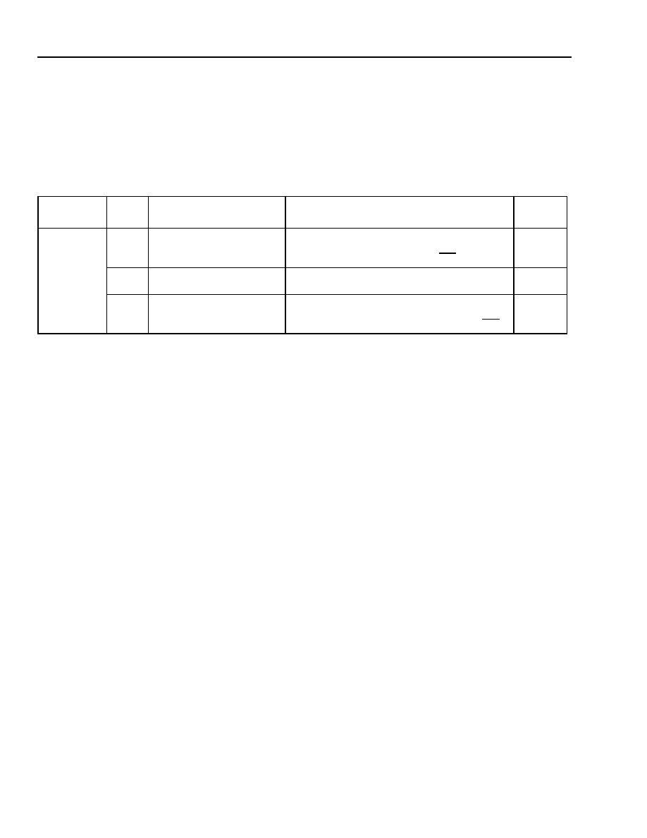
196
Agere Systems Inc.
Data Sheet
May 2001
155/622/2488 Mbits/s Data Interface
TDAT042G5 SONET/SDH
Register Descriptions
(continued)
PT Registers
(continued)
Table 100. Registers 0x097F--0x0980, 0x098C--0x098D, 0x0999--0x099A, 0x09A6--0x09A7: PT Interrupt
Mask Control (R/W)
Reset default of registers 0x097F, 0x098C, 0x0999, 0x09A6 = 0x8FFF.
Reset default of registers 0x0980, 0x098D, 0x099A, 0x09A7 = 0xFFFF.
Address
(Hex)
Bit #
Name
Function (All Mask Bits Are Active-High)
Reset
Default
097F, 098C,
0999, 09A6
15
RJ1DMONMISM[A--D]
Receive J1 Data Monitor Mismatch Mask.
Mask bit to inhibit the associated event bit from
contributing to the interrupt pin (INT).
1
14--12
--
Reserved. These bits must be written to their
reset default value (000).
000
11--0
RPIH_STATEM[A--D]
[1--12]
Receive Pointer Interpretation Hardware
Mask. Mask bits to inhibit the associated delta
bits from contributing to the interrupt pin (INT).
0xFFF
Agere Systems Inc.
197
Data Sheet
May 2001
155/622/2488 Mbits/s Data Interface
TDAT042G5 SONET/SDH
Register Descriptions
(continued)
PT Registers
(continued)
Table 100. Registers 0x097F--0x0980, 0x098C--0x098D, 0x0999--0x099A, 0x09A6--0x09A7: PT Interrupt
Mask Control (R/W)
(continued)
Reset default of registers 0x097F, 0x098C, 0x0999, 0x09A6 = 0x8FFF.
Reset default of registers 0x0980, 0x098D, 0x099A, 0x09A7 = 0xFFFF.
Address
(Hex)
Bit #
Name
Function (All Mask Bits Are Active-High)
Reset
Default
0980, 098D,
099A, 09A7
15
TRDIPINTM[A--D]
Transmit RDI-P Mask. Mask bit to inhibit the
associated delta bit from contributing to the
interrupt pin (INT).
1
14--11
--
Reserved. These bits must be written to their
reset default value (1111).
1111
10
RZ5DMONM[A--D]
Receive Z5 Data Monitor Mask. Mask bit to
inhibit the associated delta bit from contributing
to the interrupt pin (INT).
1
9
RZ4DMONM[A--D]
Receive Z4 Data Monitor Mask. Mask bit to
inhibit the associated delta bit from contributing
to the interrupt pin (INT).
1
8
RZ3DMONM[A--D]
Receive Z3 Data Monitor Mask. Mask bit to
inhibit the associated delta bit from contributing
to the interrupt pin (INT).
1
7
RH4DMONM[A--D]
Receive H4 Data Monitor Mask. Mask bit to
inhibit the associated delta bit from contributing
to the interrupt pin (INT).
1
6
RF2DMONM[A--D]
Receive F2 Data Monitor Mask. Mask bit to
inhibit the associated delta bit from contributing
to the interrupt pin (INT).
1
5
RRDIPDMONM[A--D]
Receive RDI-P Data Monitor Mask. Mask bit
to inhibit the associated delta bit from
contributing to the interrupt pin (INT).
1
4
RC2DMONM[A--D]
Receive C2 Value Mask. Mask bit to inhibit the
associated delta bit from contributing to the
interrupt pin (INT).
1
3
RUC2VM[A--D]
Receive Unequipped C2 Values Mask. Mask
bit to inhibit the associated delta bit from
contributing to the interrupt pin (INT).
1
2
RPPLMM[A--D]
Receive Path Payload Label Mismatch Mask.
Mask bit to inhibit the associated delta bit from
contributing to the interrupt pin (INT).
1
1
RSDM[A--D]
Receive Signal Degrade Mask. Mask bit to
inhibit the associated delta bit from contributing
to the interrupt pin (INT).
1
0
RSFM[A--D]
Receive Signal Fail Mask. Mask bit to inhibit
the associated delta bit from contributing to the
interrupt pin (INT).
1

198
Agere Systems Inc.
Data Sheet
May 2001
155/622/2488 Mbits/s Data Interface
TDAT042G5 SONET/SDH
Register Descriptions
(continued)
PT Registers
(continued)
Table 101. Registers (0x09B3, 0x09BF, 0x09CB, 0x09D7, 0x09E3), (0x09EF, 0x09FB, 0x0A07, 0x0A14,
0x0A20), (0x0A2C, 0x0A38, 0x0A44, 0x0A50, 0x0A5C), (0x0A68, 0x0A74, 0x0A80, 0x0A8C,
0x0A98): Error Counters (RO)
Reset default of registers = 0x0000.
Table 102. Register 0x0AA4: PT One-Shot Control Parameters (WO)
Address
(Hex)
Bit #
Name
Function
Reset
Default
09B3, 09EF,
0A2C, 0A68
15--11
--
Reserved. These bits must be written to their
reset default value (00000).
00000
10--0
RPI_INC[A--D][10:0]
Receive Pointer Interpreter Increment
Counter. Counter that counts the number of
increments that occurred on the selected time
slot.
000
0000
0000
09BF, 09FB,
0A38, 0A74
15--11
--
Reserved. These bits must be written to their
reset default value (00000).
00000
10--0
RPI_DEC[A--D][10:0]
Receive Pointer Interpreter Decrements
Counter. Counter that counts the number of
decrements that occurred on the selected time
slot.
000
0000
0000
09CB, 0A07,
0A44, 0A80
15--13
--
Reserved. These bits must be written to their
reset default value (000).
000
12--0
RNDFCNT[A--D][12:0]
Receive Pointer Interpreter NDF Counter.
Counter that counts the number of set NDF
(1001) values received on the selected time
slot.
0
0000
0000
0000
09D7, 0A14,
0A50, 0A8C
15--0
RB3ERRCNT[A--D][15:0]
B3 Error Count. Number of B3 errors detected
on the monitored STS-1 time slots.
0x0000
09E3, 0A20,
0A5C, 0A98
15--0
RREIPERRCNT
[A--D][15:0]
Receive Remote Error Indication--Path
Error Count. Count of the number of B3 errors
detected in the G1[7:4] nibble.
0x0000
Address
(Hex)
Bit #
Name
Function
Reset
Default
0AA4
15--12
SDCLEAR[A--D]
Signal Degrade Clear. One-shot clear control.
--
11--8
SDSET[A--D]
Signal Degrade Set. One-shot set control.
--
7--4
SFCLEAR[A--D]
Signal Fail Clear. One-shot clear control.
--
3--0
SFSET[A--D]
Signal Fail Set. One-shot set control.
--

Agere Systems Inc.
199
Data Sheet
May 2001
155/622/2488 Mbits/s Data Interface
TDAT042G5 SONET/SDH
Register Descriptions
(continued)
PT Registers
(continued)
Table 103. Registers 0x0AA6--0x0AAD, 0x0AAE, 0x0AB5, 0x0AB6--0x0ABD, 0x0ABE--0x0AC5: PT Control
Parameters (R/W)
Reset default of registers 0x0AA6, 0x0AAE, 0x0AB6, 0x0ABE = 0x1200.
Reset default of registers 0x0AA7, 0x0AAF, 0x0AB7, 0x0ABF = 0x0000.
Reset default of registers 0x0AA8, 0x0AB0, 0x0AB8, 0x0AC0 = 0x0FFF.
Reset default of registers 0x0AA9, 0x0AB1, 0x0AB9, 0x0AC1 = 0x0000.
Reset default of registers 0x0AAA, 0x0AB2, 0x0ABA, 0x0AC2 = 0x0000.
Reset default of registers 0x0AAB, 0x0AB3, 0x0ABB, 0x0AC3 = 0x1AAA.
Reset default of registers 0x0AAC, 0x0AB4, 0x0ABC, 0x0AC4 = 0x3AAA.
Reset default of registers 0x0AAD, 0x0AB5, 0x0ABD, 0x0AC5 = 0x3333.
* These bits maintain the validated J1 byte, place 0x0000 into all other POH bytes, and invalidate the received payload so that no data is passed
through the DE. These bits do not affect the transmit path and do not affect the transmitted G1 byte.
Address
(Hex)
Bit #
Name
Function
Reset
Default
0AA6, 0AAE,
0AB6, 0ABE
15--12
RPOHMONSEL
[A--D][3:0]
Receive POH Monitor Select. Control bit selects which
of the 12 time-slot POH bytes are monitored in the
associated data stream. A total of four
STS-Nc streams can be monitored at any one time.
Only values from 0001 (time slot 1) to 1100
(time slot 12) are valid. For quad OC-3 and quad OC-12
mode, use the default value 0001.
0001
11--10
--
Reserved. These bits must be written to their reset
default value (00).
00
9
RCONC_ALLOR
FIRST[A--D]
Receive Concatenation State: Use All STS-1 Time
Slots or Just the First One. If set to 1, all STS-1 time
slots are used. If set to 0, a higher level state machine
(CONC) is used to process the individual states from
the associated time slots. The higher-order state
machine is defined as follows.
CONC State Equations (ETSI and G.783 (SDH)):
States
Concatenation States
(bold states are reported)
AISX
AIS
#1
AND AISC
#2
AND . . . AISC
#X
NORMX
NORM
#1
AND CONC
#2
AND . . . CONC
#N
INCX*
INC
#1
AND CONC
#2
AND . . . CONC
#N
DECX*
DEC
#1
AND CONC
#2
AND . . . CONC
#N
NDFX*
NDF
#1
AND CONC
#2
AND . . . CONC
#N
LOPX
(Any other): NOT AISX
AND NOT NORMX
AND NOT INCX
AND NOT DECX
AND NOT NDFX
* States INCX, DECX, and NDFX are considered the same as
NORMX state in terms of reporting.
1
8--7
RJ1FRAMEA
[A--D][1:0]
Receive J1 Frame Algorithm. Control bits, when set to
00 or 11 = no framing; 01 = SONET framing; 10 = SDH
framing.
00

200
Agere Systems Inc.
Data Sheet
May 2001
155/622/2488 Mbits/s Data Interface
TDAT042G5 SONET/SDH
Register Descriptions
(continued)
PT Registers
(continued)
Table 103. Registers 0x0AA6--0x0AAD, 0x0AAE, 0x0AB5, 0x0AB6--0x0ABD, 0x0ABE--0x0AC5: PT Con-
trol Parameters (R/W) (continued)
Reset default of registers 0x0AA6, 0x0AAE, 0x0AB6, 0x0ABE = 0xF200.
Reset default of registers 0x0AA7, 0x0AAF, 0x0AB7, 0x0ABF = 0x0000.
Reset default of registers 0x0AA8, 0x0AB0, 0x0AB8, 0x0AC0 = 0x0FFF.
Reset default of registers 0x0AA9, 0x0AB1, 0x0AB9, 0x0AC1 = 0x0000.
Reset default of registers 0x0AAA, 0x0AB2, 0x0ABA, 0x0AC2 = 0x0000.
Reset default of registers 0x0AAB, 0x0AB3, 0x0ABB, 0x0AC3 = 0x1AAA.
Reset default of registers 0x0AAC, 0x0AB4, 0x0ABC, 0x0AC4 = 0x3AAA.
Reset default of registers 0x0AAD, 0x0AB5, 0x0ABD, 0x0AC5 = 0x3333
* SS pointer interpretation algorithm is not implemented.
These bits maintain the validated J1 byte, place 0x0000 into all other POH bytes, and invalidate the received payload so that no data is passed
through the DE. These bits do not affect the transmit path and do not affect the transmitted G1 byte.
Address
(Hex)
Bit #
Name
Function
Reset
Default
0AA6, 0AAE,
0AB6, 0ABE
6
RJ1DMPC[A--D]
Receive J1 Dump Control. Control bit, when set
to a logic 1, causes the device to store the J1 byte
of the selected STS-1 time slot.
0
5
--
Reserved. This bit must be written to its reset
default value (0).*
0
4
RB3BITBLKCNT[A--D]
Receive B3 Bit/Block Count. Control bit, when
set to a logic 0, causes the B3 error counter to
count bit errors; otherwise, block errors are
counted.
0
3
RINCDEC_6OR8MAJ
[A--D]
Receive Increment/Decrement 6-or-8 Majority
Voting. If programmed to a logic 0, uses 6 of 10
majority voting to determine a valid increment or
decrement; otherwise, uses 8 of 10 majority voting.
0
2--1
--
Reserved. These bits must be written to their reset
default value (00).
00
0
RDIPMON_ENH_OR1B
[A--D]
Remote Defect Indication Enhanced or 1-Bit
Monitoring. Control bit, when set to a logic 1,
causes the RDI-P to detect G1[3:1] bits for an
enhanced failure code; otherwise, monitors G1[3]
for a 1-bit code.
0
0AA7, 0AAF,
0AB7, 0ABF
15--12
RFORCE_LOP[A--D]
[1--4]
Receive FORCE_LOP. Control bits, when set to a
logic 1, force the associated time slot into the LOP
state; otherwise, does nothing.
0x0
11--0
CONCATI_EXPECTED
[A--D][1--12]
Concatenation Indication Expected. Control bits,
when set to 0 = do not expect associated time slot
to be in CONC mode; otherwise, expect CONC
mode.
0x000
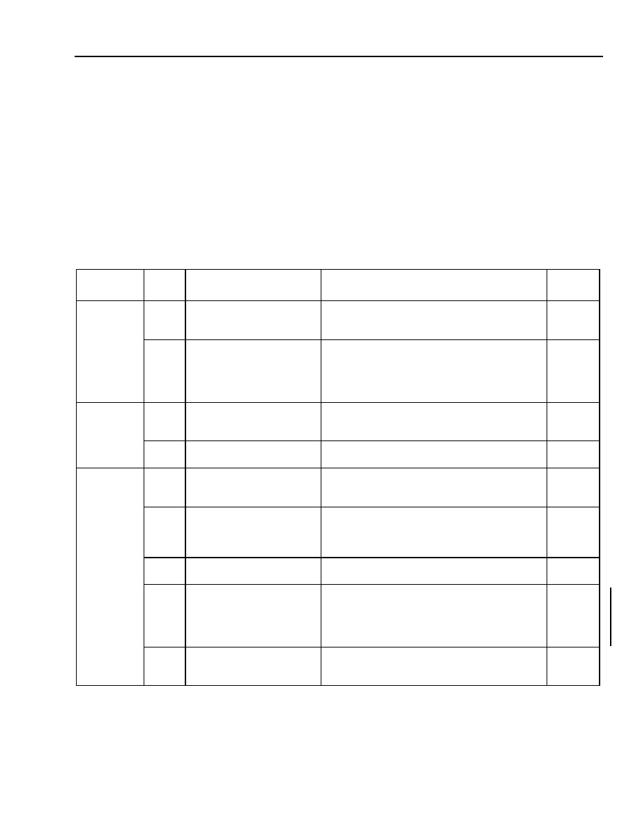
Agere Systems Inc.
201
Data Sheet
May 2001
155/622/2488 Mbits/s Data Interface
TDAT042G5 SONET/SDH
Register Descriptions
(continued)
PT Registers
(continued)
Table 103. Registers 0x0AA6--0x0AAD, 0x0AAE, 0x0AB5, 0x0AB6--0x0ABD, 0x0ABE--0x0AC5: PT Con-
trol Parameters (R/W) (continued)
Reset default of registers 0x0AA6, 0x0AAE, 0x0AB6, 0x0ABE = 0xF200.
Reset default of registers 0x0AA7, 0x0AAF, 0x0AB7, 0x0ABF = 0x0000.
Reset default of registers 0x0AA8, 0x0AB0, 0x0AB8, 0x0AC0 = 0x0FFF.
Reset default of registers 0x0AA9, 0x0AB1, 0x0AB9, 0x0AC1 = 0x0000.
Reset default of registers 0x0AAA, 0x0AB2, 0x0ABA, 0x0AC2 = 0x0000.
Reset default of registers 0x0AAB, 0x0AB3, 0x0ABB, 0x0AC3 = 0x1AAA.
Reset default of registers 0x0AAC, 0x0AB4, 0x0ABC, 0x0AC4 = 0x3AAA.
Reset default of registers 0x0AAD, 0x0AB5, 0x0ABD, 0x0AC5 = 0x3333.
* These bits maintain the validated J1 byte, place 0x0000 into all other POH bytes, and invalidate the received payload so that no data is passed
through the DE. These bits do not affect the transmit path and do not affect the transmitted G1 byte.
Address
(Hex)
Bit #
Name
Function
Reset
Default
0AA8, 0AB0,
0AB8, 0AC0
15--12
RFORCE_LOP[A--D]
[5--8]
Receive FORCE_LOP. Control bits, when set
to a logic 1, force the associated time slot into
the LOP state; otherwise, does nothing.*
0x0
11--0
MASK_CONCAT[A--D]
[1--12]
MASK_CONCATENATION Expected
Indication. When set, mask bits inhibit the
generation of AIS when the selected time slot
transitions to a state other than
CONCAT_EXPECTED[A--D].
0xFFF
0AA9, 0AB1,
0AB9, 0AC1
15--12
RFORCE_LOP[A--D]
[9--12]
Receive FORCE_LOP. Control bits, when set
to a logic 1, force the associated time slot into
the LOP state; otherwise, does nothing.*
0x0
11--0
RFORCE_AIS[A--D]
[1--12]
Receive FORCE AIS. If set, control bits insert
AIS-P into the selected STS-1 time slot.*
0x000
0AAA, 0AB2,
0ABA, 0AC2
15--12
Tx_REIP_VALUE
[A--D][3:0]
Transmit REI-P Error Value. REI software
error value. Error values are 1 to 8; all others
are interpreted as no errors.
0x0
11
TRDIPSINS[A--D]
Transmit RDI-P Software Insert. Control bit,
when set, forces the value in
TRDIPDINS[A--D][2:0] into the outgoing
G1[3:1] bits.
0
10
--
Reserved. This bit must be written to its reset
default value (0).
0
9
TRDIP_LCD[A--D]
Transmit RDI-P LCD. Control bit, when clear,
generates an LCD failure that causes an RDI-P
generation. When set, no LCD failure is
generated. LCD determination must be done
via software.
0
8
TRDIP_PLMPINH[A--D]
Transmit RDI-P PLM-P Inhibit. Control bit,
when set, causes the PLM-P failure to not
contribute to RDI-P generation.
0

202
Agere Systems Inc.
Data Sheet
May 2001
155/622/2488 Mbits/s Data Interface
TDAT042G5 SONET/SDH
Register Descriptions
(continued)
PT Registers
(continued)
Table 103. Registers 0x0AA6--0x0AAD, 0x0AAE, 0x0AB5, 0x0AB6--0x0ABD, 0x0ABE--0x0AC5: PT Con-
trol Parameters (R/W) (continued)
Reset default of registers 0x0AA6, 0x0AAE, 0x0AB6, 0x0ABE = 0xF200.
Reset default of registers 0x0AA7, 0x0AAF, 0x0AB7, 0x0ABF = 0x0000.
Reset default of registers 0x0AA8, 0x0AB0, 0x0AB8, 0x0AC0 = 0x0FFF.
Reset default of registers 0x0AA9, 0x0AB1, 0x0AB9, 0x0AC1 = 0x0000.
Reset default of registers 0x0AAA, 0x0AB2, 0x0ABA, 0x0AC2 = 0x0000.
Reset default of registers 0x0AAB, 0x0AB3, 0x0ABB, 0x0AC3 = 0x1AAA.
Reset default of registers 0x0AAC, 0x0AB4, 0x0ABC, 0x0AC4 = 0x3AAA.
Reset default of registers 0x0AAD, 0x0AB5, 0x0ABD, 0x0AC5 = 0x3333.
Address
(Hex)
Bit #
Name
Function
Reset
Default
0AAA, 0AB2,
0ABA, 0AC2
7
TRDIP_UNEQUIPINH
[A--D]
Transmit RDI-P UNEQUIP Inhibit. Control bit,
when set, causes the UNEQUIP failure to not
contribute to RDI-P generation.
0
6
TRDIP_LOPPINH[A--D]
Transmit RDI-P LOP-P Inhibit. Control bit,
when set, causes the LOP-P failure to not
contribute to RDI-P generation.
0
5
TRDIP_AISINH[A--D]
Transmit RDI-P AIS-P Inhibit. Control bit,
when set, causes the AIS-P failure to not
contribute to RDI-P generation.
0
4
TRDIP_ENH_OR1B[A--D] Transmit RDI-P Enhanced or 1-Bit
Monitoring. Control bit, when set, causes
enhanced failure code insert to occur on the
G1[3:1] bits; otherwise, inserts a single bit
failure code into G1[3].
0
3
TREIPERRINS[A--D]
Transmit REI-P Error Insert. Control bit, when
set, causes an error to be continuously injected
into the G1[7:4] bits.
0
2
TB3ERRINS[A--D]
Transmit B3 Error Insert. Control bit, when
set, causes the B3 value to be inverted.
0
1
TJ1SINS[A--D]
Transmit J1 Software Insert. Control bit, when
set, causes the J1 byte stored in the
TJ1DINS[A--D][1--64][7:0] register to be
injected into the outgoing J1 byte; otherwise,
inserts 0x00 into the J1 byte.
0
0
--
Reserved. This bit must be written to its reset
default value (0).
0

Agere Systems Inc.
203
Data Sheet
May 2001
155/622/2488 Mbits/s Data Interface
TDAT042G5 SONET/SDH
Register Descriptions
(continued)
PT Registers
(continued)
Table 103. Registers 0x0AA6--0x0AAD, 0x0AAE, 0x0AB5, 0x0AB6--0x0ABD, 0x0ABE--0x0AC5: PT Con-
trol Parameters (R/W) (continued)
Reset default of registers 0x0AA6, 0x0AAE, 0x0AB6, 0x0ABE = 0xF200.
Reset default of registers 0x0AA7, 0x0AAF, 0x0AB7, 0x0ABF = 0x0000.
Reset default of registers 0x0AA8, 0x0AB0, 0x0AB8, 0x0AC0 = 0x0FFF.
Reset default of registers 0x0AA9, 0x0AB1, 0x0AB9, 0x0AC1 = 0x0000.
Reset default of registers 0x0AAA, 0x0AB2, 0x0ABA, 0x0AC2 = 0x0000.
Reset default of registers 0x0AAB, 0x0AB3, 0x0ABB, 0x0AC3 = 0x1AAA.
Reset default of registers 0x0AAC, 0x0AB4, 0x0ABC, 0x0AC4 = 0x3AAA.
Reset default of registers 0x0AAD, 0x0AB5, 0x0ABD, 0x0AC5 = 0x3333.
Address
(Hex)
Bit #
Name
Function
Reset
Default
0AAB, 0AB3,
0ABB, 0AC3
15--12
TPOHINSSEL[A--D][3:0]
Transmit POH Insert Select. Control bits,
when set, select the STS-1 time slot into which
POH data is injected.
0x1
11--0
THx_STATE[A--D]
[1--6][1:0]
Transmit H Bytes Software State. Control
bits, when set to a logic 00 = normal state,
01 = CONC, 10 = unequipped, 11 = AIS.
0xAAA
0AAC, 0AB4,
0ABC, 0AC4
15--12
CNTDH4Z3Z4[A--D][3:0]
Continuous N Times Detect H4/Z3/Z4 Bytes.
Control signal for detecting changes in state of
the H4, Z3, and Z4 bytes. Valid values are 0 to
15. A value of 0 or 1 causes the data monitor
byte to be updated every frame.
A value of n, where 2
n
15, of these four bits
means that the same value of the H4, Z3, or Z4
byte must be detected n times consecutively to
declare a new value in the H4, Z3, or Z4 byte
register.
0x3
11--0
THx_STATE[A--D]
[7--12][1:0]
Transmit H Bytes Software State. Control
bits, when set to a logic 00 = normal state,
01 = CONC, 10 = unequipped, 11 = AIS.
0xAAA

204
Agere Systems Inc.
Data Sheet
May 2001
155/622/2488 Mbits/s Data Interface
TDAT042G5 SONET/SDH
Register Descriptions
(continued)
PT Registers
(continued)
Table 103. Registers 0x0AA6--0x0AAD, 0x0AAE, 0x0AB5, 0x0AB6--0x0ABD, 0x0ABE--0x0AC5: PT Con-
trol Parameters (R/W) (continued)
Reset default of registers 0x0AA6, 0x0AAE, 0x0AB6, 0x0ABE = 0xF200.
Reset default of registers 0x0AA7, 0x0AAF, 0x0AB7, 0x0ABF = 0x0000.
Reset default of registers 0x0AA8, 0x0AB0, 0x0AB8, 0x0AC0 = 0x0FFF.
Reset default of registers 0x0AA9, 0x0AB1, 0x0AB9, 0x0AC1 = 0x0000.
Reset default of registers 0x0AAA, 0x0AB2, 0x0ABA, 0x0AC2 = 0x0000.
Reset default of registers 0x0AAB, 0x0AB3, 0x0ABB, 0x0AC3 = 0x1AAA.
Reset default of registers 0x0AAC, 0x0AB4, 0x0ABC, 0x0AC4 = 0x3AAA.
Reset default of registers 0x0AAD, 0x0AB5, 0x0ABD, 0x0AC5 = 0x3333.
Address
(Hex)
Bit #
Name
Function
Reset
Default
0AAD, 0AB5,
0ABD, 0AC5
15--12
CNTDZ5[A--D][3:0]
Continuous N Times Detect Z5 Byte. Control
signal for detecting changes in state of the Z5
byte. Valid values are 0 to 15. A value of 0 or 1
causes the data monitor byte to be updated
every frame.
A value of n, where 2
n
15, of these four bits
means that the same value of the Z5 byte must
be detected n times consecutively to declare a
new value in the Z5 byte register.
0x3
11--8
CNTDF2[A--D][3:0]
Continuous N Times Detect F2 Byte. Control
signal for detecting changes in state of the F2
byte. Valid values are 0 to 15. A value of 0 or 1
causes the data monitor byte to be updated
every frame.
A value of n, where 2
n
15, of these four bits
means that the same value of the F2 byte must
be detected n times consecutively to declare a
new value in the F2 byte register.
0x3
7--4
CNTDRDIP[A--D][3:0]
Continuous N Times Detect RDI-P. Control
signal for detecting changes in state of the
G1[3:1] bits. Valid values are 0 to 15. A value of
0 or 1 causes the data monitor byte to be
updated every frame.
A value of n, where 2
n
15, of these four bits
means that the same value of the RDI-P byte
must be detected n times consecutively to
declare a new value in the RDI-P byte register.
0x3
3--0
CNTDC2[A--D][3:0]
Continuous N Times Detect C2 Byte. Control
signal for detecting changes in state of the C2
byte. Valid values are 0 to 15. A value of 0 or 1
causes the data monitor byte to be updated
every frame.
A value of n, where 2
n
15, of these four bits
means that the same value of the C2 byte must
be detected n times consecutively to declare a
new value in the C2 byte register.
0x3

Agere Systems Inc.
205
Data Sheet
May 2001
155/622/2488 Mbits/s Data Interface
TDAT042G5 SONET/SDH
Register Descriptions
(continued)
PT Registers
(continued)
Table 104. Registers 0x0AC6--0x0AF7: PT Provisioning (R/W)
Reset default of register 0x0AC6 = 0x0001.
Reset default of registers 0x0AC7--0x0ACB = 0x0000.
* SS pointer interpretation algorithm is not implemented.
Address
(Hex)
Bit #
Name
Function
Reset
Default
0AC6
15--6
--
Reserved. These bits must be written to their
reset default value (0000000000).
00
0000
0000
5--4
PG_PROV_PNUM[1:0]
Page Provisioning Port Number. Control bit
that selects the port being provisioned. 00 =
port A, 01 = port B, 10 = port C, and 11 = port
D.
00
3--0
PG_PROV_TNUM[3:0]
Page Provisioning Time-Slot Number.
Control bit that selects the time slot being
provisioned. Legal values are 1 to 12, all illegal
values default to time slot 1.
0x1
0AC7
15--13
TRDIPDINS[2:0]
Transmit RDI-P Data Insert. Software insert
value.
000
12--11
TSS[1:0]
Transmit SS Value. Control values inserted
into the SS bits in the H1 byte.
00
10--2
--
Reserved. These bits must be written to their
reset default value (000000000).
0
0000
0000
1--0
--
Reserved. These bits must be written to their
reset default value (00).*
00
0AC8
15--8
--
Reserved. These bits must be written to their
reset default value (0x00).
0x00
7--0
RC2EXPVAL[7:0]
Receive C2 Expected Value. Expected value
for the C2 byte.
0x00
0AC9
15--8
TF2DINS[7:0]
Transmit F2 Data Insert. Programmable F2
byte insert value.
0x00
7--0
TC2DINS[7:0]
Transmit C2 Data Insert. Insert byte for the
outgoing C2 bytes.
Note: A value of zero causes an unequipped
signal to be generated.
0x00
0ACA
15--8
TZ3DINS[7:0]
Transmit Z3 Data Insert. Programmable Z3
byte insert value.
0x00
7--0
TH4DINS[7:0]
Transmit H4 Data Insert. Programmable H4
byte insert value.
0x00
0ACB
15--8
TZ5DINS[7:0]
Transmit Z5 Data Insert. Programmable Z5
byte insert value.
0x00
7--0
TZ4DINS[7:0]
Transmit Z4 Data Insert. Programmable Z4
byte insert value.
0x00

206
Agere Systems Inc.
Data Sheet
May 2001
155/622/2488 Mbits/s Data Interface
TDAT042G5 SONET/SDH
Register Descriptions
(continued)
PT Registers
(continued)
Table 105. Registers 0x0ACC--0x0AD1: PT Signal Fail BER Algorithm Parameters (R/W)
Reset default of registers 0x0ACC--0x0AD1 = 0x0000.
Address
(Hex)
Bit #
Name
Function
Reset
Default
0ACC
15--8
PT_SFMSET[7:0]
Signal Fail M Set. Threshold of the number of
bad monitoring blocks in an observation
interval. If the number of bad blocks is below
this threshold, then RHSSD is cleared.
0x00
7--4
--
Reserved. These bits must be written to their
reset default value (0x0).
0x0
3--0
PT_SFLSET[3:0]
Signal Fail L Set. Error threshold for
determining if a monitoring block is bad.
0x0
0ACD
15--13
PT_SFNSSET[18:16]
Signal Fail Ns Set. Number of frames in a
monitoring block for RHSSD.
000
12
--
Reserved. This bit must be written to its reset
default value (0).
0
11--0
PT_SFBSET[11:0]
Signal Fail B Set. Number of monitoring
blocks.
0x000
0ACE
15--0
PT_SFNSSET[15:0]
Signal Fail Ns Set. Number of frames in a
monitoring block for RHSSD.
0x0000
0ACF
15--8
PT_SFMCLEAR[7:0]
Signal Fail M Clear. Threshold of the number
of bad monitoring blocks in an observation
interval. If the number of bad blocks is below
this threshold, then RHSSD is cleared.
0x00
7--4
--
Reserved. These bits must be written to their
reset default value (0x0).
0x0
3--0
PT_SFLCLEAR[3:0]
Signal Fail L Clear. Error threshold for
determining if a monitoring block is bad.
0x0
0AD0
15--13
PT_SFNSCLEAR[18:16]
Signal Fail Ns Clear. Number of frames in a
monitoring block for RHSSD.
000
12
--
Reserved. This bit must be written to its reset
default value (0).
0
11--0
PT_SFBCLEAR[11:0]
Signal Fail B Clear. Number of monitoring
blocks.
0x000
0AD1
15--0
PT_SFNSCLEAR[15:0]
Signal Fail Ns Clear. Number of frames in a
monitoring block for RHSSD.
0x0000

Agere Systems Inc.
207
Data Sheet
May 2001
155/622/2488 Mbits/s Data Interface
TDAT042G5 SONET/SDH
Register Descriptions
(continued)
PT Registers
(continued)
Table 106. Registers 0x0AD2--0x0AD7: PT Signal Degrade BER Algorithm Parameters (R/W)
Reset default of registers 0x0AD2--0x0AD7 = 0x0000.
Address
(Hex)
Bit #
Name
Function
Reset
Default
0AD2
15--8
PT_SDMSET[7:0]
Signal Degrade M Set. Threshold of the number of
bad monitoring blocks in an observation interval. If
the number of bad blocks is below this threshold, then
RHSSD is cleared.
0x00
7--4
--
Reserved. These bits must be written to their reset
default value (0x0).
0x0
3--0
PT_SDLSET[3:0]
Signal Degrade L Set. Error threshold for
determining if a monitoring block is bad.
0x0
0AD3
15--13
PT_SDNSSET[18:16] Signal Degrade Ns Set. Number of frames in a
monitoring block for RHSSD.
000
12
--
Reserved. This bit must be written to its reset default
value (0).
0
11--0
PT_SDBSET[11:0]
Signal Degrade B Set. Number of monitoring blocks.
0x000
0AD4
15--0
PT_SDNSSET[15:0]
Signal Degrade Ns Set. Number of frames in a
monitoring block for RHSSD.
0x0000
0AD5
15--8
PT_SDMCLEAR[7:0]
Signal Degrade M Clear. Threshold of the number of
bad monitoring blocks in an observation interval. If
the number of bad blocks is below this threshold, then
RHSSD is cleared.
0x00
7--4
--
Reserved. These bits must be written to their reset
default value (0x0).
0x0
3--0
PT_SDLCLEAR[3:0]
Signal Degrade L Clear. Error threshold for
determining if a monitoring block is bad.
0x0
0AD6
15--13
PT_SDNSCLEAR
[18:16]
Signal Degrade Ns Clear. Number of frames in a
monitoring block for RHSSD.
000
12
--
Reserved. This bit must be written to its reset default
value (0).
0
11--0
PT_SDBCLEAR[11:0] Signal Degrade B Clear. Number of monitoring
blocks.
0x000
0AD7
15--0
PT_SDNSCLEAR
[15:0]
Signal Degrade Ns Clear. Number of frames in a
monitoring block for RHSSD.
0x0000
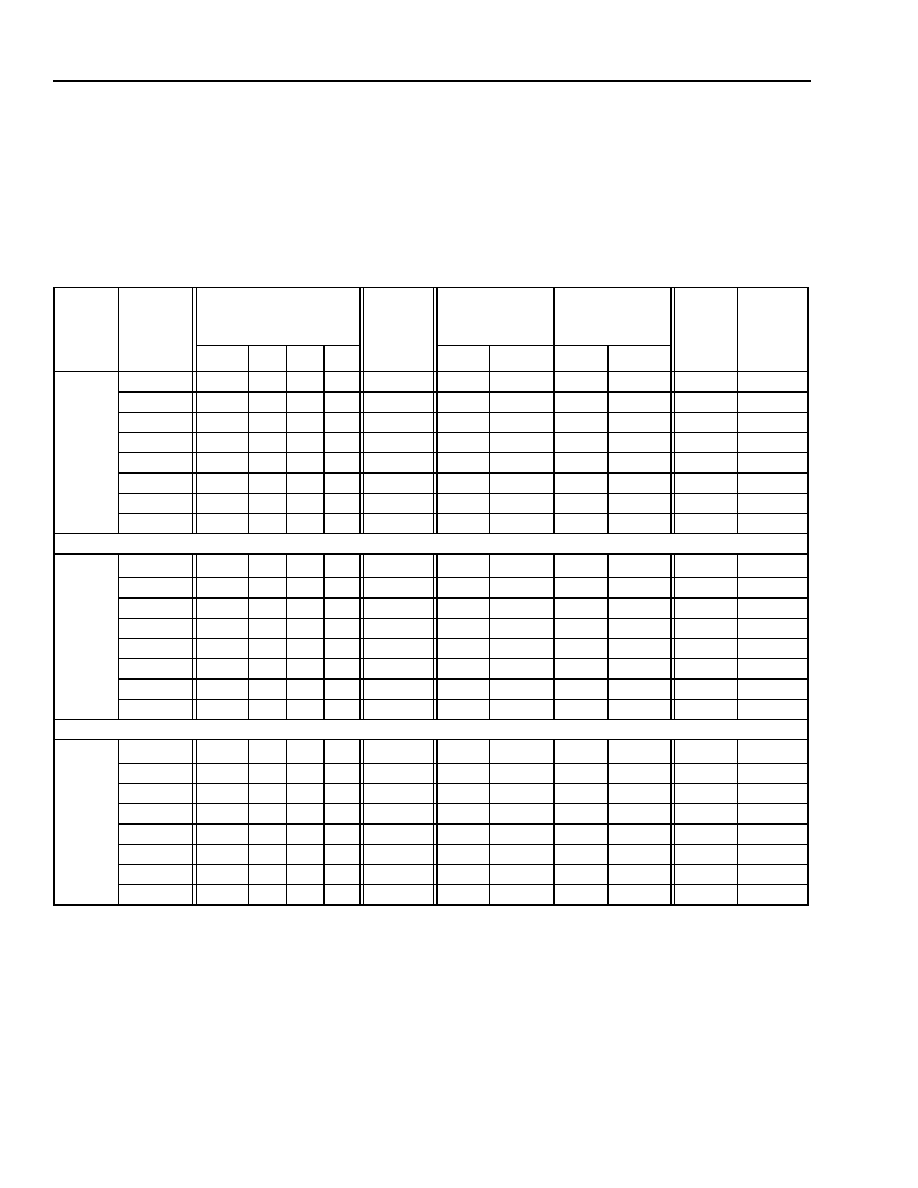
208
Agere Systems Inc.
Data Sheet
May 2001
155/622/2488 Mbits/s Data Interface
TDAT042G5 SONET/SDH
Register Descriptions
(continued)
PT Registers
(continued)
Table 107 and Table 108 show values of Ns, L, M, and B for STS-3/STM-1, STS-12/STM-4, and STS-48/STM-16 to
set and clear the BER indicator. SF registers are 0x0ACC--0x0AD1, and SD registers are 0x0AD2--0x0AD7. All
SF/SD set and clear values are hexadecimal.
Table 107. Ns, L, M, and B Values to Set the BER Indicator
* These are the numbers to be provisioned in TDAT042G5. The actual values of the BER algorithm are 1 greater than the actual values shown.
These BER values cannot be provisioned because the maximum value of L is 0xF (i.e., L is a 4-bit register).
Mode
BER
SF/SD Set Values
Actual
Number of
Frames
Probability of
Detecting L
Errors (%)
Probability of
Declaring
SF/SD (%)
Integra-
tion
Time
(s)
Max-
imum
Number
of Frames
Ns*
L*
M*
B*
@BER
@BER/2
@BER
@BER/2
STS-3/
STM-1
1.00E-03
1
6
3D
3D
62
99.96
85.13
97.68
0.00
0.008
64
1.00E-04
6
9
3
7
48
72.70
7.28
96.06
0.16
0.013
104
1.00E-05
30
7
3
7
384
71.34
10.08
95.19
0.52
0.1
800
1.00E-06
1E0
7
3
7
3840
71.34
10.09
95.19
0.52
1
8000
1.00E-07
1275
7
4
9
47250
69.74
9.44
95.07
0.13
10
80000
1.00E-08
B5A4
7
3
9
465000
68.07
8.82
98.47
0.82
83
664000
1.00E-09
3F7A0
4
5
F
4160000
56.90
11.25
96.52
0.60
667
5336000
1.00E-10
--
--
--
--
--
--
--
--
--
--
--
STS-12/
STM-4
1.00E-03
--
--
--
--
64
100.00
88.43
100.00
0.04
0.008
64
1.00E-04
2
B
6
A
22
84.92
9.64
98.38
0.00
0.008
64
1.00E-05
D
8
3
8
117
67.93
7.17
96.48
0.25
0.025
200
1.00E-06
80
8
3
8
1152
66.19
6.66
95.46
0.19
0.25
2000
1.00E-07
4FB
8
3
8
11475
65.75
6.53
95.16
0.18
2.5
20000
1.00E-08
31CE
8
3
8
114750
65.75
6.53
95.16
0.18
21
168000
1.00E-09
1F20C
8
3
8
1147500
65.75
6.53
95.16
0.18
167
1336000
1.00E-10
--
--
--
--
--
--
--
--
--
--
--
STS-48/
STM-16
1.00E-03
--
--
--
--
64
100.00
100.00
100.00
100.00
0.008
64
1.00E-04
1
E
3F
3F
64
99.95
58.97
96.89
0.00
0.008
64
1.00E-05
5
A
35
3F
320
90.60
16.25
96.47
0.00
0.008
64
1.00E-06
20
7
8
E
480
77.55
13.09
96.69
0.00
0.0625
500
1.00E-07
13A
7
8
E
4710
75.80
12.15
95.17
0.00
0.625
5000
1.00E-08
C1C
7
7
E
46500
74.58
11.54
98.09
0.01
5.2
41600
1.00E-09
765C
6
6
A
333300
82.92
19.71
97.29
0.18
42
336000
1.00E-10
--
--
--
--
--
--
--
--
--
--
--
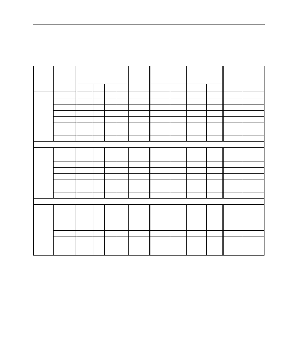
Agere Systems Inc.
209
Data Sheet
May 2001
155/622/2488 Mbits/s Data Interface
TDAT042G5 SONET/SDH
Register Descriptions
(continued)
PT Registers
(continued)
Table 108. Ns, L, M, and B Values to Clear the BER Indicator
* These are the numbers to be provisioned in TDAT042G5. The actual values of the BER algorithm are 1 greater than the actual values shown.
These BER values cannot be provisioned because the maximum value of L is 0xF (i.e., L is a 4-bit register).
Mode
BER
SF/SD Set Values
Actual
Number of
Frames
Probability of
Detecting L
Errors (%)
Probability of
Clearing
SF/SD (%)
Integra-
tion
Time
(s)
Max-
imum
Number
of Frames
Ns*
L*
M*
B*
@BER*5
@BER
@BER*5
@BER
STS-3/
STM-1
1.00E-03
--
--
--
--
--
--
--
--
--
--
--
1.00E-04
1
6
3
7
8
85.13
0.39
0.27
100.00
0.013
104
1.00E-05
6
2
3
7
48
93.01
11.33
0.01
99.21
0.1
800
1.00E-06
30
2
3
7
384
84.42
6.84
0.34
99.88
1
8000
1.00E-07
1E05
2
3
7
3840
84.42
6.84
0.34
99.88
10
80000
1.00E-08
1275
2
4
9
47250
83.66
6.59
0.22
99.98
83
664000
1.00E-09
B5A4
2
3
9
465000
82.86
6.35
0.03
99.75
667
5336000
1.00E-10
3F7A0
2
2
F
4160000
46.31
1.48
0.50
99.84
6670
53360000
STS-12/
STM-4
1.00E-03
--
--
--
--
--
--
--
--
--
--
--
1.00E-04
1
7
6
6
7
100.00
51.54
0.00
99.03
0.008
64
1.00E-05
2
2
8
A
22
98.36
20.51
0.07
100.00
0.025
200
1.00E-06
D
2
3
8
117
87.99
8.23
0.02
99.59
0.25
2000
1.00E-07
80
2
3
8
1152
87.34
7.94
0.02
99.64
2.5
20000
1.00E-08
4FB
2
3
8
11475
87.17
7.87
0.03
99.65
21
168000
1.00E-09
31CE
2
3
8
114750
87.17
7.87
0.03
99.65
167
1336000
1.00E-10
1F20C
2
3
8
1147500
87.17
7.87
0.03
99.65
1670
13360000
STS-48/
STM-16
1.00E-03
--
--
--
--
--
--
--
--
--
--
--
1.00E-04
64
100.00
45.99
0.00
99.42
0.008
64
1.00E-05
1
2
D
E
15
100.00
60.11
0.00
99.47
0.008
64
1.00E-06
5
3
D
3F
320
95.07
7.28
0.00
99.98
0.0625
500
1.00E-07
20
2
6
13
640
87.34
7.94
0.00
99.94
0.625
5000
1.00E-08
13A
2
6
13
6280
86.52
7.61
0.00
99.95
5.2
41600
1.00E-09
C1C
2
6
13
62000
85.95
7.38
0.00
99.96
42
336000
1.00E-10
765C
2
4
A
333300
84.89
7.00
0.03
99.95
420
3360000
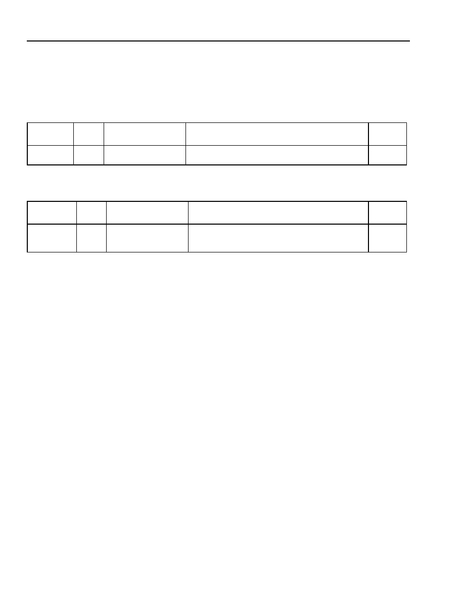
210
Agere Systems Inc.
Data Sheet
May 2001
155/622/2488 Mbits/s Data Interface
TDAT042G5 SONET/SDH
Register Descriptions
(continued)
PT Registers
(continued)
Table 109. Registers 0x0AD8--0x0AF7: Transmit J1 Data Insert (R/W)
Reset default of register = 0x0000.
Table 110. Register 0x0AF8: Scratch Register (R/W)
Reset default of register = 0x0000.
Address
(Hex)
Bit #
Name
Function
Reset
Default
0AD8--
0AF7
15--0
TJ1DINS[1--64][7:0]
Transmit J1 Data Insert. Insert values for the
selected J1 bytes.
0x0000
Address
(Hex)
Bit #
Name
Function
Reset
Default
0AF8
15--0
PT_SCRATCH[15:0]
Scratch Register. Diagnostic register used by the
microprocessor. Has no effect on the macro
operation.
0x0000

Agere Systems Inc.
211
Data Sheet
May 2001
155/622/2488 Mbits/s Data Interface
TDAT042G5 SONET/SDH
Register Descriptions
(continued)
DE Registers
This section gives a brief description of each register bit and its functionality. All algorithms are described in the
main text of the document. The abbreviations after each register indicate if the register is read only (RO), read/write
(R/W), write only (WO), or clear-on-read or clear-on-write (COR/W).
0x indicates a hexadecimal value in the Reset Default column. Otherwise, the entry is binary. This is true for every
register table in the document.
Table 111. Register 0x1000: DE Macrocell Version Number (RO)
Reset default of register = 0x0001.
Table 112. Register 0x1001, 0x1002: DE Interrupts (0x1001 is RO, 0x1002 is RO and COR/W)
Reset default of registers = 0x0000.
Note: Register 0x1001 is cleared by accessing the source register of the interrupt. The source register must be
read and cleared to clear these registers.
Address
(Hex)
Bit #
Name
Function
Reset
Default
1000
15--0
DE_VERSION
Macrocell Version Number. The version of the macrocell will
increment each time a change occurs to the macrocell
functionality.
0x0001
Address
(Hex)
Bit #
Name
Function
Reset
Default
1001
15--5
--
Reserved. These bits must be written to their reset default
value (00000000000).
000
0000
0000
4
DEINT_SDLMS
SDL Message Sent Interrupt.
Note: This bit indicates that the SDL frame inserter is
experiencing an interrupt. This bit will not clear on a
read or a write of this register, but will clear when the
SDL SDLMSI register (0x1606, bit 0) is read.
These interrupts will generate a DE interrupt.
0
3--0
DEINTCH[3:0]
Channel Interrupt. Active-high interrupt bit on a per-
channel basis. These bits are the ORing of all interrupt bits
associated with the error counters described in registers
0x1100--0x111F (pages 238--page 143). The error counter
can be inhibited from contributing to the interrupt by setting the
appropriate mask bit in register
DEDINTM[0--3] (addresses 0x1180, 0x1182, 0x1184, 0x1186
on page 243).
The following interrupts will generate a DE interrupt:
Bit 0 corresponds to channel 0 interrupt.
Bit 1 corresponds to channel 1 interrupt.
Bit 2 corresponds to channel 2 interrupt.
Bit 3 corresponds to channel 3 interrupt.
Note: This bit indicates that the channel is experiencing an
interrupt. This bit will not clear on a read or a write of
this register, but will clear when the counter interrupt
register DEDINTM[0--3] (addresses 0x1181, 0x1183,
0x1185, 0x1187 on page 244) is read or written.
0x0

212
Agere Systems Inc.
Data Sheet
May 2001
155/622/2488 Mbits/s Data Interface
TDAT042G5 SONET/SDH
Register Descriptions
(continued)
DE Registers
(continued)
Table 112. Register 0x1001, 0x1002: DE Interrupts (0x1001 is RO, 0x1002 is RO and COR/W) (continued)
Reset default of registers = 0x0000.
Notes: Register 0x1002 must be used only in the COR mode, where core register 0x0010, bit 6 = 1.
Bits 15--12, SDL Rx frame state interrupt (DEINT_SDLRxFS), are read only. Bits 15--12 are cleared by
reading and clearing the corresponding interrupt source registers, 0x14E0--0x14E3.
Address
(Hex)
Bit #
Name
Function
Reset
Default
1002
15--12
DEINT_SDLRxFS
SDL Rx Frame State Interrupt. This interrupt
is generated when the SDL frame state is
transitioned from sync to hunt. This bit is
cleared when read only.
The following interrupts will generate a DE
interrupt:
Bit 12 corresponds to channel 0 interrupt.
Bit 13 corresponds to channel 1 interrupt.
Bit 14 corresponds to channel 2 interrupt.
Bit 15 corresponds to channel 3 interrupt.
0x0
11--8
DEINT_ATMRxAC
ATM Rx All-Cool Interrupt. This interrupt is
generated when the payload of received null/
idle cells is correctly incrementing. This bit may
clear when read or written. This interrupt is
used in conjunction with the optional
incrementing payload sequence mode for
debug purposes and is used in conjunction with
DE register 0x12F0.
Bit 8 corresponds to channel 0 interrupt.
Bit 9 corresponds to channel 1 interrupt.
Bit 10 corresponds to channel 2 interrupt.
Bit 11 corresponds to channel 3 interrupt.
Note: This signal does not generate a DE
interrupt under any circumstances.
0x0

Agere Systems Inc.
213
Data Sheet
May 2001
155/622/2488 Mbits/s Data Interface
TDAT042G5 SONET/SDH
Register Descriptions
(continued)
DE Registers
(continued)
Table 112. Register 0x1001, 0x1002: DE Interrupts (0x1001 is RO, 0x1002 is RO and COR/W) (continued)
Reset default of registers = 0x0000.
Note: Register 0x1002 must be used only in the COR mode, where core register 0x0010, bit 6 = 1.
Table 113. Register 0x1004: Dry Escape Marker (R/W)
Reset default of register = 0x0020.
Address
(Hex)
Bit #
Name
Function
Reset
Default
1002
7--4
DEINT_ATMRxF
ATM Rx Frame State Interrupt. This interrupt is
generated when the ATM frame state is
transitioned from sync to hunt. This bit may clear
when read or written.
The following interrupts will generate a DE
interrupt:
Bit 0 corresponds to channel 0 interrupt.
Bit 1 corresponds to channel 1 interrupt.
Bit 2 corresponds to channel 2 interrupt.
Bit 3 corresponds to channel 3 interrupt.
0x0
3--0
DEINT_ATMRxS
ATM Rx X
31
Scrambler State Interrupt. This
interrupt is generated when the ATM scrambler
state is transitioned from synchronization to
verification. This bit may clear when read or
written.
The following interrupts will generate a DE
interrupt:
Bit 4 corresponds to channel 0 interrupt.
Bit 5 corresponds to channel 1 interrupt.
Bit 6 corresponds to channel 2 interrupt.
Bit 7 corresponds to channel 3 interrupt.
0x0
Address
(Hex)
Bit #
Name
Function
Reset
Default
1004
15--8
--
Reserved. These bits must be written to their
reset default value (0x00).
0x00
7--0
DRYESCAPE[7:0]
Dry Escape Value. This 8-bit value, attached
with 0x7D, sets the dry marker value. The default
dry marker value would then be 0x7D20.
0x20

214
Agere Systems Inc.
Data Sheet
May 2001
155/622/2488 Mbits/s Data Interface
TDAT042G5 SONET/SDH
Register Descriptions
(continued)
DE Registers
(continued)
Table 114. Registers 0x1010--0x1015: Sequencer Provisioning Registers (R/W) (continued)
Reset default of register 0x1010 = 0x0002.
Reset default of register 0x1011 = 0x2210.
Reset default of registers 0x1012, 0x1014 = 0x0435.
Reset default of registers 0x1013, 0x1015 = 0x0025.
Note: The settings of these registers must be consistent with core mode register (address 0x0010).
Address
(Hex)
Bit #
Name
Function
Reset
Default
1010
--
SEQ_CTRL
Sequencer Control. Selects STS-3/STM-1, STS-
12/STM-4, or STS-48/STM-16 mode for the data
engine. Allowed values are as follows:
STS-3/STM-1 = 0x0001
STS-12/STM-4 = 0x0003
STS-48/STM-16 = 0x0002
0x0002
15--2
--
Reserved. These bits must be written to their reset
default value (00000000000000).
00
0000
0000
0000
1
SEQ_RATE
Sequencer Rate. Configures internal clock
derived from TxCKP/TxCKN.
0 = STS-3/STM-1 (internal clock = 19.440 MHz)
1 = STS-12/STM-4 or STS-48/STM-16
(internal clock = 77.760 MHz)
1
0
SEQ_MODE
Sequencer Mode. Used with bit 1 above to select
the mode.
0 = STS-48/STM-16
1 = STS-3/STM-1 or STS-12/STM-4
0
1011
15--0
INIT_CNTS
Initial Counts. This register must be set to the
default value (0x2210).
0x2210
1012
15--0
OH_MARKER_LO
OHP Marker Low. This register must be
programmed as follows:
STS-48/STM-16 = 0x0435
STS-12/STM-4 = 0x0435
STS-3/STM-1 = 0x010B
0x0435
1013
15--0
OH_MARKER_HI
OHP Marker High. This register must be
programmed as follows:
STS-48/STM-16 = 0x0025
STS-12/STM-4 = 0x0025
STS-3/STM-1 = 0x0007
0x0025
1014
15--0
SOH_MARKER_LO
Sequence Provisioning for OHP Marker Low.
This register must be programmed as follows:
STS-48/STM-16 = 0x0435
STS-12/STM-4 = 0x0435
STS-3/STM-1 = 0x010B
0x0435
1015
15--0
SOH_MARKER_HI
Sequence Provisioning for OHP Marker High.
This register must be programmed as follows:
STS-48/STM-16 = 0x0025
STS-12/STM-4 = 0x0025
STS-3/STM-1 = 0x0007
0x0025

Agere Systems Inc.
215
Data Sheet
May 2001
155/622/2488 Mbits/s Data Interface
TDAT042G5 SONET/SDH
Register Descriptions
(continued)
DE Registers
(continued)
Table 115. Registers 0x1016--0x1021: Egress Configuration (R/W)
Reset default of registers 0x1016, 0x101A, 0x101E = 0x4444.
Reset default of registers 0x1017, 0x101B, 0x101F = 0x5555.
Reset default of registers 0x1018, 0x101C, 0x1020 = 0x6666.
Reset default of registers 0x1019, 0x101D, 0x1021 = 0x7777.
Note: See Figures 17--20, pages 78--81. The notation X/Y means the following: X = STS-48/STM-16 byte,
Y = STS-12/STM-4 or STS-3/STM-1 byte.
Address
(Hex)
Bit #
Name
Function
Reset
Default
1016--1021
15--0
Tx_TS[1--12]
Egress Time Slot [1--12]. These 12 registers
define the egress time slots. The default is set to
quad channel STS-48/STM-16. The payload bits
may be set low to account for any unused slots.
Possible configurations are as follows:
I
Multichannel STS-48/STM-16. Each time slot will
use only one channel, but the channel will vary
for each time slot.
I
Single-channel STS-48/STM-16. Each time slot
will use only one channel for every time slot.
I
STS-3/STM-1 or STS-12/STM-4. Each of four
channels will be defined once for each time slot.
See
below.

216
Agere Systems Inc.
Data Sheet
May 2001
155/622/2488 Mbits/s Data Interface
TDAT042G5 SONET/SDH
Register Descriptions
(continued)
DE Registers
(continued)
Table 115. Registers 0x1016--0x1021: Egress Configuration (R/W) (continued)
Reset default of registers 0x1016, 0x101A, 0x101E = 0x4444.
Reset default of registers 0x1017, 0x101B, 0x101F = 0x5555.
Reset default of registers 0x1018, 0x101C, 0x1020 = 0x6666.
Reset default of registers 0x1019, 0x101D, 0x1021 = 0x7777.
Note: See Figures 17--20, pages 78--81. The notation X/Y means the following: X = STS-48/STM-16 byte,
Y = STS-12/STM-4 or STS-3/STM-1 byte.
Address
(Hex)
Bit #
Name
Function
Reset
Default
1016
--
Tx_TS1
Egress Time Slot 1.
0x444
--
--
Tx_TS1[15:12]: Byte 1/1A : Byte 1 transmit
sequence map and channel.
0x4
15
--
Reserved. This bit must be written to its reset
default value (0).
0
14
Tx_PLD1
PLD. Defines the validity of the payload in the time
slot.
1 = valid
0 = invalid
1
13--12
Tx_CH1
CH. Defines one of four channels (00, 01, 10, 11).
00
--
--
Tx_TS1[11:8]: Byte 4/1B: Byte 4 transmit
sequence map and channel.
0x4
11
--
Reserved. This bit must be written to its reset
default value (0).
0
10
Tx_PLD4
PLD. Defines the validity of the payload in the time
slot.
1 = valid
0 = invalid
1
9--8
Tx_CH4
CH. Defines one of four channels (00, 01, 10, 11).
00
--
--
Tx_TS1[7:4]: Byte 7/1C: Byte 7 transmit sequence
map and channel.
0x4
7
--
Reserved. This bit must be written to its reset
default value (0).
0
6
Tx_PLD7
PLD. Defines the validity of the payload in the time
slot.
1 = valid
0 = invalid
1
5--4
Tx_CH7
CH. Defines one of four channels (00, 01, 10, 11).
00
--
--
Tx_TS1[3:0]: Byte 10/1D: Byte 10 transmit
sequence map and channel.
0x4
3
--
Reserved. This bit must be written to its reset
default value (0x4).
2
Tx_PLD10
PLD. Defines the validity of the payload in the time
slot.
1 = valid
0 = invalid
1--0
Tx_CH10
CH. Defines one of four channels (00, 01, 10, 11).

Agere Systems Inc.
217
Data Sheet
May 2001
155/622/2488 Mbits/s Data Interface
TDAT042G5 SONET/SDH
Register Descriptions
(continued)
DE Registers
(continued)
Table 115. Registers 0x1016--0x1021: Egress Configuration (R/W) (continued)
Reset default of registers 0x1016, 0x101A, 0x101E = 0x4444.
Reset default of registers 0x1017, 0x101B, 0x101F = 0x5555.
Reset default of registers 0x1018, 0x101C, 0x1020 = 0x6666.
Reset default of registers 0x1019, 0x101D, 0x1021 = 0x7777.
Note: See Figures 17--20, pages 78--81. The notation X/Y means the following: X = STS-48/STM-16 byte,
Y = STS-12/STM-4 or STS-3/STM-1 byte.
Address
(Hex)
Bit #
Name
Function
Reset
Default
1017
--
Tx_TS2
Egress Time Slot 2. Refer to egress time slot 1.
0x5555
15--12
--
Byte 13/4A definition.
11--8
--
Byte 16/4B definition.
7--4
--
Byte 19/4C definition.
3--0
--
Byte 22/4D definition.
1018
--
Tx_TS3
Egress Time Slot 3. Refer to egress time slot 1.
0x6666
15--12
--
Byte 25/7A definition.
11--8
--
Byte 28/7B definition.
7--4
--
Byte 31/7C definition.
3--0
--
Byte 34/7D definition.
1019
--
Tx_TS4
Egress Time Slot 4. Refer to egress time slot 1.
0x7777
15--12
--
Byte 37/10A definition.
11--8
--
Byte 40/10B definition.
7--4
--
Byte 43/10C definition.
3--0
--
Byte 46/10D definition.
101A
--
Tx_TS5
Egress Time Slot 5. Refer to egress time slot 1.
0x4444
15--12
--
Byte 2/2A definition.
11--8
--
Byte 5/2B definition.
7--4
--
Byte 8/2C definition.
3--0
--
Byte 11/2D definition.
101B
--
Tx_TS6
Egress Time Slot 6. Refer to egress time slot 1.
0x5555
15--12
--
Byte 14/5A definition.
11--8
--
Byte 17/5B definition.
7--4
--
Byte 20/5C definition.
3--0
--
Byte 23/5D definition.
101C
--
Tx_TS7
Egress Time Slot 7. Refer to egress time slot 1.
0x6666
15--12
--
Byte 26/8A definition.
11--8
--
Byte 29/8B definition.
7--4
--
Byte 32/8C definition.
3--0
--
Byte 35/8D definition.

218
Agere Systems Inc.
Data Sheet
May 2001
155/622/2488 Mbits/s Data Interface
TDAT042G5 SONET/SDH
Register Descriptions
(continued)
DE Registers
(continued)
Table 115. Registers 0x1016--0x1021: Egress Configuration (R/W) (continued)
Reset default of registers 0x1016, 0x101A, 0x101E = 0x4444.
Reset default of registers 0x1017, 0x101B, 0x101F = 0x5555.
Reset default of registers 0x1018, 0x101C, 0x1020 = 0x6666.
Reset default of registers 0x1019, 0x101D, 0x1021 = 0x7777.
Note: See Figures 17--20, pages 78--81. The notation X/Y means the following: X = STS-48/STM-16 byte,
Y = STS-12/STM-4 or STS-3/STM-1 byte.
Address
(Hex)
Bit #
Name
Function
Reset
Default
101D
--
Tx_TS8
Egress Time Slot 8. Refer to egress time slot 1.
0x7777
15--12
--
Byte 38/11A definition.
11--8
--
Byte 41/11B definition.
7--4
--
Byte 44/11C definition.
3--0
--
Byte 47/11D definition.
101E
--
Tx_TS9
Egress Time Slot 9. Refer to egress time slot 1.
0x4444
15--12
--
Byte 3/3A definition.
11--8
--
Byte 6/3B definition.
7--4
--
Byte 9/3C definition.
3--0
--
Byte 12/3D definition.
101F
--
Tx_TS10
Egress Time Slot 10. Refer to egress time slot 1.
0x5555
15--12
--
Byte 15/6A definition.
11--8
--
Byte 18/6B definition.
7--4
--
Byte 21/6C definition.
3--0
--
Byte 24/6D definition.
1020
--
Tx_TS11
Egress Time Slot 11. Refer to egress time slot 1.
0x6666
15--12
--
Byte 27/9A definition.
11--8
--
Byte 30/9B definition.
7--4
--
Byte 33/9C definition.
3--0
--
Byte 36/9D definition.
1021
--
Tx_TS12
Egress Time Slot 12. Refer to egress time slot 1.
0x7777
15--12
--
Byte 39/12A definition.
11--8
--
Byte 42/12B definition.
7--4
--
Byte 45/12C definition.
3--0
--
Byte 48/12D definition.

Agere Systems Inc.
219
Data Sheet
May 2001
155/622/2488 Mbits/s Data Interface
TDAT042G5 SONET/SDH
Register Descriptions
(continued)
DE Registers
(continued)
Table 116. Registers 0x1022--0x102D: Ingress Configuration (R/W)
Reset default of registers 0x1022, 0x1026, 0x102A = 0x4444.
Reset default of registers 0x1023, 0x1027, 0x102B = 0x5555.
Reset default of registers 0x1024, 0x1028, 0x102C = 0x6666.
Reset default of registers 0x1025, 0x1029, 0x102D = 0x7777.
Note: See Figures 17--20, pages 78--81. The notation X/Y means the following: X = STS-48/STM-16 byte,
Y = STS-12/STM-4 or STS-3/STM-1 byte.
Address
(Hex)
Bit #
Name
Function
Reset
Default
1022--102D
15--0
Rx_TS[1--12]
Ingress Time Slot [1--12]. These 12 registers
define the ingress time slots. The default is set to
quad channel STS-48/STM-16. The payload bits
may be turned low to account for any unused slots.
Possible configurations are as follows:
I
Multichannel STS-48/STM-16. Each time slot will
use only one channel, but the channel will vary
for each time slot.
I
Single-channel STS-48/STM-16. Each time slot
will use only one channel for every time slot.
I
STS-3/STM-1 or STS-12/STM-4. Each of four
channels will be defined once for each time slot.
See
below.

220
Agere Systems Inc.
Data Sheet
May 2001
155/622/2488 Mbits/s Data Interface
TDAT042G5 SONET/SDH
Register Descriptions
(continued)
DE Registers
(continued)
Table 116. Registers 0x1022--0x102D: Ingress Configuration (R/W) (continued)
Reset default of registers 0x1022, 0x1026, 0x102A = 0x4444.
Reset default of registers 0x1023, 0x1027, 0x102B = 0x5555.
Reset default of registers 0x1024, 0x1028, 0x102C = 0x6666.
Reset default of registers 0x1025, 0x1029, 0x102D = 0x7777.
Note: See Figures 17--20, pages 78--81. The notation X/Y means the following: X = STS-48/STM-16 byte,
Y = STS-12/STM-4 or STS-3/STM-1 byte.
Address
(Hex)
Bit #
Name
Function
Reset
Default
1022
--
Rx_TS1
Ingress Time Slot 1.
0x4444
--
--
Rx_TS1[15:12]. Byte 1/Byte 1A: Byte 1 receive
sequence map and channel.
0x4
15
--
Reserved. This bit must be written to its reset
default value (0).
0
14
Rx_PLD1
PLD. Defines the validity of the payload in the time
slot.
1 = valid
0 = invalid
1
13--12
Rx_CH1
CH. Defines one of four channels (00, 01, 10, 11).
00
--
--
Rx_TS1[11:8]. Byte 4/Byte 1B: Byte 4 receive
sequence map and channel.
0x4
11
--
Reserved. This bit must be written to its reset
default value (0).
0
10
Rx_PLD4
PLD. Defines the validity of the payload in the time
slot.
1 = valid
0 = invalid
1
9--8
Rx_CH4
CH. Defines one of four channels (00, 01, 10, 11).
00
--
--
Rx_TS1[7:4]. Byte 7/Byte 1C: Byte 7 receive
sequence map and channel.
0x4
7
--
Reserved. This bit must be written to its reset
default value (0).
0
6
Rx_PLD7
PLD. Defines the validity of the payload in the time
slot.
1 = valid
0 = invalid
1
5--4
Rx_CH7
CH. Defines one of four channels (00, 01, 10, 11).
00
--
--
Rx_TS1[3:0]. Byte 10/Byte 1D: Byte 10 receive
sequence map and channel.
0x4
3
--
Reserved. This bit must be written to its reset
default value (0).
0
2
Rx_PLD10
PLD. Defines the validity of the payload in the time
slot.
1 = valid
0 = invalid
1
1--0
Rx_CH10
CH. Defines one of four channels(00, 01, 10, 11).
00

Agere Systems Inc.
221
Data Sheet
May 2001
155/622/2488 Mbits/s Data Interface
TDAT042G5 SONET/SDH
Register Descriptions
(continued)
DE Registers
(continued)
Table 116. Registers 0x1022--0x102D: Ingress Configuration (R/W) (continued)
Reset default of registers 0x1022, 0x1026, 0x102A = 0x4444.
Reset default of registers 0x1023, 0x1027, 0x102B = 0x5555.
Reset default of registers 0x1024, 0x1028, 0x102C = 0x6666.
Reset default of registers 0x1025, 0x1029, 0x102D = 0x7777.
Note: See Figures 17--20, pages 78--81. The notation X/Y means the following: X = STS-48/STM-16 byte,
Y = STS-12/STM-4 or STS-3/STM-1 byte.
Address
(Hex)
Bit #
Name
Function
Reset
Default
1023
--
Rx_TS2
Ingress Time Slot 2. Refer to ingress time slot 1.
0x5555
15--12
--
Byte 13/4A definition.
11--8
--
Byte 16/4B definition.
7--4
--
Byte 19/4C definition.
3--0
--
Byte 22/4D definition.
1024
--
Rx_TS3
Ingress Time Slot 3. Refer to ingress time slot 1.
0x6666
15--12
--
Byte 25/7A definition.
11--8
--
Byte 28/7B definition.
7--4
--
Byte 31/7C definition.
3--0
--
Byte 34/7D definition.
1025
--
Rx_TS4
Ingress Time Slot 4. Refer to ingress time slot 1.
0x7777
15--12
--
Byte 37/10A definition.
11--8
--
Byte 40/10B definition.
7--4
--
Byte 43/10C definition.
3--0
--
Byte 46/10D definition.
1026
--
Rx_TS5
Ingress Time Slot 5. Refer to ingress time slot 1.
0x4444
15--12
--
Byte 2/2A definition.
11--8
--
Byte 5/2B definition.
7--4
--
Byte 8/2C definition.
3--0
--
Byte 11/2D definition.
1027
--
Rx_TS6
Ingress Time Slot 6. Refer to ingress time slot 1.
0x5555
15--12
--
Byte 14/5A definition.
11--8
--
Byte 17/5B definition.
7--4
--
Byte 20/5C definition.
3--0
--
Byte 23/5D definition.
1028
--
Rx_TS7
Ingress Time Slot 7. Refer to ingress time slot 1.
0x6666
15--12
--
Byte 26/8A definition.
11--8
--
Byte 29/8B definition.
7--4
--
Byte 32/8C definition.
3--0
--
Byte 35/8D definition.
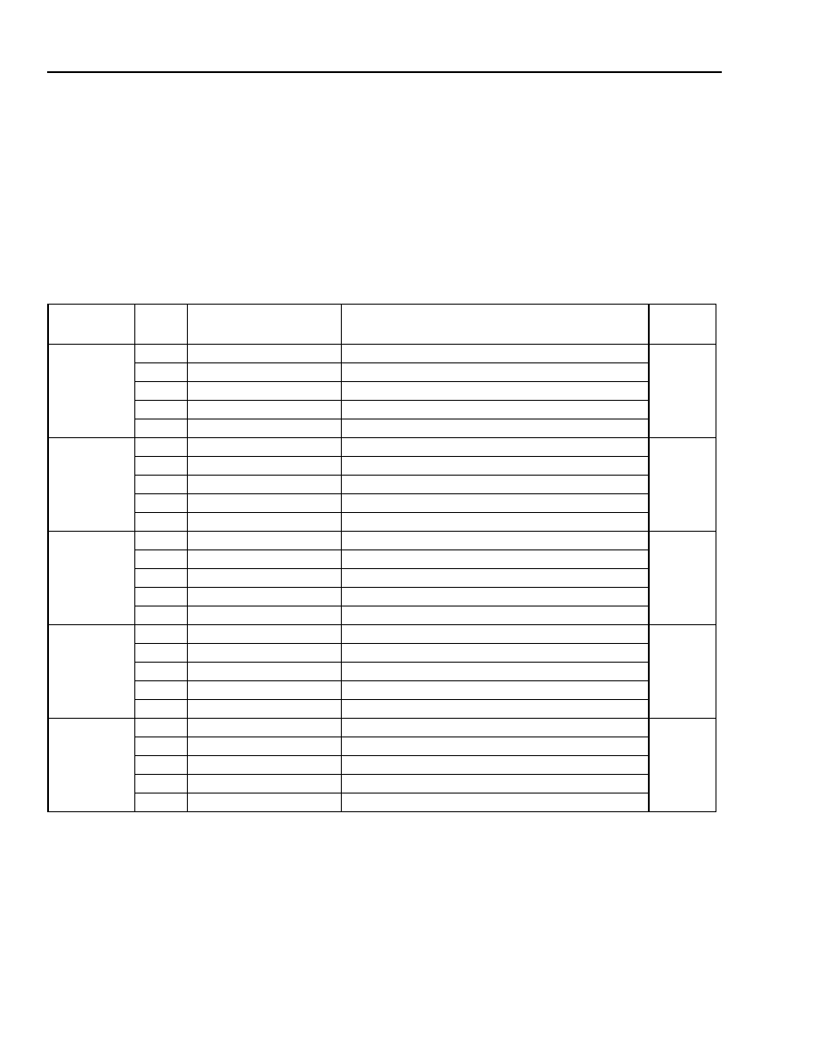
222
Agere Systems Inc.
Data Sheet
May 2001
155/622/2488 Mbits/s Data Interface
TDAT042G5 SONET/SDH
Register Descriptions
(continued)
DE Registers
(continued)
Table 116. Registers 0x1022--0x102D: Ingress Configuration (R/W) (continued)
Reset default of registers 0x1022, 0x1026, 0x102A = 0x4444.
Reset default of registers 0x1023, 0x1027, 0x102B = 0x5555.
Reset default of registers 0x1024, 0x1028, 0x102C = 0x6666.
Reset default of registers 0x1025, 0x1029, 0x102D = 0x7777.
Note:See Figures 17--20, pages 78--81. The notation X/Y means the following: X = STS-48/STM-16 byte,
Y = STS-12/STM-4 or STS-3/STM-1 byte.
Address
(Hex)
Bit #
Name
Function
Reset
Default
1029
--
Rx_TS8
Ingress Time Slot 8. Refer to ingress time slot 1.
0x7777
15--12
--
Byte 38/11A definition.
11--8
--
Byte 41/11B definition.
7--4
--
Byte 44/11C definition.
3--0
--
Byte 47/11D definition.
102A
--
Rx_TS9
Ingress Time Slot 9. Refer to ingress time slot 1.
0x4444
15--12
--
Byte 3/3A definition.
11--8
--
Byte 6/3B definition.
7--4
--
Byte 9/3C definition.
3--0
--
Byte 12/3D definition.
102B
--
Rx_TS10
Ingress Time Slot 10. Refer to ingress time slot 1.
0x5555
15--12
--
Byte 15/6A definition.
11--8
--
Byte 18/6B definition.
7--4
--
Byte 21/6C definition.
3--0
--
Byte 24/6D definition.
102C
--
Rx_TS11
Ingress Time Slot 11. Refer to ingress time slot 1.
0x6666
15--12
--
Byte 27/9A definition.
11--8
--
Byte 30/9B definition.
7--4
--
Byte 33/9C definition.
3--0
--
Byte 36/9D definition.
102D
--
Rx_TS12
Ingress Time Slot 12. Refer to ingress time slot 1.
0x7777
15--12
--
Byte 39/12A definition.
11--8
--
Byte 42/12B definition.
7--4
--
Byte 45/12C definition.
3--0
--
Byte 48/12D definition.
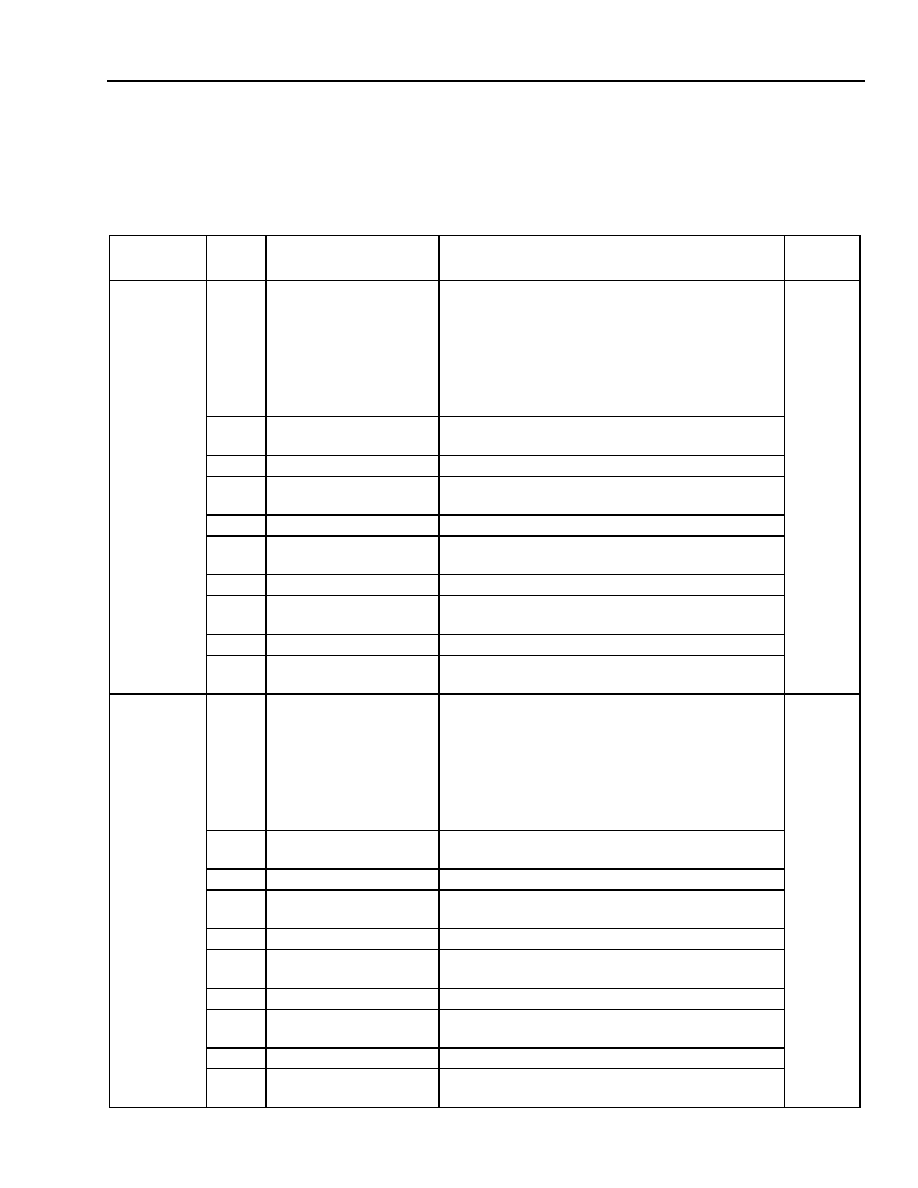
Agere Systems Inc.
223
Data Sheet
May 2001
155/622/2488 Mbits/s Data Interface
TDAT042G5 SONET/SDH
Register Descriptions
(continued)
DE Registers
(continued)
Table 117. Registers 0x102E--0x1031: Over-Fiber Mode (Packet-Over-Fiber or POF) Control (R/W)
Reset default of registers = 0x0000.
Address
(Hex)
Bit #
Name
Function
Reset
Default
102E
--
Rx_OF_CTRL
Ingress Over-Fiber Mode Register. This register
will define the channels, if any, that are carrying
over-fiber payload in the ingress direction.
0 = SONET
1 = over-fiber mode
(For specific bits, see register Rx_TS[1--12],
page 219.)
0x0000
15
--
Reserved. These bits must be written to their reset
default value (0).
14
--
Physical channel (line) A mode.
13--12
--
Reserved. These bits must be written to their reset
default value (00).
10
--
Physical channel (line) B mode.
9--7
--
Reserved. These bits must be written to their reset
default value (000).
6
--
Physical channel (line) C mode.
5--3
--
Reserved. These bits must be written to their reset
default value (000).
2
--
Physical channel (line) D mode.
1--0
--
Reserved. These bits must be written to their reset
default value (00).
102F
--
Tx_OF_CTRL
Egress Over-Fiber Mode Register. This register
will define the channels, if any, that are carrying
over-fiber payload in the egress direction.
0 = SONET
1 = over-fiber mode
(For specific bits, see register Tx_TS[1--12],
page 215.)
0x0000
15
--
Reserved. These bits must be written to their reset
default value (0).
14
--
Physical channel (line) A mode.
13--12
--
Reserved. These bits must be written to their reset
default value (00).
10
--
Physical channel (line) B mode.
9--7
--
Reserved. These bits must be written to their reset
default value (000).
6
--
Physical channel (line) C mode.
5--3
--
Reserved. These bits must be written to their reset
default value (000).
2
--
Physical channel (line) D mode.
1--0
--
Reserved. These bits must be written to their reset
default value (00).
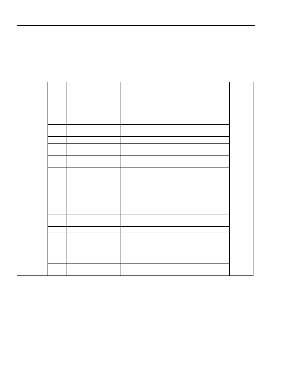
224
Agere Systems Inc.
Data Sheet
May 2001
155/622/2488 Mbits/s Data Interface
TDAT042G5 SONET/SDH
Register Descriptions
(continued)
DE Registers
(continued)
Table 117. Registers 0x102E--0x1031: Over-Fiber Mode (Packet-Over-Fiber or POF) Control (R/W)
(continued)
Reset default of registers = 0x0000.
Address
(Hex)
Bit #
Name
Function
Reset
Default
1030
--
Rx_CHCD_FM[15:0]
Receive Channel C/D Framer Mode. This
register is used in over-fiber mode to give the Rx
sequencer prior knowledge of the time slot and
byte location within a time slot of the valid byte of a
transparent packet for a given frame.
0x0000
15--14
--
Reserved. These bits must be written to their reset
default value (00).
13--10
--
Time slot having the last payload for channel C.
9--8
--
Last byte location out of 4-byte output for
channel C.
7--6
--
Reserved. These bits must be written to their reset
default value (00).
5--2
--
Time slot having the last payload for channel D.
1--0
--
Last byte location out of 4-byte output for
channel D.
1031
--
Rx_CHAB_FM[15:0]
Receive Channel A/B Framer Mode. This
register is used in over-fiber mode to give the Rx
sequencer prior knowledge of the time slot and
byte location within a time slot of the valid byte of a
transparent packet for a given frame.
0x0000
15--14
--
Reserved. These bits must be written to their reset
default value (00).
13--10
--
Time slot having the last payload for channel A.
9--8
--
Last byte location out of 4-byte output for
channel A.
7--6
--
Reserved. These bits must be written to their reset
default value (00).
5--2
--
Time slot having the last payload for channel B.
1--0
--
Last byte location out of 4-byte output for
channel B.
Agere Systems Inc.
225
Data Sheet
May 2001
155/622/2488 Mbits/s Data Interface
TDAT042G5 SONET/SDH
Register Descriptions
(continued)
DE Registers
(continued)
Table 118. Registers 0x1032--0x1036: Sequencer Cell State Registers (R/W)
Reset default of registers 0x1032--0x1035 = 0x0000.
Reset default of register 0x1036 = 0x000F.
Table 119. Registers 0x1040--0x1043: Ingress Payload Type and Mode Control (R/W)
Reset default of registers = 0x0700.
Address
(Hex)
Bit #
Name
Function
Reset
Default
1032--1035
--
Rx_CELL[A--D]_FM
Rx Channel [A--D] Cell Register. This register is
used in over-fiber mode to give the Rx sequencer
prior knowledge of the cell in which the last byte of
a transparent packet for a given frame is located.
0x0000
15--10
--
Reserved. These bits must be written to their reset
default value (000000).
00
0000
9--0
RxLBCF
Rx Last Byte of Current Frame. Defines which of
the 810 SONET cells has the last byte of the
current frame in channel [A--D].
00
0000
0000
1036
--
Tx_SEQ_DISABLE
Tx Sequencer Disable. This register is used to
enable or disable channels. The default is all four
channels are disabled. In other words, the disables
on the channels must be cleared or the sequencer
will not operate.
1 = the channel is disabled; 0 = the channel is
enabled.
0x000F
15--4
--
Reserved. These bits must be written to their reset
default value (0x000).
0x000
3
--
Channel A Disable.
1
2
--
Channel B Disable.
1
1
--
Channel C Disable.
1
0
--
Channel D Disable.
1
Address
(Hex)
Bit #
Name
Function
Reset
Default
1040--1043
--
Rx_PCTL_[0--3]
Channel [0--3] Payload Type and Control.
See Table 120 for receive type and mode
control summary.
0x0700
15--11
--
Reserved. These bits must be written to their
reset default value (00000).
00000
10--8
--
Payload Type. Defines the payload type being
received.
111
7--0
--
Payload Control. Allows for different options
when receiving data, such as pre- or post-
unscrambling, PPP header discard, etc.
0x00

226
Agere Systems Inc.
Data Sheet
May 2001
155/622/2488 Mbits/s Data Interface
TDAT042G5 SONET/SDH
Register Descriptions
(continued)
DE Registers
(continued)
Table 120. Receive Type and Mode Control Summary Table (Registers 0x1040--0x1043)
* No discard--Pass all ATM cells with no error correction.
Discard--Discard cells with multiple-bit header errors. Correct and pass all cells with single-bit header errors.
Smart discard--Discard cells with multiple-bit header errors, and only correct and pass the first of back-to-back single-bit header errors.
ß Discard, no correction--Discard all cells with header errors.
Payload
Type, Bits
[10:8]
Payload Control, Bits [7:0]
7
6
5
4
3
2
1
0
000
PPP
0 = discard
1 = no discard
0 = header
stripped
1 = header
on
0 = CRC-16
1 = CRC-32
0 = CRC
stripped
1 = CRC on
0 = CRC reversed
1 = CRC normal
0 = no dry mode
1 = dry mode
00 = no unscrambling
01 = post-unscrambling
10 = pre-unscrambling
11 = undefined
001
HDLC with
CRC
0
0
0 = CRC-16
1 = CRC-32
0 = CRC
stripped
1 = CRC on
0 = CRC reversed
1 = CRC normal
0 = no dry mode
1 = dry mode
00 = no unscrambling
01 = post-unscrambling
10 = pre-unscrambling
11 = undefined
010
HDLC
without CRC
0
0
0
0
0
0 = no dry mode
1 = dry mode
00 = no unscrambling
01 = post-unscrambling
10 = pre-unscrambling
11 = undefined
011
ATM
0 = byte sync
1 = bit sync
0
00 = X
43
unscrambling
01 = no unscrambling
10 = X
31
unscrambling
11 = no unscrambling
0 = unassigned
cell discard
1 = unassigned
cell pass-
through
0 = idle cell
discard
1 = idle cell
passthrough
00 = no discard*
01 = discard
10 = smart discard
11 = discard, no
correction
ß
100
SDL without
CRC
0 = byte sync
1 = bit sync
0 = length
stripped
1 = length on
0
0
Length offset (0x0 to 0xF)
101
SDL with
CRC
0 = byte sync
1 = bit sync
0 = length
stripped
1 = length on
0 = CRC-16
1 = CRC-32
0 = CRC
stripped
1 = CRC on
Length offset (0x0 to 0xF)
110
Transparent
payload
0
0
0
0
0
0
0
0
111
Not defined
(reset mode)
0
0
0
0
0
0
0
0

Agere Systems Inc.
227
Data Sheet
May 2001
155/622/2488 Mbits/s Data Interface
TDAT042G5 SONET/SDH
Register Descriptions
(continued)
DE Registers
(continued)
Table 121. Registers 0x1080--0x1087: ATM Framer Idle Cell Match Mask (R/W)
Reset default of registers = 0xFFFF.
Table 122. Registers 0x1088--0x108F: ATM Idle Cell Registers (R/W)
Reset default of registers 0x1088, 0x108A, 0x108C, 0x108E = 0x0000.
Reset default of registers 0x1089, 0x108B, 0x108D, 0x108F = 0x0001.
Address
(Hex)
Bit #
Name
Function
Reset
Default
1080--1087
--
ATM_IDM_[0--3][31:0]
ATM Idle Cell Match Mask Channel [0--3].
This 32-bit register defines which of the 32 bits
will be used for comparison between the idle
cell register and the header data in the ATM
framer. A value of 1 enables the comparison
with the corresponding bit in the ATM idle cell
register.
0xFFFF
1080
15--0
ATM_IDM_0[31:16]
[31:24] is the MSByte of ATM_IDM_0.
0xFFFF
1081
15--0
ATM_IDM_0[15:0]
[7:0] is the LSByte of ATM_IDM_0.
0xFFFF
1082
15--0
ATM_IDM_1[31:16]
[31:24] is the MSByte of ATM_IDM_1.
0xFFFF
1083
15--0
ATM_IDM_1[15:0]
[7:0] is the LSByte of ATM_IDM_1.
0xFFFF
1084
15--0
ATM_IDM_2[31:16]
[31:24] is the MSByte of ATM_IDM_2.
0xFFFF
1085
15--0
ATM_IDM_2[15:0]
[7:0] is the LSByte of ATM_IDM_2.
0xFFFF
1086
15--0
ATM_IDM_3[31:16]
[31:24] is the MSByte of ATM_IDM_3.
0xFFFF
1087
15--0
ATM_IDM_3[15:0]
[7:0] is the LSByte of ATM_IDM_3.
0xFFFF
Address
(Hex)
Bit #
Name
Function
Reset Default
1088--108F
--
ATM_IDC_[0--3][31:0]
ATM Idle Cell Register Channel [0--3].
This 32-bit register will store the expected
header value for idle cells. If the ATM framer
sees a header for an ATM packet which
matches this register at the bit positions
designated by the ATM idle cell match mask,
the packet will be treated as an idle cell.
See below.
1088
15--0
ATM_IDC_0[31:16]
[31:24] is the MSByte of ATM_IDC_0.
0x0000
1089
15--0
ATM_IDC_0[15:0]
[7:0] is the LSByte of ATM_IDC_0.
0x0001
108A
15--0
ATM_IDC_1[31:16]
[31:24] is the MSByte of ATM_IDC_1.
0x0000
108B
15--0
ATM_IDC_1[15:0]
[7:0] is the LSByte of ATM_IDC_1.
0x0001
108C
15--0
ATM_IDC_2[31:16]
[31:24] is the MSByte of ATM_IDC_2.
0x0000
108D
15--0
ATM_IDC_2[15:0]
[7:0] is the LSByte of ATM_IDC_2.
0x0001
108E
15--0
ATM_IDC_3[31:16]
[31:24] is the MSByte of ATM_IDC_3.
0x0000
108F
15--0
ATM_IDC_3[15:0]
[7:0] is the LSByte of ATM_IDC_3.
0x0001
228
Agere Systems Inc.
Data Sheet
May 2001
155/622/2488 Mbits/s Data Interface
TDAT042G5 SONET/SDH
Register Descriptions
(continued)
DE Registers
(continued)
Table 123. Registers 0x1090--0x1097: ATM Unassigned Cell Match Mask (R/W)
Reset default of registers = 0xFFFF.
Table 124. Registers 0x1098--0x109F: ATM Unassigned Cell Registers (R/W)
Reset default of registers = 0x0000.
Address
(Hex)
Bit #
Name
Function
Reset Default
1090--1097
--
ATM_USM_[0--3][31:0] ATM Unassigned Cell Match Mask
Channel [0--3]. This 32-bit register defines
which of the 32 bits will be used for
comparison between the unassigned cell
register and the header data in the ATM
framer. A value of 1 enables the comparison
with the corresponding bit in the ATM
unassigned cell register.
0xFFFF
1090
15--0
ATM_USM_0[31:16]
[31:24] is the MSByte of ATM_USM_0.
0xFFFF
1091
15--0
ATM_USM_0[15:0]
[7:0] is the LSByte of ATM_USM_0.
0xFFFF
1092
15--0
ATM_USM_1[31:16]
[31:24] is the MSByte of ATM_USM_1.
0xFFFF
1093
15--0
ATM_USM_1[15:0]
[7:0] is the LSByte of ATM_USM_1.
0xFFFF
1094
15--0
ATM_USM_2[31:16]
[31:24] is the MSByte of ATM_USM_2.
0xFFFF
1095
15--0
ATM_USM_2[15:0]
[7:0] is the LSByte of ATM_USM_2.
0xFFFF
1096
15--0
ATM_USM_3[31:16]
[31:24] is the MSByte of ATM_USM_3.
0xFFFF
1097
15--0
ATM_USM_3[15:0]
[7:0] is the LSByte of ATM_USM_3.
0xFFFF
Address
(Hex)
Bit #
Name
Function
Reset
Default
1098--109F
--
ATM_USG_[0--3][31:0]
ATM Unassigned Cell Register Channel 0.
This 32-bit register will store the expected
header value for unassigned cells. If the ATM
framer sees a header for an ATM packet which
matches this register at the bit positions
designated by the ATM unassigned cell match
mask, the packet will be treated as an
unassigned cell.
0x0000
1098
15--0
ATM_USG_0[31:16]
[31:24] is the MSByte of ATM_USG_0.
0x0000
1099
15--0
ATM_USG_0[15:0]
[7:0] is the LSByte of ATM_USG_0.
0x0000
109A
15--0
ATM_USG_1[31:16]
[31:24] is the MSByte of ATM_USG_1.
0x0000
109B
15--0
ATM_USG_1[15:0]
[7:0] is the LSByte of ATM_USG_1.
0x0000
109C
15--0
ATM_USG_2[31:16]
[31:24] is the MSByte of ATM_USG_2.
0x0000
109D
15--0
ATM_USG_2[15:0]
[7:0] is the LSByte of ATM_USG_2.
0x0000
109E
15--0
ATM_USG_3[31:16]
[31:24] is the MSByte of ATM_USG_3.
0x0000
109F
15--0
ATM_USG_3[15:0]
[7:0] is the LSByte of ATM_USG_3.
0x0000

Agere Systems Inc.
229
Data Sheet
May 2001
155/622/2488 Mbits/s Data Interface
TDAT042G5 SONET/SDH
Register Descriptions
(continued)
DE Registers
(continued)
Table 125. Registers 0x10A0--0x10A3: ATM Framer State Registers (RO)
Reset default of registers = 0x0000.
Table 126. Register 0x10A4: ATM X43 Frame Control (R/W)
Reset default of register = 0x01C6.
Address
(Hex)
Bit #
Name
Function
Reset
Default
10A0--10A3
--
ATM_ST_[0--3]
Channel [0--3] ATM Scrambler Framer
State.
0x0000
15--4
--
Reserved. These bits must be written to their
reset default value (0x000).
0x000
3--2
--
ATM Framer Sync State. These bits indicate
the X31 sync state of each channel.
ATM_ST_[0--3][3:2] = 00 Acquisition
ATM_ST_[0--3][3:2] = 01 Verification
ATM_ST_[0--3][3:2] = 10 Synchronized
ATM_ST_[0--3][3:2] = 11 Undefined
00
1--0
--
ATM Frame State. These bits indicate the
frame state of each channel.
ATM_ST_[0--3][1:0] = 00 Hunt
ATM_ST_[0--3][1:0] = 01 Presync
ATM_ST_[0--3][1:0] = 10 Sync
ATM_ST_[0--3][1:0] = 11 Undefined
00
Address
(Hex)
Bit #
Name
Function
Reset
Default
10A4
--
ATM_X43[11:0]
ATM X43 Frame Control.
0x01C6
15--12
--
Reserved. These bits must be written to their
reset default value (0x0).
0x0
11--6
--
X43-Alpha. This register will define the alpha
value for the X43 alpha-delta framer which is
the number of consecutive incorrect ATM cells
that must be received in order to transition from
the sync state to the hunt state.
000111
5--0
--
X43-Delta. This register will define the delta
value for the X43 alpha-delta framer which is
the number of consecutive correct ATM cells
that must be received in order to transition from
the presync state to the sync state.
000110

230
Agere Systems Inc.
Data Sheet
May 2001
155/622/2488 Mbits/s Data Interface
TDAT042G5 SONET/SDH
Register Descriptions
(continued)
DE Registers
(continued)
Table 127. Register 0x10A5: ATM X31 Frame Control (R/W)
Reset default of register = 0x01C8.
Table 128. Register 0x10A6: ATM X31 V/W Values (R/W)
Reset default of register = 0x0210.
Address
(Hex)
Bit #
Name
Function
Reset
Default
10A5
--
ATM_X31[11:0]
ATM X31 Framer Control.
0x01C8
15--12
--
Reserved. These bits must be written to their
reset default value (0x0).
0x0
11--6
--
X31-Alpha. This register will define the alpha
value for the X31 alpha-delta framer which is
the number of consecutive incorrect ATM cells
that must be received in order to transition from
the sync state to the hunt state.
000111
5--0
--
X31-Delta. This register will define the delta
value for the X31 alpha-delta framer which is
the number of consecutive correct ATM cells
that must be received in order to transition from
the presync state to the sync state.
001000
Address
(Hex)
Bit #
Name
Function
Reset
Default
10A6
--
ATM_X31VW[11:0]
X31 V and W Values.
0x0210
15--12
--
Reserved. These bits must be written to their
reset default value (0x0).
0x0
11--6
--
X31 V Value. This register specifies the value
the confidence counter in the X
31
scrambler
synchronization process must drop below in
order to transition to the acquisition state from
the verification state. The confidence counter is
incremented every time the local scrambler
samples match the received samples, and
decremented when they do not (see standard
I.432).
001000
5--0
--
X31 W Value. This register specifies the value
the confidence counter in the X
31
scrambler
synchronization process must drop below in
order to declare loss of synchronization and
transition to the acquisition state. The
confidence counter is incremented every time
the local scrambler samples match the received
samples, and decremented when they do not
(see standard I.432).
010000

Agere Systems Inc.
231
Data Sheet
May 2001
155/622/2488 Mbits/s Data Interface
TDAT042G5 SONET/SDH
Register Descriptions
(continued)
DE Registers
(continued)
Table 129. Register 0x10A7: ATM X31 X/Y Values (R/W)
Reset default of register = 0x0418.
Table 130. Register 0x10A8: ATM X31 Z Value (R/W)
Reset default of register = 0x0018.
Address
(Hex)
Bit #
Name
Function
Reset
Default
10A7
--
ATM_X31XY[11:0]
X31 X and Y Values.
0x0418
15--12
--
Reserved. These bits must be written to their
reset default value (0x0).
0x0
11--6
--
X31 X Value. This register specifies the
minimum value the confidence counter in the
X
31
scrambler synchronization process must
reach in order to transition to the verification
state from the acquisition state. The confidence
counter is incremented every time the local
scrambler samples match the received
samples, and decremented when they do not
(see standard I.432).
010000
5--0
--
X31 Y Value. This register specifies the
minimum value the confidence counter in the
X
31
scrambler synchronization process must
reach in order to transition to the synchronized
state from the verification state. The confidence
counter is incremented every time the local
scrambler samples match the received
samples, and decremented when they do not
(see standard I.432).
011000
Address
(Hex)
Bit #
Name
Function
Reset
Default
10A8
--
ATM_X31Z[5:0]
X31 Z Value.
0x0018
15--6
--
Reserved. These bits must be written to their
reset default value (0000000000).
00
0000
0000
5--0
--
X31 Z Value. This register specifies the
maximum value the confidence counter in the
X
31
scrambler synchronization process can
achieve. The confidence counter is
incremented every time the local scrambler
samples match the received samples, and
decremented when they do not (see standard
I.432).
011000

232
Agere Systems Inc.
Data Sheet
May 2001
155/622/2488 Mbits/s Data Interface
TDAT042G5 SONET/SDH
Register Descriptions
(continued)
DE Registers
(continued)
Table 131. Register 0x10A9: Frame State Interrupt Mask (R/W)
Reset default of register = 0x000F.
Table 132. Register 0x10AA: Scrambler State Interrupt Mask (R/W)
Reset default of register = 0x000F.
Address
(Hex)
Bit #
Name
Function
Reset
Default
10A9
--
FS_INT_MASK[3:0]
Frame State Interrupt Mask. When active
(logic 1), the associated event/delta is inhibited
from contributing to the interrupt on a per-
channel basis. Otherwise, an interrupt is
generated when the ATM frame state transitions
from sync to hunt state.
0x000F
15--4
--
Reserved. These bits must be written to their
reset default value (0x000).
0x000
3
--
Channel 3 Mask Value.
1
2
--
Channel 2 Mask Value.
1
1
--
Channel 1 Mask Value.
1
0
--
Channel 0 Mask Value.
1
Address
(Hex)
Bit #
Name
Function
Reset
Default
10AA
--
SS_INT_MASK[3:0]
Scrambler State Interrupt Mask. When active
(logic 1), the associated event/delta is inhibited
from contributing to the interrupt on a per-
channel basis. Otherwise, an interrupt is
generated when the ATM frame state transitions
from synchronization to verification state.
0x000F
15--4
--
Reserved. These bits must be written to their
reset default value (0x000).
0x000
3
--
Channel 3 Mask Value.
1
2
--
Channel 2 Mask Value.
1
1
--
Channel 1 Mask Value.
1
0
--
Channel 0 Mask Value.
1

Agere Systems Inc.
233
Data Sheet
May 2001
155/622/2488 Mbits/s Data Interface
TDAT042G5 SONET/SDH
Register Descriptions
(continued)
DE Registers
(continued)
Table 133. Register 0x10AB: ATM Receive Debug Register (R/W)
Reset default of register = 0x003C.
Address
(Hex)
Bit #
Name
Function
Reset
Default
10AB
--
ATM_Rx_DEBUG_REG[5:0] ATM Receive Debug Register.
0x003C
15--6
--
Reserved. These bits must be written to their
reset default value (0000000000).
00
0000
0000
5
--
Channel 3 All Cool-Interrupt Mask Value.
When active (logic 1), the associated event/
delta is inhibited from contributing to the
interrupt on a per-channel basis.
1
4
--
Channel 2 All-Cool Interrupt Mask Value.
When active (logic 1), the associated event/
delta is inhibited from contributing to the
interrupt on a per-channel basis.
1
3
--
Channel 1 All-Cool Interrupt Mask Value.
When active (logic 1), the associated event/
delta is inhibited from contributing to the
interrupt on a per-channel basis.
1
2
--
Channel 0 All-Cool Interrupt Mask Value.
When active (logic 1), the associated event/
delta is inhibited from contributing to the
interrupt on a per-channel basis.
1
1
--
Incrementing NULL Cell Payload Sequence.
This bit governs whether 0x6A is used for the
payload of NULL cells, or whether an
incrementing 8-bit count is used (0x00
0xFF). A value of 1 selects the incrementing
sequence. This can be used with the All_Cool
interrupt.
0
0
--
X31_Sync_Compare. In X
31
mode, when this
value is 0, the ATM framer does 6-bit
comparisons of the HEC, which does not allow
for error correction. When this value is 1, all 8
bits of the HEC are used, which does allow for
error correction.
0
234
Agere Systems Inc.
Data Sheet
May 2001
155/622/2488 Mbits/s Data Interface
TDAT042G5 SONET/SDH
Register Descriptions
(continued)
DE Registers
(continued)
Table 134. Registers 0x10B0--0x10B3: PPP Attach (R/W)
Reset default of registers = 0x0000.
Table 135. Registers 0x10E0--0x10E3: Egress Payload Type and Mode Control (R/W)
Reset default of registers = 0x0700.
Address
(Hex)
Bit #
Name
Function
Reset
Default
10B0--10B3 15--0
PPP_Tx_CHAN[0--3]
Channel [0--3] PPP Header. This register
defines the 2 bytes that will be generated as the
PPP header in compressed header PPP mode.
In uncompressed header PPP mode, they will
serve as the third and fourth bytes of the 4-byte
header, with 0xFF03 being the first and second
bytes.
0x0000
Address
(Hex)
Bit #
Name
Function
Reset
Default
10E0--10E3
--
Tx_PCTL_[0--3][10:0]
Channel [0--3] Payload Type and Control.
See Table 136 for transmit type and mode
control summary.
0x0700
15--11
--
Reserved. These bits must be written to their
reset default value (00000).
00000
10--8
--
Payload Type. Defines the payload type being
received.
111
7--0
--
Payload Control. Allows for different options
when transmitting data, such as pre- or
postscrambling, dry mode, PPP header
discard, etc.
0x00

Agere Systems Inc.
235
Data Sheet
May 2001
155/622/2488 Mbits/s Data Interface
TDAT042G5 SONET/SDH
Register Descriptions
(continued)
DE Registers
(continued)
Table 136. Transmit Type and Mode Control Summary Table (Registers 0x10E0--0x10E3)
Note: In the table below, X indicates the bit may either be 0 or 1.
Table 137. Registers 0x10F0--10FB: PPP Header Value Detach (R/W)
Reset default of registers = 0x0000.
Payload
Type, Bits
[10:8]
Payload Control, Bits [7:0]
7
6
5
4
3
2
1
0
000
PPP
0 = compression
1 = no compression
0
0 = CRC-16
1 = CRC-32
0
0 = CRC reversed
1 = CRC normal
0 = no dry
mode
1 = dry mode
00 = no scrambling
01 = postscrambling
10 = pre-scrambling
11 = undefined
001
HDLC with CRC
0
0
0 = CRC-16
1 = CRC-32
0
0 = CRC reversed
1 = CRC normal
0 = no dry
mode
1 = dry mode
00 = no scrambling
01 = postscrambling
10 = prescrambling
11 = undefined
010
HDLC
without CRC
0
0
0
0
0
0 = no dry
mode
1 = dry mode
00 = no scrambling
01 = postscrambling
10 = prescrambling
11 = undefined
011
ATM
0
0
00 = X
43
scrambling
01 = no scrambling
10 = X
31
scrambling
11 = no scrambling
0
0
0
0
100
SDL without CRC
X
X
X
X
X
X
X
X
101
SDL with CRC
0
0
0 = CRC-16
1 = CRC-32
0
0
0
0
0
110
Transparent
payload
0
0
0
0
0
0
0
0
111
Not defined
(reset mode)
0
0
0
0
0
0
0
0
Address
(Hex)
Bit #
Name
Function
Reset Default
10F0--10FB
15--0
PPP_Rx_HDR
[0--11][15:0]
Register [0--11] PPP Header. This register
defines the 2 bytes that can be used by all
four channels to validate a PPP packet. Byte
[15:8] is the MSByte and byte [7:0] is the
LSByte. The register defining the valid PPP
header is determined by the settings of
registers 0x0FC--0x0FF. Any channel can
compare the received PPP header to this
value. If there is a mismatch, then the PPP
mismatched header counter (addresses
0x1118--0x111F) will increment.
0x0000

236
Agere Systems Inc.
Data Sheet
May 2001
155/622/2488 Mbits/s Data Interface
TDAT042G5 SONET/SDH
Register Descriptions
(continued)
DE Registers
(continued)
Table 138. Registers 0x10FC--0x10FF: PPP Header Detach Search (R/W)
Reset default of register 10FC = 0xC001.
Reset default of register 10FD = 0xC002.
Reset default of register 10FE = 0xC004.
Reset default of register 10FF = 0xC008.
Address
(Hex)
Bit #
Name
Function
Reset
Default
10FC--10FF
--
PPP_Rx_CHK_CH
[0--3][15:0]
Channel [0--3] PPP Header Search. This register
will control the headers that channel [0--3] PPP
detach block looks for. Mismatched headers will be
noted in a separate counter (addresses 0x1118--
0x111F).
See
below.
15--14
--
Controls the way the PPP headers are searched for
and passed through.
00 = Pass any 32-bit header where the first 16 bits
are 0xFF03. The 0xFF03 (2 bytes) is stripped, and
the protocol field remains.
01 = Pass only specified uncompressed patterns
(first 16 bits are 0xFF03; last 16 bits are defined by
fixed patterns and/or register values). A 32-bit match
is performed, and the 32 bits are all stripped. See
below.
10 = Pass only specified compressed pattern (all 16
bits are defined by fixed patterns and/or register
values). A search is made for one of the provisioned
headers, and those 16 bits are stripped. See below.
11 = Pass any pattern defined by fixed patterns and/
or registers values. See below.
11
13
--
A value of 1 in this bit will enable a search for the
16-bit fixed value 0x8021.
0
12
--
A value of 1 in this bit will enable a search for the
16-bit fixed value 0x0021.
0
11
--
A value of 1 in this bit will enable a search of the
16-bit value in register address 0x10FB.
0
10
--
A value of 1 in this bit will enable a search of the
16-bit value in register address 0x10FA.
0
9
--
A value of 1 in this bit will enable a search of the
16-bit value in register address 0x10F9.
0
8
--
A value of 1 in this bit will enable a search of the
16-bit value in register address 0x10F8.
0
7
--
A value of 1 in this bit will enable a search of the
16-bit value in register address 0x10F7.
0
6
--
A value of 1 in this bit will enable a search of the
16-bit value in register address 0x10F6.
0
5
--
A value of 1 in this bit will enable a search of the
16-bit value in register address 0x10F5.
0
4
--
A value of 1 in this bit will enable a search of the
16-bit value in register address 0x10F4.
0
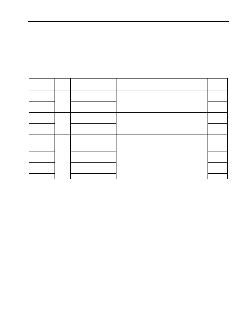
Agere Systems Inc.
237
Data Sheet
May 2001
155/622/2488 Mbits/s Data Interface
TDAT042G5 SONET/SDH
Register Descriptions
(continued)
DE Registers
(continued)
Table 138. Registers 0x10FC--0x10FF: PPP Header Detach Search (R/W)
(continued)
Reset default of register 10FC = 0xC001.
Reset default of register 10FD = 0xC002.
Reset default of register 10FE = 0xC004.
Reset default of register 10FF = 0xC008.
Address
(Hex)
Bit #
Name
Function
Reset
Default
10FC
3
--
A value of 1 in this bit will enable a search of the
16-bit value in register address 0x10F3.
0
10FD
--
0
10FE
--
0
10FF
--
1
10FC
2
--
A value of 1 in this bit will enable a search of the
16-bit value in register address 0x10F2.
0
10FD
--
0
10FE
--
1
10FF
--
0
10FC
1
--
A value of 1 in this bit will enable a search of the
16-bit value in register address 0x10F1.
0
10FD
--
1
10FE
--
0
10FF
--
0
10FC
0
--
A value of 1 in this bit will enable a search of the
16-bit value in register address 0x10F0.
1
10FD
--
0
10FE
--
0
10FF
--
0
238
Agere Systems Inc.
Data Sheet
May 2001
155/622/2488 Mbits/s Data Interface
TDAT042G5 SONET/SDH
Register Descriptions
(continued)
DE Registers
(continued)
Table 139. Registers 0x1100--0x1107: ATM/HDLC/SDL Framer--Condition Counter 1 (PMRST Update) (RO)
Reset default of registers = 0x0000.
Address
(Hex)
Bit #
Name
Function
Reset Default
1100--1107
--
PM_FC1_[0--3][27:0]
ATM/HDLC/SDL Counter 1
Channel [0--3]. Keeps a count of
conditions detected by the data framer in the
particular channel. This register can
represent only one of the following based
upon the channel's payload type:
I
HDLC invalid sequences (as defined in
IETF RFC 1622 below)
I
ATM corrected cells
I
SDL corrected header
This value is updated upon assertion of
PMRST, and the real-time counter value is
reset to zero.
From IETF RFC 1622, invalid sequences are
the following:
1. Frames which are too short (less than 4
data bytes). See register PM_FC2_0
(addresses 0x1108--0x110F).
2. Frames which end with a control escape
octet followed immediately by a coding flag
sequence (0x7D7E).
3. Frames in which octet framing is violated
by transmitting a 0 stop bit where a 1 bit is
expected.
0x0000
1100
15--12
--
Reserved. These bits must be written to
their reset default value (0x0).
0x0
11--0
PM_FC1_0[27:16]
[11:4] is the MSByte of PM_FC1_0.
0x000
1101
15--0
PM_FC1_0[15:0]
[7:0] is the LSByte of PM_FC1_0.
0x0000
1102
15--12
--
Reserved. These bits must be written to
their reset default value (0x0).
0x0
11--0
PM_FC1_1[27:16]
[11:4] is the MSByte PM_FC1_1.
0x000
1103
15--0
PM_FC1_1[15:0]
[7:0] is the LSByte of PM_FC1_1.
0x0000
1104
15--12
--
Reserved. These bits must be written to
their reset default value (0x0).
0x0
11--0
PM_FC1_2[27:16]
[11:4] is the MSByte of PM_FC1_2.
0x000
1105
15--0
PM_FC1_2[15:0]
[7:0] is the LSByte of PM_FC1_2.
0x0000
1106
15--12
--
Reserved. These bits must be written to
their reset default value (0x0).
0x0
11--0
PM_FC1_3[27:16]
[11:4] is the MSByte of PM_FC1_3.
0x000
1107
15--0
PM_FC1_3[15:0]
[7:0] is the LSByte of PM_FC1_3.
0x0000
Agere Systems Inc.
239
Data Sheet
May 2001
155/622/2488 Mbits/s Data Interface
TDAT042G5 SONET/SDH
Register Descriptions
(continued)
DE Registers
(continued)
Table 140. Registers 0x1108--0x110F: ATM/HDLC/SDL Framer--Condition Counter 2 (PMRST Update)
(RO)
Reset default of registers = 0x0000.
Address
(Hex)
Bit #
Name
Function
Reset Default
1108--110F
--
PM_FC2_[0--3][27:0]
ATM/HDLC/SDL Counter 2
Channel [0--3]. Keeps a count of
conditions detected by the data framer in the
particular channel. This register can
represent only one of the following based
upon the channel's payload type:
I
HDLC short packets (packet < 4 data
bytes)
I
ATM discarded cells
I
SDL errored header
This value is updated upon PMRST, and the
real-time counter value is reset to zero.
0x0000
1108
15--12
--
Reserved. These bits must be written to
their reset default value (0x0).
0x0
11--0
PM_FC2_0[27:16]
[11:4] is the MSByte of PM_FC2_0.
0x000
1109
15--0
PM_FC2_0[15:0]
[7:0] is the LSByte of PM_FC2_0.
0x0000
110A
15--12
--
Reserved. These bits must be written to
their reset default value (0x0).
0x0
11--0
PM_FC2_1[27:16]
[11:4] is the MSByte of PM_FC2_1.
0x000
110B
15--0
PM_FC2_1[15:0]
[7:0] is the LSByte of PM_FC2_1.
0x0000
110C
15--12
--
Reserved. These bits must be written to
their reset default value (0x0).
0x0
11--0
PM_FC2_2[27:16]
[11:4] is the MSByte of PM_FC2_2.
0x000
110D
15--0
PM_FC2_2[15:0]
[7:0] is the LSByte of PM_FC2_2.
0x0000
110E
15--12
--
Reserved. These bits must be written to
their reset default value (0x0).
0x0
11--0
PM_FC2_3[27:16]
[11:4] is the MSByte of PM_FC2_3.
0x000
110F
15--0
PM_FC2_3[15:0]
[7:0] is the LSByte of PM_FC2_3.
0x0000
240
Agere Systems Inc.
Data Sheet
May 2001
155/622/2488 Mbits/s Data Interface
TDAT042G5 SONET/SDH
Register Descriptions
(continued)
DE Registers
(continued)
Table 141. Registers 0x1110--0x1117: CRC Checker--Bad Packet Counter (PMRST Update) (RO)
Reset default of registers = 0x0000.
Address
(Hex)
Bit #
Name
Function
Reset Default
1110--1117
--
PM_BPC_[0--3][27:0]
CRC Bad Packet Counter Channel [0--3].
Keeps a count of bad packets detected by
the CRC checker. This value is updated
upon PMRST, and the real-time counter
value is reset to zero.
0x0000
1110
15--12
--
Reserved. These bits must be written to
their reset default value (0x0).
0x0
11--0
PM_BPC_0[27:16]
[11:4] is the MSByte of PM_BPC_0.
0x000
1111
15--0
PM_BPC_0[15:0]
[7:0] is the LSByte of PM_BPC_0.
0x0000
1112
15--12
--
Reserved. These bits must be written to
their reset default value (0x0).
0x0
11--0
PM_BPC_1[27:16]
[11:4] is the MSByte of PM_BPC_1.
0x000
1113
15--0
PM_BPC_1[15:0]
[7:0] is the LSByte of PM_BPC_1.
0x0000
1114
15--12
--
Reserved. These bits must be written to
their reset default value (0x0).
0x0
11--0
PM_BPC_2[27:16]
[11:4] is the MSByte of PM_BPC_2.
0x000
1115
15--0
PM_BPC_2[15:0]
[7:0] is the LSByte of PM_BPC_2.
0x0000
1116
15--12
--
Reserved. These bits must be written to
their reset default value (0x0).
0x0
11--0
PM_BPC_3[27:16]
[11:4] is the MSByte of PM_BPC_3
0x000
1117
15--0
PM_BPC_3[15:0]
[7:0] is the LSByte of PM_BPC_3
0x0000

Agere Systems Inc.
241
Data Sheet
May 2001
155/622/2488 Mbits/s Data Interface
TDAT042G5 SONET/SDH
Register Descriptions
(continued)
DE Registers
(continued)
Table 142. Registers 0x1118--0x111F: PPP Detach--Mismatched Header Counter (PMRST Update) (RO)
Reset default of registers = 0x0000.
Address
(Hex)
Bit #
Name
Function
Reset Default
1118--111F
--
PM_MHC_[0--3][27:0]
PPP Mismatched Header Counter
Channel [0--3]. Keeps a count of packets
with a mismatched header detected by the
PPP detach block. This value is updated
upon PMRST, and the real-time counter
value is reset to zero.
0x0000
1118
15--12
--
Reserved. These bits must be written to
their reset default value (0x0).
0x0
11--0
PM_MHC_0[27:16]
[11:4] is the MSByte of PM_MHC_0.
0x000
1119
15--0
PM_MHC_0[15:0]
[7:0] is the LSByte of PM_MHC_0.
0x0000
111A
15--12
--
Reserved. These bits must be written to
their reset default value (0x0).
0x0
11--0
PM_MHC_1[27:16]
[11:4] is the MSByte of PM_MHC_1.
0x000
111B
15--0
PM_MHC_1[15:0]
[7:0] is the LSByte of PM_MHC_1.
0x0000
111C
15--12
--
Reserved. These bits must be written to
their reset default value (0x0).
0x0
11--0
PM_MHC_2[27:16]
[11:4] is the MSByte of PM_MHC_2.
0x000
111D
15--0
PM_MHC_2[15:0]
[7:0] is the LSByte of PM_MHC_2.
0x0000
111E
15--12
--
Reserved. These bits must be written to
their reset default value (0x0).
0x0
11--0
PM_MHC_3[27:16]
[11:4] is the MSByte of PM_MHC_3.
0x000
111F
15--0
PM_MHC_3[15:0]
[7:0] is the LSByte of PM_MHC_3.
0x0000
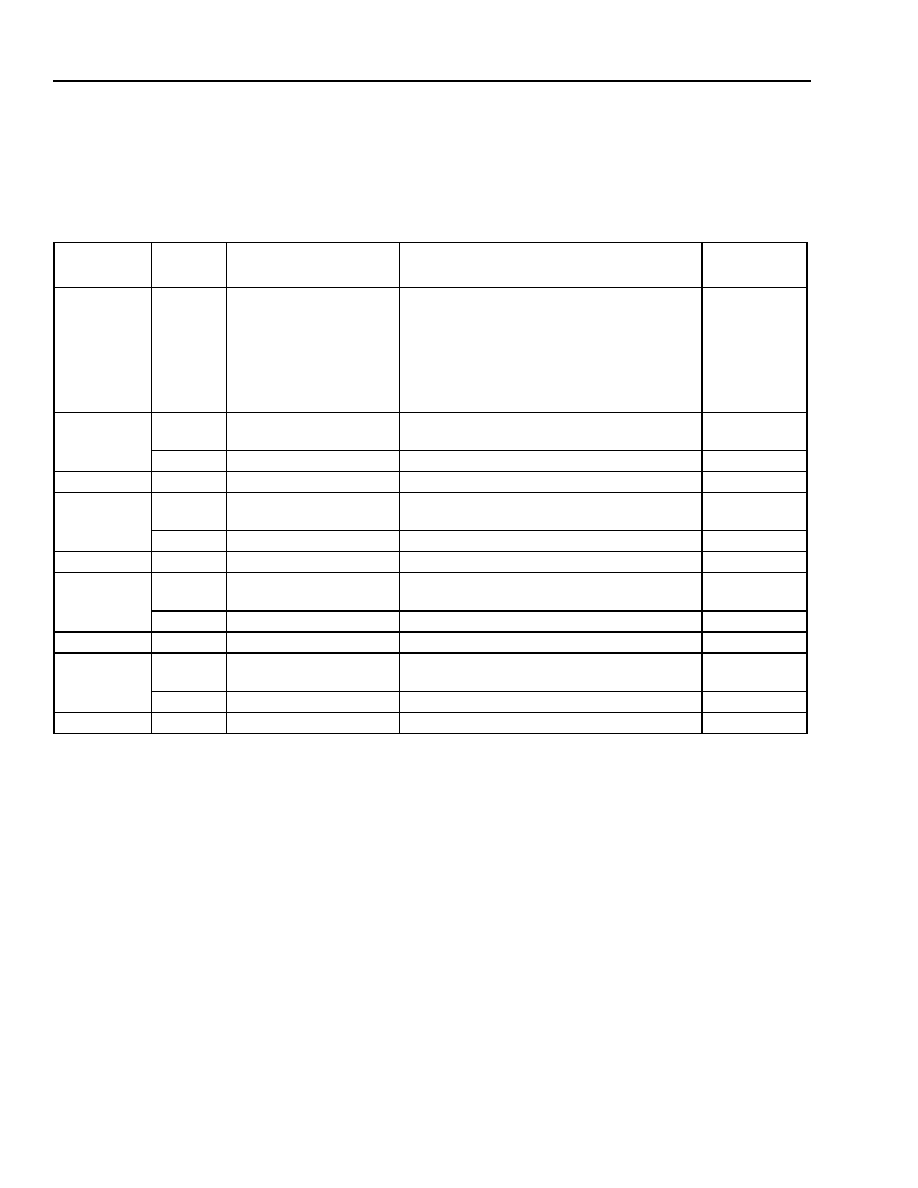
242
Agere Systems Inc.
Data Sheet
May 2001
155/622/2488 Mbits/s Data Interface
TDAT042G5 SONET/SDH
Register Descriptions
(continued)
DE Registers
(continued)
Table 143. Registers 0x1120--0x1127: Receive Good Packet/Cell Counter (PMRST Update) (RO)
Reset default of registers = 0x0000.
Address
(Hex)
Bit #
Name
Function
Reset Default
1120--1127
--
PM_GPC_RX_[0--3]
[27:0]
Good Packet/Cell Counter Channel
[0--3]. Keeps a count of good packets
detected by the receive data engine. This
value is updated upon PMRST, and the real-
time counter value is reset to zero. In ATM
mode, this counter counts the number of
good ATM cells received.
0x0000
1120
15--12
--
Reserved. These bits must be written to
their reset default value (0x0).
0x0
11--0
PM_GPC_RX_0[27:16] [11:4] is the MSByte of PM_GPC_RX_0.
0x000
1121
15--0
PM_GPC_RX_0[15:0]
[7:0] is the LSByte of PM_GPC_RX_0.
0x0000
1122
15--12
--
Reserved. These bits must be written to
their reset default value (0x0).
0x0
11--0
PM_GPC_RX_1[27:16] [11:4] is the MSByte of PM_GPC_RX_1.
0x000
1123
15--0
PM_GPC_RX_1[15:0]
[7:0] is the LSByte of PM_GPC_RX_1.
0x0000
1124
15--12
--
Reserved. These bits must be written to
their reset default value (0x0).
0x0
11--0
PM_GPC_RX_2[27:16] [11:4] is the MSByte of PM_GPC_RX_2.
0x000
1125
15--0
PM_GPC_RX_2[15:0]
[7:0] is the LSByte of PM_GPC_RX_2.
0x0000
1126
15--12
--
Reserved. These bits must be written to
their reset default value (0x0).
0x0
11--0
PM_GPC_RX_3[27:16] [11:4] is the MSByte of PM_GPC_RX_3.
0x000
1127
15--0
PM_GPC_RX_3[15:0]
[7:0] is the LSByte of PM_GPC_RX_3.
0x0000
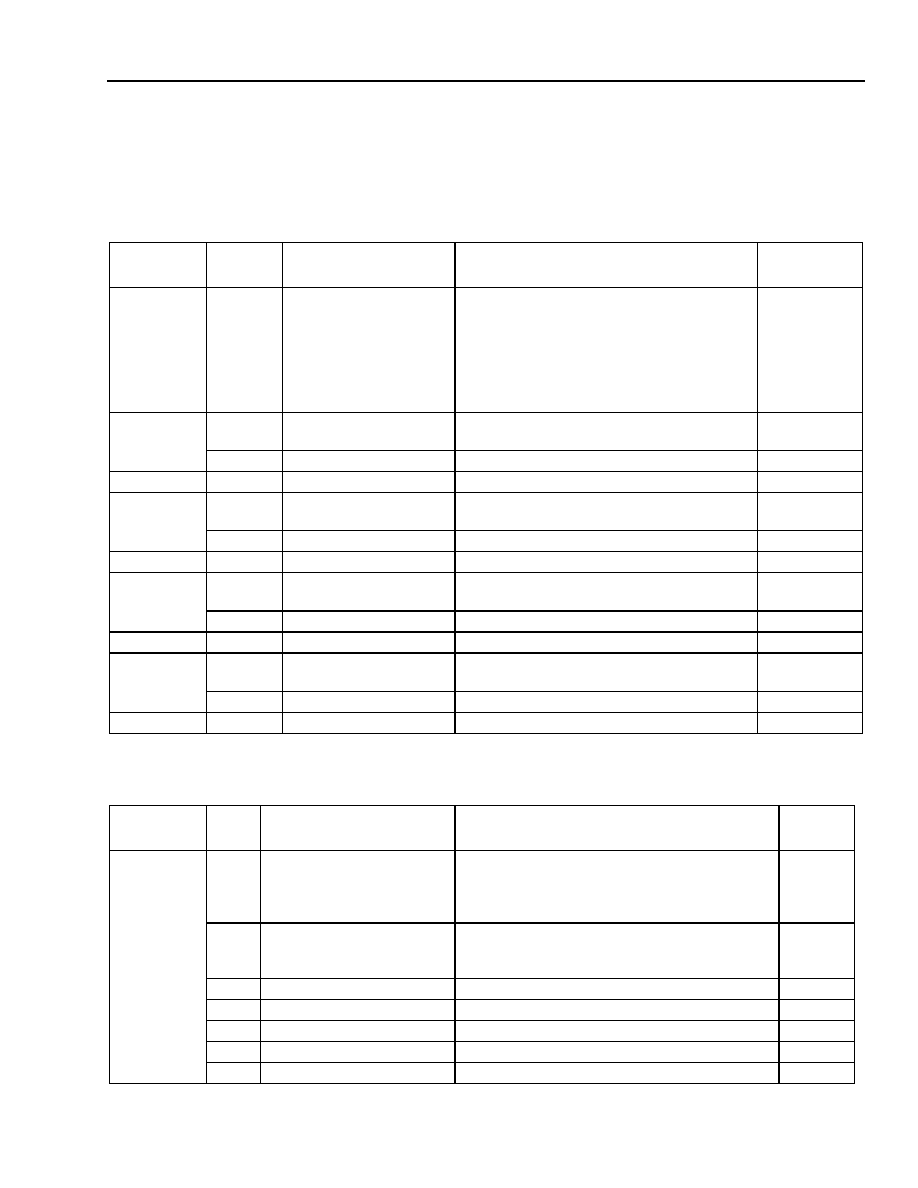
Agere Systems Inc.
243
Data Sheet
May 2001
155/622/2488 Mbits/s Data Interface
TDAT042G5 SONET/SDH
Register Descriptions
(continued)
DE Registers
(continued)
Table 144. Registers 0x1128--0x112F: Transmit Good Packet/Cell Counter (PMRST Update) (RO)
Reset default of registers = 0x0000.
Table 145. Registers 0x1180--0x1186: Interrupt Masks for Packet Counters (R/W)
Reset default of registers = 0x001F.
Address
(Hex)
Bit #
Name
Function
Reset Default
1128--112F
--
PM_GPC_TX_[0--3]
[27:0]
Good Packet/Cell Counter Channel
[0--3]. Keeps a count of good packets
detected by the transmit data engine. This
value is updated upon PMRST, and the real-
time counter value is reset to zero. In ATM
mode, this counter counts the number of
good ATM cells transmitted.
0x0000
1128
15--12
--
Reserved. These bits must be written to
their reset default value (0x0).
0x0
11--0
PM_GPC_TX_0[27:16]
[11:4] is the MSByte of PM_GPC_TX_0.
0x000
1129
15--0
PM_GPC_TX_0[15:0]
[7:0] is the LSByte of PM_GPC_TX_0.
0x0000
112A
15--12
--
Reserved. These bits must be written to
their reset default value (0x0).
0x0
11--0
PM_GPC_TX_1[27:16]
[11:4] is the MSByte of PM_GPC_TX_1.
0x000
112B
15--0
PM_GPC_TX_1[15:0]
[7:0] is the LSByte of PM_GPC_TX_1.
0x0000
112C
15--12
--
Reserved. These bits must be written to
their reset default value (0x0).
0x0
11--0
PM_GPC_TX_2[27:16]
[11:4] is the MSByte of PM_GPC_TX_2.
0x000
112D
15--0
PM_GPC_TX_2[15:0]
[7:0] is the LSByte of PM_GPC_TX_2.
0x0000
112E
15--12
--
Reserved. These bits must be written to
their reset default value (0x0).
0x0
11--0
PM_GPC_TX_3[27:16]
[11:4] is the MSByte of PM_GPC_TX_3.
0x000
112F
15--0
PM_GPC_TX_3[15:0]
[7:0] is the LSByte of PM_GPC_TX_3.
0x0000
Address
(Hex)
Bit #
Name
Function
Reset
Default
1180, 1182,
1184, 1186
--
DEDINTM[0--3]
Data Interrupt Mask Channel [0--3]. When
active (logic 1), the associated event/delta is
inhibited from contributing to the interrupt on a
per-channel basis.
0x001F
15--5
--
Reserved. These bits must be written to their
reset default value (00000000000).
000
0000
0000
4
--
Rx-Side Good Packet.
1
3
--
PPP Mismatched Header.
1
2
--
CRC Bad Packet.
1
1
--
ATM/HDLC/SDL Counter 2.
1
0
--
ATM/HDLC/SDL Counter 1.
1
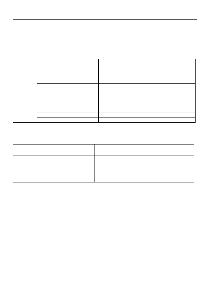
244
Agere Systems Inc.
Data Sheet
May 2001
155/622/2488 Mbits/s Data Interface
TDAT042G5 SONET/SDH
Register Descriptions
(continued)
DE Registers
(continued)
Table 146. Registers 0x1181--0x1187: Interrupts for Packet Counters (COR/W)
Reset default of registers = 0x0000.
Table 147. Registers 0x1200--0x1213, 0x12F0: ATM Transmit Registers (R/W)
Reset default of registers 0x1200--0x1203, 0x12F0 = 0x0000.
Reset default of registers 0x1210--0x1213 = 0x0001.
Address
(Hex)
Bit #
Name
Function
Reset
Default
1181, 1183,
1185, 1187
--
DEDINT[0--3]
Data Interrupt Channel [0--3]. Stores bits that
describe which conditions of corrupted data
exist in channel [0--3].
0x0000
15--5
--
Reserved. These bits must be written to their
reset default value (00000000000).
000
0000
0000
4
--
Rx-Side Good Packet.
0
3
--
PPP Mismatched Header.
0
2
--
CRC Bad Packet.
0
1
--
ATM/HDLC/SDL Counter 2.
0
0
--
ATM/HDLC/SDL Counter 1.
0
Address
(Hex)
Bit #
Name
Function
Reset
Default
1200, 1201,
1202, 1203
15--0
NULLCELL1[0--3]
ATM Null (Idle) Cell MSB Channel [0--3]. This
defines the first 2 bytes of a NULL ATM cell (i.e.,
15:0 = h0h1).
0x0000
1210, 1211,
1212, 1213
15--0
NULLCELL2[0--3]
ATM Null (Idle) Cell LSB Channel [0--3]. This
defines the second 2 bytes of a NULL ATM cell
(i.e., 15:0 = h2h3).
0x0001

Agere Systems Inc.
245
Data Sheet
May 2001
155/622/2488 Mbits/s Data Interface
TDAT042G5 SONET/SDH
Register Descriptions
(continued)
DE Registers
(continued)
Table 147. Registers 0x1200--0x1213, 0x12F0: ATM Transmit Registers (R/W) (continued)
Reset default of registers 0x1200--0x1203, 0x12F0 = 0x0000.
Reset default of registers 0x1210--0x1213 = 0x0001.
Address
(Hex)
Bit #
Name
Function
Reset
Default
12F0
--
ATM_HEADER_ERROR
ATM Tx Debug Control. Used for debug
purposes to inject errors, and to increment the
payload sequence for NULL cells.
0x0000
15--8
--
Reserved. These bits must be written to their
reset default value (0x00).
0x00
7
--
Incrementing Null (Idle) Cell Payload
Sequence. This bit governs whether 0x6A is
used for the payload of NULL cells, or whether an
incrementing 8-bit count is used (0x00
0xFF).
A value of 1 selects the incrementing sequence.
This is used with DE register 0x1002 bits [11:8].
0
6
--
Error Strobe. Writing a value of 1 to this register
initiates the injection of a single or double shot
error injection, assuming one of these two modes
is selected.
0
5--4
--
Error Injection Mode. These bits control the
mode of operation of the error injection.
00 = continuous injection
01 = single shot (isolated cell)
10, 11 = double shot (i.e., two back-to-back cells)
00
3--2
--
Error Type. These bits control the injection of a
walking error pattern into the headers of all
outgoing cells.
00 = no errors
01 = single bit errors
10, 11 = double bit errors
00
1--0
--
Error Channel ID. The logical channel in which
to inject the header errors.
00

246
Agere Systems Inc.
Data Sheet
May 2001
155/622/2488 Mbits/s Data Interface
TDAT042G5 SONET/SDH
Register Descriptions
(continued)
DE Registers
(continued)
Table 148. Registers 0x1400--0x1403: SDL State Registers (RO)
Reset default of registers = 0x0000.
Address
(Hex)
Bit #
Name
Function
Reset
Default
1400, 1401,
1402, 1403
--
SDL_ST[0--3]
SDL State Channel [0--3]. These registers
describe the SDL framer and scrambler states.
0x0000
15--4
--
Reserved. These bits must be written to their
reset default value (0x000).
0x000
3--2
--
SDL Frame State. Indicates the frame state of
each channel.
SDL_ST[0--3][3:2] = 00. Out-of-Frame. The
SDL framer is in search of a successful SDL
framing.
SDL_ST[0--3][3:2] = 01. Presync. The SDL
framer has transitioned from the out of frame to
the presync state. The SDL framer has
successfully framed one SDL header.
SDL_ST[0--3][3:2] = 10. Sync. The SDL
framer has transitioned from the presync to the
sync state. The framer has successfully
detected the second consecutive SDL packet.
The SDL framer is correctly framed on the SDL
signal. The SDL framer remains in the sync
state until a bad packet frame is detected.
Detection of a bad packet frame places the SDL
framer in the out-of-frame state.
SDL_ST[0--3][3:2] = 11. Undefined.
00
1--0
--
SDL Scram State. Indicates the X48 sync state
of each channel.
SDL_ST[0--3][1:0] = 00. Hunt. The SDL
scrambler has yet to detect a valid scrambler
state.
SDL_ST[0--3][1:0] = 01. Sync. The SDL
scrambler is in sync.
SDL_ST[0--3][1:0] = 10. Postsync. The SDL
scrambler was in sync, but detected an SDL
state that did not match the expected state. If
two consecutive nonmatching states are
detected, then (1) the SDL framer is reset with
the scrambler state received in the bit stream,
and (2) a sync slip interrupt is generated.
SDL_ST[0--3][1:0] = 11. Undefined.
00

Agere Systems Inc.
247
Data Sheet
May 2001
155/622/2488 Mbits/s Data Interface
TDAT042G5 SONET/SDH
Register Descriptions
(continued)
DE Registers
(continued)
Table 149. Registers 0x1470--0x1473: A Message Mailbox Registers (RO)
Reset default of registers = 0x0000.
Table 150. Registers 0x1480--0x1483: A Message Mailbox Registers (RO)
Reset default of registers = 0x0000.
Table 151. Registers 0x1490--0x1493: A Message Mailbox Registers (RO
)
Reset default of registers = 0x0000.
Table 152. Registers 0x14A0--0x14A3: B Message Mailbox Registers (RO
)
Reset default of registers = 0x0000.
Address
(Hex)
Bit #
Name
Function
Reset
Default
1470, 1471,
1472, 1473
15--0
SDL_AMM1[0--3]
A Message Mailbox 1: Channel [0--3]. These
registers will store the first 16 bits of a valid A
message header. A maskable interrupt will be
generated if the SDL framer receives an A
message.
0x0000
Address
(Hex)
Bit #
Name
Function
Reset
Default
1480, 1481,
1482, 1483
15--0
SDL_AMM2[0--3]
A Message Mailbox 2: Channel [0--3]. These
registers will store the middle 16 bits of a valid
A message header. A maskable interrupt will be
generated if the SDL framer receives an A
message.
0x0000
Address
(Hex)
Bit #
Name
Function
Reset
Default
1490, 1491,
1492, 1493
15--0
SDL_AMM3[0--3]
A Message Mailbox 3: Channel [0--3]. These
registers will store the last 16 bits of a valid A
message header. A maskable interrupt will be
generated if the SDL framer receives an A
message.
0x0000
Address
(Hex)
Bit #
Name
Function
Reset
Default
14A0, 14A1,
14A2, 14A3
15--0
SDL_BMM1[0--3]
B Message Mailbox 1: Channel [0--3]. These
registers will store the first 16 bits of a valid B
message header. A maskable interrupt will be
generated if the SDL framer receives a B
message.
0x0000

248
Agere Systems Inc.
Data Sheet
May 2001
155/622/2488 Mbits/s Data Interface
TDAT042G5 SONET/SDH
Register Descriptions
(continued)
DE Registers
(continued)
Table 153. Registers 0x14B0--0x14B3: B Message Mailbox Registers (RO
)
Reset default of registers = 0x0000.
Table 154. Registers 0x14C0--0x14C3: B Message Mailbox Registers (RO)
Reset default of registers = 0x0000.
Table 155. Registers 0x14D0--0x14D3: SDL Interrupt Masks (R/W)
Reset default of registers = 0x00FF.
Address
(Hex)
Bit #
Name
Function
Reset
Default
14B0, 14B1,
14B2, 14B3
15--0
SDL_BMM2[0--3]
B Message Mailbox 2: Channel [0--3]. These
registers will store the middle 16 bits of a valid
B message header. A maskable interrupt will be
generated if the SDL framer receives a B
message.
0x0000
Address
(Hex)
Bit #
Name
Function
Reset
Default
14C0, 14C1,
14C2, 14C3
15--0
SDL_BMM3[0--3]
B Message Mailbox 3: Channel [0--3]. These
registers will store the last 16 bits of a valid B
message header. A maskable interrupt will be
generated if the SDL framer receives a B
message.
0x0000
Address
(Hex)
Bit #
Name
Function
Reset
Default
14D0, 14D1,
14D2, 14D3
--
SDLINTM[0--3]
SDL Interrupt Mask Channel [0--3]. When
active (logic 1), the associated event/delta is
inhibited from contributing to the interrupt on a
per-channel basis.
0x00FF
15--8
--
Reserved. These bits must be written to their
reset default value (0x00).
0x00
7
--
B_Message Reception.
1
6
--
A_Message Reception.
1
5
--
Uncorrectable Special Payload Error.
1
4
--
Uncorrectable Bit Error.
1
3
--
Reserved. This bit must be written to its reset
default value (1).
1
2
--
Single Bit Error.
1
1
--
Scrambler Out of Sync.
1
0
--
Framer Out of Sync.
1

Agere Systems Inc.
249
Data Sheet
May 2001
155/622/2488 Mbits/s Data Interface
TDAT042G5 SONET/SDH
Register Descriptions
(continued)
DE Registers
(continued)
Table 156. Registers 0x14E0--0x14E3: SDL Interrupts (COR/W)
Reset default of registers = 0x0000.
Table 157. Register 0x14F0: SDL Receive Configuration Registers (R/W)
Reset default of registers = 0x0001.
Address
(Hex)
Bit #
Name
Function
Reset
Default
14E0, 14E1,
14E2, 14E3
--
SDLINT[0--3]
SDL Interrupt Channel [0--3]. Used to record
various occurrences within the SDL framer. The
bits will generate an interrupt if defined by the
interrupt mask, but the register values here are
independent of the interrupt mask values.
0x0000
15--8
--
Reserved. These bits must be written to their
reset default value (0x00).
0x00
7
--
B_Message Reception.
0
6
--
A_Message Reception.
0
5
--
Uncorrectable Special Payload Error.
Indicates occurrence of two or more special
payload errors.
0
4
--
Uncorrectable Header Bit Error. Indicates
occurrence of two or more header errors.
0
3
--
Reserved. This bit must be written to its reset
default value (0).
0
2
--
Single Bit Header Error.
0
1
--
Scrambler Out of Sync. Indicates a scrambler
sync slip.
0
0
--
Framer Out of Sync.
0
Address
(Hex)
Bit #
Name
Function
Reset
Default
14F0
--
SDL_DELTA
SDL Receive Frame Configuration Register.
0x0001
15--7
--
Reserved. These bits must be written to their
reset default value (000000000).
0000
00000
6
--
Disable Scrambling. When this value is 1, the
SDL framer will not unscramble the data prior to
framing.
0
5
--
Reserved. These bits must be written to their
reset default value (0).
0
4
--
Sync Mode. When bit 4 has a value of 1, then
only one framer is used at all times to frame
SDL data. Normally, this bit is 0, and four
coordinated framers are active simultaneously
to synchronize the scrambler process.
0
3--0
--
Framer Delta. This register will define the delta
value for the CRC-16 framer.
0x1

250
Agere Systems Inc.
Data Sheet
May 2001
155/622/2488 Mbits/s Data Interface
TDAT042G5 SONET/SDH
Register Descriptions
(continued)
DE Registers
(continued)
Table 158. Registers 0x1600--0x1607: SDL Transmit Registers (R/W)
Reset default of registers 0x1600, 0x1601, 0x1602, 0x1603, 0x1606 = 0x0000.
Reset default of register 0x1604 = 0x0008.
Reset default of register 0x1605 = 0x8000.
Note: These registers must be written in the following order: 0x1603, then 0x1600, 0x1601, 0x1602. Register
0x1603 is a clear-on-write (COW) register.
Address
(Hex)
Bit #
Name
Function
Reset
Default
1600
15--0
SDLFI_MSG1
SDL Message. These registers will store the
first 16 bits of a header of an outgoing A or B
message.
0x0000
1601
15--0
SDLFI_MSG2
SDL Message. These registers will store the
middle 16 bits of a header of an outgoing A or B
message.
0x0000
1602
15--0
SDLFI_MSG3
SDL Message. These registers will store the
last 16 bits of a header of an outgoing A or B
message. Writing to this register causes the
message to be sent.
0x0000
1603
--
SDLFI_MSG_TYPE
SDL Message Type.
0x0000
15
SDLMTB
Message Type Bit.
0 = A Message
1 = B Message
0
14--2
--
Reserved. These bits must be written to their
reset default value (00000000000000).
0
0000
0000
0000
1--0
SDLCHID[1:0]
Channel ID. Defines on which channel the
special message will be transmitted.
00
1604
15--0
SDLFI_INT
SDL State Transmit Interval. Defines the
number of packets (or dWords) separating
scrambler state transmissions. Use register
0x1605 to determine if units are packets or
dwords.
0x0008

Agere Systems Inc.
251
Data Sheet
May 2001
155/622/2488 Mbits/s Data Interface
TDAT042G5 SONET/SDH
Register Descriptions
(continued)
DE Registers
(continued)
Table 158. Registers 0x1600--0x1607: SDL Transmit Registers (R/W) (continued)
Reset default of registers 0x1600, 0x1601, 0x1602, 0x1603, 0x1606 = 0x0000.
Reset default of register 0x1604 = 0x0008.
Reset default of register 0x1605 = 0x8000.
Note: These registers must be written in the following order: 0x1603, then 0x1600, 0x1601, 0x1602. Register
0x1603 is a clear-on-write (COW) register.
Address
(Hex)
Bit #
Name
Function
Reset
Default
1605
--
SDLFI_MODE
SDL State Transmit Mode.
0x8000
15
SDLSMIE
Special Message Interrupt Enable. The SDL
line transmitter generates an interrupt when
transmission of a special message is complete.
In this case, used to signal the sending of a
special message (A or B message).
1
14--2
--
Reserved. These bits must be written to their
reset default value (0000000000000).
0
0000
0000
0000
1
SDLSC
Scrambler Control.
1 = disables data scrambling
0 = enables data scrambling
0
0
SDLSSTMS
Scrambler State Transmit Mode Select.
0 = packets
1 = dWord (32 bits)
0

252
Agere Systems Inc.
Data Sheet
May 2001
155/622/2488 Mbits/s Data Interface
TDAT042G5 SONET/SDH
Register Descriptions
(continued)
DE Registers
(continued)
Table 158. Registers 0x1600--0x1607: SDL Transmit Registers (R/W)
(continued)
Reset default of registers 0x1600, 0x1601, 0x1602, 0x1603, 0x1606 = 0x0000.
Reset default of register 0x1604 = 0x0008.
Reset default of register 0x1605 = 0x8000.
Note: These registers must be written in the following order: 0x1603, then 0x1600, 0x1601, 0x1602. Register
0x1603 is a clear-on-write (COW) register
.
Address
(Hex)
Bit #
Name
Function
Reset
Default
1606
--
SDLFI_INTR
Status Register.
0x0000
15--2
--
Reserved. These bits must be written to their
reset default value (000000000000000).
00
0000
0000
0000
1
SDLFDO
SDLFIFO Depth Out. When this bit has a value
of 1, it indicates that the FIFO in the SDL Tx
data buffer is over half full.
0
0
SDLMSI
Message Sent Interrupt. When this bit has a
value of 1, it indicates that an SDL A/B
message has been sent. This value may be
cleared when read or written.
0
1607
--
SDLFI_DEBUG
SDL Debug Register.
0x0000
15--6
--
Reserved. These bits must be written to their
reset default value (0000000000).
00
0000
0000
5--4
SDLHE[1:0]
Header Error. This value indicates the number
of errors to insert into the SDL header on a
given channel for debug purposes. The error
injection is done using a walking ones pattern
to cover all possibilities.
0x0 = no errors
0x1 = single error
0x2 = double error
0x3 = double error
00
3--2
SDLPE[1:0]
Payload Error. This value indicates the number
of errors to insert into the payload of special
packets on a given channel for debug purposes.
The error injection is done using a walking ones
pattern to cover all possibilities.
00 = no errors
01 = single error
10 = double error
11 = double error
00
1--0
SDLECID[1:0]
Error Channel ID. This value specifies the
channel on which the errors are to be sent.
00
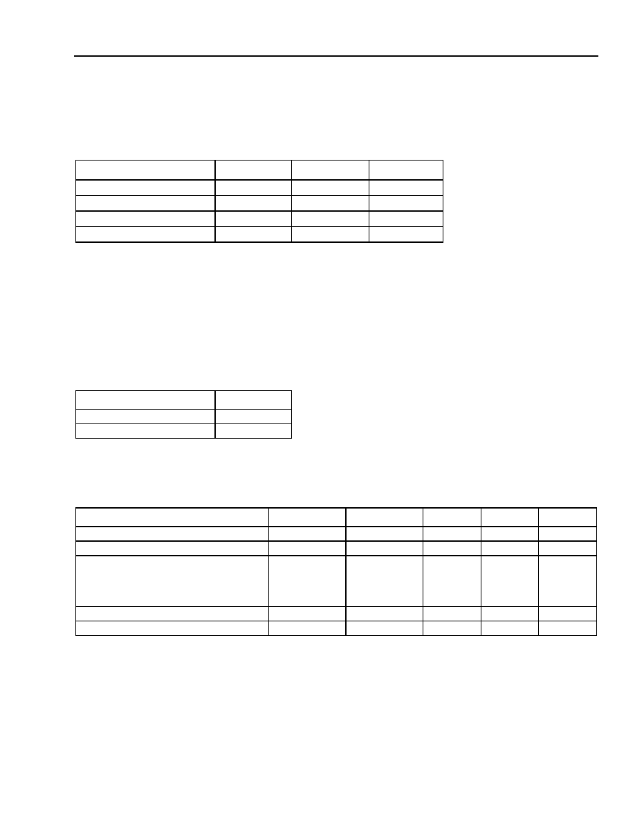
Agere Systems Inc.
253
Data Sheet
May 2001
155/622/2488 Mbits/s Data Interface
TDAT042G5 SONET/SDH
Absolute Maximum Ratings
Stresses in excess of the absolute maximum ratings can cause permanent damage to the device. These are abso-
lute stress ratings only. Functional operation of the device is not implied at these or any other conditions in excess
of those given in the operational sections of the data sheet. Exposure to absolute maximum ratings for extended
periods can adversely affect device reliability.
Note: V
DD
= V
DDA
= V
DDD.
Handling Precautions
Although protection circuitry has been designed into this device, proper precautions should be taken to avoid expo-
sure to electrostatic discharge (ESD) during handling and mounting. Agere employs a human-body model (HBM)
and a charged-device model (CDM) for ESD-susceptibility testing and protection design evaluation. ESD voltage
thresholds are dependent on the circuit parameters used in the defined model. No industry-wide standard has
been adopted for the CDM. However, a standard HBM (resistance = 1500
, capacitance = 100 pF) is widely used
and, therefore, can be used for comparison purposes:
Operating Conditions
Table 159. Recommended Operating Conditions
Note: V
DD
= V
DDA
= V
DDD.
Parameter
Min
Max
Unit
Power Supply Voltage
≠0.5
4.2
V
Storage Temperature
≠65
125
∞C
Pin Voltage (3.3 V)
GND ≠ 0.5
V
DD
+ 0.5
V
Pin Voltage (5 V tolerant)
GND ≠ 0.5
5.5
V
Device
Voltage
TDAT042G5
TBD
TDAT042G51A
TBD
Parameter
Symbol
Min
Typ
Max
Unit
Power Supply (dc voltage)
V
DD
3.135
--
3.465
V
Ground
--
--
--
--
V
Input Voltage:
Low
High
V
IL
V
IH
GND
V
DD
≠ 1.0
--
--
1.0
V
DD
V
V
Ambient Temperature
--
≠40
--
85
∞C
Power Dissipation (V
DD
= 3.465 V)
P
D
--
--
7.5
W

254
Agere Systems Inc.
Data Sheet
May 2001
155/622/2488 Mbits/s Data Interface
TDAT042G5 SONET/SDH
Electrical Characteristics
The following characteristics are guaranteed over the recommended operating conditions, unless otherwise speci-
fied in the test conditions.
Table 160. 3.3 V Logic Interface Characteristics
These logic levels are TTL 5 V compliant.
* Load for the UTOPIA ports are given in Table 170, page 269. Load for all microprocessor outputs is 50 pF.
Note: V
DD
= V
DDA
= V
DDD.
Table 161. LVPECL Interface Characteristics
The range for V
DD
in this table is as follows: 3.0 V < V
DD
< 3.63 V, and V
DD
nominal = 3.30 V.
Note: V
DD
= V
DDA
= V
DDD.
Parameter
Symbol
Test Conditions
Min
Max
Unit
Input Leakage
I
L
--
--
1.0
µA
Output Voltage:
Low
High
V
OL
V
OH
≠5.0 mA
5.0 mA
GND
V
DD
≠ 1.0
0.5
V
DD
V
V
Input Capacitance
C
I
--
--
--
pF
Load Capacitance
C
L
*
--
--
pF
Parameter
Symbol
Test
Conditions
Min
Nominal
Max
Unit
Output Voltage:
Low
High
V
OL
V
OH
--
--
V
DD
≠ 1.810
V
DD
≠ 1.025
--
V
DD
≠ 1.620
V
DD
≠ 0.880
V
V
Input Voltage:
Low
High
V
IL
V
IH
--
--
V
DD
≠ 1.810
V
DD
≠ 1.165
--
--
V
DD
≠ 1.475
V
DD
≠ 0.880
V
V
Input Capacitance
C
I
--
--
--
2.5
pF
Load Capacitance
C
L
--
--
--
0.4
pF
Input Buffer Gain
V
G
--
--
125
--
dB
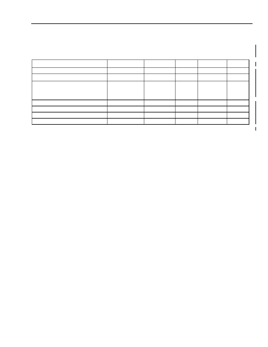
Agere Systems Inc.
255
Data Sheet
May 2001
155/622/2488 Mbits/s Data Interface
TDAT042G5 SONET/SDH
Electrical Characteristics
(continued)
Table 162. LVPECL 3.3 V Logic Interface Characteristics
V
DDD
has a range of 3.0 V < V
DDD
< 3.63 V, V
DDD
typical = 3.3 V.
Parameter
Symbol
Min
Typical
Max
Unit
Input Leakage Current
I
L
--
--
20
µ
A
Input Common Mode Voltage Range
1
1. With a swing of 300 mV: V
ID
= 300 mV where V
IL
(min) = 0.85 V and V
IH
(max) = 2.9 V.
V
CMR
1
--
2.75
V
Output Voltage:
Low
High
V
OLLVPECL
V
OHLVPECL
V
DDD
≠ 1.97
V
DDD
≠ 1.025
--
--
V
DDD
≠ 1.620
V
DDD
≠ 0.72
V
V
Output Voltage Swing
V
OSWING
0.595
--
1.25
V
Input Capacitance
C
I
--
--
2.3
pF
Load Capacitance
C
L
--
--
0.4
pF
Input Buffer Gain
V
G
--
125
--
dB
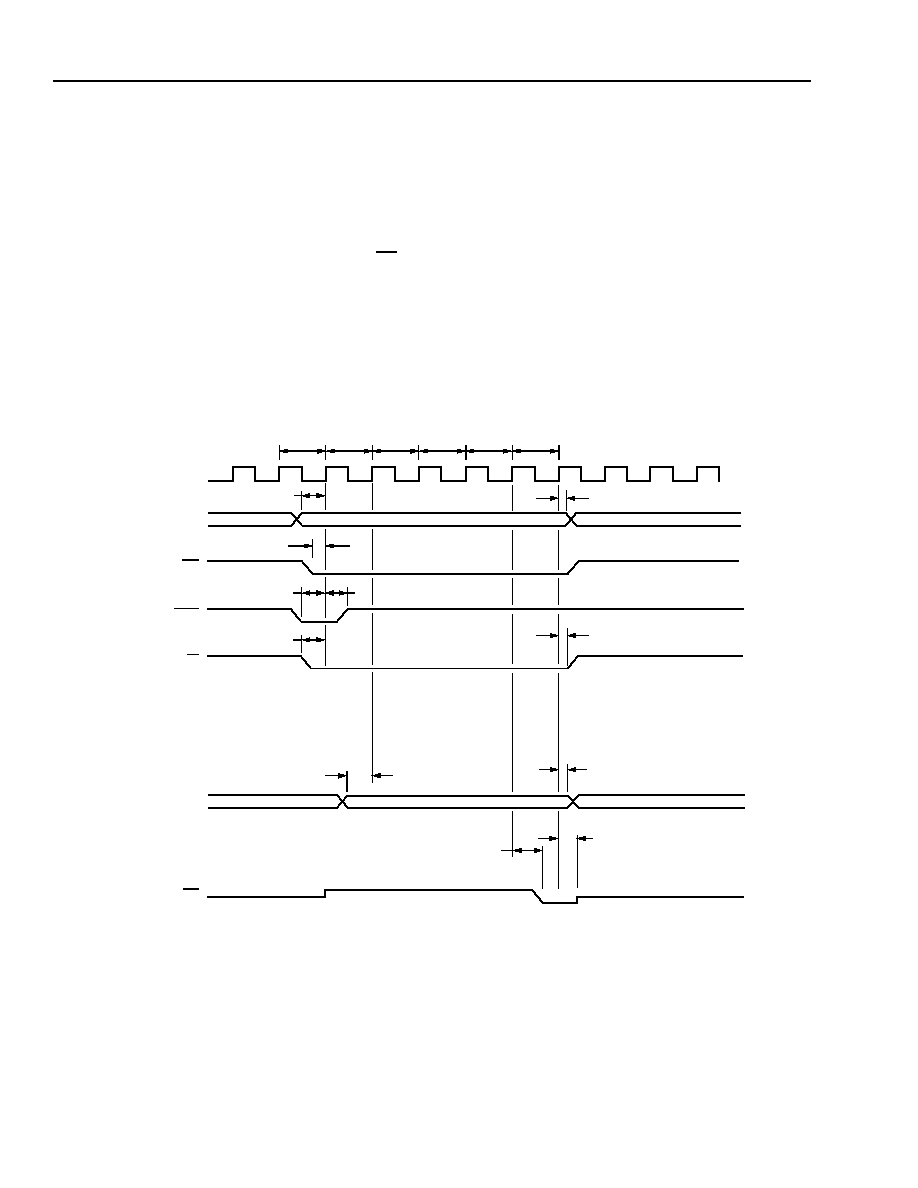
256
Agere Systems Inc.
Data Sheet
May 2001
155/622/2488 Mbits/s Data Interface
TDAT042G5 SONET/SDH
Interface Timing Specifications
This section specifies the interface timing requirements for the microprocessor interface, line interface, UTOPIA
interface, and SONET transport overhead (TOAC) interface.
Microprocessor Interface Timing
In all modes of the microprocessor interface, the CS may be held active continuously without affecting the function-
ality of TDAT042G5. There is no minimum time between successive microprocessor accesses to TDAT042G5, i.e.,
successive reads or writes may be back to back.
Synchronous Mode
The synchronous microprocessor interface mode is selected when MPMODE (pin D8) = 1. Interface timing for the
synchronous mode write cycle is given in Figure 38 and in Table 163 (pages 256--257), and for the read cycle in
Figure 39 and in Table 164 (pages 258--259).
5-7659(F)r.2
Figure 38. Microprocessor Interface Synchronous Write Cycle (MPMODE (Pin D8) = 1)
MPCLK
ADDR[15:0]
CS
ADS
R/W
DATA[15:0]
DT
(66 MHz MAX)
(INPUT)
t4
t1
t6
t7
t2
t2
t1
t3
t5
t1
t2
T0
T1
T2
T3
T4
T5
HIGH Z
HIGH Z
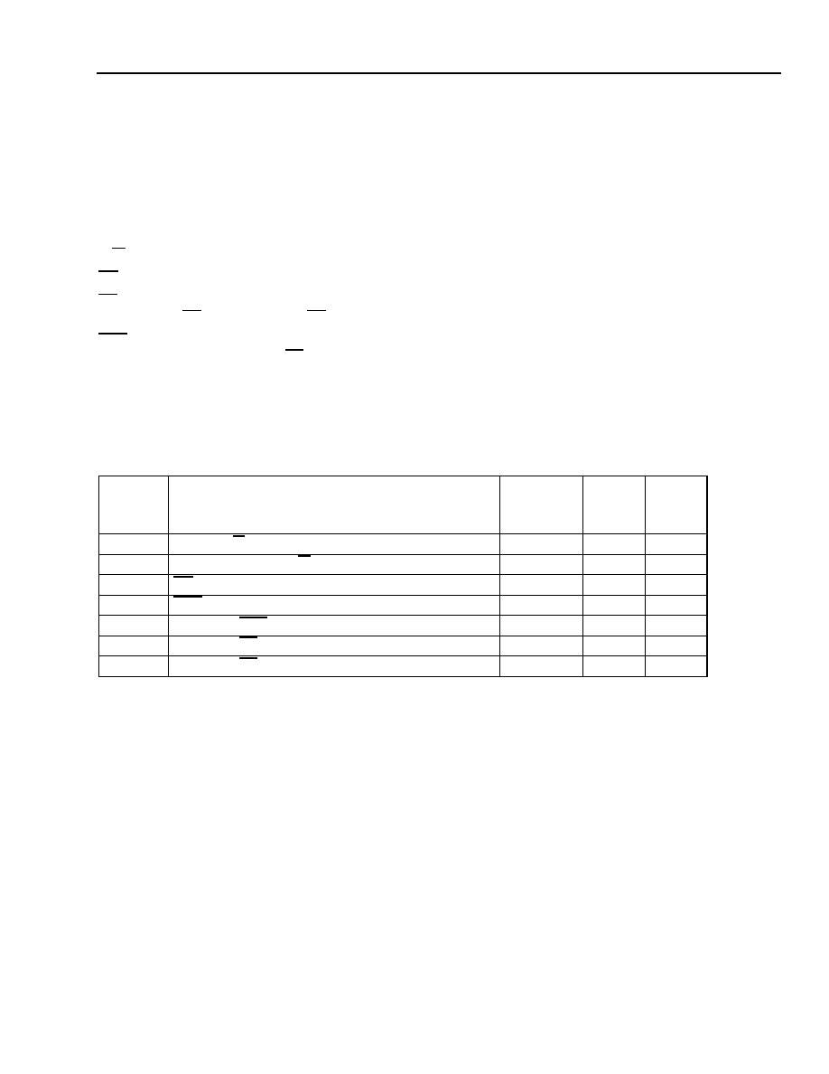
Agere Systems Inc.
257
Data Sheet
May 2001
155/622/2488 Mbits/s Data Interface
TDAT042G5 SONET/SDH
Interface Timing Specifications
(continued)
Microprocessor Interface Timing
(continued)
Synchronous Mode (continued)
ADDR[15:0] The address will be available throughout the entire cycle.
DATA[15:0]
Data will be available during cycles T1 through T5.
R/W (Input)
The read (H) write (L) signal is always high except during a write cycle.
CS (Input)
Chip select is an active-low signal.
DT (Output)
Data transfer acknowledge is active-low on the host bus interface. It is initiated in timing cycle T5.
DT is 3-stated when CS is high.
ADS (Input)
Address strobe is active-low for one clock cycle, T0. When used with the Power PC* (Motorola
MPC860), this is TS (transfer start).
* PowerPC is a registered trademark of International Business Machines Corporation.
Motorola is a registered trademark of Motorola, Inc.
Table 163. Microprocessor Interface Synchronous Write Cycle Specifications
(See Figure 38 on page 256 for the timing diagram.)
Symbol
Parameter
Setup
(ns)
(Min)
Hold
(ns)
(Min)
Delay
(ns)
(Max)
t1
ADDR, R/W, DATA (write) Valid to MPCLK
3
--
--
t2
MPCLK to ADDR, R/W, DATA (write) Invalid
--
5
--
t3
CS Valid to MPCLK
3.5
--
--
t4
ADS Valid to MPCLK
5.5
--
--
t5
MPCLK to ADS Invalid
--
5
--
t6
MPCLK to DT Valid
--
--
8
t7
MPCLK to DT Invalid
--
1
--
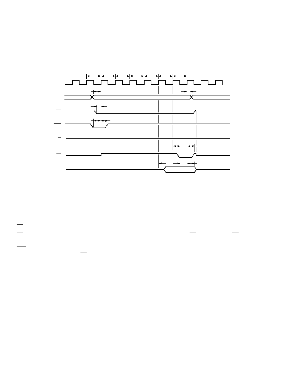
258
Agere Systems Inc.
Data Sheet
May 2001
155/622/2488 Mbits/s Data Interface
TDAT042G5 SONET/SDH
Interface Timing Specifications
(continued)
Microprocessor Interface Timing
(continued)
Synchronous Mode (continued)
5-7660(F)r.6
Figure 39. Microprocessor Interface Synchronous Read Cycle (MPMODE (Pin D8) = 1)
ADDR[15:0] The address will be available throughout the entire cycle.
DATA[15:0]
Read data is available in T6.
R/W (Input)
The read (H) write (L) signal is always high during the read cycle.
CS (Input)
Chip select is an active-low signal.
DT (Output)
Data transfer acknowledge on the host bus interface is initiated on T6. DT is 3-stated when CS is
high.
ADS (Input)
Address strobe is active-low for one clock cycle, T0. When used with the Power PC (Motorola
MPC860), this is TS (transfer start).
MPCLK
ADDR[15:0]
CS
ADS
R/W
(66 MHz MAX)
t9
t11
t12
t10
t8
T0
T1
T2
T3
T4
T5
T6
DT
DATA[15:0]
(OUTPUT)
t15
t16
t14
t13
HIGH Z
HIGH Z
HIGH Z
HIGH Z
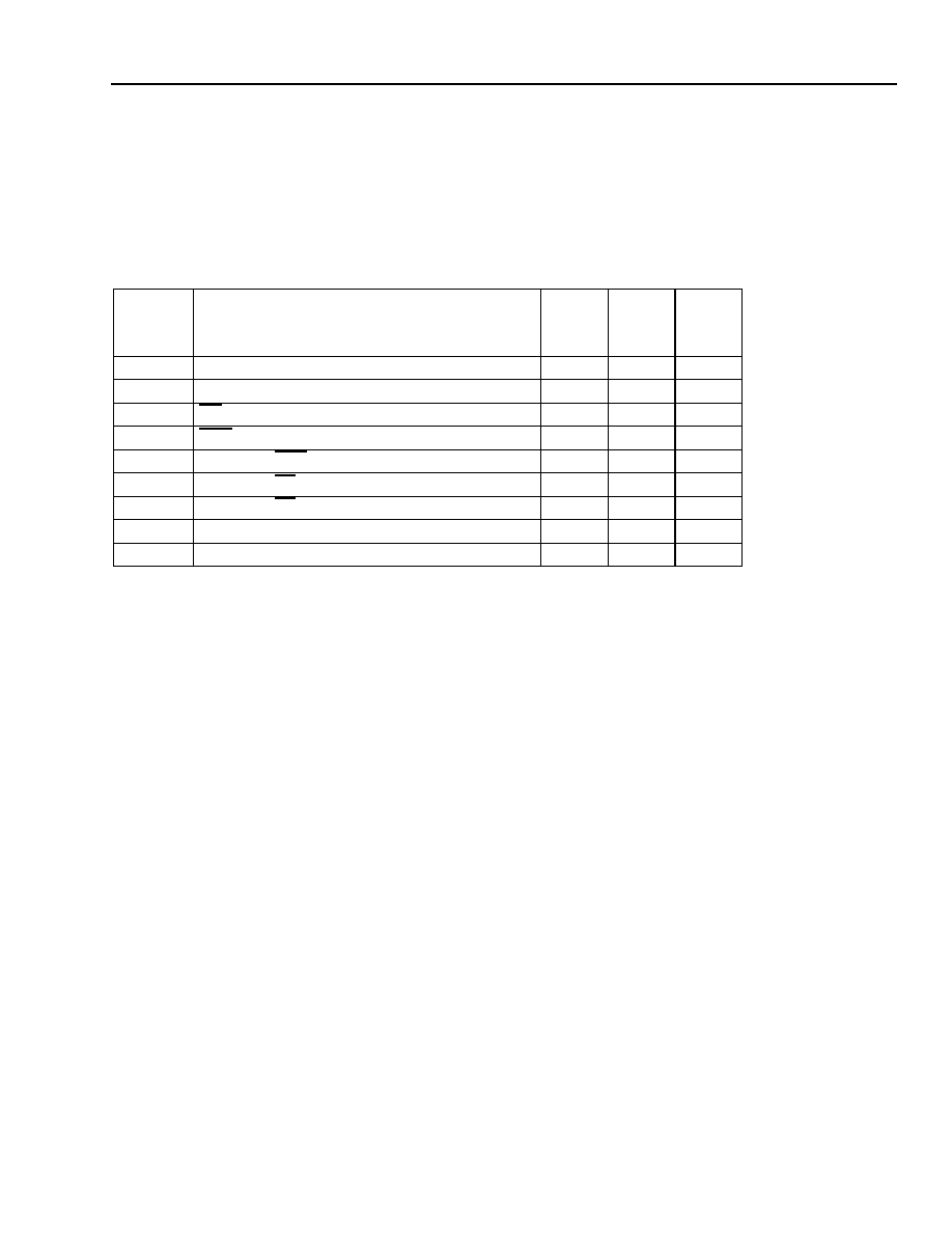
Agere Systems Inc.
259
Data Sheet
May 2001
155/622/2488 Mbits/s Data Interface
TDAT042G5 SONET/SDH
Interface Timing Specifications
(continued)
Microprocessor Interface Timing
(continued)
Synchronous Mode (continued)
Table 164. Microprocessor Interface Synchronous Read Cycle Specifications
(See Figure 39 on page 258 for the timing diagram.)
Symbol
Parameter
Setup
(ns)
(Min)
Hold
(ns)
(Min)
Delay
(ns)
(Max)
t8
ADDR Valid to MPCLK
3
--
--
t9
MPCLK to ADDR Invalid
--
5
--
t10
CS Valid to MPCLK
3.5
--
--
t11
ADS Valid to MPCLK
5.5
--
--
t12
MPCLK to ADS Invalid
--
5
--
t13
MPCLK to DT Valid
--
--
8
t14
MPCLK to DT Invalid
--
1
--
t15
MPCLK to DATA Valid
--
--
24
t16
MPCLK to DATA 3-state
--
1
--
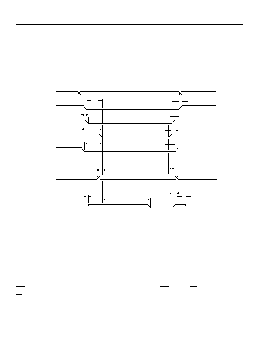
260
Agere Systems Inc.
Data Sheet
May 2001
155/622/2488 Mbits/s Data Interface
TDAT042G5 SONET/SDH
Interface Timing Specifications
(continued)
Microprocessor Interface Timing
(continued)
Asynchronous Mode
The asynchronous microprocessor interface mode is selected when MPMODE (pin D8) = 0. Interface timing for the
asynchronous mode write cycle is given in Figure 40 and in Table 165 (see pages 260--261), and for the read
cycle in Figure 41 and in Table 166 (see pages 262--263).
5-7661(F)r.3
Figure 40. Microprocessor Interface Asynchronous Write Cycle Description (MPMODE (Pin D8) = 0)
ADDR[15:0] The address must be valid when ADS is low.
DATA[15:0]
Data must be valid when DS is low.
R/W (Input)
The read (H) write (L) signal is always high except during a write cycle.
CS (Input)
Chip select is an active-low signal.
DT (Output)
Data transfer acknowledge (active-low). DT is driven asynchronously based on the arrival of CS.
DT is driven high until the internal transaction is done. DT is driven high again when ADS is deas-
serted. DT will become 3-stated when CS is high.
ADS (Input)
Address strobe is active-low. The microprocessor can pull ADS high after DT goes high.
DS (Input)
Data strobe is active-low.
ADDR[15:0]
CS
ADS
DS
R/W
DATA[15:0]
DT
(INPUT)
t17
t19
t25
t27
t28
t29
t30
t26
t24
t22
t20
t18
t23
t21
HIGH Z
HIGH Z
Agere Systems Inc.
261
Data Sheet
May 2001
155/622/2488 Mbits/s Data Interface
TDAT042G5 SONET/SDH
Interface Timing Specifications
(continued)
Microprocessor Interface Timing
(continued)
Asynchronous Mode (continued)
Table 165. Microprocessor Interface Asynchronous Write Cycle Specifications
(See Figure 40 on page 260 for the timing diagram.)
Symbol
Parameter
Min Interval
(ns)
Max Interval
(ns)
t17
CS Fall to DS Fall
0
--
t18
ADDR Invalid to CS Rise
0
--
t19
ADDR Valid to ADS Fall
0
--
t20
ADS Rise to ADDR Invalid
5
--
t21
ADDR Valid to DS Fall
0
--
t22
DS Rise to ADDR Invalid
0
--
t23
R/W Fall to DS Fall
0
--
t24
DS Rise to R/W Rise
0
--
t25
DATA Valid to DS Fall
0
--
t26
DS Rise to DATA Invalid
0
--
t27
CS Fall to DT High
0
--
t28
DS Fall to DT Fall
77
103
t29
ADS Rise to DT Rise
0
37.5
t30
CS Rise to DT 3-state
0
--
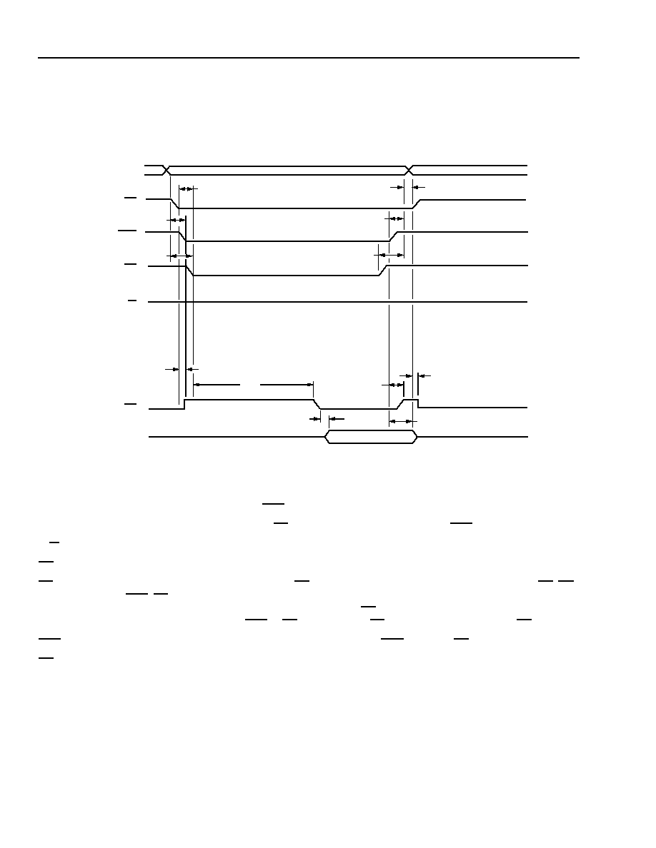
262
Agere Systems Inc.
Data Sheet
May 2001
155/622/2488 Mbits/s Data Interface
TDAT042G5 SONET/SDH
Interface Timing Specifications
(continued)
Microprocessor Interface Timing
(continued)
Asynchronous Mode (continued)
5-7662(F)r.6
Figure 41. Microprocessor Interface Asynchronous Read Cycle (MPMODE (Pin D8) = 0)
ADDR[15:0] The address must be valid when ADS is low.
DATA[15:0]
Read data becomes available after DT goes low. It will be 3-stated when ADS goes high.
R/W (Input)
The read (H) write (L) signal is always high during a read cycle.
CS (Input)
Chip select is an active-low signal.
DT (Output)
Data transfer acknowledge (active-low). DT is driven asynchronously based on the arrival of CS, DS,
and ADS. DT is driven high while the internal bus transaction is in progress. There is no need to pro-
vide synchronization to outgoing signals in this mode. DT is driven high and then placed in a high-
impedance state when either ADS or DS is deasserted. DT will become 3-stated when CS is high.
ADS (Input)
Address strobe is active-low. The microprocessor can pull ADS high after DT goes high.
DS (Input)
Data strobe is active-low.
ADDR[15:0]
CS
ADS
DS
DT
DATA[15:0]
t42
t40
t39
t31
R/W
t33
t35
t32
t34
t36
t41
t38
t37
HIGH Z
HIGH Z
HIGH Z
HIGH Z
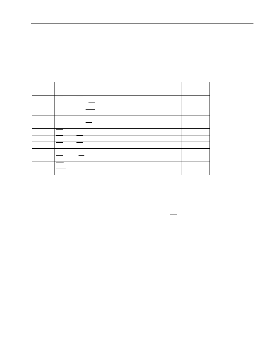
Agere Systems Inc.
263
Data Sheet
May 2001
155/622/2488 Mbits/s Data Interface
TDAT042G5 SONET/SDH
Interface Timing Specifications
(continued)
Microprocessor Interface Timing
(continued)
Asynchronous Mode (continued)
Table 166. Microprocessor Interface Asynchronous Read Cycle Specifications
(See Figure 41 on page 262 for the timing diagram.)
Reset
Software Reset. Writing the binary value 101 to SWRST (core register 0x000E, bits 2--0) causes a 0 to 1 transi-
tion on the internal PMRST signal. This pulse will be high for 100 clock cycles and then low for 100 clock cycles of
the 77.76 MHz internal clock. Writing a logic 1 to these bits during this 200 clock-cycle interval (2.57
µ
s) has no
effect.
Interrupt. Occurrence of an interrupt is event driven. The interrupt pin, INT (B7), will be deasserted after a mini-
mum of either one MPU clock cycle in the synchronous microprocessor mode or 13 ns in the asynchronous micro-
processor mode after clearing the interrupt register.
Symbol
Parameter
Min Interval
(ns)
Max Interval
(ns)
t31
CS Fall to DS Fall
0
--
t32
ADDR Invalid to CS Rise
0
--
t33
ADDR Valid to ADS Fall
0
--
t34
ADS Rise to ADDR Invalid
5
--
t35
ADDR Valid to DS Fall
0
--
t36
DS Rise to ADDR Invalid
0
--
t37
CS Fall to DT High
0
--
t38
DS Fall to DT Fall
90
115
t39
ADS Rise to DT Rise
--
37.5
t40
CS Rise to DT 3-state
0
--
t41
DT Valid to DATA Valid
--
12
t42
ADS Rise to DATA 3-state
0
--
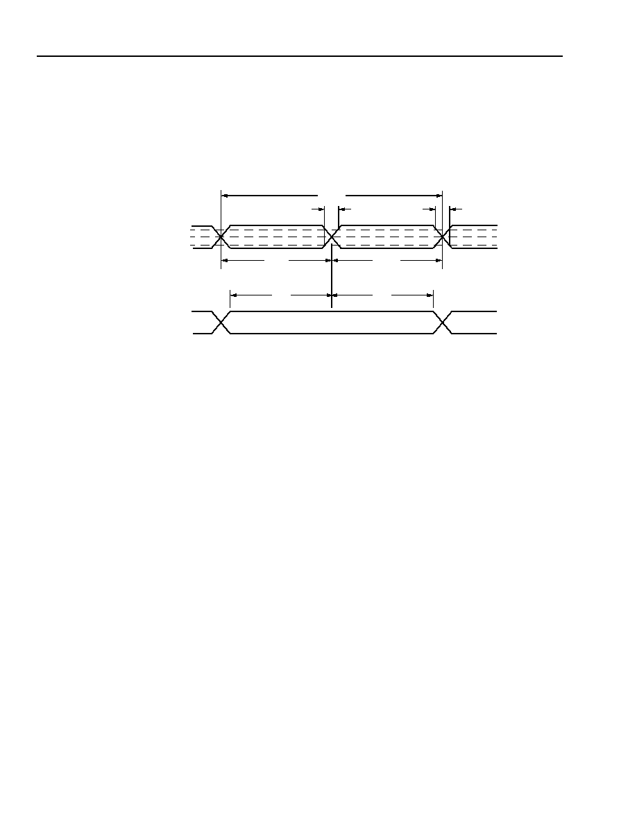
264
Agere Systems Inc.
Data Sheet
May 2001
155/622/2488 Mbits/s Data Interface
TDAT042G5 SONET/SDH
Interface Timing Specifications
(continued)
Line Interface I/O Timing
Note: V
DD
= V
DDA
= V
DDD
(3.300 volts nominal) in this section.
Figure 42--Figure 45, Table 167, and Table 168 give the timing specifications for the STS-3/STM-1,
STS-12/STM-4, and STS-48/STM-16 interfaces.
5-9252 (F)r.4
Figure 42. Receive Line-Side Timing Waveform
RxD[15:0]P/RxD[D:A]P
t44
RxCKP/RxCLK[D:A]P
RxCKN/RxCLK[D:A]N
t45
t43
t46
t47
RxD[15:0]N/RxD[D:A]N
50%
V
IL (MAX)
V
IH (MIN)
t49
t48
Agere Systems Inc.
265
Data Sheet
May 2001
155/622/2488 Mbits/s Data Interface
TDAT042G5 SONET/SDH
Interface Timing Specifications
(continued)
Line Interface I/O Timing
(continued)
5-9253(F).i
* Loading of TxD[15:4]P/N is 12 pF. Loading of TxD[3:0]P/N / TxD[D:A]P/N is 8 pF with the PLL on, and 12 pF with the PLL off.
Figure 43. Transmit Line-Side Timing Waveform-- STS-48/STM-16 Contraclocking
5-9253(F).g
Figure 44. Transmit Line-Side Timing Waveform--Frame Synch
5-9253(F).h
* Loading of TxD[15:4]P/N is 12 pF. Loading of TxD[3:0]P/N / TxD[D:A]P/N is 8 pF with the PLL on, and 12 pF with the PLL off.
Figure 45. Transmit Line-Side Timing Waveform--STS-48/STM-16 Forward Clocking
t51
TxCKP
TxCKN
t52
t50
t53
t54
50%
V
IL (MAX)
V
IH (MIN)
TxD[15:0]P/TxD[D:A]P*
TxD[15:0]N/TxD[D:A]N*
t55
50%
TxFSYNCN
TxCKP
TxCKN
TxFSYNCP
50%
V
IL (MAX)
V
IH (MIN)
t61
t60
t59
TxCKP
TxCKN
50%
V
IL (MAX)
V
IH (MIN)
TxCKQP
TxCKQN
TxD[15:0]P/TxD[D:A]P*
TxD[15:0]N/TxD[D:A]N*
50%
50%
t57
t56
t58

266
Agere Systems Inc.
Data Sheet
May 2001
155/622/2488 Mbits/s Data Interface
TDAT042G5 SONET/SDH
Interface Timing Specifications
(continued)
Line Interface I/O Timing
(continued)
For the following tables,
V
IL
(max) = (V
DD
≠1.475) volts, nominal of 1.825 volts;
V
IH
(min) = (V
DD
≠1.165) volts, nominal of 2.135 volts;
V
OH
(min) = (V
DD
≠1.025) volts, nominal of 2.275 volts;
V
OL
(max) = (V
DD
≠1.620) volts, nominal of 1.680 volts.
Table 167. Receive Line-Side Timing Specifications
Symbol
Parameter
Min
Typ
Max
Units
t43
Receive Clock-Cycle Period:
STS-3/STM-1 and STS-48/STM-16
STS-12/STM-4
--
--
6.4300
1.60751
--
--
ns
ns
t44
Receive Clock Rise
--
--
500
ps
t45
Receive Clock Fall
--
--
500
ps
t46
Receive Clock Pulse Low (for P input):
STS-3/STM-1 and STS-48/STM-16
STS-12/STM-4
2.800
700
3.2150
803.75
3.630
907
ns
ps
t47
Receive Clock Pulse High (for P input):
STS-3/STM-1 and STS-48/STM-16
STS-12/STM-4
2.800
700
3.2150
803.75
3.630
907
ns
ps
t48
RxD[15:0]P/N / RxD[D:A]P/N Setup
100
--
--
ps
t49
RxD[15:0]P/N / RxD[D:A]P/N Hold
100
--
--
ps

Agere Systems Inc.
267
Data Sheet
May 2001
155/622/2488 Mbits/s Data Interface
TDAT042G5 SONET/SDH
Interface Timing Specifications
(continued)
Line Interface I/O Timing
(continued)
Table 168. Transmit Line-Side Timing Specifications
* TxCKQP/N is used in STS-48/STM-16 mode only.
TxFSYNCP/N must be synchronized to TxCKP/N; it must be at least one TxCKP/N clock-cycle wide, but less than one frame
period minus two TxCKP/N clock-cycles wide.
Symbol
Parameter
Min
Typ
Max
Units
t50
Transmit Clock-Cycle Period:
STS-3/STM-1 and STS-48/STM-16
STS-12/STM-4
--
--
6.4300
1.60751
--
--
ns
ns
t51
Transmit Clock Rise
--
--
500
ps
t52
Transmit Clock Fall
--
--
500
ps
t53
Transmit Clock Pulse Low (for P input):
STS-3/STM-1 and STS-48/STM-16
STS-12/STM-4
2.800
700
3.2150
803.75
3.630
907
ns
ps
t54
Transmit Clock Pulse High (for P input):
STS-3/STM-1 and STS-48/STM-16
STS-12/STM-4
2.800
700
3.2150
803.75
3.630
907
ns
ps
t55
Propagation Delay--contra clocking:
(TxCKP/N to TxD[15:0]P/N, with PLL)
1
--
3
ns
t56
Propagation Delay--forward clocking:
(TxCKP/N to TxCKQP/N)*
1.5
--
4.5
ns
t57
Propagation Delay--forward clocking:
(TxCKQP/N to TxD[15:0]P/N, no PLL)*
0.5
--
1.5
ns
t58
Propagation Delay--forward clocking:
(TxCKP/N to TxD[15:0]P/N, no PLL)
2
--
5
ns
t59
TxFSYNC Setup
100
--
--
ps
t60
TxFSYNC Hold
100
--
--
ps
t61
Transmit TxFSYNC width
:
STS-3/STM-1 and STS-48/STM-16
STS-12/STM-4
6.430
1.608
--
--
19,438
77,758
clock cycles
clock cycles
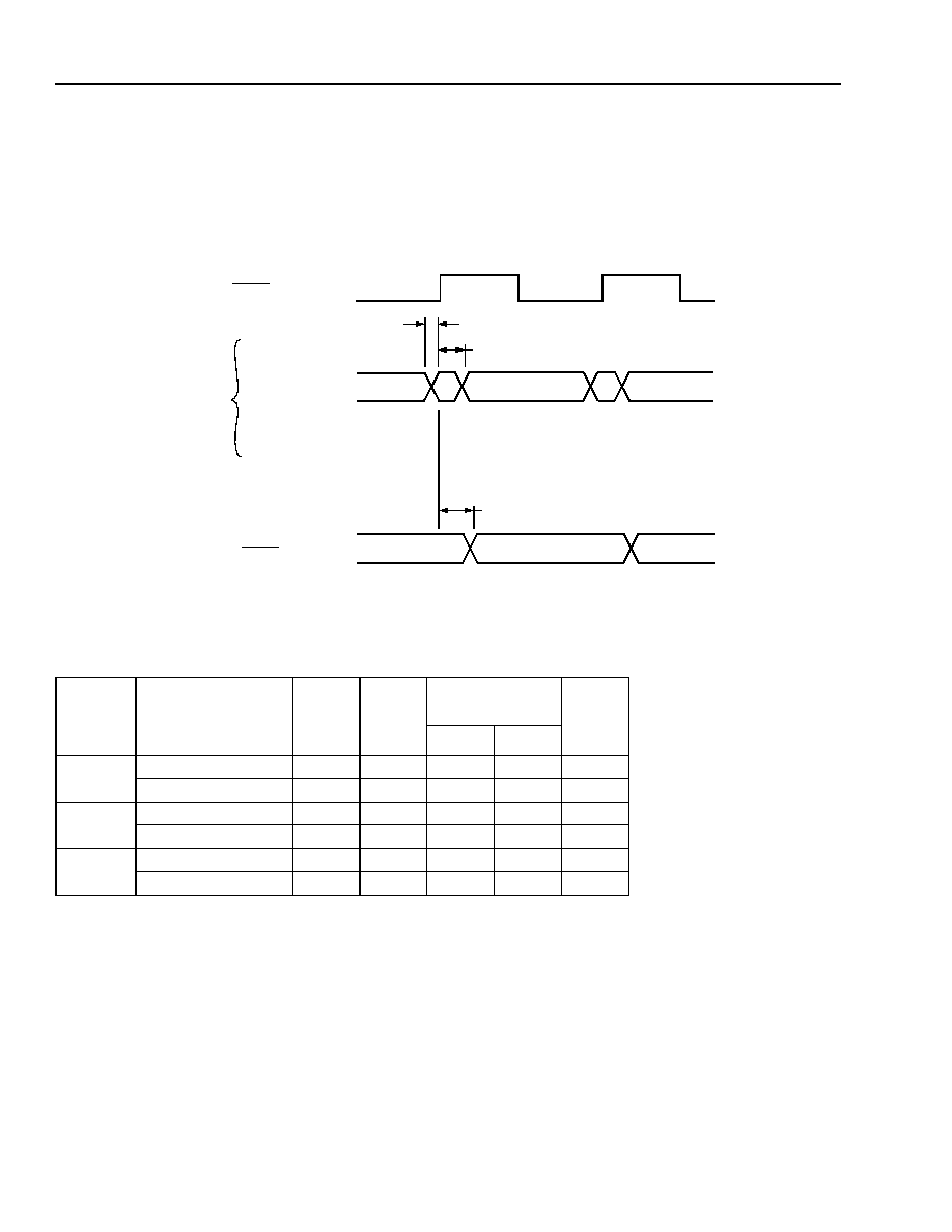
268
Agere Systems Inc.
Data Sheet
May 2001
155/622/2488 Mbits/s Data Interface
TDAT042G5 SONET/SDH
Interface Timing Specifications
(continued)
UTOPIA Interface Timing
UTOPIA interface timing specifications are given for the transmit direction in Figure 46 and in Table 169, and for
the receive direction in Figure 47 and in Table 170 (see page 269). Specifications for the UTOPIA clock interface
are given in Table 171 (see page 270).
5-7663(F)r.5
Figure 46. Transmit UTOPIA Interface Timing
Table 169. Transmit UTOPIA Interface Timing Specifications
Symbol
Test Conditions
Setup
(Min)
Hold
(Min)
Propagation
Delay
Unit
(Min)
(Max)
t62
U3, U3+
2.5
--
--
--
ns
U2, U2+
4.0
--
--
--
ns
t63
U3, U3+
--
0.0
--
--
ns
U2, U2+
--
1.0
--
--
ns
t64
U3, U3+
--
--
2.0
5.0
ns
U2, U2+
--
--
2.0
13.0
ns
TxCLK[D:A]
TxPA[D:A]
t64
TxENB[D:A]
t62
t63
TxSZ[D:A]
TxPRTY[D:A]
TxSOP[D:A]
TxEOP[D:A]
TxERR[D:A]
TxDATA[D:A][15:0]
INPUTS
INPUT
OUTPUT
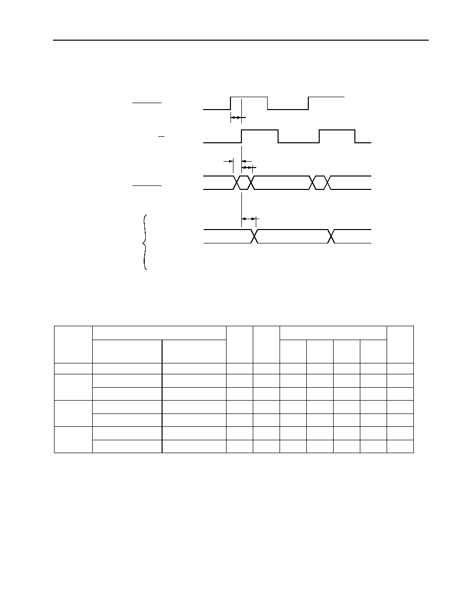
Agere Systems Inc.
269
Data Sheet
May 2001
155/622/2488 Mbits/s Data Interface
TDAT042G5 SONET/SDH
Interface Timing Specifications
(continued)
UTOPIA Interface Timing
(continued)
5-7664(F)r.4
Figure 47. Receive UTOPIA Interface Timing
Table 170. Receive UTOPIA Interface Timing Specifications
* TxCLK[D:A] of the corresponding port is the source for RxCLK[D:A]. RxCLK[D:A] is an output in this case.
C
L
is the load on the outputs listed in Figure47. The UTOPIA Level 2 standard specifies a loading of 50 pF at 52 MHz. The UTOPIA L evel 3
standard specifies a loading of 25 pF in point-to-point configuration (only two devices involved).
Symbol
Test Conditions
Setup
(Min)
Hold
(Min)
Propagation Delay Range
Unit
52 MHz
RxCLK
104 MHz
RxCLK
52 MHz
(Min)
(Max)
(Min)
(Max)
t65
*
*
--
--
--
--
2.3
5.0
ns
t66
C
L
= 25 pF
--
2.5
--
--
--
--
--
ns
--
C
L
= 50 pF
4.0
--
--
--
--
--
ns
t67
C
L
= 25 pF
--
--
0.0
--
--
--
--
ns
--
C
L
= 50 pF
--
1.0
--
--
--
--
ns
t68
C
L
= 25 pF
--
--
--
2.0
6.5
--
--
ns
--
C
L
= 50 pF
--
--
4.0
13.0
--
--
ns
TxCLK[D:A]
RxPA[D:A]
t68
RxENB[D:A]
t66
t67
RxSZ[D:A]
RxPRTY[D:A]
RxSOP[D:A]
RxEOP[D:A]
RxERR[D:A]
RxDATA[D:A][15:0]
OUTPUTS
INPUT
INPUT/OUTPUT
RxCLK[D:A]
t65
INPUT
270
Agere Systems Inc.
Data Sheet
May 2001
155/622/2488 Mbits/s Data Interface
TDAT042G5 SONET/SDH
Interface Timing Specifications
(continued)
UTOPIA Interface Timing
(continued)
Table 171. UTOPIA Interface Clock Specifications
Mode
Signal
Name
Parameter
Test Conditions
Min
Max
Unit
Transmit
U3+
TxCLK[D:A] TxCLK Frequency
104 MHz,
Multi-PHY Signal
0
104
MHz
TxCLK Duty Cycle
40
60
%
TxCLK Peak-to-Peak Jitter
--
2
%
TxCLK Rise/Fall Time
--
2
ns
TxCLK Skew
--
1
ns
Receive
U3+
RxCLK[D:A] RxCLK Frequency
104 MHz,
Multi-PHY Signal
0
104
MHz
RxCLK Duty Cycle
40
60
%
RxCLK Peak-to-Peak Jitter
--
2
%
RxCLK Rise/Fall Time
--
2
ns
RxCLK Skew
--
1
ns
RxCLK-toRxCLK Skew
(Source Mode)
--
700
ps
Transmit
U2+
TxCLK[D:A] TxCLK Frequency
52 MHz,
Multi-PHY Signal
0
50
MHz
TxCLK Duty Cycle
40
60
%
TxCLK Peak-to-Peak Jitter
--
5
%
TxCLK Rise/Fall Time
--
2
ns
TxCLK Skew
--
1
ns
Receive
U2+
RxCLK[D:A] RxCLK Frequency
52 MHz,
Multi-PHY Signal
0
50
MHz
RxCLK Duty Cycle
40
60
%
RxCLK Peak-to-Peak Jitter
--
5
%
RxCLK Rise/Fall Time
--
2
ns
RxCLK Skew
--
1
ns
RxCLK-toRxCLK Skew
(Source Mode)
--
700
ps
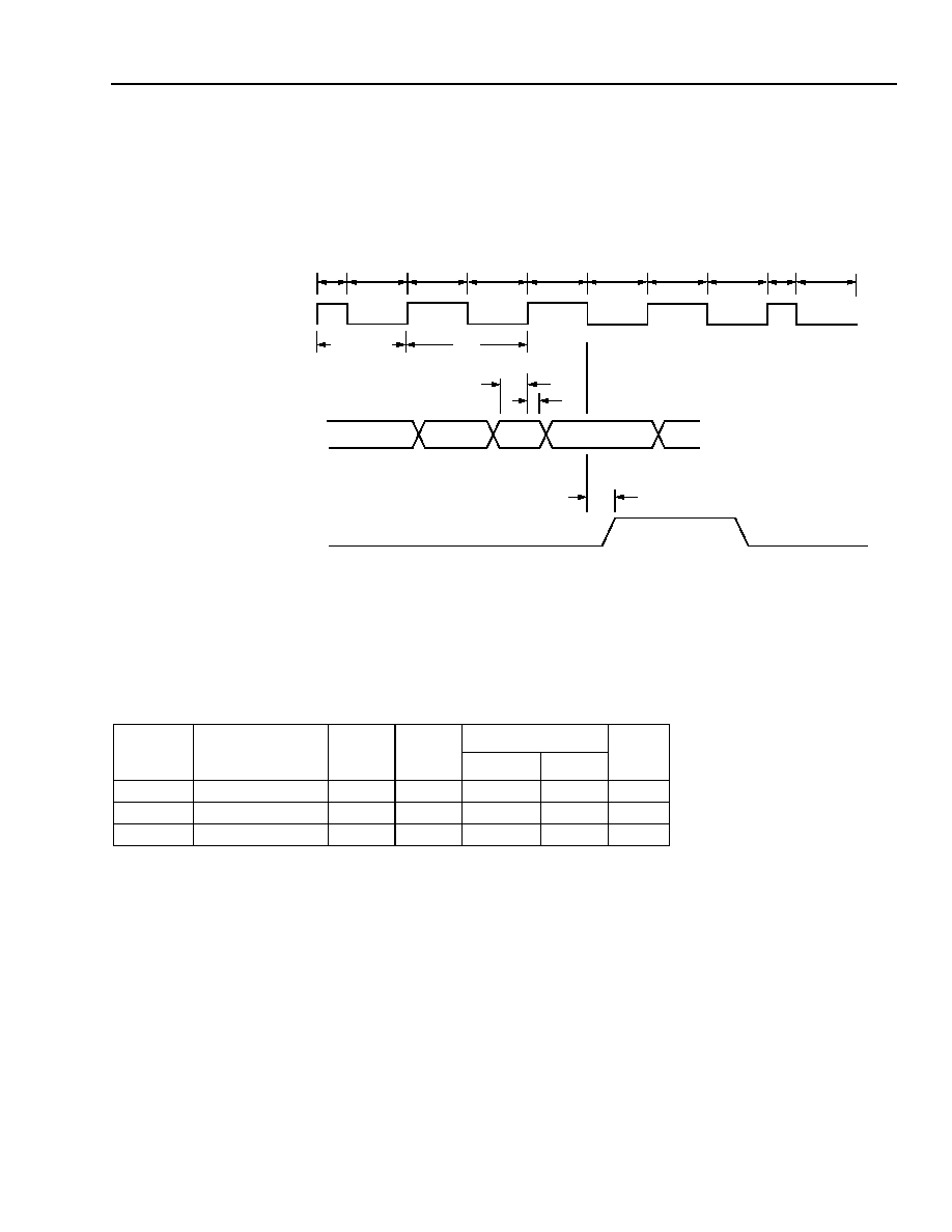
Agere Systems Inc.
271
Data Sheet
May 2001
155/622/2488 Mbits/s Data Interface
TDAT042G5 SONET/SDH
Interface Timing Specifications
(continued)
Transport Overhead Access Channel (TOAC) Interface Timing
Transport overhead access channel (TOAC) interface timing specifications are given for the transmit direction in
Figure 48 and in Table 172. The specifications for the receive direction are given in Figur e49, Figur e50, and in
Table 173.
0151(F).a
* Clock pulse tCP = x/y, where:
x = 32 for STS-3/STM-1 and STS-12/STM-4, or x = 8 for STS-48/STM-16;
y = clock frequency in MHz on the transmit line clock pins TxCKP/N.
Note: Duty cycles shown are nominal.
Figure 48. Transmit TOAC Interface Timing
Table 172. Transmit TOAC Interface Timing Specifications
Symbol
Test Conditions
Setup
(Min)
Hold
(Min)
Propagation Delay
Unit
(Min)
(Max)
t69
--
10
--
--
--
ns
t70
--
--
10
--
--
ns
t71
C
L
= 50 pF
--
--
0
10
ns
50%
50%
50%
50%
50%
t69
OUTPUT--TxTOHCK
INPUT--TxTOHD[D:A]
OUTPUT--TxTOHF 8 kHz
DUTY CYCLE CLOCK
5.184 MHz (STS-3/STM-1)
20.736 MHz (STS-12/STM-4)
(STS-48/STM-16)
66%
33%
33%
66%
t71
50%
(0.75)tCP*
tCP
t70
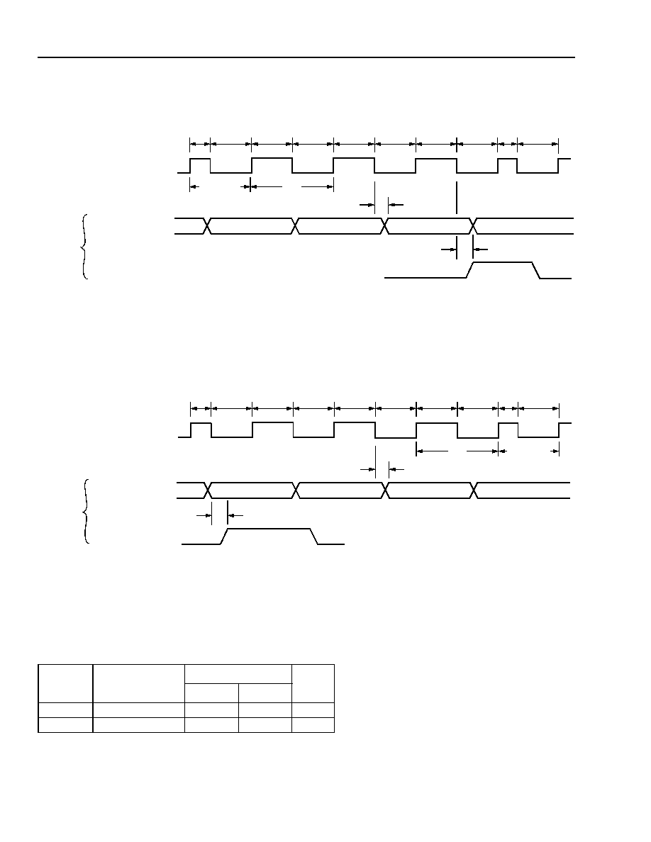
272
Agere Systems Inc.
Data Sheet
May 2001
155/622/2488 Mbits/s Data Interface
TDAT042G5 SONET/SDH
Interface Timing Specifications
(continued)
Transport Overhead Access Channel (TOAC) Interface Timing
(continued)
0152(F).a
* Clock pulse tCP = x/y, where:
x = 32 for STS-3/STM-1 and STS-12/STM-4, or x = 8 for STS-48/STM-16;
y = clock frequency in MHz on the transmit line clock pins TxCKP/N.
Note: Duty cycles shown are nominal.
Figure 49. STS-12/STM-4 and STS-48/STM-16 Receive TOAC Interface Timing
0153(F).a
* Clock pulse tCP = x/y, where:
x = 32 for STS-3/STM-1 and STS-12/STM-4, or x = 8 for STS-48/STM-16;
y = clock frequency in MHz on the transmit line clock pins TxCKP/N.
Note: Duty cycles shown are nominal.
Figure 50. STS-3/STM-1 Receive TOAC Interface Timing
Table 173. Receive TOAC Interface Timing Specifications
Symbol
Test Conditions
Propagation Delay
Unit
(Min)
(Max)
t72
C
L
= 50 pF
0
10
ns
t73
C
L
= 50 pF
0
10
ns
50%
50%
50%
50%
50%
66%
33%
33%
66%
50%
(0.75)tCP*
tCP
OUTPUT--RxTOHCK[D:A]
RxTOHD[D:A]
OUTPUTS
DUTY CYCLE CLOCK
RxTOHF[D:A] 8 kHz
(STS-48/STM-16)
t72
t73
20.736 MHz (STS-12/STM-4)
50%
50%
50%
50%
50%
66%
33%
33%
66%
50%
(0.75)tCP*
tCP
OUTPUT--RxTOHCK[D:A]
RxTOHD[D:A]
OUTPUTS
DUTY CYCLE CLOCK
RxTOHF[D:A] 8 kHz
t72
t73
5.184 MHz (STS-3/STM-1)

Agere Systems Inc.
273
Data Sheet
May 2001
155/622/2488 Mbits/s Data Interface
TDAT042G5 SONET/SDH
Reference of SONET/SDH Terms and Comparisons
Definitions of SONET/SDH Bytes
I
A1: Framing byte 0xF6
I
A2: Framing byte 0x28
I
B1: BIP-8 parity for section (regenerator section)
I
B2: BIP-8xN parity for STS-N signal for line (multiplexer section)
I
B3: BIP-8 parity for path
I
C1: Redefined to J0/Z0
I
D1--D3: Section (regenerator section) data communication channels
I
D4--D12: Line (multiplexer section) data communication channels
I
E1: Section (regenerator section) orderwire
I
E2: Line (multiplexer section) orderwire
I
F1: Section user channel
I
F2, F3: Path user channels
I
G1: Path status byte
I
H1, H2: Higher-order (AU) pointer
I
H3: Pointer action byte
I
H4: Multiframe indicator
I
J0: Section (regenerator section) trace
I
J1: Path trace
I
J2: Lower-order path trace
I
K1, K2: Automatic protection switching (APS) channel and line (multiplexer section) RDI
I
K3: Path APS
I
K4: Lower-order path APS
I
M1: Line (multiplexer section) REI
I
N1: Higher-order tandem connection
I
N2: Lower-order tandem connection
I
S1: Synchronization status
I
V1, V2: Lower-order (TU) pointer
I
V3: Lower-order pointer action byte
I
V4: Reserved
I
V5: Lower-order BIP-2, SLM, and status
I
Z0, Z1, Z2: Growth bytes
274
Agere Systems Inc.
Data Sheet
May 2001
155/622/2488 Mbits/s Data Interface
TDAT042G5 SONET/SDH
Reference of SONET/SDH Terms and Comparisons
(continued)
SONET/SDH Comparisons
Table 174. SONET/SDH Comparisons
SONET/SDH New Terminology
Table 175. SONET/SDH New Terminology
SONET
SDH
SPE
VC
SPE and Pointer
AU
STS-3xN
STM-N
VT1.5
TU-11
VT2
TU-12
VT6
TU-2
VTG
TUG-2
Transport Overhead
Section Overhead
Section Overhead
Regenerator Section Overhead
Line Overhead
Multiplexer Section Overhead
Was
Is
FERF: Far-End Receive Failure
RDI: Remote Defect Indicator
FEBE: Far-End Block Error
REI: Remote Error Indicator (SDH only)
Path Yellow Alarm
RAI: Remote Alarm Indicator
C1: STS-1 Identifier
J0: Section Trace /Z0: Growth
First Z1: Growth
S1: Synchronization
Third Z1: Growth
M1: Line REI
Z3: Growth
F3: User Channel (SDH only)
Z4: Growth
K3: APS (SDH only)
Z5: Growth
N1: Tandem Connection (SDH only)
Z6: Growth
N2: Tandem Connection (SDH only)
Z7: Growth
K4: LO APS (SDH only)
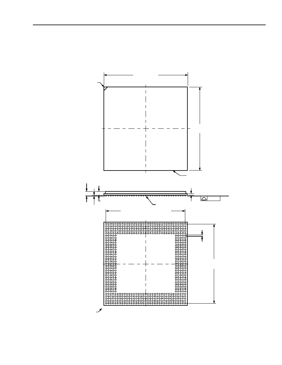
Agere Systems Inc.
275
Data Sheet
May 2001
155/622/2488 Mbits/s Data Interface
TDAT042G5 SONET/SDH
Outline Diagram
600-Pin LBGA
Dimensions are in millimeters.
5-9212 (F)r.2
The dimensions in this outline diagram are intended for informational purposes only. For detailed schematics to
assist your design efforts, please contact your Agere Sales Representative.
45.00
±
0.10
45.00
A1 BALL
T
D
H
AL
F
K
B
P
M
L
J
AH
R
C
E
Y
N
U
AN
G
AD
V
AM
AJ
AG
AE
AC
AA
W
AP
AK
AF
AB
AR
A
19
30
26
28
24
32
22
20
18
4
6
8 10 12
14 16
2
34
5
23 25
7
31
29
15
21
3
27
11
17
9
13
1
35
33
34 SPACES @ 1.27 = 43.18
34 SPACES
A1 BALL
0.75
±
0.15
IDENTIFIER ZONE
±
0.10
@ 1.27 = 43.18
CORNER
1.71/2.58
SEATING PLANE
SOLDER BALL
0.60
±
0.10
0.20
1.43/1.92
ELECTRICALLY ISOLATED
HEAT SPREADER
2.17/3.28

276
Agere Systems Inc.
Data Sheet
May 2001
155/622/2488 Mbits/s Data Interface
TDAT042G5 SONET/SDH
Ordering Information
Device Code
Package
Temperature
Comcode
(Ordering Number)
TDAT042G51A-3BLL1
600-pin LBGA
≠40 ∞C to +85 ∞C
108696006

Agere Systems Inc.
277
Data Sheet
May 2001
155/622/2488 Mbits/s Data Interface
TDAT042G5 SONET/SDH
DS98-193SONT-4 Replaces DS98-193SONT-3 to Incorporate the Following Updates
1. Globally numbered all the transmit sequencer time slots the same, from 1 to 12. Affects Figures 13, 14,
and 16, DE egress configuration registers Tx_TS (0x1016--0x1021), and DE ingress configuration registers
Rx_TS (0x1022--0x102D).
2. Bad PPP header counter changed to mismatched PPP header counter globally.
3. Changed bit TRDIP_LCDINH[A--D] to TRDIP_LCD[A--D] thorughout document.
4. Page 1, the number of the IETF RFC standard was corrected from 1619 to 2615; the title is still the same.
5. Page 11, moved Description section from page 1 for readability.
6. Page 24, added the note about the TDAT042G5's internal circuitry under Table 3.
7. Page 25, Table 3, Pin Descriptions--Line Interface Signals, TxFSYNCP and TxFSYNCN pins. Corrected the
inadvertent switch of I
u
and I
d
in the I/O column, provided values for all I
u
and I
d
, corrected cycle width in last
sentence.
8. Page 27, Table 4, Pin Descriptions--TOH Interface Signals, clarified RxREF pin.
9. Pages 32, 38, and 164, TxSIZE_[D:A] and RxSIZE_[D:A] bits (address 0x0226), corrected bit and pin names in
the register description and pin descriptions.
10.Page 33, Table 5, Pin AM18, AM30, AA35, and H32, under the Name/Description column, second paragraph,
changed the wording to include the TxERR[A] and the TxERR[B] input pins.
11.Page 33--page 39, Table 5, Pin Descriptions--Enhanced UTOPIA Interface Signals, added "These pins are
used only in U2+ and U3+ (packet) modes" to size, end-of-packet, and error receive pins and transmit pins.
12.Page 38, Table 5, Pin Descriptions--Enhanced UTOPIA Interface Signals, corrected "must be placed" to "will be
placed" in the paragraph beginning with, "In U3+ (32-bit mode). . ."
13.Page 39, Table 5, Pin Descriptions--Enhanced UTOPIA Interface Signals, clarified RxERR pin.
14.Page 40, Table 6, Pin Descriptions--Microprocessor Interface Signals, clarified PMRST pin.
15.Page 42, Table 8, Pin Descriptions--JTAG Interface Signals, corrected TMS pin to be active-high.
16.Page 42, Table 8, Pin Descriptions--JTAG Interface Signals, expanded TRST description.
17.Page 45, Overview, corrected and expanded second paragraph.
18.Page 46, Overview, deleted any reference to cell-based UNI since not supported by this device.
19.Page 49, Overview, Over-Fiber Mode section, corrected transparent mode to over-fiber mode in this section.
20.Page 52, Transmit Line Interface Summary section, updated TxFSYNCP/N bullet item.
21.Page 53, SONET Framer, added section.
22.Page 55 (in revision 3 of data sheet), Table 16, Values of SFNSSET[A--D][18:0], SFMSET[A--D][7:0],
SFLSET[A--D][3:0], SFBSET[A--D][15:0] in Terms of Equivalent BER for BIP-24 Case, removed table.
23.Pages 57--58, pages 187--188, and pages 208--209; Table 16, Table 17, Table 86, Table 87, Table 107, and
Table 108; Ns, L, M, and B Values to Set the BER Indicator, Ns, L, M, and B Values to Clear the BER Indicator,
updated tables and added them to the PT Registers section, also.
24.Pages 63, 200, and 205, SS pointer interpretation algorithm not implemented. Affects bit 5 of registers 0x0AA6,
0x0AAE, 0x0AB6, 0x0ABE; corrected from RSSPTRNORM[A--D] to Reserved in Register Maps and Register
Descriptions sections. Also affects bits 1--0 of register 0x0AC7; corrected from RSSEXP[1:0] to Reserved in
Register Maps and Register Descriptions sections. Removed item 4 from the normal pointer description on
page 63.
25.Page 65--Page 68, SPE Generate section, corrected and expanded.
26.Page 70, Data Engine (DE) Block section, expanded second paragraph.

278
Agere Systems Inc.
Data Sheet
May 2001
155/622/2488 Mbits/s Data Interface
TDAT042G5 SONET/SDH
DS98-193SONT-4 Replaces DS98-193SONT-3 to Incorporate the Following
Updates
(continued)
27.Page 71, ATM Cell Processor section under Data Engine (DE) Block, expanded.
28.Page 75, PPP Header Detach section, added footnote and updated Figure 16, Uncompressed and Com-
pressed PPP Packets.
29.Page 77 and page 94, HDLC Inserter in the Data Engine (DE) Block section and FIFO in the UT Transmit Input
Path (Egress) section, corrected description of 0x7D20.
30.Page 82, Data Engine (DE) Block, Over-Fiber Modes section, clarified description.
31.Page 83, Transparent Payload Mode section, updated.
32.Page 85, Table 24, UTOPIA Traffic Types, updated.
33.Page 86, UTOPIA ATM Cell Processing section, added.
34.Page 88, added UT Clocking, UT Transmit Path (Egress) Clock, UT Receive Path (Ingress) Clock sections;
removed Clocks section on page 91.
35.Page 90, Two-Cycle Delay Mode section, provided reference for RxPA[D:A] definition.
36.Page 91 and page 92, updated Figure 23, Receive-Side Interface Handshaking in Point-to-Point, Single Cycle
Mode; added Figure 24, Receive-Side Interface Handshaking in Point-to-Point, Two-Cycle Mode.
37.Page 93, Transmit Cell/Packet Available (TxPA) section, expanded definition.
38.Page 94, Table 29, Egress High Watermark Thresholds, added.
39.Page 95, Figure 25, Transmit-Side Interface Handshaking in Point-to-Point, Single Cycle Mode, updated.
40.Page 96, Multi-PHY Support section, clarified the concept of point-to-point vs. polled mode configuration.
41.Page 100, JTAG (Boundary-Scan) Test Block section, added second paragraph.
42.Page 100, Reset of JTAG Logic section, added.
43.Page 100, Line Interface section added to document (including Table 30).
44.Page 102, General-Purpose I/O Bus (GPIO) section, expanded.
45.Page 105, Performance Monitor Reset (PMRST) section, expanded.
46.Page 106, Far-End Loopback, Terminal Loopback, Facility Loopback, expanded sections.
47.Page 108--page 110, Figur e34, Single ATM UTOPIA 3; Figur e36, Single POS UTOPIA 3, updated.
48.Page 112 and p age152, GPIO Output Configuration register (addresses 0x0014 and 0x0015), updated in Reg-
ister Maps and Register Descriptions sections.
49.Pages 124--125, 191, TZ0DINS[A--D][2--12][7:0] registers (addresses 0x05AA--0x05C1), updated in the
Register Maps and Register Descriptions sections.
50.Page 119, Register Maps section, corrected subtitle in OHP map from Signal Degrade Set/Clear Control Regis-
ters to Signal Degrade BER Algorithm Parameters.
51.Page 120, Register Maps section, corrected subtitle in OHP map from Signal Fail Set/Clear Control Registers to
Signal Fail BER Algorithm Parameters.
52.Pages 119--121, 136, 185--186, 198, Register Maps and Register Descriptions sections, differentiated bit-
names in OHP sections from bitnames in PT sections for signal degrade and signal fail BER algorithm parame-
ters.
53.Pages 134--135, 199, changed bits [15:9] from Reserved to RPOHMONSEL[A--D][3:0] and RCONC_ALLOR
FIRST[A--D] in the Register Maps and Register Descriptions sections.

Agere Systems Inc.
279
Data Sheet
May 2001
155/622/2488 Mbits/s Data Interface
TDAT042G5 SONET/SDH
DS98-193SONT-4 Replaces DS98-193SONT-3 to Incorporate the Following
Updates
(continued)
54.Page 143, Register Maps section, corrected subtitle in DE map from PPP Detach--Rx Good Packet/Cell
Counter (PMRST Update) to Receive Good Packet/Cell Counter (PMRST Update).
55.Page 143, Register Maps section, corrected subtitle in DE map from PPP Attach--Tx Good Packet/Cell
Counter (PMRST Update) to Transmit Good Packet/Cell Counter (PMRST Update).
56.Page 150, updated register description of PLL_MODE bit (address 0x0010).
57.Page 151, Table 50, Register 0x0012: Loopback Control (R/W), updated description of valid combinations.
58.Page 157 and page158, clarified UTOPIA_MODE_Rx bit (addresses 0x020F, 0x0213, 0x0217, 0x021B) in the
Register Maps and Register Descriptions sections.
59.Page 158, Table 61, Registers 0x020F, 0x0213, 0x0217, 0x021B: Channel [A--D] Receive Provisioning Regis-
ter (R/W), corrected the reset default value of register 0x0217 from 0x0020 to 0x0220.
60.Page 158, clarified ATM_SIZE_Rx[A--D] bits (addresses 0x020F, 0x0213, 0x0217, 0x021B).
61.Page 160, corrected description of PARITY_Tx[A] bit (addresses 0x0210, 0x0214, 0x0218, 0x021C). Corrected
even parity from bit = 1 to bit = 0.
62.Page 160, clarified PARITY_Tx[B--D] bits (addresses 0x0210, 0x0214, 0x0218, 0x021C).
63.Page 160, clarified ATM_SIZE_Tx[A--D] bits (addresses 0x0210, 0x0214, 0x0218, 0x021C) and corrected
"received" to "transmitted."
64.Page 161, Table 63, Bits 13--8, INGRESS_WATERMARK_HIGH_[A--D][6:0], changed the function definition
to current one.
65.Pages 165--page 167, Table 72, Registers 0x0402--0x0409: Delta/Event (COR/W), deleted statement that the
delta bits clear when read (or written).
66.Page 171, Table 76, Registers 0x0416--0x0419: Toggles (R/W), corrected and expanded note.
67.Page 173, LOS_AISINH[A--D] bit (addresses 0x0422, 0x0424, 0x0426, 0x0428), clarified the description.
68.Page 177 and page181, TJ0INS and TTOAC_J0 bits (addresses 0x042E, 0x0430, 0x0432, 0x0434), updated
description.
69.Page 179 and page183, TM1_ERR_INS and TM1_REIL_INH bits (addresses 0x042E, 0x0430, 0x0432,
0x0434), updated description.
70.Page 200 and page201, RFORCE_LOP[A--D][1--12] and RFORCE_AIS[A--D] [1--12] bits
(addresses 0x0AA7, 0x0AA8, 0x0AA9), updated description.
71.Page 201, Table 103, address 0AAA, 0AB2, 0ABA, OAC2, bit 9, name TRDIP_LCD[A--D], changed the func-
tion definition to the current one.
72.Page 201 and page 202, TRDIP_LCD[A--D], TRDIP_PLMPINH[A--D], TRDIP_UNEQUIPINH [A--D] bits, cor-
rected the bit numbers from 7, 9, 8, to the bit numbers 9, 8, 7, respectively.
73.Page 212 and page 213, Table 112, Register 0x1001, 0x1002: DE Interrupts (0x1001 is RO, 0x1002 is RO and
COR/W), register 0x1002, updated note, added footnote, and corrected the placement of bits of 7--4 and 3--0
which were interposed.
74.Page 226, Table 120, Receive Type and Mode Control Summary Table (Registers 0x1040--0x1043), clarified
bits [1:0] for ATM.
75.Page 235, PPP_Rx_HDR [0--11][15:0] registers (addresses 0x10F0--0x10FB), corrected name and descrip-
tion.
76.Page 236, PPP_Rx_CHK_CH [0--3][15:0] registers (addresses 0x10FC--0x10FF), bits 15--14, updated
description.

280
Agere Systems Inc.
Data Sheet
May 2001
155/622/2488 Mbits/s Data Interface
TDAT042G5 SONET/SDH
DS98-193SONT-4 Replaces DS98-193SONT-3 to Incorporate the Following
Updates
(continued)
77.Page 241, PM_MHC_[0--3][27:0] registers (addresses 0x1118--0x111F), updated name and description.
78.Page 250, Table 158, Registers 0x1600--0x1607: SDL Transmit Registers (R/W), updated note.
79.Page 253, Absolute Maximum Ratings, corrected text above table to refer to permanent damage and to the data
sheet; removed typical power supply value.
80.Page 253, Table 159, Recommended Operating Conditions, updated power dissipation.
81.Page 254, Table 160, 3.3 V Logic Interface Characteristics, updated load capacitance.
82.Page 255, Table 162, added table to document.
83.Pages 256, 258, 262, Microprocessor Interface Timing section, updated figures (Figure 38, Figure 39,
Figure 41) and text in section.
84.Page 260, Asynchronous Mode in Microprocessor Interface Timing section, updated text and corrected t28 in
Table 165, Microprocessor Interface Asynchronous Write Cycle Specifications. Corrected t28 min from 0 ns to
77 ns. Corrected t28 max from 72 ns to 103 ns.
85.Page 263, Asynchronous Mode in Microprocessor Interface Timing section, corrected t38 in Table 166, Micro-
processor Interface Asynchronous Read Cycle Specifications. Corrected t38 min from 0 ns to 90 ns. Corrected
t38 max from 34 ns to 115 ns.
86.Pages 264--page 265, Figure 42, Receive Line-Side Timing Waveform--Figure 45, Transmit Line-Side Timing
Waveform--STS-48/STM-16 Forward Clocking, updated.
87.Page 266, Table 167, Receive Line-Side Timing Specifications and Table 168, Transmit Line-Side Timing Spec-
ifications; replaced tables labeled Clock Input Specifications, Line Input Specifications, and Line Output Specifi-
cations with these tables.
88.Page 268 and page 269, UTOPIA Interface Timing section, updated receive and transmit figures and tables.
89.Page 271, Transport Overhead Access Channel (TOAC) Interface Timing section, updated transmit and receive
figures and tables.
90.Page 275, updated 600-pin LBGA package outline.

Agere Systems Inc.
281
Data Sheet
May 2001
155/622/2488 Mbits/s Data Interface
TDAT042G5 SONET/SDH

Data Sheet
May 2001
155/622/2488 Mbits/s Data Interface
TDAT042G5 SONET/SDH
Agere Systems Inc. reserves the right to make changes to the product(s) or information contained herein without notice. No liability is assumed as a result of their use or application.
Copyright © 2001 Agere Systems Inc.
All Rights Reserved
Printed in U.S.A.
May 2001
DS98-193SONT-04 (Replaces DS98-193SONT-03 Must Acompany DA01-010SONT and AY01-015SONT)
For additional information, contact your Agere Systems Account Manager or the following:
INTERNET: http://www.agere.com
E-MAIL: docmaster@micro.lucent.com
N. AMERICA:
Agere Systems Inc., 555 Union Boulevard, Room 30L-15P-BA, Allentown, PA 18109-3286
1-800-372-2447, FAX 610-712-4106 (In CANADA: 1-800-553-2448, FAX 610-712-4106)
ASIA PACIFIC: Agere Systems Singapore Pte. Ltd., 77 Science Park Drive, #03-18 Cintech III, Singapore 118256
Tel. (65) 778 8833, FAX (65) 777 7495
CHINA: Agere Systems (Shanghai) Co., Ltd., 33/F Jin Mao Tower, 88 Century Boulevard Pudong, Shanghai 200121 PRC
Tel. (86) 21 50471212, FAX (86) 21 50472266
JAPAN: Agere Systems Japan Ltd., 7-18, Higashi-Gotanda 2-chome, Shinagawa-ku, Tokyo 141, Japan
Tel. (81) 3 5421 1600, FAX (81) 3 5421 1700
EUROPE: Data Requests: DATALINE: Tel. (44) 7000 582 368, FAX (44) 1189 328 148
Technical Inquiries: GERMANY: (49) 89 95086 0 (Munich), UNITED KINGDOM: (44) 1344 865 900 (Ascot),
FRANCE: (33) 1 40 83 68 00 (Paris), SWEDEN: (46) 8 594 607 00 (Stockholm), FINLAND: (358) 9 3507670 (Helsinki),
ITALY: (39) 02 6608131 (Milan), SPAIN: (34) 1 807 1441 (Madrid)