Document Outline
- Features
- Description
- Target Applications Supported
- Overview
- MARS2G5 P-Pro (792-Pin PBGA) Low-Speed Devices Available
- MARS2G5 P-Pro Device Product Line Table Summaries
- Pin Information
- Pin Descriptions
- Microprocessor (MPU) Interface
- Functional Description
- Line Interface
- Transport Overhead Processor (TOHP-48) Block
- Pointer Processor (PP)
- Path Terminator (PT)
- STS Receive Terminator (RXT) Block
- DS3/E3 Block
- Receive Sequencer (RXS) Block
- Data Engine Block
- Data Engine Block-ATM Framer/Frame Inserter Subblock
- Data Engine Block-HDLC Framer and Escaper Subblock
- Data Engine Block-CRC Generator/Checker Subblock
- Data Engine Block-PPP Detach Subblock
- Data Engine Block-Data Engine Counter Subblock
- Data Engine Block-Channel Distribution and Allocation Subblock
- Data Engine Block-GFP General Framing Procedure Subblock
- Data Engine Block Registers
- UTOPIA (UT) Block
- System Interface
- Test
- Absolute Maximum Ratings
- Handling Precautions
- Operating Conditions
- Electrical Characteristics
- Outline Diagrams
- Ordering Information
- MARS2G5 P-Pro (TDAT162G52) (Version 2.2 and 2.3 Only)
- MARS2G5 P-Pro (TDAT162G52) (Version 2.3 Only)
- Appendix: Line Loopback Block
- Appendix: Line Loopback Block Script
- List of Figures
- List of Tables
- Table 1. List of the Clock Domains in the MARS2G5 P-Pro, SONET/SDH Mode
- Table 2. MARS2G5 P-Pro Device Product Line-Data Port Summary
- Table 3. Pin Assignments for 792-Pin PBGA and 600-Pin LBGA by Pin Number Order
- Table 4. Pin Assignments for 792-Pin PBGA by Signal Name
- Table 5. Pin Assignments for 600-Pin LBGA by Pin Number Order
- Table 6. Pin Assignments for 600-Pin LBGA by Signal Name
- Table 7. Pin Descriptions-Line Interface Signals
- Table 8. Pin Descriptions-TOH Interface Signals
- Table 9. Pin Descriptions-Enhanced UTOPIA Interface Signals
- Table 10. Pin Descriptions-Microprocessor Interface Signals
- Table 11. Pin Descriptions-General-Purpose I/O Signals: Interface Signals
- Table 12. Pin Descriptions-JTAG Interface Signals
- Table 13. Pin Descriptions-Power Signals
- Table 14. PLL Test Outputs
- Table 15. Pin Descriptions-No-Connect Pins
- Table 16. Leakage Test Pin
- Table 17. Device Address Space Assignment
- Table 18. MPU Modes
- Table 19. Microprocessor Interface Synchronous Write Cycle Specifications
- Table 20. Microprocessor Interface Synchronous Read Cycle Specifications
- Table 21. Microprocessor Interface Asynchronous Write Cycle Specifications
- Table 22. Microprocessor Interface Asynchronous Read Cycle Specifications
- Table 23. PM Reset Signal Provisioning
- Table 24. MPU_VERR[0-5], Version Control Registers (RO)
- Table 25. MPU_ISR, Interrupt Status Register (RO or COR/W)
- Table 26. MPU_CNDR, Condition Register (RO)
- Table 27. MPU_IMR, Interrupt Mask Register (R/W)
- Table 28. MPU_ICLRR, Interrupt Clear Register (R/W)
- Table 29. MPU_SWRSR, Software Reset Register (R/W)
- Table 30. MPU_GPIO_CTLR, GPIO Output Value (R/W)
- Table 31. MPU_PROVISION0, Provisioning Register 0 (R/W)
- Table 32. MPU_PROVISION1, Provisioning Register 1 (R/W)
- Table 33. MPU_LPBKCTLR, Loopback Control Register (R/W)
- Table 34. MPU_GPIOCFG, GPIO Configuration Register (R/W)
- Table 35. MPU_GPIO_OER[1-2], GPIO Output Enable (R/W)
- Table 36. MPU_PDN1, Powerdown Register 1 (R/W)
- Table 37. MPU_PDN2, Powerdown Register 2 (R/W)
- Table 38. MPU_PDN3, Powerdown Register 3 (R/W)
- Table 39. MPU_SCRATCHR, Scratch Register (R/W)
- Table 40. MPU_TDAT16_MODER, MARS2G5 P-Pro Mode Selection Register (R/W)
- Table 41. MPU_LI_MODER, Register (R/W)*
- Table 42. MPU_HSI_TST_CTL, High-Speed Interface Control
- Table 43. MPU_HSI_LPBKR, High-Speed Interface Loopback Register
- Table 44. MPU Register Map
- Table 45. Line Interface Modes
- Table 46. Nominal dc Power for Suggested Terminations
- Table 47. Receive Line-Side Timing Specifications
- Table 48. Transmit Line-Side Timing Specifications
- Table 49. Framing Bytes Observed for Framing Integrity
- Table 50. TOAC Channel Output Versus Time-Slot Assignment
- Table 51. Transport Overhead Bytes Received Via RxTOAC Interface*
- Table 52. TOAC Channel Input Versus Time-Slot Assignments
- Table 53. TTOAC OC-3 Signal Definition*
- Table 54. TTOAC OC-12 Signal Definition
- Table 55. TTOAC OC-48 Signal Definition
- Table 56. TTOAC Control Bits
- Table 57. Rx/Tx TOHP-48 Interface Rates
- Table 58. Transmit TOAC Interface Timing Specifications
- Table 59. Receive TOAC Interface Timing Specifications
- Table 60. TOHP_MODE_VERR, Mode (R/W) and Block Version (RO)
- Table 61. TOHP_CH_INT, Channel Interrupt (R/W, RO)
- Table 62. TOHP_DLT_EVT[A-D][1-2], 0x0802-0x0809, Delta/Event Registers (COR/COW-RO)
- Table 63. TOHP_RX_TX_STATE[A-D], 0x080A-0x080D, Receive/Transmit State Registers (RO)
- Table 64. TOHP_MSK[A-D][1-2], 0x080E-0x0815, Mask Bit Registers (R/W)
- Table 65. TOHP_TRG[A-D], 0x0816-0x0819, Trigger Register 0 ∆ 1 (R/W)
- Table 66. TOHP_CNTD[A-D][1-2], 0x081A-0x0821, Continuous N-Times Detect (CNTD) Values (R/W)
- Table 67. TOHP_RCTL[A-D][1-2], 0x0822-0x0829, Receive Control [1-2] (R/W)
- Table 68. TOHP_RCTL[A-D][3], 0x082A-0x082D, Receive Control 3 (R/W)
- Table 69. TOHP_TCTL[A-D][1-2], 0x082E-0x0835, Transmit Control [1-2] (R/W)
- Table 70. TOHP_TCTL[A-D][3], 0x0836-0x0839, Transmit Control 3 (R/W)
- Table 71. TOHP_SD_SETR[A-D][1-2], 0x083A-0x0841, Signal Degrade BER Algorithm Set Control Registers [1-2] (R/W)
- Table 72. TOHP_SD_SETR[A-D][3], 0x0842-0x0845, Signal Degrade BER Algorithm Set Control Register [3] (R/W)
- Table 73. TOHP_SD_CLEARR[A-D][1-2], 0x0846-0x084D, Signal Degrade BER Algorithm Clear Control Registers [1-2] (R/W)
- Table 74. TOHP_SD_CLEARR[A-D][3], 0x084E-0x0851, Signal Degrade BER Algorithm Clear Control Register [3] (R/W)
- Table 75. TOHP_SF_SETR[A-D][1-2], 0x0852-0x0859, Signal Fail Set BER Algorithm Control Registers [1-2] (R/W)*
- Table 76. TOHP_SF_SETR[A-D][3], 0x085A-0x085D, Signal Fail BER Algorithm Set Control Register [3] (R/W)
- Table 77. TOHP_SF_CLEARR[A-D][1-2], 0x085E-0x0865, Signal Fail BER Algorithm Clear Control Registers [1-2] (R/W)*
- Table 78. TOHP_SF_CLEARR[A-D][3], 0x0866-0x0869, Signal Fail BER Algorithm Clear Control Register [3] (R/W)
- Table 79. Ns, L, M, and B Values to Set the BER Indicator
- Table 80. Ns, L, M, and B Values to Clear the BER Indicator
- Table 81. TOHP_B1ECNTR[A-D], 0x086A-0x086D, B1 Error Count (RO)
- Table 82. TOHP_B2ECNTR[A-D][1-2], 0x086E-0x0875, B2 Error Count (RO)
- Table 83. TOHP_M1ECNTR[A-D][1-2], 0x0876-0x087D, M1 Error Count (RO)
- Table 84. TOHP_TOH_INSR[A-D][1-2], 0x087E-0x0885, Transmit OH Insert Value (R/W)
- Table 85. TOHP_RMONR[A-D][1-3], 0x0886-0x0891, Receive Monitor Value (RO)
- Table 86. TOHP_RJ0DMONR[A-D][1-32], 0x0892-0x0911, Receive J0/Z0 Monitor Value Registers (RO)
- Table 87. TOHP_TJ0DINSR[A-D][1-32], 0x0912-0x09A9, Transmit J0/Z0 Insert Value Registers (R/W)
- Table 88. TOHP_TZ0DINSR[A-D][1-6], 0x09AA-0x09C1, Transmit Z0 Insert Value Registers (R/W)
- Table 89. Z0 Byte Ordering STS-48 Mode for Z0-1-Z0-47
- Table 90. Z0 Byte Ordering STS-12 Mode for Z0-1-Z0-11
- Table 91. Z0 Byte Ordering STS-3 Mode for Z0-1-Z0-2
- Table 92. TOHP_SCRATCHR, 0x09C2, TOHP-48 Scratch Register (R/W)
- Table 93. TOHP-48 Register Map
- Table 94. E1/F1 Path Status Definition
- Table 95. RDI-P Codes and Interpretation
- Table 96. PP_IDR, PP Identification Register (RO, Fixed Value)
- Table 97. PP_CORWR, PP Clear on Read/Write Register (R/W, Control)
- Table 98. PP_POH_ALMBNR[1-2], Path Overhead Alarm Status Binning Register (RO)
- Table 99. PP_ES_ALMBNBSR, Elastic Store Overrun/Underrun Alarm Status Binning Bytestream A-D (RO)
- Table 100. PP_TSES_ALMBSR[A-D], Time Slots 1-12 Elastic Store Overrun/Underrun Alarm Bytestream A-D (RO, COR/COW)
- Table 101. PP_SF_ALMBNBSR, Signal Fail Alarm Status Binning Bytestream A-D (RO)
- Table 102. PP_TSSF_ALMBSR[A-D], Time Slots 1-12 Signal Fail Alarm Bytestream A-D (RO, COR/ COW)
- Table 103. PP_RDI_ALMBNBSR, Remote Defect Indicator Alarm Status Binning Bytestream A-D (RO)
- Table 104. PP_TSRDI_ALMBSR[A-D], Time Slots 1-12 Remote Defect Indicator Alarm Bytestream A-D (RO, COR/COW)
- Table 105. PP_PLM_ALMBNBSR, Payload Label Mismatch Alarm Status Binning Bytestream A-D (RO)
- Table 106. PP_TSPLM_ALMBSR[A-D], Time Slots 1-12 Payload Label Mismatch Alarm Bytestream A-D (RO, COR/COW)
- Table 107. PP_UNEQR_ALMBNBSR, Unequipped Received Alarm Status Binning Bytestream A-D (RO)
- Table 108. PP_TSUNEQR_ALMBSR[A-D], Time Slots 1-12 Unequipped Received Alarm Bytestream A-D (RO, COR/COW)
- Table 109. PP_AIS_ALMBNBSR, Alarms Indicator Signal Alarm Status Binning Bytestream A-D (RO)
- Table 110. PP_TSAIS_ALMBSR[A-D], Time Slots 1-12 Alarms Indicator Signal Alarm Bytestream A-D (RO, COR/COW)
- Table 111. PP_LOP_ALMBNBSR, Loss of Pointer Alarm Status Binning Bytestream A-D (RO)
- Table 112. PP_TSLOP_ALMBSR[A-D], Time Slots 1-12 Loss of Pointer Alarm Bytestream A-D (RO, COR/COW)
- Table 113. PP_CNCTMM_ALMBNBSR, Channel Path Concatenation Map Mismatch Alarm Status Binning Bytestream A-D (RO, COR/COW)
- Table 114. PP_USCNCTM_ALMBNBSR, Channel Path Unsupported Concatenation Map Alarm Binning Bytestream A-D (RO, COR/COW)
- Table 115. PP_J1NVLDMSG_ALMBNBSR, Channel Path J1 New Validated Message Alarm Binning Bytestream A-D (RO, COR/COW)
- Table 116. PP_J1MSGMM_ALMBNBSR, Channel Path J1 Message Mismatch Alarm Status Binning Bytestream A-D (RO, COR/COW)
- Table 117. PP_PDI_ALMBNBSR, Payload Defect Indicator Alarm Status Binning Bytestream A-D (RO)
- Table 118. PP_TSPDI_ALMBSR[A-D], Time Slots 1-12 Payload Defect Indicator Alarm Bytestream A-D (RO, COR/COW)
- Table 119. PP_RDI_ALMDBNBSR, Path Overhead STS-1 Remote Defect Indicator Alarm Delta Status Binning Bytestream A-D (RO)
- Table 120. PP_TSRDI_ALMDBSR[A-D], Path Overhead STS-1 Time Slots 1-12 Remote Defect Indicator Alarm Delta Bytestream A-D (RO, COR/COW)
- Table 121. PP_PLM_ALMDBNBSR, Path Overhead STS-1 Payload Label Mismatch Alarm Delta Status Binning Bytestream A-D (RO)
- Table 122. PP_TSPLM_ALMDBSR[A-D], Path Overhead STS-1 Time Slots 1-12 Payload Label Mismatch Alarm Delta Bytestream A-D (RO, COR/COW)
- Table 123. PP_UNEQR_ALMDBNBSR, Path Overhead STS-1 Unequipped Received Alarm Delta Status Binning Bytestream A-D (RO)
- Table 124. PP_TSUNEQR_ALMDBSR[A-D], Path Overhead STS-1 Time Slots 1-12 Unequipped Received Alarm Delta Bytestream A-D (RO, COR/COW)
- Table 125. PP_AIS_ALMDBNBSR, Path Overhead STS-1 Alarm Indicator Signal Alarm Delta Status Binning Bytestream A-D (RO)
- Table 126. PP_TSAIS_ALMDBSR[A-D], Path Overhead STS-1 Time Slots 1-12 Alarm Indicator Signal Alarm Delta Bytestream A-D (RO, COR/COW)
- Table 127. PP_LOP_ALMDBNBSR, Path Overhead STS-1 Loss of Pointer Alarm Delta Status Binning Bytestream A-D (RO)
- Table 128. PP_TSLOP_ALMDBSR[A-D], Path Overhead STS-1 Time Slots 1-12 Loss of Pointer Alarm Delta Bytestream A-D (RO, COR/COW)
- Table 129. PP_PTRACCMPIR, Path Trace Access Complete Interrupt (RO, COR/COW)
- Table 130. PP_PDI_ALMDBNBSR, Path Overhead STS-1 Payload Defect Indicator Alarm Delta Status Binning Bytestream A-D (RO)
- Table 131. PP_TSPDI_ALMDBSR[A-D], Path Overhead STS-1 Time Slots 1-12 Payload Defect Indicator Alarm Delta Bytestream A-D (RO, COR/COW)
- Table 132. STS-1 #12 Channel Path Alarm Binning Status Registers (RO)
- Table 133. STS-1 Channel Path SS New Validated Bits Alarm Status Binning Bytestream A-D (RO)
- Table 134. STS-1 Channel Path Time Slots 1-12 SS New Validated Bits Alarm Status Bytestream A-D (RO, COR/COW)
- Table 135. STS-1 Channel Path SS Bits Mismatch Alarm Status Binning Bytestream A-D (RO)
- Table 136. STS-1 Channel Path Time Slots 1-12 SS Bits Mismatch Alarm Status Bytestream A-D (RO, COR/COW)
- Table 137. PP_POH_ALMBNMR[1-2], Path Overhead Alarm Status Binning Masks (R/W)
- Table 138. PP_ES_ALMBNMBSR, Elastic Store Overrun/Underrun Alarm Status Binning Masks Bytestream A-D (R/W)
- Table 139. PP_TSES_ALMMBSR[A-D], Time Slots 1-12 Elastic Store Overrun/Underrun Alarm Masks Bytestream A-D (R/W)
- Table 140. PP_SF_ALMBNMBSR, Signal Fail Alarm Status Binning Masks Bytestream A-D (R/W)
- Table 141. PP_TSSF_ALMMBSR[A-D], Time Slots 1-12 Signal Fail Alarm Masks Bytestream A-D (R/W)
- Table 142. PP_RDI_ALMBNMBSR, Remote Defect Indicator Alarm Status Binning Masks Bytestream A-D (R/W)
- Table 143. PP_TSRDI_ALMMBSR[A-D], Time Slots 1-12 Remote Defect Indicator Alarm Masks Bytestream A-D (R/W)
- Table 144. PP_PLM_ALMBNMBSR, Payload Label Mismatch Alarm Status Binning Masks Bytestream A-D (R/W)
- Table 145. PP_TSPLM_ALMMBSR[A-D], Time Slots 1-12 Payload Label Mismatch Alarm Masks Bytestream A-D (R/W)
- Table 146. PP_UNEQR_ALMBNMBSR, Unequipped Received Alarm Status Binning Masks Bytestream A-D (R/W)
- Table 147. PP_TSUNEQR_ALMMBSR[A-D], Time Slots 1-12 Unequipped Received Alarm Masks Bytestream A-D (R/W)
- Table 148. PP_AIS_ALMBNMBSR, Alarms Indicator Signal Alarm Status Binning Masks Bytestream A-D (R/W)
- Table 149. PP_TSAIS_ALMMBSR[A-D], Time Slots 1-12 Alarms Indicator Signal Alarm Masks Bytestream A-D (R/W)
- Table 150. PP_LOP_ALMBNMBSR, Loss of Pointer Alarm Status Binning Masks Bytestream A-D (R/W)
- Table 151. PP_TSLOP_ALMMBSR[A-D], Time Slots 1-12 Loss of Pointer Alarm Masks Bytestream A-D (R/W)
- Table 152. PP_CNCTMM_ALMMBSR, Channel Path Concatenation Map Mismatch Alarm Status Masks Bytestream A-D (R/W)
- Table 153. PP_USCNCTM_ALMMBSR, Channel Path Unsupported Concatenation Map Alarm Masks Bytestream A-D (R/W)
- Table 154. PP_J1NVLDMSG_ALMMBSR, Channel Path J1 New Validated Message Alarm Masks Bytestream A-D(R/W)
- Table 155. PP_J1MSGMM_ALMMBSR, Channel Path J1 Message Mismatch Alarm Status Masks Bytestream A-D (R/W)
- Table 156. PP_PDI_ALMBNMBSR, Payload Defect Indicator Alarm Status Binning Masks Bytestream A-D (R/W)
- Table 157. PP_TSPDI_ALMMBSR[A-D], Time Slots 1-12 Payload Defect Indicator Alarm Masks Bytestream A-D (R/W)
- Table 158. PP_RDI_ALMDBNMBSR, Path Overhead STS-1 Remote Defect Indicator Alarm Delta Status Binning Masks Bytestream A-D (R/W)
- Table 159. PP_TSRDI_ALMDMBSR[A-D], Path Overhead STS-1 Time Slots 1-12 Remote Defect Indicator Alarm Delta Masks Bytestream A-D (R/W)
- Table 160. PP_PLM_ALMDBNMBSR, Path Overhead STS-1 Payload Label Mismatch Alarm Delta Status Binning Masks Bytestream A-D (R/W)
- Table 161. PP_TSPLM_ALMDMBSR[A-D], Path Overhead STS-1 Time Slots 1-12 Payload Label Mismatch Alarm Delta Masks Bytestream A-D (R/W)
- Table 162. PP_UNEQR_ALMDBNMBSR, Path Overhead STS-1 Unequipped Received Alarm Delta Status Binning Masks Bytestream A-D (R/W)
- Table 163. PP_TSUNEQR_ALMDMBSR[A-D], Path Overhead STS-1 Time Slots 1-12 Unequipped Received Alarm Delta Masks Bytestream A-D (R/W)
- Table 164. PP_AIS_ALMDBNMBSR, Path Overhead STS-1 Alarm Indicator Signal Alarm Delta Status Binning Masks Bytestream A-D (R/W)
- Table 165. PP_TSAIS_ALMDMBSR[A-D], Path Overhead STS-1 Time Slots 1-12 Alarm Indicator Signal Alarm Delta Masks Bytestream A-D (R/W)
- Table 166. PP_LOP_ALMDBNMBSR, Path Overhead STS-1 Loss of Pointer Alarm Delta Status Binning Masks Bytestream A-D (R/W)
- Table 167. PP_TSLOP_ALMDMBSR[A-D], Path Overhead STS-1 Time Slots 1-12 Loss of Pointer Alarm Delta Masks Bytestream A-D (R/W)
- Table 168. PP_PTRACCMPIR, Path Trace Access Complete Interrupt Mask (R/W)
- Table 169. STS-1 Channel Path SS Bits Mismatch Alarm Status Binning Masks Bytestream A-D (R/W)
- Table 170. STS-1 Channel Path Time Slots 1-12 SS Bits Mismatch Alarm Status Binning Masks Bytestream A-D (R/W)
- Table 171. PP_PDI_ALMDBNMBSR, Path Overhead STS-1 Payload Defect Indicator Alarm Delta Status Binning Masks Bytestream A-D (R/W)
- Table 172. PP_TSPDI_ALMDMBSR[A-D], Path Overhead STS-1 Time Slots 1-12 Payload Defect Indicator Alarm Delta Masks Bytestream A-D (R/W)
- Table 173. STS-1 #12 Channel Path Alarm Binning Mask Status Registers (R/W)
- Table 174. STS-1 Channel Path SS New Validated Bits Alarm Binning Masks Bytestream A-D (R/W)
- Table 175. STS-1 Channel Path Time Slots 1-12 SS New Validated Bits Alarm Masks Bytestream A-D (R/W)
- Table 176. PP_PTRBFR[1-32], Path Trace Buffer Registers 1-32 (R/W)
- Table 177. PP_PTRACCTLR1, Path Trace Access Control Register 1 (R/W)
- Table 178. PP_PTRACCTLR2, Path Trace Access Control Register 2 (R/W)
- Table 179. PP_PTRACCTLR3, Path Trace Access Control Register 3 (R/W)
- Table 180. PP_PTRACBGR, Path Trace Access Begin (WO)
- Table 181. PP_STS12PTRCTLR[1-6], STS-12 Channel Path Trace Control Registers 1-6 (R/W)
- Table 182. STS-12 F2, H4, Z3, Z4, and Z5 Status (RO)
- Table 183. Path F2, H4, Z3, Z4, and Z5 Provisioning Bytestream A-D (R/W, Control)
- Table 184. STS-12 SS Bits Status (RO)
- Table 185. PP_TSRDI_ALMPSBSR[A-D], Time Slots 1-12 RDI Alarm Persistency Bytestream A-D (RO)
- Table 186. PP_TSPLM_ALMPSBSR[A-D], Time Slots 1-12 PLM Alarm Persistency Bytestream A-D (RO)
- Table 187. PP_TSPUNEQ_ALMPSBSR[A-D], Time Slots 1-12 Path Unequipped Alarm Persistency Bytestream A-D (RO)
- Table 188. PP_TSAIS_ALMPSBSR[A-D], Time Slots 1-12 AIS Alarm Persistency Bytestream A-D (RO)
- Table 189. PP_TSLOP_ALMPSBSR[A-D], Time Slots 1-12 LOP Alarm Persistency Bytestream A-D (RO)
- Table 190. PP_TSPDI_ALMPSBSR[A-D], Time Slots 1-12 PDI Alarm Persistency Bytestream A-D (RO)
- Table 191. PP_TSRDI_STBSR[A-D], Time Slots 1-12 RDI State Bytestream A-D (RO)
- Table 192. PP_TSPLM_STBSR[A-D], Time Slots 1-12 PLM State Bytestream A-D (RO)
- Table 193. PP_TSPUNEQ_STBSR[A-D], Time Slots 1-12 Path Unequipped State Bytestream A-D (RO)
- Table 194. PP_TSAIS_STBSR[A-D], Time Slots 1-12 AIS State Bytestream A-D (RO)
- Table 195. PP_TSLOP_STBSR[A-D], Time Slots 1-12 LOP State Bytestream A-D (RO)
- Table 196. PP_TSPDI_STBSR[A-D], Time Slots 1-12 PDI State Bytestream A-D (RO)
- Table 197. PP_SFWSZ_SELR[1-2], Signal Fail Window Size Select Registers 1-2 (R/W, Control)
- Table 198. PP_SFDR[0-7], Signal Fail Detect Threshold Registers 0-7 (R/W, Control)
- Table 199. PP_SFCLRR[0-7], Signal Fail Clear Threshold Registers 0-7 (R/W, Control)
- Table 200. PP_SFWSZR[0-3], Signal Fail Window Size 0/1/2/3 Registers (R/W, Control)
- Table 201. PP_ECNCTM_TSBSR[A-D], Expected Concatenation Map Time Slots 1-12 in Bytestream A-D (R/W)
- Table 202. PP_CNCTCPREN_TSBSR[A-D], Concatenation Compare Enable Time Slots 1-12 in Bytestream A-D (R/W)
- Table 203. PP_RCNCTM_TSBSR[A-D], Received Concatenation Map Time Slots 1-12 in Bytestream A-D (RO)
- Table 204. PP_SWAIS_ISRTR, Software AIS Insert (R/W)
- Table 205. PP_STS12_PINCDECR, STS-12 Pointer Increment/Decrement (R/W)
- Table 206. PP_TSSS_ISRTBSR[A-D], Time Slot 1-Time Slot 12 SS Bits Insert Bytestream A-D (R/W)
- Table 207. PP_TSE1F1_ISRTBSR[A-D], Time Slot 1-Time Slot 12 E1/F1 Insert Bytestream A-D (R/W)
- Table 208. PP_E2_ISRTCTLR[A-D], E2 Insert Control Bytestream A-D (R/W)
- Table 209. PP_TS_INCDECBNR[A-D], Time Slots 1-12 Increment/Decrement Binning Select Bytestream A-D (R/W)
- Table 210. PP_AISONTIM_ISRTR[A-D], STS-12 Pointer Processor Control (R/W)
- Table 211. PP_TSPDIVLD_CTLBSR[A-D], Time Slot 1-Time Slot 12 PDI Validate Control Bytestream A-D (R/W)
- Table 212. PP_EXPC2_PVSNR[1-24], Expected C2 Byte Provisioning (R/W)
- Table 213. PP_TSCBB_ERRBSR[A-D], Time Slot 1-Time Slot 12 Count Block/Bit Errors Bytestream A-D
- Table 214. PP_TS1_6_SSBSRA, PP_TS7_12_SSBSRA, Time Slots 1-12 SS Bits Insertion Value Bytestream A (R/W)
- Table 215. PP_TS1_6_SSBSRB, PP_TS7_12_SSBSRB, Time Slots 1-12 SS Bits Insertion Value Bytestream B (R/W)
- Table 216. PP_TS1_6_SSBSRC, PP_TS7_12_SSBSRC, Time Slots 1-12 SS Bits Insertion Value Bytestream C (R/W)
- Table 217. PP_TS1_6_SSBSRD, PP_TS7_12_SSBSRD, Time Slots 1-12 SS Bits Insertion Value Bytestream D (R/W)
- Table 218. SS Bits Provisioning (R/W)
- Table 219. SS Bits Validation/Compare Period (R/W)
- Table 220. Elastic Store Decrement and Increment (R/W)
- Table 221. Elastic Store Overflow Region (R/W)
- Table 222. PP_TS_E1F1ISRTR[1-24], Time Slots 1-48 E1/F1 Insert
- Table 223. PP_E2_ISRTBSR[A-D], E2 Byte Insert Bytestream A-D
- Table 224. PP_TSMNTR[1-48], Time Slots 1-48 Maintenance (R/W)
- Table 225. PP_PI_LSECINCR[A-D], Pointer Interpreter Last Second Increments Bytestream A-D (RO)
- Table 226. PP_PI_LSECDECR[A-D], Pointer Interpreter Last Second Decrements Bytestream A-D (RO)
- Table 227. PP_PG_LSECINCR[A-D], Pointer Generator Last Second Increments Bytestream A-D (RO)
- Table 228. PP_PG_LSECDECR[A-D], Pointer Generator Last Second Decrements Bytestream A-D (RO)
- Table 229. PP_POH_ALMPMR, Path Overhead Alarm Performance Monitoring (RO)
- Table 230. PP_1BRDI_DPMBSR, Path Overhead One-Bit RDI Defect PM Bytestream A-D (RO)
- Table 231. PP_TS1BRDI_DPMBSR[A-D], Path Overhead Time Slots 1-12 One-Bit RDI Defect PM Bytestream A-D (RO)
- Table 232. PP_ERDI_PDPMBSR, Path Overhead ERDI Payload Defect PM Bytestream A-D (RO)
- Table 233. PP_TSERDI_PDPMBSR[A-D], Path Overhead Time Slots 1-12 ERDI Payload Defect PM Bytestream A-D (RO)
- Table 234. PP_ERDI_CDPMBSR, Path Overhead ERDI Connectivity Defect PM Bytestream A-D (RO)
- Table 235. PP_TSERDI_CDPMBSR[A-D], Path Overhead Time Slots 1-12 ERDI Connectivity Defect PM Bytestream A-D (RO)
- Table 236. PP_ERDI_SDPMBSR, Path Overhead ERDI Server Defect PM Bytestream A-D (RO)
- Table 237. PP_TSERDI_SDPMBSR[A-D], Path Overhead Time Slots 1-12 ERDI Server Defect PM Bytestream A-D (RO)
- Table 238. PP_UNEQR_PMBSR, Path Overhead Unequipped Received PM Bytestream A-D (RO)
- Table 239. PP_TSUNEQR_PMBSR[A-D], Path Overhead Time Slots 1-12 Unequipped Received PM Bytestream A-D (RO)
- Table 240. PP_AIS_PMBSR, Path Overhead Alarm Indicator Signal PM Bytestream A-D (RO)
- Table 241. PP_TSAIS_PMBSR[A-D], Path Overhead Time Slots 1-12 Alarm Indicator Signal PM Bytestream A-D (RO)
- Table 242. PP_LOP_PMBSR, Path Overhead Loss of Pointer PM Bytestream A-D (RO)
- Table 243. PP_TSLOP_PMBSR[A-D], Path Overhead Time Slots 1-12 Loss of Pointer PM Bytestream A-D (RO)
- Table 244. PP_LSECCVP_CPMR[1-48], Last Second CV-P Count Time Slot 1-Time Slot 48 PM (RO)
- Table 245. PP_LSECREIP_CPMR[1-48], Last Second REI-P Count Time Slot 1-Time Slot 48 PM (RO)
- Table 246. PP_TSRDIPR[1-48], Time Slots 1-48 Path RDI Status (RO)
- Table 247. PP_TSC2R[1-24], Time Slots 1-48 Path C2 Status (RO)
- Table 248. PP_TSPDIR[1-24], Time Slots 1-48 Path PDI Status (RO)
- Table 249. Pointer Processor Register Map
- Table 250. STS-48 Time-Slot Assignments
- Table 251. STS-12 Time-Slot Assignments
- Table 252. STS-3 Time-Slot Assignments
- Table 253. Sequence Register Map TS[0-23]_PM_[A-D]
- Table 254. Logical 16-Channel Configuration Concatenation Register Map CH[0-15]_NC
- Table 255. C2 Path Signal Label
- Table 256. G1 RDI-P Codes
- Table 257. STS-48 Time-Slot Internal Ordering
- Table 258. (PT_TX_VERSION), Version Control (RO)
- Table 259. (PT_TX_CH_INT), Tx Channel Composite Interrupt (RO)
- Table 260. (PT_TX_TS_[A-D]_INT), Tx Time-Slot Composite Interrupt (RO)
- Table 261. (PT_TX_CH_INTMASK), Tx Channel Composite Interrupt Mask (R/W)
- Table 262. (PT_TX_TS[A-D]_INTMASK), Tx Time-Slot Composite Interrupt Mask (R/W)
- Table 263. (PT_TX_MODE), Mode (R/W)
- Table 264. (PT_TX_BANKAorB), Tx_BANKAorB (R/W)
- Table 265. (PT_TX_SCRATCH), SCRATCH (R/W)
- Table 266. (PT_TX_SOFTRST), Tx Channel FIFO Reset (R/W)
- Table 267. (PT_TX_CH_DELTA [0-15]), Tx Channel Delta/Event (COR/W)
- Table 268. (PT_Tx_TS_[A-D]_Delta), Tx Delta/Event Register (COR/W)
- Table 269. (PT_Tx_CH_Status_[0-15]), Transmit Status Register (RO)
- Table 270. (PT_TX_TS_[A-D]0_Status), Transmit Status Register (RO)
- Table 271. (PT_TX_TS_[A-D]1_Status), Transmit Status Register (RO)
- Table 272. (PT_TX_TS_[A-D]2_Status), Transmit Status Register (RO)
- Table 273. (PT_Tx_CH_Mask_[0-15]), Tx Channel Mask Register (R/W)
- Table 274. (PT_Tx_TS_[A-D]_Mask), Tx Mask Register (COR/W)
- Table 275. (PT_Tx_Mask_A_[1-6]), Transmit Provisioning Register (R/W)
- Table 276. (PT_Tx_Mask_B_[1-6]), Transmit Provisioning Register (R/W)
- Table 277. (PT_Tx_Mask_C_[1-6]), Transmit Provisioning Register (R/W)
- Table 278. (PT_Tx_Mask_D_[1-6]), Transmit Provisioning Register (R/W)
- Table 279. (PT_Tx_RW4_[0-15]), Transmit Provisioning Register 4 (R/W)
- Table 280. (PT_Tx_RW1_[0-47]), Transmit Provisioning Register, Per Time Slot (R/W)
- Table 281. (PT_Tx_RW2_[0-15]), Transmit Provisioning Register, Per Channel (R/W)
- Table 282. (PT_Tx_RW3_[0-15]), Transmit Provisioning Register 3 (R/W)
- Table 283. (PT_Tx_alarm_[A-D]_[1]]), TX Alarm Mapper Register 1 (R/W)
- Table 284. (PT_Tx_alarm_[A-D]_[2]]), TX Alarm Mapper Register 2 (R/W)
- Table 285. (PT_Tx_alarm_[A-D]_[3]]), TX Alarm Mapper Register 3 (R/W)
- Table 286. (PT_Tx_alarm_[A-D]_[4]]), TX Alarm Mapper Register 4 (R/W)
- Table 287. (PT_Tx_alarm_[A-D]_[5]]), TX Alarm Mapper Register 5 (R/W)
- Table 288. (PT_Tx_alarm_[A-D]_[6]]), TX Alarm Mapper Register 6 (R/W)
- Table 289. (PT_Tx_RW5_[0-15]), Transmit Provisioning Register 5 (R/W)
- Table 290. (PT_Tx_TIMP_[A-D]), TX TIMP Alarm Register, Per Time Slot (R/W)
- Table 291. (PT_Tx_DS3E3_[A-B]), Transmit Provisioning Register (R/W)
- Table 292. (PT_Tx_STS1_[A-D]), Transmit Provisioning Register (R/W)
- Table 293. (PT_Tx_Cnfg_Alow), Transmit STS Configuration, Time Slots 0-5 (R/W)
- Table 294. (PT_Tx_Cnfg_Ahigh), Transmit STS Configuration, Time Slots 6-11 (R/W)
- Table 295. (PT_Tx_Cnfg_Blow), Transmit STS Configuration, Time Slots 0-5 (R/W)
- Table 296. (PT_Tx_Cnfg_Bhigh), Transmit STS Configuration, Time Slots 6-11 (R/W)
- Table 297. (PT_Tx_Cnfg_Clow), Transmit STS Configuration, Time Slots 0-5 (R/W)
- Table 298. (PT_Tx_Cnfg_Chigh), Transmit STS Configuration, Time Slots 6-11 (R/W)
- Table 299. (PT_Tx_Cnfg_Dlow), Transmit STS Configuration, Time Slots 0-5 (R/W)
- Table 300. (PT_Tx_Cnfg_Dhigh), Transmit STS Configuration, Time Slots 6-11 (R/W)
- Table 301. (PT_Tx_Stuffbyte_cnfg]), Tx Stuff Byte Configuration Register (R/W)
- Table 302. (PT_TX_SEQMAP_A_AB[0-11]), Sequence Map, Bank A, Slices A and B, Per Time Slot (R/W)
- Table 303. (PT_TX_SEQMAP_B_AB[0-11]), Sequence Map, Bank B, Slices A and B, Per Time Slot (R/W)
- Table 304. (PT_TX_SEQMAP_A_CD[0-11]), Sequence Map, Bank A, Slices C and D, Per Time Slot (R/W)
- Table 305. (PT_TX_SEQMAP_B_CD[0-11]), Sequence Map, Bank B, Slices C and D, Per Time Slot (R/W)
- Table 306. (PT_Tx_J1Byte_start_0_[0-31]), Transmit J1 Byte Message Channel 0 (R/W)
- Table 307. (PT_Tx_J1Byte_start_1_[0-31]), Transmit J1 Byte Message Channel 1 (R/W)
- Table 308. (PT_Tx_J1Byte_start_2_[0-31]), Transmit J1 Byte Message Channel 2 (R/W)
- Table 309. (PT_Tx_J1Byte_start_3_[0-31]), Transmit J1 Byte Message Channel 3 (R/W)
- Table 310. (PT_Tx_J1Byte_start_4_[0-31]), Transmit J1 Byte Message Channel 4 (R/W)
- Table 311. (PT_Tx_J1Byte_start_5_[0-31]), Transmit J1 Byte Message Channel 5 (R/W)
- Table 312. (PT_Tx_J1Byte_start_6_[0-31]), Transmit J1 Byte Message Channel 6 (R/W)
- Table 313. (PT_Tx_J1Byte_start_7_[0-31]), Transmit J1 Byte Message Channel 7 (R/W)
- Table 314. (PT_Tx_J1Byte_start_8_[0-31]), Transmit J1 Byte Message Channel 8 (R/W)
- Table 315. (PT_Tx_J1Byte_start_9_[0-31]), Transmit J1 Byte Message Channel 9 (R/W)
- Table 316. (PT_Tx_J1Byte_start_10_[0-31]), Transmit J1 Byte Message Channel 10 (R/W)
- Table 317. (PT_Tx_J1Byte_start_11_[0-31]), Transmit J1 Byte Message Channel 11 (R/W)
- Table 318. (PT_Tx_J1Byte_start_12_[0-31]), Transmit J1 Byte Message Channel 12 (R/W)
- Table 319. (PT_Tx_J1Byte_start_13_[0-31]), Transmit J1 Byte Message Channel 13 (R/W)
- Table 320. (PT_Tx_J1Byte_start_14_[0-31]), Transmit J1 Byte Message Channel 14 (R/W)
- Table 321. (PT_Tx_J1Byte_start_15_[0-31]), Transmit J1 Byte Message Channel 15 (R/W)
- Table 322. PT Register Map
- Table 323. Path Overhead Extraction Compare Values
- Table 324. Set/Clear Threshold and Window Settings
- Table 325. Default Signal Fail Window Size Settings
- Table 326. STS Path Signal Label Assignments
- Table 327. Payload Label Conditions
- Table 328. RDI-P Codes and Interpretation
- Table 329. RXT_IDR, RXT Identification Register (RO, Fixed Value)
- Table 330. PP_CORWR, PP Clear on Read/Write Register (R/W, Control)
- Table 331. RXT_POH_ALMBNR[1-2], Path Overhead Alarm Status Binning Register (RO)
- Table 332. RXT_SF_ALMBNBSR, Signal Fail Alarm Status Binning Bytestream A-D (RO)
- Table 333. RXT_TSSF_ALMBSR[A-D], Time Slots 1-12 Signal Fail Alarm Bytestream A-D (RO, COR/COW)
- Table 334. RXT_RDI_ALMBNBSR, Remote Defect Indicator Alarm Status Binning Bytestream A-D (RO)
- Table 335. RXT_TSRDI_ALMBSR[A-D], Time Slots 1-12 Remote Defect Indicator Alarm Bytestream A-D (RO, COR/COW)
- Table 336. RXT_PLM_ALMBNBSR, Payload Label Mismatch Alarm Status Binning Bytestream A-D (RO)
- Table 337. RXT_TSPLM_ALMBSR[A-D], Time Slots 1-12 Payload Label Mismatch Alarm Bytestream A-D (RO, COR/COW)
- Table 338. RXT_UNEQR_ALMBNBSR, Unequipped Received Alarm Status Binning Bytestream A-D (RO)
- Table 339. RXT_TSUNEQR_ALMBSR[A-D], Time Slots 1-12 Unequipped Received Alarm Bytestream A- D (RO, COR/COW)
- Table 340. RXT_AIS_ALMBNBSR, Alarms Indicator Signal Alarm Status Binning Bytestream A-D (RO)
- Table 341. PP_TSAIS_ALMBSR[A-D], Time Slots 1-12 Alarms Indicator Signal Alarm Bytestream A-D (RO, COR/COW)
- Table 342. RXT_LOP_ALMBNBSR, Loss of Pointer Alarm Status Binning Bytestream A-D (RO)
- Table 343. RXT_TSLOP_ALMBSR[A-D], Time Slots 1-12 Loss of Pointer Alarm Bytestream A-D (RO, COR/COW)
- Table 344. RXT_CNCTMM_ALMBNBSR, Channel Path Concatenation Map Mismatch Alarm Status Binning Bytestream A-D (RO, COR/COW)
- Table 345. RXT_USCNCTM_ALMBNBSR, Channel Path Unsupported Concatenation Map Alarm Binning Bytestream A-D (RO, COR/COW)
- Table 346. RXT_J1NVLDMSG_ALMBNBSR, Channel Path J1 New Validated Message Alarm Binning Bytestream A-D (RO, COR/COW)
- Table 347. RXT_J1MSGMM_ALMBNBSR, Channel Path J1 Message Mismatch Alarm Status Binning Bytestream A-D (RO, COR/COW)
- Table 348. RXT_PDI_ALMBNBSR, Payload Defect Indicator Alarm Status Binning Bytestream A-D (RO)
- Table 349. RXT_TSPDI_ALMBSR[A-D], Time Slots 1-12 Payload Defect Indicator Alarm Bytestream A-D (RO, COR/COW)
- Table 350. RXT_RDI_ALMDBNBSR, Path Overhead STS-1 Remote Defect Indicator Alarm Delta Status Binning Bytestream A-D (RO)
- Table 351. RXT_TSRDI_ALMDBSR[A-D], Path Overhead STS-1 Time Slots 1-12 Remote Defect Indicator Alarm Delta Bytestream A-D (RO, COR/COW)
- Table 352. RXT_PLM_ALMDBNBSR, Path Overhead STS-1 Payload Label Mismatch Alarm Delta Status Binning Bytestream A-D (RO)
- Table 353. RXT_TSPLM_ALMDBSR[A-D], Path Overhead STS-1 Time Slots 1-12 Payload Label Mismatch Alarm Delta Bytestream A-D (RO, COR/COW)
- Table 354. RXT_UNEQR_ALMDBNBSR, Path Overhead STS-1 Unequipped Received Alarm Delta Status Binning Bytestream A-D (RO)
- Table 355. RXT_TSUNEQR_ALMDBSR[A-D], Path Overhead STS-1 Time Slots 1-12 Unequipped Received Alarm Delta Bytestream A-D (RO, COR/COW)
- Table 356. RXT_AIS_ALMDBNBSR, Path Overhead STS-1 Alarm Indicator Signal Alarm Delta Status Binning Bytestream A-D (RO)
- Table 357. RXT_TSAIS_ALMDBSR[A-D], Path Overhead STS-1 Time Slots 1-12 Alarm Indicator Signal Alarm Delta Bytestream A-D (RO, COR/COW)
- Table 358. RXT_LOP_ALMDBNBSR, Path Overhead STS-1 Loss of Pointer Alarm Delta Status Binning Bytestream A-D (RO)
- Table 359. RXT_TSLOP_ALMDBSR[A-D], Path Overhead STS-1 Time Slots 1-12 Loss of Pointer Alarm Delta Bytestream A-D (RO, COR/COW)
- Table 360. RXT_PTRACCMPIR, Path Trace Access Complete Interrupt (RO, COR/COW)
- Table 361. RXT_PDI_ALMDBNBSR, Path Overhead STS-1 Payload Defect Indicator Alarm Delta Status Binning Bytestream A-D (RO)
- Table 362. RXT_TSPDI_ALMDBSR[A-D], Path Overhead STS-1 Time Slots 1-12 Payload Defect Indicator Alarm Delta Bytestream A-D (RO, COR/COW)
- Table 363. RXT_POH_ALMBNMR[1-2], Path Overhead Alarm Status Binning Masks (R/W)
- Table 364. RXT_SF_ALMBNMBSR, Signal Fail Alarm Status Binning Masks Bytestream A-D (R/W)
- Table 365. RXT_TSSF_ALMMBSR[A-D], Time Slots 1-12 Signal Fail Alarm Masks Bytestream A-D (R/W)
- Table 366. RXT_RDI_ALMBNMBSR, Remote Defect Indicator Alarm Status Binning Masks Bytestream A-D (R/W)
- Table 367. RXT_TSRDI_ALMMBSR[A-D], Time Slots 1-12 Remote Defect Indicator Alarm Masks Bytestream A-D (R/W)
- Table 368. RXT_PLM_ALMBNMBSR, Payload Label Mismatch Alarm Status Binning Masks Bytestream A-D (R/W)
- Table 369. RXT_TSPLM_ALMMBSR[A-D], Time Slots 1-12 Payload Label Mismatch Alarm Masks Bytestream A-D (R/W)
- Table 370. RXT_UNEQR_ALMBNMBSR, Unequipped Received Alarm Status Binning Masks Bytestream A-D (R/W)
- Table 371. RXT_TSUNEQR_ALMMBSR[A-D], Time Slots 1-12 Unequipped Received Alarm Masks Bytestream A-D (R/W)
- Table 372. RXT_AIS_ALMBNMBSR, Alarms Indicator Signal Alarm Status Binning Masks Bytestream A-D (R/W)
- Table 373. RXT_TSAIS_ALMMBSR[A-D], Time Slots 1-12 Alarms Indicator Signal Alarm Masks Bytestream A-D (R/W)
- Table 374. RXT_LOP_ALMBNMBSR, Loss of Pointer Alarm Status Binning Masks Bytestream A-D (R/W)
- Table 375. RXT_TSLOP_ALMMBSR[A-D], Time Slots 1-12 Loss of Pointer Alarm Masks Bytestream A-D (R/W)
- Table 376. RXT_CNCTMM_ALMMBSR, Channel Path Concatenation Map Mismatch Alarm Status Masks Bytestream A-D (R/W)
- Table 377. RXT_USCNCTM_ALMMBSR, Channel Path Unsupported Concatenation Map Alarm Masks Bytestream A-D (R/W)
- Table 378. RXT_J1NVLDMSG_ALMMBSR, Channel Path J1 New Validated Message Alarm Masks Bytestream A-D (R/W)
- Table 379. RXT_J1MSGMM_ALMMBSR, Channel Path J1 Message Mismatch Alarm Status Masks Bytestream A-D (R/W)
- Table 380. RXT_PDI_ALMBNMBSR, Payload Defect Indicator Alarm Status Binning Masks Bytestream A-D (R/W)
- Table 381. RXT_TSPDI_ALMMBSR[A-D], Time Slots 1-12 Payload Defect Indicator Alarm Masks Bytestream A-D (R/W)
- Table 382. RXT_RDI_ALMDBNMBSR, Path Overhead STS-1 Remote Defect Indicator Alarm Delta Status Binning Masks Bytestream A-D (R/W)
- Table 383. RXT_TSRDI_ALMDMBSR[A-D], Path Overhead STS-1 Time Slots 1-12 Remote Defect Indicator Alarm Delta Masks Bytestream A-D (R/W)
- Table 384. RXT_PLM_ALMDBNMBSR, Path Overhead STS-1 Payload Label Mismatch Alarm Delta Status Binning Masks Bytestream A-D (R/W)
- Table 385. RXT_TSPLM_ALMDMBSR[A-D], Path Overhead STS-1 Time Slots 1-12 Payload Label Mismatch Alarm Delta Masks Bytestream A-D (R/W)
- Table 386. RXT_UNEQR_ALMDBNMBSR, Path Overhead STS-1 Unequipped Received Alarm Delta Status Binning Masks Bytestream A-D (R/W)
- Table 387. RXT_TSUNEQR_ALMDMBSR[A-D], Path Overhead STS-1 Time Slots 1-12 Unequipped Received Alarm Delta Masks Bytestream A-D (R/W)
- Table 388. RXT_AIS_ALMDBNMBSR, Path Overhead STS-1 Alarm Indicator Signal Alarm Delta Status Binning Masks Bytestream A-D (R/W)
- Table 389. RXT_TSAIS_ALMDMBSR[A-D], Path Overhead STS-1 Time Slots 1-12 Alarm Indicator Signal Alarm Delta Masks Bytestream A-D (R/W)
- Table 390. RXT_LOP_ALMDBNMBSR, Path Overhead STS-1 Loss of Pointer Alarm Delta Status Binning Masks Bytestream A-D (R/W)
- Table 391. RXT_TSLOP_ALMDMBSR[A-D], Path Overhead STS-1 Time Slots 1-12 Loss of Pointer Alarm Delta Masks Bytestream A-D (R/W)
- Table 392. RXT_PTRACCMPIR, Path Trace Access Complete Interrupt Mask (R/W)
- Table 393. RXT_PDI_ALMDBNMBSR, Path Overhead STS-1 Payload Defect Indicator Alarm Delta Status Binning Masks Bytestream A-D (R/W)
- Table 394. RXT_TSPDI_ALMDMBSR[A-D], Path Overhead STS-1 Time Slots 1-12 Payload Defect Indicator Alarm Delta Masks Bytestream A-D (R/W)
- Table 395. RXT_PTRBFR[1-32], Path Trace Buffer Registers 1-32 (R/W)
- Table 396. RXT_PTRACCTLR1, Path Trace Access Control Register 1 (R/W)
- Table 397. RXT_PTRACCTLR2, Path Trace Access Control Register 2 (R/W)
- Table 398. RXT_PTRACCTLR3, Path Trace Access Control Register 3 (R/W)
- Table 399. RXT_PTRACBGR, Path Trace Access Begin (WO)
- Table 400. RXT_STS12PTRCTLR[1-6], STS-12 Channel Path Trace Control Registers 1-6 (R/W)
- Table 401. RXT_TSRDI_ALMPSBSR[A-D], Time Slots 1-12 RDI Alarm Persistency Bytestream A-D (RO)
- Table 402. RXT_TSPLM_ALMPSBSR[A-D], Time Slots 1-12 PLM Alarm Persistency Bytestream A-D (RO)
- Table 403. RXT_TSPUNEQ_ALMPSBSR[A-D], Time Slots 1-12 Path Unequipped Alarm Persistency Bytestream A-D (RO)
- Table 404. RXT_TSAIS_ALMPSBSR[A-D], Time Slots 1-12 AIS Alarm Persistency Bytestream A-D (RO)
- Table 405. RXT_TSLOP_ALMPSBSR[A-D], Time Slots 1-12 LOP Alarm Persistency Bytestream A-D (RO)
- Table 406. RXT_TSPDI_ALMPSBSR[A-D], Time Slots 1-12 PDI Alarm Persistency Bytestream A-D (RO)
- Table 407. RXT_TSRDI_STBSR[A-D], Time Slots 1-12 RDI State Bytestream A-D (RO)
- Table 408. RXT_TSPLM_STBSR[A-D], Time Slots 1-12 PLM State Bytestream A-D (RO)
- Table 409. RXT_TSPUNEQ_STBSR[A-D], Time Slots 1-12 Path Unequipped State Bytestream A-D (RO)
- Table 410. RXT_TSAIS_STBSR[A-D], Time Slots 1-12 AIS State Bytestream A-D (RO)
- Table 411. RXT_TSLOP_STBSR[A-D], Time Slots 1-12 LOP State Bytestream A-D (RO)
- Table 412. RXT_TSPDI_STBSR[A-D], Time Slots 1-12 PDI State Bytestream A-D (RO)
- Table 413. RXT_SFWSZ_SELR[1-2], Signal Fail Window Size Select Registers 1-2 (R/W, Control)
- Table 414. RXT_SFDR[0-7], Signal Fail Detect Threshold Registers 0-7 (R/W, Control)
- Table 415. RXT_SFCLRR[0-7], Signal Fail Clear Threshold Registers 0-7 (R/W, Control)
- Table 416. RXT_SFWSZR[0-3], Signal Fail Window Size 0-3 Registers (R/W, Control)
- Table 417. RXT_ECNCTM_TSBSR[A-D], Expected Concatenation Map Time Slots 1-12 in Bytestream A-D (R/W, Control)
- Table 418. RXT_CNCTCPREN_TSBSR[A-D], Concatenation Compare Enable Time Slots 1-12 in Bytestream A-D (R/W, Control)
- Table 419. RXT_RCNCTM_TSBSR[A-D], Received Concatenation Map Time Slots 1-12 in Bytestream A-D (RO)
- Table 420. RXT_SWAIS_ISRTR, Software AIS Insert (R/W, Control)
- Table 421. RXT_AISONUNEQ_PR[A-D], Time Slot 1-Time Slot 12 AIS Insert on UNEQ-P Bytestream A-D (R/W, Control)
- Table 422. RXT_AISONPLM_PR[A-D], Time Slot 1-Time Slot 12 AIS Insert on PLM-P Bytestream A-D (R/W, Control)
- Table 423. RXT_AISONTIM_PR[A-D], Time Slot 1-Time Slot 12 Software AIS Insert on TIM-P Bytestream A-D (R/W, Control)
- Table 424. RXT_STS12_PINCDECR, STS-12 Pointer Increment/Decrement (R/W, Control)
- Table 425. RXT_TS_INCDECBNR[A-D], Time Slots 1-12 Increment/Decrement Binning Select Bytestream A-D (R/W, Control)
- Table 426. RXT_TSPDIVLD_CTLBSR[A-D], Time Slot 1-Time Slot 12 PDI Validate Control Bytestream A-D (R/W, Control)
- Table 427. RXT_EXPC2_PVSNR[1-24], Expected C2 Byte Provisioning (R/W, Control)
- Table 428. RXT_TSCBB_ERRBSR[A-D], Time Slot 1-Time Slot 12 Count Block/Bit Errors Bytestream A-D
- Table 429. RXT_TSMNTR[1-48], Time Slots 1-48 Maintenance (R/W, Control)
- Table 430. RXT_PI_LSECINCR[A-D], Pointer Interpreter Last Second Increments Bytestream A-D (RO)
- Table 431. RXT_PI_LSECDECR[A-D], Pointer Interpreter Last Second Decrements Bytestream A-D (RO)
- Table 432. RXT_POH_ALMPMR, Path Overhead Alarm Performance Monitoring (RO)
- Table 433. RXT_1BRDI_DPMBSR, Path Overhead One-Bit RDI Defect PM Bytestream A-D (RO)
- Table 434. RXT_TS1BRDI_DPMBSR[A-D], Path Overhead Time Slots 1-12 One-Bit RDI Defect PM Bytestream A-D (RO)
- Table 435. RXT_ERDI_PDPMBSR, Path Overhead ERDI Payload Defect PM Bytestream A-D (RO)
- Table 436. RXT_TSERDI_PDPMBSR[A-D], Path Overhead Time Slots 1-12 ERDI Payload Defect PM Bytestream A-D (RO)
- Table 437. RXT_ERDI_CDPMBSR, Path Overhead ERDI Connectivity Defect PM Bytestream A-D (RO)
- Table 438. RXT_TSERDI_CDPMBSR[A-D], Path Overhead Time Slots 1-12 ERDI Connectivity Defect PM Bytestream A-D (RO)
- Table 439. RXT_ERDI_SDPMBSR, Path Overhead ERDI Server Defect PM Bytestream A-D (RO)
- Table 440. RXT_TSERDI_SDPMBSR[A-D], Path Overhead Time Slots 1-12 ERDI Server Defect PM Bytestream A-D (RO)
- Table 441. RXT_UNEQR_PMBSR, Path Overhead Unequipped Received PM Bytestream A-D (RO)
- Table 442. RXT_TSUNEQR_PMBSR[A-D], Path Overhead Time Slots 1-12 Unequipped Received PM Bytestream A-D (RO)
- Table 443. RXT_AIS_PMBSR, Path Overhead Alarm Indicator Signal PM Bytestream A-D (RO)
- Table 444. RXT_TSAIS_PMBSR[A-D], Path Overhead Time Slots 1-12 Alarm Indicator Signal PM Bytestream A-D (RO)
- Table 445. RXT_LOP_PMBSR, Path Overhead Loss of Pointer PM Bytestream A-D (RO)
- Table 446. RXT_TSLOP_PMBSR[A-D], Path Overhead Time Slots 1-12 Loss of Pointer PM Bytestream A-D (RO)
- Table 447. RXT_LSECCVP_CPMR[1-48], Last Second CV-P Count Time Slot 1-Time Slot 48 PM (RO)
- Table 448. RXT_LSECREIP_CPMR[1-48], Last Second REI-P Count Time Slot 1-Time Slot 48 PM (RO)
- Table 449. RXT_TSRDIPR[1-48], Time Slots 1-48 Path RDI Status (RO)
- Table 450. RXT_TSC2R[1-24], Time Slots 1-48 Path C2 Status (RO)
- Table 451. RXT_TSPDIR[1-24], Time Slots 1-48 Path PDI Status (RO)
- Table 452. RXT Register Map
- Table 453. Overhead Bits Defined in a 44.736 Mbits/s Multiframe Structure
- Table 454. RAI Code Words
- Table 455. POI Values
- Table 456. G1 Byte Definition
- Table 457. Trailer Length
- Table 458. PLCP Nibble Stuff Sequence
- Table 459. C-Bit Insert
- Table 460. Overhead Allocation at 34,368 kbits/s
- Table 461. MA Byte Description
- Table 462. G.751 E3 Frame Format
- Table 463. E3-PLCP Mapping of ATM Cells
- Table 464. Path Overhead Identifier Codes (POI)
- Table 465. PLCP G1 byte
- Table 466. C1 Values and Transmit Insert Sequence
- Table 467. Receive Mode Control Signals
- Table 468. Transmit Mode Control Signals
- Table 469. G.751 E3 Frame Transmit Overhead Operation
- Table 470. G.751 E3 Frame Receive Overhead Operation
- Table 471. G.751 E3-PLCP Transmit Overhead Operation
- Table 472. G.751 E3-PLCP Receive Overhead Operation
- Table 473. G.832 E3 Transmit Frame Overhead Operation
- Table 474. G.832 E3 Receive Frame Overhead Operation
- Table 475. PRBS Receive (Monitor) Pattern Control Signals
- Table 476. PRBS Transmit Pattern Control Signals
- Table 477. DS3E3_VERR, Version Control (RO)
- Table 478. DS3_SCRATCHR, Scratch Register (R/W)
- Table 479. DS3_CORW_GPOSEL, Clear-on-Read/Clear-on-Write Global Select for Delta/Event Registers (R/W)
- Table 480. DS3FRMD_A, DS3 Out-of-Frame Delta (COR/COW)
- Table 481. DS3LOFD_A, DS3 Loss-of-Frame Delta (COR/COW)
- Table 482. DS3SEFD_A, DS3 Severely Errored Frame (SEF) Delta (COR/COW)
- Table 483. DS3AISD_A, DS3 AIS Detection Delta (COR/COW)
- Table 484. DS3IDLED_A, DS3 Idle Detection Delta (COR/COW)
- Table 485. DS3CBD_A, DS3 C-Bit Detect Delta (COR/COW)
- Table 486. DS3RAID_A, DS3 X-Bit Detect Delta (COR/COW)
- Table 487. DS3FEACALMD_A, DS3 Far-End Alarm and Control (FEAC) RAI Delta (COR/COW)
- Table 488. DS3FEACCTLD_A, DS3 Far-End Alarm and Control (FEAC) Control Delta (COR/COW)
- Table 489. DS3_PLCPOOFD_A, PLCP Out-of-Frame Monitor Delta (COR/COW)
- Table 490. DS3_PLCPRAID_A, PLCP RAI (G1[3]) Monitoring Delta (COR/COW)
- Table 491. DS3_RXPRBS_SYNCD_A, PRBS Detector Sync Delta (COR/COW)
- Table 492. DS3FRMD_B, DS3 Out-of-Frame Delta (COR/COW)
- Table 493. DS3LOFD_B, DS3 Loss-of-Frame Delta (COR/COW)
- Table 494. DS3SEFD_B, DS3 Severely Errored Frame (SEF) Delta (COR/COW)
- Table 495. DS3AISD_B, DS3 AIS Detection Delta (COR/COW)
- Table 496. DS3IDLED_B, DS3 Idle Detection Delta (COR/COW)
- Table 497. DS3CBD_B, DS3 C-Bit Detect Delta (COR/COW)
- Table 498. DS3RAID_B, DS3 X-Bit Detect Delta (COR/COW)
- Table 499. DS3FEACALMD_B, DS3 Far-End Alarm and Control (FEAC) RAI Delta (COR/COW)
- Table 500. DS3FEACCTLD_B, DS3 Far-End Alarm and Control (FEAC) Control Delta (COR/COW)
- Table 501. DS3_PLCPOOFD_B, PLCP Out-of-Frame Monitor Delta (COR/COW)
- Table 502. DS3_PLCPRAID_B, PLCP RAI (G1[3]) Monitoring Delta (COR/COW)
- Table 503. DS3_RXPRBS_SYNCD_B, PRBS Detector Sync Delta (COR/COW)
- Table 504. DS3_TXFIFOERRE, FIFO Overflow Indicator Event (COR/COW)
- Table 505. DS3_TXEOPERRER, EOP Marker Error Event (COR/COW)
- Table 506. DS3FRMM_A, DS3 Out-of-Frame Mask (R/W)
- Table 507. DS3LOFM_A, DS3 Loss-of-Frame Mask (R/W)
- Table 508. DS3SEFM_A, DS3 Severely Errored Frame (SEF) Mask (R/W)
- Table 509. DS3AISM_A, DS3 AIS Detection Mask (R/W)
- Table 510. DS3IDLEM_A, DS3 Idle Detection Mask (R/W)
- Table 511. DS3CBM_A, DS3 C-Bit Detect Mask (R/W)
- Table 512. DS3RAIM_A, DS3 X-Bit Detect Mask (R/W)
- Table 513. DS3FEACALMM_A, DS3 Far-End Alarm and Control (FEAC) Alarm Mask (R/W)
- Table 514. DS3FEACCTLM_A, DS3 Far-End Alarm and Control (FEAC) Control Mask (R/W)
- Table 515. DS3_PLCPOOFM_A, PLCP Out-of-Frame Monitor Mask (R/W)
- Table 516. DS3_PLCPRAIM_A, PLCP RAI (G1[3]) Monitoring Mask (R/W)
- Table 517. DS3_RXPRBS_SYNCM_A, PRBS Detector Sync Mask (R/W)
- Table 518. DS3_DS3FRMM_B, DS3 Out-of-Frame Mask (R/W)
- Table 519. DS3LOFM_B, DS3 Loss-of-Frame Mask (R/W)
- Table 520. DS3SEFM_B, DS3 Severely Errored Frame (SEF) Mask (R/W)
- Table 521. DS3AISM_B, DS3 AIS Detection Mask (R/W)
- Table 522. DS3IDLEM_B, DS3 Idle Detection Mask (R/W)
- Table 523. DS3CBM_B, DS3 C-Bit Detect Mask (R/W)
- Table 524. DS3RAIM_B, DS3 X-Bit Detect Mask (R/W)
- Table 525. DS3FEACALMM_B, DS3 Far-End Alarm and Control (FEAC) Alarm Mask (R/W)
- Table 526. DS3FEACCTLM_B, DS3 Far-End Alarm and Control (FEAC) Control Mask (R/W)
- Table 527. DS3_PLCPOOFM_B, PLCP Out-of-Frame Monitor Mask (R/W)
- Table 528. DS3_PLCPRAIM_B, PLCP RAI (G1[3]) Monitoring Mask (R/W)
- Table 529. DS3_RXPRBS_SYNCM_B, PRBS Detector Sync Mask (R/W)
- Table 530. DS3_TXFIFOERRM, FIFO Overflow Indicator Mask (R/W)
- Table 531. DS3_TXEOPERRM, EOP Marker Error Mask (R/W)
- Table 532. DS3FRM_A, DS3 Out-of-Frame State (RO)
- Table 533. DS3LOF_A, DS3 Loss-of-Frame State (RO)
- Table 534. DS3SEF_A, DS3 Severely Errored Frame (SEF) (RO)
- Table 535. DS3AIS_A, DS3 AIS Detection (RO)
- Table 536. DS3IDLE_A, DS3 Idle Detection (RO)
- Table 537. DS3CB_A, DS3 C-Bit Detect (RO)
- Table 538. DS3RAI_A, DS3 X-Bit Detect (RO)
- Table 539. DS3FEACALM_A, DS3 Far-End Alarm and Control (FEAC) (RO)
- Table 540. DS3FEACCTL_A, DS3 Far-End Alarm and Control (FEAC) (RO)
- Table 541. DS3_PLCPOOF_A, PLCP Out-of-Frame Monitor (RO)
- Table 542. DS3_PLCPRAI_A, PLCP RAI (G1[3]) Monitoring (RO)
- Table 543. DS3_RXPRBS_SYNC_A, PRBS Detector Sync State (RO)
- Table 544. DS3FEACCODE_A[1-6], DS3 Far-End Alarm and Control (FEAC) (RO)
- Table 545. DS3_RXPRBSERRCNT_A, PRBS Error Counter (RO)
- Table 546. DS3FRM_B, DS3 Out-of-Frame State (RO)
- Table 547. DS3LOF_B, DS3 Loss-of-Frame State (RO)
- Table 548. DS3SEF_B, DS3 Severely Errored Frame (SEF) (RO)
- Table 549. DS3AIS_B, DS3 AIS Detection (RO)
- Table 550. DS3IDLE_B, DS3 Idle Detection (RO)
- Table 551. DS3CB_B, DS3 C-Bit Detect (RO)
- Table 552. DS3RAI_B, DS3 X-Bit Detect (RO)
- Table 553. DS3FEACALM_B, DS3 Far-End Alarm and Control (FEAC) (RO)
- Table 554. DS3FEACCTL_B, DS3 Far-End Alarm and Control (FEAC) (RO)
- Table 555. DS3_PLCPOOF_B, PLCP Out-of-Frame Monitor (RO)
- Table 556. DS3_PLCPRAI_B, PLCP RAI (G1[3]) Monitoring (RO)
- Table 557. DS3_RXPRBS_SYNC_B, PRBS Detector Sync State (RO)
- Table 558. DS3FEACCODE_B[1-6], DS3 Far-End Alarm and Control (FEAC) (RO)
- Table 559. DS3_RXPRBSERRCNT_B, PRBS Error Counter (RO)
- Table 560. DS3_RXMODE_A_1, Receive Interface A Control Register 1 (R/W)
- Table 561. DS3_RXMODE_A_2, Receive Interface A Control Register 2 (R/W)
- Table 562. DS3_RXPRBS_A, Receive PRBS (R/W)
- Table 563. DS3_RXMODE_B_1, Receive Interface B Control Register 1 (R/W)
- Table 564. DS3_RXMODE_B_2, Receive Interface B Control Register 2 (R/W)
- Table 565. DS3_RXPRBS_B, Receive PRBS (R/W)
- Table 566. DS3_RXDS3FBIT_A[1-12], DS3 F-Bit and M-Bit Error Count (RO)
- Table 567. DS3_RXDS3_CVP_P_A[1-12], DS3 P-Bit CVP-P Error Counter (CVP-P) (RO)
- Table 568. DS3_RXDS3_CVCP_P_A[1-12], DS3 CP-Bit Error Counter (CVCP-P) (RO)
- Table 569. DS3_RXDS3FEBE_A[1-12], DS3 FEBE Error Counter (CVCP-PFE) (RO)
- Table 570. DS3_RXPLCPB1ECNT_A[1-12], PLCP B1 Error Count (RO)
- Table 571. DS3_PLCPFEBECNT_A[1-12], PLCP FEBE (G1[7:4]) Error Count (RO)
- Table 572. DS3_RXDS3FBIT_B[1-12], DS3 F-Bit and M-Bit Error Count (RO)
- Table 573. DS3_RDS3_CVP_P_B[1-12], DS3 P-Bit CVP-P Error Counter (CVP-P)
- Table 574. DS3_RXDS3_CVCP_P_B[1-12], DS3 CP-Bit Error Counter (CVCP-P) (RO)
- Table 575. DS3_RXDS3FEBE_B[1-12], DS3 FEBE Error Counter (CVCP-PFE) (RO)
- Table 576. DS3_RXPLCPB1ECNT_B[1-12], PLCP B1 Error Count (RO)
- Table 577. DS3_PLCPFEBECNT_B[1-12], PLCP FEBE (G1[7:4]) Error Count (RO)
- Table 578. DS3_TDS3PLCPCTL1_CHD[1-16], Transmit PLCP (R/W)
- Table 579. DS3_TDS3CTL_CHD[1-16], Transmit DS3 (R/W)
- Table 580. DS3_TXPRBSCTL_[1-2], Transmit PRBS Control (R/W)
- Table 581. DS3_TXFEBEDINS, Transmit Blank Request Counter Reset (R/W)
- Table 582. DS3_TXFIFO, Transmit FIFO Min/Max Thresholds (R/W)
- Table 583. DS3E3_VERR, Version Control (RO)
- Table 584. E3_SCRATCHR, Scratch Register (R/W)
- Table 585. E3_CORW_GPOSEL, Clear-on-Read/Clear-on-Write Global Select for Delta/Event Registers (R/W)
- Table 586. E3FRMD_A, E3 Out-of-Frame Delta (COR/COW)
- Table 587. E3LOFD_A, E3 Loss-of-Frame Delta (COR/COW)
- Table 588. E3_TR_MISMATCHD_A, E3 Delta (COR/COW)
- Table 589. E3AISD_A, E3 AIS Detection Delta (COR/COW)
- Table 590. E3_D_A, E3 Delta (COR/COW)
- Table 591. E3_MA_SSMD_A, E3 Delta (COR/COW)
- Table 592. E3_D_A, E3 Delta (COR/COW)
- Table 593. E3_MA_PTD_A, E3 Delta (COR/COW)
- Table 594. E3_PLCP_LOFD_A, E3 Delta (COR/COW)
- Table 595. E3_PLCPOOFD_A, PLCP Out-of-Frame Monitor Delta (COR/COW)
- Table 596. E3_PLCPASD_A, PLCP (G1[3]) Monitoring Delta (COR/COW)
- Table 597. E3FRMD_B, E3 Out-of-Frame Delta (COR/COW)
- Table 598. E3LOFD_B, E3 Loss-of-Frame Delta (COR/COW)
- Table 599. E3_TR_MISMATCHD_B, E3 Delta (COR/COW)
- Table 600. E3AISD_B, E3 AIS Detection Delta (COR/COW)
- Table 601. E3_D_B, E3 Delta (COR/COW)
- Table 602. E3_MA_SSMD_B, E3 Delta (COR/COW)
- Table 603. E3_D_B, E3 Delta (COR/COW)
- Table 604. E3_MA_PTD_B, E3 Delta (COR/COW)
- Table 605. E3_PLCP_LOFD_B, E3 Delta (COR/COW)
- Table 606. E3_PLCPOOFD_B, PLCP Out-of-Frame Monitor Delta (COR/COW)
- Table 607. E3_PLCP_G1_ASD_B, PLCP (G1[3]) Monitoring Delta (COR/COW)
- Table 608. E3FRMM_A, E3 Out-of-Frame Mask (R/W)
- Table 609. E3LOFM_A, E3 Loss-of-Frame Mask (R/W)
- Table 610. E3SEFM_A, E3 Severely Errored Frame (SEF) Mask (R/W)
- Table 611. E3AISM_A, E3 AIS Detection Mask (R/W)
- Table 612. E3_M_A, E3 Mask (R/W)
- Table 613. E3MAM_A, E3 MA-Bit Detect Mask (R/W)
- Table 614. E3_M_A, E3 Detect Mask (R/W)
- Table 615. E3_MA_PTM_A, E3 Mask (R/W)
- Table 616. E3_PLCP_LOFM_A, E3 Mask (R/W)
- Table 617. E3_PLCPOOFM_A, PLCP Out-of-Frame Monitor Mask (R/W)
- Table 618. DS3_PLCPASM_A, PLCP (G1[3]) Monitoring Mask (R/W)
- Table 619. E3FRMM_B, E3 Out-of-Frame Mask (R/W)
- Table 620. E3LOFM_B, E3 Loss-of-Frame Mask (R/W)
- Table 621. E3SEFM_B, E3 Severely Errored Frame (SEF) Mask (R/W)
- Table 622. E3AISM_B, E3 AIS Detection Mask (R/W)
- Table 623. E3_M_B, E3 Mask (R/W)
- Table 624. E3MAM_B, E3 MA-Bit Detect Mask (R/W)
- Table 625. E3_M_B, E3 Detect Mask (R/W)
- Table 626. E3_MA_PTM_B, E3 Mask (R/W)
- Table 627. E3_PLCP_LOFM_B, E3 Mask (R/W)
- Table 628. E3_PLCPOOFM_B, PLCP Out-of-Frame Monitor Mask (R/W)
- Table 629. E3_PLCPASM_B, PLCP (G1[3]) Monitoring Mask (R/W)
- Table 630. E3FRM_A, E3 Out-of-Frame State (RO)
- Table 631. E3LOF_A, E3 Loss-of-Frame State (RO)
- Table 632. E3SEF_A, E3 Severely Errored Frame (SEF) (RO)
- Table 633. E3AIS_A, E3 AIS Detection (RO)
- Table 634. E3E3_A, E3 Detect (RO)
- Table 635. E3_PLCP_LOF_A, E3 PLCP Loss-of-Frame Monitor (RO)
- Table 636. E3_PLCPOOF_A, PLCP Out-of-Frame Monitor (RO)
- Table 637. E3_PLCPAS_A, PLCP (G1[3]) Monitoring (RO)
- Table 638. E3SSMCODE_A[1-6], E3 (RO)
- Table 639. E3FRM_B, E3 Out-of-Frame State (RO)
- Table 640. E3LOF_B, E3 Loss-of-Frame State (RO)
- Table 641. E3SEF_B, E3 Severely Errored Frame (SEF) (RO)
- Table 642. E3AIS_B, E3 AIS Detection (RO)
- Table 643. E3_B, E3 Detect (RO)
- Table 644. E3_PLCP_LOF_B, E3 PLCP Loss-of-Frame Monitor (RO)
- Table 645. E3_PLCPOOF_B, PLCP Out-of-Frame Monitor (RO)
- Table 646. E3_PLCPAS_B, PLCP (G1[3]) Monitoring (RO)
- Table 647. E3SSMCODE_B[1-6], E3 (RO)
- Table 648. E3_RXMODE_A_1, Receive Interface A Control Register 1 (R/W)
- Table 649. E3_RXMODE_A_2, Receive Interface A Control Register 2 (R/W)
- Table 650. RDS3E3_A, Receive Mode Control (R/W)
- Table 651. E3_RXMODE_B_1, Receive Interface B Control Register 1 (R/W)
- Table 652. E3_RXMODE_B_2, Receive Interface B Control Register 2 (R/W)
- Table 653. RDS3E3_B, Receive Mode Control
- Table 654. E3PROV_1, E3 Provisioning Parameters (Per Block) (R/W)
- Table 655. E3PROV_2, E3 PLCP Provisioning Parameters (Per Block) (R/W)
- Table 656. E3PROV_3, E3 AIS Provisioning Parameters (Per Block) (R/W)
- Table 657. E3PROV_4, E3 Provisioning Parameters (Per Block) (R/W)
- Table 658. E3PROV_5, E3 Provisioning Parameters (Per Block) (R/W)
- Table 659. E3_MA_MF_[A-B], E3 Provisioning Parameters
- Table 660. E3_TR_NMODE_[A-B][1-2], (R/W)
- Table 661. E3PLCP_MON[A-B][1-2], (RO)
- Table 662. E3_MA_REI_ERRCNT_A[1-12], E3 MA REI Error Count (RO)
- Table 663. E3_B1_ERRCNT_A[1-12], E3 B1 Error Counter (RO)
- Table 664. E3_RXPLCPB1ECNT_A[1-12], PLCP B1 Error Count (RO)
- Table 665. E3_PLCPFEBECNT_A[1-12], PLCP FEBE (G1[7:4]) Error Count (RO)
- Table 666. E3_MA_REI_ERRCNT_B[1-12], E3 MA REI Error Count (RO)
- Table 667. E3_B1_ERRCNT_B[1-12], E3 B1 Error Counter (RO)
- Table 668. E3_RXPLCPB1ECNT_B[1-12], PLCP B1 Error Count (RO)
- Table 669. E3_PLCPFEBECNT_B[1-12], PLCP FEBE (G1[7:4]) Error Count (RO)
- Table 670. E3_TE3PLCPCTL1_CHD[1-16], Transmit PLCP (R/W)
- Table 671. E3_TE3CTL_CHD[1-16], Transmit E3 (R/W)
- Table 672. E3_TXFEBEDINS, Transmit PLCP FEBE Insert Data Value for All Channel (R/W)
- Table 673. TXE3PLCP_P[1-3], Transmit G.751 E3 PLCP Z1-Z3, F1 Insert Control (R/W)
- Table 674. TXTRACE[1-16]_B[1-8], Transmit E3 G.832 Trail Trace (TR) Insert Registers (128 Locations) (R/W)
- Table 675. Receive E3 (G.832) Trail Trace Expected/Captured Value-Expected/Capture Format Same as Transmit Insert Format
- Table 676. DS3 Register Map
- Table 677. E3 Register Map
- Table 678. STS-1 Mapping of DS3 Information
- Table 679. (RXSVERSION) Version Control (RO)
- Table 680. RXS_CONTROL, Receive Sequencer Control Register (R/W)
- Table 681. RXS_TS[0-11][A-D], X Sequence Map Register (R/W)
- Table 682. RYS_TS[0-11][A-D], Y Sequence Map Register (R/W)
- Table 683. DS3 Support Registers
- Table 684. RXS PRBS Control Register for Monitor 1 (R/W)
- Table 685. RXS PRBS Control Register for Monitor 2 (R/W)
- Table 686. RXS PRBS Status Register for Monitor 1 (Mixed)
- Table 687. RXS PRBS Status Register for Monitor 2 (Mixed)
- Table 688. Sequencer Register Map 1 Field Definition
- Table 689. Sequencer Register Map 2 Field Definition
- Table 690. General Registers (RO)
- Table 691. CORWN Register (R/W)
- Table 692. TXMUX Mask Register (R/W)
- Table 693. RXMUX Mask Register (R/W)
- Table 694. FIFO Control (FC) Bandwidth Register (R/W)
- Table 695. DE Scratch Register (R/W)
- Table 696. Counter Interrupts (COR/COW)
- Table 697. GFP Message Interrupts (COR/COW)
- Table 698. Composite Interrupt Register for GFP Interrupts at the Channel Level (COR/COW)
- Table 699. ATM Frame State Interrupts (COR/COW)
- Table 700. ATM Cool Interrupts (COR/COW)
- Table 701. CDA MAP0 Register (R/W)
- Table 702. CDA MAP Control Register (R/W)
- Table 703. CDA MAP1 Register (R/W)
- Table 704. ATM Framer Idle Cell Match Mask (R/W)
- Table 705. ATM_LCD[0-15] (R/W)
- Table 706. ATM_LCDCLK (R/W)
- Table 707. ATM_IN_LCD_MASK (R/W)
- Table 708. ATM_OUT_LCD_MASK (R/W)
- Table 709. ATM_IN_LCD (COR/COW)
- Table 710. ATM_OUT_LCD (COR/COW)
- Table 711. ATM Framer Idle Cell (R/W)
- Table 712. ATM Unassigned Cell Match/Register (R/W)
- Table 713. ATM Unassigned Cell (R/W)
- Table 714. ATM Frame State Channel [0-15] Registers (RO)
- Table 715. ATM Configuration Registers (R/W)
- Table 716. Rx Channel [0-15] Payload Type and Control (R/W)
- Table 717. Rx Payload Type and Payload Control Summary Table
- Table 718. GFP State Register (R/W, RO)
- Table 719. Registers 0x6470-0x6473 A Message Mailbox Registers (RO)
- Table 720. A Message Mailbox Registers (RO)
- Table 721. Registers 1168-1171 A Message Mailbox Registers (RO)
- Table 722. Registers 1184-1187 B Message Mailbox Registers (RO)
- Table 723. B Message Mailbox Registers (RO)
- Table 724. B Message Mailbox Registers (RO)
- Table 725. GFP Interrupt Masks R/W
- Table 726. Per-Channel Framer State
- Table 727. GFP Interrupts (COW)
- Table 728. GFP Receive Configuration Registers (R/W)
- Table 729. PPP Detach Channel 0-15 PPP Protocol Check (R/W)
- Table 730. PPP Detach Programmable PPP Protocol Register 0-11 (R/W)
- Table 731. PPP Detach Channel 0-15 PPP Header Search (R/W)
- Table 732. ATM Null Cell Register in TX (R/W)
- Table 733. ATM Header Error Register in Tx (R/W)
- Table 734. CRC Transmit Registers (R/W)
- Table 735. GFP Transmit Registers (R/W)
- Table 736. GFP Transmit Registers (RO)
- Table 737. GFP Transmit Registers (R/W)
- Table 738. HDLC-Tx Dry Character
- Table 739. HDLC-Tx FIFO Threshold
- Table 740. Tx Payload Type and Control (R/W)
- Table 741. Tx Payload Type and Payload Control Summary Table
- Table 742. ATM/HDLC/GFP Framer-Condition Counter 1 (PMRST Update) (RO)
- Table 743. ATM/HDLC/GFP Framer-Condition Counter 2 (PMRST Update) (RO
- Table 744. CRC Checker-Bad Packet Counter (PMRST Update) (RO)
- Table 745. PPP Detach-Bad Header Counter (PMRST Update) (RO)
- Table 746. Interrupts and Interrupt Masks for Packet Counters (R/W)
- Table 747. Interrupts for Packet Counters (COR/COW)
- Table 748. Transmit (Tx) Good Packet Counter (PMRST Update) (RO)
- Table 749. DE Register Map
- Table 750. Slices, Channels, and Channel IDs
- Table 751. UTOPIA Traffic Types
- Table 752. Interface Configurations Supported
- Table 753. UTOPIA Address Modes
- Table 754. MARS2G5 P-ProLT/MARS2G5 P-Pro UTOPIA (Virtual) Address Pin Mappings
- Table 755. PHY Channel Address Allocation Related to Status Signal
- Table 756. UTOPIA Tx Interface Pins that Have Different Meanings in Different Modes
- Table 757. UTOPIA Rx Interface Pins that Have Different Meanings in Different Modes
- Table 758. Channel B0/B1 Ganging Settings for ATM Cells
- Table 759. Transmit UTOPIA Interface Timing Specifications
- Table 760. Receive UTOPIA Interface Timing Specifications
- Table 761. UTOPIA Interface Clock Specifications
- Table 762. (UTVER) Version Control (RO)
- Table 763. (XBARCFGRX) Cross-Bar Configuration Register for Rx (R/W)
- Table 764. (XBARCFGTX) Cross-Bar Configuration Register for Tx (R/W)
- Table 765. (INTSTATUS) Interrupts (RO)
- Table 766. (INTMASK) Interrupt Masks (R/W)
- Table 767. (ARST) ARST Register (R/W)
- Table 768. (CORWN) Clear-On-Read or Clear-On-Write Select Register (R/W)
- Table 769. UTOPIA Provisioning Field Description
- Table 770. Rx/Tx UTOPIA Interface A-D Provisioning Registers
- Table 771. (PARERRA_PM) Interface A Error Count in PMRST Mode (RO)
- Table 772. (PARERRA) Interface A Error Count (RO/COR)
- Table 773. (RXMODEA) Rx Interface A Provisioning Registers (R/W)
- Table 774. (TXMODEA) Tx Interface A Provisioning Registers (R/W)
- Table 775. (TxWC[A-D]) Channel A-D Transmit Wait Register (R/W)
- Table 776. UTOPIA Channel [A-D](0-3) Provisioning Registers
- Table 777. (INTA0) Channel A0-Overflow/Underflow (COR/COW)
- Table 778. (INTA0m) Channel A0-Overflow/Underflow Mask (R/W)
- Table 779. (RxProvA0) Channel A0-Provisioning Registers (R/W)
- Table 780. (TxProvA0) Channel A0-Provisioning Registers (R/W)
- Table 781. (RxThA0) Channel A0-Provisioning Registers (R/W)
- Table 782. (TxThA0) Channel A0-Provisioning Registers (R/W)
- Table 783. (RxThMinA0) Channel A0-Provisioning Registers (R/W)
- Table 784. (TxThMaxA0) Channel A0-Provisioning Registers (R/W)
- Table 785. UT Register Map
- Table 786. JTAG ID Register Codings
- Table 787. ESD Threshold Voltage
- Table 788. LVTTL 3.3 V Logic Interface Characteristics
- Table 789. LVPECL 3.3 V Logic Interface Characteristics
- Table 790. Substrate Thickness
- Table 791. Loopback Mode
- Table 792. Connection Memory Map (WO)
- Contact Us

Data Sheet
August 18, 2004
MARS
Æ
2G5 P-Pro (TDAT162G52) SONET/SDH
155/622/2488 Mbits/s Data Interface
Features
One of the next-generation, system-on-a-chip
devices of Agere Systems' multiservice access &
rate solutions MARS
TM
family of framers.
Transmission convergence and SONET/SDH ter-
minal functionality for linear networks.
Versatile IC supports 155/622/2488 Mbits/s
SONET/SDH interface solutions for packet over
SONET (POS), packet over fiber (POF), or asyn-
chronous transfer mode (ATM) applications.
Low-power 1.6 V/3.3 V operation.
SONET/SDH Interface
Termination of quad STS-3/STM-1,
quad STS-12/STM-4, or single STS-48/STM-16.
Supports overhead processing for transport and
path overhead bytes.
Optional insertion and extraction of overhead bytes
via serial overhead interface.
STS pointer processing to align the receive frame
to the system frame.
Support for 1 + 1 and 1:1 linear networks.
Full path termination and SPE extraction/insertion.
SONET/SDH compliant condition and alarm
reporting.
Handles all concatenation levels of STS-3c to
STS-48c (in multiples of 3: e.g., 3c, 6c, 9c, etc.).
Built-in diagnostic loopback modes.
Compliant with the following Telcordia Technolo-
gies
Æ
, ANSI
Æ
, and ITU standards:
-- GR-253 CORE: SONET Transport Systems:
Common Generic Criteria.
-- ITU-T G.707: Network Node Interface for the
Synchronous Digital Hierarchy.
-- ITU-T G.803: Architecture of Transport Net-
works Based on the Synchronous Digital Hierar-
chy.
-- T1.105: SONET-Basic Description including
Multiplex Structure, Rates, and Formats.
-- T1.105.02 SONET-Payload Mappings.
-- T1.105.03 SONET-Jitter at Network Interfaces.
-- T1.105.06 SONET Physical Layer Specifica-
tions.
-- T1.105.07 SONET-Sub-STS-1 Interface Rates
and Formats Specification.
-- ITU-T I.432: B-ISDN User-Network Interface-
Physical Layer Specification.
-- IETF RFC 2615: PPP over SONET/SDH.
-- IETF RFC 1661: The Point-to-Point Protocol
(PPP).
-- IETF RFC 1662: PPP in HDLC-like Framing.
Data Processing
Provisionable data engine supports payload inser-
tion/extraction for PPP, ATM, or HDLC streams.
Extraction and insertion of DS3 frames containing
HDLC or ATM data streams for up to 16 channels.
Integrated UTOPIA Level 2 and Level 3 compatible
physical layer interface for packets or ATM cells.
Provides/supports internal E3 mapping.
Supports DS3/PLCP and clear channel DS3 map-
ping.
Insertion and extraction of up to 16 separate data
channels.
Direct cell/packet over fiber interface device.
Compliant with ATM forum, ITU standards, and
IETF standards.
Supports generic framing procedure (GFP) proto-
col.
Interfaces
Enhanced UTOPIA interface for cell and packet
transfer.
IEEE
Æ
1149.1 port with BIST, scan, and boundry
scan.
Microprocessor Interface
Up to 66 MHz synchronous.
16-bit address and 16-bit data interface.
Synchronous or asynchronous modes available.
Configurable to operate with most commercial
microprocessors.

MARS2G5 P-Pro (TDAT162G52) SONET/SDH
Data Sheet
155/622/2488 Mbits/s Data Interface
August 18, 2004
2
Table of Contents
Contents
Page
Agere Systems Inc.
Features ................................................................................................................................................................... 1
SONET/SDH Interface ....................................................................................................................................... 1
Data Processing................................................................................................................................................. 1
Interfaces ........................................................................................................................................................... 1
Microprocessor Interface ................................................................................................................................... 1
Description.............................................................................................................................................................. 27
Generic Framing Procedure (GFP) .................................................................................................................. 28
Target Applications Supported ............................................................................................................................... 29
MARS2G5 P-Pro (600-Pin LBGA and 792-Pin PBGA) .................................................................................... 29
MARS1G2 P-Pro (TDAT161G2) (792-Pin PBGA) ........................................................................................... 30
MARS622 P-Pro (TDAT12622) (792-Pin PBGA) ............................................................................................. 31
Overview................................................................................................................................................................. 32
Clocking ........................................................................................................................................................... 34
MARS2G5 P-Pro (792-Pin PBGA) Low-Speed Devices Available......................................................................... 36
MARS1G2 P-Pro (TDAT161G2) (792-Pin PBGA) ........................................................................................... 36
MARS622 P-Pro (TDAT12622) (792-Pin PBGA) ............................................................................................. 36
MARS2G5 P-Pro Device Product Line Table Summaries...................................................................................... 37
Pin Information ....................................................................................................................................................... 38
792-Pin PBGA Pin Assignments ...................................................................................................................... 38
600-Pin LBGA Pin Assignments ...................................................................................................................... 87
Pin Descriptions...................................................................................................................................................... 97
Microprocessor (MPU) Interface........................................................................................................................... 123
Device Address Space Assignments ............................................................................................................. 123
Microprocessor Interface Modes.................................................................................................................... 124
Microprocessor Interface Timing.................................................................................................................... 125
Necessary Register Provisioning Sequence and Clocks ............................................................................... 133
Clocks Required for MPU Read or Write of MARS2G5 P-Pro Registers....................................................... 134
Performance Monitor (PM) Reset .................................................................................................................. 158
General-Purpose Input/Output Interface ........................................................................................................ 160
Interrupts ........................................................................................................................................................ 162
Loopback Operation....................................................................................................................................... 163
MPU Register Descriptions ............................................................................................................................ 164
MPU Register Map......................................................................................................................................... 173
Functional Description .......................................................................................................................................... 175
Line Interface........................................................................................................................................................ 176
LVPECL I/O Termination and Load Specifications ........................................................................................ 178
Line Interface I/O Timing................................................................................................................................ 180
Transport Overhead Processor (TOHP-48) Block................................................................................................ 184
Introduction .................................................................................................................................................... 184
TOHP-48 Functional Block Diagram .............................................................................................................. 184
Enhancements ............................................................................................................................................... 186
APSMON and K2MON Processing (Including K1K2 Validation and Pass Through) ..................................... 186
TOHP-48 Receive Direction........................................................................................................................... 187
Transmit Direction (to SONET/SDH line) ....................................................................................................... 197
Receive/Transmit TOHP-48 Interface ............................................................................................................ 204
TOHP-48 Register Descriptions..................................................................................................................... 208
TOHP-48 Register Map ................................................................................................................................. 237
Pointer Processor (PP)......................................................................................................................................... 247
Introduction .................................................................................................................................................... 247
Detailed Description ....................................................................................................................................... 250
PP Register Map Overview ............................................................................................................................ 257
PP Register Descriptions ............................................................................................................................... 258

Data Sheet
MARS2G5 P-Pro (TDAT162G52) SONET/SDH
August 18, 2004
155/622/2488 Mbits/s Data Interface
3
Agere Systems Inc.
Contents
Page
Table of Contents
(continued)
PP Register Map ............................................................................................................................................ 317
Path Terminator (PT)............................................................................................................................................ 345
Introduction .................................................................................................................................................... 345
SPE Mapper................................................................................................................................................... 346
Supported SPE Formats ................................................................................................................................ 349
SPE Mapper Architecture............................................................................................................................... 352
Transpose Block ............................................................................................................................................ 356
PT Register Descriptions ............................................................................................................................... 357
PT Register Map (Entire PT Except RXT Block)............................................................................................ 385
STS Receive Terminator (RXT) Block.................................................................................................................. 391
Introduction .................................................................................................................................................... 391
Receive Timing Functions.............................................................................................................................. 393
Pointer Interpreter Functions.......................................................................................................................... 394
Concatenation ................................................................................................................................................ 398
RXT Register Descriptions............................................................................................................................. 414
RXT Register Map.......................................................................................................................................... 460
DS3/E3 Block ....................................................................................................................................................... 486
DS3 Functional Description............................................................................................................................ 486
DS3 Transmit Direction .................................................................................................................................. 494
FIFO Block ..................................................................................................................................................... 494
DS3 PLCP Frame/Data Insert........................................................................................................................ 495
DS3 Frame Generate/OH Bit Inserter ............................................................................................................ 497
Transparent Payload Mode (Used in Conjunction with DS3 Mapping) .......................................................... 498
E3 Functional Description .............................................................................................................................. 499
DS3 Register Descriptions ............................................................................................................................. 518
E3 Register Descriptions................................................................................................................................ 550
DS3 Register Map.......................................................................................................................................... 582
E3 Register Map ............................................................................................................................................ 595
Appendix: DS3 to STS-1 Mapping ................................................................................................................. 609
Receive Sequencer (RXS) Block.......................................................................................................................... 611
Introduction .................................................................................................................................................... 611
RXS PRBS Monitor ........................................................................................................................................ 612
RXS Register Descriptions............................................................................................................................. 613
RXS Register Maps........................................................................................................................................ 618
Data Engine Block ................................................................................................................................................ 623
Data Engine Block--Subblocks ..................................................................................................................... 623
Data Engine Block--ATM Framer/Frame Inserter Subblock................................................................................ 624
Overview ........................................................................................................................................................ 624
Capabilities..................................................................................................................................................... 624
Architecture .................................................................................................................................................... 626
Data Engine Block--HDLC Framer and Escaper Subblock ................................................................................. 627
Introduction .................................................................................................................................................... 627
Features ......................................................................................................................................................... 627
Byte-Synchronous Mode................................................................................................................................ 628
Examples of Byte-Synchronous Mode Escaper Operation ............................................................................ 629
Examples of Byte-Synchronous Mode Framer Operation.............................................................................. 631
Bit-Synchronous Mode................................................................................................................................... 632
Examples of Bit-Synchronous Mode Framer Operation................................................................................. 634
Examples of Bit-Synchronous Mode Escaper Operation ............................................................................... 635
Data Engine Block--CRC Generator/Checker Subblock ..................................................................................... 636
Overview ........................................................................................................................................................ 636

MARS2G5 P-Pro (TDAT162G52) SONET/SDH
Data Sheet
155/622/2488 Mbits/s Data Interface
August 18, 2004
4
Contents
Page
Table of Contents
(continued)
Agere Systems Inc.
Receive .......................................................................................................................................................... 636
Transmit ......................................................................................................................................................... 639
Examples of CRC Insertion/Testing ............................................................................................................... 641
Data Engine Block--PPP Detach Subblock ......................................................................................................... 645
PPP Header Detach....................................................................................................................................... 645
Data Engine Block--Data Engine Counter Subblock ........................................................................................... 648
Introduction .................................................................................................................................................... 648
Overview ........................................................................................................................................................ 648
Implementation .............................................................................................................................................. 648
Data Engine Block--Channel Distribution and Allocation Subblock..................................................................... 651
Channel Distribution and Allocation Subblock Description ............................................................................ 651
Operation and Programming of the CDA Maps ............................................................................................. 652
Data Engine Block--GFP General Framing Procedure Subblock........................................................................ 668
Introduction .................................................................................................................................................... 668
Overview ........................................................................................................................................................ 668
GFP Control Messages.................................................................................................................................. 670
GFP Frame Delineation/Frame Insertion ....................................................................................................... 671
GFP Scrambling/Descrambling...................................................................................................................... 673
Packet-Over-Wavelength Mode ..................................................................................................................... 676
Data Engine Block Registers................................................................................................................................ 677
DE Register Descriptions ............................................................................................................................... 677
DE Register Map............................................................................................................................................ 703
UTOPIA (UT) Block .............................................................................................................................................. 716
UTOPIA Interface Features ........................................................................................................................... 716
UTOPIA Modes .............................................................................................................................................. 718
32-Bit Mode Configuration (Necessary Configuration for Proper Operation)................................................. 718
UT Receive Path (Ingress)............................................................................................................................. 721
UT Transmit Path (Egress) ............................................................................................................................ 724
Address Modes and Pin Assignments of MPHY Interfaces ........................................................................... 726
UTOPIA Loopbacks ....................................................................................................................................... 729
Basic Modes of Operations ............................................................................................................................ 730
Mixed Modes of Operations ........................................................................................................................... 739
Reference Configurations .............................................................................................................................. 741
UTOPIA Interface Pin Description ................................................................................................................. 742
FIFO Ganging ................................................................................................................................................ 744
Packet Packing .............................................................................................................................................. 744
Default Channel Configuration ....................................................................................................................... 744
UTOPIA Interface Timing ............................................................................................................................... 745
UT Global Registers....................................................................................................................................... 748
UT Per-Interface Registers ............................................................................................................................ 750
UT Register Map ............................................................................................................................................ 764
System Interface................................................................................................................................................... 772
ATM Interfaces............................................................................................................................................... 772
POS Interfaces............................................................................................................................................... 775
Test....................................................................................................................................................................... 778
Scan ............................................................................................................................................................... 778
Boundary Scan .............................................................................................................................................. 778
RAM BIST ...................................................................................................................................................... 778
GFP Payload Area CRC-32 Insertion (Version 2.2 and 2.3 Only) ................................................................. 786
Introduction .................................................................................................................................................... 793

Data Sheet
MARS2G5 P-Pro (TDAT162G52) SONET/SDH
August 18, 2004
155/622/2488 Mbits/s Data Interface
5
Agere Systems Inc.
List of Figures
Figure
Page
Figure 1. MARS2G5 P-Pro Block Diagram ............................................................................................................ 27
Figure 2. GFP Relationship to Transport Payloads ............................................................................................... 28
Figure 3. MARS2G5 P-Pro Device Interface Speed/Rate Diagram ...................................................................... 29
Figure 4. MARS1G2 P-Pro Device Interface Speed/Rate Diagram ...................................................................... 30
Figure 5. MARS622 P-Pro Device Interface Speed/Rate Diagram ....................................................................... 31
Figure 6. MARS2G5 P-Pro External Interfaces ..................................................................................................... 33
Figure 7. Clock Domains in the MARS2G5 P-Pro, SONET/SDH Mode ................................................................ 34
Figure 8. Clock Domains in the Packet-Over-Fiber (POF) Mode .......................................................................... 35
Figure 9. PLL Outputs Lock-In Process ............................................................................................................... 122
Figure 10. Microprocessor Interface Synchronous Write Cycle (MPU_MPMODE (Pin D8) = 1) ......................... 125
Figure 11. Microprocessor Interface Synchronous Read Cycle (MPU_MPMODE (Pin D8) = 1) ........................ 127
Figure 12. Microprocessor Interface Asynchronous Write Cycle Description (MPU_MPMODE (Pin D8) = 0) .... 129
Figure 13. Microprocessor Interface Asynchronous Read Cycle (MPMODE (Pin D8) = 0) ................................. 131
Figure 14. PM Reset Signal Generation .............................................................................................................. 159
Figure 15. General Input/Output (GPIO) ............................................................................................................. 161
Figure 16. Interrupt Functionality ......................................................................................................................... 162
Figure 17. Loopback Operation ........................................................................................................................... 163
Figure 18. MARS2G5 P-Pro Block Diagram Indicating the Signal Pins per Block .............................................. 175
Figure 19. Line Interface ...................................................................................................................................... 177
Figure 20. LVPECL Load Connections ................................................................................................................ 179
Figure 21. Receive Line-Side Timing Waveform ................................................................................................. 180
Figure 22. Transmit Line-Side Timing Waveform--OC-48 Contraclocking ......................................................... 181
Figure 23. Transmit Line-Side Timing Waveform--OC-48 Forward Clocking ..................................................... 181
Figure 24. Transmit Line-Side Timing Waveform--Frame Sync ......................................................................... 181
Figure 25. High-Level Block Interconnect ............................................................................................................ 184
Figure 26. TOHP-48 Block Diagram (One Channel) ........................................................................................... 185
Figure 27. Time-Slot Assignments ...................................................................................................................... 194
Figure 28. REI-L (MS-REI) Location .................................................................................................................... 202
Figure 29. RTOH Interface .................................................................................................................................. 205
Figure 30. TTOH Interface ................................................................................................................................... 205
Figure 31. STS-3/STM1, STS-12/STM-4, and STS-48/STM-16 Transmit TOAC Interface Timing ..................... 206
Figure 32. STS-12/STM-4 and STS-48/STM-16 Receive TOAC Interface Timing .............................................. 206
Figure 33. STS-3/STM-1 Receive TOAC Interface Timing .................................................................................. 207
Figure 34. Signal Degrade and Failure Parameters for BER .............................................................................. 228
Figure 35. Replication of STS-3 in OC-3 Mode into STS-12 Prior to Input of Pointer Processor ........................ 250
Figure 36. Top Level Block Diagram of the Pointer Processor Block .................................................................. 251
Figure 37. Overview of Pointer Processor Register Map .................................................................................... 257
Figure 38. Path Terminator Block Diagram ......................................................................................................... 345
Figure 39. Block Diagram of SPE Mapper Block ................................................................................................. 346
Figure 40. Direct Mapping into STS SPE ............................................................................................................ 349
Figure 41. STS-Nc SPE ....................................................................................................................................... 349
Figure 42. Asynchronous Mapping of DS3 into STS-1 SPE ................................................................................ 350
Figure 43. Asynchronous Mapping of E3 into STS-1 SPE .................................................................................. 351
Figure 44. STS-48 Frame Structure .................................................................................................................... 352
Figure 45. STS-12 Frame Structure .................................................................................................................... 353
Figure 46. Replication of STS-3 in OC-3 Mode into STS-12 Prior to Input of STS Receive Terminator ............. 391
Figure 47. STS Receive Terminator (RXT) Functional Block Diagram ............................................................... 392
Figure 48. Interpreter State Machine ................................................................................................................... 394
Figure 49. STS-12 RXT Concatenated Offset Passing ....................................................................................... 398
Figure 50. STS-6 RXT Concatenated Offset Passing ......................................................................................... 398
Figure 51. STS-3 and STS-1 RXT Concatenated Offset Passing ....................................................................... 399

MARS2G5 P-Pro (TDAT162G52) SONET/SDH
Data Sheet
155/622/2488 Mbits/s Data Interface
August 18, 2004
6
Agere Systems Inc.
List of Figures
(continued)
Figure
Page
Figure 52. STS-6c Offset Passing in an STS-12 RXT ......................................................................................... 399
Figure 53. Concatenated Offset Passing ............................................................................................................. 400
Figure 54. Overview of RXT Register Map .......................................................................................................... 414
Figure 55. DS3 Block Interface Diagram ............................................................................................................. 486
Figure 56. DS3 Receive Subblock ....................................................................................................................... 487
Figure 57. DS3/E3 Mappings .............................................................................................................................. 499
Figure 58. VC-3 Into an AU-3 .............................................................................................................................. 500
Figure 59. Asynchronous Mapping of 34,368 kbits/s Tributary Into VC-3 ........................................................... 501
Figure 60. G.832 E3 Frame Structure at 34,368 kbits/s ...................................................................................... 502
Figure 61. DS3 Multiframe Format ...................................................................................................................... 609
Figure 62. PLCP Mapping of ATM Cells .............................................................................................................. 610
Figure 63. MARS2G5 P-Pro PRBS Monitor/Generator Locations ....................................................................... 612
Figure 64. ATM Cell Format ................................................................................................................................ 624
Figure 65. Alpha-Delta Framer State Machine .................................................................................................... 626
Figure 66. Legend for Escaper Examples ........................................................................................................... 629
Figure 67. Escaping and EOP ............................................................................................................................. 629
Figure 68. Escaping Dry and Abort ..................................................................................................................... 630
Figure 69. Aborting a Dry .................................................................................................................................... 630
Figure 70. Framing and EOP ............................................................................................................................... 631
Figure 71. Framing Dry and Abort ....................................................................................................................... 631
Figure 72. Aborting a Dry .................................................................................................................................... 631
Figure 73. Bit-Synchronous HDLC Framer Operation ......................................................................................... 634
Figure 74. Bit-Synchronous HDLC Abort ............................................................................................................. 634
Figure 75. Bit-Synchronous HDLC Escaper Operation ....................................................................................... 635
Figure 76. Bit-Synchronous HDLC Escaper Abort .............................................................................................. 635
Figure 77. CRC-16 Checker Data Arriving Across Two Words ........................................................................... 636
Figure 78. CRC-32 Check Arriving Across Two Words ....................................................................................... 637
Figure 79. A CRC-16/32 Checker Circuit ............................................................................................................ 638
Figure 80. Normal CRC-16 and CRC-32 Cases .................................................................................................. 639
Figure 81. CRC Generator Block Diagram .......................................................................................................... 640
Figure 82. Assorted CRC Generator Cases ........................................................................................................ 641
Figure 83. Assorted CRC Generator Cases ........................................................................................................ 642
Figure 84. Assorted CRC Checker Cases ........................................................................................................... 643
Figure 85. Assorted CRC Checker Cases ........................................................................................................... 644
Figure 86. DE Counter Block ............................................................................................................................... 649
Figure 87. GFP Encapsulations of Packet Data .................................................................................................. 669
Figure 88. Special-Purpose GFP Header Definitions .......................................................................................... 669
Figure 89. Special-Purpose GFP Header Definitions .......................................................................................... 672
Figure 90. X43 Self-Synchronous Scrambler/Descrambler ................................................................................. 674
Figure 91. X48 Set-Reset Scrambler ................................................................................................................... 675
Figure 92. X48 Scrambler Synchronization State Machine ................................................................................. 676
Figure 93. UT48: Generic Structure of UTOPIA Block ........................................................................................ 717
Figure 94. Receive-Side Interface Handshaking in Point-to-Point Mode (RXPPA as Single Cycle) ................... 723
Figure 95. Transmit-Side Interface Handshaking in Point-to-Point Mode (TXPPA as Single Cycle) .................. 725
Figure 96. Near-End Loopback for Slice D .......................................................................................................... 729
Figure 97. Overall Structure for Receive Direction .............................................................................................. 731
Figure 98. Overall Structure for Transmit Direction ............................................................................................. 732
Figure 99. Four Groups of Multi-PHY Devices of Four Channels for Receive Direction ..................................... 733
Figure 100. Four Groups of Multi-PHY Devices of Four Channels for Transmit Direction .................................. 734
Figure 101. Two Groups of Multi-PHY Devices of Eight Channels for Receive Direction ................................... 735
Figure 102. Two Groups of Multi-PHY Devices of Eight Channels for Transmit Direction .................................. 736

Data Sheet
MARS2G5 P-Pro (TDAT162G52) SONET/SDH
August 18, 2004
155/622/2488 Mbits/s Data Interface
7
Agere Systems Inc.
List of Figures
(continued)
Figure
Page
Figure 103. A Multi-PHY Device of 16 Channels for Receive 16-Bit or 8-Bit Modes ........................................... 737
Figure 104. A Multi-PHY Device of 16 Channels of Receive 32-Bit Mode .......................................................... 738
Figure 105. Mixed Modes of Operations for Receive Direction ........................................................................... 739
Figure 106. Mixed Modes of Operation of the Receive Side and the Transmit Side ........................................... 740
Figure 107. Reference Configurations ................................................................................................................. 741
Figure 108. Transmit UTOPIA Interface Timing .................................................................................................. 745
Figure 109. Receive UTOPIA Interface Timing ................................................................................................... 746
Figure 110. Quad 16-Bit ATM Level 2 ................................................................................................................. 772
Figure 111. Quad 8-Bit ATM Level 3 ................................................................................................................... 773
Figure 112. Single 32-Bit ATM Level 3 ................................................................................................................ 774
Figure 113. Quad 16-Bit POS Level 2 ................................................................................................................. 775
Figure 114. Quad 8-Bit POS Level 3 ................................................................................................................... 776
Figure 115. Single 32-Bit POS Level 3 ................................................................................................................ 777

MARS2G5 P-Pro (TDAT162G52) SONET/SDH
Data Sheet
155/622/2488 Mbits/s Data Interface
August 18, 2004
8
Agere Systems Inc.
List of Tables
Table
Page
Table 1. List of the Clock Domains in the MARS2G5 P-Pro, SONET/SDH Mode.................................................. 34
Table 2. MARS2G5 P-Pro Device Product Line--Data Port Summary.................................................................. 37
Table 3. Pin Assignments for 792-Pin PBGA and 600-Pin LBGA by Pin Number Order ....................................... 38
Table 4. Pin Assignments for 792-Pin PBGA by Signal Name............................................................................... 62
Table 5. Pin Assignments for 600-Pin LBGA by Pin Number Order....................................................................... 87
Table 6. Pin Assignments for 600-Pin LBGA by Signal Name ............................................................................... 92
Table 7. Pin Descriptions--Line Interface Signals ................................................................................................. 97
Table 8. Pin Descriptions--TOH Interface Signals............................................................................................... 102
Table 9. Pin Descriptions--Enhanced UTOPIA Interface Signals........................................................................ 104
Table 10. Pin Descriptions--Microprocessor Interface Signals............................................................................ 117
Table 11. Pin Descriptions--General-Purpose I/O Signals: Interface Signals ..................................................... 118
Table 12. Pin Descriptions--JTAG Interface Signals ........................................................................................... 119
Table 13. Pin Descriptions--Power Signals ......................................................................................................... 120
Table 14. PLL Test Outputs.................................................................................................................................. 122
Table 15. Pin Descriptions--No-Connect Pins..................................................................................................... 122
Table 16. Leakage Test Pin.................................................................................................................................. 122
Table 17. Device Address Space Assignment ..................................................................................................... 123
Table 18. MPU Modes.......................................................................................................................................... 124
Table 19. Microprocessor Interface Synchronous Write Cycle Specifications ..................................................... 126
Table 20. Microprocessor Interface Synchronous Read Cycle Specifications ..................................................... 128
Table 21. Microprocessor Interface Asynchronous Write Cycle Specifications.................................................... 130
Table 22. Microprocessor Interface Asynchronous Read Cycle Specifications ................................................... 132
Table 23. PM Reset Signal Provisioning .............................................................................................................. 158
Table 24. MPU_VERR[0--5], Version Control Registers (RO) ............................................................................ 164
Table 25. MPU_ISR, Interrupt Status Register (RO or COR/W) .......................................................................... 165
Table 26. MPU_CNDR, Condition Register (RO)................................................................................................. 166
Table 27. MPU_IMR, Interrupt Mask Register (R/W) ........................................................................................... 166
Table 28. MPU_ICLRR, Interrupt Clear Register (R/W) ....................................................................................... 167
Table 29. MPU_SWRSR, Software Reset Register (R/W)................................................................................... 167
Table 30. MPU_GPIO_CTLR, GPIO Output Value (R/W).................................................................................... 168
Table 31. MPU_PROVISION0, Provisioning Register 0 (R/W) ............................................................................ 168
Table 32. MPU_PROVISION1, Provisioning Register 1 (R/W) ............................................................................ 168
Table 33. MPU_LPBKCTLR, Loopback Control Register (R/W) .......................................................................... 169
Table 34. MPU_GPIOCFG, GPIO Configuration Register (R/W)......................................................................... 169
Table 35. MPU_GPIO_OER[1--2], GPIO Output Enable (R/W).......................................................................... 170
Table 36. MPU_PDN1, Powerdown Register 1 (R/W) ......................................................................................... 171
Table 37. MPU_PDN2, Powerdown Register 2 (R/W) ......................................................................................... 171
Table 38. MPU_PDN3, Powerdown Register 3 (R/W) ......................................................................................... 171
Table 39. MPU_SCRATCHR, Scratch Register (R/W)......................................................................................... 171
Table 40. MPU_TDAT16_MODER, MARS2G5 P-Pro Mode Selection Register (R/W)....................................... 171
Table 41. MPU_LI_MODER, Register (R/W) ....................................................................................................... 172
Table 42. MPU_HSI_TST_CTL, High-Speed Interface Control ........................................................................... 172
Table 43. MPU_HSI_LPBKR, High-Speed Interface Loopback Register............................................................. 172
Table 44. MPU Register Map ............................................................................................................................... 173
Table 45. Line Interface Modes ............................................................................................................................ 177
Table 46. Nominal dc Power for Suggested Terminations ................................................................................... 179
Table 47. Receive Line-Side Timing Specifications ............................................................................................. 182
Table 48. Transmit Line-Side Timing Specifications ............................................................................................ 183
Table 49. Framing Bytes Observed for Framing Integrity..................................................................................... 188
Table 50. TOAC Channel Output Versus Time-Slot Assignment ......................................................................... 195
Table 51. Transport Overhead Bytes Received Via RxTOAC Interface............................................................... 196

Data Sheet
MARS2G5 P-Pro (TDAT162G52) SONET/SDH
August 18, 2004
155/622/2488 Mbits/s Data Interface
9
Agere Systems Inc.
List of Tables
(continued)
Table
Page
Table 52. TOAC Channel Input Versus Time-Slot Assignments .......................................................................... 198
Table 53. TTOAC OC-3 Signal Definition ............................................................................................................. 198
Table 54. TTOAC OC-12 Signal Definition........................................................................................................... 199
Table 55. TTOAC OC-48 Signal Definition........................................................................................................... 200
Table 56. TTOAC Control Bits.............................................................................................................................. 201
Table 57. Rx/Tx TOHP-48 Interface Rates........................................................................................................... 204
Table 58. Transmit TOAC Interface Timing Specifications................................................................................... 206
Table 59. Receive TOAC Interface Timing Specifications.................................................................................... 207
Table 60. TOHP_MODE_VERR, Mode (R/W) and Block Version (RO)............................................................... 208
Table 61. TOHP_CH_INT, Channel Interrupt (R/W, RO) ..................................................................................... 208
Table 62. TOHP_DLT_EVT[A--D][1--2], 0x0802--0x0809, Delta/Event Registers (COR/COW-RO) ................ 209
Table 63. TOHP_RX_TX_STATE[A--D], 0x080A--0x080D, Receive/Transmit State Registers (RO) ............... 211
Table 64. TOHP_MSK[A--D][1--2], 0x080E--0x0815, Mask Bit Registers (R/W).............................................. 212
Table 65. TOHP_TRG[A--D], 0x0816--0x0819, Trigger Register 0 ∆ 1 (R/W) ................................................. 213
Table 66. TOHP_CNTD[A--D][1--2], 0x081A--0x0821, Continuous N-Times Detect (CNTD) Values (R/W) .... 214
Table 67. TOHP_RCTL[A--D][1--2], 0x0822--0x0829, Receive Control [1--2] (R/W) ...................................... 215
Table 68. TOHP_RCTL[A--D][3], 0x082A--0x082D, Receive Control 3 (R/W) .................................................. 218
Table 69. TOHP_TCTL[A--D][1--2], 0x082E--0x0835, Transmit Control [1--2] (R/W) ..................................... 219
Table 70. TOHP_TCTL[A--D][3], 0x0836--0x0839, Transmit Control 3 (R/W) ................................................... 223
Table 71. TOHP_SD_SETR[A--D][1--2], 0x083A--0x0841, Signal Degrade BER Algorithm Set Control
Registers [1--2] (R/W)....................................................................................................................................... 224
Table 72. TOHP_SD_SETR[A--D][3], 0x0842--0x0845, Signal Degrade BER Algorithm Set Control
Register [3] (R/W) .............................................................................................................................................. 224
Table 73. TOHP_SD_CLEARR[A--D][1--2], 0x0846--0x084D, Signal Degrade BER Algorithm Clear
Control Registers [1--2] (R/W) .......................................................................................................................... 225
Table 74. TOHP_SD_CLEARR[A--D][3], 0x084E--0x0851, Signal Degrade BER Algorithm Clear Control
Register [3] (R/W) .............................................................................................................................................. 225
Table 75. TOHP_SF_SETR[A--D][1--2], 0x0852--0x0859, Signal Fail Set BER Algorithm Control
Registers [1--2] (R/W)....................................................................................................................................... 226
Table 76. TOHP_SF_SETR[A--D][3], 0x085A--0x085D, Signal Fail BER Algorithm Set Control
Register [3] (R/W) .............................................................................................................................................. 226
Table 77. TOHP_SF_CLEARR[A--D][1--2], 0x085E--0x0865, Signal Fail BER Algorithm Clear
Control Registers [1--2] (R/W) .......................................................................................................................... 227
Table 78. TOHP_SF_CLEARR[A--D][3], 0x0866--0x0869, Signal Fail BER Algorithm Clear
Control Register [3] (R/W).................................................................................................................................. 227
Table 79. Ns, L, M, and B Values to Set the BER Indicator ................................................................................. 229
Table 80. Ns, L, M, and B Values to Clear the BER Indicator .............................................................................. 230
Table 81. TOHP_B1ECNTR[A--D], 0x086A--0x086D, B1 Error Count (RO) ..................................................... 231
Table 82. TOHP_B2ECNTR[A--D][1--2], 0x086E--0x0875, B2 Error Count (RO) ............................................ 231
Table 83. TOHP_M1ECNTR[A--D][1--2], 0x0876--0x087D, M1 Error Count (RO) ........................................... 231
Table 84. TOHP_TOH_INSR[A--D][1--2], 0x087E--0x0885, Transmit OH Insert Value (R/W)......................... 232
Table 85. TOHP_RMONR[A--D][1--3], 0x0886--0x0891, Receive Monitor Value (RO).................................... 232
Table 86. TOHP_RJ0DMONR[A--D][1--32], 0x0892--0x0911, Receive J0/Z0 Monitor Value Registers (RO) . 233
Table 87. TOHP_TJ0DINSR[A--D][1--32], 0x0912--0x09A9, Transmit J0/Z0 Insert Value Registers (R/W) .... 234
Table 88. TOHP_TZ0DINSR[A--D][1--6], 0x09AA--0x09C1, Transmit Z0 Insert Value Registers (R/W) ......... 235
Table 89. Z0 Byte Ordering STS-48 Mode for Z0-1--Z0-47 ................................................................................ 236
Table 90. Z0 Byte Ordering STS-12 Mode for Z0-1--Z0-11 ................................................................................ 236
Table 91. Z0 Byte Ordering STS-3 Mode for Z0-1--Z0-2 .................................................................................... 236
Table 92. TOHP_SCRATCHR, 0x09C2, TOHP-48 Scratch Register (R/W) ........................................................ 236
Table 93. TOHP-48 Register Map ........................................................................................................................ 237
Table 94. E1/F1 Path Status Definition ................................................................................................................ 249

MARS2G5 P-Pro (TDAT162G52) SONET/SDH
Data Sheet
155/622/2488 Mbits/s Data Interface
August 18, 2004
10
Agere Systems Inc.
List of Tables
(continued)
Table
Page
Table 95. RDI-P Codes and Interpretation ........................................................................................................... 256
Table 96. PP_IDR, PP Identification Register (RO, Fixed Value) ........................................................................ 258
Table 97. PP_CORWR, PP Clear on Read/Write Register (R/W, Control) .......................................................... 258
Table 98. PP_POH_ALMBNR[1--2], Path Overhead Alarm Status Binning Register (RO) ................................ 259
Table 99. PP_ES_ALMBNBSR, Elastic Store Overrun/Underrun Alarm Status Binning Bytestream A--D (RO) 263
Table 100. PP_TSES_ALMBSR[A--D], Time Slots 1--12 Elastic Store Overrun/Underrun Alarm
Bytestream A--D (RO, COR/COW)................................................................................................................... 263
Table 101. PP_SF_ALMBNBSR, Signal Fail Alarm Status Binning Bytestream A--D (RO) ............................... 263
Table 102. PP_TSSF_ALMBSR[A--D], Time Slots 1--12 Signal Fail Alarm Bytestream
A--D (RO, COR/COW)...................................................................................................................................... 263
Table 103. PP_RDI_ALMBNBSR, Remote Defect Indicator Alarm Status Binning Bytestream A--D (RO)........ 264
Table 104. PP_TSRDI_ALMBSR[A--D], Time Slots 1--12 Remote Defect Indicator Alarm
Bytestream A--D (RO, COR/COW)................................................................................................................... 264
Table 105. PP_PLM_ALMBNBSR, Payload Label Mismatch Alarm Status Binning Bytestream A--D (RO) ...... 264
Table 106. PP_TSPLM_ALMBSR[A--D], Time Slots 1--12 Payload Label Mismatch Alarm
Bytestream A--D (RO, COR/COW)................................................................................................................... 264
Table 107. PP_UNEQR_ALMBNBSR, Unequipped Received Alarm Status Binning Bytestream A--D (RO) .... 265
Table 108. PP_TSUNEQR_ALMBSR[A--D], Time Slots 1--12 Unequipped Received Alarm
Bytestream A--D (RO, COR/COW)................................................................................................................... 265
Table 109. PP_AIS_ALMBNBSR, Alarms Indicator Signal Alarm Status Binning Bytestream A--D (RO) .......... 265
Table 110. PP_TSAIS_ALMBSR[A--D], Time Slots 1--12 Alarms Indicator Signal Alarm Bytestream
A--D (RO, COR/COW)...................................................................................................................................... 265
Table 111. PP_LOP_ALMBNBSR, Loss of Pointer Alarm Status Binning Bytestream A--D (RO)...................... 266
Table 112. PP_TSLOP_ALMBSR[A--D], Time Slots 1--12 Loss of Pointer Alarm Bytestream A--D
(RO, COR/COW) ............................................................................................................................................... 266
Table 113. PP_CNCTMM_ALMBNBSR, Channel Path Concatenation Map Mismatch Alarm Status Binning
Bytestream A--D (RO, COR/COW)................................................................................................................... 267
Table 114. PP_USCNCTM_ALMBNBSR, Channel Path Unsupported Concatenation Map Alarm Binning
Bytestream A--D (RO, COR/COW)................................................................................................................... 267
Table 115. PP_J1NVLDMSG_ALMBNBSR, Channel Path J1 New Validated Message Alarm Binning Bytestream
A--D (RO, COR/COW)...................................................................................................................................... 267
Table 116. PP_J1MSGMM_ALMBNBSR, Channel Path J1 Message Mismatch Alarm Status Binning Bytestream
A--D (RO, COR/COW)...................................................................................................................................... 267
Table 117. PP_PDI_ALMBNBSR, Payload Defect Indicator Alarm Status Binning Bytestream A--D (RO)........ 268
Table 118. PP_TSPDI_ALMBSR[A--D], Time Slots 1--12 Payload Defect Indicator Alarm Bytestream
A--D (RO, COR/COW)...................................................................................................................................... 268
Table 119. PP_RDI_ALMDBNBSR, Path Overhead STS-1 Remote Defect Indicator Alarm Delta Status Binning
Bytestream A--D (RO) ...................................................................................................................................... 268
Table 120. PP_TSRDI_ALMDBSR[A--D], Path Overhead STS-1 Time Slots 1--12 Remote Defect Indicator Alarm
Delta Bytestream A--D (RO, COR/COW) ......................................................................................................... 268
Table 121. PP_PLM_ALMDBNBSR, Path Overhead STS-1 Payload Label Mismatch Alarm Delta Status Binning
Bytestream A--D (RO) ...................................................................................................................................... 269
Table 122. PP_TSPLM_ALMDBSR[A--D], Path Overhead STS-1 Time Slots 1--12 Payload Label
Mismatch Alarm Delta Bytestream A--D (RO, COR/COW) .............................................................................. 269
Table 123. PP_UNEQR_ALMDBNBSR, Path Overhead STS-1 Unequipped Received Alarm Delta Status Binning
Bytestream A--D (RO) ...................................................................................................................................... 269
Table 124. PP_TSUNEQR_ALMDBSR[A--D], Path Overhead STS-1 Time Slots 1--12 Unequipped Received
Alarm Delta Bytestream A--D (RO, COR/COW)............................................................................................... 269
Table 125. PP_AIS_ALMDBNBSR, Path Overhead STS-1 Alarm Indicator Signal Alarm Delta Status Binning
Bytestream A--D (RO) ...................................................................................................................................... 270

Data Sheet
MARS2G5 P-Pro (TDAT162G52) SONET/SDH
August 18, 2004
155/622/2488 Mbits/s Data Interface
11
Agere Systems Inc.
List of Tables
(continued)
Table
Page
Table 126. PP_TSAIS_ALMDBSR[A--D], Path Overhead STS-1 Time Slots 1--12 Alarm Indicator Signal Alarm
Delta Bytestream A--D (RO, COR/COW) ......................................................................................................... 270
Table 127. PP_LOP_ALMDBNBSR, Path Overhead STS-1 Loss of Pointer Alarm Delta Status Binning
Bytestream A--D (RO) ...................................................................................................................................... 270
Table 128. PP_TSLOP_ALMDBSR[A--D], Path Overhead STS-1 Time Slots 1--12 Loss of Pointer Alarm Delta
Bytestream A--D (RO, COR/COW)................................................................................................................... 270
Table 129. PP_PTRACCMPIR, Path Trace Access Complete Interrupt (RO, COR/COW) ................................. 271
Table 130. PP_PDI_ALMDBNBSR, Path Overhead STS-1 Payload Defect Indicator Alarm Delta Status Binning
Bytestream A--D (RO) ...................................................................................................................................... 271
Table 131. PP_TSPDI_ALMDBSR[A--D], Path Overhead STS-1 Time Slots 1--12 Payload Defect
Indicator Alarm Delta Bytestream A--D (RO, COR/COW) ................................................................................ 271
Table 132. STS-1 #12 Channel Path Alarm Binning Status Registers (RO) ........................................................ 272
Table 133. STS-1 Channel Path SS New Validated Bits Alarm Status Binning Bytestream A--D (RO) ............. 273
Table 134. STS-1 Channel Path Time Slots 1--12 SS New Validated Bits Alarm Status Bytestream
A--D (RO, COR/COW)...................................................................................................................................... 273
Table 135. STS-1 Channel Path SS Bits Mismatch Alarm Status Binning Bytestream A--D (RO) ..................... 273
Table 136. STS-1 Channel Path Time Slots 1--12 SS Bits Mismatch Alarm Status Bytestream A--D
(RO, COR/COW) ............................................................................................................................................... 273
Table 137. PP_POH_ALMBNMR[1--2], Path Overhead Alarm Status Binning Masks (R/W) ............................. 274
Table 138. PP_ES_ALMBNMBSR, Elastic Store Overrun/Underrun Alarm Status Binning Masks
Bytestream A--D (R/W)..................................................................................................................................... 277
Table 139. PP_TSES_ALMMBSR[A--D], Time Slots 1--12 Elastic Store Overrun/Underrun Alarm Masks
Bytestream A--D (R/W)..................................................................................................................................... 277
Table 140. PP_SF_ALMBNMBSR, Signal Fail Alarm Status Binning Masks Bytestream A--D (R/W) ............... 277
Table 141. PP_TSSF_ALMMBSR[A--D], Time Slots 1--12 Signal Fail Alarm Masks Bytestream A--D (R/W) . 277
Table 142. PP_RDI_ALMBNMBSR, Remote Defect Indicator Alarm Status Binning Masks Bytestream
A--D (R/W) ........................................................................................................................................................ 278
Table 143. PP_TSRDI_ALMMBSR[A--D], Time Slots 1--12 Remote Defect Indicator Alarm Masks
Bytestream A--D (R/W)..................................................................................................................................... 278
Table 144. PP_PLM_ALMBNMBSR, Payload Label Mismatch Alarm Status Binning Masks Bytestream
A--D (R/W) ........................................................................................................................................................ 278
Table 145. PP_TSPLM_ALMMBSR[A--D], Time Slots 1--12 Payload Label Mismatch Alarm Masks Bytestream
A--D (R/W) ........................................................................................................................................................ 278
Table 146. PP_UNEQR_ALMBNMBSR, Unequipped Received Alarm Status Binning Masks
Bytestream A--D (R/W)..................................................................................................................................... 279
Table 147. PP_TSUNEQR_ALMMBSR[A--D], Time Slots 1--12 Unequipped Received Alarm Masks Bytestream
A--D (R/W) ........................................................................................................................................................ 279
Table 148. PP_AIS_ALMBNMBSR, Alarms Indicator Signal Alarm Status Binning Masks
Bytestream A--D (R/W)..................................................................................................................................... 279
Table 149. PP_TSAIS_ALMMBSR[A--D], Time Slots 1--12 Alarms Indicator Signal Alarm Masks
Bytestream A--D (R/W)..................................................................................................................................... 279
Table 150. PP_LOP_ALMBNMBSR, Loss of Pointer Alarm Status Binning Masks Bytestream A--D (R/W)...... 280
Table 151. PP_TSLOP_ALMMBSR[A--D], Time Slots 1--12 Loss of Pointer Alarm Masks Bytestream
A--D (R/W) ........................................................................................................................................................ 280
Table 152. PP_CNCTMM_ALMMBSR, Channel Path Concatenation Map Mismatch Alarm Status Masks
Bytestream A--D (R/W)..................................................................................................................................... 281
Table 153. PP_USCNCTM_ALMMBSR, Channel Path Unsupported Concatenation Map Alarm Masks
Bytestream A--D (R/W)..................................................................................................................................... 281
Table 154. PP_J1NVLDMSG_ALMMBSR, Channel Path J1 New Validated Message Alarm Masks
Bytestream A--D(R/W)...................................................................................................................................... 281

MARS2G5 P-Pro (TDAT162G52) SONET/SDH
Data Sheet
155/622/2488 Mbits/s Data Interface
August 18, 2004
12
Agere Systems Inc.
List of Tables
(continued)
Table
Page
Table 155. PP_J1MSGMM_ALMMBSR, Channel Path J1 Message Mismatch Alarm Status Masks
Bytestream A--D (R/W)..................................................................................................................................... 281
Table 156. PP_PDI_ALMBNMBSR, Payload Defect Indicator Alarm Status Binning Masks
Bytestream A--D (R/W)..................................................................................................................................... 282
Table 157. PP_TSPDI_ALMMBSR[A--D], Time Slots 1--12 Payload Defect Indicator Alarm Masks
Bytestream A--D (R/W)..................................................................................................................................... 282
Table 158. PP_RDI_ALMDBNMBSR, Path Overhead STS-1 Remote Defect Indicator Alarm Delta Status Binning
Masks Bytestream A--D (R/W) ......................................................................................................................... 283
Table 159. PP_TSRDI_ALMDMBSR[A--D], Path Overhead STS-1 Time Slots 1--12 Remote Defect Indicator
Alarm Delta Masks Bytestream A--D (R/W)...................................................................................................... 283
Table 160. PP_PLM_ALMDBNMBSR, Path Overhead STS-1 Payload Label Mismatch Alarm Delta Status Binning
Masks Bytestream A--D (R/W) ......................................................................................................................... 283
Table 161. PP_TSPLM_ALMDMBSR[A--D], Path Overhead STS-1 Time Slots 1--12 Payload Label Mismatch
Alarm Delta Masks Bytestream A--D (R/W)...................................................................................................... 283
Table 162. PP_UNEQR_ALMDBNMBSR, Path Overhead STS-1 Unequipped Received Alarm Delta Status Binning
Masks Bytestream A--D (R/W) ......................................................................................................................... 284
Table 163. PP_TSUNEQR_ALMDMBSR[A--D], Path Overhead STS-1 Time Slots 1--12 Unequipped Received
Alarm Delta Masks Bytestream A--D (R/W)...................................................................................................... 284
Table 164. PP_AIS_ALMDBNMBSR, Path Overhead STS-1 Alarm Indicator Signal Alarm Delta Status Binning
Masks Bytestream A--D (R/W) ......................................................................................................................... 285
Table 165. PP_TSAIS_ALMDMBSR[A--D], Path Overhead STS-1 Time Slots 1--12 Alarm Indicator Signal Alarm
Delta Masks Bytestream A--D (R/W) ................................................................................................................ 285
Table 166. PP_LOP_ALMDBNMBSR, Path Overhead STS-1 Loss of Pointer Alarm Delta Status Binning Masks
Bytestream A--D (R/W)..................................................................................................................................... 285
Table 167. PP_TSLOP_ALMDMBSR[A--D], Path Overhead STS-1 Time Slots 1--12 Loss of Pointer Alarm Delta
Masks Bytestream A--D (R/W) ......................................................................................................................... 285
Table 168. PP_PTRACCMPIR, Path Trace Access Complete Interrupt Mask (R/W) .......................................... 286
Table 169. STS-1 Channel Path SS Bits Mismatch Alarm Status Binning Masks Bytestream A--D (R/W) ........ 286
Table 170. STS-1 Channel Path Time Slots 1--12 SS Bits Mismatch Alarm Status Binning Masks
Bytestream A--D (R/W)..................................................................................................................................... 286
Table 171. PP_PDI_ALMDBNMBSR, Path Overhead STS-1 Payload Defect Indicator Alarm Delta Status Binning
Masks Bytestream A--D (R/W) ......................................................................................................................... 287
Table 172. PP_TSPDI_ALMDMBSR[A--D], Path Overhead STS-1 Time Slots 1--12 Payload Defect Indicator
Alarm Delta Masks Bytestream A--D (R/W)...................................................................................................... 287
Table 173. STS-1 #12 Channel Path Alarm Binning Mask Status Registers (R/W)............................................. 288
Table 174. STS-1 Channel Path SS New Validated Bits Alarm Binning Masks Bytestream A--D (R/W)............ 289
Table 175. STS-1 Channel Path Time Slots 1--12 SS New Validated Bits Alarm Masks
Bytestream A--D (R/W)..................................................................................................................................... 289
Table 176. PP_PTRBFR[1--32], Path Trace Buffer Registers 1--32 (R/W) ....................................................... 290
Table 177. PP_PTRACCTLR1, Path Trace Access Control Register 1 (R/W)..................................................... 290
Table 178. PP_PTRACCTLR2, Path Trace Access Control Register 2 (R/W)..................................................... 290
Table 179. PP_PTRACCTLR3, Path Trace Access Control Register 3 (R/W)..................................................... 290
Table 180. PP_PTRACBGR, Path Trace Access Begin (WO)............................................................................. 290
Table 181. PP_STS12PTRCTLR[1--6], STS-12 Channel Path Trace Control Registers 1--6 (R/W)................. 291
Table 182. STS-12 F2, H4, Z3, Z4, and Z5 Status (RO) ...................................................................................... 292
Table 183. Path F2, H4, Z3, Z4, and Z5 Provisioning Bytestream A--D (R/W, Control) ..................................... 293
Table 184. STS-12 SS Bits Status (RO)............................................................................................................... 294
Table 185. PP_TSRDI_ALMPSBSR[A--D], Time Slots 1--12 RDI Alarm Persistency Bytestream A--D (RO) . 296
Table 186. PP_TSPLM_ALMPSBSR[A--D], Time Slots 1--12 PLM Alarm Persistency Bytestream A--D (RO) 296
Table 187. PP_TSPUNEQ_ALMPSBSR[A--D], Time Slots 1--12 Path Unequipped Alarm Persistency
Bytestream A--D (RO) ...................................................................................................................................... 296

Data Sheet
MARS2G5 P-Pro (TDAT162G52) SONET/SDH
August 18, 2004
155/622/2488 Mbits/s Data Interface
13
Agere Systems Inc.
List of Tables
(continued)
Table
Page
Table 188. PP_TSAIS_ALMPSBSR[A--D], Time Slots 1--12 AIS Alarm Persistency Bytestream A--D (RO) .. 297
Table 189. PP_TSLOP_ALMPSBSR[A--D], Time Slots 1--12 LOP Alarm Persistency Bytestream A--D (RO) 297
Table 190. PP_TSPDI_ALMPSBSR[A--D], Time Slots 1--12 PDI Alarm Persistency Bytestream A--D (RO) .. 297
Table 191. PP_TSRDI_STBSR[A--D], Time Slots 1--12 RDI State Bytestream A--D (RO).............................. 298
Table 192. PP_TSPLM_STBSR[A--D], Time Slots 1--12 PLM State Bytestream A--D (RO) ........................... 298
Table 193. PP_TSPUNEQ_STBSR[A--D], Time Slots 1--12 Path Unequipped State Bytestream A--D (RO) . 298
Table 194. PP_TSAIS_STBSR[A--D], Time Slots 1--12 AIS State Bytestream A--D (RO) .............................. 299
Table 195. PP_TSLOP_STBSR[A--D], Time Slots 1--12 LOP State Bytestream A--D (RO)............................ 299
Table 196. PP_TSPDI_STBSR[A--D], Time Slots 1--12 PDI State Bytestream A--D (RO) .............................. 299
Table 197. PP_SFWSZ_SELR[1--2], Signal Fail Window Size Select Registers 1--2 (R/W, Control) ............... 300
Table 198. PP_SFDR[0--7], Signal Fail Detect Threshold Registers 0--7 (R/W, Control) ................................. 301
Table 199. PP_SFCLRR[0--7], Signal Fail Clear Threshold Registers 0--7 (R/W, Control)............................... 302
Table 200. PP_SFWSZR[0--3], Signal Fail Window Size 0/1/2/3 Registers (R/W, Control) ............................... 302
Table 201. PP_ECNCTM_TSBSR[A--D], Expected Concatenation Map Time Slots 1--12 in
Bytestream A--D (R/W)..................................................................................................................................... 303
Table 202. PP_CNCTCPREN_TSBSR[A--D], Concatenation Compare Enable Time Slots 1--12 in
Bytestream A--D (R/W)..................................................................................................................................... 303
Table 203. PP_RCNCTM_TSBSR[A--D], Received Concatenation Map Time Slots 1--12 in
Bytestream A--D (RO) ...................................................................................................................................... 303
Table 204. PP_SWAIS_ISRTR, Software AIS Insert (R/W) ................................................................................. 304
Table 205. PP_STS12_PINCDECR, STS-12 Pointer Increment/Decrement (R/W) ............................................ 304
Table 206. PP_TSSS_ISRTBSR[A--D], Time Slot 1--Time Slot 12 SS Bits Insert Bytestream A--D (R/W) ..... 304
Table 207. PP_TSE1F1_ISRTBSR[A--D], Time Slot 1--Time Slot 12 E1/F1 Insert Bytestream A--D (R/W).... 304
Table 208. PP_E2_ISRTCTLR[A--D], E2 Insert Control Bytestream A--D (R/W) .............................................. 305
Table 209. PP_TS_INCDECBNR[A--D], Time Slots 1--12 Increment/Decrement Binning Select
Bytestream A--D (R/W)..................................................................................................................................... 305
Table 210. PP_AISONTIM_ISRTR[A--D], STS-12 Pointer Processor Control (R/W) ......................................... 305
Table 211. PP_TSPDIVLD_CTLBSR[A--D], Time Slot 1--Time Slot 12 PDI Validate Control Bytestream
A--D (R/W) ........................................................................................................................................................ 306
Table 212. PP_EXPC2_PVSNR[1--24], Expected C2 Byte Provisioning (R/W) ................................................. 306
Table 213. PP_TSCBB_ERRBSR[A--D], Time Slot 1--Time Slot 12 Count Block/Bit Errors Bytestream A--D 306
Table 214. PP_TS1_6_SSBSRA, PP_TS7_12_SSBSRA, Time Slots 1--12 SS Bits Insertion Value
Bytestream A (R/W) ........................................................................................................................................... 307
Table 215. PP_TS1_6_SSBSRB, PP_TS7_12_SSBSRB, Time Slots 1--12 SS Bits Insertion Value
Bytestream B (R/W) ........................................................................................................................................... 307
Table 216. PP_TS1_6_SSBSRC, PP_TS7_12_SSBSRC, Time Slots 1--12 SS Bits Insertion Value
Bytestream C (R/W)........................................................................................................................................... 308
Table 217. PP_TS1_6_SSBSRD, PP_TS7_12_SSBSRD, Time Slots 1--12 SS Bits Insertion Value
Bytestream D (R/W)........................................................................................................................................... 308
Table 218. SS Bits Provisioning (R/W)................................................................................................................. 309
Table 219. SS Bits Validation/Compare Period (R/W) ......................................................................................... 309
Table 220. Elastic Store Decrement and Increment (R/W) .................................................................................. 309
Table 221. Elastic Store Overflow Region (R/W) ................................................................................................. 309
Table 222. PP_TS_E1F1ISRTR[1--24], Time Slots 1--48 E1/F1 Insert ............................................................. 309
Table 223. PP_E2_ISRTBSR[A--D], E2 Byte Insert Bytestream A--D ............................................................... 309
Table 224. PP_TSMNTR[1--48], Time Slots 1--48 Maintenance (R/W)............................................................. 310
Table 225. PP_PI_LSECINCR[A--D], Pointer Interpreter Last Second Increments Bytestream A--D (RO) ...... 310
Table 226. PP_PI_LSECDECR[A--D], Pointer Interpreter Last Second Decrements Bytestream A--D (RO) ... 310
Table 227. PP_PG_LSECINCR[A--D], Pointer Generator Last Second Increments Bytestream A--D (RO) ..... 310
Table 228. PP_PG_LSECDECR[A--D], Pointer Generator Last Second Decrements Bytestream A--D (RO) .. 310
Table 229. PP_POH_ALMPMR, Path Overhead Alarm Performance Monitoring (RO) ....................................... 311

MARS2G5 P-Pro (TDAT162G52) SONET/SDH
Data Sheet
155/622/2488 Mbits/s Data Interface
August 18, 2004
14
Agere Systems Inc.
List of Tables
(continued)
Table
Page
Table 230. PP_1BRDI_DPMBSR, Path Overhead One-Bit RDI Defect PM Bytestream A--D (RO)................... 312
Table 231. PP_TS1BRDI_DPMBSR[A--D], Path Overhead Time Slots 1--12 One-Bit RDI Defect PM Bytestream
A--D (RO).......................................................................................................................................................... 312
Table 232. PP_ERDI_PDPMBSR, Path Overhead ERDI Payload Defect PM Bytestream A--D (RO) ............... 312
Table 233. PP_TSERDI_PDPMBSR[A--D], Path Overhead Time Slots 1--12 ERDI Payload Defect PM Bytestream
A--D (RO).......................................................................................................................................................... 312
Table 234. PP_ERDI_CDPMBSR, Path Overhead ERDI Connectivity Defect PM Bytestream A--D (RO) ........ 313
Table 235. PP_TSERDI_CDPMBSR[A--D], Path Overhead Time Slots 1--12 ERDI Connectivity Defect PM
Bytestream A--D (RO) ...................................................................................................................................... 313
Table 236. PP_ERDI_SDPMBSR, Path Overhead ERDI Server Defect PM Bytestream A--D (RO).................. 313
Table 237. PP_TSERDI_SDPMBSR[A--D], Path Overhead Time Slots 1--12 ERDI Server Defect PM Bytestream
A--D (RO).......................................................................................................................................................... 313
Table 238. PP_UNEQR_PMBSR, Path Overhead Unequipped Received PM Bytestream A--D (RO) .............. 314
Table 239. PP_TSUNEQR_PMBSR[A--D], Path Overhead Time Slots 1--12 Unequipped Received PM
Bytestream A--D (RO) ...................................................................................................................................... 314
Table 240. PP_AIS_PMBSR, Path Overhead Alarm Indicator Signal PM Bytestream A--D (RO)...................... 314
Table 241. PP_TSAIS_PMBSR[A--D], Path Overhead Time Slots 1--12 Alarm Indicator Signal PM
Bytestream A--D (RO) ...................................................................................................................................... 314
Table 242. PP_LOP_PMBSR, Path Overhead Loss of Pointer PM Bytestream A--D (RO)................................ 315
Table 243. PP_TSLOP_PMBSR[A--D], Path Overhead Time Slots 1--12 Loss of Pointer PM
Bytestream A--D (RO) ...................................................................................................................................... 315
Table 244. PP_LSECCVP_CPMR[1--48], Last Second CV-P Count Time Slot 1--Time Slot 48 PM (RO) ....... 315
Table 245. PP_LSECREIP_CPMR[1--48], Last Second REI-P Count Time Slot 1--Time Slot 48 PM (RO) ..... 315
Table 246. PP_TSRDIPR[1--48], Time Slots 1--48 Path RDI Status (RO) ........................................................ 316
Table 247. PP_TSC2R[1--24], Time Slots 1--48 Path C2 Status (RO).............................................................. 316
Table 248. PP_TSPDIR[1--24], Time Slots 1--48 Path PDI Status (RO) ........................................................... 316
Table 249. Pointer Processor Register Map......................................................................................................... 317
Table 250. STS-48 Time-Slot Assignments ......................................................................................................... 346
Table 251. STS-12 Time-Slot Assignments
................................................................................................. 347
Table 252. STS-3 Time-Slot Assignments ........................................................................................................... 347
Table 253. Sequence Register Map TS[0--23]_PM_[A--D]................................................................................ 348
Table 254. Logical 16-Channel Configuration Concatenation Register Map CH[0--15]_NC............................... 348
Table 255. C2 Path Signal Label.......................................................................................................................... 354
Table 256. G1 RDI-P Codes................................................................................................................................. 355
Table 257. STS-48 Time-Slot Internal Ordering ................................................................................................... 356
Table 258. (PT_TX_VERSION), Version Control (RO) ........................................................................................ 357
Table 259. (PT_TX_CH_INT), Tx Channel Composite Interrupt (RO) ................................................................. 357
Table 260. (PT_TX_TS_[A--D]_INT), Tx Time-Slot Composite Interrupt (RO) ................................................... 357
Table 261. (PT_TX_CH_INTMASK), Tx Channel Composite Interrupt Mask (R/W)............................................ 357
Table 262. (PT_TX_TS[A--D]_INTMASK), Tx Time-Slot Composite Interrupt Mask (R/W)................................ 357
Table 263. (PT_TX_MODE), Mode (R/W)............................................................................................................ 358
Table 264. (PT_TX_BANKAorB), Tx_BANKAorB (R/W) ...................................................................................... 359
Table 265. (PT_TX_SCRATCH), SCRATCH (R/W)............................................................................................. 359
Table 266. (PT_TX_SOFTRST), Tx Channel FIFO Reset (R/W)......................................................................... 359
Table 267. (PT_TX_CH_DELTA [0--15]), Tx Channel Delta/Event (COR/W)..................................................... 360
Table 268. (PT_Tx_TS_[A--D]_Delta), Tx Delta/Event Register (COR/W) ......................................................... 360
Table 269. (PT_Tx_CH_Status_[0--15]), Transmit Status Register (RO) ........................................................... 360
Table 270. (PT_TX_TS_[A--D]0_Status), Transmit Status Register (RO) .......................................................... 361
Table 271. (PT_TX_TS_[A--D]1_Status), Transmit Status Register (RO) .......................................................... 361
Table 272. (PT_TX_TS_[A--D]2_Status), Transmit Status Register (RO) .......................................................... 361
Table 273. (PT_Tx_CH_Mask_[0--15]), Tx Channel Mask Register (R/W) ........................................................ 362

Data Sheet
MARS2G5 P-Pro (TDAT162G52) SONET/SDH
August 18, 2004
155/622/2488 Mbits/s Data Interface
15
Agere Systems Inc.
List of Tables
(continued)
Table
Page
Table 274. (PT_Tx_TS_[A--D]_Mask), Tx Mask Register (COR/W) ................................................................... 362
Table 275. (PT_Tx_Mask_A_[1--6]), Transmit Provisioning Register (R/W)....................................................... 363
Table 276. (PT_Tx_Mask_B_[1--6]), Transmit Provisioning Register (R/W)....................................................... 364
Table 277. (PT_Tx_Mask_C_[1--6]), Transmit Provisioning Register (R/W) ...................................................... 365
Table 278. (PT_Tx_Mask_D_[1--6]), Transmit Provisioning Register (R/W) ...................................................... 366
Table 279. (PT_Tx_RW4_[0--15]), Transmit Provisioning Register 4 (R/W)....................................................... 367
Table 280. (PT_Tx_RW1_[0--47]), Transmit Provisioning Register, Per Time Slot (R/W) .................................. 367
Table 281. (PT_Tx_RW2_[0--15]), Transmit Provisioning Register, Per Channel (R/W).................................... 367
Table 282. (PT_Tx_RW3_[0--15]), Transmit Provisioning Register 3 (R/W)....................................................... 367
Table 283. (PT_Tx_alarm_[A--D]_[1]]), TX Alarm Mapper Register 1 (R/W) ...................................................... 368
Table 284. (PT_Tx_alarm_[A--D]_[2]]), TX Alarm Mapper Register 2 (R/W) ...................................................... 368
Table 285. (PT_Tx_alarm_[A--D]_[3]]), TX Alarm Mapper Register 3 (R/W) ...................................................... 369
Table 286. (PT_Tx_alarm_[A--D]_[4]]), TX Alarm Mapper Register 4 (R/W) ...................................................... 369
Table 287. (PT_Tx_alarm_[A--D]_[5]]), TX Alarm Mapper Register 5 (R/W) ...................................................... 370
Table 288. (PT_Tx_alarm_[A--D]_[6]]), TX Alarm Mapper Register 6 (R/W) ...................................................... 370
Table 289. (PT_Tx_RW5_[0--15]), Transmit Provisioning Register 5 (R/W)....................................................... 371
Table 290. (PT_Tx_TIMP_[A--D]), TX TIMP Alarm Register, Per Time Slot (R/W) ............................................ 371
Table 291. (PT_Tx_DS3E3_[A--B]), Transmit Provisioning Register (R/W) ....................................................... 372
Table 292. (PT_Tx_STS1_[A--D]), Transmit Provisioning Register (R/W).......................................................... 372
Table 293. (PT_Tx_Cnfg_Alow), Transmit STS Configuration, Time Slots 0--5 (R/W) ....................................... 373
Table 294. (PT_Tx_Cnfg_Ahigh), Transmit STS Configuration, Time Slots 6--11 (R/W) ................................... 373
Table 295. (PT_Tx_Cnfg_Blow), Transmit STS Configuration, Time Slots 0--5 (R/W) ....................................... 374
Table 296. (PT_Tx_Cnfg_Bhigh), Transmit STS Configuration, Time Slots 6--11 (R/W) ................................... 374
Table 297. (PT_Tx_Cnfg_Clow), Transmit STS Configuration, Time Slots 0--5 (R/W)....................................... 375
Table 298. (PT_Tx_Cnfg_Chigh), Transmit STS Configuration, Time Slots 6--11 (R/W) ................................... 375
Table 299. (PT_Tx_Cnfg_Dlow), Transmit STS Configuration, Time Slots 0--5 (R/W)....................................... 376
Table 300. (PT_Tx_Cnfg_Dhigh), Transmit STS Configuration, Time Slots 6--11 (R/W) ................................... 376
Table 301. (PT_Tx_Stuffbyte_cnfg]), Tx Stuff Byte Configuration Register (R/W)............................................... 377
Table 302. (PT_TX_SEQMAP_A_AB[0--11]), Sequence Map, Bank A, Slices A and B, Per Time Slot (R/W) .. 378
Table 303. (PT_TX_SEQMAP_B_AB[0--11]), Sequence Map, Bank B, Slices A and B, Per Time Slot (R/W) .. 379
Table 304. (PT_TX_SEQMAP_A_CD[0--11]), Sequence Map, Bank A, Slices C and D, Per Time Slot (R/W).. 380
Table 305. (PT_TX_SEQMAP_B_CD[0--11]), Sequence Map, Bank B, Slices C and D, Per Time Slot (R/W).. 381
Table 306. (PT_Tx_J1Byte_start_0_[0--31]), Transmit J1 Byte Message Channel 0 (R/W)............................... 382
Table 307. (PT_Tx_J1Byte_start_1_[0--31]), Transmit J1 Byte Message Channel 1 (R/W)............................... 382
Table 308. (PT_Tx_J1Byte_start_2_[0--31]), Transmit J1 Byte Message Channel 2 (R/W)............................... 382
Table 309. (PT_Tx_J1Byte_start_3_[0--31]), Transmit J1 Byte Message Channel 3 (R/W)............................... 382
Table 310. (PT_Tx_J1Byte_start_4_[0--31]), Transmit J1 Byte Message Channel 4 (R/W)............................... 382
Table 311. (PT_Tx_J1Byte_start_5_[0--31]), Transmit J1 Byte Message Channel 5 (R/W)............................... 383
Table 312. (PT_Tx_J1Byte_start_6_[0--31]), Transmit J1 Byte Message Channel 6 (R/W)............................... 383
Table 313. (PT_Tx_J1Byte_start_7_[0--31]), Transmit J1 Byte Message Channel 7 (R/W)............................... 383
Table 314. (PT_Tx_J1Byte_start_8_[0--31]), Transmit J1 Byte Message Channel 8 (R/W)............................... 383
Table 315. (PT_Tx_J1Byte_start_9_[0--31]), Transmit J1 Byte Message Channel 9 (R/W)............................... 383
Table 316. (PT_Tx_J1Byte_start_10_[0--31]), Transmit J1 Byte Message Channel 10 (R/W)........................... 383
Table 317. (PT_Tx_J1Byte_start_11_[0--31]), Transmit J1 Byte Message Channel 11 (R/W)........................... 384
Table 318. (PT_Tx_J1Byte_start_12_[0--31]), Transmit J1 Byte Message Channel 12 (R/W)........................... 384
Table 319. (PT_Tx_J1Byte_start_13_[0--31]), Transmit J1 Byte Message Channel 13 (R/W)........................... 384
Table 320. (PT_Tx_J1Byte_start_14_[0--31]), Transmit J1 Byte Message Channel 14 (R/W)........................... 384
Table 321. (PT_Tx_J1Byte_start_15_[0--31]), Transmit J1 Byte Message Channel 15 (R/W)........................... 384
Table 322. PT Register Map................................................................................................................................. 385
Table 323. Path Overhead Extraction Compare Values....................................................................................... 393
Table 324. Set/Clear Threshold and Window Settings......................................................................................... 403

MARS2G5 P-Pro (TDAT162G52) SONET/SDH
Data Sheet
155/622/2488 Mbits/s Data Interface
August 18, 2004
16
Agere Systems Inc.
List of Tables
(continued)
Table
Page
Table 325. Default Signal Fail Window Size Settings........................................................................................... 408
Table 326. STS Path Signal Label Assignments.................................................................................................. 410
Table 327. Payload Label Conditions................................................................................................................... 411
Table 328. RDI-P Codes and Interpretation ......................................................................................................... 412
Table 329. RXT_IDR, RXT Identification Register (RO, Fixed Value).................................................................. 415
Table 330. PP_CORWR, PP Clear on Read/Write Register (R/W, Control) ........................................................ 415
Table 331. RXT_POH_ALMBNR[1--2], Path Overhead Alarm Status Binning Register (RO) ............................ 416
Table 332. RXT_SF_ALMBNBSR, Signal Fail Alarm Status Binning Bytestream A--D (RO) ............................. 419
Table 333. RXT_TSSF_ALMBSR[A--D], Time Slots 1--12 Signal Fail Alarm Bytestream A--D
(RO, COR/COW) ............................................................................................................................................... 419
Table 334. RXT_RDI_ALMBNBSR, Remote Defect Indicator Alarm Status Binning Bytestream A--D (RO) ..... 419
Table 335. RXT_TSRDI_ALMBSR[A--D], Time Slots 1--12 Remote Defect Indicator Alarm
Bytestream A--D (RO, COR/COW)................................................................................................................... 419
Table 336. RXT_PLM_ALMBNBSR, Payload Label Mismatch Alarm Status Binning Bytestream A--D (RO).... 420
Table 337. RXT_TSPLM_ALMBSR[A--D], Time Slots 1--12 Payload Label Mismatch Alarm
Bytestream A--D (RO, COR/COW)................................................................................................................... 420
Table 338. RXT_UNEQR_ALMBNBSR, Unequipped Received Alarm Status Binning Bytestream A--D (RO) .. 420
Table 339. RXT_TSUNEQR_ALMBSR[A--D], Time Slots 1--12 Unequipped Received Alarm Bytestream A--D
(RO, COR/COW) ............................................................................................................................................... 420
Table 340. RXT_AIS_ALMBNBSR, Alarms Indicator Signal Alarm Status Binning Bytestream A--D (RO)........ 421
Table 341. PP_TSAIS_ALMBSR[A--D], Time Slots 1--12 Alarms Indicator Signal Alarm Bytestream
A--D (RO, COR/COW)...................................................................................................................................... 421
Table 342. RXT_LOP_ALMBNBSR, Loss of Pointer Alarm Status Binning Bytestream A--D (RO) ................... 421
Table 343. RXT_TSLOP_ALMBSR[A--D], Time Slots 1--12 Loss of Pointer Alarm Bytestream A--D
(RO, COR/COW) ............................................................................................................................................... 421
Table 344. RXT_CNCTMM_ALMBNBSR, Channel Path Concatenation Map Mismatch Alarm Status Binning
Bytestream A--D (RO, COR/COW)................................................................................................................... 422
Table 345. RXT_USCNCTM_ALMBNBSR, Channel Path Unsupported Concatenation Map Alarm Binning
Bytestream A--D (RO, COR/COW)................................................................................................................... 422
Table 346. RXT_J1NVLDMSG_ALMBNBSR, Channel Path J1 New Validated Message Alarm Binning
Bytestream A--D (RO, COR/COW)................................................................................................................... 422
Table 347. RXT_J1MSGMM_ALMBNBSR, Channel Path J1 Message Mismatch Alarm Status Binning
Bytestream A--D (RO, COR/COW)................................................................................................................... 422
Table 348. RXT_PDI_ALMBNBSR, Payload Defect Indicator Alarm Status Binning Bytestream A--D (RO) ..... 423
Table 349. RXT_TSPDI_ALMBSR[A--D], Time Slots 1--12 Payload Defect Indicator Alarm Bytestream
A--D (RO, COR/COW)...................................................................................................................................... 423
Table 350. RXT_RDI_ALMDBNBSR, Path Overhead STS-1 Remote Defect Indicator Alarm Delta Status Binning
Bytestream A--D (RO) ...................................................................................................................................... 423
Table 351. RXT_TSRDI_ALMDBSR[A--D], Path Overhead STS-1 Time Slots 1--12 Remote Defect
Indicator Alarm Delta Bytestream A--D (RO, COR/COW) ................................................................................ 423
Table 352. RXT_PLM_ALMDBNBSR, Path Overhead STS-1 Payload Label Mismatch Alarm Delta Status Binning
Bytestream A--D (RO) ...................................................................................................................................... 424
Table 353. RXT_TSPLM_ALMDBSR[A--D], Path Overhead STS-1 Time Slots 1--12 Payload Label Mismatch
Alarm Delta Bytestream A--D (RO, COR/COW)............................................................................................... 424
Table 354. RXT_UNEQR_ALMDBNBSR, Path Overhead STS-1 Unequipped Received Alarm Delta Status Binning
Bytestream A--D (RO) ...................................................................................................................................... 424
Table 355. RXT_TSUNEQR_ALMDBSR[A--D], Path Overhead STS-1 Time Slots 1--12 Unequipped Received
Alarm Delta Bytestream A--D (RO, COR/COW)............................................................................................... 424
Table 356. RXT_AIS_ALMDBNBSR, Path Overhead STS-1 Alarm Indicator Signal Alarm Delta Status Binning
Bytestream A--D (RO) ...................................................................................................................................... 425

Data Sheet
MARS2G5 P-Pro (TDAT162G52) SONET/SDH
August 18, 2004
155/622/2488 Mbits/s Data Interface
17
Agere Systems Inc.
List of Tables
(continued)
Table
Page
Table 357. RXT_TSAIS_ALMDBSR[A--D], Path Overhead STS-1 Time Slots 1--12 Alarm Indicator Signal Alarm
Delta Bytestream A--D (RO, COR/COW) ......................................................................................................... 425
Table 358. RXT_LOP_ALMDBNBSR, Path Overhead STS-1 Loss of Pointer Alarm Delta Status Binning
Bytestream A--D (RO) ...................................................................................................................................... 425
Table 359. RXT_TSLOP_ALMDBSR[A--D], Path Overhead STS-1 Time Slots 1--12 Loss of Pointer Alarm Delta
Bytestream A--D (RO, COR/COW)................................................................................................................... 425
Table 360. RXT_PTRACCMPIR, Path Trace Access Complete Interrupt (RO, COR/COW) ............................... 426
Table 361. RXT_PDI_ALMDBNBSR, Path Overhead STS-1 Payload Defect Indicator Alarm Delta Status Binning
Bytestream A--D (RO) ...................................................................................................................................... 426
Table 362. RXT_TSPDI_ALMDBSR[A--D], Path Overhead STS-1 Time Slots 1--12 Payload Defect
Indicator Alarm Delta Bytestream A--D (RO, COR/COW) ................................................................................ 426
Table 363. RXT_POH_ALMBNMR[1--2], Path Overhead Alarm Status Binning Masks (R/W) .......................... 427
Table 364. RXT_SF_ALMBNMBSR, Signal Fail Alarm Status Binning Masks Bytestream A--D (R/W) ............. 429
Table 365. RXT_TSSF_ALMMBSR[A--D], Time Slots 1--12 Signal Fail Alarm Masks Bytestream A--D (R/W)429
Table 366. RXT_RDI_ALMBNMBSR, Remote Defect Indicator Alarm Status Binning Masks
Bytestream A--D (R/W)..................................................................................................................................... 430
Table 367. RXT_TSRDI_ALMMBSR[A--D], Time Slots 1--12 Remote Defect Indicator Alarm Masks Bytestream
A--D (R/W) ........................................................................................................................................................ 430
Table 368. RXT_PLM_ALMBNMBSR, Payload Label Mismatch Alarm Status Binning Masks
Bytestream A--D (R/W)..................................................................................................................................... 430
Table 369. RXT_TSPLM_ALMMBSR[A--D], Time Slots 1--12 Payload Label Mismatch Alarm Masks Bytestream
A--D (R/W) ........................................................................................................................................................ 430
Table 370. RXT_UNEQR_ALMBNMBSR, Unequipped Received Alarm Status Binning Masks
Bytestream A--D (R/W)..................................................................................................................................... 431
Table 371. RXT_TSUNEQR_ALMMBSR[A--D], Time Slots 1--12 Unequipped Received Alarm Masks
Bytestream A--D (R/W)..................................................................................................................................... 431
Table 372. RXT_AIS_ALMBNMBSR, Alarms Indicator Signal Alarm Status Binning Masks
Bytestream A--D (R/W)..................................................................................................................................... 431
Table 373. RXT_TSAIS_ALMMBSR[A--D], Time Slots 1--12 Alarms Indicator Signal Alarm Masks
Bytestream A--D (R/W)..................................................................................................................................... 431
Table 374. RXT_LOP_ALMBNMBSR, Loss of Pointer Alarm Status Binning Masks Bytestream A--D (R/W) ... 432
Table 375. RXT_TSLOP_ALMMBSR[A--D], Time Slots 1--12 Loss of Pointer Alarm Masks
Bytestream A--D (R/W)..................................................................................................................................... 432
Table 376. RXT_CNCTMM_ALMMBSR, Channel Path Concatenation Map Mismatch Alarm Status Masks
Bytestream A--D (R/W)..................................................................................................................................... 432
Table 377. RXT_USCNCTM_ALMMBSR, Channel Path Unsupported Concatenation Map Alarm Masks
Bytestream A--D (R/W)..................................................................................................................................... 432
Table 378. RXT_J1NVLDMSG_ALMMBSR, Channel Path J1 New Validated Message Alarm Masks
Bytestream A--D (R/W)..................................................................................................................................... 433
Table 379. RXT_J1MSGMM_ALMMBSR, Channel Path J1 Message Mismatch Alarm Status Masks
Bytestream A--D (R/W)..................................................................................................................................... 433
Table 380. RXT_PDI_ALMBNMBSR, Payload Defect Indicator Alarm Status Binning Masks
Bytestream A--D (R/W)..................................................................................................................................... 433
Table 381. RXT_TSPDI_ALMMBSR[A--D], Time Slots 1--12 Payload Defect Indicator Alarm Masks
Bytestream A--D (R/W)..................................................................................................................................... 433
Table 382. RXT_RDI_ALMDBNMBSR, Path Overhead STS-1 Remote Defect Indicator Alarm Delta Status
Binning Masks Bytestream A--D (R/W) ............................................................................................................ 434
Table 383. RXT_TSRDI_ALMDMBSR[A--D], Path Overhead STS-1 Time Slots 1--12 Remote Defect Indicator
Alarm Delta Masks Bytestream A--D (R/W)...................................................................................................... 434
Table 384. RXT_PLM_ALMDBNMBSR, Path Overhead STS-1 Payload Label Mismatch Alarm Delta
Status Binning Masks Bytestream A--D (R/W) ................................................................................................. 434

MARS2G5 P-Pro (TDAT162G52) SONET/SDH
Data Sheet
155/622/2488 Mbits/s Data Interface
August 18, 2004
18
Agere Systems Inc.
List of Tables
(continued)
Table
Page
Table 385. RXT_TSPLM_ALMDMBSR[A--D], Path Overhead STS-1 Time Slots 1--12 Payload Label Mismatch
Alarm Delta Masks Bytestream A--D (R/W)...................................................................................................... 434
Table 386. RXT_UNEQR_ALMDBNMBSR, Path Overhead STS-1 Unequipped Received Alarm Delta Status
Binning Masks Bytestream A--D (R/W) ............................................................................................................ 435
Table 387. RXT_TSUNEQR_ALMDMBSR[A--D], Path Overhead STS-1 Time Slots 1--12 Unequipped Received
Alarm Delta Masks Bytestream A--D (R/W)...................................................................................................... 435
Table 388. RXT_AIS_ALMDBNMBSR, Path Overhead STS-1 Alarm Indicator Signal Alarm Delta Status Binning
Masks Bytestream A--D (R/W) ......................................................................................................................... 435
Table 389. RXT_TSAIS_ALMDMBSR[A--D], Path Overhead STS-1 Time Slots 1--12 Alarm Indicator
Signal Alarm Delta Masks Bytestream A--D (R/W)........................................................................................... 435
Table 390. RXT_LOP_ALMDBNMBSR, Path Overhead STS-1 Loss of Pointer Alarm Delta Status Binning
Masks Bytestream A--D (R/W) ......................................................................................................................... 436
Table 391. RXT_TSLOP_ALMDMBSR[A--D], Path Overhead STS-1 Time Slots 1--12 Loss of Pointer
Alarm Delta Masks Bytestream A--D (R/W)...................................................................................................... 436
Table 392. RXT_PTRACCMPIR, Path Trace Access Complete Interrupt Mask (R/W)........................................ 436
Table 393. RXT_PDI_ALMDBNMBSR, Path Overhead STS-1 Payload Defect Indicator Alarm Delta Status Binning
Masks Bytestream A--D (R/W) ......................................................................................................................... 437
Table 394. RXT_TSPDI_ALMDMBSR[A--D], Path Overhead STS-1 Time Slots 1--12 Payload Defect Indicator
Alarm Delta Masks Bytestream A--D (R/W)...................................................................................................... 437
Table 395. RXT_PTRBFR[1--32], Path Trace Buffer Registers 1--32 (R/W) ..................................................... 438
Table 396. RXT_PTRACCTLR1, Path Trace Access Control Register 1 (R/W) .................................................. 438
Table 397. RXT_PTRACCTLR2, Path Trace Access Control Register 2 (R/W) .................................................. 438
Table 398. RXT_PTRACCTLR3, Path Trace Access Control Register 3 (R/W) .................................................. 438
Table 399. RXT_PTRACBGR, Path Trace Access Begin (WO) .......................................................................... 438
Table 400. RXT_STS12PTRCTLR[1--6], STS-12 Channel Path Trace Control Registers 1--6 (R/W) .............. 439
Table 401. RXT_TSRDI_ALMPSBSR[A--D], Time Slots 1--12 RDI Alarm Persistency Bytestream A--D (RO)440
Table 402. RXT_TSPLM_ALMPSBSR[A--D], Time Slots 1--12 PLM Alarm Persistency Bytestream
A--D (RO).......................................................................................................................................................... 440
Table 403. RXT_TSPUNEQ_ALMPSBSR[A--D], Time Slots 1--12 Path Unequipped Alarm Persistency
Bytestream A--D (RO) ...................................................................................................................................... 440
Table 404. RXT_TSAIS_ALMPSBSR[A--D], Time Slots 1--12 AIS Alarm Persistency Bytestream A--D (RO) 441
Table 405. RXT_TSLOP_ALMPSBSR[A--D], Time Slots 1--12 LOP Alarm Persistency Bytestream
A--D (RO).......................................................................................................................................................... 441
Table 406. RXT_TSPDI_ALMPSBSR[A--D], Time Slots 1--12 PDI Alarm Persistency Bytestream A--D (RO) 441
Table 407. RXT_TSRDI_STBSR[A--D], Time Slots 1--12 RDI State Bytestream A--D (RO) ........................... 442
Table 408. RXT_TSPLM_STBSR[A--D], Time Slots 1--12 PLM State Bytestream A--D (RO)......................... 442
Table 409. RXT_TSPUNEQ_STBSR[A--D], Time Slots 1--12 Path Unequipped State Bytestream A--D (RO) 442
Table 410. RXT_TSAIS_STBSR[A--D], Time Slots 1--12 AIS State Bytestream A--D (RO) ............................ 443
Table 411. RXT_TSLOP_STBSR[A--D], Time Slots 1--12 LOP State Bytestream A--D (RO) ......................... 443
Table 412. RXT_TSPDI_STBSR[A--D], Time Slots 1--12 PDI State Bytestream A--D (RO)............................ 443
Table 413. RXT_SFWSZ_SELR[1--2], Signal Fail Window Size Select Registers 1--2 (R/W, Control) ............ 444
Table 414. RXT_SFDR[0--7], Signal Fail Detect Threshold Registers 0--7 (R/W, Control) ............................... 445
Table 415. RXT_SFCLRR[0--7], Signal Fail Clear Threshold Registers 0--7 (R/W, Control) ............................ 446
Table 416. RXT_SFWSZR[0--3], Signal Fail Window Size 0--3 Registers (R/W, Control) ................................ 447
Table 417. RXT_ECNCTM_TSBSR[A--D], Expected Concatenation Map Time Slots 1--12 in Bytestream
A--D (R/W, Control) .......................................................................................................................................... 448
Table 418. RXT_CNCTCPREN_TSBSR[A--D], Concatenation Compare Enable Time Slots 1--12 in Bytestream
A--D (R/W, Control) .......................................................................................................................................... 448
Table 419. RXT_RCNCTM_TSBSR[A--D], Received Concatenation Map Time Slots 1--12 in Bytestream
A--D (RO).......................................................................................................................................................... 448
Table 420. RXT_SWAIS_ISRTR, Software AIS Insert (R/W, Control) ................................................................. 449

Data Sheet
MARS2G5 P-Pro (TDAT162G52) SONET/SDH
August 18, 2004
155/622/2488 Mbits/s Data Interface
19
Agere Systems Inc.
List of Tables
(continued)
Table
Page
Table 421. RXT_AISONUNEQ_PR[A--D], Time Slot 1--Time Slot 12 AIS Insert on UNEQ-P Bytestream
A--D (R/W, Control) .......................................................................................................................................... 449
Table 422. RXT_AISONPLM_PR[A--D], Time Slot 1--Time Slot 12 AIS Insert on PLM-P Bytestream A--D
(R/W, Control) .................................................................................................................................................... 449
Table 423. RXT_AISONTIM_PR[A--D], Time Slot 1--Time Slot 12 Software AIS Insert on TIM-P Bytestream
A--D (R/W, Control) .......................................................................................................................................... 449
Table 424. RXT_STS12_PINCDECR, STS-12 Pointer Increment/Decrement (R/W, Control) ............................ 450
Table 425. RXT_TS_INCDECBNR[A--D], Time Slots 1--12 Increment/Decrement Binning Select
Bytestream A--D (R/W, Control) ....................................................................................................................... 450
Table 426. RXT_TSPDIVLD_CTLBSR[A--D], Time Slot 1--Time Slot 12 PDI Validate Control Bytestream
A--D (R/W, Control) .......................................................................................................................................... 451
Table 427. RXT_EXPC2_PVSNR[1--24], Expected C2 Byte Provisioning (R/W, Control) ................................. 452
Table 428. RXT_TSCBB_ERRBSR[A--D], Time Slot 1--Time Slot 12 Count Block/Bit Errors
Bytestream A--D ............................................................................................................................................... 452
Table 429. RXT_TSMNTR[1--48], Time Slots 1--48 Maintenance (R/W, Control)............................................. 453
Table 430. RXT_PI_LSECINCR[A--D], Pointer Interpreter Last Second Increments Bytestream A--D (RO) .... 453
Table 431. RXT_PI_LSECDECR[A--D], Pointer Interpreter Last Second Decrements Bytestream A--D (RO) . 453
Table 432. RXT_POH_ALMPMR, Path Overhead Alarm Performance Monitoring (RO) .................................... 454
Table 433. RXT_1BRDI_DPMBSR, Path Overhead One-Bit RDI Defect PM Bytestream A--D (RO) ................ 455
Table 434. RXT_TS1BRDI_DPMBSR[A--D], Path Overhead Time Slots 1--12 One-Bit RDI Defect
PM Bytestream A--D (RO) ................................................................................................................................ 455
Table 435. RXT_ERDI_PDPMBSR, Path Overhead ERDI Payload Defect PM Bytestream A--D (RO) ............. 455
Table 436. RXT_TSERDI_PDPMBSR[A--D], Path Overhead Time Slots 1--12 ERDI Payload Defect PM
Bytestream A--D (RO) ...................................................................................................................................... 455
Table 437. RXT_ERDI_CDPMBSR, Path Overhead ERDI Connectivity Defect PM Bytestream A--D (RO) ...... 456
Table 438. RXT_TSERDI_CDPMBSR[A--D], Path Overhead Time Slots 1--12 ERDI Connectivity Defect PM
Bytestream A--D (RO) ...................................................................................................................................... 456
Table 439. RXT_ERDI_SDPMBSR, Path Overhead ERDI Server Defect PM Bytestream A--D (RO) ............... 456
Table 440. RXT_TSERDI_SDPMBSR[A--D], Path Overhead Time Slots 1--12 ERDI Server Defect PM
Bytestream A--D (RO) ...................................................................................................................................... 456
Table 441. RXT_UNEQR_PMBSR, Path Overhead Unequipped Received PM Bytestream A--D (RO) ............ 457
Table 442. RXT_TSUNEQR_PMBSR[A--D], Path Overhead Time Slots 1--12 Unequipped Received PM
Bytestream A--D (RO) ...................................................................................................................................... 457
Table 443. RXT_AIS_PMBSR, Path Overhead Alarm Indicator Signal PM Bytestream A--D (RO) ................... 457
Table 444. RXT_TSAIS_PMBSR[A--D], Path Overhead Time Slots 1--12 Alarm Indicator Signal PM
Bytestream A--D (RO) ...................................................................................................................................... 457
Table 445. RXT_LOP_PMBSR, Path Overhead Loss of Pointer PM Bytestream A--D (RO) ............................. 458
Table 446. RXT_TSLOP_PMBSR[A--D], Path Overhead Time Slots 1--12 Loss of Pointer PM
Bytestream A--D (RO) ...................................................................................................................................... 458
Table 447. RXT_LSECCVP_CPMR[1--48], Last Second CV-P Count Time Slot 1--Time Slot 48 PM (RO) ..... 458
Table 448. RXT_LSECREIP_CPMR[1--48], Last Second REI-P Count Time Slot 1--Time Slot 48 PM (RO) ... 458
Table 449. RXT_TSRDIPR[1--48], Time Slots 1--48 Path RDI Status (RO)...................................................... 459
Table 450. RXT_TSC2R[1--24], Time Slots 1--48 Path C2 Status (RO) ........................................................... 459
Table 451. RXT_TSPDIR[1--24], Time Slots 1--48 Path PDI Status (RO)......................................................... 459
Table 452. RXT Register Map .............................................................................................................................. 460
Table 453. Overhead Bits Defined in a 44.736 Mbits/s Multiframe Structure....................................................... 490
Table 454. RAI Code Words................................................................................................................................. 492
Table 455. POI Values ......................................................................................................................................... 495
Table 456. G1 Byte Definition............................................................................................................................... 496
Table 457. Trailer Length ..................................................................................................................................... 496
Table 458. PLCP Nibble Stuff Sequence ............................................................................................................. 496

MARS2G5 P-Pro (TDAT162G52) SONET/SDH
Data Sheet
155/622/2488 Mbits/s Data Interface
August 18, 2004
20
Agere Systems Inc.
List of Tables
(continued)
Table
Page
Table 459. C-Bit Insert.......................................................................................................................................... 497
Table 460. Overhead Allocation at 34,368 kbits/s ................................................................................................ 502
Table 461. MA Byte Description ........................................................................................................................... 504
Table 462. G.751 E3 Frame Format..................................................................................................................... 505
Table 463. E3-PLCP Mapping of ATM Cells ........................................................................................................ 505
Table 464. Path Overhead Identifier Codes (POI)................................................................................................ 506
Table 465. PLCP G1 byte..................................................................................................................................... 507
Table 466. C1 Values and Transmit Insert Sequence.......................................................................................... 508
Table 467. Receive Mode Control Signals ........................................................................................................... 509
Table 468. Transmit Mode Control Signals .......................................................................................................... 509
Table 469. G.751 E3 Frame Transmit Overhead Operation ................................................................................ 510
Table 470. G.751 E3 Frame Receive Overhead Operation ................................................................................. 510
Table 471. G.751 E3-PLCP Transmit Overhead Operation ................................................................................. 512
Table 472. G.751 E3-PLCP Receive Overhead Operation .................................................................................. 513
Table 473. G.832 E3 Transmit Frame Overhead Operation ................................................................................ 514
Table 474. G.832 E3 Receive Frame Overhead Operation ................................................................................. 515
Table 475. PRBS Receive (Monitor) Pattern Control Signals .............................................................................. 517
Table 476. PRBS Transmit Pattern Control Signals............................................................................................. 517
Table 477. DS3E3_VERR, Version Control (RO)................................................................................................. 518
Table 478. DS3_SCRATCHR, Scratch Register (R/W)........................................................................................ 518
Table 479. DS3_CORW_GPOSEL, Clear-on-Read/Clear-on-Write Global Select for Delta/Event
Registers (R/W) ................................................................................................................................................. 518
Table 480. DS3FRMD_A, DS3 Out-of-Frame Delta (COR/COW)........................................................................ 521
Table 481. DS3LOFD_A, DS3 Loss-of-Frame Delta (COR/COW)....................................................................... 521
Table 482. DS3SEFD_A, DS3 Severely Errored Frame (SEF) Delta (COR/COW) ............................................. 522
Table 483. DS3AISD_A, DS3 AIS Detection Delta (COR/COW) ......................................................................... 522
Table 484. DS3IDLED_A, DS3 Idle Detection Delta (COR/COW) ....................................................................... 522
Table 485. DS3CBD_A, DS3 C-Bit Detect Delta (COR/COW)............................................................................. 522
Table 486. DS3RAID_A, DS3 X-Bit Detect Delta (COR/COW)............................................................................ 522
Table 487. DS3FEACALMD_A, DS3 Far-End Alarm and Control (FEAC) RAI Delta (COR/COW) ..................... 523
Table 488. DS3FEACCTLD_A, DS3 Far-End Alarm and Control (FEAC) Control Delta (COR/COW) ................ 523
Table 489. DS3_PLCPOOFD_A, PLCP Out-of-Frame Monitor Delta (COR/COW)............................................. 523
Table 490. DS3_PLCPRAID_A, PLCP RAI (G1[3]) Monitoring Delta (COR/COW) ............................................. 523
Table 491. DS3_RXPRBS_SYNCD_A, PRBS Detector Sync Delta (COR/COW)............................................... 523
Table 492. DS3FRMD_B, DS3 Out-of-Frame Delta (COR/COW)........................................................................ 524
Table 493. DS3LOFD_B, DS3 Loss-of-Frame Delta (COR/COW)....................................................................... 524
Table 494. DS3SEFD_B, DS3 Severely Errored Frame (SEF) Delta (COR/COW) ............................................. 524
Table 495. DS3AISD_B, DS3 AIS Detection Delta (COR/COW) ......................................................................... 524
Table 496. DS3IDLED_B, DS3 Idle Detection Delta (COR/COW) ....................................................................... 524
Table 497. DS3CBD_B, DS3 C-Bit Detect Delta (COR/COW)............................................................................. 525
Table 498. DS3RAID_B, DS3 X-Bit Detect Delta (COR/COW)............................................................................ 525
Table 499. DS3FEACALMD_B, DS3 Far-End Alarm and Control (FEAC) RAI Delta (COR/COW) ..................... 525
Table 500. DS3FEACCTLD_B, DS3 Far-End Alarm and Control (FEAC) Control Delta (COR/COW) ................ 525
Table 501. DS3_PLCPOOFD_B, PLCP Out-of-Frame Monitor Delta (COR/COW)............................................. 525
Table 502. DS3_PLCPRAID_B, PLCP RAI (G1[3]) Monitoring Delta (COR/COW) ............................................. 526
Table 503. DS3_RXPRBS_SYNCD_B, PRBS Detector Sync Delta (COR/COW)............................................... 526
Table 504. DS3_TXFIFOERRE, FIFO Overflow Indicator Event (COR/COW) .................................................... 526
Table 505. DS3_TXEOPERRER, EOP Marker Error Event (COR/COW)............................................................ 526
Table 506. DS3FRMM_A, DS3 Out-of-Frame Mask (R/W).................................................................................. 527
Table 507. DS3LOFM_A, DS3 Loss-of-Frame Mask (R/W)................................................................................. 527
Table 508. DS3SEFM_A, DS3 Severely Errored Frame (SEF) Mask (R/W) ....................................................... 527

Data Sheet
MARS2G5 P-Pro (TDAT162G52) SONET/SDH
August 18, 2004
155/622/2488 Mbits/s Data Interface
21
Agere Systems Inc.
List of Tables
(continued)
Table
Page
Table 509. DS3AISM_A, DS3 AIS Detection Mask (R/W) ................................................................................... 527
Table 510. DS3IDLEM_A, DS3 Idle Detection Mask (R/W) ................................................................................. 527
Table 511. DS3CBM_A, DS3 C-Bit Detect Mask (R/W)....................................................................................... 528
Table 512. DS3RAIM_A, DS3 X-Bit Detect Mask (R/W) ...................................................................................... 528
Table 513. DS3FEACALMM_A, DS3 Far-End Alarm and Control (FEAC) Alarm Mask (R/W) ............................ 528
Table 514. DS3FEACCTLM_A, DS3 Far-End Alarm and Control (FEAC) Control Mask (R/W) .......................... 528
Table 515. DS3_PLCPOOFM_A, PLCP Out-of-Frame Monitor Mask (R/W) ....................................................... 528
Table 516. DS3_PLCPRAIM_A, PLCP RAI (G1[3]) Monitoring Mask (R/W) ....................................................... 529
Table 517. DS3_RXPRBS_SYNCM_A, PRBS Detector Sync Mask (R/W) ......................................................... 529
Table 518. DS3_DS3FRMM_B, DS3 Out-of-Frame Mask (R/W)......................................................................... 529
Table 519. DS3LOFM_B, DS3 Loss-of-Frame Mask (R/W)................................................................................. 529
Table 520. DS3SEFM_B, DS3 Severely Errored Frame (SEF) Mask (R/W) ....................................................... 529
Table 521. DS3AISM_B, DS3 AIS Detection Mask (R/W) ................................................................................... 530
Table 522. DS3IDLEM_B, DS3 Idle Detection Mask (R/W) ................................................................................. 530
Table 523. DS3CBM_B, DS3 C-Bit Detect Mask (R/W)....................................................................................... 530
Table 524. DS3RAIM_B, DS3 X-Bit Detect Mask (R/W) ...................................................................................... 530
Table 525. DS3FEACALMM_B, DS3 Far-End Alarm and Control (FEAC) Alarm Mask (R/W) ............................ 530
Table 526. DS3FEACCTLM_B, DS3 Far-End Alarm and Control (FEAC) Control Mask (R/W) .......................... 531
Table 527. DS3_PLCPOOFM_B, PLCP Out-of-Frame Monitor Mask (R/W) ....................................................... 531
Table 528. DS3_PLCPRAIM_B, PLCP RAI (G1[3]) Monitoring Mask (R/W) ....................................................... 531
Table 529. DS3_RXPRBS_SYNCM_B, PRBS Detector Sync Mask (R/W) ......................................................... 531
Table 530. DS3_TXFIFOERRM, FIFO Overflow Indicator Mask (R/W) ............................................................... 532
Table 531. DS3_TXEOPERRM, EOP Marker Error Mask (R/W) ......................................................................... 532
Table 532. DS3FRM_A, DS3 Out-of-Frame State (RO)....................................................................................... 533
Table 533. DS3LOF_A, DS3 Loss-of-Frame State (RO)...................................................................................... 533
Table 534. DS3SEF_A, DS3 Severely Errored Frame (SEF) (RO)...................................................................... 533
Table 535. DS3AIS_A, DS3 AIS Detection (RO).................................................................................................. 533
Table 536. DS3IDLE_A, DS3 Idle Detection (RO) ............................................................................................... 534
Table 537. DS3CB_A, DS3 C-Bit Detect (RO) ..................................................................................................... 534
Table 538. DS3RAI_A, DS3 X-Bit Detect (RO) .................................................................................................... 534
Table 539. DS3FEACALM_A, DS3 Far-End Alarm and Control (FEAC) (RO) .................................................... 534
Table 540. DS3FEACCTL_A, DS3 Far-End Alarm and Control (FEAC) (RO) ..................................................... 535
Table 541. DS3_PLCPOOF_A, PLCP Out-of-Frame Monitor (RO) ..................................................................... 535
Table 542. DS3_PLCPRAI_A, PLCP RAI (G1[3]) Monitoring (RO)...................................................................... 535
Table 543. DS3_RXPRBS_SYNC_A, PRBS Detector Sync State (RO).............................................................. 535
Table 544. DS3FEACCODE_A[1--6], DS3 Far-End Alarm and Control (FEAC) (RO) ........................................ 536
Table 545. DS3_RXPRBSERRCNT_A, PRBS Error Counter (RO) ..................................................................... 536
Table 546. DS3FRM_B, DS3 Out-of-Frame State (RO)....................................................................................... 536
Table 547. DS3LOF_B, DS3 Loss-of-Frame State (RO)...................................................................................... 536
Table 548. DS3SEF_B, DS3 Severely Errored Frame (SEF) (RO)...................................................................... 537
Table 549. DS3AIS_B, DS3 AIS Detection (RO).................................................................................................. 537
Table 550. DS3IDLE_B, DS3 Idle Detection (RO) ............................................................................................... 537
Table 551. DS3CB_B, DS3 C-Bit Detect (RO) ..................................................................................................... 537
Table 552. DS3RAI_B, DS3 X-Bit Detect (RO) .................................................................................................... 538
Table 553. DS3FEACALM_B, DS3 Far-End Alarm and Control (FEAC) (RO) .................................................... 538
Table 554. DS3FEACCTL_B, DS3 Far-End Alarm and Control (FEAC) (RO) ..................................................... 538
Table 555. DS3_PLCPOOF_B, PLCP Out-of-Frame Monitor (RO) ..................................................................... 538
Table 556. DS3_PLCPRAI_B, PLCP RAI (G1[3]) Monitoring (RO)...................................................................... 539
Table 557. DS3_RXPRBS_SYNC_B, PRBS Detector Sync State (RO).............................................................. 539
Table 558. DS3FEACCODE_B[1--6], DS3 Far-End Alarm and Control (FEAC) (RO)........................................ 539
Table 559. DS3_RXPRBSERRCNT_B, PRBS Error Counter (RO) ..................................................................... 539

MARS2G5 P-Pro (TDAT162G52) SONET/SDH
Data Sheet
155/622/2488 Mbits/s Data Interface
August 18, 2004
22
Agere Systems Inc.
List of Tables
(continued)
Table
Page
Table 560. DS3_RXMODE_A_1, Receive Interface A Control Register 1 (R/W)................................................. 540
Table 561. DS3_RXMODE_A_2, Receive Interface A Control Register 2 (R/W)................................................. 540
Table 562. DS3_RXPRBS_A, Receive PRBS (R/W) ........................................................................................... 541
Table 563. DS3_RXMODE_B_1, Receive Interface B Control Register 1 (R/W)................................................. 541
Table 564. DS3_RXMODE_B_2, Receive Interface B Control Register 2 (R/W)................................................. 542
Table 565. DS3_RXPRBS_B, Receive PRBS (R/W) ........................................................................................... 542
Table 566. DS3_RXDS3FBIT_A[1--12], DS3 F-Bit and M-Bit Error Count (RO) ................................................ 543
Table 567. DS3_RXDS3_CVP_P_A[1--12], DS3 P-Bit CVP-P Error Counter (CVP-P) (RO) ............................. 543
Table 568. DS3_RXDS3_CVCP_P_A[1--12], DS3 CP-Bit Error Counter (CVCP-P) (RO) ................................. 543
Table 569. DS3_RXDS3FEBE_A[1--12], DS3 FEBE Error Counter (CVCP-PFE) (RO)..................................... 544
Table 570. DS3_RXPLCPB1ECNT_A[1--12], PLCP B1 Error Count (RO)......................................................... 544
Table 571. DS3_PLCPFEBECNT_A[1--12], PLCP FEBE (G1[7:4]) Error Count (RO) ....................................... 544
Table 572. DS3_RXDS3FBIT_B[1--12], DS3 F-Bit and M-Bit Error Count (RO) ................................................ 545
Table 573. DS3_RDS3_CVP_P_B[1--12], DS3 P-Bit CVP-P Error Counter (CVP-P) ........................................ 545
Table 574. DS3_RXDS3_CVCP_P_B[1--12], DS3 CP-Bit Error Counter (CVCP-P) (RO) ................................. 545
Table 575. DS3_RXDS3FEBE_B[1--12], DS3 FEBE Error Counter (CVCP-PFE) (RO)..................................... 546
Table 576. DS3_RXPLCPB1ECNT_B[1--12], PLCP B1 Error Count (RO)......................................................... 546
Table 577. DS3_PLCPFEBECNT_B[1--12], PLCP FEBE (G1[7:4]) Error Count (RO) ....................................... 546
Table 578. DS3_TDS3PLCPCTL1_CHD[1--16], Transmit PLCP (R/W) ............................................................. 547
Table 579. DS3_TDS3CTL_CHD[1--16], Transmit DS3 (R/W)........................................................................... 548
Table 580. DS3_TXPRBSCTL_[1--2], Transmit PRBS Control (R/W) ................................................................ 549
Table 581. DS3_TXFEBEDINS, Transmit Blank Request Counter Reset (R/W) ................................................. 549
Table 582. DS3_TXFIFO, Transmit FIFO Min/Max Thresholds (R/W)................................................................. 549
Table 583. DS3E3_VERR, Version Control (RO)................................................................................................. 550
Table 584. E3_SCRATCHR, Scratch Register (R/W) .......................................................................................... 550
Table 585. E3_CORW_GPOSEL, Clear-on-Read/Clear-on-Write Global Select for Delta/Event
Registers (R/W) ................................................................................................................................................. 550
Table 586. E3FRMD_A, E3 Out-of-Frame Delta (COR/COW)............................................................................. 553
Table 587. E3LOFD_A, E3 Loss-of-Frame Delta (COR/COW)............................................................................ 553
Table 588. E3_TR_MISMATCHD_A, E3 Delta (COR/COW) ............................................................................... 553
Table 589. E3AISD_A, E3 AIS Detection Delta (COR/COW) .............................................................................. 553
Table 590. E3_D_A, E3 Delta (COR/COW) ......................................................................................................... 554
Table 591. E3_MA_SSMD_A, E3 Delta (COR/COW) .......................................................................................... 554
Table 592. E3_D_A, E3 Delta (COR/COW) ......................................................................................................... 554
Table 593. E3_MA_PTD_A, E3 Delta (COR/COW) ............................................................................................. 554
Table 594. E3_PLCP_LOFD_A, E3 Delta (COR/COW)....................................................................................... 555
Table 595. E3_PLCPOOFD_A, PLCP Out-of-Frame Monitor Delta (COR/COW) ............................................... 555
Table 596. E3_PLCPASD_A, PLCP (G1[3]) Monitoring Delta (COR/COW) ........................................................ 555
Table 597. E3FRMD_B, E3 Out-of-Frame Delta (COR/COW)............................................................................. 556
Table 598. E3LOFD_B, E3 Loss-of-Frame Delta (COR/COW)............................................................................ 556
Table 599. E3_TR_MISMATCHD_B, E3 Delta (COR/COW) ............................................................................... 556
Table 600. E3AISD_B, E3 AIS Detection Delta (COR/COW) .............................................................................. 556
Table 601. E3_D_B, E3 Delta (COR/COW) ......................................................................................................... 557
Table 602. E3_MA_SSMD_B, E3 Delta (COR/COW) .......................................................................................... 557
Table 603. E3_D_B, E3 Delta (COR/COW) ......................................................................................................... 557
Table 604. E3_MA_PTD_B, E3 Delta (COR/COW) ............................................................................................. 557
Table 605. E3_PLCP_LOFD_B, E3 Delta (COR/COW)....................................................................................... 558
Table 606. E3_PLCPOOFD_B, PLCP Out-of-Frame Monitor Delta (COR/COW) ............................................... 558
Table 607. E3_PLCP_G1_ASD_B, PLCP (G1[3]) Monitoring Delta (COR/COW) ............................................... 558
Table 608. E3FRMM_A, E3 Out-of-Frame Mask (R/W) ....................................................................................... 559
Table 609. E3LOFM_A, E3 Loss-of-Frame Mask (R/W) ...................................................................................... 559

Data Sheet
MARS2G5 P-Pro (TDAT162G52) SONET/SDH
August 18, 2004
155/622/2488 Mbits/s Data Interface
23
Agere Systems Inc.
List of Tables
(continued)
Table
Page
Table 610. E3SEFM_A, E3 Severely Errored Frame (SEF) Mask (R/W)............................................................. 559
Table 611. E3AISM_A, E3 AIS Detection Mask (R/W)......................................................................................... 559
Table 612. E3_M_A, E3 Mask (R/W) ................................................................................................................... 560
Table 613. E3MAM_A, E3 MA-Bit Detect Mask (R/W)......................................................................................... 560
Table 614. E3_M_A, E3 Detect Mask (R/W) ........................................................................................................ 560
Table 615. E3_MA_PTM_A, E3 Mask (R/W) ....................................................................................................... 560
Table 616. E3_PLCP_LOFM_A, E3 Mask (R/W) ................................................................................................. 561
Table 617. E3_PLCPOOFM_A, PLCP Out-of-Frame Monitor Mask (R/W).......................................................... 561
Table 618. DS3_PLCPASM_A, PLCP (G1[3]) Monitoring Mask (R/W)................................................................ 561
Table 619. E3FRMM_B, E3 Out-of-Frame Mask (R/W) ....................................................................................... 562
Table 620. E3LOFM_B, E3 Loss-of-Frame Mask (R/W) ...................................................................................... 562
Table 621. E3SEFM_B, E3 Severely Errored Frame (SEF) Mask (R/W)............................................................. 562
Table 622. E3AISM_B, E3 AIS Detection Mask (R/W)......................................................................................... 562
Table 623. E3_M_B, E3 Mask (R/W) ................................................................................................................... 563
Table 624. E3MAM_B, E3 MA-Bit Detect Mask (R/W)......................................................................................... 563
Table 625. E3_M_B, E3 Detect Mask (R/W) ........................................................................................................ 563
Table 626. E3_MA_PTM_B, E3 Mask (R/W) ....................................................................................................... 563
Table 627. E3_PLCP_LOFM_B, E3 Mask (R/W) ................................................................................................. 564
Table 628. E3_PLCPOOFM_B, PLCP Out-of-Frame Monitor Mask (R/W).......................................................... 564
Table 629. E3_PLCPASM_B, PLCP (G1[3]) Monitoring Mask (R/W) .................................................................. 564
Table 630. E3FRM_A, E3 Out-of-Frame State (RO)............................................................................................ 565
Table 631. E3LOF_A, E3 Loss-of-Frame State (RO)........................................................................................... 565
Table 632. E3SEF_A, E3 Severely Errored Frame (SEF) (RO)........................................................................... 565
Table 633. E3AIS_A, E3 AIS Detection (RO)....................................................................................................... 565
Table 634. E3E3_A, E3 Detect (RO).................................................................................................................... 566
Table 635. E3_PLCP_LOF_A, E3 PLCP Loss-of-Frame Monitor (RO) ............................................................... 566
Table 636. E3_PLCPOOF_A, PLCP Out-of-Frame Monitor (RO)........................................................................ 566
Table 637. E3_PLCPAS_A, PLCP (G1[3]) Monitoring (RO) ................................................................................ 567
Table 638. E3SSMCODE_A[1--6], E3 (RO)........................................................................................................ 567
Table 639. E3FRM_B, E3 Out-of-Frame State (RO)............................................................................................ 568
Table 640. E3LOF_B, E3 Loss-of-Frame State (RO)........................................................................................... 568
Table 641. E3SEF_B, E3 Severely Errored Frame (SEF) (RO)........................................................................... 568
Table 642. E3AIS_B, E3 AIS Detection (RO)....................................................................................................... 568
Table 643. E3_B, E3 Detect (RO) ........................................................................................................................ 569
Table 644. E3_PLCP_LOF_B, E3 PLCP Loss-of-Frame Monitor (RO) ............................................................... 569
Table 645. E3_PLCPOOF_B, PLCP Out-of-Frame Monitor (RO)........................................................................ 569
Table 646. E3_PLCPAS_B, PLCP (G1[3]) Monitoring (RO) ................................................................................ 570
Table 647. E3SSMCODE_B[1--6], E3 (RO)........................................................................................................ 570
Table 648. E3_RXMODE_A_1, Receive Interface A Control Register 1 (R/W) ................................................... 571
Table 649. E3_RXMODE_A_2, Receive Interface A Control Register 2 (R/W) ................................................... 571
Table 650. RDS3E3_A, Receive Mode Control (R/W) ......................................................................................... 571
Table 651. E3_RXMODE_B_1, Receive Interface B Control Register 1 (R/W) ................................................... 572
Table 652. E3_RXMODE_B_2, Receive Interface B Control Register 2 (R/W) ................................................... 572
Table 653. RDS3E3_B, Receive Mode Control.................................................................................................... 572
Table 654. E3PROV_1, E3 Provisioning Parameters (Per Block) (R/W) ............................................................. 573
Table 655. E3PROV_2, E3 PLCP Provisioning Parameters (Per Block) (R/W)................................................... 573
Table 656. E3PROV_3, E3 AIS Provisioning Parameters (Per Block) (R/W) ...................................................... 573
Table 657. E3PROV_4, E3 Provisioning Parameters (Per Block) (R/W) ............................................................. 574
Table 658. E3PROV_5, E3 Provisioning Parameters (Per Block) (R/W) ............................................................. 574
Table 659. E3_MA_MF_[A--B], E3 Provisioning Parameters.............................................................................. 574
Table 660. E3_TR_NMODE_[A--B][1--2], (R/W)................................................................................................ 575

MARS2G5 P-Pro (TDAT162G52) SONET/SDH
Data Sheet
155/622/2488 Mbits/s Data Interface
August 18, 2004
24
Agere Systems Inc.
List of Tables
(continued)
Table
Page
Table 661. E3PLCP_MON[A--B][1--2], (RO)...................................................................................................... 575
Table 662. E3_MA_REI_ERRCNT_A[1--12], E3 MA REI Error Count (RO)....................................................... 576
Table 663. E3_B1_ERRCNT_A[1--12], E3 B1 Error Counter (RO) .................................................................... 576
Table 664. E3_RXPLCPB1ECNT_A[1--12], PLCP B1 Error Count (RO) ........................................................... 576
Table 665. E3_PLCPFEBECNT_A[1--12], PLCP FEBE (G1[7:4]) Error Count (RO).......................................... 576
Table 666. E3_MA_REI_ERRCNT_B[1--12], E3 MA REI Error Count (RO)....................................................... 577
Table 667. E3_B1_ERRCNT_B[1--12], E3 B1 Error Counter (RO) .................................................................... 577
Table 668. E3_RXPLCPB1ECNT_B[1--12], PLCP B1 Error Count (RO) ........................................................... 577
Table 669. E3_PLCPFEBECNT_B[1--12], PLCP FEBE (G1[7:4]) Error Count (RO).......................................... 577
Table 670. E3_TE3PLCPCTL1_CHD[1--16], Transmit PLCP (R/W) .................................................................. 578
Table 671. E3_TE3CTL_CHD[1--16], Transmit E3 (R/W)................................................................................... 579
Table 672. E3_TXFEBEDINS, Transmit PLCP FEBE Insert Data Value for All Channel (R/W) .......................... 580
Table 673. TXE3PLCP_P[1--3], Transmit G.751 E3 PLCP Z1--Z3, F1 Insert Control (R/W) ............................ 580
Table 674. TXTRACE[1--16]_B[1--8], Transmit E3 G.832 Trail Trace (TR) Insert Registers
(128 Locations) (R/W)........................................................................................................................................ 580
Table 675. Receive E3 (G.832) Trail Trace Expected/Captured Value--Expected/Capture Format Same as
Transmit Insert Format....................................................................................................................................... 581
Table 676. DS3 Register Map .............................................................................................................................. 582
Table 677. E3 Register Map................................................................................................................................. 595
Table 678. STS-1 Mapping of DS3 Information.................................................................................................... 609
Table 679. (RXSVERSION) Version Control (RO) ............................................................................................... 613
Table 680. RXS_CONTROL, Receive Sequencer Control Register (R/W).......................................................... 613
Table 681. RXS_TS[0--11][A--D], X Sequence Map Register (R/W) ................................................................. 614
Table 682. RYS_TS[0--11][A--D], Y Sequence Map Register (R/W) ................................................................. 614
Table 683. DS3 Support Registers....................................................................................................................... 615
Table 684. RXS PRBS Control Register for Monitor 1 (R/W)............................................................................... 616
Table 685. RXS PRBS Control Register for Monitor 2 (R/W)............................................................................... 616
Table 686. RXS PRBS Status Register for Monitor 1 (Mixed).............................................................................. 617
Table 687. RXS PRBS Status Register for Monitor 2 (Mixed).............................................................................. 617
Table 688. Sequencer Register Map 1 Field Definition ........................................................................................ 618
Table 689. Sequencer Register Map 2 Field Definition ........................................................................................ 622
Table 690. General Registers (RO)...................................................................................................................... 677
Table 691. CORWN Register (R/W)..................................................................................................................... 677
Table 692. TXMUX Mask Register (R/W)............................................................................................................. 677
Table 693. RXMUX Mask Register (R/W) ............................................................................................................ 677
Table 694. FIFO Control (FC) Bandwidth Register (R/W) .................................................................................... 678
Table 695. DE Scratch Register (R/W)................................................................................................................. 678
Table 696. Counter Interrupts (COR/COW) ......................................................................................................... 678
Table 697. GFP Message Interrupts (COR/COW) ............................................................................................... 678
Table 698. Composite Interrupt Register for GFP Interrupts at the Channel Level (COR/COW)......................... 679
Table 699. ATM Frame State Interrupts (COR/COW).......................................................................................... 680
Table 700. ATM Cool Interrupts (COR/COW) ...................................................................................................... 680
Table 701. CDA MAP0 Register (R/W) ................................................................................................................ 681
Table 702. CDA MAP Control Register (R/W)...................................................................................................... 681
Table 703. CDA MAP1 Register (R/W) ................................................................................................................ 681
Table 704. ATM Framer Idle Cell Match Mask (R/W)........................................................................................... 681
Table 705. ATM_LCD[0--15] (R/W)..................................................................................................................... 682
Table 706. ATM_LCDCLK (R/W) ......................................................................................................................... 682
Table 707. ATM_IN_LCD_MASK (R/W)............................................................................................................... 682
Table 708. ATM_OUT_LCD_MASK (R/W)........................................................................................................... 682
Table 709. ATM_IN_LCD (COR/COW) ................................................................................................................ 682

Data Sheet
MARS2G5 P-Pro (TDAT162G52) SONET/SDH
August 18, 2004
155/622/2488 Mbits/s Data Interface
25
Agere Systems Inc.
List of Tables
(continued)
Table
Page
Table 710. ATM_OUT_LCD (COR/COW) ............................................................................................................ 682
Table 711. ATM Framer Idle Cell (R/W) ............................................................................................................... 683
Table 712. ATM Unassigned Cell Match/Register (R/W) ..................................................................................... 683
Table 713. ATM Unassigned Cell (R/W) .............................................................................................................. 684
Table 714. ATM Frame State Channel [0--15] Registers (RO) ........................................................................... 684
Table 715. ATM Configuration Registers (R/W) ................................................................................................... 685
Table 716. Rx Channel [0--15] Payload Type and Control (R/W) ....................................................................... 686
Table 717. Rx Payload Type and Payload Control Summary Table .................................................................... 687
Table 718. GFP State Register (R/W, RO)........................................................................................................... 688
Table 719. Registers 0x6470--0x6473 A Message Mailbox Registers (RO)....................................................... 688
Table 720. A Message Mailbox Registers (RO) ................................................................................................... 688
Table 721. Registers 1168--1171 A Message Mailbox Registers (RO) .............................................................. 689
Table 722. Registers 1184--1187 B Message Mailbox Registers (RO) .............................................................. 689
Table 723. B Message Mailbox Registers (RO) ................................................................................................... 689
Table 724. B Message Mailbox Registers (RO) ................................................................................................... 689
Table 725. GFP Interrupt Masks R/W .................................................................................................................. 690
Table 726. Per-Channel Framer State ................................................................................................................. 690
Table 727. GFP Interrupts (COW)........................................................................................................................ 691
Table 728. GFP Receive Configuration Registers (R/W) ..................................................................................... 691
Table 729. PPP Detach Channel 0--15 PPP Protocol Check (R/W) ................................................................... 692
Table 730. PPP Detach Programmable PPP Protocol Register 0--11 (R/W)...................................................... 692
Table 731. PPP Detach Channel 0--15 PPP Header Search (R/W) ................................................................... 693
Table 732. ATM Null Cell Register in TX (R/W) ................................................................................................... 694
Table 733. ATM Header Error Register in Tx (R/W)............................................................................................. 695
Table 734. CRC Transmit Registers (R/W) .......................................................................................................... 695
Table 735. GFP Transmit Registers (R/W)........................................................................................................... 696
Table 736. GFP Transmit Registers (RO) ............................................................................................................ 697
Table 737. GFP Transmit Registers (R/W)........................................................................................................... 697
Table 738. HDLC-Tx Dry Character ..................................................................................................................... 698
Table 739. HDLC-Tx FIFO Threshold .................................................................................................................. 698
Table 740. Tx Payload Type and Control (R/W)................................................................................................... 698
Table 741. Tx Payload Type and Payload Control Summary Table..................................................................... 699
Table 742. ATM/HDLC/GFP Framer--Condition Counter 1 (PMRST Update) (RO) ........................................... 700
Table 743. ATM/HDLC/GFP Framer--Condition Counter 2 (PMRST Update) (RO ............................................ 700
Table 744. CRC Checker--Bad Packet Counter (PMRST Update) (RO) ............................................................ 701
Table 745. PPP Detach--Bad Header Counter (PMRST Update) (RO) .............................................................. 701
Table 746. Interrupts and Interrupt Masks for Packet Counters (R/W) ................................................................ 701
Table 747. Interrupts for Packet Counters (COR/COW) ...................................................................................... 702
Table 748. Transmit (Tx) Good Packet Counter (PMRST Update) (RO) ............................................................. 702
Table 749. DE Register Map ................................................................................................................................ 703
Table 750. Slices, Channels, and Channel IDs .................................................................................................... 717
Table 751. UTOPIA Traffic Types ........................................................................................................................ 719
Table 752. Interface Configurations Supported ................................................................................................... 720
Table 753. UTOPIA Address Modes .................................................................................................................... 727
Table 754. MARS2G5 P-ProLT/MARS2G5 P-Pro UTOPIA (Virtual) Address Pin Mappings............................... 728
Table 755. PHY Channel Address Allocation Related to Status Signal ............................................................... 730
Table 756. UTOPIA Tx Interface Pins that Have Different Meanings in Different Modes .................................... 742
Table 757. UTOPIA Rx Interface Pins that Have Different Meanings in Different Modes .................................... 743
Table 758. Channel B0/B1 Ganging Settings for ATM Cells ................................................................................ 744
Table 759. Transmit UTOPIA Interface Timing Specifications ............................................................................. 745
Table 760. Receive UTOPIA Interface Timing Specifications .............................................................................. 746

MARS2G5 P-Pro (TDAT162G52) SONET/SDH
Data Sheet
155/622/2488 Mbits/s Data Interface
August 18, 2004
26
Agere Systems Inc.
List of Tables
(continued)
Table
Page
Table 761. UTOPIA Interface Clock Specifications .............................................................................................. 747
Table 762. (UTVER) Version Control (RO) .......................................................................................................... 748
Table 763. (XBARCFGRX) Cross-Bar Configuration Register for Rx (R/W)........................................................ 748
Table 764. (XBARCFGTX) Cross-Bar Configuration Register for Tx (R/W)......................................................... 748
Table 765. (INTSTATUS) Interrupts (RO) ............................................................................................................ 748
Table 766. (INTMASK) Interrupt Masks (R/W) .................................................................................................... 748
Table 767. (ARST) ARST Register (R/W) ............................................................................................................ 749
Table 768. (CORWN) Clear-On-Read or Clear-On-Write Select Register (R/W)................................................. 749
Table 769. UTOPIA Provisioning Field Description.............................................................................................. 750
Table 770. Rx/Tx UTOPIA Interface A--D Provisioning Registers ...................................................................... 752
Table 771. (PARERRA_PM) Interface A Error Count in PMRST Mode (RO) ...................................................... 753
Table 772. (PARERRA) Interface A Error Count (RO/COR) ................................................................................ 753
Table 773. (RXMODEA) Rx Interface A Provisioning Registers (R/W) ................................................................ 753
Table 774. (TXMODEA) Tx Interface A Provisioning Registers (R/W)................................................................. 757
Table 775. (TxWC[A--D]) Channel A--D Transmit Wait Register (R/W)............................................................. 758
Table 776. UTOPIA Channel [A--D](0--3) Provisioning Registers ..................................................................... 759
Table 777. (INTA0) Channel A0--Overflow/Underflow (COR/COW) ................................................................... 760
Table 778. (INTA0m) Channel A0--Overflow/Underflow Mask (R/W) ................................................................. 760
Table 779. (RxProvA0) Channel A0--Provisioning Registers (R/W) ................................................................... 761
Table 780. (TxProvA0) Channel A0--Provisioning Registers (R/W).................................................................... 761
Table 781. (RxThA0) Channel A0--Provisioning Registers (R/W)....................................................................... 762
Table 782. (TxThA0) Channel A0--Provisioning Registers (R/W) ....................................................................... 762
Table 783. (RxThMinA0) Channel A0--Provisioning Registers (R/W)................................................................. 763
Table 784. (TxThMaxA0) Channel A0--Provisioning Registers (R/W) ................................................................ 763
Table 785. UT Register Map ................................................................................................................................ 764
Table 786. JTAG ID Register Codings ................................................................................................................. 778
Table 787. ESD Threshold Voltage ...................................................................................................................... 779
Table 788. LVTTL 3.3 V Logic Interface Characteristics ...................................................................................... 781
Table 789. LVPECL 3.3 V Logic Interface Characteristics ................................................................................... 782
Table 790. Substrate Thickness ........................................................................................................................... 784
Table 791. Loopback Mode .................................................................................................................................. 793
Table 792. Connection Memory Map (WO).......................................................................................................... 795
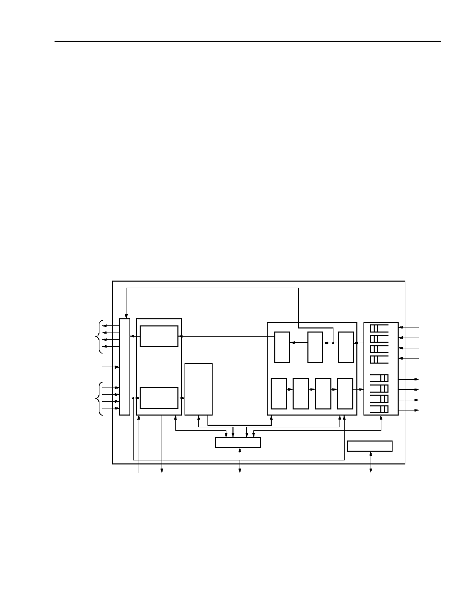
Data Sheet
MARS2G5 P-Pro (TDAT162G52) SONET/SDH
August 18, 2004
155/622/2488 Mbits/s Data Interface
27
Agere Systems Inc.
Description
The MARS2G5 P-Pro SONET/SDH interface device provides a versatile solution for quad OC-3, quad OC-12, and
for single OC-48 linear datacom/telecom applications. Constructed using COM2 CMOS modular process, this
device incorporates integrated SONET/SDH framing, section/line/path termination, pointer processing, and data
engine blocks.
The device provides complete encapsulation and de-encapsulation for packet and ATM streams into and out of
SONET/SDH payloads.
Communication with the MARS2G5 P-Pro device is accomplished through a generic microprocessor interface. The
device supports separate address and data buses.
With the MARS2G5 P-Pro device, support for different types of applications for OC-3/OC-12/OC-48 data equip-
ment is possible, enabling dramatic system cost reduction and the ease of development of extremely competitive
solutions.
This device integrates the SONET/SDH network termination functions with a generic cell/packet delineation circuit.
The interface rates supported are STS-48/STM-16, quad STS-12/STM-4, and quad STS-3/STM-1. The UTOPIA
interface can process and hand off up to 16 channels transported within an STS-N payload. The concatenation lev-
els supported by this device are STS-1, STS-3c, STS-6c, STS-9c, STS-12c, STS-15c, . . . , STS-45c, and STS-
48c. The data formats processed by this device are ATM cells or HDLC framed packets such as PPP or GFP
framed packets.
5-7393(F).dTDAT16
Note: PT = path terminator, RXS = receive sequencer, and DE = data engine.
* In the transmit path, the data engine performs packet/cell processing (encapsulation, scrambling).
In the receive path, the data engine performs packet/cell processing (delineation, descrambling, de-encapsulation).
Figure 1. MARS2G5 P-Pro Block Diagram
OVERHEAD
PROCESSOR
MONITOR
OVERHEAD
PROCESSOR
INSERT
TRANSPORT
OVERHEAD
I
N
TE
RFA
C
E BL
O
C
K
P
OINT
E
R
P
R
O
C
ESS
O
R
PACKET/CELL
FIFOs
CONTROL
UTOPIA
INTERFACE
MPU INTERFACE
DIRECT CELL/PACKET OVER FIBER
SINGLE
STM-16/STS-48
OR QUAD
STM-4/STS-12
OR QUAD
STM-1/STS-3
SINGLE
STM-16/STS-48
OR QUAD
STM-4/STS-12
OR QUAD
STM-1/STS-3
MISCELLANEOUS
GPIO
TOAC INTERFACE
TERMINATION
TXCLK
TXTOAC
RXTOAC
RXD
RXC
RXB
RXA
TXD
TXC
TXB
TXA
DIRECT CELL/PACKET OVER FIBER
DE*
DS3
PT
DS3
PT
RXS
DE
(SPE
MPR)
(PTR
INTER)

MARS2G5 P-Pro (TDAT162G52) SONET/SDH
Data Sheet
155/622/2488 Mbits/s Data Interface
August 18, 2004
28
Agere Systems Inc.
Description
(continued)
Generic Framing Procedure (GFP)
GFP is an emerging new global standard for data encapsulation over SONET/SDH or G.709 (ITU-T G.gfp draft new
standard). It is a generic mechanism for adapting variable length client signals onto an octet synchronous transport
network.
Client signals may be PDU oriented, such as IP/PPP or ethernet MAC (frame-mapped GFP), or block-code ori-
ented, such as fiber channel or ESCON (transparent GFP).
Frame-mapped GFP adaptation may operate at the physical or data-link layer of the client signal. Client PDU visi-
bility is required.
Transparent-mapped GFP operates on the coded 8B/10B character stream, rather than on the incoming client
PDUs.
Figure 2 illustrates the relationship between the higher-layer payloads, GFP, and SDH/OTN paths.
GFP benefits include:
Equips SONET/SDH with flexible/efficient data transport capabilities.
More robust frame delineation than flag-based mechanisms such as HDLC.
No payload dependent frame expansion (no HDLC type byte stuffing).
Flexibility of extension headers. This allows for topology/application specific fields to be defined without affecting
frame delineation functions.
Ability to identify the encapsulated client protocol separately from the extension header. This allows frame for-
warding based on extension header fields without requiring recognition of the encapsulated client protocol.
Optional GFP 16-bit or 32-bit frame check sequence (FCS). This allows for fault location on a GFP frame basis
without requiring recognition of the encapsulated client protocol. It also provides a data integrity mechanism for
the encapsulation of protocols that may not have such a mechanism.
2682(F)s
Figure 2. GFP Relationship to Transport Payloads
GFP Payload Area CRC-32 Insertion (Version 2.2 and 2.3 Only)
GFP block upgrade on transmit and receive to calculate the CRC-32 over only the payload information area.
MARS2G5 P-Pro (version 2.0/2.1) calculated CRC-32 over everything except the PLI field.
Two modes are supported for CRC-32 insertion/checking:
1. Null-extension headers:
4-byte header.
Calculation starts after PLI field and 4 bytes of TYPE field.
2. Linear-extension headers:
8-byte header.
Calculation starts after PLI field and 4 bytes of TYPE field and 4 bytes of EXT header field.
PLI field value will be modified on transmit by +4 to include CRC-32 bytes.
PLI field value will be modified on receive by ≠4 when CRC-32 is stripped.
MARS2G5 P-Pro (version 2.2 and 2.3) does not touch PFI field value because it will corrupt tHEC.
ETHERNET
PPP/HDLC
OTHER PACKET ORIENTED
GFP ≠ PAYLOAD DEPENDENT
(CLIENT SPECIFIC ASPECTS)
SDH PATH
OTN OPU
BEARER SERVICES
GFP--PAYLOAD INDEPENDENT
(COMMON GFP ASPECTS)
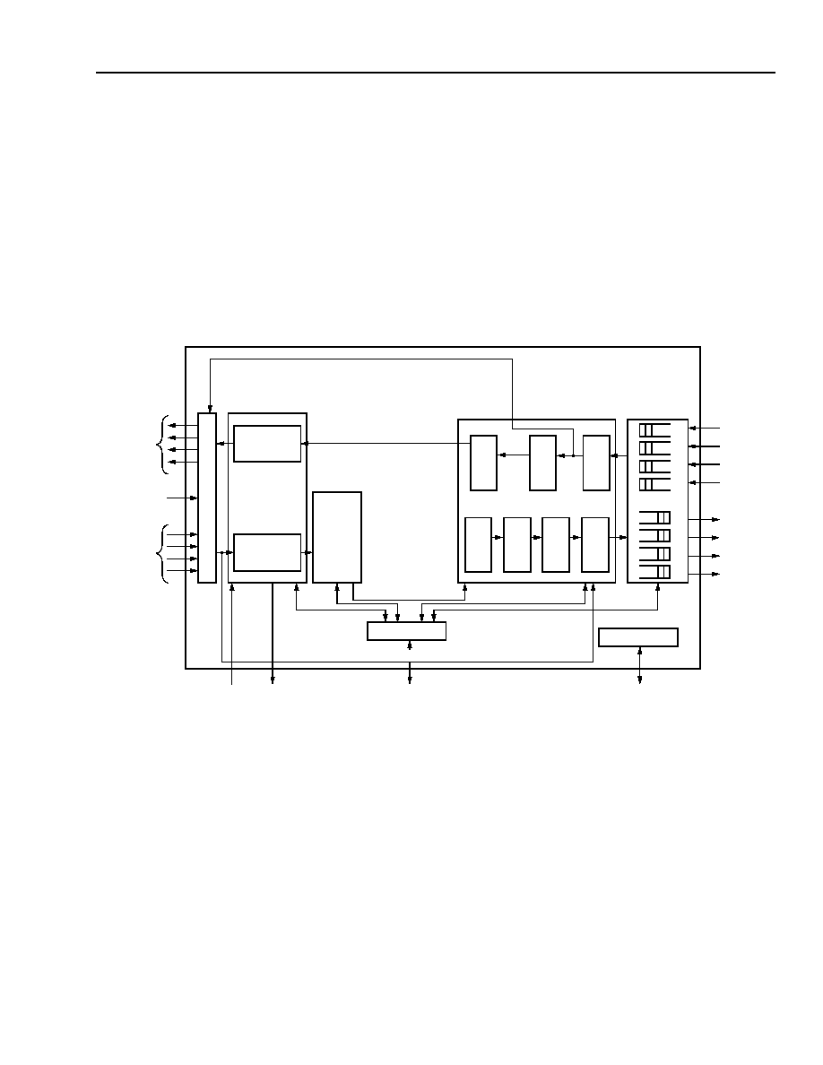
Data Sheet
MARS2G5 P-Pro (TDAT162G52) SONET/SDH
August 18, 2004
155/622/2488 Mbits/s Data Interface
29
Agere Systems Inc.
Target Applications Supported
MARS2G5 P-Pro (600-Pin LBGA and 792-Pin PBGA)
This multirate/multiprotocol/multimode SONET/SDH data interface device targets the following applications (see
Figure 3 for device interface speed/rate information):
Mixed ATM/POS-TDM.
Access router and aggregation.
Wireless, DSLAM, and gateway.
Figure 3. MARS2G5 P-Pro Device Interface Speed/Rate Diagram
OVERHEAD
PROCESSOR
MONITOR
OVERHEAD
PROCESSOR
INSERT
TRANSPORT
OVERHEAD
I
N
TER
F
ACE
BL
O
C
K
P
OINT
E
R
PRO
C
E
SSO
R
PACKET/CELL
FIFOs
CONTROL
UTOPIA/DATA
INTERFACE
MPU INTERFACE
DIRECT CELL/PACKET OVER FIBER
MISCELLANEOUS
GPIO
TOAC INTERFACE
TERMINATION
TXCLK
TXTOAC
RXTOAC
DIRECT CELL/PACKET OVER FIBER
DE
DS3
PT
DS3
PT
RXS
DE
(SPE
MPR)
(PTR
INTER)
LINE
SINGLE
(16 x 155 Mbits/s
LVPECL)
or
QUAD
(1 x 622 Mbits/s
LVPECL)
or
QUAD
(1 x 155 Mbits/s
LVPECL)
INTERFACE
SINGLE
(16 x 155 Mbits/s
LVPECL)
or
QUAD
(1 x 622 Mbits/s
LVPECL)
or
QUAD
(1 x 155 Mbits/s
LVPECL)
SEE TABLE 2
SEE TABLE 2

MARS2G5 P-Pro (TDAT162G52) SONET/SDH
Data Sheet
155/622/2488 Mbits/s Data Interface
August 18, 2004
30
Agere Systems Inc.
Target Applications Supported
(continued)
MARS1G2 P-Pro (TDAT161G2) (792-Pin PBGA)
This multirate/multiprotocol/multimode SONET/SDH data interface device targets the following applications (see
Figure 4 for device interface speed/rate information):
Mixed ATM/POS-TDM.
Access router and aggregation.
Wireless, DSLAM, and gateway.
Figure 4. MARS1G2 P-Pro Device Interface Speed/Rate Diagram
OVERHEAD
PROCESSOR
MONITOR
OVERHEAD
PROCESSOR
INSERT
TRANSPORT
OVERHEAD
I
N
T
E
RF
ACE B
L
O
C
K
PO
I
N
TE
R
PRO
C
ES
SO
R
PACKET/CELL
FIFOs
CONTROL
UTOPIA/DATA
INTERFACE
MPU INTERFACE
DIRECT CELL/PACKET OVER FIBER
MISCELLANEOUS
GPIO
TOAC INTERFACE
TERMINATION
TXCLK
TXTOAC
RXTOAC
DIRECT CELL/PACKET OVER FIBER
DE
DS3
PT
DS3
PT
RXS
DE
(SPE
MPR)
(PTR
INTER)
LINE
DUAL
(1 x 622 Mbits/s
LVPECL)
or
QUAD
(1 x 155 Mbits/s
LVPECL)
INTERFACE
DUAL
(1 x 622 Mbits/s
LVPECL)
or
QUAD
(1 x 155 Mbits/s
LVPECL)
SEE TABLE 2
SEE TABLE 2
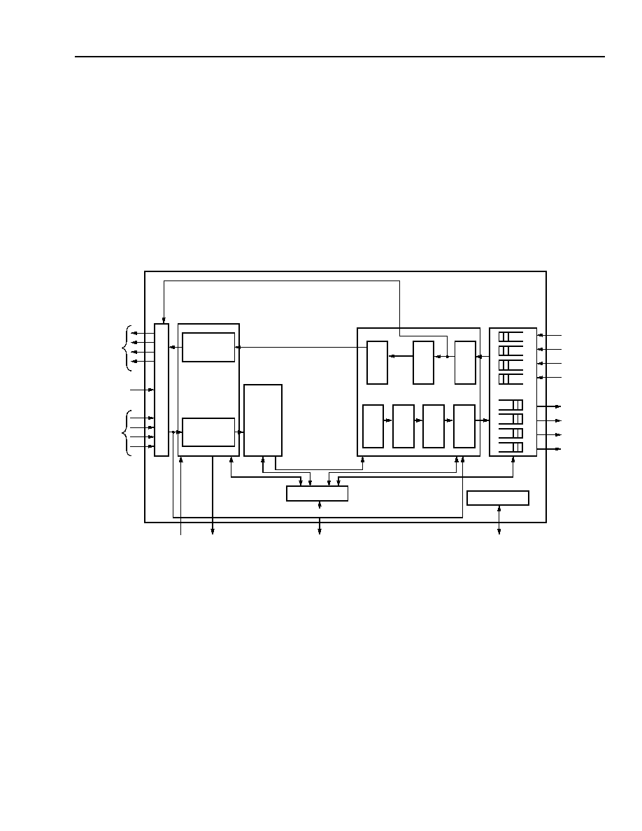
Data Sheet
MARS2G5 P-Pro (TDAT162G52) SONET/SDH
August 18, 2004
155/622/2488 Mbits/s Data Interface
31
Agere Systems Inc.
Target Applications Supported
(continued)
MARS622 P-Pro (TDAT12622) (792-Pin PBGA)
This multirate/multiprotocol/multimode SONET/SDH data interface device targets the following applications (see
Figure 5 for device interface speed/rate information):
Mixed ATM/POS-TDM.
Access router and aggregation.
Wireless, DSLAM, and gateway.
Figure 5. MARS622 P-Pro Device Interface Speed/Rate Diagram
OVERHEAD
PROCESSOR
MONITOR
OVERHEAD
PROCESSOR
INSERT
TRANSPORT
OVERHEAD
I
N
T
E
RF
ACE B
L
O
C
K
PO
I
N
TE
R
PRO
C
ES
SO
R
PACKET/CELL
FIFOs
CONTROL
UTOPIA/DATA
INTERFACE
MPU INTERFACE
DIRECT CELL/PACKET OVER FIBER
MISCELLANEOUS
GPIO
TOAC INTERFACE
TERMINATION
TXCLK
TXTOAC
RXTOAC
DIRECT CELL/PACKET OVER FIBER
DE
DS3
PT
DS3
PT
RXS
DE
(SPE
MPR)
(PTR
INTER)
LINE
SINGLE
(1 x 622 Mbits/s
LVPECL)
or
QUAD
(1 x 155 Mbits/s
LVPECL)
INTERFACE
SINGLE
(1 x 622 Mbits/s
LVPECL)
or
QUAD
(1 x 155 Mbits/s
LVPECL)
SEE TABLE 2
SEE TABLE 2

MARS2G5 P-Pro (TDAT162G52) SONET/SDH
Data Sheet
155/622/2488 Mbits/s Data Interface
August 18, 2004
32
Agere Systems Inc.
Overview
This SONET line interface integrated circuit (IC) implements a four-port, sixteen-channel SONET/SDH interface for
asynchronous transfer mode (ATM) and packet over SONET (POS) mappings at the STS-3 (STM-1), STS-12
(STM-4), or STS-48 (STM-12) rate. This device also supports direct cell/packet over fiber at up to 2.488 Gbits/s.
The receive path terminates and processes section, line, and path overhead. It performs framing (A1, A2) and
descrambling, detects alarm conditions, and monitors section, line, and path BIP-8s (B1, B2, and B3), accumulat-
ing error counts for each level for performance-monitoring purposes. Line and path remote error indications (M1,
G1) are also accumulated. The payload pointers (H1, H2) are interpreted and the synchronous payload envelope
(SPE) is extracted.
When used to implement an ATM UNI, the device performs cell delineation on the SPE. HCS error correction is
provided. Idle/unassigned cells may be dropped according to a programmable filter. Cells are also dropped upon
detection of an uncorrectable header check sequence error. The ATM cell payloads are descrambled before being
passed to a 32-cell FIFO buffer. The received cells are read from the FIFO using one of four generic 8-/16-/32-bit
wide UTOPIA level 2 and level 3 compliant interface. Counts of received ATM cells, uncorrectable HCS errors, cor-
rectable HCS errors, and idle/unassigned ATM cells are accumulated independently for performance-monitoring
purposes.
When used to implement a POS UNI, the device descrambles the SPE before extracting HDLC frames. The con-
trol escape characters are removed. Descrambling can be performed after control escape byte destuffing (or
before to control malicious HDLC expansion)
.
The optional 16- or 32-bit error check sequence is verified for cor-
rectness. The packets are placed into a 256-byte FIFO buffer. The received packets are read from the FIFO using
a generic 8-/16-/32-bit wide enhanced UTOPIA level 2 and level 3 compliant interface. Counts of errored/dropped
packets are accumulated independently for performance-monitoring purposes. The device POS implementation
also allows the optional detach of a per-channel provisionable PPP header.
The transmit path inserts section, line, and path overhead. It inserts the framing pattern (A1, A2), performs scram-
bling, inserts AIS (optionally), and calculates and inserts section, line, and path BIP-8s (B1, B2, B3). Line and path
remote failure indications (M1, G1) are inserted based on received BIP-8 errors. The payload pointers (H1, H2) are
generated, and the SPE is inserted.
When used to implement an ATM UNI, ATM cells are written into an internal four-cell (per channel) FIFO buffer
using a generic 8-/16-/32-bit wide UTOPIA level 2 and level 3 compliant interface. Idle/unassigned cells are auto-
matically inserted when the internal FIFO is empty. The device provides generation of the header check sequence
and scrambles the ATM payload. Also supports cell-based UNI per I.432 (i.e., ATM over fiber).
When used to implement a POS UNI, the device writes packets into an internal 256-byte (per channel) FIFO buffer
using a generic 8/16/32-bit wide enhanced UTOPIA level 2 and level 3 compliant interface. HDLC framing performs
the insertion of flags, control escape characters and the FCS fields. Either the CRC-CCITT or CRC-32 (in regular
or reversed mode) can be computed and added to the frame. Counts of transmitted packets and errored/dropped
packets are accumulated for performance-monitoring purposes.
The device is provisioned, controlled, and monitored using a generic 16-bit microprocessor interface. A standard
five-signal IEEE
Æ
1149.1 compliant JTAG test port is also provided for scan, boundary scan, and BIST purposes.
A 4-bit general-purpose input/output (GPIO) interface is provided to control and/or monitor other onboard devices.

Data Sheet
MARS2G5 P-Pro (TDAT162G52) SONET/SDH
August 18, 2004
155/622/2488 Mbits/s Data Interface
33
Agere Systems Inc.
Overview
(continued)
Figure 6 shows the external interfaces.
5-7395(F).aTDAT162
Figure 6. MARS2G5 P-Pro External Interfaces
TOH
FRMR
SCRM
DSCRM
SOH
LOH
POH
POINTER
SOH
LOH
SCRM
ATM
DSCRM
HDLC
HDLC
ATM
UT
OP
IA
I
N
T
E
RF
A
C
E
CONTROL
POH
PROCESSOR
CD
FRAME
INSERTION
32
2
32
2
STS-48 TXQ
STS-3/12
ECLREF
STS-3/12
STS-48 RXD
RXCLK
RXREF
RXTOH
12
43
4
6
MPU
GPIO
JTAG
110
110
TXUTOPIA
RXUTOPIA
2
2
2
3
4
TXCLK
TXCLKQ
TXFSYNC
PLL
TEST
TXTOH
INTERFACE
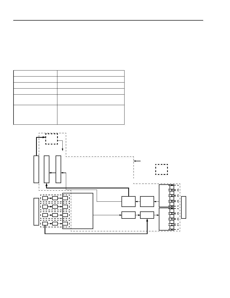
MARS2G5 P-Pro (TDAT162G52) SONET/SDH
Data Sheet
155/622/2488 Mbits/s Data Interface
August 18, 2004
34
Agere Systems Inc.
Overview
(continued)
Clocking
The following diagram shows a somewhat simplified picture of the major clock domains within the MARS2G5 P-Pro
in the normal SONET/SDH operating mode. There are a total of 16 different clock domains as shown in the follow-
ing table.
Table 1. List of the Clock Domains in the MARS2G5 P-Pro, SONET/SDH Mode
5-8701(F)r.3TDAT16
Figure 7. Clock Domains in the MARS2G5 P-Pro, SONET/SDH Mode
Clock Domain Name
Number of Clocks
Core
1
PLL
2
MPU
1
Receive Line Interface
4
(one each for A, B, C, and D)
UTOPIA Interface
8
(one each for A, B, C, and D);
(one each for Rx and Tx on interface A;
one each for Rx and Tx on interface B)
PLL
A
B
C
D
TXLINE TXOHP
A
B
C
D
PEC
L I
/
O
RXLINE RXOHP
PE
C
L
I/
O
A
A
A
B
B
B
C
C
C
D
D
D
PT/DS3
PT/DS3
DATA
ENGINE
(DE)
RXS/DE
PATH FOR POF SUPPORT
MPU
POINTER
PROCESSOR
(PP)
CORE
CLOCK
DOMAIN
78 MHz
CORE
CLOCK
PATH FOR POF SUPPORT
UT TX
U
T
I/O
A
B
C
D
UT RX
A
B
C
D

Data Sheet
MARS2G5 P-Pro (TDAT162G52) SONET/SDH
August 18, 2004
155/622/2488 Mbits/s Data Interface
35
Agere Systems Inc.
Overview
(continued)
Clocking
(continued)
The following diagram shows a somewhat simplified picture of the clock domains within the MARS2G5 P-Pro when
it is configured into the packet over fiber (POF) mode. In this mode, large subsections of the device are unused.
5-8702(F)
Figure 8. Clock Domains in the Packet-Over-Fiber (POF) Mode
PLL
A
B
C
D
PE
C
L
I
/
O
RXLINE
PEC
L I
/
O
A
B
C
D
PT/DS3
DATA
ENGINE
(DE)
UT TX
UT I/
O
MPU
CORE
CLOCK
DOMAIN
78 MHz
CORE
CLOCK
TXLINE
PATH FOR POF SUPPORT
UT RX
RXS/DE
PATH FOR POF SUPPORT

MARS2G5 P-Pro (TDAT162G52) SONET/SDH
Data Sheet
155/622/2488 Mbits/s Data Interface
August 18, 2004
36
Agere Systems Inc.
MARS2G5 P-Pro (792-Pin PBGA) Low-Speed Devices Available
The functionality of the MARS2G5 P-Pro (792-Pin PBGA) is available in lower-speed devices which are indicated
below with the limitations noted.
MARS1G2 P-Pro (TDAT161G2) (792-Pin PBGA)
MARS1G2 P-Pro is intended for use in quad OC-3 or dual OC-12 TDAT applications. It has the following limitations
with respect to MARS2G5 P-Pro (TDAT162G52):
Supports quad OC-3 or dual OC-12 rate line ports.
The UTOPIA interface for the device can be operated as follows:
-- 4 x 16-bit interfaces (A, B, C, and D) operating up to 26 MHz (2 x 16-bit interface (UT ports A and B only) oper-
ating up to 52 MHz (U2/U2+)).
-- 4 x 8-bit interfaces (A, B, C, and D) operating up to 52 MHz (U2/U2+).
-- 1 x 32-bit interface (UT ports A and B) operating up to 52 MHz (U3/U3+).
-- 2 x 8-bit interfaces (A and B) operating up to 104 MHz (U3/U3+).
MPHY is possible in all UTOPIA interfacing modes, (i.e., channels addressed from any interface in MPHY
mode). For example, when connecting to an APP550 (Agere's network processor), the 2 x 8 (UT ports A and B)
mode at 104 MHz can be used.
MARS622 P-Pro (TDAT12622) (792-Pin PBGA)
MARS622 P-Pro is intended for use in quad OC-3 or single OC-12 TDAT applications. The minimum channel size
is one STS-1, and the device is limited to 12 channels. In addition to the 12-channel limitation, the MARS622 P-Pro
(TDAT12622) also has the following limitations with respect to MARS2G5 P-Pro (TDAT162G52):
Supports quad OC-3 rate line ports or a single OC-12 rate line port.
The UTOPIA interface for this device can be operated as follows:
-- 4 x 16-bit interfaces (UT ports A, B, C, and D) operating up to 26 MHz, (1 x 16-bit interface (UT port A only)
operating up to 52 MHz (U2/U2+)).
-- 4 x 8-bit interfaces (UT ports A, B, C, and D) operating up to 52 MHz (U2/U2+).
-- 1 x 8-bit interfaces (UT port A only) operating up to 104 MHz (U3/U3+).
MPHY is possible in all UTOPIA interfacing modes, (i.e., channels can be addressed from any interface in MPHY
mode). For example, when connecting to APP550 (Agere's network processor), the 1 x 8 (UT port A only) mode
at 104 MHz can be used.
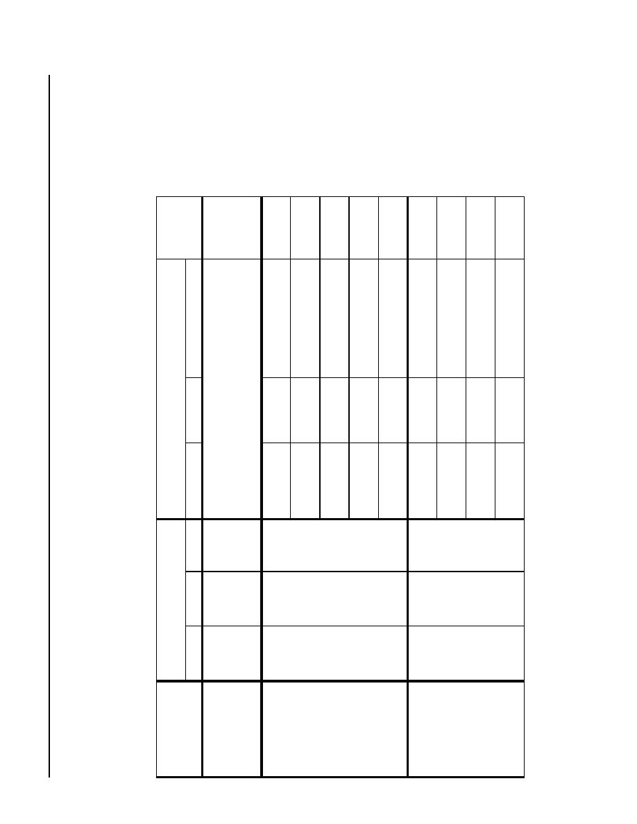
Data Sheet
MARS2G5 P-Pro (TDAT162G52) SONET/SDH
August 18, 2004
155/622/2488 Mbits/s Data Interface
37
Agere Systems Inc.
MARS2G5 P-Pro Device Product Line Table Summaries
Table 2 highlights which ports are supported for the line and UTOPIA interfaces for the MARS2G5 P-Pro. Letters in parentheses indicate which ports are
available for that particular interface.
Table 2. MARS2G5 P-Pro Device Product Line--Data Port Summary
* No support for DS3 and E3 framing on ports C and D.
Note: NA = not available.
Device
Line Ports
UTOPIA MPHY/Data Interface
UTOPIA
Ports
OC-3
OC-12
OC-48
UTOPIA Level
Interface
Max Frequency
MARS2G5 P
(TADM042G52)
(792-Pin PBGA
and 600-Pin LBGA)
4*
(A, B, C, D)
4*
(A, B, C, D)
1
(A)
See the UTOPIA (UT) Block section and the MARS2G5
P-VC (TADMVC2G52) Device Advisory for Version 2.2
and Version 2.3 of the Device (AY03-015SONT) item
UT27. Limitations in UTOPIA Clock Frequency.
4
(A, B, C, D)
MARS1G2 P
(TADM021G2)
(792-Pin PBGA)
4*
(A, B, C, D)
2
(A,B)
NA
U2/U2+
4 x 16-bit
26 MHz
4
(A, B, C, D)
U2/U2+
2 x 16-bit
52 MHz
2
(A, B)
U2/U2+
4 x 8-bit
52 MHz
4
(A, B, C, D)
U3/U3+
1 x 32-bit
52 MHz
2
(A, B)
U3/U3+
2 x 8-bit
104 MHz
2
(A, B)
MARS622 P
(TADM04622)
(792-Pin PBGA)
4
(A, B, C, D)
1
(A)
NA
U2/U2+
4 x 16-bit
26 MHz
4
(A, B, C, D)
U2/U2+
1 x 16-bit
52 MHz
1
(A)
U2/U2+
4 x 8-bit
52 MHz
4
(A, B, C, D)
U3/U3+
1 x 8-bit
104 MHz
1
(A)

MARS2G5 P-Pro (TDAT162G52) SONET/SDH
Data Sheet
155/622/2488 Mbits/s Data Interface
August 18, 2004
38
Agere Systems Inc.
Pin Information
792-Pin PBGA Pin Assignments
A pin assignment conversion between the 792-pin and 600-pin devices is shown in Table 3.
Table 3. Pin Assignments for 792-Pin PBGA and 600-Pin LBGA by Pin Number Order
Note: NC refers to no connect. Do not connect pins so designated. -- indicates the pin does not exist for the specified package.
Pin
792-Pin Signal Name
600-Pin Signal Name
A1
V
DDD2
V
DDD
A2
V
DDD2
V
DDD
A3
V
DDD2
GND
D
A4
GND
D
GND
D
A5
GND
D
V
DDD2
A6
V
DDD2
V
DDD2
A7
V
DDD2
GND
D
A8
NC
GND
D
A9
GND
D
MPU_DATA1
A10
NC
MPU_DATA6
A11
V
DDD2
MPU_DATA10
A12
V
DDD2
MPU_DATA15
A13
NC
GND
D
A14
NC
MPU_ADDR8
A15
GND
D
MPU_ADDR12
A16
GND
D
GND
D
A17
NC
V
DDD
A18
NC
V
DDD
A19
V
DDD2
NC
A20
V
DDD2
GND
D
A21
V
DDD2
NC
A22
MPU_ADDR8
NC
A23
MPU_ADDR2
GND
D
A24
GND
D
NC
A25
GND
D
NC
A26
GND
D
NC
A27
GND
D
GND
D
A28
V
DDD2
GND
D
A29
V
DDD2
GND
D
A30
V
DDD2
V
DDD2
A31
V
DDD2
V
DDD2
A32
V
DDD2
GND
D
A33
V
DDD2
GND
D
A34
GND
D
V
DDD
A35
GND
D
V
DDD
A36
GND
D
--
A37
V
DDD2
--
A38
V
DDD2
--
A39
V
DDD2
--

Data Sheet
MARS2G5 P-Pro (TDAT162G52) SONET/SDH
August 18, 2004
155/622/2488 Mbits/s Data Interface
39
Agere Systems Inc.
Pin Information
(continued)
792-Pin PBGA Pin Assignments
(continued)
Table 3.
Pin Assignments for 792-Pin PBGA and 600-Pin LBGA by Pin Number Order (continued)
Note: NC refers to no connect. Do not connect pins so designated. -- indicates the pin does not exist for the specified package.
Pin
792-Pin Signal Name
600-Pin Signal Name
B1
V
DDD2
V
DDD
B2
V
DDD2
V
DDD
B3
V
DDD2
GND
D
B4
GND
D
GND
D
B5
GND
D
NC
B6
V
DDD2
PLL_V
DDD2
B7
NC
MPU_INTN
B8
NC
MPU_CSN
B9
NC
MPU_DATA0
B10
NC
MPU_DATA5
B11
NC
MPU_DATA9
B12
NC
MPU_DATA14
B13
NC
MPU_ADDR3
B14
NC
MPU_ADDR7
B15
NC
MPU_ADDR11
B16
NC
MPU_ADDR15
B17
NC
NC
B18
NC
NC
B19
NC
NC
B20
MPU_ADDR12
NC
B21
MPU_ADDR9
NC
B22
MPU_ADDR3
NC
B23
MPU_DATA13
NC
B24
MPU_DATA9
NC
B25
MPU_DATA8
NC
B26
MPU_DATA4
NC
B27
MPU_DSN
NC
B28
V
DDD2
NC
B29
V
DDD2
NC
B30
V
DDD2
NC
B31
V
DDD2
NC
B32
V
DDD2
GND
D
B33
V
DDD2
GND
D
B34
GND
D
V
DDD
B35
GND
D
V
DDD
B36
GND
D
--
B37
V
DDD2
--
B38
V
DDD2
--
B39
V
DDD2
--

MARS2G5 P-Pro (TDAT162G52) SONET/SDH
Data Sheet
155/622/2488 Mbits/s Data Interface
August 18, 2004
40
Agere Systems Inc.
Pin Information
(continued)
792-Pin PBGA Pin Assignments
(continued)
Table 3.
Pin Assignments for 792-Pin PBGA and 600-Pin LBGA by Pin Number Order (continued)
Note: NC refers to no connect. Do not connect pins so designated. -- indicates the pin does not exist for the specified package.
Pin
792-Pin Signal Name
600-Pin Signal Name
C1
V
DDD2
GND
D
C2
V
DDD2
GND
D
C3
V
DDD2
V
DDD
C4
GND
D
GND
D
C5
GND
D
PLLREF
C6
V
DDD2
PLL_GND
C7
NC
RSTN
C8
NC
MPU_MPCLK
C9
NC
MPU_DSN
C10
GND
D
MPU_DATA4
C11
NC
MPU_DATA8
C12
NC
MPU_DATA13
C13
NC
MPU_ADDR2
C14
NC
MPU_ADDR6
C15
NC
MPU_ADDR10
C16
NC
MPU_ADDR14
C17
NC
NC
C18
NC
NC
C19
NC
NC
C20
MPU_ADDR13
NC
C21
NC
NC
C22
MPU_ADDR4
NC
C23
MPU_DATA14
NC
C24
MPU_DATA12
NC
C25
MPU_DATA7
NC
C26
MPU_DATA3
NC
C27
MPU_RWN
NC
C28
MPU_MPCLK
NC
C29
RSTN
NC
C30
PLL_V
DDD2
NC
C31
GND
D
NC
C32
GND
D
GND
D
C33
GND
D
V
DDD
C34
GND
D
GND
D
C35
GND
D
GND
D
C36
GND
D
--
C37
V
DDD2
--
C38
V
DDD2
--
C39
V
DDD2
--

Data Sheet
MARS2G5 P-Pro (TDAT162G52) SONET/SDH
August 18, 2004
155/622/2488 Mbits/s Data Interface
41
Agere Systems Inc.
Pin Information
(continued)
792-Pin PBGA Pin Assignments
(continued)
Table 3.
Pin Assignments for 792-Pin PBGA and 600-Pin LBGA by Pin Number Order (continued)
Note: NC refers to no connect. Do not connect pins so designated. -- indicates the pin does not exist for the specified package.
Pin
792-Pin Signal Name
600-Pin Signal Name
D1
GND
D
GND
D
D2
GND
D
GND
D
D3
GND
D
GND
D
D4
GND
D
V
DDD2
D5
GND
D
PLLFB
D6
V
DDD2
NC
D7
NC
PMRST
D8
NC
MPU_MPMODE
D9
NC
MPU_RWN
D10
V
DDD2
MPU_DATA3
D11
NC
MPU_DATA7
D12
NC
MPU_DATA12
D13
NC
MPU_ADDR1
D14
NC
MPU_ADDR5
D15
NC
NC
D16
NC
MPU_ADDR13
D17
NC
NC
D18
NC
NC
D19
NC
NC
D20
MPU_ADDR14
NC
D21
MPU_ADDR10
NC
D22
MPU_ADDR5
NC
D23
MPU_DATA15
NC
D24
MPU_DATA10
NC
D25
MPU_DATA6
NC
D26
MPU_DATA2
NC
D27
MPU_ADSN
V
DDD2
D28
MPU_DTN
NC
D29
PMRST
NC
D30
PLL_GND
NC
D31
GND
D
NC
D32
GND
D
V
DDD2
D33
GND
D
GND
D
D34
GND
D
GND
D
D35
GND
D
GND
D
D36
GND
D
--
D37
GND
D
--
D38
GND
D
--
D39
GND
D
--

MARS2G5 P-Pro (TDAT162G52) SONET/SDH
Data Sheet
155/622/2488 Mbits/s Data Interface
August 18, 2004
42
Agere Systems Inc.
Pin Information
(continued)
792-Pin PBGA Pin Assignments
(continued)
Table 3.
Pin Assignments for 792-Pin PBGA and 600-Pin LBGA by Pin Number Order (continued)
Note: NC refers to no connect. Do not connect pins so designated. -- indicates the pin does not exist for the specified package.
Pin
792-Pin Signal Name
600-Pin Signal Name
E1
GND
D
V
DDD2
E2
GND
D
IDDQMODE
E3
GND
D
PLL_V
DDD2
E4
GND
D
PLL_GND
D
E5
GND
D
V
DDD2
E6
V
DDD
NC
E7
V
DDD
ICTN
E8
NC
MPU_DTN
E9
NC
MPU_ADSN
E10
NC
MPU_DATA2
E11
NC
V
DDD
E12
NC
MPU_DATA11
E13
NC
MPU_ADDR0
E14
NC
MPU_ADDR4
E15
NC
MPU_ADDR9
E16
NC
V
DDD2
E17
NC
NC
E18
NC
NC
E19
NC
NC
E20
MPU_ADDR15
V
DDD2
E21
MPU_ADDR11
NC
E22
MPU_ADDR6
NC
E23
MPU_ADDR0
NC
E24
MPU_DATA11
NC
E25
MPU_DATA5
V
DDD
E26
MPU_DATA1
NC
E27
MPU_CSN
NC
E28
MPU_INTN
NC
E29
ICTN
NC
E30
NC
NC
E31
NC
V
DDD2
E32
GND
D
NC
E33
V
DDD
NC
E34
V
DDD
NC
E35
GND
D
V
DDD2
E36
GND
D
--
E37
GND
D
--
E38
GND
D
--
E39
GND
D
--

Data Sheet
MARS2G5 P-Pro (TDAT162G52) SONET/SDH
August 18, 2004
155/622/2488 Mbits/s Data Interface
43
Agere Systems Inc.
Pin Information
(continued)
792-Pin PBGA Pin Assignments
(continued)
Table 3.
Pin Assignments for 792-Pin PBGA and 600-Pin LBGA by Pin Number Order (continued)
Note: NC refers to no connect. Do not connect pins so designated. -- indicates the pin does not exist for the specified package.
Pin
792-Pin Signal Name
600-Pin Signal Name
F1
GND
D
V
DDD2
F2
GND
D
TCLK
F3
GND
D
GND
D
F4
GND
D
TMS
F5
V
DDD
NC
F6
V
DDD
--
F7
V
DDD
--
F8
NC
--
F9
NC
--
F10
NC
--
F11
GND
D
--
F12
GND
D
--
F13
NC
--
F14
NC
--
F15
V
DDD
--
F16
V
DDD
--
F17
NC
--
F18
NC
--
F19
GND
D
--
F20
GND
D
--
F21
GND
D
--
F22
MPU_ADDR7
--
F23
MPU_ADDR1
--
F24
V
DDD
--
F25
V
DDD
--
F26
MPU_DATA0
--
F27
MPU_MPMODE
--
F28
GND
D
--
F29
GND
D
--
F30
NC
--
F31
PLLREF
RXSPAA
F32
PLLFB
RXSPAB
F33
V
DDD
RXSPAC
F34
V
DDD
RXSPAD
F35
V
DDD
V
DDD2
F36
GND
D
--
F37
GND
D
--
F38
GND
D
--
F39
GND
D
--

MARS2G5 P-Pro (TDAT162G52) SONET/SDH
Data Sheet
155/622/2488 Mbits/s Data Interface
August 18, 2004
44
Agere Systems Inc.
Pin Information
(continued)
792-Pin PBGA Pin Assignments
(continued)
Table 3.
Pin Assignments for 792-Pin PBGA and 600-Pin LBGA by Pin Number Order (continued)
Note: NC refers to no connect. Do not connect pins so designated. -- indicates the pin does not exist for the specified package.
Pin
792-Pin Signal Name
600-Pin Signal Name
G1
V
DDD2
GND
D
G2
V
DDD2
TDO
G3
GND
D
TRSTN
G4
GND
D
NC
G5
V
DDD
TDI
G6
V
DDD
--
G31
--
TXSPAA
G32
--
TXADDRA0
G33
--
TXADDRA1
G34
V
DDD
TXCLKA
G35
PLL_GND
D
GND
D
G36
GND
D
--
G37
GND
D
--
G38
V
DDD2
--
G39
V
DDD2
--
H1
V
DDD2
GND
D
H2
V
DDD2
TXCLKQP
H3
GND
D
GND
D
H4
GND
D
CLKDIV
H5
NC
GND
D
H6
NC
--
H31
--
TXSZA
H32
--
TXERRA
H33
--
TXPPAA
H34
PLL_V
DDD2
TXENBA
H35
GND
D
GND
D
H36
IDDQMODE
--
H37
GND
D
--
H38
V
DDD2
--
H39
V
DDD2
--
J1
V
DDD2
TXD14N
J2
V
DDD2
TXD14P
J3
GND
D
TXD15N
J4
RXSPAC
TXD15P
J5
RXSPAB
TXCLKQN
J6
NC
--
J31
--
TXEOPA
J32
--
TXSOPA
J33
--
TXPRTYA
J34
GND
D
TXDATAA15

Data Sheet
MARS2G5 P-Pro (TDAT162G52) SONET/SDH
August 18, 2004
155/622/2488 Mbits/s Data Interface
45
Agere Systems Inc.
Pin Information
(continued)
792-Pin PBGA Pin Assignments
(continued)
Table 3.
Pin Assignments for 792-Pin PBGA and 600-Pin LBGA by Pin Number Order (continued)
Note: NC refers to no connect. Do not connect pins so designated. -- indicates the pin does not exist for the specified package.
Pin
792-Pin Signal Name
600-Pin Signal Name
J35
NC
TXDATAA14
J36
GND
D
--
J37
GND
D
--
J38
GND
D
--
J39
V
DDD2
--
K1
V
DDD2
TXD12N
K2
V
DDD2
TXD12P
K3
TXADDRA1
TXD13N
K4
TXSPAA
TXD13P
K5
RXSPAD
V
DDD
K6
RXSPAA
--
K31
--
TXDATAA13
K32
--
TXDATAA12
K33
--
TXDATAA11
K34
TMS
TXDATAA10
K35
TCLK
TXDATAA9
K36
TDI
--
K37
NC
--
K38
V
DDD2
--
K39
V
DDD2
--
L1
V
DDD2
TXD10N
L2
TXEOPA
TXD10P
L3
TXERRA
TXD11N
L4
TXCLKA
TXD11P
L5
TXADDRA0
V
DDD
L6
GND
D
--
L31
--
V
DDD
L32
--
TXDATAA8
L33
--
TXDATAA7
L34
GND
D
TXDATAA6
L35
TRSTN
TXDATAA5
L36
TDO
--
L37
CLKDIV
--
L38
V
DDD2
--
L39
V
DDD2
--
M1
V
DDD2
TXD8N
M2
TXDATAA15
TXD8P
M3
TXSOPA
TXD9N
M4
TXPPAA
TXD9P
M5
TXSZA
V
DDD

MARS2G5 P-Pro (TDAT162G52) SONET/SDH
Data Sheet
155/622/2488 Mbits/s Data Interface
August 18, 2004
46
Agere Systems Inc.
Pin Information
(continued)
792-Pin PBGA Pin Assignments
(continued)
Table 3.
Pin Assignments for 792-Pin PBGA and 600-Pin LBGA by Pin Number Order (continued)
Note: NC refers to no connect. Do not connect pins so designated. -- indicates the pin does not exist for the specified package.
Pin
792-Pin Signal Name
600-Pin Signal Name
M6
GND
D
--
M31
--
TXDATAA4
M32
--
TXDATAA3
M33
--
TXDATAA2
M34
GND
D
TXDATAA1
M35
TXCLKQP
TXDATAA0
M36
TXCLKQN
--
M37
TXD15P
--
M38
TXD15N
--
M39
V
DDD2
--
N1
TXDATAA7
GND
D
N2
TXDATAA10
TXD6N
N3
TXDATAA12
TXD6P
N4
TXDATAA13
TXD7N
N5
TXPRTYA
TXD7P
N6
TXENBA
--
N31
--
RXDATAA15
N32
--
RXDATAA14
N33
--
RXDATAA13
N34
TXD14P
RXDATAA12
N35
TXD14N
GND
D
N36
TXD13P
--
N37
TXD13N
--
N38
TXD12P
--
N39
TXD12N
--
P1
TXDATAA2
TXD4N
P2
TXDATAA5
TXD4P
P3
TXDATAA8
TXD5N
P4
TXDATAA9
V
DDD
P5
TXDATAA11
TXD5P
P6
TXDATAA14
--
P31
--
RXDATAA11
P32
--
RXDATAA10
P33
--
RXDATAA9
P34
TXD11P
RXDATAA8
P35
TXD11N
RXDATAA7
P36
TXD10P
--
P37
TXD10N
--
P38
TXD8P
--
P39
TXD8N
--

Data Sheet
MARS2G5 P-Pro (TDAT162G52) SONET/SDH
August 18, 2004
155/622/2488 Mbits/s Data Interface
47
Agere Systems Inc.
Pin Information
(continued)
792-Pin PBGA Pin Assignments
(continued)
Table 3.
Pin Assignments for 792-Pin PBGA and 600-Pin LBGA by Pin Number Order (continued)
Note: NC refers to no connect. Do not connect pins so designated. -- indicates the pin does not exist for the specified package.
Pin
792-Pin Signal Name
600-Pin Signal Name
R1
GND
D
V
DDD
R2
TXDATAA0
TXD2N_TXDBN
R3
TXDATAA3
TXD2P_TXDBP
R4
TXDATAA4
TXD3P_TXDAP
R5
TXDATAA6
TXD3N_TXDAN
R6
V
DDD
--
R31
--
RXDATAA6
R32
--
RXDATAA5
R33
--
RXDATAA4
R34
V
DDD
RXDATAA3
R35
TXD9P
RXDATAA2
R36
TXD9N
--
R37
TXD7P
--
R38
TXD7N
--
R39
GND
D
--
T1
GND
D
GND
D
T2
RXDATAA11
TXD0P_TXDDP
T3
RXDATAA13
TXD1N_TXDCN
T4
RXDATAA15
TXD1P_TXDCP
T5
TXDATAA1
V
DDD2
T6
V
DDD
--
T31
--
V
DDD2
T32
--
RXDATAA1
T33
--
RXDATAA0
T34
V
DDD
RXPRTYA
T35
TXD6P
GND
D
T36
TXD6N
--
T37
TXD5P
--
T38
TXD5N
--
T39
GND
D
--
U1
RXDATAA4
TXFSYNCN
U2
RXDATAA6
TXD0N_TXDDN
U3
RXDATAA8
TXFSYNCP
U4
RXDATAA10
TXCLKP
U5
RXDATAA12
TXCLKN
U6
RXDATAA14
--
U31
--
RXSOPA
U32
--
RXEOPA
U33
--
TXADDRA2
U34
TXD4P
RXENBA
U35
TXD4N
V
DDD

MARS2G5 P-Pro (TDAT162G52) SONET/SDH
Data Sheet
155/622/2488 Mbits/s Data Interface
August 18, 2004
48
Agere Systems Inc.
Pin Information
(continued)
792-Pin PBGA Pin Assignments
(continued)
Table 3.
Pin Assignments for 792-Pin PBGA and 600-Pin LBGA by Pin Number Order (continued)
Note: NC refers to no connect. Do not connect pins so designated. -- indicates the pin does not exist for the specified package.
Pin
792-Pin Signal Name
600-Pin Signal Name
U36
TXD3P_TXDAP
--
U37
TXD3N_TXDAN
--
U38
TXD2P_TXDBP
--
U39
TXD2N_TXDBN
--
V1
RXPRTYA
V
DDD
V2
RXDATAA2
V
DDD
V3
RXDATAA3
GND
D
V4
RXDATAA5
RXCLKN_RXDAN
V5
RXDATAA7
RXCLKP_RXDAP
V6
RXDATAA9
--
V31
--
GND
D
V32
--
RXERRA
V33
--
RXPPAA
V34
TXD1P_TXDCP
RXADDRA2
V35
TXD1N_TXDCN
V
DDD
V36
TXD0P_TXDDP
--
V37
TXD0N_TXDDN
--
V38
TXCLKP
--
V39
TXCLKN
--
W1
V
DDD2
V
DDD
W2
RXEOPA
RXD14N_RXCLKAN
W3
RXSOPA
RXD14P_RXCLKAP
W4
RXDATAA0
RXD15N_RXDBN
W5
RXDATAA1
RXD15P_RXDBP
W6
GND
D
--
W31
--
RXADDRA0
W32
--
RXADDRA1
W33
--
RXCLKA
W34
GND
D
TXADDRB0
W35
GND
D
RXSZA
W36
TXFSYNCN
--
W37
TXFSYNCP
--
W38
RXCLKN_RXDAN
--
W39
V
DDD2
--
Y1
V
DDD2
GND
D
Y2
RXERRA
RXD13N_RXCLKBN
Y3
RXPPAA
RXD13P_RXCLKBP
Y4
RXENBA
GND
D
Y5
TXADDRA2
V
DDD2
Y6
GND
D
--

Data Sheet
MARS2G5 P-Pro (TDAT162G52) SONET/SDH
August 18, 2004
155/622/2488 Mbits/s Data Interface
49
Agere Systems Inc.
Pin Information
(continued)
792-Pin PBGA Pin Assignments
(continued)
Table 3.
Pin Assignments for 792-Pin PBGA and 600-Pin LBGA by Pin Number Order (continued)
Note: NC refers to no connect. Do not connect pins so designated. -- indicates the pin does not exist for the specified package.
Pin
792-Pin Signal Name
600-Pin Signal Name
Y31
--
V
DDD2
Y32
--
TXSZB
Y33
--
TXCLKB
Y34
GND
D
TXADDRB1
Y35
RXD13N_RXCLKBN
GND
D
Y36
RXD14P_RXCLKAP
--
Y37
RXD14N_RXCLKAN
--
Y38
RXCLKP_RXDAP
--
Y39
V
DDD2
--
AA1
RXADDRA2
RXD11N_RXCLKCN
AA2
RXADDRA1
RXD11P_RXCLKCP
AA3
RXSZA
RXD12N_RXDCN
AA4
RXADDRA0
RXD12P_RXDCP
AA5
RXCLKA
GND
D
AA6
GND
D
--
AA31 --
TXEOPB
AA32 --
TXSOPB
AA33 --
TXENBB
AA34 GND
D
TXPPAB
AA35 RXD13P_RXCLKBP
TXERRB
AA36 RXD15P_RXDBP
--
AA37 RXD15N_RXDBN
--
AA38 V
DDD2
--
AA39 V
DDD2
--
AB1
TXADDRB0
RXD9N_RXCLKDN
AB2
TXPPAB
RXD9P_RXCLKDP
AB3
TXERRB
RXD10N_RXDDN
AB4
TXSZB
RXD10P_RXDDP
AB5
TXCLKB
V
DDD
AB6
TXADDRB1
--
AB31 --
TXDATAB13
AB32 --
TXDATAB12
AB33 --
TXDATAB14
AB34 RXD9P_RXCLKDP
TXDATAB15
AB35 RXD9N_RXCLKDN
TXPRTYB
AB36 RXD12P_RXDCP
--
AB37 RXD12N_RXDCN
--
AB38 RXD11P_RXCLKCP
--
AB39 RXD11N_RXCLKCN
--

MARS2G5 P-Pro (TDAT162G52) SONET/SDH
Data Sheet
155/622/2488 Mbits/s Data Interface
August 18, 2004
50
Agere Systems Inc.
Pin Information
(continued)
792-Pin PBGA Pin Assignments
(continued)
Table 3.
Pin Assignments for 792-Pin PBGA and 600-Pin LBGA by Pin Number Order (continued)
Note: NC refers to no connect. Do not connect pins so designated. -- indicates the pin does not exist for the specified package.
Pin
792-Pin Signal Name
600-Pin Signal Name
AC1
TXENBB
GND
D
AC2
TXDATAB14
RXD7N
AC3
TXDATAB15
RXD7P
AC4
TXPRTYB
RXD8N
AC5
TXSOPB
RXD8P
AC6
TXEOPB
--
AC31 --
TXDATAB8
AC32 --
TXDATAB9
AC33 --
TXDATAB10
AC34 RXD8P
TXDATAB11
AC35 RXD8N
GND
D
AC36 RXD7P
--
AC37 RXD7N
--
AC38 RXD10P_RXDDP
--
AC39 RXD10N_RXDDN
--
AD1
GND
D
RXD5N
AD2
TXDATAB10
RXD5P
AD3
TXDATAB11
RXD6N
AD4
TXDATAB13
RXD6P
AD5
TXDATAB12
V
DDD
AD6
V
DDD
--
AD31 --
TXDATAB3
AD32 --
TXDATAB4
AD33 --
TXDATAB5
AD34 V
DDD
TXDATAB6
AD35 RXD6P
TXDATAB7
AD36 RXD6N
--
AD37 RXD5P
--
AD38 RXD5N
--
AD39 GND
D
--
AE1
GND
D
RXD3N
AE2
TXDATAB9
RXD3P
AE3
TXDATAB8
RXD4N
AE4
TXDATAB7
RXD4P
AE5
TXDATAB6
V
DDD
AE6
V
DDD
--
AE31 --
V
DDD
AE32 --
RXDATAB15
AE33 --
TXDATAB0
AE34 V
DDD
TXDATAB1
AE35 RXD4P
TXDATAB2

Data Sheet
MARS2G5 P-Pro (TDAT162G52) SONET/SDH
August 18, 2004
155/622/2488 Mbits/s Data Interface
51
Agere Systems Inc.
Pin Information
(continued)
792-Pin PBGA Pin Assignments
(continued)
Table 3.
Pin Assignments for 792-Pin PBGA and 600-Pin LBGA by Pin Number Order (continued)
Note: NC refers to no connect. Do not connect pins so designated. -- indicates the pin does not exist for the specified package.
Pin
792-Pin Signal Name
600-Pin Signal Name
AE36 RXD4N
--
AE37 RXD3P
--
AE38 RXD3N
--
AE39 GND
D
--
AF1
TXDATAB5
RXD1N
AF2
TXDATAB4
RXD1P
AF3
TXDATAB3
RXD2N
AF4
TXDATAB2
RXD2P
AF5
TXDATAB1
V
DDD
AF6
TXDATAB0
--
AF31 --
RXDATAB10
AF32 --
RXDATAB11
AF33 --
RXDATAB12
AF34 RXD0P
RXDATAB13
AF35 RXD0N
RXDATAB14
AF36 RXD2P
--
AF37 RXD2N
--
AF38 RXD1P
--
AF39 RXD1N
--
AG1
RXDATAB15
RXD0N
AG2
RXDATAB14
RXD0P
AG3
RXDATAB13
ECLREFLO
AG4
RXDATAB12
ECLREFHI
AG5
RXDATAB10
GPIO3
AG6
RXDATAB11
--
AG31 --
RXDATAB5
AG32 --
RXDATAB6
AG33 --
RXDATAB7
AG34 GPIO2
RXDATAB8
AG35 GPIO3
RXDATAB9
AG36 ECLREFHI
--
AG37 ECLREFLO
--
AG38 V
DDD2
--
AG39 V
DDD2
--
AH1
V
DDD2
GND
D
AH2
RXDATAB9
GPIO2
AH3
RXDATAB8
GPIO1
AH4
RXDATAB7
GPIO0
AH5
RXDATAB6
TXTOHF
AH6
GND
D
--

MARS2G5 P-Pro (TDAT162G52) SONET/SDH
Data Sheet
155/622/2488 Mbits/s Data Interface
August 18, 2004
52
Agere Systems Inc.
Pin Information
(continued)
792-Pin PBGA Pin Assignments
(continued)
Table 3.
Pin Assignments for 792-Pin PBGA and 600-Pin LBGA by Pin Number Order (continued)
Note: NC refers to no connect. Do not connect pins so designated. -- indicates the pin does not exist for the specified package.
Pin
792-Pin Signal Name
600-Pin Signal Name
AH31 --
RXDATAB1
AH32 --
RXDATAB2
AH33 --
RXDATAB3
AH34 GND
D
RXDATAB4
AH35 TXTOHF
GND
D
AH36 GPIO0
--
AH37 GPIO1
--
AH38 V
DDD2
--
AH39 V
DDD2
--
AJ1
V
DDD2
GND
D
AJ2
RXDATAB5
TXTOHCLK
AJ3
RXDATAB4
TXTOHD
AJ4
RXDATAB3
TXSPAD
AJ5
RXDATAB2
TXSPAC
AJ6
GND
D
--
AJ31
--
RXEOPB
AJ32
--
RXSOPB
AJ33
--
RXPRTYB
AJ34
GND
D
RXDATAB0
AJ35
TXSPAD
GND
D
AJ36
TXTOHD
--
AJ37
TXTOHCLK
--
AJ38
V
DDD2
--
AJ39
V
DDD2
--
AK1
V
DDD2
V
DDD2
AK2
V
DDD2
TXSPAB
AK3
RXDATAB1
RXREF
AK4
RXDATAB0
RXTOHFA
AK5
RXPRTYB
RXTOHCLKA
AK6
RXEOPB
--
AK31 --
RXSZB
AK32 --
RXERRB
AK33 --
RXPPAB
AK34 RXREF
RXENBB
AK35 TXSPAB
V
DDD2
AK36 TXSPAC
--
AK37 GND
D
--
AK38 V
DDD2
--
AK39 V
DDD2
--

Data Sheet
MARS2G5 P-Pro (TDAT162G52) SONET/SDH
August 18, 2004
155/622/2488 Mbits/s Data Interface
53
Agere Systems Inc.
Pin Information
(continued)
792-Pin PBGA Pin Assignments
(continued)
Table 3.
Pin Assignments for 792-Pin PBGA and 600-Pin LBGA by Pin Number Order (continued)
Note: NC refers to no connect. Do not connect pins so designated. -- indicates the pin does not exist for the specified package.
Pin
792-Pin Signal Name
600-Pin Signal Name
AL1
V
DDD2
V
DDD2
AL2
V
DDD2
RXTOHDA
AL3
RXSOPB
RXTOHFB
AL4
RXENBB
RXTOHCLKB
AL5
RXPPAB
V
DDD2
AL6
RXERRB
RXTOHCLKC
AL7
--
RXTOHCLKD
AL8
--
RXADDRD0
AL9
--
RXPPAD
AL10
--
RXDATAD0
AL11
--
V
DDD
AL12
--
RXDATAD9
AL13
--
RXDATAD14
AL14
--
TXDATAD3
AL15
--
TXDATAD8
AL16
--
V
DDD2
AL17
--
TXSOPD
AL18
--
V
DDD
AL19
--
RXADDRC1
AL20
--
V
DDD2
AL21
--
RXSOPC
AL22
--
RXDATAC3
AL23
--
RXDATAC7
AL24
--
RXDATAC12
AL25
--
V
DDD
AL26
--
TXDATAC5
AL27
--
TXDATAC10
AL28
--
TXDATAC14
AL29
--
TXEOPC
AL30
--
TXSZC
AL31
--
V
DDD2
AL32
--
RXADDRB1
AL33
--
RXADDRB0
AL34
RXTOHDA
RXCLKB
AL35
RXTOHCLKA
V
DDD2
AL36
RXTOHFA
--
AL37
GND
D
--
AL38
V
DDD2
--
AL39
V
DDD2
--

MARS2G5 P-Pro (TDAT162G52) SONET/SDH
Data Sheet
155/622/2488 Mbits/s Data Interface
August 18, 2004
54
Agere Systems Inc.
Pin Information
(continued)
792-Pin PBGA Pin Assignments
(continued)
Table 3.
Pin Assignments for 792-Pin PBGA and 600-Pin LBGA by Pin Number Order (continued)
Note: NC refers to no connect. Do not connect pins so designated. -- indicates the pin does not exist for the specified package.
Pin
792-Pin Signal Name
600-Pin Signal Name
AM1
V
DDD2
GND
D
AM2
V
DDD2
GND
D
AM3
GND
D
GND
D
AM4
RXSZB
V
DDD2
AM5
RXCLKB
RXTOHDB
AM6
RXADDRB0
RXTOHDC
AM7
--
TXADDRD0
AM8
--
RXCLKD
AM9
--
RXENBD
AM10 --
RXDATAD1
AM11 --
RXDATAD5
AM12 --
RXDATAD10
AM13 --
RXDATAD15
AM14 --
TXDATAD2
AM15 --
TXDATAD7
AM16 --
TXDATAD12
AM17 --
TXPRTYD
AM18 --
TXERRD
AM19 --
TXADDRC2
AM20 --
RXSZC
AM21 --
RXEOPC
AM22 --
RXDATAC2
AM23 --
RXDATAC6
AM24 --
RXDATAC11
AM25 --
TXDATAC0
AM26 --
TXDATAC4
AM27 --
TXDATAC9
AM28 --
TXDATAC13
AM29 --
TXSOPC
AM30 --
TXERRC
AM31 --
TXADDRC0
AM32 --
V
DDD2
AM33 --
GND
D
AM34 RXTOHCLKB
GND
D
AM35 RXTOHFB
GND
D
AM36 GND
D
--
AM37 GND
D
--
AM38 V
DDD2
--
AM39 V
DDD2
--

Data Sheet
MARS2G5 P-Pro (TDAT162G52) SONET/SDH
August 18, 2004
155/622/2488 Mbits/s Data Interface
55
Agere Systems Inc.
Pin Information
(continued)
792-Pin PBGA Pin Assignments
(continued)
Table 3.
Pin Assignments for 792-Pin PBGA and 600-Pin LBGA by Pin Number Order (continued)
Note: NC refers to no connect. Do not connect pins so designated. -- indicates the pin does not exist for the specified package.
Pin
792-Pin Signal Name
600-Pin Signal Name
AN1
V
DDD2
GND
D
AN2
V
DDD2
GND
D
AN3
GND
D
V
DDD
AN4
GND
D
GND
D
AN5
RXADDRB1
RXTOHFC
AN6
V
DDD
GND
D
AN7
--
RXTOHDD
AN8
--
RXSZD
AN9
--
RXEOPD
AN10 --
RXDATAD2
AN11 --
RXDATAD6
AN12 --
RXDATAD11
AN13 --
TXDATAD0
AN14 --
TXDATAD4
AN15 --
TXDATAD9
AN16 --
TXDATAD13
AN17 --
TXEOPD
AN18 --
TXSZD
AN19 --
RXADDRC2
AN20 --
RXCLKC
AN21 --
RXENBC
AN22 --
RXDATAC1
AN23 --
RXDATAC5
AN24 --
RXDATAC10
AN25 --
RXDATAC15
AN26 --
TXDATAC3
AN27 --
TXDATAC8
AN28 --
TXDATAC12
AN29 --
TXPRTYC
AN30 --
TXPPAC
AN31 --
TXADDRC1
AN32 --
GND
D
AN33 --
V
DDD
AN34 V
DDD
GND
D
AN35 V
DDD
GND
D
AN36 GND
D
--
AN37 GND
D
--
AN38 V
DDD2
--
AN39 V
DDD2
--

MARS2G5 P-Pro (TDAT162G52) SONET/SDH
Data Sheet
155/622/2488 Mbits/s Data Interface
August 18, 2004
56
Agere Systems Inc.
Pin Information
(continued)
792-Pin PBGA Pin Assignments
(continued)
Table 3.
Pin Assignments for 792-Pin PBGA and 600-Pin LBGA by Pin Number Order (continued)
Note: NC refers to no connect. Do not connect pins so designated. -- indicates the pin does not exist for the specified package.
Pin
792-Pin Signal Name
600-Pin Signal Name
AP1
GND
D
V
DDD
AP2
GND
D
V
DDD
AP3
GND
D
GND
D
AP4
GND
D
GND
D
AP5
V
DDD
TXADDRD1
AP6
V
DDD
RXTOHFD
AP7
V
DDD
RXADDRD1
AP8
TXADDRC1
RXERRD
AP9
TXERRC
RXSOPD
AP10 TXSOPC
RXDATAD3
AP11 GND
D
RXDATAD7
AP12 GND
D
RXDATAD12
AP13 TXDATAC4
TXDATAD1
AP14 RXDATAC14
TXDATAD5
AP15 V
DDD
TXDATAD10
AP16 V
DDD
TXDATAD14
AP17 RXEOPC
TXDATAD15
AP18 RXADDRC0
TXPPAD
AP19 GND
D
TXCLKD
AP20 GND
D
RXADDRC0
AP21 GND
D
RXPPAC
AP22 TXDATAD7
RXDATAC0
AP23 TXDATAD1
RXDATAC4
AP24 V
DDD
RXDATAC9
AP25 V
DDD
RXDATAC14
AP26 RXDATAD1
TXDATAC2
AP27 RXENBD
TXDATAC7
AP28 GND
D
TXDATAC11
AP29 GND
D
TXDATAC15
AP30 RXTOHFD
TXENBC
AP31 TXADDRD1
TXCLKC
AP32 RXTOHDB
GND
D
AP33 V
DDD
GND
D
AP34 V
DDD
V
DDD
AP35 V
DDD
V
DDD
AP36 GND
D
--
AP37 GND
D
--
AP38 GND
D
--
AP39 GND
D
--

Data Sheet
MARS2G5 P-Pro (TDAT162G52) SONET/SDH
August 18, 2004
155/622/2488 Mbits/s Data Interface
57
Agere Systems Inc.
Pin Information
(continued)
792-Pin PBGA Pin Assignments
(continued)
Table 3.
Pin Assignments for 792-Pin PBGA and 600-Pin LBGA by Pin Number Order (continued)
Note: NC refers to no connect. Do not connect pins so designated. -- indicates the pin does not exist for the specified package.
Pin
792-Pin Signal Name
600-Pin Signal Name
AR1
GND
D
V
DDD
AR2
GND
D
V
DDD
AR3
GND
D
GND
D
AR4
GND
D
GND
D
AR5
GND
D
V
DDD2
AR6
V
DDD
V
DDD2
AR7
TXADDRC0
GND
D
AR8
TXCLKC
GND
D
AR9
TXPPAC
RXPRTYD
AR10 TXPRTYC
RXDATAD4
AR11 TXDATAC13
RXDATAD8
AR12 TXDATAC9
RXDATAD13
AR13 TXDATAC3
GND
D
AR14 RXDATAC15
TXDATAD6
AR15 RXDATAC8
TXDATAD11
AR16 RXDATAC3
GND
D
AR17 RXSOPC
TXENBD
AR18 RXCLKC
V
DDD
AR19 RXADDRC2
V
DDD
AR20 TXERRD
GND
D
AR21 TXDATAD14
RXERRC
AR22 TXDATAD9
RXPRTYC
AR23 TXDATAD3
GND
D
AR24 RXDATAD14
RXDATAC8
AR25 RXDATAD9
RXDATAC13
AR26 RXDATAD3
TXDATAC1
AR27 RXSOPD
TXDATAC6
AR28 RXSZD
GND
D
AR29 RXADDRD1
GND
D
AR30 RXTOHCLKD
V
DDD2
AR31 RXTOHCLKC
V
DDD2
AR32 RXTOHFC
GND
D
AR33 V
DDD
GND
D
AR34 V
DDD
V
DDD
AR35 GND
D
V
DDD
AR36 GND
D
--
AR37 GND
D
--
AR38 GND
D
--
AR39 GND
D
--

MARS2G5 P-Pro (TDAT162G52) SONET/SDH
Data Sheet
155/622/2488 Mbits/s Data Interface
August 18, 2004
58
Agere Systems Inc.
Pin Information
(continued)
792-Pin PBGA Pin Assignments
(continued)
Table 3.
Pin Assignments for 792-Pin PBGA and 600-Pin LBGA by Pin Number Order (continued)
Note: NC refers to no connect. Do not connect pins so designated. -- indicates the pin does not exist for the specified package.
Pin
792-Pin Signal Name
600-Pin Signal Name
AT1
GND
D
--
AT2
GND
D
--
AT3
GND
D
--
AT4
GND
D
--
AT5
GND
D
--
AT6
GND
D
--
AT7
GND
D
--
AT8
TXSZC
--
AT9
TXENBC
--
AT10
TXDATAC15
--
AT11
TXDATAC12
--
AT12
TXDATAC8
--
AT13
TXDATAC5
--
AT14
RXDATAC13
--
AT15
RXDATAC9
--
AT16
RXDATAC4
--
AT17
RXPRTYC
--
AT18
RXSZC
--
AT19
TXCLKD
--
AT20
TXPPAD
--
AT21
TXDATAD15
--
AT22
TXDATAD10
--
AT23
TXDATAD5
--
AT24
TXDATAD0
--
AT25
RXDATAD11
--
AT26
RXDATAD6
--
AT27
RXDATAD0
--
AT28
RXPPAD
--
AT29
RXADDRD0
--
AT30
TXADDRD0
--
AT31
RXTOHDC
--
AT32
GND
D
--
AT33
GND
D
--
AT34
GND
D
--
AT35
GND
D
--
AT36
GND
D
--
AT37
GND
D
--
AT38
GND
D
--
AT39
GND
D
--

Data Sheet
MARS2G5 P-Pro (TDAT162G52) SONET/SDH
August 18, 2004
155/622/2488 Mbits/s Data Interface
59
Agere Systems Inc.
Pin Information
(continued)
792-Pin PBGA Pin Assignments
(continued)
Table 3.
Pin Assignments for 792-Pin PBGA and 600-Pin LBGA by Pin Number Order (continued)
Note: NC refers to no connect. Do not connect pins so designated. -- indicates the pin does not exist for the specified package.
Pin
792-Pin Signal Name
600-Pin Signal Name
AU1
V
DDD2
--
AU2
V
DDD2
--
AU3
V
DDD2
--
AU4
GND
D
--
AU5
GND
D
--
AU6
GND
D
--
AU7
GND
D
--
AU8
GND
D
--
AU9
TXEOPC
--
AU10 TXDATAC14
--
AU11 TXDATAC11
--
AU12 TXDATAC7
--
AU13 TXDATAC2
--
AU14 TXDATAC0
--
AU15 RXDATAC7
--
AU16 RXDATAC5
--
AU17 RXDATAC0
--
AU18 RXPPAC
--
AU19 TXADDRC2
--
AU20 TXSZD
--
AU21 TXSOPD
--
AU22 TXDATAD12
--
AU23 TXDATAD6
--
AU24 TXDATAD2
--
AU25 RXDATAD12
--
AU26 RXDATAD7
--
AU27 RXDATAD2
--
AU28 RXEOPD
--
AU29 RXCLKD
--
AU30 RXTOHDD
--
AU31 GND
D
--
AU32 GND
D
--
AU33 GND
D
--
AU34 GND
D
--
AU35 GND
D
--
AU36 GND
D
--
AU37 V
DDD2
--
AU38 V
DDD2
--
AU39 V
DDD2
--

MARS2G5 P-Pro (TDAT162G52) SONET/SDH
Data Sheet
155/622/2488 Mbits/s Data Interface
August 18, 2004
60
Agere Systems Inc.
Pin Information
(continued)
792-Pin PBGA Pin Assignments
(continued)
Table 3.
Pin Assignments for 792-Pin PBGA and 600-Pin LBGA by Pin Number Order (continued)
Note: NC refers to no connect. Do not connect pins so designated. -- indicates the pin does not exist for the specified package.
Pin
792-Pin Signal Name
600-Pin Signal Name
AV1
V
DDD2
--
AV2
V
DDD2
--
AV3
V
DDD2
--
AV4
GND
D
--
AV5
GND
D
--
AV6
GND
D
--
AV7
V
DDD2
--
AV8
V
DDD2
--
AV9
V
DDD2
--
AV10 V
DDD2
--
AV11
TXDATAC10
--
AV12 TXDATAC6
--
AV13 TXDATAC1
--
AV14 RXDATAC12
--
AV15 RXDATAC10
--
AV16 RXDATAC6
--
AV17 RXDATAC2
--
AV18 RXENBC
--
AV19 RXADDRC1
--
AV20 TXENBD
--
AV21 TXEOPD
--
AV22 TXDATAD13
--
AV23 TXDATAD8
--
AV24 TXDATAD4
--
AV25 RXDATAD15
--
AV26 RXDATAD10
--
AV27 RXDATAD5
--
AV28 RXPRTYD
--
AV29 RXERRD
--
AV30 V
DDD2
--
AV31 V
DDD2
--
AV32 V
DDD2
--
AV33 V
DDD2
--
AV34 GND
D
--
AV35 GND
D
--
AV36 GND
D
--
AV37 V
DDD2
--
AV38 V
DDD2
--
AV39 V
DDD2
--

Data Sheet
MARS2G5 P-Pro (TDAT162G52) SONET/SDH
August 18, 2004
155/622/2488 Mbits/s Data Interface
61
Agere Systems Inc.
Pin Information
(continued)
792-Pin PBGA Pin Assignments
(continued)
Table 3.
Pin Assignments for 792-Pin PBGA and 600-Pin LBGA by Pin Number Order (continued)
Note: NC refers to no connect. Do not connect pins so designated. -- indicates the pin does not exist for the specified package.
Pin
792-Pin Signal Name
600-Pin Signal Name
AW1
V
DDD2
--
AW2
V
DDD2
--
AW3
V
DDD2
--
AW4
GND
D
--
AW5
GND
D
--
AW6
GND
D
--
AW7
V
DDD2
--
AW8
V
DDD2
--
AW9
V
DDD2
--
AW10 V
DDD2
--
AW11 V
DDD2
--
AW12 V
DDD2
--
AW13 V
DDD2
--
AW14 RXDATAC11
--
AW15 GND
D
--
AW16 GND
D
--
AW17 RXDATAC1
--
AW18 RXERRC
--
AW19 V
DDD2
--
AW20 V
DDD2
--
AW21 V
DDD2
--
AW22 TXPRTYD
--
AW23 TXDATAD11
--
AW24 GND
D
--
AW25 GND
D
--
AW26 RXDATAD13
--
AW27 RXDATAD8
--
AW28 RXDATAD4
--
AW29 V
DDD2
--
AW30 V
DDD2
--
AW31 V
DDD2
--
AW32 V
DDD2
--
AW33 V
DDD2
--
AW34 GND
D
--
AW35 GND
D
--
AW36 GND
D
--
AW37 V
DDD2
--
AW38 V
DDD2
--
AW39 V
DDD2
--

MARS2G5 P-Pro (TDAT162G52) SONET/SDH
Data Sheet
155/622/2488 Mbits/s Data Interface
August 18, 2004
62
Agere Systems Inc.
Pin Information
(continued)
792-Pin PBGA Pin Assignments
(continued)
Table 4. Pin Assignments for 792-Pin PBGA by Signal Name
Note: NC refers to no connect. Do not connect pins so designated. -- indicates the pin does not exist for the specified package.
Pin
792-Pin Signal Name
Pin
600-Pin Signal Name
L37
CLKDIV
L37
--
AG36 ECLREFHI
AG36 --
AG37 ECLREFLO
AG37 --
A4
GND
D
A4
GND
D
A5
GND
D
A5
V
DDD2
A9
GND
D
A9
MPU_DATA1
A15
GND
D
A15
MPU_ADDR12
A16
GND
D
A16
GND
D
A24
GND
D
A24
NC
A25
GND
D
A25
NC
A26
GND
D
A26
NC
A27
GND
D
A27
GND
D
A34
GND
D
A34
V
DDD
A35
GND
D
A35
V
DDD
A36
GND
D
A36
--
B4
GND
D
B4
GND
D
B5
GND
D
B5
NC
B34
GND
D
B34
V
DDD
B35
GND
D
B35
V
DDD
B36
GND
D
B36
--
C4
GND
D
C4
GND
D
C5
GND
D
C5
PLLREF
C31
GND
D
C31
NC
C32
GND
D
C32
GND
D
C33
GND
D
C33
V
DDD
C34
GND
D
C34
GND
D
C35
GND
D
C35
GND
D
C36
GND
D
C36
--
D1
GND
D
D1
GND
D
D2
GND
D
D2
GND
D
D3
GND
D
D3
GND
D
D4
GND
D
D4
V
DDD2
D5
GND
D
D5
PLLFB
D31
GND
D
D31
NC
D32
GND
D
D32
V
DDD2
D33
GND
D
D33
GND
D
D34
GND
D
D34
GND
D
D35
GND
D
D35
GND
D
D36
GND
D
D36
--

Data Sheet
MARS2G5 P-Pro (TDAT162G52) SONET/SDH
August 18, 2004
155/622/2488 Mbits/s Data Interface
63
Agere Systems Inc.
Pin Information
(continued)
792-Pin PBGA Pin Assignments
(continued)
Table 4. Pin Assignments for 792-Pin PBGA by Signal Name (continued)
Note: NC refers to no connect. Do not connect pins so designated. -- indicates the pin does not exist for the specified package.
Pin
792-Pin Signal Name
Pin
600-Pin Signal Name
D37
GND
D
D37
--
D38
GND
D
D38
--
D39
GND
D
D39
--
E1
GND
D
E1
V
DDD2
E2
GND
D
E2
IDDQMODE
E3
GND
D
E3
PLL_V
DDD2
E4
GND
D
E4
PLL_GND
D
E5
GND
D
E5
V
DDD2
E32
GND
D
E32
NC
E35
GND
D
E35
V
DDD2
E36
GND
D
E36
--
E37
GND
D
E37
--
E38
GND
D
E38
--
E39
GND
D
E39
--
F1
GND
D
F1
V
DDD2
F2
GND
D
F2
TCLK
F3
GND
D
F3
GND
D
F4
GND
D
F4
TMS
F11
GND
D
F11
--
F12
GND
D
F12
--
F19
GND
D
F19
--
F20
GND
D
F20
--
F21
GND
D
F21
--
F28
GND
D
F28
--
F29
GND
D
F29
--
F36
GND
D
F36
--
F37
GND
D
F37
--
F38
GND
D
F38
--
F39
GND
D
F39
--
G3
GND
D
G3
TRSTN
G4
GND
D
G4
NC
G36
GND
D
G36
--
G37
GND
D
G37
--
H3
GND
D
H3
GND
D
H4
GND
D
H4
CLKDIV
H35
GND
D
H35
GND
D
H37
GND
D
H37
--
J3
GND
D
J3
TXD15N
J34
GND
D
J34
TXDATAA15

MARS2G5 P-Pro (TDAT162G52) SONET/SDH
Data Sheet
155/622/2488 Mbits/s Data Interface
August 18, 2004
64
Agere Systems Inc.
Pin Information
(continued)
792-Pin PBGA Pin Assignments
(continued)
Table 4. Pin Assignments for 792-Pin PBGA by Signal Name (continued)
Note: NC refers to no connect. Do not connect pins so designated. -- indicates the pin does not exist for the specified package.
Pin
792-Pin Signal Name
Pin
600-Pin Signal Name
J36
GND
D
J36
--
J37
GND
D
J37
--
J38
GND
D
J38
--
L6
GND
D
L6
--
L34
GND
D
L34
TXDATAA6
M6
GND
D
M6
--
M34
GND
D
M34
TXDATAA1
R1
GND
D
R1
V
DDD
R39
GND
D
R39
--
T1
GND
D
T1
GND
D
T39
GND
D
T39
--
W6
GND
D
W6
--
W34
GND
D
W34
TXADDRB0
W35
GND
D
W35
RXSZA
Y6
GND
D
Y6
--
Y34
GND
D
Y34
TXADDRB1
AA6
GND
D
AA6
--
AA34 GND
D
AA34 TXPPAB
AD1
GND
D
AD1
RXD5N
AD39 GND
D
AD39 --
AE1
GND
D
AE1
RXD3N
AE39 GND
D
AE39 --
AH6
GND
D
AH6
--
AH34 GND
D
AH34 RXDATAB4
AJ6
GND
D
AJ6
--
AJ34
GND
D
AJ34
RXDATAB0
AK37 GND
D
AK37 --
AL37
GND
D
AL37
--
AM3
GND
D
AM3
GND
D
AM36 GND
D
AM36 --
AM37 GND
D
AM37 --
AN3
GND
D
AN3
V
DDD
AN4
GND
D
AN4
GND
D
AN36 GND
D
AN36 --
AN37 GND
D
AN37 --
AP1
GND
D
AP1
V
DDD
AP2
GND
D
AP2
V
DDD
AP3
GND
D
AP3
GND
D
AP4
GND
D
AP4
GND
D

Data Sheet
MARS2G5 P-Pro (TDAT162G52) SONET/SDH
August 18, 2004
155/622/2488 Mbits/s Data Interface
65
Agere Systems Inc.
Pin Information
(continued)
792-Pin PBGA Pin Assignments
(continued)
Table 4. Pin Assignments for 792-Pin PBGA by Signal Name (continued)
Note: NC refers to no connect. Do not connect pins so designated. -- indicates the pin does not exist for the specified package.
Pin
792-Pin Signal Name
Pin
600-Pin Signal Name
AP11
GND
D
AP11
RXDATAD7
AP12 GND
D
AP12 RXDATAD12
AP19 GND
D
AP19 TXCLKD
AP20 GND
D
AP20 RXADDRC0
AP21 GND
D
AP21 RXPPAC
AP28 GND
D
AP28 TXDATAC11
AP29 GND
D
AP29 TXDATAC15
AP36 GND
D
AP36 --
AP37 GND
D
AP37 --
AP38 GND
D
AP38 --
AP39 GND
D
AP39 --
AR1
GND
D
AR1
V
DDD
AR2
GND
D
AR2
V
DDD
AR3
GND
D
AR3
GND
D
AR4
GND
D
AR4
GND
D
AR5
GND
D
AR5
V
DDD2
AR35 GND
D
AR35 V
DDD
AR36 GND
D
AR36 --
AR37 GND
D
AR37 --
AR38 GND
D
AR38 --
AR39 GND
D
AR39 --
AT1
GND
D
AT1
--
AT2
GND
D
AT2
--
AT3
GND
D
AT3
--
AT4
GND
D
AT4
--
AT5
GND
D
AT5
--
AT6
GND
D
AT6
--
AT7
GND
D
AT7
--
AT32
GND
D
AT32
--
AT33
GND
D
AT33
--
AT34
GND
D
AT34
--
AT35
GND
D
AT35
--
AT36
GND
D
AT36
--
AT37
GND
D
AT37
--
AT38
GND
D
AT38
--
AT39
GND
D
AT39
--
AU4
GND
D
AU4
--
AU5
GND
D
AU5
--
AU6
GND
D
AU6
--

MARS2G5 P-Pro (TDAT162G52) SONET/SDH
Data Sheet
155/622/2488 Mbits/s Data Interface
August 18, 2004
66
Agere Systems Inc.
Pin Information
(continued)
792-Pin PBGA Pin Assignments
(continued)
Table 4. Pin Assignments for 792-Pin PBGA by Signal Name (continued)
Note: NC refers to no connect. Do not connect pins so designated. -- indicates the pin does not exist for the specified package.
Pin
792-Pin Signal Name
Pin
600-Pin Signal Name
AU7
GND
D
AU7
--
AU8
GND
D
AU8
--
AU31 GND
D
AU31 --
AU32 GND
D
AU32 --
AU33 GND
D
AU33 --
AU34 GND
D
AU34 --
AU35 GND
D
AU35 --
AU36 GND
D
AU36 --
AV4
GND
D
AV4
--
AV5
GND
D
AV5
--
AV6
GND
D
AV6
--
AV34 GND
D
AV34 --
AV35 GND
D
AV35 --
AV36 GND
D
AV36 --
AW4
GND
D
AW4
--
AW5
GND
D
AW5
--
AW6
GND
D
AW6
--
AW15 GND
D
AW15 --
AW16 GND
D
AW16 --
AW24 GND
D
AW24 --
AW25 GND
D
AW25 --
AW34 GND
D
AW34 --
AW35 GND
D
AW35 --
AW36 GND
D
AW36 --
AH36 GPIO0
AH36 --
AH37 GPIO1
AH37 --
AG34 GPIO2
AG34 RXDATAB8
AG35 GPIO3
AG35 RXDATAB9
C10
GND
D
C10
MPU_DATA4
D10
V
DDD2
D10
MPU_DATA3
E29
ICTN
E29
NC
H36
IDDQMODE
H36
--
B15
NC
B15
MPU_ADDR11
C15
NC
C15
MPU_ADDR10
D15
NC
D15
NC
E15
NC
E15
MPU_ADDR9
E23
MPU_ADDR0
E23
NC
F23
MPU_ADDR1
F23
--
A23
MPU_ADDR2
A23
GND
D

Data Sheet
MARS2G5 P-Pro (TDAT162G52) SONET/SDH
August 18, 2004
155/622/2488 Mbits/s Data Interface
67
Agere Systems Inc.
Pin Information
(continued)
792-Pin PBGA Pin Assignments
(continued)
Table 4. Pin Assignments for 792-Pin PBGA by Signal Name (continued)
Note: NC refers to no connect. Do not connect pins so designated. -- indicates the pin does not exist for the specified package.
Pin
792-Pin Signal Name
Pin
600-Pin Signal Name
B22
MPU_ADDR3
B22
NC
C22
MPU_ADDR4
C22
NC
D22
MPU_ADDR5
D22
NC
E22
MPU_ADDR6
E22
NC
F22
MPU_ADDR7
F22
--
A22
MPU_ADDR8
A22
NC
B21
MPU_ADDR9
B21
NC
D21
MPU_ADDR10
D21
NC
E21
MPU_ADDR11
E21
NC
B20
MPU_ADDR12
B20
NC
C20
MPU_ADDR13
C20
NC
D20
MPU_ADDR14
D20
NC
E20
MPU_ADDR15
E20
V
DDD2
D27
MPU_ADSN
D27
V
DDD2
E27
MPU_CSN
E27
NC
F26
MPU_DATA0
F26
--
E26
MPU_DATA1
E26
NC
D26
MPU_DATA2
D26
NC
C26
MPU_DATA3
C26
NC
B26
MPU_DATA4
B26
NC
E25
MPU_DATA5
E25
V
DDD
D25
MPU_DATA6
D25
NC
C25
MPU_DATA7
C25
NC
B25
MPU_DATA8
B25
NC
B24
MPU_DATA9
B24
NC
D24
MPU_DATA10
D24
NC
E24
MPU_DATA11
E24
NC
C24
MPU_DATA12
C24
NC
B23
MPU_DATA13
B23
NC
C23
MPU_DATA14
C23
NC
D23
MPU_DATA15
D23
NC
B27
MPU_DSN
B27
NC
D28
MPU_DTN
D28
NC
E28
MPU_INTN
E28
NC
C28
MPU_MPCLK
C28
NC
F27
MPU_MPMODE
F27
--
C27
MPU_RWN
C27
NC
C21
NC
C21
NC
D12
NC
D12
MPU_DATA12

MARS2G5 P-Pro (TDAT162G52) SONET/SDH
Data Sheet
155/622/2488 Mbits/s Data Interface
August 18, 2004
68
Agere Systems Inc.
Pin Information
(continued)
792-Pin PBGA Pin Assignments
(continued)
Table 4. Pin Assignments for 792-Pin PBGA by Signal Name (continued)
Note: NC refers to no connect. Do not connect pins so designated. -- indicates the pin does not exist for the specified package.
Pin
792-Pin Signal Name
Pin
600-Pin Signal Name
E30
NC
E30
NC
E31
NC
E31
V
DDD2
F30
NC
F30
--
J35
NC
J35
TXDATAA14
K37
NC
K37
--
D30
PLL_GND
D30
NC
G35
PLL_GND
D
G35
GND
D
C30
PLL_V
DDD2
C30
NC
H34
PLL_V
DDD2
H34
TXENBA
F32
PLLFB
F32
RXSPAB
F31
PLLREF
F31
RXSPAA
D29
PMRST
D29
NC
F13
NC
F13
--
B11
NC
B11
MPU_DATA9
C11
NC
C11
MPU_DATA8
E13
NC
E13
MPU_ADDR0
D13
NC
D13
MPU_ADDR1
C12
NC
C12
MPU_DATA13
B12
NC
B12
MPU_DATA14
B13
NC
B13
MPU_ADDR3
C13
NC
C13
MPU_ADDR2
A13
NC
A13
GND
D
E14
NC
E14
MPU_ADDR4
F14
NC
F14
--
H5
NC
H5
GND
D
H6
NC
H6
--
J6
NC
J6
--
D7
NC
D7
PMRST
B7
NC
B7
MPU_INTN
C7
NC
C7
RSTN
F8
NC
F8
--
D8
NC
D8
MPU_MPMODE
E8
NC
E8
MPU_DTN
C8
NC
C8
MPU_MPCLK
E9
NC
E9
MPU_ADSN
F9
NC
F9
--
F10
NC
F10
--
A8
NC
A8
GND
D
B8
NC
B8
MPU_CSN

Data Sheet
MARS2G5 P-Pro (TDAT162G52) SONET/SDH
August 18, 2004
155/622/2488 Mbits/s Data Interface
69
Agere Systems Inc.
Pin Information
(continued)
792-Pin PBGA Pin Assignments
(continued)
Table 4. Pin Assignments for 792-Pin PBGA by Signal Name (continued)
Note: NC refers to no connect. Do not connect pins so designated. -- indicates the pin does not exist for the specified package.
Pin
792-Pin Signal Name
Pin
600-Pin Signal Name
E10
NC
E10
MPU_DATA2
C9
NC
C9
MPU_DSN
D9
NC
D9
MPU_RWN
B9
NC
B9
MPU_DATA0
D11
NC
D11
MPU_DATA7
E11
NC
E11
V
DDD
E12
NC
E12
MPU_DATA11
A10
NC
A10
MPU_DATA6
B10
NC
B10
MPU_DATA5
C29
RSTN
C29
NC
AA4
RXADDRA0
AA4
RXD12P_RXDCP
AA2
RXADDRA1
AA2
RXD11P_RXCLKCP
AA1
RXADDRA2
AA1
RXD11N_RXCLKCN
AM6
RXADDRB0
AM6
RXTOHDC
AN5
RXADDRB1
AN5
RXTOHFC
AP18 RXADDRC0
AP18 TXPPAD
AV19
RXADDRC1
AV19
--
AR19 RXADDRC2
AR19 V
DDD
AT29
RXADDRD0
AT29
--
AR29 RXADDRD1
AR29 GND
D
AA5
RXCLKA
AA5
GND
D
AM5
RXCLKB
AM5
RXTOHDB
AR18 RXCLKC
AR18 V
DDD
AU29 RXCLKD
AU29 --
W38
RXCLKN_RXDAN
W38
--
Y38
RXCLKP_RXDAP
Y38
--
AF35 RXD0N
AF35 RXDATAB14
AF34 RXD0P
AF34 RXDATAB13
AF39 RXD1N
AF39 --
AF38 RXD1P
AF38 --
AF37 RXD2N
AF37 --
AF36 RXD2P
AF36 --
AE38 RXD3N
AE38 --
AE37 RXD3P
AE37 --
AE36 RXD4N
AE36 --
AE35 RXD4P
AE35 TXDATAB2
AD38 RXD5N
AD38 --
AD37 RXD5P
AD37 --
AD36 RXD6N
AD36 --

MARS2G5 P-Pro (TDAT162G52) SONET/SDH
Data Sheet
155/622/2488 Mbits/s Data Interface
August 18, 2004
70
Agere Systems Inc.
Pin Information
(continued)
792-Pin PBGA Pin Assignments
(continued)
Table 4. Pin Assignments for 792-Pin PBGA by Signal Name (continued)
Note: NC refers to no connect. Do not connect pins so designated. -- indicates the pin does not exist for the specified package.
Pin
792-Pin Signal Name
Pin
600-Pin Signal Name
AD35 RXD6P
AD35 TXDATAB7
AC37 RXD7N
AC37 --
AC36 RXD7P
AC36 --
AC35 RXD8N
AC35 GND
D
AC34 RXD8P
AC34 TXDATAB11
AB35 RXD9N_RXCLKDN
AB35 TXPRTYB
AB34 RXD9P_RXCLKDP
AB34 TXDATAB15
AC39 RXD10N_RXDDN
AC39 --
AC38 RXD10P_RXDDP
AC38 --
AB39 RXD11N_RXCLKCN
AB39 --
AB38 RXD11P_RXCLKCP
AB38 --
AB37 RXD12N_RXDCN
AB37 --
AB36 RXD12P_RXDCP
AB36 --
Y35
RXD13N_RXCLKBN
Y35
GND
D
AA35 RXD13P_RXCLKBP
AA35 TXERRB
Y37
RXD14N_RXCLKAN
Y37
--
Y36
RXD14P_RXCLKAP
Y36
--
AA37 RXD15N_RXDBN
AA37 --
AA36 RXD15P_RXDBP
AA36 --
W4
RXDATAA0
W4
RXD15N_RXDBN
W5
RXDATAA1
W5
RXD15P_RXDBP
V2
RXDATAA2
V2
V
DDD
V3
RXDATAA3
V3
GND
D
U1
RXDATAA4
U1
TXFSYNCN
V4
RXDATAA5
V4
RXCLKN_RXDAN
U2
RXDATAA6
U2
TXD0N_TXDDN
V5
RXDATAA7
V5
RXCLKP_RXDAP
U3
RXDATAA8
U3
TXFSYNCP
V6
RXDATAA9
V6
--
U4
RXDATAA10
U4
TXCLKP
T2
RXDATAA11
T2
TXD0P_TXDDP
U5
RXDATAA12
U5
TXCLKN
T3
RXDATAA13
T3
TXD1N_TXDCN
U6
RXDATAA14
U6
--
T4
RXDATAA15
T4
TXD1P_TXDCP
AK4
RXDATAB0
AK4
RXTOHFA
AK3
RXDATAB1
AK3
RXREF
AJ5
RXDATAB2
AJ5
TXSPAC
AJ4
RXDATAB3
AJ4
TXSPAD

Data Sheet
MARS2G5 P-Pro (TDAT162G52) SONET/SDH
August 18, 2004
155/622/2488 Mbits/s Data Interface
71
Agere Systems Inc.
Pin Information
(continued)
792-Pin PBGA Pin Assignments
(continued)
Table 4. Pin Assignments for 792-Pin PBGA by Signal Name (continued)
Note: NC refers to no connect. Do not connect pins so designated. -- indicates the pin does not exist for the specified package.
Pin
792-Pin Signal Name
Pin
600-Pin Signal Name
AJ3
RXDATAB4
AJ3
TXTOHD
AJ2
RXDATAB5
AJ2
TXTOHCLK
AH5
RXDATAB6
AH5
TXTOHF
AH4
RXDATAB7
AH4
GPIO0
AH3
RXDATAB8
AH3
GPIO1
AH2
RXDATAB9
AH2
GPIO2
AG5
RXDATAB10
AG5
GPIO3
AG6
RXDATAB11
AG6
--
AG4
RXDATAB12
AG4
ECLREFHI
AG3
RXDATAB13
AG3
ECLREFLO
AG2
RXDATAB14
AG2
RXD0P
AG1
RXDATAB15
AG1
RXD0N
AU17 RXDATAC0
AU17 --
AW17 RXDATAC1
AW17 --
AV17
RXDATAC2
AV17
--
AR16 RXDATAC3
AR16 GND
D
AT16
RXDATAC4
AT16
--
AU16 RXDATAC5
AU16 --
AV16
RXDATAC6
AV16
--
AU15 RXDATAC7
AU15 --
AR15 RXDATAC8
AR15 TXDATAD11
AT15
RXDATAC9
AT15
--
AV15
RXDATAC10
AV15
--
AW14 RXDATAC11
AW14 --
AV14
RXDATAC12
AV14
--
AT14
RXDATAC13
AT14
--
AP14 RXDATAC14
AP14 TXDATAD5
AR14 RXDATAC15
AR14 TXDATAD6
AT27
RXDATAD0
AT27
--
AP26 RXDATAD1
AP26 TXDATAC2
AU27 RXDATAD2
AU27 --
AR26 RXDATAD3
AR26 TXDATAC1
AW28 RXDATAD4
AW28 --
AV27
RXDATAD5
AV27
--
AT26
RXDATAD6
AT26
--
AU26 RXDATAD7
AU26 --
AW27 RXDATAD8
AW27 --
AR25 RXDATAD9
AR25 RXDATAC13
AV26
RXDATAD10
AV26
--

MARS2G5 P-Pro (TDAT162G52) SONET/SDH
Data Sheet
155/622/2488 Mbits/s Data Interface
August 18, 2004
72
Agere Systems Inc.
Pin Information
(continued)
792-Pin PBGA Pin Assignments
(continued)
Table 4. Pin Assignments for 792-Pin PBGA by Signal Name (continued)
Note: NC refers to no connect. Do not connect pins so designated. -- indicates the pin does not exist for the specified package.
Pin
792-Pin Signal Name
Pin
600-Pin Signal Name
AT25
RXDATAD11
AT25
--
AU25 RXDATAD12
AU25 --
AW26 RXDATAD13
AW26 --
AR24 RXDATAD14
AR24 RXDATAC8
AV25 RXDATAD15
AV25 --
Y4
RXENBA
Y4
GND
D
AL4
RXENBB
AL4
RXTOHCLKB
AV18 RXENBC
AV18 --
AP27 RXENBD
AP27 TXDATAC7
W2
RXEOPA
W2
RXD14N_RXCLKAN
AK6
RXEOPB
AK6
--
AP17 RXEOPC
AP17 TXDATAD15
AU28 RXEOPD
AU28 --
Y2
RXERRA
Y2
RXD13N_RXCLKBN
AL6
RXERRB
AL6
RXTOHCLKC
AW18 RXERRC
AW18 --
AV29 RXERRD
AV29 --
Y3
RXPPAA
Y3
RXD13P_RXCLKBP
AL5
RXPPAB
AL5
V
DDD2
AU18 RXPPAC
AU18 --
AT28
RXPPAD
AT28
--
V1
RXPRTYA
V1
V
DDD
AK5
RXPRTYB
AK5
RXTOHCLKA
AT17
RXPRTYC
AT17
--
AV28 RXPRTYD
AV28 --
AK34 RXREF
AK34 RXENBB
W3
RXSOPA
W3
RXD14P_RXCLKAP
AL3
RXSOPB
AL3
RXTOHFB
AR17 RXSOPC
AR17 TXENBD
AR27 RXSOPD
AR27 TXDATAC6
K6
RXSPAA
K6
--
J5
RXSPAB
J5
TXCLKQN
J4
RXSPAC
J4
TXD15P
K5
RXSPAD
K5
V
DDD
AA3
RXSZA
AA3
RXD12N_RXDCN
AM4
RXSZB
AM4
V
DDD2
AT18
RXSZC
AT18
--
AR28 RXSZD
AR28 GND
D
AL35
RXTOHCLKA
AL35
V
DDD2

Data Sheet
MARS2G5 P-Pro (TDAT162G52) SONET/SDH
August 18, 2004
155/622/2488 Mbits/s Data Interface
73
Agere Systems Inc.
Pin Information
(continued)
792-Pin PBGA Pin Assignments
(continued)
Table 4. Pin Assignments for 792-Pin PBGA by Signal Name (continued)
Note: NC refers to no connect. Do not connect pins so designated. -- indicates the pin does not exist for the specified package.
Pin
792-Pin Signal Name
Pin
600-Pin Signal Name
AM34 RXTOHCLKB
AM34 GND
D
AR31 RXTOHCLKC
AR31 V
DDD2
AR30 RXTOHCLKD
AR30 V
DDD2
AL34
RXTOHDA
AL34
RXCLKB
AP32 RXTOHDB
AP32 GND
D
AT31
RXTOHDC
AT31
--
AU30 RXTOHDD
AU30 --
AL36
RXTOHFA
AL36
--
AM35 RXTOHFB
AM35 GND
D
AR32 RXTOHFC
AR32 GND
D
AP30 RXTOHFD
AP30 TXENBC
C18
NC
C18
NC
D18
NC
D18
NC
A18
NC
A18
V
DDD
B18
NC
B18
NC
D19
NC
D19
NC
E19
NC
E19
NC
B19
NC
B19
NC
C19
NC
C19
NC
C14
NC
C14
MPU_ADDR6
D14
NC
D14
MPU_ADDR5
A14
NC
A14
MPU_ADDR8
B14
NC
B14
MPU_ADDR7
D16
NC
D16
MPU_ADDR13
E16
NC
E16
V
DDD2
B16
NC
B16
MPU_ADDR15
C16
NC
C16
MPU_ADDR14
E17
NC
E17
NC
F17
NC
F17
--
C17
NC
C17
NC
D17
NC
D17
NC
A17
NC
A17
V
DDD
B17
NC
B17
NC
F18
NC
F18
--
E18
NC
E18
NC
K35
TCLK
K35
TXDATAA9
K36
TDI
K36
--
L36
TDO
L36
--
K34
TMS
K34
TXDATAA10

MARS2G5 P-Pro (TDAT162G52) SONET/SDH
Data Sheet
155/622/2488 Mbits/s Data Interface
August 18, 2004
74
Agere Systems Inc.
Pin Information
(continued)
792-Pin PBGA Pin Assignments
(continued)
Table 4. Pin Assignments for 792-Pin PBGA by Signal Name (continued)
Note: NC refers to no connect. Do not connect pins so designated. -- indicates the pin does not exist for the specified package.
Pin
792-Pin Signal Name
Pin
600-Pin Signal Name
L35
TRSTN
L35
TXDATAA5
L5
TXADDRA0
L5
V
DDD
K3
TXADDRA1
K3
TXD13N
Y5
TXADDRA2
Y5
V
DDD2
AB1
TXADDRB0
AB1
RXD9N_RXCLKDN
AB6
TXADDRB1
AB6
--
AR7
TXADDRC0
AR7
GND
D
AP8
TXADDRC1
AP8
RXERRD
AU19 TXADDRC2
AU19 --
AT30
TXADDRD0
AT30
--
AP31 TXADDRD1
AP31 TXCLKC
L4
TXCLKA
L4
TXD11P
AB5
TXCLKB
AB5
V
DDD
AR8
TXCLKC
AR8
GND
D
AT19
TXCLKD
AT19
--
V39
TXCLKN
V39
--
V38
TXCLKP
V38
--
M36
TXCLKQN
M36
--
M35
TXCLKQP
M35
TXDATAA0
V37
TXD0N_TXDDN
V37
--
V36
TXD0P_TXDDP
V36
--
V35
TXD1N_TXDCN
V35
V
DDD
V34
TXD1P_TXDCP
V34
RXADDRA2
U39
TXD2N_TXDBN
U39
--
U38
TXD2P_TXDBP
U38
--
U37
TXD3N_TXDAN
U37
--
U36
TXD3P_TXDAP
U36
--
U35
TXD4N
U35
V
DDD
U34
TXD4P
U34
RXENBA
T38
TXD5N
T38
--
T37
TXD5P
T37
--
T36
TXD6N
T36
--
T35
TXD6P
T35
GND
D
R38
TXD7N
R38
--
R37
TXD7P
R37
--
P39
TXD8N
P39
--
P38
TXD8P
P38
--
R36
TXD9N
R36
--
R35
TXD9P
R35
RXDATAA2

Data Sheet
MARS2G5 P-Pro (TDAT162G52) SONET/SDH
August 18, 2004
155/622/2488 Mbits/s Data Interface
75
Agere Systems Inc.
Pin Information
(continued)
792-Pin PBGA Pin Assignments
(continued)
Table 4. Pin Assignments for 792-Pin PBGA by Signal Name (continued)
Note: NC refers to no connect. Do not connect pins so designated. -- indicates the pin does not exist for the specified package.
Pin
792-Pin Signal Name
Pin
600-Pin Signal Name
P37
TXD10N
P37
--
P36
TXD10P
P36
--
P35
TXD11N
P35
RXDATAA7
P34
TXD11P
P34
RXDATAA8
N39
TXD12N
N39
--
N38
TXD12P
N38
--
N37
TXD13N
N37
--
N36
TXD13P
N36
--
N35
TXD14N
N35
GND
D
N34
TXD14P
N34
RXDATAA12
M38
TXD15N
M38
--
M37
TXD15P
M37
--
R2
TXDATAA0
R2
TXD2N_TXDBN
T5
TXDATAA1
T5
V
DDD2
P1
TXDATAA2
P1
TXD4N
R3
TXDATAA3
R3
TXD2P_TXDBP
R4
TXDATAA4
R4
TXD3P_TXDAP
P2
TXDATAA5
P2
TXD4P
R5
TXDATAA6
R5
TXD3N_TXDAN
N1
TXDATAA7
N1
GND
D
P3
TXDATAA8
P3
TXD5N
P4
TXDATAA9
P4
V
DDD
N2
TXDATAA10
N2
TXD6N
P5
TXDATAA11
P5
TXD5P
N3
TXDATAA12
N3
TXD6P
N4
TXDATAA13
N4
TXD7N
P6
TXDATAA14
P6
--
M2
TXDATAA15
M2
TXD8P
AF6
TXDATAB0
AF6
--
AF5
TXDATAB1
AF5
V
DDD
AF4
TXDATAB2
AF4
RXD2P
AF3
TXDATAB3
AF3
RXD2N
AF2
TXDATAB4
AF2
RXD1P
AF1
TXDATAB5
AF1
RXD1N
AE5
TXDATAB6
AE5
V
DDD
AE4
TXDATAB7
AE4
RXD4P
AE3
TXDATAB8
AE3
RXD4N
AE2
TXDATAB9
AE2
RXD3P
AD2
TXDATAB10
AD2
RXD5P

MARS2G5 P-Pro (TDAT162G52) SONET/SDH
Data Sheet
155/622/2488 Mbits/s Data Interface
August 18, 2004
76
Agere Systems Inc.
Pin Information
(continued)
792-Pin PBGA Pin Assignments
(continued)
Table 4. Pin Assignments for 792-Pin PBGA by Signal Name (continued)
Note: NC refers to no connect. Do not connect pins so designated. -- indicates the pin does not exist for the specified package.
Pin
792-Pin Signal Name
Pin
600-Pin Signal Name
AD3
TXDATAB11
AD3
RXD6N
AD5
TXDATAB12
AD5
V
DDD
AD4
TXDATAB13
AD4
RXD6P
AC2
TXDATAB14
AC2
RXD7N
AC3
TXDATAB15
AC3
RXD7P
AU14 TXDATAC0
AU14 --
AV13 TXDATAC1
AV13 --
AU13 TXDATAC2
AU13 --
AR13 TXDATAC3
AR13 GND
D
AP13 TXDATAC4
AP13 TXDATAD1
AT13
TXDATAC5
AT13
--
AV12 TXDATAC6
AV12 --
AU12 TXDATAC7
AU12 --
AT12
TXDATAC8
AT12
--
AR12 TXDATAC9
AR12 RXDATAD13
AV11
TXDATAC10
AV11
--
AU11 TXDATAC11
AU11 --
AT11
TXDATAC12
AT11
--
AR11 TXDATAC13
AR11 RXDATAD8
AU10 TXDATAC14
AU10 --
AT10
TXDATAC15
AT10
--
AT24
TXDATAD0
AT24
--
AP23 TXDATAD1
AP23 RXDATAC4
AU24 TXDATAD2
AU24 --
AR23 TXDATAD3
AR23 GND
D
AV24 TXDATAD4
AV24 --
AT23
TXDATAD5
AT23
--
AU23 TXDATAD6
AU23 --
AP22 TXDATAD7
AP22 RXDATAC0
AV23 TXDATAD8
AV23 --
AR22 TXDATAD9
AR22 RXPRTYC
AT22
TXDATAD10
AT22
--
AW23 TXDATAD11
AW23 --
AU22 TXDATAD12
AU22 --
AV22 TXDATAD13
AV22 --
AR21 TXDATAD14
AR21 RXERRC
AT21
TXDATAD15
AT21
--
N6
TXENBA
N6
--
AC1
TXENBB
AC1
GND
D

Data Sheet
MARS2G5 P-Pro (TDAT162G52) SONET/SDH
August 18, 2004
155/622/2488 Mbits/s Data Interface
77
Agere Systems Inc.
Pin Information
(continued)
792-Pin PBGA Pin Assignments
(continued)
Table 4. Pin Assignments for 792-Pin PBGA by Signal Name (continued)
Note: NC refers to no connect. Do not connect pins so designated. -- indicates the pin does not exist for the specified package.
Pin
792-Pin Signal Name
Pin
600-Pin Signal Name
AT9
TXENBC
AT9
--
AV20
TXENBD
AV20
--
L2
TXEOPA
L2
TXD10P
AC6
TXEOPB
AC6
--
AU9
TXEOPC
AU9
--
AV21
TXEOPD
AV21
--
L3
TXERRA
L3
TXD11N
AB3
TXERRB
AB3
RXD10N_RXDDN
AP9
TXERRC
AP9
RXSOPD
AR20 TXERRD
AR20 GND
D
W36
TXFSYNCN
W36
--
W37
TXFSYNCP
W37
--
M4
TXPPAA
M4
TXD9P
AB2
TXPPAB
AB2
RXD9P_RXCLKDP
AR9
TXPPAC
AR9
RXPRTYD
AT20
TXPPAD
AT20
--
N5
TXPRTYA
N5
TXD7P
AC4
TXPRTYB
AC4
RXD8N
AR10 TXPRTYC
AR10 RXDATAD4
AW22 TXPRTYD
AW22 --
M3
TXSOPA
M3
TXD9N
AC5
TXSOPB
AC5
RXD8P
AP10 TXSOPC
AP10 RXDATAD3
AU21 TXSOPD
AU21 --
K4
TXSPAA
K4
TXD13P
AK35 TXSPAB
AK35 V
DDD2
AK36 TXSPAC
AK36 --
AJ35
TXSPAD
AJ35
GND
D
M5
TXSZA
M5
V
DDD
AB4
TXSZB
AB4
RXD10P_RXDDP
AT8
TXSZC
AT8
--
AU20 TXSZD
AU20 --
AJ37
TXTOHCLK
AJ37
--
AJ36
TXTOHD
AJ36
--
AH35 TXTOHF
AH35 GND
D
E6
V
DDD
E6
NC
E7
V
DDD
E7
ICTN
E33
V
DDD
E33
NC
E34
V
DDD
E34
NC

MARS2G5 P-Pro (TDAT162G52) SONET/SDH
Data Sheet
155/622/2488 Mbits/s Data Interface
August 18, 2004
78
Agere Systems Inc.
Pin Information
(continued)
792-Pin PBGA Pin Assignments
(continued)
Table 4. Pin Assignments for 792-Pin PBGA by Signal Name (continued)
Note: NC refers to no connect. Do not connect pins so designated. -- indicates the pin does not exist for the specified package.
Pin
792-Pin Signal Name
Pin
600-Pin Signal Name
F5
V
DDD
F5
NC
F6
V
DDD
F6
--
F7
V
DDD
F7
--
F15
V
DDD
F15
--
F16
V
DDD
F16
--
F24
V
DDD
F24
--
F25
V
DDD
F25
--
F33
V
DDD
F33
RXSPAC
F34
V
DDD
F34
RXSPAD
F35
V
DDD
F35
V
DDD2
G5
V
DDD
G5
TDI
G6
V
DDD
G6
--
G34
V
DDD
G34
TXCLKA
R6
V
DDD
R6
--
R34
V
DDD
R34
RXDATAA3
T6
V
DDD
T6
--
T34
V
DDD
T34
RXPRTYA
AD6
V
DDD
AD6
--
AD34 V
DDD
AD34 TXDATAB6
AE6
V
DDD
AE6
--
AE34 V
DDD
AE34 TXDATAB1
AN6
V
DDD
AN6
GND
D
AN34 V
DDD
AN34 GND
D
AN35 V
DDD
AN35 GND
D
AP5
V
DDD
AP5
TXADDRD1
AP6
V
DDD
AP6
RXTOHFD
AP7
V
DDD
AP7
RXADDRD1
AP15 V
DDD
AP15 TXDATAD10
AP16 V
DDD
AP16 TXDATAD14
AP24 V
DDD
AP24 RXDATAC9
AP25 V
DDD
AP25 RXDATAC14
AP33 V
DDD
AP33 GND
D
AP34 V
DDD
AP34 V
DDD
AP35 V
DDD
AP35 V
DDD
AR6
V
DDD
AR6
V
DDD2
AR33 V
DDD
AR33 GND
D
AR34 V
DDD
AR34 V
DDD
A1
V
DDD2
A1
V
DDD
A2
V
DDD2
A2
V
DDD

Data Sheet
MARS2G5 P-Pro (TDAT162G52) SONET/SDH
August 18, 2004
155/622/2488 Mbits/s Data Interface
79
Agere Systems Inc.
Pin Information
(continued)
792-Pin PBGA Pin Assignments
(continued)
Table 4. Pin Assignments for 792-Pin PBGA by Signal Name (continued)
Note: NC refers to no connect. Do not connect pins so designated. -- indicates the pin does not exist for the specified package.
Pin
792-Pin Signal Name
Pin
600-Pin Signal Name
A3
V
DDD2
A3
GND
D
A6
V
DDD2
A6
V
DDD2
A7
V
DDD2
A7
GND
D
A11
V
DDD2
A11
MPU_DATA10
A12
V
DDD2
A12
MPU_DATA15
A19
V
DDD2
A19
NC
A20
V
DDD2
A20
GND
D
A21
V
DDD2
A21
NC
A28
V
DDD2
A28
GND
D
A29
V
DDD2
A29
GND
D
A30
V
DDD2
A30
V
DDD2
A31
V
DDD2
A31
V
DDD2
A32
V
DDD2
A32
GND
D
A33
V
DDD2
A33
GND
D
A37
V
DDD2
A37
--
A38
V
DDD2
A38
--
A39
V
DDD2
A39
--
B1
V
DDD2
B1
V
DDD
B2
V
DDD2
B2
V
DDD
B3
V
DDD2
B3
GND
D
B6
V
DDD2
B6
PLL_V
DDD2
B28
V
DDD2
B28
NC
B29
V
DDD2
B29
NC
B30
V
DDD2
B30
NC
B31
V
DDD2
B31
NC
B32
V
DDD2
B32
GND
D
B33
V
DDD2
B33
GND
D
B37
V
DDD2
B37
--
B38
V
DDD2
B38
--
B39
V
DDD2
B39
--
C1
V
DDD2
C1
GND
D
C2
V
DDD2
C2
GND
D
C3
V
DDD2
C3
V
DDD
C6
V
DDD2
C6
PLL_GND
C37
V
DDD2
C37
--
C38
V
DDD2
C38
--
C39
V
DDD2
C39
--
D6
V
DDD2
D6
NC
G1
V
DDD2
G1
GND
D

MARS2G5 P-Pro (TDAT162G52) SONET/SDH
Data Sheet
155/622/2488 Mbits/s Data Interface
August 18, 2004
80
Agere Systems Inc.
Pin Information
(continued)
792-Pin PBGA Pin Assignments
(continued)
Table 4. Pin Assignments for 792-Pin PBGA by Signal Name (continued)
Note: NC refers to no connect. Do not connect pins so designated. -- indicates the pin does not exist for the specified package.
Pin
792-Pin Signal Name
Pin
600-Pin Signal Name
G2
V
DDD2
G2
TDO
G38
V
DDD2
G38
--
G39
V
DDD2
G39
--
H1
V
DDD2
H1
GND
D
H2
V
DDD2
H2
TXCLKQP
H38
V
DDD2
H38
--
H39
V
DDD2
H39
--
J1
V
DDD2
J1
TXD14N
J2
V
DDD2
J2
TXD14P
J39
V
DDD2
J39
--
K1
V
DDD2
K1
TXD12N
K2
V
DDD2
K2
TXD12P
K38
V
DDD2
K38
--
K39
V
DDD2
K39
--
L1
V
DDD2
L1
TXD10N
L38
V
DDD2
L38
--
L39
V
DDD2
L39
--
M1
V
DDD2
M1
TXD8N
M39
V
DDD2
M39
--
W1
V
DDD2
W1
V
DDD
W39
V
DDD2
W39
--
Y1
V
DDD2
Y1
GND
D
Y39
V
DDD2
Y39
--
AA38 V
DDD2
AA38 --
AA39 V
DDD2
AA39 --
AG38 V
DDD2
AG38 --
AG39 V
DDD2
AG39 --
AH1
V
DDD2
AH1
GND
D
AH38 V
DDD2
AH38 --
AH39 V
DDD2
AH39 --
AJ1
V
DDD2
AJ1
GND
D
AJ38
V
DDD2
AJ38
--
AJ39
V
DDD2
AJ39
--
AK1
V
DDD2
AK1
V
DDD2
AK2
V
DDD2
AK2
TXSPAB
AK38 V
DDD2
AK38 --
AK39 V
DDD2
AK39 --
AL1
V
DDD2
AL1
V
DDD2
AL2
V
DDD2
AL2
RXTOHDA

Data Sheet
MARS2G5 P-Pro (TDAT162G52) SONET/SDH
August 18, 2004
155/622/2488 Mbits/s Data Interface
81
Agere Systems Inc.
Pin Information
(continued)
792-Pin PBGA Pin Assignments
(continued)
Table 4. Pin Assignments for 792-Pin PBGA by Signal Name (continued)
Note: NC refers to no connect. Do not connect pins so designated. -- indicates the pin does not exist for the specified package.
Pin
792-Pin Signal Name
Pin
600-Pin Signal Name
AL38
V
DDD2
AL38
--
AL39
V
DDD2
AL39
--
AM1
V
DDD2
AM1
GND
D
AM2
V
DDD2
AM2
GND
D
AM38 V
DDD2
AM38 --
AM39 V
DDD2
AM39 --
AN1
V
DDD2
AN1
GND
D
AN2
V
DDD2
AN2
GND
D
AN38 V
DDD2
AN38 --
AN39 V
DDD2
AN39 --
AU1
V
DDD2
AU1
--
AU2
V
DDD2
AU2
--
AU3
V
DDD2
AU3
--
AU37 V
DDD2
AU37 --
AU38 V
DDD2
AU38 --
AU39 V
DDD2
AU39 --
AV1
V
DDD2
AV1
--
AV2
V
DDD2
AV2
--
AV3
V
DDD2
AV3
--
AV7
V
DDD2
AV7
--
AV8
V
DDD2
AV8
--
AV9
V
DDD2
AV9
--
AV10
V
DDD2
AV10
--
AV30
V
DDD2
AV30
--
AV31
V
DDD2
AV31
--
AV32
V
DDD2
AV32
--
AV33
V
DDD2
AV33
--
AV37
V
DDD2
AV37
--
AV38
V
DDD2
AV38
--
AV39
V
DDD2
AV39
--
AW1
V
DDD2
AW1
--
AW2
V
DDD2
AW2
--
AW3
V
DDD2
AW3
--
AW7
V
DDD2
AW7
--
AW8
V
DDD2
AW8
--
AW9
V
DDD2
AW9
--
AW10 V
DDD2
AW10 --
AW11 V
DDD2
AW11 --
AW12 V
DDD2
AW12 --

MARS2G5 P-Pro (TDAT162G52) SONET/SDH
Data Sheet
155/622/2488 Mbits/s Data Interface
August 18, 2004
82
Agere Systems Inc.
Pin Information
(continued)
792-Pin PBGA Pin Assignments
(continued)
Table 4. Pin Assignments for 792-Pin PBGA by Signal Name (continued)
Note: NC refers to no connect. Do not connect pins so designated. -- indicates the pin does not exist for the specified package.
Pin
792-Pin Signal Name
Pin
600-Pin Signal Name
AW13 V
DDD2
AW13 --
AW19 V
DDD2
AW19 --
AW20 V
DDD2
AW20 --
AW21 V
DDD2
AW21 --
AW29 V
DDD2
AW29 --
AW30 V
DDD2
AW30 --
AW31 V
DDD2
AW31 --
AW32 V
DDD2
AW32 --
AW33 V
DDD2
AW33 --
AW37 V
DDD2
AW37 --
AW38 V
DDD2
AW38 --
AW39 V
DDD2
AW39 --
G31
--
G31
TXSPAA
G32
--
G32
TXADDRA0
G33
--
G33
TXADDRA1
H31
--
H31
TXSZA
H32
--
H32
TXERRA
H33
--
H33
TXPPAA
J31
--
J31
TXEOPA
J32
--
J32
TXSOPA
J33
--
J33
TXPRTYA
K31
--
K31
TXDATAA13
K32
--
K32
TXDATAA12
K33
--
K33
TXDATAA11
L31
--
L31
V
DDD
L32
--
L32
TXDATAA8
L33
--
L33
TXDATAA7
M31
--
M31
TXDATAA4
M32
--
M32
TXDATAA3
M33
--
M33
TXDATAA2
N31
--
N31
RXDATAA15
N32
--
N32
RXDATAA14
N33
--
N33
RXDATAA13
P31
--
P31
RXDATAA11
P32
--
P32
RXDATAA10
P33
--
P33
RXDATAA9
R31
--
R31
RXDATAA6
R32
--
R32
RXDATAA5
R33
--
R33
RXDATAA4

Data Sheet
MARS2G5 P-Pro (TDAT162G52) SONET/SDH
August 18, 2004
155/622/2488 Mbits/s Data Interface
83
Agere Systems Inc.
Pin Information
(continued)
792-Pin PBGA Pin Assignments
(continued)
Table 4. Pin Assignments for 792-Pin PBGA by Signal Name (continued)
Note: NC refers to no connect. Do not connect pins so designated. -- indicates the pin does not exist for the specified package.
Pin
792-Pin Signal Name
Pin
600-Pin Signal Name
T31
--
T31
V
DDD2
T32
--
T32
RXDATAA1
T33
--
T33
RXDATAA0
U31
--
U31
RXSOPA
U32
--
U32
RXEOPA
U33
--
U33
TXADDRA2
V31
--
V31
GND
D
V32
--
V32
RXERRA
V33
--
V33
RXPPAA
W31
--
W31
RXADDRA0
W32
--
W32
RXADDRA1
W33
--
W33
RXCLKA
Y31
--
Y31
V
DDD2
Y32
--
Y32
TXSZB
Y33
--
Y33
TXCLKB
AA31 --
AA31 TXEOPB
AA32 --
AA32 TXSOPB
AA33 --
AA33 TXENBB
AB31 --
AB31 TXDATAB13
AB32 --
AB32 TXDATAB12
AB33 --
AB33 TXDATAB14
AC31 --
AC31 TXDATAB8
AC32 --
AC32 TXDATAB9
AC33 --
AC33 TXDATAB10
AD31 --
AD31 TXDATAB3
AD32 --
AD32 TXDATAB4
AD33 --
AD33 TXDATAB5
AE31 --
AE31 V
DDD
AE32 --
AE32 RXDATAB15
AE33 --
AE33 TXDATAB0
AF31 --
AF31 RXDATAB10
AF32 --
AF32 RXDATAB11
AF33 --
AF33 RXDATAB12
AG31 --
AG31 RXDATAB5
AG32 --
AG32 RXDATAB6
AG33 --
AG33 RXDATAB7
AH31 --
AH31 RXDATAB1
AH32 --
AH32 RXDATAB2
AH33 --
AH33 RXDATAB3

MARS2G5 P-Pro (TDAT162G52) SONET/SDH
Data Sheet
155/622/2488 Mbits/s Data Interface
August 18, 2004
84
Agere Systems Inc.
Pin Information
(continued)
792-Pin PBGA Pin Assignments
(continued)
Table 4. Pin Assignments for 792-Pin PBGA by Signal Name (continued)
Note: NC refers to no connect. Do not connect pins so designated. -- indicates the pin does not exist for the specified package.
Pin
792-Pin Signal Name
Pin
600-Pin Signal Name
AJ31
--
AJ31
RXEOPB
AJ32
--
AJ32
RXSOPB
AJ33
--
AJ33
RXPRTYB
AK31 --
AK31 RXSZB
AK32 --
AK32 RXERRB
AK33 --
AK33 RXPPAB
AL7
--
AL7
RXTOHCLKD
AL8
--
AL8
RXADDRD0
AL9
--
AL9
RXPPAD
AL10
--
AL10
RXDATAD0
AL11
--
AL11
V
DDD
AL12
--
AL12
RXDATAD9
AL13
--
AL13
RXDATAD14
AL14
--
AL14
TXDATAD3
AL15
--
AL15
TXDATAD8
AL16
--
AL16
V
DDD2
AL17
--
AL17
TXSOPD
AL18
--
AL18
V
DDD
AL19
--
AL19
RXADDRC1
AL20
--
AL20
V
DDD2
AL21
--
AL21
RXSOPC
AL22
--
AL22
RXDATAC3
AL23
--
AL23
RXDATAC7
AL24
--
AL24
RXDATAC12
AL25
--
AL25
V
DDD
AL26
--
AL26
TXDATAC5
AL27
--
AL27
TXDATAC10
AL28
--
AL28
TXDATAC14
AL29
--
AL29
TXEOPC
AL30
--
AL30
TXSZC
AL31
--
AL31
V
DDD2
AL32
--
AL32
RXADDRB1
AL33
--
AL33
RXADDRB0
AM7
--
AM7
TXADDRD0
AM8
--
AM8
RXCLKD
AM9
--
AM9
RXENBD
AM10 --
AM10 RXDATAD1
AM11 --
AM11 RXDATAD5
AM12 --
AM12 RXDATAD10

Data Sheet
MARS2G5 P-Pro (TDAT162G52) SONET/SDH
August 18, 2004
155/622/2488 Mbits/s Data Interface
85
Agere Systems Inc.
Pin Information
(continued)
792-Pin PBGA Pin Assignments
(continued)
Table 4. Pin Assignments for 792-Pin PBGA by Signal Name (continued)
Note: NC refers to no connect. Do not connect pins so designated. -- indicates the pin does not exist for the specified package.
Pin
792-Pin Signal Name
Pin
600-Pin Signal Name
AM13 --
AM13 RXDATAD15
AM14 --
AM14 TXDATAD2
AM15 --
AM15 TXDATAD7
AM16 --
AM16 TXDATAD12
AM17 --
AM17 TXPRTYD
AM18 --
AM18 TXERRD
AM19 --
AM19 TXADDRC2
AM20 --
AM20 RXSZC
AM21 --
AM21 RXEOPC
AM22 --
AM22 RXDATAC2
AM23 --
AM23 RXDATAC6
AM24 --
AM24 RXDATAC11
AM25 --
AM25 TXDATAC0
AM26 --
AM26 TXDATAC4
AM27 --
AM27 TXDATAC9
AM28 --
AM28 TXDATAC13
AM29 --
AM29 TXSOPC
AM30 --
AM30 TXERRC
AM31 --
AM31 TXADDRC0
AM32 --
AM32 V
DDD2
AM33 --
AM33 GND
D
AN7
--
AN7
RXTOHDD
AN8
--
AN8
RXSZD
AN9
--
AN9
RXEOPD
AN10 --
AN10 RXDATAD2
AN11 --
AN11 RXDATAD6
AN12 --
AN12 RXDATAD11
AN13 --
AN13 TXDATAD0
AN14 --
AN14 TXDATAD4
AN15 --
AN15 TXDATAD9
AN16 --
AN16 TXDATAD13
AN17 --
AN17 TXEOPD
AN18 --
AN18 TXSZD
AN19 --
AN19 RXADDRC2
AN20 --
AN20 RXCLKC
AN21 --
AN21 RXENBC
AN22 --
AN22 RXDATAC1
AN23 --
AN23 RXDATAC5
AN24 --
AN24 RXDATAC10

MARS2G5 P-Pro (TDAT162G52) SONET/SDH
Data Sheet
155/622/2488 Mbits/s Data Interface
August 18, 2004
86
Agere Systems Inc.
Pin Information
(continued)
792-Pin PBGA Pin Assignments
(continued)
Table 4. Pin Assignments for 792-Pin PBGA by Signal Name (continued)
Note: NC refers to no connect. Do not connect pins so designated. -- indicates the pin does not exist for the specified package.
Pin
792-Pin Signal Name
Pin
600-Pin Signal Name
AN25 --
AN25 RXDATAC15
AN26 --
AN26 TXDATAC3
AN27 --
AN27 TXDATAC8
AN28 --
AN28 TXDATAC12
AN29 --
AN29 TXPRTYC
AN30 --
AN30 TXPPAC
AN31 --
AN31 TXADDRC1
AN32 --
AN32 GND
D
AN33 --
AN33 V
DDD

Data Sheet
MARS2G5 P-Pro (TDAT162G52) SONET/SDH
August 18, 2004
155/622/2488 Mbits/s Data Interface
87
Agere Systems Inc.
Pin Information
(continued)
600-Pin LBGA Pin Assignments
Table 5. Pin Assignments for 600-Pin LBGA by Pin Number Order
Note: NC refers to no connect. Do not connect pins so designated.
Pin
Signal Name
Pin
Signal Name
Pin
Signal Name
Pin
Signal Name
A1
V
DDD
B1
V
DDD
C1
GND
D
D1
GND
D
A2
V
DDD
B2
V
DDD
C2
GND
D
D2
GND
D
A3
GND
D
B3
GND
D
C3
V
DDD
D3
GND
D
A4
GND
D
B4
GND
D
C4
GND
D
D4
V
DDD2
A5
V
DDD2
B5
NC
C5
PLLREF
D5
PLLFB
A6
V
DDD2
B6
PLL_V
DDD2
C6
PLL_GND
D6
NC
A7
GND
D
B7
MPU_INTN
C7
RSTN
D7
PMRST
A8
GND
D
B8
MPU_CSN
C8
MPU_MPCLK
D8
MPU_MPMODE
A9
MPU_DATA1
B9
MPU_DATA0
C9
MPU_DSN
D9
MPU_RWN
A10
MPU_DATA6
B10
MPU_DATA5
C10
MPU_DATA4
D10
MPU_DATA3
A11
MPU_DATA10
B11
MPU_DATA9
C11
MPU_DATA8
D11
MPU_DATA7
A12
MPU_DATA15
B12
MPU_DATA14
C12
MPU_DATA13
D12
MPU_DATA12
A13
GND
D
B13
MPU_ADDR3
C13
MPU_ADDR2
D13
MPU_ADDR1
A14
MPU_ADDR8
B14
MPU_ADDR7
C14
MPU_ADDR6
D14
MPU_ADDR5
A15
MPU_ADDR12
B15
MPU_ADDR11
C15
MPU_ADDR10
D15
NC
A16
GND
D
B16
MPU_ADDR15
C16
MPU_ADDR14
D16
MPU_ADDR13
A17
V
DDD
B17
NC
C17
NC
D17
NC
A18
V
DDD
B18
NC
C18
NC
D18
NC
A19
NC
B19
NC
C19
NC
D19
NC
A20
GND
D
B20
NC
C20
NC
D20
NC
A21
NC
B21
NC
C21
NC
D21
NC
A22
NC
B22
NC
C22
NC
D22
NC
A23
GND
D
B23
NC
C23
NC
D23
NC
A24
NC
B24
NC
C24
NC
D24
NC
A25
NC
B25
NC
C25
NC
D25
NC
A26
NC
B26
NC
C26
NC
D26
NC
A27
GND
D
B27
NC
C27
NC
D27
V
DDD2
A28
GND
D
B28
NC
C28
NC
D28
NC
A29
GND
D
B29
NC
C29
NC
D29
NC
A30
V
DDD2
B30
NC
C30
NC
D30
NC
A31
V
DDD2
B31
NC
C31
NC
D31
NC
A32
GND
D
B32
GND
D
C32
GND
D
D32
V
DDD2
A33
GND
D
B33
GND
D
C33
V
DDD
D33
GND
D
A34
V
DDD
B34
V
DDD
C34
GND
D
D34
GND
D
A35
V
DDD
B35
V
DDD
C35
GND
D
D35
GND
D

MARS2G5 P-Pro (TDAT162G52) SONET/SDH
Data Sheet
155/622/2488 Mbits/s Data Interface
August 18, 2004
88
Agere Systems Inc.
Pin Information
(continued)
600-Pin LBGA Pin Assignments
(continued)
Table 5.
Pin Assignments for 600-Pin LBGA by Pin Number Order (continued)
Note: NC refers to no connect. Do not connect pins so designated.
Pin
Signal Name
Pin
Signal Name
Pin
Signal Name
Pin
Signal Name
E1
V
DDD2
F1
V
DDD2
J31
TXEOPA
N1
GND
D
E2
IDDQMODE
F2
TCLK
J32
TXSOPA
N2
TXD6N
E3
PLL_V
DDD2
F3
GND
D
J33
TXPRTYA
N3
TXD6P
E4
PLL_GND
D
F4
TMS
J34
TXDATAA15
N4
TXD7N
E5
V
DDD2
F5
NC
J35
TXDATAA14
N5
TXD7P
E6
NC
F31
RXSPAA
K1
TXD12N
N31
RXDATAA15
E7
ICTN
F32
RXSPAB
K2
TXD12P
N32
RXDATAA14
E8
MPU_DTN
F33
RXSPAC
K3
TXD13N
N33
RXDATAA13
E9
MPU_ADSN
F34
RXSPAD
K4
TXD13P
N34
RXDATAA12
E10
MPU_DATA2
F35
V
DDD2
K5
V
DDD
N35
GND
D
E11
V
DDD
G1
GND
D
K31
TXDATAA13
P1
TXD4N
E12
MPU_DATA11
G2
TDO
K32
TXDATAA12
P2
TXD4P
E13
MPU_ADDR0
G3
TRSTN
K33
TXDATAA11
P3
TXD5N
E14
MPU_ADDR4
G4
NC
K34
TXDATAA10
P4
V
DDD
E15
MPU_ADDR9
G5
TDI
K35
TXDATAA9
P5
TXD5P
E16
V
DDD2
G31
TXSPAA
L1
TXD10N
P31
RXDATAA11
E17
NC
G32
TXADDRA0
L2
TXD10P
P32
RXDATAA10
E18
NC
G33
TXADDRA1
L3
TXD11N
P33
RXDATAA9
E19
NC
G34
TXCLKA
L4
TXD11P
P34
RXDATAA8
E20
V
DDD2
G35
GND
D
L5
V
DDD
P35
RXDATAA7
E21
NC
H1
GND
D
L31
V
DDD
R1
V
DDD
E22
NC
H2
TXCLKQP
L32
TXDATAA8
R2
TXD2N_TXDBN
E23
NC
H3
GND
D
L33
TXDATAA7
R3
TXD2P_TXDBP
E24
NC
H4
CLKDIV
L34
TXDATAA6
R4
TXD3P_TXDAP
E25
V
DDD
H5
GND
D
L35
TXDATAA5
R5
TXD3N_TXDAN
E26
NC
H31
TXSZA
M1
TXD8N
R31
RXDATAA6
E27
NC
H32
TXERRA
M2
TXD8P
R32
RXDATAA5
E28
NC
H33
TXPPAA
M3
TXD9N
R33
RXDATAA4
E29
NC
H34
TXENBA
M4
TXD9P
R34
RXDATAA3
E30
NC
H35
GND
D
M5
V
DDD
R35
RXDATAA2
E31
V
DDD2
J1
TXD14N
M31
TXDATAA4
T1
GND
D
E32
NC
J2
TXD14P
M32
TXDATAA3
T2
TXD0P_TXDDP
E33
NC
J3
TXD15N
M33
TXDATAA2
T3
TXD1N_TXDCN
E34
NC
J4
TXD15P
M34
TXDATAA1
T4
TXD1P_TXDCP
E35
V
DDD2
J5
TXCLKQN
M35
TXDATAA0
T5
V
DDD2

Data Sheet
MARS2G5 P-Pro (TDAT162G52) SONET/SDH
August 18, 2004
155/622/2488 Mbits/s Data Interface
89
Agere Systems Inc.
Pin Information
(continued)
600-Pin LBGA Pin Assignments
(continued)
Table 5.
Pin Assignments for 600-Pin LBGA by Pin Number Order (continued)
Note: NC refers to no connect. Do not connect pins so designated.
Pin
Signal Name
Pin
Signal Name
Pin
Signal Name
Pin
Signal Name
T31
V
DDD2
Y1
GND
D
AC31 TXDATAB8
AG1
RXD0N
T32
RXDATAA1
Y2
RXD13N_RXCLKBN
AC32 TXDATAB9
AG2
RXD0P
T33
RXDATAA0
Y3
RXD13P_RXCLKBP
AC33 TXDATAB10
AG3
ECLREFLO
T34
RXPRTYA
Y4
GND
D
AC34 TXDATAB11
AG4
ECLREFHI
T35
GND
D
Y5
V
DDD2
AC35 GND
D
AG5
GPIO3
U1
TXFSYNCN
Y31
V
DDD2
AD1
RXD5N
AG31 RXDATAB5
U2
TXD0N_TXDDN
Y32
TXSZB
AD2
RXD5P
AG32 RXDATAB6
U3
TXFSYNCP
Y33
TXCLKB
AD3
RXD6N
AG33 RXDATAB7
U4
TXCLKP
Y34
TXADDRB1
AD4
RXD6P
AG34 RXDATAB8
U5
TXCLKN
Y35
GND
D
AD5
V
DDD
AG35 RXDATAB9
U31
RXSOPA
AA1
RXD11N_RXCLKCN
AD31 TXDATAB3
AH1
GND
D
U32
RXEOPA
AA2
RXD11P_RXCLKCP
AD32 TXDATAB4
AH2
GPIO2
U33
TXADDRA2
AA3
RXD12N_RXDCN
AD33 TXDATAB5
AH3
GPIO1
U34
RXENBA
AA4
RXD12P_RXDCP
AD34 TXDATAB6
AH4
GPIO0
U35
V
DDD
AA5
GND
D
AD35 TXDATAB7
AH5
TXTOHF
V1
V
DDD
AA31 TXEOPB
AE1
RXD3N
AH31 RXDATAB1
V2
V
DDD
AA32 TXSOPB
AE2
RXD3P
AH32 RXDATAB2
V3
GND
D
AA33 TXENBB
AE3
RXD4N
AH33 RXDATAB3
V4
RXCLKN_
RXDAN
AA34 TXPPAB
AE4
RXD4P
AH34 RXDATAB4
V5
RXCLKP_
RXDAP
AA35 TXERRB
AE5
V
DDD
AH35 GND
D
V31
GND
D
AB1
RXD9N_RXCLKDN
AE31 V
DDD
AJ1
GND
D
V32
RXERRA
AB2
RXD9P_RXCLKDP
AE32 RXDATAB15
AJ2
TXTOHCLK
V33
RXPPAA
AB3
RXD10N_RXDDN
AE33 TXDATAB0
AJ3
TXTOHD
V34
RXADDRA2
AB4
RXD10P_RXDDP
AE34 TXDATAB1
AJ4
TXSPAD
V35
V
DDD
AB5
V
DDD
AE35 TXDATAB2
AJ5
TXSPAC
W1
V
DDD
AB31 TXDATAB13
AF1
RXD1N
AJ31
RXEOPB
W2
RXD14N_
RXCLKAN
AB32 TXDATAB12
AF2
RXD1P
AJ32
RXSOPB
W3
RXD14P_
RXCLKAP
AB33 TXDATAB14
AF3
RXD2N
AJ33
RXPRTYB
W4
RXD15N_
RXDBN
AB34 TXDATAB15
AF4
RXD2P
AJ34
RXDATAB0
W5
RXD15P_
RXDBP
AB35 TXPRTYB
AF5
V
DDD
AJ35
GND
D
W31
RXADDRA0
AC1
GND
D
AF31 RXDATAB10
AK1
V
DDD2
W32
RXADDRA1
AC2
RXD7N
AF32 RXDATAB11
AK2
TXSPAB
W33
RXCLKA
AC3
RXD7P
AF33 RXDATAB12
AK3
RXREF
W34
TXADDRB0
AC4
RXD8N
AF34 RXDATAB13
AK4
RXTOHFA
W35
RXSZA
AC5
RXD8P
AF35 RXDATAB14
AK5
RXTOHCLKA

MARS2G5 P-Pro (TDAT162G52) SONET/SDH
Data Sheet
155/622/2488 Mbits/s Data Interface
August 18, 2004
90
Agere Systems Inc.
Pin Information
(continued)
600-Pin LBGA Pin Assignments
(continued)
Table 5.
Pin Assignments for 600-Pin LBGA by Pin Number Order (continued)
Note: NC refers to no connect. Do not connect pins so designated.
Pin
Signal Name
Pin
Signal Name
Pin
Signal Name
Pin
Signal Name
AK31 RXSZB
AL31
V
DDD2
AM31 TXADDRC0
AN31 TXADDRC1
AK32 RXERRB
AL32
RXADDRB1
AM32 V
DDD2
AN32 GND
D
AK33 RXPPAB
AL33
RXADDRB0
AM33 GND
D
AN33 V
DDD
AK34 RXENBB
AL34
RXCLKB
AM34 GND
D
AN34 GND
D
AK35 V
DDD2
AL35
V
DDD2
AM35 GND
D
AN35 GND
D
AL1
V
DDD2
AM1
GND
D
AN1
GND
D
AP1
V
DDD
AL2
RXTOHDA
AM2
GND
D
AN2
GND
D
AP2
V
DDD
AL3
RXTOHFB
AM3
GND
D
AN3
V
DDD
AP3
GND
D
AL4
RXTOHCLKB
AM4
V
DDD2
AN4
GND
D
AP4
GND
D
AL5
V
DDD2
AM5
RXTOHDB
AN5
RXTOHFC
AP5
TXADDRD1
AL6
RXTOHCLKC
AM6
RXTOHDC
AN6
GND
D
AP6
RXTOHFD
AL7
RXTOHCLKD
AM7
TXADDRD0
AN7
RXTOHDD
AP7
RXADDRD1
AL8
RXADDRD0
AM8
RXCLKD
AN8
RXSZD
AP8
RXERRD
AL9
RXPPAD
AM9
RXENBD
AN9
RXEOPD
AP9
RXSOPD
AL10
RXDATAD0
AM10 RXDATAD1
AN10 RXDATAD2
AP10 RXDATAD3
AL11
V
DDD
AM11 RXDATAD5
AN11 RXDATAD6
AP11 RXDATAD7
AL12
RXDATAD9
AM12 RXDATAD10
AN12 RXDATAD11
AP12 RXDATAD12
AL13
RXDATAD14
AM13 RXDATAD15
AN13 TXDATAD0
AP13 TXDATAD1
AL14
TXDATAD3
AM14 TXDATAD2
AN14 TXDATAD4
AP14 TXDATAD5
AL15
TXDATAD8
AM15 TXDATAD7
AN15 TXDATAD9
AP15 TXDATAD10
AL16
V
DDD2
AM16 TXDATAD12
AN16 TXDATAD13
AP16 TXDATAD14
AL17
TXSOPD
AM17 TXPRTYD
AN17 TXEOPD
AP17 TXDATAD15
AL18
V
DDD
AM18 TXERRD
AN18 TXSZD
AP18 TXPPAD
AL19
RXADDRC1 AM19 TXADDRC2
AN19 RXADDRC2
AP19 TXCLKD
AL20
V
DDD2
AM20 RXSZC
AN20 RXCLKC
AP20 RXADDRC0
AL21
RXSOPC
AM21 RXEOPC
AN21 RXENBC
AP21 RXPPAC
AL22
RXDATAC3
AM22 RXDATAC2
AN22 RXDATAC1
AP22 RXDATAC0
AL23
RXDATAC7
AM23 RXDATAC6
AN23 RXDATAC5
AP23 RXDATAC4
AL24
RXDATAC12
AM24 RXDATAC11
AN24 RXDATAC10
AP24 RXDATAC9
AL25
V
DDD
AM25 TXDATAC0
AN25 RXDATAC15
AP25 RXDATAC14
AL26
TXDATAC5
AM26 TXDATAC4
AN26 TXDATAC3
AP26 TXDATAC2
AL27
TXDATAC10
AM27 TXDATAC9
AN27 TXDATAC8
AP27 TXDATAC7
AL28
TXDATAC14
AM28 TXDATAC13
AN28 TXDATAC12
AP28 TXDATAC11
AL29
TXEOPC
AM29 TXSOPC
AN29 TXPRTYC
AP29 TXDATAC15
AL30
TXSZC
AM30 TXERRC
AN30 TXPPAC
AP30 TXENBC

Data Sheet
MARS2G5 P-Pro (TDAT162G52) SONET/SDH
August 18, 2004
155/622/2488 Mbits/s Data Interface
91
Agere Systems Inc.
Pin Information
(continued)
600-Pin LBGA Pin Assignments
(continued)
Table 5.
Pin Assignments for 600-Pin LBGA by Pin Number Order (continued)
Note: NC refers to no connect. Do not connect pins so designated.
Pin
Signal Name
Pin
Signal Name
AP31 TXCLKC
AR31 V
DDD2
AP32 GND
D
AR32 GND
D
AP33 GND
D
AR33 GND
D
AP34 V
DDD
AR34 V
DDD
AP35 V
DDD
AR35 V
DDD
AR1
V
DDD
AR2
V
DDD
AR3
GND
D
AR4
GND
D
AR5
V
DDD2
AR6
V
DDD2
AR7
GND
D
AR8
GND
D
AR9
RXPRTYD
AR10 RXDATAD4
AR11 RXDATAD8
AR12 RXDATAD13
AR13 GND
D
AR14 TXDATAD6
AR15 TXDATAD11
AR16 GND
D
AR17 TXENBD
AR18 V
DDD
AR19 V
DDD
AR20 GND
D
AR21 RXERRC
AR22 RXPRTYC
AR23 GND
D
AR24 RXDATAC8
AR25 RXDATAC13
AR26 TXDATAC1
AR27 TXDATAC6
AR28 GND
D
AR29 GND
D
AR30 V
DDD2

MARS2G5 P-Pro (TDAT162G52) SONET/SDH
Data Sheet
155/622/2488 Mbits/s Data Interface
August 18, 2004
92
Agere Systems Inc.
Pin Information
(continued)
600-Pin LBGA Pin Assignments
(continued)
Table 6. Pin Assignments for 600-Pin LBGA by Signal Name
Note: NC refers to no connect. Do not connect pins so designated.
Signal Name
Pin
Signal Name
Pin
Signal Name
Pin
Signal Name
Pin
CLKDIV
H4
GND
D
H3
GND
D
AP33
MPU_ADDR9
E15
ECLREFHI
AG4
GND
D
H5
GND
D
AR3
MPU_ADDR10
C15
ECLREFLO
AG3
GND
D
H35
GND
D
AR4
MPU_ADDR11
B15
GND
D
A3
GND
D
N1
GND
D
AR7
MPU_ADDR12
A15
GND
D
A4
GND
D
N35
GND
D
AR8
MPU_ADDR13
D16
GND
D
A7
GND
D
T1
GND
D
AR13
MPU_ADDR14
C16
GND
D
A8
GND
D
T35
GND
D
AR16
MPU_ADDR15
B16
GND
D
A13
GND
D
V3
GND
D
AR20
MPU_ADSN
E9
GND
D
A16
GND
D
V31
GND
D
AR23
MPU_CSN
B8
GND
D
A20
GND
D
Y1
GND
D
AR28
MPU_DATA0
B9
GND
D
A23
GND
D
Y4
GND
D
AR29
MPU_DATA1
A9
GND
D
A28
GND
D
Y35
GND
D
AR32
MPU_DATA2
E10
GND
D
A29
GND
D
AA5
GND
D
AR33
MPU_DATA3
D10
GND
D
A32
GND
D
AC1
GPIO0
AH4
MPU_DATA4
C10
GND
D
A33
GND
D
AC35
GPIO1
AH3
MPU_DATA5
B10
GND
D
B3
GND
D
AH1
GPIO2
AH2
MPU_DATA6
A10
GND
D
B4
GND
D
AH35
GPIO3
AG5
MPU_DATA7
D11
GND
D
B32
GND
D
AJ1
GND
D
A27
MPU_DATA8
C11
GND
D
B33
GND
D
AJ35
NC
E26
MPU_DATA9
B11
GND
D
C1
GND
D
AM1
V
DDD2
D27
MPU_DATA10
A11
GND
D
C2
GND
D
AM2
ICTN
E7
MPU_DATA11
E12
GND
D
C4
GND
D
AM3
IDDQMODE
E2
MPU_DATA12
D12
GND
D
C32
GND
D
AM33
NC
D21
MPU_DATA13
C12
GND
D
C34
GND
D
AM34
NC
A22
MPU_DATA14
B12
GND
D
C35
GND
D
AM35
NC
B22
MPU_DATA15
A12
GND
D
D1
GND
D
AN1
NC
C22
MPU_DSN
C9
GND
D
D2
GND
D
AN2
MPU_ADDR0
E13
MPU_DTN
E8
GND
D
D3
GND
D
AN4
MPU_ADDR1
D13
MPU_INTN
B7
GND
D
D33
GND
D
AN6
MPU_ADDR2
C13
MPU_MPCLK
C8
GND
D
D34
GND
D
AN32
MPU_ADDR3
B13
MPU_MPMODE
D8
GND
D
D35
GND
D
AN34
MPU_ADDR4
E14
MPU_RWN
D9
GND
D
F3
GND
D
AN35
MPU_ADDR5
D14
NC
D6
GND
D
G1
GND
D
AP3
MPU_ADDR6
C14
NC
E6
GND
D
G35
GND
D
AP4
MPU_ADDR7
B14
NC
F5
GND
D
H1
GND
D
AP32
MPU_ADDR8
A14
PLL_GND
C6

Data Sheet
MARS2G5 P-Pro (TDAT162G52) SONET/SDH
August 18, 2004
155/622/2488 Mbits/s Data Interface
93
Agere Systems Inc.
Pin Information
(continued)
600-Pin LBGA Pin Assignments
(continued)
Table 6.
Pin Assignments for 600-Pin LBGA by Signal Name (continued)
Note: NC refers to no connect. Do not connect pins so designated.
Signal Name
Pin
Signal Name
Pin
Signal Name
Pin
Signal Name
Pin
PLL_GND
D
E4
NC
C29
RXD4N
AE3
RXDATAA11
P31
PLL_V
DDD2
B6
NC
B28
RXD4P
AE4
RXDATAA12
N34
PLL_V
DDD2
E3
NC
C28
RXD5N
AD1
RXDATAA13
N33
PLLFB
D5
NC
B27
RXD5P
AD2
RXDATAA14
N32
PLLREF
C5
NC
C27
RXD6N
AD3
RXDATAA15
N31
PMRST
D7
NC
B26
RXD6P
AD4
RXDATAB0
AJ34
NC
C25
NC
C26
RXD7N
AC2
RXDATAB1
AH31
NC
D25
NC
G4
RXD7P
AC3
RXDATAB2
AH32
NC
A25
NC
D15
RXD8N
AC4
RXDATAB3
AH33
NC
B25
NC
B5
RXD8P
AC5
RXDATAB4
AH34
NC
B24
RSTN
C7
RXD9N_RXCLKDN
AB1
RXDATAB5
AG31
NC
C24
RXADDRA0
W31
RXD9P_RXCLKDP
AB2
RXDATAB6
AG32
NC
D23
RXADDRA1
W32
RXD10N_RXDDN
AB3
RXDATAB7
AG33
NC
E23
RXADDRA2
V34
RXD10P_RXDDP
AB4
RXDATAB8
AG34
NC
E34
RXADDRB0
AL33
RXD11N_RXCLKCN
AA1
RXDATAB9
AG35
NC
D31
RXADDRB1
AL32
RXD11P_RXCLKCP
AA2
RXDATAB10
AF31
NC
E30
RXADDRC0
AP20
RXD12N_RXDCN
AA3
RXDATAB11
AF32
NC
B30
RXADDRC1
AL19
RXD12P_RXDCP
AA4
RXDATAB12
AF33
NC
E28
RXADDRC2
AN19
RXD13N_RXCLKBN
Y2
RXDATAB13
AF34
NC
D28
RXADDRD0
AL8
RXD13P_RXCLKBP
Y3
RXDATAB14
AF35
NC
E27
RXADDRD1
AP7
RXD14N_RXCLKAN
W2
RXDATAB15
AE32
NC
D26
RXCLKA
W33
RXD14P_RXCLKAP
W3
RXDATAC0
AP22
NC
A26
RXCLKB
AL34
RXD15N_RXDBN
W4
RXDATAC1
AN22
NC
E24
RXCLKC
AN20
RXD15P_RXDBP
W5
RXDATAC2
AM22
NC
D24
RXCLKD
AM8
RXDATAA0
T33
RXDATAC3
AL22
NC
A24
RXCLKN
_RXDAN
V4
RXDATAA1
T32
RXDATAC4
AP23
NC
E32
RXCLKP
_RXDAP
V5
RXDATAA2
R35
RXDATAC5
AN23
NC
E33
RXD0N
AG1
RXDATAA3
R34
RXDATAC6
AM23
NC
B31
RXD0P
AG2
RXDATAA4
R33
RXDATAC7
AL23
NC
C31
RXD1N
AF1
RXDATAA5
R32
RXDATAC8
AR24
NC
C30
RXD1P
AF2
RXDATAA6
R31
RXDATAC9
AP24
NC
D30
RXD2N
AF3
RXDATAA7
P35
RXDATAC10
AN24
NC
D29
RXD2P
AF4
RXDATAA8
P34
RXDATAC11
AM24
NC
E29
RXD3N
AE1
RXDATAA9
P33
RXDATAC12
AL24
NC
B29
RXD3P
AE2
RXDATAA10
P32
RXDATAC13
AR25

MARS2G5 P-Pro (TDAT162G52) SONET/SDH
Data Sheet
155/622/2488 Mbits/s Data Interface
August 18, 2004
94
Agere Systems Inc.
Pin Information
(continued)
600-Pin LBGA Pin Assignments
(continued)
Table 6.
Pin Assignments for 600-Pin LBGA by Signal Name (continued)
Note: NC refers to no connect. Do not connect pins so designated.
Signal Name
Pin
Signal Name
Pin
Signal Name
Pin
Signal Name
Pin
RXDATAC14
AP25
RXPRTYB
AJ33
NC
D17
TXCLKD
AP19
RXDATAC15
AN25
RXPRTYC
AR22
NC
B23
TXCLKN
U5
RXDATAD0
AL10
RXPRTYD
AR9
NC
C23
TXCLKP
U4
RXDATAD1
AM10
RXREF
AK3
NC
E22
TXCLKQN
J5
RXDATAD2
AN10
RXSOPA
U31
NC
D22
TXCLKQP
H2
RXDATAD3
AP10
RXSOPB
AJ32
NC
C21
TXD0N_TXDDN
U2
RXDATAD4
AR10
RXSOPC
AL21
NC
E21
TXD0P_TXDDP
T2
RXDATAD5
AM11
RXSOPD
AP9
NC
A21
TXD1N_TXDCN
T3
RXDATAD6
AN11
RXSPAA
F31
NC
B21
TXD1P_TXDCP
T4
RXDATAD7
AP11
RXSPAB
F32
NC
C20
TXD2N_TXDBN
R2
RXDATAD8
AR11
RXSPAC
F33
NC D20
TXD2P_TXDBP
R3
RXDATAD9
AL12
RXSPAD
F34
NC
B19
TXD3N_TXDAN
R5
RXDATAD10
AM12
RXSZA
W35
NC
B20
TXD3P_TXDAP
R4
RXDATAD11
AN12
RXSZB
AK31
NC
E19
TXD4N
P1
RXDATAD12
AP12
RXSZC
AM20
NC
D19
TXD4P
P2
RXDATAD13
AR12
RXSZD
AN8
NC
A19
TXD5N
P3
RXDATAD14
AL13
RXTOHCLKA
AK5
NC
C19
TXD5P
P5
RXDATAD15
AM13
RXTOHCLKB
AL4
TCLK
F2
TXD6N
N2
RXENBA
U34
RXTOHCLKC
AL6
TDI
G5
TXD6P
N3
RXENBB
AK34
RXTOHCLKD
AL7
TDO
G2
TXD7N
N4
RXENBC
AN21
RXTOHDA
AL2
TMS
F4
TXD7P
N5
RXENBD
AM9
RXTOHDB
AM5
TRSTN
G3
TXD8N
M1
RXEOPA
U32
RXTOHDC
AM6
TXADDRA0
G32
TXD8P
M2
RXEOPB
AJ31
RXTOHDD
AN7
TXADDRA1
G33
TXD9N
M3
RXEOPC
AM21
RXTOHFA
AK4
TXADDRA2
U33
TXD9P
M4
RXEOPD
AN9
RXTOHFB
AL3
TXADDRB0
W34
TXD10N
L1
RXERRA
V32
RXTOHFC
AN5
TXADDRB1
Y34
TXD10P
L2
RXERRB
AK32
RXTOHFD
AP6
TXADDRC0
AM31
TXD11N
L3
RXERRC
AR21
NC
D18
TXADDRC1
AN31
TXD11P
L4
RXERRD
AP8
NC
B18
TXADDRC2
AM19
TXD12N
K1
RXPPAA
V33
NC
C18
TXADDRD0
AM7
TXD12P
K2
RXPPAB
AK33
NC
E18
TXADDRD1
AP5
TXD13N
K3
RXPPAC
AP21
NC
C17
TXCLKA
G34
TXD13P
K4
RXPPAD
AL9
NC
B17
TXCLKB
Y33
TXD14N
J1
RXPRTYA
T34
NC
E17
TXCLKC
AP31
TXD14P
J2

Data Sheet
MARS2G5 P-Pro (TDAT162G52) SONET/SDH
August 18, 2004
155/622/2488 Mbits/s Data Interface
95
Agere Systems Inc.
Pin Information
(continued)
600-Pin LBGA Pin Assignments
(continued)
Table 6.
Pin Assignments for 600-Pin LBGA by Signal Name (continued)
Note: NC refers to no connect. Do not connect pins so designated.
Signal Name
Pin
Signal Name
Pin
Signal Name
Pin
Signal Name
Pin
TXD15N
J3
TXDATAC1
AR26
TXEOPA
J31
V
DDD
A17
TXD15P
J4
TXDATAC2
AP26
TXEOPB
AA31
V
DDD
A18
TXDATAA0
M35
TXDATAC3
AN26
TXEOPC
AL29
V
DDD
A34
TXDATAA1
M34
TXDATAC4
AM26
TXEOPD
AN17
V
DDD
A35
TXDATAA2
M33
TXDATAC5
AL26
TXERRA
H32
V
DDD
B1
TXDATAA3
M32
TXDATAC6
AR27
TXERRB
AA35
V
DDD
B2
TXDATAA4
M31
TXDATAC7
AP27
TXERRC
AM30
V
DDD
B34
TXDATAA5
L35
TXDATAC8
AN27
TXERRD
AM18
V
DDD
B35
TXDATAA6
L34
TXDATAC9
AM27
TXFSYNCN
U1
V
DDD
C3
TXDATAA7
L33
TXDATAC10
AL27
TXFSYNCP
U3
V
DDD
C33
TXDATAA8
L32
TXDATAC11
AP28
TXPPAA
H33
V
DDD
E11
TXDATAA9
K35
TXDATAC12
AN28
TXPPAB
AA34
V
DDD
E25
TXDATAA10
K34
TXDATAC13
AM28
TXPPAC
AN30
V
DDD
K5
TXDATAA11
K33
TXDATAC14
AL28
TXPPAD
AP18
V
DDD
L5
TXDATAA12
K32
TXDATAC15
AP29
TXPRTYA
J33
V
DDD
L31
TXDATAA13
K31
TXDATAD0
AN13
TXPRTYB
AB35
V
DDD
M5
TXDATAA14
J35
TXDATAD1
AP13
TXPRTYC
AN29
V
DDD
P4
TXDATAA15
J34
TXDATAD2
AM14
TXPRTYD
AM17
V
DDD
R1
TXDATAB0
AE33
TXDATAD3
AL14
TXSOPA
J32
V
DDD
U35
TXDATAB1
AE34
TXDATAD4
AN14
TXSOPB
AA32
V
DDD
V1
TXDATAB2
AE35
TXDATAD5
AP14
TXSOPC
AM29
V
DDD
V2
TXDATAB3
AD31
TXDATAD6
AR14
TXSOPD
AL17
V
DDD
V35
TXDATAB4
AD32
TXDATAD7
AM15
TXSPAA
G31
V
DDD
W1
TXDATAB5
AD33
TXDATAD8
AL15
TXSPAB
AK2
V
DDD
AB5
TXDATAB6
AD34
TXDATAD9
AN15
TXSPAC
AJ5
V
DDD
AD5
TXDATAB7
AD35
TXDATAD10
AP15
TXSPAD
AJ4
V
DDD
AE5
TXDATAB8
AC31
TXDATAD11
AR15
TXSZA
H31
V
DDD
AE31
TXDATAB9
AC32
TXDATAD12
AM16
TXSZB
Y32
V
DDD
AF5
TXDATAB10
AC33
TXDATAD13
AN16
TXSZC
AL30
V
DDD
AL11
TXDATAB11
AC34
TXDATAD14
AP16
TXSZD
AN18
V
DDD
AL18
TXDATAB12
AB32
TXDATAD15
AP17
TXTOHCLK
AJ2
V
DDD
AL25
TXDATAB13
AB31
TXENBA
H34
TXTOHD
AJ3
V
DDD
AN3
TXDATAB14
AB33
TXENBB
AA33
TXTOHF
AH5
V
DDD
AN33
TXDATAB15
AB34
TXENBC
AP30
V
DDD
A1
V
DDD
AP1
TXDATAC0
AM25
TXENBD
AR17
V
DDD
A2
V
DDD
AP2

MARS2G5 P-Pro (TDAT162G52) SONET/SDH
Data Sheet
155/622/2488 Mbits/s Data Interface
August 18, 2004
96
Agere Systems Inc.
Pin Information
(continued)
600-Pin LBGA Pin Assignments
(continued)
Table 6.
Pin Assignments for 600-Pin LBGA by Signal Name (continued)
Note: NC refers to no connect. Do not connect pins so designated.
Signal Name
Pin
Signal Name
Pin
V
DDD
AP34
V
DDD2
AM32
V
DDD
AP35
V
DDD2
AR5
V
DDD
AR1
V
DDD2
AR6
V
DDD
AR2
V
DDD2
AR30
V
DDD
AR18
V
DDD2
AR31
V
DDD
AR19
V
DDD
AR34
V
DDD
AR35
V
DDD2
A5
V
DDD2
A6
V
DDD2
A30
V
DDD2
A31
V
DDD2
D4
V
DDD2
D32
V
DDD2
E1
V
DDD2
E5
V
DDD2
E16
V
DDD2
E20
V
DDD2
E31
V
DDD2
E35
V
DDD2
F1
V
DDD2
F35
V
DDD2
T5
V
DDD2
T31
V
DDD2
Y5
V
DDD2
Y31
V
DDD2
AK1
V
DDD2
AK35
V
DDD2
AL1
V
DDD2
AL5
V
DDD2
AL16
V
DDD2
AL20
V
DDD2
AL31
V
DDD2
AL35
V
DDD2
AM4

Data Sheet
MARS2G5 P-Pro (TDAT162G52) SONET/SDH
August 18, 2004
155/622/2488 Mbits/s Data Interface
97
Agere Systems Inc.
Pin Descriptions
Note: CMOS inputs are 5 V tolerant. Logic inputs can be driven from standard TTL levels, and logic outputs can
drive standard TTL inputs. All LVPECL buffers are differential. LVPECL inputs with an _ in the name indicate
multiple functionality. The name preceding the _ is the function in STS-48/STM-16 mode. The name after the
_ is the function in STS-3/STM-1 or STS-12/STM-4 mode. LVPECL is compliant with low-voltage (3.3 V)
pseudo-emitter-coupled logic interface levels. Load and termination specifications for the LVPECL I/O are
given in LVPECL I/O Termination and Load Specifications on page 178.
Table 7. Pin Descriptions--Line Interface Signals
Unused LVPECL outputs should not be terminated to minimize power consumption. Unused inputs are internally
disabled whenever the core registers are properly provisioned. The unused inputs can be considered to be NC
(no-connect).
* I
U
indicates a 100 k
internal pull-up. I
D
indicates a 50 k
internal pull-down.
This buffer is internally disabled when the input is not active.
600
792
Symbol
Type
I/O*
Name/Description
V5
Y38
RXCLKP_
RXDAP
LVPECL
I
Receive Line Clock (STS-48/STM-16)/Receive Data Input
Channel A. In STS-48/STM-16 mode, the pins function as receive
line clock. This 155 MHz clock comes from an external clock and
data recovery circuit. This clock is used to clock in the RXD[15:0]
data inputs. This buffer is internally disabled when not in STS-48/
STM-16 mode.
In STS-3/STM-1 or STS-12/STM-4 mode, the pins function as
receive data input channel A.
V4
W38
RXCLKN_
RXDAN
AG2
AF34
RXD0P
LVPECL
I
Receive Data Inputs (STS-48/STM-16). In STS-48/STM-16 mode,
the pins function as receive line data inputs [8:0]. The remaining
line data inputs [15:9] (described below and on the next page) are
multiplexed for use in the STS-3/STM-1 or STS-12/STM-4 modes.
All 32 differential data input pins (RXD[15:0]P/N) are used when in
STS-48/STM-16 mode.
AG1
AF35
RXD0N
AF2
AF38
RXD1P
LVPECL
AF1
AF39
RXD1N
AF4
AF36
RXD2P
LVPECL
AF3
AF37
RXD2N
AE2
AE37
RXD3P
LVPECL
AE1
AE38
RXD3N
AE4
AE35
RXD4P
LVPECL
AE3
AE36
RXD4N
AD2
AD37
RXD5P
LVPECL
AD1
AD38
RXD5N
AD4
AD35
RXD6P
LVPECL
AD3
AD36
RXD6N
AC3
AC36
RXD7P
LVPECL
AC2
AC37
RXD7N
AC5
AC34
RXD8P
LVPECL
AC4
AC35
RXD8N
AB2
AB34
RXD9P_
RXCLKDP
LVPECL
I
Receive Data Input [9]/Receive Line Clock Channel D
. In STS-
48/STM-16 mode, the pins function as receive data input [9].
In STS-3/STM-1 or STS-12/STM-4 mode, the pins function as
receive line clock channel D.
This 155/622 MHz clock is used to clock in the RXDD data inputs.
AB1
AB35
RXD9N_
RXCLKDN
AB4
AC38
RXD10P_
RXDDP
LVPECL
I
Receive Data Input [10]/Receive Data Input Channel D. In STS-
48/STM-16 mode, the pins function as receive data input [10].
In STS-3/STM-1 or STS-12/STM-4 mode, the pins function as
receive data input channel D.
AB3
AC39
RXD10N_
RXDDN

MARS2G5 P-Pro (TDAT162G52) SONET/SDH
Data Sheet
155/622/2488 Mbits/s Data Interface
August 18, 2004
98
Agere Systems Inc.
Pin Descriptions
(continued)
Note: CMOS inputs are 5 V tolerant. Logic inputs can be driven from standard TTL levels, and logic outputs can
drive standard TTL inputs. All 2 V LVPECL buffers are differential. LVPECL inputs with a _ in the name indi-
cate multiple functionality. The name preceding the _ is the function in STS-48/STM-16 mode. The name
after the _ is the function in STS-3/STM-1 or STS-12/STM-4 mode. LVPECL is compliant with low-voltage
(3.3 V) pseudo-emitter-coupled logic interface levels. Load and termination specifications for the LVPECL
I/O are given in LVPECL I/O Termination and Load Specifications on page 178.
Table 7. Pin Descriptions--Line Interface Signals (continued)
* I
U
indicates a 100 k
internal pull-up. I
D
indicates a 50 k
internal pull-down.
This buffer is internally disabled when the input is not active.
600
792
Symbol
Type
I/O*
Name/Description
AA2
AB38
RXD11P_
RXCLKCP
LVPECL
I
Receive Data Input [11]/Receive Line Clock Channel C
. In
STS-48/STM-16 mode, the pins function as receive data input
[11].
In STS-3/STM-1 or STS-12/STM-4 mode, the pins function as
receive line clock channel C.
This 155/622 MHz clock is used to clock in the RXDC data inputs.
AA1
AB39
RXD11N_
RXCLKCN
AA4
AB36
RXD12P_
RXDCP
LVPECL
I
Receive Data Input [12]/Receive Data Input Channel C. In
STS-48/STM-16 mode, the pins function as receive data input
[12].
In STS-3/STM-1 or STS-12/STM-4 mode, the pins function as
receive data input channel C.
AA3
AB37
RXD12N_
RXDCN
Y3
AA35
RXD13P_
RXCLKBP
LVPECL
I
Receive Data Input [13]/Receive Line Clock Channel B
. In
STS-48/STM-16 mode, the pins function as receive data input
[13].
In STS-3/STM-1 or STS-12/STM-4 mode, the pins function as
receive line clock channel B.
This 155/622 MHz clock is used to clock in the RXDB data inputs.
Y2
Y35
RXD13N_
RXCLKBN
W3
Y36
RXD14P_
RXCLKAP
LVPECL
I
Receive Data Input [14]/Receive Line Clock Channel A
. In
STS-48/STM-16 mode, the pins function as receive data input
[14].
In STS-3/STM-1 or STS-12/STM-4 mode, the pins function as
receive line clock channel A.
This 155/622 MHz clock is used to clock in the RXDA data inputs.
W2
Y37
RXD14N_
RXCLKAN
W5
AA36
RXD15P_
RXDBP
LVPECL
I
Receive Data Input [15]/Receive Data Input Channel B. In
STS-48/STM-16 mode, the pins function as receive data input
[15].
In STS-3/STM-1 or STS-12/STM-4 mode, the pins function as
receive data input channel B.
W4
AA37
RXD15N_
RXDBN
H4
L37
CLKDIV
3.3 V
(5 V toler-
ant)
I
U
Clock Division. This pin controls a divider in the line transmit
block to create a 77.76 MHz clock from either the 155.52 MHz
STS-3/STM-1 or STS-48/STM-16 transmit line clock, or the
622.08 MHz STS-12/STM-4 transmit line clock.
CLKDIV = 1 for STS-12/STM-4 (divide by 8).
CLKDIV = 0 for STS-3/STM-1 and STS-48 /STM-16 (divide by 2).

Data Sheet
MARS2G5 P-Pro (TDAT162G52) SONET/SDH
August 18, 2004
155/622/2488 Mbits/s Data Interface
99
Agere Systems Inc.
Pin Descriptions
(continued)
Note: CMOS inputs are 5 V tolerant. Logic inputs can be driven from standard TTL levels, and logic outputs can
drive standard TTL inputs. All 2 V LVPECL buffers are differential. LVPECL inputs with a _ in the name indi-
cate multiple functionality. The name preceding the _ is the function in STS-48/STM-16 mode. The name
after the _ is the function in STS-3/STM-1 or STS-12/STM-4 mode. LVPECL is compliant with low-voltage
(3.3 V) pseudo-emitter-coupled logic interface levels. Load and termination specifications for the LVPECL
I/O are given in LVPECL I/O Termination and Load Specifications on page 178.
Table 7. Pin Descriptions--Line Interface Signals (continued)
* I
U
indicates a 100 k
internal pull-up. I
D
indicates a 50 k
internal pull-down.
This buffer is internally disabled when the input is not active.
600
792
Symbol
Type
I/O*
Name/Description
AG3
AG37
ECLREFLO
--
--
Reference Voltage for LVPECL I/O Buffers. ECLREFLO and
ECLREFHI provide the reference for the output level of the
LVPECL output buffers. The standard value for ECL termination
voltage is V
DD
≠ 2 V and the standard termination resistance is
50
. All ECL output buffers on the chip must have the same
termination voltage and termination resistance as ECLREFLO
and ECLREFHI. ECLREFLO and ECLREFHI must have
separate termination. Thevenin termination of 50
into V
DDD
≠
2 V
(this may be obtained from a passive voltage divider of a
130
resistor connected from V
DDD
to one end of an 82
resistor, the other end of which is connected to GND
D
) is
recommended for all ECL output buffers and ECLREFLO and
ECLREFHI.
AG4
AG36
ECLREFHI
--
--
U4
V38
TXCLKP
LVPECL
I
Transmit Line Clock. When in STS-48/STM-16 or quad STS-3/
STM-1 mode, this clock is a 155.52 MHz input and clocks out
TXD[15:0].
When in STS-12/STM-4 mode, it is a 622.08 MHz input and
clocks out TXD[A--D].
U5
V39
TXCLKN
U3
W37
TXFSYNCP
LVPECL
I
D
Transmit Line 8 kHz Frame Sync. This input is the external
8 kHz transmit line frame sync. Driving this input is optional. If
undriven from an external source, these pins must be no
connects. When this input is used, it must be (1) synchronized to
TXCLKP/N, and (2) at least one TXCLKP/N cycle wide, up to a
maximum of 1 frame period minus two TXCLKP/N cycles wide.
U1
W36
TXFSYNCN
I
U

MARS2G5 P-Pro (TDAT162G52) SONET/SDH
Data Sheet
155/622/2488 Mbits/s Data Interface
August 18, 2004
100
Agere Systems Inc.
Pin Descriptions
(continued)
Note: CMOS inputs are 5 V tolerant. Logic inputs can be driven from standard TTL levels, and logic outputs can
drive standard TTL inputs. All 2 V LVPECL buffers are differential. LVPECL inputs with a _ in the name indi-
cate multiple functionality. The name preceding the _ is the function in STS-48/STM-16 mode. The name
after the _ is the function in STS-3/STM-1 or STS-12/STM-4 mode. LVPECL is compliant with low-voltage
(3.3 V) pseudo-emitter-coupled logic interface levels. Load and termination specifications for the LVPECL
I/O are given in LVPECL I/O Termination and Load Specifications on page 178.
Table 7. Pin Descriptions--Line Interface Signals (continued)
* I
U
indicates a 100 k
internal pull-up. I
D
indicates a 50 k
internal pull-down.
This buffer is internally disabled when the input is not active.
600
792
Symbol
Type
I/O*
Name/Description
T2
V36
TXD0P_
TXDDP
LVPECL
O
Transmit Data Output [0]/Transmit Data Output Channel D.
In STS-48/STM-16 mode, the pins function as transmit data out-
put [0].
In STS-3/STM-1 or STS-12/STM-4 mode, the pins function as
transmit data output channel D.
All 32 pins are used when in STS-48/STM-16 mode.
U2
V37
TXD0N_
TXDDN
T4
V34
TXD1P_
TXDCP
LVPECL
O
Transmit Data Output [1]/Transmit Data Output Channel C.
In STS-48/STM-16 mode, the pins function as transmit data out-
put [1].
In STS-3/STM-1 or STS-12/STM-4 mode, the pins function as
transmit data output channel C.
All 32 pins are used when in STS-48/STM-16 mode.
T3
V35
TXD1N_
TXDCN
R3
U38
TXD2P_
TXDBP
LVPECL
O
Transmit Data Output [2]/Transmit Data Output Channel B.
In STS-48/STM-16 mode, the pins function as transmit data out-
put [2].
In STS-3/STM-1 or STS-12/STM-4 mode, the pins function as
transmit data output channel B.
All 32 pins are used when in STS-48/STM-16 mode.
R2
U39
TXD2N_
TXDBN
R4
U36
TXD3P_
TXDAP
LVPECL
O
Transmit Data Output [3]/Transmit Data Output Channel A.
In STS-48/STM-16 mode, the pins function as transmit data out-
put [3].
In STS-3/STM-1 or STS-12/STM-4 mode, the pins function as
transmit data output channel A.
All 32 pins are used when in STS-48/STM-16 mode.
R5
U37
TXD3N_
TXDAN

Data Sheet
MARS2G5 P-Pro (TDAT162G52) SONET/SDH
August 18, 2004
155/622/2488 Mbits/s Data Interface
101
Agere Systems Inc.
Pin Descriptions
(continued)
Note: CMOS inputs are 5 V tolerant. Logic inputs can be driven from standard TTL levels, and logic outputs can
drive standard TTL inputs. All 2 V LVPECL buffers are differential. LVPECL inputs with a _ in the name indi-
cate multiple functionality. The name preceding the _ is the function in STS-48/STM-16 mode. The name
after the _ is the function in STS-3/STM-1 or STS-12/STM-4 mode. LVPECL is compliant with low-voltage
(3.3 V) pseudo-emitter-coupled logic interface levels. Load and termination specifications for the LVPECL
I/O are given in LVPECL I/O Termination and Load Specifications on page 178.
Table 7. Pin Descriptions--Line Interface Signals (continued)
* I
U
indicates a 100 k
internal pull-up. I
D
indicates a 50 k
internal pull-down.
This buffer is internally disabled when the input is not active.
600
792
Symbol
Type
I/O*
Name/Description
H2
M35
TXCLKQP
LVPECL
O
Transmit Line Clock. This 155.52 MHz clock is used in the
OC-48 mode for forward-directional timing with the 155 Mbits/s
16-bit parallel-to-2.5 Gbits/s serial MUX to clock out the data.
In OC-48 forward clock mode, TXD[15:0]P/N transitions at the
rising edge of TXCLKQP.
For an OC-48 contraclocking interface with the 155 Mbits/s
parallel-to-2.5 Gbits/s serial MUX, this clock is not used. In the
contraclocking mode, the SONET PLL must be active (see MPU
register MPU_LI_MODER, address 0x0021, bit 5.
J5
M36
TXCLKQN
P2
U34
TXD4P
LVPECL
O
Transmit Data Outputs (STS-48/STM-16). All 32 differential data
input pins (TXD[15:0]P/N) are used when in STS-48 mode.
P1
U35
TXD4N
P5
T37
TXD5P
LVPECL
P3
T38
TXD5N
N3
T35
TXD6P
LVPECL
N2
T36
TXD6N
N5
R37
TXD7P
LVPECL
N4
R38
TXD7N
M2
P38
TXD8P
LVPECL
M1
P39
TXD8N
M4
R35
TXD9P
LVPECL
M3
R36
TXD9N
L2
P36
TXD10P
LVPECL
L1
P37
TXD10N
L4
P34
TXD11P
LVPECL
L3
P35
TXD11N
K2
N38
TXD12P
LVPECL
K1
N39
TXD12N
K4
N36
TXD13P
LVPECL
K3
N37
TXD13N
J2
N34
TXD14P
LVPECL
J1
N35
TXD14N
J4
M37
TXD15P
LVPECL
J3
M38
TXD15N

MARS2G5 P-Pro (TDAT162G52) SONET/SDH
Data Sheet
155/622/2488 Mbits/s Data Interface
August 18, 2004
102
Agere Systems Inc.
Pin Descriptions
(continued)
Note: All 3.3 V logic is rated as 5 V TTL tolerant. Logic inputs can be driven from standard TTL levels, and logic
outputs can drive standard TTL inputs.
Table 8. Pin Descriptions--TOH Interface Signals
* I
U
indicates a 100 k
internal pull-up. I
D
indicates a 50 k
internal pull-down.
Note: [D--A] refers to four physical interfaces (when bundled, D = last byte, A = first byte).
600
792
Symbol
Type
I/O*
Name/Description
AK3
AK34
RXREF
3.3 V
O
Receive Line Frame. This output provides the receive 8 kHz
frame reference for external timing needs. RXREF is derived from
one of the received line clocks (user-selectable). It is a 50% duty
cycle clock when MARS2G5 P-Pro is in frame. This signal may be
used to implement line timing on a SONET ring. When not
provisioned, this signal must not be used. RXREF is valid only
when the SONET framer is in frame. Upon LOC, RXREF is not
present. Upon LOF, RXREF is present but is free-running.
Because jitter may be present on this signal when the device
goes into and out of an LOF state, it should not be used as a
reference for TXFSYNCP/N.
AL7
AL6
AL4
AK5
AR30
AR31
AM34
AL35
RXTOHCLKD
RXTOHCLKC
RXTOHCLKB
RXTOHCLKA
3.3 V
O
Receive TOH Interface Clock. This clock is nominally a
5.184 MHz (STS-3/STM-1), 20.736 MHz (STS-12/STM-4), or a
20.736 MHz (STS-48/STM-16) clock which provides timing for
circuitry that receives and externally processes the receive
transport overhead bytes. These clocks are frequency shifted as
shown in Figure 32, STS-12/STM-4 and STS-48/STM-16
Receive TOAC Interface Timing on page 206 and Figure 33,
STS-3/STM-1 Receive TOAC Interface Timing on page 207.
AN7
AM6
AM5
AL2
AU30
AT31
AP32
AL34
RXTOHDD
RXTOHDC
RXTOHDB
RXTOHDA
3.3 V
O
Receive TOH Interface Data. This 5.184 Mbits/s or
20.736 Mbits/s signal contains all the receive transport overhead
bytes (A1, A2, J0/Z0, B1, E1, F1, D1--D3, H1--H3, K1, K2,
D4--D12, S1/Z1, M0, and E2) for all 3/12/48 STS-1s. This signal
can be used by external circuitry to process the TOH bytes.
RXTOHD is updated on the falling edge of RXTOHCLK.
AP6
AN5
AL3
AK4
AP30
AR32
AM35
AL36
RXTOHFD
RXTOHFC
RXTOHFB
RXTOHFA
3.3 V
O
Receive TOH Interface Frame. This 8 kHz framing signal is used
to locate the individual receive transport overhead bits in the
RXTOHD bit stream. RXTOHF[D--A] is only high while bit 1
(MSB) of the first framing byte (A1 during parity time in first byte)
is present on the RXTOHD output. RXTOHF[D--A] is updated on
the falling edge of RXTOHCLK.

Data Sheet
MARS2G5 P-Pro (TDAT162G52) SONET/SDH
August 18, 2004
155/622/2488 Mbits/s Data Interface
103
Agere Systems Inc.
Pin Descriptions
(continued)
Note: All 3.3 V logic is rated as 5 V TTL tolerant. Logic inputs can be driven from standard TTL levels, and logic
outputs can drive standard TTL inputs.
Table 8. Pin Descriptions--TOH Interface Signals (continued)
* I
U
indicates a 100 k
internal pull-up. I
D
indicates a 50 k
internal pull-down.
Note: [D--A] refers to four physical interfaces (when bundled, D = last byte, A = first byte).
600
792
Symbol
Type
I/O*
Name/Description
AJ2
AJ37
TXTOHCLK
3.3 V
O
Transmit TOH Interface Clock. This clock is nominally a
5.184 MHz (STS-3/STM-1), 20.736 MHz (STS-12/STM-4), or a
20.736 MHz (STS-48/STM-16) clock which provides timing for
circuitry that externally generates and transmits the transmit
transport overhead bytes for inclusion in the transmit data stream.
This clock is frequency shifted as shown in Figure 31, STS-3/
STM1, STS-12/STM-4, and STS-48/STM-16 Transmit TOAC
Interface Timing on page 206.
AJ3
AJ36
TXTOHD
3.3 V
(5 V toler-
ant)
I
U
Transmit TOH Interface Data. This 5.184 Mbits/s or
20.736 Mbits/s signal contains all the transmit transport overhead
bytes (A1, A2, J0/Z0, E1, F1, D1--D3, D4--D12, S1/Z1, M0, and
E2) for all 3/12/48 STS-1s. This signal is generated by external
circuitry for custom TOH byte definitions. TXTOHD is sampled on
the rising edge of TXTOHCK. The data format is different from
MARS2G5 P-ProLT.
AH5
AH35
TXTOHF
3.3 V
O
Transmit TOH Interface Frame. This 8 kHz framing signal is
used to align the individual transmit transport overhead bits in the
TXTOHD bit stream. TXTOHF is only high while bit 1 (MSB) of the
first framing byte (A1 during parity time in first byte) is expected
on the TXTOHD input. TXTOHF is updated on the falling edge of
TXTOHCK. This pin function is different from MARS2G5 P-ProLT.

MARS2G5 P-Pro (TDAT162G52) SONET/SDH
Data Sheet
155/622/2488 Mbits/s Data Interface
August 18, 2004
104
Agere Systems Inc.
Pin Descriptions
(continued)
Note: All 3.3 V logic is rated as 5 V TTL tolerant. Logic inputs can be driven from standard TTL levels, and logic
outputs can drive standard TTL inputs.
Table 9. Pin Descriptions--Enhanced UTOPIA Interface Signals
Note: For 32-bit mode operation, both 16-bit interfaces forming the 32-bit interface must be configured; see 32-Bit
Mode Configuration (Necessary Configuration for Proper Operation) on page 718.
* I
U
indicates a 100 k
internal pull-up. This makes external pull-up resistors on unused inputs unnecessary.
Note: [15:0] refers to a 16-bit data bus (15 = MSB, 0 = LSB). [D--A] refers to four physical interfaces (when bundled, D = last byte, A = first
byte).
600
792
Symbol
Type
I/O*
Name/Description
U33
G33
G32
Y34
W34
AM19
AN31
AM31
AP5
AM7
Y5
K3
L5
AB6
AB1
AU19
AP8
AR7
AP31
AT30
TXADDRA2
TXADDRA1
TXADDRA0
TXADDRB1
TXADDRB0
TXADDRC2
TXADDRC1
TXADDRC0
TXADDRD1
TXADDRD0
3.3 V
(5 V
tolerant)
I
U
Transmit Address. The TXADDR is driven by the UTOPIA
master to poll and select the appropriate PHY channel of
MARS2G5 P-Pro to transmit data.
Note: The PHY address (0x00 to 0x1E) for each of the four
channels in MARS2G5 P-Pro is configured via software
provisioning. TXADDRA[2:0] concatenated with
TXDATAA[7:6] forms a 5-bit address bus.
TXADDRB[1:0] concatenated with TXDATAB[7:5] forms
a 5-bit address bus. TXADDRC[2:0] concatenated with
TXDATAC[7:6] forms a 5-bit address bus.
TXADDRD[1:0] concatenated with TXDATAD[7:5] forms
a 5-bit address bus.
J34
J35
K31
K32
K33
K34
K35
L32
L33
L34
L35
M31
M32
M33
M34
M35
M2
P6
N4
N3
P5
N2
P4
P3
N1
R5
P2
R4
R3
P1
T5
R2
TXDATAA15
TXDATAA14
TXDATAA13
TXDATAA12
TXDATAA11
TXDATAA10
TXDATAA9
TXDATAA8
TXDATAA7
TXDATAA6
TXDATAA5
TXDATAA4
TXDATAA3
TXDATAA2
TXDATAA1
TXDATAA0
3.3 V
(5 V toler-
ant)
I
U
Transmit Data Channel A. Used to transport data into the
UTOPIA PHY Tx block. TXDATAA is only valid when TXENBA
is asserted, and is sampled on the rising edge of TXCLKA.
Note: TXDATAA is used in various UTOPIA modes. In 8-bit
mode, only bits 15 to 8 are valid.
In 32-bit mode, TXDATAA[15:0] forms the most significant
16 bits of the combined data bus (bits 31 to 16), and
TXDATAB[15:0] forms the least significant 16 bits of the com-
bined data bus (bits 15 to 0).

Data Sheet
MARS2G5 P-Pro (TDAT162G52) SONET/SDH
August 18, 2004
155/622/2488 Mbits/s Data Interface
105
Agere Systems Inc.
Pin Descriptions
(continued)
Note: All 3.3 V logic is rated as 5 V TTL tolerant. Logic inputs can be driven from standard TTL levels, and logic
outputs can drive standard TTL inputs.
Table 9. Pin Descriptions--Enhanced UTOPIA Interface Signals (continued)
Note: For 32-bit mode operation, both 16-bit interfaces forming the 32-bit interface must be configured; see 32-Bit
Mode Configuration (Necessary Configuration for Proper Operation) on page 718.
* I
U
indicates a 100 k
internal pull-up. This makes external pull-up resistors on unused inputs unnecessary.
Note: [15:0] refers to a 16-bit data bus (15 = MSB, 0 = LSB). [D--A] refers to four physical interfaces (when bundled, D = last byte, A = first
byte).
600
792
Symbol
Type
I/O*
Name/Description
AB34
AB33
AB31
AB32
AC34
AC33
AC32
AC31
AD35
AD34
AD33
AD32
AD31
AE35
AE34
AE33
AC3
AC2
AD4
AD5
AD3
AD2
AE2
AE3
AE4
AE5
AF1
AF2
AF3
AF4
AF5
AF6
TXDATAB15
TXDATAB14
TXDATAB13
TXDATAB12
TXDATAB11
TXDATAB10
TXDATAB9
TXDATAB8
TXDATAB7
TXDATAB6
TXDATAB5
TXDATAB4
TXDATAB3
TXDATAB2
TXDATAB1
TXDATAB0
3.3 V
(5 V toler-
ant)
I
U
Transmit Data Channel B. Used to transport data into the
UTOPIA PHY Tx block. TXDATAB is only valid when TXENBB
is asserted (TXENBA for 32-bit mode), and is sampled on the
rising edge of TXCLKB (TXCLKA for 32-bit mode).
Note: TXDATAB is used in various UTOPIA modes. In 8-bit
mode, only bits 15 to 8 are valid.
In 32-bit mode, TXDATAB[15:0] forms the least significant
16 bits of the combined data bus (bits 15 to 0), and
TXDATAA[15:0] forms the most significant 16 bits of the com-
bined data bus (bits 31 to 16).
AP29
AL28
AM28
AN28
AP28
AL27
AM27
AN27
AP27
AR27
AL26
AM26
AN26
AP26
AR26
AM25
AT10
AU10
AR11
AT11
AU11
AV11
AR12
AT12
AU12
AV12
AT13
AP13
AR13
AU13
AV13
AU14
TXDATAC15
TXDATAC14
TXDATAC13
TXDATAC12
TXDATAC11
TXDATAC10
TXDATAC9
TXDATAC8
TXDATAC7
TXDATAC6
TXDATAC5
TXDATAC4
TXDATAC3
TXDATAC2
TXDATAC1
TXDATAC0
3.3 V
(5 V toler-
ant)
I
U
Transmit Data Channel C. Used to transport data into the
UTOPIA PHY Tx block. TXDATAC is only valid when TXENBC
is asserted, and is sampled on the rising edge of TXCLKC.
Note: TXDATAC is used in various UTOPIA modes. In 8-bit
mode, only bits 15 to 8 are valid.
In 32-bit mode, TXDATAC[15:0] forms the most significant
16 bits of the combined data bus (bits 31 to 16), and
TXDATAD[15:0] forms the least significant 16 bits of the com-
bined data bus (bits 15 to 0).

MARS2G5 P-Pro (TDAT162G52) SONET/SDH
Data Sheet
155/622/2488 Mbits/s Data Interface
August 18, 2004
106
Agere Systems Inc.
Pin Descriptions
(continued)
Note: All 3.3 V logic is rated as 5 V TTL tolerant. Logic inputs can be driven from standard TTL levels, and logic
outputs can drive standard TTL inputs.
Table 9. Pin Descriptions--Enhanced UTOPIA Interface Signals (continued)
Note: For 32-bit mode operation, both 16-bit interfaces forming the 32-bit interface must be configured; see 32-Bit
Mode Configuration (Necessary Configuration for Proper Operation) on page 718.
* I
U
indicates a 100 k
internal pull-up. This makes external pull-up resistors on unused inputs unnecessary.
Note: [15:0] refers to a 16-bit data bus (15 = MSB, 0 = LSB). [D--A] refers to four physical interfaces (when bundled, D = last byte, A = first
byte).
600
792
Symbol
Type
I/O*
Name/Description
AP17
AP16
AN16
AM16
AR15
AP15
AN15
AL15
AM15
AR14
AP14
AN14
AL14
AM14
AP13
AN13
AT21
AR21
AV22
AU22
AW23
AT22
AR22
AV23
AP22
AU23
AT23
AV24
AR23
AU24
AP23
AT24
TXDATAD15
TXDATAD14
TXDATAD13
TXDATAD12
TXDATAD11
TXDATAD10
TXDATAD9
TXDATAD8
TXDATAD7
TXDATAD6
TXDATAD5
TXDATAD4
TXDATAD3
TXDATAD2
TXDATAD1
TXDATAD0
3.3 V
(5 V toler-
ant)
I
U
Transmit Data Channel D. Used to transport data into the UTO-
PIA PHY Tx block. TXDATAD is only valid when TXENBD is
asserted, and is sampled on the rising edge of TXCLKD
(TXCLKA for 32-bit mode).
Note: TXDATAD is used in various UTOPIA modes. In 8-bit
mode, only bits 15 to 8 are valid.
In 32-bit mode, TXDATAD[15:0] forms the least significant
16 bits of the combined data bus (bits 15 to 0), and
TXDATAC[15:0] forms the most significant 16 bits of the com-
bined data bus (bits 31 to 16).
AM17
AN29
AB35
J33
AW22
AR10
AC4
N5
TXPRTYD
TXPRTYC
TXPRTYB
TXPRTYA
3.3 V
(5 V toler-
ant)
I
U
Transmit Parity. This signal indicates the parity on the
TXDATA[D--A][15:0] bus. A parity error raises an alarm but does
not cause the cell/packet to be dropped. Odd or even parity may
be provisioned through a software register. TXPRTY[D--A] is
considered valid only when TXENB[D--A] is asserted, and is
sampled on the rising edge of TXCLK[D--A].
In 32-bit mode, the TXPRTYA and TXPRTYC parity pin of port A
and port C, respectively, indicates the parity for the entire 32-bit
data input.
AL17
AM29
AA32
J32
AU21
AP10
AC5
M3
TXSOPD
TXSOPC
TXSOPB
TXSOPA
3.3 V
(5 V toler-
ant)
I
U
Transmit Start of Packet/Cell. In ATM mode, the TXSOP[D--A]
signal marks the start of a cell on the TXDATA[D--A][15:0] bus.
When TXSOP[D--A] is active, the first word of the cell is present
on the TXDATA[D--A][15:0] bus. An alarm will be raised if
TXSOP[D--A] goes high before the previous cell was completely
sent.
In packet modes, the TXSOP[D--A] signal marks the start of a
packet on the TXDATA[D--A][15:0] bus. When TXSOP[D--A] is
active, the first word of the packet is present on the TXDATA[D--
A][15:0] bus.
TXSOP[D--A] is considered valid only when TXENB[D--A] is
asserted, and is sampled on the rising edge of TXCLK[D--A].
In 32-bit mode, only the TXSOPA and TXSOPC pin of port A and
port C, respectively, is used to indicate a start of packet/cell for
the 32-bit data input.

Data Sheet
MARS2G5 P-Pro (TDAT162G52) SONET/SDH
August 18, 2004
155/622/2488 Mbits/s Data Interface
107
Agere Systems Inc.
Pin Descriptions
(continued)
Note: All 3.3 V logic is rated as 5 V TTL tolerant. Logic inputs can be driven from standard TTL levels, and logic
outputs can drive standard TTL inputs.
Table 9. Pin Descriptions--Enhanced UTOPIA Interface Signals (continued)
Note: For 32-bit mode operation, both 16-bit interfaces forming the 32-bit interface must be configured; see 32-Bit
Mode Configuration (Necessary Configuration for Proper Operation) on page 718.
* I
U
indicates a 100 k
internal pull-up. This makes external pull-up resistors on unused inputs unnecessary.
Note: [15:0] refers to a 16-bit data bus (15 = MSB, 0 = LSB). [D--A] refers to four physical interfaces (when bundled, D = last byte, A = first
byte).
600
792
Symbol
Type
I/O*
Name/Description
AP18
AN30
AA34
H33
AT20
AR9
AB2
M4
TXPPAD
TXPPAC
TXPPAB
TXPPAA
3.3 V
O
Transmit Cell/Polled Packet Available. This signal indicates
when the transmit FIFO is below a provisionable level. If the FIFO
is empty or more than the provisioned space is available in the
FIFO, TXPPA[D--A] is set active. In ATM mode, asserting
TXPPA[D--A] means that FIFO has room for one entire ATM cell.
TXPPA[D--A] should go low four cycles before the end of cell if the
selected channel does not have space available for one entire cell.
In packet modes, asserting TXPPA[D--A] means that the FIFO
has room for several words. If TXPPA[D--A] is inactive, it indicates
that the FIFO is full or that less than the provisioned amount of
space available. TXPPA[D--A] is updated on the rising edge of
TXCLK[D--A].
In 32-bit mode, only the TXPPA and TXPPC pin of port A and port
C, respectively, is used to indicate the packet/cell available status.
AP19
AP31
Y33
G34
AT19
AR8
AB5
L4
TXCLKD
TXCLKC
TXCLKB
TXCLKA
3.3 V
(5 V toler-
ant)
I
U
Transmit Clock. This clock is used to write cells or packets into
the transmit FIFO. TXCLK[D--A] can operate at speeds from dc to
104 MHz.
This clock is required to access channels, i.e., to access channel 2
of slice C, this clock must be provided to slice C (see Table 750).
In 32-bit mode, both TXCLKA and TXCLKB are used and required
to clock data into port A. Both TXCLKC and TXCLKD are used and
required to clock data into port C.
AR17
AP30
AA33
H34
AV20
AT9
AC1
N6
TXENBD
TXENBC
TXENBB
TXENBA
3.3 V
(5 V toler-
ant)
I
U
Transmit Data Enable (Active-Low). This signal is used to trans-
fer data on the TXDATA[D--A][15:0] bus into the transmit FIFOs. If
TXENB[D--A] is high, no operation is performed. If TXENB[D--A]
is low, a write occurs.
TXENB[D--A] is sampled on the rising edge of TXCLK[D--A].
TXENB[D--A] has the same meaning as data valid.
In 32-bit mode, only the TXENBA and TXENBC input pin of port A
and port C, respectively, is used to enable the transfer of data.

MARS2G5 P-Pro (TDAT162G52) SONET/SDH
Data Sheet
155/622/2488 Mbits/s Data Interface
August 18, 2004
108
Agere Systems Inc.
Pin Descriptions
(continued)
Note: All 3.3 V logic is rated as 5 V TTL tolerant. Logic inputs can be driven from standard TTL levels, and logic
outputs can drive standard TTL inputs.
Table 9. Pin Descriptions--Enhanced UTOPIA Interface Signals (continued)
Note: For 32-bit mode operation, both 16-bit interfaces forming the 32-bit interface must be configured; see 32-Bit
Mode Configuration (Necessary Configuration for Proper Operation) on page 718.
* I
U
indicates a 100 k
internal pull-up. This makes external pull-up resistors on unused inputs unnecessary.
Note: [15:0] refers to a 16-bit data bus (15 = MSB, 0 = LSB). [D--A] refers to four physical interfaces (when bundled, D = last byte, A = first
byte).
600
792
Symbol
Type
I/O*
Name/Description
AN18
AL30
Y32
H31
AU20
AT8
AB4
M5
TXSZD
TXSZC
TXSZB
TXSZA
3.3 V
(5 V toler-
ant)
I
U
Transmit Size. This signal defines the valid bytes transmitted and
their packing within (1) TXDATA[D--A][15:0] for 16-bit modes,
and (2) TXDATAA[15:0] and TXDATAB[15:0] for the 32-bit mode.
The meaning of these bits may be inverted through the
appropriate UT control register TXSZ/RXSZ mode.
In 8-bit modes, TXSZ[D--A] are unused.
For 16-bit mode,
TXSZ[D--A] = 0 defines the MSByte of TXDATA[D--A][15:0], i.e.,
TXDATA[D--A][15:8], to be the last byte of the packet transmitted
when using the default configuration.
TXSZ[D--A] = 1 defines the LSByte of TXDATA[D--A][15:0], i.e.,
TXDATA[D--A][7:0], to be the last byte of the packet transmitted
when using the default configuration.
For 32-bit mode, TXSZA and TXSZB are combined to define
four states of the transmitted data stream on ports A and B. Ports
C and D are controlled by TXSZC and TXSZD. The following
states are assigned by TXSZA and TXSZB (or TXSZC and
TXSZD) when TXEOPA (or TXEOPC) is asserted when using the
default configuration.
TXDATAA
TXDATAB
TXDATAA[15:8] TXDATAA[7:0]
TXDATAB[15:8] TXDATAB[7:0]
TXSZA TXSZB
DATA[31:24]
DATA[23:16]
DATA[15:8]
DATA[7:0]
0
0
Valid
Not Valid
Not Valid
Not Valid
0
1
Valid
Valid
Not Valid
Not Valid
1
0
Valid
Valid
Valid
Not Valid
1
1
Valid
Valid
Valid
Valid
There is no byte swapping and the data bytes are packed into the
upper transmitted bytes first.

Data Sheet
MARS2G5 P-Pro (TDAT162G52) SONET/SDH
August 18, 2004
155/622/2488 Mbits/s Data Interface
109
Agere Systems Inc.
Pin Descriptions
(continued)
Note: All 3.3 V logic is rated as 5 V TTL tolerant. Logic inputs can be driven from standard TTL levels, and logic
outputs can drive standard TTL inputs.
Table 9. Pin Descriptions--Enhanced UTOPIA Interface Signals (continued)
Note: For 32-bit mode operation, both 16-bit interfaces forming the 32-bit interface must be configured; see 32-Bit
Mode Configuration (Necessary Configuration for Proper Operation) on page 718.
* I
U
indicates a 100 k
internal pull-up. This makes external pull-up resistors on unused inputs unnecessary.
Note: [15:0] refers to a 16-bit data bus (15 = MSB, 0 = LSB). [D--A] refers to four physical interfaces (when bundled, D = last byte, A = first
byte).
600
792
Symbol
Type
I/O*
Name/Description
AN17
AL29
AA31
J31
AV21
AU9
AC6
L2
TXEOPD
TXEOPC
TXEOPB
TXEOPA
3.3 V
(5 V toler-
ant)
I
U
Transmit End of Packet. This signal indicates that the last word
of a packet is on the TXDATA[D--A][15:0] bus. TXEOP[D--A] is
valid only when TXENB[D--A] is asserted, and is sampled on the
rising edge of TXCLK[D--A].
In 32-bit mode, only the TXEOPA and TXEOPC input pin of port A
and port C, respectively, is used to indicate the end of the
incoming packet.
AM18
AM30
AA35
H32
AR20
AP9
AB3
L3
TXERRD
TXERRC
TXERRB
TXERRA
3.3 V
(5 V toler-
ant)
I
U
Transmit Error. TXERR[D--A] is only used in packet modes, and
indicates that the current packet is to be aborted and discarded, if
possible. TXERR[D--A] is only valid when TXEOP[D--A] and
TXENB[D--A] are asserted, and is sampled on the rising edge of
TXCLK[D--A].
In 32-bit mode, only the TXERRA and TXERRC input pin of port A
and port C, respectively, is used to indicate an error on the
incoming packet.

MARS2G5 P-Pro (TDAT162G52) SONET/SDH
Data Sheet
155/622/2488 Mbits/s Data Interface
August 18, 2004
110
Agere Systems Inc.
Pin Descriptions
(continued)
Note: All 3.3 V logic is rated as 5 V TTL tolerant. Logic inputs can be driven from standard TTL levels, and logic
outputs can drive standard TTL inputs.
Table 9. Pin Descriptions--Enhanced UTOPIA Interface Signals (continued)
Note: For 32-bit mode operation, both 16-bit interfaces forming the 32-bit interface must be configured; see 32-Bit
Mode Configuration (Necessary Configuration for Proper Operation) on page 718.
* I
U
indicates a 100 k
internal pull-up. This makes external pull-up resistors on unused inputs unnecessary.
Note: [15:0] refers to a 16-bit data bus (15 = MSB, 0 = LSB). [D--A] refers to four physical interfaces (when bundled, D = last byte, A = first
byte).
600
792
Symbol
Type
I/O*
Name/Description
V34
W32
W31
AL32
AL33
AN19
AL19
AP20
AP7
AL8
AA1
AA2
AA4
AN5
AM6
AR19
AV19
AP18
AR29
AT29
RXADDRA2
RXADDRA1
RXADDRA0
RXADDRB1
RXADDRB0
RXADDRC2
RXADDRC1
RXADDRC0
RXADDRD1
RXADDRD0
3.3 V
(5 V
tolerant)
I
U
Receive Address. Receive address is driven in MPHY mode to
poll and select the appropriate MPHY channel.
Note: The address for each channel is configured by the
microprocessor. RXADDRA[2:0] concatenated with
TXDATAA[1:0] forms a 5-bit address bus. RXADDRB[1:0]
concatenated with TXDATAB[2:0] forms a 5-bit address
bus. RXADDRC[2:0] concatenated with TXDATAC[1:0]
forms a 5-bit address bus. RXADDRD[1:0] concatenated
with TXDATAD[2:0] forms a 5-bit address bus.
N31
N32
N33
N34
P31
P32
P33
P34
P35
R31
R32
R33
R34
R35
T32
T33
T4
U6
T3
U5
T2
U4
V6
U3
V5
U2
V4
U1
V3
V2
W5
W4
RXDATAA15
RXDATAA14
RXDATAA13
RXDATAA12
RXDATAA11
RXDATAA10
RXDATAA9
RXDATAA8
RXDATAA7
RXDATAA6
RXDATAA5
RXDATAA4
RXDATAA3
RXDATAA2
RXDATAA1
RXDATAA0
3.3 V
O
Receive Data Channel A. Used to transport data out of the
UTOPIA PHY Rx block. RXDATAA[15:0] is only valid when
RXENBA is asserted, and is updated on the rising edge of
RXCLKA.
Note: RXDATAA[15:0] is used in various UTOPIA modes. In 8-bit
mode, only bits 15 to 8 are valid.
In 32-bit mode, RXDATAA[15:0] forms the most significant
16 bits of the combined data bus (bits 31 to 16), and
RXDATAB[15:0] forms the least significant 16 bits of the
combined data bus (bits 15 to 0).
AE32
AF35
AF34
AF33
AF32
AF31
AG35
AG34
AG33
AG32
AG31
AH34
AH33
AH32
AH31
AJ34
AG1
AG2
AG3
AG4
AG6
AG5
AH2
AH3
AH4
AH5
AJ2
AJ3
AJ4
AJ5
AK3
AK4
RXDATAB15
RXDATAB14
RXDATAB13
RXDATAB12
RXDATAB11
RXDATAB10
RXDATAB9
RXDATAB8
RXDATAB7
RXDATAB6
RXDATAB5
RXDATAB4
RXDATAB3
RXDATAB2
RXDATAB1
RXDATAB0
3.3 V
O
Receive Data Channel B. Used to transport data out of the
UTOPIA PHY Rx block. RXDATAB[15:0] is only valid when
RXENBB is asserted, and is updated on the rising edge of
RXCLKB.
Note: RXDATAB[15:0] is used in various UTOPIA modes. In 8-bit
mode, only bits 15 to 8 are valid.
In 32-bit mode, RXDATAB[15:0] forms the least significant
16 bits of the combined data bus (bits 15 to 0), and
RXDATAA[15:0] forms the most significant 16 bits of the com-
bined data bus (bits 31 to 16).

Data Sheet
MARS2G5 P-Pro (TDAT162G52) SONET/SDH
August 18, 2004
155/622/2488 Mbits/s Data Interface
111
Agere Systems Inc.
Pin Descriptions
(continued)
Note: All 3.3 V logic is rated as 5 V TTL tolerant. Logic inputs can be driven from standard TTL levels, and logic
outputs can drive standard TTL inputs.
Table 9. Pin Descriptions--Enhanced UTOPIA Interface Signals (continued)
Note: For 32-bit mode operation, both 16-bit interfaces forming the 32-bit interface must be configured; see 32-Bit
Mode Configuration (Necessary Configuration for Proper Operation) on page 718.
* I
U
indicates a 100 k
internal pull-up. This makes external pull-up resistors on unused inputs unnecessary.
Note: [15:0] refers to a 16-bit data bus (15 = MSB, 0 = LSB). [D--A] refers to four physical interfaces (when bundled, D = last byte, A = first
byte).
600
792
Symbol
Type
I/O*
Name/Description
AN25
AP25
AR25
AL24
AM24
AN24
AP24
AR24
AL23
AM23
AN23
AP23
AL22
AM22
AN22
AP22
AR14
AP14
AT14
AV14
AW14
AV15
AT15
AR15
AU15
AV16
AU16
AT16
AR16
AV17
AW17
AU17
RXDATAC15
RXDATAC14
RXDATAC13
RXDATAC12
RXDATAC11
RXDATAC10
RXDATAC9
RXDATAC8
RXDATAC7
RXDATAC6
RXDATAC5
RXDATAC4
RXDATAC3
RXDATAC2
RXDATAC1
RXDATAC0
3.3 V
O
Receive Data Channel C. Used to transport data out of the
UTOPIA PHY Rx block. RXDATAC[15:0] is only valid when
RXENBC is asserted, and is updated on the rising edge of
RXCLKC.
Note: RXDATAC[15:0] is used in various UTOPIA modes. In 8-bit
mode, only bits 15 to 8 are valid.
In 32-bit mode, RXDATAC[15:0] forms the most significant
16 bits of the combined data bus (bits 31 to 16), and
RXDATAD[15:0] forms the least significant 16 bits of the com-
bined data bus (bits 15 to 0).
AM13
AL13
AR12
AP12
AN12
AM12
AL12
AR11
AP11
AN11
AM11
AR10
AP10
AN10
AM10
AL10
AV25
AR24
AW26
AU25
AT25
AV26
AR25
AW27
AU26
AT26
AV27
AW28
AR26
AU27
AP26
AT27
RXDATAD15
RXDATAD14
RXDATAD13
RXDATAD12
RXDATAD11
RXDATAD10
RXDATAD9
RXDATAD8
RXDATAD7
RXDATAD6
RXDATAD5
RXDATAD4
RXDATAD3
RXDATAD2
RXDATAD1
RXDATAD0
3.3 V
O
Receive Data Channel D. Used to transport data out of the
UTOPIA PHY Rx block. RXDATAD[15:0] is only valid when
RXENBD is asserted, and is updated on the rising edge of
RXCLKD.
Note: RXDATAD[15:0] is used in various UTOPIA modes. In 8-bit
mode, only bits 15 to 8 are valid.
In 32-bit mode, RXDATAD[15:0] forms the least significant
16 bits of the combined data bus (bits 15 to 0), and
RXDATAC[15:0] forms the most significant 16 bits of the com-
bined data bus (bits 31 to 16).
AR9
AR22
AJ33
T34
AV28
AT17
AK5
V1
RXPRTYD
RXPRTYC
RXPRTYB
RXPRTYA
3.3 V
O
Receive Parity. This signal indicates the parity on the
RXDATA[D--A][15:0] bus, when it is used. Odd or even parity is
provisioned through bit 3 of register 0x7012 (Table 773).
RXPRTY[D--A] is considered valid only when RXENB[D--A] is
asserted, and is updated on the rising edge of RXCLK[D--A].
In 32-bit mode, the RXPRTYA and RXPRTYC parity pin of port A
and port C, respectively, indicates the parity for the entire 32-bit
data output.

MARS2G5 P-Pro (TDAT162G52) SONET/SDH
Data Sheet
155/622/2488 Mbits/s Data Interface
August 18, 2004
112
Agere Systems Inc.
Pin Descriptions
(continued)
Note: All 3.3 V logic is rated as 5 V TTL tolerant. Logic inputs can be driven from standard TTL levels, and logic
outputs can drive standard TTL inputs.
Table 9. Pin Descriptions--Enhanced UTOPIA Interface Signals (continued)
Note: For 32-bit mode operation, both 16-bit interfaces forming the 32-bit interface must be configured; see 32-Bit
Mode Configuration (Necessary Configuration for Proper Operation) on page 718.
* I
U
indicates a 100 k
internal pull-up. This makes external pull-up resistors on unused inputs unnecessary.
Note: [15:0] refers to a 16-bit data bus (15 = MSB, 0 = LSB). [D--A] refers to four physical interfaces (when bundled, D = last byte, A = first
byte).
600
792
Symbol
Type
I/O*
Name/Description
AP9
AL21
AJ32
U31
AR27
AR17
AL3
W3
RXSOPD
RXSOPC
RXSOPB
RXSOPA
3.3 V
O
Receive Start of Packet/Cell. In ATM mode, RXSOP[D--A] signal
marks the start of a cell on the RXDATA[D--A][15:0] bus. When
RXSOP[D--A] is high, the first word of the cell structure is present
on the RXDATA[D--A][15:0] bus.
In packet modes, the RXSOP[D--A] signal marks the start of a
packet on the RXDATA[D--A][15:0] bus. When RXSOP[D--A] is
high, the first word of the packet is present on the RXDATA[D--
A][15:0] bus. RXSOP[D--A] is considered valid only when
RXENB[D--A] is asserted, and is updated on the rising edge of
RXCLK[D--A].
In 32-bit mode, only the RXSOPA and RXSOPC pin of port A and
port C, respectively, is used to indicate a start of packet/cell for the
32-bit data output.
AL9
AP21
AK33
V33
AT28
AU18
AL5
Y3
RXPPAD
RXPPAC
RXPPAB
RXPPAA
3.3 V
O
Receive Cell/Polled Packet Available. This signal indicates when
the receive FIFO is below a provisionable level. If the FIFO is empty
or less than the provisioned number of bytes are available in the
FIFO, RXPPA[D--A] is set low. If RXPPA[D--A] is high, it indicates
that the FIFO is full or that more than the provisioned number of
bytes are available.
In ATM mode, asserting RXPPA[D--A] means that FIFO has one
entire ATM cell to send. On the other hand, in packet modes,
RXPPA[D--A] just tells that FIFO has data to send, and it operates
on a word-by-word basis. RXPPA[D--A] is updated on the rising
edge of RXCLK[D--A].
In 32-bit mode, only the RXPPAA and RXPPAC pin of port A and
port C, respectively, is used to indicate the packet/cell available sta-
tus.

Data Sheet
MARS2G5 P-Pro (TDAT162G52) SONET/SDH
August 18, 2004
155/622/2488 Mbits/s Data Interface
113
Agere Systems Inc.
Pin Descriptions
(continued)
Note: All 3.3 V logic is rated as 5 V TTL tolerant. Logic inputs can be driven from standard TTL levels, and logic
outputs can drive standard TTL inputs.
Table 9. Pin Descriptions--Enhanced UTOPIA Interface Signals (continued)
Note: For 32-bit mode operation, both 16-bit interfaces forming the 32-bit interface must be configured; see 32-Bit
Mode Configuration (Necessary Configuration for Proper Operation) on page 718.
* I
U
indicates a 100 k
internal pull-up. This makes external pull-up resistors on unused inputs unnecessary.
Note: [15:0] refers to a 16-bit data bus (15 = MSB, 0 = LSB). [D--A] refers to four physical interfaces (when bundled, D = last byte, A = first
byte).
600
792
Symbol
Type
I/O*
Name/Description
AM8
AN20
AL34
W33
AU29
AR18
AM5
AA5
RXCLKD
RXCLKC
RXCLKB
RXCLKA
3.3 V
(5 V toler-
ant)
I/O Receive Clock. This clock is used to read cells or packets from the
receive FIFO. RXCLK[D--A] can operate at speeds from dc to
104 MHz.
This clock is required to access channels, i.e., to access channel 2
of slice C, this clock must be provided to slice C (see Table 750).
In 32-bit mode, both RXCLKA and RXCLKB are used and required
to clock data out of port A. Both RXCLKC and RXCLKD are used
and required to clock data out of port C.
AM9
AN21
AK34
U34
AP27
AV18
AL4
Y4
RXENBD
RXENBC
RXENBB
RXENBA
3.3 V
(5 V toler-
ant)
I
U
Receive Data Enable (Active-Low). This signal is used to indicate
to the UTOPIA PHY Rx block that it is selected. If RXENB[D--A] is
high, no operation is performed. For an unused interface,
RXENB[D--A] must be tied high or left unconnected. If RXENB[D--
A] is low, the UTOPIA PHY Rx block sends the next word.
In 32-bit mode, only the RXENBA and RXENBC input pin of port A
and port C, respectively, is used to enable the transfer of data.

MARS2G5 P-Pro (TDAT162G52) SONET/SDH
Data Sheet
155/622/2488 Mbits/s Data Interface
August 18, 2004
114
Agere Systems Inc.
Pin Descriptions
(continued)
Note: All 3.3 V logic is rated as 5 V TTL tolerant. Logic inputs can be driven from standard TTL levels, and logic
outputs can drive standard TTL inputs.
Table 9. Pin Descriptions--Enhanced UTOPIA Interface Signals (continued)
Note: For 32-bit mode operation, both 16-bit interfaces forming the 32-bit interface must be configured; see 32-Bit
Mode Configuration (Necessary Configuration for Proper Operation) on page 718.
* I
U
indicates a 100 k
internal pull-up. This makes external pull-up resistors on unused inputs unnecessary.
Note: [15:0] refers to a 16-bit data bus (15 = MSB, 0 = LSB). [D--A] refers to four physical interfaces (when bundled, D = last byte, A = first
byte).
600
792
Symbol
Type
I/O*
Name/Description
AN8
AM20
AK31
W35
AR28
AT18
AM4
AA3
RXSZD
RXSZC
RXSZB
RXSZA
3.3 V
O
Receive Size. This signal defines the valid bytes received and
their packing within (1) RXDATA[D--A][15:0] for 16-bit mode, and
(2) RXDATAA[15:0] and RXDATAB[15:0] for the 32-bit mode. The
meaning of these bits may be inverted through TXSZ/RXSZ mode.
In 8-bit modes, RXSZ[D--A] are unused.
For 16-bit mode,
RXSZ[D--A] = 0 defines the MSByte of RXDATA[D--A][15:0], i.e.,
RXDATA[D--A][15:8], to be the last byte of the packet received
when using the default configuration.
RXSZ[D--A] = 1 defines the LSByte of RXDATA[D--A][15:0], i.e.,
RXDATA[D--A][7:0], to be the last byte of the packet received
when using the default configuration.
For 32-bit mode, RXSZA and RXSZB are combined to define
four states of the transmitted data stream on ports A and B. Ports
C and D are controlled by RXSZC and RXSZD. The following
states are assigned by RXSZA and RXSZB (or RXSZC and
RXSZD) when RXEOPA (or RXEOPC) is asserted when using the
default configuration.
RXDATAA RXDATAB
RXDATAA[15:8] RXDATAA[7:0] RXDATAB[15:8] RXDATAB[7:0]
RXSZA RXSZB DATA[31:24]
DATA[23:16]
DATA[15:8]
DATA[7:0]
0
0
Valid
Not Valid
Not Valid
Not Valid
0
1
Valid
Valid
Not Valid
Not Valid
1
0
Valid
Valid
Valid
Not Valid
1
1
Valid
Valid
Valid
Valid
There is no byte swapping and the data bytes are packed into the
upper transmitted bytes first.

Data Sheet
MARS2G5 P-Pro (TDAT162G52) SONET/SDH
August 18, 2004
155/622/2488 Mbits/s Data Interface
115
Agere Systems Inc.
Pin Descriptions
(continued)
Note: All 3.3 V logic is rated as 5 V TTL tolerant. Logic inputs can be driven from standard TTL levels, and logic
outputs can drive standard TTL inputs.
Table 9. Pin Descriptions--Enhanced UTOPIA Interface Signals (continued)
Note: For 32-bit mode operation, both 16-bit interfaces forming the 32-bit interface must be configured; see 32-Bit
Mode Configuration (Necessary Configuration for Proper Operation) on page 718.
* I
U
indicates a 100 k
internal pull-up. This makes external pull-up resistors on unused inputs unnecessary.
Note: [15:0] refers to a 16-bit data bus (15 = MSB, 0 = LSB). [D--A] refers to four physical interfaces (when bundled, D = last byte, A = first
byte).
600
792
Symbol
Type
I/O*
Name/Description
AN9
AM21
AJ31
U32
AU28
AP17
AK6
W2
RXEOPD
RXEOPC
RXEOPB
RXEOPA
3.3 V
O
Receive End of Packet. This signal indicates that the last word of
a packet is on the RXDATA[D--A][15:0] bus. RXEOP[D--A] is
valid only when RXENB[D--A] is asserted, and is updated on the
rising edge of RXCLK[D--A].
In 32-bit mode, only the RXEOPA and RXEOPC output pin of port
A and port C, respectively, is used to indicate the end of the
outgoing packet.
AP8
AR21
AK32
V32
AV29
AW18
AL6
Y2
RXERRD
RXERRC
RXERRB
RXERRA
3.3 V
O
Receive Error. RXERR[D--A] is only used in POS mode, and
indicates that the current packet is to be aborted and discarded, if
possible. RXERR[D--A] is only valid when RXEOP[D--A] and
RXENB[D--A] are asserted, and is updated on the rising edge of
RXCLK[D--A].
In 32-bit mode, only the RXERRA and RXERRC output pin of port
A and port C, respectively, is used to indicate an error on the
outgoing packet.

MARS2G5 P-Pro (TDAT162G52) SONET/SDH
Data Sheet
155/622/2488 Mbits/s Data Interface
August 18, 2004
116
Agere Systems Inc.
Pin Descriptions
(continued)
Note: All 3.3 V logic is rated as 5 V TTL tolerant. Logic inputs can be driven from standard TTL levels, and logic
outputs can drive standard TTL inputs.
Table 9. Pin Descriptions--Enhanced UTOPIA Interface Signals (continued)
Note: For 32-bit mode operation, both 16-bit interfaces forming the 32-bit interface must be configured; see 32-Bit
Mode Configuration (Necessary Configuration for Proper Operation) on page 718.
* I
U
indicates a 100 k
internal pull-up. This makes external pull-up resistors on unused inputs unnecessary.
Note: These active-high signals indicate the FIFO status of the selected channel on the given interface. On the MARS2G5 P-Pro, two different
types of packet available signals are provided, known as polled packet available (PPA) and selected packet available (SPA). PPA is sim-
ilar to the normal CLAV (cell available) signal in UTOPIA standard documentation, and operates similarly to the PA signals in the
MARS2G5 P-ProLT (TDAT042G5)
device. PPA is feedback to the UTOPIA master about whether it can start a transfer at some time in
the near future on a given interface. SPA is similar to PPA, except that it is feedback to the master about the current transfer, and tells it
whether that transfer needs to pause. For the Tx direction, it would need to pause transmission of a long packet when the UTOPIA inter-
face FIFO becomes full. For the Rx direction, it would need to pause transmission of a long packet if the UTOPIA FIFO becomes empty
(or nearly so). So while the function of these two signals is similar, the semantics are quite different. PPA tells a master whether it can
start a transfer on a given interface. SPA tells a master whether it has to end it. The distinction between PPA and SPA is only needed in
cases where the length of the transfer is not known a priori. For ATM cells, the length is fixed (53 bytes), so when a transfer is started, it
is known whether there is enough data to complete the transfer, and the SPA signal is not required. On the other hand, for packets of
arbitrary length, there is no guarantee, and the SPA signal can be used to differentiate between the end of a packet and the FIFO tempo-
rarily running dry/full. Although the SPA signals need not be used when transferring ATM cells, the SPA can indicate to the master when
back-to-back transfers are possible, which maximizes the bandwidth efficiency of the interface.
600
792
Symbol
Type
I/O*
Name/Description
F31
K6
RXSPAA
3.3 V
O
Receive Selected Cell/Packet Available, Interface A.
F32
J5
RXSPAB
O
Receive Selected Cell/Packet Available, Interface B.
F33
J4
RXSPAC
O
Receive Selected Cell/Packet Available, Interface C.
F34
K5
RXSPAD
O
Receive Selected Cell/Packet Available, Interface D.
G31
K4
TXSPAA
O
Transmit Selected Cell/Packet Available, Interface A.
AK2
AK35
TXSPAB
O
Transmit Selected Cell/Packet Available, Interface B.
AJ5
AK36
TXSPAC
O
Transmit Selected Cell/Packet Available, Interface C.
AJ4
AJ35
TXSPAD
O
Transmit Selected Cell/Packet Available, Interface D.

Data Sheet
MARS2G5 P-Pro (TDAT162G52) SONET/SDH
August 18, 2004
155/622/2488 Mbits/s Data Interface
117
Agere Systems Inc.
Pin Descriptions
(continued)
Note: All 3.3 V logic is rated as 5 V TTL tolerant. Logic inputs can be driven from standard TTL levels, and logic
outputs can drive standard TTL inputs.
Table 10. Pin Descriptions--Microprocessor Interface Signals
* I
U
indicates a 100 k
internal pull-up.
Note: [15:0] refers to a 16-bit data bus (15 = MSB, 0 = LSB).
600
792
Symbol
Type
I/O*
Name/Description
C7
C29
RSTN
3.3 V
(5 V tolerant)
I
U
Reset (Synchronous) (Active-Low). The RSTN signal high-
to-low transition (given that RSTN is high for at least four
TXCLKP/TXCLKN clock cycles for the edge detector to work
properly) resets the digital auto-trim logic of the OC-48 contra-
clocking 1x PLL (resets the PLL).
After the high-to-low transition of RSTN, the PLL will then
reset (the auto-trimming function will be done and then normal
locking will be completed, a process which may take up to
100 ms) at the end of which time the PLL will be locked. It is
suggested that RSTN remain low during this time. The PLL
outputs may change over a wide range of frequencies during
the 100 ms. See Figure 9 on page 122.
E7
E29
ICTN
3.3 V
(5 V tolerant)
I
U
3-State Control (Active-Low). ICTN has an internal 100 k
pull-up. Assertion of this input causes all 3.3 V IO pins to enter
a 3-state mode.
D7
D29
PMRST
3.3 V
(5 V tolerant)
I
U
/
O
1 Second PM Clock. PM clock can be generated on-chip.
This signal will have a 50% duty cycle. When the PMRST is
under software control (PM mode), it can be activated longer
or shorter than once per second. The performance-monitoring
registers are updated on the rising edge of this signal.
D8
F27
MPU_
MPMODE
3.3 V
(5 V tolerant)
I
U
MPU Mode Select. This signal is set high for a synchronous
microprocessor, or low for an asynchronous microprocessor.
C8
C28
MPU_
MPCLK
3.3 V
(5 V tolerant)
I
U
MPU Clock. This clock can operate at up to 66 MHz when in
synchronous mode.
B8
E27
MPU_CSN
3.3 V
(5 V tolerant)
I
U
Chip Select (Active-Low). This signal must be low during
register access.
B7
E28
MPU_INTN
3.3 V
O
Interrupt (Active-Low). This signal goes low when the device
generates an unmasked interrupt. This signal is open drain.
A12
B12
C12
D12
E12
A11
B11
C11
D11
A10
B10
C10
D10
E10
A9
B9
D23
C23
B23
C24
E24
D24
B24
B25
C25
D25
E25
B26
C26
D26
E26
F26
MPU_DATA15
MPU_DATA14
MPU_DATA13
MPU_DATA12
MPU_DATA11
MPU_DATA10
MPU_DATA9
MPU_DATA8
MPU_DATA7
MPU_DATA6
MPU_DATA5
MPU_DATA4
MPU_DATA3
MPU_DATA2
MPU_DATA1
MPU_DATA0
3.3 V
(5 V tolerant)
I
U
/
O
Data Bus. This bus is a bidirectional data bus for writing and
reading software registers.

MARS2G5 P-Pro (TDAT162G52) SONET/SDH
Data Sheet
155/622/2488 Mbits/s Data Interface
August 18, 2004
118
Agere Systems Inc.
Pin Descriptions
(continued)
Note: All 3.3 V logic is rated as 5 V TTL tolerant. Logic inputs can be driven from standard TTL levels, and logic
outputs can drive standard TTL inputs.
Table 10. Pin Descriptions--Microprocessor Interface Signals (continued)
* I
U
indicates a 100 k
internal pull-up.
Table 11. Pin Descriptions--General-Purpose I/O Signals: Interface Signals
* I
U
indicates a 100 k
internal pull-up.
600
792
Symbol
Type
I/O*
Name/Description
B16
C16
D16
A15
B15
C15
E15
A14
B14
C14
D14
E14
B13
C13
D13
E13
E20
D20
C20
B20
E21
D21
B21
A22
F22
E22
D22
C22
B22
A23
F23
E23
MPU_ADDR15
MPU_ADDR14
MPU_ADDR13
MPU_ADDR12
MPU_ADDR11
MPU_ADDR10
MPU_ADDR9
MPU_ADDR8
MPU_ADDR7
MPU_ADDR6
MPU_ADDR5
MPU_ADDR4
MPU_ADDR3
MPU_ADDR2
MPU_ADDR1
MPU_ADDR0
3.3 V
(5 V toler-
ant)
I
U
Address Bus. This bus is used to address registers.
E9
D27
MPU_ADSN
3.3 V
(5 V toler-
ant)
I
U
Address Strobe (Active-Low). This signal indicates the
address is valid for MPU access.
D9
C27
MPU_RWN
3.3 V
(5 V toler-
ant)
I
U
Read/Write. This signal is low to indicate a write operation and
is high to indicate a read operation.
C9
B27
MPU_DSN
3.3 V
(5 V toler-
ant)
I
U
Data Strobe (Active-Low). This signal used in the asynchro-
nous mode (MPU_MPMODE = 0) indicates that the data is
valid for MPU writes.
E8
D28
MPU_DTN
3.3 V
O
Data Transfer Acknowledge (Active-Low). This signal
acknowledges the data transfer cycle.
600
792
Symbol
Type
I/O*
Name/Description
AG5
AH2
AH3
AH4
AG35
AG34
AH37
AH36
GPIO3
GPIO2
GPIO1
GPIO0
3.3 V
(5 V toler-
ant)
I
U
/
O
General-Purpose I/O. These programmable I/O pins may be used
to monitor or control external circuitry.

Data Sheet
MARS2G5 P-Pro (TDAT162G52) SONET/SDH
August 18, 2004
155/622/2488 Mbits/s Data Interface
119
Agere Systems Inc.
Pin Descriptions
(continued)
Note: All 3.3 V logic is rated as 5 V TTL tolerant. Logic inputs can be driven from standard TTL levels, and logic
outputs can drive standard TTL inputs.
Table 12. Pin Descriptions--JTAG Interface Signals
* I
U
indicates a 100 k
internal pull-up.
Note: JTAG interface signals are used for test operations that are carried out using the IEEE P1149.1 test access port (TAP).
600
792
Symbol
Type
I/O*
Name/Description
F2
K35
TCLK
3.3 V
(5 V toler-
ant)
I
U
JTAG Test Clock. This 10 MHz maximum signal provides timing
for test operations.
F4
K34
TMS
3.3 V
(5 V toler-
ant)
I
U
JTAG Test Mode Select. Controls test operations. TMS is sam-
pled on the rising edge of TCK. TMS has an internal 100 k
pull-
up resister.
G5
K36
TDI
3.3 V
(5 V toler-
ant)
I
U
JTAG Test Data In. Serial 10 Mbits/s maximum test data input sig-
nal. TDI is sampled on the rising edge of TCK. TDI has an internal
100 k
pull-up resister.
G2
L36
TDO
3.3 V
O
JTAG Test Data Out. This serial 10 Mbits/s maximum data output
signal is updated on the falling edge of TCK. The TDO output is
3-stated except when scanning out test data.
G3
L35
TRSTN
3.3 V
(5 V toler-
ant)
I
JTAG Test Reset (Active-Low). This signal provides an asynchro-
nous reset for the test access port (TAP). TRSTN has an internal
200 k
pull-up resistor.

MARS2G5 P-Pro (TDAT162G52) SONET/SDH
Data Sheet
155/622/2488 Mbits/s Data Interface
August 18, 2004
120
Agere Systems Inc.
Pin Descriptions
(continued)
Table 13. Pin Descriptions--Power Signals
* P = power.
600
792
Symbol
Type* I/O
Name/Description
B6
C30
PLL_
V
DDD2
P
--
OC-48 Contraclocking 1x PLL
1.6 V Digital Power Supply.
A1, A2, A17, A18, A34,
A35, B1, B2, B34, B35,
C3, C33, E11, E25, K5, L5,
L31, M5, P4, R1, U35, V1,
V2, V35, W1, AB5, AD5,
AE5, AE31, AF5, AL11,
AL18, AL25, AN3, AN33,
AP1, AP2, AP34, AP35,
AR1, AR2, AR18, AR19,
AR34, AR35
E6, E7, E33, E34,F5, F6,
F7, F15, F16, F24, F25,
F33, F34, F35, G5, G6,
G34, R6, R34, T6, T34,
AD6, AD34, AE6, AE34,
AN6, AN34, AN35, AP5,
AP6, AP7, AP15, AP16,
AP24, AP25, AP33, AP34,
AP35, AR6, AR33, AR34
V
DDD
P
--
3.3 V Digital Power Supply.
A5, A6, A30, A31, D4,
D27, D32, E1, E5, E16,
E20, E31, E35, F1, F35,
T5, T31, Y5, Y31, AK1,
AK35, AL1, AL5, AL16,
AL20, AL31, AL35, AM4,
AM32, AR5, AR6, AR30,
AR31
A1, A2, A3, A6, A7, A11,
A12, A19, A20, A21, A28,
A29, A30, A31, A32, A33,
A37, A38, A39, B1, B2, B3,
B6, B28, B29, B30, B31,
B32, B33, B37, B38, B39,
C1, C2, C3, C6, C37, C38,
C39, D6, D10, G1, G2,
G38, G39, H1, H2, H38,
H39, J1, J2, J39, K1, K2,
K38, K39, L1, L38, L39,
M1, M39, W1, W39, Y1,
Y39, AA38, AA39, AG38,
AG39, AH1, AH38, AH39,
AJ1, AJ38, AJ39, AK1,
AK2, AK38, AK39, AL1,
AL2, AL38, AL39, AM1,
AM2, AM38, AM39, AN1,
AN2, AN38, AN39, AU1,
AU2, AU3, AU37, AU38,
AU39, AV1, AV2, AV3,
AV7, AV8, AV9, AV10,
AV30, AV31, AV32, AV33,
AV37, AV38, AV39, AW1,
AW2,AW3, AW7, AW8,
AW9, AW10, AW11,AW12,
AW13, AW19, AW20,
AW21, AW29, AW30,
AW31, AW32, AW33,
AW37, AW38, AW39
V
DDD2
P
--
1.6 V Digital Power Supply.
E3
H34
PLL_
V
DDD2
P
--
OC-48 Contraclocking 1x PLL
1.6 V Digital Power Supply.
C6
D30
PLL_
GND
P
--
OC-48 Contraclocking 1x PLL
Ground.

Data Sheet
MARS2G5 P-Pro (TDAT162G52) SONET/SDH
August 18, 2004
155/622/2488 Mbits/s Data Interface
121
Agere Systems Inc.
Pin Descriptions
(continued)
Table 13. Pin Descriptions--Power Signals (continued)
* P = power.
600
792
Symbol
Type* I/O
Name/Description
A3, A4, A7, A8, A13, A16,
A20, A23, A27, A28, A29,
A32, A33, B3, B4, B32,
B33, C1, C2, C4, C32,
C34, C35, D1, D2, D3,
D33, D34, D35, F3, G1,
G35, H1, H3, H5, H35, N1,
N35, T1, T35, V3, V31, Y1,
Y4, Y35, AA5, AC1, AC35,
AH1, AH35, AJ1, AJ35,
AM1, AM2, AM3, AM33,
AM34, AM35, AN1, AN2,
AN4, AN6, AN32, AN34,
AN35, AP3, AP4, AP32,
AP33, AR3, AR4, AR7,
AR8, AR13, AR16, AR20,
AR23, AR28, AR29, AR32,
AR33
A4, A5, A9, A15, A16, A24,
A25, A26, A27, A34, A35,
A36, B4, B5, B34, B35,
B36, C4, C5, C10, C31,
C32, C33, C34, C35, C36,
D1, D2, D3, D4, D5, D31,
D32, D33, D34, D35, D36,
D37, D38, D39, E1, E2,
E3, E4, E5, E32, E35, E36,
E37, E38, E39, F1, F2, F3,
F4, F11, F12, F19, F20,
F21, F28, F29, F36, F37,
F38, F39, G3, G4, G36,
G37, H3, H4, H35, H37,
J3, J34, J36, J37, J38, L6,
L34, M6, M34, R1, R39,
T1, T39, W6, W34, W35,
Y6, Y34, AA6, AA34, AD1,
AD39, AE1, AE39, AH6,
AH34, AJ6, AJ34, AK37,
AL37, AM3, AM36, AM37,
AN3, AN4, AN36, AN37,
AP1, AP2, AP3, AP4,
AP11, AP12, AP19, AP20,
AP21, AP28, AP29, AP36,
AP37, AP38, AP39, AR1,
AR2, AR3, AR4, AR5,
AR35, AR36, AR37, AR38,
AR39, AT1, AT2, AT3, AT4,
AT5, AT6, AT7, AT32,
AT33, AT34, AT35, AT36,
AT37, AT38, AT39, AU4,
AU5, AU6, AU7, AU8,
AU31, AU32, AU33, AU34,
AU35, AU36, AV4, AV5,
AV6, AV34, AV35, AV36,
AW4, AW5, AW6, AW15,
AW16, AW24, AW25,
AW34, AW35, AW36
GND
D
P
--
Digital Ground.
E4
G35
PLL_
GND
D
P
--
OC-48 Contraclocking 1x PLL
Digital Ground.
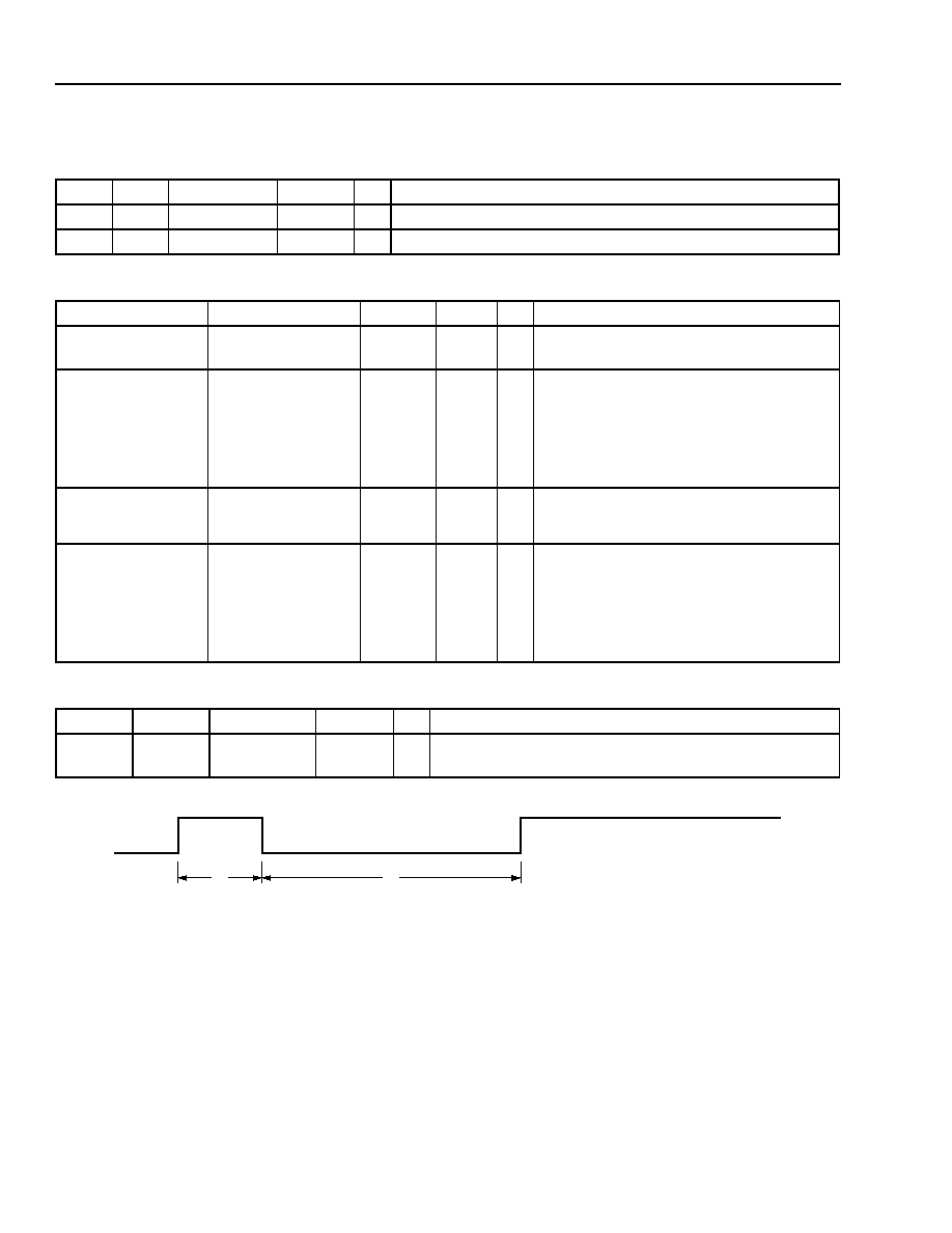
MARS2G5 P-Pro (TDAT162G52) SONET/SDH
Data Sheet
155/622/2488 Mbits/s Data Interface
August 18, 2004
122
Agere Systems Inc.
Pin Descriptions
(continued)
Table 14. PLL Test Outputs
Table 15. Pin Descriptions--No-Connect Pins
Table 16. Leakage Test Pin
2668(F)
Note: A = 4 TXCLKP/TXCLKN clock cycles, B = 100 ms, and C = PLL in normal-locking mode.
Figure 9. PLL Outputs Lock-In Process
600
792
Symbol
Type
I/O
Name/Description
C5
F31
PLLREF
--
O
Test output for PLL (normally no connect).
D5
F32
PLLFB
--
O
Test output for PLL (normally no connect).
600
792
Symbol
Type
I/O
Name/Description
B5, D6, D15,
E6, F5, G4
C21, E30, E31, F30,
J35, K37
NC
--
--
No Connection. Has internal 100 k
pull-
up resistor. Do not connect to these pins.
B26, B27, B28, B29,
B31, B24, B25, B22,
A22, A25, C22, C24,
C25, C26, C27, C28,
C29, C30, C31, D21,
D23, D25, D29, D30,
E23, E29, E32, E33
A8, A10, B7, B8,
B10, B11, B13, B15,
C7, C9, C11, C12,
C13, C15, D8, D9,
D11, D13, D15, E8,
E9, E11, E14, E15,
F9, F14, H6, J6
NC
--
--
No Connection. Do not connect to these
pins.
A24, A26, B30, D24,
D26, D28, D31, E24,
E27, E28, E30, E34
A13, B9, B12, C8,
D7, E10, E12, E13
F8, F10, F13, H5
NC
--
--
No Connection. Do not connect to these
pins.
A19, A21, B17, B18,
B19, B20, B21, B23,
C17, C18, C19, C20,
C21, C23, D17, D18,
D19, D20, D22, E17,
E18, E19, E21, E22,
E26
A14, A17, A18, B14,
B16, B17, B18, B19,
C14, C16, C17, C18,
C19, D12, D14, D16,
D17, D18, D19, E16,
E17, E18, E19, F17,
F18
NC
--
--
No Connection. Do not connect to these
pins.
600
792
Symbol
Type
I/O
Name/Description
E2
H36
IDDQMODE
--
I
Leakage Test Pin. This must be connected to digital
ground via a 1 k
resistor.
A
B
C

Data Sheet
MARS2G5 P-Pro (TDAT162G52) SONET/SDH
August 18, 2004
155/622/2488 Mbits/s Data Interface
123
Agere Systems Inc.
Microprocessor (MPU) Interface
Device Address Space Assignments
This device is equipped with a generic 16-bit microprocessor interface that allows operation with most commer-
cially available microprocessors. A 16-bit address space allows the selection of the registers in each block of the
chip, shown in the following table. The addresses are 16-bit word addresses, not byte addresses. When writing
reserved bits, a value of 0 should be used, unless otherwise specified.
Note: Specified device reset default values are valid only when line interface RXCLK[A--D][P/N] and TXCLK[P/N]
clocks; UTOPIA interface TXCLK[A--D] and RXCLK[A--D] clocks are present, the microprocessor clock
(MPU_MPCLK) does not need to be present.
Reset Default Value of Registers/Bits
The reset default value is defined as:
1.
The value after RSTN (pin C7, Table 10) is pulled high.
2.
OC-48 optics transponder is attached to the device line interface with valid STS-48 data being transferred.
3.
Valid TXCLKP/N clock.
4.
All UTOPIA clocks supplied.
A reset default value of X represents an undefined value of either a 0 or 1. Generally, status register contents after
a reset are dependent on architecture and system design; therefore, may vary from one design to the next.
Table 17. Device Address Space Assignment
Base Address and Page
Block
Block Name
0x0000 (page 164)
Microprocessor Interface.
MPU
0x0800 (page 208)
Transport Overhead Processor.
TOHP
0x1000 (page 258)
Pointer Processor.
PP
0x2000
Reserved.
--
0x3000
Reserved.
--
0x4000 (page 357)
Path Terminator.
PT
0x5000 (page 518)
DS3/E3 Mapper.
DS3
0x5800 (page 613)
Receive Sequencer.
RXS
0x6000 (page 677)
Data Engine.
DE
0x7000 (page 748)
UTOPIA Interface.
UT
0x7400
Reserved.
--
0x8000 (page 415)
Receive Terminator.
RXT
0x8968--0xFFFF
Reserved.
--
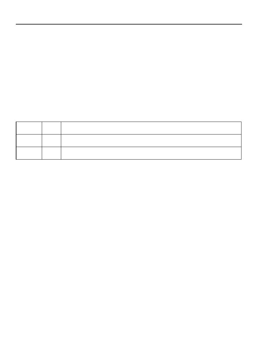
MARS2G5 P-Pro (TDAT162G52) SONET/SDH
Data Sheet
155/622/2488 Mbits/s Data Interface
August 18, 2004
124
Agere Systems Inc.
Microprocessor (MPU) Interface
(continued)
Microprocessor Interface Modes
Input MPU_MPMODE (pin D8) is used to configure the microprocessor interface into one of two possible modes
(synchronous or asynchronous). In synchronous mode, the microprocessor interface can operate at speeds from
1 MHz up to 66 MHz. In asynchronous mode, the internal 78 MHz system clock is used to operate this interface.
This interface is functionally identical to the interface in the MARS2G5 P-ProLT (TDAT042G5) device with one
enhancement made to the synchronous interface mode. In order to enhance reliability, the internal 78 MHz system
clock is used to transfer data between the internal device blocks and the MPU interface. The data transferred is
then resynchronized to the external MPU clock at the microprocessor interface. The net effect will be a slight
uncertainty in the length of an access cycle. Thus, the location of the MPU_DTN (pin E8) signal may not be deter-
ministic. A compatibility mode with MARS2G5 P-ProLT has been preserved, which utilizes the MPU_MPCLK (pin
C8) for internal data transfer, but this mode is not recommended.
The host interface is designed to connect directly to a commonly used asynchronous or synchronous host buses.
The interface to this block includes a separate clock, MPU_MPCLK, which is used in the synchronous interface
mode. The interface is only a slave on the host bus. There is no posting of writes in the host interface all registers
are directly accessible. Following are the timing diagrams for reads and writes in both synchronous and asynchro-
nous modes.
Table 18. MPU Modes
MPU_
MPMODE
Mode
Microprocessor Interface Signals
0
Async
MPU_CSN, MPU_INTN, MPU_DATA[15:0], MPU_ADDR[15:0], MPU_ADSN, MPU_RWN,
MPU_DSN, MPU_DTN
1
Sync
MPU_MPCLK, MPU_CSN, MPU_INTN, MPU_DATA[15:0], MPU_ADDR[15:0],
MPU_ADSN, MPU_RWN, MPU_DSN, MPU_DTN
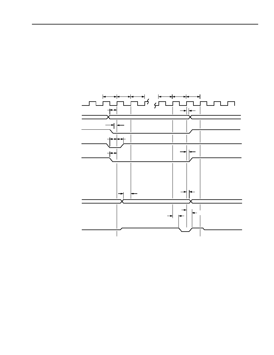
Data Sheet
MARS2G5 P-Pro (TDAT162G52) SONET/SDH
August 18, 2004
155/622/2488 Mbits/s Data Interface
125
Agere Systems Inc.
Microprocessor (MPU) Interface
(continued)
Microprocessor Interface Timing
Synchronous Mode
The synchronous microprocessor interface mode is selected when MPU_MPMODE (pin D8) = 1. Interface timing
for the synchronous mode write cycle is given in Figure 10 and in Table 19 (pages 125--126), and for the read
cycle in Figure 11 and in Table 20 (pages 127--128).
5-8718(F)r.5
Figure 10. Microprocessor Interface Synchronous Write Cycle (MPU_MPMODE (Pin D8) = 1)
MPU_MPCLK
MPU_ADDR[15:0]
MPU_CSN
MPU_ADSN
MPU_RWN
MPU_DATA[15:0]
MPU_DTN
(66 MHz MAX)
(INPUT)
t4
t1
t6
t2
t2
t1
t3
t5
t1
t2
T0
T1
T2
Tn ≠ 2 Tn ≠ 1
Tn
t7
HIGH
IMPEDANCE

MARS2G5 P-Pro (TDAT162G52) SONET/SDH
Data Sheet
155/622/2488 Mbits/s Data Interface
August 18, 2004
126
Agere Systems Inc.
Microprocessor (MPU) Interface
(continued)
Microprocessor Interface Timing
(continued)
Table 19. Microprocessor Interface Synchronous Write Cycle Specifications
(See Figure 10 on page 125 for the timing diagram.)
Symbol
Parameter
Setup
(ns)
(Min)
Hold
(ns)
(Min)
Delay
(ns)
(Max)
t1
MPU_ADDR, MPU_RWN, MPU_DATA (write) Valid to MPU_MPCLK
3
--
--
t2
MPU_MPCLK to ADDR, MPU_RWN, MPU_DATA (write) Invalid
--
5
--
t3
MPU_CSN Valid to MPU_MPCLK
3.5
--
--
t4
MPU_ADSN Valid to MPU_MPCLK
5.5
--
--
t5
MPU_MPCLK to MPU_ADSN Invalid
--
5
--
t6
MPU_MPCLK to MPU_DTN Valid
--
--
8
t7
MPU_MPCLK to MPU_DTN Invalid
--
1
--
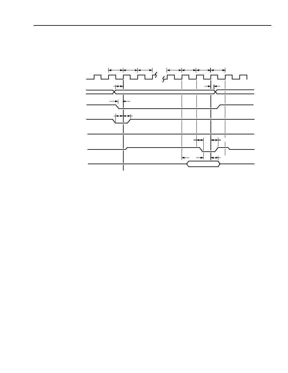
Data Sheet
MARS2G5 P-Pro (TDAT162G52) SONET/SDH
August 18, 2004
155/622/2488 Mbits/s Data Interface
127
Agere Systems Inc.
Microprocessor (MPU) Interface
(continued)
Microprocessor Interface Timing
(continued)
5-8719(F)r.4
Figure 11. Microprocessor Interface Synchronous Read Cycle (MPU_MPMODE (Pin D8) = 1)
MPU_MPCLK
MPU_ADDR[15:0]
MPU_CSN
MPU_ADSN
MPU_RWN
MPU_DTN
MPU_DATA[15:0]
(OUTPUT)
(66 MHz MAX)
t15
t16
t13
t9
t11
t12
t10
t8
T0
T1
T2
Tn ≠ 3
Tn ≠ 2
Tn ≠ 1
Tn
t14
HIGH
IMPEDANCE

MARS2G5 P-Pro (TDAT162G52) SONET/SDH
Data Sheet
155/622/2488 Mbits/s Data Interface
August 18, 2004
128
Agere Systems Inc.
Microprocessor (MPU) Interface
(continued)
Microprocessor Interface Timing
(continued)
Table 20. Microprocessor Interface Synchronous Read Cycle Specifications
(See Figure 11 on page 127 for the timing diagram.)
Symbol
Parameter
Setup
(ns)
(Min)
Hold
(ns)
(Min)
Delay
(ns)
(Max)
t8
MPU_ADDR Valid to MPU_MPCLK
3
--
--
t9
MPU_MPCLK to MPU_ADDR Invalid
--
5
--
t10
MPU_CSN Valid to MPU_MPCLK
3.5
--
--
t11
MPU_ADSN Valid to MPU_MPCLK
5.5
--
--
t12
MPU_MPCLK to MPU_ADSN Invalid
--
5
--
t13
MPU_MPCLK to MPU_DTN Valid
--
--
8
t14
MPU_MPCLK to MPU_DTN Invalid
--
1
--
t15
MPU_MPCLK to MPU_DATA Valid
--
--
24
t16
MPU_MPCLK to MPU_DATA 3-state
--
1
--
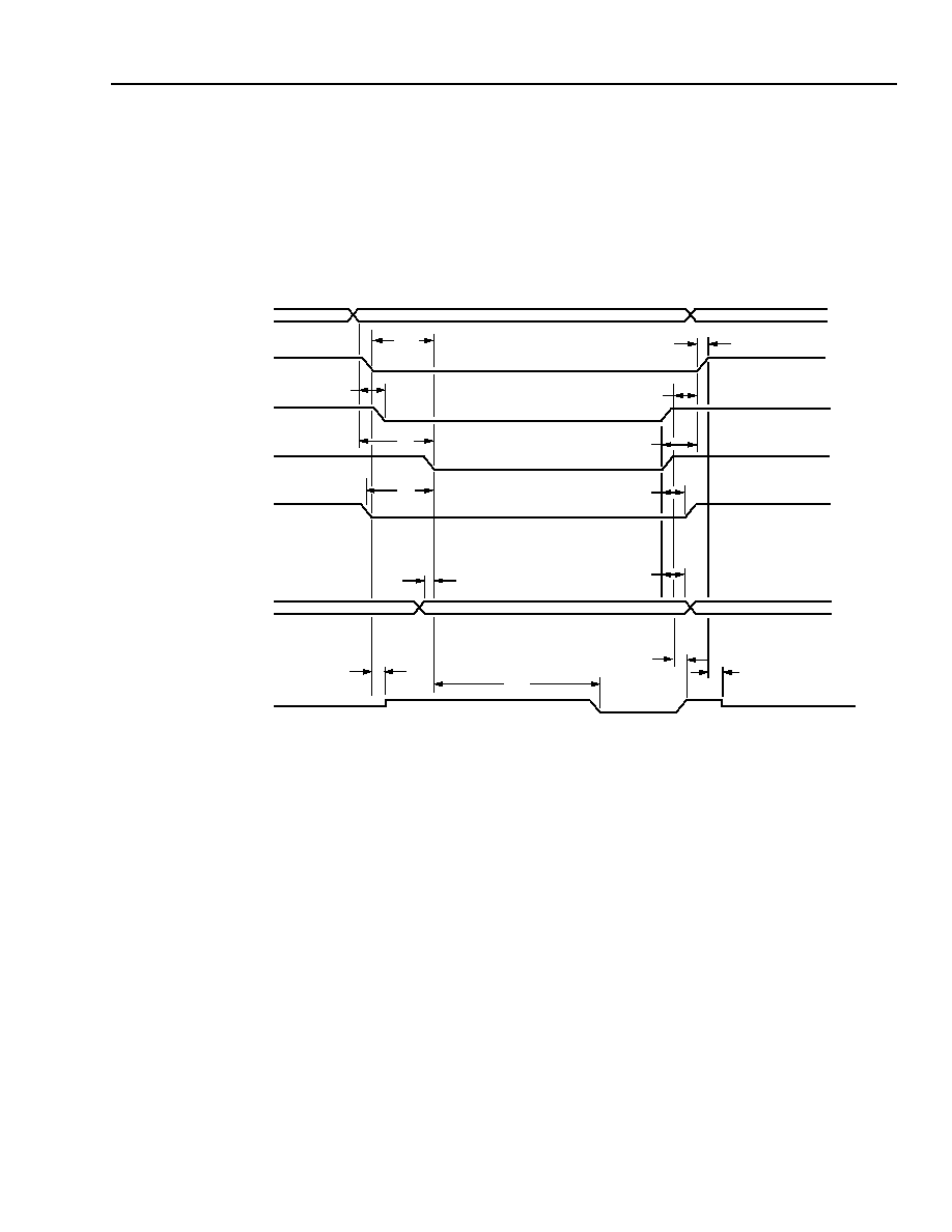
Data Sheet
MARS2G5 P-Pro (TDAT162G52) SONET/SDH
August 18, 2004
155/622/2488 Mbits/s Data Interface
129
Agere Systems Inc.
Microprocessor (MPU) Interface
(continued)
Microprocessor Interface Timing
(continued)
Asynchronous Mode
The asynchronous microprocessor interface mode is selected when MPU_MPMODE (pin D8) = 0. Interface timing
for the asynchronous mode write cycle is given in Figure 12 and in Table 21 on page 130, and for the read cycle in
Figure 13 and in Table 22 (see pages 131--132).
5-8720(F)r.1
Figure 12. Microprocessor Interface Asynchronous Write Cycle Description (MPU_MPMODE (Pin D8) = 0)
MPU_ADDR[15:0]
MPU_CSN
MPU_ADSN
MPU_DSN
MPU_RWN
MPU_DATA[15:0]
MPU_DTN
(INPUT)
t19
t21
t23
t25
t27
t28
t29
t30
t26
t24
t22
t20
t18
t17

MARS2G5 P-Pro (TDAT162G52) SONET/SDH
Data Sheet
155/622/2488 Mbits/s Data Interface
August 18, 2004
130
Agere Systems Inc.
Microprocessor (MPU) Interface
(continued)
Microprocessor Interface Timing
(continued)
Table 21. Microprocessor Interface Asynchronous Write Cycle Specifications
(See Figure 12 on page 129 for the timing diagram.)
* Use the following formula to obtain the maximum value of t28, which is dependent on the UTOPIA clock
frequency (TXCLK[D--A], RXCLK[D--A]), which can vary from dc to 104 MHz.
t28 maximum = 145 ns + 4(1/UTOPIA clock frequency).
For example, at a UTOPIA clock frequency of 52 MHz the maximum value of t28 is:
t28 (@ 52 MHz) = 145 ns + 4(1/52,000,000) = 232 ns
and t28 (@ 104 MHz) = 193 ns.
Symbol
Parameter
Min Interval
(ns)
Max Interval
(ns)
t17
MPU_CSN Fall to MPU_DSN Fall
0
--
t18
MPU_ADDR Invalid to MPU_CSN Rise
0
--
t19
MPU_ADDR Valid to MPU_ADSN Fall
0
--
t20
MPU_ADSN Rise to MPU_ADDR Invalid
5
--
t21
MPU_ADDR Valid to MPU_DSN Fall
0
--
t22
MPU_DSN Rise to MPU_ADDR Invalid
0
--
t23
MPU_RWN Fall to MPU_DSN Fall
0
--
t24
MPU_DSN Rise to MPU_RWN Rise
0
--
t25
MPU_DATA Valid to MPU_DSN Fall
0
--
t26
MPU_DSN Rise to MPU_DATA Invalid
0
--
t27
MPU_CSN Fall to MPU_DTN High
0
--
t28
MPU_DSN Fall to MPU_DTN Fall
0
--*
t29
MPU_ADSN Rise to MPU_DTN Rise
0
37.5
t30
MPU_CSN Rise to MPU_DTN 3-state
0
--

Data Sheet
MARS2G5 P-Pro (TDAT162G52) SONET/SDH
August 18, 2004
155/622/2488 Mbits/s Data Interface
131
Agere Systems Inc.
Microprocessor (MPU) Interface
(continued)
Microprocessor Interface Timing
(continued)
5-8721(F)r.1
Figure 13. Microprocessor Interface Asynchronous Read Cycle (MPMODE (Pin D8) = 0)
MPU_ADDR
MPU_CSN
MPU_ADSN
MPU_DSN
MPU_DTN
MPU_DATA
MPU_RWN
t42
t40
t39
t31
t33
t35
t32
t34
t36
t41
t38
t37

MARS2G5 P-Pro (TDAT162G52) SONET/SDH
Data Sheet
155/622/2488 Mbits/s Data Interface
August 18, 2004
132
Agere Systems Inc.
Microprocessor (MPU) Interface
(continued)
Microprocessor Interface Timing
(continued)
Table 22. Microprocessor Interface Asynchronous Read Cycle Specifications
(See Figure 13 on page 131 for the timing diagram.)
* Use the following formula to obtain the maximum value of t38, which is dependent on the UTOPIA clock
frequency (TXCLK[D--A], RXCLK[D--A]), which can vary from dc to 104 MHz.
t38 maximum = 145 ns + 4(1/UTOPIA clock frequency).
For example, at a UTOPIA clock frequency of 52 MHz the maximum value of t38 is:
t38 (@ 52 MHz) = 145 ns + 4(1/52,000,000) = 232 ns
and t38 (@ 104 MHz) = 193 ns.
Symbol
Parameter
Min Interval
(ns)
Max Interval
(ns)
t31
MPU_CSN Fall to MPU_DSN Fall
0
--
t32
MPU_ADDR Invalid to MPU_CSN Rise
0
--
t33
MPU_ADDR Valid to MPU_ADSN Fall
0
--
t34
MPU_ADSN Rise to MPU_ADDR Invalid
0
--
t35
MPU_ADDR Valid to MPU_DSN Fall
0
--
t36
MPU_DSN Rise to MPU_ADDR Invalid
0
--
t37
MPU_CSN Fall to MPU_DTN High
0
--
t38
MPU_DSN Fall to MPU_DTN Fall
0
--*
t39
MPU_ADSN Rise to MPU_DTN Rise
--
37.5
t40
MPU_CSN Rise to MPU_DTN 3-state
0
--
t41
MPU_DTN Valid to MPU_DATA Valid
--
12
t42
MPU_ADSN Rise to MPU_DATA 3-state
0
--

Data Sheet
MARS2G5 P-Pro (TDAT162G52) SONET/SDH
August 18, 2004
155/622/2488 Mbits/s Data Interface
133
Agere Systems Inc.
Microprocessor (MPU) Interface
(continued)
Necessary Register Provisioning Sequence and Clocks
When configuring the device internal clock rates, core registers must be written (programmed) prior to provisioning
any other registers because writing to certain core registers resets the remainder of the device. Specific clocks
must be present to read/write registers prior to provisioning the device.
One of the following clocks must be present prior to provisioning to enable register access:
TXCLKP (pin U4) and TXCLKN (pin U5).
MPU clock (microprocessor interface synchronous mode only).
Provisioning must be implemented in the following sequence:
Core register 0x0021 (MPU_LI_MODER (Table 41)).
Remainder of the core registers must then be provisioned (order does not matter).
It is recommended that the remainder of the device be provisioned in the following order (allowing the path termi-
nator (PT) synchronous payload envelop (SPE) FIFO to operate properly, i.e., FIFO overflow on setup is pre-
vented):
TOHP, PP, CDA maps within the DE, remainder of the DE, DS3 mapper, SPE mapper/pointer interpreter (PT),
RXS block (order does not matter).
UT block to turn on the data source to the master and slave.
If after provisioning the device as described above there is a lockup in the SPE transmit FIFO, software reset the
SPE FIFO by writing a 1 to the appropriate channel through the PT_TX_SOFTRST (Table 266) register and then
writing a 0 to release the reset.

MARS2G5 P-Pro (TDAT162G52) SONET/SDH
Data Sheet
155/622/2488 Mbits/s Data Interface
August 18, 2004
134
Agere Systems Inc.
Microprocessor (MPU) Interface
(continued)
Clocks Required for MPU Read or Write of MARS2G5 P-Pro Registers
Several registers in MARS2G5 P-Pro require that certain clocks be present in order to be read or written by the
microprocessor.
Internal clocks SYSCLK, PAY_RXCLK, PAY_SYSCLK, RX_CLK1, RX_CLK2, RX_CLK3, and RX_CLK4 are used
as domain names only. How to ensure the activation of each clock domain is described below the reference to that
domain.
All RXT registers are in the PAY_RXCLK domain.
> MPU_PAY_RXCLKPDN_SYSCLKPDN reg 0x001b bit 4 must be 0 and
> if MPU_LI_MODE reg 0x0021 bit 6 is 0 (not POF)
> or MPU_LPBKCTRL reg 0x0012 bit 13 is 1 (SONET terminal loopback)
> A clock must be present on TXCLKP and TXCLKN
> else if MPU_LI_MODE reg 0x0021 bit 4 is 1 (OC48)
> A clock is present on RXCLKP_RXDAP and RXCLKN_RXDAN
> else
> MPU_LI_MODE reg 0x0021 bit 11 is 1
> A clock is present on RXD14P_RXCLKAP and RXD14N_RXCLKAN
Other PT registers are in the PAY_SYSCLK domain.
MPU_PAY_TXCLKPDN_SYSCLKPDN reg 0x001b bit 5 must be 0.
A clock must be present on TXCLKP and TXCLKN.
Some DS3 registers are in the PAY_RXCLK domain.
PAY_RXCLK is as specified for RXT.
0x5081 and 0x5094 registers require PAY_RXCLK to complete the MPU bus cycle. Otherwise, the MPU must
drop MPU_CSN (Chip Select) before proceeding.

Data Sheet
MARS2G5 P-Pro (TDAT162G52) SONET/SDH
August 18, 2004
155/622/2488 Mbits/s Data Interface
135
Agere Systems Inc.
Microprocessor (MPU) Interface
(continued)
Clocks Required for MPU Read or Write of MARS2G5 P-Pro Registers
(continued)
The following UTOPIA registers require clocks as specified. (PAY_SYSCLK and PAY_RXCLK are as specified for
PT and RXT. TxClkA, TxClkB, TxClkC, TxClkD, RxClkA, RxClkB, RxClkC, and RxClkD are pins.)
0x7011 TxClkA
0x7015 TxClkB
0x7019 TxClkC
0x701D TxClkD
0x7030 TxClkA
0x7038 TxClkA
0x7040 TxClkA
0x7048 TxClkA
0x7050 TxClkB
0x7058 TxClkB
0x7060 TxClkB
0x7068 TxClkB
0x7070 TxClkC
0x7078 TxClkC
0x7080 TxClkC
0x7088 TxClkC
0x7090 TxClkD
0x7098 TxClkD
0x70A0 TxClkD
0x70A8 TxClkD
If these UTOPIA registers do not have the required clocks, the MPU bus cycle will not complete. In this case, the
MPU must drop MPU_CSN (chip select) before proceeding.

MARS2G5 P-Pro (TDAT162G52) SONET/SDH
Data Sheet
155/622/2488 Mbits/s Data Interface
August 18, 2004
136
Agere Systems Inc.
Microprocessor (MPU) Interface
(continued)
Clocks Required for MPU Read or Write of MARS2G5 P-Pro Registers
(continued)
PP registers fall in five domains:
1.
For PP registers in the SYSCLK domain.
MPU_SON_PP_SYSCLKPDN reg 0x001b bit 2 must be 0.
A clock must be present on TXCLKP and TXCLKN.
2.
For PP registers in RX_CLK1 domain (A).
> if MPU_LPBKCTRL reg 0x0012 bit 13 is 1 (SONET terminal loopback)
> A clock must be present on TXCLKP and TXCLKN
> else if MPU_LI_MODE reg 0x0021 bit4 is 1 (OC48)
> A clock is present on RXCLKP_RXDAP and RXCLKN_RXDAN
> else
> MPU_LI_MODE reg 0x0021 bit 11 is 1
> A clock is present on RXD14P_RXCLKAP and RXD14N_RXCLKAN
3.
For PP registers in RX_CLK2 domain (B).
> if MPU_LPBKCTRL reg 0x0012 bit 13 is 1 (SONET terminal loopback)
> A clock must be present on TXCLKP and TXCLKN
> else if MPU_LI_MODE reg 0x0021 bit 4 is 1 (OC48)
> A clock is present on RXCLKP_RXDAP and RXCLKN_RXDAN
> else
> MPU_LI_MODE reg 0x0021 bit 10 is 1
> A clock is present on RXD13P_RXCLKBP and RXD13N_RXCLKBN

Data Sheet
MARS2G5 P-Pro (TDAT162G52) SONET/SDH
August 18, 2004
155/622/2488 Mbits/s Data Interface
137
Agere Systems Inc.
Microprocessor (MPU) Interface
(continued)
Clocks Required for MPU Read or Write of MARS2G5 P-Pro Registers
(continued)
4.
For PP registers in RX_CLK3 domain (C).
> if MPU_LPBKCTRL reg 0x0012 bit 13 is 1 (SONET terminal loopback)
> A clock must be present on TXCLKP and TXCLKN
> else if MPU_LI_MODE reg 0x0021 bit 4 is 1 (OC48)
> A clock is present on RXCLKP_RXDAP and RXCLKN_RXDAN
> else
> MPU_LI_MODE reg 0x0021 bit 9 is 1
> A clock is present on RXD11P_RXCLKCP and RXD11N_RXCLKCN
5.
For PP registers in RX_CLK3 domain (D)
> if MPU_LPBKCTRL reg 0x0012 bit 13 is 1 (SONET terminal loopback)
> A clock must be present on TXCLKP and TXCLKN
> else if MPU_LI_MODE reg 0x0021 bit 4 is 1 (OC48)
> A clock is present on RXCLKP_RXDAP and RXCLKN_RXDAN
> else
> MPU_LI_MODE reg 0x0021 bit 8 is 1
> A clock is present on RXD9P_RXCLKDP and RXD9N_RXCLKDN

MARS2G5 P-Pro (TDAT162G52) SONET/SDH
Data Sheet
155/622/2488 Mbits/s Data Interface
August 18, 2004
138
Agere Systems Inc.
Microprocessor (MPU) Interface
(continued)
Clocks Required for MPU Read or Write of MARS2G5 P-Pro Registers
(continued)
If PP registers in an unclocked domain are written, they will not be written but the MPU bus cycle will complete. If
PP registers in an unclocked domain are read, garbage will be read and the MPU bus cycle will complete.
The following PP registers are in the SYSCLK domain:
0x1300: 32 // PATH_TRACE_BUF_1f
0x1301: 31 // PATH_TRACE_BUF_1e
0x1302: 30 // PATH_TRACE_BUF_1d
0x1303: 29 // PATH_TRACE_BUF_1c
0x1304: 28 // PATH_TRACE_BUF_1b
0x1305: 27 // PATH_TRACE_BUF_1a
0x1306: 26 // PATH_TRACE_BUF_19
0x1307: 25 // PATH_TRACE_BUF_18
0x1308: 24 // PATH_TRACE_BUF_17
0x1309: 23 // PATH_TRACE_BUF_16
0x130A: 22 // PATH_TRACE_BUF_15
0x130B: 21 // PATH_TRACE_BUF_14
0x130C: 20 // PATH_TRACE_BUF_13
0x130D: 19 // PATH_TRACE_BUF_12
0x130E: 18 // PATH_TRACE_BUF_11
0x130F: 17 // PATH_TRACE_BUF_10
0x1310: 16 // PATH_TRACE_BUF_f
0x1311: 15 // PATH_TRACE_BUF_e
0x1312: 14 // PATH_TRACE_BUF_d
0x1313: 13 // PATH_TRACE_BUF_c
0x1314: 12 // PATH_TRACE_BUF_b
0x1315: 11 // PATH_TRACE_BUF_a
0x1316: 10 // PATH_TRACE_BUF_9
0x1317: 9 // PATH_TRACE_BUF_8
0x1318: 8 // PATH_TRACE_BUF_7
0x1319: 7 // PATH_TRACE_BUF_6
0x131A: 6 // PATH_TRACE_BUF_5
0x131B: 5 // PATH_TRACE_BUF_4
0x131C: 4 // PATH_TRACE_BUF_3
0x131D: 3 // PATH_TRACE_BUF_2
0x131E: 2 // PATH_TRACE_BUF_1
0x131F: 1 // PATH_TRACE_BUF_0
0x1333: 0 // J1_BUFFER_ACCESS_BEGIN

Data Sheet
MARS2G5 P-Pro (TDAT162G52) SONET/SDH
August 18, 2004
155/622/2488 Mbits/s Data Interface
139
Agere Systems Inc.
Microprocessor (MPU) Interface
(continued)
Clocks Required for MPU Read or Write of MARS2G5 P-Pro Registers
(continued)
> Dpathtrace_regsel[32:0] = 33'h0;
0x1000: 102 // PP_ID
0x1001: 101 // CORW_SETTING
0x1010: 100 // GLOBAL_ALARM
0x1210: 99 // GLOBAL_ALARM_IMR
0x100F: 98 // GLOBAL_ALARM2
0x120F: 97 // GLOBAL_ALARM2_IMR
0x1021: 96 // MAIN_ELASTIC_STORE_OVERRUN
0x1211: 95 // MAIN_ELASTIC_STORE_OVERRUN_IMR
0x1031: 94 // MAIN_SF_P
0x1221: 93 // MAIN_SF_P_IMR
0x1041: 92 // MAIN_RDI_P
0x1231: 91 // MAIN_RDI_P_IMR
0x1111: 90 // MAIN_RDI_DELTA_P
0x1291: 89 // MAIN_RDI_DELTA_P_IMR
0x1051: 88 // MAIN_PLM_P
0x1241: 87 // MAIN_PLM_P_IMR
0x1121: 86 // MAIN_PLM_DELTA_P
0x12A1: 85 // MAIN_PLM_DELTA_P_IMR
0x1061: 84 // MAIN_UNEQ_P
0x1251: 83 // MAIN_UNEQ_P_IMR
0x1131: 82 // MAIN_UNEQ_DELTA_P
0x12B1: 81 // MAIN_UNEQ_DELTA_P_IMR
0x1071: 80 // MAIN_AIS_P
0x1261: 79 // MAIN_AIS_P_IMR
0x1141: 78 // MAIN_AIS_DELTA_P
0x12C1: 77 // MAIN_AIS_DELTA_P_IMR
0x1081: 76 // MAIN_LOP_P
0x1271: 75 // MAIN_LOP_P_IMR
0x1151: 74 // MAIN_LOP_DELTA_P
0x12D1: 73 // MAIN_LOP_DELTA_P_IMR
0x1181: 72 // MAIN_SS_NEW_VALIDATED
0x12F9: 71 // MAIN_SS_NEW_VALIDATED_IMR
0x1187: 70 // MAIN_SS_MISMATCH

MARS2G5 P-Pro (TDAT162G52) SONET/SDH
Data Sheet
155/622/2488 Mbits/s Data Interface
August 18, 2004
140
Agere Systems Inc.
Microprocessor (MPU) Interface
(continued)
Clocks Required for MPU Read or Write of MARS2G5 P-Pro Registers
(continued)
0x12E2: 69 // MAIN_SS_MISMATCH_IMR
0x117F: 68 // F2_NEW_VALIDATED
0x12F7: 67 // F2_NEW_VALIDATED_IMR
0x117D: 66 // H4_NEW_VALIDATED
0x12F5: 65 // H4_NEW_VALIDATED_IMR
0x117B: 64 // Z3_NEW_VALIDATED
0x12F3: 63 // Z3_NEW_VALIDATED_IMR
0x1179: 62 // Z4_NEW_VALIDATED
0x12F1: 61 // Z4_NEW_VALIDATED_IMR
0x1177: 60 // Z5_NEW_VALIDATED
0x12EF: 59 // Z5_NEW_VALIDATED_IMR
0x1101: 58 // MAIN_PDI_P
0x1281: 57 // MAIN_PDI_P_IMR
0x1171: 56 // MAIN_PDI_DELTA_P
0x12E9: 55 // MAIN_PDI_DELTA_P_IMR
0x1091: 54 // CONC_MISMATCH
0x1277: 53 // CONC_MISMATCH_MASK
0x10A1: 52 // CONC_UNSUPPORT
0x1279: 51 // CONC_UNSUPPORT_MASK
0x1400: 50 // SET_SF_WINDOW_SIZE_SEL[0:7]
0x1401: 49 // CLEAR_SF_WINDOW_SIZE_SEL[0:7]
0x1410--0x1417 // TH_DETECT_[0:7]
0x1418--0x141F // TH_CLEAR_[0:7]
0x1420: 32 // SF_WINDOW_SIZE0
0x1430: 31 // SF_WINDOW_SIZE1
0x1440: 30 // SF_WINDOW_SIZE2
0x1450: 29 // SF_WINDOW_SIZE3
0x1590: 28 // INC_DEC_SEL_1
0x1591: 27 // INC_DEC_SEL_2
0x1592: 26 // INC_DEC_SEL_3
0x1593: 25 // INC_DEC_SEL_4
0x162C: 24 // ES_INC_MIN, // ES_DEC_MAX
0x162D: 23 // ES_OVR_MIN, // ES_OVR_MAX
0x1330: 22 // J1_CHANNEL_SEL

Data Sheet
MARS2G5 P-Pro (TDAT162G52) SONET/SDH
August 18, 2004
155/622/2488 Mbits/s Data Interface
141
Agere Systems Inc.
Microprocessor (MPU) Interface
(continued)
Clocks Required for MPU Read or Write of MARS2G5 P-Pro Registers
(continued)
0x1331: 21 // J1_BUFFER_MESSAGE_TYPE
0x1332: 20 // J1_BUFFER_ACCESS_TYPE
0x1338: 19 // J1_MESSAGE_MODE_STREAM_SEL
0x1339: 18 // J1_MESSAGE_TYPE_STREAM_SEL
0x133C: 17 // J1_ACCUM_CHANNEL_SEL_1
0x133D: 16 // J1_ACCUM_CHANNEL_SEL_2
0x133E: 15 // J1_ACCUM_CHANNEL_SEL_3
0x133F: 14 // J1_ACCUM_CHANNEL_SEL_4
0x1160: 13 // J1_ACCESS_COMPLETE
0x12E0: 12 // J1_ACCESS_COMPLETE_IMR
0x1C1: 11 // J1_NEW_VALIDATED
0x127B: 10 // J1_NEW_VALIDATED_IMR
0x10D1: 9 // J1_MISMATCH
0x127D: 8 // J1_MISMATCH_IMR
0x1780: 7 // GLOBAL_PM
0x1781: 6 // ONE_BIT_RDI_P_PM_STREAM
0x1791: 5 // ERDI_PAYLOAD_P_PM_STREAM
0x17A1: 4 // ERDI_CONNECT_P_PM_STREAM
0x17B1: 3 // ERDI_SERVER_P_PM_STREAM
0x17C1: 2 // UNEQ_P_PM_STREAM
0x17D1: 1 // AIS_P_PM_STREAM
0x17E1: 0 // LOP_P_PM_STREAM
> Dsys_regsel[102:0] = 103'h0;

MARS2G5 P-Pro (TDAT162G52) SONET/SDH
Data Sheet
155/622/2488 Mbits/s Data Interface
August 18, 2004
142
Agere Systems Inc.
Microprocessor (MPU) Interface
(continued)
Clocks Required for MPU Read or Write of MARS2G5 P-Pro Registers
(continued)
The following PP registers are in RX_CLK1 domain:
0x1022: 148 // ELASTIC_STORE_OVERRUN_1
0x1212: 147 // ELASTIC_STORE_OVERRUN_MASK_1
0x1032: 146 // SF_P_1
0x1222: 145 // SF_P_MASK_1
0x1042: 144 // RDI_P_1
0x1232: 143 // RDI_P_MASK_1
0x1112: 142 // RDI_DELTA_P_1
0x1292: 141 // RDI_DELTA_P_MASK_1
0x1382: 140 // RDI_PERSIST_P_1
0x13C2: 139 // RDI_DELTA_STATE_P_1
0x1052: 138 // PLM_P_1
0x1242: 137 // PLM_P_MASK_1
0x1122: 136 // PLM_DELTA_P_1
0x12A2: 135 // PLM_DELTA_P_MASK_1
0x138A: 134 // PLM_PERSIST_P_1
0x13CA: 133 // PLM_DELTA_STATE_P_1
0x1062: 132 // UNEQ_P_1
0x1252: 131 // UNEQ_P_MASK_1
0x1132: 130 // UNEQ_DELTA_P_1
0x12B2: 129 // UNEQ_DELTA_P_MASK_1
0x1392: 128 // UNEQ_PERSIST_P_1
0x13D2: 127 // UNEQ_DELTA_STATE_P_1
0x1072: 126 // AIS_P_1
0x1262: 125 // AIS_P_MASK_1
0x1142: 124 // AIS_DELTA_P_1
0x12C2: 123 // AIS_DELTA_P_MASK_1
0x139A: 122 // AIS_PERSIST_P_1
0x13DA: 121 // AIS_DELTA_STATE_P_1 PDI_DELTA_STATE_P_1
0x1082: 120 // LOP_P_1
0x1272: 119 // LOP_P_MASK_1
0x1152: 118 // LOP_DELTA_P_1
0x12D2: 117 // LOP_DELTA_P_MASK_1
0x13A2: 116 // LOP_PERSIST_P_1

Data Sheet
MARS2G5 P-Pro (TDAT162G52) SONET/SDH
August 18, 2004
155/622/2488 Mbits/s Data Interface
143
Agere Systems Inc.
Microprocessor (MPU) Interface
(continued)
Clocks Required for MPU Read or Write of MARS2G5 P-Pro Registers
(continued)
0x13E2: 115 // LOP_DELTA_STATE_P_1
0x1102: 114 // PDI_P_1
0x1282: 113 // PDI_P_MASK_1 SS_MISMATCH_MASK_1
0x1172: 112 // PDI_DELTA_P_1
0x12EA: 111 // PDI_DELTA_P_MASK_1
0x13AA: 110 // PDI_PERSIST_P_1
0x1182: 109 // SS_NEW_VLD_1
0x12FA: 108 // SS_NEW_VLD_MASK_1
0x1188: 107 // SS_MISMATCH_1
0x1502: 106 // EXP_CONC_1
0x1507: 105 // CONC_EN_1
0x1512: 104 // REC_CONC_1
0x1542: 103 // PATH_AIS_INS_1
0x1547: 102 // UNEQ_AIS_INS_1
0x154C: 101 // PLM_AIS_INS_1
0x1551: 100 // TIM_AIS_INS_1
0x1582: 99 // SS_INSERT_CONTROL_1
0x1587: 98 // E1_F1_INSERT_CONTROL_1
0x158C: 97 // E2_INSERT_CONTROL_1
0x15A2: 96 // PDI_VALIDATE_ENABLE_1
0x1594: 95 // TIM_P_INSERT_CONTROL_1
0x1341: 94 // REC_F2_1 REC_H4_1
0x1342: 93 // REC_Z3_1 REC_Z4_1
0x1343: 92 // REC_Z5_1
0x1344: 91 // F2_VLDP_1 H4Z3Z4_VLDP_1 Z5_VLDP_1 CH_SEL_1
0x1351: 90 // REC_SS_1_TSLOT[1:6]
0x1352: 89 // REC_SS_1_TSLOT[7:12]
0x1600--0x1605 // EXP_C2_STS_[1:12]
0x1618: 82 // COUNT_BB_ERRORS_SEL_1
0x1580: 81 // SONET_SDH_RULES_1
0x1620: 80 // SS_BITS_SETTING_[1:6]
0x1621: 79 // SS_BITS_SETTING_[7:12]
0x1650--0x1655 //E1_F1_INSERT_BYTE_[1:12]
0x1668: 72 // E2_INSERT_BYTE_1

MARS2G5 P-Pro (TDAT162G52) SONET/SDH
Data Sheet
155/622/2488 Mbits/s Data Interface
August 18, 2004
144
Agere Systems Inc.
Microprocessor (MPU) Interface
(continued)
Clocks Required for MPU Read or Write of MARS2G5 P-Pro Registers
(continued)
0x1682: 71 // SD_INSERT_1
0x1690: 70 // SF_THRESH_SEL_STS_1
0x1691: 69 // SF_THRESH_SEL_STS_2
0x1692: 68 // SF_THRESH_SEL_STS_3
0x1693: 67 // SF_THRESH_SEL_STS_4
0x1694: 66 // SF_THRESH_SEL_STS_5
0x1695: 65 // SF_THRESH_SEL_STS_6
0x1696: 64 // SF_THRESH_SEL_STS_7
0x1697: 63 // SF_THRESH_SEL_STS_8
0x1698: 62 // SF_THRESH_SEL_STS_9
0x1699: 61 // SF_THRESH_SEL_STS_10
0x169A: 60 // SF_THRESH_SEL_STS_11
0x169B: 59 // SF_THRESH_SEL_STS_12
0x1702: 58 // LAST_INT_INC_1
0x1712: 57 // LAST_INT_DEC_1
0x1742: 56 // LAST_GEN_INC_1
0x1752: 55 // LAST_GEN_DEC_1
0x1782: 54 // ONE_BIT_RDI_PM_1
0x1792: 53 // ERDI_PAYLOAD_PM_1
0x17A2: 52 // ERDI_CONNECT_PM_1
0x17B2: 51 // ERDI_SERVER_PM_1
0x17C2: 50 // UNEQ_P_PM_1
0x17D2: 49 // AIS_P_PM_1
0x17E2: 48 // LOP_P_PM_1
0x1800: 47 // CV_COUNT_STS_1_PM
0x1801: 46 // CV_COUNT_STS_2_PM
0x1802: 45 // CV_COUNT_STS_3_PM
0x1803: 44 // CV_COUNT_STS_4_PM
0x1804: 43 // CV_COUNT_STS_5_PM
0x1805: 42 // CV_COUNT_STS_6_PM
0x1806: 41 // CV_COUNT_STS_7_PM
0x1807: 40 // CV_COUNT_STS_8_PM
0x1808: 39 // CV_COUNT_STS_9_PM
0x1809: 38 // CV_COUNT_STS_10_PM

Data Sheet
MARS2G5 P-Pro (TDAT162G52) SONET/SDH
August 18, 2004
155/622/2488 Mbits/s Data Interface
145
Agere Systems Inc.
Microprocessor (MPU) Interface
(continued)
Clocks Required for MPU Read or Write of MARS2G5 P-Pro Registers
(continued)
0x180A: 37 // CV_COUNT_STS_11_PM
0x180B: 36 // CV_COUNT_STS_12_PM
0x1880: 35 // REI_COUNT_STS_1_PM
0x1881: 34 // REI_COUNT_STS_2_PM
0x1882: 33 // REI_COUNT_STS_3_PM
0x1883: 32 // REI_COUNT_STS_4_PM
0x1884: 31 // REI_COUNT_STS_5_PM
0x1885: 30 // REI_COUNT_STS_6_PM
0x1886: 29 // REI_COUNT_STS_7_PM
0x1887: 28 // REI_COUNT_STS_8_PM
0x1888: 27 // REI_COUNT_STS_9_PM
0x1889: 26 // REI_COUNT_STS_10_PM
0x188A: 25 // REI_COUNT_STS_11_PM
0x188B: 24 // REI_COUNT_STS_12_PM
0x1900--0x190B // RECEIVED_RDI_STS_[1:12]
0x1930: 11 // REC_C2_STS_1, // REC_C2_STS_2
0x1931: 10 // REC_C2_STS_3, // REC_C2_STS_4
0x1932: 9 // REC_C2_STS_5, // REC_C2_STS_6
0x1933: 8 // REC_C2_STS_7, // REC_C2_STS_8
0x1934: 7 // REC_C2_STS_9, // REC_C2_STS_10
0x1935: 6 // REC_C2_STS_11, // REC_C2_STS_12
0x1960: 5 // REC_PDI_STS_1, // REC_PDI_STS_2
0x1961: 4 // REC_PDI_STS_3, // REC_PDI_STS_4
0x1962: 3 // REC_PDI_STS_5, // REC_PDI_STS_6
0x1963: 2 // REC_PDI_STS_7, // REC_PDI_STS_8
0x1964: 1 // REC_PDI_STS_9, // REC_PDI_STS_10
0x1965: 0 // REC_PDI_STS_11, // REC_PDI_STS_12

MARS2G5 P-Pro (TDAT162G52) SONET/SDH
Data Sheet
155/622/2488 Mbits/s Data Interface
August 18, 2004
146
Agere Systems Inc.
Microprocessor (MPU) Interface
(continued)
Clocks Required for MPU Read or Write of MARS2G5 P-Pro Registers
(continued)
The following PP registers are in RX_CLK2 domain:
0x1023: 149 // ELASTIC_STORE_OVERRUN_2
0x1213: 148 // ELASTIC_STORE_OVERRUN_MASK_2
0x1033: 147 // SF_P_2
0x1223: 146 // SF_P_MASK_2
0x1043: 145 // RDI_P_2
0x1233: 144 // RDI_P_MASK_2
0x1113: 143 // RDI_DELTA_P_2
0x1293: 142 // RDI_DELTA_P_MASK_2
0x1383: 141 // RDI_PERSIST_P_2
0x13C3: 140 // RDI_DELTA_STATE_P_2
0x1053: 139 // PLM_P_2
0x1243: 138 // PLM_P_MASK_2
0x1123: 137 // PLM_DELTA_P_2
0x12A3: 136 // PLM_DELTA_P_MASK_2
0x138B: 135 // PLM_PERSIST_P_2
0x13CB: 134 // PLM_DELTA_STATE_P_2
0x1063: 133 // UNEQ_P_2
0x1253: 132 // UNEQ_P_MASK_2
0x1133: 131 // UNEQ_DELTA_P_2
0x12B3: 130 // UNEQ_DELTA_P_MASK_2
0x1393: 129 // UNEQ_PERSIST_P_2
0x13D3: 128 // UNEQ_DELTA_STATE_P_2
0x1073: 127 // AIS_P_2
0x1263: 126 // AIS_P_MASK_2
0x1143: 125 // AIS_DELTA_P_2
0x12C3: 124 // AIS_DELTA_P_MASK_2
0x139B: 123 // AIS_PERSIST_P_2
0x13DB: 122 // AIS_DELTA_STATE_P_2, // PDI_DELTA_STATE_P_2
0x1083: 121 // LOP_P_2
0x1273: 120 // LOP_P_MASK_2
0x1153: 119 // LOP_DELTA_P_2
0x12D3: 118 // LOP_DELTA_P_MASK_2
0x13A3: 117 // LOP_PERSIST_P_2

Data Sheet
MARS2G5 P-Pro (TDAT162G52) SONET/SDH
August 18, 2004
155/622/2488 Mbits/s Data Interface
147
Agere Systems Inc.
Microprocessor (MPU) Interface
(continued)
Clocks Required for MPU Read or Write of MARS2G5 P-Pro Registers
(continued)
0x13E3: 116 // LOP_DELTA_STATE_P_2
0x1103: 115 // PDI_P_2
0x1283: 114 // PDI_P_MASK_2
0x1173: 113 // PDI_DELTA_P_2
0x12EB: 112 // PDI_DELTA_P_MASK_2
0x13AB: 111 // PDI_PERSIST_P_2
0x1183: 110 // SS_NEW_VLD_2
0x12FB: 109 // SS_NEW_VLD_MASK_2
0x1189: 108 // SS_MISMATCH_2
0x12E4: 107 // SS_MISMATCH_MASK_2
0x1503: 106 // EXP_CONC_2
0x1508: 105 // CONC_EN_2
0x1513: 104 // REC_CONC_2
0x1543: 103 // PATH_AIS_INS_2
0x1548: 102 // UNEQ_AIS_INS_2
0x154D: 101 // PLM_AIS_INS_2
0x1552: 100 // TIM_AIS_INS_2
0x1583: 99 // SS_INSERT_CONTROL_2
0x1588: 98 // E1_F1_INSERT_CONTROL_2
0x158D: 97 // E2_INSERT_CONTROL_2
0x15A3: 96 // PDI_VALIDATE_ENABLE_2
0x1345: 95 // REC_F2_2, // REC_H4_2
0x1346: 94 // REC_Z3_2, // REC_Z4_2
0x1347: 93 // REC_Z5_2
0x1348: 92 // F2_VLDP_2 H4Z3Z4_VLDP_2 Z5_VLDP_2 CH_SEL_2
0x1353: 91 // REC_SS_2_TSLOT[1:6]
0x1354: 90 // REC_SS_2_TSLOT[7:12]
0x1606--0x160B // EXP_C2_STS_[13:24]
0x1619: 83 // COUNT_BB_ERRORS_SEL_2
0x1580: 82 // SONET_SDH_RULES_2
0x1622: 81 //SS_BITS_SETTING_[13:18]
0x1623: 80 //SS_BITS_SETTING_[19:24]
0x1656--0x165B // E1_F1_INSERT_BYTE_[13:24]
0x1669: 73 // E2_INSERT_BYTE_2

MARS2G5 P-Pro (TDAT162G52) SONET/SDH
Data Sheet
155/622/2488 Mbits/s Data Interface
August 18, 2004
148
Agere Systems Inc.
Microprocessor (MPU) Interface
(continued)
Clocks Required for MPU Read or Write of MARS2G5 P-Pro Registers
(continued)
0x1595: 72 // TIM_P_INSERT_CONTROL_2
0x1683: 71 // SD_INSERT_2
0x169C: 70 // SF_THRESH_SEL_STS_13
0x169D: 69 // SF_THRESH_SEL_STS_14
0x169E: 68 // SF_THRESH_SEL_STS_15
0x169F: 67 // SF_THRESH_SEL_STS_16
0x16A0: 66 // SF_THRESH_SEL_STS_17
0x16A1: 65 // SF_THRESH_SEL_STS_18
0x16A2: 64 // SF_THRESH_SEL_STS_19
0x16A3: 63 // SF_THRESH_SEL_STS_20
0x16A4: 62 // SF_THRESH_SEL_STS_21
0x16A5: 61 // SF_THRESH_SEL_STS_22
0x16A6: 60 // SF_THRESH_SEL_STS_23
0x16A7: 59 // SF_THRESH_SEL_STS_24
0x1703: 58 // LAST_INT_INC_2
0x1713: 57 // LAST_INT_DEC_2
0x1743: 56 // LAST_GEN_INC_2
0x1753: 55 // LAST_GEN_DEC_2
0x1783: 54 // ONE_BIT_RDI_PM_2
0x1793: 53 // ERDI_PAYLOAD_PM_2
0x17A3: 52 // ERDI_CONNECT_PM_2
0x17B3: 51 // ERDI_SERVER_PM_2
0x17C3: 50 // UNEQ_P_PM_2
0x17D3: 49 // AIS_P_PM_2
0x17E3: 48 // LOP_P_PM_2
0x180C: 47 // CV_COUNT_STS_13_PM
0x180D: 46 // CV_COUNT_STS_14_PM
0x180E: 45 // CV_COUNT_STS_15_PM
0x180F: 44 // CV_COUNT_STS_16_PM
0x1810: 43 // CV_COUNT_STS_17_PM
0x1811: 42 // CV_COUNT_STS_18_PM
0x1812: 41 // CV_COUNT_STS_19_PM
0x1813: 40 // CV_COUNT_STS_20_PM
0x1814: 39 // CV_COUNT_STS_21_PM

Data Sheet
MARS2G5 P-Pro (TDAT162G52) SONET/SDH
August 18, 2004
155/622/2488 Mbits/s Data Interface
149
Agere Systems Inc.
Microprocessor (MPU) Interface
(continued)
Clocks Required for MPU Read or Write of MARS2G5 P-Pro Registers
(continued)
0x1815: 38 // CV_COUNT_STS_22_PM
0x1816: 37 // CV_COUNT_STS_23_PM
0x1817: 36 // CV_COUNT_STS_24_PM
0x188C: 35 // REI_COUNT_STS_13_PM
0x188D: 34 // REI_COUNT_STS_14_PM
0x188E: 33 // REI_COUNT_STS_15_PM
0x188F: 32 // REI_COUNT_STS_16_PM
0x1890: 31 // REI_COUNT_STS_17_PM
0x1891: 30 // REI_COUNT_STS_18_PM
0x1892: 29 // REI_COUNT_STS_19_PM
0x1893: 28 // REI_COUNT_STS_20_PM
0x1894: 27 // REI_COUNT_STS_21_PM
0x1895: 26 // REI_COUNT_STS_22_PM
0x1896: 25 // REI_COUNT_STS_23_PM
0x1897: 24 // REI_COUNT_STS_24_PM
0x190C--0x1917 // RECEIVED_RDI_STS_[13:24]
0x1936: 11 // REC_C2_STS_13, // REC_C2_STS_14
0x1937: 10 // REC_C2_STS_15, // REC_C2_STS_16
0x1938: 9 // REC_C2_STS_17, // REC_C2_STS_18
0x1939: 8 // REC_C2_STS_19, // REC_C2_STS_20
0x193A: 7 // REC_C2_STS_21, // REC_C2_STS_22
0x193B: 6 // REC_C2_STS_23, // REC_C2_STS_24
0x1966: 5 // REC_PDI_STS_13, // REC_PDI_STS_14
0x1967: 4 // REC_PDI_STS_15, // REC_PDI_STS_16
0x1968: 3 // REC_PDI_STS_17, // REC_PDI_STS_18
0x1969: 2 // REC_PDI_STS_19, // REC_PDI_STS_20
0x196A: 1 // REC_PDI_STS_21, // REC_PDI_STS_22
0x196B: 0 // REC_PDI_STS_23, // REC_PDI_STS_24

MARS2G5 P-Pro (TDAT162G52) SONET/SDH
Data Sheet
155/622/2488 Mbits/s Data Interface
August 18, 2004
150
Agere Systems Inc.
Microprocessor (MPU) Interface
(continued)
Clocks Required for MPU Read or Write of MARS2G5 P-Pro Registers
(continued)
The following PP registers are in RX_CLK3 domain:
0x1024: 151 // ELASTIC_STORE_OVERRUN_3
0x1214: 150 // ELASTIC_STORE_OVERRUN_MASK_3
0x1034: 149 // SF_P_3
0x1224: 148 // SF_P_MASK_3
0x1044: 147 // RDI_P_3
0x1234: 146 // RDI_P_MASK_3
0x1114: 145 // RDI_DELTA_P_3
0x1294: 144 // RDI_DELTA_P_MASK_3
0x1384: 143 // RDI_PERSIST_P_3
0x13C4: 142 // RDI_DELTA_STATE_P_3
0x1054: 141 // PLM_P_3
0x1244: 140 // PLM_P_MASK_3
0x1124: 139 // PLM_DELTA_P_3
0x12A4: 138 // PLM_DELTA_P_MASK_3
0x138C: 137 // PLM_PERSIST_P_3
0x13CC: 136 // PLM_DELTA_STATE_P_3
0x1064: 135 // UNEQ_P_3
0x1254: 134 // UNEQ_P_MASK_3
0x1134: 133 // UNEQ_DELTA_P_3
0x12b4: 132 // UNEQ_DELTA_P_MASK_3
0x1394: 131 // UNEQ_PERSIST_P_3
0x13D4: 130 // UNEQ_DELTA_STATE_P_3
0x1074: 129 // AIS_P_3
0x1264: 128 // AIS_P_MASK_3
0x1144: 127 // AIS_DELTA_P_3
0x12C4: 126 // AIS_DELTA_P_MASK_3
0x139C: 125 // AIS_PERSIST_P_3
0x13DC: 124 // AIS_DELTA_STATE_P_3, // PDI_DELTA_STATE_P_3
0x1084: 123 // LOP_P_3
0x1274: 122 // LOP_P_MASK_3
0x1154: 121 // LOP_DELTA_P_3
0x12D4: 120 // LOP_DELTA_P_MASK_3
0x13A4: 119 // LOP_PERSIST_P_3

Data Sheet
MARS2G5 P-Pro (TDAT162G52) SONET/SDH
August 18, 2004
155/622/2488 Mbits/s Data Interface
151
Agere Systems Inc.
Microprocessor (MPU) Interface
(continued)
Clocks Required for MPU Read or Write of MARS2G5 P-Pro Registers
(continued)
0x13E4: 118 // LOP_DELTA_STATE_P_3
0x1104: 117 // PDI_P_3
0x1284: 116 // PDI_P_MASK_3
0x1174: 115 // PDI_DELTA_P_3
0x12EC: 114 // PDI_DELTA_P_MASK_3
0x13AC: 113 // PDI_PERSIST_P_3
0x1184: 112 // SS_NEW_VLD_3
0x12FC: 111 // SS_NEW_VLD_MASK_3
0x118A: 110 // SS_MISMATCH_3
0x12E5: 109 // SS_MISMATCH_MASK_3
0x1504: 108 // EXP_CONC_3
0x1509: 107 // CONC_EN_3
0x1514: 106 // REC_CONC_3
0x1544: 105 // PATH_AIS_INS_3
0x1549: 104 // UNEQ_AIS_INS_3
0x154E: 103 // PLM_AIS_INS_3
0x1553: 102 // TIM_AIS_INS_3
0x1584: 101 // SS_INSERT_CONTROL_3
0x1589: 100 // E1_F1_INSERT_CONTROL_3
0x158E: 99 // E2_INSERT_CONTROL_3
0x15A4: 98 // PDI_VALIDATE_ENABLE_3
0x1349: 97 // REC_F2_3, // REC_H4_3
0x134A: 96 // REC_Z3_3, // REC_Z4_3
0x134B: 95 // REC_Z5_3
0x134C: 94 // F2_VLDP_3 H4Z3Z4_VLDP_3 Z5_VLDP_3 CH_SEL_3
0x1355: 93 // REC_SS_3_TSLOT[1:6]
0x1356: 92 // REC_SS_3_TSLOT[7:12]
0x160C--0x1611 // EXP_C2_STS_[25:36]
0x161A: 85 // COUNT_BB_ERRORS_SEL_3
0x1580: 84 // SONET_SDH_RULES_3
0x1624: 83 // SS_BITS_SETTING_[25:30]
0x1625: 82 // SS_BITS_SETTING_[31:36]
0x1629: 81 // SS_BITS_MONITOR_MODE
0x162A: 80 // SS_BITS_VALIDATE_PERIOD

MARS2G5 P-Pro (TDAT162G52) SONET/SDH
Data Sheet
155/622/2488 Mbits/s Data Interface
August 18, 2004
152
Agere Systems Inc.
Microprocessor (MPU) Interface
(continued)
Clocks Required for MPU Read or Write of MARS2G5 P-Pro Registers
(continued)
0x165C--0x1661 // E1_F1_INSERT_BYTE_[25:36]
0x166A: 73 // E2_INSERT_BYTE_3
0x1596: 72 // TIM_P_INSERT_CONTROL_3
0x1684: 71 // SD_INSERT_3
0x16A8: 70 // SF_THRESH_SEL_STS_25
0x16A9: 69 // SF_THRESH_SEL_STS_26
0x16AA: 68 // SF_THRESH_SEL_STS_27
0x16AB: 67 // SF_THRESH_SEL_STS_28
0x16AC: 66 // SF_THRESH_SEL_STS_29
0x16AD: 65 // SF_THRESH_SEL_STS_30
0x16AE: 64 // SF_THRESH_SEL_STS_31
0x16AF: 63 // SF_THRESH_SEL_STS_32
0x16B0: 62 // SF_THRESH_SEL_STS_33
0x16B1: 61 // SF_THRESH_SEL_STS_34
0x16B2: 60 // SF_THRESH_SEL_STS_35
0x16B3: 59 // SF_THRESH_SEL_STS_36
0x1704: 58 // LAST_INT_INC_3
0x1714: 57 // LAST_INT_DEC_3
0x1744: 56 // LAST_GEN_INC_3
0x1754: 55 // LAST_GEN_DEC_3
0x1784: 54 // ONE_BIT_RDI_PM_3
0x1794: 53 // ERDI_PAYLOAD_PM_3
0x17A4: 52 // ERDI_CONNECT_PM_3
0x17B4: 51 // ERDI_SERVER_PM_3
0x17C4: 50 // UNEQ_P_PM_3
0x17D4: 49 // AIS_P_PM_3
0x17E4: 48 // LOP_P_PM_3
0x1818: 47 // CV_COUNT_STS_25_PM
0x1819: 46 // CV_COUNT_STS_26_PM
0x181A: 45 // CV_COUNT_STS_27_PM
0x181B: 44 // CV_COUNT_STS_28_PM
0x181C: 43 // CV_COUNT_STS_29_PM
0x181D: 42 // CV_COUNT_STS_30_PM
0x181E: 41 // CV_COUNT_STS_31_PM

Data Sheet
MARS2G5 P-Pro (TDAT162G52) SONET/SDH
August 18, 2004
155/622/2488 Mbits/s Data Interface
153
Agere Systems Inc.
Microprocessor (MPU) Interface
(continued)
Clocks Required for MPU Read or Write of MARS2G5 P-Pro Registers
(continued)
0x181F: 40 // CV_COUNT_STS_32_PM
0x1820: 39 // CV_COUNT_STS_33_PM
0x1821: 38 // CV_COUNT_STS_34_PM
0x1822: 37 // CV_COUNT_STS_35_PM
0x1823: 36 // CV_COUNT_STS_36_PM
0x1898: 35 // REI_COUNT_STS_25_PM
0x1899: 34 // REI_COUNT_STS_26_PM
0x189A: 33 // REI_COUNT_STS_27_PM
0x189B: 32 // REI_COUNT_STS_28_PM
0x189C: 31 // REI_COUNT_STS_29_PM
0x189D: 30 // REI_COUNT_STS_30_PM
0x189E: 29 // REI_COUNT_STS_31_PM
0x189F: 28 // REI_COUNT_STS_32_PM
0x18A0: 27 // REI_COUNT_STS_33_PM
0x18A1: 26 // REI_COUNT_STS_34_PM
0x18A2: 25 // REI_COUNT_STS_35_PM
0x18A3: 24 // REI_COUNT_STS_36_PM
0x1918--0x1923 // RECEIVED_RDI_STS_[25:36]
0x193C: 11 // REC_C2_STS_25, // REC_C2_STS_26
0x193D: 10 // REC_C2_STS_27, // REC_C2_STS_28
0x193E: 9 // REC_C2_STS_29, // REC_C2_STS_30
0x193F: 8 // REC_C2_STS_31, // REC_C2_STS_32
0x1940: 7 // REC_C2_STS_33, // REC_C2_STS_34
0x1941: 6 // REC_C2_STS_35, // REC_C2_STS_36
0x196C: 5 // REC_PDI_STS_25, // REC_PDI_STS_26
0x196D: 4 // REC_PDI_STS_27, // REC_PDI_STS_28
0x196E: 3 // REC_PDI_STS_29, // REC_PDI_STS_30
0x196F: 2 // REC_PDI_STS_31, // REC_PDI_STS_32
0x1970: 1 // REC_PDI_STS_33, // REC_PDI_STS_34
0x1971: 0 // REC_PDI_STS_35, // REC_PDI_STS_36

MARS2G5 P-Pro (TDAT162G52) SONET/SDH
Data Sheet
155/622/2488 Mbits/s Data Interface
August 18, 2004
154
Agere Systems Inc.
Microprocessor (MPU) Interface
(continued)
Clocks Required for MPU Read or Write of MARS2G5 P-Pro Registers
(continued)
The following PP registers are in RX_CLK4 domain:
0x1025: 149 // ELASTIC_STORE_OVERRUN_4
0x1215: 148 // ELASTIC_STORE_OVERRUN_MASK_4
0x1035: 147 // SF_P_4
0x1225: 146 // SF_P_MASK_4
0x1045: 145 // RDI_P_4
0x1235: 144 // RDI_P_MASK_4
0x1115: 143 // RDI_DELTA_P_4
0x1295: 142 // RDI_DELTA_P_MASK_4
0x1385: 141 // RDI_PERSIST_P_4
0x13C5: 140 // RDI_DELTA_STATE_P_4
0x1055: 139 // PLM_P_4
0x1245: 138 // PLM_P_MASK_4
0x1125: 137 // PLM_DELTA_P_4
0x12A5: 136 // PLM_DELTA_P_MASK_4
0x138D: 135 // PLM_PERSIST_P_4
0x13CD: 134 // PLM_DELTA_STATE_P_4
0x1065: 133 // UNEQ_P_4
0x1255: 132 // UNEQ_P_MASK_4
0x1135: 131 // UNEQ_DELTA_P_4
0x12B5: 130 // UNEQ_DELTA_P_MASK_4
0x1395: 129 // UNEQ_PERSIST_P_4
0x13D5: 128 // UNEQ_DELTA_STATE_P_4
0x1075: 127 // AIS_P_4
0x1265: 126 // AIS_P_MASK_4
0x1145: 125 // AIS_DELTA_P_4
0x12C5: 124 // AIS_DELTA_P_MASK_4
0x139D: 123 // AIS_PERSIST_P_4
0x13DD: 122 // AIS_DELTA_STATE_P_4, PDI_DELTA_STATE_P_4
0x1085: 121 // LOP_P_4
0x1275: 120 // LOP_P_MASK_4
0x1155: 119 // LOP_DELTA_P_4
0x12D5: 118 // LOP_DELTA_P_MASK_4
0x13A5: 117 // LOP_PERSIST_P_4

Data Sheet
MARS2G5 P-Pro (TDAT162G52) SONET/SDH
August 18, 2004
155/622/2488 Mbits/s Data Interface
155
Agere Systems Inc.
Microprocessor (MPU) Interface
(continued)
Clocks Required for MPU Read or Write of MARS2G5 P-Pro Registers
(continued)
0x13E5: 116 // LOP_DELTA_STATE_P_4
0x1105: 115 // PDI_P_4
0x1285: 114 // PDI_P_MASK_4
0x1175: 113 // PDI_DELTA_P_4
0x12ED: 112 // PDI_DELTA_P_MASK_4
0x13AD: 111 // PDI_PERSIST_P_4
0x1185: 110 // SS_NEW_VLD_4
0x12FD: 109 // SS_NEW_VLD_MASK_4
0x118B: 108 // SS_MISMATCH_4
0x12E6: 107 // SS_MISMATCH_MASK_4
0x1505: 106 // EXP_CONC_4
0x150A: 105 // CONC_EN_4
0x1515: 104 // REC_CONC_4
0x1545: 103 // PATH_AIS_INS_4
0x154A: 102 // UNEQ_AIS_INS_4
0x154F: 101 // PLM_AIS_INS_4
0x1554: 100 // TIM_AIS_INS_4
0x1585: 99 // SS_INSERT_CONTROL_4
0x158A: 98 // E1_F1_INSERT_CONTROL_4
0x158F: 97 // E2_INSERT_CONTROL_4
0x134D: 96 // REC_F2_4, // REC_H4_4
0x134E: 95 // REC_Z3_4, // REC_Z4_4
0x134F: 94 // REC_Z5_4
0x1350: 93 // F2_VLDP_4 H4Z3Z4_VLDP_4 Z5_VLDP_4 CH_SEL_4
0x1357: 92 // REC_SS_4_TSLOT[1:6]
0x1358: 91 // REC_SS_4_TSLOT[7:12]
0x1612--0x1617 // EXP_C2_STS_[37:48]
0x15A5: 84 // PDI_VALIDATE_ENABLE_4
0x161B: 83 // COUNT_BB_ERRORS_SEL_4
0x1580: 82 // SONET_SDH_RULES_4
0x1626: 81 // SS_BITS_SETTING_[37:42]
0x1627: 80 // SS_BITS_SETTING_[43:48]
0x1662--0x1667 // E1_F1_INSERT_BYTE_[37:48]
0x166B: 73 // E2_INSERT_BYTE_4

MARS2G5 P-Pro (TDAT162G52) SONET/SDH
Data Sheet
155/622/2488 Mbits/s Data Interface
August 18, 2004
156
Agere Systems Inc.
Microprocessor (MPU) Interface
(continued)
Clocks Required for MPU Read or Write of MARS2G5 P-Pro Registers
(continued)
0x1597: 72 // TIM_P_INSERT_CONTROL_4
0x1685: 71 // SD_INSERT_4
0x16B4: 70 // SF_THRESH_SEL_STS_37
0x16B5: 69 // SF_THRESH_SEL_STS_38
0x16B6: 68 // SF_THRESH_SEL_STS_39
0x16B7: 67 // SF_THRESH_SEL_STS_40
0x16B8: 66 // SF_THRESH_SEL_STS_41
0x16B9: 65 // SF_THRESH_SEL_STS_42
0x16BA: 64 // SF_THRESH_SEL_STS_43
0x16BB: 63 // SF_THRESH_SEL_STS_44
0x16BC: 62 // SF_THRESH_SEL_STS_45
0x16BD: 61 // SF_THRESH_SEL_STS_46
0x16BE: 60 // SF_THRESH_SEL_STS_47
0x16BF: 59 // SF_THRESH_SEL_STS_48
0x1705: 58 // LAST_INT_INC_4
0x1715: 57 // LAST_INT_DEC_4
0x1745: 56 // LAST_GEN_INC_4
0x1755: 55 // LAST_GEN_DEC_4
0x1785: 54 // ONE_BIT_RDI_PM_4
0x1795: 53 // ERDI_PAYLOAD_PM_4
0x17A5: 52 // ERDI_CONNECT_PM_4
0x17B5: 51 // ERDI_SERVER_PM_4
0x17C5: 50 // UNEQ_P_PM_4
0x17D5: 49 // AIS_P_PM_4
0x17E5: 48 // LOP_P_PM_4
0x1824: 47 // CV_COUNT_STS_37_PM
0x1825: 46 // CV_COUNT_STS_38_PM
0x1826: 45 // CV_COUNT_STS_39_PM
0x1827: 44 // CV_COUNT_STS_40_PM
0x1828: 43 // CV_COUNT_STS_41_PM
0x1829: 42 // CV_COUNT_STS_42_PM
0x182A: 41 // CV_COUNT_STS_43_PM
0x182B: 40 // CV_COUNT_STS_44_PM
0x182C: 39 // CV_COUNT_STS_45_PM

Data Sheet
MARS2G5 P-Pro (TDAT162G52) SONET/SDH
August 18, 2004
155/622/2488 Mbits/s Data Interface
157
Agere Systems Inc.
Microprocessor (MPU) Interface
(continued)
Clocks Required for MPU Read or Write of MARS2G5 P-Pro Registers
(continued)
0x182D: 38 // CV_COUNT_STS_46_PM
0x182E: 37 // CV_COUNT_STS_47_PM
0x182F: 36 // CV_COUNT_STS_48_PM
0x18A4: 35 // REI_COUNT_STS_37_PM
0x18A5: 34 // REI_COUNT_STS_38_PM
0x18A6: 33 // REI_COUNT_STS_39_PM
0x18A7: 32 // REI_COUNT_STS_40_PM
0x18A8: 31 // REI_COUNT_STS_41_PM
0x18A9: 30 // REI_COUNT_STS_42_PM
0x18AA: 29 // REI_COUNT_STS_43_PM
0x18AB: 28 // REI_COUNT_STS_44_PM
0x18AC: 27 // REI_COUNT_STS_45_PM
0x18AD: 26 // REI_COUNT_STS_46_PM
0x18AE: 25 // REI_COUNT_STS_47_PM
0x18AF: 24 // REI_COUNT_STS_48_PM
0x1924--0x192F // RECEIVED_RDI_STS_[37:48]
0x1942: 11 // REC_C2_STS_37, // REC_C2_STS_38
0x1943: 10 // REC_C2_STS_39, // REC_C2_STS_40
0x1944: 9 // REC_C2_STS_41, // REC_C2_STS_42
0x1945: 8 // REC_C2_STS_43, // REC_C2_STS_44
0x1946: 7 // REC_C2_STS_45, // REC_C2_STS_46
0x1947: 6 // REC_C2_STS_47, // REC_C2_STS_48
0x1972: 5 // REC_PDI_STS_37, // REC_PDI_STS_38
0x1973: 4 // REC_PDI_STS_39, // REC_PDI_STS_40
0x1974: 3 // REC_PDI_STS_41, // REC_PDI_STS_42
0x1975: 2 // REC_PDI_STS_43, // REC_PDI_STS_44
0x1976: 1 // REC_PDI_STS_45, // REC_PDI_STS_46
0x1977: 0 // REC_PDI_STS_47, // REC_PDI_STS_48

MARS2G5 P-Pro (TDAT162G52) SONET/SDH
Data Sheet
155/622/2488 Mbits/s Data Interface
August 18, 2004
158
Agere Systems Inc.
Microprocessor (MPU) Interface
(continued)
Performance Monitor (PM) Reset
A PM reset signal is sent to all blocks for performing monitoring (collecting statistics). A PM reset signal can come
from external pins, internal 1 second timer, or be controlled by software, depending on the PM mode,
MPU_PMMODE[1:0] bits (Table 31).
Table 23. PM Reset Signal Provisioning
The external PMRST pin is a bidirectional signal controlled by the MPU_PMRST_OE bit (Table 31). This bit
defaults to 0, making the pin an input.
MPU_
PMMODE[1:0]
(Table 31)
Description
00
PM Reset Signal Comes from External Pin (1 Hz, 50% Duty Cycle Signal).
01
PM Reset Signal Comes from Internal 1 Second Counter (1 Hz, 50% Duty Cycle Signal).
Writing a logic 1 to the PM reset signal bit MPU_PM_TRIGGER_SWRS (Table 29) in this mode
will reset the counter so that a 0
1 transition occurs on the PM reset signal within 10 clock
cycles of the 77.76 MHz clock.
11
PM Reset Signal Is Software Controlled. Writing a logic 1 to the PM reset signal bit
MPU_PM_TRIGGER_SWRS will cause a 0
1 transition on the internal PM reset signal. This
pulse will be high for 100 cycles of the 77.76 MHz clock and low for 100 cycles of the 77.76 MHz
clock. Writing the PM reset signal bit to a logic 1 during this 200 clock cycle interval will have no
effect (2.57
µ
s). The PM reset signal rising edge must occur within 10 clock cycles of writing the
PM reset signal bit.
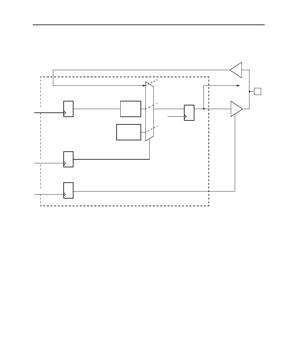
Data Sheet
MARS2G5 P-Pro (TDAT162G52) SONET/SDH
August 18, 2004
155/622/2488 Mbits/s Data Interface
159
Agere Systems Inc.
Microprocessor (MPU) Interface
(continued)
Performance Monitor (PM) Reset
(continued)
5-8157(F)r.1
Figure 14. PM Reset Signal Generation
PMRSTI
PMRSTO
CLK78M
IPMRST(TO BLOCKS)
EXTERNAL
DELAY
1/2 SECOND
MPU_PM_TRIGGER_SWRS
MPU_SWRSR REGISTER
MPU_PROVISION0 REGISTER
MPU_PMMODE[1:0]
SOFTWARE CONTROLLED
MPU_PROVISION0 REGISTER
MPU_PMRST_OE
PMRST
MPU BLOCK
MPU_PM_TRIGGER_SWRS BIT
MPU_PMMODE[1:0] BITS
MPU_PMRST_OE BIT
MPU_MPCLK
MPU_MPCLK
MPU_MPCLK
COUNTER
FREE RUNNING
(MPU_PMMODE[1:0] = 01)
(MPU_PMMODE[1:0] = 11)
(MPU_PMMODE[1:0] = 00)
PIN

MARS2G5 P-Pro (TDAT162G52) SONET/SDH
Data Sheet
155/622/2488 Mbits/s Data Interface
August 18, 2004
160
Agere Systems Inc.
Microprocessor (MPU) Interface
(continued)
General-Purpose Input/Output Interface
The programmable I/O general-purpose input/output (GPIO) consists of four device pins that can be used for inter-
nal block state observation. There functionality is controlled by MPU_GPIO_MODE[3:0] bits (Table 34).
MPU_GPIO_MODE[3:0] = 0000 normal mode
MPU_GPIO_MODE[3:0] = others undefined
Mode 0 (normal mode):
In normal mode, GPIO pins can be programmed individually to be either input or output through
MPU_GPIO_DIR_CTL[3:0] bits (Table 34). Figure 15 shows pictorially the GPIO functionality. These pins are use-
ful for board designers who need the ability to monitor or control signals on their boards. If the pin is an input, the
value on the pin can be read from MPU_GPIO_I_CND[3:0] bits (Table 26). It can also be programmed to generate
a level-sensitive interrupt or a positive-edge detect interrupt contributing to the external interrupt pin. If the pin is an
output, the value provisioned in MPU_GPIO_O_CTL[3:0] bits (Table 30) will appear on the device pin immediately.
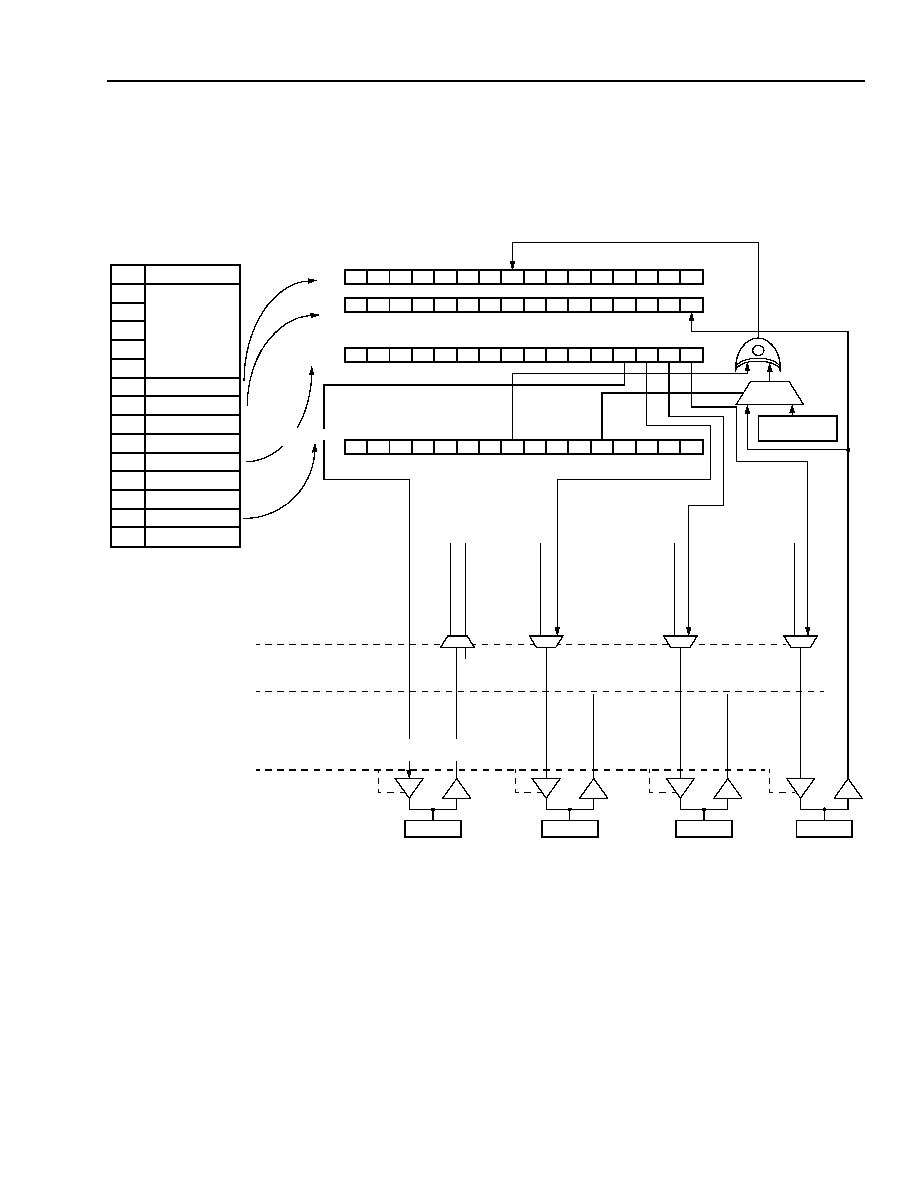
Data Sheet
MARS2G5 P-Pro (TDAT162G52) SONET/SDH
August 18, 2004
155/622/2488 Mbits/s Data Interface
161
Agere Systems Inc.
Microprocessor (MPU) Interface
(continued)
General-Purpose Input/Output Interface
(continued)
Programmable I/O Bus
5-8158(F).a
Figure 15. General Input/Output (GPIO)
0x001F
0x0013
0x0012
SCRATCH
GPIO MODE
LOOPBACK
+
POSITIVE
GPIO0 PIN
0
1
2
3
0
1
2
3
0
1
2
3
0
1
2
3
0
1
2
3
0
1
2
3
DIRECTION
ACTIVE H/L
LEVEL/EDGE
IRQ
GPIO INPUT
GPIO OUT
GPIO MODE
ST
M
_
DCC
_TX_
CLK
ST
M
_
DCC
_RX_
DATA
ST
M
_
DCC
_RX_
CLK
MODE 1
STM/DCC MODE 2
ST
M
_
DCC
_TX_
DATA
0
EDGE DET
OUTPUT ENABLE CONTROLS:
NORMAL MODE 0 EN = MPU_GPIO_MODE[3:0]
STM/DCC MODE 2 EN = 0111
0x000C
0x000E
0x000F
0x0010
0x0005
0x0008
0x000A
0x0004
0x0003
0x0002
0x0001
0x0000
IRQ MASKS
ONE SHOTS
GPIO OUTPUTS
LINE PROVISION
INTERRUPTS
GPIO INPUTS
TADMVC2G52
NAME =
VERSION
INPUT
0
IN
P
U
T
1
IN
P
U
T
2
INPUT
S
GPIO1 PIN
GPIO2 PIN
GPIO3 PIN
MPU_GPIOCFG
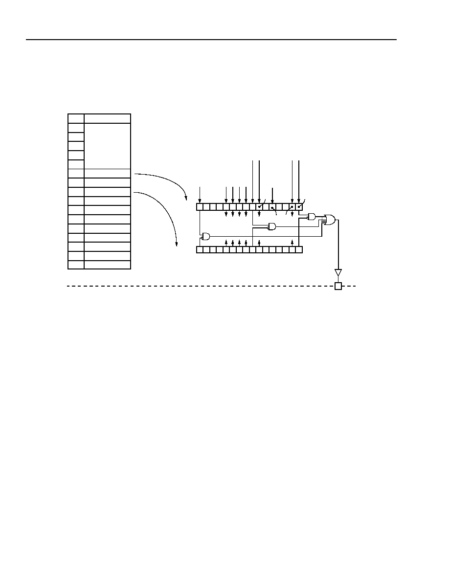
MARS2G5 P-Pro (TDAT162G52) SONET/SDH
Data Sheet
155/622/2488 Mbits/s Data Interface
August 18, 2004
162
Agere Systems Inc.
Microprocessor (MPU) Interface
(continued)
Interrupts
The interrupt functionality is shown in Figure 16.
5-7409(F).a
Figure 16. Interrupt Functionality
0x000C
0x000E
0x000F
0x001F
0x0015
0x0014
0x0013
0x0012
0x0010
0x0005
0x0008
0x000A
0x0004
0x0003
0x0002
0x0001
0x0000
IRQ MASKS
ONE SHOTS
GPIO OUTPUTS
SCRATCH
GPIO SELECT[3:2]
GPIO SELECT[1:0]
GPIO MODE
LOOPBACK
LINE PROVISION
INTERRUPTS
GPIO INPUTS
TADMVC2G52
NAME =
VERSION
IRQ MASKS
IRQ
INT
IRQ[
3] (UT
)
IRQ[
2] (DE
)
IRQ[
1] (P
T
)
IRQ[
0] (T
OHP
)
(GPIO)
SYNC_ERR
3
2
1
0
3
2
1
0 UT
DE
PT
OH
PMIRQ
PM
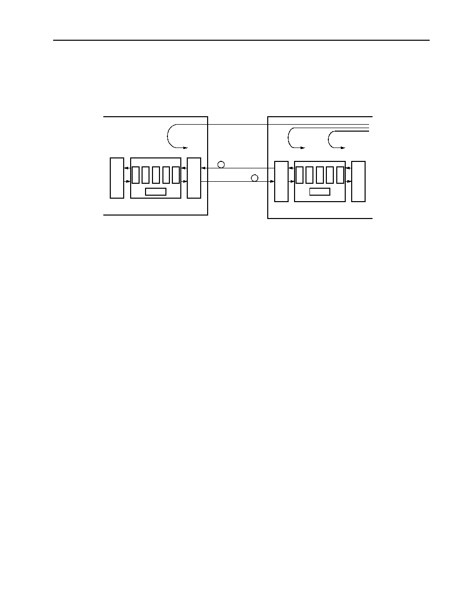
Data Sheet
MARS2G5 P-Pro (TDAT162G52) SONET/SDH
August 18, 2004
155/622/2488 Mbits/s Data Interface
163
Agere Systems Inc.
Microprocessor (MPU) Interface
(continued)
Loopback Operation
Figure 17 illustrates the different types of loopback provided in the device.
5-7411(F)r.2TDAT16
Figure 17. Loopback Operation
In the following description, only the data path from A to B is discussed, but the same terms apply to the reverse
direction.
Near-End Loopback (NELB)
The packet/cell payload is looped back to the data source (layer 2 device) as soon as it crosses the layer 1 to layer
2 mapping (UTOPIA block).
Terminal Loopback
The SDH signal is looped back to the terminal at the end of the piece of equipment (before it is transmitted onto the
facility).
Facility Loopback
The optical signal is looped back to the facility as soon as it enters the terminal.
FACILITY
(OPTICS)
LA
YE
R 2
OPT
I
CS
TERMINAL B
LA
YER
2
OP
TICS
TERMINAL A
SO
U
R
C
E
NEAR
END
TERMINAL
FACILITY
SI
N
K
DE
PP
TO
H
P
LI
N
E
UT
CONT
DE
PP
TO
H
P
LI
N
E
UT
CONT

MARS2G5 P-Pro (TDAT162G52) SONET/SDH
Data Sheet
155/622/2488 Mbits/s Data Interface
August 18, 2004
164
Agere Systems Inc.
Microprocessor (MPU) Interface
(continued)
MPU Register Descriptions
Table 24. MPU_VERR[0--5], Version Control Registers (RO)
Address
Bit
Name
Function
Reset
Default
0x0000
15:0
MPU_VER0
Indicates version number for version 2.0.
0x0207
Indicates version number for version 2.2.
0x0227
Indicates version number for version 2.3.
0x0237
0x0001
15:0
MPU_VER1
Indicates version number.
ASCII T A.
0x5441
0x0002
15:0
MPU_VER2
Indicates version number.
ASCII D M.
0x444D
0x0003
15:0
MPU_VER3
Indicates version number.
ASCII 0 4.
0x3034
0x0004
15:0
MPU_VER4
Indicates version number.
ASCII 2 G.
0x3247
0x0005
15:0
MPU_VER5
Indicates version number.
ASCII 5 CR.
0x350D

Data Sheet
MARS2G5 P-Pro (TDAT162G52) SONET/SDH
August 18, 2004
155/622/2488 Mbits/s Data Interface
165
Agere Systems Inc.
Microprocessor (MPU) Interface
(continued)
MPU Register Descriptions
(continued)
Table 25. MPU_ISR, Interrupt Status Register (RO or COR/W)
Address
Bit
Name
Function
Reset
Default
0x0008
15
MPU_SYNC_ERR_IS
Sync Error Interrupt (RO). This is a read-only bit. This
bit is set when the TXFSYNCP/N pins (U3, U1) are not
driven by a 2 kHz or greater frame sync signal. When
the TXFSYNCP/N pins are not used, simply ignore this
interrupt by setting the corresponding mask bit
MPU_SYNC_ERR_IM (Table 27) so that the interrupt
does not contribute to the MPU_INTN pin (B7). This bit
can be cleared by setting bit MPU_SYNC_ERR_ICLR
(Table 28).
X
14:13
--
Reserved.
12
MPU_PP_IS
PP Composite Interrupt (RO). When set, indicates
that an interrupt from the PP block is active.
11:8
MPU_GPI_IS[3:0]
General-Purpose Inputs Interrupt (RO or COR/W).
Signal indicating the associated input is active. When
the GPIO are outputs, this signal will be forced low.
These interrupts are COR/COW when the interrupt is
programmed to the positive edge mode; otherwise, this
is a read-only (RO) location.
7
MPU_UT48_IS
UTOPIA Composite Interrupt (RO). Active-high signal
indicating an unmasked delta or event is active in the
UTOPIA block.
6
MPU_DE48_IS
Data Engine Composite Interrupt (RO). Active-high
signal indicating an unmasked delta or event is active
in the data engine block.
5
MPU_PMRST_IS
Performance-Monitor Reset Interrupt (COR/W).
Active-high signal indicating a 1 second event has
occurred.
4
--
Reserved.
3
MPU_DS3_IS
DS3 Composite Interrupt (RO). When set, indicates
that an interrupt from the DS3 block is active.
2
MPU_RXT_IS
RXT Composite Interrupt (RO). When set, indicates
that an interrupt from the RXT block is active.
1
MPU_PT48_IS
Path Terminator Composite Interrupt (RO). Active-
high signal indicating an unmasked delta or event is
active in the path terminator block.
0
MPU_TOHP48_IS
Transport Overhead Processor Composite Inter-
rupt (RO). Active-high signal indicating an unmasked
delta or event is active in the transport overhead pro-
cessor block.

MARS2G5 P-Pro (TDAT162G52) SONET/SDH
Data Sheet
155/622/2488 Mbits/s Data Interface
August 18, 2004
166
Agere Systems Inc.
Microprocessor (MPU) Interface
(continued)
MPU Register Descriptions
(continued)
Table 26. MPU_CNDR, Condition Register (RO)
Table 27. MPU_IMR, Interrupt Mask Register (R/W)
Address
Bit
Name
Function
Reset
Default
0x000A
15:4
--
Reserved.
--
3:0
MPU_GPIO_I_CND[3:0]
General-Purpose Input Value. These values are
direction connections between the GPIO[3:0] input pins
and the register map. The value at the GPIO pins is
latched when this register is read.
N/A
Address
Bit
Name
Function
Reset
Default
0x000C
15
MPU_SYNC_ERR_IM
Sync Error Interrupt Mask. When set (active-high), the
associated interrupt bit will be inhibited from contribut-
ing to the interrupt pin (MPU_INTN).
1
14:13
--
Reserved.
11
12
MPU_PP_IM
Pointer Processor Composite Interrupt Mask. When
set (active-high), the associated composite interrupt bit
will be inhibited from contributing to the interrupt pin
(MPU_INTN).
1
11:8
MPU_GPI_IM[3:0]
General-Purpose Inputs Composite Interrupt Mask.
When set (active-high), the associated composite inter-
rupt bit will be inhibited from contributing to the interrupt
pin (MPU_INTN).
1111
7
MPU_UT48_IM
UTOPIA Composite Interrupt Mask. When set (active-
high), the associated composite interrupt bit will be
inhibited from contributing to the interrupt pin
(MPU_INTN).
1
6
MPU_DE48_IM
Data Engine Composite Interrupt Mask. When set
(active-high), the associated composite interrupt bit will
be inhibited from contributing to the interrupt pin
(MPU_INTN).
1
5
MPU_PMRST_IM
Performance-Monitor Composite Reset Mask. When
set (active-high), the associated composite interrupt bit
will be inhibited from contributing to the interrupt pin
(MPU_INTN).
1

Data Sheet
MARS2G5 P-Pro (TDAT162G52) SONET/SDH
August 18, 2004
155/622/2488 Mbits/s Data Interface
167
Agere Systems Inc.
Microprocessor (MPU) Interface
(continued)
MPU Register Descriptions
(continued)
Table 27. MPU_IMR, Interrupt Mask Register (R/W) (continued)
Table 28. MPU_ICLRR, Interrupt Clear Register (R/W)
Table 29. MPU_SWRSR, Software Reset Register (R/W)
Address
Bit
Name
Function
Reset
Default
0x000C
4
--
Reserved.
--
3
MPU_DS3_IM
DS3 Composite Interrupt Mask. When set (active-
high), the associated composite interrupt bit will be
inhibited from contributing to the interrupt pin
MPU_INTN (pin B7).
1
2
MPU_RXT_IM
Receive Terminator Composite Interrupt Mask. When
set (active-high), the associated composite interrupt bit
will be inhibited from contributing to the interrupt pin
MPU_INTN.
1
1
MPU_PT48_IM
Path Terminator Composite Interrupt Mask. When set
(active-high), the associated composite interrupt bit will
be inhibited from contributing to the interrupt pin
MPU_INTN.
1
0
MPU_TOHP48_IM
Transport Overhead Processor Composite Interrupt
Mask. When set (active-high), the associated composite
interrupt bit will be inhibited from contributing to the inter-
rupt pin MPU_INTN.
1
Address
Bit
Name
Function
Reset
Default
0x000D
15
MPU_SYNC_ERR_ICLR Sync Error Interrupt Clear. When this bit is set, inter-
rupt status bit MPU_SYNC_ERR_IS (Table 25) will be
cleared.
0
14:0
--
Reserved.
0
Address
Bit
Name
Function
Reset
Default
0x000E
15:8
--
Reserved.
0
7
MPU_PM_TRIGGER_SWRS Performance-Monitor Reset Trigger. This bit is
used in software controlled mode to generate a PM
reset signal pulse. It is also used in free-running
mode to synchronize the PM reset signal pulse. To
generate the trigger, write 1, then write 0 to this bit.
0
6:1
--
Reserved.
0
0
MPU_RST_SWRS
Software Reset. Writing 1 to this bit will reset the
device. This bit will clear itself.
0

MARS2G5 P-Pro (TDAT162G52) SONET/SDH
Data Sheet
155/622/2488 Mbits/s Data Interface
August 18, 2004
168
Agere Systems Inc.
Microprocessor (MPU) Interface
(continued)
MPU Register Descriptions
(continued)
Table 30. MPU_GPIO_CTLR, GPIO Output Value (R/W)
Table 31. MPU_PROVISION0, Provisioning Register 0 (R/W)
Table 32. MPU_PROVISION1, Provisioning Register 1 (R/W)
Address
Bit
Name
Function
Reset
Default
0x000F
15:4
--
Reserved.
0
3:0
MPU_GPIO_O_CTL[3:0]
General-Purpose Output Values. The value written
into these registers will appear on the associated
output.
0000
Address
Bit
Name
Function
Reset
Default
0x0010
15
MPU_PMRST_OE
PMRST Output Enable. Controls the 3-state buffer
that drives the external PMRST (pin D7). If 0, the
buffer is disabled, and PMRST is input. If 1, PMRST is
output.
0
14:10
--
Reserved.
00100
9:8
MPU_PMMODE[1:0]
Performance-Monitoring Mode. 00 or 10 = PM reset
signal comes from external pin; 01 = PM reset signal
comes from internal 1 second counter; 11 = PM reset
signal is software controlled.
00
7
--
Reserved.
0
6
MPU_COR_COW_CTL
Clear-on-Read/Clear-on-Write Control for MPU
Registers. 1 = COR, 0 = COW.
0
5
--
Reserved.
1
4
--
OC-48/OC-3 Mode for Internal System Clock Divi-
sor. 1 = OC-48, 0 = OC-12 and OC-3.
1
3:0
--
Reserved.
0
Address
Bit
Name
Function
Reset
Default
0x0011
15
MPU_EQA
Equip Channel A. 1 = enable; 0 = disable. Turn off clock in
receive direction, no effect in transmit direction.
0
14:12
--
Reserved.
0
11
MPU_EQB
Equip Channel B. 1 = enable; 0 = disable. Turn off clock in
receive direction, no effect in transmit direction.
0
10:8
--
Reserved.
0
7
MPU_EQC
Equip Channel C. 1 = enable; 0 = disable. Turn off clock in
receive direction, no effect in transmit direction.
0
6:4
--
Reserved.
0
3
MPU_EQD
Equip Channel D. 1 = enable; 0 = disable. Turn off clock in
receive direction, no effect in transmit direction.
0
2:0
--
Reserved.
0
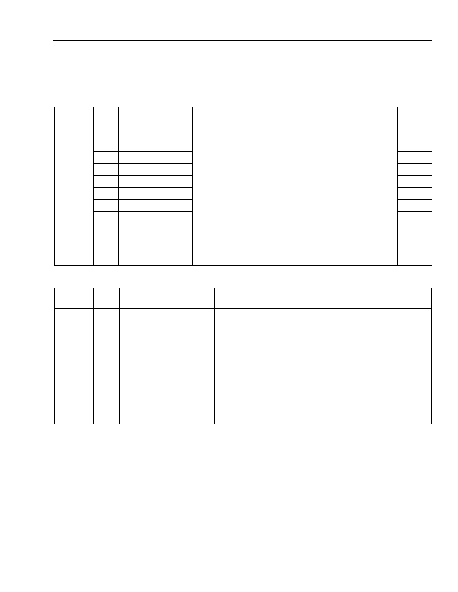
Data Sheet
MARS2G5 P-Pro (TDAT162G52) SONET/SDH
August 18, 2004
155/622/2488 Mbits/s Data Interface
169
Agere Systems Inc.
Microprocessor (MPU) Interface
(continued)
MPU Register Descriptions
(continued)
Table 33. MPU_LPBKCTLR, Loopback Control Register (R/W)
Table 34. MPU_GPIOCFG, GPIO Configuration Register (R/W)
Address
Bit
Name
Function
Reset
Default
0x0012
15:14
MPU_LPBKD[3:2]
Loopback Control. SONET facility and terminal loopback
are only available in STS-3/STM-1 and STS-12/STM-4
modes.
For MPU_LPBK[A--D][1:0]:
00 = No loopbacks.
01 = SONET facility loopback.
10 = SONET terminal loopback.
11 = Reserved.
For MPU_LPBK[D--A][3:2]:
00 = No loopbacks.
01 = Reserved.
10 = UTOPIA near-end loopback.
11 = Reserved.
00
13:12
MPU_LPBKA[1:0]
00
11:10
MPU_LPBKC[3:2]
00
9:8
MPU_LPBKB[1:0]
00
7:6
MPU_LPBKB[3:2]
00
5:4
MPU_LPBKC[1:0]
00
3:2
MPU_LPBKA[3:2]
00
1:0
MPU_LPBKD[1:0]
00
Address
Bit
Name
Function
Reset
Default
0x0013
15:12
MPU_GPIO_MODE[3:0]
GPIO Mode.
0000 = Normal mode. Enables all four GPIO signals.
0001 = Reserved.
Else = Undefined.
0000
11:8
MPU_GPIO_POL[3:0]
GPIO Interrupt Active State. 0 = report received
value unchanged. (Level = input pin value, positive
edge = 1 when signal rises); 1 = invert received value
(level = invert input pin value, positive edge = 0 when
detected).
0000
7:4
MPU_GPIO_ITYPE[3:0]
GPIO Interrupt Type. 0 = positive edge; 1 = level.
0000
3:0
MPU_GPIO_DIR_CTL[3:0] GPIO Direction Control. 0 = input; 1 = output.
0000

MARS2G5 P-Pro (TDAT162G52) SONET/SDH
Data Sheet
155/622/2488 Mbits/s Data Interface
August 18, 2004
170
Agere Systems Inc.
Microprocessor (MPU) Interface
(continued)
MPU Register Descriptions
(continued)
Table 35. MPU_GPIO_OER[1--2], GPIO Output Enable (R/W)
Address
Bit
Name
Function
Reset
Default
0x0014
15:9
--
Reserved.
0x0000
8
MPU_GPIO1_OE GPIO1 Output Enable. Write 1 to enable output. Write 0 to
3-state the output.
7:1
--
Reserved.
0
MPU_GPIO0_OE GPIO0 Output Enable. Write 1 to enable output. Write 0 to
3-state the output.
0x0015
15:9
--
Reserved.
0x0000
8
MPU_GPIO3_OE GPIO3 Output Enable. Write 1 to enable output. Write 0 to
3-state the output.
7:1
--
Reserved.
0
MPU_GPIO2_OE GPIO2 Output Enable. Write 1 to enable output. Write 0 to
3-state the output.

Data Sheet
MARS2G5 P-Pro (TDAT162G52) SONET/SDH
August 18, 2004
155/622/2488 Mbits/s Data Interface
171
Agere Systems Inc.
Microprocessor (MPU) Interface
(continued)
MPU Register Descriptions
(continued)
Table 36. MPU_PDN1, Powerdown Register 1 (R/W)
Note: A read or write should not be performed to blocks that are powered down, since it may not be completed.
The MPU_DTN signal may not be generated for blocks that are powered down.
Table 37. MPU_PDN2, Powerdown Register 2 (R/W)
Table 38. MPU_PDN3, Powerdown Register 3 (R/W)
Table 39. MPU_SCRATCHR, Scratch Register (R/W)
Table 40. MPU_TDAT16_MODER, MARS2G5 P-Pro Mode Selection Register (R/W)
Address
Bit
Name
Function
Reset
Default
0x001B
15:14
--
Reserved.
0
13
MPU_LI_PDN
Power Down the Line Interface Block. 1 = pow-
erdown.
0
12:9
--
Reserved.
0
8
--
Must Be Set to 1.
0
7:6
--
Reserved.
0
5
MPU_PAY_TXCLKPDN
Power Down PAY Transmit Clock. 1 = power-
down.
0
4
MPU_PAY_RXCLKPDN
Power Down PAY Receive Clock. 1 = power-
down.
0
3
MPU_SON_TOH_SYCLKPDN Power Down the TOH System Clock. 1 = power-
down.
0
2
MPU_SON_PP_SYCLKPDN
Power Down the PP System Clock. 1 = power-
down.
0
1:0
--
Must Be Set to 11.
00
Address
Bit
Name
Function
Reset
Default
0x001D
15:12
--
Reserved.
0000
11:0
--
Must Be Set to 0xFFF.
0x000
Address
Bit
Name
Function
Reset
Default
0x001E
15:12
--
Reserved.
0000
11:0
--
Must Be Set to 0xFFF.
0x000
Address
Bit
Name
Function
Reset
Default
0x001F
15:0
MPU_SCRATCH[15:0] Read/Write Register with No Other Internal Connec-
tions.
0x0
Address
Bit
Name
Function
Reset
Default
0x0020
15:1
--
Reserved.
0
0
--
Must Be Set to 1.
0

MARS2G5 P-Pro (TDAT162G52) SONET/SDH
Data Sheet
155/622/2488 Mbits/s Data Interface
August 18, 2004
172
Agere Systems Inc.
Microprocessor (MPU) Interface
(continued)
MPU Register Descriptions
(continued)
Table 41. MPU_LI_MODER, Register (R/W)*
* For normal OC-12 operation write 0x0F0F, normal OC-3 operation write 0x0F00, and normal OC-48 operation write 0x0010.
For OC-48 mode, channels A, B, C, and D are always enabled (on). There is no way to disable them in OC-48 mode.
Table 42. MPU_HSI_TST_CTL, High-Speed Interface Control
Table 43. MPU_HSI_LPBKR, High-Speed Interface Loopback Register
Address
Bit
Name
Function
Reset
Default
0x0021
15:12
--
Reserved.
0
11
MPU_LI_MODE[11:0] Channel A OC-12 and OC-3 Enable
. 1 = enable, 0 = disable.
0
10
Channel B OC-12 and OC-3 Enable
. 1 = enable, 0 = disable.
0
9
Channel C OC-12 and OC-3 Enable
. 1 = enable, 0 = disable.
0
8
Channel D OC-12 and OC-3 Enable
. 1 = enable, 0 = disable.
0
7
Additional Delay in PLL Feedback Path When Set to 1.
0
6
POF/SONET Select. 1 = packet over fiber (POF), 0 = SONET.
Note: For proper operation of POF mode, register 0x400F bit 5
(Table 263) and register 0x5801 (Table 680) need to be
configured correctly.
0
5
PLL On/Off Select. Controls the transmit line clock PLL used
for STS-48/STM-16 contraclocking mode. 1 = PLL off (inac-
tive), 0 = PLL on (active).
1
4
OC-48/OC-3 Mode for Internal System Clock Divisor.
1 = OC-48, 0 = OC-12 and OC-3.
1
3
Channel A OC-12/OC-3 Select. 1 = OC-12, 0 = OC-3.
0
2
Channel B OC-12/OC-3 Select. 1 = OC-12, 0 = OC-3.
0
1
Channel C OC-12/OC-3 Select. 1 = OC-12, 0 = OC-3.
0
0
Channel D OC-12/OC-3 Select. 1 = OC-12, 0 = OC-3.
0
Address
Bit
Name
Function
Reset
Default
0x0030
15
--
Reserved.
0
14
--
Must Be Set to 1.
0
13:11
--
Reserved.
000
10:8
--
Reserved.
110
7:0
--
Reserved.
0x00
Address
Bit
Name
Function
Reset
Default
0x0032
15:12
--
Reserved.
0x0
11:0
--
Must Be Set to 0xFFF.
0x000

Data Sheet
MARS2G5 P-Pro (TDAT162G52) SONET/SDH
August 18, 2004
155/622/2488 Mbits/s Data Interface
173
Agere Systems Inc.
Microprocessor (MPU) Interface
(continued)
MPU Register Map
Table 44. MPU Register Map
Note: Shading denotes reserved bits.
Addr
Symbol
Type
Bit 15
Bit 14
Bit 13
Bit 12
Bit 11
Bit 10
Bit 9
Bit 8
Bit 7
Bit 6
Bit 5
Bit 4
Bit 3
Bit 2
Bit 1
Bit 0
0x0000
MPU_VER0
RO
VERSION = 0x01
0
0
0
0
0
0
0
0
0x0001
MPU_VER1
RO
0x54 = T
0x41 = A
0x0002
MPU_VER2
RO
0x44 = D
0x4C = M
0x0003
MPU_VER3
RO
0x30 = 0
0x34 = 4
0x0004
MPU_VER4
RO
0x32 = 2
0x47 = G
0x0005
MPU_VER5
RO
0x35 = 5
0x0D = CR
0x0006
--
--
0x0007
--
--
0x0008
MPU_ISR
RO or
COR/W
MPU_
SYNC_
ERR_IS
MPU_
PP_IS
MPU_GP_IS[3:0]
MPU_
UT48_IS
MPU_
DE48_IS
MPU_
PMRST_
IS
MPU_
DS3_IS
MPU_
RXT_IS
MPU_
PT48_IS
MPU_
TOHP48_
IS
0x0009
--
--
0x000A
MPU_CNDR
R/W
MPU_GPIO_I_CND[3:0]
0x000B
--
--
0x000C
MPU_IMR
R/W
MPU_
SYNC_
ERR_IM
MPU_
PP_IM
MPU_
GP_IM3
MPU_
GP_IM2
MPU_
GP_IM1
MPU_
GP_IM0
MPU_
UT48_IM
MPU_
DE48_IM
MPU_
PMRST_
IM
MPU_
DS3_IM
MPU_
RXT_IM
MPU_
PT48_IM
MPU_
TOHP48_
IM
0x000D
MPU_ICLRR
R/W
MPU_
SYNC_ER
R_ICLR
0x000E
MPU_SWRSR
R/W
MPU_PM_
TRIGGER
_SWRS
MPU_
RST_
SWRS
0x000F
MPU_GPIO_CTLR
R/W
MPU_GPIO_O_CTL[3:0]
0x0010
MPU_PROVISION0
R/W
MPU_
PMRST_
IOCTL
MPU_PMMODE[1:0]
MPU_
COR_CO
W_CTL
--
0x0011
MPU_PROVISION1
R/W
MPU_EQA
MPU_EQB
MPU_EQC
MPU_EQD
0x0012
MPU_LPBKCTLR
R/W
MPU_LPBKD[3:2]
MPU_LPBKA[1:0]
MPU_LPBKC[3:2]
MPU_LPBKB[1:0]
MPU_LPBKB[3:2]
MPU_LPBKC[1:0]
MPU_LPBKA[3:2]
MPU_LPBKD[1:0]
0x0013
MPU_GPIOCFG
R/W
MPU_GPIO_MODE[3:0]
MPU_GPIO_POL[3:0]
MPU_GPIO_ITYPE[3:0]
MPU_GPIO_DIR_CTL[3:0]
0x0014
MPU_GPIO_OER1
R/W
MPU_GPI
O1_OE
MPU_GPI
O0_OE
0x0015
MPU_GPIO_OER2
R/W
MPU_GPI
O3_OE
MPU_GPI
O2_OE
0x0016
--
0x001A
--
--
MARS2G5 P-Pro (TDAT162G52) SONET/SDH
Data Sheet
155/622/2488 Mbits/s Data Interface
August 18, 2004
174
Agere Systems Inc.
Microprocessor (MPU) Interface
(continued)
MPU Register Map
(continued)
Table 44. MPU Register Map (continued)
Note: Shading denotes reserved bits.
Addr
Symbol
Type
Bit 15
Bit 14
Bit 13
Bit 12
Bit 11
Bit 10
Bit 9
Bit 8
Bit 7
Bit 6
Bit 5
Bit 4
Bit 3
Bit 2
Bit 1
Bit 0
0x001B
MPU_PDN1
R/W
MPU_LI_P
DN
MPU_PAY
_TXCLKP
DN
MPU_PAY
_RXCLKP
DN
MPU_SON
_TOH_SY
CLKPDN
MPU_SON
_PP_SYC
LKPDN
0x001C--
0x001E
--
--
0x001F
MPU_SCRATCHR
R/W
MPU_SCRATCH[15:0]
0x0020
--
--
0x0021
MPU_LI_MODER
R/W
MPU_LI_MODE[11:0]
0x0022--
0x07FF
--
--

Data Sheet
MARS2G5 P-Pro (TDAT162G52) SONET/SDH
August 18, 2004
155/622/2488 Mbits/s Data Interface
175
Agere Systems Inc.
Functional Description
The block diagram for the MARS2G5 P-Pro indicating the signal pins per block is shown in Figure 18.
5-7396(F)r.2TDAT162
Figure 18. MARS2G5 P-Pro Block Diagram Indicating the Signal Pins per Block
DE
UTOP
I
A
UT
PP
OHP
CTRL
TX
L
I
N
E
RX
LINE
43
6
4
MPU
JTAG ALM/GPIO
4 x 24
4 x 24
TX
UTOPIA
RX
UTOPIA
350 SIGNAL PINS
6
TXTOH
6
TXCLKQP/N,
TXCLKP/N,
AND TXF
32
2
32
2
TXD
ECL
REF
RXD
RXC
12
RXREF
RXTOH
IN
T
E
R
F
A
C
E
INTERFACE

MARS2G5 P-Pro (TDAT162G52) SONET/SDH
Data Sheet
155/622/2488 Mbits/s Data Interface
August 18, 2004
176
Agere Systems Inc.
Line Interface
This block provides the interface between the SONET/SDH line and the transport overhead (TOH) processing
block. The line interface must provide transmit/receive functions for quad OC-3, quad OC-12, and single OC-48
applications. All external inputs and outputs for the MARS2G5 P-Pro line I/O block are referenced to the positive
edge of the clock.
The following is a list of the receive line interface functions:
The quad OC-3 application consists of four differential PECL 155.52 Mbits/s data inputs and four 155.52 MHz dif-
ferential clocks from an optical transceiver.
The quad OC-12 application consists of four differential PECL 622.08 Mbits/s data inputs and four 622.08 MHz
differential clocks from an optical transceiver.
The OC-48 application consists of 16 differential PECL data inputs at 155.52 Mbits/s with a single differential
PECL 155.52 MHz clock.
The transmit interface performs the following functions:
The quad OC-3 application consists of four differential PECL 155.52 Mbits/s data outputs to an optical trans-
ceiver. A SONET compliant 155 MHz differential PECL clock input is required in this mode.
The quad OC-12 application consists of four each: a differential PECL 622.08 Mbits/s data to an optical trans-
ceiver. A SONET compliant 622 MHz differential PECL clock input is required in this mode.
The OC-48 application consists of 16 differential PECL data outputs at 155.52 Mbits/s with a differential PECL
155.52 MHz clock.
The 8k frame sync is a clock cycle wide pulse latched in at the system rate (622.08 MHz or 155.52 MHz). This
signal will set the transmit frame location. If this signal is kept low, the transmit frame will free-run at the 8 kHz
rate.
The line interface also supports loopback functions:
In the quad OC-3 and quad OC-12 applications, the line interface supports both terminal and facility loopback on
a per-port basis.

Data Sheet
MARS2G5 P-Pro (TDAT162G52) SONET/SDH
August 18, 2004
155/622/2488 Mbits/s Data Interface
177
Agere Systems Inc.
Line Interface
(continued)
This device is designed to work with commonly available multiplexer and demultiplexer chipsets for STS-3, STS-
12, and STS-48 line interface rates. The line interface will operate in one of three possible modes.
5-7418(F)r.2
Figure 19. Line Interface
Table 45. Line Interface Modes
MPU_LI_MODE[4:0]
0x0021 (Table 41)
Interfaces
Line Interface Signals
10000
OC-48
RXCLK[P/N], RXD[15:0], TXCLK[P/N], TXD[15:0]
01111
OC-12
RXCLKD[P/N], RXDD[P/N], TXCLK[P/N], TXDD[P/N]
RXCLKC[P/N], RXDC[P/N], TXCLK[P/N], TXDC[P/N]
RXCLKB[P/N], RXDB[P/N], TXCLK[P/N], TXDB[P/N]
RXCLKA[P/N], RXDA[P/N], TXCLK[P/N], TXDA[P/N]
00000
OC-3
RXCLKD[P/N], RXDD[P/N], TXCLK[P/N], TXDD[P/N]
RXCLKC[P/N], RXDC[P/N], TXCLK[P/N], TXDC[P/N]
RXCLKB[P/N], RXDB[P/N], TXCLK[P/N], TXDB[P/N]
RXCLKA[P/N], RXDA[P/N], TXCLK[P/N], TXDA[P/N]
VALID
TXCLKP
TXCLKN
TXD[15:0]
VALID
RXCLK[A:D]P
RXCLK[A:D]N
RXD[15:0]

MARS2G5 P-Pro (TDAT162G52) SONET/SDH
Data Sheet
155/622/2488 Mbits/s Data Interface
August 18, 2004
178
Agere Systems Inc.
Line Interface
(continued)
LVPECL I/O Termination and Load Specifications
The LVPECL buffers are compatible with the temperature independent ECL 100K levels, but the output levels that
are guaranteed are relaxed 30 mV from the actual 100K levels allowing for noise and variations in the power sup-
ply and process.
All LVPECL output buffers require a terminating resistor. These terminating resistors, which must also be con-
nected to both LVPECLREFHI and LVPECLREFLO, go to a common terminating voltage. All of the terminating
resistors used with a chip must be identical precision (1%) resistors. The value of these terminating resistors is
usually chosen to match the characteristic impedance of the board. To save on power, a terminating voltage equal
to V
DDD
≠ 2 V is available in most ECL systems. The minimum value of the terminating resistor that can be used on
these buffers is 50
. This is also the standard termination used in most ECL systems. Larger values of resistance
will save power, but will also slow down the high-to-low transition of the output, since it is RC limited.
If no V
DDD
≠ 2 V supply is available, a larger value resistor may be connected directly to GND. It should be chosen
such that the current through it does not exceed the current through a 50
resistor to V
DDD
≠ 2 V (21 mA in the
high state). This large resistor will most likely be a poor match to the board impedance. The match can be
improved by the use of a Thevenin equivalent resistor pair. Such a Thevenin equivalent resistor will burn much
more system power (but not on-chip power) than would a single resistor, but it does allow for impedance matching
in the absence of a V
DDD
≠ 2 V supply. Termination resistor options are shown in Table 46 and Figure 20.
Experienced ECL designers sometimes use the (bipolar) ECL output buffers in a tied-OR configuration. Unfortu-
nately, this cannot be done with these LVPECL buffers.
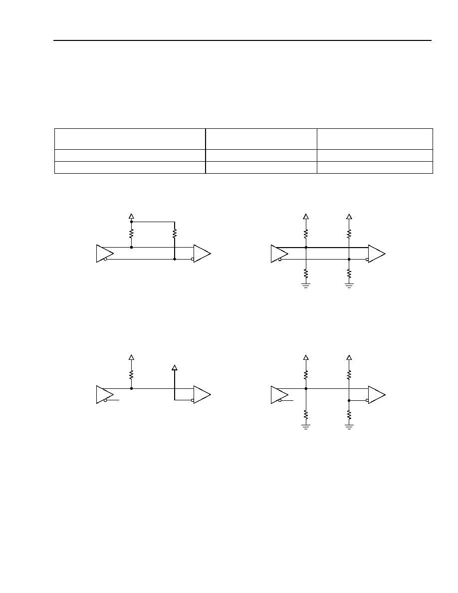
Data Sheet
MARS2G5 P-Pro (TDAT162G52) SONET/SDH
August 18, 2004
155/622/2488 Mbits/s Data Interface
179
Agere Systems Inc.
Line Interface
(continued)
LVPECL I/O Termination and Load Specifications
(continued)
Table 46. Nominal dc Power for Suggested Terminations
Note: The value is the average of the high and low states in LVPECL output buffer and external terminating resis-
tors, for a single-ended output. The values double for double-ended outputs.
* Standard ECL termination (parallel).
Thevenin equivalent of 50
to V
DDD
≠ 2 V.
1264(F)a
Figure 20. LVPECL Load Connections
Terminating Resistor and Voltage
Output Transistor (On-Chip)
Power (mW)
Terminating Resistor (Off-Chip)
Power (mW)
50
(R
P
) to V
DDD
≠ 2 V*
15
13
130
(R1) to V
DDD
and 82
(R2) to GND
15
52
LVPECL OUTPUT
R1
V
DDD
LVPECL INPUT
R2
R1
V
DDD
R2
LVPECL OUTPUT
R
P
LVPECL INPUT
R
P
LVPECL OUTPUT
R2
V
DDD
LVPECL INPUT
R1
R1
V
DDD
R2
X
LVPECL OUTPUT
LVPECL INPUT
R
P
X
DIFFERENTIAL CONFIGURATION
WITH PARALLEL TERMINATION
DIFFERENTIAL CONFIGURATION
WITH THEVENIN TERMINATION
SINGLE-ENDED CONFIGURATION
WITH THEVENIN TERMINATION
SINGLE-ENDED CONFIGURATION
WITH PARALLEL TERMINATION
V
DDD
≠ 2 V
V
DDD
≠ 2 V
V
DDD
≠ 1.3 V
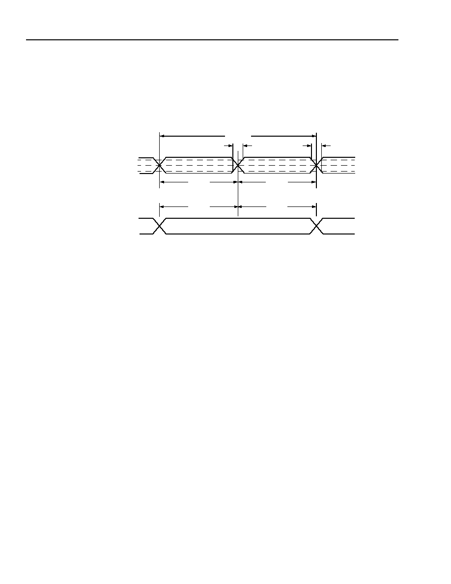
MARS2G5 P-Pro (TDAT162G52) SONET/SDH
Data Sheet
155/622/2488 Mbits/s Data Interface
August 18, 2004
180
Agere Systems Inc.
Line Interface
(continued)
Line Interface I/O Timing
Note: V
DD
= V
DDA
= V
DDD
(3.300 volts nominal) in this section.
Figure 21, Figure 22, Table 47, and Table 48 give the timing specifications for the STS-3/STM-1,
STS-12/STM-4, and STS-48/STM-16 interfaces.
5-9252 (F).ar.2
Figure 21. Receive Line-Side Timing Waveform
RXD[15:0]P/RXD[D--A]P
tRCR
RXCLKP/RXCLK[D--A]P
RXCLKN/RXCLK[D--A]N
tRCF
tRCCP
tRCPL
tRCPH
RXD[15:0]N/RXD[D--A]N
50%
V
IL (MAX)
V
IH (MIN)
tRSU
tRH

Data Sheet
MARS2G5 P-Pro (TDAT162G52) SONET/SDH
August 18, 2004
155/622/2488 Mbits/s Data Interface
181
Agere Systems Inc.
Line Interface
(continued)
Line Interface I/O Timing
(continued)
5-9253(F).dr.1
* Loading of TXD[15:4][P/N] is 12 pF. Loading of TXD[3:0][P/N]/TXD[D:A][P/N] is 8 pF with the PLL on, and 12 pF with the PLL off.
Figure 22. Transmit Line-Side Timing Waveform--OC-48 Contraclocking
5-9253(F).fr.2
* Loading of TXD[15:4][P/N] is 12 pF. Loading of TXD[3:0][P/N]/TXD[D:A][P/N] is 8 pF with the PLL on, and 12 pF with the PLL off.
Figure 23. Transmit Line-Side Timing Waveform--OC-48 Forward Clocking
5-9253(F).er.4
Figure 24. Transmit Line-Side Timing Waveform--Frame Sync
tTCR
TXCLKP
TXCLKN
tTCF
tTCCP
tTCPL
tTCPH
50%
V
IL (MAX)
V
IH (MIN)
TXD[15:0]P/TXD[D--A]P*
TXD[15:0]N/TXD[D--A]N*
tPDCC
50%
TXCLKP
TXCLKN
50%
V
IL (MAX)
V
IH (MIN)
TXCLKQP
TXCLKQN
TXD[15:0]P/TXD[D--A]P*
TXD[15:0]N/TXD[D--A]N*
50%
50%
tPDFC2
tPDFC1
tPDFC3
TXFSYNCN
TXCLKP
TXCLKN
TXFSYNCP
50%
V
IL (MAX)
V
IH (MIN)
tTFSPW
tTFSH
tTFSSU

MARS2G5 P-Pro (TDAT162G52) SONET/SDH
Data Sheet
155/622/2488 Mbits/s Data Interface
August 18, 2004
182
Agere Systems Inc.
Line Interface
(continued)
Line Interface I/O Timing
(continued)
For the following tables,
V
IL
(max) = (V
DD
≠ 1.475) V, nominal of 1.825 V;
V
IH
(min) = (V
DD
≠ 1.165) V, nominal of 2.135 V;
V
OH
(min) = (V
DD
≠ 1.025) V, nominal of 2.275 V;
V
OL
(max) = (V
DD
≠ 1.620) V, nominal of 1.680 V.
Table 47. Receive Line-Side Timing Specifications
Symbol
Parameter
Min
Typ
Max
Units
t
RCCP
Receive Clock-Cycle Period:
STS-3/STM-1 and STS-48/STM-16
STS-12/STM-4
--
--
6.4300
1.60751
--
--
ns
ns
t
RCR
Receive Clock/Data Rise Time:
OC-3 Mode
OC-12 Mode
OC-48 Mode
200
200
200
--
--
--
2200
600
1500
ps
ps
ps
t
RCF
Receive Clock/Data Fall Time:
OC-3 Mode
OC-12 Mode
OC-48 Mode
200
200
200
--
--
--
2200
600
1500
ps
ps
ps
t
RCPL
Receive Clock Pulse Low (for P input):
STS-3/STM-1 and STS-48/STM-16
STS-12/STM-4
2.800
700
3.2150
803.75
3.630
907
ns
ps
t
RCPH
Receive Clock Pulse High (for P input):
STS-3/STM-1 and STS-48/STM-16
STS-12/STM-4
2.800
700
3.2150
803.75
3.630
907
ns
ps
t
RSU
Receive Data Setup Time:
RXD[D--A][P/N]
OC-3 Mode
OC-12 Mode
RXD[15:0][P/N]
OC-48 Mode
600
400
500
--
--
--
--
--
--
ps
ps
ps
t
RH
Receive Data Hold Time:
RXD[D--A][P/N]
OC-3 Mode
OC-12 Mode
RXD[15:0][P/N]
OC-48 Mode
600
400
1
--
--
--
--
--
--
ps
ps
ns

Data Sheet
MARS2G5 P-Pro (TDAT162G52) SONET/SDH
August 18, 2004
155/622/2488 Mbits/s Data Interface
183
Agere Systems Inc.
Line Interface
(continued)
Line Interface I/O Timing
(continued)
Table 48. Transmit Line-Side Timing Specifications
Note: The recommended termination for LVPECL outputs is 50
to a termination voltage equal to V
DD
≠ 2 V.
* TXFSYNC[P/N] must be synchronized to TXCLK[P/N]; it must be at least one TXCLK[P/N] clock-cycle wide, but less than one frame
period minus two TXCLK[P/N] clock-cycles wide.
TXCLKQ[P/N] is used in STS-48/STM-16 mode only.
The PLL can be invoked in STS-48/STM-16 mode only.
Symbol
Parameter
Min
Typ
Max
Unit
t
TCCP
Transmit Clock-Cycle Period:
STS-3/STM-1 and STS-48/STM-16
STS-12/STM-4
--
--
6.4300
1.60751
--
--
ns
ns
t
TCR
Transmit Clock (TXCLK[P/N])/Transmit Frame Sync
(TXFSYNC[P/N]) Rise Time:
OC-3 Mode
OC-12 Mode
OC-48 Mode
200
200
200
--
--
--
2200
600
1500
ps
ps
ps
t
TCF
Transmit Clock (TXCLK[P/N])/Frame Sync
(TXFSYNC[P/N]) Fall Time:
OC-3 Mode
OC-12 Mode
OC-48 Mode
200
200
200
--
--
--
2200
600
1500
ps
ps
ps
t
TCPL
Transmit Clock Pulse Low (for P input):
STS-3/STM-1 and STS-48/STM-16
STS-12/STM-4
2.800
700
3.2150
803.75
3.630
907
ns
ps
t
TCPH
Transmit Clock Pulse High (for P input):
STS-3/STM-1 and STS-48/STM-16
STS-12/STM-4
2.800
700
3.2150
803.75
3.630
907
ns
ps
t
PDCC
Propagation Delay--Contraclocking*:
(TXCLK[P/N] to TXD[15:0][P/N], with PLL)
1
--
3
ns
t
PDFC1
Propagation Delay--Forward Clocking:
(TXCLK[P/N] to TXCLKQ[P/N])
1.5
--
4.5
ns
t
PDFC2
Propagation Delay--Forward Clocking:
(TXCLKQ[P/N] to TXD[15:0][P/N], no PLL)*
0
--
1.5
ns
t
PDFC3
Propagation Delay--Forward Clocking:
(TXCLK[P/N] to TXD[15:0][P/N], no PLL)
2
--
5
ns
t
TFSSU
TXFSYNC[P/N] Setup Time:
OC-3 Mode
OC-12 Mode
OC-48 Mode (no PLL)
OC-48 Mode (with PLL)
600
400
0
2
--
--
--
--
--
--
--
--
ps
ps
ns
ns
t
TFSH
TXFSYNC[P/N] Hold Time:
OC-3 Mode
OC-12 Mode
OC-48 Mode (no PLL)
OC-48 Mode (with PLL)
600
400
2
0
--
--
--
--
--
--
--
--
ps
ps
ns
ns
t
TFSPW
Transmit TXFSYNC[P/N] Width
:
STS-3/STM-1 and STS-48/STM-16
STS-12/STM-4
6.430
1.608
--
--
19,438
77,758
clock cycles
clock cycles
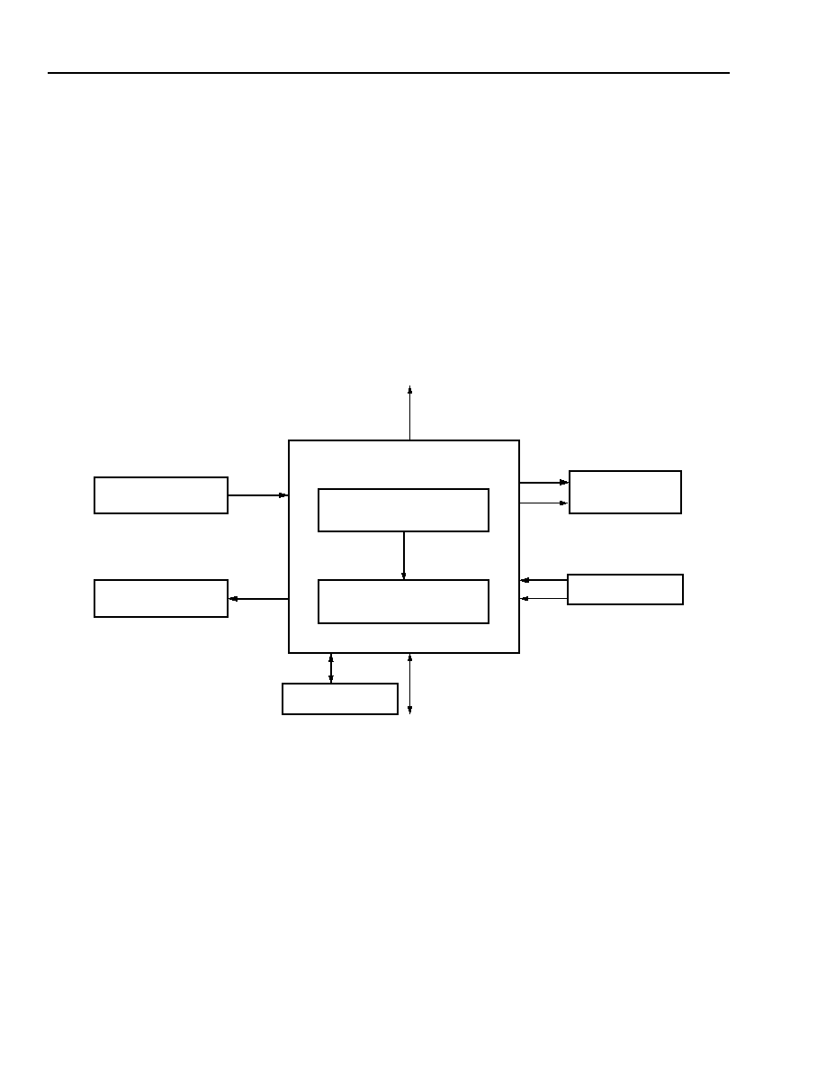
MARS2G5 P-Pro (TDAT162G52) SONET/SDH
Data Sheet
155/622/2488 Mbits/s Data Interface
August 18, 2004
184
Agere Systems Inc.
Transport Overhead Processor (TOHP-48) Block
Introduction
This section describes the functions of the transport overhead processing block (TOHP-48) in the MARS2G5 P-
Pro. This block supports regenerator section overhead (RSOH) or line section overhead and multiplex section
overhead (MSOH) processing for quad STS-3/STM-1, quad STS-12/STM-4 signals, or a single STS-48/STM-16
signal. Control inputs and outputs for each functional block are specified, along with the appropriate control register
bit definitions.
TOHP-48 Functional Block Diagram
Figure 25 shows a high-level view of the interconnect between the TOHP-48 processor block and other blocks
(pointer interpreter, SPE mapper block, serial-to-parallel and parallel-to-serial conversion blocks, and the micropro-
cessor interface).
5-8127(F)r.1TDAT16
Figure 25. High-Level Block Interconnect
TRANSMIT DIRECTION
RX_DATAO[31:0]
RX_SYNCO
RX_DATAI[31:0]
TX_DATAI[31:0]
TX_SYNCI
POINTER
PROCESSOR
TOH PROCESSOR
SERIAL-TO-PARALLEL
CONVERSION
TX_DATAO[31:0]
PARALLEL-TO-SERIAL
CONVERSION
TRANSMIT
TOAC
CHANNELS
RECEIVE
TOAC
CHANNELS
CONTROL AND STATUS
PATH TERMINATOR
MICROPROCESSOR
RECEIVE DIRECTION
(FROM SONET/SDH LINE)
(TO SONET/SDH LINE)

Data Sheet
MARS2G5 P-Pro (TDAT162G52) SONET/SDH
August 18, 2004
155/622/2488 Mbits/s Data Interface
185
Agere Systems Inc.
Transport Overhead Processor (TOHP-48) Block
(continued)
TOHP-48 Functional Block Diagram
(continued)
The TOHP-48 functional blocks are shown in Figure 26.
5-8129(F)r.1
Figure 26. TOHP-48 Block Diagram (One Channel)
Figure 26 describes a detailed view of one of four TOH channel processing blocks in both the receive and transmit
direction. A detailed description of each block is provided in the following sections.
M1
M1
TRANSPOSE
FRAME
DESCRAM-
INSERT
B1
J0
LOS
F1
B2
K1/K2
AIS-L
M1
SYNC
MONITOR
B2
K1
K2
M1
S1
STATUS
B1
J0
F1
TOAC
OOF
FROM SONET/SDH LINE (RECEIVE DIRECTION)
RDATAI
[31:0]
SCRAM-
INSERT
INSERT
INSERT LINE/MSOH
B1
F1
B2
K1/K2
RDI-L
SYNC
B2
K1
K2[2:0]
S1
B1
F1
TDATAI[31:0]
INSERT J0
GENERATE
M1
RDATAO
TO SONET/SDH LINE (TRANSMIT DIRECTION)
TOAC INSERT
RSYNCO
TSYNCI
J0, E1, F1, D1--D3 INSERT
TSYNCO
ALIGN
BLER
LOC
MONITOR
LOF
MONITOR
DETECTOR
MONITOR
MONITOR
BIP N
CHECK
APS
MONITOR
RDI-L
DETECT
REI-L
DETECT
DROP
REI
COUNTER
AIS-L
[7:0]
BIP-8
CHECK
BER
ALGORITHM
K2
TDATAO[7:0]
Z0-X,
A1/A2
BLER
SECTION/RSOH
AIS
MSOH
GENERATE
APS
INSERT
REI-L
STATUS
K2
D4--D12, S1, AND E2
(Z1 AND Z2 ONLY OC-12/OC-48)
INPUT
DIVIDER

MARS2G5 P-Pro (TDAT162G52) SONET/SDH
Data Sheet
155/622/2488 Mbits/s Data Interface
August 18, 2004
186
Agere Systems Inc.
Transport Overhead Processor (TOHP-48) Block
(continued)
Enhancements
This section includes the enhancements added to the TOHP block for the MARS2G5 P-Pro device. The enhance-
ments are K1K2 validation and pass through mode for APSMON and K2MON processing, transposer (OC-48) and
divider (OC-3), the TOAC must run at 20.736 MHz clock for all modes, and Rx output to the pointer processor block
changes on the falling edge of the clock.
APSMON and K2MON Processing (Including K1K2 Validation and Pass Through)
Note: The three least significant bits of the K2 byte take on different meaning depending on the linear APS mode or
ring status mode. Therefore, the integration is different.
The K1 byte will be stored in TOHP_K1DMON[7:0] (Table 85), while the K2 byte will be stored in
TOHP_K2DMON[7:0] (Table 85). The updating of these registers depends on mode bit TOHP_K1K2_2OR1
(Table 67), as follows:
When TOHP_K1K2_2OR1 = 0, the K1 and K2 byte registers will be updated after TOHP_CNTDK1K2[3:0]
(Table 66) consecutive frames of identical K1[7:0] and K2[7:3], i.e., the 13-bit pattern must be identical for
TOHP_CNTDK1K2[3:0] frames prior to updating the K1 and K2 registers. In this mode, the TOHP_K2DMON[2:0]
register will be updated after TOHP_CNTDK2[3:0] (Table 66) consecutive frames of identical K2[2:0].
When TOHP_K1K2_2OR1 = 1, the K1 and K2 byte registers will be updated after TOHP_CNTDK1K2[3:0] con-
secutive frames of identical K1[7:0] and K2[7:0], i.e., the 16-bit pattern must be identical for
TOHP_CNTDK1K2[3:0] frames prior to updating the registers.
Whenever the contents of the TOHP_K1DMON[7:0] and TOHP_K2DMON[7:3] (for TOHP_K1K2_2OR1 = 0) or
TOHP_K2DMON[7:0] (for TOHP_K1K2_2OR1 = 1) register changes, a delta bit TOHP_K1K2DMOND (Table 62)
will be set (TOHP_K1K2DMONM (Table 64)). This event bit is valid in both monitoring modes.
The block will monitor the APS bytes (K1[7:0], K2[7:3]) or K2[7:0] (when TOHP_K1K2_2OR1 = 1) in the receive
direction and report to the control interface (TOHP_RAPSBABLEE (Table 62), TOHP_RAPSBABLEM (Table 64))
when the K1 bytes are inconsistent. Inconsistent APS bytes are defined as TOHP_CNTDK1K2FRAME[3:0]
(Table 66) (default = 0xC) successive frames, starting with the last frame containing previously consistent code,
where no TOHP_CNTDK1K2[3:0] (default = 0x3) consecutive frames contain identical APS bytes.
Whenever the contents of TOHP_K2DMON[2:0] changes, a delta bit TOHP_K2DMOND (Table 62) will be set
(TOHP_K2DMONM (Table 64)). This event bit is only valid when TOHP_K1K2_2OR1 is a logic 0.
Whenever the register bit TOHP_RVALIDK_CTL (Table 67) is a logic 1, the received K1K2 bytes will be compared
with their reverse bytes for validation. Using the TOHP_CNTDK1K2[3:0] for the K1 byte and TOHP_CNTDK2[3:0]
for the K2 byte, the received K1K2 will be written to the output TOHP_K1DMON[7:0] and TOHP_K2DMON[7:0].
Otherwise, TOHP_K1DMON[7:0] and TOHP_K2DMON[7:0] will be updated every frame with new received K1[7:0]
and K2[7:0] bytes. (TOHP_K1K2_2OR1 has a higher priority.)
All continuous N-times detection counters will be reset to 0, if there are any received B1 errors and the register bit
TOHP_CNTDB1SEL (Table 67) is set to 1.

Data Sheet
MARS2G5 P-Pro (TDAT162G52) SONET/SDH
August 18, 2004
155/622/2488 Mbits/s Data Interface
187
Agere Systems Inc.
Transport Overhead Processor (TOHP-48) Block
(continued)
TOHP-48 Receive Direction
All monitoring functions supported by TOHP-48 in the receive direction are summarized here:
Input clock and loss-of-signal monitoring
Frame alignment and short frame
B1 BIP-8 check
J0/Z0 monitor
Descrambler
F1 monitor
B2 BIP-8xN check
APSMON and K2MON processing (including K1K2 validation and pass through)
AIS-L and RDI-L detect
MS-REI detect
Sync status monitor
Signal degrade BER algorithm
Signal fail BER algorithm
Transport overhead access channel (TOAC) drop
Insertion of AIS-L (MS-AIS)
Whenever the continuous N times detect (CNTD) signals are defined, they require not only that the monitored sig-
nal be consistent for N consecutive frames, but also that the frame bytes be error free for all N frames before the
status can be updated. If there are any errors in the framing pattern, then the consecutive N times detection
counters will reset to 0. N can range from 1 to 15. Programming a CNTD block with any value less than 1 will set
the CNTD to 1 time detect. The receive direction can be programmed into bypass mode bit TOHP_ROH_BYPASS
(Table 67), in which all 32-bit input data will be retimed and passed through without any processing. The four out-
put sync signals are forced low in this mode.
Loss of Input Clock (LOC) and Loss of Signal (LOS) Monitoring
The TOHP-48 block detects and reports loss of input clock (LOC), as determined by stuck high or stuck low for
time T. The detection time T is greater than 6.58 µs. The state of monitoring is controlled by bits (TOHP_LOC[A--
D] (Table 63), TOHP_LOCD[A--D] (Table 62), and TOHP_LOCM[A--D] (Table 64)).
The TOHP-48 block detects and reports loss of signal (LOS) on the input data signal before descrambling, as
determined by stuck high or stuck low for time T. The detection time T is user programmable through
TOHP_LOSDETCNT[A--D][12:0] (Table 67), in steps of 8 (OC-3, OC-12) or 32 bits (OC-48) at a time with a range
of (51.44 ns to 421.4 µs) for OC-3 or (12.86 ns to 105.35 µs) for OC-12/OC-48, respectively. A value of zero dis-
ables the stuck high/low monitoring feature of LOS detection. An LOS is not reported unless a clock is present.
To recover from the LOS state, two consecutive frames must be received with the correct framing pattern spaced
125 µs apart and, during the intervening time (one frame), no all-zeros/ones pattern indicates an LOS defect.

MARS2G5 P-Pro (TDAT162G52) SONET/SDH
Data Sheet
155/622/2488 Mbits/s Data Interface
August 18, 2004
188
Agere Systems Inc.
Transport Overhead Processor (TOHP-48) Block
(continued)
TOHP-48 Receive Direction
(continued)
Frame Alignment
Specification
The framer goes in frame if it finds two consecutive frames with the desired framing bytes and goes out of frame if
it finds five consecutive frames with at least one framing bit error in each frame.
The following framing bytes indicate frame integrity and are observed every 125 µs.
Table 49. Framing Bytes Observed for Framing Integrity
OOF is declared after the fifth errored A1A1A2A2 pattern, and reported to the control system (TOHP_OOF
(Table 63), TOHP_OOFD (Table 62), and TOHP_OOFM (Table 64)).
After 24 continuous frames (3 ms) of OOF, the block will declare a loss of frame defect and report this state
(TOHP_LOF (Table 63), TOHP_LOFD (Table 62), and TOHP_LOFM (Table 64)).
Once set, the block will clear the LOF state after 24 consecutive frames (3 ms) of no OOF events with correct fram-
ing patterns spaced 125 µs apart.
B1 BIP-8 Check
A BIP-8 even parity is computed over the incoming scrambled data, and compared to the B1 byte received in the
next frame.
The total number of B1 BIP-8 bit errors (raw count), or block errors (as determined by bit TOHP_B1BITBLKCNT
(Table 67), is counted. Upon the performance-monitor latch control signal, the value of the counter is presented to
the control interface in a 16-bit counter, TOHP_B1ECNT[15:0] (Table 81). In case of overflow, the counter remains
at its maximum value until it is cleared. Host microprocessor is expected to clear the counter at least once a sec-
ond.
Interface
Sequence
OC-3
F6, 28
OC-12
F6, F6, 28, 28
OC-48 (32-bit)
F6, F6, 28, 28

Data Sheet
MARS2G5 P-Pro (TDAT162G52) SONET/SDH
August 18, 2004
155/622/2488 Mbits/s Data Interface
189
Agere Systems Inc.
Transport Overhead Processor (TOHP-48) Block
(continued)
TOHP-48 Receive Direction
(continued)
J0/Z0 Monitor
J0 (section trace) monitoring has four different monitoring modes controlled by TOHP_J0MONMODE[1:0]
(Table 67):
J0MONMODE[1:0] = 00: The J0 byte of every frame is captured for 64 consecutive frames for a total of 64 bytes
(RJ0DMON[1--64][7:0] (Table 86)). The incoming J0 byte is compared with the next expected-value (the
expected value is obtained by cycling through the previous stored 64 received bytes in round-robin fashion) and
sets an event bit (J0MISE, J0MISM), if different.
J0MONMODE[1:0] = 01: This is the SONET framing mode. A J0 byte pattern of 0x0D followed by 0x0A charac-
ter indicates that the next byte is the first byte of the path trace message. The J0 byte message is continuously
written into RJ0DMON[1--64][7:0] with the first byte residing at the first address. If any received byte does not
match the previously received byte for its location, then an event bit (J0MISE, J0MISM) is set.
J0MONMODE[1:0] = 10: This is the SDH framing mode. The first J0 byte with the MSB set to one indicates that
the next byte is the second byte of the message. The rest of operation is the same as in SONET framing mode.
J0MONMODE[1:0] = 11: A new J0 byte (RJ0DMON[1][7:0]) will be detected after CNTDJ0Z0[3:0] consecutive
consistent occurrences of a new pattern in the J0 overhead byte. Any changes to this byte is reported by
(J0MISE, J0MISM). This event bit acts as a delta bit in this mode indicating a change in state for the
RJ0DMON[1][7:0] byte.
Note: In OC-48 mode, the device will monitor the first three (2, 3, and 4) Z0 bytes using the CNTD mode of the J0
monitors.
Descrambler
A frame synchronous descrambler of length 127 and generating polynomial x
7
+ x
6
+1 will descramble the entire
STS/STM signals except for the first row of overhead. The framing bytes (A1, A2), the section trace bytes (J0), and
the growth bytes (Z0) are not descrambled. The scrambler will be set to 1111111 on the first byte following the last
section OH byte in the first row (i.e., after byte J0 for STS-1, after the second Z0 for STS-3, etc.). The descrambler
operates in a byte wide mode for OC-3/OC-12 and a 32-bit-word wide mode for OC-48.
The frame descrambler can be disabled through TOHP_DSCRINH (Table 67).
F1 Monitor
The fault location byte TOHP_F1DMON0[7:0] (Table 85) is monitored by the F1 monitor. A new fault location state
is detected after TOHP_CNTDF1[3:0] (Table 66) consecutive consistent occurrences of a new pattern in the F1
overhead byte. A history of the previous valid F1 byte, TOHP_F1DMON1[7:0], is also maintained. Any changes to
this byte will be reported by bits TOHP_F1DMOND (Table 62) and TOHP_F1DMONM (Table 64).
B2 BIP-8xN Check
A BIP-8N even parity is computed over the incoming frame (except for rows 1, 2, and 3 of the section OH), and
compared to the N B2 bytes received in the next frame, (N = 3, 12, or 48). The total number of B2 BIP-8N bit errors
(raw count), or block errors as determined by TOHP_B2BITBLKCNT (Table 67) is counted. Upon a PM latch con-
trol signal PM_LATCH, the internal running counter is placed into a holding register TOHP_B2ECNTR (Table 82)
and then cleared. In case of overflow, the internal counter will stay at its maximum value until cleared.
The checker must output a per-frame error count (B2ECntPerF[7:0]), which is needed in the transmit direction to
form M1 byte. The count is truncated at 255 for OC-48.

MARS2G5 P-Pro (TDAT162G52) SONET/SDH
Data Sheet
155/622/2488 Mbits/s Data Interface
August 18, 2004
190
Agere Systems Inc.
Transport Overhead Processor (TOHP-48) Block
(continued)
TOHP-48 Receive Direction
(continued)
APSMON and K2MON Processing (Including K1K2 Validation and Pass Through)
Note: The three least significant bits of the K2 byte take on different meaning depending on the linear APS mode or
ring status mode. Therefore, the integration is different.
The K1 byte will be stored in TOHP_K1DMON[7:0] (Table 85), while the K2 byte will be stored in
TOHP_K2DMON[7:0] (Table 85). The updating of these registers depends on mode bit TOHP_K1K2_2OR1
(Table 67), as follows:
When TOHP_K1K2_2OR1 = 0, the K1 and K2 byte registers will be updated after TOHP_CNTDK1K2[3:0]
(Table 66) consecutive frames of identical K1[7:0] and K2[7:3], i.e., the 13-bit pattern must be identical for
TOHP_CNTDK1K2[3:0] frames prior to updating the K1 and K2 registers. In this mode, the TOHP_K2DMON[2:0]
register will be updated after TOHP_CNTDK2[3:0] (Table 66) consecutive frames of identical K2[2:0].
When TOHP_K1K2_2OR1 = 1, the K1 and K2 byte registers will be updated after TOHP_CNTDK1K2[3:0] con-
secutive frames of identical K1[7:0] and K2[7:0], i.e., the 16-bit pattern must be identical for
TOHP_CNTDK1K2[3:0] frames prior to updating the registers.
Whenever the contents of the TOHP_K1DMON[7:0] and TOHP_K2DMON[7:3] (for TOHP_K1K2_2OR1 = 0) or
TOHP_K2DMON[7:0] (for TOHP_K1K2_2OR1 = 1) register changes, a delta bit TOHP_K1K2DMOND (Table 62)
will be set (TOHP_K1K2DMONM (Table 64)). This event bit is valid in both monitoring modes.
The block will monitor the APS bytes (K1[7:0], K2[7:3]) or K2[7:0] (when TOHP_K1K2_2OR1 = 1) in the receive
direction and report to the control interface (TOHP_RAPSBABLEE (Table 62), TOHP_RAPSBABLEM (Table 64))
when the K1 bytes are inconsistent. Inconsistent APS bytes are defined as TOHP_CNTDK1K2FRAME[3:0]
(Table 66) (default = 0xC) successive frames, starting with the last frame containing previously consistent code,
where no TOHP_CNTDK1K2[3:0] (default = 0x3) consecutive frames contain identical APS bytes.
Whenever the contents of TOHP_K2DMON[2:0] changes, a delta bit TOHP_K2DMOND (Table 62) will be set
(TOHP_K2DMONM (Table 64)). This event bit is only valid when TOHP_K1K2_2OR1 is a logic 0.
Whenever the register bit TOHP_RVALIDK_CTL (Table 67) is a logic 1, the received K1K2 bytes will be compared
with their reverse bytes for validation. Using the TOHP_CNTDK1K2[3:0] for the K1 byte and TOHP_CNTDK2[3:0]
for the K2 byte, the received K1K2 will be written to the output TOHP_K1DMON[7:0] and TOHP_K2DMON[7:0].
Otherwise, TOHP_K1DMON[7:0] and TOHP_K2DMON[7:0] will be updated every frame with new received K1[7:0]
and K2[7:0] bytes. (TOHP_K1K2_2OR1 has a higher priority.)
All continuous N-times detection counters will be reset to 0, if there are any received B1 errors and the register bit
TOHP_CNTDB1SEL (Table 67) is set to 1.
AIS-L and RDI-L Detect
The block will monitor for line AIS (AIS-L/MS-AIS) in the K2[2:0] bits. Line AIS will be detected and LAISMON will
be set to 1 after TOHP_CNTDK2[3:0] consecutive occurrences of K2[2:0] = 111. Once set, AIS-L will be cleared
after TOHP_CNTDK2[3:0] consecutive frames of K2[2:0] = 111. Any change to TOHP_LAISMON (Table 63) will be
reported (TOHP_LAISMOND (Table 62), TOHP_LAISMONM (Table 64)). This function is only valid when
TOHP_K1K2_2OR1 is a logic 0.
The block will also monitor for a remote defect indication (RDI-L/MS-RDI) condition in the K2[2:0] bits. A line RDI
condition will be detected, and TOHP_LRDIMON (Table 63) will be set to 1 after TOHP_CNTDK2[3:0] consecutive
occurrences of K2[2:0] = 110. Once set, RDI-L will be cleared after TOHP_CNTDK2[3:0] consecutive frames of
K2[2:0] = 110. Any change to TOHP_LRDIMON will be reported (TOHP_LRDIMOND (Table 62),
TOHP_LRDIMONM (Table 64)). This function is only valid when TOHP_K1K2_2OR1 is a logic 0.
All continuous N times detection counters will be reset to 0 if there are any received B1 errors and the register bit
TOHP_CNTDB1SEL (Table 67) is set to 1.

Data Sheet
MARS2G5 P-Pro (TDAT162G52) SONET/SDH
August 18, 2004
155/622/2488 Mbits/s Data Interface
191
Agere Systems Inc.
Transport Overhead Processor (TOHP-48) Block
(continued)
TOHP-48 Receive Direction
(continued)
Multiplex Section Remote Error Indication (MS-REI) Detect
One byte (M1) is allocated for use as a MS-REI. For STS/STM signals, this byte conveys the count (in the range of
[0, 255]) of interleaved bit blocks that have been detected by the BIP-8xN (B2). For rates of STS-48/STM-16, this
value will be truncated to 255.
The block will allow access to the MS-REI errored bit count TOHP_M1ECNT[20:0] (Table 83), which is the accu-
mulated error count from the M1 byte. This counter will hold at its maximum value and update when PMRST
(pin D7) transitions from a logic 0 to a logic 1.

MARS2G5 P-Pro (TDAT162G52) SONET/SDH
Data Sheet
155/622/2488 Mbits/s Data Interface
August 18, 2004
192
Agere Systems Inc.
Transport Overhead Processor (TOHP-48) Block
(continued)
TOHP-48 Receive Direction
(continued)
Sync Status Monitor
The S1 byte is allocated for synchronization status. S1 bits 3 to 0 are used to convey a 4-bit code of which only six
patterns are defined with the remaining codes reserved for quality levels defined by individual administrations.
The S1 byte can be monitored in two modes: (1) as an entire 8-bit word or (2) as two 4-bit nibbles as programmed
by TOHP_S1MON8OR4CTL (Table 67) control bit.
TOHP_S1DMON8OR4CTL = 0 the associated state, delta, and mask registers are TOHP_S1DMON[7:0]
(Table 85), TOHP_S1DMON8D (Table 62), TOHP_S1DMON8M (Table 64), respectively.
TOHP_S1DMON8OR4CTL = 1 the associated state, delta, and mask registers are TOHP_S1DMON[7:4],
TOHP_S1DMON8D, TOHP_S1DMON8M (most significant nibble (MSN)), and TOHP_S1DMON[3:0],
TOHP_S1DMON4D (Table 62), TOHP_S1DMON4M (Table 64) (least significant nibble (LSN)), respectively.
A new value will be detected after TOHP_CNTDS1[3:0] (Table 66) consecutive occurrences of a consistent new
value in the incoming S1 byte. This value is used in both monitoring modes. An event bit TOHP_S1BABLEE
(Table 62) will be set (TOHP_S1BABLEM (Table 64)) if TOHP_CNTDS1BABLE[3:0] (Table 66) consecutive frames
pass without a validated message occurring. In 8-bit mode, the entire value is monitored for an inconsistent value;
while in 4-bit mode, only the LSN is monitored for an inconsistent value.
Signal Degrade BER Algorithm
A signal degrade state and change of state indication will be provided to the control interface (SD, SDD, and SDM).
This bit error rate algorithm can operate on either B1 or B2 errors (TOHP_SDB1B2SEL (Table 67)). Signal degrade
is declared when TOHP_SDLSET[6:0] (Table 71) or more bit errors in TOHP_SDNSSET[17:0] (Table 71) frames
occur TOHP_SDMSET[7:0] (Table 71) times out of TOHP_SDBSET[15:0] (Table 72) blocks (one block is equal to
one measurement period of TOHP_SDNSSET[17:0] frames), and it is removed when less than
TOHP_SDLCLEAR[3:0] (Table 73) bit errors in TOHP_SDNSCLEAR[17:0] (Table 71) frames occur
TOHP_SDMCLEAR[6:0] (Table 73) times out of TOHP_SDBCLEAR[15:0] (Table 74) blocks.
A TOHP_SDSET (Table 65) and TOHP_SDCLEAR (Table 65) one shot signal must be provided to force the BER
algorithm into the failed state or normal state, respectively.
The set parameters are used when SD = 0, and the clear parameters are used when SD = 1.
The above algorithm can detect bit error rates from 1 x 10
≠3
to 1 x 10
≠9
.
Signal Fail BER Algorithm
A signal fail state and change of state indication will be provided to the control interface (SF, SFD, and SFM). This
bit error rate algorithm can operate on either B1 or B2 errors (TOHP_SFB1B2SEL(Table 67)). Signal fail is
declared when TOHP_SFLSET[7 (version 2.2 and version 2.3) 6 (version 2.0):0] (Table 75) or more bit errors in
TOHP_SFNSSET[17:0] (Table 75) frames occur TOHP_SFMSET[5 (version 2.2 and version 2.3) 6 (version 2.0):0]
(Table 75) times out of TOHP_SFBSET[15:0] (Table 76) blocks (one block is equal to one measurement period of
TOHP_SFNSSET[17:0] frames), and it is removed when less than TOHP_SFLCLEAR[3:0] (Table 77) bit errors in
TOHP_SFNSCLEAR[17:0] (Table 77) frames occur TOHP_SFMCLEAR[6:0] (Table 77) times out of
TOHP_SFBCLEAR[15:0] (Table 78) blocks.
A SFSET and SFCLEAR one shot signal must be provided to force the BER algorithm into the failed state or nor-
mal state, respectively.
The set parameters are used when SF = 0, and the clear parameters are used when SF = 1.
The above algorithm can detect bit error rates from 1 x 10
≠3
to 1 x 10
≠9
.

Data Sheet
MARS2G5 P-Pro (TDAT162G52) SONET/SDH
August 18, 2004
155/622/2488 Mbits/s Data Interface
193
Agere Systems Inc.
Transport Overhead Processor (TOHP-48) Block
(continued)
TOHP-48 Receive Direction
(continued)
TOAC Drop
The receive TOAC interface provides four TOAC output signals. Depending on the operation mode, the data rate
of TOAC channels is listed as follows:
Quad STS-3/STM-1. Four (1) TOAC channels, each at 5.184 Mbits/s.
Quad STS-12/STM-4. Four (1) TOAC channels, each at 20.736 Mbits/s.
Single STS-48/STM-16. Four (4) TOAC channels, each at 20.736 Mbits/s.
To form a higher-level signal STS-N (N = 3M; M = 1, 4, 16), M STS-3s are interleaved one byte at a time. The first
byte of the STS-N is the first A1 framing byte from STS-3 number 1 followed sequentially by the first A1 byte from
STS-3 number 2 through M. [The lowest bit rate signal for SDH is STM-1, which is equivalent to a SONET OC-3
signal. To form a higher-level STM-M (M = 1, 2, or 16), M administrative unit groups (AUG) are interleaved one
byte at a time. An AUG consists of either 1 AU-4 (STS-3c) or 3 AU-3s (STS-1).]
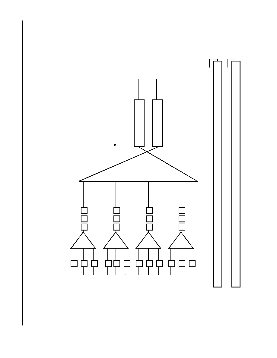
MARS2G5 P-Pro (TDAT162G52) SONET/SDH
Data Sheet
155/622/2488 Mbits/s Data Interface
August 18, 2004
194
Agere Systems Inc.
Transport Overhead Processor (TOHP-48) Block
(continued)
TOHP-48 Receive Direction
(continued)
The following figure shows the time-slot byte interleaving sequence per STS-1.
Figure 27. Time-Slot Assignments
STS-3/STM-1
STS-1
STS-1
STS-1
1
2
3
STS-3/STM-1
STS-1
STS-1
STS-1
4
5
6
8
9
STS-3/STM-1
STS-1
STS-1
STS-1
10
11
12
3:1
4:1
STS-12
INTERLEAVING ORDER
TIME
10 7 4 1 10 7 4 1 10 7 4 1
12 9 6 3 11 8 5 2 10 7 4 1
STM-4
THE INTERLEAVING ORDER FOR A STS-48/STM-16 IS AS FOLLOWS:
48 45 42 39 36 33 30 27 24 21 18 15 12 9 6 3 47 44 41 38 35 32 29 26 23 20 17 14 11 8 5 2 46 43 40 37 34 31 28 25 22 19 16 13 10 7 4 1
STS-48
46 43 40 37 34 31 28 25 22 19 16 13 10 7 4 1 46 43 40 37 34 31 28 25 22 19 16 13 10 7 4 1 46 43 40 37 34 31 28 25 22 19 16 13 10 7 4 1
STM-16
STS-3/STM-1
STS-1
STS-1
STS-1
7
3:1
3:1
3:1
3
2
1
6
5
4
9
8
7
12
11
10

Data Sheet
MARS2G5 P-Pro (TDAT162G52) SONET/SDH
August 18, 2004
155/622/2488 Mbits/s Data Interface
195
Agere Systems Inc.
Transport Overhead Processor (TOHP-48) Block
(continued)
TOHP-48 Receive Direction
(continued)
The time-slot assignment for each TOAC channel is summarized in the following table.
The transport overhead access channel consists of the following signals:
Four 5.184/20.736 MHz clock signals, RXTOHCLK[A--D] pins AK5, AL4, AL6, and AL7, respectively.
Four 5.184/20.736 Mbits/s data signals, RXTOHD[A--D] pins AL2, AM5, AM6, and AN7, respectively.
Four 8 kHz synchronization signals, RXTOHF[A--D] pins AK4, AL3, AN5, and AP6, respectively.
An inhibit signal is provided through the control interface to force the clock, sync, and selected data signal to zero
(TOHP_RTOACCINH (Table 68), TOHP_RTOACSINH (Table 68), and TOHP_RTOACDINH (Table 68)).
The data signal is partitioned into frames of 81 bytes for STS-3 mode and 324 bytes for STS-12 or STS-48 modes.
The frame repetition rate is 8 kHz. Each byte consists of 8 bits that are transmitted/received most significant bit
first. The MSB of the first byte of each frame contains an odd/even parity bit over the 648 bits of the previous
frame. The remaining 7 bits of this byte are not specified.
Bytes shown in Table 51 summarize the access capabilities of the receive TOAC. Bytes indicated in bold type
are not specified in the standard, but are labeled here for clarity.
Table 50. TOAC Channel Output Versus Time-Slot Assignment
Output Rate
TOAC Channel Outputs vs. Output Time Slot
A
B
C
D
STS-3/STM-1
3 2 1
3 2 1
3 2 1
3 2 1
STS-12/STM-4
12 9 6 3 11 8 5 2 10
7 4 1
12 9 6 3 11 8 5 2 10
7 4 1
12 9 6 3 11 8 5 2 10
7 4 1
12 9 6 3 11 8 5 2 10
7 4 1
STS-48/STM-16
39 27 15 3 38 26 14
2 37 25 13 1
42 30 18 6 41 29 17
5 40 28 16 4
45 33 21 9 44 32 20
8 43 31 19 7
48 36 24 12 47 35
23 11 46 34 22 10

MARS2G5 P-Pro (TDAT162G52) SONET/SDH
Data Sheet
155/622/2488 Mbits/s Data Interface
August 18, 2004
196
Agere Systems Inc.
Transport Overhead Processor (TOHP-48) Block
(continued)
TOHP-48 Receive Direction
(continued)
Table 51. Transport Overhead Bytes Received Via RxTOAC Interface*
Note: Numbers after - indicates byte number.
* Each TOAC output will have the corresponding byte value assigned to the time slot being accessed. This example is for an STS-12 signal for
TOAC output.
Even or odd parity can be inserted into the first bit of the MSB byte of the TOAC outgoing frame, using register bits
(TOHP_RTOAC_OEPINS[A--D] (Table 68)).
Insertion of AIS-L (MS-AIS)
The TOH-48 block will automatically generate AIS-L (MS-AIS) when TOHP_LOS, TOHP_OOF, or TOHP_LOF
state bits (Table 63) are active and the appropriate inhibit signals are inactive or software insert TOHP_LAISINS
(Table 67) is active.
Failure signal is comprised of LINE_AIS_GENERATE and FRM_ERR value for continuous N-times detect
(CNTD) detectors, but only LINE_AIS_GENERATE for error counters.
The TOHP-48 block will start/stop generating AIS-L within 125 µs of the detection/absence of a failure condition.
AIS-L (MS-AIS) is generated as a valid section overhead and an all 1s pattern in the remainder of the signal.
OH Parity A1-[2--12]
A2-1
A2-[2--12]
J0
Z0-[2--12]
B1-1
B1-[2--12]
E1-1
E1-[2--12]
F1-1
F1-[2--12]
D1-1
D1-[2--12]
D2-1
D2-[2--12]
D3-1
D3-[2--12]
H1-1
H1-[2--12]
H2-1
H2-[2--12]
H3-1
H3-[2--12]
B2-1
B2-[2--12]
K1-1
K1-[2--12]
K2-1
K2-[2--12]
D4-1
D4-[2--12]
D5-1
D5-[2--12]
D6-1
D6-[2--12]
D7-1
D7-[2--12]
D8-1
D8-[2--12]
D9-1
D9-[2--12]
D10-1
D10-[2--12] D11-1
D11-[2--12]
D12-1
D12-[2--12]
S1
Z1-[2--12]
Z2-1
Z2-2
M1 (Z2-3)
Z2-[4--12]
E2-1
E2-[2--12]

Data Sheet
MARS2G5 P-Pro (TDAT162G52) SONET/SDH
August 18, 2004
155/622/2488 Mbits/s Data Interface
197
Agere Systems Inc.
Transport Overhead Processor (TOHP-48) Block
(continued)
Transmit Direction (to SONET/SDH line)
This block accepts a frame with payload data (SPE), path overhead (POH), and pointer information (H1--H3)
bytes inserted. All other overhead bytes are inserted by this block; therefore, the incoming frame may put a fixed
stuff value into these time slots. The only other control signal needed by the block along with the data is a frame
sync signal active high one clock cycle aligned the A1-1 byte time. A bypass mode is also supported in the transmit
direction. When TOHP_TOH_BYPASS (Table 69) is set high, all 32 bits input data will be passed through to output
unprocessed and the output sync signal is invalid.
This section is broken down into the following functional parts:
Transpose (OC-48) and divider (OC-3)
TOAC insert
Sync status byte (S1) insert
REI-L insert: M1
K1 and K2 insert (including validation and pass through)
AIS-L insert
B2 calculation and insert
F1 byte insert
B1 generate and error insert
Scrambler
J0/Z0 insert control
A2 error insert
All insert control functions that are inhibited will insert all 0s for SONET and all 1s for SDH into the outgoing byte.
MARS2G5 P-Pro (TDAT162G52) SONET/SDH
Data Sheet
155/622/2488 Mbits/s Data Interface
August 18, 2004
198
Agere Systems Inc.
Transport Overhead Processor (TOHP-48) Block
(continued)
Transmit Direction (to SONET/SDH line)
(continued)
TOAC Insert
One transport overhead access channel (TOAC) is provided on-chip to provision the TOH portion of the outgoing
frame. The TOAC consists of the following signals:
A 5.184/20.736 MHz clock signal, sourced by the block (TTOACCLKO).
One 20.736 Mbits/s data signal received by the block in the transmit direction (TTOACDATAI).
An 8 kHz synchronization signal (TTOACSYNCO), sourced by this block. The sync signal is normally low; during
the first clock period of each frame coincident with the most significant bit of the first byte, the sync signal will go
high.
An inhibit signal is provided to place the clock and sync signal in a logic 0 state (TOHP_TTOACINH (Table 69)).
TOAC Channel Input Versus Time-Slot Assignments
The data signal is partitioned into frames of 324 bytes (except for OC-3). The frame repetition rate is 8 kHz. Each
byte consists of 8 bits that are received most significant bit first. The MSB of the first byte of each frame contains an
odd/even parity bit over the 648(OC-3)/2592(OC-12/OC-48) bits of the previous frame. The remaining 7 bits of this
byte are not specified. In mixed/quad STS-3/STS-12 mode, the TOAC input has byte multiplexed data from each
output signal (see Table 53, Table 54, and Table 55).
* X = reserved bytes (4 bytes).
Inserted via TOAC or TOHP registers.
Table 52. TOAC Channel Input Versus Time-Slot Assignments
Output Rate
TOAC Channel
Inputs vs. Input
Time Slot
STS-3/STM-1
1
STS-12/STM-4
7 4 1
STS-48/STM-16
34 31 28 25 22 19
16 13 10 7 4 1
Table 53. TTOAC OC-3 Signal Definition*
OC-3 Mode Signal Format (Letters Indicate Port Designations)
OH Pty
X
K1-A
K2-A
J0-A
J0-B
J0-C
J0-D
X
E1-A
E1-B
E1-C
E1-D
F1-A
F1-B
F1-C
F1-D
X
D1-A
D1-B
D1-C
D1-D
D2-A
D2-B
D2-C
D2-D
D3-A
D3-B
D3-C
D3-D
K1-B
K2-B
K1-C
K2-C
K1-D
K2-D
D4-A/
K1-A
D4-B/
K2-A
D4-C/
K1-B
D4-D/
K2-B
D5-A/
K1-C
D5-B/
K2-C
D5-C/
K1-D
D5-D/
K2-D
D6-A
D6-B
D6-C
D6-D
D7-A
D7-B
D7-C
D7-D
D8-A
D8-B
D8-C
D8-D
D9-A
D9-B
D9-C
D9-D
D10-A
D10-B
D10-C
D10-D
D11-A
D11-B
D11-C
D11-D
D12-A
D12-B
D12-C
D12-D
S1-A
S1-B
S1-C
S1-D
E2-A
E2-B
E2-C
E2-D
X
Data Sheet
MARS2G5 P-Pro (TDAT162G52) SONET/SDH
August 18, 2004
155/622/2488 Mbits/s Data Interface
199
Agere Systems Inc.
Transport Overhead Processor (TOHP-48) Block
(continued)
Transmit Direction (to SONET/SDH line)
(continued)
Note: X = reserved bytes (99 bytes).
Table 54. TTOAC OC-12 Signal Definition
OC-12 Mode Signal Format (Letters Indicate Port Designations)
A B C D
A
B
C
D
A
B
C
D
A B C D
A
B
C
D
A
B
C
D
A B C D
A
B
C
D
A
B
C
D
OH
Pty
X
X
X
X
X
X
X
X
X
X
X
X
X
X
X
X
X
X
X
X
X
X
X
J0
J0
J0
J0
X
X
X
X
X
X
X
X
X
X
X
X
X
X
X
X
X
X
X
X
E1
E1
E1
E1
E1-2
E1-2
E1-2
E1-2
E1-3
E1-3
E1-3
E1-3
F1
F1
F1
F1
F1-2
F1-2
F1-2
F1-2
F1-3
F1-3
F1-3
F1-3
D1
D1
D1
D1
D1-2
D1-2
D1-2
D1-2
D1-3
D1-3
D1-3
D1-3
D2
D2
D2
D2
D2-2
D2-2
D2-2
D2-2
D2-3
D2-3
D2-3
D2-3
D3
D3
D3
D3
D3-2
D3-2
D3-2
D3-2
D3-3
D3-3
D3-3
D3-3
X
X
X
X
X
X
X
X
X
X
X
X
X
X
X
X
X
X
X
X
X
X
X
X
X
X
X
X
X
X
X
X
X
X
X
X
X
X
X
X
X
X
X
X
X
X
X
X
K1
K1
K1
K1
K2
K2
K2
K2
X
X
X
X
K2
K2
K2
K2
K1
K1
K1
K1
X
X
X
X
D4
D4
D4
D4
D4-2
D4-2
D4-2
D4-2
D4-3
D4-3
D4-3
D4-3
D5
D5
D5
D5
D5-2
D5-2
D5-2
D5-2
D5-3
D5-3
D5-3
D5-3
D6
D6
D6
D6
D6-2
D6-2
D6-2
D6-2
D6-3
D6-3
D6-3
D6-3
D7
D7
D7
D7
D7-2
D7-2
D7-2
D7-2
D7-3
D7-3
D7-3
D7-3
D8
D8
D8
D8
D6-2
D6-2
D6-2
D6-2
D6-3
D6-3
D6-3
D6-3
D9
D9
D9
D9
D9-3
D9-3
D9-3
D9-3
D9-3
D9-3
D9-3
D9-3
D10 D10 D10 D10 D10-2 D10-2 D10-2 D10-2 D10-3 D10-3 D10-3 D10-3 D11 D11 D11 D11 D11-2 D11-2 D11-2 D11-2 D11-3 D11-3 D11-3 D11-3 D12 D12 D12 D12 D12-2 D12-2 D12-2 D12-2 D12-3 D12-3 D12-3 D12-3
S1
S1
S1
S1
Z1 -2
Z1 -2
Z1 -2
Z1 -2
Z1-3
Z1-3
Z1-3
Z1-3
Z2
Z2
Z2
Z2
Z2-2
Z2-2
Z2-2
Z2-2
Z2-4
Z2-4
Z2-4
Z2-4
E2
E2
E2
E2
E2-2
E2-2
E2-2
E2-2
E2-3
E2-3
E2-3
E2-3
MARS2G5 P-Pro (TDAT162G52) SONET/SDH
Data Sheet
155/622/2488 Mbits/s Data Interface
August 18, 2004
200
Agere Systems Inc.
Transport Overhead Processor (TOHP-48) Block
(continued)
Transmit Direction (to SONET/SDH line)
(continued)
Note: X = reserved bytes (115 bytes).
Table 55. TTOAC OC-48 Signal Definition
OC-48 Mode Signal Format (Letters Indicate Port Designations)
OH
Pty
X
X
X
X
X
X
X
X
X
X
X
X
X
X
X
X
X
X
X
X
X
X
X
J0
X
X
X
X
X
X
X
X
X
X
X
X
X
X
X
X
X
X
X
X
X
X
X
E1
E1-2 to 12
F1
F1-2 to 12
D1
D1-2 to 12
D2
D2-2 to 12
D3
D3-2 to 12
X
X
X
X
X
X
X
X
X
X
X
X
X
X
X
X
X
X
X
X
X
X
X
X
X
X
X
X
X
X
X X
X
X
X
X
X
X
X
X
X
X
X
X
X
X
X
X
K1
K2
X
X
X
X
X
X
X
X
X
X
K2
K1
X
X
X
X
X X
X
X
X
X
D4
D4-2 to 12
D5
D5-2 to 12
D6
D6-2 to 12
D7
D7-2 to 12
D8
D8 -2 to 12
D9
D9-2 to 12
D10
D10-2 to 12
D11
D11-2 to 12
D12
D12-2 to 12
S1
Z1-2 to 12
Z2
Z2-2 X
Z2-4 to 12
E2
E2-2 to 12
Data Sheet
MARS2G5 P-Pro (TDAT162G52) SONET/SDH
August 18, 2004
155/622/2488 Mbits/s Data Interface
201
Agere Systems Inc.
Transport Overhead Processor (TOHP-48) Block
(continued)
Transmit Direction (to SONET/SDH line)
(continued)
In STS-48 mode, each TOAC input has access to those columns of overhead bytes as defined in Table 52.
An event indication is provided to indicate parity errors on the TOAC input channel. Odd (logic 0)/even (logic 1)
parity is checked (TOHP_TTOAC_OEPMON (Table 69), TOHP_TTOAC_PERRM (Table 64),
TOHP_TTOAC_PERRE (Table 62)).
Table 56 summarizes the insertion options for the specified overhead bytes for the transmit TOAC. A predefined
stuff value (all 0s for SONET and all 1s for SDH) or the corresponding TOAC value is inserted as shown in
Table 56.
* When TOHP_TK2SINS[A--D][1:0] = 11 TOAC data is inserted into the outgoing k2[2:0] value; otherwise, the source of this value can come
from hardware, software, or raw K value.
Table 56. TTOAC Control Bits
Overhead Bytes
Control Bits
(Table 69)
Values
OC-3
OC-12
OC-48
0 (Default
Value)
1
J0
TOHP_TTOAC_J0[A--D]
SONET/SDH
(00000000/
11111111)
TTOAC
Data
E1
TOHP_TTOAC_E1[A--D]
F1
TOHP_TTOAC_F1[A--D]
D1--D3
TOHP_TTOAC_D1TO3[A--D]
K1, K2[7:3]
TOHP_TTOAC_K1K2[A--D]
K2[2:0]*
TOHP_TK2SINS[A--D][1:0]
D4--D12
TOHP_TTOAC_D4TO12[A--D]
S1
TOHP_TTOAC_S1[A--D]
E2
TOHP_TTOAC_E2[A--D]
D1-[2-3]
to
D3, D3-[2-3]
D1-2, . . ., N to
D3-2, . . ., N
TOHP_TTOAC_INS
SONET/SDH
(00000000/
11111111)
TTOAC
Data
D4-[2-3]
to
D12, D12-[2-3]
D4-2, . . ., N to
D12-2, . . ., N
E1-[2-3]
E1-2, . . ., E1-N
F1-[2-3]
F1-2, . . ., F1-N
E2-[2-3]
E2-2, . . ., E2-N
Z1-2, Z1-3
Z1-2, . . ., Z1-N
Z2-[2-3]
Z2-1, Z2-2
Z2-4, . . ., Z2-N

MARS2G5 P-Pro (TDAT162G52) SONET/SDH
Data Sheet
155/622/2488 Mbits/s Data Interface
August 18, 2004
202
Agere Systems Inc.
Transport Overhead Processor (TOHP-48) Block
(continued)
Transmit Direction (to SONET/SDH line)
(continued)
Sync Status Byte Insert
Via microprocessor control of TOHP_TS1INS (active-high) (Table 69) and TOHP_TS1DINS[7:0] (Table 84), data
information may be inserted into the outgoing S1 byte [9, 1, 1]. Direct microprocessor insert has higher priority than
the TOAC insert control bit (TOHP_TTOAC_S1(Table 69)).
REI-L (MS-REI): M1
One byte is allocated for use as an MS-REI. For STS-N/STM-M levels, this byte conveys the count (in the range of
[0, 255]) of interleaved bit blocks that have been detected in error by the BIP-24xM (B2) detector on the received
signal (B2ECntPerF[7:0]). For STS-48/STM-16 signals, this value is held at 255 if the received signal has more
than 255 BIP errors.
This function can be inhibited (TOHP_TM1_REIL_INH (Table 69)) and the default value inserted (STUFF-
BYTE[7:0]) via microprocessor control. A continuous error in the M1 byte can be inserted under user control
(TOHP_TM1_ERR_INS (Table 69)). A value of 0x03 is inserted when the TOHP_TM1_ERR_INS signal is active.
REI-L (MS-REI) is inserted into M1 byte as defined in the following figure.
5-8497(F)r.1
Figure 28. REI-L (MS-REI) Location
For STS-3/STM-1 signals, the M1 value is in the range of 0 to 24. For STS-12/STM-4 signals, the M1 value is in the
range of 0 to 96. For STS-48/STM-16 signals, the M1 value is in the range of 0 to 255 (truncated).
K1 and K2 Insert Control Parameters
Via microprocessor control (TOHP_TAPSINS = 1 (Table 70)) the K1 [5, 2, 1] and K2 [5, 3, 1] outgoing bytes are
written from TK1DINS[7:0] (Table 84) and TK2DINS[7:3] (Table 84), respectively. When TOHP_TAPSINS is logic 0,
K1[7:0] and K2[7:3] outgoing bytes are written from TX_RAWK[15:3]. Since TX_RAWK[15:0] is a multibyte register,
both values must be valid at the same time. When TOHP_TK2SINS[1] = 1 (Table 70), data from the
TOHP_TK2DINS[2:0] register is written into K2[2:0] (transmit K2 software insertion). For hardware insertion of RDI-
L (110) to be written to K2[2:0], set TOHP_TK2SINS[1:0] = 01. Otherwise, when TOHP_TK2SINS[1:0] = 00,
TX_RAWK[2:0] is written to K2[2:0].
When TOHP_TVALIDK_CTL (Table 70) is a logic 1, reversed K1 byte is written to K1 ([5, 2, 2] for OC-3/OC-12,
[5, 2, 5] for OC-48) and reversed K2 byte is written to K2 ([5, 3, 2] for OC-3/OC-12, [5, 3, 5] for OC-48). Otherwise,
K1 and K2 reverse bytes are written with default values (all 0s for SONET and all 1s for SDH).
APS babbling test control: Setting the TOHP_TAPSBABLEINS bit (Table 69), via microprocessor control, forces
the K1[7:0], K2[7:3) to an inconsistent state; no three consecutive values are the same continuously.
Z2-1
Z2-2
M1
23 (MSB)
0 (LSB)
0 (LSB)
7 (MSB)
REI-L (MS-REI) [9, 2, 3]

Data Sheet
MARS2G5 P-Pro (TDAT162G52) SONET/SDH
August 18, 2004
155/622/2488 Mbits/s Data Interface
203
Agere Systems Inc.
Transport Overhead Processor (TOHP-48) Block
(continued)
Transmit Direction (to SONET/SDH line)
(continued)
Line RDI is inserted into the data signal when one or more of the following occurs and the corresponding inhibit bit
is not set:
Input loss of clock (LOC)
Loss-of-signal (LOS)
Out-of-frame (OOF)
Loss-of-frame (LOF)
Line AIS (LAISMON)
Signal fail (BER algorithm) (SF)
When a failure condition exists that will cause RDI-L to be generated, the generation of RDI-L will last for at least
20 frames before clearing; even if the original failure cause has cleared in less than 20 frames. This function can
be inhibited by setting TOHP_TIMER_LRDIINH (Table 69) to a logic 1.
AIS Line/MS-AIS Generation
Line AIS/MS-AIS is specified as all 1s in the entire STS/STM signal before scrambling, excluding the section over-
head (RSOH).
Line AIS can be generated via microprocessor control on a per STS-1 basis (TOHP_TAISLINS[48:1] (Table 70)).
For a concatenated or STM type signal, the user must determine which time slots should be provisioned to gener-
ate a valid AIS signal.
B2 BIP 8XN Calculation and Insert
The B2 bytes are allocated for a line overhead (multiplex section) error monitoring function. This function will be a
bit interleaved parity N X 8 code (BIP-N X 8) using even parity. The BIP-N X 8 is computed over all bits of the pre-
vious STS-N/STM-M frame except the first three rows of SOH (RSOH) and is placed in bytes B2 of the current
frame before scrambling. N = 3M and M = 1, 4, and 16.
Via microprocessor control all B2 bytes can be inverted (TOHP_TB2ERRINS (Table 69)).
F1 Byte Insert
Via microprocessor control of TOHP_TF1INS (Table 69) and TOHP_TF1DINS[7:0] (Table 84), data information
may be inserted into the outgoing F1 byte[2, 3, 1]. Direct microprocessor insert has higher priority than the TOAC
insert control bit (TOHP_TTOAC_F1 (Table 69)).
When TOHP_TF1INS is a logic 1, insert the value in register TOHP_TF1DINS[7:0]; otherwise, insert the associ-
ated TOAC value when TOHP_TTOAC_F1 is a logic 1 or insert the default value of all zeros for SONET and all
ones for SDH when TOHP_TTOAC_F1 is logic 0.
B1 Generate and Error Insert
The section bit interleaved parity code (BIP-8) byte--this is a parity code (even parity), used to check for transmis-
sion errors over a section. Its value is calculated over all bits in the previous frame after scrambling, and then
placed in the B1 byte of time slot 1 before scrambling.
Via microprocessor control the B1 byte can be inverted (TOHP_TB1ERRINS (Table 69)).

MARS2G5 P-Pro (TDAT162G52) SONET/SDH
Data Sheet
155/622/2488 Mbits/s Data Interface
August 18, 2004
204
Agere Systems Inc.
Transport Overhead Processor (TOHP-48) Block
(continued)
Transmit Direction (to SONET/SDH line)
(continued)
Scrambler
The outgoing frame will be scrambled with the frame synchronous scrambler of length 127 and generating polyno-
mial x
7
+ x
6
+ 1. The entire STS/STM signal will be scrambled except for the first row of overhead. The scrambler
will be set to 1111111 on the first byte following the last overhead byte in the first row.
For test purposes, the scrambler will be disabled when TOHP_SCRINH (Table 69) is a logic 1.
J0/Z0 Insert Control
A 16-byte sequence stored in registers TOHP_TJ0DINS[1--16][7:0] (Table 87) will be inserted into the outgoing J0
byte if TOHP_TJ0INS (Table 69) is set to logic 1; otherwise, the associated TOAC value is inserted when
TOHP_TTOAC_J0 (Table 69) is a logic 1 or the default value is inserted when TOHP_TTOAC_J0 is logic 0.
A programmable value is inserted into each Z0 byte. The values are stored in registers TOHP_TZ0DINS[A--D][3--
2][7:0] (Table 88) for OC-3 mode and TOHP_TZ0DINS[A--D][12--2][7:0] for OC-12 mode. In OC-48 mode, there
are 47 Z0 bytes that are stored in {TOHP_TZ0DINS[D][12--2], TOHP_TJ0INS[D][1], TOHP_TZ0DINS[C][12--2],
TOHP_TJ0INS[C][1], TOHP_TZ0DINS[B][12--2], TOHP_TJ0INS[B][1], and TOHP_TZ0DINS[A][12--2]}.
A2 Error Insert
From 1 to 32 continuous outgoing (TOHP_TA1A2ERRINS[4:0] (Table 69), TOHP_TA1A2ERREN (Table 65))
frames can have inverted A2-1 (0x28 to 0xD7) pattern. The value in the TOHP_TA1A2ERRINS[4:0] register speci-
fies the number of frames to insert errors into, while the TOHP_TA1A2ERREN one-shot register starts the error
insertion process.
Receive/Transmit TOHP-48 Interface
All receive transport overhead bytes are output on the RTOH interface for external processing needs. All transmit
transport overhead bytes can optionally be inserted from the TTOH interface for external needs.
* This OC-48 interface is a four-line interface resulting in an effective interface rate of 82,944,000 bits/s.
Table 57. Rx/Tx TOHP-48 Interface Rates
Rate Selection R/T
(TOHP_RX_MODE[1:0]/
TOHP_TX_MODE[1:0] 0x0800 (Table 60))
Mode
Rx/Tx TOHP-48 Interface Rate
1X
OC-48
20,736,000* baud
01
OC-12
20,736,000 bits/s
00
OC-3
5,184,000 bits/s
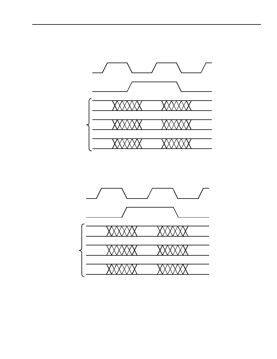
Data Sheet
MARS2G5 P-Pro (TDAT162G52) SONET/SDH
August 18, 2004
155/622/2488 Mbits/s Data Interface
205
Agere Systems Inc.
Transport Overhead Processor (TOHP-48) Block
(continued)
Receive/Transmit TOHP-48 Interface
(continued)
5-7419(F)r.5U
Note: Numbers in brackets denote bits. X[number] indicates a reserved bit.
Figure 29. RTOH Interface
5-7420(F)r.4U
Note: Numbers in brackets denote bits. X[number] indicates a reserved bit.
Figure 30. TTOH Interface
OH PARITY[7]
RXTOHCLK[A--D]
RXTOHF[A--D]
RXTOHD[A--D]
E2#34[0]
X[6]
OH PARITY[7]
E2--3D[0]
X[6]
OH PARITY[7]
E2--3[0]
X[6]
OC-48 MODE
OC-12 MODE
OC-3 MODE
OH PARITY[7]
TXTOHCLK
TXTOHF
E2#34[0]
X[6]
OH PARITY[7]
TXTOHD
E2--3D[0]
X[6]
OH PARITY[7]
X[0]
X[6]
OC-48 MODE
OC-12 MODE
OC-3 MODE
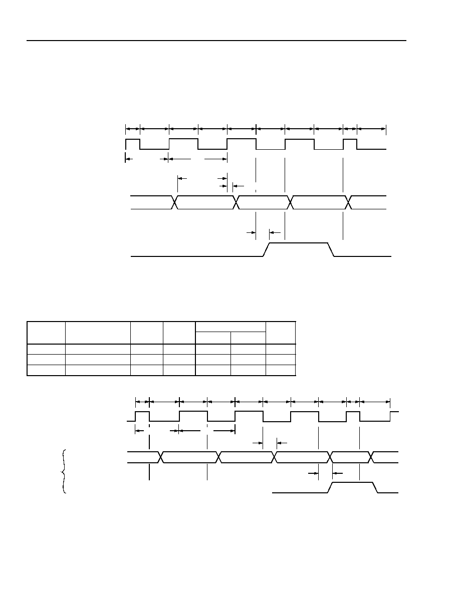
MARS2G5 P-Pro (TDAT162G52) SONET/SDH
Data Sheet
155/622/2488 Mbits/s Data Interface
August 18, 2004
206
Agere Systems Inc.
Transport Overhead Processor (TOHP-48) Block
(continued)
Transport Overhead Access Channel (TOAC) Interface Timing
Transport overhead access channel (TOAC) interface timing specifications are given for the transmit direction in
Figure 31 and in Table 58, and for the receive direction in Figure 32 and in Table 59.
0151(F)r.4
Note: Duty cycles shown are nominal.
* tCP = x/y where y is the clock frequency in MHz on the TXCLKP/N pins and x = 32 for OC-3 and OC-12. For OC-48, x = 8.
Figure 31. STS-3/STM1, STS-12/STM-4, and STS-48/STM-16 Transmit TOAC Interface Timing
Table 58. Transmit TOAC Interface Timing Specifications
0152(F)r.2
Note: Duty cycles shown are nominal.
* tCP = x/y where y is the clock frequency in MHz on the TXCLKP/N pins and x = 32 for OC-3 and OC-12. For OC-48, x = 8.
Figure 32. STS-12/STM-4 and STS-48/STM-16 Receive TOAC Interface Timing
Symbol
Test Conditions
Setup
(Min)
Hold
(Min)
Propagation Delay
Unit
(Min)
(Max)
tTTDSU
--
10
--
--
--
ns
tTTDH
--
--
10
--
--
ns
tTTFSPD
C
L
= 50 pF
--
--
0
10
ns
50%
50%
50%
50%
50%
OUTPUT--TXTOHCLK
INPUT--TXTOHD
OUTPUT--TXTOHF 8 kHz
DUTY CYCLE CLOCK
5.184 MHz (STS-3/STM-1)
20.736 MHz (STS-12/STM-4)
(STS-48/STM-16)
67%
33%
33%
67%
tTTFSPD
50%
0.75tCP*
tCP
tTTDH
tTTSDU
50%
50%
50%
50%
50%
67%
33%
33%
67%
50%
OUTPUT--RXTOHCLK[D--A]
RXTOHD[D--A]
OUTPUTS
DUTY CYCLE CLOCK
RXTOHF[D--A] 8 kHz
(STS-48/STM-16)
tRTDPD
tRTFSPD
20.736 MHz (STS-12/STM-4)
0.75tCP*
tCP
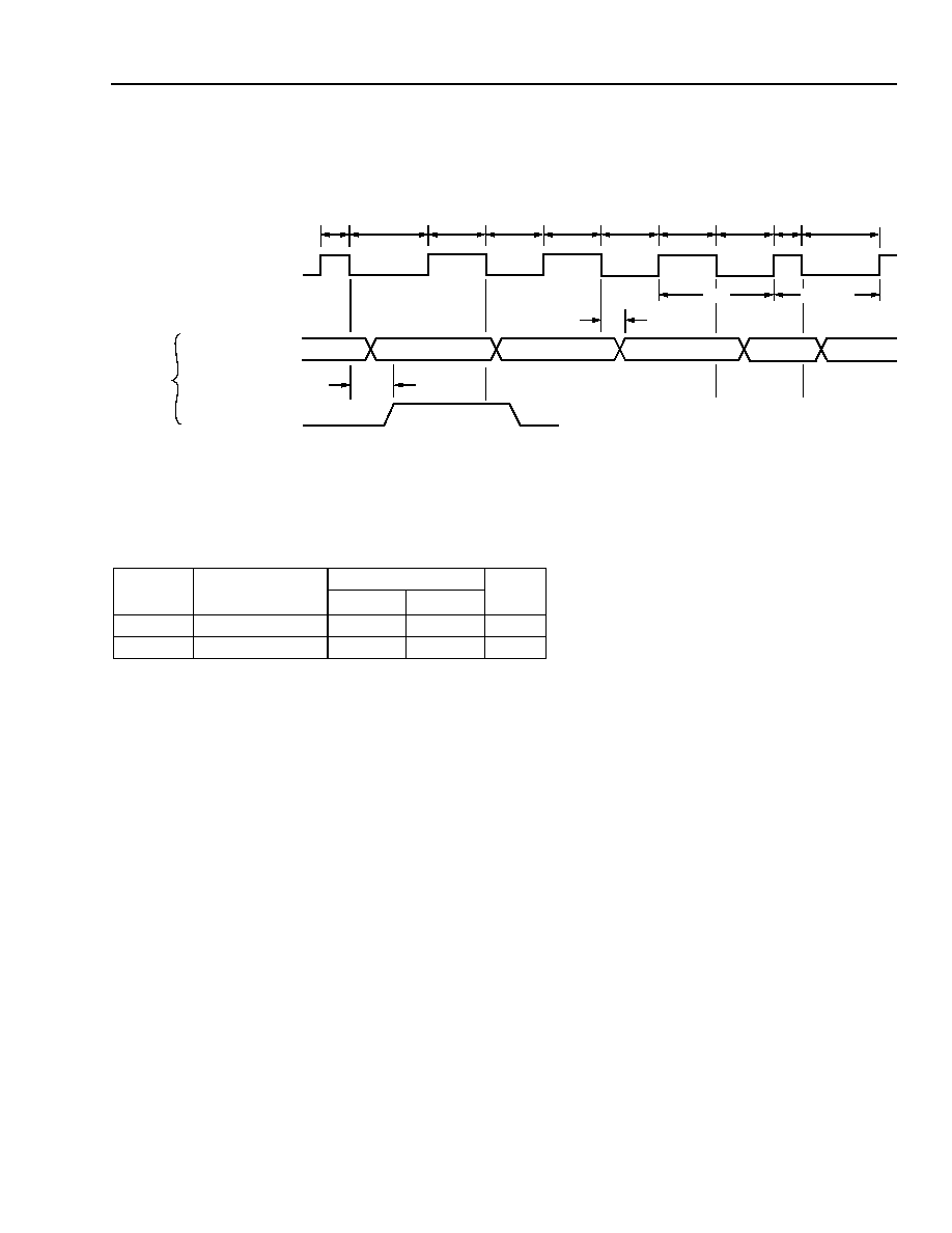
Data Sheet
MARS2G5 P-Pro (TDAT162G52) SONET/SDH
August 18, 2004
155/622/2488 Mbits/s Data Interface
207
Agere Systems Inc.
Transport Overhead Processor (TOHP-48) Block
(continued)
Transport Overhead Access Channel (TOAC) Interface Timing
(continued)
0153(F)r.4
Note: Duty cycles shown are nominal.
* tCP = x/y where y is the clock frequency in MHz on the TXCLKP/N pins and x = 32 for OC-3 and OC-12. For OC-48, x = 8.
Figure 33. STS-3/STM-1 Receive TOAC Interface Timing
Table 59. Receive TOAC Interface Timing Specifications
Symbol
Test Conditions
Propagation Delay
Unit
(Min)
(Max)
tRTDPD
C
L
= 50 pF
0
10
ns
tRTFSPD
C
L
= 50 pF
0
10
ns
50%
50%
50%
50%
50%
67%
33%
33%
67%
50%
0.75tCP*
tCP
OUTPUT--RXTOCLK[D--A]
RXTOHD[D--A]
OUTPUTS
DUTY CYCLE CLOCK
RXTOHF[D--A] 8 kHz
tRTDPD
tRTFSPD
5.184 MHz (STS-3/STM-1)

MARS2G5 P-Pro (TDAT162G52) SONET/SDH
Data Sheet
155/622/2488 Mbits/s Data Interface
August 18, 2004
208
Agere Systems Inc.
Transport Overhead Processor (TOHP-48) Block
(continued)
TOHP-48 Register Descriptions
To access (read and write) registers RXCLK[A--D][P/N] (see Pin Descriptions--Line Interface Signals, Table 7 on
page 97) must always be present for a given application.
Note:Parameters of more than 16 bits are made up of 32-bit register pairs (Table 75, Table 77). Each pair gets writ-
ten at the same time.
Two consecutive writes are needed to complete a write to these registers. For example, when writing
address 0x0852, the data is held in a shadow register; when writing address 0x0853, the data gets written in
0x0853 and at the same time, the data in the shadow register is transferred to address 0x0852.
When reading, the registers are accessed without using the shadow register and are read one at a time.
Table 60. TOHP_MODE_VERR, Mode (R/W) and Block Version (RO)
Table 61. TOHP_CH_INT, Channel Interrupt (R/W, RO)
Address
Bit
Name
Function
Reset
Default
0x0800
15:13
TOHP_RX_MODE[2:0] Receive Direction Mode. TOHP_RX_MODE[2], bit
15, has two functions: default value for the registers
and the number of errored frames required before
declaring and OOF condition in the framer.
[2] 1 = SDH, 0 = SONET
[1] 1= OC-48, 0 = OC-3/12
[0] 1 = OC-12, 0 = OC-3
011
12:10
TOHP_TX_MODE[2:0]
Transmit Direction Mode. TOHP_TX_MODE[2], bit
12, has two functions: default value for the registers
and the number of errored frames required before
declaring and OOF condition in the framer.
[2] 1 = SDH, 0 = SONET
[1] 1 = OC-48, 0 = OC-3/12
[0] 1 = OC-12, 0 = OC-3
011
9:0
TOHP_VER[9:0]
Block Version Number. Block version register will
change each time the device is changed.
0000000
00
1
Address
Bit
Name
Function
Reset
Default
0x0801
15
TOHP_CORWN
Clear on Read/(Not) Write. 1 = COR, 0 = COW.
0
14:12
--
Reserved.
0x0
11:8
TOHP_INTH[D--A]
High Interrupt (RO). Active-high interrupt bits for chan-
nel D to A. Each bit is the ORing of all event and delta
signals of OOF, LOF, LOS, and LOC of that channel
(Table 62).
0x0
7:4
--
Reserved.
0x0
3:0
TOHP_INTL[D--A]
Low Interrupt (RO). Active-high interrupt bits for chan-
nel D to A. Each bit is the ORing of all event and delta of
all monitoring features, i.e., TOHP_K2DMON
(Table 85), of that channel.
0x0

Data Sheet
MARS2G5 P-Pro (TDAT162G52) SONET/SDH
August 18, 2004
155/622/2488 Mbits/s Data Interface
209
Agere Systems Inc.
Transport Overhead Processor (TOHP-48) Block
(continued)
TOHP-48 Register Descriptions
(continued)
Table 62. TOHP_DLT_EVT[A--D][1--2], 0x0802--0x0809, Delta/Event Registers (COR/COW-RO)
Address
Bit
Name
Function
Reset
Default
0x0802,
0x0804,
0x0806,
0x0808
15
TOHP_LRDIMOND
[A--D]
Line/Multiplex RDI Delta. Delta bit indicates a change of state
for the line/multiplex RDI state bits, TOHP_LRDIMON[A--D].
The delta bits clear when read. Their mask bits are
TOHP_LRDIMONM[A--D]. In STS-48 mode, only
TOHP_LRDIMOND[A] is valid.
1, 1, 1,
1
14
TOHP_LAISMOND
[A--D]
Line/Multiplex AIS Delta. Delta bit indicates a change of
states for the line/multiplex AIS state bits
TOHP_LAISMON[A--D]. The delta bits clear when read. Their
mask bits are TOHP_LAISMONM[A--D]. In STS-48 mode,
only TOHP_LAISMOND[A] is valid.
1, 1, 1,
1
13
TOHP_
RAPSBABLEE
[A--D]
APS Babble Event Bit. Each bit is active-high to indicate the
inconsistence in K1 byte of that channel. Their mask bits are
TOHP_RAPSBABLEM[A--D]. In STS-48 mode, only
TOHP_RAPSBABLEE[A] is valid.
0, 0, 0,
0
12
TOHP_S1DMON4D
[A--D]
Delta Register for S1DMON[3:0] When S1MON8or4CTL = 1.
Each delta bit indicates a change of state for
TOHP_S1DMON[3:0] in its channel. The delta bit clears when
read. Their mask bits are TOHP_S1DMON4M[A--D]. In
STS-48 mode, only TOHP_S1DMON4D[A] is valid.
0, 0, 0,
0
11
TOHP_S1DMON8D
[A--D]
Delta Register for S1DMON[7:4] When S1MON8or4CTL = 1
or S1DMON[7:0] When S1MON8or4CTL = 0. Each delta bit
indicates a change of state for TOHP_S1DMON[7:4]/
TOHP_S1DMON[7:0] in its channel. The delta bit clears when
read. Their mask bits are TOHP_S1DMON8M[A--D]. In
STS-48 mode, only S1DMON8D[A] is valid.
0, 0, 0,
0
10
TOHP_K2DMOND
[A--D]
K2[2:0] Data Monitor Delta Bit. Each bit is active-high to indi-
cate a change in TOHP_K2DMON[A--D] for that channel.
These bits will clear when read or write. Their mask bits are
TOHP_K2DMONM[A--D]. In STS-48 mode, only
TOHP_K2DMONE[A] is valid.
0, 0, 0,
0
9
TOHP_K1K2DMOND
[A--D]
K1K2 Data Monitor Delta Bit. Each bit is active-high to indi-
cate a change in (K1[7:0] and K2[7:3]) or (K1[7:0] and K2[7:0])
for that channel depending on K1K2_2OR1. Their mask bits
are TOHP_K1K2DMONM[A--D]. In STS-48 mode, only
TOHP_K1K2DMONE[A] is valid.
0, 0, 0,
0
8
TOHP_F1DMOND
[A--D]
F1 Data Monitor Delta Bit. Their mask bits are
TOHP_F1DMONM[A--D]. In STS-48 mode, only
TOHP_F1DMOND[A] is valid.
0, 0, 0,
0
0x0802
7
TOHP_
TTOAC_PERRE
Transmit TOAC Parity Error Event. Event register indicates a
parity error was detected on the incoming TOAC.
1, 0, 0,
0

MARS2G5 P-Pro (TDAT162G52) SONET/SDH
Data Sheet
155/622/2488 Mbits/s Data Interface
August 18, 2004
210
Agere Systems Inc.
Transport Overhead Processor (TOHP-48) Block
(continued)
TOHP-48 Register Descriptions
(continued)
Table 62. TOHP_DLT_EVT[A--D][1--2], 0x0802--0x0809, Delta/Event Registers (COR/COW-RO) (continued)
Address
Bit
Name
Function
Reset
Default
0x0802,
0x0804,
0x0806,
0x0808
6
TOHP_
S1BABLEE[A--D]
Receive S1 Byte Babbling Event. This event register will be
set if TOHP_CNTDS1BABLE[A--D][3:0] consecutive frames
pass without a validated S1 byte.
0, 0, 0,
0
5
TOHP_SFD[A--D]
Signal Fail BER Algorithm Delta. Delta bit indicates a
change of state for the signal fail BER algorithm state bits
TOHP_SF[A--D]. The delta bits clear when read. Their mask
bits are TOHP_SFM[A--D]. In STS-48 mode, only
TOHP_SFD[A] is valid.
1, 1, 1,
1
0x0802,
0x0804,
0x0806,
0x0808
4
TOHP_SDD[A--D]
Signal Degrade BER Algorithm Delta. Delta bit indicates a
change of states for the signal degrade BER algorithm state
bits TOHP_SD[A--D]. The delta bits clear when read. Their
mask bits are TOHP_SDM[A--D]. In STS-48 mode, only
TOHP_SDD[A] is valid.
1, 1, 1,
1
3
TOHP_OOFD
[A--D]
Receive Out of Frame Delta. Delta bit indicates change of
state for the out-of-frame TOHP_OOF[A--D]. The delta bits
clear when read. Their mask bits are TOHP_OOFM[A--D]. In
STS-48 mode, only TOHP_OOFD[A] is valid.
1, 0, 0,
0
2
TOHP_LOFD
[A--D]
Receive Loss of Frame Delta. Delta bit indicates change of
state for the loss-of-frame TOHP_LOF[A--D]. The delta bits
clear when read. Their mask bits are TOHP_LOFM[A--D]. In
STS-48 mode, only TOHP_LOFD[A] is valid.
1, 0, 0,
0
1
TOHP_LOSD
[A--D]
Receive Loss of Signal Delta. Delta bit indicates change of
state for the loss-of-signal TOHP_LOS[A--D]. The delta bits
clear when read. Their mask bits are TOHP_LOSM[A--D]. In
STS-48 mode, only TOHP_LOSD[A] is valid.
1, 1, 1,
1
0
TOHP_LOCD
[A--D]
Receive Loss of Clock Delta. Delta bit indicates change of
states for the loss-of-clock TOHP_LOC[A--D]. The delta bits
clear when read. Their mask bits are TOHP_LOCM[A--D]. In
STS-48 mode, only TOHP_LOCD[A] is valid.
1, 1, 1,
1
0x0803,
0x0805,
0x0807,
0x0809
15:2
--
Reserved.
000
0000
0000
000
1
TOHP_TTOAC_
K1K2ERRE[A--D]
Transmit TOAC K1and K2 Error Event. Event bits indicate
when an error is detected between the true and complement
K1/K2 values. Their mask bits are
TOHP_TTOAC_K1K2ERRM[A--D]. In STS-48 mode, only
TOHP_TTOAC_K1K2ERRE[A] is valid.
0
0
TOHP_J0MISE
[A--D]
J0 Mismatch Event Bits. Their mask bits are
TOHP_J0MISM[A--D]. In STS-48 mode, only
TOHP_J0MISE[A] is valid for J0 byte while
TOHP_J0MISE[D--B] are used for Z0 bytes as
TOHP_Z0DMOND[D--B][1].
1

Data Sheet
MARS2G5 P-Pro (TDAT162G52) SONET/SDH
August 18, 2004
155/622/2488 Mbits/s Data Interface
211
Agere Systems Inc.
Transport Overhead Processor (TOHP-48) Block
(continued)
TOHP-48 Register Descriptions
(continued)
Table 63. TOHP_RX_TX_STATE[A--D], 0x080A--0x080D, Receive/Transmit State Registers (RO)
Address
Bit
Name
Function
Reset
Default
0x080A--
0x080D
15
TOHP_LRDIMON[A--D]
Line/Multiplex RDI State Bit. In STS-48 mode,
only TOHP_LRDIMON[A] is valid.
0
14
TOHP_LAISMON[A--D]
Line/Multiplex AIS State Bit. In STS-48 mode,
only TOHP_LAISMON[A] is valid.
0
13:7
--
Reserved.
0
6
TOHP_TLRDIINT[A--D]
Transmit Line RDI Insert State Bit. State bit for
inserting line RDI value into the K2[2:0] bits. In
STS-48 mode, only TOHP_TLRDIINT[A] is valid.
0
5
TOHP_SF[A--D]
Signal Fail State Bit. In STS-48 mode, only
TOHP_SF[A] is valid.
0
4
TOHP_SD[A--D]
Signal Degrade State Bit. In STS-48 mode,
only TOHP_SD[A] is valid.
0
3
TOHP_OOF[A--D]
Out-of-Frame. Active-high out-of-frame state
bit. In STS-48 mode, only TOHP_OOF[A] is
valid.
0
2
TOHP_LOF[A--D]
Loss-of-Frame. Active-high loss-of-frame state
bit. In STS-48 mode, only TOHP_LOF[A] is valid.
0
1
TOHP_LOS[A--D]
Loss-of-Signal. Active-high loss-of-signal state
bit. In STS-48 mode, only TOHP_LOS[A] is
valid.
0
0
TOHP_LOC[A--D]
Loss-of-Clock. Active-high loss-of-clock state
bit. In STS-48 mode, only TOHP_LOC[A] is
valid.
When a loss-of-clock is detected for a line inter-
face, associated status registers for that line
interface may not be updated.
0

MARS2G5 P-Pro (TDAT162G52) SONET/SDH
Data Sheet
155/622/2488 Mbits/s Data Interface
August 18, 2004
212
Agere Systems Inc.
Transport Overhead Processor (TOHP-48) Block
(continued)
TOHP-48 Register Descriptions
(continued)
Table 64. TOHP_MSK[A--D][1--2], 0x080E--0x0815, Mask Bit Registers (R/W)
Address
Bit
Name
Function
Reset
Default
0x080E,
0x0810,
0x0812,
0x0814
15
TOHP_LRDIMONM
[A--D]
Line/Multiplex RDI Mask Bit. A 1 masks the corre-
sponding occurrence of the alarm to the interrupt. In
STS-48 mode, only TOHP_LRDIMONM[A] is valid.
1
14
TOHP_LAISMONM
[A--D]
Line/Multiplex AIS Mask Bit. A 1 masks the corre-
sponding occurrence of the alarm to the interrupt. In
STS-48 mode, only TOHP_LAISMONM[A] is valid.
1
13
TOHP_RAPSBABLEM
[A--D]
APS Babble Mask Bit. A 1 masks the corresponding
occurrence of the alarm to the interrupt. In STS-48
mode, only TOHP_RAPSBABLEM[A] is valid.
1
12
TOHP_S1DMON4M
[A--D]
Mask Bit for S1DMON4D When S1MON8or4CTL = 1.
A 1 masks the corresponding occurrence of the alarm to
the interrupt. In STS-48 mode, only
TOHP_S1DMON4LSNM[A] is valid.
1
11
TOHP_S1DMON8M
[A--D]
Mask Bit for S1DMON8D. A 1 masks the corresponding
occurrence of the alarm to the interrupt. In STS-48
mode, only TOHP_S1DMON8M[A] is valid.
1
10
TOHP_K2DMONM[A--D] K2[2:0] Data Monitor Mask Bit. A 1 masks the corre-
sponding occurrence of the alarm to the interrupt. In
STS-48 mode, only TOHP_K2DMONM[A] is valid.
1
9
TOHP_K1K2DMONM
[A--D]
K1K2 Data Monitor Mask Bit. A 1 masks the corre-
sponding occurrence of the alarm to the interrupt. In
STS-48 mode, only TOHP_K1K2DMONM[A] is valid.
1
8
TOHP_F1DMONM[A--D] F1 Data Monitor Mask Bit. A 1 masks the correspond-
ing occurrence of the alarm to the interrupt. In STS-48
mode, only TOHP_F1DMONM[A] is valid.
1
0x080E
7
TOHP_TTOAC_PERRM Transmit TOAC Parity Error Mask. A 1 masks the cor-
responding occurrence of the alarm to the interrupt. All
4 bits are valid in every mode.
1
0x080E,
0x0810,
0x0812,
0x0814
6
TOHP_S1BABLEM
[A--D]
S1 Babbling Mask Bit. A 1 masks the corresponding
occurrence of the alarm to the interrupt. In STS-48
mode, only TOHP_S1BABLEM[A] is valid.
1
5
TOHP_SFM[A--D]
Signal Fail Mask Bit. Active-high signal fail mask bit. In
STS-48 mode, only TOHP_SFM[A] is valid.
1
4
TOHP_SDM[A--D]
Signal Degrade Mask Bit. Active-high signal degrade
mask bit. In STS-48 mode, only TOHP_SDM[A] is valid.
1
3
TOHP_OOFM[A--D]
Out-of-Frame Mask Bit. Active-high out-of-frame mask
bit. In STS-48 mode, only TOHP_OOFM[A] is valid.
1
2
TOHP_LOFM[A--D]
Loss-of-Frame Mask Bit. Active-high loss-of-frame
mask bit. In STS-48 mode, only TOHP_LOFM[A] is valid.
1
1
TOHP_LOSM[A--D]
Loss-of-Signal Mask Bit. Active-high loss-of-signal
mask bit. In STS-48 mode, only TOHP_LOSM[A] is valid.
1
0
TOHP_LOCM[A--D]
Loss-of-Clock Mask Bit. Active-high loss-of-clock mask
bit. In STS-48 mode, only TOHP_LOCM[A] is valid.
1

Data Sheet
MARS2G5 P-Pro (TDAT162G52) SONET/SDH
August 18, 2004
155/622/2488 Mbits/s Data Interface
213
Agere Systems Inc.
Transport Overhead Processor (TOHP-48) Block
(continued)
TOHP-48 Register Descriptions
(continued)
Table 64. TOHP_MSK[A--D][1--2], 0x080E--0x0815, Mask Bit Registers (R/W) (continued)
Table 65. TOHP_TRG[A--D], 0x0816--0x0819, Trigger Register 0
1 (R/W)
Address
Bit
Name
Function
Reset
Default
0x080F,
0x0811,
0x0813,
0x0815
15
TOHP_INTM[A--D]
Interrupt Mask Bit. A 1 masks the alarm to the inter-
rupt.
1
14:2
--
Reserved.
00
0000
0000
000
1
TOHP_TTOAC_
K1K2ERRM[A--D]
Transmit TOAC K1 and K2 Error Mask Bits. Active-
high. Transmit TOAC K1 and K2 error mask bits. In
STS-48 mode, only TOHP_TTOAC_K1K2ERRM[A] is
valid.
1
0
TOHP_J0MISM[A--D]
J0 Mismatch Mask Bit. A 1 masks the alarm to the
TOHP_INTL[D--A] (Table 61) interrupt.
1
Address
Bit
Name
Function
Reset
Default
0x0816--
0x0819
15:12
TOHP_RST_SWRS
[A--D][3:0]
Software Reset. For channels A to D, to enable
software reset, write TOHP_RST_SWRS
[A--D][3:0] to 1100 (0xC) and then write it to 0 to
release the reset.
0x0
11:5
--
Reserved.
0000
000
4
TOHP_TA1A2ERREN
[A--D]
Transmit A1/A2 Error Enable. Enable signal to
start the insertion of A2 errors in the outgoing
frame. The number of consecutive errors is con-
trolled by TOHP_TA1A2ERRINS[4:0].
TOHP_TA1A2ERREN[A] is valid in STS-48
mode.
0
3
TOHP_SFCLEAR[A--D]
Signal Fail Clear. Allows the signal fail algorithm
to be forced into the normal state.
0
2
TOHP_SFSET[A--D]
Signal Fail Set. Allows the signal fail algorithm to
be forced into the failed state.
0
1
TOHP_SDCLEAR[A--D]
Signal Degrade Clear. Allows the signal degrade
algorithm to be forced into the normal state.
0
0
TOHP_SDSET[A--D]
Signal Degrade Set. Allows the signal degrade
algorithm to be forced into the degraded state.
0

MARS2G5 P-Pro (TDAT162G52) SONET/SDH
Data Sheet
155/622/2488 Mbits/s Data Interface
August 18, 2004
214
Agere Systems Inc.
Transport Overhead Processor (TOHP-48) Block
(continued)
TOHP-48 Register Descriptions
(continued)
Table 66. TOHP_CNTD[A--D][1--2], 0x081A--0x0821, Continuous N-Times Detect (CNTD) Values (R/W)
Address
Bit
Name
Function
Reset
Default
0x081A,
0x081C,
0x081E,
0x0820
15:12
TOHP_CNTDK2
[A--D][3:0]
Continuous N-Times Detect for K2[2:0] Byte.
The valid range for this register is 0x3-0xF.
Invalid values will be mapped to a value of 0x3.
In STS-48 mode, CNTDK2[A] is valid.
0x3
11:8
TOHP_CNTDK1K2
[A--D][3:0]
Continuous N-Times Detect for APS (K1,
K2[7:3]) Byte. The valid range for this register is
0x3--0xF. Invalid values will be mapped to a
value of 0x3. In STS-48 mode, CNTDK1K2[A] is
valid.
0x3
7:4
TOHP_CNTDF1[A--D][3:0] Continuous N-Times Detect for F1 Byte. The
valid range for this register is 0x3--0xF. Invalid
values will be mapped to a value of 0x3. In
STS-48 mode, CNTDF1[A] is valid.
0x3
3:0
TOHP_CNTDJ0Z0
[A--D][3:0]
Continuous N-Times Detect for J0Z0 Bytes.
The valid range for this register is 0x3--0xF.
Invalid values will be mapped to a value of 0x3.
In STS-48 mode, CNTDJ0Z0[A] is valid.
0x3
0x081B,
0x081D,
0x081F,
0x0821
15:13
--
Reserved. Applies for version 2.2 and 2.3 only.
0x0
12
--
APS Babble. Applies for version 2.2 and 2.3
only.
0 = Use either K1 and K2[7:3] or K1 and K2[7:0]
1 = K1 only
15:12
--
Reserved. Applies for version 2.0 only.
0x0
11:8
TOHP_CNTDS1BABLE
[A--D][3:0]
Continuous N-Times Detect for S1 Byte Bab-
bling. The valid range for this register is 0x3--
0xF. Invalid values will be mapped to a value of
0x3. In STS-48 mode,
TOHP_CNTDS1BABLE[A] is valid.
0x5
7:4
TOHP_CNTDS1
[A--D][3:0]
Continuous N-Times Detect for S1 Byte. The
valid range for this register is 0x3--0xF. Invalid
values will be mapped to a value of 0x3. In
STS-48 mode, TOHP_CNTDS1[A] is valid.
0x3
3:0
TOHP_CNTDK1K2FRAME
[A--D][3:0]
Continuous N-Times Detect for APS Frame.
The valid range for this register is 0x3--0xF.
Invalid values will be mapped to a value of 0x3.
In STS-48 mode, TOHP_CNTDK1K2FRAME[A]
is valid.
0xC

Data Sheet
MARS2G5 P-Pro (TDAT162G52) SONET/SDH
August 18, 2004
155/622/2488 Mbits/s Data Interface
215
Agere Systems Inc.
Transport Overhead Processor (TOHP-48) Block
(continued)
TOHP-48 Register Descriptions
(continued)
Table 67. TOHP_RCTL[A--D][1--2], 0x0822--0x0829, Receive Control [1--2] (R/W)
Address
Bit
Name
Function
Reset
Default
0x0822,
0x0824,
0x0826,
0x0828
15:14
TOHP_J0MONMODE
[A--D][1:0]
J0 Monitoring Mode. There are four modes as
defined in the document. All four parameters
TOHP_J0MONMODE[A--D] need to be set in
STS-48 mode.
00 = The TOHP-48 will latch the value of the J0
byte every frame for a total of 16 bytes. The
TOHP-48 will compare the incoming J0 byte
with the next expected value (the expected
value is obtained by cycling through the
previously stored 16 received bytes in
round-robin fashion) and set the event bit if
different.
01 = This is the SONET-framing mode. The
hardware looks for 0x0D followed by 0x0A
to indicate that the next byte is the first byte
of the path trace message. The J0 byte is
continuously written into TOHP_RJ0DMON
(Table 86) with the first byte residing at the
first address. If any received byte does not
match the previously received byte for its
location, then the event bit is set.
10 = This is the SDH-framing mode. The hard-
ware looks for the byte with the MSB set to
1, which indicates that the next byte is the
second byte of the message. The rest of the
operation is the same as the SONET fram-
ing mode.
11 = A new J0 byte TOHP_RJ0DMON[1][7:0] will
be detected after TOHP_CNTDJ0Z0[3:0]
(Table 66) consecutive consistent occur-
rences of a new pattern in the J0 overhead
byte. Any changes to this byte are reported
to TOHP_J0MISE[A--D] (Table 62) and
TOHP_J0MISM[A--D] (Table 64). These
event bits will act as delta bits indicating a
change of state for the
TOHP_RJ0DMON[1][7:0].
00
13
TOHP_M1B7IGNORE
[A--D]
Bit 7 of M1 Byte Ignore. Bit 7 of M1 byte will be
ignored if TOHP_M1B7IGNORE is set to 1 for
that channel. Only TOHP_M1B7IGNORE[A] is
valid for STS-48.
0
12
TOHP_LAISINS[A--D]
Line AIS Software Insertion. Active-high for
AIS insertion. In STS-48 mode, only
TOHP_LAISINS[A] is valid.
0

MARS2G5 P-Pro (TDAT162G52) SONET/SDH
Data Sheet
155/622/2488 Mbits/s Data Interface
August 18, 2004
216
Agere Systems Inc.
Transport Overhead Processor (TOHP-48) Block
(continued)
TOHP-48 Register Descriptions
(continued)
Table 67. TOHP_RCTL[A--D][1--2], 0x0822--0x0829, Receive Control [1--2] (R/W) (continued)
Address
Bit
Name
Function
Reset
Default
0x0822,
0x0824,
0x0826,
0x0828
11
TOHP_LOF_AISINH[A--D] Loss-of-Frame AIS Inhibit. When set to logic 1,
the AIS insertion will be inhibited in case of loss-
of-frame.
0
10
TOHP_OOF_AISINH
[A--D]
Out-of-Frame AIS Inhibit. When set to logic 1,
the AIS insertion will be inhibited in case of out-
of-frame.
0
9
TOHP_LOS_AISINH[A--D] Loss-of-Signal AIS Inhibit. When set to logic 1,
the AIS insertion will be inhibited in case of loss-
of-signal.
0
8
TOHP_SFB1B2SEL[A--D] Signal Fail B1/B2 Error Count Select. When
set to logic 0, the B1 errors will be used by the
signal fail error rate algorithm; otherwise, B2
errors are used.
0
7
TOHP_SDB1B2SEL[A--D] Signal Degrade B1/B2 Error Count Select.
When set to logic 0, the B1 errors will be used by
the signal degrade error rate algorithm; other-
wise, B2 errors are used.
0
6
TOHP_CNTDB1SEL[A--D] Reset CNTD Counters on B1 Error. Active-high
control bit to reset continuous N-times detect
counters upon received B1 errors. Only
TOHP_CNTDB1SEL[A] is valid for STS-48.
0
5
TOHP_S1MON8OR4CTL
[A--D]
S1 Byte or Nibble. When set to logic 1, the S1
byte will be monitored as two nibbles. Otherwise,
it is treated as a byte. Only
TOHP_S1MON8OR4CTL[A] is valid for STS-48.
0
4
TOHP_K1K2_2OR1[A--D] K1 and K2 Treated as 2 Registers or 1. When
set to 1, the K1 and K2 bytes will be treated as
one 16-bit register. When K1 and K2 are treated
as one 16-bit register, AIS-L detection is dis-
abled. Both AIS-L and RDI-L monitoring will not
be performed. When set to 0, the K1 and K2
bytes will be treated as 2 registers of size 13 bits
(K1[7:0], K2[7:3]) and 3 bits (K2[2:0]). Only
TOHP_K1K2_2OR1[A] is valid for STS-48.
0

Data Sheet
MARS2G5 P-Pro (TDAT162G52) SONET/SDH
August 18, 2004
155/622/2488 Mbits/s Data Interface
217
Agere Systems Inc.
Transport Overhead Processor (TOHP-48) Block
(continued)
TOHP-48 Register Descriptions
(continued)
Table 67. TOHP_RCTL[A--D][1--2], 0x0822--0x0829, Receive Control [1--2] (R/W) (continued)
Address
Bit
Name
Function
Reset
Default
0x0822,
0x0824,
0x0826,
0x0828
3
TOHP_B2BITBLKCNT
[A--D]
B2 Error Count in Bit or Block. When set to 0,
B2 check logic will count bit errors; otherwise, it
counts block errors. Only
TOHP_B2BITBLKCNT[A] is valid for STS-48.
0
2
TOHP_DSCRINH[A--D]
Descramble Inhibit Control. When a bit is set to
1, the descrambler for that is disabled. In STS-48
mode, all 4 bits need to be set to same value.
0
1
TOHP_B1BITBLKCNT
[A--D]
B1 Error Count in Bit or Block. When set to 0,
B1 check logic will count bit errors; otherwise, it
counts block errors. Only
TOHP_B1BITBLKCNT[A] is valid for STS-48.
0
0
TOHP_ROH_BYPASS
[A--D]
Receive Overhead Bypass. Control bit, when
set to 1, causes the received data to pass
through the block retimed. In STS-48 mode, all
4 bits need to be set to same value.
0
0x0823,
0x0825,
0x0827,
0x0829
15
TOHP_M1BITBLKCNT
[A--D]
M1 Error Count in Bit or Block. When set to 0,
M1 check logic will count bit errors; otherwise, it
counts block errors. Only
TOHP_M1BITBLKCNT[C] is valid for STS-48.
0
14
--
Reserved.
0
13
TOHP_RVALIDK_CTL
[A--D]
Receive Validated K Bytes Control. When set
to 1, received K1[5, 2, 1] and K2 [5, 3, 1] bytes
are used to compare with received reversed
K1[5, 2, 2] and K2 [5, 3, 2] bytes, respectively.
0
12:0
TOHP_LOSDETCNT
[A--D][12:0]
Loss-of-Signal Detection Count. Set the num-
ber of consecutive all-zeros/ones pattern
detected to declare receive LOS state for each
channel. The time scale is in steps of 8 bits (for
STS-3 and STS-12) or 32 (STS-48) at a time.
Only TOHP_LOSDETCNT[A][12:0] is valid for
STS-48.
0x0000

MARS2G5 P-Pro (TDAT162G52) SONET/SDH
Data Sheet
155/622/2488 Mbits/s Data Interface
August 18, 2004
218
Agere Systems Inc.
Transport Overhead Processor (TOHP-48) Block
(continued)
TOHP-48 Register Descriptions
(continued)
Table 68. TOHP_RCTL[A--D][3], 0x082A--0x082D, Receive Control 3 (R/W)
Address
Bit
Name
Function
Reset
Default
0x082A
15:14
TOHP_RREFSEL[1:0]
Receive Reference Sync Select. Select refer-
ence output from channel A (00), B (01), C (10),
and D (11).
0
13
TOHP_RREF_EN
Receive Reference Sync Enable. Enables or
disables output from the RXREF pin AK3
(Table 8). When set to 1, the receive 8 kHz 50%
duty cycle sync output is high impedance.
0
12
TOHP_RREF_INH
Receive Reference Sync Inhibit. When set to
logic 0, the receive 8 kHz 50% duty cycle sync
output. When set to 1, the RXREF (pin AK3
Table 8) output is forced to 0 during LOS, OOF,
and LOF conditions.
0
11:4
--
Reserved.
000
00000
0x082B--
0x082D
15:4
--
Reserved.
0x000
0x082A--
0x082D
3
TOHP_RTOACSINH[A--D] Receive TOAC Sync Inhibit. When set to logic
1, the TOAC sync output, RXTOHF[A--D] is
forced to high impedance.
0
2
TOHP_RTOACCINH[A--D] Receive TOAC Clock Inhibit. When set to logic
1, the TOAC clock output is forced to high imped-
ance.
0
1
TOHP_RTOACDINH[A--D] Receive TOAC Data Inhibit. When set to logic 1,
the TOAC data output is high impedance.
0
0
TOHP_RTOAC_OEPINS
[A--D]
Receive TOAC Odd or Even Parity Insert.
When set to logic 1, the output TOAC parity bit is
even; otherwise, the parity is odd.
0

Data Sheet
MARS2G5 P-Pro (TDAT162G52) SONET/SDH
August 18, 2004
155/622/2488 Mbits/s Data Interface
219
Agere Systems Inc.
Transport Overhead Processor (TOHP-48) Block
(continued)
TOHP-48 Register Descriptions
(continued)
Table 69. TOHP_TCTL[A--D][1--2], 0x082E--0x0835, Transmit Control [1--2] (R/W)
* TOHP_TJ0INS = 1 always sets J0 to the TOHP_TJ0DINS values regardless of the value of TOHP_TTOAC_J0.
Address
Bit
Name
Function
Reset
Default
0x082E
15
TOHP_TTOACINH
Transmit TOAC Clock and Sync Inhibit. When
set to 1, the transmit TOAC clock and sync are high
impedance.
0
0x0830
15
TOHP_TTOAC_K1K2[A]
Transmit TOAC K1K2 Byte Control. Control bits,
when set to logic 0, the value in registers
TOHP_TK1DINS[7:0] and TOHP_TK2DINS[7:3]
will be inserted into the K1K2 byte in the transmit
frame. Setting these bits to logic 1 causes the
TTOAC value to be inserted into the K1K2 byte.
TOHP_TTOAC_K1K2[A] is valid for STS-48 mode
only.
0
0x0832
15
TOHP_TTOAC_
VALIDK_CTL
Transmit TOAC Validated K1K2 Byte Control.
Control bit, when set to 1, the reversed K1 K2 bytes
are compared to the received K1 K2 bytes (all 16
bits) before the insertion; otherwise, TTOAC
received K1K2 bytes are inserted.
0
0x0834
15
TOHP_TK2SWHWINS_INH Transmit K2 Byte Software and Hardware Con-
trol. Control bit, when set to 1, K2[2:0] =
TTOAC_K1K2[2:0] or TK2SINS[2:0]. When
TK2SWHW_INT clear to 0 and LRDIINT = 1, the
K2[2:0] is set to 110 (RDI-L).
0
0x082E,
0x0830,
0x0832,
0x0834
14
TOHP_TJ0INS[A--D]
Transmit J0 Insert Control. Control bit, when set
to a logic 1, inserts the value in
TOHP_TJ0DINS[A--D][64:1][7:0] into the outgo-
ing J0 bytes; otherwise, the insert value depends
on TOHP_TTOAC_J0[A--D] registers. TJ0INS[A]
is valid in STS-48 mode.*
0
13
TOHP_TTOAC_J0[A--D]
Transmit TOAC J0 Byte Control. Control bits,
when set to logic 0, cause the default value
00000000 for SONET or 11111111 for SDH to be
inserted into the J0 byte in the transmit frame. Set-
ting these bits to logic 1 causes the TTOAC value
to be inserted into the J0 byte.
TOHP_TTOAC_J0[A] is valid for STS-48 mode.*
0
0x0830,
0x0832,
0x0834
12
TOHP_TTOAC_
K1K2[B--D]
Transmit TOAC K1K2 Byte Control. Control bits,
when set to logic 0, the value in registers
TOHP_TK1DINS[7:0] and TOHP_TK2DINS[7:3]
will be inserted into the K1K2 byte in the transmit
frame. Setting these bits to logic 1 causes the
TTOAC value to be inserted into the K1K2 byte.
TOHP_TTOAC_K1K2[A] is valid for STS-48 mode.
0
0x082E
TOHP_TTOAC_OEPMON Transmit TOAC Odd or Even Parity Monitor.
When set to 1, even parity is checked for transmit
TOAC channels; otherwise, odd parity is checked.
0

MARS2G5 P-Pro (TDAT162G52) SONET/SDH
Data Sheet
155/622/2488 Mbits/s Data Interface
August 18, 2004
220
Agere Systems Inc.
Transport Overhead Processor (TOHP-48) Block
(continued)
TOHP-48 Register Descriptions
(continued)
Table 69. TOHP_TCTL[A--D][1--2], 0x082E--0x0835, Transmit Control [1--2] (R/W) (continued)
* TOHP_TJ0INS = 1 always sets J0 to the TOHP_TJ0DINS values regardless of the value of TOHP_TTOAC_J0.
Address
Bit
Name
Function
Reset
Default
0x082E,
0x0830,
0x0832,
0x0834
11
TOHP_TTOAC_INS[A--D] Transmit TOAC Byte Control. Control bits, when
set to logic 0, cause the default value 00000000 for
SONET or 11111111 for SDH to be inserted into all
overhead bytes without specific insert control bits in
the transmit frame. Setting these bits to logic 1
causes the TTOAC value to be inserted into all
overhead bytes without specific insert control bits.
TOHP_TTOAC_INS[A] is valid for STS-48 mode.
0
10
TOHP_TTOAC_E2[A--D]
Transmit TOAC E2 Byte Control. Control bits,
when set to logic 0, cause the default value to be
inserted into the E2 byte in the transmit frame. Set-
ting these bits to logic 1 causes the TTOAC value
to be inserted into the E2 byte.
TOHP_TTOAC_E2[A] is valid for STS-48 mode.
0
9
TOHP_TTOAC_S1[A--D]
Transmit TOAC S1 Byte Control. Control bits,
when set to logic 0, cause the default value to be
inserted into the S1 byte in the transmit frame. Set-
ting these bits to logic 1 causes the TTOAC value
to be inserted into the S1 byte.
TOHP_TTOAC_S1[A] is valid for STS-48 mode.
0
8
TOHP_TTOAC_D4TO12
[A--D]
Transmit TOAC D4 to D12 Byte Control. Control
bits, when set to logic 0, cause the default value to
be inserted into the D4 to D12 bytes in the transmit
frame. Setting these bits to logic 1 causes the
TTOAC value to be inserted into the D4 to D12
bytes. TOHP_TTOAC_D4TO12[A] is valid for
STS-48 mode.
Note: When TOHP_TTOAC_K1K2 = 1 and
TOHP_TTOAC_VALIDK_CTL = 1,
TOHP_TTOAC_D4TO12[A--D] has
0

Data Sheet
MARS2G5 P-Pro (TDAT162G52) SONET/SDH
August 18, 2004
155/622/2488 Mbits/s Data Interface
221
Agere Systems Inc.
Transport Overhead Processor (TOHP-48) Block
(continued)
TOHP-48 Register Descriptions
(continued)
Table 69. TOHP_TCTL[A--D][1--2], 0x082E--0x0835, Transmit Control [1--2] (R/W) (continued)
* TOHP_TJ0INS = 1 always sets J0 to the TOHP_TJ0DINS values regardless of the value of TOHP_TTOAC_J0.
Address
Bit
Name
Function
Reset
Default
0x082E,
0x0830,
0x0832,
0x0834
7
TOHP_TTOAC_D1TO3
[A--D]
Transmit TOAC D1 to D3 Byte Control. Control
bits, when set to logic 0, cause the default value
to be inserted into the D1 to D3 bytes in the
transmit frame. Setting these bits to logic 1
causes the TTOAC value to be inserted into the
D1 to D3 bytes. TOHP_TTOAC_D1TO3[A] is
valid for STS-48 mode.
0
6
TOHP_TTOAC_F1[A--D]
Transmit TOAC F1 Byte Control. Control bits,
when set to logic 0, cause the default value to be
inserted into the F1 byte in the transmit frame.
Setting these bits to logic 1 causes the TTOAC
value to be inserted into the F1 byte.
TOHP_TTOAC_F1[A] is valid for STS-48 mode.
0
5
TOHP_TTOAC_E1[A--D]
Transmit TOAC E1 Byte Control. Control bits,
when set to logic 0, cause the default value to be
inserted into the E1 byte in the transmit frame.
Setting these bits to logic 1 causes the TTOAC
value to be inserted into the E1 byte.
TOHP_TTOAC_E1[A] is valid for STS-48 mode.
0
4
TOHP_TAPSBABLEINS
[A--D]
Transmit APS Babble Insert. Control bit, when
set to 1, causes an inconsistent APS byte
(K1[7:0], K2[7:3]) to be inserted into the outgoing
STS-M frame until this register is reset to 0.
0
3
TOHP_TM1_ERR_INS
[A--D]
Transmit M1 Error Insert. Once this register is
set to 1, an error will be inserted continuously
into the outgoing M1 byte until this register is
reset to 0. In STS-48 mode, only
TOHP_TM1_ERR_INS[C] is valid.
0
2
TOHP_TM1_REIL_INH
[A--D]
Transmit M1 REI-L Inhibit. Active high to inhibit
automatic insertion of REI-L (MS-REI). In
STS-48 mode, only TOHP_TM1_REIL_INH[C] is
valid.
0
1
TOHP_TF1INS[A--D]
Transmit F1 Insert Control. Control bit, when
set to a logic 1, inserts the value in
TOHP_TF1DINS[7:0] into the outgoing F1 byte in
the STS-M frame; otherwise, the insert value
depends on TTOAC_F1 register.
TOHP_TF1INS[A] is valid in STS-48 mode.
1
0
TOHP_TS1INS[A--D]
Transmit S1 Insert Control. Control bit, when
set to a logic 1, inserts the value in
TOHP_TS1DINS[7:0] into the outgoing S1 byte
in the STS-M frame; otherwise, the insert value
depends on TOHP_TTOAC_S1 bit.
TOHP_TS1INS[A] is valid in STS-48 mode.
1

MARS2G5 P-Pro (TDAT162G52) SONET/SDH
Data Sheet
155/622/2488 Mbits/s Data Interface
August 18, 2004
222
Agere Systems Inc.
Transport Overhead Processor (TOHP-48) Block
(continued)
TOHP-48 Register Descriptions
(continued)
Table 69. TOHP_TCTL[A--D][1--2], 0x082E--0x0835, Transmit Control [1--2] (R/W) (continued)
* TOHP_TJ0INS = 1 always sets J0 to the TOHP_TJ0DINS values regardless of the value of TOHP_TTOAC_J0.
Address
Bit
Name
Function
Reset
Default
0x082F,
0x0831,
0x0833,
0x0835
15:11
TOHP_TA1A2ERRINS
[A--D][4:0]
Number of Consecutive Frames with A2
Error Insertion. These bits specify the number
of consecutive frames to be inserted with a
frame error of A2.
0x00
10
TOHP_TOH_BYPASS[A--D] Transmit Overhead Bypass. Control bit, when
set to 1, causes the frame from PT pass through
untouched. In STS-48 mode, all 4 bits need to
be set to same value.
0
9
TOHP_SCRINH[A--D]
Scramble Inhibit. When set to high, the scram-
bling is inhibited. In STS-48 mode, all 4 bits
need to be set to same value.
0
8
TOHP_TB1ERRINS[A--D]
Transmit B1 Error Insertion. When set to high,
the B1 output will be inverted. For STS-48, only
TOHP_TB1ERRINS[A] is valid.
0
7
TOHP_TB2ERRINS[A--D]
Transmit B2 Error Insertion. When set to high,
all B2 bytes in that channel will be inverted. All
4 bits are valid in STS-48 mode.
0
6
TOHP_TIMER_LRDIINH
[A--D]
Transmit 20-Frame Line RDI Inhibit. Control
bits, when set to high, inhibit the requirement of
minimum 20 frame RDI insertion.
0
5
TOHP_TSF_LRDIINH[A--D] Transmit Signal Fail Line RDI Inhibit. Active-
high.
0
4
TOHP_TLAISMON_LRDIINH
[A--D]
Transmit Line-AIS-Monitored Line RDI
Inhibit. Active-high.
0
3
TOHP_TLOF_LRDIINH
[A--D]
Transmit Loss-of-Frame Line RDI Inhibit.
Active-high.
0
2
TOHP_TOOF_LRDIINH
[A--D]
Transmit Out-of-Frame Line RDI Inhibit.
Active-high.
0
1
TOHP_TLOS_LRDIINH
[A--D]
Transmit Loss-of-Signal Line RDI Inhibit.
Active-high.
0
0
TOHP_TLOC_LRDIINH
[A--D]
Transmit Loss-of-Clock Line RDI Inhibit. Con-
trol bits, when set to a logic 1, cause the associ-
ated failure not to contribute to the automatic
insertion of RDI-L; otherwise, the associated
alarm contributes to the generation of RDI-L.
0

Data Sheet
MARS2G5 P-Pro (TDAT162G52) SONET/SDH
August 18, 2004
155/622/2488 Mbits/s Data Interface
223
Agere Systems Inc.
Transport Overhead Processor (TOHP-48) Block
(continued)
TOHP-48 Register Descriptions
(continued)
Table 70. TOHP_TCTL[A--D][3], 0x0836--0x0839, Transmit Control 3 (R/W)
Address
Bit
Name
Function
Reset
Default
0x0836--
0x0839
15
TOHP_TAPSINS[A--D]
Transmit APS Software Insert. When set to
logic 1, the value in registers
TOHP_TK1DINS[7:0] and TOHP_TK2DINS[7:3],
or TTOAC value controlled by
TOHP_TTOAC_K1K2, will be inserted into
K1[7:0] and K2[7:3] in the transmit frame; other-
wise, data from TX_RAWK[15:3] will be inserted.
1
14:13
TOHP_TK2SINS
[A--D][1:0]
Transmit K2 Software Insert.
11 = TTOAC_K1K2[2:0].
10 = TK2DINS[2:0].
01 = Hardware insert is enabled for RDI-L (110).
00 = The value in TX_RAWK[2:0] will be inserted
into K2[2:0] in the transmit frame.
0x0
12
TOHP_TVALIDK_CTL
[A--D]
Transmit Validated K Bytes Control. When set
to 1, reversed K1[5, 2, 1] and K2 [5, 3, 1] bytes
will be inserted into K1[5, 2, 2] and K2 [5, 3, 2]
bytes, respectively; otherwise, default value (all
1s for SDH and all 0s for SONET) will be inserted
at this location.
0
11:0
TOHP_TAISLINS
[A--D][11:0]
Force Line AIS in the Selected Output Time
Slot. Active-high. For OC-3, the index [0:2] corre-
sponds to time slot 1-2-3; for OC-12, the
index[0:11] corresponds to time slot 1-4-7-10-2-5-
8-11-3-6-9-12; and for OC-48, the index [A][0:11]
is for time slot 1-13-25-37-2-14-26-38-3-15-27-
39, [B][0:11] for 4-16-28-40-5-17-29-41-6-18-30-
42, [C][0:11] for 7-19-31-43-8-20-32-44-9-21-33-
45, and [D][0:11] for 10-22-34-46-11-23-35-47-
12-24-36-48.
0x000

MARS2G5 P-Pro (TDAT162G52) SONET/SDH
Data Sheet
155/622/2488 Mbits/s Data Interface
August 18, 2004
224
Agere Systems Inc.
Transport Overhead Processor (TOHP-48) Block
(continued)
TOHP-48 Register Descriptions
(continued)
Table 71. TOHP_SD_SETR[A--D][1--2], 0x083A--0x0841, Signal Degrade BER Algorithm Set Control
Registers [1--2] (R/W)
Table 72. TOHP_SD_SETR[A--D][3], 0x0842--0x0845, Signal Degrade BER Algorithm Set Control
Register [3] (R/W)
Address
Bit
Name
Function
Reset
Default
0x083A,
0x083C,
0x083E,
0x0840
15:0
TOHP_SDNSSET
[A--D][17:2]
Signal Degrade Ns Set. Number of frames in a
monitoring block for signal degrade (SD) of slice
[A--D] is equal to
TOHP_SDNSSET[A--D][17:0], respectively.
0x00000
0x083B,
0x083D,
0x083F,
0x0841
1:0
TOHP_SDNSSET
[A--D][1:0]
0x083B,
0x083D,
0x083F,
0x0841
15:9
TOHP_SDMSET
[A--D][6:0]
Signal Degrade M Set. Threshold of the num-
ber of bad monitoring blocks in an observation
interval. If the number of bad blocks is above this
threshold, then signal degrade is set.
0x00
8:2
TOHP_SDLSET[A--D][6:0] Signal Degrade L Set. Error threshold for deter-
mining if a monitoring block is bad.
0x00
Address
Bit
Name
Function
Reset
Default
0x0842--
0x0845
15:0
TOHP_SDBSET
[A--D][15:0]
Signal Degrade B Set. Number of monitoring
blocks.
0x0000

Data Sheet
MARS2G5 P-Pro (TDAT162G52) SONET/SDH
August 18, 2004
155/622/2488 Mbits/s Data Interface
225
Agere Systems Inc.
Transport Overhead Processor (TOHP-48) Block
(continued)
TOHP-48 Register Descriptions
(continued)
Table 73. TOHP_SD_CLEARR[A--D][1--2], 0x0846--0x084D, Signal Degrade BER Algorithm Clear
Control Registers [1--2] (R/W)
Table 74. TOHP_SD_CLEARR[A--D][3], 0x084E--0x0851, Signal Degrade BER Algorithm Clear Control
Register [3] (R/W)
Address
Bit
Name
Function
Reset
Default
0x0846,
0x0848,
0x084A,
0x084C
15:0
TOHP_SDNSCLEAR
[A--D][17:2]
Signal Degrade Ns Clear. Number of frames in
a monitoring block for SD of slice[A--D] is equal
to TOHP_SDNSCLEAR[A--D][17:0], respec-
tively.
0x00000
0x0847,
0x0849,
0x084B,
0x084D
1:0
TOHP_SDNSCLEAR
[A--D][1:0]
0x0847,
0x0849,
0x084B,
0x084D
15:9
TOHP_SDMCLEAR
[A--D][6:0]
Signal Degrade M Clear. Threshold of the num-
ber of bad monitoring blocks in an observation
interval. If the number of bad blocks is below this
threshold, then SD is cleared.
0x00
8:2
TOHP_SDLCLEAR
[A--D][6:0]
Signal Degrade L Clear. Error threshold for
determining if a monitoring block is bad.
0x0
Address
Bit
Name
Function
Reset
Default
0x084E--
0x0851
15:0
TOHP_SDBCLEAR
[A--D][15:0]
Signal Degrade B Clear. Number of monitoring
blocks.
0x0000

MARS2G5 P-Pro (TDAT162G52) SONET/SDH
Data Sheet
155/622/2488 Mbits/s Data Interface
August 18, 2004
226
Agere Systems Inc.
Transport Overhead Processor (TOHP-48) Block
(continued)
TOHP-48 Register Descriptions
(continued)
Table 75. TOHP_SF_SETR[A--D][1--2], 0x0852--0x0859, Signal Fail Set BER Algorithm Control
Registers [1--2] (R/W)*
* See page 208 for the description of reading and writing parameters of more than 16 bits.
Table 76. TOHP_SF_SETR[A--D][3], 0x085A--0x085D, Signal Fail BER Algorithm Set Control
Register [3] (R/W)
Address
Bit
Name
Function
Reset
Default
0x0852,
0x0854,
0x0856,
0x0858
15:0
TOHP_SFNSSET
[A--D][17:2]
Signal Fail Ns Set. Number of frames in a mon-
itoring block for signal fail (SF) of slice[A--D] is
equal to TOHP_SFNSSET[A--D][17:0], respec-
tively.
0x00000
0x0853,
0x0855,
0x0857,
0x0859
1:0
TOHP_SFNSSET
[A--D][1:0]
0x0853,
0x0855,
0x0857,
0x0859
15:10
TOHP_SFMSET
[A--D][5:0] Applies for
version 2.2 and 2.3 only.
Signal Fail M Set. Threshold of the number of
bad monitoring blocks in an observation interval.
If the number of bad blocks is above this thresh-
old, then signal fail is set.
0x00
9:2
TOHP_SFLSET[A--D][7:0]
Applies for version 2.2
and 2.3 only.
Signal Fail L Set. Error threshold for determin-
ing if a monitoring block is bad.
0x00
15:9
TOHP_SFMSET
[A--D][6:0] Applies for
version 2.0 only.
Signal Fail M Set. Threshold of the number of
bad monitoring blocks in an observation interval.
If the number of bad blocks is above this thresh-
old, then signal fail is set.
0x00
8:2
TOHP_SFLSET[A--D][6:0]
Applies for version 2.0
only.
Signal Fail L Set. Error threshold for determin-
ing if a monitoring block is bad.
0x00
Address
Bit
Name
Function
Reset
Default
0x085A--
0x085D
15:0
TOHP_SFBSET
[A--D][15:0]
Signal Fail B Set. Number of monitoring blocks.
0x0000

Data Sheet
MARS2G5 P-Pro (TDAT162G52) SONET/SDH
August 18, 2004
155/622/2488 Mbits/s Data Interface
227
Agere Systems Inc.
Transport Overhead Processor (TOHP-48) Block
(continued)
TOHP-48 Register Descriptions
(continued)
Table 77. TOHP_SF_CLEARR[A--D][1--2], 0x085E--0x0865, Signal Fail BER Algorithm Clear
Control Registers [1--2] (R/W)*
* See page 208 for the description of reading and writing parameters of more than 16 bits.
Table 78. TOHP_SF_CLEARR[A--D][3], 0x0866--0x0869, Signal Fail BER Algorithm Clear
Control Register [3] (R/W)
Address
Bit
Name
Function
Reset
Default
0x085E,
0x0860,
0x0862,
0x0864
15:0
TOHP_SFNSCLEAR
[A--D][17:2]
Signal Fail Ns Clear. Number of frames in a
monitoring block for SD of slice[A--D] is equal to
TOHP_SFNSCLEAR[A--D][17:0], respectively.
0x00000
0x085F,
0x0861,
0x0863,
0x0865
1:0
TOHP_SFNSCLEAR
[A--D][1:0]
0x085F,
0x0861,
0x0863,
0x0865
15:9
TOHP_SFMCLEAR
[A--D][6:0]
Signal Fail M Clear. Threshold of the number of
bad monitoring blocks in an observation interval.
If the number of bad blocks is below this thresh-
old, then SF is cleared.
0x00
8:2
TOHP_SFLCLEAR
[A--D][6:0]
Signal Fail L Clear. Error threshold for deter-
mining if a monitoring block is bad.
0x0
Address
Bit
Name
Function
Reset
Default
0x0866--
0x0869
15:0
TOHP_SFBCLEAR
[A--D][15:0]
Signal Fail B Clear. Number of monitoring
blocks.
0x0000
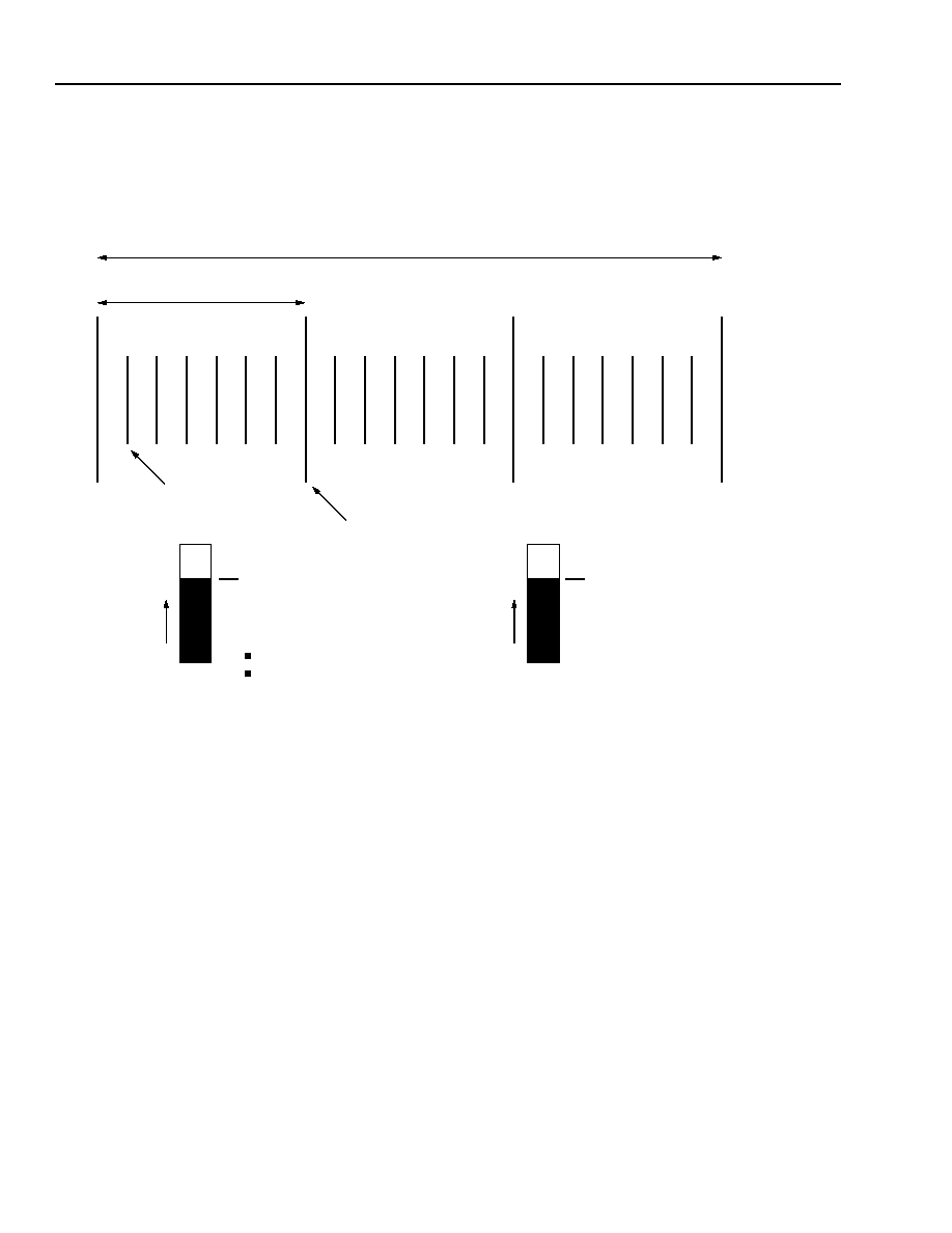
MARS2G5 P-Pro (TDAT162G52) SONET/SDH
Data Sheet
155/622/2488 Mbits/s Data Interface
August 18, 2004
228
Agere Systems Inc.
Transport Overhead Processor (TOHP-48) Block
(continued)
TOHP-48 Register Descriptions
(continued)
Figure 34 illustrates the parameters used in determining the bit error detection rate.
5-7934(F)
Figure 34. Signal Degrade and Failure Parameters for BER
MARS2G5 P-Pro provides a method to monitor the BER at the line and path layers. The following explains the
algorithm for this method to set and clear the BER. The algorithm for this method is the same for setting and clear-
ing the BER; the only difference is the programmed values. MARS2G5 P-Pro includes two complete sets of identi-
cal counters, one used to determine signal fail (SF) and one used to determine signal degrade (SD). The only
difference between SF and SD is the provisioned values. The same algorithm is used for both the line and path lay-
ers of SONET.
The algorithm uses four sets of counters: labeled Ns (number of frames), L (number of errors), M (number of
errored blocks), and B (total number of blocks). Each of these counters has different values that are provisioned to
either set the BER high or clear the BER indication. The algorithm works by counting blocks, i.e., a preset number
of SONET/SDH frames (Ns). If the number of errors in the block exceeds the provisioned level (L), then the errored
block counter is incremented by 1; otherwise, the number of blocks in error stays at its current level. At this point,
the frame counter and the error counter are reset back to 0 and counting is started again. At the end of a preset
number of blocks (B), the count in the errored block counter is compared against a provisioned threshold (M). If the
total number of blocks in error equals or exceeds the provisioned threshold (M), then the BER alarm is raised. If the
total number of blocks in error is less than the provisioned amount (M), then the BER alarm is cleared. In other
words: given the error distribution as defined by the GR-253 standard, the probability of getting L BIP errors out of
8 * N BIP bits in M out of B blocks.
The values used by the counters are determined by the state of the algorithm. If the BER state is low, then the set
parameters are used. If the BER state is high, then the clear parameters are used.
NUMBER OF MONITORING BLOCKS SFBSET[A--D] OR SDBSET[A--D] (IN THIS CASE, 3)
NUMBER OF FRAMES IN A MONITORING BLOCK SFNSSET[A--D] OR SDNSSET[A--D],
BLOCK
BOUNDARY
ACCUMULATED BIP ERROR COUNT:
B1 OR B2 FOR LINE
B3 FOR PATH
FRAME
BOUNDARY
BLOCK GOOD/BAD COUNT
SFNSCLEAR[A--D] OR SDNSCLEAR[A--D]
SFLSET[A--D] OR SDLSET[A--D]
SFLCLEAR[A--D] OR SDLCLEAR[A--D]
SFMSET[A--D] OR SDMSET[A--D]
SFMCLEAR[A--D] OR SDMCLEAR[A--D]
(IN THIS CASE, 7)
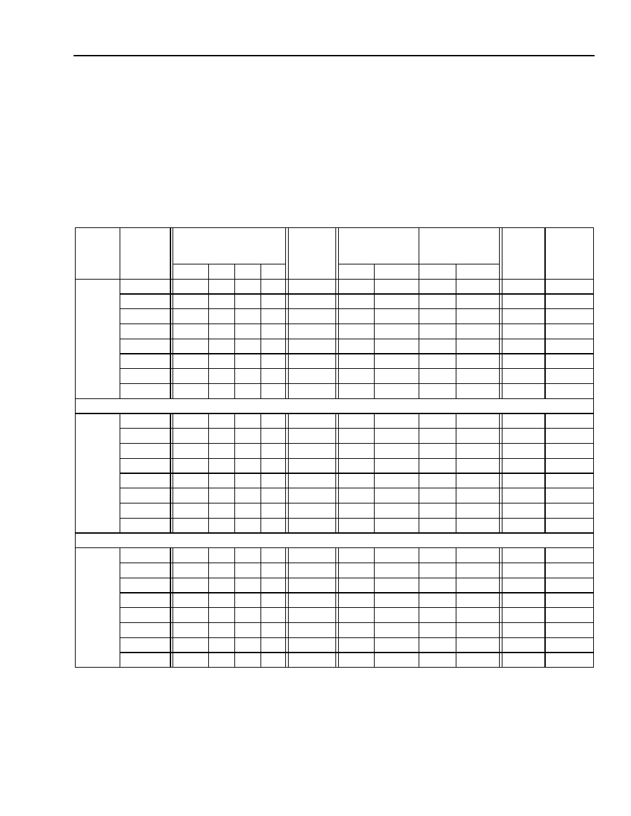
Data Sheet
MARS2G5 P-Pro (TDAT162G52) SONET/SDH
August 18, 2004
155/622/2488 Mbits/s Data Interface
229
Agere Systems Inc.
Transport Overhead Processor (TOHP-48) Block
(continued)
TOHP-48 Register Descriptions
(continued)
Table 79 and Table 80 show values of Ns, L, M, and B for STS-3/STM-1, STS-12/STM-4, and STS-48/STM-16 to
set and clear the BER indicator. SF registers are 0x852--0x0869 (Table 75--Table 78) and SD registers are
0x083A--0x0851 (Table 71--Table 74). All SF/SD set and clear values are hexadecimal.
Table 79. Ns, L, M, and B Values to Set the BER Indicator
Note: The Ns, L, M, and B values shown are the numbers to be provisioned in the MARS2G5 P-Pro. The actual
values of Ns, M, and B of the BER algorithm are 1 greater than the values shown, excluding L.
Mode
BER
SF/SD Set Values
Actual
Number of
Frames
Probability of
Detecting L
Errors (%)
Probability of
Declaring
SF/SD (%)
Integra-
tion
Time
(s)
Maxi-
mum
Number
of Frames
Ns
L
M
B
@BER
@BER/2
@BER
@BER/2
STS-3/
STM-1
1.00E-03
0
7
3D
3D
62
99.96
85.13
97.68
0.00
0.008
64
1.00E-04
5
A
3
7
48
72.70
7.28
96.06
0.16
0.013
104
1.00E-05
2F
8
3
7
384
71.34
10.08
95.19
0.52
0.1
800
1.00E-06
1DF
8
3
7
3840
71.34
10.09
95.19
0.52
1
8000
1.00E-07
1274
8
4
9
47250
69.74
9.44
95.07
0.13
10
80000
1.00E-08
B5A3
8
3
9
465000
68.07
8.82
98.47
0.82
83
664000
1.00E-09
3F79F
5
5
F
4160000
56.90
11.25
96.52
0.60
667
5336000
1.00E-10
--
--
--
--
--
--
--
--
--
--
--
STS-12/
STM-4
1.00E-03
0
20
3F
3F
64
100.00
88.43
100.00
0.04
0.008
64
1.00E-04
1
C
6
A
22
84.92
9.64
98.38
0.00
0.008
64
1.00E-05
C
9
3
8
117
67.93
7.17
96.48
0.25
0.025
200
1.00E-06
7F
9
3
8
1152
66.19
6.66
95.46
0.19
0.25
2000
1.00E-07
4FA
9
3
8
11475
65.75
6.53
95.16
0.18
2.5
20000
1.00E-08
31CD
9
3
8
114750
65.75
6.53
95.16
0.18
21
168000
1.00E-09
1F20B
9
3
8
1147500
65.75
6.53
95.16
0.18
167
1336000
1.00E-10
--
--
--
--
--
--
--
--
--
--
--
STS-48/
STM-16
1.00E-03
0
4B
3F
3F
64
100.00
100.00
100.00
100.00
0.008
64
1.00E-04
0
F
3F
3F
64
99.95
58.97
96.89
0.00
0.008
64
1.00E-05
4
B
35
3F
320
90.60
16.25
96.47
0.00
0.008
64
1.00E-06
1F
8
8
E
480
77.55
13.09
96.69
0.00
0.0625
500
1.00E-07
139
8
8
E
4710
75.80
12.15
95.17
0.00
0.625
5000
1.00E-08
C1B
8
7
E
46500
74.58
11.54
98.09
0.01
5.2
41600
1.00E-09
765B
7
6
A
333300
82.92
19.71
97.29
0.18
42
336000
1.00E-10
--
--
--
--
--
--
--
--
--
--
--

MARS2G5 P-Pro (TDAT162G52) SONET/SDH
Data Sheet
155/622/2488 Mbits/s Data Interface
August 18, 2004
230
Agere Systems Inc.
Transport Overhead Processor (TOHP-48) Block
(continued)
TOHP-48 Register Descriptions
(continued)
Table 80. Ns, L, M, and B Values to Clear the BER Indicator
Note: The Ns, L, M, and B values shown are the numbers to be provisioned in the MARS2G5 P-Pro. The actual
values of Ns, M, and B of the BER algorithm are 1 greater than the values shown, excluding L.
Mode
BER
SF/SD Set Values
Actual
Number
of Frames
Probability of
Detecting L Errors
(%)
Probability of
Clearing
SF/SD (%)
Integra-
tion
Time
(s)
Maxi-
mum
Number
of Frames
Ns
L
M
B
@BER * 5
@BER
@BER * 5
@BER
STS-3/
STM-1
1.00E-03
--
--
--
--
--
--
--
--
--
--
--
1.00E-04
0
7
3
7
8
85.13
0.39
0.27
100.00
0.013
104
1.00E-05
5
3
3
7
48
93.01
11.33
0.01
99.21
0.1
800
1.00E-06
2F
3
3
7
384
84.42
6.84
0.34
99.88
1
8000
1.00E-07
1DF
3
3
7
3840
84.42
6.84
0.34
99.88
10
80000
1.00E-08
1274
3
4
9
47250
83.66
6.59
0.22
99.98
83
664000
1.00E-09
B5A3
3
3
9
465000
82.86
6.35
0.03
99.75
667
5336000
1.00E-10
3F79F
3
2
F
4160000
46.31
1.48
0.50
99.84
6670
53360000
STS-12/
STM-4
1.00E-03
--
--
--
--
--
--
--
--
--
--
--
1.00E-04
0
8
6
6
7
100.00
51.54
0.00
99.03
0.008
64
1.00E-05
1
3
8
A
22
98.36
20.51
0.07
100.00
0.025
200
1.00E-06
C
3
3
8
117
87.99
8.23
0.02
99.59
0.25
2000
1.00E-07
7F
3
3
8
1152
87.34
7.94
0.02
99.64
2.5
20000
1.00E-08
4FA
3
3
8
11475
87.17
7.87
0.03
99.65
21
168000
1.00E-09
31CD
3
3
8
114750
87.17
7.87
0.03
99.65
167
1336000
1.00E-10
1F20B
3
3
8
1147500
87.17
7.87
0.03
99.65
1670
13360000
STS-48/
STM-16
1.00E-03
--
--
--
--
--
--
--
--
--
--
--
1.00E-04
0
20
27
3F
64
100.00
45.99
0.00
99.42
0.008
64
1.00E-05
0
3
D
E
15
100.00
60.11
0.00
99.47
0.008
64
1.00E-06
4
4
D
3F
320
95.07
7.28
0.00
99.98
0.0625
500
1.00E-07
1F
3
6
13
640
87.34
7.94
0.00
99.94
0.625
5000
1.00E-08
139
3
6
13
6280
86.52
7.61
0.00
99.95
5.2
41600
1.00E-09
C1B
3
6
13
62000
85.95
7.38
0.00
99.96
42
336000
1.00E-10
765B
3
4
A
333300
84.89
7.00
0.03
99.95
420
3360000

Data Sheet
MARS2G5 P-Pro (TDAT162G52) SONET/SDH
August 18, 2004
155/622/2488 Mbits/s Data Interface
231
Agere Systems Inc.
Transport Overhead Processor (TOHP-48) Block
(continued)
TOHP-48 Register Descriptions
(continued)
Table 81. TOHP_B1ECNTR[A--D], 0x086A--0x086D, B1 Error Count (RO)
Table 82. TOHP_B2ECNTR[A--D][1--2], 0x086E--0x0875, B2 Error Count (RO)
Table 83. TOHP_M1ECNTR[A--D][1--2], 0x0876--0x087D, M1 Error Count (RO)
Note:Stream C of the M1 error count registers 0x087A[4:0] and 0x087B[15:0] must be used for OC-48 mode.
Address
Bit
Name
Function
Reset
Default
0x086A--
0x086D
15:0
TOHP_B1ECNT
[A--D][15:0]
B1 Error Count. The value of internal running
counter is transferred into this holding register
at the 0-to-1 transition of PMRST (pin D7)
(Table 10) signal.
0x0000
Address
Bit
Name
Function
Reset
Default
0x086E, 0x0870,
0x0872, 0x0874
0x086F, 0x0871,
0x0873, 0x0875
5:0
15:0
TOHP_B2ECNT
[A--D][21:16]
TOHP_B2ECNT
[A--D][15:0]
B2 Error Count. The value of internal running
counter is transferred into this holding register
at the 0-to-1 transition of PMRST (pin D7)
(Table 10) signal.
0x000000
Address
Bit
Name
Function
Reset
Default
0x0876, 0x0878,
0x087A, 0x087C
0x0877, 0x0879,
0x087B, 0x087D
4:0
15:0
TOHP_M1ECNT
[A--D][20:16]
TOHP_M1ECNT
[A--D][15:0]
M1 Error Count. The value of internal running
counter is transferred into this holding register
at the 0-to-1 transition of PMRST (pin D7)
(Table 10) signal.
0x000000

MARS2G5 P-Pro (TDAT162G52) SONET/SDH
Data Sheet
155/622/2488 Mbits/s Data Interface
August 18, 2004
232
Agere Systems Inc.
Transport Overhead Processor (TOHP-48) Block
(continued)
TOHP-48 Register Descriptions
(continued)
Table 84. TOHP_TOH_INSR[A--D][1--2], 0x087E--0x0885, Transmit OH Insert Value (R/W)
Table 85. TOHP_RMONR[A--D][1--3], 0x0886--0x0891, Receive Monitor Value (RO)
Address
Bit
Name
Function
Reset
Default
0x087E, 0x0880,
0x0882, 0x0884
15:8
TOHP_TF1DINS
[A--D][7:0]
Transmit F1 Byte Value. Register value is
inserted into the transmit F1 byte.
0x00
7:0
TOHP_TS1DINS
[A--D][7:0]
Transmit S1 Byte Value. Register value is
inserted into the transmit S1 byte.
0x00
0x087F, 0x0881,
0x0883, 0x0885
15:8
TOHP_TK2DINS
[A--D][7:0]
Transmit K2 Byte Value. Register value is
inserted into the transmit K2 byte.
0x00
7:0
TOHP_TK1DINS
[A--D][7:0]
Transmit K1 Byte Value. Register value is
inserted into the transmit K1 byte.
0x00
Address
Bit
Name
Function
Reset
Default
0x0886, 0x0889,
0x088C, 0x088F
15:8
TOHP_F1DMON1
[A--D][7:0]
Receive F1 Previous Monitor Value.
0x00
7:0
TOHP_F1DMON0
[A--D][7:0]
Receive F1 Current Monitor Value.
0x00
0x0887, 0x088A,
0x088D, 0x0890
15:8
TOHP_K2DMON
[A--D[7:0]
Receive K2 Monitor Value.
0x00
7:0
TOHP_K1DMON
[A--D][7:0]
Receive K1 Monitor Value.
0x00
0x0888, 0x088B,
0x088E, 0x0891
7:0
TOHP_S1DMON
[A--D][7:0]
Receive S1 Monitor Value.
0x00

Data Sheet
MARS2G5 P-Pro (TDAT162G52) SONET/SDH
August 18, 2004
155/622/2488 Mbits/s Data Interface
233
Agere Systems Inc.
Transport Overhead Processor (TOHP-48) Block
(continued)
TOHP-48 Register Descriptions
(continued)
Table 86. TOHP_RJ0DMONR[A--D][1--32], 0x0892--0x0911, Receive J0/Z0 Monitor Value Registers (RO)
Address
Bit
Name
Function
Reset
Default
0x0892--
0x08B1
15:8
TOHP_RJ0DMON
[A][2, 4, 6, . . ., 64][7:0]
Receive J0 Monitor Value. These registers cap-
ture a 64-byte sequence from the J0 byte of each
channel.
In STS-48 mode, TOHP_RJ0DMON[A]
[1--64][7:0] is valid for J0 bytes while
TOHP_RJ0DMON[B--D][1][7:0] are used for
TOHP_Z0DMON[B--D][1][7:0] (see TOHP-48
register map (Table 93)).
0x0000
7:0
TOHP_RJ0DMON
[A][1, 3, 5, . . ., 63][7:0]
0x08B2--
0x08D1
15:8
TOHP_RJ0DMON
[B][2, 4, 6, . . ., 64][7:0]
Receive J0 Monitor Value. See functional
description above.
0x0000
7:0
TOHP_RJ0DMON
[B][1, 3, 5, . . ., 63][7:0]
0x08D2--
0x08F1
15:8
TOHP_RJ0DMON
[C][2, 4, 6, . . ., 64][7:0]
Receive J0 Monitor Value. See functional
description above.
0x0000
7:0
TOHP_RJ0DMON
[C][1, 3, 5, . . ., 63][7:0]
0x08F2--
0x0911
15:8
TOHP_RJ0DMON
[D][2, 4, 6, . . ., 64][7:0]
Receive J0 Monitor Value. See functional
description above.
0x0000
7:0
TOHP_RJ0DMON
[D][1, 3, 5, . . ., 63][7:0]

MARS2G5 P-Pro (TDAT162G52) SONET/SDH
Data Sheet
155/622/2488 Mbits/s Data Interface
August 18, 2004
234
Agere Systems Inc.
Transport Overhead Processor (TOHP-48) Block
(continued)
TOHP-48 Register Descriptions
(continued)
Table 87. TOHP_TJ0DINSR[A--D][1--32], 0x0912--0x09A9, Transmit J0/Z0 Insert Value Registers (R/W)
Address
Bit
Name
Function
Reset
Default
0x0912--
0x0931
15:8
TOHP_TJ0DINS
[A][2, 4, 6, . . ., 64][7:0]
Transmit J0 Insert Value. These registers allow
a 64-byte sequence to be inserted into the J0
byte of each channel.
In STS-48 mode, TOHP_TJ0DINS[A][1--64][7:0]
is valid for J0 bytes while TOHP_TJ0DINS[B--
D][1][7:0] are used for TOHP_TZ0DINS[B--D][1,
2, 3][7:0] (see TOHP-48 register map (Table 93)).
0x0000
7:0
TOHP_TJ0DINS
[A][1, 3, 5, . . ., 63][7:0]
0x0932--
0x0951
15:8
TOHP_TJ0DINS
[B][2, 4, 6, . . ., 64][7:0]
Transmit J0 Insert Value. See functional
description above.
0x0000
7:0
TOHP_TJ0DINS
[B][1, 3, 5, . . ., 63][7:0]
0x0952--
0x0971
15:8
TOHP_TJ0DINS
[C][2, 4, 6, . . ., 64][7:0]
Transmit J0 Insert Value. See functional
description above.
0x0000
7:0
TOHP_TJ0DINS
[C][1, 3, 5, . . ., 63][7:0]
0x0972--
0x09A9
15:8
TOHP_TJ0DINS
[D][2, 4, 6, . . ., 64][7:0]
Transmit J0 Insert Value. See functional
description above.
0x0000
7:0
TOHP_TJ0DINS
[D][1, 3, 5, . . ., 63][7:0]

Data Sheet
MARS2G5 P-Pro (TDAT162G52) SONET/SDH
August 18, 2004
155/622/2488 Mbits/s Data Interface
235
Agere Systems Inc.
Transport Overhead Processor (TOHP-48) Block
(continued)
TOHP-48 Register Descriptions
(continued)
Table 88. TOHP_TZ0DINSR[A--D][1--6], 0x09AA--0x09C1, Transmit Z0 Insert Value Registers (R/W)
Address
Bit
Name
Function
Reset
Default
0x09AA
15:8
TOHP_TZ0DINS[A][2][7:0] Transmit Z0 Insert Value. Register values are
inserted into the transmit Z0 bytes.
In STS-3 mode, TOHP_TZ0DINS[A--D][2--3] are
valid; in STS-12 mode, TOHP_TZ0DINS[A--D][2--
12][7:0] are valid; and in STS-48 mode, all 44
TOHP_TZ0DINS bytes plus TOHP_TJ0DINS[B--
D][1][7:0] (Table 87) are used for 47 Z0 byte values
(see Table 89 for Z0 byte ordering in these registers).
--
7:0
--
Reserved.
--
0x09AB--
0x09AF
15:8
TOHP_TZ0DINS[A]
[4, 6, 8, 10, 12][7:0]
Transmit Z0 Insert Value. See functional description
above.
0x0
7:0
TOHP_TZ0DINS[A]
[3, 5, 7, 9, 11][7:0]
0x0
0x09B0
15:8
TOHP_TZ0DINS[B][2][7:0]
--
7:0
--
Reserved. 0x0
0x09B1--
0x09B5
15:8
TOHP_TZ0DINS[B]
[4, 6, 8, 10, 12][7:0]
Transmit Z0 Insert Value. See functional description
above.
0x0
7:0
TOHP_TZ0DINS[B]
[3, 5, 7, 9, 11][7:0]
0x0
0x09B6
15:8
TOHP_TZ0DINS[C][2][7:0]
0x0
7:0
--
Reserved.
--
0x09B7--
0x09BB
15:8
TOHP_TZ0DINS[C]
[4, 6, 8, 10, 12][7:0]
Transmit Z0 Insert Value. See functional description
above.
0x0
7:0
TOHP_TZ0DINS[C]
[3, 5, 7, 9, 11][7:0]
0x0
0x09BC
15:8
TOHP_TZ0DINS[D][2][7:0]
0x0
7:0
--
Reserved.
--
0x09BD--
0x09C1
15:8
TOHP_TZ0DINS[D]
[4, 6, 8, 10, 12][7:0]
Transmit Z0 Insert Value. See functional description
above.
0x0
7:0
TOHP_TZ0DINS[D]
[3, 5, 7, 9, 11][7:0]
0x0

MARS2G5 P-Pro (TDAT162G52) SONET/SDH
Data Sheet
155/622/2488 Mbits/s Data Interface
August 18, 2004
236
Agere Systems Inc.
Transport Overhead Processor (TOHP-48) Block
(continued)
TOHP-48 Register Descriptions
(continued)
Table 89. Z0 Byte Ordering STS-48 Mode for Z0-1--Z0-47
Table 90. Z0 Byte Ordering STS-12 Mode for Z0-1--Z0-11
Table 91. Z0 Byte Ordering STS-3 Mode for Z0-1--Z0-2
Table 92. TOHP_SCRATCHR, 0x09C2, TOHP-48 Scratch Register (R/W)
Channel
Time Slots [1--12]
1
2
3
4
5
6
7
8
9
10
11
12
A
J0
Z0-12
Z0-24
Z0-36
Z0-1
Z0-13
Z0-25
Z0-37
Z0-2
Z0-14
Z0-26
Z0-38
B
Z0-3
Z0-15
Z0-27
Z0-39
Z0-4
Z0-16
Z0-28
Z0-40
Z0-5
Z0-17
Z0-29
Z0-41
C
Z0-6
Z0-18
Z0-30
Z0-42
Z0-7
Z0-19
Z0-31
Z0-43
Z0-8
Z0-20
Z0-32
Z0-44
D
Z0-9
Z0-21
Z0-33
Z0-45
Z0-10
Z0-22
Z0-34
Z0-46
Z0-11
Z0-23
Z0-35
Z0-47
Channel
Time Slots [1--12]
1
2
3
4
5
6
7
8
9
10
11
12
A
J0
Z0-3
Z0-6
Z0-9
Z0-1
Z0-4
Z0-7
Z0-10
Z0-2
Z0-5
Z0-8
Z0-11
B
J0
Z0-3
Z0-6
Z0-9
Z0-1
Z0-4
Z0-7
Z0-10
Z0-2
Z0-5
Z0-8
Z0-11
C
J0
Z0-3
Z0-6
Z0-9
Z0-1
Z0-4
Z0-7
Z0-10
Z0-2
Z0-5
Z0-8
Z0-11
D
J0
Z0-3
Z0-6
Z0-9
Z0-1
Z0-4
Z0-7
Z0-10
Z0-2
Z0-5
Z0-8
Z0-11
Channel
Time Slots [1--3]
1
2
3
A
J0
Z0-1
Z0-2
B
J0
Z0-1
Z0-2
C
J0
Z0-1
Z0-2
D
J0
Z0-1
Z0-2
Address
Bit
Name
Function
Reset
Default
0x09C2
15:0
TOHP_SCRATCH[15:0]
TOHP-48 Scratch Register. Allows the control
system to verify read and write operations to the
device without affecting device operation.
0x0000

Data Sheet
MARS2G5 P-Pro (TDAT162G52) SONET/SDH
August 18, 2004
155/622/2488 Mbits/s Data Interface
237
Agere Systems Inc.
Transport Overhead Processor (TOHP-48) Block
(continued)
TOHP-48 Register Map
Table 93. TOHP-48 Register Map
Note: Shading denotes reserved bits.
Addr
Symbol
Bit 15
Bit 14
Bit 13
Bit 12
Bit 11
Bit 10
Bit 9
Bit 8
Bit 7
Bit 6
Bit 5
Bit 4
Bit 3
Bit 2
Bit 1
Bit 0
TOHP-48 MODE--R/W and Block Version--RO
0x0800
TOHP_MODE
_VERR
TOHP_RX_MODE[2:0]
TOHP_TX_MODE[2:0]
TOHP_VER[9:0]
Channel Interrupts--RO
0x0801
TOHP_CH_
INT
TOHP_
CORWN
TOHP_
INTH[D]
TOHP_
INTH[C]
TOHP_
INTH[B]
TOHP_
INTH[A]
TOHP_
INTL[D]
TOHP_
INTL[C]
TOHP_
INTL[B]
TOHP_
INTL[A]
TOHP-48 Delta and Event Parameters--COR/COW--RO
0x0802
TOHP_DLT_
EVTA1
TOHP_LRD
IMOND[A]
TOHP_LAIS
MOND[A]
TOHP_RAP
SBABLEE
[A]
TOHP_S1D
MON4D[A]
TOHP_S1D
MON8D[A]
TOHP_K2D
MOND[A]
TOHP_K1K
2DMOND
[A]
TOHP_F1D
MOND[A]
TOHP_TTO
AC_PERRE
[A]
TOHP_S1B
ABLEE[A]
TOHP_
SFD[A]
TOHP_
SDD[A]
TOHP_
OOFD[A]
TOHP_
LOFD[A]
TOHP_
LOSD[A]
TOHP_
LOCD[A]
0x0803
TOHP_DLT_
EVTA2
TOHP_
TTOAC_K1
K2ERRE[A]
TOHP_J0MI
SE[A]
0x0804
TOHP_DLT_
EVTB1
TOHP_LRD
IMOND[B]
TOHP_LAIS
MOND[B]
TOHP_RAP
SBABLEE
[B]
TOHP_S1D
MON4D[B]
TOHP_S1D
MON8D[B]
TOHP_K2D
MOND[B]
TOHP_K1K
2DMOND
[B]
TOHP_F1D
MOND[B]
TOHP_S1B
ABLEE[B]
TOHP_SFD
[B]
TOHP_SDD
[B]
TOHP_
OOFD[B]
TOHP_
LOFD[B]
TOHP_
LOSD[B]
TOHP_
LOCD[B]
0x0805
TOHP_DLT_
EVTB2
TOHP_
TTOAC_K1
K2ERRE[B]
TOHP_J0MI
SE[B]
0x0806
TOHP_DLT_
EVTC1
TOHP_LRD
IMOND[C]
TOHP_LAIS
MOND[C]
TOHP_RAP
SBABLEE
[C]
TOHP_S1D
MON4D[C]
TOHP_S1D
MON8D[C]
TOHP_K2D
MOND[C]
TOHP_K1K
2DMOND
[C]
TOHP_F1D
MOND[C]
TOHP_S1B
ABLEE[C]
TOHP_SFD
[C]
TOHP_SDD
[C]
TOHP_
OOFD[C]
TOHP_
LOFD[C]
TOHP_
LOSD[C]
TOHP_
LOCD[C]
0x0807
TOHP_DLT_
EVTC2
TOHP_
TTOAC_K1
K2ERRE[C]
TOHP_J0MI
SE[C]
0x0808
TOHP_DLT_
EVTD1
TOHP_LRD
IMOND[D]
TOHP_LAIS
MOND[D]
TOHP_RAP
SBABLEE
[D]
TOHP_S1D
MON4D[D]
TOHP_S1D
MON8D[D]
TOHP_K2D
MOND[D]
TOHP_K1K
2DMOND
[D]
TOHP_F1D
MOND[D]
TOHP_S1B
ABLEE[D]
TOHP_SFD
[D]
TOHP_SDD
[D]
TOHP_
OOFD[D]
TOHP_
LOFD[D]
TOHP_
LOSD[D]
TOHP_
LOCD[D]
0x0809
TOHP_DLT_
EVTD2
TOHP_
TTOAC_K1
K2ERRE[D]
TOHP_
J0MISE[D]
TOHP-48 Receive/Transmit State and Value Parameters--RO
0x080A
TOHP_RX_
TX_STATEA
TOHP_LRD
IMON[A]
TOHP_LAIS
MON[A]
TOHP_TLR
DIINT[A]
TOHP_
SF[A]
TOHP_
SD[A]
TOHP_OOF
[A]
TOHP_LOF
[A]
TOHP_LOS
[A]
TOHP_LOC[
A]
0x080B
TOHP_RX_
TX_STATEB
TOHP_LRD
IMON[B]
TOHP_LAIS
MON[B]
TOHP_TLR
DIINT[B]
TOHP_
SF[B]
TOHP_
SD[B]
TOHP_OOF
[B]
TOHP_LOF
[B]
TOHP_LOS
[B]
TOHP_LOC[
B]
0x080C
TOHP_RX_
TX_STATEC
TOHP_LRD
IMON[C]
TOHP_LAIS
MON[C]
TOHP_TLR
DIINT[C]
TOHP_
SF[C]
TOHP_
SD[C]
TOHP_OOF
[C]
TOHP_LOF
[C]
TOHP_LOS
[C]
TOHP_LOC[
C]
0x080D
TOHP_RX_
TX_STATED
TOHP_LRD
IMON[D]
TOHP_LAIS
MON[D]
TOHP_TLR
DIINT[D]
TOHP_
SF[D]
TOHP_
SD[D]
TOHP_OOF
[D]
TOHP_LOF
[D]
TOHP_LOS
[D]
TOHP_LOC[
D]
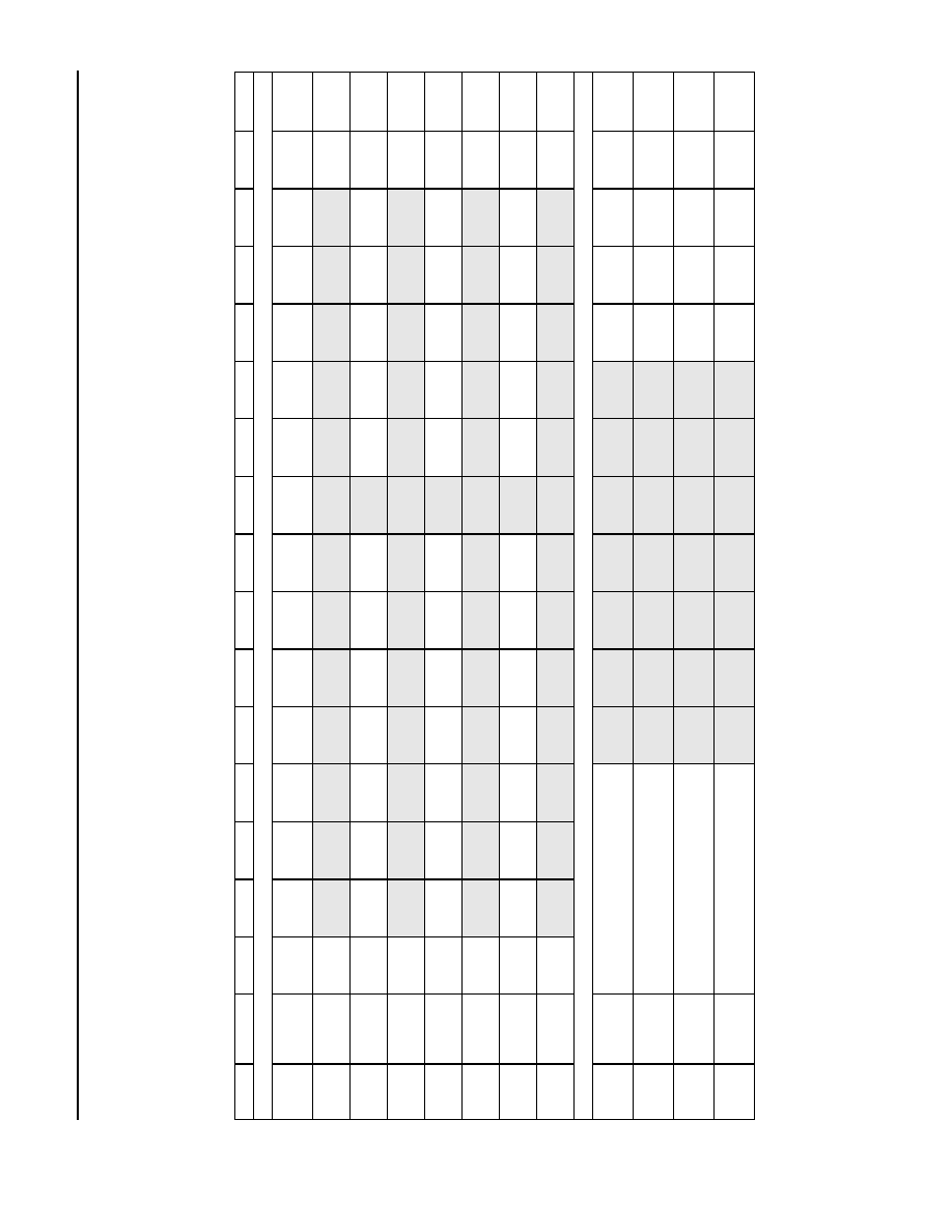
MARS2G5 P-Pro (TDAT162G52) SONET/SDH
Data Sheet
155/622/2488 Mbits/s Data Interface
August 18, 2004
238
Agere Systems Inc.
Transport Overhead Processor (TOHP-48) Block
(continued)
TOHP-48 Register Map
(continued)
Table 93. TOHP-48 Register Map (continued)
Note: Shading denotes reserved bits.
Addr
Symbol
Bit 15
Bit 14
Bit 13
Bit 12
Bit 11
Bit 10
Bit 9
Bit 8
Bit 7
Bit 6
Bit 5
Bit 4
Bit 3
Bit 2
Bit 1
Bit 0
Interrupt Mask Parameters--R/W
0x080E
TOHP_
MSKA1
TOHP_LRD
IMONM[A]
TOHP_LAIS
MONM[A]
TOHP_RAP
SBABLEM
[A]
TOHP_S1D
MON4M[A]
TOHP_S1D
MON8M[A]
TOHP_K2D
MONM
[A]
TOHP_K1K
2DMONM
[A]
TOHP_F1D
MONM[A]
TOHP_TTO
AC_PERR
M[A]
TOHP_S1B
ABLEM[A]
TOHP_SFM
[A]
TOHP_SD
M[A]
TOHP_OOF
M[A]
TOHP_LOF
M[A]
TOHP_LOS
M[A]
TOHP_LOC
M[A]
0x080F
TOHP_
MSKA2
TOHP_INT
M[A]
TOHP_
TTOAC_K1
K2ERRM[A]
TOHP_J0MI
SM[A]
0x0810
TOHP_
MSKB1
TOHP_LRD
IMONM[B]
TOHP_LAIS
MONM[B]
TOHP_RAP
SBABLEM
[B]
TOHP_S1D
MON4M[B]
TOHP_S1D
MON8M[B]
TOHP_K2D
MONM[B]
TOHP_K1K
2DMONM
[B]
TOHP_F1D
MONM[B]
TOHP_S1B
ABLEM[B]
TOHP_SFM
[B]
TOHP_SD
M[B]
TOHP_OOF
M[B]
TOHP_LOF
M[B]
TOHP_LOS
M[B]
TOHP_LOC
M[B]
0x0811
TOHP_
MSKB2
TOHP_INT
M[B]
TOHP_
TTOAC_K1
K2ERRM[B]
J0MISM[B]
0x0812
TOHP_
MSKC1
TOHP_LRD
IMONM[C]
TOHP_LAIS
MONM[C]
TOHP_RAP
SBABLEM
[C]
TOHP_S1D
MON4M[C]
TOHP_S1D
MON8M[C]
TOHP_K2D
MONM[C]
TOHP_K1K
2DMONM
[C]
TOHP_F1D
MONM[C]
TOHP_S1B
ABLEM[C]
TOHP_SFM
[C]
TOHP_SD
M[C]
TOHP_OOF
M[C]
TOHP_LOF
M[C]
TOHP_LOS
M[C]
TOHP_LOC
M[C]
0x0813
TOHP_
MSKC2
TOHP_INT
M[C]
TOHP_
TTOAC_K1
K2ERRM[C]
TOHP_J0MI
SM[C]
0x0814
TOHP_
MSKD1
TOHP_LRD
IMONM[D]
TOHP_LAIS
MONM[D]
TOHP_RAP
SBABLEM
[D]
TOHP_S1D
MON4M[D]
TOHP_S1D
MON8M[D]
TOHP_K2D
MONM[D]
TOHP_K1K
2DMONM
[D]
TOHP_F1D
MONM[D]
TOHP_S1B
ABLEM[D]
TOHP_SFM
[D]
TOHP_SD
M[D]
TOHP_OOF
M[D]
TOHP_LOF
M[D]
TOHP_LOS
M[D]
TOHP_LOC
M[D]
0x0815
TOHP_
MSKD2
TOHP_INT
M[D]
TOHP_
TTOAC_K1
K2ERRM[D]
TOHP_J0MI
SM[D]
Triggers--R/W
0x0816
TOHP_TRGA
TOHP_RSTN_SW[A][15:12]
TOHP_TA1
A2ERREN
[A]
TOHP_SFC
LEAR[A]
TOHP_
SFSET[A]
TOHP_SDC
LEAR[A]
TOHP_
SDSET[A]
0x0817
TOHP_TRGB
TOHP_RSTN_SW[B][15:12]
TOHP_TA1
A2ERREN
[B]
TOHP_SFC
LEAR[B]
TOHP_
SFSET[B]
TOHP_SDC
LEAR[B]
TOHP_
SDSET[B]
0x0818
TOHP_TRGC
TOHP_RSTN_SW[C][[15:12]
TOHP_TA1
A2ERREN
[C]
TOHP_SFC
LEAR[C]
TOHP_
SFSET[C]
TOHP_SDC
LEAR[C]
TOHP_
SDSET[C]
0x0819
TOHP_TRGD
TOHP_RSTN_SW[D][15:12]
TOHP_TA1
A2ERREN
[D]
TOHP_SFC
LEAR[D]
TOHP_
SFSET[D]
TOHP_SDC
LEAR[D]
TOHP_
SDSET[D]

Data Sheet
MARS2G5 P-Pro (TDAT162G52) SONET/SDH
August 18, 2004
155/622/2488 Mbits/s Data Interface
239
Agere Systems Inc.
Transport Overhead Processor (TOHP-48) Block
(continued)
TOHP-48 Register Map
(continued)
Table 93. TOHP-48 Register Map (continued)
Note: Shading denotes reserved bits.
Addr
Symbol
Bit 15
Bit 14
Bit 13
Bit 12
Bit 11
Bit 10
Bit 9
Bit 8
Bit 7
Bit 6
Bit 5
Bit 4
Bit 3
Bit 2
Bit 1
Bit 0
Continuous N-Times Detect Values--R/W
0x081A
TOHP_
CNTDA1
TOHP_CNTDK2[A][3:0]
TOHP_CNTDK1K2[A][3:0]
TOHP_CNTDF1[A][3:0]
TOHP_CNTDJ0Z0[A][3:0]
0x081B
TOHP_
CNTDA2
-- (Version
2.2 and 2.3)
Reserved
(Version 2.0)
TOHP_CNTDS1BABLE[A][3:0]
TOHP_CNTDS1[A][3:0]
TOHP_CNTDK1K2FRAME[A][3:0]
0x081C
TOHP_
CNTDB1
TOHP_CNTDK2[B][3:0]
TOHP_CNTDK1K2[B][3:0]
TOHP_CNTDF1[B][3:0]
TOHP_CNTDJ0Z0[B][3:0]
0x081D
TOHP_
CNTDB2
-- (Version
2.2 and 2.3)
Reserved
(Version 2.0)
TOHP_CNTDS1BABLE[B][3:0]
TOHP_CNTDS1[B]3:0]
TOHP_CNTDK1K2FRAME[B][3:0]
0x081E
TOHP_
CNTDC1
TOHP_CNTDK2[C][3:0]
TOHP_CNTDK1K2[C][3:0]
TOHP_CNTDF1[C][3:0]
TOHP_CNTDJ0Z0[C][3:0]
0x081F
TOHP_
CNTDC2
-- (Version
2.2 and 2.3)
Reserved
(Version 2.0)
TOHP_CNTDS1BABLE[C][3:0]
TOHP_CNTDS1[C]3:0]
TOHP_CNTDK1K2FRAME[C][3:0]
0x0820
TOHP_
CNTDD1
TOHP_CNTDK2[D][3:0]
TOHP_CNTDK1K2[D][3:0]
TOHP_CNTDF1[D][3:0]
TOHP_CNTDJ0Z0[D][3:0]
0x0821
TOHP_
CNTDD2
-- (Version
2.2 and 2.3)
Reserved
(Version 2.0)
TOHP_CNTDS1BABLE[D][3:0]
TOHP_CNTDS1[D]3:0]
TOHP_CNTDK1K2FRAME[D][3:0]
Receive Control Parameters--R/W
0x0822
TOHP_
RCTLA1
TOHP_J0MONMODE
[A][1:0]
TOHP_M1B
7IGNORE
[A]
TOHP_LAIS
INS[A]
TOHP_LOF
_AISINH[A]
TOHP_OOF
_AISINH[A]
TOHP_LOS
_AISINH[A]
TOHP_SFB
1B2SEL[A]
TOHP_SDB
1B2SEL[A]
TOHP_CNT
DB1SEL[A]
TOHP_S1M
ON8OR4CT
L[A]
TOHP_K1K
2_2OR1[A]
TOHP_B2BI
TBLKCNT
[A]
TOHP_DSC
RINH[A]
TOHP_B1BI
TBLKCNT
[A]
TOHP_ROH
_BYPASS
[A]
0x0823
TOHP_
RCTLA2
TOHP_M1B
ITBLKCNT
[A]
TOHP_RVA
LIDK_CTL
[A]
TOHP_LOSDETCNT[A][12:0]
0x0824
TOHP_
RCTLB1
TOHP_J0MONMODE
[B][1:0]
TOHP_M1B
7IGNOR[B]
TOHP_LAIS
INS[B]
TOHP_LOF
_AISINH[B]
TOHP_OOF
_AISINH[B]
TOHP_LOS
_AISINH[B]
TOHP_SFB
1B2SEL[B]
TOHP_SDB
1B2SEL[B]
TOHP_CNT
DB1SEL[B]
TOHP_S1M
ON8OR4CT
L[B]
TOHP_K1K
2_2OR1[B]
TOHP_B2BI
TBLKCNT
[B]
TOHP_DSC
RINH[B]
TOHP_B1BI
TBLKCNT
[B]
TOHP_ROH
_BYPASS
[B]
0x0825
TOHP_
RCTLB2
TOHP_M1B
ITBLKCNT
[B]
TOHP_RVA
LIDK_CTL
[B]
TOHP_LOSDETCNT[B][12:0]
0x0826
TOHP_
RCTLC1
TOHP_J0MONMODE
[C][1:0]
TOHP_M1B
7IGNORE
[C]
TOHP_LAIS
INS[C]
TOHP_LOF
_AISINH[C]
TOHP_OOF
_AISINH[C]
TOHP_LOS
_AISINH[C]
TOHP_SFB
1B2SEL[C]
TOHP_SDB
1B2SEL[C]
TOHP_CNT
DB1SEL[C]
TOHP_S1M
ON8OR4CT
L[C]
TOHP_K1K
2_2OR1[C]
TOHP_B2BI
TBLKCNT
[C]
TOHP_DSC
RINH[C]
TOHP_B1BI
TBLKCNT
[C]
TOHP_ROH
_BYPASS
[C]
0x0827
TOHP_
RCTLC2
TOHP_M1B
ITBLKCNT
[C]
TOHP_RVA
LIDK_CTL
[C]
TOHP_LOSDETCNT[C][12:0]
0x0828
TOHP_
RCTLD1
TOHP_J0MONMODE
[D][1:0]
TOHP_M1B
7IGNORE
[D]
TOHP_LAIS
INS[D]
TOHP_LOF
_AISINH[D]
TOHP_OOF
_AISINH[D]
TOHP_LOS
_AISINH[D]
TOHP_SFB
1B2SEL[D]
TOHP_SDB
1B2SEL[D]
TOHP_CNT
DB1SEL[D]
TOHP_S1M
ON8OR4CT
L[D]
TOHP_K1K
2_2OR1[D]
TOHP_B2BI
TBLKCNT
[D]
TOHP_DSC
RINH[D]
TOHP_B1BI
TBLKCNT
[D]
TOHP_ROH
_BYPASS
[D]
0x0829
TOHP_
RCTLD2
TOHP_M1B
ITBLKCNT
[D]
TOHP_RVA
LIDK_CTL
[D]
TOHP_LOSDETCNT[D][12:0]
0x082A
TOHP_
RCTLA3
TOHP_RREFSEL[1:0]
TOHP_
RREF_EN
TOHP_
RREF_INH
TOHP_RTO
ACSINH[A]
TOHP_RTO
ACCINH[A]
TOHP_RTO
ACDINH[A]
TOHP_RTO
AC_OEPIN
S[A]
0x082B
TOHP_
RCTLB3
TOHP_RTO
ACSINH[B]
TOHP_RTO
ACCINH[B]
TOHP_RTO
ACDINH[B]
TOHP_RTO
AC_OEPIN
S[B]
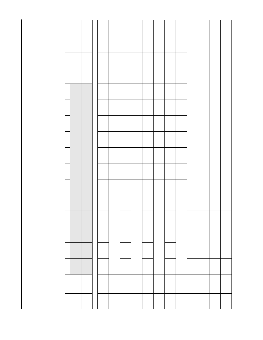
MARS2G5 P-Pro (TDAT162G52) SONET/SDH
Data Sheet
155/622/2488 Mbits/s Data Interface
August 18, 2004
240
Agere Systems Inc.
Transport Overhead Processor (TOHP-48) Block
(continued)
TOHP-48 Register Map
(continued)
Table 93. TOHP-48 Register Map (continued)
Note: Shading denotes reserved bits.
Addr
Symbol
Bit 15
Bit 14
Bit 13
Bit 12
Bit 11
Bit 10
Bit 9
Bit 8
Bit 7
Bit 6
Bit 5
Bit 4
Bit 3
Bit 2
Bit 1
Bit 0
0x082C
TOHP_
RCTLC3
TOHP_RTO
ACSINH[C]
TOHP_RTO
ACCINH[C]
TOHP_RTO
ACDINH[C]
TOHP_RTO
AC_OEPIN
S[C]
0x082D
TOHP_
RCTLD3
TOHP_RTO
ACSINH[D]
TOHP_RTO
ACCINH[D]
TOHP_RTO
ACDINH[D]
TOHP_RTO
AC_OEPIN
S[D]
Transmit Control Parameters--R/W
0x082E
TOHP_
TCTLA1
TOHP_TTO
ACINH
TOHP_TJ0I
NS[A]
TOHP_TTO
AC_J0[A]
TOHP_TTO
AC_OEPM
ON[A]
TOHP_TTO
AC_INS[A]
TOHP_TTO
AC_E2[A]
TOHP_TTO
AC_S1[A]
TOHP_TTO
AC_D4TO1
2[A]
TOHP_TTO
AC_D1TO3
[A]
TOHP_TTO
AC_F1[A]
TOHP_TTO
AC_E1[A]
TOHP_TAP
SBABLEIN
S[A]
TOHP_TM1
_ERR_INS
[A]
TOHP_TM1
_REIL_INH
[A]
TOHP_
TF1INS[A]
TOHP_
TS1INS[A]
0x082F
TOHP_
TCTLA2
TOHP_TA1A2ERRINS[A][4:0]
TOHP_TOH
_BYPASS
[A]
TOHP_SCR
INH[A]
TOHP_TB1
ERRINS[A]
TOHP_TB2
ERRINS[A]
TOHP_TIM
ER_LRDIIN
H[A]
TOHP_TSF
_LRDIINH
[A]
TOHP_TLAI
SMON_LR
DIINH[A]
TOHP_TLO
F_LRDIINH
[A]
TOHP_TOO
F_LRDIINH
[A]
TOHP_TLO
S_LRDIINH
[A]
TOHP_TLO
C_LRDIINH
[A]
0x0830
TOHP_
TCTLB1
TOHP_
TTOAC_
K1K2[A]
TOHP_TJ0I
NS[B]
TOHP_TTO
AC_J0[B]
TOHP_
TTOAC_
K1K2[B]
TOHP_TTO
AC_INS[B]
TOHP_TTO
AC_E2[B]
TOHP_TTO
AC_S1[B]
TOHP_TTO
AC_D4TO1
2[B]
TOHP_TTO
AC_D1TO3
[B]
TOHP_TTO
AC_F1[B]
TOHP_TTO
AC_E1[B]
TOHP_TAP
SBABLEIN
S[B]
TOHP_TM1
_ERR_INS
[B]
TOHP_TM1
_REIL_INH
[B]
TOHP_
TF1INS[B]
TOHP_
TS1INS[B]
0x0831
TOHP_
TCTLB2
TOHP_TA1A2ERRINS[B][4:0]
TOHP_TOH
_BYPASS[B
]
TOHP_SCR
INH[B]
TOHP_TB1
ERRINS[B]
TOHP_TB2
ERRINS[B]
TOHP_TIM
ER_LRDIIN
H[B]
TOHP_TSF
_LRDIINH
[B]
TOHP_TLAI
SMON_LR
DIINH[B]
TOHP_TLO
F_LRDIINH
[B]
TOHP_TOO
F_LRDIINH
[B]
TOHP_TLO
S_LRDIINH
[B]
TOHP_TLO
C_LRDIINH
[B]
0x0832
TOHP_
TCTLC1
TOHP_
TTOAC_VA
LIDK_CTL
TOHP_TJ0I
NS[C]
TOHP_TTO
AC_J0[C]
TOHP_
TTOAC_
K1K2[C]
TOHP_TTO
AC_INS[C]
TOHP_TTO
AC_E2[C]
TOHP_TTO
AC_S1[C]
TOHP_TTO
AC_D4TO1
2[C]
TOHP_TTO
AC_D1TO3
[C]
TOHP_TTO
AC_F1[C]
TOHP_TTO
AC_E1[C]
TOHP_TAP
SBABLEIN
S[C]
TOHP_TM1
_ERR_INS
[C]
TOHP_TM1
_REIL_INH
[C]
TOHP_
TF1INS[C]
TOHP_
TS1INS[C]
0x0833
TOHP_
TCTLC2
TOHP_TA1A2ERRINS[C][4:0]
TOHP_TOH
_BYPASS
[C]
TOHP_SCR
INH[C]
TOHP_TB1
ERRINS[C]
TOHP_TB2
ERRINS[C]
TOHP_TIM
ER_LRDIIN
H[C]
TOHP_TSF
_LRDIINH
[C]
TOHP_TLAI
SMON_LR
DIINH[C]
TOHP_TLO
F_LRDIINH
[C]
TOHP_TOO
F_LRDIINH
[C]
TOHP_TLO
S_LRDIINH
[C]
TOHP_TLO
C_LRDIINH
[C]
0x0834
TOHP_
TCTLD1
TOHP_
TK2SWHWI
NS_INH
TOHP_TJ0I
NS[D]
TOHP_TTO
AC_J0[D]
TOHP_
TTOAC_
K1K2[D]
TOHP_TTO
AC_INS[D]
TOHP_TTO
AC_E2[D]
TOHP_TTO
AC_S1[D]
TOHP_TTO
AC_D4TO1
2[D]
TOHP_TTO
AC_D1TO3
[D]
TOHP_TTO
AC_F1[D]
TOHP_TTO
AC_E1[D]
TOHP_TAP
SBABLEIN
S[D]
TOHP_TM1
_ERR_INS
[D]
TOHP_TM1
_REIL_INH
[D]
TOHP_
TF1INS[D]
TOHP_
TS1INS[D]
0x0835
TOHP_
TCTLD2
TOHP_TA1A2ERRINS[D][4:0]
TOHP_TOH
_BYPASS
[D]
TOHP_SCR
INH[D]
TOHP_TB1
ERRINS[D]
TOHP_TB2
ERRINS[D]
TOHP_TIM
ER_LRDIIN
H[D]
TOHP_TSF
_LRDIINH
[D]
TOHP_TLAI
SMON_LR
DIINH[D]
TOHP_TLO
F_LRDIINH
[D]
TOHP_TOO
F_LRDIINH
[D]
TOHP_TLO
S_LRDIINH
[D]
TOHP_TLO
C_LRDIINH
[D]
0x0836
TOHP_
TCTLA3
TOHP_
TAPSINS[A]
TOHP_TK2SINS[A][1:0]
TOHP_TVA
LIDK_
CTL[A]
TOHP_TAISLINS[A][11:0]
0x0837
TOHP_
TCTLB3
TOHP_
TAPSINS[B]
TOHP_TK2SINS[B][1:0]
TOHP_TVA
LIDK_
CTL[B]
TOHP_TAISLINS[B][11:0]
0x0838
TOHP_
TCTLC3
TOHP_
TAPSINS
[C]
TOHP_TK2SINS[C][1:0]
TOHP_TVA
LIDK_
CTL[C]
TOHP_TAISLINS[C][11:0]
0x0839
TOHP_
TCTLD3
TOHP_
TAPSINS
[D]
TOHP_TK2SINS[D][1:0]
TOHP_TVA
LIDK_
CTL[D]
TOHP_TAISLINS[D][11:0]

Data Sheet
MARS2G5 P-Pro (TDAT162G52) SONET/SDH
August 18, 2004
155/622/2488 Mbits/s Data Interface
241
Agere Systems Inc.
Transport Overhead Processor (TOHP-48) Block
(continued)
TOHP-48 Register Map
(continued)
Table 93. TOHP-48 Register Map (continued)
Note: Shading denotes reserved bits.
Addr
Symbol
Bit 15
Bit 14
Bit 13
Bit 12
Bit 11
Bit 10
Bit 9
Bit 8
Bit 7
Bit 6
Bit 5
Bit 4
Bit 3
Bit 2
Bit 1
Bit 0
Signal Degrade Set/Clear Control Registers--R/W
0x083A
TOHP_SD_
SETRA1
TOHP_SDNSSET[A][17:2]
0x083B
TOHP_SD_
SETRA2
TOHP_SDMSET[A][6:0]
TOHP_SDLSET[A][6:0]
TOHP_SDNSSET[A][1:0]
0x083C
TOHP_SD_
SETRB1
TOHP_SDNSSET[B][17:2]
0x083D
TOHP_SD_
SETRB2
TOHP_SDMSET[B][6:0]
TOHP_SDLSET[B][6:0]
TOHP_SDNSSET[B][1:0]
0x083E
TOHP_SD_
SETRC1
TOHP_SDNSSET[C][17:2]
0x083F
TOHP_SD_
SETRC2
TOHP_SDMSET[C][6:0]
TOHP_SDLSET[C][6:0]
TOHP_SDNSSET[C][1:0]
0x0840
TOHP_SD_
SETRD1
TOHP_SDNSSET[D][17:2]
0x0841
TOHP_SD_
SETRD2
TOHP_SDMSET[D][6:0]
TOHP_SDLSET[D][6:0]
TOHP_SDNSSET[D][1:0]
0x0842
TOHP_SD_
SETRA3
TOHP_SDBSET[A][15:0]
0x0843
TOHP_SD_
SETRB3
TOHP_SDBSET[B][15:0]
0x0844
TOHP_SD_
SETRC3
TOHP_SDBSET[C][15:0]
0x0845
TOHP_SD_
SETRD3
TOHP_SDBSET[D][15:0]
0x0846
TOHP_SD_
CLEARRA1
TOHP_SDNSCLEAR[A][17:2]
0x0847
TOHP_SD_
CLEARRA2
TOHP_SDMCLEAR[A][6:0]
TOHP_SDLCLEAR[A][6:0]
TOHP_SDNSCLEAR
[A][1:0]
0x0848
TOHP_SD_
CLEARRB1
TOHP_SDNSCLEAR[B][17:2]
0x0849
TOHP_SD_
CLEARRB2
TOHP_SDMCLEAR[B][6:0]
TOHP_SDLCLEAR[B][6:0]
TOHP_SDNSCLEAR
[B][1:0]
0x084A
TOHP_SD_
CLEARRC1
TOHP_SDNSCLEAR[C][17:2]
0x084B
TOHP_SD_
CLEARRC2
TOHP_SDMCLEAR[C][6:0]
TOHP_SDLCLEAR[C][6:0]
TOHP_SDNSCLEAR
[C][1:0]
0x084C
TOHP_SD_
CLEARRD1
TOHP_SDNSCLEAR[D][17:2]
0x084D
TOHP_SD_
CLEARRD2
TOHP_SDMCLEAR[D][6:0]
TOHP_SDLCLEAR[D][6:0]
TOHP_SDNSCLEAR
[D][1:0]
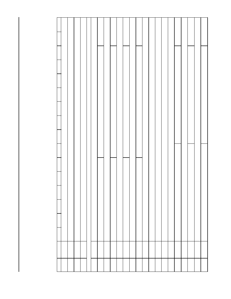
MARS2G5 P-Pro (TDAT162G52) SONET/SDH
Data Sheet
155/622/2488 Mbits/s Data Interface
August 18, 2004
242
Agere Systems Inc.
Transport Overhead Processor (TOHP-48) Block
(continued)
TOHP-48 Register Map
(continued)
Table 93. TOHP-48 Register Map (continued)
Note: Shading denotes reserved bits.
Addr
Symbol
Bit 15
Bit 14
Bit 13
Bit 12
Bit 11
Bit 10
Bit 9
Bit 8
Bit 7
Bit 6
Bit 5
Bit 4
Bit 3
Bit 2
Bit 1
Bit 0
0x084E
TOHP_SD_
CLEARRA3
TOHP_SDBCLEAR[A][15:0]
0x084F
TOHP_SD_
CLEARRB3
TOHP_SDBCLEAR[B][15:0]
0x0850
TOHP_SD_
CLEARRC3
TOHP_SDBCLEAR[C][15:0]
0x0851
TOHP_SD_
CLEARRD3
TOHP_SDBCLEAR[D][15:0]
Signal Fail Set/Clear Control Registers--R/W
0x0852
TOHP_SF_
SETRA1
TOHP_SFNSSET[A][17:2]
0x0853
TOHP_SF_
SETRA2
TOHP_SFMSET[A][5:0] Applies for version 2.2 and 2.3 only.
TOHP_SFMSET[A][6:0] Applies for version 2.0 only.
TOHP_SFLSET[A][7:0] Applies for version 2.2 and 2.3 only.
TOHP_SFLSET[A][6:0] Applies for version 2.0 only.
TOHP_SFNSSET[A][1:0]
0x0854
TOHP_SF_
SETRB1
TOHP_SFNSSET[B][17:2]
0x0855
TOHP_SF_
SETRB2
TOHP_SFMSET[B][5:0] Applies for version 2.2 and 2.3 only.
TOHP_SFMSET[B][6:0] Applies for version 2.0 only.
TOHP_SFLSET[B][7:0] Applies for version 2.2 and 2.3 only.
TOHP_SFLSET[B][6:0] Applies for version 2.0 only.
TOHP_SFNSSET[B][1:0]
0x0856
TOHP_SF_
SETRC1
TOHP_SFNSSET[C][17:2]
0x0857
TOHP_SF_
SETRC2
TOHP_SFMSET[C][5:0] Applies for version 2.2 and 2.3 only.
TOHP_SFMSET[C][6:0] Applies for version 2.0 only.
TOHP_SFLSET[C][7:0] Applies for version 2.2 and 2.3 only.
TOHP_SFLSET[C][6:0] Applies for version 2.0 only.
TOHP_SFNSSET[C][1:0]
0x0858
TOHP_SF_
SETRD1
TOHP_SFNSSET[D][17:2]
0x0859
TOHP_SF_
SETRD2
TOHP_SFMSET[D][5:0] Applies for version 2.2 and 2.3 only.
TOHP_SFMSET[D][6:0] Applies for version 2.0 only.
TOHP_SFLSET[D][7:0] Applies for version 2.2 and 2.3 only.
TOHP_SFLSET[D][6:0] Applies for version 2.0 only.
TOHP_SFNSSET[D][1:0]
0x085A
TOHP_SF_
SETRA3
TOHP_SFBSET[A][15:0]
0x085B
TOHP_SF_
SETRB3
TOHP_SFBSET[B][15:0]
0x085C
TOHP_SF_
SETRC3
TOHP_SFBSET[C][15:0]
0x085D
TOHP_SF_
SETRD3
TOHP_SFBSET[D][15:0]
0x085E
TOHP_SF_
CLEARRA1
TOHP_SFNSCLEAR[A][17:2]
0x085F
TOHP_SF_
CLEARRA2
TOHP_SFMCLEAR[A][6:0]
TOHP_SFLCLEAR[A][6:0]
TOHP_SFNSCLEAR
[A][1:0]
0x0860
TOHP_SF_
CLEARRB1
TOHP_SFNSCLEAR[B][17:2]
0x0861
TOHP_SF_
CLEARRB2
TOHP_SFMCLEAR[B][6:0]
TOHP_SFLCLEAR[B][6:0]
OHP_SFNSCLEAR
[B][1:0]
0x0862
TOHP_SF_
CLEARRC1
TOHP_SFNSCLEAR[C][17:2]
0x0863
TOHP_SF_
CLEARRC2
TOHP_SFMCLEAR[C][6:0]
TOHP_SFLCLEAR[C][6:0]
OHP_SFNSCLEAR
[C][1:0]
Data Sheet
MARS2G5 P-Pro (TDAT162G52) SONET/SDH
August 18, 2004
155/622/2488 Mbits/s Data Interface
243
Agere Systems Inc.
Transport Overhead Processor (TOHP-48) Block
(continued)
TOHP-48 Register Map
(continued)
Table 93. TOHP-48 Register Map (continued)
Note: Shading denotes reserved bits.
Addr
Symbol
Bit 15
Bit 14
Bit 13
Bit 12
Bit 11
Bit 10
Bit 9
Bit 8
Bit 7
Bit 6
Bit 5
Bit 4
Bit 3
Bit 2
Bit 1
Bit 0
0x0864
TOHP_SF_
CLEARRD1
TOHP_SFNSCLEAR[D][17:2]
0x0865
TOHP_SF_
CLEARRD2
TOHP_SFMCLEAR[D][6:0]
TOHP_SFLCLEAR[D][6:0]
OHP_SFNSCLEAR
[D][1:0]
0x0866
TOHP_SF_
CLEARRA3
TOHP_SFBCLEAR[A][15:0]
0x0867
TOHP_SF_
CLEARRB3
TOHP_SFBCLEAR[B][15:0]
0x0868
TOHP_SF_
CLEARRC3
TOHP_SFBCLEAR[C][15:0]
0x0869
TOHP_SF_
CLEARRD3
TOHP_SFBCLEAR[D][15:0]
B1, B2, and M1 Error Counts--RO
0x086A
TOHP_
B1ECNTRA
TOHP_B1ECNT[A][15:0]
0x086B
TOHP_
B1ECNTRB
TOHP_B1ECNT[B][15:0]
0x086C
TOHP_
B1ECNTRC
TOHP_B1ECNT[C][15:0]
0x086D
TOHP_
B1ECNTRD
TOHP_B1ECNT[D][15:0]
0x086E
TOHP_
B2ECNTRA1
TOHP_B2ECNT[A][21:16]
0x086F
TOHP_
B2ECNTRA2
TOHP_B2ECNT[A][15:0]
0x0870
TOHP_
B2ECNTRB1
TOHP_B2ECNT[B][21:16]
0x0871
TOHP_
B2ECNTRB2
TOHP_B2ECNT[B][15:0]
0x0872
TOHP_
B2ECNTRC1
TOHP_B2ECNT[C][21:16]
0x0873
TOHP_
B2ECNTRC2
TOHP_B2ECNT[C][15:0]
0x0874
TOHP_
B2ECNTRD1
TOHP_B2ECNT[D][21:16]
0x0875
TOHP_
B2ECNTRD2
TOHP_B2ECNT[D][15:0]
0x0876
TOHP_
M1ECNTRA1
TOHP_M1ECNT[A][20:16]
0x0877
TOHP_
M1ECNTRA2
TOHP_M1ECNT[A][15:0]
MARS2G5 P-Pro (TDAT162G52) SONET/SDH
Data Sheet
155/622/2488 Mbits/s Data Interface
August 18, 2004
244
Agere Systems Inc.
Transport Overhead Processor (TOHP-48) Block
(continued)
TOHP-48 Register Map
(continued)
Table 93. TOHP-48 Register Map (continued)
Note: Shading denotes reserved bits.
Addr
Symbol
Bit 15
Bit 14
Bit 13
Bit 12
Bit 11
Bit 10
Bit 9
Bit 8
Bit 7
Bit 6
Bit 5
Bit 4
Bit 3
Bit 2
Bit 1
Bit 0
0x0878
TOHP_
M1ECNTRB1
TOHP_M1ECNT[B][20:16]
0x0879
TOHP_
M1ECNTRB2
TOHP_M1ECNT[B][15:0]
0x087A
TOHP_
M1ECNTRC1
TOHP_M1ECNT[C][20:16]
0x087B
TOHP_
M1ECNTRC2
TOHP_M1ECNT[C][15:0]
0x087C
TOHP_
M1ECNTRD1
TOHP_M1ECNT[D][20:16]
0x087D
TOHP_
M1ECNTRD2
TOHP_M1ECNT[D][15:0]
Transmit OH Insert Value--R/W
0x087E
TOHP_TOH_
INSRA1
TOHP_TF1DINS[A][7:0]
TOHP_TS1DINS[A][7:0]
0x087F
TOHP_TOH_
INSRA2
TOHP_TK2DINS[A][7:0]
TOHP_TK1DINS[A][7:0]
0x0880
TOHP_TOH_
INSRB1
TOHP_TF1DINS[B][7:0]
TOHP_TS1DINS[B][7:0]
0x0881
TOHP_TOH_
INSRB2
TOHP_TK2DINS[B][7:0]
TOHP_TK1DINS[B][7:0]
0x0882
TOHP_TOH_
INSRC1
TOHP_TF1DINS[C][7:0]
TOHP_TS1DINS[C][7:0]
0x0883
TOHP_TOH_
INSRC2
TOHP_TK2DINS[C][7:0]
TOHP_TK1DINS[C][7:0]
0x0884
TOHP_TOH_
INSRD1
TOHP_TF1DINS[D][7:0]
TOHP_TS1DINS[D][7:0]
0x0885
TOHP_TOH_
INSRD2
TOHP_TK2DINS[D][7:0]
TOHP_TK1DINS[D][7:0]
Receive Monitor Values--RO
0x0886
TOHP_
RMONRA1
TOHP_F1DMON1[A][7:0]
TOHP_F1DMON0[A][7:0]
0x0887
TOHP_
RMONRA2
TOHP_K2DMON[A][7:0]
TOHP_K1DMON[A][7:0]
0x0888
TOHP_
RMONRA3
TOHP_S1DMON[A][7:0]
0x0889
TOHP_
RMONRB1
TOHP_F1DMON1[B][7:0]
TOHP_F1DMON0[B][7:0]
0x088A
TOHP_
RMONRB2
TOHP_K2DMON[B][7:0]
TOHP_K1DMON[B][7:0]
0x088B
TOHP_
RMONRB3
TOHP_S1DMON[B][7:0]
0x088C
TOHP_
RMONRC1
TOHP_F1DMON1[C][7:0]
TOHP_F1DMON0[C][7:0]

Data Sheet
MARS2G5 P-Pro (TDAT162G52) SONET/SDH
August 18, 2004
155/622/2488 Mbits/s Data Interface
245
Agere Systems Inc.
Transport Overhead Processor (TOHP-48) Block
(continued)
TOHP-48 Register Map
(continued)
Table 93. TOHP-48 Register Map (continued)
Note: Shading denotes reserved bits.
Addr
Symbol
Bit 15
Bit 14
Bit 13
Bit 12
Bit 11
Bit 10
Bit 9
Bit 8
Bit 7
Bit 6
Bit 5
Bit 4
Bit 3
Bit 2
Bit 1
Bit 0
0x088D
TOHP_
RMONRC2
TOHP_K2DMON[C][7:0]
TOHP_K1DMON[C][7:0]
0x088E
TOHP_
RMONRC3
TOHP_S1DMON[C][7:0]
0x088F
TOHP_
RMONRD1
TOHP_F1DMON1[D][7:0]
TOHP_F1DMON0[D][7:0]
0x0890
TOHP_
RMONRD2
TOHP_K2DMON[D][7:0]
TOHP_K1DMON[D][7:0]
0x0891
TOHP_
RMONRD3
TOHP_S1DMON[D][7:0]
J0 Byte Receive Monitor (64 bytes)--RO
0x0892--
0x08B1
TOHP_RJ0DM
ONR[A][1--32]
TOHP_RJ0DMON[A][2, 4, 6, . . ., 64][7:0]
TOHP_RJ0DMON[A][1, 3, 5, . . ., 63][7:0]
0x08B2--
0x08D1
TOHP_RJ0DM
ONR[B][1--32]
TOHP_RJ0DMON[B][2, 4, 6, . . ., 64][7:0]
TOHP_RJ0DMON[B][1, 3, 5, . . ., 63][7:0]
0x08D2--
0x08F1
TOHP_RJ0DM
ONR[C][1--32]
TOHP_RJ0DMON[C][2, 4, 6, . . ., 64][7:0]
TOHP_RJ0DMON[C][1, 3, 5, . . ., 63][7:0]
0x08F2--
0x0911
TOHP_RJ0DM
ONR[D][1--32]
TOHP_RJ0DMON[D][2, 4, 6, . . ., 64][7:0]
TOHP_RJ0DMON[D][1, 3, 5, . . ., 63][7:0]
J0 Byte Transmit Insert (64 bytes)--R/W
0x0912--
0x0931
TOHP_TJ0DIN
SR[A][1--32]
TOHP_TJ0DINS[A][2, 4, 6, . . ., 64][7:0]
TOHP_TJ0DINS[A][1, 3, 5, . . ., 63][7:0]
0x0932--
0x0951
TOHP_TJ0DIN
SR[B][1--32]
TOHP_TJ0DINS[B][2, 4, 6, . . ., 64][7:0]
TOHP_TJ0DINS[B][1, 3, 5, . . ., 63][7:0]
0x0952--
0x0971
TOHP_TJ0DIN
SR[C][1--32]
TOHP_TJ0DINS[C][2, 4, 6, . . ., 64][7:0]
TOHP_TJ0DINS[C][1, 3, 5, . . ., 63][7:0]
0x0972--
0x09A9
TOHP_TJ0DIN
SR[D][1--32]
TOHP_TJ0DINS[D][2, 4, 6, . . ., 64][7:0]
TOHP_TJ0DINS[D][1, 3, 5, . . ., 63][7:0]
MARS2G5 P-Pro (TDAT162G52) SONET/SDH
Data Sheet
155/622/2488 Mbits/s Data Interface
August 18, 2004
246
Agere Systems Inc.
Transport Overhead Processor (TOHP-48) Block
(continued)
TOHP-48 Register Map
(continued)
Table 93. TOHP-48 Register Map (continued)
Note: Shading denotes reserved bits.
Addr
Symbol
Bit 15
Bit 14
Bit 13
Bit 12
Bit 11
Bit 10
Bit 9
Bit 8
Bit 7
Bit 6
Bit 5
Bit 4
Bit 3
Bit 2
Bit 1
Bit 0
Z0 Byte Transmit Insert--R/W
0x09AA
TOHP_TZ0DIN
SR[A][1]
TOHP_TZ0DINS[A][2][7:0]
0x09AB--
0x09AF
TOHP_TZ0DIN
SR[A][2--6]
TOHP_TZ0DINS[A][4, 6, 8, 10, 12][7:0]
TOHP_TZ0DINS[A][3, 5, 7, 9, 11][7:0]
0x09B0
TOHP_TZ0DIN
SR[B][1]
TOHP_TZ0DINS[B][2][7:0]
0x09B1--
0x09B5
TOHP_TZ0DIN
SR[B][2--6]
TOHP_TZ0DINS[B][4, 6, 8, 10, 12][7:0]
TOHP_TZ0DINS[B][3, 5, 7, 9, 11][7:0]
0x09B6
TOHP_TZ0DIN
SR[C][1]
TOHP_TZ0DINS[C][2][7:0]
0x09B7--
0x09BB
TOHP_TZ0DIN
SR[C][2--6]
TOHP_TZ0DINS[C][4, 6, 8, 10, 12][7:0]
TOHP_TZ0DINS[C][3, 5, 7, 9, 11][7:0]
0x09BC
TOHP_TZ0DIN
SR[D][1]
TOHP_TZ0DINS[D][2][7:0]
0x09BD--
0x09C1
TOHP_TZ0DIN
SR[D][2--6]
TOHP_TZ0DINS[D][4, 6, 8, 10, 12][7:0]
TOHP_TZ0DINS[D][3, 5, 7, 9, 11][7:0]
Scratch Register--R/W
0x09C2
TOHP_
SCRATCHR
TOHP_SCRATCH[15:0]
0x09C3--
0x09FF

Data Sheet
MARS2G5 P-Pro (TDAT162G52) SONET/SDH
August 18, 2004
155/622/2488 Mbits/s Data Interface
247
Agere Systems Inc.
Pointer Processor (PP)
Introduction
The pointer processor block handles one STS-48 stream (single-channel mode) or four STS-12 or STS-3 streams
(quad-channel mode).
The pointer processor performs pointer interpretation, path overhead (POH) monitoring, and generates a new STS
frame aligned to the system frame pulse. The pointer interpreter block interprets the incoming H1/H2 pointer of
each incoming STS channel. The pointer interpreter supports up to 48 channels and performs path overhead mon-
itoring on each channel. Each channel may be either an STS-1, STS-3c, STS-6c, STS-9c, . . . , STS-45c, STS-
48c. An STS-3nc channel must start at time slots 1, 4, 7, 10, . . . , or 46 (assuming that it can fit). For example, an
STS-36c must start in time slots 1, 4, 7, 10, or 13; an STS-45c must start at time slot 1 or 4.
The pointer is validated according to Telcordia and ITU specifications. The H1/H2 pointer is used to determine the
location of the first path overhead (POH) byte (J1). The pointer interpreter consists of a finite state machine (FSM)
with four steady states. These states are defined as:
Normal state
Loss of pointer (LOP)
Alarm indication signal (AIS)
Concatenation
The transition between states will require several consecutive events to protect against transient conditions
caused by bit errors during high BER conditions.
This pointer processor block monitors for the following conditions and takes appropriate actions:
Pointer increment
Pointer decrement
Loss of pointer
AIS-P
New pointer
Invalid pointer
Receive Path Trace
The path trace message is extracted and stored in a 64-byte memory that can be accessed through the micropro-
cessor interface. The first byte of the message can be provisioned to be either: the byte with the most significant bit
(MSB) set high, or the byte following a carriage return (0x0D) and line feed (0x0A) sequence. This frame synchro-
nization can be disabled.

MARS2G5 P-Pro (TDAT162G52) SONET/SDH
Data Sheet
155/622/2488 Mbits/s Data Interface
August 18, 2004
248
Agere Systems Inc.
Pointer Processor (PP)
(continued)
Introduction
(continued)
Receive Error Monitor
The PBIP block counts path BIP-8 errors. A theoretical maximum of 64,000 (x concatenation level) errors may be
detected per second. A practical average of 32,000 errors per second will be detected under the worst error condi-
tions. The PBIP block accumulates these errors in a 16-bit saturating counter. This counter is operated in latch and
clear mode to ensure Telcordia and ITU compliance with regard to not missing any events (bit errors). It is intended
that this counter be polled at least once per second to ensure that no error events are missed. The REI_P block
counts remote error indication (formally known as FEBE) block errors.
Receive Signal Label
The C2 block will extract and validate the signal label byte (C2) and store it in registers PP_TSC2R[1--24], Time
Slots 1--48 Path C2 Status (RO), Table 247, addresses 0x1930--0x1947.
Receive Path Status
The G1 block extracts the path remote error indication (REI-P) bits of G1 and accumulates the REI-P errors in a 16-
bit saturating counter. This counter is operated in latch and clear mode to ensure Telcordia and ITU compliance. It
is intended that this counter be polled at least once per second to ensure that no error events are missed.
This block will also validate the path remote defect indication (RDI-P) bits and store the result in registers
PP_TSRDIPR[1--48], Time Slots 1--48 Path RDI Status (RO), Table 246, addresses 0x1900--0x192F.
Elastic Store
For each STS channel, the SPE is placed into an elastic store buffer. The system (transmit) clock and 8 kHz frame
is used to generate a new STS frame with the SPE extracted from the elastic store. The level of the elastic store is
monitored and positive/negative stuffs are performed on the new STS frame in order to prevent elastic store over-
flows/underflows.

Data Sheet
MARS2G5 P-Pro (TDAT162G52) SONET/SDH
August 19, 2004
155/622/2488 Mbits/s Data Interface
249
Agere Systems Inc.
Pointer Processor (PP)
(continued)
Introduction
(continued)
Z5/N1, Z4/K4, Z3/F3, H4, and F2 Monitoring
Also monitored are the F2 user channel byte, the H4 VT multiframe indicator byte, Z3/F3 growth/user byte, Z4/K4
growth/APS path byte, and the Z5/N1 tandem connection byte. These bytes are stored in software registers. These
registers are updated when a provisionable number of detections of new values occurs on the associated incoming
byte. Note that there are four circuits--1 per STS-12 channel, each monitoring the Z5/N1, Z4/K4, Z3/F3, H4, and
F2 bytes of their selected STS-1 stream.
SS Bits Monitoring
Although the SS bits are not defined at the STS-N level in GR-253, SDH-based equipment supports the SS bits
monitoring feature. Therefore, for SDH conformance the SS bits, contained in the H1 byte, are stored in software
registers. These registers are updated when a provisionable number of mismatches occurs in the provisioned
mode. The same registers are updated when a provisionable number of detections of new values of the SS bits
occurs while in the validation mode. In both the provisioned and validation mode, the processor is interrupted when
a mismatch or a validation takes place. In SDH, only 16 channels need to be monitored (1 per STS-3 stream) and
the register space is extended to cover 48 STS-1s. SS bits monitoring is enabled only when the J1 message type
is set to SDH (register 0x1339, Table 181).
E1 and F1 Path Status Bytes
Each STS-1 time slot will contain an independent E1/F1 value. For each STS-1 time slot, the E1 and F1 bytes will
be identical (E1 = F1) and will contain a code indicating the status of that time slot. The following values are
defined for E1/F1. This is a priority encoder, only one status condition can be communicated at once, the higher
conditions in the following table having higher priority. Note that the PDI code received (if one is received) will not
be considered unless the PDI validate enable is set.
This value can be overwritten by software by setting the E1/F1_INSERT_CONTROL register for those individual
Sets one wishes to override and placing the desired byte in the corresponding E1/F1 INSERT register.
Table 94. E1/F1 Path Status Definition
E1/F1 Value
Definition
0011 1111
Loss of Pointer (LOP-P) repass AIS.
1111 1111
Concatenation Mismatch or Software Insertion of AIS.
0011 1110
Unequipped Signal Label (UNEQ-P).
0001 1100
Trace Identifier (J1) Mismatch (TIM-P).
0011 1101
Signal Fail (SF).
0011 1100
to
0010 0001
PDI code 28
to
PDI code 1
(This E1/F1 value will only occur if the corresponding bit in the PDI
VALIDATE ENABLE register is high).
0001 1111
Signal Degrade (SD).
0001 1110
Payload Label Mismatch (PLM-P).
0000 0000
No Alarms.
MARS2G5 P-Pro (TDAT162G52) SONET/SDH
Data Sheet
155/622/2488 Mbits/s Data Interface
August 18, 2004
250
Agere Systems Inc.
Pointer Processor (PP)
(continued)
Detailed Description
The pointer processor is used to transfer input stream(s) to the system timing of the device. It can accept one STS-
48 or 4 STS-12 or STS-3 streams. In single-channel mode, the input stream is converted to four STS-12 signals, all
on system timing. In quad-channel mode, the same output is produced from four asynchronous input streams of
either STS-12 or STS-3 capacities. The four outgoing streams are synchronized to the system clock and system
frame sync. A block diagram is shown in Figure 36 on page 251.
The main blocks of this block are the time-slot interchange (TSI), four STS-12 pointer processor modules, and the
microprocessor interface. The TSI is required because the pointer processor operates at an STS-12 granularity.
The TSI is only used in the STS-48 mode.
In OC-3 mode, the pointer processor still operates at an STS-12 rate and data bytes are replicated four times to
achieve this as shown in Figure 35.
5-8151(F)r.2
Figure 35. Replication of STS-3 in OC-3 Mode into STS-12 Prior to Input of Pointer Processor
The pointer processor block requires a frame pulse for each input stream. In the MARS2G5 P-Pro device, these
four signals are provided from the transport overhead processor block. The pointer processor block performs inter-
mediate performance monitoring of the input stream(s), and can interrupt the host microprocessor with alarms and
make available the collected results through a register set.
The pointer processor is SONET and SDH compliant.
#1 STS-1
#2 STS-1
#3 STS-1
#1 STS-1
2 2 2 2 3 3 3 3
1 1 1 1
1 1 1 1
STS-3
STS-12
#1 STS-1s #2 STS-1s
#3 STS-1s

Data Sheet
MARS2G5 P-Pro (TDAT162G52) SONET/SDH
August 18, 2004
155/622/2488 Mbits/s Data Interface
251
Agere Systems Inc.
Pointer Processor (PP)
(continued)
Detailed Description
(continued)
5-8152(F)r.1
Figure 36. Top Level Block Diagram of the Pointer Processor Block
The STS pointer processor is used for phase absorption and frequency synchronization of SONET payload from
one clock domain (the receive or line timing) to another (the transmit or system timing). This is accomplished in
three basic functions: pointer interpreter, elastic store, and pointer generator. The pointer interpreter extracts the
SONET synchronous payload envelope (SPE) from the incoming data by interpreting the H1 and H2 pointer bytes
of the line overhead. The SPE is then written to the elastic store. The pointer generator reads the SPE from the
elastic store and regenerates the H1 and H2 pointer bytes. Since the pointer processor does not terminate the
path, intermediate performance monitoring is performed (i.e., the path overhead is not modified). A block diagram
of the pointer processor is shown in Figure 36, above.
SYSTEM TIMING
RX_CLK_1 TIMING
POINTER
ELASTIC
POINTER
MICROPROCESSOR
FRAME_PULSE_RX_LTE1
RX_CLK_1
RX_LTE_STS_DATA[31:24]
TSI
FRAME_PULSE_PP_1
RX_CLK_1
RX_LTE_STS_DATA[31:0]
PP_STS_DATA_1[7:0]
RX_RST_N1
FRAME_PULSE_PP_1
ADDRESS_BUS[7:0]
BUS CONTROL SIGNALS
WRITE_DATA_BUS[15:0]
INTERRUPTS
READ_DATA_BUS[15:0]
RX_RST_N1
(TIME-SLOT
INTERCHANGE)
INTERFACE
INTERPRETER
STORE
GENERATOR
SYSTEM TIMING
RX_CLK_2 TIMING
POINTER
ELASTIC
POINTER
FRAME_PULSE_RX_LTE2
RX_CLK_2
RX_LTE_STS_DATA[23:16]
PP_STS_DATA_2[7:0]
FRAME_PULSE_PP_2
RX_RST_N2
INTERPRETER
STORE
GENERATOR
SYSTEM TIMING
RX_CLK_3 TIMING
POINTER
ELASTIC
POINTER
FRAME_PULSE_RX_LTE3
RX_CLK_3
RX_LTE_STS_DATA[15:8]
PP_STS_DATA_3[7:0]
FRAME_PULSE_PP_3
RX_RST_N3
INTERPRETER
STORE
GENERATOR
SYSTEM TIMING
RX_CLK_4 TIMING
POINTER
ELASTIC
POINTER
FRAME_PULSE_RX_LTE4
RX_CLK_4
RX_LTE_STS_DATA[7:0]
PP_STS_DATA_4[7:0]
FRAME_PULSE_PP_4
RX_RST_N4
INTERPRETER
STORE
GENERATOR

MARS2G5 P-Pro (TDAT162G52) SONET/SDH
Data Sheet
155/622/2488 Mbits/s Data Interface
August 18, 2004
252
Agere Systems Inc.
Pointer Processor (PP)
(continued)
Detailed Description
(continued)
Performance Monitoring
This block accepts the payload mapping information, status, and timing from the Rx pointer interpreter and extracts
the path overhead from up to 12 STS channels. The extracted overhead is then either stored internally or provided
externally on a serial output, and may also be further processed for alarm or performance-monitoring purposes.
While an STS channel is in AIS or LOP status, all path overhead processing for the channel is inhibited. The defini-
tion and associated storage or processing of each byte is detailed below.
Path Trace (J1). The path trace byte carries a repeating message that is defined in SONET as 64 bytes (ASCII,
<CR><LF> terminated) and in SDH as 16 bytes (E.164). The POH processor extracts either type of message from
one selectable STS-1 per channel and stores the message in an internal register bank. The contents of the mes-
sage can then optionally be monitored for either a mismatch from a provisioned expected message or a sustained
change in the received message. A mismatch is declared if the received message differs from the expected mes-
sage for ten consecutive messages. The mismatch clears when four out of five received messages match the
expected message. A sustained change is detected when the received message differs from the last stable mes-
sage for ten consecutive messages. The new message then becomes the stable message and the processor starts
checking for a sustained change from this new stable message (i.e., there is no clearing criteria for a sustained
change). Both defects are indicated by corresponding latched alarm status bits in the memory map.
Selection of the message protocol, 16- or 64-byte, the content monitoring option, and the monitored STS channel
are provisionable on a per-channel basis through the path trace control registers (addresses 0x1330--0x133F,
Table 177--Table 181). The expected messages for all channels are provisioned through the microprocessor inter-
face using a 64-byte data buffer. This data buffer is also used to read the contents of the expected, stable, or
received message buffers for all blocks. Accesses using the data buffer are paged according to channel and mes-
sage buffer (expected/stable or received). Selection of paging, as well as access type (read or write), is done using
the path trace access control register. The actual access is triggered by writing a 0001 hex value to the path trace
access start register and is performed on a nonreal time basis. Completion of the access is indicated by the mes-
sage buffer access complete bit in the path trace status register being set.
Note: There are four circuits (1 per STS-12 channel) each monitoring the path trace byte of their selected STS-1
stream.
Path BIP-8 (B3). The path BIP-8 byte carries the even parity of the data in the previous STS SPE frame (783 bytes
for STS-1, Nx783 for STS-Nc). Every frame, the received B3 value is extracted and compared to the calculated
BIP-8 for the previous frame. Detected errors are accumulated in an internal 16-bit counter based on either bit or
block errors as provisioned per channel through the microprocessor interface. If bit error mode is enabled for the
channel, each BIP-8 bit found in error causes the counter to increment. If block error mode is enabled for the chan-
nel, the counter is only incremented by one regardless of the number of BIP-8 bits in error. The value in the counter
is transferred to the path coding violation (CV-P) registers on the positive edge of the performance-monitoring
strobe (PMSTB input), at which point the counter is cleared.

Data Sheet
MARS2G5 P-Pro (TDAT162G52) SONET/SDH
August 18, 2004
155/622/2488 Mbits/s Data Interface
253
Agere Systems Inc.
Pointer Processor (PP)
(continued)
Detailed Description
(continued)
Signal Fail Alarms. Each of the 48 STS-1s entering the PP can be automatically monitored for B3 errors against
a programmable threshold. Concatenated payloads are supported by programming the threshold values for the
head STS-1.
Each STS-1 or head of an STS-NC has a select to choose which threshold group's parameters to compare
against. There are eight threshold groups available, each group consisting of:
Set Threshold. If the B3 errors is equal or greater than this value in the given time window, the signal fail alarm
for this STS-1 is set. The B3 count in subsequent window times must be less than the clear threshold listed
below to clear this error condition.
Set Threshold Window Select. There are four time windows available between the eight groups. The set
threshold window select can be set to one of these window sizes.
Clear Threshold. If the signal fail alarm has been previously set, it will be cleared if an entire clear window time
goes past with the B3 error count less than this value.
Clear Threshold Window Select. If the signal fail alarm has been previously set, this window size will be used
to measure B3 errors.
Each STS-1 has a 9-bit B3 counter, which is incremented every time a B3 error appears. If STSs are part of an
STS-Nc, there is one 14-bit counter for the entire concatenation. This counter is cleared at the end of the window
selected for the threshold group for which this STS-1 or STS-Nc is set to. This counter (9 or 14 bits) can be incre-
mented by 0 (if no B3 errors occurred) or up to 8 counts (if all the bits in the B3's BIP-8 calculation are opposite
from expected). Note there are no bit/block issues with the signal fail counters; only bit errors are counted. Bit/
block is only an option for the B3 counters in the path monitoring (PM).
The signal fail alarm is set if the number of B3 errors for an STS-1 or STS-Nc is above the set threshold within this
window time. The B3 error counter for each STS-1 or STS-Nc is cleared at the end of each window and counts up
again in the next window.
One can set an individual STS-1/STS-Nc to set an alarm on one BER and clear this alarm on another. For this, a
threshold count value and timing window is provided for both set and clear.
For each STS-1 or STS-Nc, its B3 counter is running for either the time set by the set threshold window or the time
set by the clear threshold window. If this STS-1/STS-Nc is in the clear state (the alarm bit is clear), then the signal
fail circuitry will be looking for the case when the number of B3 errors equals or exceeds the set threshold. The
counter will be running for the duration of the set threshold window. If this condition is reached, the alarm will be set
immediately and the system will switch to watching the desired clear window. It will wait until the clear window has
completed its current cycle and will start counting B3 errors again in the next cycle. The B3 counter will be cleared,
and B3 errors will be added; at the end of this window time (now the clear window time), the decision will be made
to clear the alarm condition or not. If the number of B3 errors in the counter is less than the clear threshold, the
alarm will be cleared and, during the next window of length = set threshold window size, the counter will be com-
pared to the set threshold. Otherwise, this error condition will remain set and another window of duration = clear
threshold window size will commence.

MARS2G5 P-Pro (TDAT162G52) SONET/SDH
Data Sheet
155/622/2488 Mbits/s Data Interface
August 18, 2004
254
Agere Systems Inc.
Pointer Processor (PP)
(continued)
Detailed Description
(continued)
The signal fail alarm can be set anywhere during the window, but can only be cleared at the end of a window time.
The PP is either checking for the set or clear condition for an STS-1/STS-Nc at a given time. One implication of this
is that if the clear threshold was set for a BER higher than the set threshold and an incoming signal of a constant
BER between the two was present, the signal fail alarm would oscillate, set, and clear with a period of zero to one
times the set window threshold window time plus one to two times the period of the clear window threshold window
time.
There are eight threshold groups available (see Table 197--Table 200); two are labelled as being used for STS-1s
(group 0 and 1) and six (groups 2--7) are labelled for use as STS-Ncs. Group 0 and 1 have set and clear thresh-
olds of 9 bits (0--511) whereas groups 2--7 have set and clear thresholds of up to 14 bits (0--16383). This is to
accommodate the higher data rate of a concatenated payload and thus the higher number of bit errors one would
see in the same time window for the same BER. However, one could point an STS-1 to group 2--7 as long as the
thresholds are set to 511 or less to stay within the 9-bit size of an individual STS-1s counter.
There are four threshold window size registers, each 16 bits, in increments of 0.5 ms (for a maximum of window
size of 32 seconds).
Table 324 on page 403 shows the recommended set/clear threshold and window values for the BER they are
intended for.

Data Sheet
MARS2G5 P-Pro (TDAT162G52) SONET/SDH
August 18, 2004
155/622/2488 Mbits/s Data Interface
255
Agere Systems Inc.
Pointer Processor (PP)
(continued)
Detailed Description
(continued)
Path Signal Label (C2). The path signal label byte is used to indicate either the type of payload carried in the STS
SPE or the status of the payload. Of the 256 possible values, only the codes 0x01 to 0x04 and 0x12 to 0x15 are
currently defined to identify payload types, while the codes E1 to FC are defined to indicate payload defects. The
code 0xFF is a special reserved code due to its appearance in an STS AIS and is treated as a don't care during
any defect detection or clearing. The C2 byte is extracted each frame and stored in the receive signal label regis-
ters. If the locally provisioned value, configured in the expected signal label registers, is any equipped value (i.e.,
not 00), the extracted signal label is also processed for the following defects:
Payload Label Mismatch (PLM)--Detected if the extracted signal label is a valid payload-specific code and does
not match the locally provisioned value in the expected signal label registers for five consecutive frames.
Cleared if the extracted signal label matches the locally provisioned value, the equipped nonspecific code
(0x01), or a valid PDI code for five consecutive frames. If the locally provisioned value is the equipped nonspe-
cific code, then it matches any valid equipped code (including PDI). The valid payload specific codes are by
default 0x02 to 0xE0, 0xFD and 0xFE, with the codes 0xE1 to 0xFB also included if the locally provisioned pay-
load is VT structured (0x02 or 0x03). If payload defect indication detection is disabled, 0xE1 to 0xFC are always
included. Detection of a PLM defect is indicated by a latched alarm status bit in the memory map.
Path Unequipped (UNEQ)--Detected if the extracted signal label matches the unequipped code (0x00) for five
consecutive frames. Cleared if the extracted signal label does not match the unequipped code for five consecu-
tive frames. Detection of an UNEQ defect is indicated by a latched alarm status bit and a one second PM in the
memory map.
Update--The C2 value is dumped into an MPU register. Each time the captured value changes, a delta bit is set.
Payload Defect Indication (PDI)--Detected if the extracted signal label matches a valid PDI code for five consec-
utive frames. Cleared if the extracted signal label does not match a valid PDI code for five consecutive frames.
Valid PDI codes are 0xE1 to 0xFC when the locally provisioned payload label is 0x01, 0x02, or 0x03 (VT-struc-
tured STS) or just 0xFC otherwise. PDI detection can be disabled per STS through the microprocessor interface.
Path Status (G1). The path status byte is used to convey the path termination status and performance back to the
originating STS PTE. This allows the performance of the full-duplex path to be monitored from any single point
along the path. Bits 1 to 4 are used as a remote error indication (formerly far-end block error or FEBE), while bits 5
to 7 are used as a remote defect indication. The G1 byte is extracted each frame and processed for these func-
tions as described below.
Remote Error Indication (REI-P)--Indicates the count of bit errors detected at the far-end STS PTE using the
path BIP-8. The error count is a binary number from 0 to 8 (values above 8 are invalid and interpreted as 0) and
is accumulated in an internal 16-bit counter based on either bit or block errors as provisioned per channel
through the microprocessor interface. If bit error mode is enabled for the channel, the counter is incremented by
the actual error count. If block error mode is enabled for the channel the counter is only incremented by one,
when the error count is not 0, regardless of the actual value. The value in the counter accumulates until it is
transferred to the REI-P registers on the positive edge of the performance-monitoring strobe (PMSTB input) at
which point the counter is cleared.
Remote Defect Indication (RDI-P)--Indicates the detection of a defect at the far-end STS PTE. Initially RDI-P
was defined as a one bit value in bit 5, but has since been expanded to a 3-bit enhanced value (ERDI-P).
Table 95 on page 256 shows the valid codes and interpretation for both the one bit and enhanced RDI schemes.
As can be seen, bits 6 and 7 are always set to opposite values for ERDI while they are set to the same value for
1-bit RDI. The POH uses this fact to determine which RDI scheme is being used on a per STS basis. An RDI-P
defect is then detected if a valid defect code for one of the RDI schemes is received for ten consecutive frames.
The RDI-P defect is cleared when the no defects code for that scheme is received for ten consecutive frames.
The value of the last validated 3-bit RDI code is stored in the ERDI-P registers in the memory map. In addition,
detection of a 1-bit RDI defect or each of the three ERDI defects is indicated by a one second PM bit in the mem-
ory map.

MARS2G5 P-Pro (TDAT162G52) SONET/SDH
Data Sheet
155/622/2488 Mbits/s Data Interface
August 18, 2004
256
Agere Systems Inc.
Pointer Processor (PP)
(continued)
Detailed Description
(continued)
* These codes are transmitted by STS PTE that do not support enhanced RDI-P. If enhanced RDI-P is not supported, G1 bits 2 and 1 must be
set to the same value, and should be set to 00.
These codes are transmitted by STS PTE that support enhanced RDI-P.
Table 95. RDI-P Codes and Interpretation
G1[5:7]
Priority of Enhanced
RDI-P Codes
Trigger
Interpretation
0xx*
Not applicable
No defects
No RDI-P defect.
1xx*
Not applicable
AIS-P, LOP-P
1-bit RDI-P defect.
001
4
No defects
NO ERDI-P defects.
010
3
PLM-P, LCD-P
ERDI-P payload defect.
101
1
AIS-P, LOP-P
ERDI-P server defect.
110
2
UNEQ-P, TIM-P
ERDI-P connectivity defect.

Data Sheet
MARS2G5 P-Pro (TDAT162G52) SONET/SDH
August 18, 2004
155/622/2488 Mbits/s Data Interface
257
Agere Systems Inc.
Pointer Processor (PP)
(continued)
PP Register Map Overview
5-8156(F).ar.1
Figure 37. Overview of Pointer Processor Register Map
ID REGISTER
INTERRUPTS
MASKS
PATH TRACE
PATH PROVISIONING
PATH MAINTENANCE
INTER INC/DEC (PM)
POH PM
CV COUNT PM
0x1000
0x100F
0x1300
0x1702
0x1742
0x1780
0x1800
0x1900
0x1400
0x1580
0x1690
0x1600
0x120F
0x1542
0x1502
RESERVED
0x1880
SF DETECT/CLEAR
AIS-P GENERAL CONTROL
PP CONTROL
REI COUNT PM
RDI, C2, PDI
GEN INC/DEC (PM)
CONCATENATION MAP
PERSISTENCY
STATE
0x13C2
0x1382

MARS2G5 P-Pro (TDAT162G52) SONET/SDH
Data Sheet
155/622/2488 Mbits/s Data Interface
August 18, 2004
258
Agere Systems Inc.
Pointer Processor (PP)
(continued)
PP Register Descriptions
To access (read and write) registers RXCLK[A--D][P/N] (see Pin Descriptions--Line Interface Signals, Table 7, on
page 97) must always be present for a given application.
Table 96. PP_IDR, PP Identification Register (RO, Fixed Value)
Table 97. PP_CORWR, PP Clear on Read/Write Register (R/W, Control)
Address
Bit
Name
Function
Reset
Default
0x1000
15:0
PP_ID[15:0]
Pointer Processor Identification Register.
0001
Address
Bit
Name
Function
Reset
Default
0x1001
15:1
--
Reserved.
0
0
PP_CORW
PP Clear On Read/Write. Sets the mode for clearing alarm
bit in the PP block.
0 = Clear interrupt bits with writing 1 to that bit in the alarm
register.
1 = Clear all alarm bits in an interrupt alarm register by
reading that register.
Note:This affects only the pointer processor interrupt
alarms, i.e., only the ones listed in this section (pointer
processor) of the data sheet.
0

Data Sheet
MARS2G5 P-Pro (TDAT162G52) SONET/SDH
August 18, 2004
155/622/2488 Mbits/s Data Interface
259
Agere Systems Inc.
Pointer Processor (PP)
(continued)
PP Register Descriptions
(continued)
Interrupts
Table 98. PP_POH_ALMBNR[1--2], Path Overhead Alarm Status Binning Register (RO)
Address
Bit
Name
Function
Reset
Default
0x100F
15:10
--
Reserved.
0
9
--
SS Mismatch Alarm.
0 = SS mismatch alarm has not been detected for any STS-
1 in any bytestream.
1 = SS mismatch alarm has been detected for one or more
STS-1s in one or more bytestreams.
0
8
--
SS Validated Alarm.
0 = SS validated alarm has not been detected for any STS-
1 in any bytestream.
1 = SS validated alarm has been detected for one or more
STS-1s in one or more bytestreams.
0
7
--
F2 Validated Alarm.
0 = F2 validated alarm has not been detected for the
selected STS-1 in any bytestream.
1 = F2 validated alarm has been detected for the selected
STS-1 in one or more bytestreams.
0
6
--
H4 Validated Alarm.
0 = H4 validated alarm has not been detected for the
selected STS-1 in any bytestream.
1 = H4 validated alarm has been detected for the selected
STS-1 in one or more bytestreams.
0
5
--
Z3 Validated Alarm.
0 = Z3 validated alarm has not been detected for the
selected STS-1 in any bytestream.
1 = Z3 validated alarm has been detected for the selected
STS-1 in one or more bytestreams.
0
4
--
Z4 Validated Alarm.
0 = Z4 validated alarm has not been detected for the
selected STS-1 in any bytestream.
1 = Z4 validated alarm has been detected for the selected
STS-1 in one or more bytestreams.
0
3
--
Z5 Validated Alarm.
0 = Z5 validated alarm has not been detected for the
selected STS-1 in any bytestream.
1 = Z5 validated alarm has been detected for the selected
STS-1 in one or more bytestreams.
0

MARS2G5 P-Pro (TDAT162G52) SONET/SDH
Data Sheet
155/622/2488 Mbits/s Data Interface
August 18, 2004
260
Agere Systems Inc.
Pointer Processor (PP)
(continued)
PP Register Descriptions
(continued)
Table 98. PP_POH_ALMBNR[1--2], Path Overhead Alarm Status Binning Register (RO) (continued)
Address
Bit
Name
Function
Reset
Default
0x100F
2
PP_PDI_ALMDBN
Payload Defect Indicator (PDI) Alarm Delta Binning.
0 = PDI alarm delta has not been detected for any STS-1 in
any bytestream.
1 = PDI alarm delta has been detected for one or more
STS-1s in one or more bytestreams.
0
1
PP_PDI_ALMBN
Payload Defect Indicator (PDI) Alarm Binning.
0 = PDI alarm has not been detected for any STS-1 in any
bytestream.
1 = PDI alarm has been detected for one or more STS-1s in
one or more bytestreams.
0
0
PP_J1ACCMP_ALMBN J1 Access Complete Alarm Binning.
0 = J1 access complete alarm has not been detected for
any STS-1 in any bytestream.
1 = J1 access complete alarm has been detected for one or
more STS-1s in one or more bytestreams.
0

Data Sheet
MARS2G5 P-Pro (TDAT162G52) SONET/SDH
August 18, 2004
155/622/2488 Mbits/s Data Interface
261
Agere Systems Inc.
Pointer Processor (PP)
(continued)
PP Register Descriptions
(continued)
Table 98. PP_POH_ALMBNR[1--2], Path Overhead Alarm Status Binning Register (RO) (continued)
Address
Bit
Name
Function
Reset
Default
0x1010
15
PP_RDI_ALMDBN
Remote Defect Indicator Alarm Delta Binning.
0 = Alarm has not been detected for any STS-1 in any
bytestream.
1 = Alarm has been detected for one or more STS-1s in one or
more bytestreams.
0
14
PP_PLM_ALMDBN Payload Label Mismatch Alarm Delta Binning.
0 = Alarm has not been detected for any STS-1 in any
bytestream.
1 = Alarm has been detected for one or more STS-1s in one or
more bytestreams.
0
13
PP_UNEQR_
ALMDBN
Unequipped Received Alarm Delta Binning.
0 = Alarm has not been detected for any STS-1 in any
bytestream.
1 = Alarm has been detected for one or more STS-1s in one or
more bytestreams.
0
12
PP_AIS_ALMDBN
Alarm Indicator Signal Alarm Delta Binning.
0 = Alarm has not been detected for any STS-1 in any
bytestream.
1 = Alarm has been detected for one or more STS-1s in one or
more bytestreams.
0
11
PP_LOP_ALMDBN
Loss of Pointer Alarm Delta Binning.
0 = Alarm has not been detected for any STS-1 in any
bytestream.
1 = Alarm has been detected for one or more STS-1s in one or
more bytestreams.
0
10
PP_J1MM_ALMBN
J1 Mismatch Alarm Binning.
0 = No J1 mismatch alarm has been detected in any
bytestream.
1 = J1 mismatch alarm has been detected in one or more
bytestreams.
0
9
PP_J1VLD_ALMBN J1 Validated Alarm Binning.
0 = No new validated J1 has been detected in any bytestream.
1 = New validated J1 has been detected in one or more
bytestreams.
0
8
PP_USCNCT_
ALMBN
Unsupported Concatenation Alarm Binning.
0 = None of the four bytestreams has an unsupported
concatenation.
1 = One of the four bytestreams has an unsupported
concatenation.
0

MARS2G5 P-Pro (TDAT162G52) SONET/SDH
Data Sheet
155/622/2488 Mbits/s Data Interface
August 18, 2004
262
Agere Systems Inc.
Pointer Processor (PP)
(continued)
PP Register Descriptions
(continued)
Table 98. PP_POH_ALMBNR[1--2], Path Overhead Alarm Status Binning Register (RO) (continued)
Address
Bit
Name
Function
Reset
Default
0x1010
7
PP_CNCTMM_
ALMBN
Concatenation Mismatch Alarm Binning.
0 = None of the four bytestreams has a concatenation
mismatch.
1 = One of the four bytestreams has a concatenation mismatch.
0
6
PP_ES_ALMBN
Elastic Store Overrun/Underrun Alarm Binning.
0 = Alarm has not been detected for any STS-1 in any
bytestream.
1 = Alarm has been detected for one or more STS-1s in one or
more bytestreams.
0
5
PP_SF_ALMBN
Signal Fail Alarm Binning.
0 = Alarm has not been detected for any STS-1 in any
bytestream.
1 = Alarm has been detected for one or more STS-1s in one or
more bytestreams.
0
4
PP_RDI_ALMBN
Remote Defect Indicator Alarm Binning.
0 = Alarm has not been detected for any STS-1 in any
bytestream.
1 = Alarm has been detected for one or more STS-1s in one or
more bytestreams.
0
3
PP_PLM_ALMBN
Payload Label Mismatch Alarm Binning.
0 = Alarm has not been detected for any STS-1 in any
bytestream.
1 = Alarm has been detected for one or more STS-1s in one or
more bytestreams.
0
2
PP_UNEQR_
ALMBN
Unequipped Received Alarm Binning.
0 = Alarm has not been detected for any STS-1 in any
bytestream.
1 = Alarm has been detected for one or more STS-1s in one or
more bytestreams.
0
1
PP_AIS_ALMBN
Alarm Indicator Signal Alarm Binning.
0 = Alarm has not been detected for any STS-1 in any
bytestream.
1 = Alarm has been detected for one or more STS-1s in one or
more bytestreams.
0
0
PP_LOP_ALMBN
Loss of Pointer Alarm Binning.
0 = Alarm has not been detected for any STS-1 in any
bytestream.
1 = Alarm has been detected for one or more STS-1s in one or
more bytestreams.
0

Data Sheet
MARS2G5 P-Pro (TDAT162G52) SONET/SDH
August 18, 2004
155/622/2488 Mbits/s Data Interface
263
Agere Systems Inc.
Pointer Processor (PP)
(continued)
PP Register Descriptions
(continued)
Table 99. PP_ES_ALMBNBSR, Elastic Store Overrun/Underrun Alarm Status Binning Bytestream A--D
(RO)
Table 100. PP_TSES_ALMBSR[A--D], Time Slots 1--12 Elastic Store Overrun/Underrun Alarm
Bytestream A--D (RO, COR/COW)
Table 101. PP_SF_ALMBNBSR, Signal Fail Alarm Status Binning Bytestream A--D (RO)
Table 102. PP_TSSF_ALMBSR[A--D], Time Slots 1--12 Signal Fail Alarm Bytestream A--D (RO, COR/
COW)
Address
Bit
Name
Function
Reset
Default
0x1021
15:4
--
Reserved.
0
3:0
PP_ES_ALMBNBS[A--D] Elastic Store Overrun/Underrun Binning Bytestream
A--D.
0 = Elastic store overrun/underrun has not been detected
for any STS-1s in bytestream A--D.
1 = Elastic store overrun/underrun has been detected for
one or more STS-1s in bytestream A--D.
0
Address
Bit
Name
Function
Reset
Default
0x1022,
0x1023,
0x1024,
0x1025
15:12
--
Reserved.
0
11:0
PP_TSES_ALMBS
[A--D][1--12]
Time Slot 1--Time Slot 12 Elastic Store Overrun/
Underrun Bytestream A--D.
0 = Elastic store overrun/underrun has not been detected.
1 = Elastic store overrun/underrun has been detected.
1
Address
Bit
Name
Function
Reset
Default
0x1031
15:4
--
Reserved.
0
3:0
PP_SF_ALMBNBS[A--D] Signal Fail Binning Bytestream A--D.
0 = Signal fail has not been detected for any STS-1s in
bytestream A--D.
1 = Signal fail has been detected for one or more STS-1s
in bytestream A--D.
0
Address
Bit
Name
Function
Reset
Default
0x1032,
0x1033,
0x1034,
0x1035
15:12
--
Reserved.
0
11:0
PP_TSSF_ALMBS
[A--D][1--12]
Time Slot 1--Time Slot 12 Signal Fail Bytestream
A--D.
0 = Signal fail has not been detected.
1 = Signal fail has been detected.
0

MARS2G5 P-Pro (TDAT162G52) SONET/SDH
Data Sheet
155/622/2488 Mbits/s Data Interface
August 18, 2004
264
Agere Systems Inc.
Pointer Processor (PP)
(continued)
PP Register Descriptions
(continued)
Table 103. PP_RDI_ALMBNBSR, Remote Defect Indicator Alarm Status Binning Bytestream A--D (RO)
Table 104. PP_TSRDI_ALMBSR[A--D], Time Slots 1--12 Remote Defect Indicator Alarm
Bytestream A--D (RO, COR/COW)
Table 105. PP_PLM_ALMBNBSR, Payload Label Mismatch Alarm Status Binning Bytestream A--D (RO)
Table 106. PP_TSPLM_ALMBSR[A--D], Time Slots 1--12 Payload Label Mismatch Alarm
Bytestream A--D (RO, COR/COW)
Address
Bit
Name
Function
Reset
Default
0x1041
15:4
--
Reserved.
0
3:0
PP_RDI_
ALMBNBS[A--D]
Remote Defect Indicator Binning Bytestream A--D.
0 = Remote defect indicator has not been detected for any
STS-1s in bytestream A--D.
1 = Remote defect indicator has been detected for one or
more STS-1s in bytestream A--D.
0
Address
Bit
Name
Function
Reset
Default
0x1042,
0x1043,
0x1044,
0x1045
15:12
--
Reserved.
0
11:0
PP_TSRDI_ALMBS
[A--D][1--12]
Time Slot 1--Time Slot 12 Remote Defect Indicator
Bytestream A--D.
0 = Remote defect indicator has not been detected.
1 = Remote defect indicator has been detected.
0
Address
Bit
Name
Function
Reset
Default
0x1051
15:4
--
Reserved.
0
3:0
PP_PLM_
ALMBNBS[A--D]
Payload Label Mismatch Binning Bytestream A--D.
0 = Payload label mismatch has not been detected for any
STS-1s in bytestream A--D.
1 = Payload label mismatch has been detected for one or
more STS-1s in bytestream A--D.
0
Address
Bit
Name
Function
Reset
Default
0x1052,
0x1053,
0x1054,
0x1055
15:12
--
Reserved.
0
11:0
PP_TSPLM_ALMBS
[A--D][1--12]
Time Slot 1--Time Slot 12 Payload Label Mismatch
Bytestream A--D.
0 = Payload label mismatch has not been detected.
1 = Payload label mismatch has been detected.
0

Data Sheet
MARS2G5 P-Pro (TDAT162G52) SONET/SDH
August 18, 2004
155/622/2488 Mbits/s Data Interface
265
Agere Systems Inc.
Pointer Processor (PP)
(continued)
PP Register Descriptions
(continued)
Table 107. PP_UNEQR_ALMBNBSR, Unequipped Received Alarm Status Binning Bytestream A--D (RO)
Table 108. PP_TSUNEQR_ALMBSR[A--D], Time Slots 1--12 Unequipped Received Alarm Bytestream A--D
(RO, COR/COW)
Table 109. PP_AIS_ALMBNBSR, Alarms Indicator Signal Alarm Status Binning Bytestream A--D (RO)
Table 110. PP_TSAIS_ALMBSR[A--D], Time Slots 1--12 Alarms Indicator Signal Alarm Bytestream A--D
(RO, COR/COW)
Address
Bit
Name
Function
Reset
Default
0x1061
15:4
--
Reserved.
0
3:0
PP_UNEQR_
ALMBNBS[A--D]
Unequipped Received Binning Bytestream A--D.
0 = Unequipped received has not been detected for any
STS-1s in bytestream A--D.
1 = Unequipped received has been detected for one or
more STS-1s in bytestream A--D.
0
Address
Bit
Name
Function
Reset
Default
0x1062,
0x1063,
0x1064,
0x1065
15:12
--
Reserved.
0
11:0
PP_TSUNEQR_ALMBS
[A--D][1--12]
Time Slot 1--Time Slot 12 Unequipped Received
Bytestream A--D.
0 = Unequipped received has not been detected.
1 = Unequipped received has been detected.
0
Address
Bit
Name
Function
Reset
Default
0x1071
15:4
--
Reserved.
0
3:0
PP_AIS_ALMBNBS[A--D] Alarms Indicator Signal Binning Bytestream A--D.
0 = Alarms indicator signal has not been detected for any
STS-1s in bytestream A--D.
1 = Alarms indicator signal has been detected for one or
more STS-1s in bytestream A--D.
0
Address
Bit
Name
Function
Reset
Default
0x1072,
0x1073,
0x1074,
0x1075
15:12
--
Reserved.
0
11:0
PP_TSAIS_ALMBS
[A--D][1--12]
Time Slot 1--Time Slot 12 Alarms Indicator Signal
Bytestream A--D.
0 = Alarms indicator signal has not been detected.
1 = Alarms indicator signal has been detected.
1

MARS2G5 P-Pro (TDAT162G52) SONET/SDH
Data Sheet
155/622/2488 Mbits/s Data Interface
August 18, 2004
266
Agere Systems Inc.
Pointer Processor (PP)
(continued)
PP Register Descriptions
(continued)
Table 111. PP_LOP_ALMBNBSR, Loss of Pointer Alarm Status Binning Bytestream A--D (RO)
Table 112. PP_TSLOP_ALMBSR[A--D], Time Slots 1--12 Loss of Pointer Alarm Bytestream A--D
(RO, COR/COW)
Address
Bit
Name
Function
Reset
Default
0x1081
15:4
--
Reserved.
0
3:0
PP_LOP_
ALMBNBS[A--D]
Loss of Pointer Binning Bytestream A--D.
0 = Loss of pointer has not been detected for any STS-1s
in bytestream A--D.
1 = Loss of pointer has been detected for one or more
STS-1s in bytestream A--D.
0
Address
Bit
Name
Function
Reset
Default
0x1082,
0x1083,
0x1084,
0x1085
15:12
--
Reserved.
0
11:0
PP_TSLOP_ALMBS
[A--D][1--12]
Time Slot 1--Time Slot 12 Loss of Pointer Bytestream
A--D.
0 = Loss of pointer has not been detected.
1 = Loss of pointer has been detected.
1

Data Sheet
MARS2G5 P-Pro (TDAT162G52) SONET/SDH
August 18, 2004
155/622/2488 Mbits/s Data Interface
267
Agere Systems Inc.
Pointer Processor (PP)
(continued)
PP Register Descriptions
(continued)
Table 113. PP_CNCTMM_ALMBNBSR, Channel Path Concatenation Map Mismatch Alarm Status Binning
Bytestream A--D (RO, COR/COW)
Table 114. PP_USCNCTM_ALMBNBSR, Channel Path Unsupported Concatenation Map Alarm Binning
Bytestream A--D (RO, COR/COW)
Table 115. PP_J1NVLDMSG_ALMBNBSR, Channel Path J1 New Validated Message Alarm Binning
Bytestream A--D (RO, COR/COW)
Table 116. PP_J1MSGMM_ALMBNBSR, Channel Path J1 Message Mismatch Alarm Status Binning
Bytestream A--D (RO, COR/COW)
Address
Bit
Name
Function
Reset
Default
0x1091
15:4
--
Reserved.
0
3:0
PP_CNCTMM_
ALMBNBS[A--D]
Concatenation Map Mismatch Binning
Bytestream A--D.
0 = No expected/received concatenation state
mismatches on any time slot.
1 = Expected/received concatenation state mismatch in at
least one time slot.
0
Address
Bit
Name
Function
Reset
Default
0x10A1
15:4
--
Reserved.
0
3:0
PP_USCNCTM_
ALMBNBS[A--D]
Unsupported Concatenation Map Binning
Bytestream A--D.
0 = No path alarm.
1 = Alarm detected.
0
Address
Bit
Name
Function
Reset
Default
0x10C1
15:4
--
Reserved.
0
3:0
PP_J1NVLDMSG_
ALMBNBS[A--D]
J1 New Validated Message Binning Bytestream A--D.
0 = No path alarm.
1 = Alarm detected.
0
Address
Bit
Name
Function
Reset
Default
0x10D1
15:4
--
Reserved.
0
3:0
PP_J1MSGMM_
ALMBNBS[A--D]
J1 Message Mismatch Binning Bytestream A--D.
0 = No path alarm.
1 = Alarm detected.
0

MARS2G5 P-Pro (TDAT162G52) SONET/SDH
Data Sheet
155/622/2488 Mbits/s Data Interface
August 18, 2004
268
Agere Systems Inc.
Pointer Processor (PP)
(continued)
PP Register Descriptions
(continued)
Table 117. PP_PDI_ALMBNBSR, Payload Defect Indicator Alarm Status Binning Bytestream A--D (RO)
Table 118. PP_TSPDI_ALMBSR[A--D], Time Slots 1--12 Payload Defect Indicator Alarm Bytestream A--D
(RO, COR/COW)
Table 119. PP_RDI_ALMDBNBSR, Path Overhead STS-1 Remote Defect Indicator Alarm Delta Status
Binning Bytestream A--D (RO)
Table 120. PP_TSRDI_ALMDBSR[A--D], Path Overhead STS-1 Time Slots 1--12 Remote Defect Indicator
Alarm Delta Bytestream A--D (RO, COR/COW)
Address
Bit
Name
Function
Reset
Default
0x1101
15:4
--
Reserved.
0
3:0
PP_PDI_ALMBNBS[A--D] Payload Defect Indicator Binning Bytestream A--D.
0 = Payload defect indicator has not been detected for
any STS-1s in bytestream A--D.
1 = Payload defect indicator has been detected for one or
more STS-1s in bytestream A--D.
0
Address
Bit
Name
Function
Reset
Default
0x1102,
0x1103,
0x1104,
0x1105
15:12
--
Reserved.
0
11:0
PP_TSPDI_ALMBS
[A--D][1--12]
Time Slot 1--Time Slot 12 Payload Defect Indicator
Bytestream A--D.
0 = Payload defect indicator has not been detected.
1 = Payload defect indicator has been detected.
0
Address
Bit
Name
Function
Reset
Default
0x1111
15:4
--
Reserved.
0
3:0
PP_RDI_
ALMDBNBS[A--D]
Remote Defect Indicator Delta Binning
Bytestream A--D.
0 = Remote defect indicator delta has not been detected
for any STS-1s in bytestream A--D.
1 = Remote defect indicator delta has been detected for
one or more STS-1s in bytestream A--D.
0
Address
Bit
Name
Function
Reset
Default
0x1112,
0x1113,
0x1114,
0x1115
15:12
--
Reserved.
0
11:0
PP_TSRDI_ALMDBS
[A--D][1--12]
Time Slot 1--Time Slot 12 Remote Defect Indicator
Delta Bytestream A--D.
0 = Remote defect indicator delta has not been detected.
1 = Remote defect indicator delta has been detected.
0

Data Sheet
MARS2G5 P-Pro (TDAT162G52) SONET/SDH
August 18, 2004
155/622/2488 Mbits/s Data Interface
269
Agere Systems Inc.
Pointer Processor (PP)
(continued)
PP Register Descriptions
(continued)
Table 121. PP_PLM_ALMDBNBSR, Path Overhead STS-1 Payload Label Mismatch Alarm Delta Status
Binning Bytestream A--D (RO)
Table 122. PP_TSPLM_ALMDBSR[A--D], Path Overhead STS-1 Time Slots 1--12 Payload Label Mismatch
Alarm Delta Bytestream A--D (RO, COR/COW)
Table 123. PP_UNEQR_ALMDBNBSR, Path Overhead STS-1 Unequipped Received Alarm Delta Status
Binning Bytestream A--D (RO)
Table 124. PP_TSUNEQR_ALMDBSR[A--D], Path Overhead STS-1 Time Slots 1--12 Unequipped Received
Alarm Delta Bytestream A--D (RO, COR/COW)
Address
Bit
Name
Function
Reset
Default
0x1121
15:4
--
Reserved.
0
3:0
PP_PLM_
ALMDBNBS[A--D]
Payload Label Mismatch Delta Binning
Bytestream A--D.
0 = Payload label mismatch delta has not been detected
for any STS-1s in bytestream A--D.
1 = Payload label mismatch delta has been detected for
one or more STS-1s in bytestream A--D.
6
Address
Bit
Name
Function
Reset
Default
0x1122,
0x1123,
0x1124,
0x1125
15:12
--
Reserved.
0
11:0
PP_TSPLM_ALMDBS
[A--D][1--12]
Time Slot 1--Time Slot 12 Payload Label Mismatch
Delta Bytestream A--D.
0 = Payload label mismatch delta has not been detected.
1 = Payload label mismatch delta has been detected.
0
Address
Bit
Name
Function
Reset
Default
0x1131
15:4
--
Reserved.
0
3:0
PP_UNEQR_
ALMDBNBS[A--D]
Unequipped Received Delta Binning
Bytestream A--D.
0 = Unequipped received delta has not been detected for
any STS-1s in bytestream A--D.
1 = Unequipped received delta has been detected for one
or more STS-1s in bytestream A--D.
0
Address
Bit
Name
Function
Reset
Default
0x1132,
0x1133,
0x1134,
0x1135
15:12
--
Reserved.
0
11:0
PP_TSUNEQR_ALMDBS
[A--D][1--12]
Time Slot 1--Time Slot 12 Unequipped Received Delta
Bytestream A--D.
0 = Unequipped received delta has not been detected.
1 = Unequipped received delta has been detected.
0

MARS2G5 P-Pro (TDAT162G52) SONET/SDH
Data Sheet
155/622/2488 Mbits/s Data Interface
August 18, 2004
270
Agere Systems Inc.
Pointer Processor (PP)
(continued)
PP Register Descriptions
(continued)
Table 125. PP_AIS_ALMDBNBSR, Path Overhead STS-1 Alarm Indicator Signal Alarm Delta Status Binning
Bytestream A--D (RO)
Table 126. PP_TSAIS_ALMDBSR[A--D], Path Overhead STS-1 Time Slots 1--12 Alarm Indicator Signal
Alarm Delta Bytestream A--D (RO, COR/COW)
Table 127. PP_LOP_ALMDBNBSR, Path Overhead STS-1 Loss of Pointer Alarm Delta Status Binning
Bytestream A--D (RO)
Table 128. PP_TSLOP_ALMDBSR[A--D], Path Overhead STS-1 Time Slots 1--12 Loss of Pointer Alarm
Delta Bytestream A--D (RO, COR/COW)
Address
Bit
Name
Function
Reset
Default
0x1141
15:4
--
Reserved.
0
3:0
PP_AIS_
ALMDBNBS[A--D]
Alarm Indicator Signal Delta Binning
Bytestream A--D.
0 = Alarm indicator signal delta has not been detected for
any STS-1s in bytestream A--D.
1 = Alarm indicator signal delta has been detected for one
or more STS-1s in bytestream A--D.
0
Address
Bit
Name
Function
Reset
Default
0x1142,
0x1143,
0x1144,
0x1145
15:12
--
Reserved.
0
11:0
PP_TSAIS_ALMDBS
[A--D][1--12]
Time Slot 1--Time Slot 12 Alarm Indicator Signal Delta
Bytestream A--D.
0 = Alarm indicator signal delta has not been detected.
1 = Alarm indicator signal delta has been detected.
1
Address
Bit
Name
Function
Reset
Default
0x1151
15:4
--
Reserved.
0
3:0
PP_LOP_
ALMDBNBS[A--D]
Loss of Pointer Delta Binning Bytestream A--D.
0 = Loss of pointer delta has not been detected for any
STS-1s in bytestream A--D.
1 = Loss of pointer delta has been detected for one or
more STS-1s in bytestream A--D.
0
Address
Bit
Name
Function
Reset
Default
0x1152,
0x1153,
0x1154,
0x1155
15:12
--
Reserved.
0
11:0
PP_TSLOP_ALMDBS
[A--D][1--12]
Time Slot 1--Time Slot 12 Loss of Pointer Delta
Bytestream A--D.
0 = Loss of pointer delta has not been detected.
1 = Loss of pointer delta has been detected.
1

Data Sheet
MARS2G5 P-Pro (TDAT162G52) SONET/SDH
August 18, 2004
155/622/2488 Mbits/s Data Interface
271
Agere Systems Inc.
Pointer Processor (PP)
(continued)
PP Register Descriptions
(continued)
Table 129. PP_PTRACCMPIR, Path Trace Access Complete Interrupt (RO, COR/COW)
Table 130. PP_PDI_ALMDBNBSR, Path Overhead STS-1 Payload Defect Indicator Alarm Delta Status
Binning Bytestream A--D (RO)
Table 131. PP_TSPDI_ALMDBSR[A--D], Path Overhead STS-1 Time Slots 1--12 Payload Defect Indicator
Alarm Delta Bytestream A--D (RO, COR/COW)
Address
Bit
Name
Function
Reset
Default
0x1160
15:1
--
Reserved.
0
0
PP_J1BFACCMPI
J1 Buffer Access Complete Interrupt.
0 = No alarm.
1 = Alarm detected.
0
Address
Bit
Name
Function
Reset
Default
0x1171
15:4
--
Reserved.
0
3:0
PP_PDI_
ALMDBNBS[A--D]
Payload Defect Indicator Delta Binning
Bytestream A--D.
0 = Payload defect indicator delta has not been detected
for any STS-1s in bytestream A--D.
1 = Payload defect indicator delta has been detected for
one or more STS-1s in bytestream A--D.
0
Address
Bit
Name
Function
Reset
Default
0x1172,
0x1173,
0x1174,
0x1175
15:12
--
Reserved.
0
11:0
PP_TSPDI_ALMDBS
[A--D][1--12]
Time Slot 1--Time Slot 12 Payload Defect Indicator
Delta Bytestream A--D.
0 = Payload defect indicator delta has not been detected.
1 = Payload defect indicator delta has been detected.
0

MARS2G5 P-Pro (TDAT162G52) SONET/SDH
Data Sheet
155/622/2488 Mbits/s Data Interface
August 18, 2004
272
Agere Systems Inc.
Pointer Processor (PP)
(continued)
PP Register Descriptions
(continued)
Table 132. STS-1 #12 Channel Path Alarm Binning Status Registers (RO)
Address
Bit
Name
Function
Reset
Default
0x1177
15:4
--
Reserved.
0
3
--
Z5 New Validated Bytestream A.
0
2
--
Z5 New Validated Bytestream B.
0
1
--
Z5 New Validated Bytestream C.
0
0
--
Z5 New Validated Bytestream D.
0
0x1179
15:4
--
Reserved.
0
3
--
Z4 New Validated Bytestream A.
0
2
--
Z4 New Validated Bytestream B.
0
1
--
Z4 New Validated Bytestream C.
0
0
--
Z4 New Validated Bytestream D.
0
0x117B
15:4
--
Reserved.
0
3
--
Z3 New Validated Bytestream A.
0
2
--
Z3 New Validated Bytestream B.
0
1
--
Z3 New Validated Bytestream C.
0
0
--
Z3 New Validated Bytestream D.
0
0x117D
15:4
--
Reserved.
0
3
--
H4 New Validated Bytestream A.
0
2
--
H4 New Validated Bytestream B.
0
1
--
H4 New Validated Bytestream C.
0
0
--
H4 New Validated Bytestream D.
0
0x117F
15:4
--
Reserved.
0
3
--
F2 New Validated Bytestream A.
0
2
--
F2 New Validated Bytestream B.
0
1
--
F2 New Validated Bytestream C.
0
0
--
F2 New Validated Bytestream D.
0

Data Sheet
MARS2G5 P-Pro (TDAT162G52) SONET/SDH
August 18, 2004
155/622/2488 Mbits/s Data Interface
273
Agere Systems Inc.
Pointer Processor (PP)
(continued)
PP Register Descriptions
(continued)
Table 133. STS-1 Channel Path SS New Validated Bits Alarm Status Binning Bytestream A--D (RO)
Table 134. STS-1 Channel Path Time Slots 1--12 SS New Validated Bits Alarm Status Bytestream A--D
(RO, COR/COW)
Table 135. STS-1 Channel Path SS Bits Mismatch Alarm Status Binning Bytestream A--D (RO)
Table 136. STS-1 Channel Path Time Slots 1--12 SS Bits Mismatch Alarm Status Bytestream A--D
(RO, COR/COW)
Address
Bits
Name
Description
Reset
Default
0x1181
15:4
--
Reserved.
0
3:0
--
SS New Validated Bits Bytestream A--D.
0 = SS new validated bits has not been detected for any
STS-1s in bytestream A--D.
1 = SS new validated bits has been detected for one or
more STS-1s in bytestream A--D.
0
Address
Bits
Name
Description
Reset
Default
0x1182,
0x1183,
0x1184,
0x1185
15:12
--
Reserved.
0
11:0
--
Time Slot 1--Time Slot 12 SS New Validated Bits
Bytestream A--D.
0
Address
Bits
Name
Description
Reset
Default
0x1187
15:4
--
Reserved.
0
3:0
--
SS Bits Mismatch Bytestream A--D.
0 = SS bits mismatch has not been detected for any STS-1s
in bytestream A--D.
1 = SS bits mismatch has been detected for one or more
STS-1s in bytestream A--D.
0
Address
Bits
Name
Description
Reset
Default
0x1188,
0x1189,
0x118A,
0x118B
15:12
--
Reserved.
0
11:0
--
Time Slot 1--Time Slot 12 SS Bits Mismatch Bytestream
A--D.
0

MARS2G5 P-Pro (TDAT162G52) SONET/SDH
Data Sheet
155/622/2488 Mbits/s Data Interface
August 18, 2004
274
Agere Systems Inc.
Pointer Processor (PP)
(continued)
PP Register Descriptions
(continued)
Masks
Table 137. PP_POH_ALMBNMR[1--2], Path Overhead Alarm Status Binning Masks (R/W)
Address
Bit
Name
Function
Reset
Default
0x120F
15:10
--
Reserved.
--
9
--
SS Mismatch Alarm Mask.
0 = SS mismatch alarm is passed through.
1 = SS mismatch alarm masked.
1
8
--
SS Validated Alarm Mask.
0 = SS validated alarm is passed through.
1 = SS validated alarm masked.
1
7
--
F2 Validated Alarm Mask.
0 = F2 validated alarm is passed through.
1 = F2 validated alarm masked.
1
6
--
H4 Validated Alarm Mask.
0 = H4 validated alarm is passed through.
1 = H4 validated alarm masked.
1
5
--
Z3 Validated Alarm Mask.
0 = Z3 validated alarm is passed through.
1 = Z3 validated alarm masked.
1
4
--
Z4 Validated Alarm Mask.
0 = Z4 validated is passed through.
1 = Z4 validated alarm masked.
1
3
--
Z5 Validated Alarm Mask.
0 = Z5 validated alarm is passed through.
1 = Z5 validated alarm masked.
1
2
PP_PDI_ALMDBNM
Payload Defect Indicator (PDI) Alarm Delta Binning
Mask.
0 = PDI delta alarm is passed through.
1 = PDI delta alarm masked.
1
1
PP_PDI_ALMBNM
Payload Defect Indicator (PDI) Alarm Binning Mask.
0 = PDI alarm is passed through.
1 = PDI alarm masked.
1
0
PP_J1ACCMP_ALMBNM J1 Access Complete Alarm Binning Mask.
0 = J1 access complete alarm is passed through.
1 = J1 access complete alarm masked.
1

Data Sheet
MARS2G5 P-Pro (TDAT162G52) SONET/SDH
August 18, 2004
155/622/2488 Mbits/s Data Interface
275
Agere Systems Inc.
Pointer Processor (PP)
(continued)
PP Register Descriptions
(continued)
Table 137. PP_POH_ALMBNMR[1--2], Path Overhead Alarm Status Binning Masks (R/W) (continued)
Address
Bit
Name
Function
Reset
Default
0x1210
15
PP_RDI_ALMDBNM
Remote Defect Indicator Alarm Delta Binning Mask.
0 = Remote defect indicator delta alarm is passed
through.
1 = Remote defect indicator delta alarm masked.
1
14
PP_PLM_ALMDBNM
Payload Label Mismatch Alarm Delta Binning Mask.
0 = Payload label mismatch delta alarm is passed
through.
1 = Payload label mismatch delta alarm masked.
1
13
PP_UNEQR_ALMDBNM
Unequipped Received Alarm Delta Binning Mask.
0 = Unequipped received delta alarm is passed through.
1 = Unequipped received delta alarm masked.
1
12
PP_AIS_ALMDBNM
Alarm Indicator Signal Alarm Delta Binning Mask.
0 = Alarm indicator signal delta alarm is passed through.
1 = Alarm indicator signal delta alarm masked.
1
11
PP_LOP_ALMDBNM
Loss of Pointer Alarm Delta Binning Mask.
0 = Loss of pointer delta alarm is passed through.
1 = Loss of pointer delta alarm masked.
1
10
PP_J1MM_ALMM
J1 Mismatch Alarm Binning Mask.
0 = J1 mismatch alarm is passed through.
1 = J1 mismatch alarm masked.
1
9
PP_J1VLD_ALMBNM
J1 Validated Alarm Binning Mask.
0 = J1 validated alarm is passed through.
1 = J1 validated alarm masked.
1
8
PP_USCNCT_ALMBNM
Unsupported Concatenation Alarm Binning Mask.
0 = Unsupported concatenation alarm is passed through.
1 = Unsupported concatenation alarm masked.
1
7
PP_CNCTMM_ALMBNM
Concatenation Mismatch Alarm Binning Mask.
0 = Concatenation mismatch alarm is passed through.
1 = Concatenation mismatch alarm masked.
1
6
PP_ES_ALMBNM
Elastic Store Overrun/Underrun Alarm Binning Mask.
0 = Elastic store overrun/underrun alarm is passed
through.
1 = Elastic store overrun/underrun alarm masked.
1
5
PP_SF_ALMBNM
Signal Fail Alarm Binning Mask.
0 = Signal fail alarm is passed through.
1 = Signal fail alarm masked.
1

MARS2G5 P-Pro (TDAT162G52) SONET/SDH
Data Sheet
155/622/2488 Mbits/s Data Interface
August 18, 2004
276
Agere Systems Inc.
Pointer Processor (PP)
(continued)
PP Register Descriptions
(continued)
Table 137. PP_POH_ALMBNMR[1--2], Path Overhead Alarm Status Binning Masks (R/W) (continued)
Address
Bit
Name
Function
Reset
Default
0x1210
4
PP_RDI_ALMBNM
Remote Defect Indicator Alarm Binning Mask.
0 = Remote defect indicator alarm is passed through.
1 = Remote defect indicator alarms masked.
1
3
PP_PLM_ALMBNM
Payload Label Mismatch Alarm Binning Mask.
0 = Payload label mismatch alarm is passed through.
1 = Payload label mismatch alarms masked.
1
2
PP_UNEQR_ALMBNM
Unequipped Received Alarm Binning Mask.
0 = Unequipped received alarm is passed through.
1 = Unequipped received alarms masked.
1
1
PP_AIS_ALMBNM
Alarm Indicator Signal Alarm Binning Mask.
0 = Alarm indicator signal alarm is passed through.
1 = Alarm indicator signal alarms masked.
1
0
PP_LOP_ALMBNM
Loss of Pointer Alarm Binning Mask.
0 = Loss of pointer alarm is passed through.
1 = Loss of pointer alarms masked.
1

Data Sheet
MARS2G5 P-Pro (TDAT162G52) SONET/SDH
August 18, 2004
155/622/2488 Mbits/s Data Interface
277
Agere Systems Inc.
Pointer Processor (PP)
(continued)
PP Register Descriptions
(continued)
Table 138. PP_ES_ALMBNMBSR, Elastic Store Overrun/Underrun Alarm Status Binning Masks
Bytestream A--D (R/W)
Table 139. PP_TSES_ALMMBSR[A--D], Time Slots 1--12 Elastic Store Overrun/Underrun Alarm Masks
Bytestream A--D (R/W)
Table 140. PP_SF_ALMBNMBSR, Signal Fail Alarm Status Binning Masks Bytestream A--D (R/W)
Table 141. PP_TSSF_ALMMBSR[A--D], Time Slots 1--12 Signal Fail Alarm Masks Bytestream A--D (R/W)
Address
Bit
Name
Function
Reset
Default
0x1211
15:4
--
Reserved.
--
3:0
PP_ES_
ALMMBSBN[A--D]
Elastic Store Overrun/Underrun Binning Masks
Bytestream A--D.
0 = Elastic store overrun/underrun alarms in bytestream
A--D are passed through.
1 = Elastic store overrun/underrun alarms in bytestream
A--D are masked.
1111
Address
Bit
Name
Function
Reset
Default
0x1212,
0x1213,
0x1214,
0x1215
15:12
--
Reserved.
--
11:0
PP_TSES_ALMMBS
[A--D][1--12]
Time Slot 1--Time Slot 12 Elastic Store Overrun/
Underrun Masks Bytestream A--D.
1
Address
Bit
Name
Function
Reset
Default
0x1221
15:4
--
Reserved.
--
3:0
PP_SF_
ALMBNMBS[A--D]
Signal Fail Binning Masks Bytestream A--D.
0 = Signal fail alarms in bytestream A--D are passed
through.
1 = Signal fail alarms in bytestream A--D are masked.
1111
Address
Bit
Name
Function
Reset
Default
0x1222,
0x1223,
0x1224,
0x1225
15:12
--
Reserved.
--
11:0
PP_TSSF_ALMMBS
[A--D][1--12]
Time Slot 1--Time Slot 12 Signal Fail Masks
Bytestream A--D.
1

MARS2G5 P-Pro (TDAT162G52) SONET/SDH
Data Sheet
155/622/2488 Mbits/s Data Interface
August 18, 2004
278
Agere Systems Inc.
Pointer Processor (PP)
(continued)
PP Register Descriptions
(continued)
Table 142. PP_RDI_ALMBNMBSR, Remote Defect Indicator Alarm Status Binning Masks Bytestream A--D
(R/W)
Table 143. PP_TSRDI_ALMMBSR[A--D], Time Slots 1--12 Remote Defect Indicator Alarm Masks
Bytestream A--D (R/W)
Table 144. PP_PLM_ALMBNMBSR, Payload Label Mismatch Alarm Status Binning Masks Bytestream A--D
(R/W)
Table 145. PP_TSPLM_ALMMBSR[A--D], Time Slots 1--12 Payload Label Mismatch Alarm Masks
Bytestream A--D (R/W)
Address
Bit
Name
Function
Reset
Default
0x1231
15:4
--
Reserved.
--
3:0
PP_RDI_
ALMBNMBS[A--D]
Remote Defect Indicator Binning Masks
Bytestream A--D.
0 = Remote defect indicator alarms in bytestream A--D
are passed through.
1 = Remote defect indicator alarms in bytestream A--D
are masked.
1
Address
Bit
Name
Function
Reset
Default
0x1232,
0x1233,
0x1234,
0x1235
15:12
--
Reserved.
--
11:0
PP_TSRDI_ALMMBS
[A--D][1--12]
Time Slot 1--Time Slot 12 Remote Defect Indicator
Masks Bytestream A--D.
1
Address
Bit
Name
Function
Reset
Default
0x1241
15:4
--
Reserved.
--
3:0
PP_PLM_
ALMBNMBS[A--D]
Payload Label Mismatch Binning Masks
Bytestream A--D.
0 = Payload label mismatch alarms in bytestream A--D
are passed through.
1 = Payload label mismatch alarms in bytestream A--D
are masked.
1
Address
Bit
Name
Function
Reset
Default
0x1242,
0x1243,
0x1244,
0x1245
15:12
--
Reserved.
--
11:0
PP_TSPLM_ALMMBS
[A--D][1--12]
Time Slot 1--Time Slot 12 Payload Label Mismatch
Masks Bytestream A--D.
1

Data Sheet
MARS2G5 P-Pro (TDAT162G52) SONET/SDH
August 18, 2004
155/622/2488 Mbits/s Data Interface
279
Agere Systems Inc.
Pointer Processor (PP)
(continued)
PP Register Descriptions
(continued)
Table 146. PP_UNEQR_ALMBNMBSR, Unequipped Received Alarm Status Binning Masks
Bytestream A--D (R/W)
Table 147. PP_TSUNEQR_ALMMBSR[A--D], Time Slots 1--12 Unequipped Received Alarm Masks
Bytestream A--D (R/W)
Table 148. PP_AIS_ALMBNMBSR, Alarms Indicator Signal Alarm Status Binning Masks
Bytestream A--D (R/W)
Table 149. PP_TSAIS_ALMMBSR[A--D], Time Slots 1--12 Alarms Indicator Signal Alarm Masks
Bytestream A--D (R/W)
Address
Bit
Name
Function
Reset
Default
0x1251
15:4
--
Reserved.
--
3:0
PP_UNEQR_
ALMBNMBS[A--D]
Unequipped Received Binning Masks
Bytestream A--D.
0 = Unequipped received alarms in bytestream A--D are
passed through.
1 = Unequipped received alarms in bytestream A--D are
masked.
1
Address
Bit
Name
Function
Reset
Default
0x1252,
0x1253,
0x1254,
0x1255
15:12
--
Reserved.
--
11:0
PP_TSUNEQR_ALMMBS
[A--D][1--12]
Time Slot 1--Time Slot 12 Unequipped Received
Masks Bytestream A--D.
1
Address
Bit
Name
Function
Reset
Default
0x1261
15:4
--
Reserved.
--
3:0
PP_AIS_
ALMBNMBS[A--D]
Alarms Indicator Signal Binning Masks
Bytestream A--D.
0 = Alarms indicator signal alarms in bytestream A--D are
passed through.
1 = Alarms indicator signal alarms in bytestream A--D are
masked.
1
Address
Bit
Name
Function
Reset
Default
0x1262,
0x1263,
0x1264,
0x1265
15:12
--
Reserved.
--
11:0
PP_TSAIS_ALMMBS
[A--D][1--12]
Time Slot 1--Time Slot 12 Alarms Indicator Signal
Masks Bytestream A--D.
1

MARS2G5 P-Pro (TDAT162G52) SONET/SDH
Data Sheet
155/622/2488 Mbits/s Data Interface
August 18, 2004
280
Agere Systems Inc.
Pointer Processor (PP)
(continued)
PP Register Descriptions
(continued)
Table 150. PP_LOP_ALMBNMBSR, Loss of Pointer Alarm Status Binning Masks Bytestream A--D (R/W)
Table 151. PP_TSLOP_ALMMBSR[A--D], Time Slots 1--12 Loss of Pointer Alarm Masks Bytestream A--D
(R/W)
Address
Bit
Name
Function
Reset
Default
0x1271
15:4
--
Reserved.
--
3:0
PP_LOP_
ALMBNMBS[A--D]
Loss of Pointer Binning Masks Bytestream A--D.
0 = Loss of pointer alarms in bytestream A--D are passed
through.
1 = Loss of pointer alarms in bytestream A--D are
masked.
1
Address
Bit
Name
Function
Reset
Default
0x1272,
0x1273,
0x1274,
0x1275
15:12
--
Reserved.
--
11:0
PP_TSLOP_ALMMBS
[A--D][1--12]
Time Slot 1--Time Slot 12 Loss of Pointer Masks
Bytestream A--D.
1

Data Sheet
MARS2G5 P-Pro (TDAT162G52) SONET/SDH
August 18, 2004
155/622/2488 Mbits/s Data Interface
281
Agere Systems Inc.
Pointer Processor (PP)
(continued)
PP Register Descriptions
(continued)
Table 152. PP_CNCTMM_ALMMBSR, Channel Path Concatenation Map Mismatch Alarm Status Masks
Bytestream A--D (R/W)
Table 153. PP_USCNCTM_ALMMBSR, Channel Path Unsupported Concatenation Map Alarm Masks
Bytestream A--D (R/W)
Table 154. PP_J1NVLDMSG_ALMMBSR, Channel Path J1 New Validated Message Alarm Masks
Bytestream A--D(R/W)
Table 155. PP_J1MSGMM_ALMMBSR, Channel Path J1 Message Mismatch Alarm Status Masks
Bytestream A--D (R/W)
Address
Bit
Name
Function
Reset
Default
0x1277
15:4
--
Reserved.
--
3:0
PP_CNCTMM_
ALMMBS[A--D]
Concatenation Map Mismatch Mask Bytestream A--D.
0 = Path alarm is passed through.
1 = Path alarm is masked.
1
Address
Bit
Name
Function
Reset
Default
0x1279
15:4
--
Reserved.
--
3:0
PP_USCNCTM_
ALMMBS[A--D]
Unsupported Concatenation Map Mask Bytestream
A--D.
0 = Alarm is passed through.
1 = Alarm is masked.
1
Address
Bit
Name
Function
Reset
Default
0x127B
15:4
--
Reserved.
--
3:0
PP_J1NVLDMSG
ALMMBS[A--D]
J1 New Validated Message Mask Bytestream A--D.
0 = Alarm is passed through.
1 = Alarm is masked.
1
Address
Bit
Name
Function
Reset
Default
0x127D
15:4
--
Reserved.
--
3:0
PP_J1MSGMM_
ALMMBS[A--D]
J1 Message Mismatch Mask Bytestream A--D.
0 = Alarm is passed through.
1 = Alarm is masked.
1

MARS2G5 P-Pro (TDAT162G52) SONET/SDH
Data Sheet
155/622/2488 Mbits/s Data Interface
August 18, 2004
282
Agere Systems Inc.
Pointer Processor (PP)
(continued)
PP Register Descriptions
(continued)
Table 156. PP_PDI_ALMBNMBSR, Payload Defect Indicator Alarm Status Binning Masks
Bytestream A--D (R/W)
Table 157. PP_TSPDI_ALMMBSR[A--D], Time Slots 1--12 Payload Defect Indicator Alarm Masks
Bytestream A--D (R/W)
Address
Bit
Name
Function
Reset
Default
0x1281
15:4
--
Reserved.
0
3:0
PP_PDI_
ALMBNMBS[A--D]
Payload Defect Indicator Binning Masks
Bytestream A--D.
0 = Payload defect indicator alarms in bytestream A--D
are passed through.
1 = Payload defect indicator alarms in bytestream A--D
are masked.
1
Address
Bit
Name
Function
Reset
Default
0x1282,
0x1283,
0x1284,
0x1285
15:12
--
Reserved.
0
11:0
PP_TSPDI_ALMMBS
[A--D][1--12]
Time Slot 1--Time Slot 12 Payload Defect Indicator
Masks Bytestream A--D.
1

Data Sheet
MARS2G5 P-Pro (TDAT162G52) SONET/SDH
August 18, 2004
155/622/2488 Mbits/s Data Interface
283
Agere Systems Inc.
Pointer Processor (PP)
(continued)
PP Register Descriptions
(continued)
Table 158. PP_RDI_ALMDBNMBSR, Path Overhead STS-1 Remote Defect Indicator Alarm Delta Status
Binning Masks Bytestream A--D (R/W)
Table 159. PP_TSRDI_ALMDMBSR[A--D], Path Overhead STS-1 Time Slots 1--12 Remote Defect Indicator
Alarm Delta Masks Bytestream A--D (R/W)
Table 160. PP_PLM_ALMDBNMBSR, Path Overhead STS-1 Payload Label Mismatch Alarm Delta Status
Binning Masks Bytestream A--D (R/W)
Table 161. PP_TSPLM_ALMDMBSR[A--D], Path Overhead STS-1 Time Slots 1--12 Payload Label
Mismatch Alarm Delta Masks Bytestream A--D (R/W)
Address
Bit
Name
Function
Reset
Default
0x1291
15:4
--
Reserved.
--
3:0
PP_RDI_ALMDBNMBS
[A--D]
Remote Defect Indicator Delta Binning Masks
Bytestream A--D.
0 = Remote defect indicator delta alarms in bytestream
A--D are passed through.
1 = Remote defect indicator delta alarms in bytestream
A--D are masked.
1
Address
Bit
Name
Function
Reset
Default
0x1292,
0x1293,
0x1294,
0x1295
15:12
--
Reserved.
--
11:0
PP_TSRDI_ALMDMBS
[A--D][1--12]
Time Slot 1--Time Slot 12 Remote Defect Indicator
Delta Masks Bytestream A--D.
1
Address
Bit
Name
Function
Reset
Default
0x12A1
15:4
--
Reserved.
--
3:0
PP_PLM_ALMDBNMBS
[A--D]
Payload Label Mismatch Delta Binning Masks
Bytestream A--D.
0 = Payload label mismatch delta alarms in bytestream
A--D are passed through.
1 = Payload label mismatch delta alarms in bytestream
A--D are masked.
1
Address
Bit
Name
Function
Reset
Default
0x12A2,
0x12A3,
0x12A4,
0x12A5
15:12
--
Reserved.
--
11:0
PP_TSPLM_ALMDMBS
[A--D][1--12]
Time Slot 1--Time Slot 12 Payload Label Mismatch
Delta Masks Bytestream A--D.
1

MARS2G5 P-Pro (TDAT162G52) SONET/SDH
Data Sheet
155/622/2488 Mbits/s Data Interface
August 18, 2004
284
Agere Systems Inc.
Pointer Processor (PP)
(continued)
PP Register Descriptions
(continued)
Table 162. PP_UNEQR_ALMDBNMBSR, Path Overhead STS-1 Unequipped Received Alarm Delta Status
Binning Masks Bytestream A--D (R/W)
Table 163. PP_TSUNEQR_ALMDMBSR[A--D], Path Overhead STS-1 Time Slots 1--12 Unequipped
Received Alarm Delta Masks Bytestream A--D (R/W)
Address
Bit
Name
Function
Reset
Default
0x12B1
15:4
--
Reserved.
--
3:0
PP_UNEQR_
ALMDBNMBS[A--D]
Unequipped Received Delta Binning Masks
Bytestream A--D.
0 = Unequipped received delta alarms in bytestream
A--D are passed through.
1 = Unequipped received delta alarms in bytestream
A--D are masked.
1
Address
Bit
Name
Function
Reset
Default
0x12B2,
0x12B3,
0x12B4,
0x12B5
15:12
--
Reserved.
--
11:0
PP_TSUNEQR_
ALMDMBS[A--D][1--12]
Time Slot 1--Time Slot 12 Unequipped Received Delta
Masks Bytestream A--D.
1

Data Sheet
MARS2G5 P-Pro (TDAT162G52) SONET/SDH
August 18, 2004
155/622/2488 Mbits/s Data Interface
285
Agere Systems Inc.
Pointer Processor (PP)
(continued)
PP Register Descriptions
(continued)
Table 164. PP_AIS_ALMDBNMBSR, Path Overhead STS-1 Alarm Indicator Signal Alarm Delta Status
Binning Masks Bytestream A--D (R/W)
Table 165. PP_TSAIS_ALMDMBSR[A--D], Path Overhead STS-1 Time Slots 1--12 Alarm Indicator Signal
Alarm Delta Masks Bytestream A--D (R/W)
Table 166. PP_LOP_ALMDBNMBSR, Path Overhead STS-1 Loss of Pointer Alarm Delta Status Binning
Masks Bytestream A--D (R/W)
Table 167. PP_TSLOP_ALMDMBSR[A--D], Path Overhead STS-1 Time Slots 1--12 Loss of Pointer Alarm
Delta Masks Bytestream A--D (R/W)
Address
Bit
Name
Function
Reset
Default
0x12C1
15:4
--
Reserved.
--
3:0
PP_AIS_ALMDBNMBS
[A--D]
Alarm Indicator Signal Delta Binning Masks
Bytestream A--D.
0 = Alarm indicator signal delta alarms in bytestream
A--D are passed through.
1 = Alarm indicator signal delta alarms in bytestream
A--D are masked.
1
Address
Bit
Name
Function
Reset
Default
0x12C2,
0x12C3,
0x12C4,
0x12C5
15:12
--
Reserved.
--
11:0
PP_TSAIS_ALMDMBS
[A--D][1--12]
Time Slot 1--Time Slot 12 Alarm Indicator Signal
Delta Masks Bytestream A--D.
1
Address
Bit
Name
Function
Reset
Default
0x12D1
15:4
--
Reserved.
--
3:0
PP_LOP_ALMDBNMBS
[A--D]
Loss of Pointer Delta Binning Masks
Bytestream A--D.
0 = Loss of pointer delta alarms in bytestream A--D are
passed through.
1 = Loss of pointer delta alarms in bytestream A--D are
masked.
1
Address
Bit
Name
Function
Reset
Default
0x12D2,
0x12D3,
0x12D4,
0x12D5
15:12
--
Reserved.
--
11:0
PP_TSLOP_ALMDMBS
[A--D][1--12]
Time Slot 1--Time Slot 12 Loss of Pointer Delta Masks
Bytestream A--D.
1

MARS2G5 P-Pro (TDAT162G52) SONET/SDH
Data Sheet
155/622/2488 Mbits/s Data Interface
August 18, 2004
286
Agere Systems Inc.
Pointer Processor (PP)
(continued)
PP Register Descriptions
(continued)
Table 168. PP_PTRACCMPIR, Path Trace Access Complete Interrupt Mask (R/W)
Table 169. STS-1 Channel Path SS Bits Mismatch Alarm Status Binning Masks Bytestream A--D (R/W)
Table 170. STS-1 Channel Path Time Slots 1--12 SS Bits Mismatch Alarm Status Binning Masks
Bytestream A--D (R/W)
Address
Bit
Name
Function
Reset
Default
0x12E0
15:1
--
Reserved.
--
0
PP_J1BFACCMPIM
J1 Buffer Access Complete Mask.
0 = Alarm is passed through.
1 = Alarm is masked.
1
Address
Bits
Name
Function
Reset
Default
0x12E2
15:4
--
Reserved.
--
3:0
--
SS Bits Mismatch Mask Bytestream A--D.
0 = SS bits mismatch alarms in bytestream A--D are
passed through.
1 = SS bits mismatch alarms in bytestream A--D are
masked.
1
Address
Bit
Name
Function
Reset
Default
0x12E3,
0x12E4,
0x12E5,
0x12E6
15:12
--
Reserved.
--
11:0
--
Time Slot 1--Time Slot 12 SS Bits Mismatch Mask
Bytestream A--D.
1

Data Sheet
MARS2G5 P-Pro (TDAT162G52) SONET/SDH
August 18, 2004
155/622/2488 Mbits/s Data Interface
287
Agere Systems Inc.
Pointer Processor (PP)
(continued)
PP Register Descriptions
(continued)
Table 171. PP_PDI_ALMDBNMBSR, Path Overhead STS-1 Payload Defect Indicator Alarm Delta Status
Binning Masks Bytestream A--D (R/W)
Table 172. PP_TSPDI_ALMDMBSR[A--D], Path Overhead STS-1 Time Slots 1--12 Payload Defect Indicator
Alarm Delta Masks Bytestream A--D (R/W)
Address
Bit
Name
Function
Reset
Default
0x12E9
15:4
--
Reserved.
--
3:0
PP_PDI_ALMDBNMBS
[A--D]
Payload Defect Indicator Delta Binning Masks
Bytestream A--D.
0 = Payload defect indicator delta alarms in bytestream
A--D are passed through.
1 = Payload defect indicator delta alarms in bytestream
A--D are masked.
1
Address
Bit
Name
Function
Reset
Default
0x12EA,
0x12EB,
0x12EC,
0x12ED
15:12
--
Reserved.
--
11:0
PP_TSPDI_ALMDMBS
[A--D][1--12]
Time Slot 1--Time Slot 12 Payload Defect Indicator
Delta Masks Bytestream A--D.
1

MARS2G5 P-Pro (TDAT162G52) SONET/SDH
Data Sheet
155/622/2488 Mbits/s Data Interface
August 18, 2004
288
Agere Systems Inc.
Pointer Processor (PP)
(continued)
PP Register Descriptions
(continued)
Table 173. STS-1 #12 Channel Path Alarm Binning Mask Status Registers (R/W)
Address
Bit
Name
Function
Reset
Default
0x12EF
15:4
--
Reserved.
--
3
--
Z5 New Validated Mask Bytestream A.
1
2
--
Z5 New Validated Mask Bytestream B.
1
1
--
Z5 New Validated Mask Bytestream C.
1
0
--
Z5 New Validated Mask Bytestream D.
1
0x12F1
15:4
--
Reserved.
--
3
--
Z4 New Validated Mask Bytestream A.
1
2
--
Z4 New Validated Mask Bytestream B.
1
1
--
Z4 New Validated Mask Bytestream C.
1
0
--
Z4 New Validated Mask Bytestream D.
1
0x12F3
15:4
--
Reserved.
--
3
--
Z3 New Validated Mask Bytestream A.
1
2
--
Z3 New Validated Mask Bytestream B.
1
1
--
Z3 New Validated Mask Bytestream C.
1
0
--
Z3 New Validated Mask Bytestream D.
1
0x12F5
15:4
--
Reserved.
--
3
--
H4 New Validated Mask Bytestream A.
1
2
--
H4 New Validated Mask Bytestream B.
1
1
--
H4 New Validated Mask Bytestream C.
1
0
--
H4 New Validated Mask Bytestream D.
1
0x12F7
15:4
--
Reserved.
--
3
--
F2 New Validated Mask Bytestream A.
1
2
--
F2 New Validated Mask Bytestream B.
1
1
--
F2 New Validated Mask Bytestream C.
1
0
--
F2 New Validated Mask Bytestream D.
1

Data Sheet
MARS2G5 P-Pro (TDAT162G52) SONET/SDH
August 18, 2004
155/622/2488 Mbits/s Data Interface
289
Agere Systems Inc.
Pointer Processor (PP)
(continued)
PP Register Descriptions
(continued)
Table 174. STS-1 Channel Path SS New Validated Bits Alarm Binning Masks Bytestream A--D (R/W)
Table 175. STS-1 Channel Path Time Slots 1--12 SS New Validated Bits Alarm Masks
Bytestream A--D (R/W)
Address
Bit
Name
Function
Reset
Default
0x12F9
15:4
--
Reserved.
--
3:0
--
SS New Validated Bits Masks Bytestream A--D.
0 = SS new validated bits alarms in bytestream A--D are
passed through.
1 = SS new validated bits alarms in bytestream A--D are
masked.
1
Address
Bit
Name
Function
Reset
Default
0x12FA,
0x12FB,
0x12FC,
0x12FD
15:12
--
Reserved.
--
11:0
--
Time Slot 1--Time Slot 12 SS New Validated Bits
Masks Bytestream A--D.
1

MARS2G5 P-Pro (TDAT162G52) SONET/SDH
Data Sheet
155/622/2488 Mbits/s Data Interface
August 18, 2004
290
Agere Systems Inc.
Pointer Processor (PP)
(continued)
PP Register Descriptions
(continued)
Path Trace
Table 176. PP_PTRBFR[1--32], Path Trace Buffer Registers 1--32 (R/W)
Table 177. PP_PTRACCTLR1, Path Trace Access Control Register 1 (R/W)
Table 178. PP_PTRACCTLR2, Path Trace Access Control Register 2 (R/W)
Table 179. PP_PTRACCTLR3, Path Trace Access Control Register 3 (R/W)
Table 180. PP_PTRACBGR, Path Trace Access Begin (WO)
Address
Bit
Name
Function
Reset
Default
0x1300
--
0x131F
15:8
PP_J1BYTE1[7:0]
J1 Byte 1, 3, 5, . . . , 63 Path Trace Buffer.
0
7:0
PP_J1BYTE0[7:0]
J1 Byte 0, 2, 4, . . . , 62 Path Trace Buffer.
0
Address
Bit
Name
Function
Reset
Default
0x1330
15:2
--
Reserved.
0
1:0
PP_J1TS1_CHSEL[1:0]
J1 Time Slot 1 Channel Select.
00 = Bytestream A.
01 = Bytestream B.
10 = Bytestream C.
11 = Bytestream D.
0
Address
Bit
Name
Function
Reset
Default
0x1331
15:1
--
Reserved.
0
0
PP_J1BF_MSGSEL
J1 Buffer Message Type Select (Compare/ Received
Message).
0 = Received message.
1 = Compare.
0
Address
Bit
Name
Function
Reset
Default
0x1332
15:1
--
Reserved.
0
0
PP_J1BF_ACTYP
J1 Buffer Access Type (Read/ Write).
0 = Read.
1 = Write.
0
Address
Bit
Name
Function
Reset
Default
0x1333
15:1
--
Reserved.
0
0
PP_J1_ACBG
J1 Access Begin. Write to 1 to start J1 access.
0

Data Sheet
MARS2G5 P-Pro (TDAT162G52) SONET/SDH
August 18, 2004
155/622/2488 Mbits/s Data Interface
291
Agere Systems Inc.
Pointer Processor (PP)
(continued)
PP Register Descriptions
(continued)
Table 181. PP_STS12PTRCTLR[1--6], STS-12 Channel Path Trace Control Registers 1--6 (R/W)
Address
Bit
Name
Function
Reset
Default
0x1338
15:4
--
Reserved.
0
3:0
PP_J1MSG_MSEL[A--D] J1 Message Mode Select (Validated/Provisioned)
Bytestream A--D.
0 = Provisioned.
1 = Validated.
1
0x1339
15:4
--
Reserved.
0
3:0
PP_J1MSG_TYPSEL
[A--D]
J1 Message Type Select (SDH/SONET) Bytestream
A--D. SS bits monitoring (page 249) is enabled only when
the J1 message type SDH is selected. When the J1
message type SONET is selected, SS bits monitoring is
disabled.
0 = SONET.
1 = SDH.
0
0x133C,
0x133D,
0x133E,
0x133F
15:4
--
Reserved.
0
3:0
PP_TSSEL_J1[A--D][3:0] Time Slots 1--12 Select for J1 Accumulation
Bytestream A--D.
1111 = Reserved.
1110 = Reserved.
1101 = Reserved.
1100 = STS-1 #12 time slot 12.
1011 = STS-1 #11 time slot 8.
1010 = STS-1 #10 time slot 4.
1001 = STS-1 #9 time slot 11.
1000 = STS-1 #8 time slot 7.
0111 = STS-1 #7 time slot 3.
0110 = STS-1 #6 time slot 10.
0101 = STS-1 #5 time slot 6.
0100 = STS-1 #4 time slot 2.
0011 = STS-1 #3 time slot 9.
0010 = STS-1 #2 time slot 5.
0001 = STS-1 #1 time slot 1.
0000 = Reserved.
0

MARS2G5 P-Pro (TDAT162G52) SONET/SDH
Data Sheet
155/622/2488 Mbits/s Data Interface
August 18, 2004
292
Agere Systems Inc.
Pointer Processor (PP)
(continued)
PP Register Descriptions
(continued)
Table 182. STS-12 F2, H4, Z3, Z4, and Z5 Status (RO)
Note: For registers 0x1344, 0x1348, 0x134C, and 0x1350 see Table 183.
Address
Bit
Name
Function
Reset
Default
0x1341
15:8
--
F2 Byte--Bytestream A.
0
7:0
--
H4 Byte--Bytestream A.
0
0x1342
15:8
--
Z3 Byte--Bytestream A.
0
7:0
--
Z4 Byte--Bytestream A.
0
0x1343
15:8
--
Reserved.
0
7:0
--
Z5 Byte--Bytestream A.
0
0x1345
15:8
--
F2 Byte--Bytestream B.
0
7:0
--
H4 Byte--Bytestream B.
0
0x1346
15:8
--
Z3 Byte--Bytestream B.
0
7:0
--
Z4 Byte--Bytestream B.
0
0x1347
15:8
--
Reserved.
0
7:0
--
Z5 Byte--Bytestream B.
0
0x1349
15:8
--
F2 Byte--Bytestream C.
0
7:0
--
H4 Byte--Bytestream C.
0
0x134A
15:8
--
Z3 Byte--Bytestream C.
0
7:0
--
Z4 Byte--Bytestream C.
0
0x134B
15:8
--
Reserved.
0
7:0
--
Z5 Byte--Bytestream C.
0
0x134D
15:8
--
F2 Byte--Bytestream D.
0
7:0
--
H4 Byte--Bytestream D.
0
0x134E
15:8
--
Z3 Byte--Bytestream D.
0
7:0
--
Z4 Byte--Bytestream D.
0
0x134F
15:8
--
Reserved.
0
7:0
--
Z5 Byte--Bytestream D.
0

Data Sheet
MARS2G5 P-Pro (TDAT162G52) SONET/SDH
August 18, 2004
155/622/2488 Mbits/s Data Interface
293
Agere Systems Inc.
Pointer Processor (PP)
(continued)
PP Register Descriptions
(continued)
Monitoring the Received F2, H4, Z3, Z4, and Z5 Bytes in Terms of Individual Time Slots. First select which
time slot within the slice that you want to monitor; the CNTD counter must be set. To do this, use the 0x1344 (slice
A), 0x1348 (slice B), 0x134C (slice C), and 0x1350 (slice D) register. The lower 4 bits of each of these registers
holds a time-slot number, in the range 1--12. The upper 12 bits of these four registers hold the CNTD counters for
each of these values. The default values of zero will produce no capture of Z3, H4, etc. The appropriate CNTD
counter must be written to a value with a minimum of 3, and a maximum of 15. In the following examples, all three
CNTD counters are written to a value of 3. The time-slot number is the STS-1 number of the time slot, not its posi-
tion. Therefore, the SONET 1, 4, 7, 10 convention is used, and a value of 1 will capture the first time slot, 4 will cap-
ture the second, etc.
Three examples:
1) To monitor STS-1 # 4 in OC-48 mode.
Write 0x1344 to a value of 0x3334.
Wait for the number of frames required by the CNTD counters (three frames in this example).
Read 0x1341, 0x1342, and/or 0x1343. Extract the value from the appropriate register (0x1341--F2/H4,
0x1342--Z3/Z4, 0x1343--Z5).
2) To monitor STS-1 # 20 in OC-48 mode.
MARS2G5 P-Pro assumes each stream is 12 STS-1s, which are within an STS-12 group, i.e., stream A = STS-
1 #1 to STS-1 #12, stream B = STS-1 #13 to STS-1 #24, etc.
STS-1 # 20 is in stream B, and it is the STS-1 number 8 in that stream.
Write 0x1348 to a value of 0x3338.
Wait for the number of frames required by the CNTD counters (three frames in this example).
Read 0x1345, 0x1346, and/or 0x1347. Extract the value from the appropriate register (0x1345--F2/H4,
0x1346--Z3/Z4, 0x1347--Z5).
3) To monitor STS-1 # 7 on line B in quad OC-12 mode.
Write 0x1348 to a value of 0x3337.
Wait for the number of frames required by the CNTD counters (three frames in this example).
Read 0x1345, 0x1346, and/or 0x1347. Extract the value from the appropriate register (0x1345--F2/H4,
0x1346--Z3/Z4, 0x1347--Z5).
As well as waiting, there is a new validated value interrupt. If the new validated value is the same as the old value
when changing time slots, this interrupt may not get set. It is recommended to wait for the three-frame duration,
since this is a short time.
Table 183. Path F2, H4, Z3, Z4, and Z5 Provisioning Bytestream A--D (R/W, Control)
Address
Bit
Name
Function
Reset
Default
0x1344,
0x1348,
0x134C,
0x1350
15:12
--
F2 Validated Period Bytestream A--D.
0
11:8
--
H4/Z3/Z4 Validated Period Bytestream A--D.
0
7:4
--
Z5 Validated Period Bytestream A--D.
0
3:0
--
STS-1 Channel Select for F2/H4/Z3/Z4/Z5
Bytes Monitoring Bytestream A--D.
0

MARS2G5 P-Pro (TDAT162G52) SONET/SDH
Data Sheet
155/622/2488 Mbits/s Data Interface
August 18, 2004
294
Agere Systems Inc.
Pointer Processor (PP)
(continued)
PP Register Descriptions
(continued)
Table 184. STS-12 SS Bits Status (RO)
Address
Bit
Name
Function
Reset
Default
0x1351
15:12
--
Reserved.
0
11:10
--
Time Slot 1 Received SS Bits--Bytestream A.
0
9:8
--
Time Slot 2 Received SS Bits--Bytestream A.
0
7:6
--
Time Slot 3 Received SS Bits--Bytestream A.
0
5:4
--
Time Slot 4 Received SS Bits--Bytestream A.
0
3:2
--
Time Slot 5 Received SS Bits--Bytestream A.
0
1:0
--
Time Slot 6 Received SS Bits--Bytestream A.
0
0x1352
15:12
--
Reserved.
0
11:10
--
Time Slot 7 Received SS Bits--Bytestream A.
0
9:8
--
Time Slot 8 Received SS Bits--Bytestream A.
0
7:6
--
Time Slot 9 Received SS Bits--Bytestream A.
0
5:4
--
Time Slot 10 Received SS Bits--Bytestream A.
0
3:2
--
Time Slot 11 Received SS Bits--Bytestream A.
0
1:0
--
Time Slot 12 Received SS Bits--Bytestream A.
0
0x1353
15:12
--
Reserved.
0
11:10
--
Time Slot 1 Received SS Bits--Bytestream B.
0
9:8
--
Time Slot 2 Received SS Bits--Bytestream B.
0
7:6
--
Time Slot 3 Received SS Bits--Bytestream B.
0
5:4
--
Time Slot 4 Received SS Bits--Bytestream B.
0
3:2
--
Time Slot 5 Received SS Bits--Bytestream B.
0
1:0
--
Time Slot 6 Received SS Bits--Bytestream B.
0
0x1354
15:12
--
Reserved.
0
11:10
--
Time Slot 7 Received SS Bits--Bytestream B.
0
9:8
--
Time Slot 8 Received SS Bits--Bytestream B.
0
7:6
--
Time Slot 9 Received SS Bits--Bytestream B.
0
5:4
--
Time Slot 10 Received SS Bits--Bytestream B.
0
3:2
--
Time Slot 11 Received SS Bits--Bytestream B.
0
1:0
--
Time Slot 12 Received SS Bits--Bytestream B.
0
0x1355
15:12
--
Reserved.
0
11:10
--
Time Slot 1 Received SS Bits--Bytestream C.
0
9:8
--
Time Slot 2 Received SS Bits--Bytestream C.
0
7:6
--
Time Slot 3 Received SS Bits--Bytestream C.
0
5:4
--
Time Slot 4 Received SS Bits--Bytestream C.
0
3:2
--
Time Slot 5 Received SS Bits--Bytestream C.
0
1:0
--
Time Slot 6 Received SS Bits--Bytestream C.
0

Data Sheet
MARS2G5 P-Pro (TDAT162G52) SONET/SDH
August 18, 2004
155/622/2488 Mbits/s Data Interface
295
Agere Systems Inc.
Pointer Processor (PP)
(continued)
PP Register Descriptions
(continued)
Table 184. STS-12 SS Bits Status (RO) (continued)
Address
Bit
Name
Function
Reset
Default
0x1356
15:12
--
Reserved.
0
11:10
--
Time Slot 7 Received SS Bits--Bytestream C.
0
9:8
--
Time Slot 8 Received SS Bits--Bytestream C.
0
7:6
--
Time Slot 9 Received SS Bits--Bytestream C.
0
5:4
--
Time Slot 10 Received SS Bits--Bytestream C.
0
3:2
--
Time Slot 11 Received SS Bits--Bytestream C.
0
1:0
--
Time Slot 12 Received SS Bits--Bytestream C.
0
0x1357
15:12
--
Reserved.
0
11:10
--
Time Slot 1 Received SS Bits--Bytestream D.
0
9:8
--
Time Slot 2 Received SS Bits--Bytestream D.
0
7:6
--
Time Slot 3 Received SS Bits--Bytestream D.
0
5:4
--
Time Slot 4 Received SS Bits--Bytestream D.
0
3:2
--
Time Slot 5 Received SS Bits--Bytestream D.
0
1:0
--
Time Slot 6 Received SS Bits--Bytestream D.
0
0x1358
15:12
--
Reserved.
0
11:10
--
Time Slot 7 Received SS Bits--Bytestream D.
0
9:8
--
Time Slot 8 Received SS Bits--Bytestream D.
0
7:6
--
Time Slot 9 Received SS Bits--Bytestream D.
0
5:4
--
Time Slot 10 Received SS Bits--Bytestream D.
0
3:2
--
Time Slot 11 Received SS Bits--Bytestream D.
0
1:0
--
Time Slot 12 Received SS Bits--Bytestream D.
0

MARS2G5 P-Pro (TDAT162G52) SONET/SDH
Data Sheet
155/622/2488 Mbits/s Data Interface
August 18, 2004
296
Agere Systems Inc.
Pointer Processor (PP)
(continued)
PP Register Descriptions
(continued)
Persistency
Table 185. PP_TSRDI_ALMPSBSR[A--D], Time Slots 1--12 RDI Alarm Persistency Bytestream A--D (RO)
Table 186. PP_TSPLM_ALMPSBSR[A--D], Time Slots 1--12 PLM Alarm Persistency Bytestream A--D (RO)
Table 187. PP_TSPUNEQ_ALMPSBSR[A--D], Time Slots 1--12 Path Unequipped Alarm Persistency
Bytestream A--D (RO)
Address
Bit
Name
Function
Reset
Default
0x1382,
0x1383,
0x1384,
0x1385
15:12
--
Reserved.
0
11:0
PP_TSRDI_ALMPSBS
[A--D][1--12]
Time Slots 1--12 RDI Alarm Persistency Bytestream
A--D.
0
Address
Bit
Name
Function
Reset
Default
0x138A,
0x138B,
0x138C,
0x138D
15:12
--
Reserved.
0
11:0
PP_TSPLM_ALMPSBS
[A--D][1--12]
Time Slots 1--12 Payload Label Mismatch Alarm
Persistency Bytestream A--D.
0
Address
Bit
Name
Function
Reset
Default
0x1392,
0x1393,
0x1394,
0x1395
15:12
--
Reserved.
0
11:0
PP_TSPUNEQ_
ALMPSBS[A--D][1--12]
Time Slots 1--12 Path Unequipped Alarm Persistency
Bytestream A--D.
0

Data Sheet
MARS2G5 P-Pro (TDAT162G52) SONET/SDH
August 18, 2004
155/622/2488 Mbits/s Data Interface
297
Agere Systems Inc.
Pointer Processor (PP)
(continued)
PP Register Descriptions
(continued)
Table 188. PP_TSAIS_ALMPSBSR[A--D], Time Slots 1--12 AIS Alarm Persistency Bytestream A--D (RO)
Table 189. PP_TSLOP_ALMPSBSR[A--D], Time Slots 1--12 LOP Alarm Persistency Bytestream A--D (RO)
Table 190. PP_TSPDI_ALMPSBSR[A--D], Time Slots 1--12 PDI Alarm Persistency Bytestream A--D (RO)
Address
Bit
Name
Function
Reset
Default
0x139A,
0x139B,
0x139C,
0x139D
15:12
--
Reserved.
0
11:0
PP_TSAIS_ALMPSBS
[A--D][1--12]
Time Slots 1--12 AIS Alarm Persistency Bytestream
A--D.
0
Address
Bit
Name
Function
Reset
Default
0x13A2,
0x13A3,
0x13A4,
0x13A5
15:12
--
Reserved.
0
11:0
PP_TSLOP_ALMPSBS
[A--D][1--12]
Time Slots 1--12 LOP Alarm Persistency Bytestream
A--D.
0
Address
Bit
Name
Function
Reset
Default
0x13AA,
0x13AB,
0x13AC,
0x13AD
15:12
--
Reserved.
0
11:0
PP_TSPDI_ALMPSBS
[A--D][1--12]
Time Slots 1--12 PDI Alarm Persistency Bytestream
A--D.
0

MARS2G5 P-Pro (TDAT162G52) SONET/SDH
Data Sheet
155/622/2488 Mbits/s Data Interface
August 18, 2004
298
Agere Systems Inc.
Pointer Processor (PP)
(continued)
PP Register Descriptions
(continued)
State
Table 191. PP_TSRDI_STBSR[A--D], Time Slots 1--12 RDI State Bytestream A--D (RO)
Table 192. PP_TSPLM_STBSR[A--D], Time Slots 1--12 PLM State Bytestream A--D (RO)
Table 193. PP_TSPUNEQ_STBSR[A--D], Time Slots 1--12 Path Unequipped State Bytestream A--D (RO)
Address
Bit
Name
Function
Reset
Default
0x13C2,
0x13C3,
0x13C4,
0x13C5
15:12
--
Reserved.
0
11:0
PP_TSRDI_STBS
[A--D][1--12]
Time Slots 1--12 RDI State Bytestream A--D.
0
Address
Bit
Name
Function
Reset
Default
0x13CA,
0x13CB,
0x13CC,
0x13CD
15:12
--
Reserved.
0
11:0
PP_TSPLM_STBS
[A--D][1--12]
Time Slots 1--12 Payload Label Mismatch State
Bytestream A--D.
0
Address
Bit
Name
Function
Reset
Default
0x13D2,
0x13D3,
0x13D4,
0x13D5
15:12
--
Reserved.
0
11:0
PP_TSRDI_STBS
[A--D][1--12]
Time Slots 1--12 Path Unequipped State Bytestream
A--D.
0

Data Sheet
MARS2G5 P-Pro (TDAT162G52) SONET/SDH
August 18, 2004
155/622/2488 Mbits/s Data Interface
299
Agere Systems Inc.
Pointer Processor (PP)
(continued)
PP Register Descriptions
(continued)
Table 194. PP_TSAIS_STBSR[A--D], Time Slots 1--12 AIS State Bytestream A--D (RO)
Table 195. PP_TSLOP_STBSR[A--D], Time Slots 1--12 LOP State Bytestream A--D (RO)
Table 196. PP_TSPDI_STBSR[A--D], Time Slots 1--12 PDI State Bytestream A--D (RO)
Address
Bit
Name
Function
Reset
Default
0x13DA,
0x13DB,
0x13DC,
0x13DD
15:12
--
Reserved.
0
11:0
PP_TSAIS_STBS
[A--D][1--12]
Time Slots 1--12 AIS State Bytestream A--D.
0
Address
Bit
Name
Function
Reset
Default
0x13E2,
0x13E3,
0x13E4,
0x13E5
15:12
--
Reserved.
0
11:0
PP_TSLOP_STBS
[A--D][1--12]
Time Slots 1--12 LOP State Bytestream A--D.
0
Address
Bit
Name
Function
Reset
Default
0x13EA,
0x13EB,
0x13EC,
0x13ED
15:12
--
Reserved.
0
11:0
PP_TSPDI_STBS
[A--D][1--12]
Time Slots 1--12 PDI State Bytestream A--D.
0

MARS2G5 P-Pro (TDAT162G52) SONET/SDH
Data Sheet
155/622/2488 Mbits/s Data Interface
August 18, 2004
300
Agere Systems Inc.
Pointer Processor (PP)
(continued)
PP Register Descriptions
(continued)
Signal Fail
Table 197. PP_SFWSZ_SELR[1--2], Signal Fail Window Size Select Registers 1--2 (R/W, Control)
Address
Bit
Name
Function
Reset
Default
0x1400
15:14
13:12
11:10
9:8
7:6
5:4
3:2
1:0
PP_SFWSZ_SELSET
[0--7][1:0]
Window Size Select Set Threshold 0--7.
00 = Window size 0.
01 = Window size 1.
10 = Window size 2.
11 = Window size 3.
1
2
1
2
1
2
1
2
0x1401
15:14
13:12
11:10
9:8
7:6
5:4
3:2
1:0
PP_SFWSZ_SELCLR
[0--7][1:0]
Window Size Select Clear Threshold 0--7.
00 = Window size 0.
01 = Window size 1.
10 = Window size 2.
11 = Window size 3.
2
3
2
3
2
3
2
3

Data Sheet
MARS2G5 P-Pro (TDAT162G52) SONET/SDH
August 18, 2004
155/622/2488 Mbits/s Data Interface
301
Agere Systems Inc.
Pointer Processor (PP)
(continued)
PP Register Descriptions
(continued)
Table 198. PP_SFDR[0--7], Signal Fail Detect Threshold Registers 0--7 (R/W, Control)
Address
Bit
Name
Function
Reset
Default
0x1410
15:9
--
Reserved.
0
8:0
PP_SFD0[8:0]
STS-1 Signal Fail Detect Threshold 0.
Number of bit/block errors within detection window
required to trigger a signal fail.
0x0CF
0x1411
15:9
--
Reserved.
0
8:0
PP_SFD1[8:0]
STS-1 Signal Fail Detect Threshold 1.
0x0DE
0x1412
15:14
--
Reserved.
0
13:0
PP_SFD2[13:0]
STS-Nc Signal Fail Detect Threshold 2.
0x0233
0x1413
15:14
--
Reserved.
0
13:0
PP_SFD3[13:0]
STS-Nc Signal Fail Detect Threshold 3.
0x02B2
0x1414
15:14
--
Reserved.
0
13:0
PP_SFD4[13:0]
STS-Nc Signal Fail Detect Threshold 4.
0x3A3
0x1415
15:14
--
Reserved.
0
13:0
PP_SFD5[13:0]
STS-Nc Signal Fail Detect Threshold 5.
0x055E
0x1416
15:14
--
Reserved.
0
13:0
PP_SFD6[13:0]
STS-Nc Signal Fail Detect Threshold 6.
0x51D
0x1417
15:14
--
Reserved.
0
13:0
PP_SFD7[13:0]
STS-Nc Signal Fail Detect Threshold 7.
0x0A62

MARS2G5 P-Pro (TDAT162G52) SONET/SDH
Data Sheet
155/622/2488 Mbits/s Data Interface
August 18, 2004
302
Agere Systems Inc.
Pointer Processor (PP)
(continued)
PP Register Descriptions
(continued)
Table 199. PP_SFCLRR[0--7], Signal Fail Clear Threshold Registers 0--7 (R/W, Control)
Table 200. PP_SFWSZR[0--3], Signal Fail Window Size 0/1/2/3 Registers (R/W, Control)
Signal Fail Window Size Registers: Above are the settings for the length of the four free-running windows that
are used in conjunction with the set and clear thresholds for the signal fail detection. This time unit depends on the
number of columns in a frame setting. The time unit is four times an STS-frame size, which is 0.5 ms for a system
setting of 90 columns.
After changing one of these window registers, it will take two time unit pules to occur before this new value is used,
i.e., the old window will come to a halt and the new one will begin from 0.5 ms to 1 ms (assuming 90 columns).
Address
Bit
Name
Function
Reset
Default
0x1418
15:9
--
Reserved.
0
8:0
PP_SFCLR0[8:0]
STS-1 Signal Fail Clear Threshold 0.
Number of bit/block errors within detection window
permitted when clearing a signal fail.
0x113
0x1419
15:9
--
Reserved.
0
8:0
PP_SFCLR1[8:0]
STS-1 Signal Fail Clear Threshold 1.
0x115
0x141A
15:14
--
Reserved.
0
13:0
PP_SFCLR2[13:0]
STS-Nc Signal Fail Clear Threshold 2.
0x030B
0x141B
15:14
--
Reserved.
0
13:0
PP_SFCLR3[13:0]
STS-Nc Signal Fail Clear Threshold 3.
0x031B
0x141C
15:14
--
Reserved.
0
13:0
PP_SFCLR4[13:0]
STS-Nc Signal Fail Clear Threshold 4.
0x5D8
0x141D
15:14
--
Reserved.
0
13:0
PP_SFCLR5[13:0]
STS-Nc Signal Fail Clear Threshold 5.
0x0618
0x141E
15:14
--
Reserved.
0
13:0
PP_SFCLR6[13:0]
STS-Nc Signal Fail Clear Threshold 6.
0x0B08
0x141F
15:14
--
Reserved.
0
13:0
PP_SFCLR7[13:0]
STS-Nc Signal Fail Clear Threshold 7.
0x0BFC
Address
Bit
Name
Function
Reset
Default
0x1420
15:0
PP_SFWSZ0[15:0]
Signal Fail Window Size 0 (in 0.5 ms Increments). A
setting of zero is the same as 1; will produce a 0.5 ms
window size.
0x000A
0x1430
15:0
PP_SFWSZ1[15:0]
Signal Fail Window Size 1 (in 0.5 ms Increments). A
setting of zero is the same as 1; will produce a 0.5 ms
window size.
0x0064
0x1440
15:0
PP_SFWSZ2[15:0]
Signal Fail Window Size 2 (in 0.5 ms Increments). A
setting of zero is the same as 1; will produce a 0.5 ms
window size.
0x03E8
0x1450
15:0
PP_SFWSZ3[15:0]
Signal Fail Window Size 3 (in 0.5 ms Increments). A
setting of zero is the same as 1; will produce a 0.5 ms
window size.
0x2710

Data Sheet
MARS2G5 P-Pro (TDAT162G52) SONET/SDH
August 18, 2004
155/622/2488 Mbits/s Data Interface
303
Agere Systems Inc.
Pointer Processor (PP)
(continued)
PP Register Descriptions
(continued)
Concatenation
The expected concatenation map register is programmed via programmable registers (Table 201) on a per time-
slot (STS-1) basis. The concatenation state of each time slot can be read from the received concatenation map
register (PP_RCNCTM_TSBSR[A--D], Received Concatenation Map Time Slots 1--12 in Bytestream A--D (RO),
Table 203). Comparison of the expected and received concatenation state is enabled on a per time-slot basis by
software setting of the concatenation compare enable register (PP_CNCTCPREN_TSBSR[A--D], Concatenation
Compare Enable Time Slots 1--12 in Bytestream A--D (R/W), Table 202). Alarms are binned on a per bytestream
(STS-12) basis in the concatenation map mismatch register (PP_CNCTMM_ALMBNBSR, Channel Path Concate-
nation Map Mismatch Alarm Status Binning Bytestream A--D (RO, COR/COW), Table 113), and resulting inter-
rupts can be masked by the concatenation map mismatch mask register (see PP_CNCTMM_ALMMBSR, Channel
Path Concatenation Map Mismatch Alarm Status Masks Bytestream A--D (R/W), Table 152) mismatches in the
first time slot of a bytestream are special cases. When the expected state of a bytestream is concatenation and the
received state is normal, the mismatch status bit for the previous bytestream will be set since the errored time slot
is trying to concatenate to an STS-1 in the previous bytestream.
Table 201. PP_ECNCTM_TSBSR[A--D], Expected Concatenation Map Time Slots 1--12 in
Bytestream A--D (R/W)
Table 202. PP_CNCTCPREN_TSBSR[A--D], Concatenation Compare Enable Time Slots 1--12 in
Bytestream A--D (R/W)
Table 203. PP_RCNCTM_TSBSR[A--D], Received Concatenation Map Time Slots 1--12 in
Bytestream A--D (RO)
Address
Bit
Name
Function
Reset
Default
0x1502,
0x1503,
0x1504,
0x1505
15:12
--
Reserved.
0
11:0
PP_ECNCT_STTSBS
[A--D][1--12]
Expected Concatenation State for Time Slots 1--12 in
Bytestream A--D.
0 = Time slot not expected to be in concatenation.
1 = Time slot expected to be in concatenation.
0
Address
Bit
Name
Function
Reset
Default
0x1507,
0x1508,
0x1509,
0x150A
15:12
--
Reserved.
0
11:0
PP_CNCTCPREN_
TSBS[A--D][1--12]
Concatenation Compare Enable Time Slots 1--12 in
Bytestream A--D.
0 = Inhibit comparison of received and expected
concatenation states.
1 = Compare received and expected concatenation
states.
0
Address
Bit
Name
Function
Reset
Default
0x1512,
0x1513,
0x1514,
0x1515
15:12
--
Reserved.
0
11:0
PP_RCNCT_STTSBS
[A--D][1--12]
Received Concatenation State for Time Slots 1--12 in
Bytestream A--D.
0 = Concatenation state not detected.
1 = Concatenation state detected.
0

MARS2G5 P-Pro (TDAT162G52) SONET/SDH
Data Sheet
155/622/2488 Mbits/s Data Interface
August 18, 2004
304
Agere Systems Inc.
Pointer Processor (PP)
(continued)
PP Register Descriptions
(continued)
AIS Insert Control
Table 204. PP_SWAIS_ISRTR, Software AIS Insert (R/W)
Pointer Processor Control
Table 205. PP_STS12_PINCDECR, STS-12 Pointer Increment/Decrement (R/W)
Table 206. PP_TSSS_ISRTBSR[A--D], Time Slot 1--Time Slot 12 SS Bits Insert Bytestream A--D (R/W)
Table 207. PP_TSE1F1_ISRTBSR[A--D], Time Slot 1--Time Slot 12 E1/F1 Insert Bytestream A--D (R/W)
Address
Bit
Name
Function
Reset
Default
0x1542,
0x1543,
0x1544,
0x1545
15:12
--
Reserved.
0
11:0
PP_SWAIS_ISRT
[A--D][1--12]
Time Slot 1--Time Slot 12 STS AIS Insert Bytestream
A--D.
0 = No AIS insert.
1 = AIS insert.
0
Address
Bit
Name
Function
Reset
Default
0x1580
15:4
--
Reserved.
--
3:0
PP_PINCDEC[A--D]
Pointer Increment/Decrement Rules to Use (SONET/
SDH) Bytestream A--D.
1111
Address
Bit
Name
Function
Reset
Default
0x1582,
0x1583,
0x1584,
0x1585
15:12
--
Reserved.
--
11:0
PP_TSSS_ISRTBS
[A--D][1--12]
Time Slot 1--Time Slot 12 SS Bits Insert Bytestream
A--D.
0 = Pass through.
1 = Insert.
0
Address
Bit
Name
Function
Reset
Default
0x1587,
0x1588,
0x1589,
0x158A
15:12
--
Reserved.
--
11:0
PP_TSE1F1_ISRTBS
[A--D][1--12]
Time Slot 1--Time Slot 12 E1/F1 Insert Bytestream
A--D.
0 = Path status byte.
1 = Insert.
0

Data Sheet
MARS2G5 P-Pro (TDAT162G52) SONET/SDH
August 18, 2004
155/622/2488 Mbits/s Data Interface
305
Agere Systems Inc.
Pointer Processor (PP)
(continued)
PP Register Descriptions
(continued)
Table 208. PP_E2_ISRTCTLR[A--D], E2 Insert Control Bytestream A--D (R/W)
Table 209. PP_TS_INCDECBNR[A--D], Time Slots 1--12 Increment/Decrement Binning Select
Bytestream A--D (R/W)
Table 210. PP_AISONTIM_ISRTR[A--D], STS-12 Pointer Processor Control (R/W)
Address
Bit
Name
Function
Reset
Default
0x158C,
0x158D,
0x158E,
0x158F
15:1
--
Reserved.
--
0
PP_E2_ISRTCTL[A--D]
E2 Insert Control Bytestream A--D.
0 = Line status byte.
1 = Software insert.
0
Address
Bit
Name
Function
Reset
Default
0x1590,
0x1591,
0x1592,
0x1593
15:4
--
Reserved.
--
3:0
PP_TS_INCDECBN
[A--D][3:0]
Time Slots 1--12 Increment/Decrement Binning
Select Bytestream A--D.
1111 = None selected counter disabled (see note below).
1110 = None selected counter disabled (see note below).
1101 = None selected counter disabled (see note below).
1100 = STS-1 #12 time slot 12.
1011 = STS-1 #11 time slot 8.
1010 = STS-1 #10 time slot 4.
1001 = STS-1 #9 time slot 11.
1000 = STS-1 #8 time slot 7.
0111 = STS-1 #7 time slot 3.
0110 = STS-1 #6 time slot 10.
0101 = STS-1 #5 time slot 6.
0100 = STS-1 #4 time slot 2.
0011 = STS-1 #3 time slot 9.
0010 = STS-1 #2 time slot 5.
0001 = STS-1 #1 time slot 1.
0000 = None selected counter disabled (see note below).
Note:Selecting 0, 13, 14, 15 will cause the increment/
decrement counter to remain at its last count until
the next PM 1-second pulse when it will clear and
remain at 0 thereafter.
0000
(Disabl
ed)
Address
Bit
Name
Function
Reset
Default
0x1594,
0x1595,
0x1596,
0x1597
15:12
--
Reserved.
0
11:0
PP_AISONTIM_ISRT
[A--D][1--12]
Time Slot 1--Time Slot 12 TIM Insert
Bytestream A--D.
0 = No TIM insert.
1 = TIM insert.
0

MARS2G5 P-Pro (TDAT162G52) SONET/SDH
Data Sheet
155/622/2488 Mbits/s Data Interface
August 18, 2004
306
Agere Systems Inc.
Pointer Processor (PP)
(continued)
PP Register Descriptions
(continued)
Table 211. PP_TSPDIVLD_CTLBSR[A--D], Time Slot 1--Time Slot 12 PDI Validate Control Bytestream A--D
(R/W)
Provisioning
Table 212. PP_EXPC2_PVSNR[1--24], Expected C2 Byte Provisioning (R/W)
Note: The expected C2 byte is only a programming mode and changing them does not affect the validation
counters.
Table 213. PP_TSCBB_ERRBSR[A--D], Time Slot 1--Time Slot 12 Count Block/Bit Errors Bytestream A--D
Address
Bit
Name
Function
Reset
Default
Note: There are four PM increment/decrement counters; increment and decrement for both the interpreter and
generator for each STS-12 group. For a concatenation spanning STS-12 blocks, the select should be set to
the head of the concatenation. It is suggested for clarity that counters not being used be disabled by setting
them to 0; for example, in an STS-48C, bytestream A increment/decrement binning select should be set to
STS-1 #1 and the selects for streams B, C, and D should be set to 0. The increments and decrements for
the entire concatenation should then be read from the stream A registers.
0x15A2,
0x15A3,
0x15A4,
0x15A5
15:12
--
Reserved.
--
11:0
PP_TSPDIVLD_CTLBS
[A--D][1--12]
Time Slot 1--Time Slot 12 PDI Validate Control
Bytestream A--D.
0 = Disables PDI codes.
1 = Enables PDI codes to affect path status byte.
0
Address
Bit
Name
Function
Reset
Default
0x1600
--
0x1617
15:8
PP_EXPC2
[1, 3, 5, . . . , 47][7:0]
Time Slot 1, 3, 5, 7, 9, . . ., 47 Expected C2 Byte.
0
7:0
PP_EXPC2
[2, 4, 6, . . . , 48][7:0]
Time Slot 2, 4, 6, 8, 10, . . ., 48 Expected C2 Byte.
0
Address
Bit
Name
Function
Reset
Default
0x1618,
0x1619,
0x161A,
0x161B
15:12
--
Reserved.
--
11:0
PP_TSCBB_ERRBS
[A--D][1--12]
Time Slot 1--Time Slot 12 Count Block/Bit Errors
Bytestream A--D.
0

Data Sheet
MARS2G5 P-Pro (TDAT162G52) SONET/SDH
August 18, 2004
155/622/2488 Mbits/s Data Interface
307
Agere Systems Inc.
Pointer Processor (PP)
(continued)
PP Register Descriptions
(continued)
Table 214. PP_TS1_6_SSBSRA, PP_TS7_12_SSBSRA, Time Slots 1--12 SS Bits Insertion Value
Bytestream A (R/W)
Table 215. PP_TS1_6_SSBSRB, PP_TS7_12_SSBSRB, Time Slots 1--12 SS Bits Insertion Value
Bytestream B (R/W)
Address
Bit
Name
Function
Reset
Default
0x1620
15:12
--
Reserved.
0
11:10
PP_TS_SSA1
Time Slot 1 SS Bits Setting--Stream A.
0
9:8
PP_TS_SSA2
Time Slot 2 SS Bits Setting--Stream A.
0
7:6
PP_TS_SSA3
Time Slot 3 SS Bits Setting--Stream A.
0
5:4
PP_TS_SSA4
Time Slot 4 SS Bits Setting--Stream A.
0
3:2
PP_TS_SSA5
Time Slot 5 SS Bits Setting--Stream A.
0
1:0
PP_TS_SSA6
Time Slot 6 SS Bits Setting--Stream A.
0
0x1621
15:12
--
Reserved.
0
11:10
PP_TS_SSA7
Time Slot 7 SS Bits Setting--Stream A.
0
9:8
PP_TS_SSA8
Time Slot 8 SS Bits Setting--Stream A.
0
7:6
PP_TS_SSA9
Time Slot 9 SS Bits Setting--Stream A.
0
5:4
PP_TS_SSA10
Time Slot 10 SS Bits Setting--Stream A.
0
3:2
PP_TS_SSA11
Time Slot 11 SS Bits Setting--Stream A.
0
1:0
PP_TS_SSA12
Time Slot 12 SS Bits Setting--Stream A.
0
Address
Bit
Name
Function
Reset
Default
0x1622
15:12
--
Reserved.
0
11:10
PP_TS_SSB1
Time Slot 1 SS Bits Setting--Stream B.
0
9:8
PP_TS_SSB2
Time Slot 2 SS Bits Setting--Stream B.
0
7:6
PP_TS_SSB3
Time Slot 3 SS Bits Setting--Stream B.
0
5:4
PP_TS_SSB4
Time Slot 4 SS Bits Setting--Stream B.
0
3:2
PP_TS_SSB5
Time Slot 5 SS Bits Setting--Stream B.
0
1:0
PP_TS_SSB6
Time Slot 6 SS Bits Setting--Stream B.
0
0x1623
15:12
--
Reserved.
0
11:10
PP_TS_SSB7
Time Slot 7 SS Bits Setting--Stream B.
0
9:8
PP_TS_SSB8
Time Slot 8 SS Bits Setting--Stream B.
0
7:6
PP_TS_SSB9
Time Slot 9 SS Bits Setting--Stream B.
0
5:4
PP_TS_SSB10
Time Slot 10 SS Bits Setting--Stream B.
0
3:2
PP_TS_SSB11
Time Slot 11 SS Bits Setting--Stream B.
0
1:0
PP_TS_SSB12
Time Slot 12 SS Bits Setting--Stream B.
0

MARS2G5 P-Pro (TDAT162G52) SONET/SDH
Data Sheet
155/622/2488 Mbits/s Data Interface
August 18, 2004
308
Agere Systems Inc.
Pointer Processor (PP)
(continued)
PP Register Descriptions
(continued)
Table 216. PP_TS1_6_SSBSRC, PP_TS7_12_SSBSRC, Time Slots 1--12 SS Bits Insertion Value
Bytestream C (R/W)
Table 217. PP_TS1_6_SSBSRD, PP_TS7_12_SSBSRD, Time Slots 1--12 SS Bits Insertion Value
Bytestream D (R/W)
Address
Bit
Name
Function
Reset
Default
0x1624
15:12
--
Reserved.
0
11:10
PP_TS_SSC1
Time Slot 1 SS Bits Setting--Stream C.
0
9:8
PP_TS_SSC2
Time Slot 2 SS Bits Setting--Stream C.
0
7:6
PP_TS_SSC3
Time Slot 3 SS Bits Setting--Stream C.
0
5:4
PP_TS_SSC4
Time Slot 4 SS Bits Setting--Stream C.
0
3:2
PP_TS_SSC5
Time Slot 5 SS Bits Setting--Stream C.
0
1:0
PP_TS_SSC6
Time Slot 6 SS Bits Setting--Stream C.
0
0x1625
15:12
--
Reserved.
0
11:10
PP_TS_SSC7
Time Slot 7 SS Bits Setting--Stream C.
0
9:8
PP_TS_SSC8
Time Slot 8 SS Bits Setting--Stream C.
0
7:6
PP_TS_SSC9
Time Slot 9 SS Bits Setting--Stream C.
0
5:4
PP_TS_SSC10
Time Slot 10 SS Bits Setting--Stream C.
0
3:2
PP_TS_SSC11
Time Slot 11 SS Bits Setting--Stream C.
0
1:0
PP_TS_SSC12
Time Slot 12 SS Bits Setting--Stream C.
0
Address
Bit
Name
Function
Reset
Default
0x1626
15:12
--
Reserved.
0
11:10
PP_TS_SSD1
Time Slot 1 SS Bits Setting--Stream D.
0
9:8
PP_TS_SSD2
Time Slot 2 SS Bits Setting--Stream D.
0
7:6
PP_TS_SSD3
Time Slot 3 SS Bits Setting--Stream D.
0
5:4
PP_TS_SSD4
Time Slot 4 SS Bits Setting--Stream D.
0
3:2
PP_TS_SSD5
Time Slot 5 SS Bits Setting--Stream D.
0
1:0
PP_TS_SSD6
Time Slot 6 SS Bits Setting--Stream D.
0
0x1627
15:12
--
Reserved.
0
11:10
PP_TS_SSD7
Time Slot 7 SS Bits Setting--Stream D.
0
9:8
PP_TS_SSD8
Time Slot 8 SS Bits Setting--Stream D.
0
7:6
PP_TS_SSD9
Time Slot 9 SS Bits Setting--Stream D.
0
5:4
PP_TS_SSD10
Time Slot 10 SS Bits Setting--Stream D.
0
3:2
PP_TS_SSD11
Time Slot 11 SS Bits Setting--Stream D.
0
1:0
PP_TS_SSD12
Time Slot 12 SS Bits Setting--Stream D.
0

Data Sheet
MARS2G5 P-Pro (TDAT162G52) SONET/SDH
August 18, 2004
155/622/2488 Mbits/s Data Interface
309
Agere Systems Inc.
Pointer Processor (PP)
(continued)
PP Register Descriptions
(continued)
Table 218. SS Bits Provisioning (R/W)
Table 219. SS Bits Validation/Compare Period (R/W)
Table 220. Elastic Store Decrement and Increment (R/W)
Table 221. Elastic Store Overflow Region (R/W)
Table 222. PP_TS_E1F1ISRTR[1--24], Time Slots 1--48 E1/F1 Insert
Table 223. PP_E2_ISRTBSR[A--D], E2 Byte Insert Bytestream A--D
Address
Bit
Name
Function
Reset
Default
0x1629
15:4
--
--
--
3:0
--
SS Bits Monitoring Mode Bytestream A--D.
0 = Compare mode.
1 = Validation mode.
--
Address
Bit
Name
Function
Reset
Default
0x162A
15:4
--
--
--
3:0
--
SS Bits Validation/Compare Period Bytestream A--D.
0x5
Address
Bit
Name
Function
Reset
Default
0x162C
15:8
PP_ES_DEC_MAX[7:0]
Elastic Store Decrement Region Maximum. Must be set
to 0x03.
0x03
7:0
PP_ES_INC_MIN[7:0]
Elastic Store Increment Region Minimum. Must be set
to 0xC3.
0xA4
Address
Bit
Name
Function
Reset
Default
0x162D
15:8
PP_ES_OVR_MAX[7:0]
Elastic Store Overflow Region Maximum.
0x03
7:0
PP_ES_OVR_MIN[7:0]
Elastic Store Increment Region Minimum.
0x66
Address
Bit
Name
Function
Reset
Default
0x1650
--
0x1667
15:8
PP_TS_E1F1ISRT
[1, 3, 5, . . ., 47]
Time Slot 1--Time Slot 47 E1/F1 Insert Byte.
0
7:0
PP_TS_E1F1ISRT
[2, 4, 6, . . ., 48]
Time Slot 2--Time Slot 48 E1/F1 Insert Byte.
0
Address
Bit
Name
Function
Reset
Default
0x1668,
0x1669,
0x166A,
0x166B
15:8
--
Reserved.
0
7:0
PP_E2_ISRTBS
[A--D][7:0]
E2 Byte Insert Bytestream A--D.
0

MARS2G5 P-Pro (TDAT162G52) SONET/SDH
Data Sheet
155/622/2488 Mbits/s Data Interface
August 18, 2004
310
Agere Systems Inc.
Pointer Processor (PP)
(continued)
PP Register Descriptions
(continued)
Maintenance
Table 224. PP_TSMNTR[1--48], Time Slots 1--48 Maintenance (R/W)
Interpreter Increment/Decrement PM
Table 225. PP_PI_LSECINCR[A--D], Pointer Interpreter Last Second Increments Bytestream A--D (RO)
Table 226. PP_PI_LSECDECR[A--D], Pointer Interpreter Last Second Decrements Bytestream A--D (RO)
Generator Increment/Decrement PM
Table 227. PP_PG_LSECINCR[A--D], Pointer Generator Last Second Increments Bytestream A--D (RO)
Table 228. PP_PG_LSECDECR[A--D], Pointer Generator Last Second Decrements Bytestream A--D (RO)
Address
Bit
Name
Function
Reset
Default
0x1690
--
0x16BF
15:3
--
Reserved.
0
2:0
PP_TSSF_TH[1--48][2:0] Time Slot 1--Time Slot 48 Signal Fail Threshold
Select. This value sets the signal fail threshold for the
respective time slot.
0
Address
Bit
Name
Function
Reset
Default
0x1702,
0x1703,
0x1704,
0x1705
15:11
--
Reserved.
0
10:0
PP_PI_LSECINC
[A--D][10:0]
Last Second Increments in Pointer Interpreter
Bytestream A--D.
0
Address
Bit
Name
Function
Reset
Default
0x1712,
0x1713,
0x1714,
0x1715
15:11
--
Reserved.
0
10:0
PP_PI_LSECDEC
[A--D][10:0]
Last Second Decrements in Pointer Interpreter
Bytestream A--D.
0
Address
Bit
Name
Function
Reset
Default
0x1742,
0x1743,
0x1744,
0x1745
15:11
--
Reserved.
0
10:0
PP_PG_LSECINCR
[A--D][10:0]
Last Second Increments in Pointer Generator
Bytestream A--D.
0
Address
Bit
Name
Function
Reset
Default
0x1752,
0x1753,
0x1754,
0x1755
15:11
--
Reserved.
0
10:0
PP_PG_LSECDECR
[A--D][10:0]
Last Second Decrements in Pointer Generator
Bytestream A--D.
0

Data Sheet
MARS2G5 P-Pro (TDAT162G52) SONET/SDH
August 18, 2004
155/622/2488 Mbits/s Data Interface
311
Agere Systems Inc.
Pointer Processor (PP)
(continued)
PP Register Descriptions
(continued)
Performance Monitoring
Table 229. PP_POH_ALMPMR, Path Overhead Alarm Performance Monitoring (RO)
Address
Bit
Name
Function
Reset
Default
0x1780
15:7
--
Reserved.
0
6
PP_1BRDI_DPM
One-Bit RDI Defect PM.
0 = Alarm has not been detected for any STS-1 in any
bytestream.
1 = Alarm has been detected for one or more STS-1s in
one or more bytestreams.
0
5
PP_ERDI_PDPM
ERDI Payload Defect PM.
0 = Alarm has not been detected for any STS-1 in any
bytestream.
1 = Alarm has been detected for one or more STS-1s in
one or more bytestreams.
0
4
PP_ERDI_CDPM
ERDI Connectivity Defect PM.
0 = Alarm has not been detected for any STS-1 in any
bytestream.
1 = Alarm has been detected for one or more STS-1s in
one or more bytestreams.
0
3
PP_ERDI_SDPM
ERDI Server Defect PM.
0 = Alarm has not been detected for any STS-1 in any
bytestream.
1 = Alarm has been detected for one or more STS-1s in
one or more bytestreams.
0
2
PP_UNEQR_ALMPM
Unequipped Received Alarm PM.
0 = Alarm has not been detected for any STS-1 in any
bytestream.
1 = Alarm has been detected for one or more STS-1s in
one or more bytestreams.
0
1
PP_AIS_ALMPM
Alarm Indicator Signal Alarm PM.
0 = Alarm has not been detected for any STS-1 in any
bytestream.
1 = Alarm has been detected for one or more STS-1s in
one or more bytestreams.
0
0
PP_LOP_ALMPM
Loss of Pointer Alarm PM.
0 = Alarm has not been detected for any STS-1 in any
bytestream.
1 = Alarm has been detected for one or more STS-1s in
one or more bytestreams.
0

MARS2G5 P-Pro (TDAT162G52) SONET/SDH
Data Sheet
155/622/2488 Mbits/s Data Interface
August 18, 2004
312
Agere Systems Inc.
Pointer Processor (PP)
(continued)
PP Register Descriptions
(continued)
Table 230. PP_1BRDI_DPMBSR, Path Overhead One-Bit RDI Defect PM Bytestream A--D (RO)
Table 231. PP_TS1BRDI_DPMBSR[A--D], Path Overhead Time Slots 1--12 One-Bit RDI Defect PM
Bytestream A--D (RO)
Table 232. PP_ERDI_PDPMBSR, Path Overhead ERDI Payload Defect PM Bytestream A--D (RO)
Table 233. PP_TSERDI_PDPMBSR[A--D], Path Overhead Time Slots 1--12 ERDI Payload Defect PM
Bytestream A--D (RO)
Address
Bit
Name
Function
Reset
Default
0x1781
15:4
--
Reserved.
0
3:0
PP_1BRDI_DPMBS
[A--D]
One-Bit RDI Defect PM Bytestream A--D.
0 = One-bit RDI defect PM has not been detected for any
STS-1s in bytestream A--D.
1 = One-bit RDI defect PM has been detected for one or
more STS-1s in bytestream A--D.
0
Address
Bit
Name
Function
Reset
Default
0x1782,
0x1783,
0x1784,
0x1785
15:12
--
Reserved.
0
11:0
PP_TS1BRDI_DPMBS
[A--D][1--12]
Time Slot 1--Time Slot 12 One-Bit RDI Defect PM
Bytestream A--D.
0
Address
Bit
Name
Function
Reset
Default
0x1791
15:4
--
Reserved.
0
3:0
PP_ERDI_PDPMBS
[A--D]
ERDI Payload Defect PM Bytestream A--D.
0 = ERDI payload defect PM has not been detected for
any STS-1s in bytestream A--D.
1 = ERDI payload defect PM has been detected for one or
more STS-1s in bytestream A--D.
0
Address
Bit
Name
Function
Reset
Default
0x1792,
0x1793,
0x1794,
0x1795
15:12
--
Reserved.
0
11:0
PP_TSERDI_PDPMBS
[A--D][1--12]
Time Slot 1--Time Slot 12 ERDI Payload Defect PM
Bytestream A--D.
0

Data Sheet
MARS2G5 P-Pro (TDAT162G52) SONET/SDH
August 18, 2004
155/622/2488 Mbits/s Data Interface
313
Agere Systems Inc.
Pointer Processor (PP)
(continued)
PP Register Descriptions
(continued)
Table 234. PP_ERDI_CDPMBSR, Path Overhead ERDI Connectivity Defect PM Bytestream A--D (RO)
Table 235. PP_TSERDI_CDPMBSR[A--D], Path Overhead Time Slots 1--12 ERDI Connectivity Defect PM
Bytestream A--D (RO)
Table 236. PP_ERDI_SDPMBSR, Path Overhead ERDI Server Defect PM Bytestream A--D (RO)
Table 237. PP_TSERDI_SDPMBSR[A--D], Path Overhead Time Slots 1--12 ERDI Server Defect PM
Bytestream A--D (RO)
Address
Bit
Name
Function
Reset
Default
0x17A1
15:4
--
Reserved.
0
3:0
PP_ERDI_CDPMBS
[A--D]
ERDI Connectivity Defect PM Bytestream A--D.
0 = ERDI connectivity defect PM has not been detected
for any STS-1s in bytestream A--D.
1 = ERDI connectivity defect PM has been detected for
one or more STS-1s in bytestream A--D.
0
Address
Bit
Name
Function
Reset
Default
0x17A2,
0x17A3,
0x17A4,
0x17A5
15:12
--
Reserved.
0
11:0
PP_TSERDI_CDPMBS
[A--D][1--12]
Time Slot 1--Time Slot 12 ERDI Connectivity Defect
PM Bytestream A--D.
0
Address
Bit
Name
Function
Reset
Default
0x17B1
15:4
--
Reserved.
0
3:0
PP_ERDI_SDPMBS
[A--D]
ERDI Server Defect PM Bytestream A--D.
0 = ERDI server defect PM has not been detected for any
STS-1s in bytestream A--D.
1 = ERDI server defect PM has been detected for one or
more STS-1s in bytestream A--D.
0
Address
Bit
Name
Function
Reset
Default
0x17B2
0x17B3
0x17B4
0x17B5
15:12
--
Reserved.
0
11:0
PP_TSERDI_SDPMBS
[A--D][1--12]
Time Slot 1--Time Slot 12 ERDI Server Defect PM
Bytestream A--D.
0

MARS2G5 P-Pro (TDAT162G52) SONET/SDH
Data Sheet
155/622/2488 Mbits/s Data Interface
August 18, 2004
314
Agere Systems Inc.
Pointer Processor (PP)
(continued)
PP Register Descriptions
(continued)
Table 238. PP_UNEQR_PMBSR, Path Overhead Unequipped Received PM Bytestream A--D (RO)
Table 239. PP_TSUNEQR_PMBSR[A--D], Path Overhead Time Slots 1--12 Unequipped Received PM
Bytestream A--D (RO)
Table 240. PP_AIS_PMBSR, Path Overhead Alarm Indicator Signal PM Bytestream A--D (RO)
Table 241. PP_TSAIS_PMBSR[A--D], Path Overhead Time Slots 1--12 Alarm Indicator Signal PM
Bytestream A--D (RO)
Address
Bit
Name
Function
Reset
Default
0x17C1
15:4
--
Reserved.
0
3:0
PP_UNEQR_PMBS[A--D] Unequipped Received PM Bytestream A--D.
0 = Unequipped received PM has not been detected for
any STS-1s in bytestream A--D.
1 = Unequipped received PM has been detected for one
or more STS-1s in bytestream A--D.
0
Address
Bit
Name
Function
Reset
Default
0x17C2
0x17C3
0x17C4
0x17C5
15:12
--
Reserved.
0
11:0
PP_TSUNEQR_PMBS
[A--D][1--12]
Time Slot 1--Time Slot 12 Unequipped Received PM
Bytestream A--D.
0
Address
Bit
Name
Function
Reset
Default
0x17D1
15:4
--
Reserved.
0
3:0
PP_AIS_PMBS[A--D]
Alarm Indicator Signal PM Bytestream A--D.
0 = Alarm indicator signal PM has not been detected for
any STS-1s in bytestream A--D.
1 = Alarm indicator signal PM has been detected for one
or more STS-1s in bytestream A--D.
0
Address
Bit
Name
Function
Reset
Default
0x17D2
0x17D3
0x17D4
0x17D5
15:12
--
Reserved.
0
11:0
PP_TSAIS_PMBS
[A--D][1--12]
Time Slot 1--Time Slot 12 Alarm Indicator Signal PM
Bytestream A--D.
0

Data Sheet
MARS2G5 P-Pro (TDAT162G52) SONET/SDH
August 18, 2004
155/622/2488 Mbits/s Data Interface
315
Agere Systems Inc.
Pointer Processor (PP)
(continued)
PP Register Descriptions
(continued)
Table 242. PP_LOP_PMBSR, Path Overhead Loss of Pointer PM Bytestream A--D (RO)
Table 243. PP_TSLOP_PMBSR[A--D], Path Overhead Time Slots 1--12 Loss of Pointer PM
Bytestream A--D (RO)
Table 244. PP_LSECCVP_CPMR[1--48], Last Second CV-P Count Time Slot 1--Time Slot 48 PM (RO)
Table 245. PP_LSECREIP_CPMR[1--48], Last Second REI-P Count Time Slot 1--Time Slot 48 PM (RO)
Address
Bit
Name
Function
Reset
Default
0x17E1
15:4
--
Reserved.
0
3:0
PP_LOP_PMBSR[A--D]
Loss of Pointer PM Bytestream A--D.
0 = Loss of pointer PM has not been detected for any
STS-1s in bytestream A--D.
1 = Loss of pointer PM has been detected for one or more
STS-1s in bytestream A--D.
0
Address
Bit
Name
Function
Reset
Default
0x17E2,
0x17E3,
0x17E4,
0x17E5
15:12
--
Reserved.
0
11:0
PP_TSLOP_PMBS
[A--D][1--12]
Time Slot 1--Time Slot 12 Loss of Pointer PM
Bytestream A--D.
0
Address
Bit
Name
Function
Reset
Default
0x1800
--
0x182F
15:0
PP_LSECCVP_CPM
[1--48][15:0]
Time Slot 1--Time Slot 48 CV Count PM.
0
Address
Bit
Name
Function
Reset
Default
0x1880
--
0x18AF
15:0
PP_LSECREIP_CPM
[1--48][15:0]
Time Slot 1--Time Slot 48 REI Count PM.
0

MARS2G5 P-Pro (TDAT162G52) SONET/SDH
Data Sheet
155/622/2488 Mbits/s Data Interface
August 18, 2004
316
Agere Systems Inc.
Pointer Processor (PP)
(continued)
PP Register Descriptions
(continued)
RDI, C2, and PDI Status
Table 246. PP_TSRDIPR[1--48], Time Slots 1--48 Path RDI Status (RO)
Table 247. PP_TSC2R[1--24], Time Slots 1--48 Path C2 Status (RO)
Table 248. PP_TSPDIR[1--24], Time Slots 1--48 Path PDI Status (RO)
Address
Bit
Name
Function
Reset
Default
0x1900
--
0x192F
15:3
--
Reserved.
0
2:0
PP_TS_RRDI[1--48][2:0] Time Slot 1--Time Slot 48 Received RDI Code.
0
Address
Bit
Name
Function
Reset
Default
0x1930
--
0x1947
15:8
PP_TSRC2
[1, 3, . . ., 47][7:0]
Time Slot 1, 3, 5, 7, . . ., 47 Received C2 Byte.
0
7:0
PP_TSRC2
[2, 4, . . ., 48][7:0]
Time Slot 2, 4, 6, 8, . . ., 48 Received C2 Byte.
0
Address
Bit
Name
Function
Reset
Default
0x1960
--
0x1977
15:8
PP_TSRPDI
[1, 3, . . ., 47][7:0]
Time Slot 1, 3, 5, 7, . . ., 47 Received PDI Byte.
0
7:0
PP_TSRPDI
[2, 4, . . ., 48][7:0]
Time Slot 2, 4, 6, 8, . . ., 48 Received PDI Byte.
0

Data Sheet
MARS2G5 P-Pro (TDAT162G52) SONET/SDH
August 18, 2004
155/622/2488 Mbits/s Data Interface
317
Agere Systems Inc.
Pointer Processor (PP)
(continued)
PP Register Map
Table 249. Pointer Processor Register Map
Note: Shading denotes reserved bits.
Addr
Symbol
Bit 15
Bit 14
Bit 13
Bit 12
Bit 11
Bit 10
Bit 9
Bit 8
Bit 7
Bit 6
Bit 5
Bit 4
Bit 3
Bit 2
Bit 1
Bit 0
Version Control (RO)
0x1000
PP_IDR
PP_ID[15:0]
0x1001
PP_CORWR
PP_
CORW
0x1002
--
0x100E
--
Interrupts
0x100F
PP_POH_ALMBNR1
--
--
--
--
--
--
--
PP_PDI_A
LMDBN
PP_PDI_A
LMBN
PP_
J1ACCMP
_ALMBN
0x1010
PP_POH_ALMBNR2
PP_RDI_A
LMDBN
PP_PLM_
ALMDBN
PP_
UNEQR_
ALMDBN
PP_AIS_A
LMDBN
PP_LOP_
ALMDBN
PP_J1MM
_ALMBN
PP_J1VLD
_ALMBN
PP_
USCNCT_
ALMBN
PP_
CNCTMM
_ALMBN
PP_ES_
ALMBN
PP_SF_
ALMBN
PP_RDI_
ALMBN
PP_PLM_
ALMBN
PP_
UNEQR_
ALMBN
PP_AIS_
ALMBN
PP_LOP_
ALMBN
0x1011
--
0x1020
--
0x1021
PP_ES_ALMBNBSR
Elastic Store Overrun/Underrun Alarm Binning
PP_ES_ALMBNBS[A--D]
0x1022
PP_TSES_ALMBSRA
Elastic Store Overrun/Underrun Alarm per STS-1 Bytestream A
PP_TSES_ALMBSA[1--12]
0x1023
PP_TSES_ALMBSRB
Elastic Store Overrun/Underrun Alarm per STS-1 Bytestream B
PP_TSES_ALMBSB[1--12]
0x1024
PP_TSES_ALMBSRC
Elastic Store Overrun/Underrun Alarm per STS-1 Bytestream C
PP_TSES_ALMBSC[1--12]
0x1025
PP_TSES_ALMBSRD
Elastic Store Overrun/Underrun Alarm per STS-1 Bytestream D
PP_TSES_ALMBSD[1--12]
0x1026
--
0x1030
--
0x1031
PP_SF_ALMBNBSR
Signal Fail Binning
PP_SF_ALMBNBS[A--D]
0x1032
PP_TSSF_ALMBSRA
Signal Fail Alarm per STS-1 Bytestream A
PP_TSSF_ALMBSA[1--12]
0x1033
PP_TSSF_ALMBSRB
Signal Fail Alarm per STS-1 Bytestream B
PP_TSSF_ALMBSB[1--12]
0x1034
PP_TSSF_ALMBSRC
Signal Fail Alarm per STS-1 Bytestream C
PP_TSSF_ALMBSC[1--12]
0x1035
PP_TSSF_ALMBSRD
Signal FAil Alarm per STS-1 Bytestream D
PP_TSSF_ALMBSD[1--12]
0x1036
--
0x1040
--

MARS2G5 P-Pro (TDAT162G52) SONET/SDH
Data Sheet
155/622/2488 Mbits/s Data Interface
August 18, 2004
318
Agere Systems Inc.
Pointer Processor (PP)
(continued)
PP Register Map
(continued)
Table 249. Pointer Processor Register Map (continued)
Note: Shading denotes reserved bits.
Addr
Symbol
Bit 15
Bit 14
Bit 13
Bit 12
Bit 11
Bit 10
Bit 9
Bit 8
Bit 7
Bit 6
Bit 5
Bit 4
Bit 3
Bit 2
Bit 1
Bit 0
0x1041
PP_RDI_ALMBNBSR
Remote Defect Indicator Alarm Binning
PP_RDI_ALMBNBS[A--D]
0x1042
PP_TSRDI_ALMBSRA
Remote Defect Indicator Alarm per STS-1 Bytestream A
PP_TSRDI_ALMBSA[1--12]
0x1043
PP_TSRDI_ALMBSRB
Remote Defect Indicator Alarm per STS-1 Bytestream B
PP_TSRDI_ALMBSB[1--12]
0x1044
PP_TSRDI_ALMBSRC
Remote Defect Indicator Alarm per STS-1 Bytestream C
PP_TSRDI_ALMBSC[1--12]
0x1045
PP_TSRDI_ALMBSRD
Remote Defect Indicator Alarm per STS-1 Bytestream D
PP_TSRDI_ALMBSD[1--12]
0x1046
--
0x1050
--
0x1051
PP_PLM_ALMBNBSR
Payload Label Mismatch Alarm Binning
PP_PLM_ALMBNBS[A--D]
0x1052
PP_TSPLM_ALMBSRA
Payload Label Mismatch Alarm per STS-1 Bytestream A
PP_TSPLM_ALMBSA[1--12]
0x1053
PP_TSPLM_ALMBSRB
Payload Label Mismatch Alarm per STS-1 Bytestream B
PP_TSPLM_ALMBSB[1--12]
0x1054
PP_TSPLM_ALMBSRC
Payload Label Mismatch Alarm per STS-1 Bytestream C
PP_TSPLM_ALMBSC[1--12]
0x1055
PP_TSPLM_ALMBSRD
Payload Label Mismatch Alarm per STS-1 Bytestream D
PP_TSPLM_ALMBSD[1--12]
0x1056
--
0x1060
--
0x1061
PP_UNEQR_ALMBNBSR
Unequipped Received Alarm Binning
PP_UNEQR_ALMBNBS[A--D)
0x1062
PP_TSUNEQR_ALMBSRA
Unequipped Received Alarm per STS-1 Bytestream A
PP_TSUNEQR_ALMBSA[1--12]
0x1063
PP_TSUNEQR_ALMBSRB
Unequipped Received Alarm per STS-1 Bytestream B
PP_TSUNEQR_ALMBSB[1--12]
0x1064
PP_TSUNEQR_ALMBSRC
Unequipped Received Alarm per STS-1 Bytestream C
PP_TSUNEQR_ALMBSC[1--12]
0x1065
PP_TSUNEQR_ALMBSRD
Unequipped Received Alarm per STS-1 Bytestream D
PP_TSUNEQR_ALMBSD[1--12]
0x1066
--
0x1070
--
Data Sheet
MARS2G5 P-Pro (TDAT162G52) SONET/SDH
August 18, 2004
155/622/2488 Mbits/s Data Interface
319
Agere Systems Inc.
Pointer Processor (PP)
(continued)
PP Register Map
(continued)
Table 249. Pointer Processor Register Map (continued)
Note: Shading denotes reserved bits.
Addr
Symbol
Bit 15
Bit 14
Bit 13
Bit 12
Bit 11
Bit 10
Bit 9
Bit 8
Bit 7
Bit 6
Bit 5
Bit 4
Bit 3
Bit 2
Bit 1
Bit 0
0x1071
PP_AIS_ALMBNBSR
Alarm Indicator Signal Alarm Binning
PP_AIS_ALMBNBS[A--D]
0x1072
PP_TSAIS_ALMBSRA
Alarm Indicator Signal Alarm per STS-1 Bytestream A
PP_TSAIS_ALMBSA[1--12]
0x1073
PP_TSAIS_ALMBSRB
Alarm Indicator Signal Alarm per STS-1 Bytestream B
PP_TSAIS_ALMBSB[1--12]
0x1074
PP_TSAIS_ALMBSRC
Alarm Indicator Signal Alarm per STS-1 Bytestream C
PP_TSAIS_ALMBSC[1--12]
0x1075
PP_TSAIS_ALMBSRD
Alarm Indicator Signal Alarm per STS-1 Bytestream D
PP_TSAIS_ALMBSD[1--12]
0x1076
--
0x1080
--
0x1081
PP_LOP_ALMBNBSR
Loss of Pointer Alarm Binning
PP_LOP_ALMBNBS[A--D]
0x1082
PP_TSLOP_ALMBSRA
Loss of Pointer Alarm per STS-1 Bytestream A
PP_TSLOP_ALMBSA[1--12]
0x1083
PP_TSLOP_ALMBSRB
Loss of Pointer Alarm per STS-1 Bytestream B
PP_TSLOP_ALMBSB[1--12]
0x1084
PP_TSLOP_ALMBSRC
Loss of Pointer Alarm per STS-1 Bytestream C
PP_TSLOP_ALMBSC[1--12]
0x1085
PP_TSLOP_ALMBSRD
Loss of Pointer Alarm per STS-1 Bytestream D
PP_TSLOP_ALMBSD[1--12]
0x1086
--
0x1090
--
0x1091
PP_CNCTMM_ALMBNBSR
Concatenation Map Mismatch Alarm Binning
PP_CNCTMM_ALMBNBS[A--D]
0x1092
--
0x10A0
--
0x10A1
PP_USCNCTM_ALMBNBSR
Unsupported Concatenation Map Alarm Binning
PP_USCNCTM_ALMBNBS[A--D]
0x10A2
--
0x10C0
--
0x10C1
PP_J1NVLDMSG_ALMBNBSR
J1 New Validated Message Alarm Binning
PP_J1NVLDMSG_ALMBNBS[A--D]
0x10C2
--
0x10D0
--

MARS2G5 P-Pro (TDAT162G52) SONET/SDH
Data Sheet
155/622/2488 Mbits/s Data Interface
August 18, 2004
320
Agere Systems Inc.
Pointer Processor (PP)
(continued)
PP Register Map
(continued)
Table 249. Pointer Processor Register Map (continued)
Note: Shading denotes reserved bits.
Addr
Symbol
Bit 15
Bit 14
Bit 13
Bit 12
Bit 11
Bit 10
Bit 9
Bit 8
Bit 7
Bit 6
Bit 5
Bit 4
Bit 3
Bit 2
Bit 1
Bit 0
0x10D1
PP_J1MSGMM_ALMBNBSR
J1 Message Mismatch Alarm Binning
PP_J1MSGMM_ALMBNBS[A--D]
0x10D2
--
0x1100
--
0x1101
PP_PDI_ALMBNBSR
Payload Defect Indicator Alarm Binning
PP_PDI_ALMBNBS[A--D]
0x1102
PP_TSPDI_ALMBSRA
Payload Defect Indicator Alarm per STS-1 Bytestream A
PP_TSPDI_ALMBSA[1--12]
0x1103
PP_TSPDI_ALMBSRB
Payload Defect Indicator Alarm per STS-1 Bytestream B
PP_TSPDI_ALMBSB[1--12]
0x1104
PP_TSPDI_ALMBSRC
Payload Defect Indicator Alarm per STS-1 Bytestream C
PP_TSPDI_ALMBSC[1--12]
0x1105
PP_TSPDI_ALMBSRD
Payload Defect Indicator Alarm per STS-1 Bytestream D
PP_TSPDI_ALMBSD[1--12]
0x1106
--
0x1110
--
0x1111
PP_RDI_ALMDBNBSR
Remote Defect Indicator Alarm Delta Binning
PP_RDI_ALMDBNBS[A--D]
0x1112
PP_TSRDI_ALMDBSRA
Remote Defect Indicator Alarm Delta per STS-1 Bytestream A
PP_TSRDI_ALMDBSA[1--12]
0x1113
PP_TSRDI_ALMDBSRB
Remote Defect Indicator Alarm Delta per STS-1 Bytestream B
PP_TSRDI_ALMDBSB[1--12]
0x1114
PP_TSRDI_ALMDBSRC
Remote Defect Indicator Alarm Delta per STS-1 Bytestream C
PP_TSRDI_ALMDBSC[1--12]
0x1115
PP_TSRDI_ALMDBSRD
Remote Defect Indicator Alarm Delta per STS-1 Bytestream D
PP_TSRDI_ALMDBSD[1--12]
0x1116
--
0x1120
--
0x1121
PP_PLM_ALMDBNBSR
Payload Label Mismatch Alarm Delta Binning
PP_PLM_ALMDBNBS[A--D]
0x1122
PP_TSPLM_ALMDBSRA
Payload Label Mismatch Alarm Delta per STS-1 Bytestream A
PP_TSPLM_ALMDBSA[1--12]
0x1123
PP_TSPLM_ALMDBSRB
Payload Label Mismatch Alarm Delta per STS-1 Bytestream B
PP_TSPLM_ALMDBSB[1--12]
0x1124
PP_TSPLM_ALMDBSRC
Payload Label Mismatch Alarm Delta per STS-1 Bytestream C
PP_TSPLM_ALMDBSC[1--12]
0x1125
PP_TSPLM_ALMDBSRD
Payload Label Mismatch Alarm Delta per STS-1 Bytestream D
PP_TSPLM_ALMDBSD[1--12]
Data Sheet
MARS2G5 P-Pro (TDAT162G52) SONET/SDH
August 18, 2004
155/622/2488 Mbits/s Data Interface
321
Agere Systems Inc.
Pointer Processor (PP)
(continued)
PP Register Map
(continued)
Table 249. Pointer Processor Register Map (continued)
Note: Shading denotes reserved bits.
Addr
Symbol
Bit 15
Bit 14
Bit 13
Bit 12
Bit 11
Bit 10
Bit 9
Bit 8
Bit 7
Bit 6
Bit 5
Bit 4
Bit 3
Bit 2
Bit 1
Bit 0
0x1126
--
0x1130
--
0x1131
PP_UNEQR_ALMDBNBSR
Unequipped Received Alarm Delta Binning
PP_UNEQR_ALMDBNBS[A--D]
0x1132
PP_TSUNEQR_ALMDBSRA
Unequipped Received Alarm Delta per STS-1 Bytestream A
PP_TSUNEQR_ALMDBSA[1--12]
0x1133
PP_TSUNEQR_ALMDBSRB
Unequipped Received Alarm Delta per STS-1 Bytestream B
PP_TSUNEQR_ALMDBSB[1--12]
0x1134
PP_TSUNEQR_ALMDBSRC
Unequipped Received Alarm Delta per STS-1 Bytestream C
PP_TSUNEQR_ALMDBSC[1--12]
0x1135
PP_TSUNEQR_ALMDBSRD
Unequipped Received Alarm Delta per STS-1 Bytestream D
PP_TSUNEQR_ALMDBSD[1--12]
0x1136
--
0x1140
--
0x1141
PP_AIS_ALMDBNBSR
Alarm Indicator Signal Alarm Delta Binning
PP_AIS_ALMDBNBS[A--D]
0x1142
PP_TSAIS_ALMDBSRA
Alarm Indicator Signal Alarm Delta per STS-1 Bytestream A
PP_TSAIS_ALMDBSA[1--12]
0x1143
PP_TSAIS_ALMDBSRB
Alarm Indicator Signal Alarm Delta per STS-1 Bytestream B
PP_TSAIS_ALMDBSB[1--12]
0x1144
PP_TSAIS_ALMDBSRC
Alarm Indicator Signal Alarm Delta per STS-1 Bytestream C
PP_TSAIS_ALMDBSC[1--12]
0x1145
PP_TSAIS_ALMDBSRD
Alarm Indicator Signal Alarm Delta per STS-1 Bytestream D
PP_TSAIS_ALMDBSD[1--12]
0x1146
--
0x1150
--
0x1151
PP_LOP_ALMDBNBSR
Loss of Pointer Alarm Delta Binning
PP_LOP_ALMDBNBS[A--D]
0x1152
PP_TSLOP_ALMDBSRA
Loss of Pointer Alarm Delta per STS-1 Bytestream A
PP_TSLOP_ALMDBSA[1--12]
0x1153
PP_TSLOP_ALMDBSRB
Loss of Pointer Alarm Delta per STS-1 Bytestream B
PP_TSLOP_ALMDBSB[1--12]
0x1154
PP_TSLOP_ALMDBSRC
Loss of Pointer Alarm Delta per STS-1 Bytestream C
PP_TSLOP_ALMDBSC[1--12]
0x1155
PP_TSLOP_ALMDBSRD
Loss of Pointer Alarm Delta per STS-1 Bytestream D
PP_TSLOP_ALMDBSD[1--12]
0x1156
--
0x115F
--

MARS2G5 P-Pro (TDAT162G52) SONET/SDH
Data Sheet
155/622/2488 Mbits/s Data Interface
August 18, 2004
322
Agere Systems Inc.
Pointer Processor (PP)
(continued)
PP Register Map
(continued)
Table 249. Pointer Processor Register Map (continued)
Note: Shading denotes reserved bits.
Addr
Symbol
Bit 15
Bit 14
Bit 13
Bit 12
Bit 11
Bit 10
Bit 9
Bit 8
Bit 7
Bit 6
Bit 5
Bit 4
Bit 3
Bit 2
Bit 1
Bit 0
0x1160
PP_PTRACCMPIR
PP_J1BFA
CCMPI
0x1161
--
0x1170
--
0x1171
PP_PDI_ALMDBNBSR
PDI Alarm Delta Binning
PP_PDI_ALMDBNBS[A--D]
0x1172
PP_TSPDI_ALMDBSRA
PDI Alarm Delta per STS-1 Bytestream A
PP_TSPDI_ALMDBSA[1--12]
0x1173
PP_TSPDI_ALMDBSRB
PDI Alarm Delta per STS-1 Bytestream B
PP_TSPDI_ALMDBSB[1--12]
0x1174
PP_TSPDI_ALMDBSRC
PDI Alarm Delta per STS-1 Bytestream C
PP_TSPDI_ALMDBSC[1--12]
0x1175
PP_TSPDI_ALMDBSRD
PDI Alarm Delta per STS-1 Bytestream D
PP_TSPDI_ALMDBSD[1--12]
0x1176
--
0x1177
PP_
STS-1 #12 Channel Path Alarms Binning
--
--
--
--
0x1178
--
0x1179
PP_
--
--
--
--
0x117A
--
0x117B
PP_
--
--
--
--
0x117C
--
0x117D
PP_
--
--
--
--
0x117E
--
0x117F
PP_
--
--
--
--
0x1180
--
0x1181
PP_
STS-1 Channel Path Alarms
--
--
--
--
0x1182
PP_
--
--
--
--
--
--
--
--
--
--
--
--
0x1183
PP_
--
--
--
--
--
--
--
--
--
--
--
--
0x1184
PP_
--
--
--
--
--
--
--
--
--
--
--
--
0x1185
PP_
--
--
--
--
--
--
--
--
--
--
--
--
0x1186
--
0x1187
PP_
STS-1 Channel Path Alarms
--
--
--
--
0x1188
PP_
--
--
--
--
--
--
--
--
--
--
--
--
0x1189
PP_
--
--
--
--
--
--
--
--
--
--
--
--
0x118A
PP_
--
--
--
--
--
--
--
--
--
--
--
--
0x118B
PP_
--
--
--
--
--
--
--
--
--
--
--
--
0x118C
--
0x120E
--
Data Sheet
MARS2G5 P-Pro (TDAT162G52) SONET/SDH
August 18, 2004
155/622/2488 Mbits/s Data Interface
323
Agere Systems Inc.
Pointer Processor (PP)
(continued)
PP Register Map
(continued)
Table 249. Pointer Processor Register Map (continued)
Note: Shading denotes reserved bits.
Addr
Symbol
Bit Number
15
14
13 12
11 10
9
8
7
6 5
4
3
2 1
0
Masks
0x120F
PP_POH_ALMBNMR1
--
--
--
--
--
--
--
PP_PDI_A
LMDBNM
PP_PDI_A
LMBNM
PP_
J1ACCMP_
ALMBNM
0x1210
PP_POH_ALMBNMR2
PP_RDI_A
LMDBNM
PP_PLM_A
LMDBNM
PP_
UNEQR_
ALMDBNM
PP_AIS_
ALMDBNM
PP_LOP_
ALMDBNM
PP_J1MM_
ALMBNM
PP_
J1VLD_
ALMBNM
PP_
USCNCT_
ALMBNM
PP_
CNCTMM_
ALMBNM
PP_ES_
ALMBNM
PP_SF_
ALMBNM
PP_RDI_
ALMBNM
PP_PLM_A
LMBNM
PP_
UNEQR_
ALMBNM
PP_AIS_
ALMBNM
PP_LOP_
ALMBNM
0x1211
PP_ES_ALMBNMBSR
Elastic Store Overrun/Underrun Alarm Binning Mask
PP_ES_ALMBNMBS[A--D]
0x1212
PP_TSES_ALMMBSRA
Elastic Store Overrun/Underrun Alarm Mask per STS-1 Bytestream A
PP_TSES_ALMMBSA[1--12]
0x1213
PP_TSES_ALMMBSRB
Elastic Store Overrun/Underrun Alarm Mask per STS-1 Bytestream B
PP_TSES_ALMMBSB[1--12]
0x1214
PP_TSES_ALMMBSRC
Elastic Store Overrun/Underrun Alarm Mask per STS-1 Bytestream C
PP_TSES_ALMMBSC[1--12]
0x1215
PP_TSES_ALMMBSRD
Elastic Store Overrun/Underrun Alarm Mask per STS-1 Bytestream D
PP_TSES_ALMMBSD[1--12]
0x1216
--
0x1220
--
0x1221
PP_SF_ALMBNMBSR
Signal Fail Alarm Binning Mask
PP_SF_ALMBNMBS[A--D]
0x1222
PP_TSSF_ALMMBSRA
Signal Fail Alarm Mask per STS-1 Bytestream A
PP_TSSF_ALMMBSA[1--12]
0x1223
PP_TSSF_ALMMBSRB
Signal Fail Alarm Mask per STS-1 Bytestream B
PP_TSSF_ALMMBSB[1--12]
0x1224
PP_TSSF_ALMMBSRC
Signal Fail Alarm Mask per STS-1 Bytestream C
PP_TSSF_ALMMBSC[1--12]
0x1225
PP_TSSF_ALMMBSRD
Signal FAil Alarm Mask per STS-1 Bytestream D
PP_TSSF_ALMMBSD[1--12]
0x1226
--
0x1230
--
0x1231
PP_RDI_ALMBNMBSR
Remote Defect Indicator Alarm Binning Mask
PP_RDI_ALMBNMBS[A--D]
0x1232
PP_TSRDI_ALMMBSRA
Remote Defect Indicator Alarm Mask per STS-1 Bytestream A
PP_TSRDI_ALMMBSA[1--12]
0x1233
PP_TSRDI_ALMMBSRB
Remote Defect Indicator Alarm Mask per STS-1 Bytestream B
PP_TSRDI_ALMMBSB[1--12]
0x1234
PP_TSRDI_ALMMBSRC
Remote Defect Indicator Alarm Mask per STS-1 Bytestream C
PP_TSRDI_ALMMBSC[1--12]
MARS2G5 P-Pro (TDAT162G52) SONET/SDH
Data Sheet
155/622/2488 Mbits/s Data Interface
August 18, 2004
324
Agere Systems Inc.
Pointer Processor (PP)
(continued)
PP Register Map
(continued)
Table 249. Pointer Processor Register Map (continued)
Note: Shading denotes reserved bits.
Addr
Symbol
Bit Number
15
14
13
12
11
10
9
8
7
6
5
4
3
2
1
0
0x1235
PP_TSRDI_ALMMBSRD
Remote Defect Indicator Alarm Mask per STS-1 Bytestream D
PP_TSRDI_ALMMBSD[1--12]
0x1236
--
0x1240
--
0x1241
PP_PLM_ALMBNMBSR
Payload Label Mismatch Alarm Binning Mask
PP_PLM_ALMBNMBS[A--D]
0x1242
PP_TSPLM_ALMMBSRA
Payload Label Mismatch Alarm Mask per STS-1 Bytestream A
PP_TSPLM_ALMMBSA[1--12]
0x1243
PP_TSPLM_ALMMBSRB
Payload Label Mismatch Alarm Mask per STS-1 Bytestream B
PP_TSPLM_ALMMBSB[1--12]
0x1244
PP_TSPLM_ALMMBSRC
Payload Label Mismatch Alarm Mask per STS-1 Bytestream C
PP_TSPLM_ALMMBSC[1--12]
0x1245
PP_TSPLM_ALMMBSRD
Payload Label Mismatch Alarm Mask per STS-1 Bytestream D
PP_TSPLM_ALMMBSD[1--12]
0x1246
--
0x1250
--
0x1251
PP_UNEQR_ALMBNMBSR
Unequipped Received Alarm Binning Mask
PP_UNEQR_ALMBNMBS[A--D]
0x1252
PP_TSUNEQR_ALMMBSRA
Unequipped Received Alarm Mask per STS-1 Bytestream A
PP_TSUNEQR_ALMMBSA[1--12]
0x1253
PP_TSUNEQR_ALMMBSB
Unequipped Received Alarm Mask per STS-1 Bytestream B
PP_TSUNEQR_ALMMBSB[1--12]
0x1254
PP_TSUNEQR_ALMMBSC
Unequipped Received Alarm Mask per STS-1 Bytestream C
PP_TSUNEQR_ALMMBSC[1--12]
0x1255
PP_TSUNEQR_ALMMBSD
Unequipped Received Alarm Mask per STS-1 Bytestream D
PP_TSUNEQR_ALMMBSD[1--12]
0x1256
--
0x1260
--
0x1261
PP_AIS_ALMBNMBSR
Alarm Indicator Signal Alarm Binning Mask
PP_AIS_ALMBNMBS[A--D]
0x1262
PP_TSAIS_ALMMBSRA
Alarm Indicator Signal Alarm Mask per STS-1 Bytestream A
PP_TSAIS_ALMMBSA[1--12]
0x1263
PP_TSAIS_ALMMBSRB
Alarm Indicator Signal Alarm Mask per STS-1 Bytestream B
PP_TSAIS_ALMMBSB[1--12]
0x1264
PP_TSAIS_ALMMBSRC
Alarm Indicator Signal Alarm Mask per STS-1 Bytestream C
PP_TSAIS_ALMMBSC[1--12]
0x1265
PP_TSAIS_ALMMBSRD
Alarm Indicator Signal Alarm Mask per STS-1 Bytestream D
PP_TSAIS_ALMMBSD[1--12]
Data Sheet
MARS2G5 P-Pro (TDAT162G52) SONET/SDH
August 18, 2004
155/622/2488 Mbits/s Data Interface
325
Agere Systems Inc.
Pointer Processor (PP)
(continued)
PP Register Map
(continued)
Table 249. Pointer Processor Register Map (continued)
Note: Shading denotes reserved bits.
Addr
Symbol
Bit Number
15
14
13
12
11
10
9
8
7
6 5
4
3
2 1
0
0x1266
--
0x1270
--
0x1271
PP_LOP_ALMBNMBSR
Loss of Pointer Alarm Binning Mask
PP_LOP_ALMBNMBS[A--D]
0x1272
PP_TSLOP_ALMMBSRA
Loss of Pointer Alarm Mask per STS-1 Bytestream A
PP_TSLOP_ALMMBSA[1--12]
0x1273
PP_TSLOP_ALMMBSRB
Loss of Pointer Alarm Mask per STS-1 Bytestream B
PP_TSLOP_ALMMBSB[1--12]
0x1274
PP_TSLOP_ALMMBSRC
Loss of Pointer Alarm Mask per STS-1 Bytestream C
PP_TSLOP_ALMMBSC[1--12]
0x1275
PP_TSLOP_ALMMBSRD
Loss of Pointer Alarm Mask per STS-1 Bytestream D
PP_TSLOP_ALMMBSD[1--12]
0x1276
--
0x1277
PP_CNCTMM_ALMMBSR
Concatenation Map Mismatch Alarm Mask
PP_CNCTMM_ALMMBS[A--D]
0x1278
--
0x1279
PP_USCNCTM_ALMMBSR
Unsupported Concatenation Map Alarm Mask
PP_USCNCTM_ALMMBS[A--D]
0x127A
--
0x127B
PP_J1NVLDMSG_ALMMBSR
J1 New Validated Message Alarm Mask
PP_J1NVLDMSG_ALMMBS[A--D]
0x127C
--
0x127D
PP_J1MSGMM_ALMMBSR
J1 Message Mismatch Alarm Mask
PP_J1MSGMM_ALMMBS[A--D]
0x127E
--
0x1280
--
0x1281
PP_PDI_ALMBNMBSR
Payload Defect Indicator Alarm Binning Mask
PP_PDI_ALMBNMBS[A--D]
0x1282
PP_TSPDI_ALMMBSRA
Payload Defect Indicator Alarm Mask per STS-1 Bytestream A
PP_TSPDI_ALMMBSA[1--12]
0x1283
PP_TSPDI_ALMMBSRB
Payload Defect Indicator Alarm Mask per STS-1 Bytestream B
PP_TSPDI_ALMMBSB[1--12]
0x1284
PP_TSPDI_ALMMBSRC
Payload Defect Indicator Alarm Mask per STS-1 Bytestream C
PP_TSPDI_ALMMBSC[1--12]
0x1285
PP_TSPDI_ALMMBSRD
Payload Defect Indicator Alarm Mask per STS-1 Bytestream D
PP_TSPDI_ALMMBSD[1--12]
MARS2G5 P-Pro (TDAT162G52) SONET/SDH
Data Sheet
155/622/2488 Mbits/s Data Interface
August 18, 2004
326
Agere Systems Inc.
Pointer Processor (PP)
(continued)
PP Register Map
(continued)
Table 249. Pointer Processor Register Map (continued)
Note: Shading denotes reserved bits.
Addr
Symbol
Bit Number
15
14
13
12
11
10
9
8
7
6
5
4
3
2
1
0
0x1286
--
0x1290
--
0x1291
PP_RDI_ALMDBNMBSR
Remote Defect Indicator Alarm Delta Binning Mask
PP_RDI_ALMDBNMBS[A--D]
0x1292
PP_TSRDI_ALMDMBSRA
Remote Defect Indicator Alarm Delta Mask per STS-1 Bytestream A
PP_TSRDI_ALMDMBSA[1--12]
0x1293
PP_TSRDI_ALMDMBSRB
Remote Defect Indicator Alarm Delta Mask per STS-1 Bytestream B
PP_TSRDI_ALMDMBSB[1--12]
0x1294
PP_TSRDI_ALMDMBSRC
Remote Defect Indicator Alarm Delta Mask per STS-1 Bytestream C
PP_TSRDI_ALMDMBSC[1--12]
0x1295
PP_TSRDI_ALMDMBSRD
Remote Defect Indicator Alarm Delta Mask per STS-1 Bytestream D
PP_TSRDI_ALMDMBSD[1--12]
0x1296
--
0x12A0
--
0x12A1
PP_PLM_ALMDBNMBSR
Payload Label Mismatch Alarm Delta Binning Mask
PP_PLM_ALMDBNMBS[A--D]
0x12A2
PP_TSPLM_ALMDMBSRA
Payload Label Mismatch Alarm Delta Mask per STS-1 Bytestream A
PP_TSPLM_ALMDMBSA[1--12]
0x12A3
PP_TSPLM_ALMDMBSRB
Payload Label Mismatch Alarm Delta Mask per STS-1 Bytestream B
PP_TSPLM_ALMDMBSB[1--12]
0x12A4
PP_TSPLM_ALMDMBSRC
Payload Label Mismatch Alarm Delta Mask per STS-1 Bytestream C
PP_TSPLM_ALMDMBSC[1--12]
0x12A5
PP_TSPLM_ALMDMBSRD
Payload Label Mismatch Alarm Delta Mask per STS-1 Bytestream D
PP_TSPLM_ALMDMBSD[1--12]
0x12A6
--0x12B
--
0x12B1
PP_UNEQR_ALMDBNMBSR
Unequipped Received Alarm Delta Binning Mask
PP_UNEQR_ALMDBNMBS[A--D]
0x12B2
PP_TSUNEQR_ALMDMBSRA
Unequipped Received Alarm Delta Mask per STS-1 Bytestream A
PP_TSUNEQR_ALMDMBSA[1--12]
0x12B3
PP_TSUNEQR_ALMDMBSRB
Unequipped Received Alarm Delta Mask per STS-1 Bytestream B
PP_TSUNEQR_ALMDMBSB[1--12]
0x12B4
PP_TSUNEQR_ALMDMBSRC
Unequipped Received Alarm Delta Mask per STS-1 Bytestream C
PP_TSUNEQR_ALMDMBSC[1--12]
0x12B5
PP_TSUNEQR_ALMDMBSRD
Unequipped Received Alarm Delta Mask per STS-1 Bytestream D
PP_TSUNEQR_ALMDMBSD[1--12]
0x12B6
--
0x12C0
--
Data Sheet
MARS2G5 P-Pro (TDAT162G52) SONET/SDH
August 18, 2004
155/622/2488 Mbits/s Data Interface
327
Agere Systems Inc.
Pointer Processor (PP)
(continued)
PP Register Map
(continued)
Table 249. Pointer Processor Register Map (continued)
Note: Shading denotes reserved bits.
Addr
Symbol
Bit Number
15
14
13
12
11
10
9
8
7
6 5
4
3
2 1
0
0x12C1
PP_AIS_ALMDBNMBSR
Alarm Indicator Signal Alarm Delta Binning Mask
PP_AIS_ALMDBNMBS[A--D]
0x12C2
PP_TSAIS_ALMDMBSRA
Alarm Indicator Signal Alarm Delta Mask per STS-1 Bytestream A
PP_TSAIS_ALMDMBSA[1--12]
0x12C3
PP_TSAIS_ALMDMBSRB
Alarm Indicator Signal Alarm Delta Mask per STS-1 Bytestream B
PP_TSAIS_ALMDMBSB[1--12]
0x12C4
PP_TSAIS_ALMDMBSRC
Alarm Indicator Signal Alarm Delta Mask per STS-1 Bytestream C
PP_TSAIS_ALMDMBSC[1--12]
0x12C5
PP_TSAIS_ALMDMBSRD
Alarm Indicator Signal Alarm Delta Mask per STS-1 Bytestream D
PP_TSAIS_ALMDMBSD[1--12]
0x12C6
--
0x12D0
--
0x12D1
PP_LOP_ALMDBNMBSR
Loss of Pointer Alarm Delta Binning Mask
PP_LOP_ALMDBNMBS[A--D]
0x12D2
PP_TSLOP_ALMDMBSRA
Loss of Pointer Alarm Delta Mask per STS-1 Bytestream A
PP_TSLOP_ALMDMBSA[1--12]
0x12D3
PP_TSLOP_ALMDMBSRB
Loss of Pointer Alarm Delta Mask per STS-1 Bytestream B
PP_TSLOP_ALMDMBSB[1--12]
0x12D4
PP_TSLOP_ALMDMBSRC
Loss of Pointer Alarm Delta Mask per STS-1 Bytestream C
PP_TSLOP_ALMDMBSC[1--12]
0x12D5
PP_TSLOP_ALMDMBSRD
Loss of Pointer Alarm Delta Mask per STS-1 Bytestream D
PP_TSLOP_ALMDMBSD[1--12]
0x12D6
--
0x12DF
--
0x12E0
PP_PTRACCMPIR
PP_J1BFACCMPIM
0x12E1
--
0x12E2
PP_
STS-1 Channel Path Alarm Masks
--
--
--
--
0x12E3
PP_
--
--
--
--
--
--
--
--
--
--
--
--
0x12E4
PP_
--
--
--
--
--
--
--
--
--
--
--
--
0x12E5
PP_
--
--
--
--
--
--
--
--
--
--
--
--
0x12E6
PP_
--
--
--
--
--
--
--
--
--
--
--
--
0x12E7
--
0x12E8
--

MARS2G5 P-Pro (TDAT162G52) SONET/SDH
Data Sheet
155/622/2488 Mbits/s Data Interface
August 18, 2004
328
Agere Systems Inc.
Pointer Processor (PP)
(continued)
PP Register Map
(continued)
Table 249. Pointer Processor Register Map (continued)
Note: Shading denotes reserved bits.
Addr
Symbol
Bit Number
15
14
13 12
11
10
9
8
7
6
5
4
3
2
1
0
0x12E9
PP_PDI_ALMDBNMBSR
PDI Alarm Delta Binning Mask
PP_PDI_ALMDBNMBS[A--D]
0x12EA
PP_TSPDI_ALMDMBSRA
PDI Alarm Delta Mask per STS-1 Bytestream A
PP_TSPDI_ALMDMBSA[1--12]
0x12EB
PP_TSPDI_ALMDMBSRB
PDI Alarm Delta Mask per STS-1 Bytestream B
PP_TSPDI_ALMDMBSB[1--12]
0x12EC
PP_TSPDI_ALMDMBSRC
PDI Alarm Delta Mask per STS-1 Bytestream C
PP_TSPDI_ALMDMBSC[1--12]
0x12ED
PP_TSPDI_ALMDMBSRD
PDI Alarm Delta Mask per STS-1 Bytestream D
PP_TSPDI_ALMDMBSD[1--12]
0x12EE
--
0x12EF
PP_
STS-1 #12 Channel Path Alarm Masks
--
--
--
--
0x12F0
--
0x12F1
PP_
--
--
--
--
0x12F2
--
0x12F3
PP_
--
--
--
--
0x12F4
--
0x12F5
PP_
--
--
--
--
0x12F6
--
0x12F7
PP_
--
--
--
--
0x12F8
--
0x12F9
PP_
STS-1 Channel Path Alarm Masks
--
--
--
--
0x12FA
PP_
--
--
--
--
--
--
--
--
--
--
--
--
0x12FB
PP_
--
--
--
--
--
--
--
--
--
--
--
--
0x12FC
PP_
--
--
--
--
--
--
--
--
--
--
--
--
0x12FD
PP_
--
--
--
--
--
--
--
--
--
--
--
--
0x12FE
--
0x12FF
--
Data Sheet
MARS2G5 P-Pro (TDAT162G52) SONET/SDH
August 18, 2004
155/622/2488 Mbits/s Data Interface
329
Agere Systems Inc.
Pointer Processor (PP)
(continued)
PP Register Map
(continued)
Table 249. Pointer Processor Register Map (continued)
Note: Shading denotes reserved bits.
Addr
Symbol
Bit Number
15
14
13
12
11
10
9
8
7
6 5
4
3
2 1
0
Path Trace
--
--
J1 Byte 1, 3, 5, . . . , 63 Path Trace Buffer
J1 Byte 0, 2, 4, . . . , 62 Path Trace Buffer
0x1300
--
0x131F
PP_PTRBFR[1--32]
PP_J1BYTE[1, 3, 5, . . . , 63][7:0]
PP_J1BYTE[0, 2, 4, . . . , 62][7:0]
0x1330
PP_PTRACCTLR1
PP_J1TS1_CHSEL[1:0]
0x1331
PP_PTRACCTLR2
PP_J1BF_
MSGSEL
0x1332
PP_PTRACCTLR3
PP_J1BF_
ACTYP
0x1333
PP_PTRACBGR
PP_J1_
ACBG
0x1334
--
0x1337
--
0x1338
PP_STS12PTRCTLR1
J1 Message Mode Select
PP_J1MSG_MSEL[A--D]
0x1339
PP_STS12PTRCTLR2
J1 Message Type Select
PP_J1MSG_TYPSEL[A--D]
0x133A
--
0x133B
--
0x133C
PP_STS12PTRCTLR3
Time Slots 1--12 Select for J1 Accumulation
PP_TSSEL_J1A[3:0]
0x133D
PP_STS12PTRCTLR4
PP_TSSEL_J1B[3:0]
0x133E
PP_STS12PTRCTLR5
PP_TSSEL_J1C[3:0]
0x133F
PP_STS12PTRCTLR6
PP_TSSEL_J1D[3:0]
0x1340
--
0x1341
PP_
--
--
--
--
--
--
--
--
--
--
--
--
--
--
--
--
0x1342
PP_
--
--
--
--
--
--
--
--
--
--
--
--
--
--
--
--
0x1343
PP_
--
--
--
--
--
--
--
--
0x1344
--
F2 Validation Period
H4/Z3/Z4 Validation Period
Z5 Validation Period
STS-1 Channel Select for F2/H4/Zi Bytes Monitoring
0x1345
PP_
--
--
--
--
--
--
--
--
--
--
--
--
--
--
--
--
0x1346
PP_
--
--
--
--
--
--
--
--
--
--
--
--
--
--
--
--
0x1347
PP_
--
--
--
--
--
--
--
--
0x1348
--
F2 Validation Period
H4/Z3/Z4 Validation Period
Z5 Validation Period
STS-1 Channel Select for F2/H4/Zi Bytes Monitoring
0x1349
PP_
--
--
--
--
--
--
--
--
--
--
--
--
--
--
--
--
0x134A
PP_
--
--
--
--
--
--
--
--
--
--
--
--
--
--
--
--
0x134B
PP_
--
--
--
--
--
--
--
--
0x134C
--
F2 Validation Period
H4/Z3/Z4 Validation Period
Z5 Validation Period
STS-1 Channel Select for F2/H4/Zi Bytes Monitoring
MARS2G5 P-Pro (TDAT162G52) SONET/SDH
Data Sheet
155/622/2488 Mbits/s Data Interface
August 18, 2004
330
Agere Systems Inc.
Pointer Processor (PP)
(continued)
PP Register Map
(continued)
Table 249. Pointer Processor Register Map (continued)
Note: Shading denotes reserved bits.
Addr
Symbol
Bit Number
15
14
13
12
11
10
9
8
7
6 5
4
3
2 1
0
0x134D
PP_
--
--
--
--
--
--
--
--
--
--
--
--
--
--
--
--
0x134E
PP_
--
--
--
--
--
--
--
--
--
--
--
--
--
--
--
--
0x134F
PP_
--
--
--
--
--
--
--
--
0x1350
--
F2 Validation Period
H4/Z3/Z4 Validation Period
Z5 Validation Period
STS-1 Channel Select for F2/H4/Zi Bytes Monitoring
0x1351
PP_
--
--
--
--
--
--
--
--
--
--
--
--
0x1352
PP_
--
--
--
--
--
--
--
--
--
--
--
--
0x1353
PP_
--
--
--
--
--
--
--
--
--
--
--
--
0x1354
PP_
--
--
--
--
--
--
--
--
--
--
--
--
0x1355
PP_
--
--
--
--
--
--
--
--
--
--
--
--
0x1356
PP_
--
--
--
--
--
--
--
--
--
--
--
--
0x1357
PP_
--
--
--
--
--
--
--
--
--
--
--
--
0x1358
PP_
--
--
--
--
--
--
--
--
--
--
--
--
0x1359
--
0x137F
--

Data Sheet
MARS2G5 P-Pro (TDAT162G52) SONET/SDH
August 18, 2004
155/622/2488 Mbits/s Data Interface
331
Agere Systems Inc.
Pointer Processor (PP)
(continued)
PP Register Map
(continued)
Table 249. Pointer Processor Register Map (continued)
Note: Shading denotes reserved bits.
Addr
Symbol
Bit Number
15
14
13
12
11
10
9
8
7
6 5
4
3
2 1
0
Persistency
0x1380
--
0x1381
--
0x1382
PP_TSRDI_ALMPSBSRA
RDI Alarm Persistency per STS-1 Bytestream A
PP_TSRDI_ALMPSBSA[1--12]
0x1383
PP_TSRDI_ALMPSBSRB
RDI Alarm Persistency per STS-1 Bytestream B
PP_TSRDI_ALMPSBSB[1--12]
0x1384
PP_TSRDI_ALMPSBSRC
RDI Alarm Persistency per STS-1 Bytestream C
PP_TSRDI_ALMPSBSC[1--12]
0x1385
PP_TSRDI_ALMPSBSRD
RDI Alarm Persistency per STS-1 Bytestream D
PP_TSRDI_ALMPSBSD[1--12]
0x1386
--
0x1389
--
0x138A
PP_TSPLM_ALMPSBSRA
Payload Label Mismatch Alarm Persistency per STS-1 Bytestream A
PP_TSPLM_ALMPSBSA[1--12]
0x138B
PP_TSPLM_ALMPSBSRB
Payload Label Mismatch Alarm Persistency per STS-1 Bytestream B
PP_TSPLM_ALMPSBSB[1--12]
0x138C
PP_TSPLM_ALMPSBSRC
Payload Label Mismatch Alarm Persistency per STS-1 Bytestream C
PP_TSPLM_ALMPSBSC[1--12]
0x138D
PP_TSPLM_ALMPSBSRD
Payload Label Mismatch Alarm Persistency per STS-1 Bytestream D
PP_TSPLM_ALMPSBSD[1--12]
0x138E
--
0x1391
--
0x1392
PP_TSPUNEQ_ALMPSBSRA
Path Unequipped Alarm Persistency per STS-1 Bytestream A
PP_TSPUNEQ_ALMPSBSA[1--12]
0x1393
PP_TSPUNEQ_ALMPSBSRB
Path Unequipped Alarm Persistency per STS-1 Bytestream B
PP_TSPUNEQ_ALMPSBSB[1--12]
0x1394
PP_TSPUNEQ_ALMPSBSRC
Path Unequipped Alarm Persistency per STS-1 Bytestream C
PP_TSPUNEQ_ALMPSBSC[1--12]
0x1395
PP_TSPUNEQ_ALMPSBSRD
Path Unequipped Alarm Persistency per STS-1 Bytestream D
PP_TSPUNEQ_ALMPSBSD[1--12]
0x1396
--
0x1399
--
MARS2G5 P-Pro (TDAT162G52) SONET/SDH
Data Sheet
155/622/2488 Mbits/s Data Interface
August 18, 2004
332
Agere Systems Inc.
Pointer Processor (PP)
(continued)
PP Register Map
(continued)
Table 249. Pointer Processor Register Map (continued)
Note: Shading denotes reserved bits.
Addr
Symbol
Bit Number
15
14
13
12
11
10
9
8
7
6
5
4
3
2
1
0
0x139A
PP_TSAIS_ALMPSBSRA
AIS Alarm Persistency per STS-1 Bytestream A
PP_TSAIS_ALMPSBSA[1--12]
0x139B
PP_TSAIS_ALMPSBSRB
AIS Alarm Persistency per STS-1 Bytestream B
PP_TSAIS_ALMPSBSB[1--12]
0x139C
PP_TSAIS_ALMPSBSRC
AIS Alarm Persistency per STS-1 Bytestream C
PP_TSAIS_ALMPSBSC[1--12]
0x139D
PP_TSAIS_ALMPSBSRD
AIS Alarm Persistency per STS-1 Bytestream D
PP_TSAIS_ALMPSBSD[1--12]
0x139E
--
0x13A1
--
0x13A2
PP_TSLOP_ALMPSBSRA
LOP Alarm Persistency per STS-1 Bytestream A
PP_TSLOP_ALMPSBSA[1--12]
0x13A3
PP_TSLOP_ALMPSBSRB
LOP Alarm Persistency per STS-1 Bytestream B
PP_TSLOP_ALMPSBSB[1--12]
0x13A4
PP_TSLOP_ALMPSBSRC
LOP Alarm Persistency per STS-1 Bytestream C
PP_TSLOP_ALMPSBSC[1--12]
0x13A5
PP_TSLOP_ALMPSBSRD
LOP Alarm Persistency per STS-1 Bytestream D
PP_TSLOP_ALMPSBSD[1--12]
0x13A6
--
0x13A9
--
0x13AA
PP_TSPDI_ALMPSBSRA
PDI Alarm Persistency per STS-1 Bytestream A
PP_TSPDI_ALMPSBSA[1--12]
0x13AB
PP_TSPDI_ALMPSBSRB
PDI Alarm Persistency per STS-1 Bytestream B
PP_TSPDI_ALMPSBSB[1--12]
0x13AC
PP_TSPDI_ALMPSBSRC
PDI Alarm Persistency per STS-1 Bytestream C
PP_TSPDI_ALMPSBSC[1--12]
0x13AD
PP_TSPDI_ALMPSBSRD
PDI Alarm Persistency per STS-1 Bytestream D
PP_TSPDI_ALMPSBSD[1--12]
0x13AE
--
0x13BF
--
Data Sheet
MARS2G5 P-Pro (TDAT162G52) SONET/SDH
August 18, 2004
155/622/2488 Mbits/s Data Interface
333
Agere Systems Inc.
Pointer Processor (PP)
(continued)
PP Register Map
(continued)
Table 249. Pointer Processor Register Map (continued)
Note: Shading denotes reserved bits.
Addr
Symbol
Bit Number
15
14
13
12
11
10
9
8
7
6 5
4
3
2 1
0
State
0x13C0
--
0x13C1
--
0x13C2
PP_TSRDI_STBSRA
RDI State per STS-1 Bytestream A
PP_TSRDI_STBSA[1--12]
0x13C3
PP_TSRDI_STBSRB
RDI State per STS-1 Bytestream B
PP_TSRDI_STBSB[1--12]
0x13C4
PP_TSRDI_STBSRC
RDI State per STS-1 Bytestream C
PP_TSRDI_STBSC[1--12]
0x13C5
PP_TSRDI_STBSRD
RDI State per STS-1 Bytestream D
PP_TSRDI_STBSD[1--12]
0x13C6
--
0x13C9
--
0x13CA
PP_TSPLM_STBSRA
Payload Label Mismatch State per STS-1 Bytestream A
PP_TSPLM_STBSA[1--12]
0x13CB
PP_TSPLM_STBSRB
Payload Label Mismatch State per STS-1 Bytestream B
PP_TSPLM_STBSB[1--12]
0x13CC
PP_TSPLM_STBSRC
Payload Label Mismatch State per STS-1 Bytestream C
PP_TSPLM_STBSC[1--12]
0x13CD
PP_TSPLM_STBSRD
Payload Label Mismatch State per STS-1 Bytestream D
PP_TSPLM_STBSD[1--12]
0x13CE
--
0x13D1
--
0x13D2
PP_TSPUNEQ_STBSRA
Path Unequipped State per STS-1 Bytestream A
PP_TSPUNEQ_STBSA[1--12]
0x13D3
PP_TSPUNEQ_STBSRB
Path Unequipped State per STS-1 Bytestream B
PP_TSPUNEQ_STBSB[1--12]
0x13D4
PP_TSPUNEQ_STBSRC
Path Unequipped State per STS-1 Bytestream C
PP_TSPUNEQ_STBSC[1--12]
0x13D5
PP_TSPUNEQ_STBSRD
Path Unequipped State per STS-1 Bytestream D
PP_TSPUNEQ_STBSD[1--12]
0x13D6
--
0x13D9
--

MARS2G5 P-Pro (TDAT162G52) SONET/SDH
Data Sheet
155/622/2488 Mbits/s Data Interface
August 18, 2004
334
Agere Systems Inc.
Pointer Processor (PP)
(continued)
PP Register Map
(continued)
Table 249. Pointer Processor Register Map (continued)
Note: Shading denotes reserved bits.
Addr
Symbol
Bit Number
15
14
13
12
11
10
9
8
7
6
5
4
3
2
1
0
0x13DA
PP_TSAIS_STBSRA
AIS State per STS-1 Bytestream A
PP_TSAIS_STBSA[1--12]
0x13DB
PP_TSAIS_STBSRB
AIS State per STS-1 Bytestream B
PP_TSAIS_STBSB[1--12]
0x13DC
PP_TSAIS_STBSRC
AIS State per STS-1 Bytestream C
PP_TSAIS_STBSC[1--12]
0x13DD
PP_TSAIS_STBSRD
AIS State per STS-1 Bytestream D
PP_TSAIS_STBSD[1--12]
0x13DE
--
0x13E1
--
0x13E2
PP_TSLOP_STBSRA
LOP State per STS-1 Bytestream A
PP_TSLOP_STBSA[1--12]
0x13E3
PP_TSLOP_STBSRB
LOP State per STS-1 Bytestream B
PP_TSLOP_STBSB[1--12]
0x13E4
PP_TSLOP_STBSRC
LOP State per STS-1 Bytestream C
PP_TSLOP_STBSC[1--12]
0x13E5
PP_TSLOP_STBSRD
LOP State per STS-1 Bytestream D
PP_TSLOP_STBSD[1--12]
0x13E6
--
0x13E9
--
0x13EA
PP_TSPDI_STBSRA
PDI State per STS-1 Bytestream A
PP_TSPDI_STBSA[1--12]
0x13EB
PP_TSPDI_STBSRB
PDI State per STS-1 Bytestream B
PP_TSPDI_STBSB[1--12]
0x13EC
PP_TSPDI_STBSRC
PDI State per STS-1 Bytestream C
PP_TSPDI_STBSC[1--12]
0x13ED
PP_TSPDI_STBSRD
LOP State per STS-1 Bytestream D
PP_TSPDI_STBSD[1--12]
0x13EE
--
0x13FF
--

Data Sheet
MARS2G5 P-Pro (TDAT162G52) SONET/SDH
August 18, 2004
155/622/2488 Mbits/s Data Interface
335
Agere Systems Inc.
Pointer Processor (PP)
(continued)
PP Register Map
(continued)
Table 249. Pointer Processor Register Map (continued)
Note: Shading denotes reserved bits.
Addr
Symbol
Bit Number
15
14
13
12
11
10
9
8
7
6 5
4
3
2 1
0
Signal Fail
0x1400
PP_SFWSZ_SELR1
PP_SFWSZ_SELSET[0--7][1:0]
0x1401
PP_SFWSZ_SELR2
PP_SFWSZ_SELCLR[0--7][1:0]
0x1402
--
0x140F
--
0x1410
PP_SFDR0
PP_SFD0[8:0]
0x1411
PP_SFDR1
PP_SFD1[8:0]
0x1412
PP_SFDR2
PP_SFD2[13:0]
0x1413
PP_SFDR3
PP_SFD3[13:0]
0x1414
PP_SFDR4
PP_SFD4[13:0]
0x1415
PP_SFDR5
PP_SFD5[13:0]
0x1416
PP_SFDR6
PP_SFD6[13:0]
0x1417
PP_SFDR7
PP_SFD7[13:0]
0x1418
PP_SFCLRR0
PP_SFCLR0[8:0]
0x1419
PP_SFCLRR1
PP_SFCLR1[8:0]
0x141A
PP_SFCLRR2
PP_SFCLR2[13:0]
0x141B
PP_SFCLRR3
PP_SFCLR3[13:0]
0x141C
PP_SFCLRR4
PP_SFCLR4[13:0]
0x141D
PP_SFCLRR5
PP_SFCLR5[13:0]
0x141E
PP_SFCLRR6
PP_SFCLR6[13:0]
0x141F
PP_SFCLRR7
PP_SFCLR7[13:0]
0x1420
PP_SFWSZR0
PP_SFWSZ0[15:0]
0x1421
--
0x142F
--
0x1430
PP_SFWSZR1
PP_SFWSZ1[15:0]
0x1431
--
0x143F
--
0x1440
PP_SFWSZR2
PP_SFWSZ2[15:0]
0x1441
--
0x144F
--
0x1450
PP_SFWSZR3
PP_SFWSZ3[15:0]
0x1451
--
0x1501
--

MARS2G5 P-Pro (TDAT162G52) SONET/SDH
Data Sheet
155/622/2488 Mbits/s Data Interface
August 18, 2004
336
Agere Systems Inc.
Pointer Processor (PP)
(continued)
PP Register Map
(continued)
Table 249. Pointer Processor Register Map (continued)
Note: Shading denotes reserved bits.
Addr
Symbol
Bit Number
15
14
13
12
11
10
9
8
7
6
5
4
3
2
1
0
Concatenation
0x1502
PP_ECNCTM_TSBSRA
Expected Concatenation Map Bytestream A
PP_ECNCT_STTSBSA[1--12]
0x1503
PP_ECNCTM_TSBSRB
Expected Concatenation Map Bytestream B
PP_ECNCT_STTSBSB[1--12]
0x1504
PP_ECNCTM_TSBSRC
Expected Concatenation Map Bytestream C
PP_ECNCT_STTSBSC[1--12]
0x1505
PP_ECNCTM_TSBSRD
Expected Concatenation Map Bytestream D
PP_ECNCT_STTSBSD[1--12]
0x1506
--
0x1507
PP_CNCTCPREN_TSBSRA
Software Concatenation Compare Enable Bytestream A
PP_CNCTCPREN_TSBSA[1--12]
0x1508
PP_CNCTCPREN_TSBSRB
Software Concatenation Compare Enable Bytestream B
PP_CNCTCPREN_TSBSB[1--12]
0x1509
PP_CNCTCPREN_TSBSRC
Software Concatenation Compare Enable Bytestream C
PP_CNCTCPREN_TSBSC[1--12]
0x150A
PP_CNCTCPREN_TSBSRD
Software Concatenation Compare Enable Bytestream D
PP_CNCTCPREN_TSBSD[1--12]
0x150B
--
0x1511
--
0x1512
PP_RCNCTM_TSBSRA
Received Concatenation Map Bytestream A
PP_RCNCT_STTSBSA[1--12]
0x1513
PP_RCNCTM_TSBSRB
Received Concatenation Map Bytestream B
PP_RCNCT_STTSBSB[1--12]
0x1514
PP_RCNCTM_TSBSRC
Received Concatenation Map Bytestream C
PP_RCNCT_STTSBSC[1--12]
0x1515
PP_RCNCTM_TSBSRD
Received Concatenation Map Bytestream D
PP_RCNCT_STTSBSD[1--12]
0x1516
--
0x1541
--

Data Sheet
MARS2G5 P-Pro (TDAT162G52) SONET/SDH
August 18, 2004
155/622/2488 Mbits/s Data Interface
337
Agere Systems Inc.
Pointer Processor (PP)
(continued)
PP Register Map
(continued)
Table 249. Pointer Processor Register Map (continued)
Note: Shading denotes reserved bits.
Addr
Symbol
Bit Number
15
14
13
12
11
10
9
8
7
6 5
4
3
2 1
0
AIS Insert Control
0x1542
PP_SWAIS_ISRTRA
AIS Insert Bytestream A
PP_SWAIS_ISRTA[1--12]
0x1543
PP_SWAIS_ISRTRB
AIS Insert Bytestream B
PP_SWAIS_ISRTB[1--12]
0x1544
PP_SWAIS_ISRTRC
AIS Insert Bytestream C
PP_SWAIS_ISRTC[1--12]
0x1545
PP_SWAIS_ISRTRD
AIS Insert Bytestream D
PP_SWAIS_ISRTD[1--12]
0x1546
--
0x157F
--
Pointer Processor Control
0x1580
PP_STS12_PINCDECR
SONET/SDH Pointer Inc/Dec Rules
PP_PINCDEC[A--D]
0x1581
--
0x1582
PP_TSSS_ISRTBSRA
SS Bits Insert Control Bytestream A
PP_TSSS_ISRTBSA[1--12]
0x1583
PP_TSSS_ISRTBSRB
SS Bits Insert Control Bytestream B
PP_TSSS_ISRTBSB[1--12]
0x1584
PP_TSSS_ISRTBSRC
SS Bits Insert Control Bytestream C
PP_TSSS_ISRTBSC[1--12]
0x1585
PP_TSSS_ISRTBSRD
SS Bits Insert Control Bytestream D
PP_TSSS_ISRTBSD[1--12]
0x1586
--
0x1587
PP_TSE1F1_ISRTBSRA
E1/F1 Insert Control Bytestream A
PP_TSE1F1_ISRTBSA[1--12]
0x1588
PP_TSE1F1_ISRTBSRB
E1/F1 Insert Control Bytestream B
PP_TSE1F1_ISRTBSB[1--12]
0x1589
PP_TSE1F1_ISRTBSRC
E1/F1 Insert Control Bytestream C
PP_TSE1F1_ISRTBSC[1--12]
0x158A
PP_TSE1F1_ISRTBSRD
E1/F1 Insert Control Bytestream D
PP_TSE1F1_ISRTBSD[1--12]
0x158B
--
MARS2G5 P-Pro (TDAT162G52) SONET/SDH
Data Sheet
155/622/2488 Mbits/s Data Interface
August 18, 2004
338
Agere Systems Inc.
Pointer Processor (PP)
(continued)
PP Register Map
(continued)
Table 249. Pointer Processor Register Map (continued)
Note: Shading denotes reserved bits.
Addr
Symbol
Bit Number
15
14
13
12
11
10
9
8
7
6
5
4
3
2
1
0
0x158C
PP_E2_ISRTCTLRA
PP_E2_IS
RTCTLA
0x158D
PP_E2_ISRTCTLRB
PP_E2_IS
RTCTLB
0x158E
PP_E2_ISRTCTLRC
PP_E2_IS
RTCTLC
0x158F
PP_E2_ISRTCTLRD
PP_E2_IS
RTCTLD
0x1590
PP_TS_INCDECBNRA
STS-1 Inc/Dec Binning Select Bytestream A
PP_TS_INCDECBNA[3:0]
0x1591
PP_TS_INCDECBNRB
STS-1 Inc/Dec Binning Select Bytestream B
PP_TS_INCDECBNB[3:0]
0x1592
PP_TS_INCDECBNRC
STS-1 Inc/Dec Binning Select Bytestream C
PP_TS_INCDECBNC[3:0]
0x1593
PP_TS_INCDECBNRD
STS-1 Inc/Dec Binning Select Bytestream D
PP_TS_INCDECBND[3:0]
0x1594
PP_AISONTIM_ISRTRA
TIM Insert Control Bytestream A
PP_AISONTIM_ISRT_ A[1--12]
0x1595
PP_AISONTIM_ISRTRB
TIM Insert Control Bytestream B
PP_ AISONTIM_ISRT_B[1--12]
0x1596
PP_AISONTIM_ISRTRC
TIM Insert Control Bytestream C
PP_ AISONTIM_ISRT_C[1--12]
0x1597
PP_AISONTIM_ISRTRD
TIM Insert Control Bytestream D
PP_ AISONTIM_ISRT_D[1--12]
0x1598
--
0x15A1
--
0x15A2
PP_TSPDIVLD_CTLBSRA
PDI Validate Control Bytestream A
PP_TSPDIVLD_CTLBSA[1--12]
0x15A3
PP_TSPDIVLD_CTLBSRB
PDI Validate Control Bytestream B
PP_TSPDIVLD_CTLBSB[1--12]
0x15A4
PP_TSPDIVLD_CTLBSRC
PDI Validate Control Bytestream C
PP_TSPDIVLD_CTLBSC[1--12]
0x15A5
PP_TSPDIVLD_CTLBSRD
PDI Validate Control Bytestream D
PP_TSPDIVLD_CTLBSD[1--12]
0x15A6
--
0x15FF
--

Data Sheet
MARS2G5 P-Pro (TDAT162G52) SONET/SDH
August 18, 2004
155/622/2488 Mbits/s Data Interface
339
Agere Systems Inc.
Pointer Processor (PP)
(continued)
PP Register Map
(continued)
Table 249. Pointer Processor Register Map (continued)
Note: Shading denotes reserved bits.
Addr
Symbol
Bit Number
15
14
13
12
11
10
9
8
7
6 5
4
3
2 1
0
Provisioning
--
--
Time Slots 1, 3, 5, . . ., 47 Expected C2 Bytes
Time Slot 2, 4, 6, . . ., 48 Expected C2 Bytes
0x1600
--
0x1617
PP_EXPC2_PVSNR[1--24]
PP_EXPC2[1, 3, 5, . . ., 47][7:0]
PP_EXPCP[2, 4, 6, . . ., 48][7:0]
0x1618
PP_TSCBB_ERRBSRA
Count Bit/Block Errors Bytestream A
PP_TSCBB_ERRBSA[1--12]
0x1619
PP_TSCBB_ERRBSRB
Count Bit/Block Errors Bytestream B
PP_TSCBB_ERRBSB[1--12]
0x161A
PP_TSCBB_ERRBSRC
Count Bit/Block Errors Bytestream C
PP_TSCBB_ERRBSC[1--12]
0x161B
PP_TSCBB_ERRBSRD
Count Bit/Block Errors Bytestream D
PP_TSCBB_ERRBSD[1--12]
0x161C
--
0x161F
--
0x1620
PP_TS1_6_SSBSRA
SS Bits Setting Bytestream A
PP_TS_SSA1[1:0]
PP_TS_SSA2[1:0]
PP_TS_SSA3[1:0]
PP_TS_SSA4[1:0]
PP_TS_SSA5[1:0]
PP_TS_SSA6[1:0]
0x1621
PP_TS7_12_SSBSRA
PP_TS_SSA7[1:0]
PP_TS_SSA8[1:0]
PP_TS_SSA9[1:0]
PP_TS_SSA10[1:0]
PP_TS_SSA11[1:0]
PP_TS_SSA12[1:0]
0x1622
PP_TS1_6_SSBSRB
SS Bits Setting Bytestream B
PP_TS_SSB1[1:0]
PP_TS_SSB2[1:0]
PP_TS_SSB3[1:0]
PP_TS_SSB4[1:0]
PP_TS_SSB5[1:0]
PP_TS_SSB6[1:0]
0x1623
PP_TS7_12_SSBSRB
PP_TS_SSB7[1:0]
PP_TS_SSB8[1:0]
PP_TS_SSB9[1:0]
PP_TS_SSB10[1:0]
PP_TS_SSB11[1:0]
PP_TS_SSB12[1:0]
0x1624
PP_TS1_6_SSBSRC
SS Bits Setting Bytestream C
PP_TS_SSC1[1:0]
PP_TS_SSC2[1:0]
PP_TS_SSC3[1:0]
PP_TS_SSC4[1:0]
PP_TS_SSC5[1:0]
PP_TS_SSC6[1:0]
0x1625
PP_TS7_12_SSBSRC
PP_TS_SSC7[1:0]
PP_TS_SSC8[1:0]
PP_TS_SSC9[1:0]
PP_TS_SSC10[1:0]
PP_TS_SSC11[1:0]
PP_TS_SSC12[1:0]
0x1626
PP_TS1_6_SSBSRD
SS Bits Setting Bytestream D
PP_TS_SSD1[1:0]
PP_TS_SSD2[1:0]
PP_TS_SSD3[1:0]
PP_TS_SSD4[1:0]
PP_TS_SSD5[1:0]
PP_TS_SSD6[1:0]
0x1627
PP_TS7_12_SSBSRD
PP_TS_SSD7[1:0]
PP_TS_SSD8[1:0]
PP_TS_SSD9[1:0]
PP_TS_SSD10[1:0]
PP_TS_SSD11[1:0]
PP_TS_SSD12[1:0]
0x1628
--
0x1629
--
[A--D]
0x162A
--
[A--D]
0x162B
--
0x162C
--
PP_ES_DEC_MAX[7:0]
PP_ES_INC_MIN[7:0]
0x162D
--
PP_ES_OVR_MAX[7:0]
PP_ES_OVR_MIN[7:0]
0x162F
--
0x164F
--
MARS2G5 P-Pro (TDAT162G52) SONET/SDH
Data Sheet
155/622/2488 Mbits/s Data Interface
August 18, 2004
340
Agere Systems Inc.
Pointer Processor (PP)
(continued)
PP Register Map
(continued)
Table 249. Pointer Processor Register Map (continued)
Note: Shading denotes reserved bits.
Addr
Symbol
Bit Number
15
14
13
12
11
10
9
8
7
6
5
4
3
2
1
0
--
--
Time Slots 1, 3, 5, . . ., 47 E1/F1 insert byte
Time Slots 2, 4, 6, . . ., 48 E1/F1 insert byte
0x1650
--
0x1667
PP_TS_E1F1ISRTR[1--24]
PP_TS_E1F1ISRT[1, 3, 5, . . ., 47][7:0]
PP_TS_E1F1ISRT[2, 4, 6, . . ., 48][7:0]
0x1668
PP_E2_ISRTBSRA
Stream A E2 insert byte
PP_E2_ISRTBSA[7:0]
0x1669
PP_E2_ISRTBSRB
Stream B E2 insert byte
PP_E2_ISRTBSB[7:0]
0x166A
PP_E2_ISRTBSRC
Stream C E2 insert byte
PP_E2_ISRTBSC[7:0]
0x166B
PP_E2_ISRTBSRD
Stream D E2 insert byte
PP_E2_ISRTBSD[7:0]
0x166C
--
0x1681
--
Maintenance
0x1682
--
0x168F
--
0x1690
--
0x16BF
PP_TSMNTR[1--48]
PP_TSSF_TH[1--48][2:0]
0x16C0
--
0x1701
--
Data Sheet
MARS2G5 P-Pro (TDAT162G52) SONET/SDH
August 18, 2004
155/622/2488 Mbits/s Data Interface
341
Agere Systems Inc.
Pointer Processor (PP)
(continued)
PP Register Map
(continued)
Table 249. Pointer Processor Register Map (continued)
Note: Shading denotes reserved bits.
Addr
Symbol
Bit Number
15
14
13
12
11
10
9
8
7
6 5
4
3
2 1
0
Interpreter Inc/Dec (PM)
0x1702
PP_PI_LSECINCRA
PP_PI_LSECINCA[10:0]
0x1703
PP_PI_LSECINCRB
PP_PI_LSECINCB[10:0]
0x1704
PP_PI_LSECINCRC
PP_PI_LSECINCC[10:0]
0x1705
PP_PI_LSECINCRD
PP_PI_LSECINCD[10:0]
0x1706
--
0x1711
--
0x1712
PP_PI_LSECDECRA
PP_PI_LSECDECA[10:0]
0x1713
PP_PI_LSECDECRB
PP_PI_LSECDECB[10:0]
0x1714
PP_PI_LSECDECRC
PP_PI_LSECDECC[10:0]
0x1715
PP_PI_LSECDECRD
PP_PI_LSECDECD[10:0]
0x1716
--
0x1741
--
Generator Inc/Dec (PM)
0x1742
PP_PG_LSECINCRA
PP_PG_LSECINCA[10:0]
0x1743
PP_PG_LSECINCRB
PP_PG_LSECINCB[10:0]
0x1744
PP_PG_LSECINCRC
PP_PG_LSECINCC[10:0]
0x1745
PP_PG_LSECINCRD
PP_PG_LSECINCD[10:0]
0x1746
--
0x1751
--
0x1752
PP_PG_LSECDECRA
PP_PG_LSECDECA[10:0]
0x1753
PP_PG_LSECDECRB
PP_PG_LSECDECB[10:0]
0x1754
PP_PG_LSECDECRC
PP_PG_LSECDECC[10:0]
0x1755
PP_PG_LSECDECRD
PP_PG_LSECDECD[10:0]
0x1756
--
0x177F
--
MARS2G5 P-Pro (TDAT162G52) SONET/SDH
Data Sheet
155/622/2488 Mbits/s Data Interface
August 18, 2004
342
Agere Systems Inc.
Pointer Processor (PP)
(continued)
PP Register Map
(continued)
Table 249. Pointer Processor Register Map (continued)
Note: Shading denotes reserved bits.
Addr
Symbol
Bit Number
15
14
13
12
11
10
9
8
7
6
5
4
3
2
1
0
Performance Monitoring
0x1780
PP_POH_ALMPMR
PP_1BRDI
_DPM
PP_ERDI_
PDPM
PP_ERDI_
CDPM
PP_ERDI_
SDPM
PP_UNEQ
R_ALMPM
PP_AIS_A
LMPM
PP_LOP_
ALMPM
0x1781
PP_1BRDI_DPMBSR
One Bit RDI Alarm PM
PP_1BRDI_DPMBS[A--D]
0x1782
PP_TS1BRDI_DPMBSRA
One Bit RDI Alarm PM per STS-1 Bytestream A
PP_TS1BRDI_DPMBSA[1--12]
0x1783
PP_TS1BRDI_DPMBSRB
One Bit RDI Alarm PM per STS-1 Bytestream B
PP_TS1BRDI_DPMBSB[1--12]
0x1784
PP_TS1BRDI_DPMBSRC
One Bit RDI Alarm PM per STS-1 Bytestream C
PP_TS1BRDI_DPMBSC[1--12]
0x1785
PP_TS1BRDI_DPMBSRD
One Bit RDI Alarm PM per STS-1 Bytestream D
PP_TS1BRDI_DPMBSD[1--12]
0x1786
--
0x1790
--
0x1791
PP_ERDI_PDPMBSR
ERDI Payload Alarm PM
PP_ERDI_PDPMBS[A--D]
0x1792
PP_ERDI_PDPMBSRA
ERDI Payload Alarm PM per STS-1 Bytestream A
PP_TSERDI_PDPMBSA[1--12]
0x1793
PP_ERDI_PDPMBSRB
ERDI Payload Alarm PM per STS-1 Bytestream B
PP_TSERDI_PDPMBSB[1--12]
0x1794
PP_ERDI_PDPMBSRC
ERDI Payload Alarm PM per STS-1 Bytestream C
PP_TSERDI_PDPMBSC[1--12]
0x1795
PP_ERDI_PDPMBSRD
ERDI Payload Alarm PM per STS-1 Bytestream D
PP_TSERDI_PDPMBSD[1--12]
0x1796
--
0x17A0
--
0x17A1
PP_ERDI_CDPMBSR
ERDI Connectivity Alarm PM
PP_ERDI_CDPMBS[A--D]
0x17A2
PP_TSERDI_CDPMBSRA
ERDI Connectivity Alarm PM per STS-1 Bytestream A
PP_TSERDI_CDPMBSA[1--12]
0x17A3
PP_TSERDI_CDPMBSRB
ERDI Connectivity Alarm PM per STS-1 Bytestream B
PP_TSERDI_CDPMBSB[1--12]
0x17A4
PP_TSERDI_CDPMBSRC
ERDI Connectivity Alarm PM per STS-1 Bytestream C
PP_TSERDI_CDPMBSC[1--12]
0x17A5
PP_TSERDI_CDPMBSRD
ERDI Connectivity Alarm PM per STS-1 Bytestream D
PP_TSERDI_CDPMBSD[1--12]
0x17A6
--
0x17B0
--
Data Sheet
MARS2G5 P-Pro (TDAT162G52) SONET/SDH
August 18, 2004
155/622/2488 Mbits/s Data Interface
343
Agere Systems Inc.
Pointer Processor (PP)
(continued)
PP Register Map
(continued)
Table 249. Pointer Processor Register Map (continued)
Note: Shading denotes reserved bits.
Addr
Symbol
Bit Number
15
14
13
12
11
10
9
8
7
6 5
4
3
2 1
0
0x17B1
PP_ERDI_SDPMBSR
ERDI Server Alarm PM
PP_ERDI_SDPMBS[A--D]
0x17B2
PP_TSERDI_SDPMBSRA
ERDI Server Alarm PM per STS-1 Bytestream A
PP_TSERDI_SDPMBSA[1--12]
0x17B3
PP_TSERDI_SDPMBSRB
ERDI Server Alarm PM per STS-1 Bytestream B
PP_TSERDI_SDPMBSB[1--12]
0x17B4
PP_TSERDI_SDPMBSRC
ERDI Server Alarm PM per STS-1 Bytestream C
PP_TSERDI_SDPMBSC[1--12]
0x17B5
PP_TSERDI_SDPMBSRD
ERDI Server Alarm PM per STS-1 Bytestream D
PP_TSERDI_SDPMBSD[1--12]
0x17B6
--
0x17C0
--
0x17C1
PP_UNEQR_PMBSR
Unequipped Received Alarm PM
PP_UNEQR_PMBS[A--D]
0x17C2
PP_TSUNEQR_PMBSRA
Unequipped Received Alarm PM per STS-1 Bytestream A
PP_TSUNEQR_PMBSA[1--12]
0x17C3
PP_TSUNEQR_PMBSRB
Unequipped Received Alarm PM per STS-1 Bytestream B
PP_TSUNEQR_PMBSB[1--12]
0x17C4
PP_TSUNEQR_PMBSRC
Unequipped Received Alarm PM per STS-1 Bytestream C
PP_TSUNEQR_PMBSC[1--12]
0x17C5
PP_TSUNEQR_PMBSRD
Unequipped Received Alarm PM per STS-1 Bytestream D
PP_TSUNEQR_PMBSD[1--12]
0x17C6
--
0x17D0
--
0x17D1
PP_AIS_PMBSR
Alarm Indicator Signal Alarm PM
PP_AIS_PMBS[A--D]
0x17D2
PP_TSAIS_PMBSRA
Alarm Indicator Signal Alarm PM per STS-1 Bytestream A
PP_TSAIS_PMBSA[1--12]
0x17D3
PP_TSAIS_PMBSRB
Alarm Indicator Signal Alarm PM per STS-1 Bytestream B
PP_TSAIS_PMBSB[1--12]
0x17D4
PP_TSAIS_PMBSRC
Alarm Indicator Signal Alarm PM per STS-1 Bytestream C
PP_TSAIS_PMBSC[1--12]
0x17D5
PP_TSAIS_PMBSRD
Alarm Indicator Signal Alarm PM per STS-1 Bytestream D
PP_TSAIS_PMBSD[1--12]
0x17D6
--
0x17E0
--

MARS2G5 P-Pro (TDAT162G52) SONET/SDH
Data Sheet
155/622/2488 Mbits/s Data Interface
August 18, 2004
344
Agere Systems Inc.
Pointer Processor (PP)
(continued)
PP Register Map
(continued)
Table 249. Pointer Processor Register Map (continued)
Note: Shading denotes reserved bits.
Addr
Symbol
Bit Number
15
14
13
12
11
10
9
8
7
6
5
4
3
2
1
0
0x17E1
PP_LOP_PMBSR
Loss of Pointer Alarm PM
PP_LOP_PMBS[A--D]
0x17E2
PP_TSLOP_PMBSRA
Loss of Pointer Alarm PM per STS-1 Bytestream A
PP_TSLOP_PMBSA[1--12]
0x17E3
PP_TSLOP_PMBSRB
Loss of Pointer Alarm PM per STS-1 Bytestream B
PP_TSLOP_PMBSB[1--12]
0x17E4
PP_TSLOP_PMBSRC
Loss of Pointer Alarm PM per STS-1 Bytestream C
PP_TSLOP_PMBSC[1--12]
0x17E5
PP_TSLOP_PMBSRD
Loss of Pointer Alarm PM per STS-1 Bytestream D
PP_TSLOP_PMBSD[1--12]
0x17E6
--
0x17FF
--
0x1800
--
0x182F
PP_LSECCVP_CPMR[1--48]
Time Slots 1, 2, 3, 4, . . ., 48 CV Count PM
PP_LSECCVP_CPM[1--48][15:0]
0x1830
--
0x187F
--
0x1880
--
0x18AF
PP_LSECREIP_CPMR[1--48]
Time Slots 1, 2, 3, 4, . . ., 48 REI Count PM
PP_LSECREIP_CPM[1--48][15:0]
0x18B0
--
0x18FF
--
RDI, C2 Status
0x1900
--
0x192F
PP_TSRDIPR[1--48]
Time Slot 1--Time Slot 48 Received
RDI Code
PP_TS_RRDI[1--48][2:0]
0x1930
--
0x1947
PP_TSC2R[1--24]
Time Slots 1, 3, 5, . . ., 47 Received C2 Byte
PP_TSRC2[1, 3, 5, . . ., 47][7:0]
Time Slots 2, 4, 6, . . ., 48 Received C2 Byte
PP_TSRC2[2, 4, 6, . . ., 48][7:0]
0x1948
--
0x195F
--
PDI Status
0x1960
--
0x1977
PP_TSPDIR[1--24]
Time Slots 1, 3, 5, . . ., 47 Received PDI Byte
PP_TSRPDI[1, 3, 5, . . ., 47][7:0]
Time Slots 2, 4, 6, . . ., 48 Received PDI Byte
PP_TSRPDI[2, 4, 6, . . ., 48][7:0]
0x1968
--
0x1FFF
--
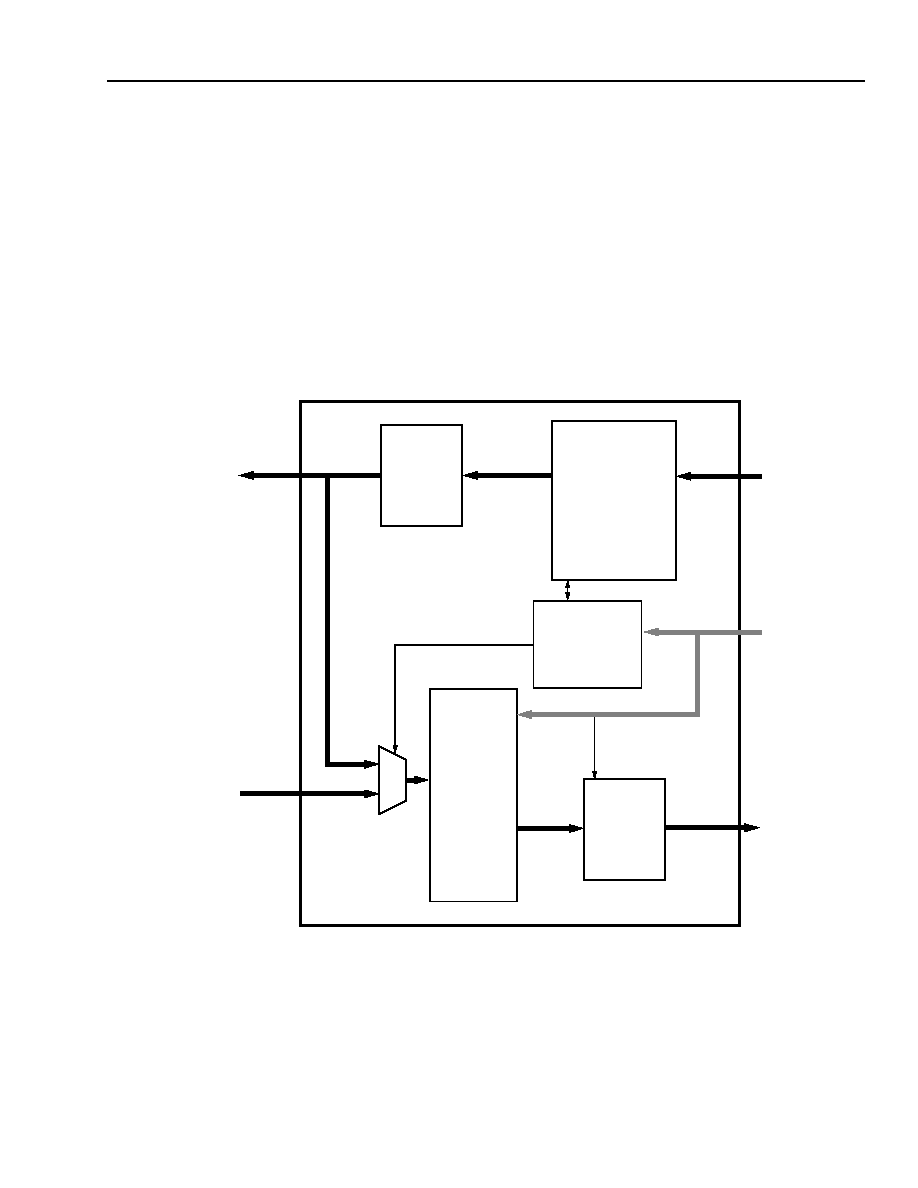
Data Sheet
MARS2G5 P-Pro (TDAT162G52) SONET/SDH
August 18, 2004
155/622/2488 Mbits/s Data Interface
345
Agere Systems Inc.
Path Terminator (PT)
Introduction
This section describes the interfaces of the path terminator (PT) block, including the register map description. A
block diagram showing the major subblocks is given.
The PT has the following subblocks:
Receive terminator (RXT)
SPE mapper (SPE)
Transpose block (TR)
Microprocessor interface (PT_MP)
5-8706(F)r.3
Figure 38. Path Terminator Block Diagram
SPE_MAPPER
RECEIVE
TERMINATOR
(RXT)
PT_MP
TRANSPOSE
(TR)
MPU REGISTER SIGNALS
PATH TERMINATOR (PT)
DS3 MAPPER
CROSS CONNECT
LOOPBACK
TO
FROM
MPU
DS3 MAPPER
FROM
CROSS CONNECT
TO
TRANSPOSE
(TR)
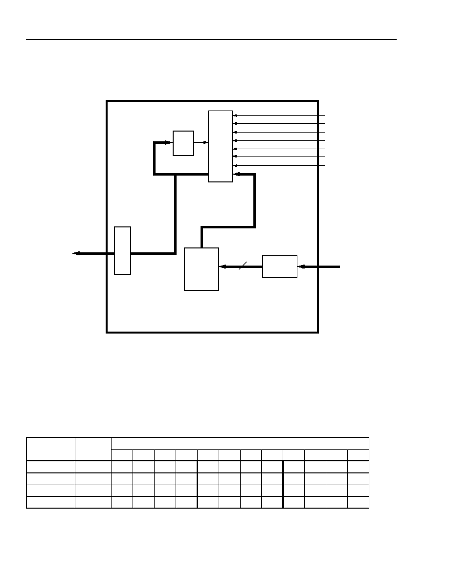
MARS2G5 P-Pro (TDAT162G52) SONET/SDH
Data Sheet
155/622/2488 Mbits/s Data Interface
August 18, 2004
346
Agere Systems Inc.
Path Terminator (PT)
(continued)
SPE Mapper
5-8707(F).b
Figure 39. Block Diagram of SPE Mapper Block
Time-Slot Assignments
The required STS-1 time-slot assignments for one STS-48 signal on a 32-bit data bus is summarized in Table 250.
The time slots repeat every 12 clock cycles.
Table 250. STS-48 Time-Slot Assignments
* Indicates valid starting time slots for concatenated signals from STS-3c to STS-48c.
Data Bus
Control
STS-48--32-Bit Input/Output Bus Format (STS-1 Numbers, Time ->)
1
2
3
4
5
6
7
8
9
10
11
12
D[31:24]
Port A
1*
4*
7*
10*
2
5
8
11
3
6
9
12
D[23:16]
Port B
13*
16*
19*
22*
14
17
20
23
15
18
21
24
D[15:8]
Port C
25*
28*
31*
34*
26
29
32
35
27
30
33
36
D[7:0]
Port D
37*
40*
43*
46*
38
41
44
47
39
42
45
48
TO CROSS CONNECT
DS3 MAPPER
PBIP
TOH/
INSERT
LCD
DS3/E3
AIS
LOP
UNEQ
PLM
B3ERR
x48
x48
POH
MAPPER
4 x 8
T
R
AN
SPO
S
E
TIM
SPE_FIFO

Data Sheet
MARS2G5 P-Pro (TDAT162G52) SONET/SDH
August 18, 2004
155/622/2488 Mbits/s Data Interface
347
Agere Systems Inc.
Path Terminator (PT)
(continued)
SPE Mapper
(continued)
The required STS-1 time-slot assignment for four STS-12 signals on a 32-bit data bus is summarized in Table 251.
The time slots repeat every 12 clock cycles. Each input stream is independent of the others.
Table 251. STS-12 Time-Slot Assignments
* Indicates valid starting time slots for concatenated signals from STS-3c to STS-12c.
The required STS-1 time-slot assignment for four STS-3 signals on a 32-bit data bus is summarized in Table 252.
The time slots repeat three additional clock cycles. Each input stream is independent of the others.
Table 252. STS-3 Time-Slot Assignments
* Indicates valid starting time slots for concatenated signals from STS-1c to STS-3c.
Any combination of STS up to STS-48c can be generated using up to 16-logical channels. Valid starting positions
are indicated by an *.
Data Bus
Control
STS-12--32-Bit Input/Output Bus Format (STS-1 Numbers, Time ->)
1
2
3
4
5
6
7
8
9
10
11
12
D[31:24]
Port A
1*
4*
7*
10*
2
5
8
11
3
6
9
12
D[23:16]
Port B
1*
4*
7*
10*
2
5
8
11
3
6
9
12
D[15:8]
Port C
1*
4*
7*
10*
2
5
8
11
3
6
9
12
D[7:0]
Port D
1*
4*
7*
10*
2
5
8
11
3
6
9
12
Data Bus
Control
STS-12--32-Bit Input/Output Bus Format (STS-1 Numbers, Time ->)
1
2
3
4
5
6
7
8
9
10
11
12
D[31:24]
Port A
1*
1*
1*
1*
2
2
2
2
3
3
3
3
D[23:16]
Port B
1*
1*
1*
1*
2
2
2
2
3
3
3
3
D[15:8]
Port C
1*
1*
1*
1*
2
2
2
2
3
3
3
3
D[7:0]
Port D
1*
1*
1*
1*
2
2
2
2
3
3
3
3

MARS2G5 P-Pro (TDAT162G52) SONET/SDH
Data Sheet
155/622/2488 Mbits/s Data Interface
August 18, 2004
348
Agere Systems Inc.
Path Terminator (PT)
(continued)
SPE Mapper
(continued)
Example of Channel-to-Time-Slot Mapping for a 16-Channel Configuration with Channel STS Sizes Indi-
cated in Table 254
Table 253. Sequence Register Map TS[0--23]_PM_[A--D]
Table 254. Logical 16-Channel Configuration Concatenation Register Map CH[0--15]_NC
Sequence Register Map TS[0--23]_PM_[A--D]
Slot #
ch_id Slot # ch_id Slot # ch_id Slot # ch_id
A1
0
B1
3
C1
6
D1
9
A2
10
B2
10
C2
10
D2
10
A3
11
B3
11
C3
11
D3
11
A4
11
B4
11
C4
11
D4
11
A5
1
B5
4
C5
7
D5
9
A6
10
B6
10
C6
10
D6
10
A7
11
B7
11
C7
11
D7
11
A8
11
B8
11
C8
11
D8
11
A9
2
B9
5
C9
8
D9
9
A10
10
B10
10
C10
10
D10
10
A11
11
B11
11
C11
11
D11
11
A12
11
B12
11
C12
11
D12
11
Logical 16-Channel Configuration
Concatenation Register Map CH[0--15]_NC
ch_id
Size
ch0
1
ch1
1
ch2
1
ch3
1
ch4
1
ch5
1
ch6
1
ch7
1
ch8
1
ch9
3
ch10
12
ch11
24
ch12
--
ch13
--
ch14
--
ch15
--

Data Sheet
MARS2G5 P-Pro (TDAT162G52) SONET/SDH
August 18, 2004
155/622/2488 Mbits/s Data Interface
349
Agere Systems Inc.
Path Terminator (PT)
(continued)
Supported SPE Formats
Direct Mapping into STS-1 SPE
Figure 40 shows direct mapping into STS-1 SPE, as per GR-253 (R3-6). This mapping can be set per time slot
(PT_TX_STS1_[A--D] (Table 292)).
5-8298(F)
Figure 40. Direct Mapping into STS SPE
STS-Nc SPE
Figure 41 shows the structure of an STS-Nc SPE, as per GR-353 (R3-9). N is valid for N = 3 to 48, where N is a
multiple of 3.
5-8299(F)r.2
Figure 41. STS-Nc SPE
PO
H
1 CO
L
28 COL'S
28 COL'S
28 COL'S
STU
F
F
STU
F
F
1 CO
L
1 CO
L
PAYLOAD
PAYLOAD
PAYLOAD
9 ROWS
N x 87 COLUMNS
ST
S PO
H
(9
B
Y
T
E
S
)
F
I
X
E
D S
T
UF
F (3N
≠
9 B
Y
TE
S
)
STS-NC PAYLOAD CAPACITY
(N x 780 BYTES)
N/3-1
COL.
MARS2G5 P-Pro (TDAT162G52) SONET/SDH
Data Sheet
155/622/2488 Mbits/s Data Interface
August 18, 2004
350
Agere Systems Inc.
Path Terminator (PT)
(continued)
Supported SPE Formats
(continued)
Asynchronous Mapping of DS3 (44.736 Mbits/s) Payload into STS-1
The DS3 frame insertion into an SPE is done as per GR253, section 3.4.2.1. The overhead communication bits
(O bits) and R bits are programmable to either 0 or 1 (PT_TX_MODE[7] (Table 263)).
The stuff opportunity bit (S bit) will contain a data bit every third subframe, starting on the first subframe. During a
row when the S bit is data the 5 C bits must be set to 1; otherwise, if the S bit is a justification bit, the 5 C bits are
set to zero. A justification will always set the S bit to zero.
The DS3 rate is 44,736,000 bits/s. This is equal to 5592 bits per 125 µs frame. The mapping into DS3 gives
5589 bits per 125 µs frame. Therefore, three extra bits are added per frame using the stuff opportunity bits.
5-8300(F)
Note:
I = ii ii ii ii
i = info bit.
R = rr rr rr rr
r = fixed stuff bit.
C1 = rr ci ii ii
c = stuff control bit.
C2 = cc rr rr rr
s = stuff opportunity bit.
C3 = cc rr oo rs
o = overhead common bit.
Figure 42. Asynchronous Mapping of DS3 into STS-1 SPE
R R C1 25 I
R C2 I 25 I
R C3 I 25 I
R R C1 25 I
R C2 I 25 I
R C3 I 25 I
R R C1 25 I
R C2 I 25 I
R C3 I 25 I
R R C1 25 I
R C2 I 25 I
R C3 I 25 I
R R C1 25 I
R C2 I 25 I
R C3 I 25 I
R R C1 25 I
R C2 I 25 I
R C3 I 25 I
R R C1 25 I
R C2 I 25 I
R C3 I 25 I
R R C1 25 I
R C2 I 25 I
R C3 I 25 I
R R C1 25 I
R C2 I 25 I
R C3 I 25 I
FI
X
E
D S
T
UF
F
FI
X
E
D S
T
UF
F
SP
E PO
H
28 BYTES
28 BYTES
28 BYTES

Data Sheet
MARS2G5 P-Pro (TDAT162G52) SONET/SDH
August 18, 2004
155/622/2488 Mbits/s Data Interface
351
Agere Systems Inc.
Path Terminator (PT)
(continued)
Supported SPE Formats
(continued)
Asynchronous Mapping of E3 (34.368 Mbits/s) Payload into STS-1
The E3 frame insertion into an SPE is done as per ITU-T G.707, Section 10.1.2.2. The r bits are programmably set
to either 0 or 1.
The E3 rate is 34.368 Mbits/s. This is equal to 4293 bits per 125 µs frame. The mapping into E3 gives 4296 bits per
125 µs frame. Therefore, three extra bits must be added per frame using the stuff opportunity bits. The stuff oppor-
tunity bit S2 will always contain a data bit (i.e., every third subframe). Thus, C2 will always be set to 1. S1 will
always contain a stuff bit, thus C1 will always be set to 0.
1623(F)r.1
Note:
I = ii ii ii ii where i = information bit.
R = rr rr rr rr where r = fixed stuff bit.
C = rr rr rr c1c2 where c1 and c2 = stuff control bits.
A = rr rr rr rr rs1 where s1 = first stuff opportunity bit.
B = s2 ii ii ii i where s2 = second stuff opportunity bit.
Figure 43. Asynchronous Mapping of E3 into STS-1 SPE
SP
E PO
H
R 3I
R 3I
R 3I
R 3I
R 3I
R 3I
R 3I
R 3I
R 3I
R 3I
R 3I
R 3I
R 3I
R 3I
R 3I
R 3I
R 3I
R 3I
R 3I
R 3I
R 3I
R 3I
R 3I
R 3I
R 3I
R 3I
R 3I
R 3I
R 3I
R 3I
R 3I
R 3I
R 3I
R 3I
R 3I
R 3I
R 3I
R 3I
R 3I
R 3I
R 3I
R 3I
R 3I
R 3I
R 3I
R
R
R
R
R
R
R
R
R
R 3I
R 3I
R 3I
R 3I
R 3I
R 3I
R 3I
R 3I
R 3I
R 2I
R 2I
R 2I
R 2I
R 2I
R 2I
R 2I
R 2I
R 2I
FI
X
E
D S
T
UFF
I
I
I
I
I
I
I
I
I
R 3I
R 3I
R 3I
R 3I
R 3I
R 3I
R 3I
R 3I
R 3I
R 3I
R 3I
R 3I
R 3I
R 3I
R 3I
R 3I
R 3I
R 3I
R
R
R
R
R
R
R
R
R
C 3I
C 3I
C 3I
C 3I
C 3I
C 3I
C 3I
C 3I
C 3I
R 3I
R 3I
R 3I
R 3I
R 3I
R 3I
R 3I
R 3I
R 3I
R 3I
R 3I
R 3I
R 3I
R 3I
R 3I
R 3I
R 3I
R 3I
R 3I
R 3I
R 3I
R 3I
R 3I
R 3I
R 3I
R 3I
R 3I
R
R
R
R
R
R
R
R
R
I
I
I
I
I
I
I
I
I
FI
X
E
D S
T
UFF
R
2I
R
2I
R
2I
R
2I
R
2I
R
2I
R
2I
R
2I
R
2I
R 3I
R 3I
R 3I
R 3I
R 3I
R 3I
R 3I
R 3I
R 3I
R 3I
R 3I
R 3I
R 3I
R 3I
R 3I
R 3I
R 3I
R 3I
R 3I
R 3I
R 3I
R 3I
R 3I
R 3I
R 3I
R 3I
R 3I
R 3I
R 3I
R 3I
R 3I
R 3I
R 3I
R 3I
R 3I
R 3I
R 3I
R 3I
R 3I
R 3I
R 3I
R 3I
R 3I
R 3I
R 3I
R
R
R
R
R
R
R
R
R
C
C
R
C
C
R
C
C
R
3I
3I
3I
3I
3I
3I
A B I
A B I
A B I
28 bytes
28 bytes
28 bytes
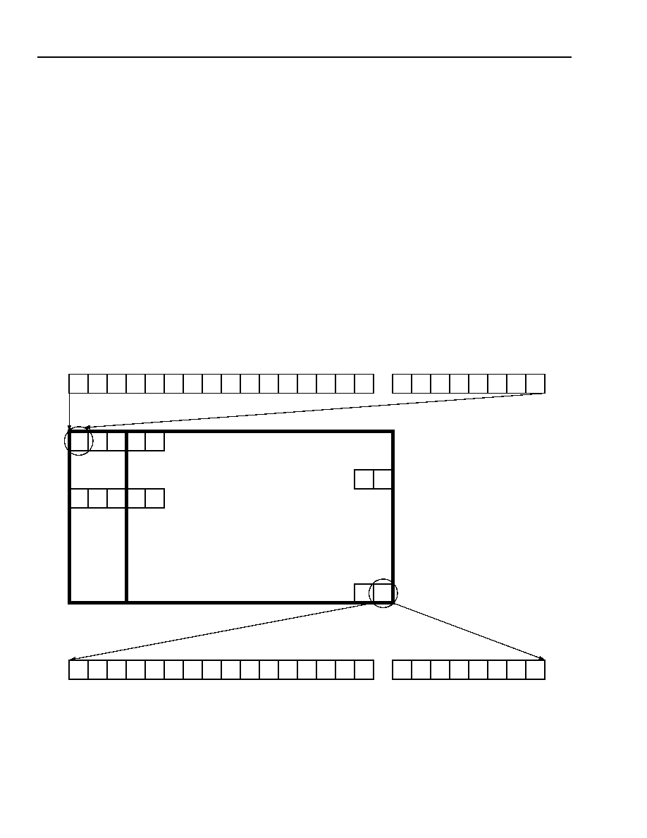
MARS2G5 P-Pro (TDAT162G52) SONET/SDH
Data Sheet
155/622/2488 Mbits/s Data Interface
August 18, 2004
352
Agere Systems Inc.
Path Terminator (PT)
(continued)
SPE Mapper Architecture
SPE Generator
The SPE generator block has the following functions: this block will send a complete frame with all the transport
overhead bytes set to the appropriate default value based on the rate mode (PT_TX_MODE[4:3] (Table 263)) input
signal and the H1, H2, H3, POH bytes, and SPE bytes set correctly. The SPE generator will accept data with the
correct byte interleaving for the type of signal provisioned from the data engine.
The SPE generator operates in three timing modes: one STS-48 signal, four STS-12 signals, or four STS-3 sig-
nals. Shown in Figure 44 below is the frame structure of the data sent out of the SPE mapper when in STS-48
mode. This figure indicates the various TOH locations, and the SPE location numbers. Each location consists of 48
octets, whose numbering is also indicated (see Table 250, STS-48 Time-Slot Assignments on page 346 for more
information on how the 48 octets are mapped in time and space). When the SPE generator operates in STS-12
mode, the frame structure is shown in Figure 45, STS-12 Frame Structure on page 353. This figure indicates the
various TOH locations and the SPE location numbers. Each location consists of 12 octets, whose numbering is
also indicated (see Table 251, STS-12 Time-Slot Assignments on page 347 for more information on how the 12
octets are mapped in time and space).
5-8301(F)
Figure 44. STS-48 Frame Structure
1
4
7
10
13
16
19
22
25
28
31
34
37
40
43
46
27
30
33
36
39
42
45
48
...
A1
A2
J0 522 523
520 521
0
1
781 782
H1
H2
H3
A1 (48 OCTETS TOTAL)
1
4
7
10
13
16
19
22
25
28
31
34
37
40
43
46
27
30
33
36
39
42
45
48
...
SPE LOCATION 521 (48 OCTETS TOTAL)

Data Sheet
MARS2G5 P-Pro (TDAT162G52) SONET/SDH
August 18, 2004
155/622/2488 Mbits/s Data Interface
353
Agere Systems Inc.
Path Terminator (PT)
(continued)
SPE Mapper Architecture
(continued)
5-8303(F)
Figure 45. STS-12 Frame Structure
H1, H2 Pointer Value
The generated H1, H2 value is determined by the time-slot configuration settings (PT_TX_Cnfg_[A--D] high/low
(Table 293--Table 300). There are 48 settings, one per STS-48 location (in STS-12, the first 12 are used, and in
STS-3, the first 3 are used). If the setting indicates normal pointer (00 encoding), an H1 value of 8'b0110_ss_10,
and an H2 value of 8'b0000_1010 is sent, where ss is dependent on the SS setting configuration (there are 2 bits
per channel, used to indicate SS bit insertion, 00 = SONET, 11 = SDH). This corresponds to a normal NDF, and an
offset of 522 decimal.
If the settings indicates concatenation (01 encoding), an H1 value of 8'b1001_ss_11 and an H2 value of
8'b1111_1111 is sent.
If the settings indicates unequipped (10 encoding), an H1 value of 8'b0110_ss_00 and an H2 value of
8'b0000_0000 is sent. Additionally, the entire corresponding payload is set to 8'h00.
If the settings indicate AIS (11 encoding), an H1 value of 8'b1111_11_11 and an H2 value of 8'b1111_1111 is sent.
1
4
7
10
2
5
8
11
3
6
9
12
A1
A2
J0 522 523
520 521
0
1
781 782
H1
H2
H3
A1 (12 OCTETS TOTAL)
SPE LOCATION 521 (12 OCTETS TOTAL)
1
4
7
10
2
5
8
11
3
6
9
12

MARS2G5 P-Pro (TDAT162G52) SONET/SDH
Data Sheet
155/622/2488 Mbits/s Data Interface
August 18, 2004
354
Agere Systems Inc.
Path Terminator (PT)
(continued)
SPE Mapper Architecture
(continued)
Selective STS-1 Path Insert Functions
Sixteen path overheads can be inserted (one per channel). The valid starting locations for an STS-Nc are shown in
Table 250, STS-48 Time-Slot Assignments on page 346, Table 251, STS-12 Time-Slot Assignments on page 347,
and Table 252, STS-3 Time-Slot Assignments on page 347.
J1 Byte Trace. The insertion of the path trace for a selected STS-1 for both SONET and SDH systems is provided.
For SONET, a 64-byte microprocessor registers are provisioned to transmit the 64-byte path trace message. For
SDH, a repeated 16-byte message is inserted from the 64-byte path trace microprocessor registers.
Note: For simplicity, the 16-byte SDH message is repeated four times in the 64-byte path trace microprocessor reg-
isters. A control bit is used to start the insertion of the path trace message; otherwise, all 0s are inserted into
the outgoing J1 byte.
B3 Insertion. The SPE mapper calculates the BIP-8 even parity over all bits (783 bytes for an STS-1 SPE or
Nx783 bytes for an STS-Nc SPE), regardless of any pointer adjustments of the previous STS SPE before scram-
bling, and inserts in the B3 byte location of the current STS SPE before scrambling. The calculated B3 values can
be inverted per time slot for test purposes (PT_TX_RW1_[0--47][12] (Table 280)). Additionally, the B3 values can
be disabled (i.e., forced to 0) per time slot for testing purposes (PT_TX_RW1_[0--47][14]).
C2: Path Signal Label. The C2 byte is inserted per channel (PT_TX_RW2_[0--15][7:0] (Table 281)).
If the unequipped value of 0x00 is programmed, the SPE mapper will generate an all 0s SPE with a valid payload
pointer (H1 = 0110_SS00, H2 = 0000_0000, H3 = 0000_0000) and B3 value before scrambling.
Table 255 shows the various codes for C2 as per (GR-253, Table 3.2).
Table 255. C2 Path Signal Label
Code
Content of the STS SPE
Support
0x00
Unequipped
Yes
0x01
Equipped--Nonspecific Payload
Yes
0x02
VT-Structured STS-1 SPE
No
0x03
Locked VT Mode
No
0x04
Asynchronous Mapping DS3
No
0x12
Asynchronous Mapping for DS4NA
No
0x13
Mapping for ATM
Yes
0x14
Mapping for DQDB
No
0x15
Asynchronous Mapping for FDDI
No
0x16
Mapping for HDLC--PPP
Yes

Data Sheet
MARS2G5 P-Pro (TDAT162G52) SONET/SDH
August 19, 2004
155/622/2488 Mbits/s Data Interface
355
Agere Systems Inc.
Path Terminator (PT)
(continued)
SPE Mapper Architecture
(continued)
G1: Path Status. The G1 byte is used to convey path condition and performance parameters back to the far end.
G1[7:4]--known as the remote error indication-path (REI-P) are used to report the number of B3 BIP-8 errors
seen by the current received frames. The valid values for these 4 bits are 0000--1000. This 4-bit REI-P can be
software overridden, on a per-channel basis by setting a control bit (PT_TX_RW1_[47--0][4] (Table 280)) and
provisioning the value (PT_TX_RW1_[47--0][3:0]).
G1[3:1]--known as the path remote defect indication (RDI-P) are used to report the received defects as shown
in Table 256. Note that when detecting two or more of the listed defects, the block generates the higher-priority
RDI-P enhanced code based on the priorities listed in the table. It is required to generate the RDI-P signal for at
least 20 frames before changing the value or terminating the generation. A 3-bit state is provided to monitor the
status of RDI-P insertion (PT_TX_TS_[A--D][0--2] (Table 270--Table 272)). Each time this value changes, a
delta bit is set (PT_TX_TS_DELTA[A--D][11:0]D (Table 268), PT_TX_TS_MASK[A--D][11:0]M (Table 262)):
-- Hardware Control. The SPE mapper receives from the receive pointer interpreter four signals, on a per-port
basis, used to configure the RDI-P bits. These are AIS, LOP, UNEQUIP, TIM_P (i.e., trace mismatch), and
PLM. Additionally, the SPE mapper receives a loss of cell delineation (LCD) signal on a per-port basis, from
the receive data engine processor. Each contribution to the generation of an RDI-P failure can be inhibited from
contributing to the RDI-P generation, on a per time-slot basis. The SPE mapper must be provisioned to gen-
erate a 1-bit RDI-P or enhanced RDI-P on a per time-slot basis (PT_TX_RW1_[47--0][13]).
-- Software Control. Insertion of a user-defined value is provided by setting control bit (PT_TX_RW1_[47--0][8])
and provisioning register bits (PT_TX_RW1_[47--0][7:5]) on a per time-slot basis.
-- Trace Mismatch (TIM-P). As per ANSI T1.231, the TIM-P is supported via a programmable bit on a per time-
slot basis.
-- Enhanced or 1-bit RDI-P Mode. When PT_TX_RW1_[47--0][13] is set to 0, one bit RDI-P mode is selected;
G1[3] = 1 when either AIS, LOP, UNEQUIP, TIM_P, or PLM is detected; otherwise, when no defects are detect-
ed, set to 0.
Also, when 1-bit RDI-P mode is selected, G1[2:1] are undefined in GR-253, so these bits will be used to indi-
cated SONET or SDH mode. Therefore, when PT_TX_MODE[0] (Table 263) = 0, G1[2:1] = 00. But in
SDH_MODE, (PT_TX_MODE][0] = 1), G1[2:1] = 11.
G1[0]--This is also set to 1 if SDH_MODE is set (PT_TX_MODE[0]); otherwise, set to 0.
Table 256. G1 RDI-P Codes
* These codes are transmitted by STS PTE that do not support enhanced RDI-P. If enhanced RDI-P is not supported, G1 bits 2 and 1 must be
set to the same value, and should be set to 00.
This code is transmitted by STS PTE that support enhanced RDI-P.
G1[3:1]
Priority of
Enhanced
RDI-P Codes
Trigger
Interpretation
0xx*
Not applicable
No defects
No RDI-P defect
1xx*
Not applicable
AIS-P, LOP-P,
UNEQ-P
RDI-P (1-bit RDI-P)
001
4
No defects
No RDI-P defects
010
3
PLM-P, LCD-P
RDI-P payload defect
101
1
AIS-P, LOP-P
RDI-P server defect
110
2
UNEQ-P, TIM-P
RDI-P connectivity defect

MARS2G5 P-Pro (TDAT162G52) SONET/SDH
Data Sheet
155/622/2488 Mbits/s Data Interface
August 18, 2004
356
Agere Systems Inc.
Path Terminator (PT)
(continued)
Transpose Block
Reorder STS-48 time-slot assignments for output processing.
Input order is as shown in Table 257 below.
Output order as shown in Table 250, STS-48 Time-Slot Assignments on page 346.
It is recommended that the time slots be configured in SONET order (Table 257), transposed in the transmit direc-
tion, and sent out in time order (Table 250). In the receive direction, time slots can be received in time order and
then transposed back into SONET order.
Table 257. STS-48 Time-Slot Internal Ordering
* Indicates valid starting time slots for concatenated signals from STS-3c to STS-48c.
Data Bus
Control
STS-48--32-Bit Input/Output Bus Format (STS-1 Numbers, Time ->)
1
2
3
4
5
6
7
8
9
10
11
12
D[31:24]
Port A
1*
13*
25*
37*
2
14
26
38
3
15
27
39
D[23:16]
Port B
4*
16*
28*
40*
5
17
29
41
6
18
30
42
D[15:8]
Port C
7*
19*
31*
43*
8
20
32
44
9
21
33
45
D[7:0]
Port D
10*
22*
34*
46*
11
23
35
47
12
24
36
48

Data Sheet
MARS2G5 P-Pro (TDAT162G52) SONET/SDH
August 18, 2004
155/622/2488 Mbits/s Data Interface
357
Agere Systems Inc.
Path Terminator (PT)
(continued)
PT Register Descriptions
This section describes the MPU accessible registers in the PT block.
Global Registers
Table 258. (PT_TX_VERSION), Version Control (RO)
Table 259. (PT_TX_CH_INT), Tx Channel Composite Interrupt (RO)
Table 260. (PT_TX_TS_[A--D]_INT), Tx Time-Slot Composite Interrupt (RO)
Table 261. (PT_TX_CH_INTMASK), Tx Channel Composite Interrupt Mask (R/W)
Table 262. (PT_TX_TS[A--D]_INTMASK), Tx Time-Slot Composite Interrupt Mask (R/W)
Address
Bit
Name
Function
Reset
Default
0x4000
15:8
--
Reserved.
--
7:0
VERSION
Version Number. Indicates version number of PT block.
0x01
Address
Bit
Name
Function
Reset
Default
0x4001
15:0
Ch_Int
Transmit Channel Interrupt. Active-high interrupt bit on a
per-channel basis. These bits are the ORing of all event and
delta bits associated with a particular transmit channel. An
event or delta bit contribution can be inhibited from contribut-
ing to the interrupt by setting the appropriate mask bit.
0x0000
Address
Bit
Names
Function
Reset
Default
0x4004--
0x4007
15:12
--
Reserved. 0x0000
11:0
TX_TS_A_Int
TX_TS_B_Int
TX_TS_C_Int
TX_TS_D_Int
Transmit Time-Slot Interrupt. Active-high interrupt, per
time slot for slices A, B, C, and D.
Address
Bit
Name
Function
Reset
Default
0x4008
15:0
Ch[15:0]
Composite Channel Interrupt Mask. If set, the interrupt will
not occur for that channel.
0xFFFF
Address
Bit
Name
Function
Reset
Default
0x400B--
0x400E
15:12
--
Reserved.
0xF
11:0
TS[11:0]
Composite Interrupt Mask. If set, the interrupt will not
occur, per time slot, for slices A, B, C, and D.
0xFFF

MARS2G5 P-Pro (TDAT162G52) SONET/SDH
Data Sheet
155/622/2488 Mbits/s Data Interface
August 18, 2004
358
Agere Systems Inc.
Path Terminator (PT)
(continued)
PT Register Descriptions
(continued)
Table 263. (PT_TX_MODE), Mode (R/W)
Address
Bit
Name
Function
Reset
Default
0x400F
15
STUFFBYTE_
FORCE
Stuff Byte Force. If set to 0, the default is to put stuff bytes
in the first four STS time slots of column 4. This is the recom-
mended setting.
If set to 1, stuff byte locations are programmed using the
Stuffbyte_Config register. This may be used when configur-
ing an STS-Nc, where N is not a multiple of 3.
0
14
Stuffbyte_1or0
Stuff Byte 1 or 0.
0 = All stuff bytes are set to 0 (i.e., SONET).
1 = All stuff bytes are set to 1 (i.e., SDH).
0
13
RX_TRANSPOSE_
ENB
Rx Transpose Enable.
0 = Transpose disabled.
1 = Transpose enabled.
0
12
TX_TRANSPOSE_
ENB
Tx Transpose Enable.
0 = Transpose disabled.
1 = Transpose enabled.
0
11:8
--
Reserved. For Internal Use Only.
--
7
DS3_RO_VALUE
DS3 RO Bit Values. This is the value that all R and O bits
will be set to in DS3 mapped frames.
0
6
CORWN
Clear-On-Read/Write.
0 = Clear-on-write, writing a COW register will clear
whatever bits were written with 1.
1 = Clear-on-read, reading a COR register will clear the
entire register.
0
5
POF_ENB
Packet-Over-Fiber Enable.
0 = POF disabled.
1 = POF enabled.
0
4:3
RATE_MODE
Rate Mode.
00 = STS-3.
01 = STS-12.
10 = STS-48.
11 = STS-1.
0
2
LOOP_MODE
Loopback Mode.
1 = Loopback Tx output data to Rx input data.
0
1
--
Reserved.
0
0
SDH_MODE
SDH Mode. 0 = SONET; 1 = SDH.
0

Data Sheet
MARS2G5 P-Pro (TDAT162G52) SONET/SDH
August 18, 2004
155/622/2488 Mbits/s Data Interface
359
Agere Systems Inc.
Path Terminator (PT)
(continued)
PT Register Descriptions
(continued)
Table 264. (PT_TX_BANKAorB), Tx_BANKAorB (R/W)
Table 265. (PT_TX_SCRATCH), SCRATCH (R/W)
Table 266. (PT_TX_SOFTRST), Tx Channel FIFO Reset (R/W)
Address
Bit
Name
Function
Reset
Default
0x4010
15:1
--
Reserved.
--
0
BANKAorB_SEL
Tx BANKAorB_SEL Register.
0 = Bank A is selected for sequence map.
1 = Bank B is selected for sequence map.
0
Address
Bit
Name
Function
Reset
Default
0x4011
15:0
SCRATCH
Tx Scratchpad Register. Diagnostic register used by micro-
processor. Has no effect on the PT function.
0x0000
Address
Bit
Name
Function
Reset
Default
0x4013
15:0
SOFTRST
Channel FIFO, Soft Reset. Software reset is necessary
whenever a channel is initialized, after all other setups have
been performed. A software reset should be performed at
the end of configuration for a channel. To perform this reset,
write a 1 to reset and then write a 0 to release the reset.
0

MARS2G5 P-Pro (TDAT162G52) SONET/SDH
Data Sheet
155/622/2488 Mbits/s Data Interface
August 18, 2004
360
Agere Systems Inc.
Path Terminator (PT)
(continued)
PT Register Descriptions
(continued)
Table 267. (PT_TX_CH_DELTA [0--15]), Tx Channel Delta/Event (COR/W)
Table 268. (PT_Tx_TS_[A--D]_Delta), Tx Delta/Event Register (COR/W)
Table 269. (PT_Tx_CH_Status_[0--15]), Transmit Status Register (RO)
Address
Bit
Name
Function
Reset
Default
0x4016--
0x4025
15:2
--
Reserved.
0
1
FIFO emptyD
Delta Bit Indicating Change of Associated SPE FIFO Empty
Status.
1
0
FIFO FullD
Delta Bit Indicating Change of Associated SPE FIFO Full Sta-
tus.
0
Address
Bit
Name
Function
Reset
Default
0x4046--
0x4049
15:12
--
Reserved.
0
11:0
RDIPD
Delta Bit Indicating Change of RDI-P, per Time Slot.
0
Address
Bit
Name
Function
Reset
Default
0x404A--
0x4059
15:2
--
Reserved.
0
1
FIFO empty
FIFO Empty Status. A 1 indicates that the SPE FIFO is
empty. A 0 indicates that there is data in the FIFO.
1
0
FIFO Full
FIFO Full Status. A 1 indicates that the SPE FIFO is full.
0

Data Sheet
MARS2G5 P-Pro (TDAT162G52) SONET/SDH
August 18, 2004
155/622/2488 Mbits/s Data Interface
361
Agere Systems Inc.
Path Terminator (PT)
(continued)
PT Register Descriptions
(continued)
Table 270. (PT_TX_TS_[A--D]0_Status), Transmit Status Register (RO)
Table 271. (PT_TX_TS_[A--D]1_Status), Transmit Status Register (RO)
Table 272. (PT_TX_TS_[A--D]2_Status), Transmit Status Register (RO)
Address
Bit
Name
Function
Reset
Default
0x407A,
0x407D,
0x4080,
0x4083
15
--
Reserved.
0
14:12
RDIP3
RDIP Status, Time Slot 3.
000
11
--
Reserved.
0
10:8
RDIP2
RDIP Status, Time Slot 2.
000
7
--
Reserved.
0
6:4
RDIP1
RDIP Status, Time Slot 1.
000
3
--
Reserved.
0
2:0
RDIP0
RDIP Status, Time Slot 0.
0xx = No defects.
1xx = AIS, LOP, or UNEQ.
001 = No defects.
010 = PLM, LCD.
101 = AIS, LOP.
110 = UNEQ, TIM.
000
Address
Bit
Name
Function
Reset
Default
0x407B,
0x407E,
0x4081,
0x4084
15
--
Reserved.
0
14:12
RDIP7
RDIP Status, Time Slot 7.
000
11
--
Reserved.
0
10:8
RDIP6
RDIP Status, Time Slot 6.
000
7
--
Reserved.
0
6:4
RDIP5
RDIP Status, Time Slot 5.
000
3
--
Reserved.
0
2:0
RDIP4
RDIP Status, Time Slot 4.
000
Address
Bit
Name
Function
Reset
Default
0x407C,
0x407F,
0x4082,
0x4085
15
--
Reserved.
0
14:12
RDIP11
RDIP Status, Time Slot 11.
000
11
--
Reserved.
0
10:8
RDIP10
RDIP Status, Time Slot 10.
000
7
--
Reserved.
0
6:4
RDIP9
RDIP Status, Time Slot 9.
000
3
--
Reserved.
0
2:0
RDIP8
RDIP Status, Time Slot 8.
000
MARS2G5 P-Pro (TDAT162G52) SONET/SDH
Data Sheet
155/622/2488 Mbits/s Data Interface
August 18, 2004
362
Agere Systems Inc.
Path Terminator (PT)
(continued)
PT Register Descriptions
(continued)
Table 273. (PT_Tx_CH_Mask_[0--15]), Tx Channel Mask Register (R/W)
Table 274. (PT_Tx_TS_[A--D]_Mask), Tx Mask Register (COR/W)
Address
Bit
Name
Function
Reset
Default
0x4086--
0x4095
15:2
--
Reserved.
0xFFFF
1
FIFO empty
SPE FIFO Empty Status Mask, Per Channel. A 1 will mask
the associated delta bit from contributing to the interrupt signal.
0
FIFO Full
SPE FIFO Full Status Mask, Per Channel. A 1 will mask the
associated delta bit from contributing to the interrupt signal.
Address
Bit
Name
Function
Reset
Default
0x40B6--
0x40B9
15:12
--
Reserved.
0
11:0
RDIPM[11:0]
RDI-P Status Mask, per Time Slot.
0

Data Sheet
MARS2G5 P-Pro (TDAT162G52) SONET/SDH
August 18, 2004
155/622/2488 Mbits/s Data Interface
363
Agere Systems Inc.
Path Terminator (PT)
(continued)
PT Register Descriptions
(continued)
Table 275. (PT_Tx_Mask_A_[1--6]), Transmit Provisioning Register (R/W)
Address
Bit
Name
Function
Reset
Default
0x4112--
0x4117
15:14
--
Reserved.
0xFFFF
13
RDIPM_TIM
A[1, 3, 5, 7, 9, 11]
Mask TIMP, slice A time slots [1, 3, 5, 7, 9, 11], from contrib-
uting to RDI_P generation. A 1 will disable TIMP from con-
tributing to RDI-P.
12
RDIPM_LCD
A[1, 3, 5, 7, 9, 11]
Mask LCD, slice A time slots [1, 3, 5, 7, 9, 11], from contrib-
uting to RDI_P generation. A 1 will disable LCD from contrib-
uting to RDI-P.
11
RDIPM_PLM
A[1, 3, 5, 7, 9, 11]
Mask PLM, slice A time slots [1, 3, 5, 7, 9, 11], from contrib-
uting to RDI_P generation. A 1 will disable PLM from contrib-
uting to RDI-P.
10
RDIPM_UNEQ
A[1, 3, 5, 7, 9, 11]
Mask UNEQ, slice A time slots [1, 3, 5, 7, 9, 11], from con-
tributing to RDI_P generation. A 1 will disable UNEQ from
contributing to RDI-P.
9
RDIPM_LOP
A[1, 3, 5, 7, 9, 11]
Mask LOP, slice A time slots [1, 3, 5, 7, 9, 11], from contribut-
ing to RDI_P generation. A 1 will disable LOP from contribut-
ing to RDI-P.
8
RDIPM_AIS
A[1, 3, 5, 7, 9, 11]
Mask AIS, slice A time slots [1, 3, 5, 7, 9, 11], from contribut-
ing to RDI_P generation. A 1 will disable AIS from contribut-
ing to RDI-P.
7:6
--
Reserved.
5
RDIPM_TIM
A[0, 2, 4, 6, 8, 10]
Mask TIMP, slice A time slots [0, 2, 4, 6, 8, 10], from contrib-
uting to RDI_P generation. A 1 will disable TIMP from con-
tributing to RDI-P.
4
RDIPM_LCD
A[0, 2, 4, 6, 8, 10]
Mask LCD, slice A time slots [0, 2, 4, 6, 8, 10], from contrib-
uting to RDI_P generation. A 1 will disable LCD from contrib-
uting to RDI-P.
3
RDIPM_PLM
A[0, 2, 4, 6, 8, 10]
Mask PLM, slice A time slots [0, 2, 4, 6, 8, 10], from contrib-
uting to RDI_P generation. A 1 will disable PLM from contrib-
uting to RDI-P.
2
RDIPM_UNEQ
A[0, 2, 4, 6, 8, 10]
Mask UNEQ, slice A time slots [0, 2, 4, 6, 8, 10], from con-
tributing to RDI_P generation. A 1 will disable UNEQ from
contributing to RDI-P.
1
RDIPM_LOP
A[0, 2, 4, 6, 8, 10]
Mask LOP, slice A time slots [0, 2, 4, 6, 8, 10], from contribut-
ing to RDI_P generation. A 1 will disable LOP from contribut-
ing to RDI-P.
0
RDIPM_AIS
A[0, 2, 4, 6, 8, 10]
Mask AIS, slice A time slots [0, 2, 4, 6, 8, 10], from contribut-
ing to RDI_P generation. A 1 will disable AIS from contribut-
ing to RDI-P.

MARS2G5 P-Pro (TDAT162G52) SONET/SDH
Data Sheet
155/622/2488 Mbits/s Data Interface
August 18, 2004
364
Agere Systems Inc.
Path Terminator (PT)
(continued)
PT Register Descriptions
(continued)
Table 276. (PT_Tx_Mask_B_[1--6]), Transmit Provisioning Register (R/W)
Address
Bit
Name
Function
Reset
Default
0x4118--
0x411D
15:14
--
Reserved.
0xFFFF
13
RDIPM_TIM
B[1, 3, 5, 7, 9, 11]
Mask TIMP, slice B time slots [1, 3, 5, 7, 9, 11], from contrib-
uting to RDI_P generation. A 1 will disable TIMP from con-
tributing to RDI-P.
12
RDIPM_LCD
B[1, 3, 5, 7, 9, 11]
Mask LCD, slice B time slots [1, 3, 5, 7, 9, 11], from contrib-
uting to RDI_P generation. A 1 will disable LCD from contrib-
uting to RDI-P.
11
RDIPM_PLM
B[1, 3, 5, 7, 9, 11]
Mask PLM, slice B time slots [1, 3, 5, 7, 9, 11], from contrib-
uting to RDI_P generation. A 1 will disable PLM from contrib-
uting to RDI-P.
10
RDIPM_UNEQ
B[1, 3, 5, 7, 9, 11]
Mask UNEQ, slice B time slots [1, 3, 5, 7, 9, 11], from con-
tributing to RDI_P generation. A 1 will disable UNEQ from
contributing to RDI-P.
9
RDIPM_LOP
B[1, 3, 5, 7, 9, 11]
Mask LOP, slice B time slots [1, 3, 5, 7, 9, 11], from contribut-
ing to RDI_P generation. A 1 will disable LOP from contribut-
ing to RDI-P.
8
RDIPM_AIS
B[1, 3, 5, 7, 9, 11]
Mask AIS, slice B time slots [1, 3, 5, 7, 9, 11], from contribut-
ing to RDI_P generation. A 1 will disable AIS from contribut-
ing to RDI-P.
7:6
--
Reserved.
5
RDIPM_TIM
B[0, 2, 4, 6, 8, 10]
Mask TIMP, slice B time slots [0, 2, 4, 6, 8, 10], from contrib-
uting to RDI_P generation. A 1 will disable TIMP from con-
tributing to RDI-P.
4
RDIPM_LCD
B[0, 2, 4, 6, 8, 10]
Mask LCD, slice B time slots [0, 2, 4, 6, 8, 10], from contrib-
uting to RDI_P generation. A 1 will disable LCD from contrib-
uting to RDI-P.
3
RDIPM_PLM
B[0, 2, 4, 6, 8, 10]
Mask PLM, slice B time slots [0, 2, 4, 6, 8, 10], from contrib-
uting to RDI_P generation. A 1 will disable PLM from contrib-
uting to RDI-P.
2
RDIPM_UNEQ
B[0, 2, 4, 6, 8, 10]
Mask UNEQ, slice B time slots [0, 2, 4, 6, 8, 10], from con-
tributing to RDI_P generation. A 1 will disable UNEQ from
contributing to RDI-P.
1
RDIPM_LOP
B[0, 2, 4, 6, 8, 10]
Mask LOP, slice B time slots [0, 2, 4, 6, 8, 10], from contribut-
ing to RDI_P generation. A 1 will disable LOP from contribut-
ing to RDI-P.
0
RDIPM_AIS
B[0, 2, 4, 6, 8, 10]
Mask AIS, slice B time slots [0, 2, 4, 6, 8, 10], from contribut-
ing to RDI_P generation. A 1 will disable AIS from contribut-
ing to RDI-P.

Data Sheet
MARS2G5 P-Pro (TDAT162G52) SONET/SDH
August 18, 2004
155/622/2488 Mbits/s Data Interface
365
Agere Systems Inc.
Path Terminator (PT)
(continued)
PT Register Descriptions
(continued)
Table 277. (PT_Tx_Mask_C_[1--6]), Transmit Provisioning Register (R/W)
Address
Bit
Name
Function
Reset
Default
0x411E--
0x4123
15:14
--
Reserved.
0xFFFF
13
RDIPM_TIM
C[1, 3, 5, 7, 9, 11]
Mask TIMP, slice C time slots [1, 3, 5, 7, 9, 11], from contrib-
uting to RDI_P generation. A 1 will disable TIMP from con-
tributing to RDI-P.
12
RDIPM_LCD
C[1, 3, 5, 7, 9, 11]
Mask LCD, slice C time slots [1, 3, 5, 7, 9, 11], from contribut-
ing to RDI_P generation. A 1 will disable LCD from contribut-
ing to RDI-P.
11
RDIPM_PLM
C[1, 3, 5, 7, 9, 11]
Mask PLM, slice C time slots [1, 3, 5, 7, 9, 11], from contrib-
uting to RDI_P generation. A 1 will disable PLM from contrib-
uting to RDI-P.
10
RDIPM_UNEQ
C[1, 3, 5, 7, 9, 11]
Mask UNEQ, slice C time slots [1, 3, 5, 7, 9, 11], from con-
tributing to RDI_P generation. A 1 will disable UNEQ from
contributing to RDI-P.
9
RDIPM_LOP
C[1, 3, 5, 7, 9, 11]
Mask LOP, slice C time slots [1, 3, 5, 7, 9, 11], from contribut-
ing to RDI_P generation. A 1 will disable LOP from contribut-
ing to RDI-P.
8
RDIPM_AIS
C[1, 3, 5, 7, 9, 11]
Mask AIS, slice C time slots [1, 3, 5, 7, 9, 11], from contribut-
ing to RDI_P generation. A 1 will disable AIS from contribut-
ing to RDI-P.
7:6
--
Reserved.
5
RDIPM_TIM
C[0, 2, 4, 6, 8, 10]
Mask TIMP, slice C time slots [0, 2, 4, 6, 8, 10], from contrib-
uting to RDI_P generation. A 1 will disable TIMP from con-
tributing to RDI-P.
4
RDIPM_LCD
C[0, 2, 4, 6, 8, 10]
Mask LCD, slice C time slots [0, 2, 4, 6, 8, 10], from contribut-
ing to RDI_P generation. A 1 will disable LCD from contribut-
ing to RDI-P.
3
RDIPM_PLM
C[0, 2, 4, 6, 8, 10]
Mask PLM, slice C time slots [0, 2, 4, 6, 8, 10], from contrib-
uting to RDI_P generation. A 1 will disable PLM from contrib-
uting to RDI-P.
2
RDIPM_UNEQ
C[0, 2, 4, 6, 8, 10]
Mask UNEQ, slice C time slots [0, 2, 4, 6, 8, 10], from con-
tributing to RDI_P generation. A 1 will disable UNEQ from
contributing to RDI-P.
1
RDIPM_LOP
C[0, 2, 4, 6, 8, 10]
Mask LOP, slice C time slots [0, 2, 4, 6, 8, 10], from contribut-
ing to RDI_P generation. A 1 will disable LOP from contribut-
ing to RDI-P.
0
RDIPM_AIS
C[0, 2, 4, 6, 8, 10]
Mask AIS, slice C time slots [0, 2, 4, 6, 8, 10], from contribut-
ing to RDI_P generation. A 1 will disable AIS from contribut-
ing to RDI-P.

MARS2G5 P-Pro (TDAT162G52) SONET/SDH
Data Sheet
155/622/2488 Mbits/s Data Interface
August 18, 2004
366
Agere Systems Inc.
Path Terminator (PT)
(continued)
PT Register Descriptions
(continued)
Table 278. (PT_Tx_Mask_D_[1--6]), Transmit Provisioning Register (R/W)
Address
Bit
Name
Function
Reset
Default
0x4124--
0x4129
15:14
--
Reserved.
0xFFFF
13
RDIPM_TIM
D[1, 3, 5, 7, 9, 11]
Mask TIMP, slice D time slots [1, 3, 5, 7, 9, 11], from contrib-
uting to RDI_P generation. A 1 will disable TIMP from con-
tributing to RDI-P.
12
RDIPM_LCD
D[1, 3, 5, 7, 9, 11]
Mask LCD, slice D time slots [1, 3, 5, 7, 9, 11], from contrib-
uting to RDI_P generation. A 1 will disable LCD from contrib-
uting to RDI-P.
11
RDIPM_PLM
D[1, 3, 5, 7, 9, 11]
Mask PLM, slice D time slots [1, 3, 5, 7, 9, 11], from contrib-
uting to RDI_P generation. A 1 will disable PLM from contrib-
uting to RDI-P.
10
RDIPM_UNEQ
D[1, 3, 5, 7, 9, 11]
Mask UNEQ, slice D time slots [1, 3, 5, 7, 9, 11], from con-
tributing to RDI_P generation. A 1 will disable UNEQ from
contributing to RDI-P.
9
RDIPM_LOP
D[1, 3, 5, 7, 9, 11]
Mask LOP, slice D time slots [1, 3, 5, 7, 9, 11], from contribut-
ing to RDI_P generation. A 1 will disable LOP from contribut-
ing to RDI-P.
8
RDIPM_AIS
D[1, 3, 5, 7, 9, 11]
Mask AIS, slice D time slots [1, 3, 5, 7, 9, 11], from contribut-
ing to RDI_P generation. A 1 will disable AIS from contribut-
ing to RDI-P.
7:6
--
Reserved.
5
RDIPM_TIM
D[0, 2, 4, 6, 8, 10]
Mask TIMP, slice D time slots [0, 2, 4, 6, 8, 10], from contrib-
uting to RDI_P generation. A 1 will disable TIMP from con-
tributing to RDI-P.
4
RDIPM_LCD
D[0, 2, 4, 6, 8, 10]
Mask LCD, slice D time slots [0, 2, 4, 6, 8, 10], from contrib-
uting to RDI_P generation. A 1 will disable LCD from contrib-
uting to RDI-P.
3
RDIPM_PLM
D[0, 2, 4, 6, 8, 10]
Mask PLM, slice D time slots [0, 2, 4, 6, 8, 10], from contrib-
uting to RDI_P generation. A 1 will disable PLM from contrib-
uting to RDI-P.
2
RDIPM_UNEQ
D[0, 2, 4, 6, 8, 10]
Mask UNEQ, slice D time slots [0, 2, 4, 6, 8, 10], from con-
tributing to RDI_P generation. A 1 will disable UNEQ from
contributing to RDI-P.
1
RDIPM_LOP
D[0, 2, 4, 6, 8, 10]
Mask LOP, slice D time slots [0, 2, 4, 6, 8, 10], from contribut-
ing to RDI_P generation. A 1 will disable LOP from contribut-
ing to RDI-P.
0
RDIPM_AIS
D[0, 2, 4, 6, 8, 10]
Mask AIS, slice D time slots [0, 2, 4, 6, 8, 10], from contribut-
ing to RDI_P generation. A 1 will disable AIS from contribut-
ing to RDI-P.

Data Sheet
MARS2G5 P-Pro (TDAT162G52) SONET/SDH
August 18, 2004
155/622/2488 Mbits/s Data Interface
367
Agere Systems Inc.
Path Terminator (PT)
(continued)
PT Register Descriptions
(continued)
Table 279. (PT_Tx_RW4_[0--15]), Transmit Provisioning Register 4 (R/W)
Table 280. (PT_Tx_RW1_[0--47]), Transmit Provisioning Register, Per Time Slot (R/W)
Note: RW1_[0] is slice A, time slot 0; RW1_[47] is slice D, time slot 11.
Table 281. (PT_Tx_RW2_[0--15]), Transmit Provisioning Register, Per Channel (R/W)
Table 282. (PT_Tx_RW3_[0--15]), Transmit Provisioning Register 3 (R/W)
Address
Bit
Name
Function
Reset
Default
0x4132--
0x4141
15:8
Z4_Byte
Value of Z4 byte to insert.
0x0000
7:0
Z3_Btye
Value of Z3 byte to insert.
Address
Bit
Name
Function
Reset
Default
0x4142--
0x4171
15
--
Reserved.
0x0000
14
B3_Disable
1 = B3 POH byte is set to 0.
13
RDIP_Enh_Mode
0 = RDI_P 1-bit mode.
1 = RDI_P enhanced mode.
12
B3_Invert
1 = Invert B3 POH byte.
11:9
--
Reserved.
8
RDIP_Force
When RDIP_Force = 1, override RDI_P value with
RDIP_Bits.
7:5
RDIP_Bits
4
REIP_Force
When REIP_Force = 1, override REI_P value with
REIP_Bits.
3:0
REIP_Bits
Address
Bit
Name
Function
Reset
Default
0x4172--
0x4181
15:14
--
Reserved.
0
13:12
ss_bits
ss value (i.e., H1[3:2]).
0
11:9
--
Reserved.
0
8
J1_enb
1 = Enable J1 message.
0
7:0
C2_Byte
Value of C2 byte to insert.
0
Address
Bit
Name
Function
Reset
Default
0x4182--
0x4191
15:8
Z5_Byte
Value of Z5 byte to insert.
0x0000
7:0
H4_Byte
Value of H4 byte to insert.

MARS2G5 P-Pro (TDAT162G52) SONET/SDH
Data Sheet
155/622/2488 Mbits/s Data Interface
August 18, 2004
368
Agere Systems Inc.
Path Terminator (PT)
(continued)
PT Register Descriptions
(continued)
Table 283. (PT_Tx_alarm_[A--D]_[1]]), TX Alarm Mapper Register 1 (R/W)
Note: The Rx alarm addresses per time slot are slice A = 0--11, B = 12--23, C = 24--35, D = 36--47.
Table 284. (PT_Tx_alarm_[A--D]_[2]]), TX Alarm Mapper
Register 2 (R/W)
Note: The Rx alarm addresses per time slot are slice A = 0--11, B = 12--23, C = 24--35, D = 36--47.
Address Bit
Name
Function
Reset
Default
0x4192--
0x4195
15:14
--
Reserved.
0x0
13:8
sel_alarm1
Rx Alarm Which Maps to Slot 1.
A: 0x01,
B: 0x0D,
C: 0x19,
D: 0x25
7:6
--
Reserved.
0x0
5:0
sel_alarm0
Rx Alarm Which Maps to Slot 0.
A: 0x00,
B: 0x0C,
C: 0x18,
D: 0x24
Address Bit
Name
Function
Reset
Default
0x4196--
0x4199
15:14
--
Reserved.
0x0
13:8
sel_alarm3
Rx Alarm Which Maps to Slot 3.
A: 0x03,
B: 0x0F,
C: 0x01B,
D: 0x27
7:6
--
Reserved.
0x0
5:0
sel_alarm2
Tx Alarm Which Maps to Slot 2.
A: 0x02,
B: 0x0E,
C: 0x1A,
D: 0x26

Data Sheet
MARS2G5 P-Pro (TDAT162G52) SONET/SDH
August 18, 2004
155/622/2488 Mbits/s Data Interface
369
Agere Systems Inc.
Path Terminator (PT)
(continued)
PT Register Descriptions
(continued)
Table 285. (PT_Tx_alarm_[A--D]_[3]]), TX Alarm Mapper Register 3 (R/W)
Note: The Rx alarm addresses per time slot are slice A = 0--11, B = 12--23, C = 24--35, D = 36--47.
Table 286. (PT_Tx_alarm_[A--D]_[4]]), TX Alarm Mapper Register 4 (R/W)
Note: The Rx alarm addresses per time slot are slice A = 0--11, B = 12--23, C = 24--35, D = 36--47.
Address Bit
Name
Function
Reset
Default
0x419A--
0x419D
15:14
--
Reserved.
0x0
13:8
sel_alarm5
Rx Alarm Which Maps to Slot 5.
A: 0x05,
B: 0x11,
C: 0x1D,
D: 0x29
7:6
--
Reserved.
0x0
5:0
sel_alarm4
Rx Alarm Which Maps to Slot 4.
A: 0x04,
B: 0x10,
C: 0x1C,
D: 0x28
Address Bit
Name
Function
Reset
Default
0x419E--
0x41A1
15:14
--
Reserved.
0x0
13:8
sel_alarm7
Rx Alarm Which Maps to Slot 7.
A: 0x07,
B: 0x13,
C: 0x1F,
D: 0x2B
7:6
--
Reserved.
0x0
5:0
sel_alarm6
Rx Alarm Which Maps to Slot 6.
A: 0x06,
B: 0x12,
C: 0x1E,
D: 0x2A

MARS2G5 P-Pro (TDAT162G52) SONET/SDH
Data Sheet
155/622/2488 Mbits/s Data Interface
August 18, 2004
370
Agere Systems Inc.
Path Terminator (PT)
(continued)
PT Register Descriptions
(continued)
Table 287. (PT_Tx_alarm_[A--D]_[5]]), TX Alarm Mapper Register 5 (R/W)
Note: The Rx alarm addresses per time slot are slice A = 0--11, B = 12--23, C = 24--35, D = 36--47.
Table 288. (PT_Tx_alarm_[A--D]_[6]]), TX Alarm Mapper Register 6 (R/W)
Note: The Rx alarm addresses per time slot are slice A = 0--11, B = 12--23, C = 24--35, D = 36--47.
Address
Bit
Name
Function
Reset
Default
0x41A2--
0x41A5
15:14
--
Reserved.
0x0
13:8
sel_alarm9
Rx Alarm Which Maps to Slot 9.
A: 0x09,
B: 0x15,
C: 0x21,
D: 0x2D
7:6
--
Reserved.
0x0
5:0
sel_alarm8
Rx Alarm Which Maps to Slot 8.
A: 0x08,
B: 0x14,
C: 0x20,
D: 0x2C
Address
Bit
Name
Function
Reset
Default
0x41A6--
0x41A9
15:14
--
Reserved.
0x0
13:8
sel_alarm11
Rx Alarm Which Maps to Slot 11.
A: 0x0B,
B: 0x17,
C: 0x23,
D: 0x2F
7:6
--
Reserved.
0x0
5:0
sel_alarm10
Rx Alarm Which Maps to Slot 10.
A: 0x0A,
B: 0x16,
C: 0x22,
D: 0x2E

Data Sheet
MARS2G5 P-Pro (TDAT162G52) SONET/SDH
August 18, 2004
155/622/2488 Mbits/s Data Interface
371
Agere Systems Inc.
Path Terminator (PT)
(continued)
PT Register Descriptions
(continued)
Table 289. (PT_Tx_RW5_[0--15]), Transmit Provisioning Register 5 (R/W)
Table 290. (PT_Tx_TIMP_[A--D]), TX TIMP Alarm Register, Per Time Slot (R/W)
Address
Bit
Name
Function
Reset
Default
0x41B2--
0x41C1
15:13
--
Reserved.
0x1802
12:8
FIFO_Over_Value
Channel FIFO Overthreshold Value. When the SPE FIFO
is over threshold, backpressure will be sent upstream to the
DS3 block to prevent an overflow.
Backpressure will be released once the SPE FIFO has less
words than the overthreshold value.
This value should always be programmed to 0x16.
Note: The reset default value of 0x18 needs to be overwrit-
ten with 0x16 after powerup.
7:5
--
Reserved.
4:0
FIFO_Under_Value Channel FIFO Underthreshold Value. When the SPE FIFO
is underthreshold, the FIFO will not be read. This allows the
FIFO to fill up to the underthreshold value before being read
after initialization.
This value should always be programmed to 0x02.
Address
Bit
Name
Function
Reset
Default
0x41E6--
0x41E9
15:12
--
Reserved.
0x0000
11:0
TIMP[11:0]
Tx TIMP is used to insert a trace mismatch error into RDI-P.
This is because the Rx path doesn't automatically relay a
trace mismatch to the Tx path. Tx TIMP must be set/unset
within 30 seconds of a trace mismatch/match. A trace mis-
match occurs when J1 mismatches for more than 2.5 sec-
onds, and a trace mismatch error can be cleared when a
match occurs for more than 10 seconds.
1 = TIMP alarm is set, per channel.

MARS2G5 P-Pro (TDAT162G52) SONET/SDH
Data Sheet
155/622/2488 Mbits/s Data Interface
August 18, 2004
372
Agere Systems Inc.
Path Terminator (PT)
(continued)
PT Register Descriptions
(continued)
Table 291. (PT_Tx_DS3E3_[A--B]), Transmit Provisioning Register (R/W)
Table 292. (PT_Tx_STS1_[A--D]), Transmit Provisioning Register (R/W)
Address
Bit
Name
Function
Reset
Default
0x41EE--
0x41EF
15:12
--
Reserved.
0x0000
11:0
DS3E3[11:0]
If TX_SEQMAP[PType] is set to 1, this bit selects to either
map a DS3 or E3 signal to an STS-1.
0 = DS3.
1 = E3.
Address
Bit
Name
Function
Reset
Default
0x41FA--
0x41FD
15:12
--
Reserved.
0x0000
11:0
STS1[11:0]
This bit must be set for an STS-1 or DS3 signal, per time
slot. This will force the stuff bytes to be in columns 33 and
62, instead of columns 2--4.

Data Sheet
MARS2G5 P-Pro (TDAT162G52) SONET/SDH
August 18, 2004
155/622/2488 Mbits/s Data Interface
373
Agere Systems Inc.
Path Terminator (PT)
(continued)
PT Register Descriptions
(continued)
Table 293. (PT_Tx_Cnfg_Alow), Transmit STS Configuration, Time Slots 0--5 (R/W)
Table 294. (PT_Tx_Cnfg_Ahigh), Transmit STS Configuration, Time Slots 6--11 (R/W)
Address
Bit
Name
Function
Reset
Default
0x4276
15:12
--
Reserved.
--
11:10
TS_A0
STS Configuration for Time Slot 0.
00 = Normal.
01 = CONC.
10 = UNEQ.
11 = AIS.
00
9:8
TS_A1
STS Configuration for Time Slot 1. 00
7:6
TS_A2
STS Configuration for Time Slot 2. 00
5:4
TS_A3
STS Configuration for Time Slot 3. 00
3:2
TS_A4
STS Configuration for Time Slot 4. 00
1:0
TS_A5
STS Configuration for Time Slot 5. 00
Address
Bit
Name
Function
Reset
Default
0x4277
15:12
--
Reserved.
--
11:10
TS_A6
STS Configuration for Time Slot 6.
00 = Normal.
01 = CONC.
10 = UNEQ.
11 = AIS.
00
9:8
TS_A7
STS Configuration for Time Slot 7. 00
7:6
TS_A8
STS Configuration for Time Slot 8. 00
5:4
TS_A9
STS Configuration for Time Slot 9. 00
3:2
TS_A10
STS Configuration for Time Slot 10. 00
1:0
TS_A11
STS Configuration for Time Slot 11. 00

MARS2G5 P-Pro (TDAT162G52) SONET/SDH
Data Sheet
155/622/2488 Mbits/s Data Interface
August 18, 2004
374
Agere Systems Inc.
Path Terminator (PT)
(continued)
PT Register Descriptions
(continued)
Table 295. (PT_Tx_Cnfg_Blow), Transmit STS Configuration, Time Slots 0--5 (R/W)
Table 296. (PT_Tx_Cnfg_Bhigh), Transmit STS Configuration, Time Slots 6--11 (R/W)
Address
Bit
Name
Function
Reset
Default
0x4278
15:12
--
Reserved.
--
11:10
TS_B0
STS Configuration for Time Slot 0.
00 = Normal.
01 = CONC.
10 = UNEQ.
11 = AIS.
00
9:8
TS_B1
STS Configuration for Time Slot 1.
00
7:6
TS_B2
STS Configuration for Time Slot 2.
00
5:4
TS_B3
STS Configuration for Time Slot 3.
00
3:2
TS_B4
STS Configuration for Time Slot 4.
00
1:0
TS_B5
STS Configuration for Time Slot 5.
00
Address
Bit
Name
Function
Reset
Default
0x4279
15:12
--
Reserved.
--
11:10
TS_B6
STS Configuration for Time Slot 6.
00 = Normal.
01 = CONC.
10 = UNEQ.
11 = AIS.
00
9:8
TS_B7
STS Configuration for Time Slot 7.
00
7:6
TS_B8
STS Configuration for Time Slot 8.
00
5:4
TS_B9
STS Configuration for Time Slot 9.
00
3:2
TS_B10
STS Configuration for Time Slot 10.
00
1:0
TS_B11
STS Configuration for Time Slot 11.
00

Data Sheet
MARS2G5 P-Pro (TDAT162G52) SONET/SDH
August 18, 2004
155/622/2488 Mbits/s Data Interface
375
Agere Systems Inc.
Path Terminator (PT)
(continued)
PT Register Descriptions
(continued)
Table 297. (PT_Tx_Cnfg_Clow), Transmit STS Configuration, Time Slots 0--5 (R/W)
Table 298. (PT_Tx_Cnfg_Chigh), Transmit STS Configuration, Time Slots 6--11 (R/W)
Address
Bit
Name
Function
Reset
Default
0x427A
15:12
--
Reserved.
--
11:10
TS_C0
STS Configuration for Time Slot 0.
00 = Normal.
01 = CONC.
10 = UNEQ.
11 = AIS.
00
9:8
TS_C1
STS Configuration for Time Slot 1.
00
7:6
TS_C2
STS Configuration for Time Slot 2.
00
5:4
TS_C3
STS Configuration for Time Slot 3.
00
3:2
TS_C4
STS Configuration for Time Slot 4.
00
1:0
TS_C5
STS Configuration for Time Slot 5.
00
Address
Bit
Name
Function
Reset
Default
0x427B
15:12
--
Reserved.
--
11:10
TS_C6
STS Configuration for Time Slot 6.
00 = Normal.
01 = CONC.
10 = UNEQ.
11 = AIS.
00
9:8
TS_C7
STS Configuration for Time Slot 7.
00
7:6
TS_C8
STS Configuration for Time Slot 8.
00
5:4
TS_C9
STS Configuration for Time Slot 9.
00
3:2
TS_C10
STS Configuration for Time Slot 10.
00
1:0
TS_C11
STS Configuration for Time Slot 11. 00

MARS2G5 P-Pro (TDAT162G52) SONET/SDH
Data Sheet
155/622/2488 Mbits/s Data Interface
August 18, 2004
376
Agere Systems Inc.
Path Terminator (PT)
(continued)
PT Register Descriptions
(continued)
Table 299. (PT_Tx_Cnfg_Dlow), Transmit STS Configuration, Time Slots 0--5 (R/W)
Table 300. (PT_Tx_Cnfg_Dhigh), Transmit STS Configuration, Time Slots 6--11 (R/W)
Address
Bit
Name
Function
Reset
Default
0x427C
15:12
--
Reserved.
--
11:10
TS_D0
STS Configuration for Time Slot 0.
00 = Normal.
01 = CONC.
10 = UNEQ.
11 = AIS.
00
9:8
TS_D1
STS Configuration for Time Slot 1.
00
7:6
TS_D2
STS Configuration for Time Slot 2.
00
5:4
TS_D3
STS Configuration for Time Slot 3.
00
3:2
TS_D4
STS Configuration for Time Slot 4.
00
1:0
TS_D5
STS Configuration for Time Slot 5.
00
Address
Bit
Name
Function
Reset
Default
0x427D
15:12
--
Reserved.
--
11:10
TS_D6
STS Configuration for Time Slot 6.
00 = Normal.
01 = CONC.
10 = UNEQ.
11 = AIS.
00
9:8
TS_D7
STS Configuration for Time Slot 7.
00
7:6
TS_D8
STS Configuration for Time Slot 8.
00
5:4
TS_D9
STS Configuration for Time Slot 9.
00
3:2
TS_D10
STS Configuration for Time Slot 10.
00
1:0
TS_D11
STS Configuration for Time Slot 11. 00

Data Sheet
MARS2G5 P-Pro (TDAT162G52) SONET/SDH
August 18, 2004
155/622/2488 Mbits/s Data Interface
377
Agere Systems Inc.
Path Terminator (PT)
(continued)
PT Register Descriptions
(continued)
Table 301. (PT_Tx_Stuffbyte_cnfg]), Tx Stuff Byte Configuration Register (R/W)
Note: If STUFFBYTE_FORCE = 1 (i.e., tx_mode[15] = 1), then stuff byte locations in time slots 0--3 will be deter-
mined by this register; otherwise, stuff bytes are per SONET GR-253.
Address
Bit
Name
Function
Reset
Default
0x429F
15
TS_A_0
1 = Put stuff byte in time slot 0, slice A.
0x0000
14
TS_A_1
1 = Put stuff byte in time slot 1, slice A.
13
TS_A_2
1 = Put stuff byte in time slot 2, slice A.
12
TS_A_3
1 = Put stuff byte in time slot 3, slice A.
11
TS_B_0
1 = Put stuff byte in time slot 0, slice B.
10
TS_B_1
1 = Put stuff byte in time slot 1, slice B.
9
TS_B_2
1 = Put stuff byte in time slot 2, slice B.
8
TS_B_3
1 = Put stuff byte in time slot 3, slice B.
7
TS_C_0
1 = Put stuff byte in time slot 0, slice C.
6
TS_C_1
1 = Put stuff byte in time slot 1, slice C.
5
TS_C_2
1 = Put stuff byte in time slot 2, slice C.
4
TS_C_3
1 = Put stuff byte in time slot 3, slice C.
3
TS_D_0
1 = Put stuff byte in time slot 0, slice D.
2
TS_D_1
1 = Put stuff byte in time slot 1, slice D.
1
TS_D_2
1 = Put stuff byte in time slot 2, slice D.
0
TS_D_3
1 = Put stuff byte in time slot 3, slice D.

MARS2G5 P-Pro (TDAT162G52) SONET/SDH
Data Sheet
155/622/2488 Mbits/s Data Interface
August 18, 2004
378
Agere Systems Inc.
Path Terminator (PT)
(continued)
PT Register Descriptions
(continued)
Table 302. (PT_TX_SEQMAP_A_AB[0--11]), Sequence Map, Bank A, Slices A and B, Per Time Slot (R/W)
Address
Bit
Name
Function
Reset
Default
Bank A Is Active Whenever PT_TX_MODE[0] = 0.
0x4300--
0x430B
15
BankA_Ptype_B
Payload Type, Slice B.
0 = STS-Nc.
1 = DS3 or E3, determined by TX_DS3E3 register.
0x0000
14
BankA_PM_B
Payload Marker, Slice B. Valid/invalid indicator, i.e., if set to
0, then that time slot is not expected to contain data, e.g., in
the case where the payload is not completely full, e.g., when
there is only one STS-12c within an STS-48.
13:8
BankA_CHID_B
Channel ID, Slice B. Indicates which channel [0--15] gets
mapped to this time slot.
7
BankA_Ptype_A
Payload Type, Slice A.
0 = STS-Nc.
1 = DS3 or E3, determined by TX_DS3E3 register.
6
BankA_PM_A
Payload Marker, Slice A. Valid/invalid indicator, i.e., if set to
0, then that time slot is not expected to contain data, e.g., in
the case where the payload is not completely full, e.g., when
there is only one STS-12c within an STS-48.
5:0
BankA_CHID_A
Channel ID, Slice A. Indicates which channel [0--15] gets
mapped to this time slot.

Data Sheet
MARS2G5 P-Pro (TDAT162G52) SONET/SDH
August 18, 2004
155/622/2488 Mbits/s Data Interface
379
Agere Systems Inc.
Path Terminator (PT)
(continued)
PT Register Descriptions
(continued)
Table 303. (PT_TX_SEQMAP_B_AB[0--11]), Sequence Map, Bank B, Slices A and B, Per Time Slot (R/W)
Address
Bit
Name
Function
Reset
Default
Bank B Is Active Whenever PT_TX_MODE[0] = 1.
0x4310--
0x431B
15
BankB_Ptype_B
Payload Type, Slice B.
0 = STS-Nc.
1 = DS3 or E3, determined by TX_DS3E3 register.
0x0000
14
BankB_PM_B
Payload Marker, Slice B. Valid/invalid indicator, i.e., if set to
0, then that time slot is not expected to contain data, e.g., in
the case where the payload is not completely full, e.g., when
there is only one STS-12c within an STS-48.
13:8
BankB_CHID_B
Channel ID, Slice B. Indicates which channel [0--15] gets
mapped to this time slot.
7
BankB_Ptype_A
Payload Type, Slice A.
0 = STS-Nc.
1 = DS3 or E3, determined by TX_DS3E3 register.
6
BankB_PM_A
Payload Marker, Slice A. Valid/invalid indicator, i.e., if set to
0, then that time slot is not expected to contain data, e.g., in
the case where the payload is not completely full, e.g., when
there is only one STS-12c within an STS-48.
5:0
BankB_CHID_A
Channel ID, Slice A. Indicates which channel [0--15] gets
mapped to this time slot.

MARS2G5 P-Pro (TDAT162G52) SONET/SDH
Data Sheet
155/622/2488 Mbits/s Data Interface
August 18, 2004
380
Agere Systems Inc.
Path Terminator (PT)
(continued)
PT Register Descriptions
(continued)
Table 304. (PT_TX_SEQMAP_A_CD[0--11]), Sequence Map, Bank A, Slices C and D, Per Time Slot (R/W)
Address
Bit
Name
Function
Reset
Default
Bank A Is Active Whenever PT_TX_MODE[0] = 0.
0x4320--
0x432B
15
BankA_Ptype_D
Payload Type, Slice D.
0 = STS-Nc.
1 = DS3 or E3, determined by TX_DS3E3 register.
0x0000
14
BankA_PM_D
Payload Marker, Slice D. Valid/invalid indicator, i.e., if set to
0, then that time slot is not expected to contain data, e.g., in
the case where the payload is not completely full, e.g., when
there is only one STS-12c within an STS-48.
13:8
BankA_CHID_D
Channel ID, Slice D. Indicates which channel [0--15] gets
mapped to this time slot.
7
BankA_Ptype_C
Payload Type, Slice C.
0 = STS-Nc.
1 = DS3 or E3, determined by TX_DS3E3 register.
6
BankA_PM_C
Payload Marker, Slice C. Valid/invalid indicator, i.e., if set to
0, then that time slot is not expected to contain data, e.g., in
the case where the payload is not completely full, e.g., when
there is only one STS-12c within an STS-48.
5:0
BankA_CHID_C
Channel ID, Slice C. Indicates which channel [0--15] gets
mapped to this time slot.

Data Sheet
MARS2G5 P-Pro (TDAT162G52) SONET/SDH
August 18, 2004
155/622/2488 Mbits/s Data Interface
381
Agere Systems Inc.
Path Terminator (PT)
(continued)
PT Register Descriptions
(continued)
Table 305. (PT_TX_SEQMAP_B_CD[0--11]), Sequence Map, Bank B, Slices C and D, Per Time Slot (R/W)
Address
Bit
Name
Function
Reset
Default
Bank B Is Active Whenever PT_TX_MODE[0] = 0.
0x4330--
0x433B
15
BankB_Ptype_D
Payload Type, Slice D.
0 = STS-Nc.
1 = DS3 or E3, determined by TX_DS3E3 register.
0x0000
14
BankB_PM_D
Payload Marker, Slice D. Valid/invalid indicator, i.e., if set to
0, then that time slot is not expected to contain data, e.g., in
the case where the payload is not completely full, e.g., when
there is only one STS-12c within an STS-48.
13:8
BankB_CHID_D
Channel ID, Slice D. Indicates which channel [0--15] gets
mapped to this time slot.
7
BankB_Ptype_C
Payload Type, Slice C.
0 = STS-Nc.
1 = DS3 or E3, determined by TX_DS3E3 register.
6
BankB_PM_C
Payload Marker, Slice C. Valid/invalid indicator, i.e., if set to
0, then that time slot is not expected to contain data, e.g., in
the case where the payload is not completely full, e.g., when
there is only one STS-12c within an STS-48.
5:0
BankB_CHID_C
Channel ID, Slice C. Indicates which channel [0--15] gets
mapped to this time slot.

MARS2G5 P-Pro (TDAT162G52) SONET/SDH
Data Sheet
155/622/2488 Mbits/s Data Interface
August 18, 2004
382
Agere Systems Inc.
Path Terminator (PT)
(continued)
PT Register Descriptions
(continued)
Table 306. (PT_Tx_J1Byte_start_0_[0--31]), Transmit J1 Byte Message Channel 0 (R/W)
Table 307. (PT_Tx_J1Byte_start_1_[0--31]), Transmit J1 Byte Message Channel 1 (R/W)
Table 308. (PT_Tx_J1Byte_start_2_[0--31]), Transmit J1 Byte Message Channel 2 (R/W)
Table 309. (PT_Tx_J1Byte_start_3_[0--31]), Transmit J1 Byte Message Channel 3 (R/W)
Table 310. (PT_Tx_J1Byte_start_4_[0--31]), Transmit J1 Byte Message Channel 4 (R/W)
Address
Bit
Name
Function
Reset
Default
0x4380--
0x439F
15:8
J1_Byte_1
J1 byte, odd bytes 1, 3, 5, . . . , 63.
0x0000
7:0
J1_Byte_0
J1 byte, even bytes 0, 2, 4, . . . , 62.
Address
Bit
Name
Function
Reset
Default
0x43A0--
0x43BF
15:8
J1_Byte_1
J1 byte, odd bytes 1, 3, 5, . . . , 63.
0x0000
7:0
J1_Byte_0
J1 byte, even bytes 0, 2, 4, . . . , 62.
Address
Bit
Name
Function
Reset
Default
0x43C0--
0x43DF
15:8
J1_Byte_1
J1 byte, odd bytes 1, 3, 5, . . . , 63.
0x0000
7:0
J1_Byte_0
J1 byte, even bytes 0, 2, 4, . . . , 62.
Address
Bit
Name
Function
Reset
Default
0x43E0--
0x43FF
15:8
J1_Byte_1
J1 byte, odd bytes 1, 3, 5, . . . , 63.
0x0000
7:0
J1_Byte_0
J1 byte, even bytes 0, 2, 4, . . . , 62.
Address
Bit
Name
Function
Reset
Default
0x4400--
0x441F
15:8
J1_Byte_1
J1 byte, odd bytes 1, 3, 5, . . . , 63.
0x0000
7:0
J1_Byte_0
J1 byte, even bytes 0, 2, 4, . . . , 62.

Data Sheet
MARS2G5 P-Pro (TDAT162G52) SONET/SDH
August 18, 2004
155/622/2488 Mbits/s Data Interface
383
Agere Systems Inc.
Path Terminator (PT)
(continued)
PT Register Descriptions
(continued)
Table 311. (PT_Tx_J1Byte_start_5_[0--31]), Transmit J1 Byte Message Channel 5 (R/W)
Table 312. (PT_Tx_J1Byte_start_6_[0--31]), Transmit J1 Byte Message Channel 6 (R/W)
Table 313. (PT_Tx_J1Byte_start_7_[0--31]), Transmit J1 Byte Message Channel 7 (R/W)
Table 314. (PT_Tx_J1Byte_start_8_[0--31]), Transmit J1 Byte Message Channel 8 (R/W)
Table 315. (PT_Tx_J1Byte_start_9_[0--31]), Transmit J1 Byte Message Channel 9 (R/W)
Table 316. (PT_Tx_J1Byte_start_10_[0--31]), Transmit J1 Byte Message Channel 10 (R/W)
Address
Bit
Name
Function
Reset
Default
0x4420--
0x443F
15:8
J1_Byte_1
J1 byte, odd bytes 1, 3, 5, . . . , 63.
0x0000
7:0
J1_Byte_0
J1 byte, even bytes 0, 2, 4, . . . , 62.
Address
Bit
Name
Function
Reset
Default
0x4440--
0x445F
15:8
J1_Byte_1
J1 byte, odd bytes 1, 3, 5, . . . , 63.
0x0000
7:0
J1_Byte_0
J1 byte, even bytes 0, 2, 4, . . . , 62.
Address
Bit
Name
Function
Reset
Default
0x4460--
0x447F
15:8
J1_Byte_1
J1 byte, odd bytes 1, 3, 5, . . . , 63.
0x0000
7:0
J1_Byte_0
J1 byte, even bytes 0, 2, 4, . . . , 62.
Address
Bit
Name
Function
Reset
Default
0x4480--
0x449F
15:8
J1_Byte_1
J1 byte, odd bytes 1, 3, 5, . . . , 63.
0x0000
7:0
J1_Byte_0
J1 byte, even bytes 0, 2, 4, . . . , 62.
Address
Bit
Name
Function
Reset
Default
0x44A0--
0x44BF
15:8
J1_Byte_1
J1 byte, odd bytes 1, 3, 5, . . . , 63.
0x0000
7:0
J1_Byte_0
J1 byte, even bytes 0, 2, 4, . . . , 62.
Address
Bit
Name
Function
Reset
Default
0x44C0--
0x44DF
15:8
J1_Byte_1
J1 byte, odd bytes 1, 3, 5, . . . , 63.
0x0000
7:0
J1_Byte_0
J1 byte, even bytes 0, 2, 4, . . . , 62.

MARS2G5 P-Pro (TDAT162G52) SONET/SDH
Data Sheet
155/622/2488 Mbits/s Data Interface
August 18, 2004
384
Agere Systems Inc.
Path Terminator (PT)
(continued)
PT Register Descriptions
(continued)
Table 317. (PT_Tx_J1Byte_start_11_[0--31]), Transmit J1 Byte Message Channel 11 (R/W)
Table 318. (PT_Tx_J1Byte_start_12_[0--31]), Transmit J1 Byte Message Channel 12 (R/W)
Table 319. (PT_Tx_J1Byte_start_13_[0--31]), Transmit J1 Byte Message Channel 13 (R/W)
Table 320. (PT_Tx_J1Byte_start_14_[0--31]), Transmit J1 Byte Message Channel 14 (R/W)
Table 321. (PT_Tx_J1Byte_start_15_[0--31]), Transmit J1 Byte Message Channel 15 (R/W)
Address
Bit
Name
Function
Reset
Default
0x44E0--
0x44FF
15:8
J1_Byte_1
J1 byte, odd bytes 1, 3, 5, . . . , 63.
0x0000
7:0
J1_Byte_0
J1 byte, even bytes 0, 2, 4, . . . , 62.
Address
Bit
Name
Function
Reset
Default
0x4500--
0x451F
15:8
J1_Byte_1
J1 byte, odd bytes 1, 3, 5, . . . , 63.
0x0000
7:0
J1_Byte_0
J1 byte, even bytes 0, 2, 4, . . . , 62.
Address
Bit
Name
Function
Reset
Default
0x4520--
0x453F
15:8
J1_Byte_1
J1 byte, odd bytes 1, 3, 5, . . . , 63.
0x0000
7:0
J1_Byte_0
J1 byte, even bytes 0, 2, 4, . . . , 62.
Address
Bit
Name
Function
Reset
Default
0x4540--
0x455F
15:8
J1_Byte_1
J1 byte, odd bytes 1, 3, 5, . . . , 63.
0x0000
7:0
J1_Byte_0
J1 byte, even bytes 0, 2, 4, . . . , 62.
Address
Bit
Name
Function
Reset
Default
0x4560--
0x457F
15:8
J1_Byte_1
J1 byte, odd bytes 1, 3, 5, . . . , 63.
0x0000
7:0
J1_Byte_0
J1 byte, even bytes 0, 2, 4, . . . , 62.
Data Sheet
MARS2G5 P-Pro (TDAT162G52) SONET/SDH
August 18, 2004
155/622/2488 Mbits/s Data Interface
385
Agere Systems Inc.
Path Terminator (PT)
(continued)
PT Register Map (Entire PT Except RXT Block)
Table 322. PT Register Map
Note: Shading denotes reserved bits.
Address
Symbol
Type
15
14
13
12
11
10
9
8
7
6
5
4
3
2
1
0
Version Register
0x4000
TX_VERSION
RO
VERSION[7:0]
Composite Interrupts
0x4001
TX_CH_INT
RO
Ch15
Ch14
Ch13
Ch12
Ch11
Ch10
Ch9
Ch8
Ch7
Ch6
Ch5
Ch4
Ch3
Ch2
Ch1
Ch0
0x4002
--
--
0x4003
--
--
0x4004
TX_TS_A_INT
RO
TS11
TS10
TS9
TS8
TS7
TS6
TS5
TS4
TS3
TS2
TS1
TS0
0x4005
TX_TS_B_INT
RO
TS11
TS10
TS9
TS8
TS7
TS6
TS5
TS4
TS3
TS2
TS1
TS0
0x4006
TX_TS_C_INT
RO
TS11
TS10
TS9
TS8
TS7
TS6
TS5
TS4
TS3
TS2
TS1
TS0
0x4007
TX_TS_D_INT
RO
TS11
TS10
TS9
TS8
TS7
TS6
TS5
TS4
TS3
TS2
TS1
TS0
Composite Interrupt Masks
0x4008
TX_CH_INTMASK
R/W
Ch15
Ch14
Ch13
Ch12
Ch11
Ch10
Ch9
Ch8
Ch7
Ch6
Ch5
Ch4
Ch3
Ch2
Ch1
Ch0
0x4009
--
--
0x400A
--
--
0x400B
TX_TS_A_INTMASK
R/W
TS11
TS10
TS9
TS8
TS7
TS6
TS5
TS4
TS3
TS2
TS1
TS0
0x400C
TX_TS_B_INTMASK
R/W
TS11
TS10
TS9
TS8
TS7
TS6
TS5
TS4
TS3
TS2
TS1
TS0
0x400D
TX_TS_C_INTMASK
R/W
TS11
TS10
TS9
TS8
TS7
TS6
TS5
TS4
TS3
TS2
TS1
TS0
0x400E
TX_TS_D_INTMASK
R/W
TS11
TS10
TS9
TS8
TS7
TS6
TS5
TS4
TS3
TS2
TS1
TS0
Mode, Scratch, and GPO Select Registers
0x400F
TX_MODE
R/W
STUFFBYT
E_FORCE
Stuffbyte_
1or0
RX_
TRNSPOS
E_ENB
TX_
TRNSPOS
E_ENB
DS3_RO_
VALUE
CORWN
POF_ENB
RATE_MODE
LOOPBAC
K_MODE
SDH_
MODE
0x4010
TX_BANKAORB
R/W
BankAorB_
SEL
0x4011
TX_SCRATCH
R/W
SCRATCH
0x4012
--
--
0x4013
TX_SOFTRST
R/W
Ch15
Ch14
Ch13
Ch12
Ch11
Ch10
Ch9
Ch8
Ch7
Ch6
Ch5
Ch4
Ch3
Ch2
Ch1
Ch0
0x4014
--
--
MARS2G5 P-Pro (TDAT162G52) SONET/SDH
Data Sheet
155/622/2488 Mbits/s Data Interface
August 18, 2004
386
Agere Systems Inc.
Path Terminator (PT)
(continued)
PT Register Map (Entire PT Except RXT Block)
(continued)
Table 322. PT Register Map (continued)
Note: Shading denotes reserved bits.
Address
Symbol
Type
15
14
13
12
11
10
9
8
7
6
5
4
3
2
1
0
Delta/Event Registers
0x4016
--
0x4025
TX_CH_DELTA_0--
TX_CH_DELTA_15]
COR/W
FIFO_
EmptyD
FIFO_
FullD
0x4026
--
0x4045
--
--
0x4046
TX_TS_A_Delta
COR/W
RDIPD11
RDIPD10
RDIPD9
RDIPD8
RDIPD7
RDIPD6
RDIPD5
RDIPD4
RDIPD3
RDIPD2
RDIPD1
RDIPD0
0x4047
TX_TS_B_Delta
COR/W
RDIPD11
RDIPD10
RDIPD9
RDIPD8
RDIPD7
RDIPD6
RDIPD5
RDIPD4
RDIPD3
RDIPD2
RDIPD1
RDIPD0
0x4048
TX_TS_C_Delta
COR/W
RDIPD11
RDIPD10
RDIPD9
RDIPD8
RDIPD7
RDIPD6
RDIPD5
RDIPD4
RDIPD3
RDIPD2
RDIPD1
RDIPD0
0x4049
TX_TS_D_Delta
COR/W
RDIPD11
RDIPD10
RDIPD9
RDIPD8
RDIPD7
RDIPD6
RDIPD5
RDIPD4
RDIPD3
RDIPD2
RDIPD1
RDIPD0
Status Registers
0x404A
--
0x4059
TX_CH_STATUS_0--
TX_CH_STATUS_15]
RO
FIFO_
Empty
FIFO_
Full
0x405A
--
0x4079
--
--
0x407A
TX_TS_A0_STATUS
RO
RDIP3
RDIP2
RDIP1
RDIP0
0x407B
TX_TS_A1_STATUS
RO
RDIP7
RDIP6
RDIP5
RDIP4
0x407C
TX_TS_A2_STATUS
RO
RDIP11
RDIP10
RDIP9
RDIP8
0x407D
TX_TS_B0_STATUS
RO
RDIP3
RDIP2
RDIP1
RDIP0
0x407E
TX_TS_B1_STATUS
RO
RDIP7
RDIP6
RDIP5
RDIP4
0x407F
TX_TS_B2_STATUS
RO
RDIP11
RDIP10
RDIP9
RDIP8
0x4080
TX_TS_C0_STATUS
RO
RDIP3
RDIP2
RDIP1
RDIP0
0x4081
TX_TS_C1_STATUS
RO
RDIP7
RDIP6
RDIP5
RDIP4
0x4082
TX_TS_C2_STATUS
RO
RDIP11
RDIP10
RDIP9
RDIP8
0x4083
TX_TS_D0_STATUS
RO
RDIP3
RDIP2
RDIP1
RDIP0
0x4084
TX_TS_D1_STATUS
RO
RDIP7
RDIP6
RDIP5
RDIP4
0x4085
TX_TS_D2_STATUS
RO
RDIP11
RDIP10
RDIP9
RDIP8

Data Sheet
MARS2G5 P-Pro (TDAT162G52) SONET/SDH
August 18, 2004
155/622/2488 Mbits/s Data Interface
387
Agere Systems Inc.
Path Terminator (PT)
(continued)
PT Register Map (Entire PT Except RXT Block)
(continued)
Table 322. PT Register Map (continued)
Note: Shading denotes reserved bits.
Address
Symbol
Type
15
14
13
12
11
10
9
8
7
6
5
4
3
2
1
0
Mask Registers
0x4086
--
0x4095
TX_CH_Mask_0--
TX_CH_Mask_15
R/W
FIFO_
EmptyM
FIFO_
FullM
0x4096
--
0x40B5
--
--
0x40B6
TX_TS_A_Mask
R/W
RDIPM11
RDIPM10
RDIPM9
RDIPM8
RDIPM7
RDIPM6
RDIPM5
RDIPM4
RDIPM3
RDIPM2
RDIPM1
RDIPM0
0x40B7
TX_TS_B_Mask
R/W
RDIPM11
RDIPM10
RDIPM9
RDIPM8
RDIPM7
RDIPM6
RDIPM5
RDIPM4
RDIPM3
RDIPM2
RDIPM1
RDIPM0
0x40B8
TX_TS_C_Mask
R/W
RDIPM11
RDIPM10
RDIPM9
RDIPM8
RDIPM7
RDIPM6
RDIPM5
RDIPM4
RDIPM3
RDIPM2
RDIPM1
RDIPM0
0x40B9
TX_TS_D_Mask
R/W
RDIPM11
RDIPM10
RDIPM9
RDIPM8
RDIPM7
RDIPM6
RDIPM5
RDIPM4
RDIPM3
RDIPM2
RDIPM1
RDIPM0
0x40BA
--
0x4111
--
--
Channel Provisioning Registers
0x4112
--
0x4117
TX_Mask_A_1--
TX_Mask_A_6
R/W
RDIPM_TI
MA[1, 3, 5,
7, 9, 11]
RDIPM_LC
DA[1, 3, 5,
7, 9, 11]
RDIPM_PL
MA[1, 3, 5,
7, 9, 11]
RDIPM_UN
EQA[1, 3,
5, 7, 9, 11]
RDIPM_LO
PA[1, 3, 5,
7, 9, 11]
RDIPM_AIS
A[1, 3, 5, 7,
9, 11]
RDIPM_TI
MA[0, 2, 4,
6, 8, 10]
RDIPM_LC
DA[0, 2, 4,
6, 8, 10]
RDIPM_PL
MA[0, 2, 4,
6, 8, 10]
RDIPM_UN
EQA[0, 2,
4, 6, 8, 10]
RDIPM_LO
PA[0, 2, 4,
6, 8, 10]
RDIPM_AI
SA[0, 2, 4,
6, 8, 10]
0x4118
--
0x411D
TX_Mask_B_1
tiTX_Mask_B_6
R/W
RDIPM_TI
MB[1, 3, 5,
7, 9, 11]
RDIPM_LC
DB[1, 3, 5,
7, 9, 11]
RDIPM_PL
MB[1, 3, 5,
7, 9, 11]
RDIPM_UN
EQB[1, 3,
5, 7, 9, 11]
RDIPM_LO
PB[1, 3, 5,
7, 9, 11]
RDIPM_AIS
B[1, 3, 5, 7,
9, 11]
RDIPM_TI
MB[0, 2, 4,
6, 8, 10]
RDIPM_LC
DB[0, 2, 4,
6, 8, 10]
RDIPM_PL
MB[0, 2, 4,
6, 8, 10]
RDIPM_UN
EQB[0, 2,
4, 6, 8, 10]
RDIPM_LO
PB[0, 2, 4,
6, 8, 10]
RDIPM_AI
SB[0, 2, 4,
6, 8, 10]
0x411E
--
0x4123
TX_Mask_C_1--
TX_Mask_C_6
R/W
RDIPM_TI
MC[1, 3, 5,
7, 9, 11]
RDIPM_LC
DC[1, 3, 5,
7, 9, 11]
RDIPM_PL
MC[1, 3, 5,
7, 9, 11]
RDIPM_UN
EQC[1, 3,
5, 7, 9, 11]
RDIPM_LO
PC[1, 3, 5,
7, 9, 11]
RDIPM_AIS
C[1, 3, 5, 7,
9, 11]
RDIPM_TI
MC[0, 2, 4,
6, 8, 10]
RDIPM_LC
DC[0, 2, 4,
6, 8, 10]
RDIPM_PL
MC[0, 2, 4,
6, 8, 10]
RDIPM_UN
EQC[0, 2,
4, 6, 8, 10]
RDIPM_LO
PC[0, 2, 4,
6, 8, 10]
RDIPM_AI
SC[0, 2, 4,
6, 8, 10]
0x4124
--
0x4129
TX_Mask_D_1--
TX_Mask_D_6
R/W
RDIPM_TI
MD[1, 3, 5,
7, 9, 11]
RDIPM_LC
DD[1, 3, 5,
7, 9, 11]
RDIPM_PL
MD[1, 3, 5,
7, 9, 11]
RDIPM_UN
EQD[1, 3,
5, 7, 9, 11]
RDIPM_LO
PD[1, 3, 5,
7, 9, 11]
RDIPM_AIS
D[1, 3, 5, 7,
9, 11]
RDIPM_TI
MD[0, 2, 4,
6, 8, 10]
RDIPM_LC
DD[0, 2, 4,
6, 8, 10]
RDIPM_PL
MD[0, 2, 4,
6, 8, 10]
RDIPM_UN
EQD[0, 2,
4, 6, 8, 10]
RDIPM_LO
PD[0, 2, 4,
6, 8, 10]
RDIPM_AI
SD[0, 2, 4,
6, 8, 10]
0x412A
--
0x4131
--
--
0x4132
--
0x4141
TX_RW4_0--
TX_RW4_15
R/W
Z4_Byte
Z3_Byte
0x4142
--
0x4171
TX_RW1_0--
TX_RW1_47
R/W
B3_disable
RDIP_Enh
_Mode
B3_Invert
RDIP_Force
RDIP_Bits
REIP_Force
REIP_Bits
0x4172
--
0x4181
TX_RW2_0--
TX_RW2_15
R/W
SS_Bits
J1_Enb
C2_Byte
0x4182
--
0x4191
TX_RW3_0--
TX_RW3_15
R/W
Z5_Byte
H4_Byte
MARS2G5 P-Pro (TDAT162G52) SONET/SDH
Data Sheet
155/622/2488 Mbits/s Data Interface
August 18, 2004
388
Agere Systems Inc.
Path Terminator (PT)
(continued)
PT Register Map (Entire PT Except RXT Block)
(continued)
Table 322. PT Register Map (continued)
Note: Shading denotes reserved bits.
Address
Symbol
Type
15
14
13
12
11
10
9
8
7
6
5
4
3
2
1
0
0x4192
--
0x4195
TX_alarm_A_1
TX_alarm_B_1
TX_alarm_C_1
TX_alarm_D_1
R/W
sel_alarm_1
sel_alarm_0
0x4196
--
0x4199
TX_alarm_A_2
TX_alarm_B_2
TX_alarm_C_2
TX_alarm_D_2
R/W
sel_alarm_3
sel_alarm_2
0x419A
--
0x419D
TX_alarm_A_3
TX_alarm_B_3
TX_alarm_C_3
TX_alarm_D_3
R/W
sel_alarm_5
sel_alarm_4
0x419E
--
0x41A1
TX_alarm_A_4
TX_alarm_B_4
TX_alarm_C_4
TX_alarm_D_4
R/W
sel_alarm_7
sel_alarm_6
0x41A2
--
0x41A5
TX_alarm_A_5
TX_alarm_B_5
TX_alarm_C_5
TX_alarm_D_5
R/W
sel_alarm_9
sel_alarm_8
0x41A6
--
0x41A9
TX_alarm_A_6
TX_alarm_B_6
TX_alarm_C_6
TX_alarm_D_6
R/W
sel_alarm_11
sel_alarm_10
0x41AA
--
0x41B1
--
--
0x41B2
--
0x41C1
TX_RW5_0--
TX_RW5_15
R/W
FIFO_Over_Value
FIFO_Under_Value
0x14C2
--
0x41E5
--
--
0x41E6
--
0x41E9
TX_TIMP_A--D
R/W
TIMP11
TIMP10
TIMP9
TIMP8
TIMP7
TIMP6
TIMP5
TIMP4
TIMP3
TIMP2
TIMP1
TIMP0
0x41EA
--
0x41ED
--
--
0x41EE
--
0x41EF
PT_Tx_DS3E3_[A--B]
R/W
DS3E3[11]
DS3E3[10]
DS3E3[9]
DS3E3[8]
DS3E3[7]
DS3E3[6]
DS3E3[5]
DS3E3[4]
DS3E3[3]
DS3E3[2]
DS3E3[1]
DS3E3[0]
0x41F0
--
0x41F9
--
--
0x41FA
--
0x41FD
TX_STS1_A--D
R/W
STS1_11
STS1_10
STS1_9
STS1_8
STS1_7
STS1_6
STS1_5
STS1_4
STS1_3
STS1_2
STS1_1
STS1_0

Data Sheet
MARS2G5 P-Pro (TDAT162G52) SONET/SDH
August 18, 2004
155/622/2488 Mbits/s Data Interface
389
Agere Systems Inc.
Path Terminator (PT)
(continued)
PT Register Map (Entire PT Except RXT Block)
(continued)
Table 322. PT Register Map (continued)
Note: Shading denotes reserved bits.
Address
Symbol
Type
15
14
13
12
11
10
9
8
7
6
5
4
3
2
1
0
0x41FE
--
0x4275
--
--
Time-Slot Configuration Registers
0x4276
TX_Cnfg_Alow
R/W
TS_A0
TS_A1
TS_A2
TS_A3
TS_A4
TS_A5
0x4277
TX_Cnfg_Ahigh
R/W
TS_A6
TS_A7
TS_A8
TS_A9
TS_A10
TS_A11
0x4278
TX_Cnfg_Blow
R/W
TS_B0
TS_B1
TS_B2
TS_B3
TS_B4
TS_B5
0x4279
TX_Cnfg_Bhigh
R/W
TS_B6
TS_B7
TS_B8
TS_B9
TS_B10
TS_B11
0x427A
TX_Cnfg_Clow
R/W
TS_C0
TS_C1
TS_C2
TS_C3
TS_C4
TS_C5
0x427B
TX_Cnfg_Chigh
R/W
TS_C6
TS_C7
TS_C8
TS_C9
TS_C10
TS_C11
0x427C
TX_Cnfg_Dlow
R/W
TS_D0
TS_D1
TS_D2
TS_D3
TS_D4
TS_D5
0x427D
TX_Cnfg_Dhigh
R/W
TS_D6
TS_D7
TS_D8
TS_D9
TS_D10
TS_D11
0x427E
--
0x429E
--
--
Stuffbyte Configuration Register
0x429F
TX_Stuffbyte_Cnfg
R/W
TS_A_0
TS_A_1
TS_A_2
TS_A_3
TS_B_0
TS_B_1
TS_B_2
TS_B_3
TS_C_0
TS_C_1
TS_C_2
TS_C_3
TS_D_0
TS_D_1
TS_D_2
TS_D_3
Transmit Sequence Map Registers (Bank A)
0x4300
--
0x430B
PT_TX_SEQMAP_A_AB
_[0--11]
R/W
PType_B
PM_B
CHID_B
PType_A
PM_A
CHID_A
0x4310
--
0x431B
PT_TX_SEQMAP_B_AB
_[0--11]
R/W
PType_B
PM_B
CHID_B
PType_A
PM_A
CHID_A
Transmit Sequence Map Registers (Bank B)
0x4320
--
0x432B
PT_TX_SEQMAP_A_CD
_[0--11]
R/W
PType_D
PM_D
CHID_D
PType_C
PM_C
CHID_C
0x4330
--
0x433B
PT_TX_SEQMAP_B_CD
_[0--11]
R/W
PType_D
PM_D
CHID_D
PType_C
PM_C
CHID_C
0x433C
--
0x437F
--
--

MARS2G5 P-Pro (TDAT162G52) SONET/SDH
Data Sheet
155/622/2488 Mbits/s Data Interface
August 18, 2004
390
Agere Systems Inc.
Path Terminator (PT)
(continued)
PT Register Map (Entire PT Except RXT Block)
(continued)
Table 322. PT Register Map (continued)
Note: Shading denotes reserved bits.
Address
Symbol
Type
15
14
13
12
11
10
9
8
7
6
5
4
3
2
1
0
J1 Message Registers
0x4380
--
0x439F
Tx_J1Byte_0_[0--31]
R/W
J1_Byte_1
J1_Byte_0
0x43A0
--
0x43BF
Tx_J1Byte_1_[0--31]
R/W
J1_Byte_1
J1_Byte_0
0x43C0
--
0x43DF
Tx_J1Byte_2_[0--31]
R/W
J1_Byte_1
J1_Byte_0
0x43E0
--
0x43FF
Tx_J1Byte_3_[0--31]
R/W
J1_Byte_1
J1_Byte_0
0x4400
--
0x441F
Tx_J1Byte_4_[0--31]
R/W
J1_Byte_1
J1_Byte_0
0x4420
--
0x443F
Tx_J1Byte_5_[0--31]
R/W
J1_Byte_1
J1_Byte_0
0x4440
--
0x445F
Tx_J1Byte_6_[0--31]
R/W
J1_Byte_1
J1_Byte_0
0x4460
--
0x447F
Tx_J1Byte_7_[0--31]
R/W
J1_Byte_1
J1_Byte_0
0x4480
--
0x449F
Tx_J1Byte_8_[0--31]
R/W
J1_Byte_1
J1_Byte_0
0x44A0
--
0x44BF
Tx_J1Byte_9_[0--31]
R/W
J1_Byte_1
J1_Byte_0
0x44C0
--
0x44DF
Tx_J1Byte_10_[0--31]
R/W
J1_Byte_1
J1_Byte_0
0x44E0
--
0x44FF
Tx_J1Byte_11_[0--31]
R/W
J1_Byte_1
J1_Byte_0
0x4500
--
0x451F
Tx_J1Byte_12_[0--31]
R/W
J1_Byte_1
J1_Byte_0
0x4520
--
0x453F
Tx_J1Byte_13_[0--31]
R/W
J1_Byte_1
J1_Byte_0
0x4540
--
0x455F
Tx_J1Byte_14_[0--31]
R/W
J1_Byte_1
J1_Byte_0
0x4560
--
0x457F
Tx_J1Byte_15_[0--31]
R/W
J1_Byte_1
J1_Byte_0
0x4580
--
0x4587
--
--

Data Sheet
MARS2G5 P-Pro (TDAT162G52) SONET/SDH
August 18, 2004
155/622/2488 Mbits/s Data Interface
391
Agere Systems Inc.
STS Receive Terminator (RXT) Block
Introduction
This section describes the functions of the receive terminator block in the MARS2G5 P-Pro device. It is designed
to handle one STS-48 stream (single-channel mode) or four STS-12 or STS-3 streams (quad-channel mode) and
pass the data to the data engine block of the MARS2G5 P-Pro.
The RXT contains all the functionality of a pointer interpreter including path alarms, signal-fail detection,
performance monitoring, and path trace.
In OC-3 mode, the RXT still operates at an STS-12 rate and data bytes are replicated four times to achieve this as
shown in Figure 46.
5-8151(F)r.2
Figure 46. Replication of STS-3 in OC-3 Mode into STS-12 Prior to Input of STS Receive Terminator
The RXT block requires a frame pulse for each input stream. In the MARS2G5 P-Pro device, these four signals are
provided from the pointer processor block. The RXT block performs performance monitoring of the input stream(s),
and can interrupt the host microprocessor with alarms and make available the collected results through a register
set.
The RXT is SONET and SDH compliant.
The pointer interpreter extracts the SONET synchronous payload envelope (SPE) from the incoming data by
interpreting the H1 and H2 pointer bytes of the line overhead. The SPE is then provided as an output of the RXT
block as a 32-bit bus. Since the RXT terminates the path, performance monitoring is performed and the RDI and
ERDI codes are passed to the SPE block (which accompanies the RXT block in MARS2G5 P-Pro) for insertion in
the outgoing stream. A detailed block diagram of the RXT is shown in Figure 47 on page 392. A brief description of
each block follows the diagram. For more detail on each block, refer to the appropriate section detailing the block.
#1 STS-1
#2 STS-1
#3 STS-1
#1 STS-1
2 2 2 2 3 3 3 3
1 1 1 1
1 1 1 1
STS-3
STS-12
#1 STS-1s #2 STS-1s
#3 STS-1s
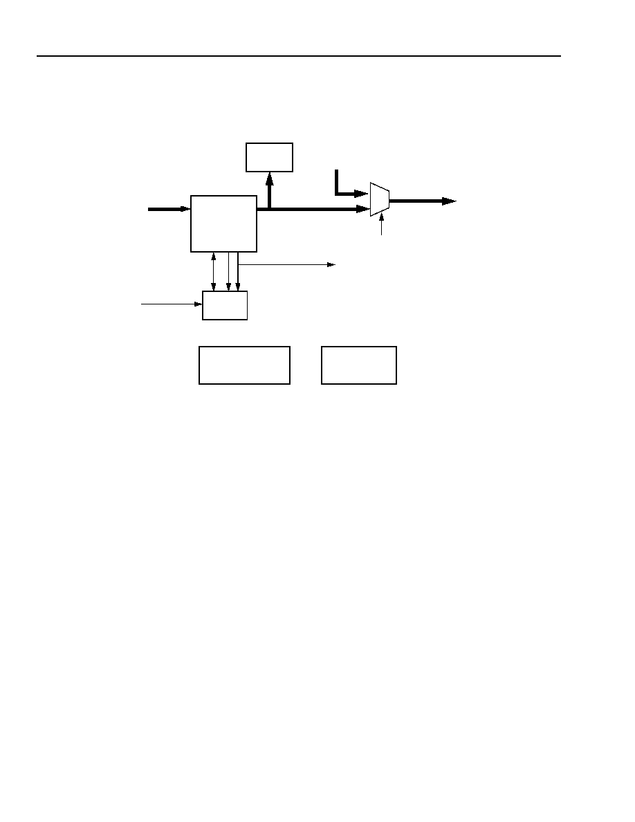
MARS2G5 P-Pro (TDAT162G52) SONET/SDH
Data Sheet
155/622/2488 Mbits/s Data Interface
August 18, 2004
392
Agere Systems Inc.
STS Receive Terminator (RXT) Block
(continued)
Introduction
(continued)
5-8708(F)r.1
Figure 47. STS Receive Terminator (RXT) Functional Block Diagram
The pointer interpreter interprets the H1 and H2 bytes and determined the offset of each STS-1, as well as the
state of the STS-1 (AIS, LOP, concatenated, normal).
The receive timing block extracts the H1, H2, and H3 bytes from the incoming data for the pointer interpreter, and
uses the offset determined by the interpreter to create signals that are used to extract the SPE and the path over-
head from the incoming data.
The path monitor implements the performance monitoring on the path overhead.
The AIS insert block allows AIS insertion under microprocessor control.
The microprocessor interface provides microprocessor registers to control the operation of the RXT and to read
the performance monitor data and RXT status.
PATH
MONITOR
MICROPROCESSOR
INTERFACE
J1 MARKER
SYNC PULSE
DATA IN
DATA OUT
RECEIVE
TIMING
POINTER
INTERPRETER
ALL 1s
AIS INSERT
PERFORMANCE
MONITORING

Data Sheet
MARS2G5 P-Pro (TDAT162G52) SONET/SDH
August 18, 2004
155/622/2488 Mbits/s Data Interface
393
Agere Systems Inc.
STS Receive Terminator (RXT) Block
(continued)
Receive Timing Functions
The timing block generates the signals required by the pointer interpreter, elastic store, and performance-
monitoring blocks. This block uses the frame pulse to create H1, H2, and STS indicators for the pointer interpreter.
The pointer interpreter provides increment, decrement, valid, and current pointer information for each STS which
allows the timing block to produce multiplexed POH indicators (i.e., J1, B3, etc.) and the associated valid SPE
signal for all STSs (SPE_VLD). The timing block has no indications of concatenation and thus produces POH
indicators for all STSs regardless of their concatenation state. The path overhead bytes are extracted by
subtracting the offset value for an STS-1 from an SPE byte counter (that counts from 0 to 782) to produce an 11-bit
signed number that indicates how far from J1 the current byte is. This value is compared to predetermined values
to find the individual overhead bytes. The compare values for each overhead byte are shown in Table 323 below.
The receive timing block also generates a POH byte signal, indicating that the current byte is part of the path
overhead. Because the drop interface may need indications of SPE and path overhead even when an STS-1 is in
AIS (to keep a FIFO from overrunning, for example), generic indications of SPE and POH are created. The generic
SPE indication is asserted for bytes in columns 4 through 90 inclusive and the generic POH indication is asserted
for bytes in column 4. The AIS insert block determines whether the actual or generic indications will be used for a
particular STS-1. If the pointer generator is not being bypassed, the equivalent signals will be created in the pointer
generator.
Table 323. Path Overhead Extraction Compare Values
Overhead
Byte
Compare Value
(SPE byte offset)
J1
0
B3
+87 or ≠696
C2
+174 or ≠609
G1
+261 or ≠522
F2
+348 or ≠435
H4
+435 or ≠348
Z3
+522 or ≠261
Z4
+609 or ≠174
Z5
+696 or ≠87
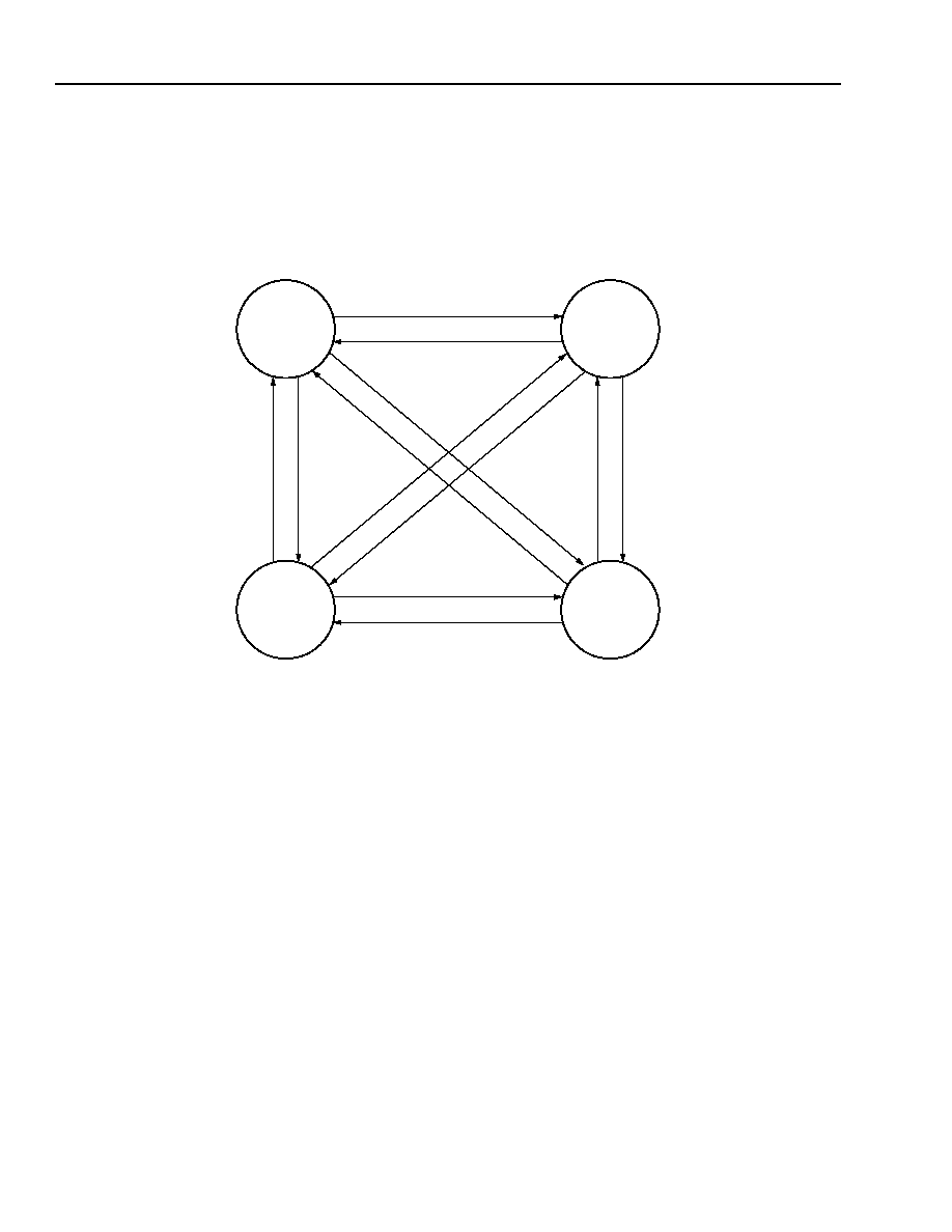
MARS2G5 P-Pro (TDAT162G52) SONET/SDH
Data Sheet
155/622/2488 Mbits/s Data Interface
August 18, 2004
394
Agere Systems Inc.
STS Receive Terminator (RXT) Block
(continued)
Pointer Interpreter Functions
The STS pointer interpreter interprets the H1 and H2 bytes for each incoming STS-1. The interpreter has four
states: loss of pointer (LOP), alarm indication signal (AIS), normal (NORM), and concatenation indication (CONC).
The state diagram is shown in Figure 48 on page 394.
5-8709(F)
Figure 48. Interpreter State Machine
NORM
LOP
AIS
CONC
3xNORM
3x
NORM
3x
NO
R
M
1x
ND
F
3xAIS
3x
AI
S
3xAI
S
3xCONC
3x
CONC
3x
C
O
N
C
8x
In
va
lid
8xINVALID
8x
Inv
a
lid
8xNDF

Data Sheet
MARS2G5 P-Pro (TDAT162G52) SONET/SDH
August 18, 2004
155/622/2488 Mbits/s Data Interface
395
Agere Systems Inc.
STS Receive Terminator (RXT) Block
(continued)
Pointer Interpreter Functions
(continued)
Incoming pointers are categorized into one or more of the following categories:
1.
Normal pointer (NDF is not set and the offset is in range).
2.
Normal pointer (offset = validated offset).
3.
Normal pointer (offset = old offset--i.e., the same offset as in the last frame).
4.
Valid NDF pointer (NDF set and offset is in range).
5.
Concatenation indicator (NDF set with an all ones offset).
6.
AIS pointer (all ones).
7.
Increment indicator (compared to validated offset).
8.
Decrement indicator (compared to validated offset).
9.
Other (unrecognized pointer).
Note: A given pointer can be classified as belonging to more than one of the above groups. There are only a few
valid combinations:
1 and 2
1 and 3
1, 2, and 3
1 and 7
1 and 8
1, 3, and 7 (if the same pointer that created (1 and 7) repeats the next frame)
1, 3, and 8 (if the same pointer that created (1 and 8) repeats the next frame)
Increments and decrements can be evaluated in either SONET or SDH modes. In SONET mode, the 8 of 10 rule is
used, where 8 of the 10 I and D bits must be evaluated to be an increment or decrement for the pointer to be con-
sidered an increment or decrement. In SDH mode, the 3 of 5 rule is used, where 3 of the 5 I bits and 3 of the 5 D
bits must be evaluated to be an increment or decrement for the pointer to be considered and increment or decre-
ment.
Note: In SDH mode, it is possible for a stuck input pointer to cause a repeating increment then decrement pattern.
To avoid this situation, increment and decrement pointers that are not perfect (10 of 10) are considered
invalid. See the description of the invalid counter for more details.

MARS2G5 P-Pro (TDAT162G52) SONET/SDH
Data Sheet
155/622/2488 Mbits/s Data Interface
August 18, 2004
396
Agere Systems Inc.
STS Receive Terminator (RXT) Block
(continued)
Pointer Interpreter Functions
(continued)
Five counters are used in conjunction with the pointer categories to determine the state of the state machine.
These counters are the following:
norm_cnt--counts how many consecutive times condition 3 occurs (condition (1 and !3) will preset this counter
to 1).
ndf_cnt--counts how many consecutive times condition 4 occurs.
ais_cnt--counts how many consecutive times condition 6 occurs.
invalid_cnt--counts how many consecutive times conditions.
(next state is NORM and !2 and !4 and !6 and !7* and !8* and !((norm_cnt ==2) and 3)) or
(next state is AIS and !6) or
(next state is CONC and !5 and !6) occurs.
concat_cnt--counts how many consecutive times condition 5 occurs.
* See details below.
The norm_cnt counter will be preset to 1 when condition 1 occurs and condition 3 doesn't occur. In other words, if
a normal pointer is received that is not the same offset as the last pointer received, the norm_cnt is set to 1.
Note: Invalid_cnt counts increments and decrements as being invalid while in the NORM state if there is less than
a 10 of 10 match in the I and D bits. For example, a pointer with all of the I bits inverted and 4 of the D bits not
inverted would be counted as an invalid pointer, and an increment would be performed. NDF pointers are
considered valid while in the NORM state. NDF pointers are counted separately with ndf_cnt. In AIS state,
any pointer that is not an AIS pointer is considered invalid. In CONC state, any pointer that is not a concate-
nation indication or an AIS pointer is considered invalid.
The count condition is evaluated at the same time as the state is evaluated. Therefore, the counter is not actually
incremented or cleared until after the state has been evaluated. Thus, the pointer condition must also be used to
evaluate the state.
If any of the conditions for a counter do not occur, the counter is cleared.
The state machine will change states based on the following conditions.
Note: If the conditions indicate that there are two possible states to change to, the one listed first will be taken.

Data Sheet
MARS2G5 P-Pro (TDAT162G52) SONET/SDH
August 18, 2004
155/622/2488 Mbits/s Data Interface
397
Agere Systems Inc.
STS Receive Terminator (RXT) Block
(continued)
Pointer Interpreter Functions
(continued)
The state changes from LOP to:
AIS--when (ais_cnt == 2) and condition 6 occurs.
NORM--when (norm_cnt == 2) and condition 3 occurs.
CONC--when (concat_cnt == 2) and condition 5 occurs.
The state changes from AIS to:
NORM--when (norm_cnt == 2) and condition 3 occurs or condition 4 occurs.
CONC--when (concat_cnt == 2) and condition 5 occurs.
LOP--when (invalid_cnt == 7) and condition 6 does not occur.
The state changes from NORM to:
AIS--when (ais_cnt == 2) and condition 6 occurs.
CONC--when (concat_cnt == 2) and condition 5 occurs.
LOP--when (invalid_cnt == 7) and condition 2 does not occur or (ndf_cnt == 7) and condition 4 occurs.
The state changes from CONC to:
AIS--when (ais_cnt == 2) and condition 6 occurs.
NORM--when (norm_cnt == 2) and condition 3 occurs.
LOP--when (invalid_cnt == 7) and condition 5 does not occur.
Note: When changing states, NORM, CONC, and AIS always take precedence over LOP (NORM, CONC, and AIS
being mutually exclusive).
The pointer interpreter provides outputs to indicate the following:
AIS-P and LOP-P defect indications on a per-STS-1 basis (RAW_AIS_P, RAW_LOP_P).
A per-STS-1 indication of CONC state (RECD_CONC_MAP).
A per-STS-1 indication of pointer state (STS_OK)--indicates that an STS-1 is in NORM state, or if it is in CONC
state and the first STS-1 in the concatenated STS-Nc is in NORM state.
A per-STS-1 indication of receipt of an all 1s pointer--this is used by the pointer generator to generate and all-
ones pointer in order to meet the all-ones pointer relay objective in GR-253.
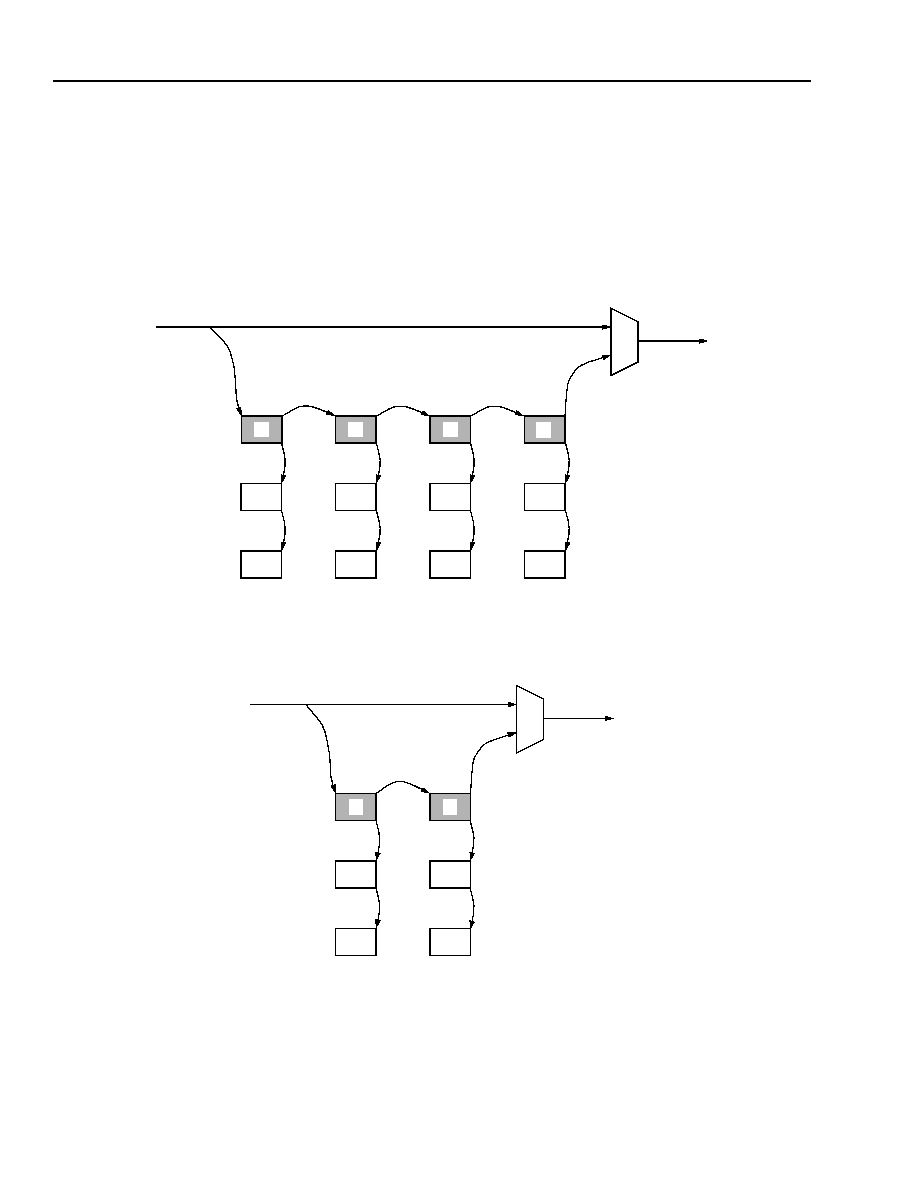
MARS2G5 P-Pro (TDAT162G52) SONET/SDH
Data Sheet
155/622/2488 Mbits/s Data Interface
August 18, 2004
398
Agere Systems Inc.
STS Receive Terminator (RXT) Block
(continued)
Concatenation
In the diagrams, the squares represent bytes coming into the RXT. Each diagram represents a different RXT
configuration. The numbers in the squares represent the order in which the bytes are received. The numbers to the
left of each square represent the SONET ordering. Each byte belongs to a separate STS-1 signal. The shaded
squares represent the possible starting points for concatenated STS signals (these are the N,1 STS-1 numbers
shown in GR-253 in Chapter 5).
5-8710(F)
Figure 49. STS-12 RXT Concatenated Offset Passing
5-8711(F)
Figure 50. STS-6 RXT Concatenated Offset Passing
6
9
12
3
10
7
4
2
5
8
11
10
11
12
6
7
9
8
5
1
STS-12
POINTER
4
3
2
1
6
3
4
5
6
1
4
2
5
3
STS-6
POINTER
1
2

Data Sheet
MARS2G5 P-Pro (TDAT162G52) SONET/SDH
August 18, 2004
155/622/2488 Mbits/s Data Interface
399
Agere Systems Inc.
STS Receive Terminator (RXT) Block
(continued)
Concatenation
(continued)
5-8712(F)
Figure 51. STS-3 and STS-1 RXT Concatenated Offset Passing
The arrows indicate how offsets are propagated between concatenated STS-1s. Offsets are propagated during the
H2 time. If an STS-1 is in concatenation state, it will use the offset from the STS-1 indicated by the arrow. For
example, if an STS-6c were constructed in an STS-12 RXT starting with STS-1 number 4 (SONET ordering) in the
STS-12 diagram, then STS-1 number 4 will be in NORM state, and STS-1 numbers 5, 6, 7, 8, and 9 would be in
CONC state. STS-1 numbers 5 and 7 would get their offset from STS-1 number 4. STS-1 number 8 would get its
offset from STS-1 number 7. STS-1 number 6 would get its offset from STS-1 number 5 and STS-1 number 9
would get its offset from STS-1 number 8. This example is shown in Figure 52 below. Note that in this situation, off-
sets are always passed to STS-1s that arrive later in time. This method will work for constructing any size and
number of concatenated streams within an STS-12.
5-8713(F)r.1
Figure 52. STS-6c Offset Passing in an STS-12 RXT
1
2
3
1
2
3
1
STS-1
POINTER
STS-3
POINTER
1
6
9
12
3
10
7
4
2
5
8
11
12
2
9
4
8
5
1
1
STS-12
POINTER
10
11
7
6
3

MARS2G5 P-Pro (TDAT162G52) SONET/SDH
Data Sheet
155/622/2488 Mbits/s Data Interface
August 18, 2004
400
Agere Systems Inc.
STS Receive Terminator (RXT) Block
(continued)
Concatenation
(continued)
The propagated offset for an STS-1 in the CONC state is stored in the same register as the validated offset is
stored if the STS-1 is in the NORM state. In addition to the offset itself, increment, decrement, and valid offset indi-
cations are propagated to concatenated STS-1s.
If any STS-1s are concatenated with STS-1s from a different STS-12 processing block, the offset must be passed
between blocks. Also, if any STS-1s from other blocks are concatenated to STS-1s in this block, an offset must be
passed to the next block. More specifically, if STS-1 number 1 is concatenated, it will receive its offset from STS-1
number 10 (SONET ordering) from the previous block. Note that the offset for STS-1 number 10 is not valid until
after the fourth clock of the H2 byte, which occurs after the state machine for STS-1 number 1 of the next STS-12
block has been processed. Thus, the offset for STS-1 number 1 and any subsequent concatenated STS-1s cannot
be processed until after the fourth byte. This means that the offsets of concatenated STS-1s must be updated after
that STS-1s state machine has been processed. This is accomplished by enabling the register that stores the prop-
agated offset just before the H3 byte of that STS-1. This means the offset must be able to reach all STS-1s in the
concatenation in at least two thirds of a byte time (approximately 100 ns). RXTs configured as STS-1 or STS-3 will
have a whole byte time (approximately 150 ns).
A further problem occurs when several STS-12 blocks contain one large STS-Nc signal. Each block after the first
would have to wait until the previous block has a valid offset for STS-1 number 10, then propagate the offset
through to the next STS-12 block, which would take another four clocks (to propagate from STS-1 number 1 to
STS-1 number 10 and out). For an STS-192c, it would take 66 clocks to propagate the offset to the last STS-1,
using an STS-12 RXT. This is considerably more than the 12 clocks during which the H2 byte is being received for
all STS-1s. To alleviate this problem, a MUX is added such that if all possible STS-1s are concatenated in a block
(numbers 1, 4, 7, and 10 for an STS-12 block or 1 and 4 for an STS-6 block), the output offset comes directly from
the concatenation input offset rather than from STS-1 number 10. This way, once the fourth STS-1 state machine is
processed in each STS-12 block (STS-1 number 10), the offset is made available to all subsequent STS-12 blocks.
This does, however, result in significant combinational logic between flip-flops; the offset may go through up to 14
2:1 MUXes. Thus, in the actual implementation, a 4:1 MUX is used, which can take the output offset from any one
of the previous three RXTs. This results in a maximum of five 4:1 MUXes the offset may go through for an STS-
192c, using STS-12 RXTs. The passing of the offsets for concatenation is illustrated in Figure 53. The MUXes are
selected to pass the offset from as close to the head of the concatenation as possible.
5-8714(F)r.2
Figure 53. Concatenated Offset Passing
RXT N
RXT N + 1
RXT N + 2
RXT N + 3

Data Sheet
MARS2G5 P-Pro (TDAT162G52) SONET/SDH
August 18, 2004
155/622/2488 Mbits/s Data Interface
401
Agere Systems Inc.
STS Receive Terminator (RXT) Block
(continued)
Concatenation
(continued)
To ensure that concatenated payloads go through the elastic store in the correct order, the address counter of a
concatenated STS-1 is synchronized to the address counter of the STS-1 at the head of the concatenation. Within
an RXT, the address of the head of the concatenation is simply passed to the concatenated STS-1s. When the
STS-1 at the head of the concatenation is in a different RXT, a synchronization signal is passed from the last STS-
1 of the previous RXT (actually, the last STS-1 on an STS-3 boundary) that indicates that the first STS-1 in the
RXT should go to address 0 on the next byte. In this way, all of the STS-1s in the concatenation will have the same
elastic store address at the same time. The synchronization signal is passed through a 4:1 MUX structure in the
same way that concatenation offsets are passed in the pointer interpreter.
Path Trace (J1)
The path trace byte carries a repeating message that is defined in SONET as 64 bytes (ASCII, <CR><LF> termi-
nated) and in SDH as 16 bytes (E.164). The POH processor extracts either type of message from one selectable
STS-1 per channel and stores the message in an internal register bank. The contents of the message can then
optionally be monitored for either a mismatch from a provisioned expected message or a sustained change in the
received message. A mismatch is declared if the received message differs from the expected message for ten con-
secutive messages. The mismatch clears when 4-out-of-5 received messages match the expected message. A
sustained change is detected when the received message differs from the last stable message for ten consecutive
messages. The new message then becomes the stable message and the processor starts checking for a sus-
tained change from this new stable message (i.e., there is no clearing criteria for a sustained change). Both defects
are indicated by corresponding latched alarm status bits in the memory map. The detection of a mismatch could
result in AIS insertion if provisioned through software.
Selection of the message protocol, 16-byte or 64-byte, the content monitoring option and the monitored STS chan-
nel are provisionable on a per-channel basis through the path trace control register in the microprocessor inter-
face. The expected messages for all channels are provisioned through the microprocessor interface using a 64-
byte data buffer. This data buffer is also used to read the contents of the expected, stable or received message
buffers for all blocks. Accesses using the data buffer are paged according to channel and message buffer
(expected/stable or received). Selection of paging as well as access type (read or write) is done using the path
trace access control register. The actual access is triggered by writing a 0x0001 (hex) value to the path trace
access start register and is performed on a non-real-time basis. Completion of the access is indicated by the mes-
sage buffer access complete bit in the path trace status register being set.
Path BIP-8 (B3)
The path BIP-8 byte carries the even parity of the data in the previous STS SPE frame (783 bytes for STS-1,
Nx783 for STS-Mc). Every frame the received B3 value is extracted and compared to the calculated BIP-8 for the
previous frame. Detected errors are accumulated in an internal 16-bit counter based on either bit or block errors as
provisioned per channel through the microprocessor interface. If bit error mode is enabled for the channel, each
BIP-8 bit found in error causes the counter to increment. If block error mode is enabled for the channel, the counter
is only incremented by one regardless of the number of BIP-8 bits in error. The value in the counter is transferred
to the path coding violation (CV-P) registers on the positive edge of the performance-monitoring strobe (PMSTB
input) at which point the counter is cleared.

MARS2G5 P-Pro (TDAT162G52) SONET/SDH
Data Sheet
155/622/2488 Mbits/s Data Interface
August 18, 2004
402
Agere Systems Inc.
STS Receive Terminator (RXT) Block
(continued)
Concatenation
(continued)
Signal Fail Alarms. Each of the 48 STS-1s entering the RXT can be automatically monitored for B3 errors against
a programmable threshold. Concatenated payloads are supported by programming the threshold values for the
head STS-1.
Each STS-1 or head of an STS-NC has a select to choose which threshold group's parameters to compare against.
There are eight threshold groups available, each group consisting of:
Set Threshold. If the B3 errors is equal or greater than this value in the given time window, the signal fail alarm
for this STS-1 is set. The B3 count in subsequent window times must be less than the clear threshold listed
below to clear this error condition.
Set Threshold Window Select. There are four time windows available between the eight groups. The set
threshold window select can be set to one of these window sizes.
Clear Threshold. If the signal fail alarm has been previously set, it will be cleared if an entire clear window time
goes past with the B3 error count less than this value.
Clear Threshold Window Select. If the signal fail alarm has been previously set, this window size will be used
to measure B3 errors.
Each STS-1 has a 9-bit B3 counter, which is incremented every time a B3 error appears. If STSs are part of an
STS-Nc, there is one 14-bit counter for the entire concatenation. This counter is cleared at the end of the window
selected for the threshold group for which this STS-1 or STS-Nc is set to. This counter (9 or 14 bits) can be incre-
mented by 0 (if no B3 errors occurred) or up to eight counts (if all the bits in the B3's BIP-8 calculation are opposite
from expected). Note there are no bit/block issues with the signal fail counters; only bit errors are counted. Bit/block
is only an option for the B3 counters in the path monitoring (PM).
The signal fail alarm is set if the number of B3 errors for an STS-1 or STS-Nc is above the set threshold within this
window time. The B3 error counter for each STS-1 or STS-Nc is cleared at the end of each window and counts up
again in the next window.
One can set an individual STS-1/STS-Nc to set an alarm on one BER and clear this alarm on another. For this, a
threshold count value and timing window is provided for both set and clear.
For each STS-1 or STS-Nc, its B3 counter is running for either the time set by the set threshold window or the time
set by the clear threshold window. If this STS-1/STS-Nc is in the clear state (the alarm bit is clear), then the signal
fail circuitry will be looking for the case when the number of B3 errors equals or exceeds the set threshold. The
counter will be running for the duration of the set threshold window. If this condition is reached, the alarm will be set
immediately and the system will switch to watching the desired clear window. It will wait until the clear window has
completed its current cycle and will start counting B3 errors again in the next cycle. The B3 counter will be cleared
and B3 errors will be added, and at the end of this window time (now the clear window time), the decision will be
made to clear the alarm condition or not. If the number of B3 errors in the counter is less than the clear threshold,
the alarm will be cleared and during the next window of length = set threshold window size the counter will be com-
pared to the set threshold. Otherwise, this error condition will remain set and another window of duration = clear
threshold window size will commence.
The signal fail alarm can be set anywhere during the window, but can only be cleared at the end of a window time.
The RXT is either checking for the set or clear condition for an STS-1/STS-Nc at a given time. One implication of
this is that if the clear threshold was set for a BER higher than the set threshold and an incoming signal of a con-
stant BER between the two was present, the signal fail alarm would oscillate, set, and clear with a period of zero to
one times the set window threshold window time plus one to two times the period of the clear window threshold
window time.

Data Sheet
MARS2G5 P-Pro (TDAT162G52) SONET/SDH
August 18, 2004
155/622/2488 Mbits/s Data Interface
403
Agere Systems Inc.
STS Receive Terminator (RXT) Block
(continued)
Concatenation
(continued)
There are eight threshold groups available (see Table 413--Table 416); two are labelled as being used for STS-1s
(group 0 and 1) and six (groups 2--7) are labelled for use as STS-Ncs. Group 0 and 1 have set and clear thresh-
olds of 9 bits (0--511) whereas groups 2--7 have set and clear thresholds of up to 14 bits (0--16383). This is to
accommodate the higher data rate of a concatenated payload and thus the higher number of bit errors one would
see in the same time window for the same BER. However, one could point an STS-1 to group 2--7 as long as the
thresholds are set to 511 or less to stay within the 9-bit size of an individual STS-1s counter.
There are four threshold window size registers, each 16 bits, in increments of 0.5 ms (for a maximum of window
size of 32 seconds).
The table below shows the recommended set/clear threshold and window values for the BER they are intended for.
Table 324. Set/Clear Threshold and Window Settings
Intended
for STS-1
or STS-Nc
Threshold
Type
Desired BER to
Detect
Threshold
Threshold Window
Select
STS-1
Set
BER = 10
≠3
0x6C
0xA
Clear
BER = 10
≠4
0x22
0xA
STS-1
Set
BER = 10
≠4
0xC9
0x64
Clear
BER = 10
≠5
0x27
0x64
STS-1
Set
BER = 10
≠5
0xCF
0x3E8
Clear
BER = 10
≠6
0x24
0x3E8
STS-3c
Set
BER = 10
≠3
0x8A
0xA
Clear
BER = 10
≠4
0x49
0xA
STS-3c
Set
BER = 10
≠4
0x226
0x64
Clear
BER = 10
≠5
0x59
0x64
STS-3c
Set
BER = 10
≠5
0x2B0
0x3E8
Clear
BER = 10
≠6
0x60
0x3E8
STS-6c
Set
BER = 10
≠3
0x89
0xA
Clear
BER = 10
≠4
0x76
0xA
STS-6c
Set
BER = 10
≠4
0x39B
0x64
Clear
BER = 10
≠5
0xA8
0x64
STS-6c
Set
BER = 10
≠5
0x53A
0x3E8
Clear
BER = 10
≠6
0xAC
0x3E8

MARS2G5 P-Pro (TDAT162G52) SONET/SDH
Data Sheet
155/622/2488 Mbits/s Data Interface
August 18, 2004
404
Agere Systems Inc.
STS Receive Terminator (RXT) Block
(continued)
Concatenation
(continued)
Table 324. Set/Clear Threshold and Window Settings (continued)
Intended
for STS-1
or STS-Nc
Threshold
Type
Desired BER to
Detect
Threshold
Threshold Window
Select
STS-9c
Set
BER = 10
≠3
0x8D
0xA
Clear
BER = 10
≠4
0x89
0xA
STS-9c
Set
BER = 10
≠4
0x47E
0x64
Clear
BER = 10
≠5
0xED
0x64
STS-9c
Set
BER = 10
≠5
0x7CA
0x3E8
Clear
BER = 10
≠6
0x103
0x3E8
STS-12c
Set
BER = 10
≠3
0x8D
0xA
Clear
BER = 10
≠4
0x9D
0xA
STS-12c
Set
BER = 10
≠4
0x50B
0x64
Clear
BER = 10
≠5
0x139
0x64
STS-12c
Set
BER = 10
≠5
0xA3F
0x3E8
Clear
BER = 10
≠6
0x14C
0x3E8
STS-15c
Set
BER = 10
≠3
0x8E
0xA
Clear
BER = 10
≠4
0xA4
0xA
STS-15c
Set
BER = 10
≠4
0x573
0x64
Clear
BER = 10
≠5
0x178
0x64
STS-15c
Set
BER = 10
≠5
0xC92
0x3E8
Clear
BER = 10
≠6
0x199
0x3E8
STS-18c
Set
BER = 10
≠3
0x89
0xA
Clear
BER = 10
≠4
0xA9
0xA
STS-18c
Set
BER = 10
≠4
0x5A4
0x64
Clear
BER = 10
≠5
0x1B5
0x64
STS-18c
Set
BER = 10
≠5
0xEE2
0x3E8
Clear
BER = 10
≠6
0x1E5
0x3E8

Data Sheet
MARS2G5 P-Pro (TDAT162G52) SONET/SDH
August 18, 2004
155/622/2488 Mbits/s Data Interface
405
Agere Systems Inc.
STS Receive Terminator (RXT) Block
(continued)
Concatenation
(continued)
Table 324. Set/Clear Threshold and Window Settings (continued)
Intended
for STS-1
or STS-Nc
Threshold
Type
Desired BER to
Detect
Threshold
Threshold Window
Select
STS-21c
Set
BER = 10
≠3
0x8E
0xA
Clear
BER = 10
≠4
0xB2
0xA
STS-21c
Set
BER = 10
≠4
0x5C8
0x64
Clear
BER = 10
≠5
0x1E8
0x64
STS-21c
Set
BER = 10
≠5
0x10F8
0x3E8
Clear
BER = 10
≠6
0x23F
0x3E8
STS-24c
Set
BER = 10
≠3
0x8D
0xA
Clear
BER = 10
≠4
0xB0
0xA
STS-24c
Set
BER = 10
≠4
0x5D1
0x64
Clear
BER = 10
≠5
0x224
0x64
STS-24c
Set
BER = 10
≠5
0x1317
0x3E8
Clear
BER = 10
≠6
0x280
0x3E8
STS-27c
Set
BER = 10
≠3
0x8C
0xA
Clear
BER = 10
≠4
0xAF
0xA
STS-27c
Set
BER = 10
≠4
0x5F2
0x64
Clear
BER = 10
≠5
0x253
0x64
STS-27c
Set
BER = 10
≠5
0x151B
0x3E8
Clear
BER = 10
≠6
0x2C0
0x3E8
STS-30c
Set
BER = 10
≠3
0x8C
0xA
Clear
BER = 10
≠4
0xB0
0xA
STS-30c
Set
BER = 10
≠4
0x5E9
0x64
Clear
BER = 10
≠5
0x27E
0x64
STS-30c
Set
BER = 10
≠5
0x16D6
0x3E8
Clear
BER = 10
≠6
0x316
0x3E8

MARS2G5 P-Pro (TDAT162G52) SONET/SDH
Data Sheet
155/622/2488 Mbits/s Data Interface
August 18, 2004
406
Agere Systems Inc.
STS Receive Terminator (RXT) Block
(continued)
Concatenation
(continued)
Table 324. Set/Clear Threshold and Window Settings (continued)
Intended
for STS-1
or STS-Nc
Threshold
Type
Desired BER to
Detect
Threshold
Threshold Window
Select
STS-33c
Set
BER = 10
≠3
0x8C
0xA
Clear
BER = 10
≠4
0xB2
0xA
STS-33c
Set
BER = 10
≠4
0x5FC
0x64
Clear
BER = 10
≠5
0x2CC
0x64
STS-33c
Set
BER = 10
≠5
0x189C
0x3E8
Clear
BER = 10
≠6
0x366
0x3E8
STS-36c
Set
BER = 10
≠3
0x90
0xA
Clear
BER = 10
≠4
0xB0
0xA
STS-36c
Set
BER = 10
≠4
0x603
0x64
Clear
BER = 10
≠5
0x2DB
0x64
STS-36c
Set
BER = 10
≠5
0x1A65
0x3E8
Clear
BER = 10
≠6
0x3AF
0x3E8
STS-39c
Set
BER = 10
≠3
0x8B
0xA
Clear
BER = 10
≠4
0xB4
0xA
STS-39c
Set
BER = 10
≠4
0x601
0x64
Clear
BER = 10
≠5
0x312
0x64
STS-39c
Set
BER = 10
≠5
0x1BC9
0x3E8
Clear
BER = 10
≠6
0x3EF
0x3E8
STS-42c
Set
BER = 10
≠3
0x93
0xA
Clear
BER = 10
≠4
0xB6
0xA
STS-42c
Set
BER = 10
≠4
0x601
0x64
Clear
BER = 10
≠5
0x336
0x64
STS-42c
Set
BER = 10
≠5
0x1D5F
0x3E8
Clear
BER = 10
≠6
0x436
0x3E8

Data Sheet
MARS2G5 P-Pro (TDAT162G52) SONET/SDH
August 18, 2004
155/622/2488 Mbits/s Data Interface
407
Agere Systems Inc.
STS Receive Terminator (RXT) Block
(continued)
Concatenation
(continued)
Table 324. Set/Clear Threshold and Window Settings (continued)
Intended
for STS-1
or STS-Nc
Threshold
Type
Desired BER to
Detect
Threshold
Threshold Window
Select
STS-45c
Set
BER = 10
≠3
0x8A
0xA
Clear
BER = 10
≠4
0xB3
0xA
STS-45c
Set
BER = 10
≠4
0x607
0x64
Clear
BER = 10
≠5
0x363
0x64
STS-45c
Set
BER = 10
≠5
0x1EEF
0x3E8
Clear
BER = 10
≠6
0x488
0x3E8
STS-48c
Set
BER = 10
≠3
0x8E
0xA
Clear
BER = 10
≠4
0xB3
0xA
STS-48c
Set
BER = 10
≠4
0x5FF
0x64
Clear
BER = 10
≠5
0x38D
0x64
STS-48c
Set
BER = 10
≠5
0x3E8
0x3E8
Clear
BER = 10
≠6
0x4C8
0x3E8
MARS2G5 P-Pro (TDAT162G52) SONET/SDH
Data Sheet
155/622/2488 Mbits/s Data Interface
August 18, 2004
408
Agere Systems Inc.
STS Receive Terminator (RXT) Block
(continued)
Concatenation
(continued)
Below are the default threshold window sizes.
Table 325. Default Signal Fail Window Size Settings
Note 1: If the window size is set to 0x0000, it will provide a 0.5 ms window, the same as if it was set to 0x0001.
Note 2: If a window size register is changed, each current window will be cut short and will finish from one to two
time units (0.5 ms to 1 ms if the block is running in 90 columns) before the new window size is loaded. For
example, if the column size is 90, and window size 3 was changed, it will not take from 0 to up to 5 seconds
to start running with the new window size, but rather 0.5 ms to 1 ms.
Note 3: The unit of time in the window size register is 0.5 ms if the block is running in 90 column mode. This unit of
time is equal to four STS-frame sizes (4 x 125 µs = 0.5 ms). If the user is operating with a number of col-
umns other than 90, such as the so-called short frame mode (where the number of columns in a frame is
less than 90 columns for reduced simulation and testing time), then the unit of time for the window size
registers is no longer 0.5 ms, but rather four times the frame size.
B3 Calculation. The B3 is calculated on the TDM data stream coming from the pointer interpreter. It is calculated
using a continuously cycling 8-bit wide shift register that is N bytes deep (where N is the number of STS-1s being
handled by the RXT). Incoming data is XORed with the value coming out the end of the shift register, if the
SPE_VLD signal from the receive timing module is asserted, and loaded into the input of the shift register. If
SPE_VLD is not asserted, the value coming out of the end of the shift register is not modified before loading it into
the input of the shift register. If the J1 indication is present from the receive timing module, the data value (J1 byte)
is loaded directly into the input of the shift register to begin the calculation for the next frame, and the value coming
out of the shift register is loaded into a holding register. This is the calculated BIP-8 for the last SPE frame.
In the case of concatenation, each STS-1 in the STS-Nc stream calculates a BIP-8 for its part of the concatenated
SPE. After the J1 byte, the last STS-1 in the concatenation will pass its BIP calculation to the previous STS-1 in the
concatenation, which will XOR the incoming BIP with its own and pass the result on to the next previous STS-1,
and so on. When the first STS-1 in the concatenation is reached, the BIP is not passed on. The concatenation is
determined by the pointer interpreter received concatenation map. Thus, if an STS-1 erroneously enters the CONC
state, the B3 calculation will cause errors on the previous STS-1, which is assumed to be the first STS-1 in the con-
catenation.
When the B3 byte arrives in the next SPE, it is compared to the calculated B3 and the result is loaded back into the
holding register. The contents of the holding register are then shifted out serially to be used as the enable for the
binning counter.
Window Size Register
Time
Register Setting
Window Size 0
5 ms
0x000A
Window Size 1
50 ms
0x0064
Window Size 2
500 ms
0x03e8
Window Size 3
5 s
0x2710

Data Sheet
MARS2G5 P-Pro (TDAT162G52) SONET/SDH
August 18, 2004
155/622/2488 Mbits/s Data Interface
409
Agere Systems Inc.
STS Receive Terminator (RXT) Block
(continued)
Concatenation
(continued)
Path Signal Label (C2)
The path signal label byte is used to indicate either the type of payload carried in the STS SPE or the status of the
payload. Of the 256 possible values, only the codes 0x01 to 0x04 and 0x12 to 0x15 are currently defined to identify
payload types, while the codes 0xE1 to 0xFC are defined to indicate payload defects (see STS Path Signal Label
Assignments, Table 326, on page 410). The code 0xFF is a special reserved code due to its appearance in an STS
AIS and is treated as a don't care during any defect detection or clearing. The C2 byte is extracted each frame and
stored in the receive signal label registers. If the locally provisioned value, configured in the expected signal label
registers, is any equipped value (i.e., not 0x00), the extracted signal label is also processed for the following
defects:
Payload Label Mismatch (PLM). Detected if the extracted signal label is a valid payload specific code and does
not match the locally provisioned value in the expected signal label registers for five consecutive frames.
Cleared if the extracted signal label matches the locally provisioned value, the equipped nonspecific code
(0x01), or a valid PDI code for five consecutive frames. If the locally provisioned value is the equipped nonspe-
cific code, then it matches any valid equipped code. The valid payload specific codes are by default 0x02 to
0xE0, 0xFD and 0xFE, with the codes 0xE1 to 0xFB also included if the locally provisioned payload is VT-struc-
tured (0x02 or 0x03). If payload defect indication detection is disabled, 0xE1 to 0xFC are always included.
Detection of a PLM defect is indicated by a latched alarm status bit in the memory map, and could result in AIS
insertion if provisioned through software.
Path Unequipped (UNEQ). Detected if the extracted signal label matches the unequipped code (0x00) for five
consecutive frames. Cleared if the extracted signal label does not match the unequipped code for five consecu-
tive frames. Detection of an UNEQ defect is indicated by a latched alarm status bit and a one second PM in the
memory map, and could result in AIS insertion if provisioned through software.
Payload Defect Indication (PDI). Detected if the extracted signal label matches a valid PDI code for five con-
secutive frames. Cleared if the extracted signal label does not match a valid PDI code for five consecutive
frames. Valid PDI codes are 0xE1 to 0xFC when the locally provisioned payload label is 0x01, 0x02, or 0x03
(VT-structured STS) or just 0xFC otherwise. PDI detection can be disabled per STS through the microprocessor
interface.
Update. The C2 value is dumped into an MPU register. Each time the captured value changes, a delta bit is set.

MARS2G5 P-Pro (TDAT162G52) SONET/SDH
Data Sheet
155/622/2488 Mbits/s Data Interface
August 18, 2004
410
Agere Systems Inc.
STS Receive Terminator (RXT) Block
(continued)
Concatenation
(continued)
Table 326. STS Path Signal Label Assignments
Code (Hex)
Content of the STS SPE
Code (Hex)
Content of the STS SPE
0x00
Unequipped
0x12
Asynchronous mapping for DS4NA
0x01
Equipped--nonspecific payload
0x13
Mapping for ATM
0x02
VT-structured STS-1 SPE
0x14
Mapping for DQDB
0x03
Locked VT mode
0x15
Asynchronous mapping for FDDI
0x04
Asynchronous mapping DS3
0x16
Mapping for HDLC-PPP (proposed)
0xE1
VT-structured STS-1 SPE with 1 VTx
payload defect (STS-1 w/1 VTx PD)
0xEF
STS-1 w/15 VTx PDs
0xF0
STS-1 w/16 VTx PDs
0xF1
STS-1 w/17 VTx PDs
0xE2
STS-1 w/2 VTx PDs
0xF2
STS-1 w/18 VTx PDs
0xE3
STS-1 w/3 VTx PDs
0xF3
STS-1 w/19 VTx PDs
0xE4
STS-1 w/4 VTx PDs
0xF4
STS-1 w/20 VTx PDs
0xE5
STS-1 w/5 VTx PDs
0xF5
STS-1 w/21 VTx PDs
0xE6
STS-1 w/6 VTx PDs
0xF6
STS-1 w/22 VTx PDs
0xE7
STS-1 w/7 VTx PDs
0xF7
STS-1 w/23 VTx PDs
0xE8
STS-1 w/8 VTx PDs
0xF8
STS-1 w/24 VTx PDs
0xE9
STS-1 w/9 VTx PDs
0xF9
STS-1 w/25 VTx PDs
0xEA
STS-1 w/10 VTx PDs
0xFA
STS-1 w/26 VTx PDs
0xEB
STS-1 w/11 VTx PDs
0xFB
STS-1 w/27 VTx PDs
0xEC
STS-1 w/12 VTx PDs
0xFC
VT-structured STS-1 SPE with
28 VT1.5 payload defects, or a non-
VT-structured STS-1 or STS-Nc SPE
with a payload defect
0xED
STS-1 w/13 VTx PDs
0xEE
STS-1 w/14 VTx PDs

Data Sheet
MARS2G5 P-Pro (TDAT162G52) SONET/SDH
August 18, 2004
155/622/2488 Mbits/s Data Interface
411
Agere Systems Inc.
STS Receive Terminator (RXT) Block
(continued)
Concatenation
(continued)
Below is a table detailing the conditions and alarms created by different states of the provisioned (expected) and
received (incoming) path label found in the C2 byte.
Table 327. Payload Label Conditions
Note: The expected C2 byte is only used as a programming mode, i.e., changing the value does not reset the vali-
dation counters (unequipped and payload mismatch).
Expected C2 Value Set in Microprocessor Register
--
Incoming C2 Byte
0x00
0x01
0x02 or
0x03
0x04--0xE0
0xFD--0xFE
0xE1--0xFB
0xFC
0xFF
Received
C2 Value
(incoming)
Unequipped
Non-
specific
equipped
VT
structured
payload
Non-VT
structured
payload
1--27
VT path
defects
28-VT path
defects
AIS
0x00
None
UNEQ-P
UNEQ-P
UNEQ-P
Nonsensical provisioning
0x01
None
Match
Match
Match
0x02 or 0x03
None
Match
Match or
PLM-P
PLM-P
0x04--0xE0
0xFD--0xFE
None
Match
PLM-P
Match or
PLM-P
0xE1--0xFB
None
PDI-P
PDI-P
PLM-P
0xFC
None
PDI-P
PDI-P
PDI-P
0xFF
None
Hold
Hold
Hold

MARS2G5 P-Pro (TDAT162G52) SONET/SDH
Data Sheet
155/622/2488 Mbits/s Data Interface
August 18, 2004
412
Agere Systems Inc.
STS Receive Terminator (RXT) Block
(continued)
Concatenation
(continued)
Path Status (G1)
The path status byte is used to convey the path termination status and performance back to the originating STS
PTE. This allows the performance of the full-duplex path to be monitored from any single point along the path. Bits
1 to 4 are used as a remote error indication (formerly far end block error or FEBE), while bits 5 to 7 are used as a
remote defect indication. The G1 byte is extracted each frame and processed for these functions as described
below.
Remote Error Indication (REI-P). Indicates the count of bit errors detected at the far-end STS PTE using the
path BIP-8. The error count is a binary number from 0 to 8 (values above 8 are invalid and interpreted as 0) and
is accumulated in an internal 16-bit counter based on either bit or block errors as provisioned per channel
through the microprocessor interface. If bit error mode is enabled for the channel, the counter is incremented by
the actual error count. If block error mode is enabled for the channel, the counter is only incremented by one,
when the error count is not 0, regardless the actual value. The value in the counter accumulates until it is trans-
ferred to the REI-P registers on the positive edge of the performance-monitoring strobe (PMSTB input) at which
point the counter is cleared.
Remote Defect Indication (RDI-P). Indicates the detection of a defect at the far-end STS PTE. Initially, RDI-P
was defined as a one-bit value in bit 5, but has since been expanded to a 3-bit enhanced value (ERDI-P).
Table 328 shows the valid codes and interpretation for both the 1-bit and enhanced RDI schemes. As can be
seen, bits 6 and 7 are always set to opposite values for ERDI while they are set to the same value for 1-bit RDI.
The POH uses this fact to determine which RDI scheme is being used on a per STS basis. An RDI-P defect is
then detected if a valid defect code for one of the RDI schemes is received for ten consecutive frames. The RDI-
P defect is cleared when the no defects code for that scheme is received for ten consecutive frames. The value
of the last validated 3-bit RDI code is stored in the ERDI-P registers in the memory map. In addition, detection of
a 1-bit RDI defect or each of the three ERDI defects is indicated by a one second PM bit in the memory map.
Table 328. RDI-P Codes and Interpretation
* These codes are transmitted by STS PTE that do not support enhanced RDI-P. If enhanced RDI-P is not supported, G1 bits 2 and 1 must be
set to the same value, and should be set to 00.
These codes are transmitted by STS PTE that support enhanced RDI-P.
G1[5:7]
Priority of Enhanced RDI-P Codes
Trigger
Interpretation
0xx*
Not applicable
No defects
No RDI-P defect
1xx*
Not applicable
AIS-P, LOP-P
1-bit RDI-P defect
001
4
No defects
No ERDI-P defects
010
3
PLM-P, LCD-P
ERDI-P payload defect
101
1
AIS-P, LOP-P
ERDI-P server defect
110
2
UNEQ-P, TIM-P
ERDI-P connectivity defect

Data Sheet
MARS2G5 P-Pro (TDAT162G52) SONET/SDH
August 18, 2004
155/622/2488 Mbits/s Data Interface
413
Agere Systems Inc.
STS Receive Terminator (RXT) Block
(continued)
Concatenation
(continued)
Interrupt Alarms and Masks
The following path conditions create alarms and set bits in the alarm registers. There is a bit for each STS-1.
Path LOP.
Path AIS.
Path UNEQ--unequipped alarm.
Path PLM--path label mismatch.
Path RDI--remote defect indicator.
SF--path signal fail.
Elastic store overrun, underrun.
The following conditions also create alarms:
Concatenation mismatch--the received concatenation map does not match the expected map.
Unsupported concatenation.
J1 validated--a new path trace message has come in and is validated. This occurs when the stream is set to
receive mode.
J1 mismatch--the path trace message that has come in does not match the provisioned one. This alarm occurs
when the stream is set to provision mode.
There is a control bit that sets whether the alarm registers are cleared by writing a one to that bit or by just reading
the register. This control bit is in the clear on read/write register.
The alarms can be masked so they do not cause an interrupt by setting the corresponding interrupt alarm mask bit
to 1. A 0 in the mask bit allows the interrupt to be generated.
The interrupt registers are categorized into three levels, a base level, and two levels of binning registers, which
accumulate alarm conditions that were not masked from the previous level. These binning registers facilitate a
faster identification of the alarm condition by the controlling software. Each level has a corresponding interrupt
mask register.
On the bottom level, there are alarm registers which have a bit per STS-1 for each path status condition. There is a
matching alarm mask to mask out individual bits. If the alarm condition for that STS-1 occurs and the alarm mask
bit is not set, then an interrupt is generated and the bit in the binning register above will read set. If the interrupt
mask is not set for that binning register, then the condition will appear in the top-level register.
Only the bottom-level registers have storage, and to remove the alarm flag, it is necessary only to clear the bottom-
level register (either with a write-one-clear or a read depending on the clear read/write control bit).
If the interrupt alarm mask bits are set for the bottom level, then no interrupts can be caused, but that condition can
be detected by polling this bottom-level register.
Note: If an error condition occurs for an STS-Nc, the condition will be reflected in the head STS-1 of the concate-
nation.

MARS2G5 P-Pro (TDAT162G52) SONET/SDH
Data Sheet
155/622/2488 Mbits/s Data Interface
August 18, 2004
414
Agere Systems Inc.
STS Receive Terminator (RXT) Block
(continued)
RXT Register Descriptions
1699(F).ar.1
Figure 54. Overview of RXT Register Map
ID REGISTER
INTERRUPTS
MASKS
CONCATENATION MAP
AIS-P GENERAL CONTROL
0x8000
0x800F
0x8300
0x8780
0x8880
0x8900
0x8400
0x8600
0x8690
0x8702
0x820F
0x8502
0x8580
0x8542
RESERVED
REI COUNT PM
CV COUNT PM
POH PM
PATH MAINTENANCE
PATH PROVISIONING
INTERPRETER
PP CONTROL
PATH TRACE
SF DETECT/CLEAR
0x8800
RDI, C2, PDI
PERSISTENCY
STATE
0x83C2
0x8382
INCREMENT/DECREMENT (PM)

Data Sheet
MARS2G5 P-Pro (TDAT162G52) SONET/SDH
August 18, 2004
155/622/2488 Mbits/s Data Interface
415
Agere Systems Inc.
STS Receive Terminator (RXT) Block
(continued)
RXT Register Descriptions
(continued)
Table 329. RXT_IDR, RXT Identification Register (RO, Fixed Value)
Table 330. PP_CORWR, PP Clear on Read/Write Register (R/W, Control)
Address
Bit
Name
Function
Reset
Default
0x8000
15:0
RXT_ID[15:0]
RXT Identification Register.
0001
Address
Bit
Name
Function
Reset
Default
0x8001
15:1
--
Reserved.
0
0
RXT_CORW
RXT Clear on Read/Write. Sets the mode for clearing alarm
bit in the RXT block.
0 = Clear interrupt bits by writing 1 to that bit in the alarm
register.
1 = Clear all alarm bits in an interrupt alarm register by
reading that register.
Note: This affects only the RXT interrupt alarms, i.e., only
the ones listed in this section (RXT) of the data sheet.
0

MARS2G5 P-Pro (TDAT162G52) SONET/SDH
Data Sheet
155/622/2488 Mbits/s Data Interface
August 18, 2004
416
Agere Systems Inc.
STS Receive Terminator (RXT) Block
(continued)
RXT Register Descriptions
(continued)
Interrupts
Table 331. RXT_POH_ALMBNR[1--2], Path Overhead Alarm Status Binning Register (RO)
Address
Bit
Name
Function
Reset
Default
0x800F
15:3
--
Reserved.
0
2
RXT_PDI_ALMDBN Payload Defect Indicator (PDI) Alarm Delta Binning.
0 = PDI alarm delta has not been detected for any STS-1 in any
bytestream.
1 = PDI alarm delta has been detected for one or more STS-1s
in one or more bytestreams.
0
1
RXT_PDI_ALMBN
Payload Defect Indicator (PDI) Alarm Binning.
0 = PDI alarm has not been detected for any STS-1 in any
bytestream.
1 = PDI alarm has been detected for one or more STS-1s in one
or more bytestreams.
0
0
RXT_J1ACCMP_
ALMBN
J1 Access Complete Alarm Binning. The alarm can be
masked from contributing to the RXT interrupt by either
registers 0x820F bit 0 (Table 363) or 0x82E0 bit 0 (Table 392).
0 = J1 access complete alarm has not been detected for any
STS-1 in any bytestream.
1 = J1 access complete alarm has been detected for one or
more STS-1s in one or more bytestreams.
0

Data Sheet
MARS2G5 P-Pro (TDAT162G52) SONET/SDH
August 18, 2004
155/622/2488 Mbits/s Data Interface
417
Agere Systems Inc.
STS Receive Terminator (RXT) Block
(continued)
RXT Register Descriptions
(continued)
Table 331. RXT_POH_ALMBNR[1--2], Path Overhead Alarm Status Binning Register (RO) (continued)
Address
Bit
Name
Function
Reset
Default
0x8010
15
RXT_RDI_ALMDBN Remote Defect Indicator Alarm Delta Binning.
0 = Alarm has not been detected for any STS-1 in any
bytestream.
1 = Alarm has been detected for one or more STS-1s in one or
more bytestreams.
0
14
RXT_PLM_
ALMDBN
Payload Label Mismatch Alarm Delta Binning.
0 = Alarm has not been detected for any STS-1 in any
bytestream.
1 = Alarm has been detected for one or more STS-1s in one or
more bytestreams.
0
13
RXT_UNEQR_
ALMDBN
Unequipped Received Alarm Delta Binning.
0 = Alarm has not been detected for any STS-1 in any
bytestream.
1 = Alarm has been detected for one or more STS-1s in one or
more bytestreams.
0
12
RXT_AIS_ALMDBN Alarm Indicator Signal Alarm Delta Binning.
0 = Alarm has not been detected for any STS-1 in any
bytestream.
1 = Alarm has been detected for one or more STS-1s in one or
more bytestreams.
0
11
RXT_LOP_
ALMDBN
Loss of Pointer Alarm Delta Binning.
0 = Alarm has not been detected for any STS-1 in any
bytestream.
1 = Alarm has been detected for one or more STS-1s in one or
more bytestreams.
0
10
RXT_J1MM_
ALMBN
J1 Mismatch Alarm Binning.
0 = J1 buffer access not complete.
1 = J1 buffer access complete.
0
9
RXT_J1VLD_
ALMBN
J1 Validated Alarm Binning.
0 = J1 buffer access not complete.
1 = J1 buffer access complete.
0
8
RXT_USCNCT_
ALMBN
Unsupported Concatenation Alarm Binning.
0 = None of the four bytestreams has an unsupported
concatenation.
1 = One of the four bytestreams has an unsupported
concatenation.
0
7
RXT_CNCTMM_
ALMBN
Concatenation Mismatch Alarm Binning.
0 = None of the four bytestreams has a concatenation
mismatch.
1 = One of the four bytestreams has a concatenation mismatch.
0

MARS2G5 P-Pro (TDAT162G52) SONET/SDH
Data Sheet
155/622/2488 Mbits/s Data Interface
August 18, 2004
418
Agere Systems Inc.
STS Receive Terminator (RXT) Block
(continued)
RXT Register Descriptions
(continued)
Table 331. RXT_POH_ALMBNR[1--2], Path Overhead Alarm Status Binning Register (RO) (continued)
Address
Bit
Name
Function
Reset
Default
0x8010
6
--
Reserved.
--
5
RXT_SF_ALMBN
Signal Fail Alarm Binning.
0 = Alarm has not been detected for any STS-1 in any
bytestream.
1 = Alarm has been detected for one or more STS-1s in one or
more bytestreams.
0
4
RXT_RDI_ALMBN
Remote Defect Indicator Alarm Binning.
0 = Alarm has not been detected for any STS-1 in any
bytestream.
1 = Alarm has been detected for one or more STS-1s in one or
more bytestreams.
0
3
RXT_PLM_ALMBN Payload Label Mismatch Alarm Binning.
0 = Alarm has not been detected for any STS-1 in any
bytestream.
1 = Alarm has been detected for one or more STS-1s in one or
more bytestreams.
0
2
RXT_UNEQR_
ALMBN
Unequipped Received Alarm Binning.
0 = Alarm has not been detected for any STS-1 in any
bytestream.
1 = Alarm has been detected for one or more STS-1s in one or
more bytestreams.
0
1
RXT_AIS_ALMBN
Alarm Indicator Signal Alarm Binning.
0 = Alarm has not been detected for any STS-1 in any
bytestream.
1 = Alarm has been detected for one or more STS-1s in one or
more bytestreams.
0
0
RXT_LOP_ALMBN
Loss of Pointer Alarm Binning.
0 = Alarm has not been detected for any STS-1 in any
bytestream.
1 = Alarm has been detected for one or more STS-1s in one or
more bytestreams.
0

Data Sheet
MARS2G5 P-Pro (TDAT162G52) SONET/SDH
August 18, 2004
155/622/2488 Mbits/s Data Interface
419
Agere Systems Inc.
STS Receive Terminator (RXT) Block
(continued)
RXT Register Descriptions
(continued)
Table 332. RXT_SF_ALMBNBSR, Signal Fail Alarm Status Binning Bytestream A--D (RO)
Table 333. RXT_TSSF_ALMBSR[A--D], Time Slots 1--12 Signal Fail Alarm Bytestream A--D
(RO, COR/COW)
Table 334. RXT_RDI_ALMBNBSR, Remote Defect Indicator Alarm Status Binning Bytestream A--D (RO)
Table 335. RXT_TSRDI_ALMBSR[A--D], Time Slots 1--12 Remote Defect Indicator Alarm
Bytestream A--D (RO, COR/COW)
Address
Bit
Name
Function
Reset
Default
0x8031
15:4
--
Reserved.
0
3:0
RXT_SF_
ALMBNBS[A--D]
Signal Fail Binning Bytestream A--D.
0 = Signal fail has not been detected for any STS-1s in
bytestream A--D.
1 = Signal fail has been detected for one or more STS-1s
in bytestream A--D.
0
Address
Bit
Name
Function
Reset
Default
0x8032,
0x8033,
0x8034,
0x8035
15:12
--
Reserved.
0
11:0
RXT_TSSF_ALMBS
[A--D][1--12]
Time Slot 1--Time Slot 12 Signal Fail Bytestream
A--D.
0 = Signal fail has not been detected.
1 = Signal fail has been detected.
0
Address
Bit
Name
Function
Reset
Default
0x8041
15:4
--
Reserved.
0
3:0
RXT_RDI_
ALMBNBS[A--D]
Remote Defect Indicator Binning Bytestream A--D.
0 = Remote defect indicator has not been detected for any
STS-1s in bytestream A--D.
1 = Remote defect indicator has been detected for one or
more STS-1s in bytestream A--D.
0
Address
Bit
Name
Function
Reset
Default
0x8042,
0x8043,
0x8044,
0x8045
15:12
--
Reserved.
0
11:0
RXT_TSRDI_ALMBS
[A--D][1--12]
Time Slot 1--Time Slot 12 Remote Defect Indicator
Bytestream A--D.
0 = Remote defect indicator has not been detected.
1 = Remote defect indicator has been detected.
0

MARS2G5 P-Pro (TDAT162G52) SONET/SDH
Data Sheet
155/622/2488 Mbits/s Data Interface
August 18, 2004
420
Agere Systems Inc.
STS Receive Terminator (RXT) Block
(continued)
RXT Register Descriptions
(continued)
Table 336. RXT_PLM_ALMBNBSR, Payload Label Mismatch Alarm Status Binning Bytestream A--D (RO)
Table 337. RXT_TSPLM_ALMBSR[A--D], Time Slots 1--12 Payload Label Mismatch Alarm
Bytestream A--D (RO, COR/COW)
Table 338. RXT_UNEQR_ALMBNBSR, Unequipped Received Alarm Status Binning Bytestream A--D (RO)
Table 339. RXT_TSUNEQR_ALMBSR[A--D], Time Slots 1--12 Unequipped Received Alarm Bytestream A--
D (RO, COR/COW)
Address
Bit
Name
Function
Reset
Default
0x8051
15:4
--
Reserved.
0
3:0
RXT_PLM_
ALMBNBS[A--D]
Payload Label Mismatch Binning Bytestream A--D.
0 = Payload label mismatch has not been detected for any
STS-1s in bytestream A--D.
1 = Payload label mismatch has been detected for one or
more STS-1s in bytestream A--D.
0
Address
Bit
Name
Function
Reset
Default
0x8052,
0x8053,
0x8054,
0x8055
15:12
--
Reserved.
0
11:0
RXT_TSPLM_ALMBS
[A--D][1--12]
Time Slot 1--Time Slot 12 Payload Label Mismatch
Bytestream A--D.
0 = Payload label mismatch has not been detected.
1 = Payload label mismatch has been detected.
0
Address
Bit
Name
Function
Reset
Default
0x8061
15:4
--
Reserved.
0
3:0
RXT_UNEQR_
ALMBNBS[A--D]
Unequipped Received Binning Bytestream A--D.
0 = Unequipped received has not been detected for any
STS-1s in bytestream A--D.
1 = Unequipped received has been detected for one or
more STS-1s in bytestream A--D.
0
Address
Bit
Name
Function
Reset
Default
0x8062,
0x8063,
0x8064,
0x8065
15:12
--
Reserved.
0
11:0
RXT_TSUNEQR_ALMBS
[A--D][1--12]
Time Slot 1--Time Slot 12 Unequipped Received
Bytestream A--D.
0 = Unequipped received has not been detected.
1 = Unequipped received has been detected.
0

Data Sheet
MARS2G5 P-Pro (TDAT162G52) SONET/SDH
August 18, 2004
155/622/2488 Mbits/s Data Interface
421
Agere Systems Inc.
STS Receive Terminator (RXT) Block
(continued)
RXT Register Descriptions
(continued)
Table 340. RXT_AIS_ALMBNBSR, Alarms Indicator Signal Alarm Status Binning Bytestream A--D (RO)
Table 341. PP_TSAIS_ALMBSR[A--D], Time Slots 1--12 Alarms Indicator Signal Alarm Bytestream A--D
(RO, COR/COW)
Table 342. RXT_LOP_ALMBNBSR, Loss of Pointer Alarm Status Binning Bytestream A--D (RO)
Table 343. RXT_TSLOP_ALMBSR[A--D], Time Slots 1--12 Loss of Pointer Alarm Bytestream A--D
(RO, COR/COW)
Address
Bit
Name
Function
Reset
Default
0x8071
15:4
--
Reserved.
0
3:0
RXT_AIS_
ALMBNBS[A--D]
Alarms Indicator Signal Binning Bytestream A--D.
0 = Alarms indicator signal has not been detected for any
STS-1s in bytestream A--D.
1 = Alarms indicator signal has been detected for one or
more STS-1s in bytestream A--D.
0
Address
Bit
Name
Function
Reset
Default
0x8072,
0x8073,
0x8074,
0x8075
15:12
--
Reserved.
0
11:0
PP_TSAIS_ALMBS
[A--D][1--12]
Time Slot 1--Time Slot 12 Alarms Indicator Signal
Bytestream A--D.
0 = Alarms indicator signal has not been detected.
1 = Alarms indicator signal has been detected.
1
Address
Bit
Name
Function
Reset
Default
0x8081
15:4
--
Reserved.
0
3:0
RXT_LOP_
ALMBNBS[A--D]
Loss of Pointer Binning Bytestream A--D.
0 = Loss of pointer has not been detected for any STS-1s
in bytestream A--D.
1 = Loss of pointer has been detected for one or more
STS-1s in bytestream A--D.
0
Address
Bit
Name
Function
Reset
Default
0x8082,
0x8083,
0x8084,
0x8085
15:12
--
Reserved.
0
11:0
RXT_TSLOP_ALMBS
[A--D][1--12]
Time Slot 1--Time Slot 12 Loss of Pointer Bytestream
A--D.
0 = Loss of pointer has not been detected.
1 = Loss of pointer has been detected.
1

MARS2G5 P-Pro (TDAT162G52) SONET/SDH
Data Sheet
155/622/2488 Mbits/s Data Interface
August 18, 2004
422
Agere Systems Inc.
STS Receive Terminator (RXT) Block
(continued)
RXT Register Descriptions
(continued)
Table 344. RXT_CNCTMM_ALMBNBSR, Channel Path Concatenation Map Mismatch Alarm Status Binning
Bytestream A--D (RO, COR/COW)
Table 345. RXT_USCNCTM_ALMBNBSR, Channel Path Unsupported Concatenation Map Alarm Binning
Bytestream A--D (RO, COR/COW)
Table 346. RXT_J1NVLDMSG_ALMBNBSR, Channel Path J1 New Validated Message Alarm Binning
Bytestream A--D (RO, COR/COW)
Table 347. RXT_J1MSGMM_ALMBNBSR, Channel Path J1 Message Mismatch Alarm Status Binning
Bytestream A--D (RO, COR/COW)
Address
Bit
Name
Function
Reset
Default
0x8091
15:4
--
Reserved.
0
3:0
RXT_CNCTMM_
ALMBNBS[A--D]
Concatenation Map Mismatch Binning
Bytestream A--D.
0 = No expected/received concatenation state
mismatches on any time slot.
1 = Expected/received concatenation state mismatch in at
least one time slot.
0
Address
Bit
Name
Function
Reset
Default
0x80A1
15:4
--
Reserved.
0
3:0
RXT_USCNCTM_
ALMBNBS[A--D]
Unsupported Concatenation Map Binning
Bytestream A--D.
0 = No path alarm.
1 = Alarm detected.
0
Address
Bit
Name
Function
Reset
Default
0x80C1
15:4
--
Reserved.
0
3:0
RXT_J1NVLDMSG_
ALMBNBS[A--D]
J1 New Validated Message Binning Bytestream A--D.
0 = No path alarm.
1 = Alarm detected.
0
Address
Bit
Name
Function
Reset
Default
0x80D1
15:4
--
Reserved.
0
3:0
RXT_J1MSGMM_
ALMBNBS[A--D]
J1 Message Mismatch Binning Bytestream A--D.
0 = No path alarm.
1 = Alarm detected.
0

Data Sheet
MARS2G5 P-Pro (TDAT162G52) SONET/SDH
August 18, 2004
155/622/2488 Mbits/s Data Interface
423
Agere Systems Inc.
STS Receive Terminator (RXT) Block
(continued)
RXT Register Descriptions
(continued)
Table 348. RXT_PDI_ALMBNBSR, Payload Defect Indicator Alarm Status Binning Bytestream A--D (RO)
Table 349. RXT_TSPDI_ALMBSR[A--D], Time Slots 1--12 Payload Defect Indicator Alarm Bytestream A--D
(RO, COR/COW)
Table 350. RXT_RDI_ALMDBNBSR, Path Overhead STS-1 Remote Defect Indicator Alarm Delta Status
Binning Bytestream A--D (RO)
Table 351. RXT_TSRDI_ALMDBSR[A--D], Path Overhead STS-1 Time Slots 1--12 Remote Defect Indicator
Alarm Delta Bytestream A--D (RO, COR/COW)
Address
Bit
Name
Function
Reset
Default
0x8101
15:4
--
Reserved.
0
3:0
RXT_PDI_
ALMBNBS[A--D]
Payload Defect Indicator Binning Bytestream A--D.
0 = Payload defect indicator has not been detected for
any STS-1s in bytestream A--D.
1 = Payload defect indicator has been detected for one or
more STS-1s in bytestream A--D.
0
Address
Bit
Name
Function
Reset
Default
0x8102,
0x8103,
0x8104,
0x8105
15:12
--
Reserved.
0
11:0
RXT_TSPDI_ALMBS
[A--D][1--12]
Time Slot 1--Time Slot 12 Payload Defect Indicator
Bytestream A--D.
0 = Payload defect indicator has not been detected.
1 = Payload defect indicator has been detected.
0
Address
Bit
Name
Function
Reset
Default
0x8111
15:4
--
Reserved.
0
3:0
RXT_RDI_ALMDBNBS
[A--D]
Remote Defect Indicator Delta Binning
Bytestream A--D.
0 = Remote defect indicator delta has not been detected
for any STS-1s in bytestream A--D.
1 = Remote defect indicator delta has been detected for
one or more STS-1s in bytestream A--D.
0
Address
Bit
Name
Function
Reset
Default
0x8112,
0x8113,
0x8114,
0x8115
15:12
--
Reserved.
0
11:0
RXT_TSRDI_ALMDBS
[A--D][1--12]
Time Slot 1--Time Slot 12 Remote Defect Indicator
Delta Bytestream A--D.
0 = Remote defect indicator delta has not been detected.
1 = Remote defect indicator delta has been detected.
0

MARS2G5 P-Pro (TDAT162G52) SONET/SDH
Data Sheet
155/622/2488 Mbits/s Data Interface
August 18, 2004
424
Agere Systems Inc.
STS Receive Terminator (RXT) Block
(continued)
RXT Register Descriptions
(continued)
Table 352. RXT_PLM_ALMDBNBSR, Path Overhead STS-1 Payload Label Mismatch Alarm Delta Status
Binning Bytestream A--D (RO)
Table 353. RXT_TSPLM_ALMDBSR[A--D], Path Overhead STS-1 Time Slots 1--12 Payload Label Mismatch
Alarm Delta Bytestream A--D (RO, COR/COW)
Table 354. RXT_UNEQR_ALMDBNBSR, Path Overhead STS-1 Unequipped Received Alarm Delta Status
Binning Bytestream A--D (RO)
Table 355. RXT_TSUNEQR_ALMDBSR[A--D], Path Overhead STS-1 Time Slots 1--12 Unequipped
Received Alarm Delta Bytestream A--D (RO, COR/COW)
Address
Bit
Name
Function
Reset
Default
0x8121
15:4
--
Reserved.
0
3:0
RXT_PLM_ALMDBNBS
[A--D]
Payload Label Mismatch Delta Binning
Bytestream A--D.
0 = Payload label mismatch delta has not been detected
for any STS-1s in bytestream A--D.
1 = Payload label mismatch delta has been detected for
one or more STS-1s in bytestream A--D.
6
Address
Bit
Name
Function
Reset
Default
0x8122,
0x8123,
0x8124,
0x8125
15:12
--
Reserved.
0
11:0
RXT_TSPLM_ALMDBS
[A--D][1--12]
Time Slot 1--Time Slot 12 Payload Label Mismatch
Delta Bytestream A--D.
0 = Payload label mismatch delta has not been detected.
1 = Payload label mismatch delta has been detected.
0
Address
Bit
Name
Function
Reset
Default
0x8131
15:4
--
Reserved.
0
3:0
RXT_UNEQR_
ALMDBNBS[A--D]
Unequipped Received Delta Binning
Bytestream A--D.
0 = Unequipped received delta has not been detected for
any STS-1s in bytestream A--D.
1 = Unequipped received delta has been detected for one
or more STS-1s in bytestream A--D.
0
Address
Bit
Name
Function
Reset
Default
0x8132,
0x8133,
0x8134,
0x8135
15:12
--
Reserved.
0
11:0
RXT_TSUNEQR_
ALMDBS[A--D][1--12]
Time Slot 1--Time Slot 12 Unequipped Received Delta
Bytestream A--D.
0 = Unequipped received delta has not been detected.
1 = Unequipped received delta has been detected.
0

Data Sheet
MARS2G5 P-Pro (TDAT162G52) SONET/SDH
August 18, 2004
155/622/2488 Mbits/s Data Interface
425
Agere Systems Inc.
STS Receive Terminator (RXT) Block
(continued)
RXT Register Descriptions
(continued)
Table 356. RXT_AIS_ALMDBNBSR, Path Overhead STS-1 Alarm Indicator Signal Alarm Delta Status
Binning Bytestream A--D (RO)
Table 357. RXT_TSAIS_ALMDBSR[A--D], Path Overhead STS-1 Time Slots 1--12 Alarm Indicator Signal
Alarm Delta Bytestream A--D (RO, COR/COW)
Table 358. RXT_LOP_ALMDBNBSR, Path Overhead STS-1 Loss of Pointer Alarm Delta Status Binning
Bytestream A--D (RO)
Table 359. RXT_TSLOP_ALMDBSR[A--D], Path Overhead STS-1 Time Slots 1--12 Loss of Pointer Alarm
Delta Bytestream A--D (RO, COR/COW)
Address
Bit
Name
Function
Reset
Default
0x8141
15:4
--
Reserved.
0
3:0
RXT_AIS_
ALMDBNBS[A--D]
Alarm Indicator Signal Delta Binning
Bytestream A--D.
0 = Alarm indicator signal delta has not been detected for
any STS-1s in bytestream A--D.
1 = Alarm indicator signal delta has been detected for one
or more STS-1s in bytestream A--D.
0
Address
Bit
Name
Function
Reset
Default
0x8142,
0x8143,
0x8144,
0x8145
15:12
--
Reserved.
0
11:0
RXT_TSAIS_ALMDBS
[A--D][1--12]
Time Slot 1--Time Slot 12 Alarm Indicator Signal Delta
Bytestream A--D.
0 = Alarm indicator signal delta has not been detected.
1 = Alarm indicator signal delta has been detected.
1
Address
Bit
Name
Function
Reset
Default
0x8151
15:4
--
Reserved.
0
3:0
RXT_LOP_
ALMDBNBS[A--D]
Loss of Pointer Delta Binning Bytestream A--D.
0 = Loss of pointer delta has not been detected for any
STS-1s in bytestream A--D.
1 = Loss of pointer delta has been detected for one or
more STS-1s in bytestream A--D.
0
Address
Bit
Name
Function
Reset
Default
0x8152,
0x8153,
0x8154,
0x8155
15:12
--
Reserved.
0
11:0
RXT_TSLOP_ALMDBS
[A--D][1--12]
Time Slot 1--Time Slot 12 Loss of Pointer Delta
Bytestream A--D.
0 = Loss of pointer delta has not been detected.
1 = Loss of pointer delta has been detected.
1

MARS2G5 P-Pro (TDAT162G52) SONET/SDH
Data Sheet
155/622/2488 Mbits/s Data Interface
August 18, 2004
426
Agere Systems Inc.
STS Receive Terminator (RXT) Block
(continued)
RXT Register Descriptions
(continued)
Table 360. RXT_PTRACCMPIR, Path Trace Access Complete Interrupt (RO, COR/COW)
Table 361. RXT_PDI_ALMDBNBSR, Path Overhead STS-1 Payload Defect Indicator Alarm Delta Status
Binning Bytestream A--D (RO)
Table 362. RXT_TSPDI_ALMDBSR[A--D], Path Overhead STS-1 Time Slots 1--12 Payload Defect Indicator
Alarm Delta Bytestream A--D (RO, COR/COW)
Address
Bit
Name
Function
Reset
Default
0x8160
15:1
--
Reserved.
0
0
RXT_J1BFACCMPI
J1 Buffer Access Complete Interrupt.
0 = No alarm.
1 = Alarm detected.
0
Address
Bit
Name
Function
Reset
Default
0x8171
15:4
--
Reserved.
0
3:0
RXT_PDI_
ALMDBNBS[A--D]
Payload Defect Indicator Delta Binning
Bytestream A--D.
0 = Payload defect indicator delta has not been detected
for any STS-1s in bytestream A--D.
1 = Payload defect indicator delta has been detected for
one or more STS-1s in bytestream A--D.
0
Address
Bit
Name
Function
Reset
Default
0x8172,
0x8173,
0x8174,
0x8175
15:12
--
Reserved.
0
11:0
RXT_TSPDI_ALMDBS
[A--D][1--12]
Time Slot 1--Time Slot 12 Payload Defect Indicator
Delta Bytestream A--D.
0 = Payload defect indicator delta has not been detected.
1 = Payload defect indicator delta has been detected.
0

Data Sheet
MARS2G5 P-Pro (TDAT162G52) SONET/SDH
August 18, 2004
155/622/2488 Mbits/s Data Interface
427
Agere Systems Inc.
STS Receive Terminator (RXT) Block
(continued)
RXT Register Descriptions
(continued)
Masks
Table 363. RXT_POH_ALMBNMR[1--2], Path Overhead Alarm Status Binning Masks (R/W)
Address
Bit
Name
Function
Reset
Default
0x820F
15:3
--
Reserved.
--
2
RXT_PDI_ALMDBNM
Payload Defect Indicator (PDI) Alarm Delta Binning
Mask.
0 = PDI delta alarm is passed through.
1 = PDI delta alarm masked.
1
1
RXT_PDI_ALMBNM
Payload Defect Indicator (PDI) Alarm Binning Mask.
0 = PDI alarm is passed through.
1 = PDI alarm masked.
1
0
RXT_J1ACCMP_
ALMBNM
J1 Access Complete Alarm Binning Mask. Setting this
bit to a 1 masks the interrupt from contributing to the RXT
interrupt. Setting this bit to a 0 and register 0x82E0 bit 0
(Table 392) to a 0 allows the interrupt to contribute to the
RXT interrupt.
0 = J1 access complete alarm is passed through.
1 = J1 access complete alarm masked.
1

MARS2G5 P-Pro (TDAT162G52) SONET/SDH
Data Sheet
155/622/2488 Mbits/s Data Interface
August 18, 2004
428
Agere Systems Inc.
STS Receive Terminator (RXT) Block
(continued)
RXT Register Descriptions
(continued)
Table 363. RXT_POH_ALMBNMR[1--2], Path Overhead Alarm Status Binning Masks (R/W) (continued)
Address
Bit
Name
Function
Reset
Default
0x8210
15
RXT_RDI_ALMDBNM
Remote Defect Indicator Alarm Delta Binning Mask.
0 = Remote defect indicator delta alarm is passed
through.
1 = Remote defect indicator delta alarm masked.
1
14
RXT_PLM_ALMDBNM
Payload Label Mismatch Alarm Delta Binning Mask.
0 = Payload label mismatch delta alarm is passed
through.
1 = Payload label mismatch delta alarm masked.
1
13
RXT_UNEQR_ALMDBNM Unequipped Received Alarm Delta Binning Mask.
0 = Unequipped received delta alarm is passed through.
1 = Unequipped received delta alarm masked.
1
12
RXT_AIS_ALMDBNM
Alarm Indicator Signal Alarm Delta Binning Mask.
0 = Alarm indicator signal delta alarm is passed through.
1 = Alarm indicator signal delta alarm masked.
1
11
RXT_LOP_ALMDBNM
Loss of Pointer Alarm Delta Binning Mask.
0 = Loss of pointer delta alarm is passed through.
1 = Loss of pointer delta alarm masked.
1
10
RXT_J1MM_ALMBNM
J1 Mismatch Alarm Binning Mask.
0 = J1 mismatch alarm is passed through.
1 = J1 mismatch alarm masked.
1
9
RXT_J1VLD_ALMBNM
J1 Validated Alarm Binning Mask.
0 = J1 validated alarm is passed through.
1 = J1 validated alarm masked.
1
8
RXT_USCNCT_ALMM
Unsupported Concatenation Alarm Binning Mask.
0 = Unsupported concatenation alarm is passed through.
1 = Unsupported concatenation alarm masked.
1
7
RXT_CNCTMM_ALMBNM Concatenation Mismatch Alarm Binning Mask.
0 = Concatenation mismatch alarm is passed through.
1 = Concatenation mismatch alarm masked.
1
6
--
Reserved.
--
5
RXT_SF_ALMBNM
Signal Fail Alarm Binning Mask.
0 = Signal fail alarm is passed through.
1 = Signal fail alarm masked.
1

Data Sheet
MARS2G5 P-Pro (TDAT162G52) SONET/SDH
August 18, 2004
155/622/2488 Mbits/s Data Interface
429
Agere Systems Inc.
STS Receive Terminator (RXT) Block
(continued)
RXT Register Descriptions
(continued)
Table 363. RXT_POH_ALMBNMR[1--2], Path Overhead Alarm Status Binning Masks (R/W) (continued)
Table 364. RXT_SF_ALMBNMBSR, Signal Fail Alarm Status Binning Masks Bytestream A--D (R/W)
Table 365. RXT_TSSF_ALMMBSR[A--D], Time Slots 1--12 Signal Fail Alarm Masks Bytestream A--D (R/W)
Address
Bit
Name
Function
Reset
Default
0x8210
4
RXT_RDI_ALMBNM
Remote Defect Indicator Alarm Binning Mask.
0 = Remote defect indicator alarm is passed through.
1 = Remote defect indicator alarms masked.
1
3
RXT_PLM_ALMBNM
Payload Label Mismatch Alarm Binning Mask.
0 = Payload label mismatch alarm is passed through.
1 = Payload label mismatch alarms masked.
1
2
RXT_UNEQR_ALMBNM
Unequipped Received Alarm Binning Mask.
0 = Unequipped received alarm is passed through.
1 = Unequipped received alarms masked.
1
1
RXT_AIS_ALMBNM
Alarm Indicator Signal Alarm Binning Mask.
0 = Alarm indicator signal alarm is passed through.
1 = Alarm indicator signal alarms masked.
1
0
RXT_LOP_ALMBNM
Loss of Pointer Alarm Binning Mask.
0 = Loss of pointer alarm is passed through.
1 = Loss of pointer alarms masked.
1
Address
Bit
Name
Function
Reset
Default
0x8221
15:4
--
Reserved.
--
3:0
RXT_SF_
ALMBNMBS[A--D]
Signal Fail Binning Masks Bytestream A--D.
0 = Signal fail alarms in bytestream A are passed through.
1 = Signal fail alarms in bytestream A are masked.
1111
Address
Bit
Name
Function
Reset
Default
0x8222,
0x8223,
0x8224,
0x8225
15:12
--
Reserved.
--
11:0
RXT_TSSF_ALMMBS
[A--D][1--12]
Time Slot 1--Time Slot 12 Signal Fail Masks
Bytestream A--D.
1

MARS2G5 P-Pro (TDAT162G52) SONET/SDH
Data Sheet
155/622/2488 Mbits/s Data Interface
August 18, 2004
430
Agere Systems Inc.
STS Receive Terminator (RXT) Block
(continued)
RXT Register Descriptions
(continued)
Table 366. RXT_RDI_ALMBNMBSR, Remote Defect Indicator Alarm Status Binning Masks
Bytestream A--D (R/W)
Table 367. RXT_TSRDI_ALMMBSR[A--D], Time Slots 1--12 Remote Defect Indicator Alarm Masks
Bytestream A--D (R/W)
Table 368. RXT_PLM_ALMBNMBSR, Payload Label Mismatch Alarm Status Binning Masks
Bytestream A--D (R/W)
Table 369. RXT_TSPLM_ALMMBSR[A--D], Time Slots 1--12 Payload Label Mismatch Alarm Masks
Bytestream A--D (R/W)
Address
Bit
Name
Function
Reset
Default
0x8231
15:4
--
Reserved.
--
3:0
RXT_RDI_
ALMBNMBS[A--D]
Remote Defect Indicator Binning Masks
Bytestream A--D.
0 = Remote defect indicator alarms in bytestream A--D
are passed through.
1 = Remote defect indicator alarms in bytestream A--D
are masked.
1
Address
Bit
Name
Function
Reset
Default
0x8232,
0x8233,
0x8234,
0x8235
15:12
--
Reserved.
--
11:0
RXT_TSRDI_ALMMBS
[A--D][1--12]
Time Slot 1--Time Slot 12 Remote Defect Indicator
Masks Bytestream A--D.
1
Address
Bit
Name
Function
Reset
Default
0x8241
15:4
--
Reserved.
--
3:0
RXT_PLM_
ALMBNMBS[A--D]
Payload Label Mismatch Binning Masks
Bytestream A--D.
0 = Payload label mismatch alarms in bytestream A--D
are passed through.
1 = Payload label mismatch alarms in bytestream A--D
are masked.
1
Address
Bit
Name
Function
Reset
Default
0x8242,
0x8243,
0x8244,
0x8245
15:12
--
Reserved.
--
11:0
RXT_TSPLM_ALMMBS
[A--D][1--12]
Time Slot 1--Time Slot 12 Payload Label Mismatch
Masks Bytestream A--D.
1

Data Sheet
MARS2G5 P-Pro (TDAT162G52) SONET/SDH
August 18, 2004
155/622/2488 Mbits/s Data Interface
431
Agere Systems Inc.
STS Receive Terminator (RXT) Block
(continued)
RXT Register Descriptions
(continued)
Table 370. RXT_UNEQR_ALMBNMBSR, Unequipped Received Alarm Status Binning Masks
Bytestream A--D (R/W)
Table 371. RXT_TSUNEQR_ALMMBSR[A--D], Time Slots 1--12 Unequipped Received Alarm Masks
Bytestream A--D (R/W)
Table 372. RXT_AIS_ALMBNMBSR, Alarms Indicator Signal Alarm Status Binning Masks
Bytestream A--D (R/W)
Table 373. RXT_TSAIS_ALMMBSR[A--D], Time Slots 1--12 Alarms Indicator Signal Alarm Masks
Bytestream A--D (R/W)
Address
Bit
Name
Function
Reset
Default
0x8251
15:4
--
Reserved.
--
3:0
RXT_UNEQR_
ALMBNMBS[A--D]
Unequipped Received Binning Masks
Bytestream A--D.
0 = Unequipped received alarms in bytestream A--D are
passed through.
1 = Unequipped received alarms in bytestream A--D are
masked.
1
Address
Bit
Name
Function
Reset
Default
0x8252,
0x8253,
0x8254,
0x8255
15:12
--
Reserved.
--
11:0
RXT_TSUNEQR_
ALMMBS[A--D][1--12]
Time Slot 1--Time Slot 12 Unequipped Received
Masks Bytestream A--D.
1
Address
Bit
Name
Function
Reset
Default
0x8261
15:4
--
Reserved.
--
3:0
RXT_AIS_
ALMBNMBS[A--D]
Alarms Indicator Signal Binning Masks
Bytestream A--D.
0 = Alarms indicator signal alarms in bytestream A--D are
passed through.
1 = Alarms indicator signal alarms in bytestream A--D are
masked.
1
Address
Bit
Name
Function
Reset
Default
0x8262,
0x8263,
0x8264,
0x8265
15:12
--
Reserved.
--
11:0
RXT_TSAIS_ALMMBS
[A--D][1--12]
Time Slot 1--Time Slot 12 Alarms Indicator Signal
Masks Bytestream A--D.
1

MARS2G5 P-Pro (TDAT162G52) SONET/SDH
Data Sheet
155/622/2488 Mbits/s Data Interface
August 18, 2004
432
Agere Systems Inc.
STS Receive Terminator (RXT) Block
(continued)
RXT Register Descriptions
(continued)
Table 374. RXT_LOP_ALMBNMBSR, Loss of Pointer Alarm Status Binning Masks Bytestream A--D (R/W)
Table 375. RXT_TSLOP_ALMMBSR[A--D], Time Slots 1--12 Loss of Pointer Alarm Masks
Bytestream A--D (R/W)
Table 376. RXT_CNCTMM_ALMMBSR, Channel Path Concatenation Map Mismatch Alarm Status Masks
Bytestream A--D (R/W)
Table 377. RXT_USCNCTM_ALMMBSR, Channel Path Unsupported Concatenation Map Alarm Masks
Bytestream A--D (R/W)
Address
Bit
Name
Function
Reset
Default
0x8271
15:4
--
Reserved.
--
3:0
RXT_LOP_
ALMBNMBS[A--D]
Loss of Pointer Binning Masks Bytestream A--D.
0 = Loss of pointer alarms in bytestream A--D are passed
through.
1 = Loss of pointer alarms in bytestream A--D are
masked.
1
Address
Bit
Name
Function
Reset
Default
0x8272,
0x8273,
0x8274,
0x8275
15:12
--
Reserved.
--
11:0
RXT_TSLOP_ALMMBS
[A--D][1--12]
Time Slot 1--Time Slot 12 Loss of Pointer Masks
Bytestream A--D.
1
Address
Bit
Name
Function
Reset
Default
0x8277
15:4
--
Reserved.
--
3:0
RXT_CNCTMM_
ALMMBS[A--D]
Concatenation Map Mismatch Mask Bytestream A--D.
0 = Path alarm is passed through.
1 = Path alarm is masked.
1
Address
Bit
Name
Function
Reset
Default
0x8279
15:4
--
Reserved.
--
3:0
RXT_USCNCTM_
ALMMBS[A--D]
Unsupported Concatenation Map Mask Bytestream
A--D.
0 = Alarm is passed through.
1 = Alarm is masked.
1

Data Sheet
MARS2G5 P-Pro (TDAT162G52) SONET/SDH
August 18, 2004
155/622/2488 Mbits/s Data Interface
433
Agere Systems Inc.
STS Receive Terminator (RXT) Block
(continued)
RXT Register Descriptions
(continued)
Table 378. RXT_J1NVLDMSG_ALMMBSR, Channel Path J1 New Validated Message Alarm Masks
Bytestream A--D (R/W)
Table 379. RXT_J1MSGMM_ALMMBSR, Channel Path J1 Message Mismatch Alarm Status Masks
Bytestream A--D (R/W)
Table 380. RXT_PDI_ALMBNMBSR, Payload Defect Indicator Alarm Status Binning Masks
Bytestream A--D (R/W)
Table 381. RXT_TSPDI_ALMMBSR[A--D], Time Slots 1--12 Payload Defect Indicator Alarm Masks
Bytestream A--D (R/W)
Address
Bit
Name
Function
Reset
Default
0x827B
15:4
--
Reserved.
--
3:0
RXT_J1NVLDMSG
ALMMBS[A--D]
J1 New Validated Message Mask Bytestream A--D.
0 = Alarm is passed through.
1 = Alarm is masked.
1
Address
Bit
Name
Function
Reset
Default
0x827D
15:4
--
Reserved.
--
3:0
RXT_J1MSGMM_
ALMMBS[A--D]
J1 Message Mismatch Mask Bytestream A--D.
0 = Alarm is passed through.
1 = Alarm is masked.
1
Address
Bit
Name
Function
Reset
Default
0x8281
15:4
--
Reserved.
0
3:0
RXT_PDI_
ALMBNMBS[A--D]
Payload Defect Indicator Binning Masks
Bytestream A--D.
0 = Payload defect indicator alarms in bytestream A--D
are passed through.
1 = Payload defect indicator alarms in bytestream A--D
are masked.
1
Address
Bit
Name
Function
Reset
Default
0x8282,
0x8283,
0x8284,
0x8285
15:12
--
Reserved.
0
11:0
RXT_TSPDI_ALMMBS
[A--D][1--12]
Time Slot 1--Time Slot 12 Payload Defect Indicator
Masks Bytestream A--D.
1

MARS2G5 P-Pro (TDAT162G52) SONET/SDH
Data Sheet
155/622/2488 Mbits/s Data Interface
August 18, 2004
434
Agere Systems Inc.
STS Receive Terminator (RXT) Block
(continued)
RXT Register Descriptions
(continued)
Table 382. RXT_RDI_ALMDBNMBSR, Path Overhead STS-1 Remote Defect Indicator Alarm Delta Status
Binning Masks Bytestream A--D (R/W)
Table 383. RXT_TSRDI_ALMDMBSR[A--D], Path Overhead STS-1 Time Slots 1--12 Remote Defect
Indicator Alarm Delta Masks Bytestream A--D (R/W)
Table 384. RXT_PLM_ALMDBNMBSR, Path Overhead STS-1 Payload Label Mismatch Alarm Delta Status
Binning Masks Bytestream A--D (R/W)
Table 385. RXT_TSPLM_ALMDMBSR[A--D], Path Overhead STS-1 Time Slots 1--12 Payload Label
Mismatch Alarm Delta Masks Bytestream A--D (R/W)
Address
Bit
Name
Function
Reset
Default
0x8291
15:4
--
Reserved.
--
3:0
RXT_RDI_ALMDBNMBS
[A--D]
Remote Defect Indicator Delta Binning Masks
Bytestream A--D.
0 = Remote defect indicator delta alarms in bytestream
A--D are passed through.
1 = Remote defect indicator delta alarms in bytestream
A--D are masked.
1
Address
Bit
Name
Function
Reset
Default
0x8292,
0x8293,
0x8294,
0x8295
15:12
--
Reserved.
--
11:0
RXT_TSRDI_ALMDMBS
[A--D][1--12]
Time Slot 1--Time Slot 12 Remote Defect Indicator
Delta Masks Bytestream A--D.
1
Address
Bit
Name
Function
Reset
Default
0x82A1
15:4
--
Reserved.
--
3:0
RXT_PLM_ALMDBNMBS
[A--D]
Payload Label Mismatch Delta Binning Masks
Bytestream A--D.
0 = Payload label mismatch delta alarms in bytestream
A--D are passed through.
1 = Payload label mismatch delta alarms in bytestream
A--D are masked.
1
Address
Bit
Name
Function
Reset
Default
0x82A2,
0x82A3,
0x82A4,
0x82A5
15:12
--
Reserved.
--
11:0
RXT_TSPLM_ALMDMBS
[A--D][1--12]
Time Slot 1--Time Slot 12 Payload Label Mismatch
Delta Masks Bytestream A--D.
1

Data Sheet
MARS2G5 P-Pro (TDAT162G52) SONET/SDH
August 18, 2004
155/622/2488 Mbits/s Data Interface
435
Agere Systems Inc.
STS Receive Terminator (RXT) Block
(continued)
RXT Register Descriptions
(continued)
Table 386. RXT_UNEQR_ALMDBNMBSR, Path Overhead STS-1 Unequipped Received Alarm Delta Status
Binning Masks Bytestream A--D (R/W)
Table 387. RXT_TSUNEQR_ALMDMBSR[A--D], Path Overhead STS-1 Time Slots 1--12 Unequipped
Received Alarm Delta Masks Bytestream A--D (R/W)
Table 388. RXT_AIS_ALMDBNMBSR, Path Overhead STS-1 Alarm Indicator Signal Alarm Delta Status
Binning Masks Bytestream A--D (R/W)
Table 389. RXT_TSAIS_ALMDMBSR[A--D], Path Overhead STS-1 Time Slots 1--12 Alarm Indicator Signal
Alarm Delta Masks Bytestream A--D (R/W)
Address
Bit
Name
Function
Reset
Default
0x82B1
15:4
--
Reserved.
--
3:0
RXT_UNEQR_
ALMDBNMBS[A--D]
Unequipped Received Delta Binning Masks
Bytestream A--D.
0 = Unequipped received delta alarms in bytestream
A--D are passed through.
1 = Unequipped received delta alarms in bytestream
A--D are masked.
1
Address
Bit
Name
Function
Reset
Default
0x82B2,
0x82B3,
0x82B4,
0x82B5
15:12
--
Reserved.
--
11:0
RXT_TSUNEQR_
ALMDMBS[A--D][1--12]
Time Slot 1--Time Slot 12 Unequipped Received Delta
Masks Bytestream A--D.
1
Address
Bit
Name
Function
Reset
Default
0x82C1
15:4
--
Reserved.
--
3:0
RXT_AIS_
ALMDBNMBS[A--D]
Alarm Indicator Signal Delta Binning Masks
Bytestream A--D.
0 = Alarm indicator signal delta alarms in bytestream
A--D are passed through.
1 = Alarm indicator signal delta alarms in bytestream
A--D are masked.
1
Address
Bit
Name
Function
Reset
Default
0x82C2,
0x82C3,
0x82C4,
0x82C5
15:12
--
Reserved.
--
11:0
RXT_TSAIS_ALMDMBS
[A--D][1--12]
Time Slot 1--Time Slot 12 Alarm Indicator Signal
Delta Masks Bytestream A--D.
1

MARS2G5 P-Pro (TDAT162G52) SONET/SDH
Data Sheet
155/622/2488 Mbits/s Data Interface
August 18, 2004
436
Agere Systems Inc.
STS Receive Terminator (RXT) Block
(continued)
RXT Register Descriptions
(continued)
Table 390. RXT_LOP_ALMDBNMBSR, Path Overhead STS-1 Loss of Pointer Alarm Delta Status Binning
Masks Bytestream A--D (R/W)
Table 391. RXT_TSLOP_ALMDMBSR[A--D], Path Overhead STS-1 Time Slots 1--12 Loss of Pointer Alarm
Delta Masks Bytestream A--D (R/W)
Table 392. RXT_PTRACCMPIR, Path Trace Access Complete Interrupt Mask (R/W)
Address
Bit
Name
Function
Reset
Default
0x82D1
15:4
--
Reserved.
--
3:0
RXT_LOP_
ALMDBNMBS[A--D]
Loss of Pointer Delta Binning Masks
Bytestream A--D.
0 = Loss of pointer delta alarms in bytestream A--D are
passed through.
1 = Loss of pointer delta alarms in bytestream A--D are
masked.
1
Address
Bit
Name
Function
Reset
Default
0x82D2,
0x82D3,
0x82D4,
0x82D5
15:12
--
Reserved.
--
11:0
RXT_TSLOP_ALMDMBS
[A--D][1--12]
Time Slot 1--Time Slot 12 Loss of Pointer Delta Masks
Bytestream A--D.
1
Address
Bit
Name
Function
Reset
Default
0x82E0
15:1
--
Reserved.
--
0
RXT_J1BFACCMPIM
J1 Buffer Access Complete Mask. Setting this bit to a 1
masks the interrupt from contributing to the RXT interrupt.
Setting this bit to a 0 and register 0x820F bit 0 (Table 363)
to a 0 allows the interrupt to contribute to the RXT
interrupt.
0 = Alarm is passed through.
1 = Alarm is masked.
1

Data Sheet
MARS2G5 P-Pro (TDAT162G52) SONET/SDH
August 18, 2004
155/622/2488 Mbits/s Data Interface
437
Agere Systems Inc.
STS Receive Terminator (RXT) Block
(continued)
RXT Register Descriptions
(continued)
Table 393. RXT_PDI_ALMDBNMBSR, Path Overhead STS-1 Payload Defect Indicator Alarm Delta Status
Binning Masks Bytestream A--D (R/W)
Table 394. RXT_TSPDI_ALMDMBSR[A--D], Path Overhead STS-1 Time Slots 1--12 Payload Defect
Indicator Alarm Delta Masks Bytestream A--D (R/W)
Address
Bit
Name
Function
Reset
Default
0x82E9
15:4
--
Reserved.
--
3:0
RXT_PDI_
ALMDBNMBS[A--D]
Payload Defect Indicator Delta Binning Masks
Bytestream A--D.
0 = Payload defect indicator delta alarms in bytestream
A--D are passed through.
1 = Payload defect indicator delta alarms in bytestream
A--D are masked.
1
Address
Bit
Name
Function
Reset
Default
0x82EA,
0x82EB,
0x82EC,
0x82ED
15:12
--
Reserved.
--
11:0
RXT_TSPDI_ALMDMBS
[A--D][1--12]
Time Slot 1--Time Slot 12 Payload Defect Indicator
Delta Masks Bytestream A--D.
1

MARS2G5 P-Pro (TDAT162G52) SONET/SDH
Data Sheet
155/622/2488 Mbits/s Data Interface
August 18, 2004
438
Agere Systems Inc.
STS Receive Terminator (RXT) Block
(continued)
RXT Register Descriptions
(continued)
Path Trace
Table 395. RXT_PTRBFR[1--32], Path Trace Buffer Registers 1--32 (R/W)
Table 396. RXT_PTRACCTLR1, Path Trace Access Control Register 1 (R/W)
Table 397. RXT_PTRACCTLR2, Path Trace Access Control Register 2 (R/W)
Table 398. RXT_PTRACCTLR3, Path Trace Access Control Register 3 (R/W)
Table 399. RXT_PTRACBGR, Path Trace Access Begin (WO)
Address
Bit
Name
Function
Reset
Default
0x8300
--
0x831F
15:8
RXT_J1BYTE1[7:0]
J1 Byte 1, 3, 5, . . . , 63 Path Trace Buffer.
0
7:0
RXT_J1BYTE0[7:0]
J1 Byte 0, 2, 6, . . . , 62 Path Trace Buffer.
0
Address
Bit
Name
Function
Reset
Default
0x8330
15:2
--
Reserved.
0
1:0
RXT_J1TS1_CHSEL[1:0] J1 Time Slots 1 Channel Select.
00 = Bytestream A.
01 = Bytestream B.
10 = Bytestream C.
11 = Bytestream D.
0
Address
Bit
Name
Function
Reset
Default
0x8331
15:1
--
Reserved.
0
0
RXT_J1BF_MSGSEL
J1 Buffer Message Type Select (Compare/ Received
Message).
0
Address
Bit
Name
Function
Reset
Default
0x8332
15:1
--
Reserved.
0
0
RXT_J1BF_ACTYP
J1 Buffer Access Type (Read/ Write). 0 = read, 1 =
write.
0
Address
Bit
Name
Function
Reset
Default
0x8333
15:1
--
Reserved.
0
0
RXT_J1_ACBG
J1 Access Begin. A J1 access complete interrupt,
through the RXT interrupt chain, will be generated from
823 ns to 8 ms after writing this bit to a 1. This bit will
return 0 after the access is complete.
0

Data Sheet
MARS2G5 P-Pro (TDAT162G52) SONET/SDH
August 18, 2004
155/622/2488 Mbits/s Data Interface
439
Agere Systems Inc.
STS Receive Terminator (RXT) Block
(continued)
RXT Register Descriptions
(continued)
Table 400. RXT_STS12PTRCTLR[1--6], STS-12 Channel Path Trace Control Registers 1--6 (R/W)
Address
Bit
Name
Function
Reset
Default
0x8338
15:4
--
Reserved.
0
3:0
RXT_J1MSG_MSEL
[A--D]
J1 Message Mode Select (Validated/Provisioned)
Bytestream A--D.
1
0x8339
15:4
--
Reserved.
0
3:0
RXT_J1MSG_TYPSEL
[A--D]
J1 Message Type Select (SDH/SONET) Bytestream
A--D.
0 = SONET.
1 = SDH.
0
0x833C,
0x833D,
0x833E,
0x833F
15:4
--
Reserved.
0
3:0
RXT_TSSEL_J1
[A--D][3:0]
Time Slots 1--12 Select for J1 Accumulation
Bytestream A--D.
1111 = Reserved.
1110 = Reserved.
1101 = Reserved.
1100 = STS-1 #12 time slot 12.
1011 = STS-1 #11 time slot 8.
1010 = STS-1 #10 time slot 4.
1001 = STS-1 #9 time slot 11.
1000 = STS-1 #8 time slot 7.
0111 = STS-1 #7 time slot 3.
0110 = STS-1 #6 time slot 10.
0101 = STS-1 #5 time slot 6.
0100 = STS-1 #4 time slot 2.
0011 = STS-1 #3 time slot 9.
0010 = STS-1 #2 time slot 5.
0001 = STS-1 #1 time slot 1.
0000 = Reserved.
0

MARS2G5 P-Pro (TDAT162G52) SONET/SDH
Data Sheet
155/622/2488 Mbits/s Data Interface
August 18, 2004
440
Agere Systems Inc.
STS Receive Terminator (RXT) Block
(continued)
RXT Register Descriptions
(continued)
Persistency
Table 401. RXT_TSRDI_ALMPSBSR[A--D], Time Slots 1--12 RDI Alarm Persistency Bytestream A--D (RO)
Table 402. RXT_TSPLM_ALMPSBSR[A--D], Time Slots 1--12 PLM Alarm Persistency Bytestream A--D
(RO)
Table 403. RXT_TSPUNEQ_ALMPSBSR[A--D], Time Slots 1--12 Path Unequipped Alarm Persistency
Bytestream A--D (RO)
Address
Bit
Name
Function
Reset
Default
0x8382,
0x8383,
0x8384,
0x8385
15:12
--
Reserved.
0
11:0
RXT_TSRDI_ALMPSBS
[A--D][1--12]
Time Slots 1--12 RDI Alarm Persistency Bytestream
A--D.
0
Address
Bit
Name
Function
Reset
Default
0x838A,
0x838B,
0x838C,
0x838D
15:12
--
Reserved.
0
11:0
RXT_TSPLM_ALMPSBS
[A--D][1--12]
Time Slots 1--12 Payload Label Mismatch Alarm
Persistency Bytestream A--D.
0
Address
Bit
Name
Function
Reset
Default
0x8392,
0x8393,
0x8394,
0x8395
15:12
--
Reserved.
0
11:0
RXT_TSPUNEQ_
ALMPSBS[A--D][1--12]
Time Slots 1--12 Path Unequipped Alarm Persistency
Bytestream A--D.
0

Data Sheet
MARS2G5 P-Pro (TDAT162G52) SONET/SDH
August 18, 2004
155/622/2488 Mbits/s Data Interface
441
Agere Systems Inc.
STS Receive Terminator (RXT) Block
(continued)
RXT Register Descriptions
(continued)
Table 404. RXT_TSAIS_ALMPSBSR[A--D], Time Slots 1--12 AIS Alarm Persistency Bytestream A--D (RO)
Table 405. RXT_TSLOP_ALMPSBSR[A--D], Time Slots 1--12 LOP Alarm Persistency Bytestream A--D
(RO)
Table 406. RXT_TSPDI_ALMPSBSR[A--D], Time Slots 1--12 PDI Alarm Persistency Bytestream A--D (RO)
Address
Bit
Name
Function
Reset
Default
0x839A,
0x839B,
0x839C,
0x839D
15:12
--
Reserved.
0
11:0
RXT_TSAIS_ALMPSBS
[A--D][1--12]
Time Slots 1--12 AIS Alarm Persistency Bytestream
A--D.
0
Address
Bit
Name
Function
Reset
Default
0x83A2,
0x83A3,
0x83A4,
0x83A5
15:12
--
Reserved.
0
11:0
RXT_TSLOP_ALMPSBS
[A--D][1--12]
Time Slots 1--12 LOP Alarm Persistency Bytestream
A--D.
0
Address
Bit
Name
Function
Reset
Default
0x83AA,
0x83AB,
0x83AC,
0x83AD
15:12
--
Reserved.
0
11:0
RXT_TSPDI_ALMPSBS
[A--D][1--12]
Time Slots 1--12 PDI Alarm Persistency Bytestream
A--D.
0

MARS2G5 P-Pro (TDAT162G52) SONET/SDH
Data Sheet
155/622/2488 Mbits/s Data Interface
August 18, 2004
442
Agere Systems Inc.
STS Receive Terminator (RXT) Block
(continued)
RXT Register Descriptions
(continued)
State
Table 407. RXT_TSRDI_STBSR[A--D], Time Slots 1--12 RDI State Bytestream A--D (RO)
Table 408. RXT_TSPLM_STBSR[A--D], Time Slots 1--12 PLM State Bytestream A--D (RO)
Table 409. RXT_TSPUNEQ_STBSR[A--D], Time Slots 1--12 Path Unequipped State Bytestream A--D (RO)
Address
Bit
Name
Function
Reset
Default
0x83C2,
0x83C3,
0x83C4,
0x83C5
15:12
--
Reserved.
0
11:0
RXT_TSRDI_STBS
[A--D][1--12]
Time Slots 1--12 RDI State Bytestream A--D.
0
Address
Bit
Name
Function
Reset
Default
0x83CA,
0x83CB,
0x83CC,
0x83CD
15:12
--
Reserved.
0
11:0
RXT_TSPLM_STBS
[A--D][1--12]
Time Slots 1--12 Payload Label Mismatch State
Bytestream A--D.
0
Address
Bit
Name
Function
Reset
Default
0x83D2,
0x83D3,
0x83D4,
0x83D5
15:12
--
Reserved.
0
11:0
RXT_TSRDI_STBS
[A--D][1--12]
Time Slots 1--12 Path Unequipped State Bytestream
A--D.
0

Data Sheet
MARS2G5 P-Pro (TDAT162G52) SONET/SDH
August 18, 2004
155/622/2488 Mbits/s Data Interface
443
Agere Systems Inc.
STS Receive Terminator (RXT) Block
(continued)
RXT Register Descriptions
(continued)
Table 410. RXT_TSAIS_STBSR[A--D], Time Slots 1--12 AIS State Bytestream A--D (RO)
Table 411. RXT_TSLOP_STBSR[A--D], Time Slots 1--12 LOP State Bytestream A--D (RO)
Table 412. RXT_TSPDI_STBSR[A--D], Time Slots 1--12 PDI State Bytestream A--D (RO)
Address
Bit
Name
Function
Reset
Default
0x83DA,
0x83DB,
0x83DC,
0x83DD
15:12
--
Reserved.
0
11:0
RXT_TSAIS_STBS
[A--D][1--12]
Time Slots 1--12 AIS State Bytestream A--D.
0
Address
Bit
Name
Function
Reset
Default
0x83E2,
0x83E3,
0x83E4,
0x83E5
15:12
--
Reserved.
0
11:0
RXT_TSLOP_STBS
[A--D][1--12]
Time Slots 1--12 LOP State Bytestream A--D.
0
Address
Bit
Name
Function
Reset
Default
0x83EA,
0x83EB,
0x83EC,
0x83ED
15:12
--
Reserved.
0
11:0
RXT_TSPDI_STBS
[A--D][1--12]
Time Slots 1--12 PDI State Bytestream A--D.
0

MARS2G5 P-Pro (TDAT162G52) SONET/SDH
Data Sheet
155/622/2488 Mbits/s Data Interface
August 18, 2004
444
Agere Systems Inc.
STS Receive Terminator (RXT) Block
(continued)
RXT Register Descriptions
(continued)
Signal Fail
Table 413. RXT_SFWSZ_SELR[1--2], Signal Fail Window Size Select Registers 1--2 (R/W, Control)
Address
Bit
Name
Function
Reset
Default
0x8400
15:14
13:12
11:10
9:8
7:6
5:4
3:2
1:0
RXT_SFWSZ_SELSET
[0--7][1:0]
Window Size Select Set Threshold 0--7.
00 = Window size 0.
01 = Window size 1.
10 = Window size 2.
11 = Window size 3.
0x1
0x2
0x1
0x2
0x1
0x2
0x1
0x2
0x8401
15:14
13:12
11:10
9:8
7:6
5:4
3:2
1:0
RXT_SFWSZ_SELCLR
[0--7][1:0]
Window Size Select Clear Threshold 0--7.
00 = Window size 0.
01 = Window size 1.
10 = Window size 2.
11 = Window size 3.
0x2
0x3
0x2
0x3
0x2
0x3
0x2
0x3

Data Sheet
MARS2G5 P-Pro (TDAT162G52) SONET/SDH
August 18, 2004
155/622/2488 Mbits/s Data Interface
445
Agere Systems Inc.
STS Receive Terminator (RXT) Block
(continued)
RXT Register Descriptions
(continued)
Table 414. RXT_SFDR[0--7], Signal Fail Detect Threshold Registers 0--7 (R/W, Control)
Address
Bit
Name
Function
Reset
Default
0x8410
15:9
--
Reserved.
0
8:0
RXT_SFD0[8:0]
STS-1 Signal Fail Detect Threshold 0.
Number of bit/block errors within detection window
required to trigger a signal fail.
0x0CF
0x8411
15:9
--
Reserved.
0
8:0
RXT_SFD1[8:0]
STS-1 Signal Fail Detect Threshold 1.
0x0DE
0x8412
15:14
--
Reserved.
0
13:0
RXT_SFD2[13:0]
STS-Nc Signal Fail Detect Threshold 2.
0x0233
0x8413
15:14
--
Reserved.
0
13:0
RXT_SFD3[13:0]
STS-Nc Signal Fail Detect Threshold 3.
0x02B2
0x8414
15:14
--
Reserved.
0
13:0
RXT_SFD4[13:0]
STS-Nc Signal Fail Detect Threshold 4.
0x3A3
0x8415
15:14
--
Reserved.
0
13:0
RXT_SFD5[13:0]
STS-Nc Signal Fail Detect Threshold 5.
0x055E
0x8416
15:14
--
Reserved.
0
13:0
RXT_SFD6[13:0]
STS-Nc Signal Fail Detect Threshold 6.
0x51D
0x8417
15:14
--
Reserved.
0
13:0
RXT_SFD7[13:0]
STS-Nc Signal Fail Detect Threshold 7.
0x0A62

MARS2G5 P-Pro (TDAT162G52) SONET/SDH
Data Sheet
155/622/2488 Mbits/s Data Interface
August 18, 2004
446
Agere Systems Inc.
STS Receive Terminator (RXT) Block
(continued)
RXT Register Descriptions
(continued)
Table 415. RXT_SFCLRR[0--7], Signal Fail Clear Threshold Registers 0--7 (R/W, Control)
Address
Bit
Name
Function
Reset
Default
0x8418
15:9
--
Reserved.
0
8:0
RXT_SFCLR0[8:0]
STS-1 Signal Fail Clear Threshold 0.
Number of bit/block errors within detection window
permitted when clearing a signal fail.
0x113
0x8419
15:9
--
Reserved.
0
8:0
RXT_SFCLR1[8:0]
STS-1 Signal Fail Clear Threshold 1.
0x115
0x841A
15:14
--
Reserved.
0
13:0
RXT_SFCLR2[13:0]
STS-Nc Signal Fail Clear Threshold 2.
0x030B
0x841B
15:14
--
Reserved.
0
13:0
RXT_SFCLR3[13:0]
STS-Nc Signal Fail Clear Threshold 3.
0x031B
0x841C
15:14
--
Reserved.
0
13:0
RXT_SFCLR4[13:0]
STS-Nc Signal Fail Clear Threshold 4.
0x5D8
0x841D
15:14
--
Reserved.
0
13:0
RXT_SFCLR5[13:0]
STS-Nc Signal Fail Clear Threshold 5.
0x0618
0x841E
15:14
--
Reserved.
0
13:0
RXT_SFCLR6[13:0]
STS-Nc Signal Fail Clear Threshold 6.
0x0B08
0x841F
15:14
--
Reserved.
0
13:0
RXT_SFCLR7[13:0]
STS-Nc Signal Fail Clear Threshold 7.
0x0BFC

Data Sheet
MARS2G5 P-Pro (TDAT162G52) SONET/SDH
August 18, 2004
155/622/2488 Mbits/s Data Interface
447
Agere Systems Inc.
STS Receive Terminator (RXT) Block
(continued)
RXT Register Descriptions
(continued)
Table 416. RXT_SFWSZR[0--3], Signal Fail Window Size 0--3 Registers (R/W, Control)
Signal Fail Window Size Registers: Above are the settings for the length of the four free-running windows that
are used in conjunction with the set and clear thresholds for the signal fail detection. This time unit depends on the
number of columns in a frame setting. The time unit is four times an STS-frame size, which is 0.5 ms for a system
setting of 90 columns.
After changing one of these window registers, it will take two time unit pules to occur before this new value is used,
i.e., the old window will come to a halt and the new one will begin from 0.5 ms to 1 ms (assuming 90 columns).
Address
Bit
Name
Function
Reset
Default
0x8420
15:0
RXT_SFWSZ0[15:0]
Signal Fail Window Size 0 (in 0.5 ms Increments). A
setting of zero is the same as 1, will produce a 0.5 ms
window size.
0x000A
0x8430
15:0
RXT_SFWSZ1[15:0]
Signal Fail Window Size 1 (in 0.5 ms Increments). A
setting of zero is the same as 1, will produce a 0.5 ms
window size.
0x0064
0x8440
15:0
RXT_SFWSZ2[15:0]
Signal Fail Window Size 2 (in 0.5 ms Increments). A
setting of zero is the same as 1, will produce a 0.5 ms
window size.
0x03E8
0x8450
15:0
RXT_SFWSZ3[15:0]
Signal Fail Window Size 3 (in 0.5 ms Increments). A
setting of zero is the same as 1, will produce a 0.5 ms
window size.
0x2710

MARS2G5 P-Pro (TDAT162G52) SONET/SDH
Data Sheet
155/622/2488 Mbits/s Data Interface
August 18, 2004
448
Agere Systems Inc.
STS Receive Terminator (RXT) Block
(continued)
RXT Register Descriptions
(continued)
Concatenation
The expected concatenation map register is programmed via programmable registers (Table 417) on a per time-
slot (STS-1) basis. The concatenation state of each time slot can be read from the received concatenation map
register (RXT_RCNCTM_TSBSR[A--D], Received Concatenation Map Time Slots 1--12 in Bytestream A--D
(RO), Table 419). Comparison of the expected and received concatenation state is enabled on a per time-slot basis
by software setting of the concatenation compare enable register (RXT_CNCTCPREN_TSBSR[A--D], Concatena-
tion Compare Enable Time Slots 1--12 in Bytestream A--D (R/W, Control), Table 418). Alarms are binned on a per
bytestream (STS-12) basis in the concatenation map mismatch register (RXT_CNCTMM_ALMBNBSR, Channel
Path Concatenation Map Mismatch Alarm Status Binning Bytestream A--D (RO, COR/COW), Table 344), and
resulting interrupts can be masked by the concatenation map mismatch mask register (see
RXT_CNCTMM_ALMMBSR, Channel Path Concatenation Map Mismatch Alarm Status Masks Bytestream A--D
(R/W), Table 376); mismatches in the first time slot of a bytestream are special cases. When the expected state of
a bytestream is concatenation and the received state is normal, the mismatch status bit for the previous bytestream
will be set since the errored time slot is trying to concatenate to an STS-1 in the previous bytestream.
Table 417. RXT_ECNCTM_TSBSR[A--D], Expected Concatenation Map Time Slots 1--12 in Bytestream
A--D (R/W, Control)
Table 418. RXT_CNCTCPREN_TSBSR[A--D], Concatenation Compare Enable Time Slots 1--12 in
Bytestream A--D (R/W, Control)
Table 419. RXT_RCNCTM_TSBSR[A--D], Received Concatenation Map Time Slots 1--12 in Bytestream
A--D (RO)
Address
Bit
Name
Function
Reset
Default
0x8502,
0x8503,
0x8504,
0x8505
15:12
--
Reserved.
0
11:0
RXT_ECNCT_STTSBS
[A--D][1--12]
Expected Concatenation State for Time Slots 1--12 in
Bytestream A--D.
0 = Time slot not expected to be in concatenation.
1 = Time slot expected to be in concatenation.
0
Address
Bit
Name
Function
Reset
Default
0x8507,
0x8508,
0x8509,
0x850A
15:12
--
Reserved.
0
11:0
RXT_CNCTCPREN_
TSBS[A--D][1--12]
Concatenation Compare Enable Time Slots 1--12 in
Bytestream A--D.
0 = Inhibit comparison of received and expected
concatenation states.
1 = Compare received and expected concatenation
states.
0
Address
Bit
Name
Function
Reset
Default
0x8512,
0x8513,
0x8514,
0x8515
15:12
--
Reserved.
0
11:0
RXT_RCNCT_STTSBS
[A--D][1--12]
Received Concatenation State for Time Slots 1--12 in
Bytestream A--D.
0 = Concatenation state not detected.
1 = Concatenation state detected.
0

Data Sheet
MARS2G5 P-Pro (TDAT162G52) SONET/SDH
August 18, 2004
155/622/2488 Mbits/s Data Interface
449
Agere Systems Inc.
STS Receive Terminator (RXT) Block
(continued)
RXT Register Descriptions
(continued)
AIS Insert Control
Table 420. RXT_SWAIS_ISRTR, Software AIS Insert (R/W, Control)
AIS Insert on UNEQ Control
AIS Insert on PLM Control
AIS Insert on TIM Control
Address
Bit
Name
Function
Reset
Default
0x8542,
0x8543,
0x8544,
0x8545
15:12
--
Reserved.
0
11:0
RXT_SWAIS_ISRT
[A--D][1--12]
Time Slot 1--Time Slot 12 STS AIS Insert Bytestream
A--D.
0 = No AIS insert.
1 = AIS insert.
0
Table 421. RXT_AISONUNEQ_PR[A--D], Time Slot 1--Time Slot 12 AIS Insert on UNEQ-P Bytestream A--D
(R/W, Control)
Address
Bit
Name
Function
Reset
Default
0x8547,
0x8548,
0x8549,
0x854A
15:12
--
Reserved.
0
11:0
RXT_AISONUNEQ_P
[A--D][1--12]
Time Slot 1--Time Slot 12 AIS Insert on
UNEQ-P Bytestream A--D.
0
Table 422. RXT_AISONPLM_PR[A--D], Time Slot 1--Time Slot 12 AIS Insert on PLM-P Bytestream A--D
(R/W, Control)
Address
Bit
Name
Function
Reset
Default
0x854C,
0x854D,
0x854E,
0x854F
15:12
--
Reserved.
0
11:0
RXT_AISONPLM_P
[A--D][1--12]
Time Slot 1--Time Slot 12 AIS Insert on PLM-
P Bytestream A--D.
0
Table 423. RXT_AISONTIM_PR[A--D], Time Slot 1--Time Slot 12 Software AIS Insert on TIM-P Bytestream
A--D (R/W, Control)
Address
Bit
Name
Function
Reset
Default
0x8551,
0x8552,
0x8553,
0x8554
15:12
--
Reserved.
0
11:0
RXT_AISONTIM_P
[A--D][1--12]
Time Slot 1--Time Slot 12 AIS Insert on TIM-P
Bytestream A--D.
0

MARS2G5 P-Pro (TDAT162G52) SONET/SDH
Data Sheet
155/622/2488 Mbits/s Data Interface
August 18, 2004
450
Agere Systems Inc.
STS Receive Terminator (RXT) Block
(continued)
RXT Register Descriptions
(continued)
Pointer Processor Control
Table 424. RXT_STS12_PINCDECR, STS-12 Pointer Increment/Decrement (R/W, Control)
Table 425. RXT_TS_INCDECBNR[A--D], Time Slots 1--12 Increment/Decrement Binning Select
Bytestream A--D (R/W, Control)
Address
Bit
Name
Function
Reset
Default
0x8580
15:4
--
Reserved.
--
3:0
RXT_PINCDEC[A--D]
Pointer Increment/Decrement Rules to Use (SONET/
SDH) Bytestream A--D.
1111
Address
Bit
Name
Function
Reset
Default
0x8590,
0x8591,
0x8592,
0x8593
15:4
--
Reserved.
--
3:0
RXT_TS_INCDECBN
[A--D][3:0]
Time Slots 1--12 Increment/Decrement Binning
Select Bytestream A--D.
1111 = None selected counter disabled (see note below).
1110 = None selected counter disabled (see note below).
1101 = None selected counter disabled (see note below).
1100 = STS-1 #12 time slot 12.
1011 = STS-1 #11 time slot 8.
1010 = STS-1 #10 time slot 4.
1001 = STS-1 #9 time slot 11.
1000 = STS-1 #8 time slot 7.
0111 = STS-1 #7 time slot 3.
0110 = STS-1 #6 time slot 10.
0101 = STS-1 #5 time slot 6.
0100 = STS-1 #4 time slot 2.
0011 = STS-1 #3 time slot 9.
0010 = STS-1 #2 time slot 5.
0001 = STS-1 #1 time slot 1.
0000 = None selected counter disabled (see note below).
Note: Selecting 0, 13, 14, 15 will cause the increment/
decrement counter to remain at its last count until
the next PM 1-second pulse when it will clear and
remain at 0 thereafter.
0000
(Disabled)

Data Sheet
MARS2G5 P-Pro (TDAT162G52) SONET/SDH
August 18, 2004
155/622/2488 Mbits/s Data Interface
451
Agere Systems Inc.
STS Receive Terminator (RXT) Block
(continued)
RXT Register Descriptions
(continued)
Table 426. RXT_TSPDIVLD_CTLBSR[A--D], Time Slot 1--Time Slot 12 PDI Validate Control Bytestream
A--D (R/W, Control)
Address
Bit
Name
Function
Reset
Default
Note: There are four PM increment/decrement counters, increment and decrement for both the interpreter and
generator, for each STS-12 group. For a concatenation spanning STS-12 blocks, the select should be set
to the head of the concatenation. It is suggested for clarity that counters not being used be disabled by
setting them to 0; for example, in an STS-48c, bytestream A increment/decrement binning select should be
set to STS-1 #1 and the selects for streams B, C, and D should be set to 0. The increments and decrements
for the entire concatenation should then be read from the stream A registers.
0x85A2,
0x85A3,
0x85A4,
0x85A5
15:12
--
Reserved.
--
11:0
RXT_TSPDIVLD_CTLBS
[A--D][1--12]
Time Slot 1--Time Slot 12 PDI Validate Control
Bytestream A--D.
0 = Disables PDI codes.
1 = Enables PDI codes to affect path status byte.
0
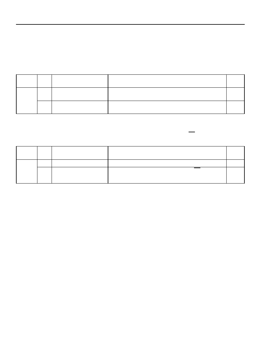
MARS2G5 P-Pro (TDAT162G52) SONET/SDH
Data Sheet
155/622/2488 Mbits/s Data Interface
August 18, 2004
452
Agere Systems Inc.
STS Receive Terminator (RXT) Block
(continued)
RXT Register Descriptions
(continued)
Provisioning
Table 427. RXT_EXPC2_PVSNR[1--24], Expected C2 Byte Provisioning (R/W, Control)
Note: The expected C2 byte is only a programming mode and changing them does not affect the validation
counters.
Table 428. RXT_TSCBB_ERRBSR[A--D], Time Slot 1--Time Slot 12 Count Block/Bit Errors Bytestream
A--D
Address
Bit
Name
Function
Reset
Default
0x8600
--
0x8617
15:8
RXT_EXPC2
[1, 3, 5, . . . , 47][7:0]
Time Slots 1, 3, 5, 7, 9, . . . , 47 Expected C2 Byte.
0
7:0
RXT_EXPC2
[2, 4, 6, . . . , 48][7:0]
Time Slots 2, 4, 6, 8, 10, . . . , 48 Expected C2 Byte.
0
Address
Bit
Name
Function
Reset
Default
0x8618,
0x8619,
0x861A,
0x861B
15:12
--
Reserved.
--
11:0
RXT_TSCBB_ERRBS
[A--D][1--12]
Time Slot 1--Time Slot 12 Count Block/Bit Errors
Bytestream A--D.
0

Data Sheet
MARS2G5 P-Pro (TDAT162G52) SONET/SDH
August 18, 2004
155/622/2488 Mbits/s Data Interface
453
Agere Systems Inc.
STS Receive Terminator (RXT) Block
(continued)
RXT Register Descriptions
(continued)
Maintenance
Table 429. RXT_TSMNTR[1--48], Time Slots 1--48 Maintenance (R/W, Control)
Interpreter Increment/Decrement PM
Table 430. RXT_PI_LSECINCR[A--D], Pointer Interpreter Last Second Increments Bytestream A--D (RO)
Table 431. RXT_PI_LSECDECR[A--D], Pointer Interpreter Last Second Decrements Bytestream A--D (RO)
Address
Bit
Name
Function
Reset
Default
0x8690
--
0x86BF
15:3
--
Reserved.
0
2:0
RXT_TSSF_TH
[1--48][2:0]
Time Slot 1--Time Slot 48 Signal Fail Threshold
Select. This value sets the signal fail threshold for the
respective time slot.
0
Address
Bit
Name
Function
Reset
Default
0x8702,
0x8703,
0x8704,
0x8705
15:11
--
Reserved.
0
10:0
RXT_PI_LSECINC
[A--D][10:0]
Last Second Increments in Pointer Interpreter
Bytestream A--D.
0
Address
Bit
Name
Function
Reset
Default
0x8712,
0x8713,
0x8714,
0x8715
15:11
--
Reserved.
0
10:0
RXT_PI_LSECDEC
[A--D][10:0]
Last Second Decrements in Pointer Interpreter
Bytestream A--D.
0

MARS2G5 P-Pro (TDAT162G52) SONET/SDH
Data Sheet
155/622/2488 Mbits/s Data Interface
August 18, 2004
454
Agere Systems Inc.
STS Receive Terminator (RXT) Block
(continued)
RXT Register Descriptions
(continued)
Performance Monitoring
Table 432. RXT_POH_ALMPMR, Path Overhead Alarm Performance Monitoring (RO)
Address
Bit
Name
Function
Reset
Default
0x8780
15:7
--
Reserved.
0
6
RXT_1BRDI_DPM
One-Bit RDI Defect PM.
0 = Alarm has not been detected for any STS-1 in any
bytestream.
1 = Alarm has been detected for one or more STS-1s in
one or more bytestreams.
0
5
RXT_ERDI_PDPM
ERDI Payload Defect PM.
0 = Alarm has not been detected for any STS-1 in any
bytestream.
1 = Alarm has been detected for one or more STS-1s in
one or more bytestreams.
0
4
RXT_ERDI_CDPM
ERDI Connectivity Defect PM.
0 = Alarm has not been detected for any STS-1 in any
bytestream.
1 = Alarm has been detected for one or more STS-1s in
one or more bytestreams.
0
3
RXT_ERDI_SDPM
ERDI Server Defect PM.
0 = Alarm has not been detected for any STS-1 in any
bytestream.
1 = Alarm has been detected for one or more STS-1s in
one or more bytestreams.
0
2
RXT_UNEQR_ALMPM
Unequipped Received Alarm PM.
0 = Alarm has not been detected for any STS-1 in any
bytestream.
1 = Alarm has been detected for one or more STS-1s in
one or more bytestreams.
0
1
RXT_AIS_ALMPM
Alarm Indicator Signal Alarm PM.
0 = Alarm has not been detected for any STS-1 in any
bytestream.
1 = Alarm has been detected for one or more STS-1s in
one or more bytestreams.
0
0
RXT_LOP_ALMPM
Loss of Pointer Alarm PM.
0 = Alarm has not been detected for any STS-1 in any
bytestream.
1 = Alarm has been detected for one or more STS-1s in
one or more bytestreams.
0

Data Sheet
MARS2G5 P-Pro (TDAT162G52) SONET/SDH
August 18, 2004
155/622/2488 Mbits/s Data Interface
455
Agere Systems Inc.
STS Receive Terminator (RXT) Block
(continued)
RXT Register Descriptions
(continued)
Table 433. RXT_1BRDI_DPMBSR, Path Overhead One-Bit RDI Defect PM Bytestream A--D (RO)
Table 434. RXT_TS1BRDI_DPMBSR[A--D], Path Overhead Time Slots 1--12 One-Bit RDI Defect PM
Bytestream A--D (RO)
Table 435. RXT_ERDI_PDPMBSR, Path Overhead ERDI Payload Defect PM Bytestream A--D (RO)
Table 436. RXT_TSERDI_PDPMBSR[A--D], Path Overhead Time Slots 1--12 ERDI Payload Defect PM
Bytestream A--D (RO)
Address
Bit
Name
Function
Reset
Default
0x8781
15:4
--
Reserved.
0
3:0
RXT_1BRDI_DPMBS
[A--D]
One-Bit RDI Defect PM Bytestream A--D.
0 = One-bit RDI defect PM has not been detected for any
STS-1s in bytestream A--D.
1 = One-bit RDI defect PM has been detected for one or
more STS-1s in bytestream A--D.
0
Address
Bit
Name
Function
Reset
Default
0x8782,
0x8783,
0x8784,
0x8785
15:12
--
Reserved.
0
11:0
RXT_TS1BRDI_DPMBS
[A--D][1--12]
Time Slot 1--Time Slot 12 One-Bit RDI Defect PM
Bytestream A--D.
0
Address
Bit
Name
Function
Reset
Default
0x8791
15:4
--
Reserved.
0
3:0
RXT_ERDI_PDPMBS
[A--D]
ERDI Payload Defect PM Bytestream A--D.
0 = ERDI payload defect PM has not been detected for
any STS-1s in bytestream A--D.
1 = ERDI payload defect PM has been detected for one or
more STS-1s in bytestream A--D.
0
Address
Bit
Name
Function
Reset
Default
0x8792,
0x8793,
0x8794,
0x8795
15:12
--
Reserved.
0
11:0
RXT_TSERDI_PDPMBS
[A--D][1--12]
Time Slot 1--Time Slot 12 ERDI Payload Defect PM
Bytestream A--D.
0

MARS2G5 P-Pro (TDAT162G52) SONET/SDH
Data Sheet
155/622/2488 Mbits/s Data Interface
August 18, 2004
456
Agere Systems Inc.
STS Receive Terminator (RXT) Block
(continued)
RXT Register Descriptions
(continued)
Table 437. RXT_ERDI_CDPMBSR, Path Overhead ERDI Connectivity Defect PM Bytestream A--D (RO)
Table 438. RXT_TSERDI_CDPMBSR[A--D], Path Overhead Time Slots 1--12 ERDI Connectivity Defect PM
Bytestream A--D (RO)
Table 439. RXT_ERDI_SDPMBSR, Path Overhead ERDI Server Defect PM Bytestream A--D (RO)
Table 440. RXT_TSERDI_SDPMBSR[A--D], Path Overhead Time Slots 1--12 ERDI Server Defect PM
Bytestream A--D (RO)
Address
Bit
Name
Function
Reset
Default
0x87A1
15:4
--
Reserved.
0
3:0
RXT_ERDI_CDPMBS
[A--D]
ERDI Connectivity Defect PM Bytestream A--D.
0 = ERDI connectivity defect PM has not been detected
for any STS-1s in bytestream A--D.
1 = ERDI connectivity defect PM has been detected for
one or more STS-1s in bytestream A--D.
0
Address
Bit
Name
Function
Reset
Default
0x87A2,
0x87A3,
0x87A4,
0x87A5
15:12
--
Reserved.
0
11:0
RXT_TSERDI_CDPMBS
[A--D][1--12]
Time Slot 1--Time Slot 12 ERDI Connectivity Defect
PM Bytestream A--D.
0
Address
Bit
Name
Function
Reset
Default
0x87B1
15:4
--
Reserved.
0
3:0
RXT_ERDI_SDPMBS
[A--D]
ERDI Server Defect PM Bytestream A--D.
0 = ERDI server defect PM has not been detected for any
STS-1s in bytestream A--D.
1 = ERDI server defect PM has been detected for one or
more STS-1s in bytestream A--D.
0
Address
Bit
Name
Function
Reset
Default
0x87B2,
0x87B3,
0x87B4,
0x87B5
15:12
--
Reserved.
0
11:0
RXT_TSERDI_SDPMBS
[A--D][1--12]
Time Slot 1--Time Slot 12 ERDI Server Defect PM
Bytestream A--D.
0

Data Sheet
MARS2G5 P-Pro (TDAT162G52) SONET/SDH
August 18, 2004
155/622/2488 Mbits/s Data Interface
457
Agere Systems Inc.
STS Receive Terminator (RXT) Block
(continued)
RXT Register Descriptions
(continued)
Table 441. RXT_UNEQR_PMBSR, Path Overhead Unequipped Received PM Bytestream A--D (RO)
Table 442. RXT_TSUNEQR_PMBSR[A--D], Path Overhead Time Slots 1--12 Unequipped Received PM
Bytestream A--D (RO)
Table 443. RXT_AIS_PMBSR, Path Overhead Alarm Indicator Signal PM Bytestream A--D (RO)
Table 444. RXT_TSAIS_PMBSR[A--D], Path Overhead Time Slots 1--12 Alarm Indicator Signal PM
Bytestream A--D (RO)
Address
Bit
Name
Function
Reset
Default
0x87C1
15:4
--
Reserved.
0
3:0
RXT_UNEQR_PMBS
[A--D]
Unequipped Received PM Bytestream A--D.
0 = Unequipped received PM has not been detected for
any STS-1s in bytestream A--D.
1 = Unequipped received PM has been detected for one
or more STS-1s in bytestream A--D.
0
Address
Bit
Name
Function
Reset
Default
0x87C2,
0x87C3,
0x87C4,
0x87C5
15:12
--
Reserved.
0
11:0
RXT_TSUNEQR_PMBS
[A--D][1--12]
Time Slot 1--Time Slot 12 Unequipped Received PM
Bytestream A--D.
0
Address
Bit
Name
Function
Reset
Default
0x87D1
15:4
--
Reserved.
0
3:0
RXT_AIS_PMBS[A--D]
Alarm Indicator Signal PM Bytestream A--D.
0 = Alarm indicator signal PM has not been detected for
any STS-1s in bytestream A--D.
1 = Alarm indicator signal PM has been detected for one
or more STS-1s in bytestream A--D.
0
Address
Bit
Name
Function
Reset
Default
0x87D2,
0x87D3,
0x87D4,
0x87D5
15:12
--
Reserved.
0
11:0
RXT_TSAIS_PMBS
[A--D][1--12]
Time Slot 1--Time Slot 12 Alarm Indicator Signal PM
Bytestream A--D.
0

MARS2G5 P-Pro (TDAT162G52) SONET/SDH
Data Sheet
155/622/2488 Mbits/s Data Interface
August 18, 2004
458
Agere Systems Inc.
STS Receive Terminator (RXT) Block
(continued)
RXT Register Descriptions
(continued)
Table 445. RXT_LOP_PMBSR, Path Overhead Loss of Pointer PM Bytestream A--D (RO)
Table 446. RXT_TSLOP_PMBSR[A--D], Path Overhead Time Slots 1--12 Loss of Pointer PM
Bytestream A--D (RO)
Table 447. RXT_LSECCVP_CPMR[1--48], Last Second CV-P Count Time Slot 1--Time Slot 48 PM (RO)
Table 448. RXT_LSECREIP_CPMR[1--48], Last Second REI-P Count Time Slot 1--Time Slot 48 PM (RO)
Address
Bit
Name
Function
Reset
Default
0x87E1
15:4
--
Reserved.
0
3:0
RXT_LOP_PMBSR[A--D] Loss of Pointer PM Bytestream A--D.
0 = Loss of pointer PM has not been detected for any
STS-1s in bytestream A--D.
1 = Loss of pointer PM has been detected for one or more
STS-1s in bytestream A--D.
0
Address
Bit
Name
Function
Reset
Default
0x87E2,
0x87E3,
0x87E4,
0x87E5
15:12
--
Reserved.
0
11:0
RXT_TSLOP_PMBS
[A--D][1--12]
Time Slot 1--Time Slot 12 Loss of Pointer PM
Bytestream A--D.
0
Address
Bit
Name
Function
Reset
Default
0x8800
--
0x882F
15:0
RXT_LSECCVP_CPM
[1--48][15:0]
Time Slot 1--Time Slot 48 CV Count PM.
0
Address
Bit
Name
Function
Reset
Default
0x8880
--
0x88AF
15:0
RXT_LSECREIP_CPM
[1--48][15:0]
Time Slot 1--Time Slot 48 REI Count PM.
0

Data Sheet
MARS2G5 P-Pro (TDAT162G52) SONET/SDH
August 18, 2004
155/622/2488 Mbits/s Data Interface
459
Agere Systems Inc.
STS Receive Terminator (RXT) Block
(continued)
RXT Register Descriptions
(continued)
RDI, C2, and PDI Status
Table 449. RXT_TSRDIPR[1--48], Time Slots 1--48 Path RDI Status (RO)
Table 450. RXT_TSC2R[1--24], Time Slots 1--48 Path C2 Status (RO)
Table 451. RXT_TSPDIR[1--24], Time Slots 1--48 Path PDI Status (RO)
Address
Bit
Name
Function
Reset
Default
0x8900
--
0x892F
15:3
--
Reserved.
0
2:0
RXT_TS_RRDI
[1--48][2:0]
Time Slot 1--Time Slot 48 Received RDI Code.
0
Address
Bit
Name
Function
Reset
Default
0x8930
--
0x8947
15:8
RXT_TSRC2
[1, 3, . . . , 47][7:0]
Time Slots 1, 3, 5, 7, . . . , 47 Received C2 Byte.
0x13
7:0
RXT_TSRC2
[2, 4, . . . , 48][7:0]
Time Slots 2, 4, 6, 8, . . . , 48 Received C2 Byte.
0x13
Address
Bit
Name
Function
Reset
Default
0x8960
--
0x8977
15:8
RXT_TSRPDI
[1, 3, . . . , 47][7:0]
Time Slots 1, 3, 5, 7, . . . , 47 Received PDI Byte.
0
7:0
RXT_TSRPDI
[2, 4, . . . , 48][7:0]
Time Slots 2, 4, 6, 8, . . . , 48 Received PDI Byte.
0
MARS2G5 P-Pro (TDAT162G52) SONET/SDH
Data Sheet
155/622/2488 Mbits/s Data Interface
August 18, 2004
460
Agere Systems Inc.
STS Receive Terminator (RXT) Block
(continued)
RXT Register Map
Table 452. RXT Register Map
Note: Shading denotes reserved bits.
Addr
Symbol
Bit 15
Bit 14
Bit 13
Bit 12
Bit 11
Bit 10
Bit 9
Bit 8
Bit 7
Bit 6
Bit 5
Bit 4
Bit 3
Bit 2
Bit 1
Bit 0
Version Control (RO)
0x8000
RXT_IDR
RXT_ID[15:0]
0x8001
RXT_CORWR
RXT_
CORW
0x8002
--
0x800E
--
Interrupts
0x800F
RXT_POH_ALMBNR1
RXT_PDI_
ALMDBN
RXT_PDI_
ALMBN
RXT_
J1ACCMP
_ALMBN
0x8010
RXT_POH_ALMBNR2
RXT_RDI_
ALMDBN
RXT_PLM
_ALMDBN
RXT_
UNEQR_
ALMDBN
RXT_AIS_
ALMDBN
RXT_LOP
_ALMDBN
RXT_
J1MM_
ALMBN
RXT_
J1VLD_
ALMBN
RXT_
USCNCT_
ALMBN
RXT_
CNCTMM
_ALMBN
RXT_SF_
ALMBN
RXT_RDI_
ALMBN
RXT_PLM
_ALMBN
RXT_
UNEQR_
ALMBN
RXT_AIS_
ALMBN
RXT_LOP
_ALMBN
0x8011
--
0x8030
--
0x8031
RXT_SF_ALMBNBSR
Signal Fail Binning
RXT_SF_ALMBNBS[A--D]
0x8032
RXT_TSSF_ALMBSRA
Signal Fail Alarm per STS-1 Bytestream A
RXT_TSSF_ALMBSA[1--12]
0x8033
RXT_TSSF_ALMBSRB
Signal Fail Alarm per STS-1 Bytestream B
RXT_TSSF_ALMBSB[1--12]
0x8034
RXT_TSSF_ALMBSRC
Signal Fail Alarm per STS-1 Bytestream C
RXT_TSSF_ALMBSC[1--12]
0x8035
RXT_TSSF_ALMBSRD
Signal Fail Alarm per STS-1 Bytestream D
RXT_TSSF_ALMBSD[1--12]
0x8036
--
0x8040
--
0x8041
RXT_RDI_ALMBNBSR
Remote Defect Indicator Alarm Binning
RXT_RDI_ALMBNBS[A--D]
0x8042
RXT_TSRDI_ALMBSRA
Remote Defect Indicator Alarm per STS-1 Bytestream A
RXT_TSRDI_ALMBSA[1--12]
0x8043
RXT_TSRDI_ALMBSRB
Remote Defect Indicator Alarm per STS-1 Bytestream B
RXT_TSRDI_ALMBSB[1--12]
0x8044
RXT_TSRDI_ALMBSRC
Remote Defect Indicator Alarm per STS-1 Bytestream C
RXT_TSRDI_ALMBSC[1--12]
0x8045
RXT_TSRDI_ALMBSRD
Remote Defect Indicator Alarm per STS-1 Bytestream D
RXT_TSRDI_ALMBSD[1--12]
0x8046
--
0x8050
--

Data Sheet
MARS2G5 P-Pro (TDAT162G52) SONET/SDH
August 18, 2004
155/622/2488 Mbits/s Data Interface
461
Agere Systems Inc.
STS Receive Terminator (RXT) Block
(continued)
RXT Register Map
(continued)
Table 452. RXT Register Map (continued)
Note: Shading denotes reserved bits.
Addr
Symbol
Bit 15
Bit 14
Bit 13
Bit 12
Bit 11
Bit 10
Bit 9
Bit 8
Bit 7
Bit 6
Bit 5
Bit 4
Bit 3
Bit 2
Bit 1
Bit 0
0x8051
RXT_PLM_ALMBNBSR
Payload Label Mismatch Alarm Binning
RXT_PLM_ALMBNBS[A--D]
0x8052
RXT_TSPLM_ALMBSRA
Payload Label Mismatch Alarm per STS-1 Bytestream A
RXT_TSPLM_ALMBSA[1--12]
0x8053
RXT_TSPLM_ALMBSRB
Payload Label Mismatch Alarm per STS-1 Bytestream B
RXT_TSPLM_ALMBSB[1--12]
0x8054
RXT_TSPLM_ALMBSRC
Payload Label Mismatch Alarm per STS-1 Bytestream C
RXT_TSPLM_ALMBSC[1--12]
0x8055
RXT_TSPLM_ALMBSRD
Payload Label Mismatch Alarm per STS-1 Bytestream D
RXT_TSPLM_ALMBSD[1--12]
0x8056
--
0x8060
--
0x8061
RXT_UNEQR_ALMBNBSR
Unequipped Received Alarm Binning
RXT_UNEQR_ALMBNBS[A--D]
0x8062
RXT_TSUNEQR_ALMBSRA
Unequipped Received Alarm per STS-1 Bytestream A
RXT_TSUNEQR_ALMBSA[1--12]
0x8063
RXT_TSUNEQR_ALMBSRB
Unequipped Received Alarm per STS-1 Bytestream B
RXT_TSUNEQR_ALMBSB[1--12]
0x8064
RXT_TSUNEQR_ALMBSRC
Unequipped Received Alarm per STS-1 Bytestream C
RXT_TSUNEQR_ALMBSC[1--12]
0x8065
RXT_TSUNEQR_ALMBSRD
Unequipped Received Alarm per STS-1 Bytestream D
RXT_TSUNEQR_ALMBSD[1--12]
0x8066
--
0x8070
--
0x8071
RXT_AIS_ALMBNBSR
Alarm Indicator Signal Alarm Binning
RXT_AIS_ALMBNBS[A--D]
0x8072
RXT_TSAIS_ALMBSRA
Alarm Indicator Signal Alarm per STS-1 Bytestream A
RXT_TSAIS_ALMBSA[1--12]
0x8073
RXT_TSAIS_ALMBSRB
Alarm Indicator Signal Alarm per STS-1 Bytestream B
RXT_TSAIS_ALMBSB[1--12]
0x8074
RXT_TSAIS_ALMBSRC
Alarm Indicator Signal Alarm per STS-1 Bytestream C
RXT_TSAIS_ALMBSC[1--12]
0x8075
RXT_TSAIS_ALMBSRD
Alarm Indicator Signal Alarm per STS-1 Bytestream D
RXT_TSAIS_ALMBSD[1--12]
0x8076
--
0x8080
--
MARS2G5 P-Pro (TDAT162G52) SONET/SDH
Data Sheet
155/622/2488 Mbits/s Data Interface
August 18, 2004
462
Agere Systems Inc.
STS Receive Terminator (RXT) Block
(continued)
RXT Register Map
(continued)
Table 452. RXT Register Map (continued)
Note: Shading denotes reserved bits.
Addr
Symbol
Bit 15
Bit 14
Bit 13
Bit 12
Bit 11
Bit 10
Bit 9
Bit 8
Bit 7
Bit 6
Bit 5
Bit 4
Bit 3
Bit 2
Bit 1
Bit 0
0x8081
RXT_LOP_ALMBNBSR
Loss of Pointer Alarm Binning
RXT_LOP_ALMBNBS[A--D]
0x8082
RXT_TSLOP_ALMBSRA
Loss of Pointer Alarm per STS-1 Bytestream A
RXT_TSLOP_ALMBSA[1--12]
0x8083
RXT_TSLOP_ALMBSRB
Loss of Pointer Alarm per STS-1 Bytestream B
RXT_TSLOP_ALMBSB[1--12]
0x8084
RXT_TSLOP_ALMBSRC
Loss of Pointer Alarm per STS-1 Bytestream C
RXT_TSLOP_ALMBSC[1--12]
0x8085
RXT_TSLOP_ALMBSRD
Loss of Pointer Alarm per STS-1 Bytestream D
RXT_TSLOP_ALMBSD[1--12]
0x8086
--
0x8090
--
0x8091
RXT_CNCTMM_ALMBNBSR
Concatenation Map Mismatch Alarm Binning
RXT_CNCTMM_ALMBNBS[A--D]
0x8092
--
0x80A0
--
0x80A1
RXT_USCNCTM_ALMBNBSR
Unsupported Concatenation Map Alarm Binning
RXT_USCNCTM_ALMBNBS[A--D]
0x80A2
--
0x80C0
--
0x80C1
RXT_J1NVLDMSG_
ALMBNBSR
J1 New Validated Message Alarm Binning
RXT_J1NVLDMSG_ALMBNBS[A--D]
0x80C2
--
0x80D0
--
0x80D1
RXT_J1MSGMM_ALMBNBSR
J1 Message Mismatch Alarm Binning
RXT_J1MSGMM_ALMBNBS[A--D]
0x80D2
--
0x8100
--
Data Sheet
MARS2G5 P-Pro (TDAT162G52) SONET/SDH
August 18, 2004
155/622/2488 Mbits/s Data Interface
463
Agere Systems Inc.
STS Receive Terminator (RXT) Block
(continued)
RXT Register Map
(continued)
Table 452. RXT Register Map (continued)
Note: Shading denotes reserved bits.
Addr
Symbol
Bit 15
Bit 14
Bit 13
Bit 12
Bit 11
Bit 10
Bit 9
Bit 8
Bit 7
Bit 6
Bit 5
Bit 4
Bit 3
Bit 2
Bit 1
Bit 0
0x8101
RXT_PDI_ALMBNBSR
Payload Defect Indicator Alarm Binning
RXT_PDI_ALMBNBS[A--D]
0x8102
RXT_TSPDI_ALMBSRA
Payload Defect Indicator Alarm per STS-1 Bytestream A
RXT_TSPDI_ALMBSA[1--12]
0x8103
RXT_TSPDI_ALMBSRB
Payload Defect Indicator Alarm per STS-1 Bytestream B
RXT_TSPDI_ALMBSB[1--12]
0x8104
RXT_TSPDI_ALMBSRC
Payload Defect Indicator Alarm per STS-1 Bytestream C
RXT_TSPDI_ALMBSC[1--12]
0x8105
RXT_TSPDI_ALMBSRD
Payload Defect Indicator Alarm per STS-1 Bytestream D
RXT_TSPDI_ALMBSD[1--12]
0x8106
--
0x8110
--
0x8111
RXT_RDI_ALMDBNBSR
Remote Defect Indicator Alarm Delta Binning
RXT_RDI_ALMDBNBS[A--D]
0x8112
RXT_TSRDI_ALMDBSRA
Remote Defect Indicator Alarm Delta per STS-1 Bytestream A
RXT_TSRDI_ALMDBSA[1--12]
0x8113
RXT_TSRDI_ALMDBSRB
Remote Defect Indicator Alarm Delta per STS-1 Bytestream B
RXT_TSRDI_ALMDBSB[1--12]
0x8114
RXT_TSRDI_ALMDBSRC
Remote Defect Indicator Alarm Delta per STS-1 Bytestream C
RXT_TSRDI_ALMDBSC[1--12]
0x8115
RXT_TSRDI_ALMDBSRD
Remote Defect Indicator Alarm Delta per STS-1 Bytestream D
RXT_TSRDI_ALMDBSD[1--12]
0x8116
--
0x8120
--
0x8121
RXT_PLM_ALMDBNBSR
Payload Label Mismatch Alarm Delta Binning
RXT_PLM_ALMDBNBS[A--D]
0x8122
RXT_TSPLM_ALMDBSRA
Payload Label Mismatch Alarm Delta per STS-1 Bytestream A
RXT_TSPLM_ALMDBSA[1--12]
0x8123
RXT_TSPLM_ALMDBSRB
Payload Label Mismatch Alarm Delta per STS-1 Bytestream B
RXT_TSPLM_ALMDBSB[1--12]
0x8124
RXT_TSPLM_ALMDBSRC
Payload Label Mismatch Alarm Delta per STS-1 Bytestream C
RXT_TSPLM_ALMDBSC[1--12]
0x8125
RXT_TSPLM_ALMDBSRD
Payload Label Mismatch Alarm Delta per STS-1 Bytestream D
RXT_TSPLM_ALMDBSD[1--12]
0x8126
--
0x8130
--

MARS2G5 P-Pro (TDAT162G52) SONET/SDH
Data Sheet
155/622/2488 Mbits/s Data Interface
August 18, 2004
464
Agere Systems Inc.
STS Receive Terminator (RXT) Block
(continued)
RXT Register Map
(continued)
Table 452. RXT Register Map (continued)
Note: Shading denotes reserved bits.
Addr
Symbol
Bit 15
Bit 14
Bit 13
Bit 12
Bit 11
Bit 10
Bit 9
Bit 8
Bit 7
Bit 6
Bit 5
Bit 4
Bit 3
Bit 2
Bit 1
Bit 0
0x8131
RXT_UNEQR_ALMDBNBSR
Unequipped Received Alarm Delta Binning
RXT_UNEQR_ALMDBNBS[A--D]
0x8132
RXT_TSUNEQR_ALMDBSRA
Unequipped Received Alarm Delta per STS-1 Bytestream A
RXT_TSUNEQR_ALMDBSA[1--12]
0x8133
RXT_TSUNEQR_ALMDBSRB
Unequipped Received Alarm Delta per STS-1 Bytestream B
RXT_TSUNEQR_ALMDBSB[1--12]
0x8134
RXT_TSUNEQR_ALMDBSRC
Unequipped Received Alarm Delta per STS-1 Bytestream C
RXT_TSUNEQR_ALMDBSC[1--12]
0x8135
RXT_TSUNEQR_ALMDBSRD
Unequipped Received Alarm Delta per STS-1 Bytestream D
RXT_TSUNEQR_ALMDBSD[1--12]
0x8136
--
0x8140
--
0x8141
RXT_AIS_ALMDBNBSR
Alarm Indicator Signal Alarm Delta Binning
RXT_AIS_ALMDBNBS[A--D]
0x8142
RXT_TSAIS_ALMDBSRA
Alarm Indicator Signal Alarm Delta per STS-1 Bytestream A
RXT_TSAIS_ALMDBSA[1--12]
0x8143
RXT_TSAIS_ALMDBSRB
Alarm Indicator Signal Alarm Delta per STS-1 Bytestream B
RXT_TSAIS_ALMDBSB[1--12]
0x8144
RXT_TSAIS_ALMDBSRC
Alarm Indicator Signal Alarm Delta per STS-1 Bytestream C
RXT_TSAIS_ALMDBSC[1--12]
0x8145
RXT_TSAIS_ALMDBSRD
Alarm Indicator Signal Alarm Delta per STS-1 Bytestream D
RXT_TSAIS_ALMDBSD[1--12]
0x8146
--
0x8150
--
0x8151
RXT_LOP_ALMDBNBSR
Loss of Pointer Alarm Delta Binning
RXT_LOP_ALMDBNBS[A--D]
0x8152
RXT_TSLOP_ALMDBSRA
Loss of Pointer Alarm Delta per STS-1 Bytestream A
RXT_TSLOP_ALMDBSA[1--12]
0x8153
RXT_TSLOP_ALMDBSRB
Loss of Pointer Alarm Delta per STS-1 Bytestream B
RXT_TSLOP_ALMDBSB[1--12]
0x8154
RXT_TSLOP_ALMDBSRC
Loss of Pointer Alarm Delta per STS-1 Bytestream C
RXT_TSLOP_ALMDBSC[1--12]
0x8155
RXT_TSLOP_ALMDBSRD
Loss of Pointer Alarm Delta per STS-1 Bytestream D
RXT_TSLOP_ALMDBSD[1--12]
0x8156
--
0x815F
--
Data Sheet
MARS2G5 P-Pro (TDAT162G52) SONET/SDH
August 18, 2004
155/622/2488 Mbits/s Data Interface
465
Agere Systems Inc.
STS Receive Terminator (RXT) Block
(continued)
RXT Register Map
(continued)
Table 452. RXT Register Map (continued)
Note: Shading denotes reserved bits.
Addr
Symbol
Bit 15
Bit 14
Bit 13
Bit 12
Bit 11
Bit 10
Bit 9
Bit 8
Bit 7
Bit 6
Bit 5
Bit 4
Bit 3
Bit 2
Bit 1
Bit 0
0x8160
RXT_PTRACCMPIR
RXT_J1BF
ACCMPI
0x8161
--
0x8170
--
0x8171
RXT_PDI_ALMDBNBSR
PDI Alarm Delta Binning
RXT_PDI_ALMDBNBS[A--D]
0x8172
RXT_TSPDI_ALMDBSRA
PDI Alarm Delta per STS-1 Bytestream A
RXT_TSPDI_ALMDBSA[1--12]
0x8173
RXT_TSPDI_ALMDBSRB
PDI Alarm Delta per STS-1 Bytestream B
RXT_TSPDI_ALMDBSB[1--12]
0x8174
RXT_TSPDI_ALMDBSRC
PDI Alarm Delta per STS-1 Bytestream C
RXT_TSPDI_ALMDBSC[1--12]
0x8175
RXT_TSPDI_ALMDBSRD
PDI Alarm Delta per STS-1 Bytestream D
RXT_TSPDI_ALMDBSD[1--12]
0x8176
--
0x820E
--

MARS2G5 P-Pro (TDAT162G52) SONET/SDH
Data Sheet
155/622/2488 Mbits/s Data Interface
August 18, 2004
466
Agere Systems Inc.
STS Receive Terminator (RXT) Block
(continued)
RXT Register Map
(continued)
Table 452. RXT Register Map (continued)
Note: Shading denotes reserved bits.
Addr
Symbol
Bit 15
Bit 14
Bit 13
Bit 12
Bit 11
Bit 10
Bit 9
Bit 8
Bit 7
Bit 6
Bit 5
Bit 4
Bit 3
Bit 2
Bit 1
Bit 0
Masks
0x820F
RXT_POH_ALMBNMR1
RXT_PDI_
ALM-
DBNM
RXT_PDI_
ALMBNM
RXT_
J1ACCMP
_ALMBNM
0x8210
RXT_POH_ALMBNMR2
RXT_RDI_
ALM-
DBNM
RXT_PLM
_ALMDBN
M
RXT_UNE
QR_ALMD
BNM
RXT_AIS_
ALM-
DBNM
RXT_LOP
_ALMDBN
M
RXT_J1M
M_ALMBN
M
RXT_J1VL
D_ALMBN
M
RXT_USC
NCT_ALM
BNM
RXT_CNC
TMM_ALM
BNM
RXT_SF_
ALMBNM
RXT_RDI_
ALMBNM
RXT_PLM
_ALMBNM
RXT_UNE
QR_ALMB
NM
RXT_AIS_
ALMBNM
RXT_LOP
_ALMBNM
0x8211
--
0x8220
--
0x8221
RXT_SF_ALMBNMBSR
Signal Fail Alarm Binning Mask
RXT_SF_ALMBNMBS[A--D]
0x8222
RXT_TSSF_ALMMBSRA
Signal Fail Alarm Mask per STS-1 Bytestream A
RXT_TSSF_ALMMBSA[1--12]
0x8223
RXT_TSSF_ALMMBSRB
Signal Fail Alarm Mask per STS-1 Bytestream B
RXT_TSSF_ALMMBSB[1--12]
0x8224
RXT_TSSF_ALMMBSRC
Signal Fail Alarm Mask per STS-1 Bytestream C
RXT_TSSF_ALMMBSC[1--12]
0x8225
RXT_TSSF_ALMMBSRD
Signal FAil Alarm Mask per STS-1 Bytestream D
RXT_TSSF_ALMMBSD[1--12]
0x8226
--
0x8230
--
0x8231
RXT_RDI_ALMBNMBSR
Remote Defect Indicator Alarm Binning Mask
RXT_RDI_ALMBNMBS[A--D]
0x8232
RXT_TSRDI_ALMMBSRA
Remote Defect Indicator Alarm Mask per STS-1 Bytestream A
RXT_TSRDI_ALMMBSA[1--12]
0x8233
RXT_TSRDI_ALMMBSRB
Remote Defect Indicator Alarm Mask per STS-1 Bytestream B
RXT_TSRDI_ALMMBSB[1--12]
0x8234
RXT_TSRDI_ALMMBSRC
Remote Defect Indicator Alarm Mask per STS-1 Bytestream C
RXT_TSRDI_ALMMBSC[1--12]
0x8235
RXT_TSRDI_ALMMBSRD
Remote Defect Indicator Alarm Mask per STS-1 Bytestream D
RXT_TSRDI_ALMMBSD[1--12]
0x8236
--
0x8240
--

Data Sheet
MARS2G5 P-Pro (TDAT162G52) SONET/SDH
August 18, 2004
155/622/2488 Mbits/s Data Interface
467
Agere Systems Inc.
STS Receive Terminator (RXT) Block
(continued)
RXT Register Map
(continued)
Table 452. RXT Register Map (continued)
Note: Shading denotes reserved bits.
Addr
Symbol
Bit 15
Bit 14
Bit 13
Bit 12
Bit 11
Bit 10
Bit 9
Bit 8
Bit 7
Bit 6
Bit 5
Bit 4
Bit 3
Bit 2
Bit 1
Bit 0
0x8241
RXT_PLM_ALMBNMBSR
Payload Label Mismatch Alarm Binning Mask
RXT_PLM_ALMBNMBS[A--D]
0x8242
RXT_TSPLM_ALMMBSRA
Payload Label Mismatch Alarm Mask per STS-1 Bytestream A
RXT_TSPLM_ALMMBSA[1--12]
0x8243
RXT_TSPLM_ALMMBSRB
Payload Label Mismatch Alarm Mask per STS-1 Bytestream B
RXT_TSPLM_ALMMBSB[1--12]
0x8244
RXT_TSPLM_ALMMBSRC
Payload Label Mismatch Alarm Mask per STS-1 Bytestream C
RXT_TSPLM_ALMMBSC[1--12]
0x8245
RXT_TSPLM_ALMMBSRD
Payload Label Mismatch Alarm Mask per STS-1 Bytestream D
RXT_TSPLM_ALMMBSD[1--12]
0x8246
--
0x8250
--
0x8251
RXT_UNEQR_ALMBNMBSR
Unequipped Received Alarm Binning Mask
RXT_UNEQR_ALMBNMBS[A--D]
0x8252
RXT_TSUNEQR_ALMMBSRA
Unequipped Received Alarm Mask per STS-1 Bytestream A
RXT_TSUNEQR_ALMMBSA[1--12]
0x8253
RXT_TSUNEQR_ALMMBSB
Unequipped Received Alarm Mask per STS-1 Bytestream B
RXT_TSUNEQR_ALMMBSB[1--12]
0x8254
RXT_TSUNEQR_ALMMBSC
Unequipped Received Alarm Mask per STS-1 Bytestream C
RXT_TSUNEQR_ALMMBSC[1--12]
0x8255
RXT_TSUNEQR_ALMMBSD
Unequipped Received Alarm Mask per STS-1 Bytestream D
RXT_TSUNEQR_ALMMBSD[1--12]
0x8256
--
0x8260
--
0x8261
RXT_AIS_ALMBNMBSR
Alarm Indicator Signal Alarm Binning Mask
RXT_AIS_ALMBNMBS[A--D]
0x8262
RXT_TSAIS_ALMMBSRA
Alarm Indicator Signal Alarm Mask per STS-1 Bytestream A
RXT_TSAIS_ALMMBSA[1--12]
0x8263
RXT_TSAIS_ALMMBSRB
Alarm Indicator Signal Alarm Mask per STS-1 Bytestream B
RXT_TSAIS_ALMMBSB[1--12]
0x8264
RXT_TSAIS_ALMMBSRC
Alarm Indicator Signal Alarm Mask per STS-1 Bytestream C
RXT_TSAIS_ALMMBSC[1--12]
0x8265
RXT_TSAIS_ALMMBSRD
Alarm Indicator Signal Alarm Mask per STS-1 Bytestream D
RXT_TSAIS_ALMMBSD[1--12]
0x8266
--
0x8270
--
MARS2G5 P-Pro (TDAT162G52) SONET/SDH
Data Sheet
155/622/2488 Mbits/s Data Interface
August 18, 2004
468
Agere Systems Inc.
STS Receive Terminator (RXT) Block
(continued)
RXT Register Map
(continued)
Table 452. RXT Register Map (continued)
Note: Shading denotes reserved bits.
Addr
Symbol
Bit 15
Bit 14
Bit 13
Bit 12
Bit 11
Bit 10
Bit 9
Bit 8
Bit 7
Bit 6
Bit 5
Bit 4
Bit 3
Bit 2
Bit 1
Bit 0
0x8271
RXT_LOP_ALMBNMBSR
Loss of Pointer Alarm Binning Mask
RXT_LOP_ALMBNMBS[A--D]
0x8272
RXT_TSLOP_ALMMBSRA
Loss of Pointer Alarm Mask per STS-1 Bytestream A
RXT_TSLOP_ALMMBSA[1--12]
0x8273
RXT_TSLOP_ALMMBSRB
Loss of Pointer Alarm Mask per STS-1 Bytestream B
RXT_TSLOP_ALMMBSB[1--12]
0x8274
RXT_TSLOP_ALMMBSRC
Loss of Pointer Alarm Mask per STS-1 Bytestream C
RXT_TSLOP_ALMMBSC[1--12]
0x8275
RXT_TSLOP_ALMMBSRD
Loss of Pointer Alarm Mask per STS-1 Bytestream D
RXT_TSLOP_ALMMBSD[1--12]
0x8276
--
0x8277
RXT_CNCTMM_ALMMBSR
Concatenation Map Mismatch Alarm Mask
RXT_CNCTMM_ALMMBS[A--D]
0x8278
--
0x8279
RXT_USCNCTM_ALMMBSR
Unsupported Concatenation Map Alarm Mask
RXT_USCNCTM_ALMMBS[A--D]
0x827A
--
0x827B
RXT_J1NVLDMSG_ALMMBSR
J1 New Validated Message Alarm Mask
RXT_J1NVLDMSG_ALMMBS[A--D]
0x827C
--
0x827D
RXT_J1MSGMM_ALMMBSR
J1 Message Mismatch Alarm Mask
RXT_J1MSGMM_ALMMBS[A--D]
0x827E
--
0x8280
--
0x8281
RXT_PDI_ALMBNMBSR
Payload Defect Indicator Alarm Binning Mask
RXT_PDI_ALMBNMBS[A--D]
0x8282
RXT_TSPDI_ALMMBSRA
Payload Defect Indicator Alarm Mask per STS-1 Bytestream A
RXT_TSPDI_ALMMBSA[1--12]
0x8283
RXT_TSPDI_ALMMBSRB
Payload Defect Indicator Alarm Mask per STS-1 Bytestream B
RXT_TSPDI_ALMMBSB[1--12]
0x8284
RXT_TSPDI_ALMMBSRC
Payload Defect Indicator Alarm Mask per STS-1 Bytestream C
RXT_TSPDI_ALMMBSC[1--12]
0x8285
RXT_TSPDI_ALMMBSRD
Payload Defect Indicator Alarm Mask per STS-1 Bytestream D
RXT_TSPDI_ALMMBSD[1--12]
0x8286
--
0x8290
--
Data Sheet
MARS2G5 P-Pro (TDAT162G52) SONET/SDH
August 18, 2004
155/622/2488 Mbits/s Data Interface
469
Agere Systems Inc.
STS Receive Terminator (RXT) Block
(continued)
RXT Register Map
(continued)
Table 452. RXT Register Map (continued)
Note: Shading denotes reserved bits.
Addr
Symbol
Bit 15
Bit 14
Bit 13
Bit 12
Bit 11
Bit 10
Bit 9
Bit 8
Bit 7
Bit 6
Bit 5
Bit 4
Bit 3
Bit 2
Bit 1
Bit 0
0x8291
RXT_RDI_ALMDBNMBSR
Remote Defect Indicator Alarm Delta Binning Mask
RXT_RDI_ALMBNDMBS[A--D]
0x8292
RXT_TSRDI_ALMDMBSRA
Remote Defect Indicator Alarm Delta Mask per STS-1 Bytestream A
RXT_TSRDI_ALMDMBSA[1--12]
0x8293
RXT_TSRDI_ALMDMBSRB
Remote Defect Indicator Alarm Delta Mask per STS-1 Bytestream B
RXT_TSRDI_ALMDMBSB[1--12]
0x8294
RXT_TSRDI_ALMDMBSRC
Remote Defect Indicator Alarm Delta Mask per STS-1 Bytestream C
RXT_TSRDI_ALMDMBSC[1--12]
0x8295
RXT_TSRDI_ALMDMBSRD
Remote Defect Indicator Alarm Delta Mask per STS-1 Bytestream D
RXT_TSRDI_ALMDMBSD[1--12]
0x8296
--
0x82A0
--
0x82A1
RXT_PLM_ALMDBNMBSR
Payload Label Mismatch Alarm Delta Binning Mask
RXT_PLM_ALMDBNMBS[A--D]
0x82A2
RXT_TSPLM_ALMDMBSRA
Payload Label Mismatch Alarm Delta Mask per STS-1 Bytestream A
RXT_TSPLM_ALMDMBSA[1--12]
0x82A3
RXT_TSPLM_ALMDMBSRB
Payload Label Mismatch Alarm Delta Mask per STS-1 Bytestream B
RXT_TSPLM_ALMDMBSB[1--12]
0x82A4
RXT_TSPLM_ALMDMBSRC
Payload Label Mismatch Alarm Delta Mask per STS-1 Bytestream C
RXT_TSPLM_ALMDMBSC[1--12]
0x82A5
RXT_TSPLM_ALMDMBSRD
Payload Label Mismatch Alarm Delta Mask per STS-1 Bytestream D
RXT_TSPLM_ALMDMBSD[1--12]
0x82A6
--0x82B
--
0x82B1
RXT_UNEQR_ALMDBNMBSR
Unequipped Received Alarm Delta Binning Mask
RXT_UNEQR_ALMDBNMBS[A--D]
0x82B2
RXT_TSUNEQR_ALMDMBSRA
Unequipped Received Alarm Delta Mask per STS-1 Bytestream A
RXT_TSUNEQR_ALMDMBSA[1--12]
0x82B3
RXT_TSUNEQR_ALMDMBSRB
Unequipped Received Alarm Delta Mask per STS-1 Bytestream B
RXT_TSUNEQR_ALMDMBSB[1--12]
0x82B4
RXT_TSUNEQR_ALMDMBSRC
Unequipped Received Alarm Delta Mask per STS-1 Bytestream C
RXT_TSUNEQR_ALMDMBSC[1--12]
0x82B5
RXT_TSUNEQR_ALMDMBSRD
Unequipped Received Alarm Delta Mask per STS-1 Bytestream D
RXT_TSUNEQR_ALMDMBSD[1--12]
0x82B6
--
0x82C0
--
MARS2G5 P-Pro (TDAT162G52) SONET/SDH
Data Sheet
155/622/2488 Mbits/s Data Interface
August 18, 2004
470
Agere Systems Inc.
STS Receive Terminator (RXT) Block
(continued)
RXT Register Map
(continued)
Table 452. RXT Register Map (continued)
Note: Shading denotes reserved bits.
Addr
Symbol
Bit 15
Bit 14
Bit 13
Bit 12
Bit 11
Bit 10
Bit 9
Bit 8
Bit 7
Bit 6
Bit 5
Bit 4
Bit 3
Bit 2
Bit 1
Bit 0
0x82C1
RXT_AIS_ALMDBNMBSR
Alarm Indicator Signal Alarm Delta Binning Mask
RXT_AIS_ALMDBNMBS[A--D]
0x82C2
RXT_TSAIS_ALMDMBSRA
Alarm Indicator Signal Alarm Delta Mask per STS-1 Bytestream A
RXT_TSAIS_ALMDMBSA[1--12]
0x82C3
RXT_TSAIS_ALMDMBSRB
Alarm Indicator Signal Alarm Delta Mask per STS-1 Bytestream B
RXT_TSAIS_ALMDMBSB[1--12]
0x82C4
RXT_TSAIS_ALMDMBSRC
Alarm Indicator Signal Alarm Delta Mask per STS-1 Bytestream C
RXT_TSAIS_ALMDMBSC[1--12]
0x82C5
RXT_TSAIS_ALMDMBSRD
Alarm Indicator Signal Alarm Delta Mask per STS-1 Bytestream D
RXT_TSAIS_ALMDMBSD[1--12]
0x82C6
--
0x82D0
--
0x82D1
RXT_LOP_ALMDBNMBSR
Loss of Pointer Alarm Delta Binning Mask
RXT_LOP_ALMDBNMBS[A--D]
0x82D2
RXT_TSLOP_ALMDMBSRA
Loss of Pointer Alarm Delta Mask per STS-1 Bytestream A
RXT_TSLOP_ALMDMBSA[1--12]
0x82D3
RXT_TSLOP_ALMDMBSRB
Loss of Pointer Alarm Delta Mask per STS-1 Bytestream B
RXT_TSLOP_ALMDMBSB[1--12]
0x82D4
RXT_TSLOP_ALMDMBSRC
Loss of Pointer Alarm Delta Mask per STS-1 Bytestream C
RXT_TSLOP_ALMDMBSC[1--12]
0x82D5
RXT_TSLOP_ALMDMBSRD
Loss of Pointer Alarm Delta Mask per STS-1 Bytestream D
RXT_TSLOP_ALMDMBSD[1--12]
0x82D6
--
0x82DF
--
0x82E0
RXT_PTRACCMPIR
RXT_J1BFACCMPIM
0x82E1
--
0x82E8
--
Data Sheet
MARS2G5 P-Pro (TDAT162G52) SONET/SDH
August 18, 2004
155/622/2488 Mbits/s Data Interface
471
Agere Systems Inc.
STS Receive Terminator (RXT) Block
(continued)
RXT Register Map
(continued)
Table 452. RXT Register Map (continued)
Note: Shading denotes reserved bits.
Addr
Symbol
Bit 15
Bit 14
Bit 13
Bit 12
Bit 11
Bit 10
Bit 9
Bit 8
Bit 7
Bit 6
Bit 5
Bit 4
Bit 3
Bit 2
Bit 1
Bit 0
0x82E9
RXT_PDI_ALMDBNMBSR
PDI Alarm Delta Binning Mask
RXT_PDI_ALMDBNMBS[A--D]
0x82EA
RXT_TSPDI_ALMDMBSRA
PDI Alarm Delta Mask per STS-1 Bytestream A
RXT_TSPDI_ALMDMBSA[1--12]
0x82EB
RXT_TSPDI_ALMDMBSRB
PDI Alarm Delta Mask per STS-1 Bytestream B
RXT_TSPDI_ALMDMBSB[1--12]
0x82EC
RXT_TSPDI_ALMDMBSRC
PDI Alarm Delta Mask per STS-1 Bytestream C
RXT_TSPDI_ALMDMBSC[1--12]
0x82ED
RXT_TSPDI_ALMDMBSRD
PDI Alarm Delta Mask per STS-1 Bytestream D
RXT_TSPDI_ALMDMBSD[1--12]
0x82EE
--
0x82FF
--
MARS2G5 P-Pro (TDAT162G52) SONET/SDH
Data Sheet
155/622/2488 Mbits/s Data Interface
August 18, 2004
472
Agere Systems Inc.
STS Receive Terminator (RXT) Block
(continued)
RXT Register Map
(continued)
Table 452. RXT Register Map (continued)
Note: Shading denotes reserved bits.
Addr
Symbol
Bit 15
Bit 14
Bit 13
Bit 12
Bit 11
Bit 10
Bit 9
Bit 8
Bit 7
Bit 6
Bit 5
Bit 4
Bit 3
Bit 2
Bit 1
Bit 0
Path Trace
--
--
J1 Byte 1, 3, 5, . . . , 63 Path Trace Buffer
J1 Byte 0, 2, 4, . . . , 62 Path Trace Buffer
0x8300
--
0x831F
RXT_PTRBFR[1--32]
RXT_J1BYTE[1, 3, 5, . . . , 63][7:0]
RXT_J1BYTE[0, 2, 4, . . . , 62][7:0]
0x8330
RXT_PTRACCTLR1
RXT_J1TS1_CHSEL[1:0]
0x8331
RXT_PTRACCTLR2
RXT_J1BF
_MSGSEL
0x8332
RXT_PTRACCTLR3
RXT_J1BF
_ACTYP
0x8333
RXT_PTRACBGR
RXT_J1_A
CBG
0x8334
--
0x8337
--
0x8338
RXT_STS12PTRCTLR1
J1 Message Mode Select
RXT_J1MSG_MSEL[A--D]
0x8339
RXT_STS12PTRCTLR2
J1 Message Type Select
RXT_J1MSG_TYPSEL[A--D]
0x833A
--
0x833B
--
0x833C
RXT_STS12PTRCTLR3
Time Slots 1--12 Select for J1 Accumulation
RXT_TSSEL_J1A[3:0]
0x833D
RXT_STS12PTRCTLR4
RXT_TSSEL_J1B[3:0]
0x833E
RXT_STS12PTRCTLR5
RXT_TSSEL_J1C[3:0]
0x833F
RXT_STS12PTRCTLR6
RXT_TSSEL_J1D[3:0]
0x8340
--
0x837F
--
Data Sheet
MARS2G5 P-Pro (TDAT162G52) SONET/SDH
August 18, 2004
155/622/2488 Mbits/s Data Interface
473
Agere Systems Inc.
STS Receive Terminator (RXT) Block
(continued)
RXT Register Map
(continued)
Table 452. RXT Register Map (continued)
Note: Shading denotes reserved bits.
Addr
Symbol
Bit 15
Bit 14
Bit 13
Bit 12
Bit 11
Bit 10
Bit 9
Bit 8
Bit 7
Bit 6
Bit 5
Bit 4
Bit 3
Bit 2
Bit 1
Bit 0
Persistency
0x8380
--
0x8381
--
0x8382
RXT_TSRDI_ALMPSBSRA
RDI Alarm Persistency per STS-1 Bytestream A
RXT_TSRDI_ALMPSBSA[1--12]
0x8383
RXT_TSRDI_ALMPSBSRB
RDI Alarm Persistency per STS-1 Bytestream B
RXT_TSRDI_ALMPSBSB[1--12]
0x8384
RXT_TSRDI_ALMPSBSRC
RDI Alarm Persistency per STS-1 Bytestream C
RXT_TSRDI_ALMPSBSC[1--12]
0x8385
RXT_TSRDI_ALMPSBSRD
RDI Alarm Persistency per STS-1 Bytestream D
RXT_TSRDI_ALMPSBSD[1--12]
0x8386
--
0x8389
--
0x838A
RXT_TSPLM_ALMPSBSRA
Payload Label Mismatch Alarm Persistency per STS-1 Bytestream A
RXT_TSPLM_ALMPSBSA[1--12]
0x838B
RXT_TSPLM_ALMPSBSRB
Payload Label Mismatch Alarm Persistency per STS-1 Bytestream B
RXT_TSPLM_ALMPSBSB[1--12]
0x838C
RXT_TSPLM_ALMPSBSRC
Payload Label Mismatch Alarm Persistency per STS-1 Bytestream C
RXT_TSPLM_ALMPSBSC[1--12]
0x838D
RXT_TSPLM_ALMPSBSRD
Payload Label Mismatch Alarm Persistency per STS-1 Bytestream D
RXT_TSPLM_ALMPSBSD[1--12]
0x838E
--
0x8391
--
0x8392
RXT_TSPUNEQ_ALMPSBSRA
Path Unequipped Alarm Persistency per STS-1 Bytestream A
RXT_TSPUNEQ_ALMPSBSA[1--12]
0x8393
RXT_TSPUNEQ_ALMPSBSRB
Path Unequipped Alarm Persistency per STS-1 Bytestream B
RXT_TSPUNEQ_ALMPSBSB[1--12]
0x8394
RXT_TSPUNEQ_ALMPSBSR
C
Path Unequipped Alarm Persistency per STS-1 Bytestream C
RXT_TSPUNEQ_ALMPSBSC[1--12]
0x8395
RXT_TSPUNEQ_ALMPSBSR
D
Path Unequipped Alarm Persistency per STS-1 Bytestream D
RXT_TSPUNEQ_ALMPSBSD[1--12]
0x8396
--
0x8399
--

MARS2G5 P-Pro (TDAT162G52) SONET/SDH
Data Sheet
155/622/2488 Mbits/s Data Interface
August 18, 2004
474
Agere Systems Inc.
STS Receive Terminator (RXT) Block
(continued)
RXT Register Map
(continued)
Table 452. RXT Register Map (continued)
Note: Shading denotes reserved bits.
Addr
Symbol
Bit 15
Bit 14
Bit 13
Bit 12
Bit 11
Bit 10
Bit 9
Bit 8
Bit 7
Bit 6
Bit 5
Bit 4
Bit 3
Bit 2
Bit 1
Bit 0
0x839A
RXT_TSAIS_ALMPSBSRA
AIS Alarm Persistency per STS-1 Bytestream A
RXT_TSAIS_ALMPSBSA[1--12]
0x839B
RXT_TSAIS_ALMPSBSRB
AIS Alarm Persistency per STS-1 Bytestream B
RXT_TSAIS_ALMPSBSB[1--12]
0x839C
RXT_TSAIS_ALMPSBSRC
AIS Alarm Persistency per STS-1 Bytestream C
RXT_TSAIS_ALMPSBSC[1--12]
0x839D
RXT_TSAIS_ALMPSBSRD
AIS Alarm Persistency per STS-1 Bytestream D
RXT_TSAIS_ALMPSBSD[1--12]
0x839E
--
0x83A1
--
0x83A2
RXT_TSLOP_ALMPSBSRA
LOP Alarm Persistency per STS-1 Bytestream A
RXT_TSLOP_ALMPSBSA[1--12]
0x83A3
RXT_TSLOP_ALMPSBSRB
LOP Alarm Persistency per STS-1 Bytestream B
RXT_TSLOP_ALMPSBSB[1--12]
0x83A4
RXT_TSLOP_ALMPSBSRC
LOP Alarm Persistency per STS-1 Bytestream C
RXT_TSLOP_ALMPSBSC[1--12]
0x83A5
RXT_TSLOP_ALMPSBSRD
LOP Alarm Persistency per STS-1 Bytestream D
RXT_TSLOP_ALMPSBSD[1--12]
0x83A6
--
0x83A9
--
0x83AA
RXT_TSPDI_ALMPSBSRA
PDI Alarm Persistency per STS-1 Bytestream A
RXT_TSPDI_ALMPSBSA[1--12]
0x83AB
RXT_TSPDI_ALMPSBSRB
PDI Alarm Persistency per STS-1 Bytestream B
RXT_TSPDI_ALMPSBSB[1--12]
0x83AC
RXT_TSPDI_ALMPSBSRC
PDI Alarm Persistency per STS-1 Bytestream C
RXT_TSPDI_ALMPSBSC[1--12]
0x83AD
RXT_TSPDI_ALMPSBSRD
PDI Alarm Persistency per STS-1 Bytestream D
RXT_TSPDI_ALMPSBSD[1--12]
0x83AE
--
0x83BF
--

Data Sheet
MARS2G5 P-Pro (TDAT162G52) SONET/SDH
August 18, 2004
155/622/2488 Mbits/s Data Interface
475
Agere Systems Inc.
STS Receive Terminator (RXT) Block
(continued)
RXT Register Map
(continued)
Table 452. RXT Register Map (continued)
Note: Shading denotes reserved bits.
Addr
Symbol
Bit 15
Bit 14
Bit 13
Bit 12
Bit 11
Bit 10
Bit 9
Bit 8
Bit 7
Bit 6
Bit 5
Bit 4
Bit 3
Bit 2
Bit 1
Bit 0
State
0x83C0
--
0x83C1
--
0x83C2
RXT_TSRDI_STBSRA
RDI State per STS-1 Bytestream A
RXT_TSRDI_STBSA[1--12]
0x83C3
RXT_TSRDI_STBSRB
RDI State per STS-1 Bytestream B
RXT_TSRDI_STBSB[1--12]
0x83C4
RXT_TSRDI_STBSRC
RDI State per STS-1 Bytestream C
RXT_TSRDI_STBSC[1--12]
0x83C5
RXT_TSRDI_STBSRD
RDI State per STS-1 Bytestream D
RXT_TSRDI_STBSD[1--12]
0x83C6
--
0x83C9
--
0x83CA
RXT_TSPLM_STBSRA
Payload Label Mismatch State per STS-1 Bytestream A
RXT_TSPLM_STBSA[1--12]
0x83CB
RXT_TSPLM_STBSRB
Payload Label Mismatch State per STS-1 Bytestream B
RXT_TSPLM_STBSB[1--12]
0x83CC
RXT_TSPLM_STBSRC
Payload Label Mismatch State per STS-1 Bytestream C
RXT_TSPLM_STBSC[1--12]
0x83CD
RXT_TSPLM_STBSRD
Payload Label Mismatch State per STS-1 Bytestream D
RXT_TSPLM_STBSD[1--12]
0x83CE
--
0x83D1
--
0x83D2
RXT_TSPUNEQ_STBSRA
Path Unequipped State per STS-1 Bytestream A
RXT_TSPUNEQ_STBSA[1--12]
0x83D3
RXT_TSPUNEQ_STBSRB
Path Unequipped State per STS-1 Bytestream B
RXT_TSPUNEQ_STBSB[1--12]
0x83D4
RXT_TSPUNEQ_STBSRC
Path Unequipped State per STS-1 Bytestream C
RXT_TSPUNEQ_STBSC[1--12]
0x83D5
RXT_TSPUNEQ_STBSRD
Path Unequipped State per STS-1 Bytestream D
RXT_TSPUNEQ_STBSD[1--12]
0x83D6
--
0x83D9
--
MARS2G5 P-Pro (TDAT162G52) SONET/SDH
Data Sheet
155/622/2488 Mbits/s Data Interface
August 18, 2004
476
Agere Systems Inc.
STS Receive Terminator (RXT) Block
(continued)
RXT Register Map
(continued)
Table 452. RXT Register Map (continued)
Note: Shading denotes reserved bits.
Addr
Symbol
Bit 15
Bit 14
Bit 13
Bit 12
Bit 11
Bit 10
Bit 9
Bit 8
Bit 7
Bit 6
Bit 5
Bit 4
Bit 3
Bit 2
Bit 1
Bit 0
0x83DA
RXT_TSAIS_STBSRA
AIS State per STS-1 Bytestream A
RXT_TSAIS_STBSA[1--12]
0x83DB
RXT_TSAIS_STBSRB
AIS State per STS-1 Bytestream B
RXT_TSAIS_STBSB[1--12]
0x83DC
RXT_TSAIS_STBSRC
AIS State per STS-1 Bytestream C
RXT_TSAIS_STBSC[1--12]
0x83DD
RXT_TSAIS_STBSRD
AIS State per STS-1 Bytestream D
RXT_TSAIS_STBSD[1--12]
0x83DE
--
0x83E1
--
0x83E2
RXT_TSLOP_STBSRA
LOP State per STS-1 Bytestream A
RXT_TSLOP_STBSA[1--12]
0x83E3
RXT_TSLOP_STBSRB
LOP State per STS-1 Bytestream B
RXT_TSLOP_STBSB[1--12]
0x83E4
RXT_TSLOP_STBSRC
LOP State per STS-1 Bytestream C
RXT_TSLOP_STBSC[1--12]
0x83E5
RXT_TSLOP_STBSRD
LOP State per STS-1 Bytestream D
RXT_TSLOP_STBSD[1--12]
0x83E6
--
0x83E9
--
0x83EA
RXT_TSPDI_STBSRA
PDI State per STS-1 Bytestream A
RXT_TSPDI_STBSA[1--12]
0x83EB
RXT_TSPDI_STBSRB
PDI State per STS-1 Bytestream B
RXT_TSPDI_STBSB[1--12]
0x83EC
RXT_TSPDI_STBSRC
PDI State per STS-1 Bytestream C
RXT_TSPDI_STBSC[1--12]
0x83ED
RXT_TSPDI_STBSRD
LOP State per STS-1 Bytestream D
RXT_TSPDI_STBSD[1--12]
0x83EE
--
0x83FF
--
Data Sheet
MARS2G5 P-Pro (TDAT162G52) SONET/SDH
August 18, 2004
155/622/2488 Mbits/s Data Interface
477
Agere Systems Inc.
STS Receive Terminator (RXT) Block
(continued)
RXT Register Map
(continued)
Table 452. RXT Register Map (continued)
Note: Shading denotes reserved bits.
Addr
Symbol
Bit 15
Bit 14
Bit 13
Bit 12
Bit 11
Bit 10
Bit 9
Bit 8
Bit 7
Bit 6
Bit 5
Bit 4
Bit 3
Bit 2
Bit 1
Bit 0
Signal Fail
0x8400
RXT_SFWSZ_SELR1
RXT_SFWSZ_SELSET[0--7][1:0]
0x8401
RXT_SFWSZ_SELR2
RXT_SFWSZ_SELCLR[0--7][1:0]
0x8402
--
0x840F
--
0x8410
RXT_SFDR0
RXT_SFD0[8:0]
0x8411
RXT_SFDR1
RXT_SFD1[8:0]
0x8412
RXT_SFDR2
RXT_SFD2[13:0]
0x8413
RXT_SFDR3
RXT_SFD3[13:0]
0x8414
RXT_SFDR4
RXT_SFD4[13:0]
0x8415
RXT_SFDR5
RXT_SFD5[13:0]
0x8416
RXT_SFDR6
RXT_SFD6[13:0]
0x8417
RXT_SFDR7
RXT_SFD7[13:0]
0x8418
RXT_SFCLRR0
RXT_SFCLR0[8:0]
0x8419
RXT_SFCLRR1
RXT_SFCLR1[8:0]
0x841A
RXT_SFCLRR2
RXT_SFCLR2[13:0]
0x841B
RXT_SFCLRR3
RXT_SFCLR3[13:0]
0x841C
RXT_SFCLRR4
RXT_SFCLR4[13:0]
0x841D
RXT_SFCLRR5
RXT_SFCLR5[13:0]
0x841E
RXT_SFCLRR6
RXT_SFCLR6[13:0]
0x841F
RXT_SFCLRR7
RXT_SFCLR7[13:0]
0x8420
RXT_SFWSZR0
RXT_SFWSZ0[15:0]
0x8421
--
0x842F
--
0x8430
RXT_SFWSZR1
RXT_SFWSZ1[15:0]
0x8431
--
0x843F
--
0x8440
RXT_SFWSZR2
RXT_SFWSZ2[15:0]
0x8441
--
0x844F
--
0x8450
RXT_SFWSZR3
RXT_SFWSZ3[15:0]
0x8451
--
0x8501
--
MARS2G5 P-Pro (TDAT162G52) SONET/SDH
Data Sheet
155/622/2488 Mbits/s Data Interface
August 18, 2004
478
Agere Systems Inc.
STS Receive Terminator (RXT) Block
(continued)
RXT Register Map
(continued)
Table 452. RXT Register Map (continued)
Note: Shading denotes reserved bits.
Addr
Symbol
Bit 15
Bit 14
Bit 13
Bit 12
Bit 11
Bit 10
Bit 9
Bit 8
Bit 7
Bit 6
Bit 5
Bit 4
Bit 3
Bit 2
Bit 1
Bit 0
Concatenation
0x8502
RXT_ECNCTM_TSBSRA
Expected Concatenation Map Bytestream A
RXT_ECNCT_STTSBSA[1--12]
0x8503
RXT_ECNCTM_TSBSRB
Expected Concatenation Map Bytestream B
RXT_ECNCT_STTSBSB[1--12]
0x8504
RXT_ECNCTM_TSBSRC
Expected Concatenation Map Bytestream C
RXT_ECNCT_STTSBSC[1--12]
0x8505
RXT_ECNCTM_TSBSRD
Expected Concatenation Map Bytestream D
RXT_ECNCT_STTSBSD[1--12]
0x8506
--
0x8507
RXT_CNCTCPREN_TSBSRA
Software Concatenation Compare Enable Bytestream A
RXT_CNCTCPREN_TSBSA[1--12]
0x8508
RXT_CNCTCPREN_TSBSRB
Software Concatenation Compare Enable Bytestream B
RXT_CNCTCPREN_TSBSB[1--12]
0x8509
RXT_CNCTCPREN_TSBSRC
Software Concatenation Compare Enable Bytestream C
RXT_CNCTCPREN_TSBSC[1--12]
0x850A
RXT_CNCTCPREN_TSBSRD
Software Concatenation Compare Enable Bytestream D
RXT_CNCTCPREN_TSBSD[1--12]
0x850B
--
0x8511
--
0x8512
RXT_RCNCTM_TSBSRA
Received Concatenation Map Bytestream A
RXT_RCNCT_STTSBSA[1--12]
0x8513
RXT_RCNCTM_TSBSRB
Received Concatenation Map Bytestream B
RXT_RCNCT_STTSBSB[1--12]
0x8514
RXT_RCNCTM_TSBSRC
Received Concatenation Map Bytestream C
RXT_RCNCT_STTSBSC[1--12]
0x8515
RXT_RCNCTM_TSBSRD
Received Concatenation Map Bytestream D
RXT_RCNCT_STTSBSD[1--12]
0x8516
--
0x8541
--
Data Sheet
MARS2G5 P-Pro (TDAT162G52) SONET/SDH
August 18, 2004
155/622/2488 Mbits/s Data Interface
479
Agere Systems Inc.
STS Receive Terminator (RXT) Block
(continued)
RXT Register Map
(continued)
Table 452. RXT Register Map (continued)
Note: Shading denotes reserved bits.
Addr
Symbol
Bit 15
Bit 14
Bit 13
Bit 12
Bit 11
Bit 10
Bit 9
Bit 8
Bit 7
Bit 6
Bit 5
Bit 4
Bit 3
Bit 2
Bit 1
Bit 0
AIS Insert Control
0x8542
RXT_SWAIS_ISRTRA
AIS Insert Bytestream A
RXT_SWAIS_ISRTA[1--12]
0x8543
RXT_SWAIS_ISRTRB
AIS Insert Bytestream B
RXT_SWAIS_ISRTB[1--12]
0x8544
RXT_SWAIS_ISRTRC
AIS Insert Bytestream C
RXT_SWAIS_ISRTC[1--12]
0x8545
RXT_SWAIS_ISRTRD
AIS Insert Bytestream D
RXT_SWAIS_ISRTD[1--12]
0x8546
--
0x8547
RXT_AISONUNEQ_PRA
AIS Insert on UNEQ Control Bytestream A
RXT_AISONUNEQ_PA[1--12]
0x8548
RXT_AISONUNEQ_PRB
AIS Insert on UNEQ Control Bytestream B
RXT_AISONUNEQ_PB[1--12]
0x8549
RXT_AISONUNEQ_PRC
AIS Insert on UNEQ Control Bytestream C
RXT_AISONUNEQ_PC[1--12]
0x854A
RXT_AISONUNEQ_PRD
AIS Insert on UNEQ Control Bytestream D
RXT_AISONUNEQ_PD[1--12]
0x854B
--
0x854C
RXT_AISONPLM_PRA
AIS Insert on PLM Control Bytestream A
RXT_AISONPLM_PA[1--12]
0x854D
RXT_AISONPLM_PRB
AIS Insert on PLM Control Bytestream B
RXT_AISONPLM_PB{1--12]
0x854E
RXT_AISONPLM_PRC
AIS Insert on PLM Control Bytestream C
RXT_AISONPLM_PC[1--12]
0x854F
RXT_AISONPLM_PRD
AIS Insert on PLM Control Bytestream D
RXT_AISONPLM_PD[1--12]
0x8550
--
0x8551
RXT_AISONTIM_PRA
AIS Insert on TIM Control Bytestream A
RXT_AISONTIM_PA[1--12]
0x8552
RXT_AISONTIM_PRB
AIS Insert on TIM Control Bytestream B
RXT_AISONTIM_PB[1--12]
0x8553
RXT_AISONTIM_PRC
AIS Insert on TIM Control Bytestream C
RXT_AISONTIM_PC[1--12]
0x8554
RXT_AISONTIM_PRD
AIS Insert on TIM Control Bytestream D
RXT_AISONTIM_PD[1--12]
0x8555
--
0x857F
--

MARS2G5 P-Pro (TDAT162G52) SONET/SDH
Data Sheet
155/622/2488 Mbits/s Data Interface
August 18, 2004
480
Agere Systems Inc.
STS Receive Terminator (RXT) Block
(continued)
RXT Register Map
(continued)
Table 452. RXT Register Map (continued)
Note: Shading denotes reserved bits.
Addr
Symbol
Bit 15
Bit 14
Bit 13
Bit 12
Bit 11
Bit 10
Bit 9
Bit 8
Bit 7
Bit 6
Bit 5
Bit 4
Bit 3
Bit 2
Bit 1
Bit 0
Pointer Processor Control
0x8580
RXT_STS12_PINCDECR
SONET/SDH Pointer Inc/Dec Rules
RXT_PINCDEC[A--D]
0x8581
--
0x858F
--
0x8590
RXT_TS_INCDECBNRA
STS-1 Inc/Dec Binning Select Bytestream A
RXT_TS_INCDECBNA[3:0]
0x8591
RXT_TS_INCDEBNCRB
STS-1 Inc/Dec Binning Select Bytestream B
RXT_TS_INCDECBNB[3:0]
0x8592
RXT_TS_INCDECBNRC
STS-1 Inc/Dec Binning Select Bytestream C
RXT_TS_INCDECBNC[3:0]
0x8593
RXT_TS_INCDECBNRD
STS-1 Inc/Dec Binning Select Bytestream D
RXT_TS_INCDECBND[3:0]
0x8594
--
0x85A1
--
0x85A2
RXT_TSPDIVLD_CTLBSRA
PDI Validate Control Bytestream A
RXT_TSPDIVLD_CTLBSA[1--12]
0x85A3
RXT_TSPDIVLD_CTLBSRB
PDI Validate Control Bytestream B
RXT_TSPDIVLD_CTLBSB[1--12]
0x85A4
RXT_TSPDIVLD_CTLBSRC
PDI Validate Control Bytestream C
RXT_TSPDIVLD_CTLBSC[1--12]
0x85A5
RXT_TSPDIVLD_CTLBSRD
PDI Validate Control Bytestream D
RXT_TSPDIVLD_CTLBSD[1--12]
0x85A6
--
0x85FF
--
Data Sheet
MARS2G5 P-Pro (TDAT162G52) SONET/SDH
August 18, 2004
155/622/2488 Mbits/s Data Interface
481
Agere Systems Inc.
STS Receive Terminator (RXT) Block
(continued)
RXT Register Map
(continued)
Table 452. RXT Register Map (continued)
Note: Shading denotes reserved bits.
Addr
Symbol
Bit 15
Bit 14
Bit 13
Bit 12
Bit 11
Bit 10
Bit 9
Bit 8
Bit 7
Bit 6
Bit 5
Bit 4
Bit 3
Bit 2
Bit 1
Bit 0
Provisioning
--
--
Time Slots 1, 3, 5, . . . , 47 Expected C2 Bytes
Time Slots 2, 4, 6, . . . , 48 Expected C2 Bytes
0x8600
--
0x8617
RXT_EXPC2_PVSNR[1--24]
RXT_EXPC2[1, 3, 5, . . . , 47][7:0]
RXT_EXPCP[2, 4, 6, . . . , 48][7:0]
0x8618
RXT_TSCBB_ERRBSRA
Count Bit/Block Errors Bytestream A
RXT_TSCBB_ERRBSA[1--12]
0x8619
RXT_TSCBB_ERRBSRB
Count Bit/Block Errors Bytestream B
RXT_TSCBB_ERRBSB[1--12]
0x861A
RXT_TSCBB_ERRBSRC
Count Bit/Block Errors Bytestream C
RXT_TSCBB_ERRBSC[1--12]
0x861B
RXT_TSCBB_ERRBSRD
Count Bit/Block Errors Bytestream D
RXT_TSCBB_ERRBSD[1--12]
0x861C
--
0x8681
--

MARS2G5 P-Pro (TDAT162G52) SONET/SDH
Data Sheet
155/622/2488 Mbits/s Data Interface
August 18, 2004
482
Agere Systems Inc.
STS Receive Terminator (RXT) Block
(continued)
RXT Register Map
(continued)
Table 452. RXT Register Map (continued)
Note: Shading denotes reserved bits.
Addr
Symbol
Bit 15
Bit 14
Bit 13
Bit 12
Bit 11
Bit 10
Bit 9
Bit 8
Bit 7
Bit 6
Bit 5
Bit 4
Bit 3
Bit 2
Bit 1
Bit 0
Maintenance
0x8682
--
0x868F
--
0x8690
--
0x86BF
RXT_TSMNTR[1--48]
RXT_TSSF_TH[1--48][2:0]
0x86C0
--
0x8701
--
Interpreter Inc/Dec (PM)
0x8702
RXT_PI_LSECINCRA
RXT_PI_LSECINCA[10:0]
0x8703
RXT_PI_LSECINCRB
RXT_PI_LSECINCB[10:0]
0x8704
RXT_PI_LSECINCRC
RXT_PI_LSECINCC[10:0]
0x8705
RXT_PI_LSECINCRD
RXT_PI_LSECINCD[10:0]
0x8706
--
0x8711
--
0x8712
RXT_PI_LSECDECRA
RXT_PI_LSECDECA[10:0]
0x8713
RXT_PI_LSECDECRB
RXT_PI_LSECDECB[10:0]
0x8714
RXT_PI_LSECDECRC
RXT_PI_LSECDECC[10:0]
0x8715
RXT_PI_LSECDECRD
RXT_PI_LSECDECD[10:0]
0x8716
--
0x877F
--
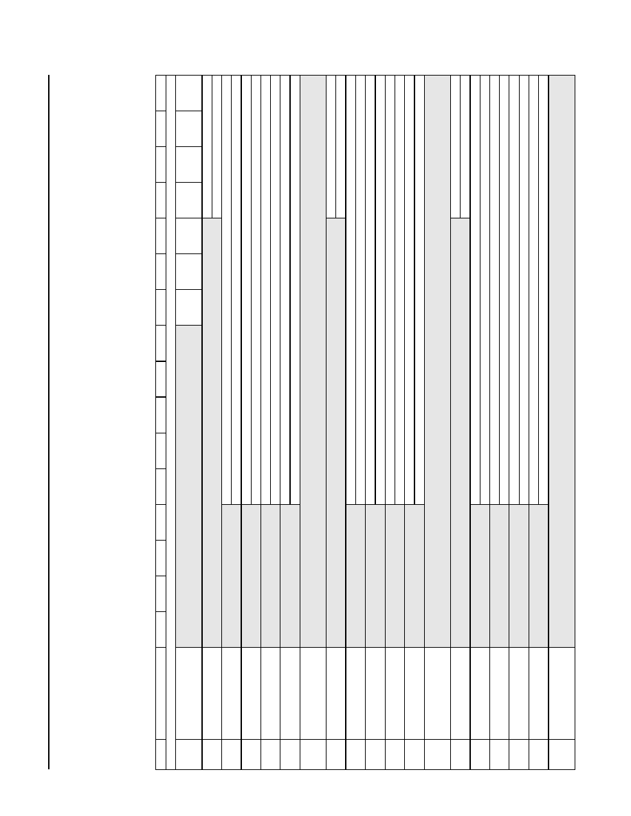
Data Sheet
MARS2G5 P-Pro (TDAT162G52) SONET/SDH
August 18, 2004
155/622/2488 Mbits/s Data Interface
483
Agere Systems Inc.
STS Receive Terminator (RXT) Block
(continued)
RXT Register Map
(continued)
Table 452. RXT Register Map (continued)
Note: Shading denotes reserved bits.
Addr
Symbol
Bit 15
Bit 14
Bit 13
Bit 12
Bit 11
Bit 10
Bit 9
Bit 8
Bit 7
Bit 6
Bit 5
Bit 4
Bit 3
Bit 2
Bit 1
Bit 0
Performance Monitoring
0x8780
RXT_POH_ALMPMR
RXT_1BR
DI_DPM
RXT_ERDI
_PDPM
RXT_ERDI
_CDPM
RXT_ERDI
_SDPM
RXT_UNE
QR_ALMP
M
RXT_AIS_
ALMPM
RXT_LOP
_ALMPM
0x8781
RXT_1BRDI_DPMBSR
One-Bit RDI Alarm PM
RXT_1BRDI_DPMBS[A--D]
0x8782
RXT_TS1BRDI_DPMBSRA
One-Bit RDI Alarm PM per STS-1 Bytestream A
RXT_TS1BRDI_DPMBSA[1--12]
0x8783
RXT_TS1BRDI_DPMBSRB
One-Bit RDI Alarm PM per STS-1 Bytestream B
RXT_TS1BRDI_DPMBSB[1--12]
0x8784
RXT_TS1BRDI_DPMBSRC
One-Bit RDI Alarm PM per STS-1 Bytestream C
RXT_TS1BRDI_DPMBSC[1--12]
0x8785
RXT_TS1BRDI_DPMBSRD
One-Bit RDI Alarm PM per STS-1 Bytestream D
RXT_TS1BRDI_DPMBSD[1--12]
0x8786
--
0x8790
--
0x8791
RXT_ERDI_PDPMBSR
ERDI Payload Alarm PM
RXT_ERDI_PDPMBS[A--D]
0x8792
RXT_ERDI_PDPMBSRA
ERDI Payload Alarm PM per STS-1 Bytestream A
RXT_TSERDI_PDPMBSA[1--12]
0x8793
RXT_ERDI_PDPMBSRB
ERDI Payload Alarm PM per STS-1 Bytestream B
RXT_TSERDI_PDPMBSB[1--12]
0x8794
RXT_ERDI_PDPMBSRC
ERDI Payload Alarm PM per STS-1 Bytestream C
RXT_TSERDI_PDPMBSC[1--12]
0x8795
RXT_ERDI_PDPMBSRD
ERDI Payload Alarm PM per STS-1 Bytestream D
RXT_TSERDI_PDPMBSD[1--12]
0x8796
--
0x87A0
--
0x87A1
RXT_ERDI_CDPMBSR
ERDI Connectivity Alarm PM
RXT_ERDI_CDPMBS[A--D]
0x87A2
RXT_TSERDI_CDPMBSRA
ERDI Connectivity Alarm PM per STS-1 Bytestream A
RXT_TSERDI_CDPMBSA[1--12]
0x87A3
RXT_TSERDI_CDPMBSRB
ERDI Connectivity Alarm PM per STS-1 Bytestream B
RXT_TSERDI_CDPMBSB[1--12]
0x87A4
RXT_TSERDI_CDPMBSRC
ERDI Connectivity Alarm PM per STS-1 Bytestream C
RXT_TSERDI_CDPMBSC[1--12]
0x87A5
RXT_TSERDI_CDPMBSRD
ERDI Connectivity Alarm PM per STS-1 Bytestream D
RXT_TSERDI_CDPMBSD[1--12]
0x87A6
--
0x87B0
--
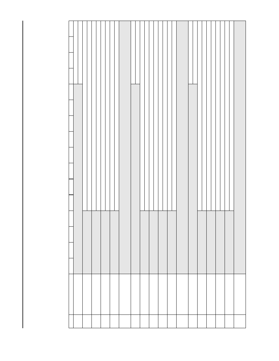
MARS2G5 P-Pro (TDAT162G52) SONET/SDH
Data Sheet
155/622/2488 Mbits/s Data Interface
August 18, 2004
484
Agere Systems Inc.
STS Receive Terminator (RXT) Block
(continued)
RXT Register Map
(continued)
Table 452. RXT Register Map (continued)
Note: Shading denotes reserved bits.
Addr
Symbol
Bit 15
Bit 14
Bit 13
Bit 12
Bit 11
Bit 10
Bit 9
Bit 8
Bit 7
Bit 6
Bit 5
Bit 4
Bit 3
Bit 2
Bit 1
Bit 0
0x87B1
RXT_ERDI_SDPMBSR
ERDI Server Alarm PM
RXT_ERDI_SDPMBS[A--D]
0x87B2
RXT_TSERDI_SDPMBSRA
ERDI Server Alarm PM per STS-1 Bytestream A
RXT_TSERDI_SDPMBSA[1--12]
0x87B3
RXT_TSERDI_SDPMBSRB
ERDI Server Alarm PM per STS-1 Bytestream B
RXT_TSERDI_SDPMBSB[1--12]
0x87B4
RXT_TSERDI_SDPMBSRC
ERDI Server Alarm PM per STS-1 Bytestream C
RXT_TSERDI_SDPMBSC[1--12]
0x87B5
RXT_TSERDI_SDPMBSRD
ERDI Server Alarm PM per STS-1 Bytestream D
RXT_TSERDI_SDPMBSD[1--12]
0x87B6
--
0x87C0
--
0x87C1
RXT_UNEQR_PMBSR
Unequipped Received Alarm PM
RXT_UNEQR_PMBS[A--D]
0x87C2
RXT_TSUNEQR_PMBSRA
Unequipped Received Alarm PM per STS-1 Bytestream A
RXT_TSUNEQR_PMBSA[1--12]
0x87C3
RXT_TSUNEQR_PMBSRB
Unequipped Received Alarm PM per STS-1 Bytestream B
RXT_TSUNEQR_PMBSB[1--12]
0x87C4
RXT_TSUNEQR_PMBSRC
Unequipped Received Alarm PM per STS-1 Bytestream C
RXT_TSUNEQR_PMBSC[1--12]
0x87C5
RXT_TSUNEQR_PMBSRD
Unequipped Received Alarm PM per STS-1 Bytestream D
RXT_TSUNEQR_PMBSD[1--12]
0x87C6
--
0x87D0
--
0x87D1
RXT_AIS_PMBSR
Alarm Indicator Signal Alarm PM
RXT_AIS_PMBS[A--D]
0x87D2
RXT_TSAIS_PMBSRA
Alarm Indicator Signal Alarm PM per STS-1 Bytestream A
RXT_TSAIS_PMBSA[1--12]
0x87D3
RXT_TSAIS_PMBSRB
Alarm Indicator Signal Alarm PM per STS-1 Bytestream B
RXT_TSAIS_PMBSB[1--12]
0x87D4
RXT_TSAIS_PMBSRC
Alarm Indicator Signal Alarm PM per STS-1 Bytestream C
RXT_TSAIS_PMBSC[1--12]
0x87D5
RXT_TSAIS_PMBSRD
Alarm Indicator Signal Alarm PM per STS-1 Bytestream D
RXT_TSAIS_PMBSD[1--12]
0x87D6
--
0x87E0
--
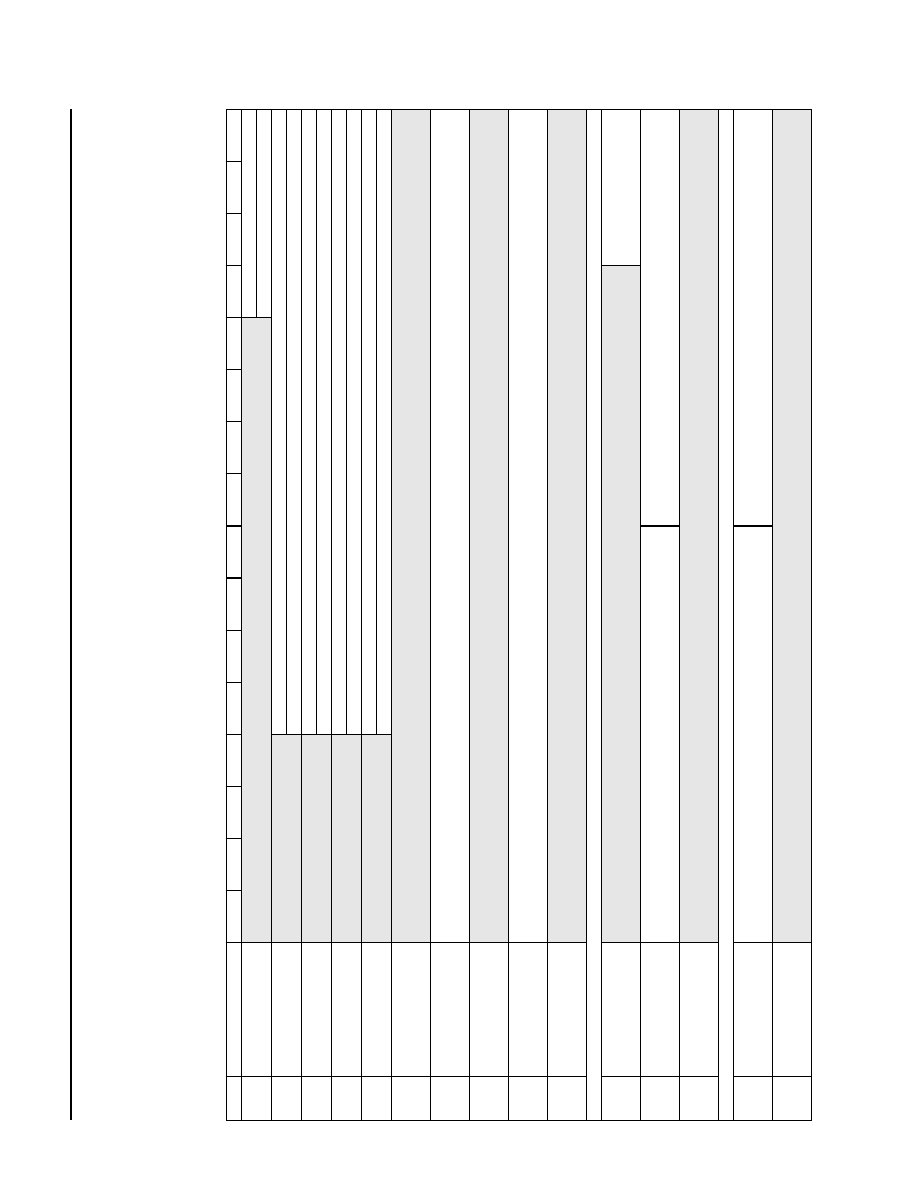
Data Sheet
MARS2G5 P-Pro (TDAT162G52) SONET/SDH
August 18, 2004
155/622/2488 Mbits/s Data Interface
485
Agere Systems Inc.
STS Receive Terminator (RXT) Block
(continued)
RXT Register Map
(continued)
Table 452. RXT Register Map (continued)
Note: Shading denotes reserved bits.
Addr
Symbol
Bit 15
Bit 14
Bit 13
Bit 12
Bit 11
Bit 10
Bit 9
Bit 8
Bit 7
Bit 6
Bit 5
Bit 4
Bit 3
Bit 2
Bit 1
Bit 0
0x87E1
RXT_LOP_PMBSR
Loss of Pointer Alarm PM
RXT_LOP_PMBS[A--D]
0x87E2
RXT_TSLOP_PMBSRA
Loss of Pointer Alarm PM per STS-1 Bytestream A
RXT_TSLOP_PMBSA[1--12]
0x87E3
RXT_TSLOP_PMBSRB
Loss of Pointer Alarm PM per STS-1 Bytestream B
RXT_TSLOP_PMBSB[1--12]
0x87E4
RXT_TSLOP_PMBSRC
Loss of Pointer Alarm PM per STS-1 Bytestream C
RXT_TSLOP_PMBSC[1--12]
0x87E5
RXT_TSLOP_PMBSRD
Loss of Pointer Alarm PM per STS-1 Bytestream D
RXT_TSLOP_PMBSD[1--12]
0x87E6
--
0x87FF
--
0x8800
--
0x882F
RXT_LSECCVP_CPMR[1--48]
Time Slots 1, 2, 3, 4, . . . , 48 CV Count PM
RXT_LSECCVP_CPM[1--48][15:0]
0x8830
--
0x887F
--
0x8880
--
0x88AF
RXT_LSECREIP_
CPMR[1--48]
Time Slots 1, 2, 3, 4, . . . , 48 REI Count PM
RXT_LSECREIP_CPM[1--48][15:0]
0x88B0
--
0x88FF
--
RDI, C2 Status
0x8900
--
0x892F
RXT_TSRDIPR[1--48]
Time Slot 1--Time Slot 48 Received
RDI Code
RXT_TS_RRDI[1--48][2:0]
0x8930
--
0x8947
RXT_TSC2R[1--24]
Time Slots 1, 3, 5, 7, . . . , 47 Received C2 Byte
RXT_TSRC2[1, 3, 5, . . . , 47][7:0]
Time Slots 2, 4, 6, 8, . . . , 48 Received C2 byte
RXT_TSRC2[2, 4, 6, . . . , 48][7:0]
0x8948
--
0x895F
--
PDI Status
0x8960
--
0x8977
RXT_TSPDIR[1--24]
Time Slots 1, 3, 5, 7, . . . , 47 Received PDI Byte
RXT_TSRPDI[1, 3, 5, . . . , 47][7:0]
Time Slots 2, 4, 6, 8, . . . , 48 Received PDI Byte
RXT_TSRPDI[2, 4, 6, . . . , 48][7:0]
0x8968
--
0x8FFF
--
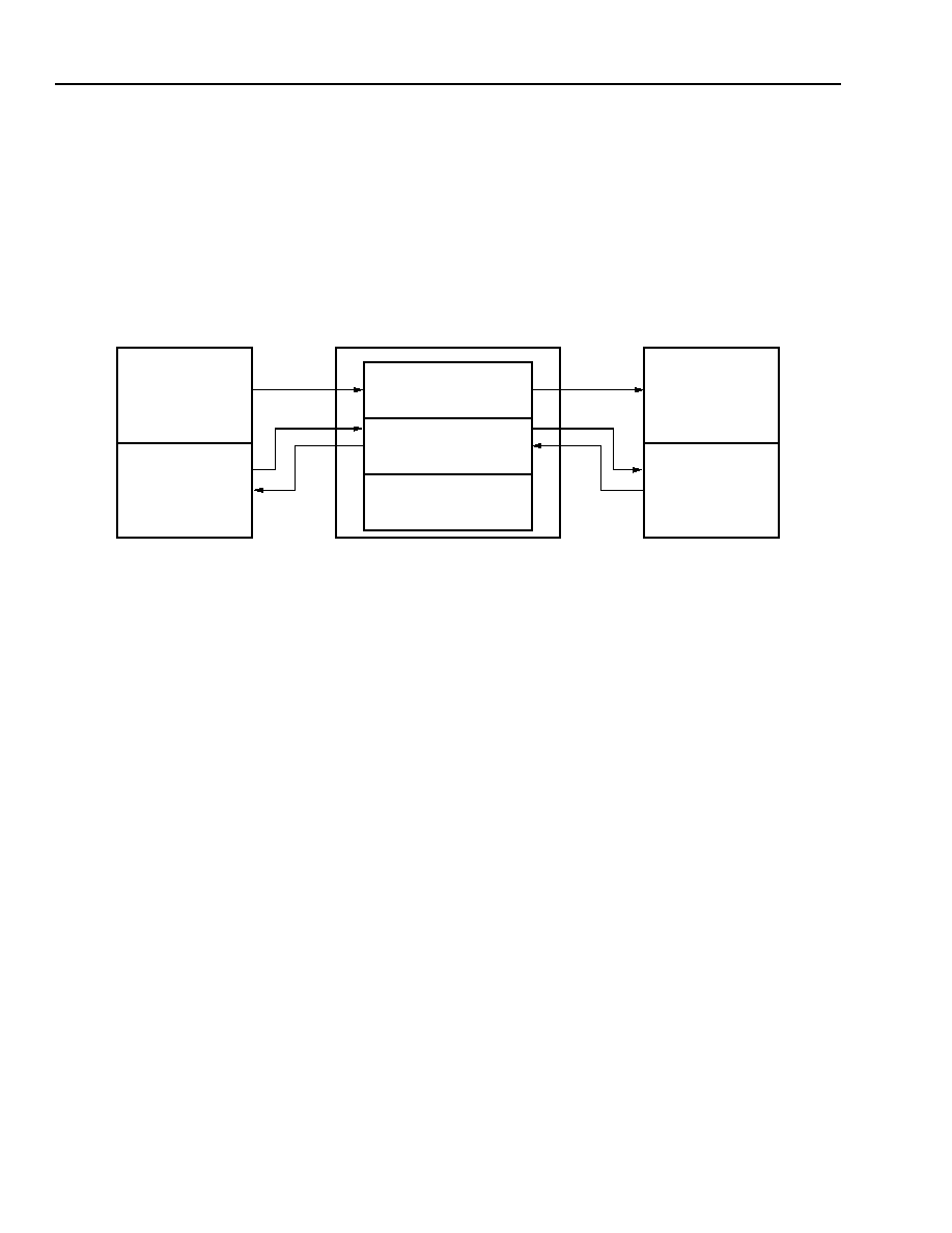
MARS2G5 P-Pro (TDAT162G52) SONET/SDH
Data Sheet
155/622/2488 Mbits/s Data Interface
August 18, 2004
486
Agere Systems Inc.
DS3/E3 Block
DS3 Functional Description
DS3 Block Interface Diagram
The DS3 block consists of three major subblocks: DS3 Rx, DS3 Tx, and microprocessor interface. The DS3 block
interfaces with the pointer interpreter and SPE blocks on one side and the receive sequencer/data engine blocks
on the other side as shown in Figure 55.
5-8326(F)r.5
Figure 55. DS3 Block Interface Diagram
DS3 Receive Subblock
The DS3 Rx block is responsible for extracting the i bits from an STS-1 frame, performing DS3 framing, and
extracting the d bits from the DS3 frame, and finally, extracting data (packets or ATM cells) from the d bits. The
ATM cells could be either direct mapped, or PLCP mapped, and packets are direct mapped.
Data arrives at the DS3 in the Rx direction grouped as four slices of 8 bits. The four slices are labeled A, B, C, and
D as shown in Figure 56. DS3 is only supported in slices A and B. The DS3 block is designed to accommodate up
to 24 channels, among the two slices. Thus, each slice could have up to 12 channels, and data for any given chan-
nel will always arrive at the same slice (that is, data for any one channel arriving on slice A, will never arrive on B,
C, or D).
Not all 16 channels need to be DS3 mapped. Any channels not DS3 mapped will be passed through the block
untouched. Additionally, the delay through each slice will be the same, if the data is not DS3 mapped, so that data
that is not DS3 mapped, belonging to a single channel, can be presented across the four slices at the same time, to
the next block, and the data will be transmitted out of the DS3 block aligned in time.
DS3 RX
DS3 TX
MICRO I/F
DS3 BLOCK
POINTER
INTERPRETER
(PTR)
SPE MAPPER
(SPE)
RECEIVE
SEQUENCER
(RXS)
DATA ENGINE
(DE)
FEEDBACK
FEEDBACK
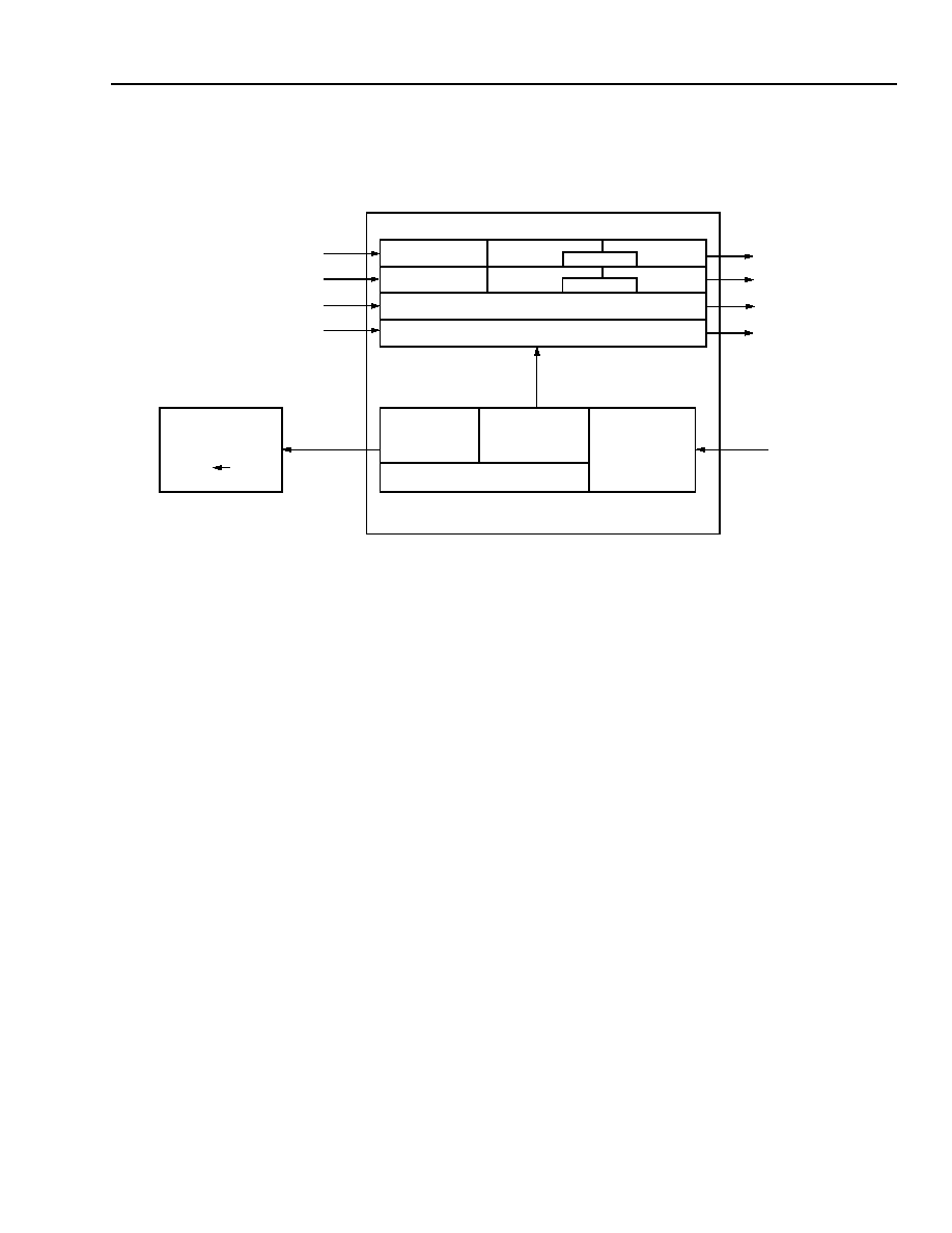
Data Sheet
MARS2G5 P-Pro (TDAT162G52) SONET/SDH
August 18, 2004
155/622/2488 Mbits/s Data Interface
487
Agere Systems Inc.
DS3/E3 Block
(continued)
DS3 Functional Description
(continued)
5-8715(F)r.1
Figure 56. DS3 Receive Subblock
The data entering the DS3 block passes through a mode look-up block, which is responsible for determining, from
the time slot, if the data for that channel is DS3 encoded. If data is DS3 encoded, then the mode look-up block is
responsible for indicating if DS3 data is PLCP encoded or clear channel as indicated by the following register bits
DS3_RDS3PLCP_[A--B][12--1][1:0] (Table 560, Table 561, Table 563, and Table 564): 00 = no mapping, 01 =
illegal (no mapping), 10 = DS3 clear channel, 11 = DS3/PLCP mapped signal.
The data is then passed through the DS3 I bits extract block, which is responsible for extracting the i bits from an
STS-1 frame. The format of DS3 i-bit mapping into an STS-1 frame is shown in Table 678. Data for any channels
not carrying DS3 traffic is sent through this block unmodified. In this block, path-level overhead bytes are ignored.
The r(reserved) and o(overhead communications channel) bits are ignored. The s bit is treated as a stuff bit
according to the majority vote of the c bits, as per GR253 R3-70 and GR253 R3-71 requirements. The DS3 I bits
extract block receives a J1 marker along with the data. All internal counters are resynchronized to the J1 marker,
on a per time-slot basis.
After the i bits are extracted, they are passed to the DS3 framer 8 bits at a time. This implies that data must be
packed in this and all blocks before being sent out for further processing. All reserved and fixed stuff bytes are
marked as invalid data, register bits DS3_RDS3PLCP_[A--B][12--1][1:0]. Setting a time slot into the no mapping
mode (00 or 01) resets all internal states for that time slot.
Once the i bits are extracted from an STS-1 frame, they are passed to the DS3 framer block, which is responsible
for performing framing onto the DS3 subframe alignment and multiframe alignment signals if the signal contains a
DS3 frame. The format of a DS3 multiframe is shown in Figure 61.
PT BLOCK
SPE
DS3 I BITS EXTR.
DS3 FRM
PLCP FRM
FIFO
PLCP INs
DS3 INs
PRBS INSERT
16 LOGICAL CHANNELS
MAPPER
(SPE DS3)
DS3 I BITS EXTR.
DS3 FRM
PLCP FRM
SLICE D--DS3 NOT SUPPORTED
SLICE C--DS3 NOT SUPPORTED
A
B
C
D
TO RXS
FROM PT
A
B
C
D
24 DS3/PLCP--12 PER SLICE A AND B
FROM DE
PRBS MON
DS3 BLOCK
PRBS MON

MARS2G5 P-Pro (TDAT162G52) SONET/SDH
Data Sheet
155/622/2488 Mbits/s Data Interface
August 18, 2004
488
Agere Systems Inc.
DS3/E3 Block
(continued)
DS3 Functional Description
(continued)
DS3 Framing Algorithm
Framing is done in two stages by first finding a bit position that matches the frame alignment pattern (F bits 1001),
and then locating the multiframe alignment signal (M bits 010). In F frame is declared once no errors are detected
in the F-bit sequence for 16 consecutive bits. After a matching F-bit sequence is found, in frame is declared
(DS3_OOF_[A--B][12--1] = 0 (Table 532 and Table 546)) when correct M bits are received for three M frames
(T1.231). The maximum average reframe time is 0.5 ms in the presence of a bit error rate of 10
≠3
.
Once in frame, the received frame bits are monitored for out-of-frame. Out-of-frame is declared (DS3_OOF_[A--
B][12--1] = 1) if too many errors are received in either the F bits (three errors in 16 bits if DS3_OOF_FMODE_[A--
B] = 0 (Table 560 and Table 563), or at least one F-bit error in each of four consecutive M subframes if
DS3_OOF_FMODE_[A--B] = 1) or the M bits (at least one error in each of three consecutive M frames). For test-
ing purposes, the user may also force the framer out-of-frame by setting the mapping bits.
The traditional algorithm for declaring out-of-frame (three errors in 16 F bits) results in false out-of-frame approxi-
mately every 30 seconds when the received bit error rate is 10
≠3
. By waiting for four consecutive M subframes with
F-bit errors before declaring out-of-frame, the framer normally stays in frame for over an hour when the bit error
rate is 10
≠3
.
After subframe and multiframe have been acquired, the DS3 channel is declared framed, and an alarm is raised.
DS3 Loss-of-Frame
The DS3_LOF_[A--B][12--1] bit (Table 533 and Table 547) is set if the associated DS3_OOF_[A--B][12--1] out-
of-frame bit is high continuously for 28 ± 1 frame periods (approximately 3 ms). Once set, the LOF state bit is not
cleared until the OOF state bit is continuously low for 28 ± 1 frame periods.
Register bits: DS3_LOF_[A--B][12--1], DS3_LOFD_[A--B][12--1] (Table 481 and Table 493), and
DS3_LOFM_[A--B][12--1] (Table 507 and Table 519).
Severely Errored Frame (SEF)
The received DS3 frames are checked for severely errored frames (SEF). A SEF defect is the occurrence of three
or more F-bit errors in 16 consecutive F bits and reported through register bits DS3_SEF_[A--B][12--1] (Table 534
and Table 548). A SEF defect is terminated when the signal is in-frame and there are less than three F-bit errors in
16 consecutive F bits. This error may cause the DS3 framer to transition to the out-of-frame state.
Register bits: DS3_SEF_[A--B][12--1], DS3_SEFD_[A--B][1--12] (Table 482 and Table 494), and
DS3_SEFM_[A--B][12--1] (Table 508 and Table 520).
AIS Detection/Removal
In each M-frame, the 4704 information bits are checked for the presence of the AIS (1010) pattern starting after
each overhead bit. In order to detect this pattern in the presence of a high error rate, AIS (DS3_AISPAT_DET_[A--
B][12--1] (Table 535 and Table 549)) pattern detection is declared if fewer than five pattern errors are received in
each of two consecutive frames. Once AIS is declared, it is not cleared until at least 16 pattern errors are received
in each of two consecutive M-frames (T1.231). In addition to detection of the pattern, the DS3 signal must be in-
frame and P-bit errors are binned during AIS detection.
Register bits: DS3_AISPAT_DET_[A--B][12--1], DS3_AISPAT_DETD_[A--B][12--1] (Table 483 and Table 495),
and DS3_AISPAT_DETM[A--B][12--1] (Table 509 and Table 521).

Data Sheet
MARS2G5 P-Pro (TDAT162G52) SONET/SDH
August 18, 2004
155/622/2488 Mbits/s Data Interface
489
Agere Systems Inc.
DS3/E3 Block
(continued)
DS3 Functional Description
(continued)
Idle Detection/Removal
In each M-frame, the 4704 information bits are checked for the presence of the idle (1100) pattern starting after
each overhead bit. In order to detect this pattern in the presence of a high error rate, idle
(DS3_IDLEPAT_DET_[A--B][12--1] (Table 536 and Table 550)) pattern detection is declared if fewer than five
pattern errors are received in each of two consecutive frames. Once Idle is declared, it is not cleared until at least
16 pattern errors are received in each of two consecutive M-frames (T1.231). In addition to detection of the pattern,
the DS3 signal must be in-frame and P-bit errors are binned during Idle detection.
Register bits: DS3_IDLEPAT_DET_[A--B][12--1], DS3_IDLEPAT_DETD[A--B][12--1] (Table 484 and
Table 496), DS3_IDLEPAT_DETM_[A--B][12--1] (Table 510 and Table 522).
C-Bit Detection and X-Bit Detection
In addition to the fixed information bit patterns, AIS and Idle signals are transmitted with all C bits set to 0 and both
X-bits set to 1. These conditions are monitored and reported in DS3_CBZ_DET_[A--B][12--1] (Table 537 and
Table 551) and DS3_RAI_DET_[A--B][12--1] (Table 538 and Table 552) bits.
If every C bit in three consecutive DS3 frame is 0, set DS3_CBZ_DET_[A--B][12--1] = 1. If the three C bits in a
single M subframe are 1, clear the associated DS3_CBZ_DET_[A--B][12--1] bit.
If both X bits (RAI or yellow signal) in two consecutive M frames are received as 0 (error-free), the device sets
DS3_RAI_DET_[A--B][12--1] = 1. Once this bit is set, it is not cleared until both X bits in two consecutive M-
frames are received as 1.
The user may wish to declare AIS or idle based on a combination of some of the DS3_CBZ_DET, DS3_RAI_DET,
and DS3_AISPAT_DET or DS3_IDLEPAT_DET bits.
Register bits: DS3_CBZ_DET_[A--B][12--1], DS3_CBZ_DETD_[A--B][12--1] (Table 485 and Table 497),
DS3_CBZ_DETM_[A--B][12--1] (Table 511 and Table 523), DS3_RAI_DET_[A--B][12--1],
DS3_RAI_DETD_[A--B][12--1] (Table 486 and Table 498), DS3_RAI_DETM_[A--B][12--1]
(Table 512 and Table 524).
Near-End Path Failure Event and Count
Near-end path failure event and count are detected via a host microprocessor.

MARS2G5 P-Pro (TDAT162G52) SONET/SDH
Data Sheet
155/622/2488 Mbits/s Data Interface
August 18, 2004
490
Agere Systems Inc.
DS3/E3 Block
(continued)
DS3 Functional Description
(continued)
DS3 OH Bits Processor
All overhead bits defined in a 44.736 kbit/s multiframe structure are defined in the table below. Bold bits are pro-
cessed by the OH processor block, while all other bits are ignored.
Table 453. Overhead Bits Defined in a 44.736 Mbits/s Multiframe Structure
Note: F1, F2, F3, F4 = 1001, M1, M2, M3 = 010, X1 = X2, P1 = P2, C31 = C32 = C33.
X-Bit Detection
The X bits are used to indicate received errored multiframes to the remote-end (remote-alarm indication RAI or yel-
low signal); these bits are set to binary 1 (i.e., X1 = X2 =1) during error-free conditions, and to binary 0 (i.e., X1 =
X2 = 0) if OOF or AIS are detected in the incoming signal. See C-Bit Detection and X-Bit Detection section on page
489 for monitoring information.
The 56 overhead bits sequential positions as follows:
X1
F1
C11
F2
C12
F3
C13
F4
X2
F1
C21
F2
C22
F3
C23
F4
P1
F1
C31
F2
C32
F3
C33
F4
P2
F1
C41
F2
C42
F3
C43
F4
M1
F1
C51
F2
C52
F3
C53
F4
M2
F1
C61
F2
C62
F3
C63
F4
M3
F1
C71
F2
C72
F3
C73
F4

Data Sheet
MARS2G5 P-Pro (TDAT162G52) SONET/SDH
August 18, 2004
155/622/2488 Mbits/s Data Interface
491
Agere Systems Inc.
DS3/E3 Block
(continued)
DS3 Functional Description
(continued)
P Bits (P1, P2)
For each channel that is DS3 mapped, parity is calculated over the 4704 data bits (84 info bits * 8 blocks/subframe
* 7 subframes/multiframe) following the X1 bit.
Parity errors are accumulated in a read-only saturating counter. The coding violation parameter count (CVP-P)
counter increments if at least one of the P bits disagree with the parity of the previous frame. This counter is
cleared on a 0-to-1 transition of the PMRST (pin D7, Table 10, Pin Descriptions--Microprocessor Interface Signals
on page 117) input signal.
Register bits: DS3_PERR_CNT_[A--B][1--12][13:0] (Table 567 and Table 573).
C31, C32, and C33 CP Bits
CP bits are used to carry path (end-to-end facility) parity information. The network terminating equipment (NTE)
that originates the DS3 signal must set these bits (C31 = C32 = C33) to the same value as the P bits.
The CP-bit coding violation parameter count (CVCP-P) counts frames with at least two of the three C-bit parity bits
indicating an error.
Register bit: DS3_CPERR_CNT_[A--B][1--12][13:0] (Table 568 and Table 574).
C41, C42, and C4 FEBE Bits
FEBE bits are used to carry far-end block error information. All three FEBE bits are set to 1 (C41 = C42 = C43 = 1)
if no errors are detected in the M bits, or F bits, or indicated by the CP bits. If any error condition is detected within
the M frame, the FEBE bits must be set to any combination of 1s or 0s (except 111).
The CVCP-PFE counter accumulates FEBE error indications (one error indication for each M-frame with at least
one FEBE bit equal to zero).
Register bit: DS3_FEBE_CNT_[A--B][1--12][13:0] (Table 569 and Table 575).
C13 FEAC (Far-End Alarm and Control)
FEAC is used to receive alarm and status information from the far-end terminal and to initiate or terminate line
loopbacks (not supported) at the request of the far-end terminal. The FEAC signal consists of a 16-bit code word of
format 0iiiiii011111111 with the right-most bit transmitted first (1); i = information bit. When no code words are trans-
mitted, the FEAC channel is set to all 1s. After validation (four consecutive times), the code word is stored in regis-
ter (DS3_RFEAC_CODE_[A--B][12--1][5:0] (Table 544 and Table 558)). If the validated codeword equals one of
the codewords listed in Table 454, the RAI state bit is set. Otherwise, the RAI state bit is zero
(DS3_RFEAC_RAI_[A--B][12--1] (Table 539 and Table 553), DS3_RFEAC_RAID_[A--B][12--1] (Table 487 and
Table 499), DS3_RFEAC_RAIM_[A--B][12--1] (Table 513 and Table 525)). If the validated code word is not listed
in Table 454, the DS3_RFEAC_CTL_[A--B][12--1] (Table 540 and Table 554) state bit is set; otherwise, this state
bit is 0 (DS3_RFEAC_CTLD_[A--B][12--1] (Table 488 and Table 500), DS3_RFEAC_CTLM_[A--B][12--1]
(Table 514 and Table 526)).
MARS2G5 P-Pro (TDAT162G52) SONET/SDH
Data Sheet
155/622/2488 Mbits/s Data Interface
August 18, 2004
492
Agere Systems Inc.
DS3/E3 Block
(continued)
DS3 Functional Description
(continued)
Table 454. RAI Code Words
C5X Processing
The C51, C52, and C53 bits are used for a 28.2 kbits/s terminal-to-terminal path maintenance data link. The imple-
mentation of this data link is optional and therefore is not monitored in this block.
All Other C-Bit Processing
C11, C12, C2X, C6X, and C7X should be set to all 1s. These bits are ignored.
PRBS Detector
The test-pattern detector contains a self-synchronizing detector using the identical QRSS sequence as found in the
test-pattern generator (2
20
≠ 1 and 2
15
≠ 1). When the detector is out of sync, the device continually monitors the
input data signal for matches to the expected data signal. When the device detects 32 matches in a row, it declares
itself in sync and the error detector is enabled. If the device detects eight consecutive mismatches, the test-pattern
detector declares itself out of sync and starts searching again.
When in sync, the device counts the number of times the input data differs from the expected data in an 8-bit
counter that holds its count when it reaches the maximum value of 255. This counter is reset when read by the
microprocessor and is not affected by the PMRST (pin D7) input signal.
This function is enabled on two time slots at a time, and the data must be DS3 or PLCP frame encoded. Two PRBS
detectors are implemented per slice. Setting the DS3_RPRBS_TSSEL_[A--B][2--1][3:0] (Table 562 and
Table 565) value to 0xF will disable the PRBS algorithm and reset all counters and state machine values to their
reset default states.
Register bits: DS3_RPRBS_TSSEL_[A--B][2--1][3:0],
DS3_RPRBS_INV_[A--B][1:0] (Table 561 and Table 564),
DS3_RPRBS_SYNC_ERR_[A--B][1:0] (Table 543 and Table 557),
DS3_RPRBS_SYNC_ERRD_[A--B][1:0] (Table 491 and Table 503),
DS3_RPRBS_SYNC_ERRM_[A--B][1:0] (Table 517 and Table 529),
DS3_RPRBS_DS3_PLCP_[A--B][1:0] (Table 562 and Table 565),
DS3_RPRBS_15or20_[A--B][1:0] (Table 562 and Table 565),
DS3_RPRBS_ERRCNT_[A--B][1--2][7:0] (Table 545 and Table 559).
Value
Description
(LSB) 011001 (MSB)
DS3 Equipment Failure Service Affecting
001110
DS3 Loss of Signal
000000
DS3 Out of Frame
010110
DS3 AIS Received

Data Sheet
MARS2G5 P-Pro (TDAT162G52) SONET/SDH
August 18, 2004
155/622/2488 Mbits/s Data Interface
493
Agere Systems Inc.
DS3/E3 Block
(continued)
DS3 Functional Description
(continued)
DS3 PLCP (Physical Layer Convergence Protocol) Framer
Once the data is extracted by the DS3 framer, if that data is PLCP mapped, PLCP framing must be performed.
Otherwise, the data is sent through this block unmodified. If the data is PLCP encoded, framing is performed by
checking for the A1A2 pattern.
Framing: In-frame is declared after two consecutive A1A2 and two consecutive path overhead indicator (POI) pat-
terns are detected in a row. Out of frame is declared after five consecutive A1A2 mismatches or five consecutive
POI values are received in error.
An alarm is issued on a per time-slot basis each time the framer changes state. Until the in-frame state is declared,
all data is marked as invalid leaving this block for the associated time slot.
Register bits: DS3_PLCP_OOF_[A--B][12--1] (Table 541 and Table 555), DS3_PLCP_OOFD_[A--B][12--1]
(Table 489 and Table 501), DS3_PLCP_OOFM_[A--B][1--12] (Table 515 and Table 527).
B1 Monitoring
The BIP-8 is computed over the 12 x 54 octet structure consisting of the POH fields and the associated ATM cells
of the previous PLCP frame and compared to the received BIP-8 value, and the errors are accumulated in a 16-bit
saturating counter. This counter is cleared by the PMRST signal, and the error value per frame is sent to the trans-
mit direction for insertion into the G1[7:4] bits.
Register bits: DS3_PLCP_B1ERRCNT_[A--B][1--12][15:0] (Table 570 and Table 576).
G1 Monitoring
The G1[7:4] FEBE error value is binned in a 16-bit saturating counter that is cleared by the PMRST signal. Valid
values are 0 to 8. Any value outside this range is considered 0 errors (DS3_PLCP_G1_FEBE_ERRCNT_[A--
B][1--12][15:0] (Table 571 and Table 577)).
The G1[3] RAI value is monitored for a change in state. Each time a validated change of state is detected
(DS3_PLCP_CNTD_G1_RAI_[A--B][3:0] (Table 562 and Table 565)), a delta bit is set (DS3_PLCP_G1_RAI_[A--
B][12--1] (Table 542 and Table 556), DS3_PLCP_G1_RAID_[A--B][12--1] (Table 490 and Table 502), and
DS3_PLCP_G1_RAIM_[A--B][12--1] (Table 516 and Table 528)).
All other bits are ignored.

MARS2G5 P-Pro (TDAT162G52) SONET/SDH
Data Sheet
155/622/2488 Mbits/s Data Interface
August 18, 2004
494
Agere Systems Inc.
DS3/E3 Block
(continued)
DS3 Transmit Direction
The DS3 transmit block consists of three functional blocks. They are the FIFO block used to buffer packets from
the data engine, the PLCP frame insert block used to pack ATM cells into a PLCP frame and insert the byte over-
head associated with this format, and the DS3 frame insert block that inserts the valid data from the FIFO block in
to a DS3 frame. The PLCP and DS3 frame insert blocks can be bypassed for pass-through traffic (virtual concate-
nation, etc.). Channel ID to slice/time-slot number mapping is provided for bidirectional alarm insertion in the DS3
(X1, X2) and PLCP (G1) frames.
Register bits: DS3_TDS3PLCP[1--16][1:0] (Table 578); 00 = no mapping, 01 = DS3 locked mode, 10 = DS3 clear
channel, 11 = DS3/PLCP mapped signal, DS3_TXCHID_TO_TSMAPPING[1--16][1:0][3:0]
(Table 578) = channel ID to slice/time-slot mapping [A--B][0--11]; A = 3, B = 2; illegal values default
to all selected signals are inactive (0).
The DS3 locked mode allows the insertion of DS3 overhead bytes into a received packed of length (84 * 7 bytes).
The DS3 frame insert mechanism will synchronize to the EOP marker. Each time the EOP marker changes posi-
tion, an event indication is set (DS3_TXEOPERRE[16--1] (Table 505), DS3_TXEOPERRM[16--1] (Table 531)).
The EOP marker indicates when the next MSByte contains the start of the packet.
The DS3_TXEOPERRE[16--1] indicates when the EOP marker changes position in the PLCP mapping mode or
DS3 locked mode.
FIFO Block
The FIFO block accepts data from the data engine input 32 bits at a time. Each 32 bits is associated with a channel
ID, a data valid indicator and a data marker for the entire bus, and an EOP marker per byte to indicate the end of a
packet (ATM, HDLC, etc). All valid data (valid indicator and data marker = 1) is written into the associated FIFO
location (16 active channels x 32 locations x 36 bits = 18,432 bits (~ 36,864 gates) for the selected channel ID.
Data is not read out of the FIFO until data has accumulated above the lower threshold (DS3_TFIFO_MIN[5:0]
(Table 582)), and blank requests are sent if the FIFO reaches the upper threshold (DS3_TFIFO_MAX[5:0]
(Table 582)).
Writes to the FIFO always occur for valid data even if the FIFO will overflow. In this case, the FIFO is considered
empty and reads are disabled until the lower threshold is reached.
Reads from the FIFO are designed as a pull mechanism. The receiving block allows data for a particular channel
ID or sends a blank request for that channel ID to the DS3 framer block. A blank request guarantees no valid data
is sent to the PT block. The DS3 block requests or inhibits data from the PLCP block by asserting its data valid sig-
nal. This same mechanism exists between the PLCP framer and FIFO. The PLCP block can inhibit reads from the
FIFO if it does not need data. The FIFO will issue blank requests upstream once the high-buffer threshold is
exceeded. This is the only mechanism that will cause blank requests to be issued for a selected channel ID.
Register bits: DS3_TFIFO_MIN[5:0], DS3_TFIFO_MAX[5:0], DS3_TFIFO_OVR_UNFLE_[16--1] (Table 504), and
DS3_TFIFO_OVR_UNFLM_[16--1] (Table 530).

Data Sheet
MARS2G5 P-Pro (TDAT162G52) SONET/SDH
August 18, 2004
155/622/2488 Mbits/s Data Interface
495
Agere Systems Inc.
DS3/E3 Block
(continued)
DS3 PLCP Frame/Data Insert
Frame Format Insert
This block is responsible for creating the PLCP frame if the associated channel is PLCP encoded; otherwise, the
data is sent through unchanged. The channel being processed is controlled incoming channel ID. The PLCP block
will request 32 bits from the FIFO when needed. The PLCP frame floats within the DS3 frame.
ATM cell header locations are determined by the location of the EOP marker. If an EOP marker abruptly changes
location, the remaining PLCP ATM location will be filled with 0s. This ensures the receive framer will stay in PLCP
frame.
Frame Alignment (A1, A2)
The A1 (0xF6) and A2 (0x28) framing bytes are the same as SONET and SDH A1 and A2 bytes, respectively. The
A2 byte can be inverted through (DS3_TPLCP_A2INV[1--16] (Table 578)).
Path Overhead Identifier (P00--P11)
The path overhead identifier (POI) indexes the adjacent path overhead (POH) octet of the PLCP. Table 455 pro-
vides the coding for each of the P00--P11 octets. The most significant bit can be inverted through
(DS3_TPLCP_POIB7INV[1--16] (Table 578)).
Table 455. POI Values
Growth Octets (Z1--Z6 and X Bytes)
The growth octets are reserved for future use. These octets are set to 0.
PLCP Path Error Monitoring (B1)
The BIP-8 field is calculated over a 12 x 54 octet structure consisting of the POH field and the associated ATM
cells (648 octets) of the previous PLCP frame. The B1 byte can be inverted on a per-channel basis by setting
(DS3_TPLCP_B1INV[1--16] (Table 578)).
POI
POI Code
POH
P11
0010_1100
Z6
P10
0010_1001
Z5
P09
0010_0101
Z4
P08
0010_0000
Z3
P07
0001_1100
Z2
P06
0001_1001
Z1
P05
0001_0101
X
P04
0001_0000
B1
P03
0000_1101
G1
P02
0000_1000
X
P01
0000_0100
X
P00
0000_0001
C1

MARS2G5 P-Pro (TDAT162G52) SONET/SDH
Data Sheet
155/622/2488 Mbits/s Data Interface
August 18, 2004
496
Agere Systems Inc.
DS3/E3 Block
(continued)
DS3 PLCP Frame/Data Insert
(continued)
PLCP Path Status (G1)
The PLCP path status is allocated to convey the received PLCP status and performance to the transmitting far-
end. Table 456 illustrates the G1 octet subfields: a 4-bit far-end block error (FEBE), a 1-bit remote alarm indication
(RAI), and 3 X bits (X bits are set to all 1s).
The FEBE is the number of B1 errors detected in the previous received PLCP frame. Valid values are 0--8. The
outgoing FEBE value can be forced to a programmable value through (DS3_TPLCP_FEBE_SWENB[1--16]
(Table 578), DS3_TPLCP_FEBE_DINS[3:0] (Table 581)). The same data value is used for all channels while the
enable signals are per channel.
The RAI bit is set to a logic 1 when the associated PLCP framer is in the out-of-frame state. This value can be over-
written through DS3_TPLCP_RAI_SWENB[1--16] (Table 578) and DS3_TPLCP_RAI_DINS[1--16] (Table 578).
Table 456. G1 Byte Definition
Cycle/Stuff Counter (C1)
The cycle/stuff counter provides a nibble stuffing opportunity cycle and length indicator for the PLCP frame. A stuff-
ing opportunity occurs every third frame of a three-frame (375
µ
s) stuffing cycle. The value of the C1 code is used
as an indication of the phase of the 375
µ
s stuffing opportunity cycle.
Table 457 shows that a trailer containing 13 nibbles is used in the first frame of the 375
µ
s stuffing opportunity
cycle. A trailer of 14 nibbles is used in the second frame. The third frame provides a nibble stuffing opportunity. The
contents of each of the 13/14 trailer nibbles will be 1100.
Table 457. Trailer Length
The algorithm for generating the stuff bytes is summarized in Table 458. Sequence number 1 is repeated 28 times,
and then sequence 2 is created. This sequence repeats after 255 PLCP frames.
Table 458. PLCP Nibble Stuff Sequence
Far-End Block Error (FEBE)
RAI
X-X-X
4 bits (MSB)
1 bit
3 bits (LSB), Set to 111
C1 Code
Frame Phase of Cycle
Trailer Length
1111_1111 (0xFF)
1
13
0000_0000 (0x00)
2
14
0110_0110 (0x66)
3 (no stuff)
13
1001_1001 (0x99)
3 (stuff)
14
Sequence Number
Sequence
Repeat Sequence N Times
1
13 - 14 - 14
28
13 - 14 - 13
13 - 14 - 14
2
13 - 14 - 13
1

Data Sheet
MARS2G5 P-Pro (TDAT162G52) SONET/SDH
August 18, 2004
155/622/2488 Mbits/s Data Interface
497
Agere Systems Inc.
DS3/E3 Block
(continued)
DS3 Frame Generate/OH Bit Inserter
F Bits and M Bits Insert
The DS3 frame generator is responsible for generating the M-frame as shown in Figure 61. It generates and
inserts the subframe framing bits F1, F2, F3, F4 = 1001, respectively, and the framing bits M1, M2, M3 = 010,
respectively. These bits can be corrupted by setting DS3_TDS3_FINV[1--16] (Table 579) to 1. This causes the F
bits to be set to 1000. To corrupt the M bits, set the DS3_TDS3_MINV[1--16] (Table 579) to 1. This causes the M
bits to be set to 011.
X Bits Insert
This block is responsible for setting the X bits. These bits are set to a binary 1 during an error-free condition or to a
binary 0 if DS3_LOF, DS3_OOF, DS3_AISPAT_DET are detected in the associated received signal. The X bits
must persist for 1 second after change of state. This means 0 to 1 or 1 to 0. The X-bit value is provisioned through
(DS3_TDS3_XDINS[1--16] (Table 579)).
P Bits (P1, P2)
This block is responsible for computing parity over the previous M-frame data bits (4704). If the digital sum is 1,
P1 = P2 = 1; otherwise, P1 = P2 = 0. If the DS3_TDS3_PINV[1--16] (Table 579) is set to a logic 1, the P bits are
inverted.
C Bits Insert
Allocation of C bits for C-bit parity applications is summarized in Table 459.
Table 459. C-Bit Insert
C Bit
Description
Settings
C11, C12
Set to binary 1.
--
C13
FEAC is a 16-bit code word of the form
0x
5
x
4
x
3
_x
2
x
1
x
0
0_1111_1111 with the right-most bit
sent first.
When DS3_TDS3_TFEAC_INS[1--
16] (Table 579) bit is a 0 the C13-bit is
set to a logic 1. When the control bit is
set to a 1, the C13 bit is sent as a 16-bit
repeating code word.
DS3_TDS3_TFEAC_CODE[1--
16][5:0] (Table 579) is sent as shown
(bit 5 = x
5
). The 16-bit codeword must
be repeated at least 10 times, or while
the condition exists, whichever is
longer.
C21, C22, C23
Not used; set to binary 1.
--
C31, C32, C33
C31 = C32 = C33 = computed P-bit value.
Setting the DS3_TDS3_CPINV[1--16]
(Table 579) = 1 inverts all CP bits.
C41. C42, C43
C41 = C42 = C43 = 1 if no errors are detected in the
received M or F bits or indicated by the received CP
bits. If any errors are detected in the previous received
DS3 frame, the FEBE bits are set to 000.
An override bit
(DS3_TDS3_FEBEINS[1--16]
(Table 579) = 1, set the FEBE bits to
000.
C51, C52, C53
Nominal carries the LAPD message. This feature is
optional and is not supported (C51 = C52 = C53 = 1).
--
C61, C62, C63
Not used; must be set to binary 1.
--
C71, C72, C73
Not used, must be set to binary 1.
--

MARS2G5 P-Pro (TDAT162G52) SONET/SDH
Data Sheet
155/622/2488 Mbits/s Data Interface
August 18, 2004
498
Agere Systems Inc.
DS3/E3 Block
(continued)
DS3 Frame Generate/OH Bit Inserter
(continued)
Data Bits
There are four types of data that can be inserted in to the d bits. They are idle. AIS, pseudorandom data, or data
engine data. This is programmable through DS3_TDS3_AIS[1--16] (Table 579), DS3_TDS3_IDLE[1--16]
(Table 579); 00 or 11 = data engine data, 01 = idle, 10 = AIS.
AIS Insert
When AIS is forced, the pattern 1010 . . . is sent in the data bits with a 1 starting after each overhead bit. Addition-
ally, the X1 = X2 = 1 and all C bits are set to 0.
Idle Insert
When idle is forced, the pattern 1100 . . . is sent in the data bits with a 1 starting after each overhead bit. Addition-
ally, the X1 = X2 = 1 and C bits are generated normally.
PRBS Sequence
When a pseudorandom sequence is inserted, a (2
15
≠ 1) or ((2
20
≠ 1) (x
20
+ x
17
+ 1 = 0 with a 14 zero limit)
sequence is inserted into the data bits with the pattern starting after each overhead bit. Additionally, all overhead
bits function normally. This pattern can be inserted in to the PLCP ATM cell payload bytes or the DS3 i bits.
Register bits: DS3_TPRBS_CHID_INS[1--2][5:0], DS3_TPRBS15or20[1--2], DS3_TPRBS_DS3orPLCP[1--2],
DS3_TPRBS_INV[1--2], DS3_TPRBS_1BERRINS[1--2] all (Table 580).
Transparent Payload Mode (Used in Conjunction with DS3 Mapping)
Transparent payload mode is used in conjunction with DS3 mapping. In this mode, full frames of DS3 payload
bytes are treated as fixed-length packets. The packets are 588 bytes long; each M subframe contains 84 data
bytes (eight blocks of 84D bits), and there are seven M subframes in a DS3 multiframe, giving 7 x 84 = 588 data
payload bytes per DS3 multiframe. The DS3 frame structure is shown for reference in Figure 61.
The fixed-length packet format allows a user to map data into consistent locations in a DS3 frame so that they can
implement any desired sub-DS3-rate mapping (standard or nonstandard). To use this mode, configure the DS3
block to be active, and configure the DE in transparent payload mode.
Configure the corresponding UT channel/interface for packets and ensure that there is enough bandwidth to avoid
starvation. Other blocks are configured as usual. It is then possible to post/preprocess data from this fixed
588-byte format to any other format that may be needed.
Payload data is mapped between the 588-byte packet format and the DS3 payload format in time order of trans-
mission. The MSB of the first byte of the 588-byte packet is mapped to the first DS3 payload data bit. The first ten
and a half bytes of the 588-byte packet format go into the first 84D block of the DS3 multiframe. This mapping con-
tinues from left to right, top to bottom through the entire DS3 frame.
It is also possible to use this mode for monitoring the contents of an SPE (i.e., to observe the number of 7E bytes
between packets or to verify the operation of the HDLC byte escaper), but in this case, there is no indication of the
beginning of the SPE (i.e., first byte following J1).
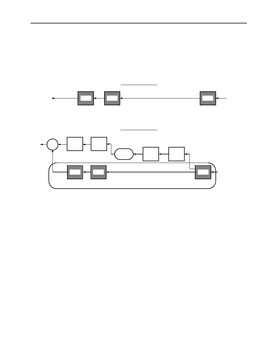
Data Sheet
MARS2G5 P-Pro (TDAT162G52) SONET/SDH
August 18, 2004
155/622/2488 Mbits/s Data Interface
499
Agere Systems Inc.
DS3/E3 Block
(continued)
E3 Functional Description
The DS3/E3 block is an enhancement of the DS3 block of the (TADM042G5 (TADMV1B)) device. The E3 subblock
was implemented in MARS2G5 P-Pro for E3 mapping into the VC-3, AU-3, and AUG path as shown in Figure 57.
The E3 (34.368 Mbits/s) signal is mapped into a VC-3 and then to an AU-3 as shown in Figure 58. The final step is
multiplexing the AU-3 map into an AUG.
2318(F)
Note: Shaded mappings are supported. AU-3 and STS-1 are equivalent.
Figure 57. DS3/E3 Mappings
C-3
STS-1
SPE
AU-3
VC-3
C-3
DS3
SONET DS3 MAPPING
SDH DS3/E3 MAPPING
AUG
AU-4
VC-4
TUG-3
TU-3
VC-3
x3
xN
x1
x3
x1
THIS PATH IS EQUIVALENT TO SONET STS-1
DS3 SPE MAPPING
DS3(44.736)
OR
E3 (34.368)

MARS2G5 P-Pro (TDAT162G52) SONET/SDH
Data Sheet
155/622/2488 Mbits/s Data Interface
August 18, 2004
500
Agere Systems Inc.
DS3/E3 Block
(continued)
E3 Functional Description
(continued)
2319(F)
Figure 58. VC-3 Into an AU-3
A 34.368 Mbits/s signal can be mapped into a VC-3 as shown in Figure 59. In addition to the VC-3 POH, the VC-3
consists of a payload of 9 x 84 bytes every 125 µs. This payload is divided in three subframes, each subframe con-
sisting of:
1431 data bits (D);
two sets of five justification control bits (C
1
, C
2
);
two justification opportunity bits (S
1
, S
2
);
573 fixed stuff bits (R);
Two sets of five justification control bits C
1
and C
2
are used to control the two justification opportunity bits S
1
and
S
2
, respectively.
C
1
C
2
C
3
C
4
C
5
= 00000 indicates that the S
1
is a data bit while C
1
C
2
C
3
C
4
C
5
= 11111 indicates that S
1
is a justifica-
tion bit. C
2
bits control S
2
in the same way. Majority vote should be used to make the justification decision in the
desynchronizer for protection against single and double bit errors in the C bits.
The value contained in S
1
and S
2
, when they are justification bits, is not defined. To maintain the E3 rate in the
transmit direction, the S
1
bit should be a fixed stuff bit while the S
2
bit is a data bit.
J1
B3
C2
G1
F2
H4
F3
K3
N1
1
29 30 31
58 59 60
87
AU-3
H1 H2 H3
VC-3 POH
FLOATING
VC-3 PLUS
(84 DATA COLUMNS)
PHASE
2 COLUMNS OF
FIXED STUFF
C-3
C-3
C-3

Data Sheet
MARS2G5 P-Pro (TDAT162G52) SONET/SDH
August 18, 2004
155/622/2488 Mbits/s Data Interface
501
Agere Systems Inc.
DS3/E3 Block
(continued)
E3 Functional Description
(continued)
2320(F)
Figure 59. Asynchronous Mapping of 34,368 kbits/s Tributary Into VC-3
E3 Frame Format
Requirements from ITU-T G.832 (10/98)
The basic G.832 E3 frame structure at 34,368 kbits/s comprises 7 octets of overhead and 530 octets of payload
capacity per 125 µs as shown in Table 463.
J1
B3
C2
G1
F2
H4
F3
K3
N1
VC-3 POH
T1
T2
84 bytes
1
C
C
3
3
3
3
3
3
3
3
3
3
3
3
3
3
3
3
3
3
3
3
3
3
3
3
3
3
3
3
3
3
3
3
3
3
3
3
3
3
3
3
3
3
3
3
3
3
3
3
3
3
3
3
3
3
3
3
3
3
3
C
C
C
A B 1
= RRRRRRRR (FIXED STUFF)
C = RRRRRRC
1
C
2
A = RRRRRRRS
1
B = S
2
DDDDDDD
3 = THREE DATA bytes (DDDDDDDD)
1 = ONE DATA byte (DDDDDDDD)
T3
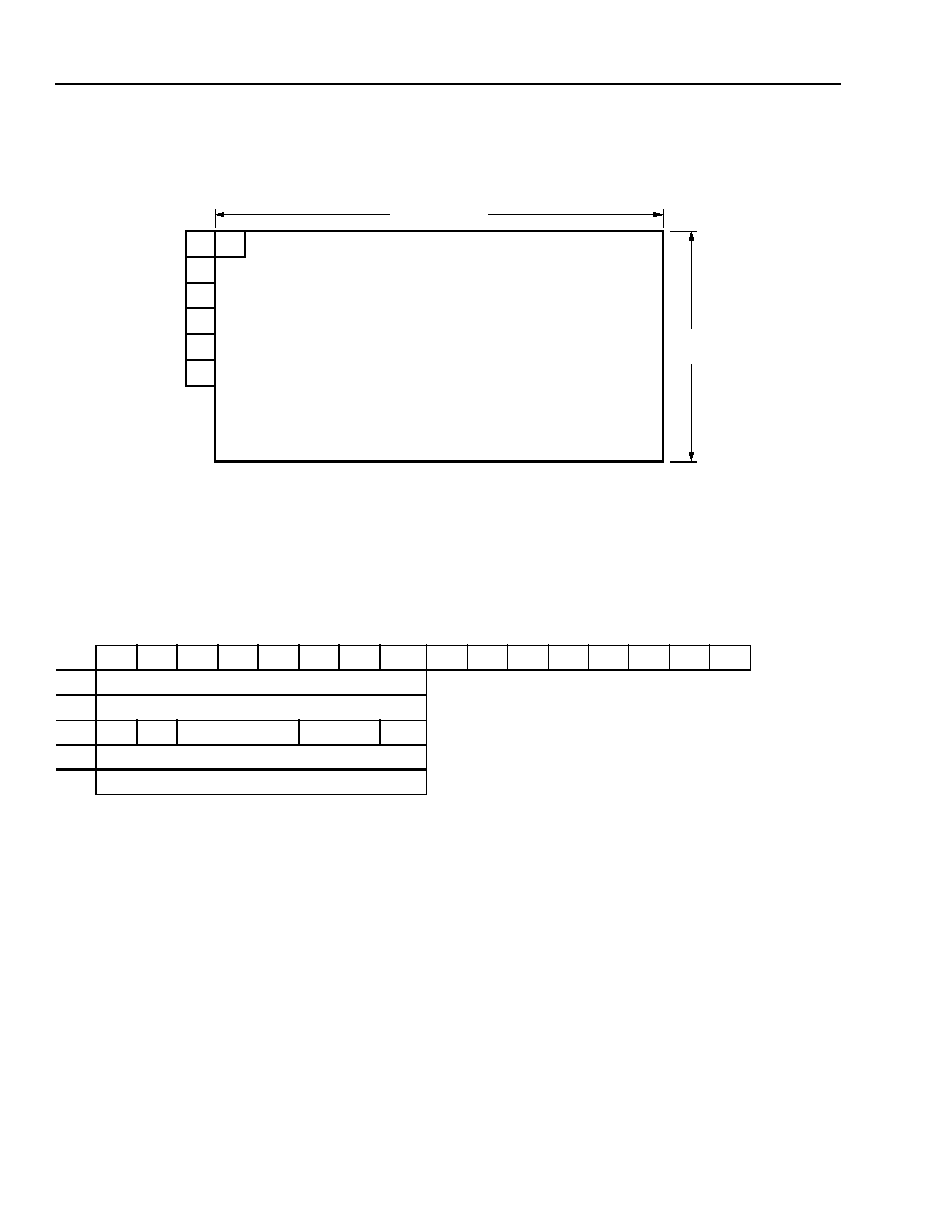
MARS2G5 P-Pro (TDAT162G52) SONET/SDH
Data Sheet
155/622/2488 Mbits/s Data Interface
August 18, 2004
502
Agere Systems Inc.
DS3/E3 Block
(continued)
E3 Functional Description
(continued)
2321(F)
Figure 60. G.832 E3 Frame Structure at 34,368 kbits/s
E3 Overhead Octets
The values and allocation of the overhead octets are shown in Table 460 and described below.
Table 460. Overhead Allocation at 34,368 kbits/s
FA1
1
1
1
1
0
1
1
0
0
0
1
0
1
0
0
0
FA2
EM
BIP-8
TR
Trail Trace--16-Byte Sequence
MA
RDI REI
Payload Type
MFI
SSM
NR
Network Operator Byte
GC
GP Communication Channel
530 OCTET PAYLOAD
FA1 FA2
EM
TR
MA
NR
GC
59 COLUMNS
9
ROWS

Data Sheet
MARS2G5 P-Pro (TDAT162G52) SONET/SDH
August 18, 2004
155/622/2488 Mbits/s Data Interface
503
Agere Systems Inc.
DS3/E3 Block
(continued)
E3 Functional Description
(continued)
Frame Synchronization Bytes (Frame Alignment: FA1/FA2)
Frame alignment signal values 0xF6/0x28 (11110110 00101000). This pattern is inserted at the transmitter at the
beginning of each 125 µs frame interval. The receiver identifies the pattern to establish frame alignment so that all
other bytes can be properly located and interpreted.
Performance Byte (Error Monitoring: EM)
One byte is allocated for error monitoring. This function will be a BIP-8 code using even parity. The BIP-8 is calcu-
lated over all bits, including the overhead bits, of the previous 125 µs frame. The receiver compares this received
parity value with the parity computed by receiver. The result of this comparison indicates the error performance of
the connection between the transmitter and the receiver.
Trail Trace Byte (TR)
This byte is used to repetitively transmit a trail access point identifier so that a trail receiving terminal can verify its
continued connection to the intended transmitter.
A 16-byte frame is defined for the transmission of the access point identifier. The most significant bit (MSB) of the
message is a logic 1 value while all other MSBs are 0.

MARS2G5 P-Pro (TDAT162G52) SONET/SDH
Data Sheet
155/622/2488 Mbits/s Data Interface
August 18, 2004
504
Agere Systems Inc.
DS3/E3 Block
(continued)
E3 Functional Description
(continued)
MA--Maintenance and Adaptation Byte
Each bit in the MA byte is defined in the table below.
Table 461. MA Byte Description
* Bit 0 is used in a four-frame multiframe. The phase of the multiframe is determined by the value of MA bits 2 and 1. The 4 bits of the multi-
frame are allocated to the synchronization status message (SSM).
When interworking with old equipment that used bit 0 as a timing marker (nonmultiframe), the new equipment
implementing the above requirement should be capable of being configured to transmit the old requirement as
given below.
Bit 0, timing marker. This bit is set to 0 to indicate that the timing source is traceable to a primary reference clock,
and is otherwise set to 1.
NR--Network Operator Byte
This byte is allocated for maintenance purposes specific to individual network operators. Its transparency from trail
termination to trail termination is not guaranteed. For tandem connection maintenance, the byte is used in accor-
dance with Annex D/G.707. Tandem connection maintenance is not supported by this block. This byte is not
supported.
GC
General purpose communication channel (e.g., to provide data/voice channel connection for maintenance pur-
poses). This byte is not supported.
Bit 7
RDI
Set when the associated receive E3 signal is in an alarm
state. This bit is controlled under software control only.
Bit 6
REI
This bit is set to 1 if one or more errors were detected by
the BIP-8, otherwise set to 0.
Bits[5:3]
Payload Type
Code
Signal
000
Unequipped
001
Equipped, Nonspecific
010
ATM
011
SDH TU-12s
Others
Undefined
Bits[2:0]
Multiframe
Indicator/
SSM*
Bit 2
Bit 1
Bit 0
0
0
SSM Bit 3 (MSB)
0
1
SSM Bit 2
1
0
SSM Bit 1
1
1
SSM Bit 0 (LSB)
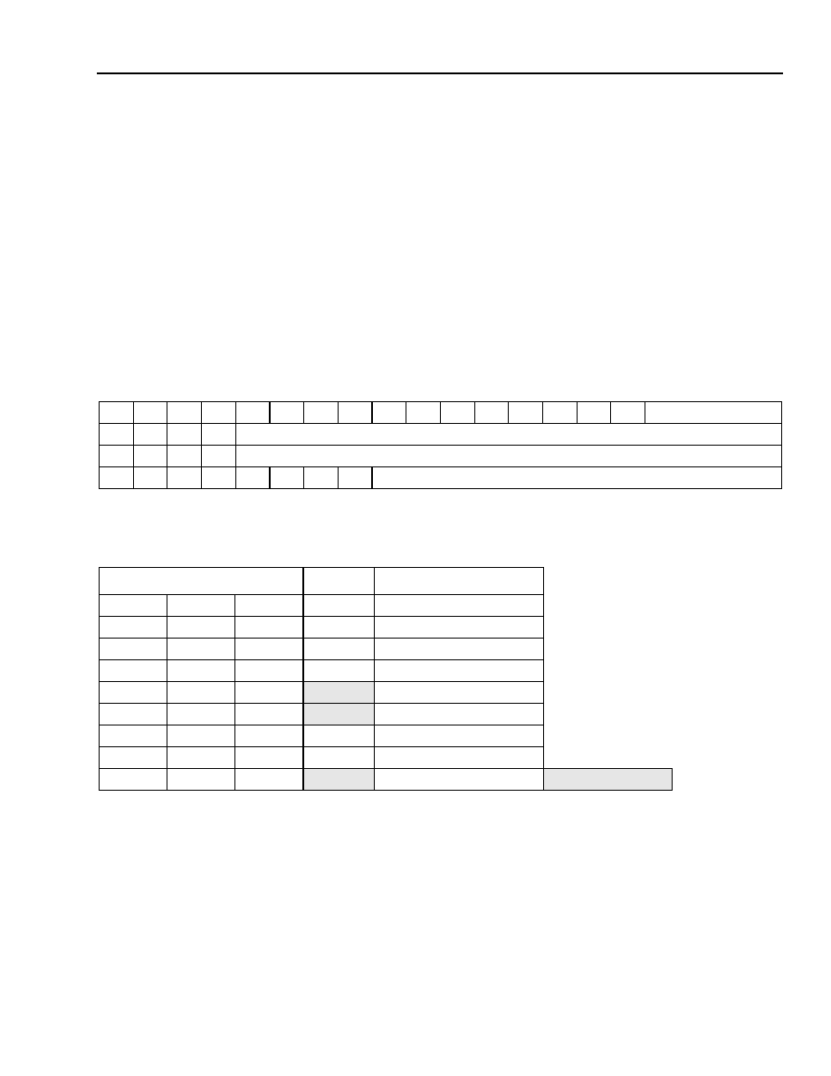
Data Sheet
MARS2G5 P-Pro (TDAT162G52) SONET/SDH
August 18, 2004
155/622/2488 Mbits/s Data Interface
505
Agere Systems Inc.
DS3/E3 Block
(continued)
E3 Functional Description
(continued)
Mapping of ATM Cells into 34,368 kbits/s--ITU-T G.804 (02/98)
The ATM cells are mapped into the 530 payload octets of the 34,368 kbit/s frame with the octet structure of the cell
aligned with the octet structure of the frame. The ATM cell payload (48 bytes) shall be scrambled before mapping
into the 34,368 kbit/s signal.
E3-PLCP Frame Format
The E3-PLCP format consists of 57 bytes x 9 rows with a programmable trailer of 17 to 21 octets in length. The
G.751 E3 framing bytes are defined to be (1111010000 A N 1100) as shown in the G.751 E3 frame in Table 462.
The overhead bits are defined as an alarm indication bit (A or RAI) and a national use bit (N). The least significant
nibble is set to a fixed pattern of 1100.
Table 462. G.751 E3 Frame Format
Note:
Framing occurs on 10-bit pattern 1111010000. When ATM cells are either directly mapped or with a PLCP frame, all C and J bits are
used as data bits.
Table 463. E3-PLCP Mapping of ATM Cells
1
1
1
1
0
1
0
0
0
0
RAI
NA
1
1
0
0
368 Payload Bits
C
11
C
21
C
31
C
41
380 Payload Bits
C
12
C
22
C
32
C
42
380 Payload Bits
C
13
C
23
C
33
C
43
J
1
J
2
J
3
J
4
376 Payload Bits
Framing (3 octets)
POH
53 octets
A1
A2
P8
Z3
ATM Cell
A1
A2
P7
Z2
ATM Cell
A1
A2
P6
Z1
ATM Cell
A1
A2
P5
F1
ATM Cell
A1
A2
P4
B1
ATM Cell
A1
A2
P3
G1
ATM Cell
A1
A2
P2
M2
ATM Cell
A1
A2
P1
M1
ATM Cell
A1
A2
P0
C1
ATM Cell
Trailer (17--21)

MARS2G5 P-Pro (TDAT162G52) SONET/SDH
Data Sheet
155/622/2488 Mbits/s Data Interface
August 18, 2004
506
Agere Systems Inc.
DS3/E3 Block
(continued)
E3 Functional Description
(continued)
E3-PLCP Field Definitions
The PLCP frame has framing, path overhead (POH), data, and trailer bytes.
Framing Octets (A1, A2). The first two columns (A1, A2) are used for frame delineation (A1 = 0xF6, A2 = 0x28).
Path Overhead Identifier (P0--P8). The third column identifies the PLCP overhead octets contained in the fourth
column of Table 463. The left most 6 bits of these octets provide numbering of the 9 rows. The 7th bit is reserved,
and the right-most bit (LSB) is parity bit. The reserved bit is set to 0. The parity bit provides odd parity over this
field. A code is considered invalid if it does not match a value in Table 464 or its parity bit is invalid and will not be
used to transition the in-PLCP-frame state.
PLCP Path User Channel (F1). The F1 octet is the user channel, which is allocated for user communication pur-
poses between adjacent PLCPs. The default code for this octet is 00000000.
Bit Interleaved Parity-8 (B1). One octet is allocated for PLCP path error monitoring. This function is a bit inter-
leaved parity-8 (BIP-8) code using even parity. The PLCP path BIP-8 is calculated over the 9 x 54 octet structure
(columns 4 to 57, numbering from 1) of the previous PLCP frame and inserted into the B1 of the current frame.
Table 464. Path Overhead Identifier Codes (POI)
POI
Row Count Value
Reserved
Odd Parity
P8
001
000
0
0
P7
000
111
0
0
P6
000
110
0
1
P5
000
101
0
1
P4
000
100
0
0
P3
000
011
0
1
P2
000
010
0
0
P1
000
001
0
0
P0
000
000
0
1

Data Sheet
MARS2G5 P-Pro (TDAT162G52) SONET/SDH
August 18, 2004
155/622/2488 Mbits/s Data Interface
507
Agere Systems Inc.
DS3/E3 Block
(continued)
E3 Functional Description
(continued)
PLCP Path Status (G1). The G1 octet is allocated to convey the received PLCP status and performance back to
the transmitting PLCP. The G1 octet consists of:
4 bits for far-end block error (FEBE--G1[7:4]) code.
-- FEBE code may be used to convey the count of the interleaved-bit blocks that have been detected to be in
error by the BIP-8 code in the preceding frame. If implemented, this count has nine legal values, namely zero
(0000) to eight (1000) errors. If not implemented, the code is 1111. All other codes are interpreted as zero er-
rors.
1 bit for the alarm signal (AS).
-- The AS bit is set to a logic 1 when a received failure is detected. This bit is set under software control only.
3 bits for a link status signal (LSS).
-- The remaining 3 bits are used for the LSS as described in IEEE Standard 802.6 Section 11.3.2. The LSS is
used to communicate information about the status of the transmission link between two adjacent PLCP entities.
The function is not supported and the bits are set to 111.
The G1 fields are illustrated in Table 465.
DQDB Layer Management Information Octets (M1, M2). The octets M1 and M2 carry the DQDB layer manage-
ment information octets that are described in IEEE Standard 802.6, Section 10.1. These bytes are not supported
and set to 0.
Table 465. PLCP G1 byte
7
6
5
4
3
2
1
0
FEBE
AS
LSS

MARS2G5 P-Pro (TDAT162G52) SONET/SDH
Data Sheet
155/622/2488 Mbits/s Data Interface
August 18, 2004
508
Agere Systems Inc.
DS3/E3 Block
(continued)
E3 Functional Description
(continued)
Stuffing (C1). The C1 octet indicates the PLCP frame in which an octet stuffing will occur and contains the number
of trailer octets transmitted (17 to 21). The allowed C1 codes are as per Table 466.
The C1 codes above provide error correction capability for one bit error and two adjacent bit errors, and error
detection capability for three random bit errors using the Abramson code (x
3
+ x + 1)(x + 1).
Growth Octets (Z1--Z3). These octets are reserved for future use. These octets are encoded to the default code
of 00000000.
Table 466. C1 Values and Transmit Insert Sequence
Trailer
Byte
Value
Numbering
Protection Code
Not
Used
Hex
7
6
5
4
3
2
1
0
17
001
1101
1
0x3B
18
010
0111
1
0x4F
19
011
1010
1
0x75
20
100
1110
1
0x9D
21
101
0011
1
0xA7
Transmit C1 Insert Sequence
Sequence
Type
Sequence
Repeat N times
A
18
19
18
19
18
6
B
18
19
1

Data Sheet
MARS2G5 P-Pro (TDAT162G52) SONET/SDH
August 18, 2004
155/622/2488 Mbits/s Data Interface
509
Agere Systems Inc.
DS3/E3 Block
(continued)
E3 Functional Description
(continued)
Register Description Control Bits for G.751 E3 Frame, E3 PLCP Frame, and G.832 Frame
This section describes the monitoring and insert capabilities for G.751 E3 frame, E3 PLCP frame, and G.832 E3
frame.
Rx/Tx Mode Control Definition. Three bits are used in the receive/transmit directions to determine the mapping/
demapping mode. See Table 467 and Table 468.
Table 467. Receive Mode Control Signals
Control Bit
Mode
Reset Default Mode
RDS3orE3
RDS3PLCP[1:0]
0
00
X/ No Mapping
000,
No Mapping
0
01
0
10
DS3/Clear Channel
Mapping
0
11
DS3/PLCP Mapping
1
00
X/No Mapping
1
01
E3/G.832 Frame
1
10
E3/G.751 Frame
1
11
E3/G.751 PLCP Mapping
Table 468. Transmit Mode Control Signals
Control Bit
Mode
Reset Default Mode
TDS3orE3
TDS3PLCP[1:0]
0
00
No Mapping
000,
No Mapping
0
01
DS3 Locked Mode
0
10
DS3 Clear Channel
0
11
DS3/PLCP Mapping
1
00
X/No Mapping
1
01
E3/G.832 Frame
1
10
E3/G751 Frame
1
11
E3/G751 PLCP Mapping

MARS2G5 P-Pro (TDAT162G52) SONET/SDH
Data Sheet
155/622/2488 Mbits/s Data Interface
August 19, 2004
510
Agere Systems Inc.
DS3/E3 Block
(continued)
E3 Functional Description
(continued)
G.751 E3 Frame. This block implements only direct or PLCP mapping into the G.751 E3 frame. ATM cells are octet
aligned with the 16 overhead bits at the start of each frame.
See Table 462 for the G.751 E3 frame format.
Table 469. G.751 E3 Frame Transmit Overhead Operation
Control Bit
Transmit Direction
Register Bits
Frame Alignment Signal
Insert value 10b`1111010000.
TE3_FA_INV[16--1]
RAI: Remote Alarm Indication (A)
Insert the RAI value under software control only.
TE3_RAI_DINS[16--1]
NA: National Use Bit
Set the NA bit to 0.
No Control Bit
C
jk
: Justification Service Bits
Included as part of payload.
No Control Bit
J
k
: Tributary Justification Bits
Included as part of payload.
No Control Bit
Table 470. G.751 E3 Frame Receive Overhead Operation
Control Bit
Receive Direction
Register Bits
Frame Alignment Signal
Out of frame = 0, when the pattern (10 or 14
bits) has been detected for three consecutive
frames.
Out of frame = 1, when four consecutive
frames are detected with errors.
Loss of frame = 1, when the associated OOF
bit is high continuously for a programmable
number of frame periods (range 0 to 4 ms in
125 µs steps).
Loss of frame = 0, when the associated OOF
bit is low continuously for a programmable
number of frame periods.
E3_OOF[A--B][12--1],
E3_OOF[A--B][12--1]D/M,
E3_G751_10or14bit_FRMPAT
E3_LOF[A--B][12--10],
E3_LOF[A--B][12--1]D/M
E3_LOF_SETCNT[4:0],
E3_LOF_CLRCNT[4:0]
RAI: Remote Alarm
Indication
Monitor with a programmable continuous N
times detect (CNTD), 0 to 15.
E3_G751_RAI_DET_CNTD[3:0],
E3_G751_RAI_DET[A--B][12--1],
E3_G751_RAI_DET[A--B][12--1]D/M
NA: National Use Bit
Not monitored.
No Control Bit
C
jk
: Justification Service
Bits
Process as part of payload.
No Control Bit
J
k
: Tributary Justification
Bits
Process as part of payload.
No Control Bit

Data Sheet
MARS2G5 P-Pro (TDAT162G52) SONET/SDH
August 18, 2004
155/622/2488 Mbits/s Data Interface
511
Agere Systems Inc.
DS3/E3 Block
(continued)
E3 Functional Description
(continued)
AIS Insertion and Detection.
Insertion. Under software control, an all 1s pattern can be generated to replace the G.751 E3 frame and payload
bytes (TE3_AISINS[16--1]).
Detection. E3_AISPAT_DET = 1, when less than a programmable number of 0s are detected during one complete
frame period while the framer is in the out-of-frame mode (E3_OOF = 1).
E3_AISPAT_DET = 0, when greater than or equal to a programmable number of 0s are detected during one com-
plete frame period, or the framer is in frame (E3_OOF = 0).
Register bits: E3_G751_AIS_0CNT[3:0] (Default Value = 5), E3_AISPAT_DET[A--B][12--1],
E3_AISPAT_DET[A--B][12--1]D/M.

MARS2G5 P-Pro (TDAT162G52) SONET/SDH
Data Sheet
155/622/2488 Mbits/s Data Interface
August 18, 2004
512
Agere Systems Inc.
DS3/E3 Block
(continued)
E3 Functional Description
(continued)
G.751 E3 PLCP Frame. The PLCP frame is octet aligned to the 16 overhead bits. There is no relationship between
the start of the PLCP frame and the start of the E3 frame.
Table 471. G.751 E3-PLCP Transmit Overhead Operation
Control Bit
Transmit Direction
Register Bits
A1, A2: Frame
Insert A1, A2 values (0xF6, 0x28),
respectively.
TE3_PLCP_A2_INV[16--1]
P0--P8: Path Overhead
Identifier
Insert per Table 464.
TE3_PLCP_POIB7_INV[16--1]
Z1--Z3: Growth
Insert a programmable value into the
selected time slot from the associated
software register; otherwise, insert a fixed
value of all zeros.
TE3_PLCP_ZF_CHID[5:0],
TE3_PLCP_Z1_DINS[7:0],TE3_
PLCP_Z2_DINS[7:0],
TE3_PLCP_Z3_DINS[7:0],
TE3_PLCP_F1_DINS[7:0],
F1: User Channel
B1: Bit Interleaved Parity
A calculated BIP-8 value over the previous
frame (Col. 4 to 57) is inserted into this byte.
TE3_PLCP_B1_INV
[16--1]
G1: Path Status
G1[7:4] = FEBE indicates the number of B1
errors detected in the receive direction. The
FEBE field has nine legal values (4b`0000 to
4b`1000). Its value can be inserted under
software control (used for testing).
G1[3] = AS, This bit is programmable
through the microprocessor interface.
G[2:0] = LSS, This function is not supported
and fixed to (3b`111).
TE3_PLCP_FEBE_SWEN
[16--1],
TE3_PLCP_FEBE_DINS
[3:0],
TE3_PLCP_G1_AS_DINS
[16--1]
M1 and M2: Control Information This function is not supported. Set both
octets to (00000000).
No control bits
C1: Stuff Counter
Table 466 defines the sequence used for the
C1 byte to yield a nominal PLCP frame rate
of 125 µs. The C1 value can only change by
±1 at any value change.
No control bits

Data Sheet
MARS2G5 P-Pro (TDAT162G52) SONET/SDH
August 18, 2004
155/622/2488 Mbits/s Data Interface
513
Agere Systems Inc.
DS3/E3 Block
(continued)
E3 Functional Description
(continued)
Table 472. G.751 E3-PLCP Receive Overhead Operation
Control Bit
Receive Direction
Register Bits
A1, A2: Frame
Out-of-frame = 0, when the pattern has been
detected for two consecutive rows, along with two
valid POI octets.
Out-of-frame = 1, when errors are detected in
both octets in a single row, or when errors are
detected in two consecutive POI octets.
Loss-of-frame = 1, when the associated OOF bit
is high continuously for a programmable number
of frame periods (range 0 to 4 ms in 125 µs
steps).
Loss-of-frame = 0, when the associated OOF bit
is low continuously for a programmable number of
frame periods.
E3_PLCP_OOF[A--B][12--1],
E3_PLCP_OOF[A--B][12--1]D/M
E3_PLCP_LOF[A--B][12--1],
E3_PLCP_LOF[A--B][12--1]D/M
E3_PLCP_LOF_SETCNT[4:0],
E3_PLCP_LOF_CLRCNT[4:0]
P0--P8: Path Overhead
Identifier
Used in PLCP framing.
No status bits
Z1--Z3: Growth
These bytes are independently monitored for a
CNTD value change.
E3_PLCP_ZF_CNTD[3:0],
E3_PLCP_ZF_TSSEL[A-D][3:0],
E3_PLCP_ZF_DMON
[A--B]D/M
E3_PLCP_Z1_DMON[A--B][7:0],
E3_PLCP_Z2_DMON[A--B][7:0],
E3_PLCP_Z3_DMON[A--B][7:0],
E3_PLCP_F1_DMON[A--B][7:0]
F1: User Channel
B1: Bit Interleaved Parity The received BIP-8 value is checked against the
calculated value. Any differences are
accumulated in a saturating counter. This counter
can count bit or block errors; this is a per block
control bit.
E3_PLCP_B1ERRCNT
[A--B][12--1][15:0],
E3_PLCP_B1_BITBLK
G1: Path Status
G1[7:4] = FEBE, All legal values are accumulated
in a saturating counter. This counter can
accumulate bit or block errors; this is a per block
control bit.
G1[3] = AS, This bit is monitored for a CNTD
value change. This is a per block control bit.
G[2:0] = LSS, This function is not supported and
ignored.
E3_PLCP_G1_FEBE_BITBLK,
E3_PLCP_G1_FEBE_ERRCNT
[A--B][12--1][15:0],
E3_PLCP_G1_AS[A--B][12--1],
E3_PLCP_G1_AS[A--B][12--
1]D/M,
E3_PLCP_G1_AS_CNTD[3:0]
M1 and M2: Control
Information
These octets are ignored.
No status bits
C1: Stuff Counter
The stuff counter is decoded and error correction
is performed to determine the number of trailer
bytes (see Stuffing (C1). The C1 octet indicates
the PLCP frame in which an octet stuffing will
occur and contains the number of trailer octets
transmitted (17 to 21). The allowed C1 codes are
as per Table 466. on page 508).
No status bits

MARS2G5 P-Pro (TDAT162G52) SONET/SDH
Data Sheet
155/622/2488 Mbits/s Data Interface
August 18, 2004
514
Agere Systems Inc.
DS3/E3 Block
(continued)
E3 Functional Description
(continued)
G.832 E3 Frame Overhead Operation. The G.832 E3 frame format allows direct byte mapping of ATM cells. ATM
cells are octet aligned with the G.832 E3 frame. This block does not support E3 PLCP mapped ATM cells in the
G.832 E3 frame.
Table 473. G.832 E3 Transmit Frame Overhead Operation
Control Bit
Transmit Direction
Register Bits
A1, A2: Frame
Insert FA1, FA2 as 0xF6, 0x28, respectively. The
framing pattern can be inverted under software
control.
TE3_FA_INV[16--1]
EM: Error Monitor BIP-8
Inserts even parity (BIP-8) calculated over the
entire frame including the overhead bits.
TE3_B1_INV[16--1]
TR: Trail Trace
Inserts the 16-byte identifier from provisionable
registers when enabled; otherwise, set TR byte to
00000000.
TE3_TR_INS[16--1],
TE3_TR_DINS[16--1][15--0][7:0]
MA: Maintenance and
Adaptation Byte
MA[7] = RDI, This bit is software provisionable
only.
MA[6] = REI, Set to 1 if one or more BIP-8 errors
were detected in the associated E3 signal. If the
error insert bit is zero, follow the hardware value;
otherwise, force the bit to 1 continuously.
MA[5:3] = Payload type. Insert value under soft-
ware control.
MA[2:0] = Multiframe indicator and SSM pattern.
Bits[2:1] are a multiframe pattern counting from 0
to 3. A multiframe count of 0 = MSB of SSM four
bit pattern. To support old equipment, set all SSM
values to 0 or 1.
TE3_MA_RDI_DINS[16--1],
TE3_MA_REI_ERRINS[16--1],
TE3_MA_PTYPE_DINS[16--
1][2:0],
TE3_MA_SSM[16--1][3:0].
NR: Network Operator
Byte
Inserts a fixed value (00000000) for this byte.
Software insert is not supported.
No control bits
GC: General-Purpose
Communication Channel
Inserts a fixed value (00000000) for this byte.
Software insert is not supported.
No control bits

Data Sheet
MARS2G5 P-Pro (TDAT162G52) SONET/SDH
August 18, 2004
155/622/2488 Mbits/s Data Interface
515
Agere Systems Inc.
DS3/E3 Block
(continued)
E3 Functional Description
(continued)
Table 474. G.832 E3 Receive Frame Overhead Operation
Control Bit
Receive Direction
Register Bits
A1, A2: Frame
Out of frame = 0, when the pattern has
been detected for two consecutive frames.
Out of frame = 1, when four consecutive
frame are detected with errors.
Loss of frame = 1, when the associated
OOF bit is high continuously for a
programmable number of frame periods
(range 0 to 4 ms in 125 µs steps).
Loss of frame = 0, when the associated
OOF bit is low continuously for a
programmable number of frame periods.
E3_OOF[A--B][12--1],
E3_OOF[A--B][12--1]D/M
E3_LOF[A--B][12--1],
E3_LOF[A--B][12--1]D/M
E3_LOF_SETCNT[4:0],
E3_LOF_CLRCNT[4:0]
EM: Error Monitor BIP-8
Computes the incoming BIP-8 and
compares that value to the incoming value.
Errors are accumulated in a 14-bit
saturating counter. Bit or block errors can
be accumulated (block control bit).
E3_B1_ERRCNT
[A--B][12--1][13:0],
E3_B1_BITBLK
TR: Trail Trace
Compares the TR 16-byte pattern with an
expected value. (See description in G.832
E3 Frame TR-Byte Processing on page
516.)
E3_TR_MODE[A--B][12--1][1:0],
E3_TR_MISMATCH
[A--B][12--1]D/M,
E3_TR_MISMATCH[A--B][12--1],
E3_TR_EXP[A--B][12--1][15--0][7:0],
E3_TR_CAP[A--B][12--1][15--0][7:0]
MA: Maintenance and
Adaptation Byte
MA[7] = RDI, this bit is monitored using a
CNTD monitor.
MA[6] = REI, A saturating counter accumu-
lates the REI values.
MA[5:3] = Payload type (PT). A CNTD
monitor is used on this field. A stable value
is accessible through the µP interface.
MA[2:0] = In nonmultiframe alignment
mode, bit 0 is monitored for a CNTD value.
In multiframe alignment mode, a CNTD
detection is performed on the 4-bit SSM
message.
E3_G832_MA_RDI_CNTD[3:0],
E3_G832_MA_RDI_DET
[A--B][12--1]D/M,
E3_G832_MA_RDI_DET
[A--B][12--1],
E3_MA_REI_ERRCNT
[A--B][12--1][13:0],
E3_MA_PT_CNTD[3:0],
E3_MA_PT[A--B][12--1]D/M,
E3_MA_PT_CODE
[A--B][12--1][2:0],
E3_MA_MF_ENABLE[A--B][12--1],
E3_MA_SSM_CNTD[3:0],
E3_MA_SSM[A--B][12--1]D/M,
E3_MA_SSM_CODE
[A--B][12--1][3:0]
NR: Network Operator
Byte
Byte not monitored.
No status bits
GC: General Purpose
Communication Channel
Byte not monitored.
No status bits

MARS2G5 P-Pro (TDAT162G52) SONET/SDH
Data Sheet
155/622/2488 Mbits/s Data Interface
August 18, 2004
516
Agere Systems Inc.
DS3/E3 Block
(continued)
E3 Functional Description
(continued)
AIS Insertion and Detection.
Insertion. Under software control an all 1s pattern can be generated to replace the G.751 E3 frame and payload
bytes (TE3_AISINS[16--1]).
Detection (Default = 8 Matches/Mismatches). E3_AISPAT_DET = 1, when less than a programmable number of
0s are detected during one complete frame period (E3 G.751 frame (192 bytes)), while the framer is in the out-of-
frame mode (E3_OOF = 1).
E3_AISPAT_DET = 0, when greater than or equal to a programmable number of 0s are detected during one com-
plete frame period, or the framer is in frame (E3_OOF = 0).
Register bits: E3_G832_AIS_0CNT[3:0], E3_AISPAT_DET[A--B][11--0], E3_AISPAT_DET[A--B][11--0]D/M.
G.832 E3 Frame TR-Byte Processing
The TR byte carries a repeating 16-byte message. The block extracts the message from all E3 channels and
stores the message in an internal register bank. Three types of monitoring are allowed:
1.
Mode = 00, disable function.
2.
Mode = 01, monitor for a mismatch between the incoming value and an expected value.
-- A mismatch is declared if the received message differs from the expected message for ten consecutive mes-
sages. A mismatch clears when 4-out-of-5 received messages match the expected message.
-- In this mode, the device frames on the most significant bit (MSB) of the first byte in the message being set to 1.
3.
Mode = 10, monitor for a sustained change in the message.
-- A sustained change is detected when the received message differs from the last stable message for ten con-
secutive messages. The new message then becomes the stable message and the device starts checking for
a sustained change from this new stable message.
-- In this mode, no framing on the MSB occurs.
4.
Mode = 11, capture incoming data.
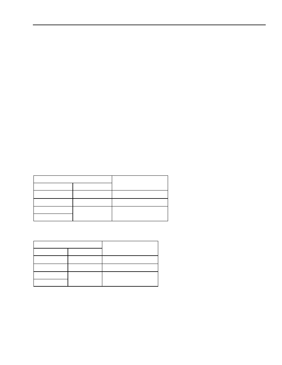
Data Sheet
MARS2G5 P-Pro (TDAT162G52) SONET/SDH
August 18, 2004
155/622/2488 Mbits/s Data Interface
517
Agere Systems Inc.
DS3/E3 Block
(continued)
E3 Functional Description
(continued)
Transmit Channel ID to Time-Slot Alarm Mapping
The control bits to provide this function are TxChidtoTSMapping[16--1][1:0][3:0], where [16--1] = channel ID num-
ber, [1:0] = slice (A = 00, B, C, or D = 11, respectively), and [3:0] = time slots 0 to 11. The following signals are
transferred from the receive in each mode.
1.
G.832 E3 framing mode.
-- MA byte, REI--One bit signal that toggles for each error detected in the received EM byte.
2.
G.751 E3 framing mode.
-- No status bits transferred.
3.
G.751 E3 PLCP framing mode.
-- G1 byte, FEBE, 4-bit field, and single toggles for each error.
PRBS Insert and Monitor
A 2
23
≠ 1 PRBS pattern can be generated and placed in either E3 frame or the E3 PLCP frame under software
control. See Table 475 and Table 476 for the control bit summary for the receive and transmit directions, respec-
tively. These bits, along with the other PRBS insert/monitor bits already defined (see DS3 requirements), control
the PRBS functions.
Table 475. PRBS Receive (Monitor) Pattern Control Signals
Control Bit
Mode
RPRBS23
RPRBS_15or20
0
0
2
15
≠ 1
0
1
2
20
≠ 1
1
X
2
23
≠ 1
1
Table 476. PRBS Transmit Pattern Control Signals
Control Bit
Mode
TPRBS23
TPRBS15or20
0
0
2
15
≠ 1
0
1
2
20
≠ 1
1
X
2
23
≠ 1
1

MARS2G5 P-Pro (TDAT162G52) SONET/SDH
Data Sheet
155/622/2488 Mbits/s Data Interface
August 18, 2004
518
Agere Systems Inc.
DS3/E3 Block
(continued)
DS3 Register Descriptions
DS3 Global Registers
Table 477. DS3E3_VERR, Version Control (RO)
Table 478. DS3_SCRATCHR, Scratch Register (R/W)
Table 479. DS3_CORW_GPOSEL, Clear-on-Read/Clear-on-Write Global Select for
Delta/Event Registers (R/W)
Address
Bit
Name
Function
Reset
Default
0x5000
15:8
--
Reserved. 0x00
7:0
DS3E3_VER[7:0]
Block Version. Indicates version number of this block.
0x00
Address
Bit
Name
Function
Reset
Default
0x5001
15:0
DS3_SCRATCH
[15:0]
Read/write register with no other internal DS3 connections. 0x0000
Address
Bit
Name
Function
Reset
Default
0x5002
15
DS3_COR_COWN
Control bit, when set (0) all delta and event registers
function in the clear-on-write (COW) mode; otherwise, they
function in the clear-on-read (COR) mode.
0
14:12
--
Reserved.
--
11
SEQ_RX
Monitor receive output signals (active-high)
DS3_TM_DATA <=
("00000000000000",
DS3_RXSYNC,
DS3_RXPM_A,
DS3_RXEOP_A,
DS3_RXPM_B,
DS3_RXEOP_B,
DS3_RXPM_C,
DS3_RXEOP_C,
DS3_RXPM_D,
DS3_RXEOP_D,
DS3_RXDATA_A,
DS3_RXDATA_B,
DS3_RXDATA_C,
DS3_RXDATA_D);
0x0

Data Sheet
MARS2G5 P-Pro (TDAT162G52) SONET/SDH
August 18, 2004
155/622/2488 Mbits/s Data Interface
519
Agere Systems Inc.
DS3/E3 Block
(continued)
DS3 Register Descriptions
(continued)
Table 479. DS3_CORW_GPOSEL, Clear-on-Read/Clear-on-Write Global Select for
Delta/Event Registers (R/W) (continued)
Address
Bit
Name
Function
Reset
Default
0x5002
10
TM_RX
Control inputs into the receive direction (active-high)
if (TM_RX = '1') the
PT_RXSYNC_i <= TM_DATA(40);
PT_RXJ1_A_i <= TM_DATA(39);
PT_RXPM_A_i <= TM_DATA(38);
PT_RXJ1_B_i <= TM_DATA(37);
PT_RXPM_B_i <= TM_DATA(36);
PT_RXJ1_C_i <= TM_DATA(35);
PT_RXPM_C_i <= TM_DATA(34);
PT_RXJ1_D_i <= TM_DATA(33);
PT_RXPM_D_i <= TM_DATA(32);
PT_RXDATA_A_i <= TM_DATA(31:24);
PT_RXDATA_B_i <= TM_DATA(23:16);
PT_RXDATA_C_i <= TM_DATA(15:8);
PT_RXDATA_D_i <= TM_DATA(7:0);
else
PT_RXSYNC_i <= PT_RXSYNC;
PT_RXJ1_A_i <= PT_RXJ1_A;
PT_RXPM_A_i <= PT_RXPM_A;
PT_RXDATA_A_i <= PT_RXDATA_A;
PT_RXJ1_B_i <= PT_RXJ1_B;
PT_RXPM_B_i <= PT_RXPM_B;
PT_RXDATA_B_i <= PT_RXDATA_B;
PT_RXJ1_C_i <= PT_RXJ1_C;
PT_RXPM_C_i <= PT_RXPM_C;
PT_RXDATA_C_i <= PT_RXDATA_C;
PT_RXJ1_D_i <= PT_RXJ1_D;
PT_RXPM_D_i <= PT_RXPM_D;
PT_RXDATA_D_i <= PT_RXDATA_D;
end if;
0x0
9
PT_TX
Monitor transmit output signals (active-high)
DS3_TM_DATA <= ("00",
PT_TXBR,
PT_TXBR_CID,
DS3_TXBR,
DS3_TXBR_CID,
DS3_TXPM,
DS3_TXCID,
DS3_TXDATA);
0x0

MARS2G5 P-Pro (TDAT162G52) SONET/SDH
Data Sheet
155/622/2488 Mbits/s Data Interface
August 18, 2004
520
Agere Systems Inc.
DS3/E3 Block
(continued)
DS3 Register Descriptions
(continued)
Table 479. DS3_CORW_GPOSEL, Clear-on-Read/Clear-on-Write Global Select for
Delta/Event Registers (R/W) (continued)
Address
Bit
Name
Function
Reset
Default
0x5002
8
TM_TX
Control inputs into the transmit direction (active-high)
DS3_TM_DATA <=
("00000000000000000",
"00000000000000000",
"00000000000000",
DS3_TXBR_CID,
DS3_TXBR);
if (TM_TX = '1') then
DE_TXDATA_i <= TM_DATA(31 0);
DE_TXPM_i <=
TM_DATA(32);
DE_TXDVLD_i <= TM_DATA(33);
DE_TXEOP_i <= TM_DATA(37:34);
DE_TXCID_i
<= TM_DATA(43: 38);
else
DE_TXDATA_i <= DE_TXDATA;
DE_TXPM_i <=
DE_TXPM;
DE_TXDVLD_i <= DE_TXDVLD;
DE_TXEOP_i <=
DE_TXEOP;
DE_TXCID_i <= DE_TXCID;
end if;
0x0
7:6
--
Reserved.
--
5:0
GPOSEL[5:0]
GPO_ADDRESS can be 0x00 to 0x2b. Configure the
GPO_ADDRESS to this register, and this address is
passed to DS3_GPO_MUX block to select one of GPO
outputs when it is selected to read.
000000

Data Sheet
MARS2G5 P-Pro (TDAT162G52) SONET/SDH
August 18, 2004
155/622/2488 Mbits/s Data Interface
521
Agere Systems Inc.
DS3/E3 Block
(continued)
DS3 Register Descriptions
(continued)
Interface A Delta/Event Registers
Table 480. DS3FRMD_A, DS3 Out-of-Frame Delta (COR/COW)
Table 481. DS3LOFD_A, DS3 Loss-of-Frame Delta (COR/COW)
Address
Bit
Name
Function
Reset
Default
0x5003
15:12
--
Reserved. 0x0
11:0
DS3_OOFD_
A[12--1]
Each time the DS3_OOF_A[12--1] state bit changes state
(0 to 1 or 1 to 0), the delta bit is set.
0x0FFF
Address
Bit
Name
Function
Reset
Default
0x5004
15:12
--
Reserved. 0x0
11:0
DS3_LOFD_
A[12--1]
Each time the DS3_LOF_A[12--1] state bit changes state
(0 to 1 or 1 to 0), the delta bit is set.
0x0FFF

MARS2G5 P-Pro (TDAT162G52) SONET/SDH
Data Sheet
155/622/2488 Mbits/s Data Interface
August 18, 2004
522
Agere Systems Inc.
DS3/E3 Block
(continued)
DS3 Register Descriptions
(continued)
Table 482. DS3SEFD_A, DS3 Severely Errored Frame (SEF) Delta (COR/COW)
Table 483. DS3AISD_A, DS3 AIS Detection Delta (COR/COW)
Table 484. DS3IDLED_A, DS3 Idle Detection Delta (COR/COW)
Table 485. DS3CBD_A, DS3 C-Bit Detect Delta (COR/COW)
Table 486. DS3RAID_A, DS3 X-Bit Detect Delta (COR/COW)
Address
Bit
Name
Function
Reset
Default
0x5005
15:12
--
Reserved. 0x0
11:0
DS3_SEFD_
A[12--1]
Each time the DS3_SEF_A[12--1] state bit changes state
(0 to 1 or 1 to 0), the delta bit is set.
0x0FFF
Address
Bit
Name
Function
Reset
Default
0x5006
15:12
--
Reserved. 0x0
11:0
DS3_AISPAT_
DETD_A[12--1]
Each time the DS3_AISPAT_DET_A[12--1] state bit
changes state (0 to 1 or 1 to 0), the delta bit is set.
0x000
Address
Bit
Name
Function
Reset
Default
0x5007
15:12
--
Reserved. 0x0
11:0
DS3_IDLEPAT_
DETD_A[12--1]
Each time the DS3_IDLEPAT_DET_A[12--1] state bit
changes state (0 to 1 or 1 to 0), the delta bit is set.
0x000
Address
Bit
Name
Function
Reset
Default
0x5008
15:12
--
Reserved. 0x0
11:0
DS3_CBZ_DETD_
A[12--1]
Each time the DS3_CBZ_DET_A[12--1] state bit changes
state (0 to 1 or 1 to 0), the delta bit is set.
0x000
Address
Bit
Name
Function
Reset
Default
0x5009
15:12
--
Reserved. 0x0
11:0
DS3_RAI_DETD_
A[12--1]
Each time the DS3_RAI_DET_A[12--1] state bit changes
state (0 to 1 or 1 to 0), the delta bit is set.
0x000

Data Sheet
MARS2G5 P-Pro (TDAT162G52) SONET/SDH
August 18, 2004
155/622/2488 Mbits/s Data Interface
523
Agere Systems Inc.
DS3/E3 Block
(continued)
DS3 Register Descriptions
(continued)
Table 487. DS3FEACALMD_A, DS3 Far-End Alarm and Control (FEAC) RAI Delta (COR/COW)
Table 488. DS3FEACCTLD_A, DS3 Far-End Alarm and Control (FEAC) Control Delta (COR/COW)
Table 489. DS3_PLCPOOFD_A, PLCP Out-of-Frame Monitor Delta (COR/COW)
Table 490. DS3_PLCPRAID_A, PLCP RAI (G1[3]) Monitoring Delta (COR/COW)
Table 491. DS3_RXPRBS_SYNCD_A, PRBS Detector Sync Delta (COR/COW)
Address
Bit
Name
Function
Reset
Default
0x500A
15:12
--
Reserved. 0x0
11:0
DS3_RFEAC_RAID_
A[12--1]
Each time the DS3_RFEAC_RAI_A[12--1] state bit
changes state (0 to 1 or 1 to 0), the delta bit is set.
0x000
Address
Bit
Name
Function
Reset
Default
0x500B
15:12
--
Reserved. 0x0
11:0
DS3_RFEAC_
CTLD_A[12--1]
Each time the DS3_RFEAC_CTL_A[12--1] state bit
changes state (0 to 1 or 1 to 0), the delta bit is set.
0x0FFF
Address
Bit
Name
Function
Reset
Default
0x500C
15:12
--
Reserved. 0x0
11:0
DS3_PLCP_OOFD_
A[12--1]
Each time the DS3_PLCP_OOF_A[12--1] state bit
changes state (0 to 1 or 1 to 0), the delta bit is set.
0x0FFF
Address
Bit
Name
Function
Reset
Default
0x500D
15:12
--
Reserved. 0x0
11:0
DS3_PLCP_G1_
RAID_A[12--1]
Each time the DS3_PLCP_G1_RAI_A[12--1] state bit
changes state (0 to 1 or 1 to 0), the delta bit is set.
0x000
Address
Bit
Name
Function
Reset
Default
0x500E
15:2
--
Reserved. 0x000
1:0
DS3_RPRBS_
SYNC_ERRD_A[1:0]
Each time the DS3_RPRBS_SYNC_ERR_A[12--1] state
bit changes state (0 to 1 or 1 to 0), the delta bit is set.
11

MARS2G5 P-Pro (TDAT162G52) SONET/SDH
Data Sheet
155/622/2488 Mbits/s Data Interface
August 18, 2004
524
Agere Systems Inc.
DS3/E3 Block
(continued)
DS3 Register Descriptions
(continued)
Interface B Delta/Event Registers
Table 492. DS3FRMD_B, DS3 Out-of-Frame Delta (COR/COW)
Table 493. DS3LOFD_B, DS3 Loss-of-Frame Delta (COR/COW)
Table 494. DS3SEFD_B, DS3 Severely Errored Frame (SEF) Delta (COR/COW)
Table 495. DS3AISD_B, DS3 AIS Detection Delta (COR/COW)
Table 496. DS3IDLED_B, DS3 Idle Detection Delta (COR/COW)
Address
Bit
Name
Function
Reset
Default
0x500F
15:12
--
Reserved. 0x0
11:0
DS3_OOFD_
B[12--1]
Each time the DS3_OOF_B[12--1] state bit changes state
(0 to 1 or 1 to 0), the delta bit is set.
0x0FFF
Address
Bit
Name
Function
Reset
Default
0x5010
15:12
--
Reserved. 0x0
11:0
DS3_LOFD_
B[12--1]
Each time the DS3_LOF_B[12--1] state bit changes state
(0 to 1 or 1 to 0), the delta bit is set.
0x0FFF
Address
Bit
Name
Function
Reset
Default
0x5011
15:12
--
Reserved. 0x0
11:0
DS3_SEFD_
B[12--1]
Each time the DS3_SEF_B[12--1] state bit changes state
(0 to 1 or 1 to 0), the delta bit is set.
0x0FFF
Address
Bit
Name
Function
Reset
Default
0x5012
15:12
--
Reserved. 0x0
11:0
DS3_AISPAT_
DETD_B[12--1]
Each time the DS3_AISPAT_DET_B[12--1] state bit
changes state (0 to 1 or 1 to 0), the delta bit is set.
0x000
Address
Bit
Name
Function
Reset
Default
0x5013
15:12
--
Reserved. 0x0
11:0
DS3_IDLEPAT_
DETD_B[12--1]
Each time the DS3_IDLEPAT_DET_B[12--1] state bit
changes state (0 to 1 or 1 to 0), the delta bit is set.
0x000

Data Sheet
MARS2G5 P-Pro (TDAT162G52) SONET/SDH
August 18, 2004
155/622/2488 Mbits/s Data Interface
525
Agere Systems Inc.
DS3/E3 Block
(continued)
DS3 Register Descriptions
(continued)
Table 497. DS3CBD_B, DS3 C-Bit Detect Delta (COR/COW)
Table 498. DS3RAID_B, DS3 X-Bit Detect Delta (COR/COW)
Table 499. DS3FEACALMD_B, DS3 Far-End Alarm and Control (FEAC) RAI Delta (COR/COW)
Table 500. DS3FEACCTLD_B, DS3 Far-End Alarm and Control (FEAC) Control Delta (COR/COW)
Table 501. DS3_PLCPOOFD_B, PLCP Out-of-Frame Monitor Delta (COR/COW)
Address
Bit
Name
Function
Reset
Default
0x5014
15:12
--
Reserved. 0x0
11:0
DS3_CBZ_DETD_
B[12--1]
Each time the DS3_CBZ_DET_B[12--1] state bit changes
state (0 to 1 or 1 to 0), the delta bit is set.
0x000
Address
Bit
Name
Function
Reset
Default
0x5015
15:12
--
Reserved. 0x0
11:0
DS3_RAI_DETD_
B[12--1]
Each time the DS3_RAI_DET_B[12--1] state bit changes
state (0 to 1 or 1 to 0), the delta bit is set.
0x000
Address
Bit
Name
Function
Reset
Default
0x5016
15:12
--
Reserved. 0x0
11:0
DS3_RFEAC_RAID_
B[12--1]
Each time the DS3_RFEAC_RAI_B[12--1] state bit
changes state (0 to 1 or 1 to 0), the delta bit is set.
0x000
Address
Bit
Name
Function
Reset
Default
0x5017
15:12
--
Reserved. 0x0
11:0
DS3_RFEAC_
CTLD_B[12--1]
Each time the DS3_RFEAC_CTL_B[12--1] state bit
changes state (0 to 1 or 1 to 0), the delta bit is set.
0x0FFF
Address
Bit
Name
Function
Reset
Default
0x5018
15:12
--
Reserved. 0x0
11:0
DS3_PLCP_OOFD_
B[12--1]
Each time the DS3_PLCP_OOF_B[12--1] state bit
changes state (0 to 1 or 1 to 0), the delta bit is set.
0x0FFF

MARS2G5 P-Pro (TDAT162G52) SONET/SDH
Data Sheet
155/622/2488 Mbits/s Data Interface
August 18, 2004
526
Agere Systems Inc.
DS3/E3 Block
(continued)
DS3 Register Descriptions
(continued)
Table 502. DS3_PLCPRAID_B, PLCP RAI (G1[3]) Monitoring Delta (COR/COW)
Table 503. DS3_RXPRBS_SYNCD_B, PRBS Detector Sync Delta (COR/COW)
Transmit Direction FIFO Overflow/Underflow Event
Table 504. DS3_TXFIFOERRE, FIFO Overflow Indicator Event (COR/COW)
Transmit Direction EOP Marker Error Event
Table 505. DS3_TXEOPERRER, EOP Marker Error Event (COR/COW)
Address
Bit
Name
Function
Reset
Default
0x5019
15:12
--
Reserved. 0x0
11:0
DS3_PLCP_G1_
RAID_B[12--1]
Each time the DS3_PLCP_G1_RAI_B[12--1] state bit
changes state (0 to 1 or 1 to 0), the delta bit is set.
0x000
Address
Bit
Name
Function
Reset
Default
0x501A
15:2
--
Reserved. 0x000
1:0
DS3_RPRBS_
SYNC_ERRD_B[1:0]
Each time the DS3_RPRBS_SYNC_ERR_B[2:1] state bit
changes state (0 to 1 or 1 to 0), the delta bit is set.
11
Address
Bit
Name
Function
Reset
Default
0x5033
15:0
DS3_TFIFO_OVR_
UNFLE[16--1]
Transmit FIFO overflow or underflow event indication
(active-high).
0x0000
Address
Bit
Name
Function
Reset
Default
0x5036
15:0
DS3_TXEOPERRE
[16--1]
EOP marker in PLCP or DS3 locked mode changed
position.
0

Data Sheet
MARS2G5 P-Pro (TDAT162G52) SONET/SDH
August 18, 2004
155/622/2488 Mbits/s Data Interface
527
Agere Systems Inc.
DS3/E3 Block
(continued)
DS3 Register Descriptions
(continued)
Interface A Mask Registers
Table 506. DS3FRMM_A, DS3 Out-of-Frame Mask (R/W)
Table 507. DS3LOFM_A, DS3 Loss-of-Frame Mask (R/W)
Table 508. DS3SEFM_A, DS3 Severely Errored Frame (SEF) Mask (R/W)
Table 509. DS3AISM_A, DS3 AIS Detection Mask (R/W)
Table 510. DS3IDLEM_A, DS3 Idle Detection Mask (R/W)
Address
Bit
Name
Function
Reset
Default
0x5039
15:12
--
Reserved. 0x0
11:0
DS3_OOFM_
A[12--1]
DS3 Out-of-Frame Mask. When set high, the delta will not
contribute to the interrupt signal.
0xFFF
Address
Bit
Name
Function
Reset
Default
0x503A
15:12
--
Reserved. 0x0
11:0
DS3_LOFM_
A[12--1]
DS3 Loss-of-Frame Mask. When set high, the delta will
not contribute to the interrupt signal.
0xFFF
Address
Bit
Name
Function
Reset
Default
0x503B
15:12
--
Reserved. 0x0
11:0
DS3_SEFM_
A[12--1]
DS3 Severely Errored Frame (SEF) Mask. When set
high, the delta will not contribute to the interrupt signal.
0xFFF
Address
Bit
Name
Function
Reset
Default
0x503C
15:12
--
Reserved. 0x0
11:0
DS3_AISPAT_
DETM_A[12--1]
DS3 AIS Detection Mask. When set high, the delta will not
contribute to the interrupt signal.
0xFFF
Address
Bit
Name
Function
Reset
Default
0x503D
15:12
--
Reserved. 0x0
11:0
DS3_IDLEPAT_
DETM_A[12--1]
DS3 Idle Detection Mask. When set high, the delta will not
contribute to the interrupt signal.
0xFFF

MARS2G5 P-Pro (TDAT162G52) SONET/SDH
Data Sheet
155/622/2488 Mbits/s Data Interface
August 18, 2004
528
Agere Systems Inc.
DS3/E3 Block
(continued)
DS3 Register Descriptions
(continued)
Table 511. DS3CBM_A, DS3 C-Bit Detect Mask (R/W)
Table 512. DS3RAIM_A, DS3 X-Bit Detect Mask (R/W)
Table 513. DS3FEACALMM_A, DS3 Far-End Alarm and Control (FEAC) Alarm Mask (R/W)
Table 514. DS3FEACCTLM_A, DS3 Far-End Alarm and Control (FEAC) Control Mask (R/W)
Table 515. DS3_PLCPOOFM_A, PLCP Out-of-Frame Monitor Mask (R/W)
Address
Bit
Name
Function
Reset
Default
0x503E
15:12
--
Reserved. 0x0
11:0
DS3_CBZ_DETM_
A[12--1]
DS3 C-Bit Detect Mask. When set high, the delta will not
contribute to the interrupt signal.
0xFFF
Address
Bit
Name
Function
Reset
Default
0x503F
15:12
--
Reserved. 0x0
11:0
DS3_RAI_DETM_
A[12--1]
DS3 X-Bit Detect Mask. When set high, the delta will not
contribute to the interrupt signal.
0xFFF
Address
Bit
Name
Function
Reset
Default
0x5040
15:12
--
Reserved. 0x0
11:0
DS3_RFEAC_RAIM_
A[12--1]
DS3 Far-End Alarm and Control (FEAC) Alarm Mask.
When set high, the delta will not contribute to the interrupt
signal.
0xFFF
Address
Bit
Name
Function
Reset
Default
0x5041
15:12
--
Reserved. 0x0
11:0
DS3_RFEAC_
CTLM_A[12--1]
DS3 Far-End Alarm and Control (FEAC) Control Mask.
When set high, the delta will not contribute to the interrupt
signal.
0xFFF
Address
Bit
Name
Function
Reset
Default
0x5042
15:12
--
Reserved. 0x0
11:0
DS3_PLCP_OOFM_
A[12--1]
PLCP Out-of-Frame Monitor Mask. When set high, the
delta will not contribute to the interrupt signal.
0xFFF

Data Sheet
MARS2G5 P-Pro (TDAT162G52) SONET/SDH
August 18, 2004
155/622/2488 Mbits/s Data Interface
529
Agere Systems Inc.
DS3/E3 Block
(continued)
DS3 Register Descriptions
(continued)
Table 516. DS3_PLCPRAIM_A, PLCP RAI (G1[3]) Monitoring Mask (R/W)
Table 517. DS3_RXPRBS_SYNCM_A, PRBS Detector Sync Mask (R/W)
Interface B Mask Registers
Table 518. DS3_DS3FRMM_B, DS3 Out-of-Frame Mask (R/W)
Table 519. DS3LOFM_B, DS3 Loss-of-Frame Mask (R/W)
Table 520. DS3SEFM_B, DS3 Severely Errored Frame (SEF) Mask (R/W)
Address
Bit
Name
Function
Reset
Default
0x5043
15:12
--
Reserved. 0x0
11:0
DS3_PLCP_G1_
RAIM_A[12--1]
PLCP RAI (G1[3]) Monitoring Mask. When set high, the
delta will not contribute to the interrupt signal.
0xFFF
Address
Bit
Name
Function
Reset
Default
0x5044
15:2
--
Reserved. 0x000
1:0
DS3_RPRBS_
SYNC_ERRM_A[1:0]
PRBS Detector Sync Mask. When set high, the delta will
not contribute to the interrupt signal.
11
Address
Bit
Name
Function
Reset
Default
0x5045
15:12
--
Reserved. 0x0
11:0
DS3_DS3_OOFM_
B[12--1]
DS3 Out-of-Frame Mask. When set high, the delta will not
contribute to the interrupt signal.
0xFFF
Address
Bit
Name
Function
Reset
Default
0x5046
15:12
--
Reserved. 0x0
11:0
DS3_LOFM_
B[12--1]
DS3 Loss-of-Frame Mask. When set high, the delta will
not contribute to the interrupt signal.
0xFFF
Address
Bit
Name
Function
Reset
Default
0x5047
15:12
--
Reserved. 0x0
11:0
DS3_SEFM_
B[12--1]
DS3 Severely Errored Frame (SEF) Mask. When set
high, the delta will not contribute to the interrupt signal.
0xFFF

MARS2G5 P-Pro (TDAT162G52) SONET/SDH
Data Sheet
155/622/2488 Mbits/s Data Interface
August 18, 2004
530
Agere Systems Inc.
DS3/E3 Block
(continued)
DS3 Register Descriptions
(continued)
Table 521. DS3AISM_B, DS3 AIS Detection Mask (R/W)
Table 522. DS3IDLEM_B, DS3 Idle Detection Mask (R/W)
Table 523. DS3CBM_B, DS3 C-Bit Detect Mask (R/W)
Table 524. DS3RAIM_B, DS3 X-Bit Detect Mask (R/W)
Table 525. DS3FEACALMM_B, DS3 Far-End Alarm and Control (FEAC) Alarm Mask (R/W)
Address
Bit
Name
Function
Reset
Default
0x5048
15:12
--
Reserved. 0x0
11:0
DS3_AISPAT_
DETM_B[12--1]
DS3 AIS Detection Mask. When set high, the delta will not
contribute to the interrupt signal.
0xFFF
Address
Bit
Name
Function
Reset
Default
0x5049
15:12
--
Reserved. 0x0
11:0
DS3_IDLEPAT_
DETM_B[12--1]
DS3 Idle Detection Mask. When set high, the delta will not
contribute to the interrupt signal.
0xFFF
Address
Bit
Name
Function
Reset
Default
0x504A
15:12
--
Reserved. 0x0
11:0
DS3_CBZ_DETM_
B[12--1]
DS3 C-Bit Detect Mask. When set high, the delta will not
contribute to the interrupt signal.
0xFFF
Address
Bit
Name
Function
Reset
Default
0x504B
15:12
--
Reserved. 0x0
11:0
DS3_RAI_DETM_
B[12--1]
DS3 X-Bit Detect Mask. When set high, the delta will not
contribute to the interrupt signal.
0xFFF
Address
Bit
Name
Function
Reset
Default
0x504C
15:12
--
Reserved. 0x0
11:0
DS3_RFEAC_RAIM_
B[12--1]
DS3 Far-End Alarm and Control (FEAC) Alarm Mask.
When set high, the delta will not contribute to the interrupt
signal.
0xFFF

Data Sheet
MARS2G5 P-Pro (TDAT162G52) SONET/SDH
August 18, 2004
155/622/2488 Mbits/s Data Interface
531
Agere Systems Inc.
DS3/E3 Block
(continued)
DS3 Register Descriptions
(continued)
Table 526. DS3FEACCTLM_B, DS3 Far-End Alarm and Control (FEAC) Control Mask (R/W)
Table 527. DS3_PLCPOOFM_B, PLCP Out-of-Frame Monitor Mask (R/W)
Table 528. DS3_PLCPRAIM_B, PLCP RAI (G1[3]) Monitoring Mask (R/W)
Table 529. DS3_RXPRBS_SYNCM_B, PRBS Detector Sync Mask (R/W)
Address
Bit
Name
Function
Reset
Default
0x504D
15:12
--
Reserved. 0x0
11:0
DS3_RFEAC_
CTLM_B[12--1]
DS3 Far-End Alarm and Control (FEAC) Control Mask.
When set high, the delta will not contribute to the interrupt
signal.
0xFFF
Address
Bit
Name
Function
Reset
Default
0x504E
15:12
--
Reserved. 0x0
11:0
DS3_PLCP_OOFM_
B[12--1]
PLCP Out-of-Frame Monitor Mask. When set high, the
delta will not contribute to the interrupt signal.
0xFFF
Address
Bit
Name
Function
Reset
Default
0x504F
15:12
--
Reserved. 0x0
11:0
DS3_PLCP_G1_
RAIM_B[12--1]
PLCP RAI (G1[3]) Monitoring Mask. When set high, the
delta will not contribute to the interrupt signal.
0xFFF
Address
Bit
Name
Function
Reset
Default
0x5050
15:2
--
Reserved. 0x000
1:0
DS3_RPRBS_
SYNC_ERRM_B[1:0]
PRBS Detector Sync Mask. When set high, the delta will
not contribute to the interrupt signal.
11

MARS2G5 P-Pro (TDAT162G52) SONET/SDH
Data Sheet
155/622/2488 Mbits/s Data Interface
August 18, 2004
532
Agere Systems Inc.
DS3/E3 Block
(continued)
DS3 Register Descriptions
(continued)
Transmit Direction FIFO Overflow/Underflow Mask
Table 530. DS3_TXFIFOERRM, FIFO Overflow Indicator Mask (R/W)
Transmit Direction EOP Marker Error Mask
Table 531. DS3_TXEOPERRM, EOP Marker Error Mask (R/W)
Address
Bit
Name
Function
Reset
Default
0x5069
15:0
DS3_TFIFO_OVR_
UNFLM[16--1]
FIFO Overflow Indicator Mask. Transmit FIFO overflow or
underflow event indication (active-high).
0xFFFF
Address
Bit
Name
Function
Reset
Default
0x506C
15:0
DS3_TXEOPERRM
[16--1]
EOP Marker Error Mask. EOP marker in PLCP or DS3
locked mode changed position.
0xFFFF

Data Sheet
MARS2G5 P-Pro (TDAT162G52) SONET/SDH
August 18, 2004
155/622/2488 Mbits/s Data Interface
533
Agere Systems Inc.
DS3/E3 Block
(continued)
DS3 Register Descriptions
(continued)
Interface A State Registers
Table 532. DS3FRM_A, DS3 Out-of-Frame State (RO)
Table 533. DS3LOF_A, DS3 Loss-of-Frame State (RO)
Table 534. DS3SEF_A, DS3 Severely Errored Frame (SEF) (RO)
Table 535. DS3AIS_A, DS3 AIS Detection (RO)
Address
Bit
Name
Function
Reset
Default
0x506F
15:12
--
Reserved. 0x0
11:0
DS3_OOF_A[12--1] DS3 Out-of-Frame State. State bit indicating on a per slice
and time-slot basis if the DS3 framer is in frame. 0 = in
frame, 1 = out of frame.
0xFFF
Address
Bit
Name
Function
Reset
Default
0x5070
15:12
--
Reserved. 0x0
11:0
DS3_LOF_A[12--1]
DS3 Loss-of-Frame State. State bit is set (1) when the
DS3 framer is in the out-of-frame state for 28 continuous
frame periods (approximately 3 ms).
0xFFF
Address
Bit
Name
Function
Reset
Default
0x5071
15:12
--
Reserved. 0x0
11:0
DS3_SEF_A[12--1]
A SEF defect is the occurrence of three or more F-bit errors
in 16 consecutive F bits. A SEF is cleared when the signal
is in-frame and there are less than 3 F-bit errors in 16
consecutive F bits.
0xFFF
Address
Bit
Name
Function
Reset
Default
0x5072
15:12
--
Reserved. 0x0
11:0
DS3_AISPAT_DET_
A[12--1]
AIS is declared if fewer than five pattern errors (1010) are
received in each of two consecutive M-frames. AIS is
cleared when at least 16 pattern errors are received in each
of two consecutive M-frames.
0x000

MARS2G5 P-Pro (TDAT162G52) SONET/SDH
Data Sheet
155/622/2488 Mbits/s Data Interface
August 18, 2004
534
Agere Systems Inc.
DS3/E3 Block
(continued)
DS3 Register Descriptions
(continued)
Table 536. DS3IDLE_A, DS3 Idle Detection (RO)
Table 537. DS3CB_A, DS3 C-Bit Detect (RO)
Table 538. DS3RAI_A, DS3 X-Bit Detect (RO)
Table 539. DS3FEACALM_A, DS3 Far-End Alarm and Control (FEAC) (RO)
Address
Bit
Name
Function
Reset
Default
0x5073
15:12
--
Reserved. 0x0
11:0
DS3_IDLEPAT_
DET_A[12--1]
Idle is declared if fewer than five pattern errors (1100) are
received in each of two consecutive M-frames. Idle is
cleared when at least 16 pattern errors are received in each
of two consecutive M-frames.
0x000
Address
Bit
Name
Function
Reset
Default
0x5074
15:12
--
Reserved. 0x0
11:0
DS3_CBZ_DET_
A[12--1]
Set if every C bit in three consecutive M frames are set to
0; clear if the three C bits in a M subframe are 1.
0x000
Address
Bit
Name
Function
Reset
Default
0x5075
15:12
--
Reserved. 0x0
11:0
DS3_RAI_DET_
A[12--1]
Set if both X bits in two consecutive M frames are received
as 0; clear when both X bits in two consecutive M frames
are received as 1.
0x000
Address
Bit
Name
Function
Reset
Default
0x5076
15:12
--
Reserved. 0x0
11:0
DS3_RFEAC_RAI_
A[12--1]
If the validated code equals (011001, 001110, 000000, or
010110), then the RAI state bit is set. When the validated
code word does not equal one of the patterns above, the
RAI state bit is 0.
0x000

Data Sheet
MARS2G5 P-Pro (TDAT162G52) SONET/SDH
August 18, 2004
155/622/2488 Mbits/s Data Interface
535
Agere Systems Inc.
DS3/E3 Block
(continued)
DS3 Register Descriptions
(continued)
Table 540. DS3FEACCTL_A, DS3 Far-End Alarm and Control (FEAC) (RO)
Table 541. DS3_PLCPOOF_A, PLCP Out-of-Frame Monitor (RO)
Table 542. DS3_PLCPRAI_A, PLCP RAI (G1[3]) Monitoring (RO)
Table 543. DS3_RXPRBS_SYNC_A, PRBS Detector Sync State (RO)
Address
Bit
Name
Function
Reset
Default
0x5077
15:12
--
Reserved. 0x0
11:0
DS3_RFEAC_CTL_
A[12--1]
If the validated code does not equal (011001, 001110,
000000, or 010110), then the CTL state bit is set. When the
validated code word equals one of the patterns above, the
CTL state bit is 0.
0xFFF
Address
Bit
Name
Function
Reset
Default
0x5078
15:12
--
Reserved. 0x0
11:0
DS3_PLCP_OOF_
A[12--1]
When the A1A2 pattern is detected in two consecutive
rows, the PLCP framer is considered in-frame. The PLCP
framer will transition to the OOF state when five
consecutive A1A2 mismatches are detected or five
consecutive POI mismatches occur.
0xFFF
Address
Bit
Name
Function
Reset
Default
0x5079
15:12
--
Reserved. 0x0
11:0
DS3_PLCP_G1_
RAI_A[12--1]
While the PLCP framer is in the in-frame state, the RAI bit
is validated for changes and the validated value is placed in
this state register.
0x000
Address
Bit
Name
Function
Reset
Default
0x507A
15:2
--
Reserved. 0x000
1:0
DS3_RPRBS_
SYNC_ERR_A[1:0]
When the device detects 32 matches in a row, it declares
itself in-sync (DS3_RPRBS_SYNC_ERR[A--B][1:0] is
cleared to 0) and the error detector is enabled. If the device
detects eight consecutive mismatches, the test-pattern
detector declares itself out-of-sync and starts searching
again.
11

MARS2G5 P-Pro (TDAT162G52) SONET/SDH
Data Sheet
155/622/2488 Mbits/s Data Interface
August 18, 2004
536
Agere Systems Inc.
DS3/E3 Block
(continued)
DS3 Register Descriptions
(continued)
Table 544. DS3FEACCODE_A[1--6], DS3 Far-End Alarm and Control (FEAC) (RO)
Table 545. DS3_RXPRBSERRCNT_A, PRBS Error Counter (RO)
Interface B State Registers
Table 546. DS3FRM_B, DS3 Out-of-Frame State (RO)
Table 547. DS3LOF_B, DS3 Loss-of-Frame State (RO)
Address
Bit
Name
Function
Reset
Default
0x507B
--
0x5080
15:12
--
Reserved.
0x0
11:0
DS3_RFEAC_
CODE_A[12--1][5:0]
This register is updated each time a validated code word is
accepted (same code word four consecutive times) serially
through the C13 bit. (Bit 5 = MSB of code word, LSB = Bit
0.)
0xFFF
Address
Bit
Name
Function
Reset
Default
0x5081
15:0
DS3_RPRBS_
ERRCNT_
A[2--1][7:0]
The device counts the number of times the input data
differs from the expected value in an 8-bit counter that
holds its count when it reaches the maximum value of 255.
This counter is reset when read by the microprocessor and
is not affected by the PMRST signal.
0x0000
Address
Bit
Name
Function
Reset
Default
0x5082
15:12
--
Reserved. 0x0
11:0
DS3_OOF_B[12--1] DS3 Out-of-Frame State. State bit indicating on a per slice
and time-slot basis if the DS3 framer is in frame. 0 = in
frame, 1 = out of frame.
0xFFF
Address
Bit
Name
Function
Reset
Default
0x5083
15:12
--
Reserved. 0x0
11:0
DS3_LOF_B[12--1]
DS3 Loss-of-Frame State. State bit is set (1) when the
DS3 framer is in the out-of-frame state for 28 continuous
frame periods (approximately 3 ms).
0xFFF

Data Sheet
MARS2G5 P-Pro (TDAT162G52) SONET/SDH
August 18, 2004
155/622/2488 Mbits/s Data Interface
537
Agere Systems Inc.
DS3/E3 Block
(continued)
DS3 Register Descriptions
(continued)
Table 548. DS3SEF_B, DS3 Severely Errored Frame (SEF) (RO)
Table 549. DS3AIS_B, DS3 AIS Detection (RO)
Table 550. DS3IDLE_B, DS3 Idle Detection (RO)
Table 551. DS3CB_B, DS3 C-Bit Detect (RO)
Address
Bit
Name
Function
Reset
Default
0x5084
15:12
--
Reserved. 0x0
11:0
DS3_SEF_B[12--1]
A SEF defect is the occurrence of three or more F-bit errors
in 16 consecutive F bits. A SEF is cleared when the signal
is in-frame and there are less than 3 F-bit errors in 16
consecutive F bits.
0xFFF
Address
Bit
Name
Function
Reset
Default
0x5085
15:12
--
Reserved. 0x0
11:0
DS3_AISPAT_DET_
B[12--1]
AIS is declared if fewer than five pattern errors (1010) are
received in each of two consecutive M frames. AIS is
cleared when at least 16 pattern errors are received in each
of two consecutive M frames.
0x000
Address
Bit
Name
Function
Reset
Default
0x5086
15:12
--
Reserved. 0x0
11:0
DS3_IDLEPAT_
DET_B[12--1]
Idle is declared if fewer than five pattern errors (1100) are
received in each of two consecutive M frames. Idle is
cleared when at least 16 pattern errors are received in each
of two consecutive M frames.
0x000
Address
Bit
Name
Function
Reset
Default
0x5087
15:12
--
Reserved. 0x0
11:0
DS3_CBZ_DET_
B[12--1]
Set if every C bit in three consecutive M frames are set to
0; clear if the three C bits in a M subframe are 1.
0x000

MARS2G5 P-Pro (TDAT162G52) SONET/SDH
Data Sheet
155/622/2488 Mbits/s Data Interface
August 18, 2004
538
Agere Systems Inc.
DS3/E3 Block
(continued)
DS3 Register Descriptions
(continued)
Table 552. DS3RAI_B, DS3 X-Bit Detect (RO)
Table 553. DS3FEACALM_B, DS3 Far-End Alarm and Control (FEAC) (RO)
Table 554. DS3FEACCTL_B, DS3 Far-End Alarm and Control (FEAC) (RO)
Table 555. DS3_PLCPOOF_B, PLCP Out-of-Frame Monitor (RO)
Address
Bit
Name
Function
Reset
Default
0x5088
15:12
--
Reserved. 0x0
11:0
DS3_RAI_DET_
B[12--1]
Set if both X bits in two consecutive M frames are received
as 0; clear when both X bits in two consecutive M frames
are received as 1.
0x000
Address
Bit
Name
Function
Reset
Default
0x5089
15:12
--
Reserved. 0x0
11:0
DS3_RFEAC_RAI_
B[12--1]
If the validated code equals (011001, 001110, 000000, or
010110), then the RAI state bit is set. When the validated
code word does not equal one of the patterns above, the
RAI state bit is 0.
0x000
Address
Bit
Name
Function
Reset
Default
0x508A
15:12
--
Reserved. 0x0
11:0
DS3_RFEAC_CTL_
B[12--1]
If the validated code does not equal (011001, 001110,
000000, or 010110), then the CTL state bit is set. When the
validated code word equals one of the patterns above, the
CTL state bit is 0.
0xFFF
Address
Bit
Name
Function
Reset
Default
0x508B
15:12
--
Reserved. 0x0
11:0
DS3_PLCP_OOF_
B[12--1]
When the A1A2 pattern is detected in two consecutive
rows, the PLCP framer is considered in frame. The PLCP
framer will transition to the OOF state when five
consecutive A1A2 mismatches are detected or five
consecutive POI mismatches occur.
0xFFF

Data Sheet
MARS2G5 P-Pro (TDAT162G52) SONET/SDH
August 18, 2004
155/622/2488 Mbits/s Data Interface
539
Agere Systems Inc.
DS3/E3 Block
(continued)
DS3 Register Descriptions
(continued)
Table 556. DS3_PLCPRAI_B, PLCP RAI (G1[3]) Monitoring (RO)
Table 557. DS3_RXPRBS_SYNC_B, PRBS Detector Sync State (RO)
Table 558. DS3FEACCODE_B[1--6], DS3 Far-End Alarm and Control (FEAC) (RO)
Table 559. DS3_RXPRBSERRCNT_B, PRBS Error Counter (RO)
Address
Bit
Name
Function
Reset
Default
0x508C
15:12
--
Reserved. 0x0
11:0
DS3_PLCP_G1_
RAI_B[12--1]
While the PLCP framer is in the in-frame state, the RAI bit
is validated for changes and the validated value is placed in
this state register.
0x000
Address
Bit
Name
Function
Reset
Default
0x508D
15:2
--
Reserved. 0x000
1:0
DS3_RPRBS_
SYNC_ERR_B[1:0]
When the device detects 32 matches in a row, it declares
itself in-sync (DS3_RPRBS_SYNC_ERR[A--B][1:0] is
cleared to 0) and the error detector is enabled. If the device
detects eight consecutive mismatches, the test-pattern
detector declares itself out-of-sync and starts searching
again.
11
Address
Bit
Name
Function
Reset
Default
0x508E
--
0x5093
15:12
--
Reserved. 0x0
11:0
DS3_RFEAC_
CODE_B[12--1][5:0
This register is updated each time a validated code word is
accepted (same code word four consecutive times) serially
through the C13 bit. (Bit 5 = MSB of code word, LSB = Bit
0.)
0xFFF
Address
Bit
Name
Function
Reset
Default
0x5094
15:0
DS3_RPRBS_
ERRCNT_
B[2--1][7:0]
The device counts the number of times the input data
differs from the expected value in an 8-bit counter that
holds its count when it reaches the maximum value of 255.
This counter is reset when read by the microprocessor, and
is not affected by the PMRST signal.
0x0000

MARS2G5 P-Pro (TDAT162G52) SONET/SDH
Data Sheet
155/622/2488 Mbits/s Data Interface
August 18, 2004
540
Agere Systems Inc.
DS3/E3 Block
(continued)
DS3 Register Descriptions
(continued)
Receive Interface A Control Registers
Table 560. DS3_RXMODE_A_1, Receive Interface A Control Register 1 (R/W)
Table 561. DS3_RXMODE_A_2, Receive Interface A Control Register 2 (R/W)
Address
Bit
Name
Function
Reset
Default
0x50BB
15
DS3_OOF_FMODE_
A
DS3 Framer F-Bit Error Control. (0 = 3 or more errors in
16 F bits) or (1 = 1 or more F-bit error in each of four
consecutive M-subframes) declare the DS3 out of frame.
0
14:12
--
Reserved. 0x0
11:0
DS3_RDS3PLCP_
A[6--1][1:0]
Receive Mode Control. 00 or 01 = no mapping, 10 = DS3
clear channel mapping, 11 = DS3/PLCP mapped signal.
See Table 560, DS3_RXMODE_A_1, Receive Interface A
Control Register 1 (R/W) on page 540 and Table 565,
DS3_RXPRBS_B, Receive PRBS (R/W) on page 542.
0x000
Address
Bit
Name
Function
Reset
Default
0x50BC
15:14
DS3_RPRBS_INV_
A[1:0]
Control bit, when set, inverts the incoming pattern before
synchronization occurs.
00
13:12
DS3_RPRBS23_
A[1:0]
Control bit, when set, generates a (2
23
≠ 1) PRBS pattern;
otherwise, follow the RPRBS_15or20 control bit.
00
11:0
DS3_RDS3PLCP_
A[12--7][1:0]
Receive Mode Control. 00 or 01 = no mapping, 10 = DS3
clear channel mapping, 11 = DS3/PLCP mapped signal.
See Table 560, DS3_RXMODE_A_1, Receive Interface A
Control Register 1 (R/W) on page 540 and Table 565,
DS3_RXPRBS_B, Receive PRBS (R/W) on page 542.
0x000

Data Sheet
MARS2G5 P-Pro (TDAT162G52) SONET/SDH
August 18, 2004
155/622/2488 Mbits/s Data Interface
541
Agere Systems Inc.
DS3/E3 Block
(continued)
DS3 Register Descriptions
(continued)
Table 562. DS3_RXPRBS_A, Receive PRBS (R/W)
Receive Interface B Control Registers
Table 563. DS3_RXMODE_B_1, Receive Interface B Control Register 1 (R/W)
Address
Bit
Name
Function
Reset
Default
0x50BD
15:8
DS3_RPRBS_
TSSEL_A[2--1][3:0]
PRBS Detector Time-Slot Detect. This register selects
which time slot the PRBS detector will monitor. Valid values
are 0 to 11, all illegal values disable the monitor. See
DS3_RPRBS_DS3_PLCP_A[1:0] bits 7:6 of this table and
DS3_PLCP_CNTD_G1_RAI_A[3:0] bits 3:0 of this table.
0xFF
7:6
DS3_RPRBS_DS3_
PLCP_A[1:0]
PRBS Detector Control. Control bit, when cleared, inserts
the PRBS sequence into a DS3 frame structure; otherwise,
it causes the PRBS sequence insertion to occur in the
PLCP ATM cell locations.
00
5:4
DS3_RPRBS_
15or20_A[1:0]
Control bit, when set, generates a (2
20
≠ 1) QRSS pattern;
otherwise, it generates a (2
15
≠ 1) PRBS pattern.
00
3:0
DS3_PLCP_CNTD_
G1_RAI_A[3:0]
(PLCPRAI[x][y]) PLCP RAI (G1[3]) Monitoring. The RAI
is validated using a continuous N times detect (CNTD)
mechanism, where the value must be the same for N times
in a row. This value can be programmed from 0 to 7. A
value of 0 or 1 causes the RAI value to be accepted each
time it changes state.
0xB
Address
Bit
Name
Function
Reset
Default
0x50BF
15
DS3_OOF_FMODE
_
B
DS3 Framer F-Bit Error Control. (0 = 3 or more errors in
16 F bits) or (1 = 1 or more F-bit error in each of four
consecutive M-subframes) declare the DS3 out of frame.
0
14:12
--
Reserved. 0x0
11:0
DS3_RDS3PLCP_
B[6--1][1:0]
Receive Mode Control. 00 or 01 = no mapping, 10 = DS3
clear channel mapping, 11 = DS3/PLCP mapped signal.
See Table 560, DS3_RXMODE_A_1, Receive Interface A
Control Register 1 (R/W) on page 540 and Table 565,
DS3_RXPRBS_B, Receive PRBS (R/W) on page 542.
0x000

MARS2G5 P-Pro (TDAT162G52) SONET/SDH
Data Sheet
155/622/2488 Mbits/s Data Interface
August 18, 2004
542
Agere Systems Inc.
DS3/E3 Block
(continued)
DS3 Register Descriptions
(continued)
Table 564. DS3_RXMODE_B_2, Receive Interface B Control Register 2 (R/W)
Table 565. DS3_RXPRBS_B, Receive PRBS (R/W)
Address
Bit
Name
Function
Reset
Default
0x50C0
15:14
DS3_RPRBS_INV_
B[1:0]
Control bit, when set, inverts the incoming pattern before
synchronization occurs.
00
13:12
DS3_RPRBS23_
B[1:0]
Control bit, when set, generates a (2
23
≠ 1) PRBS pattern;
otherwise, follow the RPRBS_15or20 control bit.
00
11:0
DS3_RDS3PLCP_
B[12--7][1:0]
Receive Mode Control. 00 or 01 = no mapping, 10 = DS3
clear channel mapping, 11 = DS3/PLCP mapped signal.
See Table 560, DS3_RXMODE_A_1, Receive Interface A
Control Register 1 (R/W) on page 540 and Table 565,
DS3_RXPRBS_B, Receive PRBS (R/W) on page 542.
0x000
Address
Bit
Name
Function
Reset
Default
0x50C1
15:8
DS3_RPRBS_
TSSEL_B[2--1][3:0]
PRBS Detector Time-Slot Detect. This register selects
which time slot the PRBS detector will monitor. Valid values
are 0 to 11; all illegal values disable the monitor. See
DS3_RPRBS_DS3_PLCP_B[1:0] bits 7:6 of this table and
DS3_PLCP_CNTD_G1_RAI_B[3:0] bit 3:0 of this table.
0xFF
7:6
DS3_RPRBS_DS3_
PLCP_B[1:0]
PRBS Detector Control. Control bit, when cleared, inserts
the PRBS sequence into a DS3 frame structure; otherwise,
it causes the PRBS sequence insertion to occur in the
PLCP ATM cell locations.
00
5:4
DS3_RPRBS_
15or20_B[1:0]
Control bit, when set, generates a (2
20
≠ 1) QRSS pattern;
otherwise, it generates a (2
15
≠ 1) PRBS pattern.
00
3:0
DS3_PLCP_CNTD_
G1_RAI_B[3:0]
(PLCPRAI[x][y]) PLCP RAI (G1[3]) Monitoring. The RAI
is validated using a continuous N times detect (CNTD)
mechanism, where the value must be the same for N times
in a row. This value can be programmed from 0 to 7. A
value of 0 or 1 causes the RAI value to be accepted each
time it changes state.
0xB

Data Sheet
MARS2G5 P-Pro (TDAT162G52) SONET/SDH
August 18, 2004
155/622/2488 Mbits/s Data Interface
543
Agere Systems Inc.
DS3/E3 Block
(continued)
DS3 Register Descriptions
(continued)
Receive Interface A Counters
Table 566. DS3_RXDS3FBIT_A[1--12], DS3 F-Bit and M-Bit Error Count (RO)
Table 567. DS3_RXDS3_CVP_P_A[1--12], DS3 P-Bit CVP-P Error Counter (CVP-P) (RO)
Table 568. DS3_RXDS3_CVCP_P_A[1--12], DS3 CP-Bit Error Counter (CVCP-P) (RO)
Address
Bit
Name
Function
Reset
Default
0x5100--
0x510B
15:14
--
Reserved. 00
13:0
DS3_FERR_CNT_
A[1--12][13:0]
This counter increments each time an error is detected in
either an F bit or M bit while the DS3 framer is in frame.
This counter is disabled while DS3_OOF = 1.
0x0000
Address
Bit
Name
Function
Reset
Default
0x510C--
0x5117
15:14
--
Reserved. 00
13:0
DS3_PERR_CNT_
A[1--12][13:0]
This counter increments if at least one of the P bits
disagree with the parity of the previous frame. This counter
saturates at its maximum value and is cleared by PMRST.
0x0000
Address
Bit
Name
Function
Reset
Default
0x5118--
0x5123
15:14
--
Reserved. 00
13:0
DS3_CPERR_CNT_
A[1--12][13:0]
This counter increments if at least two of the three CP bits
disagree with the parity of the previous frame. This counter
saturates at its maximum value and is cleared by PMRST.
0x0000

MARS2G5 P-Pro (TDAT162G52) SONET/SDH
Data Sheet
155/622/2488 Mbits/s Data Interface
August 18, 2004
544
Agere Systems Inc.
DS3/E3 Block
(continued)
DS3 Register Descriptions
(continued)
Table 569. DS3_RXDS3FEBE_A[1--12], DS3 FEBE Error Counter (CVCP-PFE) (RO)
Table 570. DS3_RXPLCPB1ECNT_A[1--12], PLCP B1 Error Count (RO)
Table 571. DS3_PLCPFEBECNT_A[1--12], PLCP FEBE (G1[7:4]) Error Count (RO)
Address
Bit
Name
Function
Reset
Default
0x5124--
0x512F
15:14
--
Reserved. 00
13:0
DS3_FEBE_CNT_
A[1--12][13:0]
The counter increments whenever 1 of the FEBE bits (C41,
C42, and C43) is set to zero in one M frame. This counter
saturates at its maximum value and is cleared by PMRST.
0x0000
Address
Bit
Name
Function
Reset
Default
0x5160--
0x516B
15:0
DS3_PLCP_
B1ERRCNT_
A[1--12][15:0]
While the PLCP framer is in the in-frame state, the number
of bit errors between the incoming BIP-8 and the calculated
BIP-8 value is accumulated in a 16-bit saturating counter.
This counter is cleared by the PMRST signal.
0x0000
Address
Bit
Name
Function
Reset
Default
0x516C--
0x5177
15:0
DS3_PLCP_G1_
FEBE_ERRCNT_
A[1--12][15:0]
While the PLCP framer is in the in-frame state, the number
of FEBE errors received (0--8) is accumulated in a 16-bit
saturating counter. Values greater than eight are ignored.
This counter is cleared by the PMRST signal.
0x0000

Data Sheet
MARS2G5 P-Pro (TDAT162G52) SONET/SDH
August 18, 2004
155/622/2488 Mbits/s Data Interface
545
Agere Systems Inc.
DS3/E3 Block
(continued)
DS3 Register Descriptions
(continued)
Receive Interface B Counters
Table 572. DS3_RXDS3FBIT_B[1--12], DS3 F-Bit and M-Bit Error Count (RO)
Table 573. DS3_RDS3_CVP_P_B[1--12], DS3 P-Bit CVP-P Error Counter (CVP-P)
Table 574. DS3_RXDS3_CVCP_P_B[1--12], DS3 CP-Bit Error Counter (CVCP-P) (RO)
Address
Bit
Name
Function
Reset
Default
0x5180--
0x518B
15:14
--
Reserved. 00
13:0
DS3_FERR_CNT_
B[1--12][13:0]
This counter increments each time an error is detected in
either an F bit or M bit while the DS3 framer is in-frame.
This counter is disabled while DS3_OOF = 1.
0x0000
Address
Bit
Name
Function
Reset
Default
0x518C--
0x5197
15:14
--
Reserved. 00
13:0
DS3_PERR_CNT_
B[1--12][13:0]
This counter increments if at least one of the P bits
disagree with the parity of the previous frame. This counter
saturates at its maximum value and is cleared by PMRST.
0x0000
Address
Bit
Name
Function
Reset
Default
0x5198--
0x51A3
15:14
--
Reserved. 00
13:0
DS3_CPERR_CNT_
B[1--12][13:0]
This counter increments if at least two of the three CP bits
disagree with the parity of the previous frame. This counter
saturates at its maximum value and is cleared by PMRST.
0x0000

MARS2G5 P-Pro (TDAT162G52) SONET/SDH
Data Sheet
155/622/2488 Mbits/s Data Interface
August 18, 2004
546
Agere Systems Inc.
DS3/E3 Block
(continued)
DS3 Register Descriptions
(continued)
Table 575. DS3_RXDS3FEBE_B[1--12], DS3 FEBE Error Counter (CVCP-PFE) (RO)
Table 576. DS3_RXPLCPB1ECNT_B[1--12], PLCP B1 Error Count (RO)
Table 577. DS3_PLCPFEBECNT_B[1--12], PLCP FEBE (G1[7:4]) Error Count (RO)
Address
Bit
Name
Function
Reset
Default
0x51A4--
0x51AF
15:14
--
Reserved. 00
13:0
DS3_FEBE_CNT_
B[1--12][13:0]
The counter increments whenever 1 of the FEBE bits (C41,
C42, and C43) is set to 0 in one M frame. This counter
saturates at its maximum value and is cleared by PMRST.
0x0000
Address
Bit
Name
Function
Reset
Default
0x51C0--
0x51CB
15:0
DS3_PLCP_
B1ERRCNT_
B[1--12][15:0]
While the PLCP framer is in the in-frame state, the number
of bit errors between the incoming BIP-8 and the calculated
BIP-8 value is accumulated in a 16-bit saturating counter.
This counter is cleared by the PMRST signal.
0x0000
Address
Bit
Name
Function
Reset
Default
0x51CC--
0x51D7
15:0
DS3_PLCP_G1_
FEBE_ERRCNT_
B[1--12][15:0]
While the PLCP framer is in the in-frame state, the number
of FEBE errors received (0--8) is accumulated in a 16-bit
saturating counter. Values greater than eight are ignored.
This counter is cleared by the PMRST (pin D7) signal.
0x0000

Data Sheet
MARS2G5 P-Pro (TDAT162G52) SONET/SDH
August 18, 2004
155/622/2488 Mbits/s Data Interface
547
Agere Systems Inc.
DS3/E3 Block
(continued)
DS3 Register Descriptions
(continued)
Transmit Control Signals (Channel Based 1--16)
Table 578. DS3_TDS3PLCPCTL1_CHD[1--16], Transmit PLCP (R/W)
Address
Bit
Name
Function
Reset
Default
0x5300--
0x530F
15:14
DS3_TDS3PLCP
[1--16][1:0]
Transmit Mode Control Per Channel.
00 = No mapping.
01 = DS3 locked mode.
10 = DS3 clear channel.
11 = DS3/PLCP mapped signal.
00
13
DS3_TPLCP_A2INV
[1--16]
Transmit PLCP A2 Byte Invert Control.
1 = Invert all A2 bytes (0xD7) of a PLCP frame.
0 = Send valid A2 byte values (0x28).
0
12
DS3_TPLCP_
POIB7INV[1--16]
Transmit PLCP POI Bit 7 Invert Control.
1 = Invert bit 7 of all POI bytes of a PLCP frame.
0 = Send valid POI B7 bits.
0
11
DS3_TPLCP_
B1INV[1--16]
Transmit PLCP B1 Byte Invert Control.
1 = Invert B1 byte of a PLCP frame.
0 = Send valid B1 values.
0
10
DS3_TPLCP_RAI_
SWENB[1--16]
Transmit PLCP RAI Insert. Control bit, when set, forces
the DS3_PLCP_RAI_DINS value to be inserted into the
outgoing G1[3] bit; otherwise, sends the hardware value.
0
9
DS3_TPLCP_RAI_
DINS[1--16]
Transmit PLCP RAI Insert Data Value for All Channels.
This bit when enabled will be inserted into the G1[3] bit.
0
8
DS3_TPLCP_FEBE_
SWENB[1--16]
Transmit PLCP FEBE Insert. Control bit, when set, forces
the DS3_TLCP_FEBE_DINS[3:0] (Table 581) value to be
inserted into the outgoing G1[7:4] nibble; otherwise, sends
the hardware value.
0
7:6
--
Reserved. 00
5:0
DS3_TXCHID_TO_
TSMAPPING
[1--16][1:0][3:0]
This parameter maps time-slot-based received alarms to
channel-based transmit far-end alarms. Valid DS3 block
slice values are [A--B] selected through bits [5:4], where
11 = A and 10 = B; valid time-slot values are 0 to 11 and are
selected through bits [3:0]. Invalid values disable the
mapping and force all error conditions to their inactive
state.
0x00

MARS2G5 P-Pro (TDAT162G52) SONET/SDH
Data Sheet
155/622/2488 Mbits/s Data Interface
August 18, 2004
548
Agere Systems Inc.
DS3/E3 Block
(continued)
DS3 Register Descriptions
(continued)
Table 579. DS3_TDS3CTL_CHD[1--16], Transmit DS3 (R/W)
Address
Bit
Name
Function
Reset
Default
0x53C0--
0x53CF
15:14
DS3_TDS3_
AIS[1--16],
DS3_TDS3_
IDLE[1--16]
Transmit DS3 Data Type.
00 or 11 = Data engine data.
01 = Idle.
10 = AIS.
0
13
DS3_TDS3_
FINV[1--16]
Transmit DS3 F-Bit Invert. Control bit, when set, forces an
error in the F-bit sequence (1000); otherwise, insert a valid
sequence (1001) into the F1--F4 framing bits, respectively.
0
12
DS3_TDS3_
MINV[1--16]
Transmit DS3 M-Bit Invert. Control bit, when set, forces
an error in the M-bit sequence (011); otherwise, insert a
valid sequence (010) into the M1--M3 bits, respectively.
0
11
DS3_TDS3_
PINV[1--16]
Transmit DS3 P1-Bit, P2-Bit Control. This bit, when set,
inverts the P1 and P2 bits in the associated DS3 frame.
10
DS3_TDS3_
CPINV[1--16]
Transmit DS3 CP-Bit Control. Control bit, when set, the
computed CP-bit value is inverted (C31 = C32 = C33);
otherwise, insert a valid CP-bit value.
0
9
DS3_TDS3_
FEBEINS[1--16]
Transmit DS3 FEBE Error Insert. Control bit, when set,
forces the FEBE bits (C41 = C42 = C43) to 000
respectively (error condition); otherwise, insert FEBE bits
under hardware control. C41 = C42 = C43 = 1, if no errors
are detected in the received M or F bits or indicated by the
received CP bits; otherwise, set the FEBE bits to 000.
0
8
--
Reserved.
0
7
DS3_TDS3_
XDINS[1--16]
Transmit DS3 X-Bit Control. X-bit value (1 = error-free,
0 = error condition).
0
6
DS3_TDS3_TFEAC_
INS[1--16]
Transmit DS3 C-Bit Control. Control bit, when set to 0,
the C13-bit is set to 1; otherwise, set the C13 bits as a
16-bit repeating sequence in the form of
0x5x4x3_x2x1x00_1111_1111 with the right-most bit sent
first. Bits x5 to x0 are programmable from register
DS3_TFEAC_CODE.
0
5:0
DS3_TDS3_TFEAC_
CODE[1--16][5:0]
Value for FEAC Programmable Bits. Bit 5 is transmitted
first.
0

Data Sheet
MARS2G5 P-Pro (TDAT162G52) SONET/SDH
August 18, 2004
155/622/2488 Mbits/s Data Interface
549
Agere Systems Inc.
DS3/E3 Block
(continued)
DS3 Register Descriptions
(continued)
Transmit PRBS Control Signals
Table 580. DS3_TXPRBSCTL_[1--2], Transmit PRBS Control (R/W)
Transmit FEBE Insert Value
Table 581. DS3_TXFEBEDINS, Transmit Blank Request Counter Reset (R/W)
Transmit FIFO Control
Table 582. DS3_TXFIFO, Transmit FIFO Min/Max Thresholds (R/W)
Address
Bit
Name
Function
Reset
Default
0x53F0--
0x53F1
15:10
--
Reserved. 0x00
9
DS3_TPRBS_
1BERRINS[1--2]
Error Insert Bit. When a 0-to-1 transition is detected, one
error is injected into the PRBS sequence.
0
8
DS3_TPRBS_15or20
[1--2]
Control bit, when set, inserts 2
20
≠ 1 QRSS pattern;
otherwise, insert 2
15
≠ 1 PRBS pattern.
0
7
DS3_TPRBS_INV
[1--2]
Control bit, when set, inverts the PRBS pattern before
insertion into the DS3 or PLCP frames.
0
6
DS3_TPRBS_DS3or
PLCP[1--2]
Control bit, when set, inserts into the PLCP ATM cell
payload bytes; otherwise, it causes the PRBS pattern to be
inserted into the DS3 frame.
0
5:0
DS3_TPRBS_CHID_
INS[1--2][5:0]
PRBS Channel ID Insert Control Function. Valid values
are 0 to 15; invalid values disable the PRBS insert function.
0x3F
Address
Bit
Name
Function
Reset
Default
0x53F2
15
DS3_TBRCNT_RST Control bit, when set, resets internal blank request counter.
0
14:4
--
Reserved. 0x000
3:0
DS3_TPLCP_FEBE_
DINS[3:0]
Transmit PLCP FEBE Insert Data Value for All
Channels.
0x0
Address
Bit
Name
Function
Reset
Default
0x53F3
15
--
Selects TFIFO_OVF_UNFL_SEL alarm.
0
14
--
Reserved.
0
13:8
DS3_TFIFO_MIN
[5:0]
Data is not read out of the FIFO until data has accumulated
to at least the lower threshold.
0x03
7:6
--
Reserved. 00
5:0
DS3_TFIFO_MAX
[5:0]
Blank requests are generated for the associated channel
when the FIFO fill has reached or exceeded the max value.
0x2A

MARS2G5 P-Pro (TDAT162G52) SONET/SDH
Data Sheet
155/622/2488 Mbits/s Data Interface
August 18, 2004
550
Agere Systems Inc.
DS3/E3 Block
(continued)
E3 Register Descriptions
Global Registers
Table 583. DS3E3_VERR, Version Control (RO)
Table 584. E3_SCRATCHR, Scratch Register (R/W)
Table 585. E3_CORW_GPOSEL, Clear-on-Read/Clear-on-Write Global Select for
Delta/Event Registers (R/W)
Address
Bit
Name
Function
Reset
Default
0x5000
15:8
--
Reserved. 0x00
7:0
DS3E3_VER[7:0]
Block Version. Indicates version number of this block.
0x00
Address
Bit
Name
Function
Reset
Default
0x5001
15:0
E3_SCRATCH
[15:0]
Read/write register with no other internal E3 connections.
0x0000
Address
Bit
Name
Function
Reset
Default
0x5002
15
E3_COR_COWN
Control bit, when set (0) all delta and event registers
function in the clear-on-write (COW) mode; otherwise, they
function in the clear-on-read (COR) mode.
0
14:12
--
Reserved.
11
SEQ_RX
Monitor receive output signals (active-high)
E3_TM_DATA <=
("00000000000000",
E3_RXSYNC,
E3_RXPM_A,
E3_RXEOP_A,
E3_RXPM_B,
E3_RXEOP_B,
E3_RXPM_C,
E3_RXEOP_C,
E3_RXPM_D,
E3_RXEOP_D,
E3_RXDATA_A,
E3_RXDATA_B,
E3_RXDATA_C,
E3_RXDATA_D);
0x0

Data Sheet
MARS2G5 P-Pro (TDAT162G52) SONET/SDH
August 18, 2004
155/622/2488 Mbits/s Data Interface
551
Agere Systems Inc.
DS3/E3 Block
(continued)
E3 Register Descriptions
(continued)
Table 585. E3_CORW_GPOSEL, Clear-on-Read/Clear-on-Write Global Select for Delta/
Event Registers (R/W) (continued)
Address
Bit
Name
Function
Reset
Default
0x5002
10
TM_RX
Control inputs into the receive direction (active-high)
if (TM_RX = 1) the
PT_RXSYNC_i <= TM_DATA(40);
PT_RXJ1_A_i <= TM_DATA(39);
PT_RXPM_A_i <= TM_DATA(38);
PT_RXJ1_B_i <= TM_DATA(37);
PT_RXPM_B_i <= TM_DATA(36);
PT_RXJ1_C_i <= TM_DATA(35);
PT_RXPM_C_i <= TM_DATA(34);
PT_RXJ1_D_i <= TM_DATA(33);
PT_RXPM_D_i <= TM_DATA(32);
PT_RXDATA_A_i <= TM_DATA(31:24);
PT_RXDATA_B_i <= TM_DATA(23:16);
PT_RXDATA_C_i <= TM_DATA(15:8);
PT_RXDATA_D_i <= TM_DATA(7:0);
else
PT_RXSYNC_i <= PT_RXSYNC;
PT_RXJ1_A_i <= PT_RXJ1_A;
PT_RXPM_A_i <= PT_RXPM_A;
PT_RXDATA_A_i <= PT_RXDATA_A;
PT_RXJ1_B_i <= PT_RXJ1_B;
PT_RXPM_B_i <= PT_RXPM_B;
PT_RXDATA_B_i <= PT_RXDATA_B;
PT_RXJ1_C_i <= PT_RXJ1_C;
PT_RXPM_C_i <= PT_RXPM_C;
PT_RXDATA_C_i <= PT_RXDATA_C;
PT_RXJ1_D_i <= PT_RXJ1_D;
PT_RXPM_D_i <= PT_RXPM_D;
PT_RXDATA_D_i <= PT_RXDATA_D;
end if;
0x0
9
PT_TX
Monitor transmit output signals (active-high)
E3_TM_DATA <= (00,
PT_TXBR,
PT_TXBR_CID,
E3_TXBR,
E3_TXBR_CID,
E3_TXPM,
E3_TXCID,
E3_TXDATA);
0x0

MARS2G5 P-Pro (TDAT162G52) SONET/SDH
Data Sheet
155/622/2488 Mbits/s Data Interface
August 18, 2004
552
Agere Systems Inc.
DS3/E3 Block
(continued)
E3 Register Descriptions
(continued)
Table 585. E3_CORW_GPOSEL, Clear-on-Read/Clear-on-Write Global Select for Delta/
Event Registers (R/W) (continued)
Address
Bit
Name
Function
Reset
Default
0x5002
8
TM_TX
Control inputs into the transmit direction (active-high)
E3_TM_DATA <=
("00000000000000000",
"00000000000000000",
"00000000000000",
E3_TXBR_CID,
E3_TXBR);
if (TM_TX = '1') then
DE_TXDATA_i <= TM_DATA(31 0);
DE_TXPM_i <=
TM_DATA(32);
DE_TXDVLD_i <= TM_DATA(33);
DE_TXEOP_i <= TM_DATA(37:34);
DE_TXCID_i
<= TM_DATA(43: 38);
else
DE_TXDATA_i <= DE_TXDATA;
DE_TXPM_i <=
DE_TXPM;
DE_TXDVLD_i <= DE_TXDVLD;
DE_TXEOP_i <=
DE_TXEOP;
DE_TXCID_i <= DE_TXCID;
end if;
0x0
7:6
--
Reserved.
5:0
GPOSEL[5:0]
GPO_ADDRESS can be 0x00 to 0x2B. Configure the
GPO_ADDRESS to this register and this address is passed
to E3_GPO_MUX block to select one of GPO outputs when
it is selected to read.
000000

Data Sheet
MARS2G5 P-Pro (TDAT162G52) SONET/SDH
August 18, 2004
155/622/2488 Mbits/s Data Interface
553
Agere Systems Inc.
DS3/E3 Block
(continued)
E3 Register Descriptions
(continued)
Interface A Delta/Event Registers
Table 586. E3FRMD_A, E3 Out-of-Frame Delta (COR/COW)
Table 587. E3LOFD_A, E3 Loss-of-Frame Delta (COR/COW)
Table 588. E3_TR_MISMATCHD_A, E3 Delta (COR/COW)
Table 589. E3AISD_A, E3 AIS Detection Delta (COR/COW)
Address
Bit
Name
Function
Reset
Default
0x5003
15:12
--
Reserved. 0x0
11:0
E3_OOFD_
A[12--1]
Each time the E3_OOFD_A[12--1] state bit changes state
(0 to 1 or 1 to 0), the delta bit is set.
0xFFF
Address
Bit
Name
Function
Reset
Default
0x5004
15:12
--
Reserved. 0x0
11:0
E3_LOFD_
A[12--1]
Each time the E3_LOFD_A[12--1] state bit changes state
(0 to 1 or 1 to 0), the delta bit is set.
0xFFF
Address
Bit
Name
Function
Reset
Default
0x5005
15:12
--
Reserved. 0x0
11:0
E3_TR_MISMATCHD
_A[12--1]
Each time the state bit changes state (0 to 1 or 1 to 0), the
delta bit is set.
0xFFF
Address
Bit
Name
Function
Reset
Default
0x5006
15:12
--
Reserved. 0x0
11:0
E3_AISPAT_
DETD_A[12--1]
Each time the E3_AISPAT_DETD_A[12--1] state bit
changes state (0 to 1 or 1 to 0), the delta bit is set.
0x000

MARS2G5 P-Pro (TDAT162G52) SONET/SDH
Data Sheet
155/622/2488 Mbits/s Data Interface
August 18, 2004
554
Agere Systems Inc.
DS3/E3 Block
(continued)
E3 Register Descriptions
(continued)
Table 590. E3_D_A, E3 Delta (COR/COW)
Table 591. E3_MA_SSMD_A, E3 Delta (COR/COW)
Table 592. E3_D_A, E3 Delta (COR/COW)
Table 593. E3_MA_PTD_A, E3 Delta (COR/COW)
Address
Bit
Name
Function
Reset
Default
0x5007
15:4
--
Reserved. 0x0
3:0
E3_PLCP_ZF_
DMON[x]D
Each time an associated state value changes, the
composite delta bit is set.
Address
Bit
Name
Function
Reset
Default
0x5008
15:12
--
Reserved. 0x0
11:0
E3_MA_SSMD_
A[12--1]
Each time the E3_MA_SSMD_A[12--1] state bit changes
state (0 to 1 or 1 to 0), the delta bit is set.
0x000
Address
Bit
Name
Function
Reset
Default
0x5009
15:12
--
Reserved. 0x0
11:0
E3_G751_RAI_
DETD_A[12--1]
Each time the state bit changes state (0 to 1 or 1 to 0), the
delta bit is set.
0x000
E3_G832_MA_RDI_
DETD_A[12--1]
Address
Bit
Name
Function
Reset
Default
0x500A
15:12
--
Reserved. 0x0
11:0
E3_MA_PTD_
A[12--1]
Each time the E3_MA_PTD_A[12--1] state bit changes
state (0 to 1 or 1 to 0), the delta bit is set.
0x000

Data Sheet
MARS2G5 P-Pro (TDAT162G52) SONET/SDH
August 18, 2004
155/622/2488 Mbits/s Data Interface
555
Agere Systems Inc.
DS3/E3 Block
(continued)
E3 Register Descriptions
(continued)
Table 594. E3_PLCP_LOFD_A, E3 Delta (COR/COW)
Table 595. E3_PLCPOOFD_A, PLCP Out-of-Frame Monitor Delta (COR/COW)
Table 596. E3_PLCPASD_A, PLCP (G1[3]) Monitoring Delta (COR/COW)
Address
Bit
Name
Function
Reset
Default
0x500B
15:12
--
Reserved. 0x0
11:0
E3_PLCP_LOFD_
A[12--1]
Each time the E3_PLCP_LOFD_A[12--1] state bit changes
state (0 to 1 or 1 to 0), the delta bit is set.
0xFFF
Address
Bit
Name
Function
Reset
Default
0x500C
15:12
--
Reserved. 0x0
11:0
E3_PLCP_OOFD_
A[12--1]
Each time the E3_PLCP_OOFD_A[12--1] state bit
changes state (0 to 1 or 1 to 0), the delta bit is set.
0xFFF
Address
Bit
Name
Function
Reset
Default
0x500D
15:12
--
Reserved. 0x0
11:0
E3_PLCP_G1_ASD_
A[12--1]
Each time the E3_PLCP_G1_ASD_A[12--1] state bit
changes state (0 to 1 or 1 to 0), the delta bit is set.
0x000

MARS2G5 P-Pro (TDAT162G52) SONET/SDH
Data Sheet
155/622/2488 Mbits/s Data Interface
August 18, 2004
556
Agere Systems Inc.
DS3/E3 Block
(continued)
E3 Register Descriptions
(continued)
Interface B Delta/Event Registers
Table 597. E3FRMD_B, E3 Out-of-Frame Delta (COR/COW)
Table 598. E3LOFD_B, E3 Loss-of-Frame Delta (COR/COW)
Table 599. E3_TR_MISMATCHD_B, E3 Delta (COR/COW)
Table 600. E3AISD_B, E3 AIS Detection Delta (COR/COW)
Address
Bit
Name
Function
Reset
Default
0x500F
15:12
--
Reserved. 0x0
11:0
E3_OOFD_
B[12--1]
Each time the E3_OOFD_B[12--1] state bit changes state
(0 to 1 or 1 to 0), the delta bit is set.
0xFFF
Address
Bit
Name
Function
Reset
Default
0x5010
15:12
--
Reserved. 0x0
11:0
E3_LOFD_
B[12--1]
Each time the E3_LOFD_B[12--1] state bit changes state
(0 to 1 or 1 to 0), the delta bit is set.
0xFFF
Address
Bit
Name
Function
Reset
Default
0x5011
15:12
--
Reserved. 0x0
11:0
E3_TR_MISMATCHD
_B[12--1]
Each time the state bit changes state (0 to 1 or 1 to 0), the
delta bit is set.
0xFFF
Address
Bit
Name
Function
Reset
Default
0x5012
15:12
--
Reserved. 0x0
11:0
E3_AISPAT_
DETD_B[12--1]
Each time the E3_AISPAT_DETD_B[12--1] state bit
changes state (0 to 1 or 1 to 0), the delta bit is set.
0x000

Data Sheet
MARS2G5 P-Pro (TDAT162G52) SONET/SDH
August 18, 2004
155/622/2488 Mbits/s Data Interface
557
Agere Systems Inc.
DS3/E3 Block
(continued)
E3 Register Descriptions
(continued)
Table 601. E3_D_B, E3 Delta (COR/COW)
Table 602. E3_MA_SSMD_B, E3 Delta (COR/COW)
Table 603. E3_D_B, E3 Delta (COR/COW)
Table 604. E3_MA_PTD_B, E3 Delta (COR/COW)
Address
Bit
Name
Function
Reset
Default
0x5013
15:4
--
Reserved. 0x000
3:0
E3_PLCP_ZF_
DMOND[A--B]
Each time an associated state value changes, the
composite delta bit is set.
Address
Bit
Name
Function
Reset
Default
0x5014
15:12
--
Reserved. 0x0
11:0
E3_MA_SSMD_
B[12--1]
Each time the E3_MA_SSMD_B[12--1] state bit changes
state (0 to 1 or 1 to 0), the delta bit is set.
0x000
Address
Bit
Name
Function
Reset
Default
0x5015
15:12
--
Reserved. 0x0
11:0
E3_G751_RAI_DET
D_B[12--1]
Each time the state bit changes state (0 to 1 or 1 to 0), the
delta bit is set.
0x000
E3_G832_MA_RDI_
DETD_B[12--1]
Address
Bit
Name
Function
Reset
Default
0x5016
15:12
--
Reserved. 0x0
11:0
E3_MA_PTD_
B[12--1]
Each time the E3_MA_PTD_B[12--1] state bit changes
state (0 to 1 or 1 to 0), the delta bit is set.
0x000

MARS2G5 P-Pro (TDAT162G52) SONET/SDH
Data Sheet
155/622/2488 Mbits/s Data Interface
August 18, 2004
558
Agere Systems Inc.
DS3/E3 Block
(continued)
E3 Register Descriptions
(continued)
Table 605. E3_PLCP_LOFD_B, E3 Delta (COR/COW)
Table 606. E3_PLCPOOFD_B, PLCP Out-of-Frame Monitor Delta (COR/COW)
Table 607. E3_PLCP_G1_ASD_B, PLCP (G1[3]) Monitoring Delta (COR/COW)
Address
Bit
Name
Function
Reset
Default
0x5017
15:12
--
Reserved. 0x0
11:0
E3_PLCP_LOFD_
B[12--1]
Each time the E3_PLCP_LOFD_B[12--1] state bit changes
state (0 to 1 or 1 to 0), the delta bit is set.
0xFFF
Address
Bit
Name
Function
Reset
Default
0x5018
15:12
--
Reserved. 0x0
11:0
E3_PLCP_OOFD_
B[12--1]
Each time the E3_PLCP_OOFD_B[12--1] state bit
changes state (0 to 1 or 1 to 0), the delta bit is set.
0xFFF
Address
Bit
Name
Function
Reset
Default
0x5019
15:12
--
Reserved. 0x0
11:0
E3_PLCP_G1_ASD_
B[12--1]
Each time the E3_PLCP_G1_ASD_B[12--1] state bit
changes state (0 to 1 or 1 to 0), the delta bit is set.
0x000

Data Sheet
MARS2G5 P-Pro (TDAT162G52) SONET/SDH
August 18, 2004
155/622/2488 Mbits/s Data Interface
559
Agere Systems Inc.
DS3/E3 Block
(continued)
E3 Register Descriptions
(continued)
Interface A Mask Registers
Table 608. E3FRMM_A, E3 Out-of-Frame Mask (R/W)
Table 609. E3LOFM_A, E3 Loss-of-Frame Mask (R/W)
Table 610. E3SEFM_A, E3 Severely Errored Frame (SEF) Mask (R/W)
Table 611. E3AISM_A, E3 AIS Detection Mask (R/W)
Address
Bit
Name
Function
Reset
Default
0x5039
15:12
--
Reserved. 0x0
11:0
E3_OOFM_
A[12--1]
E3 Out-of-Frame Mask. When set high, the delta will not
contribute to the interrupt signal.
0xFFF
Address
Bit
Name
Function
Reset
Default
0x503A
15:12
--
Reserved. 0x0
11:0
E3_LOFM_
A[12--1]
E3 Loss-of-Frame Mask. When set high, the delta will not
contribute to the interrupt signal.
0xFFF
Address
Bit
Name
Function
Reset
Default
0x503B
15:12
--
Reserved. 0x0
11:0
E3_SEFM_
A[12--1]
E3 Severely Errored Frame (SEF) Mask. When set high,
the delta will not contribute to the interrupt signal.
0xFFF
Address
Bit
Name
Function
Reset
Default
0x503C
15:12
--
Reserved. 0x0
11:0
E3_AISPAT_
DETM_A[12--1]
E3 AIS Detection Mask. When set high, the delta will not
contribute to the interrupt signal.
0xFFF

MARS2G5 P-Pro (TDAT162G52) SONET/SDH
Data Sheet
155/622/2488 Mbits/s Data Interface
August 18, 2004
560
Agere Systems Inc.
DS3/E3 Block
(continued)
E3 Register Descriptions
(continued)
Table 612. E3_M_A, E3 Mask (R/W)
Table 613. E3MAM_A, E3 MA-Bit Detect Mask (R/W)
Table 614. E3_M_A, E3 Detect Mask (R/W)
Table 615. E3_MA_PTM_A, E3 Mask (R/W)
Address
Bit
Name
Function
Reset
Default
0x503D
15:4
--
Reserved. 0x0
3:0
E3_PLCP_ZF_
DMONM[A--B]
Associated Mask. When set high, the delta will not
contribute to the interrupt signal.
Address
Bit
Name
Function
Reset
Default
0x503E
15:12
--
Reserved. 0x0
11:0
E3_MA_SSMM_
A[12--1]
E3 MA-Bit Detect Mask. When set high, the delta will not
contribute to the interrupt signal.
0xFFF
Address
Bit
Name
Function
Reset
Default
0x503F
15:12
--
Reserved. 0x0
11:0
E3_G751_RAI_DET
M_A[12--1]
E3 G751 RAI Detect Mask. When set high, the delta will
not contribute to the interrupt signal.
0xFFF
E3_G832_MA_RDI_
DETM_A[12--1]
E3 G832 MA RDI Detect Mask. When set high, the delta
will not contribute to the interrupt signal.
0xFFF
Address
Bit
Name
Function
Reset
Default
0x5040
15:12
--
Reserved. 0x0
11:0
E3_MA_PTM_
A[12--1]
Mask. When set high, the delta will not contribute to the
interrupt signal.
0xFFF

Data Sheet
MARS2G5 P-Pro (TDAT162G52) SONET/SDH
August 18, 2004
155/622/2488 Mbits/s Data Interface
561
Agere Systems Inc.
DS3/E3 Block
(continued)
E3 Register Descriptions
(continued)
Table 616. E3_PLCP_LOFM_A, E3 Mask (R/W)
Table 617. E3_PLCPOOFM_A, PLCP Out-of-Frame Monitor Mask (R/W)
Table 618. DS3_PLCPASM_A, PLCP (G1[3]) Monitoring Mask (R/W)
Address
Bit
Name
Function
Reset
Default
0x5041
15:12
--
Reserved. 0x0
11:0
E3_PLCP_LOFM_
A[12--1]
Mask. When set high, the delta will not contribute to the
interrupt signal.
0xFFF
Address
Bit
Name
Function
Reset
Default
0x5042
15:12
--
Reserved. 0x0
11:0
E3_PLCP_OOFM_
A[12--1]
PLCP Out-of-Frame Monitor Mask. When set high, the
delta will not contribute to the interrupt signal.
0xFFF
Address
Bit
Name
Function
Reset
Default
0x5043
15:12
--
Reserved. 0x0
11:0
E3_PLCP_G1_ASM
_A[12--1]
Mask. When set high, the delta will not contribute to the
interrupt signal.
0xFFF

MARS2G5 P-Pro (TDAT162G52) SONET/SDH
Data Sheet
155/622/2488 Mbits/s Data Interface
August 18, 2004
562
Agere Systems Inc.
DS3/E3 Block
(continued)
E3 Register Descriptions
(continued)
Interface B Mask Registers
Table 619. E3FRMM_B, E3 Out-of-Frame Mask (R/W)
Table 620. E3LOFM_B, E3 Loss-of-Frame Mask (R/W)
Table 621. E3SEFM_B, E3 Severely Errored Frame (SEF) Mask (R/W)
Table 622. E3AISM_B, E3 AIS Detection Mask (R/W)
Address
Bit
Name
Function
Reset
Default
0x5045
15:12
--
Reserved. 0x0
11:0
E3_OOFM_
B[12--1]
E3 Out-of-Frame Mask. When set high, the delta will not
contribute to the interrupt signal.
0xFFF
Address
Bit
Name
Function
Reset
Default
0x5046
15:12
--
Reserved. 0x0
11:0
E3_LOFM_
B[12--1]
E3 Loss-of-Frame Mask. When set high, the delta will not
contribute to the interrupt signal.
0xFFF
Address
Bit
Name
Function
Reset
Default
0x5047
15:12
--
Reserved. 0x0
11:0
E3_SEFM_
B[12--1]
E3 Severely Errored Frame (SEF) Mask. When set high,
the delta will not contribute to the interrupt signal.
0xFFF
Address
Bit
Name
Function
Reset
Default
0x5048
15:12
--
Reserved. 0x0
11:0
E3_AISPAT_
DETM_B[12--1]
E3 AIS Detection Mask. When set high, the delta will not
contribute to the interrupt signal.
0xFFF

Data Sheet
MARS2G5 P-Pro (TDAT162G52) SONET/SDH
August 18, 2004
155/622/2488 Mbits/s Data Interface
563
Agere Systems Inc.
DS3/E3 Block
(continued)
E3 Register Descriptions
(continued)
Table 623. E3_M_B, E3 Mask (R/W)
Table 624. E3MAM_B, E3 MA-Bit Detect Mask (R/W)
Table 625. E3_M_B, E3 Detect Mask (R/W)
Table 626. E3_MA_PTM_B, E3 Mask (R/W)
Address
Bit
Name
Function
Reset
Default
0x5049
15:4
--
Reserved. 0x0
3:0
E3_PLCP_ZF_
DMONM[A--B]
Associated Mask. When set high, the delta will not
contribute to the interrupt signal.
Address
Bit
Name
Function
Reset
Default
0x504A
15:12
--
Reserved. 0x0
11:0
E3_MA_SSMM_
B[12--1]
E3 MA-Bit Detect Mask. When set high, the delta will not
contribute to the interrupt signal.
0xFFF
Address
Bit
Name
Function
Reset
Default
0x504B
15:12
--
Reserved. 0x0
11:0
E3_G751_RAI_DET
M_B[12--1]
E3 G751 RAI Detect Mask. When set high, the delta will
not contribute to the interrupt signal.
0xFFF
E3_G832_MA_RDI_
DETM_B[12--1]
E3 G832 MA RDI Detect Mask. When set high, the delta
will not contribute to the interrupt signal.
0xFFF
Address
Bit
Name
Function
Reset
Default
0x504C
15:12
--
Reserved. 0x0
11:0
E3_MA_PTM_
B[12--1]
Mask. When set high, the delta will not contribute to the
interrupt signal.
0xFFF

MARS2G5 P-Pro (TDAT162G52) SONET/SDH
Data Sheet
155/622/2488 Mbits/s Data Interface
August 18, 2004
564
Agere Systems Inc.
DS3/E3 Block
(continued)
E3 Register Descriptions
(continued)
Table 627. E3_PLCP_LOFM_B, E3 Mask (R/W)
Table 628. E3_PLCPOOFM_B, PLCP Out-of-Frame Monitor Mask (R/W)
Table 629. E3_PLCPASM_B, PLCP (G1[3]) Monitoring Mask (R/W)
Address
Bit
Name
Function
Reset
Default
0x504D
15:12
--
Reserved. 0x0
11:0
E3_PLCP_LOFM_
B[12--1]
Mask. When set high, the delta will not contribute to the
interrupt signal.
0xFFF
Address
Bit
Name
Function
Reset
Default
0x504E
15:12
--
Reserved. 0x0
11:0
E3_PLCP_OOFM_
B[12--1]
PLCP Out-of-Frame Monitor Mask. When set high, the
delta will not contribute to the interrupt signal.
0xFFF
Address
Bit
Name
Function
Reset
Default
0x504F
15:12
--
Reserved. 0x0
11:0
E3_PLCP_G1_ASM
_B[12--1]
Mask. When set high, the delta will not contribute to the
interrupt signal.
0xFFF

Data Sheet
MARS2G5 P-Pro (TDAT162G52) SONET/SDH
August 18, 2004
155/622/2488 Mbits/s Data Interface
565
Agere Systems Inc.
DS3/E3 Block
(continued)
E3 Register Descriptions
(continued)
Interface A State Registers
Table 630. E3FRM_A, E3 Out-of-Frame State (RO)
Table 631. E3LOF_A, E3 Loss-of-Frame State (RO)
Table 632. E3SEF_A, E3 Severely Errored Frame (SEF) (RO)
Table 633. E3AIS_A, E3 AIS Detection (RO)
Address
Bit
Name
Function
Reset
Default
0x506F
15:12
--
Reserved. 0x0
11:0
E3_OOF_A[12--1]
E3 Out-of-Frame State. State bit indicating on a per slice
and time-slot basis if the E3 framer is in frame.
0 = in frame, 1 = out of frame.
0xFFF
Address
Bit
Name
Function
Reset
Default
0x5070
15:12
--
Reserved. 0x0
11:0
E3_LOF_A[12--1]
E3 Loss-of-Frame State. State bit is set (1) when the E3
framer is in the out-of-frame state for 28 continuous frame
periods (approximately 3 ms).
0xFFF
Address
Bit
Name
Function
Reset
Default
0x5071
15:12
--
Reserved. 0x0
11:0
E3_SEF_A[12--1]
A SEF defect is the occurrence of three or more F-bit errors
in 16 consecutive F bits. A SEF is cleared when the signal
is in-frame and there are less than 3 F-bit errors in 16
consecutive F bits.
0xFFF
Address
Bit
Name
Function
Reset
Default
0x5072
15:12
--
Reserved. 0x0
11:0
E3_AISPAT_DET_
A[12--1]
AIS is declared if fewer than five pattern errors (1010) are
received in each of two consecutive M-frames. AIS is
cleared when at least 16 pattern errors are received in each
of two consecutive M frames.
0x000

MARS2G5 P-Pro (TDAT162G52) SONET/SDH
Data Sheet
155/622/2488 Mbits/s Data Interface
August 18, 2004
566
Agere Systems Inc.
DS3/E3 Block
(continued)
E3 Register Descriptions
(continued)
Table 634.
E3
E3_A, E3 Detect (RO)
Table 635. E3_PLCP_LOF_A, E3 PLCP Loss-of-Frame Monitor (RO)
Table 636. E3_PLCPOOF_A, PLCP Out-of-Frame Monitor (RO)
Address
Bit
Name
Function
Reset
Default
0x5075
15:12
--
Reserved. 0x0
11:0
E3_G751_RAI_DET
_A[12--1]
E3_G751_RAI_DET. Monitor with a programmable
continuous N times detect monitor
(E3_G751_RAI_CNTD[3:0]).
0x000
E3_G832_MA_RDI_
DET_A[12--1]
E3_G832_MA_RDI_DET. Monitor with a programmable
continuous N times detect monitor
(E3_G832_MA_RDI_CNTD[3:0]).
Address
Bit
Name
Function
Reset
Default
0x5077
15:12
--
Reserved. 0x0
11:0
E3_PLCP_LOF_
A[12--1]
E3_PLCP_LOF. The state bit is set when the associated
E3_PLCP_OOF state bit is active (1) for a programmable
number of frames (125 µs, E3_PLCP_LOF_SETCNT[3:0]).
The state bit is cleared when the associated
E3_PLCP_OOF state bit is inactive (0) for a programmable
number of frames (125 µs, E3_PLCP_LOF_CLRCNT[3:0]).
0xFFF
Address
Bit
Name
Function
Reset
Default
0x5078
15:12
--
Reserved. 0x0
11:0
E3_PLCP_OOF_
A[12--1]
When the A1A2 pattern is detected in two consecutive
rows, the PLCP framer is considered in-frame. The PLCP
framer will transition to the OOF state when five
consecutive A1A2 mismatches are detected or five
consecutive POI mismatches occur.
E3_PLCP_OOF = 0, when the pattern has been detected
for two consecutive rows, along with two valid POI octets.
E3_PLCP_OOF= 1, when errors are detected in both
octets in a single row, or when errors are detected in two
consecutive POI octets.
0xFFF

Data Sheet
MARS2G5 P-Pro (TDAT162G52) SONET/SDH
August 18, 2004
155/622/2488 Mbits/s Data Interface
567
Agere Systems Inc.
DS3/E3 Block
(continued)
E3 Register Descriptions
(continued)
Table 637. E3_PLCPAS_A, PLCP (G1[3]) Monitoring (RO)
Table 638. E3SSMCODE_A[1--6], E3 (RO)
Address
Bit
Name
Function
Reset
Default
0x5079
15:12
--
Reserved. 0x0
11:0
E3_PLCP_G1_AS
_A[12--1]
E3_PLCP_G1_AS. When a programmable CNTD
(E3_PLCP_G1_AS_CNTD[3:0]) change is detected in the
G1 - AS bit, this value is updated.
0x000
Address
Bit
Name
Function
Reset
Default
0x507B
--
0x5080
15:14
--
Reserved.
00
13:12 E3_MA_SSM_CODE
_A[1--12][3]
State value of the received SSM code in framing and non-
framing mode. This register is updated each time a CNTD
value is detected (E3_MA_SSM_CNTD[3:0]). Each time
the multiframe indicator reaches 11 the received 4-bit code
is checked against the validated value for a consistent
change. In nonframing mode, bit 0 contains the only valid
value.
0x0000
5:3,
11:9
E3_MA_SSM_CODE
_A[1--12][2:0]
2:0,
8:6
E3_MA_PT_CODE_
A[1--12][2:0]
State value for the payload type registers in the MA byte of
an E3 G.832 frame. This byte is monitored with a
programmable CNTD monitor (E3_MA_PT_CNTD[3:0]).

MARS2G5 P-Pro (TDAT162G52) SONET/SDH
Data Sheet
155/622/2488 Mbits/s Data Interface
August 18, 2004
568
Agere Systems Inc.
DS3/E3 Block
(continued)
E3 Register Descriptions
(continued)
Interface B State Registers
Table 639. E3FRM_B, E3 Out-of-Frame State (RO)
Table 640. E3LOF_B, E3 Loss-of-Frame State (RO)
Table 641. E3SEF_B, E3 Severely Errored Frame (SEF) (RO)
Table 642. E3AIS_B, E3 AIS Detection (RO)
Address
Bit
Name
Function
Reset
Default
0x5082
15:12
--
Reserved. 0x0
11:0
E3_OOF_B[12--1]
E3 Out-of-Frame State. State bit indicating on a per slice
and time-slot basis if the E3 framer is in frame.
0 = in frame, 1 = out of frame.
0xFFF
Address
Bit
Name
Function
Reset
Default
0x5083
15:12
--
Reserved. 0x0
11:0
E3_LOF_B[12--1]
E3 Loss-of-Frame State. State bit is set (1) when the E3
framer is in the out-of-frame state for 28 continuous frame
periods (approximately 3 ms).
0xFFF
Address
Bit
Name
Function
Reset
Default
0x5084
15:12
--
Reserved. 0x0
11:0
E3_SEF_B[12--1]
A SEF defect is the occurrence of three or more F-bit errors
in 16 consecutive F bits. A SEF is cleared when the signal
is in-frame and there are less than 3 F-bit errors in 16
consecutive F bits.
0xFFF
Address
Bit
Name
Function
Reset
Default
0x5085
15:12
--
Reserved. 0x0
11:0
E3_AISPAT_DET_
B[12--1]
AIS is declared if fewer than five pattern errors (1010) are
received in each of two consecutive M frames. AIS is
cleared when at least 16 pattern errors are received in each
of two consecutive M frames.
0x000

Data Sheet
MARS2G5 P-Pro (TDAT162G52) SONET/SDH
August 18, 2004
155/622/2488 Mbits/s Data Interface
569
Agere Systems Inc.
DS3/E3 Block
(continued)
E3 Register Descriptions
(continued)
Table 643. E3_B, E3 Detect (RO)
Table 644. E3_PLCP_LOF_B, E3 PLCP Loss-of-Frame Monitor (RO)
Table 645. E3_PLCPOOF_B, PLCP Out-of-Frame Monitor (RO)
Address
Bit
Name
Function
Reset
Default
0x5088
15:12
--
Reserved. 0x0
11:0
E3_G751_RAI_DET
_B[12--1]
E3_G751_RAI_DET. Monitor with a programmable
continuous N times detect monitor
(E3_G751_RAI_CNTD[3:0]).
0x000
E3_G832_MA_RDI_
DET_B[12--1]
E3_G832_MA_RDI_DET. Monitor with a programmable
continuous N times detect monitor
(E3_G832_MA_RDI_CNTD[3:0]).
Address
Bit
Name
Function
Reset
Default
0x508A
15:12
--
Reserved. 0x0
11:0
E3_PLCP_LOF_
B[12--1]
E3_PLCP_LOF. The state bit is set when the associated
E3_PLCP_OOF state bit is active (1) for a programmable
number of frames (125 µs, E3_PLCP_LOF_SETCNT[3:0]).
The state bit is cleared when the associated
E3_PLCP_OOF state bit is inactive (0) for a programmable
number of frames (125 µs, E3_PLCP_LOF_CLRCNT[3:0]).
0xFFF
Address
Bit
Name
Function
Reset
Default
0x508B
15:12
--
Reserved. 0x0
11:0
E3_PLCP_OOF_
B[12--1]
When the A1A2 pattern is detected in two consecutive
rows, the PLCP framer is considered in-frame. The PLCP
framer will transition to the OOF state when five
consecutive A1A2 mismatches are detected or five
consecutive POI mismatches occur.
E3_PLCP_OOF = 0, when the pattern has been detected
for two consecutive rows, along with two valid POI octets.
E3_PLCP_OOF= 1, when errors are detected in both
octets in a single row, or when errors are detected in two
consecutive POI octets.
0xFFF

MARS2G5 P-Pro (TDAT162G52) SONET/SDH
Data Sheet
155/622/2488 Mbits/s Data Interface
August 18, 2004
570
Agere Systems Inc.
DS3/E3 Block
(continued)
E3 Register Descriptions
(continued)
Table 646. E3_PLCPAS_B, PLCP (G1[3]) Monitoring (RO)
Table 647. E3SSMCODE_B[1--6], E3 (RO)
Address
Bit
Name
Function
Reset
Default
0x508C
15:12
--
Reserved. 0x0
11:0
E3_PLCP_G1_AS
_B[12--1]
E3_PLCP_G1_AS. When a programmable CNTD
(E3_PLCP_G1_AS_CNTD[3:0]) change is detected in the
G1 - AS bit, this value is updated.
0x000
Address
Bit
Name
Function
Reset
Default
0x508E
--
0x5093
15:14
--
Reserved.
0x0
11:0
E3_MA_SSM_CODE
_B[1--12][3]
State value of the received SSM code in framing and non-
framing mode. This register is updated each time a CNTD
value is detected (E3_MA_SSM_CNTD[3:0]). Each time
the multiframe indicator reaches 11, the received 4-bit code
is checked against the validated value for a consistent
change. In nonframing mode, bit 0 contains the only valid
value.
0x0000
13:12
5:3,
11:9
E3_MA_SSM_CODE
_B[1--12][2:0]
2:0,
8:6
E3_MA_PT_CODE_
B[1--12][2:0]
State value for the payload type registers in the MA byte of
an E3 G.832 frame. This byte is monitored with a
programmable CNTD monitor (E3_MA_PT_CNTD[3:0]).

Data Sheet
MARS2G5 P-Pro (TDAT162G52) SONET/SDH
August 18, 2004
155/622/2488 Mbits/s Data Interface
571
Agere Systems Inc.
DS3/E3 Block
(continued)
E3 Register Descriptions
(continued)
Receive Interface A Control Registers
Table 648. E3_RXMODE_A_1, Receive Interface A Control Register 1 (R/W)
Table 649. E3_RXMODE_A_2, Receive Interface A Control Register 2 (R/W)
Table 650. RDS3E3_A, Receive Mode Control (R/W)
Address
Bit
Name
Function
Reset
Default
0x50BB
15:12
--
Reserved. 0x0
11:0
E3_RE3PLCP_
A[6--1][1:0]
Receive Mode Control E3 Mode. 00 = no mapping, 01 =
G.832 frame, 10 = G.751 frame, 11 = G.751/PLCP frame.
See Table 560, DS3_RXMODE_A_1, Receive Interface A
Control Register 1 (R/W) on page 540 and Table 565,
DS3_RXPRBS_B, Receive PRBS (R/W) on page 542.
0x000
Address
Bit
Name
Function
Reset
Default
0x50BC
15:14
--
Reserved. 00
13:12 E3_RPRBS23_A[1:0] Control bit, when set, generates a (2
23
≠ 1) PRBS pattern;
otherwise, follow the RPRBS_15or20 control bit.
00
11:0
E3_RE3PLCP_
A[12--7][1:0]
Receive Mode Control E3 Mode. 00 = no mapping, 01 =
G.832 frame, 10 = G.751 frame, 11 = G.751/PLCP frame.
See Table 560, DS3_RXMODE_A_1, Receive Interface A
Control Register 1 (R/W) on page 540 and Table 565,
DS3_RXPRBS_B, Receive PRBS (R/W) on page 542.
0x000
Address
Bit
Name
Function
Reset
Default
0x50BE
15:12
E3_PLCP_ZF_
TSSEL_A[3:0]
Control register, selects the time slot for Z1--Z3, F1
monitoring in the E3 PLCP frame.
0xF
11:0
RDS3orE3_A[12--1] 0 = DS3 mode.
1 = E3 mode.
0x000

MARS2G5 P-Pro (TDAT162G52) SONET/SDH
Data Sheet
155/622/2488 Mbits/s Data Interface
August 18, 2004
572
Agere Systems Inc.
DS3/E3 Block
(continued)
E3 Register Descriptions
(continued)
Receive Interface B Control Registers
Table 651. E3_RXMODE_B_1, Receive Interface B Control Register 1 (R/W)
Table 652. E3_RXMODE_B_2, Receive Interface B Control Register 2 (R/W)
Table 653. RDS3E3_B, Receive Mode Control
Address
Bit
Name
Function
Reset
Default
0x50BF
15:12
--
Reserved. 0x0
11:0
E3_RE3PLCP_
B[6--1][1:0]
Receive Mode Control E3 Mode. 00 = no mapping, 01 =
G.832 frame, 10 = G.751 frame, 11 = G.751/PLCP frame.
See Table 560, DS3_RXMODE_A_1, Receive Interface A
Control Register 1 (R/W) on page 540 and Table 565,
DS3_RXPRBS_B, Receive PRBS (R/W) on page 542.
0x000
Address
Bit
Name
Function
Reset
Default
0x50C0
15:14
--
Reserved. 00
13:12 E3_RPRBS23_B[1:0] Control bit, when set, generates a (2
23
≠ 1) PRBS pattern;
otherwise, follow the RPRBS_15or20 control bit.
00
11:0
E3_RE3PLCP_
B[12--7][1:0]
Receive Mode Control E3 Mode. 00 = no mapping, 01 =
G.832 frame, 10 = G.751 frame, 11 = G.751/PLCP frame.
See Table 560, DS3_RXMODE_A_1, Receive Interface A
Control Register 1 (R/W) on page 540 and Table 565,
DS3_RXPRBS_B, Receive PRBS (R/W) on page 542.
0x000
Address
Bit
Name
Function
Reset
Default
0x50C2
15:12
E3_PLCP_ZF_
TSSEL_B[3:0]
Control register, selects the time slot for Z1--Z3, F1
monitoring in the E3 PLCP frame.
0xF
11:0
RDS3orE3_B[12--1] 0 = DS3 mode.
1 = E3 mode.
0x000

Data Sheet
MARS2G5 P-Pro (TDAT162G52) SONET/SDH
August 18, 2004
155/622/2488 Mbits/s Data Interface
573
Agere Systems Inc.
DS3/E3 Block
(continued)
E3 Register Descriptions
(continued)
Receive Common Parameters (per Block)
Table 654. E3PROV_1, E3 Provisioning Parameters (Per Block) (R/W)
Table 655. E3PROV_2, E3 PLCP Provisioning Parameters (Per Block) (R/W)
Table 656. E3PROV_3, E3 AIS Provisioning Parameters (Per Block) (R/W)
Address
Bit
Name
Function
Reset
Default
0x50CB
15:12
E3_G751_RAI_DET_
CNTD[3:0]
Control register, continuous N times detect (CNTD)
value for RAI bit in the G.751 E3 frame.
4'h3
11
E3_G751_10or14BIT_
FRMPAT
Control bit, when set use 14 bits (11110100001100) in
the determining the framing pattern for an E3 G.751
frame; otherwise, use 10 bits (1111010000) for the
framing pattern.
1'b0
10:6
E3_LOF_CLRCNT[4:0]
Control register, number of 125 µs frames the OOF
state bit must be inactive (1) before the LOF state bit is
cleared. Valid for both G.751 and G.832 E3 frame
formats.
5'h18
5
--
Reserved.
--
4:0
E3_LOF_SETCNT[4:0]
Control register, number of 125 µs frames the OOF
state bit must be active (1) before the LOF state bit is
cleared. Valid for both G.751 and G.832 E3 frame
formats.
5`h18
Address
Bit
Name
Function
Reset
Default
0x50CC
15:12
E3_G832_AIS_0CNT[3:0] Control register, number of zeros that must be detected
in a G.832 E3 frame to declare or remove an AIS
condition.
4`h8
11
--
Reserved.
--
10:6
E3_PLCP_LOF_
CLRCNT[4:0]
Control register, number of 125 µs frames the OOF
PLCP state bit must be inactive (1) before the LOF
state bit is cleared. Valid for G.751 E3 frame formats.
4`h18
5
--
Reserved.
--
4:0
E3_PLCP_LOF_
SETCNT[4:0]
Control register, number of 125 µs frames the OOF
PLCP state bit must be active (1) before the LOF state
bit is cleared. Valid for G.751 E3 frame formats.
4`h18
Address
Bit
Name
Function
Reset
Default
0x50CD
15:12
E3_G751_AIS_0CNT[3:0] Control register, number of 0s that must be detected in
a G.751 E3 frame to declare or remove an AIS
condition.
4`h5
11:0
--
Reserved.
--

MARS2G5 P-Pro (TDAT162G52) SONET/SDH
Data Sheet
155/622/2488 Mbits/s Data Interface
August 18, 2004
574
Agere Systems Inc.
DS3/E3 Block
(continued)
E3 Register Descriptions
(continued)
Table 657. E3PROV_4, E3 Provisioning Parameters (Per Block) (R/W)
Table 658. E3PROV_5, E3 Provisioning Parameters (Per Block) (R/W)
Table 659. E3_MA_MF_[A--B], E3 Provisioning Parameters
Address
Bit
Name
Function
Reset
Default
0x50CE
15:12
E3_PLCP_G1_AS_
CNTD[3:0]
Control register, number of consecutive N times detect
values that must be detected to accept a new validated
value. Valid values 0 to 15.
4`h5
11:8
E3_PLCP_ZF_CNTD[3:0] Control register, number of consecutive N times detect
values that must be detected to accept a new validated
value. Valid values 0 to 15.
4`hA
7:3
--
Reserved.
--
2
E3_B1_BITBLK
Control bit, when set, forces the associated counter to
count bit errors; otherwise, count block errors, one or
more bit errors per frame equals one block error.
3`b111
1
E3_PLCP_G1_
FEBE_BITBLK
0
E3_PLCP_B1_BITBLK
Address
Bit
Name
Function
Reset
Default
0x50CF
15:12
--
Reserved.
11:8
E3_MA_SSM_CNTD[3:0]
Control register; CNTD value for SSM, PT, and RDI bits
in the MA byte of a G.832 E3 frame. Valid values are 0
to 15.
1`h3
7:4
E3_MA_PT_CNTD[3:0]
1`h3
3:0
E3_G832_MA_RDI_
CNTD[3:0]
1`h3
Address
Bit
Name
Function
Reset
Default
0x50D0--
0x50D1
15:12
--
0:11
E3_MA_MF_ENABLE_
[A--B][1--12]
Control bit, when set, indicates MA[2:1] bits contain a
multiframe that should be used in evaluating MA[0] bit;
otherwise, extract MA[0] bit without using the multi-
frame indicator bits.
1`b0

Data Sheet
MARS2G5 P-Pro (TDAT162G52) SONET/SDH
August 18, 2004
155/622/2488 Mbits/s Data Interface
575
Agere Systems Inc.
DS3/E3 Block
(continued)
E3 Register Descriptions
(continued)
Receive E3 G.832 Trail Identifier Monitor Mode per Time Slot
Table 660. E3_TR_NMODE_[A--B][1--2], (R/W)
Receive E3 PLCP Z1--Z3, F1 Byte State Values
Table 661. E3PLCP_MON[A--B][1--2], (RO)
Address
Bit
Name
Function
Reset
Default
0x50D4--
0x50D7
15:12
--
Reserved.
0:11
E3_TR_MMODE_
[A--B][1--12][1:0]
E3 TR Monitor Mode. 00 = disabled, 01 = expected value,
10 = sustained change mode, 11 = capture mode.
0x000
Address
Bit
Name
Function
Reset
Default
0x50DC--
0x50DF
15:0
E3_PLCP_
[Z1, Z2, Z3, F1]_
DMON_[A--B][7:0]
When a CNTD value change is detected, the validated
value is stored.
0x0000

MARS2G5 P-Pro (TDAT162G52) SONET/SDH
Data Sheet
155/622/2488 Mbits/s Data Interface
August 18, 2004
576
Agere Systems Inc.
DS3/E3 Block
(continued)
E3 Register Descriptions
(continued)
Receive Interface A Counters
Table 662. E3_MA_REI_ERRCNT_A[1--12], E3 MA REI Error Count (RO)
Table 663. E3_B1_ERRCNT_A[1--12], E3 B1 Error Counter (RO)
Table 664. E3_RXPLCPB1ECNT_A[1--12], PLCP B1 Error Count (RO)
Table 665. E3_PLCPFEBECNT_A[1--12], PLCP FEBE (G1[7:4]) Error Count (RO)
Address
Bit
Name
Function
Reset
Default
0x5100--
0x510B
15:14
--
Reserved. 00
13:0
E3_MA_
REI_ERRCNT_
A[1--12][13:0]
This counter increments each time an error is detected in
the G.832 MA byte REI bit. This counter is disabled while
E3_OOF = 1.
0x0000
Address
Bit
Name
Function
Reset
Default
0x510C--
0x5117
15:14
--
Reserved. 00
13:0
E3_B1_ERRCNT_
A[1--12][13:0]
This counter increments by one (block errors or 1 to 8 for
bit errors) when an error is detected in the G.832 B1 byte.
This counter saturates at its maximum value and is cleared
by PMRST (pin D7).
0x0000
Address
Bit
Name
Function
Reset
Default
0x5160--
0x516B
15:0
E3_PLCP_
B1ERRCNT_
A[1--12][15:0]
While the E3 PLCP framer is in the in-frame state, the
number of bit errors between the incoming BIP-8 and the
calculated BIP-8 value is accumulated in a 160-bit
saturating counter. This counter saturates at its maximum
value and is cleared by the PMRST signal.
0x0000
Address
Bit
Name
Function
Reset
Default
0x516C--
0x5177
15:0
E3_PLCP_G1_
FEBE_ERRCNT_
A[1--12][15:0]
While the PLCP framer is in the in-frame state the number
of FEBE errors received (0--8) are accumulated in a 16-bit
saturating counter. Bit or block counts can be accumulated
in this counter. Values greater than eight are ignored. This
counter is cleared by the PMRST signal.
0x0000

Data Sheet
MARS2G5 P-Pro (TDAT162G52) SONET/SDH
August 18, 2004
155/622/2488 Mbits/s Data Interface
577
Agere Systems Inc.
DS3/E3 Block
(continued)
E3 Register Descriptions
(continued)
Receive Interface B Counters
Table 666. E3_MA_REI_ERRCNT_B[1--12], E3 MA REI Error Count (RO)
Table 667. E3_B1_ERRCNT_B[1--12], E3 B1 Error Counter (RO)
Table 668. E3_RXPLCPB1ECNT_B[1--12], PLCP B1 Error Count (RO)
Table 669. E3_PLCPFEBECNT_B[1--12], PLCP FEBE (G1[7:4]) Error Count (RO)
Address
Bit
Name
Function
Reset
Default
0x5180--
0x518B
15:14
--
Reserved. 00
13:0
E3_MA_
REI_ERRCNT_
B[1--12][13:0]
This counter increments each time an error is detected in
the G.832 MA byte REI bit. This counter is disabled while
E3_OOF = 1.
0x0000
Address
Bit
Name
Function
Reset
Default
0x518C--
0x5197
15:14
--
Reserved. 00
13:0
E3_B1_ERRCNT_
B[1--12][13:0]
This counter increments by one (block errors or 1 to 8 for
bit errors) when an error is detected in the G.832 B1 byte.
This counter saturates at its maximum value and is cleared
by PMRST.
0x0000
Address
Bit
Name
Function
Reset
Default
0x51C0--
0x51CB
15:0
E3_PLCP_
B1ERRCNT_
B[1--12][15:0]
While the E3 PLCP framer is in the in-frame state, the
number of bit errors between the incoming BIP-8 and the
calculated BIP-8 value is accumulated in a 160-bit
saturating counter. This counter saturates at its maximum
value and is cleared by the PMRST signal.
0x0000
Address
Bit
Name
Function
Reset
Default
0x51CC--
0x51D7
15:0
E3_PLCP_G1_
FEBE_ERRCNT_
B[1--12][15:0]
While the PLCP framer is in the in-frame state, the number
of FEBE errors received (0--8) are accumulated in a 16-bit
saturating counter. Bit or block counts can be accumulated
in this counter. Values greater than eight are ignored. This
counter is cleared by the PMRST signal.
0x0000

MARS2G5 P-Pro (TDAT162G52) SONET/SDH
Data Sheet
155/622/2488 Mbits/s Data Interface
August 18, 2004
578
Agere Systems Inc.
DS3/E3 Block
(continued)
E3 Register Descriptions
(continued)
Transmit Control Signals (Channel Based 1--16)
Table 670. E3_TE3PLCPCTL1_CHD[1--16], Transmit PLCP (R/W)
Address
Bit
Name
Function
Reset
Default
0x5300--
0x530F
15:14
E3_TE3PLCP
[1--16][1:0]
Transmit Mode Control Per Channel E3 Mode.
00 = No mapping.
01 = G.832 frame.
10 = G.751 frame.
11 = G.751/PLCP mapping.
00
13
TE3_PLCP_A2_
INV[1--16]
Transmit PLCP A2 Byte Invert Control.
1 = Invert all A2 bytes (0xD7) of a PLCP frame.
0 = Send valid A2 byte values (0x28).
0
12
TE3_PLCP_
POIB7INV[1--16]
Transmit PLCP POI Bit 7 Invert Control.
1 = Invert bit 7 of all POI bytes of a PLCP frame.
0 = Send valid POI B7 bits.
0
11
TE3_PLCP_
B1INV[1--16]
Transmit PLCP B1 Byte Invert Control.
1 = Invert B1 byte of a PLCP frame.
0 = Send valid B1 values.
0
10
--
Reserved.
0
9
TE3_PLCP_G1_
AS_DINS[1--16]
Software data value for G1-AS bit per channel.
0
8
TE3_PLCP_FEBE_
SWEN[1--16]
Control bit, when 0 allows hardware control of the G1-
FEBE bit; otherwise, allows software value insertion.
0
7
TDS3orE3
0 = DS3 mode.
1 = E3 mode.
0
6:0
--
Reserved. 00

Data Sheet
MARS2G5 P-Pro (TDAT162G52) SONET/SDH
August 18, 2004
155/622/2488 Mbits/s Data Interface
579
Agere Systems Inc.
DS3/E3 Block
(continued)
E3 Register Descriptions
(continued)
Table 671. E3_TE3CTL_CHD[1--16], Transmit E3 (R/W)
Address
Bit
Name
Function
Reset
Default
0x53C0--
0x53CF
15
TE3_AISINS[1--16]
Control bit, when set, forces an all 1s pattern in place of the
selected E3 frame format.
0
14
TE3_TR_INS[1--16] Control bit, when set, inserts the provisioned trail identifier
into the G.832 E3 frame; otherwise, set this byte to zero.
0
13
TE3_FA_INV[1--16]
Control bit, when set, inverts the framing pattern in the
G.751 or G.832 out-going frame; otherwise, inserts an error
free value.
0
12
TE3_RAI_
DINS[1--16]
Data value for the RAI bit in the E3 G.751 frame.
0
11
TE3_MA_RDI_
DINS[1--16]
Data value for the MA byte RDI bit in the G.831 frame.
0
10
TE3_MA_REI_
ERRINS[1--16]
Control bit, when set, forces an error into the MA byte REI
bit in the G.832 frame.
0
9
TE3_B1INV[1--16]
Control bit, when set, inverts the B1 value in the outgoing
G.832 B1 byte (EM).
0
8:6
TE3_MA_PTY_
DINS[2:0]
Transmit E3 Payload Type Value.
000
5:4
--
Reserved. In E3 mode, these bits are reserved.
0
3:0
TE3_MA_
SSM[1--16][3:0]
Software value for SSM 4-bit pattern. Bit 3 is transmitted
with multiframe value 00.
0

MARS2G5 P-Pro (TDAT162G52) SONET/SDH
Data Sheet
155/622/2488 Mbits/s Data Interface
August 18, 2004
580
Agere Systems Inc.
DS3/E3 Block
(continued)
E3 Register Descriptions
(continued)
Transmit FEBE Insert Value
Table 672. E3_TXFEBEDINS, Transmit PLCP FEBE Insert Data Value for All Channel (R/W)
Table 673. TXE3PLCP_P[1--3], Transmit G.751 E3 PLCP Z1--Z3, F1 Insert Control (R/W)
Table 674. TXTRACE[1--16]_B[1--8], Transmit E3 G.832 Trail Trace (TR) Insert Registers (128 Locations)
(R/W)
Address
Bit
Name
Function
Reset
Default
0x53F2
15:8
--
Reserved. 0x000
7:4
TE3_PLCP_FEBE_
DINS[3:0]
Transmit PLCP FEBE Insert Data Value for All
Channels.
0x0
3:0
--
Reserved.
Address
Bit
Name
Function
Reset
Default
0x53F4
15:6
--
Reserved.
5:0
TE3_PLCP_ZF_CHID[5:0] Control value, selects the channel id to insert the Z1--
Z3, F1 values into the PLCP frame. Otherwise, inserts
the default value.
6`b3F
0x53F5
15:8
TE3_PLCP_Z1_DINS[7:0] E3 PLCP, Z1 Byte Software Value.
0x0000
7:0
TE3_PLCP_Z2_DINS[7:0] E3 PLCP, Z2 Byte Software Value.
0x53F6
15:8
TE3_PLCP_Z3_DINS[7:0] E3 PLCP, Z3 Byte Software Value.
0x0000
7:0
TE3_PLCP_F1_DINS[7:0] E3 PLCP, F1 Byte Software Value.
Address
Bit
Name
Function
Reset
Default
0x5400--
0x547F
15:0
TE3_TR_DINS
[1--16][0--15][7:0]
Trace identifier value for each channel.
0

Data Sheet
MARS2G5 P-Pro (TDAT162G52) SONET/SDH
August 18, 2004
155/622/2488 Mbits/s Data Interface
581
Agere Systems Inc.
DS3/E3 Block
(continued)
E3 Register Descriptions
(continued)
Address Space Accessed Through MPU_E3_SELP Signal
Table 675. Receive E3 (G.832) Trail Trace Expected/Captured Value--Expected/Capture Format Same as
Transmit Insert Format
Address
Bit
Name
Function
Reset
Default
0x5C00--
0x5D7F
(RO, R/W)
15:0
E3_TR_EXP
[A--B][1--12][0--15][7:0]
Mode = 00, Disable Function.
Mode = 01, Monitor for a Mismatch Between the
Incoming Value and an Expected Value. A mismatch
is declared if the received message differs from the
expected message for ten consecutive messages. A
mismatch clears when 4-out-of-5 received messages
match the expected message.
In this mode, the device frames on the most significant
bit (MSB) of the first byte in the message being set to 1.
Mode = 10, Monitor for a Sustained Change in the
Message. A sustained change is detected when the
received message differs from the last stable message
for ten consecutive messages. The new message then
becomes the stable message and the device starts
checking for a sustained change from this new stable
message.
In this mode, no framing occurs and the E3_TR_EXP is
RO.
Mode = 11, Capture Incoming Data.
0x0000
0x5D80--
0x5EFF
(RO)
15:0
E3_TR_CAP
[A--B][1--12][0--15][7:0]
0x0000
MARS2G5 P-Pro (TDAT162G52) SONET/SDH
Data Sheet
155/622/2488 Mbits/s Data Interface
August 18, 2004
582
Agere Systems Inc.
DS3/E3 Block
(continued)
DS3 Register Map
Table 676. DS3 Register Map
Note: Shading denotes reserved bits.
Addr
Register Name
Type
15
14
13
12
11
10
9
8
7
6
5
4
3
2
1
0
0x5000
DS3_VERR
RO
DS3_VER[7:0]
0x5001
DS3_SCRATCHR
R/W
DS3_SCRATCH[15:0]
0x5002
DS3_CORW_
GPOSEL
R/W
DS3_COR
_COWN
SEQ_RX
TM_RX
PT_TX
TM_TX
GPOSEL[5:0]
Interface A Delta/Event Registers
0x5003
DS3FRMD_A
COR/
W
DS3_OOFD_A[12--1]
0x5004
DS3LOFD_A
COR/
W
DS3_LOFD_A[12--1]
0x5005
DS3SEFD_A
COR/
W
DS3_SEFD_A[12--1]
0x5006
DS3AISD_A
COR/
W
DS3_AISPAT_DETD_A[12--1]
0x5007
DS3IDLED_A
COR/
W
DS3_IDLEPAT_DETD_A[12--1]
0x5008
DS3CBD_A
COR/
W
DS3_CBZ_DETD_A[12--1]
0x5009
DS3RAID_A
COR/
W
DS3_RAI_DETD_A[12--1]
0x500A
DS3FEACALMD_A
COR/
W
DS3_RFEAC_RAID_A[12--1]
0x500B
DS3FEACCTLD_A
COR/
W
DS3_RFEAC_CTLD_A[12--1]
0x500C
DS3_PLCPOOFD_A
COR/
W
DS3_PLCP_OOFD_A[12--1]
0x500D
DS3_PLCPRAID_A
COR/
W
DS3_PLCP_G1_RAID_A[12--1]
0x500E
DS3_
RXPRBSSYNCD_A
COR/
W
DS3_RPRBS_SYNC_
ERRD_A[1:0]

Data Sheet
MARS2G5 P-Pro (TDAT162G52) SONET/SDH
August 18, 2004
155/622/2488 Mbits/s Data Interface
583
Agere Systems Inc.
DS3/E3 Block
(continued)
DS3 Register Map
(continued)
Table 676. DS3 Register Map (continued)
Note: Shading denotes reserved bits.
Addr
Register Name
Type
15
14
13
12
11
10
9
8
7
6
5
4
3
2
1
0
Interface B Delta/Event Registers
0x500F
DS3FRMD_B
COR/
W
DS3_OOFD_B[12--1]
0x5010
DS3LOFD_B
COR/
W
DS3_LOFD_B[12--1]
0x5011
DS3SEFD_B
COR/
W
DS3_SEFD_B[12--1]
0x5012
DS3AISD_B
COR/
W
DS3_AISPAT_DETD_B[12--1]
0x5013
DS3IDLED_B
COR/
W
DS3_IDLEPAT_DETD_B[12--1]
0x5014
DS3CBD_B
COR/
W
DS3_CBZ_DETD_B[12--1]
0x5015
DS3RAID_B
COR/
W
DS3_RAI_DETD_B[12--1]
0x5016
DS3FEACALMD_B
COR/
W
DS3_RFEAC_RAID_B[12--1]
0x5017
DS3FEACCTLD_B
COR/
W
DS3_RFEAC_CTLD_B[12--1]
0x5018
DS3_PLCPOOFD_B
COR/
W
DS3_PLCP_OOFD_B[12--1]
0x5019
DS3_PLCPRAID_B
COR/
W
DS3_PLCP_G1_RAID_B[12--1]
0x501A
DS3_
RXPRBSSYNCD_B
COR/
W
DS3_RPRBS_SYNC_
ERRD_B[1:0]
0x501B--
0x5032
--
COR/
W
Transmit Direction FIFO Over/Underflow Registers
0x5033
DS3_TXFIFOERRE
COR/
W
DS3_TFIFO_OVR_UNFLE_[16--1]
0x5034--
0x5035
--
--
Transmit Direction EOP Marker Error
0x5036
DS3_
TXEOPERRER
COR/
W
DS3_TXEOPERRE[16--1]
0x5037--
0x5038
--
--
MARS2G5 P-Pro (TDAT162G52) SONET/SDH
Data Sheet
155/622/2488 Mbits/s Data Interface
August 18, 2004
584
Agere Systems Inc.
DS3/E3 Block
(continued)
DS3 Register Map
(continued)
Table 676. DS3 Register Map (continued)
Note: Shading denotes reserved bits.
Addr
Register Name
Type
15
14
13
12
11
10
9
8
7
6
5
4
3
2
1
0
Interface A Mask Registers
0x5039
DS3FRMM_A
R/W
DS3_OOFM_A[12--1]
0x503A
DS3LOFM_A
R/W
DS3_LOFM_A[12--1]
0x503B
DS3SEFM_A
R/W
DS3_SEFM_A[12--1]
0x503C
DS3AISM_A
R/W
DS3_AISPAT_DETM_A[12--1]
0x503D
DS3IDLEM_A
R/W
DS3_IDLEPAT_DETM_A[12--1]
0x503E
DS3CBM_A
R/W
DS3_CBZ_DETM_A[12--1]
0x503F
DS3RAIM_A
R/W
DS3_RAI_DETM_A[12--1]
0x5040
DS3FEACALMM_A
R/W
DS3_RFEAC_RAIM_A[12--1]
0x5041
DS3FEACCTLM_A
R/W
DS3_RFEAC_CTLM_A[12--1]
0x5042
DS3_
PLCPOOFM_A
R/W
DS3_PLCP_OOFM_A[12--1]
0x5043
DS3_PLCPRAIM_A
R/W
DS3_PLCP_G1_RAIM_A[12--1]
0x5044
DS3_
RXPRBSSYNCM_A
R/W
DS3_RPRBS_SYNC_
ERRM_A[1:0]
Interface B Mask Registers
0x5045
DS3FRMM_B
R/W
DS3_OOFM_B[12--1]
0x5046
DS3LOFM_B
R/W
DS3_LOFM_B[12--1]
0x5047
DS3SEFM_B
R/W
DS3_SEFM_B[12--1]
0x5048
DS3AISM_B
R/W
DS3_AISPAT_DETM_B[12--1]
0x5049
DS3IDLEM_B
R/W
DS3_IDLEPAT_DETM_B[12--1]
0x504A
DS3CBM_B
R/W
DS3_CBZ_DETM_B[12--1]
0x504B
DS3RAIM_B
R/W
DS3_RAI_DETM_B[12--1]
0x504C
DS3FEACALMM_B
R/W
DS3_RFEAC_RAIM_B[12--1]
0x504D
DS3FEACCTLM_B
R/W
DS3_RFEAC_CTLM_B[12--1]
0x504E
DS3_
PLCPOOFM_B
R/W
DS3_PLCP_OOFM_B[12--1]
0x504F
DS3_PLCPRAIM_B
R/W
DS3_PLCP_G1_RAIM_B[12--1]
0x5050
DS3_
RXPRBSSYNCM_B
DS3_RPRBS_SYNC_
ERRM_B[1:0]
0x5051--
0x5068
--
--
Data Sheet
MARS2G5 P-Pro (TDAT162G52) SONET/SDH
August 18, 2004
155/622/2488 Mbits/s Data Interface
585
Agere Systems Inc.
DS3/E3 Block
(continued)
DS3 Register Map
(continued)
Table 676. DS3 Register Map (continued)
Note: Shading denotes reserved bits.
Addr
Register Name
Type
15
14
13
12
11
10
9
8
7
6
5
4
3
2
1
0
Transmit Direction FIFO Over/Underflow Mask
0x5069
DS3_TXFIFOERRM
R/W
DS3_TFIFO_OVR_UNFLM[16--1]
0x506A--
0x506B
--
--
Transmit Direction EOP Marker Error
0x506C
DS3_TXEOPERRM
R/W
DS3_TXEOPERRM[16--1]
0x506D--
0x506E
--
--
Interface A State Registers
0x506F
DS3FRM_A
RO
DS3_OOF_A[12--1]
0x5070
DS3LOF_A
RO
DS3_LOF_A[12--1]
0x5071
DS3SEF_A
RO
DS3_SEF_A[12--1]
0x5072
DS3AIS_A
RO
DS3_AISPAT_DET_A[12--1]
0x5073
DS3IDLE_A
RO
DS3_IDLEPAT_DET_A[12--1]
0x5074
DS3CB_A
RO
DS3_CBZ_DET_A[12--1]
0x5075
DS3RAI_A
RO
DS3_RAI_DET[_A[12--1]
0x5076
DS3FEACALM_A
RO
DS3_RFEAC_RAI_A[12--1]
0x5077
DS3FEACCTL_A
RO
DS3_RFEAC_CTL_A[12--1]
0x5078
DS3_PLCPOOF_A
RO
DS3_PLCP_OOF_A[12--1]
0x5079
DS3_PLCPRAI_A
RO
DS3_PLCP_G1_RAI_A[12--1]
0x507A
DS3_
RXPRBSSYNC_A
RO
DS3_RPRBS_SYNC_
ERR_A[1:0]
0x507B
DS3FEACCODE_A1
RO
DS3_RFEAC_CODE_A[2][5:0]
DS3_RFEAC_CODE_A[1][5:0]
0x507C
DS3FEACCODE_A2
RO
DS3_RFEAC_CODE_A[4][5:0]
DS3_RFEAC_CODE_A[3][5:0]
0x507D
DS3FEACCODE_A3
RO
DS3_RFEAC_CODE_A[6][5:0]
DS3_RFEAC_CODE_A[5][5:0]
0x507E
DS3FEACCODE_A4
RO
DS3_RFEAC_CODE_A[8][5:0]
DS3_RFEAC_CODE_A[7][5:0]
0x507F
DS3FEACCODE_A5
RO
DS3_RFEAC_CODE_A[10][5:0]
DS3_RFEAC_CODE_A[9][5:0]
0x5080
DS3FEACCODE_A6
RO
DS3_RFEAC_CODE_A[12][5:0]
DS3_RFEAC_CODE_A[11][5:0]
0x5081
DS3_RXPRBSERR
CNT_A
RO
DS3_RPRBS_ERRCNT_A[2][7:0]
DS3_RPRBS_ERRCNT_A[1][7:0]

MARS2G5 P-Pro (TDAT162G52) SONET/SDH
Data Sheet
155/622/2488 Mbits/s Data Interface
August 18, 2004
586
Agere Systems Inc.
DS3/E3 Block
(continued)
DS3 Register Map
(continued)
Table 676. DS3 Register Map (continued)
Note: Shading denotes reserved bits.
Addr
Register Name
Type
15
14
13
12
11
10
9
8
7
6
5
4
3
2
1
0
Interface B State Registers
0x5082
DS3FRM_B
RO
DS3_OOF_B[12--1]
0x5083
DS3LOF_B
RO
DS3_LOF_B[12--1]
0x5084
DS3SEF_B
RO
DS3_SEF_B[12--1]
0x5085
DS3AIS_B
RO
DS3_AISPAT_DET_B[12--1]
0x5086
DS3IDLE_B
RO
DS3_IDLEPAT_DET_B[12--1]
0x5087
DS3CB_B
RO
DS3_CBZ_DET_B[12--1]
0x5088
DS3RAI_B
RO
DS3_RAI_DET_B[12--1]
0x5089
DS3FEACALM_B
RO
DS3_RFEAC_RAI_B[12--1]
0x508A
DS3FEACCTL_B
RO
DS3_RFEAC_CTL_B[12--1]
0x508B
DS3_PLCPOOF_B
RO
DS3_PLCP_OOF_B[12--1]
0x508C
DS3_PLCPRAI_B
RO
DS3_PLCP_G1_RAI_B[12--1]
0x508D
DS3_RXPRBS_
SYNC_B
RO
DS3_RPRBS_SYNC_
ERR_B[1:0]
0x508E
DS3FEACCODE_B1
RO
DS3_RFEAC_CODE_B[2][5:0]
DS3_RFEAC_CODE_B[1][5:0]
0x508F
DS3FEACCODE_B2
RO
DS3_RFEAC_CODE_B[4][5:0]
DS3_RFEAC_CODE_B[3][5:0]
0x5090
DS3FEACCODE_B3
RO
DS3_RFEAC_CODE_B[6][5:0]
DS3_RFEAC_CODE_B[5][5:0]
0x5091
DS3FEACCODE_B4
RO
DS3_RFEAC_CODE_B[8][5:0]
DS3_RFEAC_CODE_B[7][5:0]
0x5092
DS3FEACCODE_B5
RO
DS3_RFEAC_CODE_B[10][5:0]
DS3_RFEAC_CODE_B[9][5:0]
0x5093
DS3FEACCODE_B6
RO
DS3_RFEAC_CODE_B[12][5:0]
DS3_RFEAC_CODE_B[11][5:0]
0x5094
DS3_RXPRBSERR
CNT_B
RO
DS3_RPRBS_ERRCNT_B[2][7:0]
DS3_RPRBS_ERRCNT_B[1][7:0]
0x5095--
0x50BA
--
--
Data Sheet
MARS2G5 P-Pro (TDAT162G52) SONET/SDH
August 18, 2004
155/622/2488 Mbits/s Data Interface
587
Agere Systems Inc.
DS3/E3 Block
(continued)
DS3 Register Map
(continued)
Table 676. DS3 Register Map (continued)
Note: Shading denotes reserved bits.
Addr
Register Name
Type
15
14
13
12
11
10
9
8
7
6
5
4
3
2
1
0
Receive Interface A Control Registers
0x50BB
DS3_RXMODE_A_1
R/W
DS3_OOF_
FMODE_A
DS3_RDS3PLCP_A[6][1:0] DS3_RDS3PLCP_A[5][1:0] DS3_RDS3PLCP_A[4][1:0] DS3_RDS3PLCP_A[3][1:0] DS3_RDS3PLCP_A[2][1:0] DS3_RDS3PLCP_A[1][1:0]
0x50BC
DS3_RXMODE_A_2
R/W
DS3_RPRBS_INV_A[1:
0]
DS3_
RPRBS
23_
A[1:0]
DS3_RDS3PLCP_A[12][1:
0]
DS3_RDS3PLCP_A[11][1:
0]
DS3_RDS3PLCP_A[10][1:
0]
DS3_RDS3PLCP_A[9][1:0] DS3_RDS3PLCP_A[8][1:0] DS3_RDS3PLCP_A[7][1:0]
0x50BD
DS3_RXPRBS_A
R/W
DS3_RPRBS_TSSEL_A[2][3:0]
DS3_RPRBS_TSSEL_A[1][3:0]
DS3_RPRBS_DS3_PLCP_
A[1:0]
DS3_RPRBS__15or20_A[
1:0]
DS3_PLCP_CNTD_G1_RAI_A[3:0]
0x50BE
--
--
Receive Interface B Control Registers
0x50BF
DS3_RXMODE_B_1
R/W
DS3_OOF_
FMODE_B
DS3_RDS3PLCP_B[6][1:0] DS3_RDS3PLCP_B[5][1:0] DS3_RDS3PLCP_B[4][1:0] DS3_RDS3PLCP_B[3][1:0] DS3_RDS3PLCP_B[2][1:0] DS3_RDS3PLCP_B[1][1:0]
0x50C0
DS3_RXMODE_B_2
R/W
DS3_RPRBS_INV_B[1:
0]
DS3_
RPRBS
23_
B[1:0]
DS3_RDS3PLCP_B[12][1:
0]
DS3_RDS3PLCP_B[11][1:
0]
DS3_RDS3PLCP_B[10][1:
0]
DS3_RDS3PLCP_B[9][1:0] DS3_RDS3PLCP_B[8][1:0] DS3_RDS3PLCP_B[7][1:0]
0x50C1
DS3_RXPRBS_B
R/W
DS3_RPRBS_TSSEL_B[2][3:0]
DS3_RPRBS_TSSEL_B[1][3:0]
DS3_RPRBS_DS3_PLCP_
B[1:0]
DS3_RPRBS__15or20_B[
1:0]
DS3_PLCP_CNTD_G1_RAI_B[3:0]
0x50C2--
0x50CA
--
--

MARS2G5 P-Pro (TDAT162G52) SONET/SDH
Data Sheet
155/622/2488 Mbits/s Data Interface
August 18, 2004
588
Agere Systems Inc.
DS3/E3 Block
(continued)
DS3 Register Map
(continued)
Table 676. DS3 Register Map (continued)
Note: Shading denotes reserved bits.
Addr
Register Name
Type
15
14
13
12
11
10
9
8
7
6
5
4
3
2
1
0
Receive Interface A Counters
0x5100
DS3_RXDS3FBIT_A1
RO
DS3_FERR_CNT_A1[13:0]
0x5101
DS3_RXDS3FBIT_A2
RO
DS3_FERR_CNT_A2[13:0]
0x5102
DS3_RXDS3FBIT_A3
RO
DS3_FERR_CNT_A3[13:0]
0x5103
DS3_RXDS3FBIT_A4
RO
DS3_FERR_CNT_A4[13:0]
0x5104
DS3_RXDS3FBIT_A5
RO
DS3_FERR_CNT_A5[13:0]
0x5105
DS3_RXDS3FBIT_A6
RO
DS3_FERR_CNT_A6[13:0]
0x5106
DS3_RXDS3FBIT_A7
RO
DS3_FERR_CNT_A7[13:0]
0x5107
DS3_RXDS3FBIT_A8
RO
DS3_FERR_CNT_A8[13:0]
0x5108
DS3_RXDS3FBIT_A9
RO
DS3_FERR_CNT_A9[13:0]
0x5109
DS3_RXDS3FBIT_A10
RO
DS3_FERR_CNT_A10[13:0]
0x510A
DS3_RXDS3FBIT_A11
RO
DS3_FERR_CNT_A11[13:0]
0x510B
DS3_RXDS3FBIT_A12
RO
DS3_FERR_CNT_A12[13:0]
0x510C
DS3_RXDS3_CVP_P_A1
RO
DS3_PERR_CNT_A1[13:0]
0x510D
DS3_RXDS3_CVP_P_A2
RO
DS3_PERR_CNT_A2[13:0]
0x510E
DS3_RXDS3_CVP_P_A3
RO
DS3_PERR_CNT_A3[13:0]
0x510F
DS3_RXDS3_CVP_P_A4
RO
DS3_PERR_CNT_A4[13:0]
0x5110
DS3_RXDS3_CVP_P_A5
RO
DS3_PERR_CNT_A5[13:0]
0x5111
DS3_RXDS3_CVP_P_A6
RO
DS3_PERR_CNT_A6[13:0]
0x5112
DS3_RXDS3_CVP_P_A7
RO
DS3_PERR_CNT_A7[13:0]
0x5113
DS3_RXDS3_CVP_P_A8
RO
DS3_PERR_CNT_A8[13:0]
0x5114
DS3_RXDS3_CVP_P_A9
RO
DS3_PERR_CNT_A9[13:0]
0x5115
DS3_RXDS3_CVP_P_A10
RO
DS3_PERR_CNT_A10[13:0]
0x5116
DS3_RXDS3_CVP_P_A11
RO
DS3_PERR_CNT_A11[13:0]
0x5117
DS3_RXDS3_CVP_P_A12
RO
DS3_PERR_CNT_A12[13:0]
0x5118
DS3_RXDS3_CVCP_P_A1
RO
DS3_CPERR_CNT_A1[13:0]
0x5119
DS3_RXDS3_CVCP_P_A2
RO
DS3_CPERR_CNT_A2[13:0]
0x511A
DS3_RXDS3_CVCP_P_A3
RO
DS3_CPERR_CNT_A3[13:0]
0x511B
DS3_RXDS3_CVCP_P_A4
RO
DS3_CPERR_CNT_A4[13:0]
0x511C
DS3_RXDS3_CVCP_P_A5
RO
DS3_CPERR_CNT_A5[13:0]
0x511D
DS3_RXDS3_CVCP_P_A6
RO
DS3_CPERR_CNT_A6[13:0]
0x511E
DS3_RXDS3_CVCP_P_A7
RO
DS3_CPERR_CNT_A7[13:0]
0x511F
DS3_RXDS3_CVCP_P_A8
RO
DS3_CPERR_CNT_A8[13:0]
Data Sheet
MARS2G5 P-Pro (TDAT162G52) SONET/SDH
August 18, 2004
155/622/2488 Mbits/s Data Interface
589
Agere Systems Inc.
DS3/E3 Block
(continued)
DS3 Register Map
(continued)
Table 676. DS3 Register Map (continued)
Note: Shading denotes reserved bits.
Addr
Register Name
Type
15
14
13
12
11
10
9
8
7
6
5
4
3
2
1
0
0x5120
DS3_RXDS3_CVCP_P_A9
RO
DS3_CPERR_CNT_A9[13:0]
0x5121
DS3_RXDS3_CVCP_P_A10
RO
DS3_CPERR_CNT_A10[13:0]
0x5122
DS3_RXDS3_CVCP_P_A11
RO
DS3_CPERR_CNT_A11[13:0]
0x5123
DS3_RXDS3_CVCP_P_A12
RO
DS3_CPERR_CNT_A12[13:0]
0x5124
DS3_RXDS3FEBE_A1
RO
DS3_FEBE_CNT_A1[13:0]
0x5125
DS3_RXDS3FEBE_A2
RO
DS3_FEBE_CNT_A2[13:0]
0x5126
DS3_RXDS3FEBE_A3
RO
DS3_FEBE_CNT_A3[13:0]
0x5127
DS3_RXDS3FEBE_A4
RO
DS3_FEBE_CNT_A4[13:0]
0x5128
DS3_RXDS3FEBE_A5
RO
DS3_FEBE_CNT_A5[13:0]
0x5129
DS3_RXDS3FEBE_A6
RO
DS3_FEBE_CNT_A6[13:0]
0x512A
DS3_RXDS3FEBE_A7
RO
DS3_FEBE_CNT_A7[13:0]
0x512B
DS3_RXDS3FEBE_A8
RO
DS3_FEBE_CNT_A8[13:0]
0x512C
DS3_RXDS3FEBE_A9
RO
DS3_FEBE_CNT_A9[13:0]
0x512D
DS3_RXDS3FEBE_A10
RO
DS3_FEBE_CNT_A10[13:0]
0x512E
DS3_RXDS3FEBE_A11
RO
DS3_FEBE_CNT_A11[13:0]
0x512F
DS3_RXDS3FEBE_A12
RO
DS3_FEBE_CNT_A12[13:0]
0x5160
DS3_RXPLCPB1ECNT_A1
RO
DS3_PLCP_B1ERRCNT_A1[15:0]
0x5161
DS3_RXPLCPB1ECNT_A2
RO
DS3_PLCP_B1ERRCNT_A2[15:0]
0x5162
DS3_RXPLCPB1ECNT_A3
RO
DS3_PLCP_B1ERRCNT_A3[15:0]
0x5163
DS3_RXPLCPB1ECNT_A4
RO
DS3_PLCP_B1ERRCNT_A4[15:0]
0x5164
DS3_RXPLCPB1ECNT_A5
RO
DS3_PLCP_B1ERRCNT_A5[15:0]
0x5165
DS3_RXPLCPB1ECNT_A6
RO
DS3_PLCP_B1ERRCNT_A6[15:0]
0x5166
DS3_RXPLCPB1ECNT_A7
RO
DS3_PLCP_B1ERRCNT_A7[15:0]
0x5167
DS3_RXPLCPB1ECNT_A8
RO
DS3_PLCP_B1ERRCNT_A8[15:0]
0x5168
DS3_RXPLCPB1ECNT_A9
RO
DS3_PLCP_B1ERRCNT_A9[15:0]
0x5169
DS3_RXPLCPB1ECNT_A10
RO
DS3_PLCP_B1ERRCNT_A10[15:0]
0x516A
DS3_RXPLCPB1ECNT_A11
RO
DS3_PLCP_B1ERRCNT_A11[15:0]
0x516B
DS3_RXPLCPB1ECNT_A12
RO
DS3_PLCP_B1ERRCNT_A12[15:0]

MARS2G5 P-Pro (TDAT162G52) SONET/SDH
Data Sheet
155/622/2488 Mbits/s Data Interface
August 18, 2004
590
Agere Systems Inc.
DS3/E3 Block
(continued)
DS3 Register Map
(continued)
Table 676. DS3 Register Map (continued)
Note: Shading denotes reserved bits.
Addr
Register Name
Type
15
14
13
12
11
10
9
8
7
6
5
4
3
2
1
0
0x516C
DS3_PLCPFEBECNT_A1
RO
DS3_PLCP_G1_FEBE_ERRCNT_A1[15:0]
0x516D
DS3_PLCPFEBECNT_A2
RO
DS3_PLCP_G1_FEBE_ERRCNT_A2[15:0]
0x516E
DS3_PLCPFEBECNT_A3
RO
DS3_PLCP_G1_FEBE_ERRCNT_A3[15:0]
0x516F
DS3_PLCPFEBECNT_A4
RO
DS3_PLCP_G1_FEBE_ERRCNT_A4[15:0]
0x5170
DS3_PLCPFEBECNT_A5
RO
DS3_PLCP_G1_FEBE_ERRCNT_A5[15:0]
0x5171
DS3_PLCPFEBECNT_A6
RO
DS3_PLCP_G1_FEBE_ERRCNT_A6[15:0]
0x5172
DS3_PLCPFEBECNT_A7
RO
DS3_PLCP_G1_FEBE_ERRCNT_A7[15:0]
0x5173
DS3_PLCPFEBECNT_A8
RO
DS3_PLCP_G1_FEBE_ERRCNT_A8[15:0]
0x5174
DS3_PLCPFEBECNT_A9
RO
DS3_PLCP_G1_FEBE_ERRCNT_A9[15:0]
0x5175
DS3_PLCPFEBECNT_A10
RO
DS3_PLCP_G1_FEBE_ERRCNT_A10[15:0]
0x5176
DS3_PLCPFEBECNT_A11
RO
DS3_PLCP_G1_FEBE_ERRCNT_A11[15:0]
0x5177
DS3_PLCPFEBECNT_A12
RO
DS3_PLCP_G1_FEBE_ERRCNT_A12[15:0]
Data Sheet
MARS2G5 P-Pro (TDAT162G52) SONET/SDH
August 18, 2004
155/622/2488 Mbits/s Data Interface
591
Agere Systems Inc.
DS3/E3 Block
(continued)
DS3 Register Map
(continued)
Table 676. DS3 Register Map (continued)
Note: Shading denotes reserved bits.
Addr
Register Name
Type
15
14
13
12
11
10
9
8
7
6
5
4
3
2
1
0
Receive Interface B Counters
0x5180
DS3_RXDS3FBIT_B1
RO
DS3_FERR_CNT_B1[13:0]
0x5181
DS3_RXDS3FBIT_B2
RO
DS3_FERR_CNT_B2[13:0]
0x5182
DS3_RXDS3FBIT_B3
RO
DS3_FERR_CNT_B3[13:0]
0x5183
DS3_RXDS3FBIT_B4
RO
DS3_FERR_CNT_B4[13:0]
0x5184
DS3_RXDS3FBIT_B5
RO
DS3_FERR_CNT_B5[13:0]
0x5185
DS3_RXDS3FBIT_B6
RO
DS3_FERR_CNT_B6[13:0]
0x5186
DS3_RXDS3FBIT_B7
RO
DS3_FERR_CNT_B7[13:0]
0x5187
DS3_RXDS3FBIT_B8
RO
DS3_FERR_CNT_B8[13:0]
0x5188
DS3_RXDS3FBIT_B9
RO
DS3_FERR_CNT_B9[13:0]
0x5189
DS3_RXDS3FBIT_B10
RO
DS3_FERR_CNT_B10[13:0]
0x518A
DS3_RXDS3FBIT_B11
RO
DS3_FERR_CNT_B11[13:0]
0x518B
DS3_RXDS3FBIT_B12
RO
DS3_FERR_CNT_B12[13:0]
0x518C
DS3_RXDS3_CVP_P_B1
RO
DS3_PERR_CNT_B1[13:0]
0x518D
DS3_RXDS3_CVP_P_B2
RO
DS3_PERR_CNT_B2[13:0]
0x518E
DS3_RXDS3_CVP_P_B3
RO
DS3_PERR_CNT_B3[13:0]
0x518F
DS3_RXDS3_CVP_P_B4
RO
DS3_PERR_CNT_B4[13:0]
0x5190
DS3_RXDS3_CVP_P_B5
RO
DS3_PERR_CNT_B5[13:0]
0x5191
DS3_RXDS3_CVP_P_B6
RO
DS3_PERR_CNT_B6[13:0]
0x5192
DS3_RXDS3_CVP_P_B7
RO
DS3_PERR_CNT_B7[13:0]
0x5193
DS3_RXDS3_CVP_P_B8
RO
DS3_PERR_CNT_B8[13:0]
0x5194
DS3_RXDS3_CVP_P_B9
RO
DS3_PERR_CNT_B9[13:0]
MARS2G5 P-Pro (TDAT162G52) SONET/SDH
Data Sheet
155/622/2488 Mbits/s Data Interface
August 18, 2004
592
Agere Systems Inc.
DS3/E3 Block
(continued)
DS3 Register Map
(continued)
Table 676. DS3 Register Map (continued)
Note: Shading denotes reserved bits.
Addr
Register Name
Type
15
14
13
12
11
10
9
8
7
6
5
4
3
2
1
0
0x5195
DS3_RXDS3_CVP_P_B10
RO
DS3_PERR_CNT_B10[13:0]
0x5196
DS3_RXDS3_CVP_P_B11
RO
DS3_PERR_CNT_B11[13:0]
0x5197
DS3_RXDS3_CVP_P_B12
RO
DS3_PERR_CNT_B12[13:0]
0x5198
DS3_RXDS3_CVCP_P_B1
RO
DS3_CPERR_CNT_B1[13:0]
0x5199
DS3_RXDS3_CVCP_P_B2
RO
DS3_CPERR_CNT_B2[13:0]
0x519A
DS3_RXDS3_CVCP_P_B3
RO
DS3_CPERR_CNT_B3[13:0]
0x519B
DS3_RXDS3_CVCP_P_B4
RO
DS3_CPERR_CNT_B4[13:0]
0x519C
DS3_RXDS3_CVCP_P_B5
RO
DS3_CPERR_CNT_B5[13:0]
0x519D
DS3_RXDS3_CVCP_P_B6
RO
DS3_CPERR_CNT_B6[13:0]
0x519E
DS3_RXDS3_CVCP_P_B7
RO
DS3_CPERR_CNT_B7[13:0]
0x519F
DS3_RXDS3_CVCP_P_B8
RO
DS3_CPERR_CNT_B8[13:0]
0x51A0
DS3_RXDS3_CVCP_P_B9
RO
DS3_CPERR_CNT_B9[13:0]
0x51A1
DS3_RXDS3_CVCP_P_B10
RO
DS3_CPERR_CNT_B10[13:0]
0x51A2
DS3_RXDS3_CVCP_P_B11
RO
DS3_CPERR_CNT_B11[13:0]
0x51A3
DS3_RXDS3_CVCP_P_B12
RO
DS3_CPERR_CNT_B12[13:0]
0x51A4
DS3_RXDS3FEBE_B1
RO
DS3_FEBE_CNT_B1[13:0]
0x51A5
DS3_RXDS3FEBE_B2
RO
DS3_FEBE_CNT_B2[13:0]
0x51A6
DS3_RXDS3FEBE_B3
RO
DS3_FEBE_CNT_B3[13:0]
0x51A7
DS3_RXDS3FEBE_B4
RO
DS3_FEBE_CNT_B4[13:0]
0x51A8
DS3_RXDS3FEBE_B5
RO
DS3_FEBE_CNT_B5[13:0]
0x51A9
DS3_RXDS3FEBE_B6
RO
DS3_FEBE_CNT_B6[13:0]
0x51AA
DS3_RXDS3FEBE_B7
RO
DS3_FEBE_CNT_B7[13:0]
0x51AB
DS3_RXDS3FEBE_B8
RO
DS3_FEBE_CNT_B8[13:0]
0x51AC
DS3_RXDS3FEBE_B9
RO
DS3_FEBE_CNT_B9[13:0]
0x51AD
DS3_RXDS3FEBE_B10
RO
DS3_FEBE_CNT_B10[13:0]
0x51AE
DS3_RXDS3FEBE_B11
RO
DS3_FEBE_CNT_B11[13:0]
0x51AF
DS3_RXDS3FEBE_B12
RO
DS3_FEBE_CNT_B12[13:0]

Data Sheet
MARS2G5 P-Pro (TDAT162G52) SONET/SDH
August 18, 2004
155/622/2488 Mbits/s Data Interface
593
Agere Systems Inc.
DS3/E3 Block
(continued)
DS3 Register Map
(continued)
Table 676. DS3 Register Map (continued)
Note: Shading denotes reserved bits.
Addr
Register Name
Type
15
14
13
12
11
10
9
8
7
6
5
4
3
2
1
0
0x51C0
DS3_RXPLCPB1ECNT_B1
RO
DS3_PLCP_B1ERRCNT_B1[15:0]
0x51C1
DS3_RXPLCPB1ECNT_B2
RO
DS3_PLCP_B1ERRCNT_B2[15:0]
0x51C2
DS3_RXPLCPB1ECNT_B3
RO
DS3_PLCP_B1ERRCNT_B3[15:0]
0x51C3
DS3_RXPLCPB1ECNT_B4
RO
DS3_PLCP_B1ERRCNT_B4[15:0]
0x51C4
DS3_RXPLCPB1ECNT_B5
RO
DS3_PLCP_B1ERRCNT_B5[15:0]
0x51C5
DS3_RXPLCPB1ECNT_B6
RO
DS3_PLCP_B1ERRCNT_B6[15:0]
0x51C6
DS3_RXPLCPB1ECNT_B7
RO
DS3_PLCP_B1ERRCNT_B7[15:0]
0x51C7
DS3_RXPLCPB1ECNT_B8
RO
DS3_PLCP_B1ERRCNT_B8[15:0]
0x51C8
DS3_RXPLCPB1ECNT_B9
RO
DS3_PLCP_B1ERRCNT_B9[15:0]
0x51C9
DS3_RXPLCPB1ECNT_B10
RO
DS3_PLCP_B1ERRCNT_B10[15:0]
0x51CA
DS3_RXPLCPB1ECNT_B11
RO
DS3_PLCP_B1ERRCNT_B11[15:0]
0x51CB
DS3_RXPLCPB1ECNT_B12
RO
DS3_PLCP_B1ERRCNT_B12[15:0]
0x51CC
DS3_PLCPFEBECNT_B1
RO
DS3_PLCP_G1_FEBE_ERRCNT_B1[15:0]
0x51CD
DS3_PLCPFEBECNT_B2
RO
DS3_PLCP_G1_FEBE_ERRCNT_B2[15:0]
0x51CE
DS3_PLCPFEBECNT_B3
RO
DS3_PLCP_G1_FEBE_ERRCNT_B3[15:0]
0x51CF
DS3_PLCPFEBECNT_B4
RO
DS3_PLCP_G1_FEBE_ERRCNT_B4[15:0]
0x51D0
DS3_PLCPFEBECNT_B5
RO
DS3_PLCP_G1_FEBE_ERRCNT_B5[15:0]
0x51D1
DS3_PLCPFEBECNT_B6
RO
DS3_PLCP_G1_FEBE_ERRCNT_B6[15:0]
0x51D2
DS3_PLCPFEBECNT_B7
RO
DS3_PLCP_G1_FEBE_ERRCNT_B7[15:0]
0x51D3
DS3_PLCPFEBECNT_B8
RO
DS3_PLCP_G1_FEBE_ERRCNT_B8[15:0]
0x51D4
DS3_PLCPFEBECNT_B9
RO
DS3_PLCP_G1_FEBE_ERRCNT_B9[15:0]
0x51D5
DS3_PLCPFEBECNT_B10
RO
DS3_PLCP_G1_FEBE_ERRCNT_B10[15:0]
0x51D6
DS3_PLCPFEBECNT_B11
RO
DS3_PLCP_G1_FEBE_ERRCNT_B11[15:0]
0x51D7
DS3_PLCPFEBECNT_B12
RO
DS3_PLCP_G1_FEBE_ERRCNT_B12[15:0]
0x5200--
0x52D7
--
--
MARS2G5 P-Pro (TDAT162G52) SONET/SDH
Data Sheet
155/622/2488 Mbits/s Data Interface
August 18, 2004
594
Agere Systems Inc.
DS3/E3 Block
(continued)
DS3 Register Map
(continued)
Table 676. DS3 Register Map (continued)
Note: Shading denotes reserved bits.
Addr
Register Name
Type
15
14
13
12
11
10
9
8
7
6
5
4
3
2
1
0
Transmit Control Signals (Channel Based 1--16)
0x5300--
0x530F
DS3_TDS3PLCPCT
L1_CHD
[1--16]
R/W
DS3_TDS3_PLCP[1--
16][1:0]
DS3_TPLC
P_A2INV[1
--16]
DS3_TPLC
P_POIB7IN
V[1--16]
DS3_TPLC
P_B1INV[1
--16]
DS3_TPLC
P_RAI_SW
ENB[1--
16]
DS3_TPLC
P_RAI_DIN
S[1--16]
DS3_TPLC
P_FEBE_S
WENB[1--
16]
DS3_TXCHID_TO_TSMAPPING[1--16][1:0][3:0]
0x5310
--0x532F
--
--
0x53C0--
0x53CF
DS3_TDS3CTL_CH
D[1--16]
R/W
DS3_TDS3
_AIS[1--
16]
DS3_TDS3
_IDLE[1--
16]
DS3_TDS3
_FINV[1--
16]
DS3_TDS3
_MINV[1--
16]
DS3_TDS3
_PINV[1--
16]
DS3_TDS3
_CPINV[1
--16]
DS3_TDS3
_FEBEINS[
1--16]
DS3_TDS3
_XDINS[1
--16]
DS3_TDS3
_TFEAC_I
NS[1--16]
DS3_TDS3_TFEAC_CODE[1--16][5:0]
0x53D0
--
0x53EF
--
--
Transmit PRBS Control Signals
0x53F0
DS3_TXPRBSCTL_
1
R/W
DS3_TPRB
S_1BERRI
NS[1]
DS3_TPRB
S15OR20[
1]
DS3_TPRB
S_INV[1]
DS3_TPRB
S_DS3OR
PLCP[1]
DS3_TPRBS_CHID_INS[1][5:0]
0x53F1
DS3_TXPRBSCTL_
2
R/W
DS3_TPRB
S_1BERRI
NS[2]
DS3_TPRB
S15OR20[
2]
DS3_TPRB
S_INV[2]
DS3_TPRB
S_DS3OR
PLCP[2]
DS3_TPRBS_CHID_INS[2][5:0]
Transmit FEBE Insert Value
0x53F2
DS3_TXFEBEDINS
R/W
DS3_TBR
CNT_RST
DS3_TPLCP_FEBE_DINS[3:0]
Transmit FIFO Control
0x53F3
DS3_TXFIFO
R/W
--
DS3_TFIFO_MIN[5:0]
DS3_TFIFO_MAX[5:0]
Data Sheet
MARS2G5 P-Pro (TDAT162G52) SONET/SDH
August 18, 2004
155/622/2488 Mbits/s Data Interface
595
Agere Systems Inc.
DS3/E3 Block
(continued)
E3 Register Map
Table 677. E3 Register Map
Note: Shading denotes reserved bits.
Addr
Register Name
Type
15
14
13
12
11
10
9
8
7
6
5
4
3
2
1
0
0x5000
DS3E3_VERR
RO
DS3E3_VER[7:0]
0x5001
E3_SCRATCHR
R/W
E3_SCRATCH[15:0]
0x5002
E3_CORW_
GPOSEL
R/W
E3_COR_
COWN
SEQ_RX
TM_RX
PT_TX
TM_TX
GPOSEL[5:0]
Interface A Delta/Event Registers
0x5003
E3FRMD_A
COR/
W
E3_OOFD_A[12--1]
0x5004
E3LOFD_A
COR/
W
E3_LOFD_A[12--1]
0x5005
E3_TR_
MISMATCHD_A
COR/
W
E3_TR_MISMATCHD_A[12--1]
0x5006
E3AISD_A
COR/
W
E3_AISPAT_DETD_A[12--1]
0x5007
E3_D_A
COR/
W
E3_PLCP_ZF_DMON[x]D
0x5008
E3_MA_SSMD_A
COR/
W
E3_MA_SSMD_A[12--1]
0x5009
E3_D_A
COR/
W
E3_G751_RAI_DETD_A[12--1]/E3_G832_MA_RDI_DETD_A[12--1]
0x500A
E3_MA_PTD_A
COR/
W
E3_MA_PTD_A[12--1]
0x500B
E3_PLCP_LOFD_A
COR/
W
E3_PLCP_LOFD_A[12--1]
0x500C
E3_PLCPOOFD_A
COR/
W
E3_PLCP_OOFD_A[12--1]
0x500D
E3_PLCPASD_A
COR/
W
E3_PLCP_G1_ASD_A[12--1]
0x500E
--
--
MARS2G5 P-Pro (TDAT162G52) SONET/SDH
Data Sheet
155/622/2488 Mbits/s Data Interface
August 18, 2004
596
Agere Systems Inc.
DS3/E3 Block
(continued)
E3 Register Map
(continued)
Table 677. E3 Register Map (continued)
Note: Shading denotes reserved bits.
Addr
Register Name
Type
15
14
13
12
11
10
9
8
7
6
5
4
3
2
1
0
Interface B Delta/Event Registers
0x500F
E3FRMD_B
COR/
W
E3_OOFD_B[12--1]
0x5010
E3LOFD_B
COR/
W
E3_LOFD_B[12--1]
0x5011
E3_TR_
MISMATCHD_B
COR/
W
E3_TR_MISMATCHD_B[12--1]
0x5012
E3AISD_B
COR/
W
E3_AISPAT_DETD_B[12--1]
0x5013
E3_D_B
COR/
W
E3_PLCP_ZF_DMON[x]D
0x5014
E3_MA_SSMD_B
COR/
W
E3_MA_SSMD_B[12--1]
0x5015
E3_D_B
COR/
W
E3_G751_RAI_DETD_B[12--1]/E3_G832_MA_RDI_DETD_B[12--1]
0x5016
E3_MA_PTD_B
COR/
W
E3_MA_PTD_B[12--1]
0x5017
E3_PLCP_LOFD_B
COR/
W
E3_PLCP_LOFD_B[12--1]
0x5018
E3_PLCPOOFD_B
COR/
W
E3_PLCP_OOFD_B[12--1]
0x5019
E3_PLCP_G1_
ASD_B
COR/
W
E3_PLCP_G1_ASD_B[12--1]
0x501A--
0x5038
--
--
Data Sheet
MARS2G5 P-Pro (TDAT162G52) SONET/SDH
August 18, 2004
155/622/2488 Mbits/s Data Interface
597
Agere Systems Inc.
DS3/E3 Block
(continued)
E3 Register Map
(continued)
Table 677. E3 Register Map (continued)
Note: Shading denotes reserved bits.
Addr
Register Name
Type
15
14
13
12
11
10
9
8
7
6
5
4
3
2
1
0
Interface A Mask Registers
0x5039
E3FRMM_A
R/W
E3_OOFM_A[12--1]
0x503A
E3LOFM_A
R/W
E3_LOFM_A[12--1]
0x503B
E3SEFM_A
R/W
E3_SEFM_A[12--1]
0x503C
E3AISM_A
R/W
E3_AISPAT_DETM_A[12--1]
0x503D
E3_M_A
R/W
E3_PLCP_ZF_DMONM
0x503E
E3MAM_A
R/W
E3_MA_SSMM_A[12--1]
0x503F
E3_M_A
R/W
E3_G751_RAI_DETM_A[12--1]/E3_G832_MA_RDI_DETM_A[12--1]
0x5040
E3_MA_PTM_A
R/W
E3_MA_PTM_A[12--1]
0x5041
E3_PLCP_LOFM_A
R/W
E3_PLCP_LOFM_A[12--1]
0x5042
E3_PLCPOOFM_A
R/W
E3_PLCP_OOFM_A[12--1]
0x5043
E3_PLCPASM_A
R/W
E3_PLCP_G1_ASM_A[12--1]
0x5044
--
--
Interface B Mask Registers
0x5045
E3FRMM_B
R/W
E3_OOFM_B[12--1]
0x5046
E3LOFM_B
R/W
E3_LOFM_B[12--1]
0x5047
E3SEFM_B
R/W
E3_SEFM_B[12--1]
0x5048
E3AISM_B
R/W
E3_AISPAT_DETM_B[12--1]
0x5049
E3_M_B
R/W
E3_PLCP_ZF_DMONM
0x504A
E3MAM_B
R/W
E3_MA_SSMM_B[12--1]
0x504B
E3_M_B
R/W
E3_G751_RAI_DETM_B[12--1]/E3_G832_MA_RDI_DETM_B[12--1]
0x504C
E3_MA_PTM_B
R/W
E3_MA_PTM_B[12--1]
0x504D
E3_PLCP_LOFM_B
R/W
E3_PLCP_LOFM_B[12--1]
0x504E
E3_PLCPOOFM_B
R/W
E3_PLCP_OOFM_B[12--1]
0x504F
E3_PLCPASM_B
R/W
E3_PLCP_G1_ASM_B[12--1]
0x5050--
0x506E
--
--
MARS2G5 P-Pro (TDAT162G52) SONET/SDH
Data Sheet
155/622/2488 Mbits/s Data Interface
August 18, 2004
598
Agere Systems Inc.
DS3/E3 Block
(continued)
E3 Register Map
(continued)
Table 677. E3 Register Map (continued)
Note: Shading denotes reserved bits.
Addr
Register Name
Type
15
14
13
12
11
10
9
8
7
6
5
4
3
2
1
0
Interface A State Registers
0x506F
E3FRM_A
RO
E3_OOF_A[12--1]
0x5070
E3LOF_A
RO
E3_LOF_A[12--1]
0x5071
E3SEF_A
RO
E3_SEF_A[12--1]
0x5072
E3AIS_A
RO
E3_AISPAT_DET_A[12--1]
0x5073
--
--
0x5074
--
--
0x5075
E3_A
RO
E3_G751_RAI_DET_A[12--1]/E3_G832_MA_RDI_DET_A[12--1]
0x5076
--
--
0x5077
E3_PLCP_LOF_A
RO
E3_PLCP_LOF_A[12--1]
0x5078
E3_PLCPOOF_A
RO
E3_PLCP_OOF_A[12--1]
0x5079
E3_PLCPAS_A
RO
E3_PLCP_G1_AS_A[12--1]
0x507A
--
--
0x507B
E3SSMCODE_A1
RO
E3_MA_SSM_
CODE_A[1][3]
E3_MA_SSM_
CODE_A[2][3]
E3_MA_SSM_CODE_A[2][2:0]
E3_MA_PT_CODE_A[2][2:0]
E3_MA_SSM_CODE_A[1][2:0]
E3_MA_PT_CODE_A[1][2:0]
0x507C
E3SSMCODE_A2
RO
E3_MA_SSM_
CODE_A[3][3]
E3_MA_SSM_
CODE_A[4][3]
E3_MA_SSM_CODE_A[4][2:0]
E3_MA_PT_CODE_A[4][2:0]
E3_MA_SSM_CODE_A[3][2:0]
E3_MA_PT_CODE_A[3][2:0]
0x507D
E3SSMCODE_A3
RO
E3_MA_SSM_
CODE_A[5][3]
E3_MA_SSM_
CODE_A[6][3]
E3_MA_SSM_CODE_A[6][2:0]
E3_MA_PT_CODE_A[6][2:0]
E3_MA_SSM_CODE_A[5][2:0]
E3_MA_PT_CODE_A[5][2:0]
0x507E
E3SSMCODE_A4
RO
E3_MA_SSM_
CODE_A[7][3]
E3_MA_SSM_
CODE_A[8][3]
E3_MA_SSM_CODE_A[8][2:0]
E3_MA_PT_CODE_A[8][2:0]
E3_MA_SSM_CODE_A[7][2:0]
E3_MA_PT_CODE_A[7][2:0]
0x507F
E3SSMCODE_A5
RO
E3_MA_SSM_
CODE_A[9][3]
E3_MA_SSM_
CODE_A[10][3]
E3_MA_SSM_CODE_A[10][2:0]
E3_MA_PT_CODE_A[10][2:0]
E3_MA_SSM_CODE_A[9][2:0]
E3_MA_PT_CODE_A[9][2:0]
0x5080
E3SSMCODE_A6
RO
E3_MA_SSM_
CODE_A[11][3]
E3_MA_SSM_
CODE_A[12][3]
E3_MA_SSM_CODE_A[12][2:0]
E3_MA_PT_CODE_A[12][2:0]
E3_MA_SSM_CODE_A[11][2:0]
E3_MA_PT_CODE_A[11][2:0]
0x5081
--
--
Data Sheet
MARS2G5 P-Pro (TDAT162G52) SONET/SDH
August 18, 2004
155/622/2488 Mbits/s Data Interface
599
Agere Systems Inc.
DS3/E3 Block
(continued)
E3 Register Map
(continued)
Table 677. E3 Register Map (continued)
Note: Shading denotes reserved bits.
Addr
Register Name
Type
15
14
13
12
11
10
9
8
7
6
5
4
3
2
1
0
Interface B State Registers
0x5082
E3FRM_B
RO
E3_OOF_B[12--1]
0x5083
E3LOF_B
RO
E3_LOF_B[12--1]
0x5084
E3SEF_B
RO
E3_SEF_B[12--1]
0x5085
E3AIS_B
RO
E3_AISPAT_DET_B[12--1]
0x5086
--
--
0x5087
--
--
0x5088
E3_B
RO
E3_G751_RAI_DET_B[12--1]/E3_G832_MA_RDI_DET_B[12--1]
0x5089
--
--
0x508A
E3_PLCP_LOF_B
RO
E3_PLCP_LOF_B[12--1]
0x508B
E3_PLCPOOF_B
RO
E3_PLCP_OOF_B[12--1]
0x508C
E3_PLCPAS_B
RO
E3_PLCP_G1_AS_B[12--1]
0x508D
--
--
0x508E
E3SSMCODE_B1
RO
E3_MA_SSM_
CODE_B[1][3]
E3_MA_SSM_
CODE_B[2][3]
E3_MA_SSM_CODE_B[2][2:0]
E3_MA_PT_CODE_B[2][2:0]
E3_MA_SSM_CODE_B[1][2:0]
E3_MA_PT_CODE_B[1][2:0]
0x508F
E3SSMCODE_B2
RO
E3_MA_SSM_
CODE_B[3][3]
E3_MA_SSM_
CODE_B[4][3]
E3_MA_SSM_CODE_B[4][2:0]
E3_MA_PT_CODE_B[4][2:0]
E3_MA_SSM_CODE_B[3][2:0]
E3_MA_PT_CODE_B[3][2:0]
0x5090
E3SSMCODE_B3
RO
E3_MA_SSM_
CODE_B[5][3]
E3_MA_SSM_
CODE_B[6][3]
E3_MA_SSM_CODE_B[6][2:0]
E3_MA_PT_CODE_B[6][2:0]
E3_MA_SSM_CODE_B[5][2:0]
E3_MA_PT_CODE_B[5][2:0]
0x5091
E3SSMCODE_B4
RO
E3_MA_SSM_
CODE_B[7][3]
E3_MA_SSM_
CODE_B[8][3]
E3_MA_SSM_CODE_B[8][2:0]
E3_MA_PT_CODE_B[8][2:0]
E3_MA_SSM_CODE_B[7][2:0]
E3_MA_PT_CODE_B[7][2:0]
0x5092
E3SSMCODE_B5
RO
E3_MA_SSM_
CODE_B[9][3]
E3_MA_SSM_
CODE_B[10][3]
E3_MA_SSM_CODE_B[10][2:0]
E3_MA_PT_CODE_B[10][2:0]
E3_MA_SSM_CODE_B[9][2:0]
E3_MA_PT_CODE_B[9][2:0]
0x5093
E3SSMCODE_B6
RO
E3_MA_SSM_
CODE_B[11][3]
E3_MA_SSM_
CODE_B[12][3]
E3_MA_SSM_CODE_B[12][2:0]
E3_MA_PT_CODE_B[12][2:0]
E3_MA_SSM_CODE_B[11][2:0]
E3_MA_PT_CODE_B[11][2:0]
0x5094--
0x50BA
--
--

MARS2G5 P-Pro (TDAT162G52) SONET/SDH
Data Sheet
155/622/2488 Mbits/s Data Interface
August 18, 2004
600
Agere Systems Inc.
DS3/E3 Block
(continued)
E3 Register Map
(continued)
Table 677. E3 Register Map (continued)
Note: Shading denotes reserved bits.
Addr
Register Name
Type
15
14
13
12
11
10
9
8
7
6
5
4
3
2
1
0
Receive Interface A Control Registers
0x50BB
E3_RXMODE_A_1
R/W
E3_RE3PLCP_A[6][1:0]
E3_RE3PLCP_A[5][1:0]
E3_RE3PLCP_A[4][1:0]
E3_RE3PLCP_A[3][1:0]
E3_RE3PLCP_A[2][1:0]
E3_RE3PLCP_A[1][1:0]
0x50BC
E3_RXMODE_A_2
R/W
E3_RPRBS23_
A[1:0]
E3_RE3PLCP_A[12][1:0]
E3_RE3PLCP_A[11][1:0]
E3_RE3PLCP_A[10][1:0]
E3_RE3PLCP_A[9][1:0]
E3_RE3PLCP_A[8][1:0]
E3_RE3PLCP_A[7][1:0]
0x50BD
--
--
0x50BE
RDS3E3_A
R/W
E3_PLCP_ZF_TSSEL_A[3:0]
RDS3orE3_A[12--1]
Receive Interface B Control Registers
0x50BF
E3_RXMODE_B_1
R/W
E3_RE3PLCP_B[6][1:0]
E3_RE3PLCP_B[5][1:0]
E3_RE3PLCP_B[4][1:0]
E3_RE3PLCP_B[3][1:0]
E3_RE3PLCP_B[2][1:0]
E3_RE3PLCP_B[1][1:0]
0x50C0
E3_RXMODE_B_2
R/W
E3_RPRBS23_
B[1:0]
E3_RE3PLCP_B[12][1:0]
E3_RE3PLCP_B[11][1:0]
E3_RE3PLCP_B[10][1:0]
E3_RE3PLCP_B[9][1:0]
E3_RE3PLCP_B[8][1:0]
E3_RE3PLCP_B[7][1:0]
0x50C1
--
--
0x50C2
RDS3E3_B
R/W
E3_PLCP_ZF_TSSEL_B[3:0]
RDS3orE3_B[12--1]
0x50C3--
0x50CA
--
--

Data Sheet
MARS2G5 P-Pro (TDAT162G52) SONET/SDH
August 18, 2004
155/622/2488 Mbits/s Data Interface
601
Agere Systems Inc.
DS3/E3 Block
(continued)
E3 Register Map
(continued)
Table 677. E3 Register Map (continued)
Note: Shading denotes reserved bits.
Addr
Register Name
Type
15
14
13 12
11
10
9
8
7
6
5
4
3
2
1
0
Receive Common Parameters (Per Block)
0x50CB
E3PROV_1
R/W
E3_G751_RAI_DET_
CNTD[3:0]
E3_G751_1
0or14BIT_F
RMPAT
E3_LOF_CLRCNT[4:0]
E3_LOF_SETCNT[4:0]
0x50CC
E3PROV_2
R/W
E3_G832_AIS_0CNT[3:0]
E3_PLCP_LOF_CLRCNT[4:0]
E3_PLCP_LOF_SETCNT[4:0]
0x50CD
E3PROV_3
R/W
E3_G751_AIS_0CNT[3:0]
0x50CE
E3PROV_4
R/W
E3_PLCP_G1_AS_
CNTD[3:0]
E3_PLCP_ZF_CNTD[3:0]
E3_B1_
BITBLK
E3_PLCP_G
1_FEBE_BI
TBLK
E3_PLCP_B
1_
BITBLK
0x50CF
E3PROV_5
R/W
E3_MA_SSM_CNTD[3:0]
E3_MA_PT_CNTD[3:0]
E3_G832_MA_RDI_CNTD[3:0]
Receive E3 G.832 Multiframe Enable per Time Slot
0x50D0
E3_MA_MF_A
R/W
E3_MA_MF_ENABLE_A[12--1]
0x50D1
E3_MA_MF_B
R/W
E3_MA_MF_ENABLE_B[12--1]
0x50D2--
0x50D3
--
--
Receive E3 G.832 Trail Identifier Monitor Mode per Time Slot
0x50D4
E3_TR_MMODE_A1
R/W
E3_TR_MMODE_A[6][1:0]
E3_TR_MMODE_A[5][1:0]
E3_TR_MMODE_A[4][1:0]
E3_TR_MMODE_A[3][1:0]
E3_TR_MMODE_A[2][1:0]
E3_TR_MMODE_A[1][1:0]
0x50D5
E3_TR_MMODE_A2
R/W
E3_TR_MMODE_A[12][1:0] E3_TR_MMODE_A[11][1:0] E3_TR_MMODE_A[10][1:0] E3_TR_MMODE_A[9][1:0]
E3_TR_MMODE_A[8][1:0]
E3_TR_MMODE_A[7][1:0]
0x50D6
E3_TR_MMODE_B1
R/W
E3_TR_MMODE_B[6][1:0]
E3_TR_MMODE_[5][1:0]
E3_TR_MMODE_B[4][1:0]
E3_TR_MMODE_B[3][1:0]
E3_TR_MMODE_B[2][1:0]
E3_TR_MMODE_B[1][1:0]
0x50D7
E3_TR_MMODE_B2
R/W
E3_TR_MMODE_B[12][1:0] E3_TR_MMODE_B[11][1:0] E3_TR_MMODE_B[10][1:0] E3_TR_MMODE_B[9][1:0]
E3_TR_MMODE_B[8][1:0]
E3_TR_MMODE_B[7][1:0]
0x50D8--
0x50DB
--
--
Receive E3 PLCP Z1--Z3, F1 Byte State Values
0x50DC
E3PLCP_MONA1
RO
E3_PLCP_Z1_DMON_A[7:0]
E3_PLCP_Z2_DMON_A[7:0]
0x50DD
E3PLCP_MONA2
RO
E3_PLCP_Z3_DMON_A[7:0]
E3_PLCP_F1_DMON_A[7:0]
0x50DE
E3PLCP_MONB1
RO
E3_PLCP_Z1_DMON_B[7:0]
E3_PLCP_Z2_DMON_B[7:0]
0x50DF
E3PLCP_MONB2
RO
E3_PLCP_Z3_DMON_B[7:0]
E3_PLCP_F1_DMON_B[7:0]
0x50E0--
0x50FF
--
--

MARS2G5 P-Pro (TDAT162G52) SONET/SDH
Data Sheet
155/622/2488 Mbits/s Data Interface
August 18, 2004
602
Agere Systems Inc.
DS3/E3 Block
(continued)
E3 Register Map
(continued)
Table 677. E3 Register Map (continued)
Note: Shading denotes reserved bits.
Addr
Register Name
Type
15
14
13
12
11
10
9
8
7
6
5
4
3
2
1
0
Receive Interface A Counters
0x5100
E3_MA_REI_ERRCNT
_A1
RO
E3_MA_REI_ERRCNT_A1[13:0]
0x5101
E3_MA_REI_ERRCNT
_A2
RO
E3_MA_REI_ERRCNT_A2[13:0]
0x5102
E3_MA_REI_ERRCNT
_A3
RO
E3_MA_REI_ERRCNT_A3[13:0]
0x5103
E3_MA_REI_ERRCNT
_A4
RO
E3_MA_REI_ERRCNT_A4[13:0]
0x5104
E3_MA_REI_ERRCNT
_A5
RO
E3_MA_REI_ERRCNT_A5[13:0]
0x5105
E3_MA_REI_ERRCNT
_A6
RO
E3_MA_REI_ERRCNT_A6[13:0]
0x5106
E3_MA_REI_ERRCNT
_A7
RO
E3_MA_REI_ERRCNT_A7[13:0]
0x5107
E3_MA_REI_ERRCNT
_A8
RO
E3_MA_REI_ERRCNT_A8[13:0]
0x5108
E3_MA_REI_ERRCNT
_A9
RO
E3_MA_REI_ERRCNT_A9[13:0]
0x5109
E3_MA_REI_ERRCNT
_A10
RO
E3_MA_REI_ERRCNT_A10[13:0]
0x510A
E3_MA_REI_ERRCNT
_A11
RO
E3_MA_REI_ERRCNT_A11[13:0]
0x510B
E3_MA_REI_ERRCNT
_A12
RO
E3_MA_REI_ERRCNT_A12[13:0]

Data Sheet
MARS2G5 P-Pro (TDAT162G52) SONET/SDH
August 18, 2004
155/622/2488 Mbits/s Data Interface
603
Agere Systems Inc.
DS3/E3 Block
(continued)
E3 Register Map
(continued)
Table 677. E3 Register Map (continued)
Note: Shading denotes reserved bits.
Addr
Register Name
Type
15
14
13
12
11
10
9
8
7
6
5
4
3
2
1
0
0x510C
E3_B1_ERRCNT_A1
RO
E3_B1_ERRCNT_A1[13:0]
0x510D
E3_B1_ERRCNT_A2
RO
E3_B1_ERRCNT_A2[13:0]
0x510E
E3_B1_ERRCNT_A3
RO
E3_B1_ERRCNT_A3[13:0]
0x510F
E3_B1_ERRCNT_A4
RO
E3_B1_ERRCNT_A4[13:0]
0x5110
E3_B1_ERRCNT_A5
RO
E3_B1_ERRCNT_A5[13:0]
0x5111
E3_B1_ERRCNT_A6
RO
E3_B1_ERRCNT_A6[13:0]
0x5112
E3_B1_ERRCNT_A7
RO
E3_B1_ERRCNT_A7[13:0]
0x5113
E3_B1_ERRCNT_A8
RO
E3_B1_ERRCNT_A8[13:0]
0x5114
E3_B1_ERRCNT_A9
RO
E3_B1_ERRCNT_A9[13:0]
0x5115
E3_B1_ERRCNT_A10
RO
E3_B1_ERRCNT_A10[13:0]
0x5116
E3_B1_ERRCNT_A11
RO
E3_B1_ERRCNT_A11[13:0]
0x5117
E3_B1_ERRCNT_A12
RO
E3_B1_ERRCNT_A12[13:0]
0x5118--
0x515F
--
--

MARS2G5 P-Pro (TDAT162G52) SONET/SDH
Data Sheet
155/622/2488 Mbits/s Data Interface
August 18, 2004
604
Agere Systems Inc.
DS3/E3 Block
(continued)
E3 Register Map
(continued)
Table 677. E3 Register Map (continued)
Note: Shading denotes reserved bits.
Addr
Register Name
Type
15
14
13
12
11
10
9
8
7
6
5
4
3
2
1
0
0x5160
E3_PLCP_B1ERRCNT_A1
RO
E3_PLCP_B1ERRCNT_A1[15:0]
0x5161
E3_PLCP_B1ERRCNT_A2
RO
E3_PLCP_B1ERRCNT_A2[15:0]
0x5162
E3_PLCP_B1ERRCNT_A3
RO
E3_PLCP_B1ERRCNT_A3[15:0]
0x5163
E3_PLCP_B1ERRCNT_A4
RO
E3_PLCP_B1ERRCNT_A4[15:0]
0x5164
E3_PLCP_B1ERRCNT_A5
RO
E3_PLCP_B1ERRCNT_A5[15:0]
0x5165
E3_PLCP_B1ERRCNT_A6
RO
E3_PLCP_B1ERRCNT_A6[15:0]
0x5166
E3_PLCP_B1ERRCNT_A7
RO
E3_PLCP_B1ERRCNT_A7[15:0]
0x5167
E3_PLCP_B1ERRCNT_A8
RO
E3_PLCP_B1ERRCNT_A8[15:0]
0x5168
E3_PLCP_B1ERRCNT_A9
RO
E3_PLCP_B1ERRCNT_A9[15:0]
0x5169
E3_PLCP_B1ERRCNT_A10
RO
E3_PLCP_B1ERRCNT_A10[15:0]
0x516A
E3_PLCP_B1ERRCNT_A11
RO
E3_PLCP_B1ERRCNT_A11[15:0]
0x516B
E3_PLCP_B1ERRCNT_A12
RO
E3_PLCP_B1ERRCNT_A12[15:0]
0x516C
E3_PLCPFEBECNT_A1
RO
E3_PLCP_G1_FEBE_ERRCNT_A1[15:0]
0x516D
E3_PLCPFEBECNT_A2
RO
E3_PLCP_G1_FEBE_ERRCNT_A2[15:0]
0x516E
E3_PLCPFEBECNT_A3
RO
E3_PLCP_G1_FEBE_ERRCNT_A3[15:0]
0x516F
E3_PLCPFEBECNT_A4
RO
E3_PLCP_G1_FEBE_ERRCNT_A4[15:0]
0x5170
E3_PLCPFEBECNT_A5
RO
E3_PLCP_G1_FEBE_ERRCNT_A5[15:0]
0x5171
E3_PLCPFEBECNT_A6
RO
E3_PLCP_G1_FEBE_ERRCNT_A6[15:0]
0x5172
E3_PLCPFEBECNT_A7
RO
E3_PLCP_G1_FEBE_ERRCNT_A7[15:0]
0x5173
E3_PLCPFEBECNT_A8
RO
E3_PLCP_G1_FEBE_ERRCNT_A8[15:0]
0x5174
E3_PLCPFEBECNT_A9
RO
E3_PLCP_G1_FEBE_ERRCNT_A8[15:0]
0x5175
E3_PLCPFEBECNT_A10
RO
E3_PLCP_G1_FEBE_ERRCNT_A10[15:0]
0x5176
E3_PLCPFEBECNT_A11
RO
E3_PLCP_G1_FEBE_ERRCNT_A11[15:0]
0x5177
E3_PLCPFEBECNT_A12
RO
E3_PLCP_G1_FEBE_ERRCNT_A12[15:0]
0x5178--
0x517F
--
--
Data Sheet
MARS2G5 P-Pro (TDAT162G52) SONET/SDH
August 18, 2004
155/622/2488 Mbits/s Data Interface
605
Agere Systems Inc.
DS3/E3 Block
(continued)
E3 Register Map
(continued)
Table 677. E3 Register Map (continued)
Note: Shading denotes reserved bits.
Addr
Register Name
Type
15
14
13
12
11
10
9
8
7
6
5
4
3
2
1
0
Receive Interface B Counters
0x5180
E3_MA_REI_ERRCNT_B1
RO
E3_MA_REI_ERRCNT_B1[13:0]
0x5181
E3_MA_REI_ERRCNT_B2
RO
E3_MA_REI_ERRCNT_B2[13:0]
0x5182
E3_MA_REI_ERRCNT_B3
RO
E3_MA_REI_ERRCNT_B3[13:0]
0x5183
E3_MA_REI_ERRCNT_B4
RO
E3_MA_REI_ERRCNT_B4[13:0]
0x5184
E3_MA_REI_ERRCNT_B5
RO
E3_MA_REI_ERRCNT_B5[13:0]
0x5185
E3_MA_REI_ERRCNT_B6
RO
E3_MA_REI_ERRCNT_B6[13:0]
0x5186
E3_MA_REI_ERRCNT_B7
RO
E3_MA_REI_ERRCNT_B7[13:0]
0x5187
E3_MA_REI_ERRCNT_B8
RO
E3_MA_REI_ERRCNT_B8[13:0]
0x5188
E3_MA_REI_ERRCNT_B9
RO
E3_MA_REI_ERRCNT_B9[13:0]
0x5189
E3_MA_REI_ERRCNT_
B10
RO
E3_MA_REI_ERRCNT_B10[13:0]
0x518A
E3_MA_REI_ERRCNT_
B11
RO
E3_MA_REI_ERRCNT_B11[13:0]
0x518B
E3_MA_REI_ERRCNT_
B12
RO
E3_MA_REI_ERRCNT_B12[13:0]
0x518C
E3_B1_ERRCNT_B1
RO
E3_B1_ERRCNT_B1[13:0]
0x518D
E3_B1_ERRCNT_B2
RO
E3_B1_ERRCNT_B2[13:0]
0x518E
E3_B1_ERRCNT_B3
RO
E3_B1_ERRCNT_B3[13:0]
0x518F
E3_B1_ERRCNT_B4
RO
E3_B1_ERRCNT_B4[13:0]
0x5190
E3_B1_ERRCNT_B5
RO
E3_B1_ERRCNT_B5[13:0]
0x5191
E3_B1_ERRCNT_B6
RO
E3_B1_ERRCNT_B6[13:0]
0x5192
E3_B1_ERRCNT_B7
RO
E3_B1_ERRCNT_B7[13:0]
0x5193
E3_B1_ERRCNT_B8
RO
E3_B1_ERRCNT_B8[13:0]
0x5194
E3_B1_ERRCNT_B9
RO
E3_B1_ERRCNT_B9[13:0]
0x5195
E3_B1_ERRCNT_B10
RO
E3_B1_ERRCNT_B10[13:0]
0x5196
E3_B1_ERRCNT_B11
RO
E3_B1_ERRCNT_B11[13:0]
0x5197
E3_B1_ERRCNT_B12
RO
E3_B1_ERRCNT_B12[13:0]
0x5198--
0x51BF
--
--
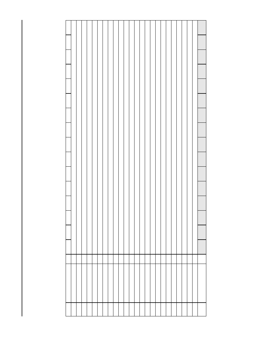
MARS2G5 P-Pro (TDAT162G52) SONET/SDH
Data Sheet
155/622/2488 Mbits/s Data Interface
August 18, 2004
606
Agere Systems Inc.
DS3/E3 Block
(continued)
E3 Register Map
(continued)
Table 677. E3 Register Map (continued)
Note: Shading denotes reserved bits.
Addr
Register Name
Type
15
14
13
12
11
10
9
8
7
6
5
4
3
2
1
0
0x51C0
E3_RXPLCPB1ECNT_B1
RO
E3_PLCP_B1ERRCNT_B1[15:0]
0x51C1
E3_RXPLCPB1ECNT_B2
RO
E3_PLCP_B1ERRCNT_B2[15:0]
0x51C2
E3_RXPLCPB1ECNT_B3
RO
E3_PLCP_B1ERRCNT_B3[15:0]
0x51C3
E3_RXPLCPB1ECNT_B4
RO
E3_PLCP_B1ERRCNT_B4[15:0]
0x51C4
E3_RXPLCPB1ECNT_B5
RO
E3_PLCP_B1ERRCNT_B5[15:0]
0x51C5
E3_RXPLCPB1ECNT_B6
RO
E3_PLCP_B1ERRCNT_B6[15:0]
0x51C6
E3_RXPLCPB1ECNT_B7
RO
E3_PLCP_B1ERRCNT_B7[15:0]
0x51C7
E3_RXPLCPB1ECNT_B8
RO
E3_PLCP_B1ERRCNT_B8[15:0]
0x51C8
E3_RXPLCPB1ECNT_B9
RO
E3_PLCP_B1ERRCNT_B9[15:0]
0x51C9
E3_RXPLCPB1ECNT_B10
RO
E3_PLCP_B1ERRCNT_B10[15:0]
0x51CA
E3_RXPLCPB1ECNT_B11
RO
E3_PLCP_B1ERRCNT_B11[15:0]
0x51CB
E3_RXPLCPB1ECNT_B12
RO
E3_PLCP_B1ERRCNT_B12[15:0]
0x51CC
E3_PLCPFEBECNT_B1
RO
E3_PLCP_G1_FEBE_ERRCNT_B1[15:0]
0x51CD
E3_PLCPFEBECNT_B2
RO
E3_PLCP_G1_FEBE_ERRCNT_B2[15:0]
0x51CE
E3_PLCPFEBECNT_B3
RO
E3_PLCP_G1_FEBE_ERRCNT_B3[15:0]
0x51CF
E3_PLCPFEBECNT_B4
RO
E3_PLCP_G1_FEBE_ERRCNT_B4[15:0]
0x51D0
E3_PLCPFEBECNT_B5
RO
E3_PLCP_G1_FEBE_ERRCNT_B5[15:0]
0x51D1
E3_PLCPFEBECNT_B6
RO
E3_PLCP_G1_FEBE_ERRCNT_B6[15:0]
0x51D2
E3_PLCPFEBECNT_B7
RO
E3_PLCP_G1_FEBE_ERRCNT_B7[15:0]
0x51D3
E3_PLCPFEBECNT_B8
RO
E3_PLCP_G1_FEBE_ERRCNT_B8[15:0]
0x51D4
E3_PLCPFEBECNT_B9
RO
E3_PLCP_G1_FEBE_ERRCNT_B9[15:0]
0x51D5
E3_PLCPFEBECNT_B10
RO
E3_PLCP_G1_FEBE_ERRCNT_B10[15:0]
0x51D6
E3_PLCPFEBECNT_B11
RO
E3_PLCP_G1_FEBE_ERRCNT_B11[15:0]
0x51D7
E3_PLCPFEBECNT_B12
RO
E3_PLCP_G1_FEBE_ERRCNT_B12[15:0]
0x5200--
0x52D7
--
--
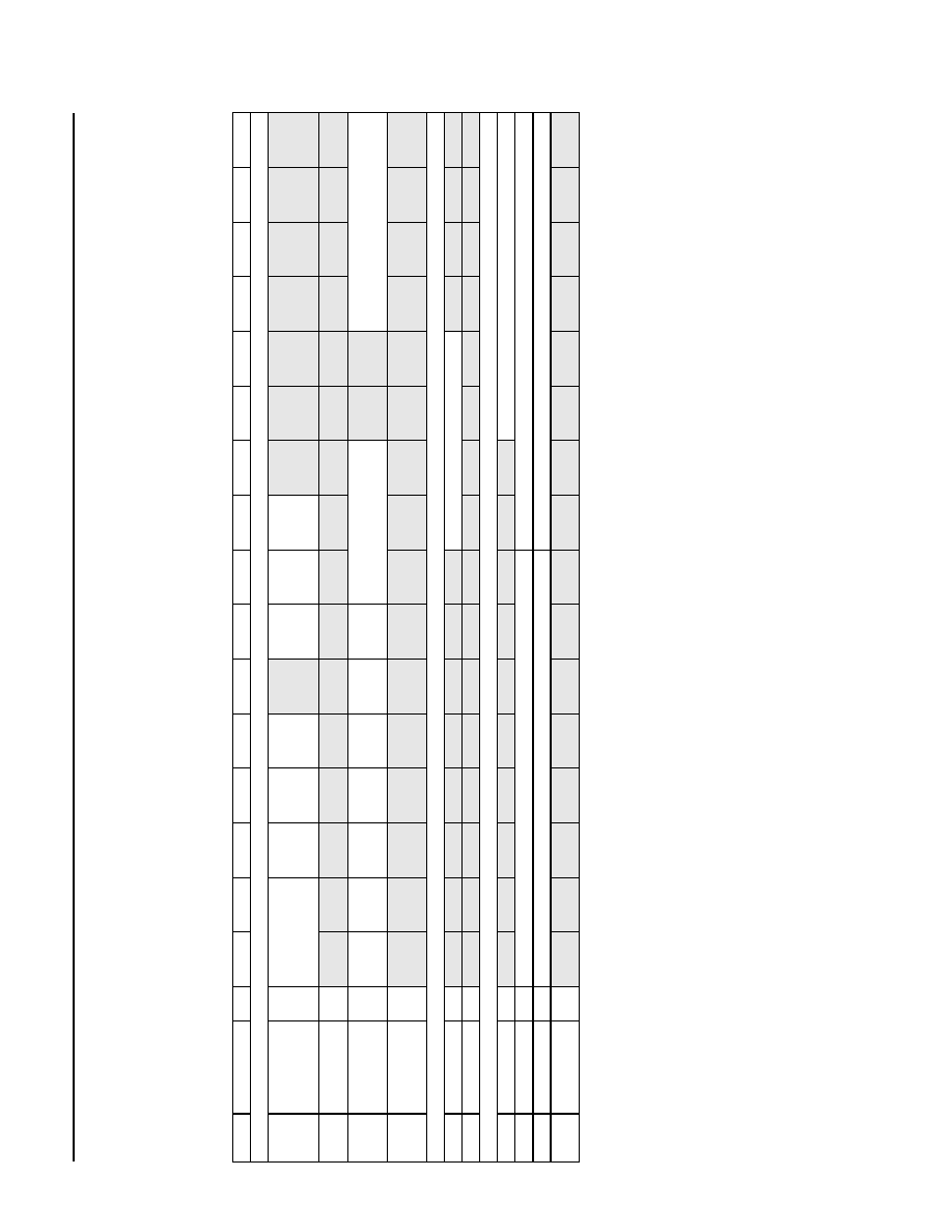
Data Sheet
MARS2G5 P-Pro (TDAT162G52) SONET/SDH
August 18, 2004
155/622/2488 Mbits/s Data Interface
607
Agere Systems Inc.
DS3/E3 Block
(continued)
E3 Register Map
(continued)
Table 677. E3 Register Map (continued)
Note: Shading denotes reserved bits.
Addr
Register Name
Type
15
14
13
12
11
10
9
8
7
6
5
4
3
2
1
0
Transmit Control Signals (Channel Based 1--16)
0x5300--
0x530F
E3_
TDS3PLCPCTL1_
CHD[1--16]
R/W
E3_TE3_
PLCP[1--16][1:0]
TE3_PLCP
_A2_INV
[1--16]
TE3_PLCP
_POIB7INV
[1--16]
TE3_PLCP
_B1INV
[1--16]
TE3_PLCP
_G1_AS_D
INS[1--16]
TE3_PLCP
_FEBE_
SWEN
[1--16]
TDS3orE3
0x5310--
0x532F
--
--
0x53C0--
0x53CF
E3_TE3CTL_
CHD[1--16]
R/W
TE3_AISIN
S[1--16]
TE3_TR_
INS[1--16]
TE3_FA_IN
V[1--16]
TE3_RAI_
DINS
[1--16]
TE3_MA_R
DI_DINS
[1--16]
TE3_MA_R
EI_ERRIN
S[1--16]
TE3_B1IN
V[1--16]
TE3_MA_PTY_DINS[2:0]
TE3_MA_SSM[1--16][3:0]
0x53D0
--
0x53F1
--
--
Transmit FEBE Insert Value
0x53F2
E3_TXFEBEDINS
R/W
TE3_PLCP_FEBE_DINS[3:0]
0x53F3
--
--
Transmit G.751 E3 PLCP Z1--Z3, F1 Insert Control
0x53F4
TXE3PLCP_P1
R/W
TE3_PLCP_ZF_CHID[5:0]
0x53F5
TXE3PLCP_P2
R/W
TE3_PLCP_Z1_DINS[7:0]
TE3_PLCP_Z2_DINS[7:0]
0x53F6
TXE3PLCP_P3
R/W
TE3_PLCP_Z3_DINS[7:0]
TE3_PLCP_F1_DINS[7:0]
0x53F7
--0x53FF
--
--
MARS2G5 P-Pro (TDAT162G52) SONET/SDH
Data Sheet
155/622/2488 Mbits/s Data Interface
August 18, 2004
608
Agere Systems Inc.
DS3/E3 Block
(continued)
E3 Register Map
(continued)
Table 677. E3 Register Map (continued)
Note: Shading denotes reserved bits.
Transmit E3 G.832 Trail Trace (TR) Insert Registers (128 Locations)
0x5400
TXTRACE[1]_B1
R/W
TE3_TR_DINS[1][1][7:0]
TE3_TR_DINS[1][0][7:0] MSB
0x5401
TXTRACE[1]_B2
R/W
TE3_TR_DINS[1][3][7:0]
TE3_TR_DINS[1][2][7:0]
0x5402
TXTRACE[1]_B3
R/W
TE3_TR_DINS[1][5][7:0]
TE3_TR_DINS[1][4][7:0]
0x5403
TXTRACE[1]_B4
R/W
TE3_TR_DINS[1][7][7:0]
TE3_TR_DINS[1][6][7:0]
0x5404
TXTRACE[1]_B5
R/W
TE3_TR_DINS[1][9][7:0]
TE3_TR_DINS[1][8][7:0]
0x5405
TXTRACE[1]_B6
R/W
TE3_TR_DINS[1][11][7:0]
TE3_TR_DINS[1][10][7:0]
0x5406
TXTRACE[1]_B7
R/W
TE3_TR_DINS[1][13][7:0]
TE3_TR_DINS[1][12][7:0]
0x5407
TXTRACE[1]_B8
R/W
TE3_TR_DINS[1][15][7:0] LSB
TE3_TR_DINS[1][14][7:0]
0x5408
TXTRACE[2]_B1
R/W
TE3_TR_DINS[2][1][7:0]
TE3_TR_DINS[2][0][7:0] MSB
0x5409
TXTRACE[2]_B2
R/W
TE3_TR_DINS[2][3][7:0]
TE3_TR_DINS[2][2][7:0]
0x540A
TXTRACE[2]_B3
R/W
TE3_TR_DINS[2][5][7:0]
TE3_TR_DINS[2][4][7:0]
0x540B
TXTRACE[2]_B4
R/W
TE3_TR_DINS[2][7][7:0]
TE3_TR_DINS[2][6][7:0]
0x540C
TXTRACE[2]_B5
R/W
TE3_TR_DINS[2][9][7:0]
TE3_TR_DINS[2][8][7:0]
0x540D
TXTRACE[2]_B6
R/W
TE3_TR_DINS[2][11][7:0]
TE3_TR_DINS[2][10][7:0]
0x540E
TXTRACE[2]_B7
R/W
TE3_TR_DINS[2][13][7:0]
TE3_TR_DINS[2][12][7:0]
0x540F
TXTRACE[2]_B8
R/W
TE3_TR_DINS[2][15][7:0] LSB
TE3_TR_DINS[2][14][7:0]
0x5410--
0x547F
TXTRACE
[3--16]_B[1--8]
R/W
E3_G832_TR Messages 3--16

Data Sheet
MARS2G5 P-Pro (TDAT162G52) SONET/SDH
August 18, 2004
155/622/2488 Mbits/s Data Interface
609
Agere Systems Inc.
DS3/E3 Block
(continued)
Appendix: DS3 to STS-1 Mapping
DS3 information is mapped into an STS-1 frame as shown in Table 678.
Table 678. STS-1 Mapping of DS3 Information
Note: R = rrrr_rrrr, C1 = rr_c_iiii_i, C2 = cc_rr_rrrr, C3 = cc_rr_oo_r_s, and I = iiii_iiii, where
r = reserved, i = information (payload) bit, c = stuff control bit, s = stuff opportunity bit, and o = overhead com-
munications channel bit (reserved).
Information is carried in the i bits. As can be seen, there are at 621 i bits per STS row, and an opportunity for one
more i bit per row, to be carried in the stuff bit, if the stuff control bits indicate so. When a majority of the c bits are
0, then the stuff bit carries information. The o and r bits are set to undefined.
The i (information) bits are organized as shown in Figure 61, into a DS3 multiframe.
5-8324(F)r.3
Figure 61. DS3 Multiframe Format
J1
R
R
C1
25I
R
C2
I
25I
R
C3
I
25I
POH
R
R
C1
25I
R
C2
I
25I
R
C3
I
25I
R
R
C1
25I
R
C2
I
25I
R
C3
I
25I
R
R
C1
25I
R
C2
I
25I
R
C3
I
25I
R
R
C1
25I
R
C2
I
25I
R
C3
I
25I
R
R
C1
25I
R
C2
I
25I
R
C3
I
25I
R
R
C1
25I
R
C2
I
25I
R
C3
I
25I
R
R
C1
25I
R
C2
I
25I
R
C3
I
25I
R
R
C1
25I
R
C2
I
25I
R
C3
I
25I
84D
C11
X1
F1
F2
C12
F3
C13
F4
84D
84D
84D
84D
84D
84D
84D
84D
C21
X2
F1
F2
C22
F3
C23
F4
84D
84D
84D
84D
84D
84D
84D
84D
C31
P1
F1
F2
C32
F3
C33
F4
84D
84D
84D
84D
84D
84D
84D
84D
C41
P2
F1
F2
C42
F3
C43
F4
84D
84D
84D
84D
84D
84D
84D
84D
C51
M1
F1
F2
C52
F3
C53
F4
84D
84D
84D
84D
84D
84D
84D
84D
C61
M2
F1
F2
C62
F3
C63
F4
84D
84D
84D
84D
84D
84D
84D
84D
C71
M3
F1
F2
C72
F3
C73
F4
84D
84D
84D
84D
84D
84D
84D
680 bits = M-SUBFRAME
7 ROWS
= 1 MULTIFRAME
= 4760 bits
= 44736 kbits/s
M-SUBFRAME ALIGNMENT SIGNAL F1F2F3F4 = 1001
MULTIFRAME ALIGNMENT SIGNAL M1M2M3 = 010
D = DATA
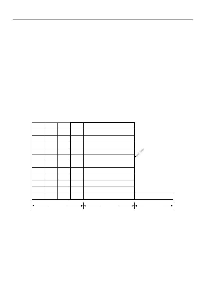
MARS2G5 P-Pro (TDAT162G52) SONET/SDH
Data Sheet
155/622/2488 Mbits/s Data Interface
August 18, 2004
610
Agere Systems Inc.
DS3/E3 Block
(continued)
Appendix: DS3 to STS-1 Mapping
(continued)
The information bits are segmented into 85 bits. Eight of these segments are grouped together to form an M-sub-
frame, also called a row. Seven rows are grouped together to form one DS3 multiframe. Each of the 85-bit seg-
ments consists of 84 d (or data) bits and 1 overhead bit. The overhead bits are used to convey framing and status.
The F1, F2, F3, and F4 bits are collectively called the M-subframe alignment signal and are fixed to the pattern
1001 (F1 = 1, F2 = 0, F3 = 0, F4 = 1). The M1, M2, and M3 bits are collectively called the multiframe alignment sig-
nal and are fixed to the pattern 010 (M1 = 0, M2 = 1, M3 = 0).
The X, P, and C bits are explained later in this document.
As can be seen, there are 84 bits x 8 blocks/row x 7 rows = 4704 data bits per multiframe. In this DS3 block, these
data bits can either carry payloads directly mapped into these bits (the payload could be ATM cells or HDLC pack-
ets or any other format) or ATM cells carried within a PLCP frame.
If ATM cells are carried within a PLCP frame, their mapping is shown in Figure 62, with the mapping nibble aligned,
with each nibble starting after each overhead bit (reference G.804 02/98 7.2, page 7). However, this DS3 block
does not require the data to be nibble aligned.
5-8325(F)r.4
Note: A1A2 = F6 28, POI = path overhead indicator, POH = path overhead, and X = unassigned.
Figure 62. PLCP Mapping of ATM Cells
In PLCP ATM cell mapping, the data bits are organized as twelve rows. Each row consists of two framing bytes,
one path overhead indicator byte, one path overhead byte, and one 53-byte ATM cell. The twelfth row also contains
a 13 or 14 nibble trailer.
A1
A2
P11
Z6
53-byte ATM CELL
A1
A2
P10
Z5
A1
A2
P09
Z4
A1
A2
P08
Z3
A1
A2
P07
Z2
A1
A2
P06
Z1
A1
A2
P05
X
A1
A2
P04
B1
A1
A2
P03
G1
A1
A2
P02
X
A1
A2
P01
X
A1
A2
P00
C1
53-byte ATM CELL
53-byte ATM CELL
53-byte ATM CELL
53-byte ATM CELL
53-byte ATM CELL
53-byte ATM CELL
53-byte ATM CELL
53-byte ATM CELL
53-byte ATM CELL
53-byte ATM CELL
53-byte ATM CELL
TRAILER
4 bytes
53 bytes
13 OR 14
NIBBLES
FRAMING
POI
POH
PLCP PAYLOAD
OBJECT OF
BIP-8
CALCULATION
53-byte ATM CELL

Data Sheet
MARS2G5 P-Pro (TDAT162G52) SONET/SDH
August 18, 2004
155/622/2488 Mbits/s Data Interface
611
Agere Systems Inc.
Receive Sequencer (RXS) Block
Introduction
The receive sequencer extracts the logical channels from SONET time slots. A total of 16 channels may be
mapped in to 48 SONET STS-1s. A channel may consist of any arbitrary number of STS-1s in any order. A fully
pointer based channel constructor can construct up to 16 channels. Each channel may consist of any number of
STS-1s such that the sum of all STS-1s contributing to 16 channels is less than or equal to 48.
In addition to packet over SONET (POS) application, the receive sequencer also supports channel construction
from packet over fiber (POF), too. Unlike in POS, only a single channel construction is supported in packet over
fiber mode. The RXS supports OC-48, OC-12, and OC-3 rates for both POS and POF modes.
Note: In OC-3 mode, only time slots 0, 4, and 8 are active in the RXS map registers (Table 681 and Table 682).
To use POF in OC-3 mode, it is necessary to provision the RXS maps to assign all 12 time slots from the
slice carrying the stream to the intended channel. This is different from normal (non-POF) programming in
OC-3 mode.
Channel construction information to the receive sequencer is provided through sequence map registers. Two sets
of sequence map registers are provided. At any time, one sequence map register is active and the other one is
standby. The standby sequence map register may be provisioned for addition of new channels or deletion of old
channels. The standby sequence map may be made active by toggling a bit in the RXS control register. A hitless
service is guaranteed on all active channels while some other channels are resizing.
A sequence map register has three fields. Bit field [11:8] defines the channel ID [0--15] associated with certain
time slot in a given slice. Bit field [5:4] defines the slice ID [A--D] associated with a time slot that belongs to the
channel id specified in channel id field. Bit field [3:0] defines a time slot [0--11] that is associated with the slice id
and the channel ID field. In summary, a sequence map register defines the channel id of any time slot of any slice.
The sequence map register is programmed in such a way that the time slots of slices that belong to a particular
channel appear in the order at which the channel constituting bytes will be stitched together to form a channel out-
put.
Up to 16 channels will be constructed by the RXS. A fair round-robin sequence arbitrator will send out the con-
structed channels to the data engine.
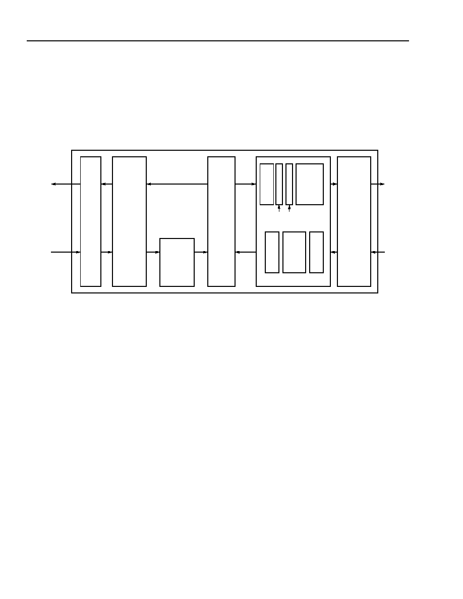
MARS2G5 P-Pro (TDAT162G52) SONET/SDH
Data Sheet
155/622/2488 Mbits/s Data Interface
August 18, 2004
612
Agere Systems Inc.
Receive Sequencer (RXS) Block
(continued)
RXS PRBS Monitor
Two independent PRBS monitors are provided in the RXS block that monitor the incoming data on a programmable
channel ID basis. Within the MARS2G5 P-Pro device, the DS3/E3 block is the source of the PRBS pattern while
the RXS PRBS monitor function is a possible sink point for the generated PRBS patterns. Figure 63 shows the
location of the PRBS generators and monitors within the device.
Figure 63. MARS2G5 P-Pro PRBS Monitor/Generator Locations
The test-pattern monitors contain self-synchronizing detectors that monitor 2
15
≠ 1, 2
20
≠ 1(QRSS), or 2
23
≠ 1 PRBS
sequences. These detected sequences can be expected to be inverted or noninverted. When the monitor is out of
sync, the device continually monitors the input data for matches to the expected data pattern. When the device
detects 32 matches in a row, it declares itself in sync and the error monitor is enabled. If the device detects eight
consecutive mismatches, the test-pattern monitor declares itself out of sync and starts searching again.
When in sync, the device counts the number of times the input data differs from the expected data in an 8-bit satu-
rating counter. This counter is reset when a 0-to-1 transition is detected on the MPU_READ signal. When the
update of the error counter is complete, the MPU_READ_FINISH signal is asserted.
Table 684 and Table 686 summarize the PRBS control and status registers, respectively.
D
S
3
/
E
3
DS3/E3
XC
Line
OHP
PP
SPE
DE
DE
(PRBS
INS)
PT
PRBS
MON(x2)
PRBS
MON
X
S
R
UTOPIA

Data Sheet
MARS2G5 P-Pro (TDAT162G52) SONET/SDH
August 18, 2004
155/622/2488 Mbits/s Data Interface
613
Agere Systems Inc.
Receive Sequencer (RXS) Block
(continued)
RXS Register Descriptions
RXS Global Registers
Table 679. (RXSVERSION) Version Control (RO)
Table 680. RXS_CONTROL, Receive Sequencer Control Register (R/W)
Address
Bit
Name
Function
Reset
Default
0x5800
7:0
RXSVERSION[7:0]
Indicates Version Number of Block.
0x01
Address
Bit
Name
Function
Reset
Default
0x5801
15:12
RXS_SL[A--D]_PM
In OC-3 or OC-12 mode, only one of these bits may be set,
corresponding to the slice carrying the ingress stream.
Ingress is limited to a single stream for those two modes
since RXS can't use multiple clocks. In OC-48 mode, all 4
bits must be set, since all four slices carry data.
0 = Slice [A--D] is off in POF mode.
1 = Slice [A--D] is on in POF mode.
0x0000
11:10
--
Reserved.
9:8
RXS_MODE
00 = Normal DS3 input to RXS.
01 = Reserved.
10 = Fiber input to RXS.
11 = All zero input to RXS.
7:1
--
Reserved.
0
RXS_XY_MAP
0 = Use X sequence map register as working map.
1 = Use Y sequence map register as working map.

MARS2G5 P-Pro (TDAT162G52) SONET/SDH
Data Sheet
155/622/2488 Mbits/s Data Interface
August 18, 2004
614
Agere Systems Inc.
Receive Sequencer (RXS) Block
(continued)
RXS Register Descriptions
(continued)
Table 681. RXS_TS[0--11][A--D], X Sequence Map Register (R/W)
Note: All unused sequence map registers must be set to 0xFFFF.
In OC-3 mode, only time slots 0, 4, and 8 are active.
Table 682. RYS_TS[0--11][A--D], Y Sequence Map Register (R/W)
Note: All unused sequence map registers must be set to 0xFFFF.
In OC-3 mode, only time slots 0, 4, and 8 are active.
Address
Bit
Name
Function
Reset
Default
0x5802--
0x5831
15:12
--
Reserved.
0x3F3F
11:8
RXS_CID_TS
[0--11][A--D][3:0]
Channel ID [0--15] for TS0--TS11 Slice A--Slice D.
These bits in each register of this 48 register bank indicate
the channel ID [0--15] of TS[0--11] for slice [A--D].
7:6
--
Reserved.
5:4
RXS_SRCSLICE_TS
[0--11][A--D][1:0]
Source Slice A--Slice D for TS0--TS11 Slice A--Slice D.
These bits assign an input slice [A--D] to a given TS[0--11]
in a given slice [A--D]. 00 = D, 01 = C, 10 = B, 11 = A.
3:0
RXS_SRCTS_TS
[0--11][A--D][3:0]
Source TS0--TS11 for TS0--TS11 Slice A--Slice D.
These bits assign an input TS[0--11] to a given TS[0--11] in
a given slice [A--D].
Address
Bit
Name
Function
Reset
Default
0x5832--
0x5861
15:12
--
Reserved.
0x3F3F
11:8
RYS_CID_TS
[0--11][A--D][3:0]
Channel ID [0--15] for TS0--TS11 Slice A--Slice D.
These bits in each register of this 48 register bank indicate
the channel ID [0--15] of TS[0--11] for slice [A--D].
7:6
--
Reserved.
5:4
RYS_SRCSLICE_TS
[0--11][A--D][1:0]
Source Slice A--Slice D for TS0--TS11 Slice A--Slice
D. These bits assign an input slice [A--D] to a given TS[0--
11] in a given slice [A--D]. 00 = D, 01 = C, 10 = B, 11 = A.
3:0
RYS_SRCTS_TS
[0--11][A--D][3:0]
Source TS0--TS11 for TS0--TS11 Slice A--Slice D.
These bits assign an input TS[0--11] to a given TS[0--11]
in a given slice [A--D].

Data Sheet
MARS2G5 P-Pro (TDAT162G52) SONET/SDH
August 18, 2004
155/622/2488 Mbits/s Data Interface
615
Agere Systems Inc.
Receive Sequencer (RXS) Block
(continued)
RXS Register Descriptions
(continued)
Table 683. DS3 Support Registers
Address
Bit
Name
Function
Reset
Default
0x5862
15:12
Slice_Match_
Param[15:12]
Destination_
TimeSlot_Ptr
Destination Time-Slot Pointer. This pointer indicates the
destination time slot that will be monitored to accept a new
slice at this location.
0x6E7A
11:10
--
Reserved.
9:8
Slice_Match_
Param[9:8]
Destination_
Slice_Ptr
Destination-Slice Pointer. This pointer indicates the desti-
nation slice that will be monitored to accept a new slice at
this location.
7:4
Slice_Match_
Param[7:4]
Source_TimeSlot_
Ptr
Source Time-Slot Pointer. This pointer indicates the source
time slot that will be monitored to move a slice to a different
slice.
3:2
--
Reserved.
1:0
Slice_Match_
Param[1:0]
Source_Slice_Ptr
Source-Slice Pointer. This pointer indicates the source slice
that will be monitored to move this slice to a different slice.
0x5863
15:4
Slice_Match_
Inst[15:4]
Match_Counter_
Threshold
Match-Counter Threshold. This threshold sets the sample
match count threshold value. Once sample match counter is
equal to or greater than this value, the match status will be
set.
0x7AF5
3:2
--
Reserved.
1
Slice_Match_Inst[1]
Sample_Match_
Holding_Counter
Sample Match Holding Counter.
0 = Keep holding register unchanged.
1 = Sample contents of the sample match counter in to the
sample count holding register.
0
Slice_Match_Inst[0]
Slice_Match_
Start_Inst
Slice Match Start Instruction.
0 = Stop slice match.
1 = Start slice match between time slots and slices specified
in Slice_Match_Param.
0x5864
15:4
Slice_Match_
Stat[15:4]
Sample_Count_
Holding
Sample Count Holding Register. Instantaneous slice
match counter value can be seen by setting
Slice_Match_Inst[1] to 1 followed by setting it to 0. Once
Slice_Match_Stat[0] converges, this field is set to the final
value of the slice match counter.
0x0000
3:1
--
Reserved.
0
Slice_Match_Stat[0]
Slice_Match_Status
Slice-Match Status.
0 = Indicates slice mismatch.
1 = Indicates slice match between time slots and slices
specified in Slice_Match_Param.

MARS2G5 P-Pro (TDAT162G52) SONET/SDH
Data Sheet
155/622/2488 Mbits/s Data Interface
August 18, 2004
616
Agere Systems Inc.
Receive Sequencer (RXS) Block
(continued)
RXS Register Descriptions
(continued)
Table 684. RXS PRBS Control Register for Monitor 1 (R/W)
Table 685. RXS PRBS Control Register for Monitor 2 (R/W)
Address
Bit
Name
Function
Reset
Default
0x5870
15
MPU_CORWN
Control for alarm signals; controls PRBS status values for
both monitors.
1 = Clear-on-read (COR) operation of event registers.
0 = Clear-on-write (COW).
0x0000
14
MPU_READ1
A 0-to-1 transition on this signal will cause an update to the
PRBS_ERRCNT1[7:0] read only register.
13
--
Reserved.
12
PRBS_INV1
Allows an inverted pattern to be expected.
0 = Normal pattern expected.
1 = Inverted pattern expected.
11:10
--
Reserved.
9:8
PRBS_
PATTERN1[1:0]
Control signal to select the PRBS pattern expected.
00 = Disable.
01 = 2
15
.
10 = 2
20
.
11 = 2
23
pattern expected.
5:0
PRBS_CIDSEL1[5:0]
Channel ID to monitor the PRBS sequence. Valid values
are 0 to 47, all illegal values disable the PRBS monitor.
Address
Bit
Name
Function
Reset
Default
0x5871
15
--
Reserved.
0x0000
14
MPU_READ2
A 0-to-1 transition on this signal will cause an update to the
PRBS_ERRCNT2[7:0] read only register.
13
--
Reserved.
12
PRBS_INV2
Allows an inverted pattern to be expected.
0 = Normal pattern expected.
1 = Inverted pattern expected.
11:10
--
Reserved.
9:8
PRBS_PATTERN2
Control signal to select the PRBS pattern expected.
00 = Disable.
01 = 2
15
.
10 = 2
20
.
11 = 2
23
pattern expected.
5:0
PRBS_CIDSEL2
Channel ID to monitor the PRBS sequence. Valid values
are 0 to 47, all illegal values disable the PRBS monitor.

Data Sheet
MARS2G5 P-Pro (TDAT162G52) SONET/SDH
August 18, 2004
155/622/2488 Mbits/s Data Interface
617
Agere Systems Inc.
Receive Sequencer (RXS) Block
(continued)
RXS Register Descriptions
(continued)
Table 686. RXS PRBS Status Register for Monitor 1 (Mixed)
Table 687. RXS PRBS Status Register for Monitor 2 (Mixed)
Address
Bit
Name
Function
Reset
Default
0x5872
15
SYNC1D (COR/W)
Delta register to indicate a change of state to the SYNC1
value.
0
14
SYNC1M (R/W)
Mask register for SYNC1D delta bit.
1 = Masked from contributing to interrupt pin.
1
13
SYNC1 (RO)
State register for PRBS monitor.
0 = In-sync.
1 = Out-of-sync.
1
12
MPU_READ_
FINISH1 (COR/W)
Active-high event indicating the MPU_READ1 operation is
complete. This indicates the PRBS_ERRCNT1[7:0] is stable.
This signal must be polled.
0
11:8
--
Reserved.
0x0
7:0
PRBS_
ERRCNT1[7:0] (RO)
PRBS saturating error counter.
0x00
Address
Bit
Name
Function
Reset
Default
0x5873
15
SYNC2D (COR/W)
Delta register to indicate a change of state to the SYNC2
value.
0
14
SYNC2M (R/W)
Mask register for SYNC2D delta bit.
1 = Masked from contributing to interrupt pin.
0
13
SYNC2 (RO)
State register for PRBS monitor.
0 = In-sync.
1 = Out-of-sync.
1
12
MPU_READ_
FINISH2 (COR/W)
Active-high event indicating the MPU_READ2 operation is
complete. This indicates the PRBS_ERRCNT2[7:0] is stable.
This signal must be polled.
0
11:8
--
Reserved.
0x0
7:0
PRBS_
ERRCNT2[7:0] (RO)
PRBS saturating error counter.
0x00
MARS2G5 P-Pro (TDAT162G52) SONET/SDH
Data Sheet
155/622/2488 Mbits/s Data Interface
August 18, 2004
618
Agere Systems Inc.
Receive Sequencer (RXS) Block
(continued)
RXS Register Maps
Table 688. Sequencer Register Map 1 Field Definition
Note: All unused sequence map registers must be set to 0xFFFF. Shading denotes reserved bits.
Addr
Symbol
Type
15
14
13
12
11
10
9
8
7
6
5
4
3
2
1
0
0x5800
RXSVERSION
RO
RXSVERSION[7:0]
0x5801
RXS_CONTROL
R/W
RXS_SLA_PM
RXS_SLB_PM
RXS_SLC_PM
RXS_SLD_PM
RXS_MODE
RXS_XY_MAP
Time Slot 0 Sequence X Map Register
0x5802
RXS_TS0A
R/W
RXS_CID_TS0A[3:0]
RXS_SRCSLICE_TS0A[1:0]
RXS_SRCTS_TS0A[3:0]
0x5803
RXS_TS0B
R/W
RXS_CID_TS0B[3:0]
RXS_SRCSLICE_TS0B[1:0]
RXS_SRCTS_TS0B[3:0]
0x5804
RXS_TS0C
R/W
RXS_CID_TS0C[3:0]
RXS_SRCSLICE_TS0C[1:0]
RXS_SRCTS_TS0C[3:0]
0x5805
RXS_TS0D
R/W
RXS_CID_TS0D[3:0]
RXS_SRCSLICE_TS0D[1:0]
RXS_SRCTS_TS0D[3:0]
Time Slot 1 Sequence X Map Register
0x5806
RXS_TS1A
R/W
RXS_CID_TS1A[3:0]
RXS_SRCSLICE_TS1A[1:0]
RXS_SRCTS_TS1A[3:0]
0x5807
RXS_TS1B
R/W
RXS_CID_TS1B[3:0]
RXS_SRCSLICE_TS1B[1:0]
RXS_SRCTS_TS1B[3:0]
0x5808
RXS_TS1C
R/W
RXS_CID_TS1C[3:0]
RXS_SRCSLICE_TS1C[1:0]
RXS_SRCTS_TS1C[3:0]
0x5809
RXS_TS1D
R/W
RXS_CID_TS1D[3:0]
RXS_SRCSLICE_TS1D[1:0]
RXS_SRCTS_TS1D[3:0]
Time Slot 2 Sequence X Map Register
0x580A
RXS_TS2A
R/W
RXS_CID_TS2A[3:0]
RXS_SRCSLICE_TS2A[1:0]
RXS_SRCTS_TS2A[3:0]
0x580B
RXS_TS2B
R/W
RXS_CID_TS2B[3:0]
RXS_SRCSLICE_TS2B[1:0]
RXS_SRCTS_TS2B[3:0]
0x580C
RXS_TS2C
R/W
RXS_CID_TS2C[3:0]
RXS_SRCSLICE_TS2C[1:0]
RXS_SRCTS_TS2C[3:0]
0x580D
RXS_TS2D
R/W
RXS_CID_TS2D[3:0]
RXS_SRCSLICE_TS2D[1:0]
RXS_SRCTS_TS2D[3:0]
Time Slot 3 Sequence X Map Register
0x580E
RXS_TS3A
R/W
RXS_CID_TS3A[3:0]
RXS_SRCSLICE_TS3A[1:0]
RXS_SRCTS_TS3A[3:0]
0x580F
RXS_TS3B
R/W
RXS_CID_TS3B[3:0]
RXS_SRCSLICE_TS3B[1:0]
RXS_SRCTS_TS3B[3:0]
0x5810
RXS_TS3C
R/W
RXS_CID_TS3C[3:0]
RXS_SRCSLICE_TS3C[1:0]
RXS_SRCTS_TS3C[3:0]
0x5811
RXD_TS3D
R/W
RXS_CID_TS3D[3:0]
RXS_SRCSLICE_TS3D[1:0]
RXS_SRCTS_TS3D[3:0]
Time Slot 4 Sequence X Map Register
0x5812
RXS_TS4A
R/W
RXS_CID_TS4A[3:0]
RXS_SRCSLICE_TS4A[1:0]
RXS_SRCTS_TS4A[3:0]
0x5813
RXS_TS4B
R/W
RXS_CID_TS4B[3:0]
RXS_SRCSLICE_TS4B[1:0]
RXS_SRCTS_TS4B[3:0]
0x5814
RXS_TS4C
R/W
RXS_CID_TS4C[3:0]
RXS_SRCSLICE_TS4C[1:0]
RXS_SRCTS_TS4C[3:0]
0x5815
RXS_TS4D
R/W
RXS_CID_TS4D[3:0]
RXS_SRCSLICE_TS4D[1:0]
RXS_SRCTS_TS4D[3:0]
Data Sheet
MARS2G5 P-Pro (TDAT162G52) SONET/SDH
August 18, 2004
155/622/2488 Mbits/s Data Interface
619
Agere Systems Inc.
Receive Sequencer (RXS) Block
(continued)
RXS Register Maps
(continued)
Table 688. Sequencer Register Map 1 Field Definition (continued)
Note: All unused sequence map registers must be set to 0xFFFF. Shading denotes reserved bit.
Addr
Symbol
Type
15
14
13
12
11
10
9
8
7
6
5
4
3
2
1
0
Time Slot 5 Sequence X Map Register
0x5816
RXS_TS5A
R/W
RXS_CID_TS5A[3:0]
RXS_SRCSLICE_TS5A[1:0]
RXS_SRCTS_TS5A[3:0]
0x5817
RXS_TS5B
R/W
RXS_CID_TS5B[3:0]
RXS_SRCSLICE_TS5B[1:0]
RXS_SRCTS_TS5B[3:0]
0x5818
RXS_TS5C
R/W
RXS_CID_TS5C[3:0]
RXS_SRCSLICE_TS5C[1:0]
RXS_SRCTS_TS5C[3:0]
0x5819
RXS_TS5D
R/W
RXS_CID_TS5D[3:0]
RXS_SRCSLICE_TS5D[1:0]
RXS_SRCTS_TS5D[3:0]
Time Slot 6 Sequence X Map Register
0x581A
RXS_TS6A
R/W
RXS_CID_TS6A[3:0]
RXS_SRCSLICE_TS6A[1:0]
RXS_SRCTS_TS6A[3:0]
0x581B
RXS_TS6B
R/W
RXS_CID_TS6B[3:0]
RXS_SRCSLICE_TS6B[1:0]
RXS_SRCTS_TS6B[3:0]
0x581C
RXS_TS6C
R/W
RXS_CID_TS6C[3:0]
RXS_SRCSLICE_TS6C[1:0]
RXS_SRCTS_TS6C[3:0]
0x581D
RXS_TS6D
R/W
RXS_CID_TS6D[3:0]
RXS_SRCSLICE_TS6D[1:0]
RXS_SRCTS_TS6D[3:0]
Time Slot 7 Sequence X Map Register
0x581E
RXS_TS7A
R/W
RXS_CID_TS7A[3:0]
RXS_SRCSLICE_TS7A[1:0]
RXS_SRCTS_TS7A[3:0]
0x581F
RXS_TS7B
R/W
RXS_CID_TS7B[3:0]
RXS_SRCSLICE_TS7B[1:0]
RXS_SRCTS_TS7B[3:0]
0x5820
RXS_TS7C
R/W
RXS_CID_TS7C[3:0]
RXS_SRCSLICE_TS7C[1:0]
RXS_SRCTS_TS7C[3:0]
0x5821
RXS_TS7D
R/W
RXS_CID_TS7D[3:0]
RXS_SRCSLICE_TS7D[1:0]
RXS_SRCTS_TS7D[3:0]
Time Slot 8 Sequence X Map Register
0x5822
RXS_TS8A
R/W
RXS_CID_TS8A[3:0]
RXS_SRCSLICE_TS8A[1:0]
RXS_SRCTS_TS8A[3:0]
0x5823
RXS_TS8B
R/W
RXS_CID_TS8B[3:0]
RXS_SRCSLICE_TS8B[1:0]
RXS_SRCTS_TS8B[3:0]
0x5824
RXS_TS8C
R/W
RXS_CID_TS8C[3:0]
RXS_SRCSLICE_TS8C[1:0]
RXS_SRCTS_TS8C[3:0]
0x5825
RXS_TS8D
R/W
RXS_CID_TS8D[3:0]
RXS_SRCSLICE_TS8D[1:0]
RXS_SRCTS_TS8D[3:0]
Time Slot 9 Sequence X Map Register
0x5826
RXS_TS9A
R/W
RXS_CID_TS9A[3:0]
RXS_SRCSLICE_TS9A[1:0]
RXS_SRCTS_TS9A[3:0]
0x5827
RXS_TS9B
R/W
RXS_CID_TS9B[3:0]
RXS_SRCSLICE_TS9B[1:0]
RXS_SRCTS_TS9B[3:0]
0x5828
RXS_TS9C
R/W
RXS_CID_TS9C[3:0]
RXS_SRCSLICE_TS9C[1:0]
RXS_SRCTS_TS9C[3:0]
0x5829
RXS_TS9D
R/W
RXS_CID_TS9D[3:0]
RXS_SRCSLICE_TS9D[1:0]
RXS_SRCTS_TS9D[3:0]
Time Slot 10 Sequence X Map Register
0x582A
RXS_TS10A
R/W
RXS_CID_TS10A[3:0]
RXS_SRCSLICE_TS10A[1:0]
RXS_SRCTS_TS10A[3:0]
0x582B
RXS_TS10B
R/W
RXS_CID_TS10B[3:0]
RXS_SRCSLICE_TS10B[1:0]
RXS_SRCTS_TS10B[3:0]
0x582C
RXS_TS10C
R/W
RXS_CID_TS10C[3:0]
RXS_SRCSLICE_TS10C[1:0]
RXS_SRCTS_TS10C[3:0]
0x582D
RXS_TS10D
R/W
RXS_CID_TS10D[3:0]
RXS_SRCSLICE_TS10D[1:0]
RXS_SRCTS_TS10D[3:0]
MARS2G5 P-Pro (TDAT162G52) SONET/SDH
Data Sheet
155/622/2488 Mbits/s Data Interface
August 18, 2004
620
Agere Systems Inc.
Receive Sequencer (RXS) Block
(continued)
RXS Register Maps
(continued)
Table 688. Sequencer Register Map 1 Field Definition (continued)
Note: All unused sequence map registers must be set to 0xFFFF. Shading denotes reserved bits.
Addr
Symbol
Type
15
14
13
12
11
10
9
8
7
6
5
4
3
2
1
0
Time Slot 11 Sequence X Map Register
0x582E
RXS_TS11A
R/W
RXS_CID_TS11A[3:0]
RXS_SRCSLICE_TS11A[1:0]
RXS_SRCTS_TS11A[3:0]
0x582F
RXS_TS11B
R/W
RXS_CID_TS11B[3:0]
RXS_SRCSLICE_TS11B[1:0]
RXS_SRCTS_TS11B[3:0]
0x5830
RXS_TS11C
R/W
RXS_CID_TS11C[3:0]
RXS_SRCSLICE_TS11C[1:0]
RXS_SRCTS_TS11C[3:0]
0x5831
RXS_TS11D
R/W
RXS_CID_TS11D[3:0]
RXS_SRCSLICE_TS11D[1:0]
RXS_SRCTS_TS11D[3:0]
Time Slot 0 Sequence Y Map Register
0x5832
RYS_TS0A
R/W
RYS_CID_TS0A[3:0]
RYS_SRCSLICE_TS0A[1:0]
RYS_SRCTS_TS0A[3:0]
0x5833
RYS_TS0B
R/W
RYS_CID_TS0B[3:0]
RYS_SRCSLICE_TS0B[1:0]
RYS_SRCTS_TS0B[3:0]
0x5834
RYS_TS0C
R/W
RYS_CID_TS0C[3:0]
RYS_SRCSLICE_TS0C[1:0]
RYS_SRCTS_TS0C[3:0]
0x5835
RYS_TS0D
R/W
RYS_CID_TS0D[3:0]
RYS_SRCSLICE_TS0D[1:0]
RYS_SRCTS_TS0D[3:0]
Time Slot 1 Sequence Y Map Register
0x5836
RYS_TS1A
R/W
RYS_CID_TS1A[3:0]
RYS_SRCSLICE_TS1A[1:0]
RYS_SRCTS_TS1A[3:0]
0x5837
RYS_TS1B
R/W
RYS_CID_TS1B[3:0]
RYS_SRCSLICE_TS1B[1:0]
RYS_SRCTS_TS1B[3:0]
0x5838
RYS_TS1C
R/W
RYS_CID_TS1C[3:0]
RYS_SRCSLICE_TS1C[1:0]
RYS_SRCTS_TS1C[3:0]
0x5839
RYS_TS1D
R/W
RYS_CID_TS1D[3:0]
RYS_SRCSLICE_TS1D[1:0]
RYS_SRCTS_TS1D[3:0]
Time Slot 2 Sequence Y Map Register
0x583A
RYS_TS2A
R/W
RYS_CID_TS2A[3:0]
RYS_SRCSLICE_TS2A[1:0]
RYS_SRCTS_TS2A[3:0]
0x583B
RYS_TS2B
R/W
RYS_CID_TS2B[3:0]
RYS_SRCSLICE_TS2B[1:0]
RYS_SRCTS_TS2B[3:0]
0x583C
RYS_TS2C
R/W
RYS_CID_TS2C[3:0]
RYS_SRCSLICE_TS2C[1:0]
RYS_SRCTS_TS2C[3:0]
0x583D
RYS_TS2D
R/W
RYS_CID_TS2D[3:0]
RYS_SRCSLICE_TS2D[1:0]
RYS_SRCTS_TS2D[3:0]
Time Slot 3 Sequence Y Map Register
0x583E
RYS_TS3A
R/W
RYS_CID_TS3A[3:0]
RYS_SRCSLICE_TS3A[1:0]
RYS_SRCTS_TS3A[3:0]
0x583F
RYS_TS3B
R/W
RYS_CID_TS3B[3:0]
RYS_SRCSLICE_TS3B[1:0]
RYS_SRCTS_TS3B[3:0]
0x5840
RYS_TS3C
R/W
RYS_CID_TS3C[3:0]
RYS_SRCSLICE_TS3C[1:0]
RYS_SRCTS_TS3C[3:0]
0x5841
RYS_TS3D
R/W
RYS_CID_TS3D[3:0]
RYS_SRCSLICE_TS3D[1:0]
RYS_SRCTS_TS3D[3:0]
Time Slot 4 Sequence Y Map Register
0x5842
RYS_TS4A
R/W
RYS_CID_TS4A[3:0]
RYS_SRCSLICE_TS4A[1:0]
RYS_SRCTS_TS4A[3:0]
0x5843
RYS_TS4B
R/W
RYS_CID_TS4B[3:0]
RYS_SRCSLICE_TS4B[1:0]
RYS_SRCTS_TS4B[3:0]
0x5844
RYS_TS4C
R/W
RYS_CID_TS4C[3:0]
RYS_SRCSLICE_TS4C[1:0]
RYS_SRCTS_TS4C[3:0]
0x5845
RYS_TS4D
R/W
RYS_CID_TS4D[3:0]
RYS_SRCSLICE_TS4D[1:0]
RYS_SRCTS_TS4D[3:0]
Data Sheet
MARS2G5 P-Pro (TDAT162G52) SONET/SDH
August 18, 2004
155/622/2488 Mbits/s Data Interface
621
Agere Systems Inc.
Receive Sequencer (RXS) Block
(continued)
RXS Register Maps
(continued)
Table 688. Sequencer Register Map 1 Field Definition (continued)
Note: All unused sequence map registers must be set to 0xFFFF. Shading denotes reserved bits.
Addr
Symbol
Type
15
14
13
12
11
10
9
8
7
6
5
4
3
2
1
0
Time Slot 5 Sequence Y Map Register
0x5846
RYS_TS5A
R/W
RYS_CID_TS5A[3:0]
RYS_SRCSLICE_TS5A[1:0]
RYS_SRCTS_TS5A[3:0]
0x5847
RYS_TS5B
R/W
RYS_CID_TS5B[3:0]
RYS_SRCSLICE_TS5B[1:0]
RYS_SRCTS_TS5B[3:0]
0x5848
RYS_TS5C
R/W
RYS_CID_TS5C[3:0]
RYS_SRCSLICE_TS5C[1:0]
RYS_SRCTS_TS5C[3:0]
0x5849
RYS_TS5D
R/W
RYS_CID_TS5D[3:0]
RYS_SRCSLICE_TS5D[1:0]
RYS_SRCTS_TS5D[3:0]
Time Slot 6 Sequence Y Map Register
0x584A
RYS_TS6A
R/W
RYS_CID_TS6A[3:0]
RYS_SRCSLICE_TS6A[1:0]
RYS_SRCTS_TS6A[3:0]
0x584B
RYS_TS6B
R/W
RYS_CID_TS6B[3:0]
RYS_SRCSLICE_TS6B[1:0]
RYS_SRCTS_TS6B[3:0]
0x584C
RYS_TS6C
R/W
RYS_CID_TS6C[3:0]
RYS_SRCSLICE_TS6C[1:0]
RYS_SRCTS_TS6C[3:0]
0x584D
RYS_TS6D
R/W
RYS_CID_TS6D[3:0]
RYS_SRCSLICE_TS6D[1:0]
RYS_SRCTS_TS6D[3:0]
Time Slot 7 Sequence Y Map Register
0x584E
RYS_TS7A
R/W
RYS_CID_TS7A[3:0]
RYS_SRCSLICE_TS7A[1:0]
RYS_SRCTS_TS7A[3:0]
0x584F
RYS_TS7B
R/W
RYS_CID_TS7B[3:0]
RYS_SRCSLICE_TS7B[1:0]
RYS_SRCTS_TS7B[3:0]
0x5850
RYS_TS7C
R/W
RYS_CID_TS7C[3:0]
RYS_SRCSLICE_TS7C[1:0]
RYS_SRCTS_TS7C[3:0]
0x5851
RYS_TS7D
R/W
RYS_CID_TS7D[3:0]
RYS_SRCSLICE_TS7D[1:0]
RYS_SRCTS_TS7D[3:0]
Time Slot 8 Sequence Y Map Register
0x5852
RYS_TS8A
R/W
RYS_CID_TS8A[3:0]
RYS_SRCSLICE_TS8A[1:0]
RYS_SRCTS_TS8A[3:0]
0x5853
RYS_TS8B
R/W
RYS_CID_TS8B[3:0]
RYS_SRCSLICE_TS8B[1:0]
RYS_SRCTS_TS8B[3:0]
0x5854
RYS_TS8C
R/W
RYS_CID_TS8C[3:0]
RYS_SRCSLICE_TS8C[1:0]
RYS_SRCTS_TS8C[3:0]
0x5855
RYS_TS8D
R/W
RYS_CID_TS8D[3:0]
RYS_SRCSLICE_TS8D[1:0]
RYS_SRCTS_TS8D[3:0]
Time Slot 9 Sequence Y Map Register
0x5856
RYS_TS9A
R/W
RYS_CID_TS9A[3:0]
RYS_SRCSLICE_TS9A[1:0]
RYS_SRCTS_TS9A[3:0]
0x5857
RYS_TS9B
R/W
RYS_CID_TS9B[3:0]
RYS_SRCSLICE_TS9B[1:0]
RYS_SRCTS_TS9B[3:0]
0x5858
RYS_TS9C
R/W
RYS_CID_TS9C[3:0]
RYS_SRCSLICE_TS9C[1:0]
RYS_SRCTS_TS9C[3:0]
0x5859
RYS_TS9D
R/W
RYS_CID_TS9D[3:0]
RYS_SRCSLICE_TS9D[1:0]
RYS_SRCTS_TS9D[3:0]
Time Slot 10 Sequence Y Map Register
0x585A
RYS_TS10A
R/W
RYS_CID_TS10A[3:0]
RYS_SRCSLICE_TS10A[1:0]
RYS_SRCTS_TS10A[3:0]
0x585B
RYS_TS10B
R/W
RYS_CID_TS10B[3:0]
RYS_SRCSLICE_TS10B[1:0]
RYS_SRCTS_TS10B[3:0]
0x585C
RYS_TS10C
R/W
RYS_CID_TS10C[3:0]
RYS_SRCSLICE_TS10C[1:0]
RYS_SRCTS_TS10C[3:0]
0x585D
RYS_TS10D
R/W
RYS_CID_TS10D[3:0]
RYS_SRCSLICE_TS10D[1:0]
RYS_SRCTS_TS10D[3:0]
MARS2G5 P-Pro (TDAT162G52) SONET/SDH
Data Sheet
155/622/2488 Mbits/s Data Interface
August 18, 2004
622
Agere Systems Inc.
Receive Sequencer (RXS) Block
(continued)
RXS Register Maps
(continued)
Table 688. Sequencer Register Map 1 Field Definition (continued)
Note: All unused sequence map registers must be set to 0xFFFF. Shading denotes reserved bits.
Table 689. Sequencer Register Map 2 Field Definition
Addr
Symbol
Type
15
14
13
12
11
10
9
8
7
6
5
4
3
2
1
0
Time Slot 11 Sequence Y Map Register
0x585E
RYS_TS11A
R/W
RYS_CID_TS11A[3:0]
RYS_SRCSLICE_TS11A[1:0]
RYS_SRCTS_TS11A[3:0]
0x585F
RYS_TS11B
R/W
RYS_CID_TS11B[3:0]
RYS_SRCSLICE_TS11B[1:0]
RYS_SRCTS_TS11B[3:0]
0x5860
RYS_TS11C
R/W
RYS_CID_TS11C[3:0]
RYS_SRCSLICE_TS11C[1:0]
RYS_SRCTS_TS11C[3:0]
0x5861
RYS_TS11D
R/W
RYS_CID_TS11D[3:0]
RYS_SRCSLICE_TS11D[1:0]
RYS_SRCTS_TS11D[3:0]
Addr
Symbol
Type
15
14
13
12
11
10
9
8
7
6
5
4
3
2
1
0
DS3 Support Registers
0x5862
Slice_Match_Para
R/W
Destination Time-Slot Pointer
Destination Slice Pointer
Source Time-Slot Pointer
Source Slice Pointer
0x5863
Slice_Match_Inst
R/W
Match Counter Threshold
Sample
Match
Holding
Counter
Slice
Match
Start
Instruction
0x5864
Slice_Match_Stat
R
Sample Count Holding
Slice
Match
Status
PRBS Control Registers
0x5870
PRBS Control Reg1
R/W
MPU_
CORWN
MPU_
READ1
PRBS_
INV1
PRBS_PATTERN1[1:0]
PRBS_CIDSEL1[5:0]
0x5871
PRBS Control Reg2
R/W
MPU_
READ2
PRBS_
INV2
PRBS_PATTERN2[1:0]
PRBS_CIDSEL2[5:0]
PRBS Status Registers
0x5872
PRBS Status Reg1
Mixed
SYNC1D
(COR/W)
SYNC1M
(R/W)
SYNC1
(RO)
MPU_
READ_
FINISH1
(COR/W)
PRBS_ERRCNT1[7:0] (RO)
0x5873
PRBS Status Reg2
Mixed
SYNC2D
(COR/W)
SYNC2M
(R/W)
SYNC2
(RO)
MPU_
READ_
FINISH2
(COR/W)
PRBS_ERRCNT2[7:0] (RO)

Data Sheet
MARS2G5 P-Pro (TDAT162G52) SONET/SDH
August 18, 2004
155/622/2488 Mbits/s Data Interface
623
Agere Systems Inc.
Data Engine Block
The data engine block interfaces with the UTOPIA (UT) Block on page 716 and the DS3/E3 Block on page 486.
Data Engine Block--Subblocks
The data engine consists of six major subblocks:
1.
Data Engine Block--ATM Framer/Frame Inserter Subblock on page 624.
2.
Data Engine Block--CRC Generator/Checker Subblock on page 636.
3.
Data Engine Block--CRC Generator/Checker Subblock on page 636.
4.
Data Engine Block--PPP Detach Subblock on page 645.
5.
Data Engine Block--Data Engine Counter Subblock on page 648.
6.
Data Engine Block--Channel Distribution and Allocation Subblock on page 651.

MARS2G5 P-Pro (TDAT162G52) SONET/SDH
Data Sheet
155/622/2488 Mbits/s Data Interface
August 18, 2004
624
Agere Systems Inc.
Data Engine Block
--
ATM Framer/Frame Inserter Subblock
Overview
The purpose of the ATM framer is to delineate incoming cell boundaries. Conversely, the purpose of the frame
inserter is to insert the HEC field in the header. This is used in ATM mode. In Figure 64, an ATM cell is shown.
5-8290(F)
Figure 64. ATM Cell Format
The basic idea with HEC framing is that the framer slides along on a bit-by-bit or byte-by-byte basis and checks for
5 bytes where the fifth byte is the HEC for the first 4.
Capabilities
Number of Channels
The ATM framer/frame inserter supports 16 channels.
HEC Framing
In ATM mode, ATM framing is done on the incoming ATM streams using the alpha-delta framer state machine
specified in I.432. Frame hunt is done on a byte-by-byte basis, except in cell UNI mode, where it is done on a per-
bit basis.
D0--D47
H3
HEADER
PAYLOAD
H0
H1
H2
HEC

Data Sheet
MARS2G5 P-Pro (TDAT162G52) SONET/SDH
August 18, 2004
155/622/2488 Mbits/s Data Interface
625
Agere Systems Inc.
Data Engine Block
--A
TM Framer/Frame Inserter Subblock
(continued)
Capabilities
(continued)
Data Passing
Data is not passed unless the framer is in the synchronized state.
Cell-Based UNI
The ATM framer supports a cell-based UNI for ATM mode (as per I.432) when PayloadControl[7] = 1. In this mode,
HEC framing is done on a per-bit basis. This implies that frame detection is required over 32 different positions for
the incoming bit stream.
HEC
The ATM framer/frame inserter generates and checks HEC fields for ATM cells. The HEC field is the fifth byte in
the ATM cell. The HEC is used to detect bit errors and correct single bit errors in the ATM cell header. The HEC
field is filled with the value of a CRC calculation, which is performed over the first 4 bytes of the header. The HEC
field contains the ones complement sum (modulo 2) of:
The remainder of the division (modulo 2) by the generator polynomial of the product of x
8
by the information in
the first 4 bytes of the ATM cell.
0x55
The HEC generator polynomial is g(x) = x
8
+ x
2
+ x + 1
The result of the CRC calculation is placed with the least significant bit right justified in the HEC field.
HEC Errors
Cells with header errors are handled in I.432 compliance when the channel's Rx payload control register is config-
ured for smart discard. In this mode, a single-bit header error is corrected, and the cell is passed to the UTOPIA
block, as long as the error occurs in isolation. If two or more cells in a row have single-bit errors, only the first will
be passed to the UTOPIA block. All cells with multiple header errors are discarded.
Two less restrictive modes are also provided. In discard mode, all single-bit errors are corrected and passed to the
UTOPIA block. In no discard mode, all received cells are passed to the UTOPIA bus. No corrections are made.
Discard mode selection does not affect the alpha-delta framer, which operates on the raw data prior to any error
correction. The framer will transition to hunt, and data delivery will stop, once alpha consecutive errored cell head-
ers have been received.
Idle/Unassigned Cells
The ATM framer generates idle cells when there are no user cells available, and discards these cells in the receive
direction.
MARS2G5 P-Pro (TDAT162G52) SONET/SDH
Data Sheet
155/622/2488 Mbits/s Data Interface
August 18, 2004
626
Agere Systems Inc.
Data Engine Block--ATM Framer/Frame Inserter Subblock
(continued)
Architecture
HEC Framer
Following this is a HEC framer. This circuit hunts for the frame in 1 of 4 or 1 of 32 possible positions (depending on
whether the channel is in bit sync or byte sync modes). The framer follows a state machine as shown in Figure 65.
Here, the first hit causes a transition to the presync state, and after delta consecutive hits on the HEC (spaced 53
bytes apart), the framer state moves to the sync state. At this point, data is allowed to pass through.
5-8294(F)r.1
Figure 65. Alpha-Delta Framer State Machine
PRESYNC
SYNCHRONIZED
HUNT
MISS BEFORE
ALPHA
MISSES
BIT/BYTE HUNT
MISS
HIT BEFORE
DELTA
HITS
DELTA
HITS
FAILURE
BEFORE DELTA
FIRST
HIT
HITS
ALPHA
MISSES

Data Sheet
MARS2G5 P-Pro (TDAT162G52) SONET/SDH
August 19, 2004
155/622/2488 Mbits/s Data Interface
627
Agere Systems Inc.
Data Engine Block--HDLC Framer and Escaper Subblock
Introduction
This section provides a description of the HDLC framer and escaper subblock of the DE-48. The framer operates
on received (ingress) data while the escaper operates on transmitted (egress) data. Data bytes are tagged with a
channel number indicating the logical channel with which the data is associated. The HDLC framer and escaper
supports up to 16 independent channels.
The HDLC framer can be provisioned on a per-channel basis to operate in either byte-synchronous or bit-synchro-
nous mode. In byte-synchronous mode, the HDLC framer and escaper operates as described in RFC1662, Sec-
tion 4 and ISO
Æ
/IEC
Æ
3309 Section 4.5.2.2. In bit-synchronous mode, the HDLC framer and escaper operates as
described in RFC1662, Section 5, and ISO/IEC 3309 Section 4.5.1.
Features
The HDLC framer/escaper supports 16 channels.
The HDLC framer/escaper operates on the following payload types as indicated by the PayloadType[2:0] bits
found in Table 740, Tx Payload Type and Control (R/W) on page 698 and Table 741, Tx Payload Type and Pay-
load Control Summary Table on page 699. No other payload types will be passed through:
-- PPP--PayloadType[2:0] = 0x0.
-- CRC--PayloadType[2:0] = 0x1.
-- HDLC--PayloadType[2:0] = 0x2.
-- Transparent Payload--PayloadType[2:0] = 0x6.
The HDLC framer/escaper supports X43 + 1 scrambling and descrambling. The post-scrambling and unscram-
bling mode operates on the entire datastream, including flags, in compliance with RFC2615. An optional pre-
scrambling mode operates on packet data and FCS only, before HDLC escaping and flag insertion.

MARS2G5 P-Pro (TDAT162G52) SONET/SDH
Data Sheet
155/622/2488 Mbits/s Data Interface
August 18, 2004
628
Agere Systems Inc.
Data Engine Block--HDLC Framer and Escaper Subblock
(continued)
Byte-Synchronous Mode
In Byte-Synchronous mode, the HDLC framer delineates incoming packet boundaries, and unescapes escaped
characters within a packet. HDLC escaper inserts HDLC flags at packet boundaries and escapes any 0x7D and
0x7E characters within a packet. This is used in PPP, HDLC, and CRC modes.
Packet Boundaries
The escaper marks the beginning and end of packets with the flag byte 0x7E.
Escaping
Bytes within a packet are escaped to hide occurrences of the value 0x7D and 0x7E. Escaping is done on a byte
basis with 0x7E being escaped to 0x7D5E, and 0x7D being escaped to 0x7D5D.
Interpacket Fill
The HDLC escaper for PPP, CRC, and HDLC modes use the HDLC flag 0x7E as the fill character between pack-
ets, with at least one 0x7E inserted between packets.
Abort
The HDLC escaper for PPP, CRC, and HDLC modes mark abort end-of-packets with 0x7D7E.
Escaper Dry Mode (Intra-Packet Fill)
The HDLC escaper for PPP, CRC, and HDLC modes provide stuffing for dry periods with 0x7D20 (NUL) if dry
mode is enabled (PayloadControl[2] = 1). Otherwise, the abort sequences written (0x7D7E).
Framer Dry Mode
The HDLC framer for PPP, CRC, and HDLC modes only support dry compression if dry mode is provisioned (Pay-
loadControl[2] = 1). Otherwise the framer provide normal unescaping on the 0x7D20 sequence resulting in 0x00.
Unescaping
Unescaping for PPP, CRC, and HDLC modes is performed on all characters preceded by a 0x7D except 0x7E, and
0x20 if dry mode is enabled (see previous requirement). Unescaping any sequence outside of 0x7D5D and
0x7D5E will result in an error.
Packet Size
The HDLC framer for PPP, CRC, and HDLC modes will discard any packets less than four bytes in length.
Framer Transparent Payload
For transparent payload, the HDLC framer (beyond matching the delay through this block) will do nothing except
translate the FrameMarker[2:0] signal into EOPMarker[3:0].
Data Sheet
MARS2G5 P-Pro (TDAT162G52) SONET/SDH
August 18, 2004
155/622/2488 Mbits/s Data Interface
629
Agere Systems Inc.
Examples of Byte-Synchronous Mode Escaper Operation
The examples shown below illustrate the operation of the byte-synchronous HDLC escaper. The first line repre-
sents the unencoded data to be transmitted, and the second line illustrates the required output from the escaper.
Flag, dry, and abort bytes are drawn using patterns illustrated in the legend below.
5-8308(F)
Figure 66. Legend for Escaper Examples
5-8309(F)
Figure 67. Escaping and EOP
PAYLOAD BYTE
BLANK BYTE
FLAG BYTE
DRY FILL SEQUENCE
7E
7D
20
ABORT SEQUENCE
7D
7E
ESCAPED BYTE
7D
XX
7E
5E
y
z
a
b
7E
d
7D
7D
g
a
b
c
EOP
7E
y
z
a
b
d
g
5D
5D
EOP
SOP
SOP
7D
7D
7D
7E
a
b
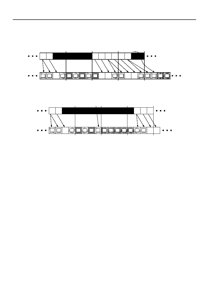
MARS2G5 P-Pro (TDAT162G52) SONET/SDH
Data Sheet
155/622/2488 Mbits/s Data Interface
August 18, 2004
630
Agere Systems Inc.
Data Engine Block--HDLC Framer and Escaper Subblock
(continued)
Examples of Byte-Synchronous Mode Escaper Operation
(continued)
5-8310(F)
Figure 68. Escaping Dry and Abort
5-8311(F)
Figure 69. Aborting a Dry
5E
7E
f
g
h
7E
j
k
7D
DRY
7E
f
5E
ABORT
7D
7D
20
7D
20
7D
20
7D
g
h
j
k
5D
7D
7D
7E
5E
7E
f
7D
DRY
7E
f
7D
20
7D
20
7D
7D
5D
7D
b
c
ABORT
7E
7E
7E
7E
b
c
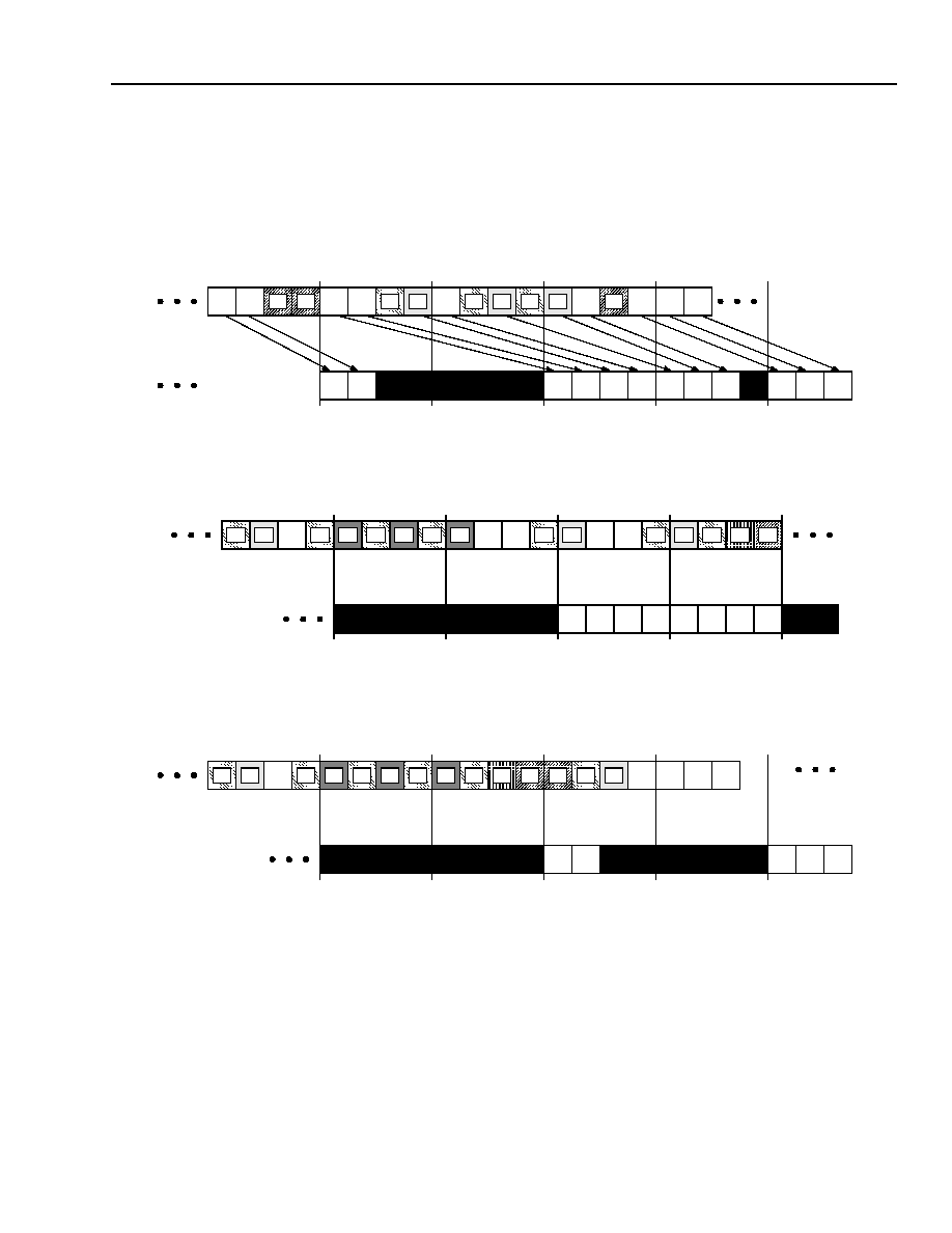
Data Sheet
MARS2G5 P-Pro (TDAT162G52) SONET/SDH
August 18, 2004
155/622/2488 Mbits/s Data Interface
631
Agere Systems Inc.
Data Engine Block--HDLC Framer and Escaper Subblock
(continued)
Examples of Byte-Synchronous Mode Framer Operation
The examples shown below illustrate the operation of the byte-synchronous HDLC framer. The first line represents
the received encoded data, and the second line illustrates the packed output of the framer. Flag, dry, and abort
bytes are drawn using patterns as in the figures above.
5-8312(F)
Figure 70. Framing and EOP
5-8313(F)r.1
Figure 71. Framing Dry and Abort
5-8314(F)
Figure 72. Aborting a Dry
7E
d
7E
z
y
z
y
5E
7D
b
a
5D
7D
5D
7D
d
g
7E
b
c
a
7E
b
a
7D
7D
g
b
c
a
EOP
EOP
SOP
SOP
h
f
7D
5D
7D
g
7E
g
f
7E
7E
j
k
7D
7E
h
20
7D
20
7D
20
5e
7D
5E
7D
j
k
7D
ABORT
f
7E
b
c
7D
SOP
f
7D
5D
7D
20
7D
20
7D
20
5e
7D
7E
7D
7E
7E
d
c
b
e
ABORT

MARS2G5 P-Pro (TDAT162G52) SONET/SDH
Data Sheet
155/622/2488 Mbits/s Data Interface
August 18, 2004
632
Agere Systems Inc.
Data Engine Block--HDLC Framer and Escaper Subblock
(continued)
Bit-Synchronous Mode
In bit-synchronous mode, the HDLC framer delineates incoming packet boundaries and removes bit-stuffing within
a packet. HDLC escaper inserts HDLC flags at packet boundaries and performs bit-stuffing within a packet follow-
ing each sequence of five ones 11111. Bit-synchronous HDLC mode supports transmission and reception of PPP
traffic carried within a DS3 payload.
Packet Boundaries
The escaper marks the beginning and end of packets by inserting the HDLC flag 0x7E (01111110). The device can
be configured to insert one to four flags between packets. Additional fill will be inserted beyond the provisioned
number of flags if the start of the next packet is not available yet.
Payload Size
Prior to bit-stuffing, transmitted packets consist of an integral number of bytes (octets).
Bit Order Within a Byte
Bits can be sent least significant bit first to most significant bit on a byte-by-byte basis. Or most significant bit first to
least significant bit, again on a byte-by-byte basis.
Stuffing
The escaper inserts (stuffs) a 0 bit following each occurrence of five consecutive 1s in a packet.
Interpacket Fill
The bitmode HDLC escaper can transmit either HDLC flags or all 1s as fill between packets when the start of the
next packet is not yet available. When the all 1s pattern is selected, the escaper will bracket the fill with two to four
HDLC flags. How these are allocated depends on the provisioned number of flags between packets and, if that
number is three, on the leading/trailing setting:
One or two flags--one flag before the fill and one after.
Three flags, leading--two flags before the fill and one after.
Three flags, trailing--one flag before the fill and two after.
Four flags--two flags before the fill and two after.
Abort
Abort is transmitted by the escaper as a sequence of seven or more consecutive ones. Abort is recognized by the
framer as a sequence of seven or more consecutive ones.

Data Sheet
MARS2G5 P-Pro (TDAT162G52) SONET/SDH
August 18, 2004
155/622/2488 Mbits/s Data Interface
633
Agere Systems Inc.
Data Engine Block--HDLC Framer and Escaper Subblock
(continued)
Bit-Synchronous Mode
(continued)
Dry Mode (Intrapacket Fill)
Dry mode is not supported.
Escaper Transparent Payload
Transparent payload is not supported.
Unstuffing
Within a packet (between flag bytes), the HDLC framer removes zero bits stuffed by the transmitter. To do this, it
replaces all occurrences of the bit string 111110 with 11111.
Framer Bit Alignment
After unstuffing, the framer packs the message bits into bytes. The first bit of a received packet is aligned with the
first bit of a byte.
Unstuffed Packet Size
After unstuffing, a packet consists of an integral number of bytes.
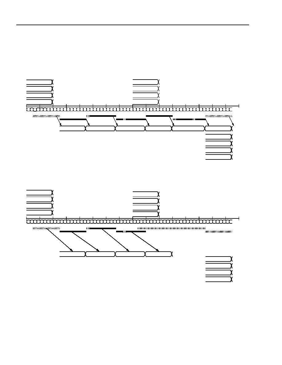
MARS2G5 P-Pro (TDAT162G52) SONET/SDH
Data Sheet
155/622/2488 Mbits/s Data Interface
August 18, 2004
634
Agere Systems Inc.
Data Engine Block--HDLC Framer and Escaper Subblock
(continued)
Examples of Bit-Synchronous Mode Framer Operation
The examples shown below illustrate the operation of the bit-synchronous HDLC framer. The first line represents
the received encoded data, and the second line illustrates the packed output of the framer.
5-8315(F)
Figure 73. Bit-Synchronous HDLC Framer Operation
5-8316(F)
Figure 74. Bit-Synchronous HDLC Abort
1 0 0 1 1 1 1 1 1 0 1 1 0 1 1 1 1 1 0 1 1 0 0 0 1 1 1 1 1 0 0 0 0 1 1 1 1 0
0 1 1 1 1 1 1 0
0 1 1 1 1 1 0 1 1 1 1 1 0 0 1
9F
DF
FLAG
C7
C7
0
FA
DF
C7
C7
9F
A
B
C
D
9F
B7
D8
F8
A
B
C
D
79
F7
C9
F8
A
B
C
D
1 0 0 1 1 1 1 1 1 0 1 1 0 1 1 1 1 1 0 1 1 0 0 0 1 1 1 1 1 0 0 0 0 1 1 1 1 1
0 1 1 1 1 1 1 0
1 1 1 1 1 1 1 1 1 1 1 1 1 1 1
DF
FLAG
C7
C7
1
ABORT
DF
C7
C7
XX
A
B
C
D
9F
B7
D8
F8
A
B
C
D
7F
FF
FD
F8
A
B
C
D
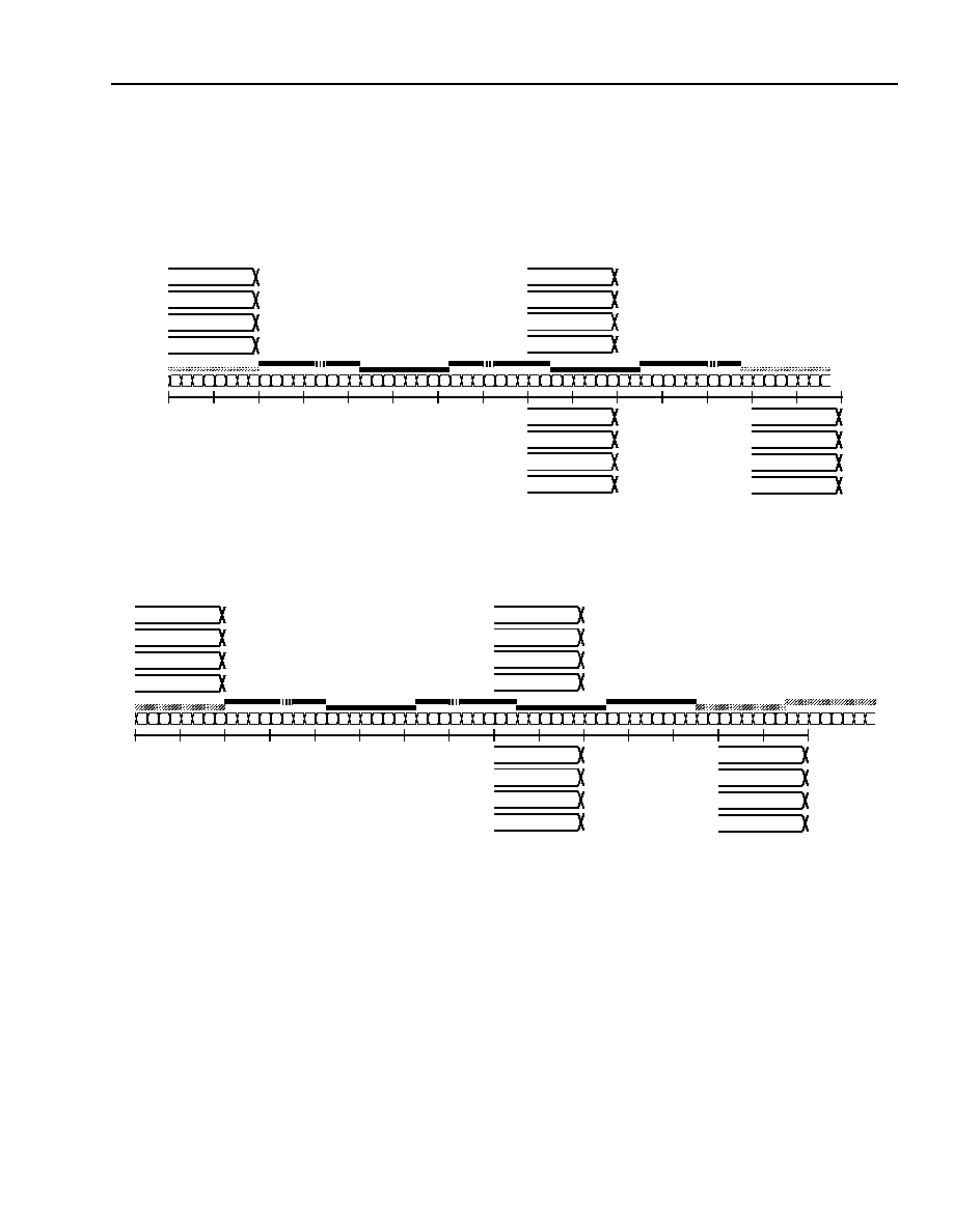
Data Sheet
MARS2G5 P-Pro (TDAT162G52) SONET/SDH
August 18, 2004
155/622/2488 Mbits/s Data Interface
635
Agere Systems Inc.
Data Engine Block--HDLC Framer and Escaper Subblock
(continued)
Examples of Bit-Synchronous Mode Escaper Operation
The examples shown below illustrate the operation of the bit-synchronous HDLC escaper. The first line represents
the received encoded data and the second line illustrates the packed output of the escaper.
5-8317(F)r.1
Figure 75. Bit-Synchronous HDLC Escaper Operation
5-8318(F)r.1
Figure 76. Bit-Synchronous HDLC Escaper Abort
FA
E3
E3
79
A
B
C
D
0 1 1 1 1 1 1 0 1 1 1 1 1 0 0 1 0 1 1 1 0 0 0 1 1 1 1 1 0 0 0 0 1 1 0 1
0 1 1 1 1 1 1 0
1 1 1 0 0 1 0 1 1 1 1 1 0 0 0
7C(EOP)
XX
XX
XX
A
B
C
D
7E
F9
71
F0
A
B
C
D
DE
5F
0F
CF
FA
E3
E3
79
A
B
C
D
0 1 1 1 1 1 1 0 1 1 1 1 1 0 0 1 0 1 1 1 0 0 0 1 1 1 1 1 0 0 0 0 1 1 0 1
0 1 1 1 1 1 1 0
1 1 1 0 0 1 1 1 1 1 1 1 1 1
ABORT
XX
XX
XX
A
B
C
D
7E
F9
71
F0
A
B
C
D
DE
7F
DF
9F
0 1 1 1 1 1 1 0
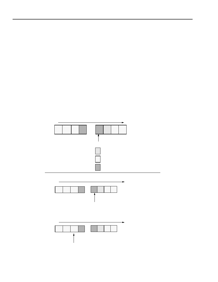
MARS2G5 P-Pro (TDAT162G52) SONET/SDH
Data Sheet
155/622/2488 Mbits/s Data Interface
August 18, 2004
636
Agere Systems Inc.
Data Engine Block--CRC Generator/Checker Subblock
Overview
The purpose of the CRC-16/32 generator and checker is to generate and check CRC-16/32 frame check
sequences on data that is being received and transmitted through the data engine on multiple channels. This is
used in PPP and CRC modes.
Receive
The CRC checker circuit is required to check a 16-bit and 32-bit CRC. In order to flag the end of the packet (2 or 4
bytes prior) as bad or OK, it is necessary to store the previous word before checking the CRC. Based on the fact
that the data is arriving 4 bytes at a time, and the minimum CRC is 2 bytes, it is desirable to check the CRC by cal-
culating the CRC in the same fashion as generating it: namely, calculate the CRC over the packet data and com-
pare it to the incoming CRC bytes. This situation is shown in Figure 77. Here, the CRC-16 would be calculated up
to byte C in the first word, and compared to bytes D and A. If the calculated CRC matches, the EOP marker will be
set either to byte C of the first word (if the CRC is supposed to be removed) or byte A of the second word (if the
CRC is supposed to remain attached). Otherwise, the BadMarker will be pointed on the byte where the EOP
marker was received.
5-8276(F)r.1
Figure 77. CRC-16 Checker Data Arriving Across Two Words
BLANK FROM 0x7E HDLC FLAG
PACKET BYTES
CRC-16 BYTES
EOP
TIME
A
B
C
D
D
A
B
C
A
B
C
D
D
A
B
C
TIME
CRC KEPT
TIME
CRC REMOVED
INPUT TO CRC
OUTPUT FROM CRC
FIRST PACKET
START OF NEXT PACKET
PLACE EOP
PLACE EOP
A
B
C
D
D
A
B
C
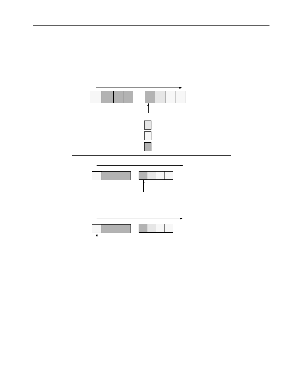
Data Sheet
MARS2G5 P-Pro (TDAT162G52) SONET/SDH
August 18, 2004
155/622/2488 Mbits/s Data Interface
637
Agere Systems Inc.
Data Engine Block--CRC Generator/Checker Subblock
(continued)
Receiver
(continued)
There can also be 32-bit CRCs. In general, the scheme is the same, but if the CRC is to be removed, the EOP
marker will need to be shifted 4 bytes instead of two. Refer to Figure 78.
5-8277(F)r.1
Figure 78. CRC-32 Check Arriving Across Two Words
Note: When the EOP marker is shifted to strip the CRC, the payload markers that indicate valid data for the CRC
values are now set low. For CRC-16, two payload markers are set low. For CRC-32, that number is four.
BLANK FROM 0x7E HDLC FLAG
PACKET BYTES
CRC-32 BYTES
EOP
TIME
A
C
D
D
A
B
C
C
D
D
A
B
C
TIME
CRC KEPT
TIME
CRC REMOVED
INPUT TO CRC
OUTPUT FROM CRC
START OF NEXT PACKET
A
B
B
FIRST PACKET
PLACE EOP
PLACE EOP
C
D
D
A
B
C
A
B
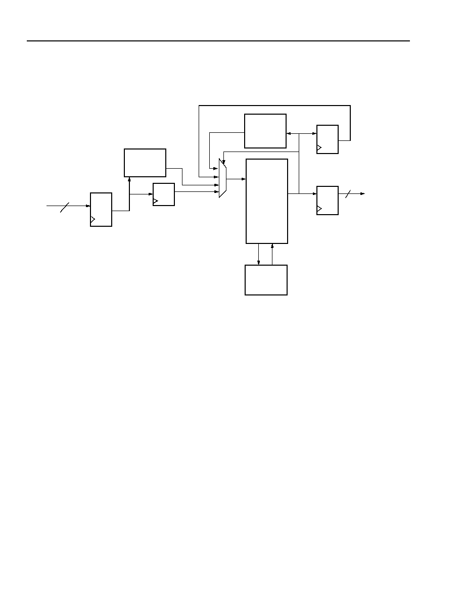
MARS2G5 P-Pro (TDAT162G52) SONET/SDH
Data Sheet
155/622/2488 Mbits/s Data Interface
August 18, 2004
638
Agere Systems Inc.
Data Engine Block--CRC Generator/Checker Subblock
(continued)
Receiver
(continued)
5-8279(F)
Figure 79. A CRC-16/32 Checker Circuit
Here, the previous bytes are stored, and a combinatorial logic circuit calculates the running CRC, and when the
EOP marker arrives, it compares the CRC with the 2 or 4 bytes before the EOP marker. Based on the results of
this, the EOP marker or bad marker is set at the new end of packet.
REGISTER FILE
REGISTER FILE
RUNNING
CRC
ABCD[31:0]
STATE
PREVIOUS
BYTES
ABCD[31:0]
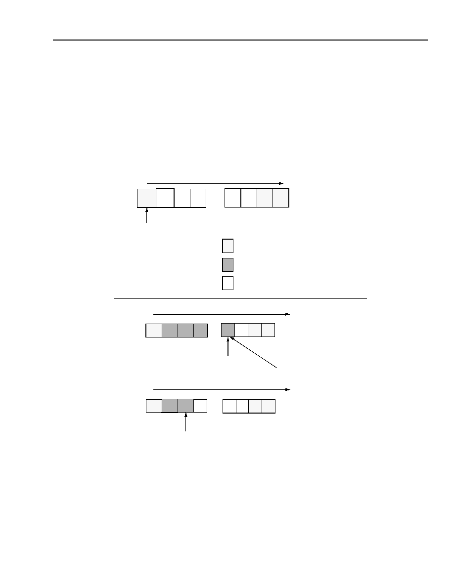
Data Sheet
MARS2G5 P-Pro (TDAT162G52) SONET/SDH
August 18, 2004
155/622/2488 Mbits/s Data Interface
639
Agere Systems Inc.
Data Engine Block--CRC Generator/Checker Subblock
(continued)
Transmit
In the transmit direction, the EOP marker is moved 2 to 4 bytes backwards, so the previous bytes are not required.
Here, the running CRC is calculated, and when the end of packet is found, the CRC bytes are inserted and the
EOP marker moved.
The figure below shows the treatment of incoming bytes into the CRC generator. The general premise is that the
CRC generator logic searches for the EOP marker and attaches its calculated value directly after the EOP. The
block must also shift the EOP marker by 2 or 4 bytes and must set high the payload markers corresponding to the
CRC bytes high.
5-8280(F)
Figure 80. Normal CRC-16 and CRC-32 Cases
For HDLC-type packets, there should still be at least one byte of spacing between packets for the insertion of the
HDLC blank flag (0x7E).
PACKET BYTES
CRC-16/CRC-32 BYTES
EOP
TIME
A
C
D
D
A
B
C
C
D
D
A
B
C
TIME
CRC-32 CASE
B
C
D
D
A
B
C
TIME
CRC-16 CASE
INPUT TO CRC
OUTPUT FROM CRC
START OF NEXT PACKET
A
A
B
B
FIRST PACKET
BLANK BYTES
READ IN FROM STORAGE
PLACE EOP
PLACE EOP
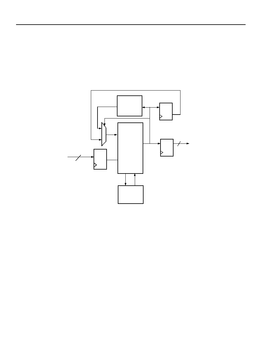
MARS2G5 P-Pro (TDAT162G52) SONET/SDH
Data Sheet
155/622/2488 Mbits/s Data Interface
August 18, 2004
640
Agere Systems Inc.
Data Engine Block--CRC Generator/Checker Subblock
(continued)
Transmit
(continued)
The CRC generator also searches for an implied start of packet. An implied start of packet corresponds to the first
valid byte (payload marker bit is high) following an end of packet. Upon an implied start of packet, the CRC value is
defaulted to 0xFFFFFFFF(or 0xFFFF for CRC-16) and the calculation restarts. Figure 81 shows the block diagram
of the CRC generator.
5-8281(F)r.1
Figure 81. CRC Generator Block Diagram
REGISTER FILE
RUNNING
ABCD[31:0]
CRC
ABCD[31:0]
STATE
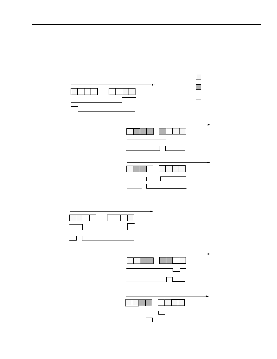
Data Sheet
MARS2G5 P-Pro (TDAT162G52) SONET/SDH
August 18, 2004
155/622/2488 Mbits/s Data Interface
641
Agere Systems Inc.
Data Engine Block--CRC Generator/Checker Subblock
(continued)
Examples of CRC Insertion/Testing
This section, describes the different cases on the CRC transmit side. The figure below shows several cases with
varying positions for the EOP marker.
5-8282(F)
5-8283(F)
Figure 82. Assorted CRC Generator Cases
PACKET BYTES
INSERTED CRC BYTES
BLANK BYTES
TIME
INPUT TO CRC
PAYLOAD MARKER
A
B
C
D
A
B
C
D
CRC-32 CASE
TIME
OUTPUT FROM CRC
PAYLOAD MARKER
A
B
C
D
A
B
C
D
CRC-16 CASE
TIME
OUTPUT FROM CRC
PAYLOAD MARKER
A
B
C
D
A
B
C
D
EOP MARKER
EOP MARKER
EOP MARKER
TIME
CRC-32 CASE
INPUT TO CRC
PAYLOAD MARKER
A
B
C
D
A
B
C
D
TIME
OUTPUT FROM CRC
PAYLOAD MARKER
A
B
C
D
A
B
C
D
CRC-16 CASE
TIME
OUTPUT FROM CRC
PAYLOAD MARKER
A
B
C
D
A
B
C
D
EOP MARKER
EOP MARKER
EOP MARKER
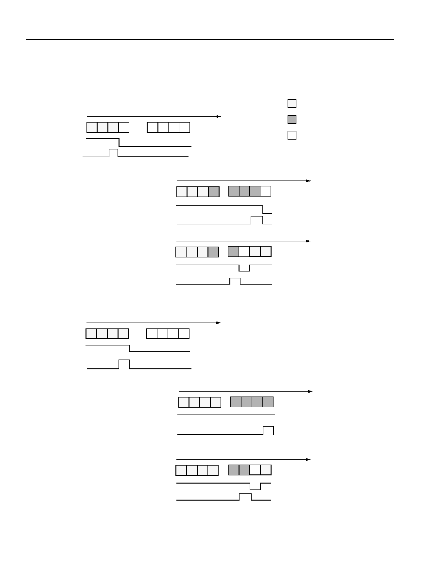
MARS2G5 P-Pro (TDAT162G52) SONET/SDH
Data Sheet
155/622/2488 Mbits/s Data Interface
August 18, 2004
642
Agere Systems Inc.
Data Engine Block--CRC Generator/Checker Subblock
(continued)
Examples of CRC Insertion/Testing
(continued)
5-8284(F)
5-8285(F)
Figure 83. Assorted CRC Generator Cases
PACKET BYTES
INSERTED CRC BYTES
BLANK BYTES
TIME
INPUT TO CRC
PAYLOAD MARKER
A
B
C
D
A
B
C
D
CRC-32 CASE
TIME
OUTPUT FROM CRC
PAYLOAD MARKER
A
B
C
D
A
B
C
D
CRC-16 CASE
TIME
OUTPUT FROM CRC
PAYLOAD MARKER
A
B
C
D
A
B
C
D
EOP MARKER
EOP MARKER
EOP MARKER
TIME
CRC-32 CASE
INPUT TO CRC
PAYLOAD MARKER
A
B
C
D
A
B
C
D
TIME
OUTPUT FROM CRC
PAYLOAD MARKER
A
B
C
D
A
B
C
D
CRC-16 CASE
TIME
OUTPUT FROM CRC
PAYLOAD MARKER
A
B
C
D
A
B
C
D
EOP MARKER
EOP MARKER
EOP MARKER
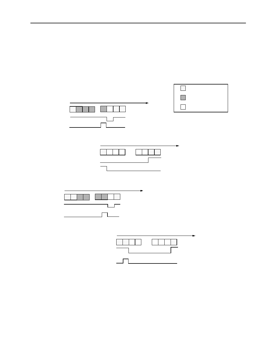
Data Sheet
MARS2G5 P-Pro (TDAT162G52) SONET/SDH
August 18, 2004
155/622/2488 Mbits/s Data Interface
643
Agere Systems Inc.
Data Engine Block--CRC Generator/Checker Subblock
(continued)
Examples of CRC Insertion/Testing
(continued)
Receive
This section, describes the different cases on the CRC receive side.
The figure below shows several cases with varying positions for the EOP marker.
5-8286(F)
5-8287(F)
Figure 84. Assorted CRC Checker Cases
PACKET BYTES
CRC BYTES
BLANK BYTES
TIME
INPUT TO CRC
PAYLOAD MARKER
A
B
C
D
A
B
C
D
CRC-32 CASE
TIME
OUTPUT FROM CRC
PAYLOAD MARKER
A
B
C
D
A
B
C
D
EOP MARKER
EOP MARKER
CRC STRIPPED
TIME
CRC-32 CASE
INPUT TO CRC
PAYLOAD MARKER
A
B
C
D
A
B
C
D
TIME
OUTPUT FROM CRC
PAYLOAD MARKER
A
B
C
D
A
B
C
D
EOP MARKER
EOP MARKER
CRC STRIPPED
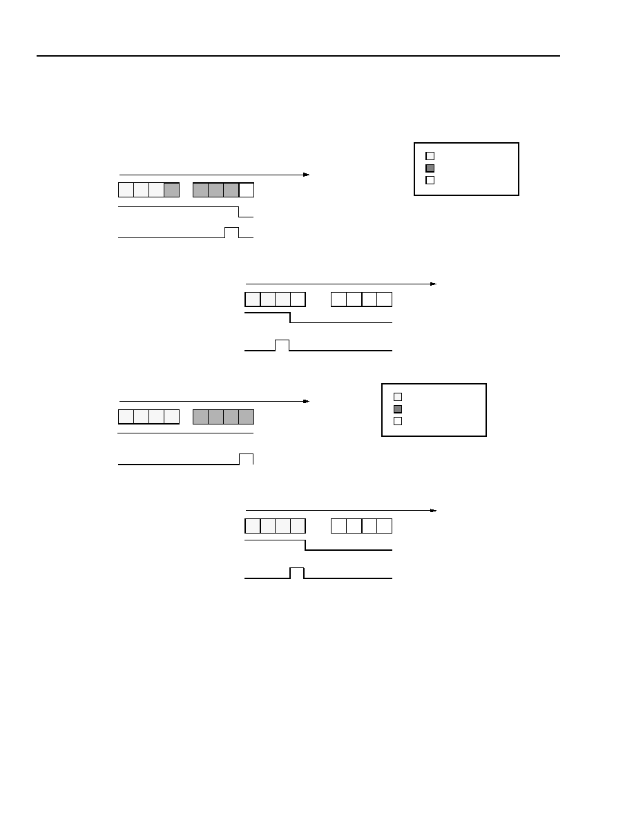
MARS2G5 P-Pro (TDAT162G52) SONET/SDH
Data Sheet
155/622/2488 Mbits/s Data Interface
August 18, 2004
644
Agere Systems Inc.
Data Engine Block--CRC Generator/Checker Subblock
(continued)
Examples of CRC Insertion/Testing
(continued)
5-8288(F)r.3
5-8289(F)r.2
Figure 85. Assorted CRC Checker Cases
TIME
CRC-32 CASE
INPUT TO CRC
PAYLOAD MARKER
A
B
C
D
A
B
C
D
TIME
OUTPUT FROM CRC
PAYLOAD MARKER
A
B
C
D
A
B
C
D
EOP MARKER
EOP MARKER
CRC STRIPPED
PACKET BYTES
CRC BYTES
BLANK BYTES
TIME
CRC-32 CASE
INPUT TO CRC
PAYLOAD MARKER
A
B
C
D
A
B
C
D
TIME
OUTPUT FROM CRC
PAYLOAD MARKER
A
B
D
A
B
C
D
EOP MARKER
EOP MARKER
CRC STRIPPED
C
PACKET BYTES
CRC BYTES
BLANK BYTES
Data Sheet
MARS2G5 P-Pro (TDAT162G52) SONET/SDH
August 18, 2004
155/622/2488 Mbits/s Data Interface
645
Agere Systems Inc.
Data Engine Block--PPP Detach Subblock
PPP Header Detach
The PPP detach function matches the PPP header (corresponding to the first 4 bytes of the PPP uncompressed
frame or first 2 bytes of the PPP compressed frame) to a set of fixed or provisionable values for each channel and
outputs frames in accordance with payload control register settings. The address and control field bytes are
assumed to be 0xFF03. The block supports two fixed protocol fields (0x0021 corresponding to the IP protocol field
and 0x8021). Additionally, 12 provisionable registers, PPP_Rx_HDRmn (mn = 00, 01, 02, . . . , 11), are supported
on-chip to allow a large number of protocols to be recognized in the receive (ingress) data path of the chip (see
register descriptions).
The PPP detach function supports compressed or uncompressed header fields, optionally matching two fixed (one
corresponding to IP protocol) 16-bit protocol fields. This optional PPP header check allows PPP (normal or com-
pressed (i.e., no FF03)) to be checked and the header optionally stripped. Packets that fail to match one of the pro-
visioned headers or the two default headers can optionally be discarded. This function supports optionally
matching 12 programmable 16-bit protocol fields. The PPP detach function provides bad PPP frame counts
through a 28-bit counter per channel and provides bad CRC field counts per channel. The function can optionally
discard packets if header fields do not match on a per-channel basis. It can also optionally strip header fields only
if they do match on a per-channel basis.
A PPP frame has the following two formats:
Uncompressed PPP Packet
Compressed PPP Packet
Each channel has a 16-bit register, PPP_Rx_CHK_CHn (n = 0, 1, 2, or 3), that can be provisioned (see register
descriptions, page 693).
If the header bytes do not match and payload control[10] = 0, the entire PPP frame is discarded for a given chan-
nel. Otherwise, if the header bytes do not match and payload control[7] = 1, the PPP frame is marked as bad and
not discarded for a given channel.
Bad packet counting is based upon the following criteria:
Header Fields. The PPP bad header counter, PM_BHC_n (n = 0, 1, 2, 3), counts for PPP frames with various
header errors/mismatches as provisioned in the registers.
CRC Field. The CRC bad packet counter, PM_BPC_n (n = 0, 1, 2, 3), increments if a CRC error is found in
channel n.
Note: Each channel only has one bad packet counter.
1 byte
1 byte
1 byte
2 bytes
64 kbytes
4 bytes
1 byte
0x7E
address field 0xFF control field 0x03 protocol field
data
CRC field
0x7E
1 byte
2 bytes
64 kbytes
4 bytes
1 byte
0x7E
protocol field
data
CRC field
0x7E

MARS2G5 P-Pro (TDAT162G52) SONET/SDH
Data Sheet
155/622/2488 Mbits/s Data Interface
August 18, 2004
646
Agere Systems Inc.
Data Engine Block--PPP Detach Subblock
(continued)
PPP Header Detach
(continued)
When a channel is configured for PPP mode, header/CRC stripping is controlled by the values in registers
0x6680--0x668F, 0x66B0--0x66BB, and 0x66C0--0x66CF.
PPP headers can have either a 32-bit format or a 16-bit format. PPP packets with a 32-bit header are said to be
uncompressed, and PPP packets with 16-bit headers are said to be compressed. In uncompressed PPP headers,
the first 2 bytes must have a fixed value of 0xFF03, and the second 2 bytes represent the protocol value. In com-
pressed PPP headers, the two bytes of the header are the protocol value.
The PPP detach block first examines each incoming packet to determine whether or not it matches one of the
desired protocol values. The matching process is controlled by the value in the PPP_RX_CHK registers, 0x66C0
through 0x66CF (for channels 0 through 15, respectively).
MARS2G5 P-Pro can recognize both compressed and uncompressed headers, with a variety of PPP protocol val-
ues. It can keep/discard each packet based on whether the PPP header type (compressed or uncompressed) and/
or protocol value matches one of the expected values or not.
Bits [15:14] of PPP_RX_CHK register control the PPP matching mode as follows:
Bit 15 Bit 14
0
0
Wildcard match mode. Passes all packets with uncompressed PPP headers. In other words, all
packets starting with the value 0xFF03 are matched.
0
1
Pass only packets with uncompressed PPP headers and one of more of the 14 PPP protocol val-
ues that can be specifically selected (as described below). In other words, packets are matched if
the first 2 bytes are 0xFF03 and the following bytes are one of the (possibly several) specifically
selected protocol values.
1
0
Pass only packets with compressed PPP headers and a PPP protocol value that is specifically
selected by settings described below. In other words, packets are matched if the first 2 bytes are
one of the (possibly several) specifically selected protocol values.
1
1
Pass only packets with a PPP protocol value that is specifically selected by settings described
below (i.e., protocol values are matched without regard to whether or not the header is com-
pressed). In other words, this represents a combination #1 and #2 above. A packet is matched if
the first 2 bytes are 0xFF03 and following 2 bytes are any one of the specifically selected protocol
values OR if the first 2 bytes of the packet match any one of the specifically selected protocol val-
ues.
In addition to the wildcard matching mode that passes any protocol value, the MARS2G5 P-Pro can filter for pack-
ets with up to 14 specific protocol values. Two of these values are already in common use and are hardcoded,
while the remaining twelve can be selected by software to allow future growth. The 14 specific protocol values that
can be matched are as follows:
0. S/W defined protocol value #1 (in 0x66B0: PPP_RX_HDR0)
1. S/W defined protocol value #2 (in 0x66B1: PPP_RX_HDR1)
2. S/W defined protocol value #3 (in 0x66B2: PPP_RX_HDR2)
3. S/W defined protocol value #4 (in 0x66B3: PPP_RX_HDR3)
4. S/W defined protocol value #5 (in 0x66B4: PPP_RX_HDR4)
5. S/W defined protocol value #6 (in 0x66B5: PPP_RX_HDR5)
6. S/W defined protocol value #7 (in 0x66B6: PPP_RX_HDR6)
7. S/W defined protocol value #8 (in 0x66B7: PPP_RX_HDR7)
8. S/W defined protocol value #9 (in 0x66B8: PPP_RX_HDR8)
9. S/W defined protocol value #10 (in 0x66B9: PPP_RX_HDR9)
10. S/W defined protocol value #11 (in 0x66BA: PPP_RX_HDR10)
11. S/W defined protocol value #12 (in 0x66BB: PPP_RX_HDR11)
12. A fixed value of 0x0021
13. A fixed value of 0x8021

Data Sheet
MARS2G5 P-Pro (TDAT162G52) SONET/SDH
August 18, 2004
155/622/2488 Mbits/s Data Interface
647
Agere Systems Inc.
Data Engine Block--PPP Detach Subblock
(continued)
PPP Header Detach
(continued)
Bits [13:0] of the PPP_RX_CHK register represent a 14-bit field that selects one or more of the above protocol val-
ues for matching. The bit numbers for the corresponding protocol values are given in the first column of the list
above. If a bit is set to one, then the corresponding protocol value is used for matching. If a bit is set to zero, then
that value is not used for matching.
If a received packet is matched for both header-type (based on bits [15:14] of PPP_RX_CHK) and protocol value
(based on the specific values selected in bits [13:0] of PPP_RX_CHK), then it is passed along for further process-
ing. If a received packet is not matched, then it is discarded. If a received packet is matched and passed along for
further processing, the values in the PPP_PROTOCOL_CONTROL registers (0x6680--0x668F: channels 0 to 15,
respectively) determine whether or not the header and CRC are stripped. In a manner similar to that described
above, bits [13:0] of the PPP_PROTOCOL_CONTROL registers allow selection of one or more specific protocol
values. Note that at this point the protocol value has been determined and it is unimportant whether the PPP
header has been compressed or not. If the protocol value matches one of the ones selected by bits [13:0], then
both the PPP header and the trailing CRC are removed from the packet before it is passed on for further process-
ing. Otherwise, the PPP header and trailing CRC are left on the packet. It is not possible to selectively strip only the
PPP header or the trailing CRC.

MARS2G5 P-Pro (TDAT162G52) SONET/SDH
Data Sheet
155/622/2488 Mbits/s Data Interface
August 18, 2004
648
Agere Systems Inc.
Data Engine Block--Data Engine Counter Subblock
Introduction
The purpose of this section is to provide an overview of the implementation of the data engine counter (DECNT)
subblock.
Overview
The purpose of the DE counter block is to be able to keep track of the number of packets passing through each
channel. This information will be read in by the microprocessor used to monitor performance in each channel.
Implementation
The DE counter block is made up of sixty-four 28-bit counters. The 64 counters are divided into four groups each
containing 16 counters, one for each channel. The four groups are listed below:
ATM single-bit error/HDLC invalid sequence
ATM discarded cell/ATM errored header
CRC bad packet
PPP bad header
The ability to share the ATM/HDLC error counters lies in the fact that each channel has a choice of ATM or HDLC
data. So, theoretically, it is impossible for an ATM single-bit error and an HDLC invalid sequence to occur on the
same channel. However, it should be noted that the HDLC/ATM counters can increment by more than 1 in any
given clock cycle.
The MPU_PMRST signal, on its rising edge, starts a process that transfers the counter values to register files.
Since only 1 value can be transferred in one cycle of the system clock (i.e., one cycle of the 77.76 MHz clock), the
transfer will take 64 clock cycles. As each value is written into the register file, the counter gets reset so that no
errors go unnoticed in the transfer. Figure 86 DE Counter Block, on page 649, shows a diagram of the DE counter
block.
Note: The MPU_PMRST signal is clocked to the MPU_CLK (microprocessor clock) domain. However, due to its
static nature (period ~1 second), the need to retime the MPU_PMRST signal is minimal and was not imple-
mented in the design.
The counters themselves receive error signals from other blocks in the data engine. If a bad packet signal is
received, the block will enable one of the four counters for a particular error. The block uses the 2-bit error channel
ID value to determine which of the counters to enable. As mentioned above, the ATM/HDLC counters can incre-
ment by more than one (1) on a given clock cycle. The design for those counters is slightly more complicated
(using 2-bit adders). All counters are designed not to overflow, meaning that once the counter has saturated
(0xFFFFFFF), the counter will not increment to 0x0000000 upon the next increment, but will remain saturated until
reset by the MPU_PMRST signal.
Data Sheet
MARS2G5 P-Pro (TDAT162G52) SONET/SDH
August 18, 2004
155/622/2488 Mbits/s Data Interface
649
Agere Systems Inc.
Data Engine Block--Data Engine Counter Subblock
(continued)
5-8320(F)r.4
Figure 86. DE Counter Block
ATM/HDLC
COUNTERS
(1ST PAIR)
ATM/HDLC
COUNTERS
(2ND PAIR)
CRC BAD
COUNTERS
PPP BAD
COUNTERS
ERROR S
I
GNA
L
S
COUNTER RESET PULSES
M
P
U_
PM
RST
DECN
T
_
DOUT
INTERRUPT STATUS
M
P
U_
ADDR
READ ADDRESS
ADDRESS
DECODER
INTERRUPT
GENERATION
CORIRQ
MPU
COUNT
ER V
A
L
U
E
W
R
I
T
E ENA
B
L
E
INTERRUPTS
INTERRUPTS
INTERRUPTS
INTERRUPTS
COUNTER
VALUES
COUNTER
VALUES
COUNTER
VALUES
COUNTER
VALUES
MUX CONTROL
MUX CONTROL
M
P
U_
WENP
M
P
U_
RENP
COR
W
N
HEADER
PACKET
COUNTER
STORAGE
TRANSFER
PROCESS

MARS2G5 P-Pro (TDAT162G52) SONET/SDH
Data Sheet
155/622/2488 Mbits/s Data Interface
August 18, 2004
650
Agere Systems Inc.
Data Engine Block--Data Engine Counter Subblock
(continued)
Since the counters have 28-bit values, two MPU transfers are needed to read the value of a counter. Therefore,
128 MPU transfers are needed to read all 64 counters (i.e., two transfers per counter for each of the 64 counters).
Counter values are transferred to holding registers following a PMRST and should be read within a PMRST cycle
to properly obtain the counter values.
Each of the counters is capable of triggering an interrupt every time the incident occurs. The interrupt is disabled
upon start-up.

Data Sheet
MARS2G5 P-Pro (TDAT162G52) SONET/SDH
August 18, 2004
155/622/2488 Mbits/s Data Interface
651
Agere Systems Inc.
Data Engine Block--Channel Distribution and Allocation Subblock
Channel Distribution and Allocation Subblock Description
The channel distribution and allocation (CDA) subblock requests data from the UTOPIA for various logical channel.
The data request generated by the CDA is proportional to the STS concatenation rate.
The sequence of Tx channel polling requests made to the UTOPIA interface is simply generated through table look
up. Two software provisionable tables (MAP0 and MAP1) each with 48 time slots is provided to generate channel
id for UTOPIA. A control register with a selection bit (CDA_MAP_CNTL) controls which table is continuously
addressed by a by-48 TS counter to generate the actual channel request IDs. The inactive sequence map can be
both read and written via the microprocessor interface for provisioning and verification. The active map cannot be
accessed by the microprocessor. When the control register selection bit is changed, the change will first clock-
cross from MPU_CLK domain to SYS_CLK domain. The actual change occurs when the counter cycles which
ensures that only complete sequences are used.
The temporal interpretation of each of the 48 memory slots is an STS-1 of channel bandwidth. Therefore, each
channel of STS-n bandwidth should occupy exactly n time slots of a map. While the position of all of the channel
time slots happens to be arbitrary, it is recommended that the occupied time slots for each active channel be dis-
persed in the map as evenly as possible to help minimize peak FIFO occupancy (i.e., to minimize the burstiness of
the channel requests).
Functions of each block in the CDA are given next.
TS Counter
The time-slot counter is a modulo 48 counter. It counts from 0 to 47. It is used as an index to the channel ID look-
up table in MAP0 and MAP1. When the counter wraps around to 0, the provisioned switching of the working map
from one to another will take effect if there is a change of value in CDA_MAP_CNTL as shown in Table 702, CDA
MAP Control Register (R/W) on page 681.
Registers
Refer to DE register map and DE register description for information.

MARS2G5 P-Pro (TDAT162G52) SONET/SDH
Data Sheet
155/622/2488 Mbits/s Data Interface
August 18, 2004
652
Agere Systems Inc.
Data Engine Block--Channel Distribution and Allocation Subblock
(continued)
Operation and Programming of the CDA Maps
The CDA map is part of the logic in the Tx data engine (DE). It allocates the bandwidth of the DE among the chan-
nels (1 to 16) that are provisioned. One entry in the CDA map corresponds to 52 Mbits/s worth of traffic. The follow-
ing rules must be followed when programming the CDA maps.
1.
The bandwidth of a channel must be less than or equal to the allocation specified in the CDA map. This
ensures that the PT FIFOs will not underflow. This means that for a channel mapped into an STS-Nc SONET
path, the CDA map must contain at least N entries for that channel. (For STM-Mc, the CDA map must contain
at least 3*M entries for the corresponding channel.)
2.
The entries in the CDA map must be programmed to maximally distribute the entries for a given channel. In
other words, it is desirable to avoid having consecutive identical entries in the CDA MAP. This ensures that
data for each channel flows smoothly (i.e., nonbursty) so that the PT FIFOS will not overflow.
Note: The order of entries in the CDA map has no relation to the order of SONET time slots.
There are two CDA maps; at any time one is active and the other is inactive. Selection of the active map is done by
writing CDA_MAP_CNTL[0] bit 0 of 0x60BF (Table 702) to 1 or 0.
Note: Reads and writes always occur to the inactive map, regardless of the address being used. There is no way
to read the active map. Once the selection has been made by writing to 0x60BF, it takes up to 617 ns for the
change to take place (48/77.76 MHz). This can be viewed by reading register 0x60BF and looking at bit 1.
0x60BF [bit1] represents the map that is currently active. When bit 0 and bit 1 match (i.e., are either 00 or
11), it is safe to write to a CDA map. If they are different (i.e., are either 10 or 01), it is not safe to write to the
CDA map, since a map change is pending (i.e., a write could end up in either the active or inactive map.)
3.
When switching maps, the MPU must poll bit 1 of 0x60BF before writing a new map. It can only proceed if bit 1
and bit 0 are identical. The code that follows represents a TCL script implementation of such a handshake.

Data Sheet
MARS2G5 P-Pro (TDAT162G52) SONET/SDH
August 18, 2004
155/622/2488 Mbits/s Data Interface
653
Agere Systems Inc.
Data Engine Block--Channel Distribution and Allocation Subblock
(continued)
Operation and Programming of the CDA Maps
(continued)
Procedure to Select a Map as Active and Handshake with MARS2G5 P-Pro to Ensure It Is Active Before
Proceeding
proc cda_select_map {map {tries 20}} {
tadmwrite 0x60BF $map
set waitval [expr $map | ($map<<1)]
for {set i 0} { $i < $tries } { incr i } {
set tmprd [tadmread 0x60BF]
if {$tmprd == $waitval} {
break
}
}
if {$tmprd != $waitval} {
puts "ERROR: CDA_SELECT_MAP $map: timeout!"
}
}
Entries in the CDA map are 6 bits wide. There is also a don't use bit, located in bit 6.
4.
All entries in the CDA map must be in the range 0--15 inclusive.
5.
The don't use bit should never be set to 1.

MARS2G5 P-Pro (TDAT162G52) SONET/SDH
Data Sheet
155/622/2488 Mbits/s Data Interface
August 18, 2004
654
Agere Systems Inc.
Data Engine Block--Channel Distribution and Allocation Subblock
(continued)
Operation and Programming of the CDA Maps
(continued)
Examples of Programming the CDA Map
Note: The value * means any channel ID, and in the official scripts is substituted with the value 0.
Example 0: Two channels, dual OC-3c.
cda_dump [ cda_calculate_map {
{0 STS-3c}
{4 STS-3c}
}
]
CH0: STS-3c needs 3 time slots.
CH4: STS-3c needs 3 time slots.
INFO: Largest configured channel is {STS-3}.
INFO: Total configured bandwidth is {STS-6}.
0 4 * * * * * * * * * *
* * * * 0 4 * * * * * *
* * * * * * * * 0 4 * *
* * * * * * * * * * * *

Data Sheet
MARS2G5 P-Pro (TDAT162G52) SONET/SDH
August 18, 2004
155/622/2488 Mbits/s Data Interface
655
Agere Systems Inc.
Data Engine Block--Channel Distribution and Allocation Subblock
(continued)
Operation and Programming of the CDA Maps
(continued)
Example 1: One channel OC-48c.
cda_dump [ cda_calculate_map { {0 STS-48c} }
]
CH0: STS-48c needs 48 time slots.
INFO: Largest configured channel is {STS-48}.
INFO: Total configured bandwidth is {STS-48}.
0 0 0 0 0 0 0 0 0 0 0 0
0 0 0 0 0 0 0 0 0 0 0 0
0 0 0 0 0 0 0 0 0 0 0 0
0 0 0 0 0 0 0 0 0 0 0 0

MARS2G5 P-Pro (TDAT162G52) SONET/SDH
Data Sheet
155/622/2488 Mbits/s Data Interface
August 18, 2004
656
Agere Systems Inc.
Data Engine Block--Channel Distribution and Allocation Subblock
(continued)
Operation and Programming of the CDA Maps
(continued)
Example 2: Four channel OC-3c
cda_dump [ cda_calculate_map {
{0 STS-3c}
{4 STS-3c}
{8 STS-3c}
{12 STS-3c}
}
]
CH0: STS-3c needs 3 time slots.
CH4: STS-3c needs 3 time slots.
CH8: STS-3c needs 3 time slots.
CH12: STS-3c needs 3 time slots.
INFO: Largest configured channel is {STS-3}.
INFO: Total configured bandwidth is {STS-12}.
0 4 8 12 * * * * * * * *
* * * * 0 4 8 12 * * * *
* * * * * * * * 0 4 8 12
* * * * * * * * * * * *

Data Sheet
MARS2G5 P-Pro (TDAT162G52) SONET/SDH
August 18, 2004
155/622/2488 Mbits/s Data Interface
657
Agere Systems Inc.
Data Engine Block--Channel Distribution and Allocation Subblock
(continued)
Operation and Programming of the CDA Maps
(continued)
Example 3: 16 channel OC-3c
cda_dump [ cda_calculate_map {
{0 STS-3c}
{1 STS-3c}
{2 STS-3c}
{3 STS-3c}
{4 STS-3c}
{5 STS-3c}
{6 STS-3c}
{7 STS-3c}
{8 STS-3c}
{9 STS-3c}
{10 STS-3c}
{11 STS-3c}
{12 STS-3c}
{13 STS-3c}
{14 STS-3c}
{15 STS-3c}
}
]

MARS2G5 P-Pro (TDAT162G52) SONET/SDH
Data Sheet
155/622/2488 Mbits/s Data Interface
August 18, 2004
658
Agere Systems Inc.
Data Engine Block--Channel Distribution and Allocation Subblock
(continued)
Operation and Programming of the CDA Maps
(continued)
CH0: STS-3c needs 3 time slots.
CH1: STS-3c needs 3 time slots.
CH2: STS-3c needs 3 time slots.
CH3: STS-3c needs 3 time slots.
CH4: STS-3c needs 3 time slots.
CH5: STS-3c needs 3 time slots.
CH6: STS-3c needs 3 time slots.
CH7: STS-3c needs 3 time slots.
CH8: STS-3c needs 3 time slots.
CH9: STS-3c needs 3 time slots.
CH10: STS-3c needs 3 time slots.
CH11: STS-3c needs 3 time slots.
CH12: STS-3c needs 3 time slots.
CH13: STS-3c needs 3 time slots.
CH14: STS-3c needs 3 time slots.
CH15: STS-3c needs 3 time slots.
INFO: Largest configured channel is {STS-3}.
INFO: Total configured bandwidth is {STS-48}.
0 1 2 3 4 5 6 7 8 9 10 11
12 13 14 15 0 1 2 3 4 5 6 7
8 9 10 11 12 13 14 15 0 1 2 3
4 5 6 7 8 9 10 11 12 13 14 15

Data Sheet
MARS2G5 P-Pro (TDAT162G52) SONET/SDH
August 18, 2004
155/622/2488 Mbits/s Data Interface
659
Agere Systems Inc.
Data Engine Block--Channel Distribution and Allocation Subblock
(continued)
Operation and Programming of the CDA Maps
(continued)
Example 4: Four channel OC-12c
cda_dump [ cda_calculate_map {
{0 STS-12c}
{4 STS-12c}
{8 STS-12c}
{12 STS-12c}
}
]
CH0: STS-12c needs 12 time slots.
CH4: STS-12c needs 12 time slots.
CH8: STS-12c needs 12 time slots.
CH12: STS-12c needs 12 time slots.
INFO: Largest configured channel is {STS-12}.
INFO: Total configured bandwidth is {STS-48}.
0 4 8 12 0 4 8 12 0 4 8 12
0 4 8 12 0 4 8 12 0 4 8 12
0 4 8 12 0 4 8 12 0 4 8 12
0 4 8 12 0 4 8 12 0 4 8 12

MARS2G5 P-Pro (TDAT162G52) SONET/SDH
Data Sheet
155/622/2488 Mbits/s Data Interface
August 18, 2004
660
Agere Systems Inc.
Data Engine Block--Channel Distribution and Allocation Subblock
(continued)
Operation and Programming of the CDA Maps
(continued)
Example 5: Four channels OC-24c, 13c, 6c, and 5c
cda_dump [ cda_calculate_map {
{0 STS-24c}
{4 STS-13c}
{8 STS-6c}
{12 STS-5c}
}
]
CH0: STS-24c needs 24 time slots.
CH4: STS-13c needs 13 time slots.
CH8: STS-6c needs 6 time slots.
CH12: STS-5c needs 5 time slots.
INFO: Largest configured channel is {STS-24}.
INFO: Total configured bandwidth is {STS-48}.
0 4 0 4 0 4 0 8 0 4 0 12
0 4 0 8 0 4 0 12 0 4 0 8
0 4 0 12 0 4 0 8 0 4 0 12
0 4 0 8 0 4 0 12 0 4 0 8

Data Sheet
MARS2G5 P-Pro (TDAT162G52) SONET/SDH
August 18, 2004
155/622/2488 Mbits/s Data Interface
661
Agere Systems Inc.
Data Engine Block--Channel Distribution and Allocation Subblock
(continued)
Operation and Programming of the CDA Maps
(continued)
Example 6: Five channels all OC-9c
cda_dump [ cda_calculate_map {
{0 STS-9c}
{3 STS-9c}
{6 STS-9c}
{9 STS-9c}
{12 STS-9c}
}
]
CH0: STS-9c needs 9 time slots.
CH3: STS-9c needs 9 time slots.
CH6: STS-9c needs 9 time slots.
CH9: STS-9c needs 9 time slots.
CH12: STS-9c needs 9 time slots.
INFO: Largest configured channel is {STS-9}.
INFO: Total configured bandwidth is {STS-45}.
0 3 6 9 12 0 3 6 9 12 0 3
6 9 12 0 3 6 9 12 0 3 6 9
12 0 3 6 9 12 0 3 6 9 12 0
3 6 9 12 0 3 6 9 12 * * *

MARS2G5 P-Pro (TDAT162G52) SONET/SDH
Data Sheet
155/622/2488 Mbits/s Data Interface
August 18, 2004
662
Agere Systems Inc.
Data Engine Block--Channel Distribution and Allocation Subblock
(continued)
Operation and Programming of the CDA Maps
(continued)
Example 7: Nine channels all OC-5c
cda_dump [ cda_calculate_map {
{0 STS-5c}
{2 STS-5c}
{4 STS-5c}
{6 STS-5c}
{8 STS-5c}
{10 STS-5c}
{12 STS-5c}
{14 STS-5c}
{15 STS-5c}
}
]
CH0: STS-5c needs 5 time slots.
CH2: STS-5c needs 5 time slots.
CH4: STS-5c needs 5 time slots.
CH6: STS-5c needs 5 time slots.
CH8: STS-5c needs 5 time slots.
CH10: STS-5c needs 5 time slots.
CH12: STS-5c needs 5 time slots.
CH14: STS-5c needs 5 time slots.
CH15: STS-5c needs 5 time slots.

Data Sheet
MARS2G5 P-Pro (TDAT162G52) SONET/SDH
August 18, 2004
155/622/2488 Mbits/s Data Interface
663
Agere Systems Inc.
Data Engine Block--Channel Distribution and Allocation Subblock
(continued)
Operation and Programming of the CDA Maps
(continued)
INFO: Largest configured channel is {STS-5}.
INFO: Total configured bandwidth is {STS-45}.
==================================================
0 2 4 6 8 10 12 14 15 15 0 2
4 6 8 10 12 14 15 * 0 2 4 6
8 10 12 14 15 * 0 2 4 6 8 10
12 14 15 * 0 2 4 6 8 10 12 14
==================================================

MARS2G5 P-Pro (TDAT162G52) SONET/SDH
Data Sheet
155/622/2488 Mbits/s Data Interface
August 18, 2004
664
Agere Systems Inc.
Data Engine Block--Channel Distribution and Allocation Subblock
(continued)
Operation and Programming of the CDA Maps
(continued)
Example 8: Two channels OC-24c
cda_dump [ cda_calculate_map {
{1 STS-24c}
{2 STS-24c}
}
]
CH1: STS-24c needs 24 time slots.
CH2: STS-24c needs 24 time slots.
INFO: Largest configured channel is {STS-24}.
INFO: Total configured bandwidth is {STS-48}.
1 2 1 2 1 2 1 2 1 2 1 2
1 2 1 2 1 2 1 2 1 2 1 2
1 2 1 2 1 2 1 2 1 2 1 2
1 2 1 2 1 2 1 2 1 2 1 2

Data Sheet
MARS2G5 P-Pro (TDAT162G52) SONET/SDH
August 18, 2004
155/622/2488 Mbits/s Data Interface
665
Agere Systems Inc.
Data Engine Block--Channel Distribution and Allocation Subblock
(continued)
Operation and Programming of the CDA Maps
(continued)
Example 9: Complicated 9 channel example
cda_dump [ cda_calculate_map {
{0 STS-7c}
{2 STS-4c}
{4 STS-7c}
{6 STS-5c}
{8 STS-5c}
{10 STS-7c}
{12 STS-4c}
{14 STS-4c}
{15 STS-4c}
}
]

MARS2G5 P-Pro (TDAT162G52) SONET/SDH
Data Sheet
155/622/2488 Mbits/s Data Interface
August 18, 2004
666
Agere Systems Inc.
Data Engine Block--Channel Distribution and Allocation Subblock
(continued)
Operation and Programming of the CDA Maps
(continued)
CH0: STS-7c needs 7 time slots.
CH2: STS-4c needs 4 time slots.
CH4: STS-7c needs 7 time slots.
CH6: STS-5c needs 5 time slots.
CH8: STS-5c needs 5 time slots.
CH10: STS-7c needs 7 time slots.
CH12: STS-4c needs 4 time slots.
CH14: STS-4c needs 4 time slots.
CH15: STS-4c needs 4 time slots.
INFO: Largest configured channel is {STS-7}.
INFO: Total configured bandwidth is {STS-47}.
0 4 10 6 8 8 2 0 4 10 12 12
14 6 0 4 10 8 2 14 15 0 4 10
6 12 14 8 0 4 10 2 15 15 6 0
4 10 8 12 14 * 0 4 10 6 2 15

Data Sheet
MARS2G5 P-Pro (TDAT162G52) SONET/SDH
August 18, 2004
155/622/2488 Mbits/s Data Interface
667
Agere Systems Inc.
Data Engine Block--Channel Distribution and Allocation Subblock
(continued)
Operation and Programming of the CDA Maps
(continued)
Example 10: Four channels, 24c, 12c, 6c, 6c
cda_dump [ cda_calculate_map {
{0 STS-24c}
{4 STS-12c}
{8 STS-6c}
{12 STS-6c}
}
]
CH0: STS-24c needs 24 time slots.
CH4: STS-12c needs 12 time slots.
CH8: STS-6c needs 6 time slots.
CH12: STS-6c needs 6 time slots.
INFO: Largest configured channel is {STS-24}.
INFO: Total configured bandwidth is {STS-48}.
0 4 0 8 0 4 0 12 0 4 0 8
0 4 0 12 0 4 0 8 0 4 0 12
0 4 0 8 0 4 0 12 0 4 0 8
0 4 0 12 0 4 0 8 0 4 0 12

MARS2G5 P-Pro (TDAT162G52) SONET/SDH
Data Sheet
155/622/2488 Mbits/s Data Interface
August 18, 2004
668
Agere Systems Inc.
Data Engine Block
--
GFP General Framing Procedure Subblock
Introduction
The purpose of this section is to provide the implementation details for the generic framing procedure (GFP) fram-
ing and frame insertion mechanisms contained within the data engine block. The functionality is similar to simple
data link (SDL, RFC 2823). SDL was intended as an extension of PPP for the encapsulation of packet data over
SONET/SDH and for the use in packet-over-wavelength applications. MARS2G5 P-Pro is compliant with RFC
2823 in all respects.
Overview
Generic framing procedure (GFP) is a framing procedure for octet-aligned, variable-length payload for subsequent
mapping into SONET/SDH synchronous payload envelopes as defined in ANSI T1.105.02 and ITU-T G.709 and
G707. GFP packets are mapped into SONET/SDH frames row-wise, similar to the mapping of ATM or PPP proto-
cols. The proposed C2 byte signal label definitions for GFP are 0x17 for X43 scrambling and 0x19 for the set-reset
X
48
scrambling.
CRC-16 based frame delineation with the CRC calculated over the 2-byte packet length indicator (PLI) field.
Single-bit and some double-bit header error correction.
Multiple-bit (uncorrected) header error detection.
Transmit-side header and payload error insertion functionality (single or multibit).
X
48
independently running set-reset scrambler with scrambler state update message functionality.
Programmable scrambler update interval.
x
43
self-synchronous scrambler.
Support for packet sizes from a minimum of 4 octets to a maximum of 655535 octets.
Optional CRC-16/32 payload frame check sequence with optional CRC stripping.
Packet-over-wavelength operation (i.e., no SONET frame insertion).
SONET/SDH/OTN mapping of GFP payload.
Two user-programmable 6-byte OAM messages.
Provisionable offset field from 0 to 32 octet for link layer procedures (e.g., MPLS tags). For GFP compliance, the
offset field must be provisioned to 0.
Three independent parallel framers for improved reframe times after loss of synchronization.
The MARS2G5 P-Pro GFP frame is shown in Figure 87 (a) without (b) and with the optional frame check sequence
(FCS) applied to the payload. The frame consist of a 4-octet header (packet length indication + CRC-16 calculated
over the packet length indicator), a 0--65535 octet payload area containing the encapsulated packet data (with
associated packet headers), and an optional CRC-16 or CRC-32 field calculated over the payload area. In
MARS2G5 P-Pro, there is an optional offset field that is used for link layer procedures as shown in Figure 88e. The
layer 2 master device that sends GFP packet data to the device (MARS2G5 P-Pro) must insert the packet length
header field at the appropriate location in the data stream, which is positioned in the first 2 bytes of the header.
When using a UTOPIA 3+ interface, these bytes must occur as the 2 most significant bytes during the bus cycle
where TxSOP is asserted. The MARS2G5 P-Pro generates and inserts the necessary CRC-16 header field over
the packet length indicator. The layer 2 master sends the payload area header and data to the device. The
MARS2G5 P-Pro calculates the optional CRC-16/32 over the payload area and attaches it to the end of the packet.

Data Sheet
MARS2G5 P-Pro (TDAT162G52) SONET/SDH
August 18, 2004
155/622/2488 Mbits/s Data Interface
669
Agere Systems Inc.
Data Engine Block
--
GFP General Framing Procedure Subblock
(continued)
Overview
(continued)
1630(F)
Figure 87. GFP Encapsulations of Packet Data
1631(F)TDAT
Figure 88. Special-Purpose GFP Header Definitions
PACKET
LENGTH
CRC-16
PACKET DATA/PAYLOAD AREA
PACKET
LENGTH
A. GFP encapsulation of packet data without CRC (GFP mode)
PACKET
LENGTH
CRC-16
PACKET DATA/PAYLOAD AREA
PACKET
LENGTH
B. GFP encapsulation of information with CRC (GFP-CRC mode)
PACKET DATA/
PAYLOAD AREA
CRC-16/32
CRC-16/32
0x0000
HEADER
CRC-16
PLI = 0 IDLE FRAME
NO PAYLOAD
NO FCS
0x0001
HEADER
CRC-16
OA & M MESSAGE (48 bits) MARS2G5 P-Pro
SCRAMBLER STATE UPDATE MESSAGE
PAYLOAD
CRC-16
0x0002
HEADER
CRC-16
A MESSAGE (48 bits)
PAYLOAD
CRC-16
0x0002
HEADER
CRC-16
B MESSAGE (48 bits)
PAYLOAD
CRC-16
PACKET
HEADER
CRC-16
PACKET
PAYLOAD
CRC-16
DATA
LINK LAYER
PROCEDURES
LENGTH
0--8, 10, 12, 14, 16, 20, 24, 32 bytes BASED ON OFFSET PROVISIONING
(OFFSET MUST BE SET TO 0 FOR GFP COMPLIANCE).
(A)
(B)
(C)
(D)
(E)
PLI = 1
RESERVED OAM MESSAGE
USED FOR SCRAMBLER STATE
UPDATE IN MARS2G5 P-Pro
PLI = 2
OAM A MESSAGE
PLI = 3
OAM B MESSAGE

MARS2G5 P-Pro (TDAT162G52) SONET/SDH
Data Sheet
155/622/2488 Mbits/s Data Interface
August 18, 2004
670
Agere Systems Inc.
Data Engine Block
--
GFP General Framing Procedure Subblock
(continued)
GFP Control Messages
The lower values of the packet length indicator (PLI) field are reserved for GFP control purposes. The absolute
minimum value of the PLI field is an information carrying GFP PDU is 4 octets. GFP assigns special meaning to
PLI field values in the 0--3 range. The PDU formats for these messages are depicted shown in Figure 88. The
FCS for the control message payload is generated using the same general procedure as for the core header CRC-
16 computation. Single bit errors contained within the payload section of special message 1--3 are corrected using
the payload CRC-16. Multibit errors are detected but not corrected.
The PLI value of 0 is defined as the interpacket fill header, and when no packet data is present, this 32-bit word is
transmitted as shown in Figure 88a. In MARS2G5 P-Pro, the PLI value of 1, which is not defined specifically in the
GFP proposals, is defined for use with the x48 scrambler and carries 6 bytes or a 48-bit scrambler state update
message from the source scrambler to the destination descrambler as shown in Figure 88b. The PLI values of 2
and 3 are used to encapsulate six byte layer 1 messages between the source and destination. The format for the
special-purpose headers is shown in Figure 88c and d.
The MARS2G5 P-Pro provides a programmable offset value as a placeholder for inclusion of specific data-link
header information. The layer 2 master device connected to the MARS2G5 P-Pro should not include this offset
value as part of its packet-length header. The MARS2G5 P-Pro accounts for the offset as an addition to the packet
length provided by the layer 2 device, on the receive side the packet-length header must be added to the offset
value to indicate the location of the start of the next packet. Link layer or layer one messaging must negotiate the
offset value field between transmitter and receiver prior to transmission. The GFP standards proposal includes the
link-layer header information as part of the packet data (payload header fields). Therefore, this header is included
in the calculation of the PLI value by the master device. So, in order for the MARS2G5 P-Pro implementation to
operate in a GFP compliant mode, the offset must be provisioned to a value of 0.

Data Sheet
MARS2G5 P-Pro (TDAT162G52) SONET/SDH
August 18, 2004
155/622/2488 Mbits/s Data Interface
671
Agere Systems Inc.
Data Engine Block
--
GFP General Framing Procedure Subblock
(continued)
GFP Frame Delineation/Frame Insertion
GFP frames are delineated using a modified version of the HEC algorithm specified for ATM in ITU-T I.432. The
frame delineation algorithm differs in two basic ways from ITU-T I.432.
1.
The algorithm uses the packet length indicator (PLI) field of the 4-byte packet length header for determining
the end of the GFP frame.
2.
The HEC field calculation uses a 16-bit polynomial to generate the CRC-16 over the PLI.
Receive Direction
The GFP framer state machine has three states, HUNT, presynchronization, and synchronization state as shown in
Figure 89. The HUNT state accepts the incoming GFP frames and checks for a CRC-16 that matches the
sequence of the last four octets. Once a match is found, the framer enters the presynchronization state. The pre-
synchronization state checks the frame delineation for a correct CRC-16. The start of the next frame and the loca-
tion of the next CRC-16 field is determined by the value in the packet length indicator field (PLI value). The PLI
value is added to the size of the header, the length of the CRC field, and the provisioned offset value (PLI + CRC-
16 + 0). This process continues until delta consecutive correct CRC-16s are confirmed, once confirmed the syn-
chronization state is entered.
All framers continue operating until one framer enters the synchronization state.
The state machine returns to the HUNT state if no CRC-16 are found while in any state.
When the device is in the HUNT state, three simultaneous hunt engines are used to find the frame bounder to
ensure adequate reframe times.
Idle frames (GFP interpacket fill frames) are used in the delineation process and discarded.
The PLI header can optionally be stripped from ingress packets being sent to the extended UTOPIA interface
output.
Single-bit and some double-bit errors can be corrected on the PLI field using the CRC-16 frame check sequence
(FCS).
Correction only occurs when the framer is in the synchronization state.
Uncorrected multibit errors are detected but not corrected.
Both single-bit and multibit errors are counted in 28-bit saturation counters.
The payload CRC-16/32 can be used to detect payload errors, but does not provide error correction capabilities.
The payload CRC-16/32 field can optionally be stripped on ingress packets.
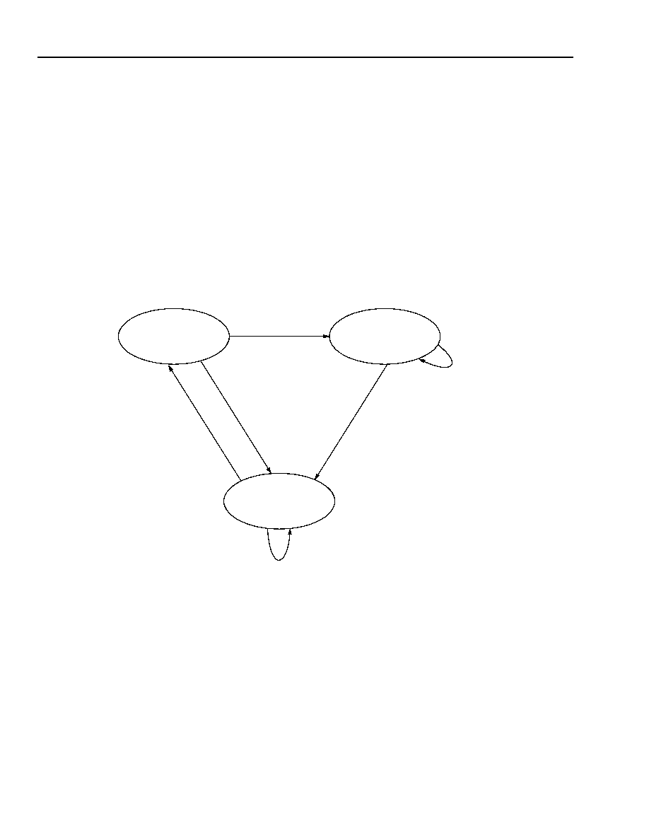
MARS2G5 P-Pro (TDAT162G52) SONET/SDH
Data Sheet
155/622/2488 Mbits/s Data Interface
August 18, 2004
672
Agere Systems Inc.
Data Engine Block
--
GFP General Framing Procedure Subblock
(continued)
GFP Frame Delineation/Frame Insertion
(continued)
Transmit Direction
The layer 2 master device must provide MARS2G5 P-Pro GFP packets with the PLI field attached to the start of the
packet in the transmit direction. The MARS2G5 P-Pro will generate the CRC-16 over the header and attach it as
the 3rd or 4th bytes of the outgoing packet. The generating polynomial used for the creation of the header CRC-16
field is X
16
+ X
12
+ X
5
+ 1. The X
43
,
X
48
, or no scrambling is applied to the payload area of the packet and scram-
bled. CRC-16/32 is attached to the end of the packet. The MARS2G5 P-Pro also provides a provisional option to
suppress the insertion of a payload area CRC. The CRC-16/32 generating polynomials used over the payload are
as follows:
CRC-16--X
16
+ X
12
+ X
5
+ 1
CRC-32--X
32
+ X
26
+ X
23
+ X
22
+ X
16
+ X
12
+ X
11
+ X
10
+ X
8
+ X
7
+ X
5
+ X
4
+
X
2
+ X+ 1
1632(F)
Figure 89. Special-Purpose GFP Header Definitions
PRESYNCHRONIZATION
SYNCHRONIZATION
HUNT
CORRECTABLE
CRC-16
FOUND
CORRECTABLE
CRC-16
NOT FOUND
SECOND
CRC-16
NOT FOUND
CRC-16
MATCH FOUND
NO CRC-16
MATCH FOUND
CRC-16s
FOUND

Data Sheet
MARS2G5 P-Pro (TDAT162G52) SONET/SDH
August 18, 2004
155/622/2488 Mbits/s Data Interface
673
Agere Systems Inc.
Data Engine Block
--
GFP General Framing Procedure Subblock
(continued)
GFP Scrambling/Descrambling
Scrambling of GFP frames are required to provide security against payload information replicating the frame syn-
chronous (or OTUk) scrambling word used at the OTUk/SONET/SDH section layer. Figure 90 illustrates the GFP
compliant scrambler and descrambler process.
For GFP compliance, all octets of the GFP payload area are scrambled using a 1 + X
43
self-synchronous scram-
bler. At the transmitter, scrambling is enabled starting at the first transmitted octet after the header CRC-16 field,
and is disabled after the last transmitted octet of the GFP frame including the payload CRC-16. The activation of
the receiver descrambler depends on the present state of the header CRC-16 check algorithm. The scrambler is
disabled in the HUNT and PRESYNC states as shown in Figure 89. In the SYNC state, the descrambler is enabled
only for the octets between the HEC field and the end of the assumed GFP frame. When the scrambler/descram-
bler is disabled, its state is retained. The scrambling is done least significant bit first.
The MARS2G5 P-Pro provides two methods for scrambling/descrambling data on the link for passing GFP packets
that are the X
43
self-synchronous scrambler/descrambler and X
48
free-running set-reset scrambler. The first
approach uses a lower complexity and less robust X
43
self-synchronization scrambler; the scrambler is considered
self-synchronous because synchronization is maintained by the data itself. This is less secure to malicious attacks
than the X
48
free-running set-reset scrambler. The diagram for the X
43
self-synchronous scrambler/descrambler is
shown in Figure 90 and the diagram for the X
48
free-running set-reset scrambler is shown in Figure 91. The X
43
scrambler uses the X
43
+ 1 primitive polynomial for its output sequence generation. In GFP, scrambling is done
over the payload area, which includes the offset field and the CRC-16/32 payload FCS, but not the 4-byte header
(PLI + CRC-16) field dc balanced Barker-like sequence of length 32. The 4-byte header is modulo 2 added (exclu-
sive ORed) to 0xB6AB31E0 prior to transmission and on reception is removed before the frame delineation.
Although GFP over SONET does not necessitate a dc balanced header, the approach facilitates the usage of GFP
channels directly over wavelength (bypass SONET framing).
The first approach uses a lower complexity and less robust X
43
self-synchronization scrambler similar to the
scramblers used for the PPP/HDLC/ATM protocols. Figure 90 shows the diagram of the X
43
self-synchronization
scrambler. The scrambler is self-synchronous because synchronization is maintained by the data itself. This is less
secure to malicious attacks than the X
48
free-running set-reset scrambler.
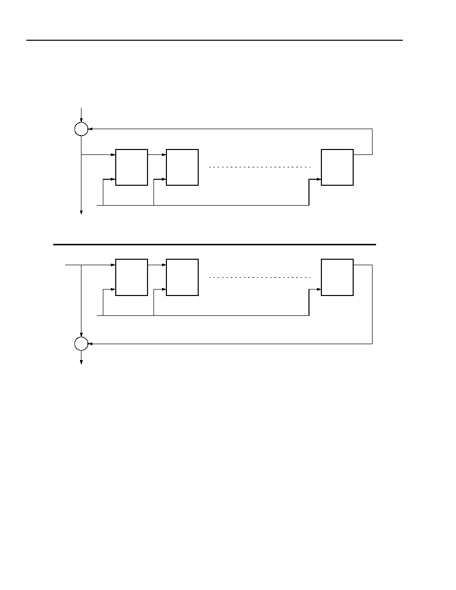
MARS2G5 P-Pro (TDAT162G52) SONET/SDH
Data Sheet
155/622/2488 Mbits/s Data Interface
August 18, 2004
674
Agere Systems Inc.
Data Engine Block
--
GFP General Framing Procedure Subblock
(continued)
GFP Scrambling/Descrambling
(continued)
1633(F)r.1
Figure 90. X
43
Self-Synchronous Scrambler/Descrambler
The X
48
scrambler provides an alternative to the standards compliant X
43
scrambler used for PPP/HDLC/ATM and
the diagram is shown in Figure 91. The X
48
scrambler initializes at 0xFFFFFFFFFFFF when the link enters the pre-
synchronization state and free runs from this starting point. The scrambler has a X
48
+ X
28
+ X
27
+ X+ 1 generating
polynomial and input data to the scrambler is exclusive ORed with the output of the generated sequence. To syn-
chronize the receivers scramble-state with the transmitters scrambler-state, scrambler-state update messages
must be sent periodically from the transmitter to the receiver. This is accomplished using the special-purpose
scrambler state messages shown in Figure 88b. The scrambler state update messages can be sent by configuring
the scrambler state transmit mode register. The provisionable resolution interval can be configured to be either
packet or 32-bit words. The default configuration is for one scrambler-state update message to be sent every eight
packets, independent of the packet size.
INPUT DATA
+
D
0
D
Q
C
D
1
D
Q
C
D
42
D
Q
C
PRIMITIVE POLYNOMIAL x
43
+ 1
SCRAMBLED
DATA OUT
CLOCK
(A) x
43
SELF-SYNCHRONOUS SCRAMBLER
+
D
0
D
Q
C
D
1
D
Q
C
D
42
D
Q
C
PRIMITIVE POLYNOMIAL x
43
+ 1
UNSCRAMBLED
DATA OUT
CLOCK
(B) x
43
SELF-SYNCHRONOUS DESCRAMBLER
INPUT DATA

Data Sheet
MARS2G5 P-Pro (TDAT162G52) SONET/SDH
August 18, 2004
155/622/2488 Mbits/s Data Interface
675
Agere Systems Inc.
Data Engine Block
--
GFP General Framing Procedure Subblock
(continued)
GFP Scrambling/Descrambling
(continued)
1634(F)r.1
Figure 91. X
48
Set-Reset Scrambler
The state machine for scrambler synchronization is shown in Figure 92. The scrambler starts in an out-of-frame
state and is required to be in synchronization before data can pass through the device. Data will flow once the
scrambler is in the synchronization state and will continue to flow in the postsynchronization state. Data will stop
flowing when the scrambler is in the presynchronization or out-of-frame states. The scrambler is initialized on reset
to a value of 0xFFFFFFFFFFFF and zero-detect circuitry is used to ensure that a state of 0x000000000000 is
never reached. If an all-zero pattern is detected, the scrambler state is reset to its default value. The scrambler
moves from the out-of-frame state to the presynchronization state on a state special message transfer. If the next
scrambler message sent by the transmitter results in a state match at the receiver, then the scrambler will go into
synchronization and begin to pass data. If the presynchronization state, a state mismatch occurs, a synchroniza-
tion slip results and the receive-side scrambler accepts the next error-free scrambler state message transfer as its
new scrambler-state and matches future messages with this newly updated message. When in the synchroniza-
tion state, a state match will maintain scrambler synchronization; however, a state mismatch will result in a soft
error and cause a transition to the postsynchronization state. Data will continue to pass in this state; however,
another mismatch will result in a synchronization slip and the state transitions to presynchronization. This will then
require the receive-side scrambler to update its state on the next available validated scrambler update message
received. When operating in any of the four scrambler states, lack of proper frame delineation will result in the
scrambler going to the out-of-frame state.
MARS2G5 P-Pro provides the option to disable scrambling on the payload. When scrambling is active, it is per-
formed over the entire payload area including the attached CRC-16/32 for both types of scramblers.
INPUT DATA
+
D
0
D
Q
C
D
1
D
Q
C
D
47
D
Q
C
SCRAMBLED
DATA OUT
CLOCK
+
D
26
D
Q
C
D
27
D
Q
C
+
+
GENERATING POLYNOMIAL x
48
+ x
28
+ x
27
+ x + 1
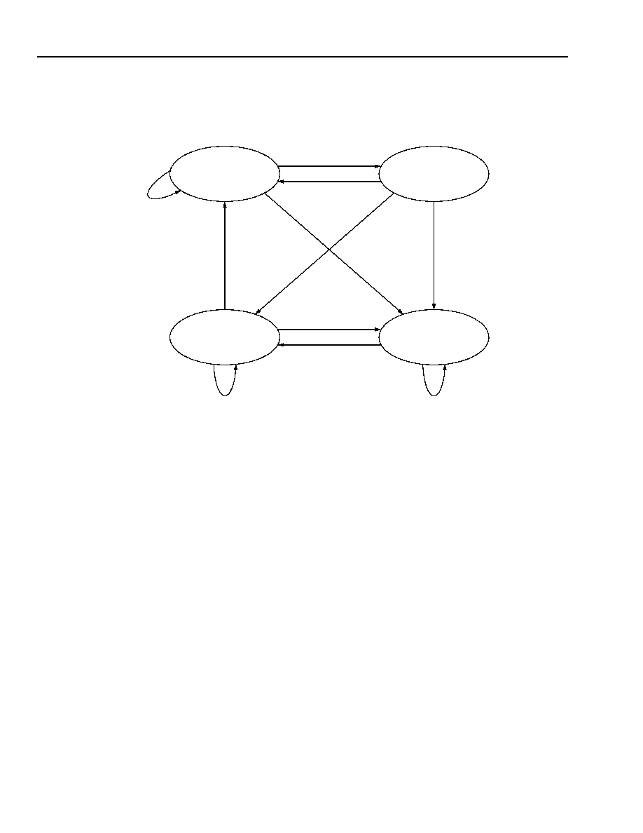
MARS2G5 P-Pro (TDAT162G52) SONET/SDH
Data Sheet
155/622/2488 Mbits/s Data Interface
August 18, 2004
676
Agere Systems Inc.
Data Engine Block
--
GFP General Framing Procedure Subblock
(continued)
GFP Scrambling/Descrambling
(continued)
1635(F)r.1
Figure 92. X
48
Scrambler Synchronization State Machine
Packet-Over-Wavelength Mode
The packet-over-wavelength mode is used for packet delivery over a link where SONET overhead insertion and
extraction are bypassed. Since no SONET overhead is inserted, the TOHP and PT/SPE blocks must be configured
for bypass mode. In transmitting from the MARS2G5 P-Pro to the line, the data engine passes the full payload
received from the UTOPIA interface to the line at the full-line rate with no loss of bandwidth for overhead insertion.
The FIFO dynamics are slightly different than in the SONET/SDH mode in this case, since there is no dead time
form overhead insertion and less backpressure to the master device as a result. In the packet-over-wavelength
mode, there is no SONET byte interleaving on a predefined time-slot basis; then no channelization can be done
and only one channel can be active sending data.
SYNCHRONIZATION
SYNCHRONIZATION
PRESYNCHRONIZATION
OUT OF FRAME
STATE MISMATCH
POST-
OUT OF FRAME
STATE MISMATCH/
TRANSFER
STATE MATCH
STATE MATCH
OUT OF FRAME
STATE TRANSFER
OUT OF
STATE
MATCH
FRAME
OUT OF
FRAME
STATE
MISMATCH/
TRANSFER

Data Sheet
MARS2G5 P-Pro (TDAT162G52) SONET/SDH
August 18, 2004
155/622/2488 Mbits/s Data Interface
677
Agere Systems Inc.
Data Engine Block Registers
DE Register Descriptions
Table 690. General Registers (RO)
Table 691. CORWN Register (R/W)
Table 692. TXMUX Mask Register (R/W)
Table 693. RXMUX Mask Register (R/W)
Address
Bit
Name
Function
Reset
Default
0x6000
15:8
--
Reserved.
0x00
7:0
DE_VERSION[7:0]
Version ID. The version of the block will increment each
time a change occurs to the block functionality.
Indicates version number for version 2.0.
0x02
Indicates version number for version 2.2.
0x03
Indicates version number for version 2.3.
0x07
Address
Bit
Name
Function
Reset
Default
0x6001
15:1
--
Reserved.
0x0
0
DE_CORWN
Data Engine Registers Clear on Read Clear on Write.
0 = Clear on write.
1 = Clear on read.
0
Address
Bit
Name
Function
Reset
Default
0x6003
15:3
--
Reserved.
2:0
TXMASK
Bit 2: ATM mask.
Bit 1: GFP mask.
Bit 0: HDLC mask.
DE Tx output is the logic OR of the outputs from HDLC,
ATM, and GFP. When a mask bit is set to one, the output
from the corresponding frame inserter is disabled (zero).
These masks are useful to isolate the malfunctioning blocks.
0x0
Address
Bit
Name
Function
Reset
Default
0x6004
15:3
--
Reserved.
2:0
RXMASK
Bit 2: ATM mask.
Bit 1: GFP mask.
Bit 0: HDLC mask.
DE Rx output is the logic OR of the outputs from HDLC,
ATM, and GFP. When a mask bit is set to one, the output
from the corresponding framer is disabled (zero). These
mask are useful to isolate the malfunctioning blocks.
0x0

MARS2G5 P-Pro (TDAT162G52) SONET/SDH
Data Sheet
155/622/2488 Mbits/s Data Interface
August 18, 2004
678
Agere Systems Inc.
Data Engine Block Registers
(continued)
DE Register Descriptions
(continued)
Table 694. FIFO Control (FC) Bandwidth Register (R/W)
Table 695. DE Scratch Register (R/W)
Table 696. Counter Interrupts (COR/COW)
Table 697. GFP Message Interrupts (COR/COW)
Address
Bit
Name
Function
Reset
Default
0x6005
15:0
[15:0]
FIFO Control (FC) Bandwidth Register. Must be set to
0x1F0A.
0x1F07
Address
Bit
Name
Function
Reset
Default
0x6007
15:0
DE_SCRATCH[15:0] DE Scratch Register. Diagnostic register used by the
microprocessor. Has no effect on the device operation.
0x0
Address
Bit
Name
Function
Reset
Default
0x6010
15:0
DE_CNT_INT[15:0]
Counter Interrupt. Active-high counter interrupt bit on a
per-channel basis. This bit will remain set in COW mode
until it is written with a 1, even if the underlying interrupt in
0x6ACn (channel #n) is cleared or the mask bit in 0x6A8n
(channel #n) is set. Each bit is the ORing of all counter
errors. An error event can be inhibited from contributing to
the interrupt by setting the appropriate mask bit. These
interrupts will generate a block-level interrupt. Bit-i
corresponds to Channel-i interrupt.
Note: This bit indicates that the counter is experiencing an
interrupt. This bit will not clear on a read or a write of
this register. To clear a bit in this register, it is first
necessary to clear the interrupts in any unmasked bit
positions in the corresponding channel packet
counter interrupt register 0x6ACn (channel #n). Only
then should the COW/COR operation to register
0x6010 be performed.
0x0000
Address
Bit
Name
Function
Reset
Default
0x6011
15:1
--
Reserved.
0
GFP_MS_INT
GFP Message Sent Interrupt. This bit indicates that the
GFP frame inserter is experiencing an interrupt. This bit will
not clear on a read or a write of this register, but will clear
when the GFP frame insert interrupt is read.
This interrupt will generate a DE48 interrupt.
0

Data Sheet
MARS2G5 P-Pro (TDAT162G52) SONET/SDH
August 18, 2004
155/622/2488 Mbits/s Data Interface
679
Agere Systems Inc.
Data Engine Block Registers
(continued)
DE Register Descriptions
(continued)
Table 698. Composite Interrupt Register for GFP Interrupts at the Channel Level (COR/COW)
Address
Bit
Name
Function
Reset
Default
0x6012
15:0
GFP[15:0]
This is the composite interrupt register for GFP interrupts at
the channel level. Each bit in this register corresponds to a
channel with the least significant bit representing the com-
posite interrupt for channel 0 and the most significant bit
representing the composite interrupt for channel 15.
A bit is set in this register location when its associated
channel has 1 or more unmasked bits in its GFP_IRQ reg-
ister set, i.e., if a bit in 0x660n is 1 and the corresponding
bit in 0x65Cn is 0, then bit n will be set.
This is a COR/COW register--the bit in 0x6012 will remain
set in COW mode until it is written with a 1, even if the
underlying interrupt in 0x660n (channel #n) is cleared or
the mask bit in 0x65Cn (channel #n) is set.
Note: To clear a bit in this register, it is first necessary to
clear the interrupts in any unmasked bit positions in
the corresponding channel GFP_INT register. Only
then should the COW/COR operation to register
0x6012 be performed.
0x0000

MARS2G5 P-Pro (TDAT162G52) SONET/SDH
Data Sheet
155/622/2488 Mbits/s Data Interface
August 18, 2004
680
Agere Systems Inc.
Data Engine Block Registers
(continued)
DE Register Descriptions
(continued)
Table 699. ATM Frame State Interrupts (COR/COW)
Table 700. ATM Cool Interrupts (COR/COW)
Address
Bit
Name
Function
Reset
Default
0x6013
15:0
ATM_FS_INT[0:15]
ATM Frame State Interrupt. This interrupt is generated
when the ATM frame state is transitioned from sync to hunt.
This register clears when read or written as defined by reg-
ister 0x6001 (Table 691).
These interrupts will generate a DE48 interrupt.
Refer to register 0x6346 (Table 715) for information on
masking these interrupts.
0x0000
Address
Bit
Name
Function
Reset
Default
0x 6014
15:0
ATM_COOL_INT[0:15] ATM All-Cool Interrupt. This interrupt is generated when
the payload in received idle and/or unassigned cells devi-
ates from an incrementing pattern. This register clears
when read or written as defined by register 0x6001
(Table 691).
These interrupts will generate a DE48 interrupt.
Table 715 contains the enable (register 0x6347 bit 1)
masks (register 0x6348) for these interrupts.
0x0000

Data Sheet
MARS2G5 P-Pro (TDAT162G52) SONET/SDH
August 18, 2004
155/622/2488 Mbits/s Data Interface
681
Agere Systems Inc.
Data Engine Block Registers
(continued)
DE Register Descriptions
(continued)
Table 701. CDA MAP0 Register (R/W)
Table 702. CDA MAP Control Register (R/W)
Table 703. CDA MAP1 Register (R/W)
Table 704. ATM Framer Idle Cell Match Mask (R/W)
Address
Bit
Name
Function
Reset
Default
0x6080--
0x60AF
15:7
--
Reserved.
--
6:4
--
Reserved. Must be written to 0.
0x40
3:0
CDA_M0_CH0[3:0]--
CDA_M0_CH47[3:0]
Used to define the channel ID for time slot 0 to 47.
Address
Bit
Name
Function
Reset
Default
0x60BF
15:2
--
Reserved.
0x0000
1
CDA_MAP_CNTL[1]
Map Control Status (RO).
0
0
CDA_MAP_CNTL[0]
Map Control Register (R/W). Select MAP0 or MAP1 as
working map. A working map is not available for update.
Only the nonworking map is available for MPU update.
0 = Select MAP0.
1 = Select MAP1.
0
Address
Bit
Name
Function
Reset
Default
0x60C0--
0x60EF
15:7
--
Reserved.
0x00
6:4
--
Reserved. Must be written to 0.
0x40
3:0
CDA_M1_CH0[3:0]--
CDA_M1_CH47[3:0]
Used to define the channel ID for time slot from 0 to 47.
Address
Bit
Name
Function
Reset
Default
(0x6100--
0x6101)
--
(0x611E--
0x611F)
31:0
ATM_IDM_0--
ATM_IDM_15
ATM Idle Cell Match Mask Channel 0--Channel
15. This 32-bit register defines which of the 32 bits
will be used for comparison between the idle cell
register and the header data in the ATM framer. A 1
indicates that the corresponding bit in the ATM idle
cell register should be compared.
0xFFFFFFFF

MARS2G5 P-Pro (TDAT162G52) SONET/SDH
Data Sheet
155/622/2488 Mbits/s Data Interface
August 18, 2004
682
Agere Systems Inc.
Data Engine Block Registers
(continued)
DE Register Descriptions
(continued)
Table 705. ATM_LCD[0--15] (R/W)
Table 706. ATM_LCDCLK (R/W)
Table 707. ATM_IN_LCD_MASK (R/W)
Table 708. ATM_OUT_LCD_MASK (R/W)
Table 709. ATM_IN_LCD (COR/COW)
Table 710. ATM_OUT_LCD (COR/COW)
Address
Bit
Name
Function
Reset
Default
0x6120
--
0x612F
15:6
--
Reserved. 0x0010
5:0
ATM_LCD[0--15]
[5:0]
Indicates number of allowable period ATM framer for channels
0--15 allowed to be out of sync before LCD is declared for chan-
nel 0--15. The definition of period is specified in explanation for
register address 0x6130. These bits are reserved in V1AAA.
Address
Bit
Name
Function
Reset
Default
0x6130
15:0
ATM_LCDCLK
[15:0]
As mentioned in Table 705, this register defines the number
of 77.76 MHz clock that constitutes a period to declare LCD.
These bits are reserved in V1AAA.
0x25F7
Address
Bit
Name
Function
Reset
Default
0x6131
15:0
ATM_IN_LCD_
MASK[15:0]
When set (logic 1), the associated event/delta is inhibited from
contributing to the interrupt on a per-channel basis. When
cleared, a DE48 interrupt is generated when the corresponding
bit in register 0x6133 is 1 (combinatorial mask).
These bits are reserved in V1AAA.
0xFFFF
Address
Bit
Name
Function
Reset
Default
0x6132
15:0
ATM_OUT_LCD_
MASK[15:0]
When set (logic 1), the associated event/delta is inhibited from
contributing to the interrupt on a per-channel basis. When
cleared, a DE48 interrupt is generated when the corresponding
bit in register 0x6134 is 1 (combinatorial mask).
These bits are reserved in V1AAA.
0xFFFF
Address
Bit
Name
Function
Reset
Default
0x6133
15:0
ATM_IN_LCD
[15:0]
A 1 indicates that the corresponding channel has transitioned into
the LCD state. These bits are reserved in V1AAA.
0x0000
Address
Bit
Name
Function
Reset
Default
0x6134
15:0
ATM_OUT_LCD
[15:0]
A 1 indicates that the corresponding channel has transitioned
out of the LCD state. These bits are reserved in V1AAA.
0x0000

Data Sheet
MARS2G5 P-Pro (TDAT162G52) SONET/SDH
August 18, 2004
155/622/2488 Mbits/s Data Interface
683
Agere Systems Inc.
Data Engine Block Registers
(continued)
DE Register Descriptions
(continued)
Table 711. ATM Framer Idle Cell (R/W)
Table 712. ATM Unassigned Cell Match/Register (R/W)
Address
Bit
Name
Function
Reset
Default
0x6180--
0x6181
31:0
ATM_IDC_0
ATM Idle Cell Register Channel 0. This 32-bit regis-
ter will store the expected header value for idle cells.
If the ATM framer sees a header for an ATM packet
that matches this register at the bit positions desig-
nated by the ATM idle cell match mask, the packet
will be treated as an idle cell.
0x00000001
(0x6182--
0x6183)
--
(0x619E--
0x619F)
31:0
ATM_IDC_1--
ATM_IDC_15
ATM Idle Cell Register Channel 1 to Channel 15.
See above.
0x00000001
Address
Bit
Name
Function
Reset
Default
0x6200--
0x6201
31:0
ATM_USM_0
ATM Unassigned Cell Match Mask Channel 0.
This 32-bit register defines which of the 32 bits will
be used for comparison between the unassigned
cell register and the header data in the ATM framer.
A 1 indicates that the corresponding bit in the ATM
unassigned cell register should be compared.
0xFFFFFFFF
(0x6202--
0x6203)
--
(0x621E--
0x621F)
31:0
ATM_USM_1--
ATM_USM_15
ATM Unassigned Cell Match Mask Channel 1 to
Channel 15. See above.
0xFFFFFFFF

MARS2G5 P-Pro (TDAT162G52) SONET/SDH
Data Sheet
155/622/2488 Mbits/s Data Interface
August 18, 2004
684
Agere Systems Inc.
Data Engine Block Registers
(continued)
DE Register Descriptions
(continued)
Table 713. ATM Unassigned Cell (R/W)
Table 714. ATM Frame State Channel [0--15] Registers (RO)
Address
Bit
Name
Function
Reset
Default
0x6280--
0x6281
31:0
ATM_USG_0
ATM Unassigned Cell Register Channel 0. This
32-bit register will store the expected header value
for unassigned cells. If the ATM framer sees a
header for an ATM packet that matches this register
at the bit positions designated by the ATM unas-
signed cell match mask, the packet will be treated as
an unassigned cell.
0x00000000
0x6282--
0x6283)
--
(0x629E--
0x629F)
31:0
ATM_USG_1--
ATM_USG_15
ATM Unassigned Cell Register Channel 1 to
Channel 15. See above.
0x00000000
Address
Bit
Name
Function
Reset
Default
0x6300
15:2
--
Reserved.
0x0000
1:0
ATM_ST_0[1:0]
ATM Frame State Channel 0. Indicates the frame state of
each channel.
In x43 scrambling mode (or no scrambling mode), 0x2 indi-
cates that the ATM framer has successfully synchronized
and can start passing data.
ATM_ST_0[1:0] = 00--Hunt.
ATM_ST_0[1:0] = 01--Presync.
ATM_ST_0[1:0] = 10--Sync.
ATM_ST_0[1:0] = 11--Undefine.
Use this register to check for the presence of an ongoing
LCD condition that started prior to device initialization.
0x0
0x6301--
0x630F
15:0
ATM_ST_1--
ATM_ST_15
ATM Frame State Channel 1 to Channel 15. See above
for description.
0x0000

Data Sheet
MARS2G5 P-Pro (TDAT162G52) SONET/SDH
August 18, 2004
155/622/2488 Mbits/s Data Interface
685
Agere Systems Inc.
Data Engine Block Registers
(continued)
DE Register Descriptions
(continued)
Table 715. ATM Configuration Registers (R/W)
Address
Bit
Name
Function
Reset
Default
X43 Framing Register
0x6340
15:12
--
Reserved.
0x0
11:8
ATM_X43[11:8]
X43 Alpha. This register will define the alpha value for the
X43 Alpha_Delta framer, which is the number of consecu-
tive incorrect ATM cells that must be received in order to
transition from the sync state to the hunt state.
0x7
7:6
--
Reserved.
00
5:0
ATM_X43[5:0]
X43 Delta. This register will define the delta value for the
X43 Alpha_Delta framer, which is the number of consecu-
tive correct ATM cells that must be received in order to tran-
sition from the presync state to the sync state.
0x06
0x6341
15:0
--
Reserved.
0x0708
0x6342
15:0
--
Reserved.
0x0810
0x6343
15:0
--
Reserved.
0x1018
0x6344
15:0
--
Reserved.
0x0018
0x6345
15:0
--
Reserved. Must be set to 0xFFFF.
0xFFFF
0x6346
15:0
ATM_FS_INTM[0:15] Frame State Interrupt Mask. When active (logic 1), the
associated event/delta is inhibited from contributing to the
interrupt on a per-channel basis. Otherwise, an interrupt is
generated when the ATM frame state transitions from syn-
chronization to hunt state.
0xFFFF
ATM Debug Rx Register
0x6347
15:2
--
Reserved.
0x000
1
ATM_COOL
ATM All-Cool Enable. This bit must be set to 1 for proper
functioning of the all-cool interrupt (Table 700).
0x0
0
--
Reserved.
0x1
0x6348
15:0
ATM_COOL_
INTM[0:15]
ATM All-Cool Interrupt Mask. When active (logic 1), the
associated event/delta is inhibited from contributing to the
interrupt on a per-channel basis. Otherwise, an interrupt is
generated on any deviation from an incrementing data pat-
tern in the payloads of received idle/unassigned cells.
Note: To avoid unexpected interrupts, channels must be in
sync and receiving idle cells before unmasking.
0xFFFF
0x6349
15:1
--
Reserved.
0x0000
0
--
Reserved. For Internal Use Only.
0x0
MARS2G5 P-Pro (TDAT162G52) SONET/SDH
Data Sheet
155/622/2488 Mbits/s Data Interface
August 18, 2004
686
Agere Systems Inc.
Data Engine Block Registers
(continued)
DE Register Descriptions
(continued)
Table 716. Rx Channel [0--15] Payload Type and Control (R/W)
Address
Bit
Name
Function
Reset
Default
0x6380
15:13
RX_PCTL_0[15:13]
Channel 0 Payload Type. Defines the payload type being
received.
111
12:0
RX_PCTL_0[12:0]
Channel 0 Payload Control. Allows for different options
when receiving data, such as pre- or post-unscrambling,
PPP header discard, etc.
000000
000000
0
0x6381--
0x638F
15:0
RX_PCTL_1--
RX_PCTL_15
Channel 1--15 Payload Type and Control. See descrip-
tion above and Table 717.
0xE000
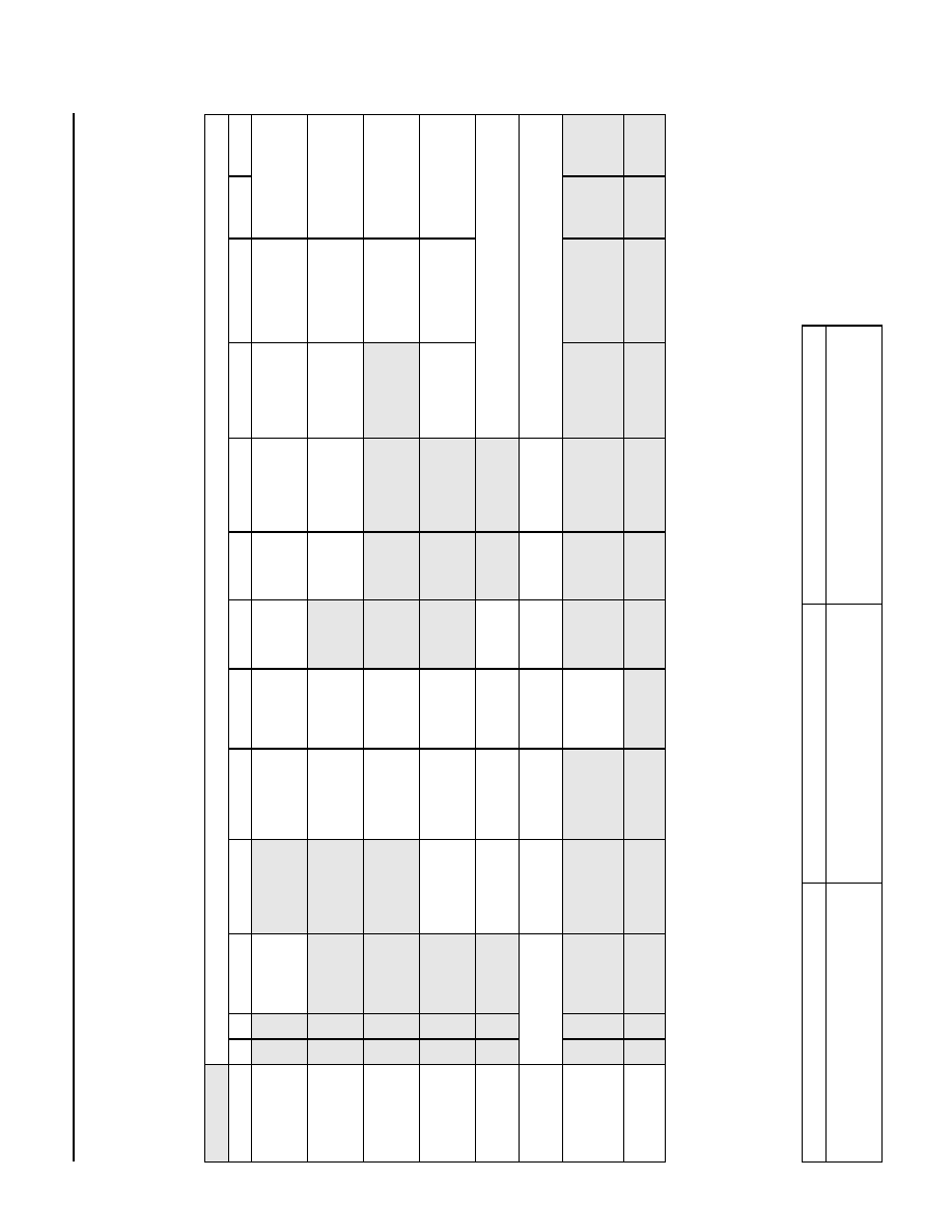
Data Sheet
MARS2G5 P-Pro (TDAT162G52) SONET/SDH
August 18, 2004
155/622/2488 Mbits/s Data Interface
687
Agere Systems Inc.
Data Engine Block Registers
(continued)
DE Register Descriptions
(continued)
Table 717. Rx Payload Type and Payload Control Summary Table
* No discard--pass all ATM cells with no error correction.
Discard--discard cells with multiple-bit header errors. Correct and pass all cells with single-bit header errors.
Smart discard--discard cells with multiple-bit header errors, and only correct and pass the first of back-to-back single-bit header errors.
Table 717. Rx Payload Type and Payload Control Summary Table (continued)
Note: This is an expansion of Table 717 for Rx payload type CRC GFP bits [12:10] and applies to only version 2.2 and 2.3 of the device.
Payload Control[12:0]
Type[15:13] 12 11
10
9
8
7
6
5
4
3
2
1
0
000
PPP
0 = discard
1 = no discard
Bit Sync
1 = no invert
0 = invert
0 = byte sync
1 = bit sync
0 = header
stripped
1 = header
on
0 = CRC-16
1 = CRC-32
0 = CRC stripped
1 = CRC on
0 = CRC reversed
1 = CRC normal
0 = no dry mode
1 = dry mode
00 = no unscrambling
01 = post-unscrambling
10 = pre-unscrambling
11 = undefined
001
CRC
Bit Sync
1 = no invert
0 = invert
0 = byte sync
1 = bit sync
0 = CRC-16
1 = CRC-32
0 = CRC stripped
1 = CRC on
0 = CRC reversed
1 = CRC normal
0 = no dry mode
1 = dry mode
00 = no unscrambling
01 = post-unscrambling
10 = pre-unscrambling
11 = undefined
010
HDLC
Bit Sync
1 = no invert
0 = invert
0 = byte sync
1 = bit sync
0 = no dry mode
1 = dry mode
00 = no unscrambling
01 = post-unscrambling
10 = pre-unscrambling
11 = undefined
011
ATM
0 = X
43
scrambler 0 = scrambler on
1 = scrambler off
0 = byte sync
1 = bit sync
Unassigned Cell
0 = discard
1 = passthrough
0 = idle cell discard
1 = idle cell
passthrough
00 = no discard*
01 = discard
10 = smart discard
11 = undefined
100
GFP
0 = X
43
scrambler
1 = X
48
scrambler
0 = scrambler on
1 = scrambler off
0 = byte sync
1 = bit sync
0 = length
stripped
1 = length on
Length offset = 0x0 to 0xF
101
CRC GFP
See Table 717 below for
description of bits [12:10].
0 = X
43
scrambler
1 = X
48
scrambler
0 = scrambler on
1 = scrambler off
0 = byte sync
1 = bit sync
0 = length
stripped
1 = length on
0 = CRC-16
1 = CRC-32
0 = CRC stripped
1 = CRC on
Length offset = 0x0 to 0xF
110
Transparent
Payload
0 = no align
1 = frame align
111
Not defined
12
11
10
0 = Indicates non-GFP mode.
1 = Must be set to1 in CRC-GFP mode.
0 = PLI field unchanged.
1 = Subtract four from the PLI field if the CRC-32 bytes
are stripped.
0 = Start CRC calculation after first 32 bits of payload (i.e.,
assume null extension header.
1 = Start CRC calculation after first 64 bits of payload (i.e.,
assume linear extension header.

MARS2G5 P-Pro (TDAT162G52) SONET/SDH
Data Sheet
155/622/2488 Mbits/s Data Interface
August 18, 2004
688
Agere Systems Inc.
Data Engine (DE) Block
(continued)
DE Register Descriptions
(continued)
Table 718. GFP State Register (R/W, RO)
Note:This register is nonfunctional for all versions of the device. In version 2.3 of the device, the function of this
register has been moved to registers 0x6600--0x660F (Table 727).
Table 719. Registers 0x6470--0x6473 A Message Mailbox Registers (RO)
Table 720. A Message Mailbox Registers (RO)
Address
Bit
Name
Function
Reset
Default
0x6400
15:8
--
Reserved.
7:4
GFP_ST_0
Audit CHID (R/W). Indicates which channel is selected for
audit.
To get the GFP state in a particular channel, write the
channel ID into bit 7:4. Then read this register, GFP state is
in bit 3:0.
0x0000
3:2
GFP Frame State (RO). Indicates the frame state of each
channel.
00 = Out of frame.
01 = Presync.
10 = Sync.
11 = Undefined.
0x0
1:0
GFP Scram State (RO). Indicates the X48 sync state of
each channel.
00 = Hunt.
01 = Sync.
10 = Postsync.
11 = Undefined.
0x0
Address
Bit
Name
Function
Reset
Default
0x6440
--
0x644F
15:0
GFP_AMM0_1
--
GFP_AMM15_1
A Message Mailbox Channel 0--15. These registers will
store the first 16 bits of a valid A message.
0x0000
Address
Bit
Name
Function
Reset
Default
0x6480
--
0x648F
15:0
GFP_AMM0_2
--
GFP_AMM15_2
A Message Mailbox Channel 0--15. These registers will
store the middle 16 bits of a valid A message.
0x0000

Data Sheet
MARS2G5 P-Pro (TDAT162G52) SONET/SDH
August 18, 2004
155/622/2488 Mbits/s Data Interface
689
Agere Systems Inc.
Data Engine (DE) Block
(continued)
DE Register Descriptions
(continued)
Table 721. Registers 1168--1171 A Message Mailbox Registers (RO)
Table 722. Registers 1184--1187 B Message Mailbox Registers (RO)
Table 723. B Message Mailbox Registers (RO)
Table 724. B Message Mailbox Registers (RO)
Address
Bit
Name
Function
Reset
Default
0x64C0
--
0x64CF
15:0
GFP_AMM0_3
--
GFP_AMM15_3
A Message Mailbox Channel 0--15. These registers will
store the last 16 bits of a valid A message.
0x0000
Address
Bit
Name
Function
Reset
Default
0x6500
--
0x650F
15:0
GFP_BMM0_1
--
ADL_BMM15_1
B Message Mailbox Channel 0--15. These registers will
store the first 16 bits of a valid B message.
0x0000
Address
Bit
Name
Function
Reset
Default
0x6540
--
0x654F
15:0
GFP_BMM0_2
--
GFP_BMM15_2
B Message Mailbox Channel 0--15. These registers will
store the middle 16 bits of a valid B message.
0x0000
Address
Bit
Name
Function
Reset
Default
0x6580
--
0x658F
15:0
GFP_BMM0_3
--
GFP_BMM15_3
B Message Mailbox Channel 0--15. These registers will
store the last 16 bits of a valid B message.
0x0000

MARS2G5 P-Pro (TDAT162G52) SONET/SDH
Data Sheet
155/622/2488 Mbits/s Data Interface
August 18, 2004
690
Agere Systems Inc.
Data Engine (DE) Block
(continued)
DE Register Descriptions
(continued)
Table 725. GFP Interrupt Masks R/W
Determining the Per-Channel Framer State (Applies to Only Version 2.3 of the Device)
Bit 4 and bit 0 of registers 0x6600--0x660F (Table 727) are used to determine the per-channel framer state. The
following table indicates the per-channel framer state (see bit 0 of registers 0x6600--0x660F (Table 727)).
Table 726. Per-Channel Framer State
Address
Bit
Name
Function
Reset
Default
0x65C0
--
0x65CF
--
GFP_IRQEN_CH0
--
GFP_IRQEN_CH15
GFP Interrupt Mask Channel 0--15. When active (logic 1),
the associated event/delta is inhibited from contributing to
the interrupt on a per-channel basis.
0x00FF
15:8
--
Reserved.
0x00
7
--
B_Message Reception.
0x1
6
--
A_Message Reception.
0x1
5
--
Uncorrectable Special Payload Error.
0x1
4
--
Uncorrectable Bit Error.
0x1
3
--
Reserved. Must be set to 1.
0x1
2
--
Single Bit Error.
0x1
1
--
Scrambler Out of Sync.
0x1
0
--
Framer State Mask Bit. Must be set to 1.
This bit applies to only version 2.3 of the device.
0x1
0
--
Framer Out of Sync.
This bit applies to only versions 2.0 and 2.2 of the
device.
0x1
Uncorrectable Bit Error
(Bit 4)
Framer State
(Bit 0)
Per-Channel Framer State
0
0
Out of frame
0
1
In frame
1
0
Undefined (not possible)
1
1
Framing was lost since the last read of this register. Perform
a COW, and then read again to confirm if framing is still lost.

Data Sheet
MARS2G5 P-Pro (TDAT162G52) SONET/SDH
August 18, 2004
155/622/2488 Mbits/s Data Interface
691
Agere Systems Inc.
Data Engine (DE) Block
(continued)
DE Register Descriptions
(continued)
Table 727. GFP Interrupts (COW)
Table 728. GFP Receive Configuration Registers (R/W)
Address
Bit
Name
Function
Reset
Default
0x6600
--
0x660F
--
GFP_IRQ_CH0
--
GFP_IRQ_CH15
GFP Interrupt Channel 0--15. Used to record various
occurrences within the GFP framer. The bits will generate
an interrupt if defined by the interrupt mask, but the register
values here are independent of the interrupt mask values.
0x0000
15:8
--
Reserved.
0x00
7
--
B_Message Reception.
0x0
6
--
A_Message Reception.
0x0
5
--
Uncorrectable Special Payload Error.
0x0
4
--
Uncorrectable Bit Error.
0x0
3
--
Reserved.
0x0
2
--
Single Bit Error.
0x0
1
--
Scrambler Out of Sync.
0x0
0
--
Framer State. This bit is a state bit and must always be
masked to prevent constant presentation of an
interrupt to the MPU. Bit 0 of registers 0x65C0--0x65CF
(Table 725) is the mask bit.
The value contained in this bit will persist until a COW is
performed, or until a transition (from 0 to 1) occurs on the
signal. To determine the per-channel frame state, see
Table 726.
This bit applies to only version 2.3 of the device.
0x0
0
--
Framer Out of Sync.
This bit applies to only versions 2.0 and 2.2 of the
device.
0x0
Address
Bit
Name
Function
Reset
Default
0x6640
--
--
CRC-16 Framing Register.
0x0001
15:5
--
Reserved.
0x000
4
GFP_MODE
Framer Mode. When set, this bit disables all but the first
framer. A 1 implies single framer mode. When cleared to 0,
all three framers are used to acquire frame lock.
0
3:0
GFP_DELTA
Framer Delta. This register defines the delta value for the
CRC-16 framer. A value of 0 programmed into this register
implies a delta value of 1.
0x1

MARS2G5 P-Pro (TDAT162G52) SONET/SDH
Data Sheet
155/622/2488 Mbits/s Data Interface
August 18, 2004
692
Agere Systems Inc.
Data Engine Block Registers
(continued)
DE Register Descriptions
(continued)
Table 729. PPP Detach Channel 0--15 PPP Protocol Check (R/W)
Table 730. PPP Detach Programmable PPP Protocol Register 0--11 (R/W)
Address
Bit
Name
Function
Reset
Default
0x6680
--
--
Channel 0 PPP Protocol Check. Instead of using the Rx
payload control register to control stripping, this register
can be used to control whether to keep or strip both CRC
and PPP header fields as indicated below. If a protocol
check is enabled and matches, the indicated header field
will be stripped. See PPP Header Detach on page 645 for a
detailed explanation.
0x0000
15:14
--
Reserved.
00
13
PPP_PROTOCOL
_CONTROL0
A 1 value in this bit will enable a protocol 0x8021 check.
0
12
A 1 value in this bit will enable a protocol 0x0021 check.
0
11:0
A 1 value in the bit i enables the corresponding protocol
stored in the register--PPP_RX_HDR[i], for checking.
0x000
0x6681--
0x668F
15:0
PPP_PROTOCOL
_CONTROL1
--
PPP_PROTOCOL
_CONTROL15
Channel 1--15 PPP Protocol Check. See above.
0x0000
Address
Bit
Name
Function
Reset
Default
0x66B0--
0x66BB
15:0
PPP_RX_HDR0--
PPP_RX_HDR11
Programmable PPP Protocol Register 0--11. This regis-
ter defines the 2-byte protocol that can be used by all chan-
nels to validate the receiving PPP packets. This can be
used to compare any received PPP headers from different
channels to this value. If there is a mismatch, then the bad
header counter will increment by one.
0x0000

Data Sheet
MARS2G5 P-Pro (TDAT162G52) SONET/SDH
August 18, 2004
155/622/2488 Mbits/s Data Interface
693
Agere Systems Inc.
Data Engine Block Registers
(continued)
DE Register Descriptions
(continued)
Table 731. PPP Detach Channel 0--15 PPP Header Search (R/W)
Address
Bit
Name
Function
Reset
Default
0x66C0
--
--
Channel 0 PPP Header Search. This register will control
the headers that channel 0 PPP detach block looks for. If
there is a match with any of the headers, a good packet
will be noted in the counter. Otherwise, a bad header will
be noted in a separate counter.
0x0000
15:14
PPP_RX_CHK_CH0
Controls the way the PPP headers are searched for and
passed through.
00 = Wildcard match mode. Passes all packets with
uncompressed PPP headers. In other words, all
packets starting with the value 0xFF03 are matched.
01 = Pass only packets with uncompressed PPP headers
and one of more of the 14 PPP protocol values that
can be specifically selected (as described below). In
other words, packets are matched if the first 2 bytes
are 0xFF03 and the following bytes are one of the
(possibly several) specifically selected protocol val-
ues.
10 = Pass only packets with compressed PPP headers
and a PPP protocol value that is specifically selected
by settings described below. In other words, packets
are matched if the first 2 bytes are one of the (possi-
bly several) specifically selected protocol values.
11 = Pass only packets with a PPP protocol value that is
specifically selected by settings described below.
(i.e., protocol values are matched without regard to
whether or not the header is compressed). In other
words, this represents a combination #1 and #2
above. A packet is matched if the first 2 bytes are
0xFF03 and following 2 bytes are any one of the spe-
cifically selected protocol values OR if the first 2
bytes of the packet match any one of the specifically
selected protocol values.
00
13
A 1 value in this bit will enable a search for the 16-bit fixed
value 0x8021.
0
12
A 1 value in this bit will enable a search for the 16-bit fixed
value 0x0021.
0
11:0
A 1 value in bit i will enable a search of the 16-bit value in
the corresponding register PPP_RX_HDR[i].
0x000
0x66C1--
0x66CF
15:0
PPP_RX_CHK_CH1
--
PPP_RX_CHK_CH15
Channel 1--15 PPP Header Search. See above.
0x0000

MARS2G5 P-Pro (TDAT162G52) SONET/SDH
Data Sheet
155/622/2488 Mbits/s Data Interface
August 18, 2004
694
Agere Systems Inc.
Data Engine Block Registers
(continued)
DE Register Descriptions
(continued)
Table 732. ATM Null Cell Register in TX (R/W)
* The reset default of the least significant byte (bits [7:0]) of the combined registers forming the 32-bit parameter is 0x01.
Address
Bit
Name
Function
Reset
Default*
0x6700--
0x6701
15:0
NULL_CELL_CH0
[31:16] 0x6700
[15:0] 0x6701
ATM Null Cell MSB Channel 0. This defines the 4 bytes
(H0H1H2H3) of a null ATM cell. (i.e., 31:0 = H0H1H2H3
with H0H1 at 0x6700, H2H3 at 0x6701). It is important to
always provision all bytes (i.e., write both the low and the
high 16-bit word) whenever changing any of these values,
even if the user only wants to change one or two of the
header bytes. Otherwise, if only one half is written, the
other half may be corrupted. The order of writing does not
matter, since either the high half or the low half can be
written first. It is important to remember to program both
halves of the word.
0x0000
--
0x0001
(0x6702--
0x6703)
--
(0x671E--
0x671F)
15:0
NULL_CELL_CH1--
NULL_CELL_CH15
ATM Null Cell MSB Channel 1--15. See above.
0x0000
--
0x0001

Data Sheet
MARS2G5 P-Pro (TDAT162G52) SONET/SDH
August 18, 2004
155/622/2488 Mbits/s Data Interface
695
Agere Systems Inc.
Data Engine Block Registers
(continued)
DE Register Descriptions
(continued)
Table 733. ATM Header Error Register in Tx (R/W)
Table 734. CRC Transmit Registers (R/W)
Address
Bit
Name
Function
Reset
Default
0x6780
--
--
ATM Tx Debug Control. Used for debug purposes to inject
errors, and use and incrementing payload sequence for
NULL cells.
0x0000
15
--
Error Strobe. Writing a 1 to this register initiates the injec-
tion of a single or double shot error injection, assuming one
of these two modes is selected.
0
14
--
Incrementing NULL Cell Payload Sequence. This bit
governs whether 0x6A is used for the payload of NULL
cells, or whether an incrementing 8-bit count is used (0x00
--0xFF). A 1 selects the incrementing sequence. This can
be used with a detector in the receiver.
0
13:8
--
Reserved.
0x0
7:4
ATM_HEADER_ERR Error Channel ID. The logical channel to inject header
errors.
0x0
3:2
--
Error Type. These bits control the injection of a walking
error pattern into the headers of all outgoing cells.
00 = No errors.
01 = Single bit errors.
10, 11 = Double bit errors.
00
1:0
--
Error Fire Mode. These bits control the mode of operation
of the error injection.
00 = Continuous injection.
01 = Single shot (isolated cell).
10, 11 = Double shot (i.e., 2 back-to-back cells).
00
0x6781
15:1
--
Reserved.
--
0
--
Reserved. For Internal Use Only.
0x0
Address
Bit
Name
Function
Reset
Default
0x6790
15:0
CRC_ERR[15:0]
CRC Error Injection for Channels 15 to 0. This register is
used to configure which channels will generate a single bit
error within the CRC. When 1, a single bit CRC error is
inserted into channel i.
0x0000

MARS2G5 P-Pro (TDAT162G52) SONET/SDH
Data Sheet
155/622/2488 Mbits/s Data Interface
August 18, 2004
696
Agere Systems Inc.
Data Engine Block Registers
(continued)
DE Register Descriptions
(continued)
Table 735. GFP Transmit Registers (R/W)
* To transmit the GFP message. The controls in this register (0x67A3) must be set up first. The message must then be entered, beginning with
register 0x67A0 then 0x67A1. When the last 2 bytes of the message are written to register 0x67A2, the message is immediately queued for
transmission.
Address
Bit
Name
Function
Reset
Default
0x67A0
15:0
GFPFI_MSG_1
GFP Message. These registers will store the first 16 bits of
a header for a special message to be sent.
0x0000
0x67A1
15:0
GFPFI_MSG_2
GFP Message. These registers will store the middle 16 bits
of a header for a special message to be sent.
0x0000
0x67A2
15:0
GFPFI_MSG_3
GFP Message. These registers will store the last 16 bits of
a header for a special message to be sent.
0x0000
0x67A3
--
GFPFI_MSG_TYPE
GFP Message Type*.
0x0000
14:6
--
Reserved.
7:4
Channel ID. Defines which channel the special message
will be transmitted on.
3:1
--
Reserved.
0
Message Bit.
0 = A message.
1 = B message.
0x67A4
15:0
GFPFI_INT
GFP State Transmit Interval. Defines the number of
packets (or dWords) separating scrambler state
transmissions. Use register GFPFI_MODE register to
determine if units are packets or dwords.
0x0008
0x67A5
--
GFPFI_MODE
GFP State Transmit Mode.
0x8000
15
--
Interrupt Enable. When active (logic 1), the associated
event/delta is inhibited from contributing to the interrupt on
a per-channel basis. In this case, used to signal the
sending of a special message (A or B message).
0x1
14:1
--
Reserved.
0x0
0
--
Message Bit.
0 = GFP state transmit interval (register 0x67A4) is
measured in packets.
1 = GFP state transmit interval (register 0x67A4) is
measured in dwords.
0x0

Data Sheet
MARS2G5 P-Pro (TDAT162G52) SONET/SDH
August 18, 2004
155/622/2488 Mbits/s Data Interface
697
Agere Systems Inc.
Data Engine Block Registers
(continued)
DE Register Descriptions
(continued)
Table 736. GFP Transmit Registers (RO)
Table 737. GFP Transmit Registers (R/W)
Address
Bit
Name
Function
Reset
Default
0x67A6
15:0
GFPFI_INTR
Status Register.
0x0000
15:1
--
Reserved.
0
Message Sent Interrupt. When 1, this indicates that a
GFP special message has been sent. This value may be
cleared when read or written.
Address
Bit
Name
Function
Reset
Default
0x67A7
15
--
Header Error Strobe. Write to a 1 to start header errors.
Each error will start in the next bit position, effectively
walking through the entire header.
0
14
--
Payload Error Strobe. Write to a 1 to start payload
(message or scramstate) errors. Each error will start in the
next bit position, effectively walking through the entire
payload.
0
13:10
--
Reserved.
0000
9
--
Payload Error Mode. 1 = one shot, 0 = continuous.
0
8
--
Header Error Mode. 1 = one shot, 0 = continuous.
0
7:4
--
Error Channel ID. Specifies the channel on which the
errors are to be sent.
0000
3:2
--
Payload Error. This value indicates the number of errors to
insert in the payload of special packets on a given channel
for debug purposes. The error injection is done using a
walking ones pattern to cover all possibilities.
00 = No errors.
01 = Single error.
10 = Double error.
11 = Undefined.
0x0
1:0
--
Header Error. This value indicates the number of errors to
insert in the GFP header on a given channel for debug
purposes. The error injection is done using a walking ones
pattern to cover all possibilities.
00 = No errors.
01 = Single error.
10 = Double error.
11 = Undefined.
0x0

MARS2G5 P-Pro (TDAT162G52) SONET/SDH
Data Sheet
155/622/2488 Mbits/s Data Interface
August 18, 2004
698
Agere Systems Inc.
Data Engine Block Registers
(continued)
DE Register Descriptions
(continued)
Table 738. HDLC-Tx Dry Character
Table 739. HDLC-Tx FIFO Threshold
Table 740. Tx Payload Type and Control (R/W)
Address
Bit
Name
Function
Reset
Default
0x67B0
15:8
DRY_CHARACTER
[15:8]
Reserved. 0x00
7:0
DRY_CHARACTER
[7:0]
Dry Character. This register will define the dry character
value for HDLC-TX.
0x00
Address
Bit
Name
Function
Reset
Default
0x67B1
15:8
HDLC_FIFO_TH
[15:8]
Reserved.
0x00
7:0
HDLC_FIFO_TH
[7:0]
This register will define the FIFO threshold used in the
blank feedback control for HDLC-TX. Must remain set at
0x38 for proper operation. See Table 741.
0x38
Address
Bit
Name
Function
Reset
Default
0x67C0
15:13
TX_PCTL_0[15:13]
Channel 0 Payload Type. Defines the payload type being
received.
111
12:0
TX_PCTL_0[12:0]
Channel 0 Payload Control. Allows for different options
when transmitting data, such as pre- or postscrambling, dry
mode, PPP header discard, etc.
000000
000000
0
0x67C1--
0x67F
15:0
TX_PCTL_1--
TX_PCTL_15
Channel 1--15 Payload Type and Control. See descrip-
tion above and Table 741.
0xE000

Data Sheet
MARS2G5 P-Pro (TDAT162G52) SONET/SDH
August 18, 2004
155/622/2488 Mbits/s Data Interface
699
Agere Systems Inc.
Data Engine Block Registers
(continued)
DE Register Descriptions
(continued)
Table 741. Tx Payload Type and Payload Control Summary Table
Table 741. Tx Payload Type and Payload Control Summary Table (continued)
Note: This is an expansion of Table 741 for Rx payload type CRC GFP bits [12:10] and applies to only version 2.2 and 2.3 of the device.
Payload Control[12:0]
Payload
Type[15:13]
12
11
10
9
8
7
6
5
4
3
2
1
0
000
PPP
0 = leading
1 = trailing
00 = 1 flag between packet
01 = 2 flags between packets
10 = 3 flags between packets
11 = 4 flags between packets
Bit-Sync Inter-Pckg-Fill
0 = 7E
1 = FF
Bit Sync
1 = no invert
0 = invert
0 = HDLC byte
1 = HDLC bit
0 = CRC-16
1 = CRC-32
0 = CRC reversed
1 = CRC normal
0 = no dry mode
1 = dry mode
00 = no scrambling
01 = postscrambling
10 = prescrambling
11 = undefined
001
CRC
0 = leading
1 = trailing
00 = 1 flag between packet
01 = 2 flags between packets
10 = 3 flags between packets
11 = 4 flags between packets
Bit-Sync Inter-Pckg-Fill
0 = 7E
1 = FF
Bit Sync
1 = no invert
0 = invert
0 = HDLC byte
1 = HDLC bit
0 = CRC-16
1 = CRC-32
0 = CRC reversed
1 = CRC normal
0 = no dry mode
1 = dry mode
00 = no scrambling
01 = postscrambling
10 = prescrambling
11 = undefined
010
HDLC
0 = leading
1 = trailing
00 = 1 flag between packet
01 = 2 flags between packets
10 = 3 flags between packets
11 = 4 flags between packets
Bit-Sync Inter-Pckg-Fill
0 = 7E
1 = FF
Bit Sync
1 = no invert
0 = invert
0 = HDLC byte
1 = HDLC bit
0 = no dry mode
1 = dry mode
00 = no scrambling
01 = postscrambling
10 = prescrambling
11 = undefined
011
ATM
0 = X
43
scrambler
0 = scrambler on
1 = scrambler off
100
GFP
0 = X
43
scrambler
1 = X
48
scrambler
0 = scrambler on
1 = scrambler off
101
CRC GFP
See Table 741 below for description of bits
[12:10].
0 = X
43
scrambler
1 = X
48
scrambler
0 = scrambler on
1 = scrambler off
0 = CRC-16
1 = CRC-32
110
Transparent
Payload
111
Not Defined
12
11
10
0 = Indicates non-GFP mode.
1 = Must be set to 1 in CRC-GFP mode.
0 = PLI field unchanged.
1 = Add four to the PLI field to include CRC-32 bytes.
0 = Start CRC calculation after first 32 bits of payload (i.e.,
assume null extension header).
1 = Start CRC calculation after first 64 bits of payload (i.e.,
assume linear extension header).

MARS2G5 P-Pro (TDAT162G52) SONET/SDH
Data Sheet
155/622/2488 Mbits/s Data Interface
August 18, 2004
700
Agere Systems Inc.
Data Engine Block Registers
(continued)
DE Register Descriptions
(continued)
Table 742. ATM/HDLC/GFP Framer--Condition Counter 1 (PMRST Update) (RO)
Table 743. ATM/HDLC/GFP Framer--Condition Counter 2 (PMRST Update) (RO
Address
Bit
Name
Function
Reset
Default
0x6800--
0x6801
31:0
31:28
27:16
15:0
PM_FC1_0
Reserved
MSB of register
LSB of register
ATM/HDLC/GFP Counter 1 Channel 0. Keeps a
count of conditions detected by the data framer in the
particular channel. This value is updated upon PMRST
and the real-time counter value is reset to zero. This
register can represent only one of the following based
upon the channel's payload type.
1. ATM single-bit error.
2. HDLC invalid sequence.
3. GFP corrected header.
0x0000000
(0x6802--
0x6803)
--
(0x681E--
0x681F)
31:0
PM_FC1_1--
PM_FC1_15
ATM/HDLC/GFP Counter 1 Channel 1--15. See
above.
0x0000000
Address
Bit
Name
Function
Reset
Default
0x6880--
0x6881
31:0
31:28
27:16
15:0
PM_FC2_0
Reserved
MSB of register
LSB of register
ATM/HDLC/GFP Counter 2 Channel 0. Keeps a
count of conditions detected by the data framer in the
particular channel. This register can represent only
one of the following based upon the channel's payload
type.
1. ATM discarded cell.
2. ATM errored header.
3. GFP errored header.
This value is updated upon PMRST, and the real-time
counter value is reset to zero.
0x0000000
(0x6882--
0x6883)
--
(0x689E--
0x689F)
31:0
PM_FC2_1--
PM_FC2_15
ATM/HDLC/GFP Counter 2 Channel 1--15. See
above.
0x0000000

Data Sheet
MARS2G5 P-Pro (TDAT162G52) SONET/SDH
August 18, 2004
155/622/2488 Mbits/s Data Interface
701
Agere Systems Inc.
Data Engine Block Registers
(continued)
DE Register Descriptions
(continued)
Table 744. CRC Checker--Bad Packet Counter (PMRST Update) (RO)
Table 745. PPP Detach--Bad Header Counter (PMRST Update) (RO)
Table 746. Interrupts and Interrupt Masks for Packet Counters (R/W)
Address
Bit
Name
Function
Reset
Default
0x6900--
0x6901
31:0
31:28
27:16
15:0
PM_BPC_0
Reserved
MSB of register
LSB of register
CRC Bad Packet Counter Channel 0. Keeps a count
of bad packets detected by the CRC checker. This
value is updated upon PMRST, and the real-time
counter value is reset to zero.
0x0000000
(0x6902--
0x6903)
--
(0x691E--
0x691F)
31:0
PM_BPC_1--
PM_BPC_15
CRC Bad Packet Counter Channel 1--15. See
above.
0x0000000
Address
Bit
Name
Function
Reset
Default
0x6980--
0x6981
31:0
31:28
27:16
15:0
PM_BHC_0
Reserved
MSB of register
LSB of register
PPP Bad Header Counter Channel 0. Keeps a count
of bad packets detected by the PPP detach block. This
value is updated upon PMRST, and the real-time
counter value is reset to zero.
0x0000000
(0x6982--
0x6983)
--
(0x699E--
0x699F)
31:0
PM_BHC_1--
PM_BHC_15
PPP Bad Header Counter Channel 1--15. See
above.
0x0000000
Address
Bit
Name
Function
Reset
Default
0x6A80
--
--
Channel 0 Data Interrupt Mask. When active (logic 1), the
associated event/delta is inhibited from contributing to the
interrupt on a per-channel basis.
0x001F
15:5
--
Reserved.
000000
00000
4
--
Reserved.
1
3
INT_EN_CH0
PPP Bad Header.
1
2
CRC Bad Packet.
1
1
ATM/HDLC/GFP Counter 2.
1
0
ATM/HDLC/GFP Counter 1.
1
0x6A81--
0x6A8F
15:4
--
Reserved.
0x001F
3:0
INT_EN_CH1--
INT_EN_CH15
Channel 1 to Channel 15 Data Interrupt Mask. See
above.

MARS2G5 P-Pro (TDAT162G52) SONET/SDH
Data Sheet
155/622/2488 Mbits/s Data Interface
August 18, 2004
702
Agere Systems Inc.
Data Engine Block Registers
(continued)
DE Register Descriptions
(continued)
Table 747. Interrupts for Packet Counters (COR/COW)
Table 748. Transmit (Tx) Good Packet Counter (PMRST Update) (RO)
Address
Bit
Name
Function
Reset
Default
0x6AC0
--
--
Channel 0 Data Interrupt. Stores bits that describe which
conditions of corrupted data exist in channel 0.
0x0000
15:4
--
Reserved.
0x000
3
INT_ST_CH0
PPP Bad Header.
0
2
CRC Bad Packet.
0
1
ATM/HDLC/GFP Counter 2.
0
0
ATM/HDLC/GFP Counter 1.
0
0x6AC1--
0x6ACF
15:4
--
Reserved.
0x0000
3:0
INT_ST_CH1--
INT_ST_CH15
Channel 1 to Channel 15 Data Interrupt. See above.
Address
Bit
Name
Function
Reset
Default
0x6B00--
0x6B01
31:0
31:28
27:16
15:0
PM_GPC_TX_0
Reserved
MSB of register
LSB of register
Transmit Good Packet Counter Channel 0. Keeps a
count of good packets transmitted in the TX direction.
In ATM mode, idle cells are not included in the count.
The counter value is updated upon PMRST, and the
real-time counter value is reset to zero.
0x0000000
(0x6B02--
0x6B03)
--
(0x6B1E--
0x6B1F)
31:0
PM_GPC_TX_1--
PM_GPC_TX_15
Transmit Good Packet Counter Channel 1--15. See
above.
0x0000000

Data Sheet
MARS2G5 P-Pro (TDAT162G52) SONET/SDH
August 18, 2004
155/622/2488 Mbits/s Data Interface
703
Agere Systems Inc.
Data Engine Block Registers
(continued)
DE Register Map
Table 749. DE Register Map
Note: Shading denotes reserved bits.
Addr
Symbol
Type
15
14
13
12
11
10
9
8
7
6
5
4
3
2
1
0
Misc
0x6000
--
RO
DE_VERSION[7:0]
0x6001
--
R/W
DE_C
ORW
N
0x6002
--
--
0x6003
--
R/W
TXMASK
0x6004
--
R/W
RXMASK
0x6005
--
R/W
[15:0]
0x6006
--
--
0x6007
--
R/W
DE_SCRATCH[15:0]
Interrupts
0x6010 DE48_CNT_
INT
COR/
COW
DE_CNT_INT[15:0]
0x6011
GFP_MS_
INT
COR/
COW
GFP_MS_INT[15:0]
0x6012
GFP
COR/
COW
GFP_INT[15:0]
0x6013
ATM_FS_
INT
COR/
COW
ATM_FS_INT[0:15]
0x6014 ATM_COOL
_INT
COR/
COW
ATM_COOL_INT[15:0]
0x6015
--
--
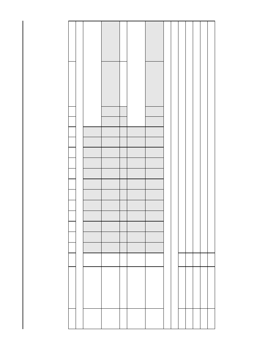
MARS2G5 P-Pro (TDAT162G52) SONET/SDH
Data Sheet
155/622/2488 Mbits/s Data Interface
August 18, 2004
704
Agere Systems Inc.
Data Engine Block Registers
(continued)
DE Register Map
(continued)
Table 749. DE Register Map (continued)
Note: Shading denotes reserved bits.
Addr
Symbol
Type
15
14
13
12
11
10
9
8
7
6
5
4
3
2
1
0
CDA Map and Control Register
0x6080
--
0x60AF
CDA_M0_CHy
R/W
CDA_M0_CH0[3:0]
--
CDA_M0_CH47[3:0]
0x60B0
--
0x60BE
--
--
0x60BF
CDA_MAP_CNTL
R/W
CDA_MAP_CNTL[1] CDA_MAP_CNTL
0x60C0
--
0x60EF
CDA_M1_CHy
R/W
CDA_M1_CH0[3:0]
--
CDA_M1_CH47[3:0]
0x60F0
--
0x60FF
--
--
ATM Framer Registers
Idle Cell Match Mask (R/W)
0x6100
--
R/W
ATM_IDM_0[31:16]
0x6101
--
R/W
ATM_IDM_0[15:0]
to
--
R/W
to
0x611E
--
R/W
ATM_IDM_15[31:16]
0x611F
--
R/W
ATM_IDM_15[15:0]
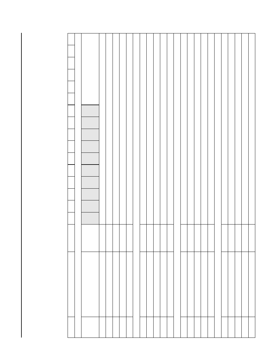
Data Sheet
MARS2G5 P-Pro (TDAT162G52) SONET/SDH
August 18, 2004
155/622/2488 Mbits/s Data Interface
705
Agere Systems Inc.
Data Engine Block Registers
(continued)
DE Register Map
(continued)
Table 749. DE Register Map (continued)
Note: Shading denotes reserved bits.
Addr
Symbol
Type
15
14
13
12
11
10
9
8
7
6
5
4
3
2
1
0
LCD Registers
0x6120
--
0x612F
ATM_LCD[0--15]
R/W
ATM_LCD[0--15][5:0]
0x6130
ATM_LCDCLK
R/W
ATM_LCDCLK[15:0]
0x6131
ATM_IN_LCD_MASK
R/W
ATM_IN_LCD_MASK[15:0]
0x6132
ATM_OUT_LCD_MASK
R/W
ATM_OUT_LCD_MASK[15:0]
0x6133
ATM_IN_LCD
COR/COW
ATM_IN_LCD[15:0]
0x6134
ATM_OUT_LCD
COR/COW
ATM_OUT_LCD[15:0]
Idle Cell Register (R/W)
0x6180
--
R/W
ATM_IDC_0[31:16]
0x6181
--
R/W
ATM_IDC_0[15:0]
to
--
R/W
to
0x619E
--
R/W
ATM_IDC_15[31:16]
0x619F
--
R/W
ATM_IDC_15[15:0]
Unassigned Cell Match Mask (R/W)
0x6200
--
R/W
ATM_USM_0[31:16]
0x6201
--
R/W
ATM_USM_0[15:0]
to
--
R/W
to
0x621E
--
R/W
ATM_USM_15[31:16]
0x621F
--
R/W
ATM_USM_15[15:0]
Unassigned Cell Register (R/W)
0x6280
--
R/W
ATM_USG_0[31:16]
0x6281
--
R/W
ATM_USG_0[15:0]
to
--
R/W
to
0x629E
--
R/W
ATM_USG_15[31:16]
0x629F
--
R/W
ATM_USG_15[15:0]
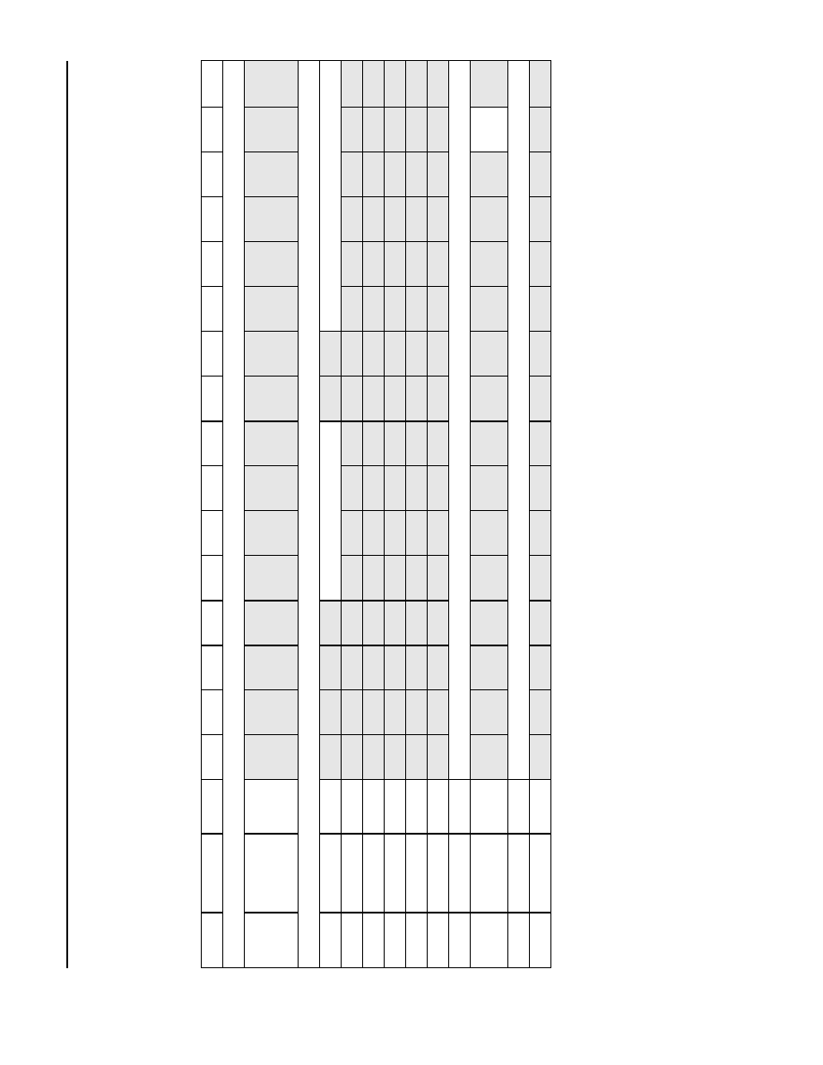
MARS2G5 P-Pro (TDAT162G52) SONET/SDH
Data Sheet
155/622/2488 Mbits/s Data Interface
August 18, 2004
706
Agere Systems Inc.
Data Engine Block Registers
(continued)
DE Register Map
(continued)
Table 749. DE Register Map (continued)
Note: Shading denotes reserved bits.
Addr
Symbol
Type
15
14
13
12
11
10
9
8
7
6
5
4
3
2
1
0
ATM Framer State (RO)
0x6300
--
0x630F
--
RO
ATM Control Registers (R/W)
0x6340
--
R/W
ATM_X43[11:8] (Alpha)
ATM_X43[5:0] (Alpha)
0x6341
--
R/W
0x6342
--
R/W
0x6343
--
R/W
0x6344
--
R/W
0x6345
--
R/W
0x6346
--
R/W
ATM_FS_INTM[0:15]
0x6347
--
R/W
ATM_
COOL
0x6348
--
R/W
ATM_COOL_INTM[0:15]
0x6349
--
--
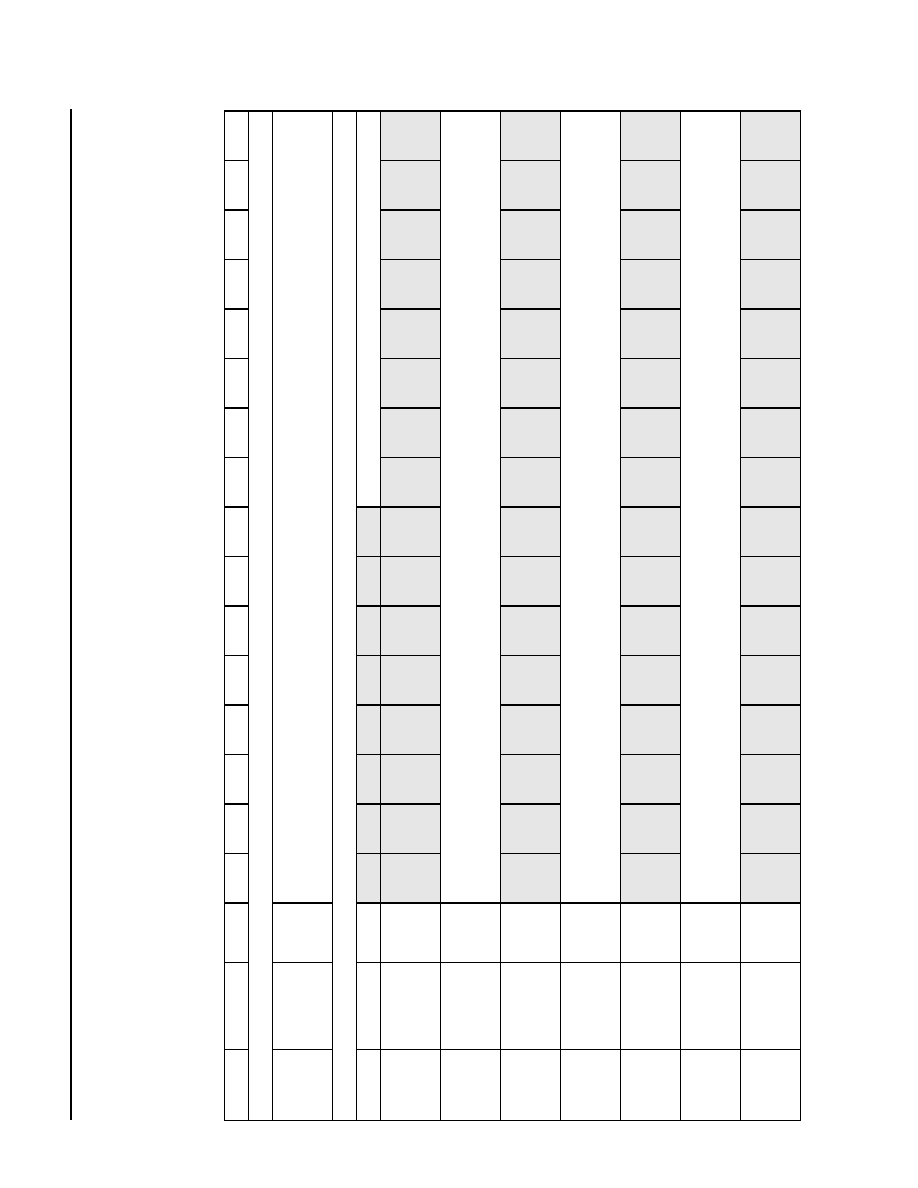
Data Sheet
MARS2G5 P-Pro (TDAT162G52) SONET/SDH
August 18, 2004
155/622/2488 Mbits/s Data Interface
707
Agere Systems Inc.
Data Engine Block Registers
(continued)
DE Register Map
(continued)
Table 749. DE Register Map (continued)
Note: Shading denotes reserved bits.
Addr
Symbol
Type
15
14
13
12
11
10
9
8
7
6
5
4
3
2
1
0
PID (R/W)
0x6380
--
0x638F
--
R/W
RX_PCTL_0[15:0]
--
RX_PCTL_15[15:0]
GFP Receive Registers (R/W)
0x6400
--
RO
GFP_ST_0[7:0]
0x6401
--
0x643F
--
--
0x6440
--
0x644F
--
R/W
GFP_AMM0_1[15:0]
--
GFP_AMM15_1[15:0]
0x6450
--
0x647F
--
--
0x6480
--
0x648F
--
R/W
GFP_AMM0_2[15:0]
--
GFP_AMM15_2[15:0]
0x6490
--
0x64BF
--
--
0x64C0
--
0x64CF
--
R/W
GFP_AMM0_3[15:0]
--
GFP_AMM15_3[15:0]
0x64D0
--
0x64FF
--
--
MARS2G5 P-Pro (TDAT162G52) SONET/SDH
Data Sheet
155/622/2488 Mbits/s Data Interface
August 18, 2004
708
Agere Systems Inc.
Data Engine Block Registers
(continued)
DE Register Map
(continued)
Table 749. DE Register Map (continued)
Note: Shading denotes reserved bits.
Addr
Symbol
Type
15
14
13
12
11
10
9
8
7
6
5
4
3
2
1
0
0x6500
--
0x650F
--
R/W
GFP_BMM0_1[15:0]
--
GFP_BMM15_1[15:0]
0x65A0
--
0x653F
--
--
0x6540
--
0x654F
--
R/W
GFP_BMM0_2[15:0]
--
GFP_BMM15_2[15:0]
0x6550
--
0x657F
--
--
0x6580
--
0x658F
--
R/W
GFP_BMM0_3[15:0]
--
GFP_BMM15_3[15:0]
0x6590
--
0x65BF
--
--
Data Sheet
MARS2G5 P-Pro (TDAT162G52) SONET/SDH
August 18, 2004
155/622/2488 Mbits/s Data Interface
709
Agere Systems Inc.
Data Engine Block Registers
(continued)
DE Register Map
(continued)
Table 749. DE Register Map (continued)
Note: Shading denotes reserved bits.
Addr
Symbol
Type
15
14
13
12
11
10
9
8
7
6
5
4
3
2
1
0
0x65C0
--
0x65CF
--
R/W
GFP_IRQEN_CH0[7:0]
--
GFP_IRQEN_CH15[7:0]
0x65D0
--
0x65FF
--
--
0x6600
--
0x660F
--
COW
GFP_IRQ_CH0[7:0]
--
GFP_IRQ_CH15[7:0]
0x66A0
--
0x663F
--
--
0x6640
--
R/W
GFP_
MOD
E
GFP_DELTA[3:0]
0x6641
--
0x667F
--
--
MARS2G5 P-Pro (TDAT162G52) SONET/SDH
Data Sheet
155/622/2488 Mbits/s Data Interface
August 18, 2004
710
Agere Systems Inc.
Data Engine Block Registers
(continued)
DE Register Map
(continued)
Table 749. DE Register Map (continued)
Note: Shading denotes reserved bits.
Addr
Symbol
Type
15
14
13
12
11
10
9
8
7
6
5
4
3
2
1
0
PPP Detach Registers (R/W)
0x6680
--
0x668F
--
R/W
PPP_PROTOCOL_CONTROL0[15:0]
--
PPP_PROTOCOL_CONTROL15[15:0]
0x6690
--
0x66AF
--
--
0x66B0
--
0x66BB
--
R/W
PPP_RX_HDR00[15:0]
--
PPP_RX_HDR11[15:0]
0x66BC
--
0x66BF
--
--
0x66C0
--
0x66CF
--
R/W
PPP_RX_CHK_CH0[15:0]
--
PPP_RX_CHK_CH15[15:0]
0x66D0
--
0x66FF
--
--

Data Sheet
MARS2G5 P-Pro (TDAT162G52) SONET/SDH
August 18, 2004
155/622/2488 Mbits/s Data Interface
711
Agere Systems Inc.
Data Engine Block Registers
(continued)
DE Register Map
(continued)
Table 749. DE Register Map (continued)
Note: Shading denotes reserved bits.
Addr
Symbol
Type
15
14
13
12
11
10
9
8
7
6
5
4
3
2
1
0
ATM Transmit Registers (R/W, RO)
0x6700
--
R/W
NULL_CELL_CH0[31:16]
0x6701
--
R/W
NULL_CELL_CH0[15:0]
to
--
--
to
0x671E
--
R/W
NULL_CELL_CH15[31:16]
0x671F
--
R/W
NULL_CELL_CH15[15:0]
0x6720
--
0x677F
--
--
0x6780
--
R/W
ATM_HEADE
R_ERR[9:8]
ATM_HEADER_ERR[7:0]
0x6781
--
0x678F
--
--
MARS2G5 P-Pro (TDAT162G52) SONET/SDH
Data Sheet
155/622/2488 Mbits/s Data Interface
August 18, 2004
712
Agere Systems Inc.
Data Engine Block Registers
(continued)
DE Register Map
(continued)
Table 749. DE Register Map (continued)
Note: Shading denotes reserved bits.
Addr
Symbol
Type
15
14
13
12
11
10
9
8
7
6
5
4
3
2
1
0
CRC Transmit Registers (R/W)
0x6790
--
R/W
CRC_ERR[11:0]
0x6791
--
0x679F
--
--
GFP Transmit Registers (R/W, RO)
0x67A0
--
R/W
GFPFI_MSG_1[15:0]
0x67A1
--
R/W
GFPFI_MSG_2[15:0]
0x67A2
--
R/W
GFPFI_MSG_3[15:0]
0x67A3
--
R/W
GFPFI_MSG_TYPE[7:4]
GFPF
I_MS
G_TY
PE[0]
0x67A4
--
R/W
GFPFI_INT[15:0]
0x67A5
--
R/W
GFPF
I_MO
DE[1
5]
GFPFI_MOD
E[1:0]
0x67A6
--
RO
GFPF
I_INT
R[0]
0x67A7
--
R/W
--
--
--
--
--
--
--
--
--
--
--
--
0x67A8
--
0x67AF
--
--
Data Sheet
MARS2G5 P-Pro (TDAT162G52) SONET/SDH
August 18, 2004
155/622/2488 Mbits/s Data Interface
713
Agere Systems Inc.
Data Engine Block Registers
(continued)
DE Register Map
(continued)
Table 749. DE Register Map (continued)
Note: Shading denotes reserved bits.
Addr
Symbol
Type
15
14
13
12
11
10
9
8
7
6
5
4
3
2
1
0
HDLC Transmit Registers (R/W)
0x67B0
--
R/W
DRY_CHARACTER[7:0]
0x67B1
--
R/W
HDLC_FIFO_TH[7:4]
(LOW)
HDLC_FIFO_TH[3:0]
(HIGH)
0x67B2
--
0x67BF
--
--
Gap Inserter Registers (R/W)
0x67C0
--
0x67CF
--
R/W
TX_PCTL_0[15:0]
--
TX_PCTL_15[15:0]
0x67C0
--0x67FF
--
--
ATM/HDLC Counter 1 (PMRST Update) (RO)
0x6800
--
RO
PM_FC1_0[27:16]
0x6801
--
RO
PM_FC1_0[15:0]
to
--
--
to
0x681E
--
RO
PM_FC1_15[27:16]
0x681F
--
RO
PM_FC1_15[15:0]
0x6820
--0x687F
--
--
MARS2G5 P-Pro (TDAT162G52) SONET/SDH
Data Sheet
155/622/2488 Mbits/s Data Interface
August 18, 2004
714
Agere Systems Inc.
Data Engine Block Registers
(continued)
DE Register Map
(continued)
Table 749. DE Register Map (continued)
Note: Shading denotes reserved bits.
Addr
Symbol
Type
15
14
13
12
11
10
9
8
7
6
5
4
3
2
1
0
ATM/HDLC Counter 2 (PMRST Update) (RO)
0x6880
--
RO
PM_FC2_0[27:16]
0x6881
--
RO
PM_FC2_0[15:0]
to
--
--
to
0x689E
--
RO
PM_FC2_15[27:16]
0x689F
--
RO
PM_FC2_15[15:0]
0x68A0
to
0x68AF
--
--
CRC Checker Bad Packet Counter (PMRST Update) (RO)
0x6900
--
RO
PM_BPC_0[27:16]
0x6901
--
RO
PM_BPC_0[15:0]
to
--
--
to
0x691E
--
RO
PM_BPC_15[27:16]
0x691F
--
RO
PM_BPC_15[15:0]
0x6920
--0x697F
--
--
Data Sheet
MARS2G5 P-Pro (TDAT162G52) SONET/SDH
August 18, 2004
155/622/2488 Mbits/s Data Interface
715
Agere Systems Inc.
Data Engine Block Registers
(continued)
DE Register Map
(continued)
Table 749. DE Register Map (continued)
Note: Shading denotes reserved bits.
Addr
Symbol
Type
15
14
13
12
11
10
9
8
7
6
5
4
3
2
1
0
PPP Detach Bad Header Counter (PMRST Update) (RO)
0x6980
--
RO
PM_BHC_0[27:16]
0x6981
--
RO
PM_BHC_0[15:0]
to
--
--
to
0x699E
--
RO
PM_BHC_15[27:16]
0x699F
--
RO
PM_BHC_15[15:0]
0x69A0
--0x69AF
--
--
0x6A00
--0x6A7F
--
--
Counter Block Control/Status (R/W, RO)
0x6A80--
0x6A8F
--
R/W
INT_EN_CH0[3:0]
--
INT_EN_CH15[3:0]
0x6A90
--0x6ABF
--
--
0x6AC0--
0x6ACF
--
COR/
COW
INT_ST_CH0[3:0]
--
INT_ST_CH15[3:0]
0x6AD0
--0x6AFF
--
--
Transmit Good Packet Counter (PMRST Update) (RO)
0x6B00
--
RO
PM_GPC_TX_0[27:16]
0x6B01
--
RO
PM_GPC_TX_0[15:0]
to
--
--
to
0x6B1E
--
RO
PM_GPC_TX_15[27:16]
0x6B1F
--
RO
PM_GPC_TX_15[15:0]
0x6B20
--0x6FFF
--
--

MARS2G5 P-Pro (TDAT162G52) SONET/SDH
Data Sheet
155/622/2488 Mbits/s Data Interface
August 18, 2004
716
Agere Systems Inc.
UTOPIA (UT) Block
This section describes the UTOPIA block (known as the UT48 core) of the MARS2G5 P-Pro device. The UTOPIA
block is responsible for transporting ingress and egress traffic through the UTOPIA interface. It supports all the fea-
tures of MARS2G5 P-ProLT UTOPIA interface with some additional enhancements while maintaining backward
compatibility. The PHY interface of the UTOPIA block has the same pins as MARS2G5 P-ProLT as well as some
additional pins to allow support of more channels.
UTOPIA Interface Features
Conformance to ATM forum UTOPIA level 2 and level 3 specifications.
Support for PLATO packet-over-SONET UTOPIA extensions.
Support for 52/53-byte ATM cells in 8-bit mode, 52/54-byte cells in 16-bit mode, 52/56-byte cells in 32-bit mode.
Support for 8-bit and 16-bit transfers in U2 mode; 8-bit, 16-bit, and 32-bit transfers in U3 mode.
Support for 16 data channels, each with (64X32) 256 bytes of FIFO storage, implemented as four ingress/egress
slices with four subchannels each.
Quad physical interfaces independently configurable as either 8-bit or 16-bit data paths.
Support for up to two 32-bit data paths. (Use of a 32-bit interface will use two 16-bit interfaces.)
Operation at 52 MHz for U2 or 104 MHz for U3 (85 MHz for U3 C/D interface, see Table 751).
Multi-PHY support on all physical interfaces with some limitations and configuration options.
Point-to-point non-MPHY operation supported at higher clock speeds.
Legacy support for a MARS2G5 P-ProLT 5-bit MPHY addressing mode.
The UT48 core provides buffering and UTOPIA interface functionality. This enhanced UTOPIA interface passes
U2, U2+, U3, and U3+ protocols. In the receive direction, data is buffered from the line side, and sent out of the
device via a UTOPIA/POS-PHY interface. In the transmit direction, data is received by the device via a UTOPIA/
POS-PHY interface, and is buffered before being sent to the line side. Data that is sent or received can be either
packet or ATM traffic, and is configurable on a per-channel basis. The UTOPIA slave interface is designed to
accommodate back-to-back ATM cell and packet data transfers in point-to-point or multi-PHY modes. The UTOPIA
block consists of four independent physical interfaces with up to 16 logical channels. If the UT is configured as four
interfaces, for example, each interface can handle up to STS-12/STM-4 traffic. If the UT is configured as one inter-
face, that interface can handle up to STS-48/STM-16 traffic. Using MPHY 32-bit mode, the single 32-bit interface
can supply data to either a single STS-48c channel or four STS-12c channels. All four physical interfaces (A, B, C,
and D) can be configured independently to carry different traffic types at different rates.
There are two basic data paths: receive side, defined as data going from the line side to the UTOPIA side, and
transmit side, defined as data going from the UTOPIA side to the line side as shown in Figure 93.
Data Sheet
MARS2G5 P-Pro (TDAT162G52) SONET/SDH
August 18, 2004
155/622/2488 Mbits/s Data Interface
717
Agere Systems Inc.
UTOPIA (UT) Block
(continued)
UTOPIA Interface Features
(continued)
5-8370(F)r.2
Figure 93. UT48: Generic Structure of UTOPIA Block
In the ingress direction, data arrives from the line (data engine (DE)) side, and is sent to one of 16 channels (A0
through D3). The most significant 2 bits of the channel ID are ignored, and the remaining 4 bits are associated with
channels in the slice. The channel ID corresponding to a slice and a channel name is shown in Table 750.
Table 750. Slices, Channels, and Channel IDs
Each slice buffers data independently, and, when sufficient data has been stored into its FIFO, sends the data out
of the slice via its UTOPIA-like interface. In the egress direction, data arrives from the various UTOPIA interfaces,
and is stored in a channel's FIFO. Each FIFO serves both as a buffer and as a means to cross data from the
egress UTOPIA side timing to the DE side timing. After sufficient data has been stored into the FIFO, it is sent out
of the UT48 core when requested to do so by the DE. Data that is transported through the UT48 can be either ATM
traffic or packet traffic. Each channel can be configured to carry only one type. That is, one channel could carry
ATM traffic while others are carrying packet traffic. However, any one channel cannot carry both ATM and packet
traffic simultaneously, unless ATM cells are viewed as 52/53 byte packets, and are transported using the packet
mode for that UTOPIA channel.
Note: If any one channel of a slice is configured to carry packet data, the interface connecting to the slice must be
provisioned in packet mode even if the rest of the channels are carrying ATM cell traffic.
Slice
Ch.
Ch. ID
Slice
Ch.
Ch. ID
Slice
Ch.
Ch. ID
Slice
Ch.
Ch. ID
A
A0
000000
B
B0
000100
C
C0
001000
D
D0
001100
A1
000001
B1
000101
C1
001001
D1
001101
A2
000010
B2
000110
C2
001010
D2
001110
A3
000011
B3
000111
C3
001011
D3
001111
INGRESS SLICE A
INGRESS SLICE B
INGRESS SLICE C
INGRESS SLICE D
EGRESS SLICE A
EGRESS SLICE B
EGRESS SLICE C
EGRESS SLICE D
EG
R
E
SS MU
X
UPRX
UPRX
UPRX
UPRX
UPTX
UPTX
UPTX
UPTX
MICRO I/F
T
X
R
X
UTOPIA SIDE
LINE (DATA ENGINE) SIDE
CROSS
BAR
R
X
T
X
CROSS
BAR
A
B
C
D
A
B
C
D
DE
DE

MARS2G5 P-Pro (TDAT162G52) SONET/SDH
Data Sheet
155/622/2488 Mbits/s Data Interface
August 18, 2004
718
Agere Systems Inc.
UTOPIA (UT) Block
(continued)
UTOPIA Modes
Each interface mode is capable of supporting various types of traffic with different bandwidth capabilities as sum-
marized in Table 751. Table 752 highlights the interfaces that can be used to support the traffic types and data
rates. Each interface type can be configured as point-to-point or multi-PHY. UTOPIA contains four slices in ingress/
egress direction with each slice comprising of four logical channels. A slice can only connect to one of the four
interfaces while an interface can connect to more than one slices. Each channel in a slice can be configured differ-
ently to support the various traffic types, e.g., channel A0 passes ATM cells using STS-12c, channel B1 passes
packets, etc. In point-to-point mode, only channel 0 of an interface's native slice is used (i.e., for interface A, chan-
nel A0).
32-Bit Mode Configuration (Necessary Configuration for Proper Operation)
Example Provisioning a 32-Bit Interface on A (Both Interfaces A and B Need to be Configured)
An active interface is one in which the enable and address inputs from a master device are actively decoded by
MARS2G5 P-Pro and whose PA pins (PPA and/or SPA) may be used by the master to determine FIFO status. An
inactive interface is one in which the enable and address inputs from a master device are ignored but whose PA
pins may still be used to determine FIFO status in direct status or multiplexed status modes. If the multiplexed sta-
tus polling scheme is to be utilized for the inactive interface, which has provisioned active channels in its native
slice, the PollEnb bit needs to be turned on within the respective MODE register. When an active interface borrows
data pins from an adjacent interface, it does not imply that the adjacent interface must also be active. It should be
provisioned idle. Certain fields of the interface configuration register are always bound only to the associated phys-
ical interface (data width, OE mode, and PA response).
Therefore, to provision a 32-bit interface on A, use the following rules as guidelines:
1.
Provision interface A for 32-bit operation as specified in this data sheet.
2.
Interface A data width should be set to 11, signifying 32-bit and active.
3.
Interface B data width should be set to 00, signifying idle.
4.
The OE mode and PA response bits for interface B should be the same as those for interface A.
5.
For transmit only, when interface A is operating in MPHY mode and direct or multiplex status is required from
inactive interfaces B, C, or D, then set the polling enable bit for each of those interfaces.
6.
The remaining fields for interface B are don't care.
If guideline 4 is not followed, then the composite data bus will have different behaviors between the A half and the
B half with respect to 3-stating (OE mode difference) and latency (PA response difference).

Data Sheet
MARS2G5 P-Pro (TDAT162G52) SONET/SDH
August 18, 2004
155/622/2488 Mbits/s Data Interface
719
Agere Systems Inc.
UTOPIA (UT) Block
(continued)
UTOPIA Modes
(continued)
Table 751. UTOPIA Traffic Types
UTOPIA Mode
MPHY
Configuration
Size
Maximum
Speed
Bandwidth
Traffic Type
Available
Interfaces
U2/U2+, 8-bit
Non-MPHY
(point-to-point)
8 bits
52 MHz
155.52 Mbits/s ATM cells only (U2)/
ATM cells/packets
(U2+)
4: A, B, C, D
Up to 4-Channel MPHY
(native slice)
Up to 8-Channel MPHY
2: A, C
Up to 16-Channel MPHY
U2/U2+, 16-bit
Non-MPHY
(point-to-point)
16 bits
622 Mbits/s
4: A, B, C, D
Up to 4-Channel MPHY
(native slice)
Up to 8-Channel MPHY
2: A, C
Up to 16-Channel MPHY
U3/U3+, 8-bit
Non-MPHY
(point-to-point)
8 bits
104 MHz
622 Mbits/s
ATM cells only (U3)/
ATM cells/packets
(U3+)
4: A, B, C, D
Up to 4-Channel MPHY
104 MHz
2: A, B
85 MHz
2: C, D
Up to 8-Channel MPHY
104 MHz
1: A
85 MHz
1: C
Up to 16-Channel MPHY
104 MHz
1: A
85 MHz
1: C
U3/U3+, 16-bit
Non-MPHY
(point-to-point)
16 bits
104 MHz
1.2 Gbits/s
4: A, B, C, D
Up to 4-Channel MPHY
104 MHz
2: A, B
85 MHz
2: C, D
Up to 8-Channel MPHY
104 MHz
1: A
85 MHz
1: C
Up to 16-Channel MPHY
104 MHz
1: A
85 MHz
1: C
U3/U3+, 32-bit
Non-MPHY
(point-to-point)
32 bits
104 MHz
2.5 Gbits/s
ATM cells only (U3)/
ATM cells/packets
(U3+)
2: A/B, C/D
Up to 4-Channel MPHY
104 MHz
1: A/B
85 MHz
1: C/D
Up to 8-Channel MPHY
104 MHz
1: A/B
85 MHz
1: C/D
Up to 16-Channel MPHY
104 MHz
1: A/B
85 MHz
1: C/D

MARS2G5 P-Pro (TDAT162G52) SONET/SDH
Data Sheet
155/622/2488 Mbits/s Data Interface
August 18, 2004
720
Agere Systems Inc.
UTOPIA (UT) Block
(continued)
UTOPIA Modes
(continued)
Table 752. Interface Configurations Supported
Traffic
Rate
Interface Supported
Notes
ATM Traffic
to STS-12/STM-4
U2 or U2+
(8-bit or 16-bit modes)
--
U3 or U3+
(8-bit, 16-bit, or32-bit
modes)
In 32-bit mode, controls are used from channel A
or C and data is used from channel A & B or C & D.
ATM Traffic
>STS-12/STM-4
U3 or U3+
(16-bit or32-bit modes)
In 32-bit mode, controls are used from channel A
or C and data is used from channel A & B or C & D.
Packet Traffic
to STS-12/STM-4
U2+
(16-bit mode)
--
U3+
(8-bit, 16-bit or 32 bit
modes)
In 32-bit mode, controls are used from channel A
or C and data is used from channel A & B or C & D.
Packet Traffic
>STS-12/STM-4
U3+
(16-bit or 32-bit
modes)
In 32-bit mode, controls are used from channel A
or C and data is used from channel A & B or C & D.

Data Sheet
MARS2G5 P-Pro (TDAT162G52) SONET/SDH
August 18, 2004
155/622/2488 Mbits/s Data Interface
721
Agere Systems Inc.
UTOPIA (UT) Block
(continued)
UT Receive Path (Ingress)
The UTOPIA PHY Rx interface is designed to accommodate ATM cells as well as packet traffic. The interfaces
supported include: UTOPIA level 2 (U2), enhanced UTOPIA level 2 (U2+), UTOPIA level 3 (U3), and enhanced
UTOPIA level 3 (U3+). Enhanced refers to the extensions that have been added to support packet transfers. These
extensions are the following: end of packet indication (RxEOP), byte on which packet ends in last word (RxSZ),
and if the packet is to be aborted early (RxERR). An abort occurs, for example, if the check sum at the end of a
packet is bad, or the end of a packet is reached prematurely. If the receive FIFO overflows because the master
cannot process packet data fast enough, an RxERR will also be generated. An additional signal (relative to
MARS2G5 P-ProLT) is the selected packet available (RxSPA), which gives a direct status indication on the
selected FIFO. RxSPA signals are defined for active interfaces only and they indicate the status of the selected
channel that currently has valid data on the RxDATA bus.
Note: The start of packets must be word-aligned and the final word of a packet must be padded with dummy data
(if needed), since this is required by the definition of the UTOPIA interface.
The UTOPIA interface can be placed in a number of modes, 8-bit, 16-bit, or 32-bit mode. These modes are depen-
dent on the type of traffic that is being carried in the ingress slice, as well as the rate of the traffic. If all four chan-
nels in a slice are in ATM mode, then the interface for that slice can be configured in ATM mode; however, if any of
the four channels in a slice are in packet mode, then the interface for that slice should be configured in packet
mode.
During packet mode operation (supported from (TADM042G5 (TADMV1B))), it is possible to cause a minimum gap
period to occur between packets on the ingress interface. In other words, it is possible to prevent back-to-back
transfer on an interface. This behavior is affected as an interface parameter, which is a 3-bit field (11:9) in the
RXMODE[A--D] (Table 770) provisioning registers. The contents of the field are the minimum number of cycles
between packet transfers. Note that when a channel is provisioned in ATM mode, the gap feature of the interface is
ignored.
If ATM cells are being transported and the interface is placed in packet mode, there is no capability to abort ATM
cells in case of a deviation from the expected EOP or size indication. This follows since EOP and size indications
are not processed by the channel transferring ATM cells. This mainly affects the Tx direction. If it is an abnormal
short ATM cell, the SOP of the next ATM cell will be ignored and the cell is attached to the short ATM cell. If it is an
abnormal long ATM cell, the portion in excess of the normal ATM cell size will be discarded.
While one ingress slice may be carrying ATM traffic, the others may be carrying packet traffic. However, not all
interfaces can coexist at the same time. For example, if ingress interface A is configured as a 32-bit mode inter-
face, then the ingress interface B cannot be used. Because each UTOPIA PHY interface has only 16 bits of output
data, if ingress interface A is placed in 32-bit mode, ingress interface A will have to send the least significant 16 bits
of data out via ingress interface B. The same principle applies to interfaces C and D.

MARS2G5 P-Pro (TDAT162G52) SONET/SDH
Data Sheet
155/622/2488 Mbits/s Data Interface
August 18, 2004
722
Agere Systems Inc.
UTOPIA (UT) Block
(continued)
UT Receive Path (Ingress)
(continued)
Channel FIFO
The (64x32) 256-byte UTOPIA Rx FIFO in each channel buffers data sent from the DE block to the UTOPIA inter-
face. The FIFO accommodates four ATM cells or 256 bytes of packet data and manages the asynchronous nature
of the UTOPIA interface. Overflow will only occur if the master device connected to the UTOPIA interface is having
congestion problems. When overflow occurs, a head of FIFO discard is performed. In order to avoid the situation
where part of one packet may be appended to another (if for example, an end of packet is discarded along with the
data at the head of the FIFO), data is discarded until the start of the next packet is observed. Upon overflow, the
RxERR and RxEOP signals are asserted to indicate to the master the corruption of the current packet. An alarm is
also sent to the microprocessor. Underflow in the receive direction can occur when there is no data, or if only part
of a packet has arrived and has been transmitted, and is normal behavior.
Data is read from the FIFO when there is sufficient data in the FIFO. Sufficient data is defined to be a minimum
amount of data in the FIFO (a programmable threshold, low watermark), or at least one end of packet stored in the
FIFO. Provisioning of high watermark and low watermark thresholds is performed in terms of 32-bit words, not
bytes.
Receive Polled Packet Available (RxPPA). Signal behavior depends on whether packet or ATM mode is selected
as described below.
Assertion of RxPPA. In packet mode, RxPPA is asserted when the FIFO has more data than threshold low or
there is an end of packet (EOP) inside the FIFO. In ATM mode, RxPPA is asserted when the FIFO contains at least
one complete ATM cell.
Deassertion of RxPPA. In packet mode, RxPPA is deasserted when the FIFO has less data than threshold mini-
mum and there isn't any EOP inside the FIFO. In ATM mode, RxPPA is deasserted when the FIFO contains less
than a complete ATM cell.

Data Sheet
MARS2G5 P-Pro (TDAT162G52) SONET/SDH
August 18, 2004
155/622/2488 Mbits/s Data Interface
723
Agere Systems Inc.
UTOPIA (UT) Block
(continued)
UT Receive Path (Ingress)
(continued)
Figure 94 illustrates the receive side interface handshaking when operating in point-to-point mode with the RXPPA
response provisioned to be a single cycle. In two-cycle mode, the RXSOP, RXDATA, and RXPPA signals are
delayed for an additional cycle. In the figure, the master device initiates the transfer after observing an asserted
packet available for the channel. The MARS2G5 P-Pro samples RXENB low on the first cycle and then asserts
RXSOP/C and RXDATA on the second cycle. RXDATA is sampled on the rising edge of the next cycle by the mas-
ter device.
In this example, the master stops the transfer in the middle of the packet. Data with value c is valid on the cycle
that RXENB goes inactive, and when RXENB returns, data is again valid on the first cycle after the slave observes
an active RXENB (data value d).
The packet transfer is complete when the slave asserts the RXEOP signal. If an error occurs in the packet, then
the RXERR signal is asserted simultaneously with the RXEOP. RXERR is ignored if it is not asserted when
RXEOP is active.
5-8716(F)
Figure 94. Receive-Side Interface Handshaking in Point-to-Point Mode (RXPPA as Single Cycle)
RXCLK
1
2
3
4
5
6
7
8
9
10
11
12
a
b
c
d
e
RXPPA
RXENB
RXSOP/C
RXDATA[15:0]
RXEOP
RXERR

MARS2G5 P-Pro (TDAT162G52) SONET/SDH
Data Sheet
155/622/2488 Mbits/s Data Interface
August 18, 2004
724
Agere Systems Inc.
UTOPIA (UT) Block
(continued)
UT Transmit Path (Egress)
In the transmit direction, data arrives from the various UTOPIA interfaces and is stored in (64x32) 256-byte FIFOs
of different channels. After sufficient data has been buffered into a FIFO, it is made available to be sent to the DE.
Like the UTOPIA Rx interface, the UTOPIA Tx interface is designed with enhancements to accommodate packet
traffic as well as ATM cells. Supported interfaces include the following: UTOPIA level 2 (U2) in 8-bit or 16-bit mode,
enhanced UTOPIA level 2 (U2+) in 8-bit or 16-bit mode, UTOPIA level 3 (U3) in 8-bit, 16-bit or 32-bit mode, and
enhanced UTOPIA level 3 (U3+) in 8-bit, 16-bit, or 32-bit mode. An additional signal (relative to MARS2G5 P-
ProLT) is the selected packet available (TXSPA), which gives a direct status indication on the selected FIFO.
TXSPA signals are defined for active interfaces only and they indicate the status of the selected channel that cur-
rently has valid data on the TxDATA bus.
The UTOPIA Tx side can indicate to the ATM side to suspend the transfer, by deasserting TXPPA, when neces-
sary. When the amount of data in the FIFO exceeds its programmable high watermark, it deasserts TXPPA. At this
point, the ATM side knows that the UTOPIA Tx block can only accept a limited number of words, after which it will
overflow. In this case, the ATM device must not exceed writing this limited number of words before suspending the
transfer. Transfer is resumed once again when the FIFO falls below the high watermark.
When transferring ATM cells, TXPPA is deasserted with SOP/SOC of the current cell unless UT is prepared to
accept an entire new cell after the current transfer. This behavior complies with both, UTOPIA level 2 and level 3
standards. level 2 requires that TXPPA be deasserted at least four cycles before the end of the current cell if it
does not have enough room to accept another complete cell. Level 3 requires deassertion of TXPPA with current
cell's SOP if there is no space for another complete cell. Only level 3 specification is implemented in UT that auto-
matically makes its behavior compliant with level 2 since SOP is at least four cycles before the end of the cell.
Deassertion of TXPPA does not immediately suspend the transfer of the current cell because the entire cell must
be transmitted without interruption.
Transmit Polled Cell/Packet Available (TXPPA)
Assertion of TXPPA. In packet mode, TXPPA is asserted when the FIFO has less data than threshold HIGH. In
ATM mode, TXPPA is asserted when the FIFO has room for a complete ATM cell.
Deassertion of TXPPA. In packet mode, TXPPA is deasserted when the FIFO has more data than threshold MAX.
In ATM mode, TXPPA is deasserted with the current cell's SOP if the FIFO does not have enough room for another
complete ATM cell on the following transmission.
Low Watermark. The low watermark in the Tx direction is relevant for defining when data is sent from the UTOPIA
block to the data engine. A particular egress slice will send data upon a request from the data engine if (1) there is
greater than or equal to low threshold amount of data in the TxFIFO or (2) there is an end of packet (EOP) cur-
rently residing in the FIFO (which may possibly be below low watermark).
Once data transmission to the data engine begins, it continues until it reaches the EOP, or until it reaches the end
of the FIFO, where it is flagged as an underflow. The UTOPIA side notifies the data engine that it has run dry. The
data engine can either insert a dry escape character into the data stream (dry mode, user-provisionable value,
0x7D20 default) or it can insert an abort character into the data stream (0x7D7E).
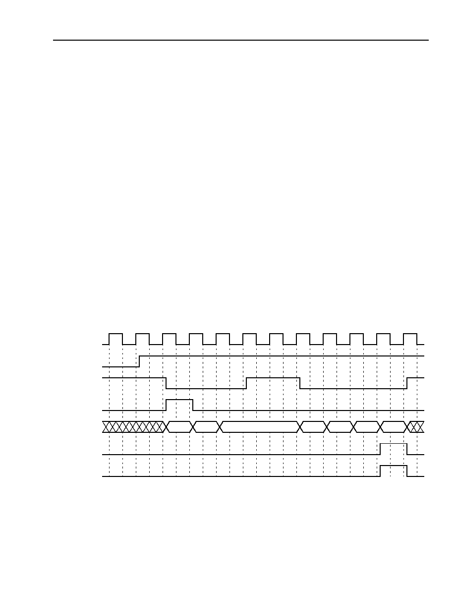
Data Sheet
MARS2G5 P-Pro (TDAT162G52) SONET/SDH
August 18, 2004
155/622/2488 Mbits/s Data Interface
725
Agere Systems Inc.
UTOPIA (UT) Block
(continued)
UT Transmit Path (Egress)
(continued)
Tx FIFO
The UTOPIA Tx FIFO is used to create an elastic store that can buffer bursts of data received via the UTOPIA Tx,
faster than can be transmitted out of the path. After the FIFO exceeds a programmable watermark (threshold
MAX), it indicates to the UTOPIA Tx master to stop sending data. The master can choose to ignore this request
causing the risk of an overflow. The FIFO block buffers sixty four 32-bit words (256 bytes) of cell/packet data. The
FIFO accommodates four ATM cells or 256 bytes of packet data to manage the asynchronous nature of the UTO-
PIA interface.
Optionally, in the case of FIFO underflow, a 0x7D207D207D20 . . . will be inserted by the data engine into the mid-
dle of the packet if dry mode is provisioned and the default dry escape character is used (0x20). This will be
removed at the far end by the device (provided the link is comprised of two devices and both sides of the link sup-
port dry mode).
Figure 95 illustrates the transmit side interface handshaking when operating in point-to-point mode with the
TXPPA response provisioned to be a single cycle. In two-cycle mode, the TXPPA signal is delayed an additional
cycle. In the figure, the master device initiates the transfer after observing an asserted packet available for the
channel by asserting the TXENB signal. The master places data and start of packet on the bus the same cycle as
TXENB, and the MARS2G5 P-Pro samples the TXSOP and TXDATA on the following clock cycle (rising edge).
In this example, the master stops transfer in the middle of the packet. Data with value c is valid on the cycle (rising
edge) that TXENB goes inactive, and when TXENB returns, data is again valid on the first cycle (data value d).
The packet transfer is complete when the master asserts the TXEOP signal. If an error occurs in the packet, then
the TXERR signal is asserted simultaneously with the TXEOP. TXERR is ignored if it is not asserted when TXEOP
is active.
5-8717(F)
Figure 95. Transmit-Side Interface Handshaking in Point-to-Point Mode (TXPPA as Single Cycle)
TXCLK
1
2
3
4
5
6
7
8
9
10
11
12
a
b
c
d
e
f
g
TXPPA
TXENB
TXSOP/C
TXDATA[15:8]
TXEOP
TXERR

MARS2G5 P-Pro (TDAT162G52) SONET/SDH
Data Sheet
155/622/2488 Mbits/s Data Interface
August 18, 2004
726
Agere Systems Inc.
UTOPIA (UT) Block
(continued)
Address Modes and Pin Assignments of MPHY Interfaces
Table 753 shows the address bus assignment for each interface depending on data transfer modes and the num-
ber of MPHY groups. Since the UTOPIA block has a limited number of pins, pins are overlayed and concatenated
to provide 5-bit address buses to each interface (& represents concatenation in Table 753). The three basic
addressing pin assignments/overlays (and corresponding address modes) are as follows:
1.
A2/A3 Address Mode. In 16-bit data transfer mode, a UTOPIA interface connected to only one slice (polling a
maximum of four channels of a particular slice) uses its own 3-bit (for interface A or C) or 2-bit (for interface B
or D) address bus. All four interfaces (ports) can be used independently in this mode.
2.
A5' Address Mode. In 8-bit data transfer mode, unused transmit data pins of an active interface (port) are over-
laid to form a 5-bit address bus for that interface. For example, TXADDRA[2:0] forms the most significant three
bits and TXDATAA[7:6] forms the least significant two bits of the 5-bit transmit address bus for interface A. Sim-
ilarly, the 5-bit receive address bus is formed with RXADDRA[2:0] and TXDATAA[1:0] (for interface A). Trans-
mit data pins in other interfaces are also used in the same manner. All four interfaces can be used
independently in this mode.
3.
A5 Address Mode. In 32-bit data transfer mode, address pins of interfaces A and B (or C and D) are concate-
nated to form a 5-bit address bus. For example, TXADDRA[2:0] and TXADDRB[1:0] form the 5-bit transmit
address bus for interface A. Only two interfaces, A (concatenated with B) and C (concatenated with D), are
available in 32-bit data transfer mode/A5 address mode. If both interfaces are used simultaneously, each can
poll a maximum of 8 channels (two slices). If only one interface is used, it can poll all 16 channels.
Point-to-Point (non-MPHY) Mode. No address decoding is performed in non-MPHY mode. An active interface is
directly connected to channel 0 of its native interface. For example, interface A is connected to channel 0 of slice A.
Address mode selection is provided through parameters RxAddrMode[A--D][1:0] and TxAddrMode[A--D][1:0] bits
[7:6] of registers 0x7012 (Table 773) and 0x7013 (Table 774).
Table 753 shows address mode configurations depending on data transfer modes and the number of MPHY
groups (active polling interfaces).
Addr_mode = 0 configures an interface in non-MPHY mode.
Addr_mode = 1 sets an interface in A2/A3 mode.
Addr_mode = 2 configures an interface in A2/A3 mode for 16-bit data transfers and in A5' address mode for 8-bit
data transfers.
Addr_mode = 3 translates into A5 address mode for interface A&B or C&D.

Data Sheet
MARS2G5 P-Pro (TDAT162G52) SONET/SDH
August 18, 2004
155/622/2488 Mbits/s Data Interface
727
Agere Systems Inc.
UTOPIA (UT) Block
(continued)
Address Modes and Pin Assignments of MPHY Interfaces
(continued)
Table 753. UTOPIA Address Modes
Note: & represents concatenation.
Tx/Rx
I/F
16-Bit Mode
8-Bit Mode
32-Bit Mode
4-Port
Mode
2-Port
Mode
1-Port
Mode
4-Port
Mode
2-Port
Mode
1-Port
Mode
2-Port
Mode
1-Port
Mode
Address Mode (addr mode)
A2/A3
A5
A5
A5'
A5
A5
A5
A5
Tx
A
TXADDRA[2:0]
TXADDRA[2:0]
&
TXADDRB[1:0]
TXADDRA[2:0]
&
TXADDRB[1:0]
or
TXADDRC[2:0]
&
TXADDRD[1:0]
TXADDRA[2:0]
&
TXDATAA[7:6]
TXADDRA[2:0]
&
TXADDRB[1:0]
TXADDRA[2:0]
&
TXADDRB[1:0]
or
TXADDRC[2:0]
&
TXADDRD[1:0]
TXADDRA[2:0]
&
TXADDRB[1:0]
TXADDRA[2:0]
&
TXADDRB[1:0]
or
TXADDRC[2:0]
&
TXADDRD[1:0]
B
TXADDRB[1:0]
TXADDRB[1:0]
&
TXDATAB[7:5]
C
TXADDRC[2:0]
TXADDRC[2:0]
&
TXADDRD[1:0]
TXADDRC[2:0]
&
TXDATAC[7:6]
TXADDRC[2:0]
&
TXADDRD[1:0]
TXADDRC[2:0]
&
TXADDRD[1:0]
D
TXADDRD[1:0]
TXADDRD[1:0]
&
TXDATAD[7:5]
Rx
A
RXADDRA[2:0]
RXADDRA[2:0]
&
RXADDRB[1:0]
RXADDRA[2:0]
&
RXADDRB[1:0]
or
RXADDRC[2:0]
&
RXADDRD[1:0]
RXADDRA[2:0]
&
TXDATAA[1:0]
RXADDRA[2:0]
&
RXADDRB[1:0]
RXADDRA[2:0]
&
RXADDRB[1:0]
or
RXADDRC[2:0]
&
RXADDRD[1:0]
RXADDRA[2:0]
&
RXADDRB[1:0]
RXADDRA[2:0]
&
RXADDRB[1:0]
or
RXADDRC[2:0]
&
RXADDRD[1:0]
B
RXADDRB[1:0]
RXADDRB[1:0]
&
TXDATAB[2:0]
C
RXADDRC[2:0]
RXADDRC[2:0]
&
RXADDRD[1:0]
RXADDRC[2:0]
&
TXDATAC[1:0]
RXADDRC[2:0]
&
RXADDRD[1:0]
RXADDRC[2:0]
&
RXADDRD[1:0]
D
RXADDRD[1:0]
RXADDRD[1:0]
&
TXDATAD[2:0]

MARS2G5 P-Pro (TDAT162G52) SONET/SDH
Data Sheet
155/622/2488 Mbits/s Data Interface
August 18, 2004
728
Agere Systems Inc.
UTOPIA (UT) Block
(continued)
Address Modes and Pin Assignments of MPHY Interfaces
(continued)
It should be noted that the RXADR and TXADR names shown in Table 754 are (virtual) UTOPIA address bits, not
physical ball names as shown in the Pin Information tables. This table is intended to give a physical mapping of the
permutation of UTOPIA port address bits in the three possible addressing modes (A2/A3, A5, and A5') of the UTO-
PIA interface. The left side of the table shows the pin-to-address bit mappings; the right side shows the address bit-
to-pin mappings. The TDAT column is provided as a reference to correlate MARS2G5 P-ProLT (TDAT042G5) pins
to MARS2G5 P-Pro (TDAT162G52) pins.
Table 754. MARS2G5 P-ProLT/MARS2G5 P-Pro UTOPIA (Virtual) Address Pin Mappings
Pin-to-Address Bit Map
Address Bit-to-Pin Map
Pin
TDAT
A2/A3
A5
A5'
Address
TDAT
A2/A3
A5
A5'
V34
--
RXADRA2
RXADRA4
RXADRA4
RXADRA4
AP20
--
V34
V34
W32
RXADRA1
RXADRA1
RXADRA3
RXADRA3
RXADRA3
AL32
--
W32
W32
W31
RXADRA0
RXADRA0
RXADRA2
RXADRA2
RXADRA2
AL33
V34
W31
W31
AL32
RXADRA3
RXADRB1
RXADRA1
RXADRB4
RXADRA1
W32
W32
AL32
M34
AL33
RXADRA2
RXADRB0
RXADRA0
RXADRB3
RXADRA0
W31
W31
AL33
M35
AN19
--
RXADRC2
RXADRC4
RXADRC4
RXADRB4
--
--
--
AL32
AL19
--
RXADRC1
RXADRC3
RXADRC3
RXADRB3
--
--
--
AL33
AP20
RXADRA4
RXADRC0
RXADRC2
RXADRC2
RXADRB2
--
--
--
AE35
AP7
--
RXADRD1
RXADRC1
RXADRD4
RXADRB1
--
AL32
--
AE34
AL8
--
RXADRD0
RXADRC0
RXADRD3
RXADRB0
--
AL33
--
AE33
--
--
--
--
--
RXADRC4
--
--
AN19
AN19
M34
--
--
--
RXADRA1
RXADRC3
--
--
AL19
AL19
M35
--
--
--
RXADRA0
RXADRC2
--
AN19
AP20
AP20
AE35
--
--
--
RXADRB2
RXADRC1
--
AL19
AP7
AP26
AE34
--
--
--
RXADRB1
RXADRC0
--
AP20
AL8
AM25
AE33
--
--
--
RXADRB0
RXADRD4
--
--
--
AP7
AR26
--
--
--
RXADRC1
RXADRD3
--
--
--
AL8
AM25
--
--
--
RXADRC0
RXADRD2
--
--
--
AM14
AM14
--
--
--
RXADRD2
RXADRD1
--
AP7
--
AP13
AP13
--
--
--
RXADRD1
RXADRD0
--
AL8
--
AN13
AN13
--
--
--
RXADRD0
--
--
--
--
--
--
--
--
--
--
TXADRA4
AM31
--
U33
U33
--
--
--
--
--
TXADRA3
Y34
--
G33
G33
U33
--
TXADRA2
TXADRA4
TXADRA4
TXADRA2
W34
U33
G32
G32
G33
TXADRA1
TXADRA1
TXADRA3
TXADRA3
TXADRA1
G33
G33
Y34
L33
G32
TXADRA0
TXADRA0
TXADRA2
TXADRA2
TXADRA0
G32
G32
W34
L34
Y34
TXADRA3
TXADRB1
TXADRA1
TXADRB4
TXADRB4
--
--
--
Y34
W34
TXADRA2
TXADRB0
TXADRA0
TXADRB3
TXADRB3
--
--
--
W34
AM19
--
TXADRC2
TXADRC4
TXADRC4
TXADRB2
--
--
--
AD35
AN31
--
TXADRC1
TXADRC3
TXADRC3
TXADRB1
--
Y34
--
AD34
AM31
TXADRA4
TXADRC0
TXADRC2
TXADRC2
TXADRB0
--
W34
--
AD33
AP5
--
TXADRD1
TXADRC1
TXADRD4
TXADRC4
--
--
AM19
AM19
AM7
--
TXADRD0
TXADRC0
TXADRD3
TXADRC3
--
--
AN31
AN31
--
--
--
--
--
TXADRC2
--
AM19
AM31
AM31
L33
--
--
--
TXADRA1
TXADRC1
--
AN31
AP5
AP27
L34
--
--
--
TXADRA0
TXADRC0
--
AM31
AM7
AR27
AD35
--
--
--
TXADRB2
TXADRD4
--
--
--
AP5
AD34
--
--
--
TXADRB1
TXADRD3
--
--
--
AM7
AD33
--
--
--
TXADRB0
TXADRD2
--
--
--
AM15
AP27
--
--
--
TXADRC1
TXADRD1
--
AP5
--
AR14
AR27
--
--
--
TXADRC0
TXADRD0
--
AM7
--
AP14
AM15
--
--
--
TXADRD2
--
--
--
--
--
AR14
--
--
--
TXADRD1
--
--
--
--
--
AP14
--
--
--
TXADRD0
--
--
--
--
--

Data Sheet
MARS2G5 P-Pro (TDAT162G52) SONET/SDH
August 18, 2004
155/622/2488 Mbits/s Data Interface
729
Agere Systems Inc.
UTOPIA (UT) Block
(continued)
UTOPIA Loopbacks
MARS2G5 P-Pro can be placed in loopback on a slice-by-slice basis. In near-end loopback (NELB), data from
channels in the egress slice is transferred to the corresponding ingress channels instead of the DE. This data is
then processed by the ingress slice and is returned to the UTOPIA master.
In summary, near-end loopback data must traverse both the egress and ingress FIFOs.
5-8371(F)r.3
Figure 96. Near-End Loopback for Slice D
INGRESS SLICE A
INGRESS SLICE B
INGRESS SLICE C
INGRESS SLICE D
EGRESS SLICE A
EGRESS SLICE B
EGRESS SLICE C
EGRESS SLICE D
EG
R
E
S
S
MU
X
UPRX
UPRX
UPRX
UPRX
UPTX
UPTX
UPTX
UPTX
T
X
R
X
UTOPIA SIDE
LINE (DATA ENGINE) SIDE
CROSS
BAR
R
X
T
X
CROSS
BAR
A
B
C
D
A
B
C
D
DE
DE
SLICE D: NEAR-END LOOPBACK
MARS2G5 P-Pro (TDAT162G52) SONET/SDH
Data Sheet
155/622/2488 Mbits/s Data Interface
August 18, 2004
730
Agere Systems Inc.
UTOPIA (UT) Block
(continued)
Basic Modes of Operations
The UTOPIA block has 16 logical channels arranged into four slices of four channels each. Four physical interfaces
(namely A, B, C, and D) are available in the both transmit and receive directions that communicate with channels/
slices through a crossbar. Each interface uses 16-bit transmit and receive data buses, and some control signals to
communicate with the master. Each channel is assigned a unique physical address through the microprocessor
interface. The following are some possible configurations of MPHY polling groups.
For 16-bit or 8-bit mode, up to four polling groups can be formed.
For 32-bit mode, up to two polling groups with a maximum of eight channels each can be formed.
All 16 channels can be arranged in a single polling group with either 8-bit, 16-bit, or 32-bit mode.
PHY Channel Addresses
When an active interface (port) connected to more than one slice selects a channel, every inactive interface whose
native slice is connected to the active interface indicates status of the corresponding channel in its native slice.
Table 755 below assumes one of four interfaces is active and connected to all four slices (meaning other three
interfaces are inactive). In this case, if interface A is the active interface, and channel A0 is polled, PPA_A, PPA_B,
PPA_C, and PPA_D will show the status of channel addresses A0, B0, C0, and D0, respectively.
Table 755. PHY Channel Address Allocation Related to Status Signal
Signal
PHY Channel Address
RXPPAA/TXPPAA
A0
A1
A2
A3
RXPPAB/TXPPAB
B0
B1
B2
B3
RXPPAC/TXPPAC
C0
C1
C2
C3
RXPPAD/TXPPAD
D0
D1
D2
D3
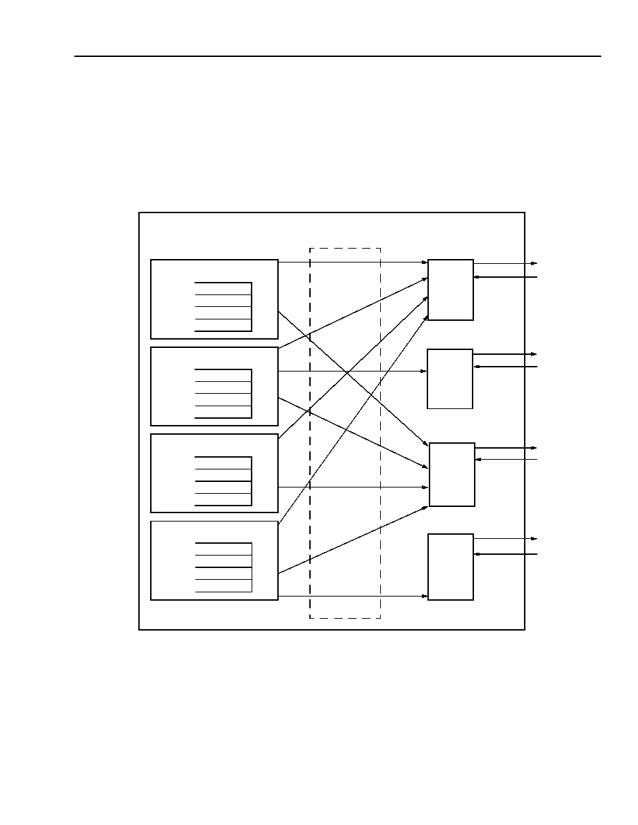
Data Sheet
MARS2G5 P-Pro (TDAT162G52) SONET/SDH
August 18, 2004
155/622/2488 Mbits/s Data Interface
731
Agere Systems Inc.
UTOPIA (UT) Block
(continued)
Basic Modes of Operations
(continued)
Figure 97 shows the overall structure of the receive direction of the UTOPIA block illustrating connections between
slices and physical interfaces. The figure shows all possible connections from four slices to four physical interfaces
through configurable cross-bar switch. Each channel and its FIFO handle 32-bit data. A UTOPIA PHY Rx block
(also referred to as interface) can connect to multiple slices but a slice cannot connect to more than one interface.
5-8372(F)r.1U
Figure 97. Overall Structure for Receive Direction
UTOPIA_
RXPPAA
RXENBA/
UTOPIA_
RXPPAB
RXENBB
UTOPIA_
RXPPAC
RXENBC
UTOPIA_
RXPPAD
RXENBD
UTOPIA BLOCK
/RXDATAB[15:0]
/RXDATAA[15:0]
/RXDATAC[15:0]
/RXDATAD[15:0]
RECEIVE CHANNEL
A0
A3
RECEIVE CHANNEL
B0
B3
RECEIVE CHANNEL
D0
D3
RECEIVE CHANNEL
C0
C3
CROSS CONNECT
PHY_RX
PHY_RX
PHY_RX
PHY_RX
RXADDRA
[2:0]
/RXADDRB
[1:0]
/RXADDRC
[2:0]
/RXADDRD
[1:0]

MARS2G5 P-Pro (TDAT162G52) SONET/SDH
Data Sheet
155/622/2488 Mbits/s Data Interface
August 18, 2004
732
Agere Systems Inc.
UTOPIA (UT) Block
(continued)
Basic Modes of Operations
(continued)
Figure 98 shows the overall structure of the transmit direction of the UTOPIA block.
5-8373(F)r.2U
Figure 98. Overall Structure for Transmit Direction
UTOPIA_
TXPPAA
TXENBA/TXADDRA[2:0]/
UTOPIA BLOCK
TXDATAA[15:0]
TRANSMIT CHANNEL
A0
A3
TRANSMIT CHANNEL
B0
B3
TRANSMIT CHANNEL
D0
D3
TRANSMIT CHANNEL
C0
C3
CROSS CONNECT
PHY_TX
UTOPIA_
PHY_TX
UTOPIA_
PHY_TX
UTOPIA_
PHY_TX
TXPPAB
TXENBB/TXADDRB[1:0]/
TXDATAB[15:0]
TXPPAC
TXENBC/TXADDRC[2:0]/
TXDATAC[15:0]
TXPPAD
TXENBD/TXADDRD[1:0]/
TXDATAD[15:0]
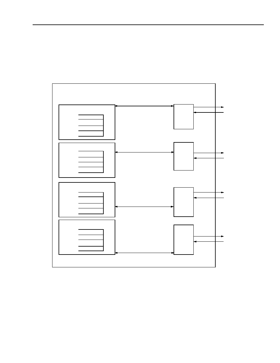
Data Sheet
MARS2G5 P-Pro (TDAT162G52) SONET/SDH
August 18, 2004
155/622/2488 Mbits/s Data Interface
733
Agere Systems Inc.
UTOPIA (UT) Block
(continued)
Basic Modes of Operations
(continued)
Figure 99 shows the receive direction of UTOPIA block, illustrating the four polling groups with four channels each
for 16-bit data transfer. Each polling group can be interfaced with different clocks. Note that this mode needs only
2-bit address bus per each interface.
5-8374(F)r.3
Figure 99. Four Groups of Multi-PHY Devices of Four Channels for Receive Direction
UTOPIA_
RXENBA/
UTOPIA_
RXPPAB/
RXENBB/
UTOPIA_
RXENBC/
UTOPIA_
UTOPIA BLOCK
RECEIVE CHANNEL
A0
A3
RECEIVE CHANNEL
B0
B3
RECEIVE CHANNEL
D0
D3
RECEIVE CHANNEL
C0
C3
PHY_RX
PHY_RX
PHY_RX
PHY_RX
RXENBD/
RXPPAA/
RXDATAA[15:0]
RXADDRA[2:0]
RXDATAB[15:0]
RXPPAC/
RXDATAC[15:0]
RXADDRC[2:0]
RXADDRB[1:0]
RXPPAD/
RXDATAD[15:0]
RXADDRD[1:0]

MARS2G5 P-Pro (TDAT162G52) SONET/SDH
Data Sheet
155/622/2488 Mbits/s Data Interface
August 18, 2004
734
Agere Systems Inc.
UTOPIA (UT) Block
(continued)
Basic Modes of Operations
(continued)
Figure 100 shows the transmit direction of the UTOPIA block, which is also divided into the four groups of four
channels each for 16-bit data transfer.
5-8375(F)r.3
Figure 100. Four Groups of Multi-PHY Devices of Four Channels for Transmit Direction
UTOPIA_
TXPPAA
UTOPIA_
TXPPAB
UTOPIA_
TXPPAC
UTOPIA_
TXPPAD
UTOPIA BLOCK
TRANSMIT CHANNEL
A0
A3
TRANSMIT CHANNEL
B0
B3
TRANSMIT CHANNEL
D0
D3
TRANSMIT CHANNEL
C0
C3
PHY_TX
PHY_TX
PHY_TX
PHY_TX
TXENBD/TXADDRD[1:0]/
TXDATAD[15:0]
TXENBC/TXADDRC[2:0]/
TXDATAC[15:0]
TXENBB/TXADDRB[1:0]/
TXDATAB[15:0]
TXENBA/TXADDRA[2:0]/
TXDATAA[15:0]
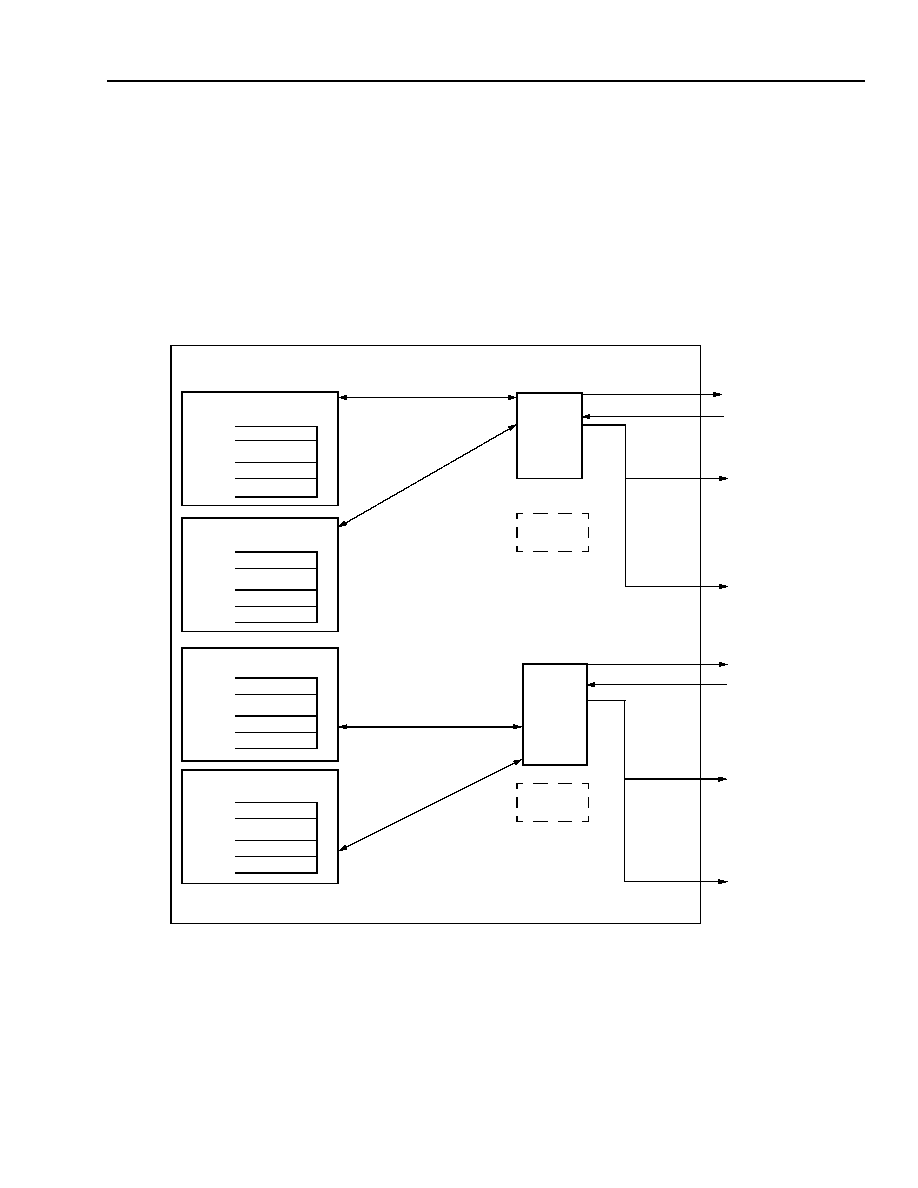
Data Sheet
MARS2G5 P-Pro (TDAT162G52) SONET/SDH
August 18, 2004
155/622/2488 Mbits/s Data Interface
735
Agere Systems Inc.
UTOPIA (UT) Block
(continued)
Basic Modes of Operations
(continued)
Figure 101 shows a 32-bit mode Rx configuration, which is divided into two groups of eight channels. Data from
and to the UTOPIA PHY Rx block is 32 bits wide. For the first eight channels, the most significant 2 bytes of data
from the UTOPIA PHY Rx block are brought out through interface A, and the least significant 2 bytes of data from
the UTOPIA PHY Rx block are sent to interface B. Each channel is addressed via a 5-bit address bus, which is
concatenated by address bus A and B (or C and D) as shown in Figure 101. By operating this way, all eight chan-
nels can be treated as a polled multi-PHY group for 32-bit data transfer. The second eight-channel polling group is
operated in the same way using interfaces C and D.
5-8376(F)r.3
Figure 101. Two Groups of Multi-PHY Devices of Eight Channels for Receive Direction
UTOPIA_
RXPPAA
RXENBA
UTOPIA_
UTOPIA_
RXPPAC
UTOPIA_
UTOPIA BLOCK
RXDATAA
RXDATAB
RXENBC
RXDATAC
RXDATAD
RECEIVE CHANNEL
A0
A3
RECEIVE CHANNEL
B0
B3
RECEIVE CHANNEL
D0
D3
RECEIVE CHANNEL
C0
C3
CROSS-BAR
SWITCH
PHY_RX
PHY_RX
PHY_RX
PHY_RX
[31:16]
[15:0]
[31:16]
[15:0]
RXADDRA[2:0]
& RXADDRB[1:0]
RXADDRC[2:0]
& RXADDRD[1:0]
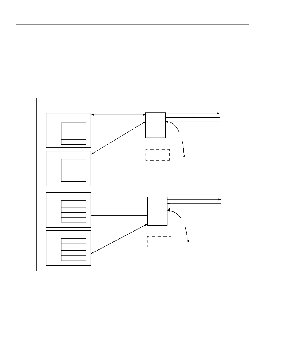
MARS2G5 P-Pro (TDAT162G52) SONET/SDH
Data Sheet
155/622/2488 Mbits/s Data Interface
August 18, 2004
736
Agere Systems Inc.
UTOPIA (UT) Block
(continued)
Basic Modes of Operations
(continued)
Figure 102 shows a 32-bit mode Tx configuration. When data coming from the outside of UTOPIA block is targeted
to one of the first eight channels, the most significant two bytes of data are brought in through interface A. The least
significant 2 bytes of data are brought in through interface B and sent to the UTOPIA PHY Tx block of the interface
A. Each channel is addressed via a 5-bit address bus, which is concatenated by address bus A and B (or C and D)
as shown in Figure 102. All eight channels are treated as a polling group. The second eight-channel polling group
is also operated in the same way using interfaces C and D.
5-8377(F)r.4
Figure 102. Two Groups of Multi-PHY Devices of Eight Channels for Transmit Direction
UTOPIA_
TXPPAA
TXENBA
UTOPIA_
UTOPIA_
TXPPAC
TXENBC
UTOPIA BLOCK
TXDATAB
TXDATAD
TRANSMIT CHANNEL
A0
A3
TRANSMIT CHANNEL
B0
B3
TRANSMIT CHANNEL
D0
D3
TRANSMIT CHANNEL
C0
C3
TXADDRA[2:0]
TXADDRC[2:0]
PHY_TX
UTOPIA_
PHY_TX
PHY_TX
PHY_TX
TXDATAA
[31:16]
[15:0]
TXDATAD
[31:16]
[15:0]
& TXADDRD[1:0]
& TXADDRB[1:0]

Data Sheet
MARS2G5 P-Pro (TDAT162G52) SONET/SDH
August 18, 2004
155/622/2488 Mbits/s Data Interface
737
Agere Systems Inc.
UTOPIA (UT) Block
(continued)
Basic Modes of Operations
(continued)
Figure 103 shows the case when all 16 channels are arranged in a polling group. Although any of the physical
interfaces can be used, interface A or C are recommended for 16 channel MPHY. In this example, interface A is
activated. Each channel is addressed via a 5-bit address bus, which is concatenated by address bus A and B. Acti-
vated interface becomes master interfaces, and the RXPA (or TXPA) for the master interface shows the polled
data availability (or room availability) of all 16 channels. Other interfaces that are not activated just show the data
availability (or room availability) of their own slice channels by asserting RXPA (or TXPA). Address and interface
mapping follows the multiplexed status polling of UTOPIA level 2 Standard Specification. According to multiplexed
status polling of UTOPIA level 2 standard specification, PHY channel addresses are grouped together and are allo-
cated in a fixed manner to one of the four status signals in each direction (TXPPAA, TXPPAB, TXPPAC, and TXP-
PAD, and RXPPAA, RXPPAB, RXPPAC, and RXPPAD) as shown in Table 755. The status signals are read
simultaneously in one status poll cycle to show the status of their own slice channels.
5-8378(F)r.3
Figure 103. A Multi-PHY Device of 16 Channels for Receive 16-Bit or 8-Bit Modes
UTOPIA_
PHY_RX
UTOPIA_
PHY_RX
UTOPIA_
PHY_RX
UTOPIA_
PHY_RX
RXPPAB
RXPPAC
RXPPAD
RXPPAA/
RXDATAA[15:0]
RXENBA
UTOPIA BLOCK
RECEIVE CHANNEL
A0
A3
RECEIVE CHANNEL
RECEIVE CHANNEL
RECEIVE CHANNEL
B0
B3
C0
C3
D0
D3
RXADDRA[2:0] &
RXADDRB[1:0]
RXCLKB
RXCLKC
RXCLKD
RXCLKA
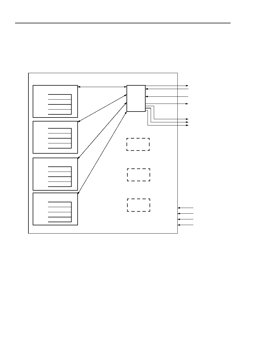
MARS2G5 P-Pro (TDAT162G52) SONET/SDH
Data Sheet
155/622/2488 Mbits/s Data Interface
August 18, 2004
738
Agere Systems Inc.
UTOPIA (UT) Block
(continued)
Basic Modes of Operations
(continued)
Figure 104 shows the case when all 16 channels are arranged in a polling group in 32-bit mode. In this configura-
tion, only interface A (with interface B) or interface C (with interface D) can be used.
5-8379(F)r.4
Figure 104. A Multi-PHY Device of 16 Channels of Receive 32-Bit Mode
UTOPIA_
RXPPAA
RXENBA
RXPPAC
UTOPIA_
UTOPIA BLOCK
RECEIVE CHANNEL
A0
A3
RECEIVE CHANNEL
B0
B3
RECEIVE CHANNEL
D0
D3
RECEIVE CHANNEL
C0
C3
RXPPAB
RXPPAD
PHY_RX
UTOPIA_
PHY_RX
UTOPIA_
PHY_RX
RXADDRA[2:0]
& RXADDRB[1:0]
RXDATAA[31:16]
& RXDATAB[15:0]
PHY_RX
RXCLKB
RXCLKC
RXCLKD
RXCLKA

Data Sheet
MARS2G5 P-Pro (TDAT162G52) SONET/SDH
August 18, 2004
155/622/2488 Mbits/s Data Interface
739
Agere Systems Inc.
UTOPIA (UT) Block
(continued)
Mixed Modes of Operations
Each slice can be operated in a different mode. For example, the first slice can be configured for 8-bit mode, the
second slice can be configured for 16-bit mode, and the next two slices can be configured for 32-bit mode.
Figure 105 shows this example of mixed mode operation in the receive direction.
5-8380(F)r.3
Figure 105. Mixed Modes of Operations for Receive Direction
UTOPIA BLOCK
(U3 8-bit MODE)
(U2 16-bit MODE)
(U3 32-bit MODE)
UTOPIA_
RXPPAA/
RXENBA
RXDATAA[7:0]
RECEIVE CHANNEL
A0
A3
UTOPIA
RXENBB
RXPPAB/
RXDATAB[15:0]
RECEIVE CHANNEL
B0
B3
UTOPIA
RXPPAC
UTOPIA_
RXENBC
RXDATAC[31:16]
RXDATAD[15:0]
RECEIVE CHANNEL
D0
D3
RECEIVE CHANNEL
C0
C3
RXADDRA[2:0] & TXDATAA[1:0]
RXADDRB[1:0]
PHY_RX
_PHY_RX
_PHY_RX
PHY_RX
RXPPAD
RXADDRC[2:0] & RXADDRD[1:0]
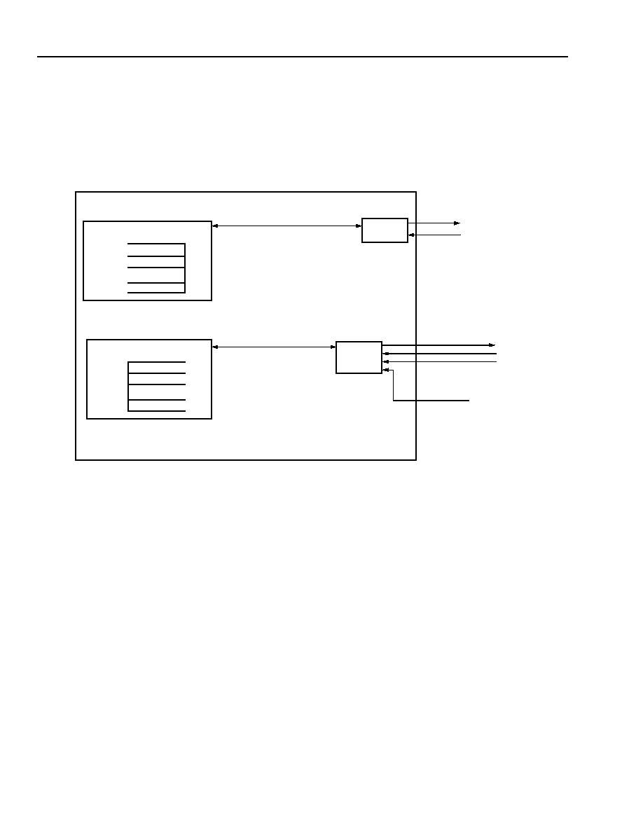
MARS2G5 P-Pro (TDAT162G52) SONET/SDH
Data Sheet
155/622/2488 Mbits/s Data Interface
August 18, 2004
740
Agere Systems Inc.
UTOPIA (UT) Block
(continued)
Mixed Modes of Operations
(continued)
The receive side and the transmit side of an MPHY channel can also be operated in different modes. For example,
the receive side of channel A is operated in 16-bit mode while the transmit side of channel A is operated in 32-bit
mode. Figure 106 shows this example of mixed modes of operation.
5-8381(F)r.3
Figure 106. Mixed Modes of Operation of the Receive Side and the Transmit Side
UTOPIA BLOCK
(U2 16-bit MODE)
(U3 32-bit MODE)
UTOPIA_
RXPPAA/
RXENBA
RXDATAA[15:0]
RECEIVE CHANNEL
A0
A3
UTOPIA
TXPPAA
TXENBA
TXDATAA[31:16]
TXDATAB[15:0]
TRANSMIT CHANNEL
A0
A3
RXADDRA[2:0]
TXADDRA[2:0]
PHY_RX
_PHY_TX
& TXADDRB[1:0]
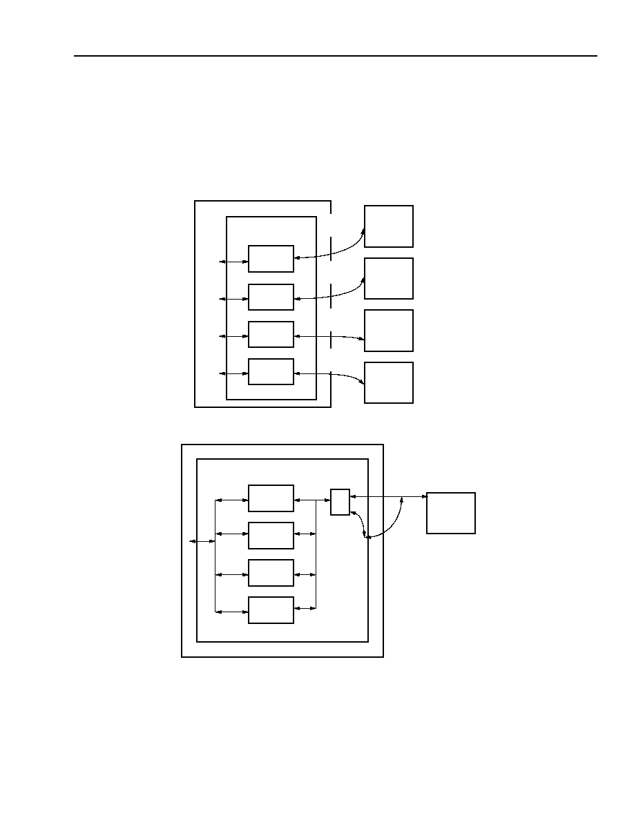
Data Sheet
MARS2G5 P-Pro (TDAT162G52) SONET/SDH
August 18, 2004
155/622/2488 Mbits/s Data Interface
741
Agere Systems Inc.
UTOPIA (UT) Block
(continued)
Reference Configurations
Examples of various UTOPIA reference configurations are shown on Figure 107. In quad OC-12c configuration
shown on Figure 107(A), four ATM devices are connected to one MARS2G5 P-Pro device, and each interface
transports 16-bit data running at 52 MHz. Figure 107(B) depicts a single OC-48c configuration for one ATM device
connected to one MARS2G5 P-Pro. Many other configurations are possible.
5-8382(F)r.3TDATU
* See Table 751 on page 719 for frequency limitations.
Figure 107. Reference Configurations
MARS2G5 P-Pro
UTOPIA
ATM
ATM
ATM
ATM
(A) QUAD OC-12C CONFIGURATION WITH 4 ATMs
MARS2G5 P-Pro
UTOPIA
ATM
(B) SINGLE OC-48C CONFIGURATION
U2
U2
U2
U2
32-bit
DEVICE
U3*
AT 104 MHz
U3 32-bit
U3 32-bit
U3 32-bit
U3 32-bit
DEVICE
DEVICE
DEVICE
DEVICE
U2 16-bit
AT 52 MHz
U2 16-bit
AT 52 MHz
U2 16-bit
AT 52 MHz
U2 16-bit
AT 52 MHz

MARS2G5 P-Pro (TDAT162G52) SONET/SDH
Data Sheet
155/622/2488 Mbits/s Data Interface
August 18, 2004
742
Agere Systems Inc.
UTOPIA (UT) Block
(continued)
UTOPIA Interface Pin Description
The UTOPIA external interface pins are listed and described in the following tables.
Note: Pins whose names are marked with an asterisk (*) are only used in POS mode.
Table 756. UTOPIA Tx Interface Pins that Have Different Meanings in Different Modes
Pin Name
Mode
Description
TXADDRA[2:0]
TXADDRB[1:0]
TXADDRC[2:0]
TXADDRD[1:0]
8-bit
(A5')
TXADDRA[2:0] concatenated with TXDATAA[7:6] forms 5-bit address bus.
TXADDRB[1:0] concatenated with TXDATAB[7:5] forms 5-bit address bus.
TXADDRC[2:0] concatenated with TXDATAC[7:6] forms 5-bit address bus.
TXADDRD[1:0] concatenated with TXDATAD[7:5] forms 5-bit address bus.
16-bit
(A2/A3)
TXADDR[A--D][1:0] selects a channel among four channels.
If more than four channels are polled, then 32-bit mode (A5) configuration is used.
32-bit
(A5)
TXADDRA[2:0] forms the most significant 3 bits and TXADDRB[1:0] forms the least
significant 2 bits of the combined address bus for interface A.
TXADDRC[2:0] forms the most significant 3 bits and TXADDRD[1:0] forms the least
significant 2 bits of the combined address bus for interface C.
TXDATA[A--D]
[15:0]
8-bit
TXDATA[A--D][15:8] are valid.
16-bit
TXDATA[A--D][15:0] are valid.
32-bit
TXDATAA[15:0] forms the most significant 16 bits 31:16, and TXDATAB[15:0] forms
the least significant 16 bits 15:0 of the combined data bus. This is the same for
TXDATAC[15:0] and TXDATAD[15:0].
TXSZ[A--D]
8-bit
Packet
Mode
Not used.
16-bit
Packet
Mode
TXSZ[A--D] = 0 indicates that the MS byte of TXDATA[A--D] is the end of packet,
and TXSZ[A--D] = 1 indicates that the LS byte of TXDATA[A--D] is the end of
packet existing in the current word. Microprocessor configurable.
32-bit
Packet
Mode
TXSZA is used in conjunction with TXSZB, with TXSZA forming the most significant
bit. For the combined results, 00, 01, 10, and 11 indicate that the last byte of data is
on the data bus bits 31:24, 23:16, 15:8, or 7:0, respectively. This is the same for
TXSZC and TXSZD. Microprocessor configurable.

Data Sheet
MARS2G5 P-Pro (TDAT162G52) SONET/SDH
August 18, 2004
155/622/2488 Mbits/s Data Interface
743
Agere Systems Inc.
UTOPIA (UT) Block
(continued)
UTOPIA Interface Pin Description
(continued)
Table 757. UTOPIA Rx Interface Pins that Have Different Meanings in Different Modes
Pin Name
Mode
Description
RXADDRA[2:0]
RXADDRB[1:0]
RXADDRC[2:0]
RXADDRD[1:0]
8-bit
(A5')
RXADDRA[2:0] concatenated with TXDATAA[1:0] forms 5-bit address bus.
RXADDRB[1:0] concatenated with TXDATAB[2:0] forms 5-bit address bus.
RXADDRC[2:0] concatenated with TXDATAC[1:0] forms 5-bit address bus.
RXADDRD[1:0] concatenated with TXDATAD[2:0] forms 5-bit address bus.
16-bit
(A2/A3)
RXADDR[A:D][1:0] selects a channel among four channels.
If more than four channels are polled then 32-bit mode (A5) configuration is used.
32-bit
(A5)
RXADDRA[2:0] forms the most significant 3 bits and RXADDRB[1:0] forms the least
significant 2 bits of the combined address bus for interface A.
RXADDRC[2:0] forms the most significant 3 bits and RXADDRD[1:0] forms the least
significant 2 bits of the combined address bus for interface C.
RXDATA[A--D]
[15:0]
8-bit
RXDATA[A:D][15:8] are valid.
16-bit
RXDATA[A:D][15:0] are valid.
32-bit
RXDATAA[15:0] forms the most significant 16 bits 31:16, and RXDATAB[15:0] forms
the least significant 16 bits 15:0 of the combined data bus. This is the same for
RXDATAC[15:0] and RXDATAD[15:0].
RXSZ[A--D]
8-bit
Packet
Mode
Not used.
16-bit
Packet
Mode
RXSZ[A--D] = 0 indicates that the MS byte of RXDATA[A--D] is the end of packet,
and RXSZ[A--D] = 1 indicates that the LS byte of RXDATA[A--D] is the end of
packet existing in the current word. Microprocessor configurable.
32-bit
Packet
Mode
RXSZA is used in conjunction with RXSZB, with RXSZA forming the most significant
bit. For the combined results, 00, 01, 10, and 11 indicates that the last byte of data
is on the data bus bits 31:24, 23:16, 15:8, or 7:0, respectively. This is the same for
RXSZC and RXSZD. Microprocessor configurable.

MARS2G5 P-Pro (TDAT162G52) SONET/SDH
Data Sheet
155/622/2488 Mbits/s Data Interface
August 18, 2004
744
Agere Systems Inc.
UTOPIA (UT) Block
(continued)
FIFO Ganging
FIFO ganging allows a slice's channel 1 FIFO (a1, b1, c1, d1) to be ganged/combined together with the same
slice's channel 0 (a0, b0, c0, d0) to result in a 128x4 byte (512-byte) FIFO. Only channels 0 and 1 of the same slice
can be combined together (e.g., a0a1, b0b1, c0c1, d0d1). This feature can be enabled by bit 2 of the Rx/TxPrv reg-
isters of channels a0, b0, c0, or d0. In slices where FIFO ganging is enabled, slice channel 1 must be idle (dis-
abled) and not used. The FIFO thresholds must be adjusted to take advantage of the extra FIFO memory.
The following settings can be used for channel b0/b1 ganging for ATM cells.
Channel 1 of a slice must be disabled when FIFO 0 and 1 are ganged. All channel 1 status signals are inactive and
output their default values. Internal FIFO read and write addresses are extended from 7 to 8 bits to accommodate
the increase in the storage locations of combined/ganged FIFO. Each slice can be configured in the gang mode.
Packet Packing
Packet packing provides a packet mode feature (ignored for ATM transfers) that compresses unused bytes
between successive packets on the egress path, which are a natural artifact of a 32-bit datapath. The packet mode
is enabled by asserting bit 8 of the Tx interface mode provisioning register. In addition, a time-out counter
(TXWC[A--D]) should be provisioned to indicate the maximum number of UTOPIA interface clocks that should
elapse before transferring the last word of a packet, so the tail of the packet does not become stuck in the datapath.
The default value of 0 will cause the immediate transfer of the final word.Small Packet Enable (Transmit Interface)
Unless provisioned otherwise, packets less than 4 bytes are discarded by UTOPIA transmit interface. A bit in
STM_bypass register (0x700E, bit 15 -- TxSmallPktEn) can be set to prevent transmit interface from discarding
packets less than 4 bytes. No such provisioning is necessary for receive interface since it passes on whatever
comes from DE.
Default Channel Configuration
MARS2G5 P-Pro specific channel configuration settings is for the ATM mode of operation with threshold settings
appropriate for ATM transfer.
Table 758. Channel B0/B1 Ganging Settings for ATM Cells
Register
Settings
RXPRVB0
0x8005
TXPRVB0
0x8005
RXTHB0
0x760E
TXTHB0
0x5E0E
RXTHMINB0
0x0000
TXTHMAXB0
0x0071
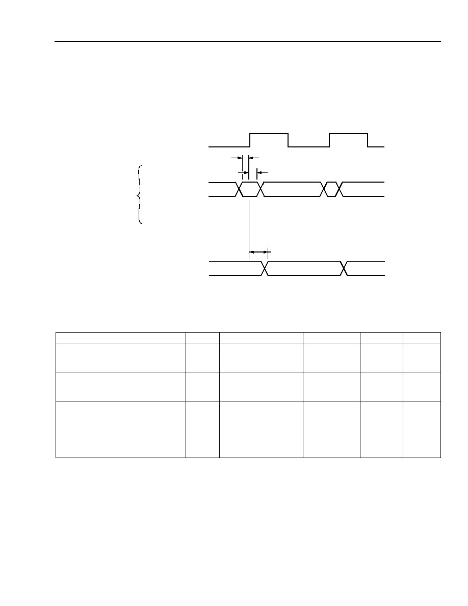
Data Sheet
MARS2G5 P-Pro (TDAT162G52) SONET/SDH
August 18, 2004
155/622/2488 Mbits/s Data Interface
745
Agere Systems Inc.
UTOPIA (UT) Block
(continued)
UTOPIA Interface Timing
UTOPIA interface timing specifications are given for the transmit direction in Figure 108 and in Table 759, and for
the receive direction in Figure 109 and in Table 760 (see page 746). Specifications for the UTOPIA clock interface
are given in Table 761 (see page 747).
5-7663(F).ar.2
Figure 108. Transmit UTOPIA Interface Timing
Table 759. Transmit UTOPIA Interface Timing Specifications
Parameter
Symbol
Test Conditions
Min
Max
Unit
Setup Time:
Inputs to TXCLK[D--A]
t43
TXCLK[D--A] as
U3/U3+
U2/U2+
2
4
--
--
ns
ns
Hold Time:
Inputs from TXCLK[D--A]
t44
TXCLK[D--A] as
U3/U3+
U2/U2+
1
1
--
--
ns
ns
Propagation Delay, Clock to Output
TXPPA[D--A], TXSPA[D--A] from
TXCLK[D--A]
t45
TXCLK[D--A]
U3/U3+, C
L
= 25 pF
U2/U2+, C
L
= 50 pF
where C
L
= the load
capacitance on the
outputs
2
2
4.5
13
ns
ns
TXCLK[D--A]
TXPPA[D--A]
t45
TXENB[D--A]
t43
t44
TXSZ[D--A]
TXPRTY[D--A]
TXSOP[D--A]
TXEOP[D--A]
TXERR[D--A]
TXDATA[D--A][15:0]
INPUTS
TXSPA[D--A]
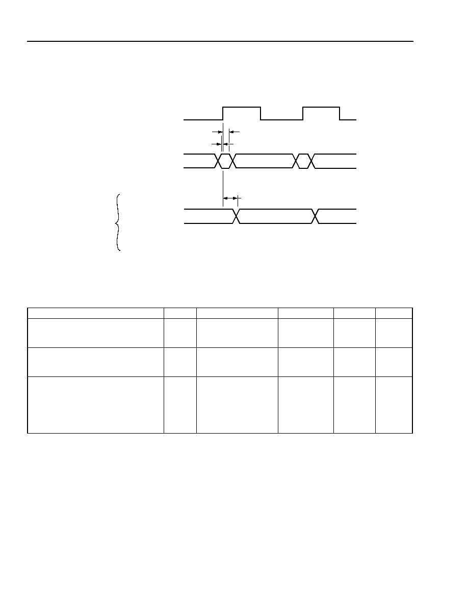
MARS2G5 P-Pro (TDAT162G52) SONET/SDH
Data Sheet
155/622/2488 Mbits/s Data Interface
August 18, 2004
746
Agere Systems Inc.
UTOPIA (UT) Block
(continued)
UTOPIA Interface Timing
(continued)
5-7664(F).ar.3
Figure 109. Receive UTOPIA Interface Timing
Table 760. Receive UTOPIA Interface Timing Specifications
Parameter
Symbol
Test Conditions
Min
Max
Unit
Set Up Time:
RXENB[D--A] to RXCLK[D--A]
t46
RXCLK[D--A] as
U3/U3+
U2/U2+
2
4
--
--
ns
ns
Hold Time:
RXENB[D--A] from RXCLK[D--A]
t47
RXCLK[D--A] as
U3/U3+
U2/U2+
1
1
--
--
ns
ns
Propagation Delay, Clock to Output:
RXPPA[D--A], RXSPA[D--A],
RXSZ[D--A], RXPRTY[D--A],
RXSOP[D--A], RXEOP[D--A],
RXERR[D--A], RXDATA[D--A](15:0)
from RXCLK[D--A]
t48
RXCLK[D--A]
C
L
= 25 pF
C
L
= 50 pF
where C
L
= the load
capacitance on the
outputs
2
6.5
6.5
13
ns
ns
RXPPA[D--A]
t48
RXENB[D--A]
t46
t47
RXSPA[D--A]
RXPRTY[D--A]
RXSOP[D--A]
RXEOP[D--A]
RXERR[D--A]
RXDATA[D--A][15:0]
OUTPUTS
RXCLK[D--A]
Data Sheet
MARS2G5 P-Pro (TDAT162G52) SONET/SDH
August 18, 2004
155/622/2488 Mbits/s Data Interface
747
Agere Systems Inc.
UTOPIA (UT) Block
(continued)
UTOPIA Interface Timing
(continued)
Table 761. UTOPIA Interface Clock Specifications
Note: See Table 751 on page 719 for frequency limitations.
Mode
Signal Name
Parameter
Test Conditions
Min
Max
Unit
Transmit
U3+
TXCLK[D--A]
TXCLK Frequency
104 MHz,
Multi-PHY Signal
0
104
MHz
TXCLK Duty Cycle
40
60
%
TXCLK Peak-to-Peak Jitter
--
2
%
TXCLK Rise/Fall Time
--
2
ns
TXCLK Skew
--
1
ns
Receive
U3+
RXCLK[D--A]
RXCLK Frequency
104 MHz,
Multi-PHY Signal
0
104
MHz
RXCLK Duty Cycle
40
60
%
RXCLK Peak-to-Peak Jitter
--
2
%
RXCLK Rise/Fall Time
--
2
ns
RXCLK Skew
--
1
ns
Transmit
U2+
TXCLK[D--A]
TXCLK Frequency
52 MHz,
Multi-PHY Signal
0
50
MHz
TXCLK Duty Cycle
40
60
%
TXCLK Peak-to-Peak Jitter
--
5
%
TXCLK Rise/Fall Time
--
2
ns
TXCLK Skew
--
1
ns
Receive
U2+
RXCLK[D--A]
RXCLK Frequency
52 MHz,
Multi-PHY Signal
0
50
MHz
RXCLK Duty Cycle
40
60
%
RXCLK Peak-to-Peak Jitter
--
5
%
RXCLK Rise/Fall Time
--
2
ns
RXCLK Skew
--
1
ns

MARS2G5 P-Pro (TDAT162G52) SONET/SDH
Data Sheet
155/622/2488 Mbits/s Data Interface
August 18, 2004
748
Agere Systems Inc.
UTOPIA (UT) Block
(continued)
UT Global Registers
Table 762. (UTVER) Version Control (RO)
Table 763. (XBARCFGRX) Cross-Bar Configuration Register for Rx (R/W)
Note: Active interfaces at a minimum must be connected to their native slices.
Table 764. (XBARCFGTX) Cross-Bar Configuration Register for Tx (R/W)
Note: Active interfaces at a minimum must be connected to their native slices.
Table 765. (INTSTATUS) Interrupts (RO)
Table 766. (INTMASK) Interrupt Masks (R/W)
Address
Bit
Name
Function
Reset
Default
0x7000
15:8
--
Reserved.
0x00
7:0
UTVER
Block Version. Indicates version number of the UTOPIA block.
0x02
Address
Bit
Name
Function
Reset
Default
0x7002
15:12
RXIFDSEL
Connection from Slices (D, C, B, A) to Interface D.
1000
11:8
RXIFCSEL
Connection from Slices (D, C, B, A) to Interface C.
0100
7:4
RXIFBSEL
Connection from Slices (D, C, B, A) to Interface B.
0010
3:0
RXIFASEL
Connection from Slices (D, C, B, A) to Interface A.
0001
Address
Bit
Name
Function
Reset
Default
0x7003
15:12
TXIFDSEL
Connection from Slices (D, C, B, A) to Interface D.
1000
11:8
TXIFCSEL
Connection from Slices (D, C, B, A) to Interface C.
0100
7:4
TXIFBSEL
Connection from Slices (D, C, B, A) to Interface B.
0010
3:0
TXIFASEL
Connection from Slices (D, C, B, A) to Interface A.
0001
Address
Bit
Name
Function
Reset
Default
0x7004
15:0
INT[D--A](3:0)
Interrupt for Channel [D--A](3:0).
0x0000
Address
Bit
Name
Function
Reset
Default
0x7008
15:0
INT[D--A](3:0)M If set, masks any interrupts from channel [D--A](3:0).
0xFFFF
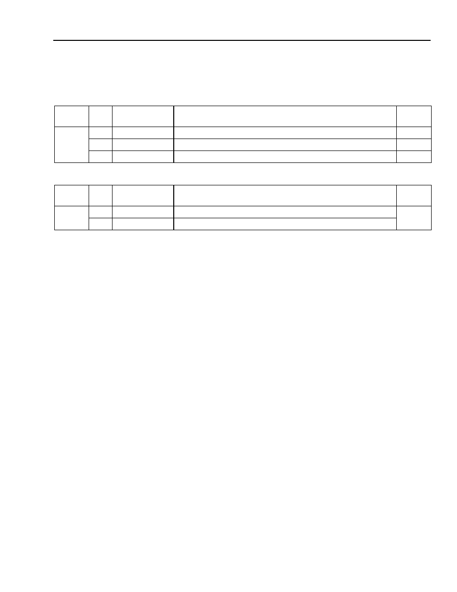
Data Sheet
MARS2G5 P-Pro (TDAT162G52) SONET/SDH
August 18, 2004
155/622/2488 Mbits/s Data Interface
749
Agere Systems Inc.
UTOPIA (UT) Block
(continued)
UT Global Registers
(continued)
Table 767. (ARST) ARST Register (R/W)
Table 768. (CORWN) Clear-On-Read or Clear-On-Write Select Register (R/W)
Address
Bit
Name
Function
Reset
Default
0x700C
15:8
--
Reserved.
0xFF
7:4
ARSTTX[D--A]
Asynchronous Reset to Tx Slice D--A. Active-high.
0xF
3:0
ARSTRX[D--A]
Asynchronous Reset to Rx Slice D--A. Active-high.
0xF
Address
Bit
Name
Function
Reset
Default
0x700F
15:1
--
Reserved.
0x0000
0
CORWN
Assert this bit for clear-on-read. Default is clear-on-write.

MARS2G5 P-Pro (TDAT162G52) SONET/SDH
Data Sheet
155/622/2488 Mbits/s Data Interface
August 18, 2004
750
Agere Systems Inc.
UTOPIA (UT) Block
(continued)
UT Per-Interface Registers
Meanings for the fields of the provisioning registers are given below.
Table 769. UTOPIA Provisioning Field Description
Field Name
Value
Encoding
Polling Enable Mode
Polling enabled (MPHY).
1
Polling disabled (non-MPHY).
0
RXCLK Mode
Sink mode (receive clocks provided by UTOPIA master).
0
SPA Enable Mode
Selected packet available (SPA) enable on.
1
Enable off.
0
Output Enable Mode
Bypassed 3-state buffers for U3 operations.
1
Operate in 3-state output mode as described in UTOPIA level 2.
0
Rx Min Pkt Gap/
Dummy Cycles
(Packet mode only)
No gap (dummy cycles) between packets on the receive interface to ATM
master.
000
Auto halt mode:
Insert dummy cycles after EOP until current channel is deselected.
111
Provisioned number of dummy cycles (gaps) are inserted between packets.
001--110
Rx PPA Style
Data valid style:
RXPPA indicates data valid. Follows the UTOPIA level 1 and level 2 stan-
dards. In packet mode, RXPPA always indicates data valid.
1
Advanced notice style:
Only used in ATM mode. RXPPA is deasserted coincident with RXSOC to
indicate to the master that the corresponding port of the PHY has no subse-
quent cell available. This gives advanced notice to master device. Follows
level 3 straw ballot.
0

Data Sheet
MARS2G5 P-Pro (TDAT162G52) SONET/SDH
August 18, 2004
155/622/2488 Mbits/s Data Interface
751
Agere Systems Inc.
UTOPIA (UT) Block
(continued)
UT Per-Interface Registers
(continued)
Table 769. UTOPIA Provisioning Field Description (continued)
Field Name
Value
Encoding
Address Mode
No address bit is assigned. Idle interface or point-to-point (non-MPHY)
mode.
00
a2/a3 mode:
Use only their own address buses (3 bits for IF A and C, 2 bits for IF B and
D).
01
a5' mode:
For 8-bit data width mode, borrow TXDATA pins to form 5-bit for all IFs.
10
a5 mode:
Borrow from neighboring IF to form 5-bit address bus.
11
Size Mode
In this mode, TX/RXSZ 0 means MS byte, 1 means LS byte.
0
In this mode, TX/RXSZ 1 means MS byte, 0 means LS byte.
1
PPA Response
PPA response is one clock later after ATM put address. Delays between
RXDATA and RXENB is also defined as one cycle.
0
PPA response is two clocks later after ATM put address. Delays between
RXDATA and RXENB is also defined as two cycles.
1
Parity
Odd.
1
Even.
0
IF Type
ATM.
1
Packet.
0
Data Width
Disabled (idle).
00
8 bit.
01
16 bit.
10
32 bit.
11

MARS2G5 P-Pro (TDAT162G52) SONET/SDH
Data Sheet
155/622/2488 Mbits/s Data Interface
August 18, 2004
752
Agere Systems Inc.
UTOPIA (UT) Block
(continued)
UT Per-Interface Registers
(continued)
The following table lists the registers used to provision Rx/Tx UTOPIA interfaces A--D. Refer to Table 771 on
page 753 through Table 774 on page 757 for a description of these registers.
Table 770. Rx/Tx UTOPIA Interface A--D Provisioning Registers
Address
Mnemonic
Interface
Default
0x7010 (See Table 771.)
PARERRA_PM
A
0x0000
0x7011 (See Table 772.)
PARERRA
0x0000
0x7012 (See Table 773.)
RxModeA
0x000C
0x7013 (See Table 774.)
TxModeA
0x000C
0x7014 (See Table 771.)
PARERRB_PM
B
0x0000
0x7015 (See Table 772.)
PARERRB
0x0000
0x7016 (See Table 773.)
RxModeB
0x000C
0x7017 (See Table 774.)
TxModeB
0x000C
0x7018 (See Table 771.)
PARERRC_PM
C
0x0000
0x7019 (See Table 772.)
PARERRC
0x0000
0x701A (See Table 773.)
RxModeC
0x000C
0x701B (See Table 774.)
TxModeC
0x000C
0x701C (See Table 771.)
PARERRD_PM
D
0x0000
0x701D (See Table 772.)
PARERRD
0x0000
0x701E (See Table 773.)
RxModeD
0x000C
0x701F (See Table 774.)
TxModeD
0x000C

Data Sheet
MARS2G5 P-Pro (TDAT162G52) SONET/SDH
August 18, 2004
155/622/2488 Mbits/s Data Interface
753
Agere Systems Inc.
UTOPIA (UT) Block
(continued)
UT Per-Interface Registers
(continued)
Table 771. (PARERRA_PM) Interface A Error Count in PMRST Mode (RO)
Table 772. (PARERRA) Interface A Error Count (RO/COR)
Note: A clock must be provided to the UTOPIA transmit clock pins for each port that requires register access and
the UTOPIA FIFOs must be reset.
Table 773. (RXMODEA) Rx Interface A Provisioning Registers (R/W)
Address
Bit
Name
Function
Reset
Default
0x7010
15:0
Parity Error Count Tx A Counts the number of parity errors that occur for Tx port A.
Only on the rising edge of PMRST signal, the value of this
register is updated.
0x0000
Address
Bit
Name
Function
Reset
Default
0x7011
15:0
Parity Error Count Tx A Counts the number of parity errors that occur for Tx port A.
The value of this register is updated in real time.
0x0000
Address
Bit
Name
Function
Reset
Default
0x7012
15
PollEnbRxA
or
(MPHYMod-
eRxA)
Polling Enable. This bit configures an interface in MPHY or non-
MPHY (point-to-point) mode. When this bit is set, the interface
decodes address pins as described in Table 9.
When this bit is cleared to zero, the interface is in non-MPHY mode
and connected to channel 0 of its native slice. RXADDR pins are
not decoded.
If multiplexed status polling is required, then this bit must be config-
ured to a 1 for all interfaces that are generating PPA responses.
For example, to obtain four PPA (PPAA, PPAB, PPAC, and PPAD)
responses on a single polling cycle then all four interfaces require
bit 15 to be set to 1.
0
14
--
Reserved.
0
13
SPAEnRxA
RXSPA (Table 9) Enable. This bit enables the nonstandard
RXSPA pin. When set to a one, RXSPA is enabled and drives a
value whenever RXDATA, RXSOP, and RXEOP, etc. drive their val-
ues (U3 behavior, 3-state bypassed). When this bit is 0, RXSPA is
3-stated during its operation similar to other output pins in U2
mode.
0

MARS2G5 P-Pro (TDAT162G52) SONET/SDH
Data Sheet
155/622/2488 Mbits/s Data Interface
August 18, 2004
754
Agere Systems Inc.
UTOPIA (UT) Block
(continued)
UT Per-Interface Registers
(continued)
Table 773. (RXMODEA) Rx Interface A Provisioning Registers (R/W) (continued)
Address
Bit
Name
Function
Reset
Default
0x7012
12
OutputEnRxA
Output Enable Mode (3-State Buffer Override). When set to 1,
the 3-state enable circuits for RxData, RxSOP, etc. are overridden
so that they are continuously driven regardless of RxEnb. When
cleared to 0, the 3-state enable circuits dynamically 3-state or drive
these outputs according to RxEnb. This pin was added for U3 com-
pliance since in U3 only point-to-point connections between a PHY
and the ATM layer are allowed. The output enable mode field for
32-bit interfaces should be set to the same value for both A and B.
If an interface is not used, then keep the default value in this regis-
ter. Only when an interface is used in conjunction with another
interface, i.e., A/B or C/D 32-bit modes, must the OE bit and the PA
response bit be set the same on both interfaces.
0
11:9
UT _MINGAP_
PCKT-
MODE[2:0]/
DummyCy-
cleRxA[2:0]
Minimum number of gap (dummy cycles) between packet transfers.
000 = No gap (default)
001 = 1 cycle gap
010 = 2 cycles gap
011 = 3 cycles gap
100 = 4 cycles gap
101 = 5 cycles gap
110 = 6 cycles gap
111 = Auto halt mode; insert dummy cycles after EOP until current
channel is deselected. In this mode, channel must be reselected in
between successive packets (i.e., RxEnbA must be toggled).
000
8
RxPPAStyleA
UTOPIA level 2 and level 1 standard require RXCLV to be asserted
for the duration of the transfer. The availability of the next cell is not
known until the current cell is transferred completely. This mode,
the data valid mode, is activated by setting RxPPAStyle[A--D] bit
to 1. In packet transfer mode, data valid style is automatically used.
UTOPIA level 3 requires an initiated transfer to proceed until the
end of the cell without interruption. In compliance with level 3,
RXCLV can be set in advanced notice mode (by setting RxPPA-
StyleA bit to 0) where RXCLV indicates next cell's availability with
the SOP of current cell being transferred.
0
(Advanc
ed
Notice
Mode)
modified
:
August 20, 1999

Data Sheet
MARS2G5 P-Pro (TDAT162G52) SONET/SDH
August 18, 2004
155/622/2488 Mbits/s Data Interface
755
Agere Systems Inc.
UTOPIA (UT) Block
(continued)
UT Per-Interface Registers
(continued)
Table 773. (RXMODEA) Rx Interface A Provisioning Registers (R/W) (continued)
Address
Bit
Name
Function
Reset
Default
0x7012
7:6
RxAddrModeA
Address Mode Selection.
In MPHY configurations, each PHY is to have five dedicated Rx
address pins according to U2 and U3. Since there are only 10 pins
available for Rx addressing, it is not possible for all four interfaces to
have the full five RXADDR (Table 9) pins at one time. To address
this issue, the MARS2G5 P-Pro has three different ways to assign
address pins to interfaces:
1.
A2/A3 mode (local address mode)--In this mode, only the
address pins that are local to this interface are used by it. Since
the 10 available address pins cannot be equally divided among
the four interfaces, the distribution is for interfaces A and C to
have 3 pins each and interfaces B and D to have 2 pins each. It
is true that the channels connected to interfaces A and C are
limited to addresses 0x00--0x07 and that the channels con-
nected to interfaces B and D are limited to addresses 0x00--
0x03. This should not be a limitation; however, because when
all four interfaces are active, each interface can only address
four channels maximum.
2.
A5' mode (TXDATA [Table 9] borrowing address mode)--If the
data width of this interface is 8 bits, then only half of the
TXDATA inputs of the corresponding Tx interface are actually
used. In this mode, some of the unused TXDATA inputs are
borrowed so that this Rx interface can have a full complement
of five Rx address pins (2 pins borrowed for interfaces A and C
and 3 pins borrowed for interfaces B and D).
3.
A5 mode (adjacent interface borrowing address mode)--If the
data width is 16 bits or 32 bits, then there are no unused
TXDATA inputs to use as address pins. The only alternative to
achieve a full complement of five address pins is to borrow the
local address pins of the adjacent interface. This mode is lim-
ited to interfaces A and C, which may borrow the two local
address pins of interfaces B and D, respectively. In 16-bit
mode, interfaces B and D must be nonpolling because their
local pins are no longer available. In 32-bit mode, interfaces B
and D must be inactive because their RXDATA pins are being
borrowed.
00 = No address pins are connected to this interface (default).
01 = Local address mode.
10 = TXDATA borrowing address mode.
11 = Adjacent interface borrowing address mode.
00
(non-
MPHY)

MARS2G5 P-Pro (TDAT162G52) SONET/SDH
Data Sheet
155/622/2488 Mbits/s Data Interface
August 18, 2004
756
Agere Systems Inc.
UTOPIA (UT) Block
(continued)
UT Per-Interface Registers
(continued)
Table 773. (RXMODEA) Rx Interface A Provisioning Registers (R/W) (continued)
Address
Bit
Name
Function
Reset
Default
0x7012
5
RxSizeModeA This bit controls the polarity of the RXSZ pin (Table 9). When set to 1,
RXSZ high indicates the MS byte and RXSZ low indicates the LS
byte. When cleared to 0, RXSZ high indicates the LS byte and RXSZ
low indicates the MS byte. In 32-bit mode, the RXSZ pin of the adja-
cent interface is borrowed to indicate one of four bytes. In this case,
the size mode of both interfaces must be the same. When both mode
bits are set to 1, RXSZ[A:B] = 11 indicates the MS byte and
RXSZ[A:B] = 00 indicates the LS byte. When both mode bits are
cleared to 0, RXSZ[A:B] = 11 indicates the LS byte and RXSZ[A:B] =
00 indicates the MS byte.
The same applies for interface C and D.
0
4
RxPPARespA This bit controls the latency of the Rx interface's outputs with respect
to the changes on inputs (RXEnb and RxADDR). When set to 1, the
interface will respond to polling and selection by RxAddr and RxEnb
after two cycles (referred to as two cycle mode). When cleared to 0,
the default setting, the Interface will respond after just one cycle
(referred to as single cycle mode). For U1/U2 applications, there-
fore, single-cycle mode should be used and for U3 applications, two-
cycle mode should be used.
If multiplexed status polling is required, then this bit must be config-
ured to either a 1 (two cycle PA response) or 0 (single cycle PA
response) for all interfaces that are generating PPA responses in mul-
tiplexed status mode. For example, to obtain four 2-cycle PPA (PPAA,
PPAB, PPAC, and PPAD) responses on a single polling cycle, all four
interface configuration registers must have bit 4 set to 1.
0
3
ParRxA
Rx Parity Type. This bit controls if odd or even parity is generated for
the data transmitted across the UTOPIA PHY Rx interface (RXPRTY
pin (Table 9) polarity). When set to 1, RXPRTY will be odd and when
cleared to 0, RXPRTY will be even.
1
2
IFTypeRxA
This bit determines whether this interface is in ATM mode or in packet
mode. When set to 1, ATM mode is selected and when cleared to 0,
packet mode is selected. In ATM mode, the RXERR, RXEOP, and
RXSZ outputs will be 3-stated (or will drive 0s when in OE mode). In
packet mode, the RXERR, RXEOP, and RXSZ pins will be driven
along with the RXDATA, RXSOP, and RXPRTY pins.
If multiplexed status polling is required, this bit must be configured to
either a 1 (ATM mode) or 0 (packet mode) for all interfaces that are
generating PPA responses in multiplexed status mode.
1
1:0
DataWidthRxA Receive Interface Data Width. These bits control the data width of
this interface. Since only interfaces A and C can be 32-bit interfaces,
32-bit mode may not be selected for interfaces B and D.
00 = Disable interface.
01 = 8-bit mode.
10 = 16-bit mode.
11 = 32-bit mode.
00

Data Sheet
MARS2G5 P-Pro (TDAT162G52) SONET/SDH
August 18, 2004
155/622/2488 Mbits/s Data Interface
757
Agere Systems Inc.
UTOPIA (UT) Block
(continued)
UT Per-Interface Registers
(continued)
Table 774. (TXMODEA) Tx Interface A Provisioning Registers (R/W)
Address Bit
Name
Function
Reset
Default
0x7013
15
PollEnbTxA
If set, polling mode is enabled.
If multiplexed status polling is required, then this bit must be configured
to a 1 for all interfaces that are generating PPA responses. For exam-
ple, to obtain four PPA (PPAA, PPAB, PPAC, and PPAD) responses on
a single polling cycle then all four interfaces require bit 15 to be set to 1.
0
14
--
Reserved.
0
13
SPAEnTxA
This bit configures the nonstandard TXSPA pin to behave in either 3-
state mode (U2) or in 3-state bypass mode (U3). When set to a one,
TXSPA is always driven as other output pins in U3 mode (i.e., 3-state is
bypassed). When cleared to 0, TXSPA is driven similar to other output
pins in U2 behavior (3-state enable).
0
12
OutputEnTxA When this bit is set to 1, 3-state buffers are bypassed (UTOPIA level 3).
When this bit is cleared to 0, outputs operate in 3-state mode behavior
as described in UTOPIA level 2 (outputs are switched dynamically
between 3-state and driven states).
This bit overrides SPAEnModeRxA.
0
11:9
--
Reserved.
000
8
TxWaitEnbA
Enables packet packing (packet gap compression feature) on trans-
mit interface.
Packet packing provides a packet mode feature (ignored for ATM
transfers) that compresses unused bytes between successive packets
on the egress path, which are a natural artifact of a 32-bit datapath. The
packet mode is enabled by asserting bit 8 of the Tx interface mode pro-
visioning register. In addition, a time-out counter (TXWC[A--D]) should
be provisioned to indicate the maximum number of UTOPIA interface
clocks that should elapse before transferring the last word of a packet
so that the tail of the packet does not become stuck in the datapath. The
default value of 0 will cause the immediate transfer of the final word.
0
(dis-
abled)
7:6
TxAddrModeA Similar modes as receive side (RxAddrModeA) except in TXDATA bor-
rowing address mode (TxAddrMode = 10), TXDATA[7:6] are borrowed
instead TXDATA[1:0].
00
(non-
MPHY)
5
TxSizeModeA In default (TxSizeMode = 0), TXSZA 0 means MS byte and 1 means LS
byte. Otherwise, TXSZA 1 means MS byte and 0 means LS byte.
In 32-bit mode for interface A, the TXSZA and TXSZB together indicate
one of four bytes. Size mode of both interfaces must be the same.
When both size mode bits are set to 1, TXSZ[A:B] = 11 indicates the MS
byte and TXSZ[A:B] = 00 indicates the LS byte. When both are cleared
to 0, TXSZ[A:B] = 11 indicates the LS byte and TXSZ[A:B] = equal to 00
indicates the MS byte.
Same applies for interface C and D.
0

MARS2G5 P-Pro (TDAT162G52) SONET/SDH
Data Sheet
155/622/2488 Mbits/s Data Interface
August 18, 2004
758
Agere Systems Inc.
UTOPIA (UT) Block
(continued)
UT Per-Interface Registers
(continued)
Table 774. (TXMODEA) Tx Interface A Provisioning Registers (R/W) (continued)
Table 775. (TxWC[A--D]) Channel A--D Transmit Wait Register (R/W)
Address
Bit
Name
Function
Reset
Default
0x7013
4
TxPPARespA
In default value of this register bit, PPA response related to polling
address is 1 clock later (for U2 mode operations); otherwise, 2
clocks later (for U3 mode).
If multiplexed status polling is required, then this bit must be config-
ured to a either a 1 (two cycle PA response) or 0 (single cycle PA
response) for all interfaces that are generating PPA responses in
multiplexed status mode. For example, to obtain four 2-cycle PPA
(PPAA, PPAB, PPAC, and PPAD) responses on a single polling
cycle, all four interface configuration registers must have bit 4 set
to 1.
0
3
ParTxA
Defines if odd or even parity is generated for the data transmitted
across the UTOPIA PHY Tx Interface.
1
2
IFTypeTxA
This bit determines whether this transmit interface is in ATM mode
or in packet mode. When set to 1, ATM mode is selected and when
cleared to 0, packet mode is selected. In ATM mode, the TXERR,
TXEOP, and TXSZ inputs pins are ignored. In packet mode, these
inputs (along with TXDATA, TXPRTY, and TXSOP) are used for
packet handling.
If multiplexed status polling is required, then this bit must be config-
ured to a either a 1 (ATM mode) or 0 (packet mode) for all inter-
faces that are generating PPA responses in multiplexed status
mode.
1
1:0
DataWidthTxA
Transmit Interface Data Width. These bits control the data width
of this interface. Since only interfaces A and C can be 32-bit inter-
faces, 32-bit mode may not be selected for interfaces B and D.
00 = Idle interface.
01 = 8-bit mode.
10 = 16-bit mode.
11 = 32-bit mode.
00
Address
Bit
Name
Function
Reset
Default
0x7020
0x7021
0x7022
0x7023
15:10
--
Reserved.
0x00
9:0
TxWC[A--D]
Interface A Tx Wait Cycles for Packet Packing. This time-out
counter is provisioned to indicate the maximum number of
UTOPIA interface clocks cycles that should elapse before
transferring the last word of a packet so that the tail of the packet
does not become stuck in the datapath.
Packet packing feature enabled by bit 8 (TxWaitEnbA) of
TXMODE[A--D] interface registers.
0x000

Data Sheet
MARS2G5 P-Pro (TDAT162G52) SONET/SDH
August 18, 2004
155/622/2488 Mbits/s Data Interface
759
Agere Systems Inc.
UTOPIA (UT) Block
(continued)
UT Per-Interface Registers
(continued)
The following table lists the registers used to provision UTOPIA channels (0--3) of interfaces [A--D]. Refer to
Table 777 on page 760 through Table 784 on page 763 for a description of these registers. To see which registers
refer to which channel, see Table 785.
Table 776. UTOPIA Channel [A--D](0--3) Provisioning Registers
Address
Symbol
Default
0x7030, 0x7038, 0x7040, 0x7048,
0x7050, 0x7058, 0x7060, 0x7068,
0x7070, 0x7078, 0x7080, 0x7088,
0x7090, 0x7098, 0x70A0, 0x70A8
INT[A--D](0--3)
0x0000
0x7031, 0x7039, 0x7041, 0x7049,
0x7051, 0x7059, 0x7061, 0x7069,
0x7071, 0x7079, 0x7081, 0x7089,
0x7091, 0x7099, 0x70A1, 0x70A9
INT[A--D](0--3)m
0xFFFF
0x7032, 0x703A, 0x7042, 0x704A,
0x7052, 0x705A, 0x7062, 0x706A,
0x7072, 0x707A, 0x7082, 0x708A,
0x7092, 0x709A, 0x70A2, 0x70AA
RxPrv[A--D](0--3)
0x1F01
0x7033, 0x703B, 0x7043, 0x704B,
0x7053, 0x705B, 0x7063, 0x706B,
0x7073, 0x707B, 0x7083, 0x708B,
0x7093, 0x709B, 0x70A3, 0x70AB
TxPrv[A--D](0--3)
0x1F01
0x7034, 0x703C, 0x7044, 0x704C,
0x7054, 0x705C, 0x7064, 0x706C,
0x7074, 0x707C, 0x7084, 0x708C,
0x7094, 0x709C, 0x70A4, 0x70AC
RxTh[A--D](0--3)
0x360E
0x7035, 0x703D, 0x7045, 0x704D,
0x7055, 0x705D, 0x7065, 0x706D,
0x7075, 0x707D, 0x7085, 0x708D,
0x7095, 0x709D, 0x70A5, 0x70AD
TxTh[A--D](0--3)
0x1E0E
0x7036, 0x703E, 0x7046, 0x704E,
0x7056, 0x705E, 0x7066, 0x706E,
0x7076, 0x707E, 0x7086, 0x708E,
0x7096, 0x709E, 0x70A6, 0x70AE
RxThMin[A--D](0--3)
0x0000
0x7037, 0x703F, 0x7047, 0x704F,
0x7057, 0x705F, 0x7067, 0x706F,
0x7077, 0x707F, 0x7087, 0x708F,
0x7097, 0x709F, 0x70A7, 0x70AF
TxThMax[A--D](0--3)
0x0031

MARS2G5 P-Pro (TDAT162G52) SONET/SDH
Data Sheet
155/622/2488 Mbits/s Data Interface
August 18, 2004
760
Agere Systems Inc.
UTOPIA (UT) Block
(continued)
UT Per-Interface Registers
(continued)
Table 777. (INTA0) Channel A0--Overflow/Underflow (COR/COW)
Table 778. (INTA0m) Channel A0--Overflow/Underflow Mask (R/W)
Address
Bit
Name
Function
Reset
Default
0x7030
15:5
--
Reserved.
0x000
4
FifoAlmostFullRx FIFO almost full alarm for a head of FIFO discard.
0
3
FifoOverflowTx
Tx FIFO overflow alarm.
0
2
FifoUnderflowTx FIFO underflow occurred in the Tx FIFO.
0
1
FifoOverflowRx
Rx FIFO overflow alarm for a tail of FIFO discard. Ingress thresh-
old high should be lowered to prevent this error.
0
0
ParityErrorTx
If set, indicates that a parity error was detected on the Tx channel.
0
Address
Bit
Name
Function
Reset
Default
0x7031
15:5
--
Reserved.
0xFFE
4
FifoAlmostFullRxMask
If set, masks this interrupt from FifoAlmostFullRxx.
1
3
FifoOverflowTxMask
If set, masks this interrupt from FifoOverflowTx.
1
2
FifoUnderflowTxMask
If set, masks this interrupt from FifoUnderflowTx.
1
1
FifoOverflowRxMask
If set, masks this interrupt from FifoOverflowRx.
1
0
ParityErrorTxMask
If set, masks this interrupt from ParityErrorTx.
1

Data Sheet
MARS2G5 P-Pro (TDAT162G52) SONET/SDH
August 18, 2004
155/622/2488 Mbits/s Data Interface
761
Agere Systems Inc.
UTOPIA (UT) Block
(continued)
UT Per-Interface Registers
(continued)
Table 779. (RxProvA0) Channel A0--Provisioning Registers (R/W)
Table 780. (TxProvA0) Channel A0--Provisioning Registers (R/W)
Address
Bit
Name
Function
Reset
Default
0x7032
15
Channel Enable
Rx
Channel is disabled by default.
0
14:13
--
Reserved.
00
12:8
Rx Addr
Assigned (Configurable) Polling Address For This Channel.
0x1F
7:3
--
Reserved.
0x00
2
GangFifoRxA
FIFO Ganging. Allows a slice's channel 1 FIFO (a1, b1, c1, d1) to
be ganged/combined together with the same slice's channel 0 (a0,
b0, c0, d0) to result in a 128X4 byte (512-byte) FIFO. Only chan-
nels 0 and 1 of the same slice can be combined together (e.g.,
a0a1, b0b1, c0c1, d0d1). GangFifoRx[1:0] bits are provided in Rx/
TxPrv registers of channels a0, b0, c0, or d0 only. In slices where
FIFO ganging is enabled, slice channel 1 must be idle (disabled)
and not used. The FIFO thresholds must be adjusted to take
advantage of the extra FIFO memory.
Channel 1 of a slice must be disabled when FIFO 0 and 1 are
ganged. All channel 1 status signals are inactive and output their
default values. Internal FIFO read and write addresses are
extended from 7 to 8 bits to accommodate the increase in the stor-
age locations of combined/ganged FIFO. Each slice can be con-
figured in the gang mode.
0
1
ATM SizeRx
If traffic type is ATM cells, this bit indicates if UDF fields are trans-
mitted across the UTOPIA PHY Rx interface. UDF is transmitted
by default. If UDF is transmitted, then ATM cell size is 53 bytes
(ATM Long Mode); otherwise, it is 52 bytes (ATM Short Mode).
0
0
TrafficTypeRx
Configures channel to carry either ATM cells (default) or packets.
1
Address
Bit
Name
Function
Reset
Default
0x7033
15
Channel Enable
Tx
Channel is disabled by default.
0
14:13
--
Reserved.
00
12:8
TxAddr
Assigned (configurable) polling address for this channel.
0x1F
7:3
--
Reserved.
0x00
2
GangFifoTxA
FIFOs in transmit channels can also be ganged together as
described receive channels above (RxProvA0 register).
0
1
ATMSizeTx
Defines whether this channel receives 53- (default) or 52-byte
ATM cells. Valid only when traffic type is ATM cells.
0
0
TrafficTypeTx
Configures channel to carry either ATM cells (default) or packets.
1

MARS2G5 P-Pro (TDAT162G52) SONET/SDH
Data Sheet
155/622/2488 Mbits/s Data Interface
August 18, 2004
762
Agere Systems Inc.
UTOPIA (UT) Block
(continued)
UT Per-Interface Registers
(continued)
FIFO Threshold Provisioning
To allow for more flexibility in performance tuning of a system, FIFO thresholds, previously ignored, are now uti-
lized for ATM operation. The net result of this change is that FIFO thresholds must be provisioned for ATM cell
applications for proper system operation. (Provisioning of thresholds in earlier versions of the device are simply
ignored and cause no change in behavior.) An example set of thresholds for channel A0 would be:
Register RXTHA0 (Table 781) set to 0x360E.
Register TXTHA0 (Table 782) set to 0x1E0E.
Register RXTHMINA0 (Table 783) set to 0x0000.
Register TXTHMAXA0 (Table 784) set to 0x0031.
Table 781. (RxThA0) Channel A0--Provisioning Registers (R/W)
Table 782. (TxThA0) Channel A0--Provisioning Registers (R/W)
Address
Bit
Name
Function
Reset
Default
0x7034
15
--
Reserved.
0
14:8
IngressThresholdHigh
Defines threshold before which overflow is detected.
When input data cross this boundary (from bottom to top
of the FIFO), head of FIFO is discarded until SOP for the
next cell/packet is observed.
0x36
7
--
Reserved.
0
6:0
IngressThresholdLow
Defines how many words must be stored in the ingress
FIFO before transmission out of the UTOPIA port, if an
end of packet is not received. When input data cross this
boundary (from bottom to top of the FIFO), RXPPA is
asserted to indicate that there is enough data to send out.
0x0E
Address
Bit
Name
Function
Reset
Default
0x7035
15
--
Reserved.
0
14:8
EgressThresholdHigh
When input data cross this boundary (from top to bottom
of the FIFO), TXPPA is asserted to indicate that there is
enough room to accept data.
0x1E
7
--
Reserved.
0
6:0
EgressThresholdLow
Defines how many words must be stored in the egress
FIFO before transmission out of the UTOPIA port to DE, if
an end of packet is not received.
0x0E
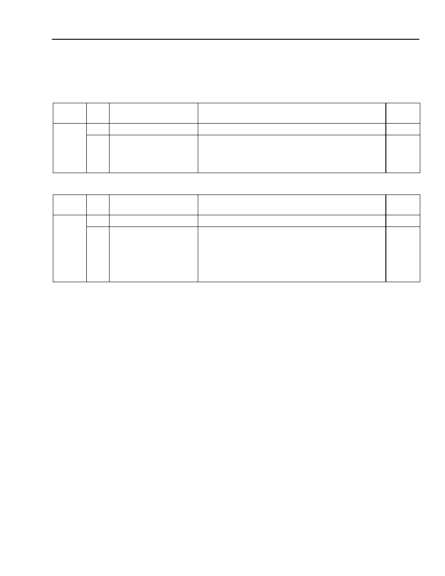
Data Sheet
MARS2G5 P-Pro (TDAT162G52) SONET/SDH
August 18, 2004
155/622/2488 Mbits/s Data Interface
763
Agere Systems Inc.
UTOPIA (UT) Block
(continued)
UT Per-Interface Registers
(continued)
Table 783. (RxThMinA0) Channel A0--Provisioning Registers (R/W)
Table 784. (TxThMaxA0) Channel A0--Provisioning Registers (R/W)
Address
Bit
Name
Function
Reset
Default
0x7036
15:5
--
Reserved.
0
6:0
Ingress ThresholdMin
If an end of packet is not received, when input data cross
this boundary (from top to bottom of the FIFO), RXPPA is
deasserted to indicate that there is not enough data to
send out.
0
Address
Bit
Name
Function
Reset
Default
0x7037
15:5
--
Reserved.
0x00
6:0
Egress ThresholdMax
Defines how many words can be stored into the egress
FIFO before backpressure is applied to the UTOPIA PHY
Tx port to stop acceptance of more traffic. When input
data cross this boundary (from bottom to top of the
FIFO), TXPPA is deasserted to indicate that there is not
enough room to accept more data.
0x31
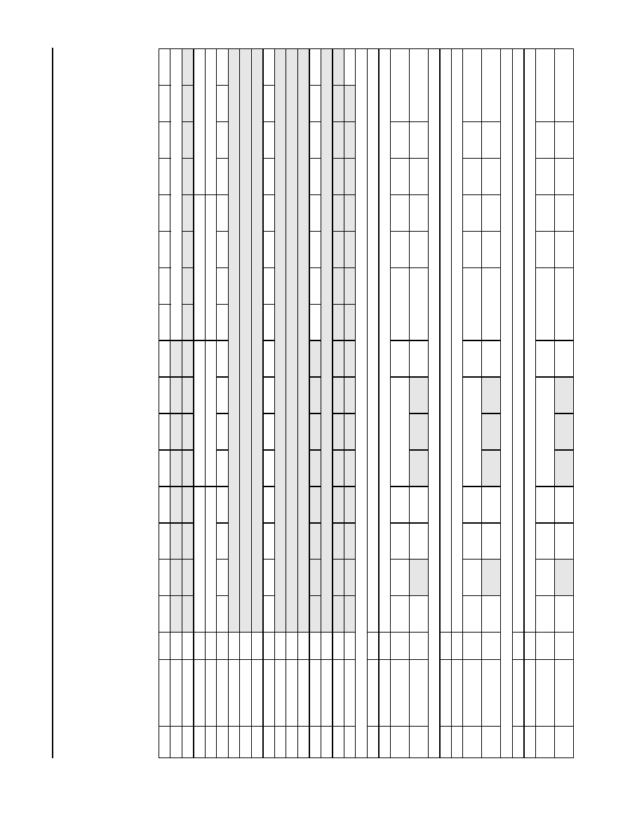
MARS2G5 P-Pro (TDAT162G52) SONET/SDH
Data Sheet
155/622/2488 Mbits/s Data Interface
August 18, 2004
764
Agere Systems Inc.
UTOPIA (UT) Block
(continued)
UT Register Map
Table 785. UT Register Map
Note: Shading denotes reserved bits.
Address
Symbol
Type
15
14
13
12
11
10
9
8
7
6
5
4
3
2
1
0
0x7000
UTVER
RO
VERSION[7:0]
0x7001
SCRATCH
--
0x7002
XBARCFGRX
R/W
RXIFDSEL
RXIFCSEL
RXIFBSEL
RXIFASEL
0x7003
XBARCFGTX
R/W
TXIFDSEL
TXIFCSEL
TXIFBSEL
TXIFASEL
0x7004
INTSTATUS
RO
IntD3
IntD2
IntD1
IntD0
IntC3
IntC2
IntC1
IntC0
IntB3
IntB2
IntB1
IntB0
IntA3
IntA2
IntA1
IntA0
0x7005
--
--
0x7006
--
--
0x7007
--
--
0x7008
INTMASK
R/W
IntD3M
IntD2M
IntD1M
IntD0M
IntC3M
IntC2M
IntC1M
IntC0M
IntB3M
IntB2M
IntB1M
IntB0M
IntA3M
IntA2M
IntA1M
IntA0M
0x7009
--
--
0x700A
--
--
0x700B
--
--
0x700C
ARST
R/W
ARSTTxD
ARSTTxC
ARSTTxB
ARSTTxA
ARSTRxD
ARSTRxC
ARSTRxB
ARSTRxA
0x700D
--
--
0x700E
--
--
0x700F
CORWN
R/W
CORWN
Interface A Registers
0x7010
PARERRA_PM
RO
PARERRCNTTXA_PM
0x7011
PARERRA
COR
PARERRCNTTXA
0x7012
RXMODEA
R/W
PollEnbRxA
ClkMod-
eRxA
SPAEn RxA
OutputEn-
RxA
UT_MINGAP_PCKTMODE[2:0]
PPA
StyleRxA
RxAddr ModeA
RxSize-
ModeA
RxPPAR-
espA
ParRxA
IF Type
RxA
DataWidth RxA
0x7013
TXMODEA
R/W
PollEnbTxA
SPAEn TxA
Out-
putEnTxA
WaitEnb
TxA
TxAddr ModeA
TxSize-
ModeA
TxPPAR-
espA
ParTxA
IF Type TxA
DataWidth TxA
Interface B Registers
0x7014
PARERRB_PM
RO
PARERRCNTTXB_PM
0x7015
PARERRB
COR
PARERRCNTTXB
0x7016
RXMODEB
R/W
PollEnbRxB
ClkMod-
eRxB
SPAEn RxB
OutputEn-
RxB
UT_MINGAP_PCKTMODE[2:0]
PA
StyleRxB
RxAddr ModeB
RxSize-
ModeB
RxPARespB
ParRxB
IF Type RxA
DataWidth RxB
0x7017
TXMODEB
R/W
PollEnbTxB
SPAEn TxB
Out-
putEnTxB
WaitEnb
TxB
TxAddr ModeB
TxSize-
ModeB
TxPARespB
ParTxB
IF Type TxB
DataWidth TxB
Interface C Registers
0x7018
PARERRC_PM
RO
PARERRCNTTXC_PM
0x7019
PARERRC
COR
PARERRCNTTXC
0x701A
RXMODEC
R/W
PollEnbRxC
ClkMod-
eRxC
SPAEn RxC
OutputEn-
RxC
UT_MINGAP_PCKTMODE[2:0]
PA
StyleRxC
RxAddr ModeC
RxSizeMo-
deC
RxPARe-
spC
ParRxC
IF Type RxC
DataWidth RxC
0x701B
TXMODEC
R/W
PollEnbTxC
SPAEn TxC
Out-
putEnTxC
WaitEnb
TxC
TxAddr ModeC
TxSizeMo-
deC
TxPARespC
ParTxC
IF Type TxC
DataWidth TxC

Data Sheet
MARS2G5 P-Pro (TDAT162G52) SONET/SDH
August 18, 2004
155/622/2488 Mbits/s Data Interface
765
Agere Systems Inc.
UTOPIA (UT) Block
(continued)
UT Register Map
(continued)
Table 785. UT Register Map (continued)
Note: Shading denotes reserved bits.
Address
Symbol
Type
15
14
13
12
11
10
9
8
7
6
5
4
3
2
1
0
Interface D Registers
0x701C
PARERRD_PM
RO
PARERRCNTTXD_PM
0x701D
PARERRD
COR
PARERRCNTTXD
0x701E
RXMODED
R/W
PollEnbRxD
ClkMod-
eRxD
SPAEn RxD
OutputEn-
RxD
UT_MINGAP_PCKTMODE[2:0]
PA
StyleRxD
RxAddr ModeD
RxSize-
ModeA
RxPARe-
spD
ParRxD
IF Type RxD
DataWidth RxD
0x701F
TXMODED
R/W
PollEnbTxD
SPAEn TxD
Out-
putEnTxD
WaitEnb
TxD
TxAddr ModeD
TxSize-
ModeD
TxPARespD
ParTxD
IF Type TxD
DataWidth TxD
0x7020
TxWCA
R/W
Interface A Tx Wait Cycles for Packet Packing
0x7021
TxWCB
R/W
Interface B Tx Wait Cycles for Packet Packing
0x7022
TxWCC
R/W
Interface C Tx Wait Cycles for Packet Packing
0x7023
TxWCD
R/W
Interface D Tx Wait Cycles for Packet Packing
0x7024
--
0x702F
--
--

MARS2G5 P-Pro (TDAT162G52) SONET/SDH
Data Sheet
155/622/2488 Mbits/s Data Interface
August 18, 2004
766
Agere Systems Inc.
UTOPIA (UT) Block
(continued)
UT Register Map
(continued)
Table 785. UT Register Map (continued)
Note: Shading denotes reserved bits.
Address
Symbol
Type
15
14
13
12
11
10
9
8
7
6
5
4
3
2
1
0
Channel A0 Registers
0x7030
INTA0
COR/W
FifoAl-
mostFullRx
FifoOver-
flowTx
FifoUnder-
flowTx
FifoOver-
flowRx
ParityEr-
rorTx
0x7031
INTA0m
R/W
FifoAl-
mostFull
RxMask
FifoOver-
flowTx
Mask
FifoUnder-
flow
TxMask
FifoOver-
flow
RxMask
ParityEr-
rorTx
Mask
0x7032
RxPrvA0
R/W
Channel
Enable Rx
RxAddr
Gang Fifo
Rx
ATMSize
Rx
Traffic-
Type Rx
0x7033
TxPrvA0
R/W
Channel
Enable Tx
TxAddr
Gang Fifo
Tx
ATMSize
Tx
Traffic-
Type Tx
0x7034
RxThA0
R/W
IngressThresholdHigh
IngressThresholdLow
0x7035
TxThA0
R/W
Egress ThresholdHigh
EgressThresholdLow
0x7036
RxThMinA0
R/W
Ingress ThresholdMin
0x7037
TxThMaxA0
R/W
Egress ThresholdMax
Channel A1 Registers
0x7038
INTA1
COR/W
FifoAl-
mostFullRx
FifoOver-
flowTx
FifoUnder-
flowTx
FifoOver-
flowRx
ParityEr-
rorTx
0x7039
INTA1m
R/W
FifoAl-
mostFull
RxMask
FifoOver-
flowTx
Mask
FifoUnder-
flow
TxMask
FifoOver-
flow
RxMask
ParityEr-
rorTx
Mask
0x703A
RxPrvA1
R/W
Channel
Enable Rx
RxAddr
ATMSize
Rx
Traffic-
Type Rx
0x703B
TxPrvA1
R/W
Channel
Enable Tx
TxAddr
ATMSize
Tx
Traffic-
Type Tx
0x703C
RxThA1
R/W
IngressThresholdHigh
IngressThresholdLow
0x703D
TxThA1
R/W
EgressThresholdHigh
EgressThresholdLow
0x703E
RxThMinA1
R/W
Ingress ThresholdMin
0x703F
TxThMaxA1
R/W
Egress ThresholdMax
Channel A2 Registers
0x7040
INTA2
COR/W
FifoAl-
mostFullRx
FifoOver-
flowTx
FifoUnder-
flowTx
FifoOver-
flowRx
ParityEr-
rorTx
0x7041
INTA2m
R/W
FifoAl-
mostFull
RxMask
FifoOver-
flowTx
Mask
FifoUnder-
flow
TxMask
FifoOver-
flow
RxMask
ParityEr-
rorTx
Mask
0x7042
RxPrvA2
R/W
Channel
Enable Rx
RxAddr
ATMSize
Rx
Traffic-
Type Rx
0x7043
TxPrvA2
R/W
Channel
Enable Tx
TxAddr
ATMSize
Tx
Traffic-
Type Tx
0x7044
RxThA2
R/W
IngressThresholdHigh
IngressThresholdLow
0x7045
TxThA2
R/W
EgressThresholdHigh
EgressThresholdLow
0x7046
RxThMinA2
R/W
Ingress ThresholdMin
0x7047
TxThMaxA2
R/W
Egress ThresholdMax
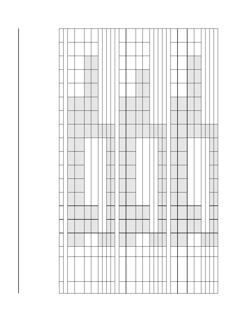
Data Sheet
MARS2G5 P-Pro (TDAT162G52) SONET/SDH
August 18, 2004
155/622/2488 Mbits/s Data Interface
767
Agere Systems Inc.
UTOPIA (UT) Block
(continued)
UT Register Map
(continued)
Table 785. UT Register Map (continued)
Note: Shading denotes reserved bits.
Address
Symbol
Type
15
14
13
12
11
10
9
8
7
6
5
4
3
2
1
0
Channel A3 Registers
0x7048
INTA3
COR/W
FifoAl-
mostFullRx
FifoOver-
flowTx
FifoUnder-
flowTx
FifoOver-
flowRx
ParityEr-
rorTx
0x7049
INTA3m
R/W
FifoAl-
mostFull
RxMask
FifoOver-
flowTx
Mask
FifoUnder-
flow
TxMask
FifoOver-
flow
RxMask
ParityEr-
rorTx
Mask
0x704A
RxPrvA3
R/W
Channel
Enable Rx
RxAddr
ATMSize
Rx
Traffic-
Type Rx
0x704B
TxPrvA3
R/W
Channel
Enable Tx
TxAddr
ATMSize
Tx
Traffic-
Type Tx
0x704C
RxThA3
R/W
IngressThresholdHigh
IngressThresholdLow
0x704D
TxThA3
R/W
EgressThresholdHigh
EgressThresholdLow
0x704E
RxThMinA3
R/W
Ingress ThresholdMin
0x704F
TxThMaxA3
R/W
Egress ThresholdMax
Channel B0 Registers
0x7050
INTB0
COR/W
FifoAl-
mostFullRx
FifoOver-
flowTx
FifoUnder-
flowTx
FifoOver-
flowRx
ParityEr-
rorTx
0x7051
INTB0m
R/W
FifoAl-
mostFull
RxMask
FifoOver-
flowTx
Mask
FifoUnder-
flow
TxMask
FifoOver-
flow
RxMask
ParityEr-
rorTx
Mask
0x7052
RxPrvB0
R/W
Channel
Enable Rx
RxAddr
Gang Fifo
Rx
ATMSize
Rx
Traffic-
Type Rx
0x7053
TxPrvB0
R/W
Channel
Enable Tx
TxAddr
Gang Fifo
Tx
ATMSize
Tx
Traffic-
Type Tx
0x7054
RxThB0
R/W
IngressThresholdHigh
IngressThresholdLow
0x7055
TxThB0
R/W
EgressThresholdHigh
EgressThresholdLow
0x7056
RxThMinB0
R/W
Ingress ThresholdMin
0x7057
TxThMaxB0
R/W
Egress ThresholdMax
Channel B1 Registers
0x7058
INTB1
COR/W
FifoAl-
mostFullRx
FifoOver-
flowTx
FifoUnder-
flowTx
FifoOver-
flowRx
ParityEr-
rorTx
0x7059
INTB1m
R/W
FifoAl-
mostFull
RxMask
FifoOver-
flowTx
Mask
FifoUnder-
flow
TxMask
FifoOver-
flow
RxMask
ParityEr-
rorTx
Mask
0x705A
RxPrvB1
R/W
Channel
Enable Rx
RxAddr
ATMSize
Rx
Traffic-
Type Rx
0x705B
TxPrvB1
R/W
Channel
Enable Tx
TxAddr
ATMSize
Tx
Traffic-
Type Tx
0x705C
RxThB1
R/W
IngressThresholdHigh
IngressThresholdLow
0x705D
TxThB1
R/W
EgressThresholdHigh
EgressThresholdLow
0x705E
RxThMinB1
R/W
Ingress ThresholdMin
0x705F
TxThMaxB1
R/W
Egress ThresholdMax

MARS2G5 P-Pro (TDAT162G52) SONET/SDH
Data Sheet
155/622/2488 Mbits/s Data Interface
August 18, 2004
768
Agere Systems Inc.
UTOPIA (UT) Block
(continued)
UT Register Map
(continued)
Table 785. UT Register Map (continued)
Note: Shading denotes reserved bits.
Address
Symbol
Type
15
14
13
12
11
10
9
8
7
6
5
4
3
2
1
0
Channel B2 Registers
0x7060
INTB2
COR/W
FifoAlmost-
FullRx
FifoOver-
flowTx
FifoUnder-
flowTx
FifoOver-
flowRx
ParityEr-
rorTx
0x7061
INTB2m
R/W
FifoAlmost-
Full
RxMask
FifoOver-
flowTx
Mask
FifoUnder-
flow
TxMask
FifoOver-
flow
RxMask
ParityEr-
rorTx
Mask
0x7062
RxPrvB2
R/W
Channel
Enable Rx
RxAddr
ATMSize
Rx
Traffic-
Type Rx
0x7063
TxPrvB2
R/W
Channel
Enable Tx
TxAddr
ATMSize
Tx
Traffic-
Type Tx
0x7064
RxThB2
R/W
IngressThresholdHigh
IngressThresholdLow
0x7065
TxThB2
R/W
EgressThresholdHigh
EgressThresholdLow
0x7066
RxThMinB2
R/W
Ingress ThresholdMin
0x7067
TxThMaxB2
R/W
Egress ThresholdMax
Channel B3 Registers
0x7068
INTB3
COR/W
FifoAlmost-
FullRx
FifoOver-
flowTx
FifoUnder-
flowTx
FifoOver-
flowRx
ParityEr-
rorTx
0x7069
INTB3m
R/W
FifoAlmost-
Full
RxMask
FifoOver-
flowTx
Mask
FifoUnder-
flow
TxMask
FifoOver-
flow
RxMask
ParityEr-
rorTx
Mask
0x706A
RxPrvB3
R/W
Channel
Enable Rx
RxAddr
ATMSize
Rx
Traffic-
Type Rx
0x706B
TxPrvB3
R/W
Channel
Enable Tx
TxAddr
ATMSize
Tx
Traffic-
Type Tx
0x706C
RxThB3
R/W
IngressThresholdHigh
IngressThresholdLow
0x706D
TxThB3
R/W
EgressThresholdHigh
EgressThresholdLow
0x706E
RxThMinB3
R/W
Ingress ThresholdMin
0x706F
TxThMaxB3
R/W
Egress ThresholdMax
Channel C0 Registers
0x7070
INTC0
COR/W
FifoAlmost-
FullRx
FifoOver-
flowTx
FifoUnder-
flowTx
FifoOver-
flowRx
ParityEr-
rorTx
0x7071
INTC0m
R/W
FifoAlmost-
Full
RxMask
FifoOver-
flowTx
Mask
FifoUnder-
flow
TxMask
FifoOver-
flow
RxMask
ParityEr-
rorTx
Mask
0x7072
RxPrvC0
R/W
Channel
Enable Rx
RxAddr
Gang Fifo
Rx
ATMSize
Rx
Traffic-
Type Rx
0x7073
TxPrvC0
R/W
Channel
Enable Tx
TxAddr
Gang Fifo
Tx
ATMSize
Tx
Traffic-
Type Tx
0x7074
RxThC0
R/W
IngressThresholdHigh
IngressThresholdLow
0x7075
TxThC0
R/W
EgressThresholdHigh
EgressThresholdLow
0x7076
RxThMinC0
R/W
Ingress ThresholdMin
0x7077
TxThMaxC0
R/W
Egress ThresholdMax

Data Sheet
MARS2G5 P-Pro (TDAT162G52) SONET/SDH
August 18, 2004
155/622/2488 Mbits/s Data Interface
769
Agere Systems Inc.
UTOPIA (UT) Block
(continued)
UT Register Map
(continued)
Table 785. UT Register Map (continued)
Note: Shading denotes reserved bits.
Address
Symbol
Type
15
14
13
12
11
10
9
8
7
6
5
4
3
2
1
0
Channel C1 Registers
0x7078
INTC1
COR/W
FifoAl-
mostFullRx
FifoOver-
flowTx
FifoUnder-
flowTx
FifoOver-
flowRx
ParityEr-
rorTx
0x7079
INTC1m
R/W
FifoAl-
mostFull
RxMask
FifoOver-
flowTx
Mask
FifoUnder-
flow
TxMask
FifoOver-
flow
RxMask
ParityEr-
rorTx
Mask
0x707A
RxPrvC1
R/W
Channel
Enable Rx
RxAddr
ATMSize
Rx
Traffic-
Type Rx
0x707B
TxPrvC1
R/W
Channel
Enable Tx
TxAddr
ATMSize
Tx
Traffic-
Type Tx
0x707C
RxThC1
R/W
IngressThresholdHigh
IngressThresholdLow
0x707D
TxThC1
R/W
EgressThresholdHigh
EgressThresholdLow
0x707E
RxThMinC1
R/W
Ingress ThresholdMin
0x707F
TxThMaxC1
R/W
Egress ThresholdMax
Channel C2 Registers
0x7080
INTC2
COR/W
FifoAl-
mostFullRx
FifoOver-
flowTx
FifoUnder-
flowTx
FifoOver-
flowRx
ParityEr-
rorTx
0x7081
INTC2m
R/W
FifoAl-
mostFull
RxMask
FifoOver-
flowTx
Mask
FifoUnder-
flow
TxMask
FifoOver-
flow
RxMask
ParityEr-
rorTx
Mask
0x7082
RxPrvC2
R/W
Channel
Enable Rx
RxAddr
ATMSize
Rx
Traffic-
Type Rx
0x7083
TxPrvC2
R/W
Channel
Enable Tx
TxAddr
ATMSize
Tx
Traffic-
Type Tx
0x7084
RxThC2
R/W
IngressThresholdHigh
IngressThresholdLow
0x7085
TxThC2
R/W
EgressThresholdHigh
EgressThresholdLow
0x7086
RxThMinC2
R/W
Ingress ThresholdMin
0x7087
TxThMaxC2
R/W
Egress ThresholdMax
Channel C3 Registers
0x7088
INTC3
COR/W
FifoAl-
mostFullRx
FifoOver-
flowTx
FifoUnder-
flowTx
FifoOver-
flowRx
ParityEr-
rorTx
0x7089
INTC3m
R/W
FifoAl-
mostFull
RxMask
FifoOver-
flowTx
Mask
FifoUnder-
flow
TxMask
FifoOver-
flow
RxMask
ParityEr-
rorTx
Mask
0x708A
RxPrvC3
R/W
Channel
Enable Rx
RxAddr
ATMSize
Rx
Traffic-
Type Rx
0x708B
TxPrvC3
R/W
Channel
Enable Tx
TxAddr
ATMSize
Tx
Traffic-
Type Tx
0x708C
RxThC3
R/W
IngressThresholdHigh
IngressThresholdLow
0x708D
TxThC3
R/W
EgressThresholdHigh
EgressThresholdLow
0x708E
RxThMinC3
R/W
Ingress ThresholdMin
0x708F
TxThMaxC3
R/W
Egress ThresholdMax
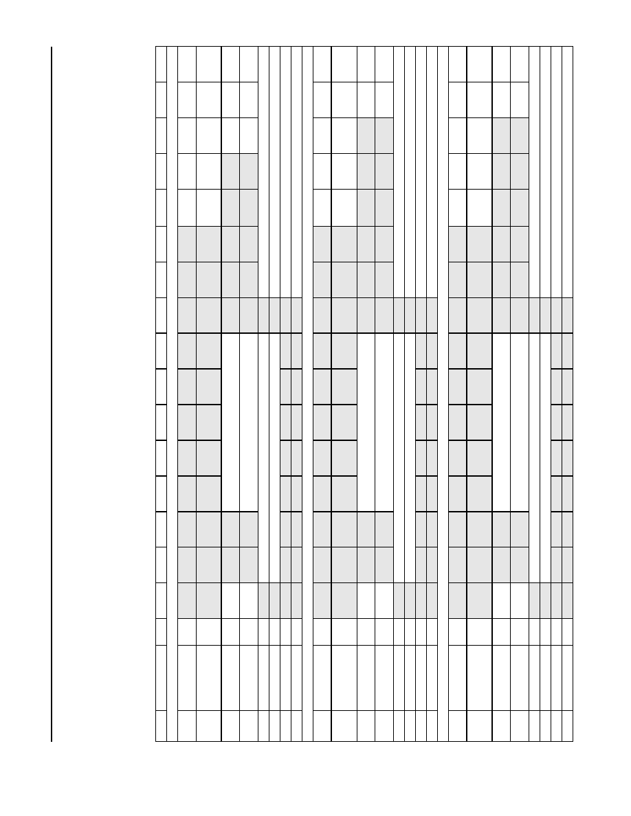
MARS2G5 P-Pro (TDAT162G52) SONET/SDH
Data Sheet
155/622/2488 Mbits/s Data Interface
August 18, 2004
770
Agere Systems Inc.
UTOPIA (UT) Block
(continued)
UT Register Map
(continued)
Table 785. UT Register Map (continued)
Note: Shading denotes reserved bits.
Address
Symbol
Type
15
14
13
12
11
10
9
8
7
6
5
4
3
2
1
0
Channel D0 Registers
0x7090
INTD0
COR/W
FifoAlmost-
FullRx
FifoOver-
flowTx
FifoUnder-
flowTx
FifoOver-
flowRx
ParityEr-
rorTx
0x7091
INTD0m
R/W
FifoAlmost-
Full
RxMask
FifoOver-
flowTx
Mask
FifoUnder-
flow
TxMask
FifoOver-
flow
RxMask
ParityEr-
rorTx
Mask
0x7092
RxPrvD0
R/W
Channel
Enable Rx
RxAddr
Gang Fifo
Rx
ATMSize
Rx
Traffic-
Type Rx
0x7093
TxPrvD0
R/W
Channel
Enable Tx
TxAddr
Gang Fifo
Tx
ATMSize
Tx
Traffic-
Type Tx
0x7094
RxThD0
R/W
IngressThresholdHigh
IngressThresholdLow
0x7095
TxThD0
R/W
EgressThresholdHigh
EgressThresholdLow
0x7096
RxThMinD0
R/W
Ingress ThresholdMin
0x7097
TxThMaxD0
R/W
Egress ThresholdMax
Channel D1 Registers
0x7098
INTD1
COR/W
FifoAlmost-
FullRx
FifoOver-
flowTx
FifoUnder-
flowTx
FifoOver-
flowRx
ParityEr-
rorTx
0x7099
INTD1m
R/W
FifoAlmost-
Full
RxMask
FifoOver-
flowTx
Mask
FifoUnder-
flow
TxMask
FifoOver-
flow
RxMask
ParityEr-
rorTx
Mask
0x709A
RxPrvD1
R/W
Channel
Enable Rx
RxAddr
ATMSize
Rx
Traffic-
Type Rx
0x709B
TxPrvD1
R/W
Channel
Enable Tx
TxAddr
ATMSize
Tx
Traffic-
Type Tx
0x709C
RxThD1
R/W
IngressThresholdHigh
IngressThresholdLow
0x709D
TxThD1
R/W
EgressThresholdHigh
EgressThresholdLow
0x709E
RxThMinD1
R/W
Ingress ThresholdMin
0x709F
TxThMaxD1
R/W
Egress ThresholdMax
Channel D2 Registers
0x70A0
INTD2
COR/W
FifoAlmost-
FullRx
FifoOver-
flowTx
FifoUnder-
flowTx
FifoOver-
flowRx
ParityEr-
rorTx
0x70A1
INTD2m
R/W
FifoAlmost-
Full
RxMask
FifoOver-
flowTx
Mask
FifoUnder-
flow
TxMask
FifoOver-
flow
RxMask
ParityEr-
rorTx
Mask
0x70A2
RxPrvD2
R/W
Channel
Enable Rx
RxAddr
ATMSize
Rx
Traffic-
Type Rx
0x70A3
TxPrvD2
R/W
Channel
Enable Tx
TxAddr
ATMSize
Tx
Traffic-
Type Tx
0x70A4
RxThD2
R/W
IngressThresholdHigh
IngressThresholdLow
0x70A5
TxThD2
R/W
EgressThresholdHigh
EgressThresholdLow
0x70A6
RxThMinD2
R/W
Ingress ThresholdMin
0x70A7
TxThMaxD2
R/W
Egress ThresholdMax
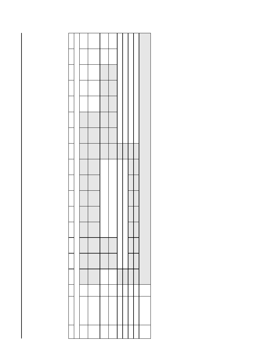
Data Sheet
MARS2G5 P-Pro (TDAT162G52) SONET/SDH
August 18, 2004
155/622/2488 Mbits/s Data Interface
771
Agere Systems Inc.
UTOPIA (UT) Block
(continued)
UT Register Map
(continued)
Table 785. UT Register Map (continued)
Note: Shading denotes reserved bits.
Address
Symbol
Type
15
14
13
12
11
10
9
8
7
6
5
4
3
2
1
0
Channel D3 Registers
0x70A8
INTD3
COR/W
FifoAl-
mostFullRx
FifoOver-
flowTx
FifoUnder-
flowTx
FifoOver-
flowRx
ParityEr-
rorTx
0x70A9
INTD3m
R/W
FifoAl-
mostFull
RxMask
FifoOver-
flowTx
Mask
FifoUnder-
flow
TxMask
FifoOver-
flow
RxMask
ParityEr-
rorTx
Mask
0x70AA
RxPrvD3
R/W
Channel
Enable Rx
RxAddr
ATMSize
Rx
Traffic-
Type Rx
0x70AB
TxPrvD3
R/W
Channel
Enable Tx
TxAddr
ATMSize
Tx
Traffic-
Type Tx
0x70AC
RxThD3
R/W
IngressThresholdHigh
IngressThresholdLow
0x70AD
TxThD3
R/W
EgressThresholdHigh
EgressThresholdLow
0x70AE
RxThMinD3
R/W
Ingress ThresholdMin
0x70AF
TxThMaxD3
R/W
Egress ThresholdMax
0x70B0
--
0x73FF
--
--
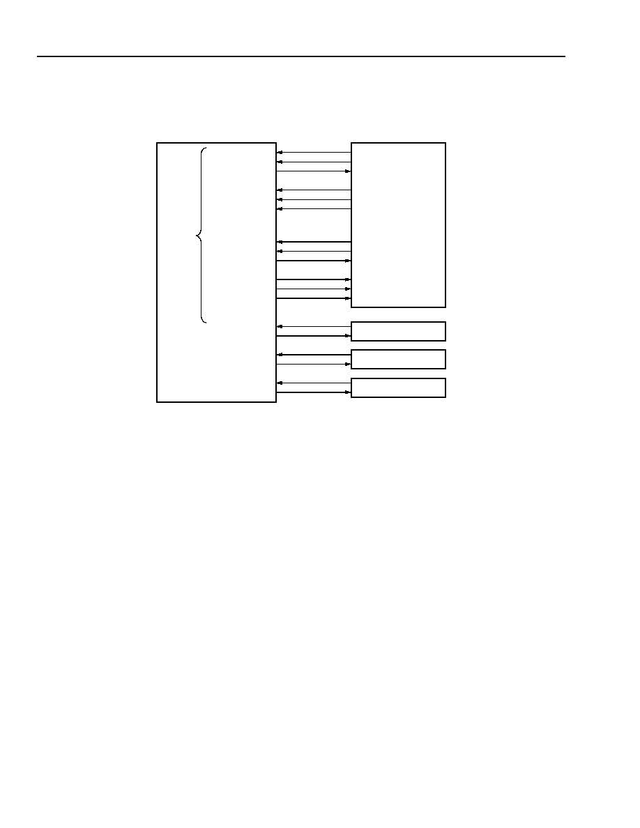
MARS2G5 P-Pro (TDAT162G52) SONET/SDH
Data Sheet
155/622/2488 Mbits/s Data Interface
August 18, 2004
772
Agere Systems Inc.
System Interface
ATM Interfaces
5-7412(F)r.4TDAT
Figure 110. Quad 16-Bit ATM Level 2
TXCLK
TXENB
TXCLAV
TXDATA[15:0]
TXPRTY
TXSOC
RXCLK
RXENB
RXCLAV
RXDATA[15:0]
RXPRTY
RXSOC
TXCLK[A]
TXENB[A]
TXPA[A]
TXDATA[15:0][A]
TXPRTY[A]
TXSOP[A]
RXCLK[A]
RXENB[A]
RXPA[A]
RXDATA[15:0][A]
RXPRTY[A]
RXSOP[A]
A
T
M
LI
NK
LA
Y
E
R DE
V
I
CE
DEVICE #2
DEVICE #3
DEVICE #4
TXSZ[A]
TXEOP[A]
TXERR[A]
RXSZ[A]
RXEOP[A]
RXERR[A]
AG
E
R
E MA
R
S
2G
5 P-P
r
o D
E
V
I
C
E
IN
TE
R
F
AC
E
A
INTERFACE B
INTERFACE C
INTERFACE D
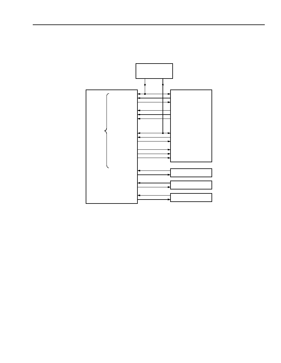
Data Sheet
MARS2G5 P-Pro (TDAT162G52) SONET/SDH
August 18, 2004
155/622/2488 Mbits/s Data Interface
773
Agere Systems Inc.
System Interface
(continued)
ATM Interfaces
(continued)
5-7413(F)r.4TDAT
Figure 111. Quad 8-Bit ATM Level 3
TXCLK
TXENB
TXCLAV
TXDATA[7:0]
TXPRTY
TXSOC
RXCLK
RXENB
RXCLAV
RXDATA[7:0]
RXPRTY
RXSOC
A
T
M
LINK
LA
Y
E
R DE
V
I
C
E
DEVICE #2
DEVICE #3
DEVICE #4
TXCLK[A]
TXENB[A]
TXPA[A]
TXDATA[7:0][A]
TXPRTY[A]
TXSOP[A]
RXCLK[A]
RXENB[A]
RXPA[A]
RXDATA[7:0][A]
RXEOP[A]
RXERR[A]
TXSZ[A]
TXEOP[A]
TXERR[A]
RXSZ[A]
RXPRTY[A]
RXSOP[A]
A
G
E
R
E MA
R
S
2
G
5
P-
Pr
o
D
E
V
I
C
E
IN
T
E
R
F
A
C
E A
INTERFACE B
INTERFACE C
INTERFACE D
TXCLK
RXCLK
CLOCKS
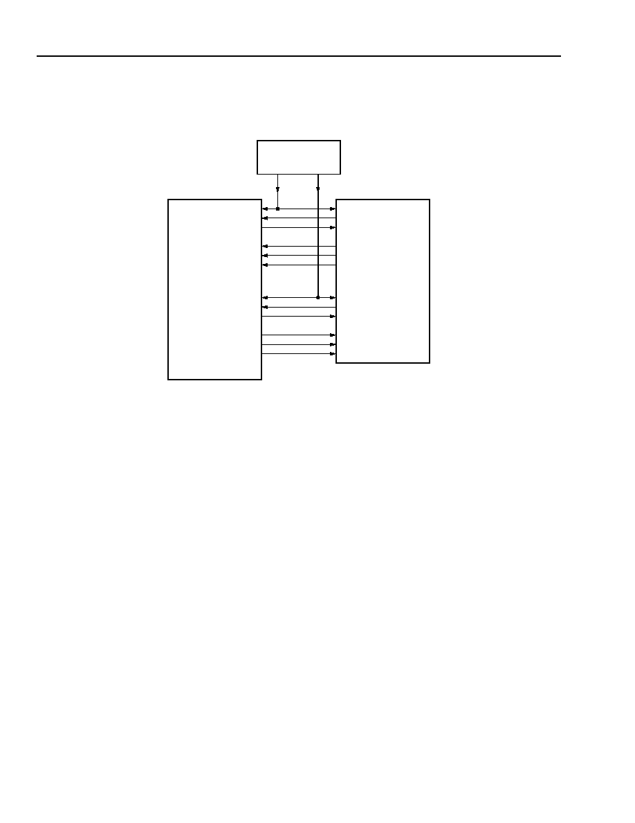
MARS2G5 P-Pro (TDAT162G52) SONET/SDH
Data Sheet
155/622/2488 Mbits/s Data Interface
August 18, 2004
774
Agere Systems Inc.
System Interface
(continued)
ATM Interfaces
(continued)
5-7414(F)r.3TDAT
Note: In 32-bit mode, both A and B clocks must be connected.
Figure 112. Single 32-Bit ATM Level 3
TXCLK
TXENB
TXCLAV
TXDATA[31:0]
TXPRTY
TXSOC
RXCLK
RXENB
RXCLAV
RXDATA[31:0]
RXPRTY
RXSOC
TXCLK[A:B]
TXENB[A]
TXPA[A]
TXDATA[15:0][A:B]
TXPRTY[A]
TXSOP[A]
RXCLK[A:B]
RXENB[A]
RXPA[A]
RXDATA[15:0][A:B]
RXPRTY[A]
RXSOP[A]
AT
M D
E
V
I
C
E
TXSZ[A:B]
TXEOP[A]
TXERR[A]
RXSZ[A]
RXEOP[A]
RXERR[A]
TXCLK
RXCLK
CLOCKS
A
G
E
R
E M
A
R
S
2G5 P-
Pro D
E
V
I
C
E
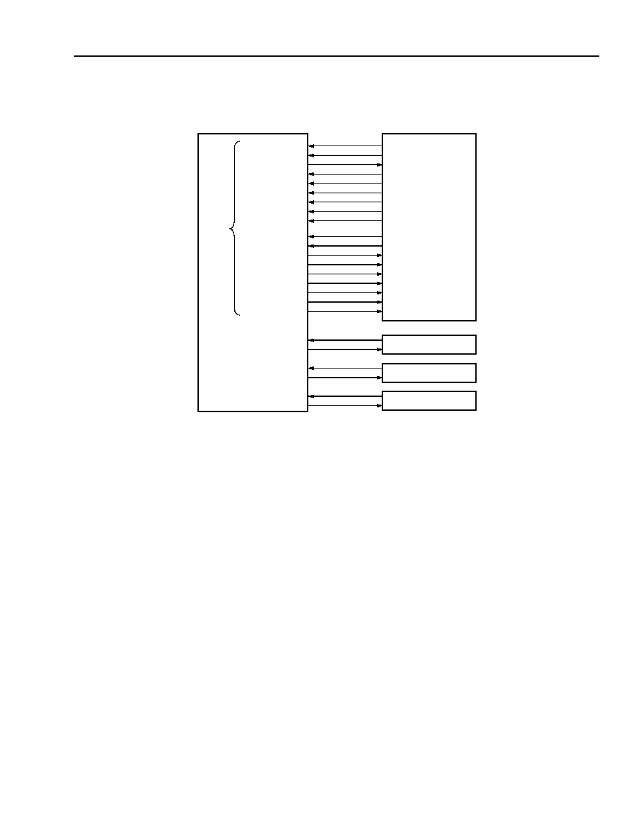
Data Sheet
MARS2G5 P-Pro (TDAT162G52) SONET/SDH
August 18, 2004
155/622/2488 Mbits/s Data Interface
775
Agere Systems Inc.
System Interface
(continued)
POS Interfaces
5-7415(F)r.3TDAT
Figure 113. Quad 16-Bit POS Level 2
TFCLK
TENB
TDAT[15:0]
TPRTY
TSOP
RFCLK
RENB
RPA
RDAT[15:0]
RPRTY
RSOP
P
O
S
CUS
TOME
R
L
O
GIC
DEVICE #2
DEVICE #3
DEVICE #4
TPA
TMOD
TEOP
TERR
RMOD
REOP
RERR
TXCLK[A]
TXENB[A]
TXPA[A]
TXDATA[15:0][A]
TXPRTY[A]
TXSOP[A]
RXCLK[A]
RXENB[A]
RXPA[A]
RXDATA[15:0][A]
RXPRTY[A]
RXSOP[A]
TXSZ[A]
TXEOP[A]
TXERR[A]
RXSZ[A]
RXEOP[A]
RXERR[A]
IN
T
E
R
F
A
C
E A
INTERFACE B
INTERFACE C
INTERFACE D
AGE
R
E MA
R
S
2
G
5
P-
P
r
o D
E
V
I
C
E

MARS2G5 P-Pro (TDAT162G52) SONET/SDH
Data Sheet
155/622/2488 Mbits/s Data Interface
August 18, 2004
776
Agere Systems Inc.
System Interface
(continued)
POS Interface
(continued)
5-7416(F)r.4TDAT
Figure 114. Quad 8-Bit POS Level 3
AGE
R
E MA
R
S
2
G
5
P-
P
r
o
D
E
V
I
C
E
TFCLK
TENB
TDAT[7:0]
TPRTY
TSOP
RFCLK
RENB
RFA
RDAT[7:0]
RPRTY
RSOP
P
O
S
CUS
TO
M
E
R
LOGI
C
DEVICE #2
DEVICE #3
DEVICE #4
TPA
TMOD
TEOP
TERR
RMOD
REOP
RERR
TXCLK[A]
TXENB[A]
TXPA[A]
TXDATA[7:0][A]
TXPRTY[A]
TXSOP[A]
RXCLK[A]
RXENB[A]
RXPA[A]
RXDATA[7:0][A]
RXPRTY[A]
RXSOP[A]
TXSZ[A]
TXEOP[A]
TXERR[A]
RXSZ[A]
RXPRTY[A]
RXSOP[A]
RXEOP[A]
RXERR[A]
TXCLK
RXCLK
CLOCKS
INT
E
RFA
C
E A
INTERFACE B
INTERFACE C
INTERFACE D
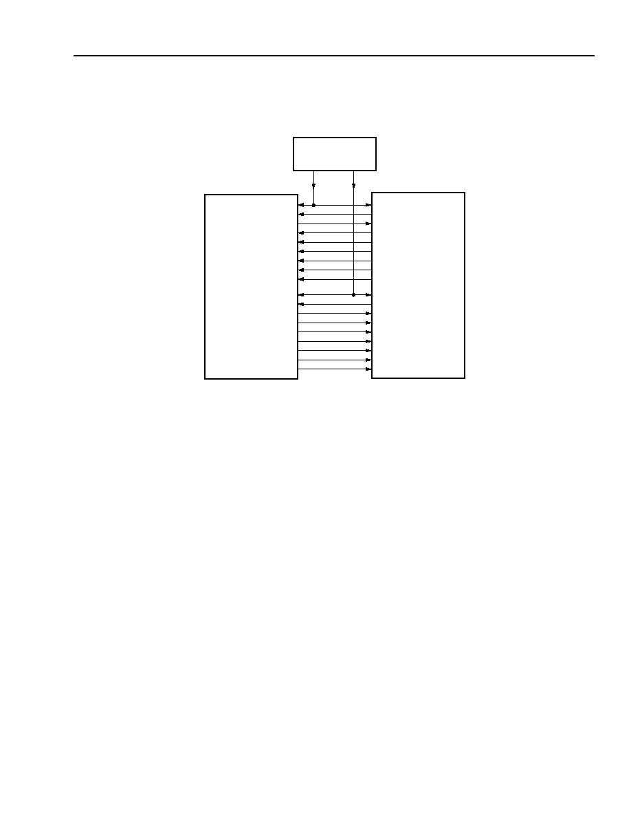
Data Sheet
MARS2G5 P-Pro (TDAT162G52) SONET/SDH
August 18, 2004
155/622/2488 Mbits/s Data Interface
777
Agere Systems Inc.
System Interface
(continued)
POS Interface
(continued)
5-7417(F)r.4TDAT
Note: In 32-bit mode, both A and B clocks must be connected.
Figure 115. Single 32-Bit POS Level 3
TFCLK
TENB
TDAT[31:0]
TPRTY
TSOP
RFCLK
RENB
RPA
RDAT[31:0]
RPRTY
RSOP
POS
D
E
VI
C
E
TPA
TMOD[1:0]
TEOP
TERR
RMOD[1:0]
REOP
RERR
TXCLK[A:B]
TXENB[A]
TXPA[A]
TXDATA[15:0][A:B]
TXPRTY[A]
TXSOP[A]
RXCLK[A:B]
RXENB[A]
RXPA[A]
RXDATA[15:0][A:B]
RXPRTY[A]
RXSOP[A]
TXSZ[A:B]
TXEOP[A]
TXERR[A]
RXSZ[A]
RXEOP[A]
RXERR[A]
TXCLK
RXCLK
CLOCKS
AG
ER
E
M
A
R
S
2
G
5
P
-
Pr
o
D
E
VI
C
E

MARS2G5 P-Pro (TDAT162G52) SONET/SDH
Data Sheet
155/622/2488 Mbits/s Data Interface
August 18, 2004
778
Agere Systems Inc.
Test
Scan
This device supports the IEEE 1149.1 JTAG interface for memory BIST, boundary scan, and 32-bit ID register
instructions.
Table 786. JTAG ID Register Codings
Boundary Scan
Full boundary scan is supported on this device. Boundary scan is activated from the JTAG port.
RAM BIST
Embedded memories support BIST. The BIST algorithm is activated from the JTAG port.
JTAG ID Bit
Device Version 2.1 Device Version 2.2 Device Version 2.3
31
1
1
1
30
0
0
0
29
0
1
1
28
1
0
0
Device ID 27
0
0
0
26
0
0
0
25
0
0
0
24
0
0
0
23
0
0
0
22
1
1
1
21
0
0
0
20
0
0
0
19
0
0
0
18
0
0
0
17
1
1
1
16
0
0
0
15
0
0
0
14
1
1
1
13
1
1
1
12
0
0
0
Manufacturer ID 11
0
0
0
10
0
0
0
9
1
1
1
8
1
1
1
7
0
0
0
6
0
0
0
5
1
1
1
4
0
0
0
3
0
0
0
2
0
0
0
1
0
0
0
0
1
1
1

Data Sheet
MARS2G5 P-Pro (TDAT162G52) SONET/SDH
August 18, 2004
155/622/2488 Mbits/s Data Interface
779
Agere Systems Inc.
Absolute Maximum Ratings
Stresses in excess of the absolute maximum ratings can cause permanent damage to the device. These are abso-
lute stress ratings only. Functional operation of the device is not implied at these or any other conditions in excess
of those given in the operations sections of this data sheet. Exposure to absolute maximum ratings for extended
periods can adversely affect device reliability. External leads can be safely soldered or bonded at temperatures up
to 300
∞
C.
* This maximum rating only applies when the device is powered up with V
DDD
.
Depending on the application for both the 792 PBGA and 600 LBGA, a heat sink may be required (suggested heat sink assembly for 600-pin
LBGA package (ChipCoolers part number HST357-D with airflow of 400 LFPM) or equivalent.
Handling Precautions
Although electrostatic discharge (ESD) protection circuitry has been designed into this device, proper precautions
must be taken to avoid exposure to ESD and electrical overstress (EOS) during all handling, assembly, and test
operations. Agere employs a human-body model (HBM) and a charged-device model (CDM) qualification require-
ment in order to determine ESD-susceptibility limits and protection design evaluation. ESD voltage thresholds are
dependent on the circuit parameters used in each of the models, as defined by JEDEC's JESD22-A114 (HBM) and
JESD22-C101 (CDM) standards.
Table 787. ESD Threshold Voltage
Parameter
Symbol
Min
Max
Unit
Storage Temperature
T
stg
≠65
125
∞
C
V
DDD
Power Supply Voltage
--
GND ≠ 0.5
V
DDD
+ 0.5*
V
V
DDD2
Power Supply Voltage
--
GND ≠ 0.5
V
DDD2
+ 0.5*
V
Total Power Dissipation
MARS2G5 P-Pro
MARS1G2 P-Pro
MARS622 P-Pro
P
DT
--
--
--
6.13
2.91
2.62
W
W
W
Device
Minimum HBM Threshold
Minimum CDM Threshold
Low Speed Pins High Speed Pins
LVDS Pins
All Pins Except LVDS
MARS2G5 P-Pro
792-Pin PBGA
>2000 V
>1000 V
>200 V
>500 V
MARS2G5 P-Pro
600-Pin LBGA
>2000 V
>1000 V
>200 V
>500 V
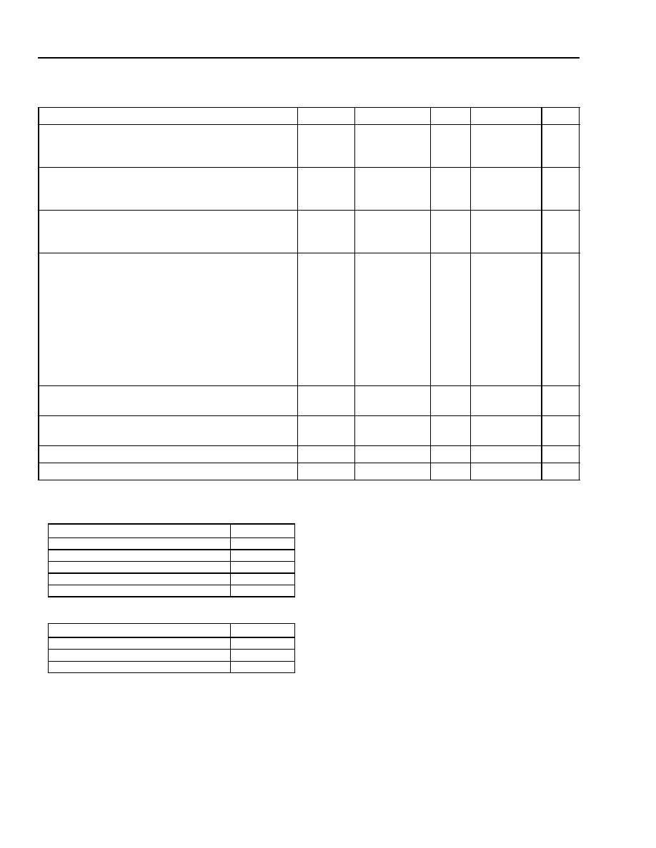
MARS2G5 P-Pro (TDAT162G52) SONET/SDH
Data Sheet
155/622/2488 Mbits/s Data Interface
August 18, 2004
780
Agere Systems Inc.
Operating Conditions
* For core voltage less than 1.5 V, the device has the following restrictions: UTOPIA C and UTOPIA D are only functional at 52 MHz or less.
The thermal resistance junction to case,
JC
, of the 600 LBGA package is 0.4 ∞C/W
.
The thermal resistance junction to ambient (to the
nearest 0.5 ∞C/W),
JA
, of the 600 LBGA package is given in the following table:
The thermal resistance junction to case,
JC
, of the 792 PBGA package is 1.7 ∞C/W
.
The thermal resistance junction to ambient (to the
nearest 0.5 ∞C/W),
JA
, of the 792 PBGA package is given in the following table:
Depending on the application for both the 792 PBGA and 600 LBGA a heat sink may be required (suggested heat sink assembly for 600-pin
LBGA package (ChipCoolers part number HST357-D with airflow of 400 LFPM) or equivalent.
Parameter
Symbol
Min
Typ
Max
Unit
Power Supply Voltage:
3.3 V I/O
1.5 V Core
V
DDD
V
DDD2
3.165
1.42
*
3.3
1.6
3.465
1.68
V
V
Low-level Input Voltage:
LVTTL
LVPECL
V
ILLVTTL
V
ILLVPECL
GND ≠ 0.3
V
DDD
≠ 1.810
--
--
0.8
V
DDD
≠ 1.475
V
V
High-level Input Voltage:
LVTTL
LVPECL
V
IHLVTTL
V
IHLVPECL
2.0
V
DDD
≠ 1.165
--
--
5.5
V
DDD
≠ 0.880
V
V
Power Dissipation
MARS2G5 P-Pro Total:
3.3 V I/O
1.6 V Core (Typical)
MARS1G2 P-Pro Total:
3.3 V I/O
1.6 V Core (Typical)
MARS622 P-Pro Total:
3.3 V I/O
1.6 V Core (Typical)
P
DTTDAT16
--
--
--
--
--
--
--
--
--
5.33
3.50
1.83
2.42
1.16
1.26
2.18
1.06
1.12
5.87
3.85
2.02
2.66
1.28
1.39
2.40
1.17
1.23
W
W
W
W
W
W
W
W
W
OC-48 Contraclocking 1x PLL 1.6 V Analog Power
Supply Current @ 1.68 V
I
PLL_VDDA
--
8.5
9.35
mA
OC-48 Contraclocking 1x PLL 1.6 V Digital Power
Supply @ 1.68 V
I
PLL_VDDD
--
1.5
1.65
mA
Junction Temperature Range
T
J
≠40
--
125
∞
C
Ambient Operating Temperature Range
T
A
≠40
--
85
∞
C
Air Speed in Linear Feet per Minute (LFPM)
JA
(∞C/W)
JEDEC Standard Natural Convection
9
100
8
200
6.5
500
6
800
5
Air Speed in Linear Feet per Minute (LFPM)
JA
(∞C/W)
JEDEC Standard Natural Convection
9.9
200
6.5
500
5.8

Data Sheet
MARS2G5 P-Pro (TDAT162G52) SONET/SDH
August 18, 2004
155/622/2488 Mbits/s Data Interface
781
Agere Systems Inc.
Electrical Characteristics
Table 788. LVTTL 3.3 V Logic Interface Characteristics
These logic levels are TTL 5 V compliant.
Parameter
Symbol
Test Conditions
Min
Max
Unit
Input Leakage Current
I
L
--
--
20
µA
Output Voltage:
Low
MPU_INTN,
MPU_DTN,
RXDATA[A--D][0--15],
RXEOP[A--D],
RXERR[A--D],
RXPPA[A--D],
RXPRTY[A--D],
RXSOP[A--D],
RXSPA[A--D],
RXSZ[A--D],
TXPPA[A--D],
TXSPA[A--D],
TDO
GPIO[3--0],
RXTOHCLK[A--D],
RXTOHD[A--D],
RXTOHF[A--D],
RXREF,
TXTOHCLK,
TXTOHF
High
MPU_DTN,
RXDATA[A--D][0--15],
RXEOP[A--D],
RXERR[A--D],
RXPPA[A--D],
RXPRTY[A--D],
RXSOP[A--D],
RXSPA[A--D],
RXSZ[A--D],
TXPPA[A--D],
TXSPA[A--D],
TDO
GPIO[3--0],
RXTOHCLK[A--D],
RXTOHD[A--D],
RXTOHF[A--D],
RXREF,
TXTOHCLK,
TXTOHF
V
OLLVTTL
V
OHLVTTL
≠10 mA
≠6 mA
10 mA
6 mA
GND
2.4
0.4
V
DDD
V
V
Input Capacitance
C
I
--
--
5.2
pF
Load Capacitance
C
L
--
--
--
pF

MARS2G5 P-Pro (TDAT162G52) SONET/SDH
Data Sheet
155/622/2488 Mbits/s Data Interface
August 18, 2004
782
Agere Systems Inc.
Electrical Characteristics
(continued)
Table 789. LVPECL 3.3 V Logic Interface Characteristics
V
DDD
has a range of 3.165 V < V
DDD
< 3.465 V, V
DDD
typical = 3.3 V.
* With a differential input swing of 100 mV minimum.
Parameter
Symbol
Min
Typical
Max
Unit
Input Leakage Current
I
L
--
--
20
µA
Input Common-mode Voltage Range*
V
CMR
0.8
--
2.6
V
Output Voltage:
Low
High
V
OLLVPECL
V
OHLVPECL
V
DDD
≠ 1.97
V
DDD
≠ 1.025
--
V
DDD
≠ 1.620
V
DDD
≠ 0.72
V
V
Output Voltage Swing
V
OSWING
0.595
--
1.25
V
Input Capacitance
C
I
--
--
2.3
pF
Load Capacitance
C
L
--
--
0.4
pF
Input Buffer Gain
V
G
--
125
--
dB
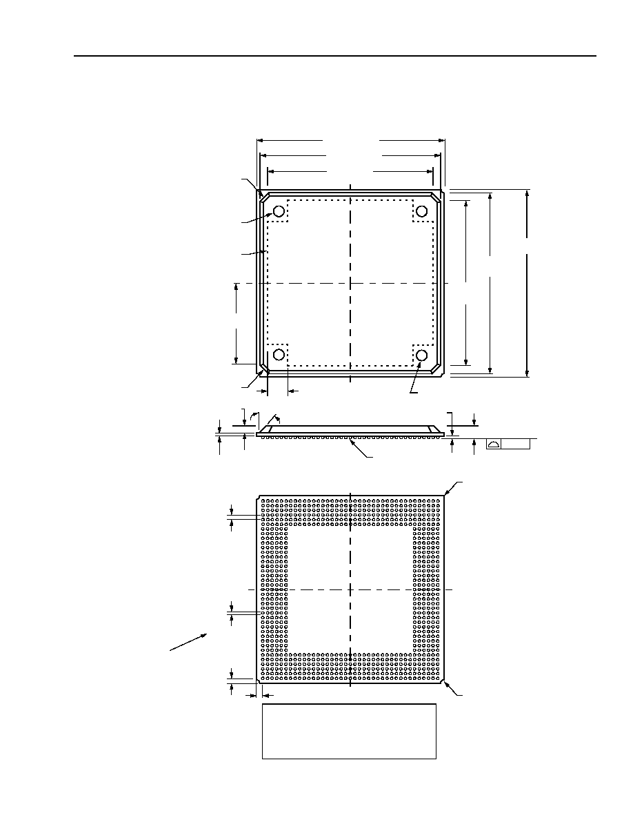
Data Sheet
MARS2G5 P-Pro (TDAT162G52) SONET/SDH
August 18, 2004
155/622/2488 Mbits/s Data Interface
783
Agere Systems Inc.
Outline Diagrams
792-Pin PBGA
5-9800(F)ar.2
SEATING PLANE
SOLDER BALL
0.20
40.00
40.00
A1 BALL PAD
T
D
H
AL
F
K
B
P
M
L
J
AH
R
C
E
Y
N
U
AN
G
AD
V
AM
AJ
AG
AE
AC
AA
W
AP
AK
AF
AB
AR
A
A1 BALL PAD
CORNER
CORNER
19
30
26
28
24
32
22 20 18
4
6
8
10
12
14
16
2
34
5
23
25
7
31 29
15
21
3
27
11
17
9
13
1
35 33
35.35
35.35 MAX
2.28
±
0.21
AU
AT
AV
AW
36
38
37
39
1.00
TOP VIEW
SIDE VIEW
BOTTOM VIEW
0.50 R,
3 PLACES
1.00
1.00
MAX
38.70
+0.70
≠0.05
38.70
+0.70
≠0.05
A1 BALL PAD
INDICATOR
4x 45∫
CHAMFER
COUNTRY OF
ORIGIN INDICATOR
AVAILABLE
MARKING AREA
8x 4.33
17.72
0.61
±
0.06
1.17
±
0.05
0.50
±
0.10
30∫ TYP
THE CONTROLLING DIMENSIONS
ARE IN MILLIMETERS.
THIS DWG. CONFORMS TO JEDEC STDS.
REF. DWG.-- 81949
0.63
+0.07
≠0.13
SOLDER BALL
DIAMETER PRIOR
TO BEING ATTACHED
TO THE PACKAGE
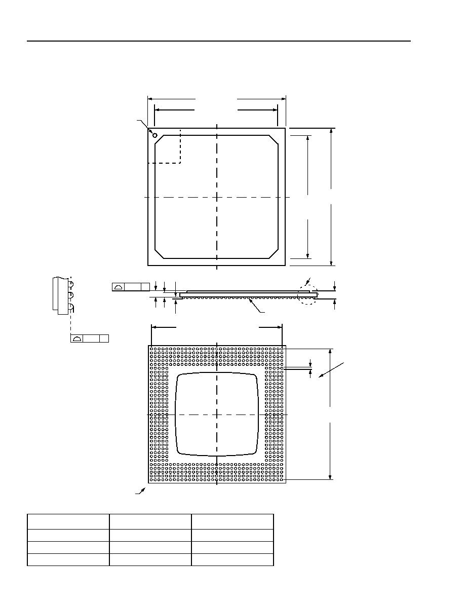
MARS2G5 P-Pro (TDAT162G52) SONET/SDH
Data Sheet
155/622/2488 Mbits/s Data Interface
August 18, 2004
784
Agere Systems Inc.
Outline Diagrams
(continued)
600-Pin LBGA
Table 790. Substrate Thickness
A
B
C
1.16 ± 0.10
1.66 ± 0.20
2.26 ± 0.30
1.14 ± 0.10
1.64 ± 0.20
2.24 ± 0.30
1.11 ± 0.10
1.61 ± 0.20
2.21 ± 0.30
A
SOLDER BALL
0.60
0.15
45.0
45.00
A1 BALL
T
D
H
AL
F
K
B
P
M
L
J
AH
R
C
E
Y
N
U
AN
G
AD
V
AM
AJ
AG
AE
AC
AA
W
AP
AK
AF
AB
AR
A
19
30
26 28
24
32
22
20
18
4
6
8 10
12
14
16
2
34
5
23
25
7
31
29
15
21
3
27
11
17
9
13
1
35
33
34 SPACES @ 1.27 = 43.18
34 SPACES
A1 BALL
0.75
±
0.15
IDENTIFIER ZONE
@ 1.27 = 43.18
CORNER
44.00
44.00 ± 0.15
SOLDER BALL
DIAMETER PRIOR
TO BEING ATTACHED
TO THE PACKAGE
±
0.15
B
C
Z
See Detail C
0.15 Z
Z
LOWEST BALL REFERENCE PLANE
(PARALLEL TO GLOBAL PLANE)
Data Sheet
MARS2G5 P-Pro (TDAT162G52) SONET/SDH
August 18, 2004
155/622/2488 Mbits/s Data Interface
785
Agere Systems Inc.
Ordering Information
* Contact Agere Systems for other package options.
These devices are only for existing customers using earlier versions of the device. All new customers are required to use the current 792-pin
package device (please contact Marketing with any questions).
Note: All references for the 600 LBGA found in this document are meant as support for existing customers. All new
customers are required to use the current 792-pin package device (please contact Marketing with any ques-
tions).
Device Code
Version
Package*
Temperature
Comcode
(Ordering Number)
Derivatives
TDAT162G52-BA23
V2.3
792-pin PBGA
≠40
∞
C to +85
∞
C
700058140
TDAT162G52-3BAL
V2.2
792-pin PBGA
≠40
∞
C to +85
∞
C
700048364M
M-TDAT162G52-3BAL2
V2.0
792-pin PBGA
≠40
∞
C to +85
∞
C
700023755M
Low-Speed Device
TDAT161G2-BA23
V2.3
792-pin PBGA
≠40
∞
C to +85
∞
C
700058138
TDAT12622-BA23
V2.3
792-pin PBGA
≠40
∞
C to +85
∞
C
700058137

MARS2G5 P-Pro (TDAT162G52) SONET/SDH
Data Sheet
155/622/2488 Mbits/s Data Interface
August 18, 2004
786
Agere Systems Inc.
MARS2G5 P-Pro (TDAT162G52) (Version 2.2 and 2.3 Only)
GFP Payload Area CRC-32 Insertion (Version 2.2 and 2.3 Only)
GFP block upgrade on transmit and receive to calculate the CRC-32 over only the payload information area.
MARS2G5 P-Pro (version 2.0/2.1) calculated CRC-32 over everything except the PLI field.
Two modes are supported for CRC-32 insertion/checking.
1. Null-extension headers.
∑ 4-byte header.
∑ Calculation starts after PLI field and 4 bytes of TYPE field.
2. Linear-extension headers.
∑ 8-byte header.
∑ Calculation starts after PLI field and 4 bytes of TYPE field and 4 bytes of EXT header field.
PLI field value will be modified on transmit by +4 to include CRC-32 bytes.
PLI field value will be modified on receive by ≠4 when CRC-32 is stripped.
MARS2G5 P-Pro (version 2.2 and 2.3) does not touch PFI field value because it will corrupt tHEC.
MPU Register Descriptions
Table 24. MPU_VERR[0--5], Version Control Registers (RO)
TOHP-48 Register Descriptions
Table 60. TOHP_MODE_VERR, Mode (R/W) and Block Version (RO)
Address
Bit
Name
Function
Reset
Default
0x0000
15:0
MPU_VER0
Indicates version number for version 2.2.
0x0227
Indicates version number for version 2.3.
0x0237
Address
Bit
Name
Function
Reset
Default
0x0800
15:13
TOHP_RX_MODE[2:0] Receive Direction Mode. TOHP_RX_MODE[2], bit
15, has two functions: default value for the registers
and the number of errored frames required before
declaring and OOF condition in the framer.
[2] 1 = SDH, 0 = SONET
[1] 1= OC-48, 0 = OC-3/12
[0] 1 = OC-12, 0 = OC-3
011
12:10
TOHP_TX_MODE[2:0]
Transmit Direction Mode. TOHP_TX_MODE[2], bit
12, has two functions: default value for the registers
and the number of errored frames required before
declaring and OOF condition in the framer.
[2] 1 = SDH, 0 = SONET
[1] 1 = OC-48, 0 = OC-3/12
[0] 1 = OC-12, 0 = OC-3
011
9:0
TOHP_VER[9:0]
Block Version Number. Block version register will
change each time the device is changed.
0000000
00
1

Data Sheet
MARS2G5 P-Pro (TDAT162G52) SONET/SDH
August 18, 2004
155/622/2488 Mbits/s Data Interface
787
Agere Systems Inc.
MARS2G5 P-Pro (TDAT162G52) (Version 2.2 and 2.3 Only)
(continued)
TOHP-48 Register Descriptions
(continued)
Table 66. TOHP_CNTD[A--D][1--2], 0x081A--0x0821, Continuous N-Times Detect (CNTD) Values (R/W)
Address
Bit
Name
Function
Reset
Default
0x081A,
0x081C,
0x081E,
0x0820
15:12
TOHP_CNTDK2
[A--D][3:0]
Continuous N-Times Detect for K2[2:0] Byte.
The valid range for this register is 0x3--0xF.
Invalid values will be mapped to a value of 0x3.
In STS-48 mode, CNTDK2[A] is valid.
0x3
11:8
TOHP_CNTDK1K2
[A--D][3:0]
Continuous N-Times Detect for APS (K1,
K2[7:3]) Byte. The valid range for this register is
0x3--0xF. Invalid values will be mapped to a
value of 0x3. In STS-48 mode, CNTDK1K2[A] is
valid.
0x3
7:4
TOHP_CNTDF1[A--D][3:0] Continuous N-Times Detect for F1 Byte. The
valid range for this register is 0x3--0xF. Invalid
values will be mapped to a value of 0x3. In
STS-48 mode, CNTDF1[A] is valid.
0x3
3:0
TOHP_CNTDJ0Z0
[A--D][3:0]
Continuous N-Times Detect for J0Z0 Bytes.
The valid range for this register is 0x3--0xF.
Invalid values will be mapped to a value of 0x3.
In STS-48 mode, CNTDJ0Z0[A] is valid.
0x3
0x081B,
0x081D,
0x081F,
0x0821
15:13
--
Reserved.
0x0
12
--
APS Babble.
0 = Use either K1 and K2[7:3] or K1 and K2[7:0]
1 = K1 only
--
11:8
TOHP_CNTDS1BABLE
[A--D][3:0]
Continuous N-Times Detect for S1 Byte Bab-
bling. The valid range for this register is 0x3--
0xF. Invalid values will be mapped to a value of
0x3. In STS-48 mode,
TOHP_CNTDS1BABLE[A] is valid.
0x5
7:4
TOHP_CNTDS1
[A--D][3:0]
Continuous N-Times Detect for S1 Byte. The
valid range for this register is 0x3--0xF. Invalid
values will be mapped to a value of 0x3. In
STS-48 mode, TOHP_CNTDS1[A] is valid.
0x3
3:0
TOHP_CNTDK1K2FRAME
[A--D][3:0]
Continuous N-Times Detect for APS Frame.
The valid range for this register is 0x3--0xF.
Invalid values will be mapped to a value of 0x3.
In STS-48 mode, TOHP_CNTDK1K2FRAME[A]
is valid.
0xC

MARS2G5 P-Pro (TDAT162G52) SONET/SDH
Data Sheet
155/622/2488 Mbits/s Data Interface
August 18, 2004
788
Agere Systems Inc.
MARS2G5 P-Pro (TDAT162G52) (Version 2.2 and 2.3 Only)
(continued)
TOHP-48 Register Descriptions
(continued)
Table 75. TOHP_SF_SETR[A--D][1--2], 0x0852--0x0859, Signal Fail Set BER Algorithm Control Registers
[1--2] (R/W)*
* See page 208 for the description of reading and writing parameters of more than 16 bits.
Address
Bit
Name
Function
Reset
Default
0x0852,
0x0854,
0x0856,
0x0858
15:0
TOHP_SFNSSET
[A--D][17:2]
Signal Fail Ns Set. Number of frames in a mon-
itoring block for signal fail (SF) of slice[A--D] is
equal to TOHP_SFNSSET[A--D][17:0], respec-
tively.
0x00000
0x0853,
0x0855,
0x0857,
0x0859
1:0
TOHP_SFNSSET
[A--D][1:0]
0x0853,
0x0855,
0x0857,
0x0859
15:10
TOHP_SFMSET
[A--D][5:0]
Signal Fail M Set. Threshold of the number of
bad monitoring blocks in an observation interval.
If the number of bad blocks is above this thresh-
old, then signal fail is set.
0x00
9:2
TOHP_SFLSET[A--D][7:0] Signal Fail L Set. Error threshold for determin-
ing if a monitoring block is bad.
0x00
Data Sheet
MARS2G5 P-Pro (TDAT162G52) SONET/SDH
August 18, 2004
155/622/2488 Mbits/s Data Interface
789
Agere Systems Inc
MARS2G5 P-Pro (TDAT162G52) (Version 2.2 and 2.3 Only)
(continued)
DE Register Descriptions
Table 717. Rx Payload Type and Payload Control Summary Table
* No discard--pass all ATM cells with no error correction.
Discard--discard cells with multiple-bit header errors. Correct and pass all cells with single-bit header errors.
Smart discard--discard cells with multiple-bit header errors, and only correct and pass the first of back-to-back single-bit header errors.
Table 717. Rx Payload Type and Payload Control Summary Table (continued)
Note: This is an expansion of Table 717 for Rx payload type CRC GFP bits [12:10] and applies to only version 2.2 and 2.3 of the device.
Payload Control[12:0]
Type[15:13] 12 11
10
9
8
7
6
5
4
3
2
1
0
000
PPP
0 = discard
1 = no discard
Bit Sync
1 = no invert
0 = invert
0 = byte sync
1 = bit sync
0 = header
stripped
1 = header
on
0 = CRC-16
1 = CRC-32
0 = CRC stripped
1 = CRC on
0 = CRC reversed
1 = CRC normal
0 = no dry mode
1 = dry mode
00 = no unscrambling
01 = post-unscrambling
10 = pre-unscrambling
11 = undefined
001
CRC
Bit Sync
1 = no invert
0 = invert
0 = byte sync
1 = bit sync
0 = CRC-16
1 = CRC-32
0 = CRC stripped
1 = CRC on
0 = CRC reversed
1 = CRC normal
0 = no dry mode
1 = dry mode
00 = no unscrambling
01 = post-unscrambling
10 = pre-unscrambling
11 = undefined
010
HDLC
Bit Sync
1 = no invert
0 = invert
0 = byte sync
1 = bit sync
0 = no dry mode
1 = dry mode
00 = no unscrambling
01 = post-unscrambling
10 = pre-unscrambling
11 = undefined
011
ATM
0 = X
43
scrambler 0 = scrambler on
1 = scrambler off
0 = byte sync
1 = bit sync
Unassigned Cell
0 = discard
1 = passthrough
0 = idle cell discard
1 = idle cell
passthrough
00 = no discard*
01 = discard
10 = smart discard
11 = undefined
100
GFP
0 = X
43
scrambler
1 = X
48
scrambler
0 = scrambler on
1 = scrambler off
0 = byte sync
1 = bit sync
0 = length
stripped
1 = length on
Length offset = 0x0 to 0xF
101
CRC GFP
See Table below for
description of bits [12:10].
0 = X
43
scrambler
1 = X
48
scrambler
0 = scrambler on
1 = scrambler off
0 = byte sync
1 = bit sync
0 = length
stripped
1 = length on
0 = CRC-16
1 = CRC-32
0 = CRC stripped
1 = CRC on
Length offset = 0x0 to 0xF
110
Transparent
Payload
0 = no align
1 = frame align
111
Not defined
12
11
10
0 = Indicates non-GFP mode.
1 = Must be set to1 in CRC-GFP mode.
0 = PLI field unchanged.
1 = Subtract four from the PLI field if the CRC-32 bytes
are stripped.
0 = Start CRC calculation after first 32 bits of payload (i.e.,
assume null extension header.
1 = Start CRC calculation after first 64 bits of payload (i.e.,
assume linear extension header.
MARS2G5 P-Pro (TDAT162G52) SONET/SDH
Data Sheet
155/622/2488 Mbits/s Data Interface
August 18, 2004
790
Agere Systems Inc
MARS2G5 P-Pro (TDAT162G52) (Version 2.2 and 2.3 Only)
(continued)
DE Register Descriptions
(continued)
Table 741. Tx Payload Type and Payload Control Summary Table
Table 741. Tx Payload Type and Payload Control Summary Table (continued)
Note: This is an expansion of Table 741 for Rx payload type CRC GFP bits [12:10] and applies to only version 2.2 and 2.3
of the device.
Payload Control[12:0]
Payload
Type[15:13]
12
11
10
9
8
7
6
5
4
3
2
1
0
000
PPP
0 = leading
1 = trailing
00 = 1 flag between packet
01 = 2 flags between packets
10 = 3 flags between packets
11 = 4 flags between packets
Bit-Sync Inter-Pckg-Fill
0 = 7E
1 = FF
Bit Sync
1 = no invert
0 = invert
0 = HDLC byte
1 = HDLC bit
0 = CRC-16
1 = CRC-32
0 = CRC reversed
1 = CRC normal
0 = no dry mode
1 = dry mode
00 = no scrambling
01 = postscrambling
10 = prescrambling
11 = undefined
001
CRC
0 = leading
1 = trailing
00 = 1 flag between packet
01 = 2 flags between packets
10 = 3 flags between packets
11 = 4 flags between packets
Bit-Sync Inter-Pckg-Fill
0 = 7E
1 = FF
Bit Sync
1 = no invert
0 = invert
0 = HDLC byte
1 = HDLC bit
0 = CRC-16
1 = CRC-32
0 = CRC reversed
1 = CRC normal
0 = no dry mode
1 = dry mode
00 = no scrambling
01 = postscrambling
10 = prescrambling
11 = undefined
010
HDLC
0 = leading
1 = trailing
00 = 1 flag between packet
01 = 2 flags between packets
10 = 3 flags between packets
11 = 4 flags between packets
Bit-Sync Inter-Pckg-Fill
0 = 7E
1 = FF
Bit Sync
1 = no invert
0 = invert
0 = HDLC byte
1 = HDLC bit
0 = no dry mode
1 = dry mode
00 = no scrambling
01 = postscrambling
10 = prescrambling
11 = undefined
011
ATM
0 = X
43
scrambler
0 = scrambler on
1 = scrambler off
100
GFP
0 = X
43
scrambler
1 = X
48
scrambler
0 = scrambler on
1 = scrambler off
101
CRC GFP
See Table below for description of bits
[12:10].
0 = X
43
scrambler
1 = X
48
scrambler
0 = scrambler on
1 = scrambler off
0 = CRC-16
1 = CRC-32
110
Transparent
Payload
111
Not Defined
12
11
10
0 = Indicates non-GFP mode.
1 = Must be set to 1 in CRC-GFP mode.
0 = PLI field unchanged.
1 = Add four to the PLI field to include CRC-32 bytes.
0 = Start CRC calculation after first 32 bits of payload (i.e.,
assume null extension header).
1 = Start CRC calculation after first 64 bits of payload (i.e.,
assume linear extension header).

Data Sheet
MARS2G5 P-Pro (TDAT162G52) SONET/SDH
August 18, 2004
155/622/2488 Mbits/s Data Interface
791
Agere Systems Inc.
MARS2G5 P-Pro (TDAT162G52) (Version 2.3 Only)
DE Register Descriptions
Table 690. General Registers (RO)
Table 725. GFP Interrupt Masks R/W
Address
Bit
Name
Function
Reset
Default
0x6000
15:8
--
Reserved.
0x00
7:0
DE_VERSION[7:0]
Version ID. The version of the block will increment each
time a change occurs to the block functionality.
Indicates version number for version 2.0.
0x02
Indicates version number for version 2.2.
0x03
Indicates version number for version 2.3.
0x07
Address
Bit
Name
Function
Reset
Default
0x65C0
--
0x65CF
--
GFP_IRQEN_CH0
--
GFP_IRQEN_CH15
GFP Interrupt Mask Channel 0--15. When active
(logic 1), the associated event/delta is inhibited from
contributing to the interrupt on a per-channel basis.
0x00FF
15:8
--
Reserved.
0x00
7
--
B_Message Reception.
0x1
6
--
A_Message Reception.
0x1
5
--
Uncorrectable Special Payload Error.
0x1
4
--
Uncorrectable Bit Error.
0x1
3
--
Reserved. Must be set to 1.
0x1
2
--
Single Bit Error.
0x1
1
--
Scrambler Out of Sync.
0x1
0
--
Framer State Mask Bit. Must be set to 1.
0x1

MARS2G5 P-Pro (TDAT162G52) SONET/SDH
Data Sheet
155/622/2488 Mbits/s Data Interface
August 18, 2004
792
Agere Systems Inc.
MARS2G5 P-Pro (TDAT162G52) (Version 2.3 Only)
(continued)
DE Register Descriptions
(continued)
Determining the Per-Channel Framer State
Bit 4 and bit 0 of registers 0x6600--0x660F (Table 727. GFP Interrupts (COW)) are used to determine the per-
channel framer state. The following table indicates the per-channel framer state (see bit 0 of registers 0x6600--
0x660F (Table 727. GFP Interrupts (COW))).
Table 726. Per-Channel Framer State
Table 727. GFP Interrupts (COW)
Uncorrectable Bit Error
(Bit 4)
Framer State
(Bit 0)
Per-Channel Framer State
0
0
Out of frame
0
1
In frame
1
0
Undefined (Not Possible)
1
1
Framing was lost since the last read of this register. Perform
a COW and then read again to confirm if framing is still lost.
Address
Bit
Name
Function
Reset
Default
0x6600
--
0x660F
--
GFP_IRQ_CH0
--
GFP_IRQ_CH15
GFP Interrupt Channel 0--15. Used to record various
occurrences within the GFP framer. The bits will generate
an interrupt if defined by the interrupt mask, but the register
values here are independent of the interrupt mask values.
0x0000
15:8
--
Reserved.
0x00
7
--
B_Message Reception.
0x0
6
--
A_Message Reception.
0x0
5
--
Uncorrectable Special Payload Error.
0x0
4
--
Uncorrectable Bit Error.
0x0
3
--
Reserved.
0x0
2
--
Single Bit Error.
0x0
1
--
Scrambler Out of Sync.
0x0
0
--
Framer State. This bit is a state bit and must always be
masked to prevent constant presentation of an
interrupt to the MPU. Bit 0 of registers 0x65C0--0x65CF
(Table 725. GFP Interrupt Masks R/W) is the mask bit.
The value contained in this bit will persist until a COW is
performed, or until a transition (from 0 to 1) occurs on the
signal. To determine the per-channel frame state, see Table
726. Per-Channel Framer State.
0x0

Data Sheet
MARS2G5 P-Pro (TDAT162G52) SONET/SDH
August 18, 2004
155/622/2488 Mbits/s Data Interface
793
Agere Systems Inc.
Appendix: Line Loopback Block
Introduction
This is a feature offered for testing purposes only, to allow line loopback. The example of the loopback configura-
tion script is available upon on request. Please contact your Agere Representative for details.
Table 791. Loopback Mode
Address
Bit
Name
Function
Reset
Default
0◊2080
15:12
--
Reserved.
0
11:8
--
Loopback Mode for Streams A--D.
0 = Loopback Mode.
Bit 11 = Stream A.
Bit 10 = Stream B.
Bit 9 = Stream C.
Bit 8 = Stream D.
0
7:4
--
W/P MUX Control Selection for Line Loopback Stream
A--D.
0
3:0
--
Reserved.
0
0◊2090
15:12
--
Stream A MUX Control.
1111 = Line Loopback Mode.
0
0
11:8
--
Stream B MUX Control. MUX control settings as per
stream A control.
0
7:4
--
Stream C MUX Control. MUX control settings as per
stream A control.
0
3:0
--
Stream D MUX Control. MUX control settings as per
stream A control.
0
0◊2091
15
--
Reserved.
0
14:12
--
Stream A MUX Control.
000 = Line Loopback.
0
11
--
Reserved.
0
10:8
--
Stream B MUX Control. MUX control settings as per
stream A control.
0
7
--
Reserved.
0
6:4
--
Stream C MUX Control. MUX control settings as per
stream A control.
0
3
--
Reserved.
0
2:0
--
Stream D MUX Control. MUX control settings as per
stream A control.
0
0◊2094
15:0
--
Reserved.
0
0◊2300
15:12
--
Reserved.
0
11:0
--
Selection of Line Loopback.
0 = Line Loopback selected.
0
0◊2301,
0◊2302,
0◊2303
15:12
--
Reserved.
--
11:0
--
Selection of Line Loopback.
0

MARS2G5 P-Pro (TDAT162G52) SONET/SDH
Data Sheet
155/622/2488 Mbits/s Data Interface
August 18, 2004
794
Agere Systems Inc.
0◊2310,
0◊2311,
0◊2312,
0◊2313
15:12
--
Reserved.
--
11:0
--
Selection of Line Loopback.
0
0◊2330
15:10
--
Reserved.
0
9:5
--
Line Loopback Mode.
0 = No override.
4:0
--
Control for Line Loopback Mode.
0 = Line Loopback.
0
0◊2333
15:4
--
Reserved.
0
3:0
--
Control for W/P Line Loopback Mode Stream A--D.
0 = Line Loopback.
0
0◊2334
15:0
--
Reserved.
0
0◊2360--
0◊236B
15:9
--
Reserved.
0
8:0
--
Audited Line Loopback Time Slot 1--12.
0
0◊2500
15:9
--
Reserved.
0
8:6
--
Stream A, Time Slot 1 Mapping.
000 = Line Loopback Mode input port selection.
Others = Unused.
0
5:4
--
Reserved.
0
3:0
--
Reserved.
0
0◊2501--
0◊250B
15:9
--
Reserved.
--
8:0
--
Stream A, Time Slot 2--12 Mapping.
0
Appendix: Line Loopback Block
Introduction
This is a feature offered for testing purposes only, to allow line loopback. The example of the loopback configura-
tion script is available upon on request. Please contact your Agere Representative for details.
Table 791. Loopback Mode
Address
Bit
Name
Function
Reset
Default

Data Sheet
MARS2G5 P-Pro (TDAT162G52) SONET/SDH
August 18, 2004
155/622/2488 Mbits/s Data Interface
795
Agere Systems Inc.
Appendix: Loopback Block
(continued)
Loopback Register Descriptions
(continued)
Table 792. Connection Memory Map (WO)
Note: Use audit memories to read the connection maps
Address
Bit
Name
Function
Reset
Default
0x2520
15:9
--
Reserved.
0
8:0
--
Line Loopback Mode Stream A.
0
0x2521
15:9
--
Reserved.
0
8:0
--
Line Loopback Mode Stream A.
0
0x2522
15:9
--
Reserved.
0
8:0
--
Line Loopback Mode Stream A.
0
0x2523
15:9
--
Reserved.
0
8:0
--
Line Loopback Mode Stream A.
0
0x2524
15:9
--
Reserved.
0
8:0
--
Line Loopback Mode Stream A.
0
0x2525
15:9
--
Reserved.
0
8:0
--
Line Loopback Mode Stream A.
0
0x2526
15:9
--
Reserved.
0
8:0
--
Line Loopback Mode Stream A.
0
0x2527
15:9
--
Reserved.
0
8:0
--
Line Loopback Mode Stream A.
0
0x2528
15:9
--
Reserved.
0
8:0
--
Line Loopback Mode Stream A.
0
0x2529
15:9
--
Reserved.
0
8:0
--
Line Loopback Mode Stream A.
0
0x2530
15:9
--
Reserved.
0
8:0
--
Line Loopback Mode Stream A.
0
0x2531
15:9
--
Reserved.
0
8:0
--
Line Loopback Mode Stream A.
0
0x2532
15:9
--
Reserved.
0
8:0
--
Line Loopback Mode Stream A.
0
0x2533
15:9
--
Reserved.
0
8:0
--
Line Loopback Mode Stream A.
0
0x2534
15:9
--
Reserved.
0
8:0
--
Line Loopback Mode Stream A.
0
0x2535
15:9
--
Reserved.
0
8:0
--
Line Loopback Mode Stream A.
0
0x2536
15:9
--
Reserved.
0
8:0
--
Line Loopback Mode Stream A.
0

MARS2G5 P-Pro (TDAT162G52) SONET/SDH
Data Sheet
155/622/2488 Mbits/s Data Interface
August 18, 2004
796
Agere Systems Inc.
0x2537
15:9
--
Reserved.
0
8:0
--
Line Loopback Mode Stream A.
0
0x2540
15:9
--
Reserved.
0
8:0
--
Line Loopback Mode Stream B.
0
0x2541
15:9
--
Reserved.
0
8:0
--
Line Loopback Mode Stream B.
0
0x2542
15:9
--
Reserved.
0
8:0
--
Line Loopback Mode Stream B.
0
0x2543
15:9
--
Reserved.
0
8:0
--
Line Loopback Mode Stream B.
0
0x2544
15:9
--
Reserved.
0
8:0
--
Line Loopback Mode Stream B.
0
0x2545
15:9
--
Reserved.
0
8:0
--
Line Loopback Mode Stream B.
0
0x2546
15:9
--
Reserved.
0
8:0
--
Line Loopback Mode Stream B.
0
0x2547
15:9
--
Reserved.
0
8:0
--
Line Loopback Mode Stream B.
0
0x2548
15:9
--
Reserved.
0
8:0
--
Line Loopback Mode Stream B.
0
0x2549
15:9
--
Reserved.
0
8:0
--
Line Loopback Mode Stream B.
0
0x2550
15:9
--
Reserved.
0
8:0
--
Line Loopback Mode Stream B.
0
0x2551
15:9
--
Reserved.
0
8:0
--
Line Loopback Mode Stream B.
0
0x2552
15:9
--
Reserved.
0
8:0
--
Line Loopback Mode Stream B.
0
0x2553
15:9
--
Reserved.
0
8:0
--
Line Loopback Mode Stream B.
0
0x2554
15:9
--
Reserved.
0
8:0
--
Line Loopback Mode Stream B.
0
0x2555
15:9
--
Reserved.
0
8:0
--
Line Loopback Mode Stream B.
0
Appendix: Loopback Block
(continued)
Loopback Register Descriptions
(continued)
Table 792. Connection Memory Map (WO)
Note: Use audit memories to read the connection maps
Address
Bit
Name
Function
Reset
Default

Data Sheet
MARS2G5 P-Pro (TDAT162G52) SONET/SDH
August 18, 2004
155/622/2488 Mbits/s Data Interface
797
Agere Systems Inc.
0x2556
15:9
--
Reserved.
0
8:0
--
Line Loopback Mode Stream B.
0
0x2557
15:9
--
Reserved.
0
8:0
--
Line Loopback Mode Stream B.
0
0x2560
15:9
--
Reserved.
0
8:0
--
Line Loopback Mode Stream B.
0
0x2561
15:9
--
Reserved.
0
8:0
--
Line Loopback Mode Stream B.
0
0x2561
15:9
--
Reserved.
0
8:0
--
Line Loopback Mode Stream B.
0
0x2562
15:9
--
Reserved.
0
8:0
--
Line Loopback Mode Stream B.
0
0x2563
15:9
--
Reserved.
0
8:0
--
Line Loopback Mode Stream B.
0
0x2564
15:9
--
Reserved.
0
8:0
--
Line Loopback Mode Stream B.
0
0x2565
15:9
--
Reserved.
0
8:0
--
Line Loopback Mode Stream B.
0
0x2566
15:9
--
Reserved.
0
8:0
--
Line Loopback Mode Stream B.
0
0x2567
15:9
--
Reserved.
0
8:0
--
Line Loopback Mode Stream B.
0
0x2568
15:9
--
Reserved.
0
8:0
--
Line Loopback Mode Stream B.
0
0x2569
15:9
--
Reserved.
0
8:0
--
Line Loopback Mode Stream B.
0
0x2570
15:9
--
Reserved.
0
8:0
--
Line Loopback Mode Stream B.
0
0x2571
15:9
--
Reserved.
0
8:0
--
Line Loopback Mode Stream B.
0
0x2572
15:9
--
Reserved.
0
8:0
--
Line Loopback Mode Stream B.
0
0x2573
15:9
--
Reserved.
0
8:0
--
Line Loopback Mode Stream B.
0
Appendix: Loopback Block
(continued)
Loopback Register Descriptions
(continued)
Table 792. Connection Memory Map (WO)
Note: Use audit memories to read the connection maps
Address
Bit
Name
Function
Reset
Default

MARS2G5 P-Pro (TDAT162G52) SONET/SDH
Data Sheet
155/622/2488 Mbits/s Data Interface
August 18, 2004
798
Agere Systems Inc.
0x2574
15:9
--
Reserved.
0
8:0
--
Line Loopback Mode Stream B.
0
0x2575
15:9
--
Reserved.
0
8:0
--
Line Loopback Mode Stream B.
0
0x2576
15:9
--
Reserved.
0
8:0
--
Line Loopback Mode Stream B.
0
0x2577
15:9
--
Reserved.
0
8:0
--
Line Loopback Mode Stream B.
0
0x2580
15:9
--
Reserved.
0
8:0
--
Line Loopback Mode Stream C.
0
0x2581
15:9
--
Reserved.
0
8:0
--
Line Loopback Mode Stream C.
0
0x2582
15:9
--
Reserved.
0
8:0
--
Line Loopback Mode Stream C.
0
0x2583
15:9
--
Reserved.
0
8:0
--
Line Loopback Mode Stream C.
0
0x2584
15:9
--
Reserved.
0
8:0
--
Line Loopback Mode Stream C.
0
0x2585
15:9
--
Reserved.
0
8:0
--
Line Loopback Mode Stream C.
0
0x2586
15:9
--
Reserved.
0
8:0
--
Line Loopback Mode Stream C.
0
0x2587
15:9
--
Reserved.
0
8:0
--
Line Loopback Mode Stream C.
0
0x2588
15:9
--
Reserved.
0
8:0
--
Line Loopback Mode Stream C.
0
0x2589
15:9
--
Reserved.
0
8:0
--
Line Loopback Mode Stream C.
0
0x2590
15:9
--
Reserved.
0
8:0
--
Line Loopback Mode Stream C.
0
0x2591
15:9
--
Reserved.
0
8:0
--
Line Loopback Mode Stream C.
0
0x2592
15:9
--
Reserved.
0
8:0
--
Line Loopback Mode Stream C.
0
Appendix: Loopback Block
(continued)
Loopback Register Descriptions
(continued)
Table 792. Connection Memory Map (WO)
Note: Use audit memories to read the connection maps
Address
Bit
Name
Function
Reset
Default

Data Sheet
MARS2G5 P-Pro (TDAT162G52) SONET/SDH
August 18, 2004
155/622/2488 Mbits/s Data Interface
799
Agere Systems Inc.
0x2593
15:9
--
Reserved.
0
8:0
--
Line Loopback Mode Stream C.
0
0x2594
15:9
--
Reserved.
0
8:0
--
Line Loopback Mode Stream C.
0
0x2595
15:9
--
Reserved.
0
8:0
--
Line Loopback Mode Stream C.
0
0x2596
15:9
--
Reserved.
0
8:0
--
Line Loopback Mode Stream C.
0
0x2597
15:9
--
Reserved.
0
8:0
--
Line Loopback Mode Stream C.
0
0x25A0
15:9
--
Reserved.
0
8:0
--
Line Loopback Mode Stream C.
0
0x25A1
15:9
--
Reserved.
0
8:0
--
Line Loopback Mode Stream C.
0
0x25A2
15:9
--
Reserved.
0
8:0
--
Line Loopback Mode Stream C.
0
0x25A3
15:9
--
Reserved.
0
8:0
--
Line Loopback Mode Stream C.
0
0x25A4
15:9
--
Reserved.
0
8:0
--
Line Loopback Mode Stream C.
0
0x25A5
15:9
--
Reserved.
0
8:0
--
Line Loopback Mode Stream C.
0
0x25A6
15:9
--
Reserved.
0
8:0
--
Line Loopback Mode Stream C.
0
0x25A7
15:9
--
Reserved.
0
8:0
--
Line Loopback Mode Stream C.
0
0x25A8
15:9
--
Reserved.
0
8:0
--
Line Loopback Mode Stream C.
0
0x25A9
15:9
--
Reserved.
0
8:0
--
Line Loopback Mode Stream C.
0
0x25B0
15:9
--
Reserved.
0
8:0
--
Line Loopback Mode Stream C.
0
0x25B1
15:9
--
Reserved.
0
8:0
--
Line Loopback Mode Stream C.
0
Appendix: Loopback Block
(continued)
Loopback Register Descriptions
(continued)
Table 792. Connection Memory Map (WO)
Note: Use audit memories to read the connection maps
Address
Bit
Name
Function
Reset
Default

MARS2G5 P-Pro (TDAT162G52) SONET/SDH
Data Sheet
155/622/2488 Mbits/s Data Interface
August 18, 2004
800
Agere Systems Inc.
0x25B2
15:9
--
Reserved.
0
8:0
--
Line Loopback Mode Stream C.
0
0x25B3
15:9
--
Reserved.
0
8:0
--
Line Loopback Mode Stream C.
0
0x25B4
15:9
--
Reserved.
0
8:0
--
Line Loopback Mode Stream C.
0
0x25B5
15:9
--
Reserved.
0
8:0
--
Line Loopback Mode Stream C.
0
0x25B6
15:9
--
Reserved.
0
8:0
--
Line Loopback Mode Stream C.
0
0x25B7
15:9
--
Reserved.
0
8:0
--
Line Loopback Mode Stream C.
0
0x25C0
15:9
--
Reserved.
0
8:0
--
Line Loopback Mode Stream D.
0
0x25C1
15:9
--
Reserved.
0
8:0
--
Line Loopback Mode Stream D.
0
0x25C2
15:9
--
Reserved.
0
8:0
--
Line Loopback Mode Stream D.
0
0x25C3
15:9
--
Reserved.
0
8:0
--
Line Loopback Mode Stream D.
0
0x25C4
15:9
--
Reserved.
0
8:0
--
Line Loopback Mode Stream D.
0
0x25C5
15:9
--
Reserved.
0
8:0
--
Line Loopback Mode Stream D.
0
0x25C6
15:9
--
Reserved.
0
8:0
--
Line Loopback Mode Stream D.
0
0x25C7
15:9
--
Reserved.
0
8:0
--
Line Loopback Mode Stream D.
0
0x25C8
15:9
--
Reserved.
0
8:0
--
Line Loopback Mode Stream D.
0
0x25C9
15:9
--
Reserved.
0
8:0
--
Line Loopback Mode Stream D.
0
0x25D0
15:9
--
Reserved.
0
8:0
--
Line Loopback Mode Stream D.
0
Appendix: Loopback Block
(continued)
Loopback Register Descriptions
(continued)
Table 792. Connection Memory Map (WO)
Note: Use audit memories to read the connection maps
Address
Bit
Name
Function
Reset
Default

Data Sheet
MARS2G5 P-Pro (TDAT162G52) SONET/SDH
August 18, 2004
155/622/2488 Mbits/s Data Interface
801
Agere Systems Inc.
0x25D1
15:9
--
Reserved.
0
8:0
--
Line Loopback Mode Stream D.
0
0x25D2
15:9
--
Reserved.
0
8:0
--
Line Loopback Mode Stream D.
0
0x25D3
15:9
--
Reserved.
0
8:0
--
Line Loopback Mode Stream D.
0
0x25D4
15:9
--
Reserved.
0
8:0
--
Line Loopback Mode Stream D.
0
0x25D5
15:9
--
Reserved.
0
8:0
--
Line Loopback Mode Stream D.
0
0x25D6
15:9
--
Reserved.
0
8:0
--
Line Loopback Mode Stream D.
0
0x25D7
15:9
--
Reserved.
0
8:0
--
Line Loopback Mode Stream D.
0
0x25E0
15:9
--
Reserved.
0
8:0
--
Line Loopback Mode Stream D.
0
0x25E1
15:9
--
Reserved.
0
8:0
--
Line Loopback Mode Stream D.
0
0x25E2
15:9
--
Reserved.
0
8:0
--
Line Loopback Mode Stream D.
0
0x25E3
15:9
--
Reserved.
0
8:0
--
Line Loopback Mode Stream D.
0
0x25E4
15:9
--
Reserved.
0
8:0
--
Line Loopback Mode Stream D.
0
0x25E5
15:9
--
Reserved.
0
8:0
--
Line Loopback Mode Stream D.
0
0x25E6
15:9
--
Reserved.
0
8:0
--
Line Loopback Mode Stream D.
0
0x25E7
15:9
--
Reserved.
0
8:0
--
Line Loopback Mode Stream D.
0
0x25E8
15:9
--
Reserved.
0
8:0
--
Line Loopback Mode Stream D.
0
0x25E9
15:9
--
Reserved.
0
8:0
--
Line Loopback Mode Stream D.
0
Appendix: Loopback Block
(continued)
Loopback Register Descriptions
(continued)
Table 792. Connection Memory Map (WO)
Note: Use audit memories to read the connection maps
Address
Bit
Name
Function
Reset
Default

MARS2G5 P-Pro (TDAT162G52) SONET/SDH
Data Sheet
155/622/2488 Mbits/s Data Interface
August 18, 2004
802
Agere Systems Inc.
0x25F0
15:9
--
Reserved.
0
8:0
--
Line Loopback Mode Stream D.
0
0x25F1
15:9
--
Reserved.
0
8:0
--
Line Loopback Mode Stream D.
0
0x25F2
15:9
--
Reserved.
0
8:0
--
Line Loopback Mode Stream D.
0
0x25F3
15:9
--
Reserved.
0
8:0
--
Line Loopback Mode Stream D.
0
0x25F4
15:9
--
Reserved.
0
8:0
--
Line Loopback Mode Stream D.
0
0x25F5
15:9
--
Reserved.
0
8:0
--
Line Loopback Mode Stream D.
0
0x25F6
15:9
--
Reserved.
0
8:0
--
Line Loopback Mode Stream D.
0
0x25F7
15:9
--
Reserved.
0
8:0
--
Line Loopback Mode Stream D.
0
0x2600--
0x2617
15:0
--
Reserved.
Registers 0x2600--0x260B must be set to 0x0000--0x000B
0
0x2620--
0x2637
15:0
--
Reserved.
0
0x2640--
0x2657
15:0
--
Reserved.
Registers 0x2640--0x264B must be set to 0x0010--0x001B
0
0x2660--
0x2677
15:0
--
Reserved.
0
0x2680--
0x2697
15:0
--
Reserved.
Registers 0x2680--0x268B must be set to 0x0020--0x002B
0
0x26A0--
0x26B7
15:0
--
Reserved.
0
0x26C0--
0x26D7
15:0
--
Reserved.
Registers 0x26C0--0x26CB must be set to 0x0030--0x003B
0
0x26E0--
0x26F7
15:0
--
Reserved.
0
0x2700--
0x2717
15:0
--
Reserved.
0
0x2720--
0x2737
15:0
--
Reserved.
0
Appendix: Loopback Block
(continued)
Loopback Register Descriptions
(continued)
Table 792. Connection Memory Map (WO)
Note: Use audit memories to read the connection maps
Address
Bit
Name
Function
Reset
Default

Data Sheet
MARS2G5 P-Pro (TDAT162G52) SONET/SDH
August 18, 2004
155/622/2488 Mbits/s Data Interface
803
Agere Systems Inc.
0x2740--
0x2757
15:0
--
Reserved.
0
0x2760--
0x2777
15:0
--
Reserved.
0
0x2780--
0x2797
15:0
--
Reserved.
0
0x27A0--
0x27B7
15:0
--
Reserved.
0
0x27C0--
0x27D7
15:0
--
Reserved.
0
0x27E0--
0x27F7
15:0
--
Reserved.
0
0x2800--
0x2817
15:0
--
Reserved.
0
0x2820--
0x2837
15:0
--
Reserved.
0
0x2840--
0x2857
15:0
--
Reserved.
0
0x2860--
0x2877
15:0
--
Reserved.
0
0x2880--
0x2897
15:0
--
Reserved.
0
0x28A0--
0x28B7
15:0
--
Reserved.
0
0x28C0--
0x28D7
15:0
--
Reserved.
0
0x28E0--
0x28F7
15:0
--
Reserved.
0
0x2900
15:0
--
Reserved.
0
0x2901
15:0
--
Reserved.
0
0x2902
15:0
--
Reserved.
0
0x2903
15:0
--
Reserved.
0
0x2904
15:0
--
Reserved.
0
0x2905
15:0
--
Reserved.
0
0x2906
15:0
--
Reserved.
0
0x2907
15:0
--
Reserved.
0
0x2908
15:0
--
Reserved.
0
0x2909
15:0
--
Reserved.
0
Appendix: Loopback Block
(continued)
Loopback Register Descriptions
(continued)
Table 792. Connection Memory Map (WO)
Note: Use audit memories to read the connection maps
Address
Bit
Name
Function
Reset
Default

MARS2G5 P-Pro (TDAT162G52) SONET/SDH
Data Sheet
155/622/2488 Mbits/s Data Interface
August 18, 2004
804
Agere Systems Inc.
0x2910
15:0
--
Reserved.
0
0x2911
15:0
--
Reserved.
0
0x2912
15:0
--
Reserved.
0
0x2913
15:0
--
Reserved.
0
0x2914
15:0
--
Reserved.
0
0x2915
15:0
--
Reserved.
0
0x2916
15:0
--
Reserved.
0
0x2917
15:0
--
Reserved.
0
0x2920
15:0
--
Reserved.
0
0x2921
15:0
--
Reserved.
0
0x2922
15:0
--
Reserved.
0
0x2923
15:0
--
Reserved.
0
0x2924
15:0
--
Reserved.
0
0x2925
15:0
--
Reserved.
0
0x2926
15:0
--
Reserved.
0
0x2927
15:0
--
Reserved.
0
0x2928
15:0
--
Reserved.
0
0x2929
15:0
--
Reserved.
0
0x2930
15:0
--
Reserved.
0
0x2931
15:0
--
Reserved.
0
0x2932
15:0
--
Reserved.
0
0x2933
15:0
--
Reserved.
0
0x2934
15:0
--
Reserved.
0
0x2935
15:0
--
Reserved.
0
0x2936
15:0
--
Reserved.
0
0x2937
15:0
--
Reserved.
0
0x2940
15:0
--
Reserved.
0
0x2941
15:0
--
Reserved.
0
0x2942
15:0
--
Reserved.
0
0x2943
15:0
--
Reserved.
0
0x2944
15:0
--
Reserved.
0
0x2945
15:0
--
Reserved.
0
0x2946
15:0
--
Reserved.
0
0x2947
15:0
--
Reserved.
0
Appendix: Loopback Block
(continued)
Loopback Register Descriptions
(continued)
Table 792. Connection Memory Map (WO)
Note: Use audit memories to read the connection maps
Address
Bit
Name
Function
Reset
Default

Data Sheet
MARS2G5 P-Pro (TDAT162G52) SONET/SDH
August 18, 2004
155/622/2488 Mbits/s Data Interface
805
Agere Systems Inc.
0x2948
15:0
--
Reserved.
0
0x2949
15:0
--
Reserved.
0
0x2950
15:0
--
Reserved.
0
0x2951
15:0
--
Reserved.
0
0x2952
15:0
--
Reserved.
0
0x2953
15:0
--
Reserved.
0
0x2954
15:0
--
Reserved.
0
0x2955
15:0
--
Reserved.
0
0x2956
15:0
--
Reserved.
0
0x2957
15:0
--
Reserved.
0
0x2960
15:0
--
Reserved.
0
0x2961
15:0
--
Reserved.
0
0x2962
15:0
--
Reserved.
0
0x2963
15:0
--
Reserved.
0
0x2964
15:0
--
Reserved.
0
0x2965
15:0
--
Reserved.
0
0x2966
15:0
--
Reserved.
0
0x2967
15:0
--
Reserved.
0
0x2968
15:0
--
Reserved.
0
0x2969
15:0
--
Reserved.
0
0x2970
15:0
--
Reserved.
0
0x2971
15:0
--
Reserved.
0
0x2972
15:0
--
Reserved.
0
0x2973
15:0
--
Reserved.
0
0x2974
15:0
--
Reserved.
0
0x2975
15:0
--
Reserved.
0
0x2976
15:0
--
Reserved.
0
0x2977
15:0
--
Reserved.
0
0x2980
15:0
--
Reserved.
0
0x2981
15:0
--
Reserved.
0
0x2982
15:0
--
Reserved.
0
0x2983
15:0
--
Reserved.
0
0x2984
15:0
--
Reserved.
0
0x2985
15:0
--
Reserved.
0
Appendix: Loopback Block
(continued)
Loopback Register Descriptions
(continued)
Table 792. Connection Memory Map (WO)
Note: Use audit memories to read the connection maps
Address
Bit
Name
Function
Reset
Default

MARS2G5 P-Pro (TDAT162G52) SONET/SDH
Data Sheet
155/622/2488 Mbits/s Data Interface
August 18, 2004
806
Agere Systems Inc.
0x2986
15:0
--
Reserved.
0
0x2987
15:0
--
Reserved.
0
0x2988
15:0
--
Reserved.
0
0x2999
15:0
--
Reserved.
0
0x2990
15:0
--
Reserved.
0
0x2991
15:0
--
Reserved.
0
0x2992
15:0
--
Reserved.
0
0x2993
15:0
--
Reserved.
0
0x2994
15:0
--
Reserved.
0
0x2995
15:0
--
Reserved.
0
0x2996
15:0
--
Reserved.
0
0x2997
15:0
--
Reserved.
0
0x29A0
15:0
--
Reserved.
0
0x29A1
15:0
--
Reserved.
0
0x29A2
15:0
--
Reserved.
0
0x29A3
15:0
--
Reserved.
0
0x29A4
15:0
--
Reserved.
0
0x29A5
15:0
--
Reserved.
0
0x29A6
15:0
--
Reserved.
0
0x29A7
15:0
--
Reserved.
0
0x29A8
15:0
--
Reserved.
0
0x29A9
15:0
--
Reserved.
0
0x29B0
15:0
--
Reserved.
0
0x29B1
15:0
--
Reserved.
0
0x29B2
15:0
--
Reserved.
0
0x29B3
15:0
--
Reserved.
0
0x29B4
15:0
--
Reserved.
0
0x29B5
15:0
--
Reserved.
0
0x29B6
15:0
--
Reserved.
0
0x29B7
15:0
--
Reserved.
0
0x29C0
15:0
--
Reserved.
0
0x29C1
15:0
--
Reserved.
0
0x29C2
15:0
--
Reserved.
0
0x29C3
15:0
--
Reserved.
0
Appendix: Loopback Block
(continued)
Loopback Register Descriptions
(continued)
Table 792. Connection Memory Map (WO)
Note: Use audit memories to read the connection maps
Address
Bit
Name
Function
Reset
Default

Data Sheet
MARS2G5 P-Pro (TDAT162G52) SONET/SDH
August 18, 2004
155/622/2488 Mbits/s Data Interface
807
Agere Systems Inc.
0x29C4
15:0
--
Reserved.
0
0x29C5
15:0
--
Reserved.
0
0x29C6
15:0
--
Reserved.
0
0x29C7
15:0
--
Reserved.
0
0x29C8
15:0
--
Reserved.
0
0x29C9
15:0
--
Reserved.
0
0x29D0
15:0
--
Reserved.
0
0x29D1
15:0
--
Reserved.
0
0x29D2
15:0
--
Reserved.
0
0x29D3
15:0
--
Reserved.
0
0x29D4
15:0
--
Reserved.
0
0x29D5
15:0
--
Reserved.
0
0x29D6
15:0
--
Reserved.
0
0x29D7
15:0
--
Reserved.
0
0x29E0
15:0
--
Reserved.
0
0x29E1
15:0
--
Reserved.
0
0x29E2
15:0
--
Reserved.
0
0x29E3
15:0
--
Reserved.
0
0x29E4
15:0
--
Reserved.
0
0x29E5
15:0
--
Reserved.
0
0x29E6
15:0
--
Reserved.
0
0x29E7
15:0
--
Reserved.
0
0x29E8
15:0
--
Reserved.
0
0x29E9
15:0
--
Reserved.
0
0x29F0
15:0
--
Reserved.
0
0x29F1
15:0
--
Reserved.
0
0x29F2
15:0
--
Reserved.
0
0x29F3
15:0
--
Reserved.
0
0x29F4
15:0
--
Reserved.
0
0x29F5
15:0
--
Reserved.
0
0x29F6
15:0
--
Reserved.
0
0x29F7
15:0
--
Reserved.
0
Appendix: Loopback Block
(continued)
Loopback Register Descriptions
(continued)
Table 792. Connection Memory Map (WO)
Note: Use audit memories to read the connection maps
Address
Bit
Name
Function
Reset
Default

MARS2G5 P-Pro (TDAT162G52) SONET/SDH
Data Sheet
155/622/2488 Mbits/s Data Interface
August 18, 2004
808
Agere Systems Inc.
Appendix: Line Loopback Block Script
Loopback Block Example Script
This script should be used after full chip configuration, for debugging purpose only.
writeport(0x2080, 0x0000);
writeport(0x2090, 0x1111);
writeport(0x2091, 0x0000);
writeport(0x2600, 0x0000);
writeport(0x2601, 0x0001);
writeport(0x2602, 0x0002);
writeport(0x2603, 0x0003);
writeport(0x2604, 0x0004);
writeport(0x2605, 0x0005);
writeport(0x2606, 0x0006);
writeport(0x2607, 0x0007);
writeport(0x2608, 0x0008);
writeport(0x2609, 0x0009);
writeport(0x260a, 0x000a);
writeport(0x260b, 0x000b);
writeport(0x2640, 0x0010);
writeport(0x2641, 0x0011);
writeport(0x2642, 0x0012);
writeport(0x2643, 0x0013);
writeport(0x2644, 0x0014);
writeport(0x2645, 0x0015);
writeport(0x2646, 0x0016);
writeport(0x2647, 0x0017);
writeport(0x2648, 0x0018);
writeport(0x2649, 0x0019);
writeport(0x264a, 0x001a);
writeport(0x264b, 0x001b);
writeport(0x2680, 0x0020);
writeport(0x2681, 0x0021);
writeport(0x2682, 0x0022);
writeport(0x2683, 0x0023);
writeport(0x2684, 0x0024);
writeport(0x2685, 0x0025);

Data Sheet
MARS2G5 P-Pro (TDAT162G52) SONET/SDH
August 18, 2004
155/622/2488 Mbits/s Data Interface
809
Agere Systems Inc.
Appendix: Line Loopback Block Script
(continued)
writeport(0x2686, 0x0026);
writeport(0x2687, 0x0027);
writeport(0x2688, 0x0028);
writeport(0x2689, 0x0029);
writeport(0x268a, 0x002a);
writeport(0x268b, 0x002b);
writeport(0x26c0, 0x0030);
writeport(0x26c1, 0x0031);
writeport(0x26c2, 0x0032);
writeport(0x26c3, 0x0033);
writeport(0x26c4, 0x0034);
writeport(0x26c5, 0x0035);
writeport(0x26c6, 0x0036);
writeport(0x26c7, 0x0037);
writeport(0x26c8, 0x0038);
writeport(0x26c9, 0x0039);
writeport(0x26ca, 0x003a);
writeport(0x26cb, 0x003b);

Copyright © 2004 Agere Systems Inc.
All Rights Reserved
August, 2004
DS02-197SONT
Agere Systems Inc. reserves the right to make changes to the product(s) or information contained herein without notice. No liability is assumed as a result of their use or application.
Agere is a registered trademark of Agere Systems Inc. Agere Systems and the Agere logo are trademarks of Agere Systems Inc. MARS is a trademark of Agere Systems Inc.
For additional information, contact your Agere Systems Account Manager or the following:
INTERNET:
http://www.agere.com
E-MAIL:
docmaster@agere.com
N. AMERICA:
Agere Systems Inc., Lehigh Valley Central Campus, Room 10A-301C, 1110 American Parkway NE, Allentown, PA 18109-9138
1-800-372-2447, FAX 610-712-4106 (In CANADA: 1-800-553-2448, FAX 610-712-4106)
ASIA:
Agere Systems Hong Kong Ltd., Suites 3201 & 3210-12, 32/F, Tower 2, The Gateway, Harbour City, Kowloon
Tel. (852) 3129-2000, FAX (852) 3129-2020
CHINA: (86) 21-5047-1212 (Shanghai), (86) 755-25881122 (Shenzhen)
JAPAN: (81) 3-5421-1600 (Tokyo), KOREA: (82) 2-767-1850 (Seoul), SINGAPORE: (65) 6778-8833, TAIWAN: (886) 2-2725-5858 (Taipei)
EUROPE:
Tel. (44) 1344 296 400
Telcordia Technologies is a registered trademark of Telcordia Technologies, Inc.
ANSI is registered trademark of American National Standards Institute, Inc.
IEEE is a registered trademark of The Institute of Electrical and Electronics Engineers, Inc.
ISO is a registered trademark of The International Organization for Standardization.
IEC is a registered trademark of The International Electrotechnical Commission.