 | –≠–ª–µ–∫—Ç—Ä–æ–Ω–Ω—ã–π –∫–æ–º–ø–æ–Ω–µ–Ω—Ç: TDCS4810G | –°–∫–∞—á–∞—Ç—å:  PDF PDF  ZIP ZIP |
Product Brief
June 2001
TDCS4810G SONET/SDH
10 Gbits/s APS Port and TSI
Features
I
10 Gbit bidirectional data path with common frame
synchronization and clocking.
I
Versatile IC which supports an aggregate band-
width of 30 Gbits/s.
I
Supports flexible 48-channel STS-12 data links.
I
Supports full nonblocking fabric with switching
granularity of STS-1/STM-1.
I
Support for line/path switching.
I
Supports any valid mix of STS-1 and concatenated
payloads from STS-3c to STS-192c.
I
Provides a standard 5-pin P1149.1 JTAG port with
memory BIST scan and boundary scan.
I
Low-power 1.5 V operation with 3.3 V inputs and
outputs.
I
Configurable on-chip TSI block for switching of
STS-1s.
I
On-chip connection memory for flexible configura-
tion of working connections and protect connec-
tions for each STS-1.
I
792 LBGA package.
I
≠40
∞C to +85 ∞C industrial temperature range.
Interface
I
Robust receiver interface capable of handling
STS-12 streams having combined static- and
dynamic-frame offsets of up to 64 bytes without
creating traffic disruption.
I
Frames to and performs integrity check on each
STS-12 interface.
I
Each STS-12 input interface consists of an LVDS
data input with integral clock and data recovery
(CDR).
I
Each STS-12 output interface consists of an LVDS
output.
I
Ability to insert on a AIS-L or pass-through when
an LOF condition occurs.
I
Interfaces have A1/A2 framing, link trace, parity,
and a communications link.
Cross Connect
I
Supports up to 576 STS-1 time slots.
I
48 input channels and 48 output channels.
I
Each input time slot can be connected to any/all
output time slots.
I
Each output time slot can be connected to any
input time slot or be assigned AIS-P or UNEQ-P.
I
Fully programmable and nonblocking cross con-
nect.
I
Supports drop-and-continue and full broadcast
capabilities.
I
Ability to insert path AIS and UNEQ indications on
any STS-1 under software control.
Protection Switching
I
Supports 1+1, 1:1, 1:N, UPSR, and BLSR protec-
tion mechanisms with four connection memory.
I
Separate line and path protection mechanisms.
I
Supports equipment protection switching.
I
On-chip working/protected memory paths for easy
switch configurations.
Microprocessor Interface
I
Microprocessor interface supports both synchro-
nous and asynchronous operations.
I
16-bit wide data bus interface and 13-bit wide
address bus.
2
2
Agere Systems Inc.
Product Brief
June 2001
10 Gbits/s APS Port and TSI
TDCS4810G SONET/SDH
Applications
I
SONET/SDH terminal equipment.
I
SONET/SDH digital cross-connect equipment.
I
SONET/SDH add-drop multiplex equipment.
I
SONET/SDH test equipment.
I
TDCS4810G will interface seamlessly to a number of
Agere Systems Inc. existing/next-generation high-
speed framers.
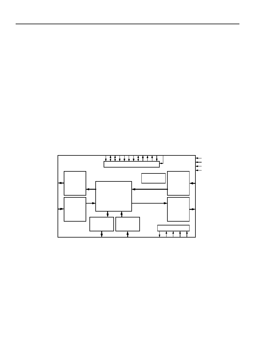
Description
The TDCS4180G has four basic elements: receive
interface channels, a cross-connect fabric core, trans-
mit channels, and a microprocessor interface. The
block diagram of the TDCS4810G is shown in Figure 1.
All data stream channels must be synchronous in fre-
quency, but can be asynchronous in phase.
The TDCS4810G does not perform pointer processing
functions. These are performed by the line and tribu-
tary cards, which align the payload at known positions
relative to a common frame signal.
The TDCS4810G is able to support SONET and SDH
cross connects.
5-8022.a (F)
Figure 1. TDCS4810G Block Diagram
FABRIC CORE
TRANSMIT
TRANSMIT
CONNECTION
MICROPROCESSOR
JTAG INTERFACE
D_OUT0_[15:0]
D_
OUT
1
_[1
5
:0
]
D_IN1
_
[1
5:0
]
D_OUT2_[15:0]
D_IN2_[15:0]
TD
O
TD
I
TC
K
TM
S
TR
ST
_N
DA
T
A
_
[
1
5
:
0
]
CS
_
N
TS_
N
DS
_
N
IN
T
_
N
M
P
MO
DE
[1:0
]
P
A
R
IT
Y
_
[1
:0]
INTERFACE
PORT 0
RECEIVE
INTERFACE
PORT 0
TRANSMIT
INTERFACE
PORT 2
RECEIVE
INTERFACE
PORT 2
INTERFACE
PORT 1
RECEIVE
INTERFACE
PORT 1
MEMORY
D_IN0_[15:0]
PCL
K
ADDRESS_
[
1
2
:
0
]
TA_
N
RW
_
N
TEA_
N
HIZ_N
RST_N
SYS_FP
SYS_CLK
PM
_
C
L
K

Agere Systems Inc.
3
Product Brief
June 2001
10 Gbits/s APS Port and TSI
TDCS4810G SONET/SDH
Description
(continued)
Supervisory Features
I
LVDS link integrity
I
Framer monitoring
I
FIFO aligner monitoring
I
Frame offset monitoring
I
CPU interface monitoring
Test Features
I
A1/A2 error insert
I
B1 error insert
I
Scrambler/descrambler disable
Additional Features
I
Software Reset: Software reset must be provided.
Software reset will be self-clearing (a reset pulse
must be internally generated upon receiving a reset
command from the CPU interface). It will reset the
whole device.

Agere Systems Inc. reserves the right to make changes to the product(s) or information contained herein without notice. No liability is assumed as a result of their use or application.
Copyright © 2001 Agere Systems Inc.
All Rights Reserved
Printed in U.S.A.
June 2001
PB01-076SONT
For additional information, contact your Agere Systems Account Manager or the following:
INTERNET:
http://www.agere.com
E-MAIL:
docmaster@micro.lucent.com
N. AMERICA: Agere Systems Inc., 555 Union Boulevard, Room 30L-15P-BA, Allentown, PA 18109-3286
1-800-372-2447, FAX 610-712-4106 (In CANADA: 1-800-553-2448, FAX 610-712-4106)
ASIA PACIFIC: Agere Systems Singapore Pte. Ltd., 77 Science Park Drive, #03-18 Cintech III, Singapore 118256
Tel. (65) 778 8833, FAX (65) 777 7495
CHINA:
Agere Systems (Shanghai) Co., Ltd., 33/F Jin Mao Tower, 88 Century Boulevard Pudong, Shanghai 200121 PRC
Tel. (86) 21 50471212, FAX (86) 21 50472266
JAPAN:
Agere Systems Japan Ltd., 7-18, Higashi-Gotanda 2-chome, Shinagawa-ku, Tokyo 141, Japan
Tel. (81) 3 5421 1600, FAX (81) 3 5421 1700
EUROPE:
Data Requests: DATALINE: Tel. (44) 7000 582 368, FAX (44) 1189 328 148
Technical Inquiries:GERMANY: (49) 89 95086 0 (Munich), UNITED KINGDOM: (44) 1344 865 900 (Ascot),
FRANCE: (33) 1 40 83 68 00 (Paris), SWEDEN: (46) 8 594 607 00 (Stockholm), FINLAND: (358) 9 3507670 (Helsinki),
ITALY: (39) 02 6608131 (Milan), SPAIN: (34) 1 807 1441 (Madrid)