 | –≠–ª–µ–∫—Ç—Ä–æ–Ω–Ω—ã–π –∫–æ–º–ø–æ–Ω–µ–Ω—Ç: TECO3264 | –°–∫–∞—á–∞—Ç—å:  PDF PDF  ZIP ZIP |
Document Outline
- Features
- Applications
- Description
- Block Diagram
- Pin Information
- Functional Description
- External Control Connection
- Parameters
- Parameter Map
- Register Architecture
- Absolute Maximum Ratings
- Recommended Operating Conditions
- Electrical Characteristics
- Physical Characteristics
- Outline Diagram
- Ordering Information
- DS99-241PDH Replaces DS98-409TIC to Incorporate the Following Updates
- List of Figures
- List of Tables
- Table 1. Pin Descriptions
- Table 2. Microprocessor Interface Control I/O
- Table 3. Relationship Between CET and CER, When CMS = 1
- Table 4. Relationship Between CET and CER, When CMS = 0
- Table 5. Programming Values (CER = Decimal) for [X, Y]RBOFF, When CMS = 1
- Table 6. Programming Values (CET = Decimal) for [C, E]XBOFF, When CMS = 1
- Table 7. Programming Values (CER = Decimal) for [X, Y]RBOFF, When CMS = 0
- Table 8. Programming Values (CET = Decimal) for [C, E]XBOFF, When CMS = 0
- Table 9. Transmission Parameter Settings and Description for Waveforms in Figure 15, PCM Input/Ou...
- Table 10. H-Register Display Output Format
- Table 11. Per-Channel Control Parameters
- Table 12. Mask Parameters
- Table 13. EC Parameters
- Table 14. Transmission Parameters
- Table 15. Tone Disabler Parameters
- Table 16. Nonlinear Processor Parameters
- Table 17. Control Parameters
- Table 18. Test and Diagnostic Parameters
- Table 19. Parameter Address Map
- Table 20. Recommended Register Values for DS1 (µ-Law) and 2.048 Mbits/s Rate
- Table 21. Recommended Register Values for E1 (A-Law)
- Table 22. Function Name to Symbol and Register Address Index
- Table 23. Symbol to Register Address and Function Name Index
- Table 24. Per-Channel Control Parameters
- Table 25. Tone Disabler Masks 1 Register (020) [00]
- Table 26. Tone Disabler Masks 2 Register (021) [02]
- Table 27. Nonlinear Processor (NLP) Control Masks Register (022) [41]
- Table 28. H-Register Control Options (023) [80]
- Table 29. Leak Control Register (024) [A1]
- Table 30. Filter and Tone Detector 2 Controls Register (025) [0C]
- Table 31. Far-End Speech Threshold 1 Register (026) [9B]
- Table 32. Far-End Speech Threshold 2 Register (027) [02]
- Table 33. Narrowband Energy Peak Factor Register (028) [18]
- Table 34. Wideband Energy Peak Factor Register (029) [18]
- Table 35. Highway Bit Rate Register (02A) [05]
- Table 36. X Parity Register (02B) [00]
- Table 37. Test 1 Register (02C) [00]
- Table 38. Test 2 Register (02D) [00]
- Table 39. A-Law/µ-Law Linear Conversion Register (02E) [1B for DS1, 09 for E1]
- Table 40. C Port Control Register (02F) [F8]
- Table 41. X-C Bulk Time-Slot Delay Register (030) [19]
- Table 42. Y-E Bulk Time-Slot Delay Register (031) [15]
- Table 43. X Input Format Register (032) [02]
- Table 44. Edge Sampling Register (033) [02]
- Table 45. SRAM Control Register (034) [01]
- Table 46. Y Port Control 1 Register (035) [02]
- Table 47. Y Port Control 2 Register (036) [07 for DS1, 05 for E1]
- Table 48. Y Test Data 1 Register (037) [00]
- Table 49. Y Test Data 2 Register (038) [00]
- Table 50. E and Y EMP Gain Filter Constant Register (039) [80]
- Table 51. E Port Control 1 Register (03A) [F7 for DS1, F6 for E1]
- Table 52. E Port Control 2 Register (03B) [08]
- Table 53. Reserved (03C) [00]
- Table 54. Low-Peak Count Register (03D) [84]
- Table 55. High-Peak Count Register (03E) [E3]
- Table 56. Interval Count Register (03F) [E4]
- Table 57. Good Intervals VPA Register (040) [00]
- Table 58. Good Intervals Declare Register (041) [70]
- Table 59. Phase Reversal Interval Minimum Register (042) [CA]
- Table 60. Phase Reversal Interval Maximum Register (043) [8A]
- Table 61. Tone Detector Declarations Register (044) [AC]
- Table 62. Low Voice Path Assurance (VPA) Count Register (045) [5F]
- Table 63. High VPA Count Register (046) [22]
- Table 64. VPA Power Minimum Register (047) [0C]
- Table 65. Tone Detector Power Minimum Register (048) [0E]
- Table 66. Phase Reversal Interval Maximum Register (049) [4D]
- Table 67. Tone Detector Threshold Register (04A) [90]
- Table 68. Y Energy Threshold Register (04B) [7F]
- Table 69. Noise Matching Enable Register (04C) [20]
- Table 70. Near-End Speech Hangover Register (04D) [F0]
- Table 71. Í Noise Floor Estimate Maximum 1 Register (04E) [1F]
- Table 72. Í Noise Floor Estimate Maximum 2 Register (04F) [00]
- Table 73. Gamma Í Noise Floor Register (050) [02]
- Table 74. Clamp Í Noise Floor 1 Register (051) [FF]
- Table 75. Clamp Í Noise Floor 2 Register (052) [3F]
- Table 76. Noise Floor Estimate High Hysteresis Threshold 1 Register (053) [00]
- Table 77. Variable Loss Noise Matching Select Register (054) [00]
- Table 78. Noise Floor Estimate Low Hysteresis Threshold Register (055) [08]
- Table 79. NLP Freeze, Soft NLP Select Register (056) [80]
- Table 80. Noise Floor Estimate Register (057) [21]
- Table 81. Spectrally Matched Noise Matching Select Register (058) [B0]
- Table 82. Soft NLP Number Interval Time Steps 1 Register (059) [08]
- Table 83. Soft NLP Number Interval Time Steps 2 Register (05A) [00]
- Table 84. Soft NLP Interval Steps Register (05B) [20]
- Table 85. Loss Increment Attenuated Í 1 Register (05C) [4C]
- Table 86. Loss Increment Attenuated Í 2 Register (05D) [8A]
- Table 87. Í Zero Crossing Threshold Register (05E) [00]
- Table 88. Soft NLP Incremental Loss Factor 1 Register (05F) [00]
- Table 89. Soft NLP Incremental Loss Factor 2 Register (060) [1E]
- Table 90. Reserved Register (061) [00]
- Table 91. State Variable Test 1 Register (062) [00]
- Table 92. State Variable Test 2 Register (063) [00]
- Table 93. State Variable Test 3 Register (064) [00]
- Table 94. Convolution Update Processor Disable Register (065) [00]
- Table 95. Test Control Register (066) [00]
- Table 96. X and Y Loss Pads Register (067) [00]
- Table 97. E and Y Exponentially Mapped (EMP) Filter Time Constant Register (068) [01]
- Table 98. Fast Convergence Register (069) [60]
- Table 99. Slow Convergence Gain Register (06A) [40]
- Table 100. Fast Convergence Beta 1 Register (06B) [12]
- Table 101. Fast Convergence Beta 2 Register (06C) [05]
- Table 102. Slow Convergence Beta 1 Register (06D) [12]
- Table 103. Slow Convergence Beta 2 Register (06E) [05]
- Table 104. Fast Convergence Gain Time Register (06F) [20]
- Table 105. Fast Convergence NLP Beta Time Register (070) [20]
- Table 106. Alpha Voice Hybrid Return Loss Threshold (071) [40]
- Table 107. Echo Cancellation Convergence Register (072) [05]
- Table 108. Alpha Data Hybrid Return Loss Threshold Register (073) [40]
- Table 109. Near-End Speech 1 Hangover Register (074) [FF]
- Table 110. NLP Hangover Register (075) [10]
- Table 111. Near-End Speech 3 Hangover Register (076) [00]
- Table 112. Fast Convergence Threshold Register (077) [AA]
- Table 113. Transient NLP Threshold Register (078) [00]
- Table 114. H-Reset Threshold Register (079) [00]
- Table 115. Near-End Speech Compare Threshold Register (07A) [00]
- Table 116. Test Channel Offset Register (07B) [03]
- Table 117. NLP Operate Time Double Register (07C) [A3]
- Table 118. High-Side 2100 Hz Peak Count Register (07D) [A4]
- Table 119. Enable Í Threshold Register (07E) [18]
- Table 120. Enable Í Threshold Register (07F) [C0]
- Table 121. Error Indicators 1 Register (100)
- Table 122. Interupt Masks 1 Register (101)
- Table 123. Error Indicators 2 Register (102)
- Table 124. Interrupt Masks 2 Register (103)
- Table 125. C Test Data Register (104)
- Table 126. E Test Data Bits [7:0] Register (105)
- Table 127. E Test Data Bits [15:8] Register (106)
- Table 128. Tone Detector Indicator Registers (107Ñ10E)
- Table 129. Absolute Maximum Ratings
- Table 130. Recommended Operating Conditions
- Table 131. Input and High-Impedance Leakage Current
- Table 132. Clock Input Specification
- Table 133. Other Input Specifications
- Table 134. Output Signal Specification
- Contact Us

Data Sheet
August 1999
TECO3264 32-Channel Echo Canceller
Features
Overall Device
s
Dual-convergence voiceband echo canceller (EC).
s
32 independent and individually controlled echo
canceller channels.
s
Stable performance across virtually all network
hybrid conditions.
s
Multiple-channel processing modes:
-- Echo cancelling ON/OFF.
-- µ-law to A-law and A-law to µ-law conversion.
-- 64-clear.
s
Tail-end delay up to 64 ms.
s
Flexible integrated nonlinear processor.
s
Automatic echo path change detection.
s
PCM interface supporting µ-law, A-law, and linear
formats.
s
Two independent tone disablers.
s
Two-band tone detection.
s
Multiple-configuration options for tone disabling:
-- 2100 Hz.
-- 2100 Hz with phase reversal only.
-- 2010 VPA.
-- Dual band.
-- None.
s
Integrated data storage in on-chip SRAM.
s
Integrated PLL for high-speed operations.
s
High-speed microprocessor interface configurable
to operate with most commercial microprocessors.
s
Built-in self-test and boundary scan.
s
IEEE
*1149.1 boundary scan (JTAG).
s
ITU-T G.165, G.168 compliance.
s
Highly provisionable and highly observable.
s
Selectable 3.3 V or 5.0 V tolerant inputs.
s
0 ∞C to 85 ∞C temperature range.
s
Typical power dissipation: 700 mW--900 mW.
s
160-pin, plastic, metric quad flat pack with heat
spreader (MQFPH) package.
*
IEEE
is a registered trademark of The Institute of Electrical and
Electronics Engineers, Inc.
Applications
s
Digital terrestrial communication networks
s
Digital wireless communications networks
s
Digital personal communication networks
s
Voiceband telephony
-- Voice calls
-- Low-speed modem calls
-- Voice over Internet
-- Packetized voice (e.g., frame relay, ATM)
s
Centralized applications
-- Local exchange (LEC) office
-- Interexchange (IEC) office
-- Mobile telephone switching office (MTSO)
-- Base-station controllers
-- Packetized voice equipment
Description
The TECO3264 32-channel echo canceller (EC)
device is a 3.3 V, CMOS, very large-scale integration
(VLSI) component offering 32 independent channels
of echo cancellation. Packaged in a 160-pin, plastic,
metric quad flat pack with heat speader (MQFPH)
and handling up to 64 ms of tail-end delay, this
device combines high performance, high channel
density, low power dissipation, high flexibility, excel-
lent maintenance capability, and low cost into a sin-
gle package.
The TECO3264 32-channel echo canceller provides
echo cancellation for both T1 and E1 systems. The
device operates from a single 3.3 V supply and
requires only an external 8.192 MHz clock and 8 kHz
frame sync.
Built-in self-test logic affords easy device verification
while integrated boundary-scan capability reduces
board verification time and cost.
A high-speed microprocessor interface and full user
provisionability on device pins provide maximum flex-
ibility.

Data Sheet
TECO3264 32-Channel Echo Canceller
August 1999
2
Lucent Technologies Inc.
Table of Contents
Contents
Page
Features ................................................................................................................................................................... 1
Overall Device .............................................................................................................................................. 1
Applications .............................................................................................................................................................. 1
Description................................................................................................................................................................ 1
Block Diagram .......................................................................................................................................................... 8
Pin Information ......................................................................................................................................................... 9
Pin Assignment ............................................................................................................................................ 9
Pin Descriptions ......................................................................................................................................... 10
Functional Description ............................................................................................................................................ 13
X(PCM/Linear) Highway Control (XPCM) .................................................................................................. 13
Y(PCM/Linear) Highway Control (YPCM) .................................................................................................. 13
E(PCM/Linear) Highway Control (EPCM) .................................................................................................. 13
Convolution/Update Processor (CUP)........................................................................................................ 13
Nonlinear Processor (NLP) ........................................................................................................................ 13
Tone Disablers (TD1, TD2) ........................................................................................................................ 13
Microprocessor Interface and Control (MPIC)............................................................................................ 13
External Control Connection................................................................................................................................... 14
Microprocessor Interface and Control (MPIC)............................................................................................ 14
Channel Status and Control ....................................................................................................................... 19
PCM Input/Output (I/O) Timing and Register Control................................................................................. 20
H-Register Channel Status......................................................................................................................... 30
Parameters ............................................................................................................................................................. 34
Parameter Overview................................................................................................................................... 34
Per-Channel Control Parameters ............................................................................................................... 34
Mask Bits.................................................................................................................................................... 35
Echo Canceller (EC) Parameters ............................................................................................................... 36
PCM Transmission Parameters ................................................................................................................. 37
Tone Disabler Parameters ......................................................................................................................... 40
Nonlinear Processor Parameters ............................................................................................................... 41
Control Parameters .................................................................................................................................... 42
Test and Diagnostic Parameters ................................................................................................................ 43
Parameter Map....................................................................................................................................................... 45
Register Architecture .............................................................................................................................................. 48
Register Scopes ......................................................................................................................................... 48
Registers, Functions, Symbols--Information Presentations ...................................................................... 49
Recommended Register Values................................................................................................................. 50
Notation and Format: Bits per Parameter and Bits in Registers................................................................. 50
Recommended Register Values for DS1 (µ-Law) ...................................................................................... 51
Recommended Register Values for E1 (A-Law) ........................................................................................ 52
Function Name to Symbol and Register Address Index............................................................................. 53
Symbol to Register Address and Function Name Index............................................................................. 59
Page 0 Read/Write Registers 000--07FE.................................................................................................. 65
Page 1 Read-Only Registers 100--10E................................................................................................... 114
Absolute Maximum Ratings.................................................................................................................................. 119
Recommended Operating Conditions .................................................................................................................. 119
Electrical Characteristics ...................................................................................................................................... 119
Input and High-Impedance Leakage Current ........................................................................................... 119
Clock Input Specifications ........................................................................................................................ 120
Other Input Specifications ........................................................................................................................ 121
Output Signal Specification ...................................................................................................................... 123

Data Sheet
August 1999
TECO3264 32-Channel Echo Canceller
3
Lucent Technologies Inc.
Table of Contents
(continued)
Contents
Page
Physical Characteristics ........................................................................................................................................124
Outline Diagram ....................................................................................................................................................125
160-Pin MQFPH........................................................................................................................................125
Ordering Information .............................................................................................................................................126
DS99-241PDH Replaces DS98-409TIC to Incorporate the Following Updates....................................................126

Data Sheet
TECO3264 32-Channel Echo Canceller
August 1999
4
Lucent Technologies Inc.
List of Figures
Figures
Page
Figure 1. 32-Channel Echo Canceller Block Diagram .............................................................................................. 8
Figure 2. Pin Assignment ......................................................................................................................................... 9
Figure 3. MPIC Write Cycle (UP_MODE = 1)......................................................................................................... 17
Figure 4. MPIC Read Cycle (UP_MODE = 1) ........................................................................................................ 17
Figure 5. MPIC Write Cycle (UP_MODE = 0)......................................................................................................... 18
Figure 6. MPIC Read Cycle (UP_MODE = 0) ........................................................................................................ 18
Figure 7. Control and Status Timing....................................................................................................................... 19
Figure 8. SYNC and PCM Timing for DS1 and CEPT Frame ................................................................................ 20
Figure 9. Interface Timing (SYNC, 8 kHz) .............................................................................................................. 21
Figure 10. Interface Timing (CK8M Clock) ............................................................................................................. 21
Figure 11. 4.096 MHz Reference Clock (FE = 0, CK8M Falling Edge) .................................................................. 22
Figure 12. 4.096 MHz Reference Clock (FE = 1, CK8M Rising Edge) ................................................................... 23
Figure 13. Received and Transmit Offsets Related to Received and Transmit Data ............................................. 25
Figure 14. SYNC Shifted to Edge of CK8M............................................................................................................ 26
Figure 15. PCM Input/Output Transmission Parameter Settings ........................................................................... 28
Figure 16. HSYNC, Frames, Bits, etc., Relationship .............................................................................................. 30
Figure 17. HSYNC, HDSP Relationship ................................................................................................................. 30
Figure 18. Clock Input Signals.............................................................................................................................. 120
Figure 19. Setup and Hold Times......................................................................................................................... 122

Data Sheet
August 1999
TECO3264 32-Channel Echo Canceller
5
Lucent Technologies Inc.
List of Tables
Tables
Page
Table 1. Pin Descriptions ........................................................................................................................................10
Table 2. Microprocessor Interface Control I/O ........................................................................................................16
Table 3. Relationship Between CET and CER, When CMS = 1 .............................................................................24
Table 4. Relationship Between CET and CER, When CMS = 0 .............................................................................24
Table 5. Programming Values (CER = Decimal) for [X, Y]RBOFF, When CMS = 1 ...............................................27
Table 6. Programming Values (CET = Decimal) for [C, E]XBOFF, When CMS = 1 ...............................................27
Table 7. Programming Values (CER = Decimal) for [X, Y]RBOFF, When CMS = 0 ...............................................27
Table 8. Programming Values (CET = Decimal) for [C, E]XBOFF, When CMS = 0 ...............................................28
Table 9. Transmission Parameter Settings and Description for Waveforms in Figure 15, PCM Input/Output
Transmission Parameter Settings ............................................................................................................29
Table 10. H-Register Display Output Format ..........................................................................................................31
Table 11. Per-Channel Control Parameters ............................................................................................................34
Table 12. Mask Parameters ....................................................................................................................................35
Table 13. EC Parameters........................................................................................................................................36
Table 14. Transmission Parameters .......................................................................................................................37
Table 15. Tone Disabler Parameters ......................................................................................................................40
Table 16. Nonlinear Processor Parameters ............................................................................................................41
Table 17. Control Parameters .................................................................................................................................42
Table 18. Test and Diagnostic Parameters.............................................................................................................43
Table 19. Parameter Address Map .........................................................................................................................45
Table 20. Recommended Register Values for DS1 (µ-Law) and 2.048 Mbits/s Rate .............................................51
Table 21. Recommended Register Values for E1 (A-Law) .....................................................................................52
Table 22. Function Name to Symbol and Register Address Index .........................................................................53
Table 23. Symbol to Register Address and Function Name Index .........................................................................59
Table 24. Per-Channel Control Parameters ............................................................................................................65
Table 25. Tone Disabler Masks 1 Register (020) [00].............................................................................................67
Table 26. Tone Disabler Masks 2 Register (021) [02].............................................................................................68
Table 27. Nonlinear Processor (NLP) Control Masks Register (022) [41] ..............................................................69
Table 28. H-Register Control Options (023) [80].....................................................................................................70
Table 29. Leak Control Register (024) [A1].............................................................................................................71
Table 30. Filter and Tone Detector 2 Controls Register (025) [0C].........................................................................72
Table 31. Far-End Speech Threshold 1 Register (026) [9B] ...................................................................................73
Table 32. Far-End Speech Threshold 2 Register (027) [02] ...................................................................................73
Table 33. Narrowband Energy Peak Factor Register (028) [18] .............................................................................73
Table 34. Wideband Energy Peak Factor Register (029) [18] ................................................................................74
Table 35. Highway Bit Rate Register (02A) [05] .....................................................................................................74
Table 36. X Parity Register (02B) [00] ....................................................................................................................75
Table 37. Test 1 Register (02C) [00] .......................................................................................................................75
Table 38. Test 2 Register (02D) [00] .......................................................................................................................75
Table 39. A-Law/µ-Law Linear Conversion Register (02E) [1B for DS1, 09 for E1]................................................76
Table 40. C Port Control Register (02F) [F8] ..........................................................................................................77
Table 41. X-C Bulk Time-Slot Delay Register (030) [19].........................................................................................77
Table 42. Y-E Bulk Time-Slot Delay Register (031) [15] .........................................................................................78
Table 43. X Input Format Register (032) [02]..........................................................................................................78
Table 44. Edge Sampling Register (033) [02] .........................................................................................................78
Table 45. SRAM Control Register (034) [01] ..........................................................................................................79
Table 46. Y Port Control 1 Register (035) [02] ........................................................................................................79
Table 47. Y Port Control 2 Register (036) [07 for DS1, 05 for E1] ..........................................................................80
Table 48. Y Test Data 1 Register (037) [00] ...........................................................................................................81
Table 49. Y Test Data 2 Register (038) [00] ...........................................................................................................81
Table 50. E and Y EMP Gain Filter Constant Register (039) [80] ...........................................................................81

Data Sheet
TECO3264 32-Channel Echo Canceller
August 1999
6
Lucent Technologies Inc.
List of Tables
(continued)
Tables
Page
Table 51. E Port Control 1 Register (03A) [F7 for DS1, F6 for E1]......................................................................... 82
Table 52. E Port Control 2 Register (03B) [08]....................................................................................................... 83
Table 53. Reserved (03C) [00] ............................................................................................................................... 83
Table 54. Low-Peak Count Register (03D) [84]...................................................................................................... 84
Table 55. High-Peak Count Register (03E) [E3]..................................................................................................... 84
Table 56. Interval Count Register (03F) [E4].......................................................................................................... 85
Table 57. Good Intervals VPA Register (040) [00] ................................................................................................. 85
Table 58. Good Intervals Declare Register (041) [70] ............................................................................................ 85
Table 59. Phase Reversal Interval Minimum Register (042) [CA] .......................................................................... 86
Table 60. Phase Reversal Interval Maximum Register (043) [8A].......................................................................... 86
Table 61. Tone Detector Declarations Register (044) [AC] .................................................................................... 87
Table 62. Low Voice Path Assurance (VPA) Count Register (045) [5F] ................................................................ 87
Table 63. High VPA Count Register (046) [22]....................................................................................................... 88
Table 64. VPA Power Minimum Register (047) [0C] .............................................................................................. 88
Table 65. Tone Detector Power Minimum Register (048) [0E]............................................................................... 88
Table 66. Phase Reversal Interval Maximum Register (049) [4D] ......................................................................... 89
Table 67. Tone Detector Threshold Register (04A) [90]......................................................................................... 89
Table 68. Y Energy Threshold Register (04B) [7F] ................................................................................................ 90
Table 69. Noise Matching Enable Register (04C) [20] ........................................................................................... 90
Table 70. Near-End Speech Hangover Register (04D) [F0]................................................................................... 91
Table 71. Í Noise Floor Estimate Maximum 1 Register (04E) [1F] ........................................................................ 91
Table 72. Í Noise Floor Estimate Maximum 2 Register (04F) [00]......................................................................... 92
Table 73. Gamma Í Noise Floor Register (050) [02].............................................................................................. 92
Table 74. Clamp Í Noise Floor 1 Register (051) [FF]............................................................................................. 92
Table 75. Clamp Í Noise Floor 2 Register (052) [3F]............................................................................................. 93
Table 76. Noise Floor Estimate High Hysteresis Threshold 1 Register (053) [00] ................................................. 93
Table 77. Variable Loss Noise Matching Select Register (054) [00] ...................................................................... 94
Table 78. Noise Floor Estimate Low Hysteresis Threshold Register (055) [08] ..................................................... 94
Table 79. NLP Freeze, Soft NLP Select Register (056) [80] .................................................................................. 95
Table 80. Noise Floor Estimate Register (057) [21] ............................................................................................... 95
Table 81. Spectrally Matched Noise Matching Select Register (058) [B0] ............................................................. 96
Table 82. Soft NLP Number Interval Time Steps 1 Register (059) [08].................................................................. 96
Table 83. Soft NLP Number Interval Time Steps 2 Register (05A) [00] ................................................................. 97
Table 84. Soft NLP Interval Steps Register (05B) [20] ........................................................................................... 97
Table 85. Loss Increment Attenuated Í 1 Register (05C) [4C]............................................................................... 98
Table 86. Loss Increment Attenuated Í 2 Register (05D) [8A]............................................................................... 98
Table 87. Í Zero Crossing Threshold Register (05E) [00]...................................................................................... 99
Table 88. Soft NLP Incremental Loss Factor 1 Register (05F) [00]........................................................................ 99
Table 89. Soft NLP Incremental Loss Factor 2 Register (060) [1E] ..................................................................... 100
Table 90. Reserved Register (061) [00] ............................................................................................................... 100
Table 91. State Variable Test 1 Register (062) [00] ............................................................................................. 100
Table 92. State Variable Test 2 Register (063) [00] ............................................................................................. 101
Table 93. State Variable Test 3 Register (064) [00] ............................................................................................. 101
Table 94. Convolution Update Processor Disable Register (065) [00] ................................................................. 101
Table 95. Test Control Register (066) [00] ........................................................................................................... 102
Table 96. X and Y Loss Pads Register (067) [00] ................................................................................................ 102
Table 97. E and Y Exponentially Mapped (EMP) Filter Time Constant Register (068) [01] ................................. 103
Table 98. Fast Convergence Register (069) [60] ................................................................................................. 104
Table 99. Slow Convergence Gain Register (06A) [40]........................................................................................ 104
Table 100. Fast Convergence Beta 1 Register (06B) [12].................................................................................... 104

Data Sheet
August 1999
TECO3264 32-Channel Echo Canceller
7
Lucent Technologies Inc.
List of Tables
(continued)
Tables
Page
Table 101. Fast Convergence Beta 2 Register (06C) [05] ....................................................................................105
Table 102. Slow Convergence Beta 1 Register (06D) [12] ...................................................................................105
Table 103. Slow Convergence Beta 2 Register (06E) [05] ...................................................................................106
Table 104. Fast Convergence Gain Time Register (06F) [20] ..............................................................................106
Table 105. Fast Convergence NLP Beta Time Register (070) [20].......................................................................107
Table 106. Alpha Voice Hybrid Return Loss Threshold (071) [40] ........................................................................107
Table 107. Echo Cancellation Convergence Register (072) [05] ..........................................................................108
Table 108. Alpha Data Hybrid Return Loss Threshold Register (073) [40] ...........................................................109
Table 109. Near-End Speech 1 Hangover Register (074) [FF] .............................................................................109
Table 110. NLP Hangover Register (075) [10] ......................................................................................................110
Table 111. Near-End Speech 3 Hangover Register (076) [00] .............................................................................110
Table 112. Fast Convergence Threshold Register (077) [AA] ..............................................................................110
Table 113. Transient NLP Threshold Register (078) [00] .....................................................................................111
Table 114. H-Reset Threshold Register (079) [00] ...............................................................................................111
Table 115. Near-End Speech Compare Threshold Register (07A) [00]................................................................111
Table 116. Test Channel Offset Register (07B) [03] .............................................................................................112
Table 117. NLP Operate Time Double Register (07C) [A3] ..................................................................................112
Table 118. High-Side 2100 Hz Peak Count Register (07D) [A4] ..........................................................................113
Table 119. Enable Í Threshold Register (07E) [18] ..............................................................................................113
Table 120. Enable Í Threshold Register (07F) [C0] .............................................................................................113
Table 121. Error Indicators 1 Register (100) .........................................................................................................114
Table 122. Interupt Masks 1 Register (101) ..........................................................................................................115
Table 123. Error Indicators 2 Register (102) .........................................................................................................116
Table 124. Interrupt Masks 2 Register (103).........................................................................................................116
Table 125. C Test Data Register (104) .................................................................................................................117
Table 126. E Test Data Bits [7:0] Register (105) ..................................................................................................117
Table 127. E Test Data Bits [15:8] Register (106) ................................................................................................117
Table 128. Tone Detector Indicator Registers (107--10E) ...................................................................................118
Table 129. Absolute Maximum Ratings ................................................................................................................119
Table 130. Recommended Operating Conditions .................................................................................................119
Table 131. Input and High-Impedance Leakage Current ......................................................................................119
Table 132. Clock Input Specification .....................................................................................................................120
Table 133. Other Input Specifications ...................................................................................................................121
Table 134. Output Signal Specification .................................................................................................................123
Data Sheet
TECO3264 32-Channel Echo Canceller
August 1999
8
Lucent Technologies Inc.
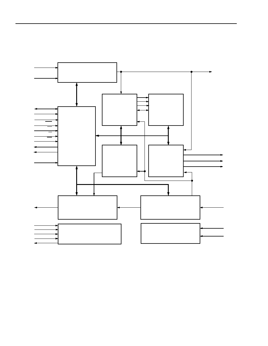
Block Diagram
The TECO3264 32-channel echo canceller block diagram is shown in Figure 1, 32-Channel Echo Canceller Block
Diagram.
5-5252(F).cr.2
* Active-high or active-low depends on microprocessor (
Intel
or
Motorola
).
Intel
is a registered trademark of Intel Corporation.
Motorola
is a registered trademark of Motorola, Inc.
Figure 1. 32-Channel Echo Canceller Block Diagram
TIMING
TEST ACCESS
E(PCM/LINEAR)
MICROPROCESSOR
CONVOLUTION
SRAM
NONLINEAR
TONE
Y(PCM/LINEAR)
CK8M
TONE
TDPR
VPA
YPCM
SYNC
TDO
CPCM
XPCM
XLINEAR
AS
ALE
UPMD
A[9:0]
D[7:0]
R/W
DS
DTACK*
INT*
RST
EPCM
TRST
TCK
TDI
TMS
UPDATE
PROCESSOR
X(PCM/LINEAR) HIGHWAY
CONTROL BLOCK
(XPCM)
INTERFACE
AND
CONTROL
BLOCK
PROCESSOR
HIGHWAY CONTROL BLOCK
(EPCM)
PORT CONTROLLER
HIGHWAY CONTROL BLOCK
(YPCM)
GENERATOR
DISABLER

Data Sheet
August 1999
TECO3264 32-Channel Echo Canceller
9
Lucent Technologies Inc.
Pin Information
Pin Assignment
5-5316(F)r.6
Note:
INT, DTACK is active-high when interfacing with
Intel
microprocessors.
INT, DTACK is active-low when interfacing with
Motorola
microprocessors.
Figure 2. Pin Assignment
1
2
3
4
5
6
7
8
9
10
11
12
13
14
15
16
17
18
19
20
21
22
23
24
25
26
27
28
29
30
31
32
33
34
35
36
37
38
39
40
42
43
44
45
46
47
49
50
51
52
53
54
55
57
61
62
63
65
67
69
70
71
72
73
74
75
76
77
79
80
56
58
59
66
48
64
41
60
68
78
TD
O
SC
AN
CK
32
TS
TM
D
HIG
H
Z
VS
S
IN
T
TO
N
E
TD
P
R
VP
A
HDS
P
VD
D
H
SYN
C
TE
S
T
1
VS
S
TE
S
T
5
TE
S
T
6
VD
D
CK
8M
CK
65E
X
T
VS
S
CCK
8P
CCK
8N
V
DD_P
L
L
CD0
VSS_
P
L
L
CD1
CD2
CD4
VD
D
TE
S
T
0
TE
S
T
2
TE
S
T
3
SL
O
W
DT
A
C
K
TE
S
T
7
VD
D
TE
S
T
4
C
KEX
T
CD3
159
158
157
156
155
154
152
151
150
149
148
147
146
144
140
139
138
136
134
132
131
130
129
128
127
126
125
124
122
121
145
143
142
135
153
137
160
141
133
123
D3
D2
D1
D0
VSS
XL
IN
EA
R
SYN
C
VD
D
CP
CM
EPC
M
CA
14
CA
13
VSS
CA
11
CA
8
CA
7
CA
6
VSS
CA
3
CA
1
VD
D
CA
0
CW
E
CRO
E
CB
WE
[D]
VSS
CB
WE
[C]
CB
WE
[B
]
VD
D
CA
12
CA
10
CA
9
CA
4
XPC
M
CA
5
VD
D
VD
D
CA
2
CB
WE
[A
]
YPC
M
119
118
117
116
115
114
112
111
110
109
108
107
106
104
100
99
98
96
94
92
91
90
89
88
87
86
85
84
82
81
105
103
102
95
113
97
120
101
93
83
CD35
CD34
CD33
VDD
CD32
CD31
CD29
VSS
CD28
CD27
CD26
CD25
VDD
CD23
CD20
CD19
CD18
VDD
CD15
CD13
VSS
CD12
CD11
CD10
CD9
VDD
CD8
CD7
CD5
VSS
CD24
CD22
CD21
CD16
CD30
CD17
VSS
VSS
CD14
CD6
D4
D5
D6
D7
A0
VDD
A2
A3
A4
A5
VSS
A6
A7
A9
AS
DS
UPMD
RST
VSS
NLPFRZ
NLPEN
HRST
HFRZ
VDD
CALLB
VSC
TDI
TCK
TMS
VSS
A8
VDD5
ALE
ECDIS
A1
R/W
VSS
VDD
ENBP
TRST

Data Sheet
TECO3264 32-Channel Echo Canceller
August 1999
10
Lucent Technologies Inc.
Pin Information
(continued)
Pin Descriptions
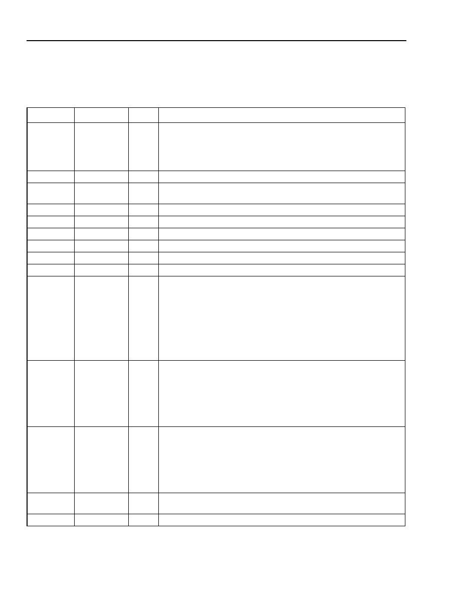
Table 1. Pin Descriptions
* I
u
indicates an internal pull-up.
Pin
Symbol
Type*
Description
152
YPCM
I
2.048/4.096 Mbits/s Near Input Serial PCM Data Stream.
153
XPCM
I
2.048/4.096 Mbits/s Far Input Serial PCM Data Stream.
154
XLINEAR
I
4.096 Mbits/s Far Input Linear PCM from Optional Coprocessor.
69
CK65EXT
I
External Clock @ 65.536 MHz. This clock is primarily intended for
factory test and should be tied low for normal use.
67
CK8M
I
Input Clock. This input clock controls the rate at which information is
sent or received on both the transmit and receive PCM streams. It
operates at 8.192 MHz.
151 SYNC
I
Frame Synchronization. The rising edge of this signal, which has a
frequency of 8 kHz, marks the beginning of a data frame. The SYNC
clock can be detected on either a rising or falling edge of CK8M by
programming the frame edge (FE) register bit. Individual time slots are
determined relative to the detection of the SYNC clock. SYNC clock
should be high for a minimum of 244 ns.
68
CKEXT
I
External/Internal Clock Select. A low on this pin will select the internal
65.536 MHz clock.
26
ECDIS
I
256 kHz Per-Channel Echo Canceller On/Off Control Stream.
(1 = on; 0 = off.)
28
ENBP
I
256 kHz Per-Channel 64-Clear On/Off Control Stream.
(1 = on; 0 = off.)
29
NLPFRZ
I
256 kHz Per-Channel NLP Freeze Control Stream.
(1 = freeze; 0 = no freeze.)
30
NLPEN
I
256 kHz Per-Channel NLP On/Off Control Stream.
(1 = on; 0 = off.)
31
HRST
I
256 kHz Per-Channel H-Reset Control Stream.
(1 = reset; 0 = no reset.)
32
HFRZ
I
256 kHz Per-Channel H-Freeze Control Stream.
(1 = freeze; 0 = no freeze.)
34
CALLB
I
256 kHz Per-Channel Call Boundary Control Stream.
(0
1 transition = call boundary event; otherwise, no call boundary
event.)
35
VSC
I
256 kHz Per-Channel Voice/Data Call Indication.
(1 = data; 0 = voice.)
19
ALE
I
Microprocessor Interface Address Latch Enable (Active-Low).
21
AS
I
Microprocessor Interface Address Strobe (Active-Low).
22
DS
I
Microprocessor Interface Data Strobe (Active-Low).
23
UPMD
I
Microprocessor Interface Mode. (1 =
Motorola
; 0 =
Intel
.)
24
R/W
I
Microprocessor Interface Read/Write Control. (1 = read; 0 = write.)

Data Sheet
August 1999
TECO3264 32-Channel Echo Canceller
11
Lucent Technologies Inc.
Pin Information
(continued)
Pin Descriptions
(continued)
Table 1. Pin Descriptions (continued)
* I
u
indicates an internal pull-up.
Pin
Symbol
Type*
Description
48
DTACK
O
Microprocessor Interface Write Acknowledge. DTACK is active-high in
the
Intel
mode and active-low in the
Motorola
mode. For the family of
Intel
8086 microprocessors, DTACK corresponds to RDY.
49
INT
O
Microprocessor Interrupt. INT is active-low in the
Motorola
mode and
active-high in the
Intel
mode, i.e.,
Intel
8086 family. In other
Intel
devices,
INT may be an active-low signal depending on the device.
6, 8--12,
14--17
A[0:9]
I
Microprocessor Interface Address Bus.
156--159,
2--5
D[0:7]
I/O
8-Bit Microprocessor Data Bus.
36
TDI
I
u
Boundary-Scan Test Data Input.
37
TCK
I
Boundary-Scan Test Clock Input. TCK must have a clock input at all
times to keep the TAP controller in an idle state.
38
TRST
I
u
Boundary-Scan Test Input. If not used, this pin must be held low.
39
TMS
I
u
Boundary-Scan Test Mode Select.
42
TDO
O
Boundary-Scan Data Output.
43
SCAN
I
SCAN Mode Switch. Leave unconnected for normal operation.
45
TSTMD
I
Static Test Enable for SCAN. Leave unconnected for normal operation.
46
HIGHZ
I
u
Force All Outputs to High-Impedance (Active-Low).
66
SLOW
I
u
Test Input. Leave unconnected for normal operation.
25
RST
I
Chip Reset (Active-High). Must be active for 500
µ
s.
18
V
DD
5
I
5.0 V Supply. For 5.0 V tolerant I/O; otherwise, connect to 3.3 V supply
(V
DD
).
148
EPCM
O
2.048/4.096 Mbits/s Far Output Serial PCM Data Stream.
149
CPCM
O
2.048/4.096 Mbits/s Near Output Serial PCM Data Stream.
71, 72
CCK8[P, N]
O
Balanced 8.192 MHz Clock Output (Factory Use Only).
44
CK32
O
32.768 MHz Clock Output for H-Register Data.
55
HSYNC
O
H-Register Data Sync Pulse. Occurs once per 16
µ
s and is one
32.768 MHz clock cycle wide.
53
HDSP
O
H-Register Data Clocked Out at 32.768 Mbits/s.
50
TONE
O
256 kHz Straight Tone Output.
51
TDPR
O
256 kHz Phase Reversed Tone Output.
52
VPA
O
256 kHz Voice Path Assurance Output.
127
CROE
O
(Factory Use.) This pin must be left unconnected.
128
CWE
O
(Factory Use.) This pin must be left unconnected.
122--124,
126
CBWE[A:D]
O
(Factory Use.) These pins must be left unconnected.
Data Sheet
TECO3264 32-Channel Echo Canceller
August 1999
12
Lucent Technologies Inc.
Pin Information
(continued)
Pin Descriptions
(continued)
Table 1. Pin Descriptions (continued)
Pin
Symbol
Type
Description
129,
131--134,
136--139,
141--144,
146, 147
CA[0:14]
O
(Factory Use.) These pins must be left unconnected.
56
TEST0
O
256 kHz Per-Channel NLP On/Off Status. (1 = on; 0 = off.)
57
TEST1
O
256 kHz Per-Channel Far-End Speech (FES) Status.
(1 = FES declared; 0 = FES not declared.)
58
TEST2
O
256 kHz Per-Channel 64-Clear Status. (1 = on; 0 = off.)
59
TEST3
O
256 kHz Per-Channel EC Status. (1 = off; 0 = on.)
60
TEST4
O
256 kHz Per-Channel H-Reset Status. (1 = reset; 0 = not reset.)
62
TEST5
O
256 kHz Per-Channel H-Freeze Status. (1 = frozen; 0 = not frozen.)
63
TEST6
O
4.096 Mbits/s Í Linear PCM Data.
64
TEST7
O
256 kHz Per-Channel Convergence Mode. (1 = fast; 0 = slow.)
74, 76--79,
82--85,
87--90,
92--95,
97--100,
102--105,
107--110,
112--115,
117--119
CD[0:35]
I/O
(Factory Use.) These pins must be left unconnected.
7, 20, 33,
41, 54, 65,
80, 86, 96,
106, 116,
121, 130,
140, 150,
160
V
DD
Power
3.3 V.
1, 13, 27,
40, 47, 61,
70, 81, 91,
101, 111,
120, 125,
135, 145,
155
V
SS
Ground Ground.
73
V
DD_PLL
Power
3.3 V. Recommended bypass capacitors 10 µF, 0.047 µF, and 2700 pF,
between V
DD_PLL
and V
SS_PLL
.
75
V
SS_PLL
Ground Ground.

Data Sheet
August 1999
TECO3264 32-Channel Echo Canceller
13
Lucent Technologies Inc.
Functional Description
X(PCM/Linear) Highway Control (XPCM)
XPCM provides all the PCM transport and format con-
version functions for the X to C direction of the trans-
mission. In addition, it provides a separate linear X
input which can be used to interface an external copro-
cessor device. The block also provides parallel linear
and companded PCM outputs to the convolution pro-
cessor, control, and tone disabler blocks. The parity
detection and generation as well as EC vector X test
data insertion and C data readback functions are also
performed in this block. Programmable bulk delay on
the PCM data is provided to allow up to one complete
frame delay through the device. A high-pass filter
(>10 Hz) is provided for x(t) prior to the convolution/
update block.
Y(PCM/Linear) Highway Control (YPCM)
YPCM implements the YPCM input functions and for-
mat conversion to linear for the convolution processing.
Parity detection is performed on the YPCM input, and
errors are reported to the control interface. The EC
vector Y test data insertion function is performed in this
block. Programmable bulk delay is provided to allow
arbitrary time-slot alignment of the Y input signal rela-
tive to the sync pulse. A high-pass filter (>10 Hz) is pro-
vided for y(t) prior to the convolution/update block.
E(PCM/Linear) Highway Control (EPCM)
EPCM performs the EPCM output formatting and EC
enable/disable and bypass functions. Conversion from
linear to companded PCM format is provided. Parity
generation on the EPCM output signal is performed.
Delay equalization for the EC enable/disable and
bypass functions is accomplished by the use of pro-
grammable bulk delay blocks. An additional program-
mable bulk delay block allows up to one full frame
delay for the Y to E direction of the transmission.
Convolution/Update Processor (CUP)
The primary function of the convolution/update proces-
sor (CUP) is to create a replica, (t), of the echo path
impulse response, h(t). The PCM samples at the C port
of the canceller are convolved with (t) to generate an
estimate, (t), of the echo signal y(t). The echo esti-
mate, (t), is subtracted from the echo signal, y(t), to
form the error signal, (t) ( is pronounced as ehat),
which is the main output from the convolution/update
processor.
In order to make the convergence time independent of
signal power, the gain is normalized by a measure of C
signal power before being applied to the update func-
tion. The power measure is the larger of the power esti-
mated from the sum of squares of the samples in the
register, or the power estimated from the peak signal in
the register multiplied by a peak factor.
An H-reset input is provided that sets all H taps to zero.
H-register freeze is achieved in the controller by setting
both the gain and leak values equal to zero. The
H reset must be applied for 500 ms. A serial H-register
display output is provided via HDSP (pin 53).
Nonlinear Processor (NLP)
The nonlinear processor (NLP) provides all the func-
tions necessary for the processing of the residual echo.
When enabled, the NLP can select from a variety of
alternate signal sources to switch into the signal path
for transmission on the EPCM output. These alternate
sources include quiet, noise matching, colored noise
matching, or a variably attenuated (t). The main func-
tion of the NLP is to generate these alternate sources
and switch the appropriate source into the signal path
when enabled by the control function. The NLP accepts
parametric inputs which determine the nature of the
selected alternate signal source. With the soft NLP
mode, the chosen comfort noise is inserted in a grad-
ual programmable fashion.
Tone Disablers (TD1, TD2)
The tone disabler functions (TD1, TD2) provide the
means to disable the echo cancellation function when
data or other specified tone signals are transmitted
through the echo canceller. This is accomplished by
detecting 2100 Hz tones with or without phase rever-
sals. The tone detection is performed on a per-channel
basis for both X and Y directions. The tone disablers
are tunable and capable of detecting tones in fre-
quency range and signal levels that are compliant for
voice path assurance (VPA) detection.
Microprocessor Interface and Control
(MPIC)
The microprocessor interface and control block func-
tion is to provide microprocessor access to the control,
provisioning, status, and alarm registers of the echo
canceller and to generate the signals required to con-
trol the operation of all echo canceller functions. The
functions performed in the MPIC block are described in
greater detail in the External Control Connection sec-
tion on page 14.
h^
h^
y^
y^
e^
e^
e^

Data Sheet
TECO3264 32-Channel Echo Canceller
August 1999
14
Lucent Technologies Inc.
External Control Connection
Microprocessor Interface and Control
(MPIC)
As given in the Functional Description section on
page 13, the microprocessor interface and control
block functions to (1) provide microprocessor access
to the control, provisioning, option, status, and alarm
registers of the echo canceller and (2) to generate the
signals required to control the operation of all echo
canceller functions. The following paragraphs
describe the functions performed in the MPIC block.
The internal register description sections which follow
detail the parameter register information and format
for each of the user-provisionable device characteris-
tics.
Channel Control (CHAN_CTRL)
The channel control function combines inputs from the
tone disabler with the user-provisionable mask and
enable register information and external inputs to gen-
erate the channel bypass and canceller enable signals.
Narrowband Energy Detector (NBE)
The narrowband energy detector measures the X sig-
nal input characteristics to differentiate between wide-
band and narrowband signals. Based on this
determination, the near-end speech detector threshold
is provisioned. In addition, this information is used in
setting the gain applied in the echo cancellation.
Near-End Speech Detectors (NES)
The function of the near-end speech detectors is to dif-
ferentiate between far-end echo and near-end speech
at the Y input port of the canceller. The H-register
updates should only be allowed if the Y input signal is
due to far-end echo and not due to near-end speech.
Two measures of near-end speech are provided.
The near-end speech detector compares the magni-
tude of the samples in the X register to the magnitude
of the Y samples. By comparing the relative magni-
tudes of the X samples and Y samples, the existence
of near-end speech can be deduced.
Far-End Speech Detector (FES)
The function of the far-end speech detector is to deter-
mine whether there is any far-end speech present. If
there is no far-end speech, there can be no echo signal
and the H-register updates should be frozen.
In the far-end speech detector, the X sample magni-
tude is compared to a threshold parameter value and a
far-end speech condition is asserted whenever the
threshold value is exceeded.
H-Register Freeze
The H-register update is frozen whenever:
s
NBE is declared and NBE detection is unmasked, or
s
NES is declared and NES detection is unmasked, or
s
FES is not declared and FES detection is unmasked,
or
s
External freeze is requested via the microprocessor
interface or external input.

Data Sheet
August 1999
TECO3264 32-Channel Echo Canceller
15
Lucent Technologies Inc.
External Control Connection
(continued)
Microprocessor Interface and Control
(MPIC)
(continued)
Fast/Slow Convergence Control (F_CONV)
NLP threshold and gain are the primary parameters
that determine convergence rate of the canceller. The
gain calculation function provisions a value for the gain
parameter and a value for the occurrence of any single
unmasked event.
The four events which cause the fast convergence
parameters to be chosen are:
1. H-register reset
2. External event such as call boundary
3. VPA tone detection
4. samples > Y samples times a threshold parameter
There is a serial output that indicates, on a per-
channel basis, the convergence mode of each channel.
See output pin TEST7.
Transient NLP Control (TRNLP)
The transient NLP control circuit can enable the NLP
whenever the power in (t) exceeds the power in Y by
a programmable threshold. These conditions exist on a
transient basis and generally indicate that the echo
canceller is not converged.
NLP Control
The NLP control function enables the NLP whenever
the magnitude of (t) exceeds the maximum magni-
tude of the samples in the X register times the NLP
threshold selected by the F_CONV function when this
feature is enabled.
The NLP may also be enabled by external command
via the microprocessor interface or external input.
e^
e^
e^

Data Sheet
TECO3264 32-Channel Echo Canceller
August 1999
16
Lucent Technologies Inc.
External Control Connection
(continued)
Microprocessor Interface and Control (MPIC)
(continued)
Microprocessor Interface
This interface provides microprocessor access to the control, provisioning, option, parameter, status, and alarm
registers, all of which are directly accessible via the address and data buses. Interrupt capability is also provided at
this interface.
1. All status and alarm registers are maskable and exercisable under microprocessor control.
2. The microprocessor has read and write access to the control, provisioning, option, parameter, and mask regis-
ters and read-only access to the status and alarm registers. Alarm registers are cleared when read by the micro-
processor. Microprocessor writes and reads at this interface are asynchronous to the clock.
3. The chip has access to the control, provisioning, option, and parameter registers and read-only access to the
status and alarm registers.
4. An interrupt signal is generated whenever any unmasked alarm condition is detected.
In order to provide flexibility in the choice of a microprocessor, two interface modes are supported. The primary
mode uses separate address and data buses, and interfaces directly with the
Motorola MC68000
* microprocessor
family. This mode is patterned on the microprocessor interfaces found in the T7270 Time-Slot Interchanger and
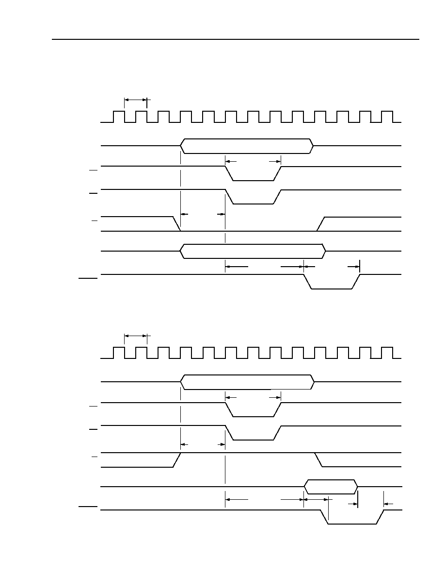
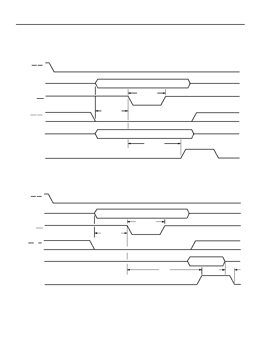
T7230 Primary Access Framer/Controller. Pin definitions for each of the modes are defined in Table 2. The I/O
specifications for these pins are defined in Table 2, Figure 3, MPIC Write Cycle (UP_MODE = 1), and Figure 4,
MPIC Read Cycle (UP_MODE = 1) for UP_MODE = 1 (
Motorola
mode), and Figure 5, MPIC Write Cycle
(UP_MODE = 0) and Figure 6, MPIC Read Cycle (UP_MODE = 0) for UP_MODE = 0 (
Intel
mode).
*
MC68000
is a trademark of Motorola, Inc.
* In other
Intel
devices, INT may be an active-low signal, depending on the device.
Table 2. Microprocessor Interface Control I/O
Device Pin
Name
Pin
Number
Type
Microprocessor Mode
Intel
Mode
Motorola
Mode
UP_MODE
23
I
UP_MODE = 0
UP_MODE = 1
ALE
19
I
Address Latch Enable (ALE)
(1 to 0 transition)
Not Used (ALE = 1)
D0--D7
(156--159,
2--5)
I/O
Data Bus
Data Bus
A0--A9
(6, 8--12,
14--17)
I
Address Bus
Address Bus
AS
21
I
Chip Select (CS) (active-low)
Address Strobe (active-low)
R/W
24
I
Read Cycle (RD) (active-low)
Read/Write Select
DS
22
I
Write Cycle (WR) (active-low)
Data Strobe (active-low)
DTACK
48
O
Ready (RDY for 8086 family)
(TECO3264 and
Intel
devices are
active-high.)
Data Transfer Acknowledge
(TECO3264 and
Motorola
devices
are active-low.)
INT
49
O
Interrupt (TECO3264 is active-high,
but
Intel
8086 family* is active-low.)
Interrupt (TECO3264 and
Motorola
devices are active-low.)
Data Sheet
August 1999
TECO3264 32-Channel Echo Canceller
17
Lucent Technologies Inc.
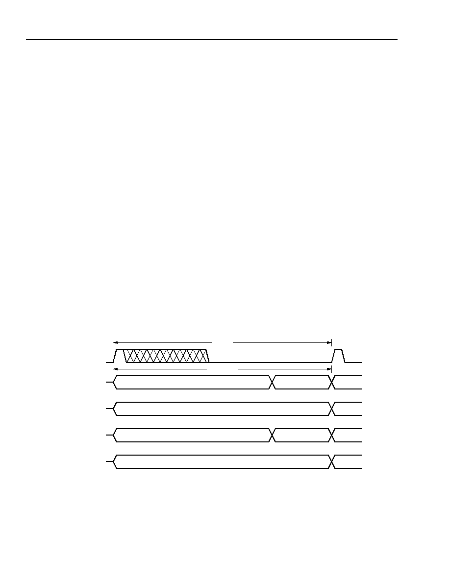
External Control Connection
(continued)
Microprocessor Interface and Control (MPIC)
(continued)
5-5345(F)r.7
Figure 3. MPIC Write Cycle (UP_MODE = 1)
5-5346(F)r.8
Figure 4. MPIC Read Cycle (UP_MODE = 1)
VALID
VALID
60 ns MIN
0 ns MIN
90 ns MIN
A[0:9]
AS
DS
R/W
D[0:7]
DTACK
60 ns MIN
30.5 ns
32 MHz CLOCK
(INTERNAL)
VALID
60 ns MIN
0 ns MIN
A[0:9]
AS
DS
R/W
30.5 ns
32 MHz CLOCK
(INTERNAL)
VALID OUT
D[0:7]
DTACK
30 ns
30 ns
90 ns MAX
Data Sheet
TECO3264 32-Channel Echo Canceller
August 1999
18
Lucent Technologies Inc.
External Control Connection
(continued)
Microprocessor Interface and Control (MPIC)
(continued)
5-5345(F).ar.6
* See Table 2, Microprocessor Interface Control I/O, on page 16.
Figure 5. MPIC Write Cycle (UP_MODE = 0)
5-5346(F).ar.7
* See Table 2, Microprocessor Interface Control I/O, on page 16.
Figure 6. MPIC Read Cycle (UP_MODE = 0)
VALID
VALID
60 ns MIN
15 ns MIN
75 ns MIN
A[0:9]
ALE
CS[AS]
WR[DS]
D[0:7]
RDY[DTACK*]
VALID OUT
60 ns MIN
A[0:9]
ALE
RD[R/W]
D[0:7]
RDY[DTACK*]
75 ns
20 ns
VALID
CS[AS]
15 ns MIN
Data Sheet
August 1999
TECO3264 32-Channel Echo Canceller
19
Lucent Technologies Inc.
External Control Connection
(continued)
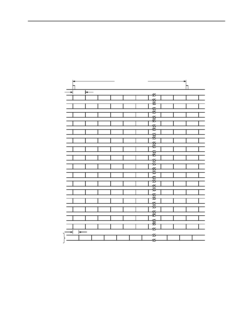
Channel Status and Control
The TECO3264 implements a highly provisionable architecture that offers per-channel control and status for
numerous functions via the respective data I/O pins. These I/O per-channel control and status pins include ENBP,
NLPFRZ, NLPEN, HRST, HFRZ, CALLB, VSC, TEST[0:7], TONE, TDPR, and VPA. For information on their pin
numbers and functions, please refer to Pin Descriptions, Table 1, on page 10. Figure 7, Control and Status Timing
shows the channel alignment for each control and status signal.
5-4902(F).ar.3
Note: There are 32 bits/frame for each serial stream. TS# represents the time-slot number.
Figure 7. Control and Status Timing
ECDIS
ENBP
TS31
TS0
TS1
TS2
TS3
TS4
TS29
TS30
TS31
TS31
TS0
TS1
TS2
TS3
TS4
TS29
TS30
TS31
TS26
TS27
TS28
TS29
TS30
TS31
TS24
TS25
TS26
TS27
TS28
TS29
TS30
TS31
TS0
TS25
TS26
TS27
TS29
TS30
TS31
TS0
TS1
TS2
TS27
TS28
TS29
TS28
TS29
TS30
TS31
TS0
TS1
TS26
TS27
TS28
TS26
TS27
TS28
TS29
TS30
TS31
TS24
TS25
TS26
TS26
TS27
TS28
TS29
TS30
TS31
TS24
TS25
TS26
NLPFRZ
NLPEN
HRST
HFRZ
CALLB
VSC
TS26
TS27
TS28
TS29
TS30
TS31
TS24
TS25
TS26
TS26
TS27
TS28
TS29
TS30
TS31
TS24
TS25
TS26
TS30
TS31
TS0
TS1
TS2
TS3
TS28
TS29
TS30
TS25
TS26
TS27
TS28
TS29
TS30
TS23
TS24
TS25
TS28
TS29
TS30
TS31
TS0
TS1
TS26
TS27
TS28
TS29
TS30
TS31
TS0
TS1
TS2
TS27
TS28
TS29
TS25
TS26
TS27
TS28
TS29
TS30
TS23
TS24
TS25
SYNC
125
µ
s FRAME
TS30
TS31
TS0
TS1
TS2
TS3
TS29
TS30
TS31
TONE
1.95
µ
s
TDPR
VPA
TEST0
TEST1
TS26
TS27
TS28
TS29
TS30
TS31
TS24
TS25
TS26
TEST2
TEST3
TEST4
TEST5
TEST6
TEST7
3.9
µ
s
Data Sheet
TECO3264 32-Channel Echo Canceller
August 1999
20
Lucent Technologies Inc.
External Control Connection
(continued)
PCM Input/Output (I/O) Timing and Register Control
The TECO3264 has a number of configurable parameters pertaining to the PCM data, the synchronization (SYNC,
8 kHz) clock, and the input clock (8.192 MHz). The only input clock that is required is the 8.192 MHz clock--there
are no other frequency options. The PCM ports support either 4.096 Mbits/s or 2.048 Mbits/s serial data. Proper
PCM timing is controlled through the use of programmable registers. Table 14, Transmission Parameters, on page
37 gives a description of the control features necessary to establish proper data and clock synchronization.
Transmission parameters can be set to sample the data wherever it needs to work. Essentiall y, the user will choose
to sample the data synchronously at either 4.096 Mbits/s or 2.048 Mbits/s and the transmission parameters can
vary the phase of the sampling relative to the sync pulse. For example, in cases when the [C, E] PCM data is not
properly aligned to time slot 0 (TS0) relative to the synchronization clock, then a combination of the bit offset
parameters (CXBOFF, XRBOFF, YRBOFF, EXBOFF), the bulk time-slot delay parameters [X, Y]DLY[4:0], and the
transmit clock edge parameters [C, E]XCE can be adjusted to fix the problem. Any properly formed 2.048 Mbits/s
(or 4.096 Mbits/s) serial stream can be made to work by adjusting these parameters.
PCM I/O Frame Timing
Figure 8, SYNC and PCM Timing for DS1 and CEPT Frame illustrates the SYNC and PCM timing for both DS1 and
CEPT frame modes. In DS1 frame mode, the PCM data consists of 24 payload time slots and eight stuffed
(unused) time slots. These eight stuffed time slots can also be placed anywhere within the 2.048 Mbits/s data
stream, and they do not have to be contiguously placed. It is recommended to set the echo canceller to bypass
mode for those time slots: set those registers to hexadecimal two (0x02). In CEPT frame mode, the PCM data con-
sists of 32 payload time slots. For the 2.048 Mbits/s rate, there are 8 bits per time slot and one bit is four cycles of
the CK8M clock. For the 4.096 Mbits/s rate, there are 16 bits per time slot and one bit is two cycles of the CK8M
clock. However, only the first 8 bits of each time slot constitute valid data, unless some of the parity bit options (or
similar features, i.e., see register 0x21 bit 4 or 5) are set. Figure 9, Interface Timing (SYNC, 8 kHz) and Figure 10,
Interface Timing (CK8M Clock) show the relationship among bits, time slots, and frame synchronization for both the
2.048 Mbits/s and 4.096 Mbits/s rate.
5-7303(F)r.1
* Only the first 8 bits in each time slot are valid data.
Figure 8. SYNC and PCM Timing for DS1 and CEPT Frame
2.048 Mbits/s
8 STUFFED
SLOTS
24 VALID TIME SLOTS (8 bits/TIME SLOT)
FRAME
2
32 VALID TIME SLOTS
FRAME
2
8 STUFFED
SLOTS
24 VALID TIME SLOTS (16 bits/TIME SLOT*)
FRAME
2
32 VALID TIME SLOTS (16 bits/TIME SLOT*)
SYNC
DS1 FORMAT
PCM DATA
2.048 Mbits/s
CEPT FORMAT
PCM DATA
4.096 Mbits/s
DS1 FORMAT
PCM DATA
4.096 Mbits/s
CEPT FORMAT
PCM DATA
125
µ
s
FRAME 1

Data Sheet
August 1999
TECO3264 32-Channel Echo Canceller
21
Lucent Technologies Inc.
External Control Connection
(continued)
PCM Input/Output (I/O) Timing and Register Control
(continued)
5-7304(F)r.3
Note: f = 8.192 MHz.
Figure 9. Interface Timing (SYNC, 8 kHz)
5-7305(F)r.3
Figure 10. Interface Timing (CK8M Clock)
MIN = 2 x
1
f
TS0
TS31
TS0
TS0
TS31
TS0
TS0
TS31
TS0
125
µ
s
16 bits
8 bits (PAYLOAD)
FRAME 1
FRAME
2
16 bits
SYNC
4.096 Mbits/s
PCM DATA
4.096 Mbits/s
LINEAR DATA
2.048 Mbits/s
DATA
BIT 0--BIT 7
BIT 0--BIT 7
BIT 0--BIT 15
BIT 0--BIT 15
BIT 0--BIT 7
BIT 0--BIT 7
BIT 0--BIT 7
BIT 0--BIT 15
BIT 0--BIT 7
TIME SLOT
BIT 0,
TS0
BIT 1,
TS0
BIT 2,
TS0
BIT 3,
TS0
BIT 14,
TS0
BIT 15,
TS0
BIT 0,
TS1
BIT 0, TS0
BIT 1, TS0
BIT 7, TS0
BIT 0, TS1
BIT 0,
TS0
BIT 1,
TS0
BIT2,
TS0
BIT 3,
TS0
BIT 14,
TS0
BIT 15,
TS0
BIT 0,
TS1
VALID DATA, BIT 0--BIT 7
DON'T CARE
VALID DATA, BIT 0--BIT 13
CK8M
PCM DATA
2.048 Mbits/s
PCM DATA
4.096 Mbits/s
LINEAR
DATA
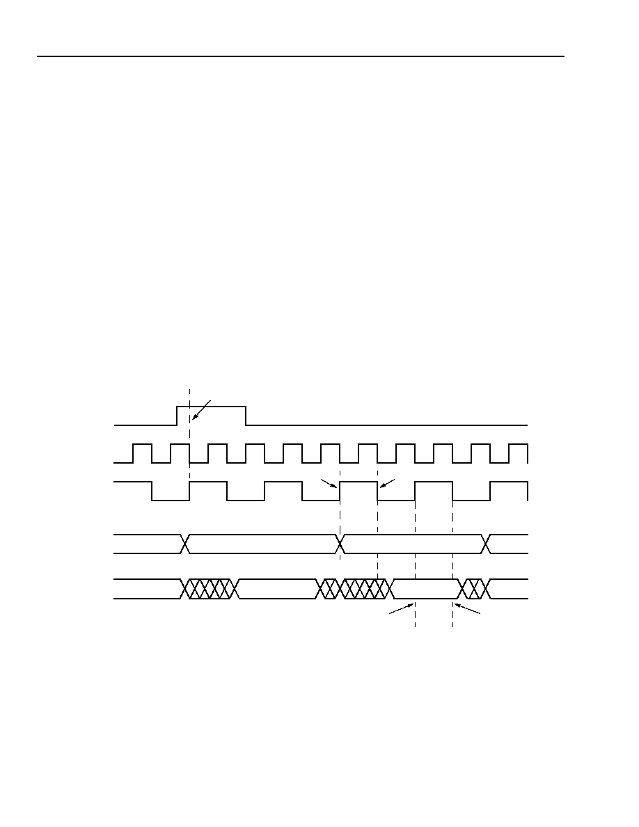
Data Sheet
TECO3264 32-Channel Echo Canceller
August 1999
22
Lucent Technologies Inc.
External Control Connection
(continued)
PCM Input/Output (I/O) Timing and Register Control
(continued)
Bit Offset Operation
The following parameters affect when the first bit of the first time slot (TS0) is transmitted and when the first
received bit is sampled relative to the SYNC clock.
s
Frame Edge Bit (FE)--The FE bit determines which edge of CK8M is used to sample the frame synchronization
(SYNC) clock signal.
s
[C, E]XCE and [X, Y]RCE--The [C, E]XCE bits specify which edge of CK8M is used to transmit data, and the
[X, Y]RCE bit specifies which edge of CK8M is used to sample received data. Received data is sampled at the
middle of the data bit.
Note:For both CMS = 1 (2.048 Mbits/s rate) and CMS = 0 (4.096 Mbits/s rate), a 4.096 MHz reference clock is
used. It is generated internally and its rising edge always coincides with the FE reference edge, whether
FE = 1 or 0 (rising or falling). Figure 11, 4.096 MHz Reference Clock (FE = 0, CK8M Falling Edge) below
shows the case when FE = 0 (CMS = 1). Similarly, Figure 12 on page 23 shows the case for FE = 1 (CMS
= 1).
s
[X, Y]RBOFF and [C, E]XBOFF--The [C, E]XBOFF bits specify the number of CK8M cycles to delay before
transmitting the first bit. Similarly, the [X, Y]RBOFF bits specify the number of CK8M cycles to delay before sam-
pling the first received bit.
5-7343(F)r.2
Figure 11. 4.096 MHz Reference Clock (FE = 0, CK8M Falling Edge)
BIT 7, TS31
BIT 0, TS0
SYNC
CK8M
[C, E]XCE = 0
CK4M
[C, E]XCE = 1
[C, E]PCM
[X, Y]PCM
BIT 7, TS31
BIT 0, TS0
1
18
2
3
4
5
6
7
8
1
10
11
12
13
14
15
16
17
FE = 0
[X, Y]RCE = 0
[X, Y]RCE = 1
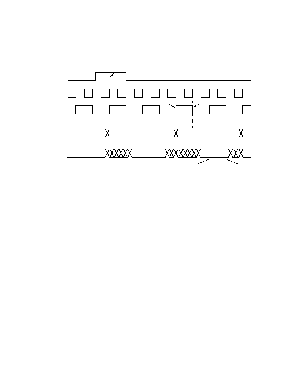
Data Sheet
August 1999
TECO3264 32-Channel Echo Canceller
23
Lucent Technologies Inc.
External Control Connection
(continued)
PCM Input/Output (I/O) Timing and Register Control
(continued)
5-7344(F)r.2
Figure 12. 4.096 MHz Reference Clock (FE = 1, CK8M Rising Edge)
BIT 7, TS31
BIT 0, TS0
SYNC
CK8M
[C, E]XCE = 0
CK4M
[C, E]XCE = 1
[C, E]PCM
[X, Y]PCM
BIT 7, TS31
BIT 0, TS0
1
2
3
4
5
6
7
8
9
10
11
12
13
14
15
16
17
FE = 1
[X, Y]RCE = 0
[X, Y]RCE = 1
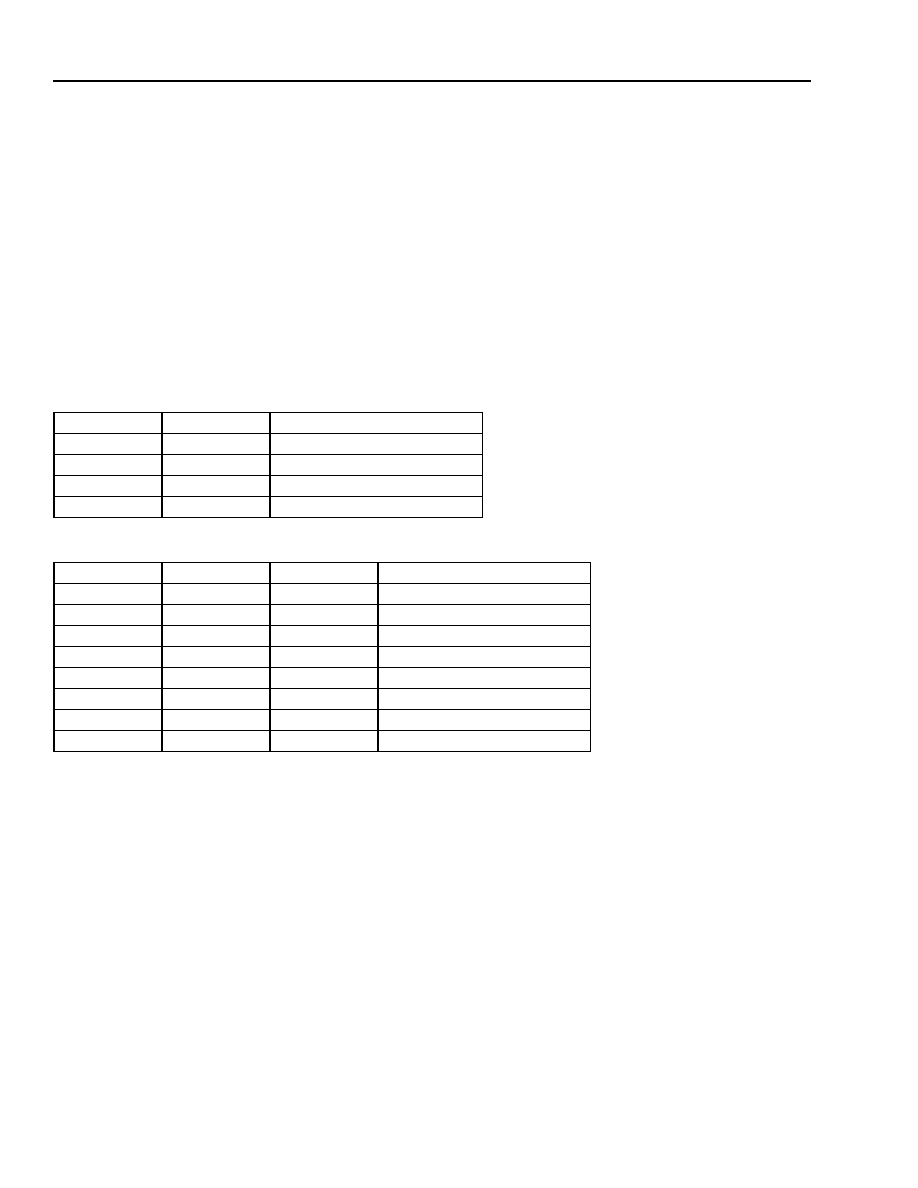
Data Sheet
TECO3264 32-Channel Echo Canceller
August 1999
24
Lucent Technologies Inc.
External Control Connection
(continued)
PCM Input/Output (I/O) Timing and Register Control
(continued)
PCM Offset Programming
To facilitate bit offset programming calculations, two variables are introduced: clock-edge transmit (CET) which
refers to the clock edge of transmission of the first bit of the first time slot, and clock-edge receive (CER) refers to
the clock edge on which the first received bit is sampled. CET and CER are counted with respect to the edge on
which the SYNC clock is sampled. Values of CER and CET depend upon the values of the parameters described
above. If [X, Y]RCE = 1 and [C, E]XCE = 1 are chosen in Figure 11 on page 22, then CER = 12 and CET = 8. Sim-
ilarly, if [X, Y]RCE = 1 and [C, E]XCE = 0, then CER = 12 and CET = 10. Table 3 and Table 4 show the relationship
between CET and CER for both CMS cases. It is important to remember that received data is sampled in the mid-
dle of the data bit.
Table 3. Relationship Between CET and CER, When CMS = 1
Table 4. Relationship Between CET and CER, When CMS = 0
[X, Y]XCE
[C, E]RCE
CER = CET + CK8M Edges
0
0
CET + 4
0
1
CET + 6
1
0
CET + 2
1
1
CET + 4
FE
[X, Y]XCE
[C, E]RCE
CER = CET + CK8M Edges
0
0
0
CET
0
0
1
CET + 2
0
1
0
CET + 2
0
1
1
CET + 4
1
0
0
CET + 4
1
0
1
CET + 2
1
1
0
CET + 6
1
1
1
CET + 4
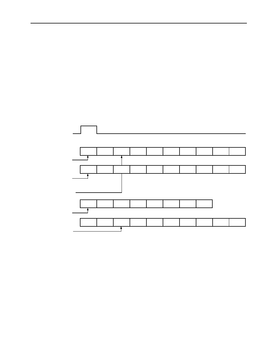
Data Sheet
August 1999
TECO3264 32-Channel Echo Canceller
25
Lucent Technologies Inc.
External Control Connection
(continued)
PCM Input/Output (I/O) Timing and Register Control
(continued)
The bit offset parameters move the PCM stream by 1 bit at the 4.096 Mbits/s rate (by 1/2 bit at the 2.048 Mbits/s
rate) in either direction when you increment or decrement the parameter value by one. For instance, if the sign bit
(for µ-law and A-law, bit 0 = sign, bit 1 = MSB, and bit 7 = LSB) of TS0 is off by 1 bit, then changing the value by
one (increment refers to right direction) will fix it. The range of the bit offset parameter will adjust the output align-
ment bit by bit within one time slot. Since the output data depends on the input data, it is important to know that
changing values in the [X, Y]RBOFF parameters will also offset the output data. Incrementing [X, Y]RBOFF by one
will move the [X, Y] PCM highway by 1 bit (to the right) and the [C, E] PCM highway by 1 bit, but in the opposite
direction. For CMS = 1, the shift is by 1/2 bit. This opposite direction behavior occurs in the output data only when
the receive bit offset parameter is changed. Figure 13, Received and Transmit Offsets Related to Received and
Transmit Data shows how the received and transmit offsets are related to the received and transmit data, respec-
tively.
5-7345(F)r.1
Note: A = any bit within the data stream.
Figure 13. Received and Transmit Offsets Related to Received and Transmit Data
The bulk time-slot delay register will move the output alignment in increments of one time slot. Therefore, for
example, if the output PCM shows up exactly one time slot early, then adding one to this value will move it out one
time slot. The transmit clock edge bit will simply change which clock edge the data is clocked out on.
The frame edge bit for sync sampling (FE, register 0x33 bit 1) samples at the positive-going/rising (FE = 1) or neg-
ative-going/falling edge (FE = 0) of the clock pulse.
The clock enable edge transfer bit for sync sampling (EET, Table 44, Edge Sampling Register (033) [02], on page
78, bit 0) allows the SYNC clock to be shifted by one edge of the CK8M clock. This is very useful in cases when the
rising edge (or falling edge) of the SYNC clock coincides with the edge of the CK8M clock where it is expected to
be sampled. Figure 14, SYNC Shifted to Edge of CK8M shows the cases when FE = 0 and EET = 0; FE = 1 and
EET = 1.
SYNC
RECEIVED DATA
TRANSMIT DATA
0
1
2
3
4
5
6
7
8
9
A2
A3
A4
A5
A6
A7
A8
A9
A0
A1
A2
A3
A4
A5
A6
A7
A8
A9
TRANSMIT OFFSET = 0
RECEIVED OFFSET = 0
RECEIVED DATA
RECEIVED OFFSET = 2
A0
A1
A2
A3
A4
A5
A6
A7
A8
A9
A0
A1
A2
A3
A4
A5
A6
A7
A8
A9
TRANSMIT DATA
TRANSMIT OFFSET = 0
TRANSMIT DATA
TRANSMIT OFFSET = 2
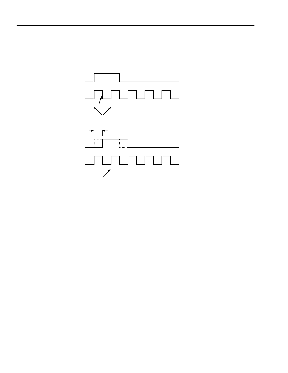
Data Sheet
TECO3264 32-Channel Echo Canceller
August 1999
26
Lucent Technologies Inc.
External Control Connection
(continued)
PCM Input/Output (I/O) Timing and Register Control
(continued)
5-7346(F)r.1
Figure 14. SYNC Shifted to Edge of CK8M
When using all of these parameters, the suggestion is to put all channels in 64-clear mode (set registers 0--1F
equal to 02 hexadecimal) and put in a fixed, recognizable bit pattern on TS0. Then look at the output data and
adjust the parameters above until it is aligned properly. Work initially with the receive path only, and then with the
send path. Once the receive path is aligned, then apply the same offsets for the send path; X and Y should have
the same offset. Similarly, C and E should also have the same offset. Both paths should now be aligned.
Note: In bypass mode, 8-bit data out is equal to the 8-bit data in; however, the condition of having the data aligned
in bypass mode is a necessary condition, but it is not sufficient.
Table 5--Table 8 give decimal values of CET and CER for various values of CMS, [X, Y]RCE, [X, Y]RBOFF[3:0],
[C, E]XBOFF[3:0], and [C, E]XCE.
The suggested procedure to set up the right parameters is as follows:
1.
Set up the TECO3264 in 64-clear mode for all channels but one by setting registers 0x00 = 0x02, 0x01 = 0x00,
and 0x02--0x1F to 0x02. Note that one channel is not being set to 64-clear mode. When using CMS = 1, the
control of time slots (per-channel provisioning) is shifted by one relative to registers 0--1F. Setting register
0x01 = 0x00 means echo cancellation is being enabled for time slot 0 (TS0, first time slot). By the same token,
setting register 0x00 = 0x02 means bypass mode is being enabled for time slot 31 (TS31, last time slot). The
same characteristic applies to the other time slots. For CMS = 0, there is a one-to-one correspondence
between time slots 0--31 and registers 0x00--0x1F, and user should not be concerned; TS0 corresponds to
register 00 and so on.
2.
Start working with the receive path, meaning a test sequence is input in X and observed at C.
3.
Enter a defined sequence pattern, i.e., 0x5B = 01011011 in time slot 0.
SYNC
CK8M
EET = 0
FE = 0
EET = 0
FE = 0
FE = 1? (CANNOT USE FE = 1)
SYNC
CK8M
EET = 1
EET = 1
FE = 1
FE = 1 (CANNOT USE FE = 0)
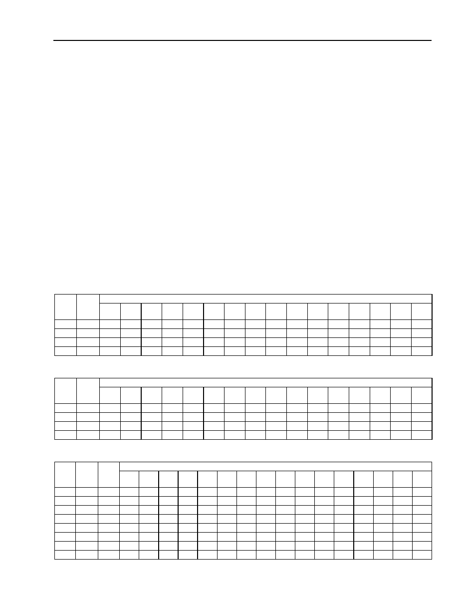
Data Sheet
August 1999
TECO3264 32-Channel Echo Canceller
27
Lucent Technologies Inc.
External Control Connection
(continued)
PCM Input/Output (I/O) Timing and Register Control
(continued)
4.
Adjust the XDLY* value such that TS0 in the XPCM data coincides with TS0 in the CPCM data. If bit 0 of
XPCM (TS0) is received more than 3.9 ms from the reference clock edge (FE), it will be considered internally
by the echo canceller as the time-slot location where it actually falls into within the 125 ms frame. For example,
if bit 0 (TS0) is being received 20 ms from FE, then TS0 will be treated (internally by the echo canceller) as
channel 5 (the sixth time slot). This means that TS27 is being treated as channel 0 (the first time slot) by the
echo canceller. For the purpose of setting the right transmission parameters, place the sequence given in (3) in
time slot 27 and set register 0x1C to 0x00. The sequence will begin 0.5 ms from FE.
5.
Record the initial value of CER. Measure the offset depending on the values of [X, Y]RCE and FE. Suggested
values are [X, Y]RCE = 1 and FE = 1. Also remember that X data is sampled in the middle of the data bit.
6.
Using Table 5, Programming Values (CER = Decimal) for [X, Y]RBOFF, When CMS = 1, or Table 7, Program-
ming Values (CER = Decimal) for [X, Y]RBOFF, When CMS = 0, locate the corresponding [X,Y]RBOFF value.
This value depends on the values of CER, FE, and [X,Y]RCE.
7.
Use Table 3, Relationship Between CET and CER, When CMS = 1, on page 24 or Table 4, Relationship
Between CET and CER, When CMS = 0, on page 24 to determine the value of CET. CET depends on what
edge ([C, E]XCE) the user wishes to transmit the data. FE must be the same as the one used in (6).
8.
Read the corresponding XRBOFF and CXBOFF values.
9.
Set the same offsets for both X and Y as well as C and E.
10. YDLY is XDLY-4.
* It is assumed that the user has already downloaded the recommended values as given in this data sheet.
Table 5. Programming Values (CER = Decimal) for [X, Y]RBOFF, When CMS = 1
Table 6. Programming Values (CET = Decimal) for [C, E]XBOFF, When CMS = 1
Table 7. Programming Values (CER = Decimal) for [X, Y]RBOFF, When CMS = 0
FE
XRCE/
YRCE
XRBOFF, YRBOFF
0
0000
1
0001
2
0010
3
0011
4
0100
5
0101
6
0110
7
0111
8
1000
9
1001
A
1010
B
1011
C
1100
D
1101
E
1110
F
1111
0
0
66
6
10
14
18
22
26
30
34
38
42
46
50
54
58
62
0
1
64
4
8
12
16
20
24
28
32
36
40
44
48
52
56
60
1
0
66
6
10
14
18
22
26
30
34
38
42
46
50
54
58
62
1
1
64
4
8
12
16
20
24
28
32
36
40
44
48
52
56
60
FE
CXCE/
EXCE
CXBOFF, EXBOFF
0
0000
1
0001
2
0010
3
0011
4
0100
5
0101
6
0110
7
0111
8
1000
9
1001
A
1010
B
1011
C
1100
D
1101
E
1110
F
1111
0
0
6
10
14
18
22
26
30
34
38
42
46
50
54
58
62
2
0
1
4
8
12
16
20
24
28
32
36
40
44
48
52
56
60
0
1
0
6
10
14
18
22
26
30
34
38
42
46
50
54
58
62
2
1
1
4
8
12
16
20
24
28
32
36
40
44
48
52
56
60
0
FE
[X, Y]
XCE
[C, E]
RCE
XRBOFF, YRBOFF
0
0000
1
0001
2
0010
3
0011
4
0100
5
0101
6
0110
7
0111
8
1000
9
1001
A
1010
B
1011
C
1100
D
1101
E
1110
F
1111
0
0
0
2
6
10
14
18
22
26
30
34
38
42
46
50
54
58
62
0
0
1
2
6
10
14
18
22
26
30
34
38
42
46
50
54
58
62
0
1
0
0
4
8
12
16
20
24
28
32
36
40
44
48
52
56
60
0
1
1
0
4
8
12
16
20
24
28
32
36
40
44
48
52
56
60
1
0
0
2
6
10
14
18
22
26
30
34
38
42
46
50
54
58
62
1
0
1
2
6
10
14
18
22
26
30
34
38
42
46
50
54
58
62
1
1
0
0
4
8
12
16
20
24
28
32
36
40
44
48
52
56
60
1
1
1
0
4
8
12
16
20
24
28
32
36
40
44
48
52
56
60
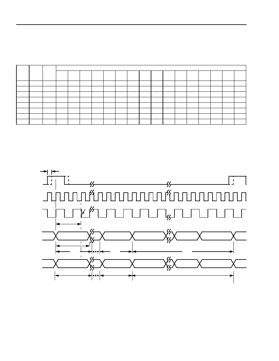
Data Sheet
TECO3264 32-Channel Echo Canceller
August 1999
28
Lucent Technologies Inc.
External Control Connection
(continued)
PCM Input/Output (I/O) Timing and Register Control
(continued)
Table 8. Programming Values (CET = Decimal) for [C, E]XBOFF, When CMS = 0
Figure 15, PCM Input/Output Transmission Parameter Settings shows a typical PCM I/O timing for the given wave-
forms and conditions. Please refer to Table 9 for the description of each note. If the user can set the transmitted
and received data as shown in Figure 15, PCM Input/Output Transmission Parameter Settings, then the setting of
transmission parameters is reduced to Table 9. Otherwise, refer to the PCM Offset Programming section of this
data sheet.
5-7347(F)r.1
Figure 15. PCM Input/Output Transmission Parameter Settings
FE
[X, Y]
XCE
[C, E]
RCE
CRBOFF, ERBOFF
0
0000
1
0001
2
0010
3
0011
4
0100
5
0101
6
0110
7
0111
8
1000
9
1001
A
1010
B
1011
C
1100
D
1101
E
1110
F
1111
0
0
0
6
10
14
18
22
26
30
34
38
42
46
50
54
58
62
2
0
0
1
4
8
12
16
20
24
28
32
36
40
44
48
52
56
60
0
0
1
0
6
10
14
18
22
26
30
34
38
42
46
50
54
58
≠2
2
0
1
1
4
8
12
16
20
24
28
32
36
40
44
48
52
56
≠4
0
1
0
0
6
10
14
18
22
26
30
34
38
42
46
50
54
58
≠2
2
1
0
1
4
8
12
16
20
24
28
32
36
40
44
48
52
56
60
0
1
1
0
6
10
14
18
22
26
30
34
38
42
46
50
54
58
≠2
2
1
1
1
4
8
12
16
20
24
28
32
36
40
44
48
52
56
60
0
BIT 7
BIT 0
SYNC
CK8M
CK4M
[X, Y]PCM
[C, E]PCM
1
2
3
BIT 7
BIT 0
BIT 6
BIT 7
BIT 0
BIT 7
BIT 0
BIT 6
4
11
TS0
TS31
TS30
TS(N MOD 32)
TS(N + 30 MOD 32)
TS(N + 31 MOD 32)
5, 6
8
7, 10
9
(INTERNALLY)
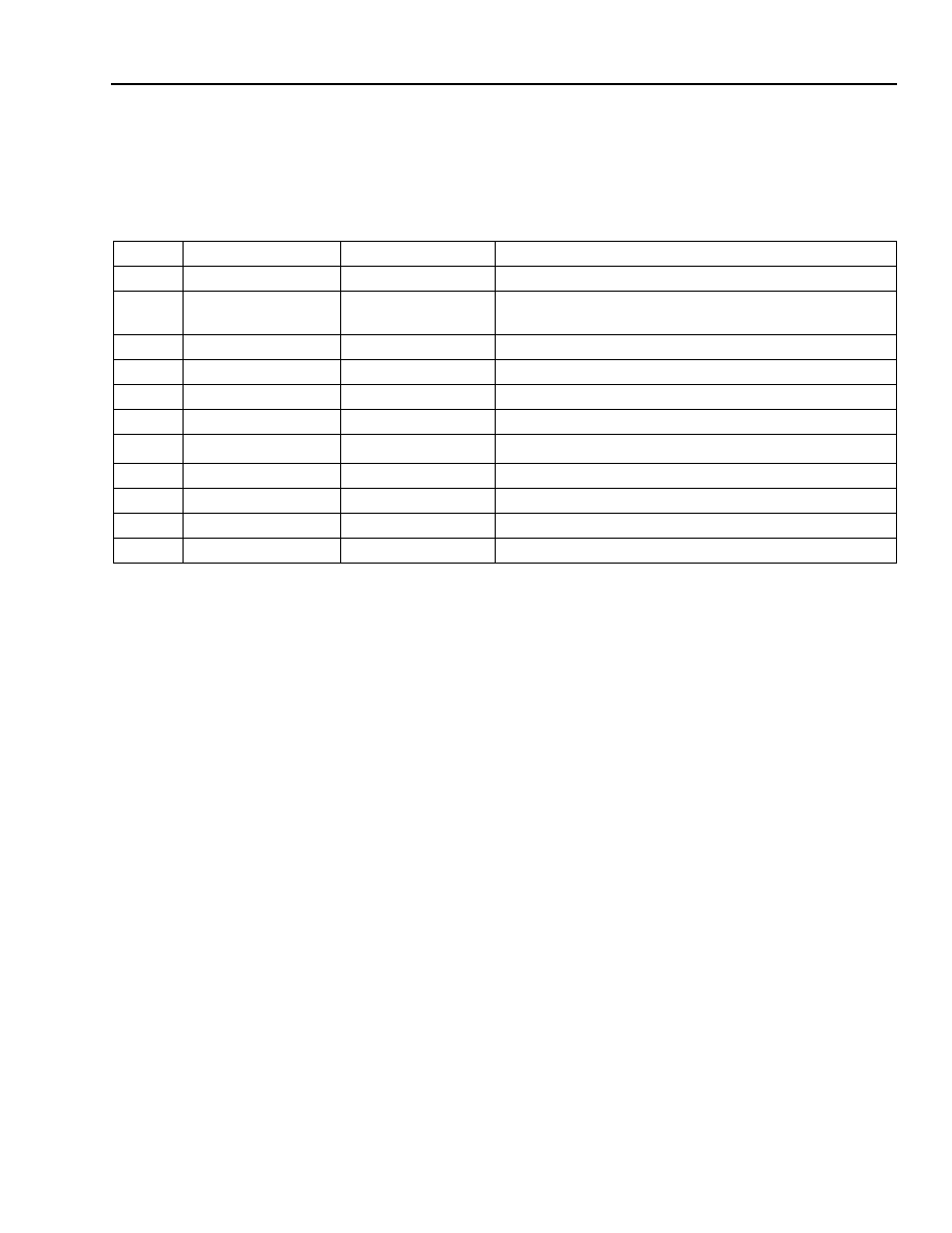
Data Sheet
August 1999
TECO3264 32-Channel Echo Canceller
29
Lucent Technologies Inc.
External Control Connection
(continued)
PCM Input/Output (I/O) Timing and Register Control
(continued)
Table 9. Transmission Parameter Settings and Description for Waveforms in Figure 15, PCM Input/Output
Transmission Parameter Settings
* mod = modulo operation.
The output time-slot number is programmable using XDLY[4:0] for CPCM and YDLY[4:0] for EPCM.
The values of [X, Y]RBOFF and [C, E]XBOFF are read directly from Table 3, Relationship Between CET and CER,
When CMS = 1, on page 24 and Table 4, Relationship Between CET and CER, When CMS = 0, on page 24 for the
conditions given by FE, [C, E]XCE, and [X, Y]RCE.
Note
Parameter
Parameter Setting
Description
1
FE
1
SYNC is sampled at the rising edge of CK8M.
2
EET
1
Enable edge transfer is set to allow SYNC to be shifted
by one edge of CK8M.
3
[X, Y]RCE
0
Receive data is sampled at the falling edge of CK4M.
4
CER
6
Six edges of CK8M.
5
[C, E]XCE
1
Transmit data is sent at the rising edge of CK4M.
6
CET
0
Zero edge of CK8M.
7
TS(N mod* 32)
TS(N = 0)
N is any value in the set [0, 31]
.
8
[X, Y]RBOFF
0x01
Receive bit offset.
9
[C, E]XBOFF
0x0F
Transmit bit offset.
10
[XDLY], [YDLY]
0x19, 0x15
[XDLY, YDLY] delays.
11
CMS
1 (2.048 Mbits/s)
Bit rate select (4 cycles of CK8M).
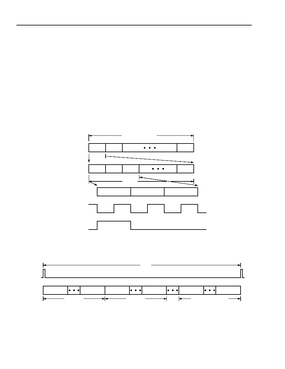
Data Sheet
TECO3264 32-Channel Echo Canceller
August 1999
30
Lucent Technologies Inc.
External Control Connection
(continued)
H-Register Channel Status
The TECO3264 provides pin access to all H-register taps for all 32 channels every 16 ms. This feature is very use-
ful for external processing and debugging. There are three signals to consider:
s
CK32 (pin 44)--the output clock for the H-register data. This is a 32.768 MHz clock signal (CK32, pin 44).
s
HSYNC (pin 55)--the H-register data sync pulse.
s
HDSP (pin 53)--the H-register data clocked out at a rate of 32.768 Mbits/s.
There are 128 frames, 32 time slots per frame, and 128 bits per time slot. These 128 bits per time slot are divided
in three important blocks: the first 16-bit block is header information, the next four 24-bit (96 bits) blocks are H-reg-
ister data (4 taps), and the last 16-bit block is just a fill up zero data. Figure 16, HSYNC, Frames, Bits, etc., Rela-
tionship and Figure 17, HSYNC, HDSP Relationship show the relationship among the H-register sync, frames, time
slots, bits, and the CK32 clock (display output timing ). Table 10 describes the H-register format.
5-7306(F)r.1
Figure 16. HSYNC, Frames, Bits, etc., Relationship
5-7307(F)r.3
Figure 17. HSYNC, HDSP Relationship
1 FRAME
BIT 0
1 TIME SLOT
CK32
HSYNC
BIT 1
BIT 2
BIT 127
TS31
TS0
TS1
BIT 0
BIT 1
BIT 2
128 bits
32 TIME SLOTS
MSB
TS0
TS31
TS0
TS31
TS0
TS31
HSYNC
HDSP
16 ms
FRAME 0
FRAME 1
FRAME 127
LSB
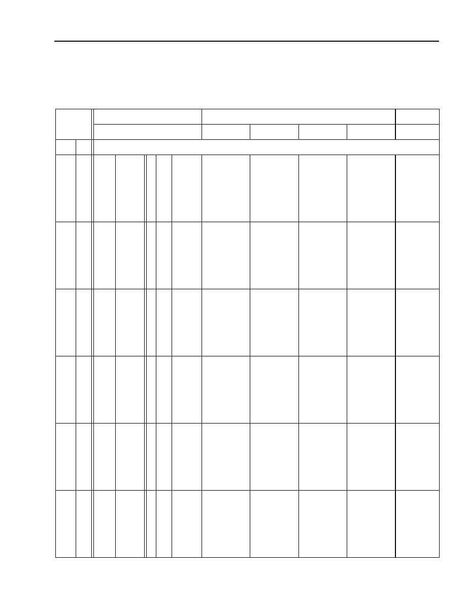
Data Sheet
August 1999
TECO3264 32-Channel Echo Canceller
31
Lucent Technologies Inc.
External Control Connection
(continued)
H-Register Channel Status
(continued)
Table 10. H-Register Display Output Format
Header
4 H Taps
Tail
0--15
16--39
40--63
64--87
88--111
112--127
FR
TS
LSB
MSB
0
0
1
.
.
.
30
31
000
000
.
.
.
000
000
10000
01000
.
.
.
11111
00000
0
0
.
.
.
0
0
00
00
.
.
.
00
10
00000
00000
.
.
.
00000
00000
H511[0:23]
H510[0:23]
H509[0:23]
H508[0:23]
0 . . . 0
1
0
1
.
.
.
30
31
000
000
.
.
.
000
000
10000
01000
.
.
.
11111
00000
0
0
.
.
.
0
0
10
10
.
.
.
10
01
00000
00000
.
.
.
00000
00000
H384[0:23]
H383[0:23]
H382[0:23]
H381[0:23]
0 . . . 0
2
0
1
.
.
.
30
31
000
000
.
.
.
000
000
10000
01000
.
.
.
11111
00000
0
0
.
.
.
0
0
01
01
.
.
.
01
11
00000
00000
.
.
.
00000
00000
H257[0:23]
H256[0:23]
H255[0:23]
H254[0:23]
0 . . . 0
3
0
1
.
.
.
30
31
000
000
.
.
.
000
000
10000
01000
.
.
.
11111
00000
0
0
.
.
.
0
0
11
11
.
.
.
11
00
00000
00000
.
.
.
00000
10000
H130[0:23]
H129[0:23]
H128[0:23]
H127[0:23]
0 . . . 0
4
0
1
.
.
.
30
31
000
000
.
.
.
000
000
10000
01000
.
.
.
11111
00000
0
0
.
.
.
0
0
00
00
.
.
.
00
10
10000
10000
.
.
.
10000
10000
H507[0:23]
H506[0:23]
H505[0:23]
H504[0:23]
0 . . . 0
5
0
1
.
.
.
30
31
000
000
.
.
.
000
000
10000
01000
.
.
.
11111
00000
0
0
.
.
.
0
0
10
10
.
.
.
10
01
10000
10000
.
.
.
10000
10000
H380[0:23]
H379[0:23]
H378[0:23]
H377[0:23]
0 . . . 0
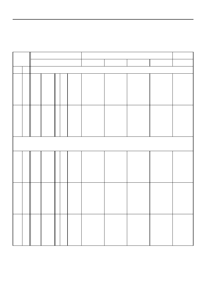
Data Sheet
TECO3264 32-Channel Echo Canceller
August 1999
32
Lucent Technologies Inc.
External Control Connection
(continued)
H-Register Channel Status
(continued)
Table 10. H-Register Display Output Format (continued)
Header
4 H Taps
Tail
0--15
16--39
40--63
64--87
88--111
112--127
FR
TS
LSB
MSB
6
0
1
.
.
.
30
31
000
000
.
.
.
000
000
10000
01000
.
.
.
11111
00000
0
0
.
.
.
0
0
01
01
.
.
.
01
11
10000
10000
.
.
.
10000
10000
H253[0:23]
H252[0:23]
H251{0:23]
H250[0:23]
0 . . . 0
7
0
1
.
.
.
30
31
000
000
.
.
.
000
000
10000
01000
.
.
.
11111
00000
0
0
.
.
.
0
0
11
11
.
.
.
11
00
10000
10000
.
.
.
10000
01000
H126[0:23]
H125[0:23]
H124[0:23]
H123[0:23]
0 . . . 0
.
.
.
120
0
1
.
.
.
30
31
000
000
.
.
.
000
000
10000
01000
.
.
.
11111
00000
0
0
.
.
.
0
0
00
00
.
.
.
00
10
01111
01111
.
.
.
01111
01111
H391[0:23]
H390[0:23]
H389[0:23]
H388[0:23]
0 . . . 0
121
0
1
.
.
.
30
31
000
000
.
.
.
000
000
10000
01000
.
.
.
11111
00000
0
0
.
.
.
0
0
10
10
.
.
.
10
01
01111
01111
.
.
.
01111
01111
H264[0:23]
H263[0:23]
H262[0:23]
H261[0:23]
0 . . . 0
122
0
1
.
.
.
30
31
000
000
.
.
.
000
000
10000
01000
.
.
.
11111
00000
0
0
.
.
.
0
0
01
01
.
.
.
01
11
01111
01111
.
.
.
01111
01111
H137[0:23]
H136[0:23]
H135[0:23]
H134[0:23]
0 . . . 0

Data Sheet
August 1999
TECO3264 32-Channel Echo Canceller
33
Lucent Technologies Inc.
External Control Connection
(continued)
H-Register Channel Status
(continued)
Table 10. H-Register Display Output Format (continued)
Header
4 H Taps
Tail
0--15
16--39
40--63
64--87
88--111
112--127
FR
TS
LSB
MSB
123
0
1
.
.
.
30
31
000
000
.
.
.
000
000
10000
01000
.
.
.
11111
00000
0
0
.
.
.
0
0
11
11
.
.
.
11
00
01111
01111
.
.
.
01111
11111
H010[0:23]
H009[0:23]
H008[0:23]
H007[0:23]
0 . . . 0
124
0
1
.
.
.
30
31
000
000
.
.
.
000
000
10000
01000
.
.
.
11111
00000
0
0
.
.
.
0
0
00
00
.
.
.
00
10
11111
11111
.
.
.
11111
11111
H387[0:23]
H386[0:23]
H385[0:23]
H003[0:23]
0 . . . 0
125
0
1
.
.
.
30
31
000
000
.
.
.
000
000
10000
01000
.
.
.
11111
00000
0
0
.
.
.
0
0
10
10
.
.
.
10
01
11111
11111
.
.
.
11111
11111
H260[0:23]
H259[0:23]
H258[0:23]
H002[0:23]
0 . . . 0
126
0
1
.
.
.
30
31
000
000
.
.
.
000
000
10000
01000
.
.
.
11111
00000
0
0
.
.
.
0
0
01
01
.
.
.
01
11
11111
11111
.
.
.
11111
11111
H133[0:23]
H132[0:23]
H131[0:23]
H001[0:23]
0 . . . 0
127
0
1
.
.
.
30
31
000
000
.
.
.
000
000
10000
01000
.
.
.
11111
00000
0
0
.
.
.
0
0
11
11
.
.
.
11
00
11111
11111
.
.
.
11111
11111
H006[0:23]
H005[0:23]
H004[0:23]
H000[0:23]
0 . . . 0
Data Sheet
TECO3264 32-Channel Echo Canceller
August 1999
34
Lucent Technologies Inc.
Parameters
Parameter Overview
Tables 11--18 list all of the parameters in the echo canceller chip. Some of the parameters are single bits and
some are groups of bits (these are shown with [n:m] to indicate that the index starts from m and goes to n inclu-
sively). The parameter map shows the mapping of the parameter name to its specific address (or addresses for
multibyte parameters). The echo canceller contains two memory pages, referred to as page 0 and page 1. Page 0
has a base address of 0, and page 1 has a base address of 0x100. Thus, the page 1 parameters have an absolute
address of 0x100 to 0x10E. Page 0 parameters are all configurable (read/write), while page 1 parameters are read-
only parameters, with the exceptions of the mask parameters (register 0x101 and 0x103) which are also read/write.
Per-Channel Control Parameters
Table 11 lists the parameters that control various functions on a per-channel basis. For each function, there are
32 single bit parameters corresponding to the 32 channels processed by the chip. Index 0 corresponds to time slot
0. The memory map shows all of the time slot 0 control bits located in byte 0. Thus, the first 32 bytes in the memory
map are referred to as the per-channel control words and the address corresponds to the time slot that the word
controls. See Table 19, Parameter Address Map, on page 45 for illustration.
* Single-bit 32-register parameters.
Table 11. Per-Channel Control Parameters
Symbol*
Description
Memory Map
Starting Address (Hex)
DEC
Per-channel disable of echo canceller for time slots 0 to 31.
1 = disable EC; 0 = enable EC.
0x00
EBP
Per-channel 64 clear enable for time slots 0 to 31.
1 = enable; 0 = disable.
0x00
ENLP
Per-channel enable of nonlinear processor for time slots 0 to 31.
1 = enable; 0 = disable.
0x00
HRST
Per-channel H-register reset for time slots 0 to 31.
1 = reset; 0 = no reset.
0x00
HFRZ
Per-channel H-register freeze for time slots 0 to 31.
1 = freeze; 0 = no freeze.
0x00
CALLB
Per-channel call boundary for time slots 0 to 31.
0
1 transition = call boundary; otherwise, no call boundary.
0x00

Data Sheet
August 1999
TECO3264 32-Channel Echo Canceller
35
Lucent Technologies Inc.
Parameters
(continued)
Mask Bits
Table 12 shows the mask parameters. Mask bits are single-bit parameters that allow a particular source to control
a particular function (such as 2100 Hz tone detection to disable the EC on a per-digroup basis).
Note: The provisioning of the mask is per-digroup, but the action is per-channel.
Table 12. Mask Parameters
Symbol
Description
Memory Map
Starting Address (Hex)
MECTD
Mask for 2100 Hz straight tone (TD) control of EC function.
1 = allow control; 0 = mask.
0x20
MECTDPR Mask for 2100 Hz phase reversed (TDPR) control of EC function.
1 = allow control; 0 = mask.
0x20
MECVPA
Mask for 2010 Hz VPA tone (VPA) control of EC function.
1 = allow control; 0 = mask.
0x20
MECEXT
Mask for ECDIS external pin control of EC function.
1 = allow control; 0 = mask.
0x20
MBIT15X
Mask for bit 15 of XPCM input control of EC function.
1 = allow control; 0 = mask.
0x20
MBIT15Y
Mask for bit 15 of YPCM input control of EC function.
1 = allow control; 0 = mask.
0x20
MBPTD
Mask for 2100 Hz straight tone (TD) control of 64-clear function.
1 = allow control; 0 = mask.
0x21
MBPTDPR Mask for 2100 Hz phase reversed (TDPR) control of 64-clear function.
1 = allow control; 0 = mask.
0x21
MBPVPA
Mask for 2100 Hz VPA tone (VPA) control of 64-clear function.
1 = allow control; 0 = mask.
0x21
MBPEXT
Mask for ECDIS external pin control of 64-clear function.
1 = allow control; 0 = mask.
0x21
MBP15X
Mask for bit 15 of XPCM input control of 64-clear function.
1 = allow control; 0 = mask.
0x21
MBP15Y
Mask for bit 15 of YPCM input control of 64-clear function.
1 = allow control; 0 = mask.
0x21
MNLPINT
Mask for internal (normal) control of NLP.
1 = allow control; 0 = mask.
0x22
MNLPEXT
Mask for NLPEN external pin control of NLP.
1 = allow control; 0 = mask.
0x22
MTNLP
Mask for transient control of NLP.
1 = allow control; 0 = mask.
0x22
MNLPFRZ
Mask for NLPFRZ control of NLP freeze.
1 = allow control; 0 = mask.
0x22
MHPFXEC Mask for EC control to also enable/disable high-pass filter in X direction.
1 = allow control; 0 = mask.
0x22
MHPFYEC Mask for EC control to also enable/disable high-pass filter in Y direction.
1 = allow control; 0 = mask.
0x22
MFREEZE
Mask for NES + not-FES control of H freeze.
1 = allow control; 0 = mask.
0x22
Data Sheet
TECO3264 32-Channel Echo Canceller
August 1999
36
Lucent Technologies Inc.
Parameters
(continued)
Mask Bits
(continued)
Echo Canceller (EC) Parameters
Table 13 shows the EC parameters which are generally static in nature.
Table 12. Mask Parameters (continued)
Symbol
Description
Memory Map
Starting Address (Hex)
MHRSTEXT Mask for HRST control of H reset.
1 = allow control; 0 = mask.
0x23
MHERR
Mask for error condition reset of H register.
1 = allow reset; 0 = mask.
0x23
MEYRST
Mask for > y control of H-register reset.
1 = allow reset; 0 = mask.
0x23
MNBE
Mask for narrowband energy (NBE) control of H freeze.
1 = allow control; 0 = mask.
0x23
MHFRZEXT Mask for HFRZ external pin control of H reset.
1 = allow control; 0 = mask.
0x23
MFES
Mask for FES component of mask-freeze control of H freeze.
Note: 0 = include FES; 1 = do not include FES.
0x23
MNES1
Mask for NES1 component of mask-freeze control of H freeze.
Note: 0 = include NES1; 1 = do not include NES1.
0x23
MNES3
Mask for NES3 component of mask-freeze control of H freeze.
Note: 0 = include NES3; 1 = do not include NES3.
0x23
Table 13. EC Parameters
Symbol
Description
Memory Map
Starting Address (Hex)
LEAK[7:0]
H-register leak rate during adaptation
0x24
LFREQ[1:0]
H-register leak application rate
0x25
XHPFEN
X high-pass filter enable
0x25
YHPFEN
Y high-pass filter enable
0x25
FESTH[12:0]
Far-end speech threshold
0x26
NBEPKF[7:0] Narrowband energy peak factor
0x28
WBEPKF[7:0] Wideband energy peak factor
0x29
HZETA[7:0]
E and Y EMP gain filter constant
0x39
HGAMMA[7:0] E and Y EMP filter time constant
0x68
e^
Data Sheet
August 1999
TECO3264 32-Channel Echo Canceller
37
Lucent Technologies Inc.
Parameters
(continued)
PCM Transmission Parameters
The parameters in Table 14 relate to the flexibility of the PCM interface. They generally instruct the device as to the
I/O format of the PCM interface ports.
* See note in Bit Offset Operation section on page 22.
Table 14. Transmission Parameters
Symbol
Description
Memory Map
Starting Address (Hex)
XRCE
Receive clock edge.
0 = sample receive data on the falling edge of CK8M*.
1 = sample receive data on the rising edge of CK8M*.
0x2A
XRBOFF[3:0] X receive bit offset. These four bits provide a fixed offset, relative to
the frame-synchronization pulse (SYNC), for the first bit received in
each time slot. The offset is the number of data periods by which
reception of the first bit on [X] is delayed. All subsequent receptions of
the first bit also follow this offset. One data period (1 bit) equals to 4
cycles of CK8M for CMS = 1, and 2 cycles of CK8M for CMS = 0.
Received data is sampled in the middle of the data bit.
0x2A
TMODE[1:0]
109-test mode.
TMODE0 = 1 send data to one channel.
TMODE1 = 1 send data to all channels.
0x2A
XPY[2:0]
X input parity detection options.
XPY0 = 1 enable parity checking; 0 = disable.
XPY1 = 1 even parity; 0 = odd parity.
XPY2 = 1 bit 8; 0 = bit 15.
0x2B
XCODEC
X input invert select (1 = inverted; 0 = noninverted).
0x2E
XULAW
X input A-law/
µ
-law select.
0x2E
AEN
Enable use of XLINEAR linear PCM input port (active-high).
0x2E
CCODEC
C output PCM invert select (1 = inverted; 0 = noninverted).
0x2E
CULAW
C output A-law/
µ
-law select.
0x2E
CUAADJ
C output A-law/
µ
-law adjustment.
0x2E
CPY[2:0]
C output parity generation options.
CPY0 = 1 enable parity generation/0 = disable.
CPY1 = 1 even parity; 0 = odd disable.
CPY2 = 1 bit 8; 0 = bit 15.
0x2F
CXBOFF[3:0] C transmit bit offset. These 4 bits provide a fixed offset, relative to the
frame-synchronization pulse (SYNC), for the first bit transmitted in
each time slot. The offset is the number of data periods by which
transmission of the first bit on [C] is delayed. All subsequent
transmissions of the first bit follow this offset. One data period (1 bit)
equals 4 cycles of CK8M for CMS = 1, and 2 cycles of CK8M for
CMS = 0.
0x2F
CXCE
C transmit clock edge.
0 = transmit on falling edge of CK8M*.
1 = transmit on rising edge of CK8M*.
0x2F
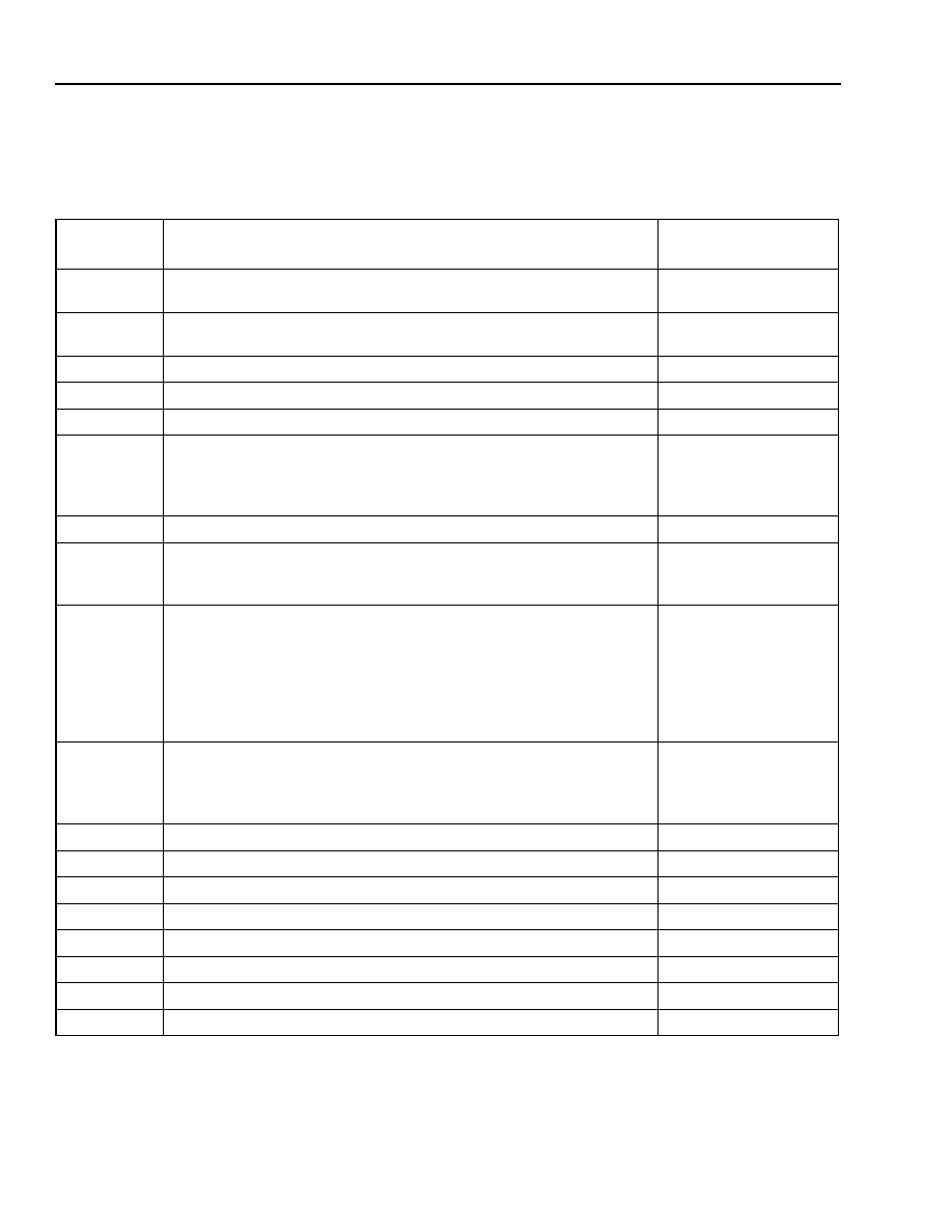
Data Sheet
TECO3264 32-Channel Echo Canceller
August 1999
38
Lucent Technologies Inc.
Parameters
(continued)
PCM Transmission Parameters
(continued)
* See note in Bit Offset Operation section on page 22.
Table 14. Transmission Parameters (continued)
Symbol
Description
Memory Map
Starting Address (Hex)
XDLY[4:0]
X
C delay. Provides up to one complete frame delay.
XDLY X
C direction bulk time-slot delay.
0x30
YDLY[4:0]
Y
E delay. Provides up to one complete frame delay.
YDLY Y
E direction bulk time-slot delay.
0x31
EX
Exercise parity error.
0x32
XCOMP
X input companded/linear select.
0x32
EET
Enable edge transfer bit for sync sampling.
0x33
FE
Frame edge. This bit allows the flexibility to sample the SYNC pulse on
either a rising or a falling edge of CK8M.
0 = SYNC is sampled on the falling edge of CK8M.
1 = SYNC is sampled on the rising edge of CK8M.
0x33
WEMODE
Write enable mode for external SRAM.
0x34
YRCE
Y receive clock edge.
0 = sample receive data on the falling edge of CK8M*.
1 = sample receive data on the rising edge of CK8M*.
0x35
YRBOFF[3:0] Y receive bit offset. These 4 bits provide a fixed offset, relative to the
frame-synchronization pulse (SYNC), for the first bit received in each
time slot. The offset is the number of data periods by which reception
of the first bit on [Y] is delayed. All subsequent receptions of the first bit
also follow this offset. One data period (1 bit) equals to 4 cycles of
CK8M for CMS = 1, and 2 cycles of CK8M for CMS = 0. Received data
is sampled in the middle of the data bit.
0x35
YPY[2:0]
Y input parity options.
YPY0 = 1 enable parity checking; 0 = disable.
YPY1 = 1 even parity; 0 = odd parity.
YPY2 = 1 bit 8; 0 = bit 15.
0x35
YCODEC
Y PCM input invert select (1 = inverted; 0 = noninverted).
0x36
YULAW
Y input A-law/
µ
-law select.
0x36
YCOMP
Y input companded/linear select.
0x36
EXY
Y input force parity error.
0x36
EULAW
E input A-law/
µ
-law select.
0x3A
ECOMP
E output companded/linear select.
0x3A
ECODEC
E output invert select (1 = inverted; 0 = noninverted).
0x3A
EUAADJ
E A-law/
µ
-law adjustment.
0x3A

Data Sheet
August 1999
TECO3264 32-Channel Echo Canceller
39
Lucent Technologies Inc.
Parameters
(continued)
PCM Transmission Parameters
(continued)
Table 14. Transmission Parameters (continued)
* See note in Bit Offset Operation section on page 22.
Symbol
Description
Memory Map
Starting Address (Hex)
EXBOFF[3:0]
E transmit bit offset. These 4 bits provide a fixed offset, relative to the
frame-synchronization pulse (SYNC), for the first bit transmitted in
each time slot. The offset is the number of data periods by which
transmission of the first bit on [E] is delayed. All subsequent
transmissions of the first bit follow this offset. One data period (1 bit)
equals 4 cycles of CK8M for CMS = 1, and 2 cycles of CK8M for
CMS = 0.
0x3A
EPY[2:0]
E output parity generation options.
EPY0 = 1 enable parity generation; 0 = disable.
EPY1 = 1 even parity; 0 = odd parity.
EPY2 = 1 bit 8; 0 = bit 15.
0x3B
EXCE
E transmit clock edge.
0 = transmit on falling edge of CK8M*.
1 = transmit on rising edge of CK8M*.
0x3B
CMS
Bit rate select. 1 = 2.048 Mbits/s data rate; 0 = 4.096 Mbits/s data rate.
0x2A

Data Sheet
TECO3264 32-Channel Echo Canceller
August 1999
40
Lucent Technologies Inc.
Parameters
(continued)
Tone Disabler Parameters
The parameters in Table 15 are used to determine the characteristics of the straight tone detector (TD), the tone
detector with periodic phase reversals (TDPR), and voice path assurance tone detection (VPA).
* See Table 128, Tone Detector Indicator Registers (107--10E), on page 118 for more details.
Table 15. Tone Disabler Parameters
Symbol
Description
Memory Map
Starting Address (Hex)
LOWCT[5:0]
Number of peaks in interval for low side of 2100 Hz.
0x3D
HICT[5:0]
Number of peaks in interval for high side of 2100 Hz.
0x3E
BADCT[1:0]
Number of bad intervals to reject 2100 Hz.
0x3E
GOODCT[5:0]
Number of good intervals to declare 2100 Hz.
0x3F
BADVPACT[1:0]
Number of bad intervals to reject VPA detection.
0x3F
MINXFRM[10:0]
Number of good intervals to declare VPA detection.
0x40
MAXHOLDTD[3:0]
Maximum silent interval before dropping tone detection.
0x41
MINPRBADCT[1:0]
Maximum number of bad primitive PR counts.
0x42
MINPRBLOCK[5:0]
Minimum number of 8 ms intervals between PRs.
0x42
MAXTDPR[8:0]
Maximum interval between PRs.
0x43
PRBADCONSEC
Controls whether bad PR counts can be consecutive.
0x43
MINPRGOODCT[2:0] Number of primitive PRs to indicate a PR.
0x44
GOODVPACT[2:0]
Number of good VPA counts to detect VPA.
0x44
PRNUM[1:0]
Number of PRs to declare TDPR (1000R is set to 2).
0x44
LOWVPACT[5:0]
Number of peaks in interval for high side of VPA.
0x45
CLRNTD
Clear TD SV storage.
0x45
HIVPACT[5:0]
Number of peaks in interval for high side of VPA.
0x46
TDTESTX
TD test input for X direction.
0x46
TDTESTY
TD test input for Y direction.
0x46
MINVPAPWR[7:0]
Minimum power to detect VPA.
0x47
MINPWRDET[7:0]
Minimum power to detect 2100 Hz.
0x48
TDCLRN2
Clear TD SV outputs.
0x49
VARP[4:0]
Sets channel alignment for TD, TDPR, and VPA outputs.
0x49
ENTDPRNF
Enable new TDPR feature.
0x4A
ENTDNF
Enable new TD feature.
0x4A
TDPRTHR[2:0]
Number of PRs allowed between valid PRs.
0x4A
TDTHR[2:0]
Number of PRs allowed during TD detection.
0x4A
SVTD[7:0]
Tone disabler state variable storage test.
0x3C
TIN
TD test input to speed up 8 ms window.
0x3D
TMODE
TD test input.
0x3D
TD
Per-channel TD indication*.
TD = 1
TD detected.
TD = 0
TD not detected.
0x107
TDPR
Per-channel TDPR indication*.
TDPR = 1
TDPR detected.
TDPR = 0
TDPR not detected.
0x107
EYTDSEL
Selects Y or Í input to TD.
0x107

Data Sheet
August 1999
TECO3264 32-Channel Echo Canceller
41
Lucent Technologies Inc.
Parameters
(continued)
Nonlinear Processor Parameters
The parameters in Table 16 determine the selection of nonlinear processor (NLP) options and how those selected
options will behave. The NLP works in conjunction with the linear processor to provide total echo control.
Table 16. Nonlinear Processor Parameters
Symbol
Description
Memory Map
Starting Address (Hex)
YHI[12:0]
Y threshold for significant energy.
0x4B
NMATCHEN
Enable noise matching.
0x4C
MAXMEMP[13:0] Maximum value of Í noise floor estimate.
0x4E
GAMMA[7:0]
Upward adaptation rate for Í noise floor estimate.
0x50
EMPCLP[13:0]
Clamp on Í EMP for noise floor estimate.
0x51
EX[1:0]
Error exercise bits.
0x52
MHI[13:0]
High hysteresis threshold for noise floor estimate.
0x53
VARLOSS
Sets noise matching mode to variable loss.
0x54
SELNF
Noise floor select for colored noise matching.
0x54
MLO[13:0]
Low hysteresis threshold for noise floor estimate.
0x55
NLPFRZ
Nonlinear processor freeze.
0x56
USE_SNLP
Soft NLP select.
0x56
AN1[4:0]
Noise floor estimate scale factor.
0x57
MSCALE[2:0]
Noise floor estimate scale factor.
0x57
AN2[5:0]
Noise floor scaling factor used to compare with Esoft.
0x58
USE_ZERO
Í zero crossing select.
0x58
USE_NM
Noise transparency select.
0x58
INT_TIME[9:0]
SNLP interval time.
0x59
TESTNM[5:0]
Noise matching circuit test inputs.
0x5A
NUM_INTS[8:0]
Number of intervals (steps) for SNLP action before noise matching.
0x5B
ELOSS[13:0]
Loss increment for attenuated Í.
0x5C
CLRNLP
Active-low clear of NLP state variable storage.
0x5D
ZERO_THR[7:0] Í zero crossing select.
0x5E
LOSS_INC[13:0] SNLP incremental loss factor applied every 125*INT_TIME µs
during ramp mode.
Max loss = NUM_intervals * LOSS_INC.
0x5F
TESTSV[7:0]
Test inputs for NLP SV storage.
0x61
SVT[21:0]
Test inputs for NLP SV storage.
0x62

Data Sheet
TECO3264 32-Channel Echo Canceller
August 1999
42
Lucent Technologies Inc.
Parameters
(continued)
Control Parameters
The parameters in Table 17 generally determine how the various detectors are used to control the operation of the
linear processor and NLP. Things such as near-end speech detection, adaptation control, NLP control, etc., fall
under this category of parameters.
Table 17. Control Parameters
Symbol
Description
Memory Map
Starting Address (Hex)
XLOSS[1:0]
X loss pad value.
0 = 0 dB
1 = 6 dB
2 = 12 dB
3 = Not allowed
0x67
YLOSS[1:0]
Y loss pad value.
0 = 0 dB
1 = 6 dB
2 = 12 dB
3 = Not allowed
0x67
NESPHOC[8:0] NES hangover.
0x4D
FGAIN[7:0]
Fast convergence gain.
0x69
SGAIN[7:0]
Slow convergence gain.
0x6A
FBETA[12:0]
Fast convergence mode beta.
0x6B
P[1:0]
NBE threshold select.
0x6C
ZEROSVRAM Clear SV storage RAM in control circuit.
0x6C
SBETA[12:0]
Slow convergence mode beta.
0x6D
XSIGN
Controls X sign bit of control multiplier for test.
0x6E
YSIGN
Controls Y sign bit of control multiplier for test.
0x6E
TGAIN[7:0]
Fast convergence gain time.
0x6F
TFNLP[7:0]
Fast convergence NLP fast beta time.
0x70
AVOICE[7:0]
Hybrid return loss threshold for voice signals.
0x71
MASK0
H-reset transition mask.
0x72
MASK1
External event mask.
0x72
MASK2
E vs. Y calculation mask.
0x72
MASK3
VPA on-off mask.
0x72
ADATA[7:0]
Hybrid return loss threshold for data signals.
0x73
NES1HOC[8:0] Near-end speech hangover.
0x74
NLPHOC[8:0]
NLP hangover.
0x75
NES3THR[8:0] NES3 hangover.
0x76
THR1[7:0]
E vs. Y fast convergence threshold.
0x77
THR2[7:0]
E vs. Y TNLP threshold.
0x78
THR3[7:0]
E vs. Y H-reset threshold.
0x79
B3[7:0]
NES3 X vs. E compare threshold.
0x7A
TOFFSET[4:0] Sets channel alignment for control output signals.
0x7B

Data Sheet
August 1999
TECO3264 32-Channel Echo Canceller
43
Lucent Technologies Inc.
Parameters
(continued)
Test and Diagnostic Parameters
The parameters in Table 18 are associated with the test and diagnostic features of the echo canceller chip.
Table 18. Test and Diagnostic Parameters
Symbol
Description
Memory Map
Starting Address (Hex)
EXCUP[1:0]
CUP exercise bits.
0x65
INIT
CUP only reset.
0x65
ERAMTEST
External RAM test.
0x65
DRINIT
D RAM initialize used for initialization and vectors.
0x65
ERAMINIT
E RAM initialize used for initialization and vectors.
0x65
MODE1CH
One channel mode (quickturn only).
0x65
CUPDIS
CUP disable. (When set, Í = Y for all channels.)
0x65
TESTCON[2:0]
TEST[7:0] output MUX select control.
0x66
PERRRV48
X parity error.
0x100
YPERRV48
Y parity error.
0x100
ERR2
NLP error.
0x100
ERR3
NLP error.
0x100
ERR4
NLP error.
0x100
OXPYERR
CUP high HC register overflow.
0x100
EXPYERR
CUP parity error.
0x100
HPYERR
CUP parity error.
0x100
PERRV48M
Mask PERRV48 from generating interrupt.
0x101
YPERV48M
Mask YPERRV48 from generating interrupt.
0x101
ERR2M
Mask ERR2 from generating interrupt.
0x101
ERR3M
Mask ERR3 from generating interrupt.
0x101
ERR4M
Mask ERR4 from generating interrupt.
0x101
OXPYERRM
Mask OXPYERR from generating interrupt.
0x101
EXPYERRM
Mask EXPYERR from generating interrupt.
0x101
HPYERRM
Mask HPYERR from generating interrupt.
0x101
DMPYERR
DAU parity error.
0x102
DAUOVERFLO
DAU overflow.
0x102
MPYERR
CUP parity error.
0x102
OVF
TD overflow error.
0x102
BADRANGE
Write or read to nonexistent memory.
0x102
BADWRITE
Write error.
0x102
DMPYERRM
Mask DMPYERR from generating interrupt.
0x103
DAUOVERFLOM Mask DAUOVERFLO from generating interrupt.
0x103
MPYERRM
Mask MPYERRM from generating interrupt.
0x103
OVFM
Mask OVF from generating interrupt.
0x103
BADRANGEM
Mask BADRANGE from generating interrupt.
0x103
BADWRITEM
Mask BADWRITE from generating interrupt.
0x103

Data Sheet
TECO3264 32-Channel Echo Canceller
August 1999
44
Lucent Technologies Inc.
Parameters
(continued)
Test and Diagnostic Parameters
(continued)
Table 18. Test and Diagnostic Parameters (continued)
Symbol
Description
Memory Map
Starting Address (Hex)
TCHAN[4:0]
EC vector test channel select.
0x2B
XDATA[15:0]
X data for 109-test.
0x2C
YDATA[15:0]
Y data for 109-test.
0x37
CDATAVFX[7:0]
C data readback for 109-test.
0x104
EDATAVFX[15:0] E data readback for 109-test.
0x105
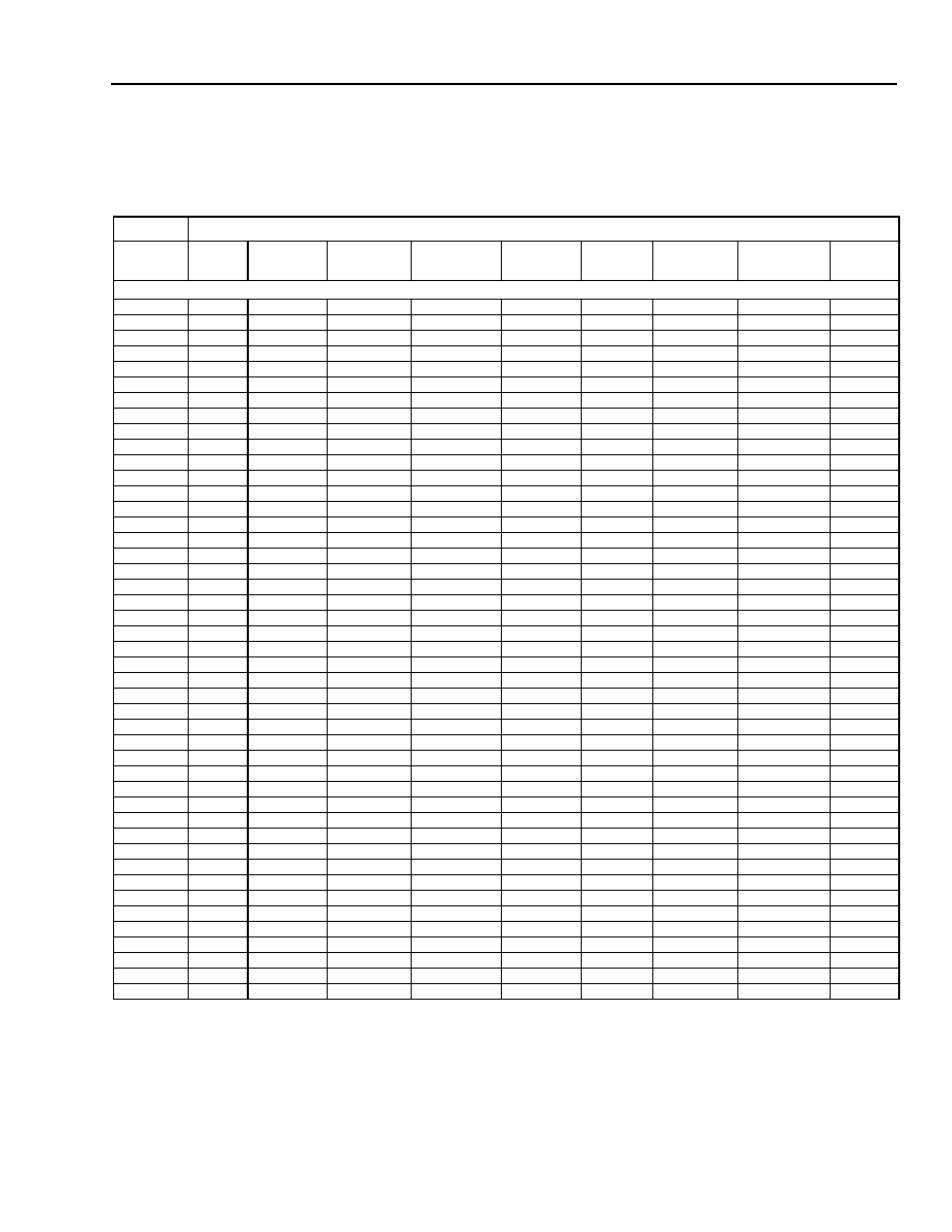
Data Sheet
August 1999
TECO3264 32-Channel Echo Canceller
45
Lucent Technologies Inc.
Parameter Map
Table 19 maps each echo canceller chip parameter to its address.
Table 19. Parameter Address Map
Register
Bit Number
Address
(Hex)
7
6
5
4
3
2
1
0
Recommended
Value (Hex)
Read/Write
0x00
--
--
CALLB0
HFRZ0
HRST0
ENLP0
EBP0
DEC0
00
0x01
--
--
CALLB1
HFRZ1
HRST1
ENLP1
EBP1
DEC1
00
0x02
--
--
CALLB2
HFRZ2
HRST2
ENLP2
EBP2
DEC2
00
0x03
--
--
CALLB3
HFRZ3
HRST3
ENLP3
EBP3
DEC3
00
0x04
--
--
CALLB4
HFRZ4
HRST4
ENLP4
EBP4
DEC4
00
0x05
--
--
CALLB5
HFRZ5
HRST5
ENLP5
EBP5
DEC5
00
0x06
--
--
CALLB6
HFRZ6
HRST6
ENLP6
EBP6
DEC6
00
0x07
--
--
CALLB7
HFRZ7
HRST7
ENLP7
EBP7
DEC7
00
0x08
--
--
CALLB8
HFRZ8
HRST8
ENLP8
EBP8
DEC8
00
0x09
--
--
CALLB9
HFRZ9
HRST9
ENLP9
EBP9
DEC9
00
0x0A
--
--
CALLB10
HFRZ10
HRST10
ENLP10
EBP10
DEC10
00
0x0B
--
--
CALLB11
HFRZ11
HRST11
ENLP11
EBP11
DEC11
00
0x0C
--
--
CALLB12
HFRZ12
HRST12
ENLP12
EBP12
DEC12
00
0x0D
--
--
CALLB13
HFRZ13
HRST13
ENLP13
EBP13
DEC13
00
0x0E
--
--
CALLB14
HFRZ14
HRST14
ENLP14
EBP14
DEC14
00
0x0F
--
--
CALLB15
HFRZ15
HRST15
ENLP15
EBP15
DEC15
00
0x10
--
--
CALLB16
HFRZ16
HRST16
ENLP16
EBP16
DEC16
00
0x11
--
--
CALLB17
HFRZ17
HRST17
ENLP17
EBP17
DEC17
00
0x12
--
--
CALLB18
HFRZ18
HRST18
ENLP18
EBP18
DEC18
00
0x13
--
--
CALLB19
HFRZ19
HRST19
ENLP19
EBP19
DEC19
00
0x14
--
--
CALLB20
HFRZ20
HRST20
ENLP20
EBP20
DEC20
00
0x15
--
--
CALLB21
HFRZ21
HRST21
ENLP21
EBP21
DEC21
00
0x16
--
--
CALLB22
HFRZ22
HRST22
ENLP22
EBP22
DEC22
00
0x17
--
--
CALLB23
HFRZ23
HRST23
ENLP23
EBP23
DEC23
00
0x18
--
--
CALLB24
HFRZ24
HRST24
ENLP24
EBP24
DEC24
00
0x19
--
--
CALLB25
HFRZ25
HRST25
ENLP25
EBP25
DEC25
00
0x1A
--
--
CALLB26
HFRZ26
HRST26
ENLP26
EBP26
DEC26
00
0x1B
--
--
CALLB27
HFRZ27
HRST27
ENLP27
EBP27
DEC27
00
0x1C
--
--
CALLB28
HFRZ28
HRST28
ENLP28
EBP28
DEC28
00
0x1D
--
--
CALLB29
HFRZ29
HRST29
ENLP29
EBP29
DEC29
00
0x1E
--
--
CALLB30
HFRZ30
HRST30
ENLP30
EBP30
DEC30
00
0x1F
--
--
CALLB31
HFRZ31
HRST31
ENLP31
EBP31
DEC31
00
0x20
--
--
MBIT15Y
MBIT15X
MECEXT
MECVPA
MECTDPR
MECTD
00
0x21
--
--
MBP15Y
MBP15X
MBPEXT
MBPVPA
MBPTDPR
MBPTD
02
0x22
--
MFREEZE
MHPFYEC
MHPFXEC
MNLPFRZ
MTNLP
MNLPEXT
MNLPINT
41
0x23
MNES3
MNES1
MFES
MHFRZEXT
MNBE
MEYRST
MHERR
MHRSTEXT
80
0x24
LEAK7
LEAK6
LEAK5
LEAK4
LEAK3
LEAK2
LEAK1
LEAK0
A1
0x25
MBPTD2
MECTD2
QTMODE
VSCEXT
YHPFEN
XHPFEN
LFREQ1
LFREQ0
0C
0x26
FESTH7
FESTH6
FESTH5
FESTH4
FESTH3
FESTH2
FESTH1
FESTH0
9B
0x27
--
--
--
FESTH12
FESTH11
FESTH10
FESTH9
FESTH8
02
0x28
NBEPKF7
NBEPKF6
NBEPKF5
NBEPKF4
NBEPKF3
NBEPKF2
NBEPKF1
NBEPKF0
18
0x29
WBEPKF7
WBEPKF6
WBEPKF5
WBEPKF4
WBEPKF3
WBEPKF2
WBEPKF1
WBEPKF0
18
0x2A
TMODE1
TMODE0
XRBOFF3
XRBOFF2
XRBOFF1
XRBOFF0
XRCE
CMS
05
0x2B
XPY2
XPY1
XPY0
TCHAN4
TCHAN3
TCHAN2
TCHAN1
TCHAN0
00
0x2C
XDATA7
XDATA6
XDATA5
XDATA4
XDATA3
XDATA2
XDATA1
XDATA0
00
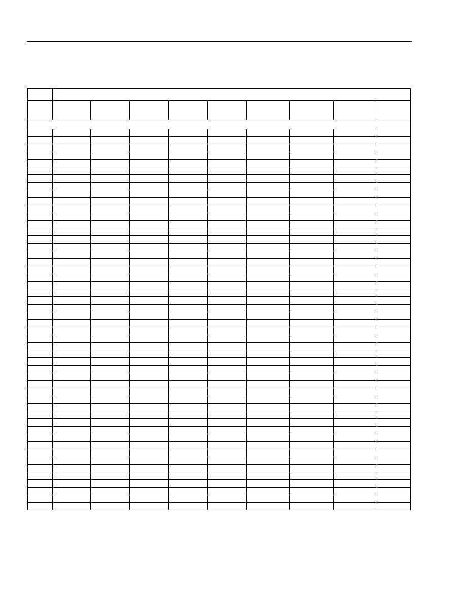
Data Sheet
TECO3264 32-Channel Echo Canceller
August 1999
46
Lucent Technologies Inc.
Parameter Map
(continued)
Table 19. Parameter Address Map (continued)
Register
Bit Number
Address
(Hex)
7
6
5
4
3
2
1
0
Recommended
Value (Hex)
Read/Write
0x2D
XDATA15
XDATA14
XDATA13
XDATA12
XDATA11
XDATA10
XDATA9
XDATA8
00
0x2E
--
--
CUAADJ
CULAW
CCODEC
AEN
XULAW
XCODEC
1B
0x2F
CXCE
CXBOFF3
CXBOFF2
CXBOFF1
CXBOFF0
CPY2
CPY1
CPY0
F8
0x30
--
--
--
XDLY4
XDLY3
XDLY2
XDLY1
XDLY0
19
0x31
--
--
--
YDLY4
YDLY3
YDLY2
YDLY1
YDLY0
15
0x32
--
--
--
--
--
--
XCOMP
EX
02
0x33
--
--
--
--
--
--
FE
EET
02
0x34
--
--
--
--
--
--
--
WEMODE
01
0x35
YPY2
YPY1
YPY0
YRBOFF3
YRBOFF2
YRBOFF1
YRBOFF0
YRCE
02
0x36
--
--
--
--
EXY
YCOMP
YULAW
YCODEC
07
0x37
YDATA7
YDATA6
YDATA5
YDATA4
YDATA3
YDATA2
YDATA1
YDATA0
00
0x38
YDATA15
YDATA14
YDATA13
YDATA12
YDATA11
YDATA10
YDATA9
YDATA8
00
0x39
HZETA7
HZETA6
HZETA5
HZETA4
HZETA3
HZETA2
HZETA1
HZETA0
80
0x3A
EXBOFF3
EXBOFF2
EXBOFF1
EXBOFF0
EUAADJ
ECODEC
ECOMP
EULAW
F7
0x3B
--
--
--
--
EXCE
EPY2
EPY1
EPY0
08
0x3C
SVTD7
SVTD6
SVTD5
SVTD4
SVTD3
SVTD2
SVTD1
SVTD0
00
0x3D
LOWCT5
LOWCT4
LOWCT3
LOWCT2
LOWCT1
LOWCT0
TMODE
TIN
84
0x3E
BADCT1
BADCT0
HICT5
HICT4
HICT3
HICT2
HICT1
HICT0
E3
0x3F
BADVPACT1
BADVPACT0
GOODCT5
GOODCT4
GOODCT3
GOODCT2
GOODCT1
GOODCT0
E4
0x40
MINXFRM7
MINXFRM6
MINXFRM5
MINXFRM4
MINXFRM3
MINXFRM2
MINXFRM1
MINXFRM0
00
0x41
--
MAXHOLDTD3
MAXHOLDTD2
MAXHOLDTD1
MAXHOLDTD0
MINXFRM10
MINXFRM9
MINXFRM8
70
0x42
MINPRBLOCK5
MINPRBLOCK4
MINPRBLOCK3
MINPRBLOCK2
MINPRBLOCK1
MINPRBLOCK0
MINPRBADCT1
MINPRBADCT0
CA
0x43
PRBADCONSEC
MAXTDPR6
MAXTDPR5
MAXTDPR4
MAXTDPR3
MAXTDPR2
MAXTDPR1
MAXTDPR0
8A
0x44
PRNUM1
PRNUM0
GOODVPACT2
GOODVPACT1
GOODVPACT0
MINPRGOODCT2
MINPRGOODCT1
MINPRGOODCT0
AC
0x45
--
CLRNTD
LOWPACT5
LOWVPACT4
LOWVPACT3
LOWVPACT2
LOWVPACT1
LOWVPACT0
5F
0x46
TDTESTY
TDTESTX
HIVPACT5
HIVPACT4
HIVPACT3
HIVPACT2
HIVPACT1
HIVPACT0
22
0x47
MINVPAPWR7
MINVPAPWR6
MINVPAPWR5
MINVPAPWR4
MINVPAPWR3
MINVPAPWR2
MINVPAPWR1
MINVPAPWR0
0C
0x48
MINPWRDET7
MINPWRDET6
MINPWRDET5
MINPWRDET4
MINPWRDET3
MINPWRDET2
MINPWRDET1
MINPWRDET0
0E
0x49
MAXTDPR8
MAXTDPR7
VARP4
VARP3
VARP2
VARP1
VARP0
TDCLRN2
4D
0x4A
TDTHR2
TDTHR1
TDTHR0
TDPRTHR2
TDPRTHR1
TDPRTHR0
ENTDNF
ENTDPRNF
90
0x4B
YHI7
YHI6
YHI5
YHI4
YHI3
YHI2
YHI1
YHI0
7F
0x4C
--
--
NMATCHEN
YHI12
YHI11
YHI10
YHI9
YHI8
20
0x4D
NESPHOC7
NESPHOC6
NESPHOC5
NESPHOC4
NESPHOC3
NESPHOC2
NESPHOC1
NESPHOC0
F0
0x4E
MAXMEMP7
MAXMEMP6
MAXMEMP5
MAXMEMP4
MAXMEMP3
MAXMEMP2
MAXMEMP1
MAXMEMP0
1F
0x4F
--
NESPHOC8
MAXMEMP13
MAXMEMP12
MAXMEMP11
MAXMEMP10
MAXMEMP9
MAXMEMP8
00
0x50
GAMMA7
GAMMA6
GAMMA5
GAMMA4
GAMMA3
GAMMA2
GAMMA1
GAMMA0
02
0x51
EMPCLP7
EMPCLP6
EMPCLP5
EMPCLP4
EMPCLP3
EMPCLP2
EMPCLP1
EMPCLP0
FF
0x52
EX1
EX0
EMPCLP13
EMPCLP12
EMPCLP11
EMPCLP10
EMPCLP9
EMPCLP8
3F
0x53
MHI7
MHI6
MHI5
MHI4
MHI3
MHI2
MHI1
MHI0
00
0x54
SELNF
VARLOSS
MHI13
MHI12
MHI11
MHI10
MHI9
MHI8
00
0x55
MLO7
MLO6
MLO5
ML04
MLO3
MLO2
MLO1
MLO0
08
0x56
USE_SNLP
NLPFRZ
MLO13
MLO12
MLO11
MLO10
MLO9
MLO8
80
0x57
MSCALE2
MSCALE1
MSCALE0
AN14
AN13
AN12
AN11
AN10
21
0x58
USE_NM
USE_ZERO
AN25
AN24
AN23
AN22
AN21
AN20
B0
0x59
INT_TIME7
INT_TIME6
INT_TIME5
INT_TIME4
INT_TIME3
INT_TIME2
INT_TIME1
INT_TIME0
08
0x5A
TESTNM5
TESTNM4
TESTNM3
TESTNM2
TESTNM1
TESTNM0
INT_TIME9
INT_TIME8
00
0x5B
NUM_INTS7
NUM_INTS6
NUM_INTS5
NUM_INTS4
NUM_INTS3
NUM_INTS2
NUM_INTS1
NUM_INTS0
20
0x5C
ELOSS7
ELOSS6
ELOSS5
ELOSS4
ELOSS3
ELOSS2
ELOSS1
ELOSS0
4C
0x5D
CLRN
NUM_INTS8
ELOSS13
ELOSS12
ELOSS11
ELOSS10
ELOSS9
ELOSS8
8A
0x5E
ZERO_THR7
ZERO_THR6
ZERO_THR5
ZERO_THR4
ZERO_THR3
ZERO_THR2
ZERO_THR1
ZERO_THR0
00
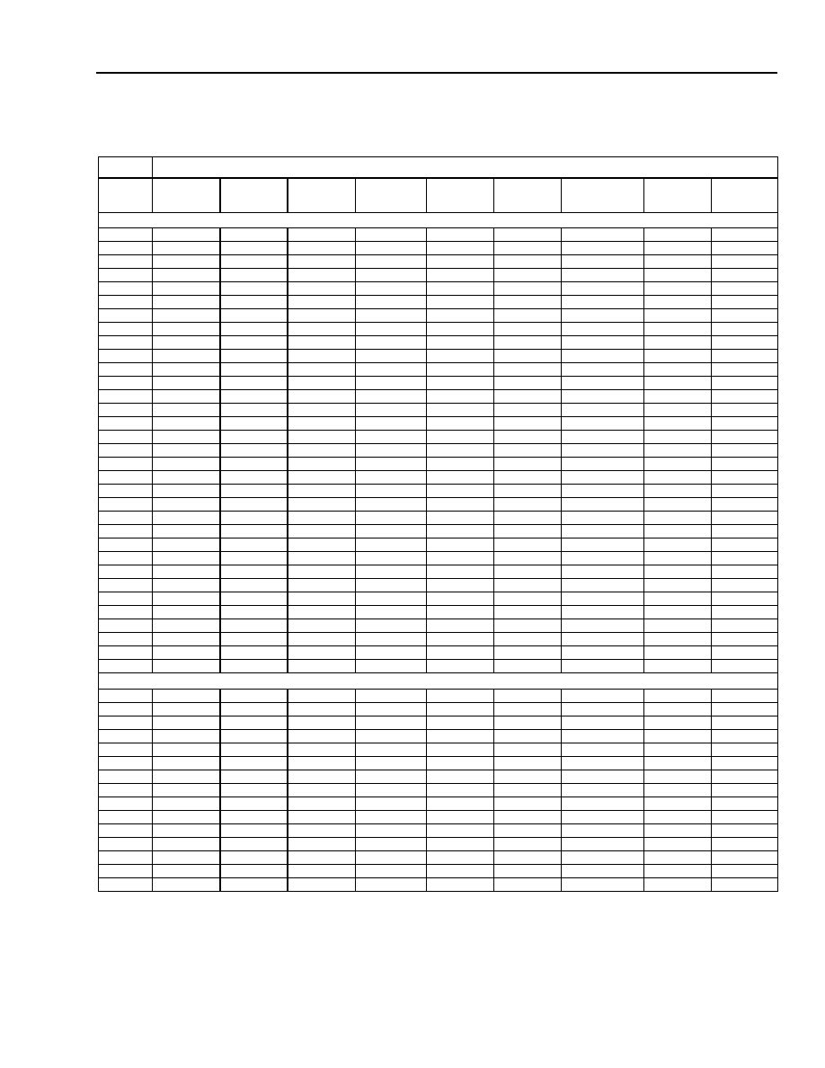
Data Sheet
August 1999
TECO3264 32-Channel Echo Canceller
47
Lucent Technologies Inc.
Parameter Map
(continued)
Table 19. Parameter Address Map (continued)
Register
Bit Number
Address
(Hex)
7
6
5
4
3
2
1
0
Recommended
Value (Hex)
Read/Write
0x5F
LOSS_INC7
LOSS_INC6
LOSS_INC5
LOSS_INC4
LOSS_INC3
LOSS_INC2
LOSS_INC1
LOSS_INC0
00
0x60
--
--
LOSS_INC13
LOSS_INC12
LOSS_INC11
LOSS_INC10
LOSS_INC9
LOSS_INC8
1E
0x61
TESTSV7
TESTSV6
TESTSV5
TESTSV4
TESTSV3
TESTSV2
TESTSV1
TESTSV0
00
0x62
SVT7
SVT6
SVT5
SVT4
SVT3
SVT2
SVT1
SVT0
00
0x63
SVT15
SVT14
SVT13
SVT12
SVT11
SVT10
SVT9
SVT8
00
0x64
--
--
SVT21
SVT20
SVT19
SVT18
SVT17
SVT16
00
0x65
CUPDIS
MODEICH
ERAMINIT
DRINIT
ERAMTEST
INIT
EXCUP2
EXCUP1
00
0x66
--
--
--
--
--
TESTOCON2
TESTOCON1
TESTOCON0
00
0x67
--
--
--
EYTDSEL
YLOSS1
YLOSS0
XLOSS1
XLOSS0
00
0x68
HGAMMA7
HGAMMA6
HGAMMA5
HGAMMA4
HGAMMA3
HGAMMA2
HGAMMA1
HGAMMA0
01
0x69
FGAIN7
FGAIN6
FGAIN5
FGAIN4
FGAIN3
FGAIN2
FGAIN1
FGAIN0
60
0x6A
SGAIN7
SGAIN6
SGAIN5
SGAIN4
SGAIN3
SGAIN2
SGAIN1
SGAIN0
40
0x6B
FBETA7
FBETA6
FBETA5
FBETA4
FBETA3
FBETA2
FBETA1
FBETA0
12
0x6C
ZEROSVRAM
P1
P0
FBETA12
FBETA11
FBETA10
FBETA9
FBETA8
05
0x6D
SBETA7
SBETA6
SBETA5
SBETA4
SBETA3
SBETA2
SBETA1
SBETA0
12
0x6E
--
YSIGN
XSIGN
SBETA12
SBETA11
SBETA10
SBETA9
SBETA8
05
0x6F
TGAIN7
TGAIN6
TGAIN5
TGAIN4
TGAIN3
TGAIN2
TGAIN1
TGAIN0
20
0x70
TFNLP7
TFNLP6
TFNLP5
TFNLP4
TFNLP3
TFNLP2
TFNLP1
TFNLP0
20
0x71
AVOICE7
AVOICE6
AVOICE5
AVOICE4
AVOICE3
AVOICE2
AVOICE1
AVOICE0
40
0x72
--
--
--
--
MASK3
MASK2
MASK1
MASK0
05
0x73
ADATA7
ADATA6
ADATA5
ADATA4
ADATA73
ADATA2
ADATA1
ADATA0
40
0x74
NES1HOC8
NES1HOC7
NES1HOC6
NES1HOC5
NES1HOC4
NES1HOC3
NES1HOC2
NES1HOC1
FF
0x75
NLPHOC8
NLPHOC7
NLPHOC6
NLPHOC5
NLPHOC4
NLPHOC3
NLPHOC2
NLPHOC1
10
0x76
NES3THR8
NES3THR7
NES3THR6
NES3THR5
NES3THR4
NES3THR3
NES3THR2
NES3THR1
00
0x77
THR17
THR16
THR15
THR14
THR13
THR12
THR11
THR10
AA
0x78
THR27
THR26
THR25
THR24
THR23
THR22
THR21
THR20
00
0x79
THR37
THR36
THR35
THR34
THR33
THR32
THR31
THR30
00
0x7A
B37
B36
B35
B34
B33
B32
B31
B30
00
0x7B
NES3THR0
NLPHOC0
NES1HOC0
TOFFSET4
TOFFSET3
TOFFSET2
TOFFSET1
TOFFSET0
03
0x7C
HMODE
NLP128
LOWCT25
LOWCT24
LOWCT23
LOWCT22
LOWCT21
LOWCT20
A3
0x7D
NMODE
SPARE
HICT25
HICT24
HICT23
HICT22
HICT21
HICT20
A4
0x7E
EETHR7
EETHR6
EETHR5
EETHR4
EETHR3
EETHR2
EETHR1
EETHR0
18
0x7F
CENABLE
EEMODE
EETHR13
EETHR12
EETHR11
EETHR10
EETHR9
EETHR8
C0
Read Only
0x100
HPYERR
EXPYERR
OXPYERR
ERR4
ERR3
ERR2
YPERRV48
PERRV48
--
0x101
HPYERRM
EXPYERRM
OXPYERRM
ERR4M
ERRM3
ERRM2
YPERRV48M
PERRV48M
--
0x102
--
--
BADWRITE
BADRANGE
OVF
MPYERR
DAUOVERFLO
DMPYERR
--
0x103
--
--
BADWRITEM
BADRANGEM
OVFM
MPYERRM
DAUOVERFLOM
DMPYERRM
--
0x104
CDATAVFX7
CDATAVFX6
CDATAVFX5
CDATAVFX4
CDATAVFX3
CDATAVFX2
CDATAVFX1
CDATAVFX0
--
0x105
EDATAVFX7
EDATAVFX6
EDATAVFX5
EDATAVFX4
EDATAVFX3
EDATAVFX2
EDATAVFX1
EDATAVFX0
--
0x106
EDATAVFX15
EDATAVFX14
EDATAVFX13
EDATAVFX12
EDATAVFX11
EDATAVFX10
EDATAVFX9
EDATAVFX8
--
0x107
TDPR3
TD3
TDPR2
TD2
TDPR1
TD1
TDPRO
TD0
--
0x108
TDPR7
TD7
TDPR6
TD6
TDPR5
TD5
TDPR4
TD4
--
0x109
TDP11
TD11
TDPR10
TD10
TDPR9
TD9
TDPR8
TD8
--
0x10A
TDP15
TD15
TDPR14
TD14
TDPR13
TD13
TDPR12
TD12
--
0x10B
TDP19
TD19
TDPR18
TD18
TDPR17
TD17
TDPR16
TD16
--
0x10C
TDP23
TD23
TDPR22
TD22
TDPR21
TD21
TDPR20
TD20
--
0x10D
TDP27
TD27
TDPR26
TD26
TDPR25
TD25
TDPR24
TD24
--
0x10E
TDP31
TD31
TDPR30
TD30
TDPR29
TD29
TDPR28
TD28
--

Data Sheet
TECO3264 32-Channel Echo Canceller
August 1999
48
Lucent Technologies Inc.
Register Architecture
Register Scopes
The TECO3264's programmable parameters and options have two scopes:
1.
Those that may be set independently for each channel. These are referred to as per-channel functions. For
example, enabling and disabling bypass modes are set on a per-channel basis. Per-channel functions are
groups of 32 single-bit functions, with one for each channel.
2.
Those that affect the operation of all channels. Examples are gains, speech detector thresholds, and selection
of µ-law or A-law coding.
There are 186 functions in the read-write page 0 registers. Only very few will be of concern in final fine tuning to
unusual conditions in a given network. The great majority of these functions will be set once for given system
design options and for normal network characteristics.
There are 28 functions in the read-only page 1 registers, 100 through 10E. These are used for status and alarm
conditions.
The first 32 Page 0 registers, 000 through 01F, allow for per-channel control of functions for individual DS0 chan-
nels of the echo canceller. Each channel has its 8-bit byte (including two unused bits). Each bit represents a binary
function for that channel. Examples include enabling/disabling the echo canceller function, nonlinear processor, H-
register freeze control, and call boundary.
Note: The terms time slots and channels are both used in TECO3264 documents to refer to bidirectional
64 kbits/s DS0 channels for one customer circuit. Channel is used in connection with echo canceller pro-
cessing functions. Time slot is used when timing relationships among the bits, sync pulses, and clocks are
the subject.
Page 0 registers, 020 through 01F, are all channel, and allow provisioning of functions for all 32 channels at once.
(The term digroup is sometimes used to mean all 32 channels even though it derives from the North American
1.544 Mbits/s DS1 24-channel systems where group refers to 12 channels and digroup refers to two groups or 24
DS0 channels.) For DS1 applications, 24 of the available channels are used and eight are unused and stuffed with
dummy bit values. E1 applications tend to use A-law coding while DS1 applications tend to use µ-law coding. (Most
applications use inverted µ-law or A-law rather than the normal versions.) Thus, E1 and T1 systems will require dif-
ferent settings of the X, Y, C, and E port PCM register settings. If the TECO3264 is used at the boundaries of A-law
and µ-law coded networks, the PCM ports must be set appropriately.

Data Sheet
August 1999
TECO3264 32-Channel Echo Canceller
49
Lucent Technologies Inc.
Register Architecture
(continued)
Registers, Functions, Symbols
--
Information Presentations
The 186 TECO3264 functional parameters vary from single-bit functions that enable/disable a particular function
like soft NLP to 14-bit variables that control the soft NLP level increments. These functions have a name, like soft
NLP increment, and a symbol, like ELOSS. These 186 functions are distributed among the 128 page 0 read/write
registers. A given function may be stored in a single register, or in as many as three registers for the 14-bit func-
tions. A given register may hold values for a single function or values for up to eight different functions.
As aids to finding the necessary functions to adjust for a particular task in the system design stage or for different
network conditions, the register, function, symbol, and function definition information is presented in several ways
in this document:
1.
Function list grouped by main echo canceller task, such as echo cancellation, masking, nonlinear processing,
tone disabling, and transmission parameters. See Table 11--Table 18, per-channel control parameters.
2.
Page 0 registers 000--01F and page 1 registers 100--10E tables with the functions appearing in each register
with recommended values and discussions for key parameters. This is the main reference for function defini-
tions. See Table 24--Table 128.
3.
Page 0 and page 1 registers address map with compact, detailed, bit-by-bit lists for each register. See Table
19, Parameter Address Map, on page 45.
4.
Index of function names to symbols and register addresses. See Table 22, Function Name to Symbol and Reg-
ister Address Index, on page 53.
5.
Index of symbols to register addresses and function names. See Table 23, Symbol to Register Address and
Function Name Index, on page 59.
6.
Tables of recommended values for page 0 registers for DS1/µ-law and E1/A-law applications. See Table 20,
Recommended Register Values for DS1 (µ-Law) and 2.048 Mbits/s Rate, on page 51 and Table 21, Recom-
mended Register Values for E1 (A-Law), on page 52, respectively.
When changing function values to adjust for different system options like µ-law or PCM timing, or for new network
conditions, it is more natural for the engineer to work in terms of the individual functions and not in terms of whole
register values. Changing one function value can change as many as three register values. A minor 1-bit change in
a function can appear to be a major change in a register value, depending on the location of the bit between most
significant and least significant positions. However, an efficient way to download new parameter values to the
TECO3264 is to download changes in whole register values by the RS-232 link. The user-interface software
between a controlling computer and the TECO3264 and its associated microprocessor can bridge this human-
machine difference in setting up the echo canceller system.

Data Sheet
TECO3264 32-Channel Echo Canceller
August 1999
50
Lucent Technologies Inc.
Register Architecture
(continued)
Recommended Register Values
The TECO3264 chip is supplied with a set of recommended register values. These values represent many years of
experience with a wide variety of networks and on extensive laboratory subjective and objective tests. With the rec-
ommended values, the performance of the TECO3264 should meet or exceed subjective expectations in a wide
range of network conditions. Some functions are set at system design time, such as system bit rate, time-slot and
sync alignment, and the settings affecting E1 or DS1 applications. As mentioned, there are a few parameters that
may be adjusted to compensate for problem or unusual, but systematic, network conditions, such as consistently
poor hybrid balance. New applications such as packet voice and Internet telephony are growing. New information
will be provided as it becomes available.
Recommended values are given in hexidecimal for each page 0 register and the equivalent binary values are given
for each bit in the 8-bit registers. The corresponding binary values may represent one to eight parameters per reg-
ister with one too many bits per function. A few functions take more than 8 bits and occupy parts of two or more
registers.
For most parameters that have a range of values, slight changes will have little audible effect. Many of the param-
eters interact to perform the echo cancelling function, and changes in one may require adjustment of others to
obtain the maximum available performance. Thus, most of the echo canceller register values are expected to be
set to a constant value during initialization.
Some functions are only used for chip development or for manufacturing tests of the TECO3264 chip and should
never be of concern in either system development or field applications. Some functions, such as adjusting the tim-
ing relationships among the sync pulse, clock, and data bits, are set during system design and never changed
again.
Most of the functions are set once for a given network architecture and remain the same. Examples are µ-law and
A-law coding and most echo canceller functions. A few echo canceller functions may need fine tuning if unusual
network conditions are found. An example is adjusting voice and data echo return loss thresholds when a network
is found to have poor four-to-two-wire hybrid performance. Another example is when network levels are known to
be high and the loss pads can be switched in.
Notation and Format: Bits per Parameter and Bits in Registers
Symbol names for single bit parameters are written without indication of any bit size. An example is CMS for con-
centration highway bit rate select (register 02F, bit position 0). Symbols for multibit parameters are written with an
indication in brackets of the bit length of the parameter. An example is the 8-bit parameter ADATA[7:0] for alpha
data where the parameters' bits are numbered [7:0] (and found in register 073, bit positions 7--0). Bit 0 is the least
significant bit, and bit 7 is the most significant bit for ADATA. A colon separates the 0 and 7 bit places within the
brackets. (Note that a dash separates the bit positions when referring to registers.)
Parameters with 8 bits or less are contained within one register. Parameters with fewer than 8 bits may share a
register with other parameters. Parameters with more than 8 bits are contained in as many registers as necessary.
Per-channel parameters, such as enable bypass (clear channel) EBP, are 1-bit long but are spread with 1 bit per
register among the first 32 registers, 000--01F. All-channel parameters with more than 8 bits may be contained in
two to three registers as needed. An example is the 14-bit enable edge threshold EETHR[13:0] contained in regis-
ter 07E, bit positions 7--0, and in register 07F, bit positions 5--0. Pointers between registers containing portions of
a parameter are included in the descriptive text for the parameters in Table 24--Table 128. Tables 22 and 23 list all
the registers connected with each parameter. The registers containing parameter portions are usually, but not
always, adjacent.
Unused register bit positions are labeled as reserved and must be set to 0.
Data Sheet
August 1999
TECO3264 32-Channel Echo Canceller
51
Lucent Technologies Inc.
Register Architecture
(continued)
Recommended Register Values for DS1 (µ-Law)
Page 0 registers 00--7F are read/write, values for µ-law (registers 2E, 36, 3A), registers 00--1F are per-channel
(it is recommended to set the eight unused per-channel registers for DS1 to 02 (hexidecimal) for 64-clear channel
mode or bypass mode), and registers 20--7F are all-channel. Common channel signaling time slots 0 and 16 for
E1 are also set for 64-clear channel mode.
Table 20. Recommended Register Values for DS1 (µ-Law) and 2.048 Mbits/s Rate
Register
Address
Recom-
mended
Value
Register
Address
Recom-
mended
Value
Register
Address
Recom-
mended
Value
Register
Address
Recom-
mended
Value
00
00
24
A1
48
0E
6C
05
01
00
25
0C
49
4D
6D
12
02
00
26
9B
4A
90
6E
05
03
00
27
02
4B
7F
6F
20
04
00
28
18
4C
20
70
20
05
00
29
18
4D
F0
71
40
06
00
2A
05
4E
1F
72
05
07
00
2B
00
4F
00
73
40
08
00
2C
00
50
02
74
FF
09
00
2D
00
51
FF
75
10
0A
00
2E
1B
52
3F
76
00
0B
00
2F
F8
53
00
77
AA
0C
00
30
19
54
00
78
00
0D
00
31
15
55
08
79
00
0E
00
32
02
56
80
7A
00
0F
00
33
02
57
21
7B
03
10
00
34
01
58
B0
7C
A3
11
00
35
02
59
08
7D
A4
12
00
36
07
5A
00
7E
18
13
00
37
00
5B
20
7F
C0
14
00
38
00
5C
4C
15
00
39
80
5D
8A
16
00
3A
F7
5E
00
17
00
3B
08
5F
00
18
00
3C
00
60
1E
19
00
3D
84
61
00
1A
00
3E
E3
62
00
1B
00
3F
E4
63
00
1C
00
40
00
64
00
1D
00
41
70
65
00
1E
00
42
CA
66
00
1F
00
43
8A
67
00
20
00
44
AC
68
01
21
02
45
5F
69
60
22
41
46
22
6A
40
23
80
47
0C
6B
12
Data Sheet
TECO3264 32-Channel Echo Canceller
August 1999
52
Lucent Technologies Inc.
Register Architecture
(continued)
Recommended Register Values for E1 (A-Law)
Page 0 registers 00--7F are read/write, values for A-law (registers 2E, 36, 3A), registers 00--1F are per-channel,
and registers 20--7F are all-channel.
Table 21. Recommended Register Values for E1 (A-Law)
Register
Address
Recom-
mended
Value
Register
Address
Recom-
mended
Value
Register
Address
Recom-
mended
Value
Register
Address
Recom-
mended
Value
00
00
25
0C
4A
90
6F
20
01
00
26
96
4B
7F
70
20
02
00
27
02
4C
20
71
40
03
00
28
18
4D
F0
72
05
04
00
29
18
4E
1F
73
40
05
00
2A
05
4F
00
74
FF
06
00
2B
00
50
02
75
10
07
00
2C
00
51
FF
76
00
08
00
2D
00
52
3F
77
AA
09
00
2E
09
53
00
78
00
0A
00
2F
F8
54
00
79
00
0B
00
30
19
55
08
7A
00
0C
00
31
15
56
80
7B
03
0D
00
32
02
57
21
7C
A3
0E
00
33
02
58
B0
7D
A4
0F
00
34
01
59
08
7E
18
10
00
35
02
5A
00
7F
C0
11
00
36
05
5B
20
12
00
37
00
5C
4C
13
00
38
00
5D
8A
14
00
39
80
5E
00
15
00
3A
F6
5F
00
16
00
3B
08
60
1E
17
00
3C
00
61
00
18
00
3D
84
62
00
19
00
3E
E3
63
00
1A
00
3F
E4
64
00
1B
00
40
00
65
00
1C
00
41
70
66
00
1D
00
42
CA
67
00
1E
00
43
8A
68
01
1F
00
44
AC
69
60
20
00
45
5F
6A
40
21
02
46
22
6B
12
22
41
47
0C
6C
05
23
80
48
0E
6D
12
24
A1
49
4D
6E
05
Data Sheet
August 1999
TECO3264 32-Channel Echo Canceller
53
Lucent Technologies Inc.
Register Architecture
(continued)
Function Name to Symbol and Register Address Index
Note: Register addresses with a 0 in the most significant digit are page 0 read/write registers. Register addresses
with 1 in the most significant digit are page 1 read-only registers. Register addresses 000--01F are per-
channel registers and register addresses 020--07F are all-channel 0--31 registers. Mask parameters are
read/write.
Table 22. Function Name to Symbol and Register Address Index
Function Name
Bits
Symbol
Register
Address
Page
Accelerate Test
1
TIN
03D
84
Address Error
1
BADRANGE
102
116
Address Error Mask
1
BADRANGEM
103
116
Alpha Data
8
ADATA[7:0]
073
109
Alpha Voice
8
AVOICE[7:0]
071
107
Bad Interval Count
2
BADCT[1:0]
03E
84
Bad Interval Count VPA
2
BADVPACT[1:0]
03F
85
Bad Primitive Minimum
2
MINPRBADCT[1:0]
042
86
Bit Rate Select
1
CMS
02A
74
Call Boundary, Channel 0--31
1
CALLB
000--01F
66
C Invert
1
CCODEC
02E
76
C Transmit Bit Offset
4
CXBOFF[3:0]
02F
77
C Transmit Clock Edge
1
CXCE
02F
77
64-Clear/Bypass Enable Channels 0--31
1
EBP
000--01F
65
Clamp Í Noise Floor
14
EMPCLP[13:0]
051, 052
92, 93
Conversion
µ
-A and A-
µ
Adjustment
1
CUAADJ
02E
76
Convolution Update Processor (CUP) Disable
1
CUPDIS
065
101
Clear Nonlinear Processor (NLP) State Variables (SV)
7
CLRN
05D
97
C Parity
3
CPY[2:0]
02F
77
CUP Parity Error
1
MPYERR
102
116
CUP Parity Error Mask (mask interrupt)
1
MPYERRM
103
116
CUP Parity Error 1
1
EXPYERR
100
114
CUP Parity Error 1 Mask (mask interrupt)
1
EXPYERRM
101
115
CUP Parity Error 2
1
HPYERR
100
114
CUP Parity Error 2 Mask (mask interrupt)
1
HPYERRM
101
115
CUP Register Overflow
1
OXPYERR1
100
114
CUP Register Overflow Mask (mask interrupt)
1
OXPYERRM
101
115
C Test Data
8
CDATAVFX[7:0]
104
117
Clamp Í Enable
1
CENABLE
07F
113
Clear Tone Detector (TD) State Variable (SV) Outputs
1
TDCLRN2
049
89
Clear TD SV Storage
1
CLRNTD
045
87
C Output
µ
-Law/A-Law Select
1
CULAW
02E
76
Disable Echo Canceller, Channel 0--31
1
DEC
000--01F
65
Digital Arithmetic Unit (DAU) Overflow Error
1
DAUOVERFLO
102
116
DAU Overflow Error Mask (mask interrupt)
1
DAUOVERFLOM
103
116
DAU Parity Error
1
DMPYERR
102
116
DAU Parity Error Mask (mask interrupt)
1
DMPYERRM 103
116
Data Sheet
TECO3264 32-Channel Echo Canceller
August 1999
54
Lucent Technologies Inc.
Register Architecture
(continued)
Function Name to Symbol and Register Address Index
(continued)
Table 22. Function Name to Symbol and Register Address Index (continued)
Function Name
Bits
Symbol
Register
Address
Page
E Data Format
1
ECOMP
03A
82
E Invert
1
ECODEC
03A
82
E Parity
3
EPY[2:0]
03B
83
E Test Data
16
EDATAVFX[15:0]
105, 106
117, 117
E Transmit Bit Offset
4
EXBOFF[3:0]
03A
82
E Transmit Clock Edge
1
EXCE
03B
83
E Output
µ
-Law/A-Law Select
1
EULAW
03A
82
E vs. Y Calculation Mask
1
MASK2
072
108
Enable Edge Threshold
8
EETHR[7:0]
07E, 07F
113, 113
Enable Edge Threshold Mode
1
EEMODE
07F
113
Enable Edge Transfer
1
EET
033
78
Enable Nonlinear Processor, Channel 0--31
1
ENLP
000--01F
65
Í Noise Floor Estimate Maximum
14
MAXMEMP[13:0]
04E, 04F
91, 92
Í Zero Crossing Select
1
USE_ZERO
058
96
Í Zero Crossing Threshold
8
ZERO_THR[7:0]
05E
97
EPCM Adjust
1
EUAADJ
03A
82
Error Exercise Test Bit 0
1
EX0
052
93
Error Exercise Test Bit 1
1
EX1
052
93
Exercise Convolution Update Processor
2
EXCUP[1:0]
065
101
Exercise Parity Error
1
EX
032
78
External RAM Test
1
ERAMTEST
065
101
External Event Mask
1
MASK1
072
108
Far-End Speech (FES) Threshold
13
FESTH[12:0]
026, 027
73, 73
Fast Convergence Beta
13
FBETA[12:0]
06B, 06C
104, 105
Fast Convergence Gain
8
FGAIN[7:0]
069
104
Fast Convergence Gain Time
8
TGAIN[7:0] 06F
106
Fast Convergence NLP Beta Time
8
TFNLP[7:0]
070
107
Fast Convergence Threshold
8
THR1[7:0]
077
110
Frame Edge
1
FE
033
78
Gamma Í Noise Floor
8
GAMMA[7:0]
050
92
Good Interval Count
6
GOODCT[5:0]
03F
85
Good Intervals Declare VPA
11
MINXFRM[10:0]
040, 041
85, 85
Good VPA Declaration Threshold
3
GOODVPACT[2:0]
044
87

Data Sheet
August 1999
TECO3264 32-Channel Echo Canceller
55
Lucent Technologies Inc.
Register Architecture
(continued)
Function Name to Symbol and Register Address Index
(continued)
Table 22. Function Name to Symbol and Register Address Index (continued)
Function Name
Bits
Symbol
Register
Address
Page
H-Register Freeze, Channel 0--31
1
HFRZ
000--01F
65
H Gamma
8
HGAMMA[7:0]
068
103
High Hysteresis Threshold NFE
14
MHI[13:0]
053, 054
93, 94
H-Register Leak Application Rate (obsolete; see Leak.)
2
LFREQ[1:0]
025
72
High Peak Count 1 (tone detector 1 (TD1))
6
HICT[5:0]
03E
84
High Peak Count 2 (tone detector 2 (TD2))
6
HICT2[5:0]
07D
113
Hot Signal Mode
1
HMODE
07C
112
H-Register Reset, Channel 0--31
1
HRST
000--01F
65
H-Reset Threshold
8
THR3[7:0]
079
111
H-Reset Transition Mask
1
MASK0
072
108
High VPA Count
6
HIVPACT[5:0]
046
88
H Zeta
8
HZETA[7:0]
039
81
Leak: Magnitude, Enable, Rate
8
LEAK[7:0]
024
71
Linear PCM Port Enable
1
AEN
02E
76
Loss Increment Attenuated Í
14
ELOSS[13:0]
05C, 05D
98, 98
Low Hysteresis Threshold NFE
14
MLO[13:0]
055, 056
94, 95
Low Peak Count 1 (tone detector 1 (TD1))
6
LOWCT[5:0]
03D
84
Low Peak Count 2 (tone detector 2 (TD2))
6
LOWCT2[5:0]
07C
112
Low VPA Count
6
LOWVPACT[5:0]
045
87
Mask Bit 15 X
1
MBlT15X
020
67
Mask Bit 15 X Control
1
MBP15X
021
68
Mask Bit 15 Y
1
MBIT15Y
020
67
Mask Bit 15 Y Control
1
MBP15Y
021
68
Mask External EC Control
1
MECEXT
020
67
Mask External EC Clear Control
1
MBPEXT
021
68
Mask EC HPF Control X
1
MHPFXEC
022
69
Mask EC HPF Control Y
1
MHPFYEC
022
69
Mask External H-Register Freeze
1
MHFRZEXT
023
70
Mask External H-Register Reset
1
MHRSTEXT
023
70
Mask External NLP Control
1
MNLPEXT
022
69
Mask External NLP Freeze Control
1
MNLPFRZ
022
69
Mask Í Y H-Register Reset
1
MEYRST
023
70
Mask FES H Freeze
1
MFES
023
70
Mask H-Register Error Reset
1
MHERR
023
70
Mask H-Register Freeze
1
MFREEZE
022
69
Mask Internal NLP Control
1
MNLPINT
022
69
Mask NES1 H Freeze
1
MNES1
023
70
Mask NES3 H Freeze
1
MNES3
023
70
Mask NBE H Freeze Control
1
MNBE
023
70
Mask NLP Transient Control
1
MTNLP
022
69
Data Sheet
TECO3264 32-Channel Echo Canceller
August 1999
56
Lucent Technologies Inc.
Register Architecture
(continued)
Function Name to Symbol and Register Address Index
(continued)
Table 22. Function Name to Symbol and Register Address Index (continued)
Function Name
Bits
Symbol
Register
Address
Page
Mask Phase Reversed Tone Detect
1
MECTDPR
020
67
Mask Phase Reversed Tone Detect Control 1 (TD1)
1
MBPTDPR
021
68
Mask Phase Reversed Tone Detect Control 2 (TD2)
1
MBPTD2
025
72
Mask Tone Detect 1 (TD1)
1
MECTD
020
67
Mask Tone Detect 2 (TD2)
1
MECTD2
025
72
Mask Tone Detect Clear
1
MBPTD
021
68
Mask VPA Clear Control
1
MBPVPA
021
68
Mask VPA
1
MECVPA
020
67
Memory Initialization 1: D-RAM
1
DRINIT
065
101
Memory Initialization 2: E-RAM
1
ERAMINIT
065
101
Narrowband Energy (NBE) Peak Factor
8
NBEPKF[7:0]
028
73
Narrowband Energy Threshold Select
2
P[1:0]
06C
105
Near-End Speech (NES) Compare Threshold
8
B3[7:0]
07A
111
NES1 Declaration Advance
1
NMODE
07D
113
Nonlinear Processor (NLP) Errors
1
ERR2, ERR3, ERR4
100
114
NLP Errors Masks (mask interrupts from ERR2,
ERR3, ERR4)
1
ERR2M, ERR3M,
ERR4M
101
115
Near-End Speech 1 Hangover
9
NES1HOC[8:0]
074, 07B
109, 112
Near-End Speech 3 Hangover
9
NES3THR[8:0]
076, 07B
110, 112
Noise Floor Select
1
SELNF
054
94
Noise Floor Estimate Scale Factor
3
MSCALE[2:0]
057
95
Noise Floor Scaling Factor 2
5
AN1[4:0]
057
95
Noise Floor Scaling Factor 1
6
AN2[5:0]
058
96
NES Hangover
9
NESPHOC[8:0]
04D, 04F
91, 91
Nonlinear Processor Double Time
1
NLP128
07C
112
Nonlinear Processor Freeze
1
NLPFRZ
056
95
Nonlinear Processor Hangover
9
NLPHOC[8:0]
075, 07B
110, 112
Noise Matching Enable
1
NMATCHEN
04C
90
Noise Matching Test
6
TESTNM[5:0]
05A
97
Noise Transparency Select
1
USE_NM
058
96
One Channel Mode (quick turn only)
1
MODE1CH
065
101
Phase Reversal (PR) Consecutive Count Control
1
PRBADCONSEC
043
86
PR Declaration Threshold
3
MINPRGOODCT[2:0]
044
87
PR Enhancement Mode (obsolete)
1
ENTDPRNF
04A
89
Phase Reversal Interval Maximum TD
9
MMAXTDPR[8:0]
043, 049
86, 89
Phase Reversal Interval Minimum TD
6
MINPRBLOCK[5:0]
042
86
Quick Turn Mode (chip development only)
1
QTMODE
025
72
Data Sheet
August 1999
TECO3264 32-Channel Echo Canceller
57
Lucent Technologies Inc.
Register Architecture
(continued)
Function Name to Symbol and Register Address Index
(continued)
Table 22. Function Name to Symbol and Register Address Index (continued)
* See Table 128, Tone Detector Indicator Registers (107--10E), on page 118 for more details.
Function Name
Bits
Symbol
Register
Address
Page
Reset Convolution/Update Processor
1
INIT
065
101
RAM State Variable Reset
1
ZEROSVRAM
06C
105
Set Channel Alignment
5
VARP[4:0]
049
89
Slow Convergence Beta
13
SBETA[12:0]
06D, 06E
105, 106
Slow Convergence Gain
8
SGAIN[7:0]
06A
104
Soft NLP Interval
9
NUM_INTS[8:0]
05B, 05D
97
SNLP Incremental Loss Factor
14
LOSS_INC[13:0]
05F, 060
98, 100
SNLP Interval Time
10
INT_TlME[9:0]
059, 05A
96, 97
Soft NLP Select
1
USE_SNLP
056
95
State Variable Test Data
8
SVTD[7:0]
03C
83
State Variable Test
22
SVT[21:0]
062, 063, 064
100, 101,
101
Test Control
3
TESTCON[2:0]
066
102
Test Channel Offset
5
TOFFSET[4:0]
07B
112
Tone Detector Enhancement (obsolete)
1
ENTDNF
04A
89
Tone Detection Hold Maximum
4
MAXHOLDTD[3:0]
041
85
Tone Detector Phase Reversals Allowed
3
TDPRTHR[2:0]
04A
89
Tone Detector Input Select
1
EYTDSEL
067
102
Test Data Input X
1
TDTESTX
046
88
Test Data Input Y
1
TDTESTY
046
88
Tone Detector Power Minimum
8
MINPWRDET[7:0]
048
88
Tone Detected (channels 0--31)
1
TDP*
107--10E
118
Tone Detected Phase Reversal (channels 0--31)
1
TDPR*
107--10E
118
TDPR Declaration Threshold
2
PRNUM[1:0]
044
87
Test Mode 0
1
TMODE0
02A
74
Test Mode 1
2
TMODE1
02A
74
Test NLP State Variables
8
TESTSV[7:0]
061
100
Transient NLP Threshold
8
THR2[7:0]
078
111
Tone Detector (TD) Overflow Error
1
OVF
102
116
Tone Detector Threshold
3
TDTHR[2:0]
04A
89
TD Overflow Error Mask (mask interrupt)
1
OVFM
103
116
TD Test Input
1
TMODE
03D
84
Echo Canceller Test Vector Channel Select
5
TCHAN[4:0]
02B
75
Variable Loss
1
VARLOSS
054
94
Voiceband Signal Classifier (VSC) External
1
VSCEXT
025
72
Voice Path Assurance (VPA) Control Mask
1
MASK3
072
108
VPA Power Minimum
8
MINVPAPWR[7:0]
047
88
Data Sheet
TECO3264 32-Channel Echo Canceller
August 1999
58
Lucent Technologies Inc.
Register Architecture
(continued)
Function Name to Symbol and Register Address Index
(continued)
Table 22. Function Name to Symbol and Register Address Index (continued)
Function Name
Bits
Symbol
Register
Address
Page
Wideband Energy Peak Factor
8
WBEPKF[7:0]
029
74
Write Enable Mode
1
WEMODE
034
79
Write Error
1
BADWRITE
102
116
Write Error Mask (mask interrupt)
1
BADWRITEM
103
116
X-C Bulk Time-Slot Delay
5
XDLY[4:0]
030
77
X Data Format
1
XCOMP
032
78
X High-Pass Filter Enable
1
XHPFEN
025
72
X Invert
1
XCODEC
02E
76
X Loss Pad
2
XLOSS[1:0]
067
102
X Parity
3
XPY[2:0]
02B
75
X Parity Error
1
PERRV48
100
114
X Parity Error Mask (mask interrupt)
1
PERRV48M
101
115
X Receive Bit Offset
4
XRBOFF[3:0]
02A
74
X Receive Clock Edge
1
XRCE
02A
74
X Sign Bit Control
1
XSIGN
06E
106
X Test Data for 109-Test
16
XDATA[15:0]
02C, 02D
75, 75
X Input
µ
-Law/A-Law Select
1
XULAW
02E
76
Y Receive Bit Offset
4
YRBOFF[3:0]
035
79
Y Receive Clock Edge
1
YRCE
035
79
Y Data Format
1
YCOMP
036
80
Y-E Bulk Time-Slot Delay
5
YDLY[4:0]
031
78
Y Energy Threshold
13
YHI[12:0]
04B, 04C
90, 90
Y Force Parity Error
1
EXY
036
80
Y High-Pass Filter Enable
1
YHPFEN
025
72
Y Invert
1
YCODEC
036
80
Y Loss Pad
2
YLOSS[1:0]
067
102
Y Parity
3
YPY[2:0]
035
79
Y Parity Error
1
YPERRV48
100
114
Y Parity Error Mask (mask interrupt)
1
YPERRV48M
101
115
Y Sign Bit Control
1
YSIGN
06E
106
Y Test Data for 109-Test
16
YDATA[15:0]
037, 038
81, 81
Y Input
µ
-Law/A-Law Select
1
YULAW
036
80
Data Sheet
August 1999
TECO3264 32-Channel Echo Canceller
59
Lucent Technologies Inc.
Register Architecture
(continued)
Symbol to Register Address and Function Name Index
Note: Register addresses with a 0 in the most significant digit are page 0 read/write registers. Register addresses
with 1 in the most significant digit are page 1 read-only registers. Register addresses 000--01F are per-
channel registers and register addresses 020--07F are all-channel 0--31 registers. Mask parameters are
read/write.
Table 23. Symbol to Register Address and Function Name Index
Symbol
Register
Address
Function Name
Bits
Page
ADATA[7:0]
073
Alpha Data
8
109
AEN
02E
Linear PCM Port Enable
1
76
AN1[4:0]
057
Noise Floor Scaling Factor 2
5
95
AN2[5:0]
058
Noise Floor Scaling Factor 1
6
96
AVOICE[7:0]
071
Alpha Voice
8
107
B3[7:0]
07A
Near-End Speech (NES) Compare Threshold
8
111
BADCT[1:0]
03E
Bad Interval Count
2
84
BADRANGE
102
Address Error
1
116
BADRANGEM
103
Address Error Mask
1
116
BADVPACT[1:0]
03F
Bad Interval Count VPA
2
85
BADWRITE
102
Write Error
1
116
BADWRITEM
103
Write Error Mask (mask interrupt)
1
116
CALLB
000--01F
Call Boundary, Channel 0--31
1
66
CCODEC
02E
C Invert
1
76
CDATAVFX[7:0]
104
C Test Data
8
117
CENABLE
07F
Clamp Í Enable
1
113
CLRN
05D
Clear Nonlinear Processor (NLP) State Variables (SV)
7
98
CLRNTD
045
Clear TD SV Storage
1
87
CMS
02A
Bit Rate Select
1
74
CPY[2:0]
02F
C Parity
3
77
CUAADJ
02E
Conversion
µ
-A and A-
µ
Adjustment
1
76
CULAW
02E
C Output
µ
-Law/A-Law Select
1
76
CUPDIS
065
Convolution Update Processor (CUP) Disable
1
101
CXBOFF[3:0]
02F
C Transmit Bit Offset
4
77
CXCE
02F
C Transmit Clock Edge
1
77
DAUOVERFLO
102
Digital Arithmetic Unit (DAU) Overflow Error
1
116
DAUOVERFLOM
103
DAU Overflow Error Mask (mask interrupt)
1
116
DEC
000--01F
Disable Echo Canceller, Channel 0--31
1
65
DMPYERR
102
DAU Parity Error
1
116
DMPYERRM
103
DAU Parity Error Mask (mask interrupt)
1
116
DRINIT
065
Memory Initialization 1: D-RAM
1
101
EBP
000--01F
64-Clear/Bypass Enable, Channels 0--31
1
65
ECODEC
03A
E Invert
1
82
ECOMP
03A
E Data Format
1
82
EDATAVFX[15:0]
105, 106
E Test Data
16
117, 117

Data Sheet
TECO3264 32-Channel Echo Canceller
August 1999
60
Lucent Technologies Inc.
Register Architecture
(continued)
Symbol to Register Address and Function Name Index
(continued)
Table 23. Symbol to Register Address and Function Name Index (continued)
Symbol
Register
Address
Function Name
Bits
Page
EEMODE
07F
Enable Edge Threshold Mode
1
113
EETHR[7:0]
07E, 07F
Enable Edge Threshold
8
113, 113
EET
033
Enable Edge Transfer
1
78
ELOSS[13:0]
05C, 05D
SNLP Loss Increment Attenuated Í
14
98, 98
EMPCLP[13:0]
051, 052
Clamp Noise Floor
14
92, 93
ENLP
000--01F
Enable Nonlinear Processor, Channel 0--31
1
65
ENTDNF
04A
Tone Detector Enhancement (obsolete)
1
89
ENTDPRNF
04A
PR Enhancement Mode (obsolete)
1
89
EPY[2:0]
03B
E Parity
3
83
ERAMINIT
065
Memory Initialization 2: E-RAM
1
101
ERAMTEST
065
External RAM Test
1
101
ERR2, ERR3, ERR4
100
Nonlinear Processor (NLP) Errors
1
114
ERR2M, ERR3M,
ERR4M
101
NLP Errors Masks (mask interrupts from ERR2, ERR3,
ERR4)
1
115
EUAADJ
03A
EPCM Adjust
1
82
EULAW
03A
E Output
µ
-Law/A-Law Select
1
82
EX
032
Exercise Parity Error
1
78
EX0
052
Error Exercise Test Bit 0
1
93
EX1
052
Error Exercise Test Bit 1
1
93
EXBOFF[3:0]
03A
E Transmit Bit Offset
4
82
EXCE
03B
E Transmit Output Clock Edge
1
83
EXCUP[1:0]
065
Exercise Convolution Update Processor
2
101
EXPYERR
100
CUP Parity Error 1
1
114
EXPYERRM
101
CUP Parity Error 1 Mask (mask interrupt)
1
115
EXY
036
Y Force Parity Error
1
80
EYTDSEL
067
Tone Detector Input Select
1
102
FBETA[12:0]
06B, 06C
Fast Convergence Beta
13
104, 105
FE
033
Frame Edge
1
78
FESTH[12:0]
026, 027
Far-End Speech (FES) Threshold
13
73, 73
FGAIN[7:0]
069
Fast Convergence Gain
8
104
GAMMA[7:0]
050
Gamma Noise Floor
8
92
GOODCT[5:0]
03F
Good Interval Count
6
85
GOODVPACT[2:0]
044
Good VPA Declaration Threshold
3
87
HFRZ
000--01F
H-Register Freeze, Channel 0--31
1
65
HGAMMA[7:0]
068
H Gamma
8
103
HICT[5:0]
03E
High Peak Count 1 (tone detector 1 (TD1))
6
84
HICT2[5:0]
07D
High Peak Count 2 (tone detector 2 (TD2))
6
113
HIVPACT[5:0]
046
High VPA Count
6
88
HMODE
07C
Hot Signal Mode
1
112
e^
e^

Data Sheet
August 1999
TECO3264 32-Channel Echo Canceller
61
Lucent Technologies Inc.
Register Architecture
(continued)
Symbol to Register Address and Function Name Index
(continued)
Table 23. Symbol to Register Address and Function Name Index (continued)
Symbol
Register
Address
Function Name
Bits
Page
HPYERR
100
CUP Parity Error 2
1
114
HPYERRM
101
CUP Parity Error 2 Mask (mask interrupt)
1
115
HRST
000--01F
H-Register Reset, Channel 0--31
1
65
HZETA[7:0]
039
E and Y EMP Gain Filter Constant
8
81
INIT
065
Reset Convolution/Update Processor
1
101
INT_TlME[9:0]
059, 05A
SNLP Interval Time
10
96, 97
LEAK[7:0]
024
Leak: Magnitude, Enable, Rate
8
71
LFREQ[1:0]
025
H-Register Leak Application Rate (obsolete; see Leak.)
2
72
LOSS_INC[13:0]
05F, 060
Incremental Loss Factor
14
99, 100
LOWCT[5:0]
03D
Low-Peak Count Tone Detector 1 (TD1)
6
84
LOWCT2[5:0]
07C
Low-Peak Count Tone Detector 2 (TD2)
6
112
LOWVPACT[5:0]
045
Low VPA Count
6
87
MASK0
072
H-Reset Transition Mask
1
108
MASK1
072
External Event Mask
1
108
MASK2
072
E vs. Y Calculation Mask
1
108
MASK3
072
Voice Path Assurance (VPA) Control Mask
1
108
MAXHOLDTD[3:0]
041
Tone Detection Hold Maximum
4
85
MAXMEMP[13:0]
04E, 04F
Noise Floor Estimate Maximum
14
91, 92
MBlT15X
020
Mask Bit 15 X
1
67
MBIT15Y
020
Mask Bit 15 Y
1
67
MBP15X
021
Mask Bit 15 X Control
1
68
MBP15Y
021
Mask Bit 15 Y Control
1
68
MBPEXT
021
Mask External EC Clear Control
1
68
MBPTD
021
Mask Tone Detect Clear
1
68
MBPTD2
025
Mask Phase Reversed Tone Detect Control 2 (TD2)
1
72
MBPTDPR
021
Mask Phase Reversed Tone Detect Control 1 (TD1)
1
68
MBPVPA
021
Mask VPA Clear Control
1
68
MECEXT
020
Mask External EC Control
1
67
MECTD
020
Mask Tone Detect 1 (TD1)
1
67
MECTDPR
020
Mask Phase Reversed Tone Detect
1
67
MECTD2
025
Mask Tone Detect 2 (TD2)
1
72
MECVPA
020
Mask VPA
1
67
MEYRST
023
Mask Y H-Register Reset
1
70
MFES
023
Mask FES H Freeze
1
70
MFREEZE
022
Mask H-Register Freeze
1
69
MHERR
023
Mask H-Register Error Reset
1
70
e^
e^

Data Sheet
TECO3264 32-Channel Echo Canceller
August 1999
62
Lucent Technologies Inc.
Register Architecture
(continued)
Symbol to Register Address and Function Name Index
(continued)
Table 23. Symbol to Register Address and Function Name Index (continued)
Symbol
Register
Address
Function Name
Bits
Page
MHI[13:0]
053, 054
High Hysteresis Threshold NFE
14
93, 94
MHFRZEXT
023
Mask External H-Register Freeze
1
70
MHPFXEC
022
Mask EC HPF Control X
1
69
MHPFYEC
022
Mask EC HPF Control Y
1
69
MHRSTEXT
023
Mask External H-Register Reset
1
70
MINPRBADCT[1:0]
042
Bad Primitive Minimum
2
86
MINPRBLOCK[5:0]
042
Phase Reversal Interval Minimum
6
86
MINPRGOODCT[2:0]
044
PR Declaration Threshold
3
87
MINPWRDET[7:0]
048
Tone Detector Power Minimum
8
88
MINVPAPWR[7:0]
047
VPA Power Minimum
8
88
MINXFRM[10:0]
040, 041
Good Intervals Declare VPA
11
85, 85
MLO[13:0]
055, 056
Low Hysteresis Threshold NFE
14
94, 95
MMAXTDPR [8:0]
043, 049
Phase Reversal Interval Maximum TD
9
86, 89
MNLPEXT
022
Mask External NLP Control
1
69
MNLPFRZ
022
Mask External NLP Freeze Control
1
69
MPYERR
102
CUP Parity Error
1
116
MPYERRM
103
CUP Parity Error Mask (mask interrupt)
1
116
MNBE
023
Mask NBE H Freeze Control
1
70
MNLPINT
022
Mask Internal NLP Control
1
69
MNES1
023
Mask NES1 H Freeze
1
70
MNES3
023
Mask NES3 H Freeze
1
70
MODE1CH
065
One Channel Mode (quick turn only)
1
101
MSCALE[2:0]
057
Noise Floor Estimate Scale Factor
3
95
MTNLP
022
Mask NLP Transient Control
1
69
NBEPKF[7:0]
028
Narrowband Energy (NBE) Peak Factor
8
73
NES1HOC[8:0]
074, 07B
Near-End Speech 1 Hangover
9
109, 112
NES3THR[8:0]
076, 07B
Near-End Speech 3 Hangover
9
110, 112
NESPHOC[8:0]
04D, 04F
NES Hangover
9
91, 92
NLP128
07C
Nonlinear Processor Double Time
1
112
NLPFRZ
056
Nonlinear Processor Freeze
1
95
NLPHOC[8:0]
075, 07B
Nonlinear Processor Hangover
9
110, 112
NMATCHEN
04C
Noise Matching Enable
1
90
NMODE
07D
NES1 Declaration Advance
1
113
NUM_INTS[8:0]
05B, 05D
SNLP Interval
9
97
OVF
102
Tone Detector (TD) Overflow Error
1
116
OVFM
103
TD Overflow Error Mask (mask interrupt)
1
116
OXPYERR
100
CUP Register Overflow
1
114
OXPYERRM
101
CUP Register Overflow Mask (mask interrupt)
1
115

Data Sheet
August 1999
TECO3264 32-Channel Echo Canceller
63
Lucent Technologies Inc.
Register Architecture
(continued)
Symbol to Register Address and Function Name Index
(continued)
Table 23. Symbol to Register Address and Function Name Index (continued)
* See Table 128, Tone Detector Indicator Registers (107--10E), on page 118 for more details.
Symbol
Register
Address
Function Name
Bits
Page
P[1:0]
06C
Narrowband Energy Threshold Select
2
105
PERRV48
100
X Parity Error
1
114
PERRV48M
101
X Parity Error Mask (mask interrupt)
1
115
PRBADCONSEC
043
Phase Reversal (PR) Consecutive Count Control
1
86
PRNUM[1:0]
044
TDPR Declaration Threshold
2
87
QTMODE
025
Quick Turn Mode (chip development only)
1
72
SBETA[12:0]
06D, 06E
Slow Convergence Beta
13
105, 106
SELNF
054
Noise Floor Select
1
94
SGAIN[7:0]
06A
Slow Convergence Gain
8
104
SVT[21:0]
062, 063,
064
State Variable Test
22
100, 101,
101
SVTD[7:0]
03C
State Variable Test Data
8
83
TCHAN[4:0]
02B
Echo Canceller Test Vector Channel Select
5
75
TD
107--10E
Tone Detected (channels 0--31)*
1
118
TDCLRN2
049
Clear Tone Detector (TD) State Variable (SV) Outputs
1
89
TDPR
107--10E
Tone Detected Phase Reversal (channels 0--31)*
1
118
TDPRTHR[2:0]
04A
Tone Detector Phase Reversals Allowed
3
89
TDTESTX
046
Test Data Input X
1
88
TDTESTY
046
Test Data Input Y
1
88
TDTHR[2:0]
04A
Tone Detector Threshold
3
89
TESTCON[2:0]
066
Test Control
3
102
TESTNM[5:0]
05A
Noise Matching Test
6
97
TESTSV[7:0]
061
Test NLP State Variables
8
100
TFNLP[7:0]
070
Fast Convergence NLP Beta Time
8
107
TGAIN[7:0] 06F
Fast
Convergence Gain Time
8
106
THR1[7:0]
077
Fast Convergence Threshold
8
110
THR2[7:0]
078
Transient NLP Threshold
8
111
THR3[7:0]
079
H-Reset Threshold
8
111
TIN
03D
Accelerate Test
1
84
TMODE
03D
TD Test Input
1
84
TMODE0
02A
Test Mode 0
1
74
TMODE1
02A
Test Mode 1
2
74
TOFFSET[4:0]
07B
Test Channel Offset
5
112
USE_NM
058
Noise Transparency Select
1
96
USE_SNLP
056
Soft NLP Select
1
95
Data Sheet
TECO3264 32-Channel Echo Canceller
August 1999
64
Lucent Technologies Inc.
Register Architecture
(continued)
Symbol to Register Address and Function Name Index
(continued)
Table 23. Symbol to Register Address and Function Name Index (continued)
Symbol
Register(s)
Function Name
Bits
Page
USE_ZERO
058
Zero Crossing Select
1
96
VARLOSS
054
Variable Loss
1
94
VARP[4:0]
049
Set Channel Alignment
5
89
VSCEXT
025
Voice Band Signal Classifier (VSC) External
1
72
WBEPKF[7:0]
029
Wideband Energy Peak Factor
8
74
WEMODE
034
Write Enable Mode
1
79
XCODEC
02E
X Invert
1
76
XCOMP
032
X Data Format
1
78
XDATA[15:0]
02C, 02D
X Test Data for 109-Test
16
75, 75
XDLY[4:0]
030
X-C Bulk Time-Slot Delay
5
77
XHPFEN
025
X High-Pass Filter Enable
1
72
XLOSS[1:0]
067
X Loss Pad
2
102
XPY[2:0]
02B
X Parity
3
75
XRBOFF[3:0]
02A
X Receive Bit Offset
4
74
XRCE
02A
X Receive Clock Edge
1
74
XSIGN
06E
X Sign Bit Control
1
106
XULAW
02E
X Input
µ
-Law/A-Law Select
1
76
YCODEC
036
Y Invert
1
80
YCOMP
036
Y Data Format
1
80
YDATA[15:0]
037, 038
Y Test Data for 109-Test
16
81, 81
YDLY[4:0]
031
Y-E Bulk Time-Slot Delay
5
78
YHI[12:0]
04B, 04C
Y Energy Threshold
13
90, 90
YHPFEN
025
Y High-Pass Filter Enable
1
72
YLOSS[1:0]
067
Y Loss Pad
2
102
YPERRV48
100
Y Parity Error
1
114
YPERRV48M
101
Y Parity Error Mask (mask interrupt)
1
115
YPY[2:0]
035
Y Parity
3
79
YRBOFF[3:0]
035
Y Receive Bit Offset
4
79
YRCE
035
Y Receive Clock Edge
1
79
YSIGN
06E
Y Sign Bit Control
1
106
YULAW
036
Y Input
µ
-Law/A-Law Select
1
80
ZEROSVRAM
06C
RAM State Variable Reset
1
105
ZERO_THR[7:0]
05E
Zero Crossing Threshold
8
99
e^
e^

Data Sheet
August 1999
TECO3264 32-Channel Echo Canceller
65
Lucent Technologies Inc.
Register Architecture
(continued)
Page 0 Read/Write Registers 000
--
07FE
Per-Channel Control Parameters
Table 16 lists the parameters in registers 000--01F for which each channel has independent control. For each
function, there are 32 bits corresponding to the 32 channels processed by the chip. The first 32 bytes in the mem-
ory map are referred to as the channel control words and the address corresponds to the time slot that the word
controls.
Register addresses: 000 to 01F. 00 = channel 0, 1F = channel 31. The recommended value is 00.
Table 24. Per-Channel Control Parameters
Bit
Symbol
Parameter Name and Description
0
DEC
Disable Echo Canceller. Per-channel disable of echo canceller (EC) for channels 0 to
31. DEC overrides all automatic EC disable options (typically those that operate on the
detection of a FAX or modem tone).
0 = Enable normal echo cancellation operation [recommended value].
1 = Disable echo cancellation.
1
EBP
Clear Enable. Per-channel 64-clear mode, also called bypass (BP) mode, enable for
time slots 0 to 31. Clear enable overrides all other per-channel provisions for the given
channel. The 64 kbits/s DS0 channel is passed unchanged from the X/receive-in port to
the C/receive-out port and from the Y/send-in port to the E/send-out port. If set, the high-
pass filters in X and Y are removed to preserve digital signal integrity. The registers for
the eight unused channels for DS1 applications may be set to 64 clear/bypass mode with
clear enable, register = 02 for the given channels. Another example is 64 clear to pass an
E1 common signaling channel.
0 = Disable 64-clear channel (bypass) [recommended value].
1 = Enable 64-clear channel.
2
ENLP
Enable Nonlinear Processor. Per-channel full-time enable of the nonlinear processor
for time slots 0 to 31.Output of E port is set to silence. ENLP has the highest precedence
over any of the automatic NLP options built into the chip. See parameter MNLPINT, regis-
ter 022, bit 0, for more information on NLP control.
0 = Normal nonlinear processing operation [recommended value].
1 = Enable full-time nonlinear processing.
3
HRST
H-Register Reset. Per-channel H-register reset for time slots 0 to 31. Taps are set to
zero.
0 = Normal operation [recommended value].
1 = Reset H-register and X-register taps to zero.
4
HFRZ
H-Register Freeze. Per-channel H-register freeze for time slots 0 to 31. Taps are held at
current value.
0 = Do not freeze H-register tap values (normal operation-permit updates) [recommended
value].
1 = Freeze H-register tap values (inhibit updates).

Data Sheet
TECO3264 32-Channel Echo Canceller
August 1999
66
Lucent Technologies Inc.
Register Architecture
(continued)
Page 0 Read/Write Registers 000
--
07FE
(continued)
Table 24. Per-Channel Control Parameters (continued)
Bit
Symbol
Parameter Name and Description
5
CALLB
Call Boundary. Per-channel call boundary marker. Call boundary refers to the point in
time when a call is terminated on a given channel and a new call is about to begin. As far
as the TECO3264 is concerned, this generally means a change in the impulse response
of the natural echo path, and therefore, the EC must reconverge. This is the point to go
into the fast convergence mode. Normally, the call progress information is automatically
extracted from the signals.
The call boundary bit allows some external mechanism to force the TECO3264 to go into
the fast convergence mode via pin 34. For example, cellular radio telephone systems
have call start and stop boundaries well defined.
A 0-to-1 transition on CALLB in a given channel will cause the corresponding channel to
go into the fast mode.
7--6
--
Reserved. Set to 0.

Data Sheet
August 1999
TECO3264 32-Channel Echo Canceller
67
Lucent Technologies Inc.
Register Architecture
(continued)
Page 0 Read/Write Registers 000
--
07FE
(continued)
All-Channel Control Parameters
Table 25--Table 120 list the parameters in registers 020--07F. The value for each register applies to all 32 chan-
nels. The register address (xyz) (hexadecimal) and recommended value [ab] (hexadecimal) are shown in the table
titles, respectively.
Tone Disabler Masks 1 Register
The bits in this register are used to mask conditions from automatically disabling the echo canceller when the con-
dition is detected. The provisioning of the mask is for all channels, but the action is per-channel.
Table 25. Tone Disabler Masks 1 Register (020) [00]
Bit
Symbol
Parameter Name and Description
0
MECTD
Mask Tone Detect 1. Mask for 2100 Hz straight tone control of echo canceller (EC) func-
tion.
0 = Mask, do not allow tone detect control of EC [recommended value].
1 = Allow control, i.e., if tone is present, EC will be disabled.
1
MECTDPR
Mask Phase Reversed Tone Detect 1. Mask for 2100 Hz phase reversed control of the EC
function.
0 = Mask, do not allow PR tone detect control of EC [recommended value].
1 = Allow control.
2
MECVPA
Mask Voice Path Assurance (VPA). Mask for 2010 Hz VPA tone control of the EC func-
tion. Voice path assurance (VPA) is a network continuity test of the voice path that can be
performed prior to the circuit being released for customer communication.
0 = Mask, do not allow VPA control of EC [recommended value].
1 = Allow control.
3
MECEXT
Mask External EC Control. Mask for ECDIS external pin control of the EC function.
0 = Mask, do not allow external control of EC [recommended value].
1 = Allow control.
4
MBlT15X
Mask Bit 15 X. Mask for bit 15 of XPCM input control of EC function.
0 = Mask, do not allow XPCM control of EC [recommended value].
1 = Allow control. XPCM bit 15 of EC function.
5
MBIT15Y
Mask Bit 15 Y. Mask for bit 15 of YPCM input control of EC function.
0 = Mask, do not allow YPCM control of EC [recommended value].
1 = Allow control. YPCM bit 15 of EC function.
7--6
--
Reserved. Set to 0.

Data Sheet
TECO3264 32-Channel Echo Canceller
August 1999
68
Lucent Technologies Inc.
Register Architecture
(continued)
Page 0 Read/Write Registers 000
--
07FE
(continued)
Tone Disabler Masks 2 Register
The bits in this register are used to mask conditions from automatically enabling clear channel operation when the
condition is detected. The provisioning of the mask is for all channels, but the action is per-channel.
Used in conjunction with other tone detector mask bits to create the global conditions for selecting what tone detec-
tion options control whether the echo canceller is enabled on a particular channel.
Table 26. Tone Disabler Masks 2 Register (021) [02]
Bit
Symbol
Parameter Name and Description
0
MBPTD
Mask Tone Detect Clear. Mask for 2100 Hz straight tone detect (TD) control of 64-clear-
channel/bypass mode.
0 = Mask, do not allow tone detect control of 64 clear [recommended value].
1 = Allow control.
1
MBPTDPR
Mask Phase Reversed Tone Detect 1. Mask for 2100 Hz phase reversed (TDPR) con-
trol of 64-clear/bypass mode.
0 = Mask, do not allow PR tone detect control of 64 clear.
1 = Allow control [recommended value].
2
MBPVPA
Mask Voice Path Assurance VPA Clear Control. Mask for 2100 Hz VPA tone control of
64-clear/bypass mode.
0 = Mask, do not allow VPA control of 64 clear [recommended value].
1 = Allow control.
3
MBPEXT
Mask External EC Clear Control. Mask for ECDIS external pin control of 64-clear/
bypass mode.
0 = Mask, do not allow ECDIS control of 64 clear [recommended value].
1 = Allow control.
4
MBP15X
Mask Bit 15 X Control. Mask for bit 15 of XPCM input control of 64-clear/bypass mode.
0 = Mask, do not allow XPCM control of 64 clear [recommended value].
1 = Allow control.
5
MBP15Y
Mask Bit 15 Y Control. Mask for bit 15 of YPCM input control of 64-clear/bypass mode.
0 = Mask, do not allow YPCM control of 64 clear [recommended value].
1 = Allow control.
7--6
--
Reserved. Set to 0.

Data Sheet
August 1999
TECO3264 32-Channel Echo Canceller
69
Lucent Technologies Inc.
Register Architecture
(continued)
Page 0 Read/Write Registers 000
--
07FE
(continued)
Nonlinear Processor (NLP) Control Masks Register
Table 27. Nonlinear Processor (NLP) Control Masks Register (022) [41]
Bit
Symbol
Parameter Name and Description
0
MNLPINT
Mask Internal Nonlinear Processor (NLP) Control. Mask for internal (normal) control
of NLP. If ENLP = 0, the NLP is only open if some other unmasked control opens the
NLP; this unmasked bit is MNLPINT.
The ENLP bit (per-channel control registers 000--01F) opens and closes the NLP on a
static basis. That is, if ENLP = 1, the NLP is always open. Internal control of the NLP can
be masked for all channels, but not for individual channels for MNLPINT = 0.
0 = Mask, do not allow internal control of NLP.
1 = Allow control [recommended value].
1
MNLPEXT
Mask External NLP Control. Mask for the external NLPEN pin control of NLP.
0 = Mask, do not allow external pin control of NLP [recommended value].
1 = Allow control.
2
MTNLP
Mask NLP Transient Control. Mask for transient control of NLP.
0 = Mask, do not allow transient control of NLP [recommended value].
1 = Allow control.
3
MNLPFRZ
Mask External NLP Freeze Control. Mask for control of NLP freeze by the external
NLPFRZ input.
0 = Mask, do not allow external control of NLP freeze [recommended value].
1 = Allow external control.
4
MHPFXEC
Mask EC HPF Control X. Mask for echo canceller control to also enable/disable high-
pass filter in X direction.
0 = Mask, do not allow echo canceller control of HPF in X direction [recommended value].
1 = Allow control. (When the EC is disabled, the HPF is also disabled.)
5
MHPFYEC
Mask EC HPF Control Y. Mask for EC control to also enable/disable high-pass filter in Y
direction.
0 = Mask, do not allow EC control of HPF in Y direction [recommended value].
1 = Allow control. (When the EC is disabled, the HPF is also disabled.)
6
MFREEZE
Mask H-Register Freeze. Mask for NES and not-FES control of H freeze.
0 = Mask, do not allow NES/not-FES control of H freeze.
1 = Allow control [recommended value].
7
--
Reserved. Set to 0.

Data Sheet
TECO3264 32-Channel Echo Canceller
August 1999
70
Lucent Technologies Inc.
Register Architecture
(continued)
Page 0 Read/Write Registers 000
--
07FE
(continued)
H-Register Control Options
Table 28. H-Register Control Options (023) [80]
Bit
Symbol
Parameter Name and Description
0 MHRSTEXT
Mask External H-Register Reset. Masks HRST input pin control of H reset.
0 = Mask, do not allow HRST pin control of H reset [recommended value].
1 = Allow control.
1
MHERR
Mask H-Register Error Reset. Mask for error condition reset of H register.
0 = Mask, do not reset H register on H-register overflow [recommended value].
1 = Allow reset.
2
MEYRST
Mask Í
>
Y H-Register Reset. Mask for
Í
>
y control of H-register reset.
0 = Mask, do not reset control [recommended value].
1 = Allow reset.
Í, often spoken and written as ehat. The output of the subtractor of the near-end input, Y,
and the estimated echo, Yhat.
3
MNBE
Mask Narrowband Energy H Freeze Control. Mask for narrowband energy (NBE) con-
trol of H freeze.
0 = Mask, do not allow NBE control of H freeze [recommended value].
1 = Allow control.
4
MHFRZEXT
Mask External H-Register Freeze. Control for HFRZ external pin control of H reset.
0 = Mask, do not allow HRFZ pin control of H reset [recommended value].
1 = Allow control.
5
MFES
Mask Far-End Speech H Freeze. Mask for FES component of mask-freeze control of H
freeze.
0 = Include FES [recommended value].
1 = Do not include FES.
6
MNES1
Mask Near-End Speech-1 H Freeze. Mask for NES1 component of mask-freeze control
of H freeze.
0 = Include NES1 [recommended value].
1 = Do not include NES1.
7
MNES3
Mask NES3 H Freeze. Mask for NES3 component of mask-freeze control of H freeze.
0 = Include NES3.
1 = Do not include NES3 [recommended value].

Data Sheet
August 1999
TECO3264 32-Channel Echo Canceller
71
Lucent Technologies Inc.
Register Architecture
(continued)
Page 0 Read/Write Registers 000
--
07FE
(continued)
Leak Control Register
Table 29. Leak Control Register (024) [A1]
Bit
Symbol
Parameter Name and Description
2--0
LEAK[7:0]
Leak [2:0]. H-register leak magnitude. Leak limits H-register response for single-tone
signals. Leak should be set as small as possible.
Range: 0--7.
Step: 1.
Recommended value = 1.
3
LEAK[7:0]
Leak Enable/Disable [3].
0 = Enable leak [recommended value].
1 = Disable leak.
Leak should always be enabled.
7--4
LEAK[7:0]
Leak Application Rate [7:4]. Sets the period between instances at which the leak is
applied.
Range: 0--15.
Step: DS1/E1 frames.
Recommended value between 10 and 13 frames [recommended value = 1010 (equals
10 frames)].

Data Sheet
TECO3264 32-Channel Echo Canceller
August 1999
72
Lucent Technologies Inc.
Register Architecture
(continued)
Page 0 Read/Write Registers 000
--
07FE
(continued)
Filter and Tone Detector 2 Controls Register
Table 30. Filter and Tone Detector 2 Controls Register (025) [0C]
Bit
Symbol
Parameter Name and Description
1--0
LFREQ[1:0]
No Longer Used. (See Leak Control Register (024) [A1], Table 29.) Set to 0.
2
XHPFEN
X HPF Enable. High-pass filter enable for data in the X input stream.
Eliminates dc (
10 Hz) from X input lead from reaching echo canceller signal processing
input. When the echo canceller is disabled by a voiceband data modem 2100 Hz tone,
the modem data will not be affected by the filter since the signals are normally band lim-
ited externally to 300 Hz--3400 Hz.
0 = Disable high-pass filter at X.
1 = Enable high-pass filter at X [recommended value].
3
YHPFEN
Y HPF Enable. Y high-pass filter enable.
Eliminates dc (
10 Hz) from Y input lead from reaching echo canceller signal processing
input. When the echo canceller is disabled by a voiceband data modem 2100 Hz tone,
the modem data will not be affected by the filter since the signals are normally band lim-
ited externally to 300 Hz--3400 Hz.
0 = Disable high-pass filter at Y.
1 = Enable high-pass filter at Y [recommended value].
4
VSCEXT
Voiceband Signal Classifier External. Selects internal or external VSC. The voiceband
signal classifications are wideband and narrowband, typically voice and tones, respec-
tively. Most applications will use the internal VSC.
1 = External VSC (from VSC, pin 35).
0 = Internal VSC [recommended value].
5
--
Reserved. Set to 0.
6
MECTD2
Mask Tone Detector 2. Mask for straight tone alternative tone detector (TD2) control of
EC function. Allows voiceband modem or facsimile terminal disabling of echo canceller
as required by ITU G.164.
0 = Mask, do not allow TD2 control of EC [recommended value].
1 = Allow TD2 control.
7
MBPTD2
Mask PR Tone Detector 2. Mask for 2100 Hz phase reversed control of 64-clear/bypass
mode by tone detector 2 (TD2). Allows voiceband modem disabling of echo canceller per
ITU G.165.
0 = Mask, do not allow TD2 control of 64 clear [recommended value].
1 = Allow control.

Data Sheet
August 1999
TECO3264 32-Channel Echo Canceller
73
Lucent Technologies Inc.
Register Architecture
(continued)
Page 0 Read/Write Registers 000
--
07FE
(continued)
Far-End Speech Threshold 1 Register
Table 31. Far-End Speech Threshold 1 Register (026) [9B]
Far-End Speech Threshold 2 Register
Table 32. Far-End Speech Threshold 2 Register (027) [02]
Narrowband Energy Peak Factor Register
Table 33. Narrowband Energy Peak Factor Register (028) [18]
Bit
Symbol
Parameter Name and Description
7--0 FESTH[12:0]
Far-End Speech Threshold [7:0]. Determines the threshold level at which receive input
level exceeds the FES threshold = (X power > FEST). Set to a few dB above network
noise threshold [FESTH[12:0] = 2B0 corresponds to ≠32 dBm0]. See Far-End Speech
Threshold 2 Register (027) [02], Table 32 for FESTH[12:8].
20log
10
(FESTH/4000) = 0 dB
Range: ≠60 dB to ≠20 dB
Step: 1 dB
Recommended value = 10011011.
Bit
Symbol
Parameter Name and Description
4--0
FESTH[12:0]
Far-End Speech Threshold [12:8]. See Far-End Speech Threshold 1 Register (026)
[9B], Table 31 for bits FESTH[7:0].
Recommended value = 00000.
7--5
--
Reserved. Set to 0.
Bit
Symbol
Parameter Name and Description
7--0
NBEPKF[7:0]
Narrowband Energy Peak Factor [7:0].
Recommended to leave at 18 for best performance of interrelated functions.

Data Sheet
TECO3264 32-Channel Echo Canceller
August 1999
74
Lucent Technologies Inc.
Register Architecture
(continued)
Page 0 Read/Write Registers 000
--
07FE
(continued)
Wideband Energy Peak Factor Register
Table 34. Wideband Energy Peak Factor Register (029) [18]
Highway Bit Rate Register
Table 35. Highway Bit Rate Register (02A) [05]
Bit
Symbol
Parameter Name and Description
7--0
WBEPKF[7:0]
Wideband Energy Peak Factor [7:0].
Range: Do not change.
Step: 1.
Recommended to leave at 18 for best performance of interrelated functions.
Bit
Symbol
Parameter Name and Description
0
CMS
Bit Rate Select. Selects the PCM highway data rate. Control is global, i.e., CMS will
affect the rate on the C, X, Y, and E PCM highways.
System designer choice. When setting registers 000--01F, channel/time-slot numbers
are rotated by one for 2.048 Mbits/s, i.e., setting for channel 31 is controlled by register
000. Linear PCM input/output is not possible for 2.048 Mbits/s since the needed extra
8 bits are not present.
0 = 4.096 Mbits/s PCM I/O.
1 = 2.048 Mbits/s PCM I/O [recommended value].
1
XRCE
X Receive Clock Edge. Determines the edge of the clock that will be used to sample the
XPCM data input.
0 = Negative-going/falling edge sampling.
1 = Positive-going/rising edge sampling [recommended value].
5--2
XRBOFF[3:0]
X Receive Bit Offset [3:0]. These 4 bits provide a fixed offset, relative to the frame-
synchronization pulse (SYNC), for the first bit received in each time slot. The offset is the
number of data periods by which reception of the first bit on [X] is delayed. All
subsequent receptions of the first bit also follow this offset. One data period (1 bit) is
equal to 4 cycles of CK8M for CMS = 1, and 2 cycles of CK8M for CMS = 0. Received
data is sampled in the middle of the data bit.
6
TMODE0
Test Mode 0. (109 test.) The channel to which data is sent is determined by the value of
TCHAN[4:0]. The 109 test is a test that network maintenance personnel can run remotely
to confirm the connection with the far end of the trunk first terminated, and then looped
with 10 dB attenuation, and also to test the echo canceller for double-talk operation.
0 = Disable [recommended value].
1 = Send data to one channel.
7
TMODE1
Test Mode 1. (109 test.)
0 = Disable [recommended value].
1 = Send data to all channels.

Data Sheet
August 1999
TECO3264 32-Channel Echo Canceller
75
Lucent Technologies Inc.
Register Architecture
(continued)
Page 0 Read/Write Registers 000
--
07FE
(continued)
X Parity Register
Table 36. X Parity Register (02B) [00]
Test 1 Register
Table 37. Test 1 Register (02C) [00]
Test 2 Register
Table 38. Test 2 Register (02D) [00]
Bit
Symbol
Parameter Name and Description
4--0 TCHAN[4:0]
Test Vector Channel [4:0]. The value written to these bits determines the channel
selected during the EC vector test. [Set to 0. TECO3264 chip manufacturing test only.]
7--5 XPY[2:0]
X Parity [2:0]. Parity Options for the X PCM input.
XPY0: 1 = enable parity checking; 0 = disable.
XPY1: 1 = even parity; 0 = odd parity.
XPY2: 1 = parity written in bit 8; 0 = parity written in bit 15.
Recommended value = 000.
Bit
Symbol
Parameter Name and Description
7--0
XDATA[15:0]
X Test Data [7:0]. Least significant byte of test data for the X input during 109 test. See
Table 38, Test 2 Register (02D) [00], for XDATA[15:8].
Recommended value = 00000000.
Bit
Symbol
Parameter Name and Description
7--0
XDATA[15:0]
X Test Data [15:8]. Most significant byte of test data for the X input during 109 test. See
Table 37, Test 1 Register (02C) [00], for XDATA[7:0].
Recommended value = 00000000.

Data Sheet
TECO3264 32-Channel Echo Canceller
August 1999
76
Lucent Technologies Inc.
Register Architecture
(continued)
Page 0 Read/Write Registers 000
--
07FE
(continued)
A-Law/µ-Law Register
Table 39. A-Law/µ-Law Linear Conversion Register (02E) [1B for DS1, 09 for E1]
Bit
Symbol
Parameter Name and Description
0
XCODEC
X Invert. This bit selects the polarity of the data in the XPCM input highway.
0 = X noninverted companded code.
1 = X inverted companded code [DS1and E1 recommended value].
Both E1 and DS1 based carrier systems tend to use inverted A-law or
µ
-law coding.
1
XULAW
X Input
µ
-Law/A-Law Input Select.
0 = XPCM input A-law code [E1 recommended value].
1 = XPCM input
µ
-law code [DS1 recommended value].
DS1 based carrier systems tend to use
µ
-law.
E1 based carrier systems tend to use A-law.
2
AEN
Linear PCM Port Enable. Enable use of XLINEAR linear PCM input port.
0 = Inactive [recommended value].
1 = Active.
May be used for DSP processing external to TECO3264.
3
CCODEC
C Invert. Selects the polarity of the data in the CPCM output highway.
0 = C noninverted companded code.
1 = C inverted companded code [DS1and E1 recommended value].
4
CULAW
C Output
µ
-Law/A-Law Output Select.
0 = CPCM output A-law code [E1 recommended value].
1 = CPCM output
µ
-law code [DS1 recommended value].
5
CUAADJ
Conversion
µ
-A and A-
µ
Adjustment. Selects the standard or adjusted code conver-
sion on the CPCM input. Adjusted code refers to the ITU G.711 Recommendation for tan-
dem
µ
-law to A-law conversions with A-law to
µ
-law (
µ
-A followed by A-
µ
) code
conversions and also for tandem A-
µ
and
µ
-A code conversions. Adjusting only 1 bit for a
few code level values in
µ
-A and A-
µ
conversions results in bit transparency for bits [7:0]
in each tandem case with only bit 8 (the least significant bit) changing.
0 = Standard code conversion between X in and C out.
1 = Adjusted code conversion between X in and C out.
7--6
--
Reserved. Set to 0.

Data Sheet
August 1999
TECO3264 32-Channel Echo Canceller
77
Lucent Technologies Inc.
Register Architecture
(continued)
Page 0 Read/Write Registers 000
--
07FE
(continued)
C Port Control Register
Table 40. C Port Control Register (02F) [F8]
X-C Bulk Time-Slot Delay Register
Table 41. X-C Bulk Time-Slot Delay Register (030) [19]
Bit
Symbol
Parameter Name and Description
2--0 CPY[2:0]
C Parity [2:0]. C output parity generation options.
CPY0: 1 = enable parity generation. 0 = disable [recommended value = 0].
CPY1: 1 = even parity; 0 = odd parity [recommended value = 0].
CPY2: 1 = bit 8 parity; 0 = bit 15 parity [recommended value = 1].
6--3
CXBOFF[3:0]
C Transmit Bit Offset [3:0]. These 4 bits provide a fixed offset, relative to the frame-
synchronization pulse (SYNC), for the first bit transmitted in each time slot. The offset is
the number of data periods by which transmission of the first bit on [C] is delayed. All
subsequent transmissions of the first bit follow this offset. One data period (1 bit) equals 4
cycles of CK8M for CMS = 1, and 2 cycles of CK8M for CMS = 0.
7
CXCE
C Transmit Clock Edge. Determines the edge of the clock that will be used to transmit
the CPCM data input.
0 = Negative-going/falling edge sampling.
1 = Positive-going/leading edge sampling [recommended value].
Bit
Symbol
Parameter Name and Description
4--0
XDLY[4:0]
X-C Time-Slot Delay[4:0]. Determines the number of time slots of delay between the X
input and the C output. 00000 = no delay; 11111 = 31 time slots of delay.
Recommended value = 11001 or 25 time slots.
7--5
--
Reserved. Set to 0.

Data Sheet
TECO3264 32-Channel Echo Canceller
August 1999
78
Lucent Technologies Inc.
Register Architecture
(continued)
Page 0 Read/Write Registers 000
--
07FE
(continued)
Y-E Bulk Time-Slot Offset Register
Table 42. Y-E Bulk Time-Slot Delay Register (031) [15]
X Input Format Register
Table 43. X Input Format Register (032) [02]
Edge Sampling Register
Table 44. Edge Sampling Register (033) [02]
Bit
Symbol
Parameter Name and Description
4--0 YDLY[4:0]
Y-E Time-Slot Delay[4:0]. Determines the number of time slots of delay between the Y
input and the E output. 00000 = no delay; 11111 = 31 time slots of delay.
Recommended value = 10101 or 21 time slots.
7--5
--
Reserved. Set to 0.
Bit
Symbol
Parameter Name and Description
0
EX
Exercise Parity Error.
0 = Parity error is disabled [recommended value].
1 = Parity error is enabled.
1
XCOMP
X Input Data Format. Selects either companded (A-law or
µ
-law) or linear data on the X
input.
0 = X linear code.
1 = X companded code [recommended value].
7--2
--
Reserved. Set to 0.
Bit
Symbol
Parameter Name and Description
0 EET
Enable Edge Transfer. Allows the sync pulse to be shifted by one edge of the 8 MHz
clock (CK8M).
0 = No shift is performed [recommended value].
1 = Shift enabled.
1
FE
Frame Edge. Allows the flexibility to sample the SYNC pulse on either rising or falling
edge of 8 MHz clock (CK8M).
0 = Sample at the negative-going/falling edge of the clock pulse.
1 = Sample at the positive-going/rising edge of the clock pulse [recommended value].
7--2
--
Reserved. Set to 0.

Data Sheet
August 1999
TECO3264 32-Channel Echo Canceller
79
Lucent Technologies Inc.
Register Architecture
(continued)
Page 0 Read/Write Registers 000
--
07FE
(continued)
SRAM Control Register
Table 45. SRAM Control Register (034) [01]
Y Port Control 1 Register
Table 46. Y Port Control 1 Register (035) [02]
Bit
Symbol
Parameter Name and Description
0
WEMODE
Write Enable Mode. Write enable mode for external SRAM.
Set to 1.
7--1
--
Reserved. Set to 0.
Bit
Symbol
Parameter Name and Description
0
YRCE
Y Receive Clock Edge. Determines the edge of the clock that will be used to sample the
YPCM data input.
0 = Negative-going/falling edge sampling [recommended value].
1 = Positive-going/rising edge sampling.
4--1
YRBOFF[3:0]
Y Receive Bit Offset [3:0]. These 4 bits provide a fixed offset, relative to the frame-syn-
chronization pulse (SYNC), for the first bit received in each time slot. The offset is the
number of data periods by which reception of the first bit on [Y] is delayed. All subse-
quent receptions of the first bit also follow this offset. One data period (1 bit) is equal to 4
cycles of CK8M for CMS = 1, and 2 cycles of CK8M for CMS = 0. Received data is sam-
pled in the middle of the data bit.
7--5
YPY[2:0]
Y Parity[2:0]. Selects various parity options that may be applied to the Y input.
YPY0: 1 = enable parity checking; 0 = disable.
YPY1: 1 = even parity; 0 = odd parity.
YPY2: 1 = bit 8; 0 = bit 15.
Recommended value = 000.

Data Sheet
TECO3264 32-Channel Echo Canceller
August 1999
80
Lucent Technologies Inc.
Register Architecture
(continued)
Page 0 Read/Write Registers 000
--
07FE
(continued)
Y Port Control 2 Register
Table 47. Y Port Control 2 Register (036) [07 for DS1, 05 for E1]
Bit
Symbol
Parameter Name and Description
0
YCODEC
Y Invert. Selects the polarity of the data in the YPCM input highway.
0 = YPCM input is noninverted companded code.
1 = YPCM input is inverted companded code [DS1 and E1 recommended value].
1
YULAW
Y Input
µ
-Law/A-Law Select.
0 = YPCM pin input A-law code [E1 recommended value].
1 = YPCM pin input
µ
-law code [DS1 recommended value].
2
YCOMP
Y Data Format. Y input companded (A-law or
µ
-law) or linear select.
0 = YPCM input is linear code.
1 = YPCM input is companded code [recommended value].
3
EXY
Y Force Parity. Forces a parity error to be declared on the YPCMI input.
0 = Disable [recommended value].
1 = Enable.
7--4
--
Reserved. Set to 0.

Data Sheet
August 1999
TECO3264 32-Channel Echo Canceller
81
Lucent Technologies Inc.
Register Architecture
(continued)
Page 0 Read/Write Registers 000
--
07FE
(continued)
Y Test Data 1 Register
Table 48. Y Test Data 1 Register (037) [00]
Y Test Data 2 Register
Table 49. Y Test Data 2 Register (038) [00]
E and Y EMP Gain Filter Constant Register
Table 50. E and Y EMP Gain Filter Constant Register (039) [80]
Bit
Symbol
Parameter Name and Description
7--0
YDATA[15:0]
Y Test Data [7:0]. Least significant byte of test data for the X input during 109 transmis-
sion maintenance test. See Y Test Data 2 Register (038) [00], Table 49.
Recommended value = 00000000.
Bit
Symbol
Parameter Name and Description
7--0
YDATA[15:0]
Y Test Data [15:8]. Most significant byte of test data for the X input during 109 test. See
Y Test Data 1 Register (037) [00], Table 48.
Recommended value = 00000000.
Bit
Symbol
Parameter Name and Description
7--0 HZETA[7:0]
E and Y EMP Gain Filter Constant [7:0]. E and Y EMP gain filter constant (DS1/E1
frames). See E and Y Exponentially Mapped (EMP) Filter Time Constant Register (068)
[01], Table 97, on page 103.
Recommended value = 10000000.
Recommended to leave at value 80 for proper operation of echo canceller algorithms.

Data Sheet
TECO3264 32-Channel Echo Canceller
August 1999
82
Lucent Technologies Inc.
Register Architecture
(continued)
Page 0 Read/Write Registers 000
--
07FE
(continued)
E Port Control 1 Register
Table 51. E Port Control 1 Register (03A) [F7 for DS1, F6 for E1]
Bit
Symbol
Parameter Name and Description
0
EULAW
E Output
µ
-Law/A-Law Select.
0 = EPCM pin output A-law code [E1 recommended value].
1 = EPCM pin output
µ
-law code [DS1 recommended value].
1
ECOMP
E Data Format. Y input companded/linear select.
0 = EPCM output linear code.
1 = EPCM output companded code [recommended value].
2
ECODEC
E Invert. Selects the polarity of the data in the EPCM output highway.
0 = EPCM delivers noninverted companded code.
1 = EPCM delivers inverted companded code [DS1 and E1 recommended value].
3
EUAADJ
EPCM Adjust.
0 = No code conversion adjust between YPCM input and EPCM output [recommended
value].
1 = Conversion adjust between YPCM input and EPCM output.
7--4 EXBOFF[3:0]
E Transmit Bit Offset [3:0]. These 4 bits provide a fixed offset, relative to the frame-syn-
chronization pulse (SYNC), for the first bit transmitted in each time slot. The offset is the
number of data periods by which transmission of the first bit on [E] is delayed. All subse-
quent transmissions of the first bit follow this offset. One data period (1 bit) equals 4
cycles of CK8M for CMS = 1, and 2 cycles of CK8M for CMS = 0.
Data Sheet
August 1999
TECO3264 32-Channel Echo Canceller
83
Lucent Technologies Inc.
Register Architecture
(continued)
Page 0 Read/Write Registers 000
--
07FE
(continued)
E Port Control 2 Register
Table 52. E Port Control 2 Register (03B) [08]
Reserved Register
Table 53. Reserved (03C) [00]
Bit
Symbol
Parameter Name and Description
2--0 EPY[2:0]
E Parity [7:0]. Selects parity options that may be applied to the E output.
EPY0: 1 = enable parity checking; 0 = disable.
EPY1: 1 = even parity; 0 = odd parity.
EPY2: 1 = bit 8; 0 = bit 15.
Recommended value = 000.
3
EXCE
EPCM Transmit Clock Edge. Determines the edge of the clock that will be used to
transmit the EPCM data input.
0 = EPCM output changes on negative-going/falling clock edges.
1 = EPCM output changes on positive-going/rising clock edges [recommended value].
7--4
--
Reserved. Set to 0.
Bit
Symbol
Parameter Name and Description
7--0
--
Reserved. Set to 0.

Data Sheet
TECO3264 32-Channel Echo Canceller
August 1999
84
Lucent Technologies Inc.
Register Architecture
(continued)
Page 0 Read/Write Registers 000
--
07FE
(continued)
Low-Peak Count Register
Table 54. Low-Peak Count Register (03D) [84]
High-Peak Count Register
Table 55. High-Peak Count Register (03E) [E3]
Bit
Symbol
Parameter Name and Description
0
TIN
Accelerate Test.
0 = Normal [recommended value].
1 = Speed up 8 ms window.
1
TMODE
Tone Detector Test Input. Set to 0.
7--2
LOWCT[5:0]
Low-Peak Count Tone Detector 1 (TD1) [5:0]. Number of peaks in interval for low side
of 2100 Hz. The tone detector will operate between 62.5LOWCT Hz and 62.5HICT Hz.
Range: 0--63 frames.
Step: 1 frame.
f
LOW
= 62.5LOWCT Hz.
Recommended value = 100001.
Bit
Symbol
Parameter Name and Description
5--0
HICT[5:0]
High-Peak Count Tone Detector 1 (TD1) [5:0]. (See also High-Side 2100 Hz Peak
Count Register (07D) [A4], Table 118, on page 113.) Number of peaks in interval for high
side of 2100 Hz. The tone detector will operate between 62.5LOWCT Hz and
62.5HICT Hz.
Range: 0--63 frames.
Step: 1 frame.
f
HIGH
= 62.5HICT Hz.
Recommended value = 100011.
Recommended to leave at E3.
7--6
BADCT[1:0]
Bad Interval Count [1:0]. Number of bad intervals to reject 2100 Hz.
Range: 0--3 frames.
Step: 1 frame.
Recommended value = 11.

Data Sheet
August 1999
TECO3264 32-Channel Echo Canceller
85
Lucent Technologies Inc.
Register Architecture
(continued)
Page 0 Read/Write Registers 000
--
07FE
(continued)
Interval Count Register
Table 56. Interval Count Register (03F) [E4]
Good Intervals VPA Register
Table 57. Good Intervals VPA Register (040) [00]
Good Interval Declare Register
Table 58. Good Intervals Declare Register (041) [70]
Bit
Symbol
Parameter Name and Description
5--0
GOODCT[5:0]
Good Interval Count [5:0]. Number of good intervals to declare 2100 Hz.
Range: 0--63 frames.
Step: 1 frame.
Recommended value = 00100.
7--6 BADVPACT[1:0] Bad Interval Count VPA [1:0]. Number of bad intervals to reject VPA detection.
Range: 0--3 frames.
Step: 1 frame.
Recommended value = 11.
Bit
Symbol
Parameter Name and Description
7--0 MINXFRM[10:0] Good Intervals Declare VPA [7:0]. Number of good intervals to declare VPA detection.
(See Good Intervals Declare Register (041) [70], Table 58, for MINXFRM[10:8].)
Range: 0--2047 frames [recommended value = 1152].
Step: 1 frame.
Recommended value = 00000000.
Bit
Symbol
Parameter Name and Description
2--0 MINXFRM[10:0] Good Intervals Declare VPA [10:8]. (See Good Intervals VPA Register (040) [00], Table
57, for MINXFRM[7:0])
Recommended value = 000.
6--3
MAXHOLDTD
[3:0]
Tone Detection Hold Maximum [3:0]. Maximum silent interval before dropping tone
detection.
Range: 0--15 frames.
Step: 1 frame.
Recommended value = 1110.
7
--
Reserved. Set to 0.

Data Sheet
TECO3264 32-Channel Echo Canceller
August 1999
86
Lucent Technologies Inc.
Register Architecture
(continued)
Page 0 Read/Write Registers 000
--
07FE
(continued)
Phase Reversal Interval Minimum Register
Table 59. Phase Reversal Interval Minimum Register (042) [CA]
Phase Reversal Interval Maximum Register
Table 60. Phase Reversal Interval Maximum Register (043) [8A]
Bit
Symbol
Parameter Name and Description
1--0 MINPRBADCT
[1:0]
Bad Primitive Minimum [1:0]. Number of bad primitive indications of phase reversal
needed to release phase reversal.
Range: 0--3 [recommended value = 2].
Step: 1 frame.
Recommended value = 10.
7--2 MINPRBLOCK
[5:0]
Phase Reversal Interval Minimum [5:0]. Minimum number of 8 ms intervals (frames) to
wait between phase reversals.
Range 0--63 [recommended value = 50].
Step: 1 frame.
Recommended value = 110010.
Bit
Symbol
Parameter Name and Description
6--0 MMAXTDPR[8:0] Phase Reversal Interval Maximum [6:0]. (See Phase Reversal Interval Maximum
Register (049) [4D], Table 66, on page 89, for MMAXTDPR[8:7]). Number of frames to
wait before ignoring phase reversals.
Range: 0--127 [recommended value = 125].
Step: 1 frame.
Recommended value = 0001010.
7
PRBADCONSEC Phase Reversal Consecutive Count Control. Controls whether bad PR counts can be
consecutive.
0 = Bad PR counts may not be consecutive.
1 = Bad PR counts may be consecutive [recommended value].

Data Sheet
August 1999
TECO3264 32-Channel Echo Canceller
87
Lucent Technologies Inc.
Register Architecture
(continued)
Page 0 Read/Write Registers 000
--
07FE
(continued)
Tone Detector Declarations Register
Table 61. Tone Detector Declarations Register (044) [AC]
Low Voice Path Assurance (VPA) Count Register
Table 62. Low Voice Path Assurance (VPA) Count Register (045) [5F]
Bit
Symbol
Parameter Name and Description
2--0 MINPRGOODCT
[2:0]
Phase Reversal Declaration Threshold [2:0]. Number of primitive indications of
phase reversal to declare phase reversal present.
Range: 0--7.
Step: 1 frame.
Recommended value = 100.
5--3
GOODVPACT
[2:0]
Good VPA Declaration Threshold [2:0]. Number of good VPA counts to declare VPA.
Range: 0--7.
Step: 1 frame.
Recommended value = 101.
7--6 PRNUM[1:0]
Tone Detector Phase Reversal Declaration Threshold [1:0]. Number of PRs to
declare TDPR.
Range: 0--3 [recommended value = 2].
Step: 1.
Bit
Symbol
Parameter Name and Description
5--0
LOWVPACT
[5:0]
Low Voice Path Assurance (VPA) Count [5:0]. Number of peaks in interval for low side
of VPA.
Range: 1--63 [recommended value = 31].
Step: 1 frame.
Recommended value = 011111.
6
CLRNTD
Clear TD SV Storage. Clear tone detector state variables. Test bit only.
Recommended value = 1.
7
--
Reserved. Set to 0.

Data Sheet
TECO3264 32-Channel Echo Canceller
August 1999
88
Lucent Technologies Inc.
Register Architecture
(continued)
Page 0 Read/Write Registers 000
--
07FE
(continued)
High VPA Count Register
Table 63. High VPA Count Register (046) [22]
VPA Power Minimum Register
Table 64. VPA Power Minimum Register (047) [0C]
Tone Detector Power Minimum Register
Table 65. Tone Detector Power Minimum Register (048) [0E]
Bit
Symbol
Parameter Name and Description
5--0
HIVPACT[5:0]
High Voice Path Assurance (VPA) Count [5:0]. Number of peaks in interval for high
side of VPA.
Range: 0--63 [recommended value = 34].
Step: 1 frame.
Recommended value = 100010.
6
TDTESTX
Test Data Input X. TD test input for X direction. Test bit only.
Recommended value = 0.
7
TDTESTY
Test Data Input Y. TD test input for Y direction. Test bit only.
Recommended value = 0.
Bit
Symbol
Parameter Name and Description
7--0
MINVPAPWR
[7:0]
Voice Path Assurance (VPA) Power Minimum [7:0]. Minimum power to detect VPA
equals ≠31 dBm0 + 20log(MINVPAPWR/0x0E) dBm0.
Recommended value = 00001100.
Bit
Symbol
Parameter Name and Description
7--0
MINPWRDET
[7:0]
Tone Detector Power Minimum [7:0]. Minimum power to detect 2100 Hz tone equals
≠31 dBm0 + 20log(MINPWRDET/0x0E) dBm0.
Recommended value = 00001110.
Data Sheet
August 1999
TECO3264 32-Channel Echo Canceller
89
Lucent Technologies Inc.
Register Architecture
(continued)
Page 0 Read/Write Registers 000
--
07FE
(continued)
Phase Reversal Interval Maximum Register
(The recommended value is 4D; do not change).
Table 66. Phase Reversal Interval Maximum Register (049) [4D]
Tone Detector Threshold Register
Table 67. Tone Detector Threshold Register (04A) [90]
Bit
Symbol
Parameter Name and Description
0
TDCLRN2
Clear Tone Detector SV Outputs. Test bit only.
Recommended value = 1.
5--1
VARP[4:0]
Set Channel Alignment [4:0]. Sets channel alignment for TD, TDPR, and VPA outputs.
Recommended value = 00110; do not change.
7--6 MMAXTDPR
[8:0]
Phase Reversal Interval Maximum [8:7]. (See also Phase Reversal Interval Maximum
Register (043) [8A], Table 60, on page 86 for MMAXTDPR[6:0].) Maximum time before it
gives up looking for a phase reversal (PR); if a PR occurs after this time, it is ignored.
Recommended value = 01.
Bit
Symbol
Parameter Name and Description
0
ENTDPRNF
Phase Reversal Enhancement.
Not used. Set to 0.
1
ENTDNF
Tone Detector Enhancement.
Not used. Set to 0.
4--2 TDPRTHR[2:0] Tone Detector Phase Reversal Threshold [2:0] (Obsolete).
Recommended value can be 000 or 001.
7--5
TDTHR[2:0]
Tone Detector Threshold [2:0]. Number of phase reversals allowed during TD detec-
tion.
Recommended value = 100.

Data Sheet
TECO3264 32-Channel Echo Canceller
August 1999
90
Lucent Technologies Inc.
Register Architecture
(continued)
Page 0 Read/Write Registers 000
--
07FE
(continued)
Y Energy Threshold Register
Table 68. Y Energy Threshold Register (04B) [7F]
Noise Matching Enable Register
Table 69. Noise Matching Enable Register (04C) [20]
Bit
Symbol
Parameter Name and Description
7--0
YHI[7:0]
Y Energy Threshold [7:0]. (See Noise Matching Enable Register (04C) [20], Table 69.)
Y threshold for significant energy. (See Noise Matching Enable Register (04C) [20], Table
69, for YHI[12:8].) This parameter sets the Y input level below which will declare the
absence of active speech or echo in the Y input signal. The Y signal must be below this
level in order to adapt the noise floor estimate.
Level = 20log10(YHI[12:0]/4000)
Associated with the NLP and NM, the noise floor of the channel is estimated and not
adapted to speech. 00000000 corresponds to maximum noise power expected (≠45 dBm
to ≠50 dBm). The noise power must be lower than the threshold. Any signal level
detected above that is declared to be speech.
13 bits compares almost directly to linear value of PCM; tone of ≠50 dBm has peak of 0A
(low), e.g., value of 10 correlates to this value, then according to that it can be adjusted
for your network.
Recommended value = 01111111.
Bit
Symbol
Parameter Name and Description
4--0
YHI[12:0]
Y Energy Threshold [12:8]. Y threshold for significant energy. (See Y Energy Threshold
Register (04B) [7F], Table 68, for YHI[7:0]).
Recommended value = 00000.
5
NMATCHEN
Noise Matching Enable. Controls what type of comfort noise is injected along with bit 6,
VARLOSS of register 054, Table 77, Variable Loss Noise Matching Select Register (054)
[00], on page 94 and bit 7 of register 058, Table 81, Spectrally Matched Noise Matching
Select Register (058) [B0], on page 96 (see table below).
USE_NM
NMATCHEN
VARLOSS
Noise Matching Mode
0
0
0
No noise matching is inserted.
0
0
1
No noise matching is inserted.
0
1
0
White noise is inserted.
0
1
1
White noise is inserted.
1
0
0
Noise transparency is inserted.
1
0
1
VARLOSS option is in effect.
1
1
0
Noise transparency is inserted.
1
1
1
VARLOSS option is in effect.
0 = Disable noise matching.
1 = Enable noise matching [recommended value].
7--6
--
Reserved. Set to 0.

Data Sheet
August 1999
TECO3264 32-Channel Echo Canceller
91
Lucent Technologies Inc.
Register Architecture
(continued)
Page 0 Read/Write Registers 000
--
07FE
(continued)
Near-End Speech Hangover Register
Table 70. Near-End Speech Hangover Register (04D) [F0]
Í Noise Floor Estimate Maximum 1 Register
Table 71. Í Noise Floor Estimate Maximum 1 Register (04E) [1F]
Bit
Symbol
Parameter Name and Description
7--0 NESPHOC[8:0] NES Hangover [7:0] (See Í Noise Floor Estimate Maximum 2 Register (04F) [00], Table
72, on page 92, for NESPHOC[8].) Near-end speech hangover time.
Number of samples that Y is less than YHI in order to declare absence of speech or echo
(range 0 ms--64 ms in 125 µs increments).
Activity detector to declare noise works with YHI.
Numerical value must be higher than YHI, then it will have noise (a # of samples in a
row), and then the echo canceller can adapt.
Recommended value = 11110000.
Bit
Symbol
Parameter Name and Description
7--0 MAXMEMP
[13:0]
Í Noise Floor Estimate Maximum [7:0]. Maximum value of Í noise floor estimate. (See
Í Noise Floor Estimate Maximum 2 Register (04F) [00], Table 72, on page 92, for
MAXMEMP[13:8].)
Controls the maximum noise power that will be generated by the noise matching circuit.
Recommend a value of about ≠45 dBm0.
Maximum power = 20 log10(MAXMEMP[13:0]/4000).
Recommended value = 00011111.

Data Sheet
TECO3264 32-Channel Echo Canceller
August 1999
92
Lucent Technologies Inc.
Register Architecture
(continued)
Page 0 Read/Write Registers 000
--
07FE
(continued)
Í Noise Floor Estimate Maximum 2 Register
Table 72. Í Noise Floor Estimate Maximum 2 Register (04F) [00]
Gamma Í Noise Floor Register
Table 73. Gamma Í Noise Floor Register (050) [02]
Clamp Í Noise Floor 1 Register
Table 74. Clamp Í Noise Floor 1 Register (051) [FF]
Bit
Symbol
Parameter Name and Description
6--0
MAXMEMP
[13:0]
Í Noise Floor Estimate Maximum [13:8]. (See Í Noise Floor Estimate Maximum 1
Register (04E) [1F], Table 71, on page 91, for MAXMEMP[7:0].) Í noise floor estimate
continued.
Recommended value = 000000.
7
NESPHOC[8:0] NES Hangover [8]. (See Near-End Speech Hangover Register (04D) [F0], Table 70, on
page 91 for NESPHOC[7:0].) Near-end speech hangover.
Recommended value = 0.
Bit
Symbol
Parameter Name and Description
7--0
GAMMA[7:0]
Gamma Í Noise Floor [7:0]. Upward adaptation rate for Í noise floor estimate. Deter-
mines the upward adaptation rate of the noise floor estimate. The range is 1--15 where
15 is the fastest rate (recommended). Changes slowly for slow gamma and fast for high
gamma. Adaptation range--the higher, the faster.
Recent indications are that value should be larger than before (was 01).
Recommended value = 00000010.
Bit
Symbol
Parameter Name and Description
7--0 EMPCLP
[13:0]
Clamp Í Noise Floor [7:0]. (See also Clamp Í Noise Floor 2 Register (052) [3F], Table
75, on page 93, for EMPCLP[13:8].) Clamp on maximum value of EMP filter for noise
floor estimate. This guarantees there will be no overflow.
Recommended value = 11111111.

Data Sheet
August 1999
TECO3264 32-Channel Echo Canceller
93
Lucent Technologies Inc.
Register Architecture
(continued)
Page 0 Read/Write Registers 000
--
07FE
(continued)
Clamp Í Noise Floor 2 Register
Table 75. Clamp Í Noise Floor 2 Register (052) [3F]
Noise Floor Estimate High Hysteresis Threshold 1 Register
Table 76. Noise Floor Estimate High Hysteresis Threshold 1 Register (053) [00]
Bit
Symbol
Parameter Name and Description
5--0
EMPCLP
[13:0]
Clamp Í Noise Floor [13:8]. (See also Clamp Í Noise Floor 1 Register (051) [FF], Table
74, on page 92, for EMPCLP[7:0].) Clamp on Í EMP for noise floor estimate.
Recommended value = 111111.
6
EX0
Error Exercise Bit 0. Test bit only. Set to 0.
7
EX1
Error Exercise Bit 1. Test bit only. Set to 0.
Bit
Symbol
Parameter Name and Description
7--0
MHI[13:0]
High Hysteresis Threshold NFE [7:0]. (See Variable Loss Noise Matching Select Reg-
ister (054) [00], Table 77, on page 94, for MHI[13:8].) High hysteresis threshold for noise
floor estimate.
The noise matching circuit has the ability to match noise down to a certain level. Below
that level, the noise matching circuit matches with silence. This will allow circuits with
very low noise floors to be matched with silence. That threshold has hysteresis to prevent
the noise matching circuit from jumping from the silence state to the nonsilent state when
the noise floor estimate is right at the threshold. The MHI threshold is the high threshold,
and the MLO (Register 055) is the low threshold. If the noise floor estimate drops below
MLO, then the noise is matched with silence. The noise floor estimate must then be
raised above MHI to enable nonsilent noise matching.
The levels are 20log10([MHI, MLO]/4000).
Set MHI and MLO to 0.
Recommended value = 00000000.

Data Sheet
TECO3264 32-Channel Echo Canceller
August 1999
94
Lucent Technologies Inc.
Register Architecture
(continued)
Page 0 Read/Write Registers 000
--
07FE
(continued)
Variable Loss Noise Matching Select Register
Table 77. Variable Loss Noise Matching Select Register (054) [00]
Noise Floor Estimate Low Hysteresis Threshold Register
Table 78. Noise Floor Estimate Low Hysteresis Threshold Register (055) [08]
Bit
Symbol
Parameter Name and Description
5--0
MHI[13:0]
High Hysteresis Threshold NFE [13:8]. (See Noise Floor Estimate High Hysteresis
Threshold 1 Register (053) [00], Table 76, on page 93, for MHI[7:0].) High hysteresis
threshold for noise floor estimate.
Recommended value = 000000.
6
VARLOSS
Variable Loss. Sets noise matching mode to variable loss. Variable loss is enabled only
when USE_NM = 1 (see Table 81, Spectrally Matched Noise Matching Select Register
(058) [B0], on page 96 and table below).
USE_NM
NMATCHEN
VARLOSS
Noise Matching Mode
0
0
0
No noise matching is inserted.
0
0
1
No noise matching is inserted.
0
1
0
White noise is inserted.
0
1
1
White noise is inserted.
1
0
0
Noise transparency is inserted.
1
0
1
VARLOSS option is in effect.
1
1
0
Noise transparency is inserted.
1
1
1
VARLOSS option is in effect.
0 = Insert other comfort noise [recommended value].
1 = Variable loss (enable loss pad, see ELOSS, Table 85, Loss Increment Attenuated Í 1
Register (05C) [4C], on page 98 and Table 86, Loss Increment Attenuated Í 2 Register
(05D) [8A], on page 98).
Recommended value = 0.
Enables option that when NLP is open, it will put a loss pad on E signal, for a combined
loss of 55 dB. You will be able to insert comfort noise when = 0, another noise signal is
used. When it's small, you may hear whispers.
7
SELNF
Noise Floor Select. Select for colored noise matching.
Matching a few dB below circuit noise is subjectively better than matching at exact level.
No spectral contrast at a little below, but with enough noise fill so that customer does not
hear chopping.
0 = Select raw noise floor estimate [recommended value].
1 = Select noise floor estimate after hystersis is applied.
Bit
Symbol
Parameter Name and Description
7--0
MLO[13:0]
Low Hysteresis Threshold NFE [7:0]. (See NLP Freeze, Soft NLP Select Register
(056) [80], Table 79, for MLO[13:8].) Low hysteresis threshold for noise floor estimate.
See MHI, Noise Floor Estimate High Hysteresis Threshold 1 Register (053) [00], Table 76
notes.
Recommended value = 00001000.

Data Sheet
August 1999
TECO3264 32-Channel Echo Canceller
95
Lucent Technologies Inc.
Register Architecture
(continued)
Page 0 Read/Write Registers 000
--
07FE
(continued)
NLP Freeze, Soft NLP Select Register
Table 79. NLP Freeze, Soft NLP Select Register (056) [80]
Noise Floor Estimate Register
Table 80. Noise Floor Estimate Register (057) [21]
Bit
Symbol
Parameter Name and Description
5--0
MLO[13:0]
Low Hysteresis Threshold NFE [13:8]. (See Noise Floor Estimate Low Hysteresis
Threshold Register (055) [08], Table 78, for MLO[7:0].) Low hysteresis threshold for noise
floor estimate.
Recommended value = 00000.
6
NLPFRZ
Nonlinear Processor Freeze. Freezes the state of the NLP. Freezing the NLP means
that if it is open, it will stay open. If disabled, the NLP will close no matter what. Set to 0.
0 = Not frozen [recommended value].
1 = Freeze NLP.
7
USE_SNLP
Soft NLP Select.
0 = Disable soft ramping of NLP.
1 = Enable soft ramping of NLP [recommended value].
Bit
Symbol
Parameter Name and Description
4--0
AN1[4:0]
Noise Floor Scaling Factor 1 [4:0]. Noise floor scaling factor used to compare with
Esoft. (See also MSCALE.)
This is a noise floor estimate scale factor. The noise floor estimate is multiplied by this
number in the following way: If AN1[4] = 1, then the multiplier is 1. Otherwise, the multi-
plier is AN1[0]/2 + AN1[1]/4 + AN1[2]/8 + AN1[3]/16.
Recommended value = 00001.
7--5
MSCALE[2:0]
Noise Floor Estimate Scale Factor [2:0].
This is also a noise floor estimate scale factor. The noise floor estimate is multiplied by
the following factor:
2
(≠MSCALE[2:0])
Note: Use recommended value.
Recommended value = 001.

Data Sheet
TECO3264 32-Channel Echo Canceller
August 1999
96
Lucent Technologies Inc.
Register Architecture
(continued)
Page 0 Read/Write Registers 000
--
07FE
(continued)
Spectrally Matched Noise Matching Select Register
Table 81. Spectrally Matched Noise Matching Select Register (058) [B0]
Soft NLP Number Interval Time Steps 1 Register
Table 82. Soft NLP Number Interval Time Steps 1 Register (059) [08]
Bit
Symbol
Parameter Name and Description
5--0
AN2[5:0]
Noise Floor Scaling Factor 2 [5:0]. Noise floor scaling factor used to compare with
Esoft.
Recommended value = 110000.
6
USE_ZERO
Í Zero Crossing Select.
0 = Go directly to noise matching after NUM_INTS[8:0] counted in ramp mode.
1 = Wait for near zero crossing to go to noise matching after NUM_INTS[8:0] counted in
ramp mode.
Recommended value = 0.
7
USE_NM
Noise Transparency Select. Noise transparency mode allows the noise matching inser-
tion to be colored by low-level, near-end input samples intended to improve spectral
noise matching. If the noise matching is enabled and the transparency mode is provi-
sioned, then the noise matching data is a combination of a randomly generated
sequence and attenuated y-y Í samples. See table below.
USE_NM
NMATCHEN
VARLOSS
Noise Matching Mode
0
0
0
No noise matching is inserted.
0
0
1
No noise matching is inserted.
0
1
0
White noise is inserted.
0
1
1
White noise is inserted.
1
0
0
Noise transparency is inserted.
1
0
1
VARLOSS option is in effect.
1
1
0
Noise transparency is inserted.
1
1
1
VARLOSS option is in effect.
0 = White noise matching.
1 = Colored noise matching, spectral noise matching, or noise transparency [recom-
mended value].
Bit
Symbol
Parameter Name and Description
7--0
INT_TlME[9:0]
Soft NLP Number Interval Time Steps [7:0]. (See Soft NLP Number Interval Time
Steps 2 Register (05A) [00], Table 83, on page 97, for INT_TIME[9:8].) The number of
sample intervals that a particular loss will be applied in the soft NLP mode (the width of
the steps in the staircase loss insertion).
Interval time = 125 µs x INT_TIME.
Recommended value = 00001000.

Data Sheet
August 1999
TECO3264 32-Channel Echo Canceller
97
Lucent Technologies Inc.
Register Architecture
(continued)
Page 0 Read/Write Registers 000
--
07FE
(continued)
Soft NLP Number Interval Time Steps 2 Register
Table 83. Soft NLP Number Interval Time Steps 2 Register (05A) [00]
Soft NLP Interval Steps Register
Table 84. Soft NLP Interval Steps Register (05B) [20]
Bit
Symbol
Parameter Name and Description
1--0
INT_TlME[9:0]
Soft NLP Number Interval Time Steps [9:8]. (See Soft NLP Number Interval Time
Steps 1 Register (059) [08], Table 82, on page 96, for INT_TIME[7:0].) Noise matching
test inputs. Set to 0.
Recommended value = 00.
7--2
TESTNM[5:0]
Noise Matching Test [5:0]. Noise matching circuit test inputs.
Recommended value = 000000.
Bit
Symbol
Parameter Name and Description
7--0
NUM_INTS
[8:0]
Soft NLP Intervals [7:0]. (See Loss Increment Attenuated Í 2 Register (05D) [8A],
Table 86, on page 98, for NUM_INTS[8].)
Number of intervals (steps) in the staircase loss
insertion for soft NLP action before noise matching.
Recommended value = 00100000.

Data Sheet
TECO3264 32-Channel Echo Canceller
August 1999
98
Lucent Technologies Inc.
Register Architecture
(continued)
Page 0 Read/Write Registers 000
--
07FE
(continued)
Loss Increment Attenuated Í 1 Register
Table 85. Loss Increment Attenuated Í 1 Register (05C) [4C]
Loss Increment Attenuted Í 2 Register
Table 86. Loss Increment Attenuated Í 2 Register (05D) [8A]
Bit
Symbol
Parameter Name and Description
7--0 ELOSS[13:0]
Loss Increment Attenuated Í [7:0]. (See Loss Increment Attenuated Í 2 Register
(05D) [8A], Table 86, for ELOSS[13:8].)
This is the loss that is applied when the VARLOSS bit is set. This causes the NLP to
behave like a loss pad that is switched into the signal path whenever the NLP is enabled
and optioned for variable loss.
Loss = 20 log10(ELOSS/0x1000), e.g., 0x800 gives 6 dB of loss.
Range: 0 to minus infinity dB.
Recommended value = 01001100.
Bit
Symbol
Parameter Name and Description
5--0
ELOSS[13:0]
Loss Increment Attenuated Í [13:8]. (See Loss Increment Attenuated Í 1 Register
(05C) [4C], Table 85, for ELOSS[7:0].)
Recommended value = 001010.
6
NUM_INTS[8:0] Soft NLP Intervals [8]. (See Soft NLP Interval Steps Register (05B) [20], Table 84, on
page 97, for NUM_INTS[7:0].)
Recommended value = 0.
7
CLRN
Clear NLP State Variables. Active-low clear of NLP state variable storage.
Recommended value = 1.

Data Sheet
August 1999
TECO3264 32-Channel Echo Canceller
99
Lucent Technologies Inc.
Register Architecture
(continued)
Page 0 Read/Write Registers 000
--
07FE
(continued)
Í Zero Crossing Threshold Register
Table 87. Í Zero Crossing Threshold Register (05E) [00]
Soft NLP Incremental Loss Factor 1 Register
Table 88. Soft NLP Incremental Loss Factor 1 Register (05F) [00]
Bit
Symbol
Parameter Name and Description
7--0
ZERO_THR
[7:0]
Í Zero Crossing Threshold [7:0]. If USE_ZERO is set, then the NLP will transition from
the RAMP mode to the colored noise matching mode only when Í is less than this thresh-
old. This prevents transitioning when there is a hot sample.
Recommended setting is 64--128.
Recommended value = 00000000.
Bit
Symbol
Parameter Name and Description
7--0
LOSS_INC
[13:0]
SNLP Incremental Loss Factor [7:0]. Applied every 125 µs.
(See Soft NLP Incremental Loss Factor 2 Register (060) [1E], Table 89, on page 100, for
LOSS_INC[13:8].)
This is the incremental loss (vertical size of the steps in the staircase loss insertion in the
SNLP mode) applied for each step.
Incremental Loss = 20log10(LOSS_INC/0x2000).
Example: 0x1000 gives 6 dB of loss every INT_TIME samples for NUM_INTS number of
steps.
Range: 0 to minus infinity dB.
Recommended value = 00000000.
Data Sheet
TECO3264 32-Channel Echo Canceller
August 1999
100
Lucent Technologies Inc.
Register Architecture
(continued)
Page 0 Read/Write Registers 000
--
07FE
(continued)
Soft NLP Incremental Loss Factor 2 Register
Table 89. Soft NLP Incremental Loss Factor 2 Register (060) [1E]
Reserved Register
Table 90. Reserved Register (061) [00]
State Variable Test 1 Register
Table 91. State Variable Test 1 Register (062) [00]
Bit
Symbol
Parameter Name and Description
5--0
LOSS_INC
[13:0]
SNLP Incremental Loss Factor [13:8]. (See Soft NLP Incremental Loss Factor 1 Regis-
ter (05F) [00], Table 88, on page 99, for LOSS_INC[7:0].)
Recommended value = 011110.
6
--
Reserved. Set to 0.
7
--
Reserved. Set to 0.
Bit
Symbol
Parameter Name and Description
7--0
--
Reserved. Set to 0.
Bit
Symbol
Parameter Name and Description
7--0
SVT[21:0]
State Variable Test [7:0]. Test inputs for NLP SV storage. Test only. Set to 0.
Recommended value = 00000000.
Data Sheet
August 1999
TECO3264 32-Channel Echo Canceller
101
Lucent Technologies Inc.
Register Architecture
(continued)
Page 0 Read/Write Registers 000
--
07FE
(continued)
State Variable Test 2 Register
Table 92. State Variable Test 2 Register (063) [00]
State Variable Test 3 Register
Table 93. State Variable Test 3 Register (064) [00]
Convolution Update Processor Disable Register
Table 94. Convolution Update Processor Disable Register (065) [00]
Bit
Symbol
Parameter Name and Description
7--0
SVT[21:0]
State Variable Test [15:8]. Test inputs for NLP SV storage. Test only. Set to 0.
Recommended value = 00000000.
Bit
Symbol
Parameter Name and Description
5--0
SVT[21:0]
State Variable Test [21:16]. Test inputs for NLP SV storage. Test only. Set to 0.
Recommended value = 000000.
7--6
--
Reserved. Set to 0.
Bit
Symbol
Parameter Name and Description
1--0
EXCUP[1:0]
Exercise Convolution/Update Processor[1:0]. CUP exercise bits. Test only. Set to 0.
Recommended value = 00.
2
INIT
Reset Convolution/Update Processor. CUP only reset [recommended value = 0].
3
ERAMTEST
External RAM Test. Recommended value = 0.
4
DRINIT
Memory Initialization 1. Initialize used for initialization and vectors [recommended value
= 0].
5
ERAMINIT
Memory Initialization 2. E RAM initialize used for initialization and vectors [recom-
mended value = 0].
6
MODE1CH
One-Channel Mode (Quick Turn Only.) Used only during TECO3264 chip development
[recommended value = 0].
7
CUPDIS
CUP Disable. When set, Í = Y for all channels [recommended value = 0].

Data Sheet
TECO3264 32-Channel Echo Canceller
August 1999
102
Lucent Technologies Inc.
Register Architecture
(continued)
Page 0 Read/Write Registers 000
--
07FE
(continued)
Test Control Register
Table 95. Test Control Register (066) [00]
X and Y Loss Pads Register
Table 96. X and Y Loss Pads Register (067) [00]
Bit
Symbol
Parameter Name and Description
2--0 TESTCON
[2:0]
Test Control [2:0]. Selects the source for the output multiplexer.
Allows selection of eight different sets of test signals to be sent out of the TEST[7:0] pins.
The value of 0 will give the recommended value set outlined in the data sheet. Set to 0.
000 = [recommended value].
001 to 111 = Chip manufacturing tests only.
7--3
--
Reserved. Set to 0.
Bit
Symbol
Parameter Name and Description
1--0
XLOSS[1:0]
X Loss Pad [1:0]. Determines the loss of the attenuator pad inserted into the XPCM
input highway and adjusts the C output port level accordingly. Used to compensate for
consistently high network signal levels.
00 = 0 dB [recommended value].
01 = 6 dB.
10 = 12 dB.
11 = Not allowed.
3--2
YLOSS[1:0]
Y Loss Pad [1:0]. Determines the loss of the attenuator pad inserted into the YPCM
input highway and adjusts the E output port level accordingly. Used to compensate for
consistently high network signal levels.
00 = 0 dB [recommended value].
01 = 6 dB.
10 = 12 dB.
11 = Not allowed.
4
EYTDSEL
Tone Detector Input Select. Selects Y or Í as the input to the tone detector.
0 = Tone detector input is Y [recommended value].
1 = Tone detector input is Í.
7--5
--
Reserved. Set to 0.

Data Sheet
August 1999
TECO3264 32-Channel Echo Canceller
103
Lucent Technologies Inc.
Register Architecture
(continued)
Page 0 Read/Write Registers 000
--
07FE
(continued)
E and Y Exponentially Mapped (EMP) Filter Time Constant Register
Table 97. E and Y Exponentially Mapped (EMP) Filter Time Constant Register (068) [01]
Bit
Symbol
Parameter Name and Description
7--0
HGAMMA[7:0]
H Gamma [7:0]. E and Y exponentially mapped (EMP) filter time constant. Recom-
mended to leave at 01 for proper operation of echo canceller algorithms. HGAMMA and
HZETA are the programmable gain and time constant of the exponentially mapped filter.
This filter smooths the input signal. See HZETA (E and Y EMP Gain Filter Constant Reg-
ister (039) [80], Table 50, on page 81).
Input signal = A (could be Y or Í).
Output signal = B (could be E EMP or Y EMP).
B = (HZETA A)/(1 ≠ HGAMMA x 1/z).
This parameter controls the gain of the E and Y EMP filters. The equation is
[E, Y]EMP(k) = (HGAMMA/128) x [E, Y](k) + (HZETA/128) x [E, Y]EMP(k ≠ 1),
where k is the sample index.

Data Sheet
TECO3264 32-Channel Echo Canceller
August 1999
104
Lucent Technologies Inc.
Register Architecture
(continued)
Page 0 Read/Write Registers 000
--
07FE
(continued)
Fast Convergence Gain Register
Table 98. Fast Convergence Register (069) [60]
Slow Convergence Gain Register
Table 99. Slow Convergence Gain Register (06A) [40]
Fast Convergence Beta 1 Register
Table 100. Fast Convergence Beta 1 Register (06B) [12]
Bit
Symbol
Parameter Name and Description
7--0
FGAIN[7:0]
Fast Convergence Gain [7:0]. May be adjusted for network conditions.
Range: ≠48 dB to 0 dB.
dB to hexadecimal formula: 20log10(FGAIN/0x80) = 0 dB.
Recommended value = 01100000.
Bit
Symbol
Parameter Name and Description
7--0
SGAIN[7:0]
Slow Convergence Gain [7:0]. Normal update gain.
Range: ≠48 dB to 0 dB.
dB to hexadecimal formula: 20log10(SGAIN/0x80) = 0 dB.
Recommended value = 01000000.
Bit
Symbol
Parameter Name and Description
7--0
FBETA[12:0]
Fast Convergence Beta [7:0]. (See also Fast Convergence Beta 2 Register (06C) [05],
Table 101, on page 105, for FBETA[12:8].) This is the NLP operate threshold used in the
fast convergence mode. If Xpower ≠ FBETA(dB) > Í power, then the NLP operates. The
threshold in dB is computed as:
FBETA(dB) = 20log10(FBETA[12:0]/0x2000).
Recommended range: 12 dB to 20 dB.
Recommended value = 00010010.

Data Sheet
August 1999
TECO3264 32-Channel Echo Canceller
105
Lucent Technologies Inc.
Register Architecture
(continued)
Page 0 Read/Write Registers 000
--
07FE
(continued)
Fast Convergence Beta 2 Register
Table 101. Fast Convergence Beta 2 Register (06C) [05]
Slow Convergence Beta 1 Register
Table 102. Slow Convergence Beta 1 Register (06D) [12]
Bit
Symbol
Parameter Name and Description
4--0
FBETA[12:0]
Fast Convergence Beta [12:8]. (See Fast Convergence Beta 1 Register (06B) [12],
Table 100, on page 104, for FBETA[7:0].)
Recommended value = 00101.
6--5
P[1:0]
Narrowband Energy Threshold Select [1:0].
Recommended value = 00.
7
ZEROSVRAM
RAM State Variable Reset. Clear SV storage RAM in control circuit.
Set to 0.
Bit
Symbol
Parameter Name and Description
7--0
SBETA[12:0]
Slow Convergence Beta [7:0]. (See Slow Convergence Beta 2 Register (06E) [05],
Table 103, on page 106, for SBETA[12:8].) This is the NLP operate threshold used in the
slow mode.
If Xpower ≠ SBETA(dB) > Í power, then the NLP operates. The threshold in dB is com-
puted as:
SBETA(dB) = 20log10(SBETA[12:0]/0x2000).
Recommended value = 00010010.
Data Sheet
TECO3264 32-Channel Echo Canceller
August 1999
106
Lucent Technologies Inc.
Register Architecture
(continued)
Page 0 Read/Write Registers 000
--
07FE
(continued)
Slow Convergence Beta 2 Register
Table 103. Slow Convergence Beta 2 Register (06E) [05]
Fast Convergence Gain Time Register
Table 104. Fast Convergence Gain Time Register (06F) [20]
Bit
Symbol
Parameter Name and Description
4--0
SBETA[12:0]
Slow Convergence Beta [12:8]. (See Slow Convergence Beta 1 Register (06D) [12],
Table 102, on page 105, for SBETA[7:0].)
Recommended value = 00101.
5
XSIGN
X Sign Bit Control. Controls X sign bit of control multiplier for test.
Recommended value = 0.
6
YSIGN
Y Sign Bit Control. Controls Y sign bit of control multiplier for test.
Recommended value = 0.
7
--
Reserved. Set to 0.
Bit
Symbol
Parameter Name and Description
7--0
TGAIN[7:0]
Fast Convergence Gain Time [7:0]. Length of adaptation time to remain in the fast con-
vergence mode in 32 ms intervals. Fast mode time = 32 ms x TGAIN[7:0].
Recommended value = 00100000.

Data Sheet
August 1999
TECO3264 32-Channel Echo Canceller
107
Lucent Technologies Inc.
Register Architecture
(continued)
Page 0 Read/Write Registers 000
--
07FE
(continued)
Fast Convergence NLP Beta Time Register
Table 105. Fast Convergence NLP Beta Time Register (070) [20]
Alpha Voice Hybrid Return Loss Threshold
Table 106. Alpha Voice Hybrid Return Loss Threshold (071) [40]
Bit
Symbol
Parameter Name and Description
7--0
TFNLP[7:0]
Fast Convergence NLP Beta Time [7:0]. Fast convergence NLP fast beta time. Length
of adaptation time to remain in the fast NLP mode in 125 µs intervals. Fast mode
time = 125 µs x TGAIN[7:0].
Recommended value = 00100000.
Bit
Symbol
Parameter Name and Description
7--0
AVOICE[7:0]
Alpha Voice [7:0]. Hybrid or echo return loss threshold (ERL) for voice signals. May be
adjusted for consistently poor network hybrids and echo return loss. See also ADATA
(Alpha Data Hybrid Return Loss Threshold Register (073) [40], Table 108, on page 109).
dB = 20log10(AVOICE-hex/0x80).
Range 0 dB--12 dB [recommended value = 6 dB].
Step: 0.1 dB.
Recommended value = 01000000.

Data Sheet
TECO3264 32-Channel Echo Canceller
August 1999
108
Lucent Technologies Inc.
Register Architecture
(continued)
Page 0 Read/Write Registers 000
--
07FE
(continued)
Echo Cancellation Convergence Register
Table 107. Echo Cancellation Convergence Register (072) [05]
Bit
Symbol
Parameter Name and Description
0
MASK0
H-Reset Transition Mask. Go into fast convergence mode if H is reset.
0 = Disables use of H-register reset transition in the determination of EC convergence.
1 = Enables use of H-register reset transition in the determination of EC convergence
[recommended value].
1
MASK1
External Event Mask. Go into fast convergence mode if call boundary (pin 34, CALLB)
transitions from 0 to 1.
0 = Disables use of externally supplied event in the determination of EC convergence
[recommended value].
1 = Enables use of externally supplied event in the determination of EC convergence.
2
MASK2
E vs. Y Calculation Mask. Go into fast convergence if Í power > Y power.
0 = Disables use of E power vs. Y power comparison in the determination of EC conver-
gence.
1 = Enables use of E power vs. Y power comparison in the determination of EC conver-
gence [recommended value].
3
MASK3
Voice Path Assurance (VPA) Control Mask.
0 = Disables use of VPA transition in the determination of EC convergence [recom-
mended value].
1 = Enables use of VPA transition in the determination of EC convergence.
7--4
--
Reserved. Set to 0.

Data Sheet
August 1999
TECO3264 32-Channel Echo Canceller
109
Lucent Technologies Inc.
Register Architecture
(continued)
Page 0 Read/Write Registers 000
--
07FE
(continued)
Alpha Data Hybrid Return Loss Threshold Register
Table 108. Alpha Data Hybrid Return Loss Threshold Register (073) [40]
Near-End Speech 1 Hangover Register
Table 109. Near-End Speech 1 Hangover Register (074) [FF]
Bit
Symbol
Parameter Name and Description
7--0
ADATA[7:0]
Alpha Data [7:0]. Hybrid or echo return loss (ERL) threshold for data signals. May be
adjusted for consistently poor network hybrids and echo return loss. See also AVOICE
(Alpha Voice Hybrid Return Loss Threshold (071) [40], Table 106, on page 107).
dB = 20log10(ADATA-hex/0x80).
Range: 0 dB--12 dB [recommended value = 6 dB].
Step: 0.1 dB.
Recommended value = 01000000.
Bit
Symbol
Parameter Name and Description
7--0
NES1HOC
[8:0]
Near-End Speech 1 Hangover [8:1]. (See Test Channel Offset Register (07B) [03],
Table 116, on page 112, for NES1HOC[0].) NES1 is the main detector for near-end
speech. NES1HOC is the hangover time of the NES1 detector. The condition for the
absence of NES must be satisfied for 125 µs x NES1HOC[8:0] in order to release the
declaration of NES. Usually values are 32 ms or 64 ms.
(NES2 is an automatic parameter used in noise floor level estimation for noise matching.)
(NES3 [Near-End Speech 3 Hangover Register (076) [00], Table 111, on page 110 and
Test Channel Offset Register (07B) [03], Table 116, on page 112] is strictly experimental.
Recommended value = 11111111.

Data Sheet
TECO3264 32-Channel Echo Canceller
August 1999
110
Lucent Technologies Inc.
Register Architecture
(continued)
Page 0 Read/Write Registers 000
--
07FE
(continued)
NLP Hangover Register
Table 110. NLP Hangover Register (075) [10]
Near-End Speech 3 Hangover Register
Table 111. Near-End Speech 3 Hangover Register (076) [00]
Fast Convergence Threshold Register
Table 112. Fast Convergence Threshold Register (077) [AA]
Bit
Symbol
Parameter Name and Description
7--0
NLPHOC
[8:0]
Nonlinear Processor Hangover [8:1]. (See Test Channel Offset Register (07B) [03],
Table 116, on page 112, for NLPHOC[0].) NLPHOC is the operate time of the NLP. The
condition to operate the NLP Xpower ≠ SBETA (dB) > Epower (essentially far-end single
talk) must exist for 125 µs x NLPHOC[8:0]. Typical value is about 32 ms.
Range: 0 ms--64 ms.
Step: 0.25 ms.
Recommended value = 00010000.
Bit
Symbol
Parameter Name and Description
7--0
NES3THR
[8:0]
Near-End Speech 3 Hangover [8:1]. (See Test Channel Offset Register (07B) [03],
Table 116, on page 112 for NES3THR[0].) Experimental. Do not use. Set to 0.
Bit
Symbol
Parameter Name and Description
7--0
THR1[7:0]
Fast Convergence Threshold [7:0]. E vs. Y fast convergence threshold.
THR1 is one of three separate identical computations that look at Epower vs. Ypower
(see also THR2, Transient NLP Threshold Register (078) [00], Table 113, on page 111
and THR3, H-Reset Threshold Register (079) [00], Table 114, on page 111).
If THR[1] x EEMP > YEMP, then trigger the fast convergence mode.
THR1 triggers fast convergence if MASK2 (bit 2 of Echo Cancellation Convergence Reg-
ister (072) [05], Table 107, on page 108) is unmasked. The value in dB is
20log10(THR[X]/128). The range is generally 0 dB--6 dB.
Recommended value = 10101010.

Data Sheet
August 1999
TECO3264 32-Channel Echo Canceller
111
Lucent Technologies Inc.
Register Architecture
(continued)
Page 0 Read/Write Registers 000
--
07FE
(continued)
Transient NLP Threshold Register
Table 113. Transient NLP Threshold Register (078) [00]
H-Reset Threshold Register
Table 114. H-Reset Threshold Register (079) [00]
Near-End Speech Compare Threshold Register
Table 115. Near-End Speech Compare Threshold Register (07A) [00]
Bit
Symbol
Parameter Name and Description
7--0
THR2[7:0]
Transient NLP Threshold [7:0]. E vs. Y TNLP threshold. See also THR1, Fast Conver-
gence Threshold Register (077) [AA], Table 112, on page 110.
If THR2 x EEMP > YEMP, then THR2 triggers NLP if MTNLP (bit 2 of Nonlinear Proces-
sor (NLP) Control Masks Register (022) [41], Table 27, on page 69) is unmasked.
Recommended value = 00000000.
Bit
Symbol
Parameter Name and Description
7--0
THR3[7:0]
H-Reset Threshold [7:0]. E vs. Y H-reset threshold. See also THR1, Fast Convergence
Threshold Register (077) [AA], Table 112, on page 110.
If THR3 x EEMP > YEMP, then THR3 triggers H-reset if MASK0 (bit 0 of Echo Cancella-
tion Convergence Register (072) [05], Table 107, on page 108) is unmasked.
Recommended value = 00000000.
Bit
Symbol
Parameter Name and Description
7--0
B3[7:0]
NES Compare Threshold [7:0]. Experimental. Do not use. Set to 0.

Data Sheet
TECO3264 32-Channel Echo Canceller
August 1999
112
Lucent Technologies Inc.
Register Architecture
(continued)
Page 0 Read/Write Registers 000
--
07FE
(continued)
Test Channel Offset Register
Table 116. Test Channel Offset Register (07B) [03]
NLP Operate Time Double Register
Table 117. NLP Operate Time Double Register (07C) [A3]
Bit
Symbol
Parameter Name and Description
4--0 TOFFSET
[4:0]
Test Channel Offset [4:0]. Sets channel alignment for control output signals. Configura-
tion register ≠ the value 0x03 is the only legal value except for test modes.
Recommended value = 0011.
5
NES1HOC
[8:0]
Near-End Speech 1 Hangover [0]. (See Near-End Speech 1 Hangover Register (074)
[FF], Table 109, on page 109, for NES1HOC[8:1].)
Recommended value = 0.
6
NLPHOC[8:0]
Nonlinear Processor Hangover[0]. (See NLP Hangover Register (075) [10], Table 110,
on page 110, for NLPHOC[8:1].)
Recommended value = 0.
7
NES3THR
[8:0]
Near-End Speech 3 Hangover [0]. (See Near-End Speech 3 Hangover Register (076)
[00], Table 111, on page 110, for NES3THR[8:1].)
Recommended value = 0.
Bit
Symbol
Parameter Name and Description
5--0
LOWCT2
[5:0]
Low-Side Peak Count [5:0]. Number of peaks in the interval of the low side of 2100 Hz
for tone detector 2 (TD2). Tone detector 2 will operate between 62.5 x LOWCT2 and 62.5
x HICT2 Hz.
Range: 0 to 64.
Step: 1.
f
LOW2
= 62.5 x LOCT2.
Recommended value = 100011.
6
NLP128
NLP Operate Time Double. Doubles NLP operate time specified by NLPHOC when set
to 1.
0 = No effect [recommended value].
1 = Double NLP time.
7
HMODE
Hot Signal Mode. Allows the AVOICE[7:0] NES1 threshold to be used for hot signals.
0 = Selection is based on the narrowband energy (NBE) detector, i.e., data or tones.
1 = Selection is based on power levels--AVOICE is used [recommended value].

Data Sheet
August 1999
TECO3264 32-Channel Echo Canceller
113
Lucent Technologies Inc.
Register Architecture
(continued)
Page 0 Read/Write Registers 000
--
07FE
(continued)
High-Side 2100 Hz Peak Count Register
Table 118. High-Side 2100 Hz Peak Count Register (07D) [A4]
Enable Í Threshold Register
Table 119. Enable Í Threshold Register (07E) [18]
Enable Í Threshold Register
Table 120. Enable Í Threshold Register (07F) [C0]
Bit
Symbol
Parameter Name and Description
5--0
HICT2[5:0]
High-Side Peak Count 2 (TD2) [5:0]. (See High-Peak Count Register (03E) [E3], Table
55, on page 84.) Number of peaks in the interval of the high side of 2100 Hz for tone
detector 2 (TD2). Tone detector 2 will operate between 62.5 x LOWCT2 and 62.5 HICT2
Hz.
Range: 0 to 64.
Step: 1.
f
HIGH2
= 62.5 x HICT2.
Recommended value = 100100.
6
--
Reserved. Set to 0.
7
NMODE
NES1 Declaration Advance:
Advances the NES1 declaration by 1 sample.
0 = Disable.
1 = Enable [recommended value].
Bit
Symbol
Parameter Name and Description
7--0
EETHR[13:0]
Enable Í Threshold [7:0]. (See Enable Í Threshold Register (07F) [C0], Table 120
below, for EETHR[13:8].) The minimum value for Í (subtractor output) for which a deter-
mination of virtual echo. Enabled by EEMODE (bit 6 of Enable Í Threshold Register
(07F) [C0], Table 120, on page 113).
Recommended value = 00011000.
Bit
Symbol
Parameter Name and Description
5--0
EETHR[13:0]
Í Enable Threshold [13:8]. (See Enable Í Threshold Register (07E) [18], Table 119, on
page 113, for EETHR[7:0].)
Recommended value = 000000.
6
EEMODE
Í Enable Mode. Enables use of EETHR[7:0] bits [7:0] of Enable Í Threshold Register
(07E) [18], Table 119 above and EETHR[13:8] bits [5:0] of this register.
0 = EETHR disabled.
1 = EETHR enabled [recommended value].
7
CENABLE
Clamp Í Enable.
Clamps Í to 0x1F00.
0 = Disable.
1 = Enable [recommended value].
Data Sheet
TECO3264 32-Channel Echo Canceller
August 1999
114
Lucent Technologies Inc.
Register Architecture
(continued)
Page 1 Read-Only Registers 100
--
10E
Error Indicators 1 Register
Note: Recommended values are not applicable for page 1 registers 100--10E.
Table 121. Error Indicators 1 Register (100)
Bit
Symbol
Parameter Name and Description
0 PERRRV48
X Input Port Parity Error.
1
YPERRV48
Y Input Port Parity Error.
2
ERR2
Nonlinear Processor (NLP) Error 2.
3
ERR3
NLP Error 3.
4
ERR4
NLP Error 4.
5
OXPYERR
Convolutional Update Processor (CUP) Register Overflow. CUP high HO register
overflow.
6
EXPYERR
CUP Parity Error 1.
7
HPYERR
CUP Parity Error 2.

Data Sheet
August 1999
TECO3264 32-Channel Echo Canceller
115
Lucent Technologies Inc.
Register Architecture
(continued)
Page 1 Read-Only Registers 100
--
10E
(continued)
Interupt Masks 1 Register
Note: Mask functions in page 1 registers Table 122, Interupt Masks 1 Register (101) and Table 124, Interrupt
Masks 2 Register (103) have the opposite operating sense to the mask functions in page 0. Here, 0 = allow
and 1 = mask or do not allow.
Table 122. Interupt Masks 1 Register (101)
Bit
Symbol
Parameter Name and Description
0
PERRV48M
Interrupt Mask 0. Mask PERRY48 from generating interrupt. (Similar for other mask
functions in page 1 registers 101 and 103).
0 = Allow PERRV48 to generate interrupt.
1 = Mask PERRV48 from generating interrupt.
1
YPERRV48M
Interrupt Mask 1.
0 = Allow YPERRV48 to generate interrupt.
1 = Mask YPERRV48 from generating interrupt.
2
ERR2M
Interrupt Mask 2.
0 = Allow ERR2 to generate interrupt.
1 = Mask ERR2 from generating interrupt.
3
ERR3M
Interrupt Mask 3.
0 = Allow ERR3 to generate interrupt.
1 = Mask ERR3 from generating interrupt.
4
ERR4M
Interrupt Mask 4.
0 = Allow ERR4 to generate interrupt.
1 = Mask ERR4 from generating interrupt.
5
OXPYERRM
Interrupt Mask 5.
0 = Allow OXPYERR to generate interrupt.
1 = Mask OXPYERR from generating interrupt.
6
EXPYERRM
Interrupt Mask 6.
0 = Allow EXPYERR to generate interrupt.
1 = Mask EXPYERR from generating interrupt.
7
HPYERRM
Interrupt Mask 7.
0 = Allow HPYERR to generate interrupt.
1 = Mask HPYERR from generating interrupt.
Data Sheet
TECO3264 32-Channel Echo Canceller
August 1999
116
Lucent Technologies Inc.
Register Architecture
(continued)
Page 1 Read-Only Registers 100
--
10E
(continued)
Error Indicators 2 Register
Table 123. Error Indicators 2 Register (102)
Interrupt Masks 2 Register
Table 124. Interrupt Masks 2 Register (103)
Bit
Symbol
Parameter Name and Description
0 DMPYERR
Digital Arithmetic Unit (DAU) Parity Error.
1
DAUOVERFLO DAU Overflow Error.
2
MPYERR
CUP Parity Error.
3
OVF
Tone Detector (TD) Overflow Error.
4
BADRANGE
Address Error. Indicates that the CPU attempted to write or read to a nonexistent mem-
ory location.
5
BADWRITE
Write Error. Indicates that the CPU attempted to write to a read-only address.
7--6
--
Reserved.
Bit
Symbol
Parameter Name and Description
0
DMPYERRM
Interrupt Mask 8.
0 = Allow DMPYERR to generate interrupt.
1 = Mask DMPYERR from generating interrupt.
1
DAUOVERFLOM Interrupt Mask 9.
0 = Allow DAUOVERFLO to generate interrupt.
1 = Mask DAUOVERFLO interrupt.
2
MPYERRM
Interrupt Mask 10.
0 = Allow MPYERR to generate interrupt.
1 = Mask MPYERR interrupt.
3
OVFM
Interrupt Mask 11.
0 = Allow OVFM to generate interrupt.
1 = Mask OVFM interrupt.
4
BADRANGEM
Interrupt Mask 12.
0 = Allow BADRANGE to generate interrupt.
1 = Mask BADRANGE interrupt.
5
BADWRITEM
Interrupt Mask 13.
0 = Allow BADWRITE to generate interrupt.
1 = Mask BADWRITE interrupt.
7--6
--
Reserved.
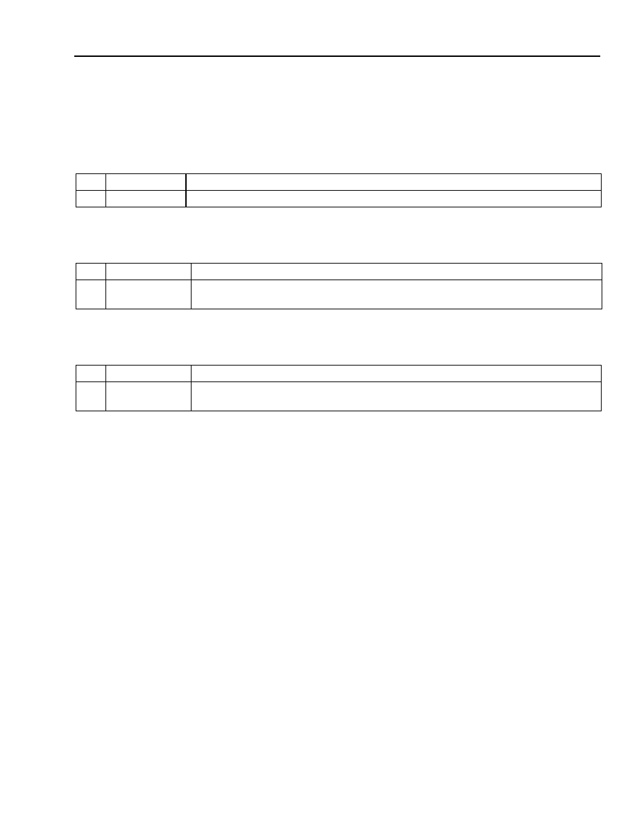
Data Sheet
August 1999
TECO3264 32-Channel Echo Canceller
117
Lucent Technologies Inc.
Register Architecture
(continued)
Page 1 Read-Only Registers 100
--
10E
(continued)
C Test Data Register
Table 125. C Test Data Register (104)
E Test Data Bits [7:0] Register
Table 126. E Test Data Bits [7:0] Register (105)
E Test Data Bits [15:8] Register
Table 127. E Test Data Bits [15:8] Register (106)
Bit
Symbol
Parameter Name and Description
7--0 CDATAVFX[7:0] C Test Data [7:0]. C data read back for 109 test.
Bit
Symbol
Parameter Name and Description
7--0 EDATAVFX[15:0] E Test Data [7:0]. Least significant byte of E test data read back for 109 test. See
Table 127, E Test Data Bits [15:8] Register (106).
Bit
Symbol
Parameter Name and Description
7--0 EDATAVFX[15:0] E Test Data [15:8]. Most significant byte of E test data read back for 109 test. See
Table 126, E Test Data Bits [7:0] Register (105).

Data Sheet
TECO3264 32-Channel Echo Canceller
August 1999
118
Lucent Technologies Inc.
Register Architecture
(continued)
Page 1 Read-Only Registers 100
--
10E
(continued)
Tone Detector Indicators Register
Register 107 is shown in Table 128 below. Registers 108--10E are arranged in a similar pattern with alternating TD
and TDPR bits with four channels per register for channels 5--31. Table 20, Recommended Register Values for
DS1 (µ-Law) and 2.048 Mbits/s Rate, on page 51 shows the detailed bit layout for all 32 channels.
Table 128. Tone Detector Indicator Registers (107--10E)
* n = 0, 1, 2, 3, 4, 5, 6, 7.
Bit
Symbol*
Parameter Name and Description
0
TD[0 + 4n]
Tone Detected, Channels 0, 4, 8, 12, 16, 20, 24, 28, Respectively, as Registers 107--
10E.
0 = Tone not detected.
1 = Tone detected.
1
TDPR[0 + 4n]
Tone Detected Phase Reversal, Channels 0, 4, 8, 12, 16, 20, 24, 28, Respectively, as
Registers 107--10E.
1 = Tone with phase reversals detected.
0 = Tone with phase reversals not detected.
2
TD[1 + 4n]
Tone Detected, Channels 1, 6, 9, 13, 17, 21, 25, 29, Respectively, as Registers 107--
10E.
0 = Tone not detected.
1 = Tone detected.
3
TDPR[1 + 4n]
Tone Detected Phase Reversal, Channels 1, 6, 9, 13, 17, 21, 25, 29, Respectively, as
Registers 107--10E.
1 = Tone with phase reversals detected.
0 = Tone with phase reversals not detected.
4
TD[2 + 4n]
Tone Detected, Channels 2, 6, 10, 14, 18, 22, 26, 30, Respectively, as Registers
107--10E.
0 = Tone not detected.
1 = Tone detected.
5
TDPR[2 + 4n]
Tone Detected Phase Reversal, Channels 2, 6, 10, 14, 18, 22, 26, 30, Respectively,
as Registers 107--10E.
1 = Tone with phase reversals detected.
0 = Tone with phase reversals not detected.
6
TD[3 + 4n]
Tone Detected, Channel 3, 7, 11, 15, 19, 23, 27, 31, Respectively, as Registers 107--
10E.
0 = Tone not detected.
1 = Tone detected.
7
TDPR[3 + 4n]
Tone Detected Phase Reversal, Channel 3, 7, 11, 15, 19, 23, 27, 31, Respectively, as
Registers 107--10E.
1 = Tone with phase reversals detected.
0 = Tone with phase reversals not detected.
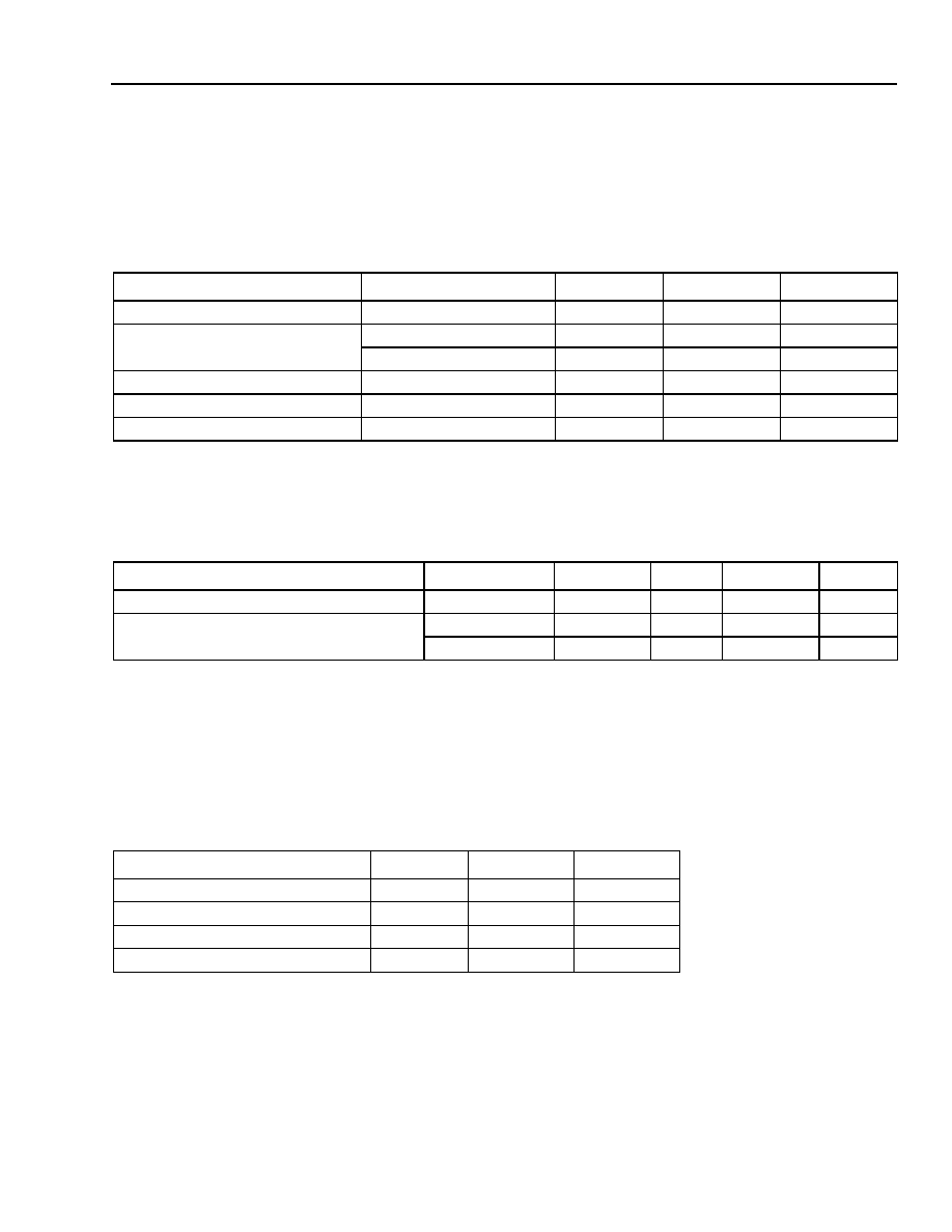
Data Sheet
August 1999
TECO3264 32-Channel Echo Canceller
119
Lucent Technologies Inc.
Absolute Maximum Ratings
Stresses in excess of the absolute maximum ratings can cause permanent damage to the device. These are abso-
lute stress ratings only. Functional operation of the device is not implied at these or any other conditions in excess
of those given in the operational sections of the data sheet. Exposure to absolute maximum ratings for extended
periods can adversely affect device reliability.
* In 5 V tolerant input mode, maximum input voltage is V
DD5
+ 0.5 V.
Recommended Operating Conditions
Electrical Characteristics
Unless otherwise indicated, characteristics apply over all operating conditions.
Input and High-Impedance Leakage Current
Table 129. Absolute Maximum Ratings
Parameter
Symbol
Min
Max
Unit
Input Voltage*
V
I
V
SS
-
0.3
V
DD
+
0.3
V
dc Supply Voltage
V
DD
≠ V
SS
--
3.3
V
V
DD5
≠ V
SS
--
5.5
V
Power Dissipation
P
D
--
1.43
W
Storage Temperature
T
stg
-
40
125
∞
C
Junction Temperature
T
J
--
125
∞
C
Table 130. Recommended Operating Conditions
Parameter
Symbol
Min
Typ
Max
Unit
Ambient Temperature
T
A
0
--
85
∞
C
Power Supply Voltage
V
DD
3.135
3.3
3.465
V
V
DD5
4.75
5.0
5.25
V
Table 131. Input and High-Impedance Leakage Current
Parameter
Min
Max
Unit
V
BIAS
Input Current
--
500
µ
A
V
DD
Input Current
--
500
mA
Input Leakage Current
--
1
µ
A
High-impedance Leakage Current
--
10
µ
A
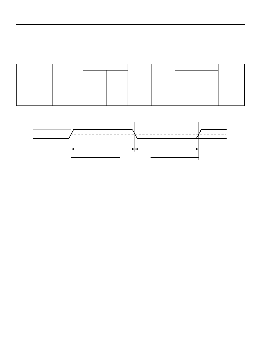
Data Sheet
TECO3264 32-Channel Echo Canceller
August 1999
120
Lucent Technologies Inc.
Electrical Characteristics
(continued)
Clock Input Specifications
Note: TCK must have a clock input applied at all times to keep the TAP controller in an idle state.
5-4905(F).ar.1
Figure 18. Clock Input Signals
Table 132. Clock Input Specification
Clock
Name
Period
(Min)
dc Levels
Rise
Time
(Max)
Fall
Time
(Max)
Duty Cycle
Sync
or
Async
V
IL
(Max)
V
IH
(Min)
High
(Min)
Low
(Min)
(ns)
(V)
(V)
(ns)
(ns)
(ns)
(ns)
CK8M
122.070
1.05
2.0
4.2
4.2
50
50
Sync
TCK
100
1.05
2.0
4.2
4.2
40
40
Async
V
IH
50%
V
IL
INPUT CLOCK
MIN HIGH
MIN LOW
CLOCK PERIOD
V
DD
50%
V
SS
Data Sheet
August 1999
TECO3264 32-Channel Echo Canceller
121
Lucent Technologies Inc.
Electrical Characteristics
(continued)
Other Input Specifications
Table 133. Other Input Specifications
Input
Name
dc Levels
Rise
Time
(Max)
Fall
Time
(Max)
Reference
Clock
Edge
(+/≠)
Setup
Time
(Min)
Hold
Time
(Min)
V
IL
(Max)
V
IH
(Min)
(V)
(V)
(ns)
(ns)
(ns)
(ns)
XPCM
1.05
2.0
4.2
4.2
CK8M
+
30
10
YPCM
1.05
2.0
4.2
4.2
CK8M
+
30
10
XLINEAR
1.05
2.0
4.2
4.2
CK8M
+
30
10
RST
1.05
2.0
4.2
4.2
CK8M
+
50
10
SYNC
1.05
2.0
4.2
4.2
CK8M
+
20
10
ECDIS
1.05
2.0
4.2
4.2
CK8M
+
40
10
ENBP
1.05
2.0
4.2
4.2
CK8M
+
40
10
NLPFRZ
1.05
2.0
4.2
4.2
CK8M
+
40
10
NLPEN
1.05
2.0
4.2
4.2
CK8M
+
40
10
HRST
1.05
2.0
4.2
4.2
CK8M
+
40
10
HFRZ
1.05
2.0
4.2
4.2
CK8M
+
40
10
CALLB
1.05
2.0
4.2
4.2
CK8M
+
40
10
VSC
1.05
2.0
4.2
4.2
CK8M
+
40
10
TDI
1.05
2.0
4.2
4.2
TCK
+
10
10
TMS
1.05
2.0
4.2
4.2
TCK
+
10
10
TRST
1.05
2.0
4.2
4.2
TCK
+
10
10
HIGHZ
1.05
2.0
NA
NA
NA
NA
dc
dc
SLOW
1.05
2.0
NA
NA
NA
NA
dc
dc
CKEXT
1.05
2.0
NA
NA
NA
NA
dc
dc
SCAN
1.05
2.0
NA
NA
NA
NA
Async
Async
TSTMD1
1.05
2.0
NA
NA
NA
NA
dc
dc

Data Sheet
TECO3264 32-Channel Echo Canceller
August 1999
122
Lucent Technologies Inc.
Electrical Characteristics
(continued)
Other Input Specifications
(continued)
5-4904(F).a
Figure 19. Setup and Hold Times
REFERENCE INPUT
DATA INPUT
t
SU
t
H
V
DD
50% V
DD
V
SS
V
DD
50% V
DD
V
SS
Data Sheet
August 1999
TECO3264 32-Channel Echo Canceller
123
Lucent Technologies Inc.
Electrical Characteristics
(continued)
Output Signal Specification
Table 134. Output Signal Specification
Output
Name
Sinking
I @ V
(Max)
Sourcing
I @ V
(Max)
Prop
Delay
(Max)
Reference
Signal
Edge
(+/≠)
Capacitive
Load
External
Pull-Up
(Range)
High-
Impedance
Mode
Y/N
(Max) (Min)
(mA @ V)
(mA @ V)
(ns)
(pF)
(pF)
(
)
CPCM
0.25 @ 0.3
0.2 @ 3.3
30
CK8M
+
30
5
NA
Y
EPCM
0.25 @ 0.3
0.2 @ 3.3
30
CK8M
+
30
5
NA
Y
DTACK
0.25 @ 0.3
0.2 @ 3.3
30
CK8M
+
30
5
NA
Y
INT
0.25 @ 0.3
0.2 @ 3.3
30
CK8M
+
30
5
NA
Y
TDO
0.25 @ 3.3
0.2 @ 0.3
40
TCK
-
30
5
NA
Y
TONE
0.25 @ 0.3
0.2 @ 3.3
30
CK8M
+
30
5
NA
Y
TDPR
0.25 @ 0.3
0.2 @ 3.3
30
CK8M
+
30
5
NA
Y
VPA
0.25 @ 0.3
0.2 @ 3.3
30
CK8M
+
30
5
NA
Y
CK32
0.25 @ 0.3
0.2 @ 3.3
20
CK8M
+
30
5
NA
Y
HDSP
0.25 @ 0.3
0.2 @ 3.3
20
CK8M
+
30
5
NA
Y
HSYNC
0.25 @ 0.3
0.2 @ 3.3
20
CK8M
+
40
5
NA
Y
TEST[0:7]
0.25 @ 0.3
0.2 @ 3.3
50
CK8M
+
30
5
NA
Y
D[0:7]
10 @ 0.3
8 @ 3.3
30
CK8M
+
50
5
NA
Y

Data Sheet
TECO3264 32-Channel Echo Canceller
August 1999
124
Lucent Technologies Inc.
Physical Characteristics
Package type: 160-pin, plastic, metric quad flat pack with heat spreader (MQFPH).
Thermal resistance: 28
∞
C/W
Inputs: 40
Outputs: 42
Bidirectional Pins: 44
V
SS
Pins: 17
V
DD
Pins: 17
Unused Pins: 0
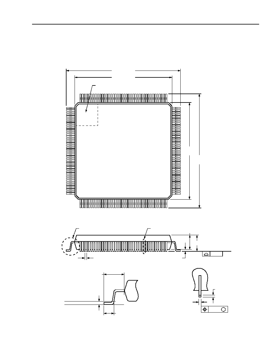
Data Sheet
August 1999
TECO3264 32-Channel Echo Canceller
125
Lucent Technologies Inc.
Outline Diagram
160-Pin MQFPH
Dimensions are in millimeters.
5-2132r.12(C)
81
120
28.00
± 0.20
31.20
± 0.20
DETAIL A
DETAIL B
4.07 MAX
0.65 TYP
SEATING PLANE
0.10
3.42 ± 0.25
0.25 MIN
1
40
121
160
PIN #1 IDENTIFIER ZONE
31.20 ± 0.20
28.00 ± 0.20
80
41
0.25
0.73/1.03
1.60 REF
GAGE PLANE
SEATING PLANE
DETAIL A
0.22/0.38
0.12
M
0.13/0.23
DETAIL B

Data Sheet
TECO3264 32-Channel Echo Canceller
August 1999
126
Lucent Technologies Inc.
Ordering Information
DS99-241PDH Replaces DS98-409TIC to Incorporate the Following Updates
1.
Throughout this data sheet, ehat and has been replaced by Í.
2.
Page 11, Table 1, Pin Descriptions, pin 38 added to description that this pin must be held when not used.
3.
Page 11, Table 1, Pin Descriptions, pin 25 corrected symbol name from RSTI to RST.
4.
Page 15, Fast/Slow Convergence Control (F_CONV) section removed paragraph that does not apply.
5.
Page 16, Table 2, Microprocessor Interface Control I/O,
Intel
Mode column updated Address Latch Enable
(ALE) to active-low.
6.
Page 16, Table 2, Microprocessor Interface Control I/O,
Intel
Mode column updated Read Cycle (RD) to active-
low.
7.
Page 18, Figure 5, MPIC Write Cycle (UP_MODE = 0) and Figure 6, MPIC Read Cycle (UP_MODE = 0) were
updated.
8.
Page 28, Table 8, Programming Values (CET = Decimal) for [C, E]XBOFF, When CMS = 0 corrected heading
XRBOFF, YRBOFF to CRBOFF, ERBOFF.
9.
Page 30, Figure 17, HSYNC, HDSP Relationship corrected 16
µ
s to 16 ms.
10. Page 47, Table 19, Parameter Address Map, updated bit 7 names of registers 7C, 7D, and 7F from spare to
HMODE, NMODE, and CENABLE, respectively.
11. Page 51, Table 20, Recommended Register Values for DS1 (µ-Law) and 2.048 Mbits/s Rate corrected recom-
mended values for register addresses 5C and 5D from 00 and 9F to 4C and 8A, respectively here and through-
out the document.
12. Page 52, Table 21, Recommended Register Values for E1 (A-Law), register address 21 corrected value from
0A to 02.
13. Page 84, Table 54, Low-Peak Count Register (03D) [84], updated the recommended values of bit 7--bit 2 to
100001 binary.
14. Page 84, Table 55, High-Peak Count Register (03E) [E3], updated the recommended values of bit 5--bit 0 to
100011 binary.
15. Page 90, Table 69, Noise Matching Enable Register (04C) [20] corrected recommended value and added table
on types of comfort noise that can be injected.
16. Page 94, Table 77, Variable Loss Noise Matching Select Register (054) [00] updated description of bit 6
VARLOSS.
17. Page 96, Table 81, Spectrally Matched Noise Matching Select Register (058) [B0] updated description of bit 7
USE_NM.
18. Page 104, Table 98, Fast Convergence Register (069) [60] and Table 99, Slow Convergence Gain Register
(06A) [40] removed Step: 0.2 dB from description.
19. Page 109, Table 109, Near-End Speech 1 Hangover Register (074) [FF], removed range and step information.
20. Page 112, Table 117, NLP Operate Time Double Register (07C) [A3] updated description of bit 7 HMODE.
21. Page 113, Table 119, Enable Í Threshold Register (07E) [18] and Table 120, Enable Í Threshold Register
(07F) [C0], updated bit symbol name from EETHO to EETHR in these tables and throughout the document.
22. Page 115, Table 122, Interupt Masks 1 Register (101), updated bit symbols ERRM2, ERRM3, and ERRM4 to
ERR2M, ERR3M, and ERR4M, respectively, in this table and throughout the document.
23. Page 123, Table 134, Output Signal Specification, outputs CPCM and EPCM (sinking and sourcing) currents
updated from (250 mA and 200 mA) to (0.25 mA and 0.2 mA), respectively.
24. Page 123, Table 134, Output Signal Specification, output D[0:7] (sinking and sourcing) currents updated from
(0.25 mA and 0.2 mA) to (10 mA and 8 mA), respectively.
25. Page 126, Ordering Information, updated Device Code from TECO3264 to TECO32642 and Comcode (Order-
ing Number) from 107956641 to 108194275, to reflect the version of the device.
Device Code
Package
Temperature
Comcode
(Ordering Number)
TECO32642-DB
160-Pin MQFPH
0
∞
C to 85
∞
C
108194275

Data Sheet
August 1999
TECO3264 32-Channel Echo Canceller
127
Lucent Technologies Inc.
Notes

Preliminary Data Sheet
Interactive Terminal Transmission Convergence
August 1999
Lucent Technologies Inc. reserves the right to make changes to the product(s) or information contained herein without notice. No liability is assumed as a result of their use or application. No
rights under any patent accompany the sale of any such product(s) or information.
Copyright © 1999 Lucent Technologies Inc.
All Rights Reserved
August 1999
DS99-241PDH (Replaces DS98-409TIC)
For additional information, contact your Microelectronics Group Account Manager or the following:
INTERNET:
http://www.lucent.com/micro
E-MAIL:
docmaster@micro.lucent.com
N. AMERICA: Microelectronics Group, Lucent Technologies Inc., 555 Union Boulevard, Room 30L-15P-BA, Allentown, PA 18103
1-800-372-2447, FAX 610-712-4106 (In CANADA: 1-800-553-2448, FAX 610-712-4106)
ASIA PACIFIC: Microelectronics Group, Lucent Technologies Singapore Pte. Ltd., 77 Science Park Drive, #03-18 Cintech III, Singapore 118256
Tel. (65) 778 8833, FAX (65) 777 7495
CHINA:
Microelectronics Group, Lucent Technologies (China) Co., Ltd., A-F2, 23/F, Zao Fong Universe Building, 1800 Zhong Shan Xi Road, Shanghai
200233 P. R. China Tel. (86) 21 6440 0468, ext. 316, FAX (86) 21 6440 0652
JAPAN:
Microelectronics Group, Lucent Technologies Japan Ltd., 7-18, Higashi-Gotanda 2-chome, Shinagawa-ku, Tokyo 141, Japan
Tel. (81) 3 5421 1600, FAX (81) 3 5421 1700
EUROPE:
Data Requests: MICROELECTRONICS GROUP DATALINE: Tel. (44) 7000 582 368, FAX (44) 1189 328 148
Technical Inquiries:
GERMANY: (49) 89 95086 0 (Munich), UNITED KINGDOM: (44) 1344 865 900 (Ascot),
FRANCE: (33) 1 40 83 68 00 (Paris), SWEDEN: (46) 8 594 607 00 (Stockholm), FINLAND: (358) 9 4354 2800 (Helsinki),
ITALY: (39) 02 6608131 (Milan), SPAIN: (34) 1 807 1441 (Madrid)