 | –≠–ª–µ–∫—Ç—Ä–æ–Ω–Ω—ã–π –∫–æ–º–ø–æ–Ω–µ–Ω—Ç: TF1001A | –°–∫–∞—á–∞—Ç—å:  PDF PDF  ZIP ZIP |
Data Sheet
February 1999
LG1602 Decision Circuit
Features
s
Operation up to 3 Gbits/s
s
Good sensitivity to low input signals
s
Low power dissipation
s
Surface-mount package
Applications
s
SONET/SDH transmission systems
s
Digital video transmission
s
Digital test instruments
Functional Description
The LG1602 is a gallium arsenide (GaAs) decision
circuit. It features a sensitive broadband input ampli-
fier and a D-type flip-flop that retimes and regener-
ates an input data stream that is weakened by noise,
jitter, and intersymbol interference.
The LG1602 has complementary 50
output buff-
ers.
dc feedback ensures input threshold control for input
levels as low as 25 mV, when using dc balanced
input data. The LG1602 is available in a hermetically
sealed 16-lead glass-metal surface-mount package.
5-7667(F)r.3
Figure 1. LG1602 Functional Diagram
V
+REF
V
+IN
V
≠IN
V
≠REF
25 k
110 pF
25 k
110 pF
D
D
Q
V
+OUT
V
≠OUT
V
SS
V
≠CLK
V
+CLK
GND
50
50
2 pF
2 pF
50
50

Data Sheet
LG1602 Decision Circuit
February 1999
2
Lucent Technologies Inc.
Pin Information
12-3223(F).ar.2
Figure 2. Pin Diagram
Table 1. Pin Descriptions
Pin
Symbol
Name/Description
2
V
+CLK
Clock Input. May be grounded, if not used.
3
V
≠CLK
Clock Input. May be grounded, if not used.
4
V
SS
dc Supply Voltage.
5
V
≠OUT
Negative Data Output. ac couple or terminate with 50
to GND.
6
V
+OUT
Positive Data Output. ac couple or terminate with 50
to GND.
9
V
≠REF
Data Negative Reference. Bypass to GND with 0.047 µF in series with 5
.
10
V
≠IN
Negative Data Input. ac couple with 0.047 µF.
11
V
+IN
Positive Data Input. ac couple with 0.047 µF.
12
V
+REF
Data Positive Reference. Bypass to GND with 0.047 µF in series with 5
.
1, 15, 16,
Package
Back
GND
Ground. For optimum performance, package back should contact board ground
plane.
7, 8, 13, 14
NC
No Connection.
GND
V
SS
1
2
3
4
V
+REF
12
11
10
9
16
15
14
13
GND GND
NC
5
6
7
8
V
≠OUT
V
+OUT
NC
V
+IN
V
≠IN
V
≠REF
NC
NC
V
+CLK
V
≠CLK
Data Sheet
February 1999
LG1602 Decision Circuit
3
Lucent Technologies Inc.
Absolute Maximum Ratings
Stresses in excess of the absolute maximum ratings can cause permanent or latent damage to the device. These
are absolute stress ratings only. Functional operation of the device is not implied at these or any other conditions in
excess of those given in the operational sections of the data sheet. Exposure to absolute maximum ratings for
extended periods can adversely affect device reliability.
Table 2. Absolute Maximum Ratings
Recommended Operating Conditions
Table 3. Recommended Operating Conditions
Handling Precautions
Although protection circuitry has been designed into this device, proper precautions should be taken to avoid expo-
sure to electrostatic discharge (ESD) during handling and mounting. Lucent employs a human-body model (HBM)
and a charged-device model (CDM) for ESD-susceptibility testing and protection design evaluation. No industry-
wide standard has been adopted for the CDM. However, a standard HBM (resistance = 1500
, capacitance =
100 pF) is widely used and, therefore, can be used for comparison purposes. The HBM ESD threshold presented
here was obtained by using these circuit parameters.
Table 4. ESD Threshold
Mounting and Connections
Certain precautions must be taken when using solder. For installation using a constant temperature solder, tem-
peratures of under 300 ∞C may be employed for periods of time up to 5 seconds, maximum. For installation with a
soldering iron (battery operated or nonswitching only), the soldering tip temperature should not be greater than
300 ∞C and the soldering time for each lead must not exceed 5 seconds.
Parameter
Min
Max
Unit
Supply Voltage Range (V
SS
)
0.5
≠7
V
Power Dissipation
--
1
W
Voltage (all pins)
0.5
V
SS
V
Clock Input (V
+CLK
, V
≠CLK
)
--
±2
V
V
+REF
≠ V
+IN
--
±2
V
V
≠REF
≠ V
≠IN
--
±2
V
Storage Temperature Range
≠40
125
∞C
Operating Case Temperature Range
0
100
∞C
Parameter
Symbol
Min
Max
Unit
Case Temperature
t
CASE
0
75
∞C
Power Supply
V
SS
≠4.7
≠5.7
V
HBM ESD Threshold
Device
Voltage
LG1602
200 V
Data Sheet
LG1602 Decision Circuit
February 1999
4
Lucent Technologies Inc.
Electrical Characteristics
Bit rate = 2.488 Mbits/s NRZ and data pattern = 2
23
≠ 1 PRBS, unless otherwise indicated. See Figure 3 for the tim-
ing and signal levels and Figure 5 for the test circuit, when using the TF1001A test fixture.
Note: Minimum and maximum values are testing requirements. Typical values are characteristics of the device
and are the result of engineering evaluations. Typical values are for information purposes only and are not
part of the testing requirements.
Parameter
Symbol
Conditions
LG1602AXB
LG1602BXB
Unit
t
CASE =
25 ∞C
V
SS
= ≠5.2 V
t
CASE =
0 ∞C--
75 ∞C
V
SS
= ≠4.9 V to
≠5.5 V
Min
Typ
Max
Min
Typ
Max
Maximum Bit Rate
--
BER = 10
≠9
3
--
--
2.5
--
--
GHz
Data Input Voltage
|
V
H
≠ <V>
|
+
|
<V> ≠ V
L
|
--
t
R
, t
F
165 ps (20%--80%)
200
--
800
200
--
900
mV
Data Input Sensitivity
--
BER = 10
≠9
, limited clock
phase margin
--
20
--
--
20
--
mV
Clock Input Voltage
|
V
H
≠ <V>
|
+
|
<V> ≠ V
L
|
--
t
R
, t
F
85 ps (20%--80%),
duty cycle = 50% ± 10%
500
--
1000 200
--
900
mV
Clock Phase Margin
--
--
250
360
--
250
360
--
ps
Clock Phase Minimum
t1
Data transition to negative
edge of CLOCK IN
--
--
--
--
150
205
ps
Clock Phase Maximum
t2
Data transition to negative
edge of CLOCK IN
--
--
--
455
510
--
ps
Clock Phase Center
t
C
Data transition to negative
edge of CLOCK IN
--
330
--
--
330
--
ps
Setup Time
t
S
Valid input data to negative
edge of CLOCK IN
--
185
--
--
185
205
ps
Hold Time
t
H
Negative edge CLOCK IN to
valid DATA IN
--
≠73
--
--
≠73
≠53
ps
Propagation Delay
t
PD
CLOCK IN negative edge to
output transition
--
1200
--
--
1200
--
ps
Output Voltage (V
H
≠ V
L
)
--
Outputs ac coupled (see
Figure 5)
500
600
--
500
600
--
mV
Output Transition Time
--
20%--80%, outputs ac cou-
pled
--
--
100
--
--
100
ps
Output Return Loss
--
1 MHz--2 GHz, outputs ac
coupled
--
15
--
--
15
--
dB
Data Input Return Loss
--
100 kHz--300 kHz
0.3 MHz--1500 MHz
1.5 GHz--1.8 GHz
--
--
--
10
15
15
--
--
--
10
15
15
--
--
--
--
--
--
dB
dB
dB
Clock Input Return Loss
--
2.4 GHz--2.6 GHz
--
15
--
15
--
--
dB
Power Supply Current
--
--
--
115
--
--
115
--
mA
Thermal Resistance
--
Junction to case bottom
--
20
--
--
20
--
∞C/W
Data Sheet
February 1999
LG1602 Decision Circuit
5
Lucent Technologies Inc.
Electrical Characteristics
(continued)
5-7668(F)r.2
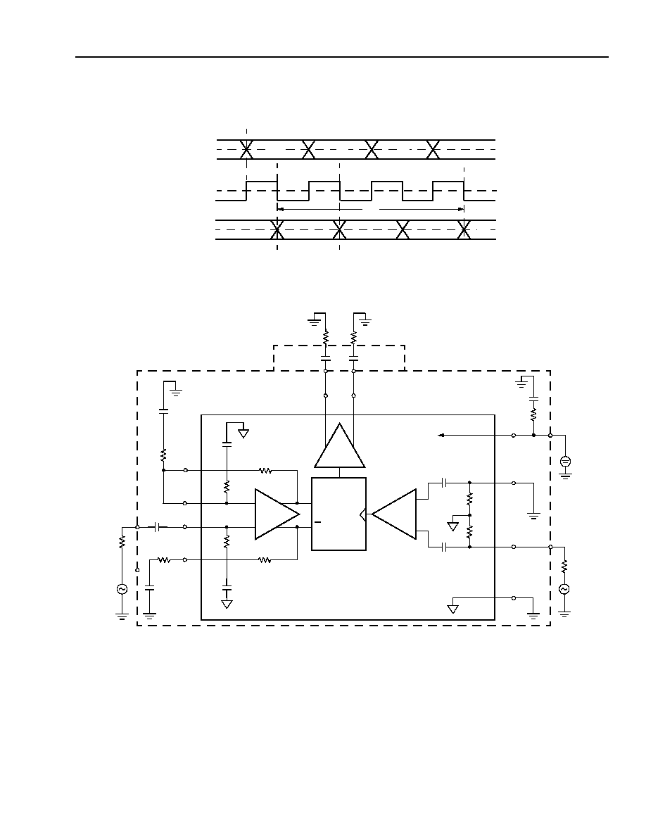
Figure 3. Timing Diagram
5-7669(F)r.2
Figure 4. Test Circuit
t
PD
D0
DATA IN
CLOCK IN
DATA OUT
V
H
<V>
V
L
V
H
<V>
V
L
V
H
0
V
L
D1
D2
t
1
D0
t
2
2 pF
2 pF
50
50
3
2
1, 15, 16
GND
50
CLOCK
V
+CLK
V
≠CLK
V
SS
≠
+
0.047
µ
F
5
4
≠5.2 V
D
D
Q
6
5
V
+OUT
V
≠OUT
50
50
0.047
µ
F
0.047
µ
F
COUPLING CAPACITORS
OPTIONAL
25 k
110 pF
V
≠REF
V
≠IN
0.1
µ
F
5
50
9
10
11
25 k
50
12
V
+IN
V
+REF
110 pF
5
0.047
µ
F
50
0.047
µ
F
TF1001A FIXTURE BOUNDARY
CLOCK
Data Sheet
LG1602 Decision Circuit
February 1999
6
Lucent Technologies Inc.
Electrical Characteristics
(continued)
5-7670(F)r.1
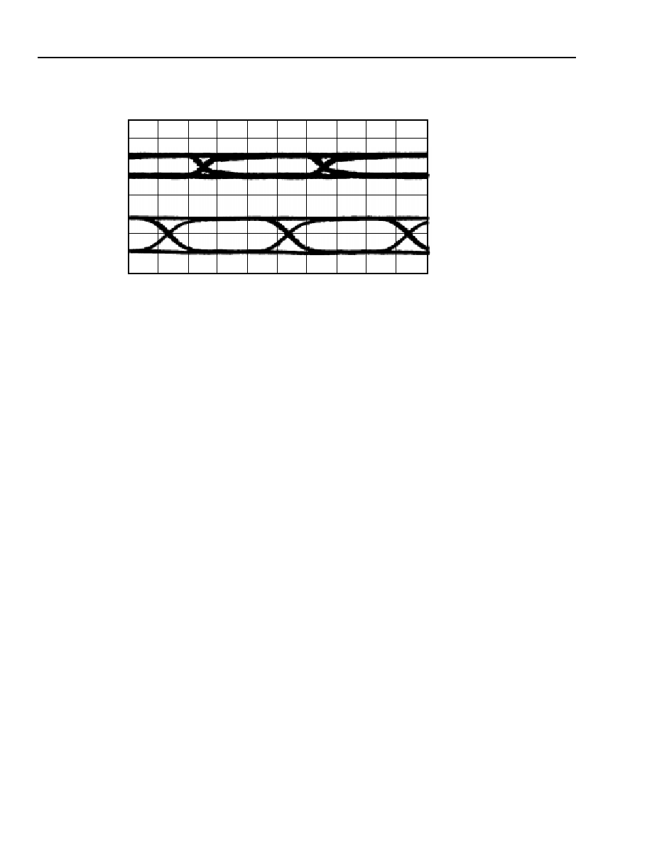
Figure 5. Typical Performance
DATA IN
(10 mV/div)
DATA OUT
(400 mV/div)
TIME (100 ps/div)
Data Sheet
February 1999
LG1602 Decision Circuit
7
Lucent Technologies Inc.
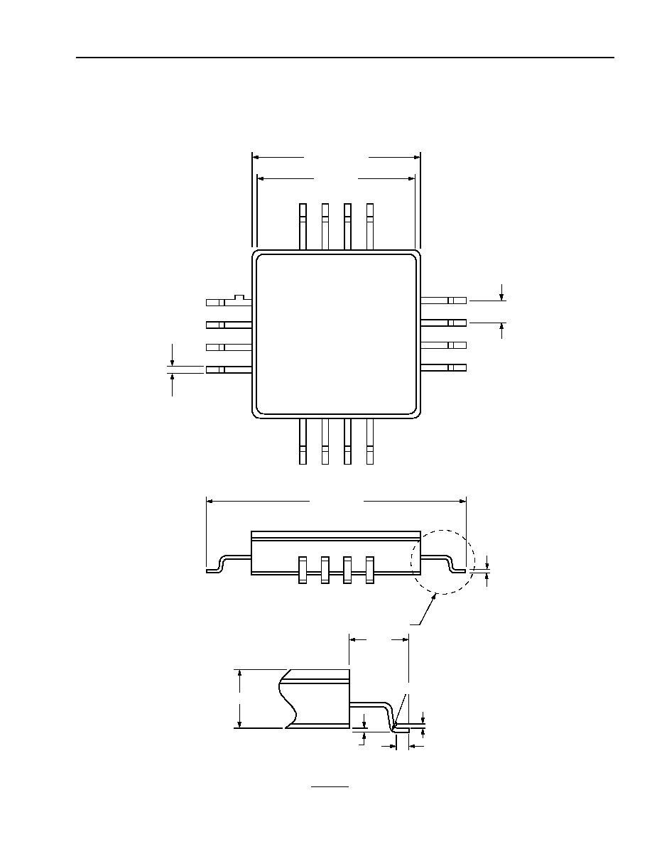
Outline Diagram
16-Pin, Glass-Metal, Surface-Mount Package
Dimensions are in inches.
12-3224(F)r.4
0.012 TYP
0.030 TYP
0.230 SQ REF
+
0.366
±
0.007
0.005
DETAIL A
+
0.215 SQ
9
13
1
5
TOP
VIEW
0.060 MAX
0.000--0.004
0.020
0--4
∞
DETAIL A
R0.08
0.068
REF

Data Sheet
LG1602 Decision Circuit
February 1999
8
Lucent Technologies Inc.
Ordering Information
Device Code
Package
Temperature
Comcode
(Ordering Number)
LG1602AXB
Packaged on 16 mm tape and reel
0 ∞C to 75 ∞C
106385297
LG1602BXB
Packaged in flat pack container
0 ∞C to 75 ∞C
106995715
TF1001A
Test fixture
--
106497589

Data Sheet
February 1999
LG1602 Decision Circuit
9
Lucent Technologies Inc.
Notes

LG1602 Decision Circuit
Preliminary Data Sheet
Interactive Terminal Transmission Convergence
February 1999
Lucent Technologies Inc. reserves the right to make changes to the product(s) or information contained herein without notice. No liability is assumed as a result of their use or application. No
rights under any patent accompany the sale of any such product(s) or information.
Copyright © 1999 Lucent Technologies Inc.
All Rights Reserved
February 1999
DS99-142HSPL
For additional information, contact your Microelectronics Group Account Manager or the following:
INTERNET:
http://www.lucent.com/micro
E-MAIL:
docmaster@micro.lucent.com
N. AMERICA: Microelectronics Group, Lucent Technologies Inc., 555 Union Boulevard, Room 30L-15P-BA, Allentown, PA 18103
1-800-372-2447, FAX 610-712-4106 (In CANADA: 1-800-553-2448, FAX 610-712-4106)
ASIA PACIFIC: Microelectronics Group, Lucent Technologies Singapore Pte. Ltd., 77 Science Park Drive, #03-18 Cintech III, Singapore 118256
Tel. (65) 778 8833, FAX (65) 777 7495
CHINA:
Microelectronics Group, Lucent Technologies (China) Co., Ltd., A-F2, 23/F, Zao Fong Universe Building, 1800 Zhong Shan Xi Road, Shanghai
200233 P. R. China Tel. (86) 21 6440 0468, ext. 316, FAX (86) 21 6440 0652
JAPAN:
Microelectronics Group, Lucent Technologies Japan Ltd., 7-18, Higashi-Gotanda 2-chome, Shinagawa-ku, Tokyo 141, Japan
Tel. (81) 3 5421 1600, FAX (81) 3 5421 1700
EUROPE:
Data Requests: MICROELECTRONICS GROUP DATALINE: Tel. (44) 1189 324 299, FAX (44) 1189 328 148
Technical Inquiries:
GERMANY: (49) 89 95086 0 (Munich), UNITED KINGDOM: (44) 1344 865 900 (Ascot),
FRANCE: (33) 1 40 83 68 00 (Paris), SWEDEN: (46) 8 594 607 00 (Stockholm), FINLAND: (358) 9 4354 2800 (Helsinki),
ITALY: (39) 02 6608131 (Milan), SPAIN: (34) 1 807 1441 (Madrid)