 | –≠–ª–µ–∫—Ç—Ä–æ–Ω–Ω—ã–π –∫–æ–º–ø–æ–Ω–µ–Ω—Ç: TF1006A | –°–∫–∞—á–∞—Ç—å:  PDF PDF  ZIP ZIP |
Data Sheet
June 1999
LG1625AXF Laser Driver
Features
s
High data-rate laser diode/LED driver
s
Adjustable output current
s
Operation up to 3 Gbits/s
s
Single ≠5.2 V power supply
s
90 ps rise and fall times
Applications
s
SONET/SDH transmission systems
s
SONET/SDH test equipment
s
Optical transmitters
Description
The LG1625AXF is a gallium-arsenide (GaAs) laser
diode driver to be used with direct modulated laser
diodes in high-speed nonreturn-to-zero (NRZ) trans-
mission systems. The device is made in a high-per-
formance 0.9
µ
m gate GaAs heterojunction FET
technology that utilizes high-density MIM capacitors,
airbridge interconnect, and NiCr film precision resis-
tors.
The device contains three cascaded stages, oper-
ates with a single ≠5.2 V power supply and accepts
ECL level inputs. Voltages control the modulated out-
put current and laser prebias current. The
LG1625AXF is available in a 24-lead hermetic, gull-
wing package.
A test fixture (TF1006A) with SMA connectors is
available to allow quick evaluation of the LG1625AXF.
5-7865(F)
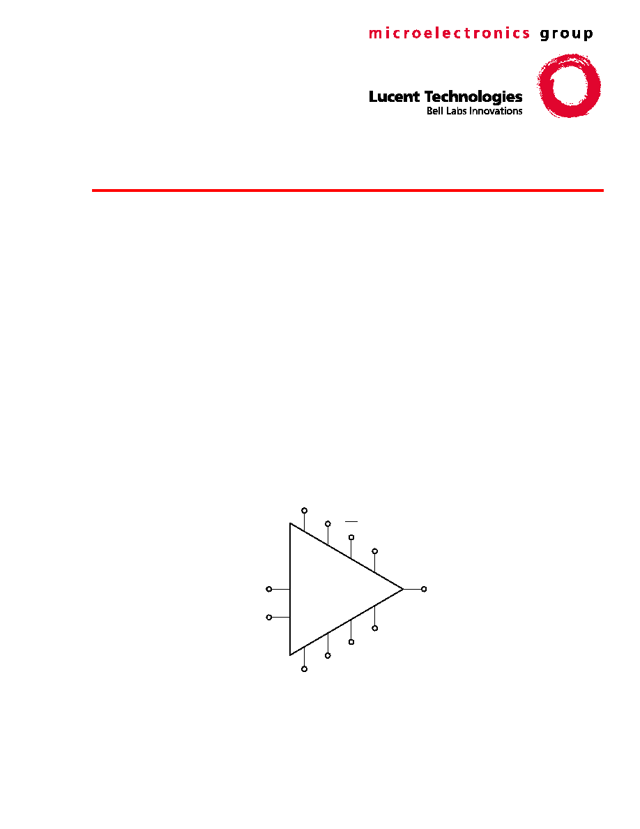
Figure 1. Functional Diagram
V
IN
MK
V
SS1
V
TH
V
SS2
GND
I
OUT
MK
V
PRE
V
SS3
V
MOD
LG1625AXF
2
Lucent Technologies Inc.
Data Sheet
June 1999
LG1625AXF Laser Driver
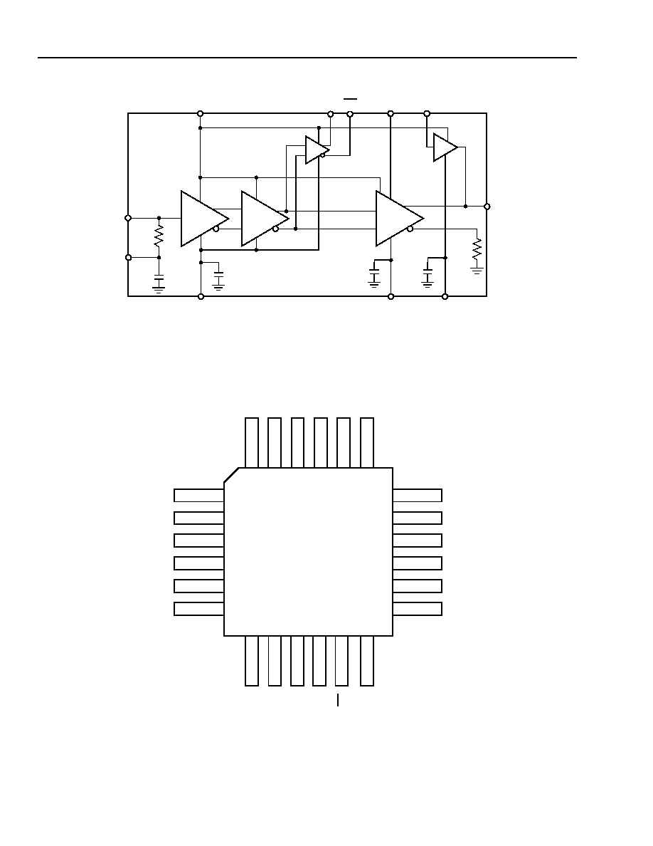
Pin Information
5-7866(F)
Figure 2. LG1625AXF Die Block Diagram
5-7867(F)r.1
Note: Figure 3 is not to scale.
Figure 3. LG1625AXF Package Pinout
V
IN
V
TH
I
OUT
V
SS3
V
MOD
V
SS1
50
GND
MK
MK
V
SS2
V
PRE
25
+
≠
+
≠
+
≠
V
SS1
GND
GND
I
OUT
GND
V
PRE
V
SS2
V
SS3
V
MO
D
V
SS1
V
SS1
V
TH
1
2
3
4
5
6
13
14
15
16
17
18
24
V
TH
GND
GND
GND
MK
MK
V
SS1
V
IN
GND
GND
GND
V
SS1
23
22
21
20
19
7
8
9
10
11
12
(O
PTI
O
N
A
L
)
LG1625AXF
Lucent Technologies Inc.
3
Data Sheet
June 1999
LG1625AXF Laser Driver
Pin Information
(continued)
Absolute Maximum Ratings
Stresses in excess of the absolute maximum ratings can cause permanent or latent damage to the device. These
are absolute stress ratings only. Functional operation of the device is not implied at these or any other conditions in
excess of those given in the operational sections of this device specification. Exposure to absolute maximum rat-
ings for extended periods can adversely affect device reliability.
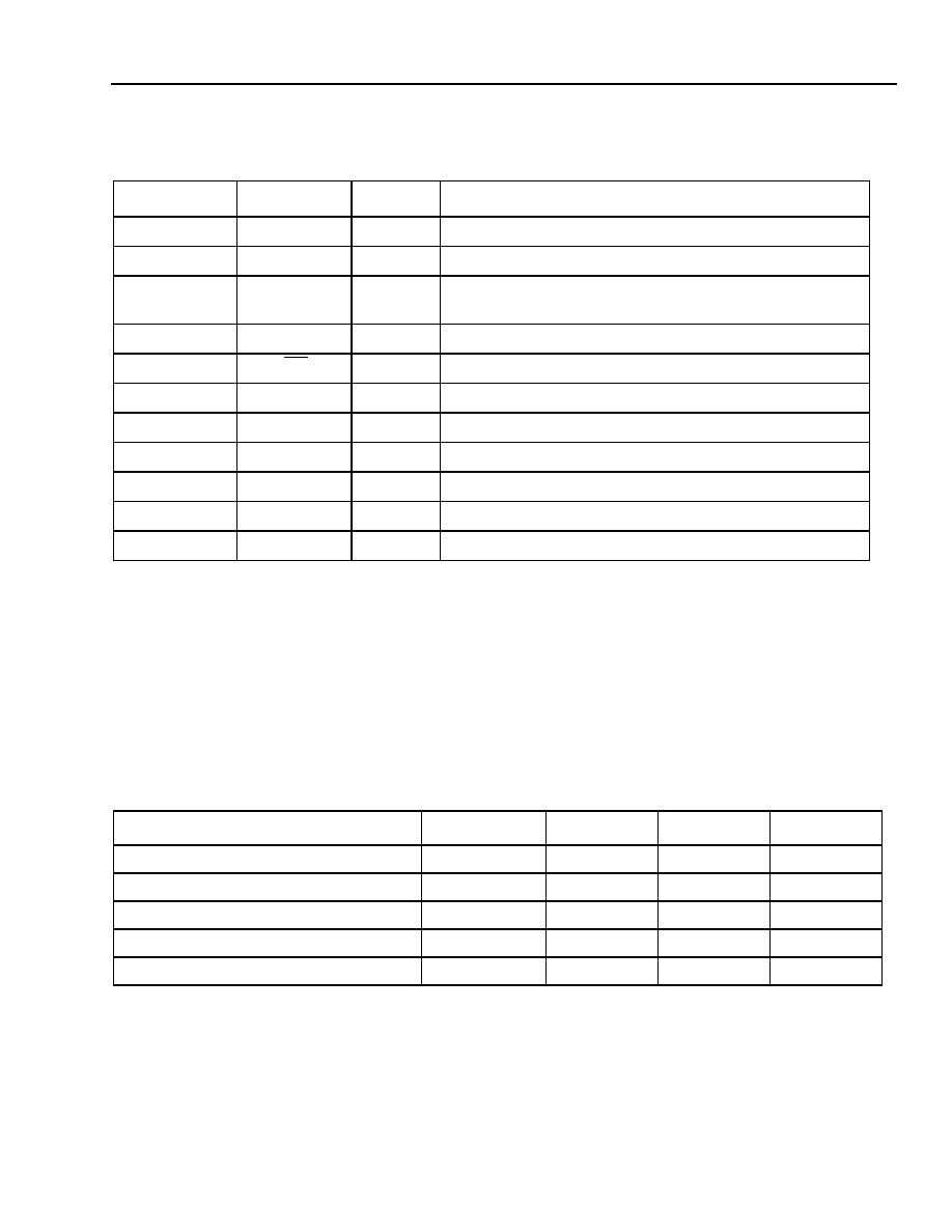
Table 1. LG1625AXF Pin Description
Pin
Symbol
Type
*
* I = input, O = output, P = power.
Name/Definition
1, 6, 13, 22, 23
V
SS1
P
V
SS1
Supply. ≠5.2 V power supply pin.
2
V
IN
I
Data Input.
3, 4, 5, 8, 9, 10,
14, 15, 17
GND
P
Ground.
7, 24
V
TH
Connection to V
TH
for threshold adjustment should be made through pin 24. Pin 7 is made available for additional bypassing of V
TH
(See
Figure 5 on page 6, Typical Test Circuit).
I
Threshold Control. Input (eye crossing).
11
MK
O
Complementary Mark Density Output.
12
MK
O
Mark Density Output.
16
I
OUT
O
Output. dc couple to laser cathode.
18
V
PRE
I
Prebias Control Input.
19
V
SS2
P
V
SS2
. ≠5.2 V supply for output prebias.
20
V
SS3
P
V
SS3
. ≠5.2 V supply for output modulation.
21
V
MOD
I
Modulation Current Control Input.
Table 2. Absolute Maximum Ratings (at T
A
= 25 ∞C unless otherwise specified)
Parameter
Symbol
Min
Max
Unit
Supply Voltage
V
SS
--
≠5.95
V
Storage Temperature
T
stg
≠40
125
∞
C
Operating Case Temperature Range
T
C
0
75
∞
C
Input Voltage
V
I
GND
V
SS
V
Power Dissipation
P
D
--
1
W
4
Lucent Technologies Inc.
Data Sheet
June 1999
LG1625AXF Laser Driver
Handling Precautions
Although protection circuitry has been designed into this device, proper precautions should be taken to avoid expo-
sure to electrostatic discharge (ESD) during handling and mounting. Lucent employs a human-body model (HBM)
and charged-device model (CDM) for ESD-susceptibility testing and protection design evaluation. ESD voltage
thresholds are dependent on the circuit parameters used in the defined model. No industry-wide standard has
been adopted for the CDM. However, a standard HBM (resistance = 1500
,
capacitance = 100 pF) is widely used
and, therefore, can be used for comparison purposes. The HBM ESD threshold presented here was obtained by
using these circuit parameters.
Mounting and Connections
Certain precautions must be taken when using solder. For installation using a constant temperature solder, temper-
atures of under 300
∞
C may be employed for periods of time up to 5 seconds, maximum. For installation with a sol-
dering iron (battery operated or nonswitching only), the soldering tip temperature should not be greater than 300
∞
C
and the soldering time for each lead must not exceed 5 seconds.
Table 3. ESD Threshold Voltage
Human-Body Model ESD Threshold
Device
Voltage
LG1625AXF
200 V

Lucent Technologies Inc.
5
Data Sheet
June 1999
LG1625AXF Laser Driver
Electrical Characteristics
T
A
= 25
∞
C, V
SS1
= V
SS2
= V
SS3
= ≠5.2 V, V
TH
= ≠1.3 V, V
MOD
= ≠3.4 V, R
L
= 25
, data input = 600 mVp-p.
Minimum and Maximum values are testing requirements. Typical values are characteristics of the device and are
the result of engineering evaluations. Typical values are for information purposes only and are not part of the test-
ing requirements. Stresses in excess of the absolute maximum ratings can cause permanent damage to the
device.
5-7869(F)
Figure 4. Typical Eye Diagram of I
MOD
Table 4. Electrical Characteristics
Parameter
Symbol
Min
Typ
Max
Unit
Data Input Voltage
V
INp-p
300
600
2000
mV
Voltage Control for Output Modulation
Current
V
MOD
≠5.5
--
≠3.0
V
Output Modulation Current
Minimum
Maximum
*
* Maximum modulation at maximum V
MOD
I
MOD LOW
I
MOD HIGH
--
55
0
65
2
--
mA
mA
Voltage Control for Prebias Current
V
PRE
≠5.5
--
≠3.0
V
Output Prebias Current
Minimum
Maximum
Maximum prebias at maximum V
PRE
I
PRE LOW
I
PRE HIGH
--
30
0
40
0.5
--
mA
mA
Output Rise & Fall Times (20%--80%)
Rise
Fall
T
RISE
T
FALL
--
--
90
90
--
--
ps
ps
Power Supply Voltage
V
SS1,
V
SS2,
V
SS3
≠4.9
≠5.2
≠5.5
V
Power Supply Current
Excludes I
PRE
and average I
MOD.
Power supply current I
SS2
(relating to prebias) is dependant on V
PRE.
Power supply current I
SS3
(relating to modulation) is dependant on V
MOD
I
SS1
50
100
120
mA
HORZ.: 100 pS/DIV., VERT.: 15 mA/DIV.

6
Lucent Technologies Inc.
Data Sheet
June 1999
LG1625AXF Laser Driver
Test Circuit
Notes:
GND pins 3, 4, 5, 8, 9, 10, 14, 15, 17.
V
SS1
pins 1, 6, 13, 22, 23.
5-7876(F)r.1
Figure 5. LG1625AXF Typical Test Circuit
LG1625AXF Application Notes
s
V
SS
bypass capacitors should be mounted close to the package.
s
5000
potentiometer is typically set for 2500
. This establishes an approximate ≠1.3 V V
TH
which will track
with V
SS
.
s
Mark density (MK and MK) outputs are terminated with 1 k
pull-up resistors.
s
I
MOD
and I
PRE
can be measured and used to control V
MOD
and V
PRE
.
V
IN
MK
V
TH
V
TH
V
SS1
MK
I
OUT
V
PRE
V
MOD
V
SS2
V
SS3
LG1625AXF
1
000
0.1
µ
F
1
000
5
00
0.
1
µ
F
10
00
V
SS
≠5.2 V
0.1
µ
F
0.1
µ
F
1
1
50
50
50
00
0.
1
µ
F
50
5
00
0.
1
µ
F
10
00
V
SS
≠5.2 V
I
PRE
IF V
PRE
> ≠5.0 V
I
MOD
0.1
µ
F
0.1
µ
F
V
SS
≠5.2 V
+
12
11
18
21
16
20
19
7
2
24
20
20
I
MOD
MONITOR
I
PRE
MONITOR
SCOPE
DATA
GENERATOR
x x
MK
MK
Lucent Technologies Inc.
7
Data Sheet
June 1999
LG1625AXF Laser Driver
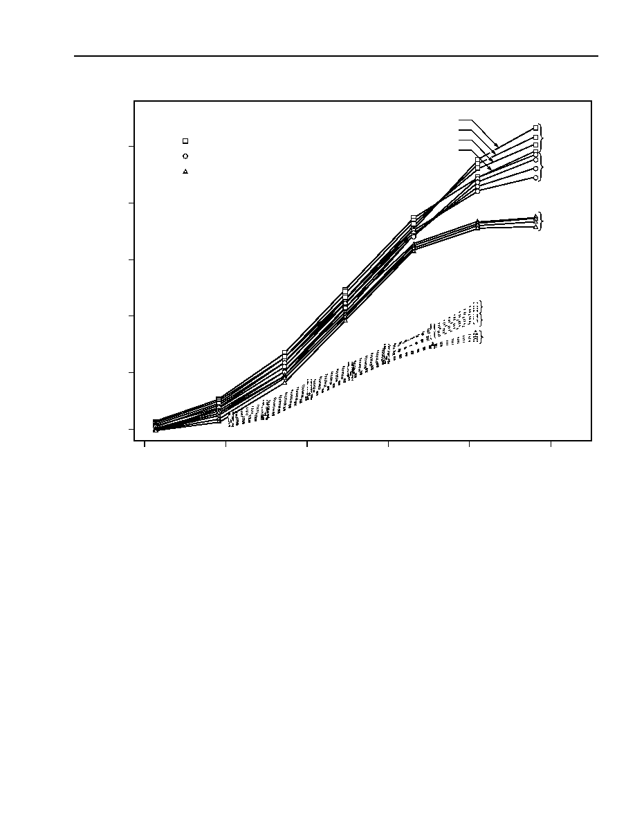
Typical Performance Characteristics
5-7870(F)r.1
Figure 6. Output Modulation Current I
MOD
vs. the External Control Voltage V
MOD
or Output Prebias Current I
PRE
vs. the External Control Voltage V
PRE
100
80
60
40
20
0
≠5.0
≠4.5
≠4.0
≠3.5
≠3.0
≠2.5
≠≠≠I
MO
D
(
m
A) o
r
--
-I
PR
E
(m
A)
V
MOD
(V) OR V
PRE
(V)
0
∞
C
25
∞
C
50
∞
C
75
∞
C
V
SS
=
V
SS
=
V
SS
=
≠5.95 V
≠5.20 V
≠4.45 V
V
SS
= ≠5.95 V
V
SS
= ≠5.20 V
V
SS
= ≠4.45 V
V
SS
= ≠5.95 V
V
SS
= ≠5.20 V
V
SS
= ≠4.45 V

8
Lucent Technologies Inc.
Data Sheet
June 1999
LG1625AXF Laser Driver
Typical Performance Characteristics
(continued)
5-7871(F)
Figure 7. Typical T
RISE
or T
FALL
vs. V
SS
for I
MOD
= 40 mA
5-7872(F)
Figure 8. Typical MK or MK vs. V
SS
for I
MOD
= 40 mA
100
80
60
40
≠6.0
≠5.5
≠5.0
≠4.5
≠4.0
T
RISE
OR
T
FA
LL
(ps
)
V
SS
(V)
75
∞
C
50
∞
C
25
∞
C
0
∞
C
≠600
≠650
≠700
≠750
≠6.0
≠5.5
≠5.0
≠4.5
MK
or
MK
(m
V)
V
SS
(V)
≠550
75
∞
C
50
∞
C
25
∞
C
0
∞
C
Lucent Technologies Inc.
9
Data Sheet
June 1999
LG1625AXF Laser Driver
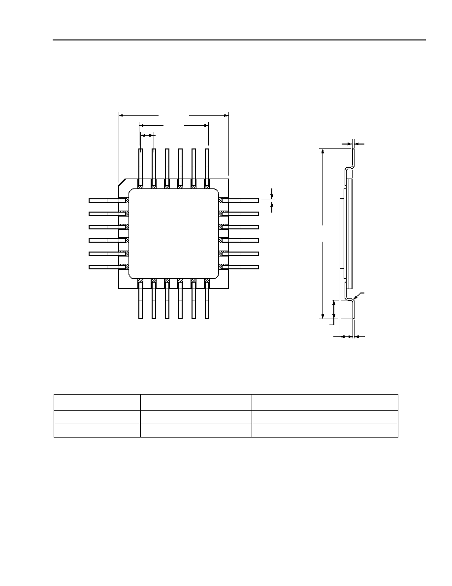
Outline Diagram
24-Pin, Gull-Wing, Surface-Mount Package
Dimensions are in inches. Tolerance is ±0.005 inches unless otherwise noted.
5-7875(F)r.2
Ordering Information
Device
Type
Comcode (Ordering Number)
LG1625AXF
24-Lead Gull Wing
107529067
TF1006A
Test Fixture
106733371
LUCENT
1625AXF
XXXXXX
0.364 SQ.
0.260
0.050
0.012
0.008
BEFORE
SOLDER
DIP
0.604
±0.015 TYP.
R0.010
0.065
0.074
0.010
BEFORE
SOLDER
DIP
1

10
Lucent Technologies Inc.
Data Sheet
June 1999
LG1625AXF Laser Driver
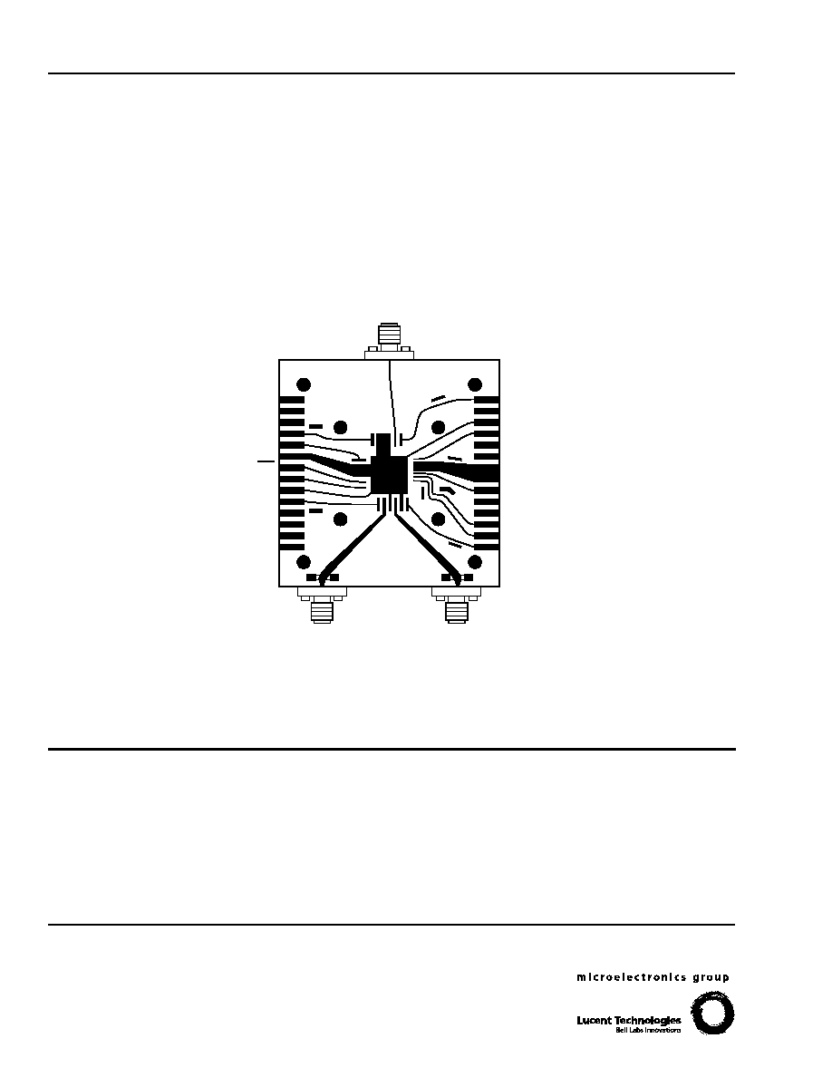
Appendix
The test fixture mentioned in the data sheet is sold separately and is described in detail below.
5-7868(F)
Figure 9. TF1006A Test Fixture
TF1006A Test Fixture Features
s
SMA connectors
s
Easy package placement
s
Good RF performance
Test Fixture Functional Description
The TF1006A test fixture is used to characterize 24-lead gullwing packages for high-speed fiber-optic communica-
tions. The fixture is a metallized substrate (PTFE filled material) fastened to a brass base. The package leads make
contact to the microstrip lines on the fixture through use of a pressure ring and two thumb screws.
Three RF connectors are provided for connections to the input and outputs. BNC connectors are provided on sol-
dered leads for dc bias lines.
The TF1006A is preassembled and fully tested prior to shipment.

Lucent Technologies Inc.
11
Data Sheet
June 1999
LG1625AXF Laser Driver
Appendix
(continued)
Test Fixture Functional Description
(continued)
5-7873(F)
Figure 10. TF1006A Electrical Diagram
Before Use of Test Fixture
s
Due to possible stress during shipment, SMA connectors may be misaligned.
s
Check each SMA for continuity.
s
If necessary, realign and retighten with a 5/64 in. hex key wrench.
Instructions for Use of Test Fixture
A pair of flat-tip tweezers can be used to insert or remove a package from the test fixture. Always wear a grounding
strap to prevent ESD.
1. To insert a package, remove the two thumb screws and gently lift the pressure ring off of the test fixture.
2. Place the pressure ring, cavity side up, on a flat ESD safe surface.
3. Connect the metal tube to a suitable vacuum source with flexible tubing.
4. Place the package, lid down, on a flat ESD safe surface. Locate pin 1 on the package.
8
9
10
11
12
0.01
µ
F
0.01
µ
F
0.01
µ
F
0.01
µ
F
0.01
µ
F
0.01
µ
F
V
SS1
V
TH
V
SS1
V
MOD
V
SS3
V
SS2
V
SS1
V
IN
0.01
µ
F
MK
MK
0.01
µ
F
1
00
1
00
1
00
1
00
0.01
µ
F
1
24
21
20
19
13
14
15
16
18
6
5
4
3
2
23
22
17
FIXTURE BOUNDARY
PACKAGE OUTLINE
V
SS1
GND
V
PRE
I
OUT
Data Sheet
June 1999
LG1625AXF Laser Driver
Lucent Technologies Inc. reserves the right to make changes to the product(s) or information contained herein without notice. No liability is assumed as a result of their use or application. No
rights under any patent accompany the sale of any such product(s) or information.
Copyright © 1999 Lucent Technologies Inc.
All Rights Reserved
June 1999
DS99-187HSPL
For additional information, contact your Microelectronics Group Account Manager or the following:
INTERNET:
http://www.lucent.com/micro
E-MAIL:
docmaster@micro.lucent.com
N. AMERICA:
Microelectronics Group, Lucent Technologies Inc., 555 Union Boulevard, Room 30L-15P-BA, Allentown, PA 18103
1-800-372-2447, FAX 610-712-4106 (In CANADA: 1-800-553-2448, FAX 610-712-4106)
ASIA PACIFIC: Microelectronics Group, Lucent Technologies Singapore Pte. Ltd., 77 Science Park Drive, #03-18 Cintech III, Singapore 118256
Tel. (65) 778 8833, FAX (65) 777 7495
CHINA:
Microelectronics Group, Lucent Technologies (China) Co., Ltd., A-F2, 23/F, Zao Fong Universe Building, 1800 Zhong Shan Xi Road, Shanghai
200233 P. R. China Tel. (86) 21 6440 0468, ext. 316, FAX (86) 21 6440 0652
JAPAN:
Microelectronics Group, Lucent Technologies Japan Ltd., 7-18, Higashi-Gotanda 2-chome, Shinagawa-ku, Tokyo 141, Japan
Tel. (81) 3 5421 1600, FAX (81) 3 5421 1700
EUROPE:
Data Requests: MICROELECTRONICS GROUP DATALINE: Tel. (44) 1189 324 299, FAX (44) 1189 328 148
Technical Inquiries: GERMANY: (49) 89 95086 0 (Munich), UNITED KINGDOM: (44) 1344 865 900 (Ascot),
FRANCE: (33) 1 40 83 68 00 (Paris), SWEDEN: (46) 8 594 607 00 (Stockholm), FINLAND: (358) 9 4354 2800 (Helsinki),
ITALY: (39) 02 6608131 (Milan), SPAIN: (34) 1 807 1441 (Madrid)
Appendix
(continued)
Instructions for Use of Test Fixture
(continued)
5. Insert the package into the pressure ring (lid down) with pin 1 located next to the orientation mark and turn on
the vacuum. The vacuum will retain the package in the pressure ring during the following steps.
6. Align the vertically conductive material on the circuit board.
7. Place the pressure ring down over the alignment pins and gently tighten the thumb screws.
8. Remove vacuum, if desired.
Note: Pressure ring not shown.
5-7874(F)
Figure 11. TF1006A Connector Assignment
DATA IN
(OPTIONAL) V
SS1
NC
GND
MK
MK
GND
(OPTIONAL) V
SS1
V
SS1
(OPTIONAL)
GND
V
TH
V
SS1
V
MOD
V
SS3
V
SS2
GND
OUTPUT
V
PRE
LW5