Document Outline
- Features
- Facility Data Link Features
- Microprocessor Interface
- Applications
- Feature Descriptions
- Functional Description
- Pin Information
- LIU-Framer Interface
- Frame Formats
- CEPT Time Slot 0 FAS/NOT FAS Control Bits
- Signaling Access
- Auxiliary Framer I/O Timing
- Alarms and Performance Monitoring
- Facility Data Link
- Phase-Lock Loop Circuit
- Framer-System Interface
- Concentration Highway Interface
- JTAG Boundary-Scan Specification
- Microprocessor Interface
- Reset
- Interrupt Generation
- Register Architecture
- Global Register Architecture
- Global Register Structure
- Framer Register Architecture
- FDL Register Architecture
- FDL Parameter/Control Registers ((A00ÑA0E); (A20ÑA2E); (B00ÑB0E); (B20ÑB2E) (C00ÑC0E); (C20ÑC2E);...
- Register Maps
- Absolute Maximum Ratings
- Operating Conditions
- Handling Precautions
- Table 187 . ESD Threshold Voltage
- Electrical Characteristics
- Table 188 . Logic Interface Characteristics (TA = Ö40 ∞C to +85 ∞C, VDD = 3.3 V ± 5%, VSS = 0)
- Power Supply Bypassing
- Outline Diagram
- Ordering Information
- List of Figures
- Figure 1 . TFRA08C13 Block Diagram (One of Eight Channels)
- Figure 2 . TFRA08C13 Block Diagram: Receive Section (One of Eight Channels)
- Figure 3 . TFRA08C13 Block Diagram: Transmit Section (One of Eight Channels)
- Figure 4 . Pin Assignment
- Figure 5 . Block Diagram of Framer Line Interface
- Figure 6 . Transmit Framer TLCK to TND, TPD and Receive Framer RND, RPD to RLCK Timing
- Figure 7 . T1 Frame Structure
- Figure 8 . T1 Transparent Frame Structure
- Figure 9 . T7633 Facility Data Link Access Timing of the Transmit and Receive Framer Sections
- Figure 10 . SLC-96 Frame Format
- Figure 11 . ITU 2.048 Basic Frame, CRC-4 Multiframe, and Channel Associated Signaling
- Figure 12 . CEPT Transparent Frame Structure
- Figure 13 . Receive CRC-4 Multiframe Search Algorithm Using the 100 ms Internal Timer
- Figure 14 . Receive CRC-4 Multiframe Search Algorithm for Automatic, CRC-4/Non-CRC-4 Equipment
- Figure 15 . Facility Data Link Access Timing of the Transmit and Receive Framer Sections
- Figure 16 . Transmit and Receive Sa Stack Accessing Protocol
- Figure 17 . Timing Specification for RFRMCK, RFRMDATA, and RFS in DS1 Mode
- Figure 18. Timing Specification for TFS, TLCK, and TPD in DS1 Mode
- Figure 19 . Timing Specification for RFRMCK, RFRMDATA, and RFS in CEPT Mode
- Figure 20 . Timing Specification for RFRMCK, RFRMDATA, RFS, and RSSFS in CEPT Mode
- Figure 21 . Timing Specification for RCRCMFS in CEPT Mode
- Figure 22 . Timing Specification for TFS, TLCK, and TPD in CEPT Mode
- Figure 23 . Timing Specification for TFS, TLCK, TPD, and TSSFS in CEPT Mode
- Figure 24 . Timing Specification for TFS, TLCK, TPD, and TCRCMFS in CEPT Mode
- Figure 25 . Relation Between RLCK1 and Interrupt (Pin AD8)
- Figure 26 . Timing for Generation of LOPLLCK (Pin F25)
- Figure 27 . The T and V Reference Points for a Typical CEPT E1 Application
- Figure 28 . Loopback and Test Transmission Modes
- Figure 29 . 20-Stage Shift Register Used to Generate the Quasi-Random Signal
- Figure 30 . 15-Stage Shift Register Used to Generate the Pseudorandom Signal
- Figure 31 . TFRA08C13 Facility Data Link Access Timing of the Transmit and Receive Framer Sections
- Figure 32 . Block Diagram for the Receive Facility Data Link Interface
- Figure 33 . Block Diagram for the Transmit Facility Data Link Interface
- Figure 34 . Local Loopback Mode
- Figure 35 . Remote Loopback Mode
- Figure 36 . TFRA08C13 Phase Detector Circuitry
- Figure 37 . Nominal Concentration Highway Interface Timing (for FRM_PR43 bit 0Ñbit 2 = 100 (Binary))
- Figure 38 . CHIDTS Mode Concentration Highway Interface Timing
- Figure 39 . Associated Signaling Mode Concentration Highway Interface Timing
- Figure 40 . CHI Timing with ASM and CHIDTS Enabled
- Figure 41 . TCHIDATA and RCHIDATA to CHICK Relationship with CMS = 0 (CEX = 3 and CER = 4, Respec...
- Figure 42 . Receive CHI (RCHIDATA) Timing
- Figure 43 . Transmit CHI (TCHIDATA) Timing
- Figure 44 . Block Diagram of the TFRA08C13's Boundary-Scan Test Logic
- Figure 45 . BS TAP Controller State Diagram
- Figure 46 . Mode 1ÑRead Cycle Timing (MPMODE = 0)
- Figure 47 . Mode 1ÑWrite Cycle Timing (MPMODE = 0)
- Figure 48 . Mode 3ÑRead Cycle Timing (MPMODE = 1)
- Figure 49 . Mode 3ÑWrite Cycle Timing (MPMODE = 1)
- List of Tables
- Contact Us

Preliminary Data Sheet
October 2000
TFRA08C13 OCTAL T1/E1 Framer
Features
s
Eight independent T1/E1 transmit and receive
framers.
s
Internal DS1 transmit clock synthesis--no external
oscillator necessary.
s
Comprehensive alarm reporting and performance
monitoring:
-- Programmable automatic and on-demand alarm
transmission.
s
Automatic facility data link:
-- Automatic transmission of ESF performance
report message.
s
Common 2.048 Mbits/s, 4.096 Mbits/s, or
8.192 Mbits/s TDM highway.
s
Dual- or single-rail line-side I/O.
s
Supports one second polling interval for perfor-
mance monitoring.
s
IEEE
* Std. 1149.1 JTAG boundary scan.
s
3.3 V low-power CMOS with 5 V tolerant inputs.
s
Available in 352-pin PBGA.
T1/E1 Framer Features
s
Supports T1 framing modes ESF, D4,
SLC
Æ
-96,
T1DM DDS.
s
Supports G.704 basic and CRC-4 multiframe for-
mat E1 framing and procedures consistent with
G.706.
s
Supports unframed transmission format.
s
T1 signaling modes: transparent; ESF 2-state,
4-state, and 16-state; D4 2-state and 4-state;
SLC
-96 2-state, 4-state, 9-state, and 16-state. E1
signaling modes: transparent and CAS.
s
Alarm reporting and performance monitoring per
AT&T,
ANSI
, and ITU-T standards.
s
Programmable, independent transmit and receive
system interfaces at a 2.048 MHz, 4.096 MHz, or
8.192 MHz data rate.
Facility Data Link Features
s
HDLC or transparent mode.
s
Automatic transmission of the ESF performance
report messages (PRM).
s
Detection of the ESF PRM.
s
Detection of the
ANSI
ESF FDL bit-oriented codes.
s
64-byte FIFO in both transmit and receive direc-
tions.
s
Programmable FIFO full and empty level interrupt.
s
User-programmable microprocessor interface.
Microprocessor Interface
s
33 MHz read and write access.
s
12-bit address, 8-bit data interface.
s
Intel
or
Motorola
ß
style control interfaces.
s
Directly addressable internal registers.
s
Programmable interrupts.
Applications
s
DS3 and E3 port cards for narrowband DXCs.
s
Multiservice switches.
s
High density DS1 and E1 port cards.
s
Frame relay access devices.
s
Byte-synchronous SDH/SONET mapping.
s
SONET and SDH drop alignment.
s
IP and packet routers.
*
IEEE
is a registered trademark of The Institute of Electrical and
Electronics Engineers, Inc.
ANSI
is a registered trademark of American National Standards
Institute, Inc.
Intel
is a registered trademark of Intel Corporation.
ß
Motorola
is a registered trademark of Motorola, Inc.

Table of Contents
Contents
Page
Preliminary Data Sheet
TFRA08C13 OCTAL T1/E1 Framer
October 2000
2
Lucent Technologies Inc.
Features ................................................................................................................................................................... 1
T1/E1 Framer Features ......................................................................................................................................... 1
Facility Data Link Features ....................................................................................................................................... 1
Microprocessor Interface .......................................................................................................................................... 1
Applications .............................................................................................................................................................. 1
Feature Descriptions .............................................................................................................................................. 10
T1/E1 Framer Feature Descriptions .................................................................................................................... 10
Functional Description ............................................................................................................................................ 11
Pin Information ....................................................................................................................................................... 15
LIU-Framer Interface .............................................................................................................................................. 29
LIU-Framer Physical Interface............................................................................................................................. 29
Line Encoding...................................................................................................................................................... 31
DS1: Zero Code Suppression (ZCS)................................................................................................................... 31
CEPT: High-Density Bipolar of Order 3 (HDB3).................................................................................................. 33
Frame Formats ....................................................................................................................................................... 34
T1 Framing Structures......................................................................................................................................... 34
T1 Loss of Frame Alignment (LFA) ..................................................................................................................... 41
T1 Frame Recovery Alignment Algorithms.......................................................................................................... 42
T1 Robbed-Bit Signaling ..................................................................................................................................... 43
CEPT 2.048 Basic Frame, CRC-4 Time Slot 0, and Signaling Time Slot 16 Multiframe Structures ................... 45
CEPT 2.048 Basic Frame Structure .................................................................................................................... 46
CEPT Loss of Basic Frame Alignment (LFA) ...................................................................................................... 48
CEPT Loss of Frame Alignment Recovery Algorithm ......................................................................................... 48
CEPT Time Slot 0 CRC-4 Multiframe Structure .................................................................................................. 49
CEPT Loss of CRC-4 Multiframe Alignment (LTS0MFA).................................................................................... 50
CEPT Loss of CRC-4 Multiframe Alignment Recovery Algorithms ..................................................................... 51
CEPT Time Slot 16 Multiframe Structure ............................................................................................................ 55
CEPT Loss of Time Slot 16 Multiframe Alignment (LTS16MFA)......................................................................... 56
CEPT Loss of Time Slot 16 Multiframe Alignment Recovery Algorithm.............................................................. 56
CEPT Time Slot 0 FAS/NOT FAS Control Bits....................................................................................................... 56
FAS/NOT FAS Si- and E-Bit Source ................................................................................................................... 56
NOT FAS A-Bit (CEPT Remote Frame Alarm) Sources ..................................................................................... 57
NOT FAS Sa-Bit Sources.................................................................................................................................... 57
Sa Facility Data Link Access ............................................................................................................................... 58
NOT FAS Sa Stack Source and Destination ....................................................................................................... 59
CEPT Time Slot 16 X0--X2 Control Bits............................................................................................................. 61
Signaling Access .................................................................................................................................................... 61
Transparent Signaling ......................................................................................................................................... 61
DS1: Robbed-Bit Signaling.................................................................................................................................. 61
CEPT: Time Slot 16 Signaling............................................................................................................................. 62
Auxiliary Framer I/O Timing ................................................................................................................................... 63
Alarms and Performance Monitoring ...................................................................................................................... 67
Interrupt Generation ............................................................................................................................................ 67
Alarm Definition ................................................................................................................................................... 67
Event Counters Definition ................................................................................................................................... 73
Loopback and Transmission Modes.................................................................................................................... 75
Line Test Patterns ............................................................................................................................................... 78
Receive Line Pattern Monitor--Using Register FRM_SR7 ................................................................................. 80
Automatic and On-Demand Commands ............................................................................................................. 82
Facility Data Link .................................................................................................................................................... 84

Lucent Technologies Inc.
3
Preliminary Data Sheet
October 2000
TFRA08C13 OCTAL T1/E1 Framer
Table of Contents
(continued)
Contents
Page
Receive Facility Data Link Interface.....................................................................................................................84
Transmit Facility Data Link Interface....................................................................................................................90
HDLC Operation ..................................................................................................................................................91
Transparent Mode................................................................................................................................................93
Diagnostic Modes ................................................................................................................................................95
Phase-Lock Loop Circuit .........................................................................................................................................96
Framer-System Interface ........................................................................................................................................98
DS1 Modes ..........................................................................................................................................................98
CEPT Modes........................................................................................................................................................98
Receive Elastic Store ...........................................................................................................................................98
Transmit Elastic Store ..........................................................................................................................................98
Concentration Highway Interface ............................................................................................................................98
CHI Parameters ...................................................................................................................................................99
CHI Frame Timing..............................................................................................................................................101
CHI Offset Programming....................................................................................................................................104
JTAG Boundary-Scan Specification ..................................................................................................................... 105
Principle of the Boundary Scan..........................................................................................................................105
Test Access Port Controller ...............................................................................................................................107
Instruction Register ............................................................................................................................................109
Boundary-Scan Register....................................................................................................................................110
BYPASS Register ..............................................................................................................................................110
DCODE Register................................................................................................................................................110
3-State Procedures ............................................................................................................................................110
Microprocessor Interface.......................................................................................................................................111
Overview ............................................................................................................................................................111
Microprocessor Configuration Modes ................................................................................................................111
Microprocessor Interface Pinout Definitions ......................................................................................................112
Microprocessor Clock (MPCLK) Specifications .................................................................................................112
Microprocessor Interface Register Address Map ...............................................................................................113
I/O Timing ..........................................................................................................................................................113
Reset.................................................................................................................................................................... 118
Hardware Reset (Pin C19).................................................................................................................................118
Software Reset/Software Restart.......................................................................................................................118
Interrupt Generation ..............................................................................................................................................118
Register Architecture.............................................................................................................................................119
Global Register Architecture .................................................................................................................................123
Global Register Structure ......................................................................................................................................123
Framer Block Interrupt Status Register (GREG0)..............................................................................................123
Framer Block Interrupt Enable Register (GREG1).............................................................................................124
FDL Block Interrupt Status Enable Register (GREG2) ......................................................................................124
FDL Block Interrupt Enable Register (GREG3) .................................................................................................124
Global Control Register (GREG4)......................................................................................................................125
Device ID and Version Registers (GREG5--GREG7) .......................................................................................125
Global Control Register (GREG8)......................................................................................................................126
Global PLLCK Control Register (GREG9) .........................................................................................................127
Framer Register Architecture ................................................................................................................................127
Framer Status/Counter Registers ......................................................................................................................128
Framer Parameter/Control Registers .................................................................................................................141
FDL Register Architecture .....................................................................................................................................168
FDL Parameter/Control Registers ((A00--A0E); (A20--A2E); (B00--B0E);
(B20--B2E) (C00--C0E); (C20--C2E); (D00--D0E); (D20--D2E)) .................................................................169

Contents
Page
Preliminary Data Sheet
TFRA08C13 OCTAL T1/E1 Framer
October 2000
4
Lucent Technologies Inc.
Table of Contents
(continued)
Register Maps ...................................................................................................................................................... 176
Global Registers................................................................................................................................................ 176
Framer Parameter/Control Registers (Read-Write)........................................................................................... 177
Receive Framer Signaling Registers (Read-Only) ............................................................................................ 179
Framer Unit Parameter Register Map ............................................................................................................... 180
Transmit Signaling Registers (Read/Write) ....................................................................................................... 183
Facility Data Link Parameter/Control and Status Registers (Read-Write)......................................................... 184
Absolute Maximum Ratings.................................................................................................................................. 185
Operating Conditions............................................................................................................................................ 185
Handling Precautions ........................................................................................................................................... 185
Electrical Characteristics ...................................................................................................................................... 186
Logic Interface Characteristics .......................................................................................................................... 186
Power Supply Bypassing...................................................................................................................................... 186
Outline Diagram.................................................................................................................................................... 187
352-Pin PBGA ................................................................................................................................................... 187
Ordering Information............................................................................................................................................. 188
Figures
Page
Figure 1. TFRA08C13 Block Diagram (One of Eight Channels)............................................................................. 11
Figure 2. TFRA08C13 Block Diagram: Receive Section (One of Eight Channels)................................................. 13
Figure 3. TFRA08C13 Block Diagram: Transmit Section (One of Eight Channels) ................................................ 14
Figure 4. Pin Assignment ....................................................................................................................................... 15
Figure 5. Block Diagram of Framer Line Interface .................................................................................................. 29
Figure 6. Transmit Framer TLCK to TND, TPD and Receive Framer RND, RPD to RLCK Timing ......................... 30
Figure 7. T1 Frame Structure ................................................................................................................................. 34
Figure 8. T1 Transparent Frame Structure ............................................................................................................. 35
Figure 9. T7633 Facility Data Link Access Timing of the Transmit and Receive Framer Sections ......................... 37
Figure 10.
SLC-
96 Frame Format........................................................................................................................... 37
Figure 11. ITU 2.048 Basic Frame, CRC-4 Multiframe, and Channel Associated
Signaling Multiframe Structures .......................................................................................................................... 45
Figure 12. CEPT Transparent Frame Structure ...................................................................................................... 47
Figure 13. Receive CRC-4 Multiframe Search Algorithm Using the 100 ms Internal Timer................................... 52
Figure 14. Receive CRC-4 Multiframe Search Algorithm for Automatic, CRC-4/Non-CRC-4 Equipment
Interworking as Defined by ITU (From ITU Rec. G.706, Annex B.2.2 - 1991)..................................................... 54
Figure 15. Facility Data Link Access Timing of the Transmit and Receive
Framer Sections in the CEPT Mode.................................................................................................................... 58
Figure 16. Transmit and Receive Sa Stack Accessing Protocol ............................................................................. 60
Figure 17. Timing Specification for RFRMCK, RFRMDATA, and RFS in DS1 Mode .............................................. 63
Figure 18. Timing Specification for TFS, TLCK, and TPD in DS1 Mode ................................................................ 63
Figure 19. Timing Specification for RFRMCK, RFRMDATA, and RFS in CEPT Mode ........................................... 64
Figure 20. Timing Specification for RFRMCK, RFRMDATA, RFS, and RSSFS in CEPT Mode ............................. 64
Figure 21. Timing Specification for RCRCMFS in CEPT Mode.............................................................................. 65
Figure 22. Timing Specification for TFS, TLCK, and TPD in CEPT Mode.............................................................. 65
Figure 23. Timing Specification for TFS, TLCK, TPD, and TSSFS in CEPT Mode ................................................ 66
Figure 24. Timing Specification for TFS, TLCK, TPD, and TCRCMFS in CEPT Mode .......................................... 66
Figure 25. Relation Between RLCK1 and Interrupt (Pin AD8)................................................................................ 67
Figure 26. Timing for Generation of LOPLLCK (Pin F25)....................................................................................... 69
Figure 27. The T and V Reference Points for a Typical CEPT E1 Application........................................................ 72
Figure 28. Loopback and Test Transmission Modes............................................................................................... 77

Lucent Technologies Inc.
5
Preliminary Data Sheet
October 2000
TFRA08C13 OCTAL T1/E1 Framer
Table of Contents
(continued)
Figures
Page
Figure 29. 20-Stage Shift Register Used to Generate the Quasi-Random Signal ..................................................78
Figure 30. 15-Stage Shift Register Used to Generate the Pseudorandom Signal ..................................................79
Figure 31. TFRA08C13 Facility Data Link Access Timing of the Transmit and Receive Framer Sections ..............84
Figure 32. Block Diagram for the Receive Facility Data Link Interface ....................................................................85
Figure 33. Block Diagram for the Transmit Facility Data Link Interface ...................................................................90
Figure 34. Local Loopback Mode ............................................................................................................................95
Figure 35. Remote Loopback Mode ........................................................................................................................96
Figure 36. TFRA08C13 Phase Detector Circuitry ...................................................................................................97
Figure 37. Nominal Concentration Highway Interface Timing (for FRM_PR43 bit 0--bit 2 = 100 (Binary)) ..........101
Figure 38. CHIDTS Mode Concentration Highway Interface Timing .....................................................................102
Figure 39. Associated Signaling Mode Concentration Highway Interface Timing .................................................103
Figure 40. CHI Timing with ASM and CHIDTS Enabled .......................................................................................103
Figure 41. TCHIDATA and RCHIDATA to CHICK Relationship with CMS = 0
(CEX = 3 and CER = 4, Respectively) ...............................................................................................................104
Figure 42. Receive CHI (RCHIDATA) Timing.........................................................................................................105
Figure 43. Transmit CHI (TCHIDATA) Timing ........................................................................................................105
Figure 44. Block Diagram of the TFRA08C13's Boundary-Scan Test Logic .........................................................106
Figure 45. BS TAP Controller State Diagram ........................................................................................................107
Figure 46. Mode 1--Read Cycle Timing (MPMODE = 0) .....................................................................................116
Figure 47. Mode 1--Write Cycle Timing (MPMODE = 0)......................................................................................116
Figure 48. Mode 3--Read Cycle Timing (MPMODE = 1) .....................................................................................117
Figure 49. Mode 3--Write Cycle Timing (MPMODE = 1)......................................................................................117
Tables
Page
Table 1. Pin Assignments for 352-Pin PBGA by Pin Number Order.......................................................................16
Table 2. Pin Descriptions........................................................................................................................................18
Table 3. AMI Encoding ...........................................................................................................................................31
Table 4. DS1 ZCS Encoding...................................................................................................................................32
Table 5. DS1 B8ZS Encoding .................................................................................................................................32
Table 6. ITUHDB3 Coding ......................................................................................................................................33
Table 7. T-Carrier Hierarchy....................................................................................................................................34
Table 8. D4 Superframe Format .............................................................................................................................36
Table 9. DDS Channel-24 Format ..........................................................................................................................37
Table 10.
SLC
-96 Data Link Block Format .............................................................................................................38
Table 11.
SLC
-96 Line Switch Message Codes .....................................................................................................39
Table 12. Transmit and Receive
SLC
-96 Stack Structure.......................................................................................39
Table 13. Extended Superframe (ESF) Structure ...................................................................................................40
Table 14. T1 Loss of Frame Alignment Criteria ......................................................................................................41
Table 15. T1 Frame Alignment Procedures ............................................................................................................42
Table 16. Robbed-Bit Signaling Options.................................................................................................................43
Table 17.
SLC
-96 9-State Signaling Format ...........................................................................................................43
Table 18.16-State Signaling Format .......................................................................................................................44
Table 19. Allocation of Bits 1 to 8 of the FAS Frame and the NOT FAS Frame ......................................................46
Table 20. ITU CRC-4 Multiframe Structure.............................................................................................................49
Table 21. ITU CEPT Time Slot 16 Channel Associated Signaling Multiframe Structure ........................................55
Table 22. Transmit and Receive Sa Stack Structure...............................................................................................59
Table 23. Associated Signaling Mode CHI 2-Byte Time-Slot Format for DS1 Frames ...........................................62
Table 24. Associated Signaling Mode CHI 2-Byte Time-Slot Format for Stuffed Channels....................................62

Table of Contents
(continued)
Tables
Page
Preliminary Data Sheet
TFRA08C13 OCTAL T1/E1 Framer
October 2000
6
Lucent Technologies Inc.
Table 25. Associated Signaling Mode CHI 2-Byte Time-Slot Format for CEPT..................................................... 62
Table 26. Red Alarm or Loss of Frame Alignment Conditions ............................................................................... 68
Table 27. Remote Frame Alarm Conditions ........................................................................................................... 68
Table 28. Alarm Indication Signal Conditions ........................................................................................................ 69
Table 29. Sa6 Bit Coding Recognized by the Receive Framer. ............................................................................. 71
Table 30. Sa6 Bit Coding of NT1 Interface Events Recognized by the Receive Framer........................................ 71
Table 31. AUXP Synchronization and Clear Synchronization Process.................................................................. 72
Table 32. Event Counters Definition ...................................................................................................................... 73
Table 33. Summary of the Deactivation of SSTSSLB and SSTSLLB Modes as a
Function of Activating the Primary Loopback Modes .......................................................................................... 76
Table 34. Register FRM_PR69 Test Patterns ........................................................................................................ 79
Table 35. Register FRM_PR70 Test Patterns ........................................................................................................ 80
Table 36. Automatic Enable Commands................................................................................................................ 82
Table 37. On-Demand Commands ........................................................................................................................ 83
Table 38. Receive
ANSI
Code ............................................................................................................................... 86
Table 39. Performance Report Message Structure................................................................................................ 86
Table 40. FDL Performance Report Message Field Definition............................................................................... 87
Table 41. Octet Contents and Definition ................................................................................................................ 87
Table 42. Receive Status of Frame Byte................................................................................................................ 88
Table 43. HDLC Frame Format .............................................................................................................................. 91
Table 44. Receiver Operation in Transparent Mode............................................................................................... 94
Table 45. Summary of the TFRA08C13's Concentration Highway Interface Parameters ...................................... 99
Table 46. Programming Values for TOFF[2:0] and ROFF[2:0] when CMS = 0 .................................................... 104
Table 47. TAP Controller States in the Data Register Branch.............................................................................. 108
Table 48. TAP Controller States in the Instruction Register Branch..................................................................... 108
Table 49. TFRA08C13's Boundary-Scan Instructions ......................................................................................... 109
Table 50. IDCODE Register................................................................................................................................. 110
Table 51. Microprocessor Configuration Modes .................................................................................................. 111
Table 52. Mode [1 and 3] Microprocessor Pin Definitions.................................................................................... 112
Table 53. Microprocessor Input Clock Specifications .......................................................................................... 112
Table 54. TFRA08C13 Register Address Map..................................................................................................... 113
Table 55. Microprocessor Interface I/O Timing Specifications ............................................................................. 114
Table 56. Status Register and Corresponding Interrupt Enable Register for Functional Blocks .......................... 118
Table 57. Asserted Value and Deasserted State for GREG4 Bit 4 and Bit 6 Logic Combinations ...................... 118
Table 58. Register Summary ............................................................................................................................... 119
Table 59. Global Register Set (0x000--0x009) ................................................................................................... 123
Table 60. Framer Block Interrupt Status Register (GREG0) (000)....................................................................... 123
Table 61. Framer Block Interrupt Enable Register (GREG1) (001)...................................................................... 124
Table 62. FDL Block Interrupt Status Register (GREG2) (002) ........................................................................... 124
Table 63. FDL Block Interrupt Enable Register (GREG3) (003) .......................................................................... 124
Table 64. Global Control Register (GREG4) (004) .............................................................................................. 125
Table 65. Device ID and Version Registers (GREG5--GREG7) (005--007) ...................................................... 125
Table 66. Global Control Register (GREG8) (008) .............................................................................................. 126
Table 67. Global PLLCK Control Register (GREG9) (009) .................................................................................. 127
Table 68. Framer Status and Control Blocks Address Range (Hexadecimal)...................................................... 127
Table 69. Interrupt Status Register (FRM_SR0) (Y00) ........................................................................................ 128
Table 70. Facility Alarm Condition Register (FRM_SR1) (Y01) ........................................................................... 129
Table 71. Remote End Alarm Register (FRM_SR2) (Y02) .................................................................................. 130
Table 72. Facility Errored Event Register-1 (FRM_SR3) (Y03) ........................................................................... 131

Lucent Technologies Inc.
7
Preliminary Data Sheet
October 2000
TFRA08C13 OCTAL T1/E1 Framer
Table of Contents
(continued)
Tables
Page
Table 73. Facility Event Register-2 (FRM_SR4) (Y04) ........................................................................................132
Table 74. Exchange Termination and Exchange Termination Remote
End Interface Status Register (FRM_SR5) (Y05) ..............................................................................................133
Table 75. Network Termination and Network Termination Remote End
Interface Status Register (FRM_SR6) (Y06)......................................................................................................134
Table 76. Facility Event Register (FRM_SR7) (Y07) ............................................................................................135
Table 77. Bipolar Violation Counter Registers (FRM_SR8--FRM_SR9) (Y08--Y09) .........................................135
Table 78. Framing Bit Error Counter Registers (FRM_SR10--FRM_SR11) (Y0A--Y0B)....................................135
Table 79. CRC Error Counter Registers (FRM_SR12--FRM_SR13) (Y0C--Y0D) .............................................136
Table 80. E-Bit Counter Registers (FRM_SR14--FRM_SR15) (Y0E--Y0F) .......................................................136
Table 81. CRC-4 Errors at NT1 from NT2 Counter Registers (FRM_SR16--FRM_SR17) (Y10--Y11) ..............136
Table 82. E Bit at NT1 from NT2 Counter (FRM_SR18--FRM_SR19) (Y12--Y13) ............................................136
Table 83. ET Errored Seconds Counter (FRM_SR20--FRM_SR21) (Y14--Y15) ...............................................137
Table 84. ET Bursty Errored Seconds Counter (FRM_SR22--FRM_SR23) (Y16--Y17) ....................................137
Table 85. ET Severely Errored Seconds Counter (FRM_SR24--FRM_SR25) (Y18--Y19) ................................137
Table 86. ET Unavailable Seconds Counter (FRM_SR26--FRM_SR27) (Y1A--Y1B)........................................137
Table 87. ET-RE Errored Seconds Counter (FRM_SR28--FRM_SR29) (Y1C--Y1D) ........................................137
Table 88. ET-RE Bursty Errored Seconds Counter (FRM_SR30--FRM_SR31) (Y1E--Y1F)..............................137
Table 89. ET-RE Severely Errored Seconds Counter (FRM_SR32--FRM_SR33) (Y20--Y21)...........................137
Table 90. ET-RE Unavailable Seconds Counter (FRM_SR34--FRM_SR35) (Y22--Y23) ...................................138
Table 91. NT1 Errored Seconds Counter (FRM_SR36--FRM_SR37) (Y24--Y25).............................................138
Table 92. NT1 Bursty Errored Seconds Counter (FRM_SR38--FRM_SR39) (Y26--Y27)..................................138
Table 93. NT1 Severely Errored Seconds Counter (FRM_SR40--FRM_SR41) (Y28--Y29) ..............................138
Table 94. NT1 Unavailable Seconds Counter (FRM_SR42--FRM_SR43) (Y2A--Y2B)......................................138
Table 95. NT1-RE Errored Seconds Counter (FRM_SR44--FRM_SR45) (Y2C--Y2D) .....................................138
Table 96. NT1-RE Bursty Errored Seconds Counter (FRM_SR46--FRM_SR47) (Y2E--Y2F) ...........................138
Table 97. NT1-RE Severely Errored Seconds Counter (FRM_SR48--FRM_SR49) (Y30--Y31) ........................138
Table 98. NT1-RE Unavailable Seconds Counter (FRM_SR50--FRM_SR51) (Y32--Y33) ................................139
Table 99. Receive NOT-FAS TS0 Register (FRM_SR52) (Y34) ...........................................................................139
Table 100. Receive Sa Register (FRM_SR53) (Y35) ...........................................................................................139
Table 101.
SLC
-96 FDL Receive Stack (FRM_SR54--FRM_SR63) (Y36--Y3F) ...............................................139
Table 102. CEPT Sa Receive Stack (FRM_SR54--FRM_SR63) (Y36--Y3F) ....................................................140
Table 103. Transmit Framer
ANSI
Performance Report Message Status Register Structure ..............................140
Table 104. Received Signaling Registers: DS1 Format (FRM_RSR0--FRM_RSR23) (Y40--Y58) ....................140
Table 105. Receive Signaling Registers: CEPT Format (FRM_RSR0--FRM_RSR31) (Y40--Y5F) ...................141
Table 106. Summary of Interrupt Group Enable Registers (FRM_PR0--FRM_PR7) (Y60--Y67) ......................141
Table 107. Primary Interrupt Group Enable Register (FRM_PR0) (Y60) .............................................................142
Table 108. Interrupt Enable Register (FRM_PR1) (Y61) ......................................................................................142
Table 109. Interrupt Enable Register (FRM_PR2) (Y62) ......................................................................................142
Table 110. Interrupt Enable Register (FRM_PR3) (Y63) ......................................................................................142
Table 111. Interrupt Enable Register (FRM_PR4) (Y64) ......................................................................................143
Table 112. Interrupt Enable Register (FRM_PR5) (Y65) ......................................................................................143
Table 113. Interrupt Enable Register (FRM_PR6) (Y66) ......................................................................................143
Table 114. Interrupt Enable Register (FRM_PR7) (Y67) ......................................................................................143
Table 115. Framer Mode Bits Decoding (FRM_PR8) (Y68) .................................................................................143
Table 116. Line Code Option Bits Decoding (FRM_PR8) (Y68)...........................................................................144
Table 117. CRC Option Bits Decoding (FRM_PR9) (Y69) ...................................................................................144
Table 118. Alarm Filter Register (FRM_PR10) (Y6A)...........................................................................................145
Table 119. Errored Event Threshold Definition.....................................................................................................145
Table 120. Errored Second Threshold Register (FRM_PR11) (Y6B) ...................................................................146

Table of Contents
(continued)
Tables
Page
Preliminary Data Sheet
TFRA08C13 OCTAL T1/E1 Framer
October 2000
8
Lucent Technologies Inc.
Table 121. Severely Errored Second Threshold Registers (FRM_PR12--FRM_PR13) (Y6C--Y6D) ................ 146
Table 122. ET1 Errored Event Enable Register (FRM_PR14) (Y6E)................................................................... 146
Table 123. ET1 Remote End Errored Event Enable Register (FRM_PR15) (Y6F).............................................. 146
Table 124. NT1 Errored Event Enable Register (FRM_PR16) (Y70)................................................................... 147
Table 125. NT1 Remote End Errored Event Enable Registers (FRM_PR17--FRM_PR18) (Y71--Y72)............ 147
Table 126. Automatic AIS to the System and Automatic Loopback Enable Register (FRM_PR19) (Y73)........... 147
Table 127. Automatic AIS to the System and Automatic Loopback Enable Register (FRM_PR19) (Y73)........... 148
Table 128. Transmit Test Pattern to the Line Enable Register (FRM_PR20) (Y74) ............................................. 148
Table 129. Framer FDL Control Command Register (FRM_PR21) (Y75) ........................................................... 149
Table 130. Framer Transmit Line Idle Code Register (FRM_PR22) (Y76)........................................................... 149
Table 131. Framer System Stuffed Time-Slot Code Register (FRM_PR23) (Y77) .............................................. 149
Table 132. Primary Time-Slot Loopback Address Register (FRM_PR24) (Y78) ................................................. 150
Table 133. Loopback Decoding of Bits LBC[2:0] in FRM_PR24, Bits 7--5 ......................................................... 150
Table 134. Secondary Time-Slot Loopback Address Register (FRM_PR25) (Y79) ............................................ 151
Table 135. Loopback Decoding of Bits LBC[1:0] in FRM_PR25, Bits 6--5 ......................................................... 151
Table 136. Framer Reset and Transparent Mode Control Register (FRM_PR26) (Y7A) ..................................... 152
Table 137. Transmission of Remote Frame Alarm and CEPT Automatic
Transmission of A Bit = 1 Control Register (FRM_PR27) (Y7B) ....................................................................... 153
Table 138. CEPT Automatic Transmission of E Bit = 0 Control Register (FRM_PR28) (Y7C)............................. 154
Table 139. Sa4--Sa8 Source Register (FRM_PR29) (Y7D) ............................................................................... 154
Table 140. Sa Bits Source Control for Bit 5--Bit 7 in FRM_PR29 ....................................................................... 155
Table 141. Sa4--Sa8 Control Register (FRM_PR30) (Y7E) ............................................................................... 155
Table 142. Sa Transmit Stack (FRM_PR31--FRM_PR40) (Y7F--Y88).............................................................. 156
Table 143.
SLC
-96 Transmit Stack (FRM_PR31--FRM_PR40) (Y7F--Y88) ...................................................... 156
Table 144. Transmit
SLC
-96 FDL Format ............................................................................................................ 156
Table 145. CEPT Time Slot 16 X-Bit Remote Multiframe Alarm and AIS
Control Register (FRM_PR41) (Y89) ................................................................................................................ 157
Table 146. Framer Exercise Register (FRM_PR42) (Y8A) .................................................................................. 157
Table 147. Framer Exercises, FRM_PR42 Bit 5--Bit 0 (Y8A) ............................................................................. 158
Table 148. DS1 System Interface Control and CEPT FDL Source Control Register (FRM_PR43) (Y8B)........... 159
Table 149. Signaling Mode Register (FRM_PR44) (Y8C) ................................................................................... 160
Table 150. CHI Common Control Register (FRM_PR45) (Y8D).......................................................................... 161
Table 151. CHI Common Control Register (FRM_PR46) (Y8E) .......................................................................... 162
Table 152. CHI Transmit Control Register (FRM_PR47) (Y8F) ........................................................................... 162
Table 153. CHI Receive Control Register (FRM_PR48) (Y90) ............................................................................ 162
Table 154. CHI Transmit Time-Slot Enable Registers (FRM_PR49--FRM_PR52) (Y91--Y94) ......................... 163
Table 155. CHI Receive Time-Slot Enable Registers (FRM_PR53--FRM_PR56) (Y95--Y98) .......................... 163
Table 156. CHI Transmit Highway Select Registers (FRM_PR57--FRM_PR60) (Y99--Y9C)............................ 163
Table 157. CHI Receive Highway Select Registers (FRM_PR61--FRM_PR64) (Y9D--YA0) ............................ 163
Table 158. CHI Transmit Control Register (FRM_PR65) (YA1)............................................................................ 164
Table 159. CHI Receive Control Register (FRM_PR66) (YA2) ............................................................................ 164
Table 160. Auxiliary Pattern Generator Control Register (FRM_PR69) (YA5) ..................................................... 165
Table 161. Pattern Detector Control Register (FRM_PR70) (YA6) ...................................................................... 166
Table 162. Transmit Signaling Registers: DS1 Format (FRM_TSR0--FRM_TSR23) (YE0--YF7) ..................... 167
Table 163. Transmit Signaling Registers: CEPT Format (FRM_TSR0--FRM_TSR31) (YE0--YFF) .................. 167
Table 164. FDL Register Set ((A00--A0E); (A20--A2E); (B00--B0E); (B20--B2E)
(C00--C0E); (C20--C2E); (D00--D0E); (D20--D2E))..................................................................................... 168
Table 165. FDL Configuration Control Register (FDL_PR0) (A00; A20; B00; B20; C00; C20; D00; D20) .......... 169
Table 166. FDL Control Register (FDL_PR1) (A01; A21; B01; B21; C01; C21; D01; D21)................................. 169

Lucent Technologies Inc.
9
Preliminary Data Sheet
October 2000
TFRA08C13 OCTAL T1/E1 Framer
Table of Contents
(continued)
Tables
Page
Table 167. FDL Interrupt Mask Control Register (FDL_PR2) (A02; A22; B02; B22; C02; C22; D02; D22) .........170
Table 168. FDL Transmitter Configuration Control Register (FDL_PR3)
(A03; A23; B03; B23; C03; C23; D03; D23).......................................................................................................171
Table 169. FDL Transmitter FIFO Register (FDL_PR4) (A04; A24; B04; B24; C04; C24; D04; D24) ..................171
Table 170. FDL Transmitter Idle Character Mask Register (FDL_PR5)
(A05; A25; B05; B25; C05; C25; D05; D25).......................................................................................................171
Table 171. FDL Receiver Interrupt Level Control Register (FDL_PR6)
(A06; A26; B06; B26; C06; C26; D06; D26).......................................................................................................172
Table 172. FDL Register FDL_PR7 ......................................................................................................................172
Table 173. FDL Receiver Match Character Register (FDL_PR8) (A08; A28; B08; B28; C08; C28; D08; D28) ...172
Table 174. FDL Transparent Control Register (FDL_PR9) (A09; A29; B09; B29; C09; C29; D09; D29)..............173
Table 175. FDL Transmit
ANSI
ESF Bit Codes (FDL_PR10) (A0A; A2A; B0A; B2A; C0A; C2A; D0A; D2A).......173
Table 176. FDL Interrupt Status Register (Clear on Read) (FDL_SR0)
(A0B; A2B; B0B; B2B; C0B; C2B; D0B; D2B) ...................................................................................................174
Table 177. FDL Transmitter Status Register (FDL_SR1) (A0C; A2C; B0C; B2C; C0C; C2C; D0C; D2C) ...........175
Table 178. FDL Receiver Status Register (FDL_SR2) (A0D; A2D; B0D; B2D; C0D; C2D; D0D; D2D) ..............175
Table 179. Receive
ANSI
FDL Status Register (FDL_SR3) (A0E; A2E; B0E; B2E; C0E; C2E; D0E; D2E) ........175
Table 180. FDL Receiver FIFO Register (FDL_SR4) (A07; A27; B07; B27; C07; C27; D07; D27)......................175
Table 181. Global Register Set.............................................................................................................................176
Table 182. Framer Unit Status Register Map .......................................................................................................177
Table 183. Receive Signaling Registers Map .......................................................................................................179
Table 184. Framer Unit Parameter Register Map .................................................................................................180
Table 185. Transmit Signaling Registers Map ......................................................................................................183
Table 186. Facility Data Link Register Map ..........................................................................................................184
Table 187. ESD Threshold Voltage.......................................................................................................................185
Table 188. Logic Interface Characteristics (T
A
= ≠40 ∞C to +85 ∞C, V
DD
= 3.3 V ± 5%, V
SS
= 0).........................186

Preliminary Data Sheet
TFRA08C13 OCTAL T1/E1 Framer
October 2000
10
Lucent Technologies Inc.
Lucent Technologies Inc.
Feature Descriptions
T1/E1 Framer Feature Descriptions
s
Framing formats:
-- Compliant with T1 standards
ANSI
T1.231 (1993),
AT&T TR54016, AT&T TR62411 (1998).
-- Unframed, transparent transmission in T1 and E1
formats.
-- DS1 extended superframe (ESF).
-- DS1 superframe (SF): D4;
SLC
-96; T1DM DDS;
T1DM DDS with FDL access.
-- DS1 independent transmit and receive framing
modes when using the ESF and D4 formats.
-- Compliant with ITU CEPT framing recommenda-
tion:
1. G.704 and G.706 basic frame format.
2. G.704 Section 2.3.3.4 and G.706 Section 4.2:
CRC-4 multiframe search algorithm.
3. G.706 Annex B: CRC-4 multiframe search algo-
rithm with 400 ms timer for interworking of
CRC-4 and non-CRC-4 equipment.
4. G.706 Section 4.3.2 Note 2: monitoring of 915
CRC-4 checksum errors for loss of frame state.
s
Framer line codes:
-- DS1: alternate mark inversion (AMI); binary eight
zero code suppression (B8ZS); per-channel zero
code suppression; decoding bipolar violation mon-
itor; monitoring of eight or fifteen bit intervals with-
out positive or negative pulses error indication.
-- DS1 independent transmit and receive path line
code formats when using AMI/ZCS and B8ZS
coding.
-- ITU-CEPT: AMI; high-density bipolar 3 (HDB3)
encoding and decoding bipolar violation monitor-
ing, monitoring of four bit intervals without positive
or negative pulses error indication.
-- Single-rail option.
s
Signaling:
-- DS1: extended superframe 2-state, 4-state, and
16-state per-channel robbed bit.
-- DS1: D4 superframe 2-state and 4-state per-
channel robbed bit.
-- DS1:
SLC
-96 superframe 2-state, 4-state, 9-state,
and 16-state per-channel robbed bit.
-- DS1: channel-24 message-oriented signaling.
-- ITU CEPT: channel associated signaling (CAS).
-- Transparent (all data channels).
s
Alarm reporting, performance monitoring, and main-
tenance:
--
ANSI
T1.403-1995, AT&T TR 54016, and ITU
G.826 standard error checking.
-- Error and status counters:
1. Bipolar violations.
2. Errored frame alignment signals.
3. Errored CRC checksum block.
4. CEPT: received E bit = 0.
5. Errored, severely errored, and unavailable
seconds.
-- Selectable errored event monitoring for errored
and severely errored seconds processing with
programmable thresholds for errored and severely
errored second monitoring.
-- CEPT: Selectable automatic transmission of E bit
to the line.
-- CEPT: Sa6 coded remote end CRC-4 error E bit =
0 events.
-- Programmable automatic and on-demand alarm
transmission:
1. Automatic transmission of remote frame alarm
to the line while in loss of frame alignment
state.
2. Automatic transmission of alarm indication
signal (AIS) to the system while in loss of frame
alignment state.
-- Multiple loopback modes.
-- Optional automatic line and payload loopback acti-
vate and deactivate modes.
-- CEPT nailed-up connect loopback and CEPT
nailed-up broadcast transmission TS-X in TS-0
transmit mode.
-- Selectable test patterns for line transmission.
-- Detection of framed and unframed pseudorandom
and quasi-random test patterns.
-- Programmable squelch and idle codes.
s
System interface:
-- Autonomous transmit and receive system inter-
faces.
-- Independent transmit and receive frame synchro-
nization input signals.
-- Independent transmit and receive system interface
clock.
-- 2.048 Mbits/s, 2.048 MHz concentration highway
interface (CHI) default mode.
-- Optional 4.096 Mbits/s and 8.192 Mbits/s data
rates.
-- Optional 4.096 MHz and 8.192 MHz frequency
system clock.
-- Programmable clock edge for latching frame syn-
chronization signals.
-- Programmable clock edge for latching transmit
and receive data.
-- Programmable bit and byte offset.
-- Programmable CHI master mode for the genera-
tion of the transmit CHI FS from internal logic with
timing derived from the receive line clock signal.
s
Digital phase comparator for clock generation in the
receive and transmit paths.
Lucent Technologies Inc.
11
Preliminary Data Sheet
October 2000
TFRA08C13 OCTAL T1/E1 Framer
Lucent Technologies Inc.
Functional Description
Note: The
Concentration Highway Interface Specification
, Lucent Technologies Microelectronics Group November
1990 (DS90-124SMOS) defines the transmit path as output to the system interface, and the receive path
as input from the system interface. This document is consistent with that definition.
5-6937(F)r.4
Figure 1. TFRA08C13 Block Diagram (One of Eight Channels)
RECEIVE
CHANNEL [1--8]
MICROPROCESSOR INTERFACE
INTERRUPT
RDY_DTACK
WR_DS
RD_R/W
ALE_AS
CS
D[7:0]
A[11:0]
CHICK
RPD[1--8]
RND_RBPV[1--8]
RLCK[1--8]
CEPT: TS16)
OR
(DS1: ROBBED-BIT
SIGNALING UNIT
RECEIVE
TRANSMIT
CONCENTRATION
HIGHWAY
INTERFACE
PHASE DETECTOR
CHANNEL DIGITAL
RECEIVE
RECEIVE FACILITY
DATA LINK MONITOR
TRANSPARENT
FRAMING)
(HDLC OR
RECEIVE
FRAMER
UNIT
(2 FRAMES)
ELASTIC STORE
RECEIVE
TRANSMIT
FRAMER
UNIT
TRANSMIT FACILITY
DATA LINK MONITOR
TRANSPARENT
FRAMING)
(HDLC OR
XMIT FRAMER
TCLK
CHICK
CHANNEL [1--8]
TRANSMIT
RECEIVE
CONCENTRATION
HIGHWAY
INTERFACE
(2 FRAMES)
ELASTIC STORE
TRANSMIT
CEPT: TS16)
OR
(DS1: ROBBED-BIT
SIGNALING UNIT
TRANSMIT
CHICK
CHIFS
TCHIDATA[1--8]
TCHIDATAB[1--8]
RFDL[1--8], RFDLCK[1--8]
RFRMCK[1--8],
RFS[1--8]
DIV-RLCK, DIV-CHICK,
CHICK-EPLL
RCHIDATA_A[1--8]
TFS[1--8]
DIV-PLLCK, DIV-CHICK,
PLLCK-EPLL
PLLCK[1--8]
TFDL[1--8], TFDLCK[1--8]
RCHIDATA_B[1--8]
MPMODE
(RCHI)
(TCHI)
RLCK
TND[1--8],
TPD[1--8],
MPCK
TLCK[1--8]
RFRMDATA[1--8],
PHASE DETECTOR
CHANNEL DIGITAL
TRANSMIT
ENCODER
DECODER
SYNTHESIZER

Preliminary Data Sheet
TFRA08C13 OCTAL T1/E1 Framer
October 2000
12
Lucent Technologies Inc.
Lucent Technologies Inc.
Functional Description
(continued)
The Lucent Technologies Microelectronics Group
TFRA08C13 OCTAL T1/E1 Framer provides eight com-
plete T1/E1 interfaces each consisting of a fully inte-
grated, full-featured, primary rate framer with an HDLC
formatter for facility data link access. The TFRA08C13
provides glueless interconnection from a T1 or E1 ana-
log line interface to devices interfacing to its CHI; for
example, the Lucent T7270 Time-Slot Interchanger or
T7115A Synchronous Protocol Data Formatter.
The line codes supported in the framer unit include
AMI, T1 B8ZS, per-channel T1 zero code suppression,
and ITU-CEPT HDB3.
The framer supports DS1 superframe (D4, T1DM,
SLC
-96) and extended superframe (ESF) formats. The
framer also supports, ITU-CEPT-E1 basic frame,
ITU-CEPT-E1 time slot 0 multiframe, and time slot 16
multiframe formats.
The receive framer monitors the following alarms: loss
of receive clock, loss of frame, alarm indication signal
(AIS), remote frame alarms, and remote multiframe
alarms. These alarms are detected as defined by the
appropriate
ANSI
, AT&T, and ITU standards. It is rec-
ommended that the LIU/Framer interface be placed in
dual rail mode, which allows the framers error/event
detector to detect and report code and BPV errors.
Performance monitoring as specified by AT&T,
ANSI
,
and ITU is provided through counters monitoring bipo-
lar violation, frame bit errors, CRC errors, errored
events, errored seconds, bursty errored seconds,
severely errored seconds, and unavailable seconds.
In-band loopback activation and deactivation codes
can be transmitted to the line via the payload or the
facility data link. In-band loopback activation and deac-
tivation codes in the payload or the facility data link are
detected.
System, payload, and line loopbacks are programma-
ble.
The default system interface is a 2.048 Mbits/s data
and 2.048 MHz clock CHI serial bus. This CHI interface
consists of independent transmit and receive paths.
The CHI interface can be reconfigured into several
modes: a 2.048 Mbits/s data interface and 4.096 MHz
clock interface, a 4.096 Mbits/s data interface and
4.096 MHz clock interface, a 4.096 Mbits/s data inter-
face and 8.192 MHz clock interface, a 8.192 Mbits/s
data interface and 8.192 MHz clock interface, and
8.192 Mbits/s data interface.
The signaling formats supported are T1 per-channel
robbed-bit signaling (RBS), channel-24 message-ori-
ented signaling (MOS), and ITU-CEPT-E1 channel-
associated signaling (CAS). In the T1, RBS mode voice
and data channels are programmable. The entire pay-
load can be forced into a data-only (no signaling chan-
nels) mode, i.e., transparent mode by programming
one control bit. Signaling access can be through the
on-chip signaling registers or the system CHI port in
the associated signaling mode. Data and its associated
signaling information can be accessed through the CHI
in either DS1 or CEPT-E1 modes.
Extraction and insertion of the facility data link in ESF,
T1DM,
SLC
-96, or CEPT-E1
modes are provided
through a four-port serial interface or through a micro-
processor-accessed, 64-byte FIFO either with HDLC
formatting or transparently. In
SLC
-96 or CEPT-E1
frame formats, a facility data link (FDL) stack (registers
in the framer section) is provided for FDL access. The
bit-oriented ESF data-link messages defined in
ANSI
T1.403-1995 are monitored by the receive framer's
facility data link unit. The transmit framer's facility data
link unit overrides the XFDL-FIFO for the transmission
of the bit-oriented ESF data-link messages defined in
ANSI
T1.403-1995.
The receive framer includes a two-frame (64-bytes)
elastic store buffer for jitter attenuation that performs
controlled slips and provides an indication of slip direc-
tion. This buffer can be programmed to operate as a
function of the receive line clock and can be reduced to
one-frame (32-bytes) in length.
Lucent Technologies Inc.
13
Preliminary Data Sheet
October 2000
TFRA08C13 OCTAL T1/E1 Framer
Lucent Technologies Inc.
Functional Description
(continued)
Accessing internal registers is done via the demultiplexed address and data bus microprocessor interface using
either the
Intel
80188 (or 80X88) interface protocol with independent read and write signals or the
Motorola
MC680X0 or M68360 interface protocol with address and data strobe signals.
The TFRA08C13 is manufactured using low-power CMOS technology and is packaged in an 352-pin plastic ball
grid array (PBGA) with 50 mils ball pitch.
5-6965(F)
Figure 2. TFRA08C13 Block Diagram: Receive Section (One of Eight Channels)
TRANSMIT
CONCENTRATION
HIGHWAY
INTERFACE
(RATE ADAPTER)
CHIFS
(2 FRAMES)
RECEIVE
ELASTIC
STORE
BUFFER
MONITOR
RECEIVE SLIP
INTERNAL
SYSTEM CLOCK
CHICK
≠ MICROPROCESSOR ACCESS
≠ CONCENTRATION HIGHWAY ACCESS
≠ CEPT CHANNEL ASSOCIATED AND
COMMON CHANNEL SIGNALING
≠ DS1 ROBBED-BIT SIGNALING (RBS)
RECEIVE SIGNALING EXTRACTER:
RFDLCK
RFDL
& SIGNALING MULTIFRAME
≠ CEPT: BASIC FRAME, CRC-4 MULTIFRAME,
≠ ESF
≠ SF: D4,
SLC-96, DDS;
REALIGNER, AND SYNC GENERATOR:
RECEIVE T1/E1 FRAME ALIGNMENT MONITOR,
≠ UNAVAILABLE SECONDS
≠ SEVERELY ERRORED SECONDS
≠ BURSTY ERRORED SECONDS
≠ ERRORED SECONDS
≠ ERRORED EVENTS
≠ BIPOLAR VIOLATION ERRORS
RECEIVE PERFORMANCE MONITOR:
≠ SLIPS
≠ ALARM INDICATION SIGNAL (AIS)
≠ CEPT REMOTE MULTIFRAME ALARM
≠ REMOTE FRAME ALARM
≠ DIGITAL LOSS OF SIGNAL
≠ ANALOG LOSS OF SIGNAL
RECEIVE ALARM MONITOR:
∑ MESSAGE-ORIENTED MESSAGES
∑ BIT-ORIENTED MESSAGES
≠
ANSI T1.403-1989 ESF FORMAT:
≠ DDS ACCESS
≠
SLC-96 FORMAT
AND MONITOR:
RECEIVE FACILITY DATA LINK EXTRACTER
RFRMCK
RPD, RND_RBPV
RLCK
RECEIVE PATTERN MONITOR:
≠ QUASI-RANDOM: 2
20
≠ 1
≠ PSEUDORANDOM: 2
15
≠ 1
≠
ANSI T1.403 BIT-ORIENTED AND ESF-FDL ACTIVATE
AND DEACTIVATE LINE LOOPBACK CODES
≠ CEPT AUXILIARY PATTERN (CEPT = 01)
≠ CEPT ACTIVATE AND DEACTIVATE LOOPBACK
≠ CEPT Sa6 CODES
≠ T1/E1 CRC ERRORS
RECEIVE FDL HDLC EXTRACTER:
≠ 64-byte RECEIVE FIFO
≠ TRANSPARENT MODE (NO HDLC FRAMING)
≠ MICROPROCESSOR ACCESS
TCHIDATA/B
CODES

Preliminary Data Sheet
TFRA08C13 OCTAL T1/E1 Framer
October 2000
14
Lucent Technologies Inc.
Lucent Technologies Inc.
Functional Description
(continued)
5-6964(F)
Figure 3. TFRA08C13 Block Diagram: Transmit Section (One of Eight Channels)
TLCK
TRANSMIT
≠ ESF
≠ CEPT
TRANSMIT T1/E1 FRAME FORMATTER,
AND FRAME SYNC GENERATOR:
≠ SF: D4,
SLC-96, DDS; SIGNALING
≠ ESF
≠ CEPT: BASIC FRAME, CRC-4
MULTIFRAME, AND SIGNALING
≠ TRANSPARENT FRAMING
SUPERFRAME
TRANSMIT FACILITY DATA LINK
≠
SLC-96 FORMAT
≠ DDS ACCESS
≠
ANSI T1.403-1989 ESF FORMAT:
∑ BIT-ORIENTED MESSAGES
∑ MESSAGE-ORIENTED MESSAGES
TRANSMIT FDL HDLC INSERTER:
≠ 64-byte TRANSMIT FIFO
≠ TRANSPARENT MODE
≠ MICROPROCESSOR ACCESS
(NO HDLC FRAMING)
INSERTER:
TFDLCK
TFDL
LINE FORMAT
(AMI; B8ZS; HDB3)
TRANSMIT PATTERN GENERATOR:
≠ QUASI-RANDOM: 2
20
≠ 1
≠ PSEUDORANDOM: 2
15
≠ 1
≠
ANSI T1.403 BIT-ORIENTED AND ESF-FDL
LOOPBACK CODES
≠ CEPT AUXILIARY PATTERN (CEPT = 01)
≠ CEPT ACTIVATE AND DEACTIVATE
≠ CEPT Sa6 CODES
ACTIVATE AND DEACTIVATE LINE
LOOPBACK CODES
TRANSMIT ELASTIC
STORE BUFFER
(2 FRAMES)
RECEIVE CONCENTRATION
HIGHWAY INTERFACE
(RATE ADAPTER)
CHICK
CHIFS
RCHIDATA/B
TRANSMIT ALARM MONITOR:
≠ LOSS OF SYSTEM BIFRAME ALIGNMENT
≠ SYSTEM ALARM INDICATION SIGNAL (AIS)
TRANSMIT SIGNALING INSERTER:
≠ DS1 ROBBED-BIT SIGNALING (RBS)
≠ CEPT CHANNEL ASSOCIATED AND
≠ CONCENTRATION HIGHWAY ACCESS
≠ MICROPROCESSOR ACCESS
COMMON-CHANNEL SIGNALING
CRC
GENERATOR:
MULTIFRAME
ENCODER
TND, TPD
Lucent Technologies Inc.
15
Preliminary Data Sheet
October 2000
TFRA08C13 OCTAL T1/E1 Framer
Lucent Technologies Inc.
Pin Information
The package type and pin assignment for the TFRA08C13 is illustrated in Figure 4.
5-6966(F)
Figure 4. Pin Assignment
26
25
24
23
22
21
20
19
18
17
16
15
14
13
12
11
10
9
8
7
6
5
4
3
2
1
A
D
C
B
E
H
G
F
J
M
L
K
N
T
R
P
U
Y
W
V
AA
AD
AC
AB
AE
AF
A1 BALL
CORNER
TFRA08CF13
352-PIN PBGA

Preliminary Data Sheet
TFRA08C13 OCTAL T1/E1 Framer
October 2000
16
Lucent Technologies Inc.
Lucent Technologies Inc.
Pin Information
(continued)
Table 1. Pin Assignments for 352-Pin PBGA by Pin Number Order
Pin
Signal Name
Pin
Signal Name
Pin
Signal Name
Pin
Signal Name
A1
NC
B13
NC
C25
NC
F3
RFRMCLK1
A2
NC
B14
NC
C26
NC
F4
NC
A3
NC
B15
NC
D1
TCHIDATA1
F23
NC
A4
RCHIDATAB1
B16
NC
D2
TFS1
F24
NC
A5
RND8
B17
NC
D3
TCHIDATAB1
F25
LOPLLCLK
A6
NC
B18
3-STATE
D4
NC
F26
DS1/CEPT7
A7
RCHIDATA8
B19
RND7
D5
PLLCK1
G1
TPD1
A8
TSSFS8
B20
RCHIDATAB7
D6
NC
G2
TND1
A9
TCHIDATAB8
B21
TCRCMFS7
D7
PLLCK8
G3
V
SS
A10
RCRCMFS8
B22
TCHIDATA7
D8
TFDL8
G4
RFRMDATA1
A11
RFRMCK8
B23
RCRCMFS7
D9
NC
G23
LORLCK
A12
TPD8
B24
RFS7
D10
RFDLCK8
G24
RLCK7
A13
V
SSD
B25
NC
D11
NC
G25
DIV-PLLCK
A14
V
DDD
B26
NC
D12
RFRMDATA8
G26
PLLCK-EPLL
A15
NC
C1
TSSFS1
D13
NC
H1
NC
A16
NC
C2
TCRCMFS1
D14
NC
H2
RLCK1
A17
NC
C3
NC
D15
NC
H3
TCK
A18
V
SS
C4
NC
D16
NC
H4
NC
A19
CHIFS
C5
RCHIDATA1
D17
V
DDA
H23
DIV-RLCK
A20
PLLCK7
C6
RND1
D18
CHICK
H24
CHICK-EPLL
A21
RCHIDATA7
C7
V
SS
D19
NC
H25
RND6
A22
TSSFS7
C8
RCHIDATAB8
D20
TFDLCK7
H26
DIV-CHICK
A23
RFDL7
C9
TCRCMFS8
D21
NC
J1
TDI
A24
RSSFS7
C10
TCHIDATA8
D22
TCHIDATAB7
J2
TRST
A25
RFRMDATA7
C11
RSSFS8
D23
NC
J3
V
SS
A26
NC
C12
TLCK8
D24
RFRMCLK7
J4
DS1/CEPT1
B1
TFDLCK1
C13
RLCK8
D25
NC
J23
NC
B2
NC
C14
NC
D26
NC
J24
DIV-CHICK
B3
TFDL1
C15
NC
E1
RSSFS1
J25
NC
B4
RPD1
C16
NC
E2
RFDL1
J26
RPD6
B5
RPD8
C17
V
SSA
E3
RCRCMFS1
K1
TDO
B6
NC
C18
NC
E4
RFDLCK1
K2
TMS
B7
TFDLCK8
C19
RESET
E23
TLCK7
K3
RPD2
B8
TFS8
C20
RPD7
E24
V
DD
K4
V
DD
B9
RFDL8
C21
TFDL7
E25
TPD7
K23
PLLCK6
B10
RFS8
C22
TFS7
E26
TND7
K24
V
SS
B11
TND8
C23
RFDLCK7
F1
TLCK1
K25
V
DD
B12
DS1/CEPT8
C24
NC
F2
RFS1
K26
NC
L1
PLLCK2
R25
TND6
Y23
TCHIDATAB5
AC19 TPD4
L2
RND2
R26
TLCK6
Y24
TFDL5
AC20 DS1/CEPT5

Lucent Technologies Inc.
17
Preliminary Data Sheet
October 2000
TFRA08C13 OCTAL T1/E1 Framer
Lucent Technologies Inc.
Pin Information
(continued)
Table 1. Pin Assignments for 352-Pin PBGA by Pin Number Order (continued)
Pin
Signal Name
Pin
Signal Name
Pin
Signal Name
Pin
Signal Name
L3
RCHIDATA2
T1
RFRMCLK2
Y25
TCRCMFS5
AC21 NC
L4
NC
T2
RFS2
Y26
TFDLCK5
AC22 NC
L23
NC
T3
NC
AA1
TSSFS3
AC23 NC
L24
NC
T4
NC
AA2
TFDLCK3
AC24 RFRMDATA5
L25
TFDLCK6
T23
NC
AA3
RFDL3
AC25 RFRMCLK5
L26
RCHIDATA6
T24
RFRMCLK6
AA4
NC
AC26 RFS5
M1
RCHIDATAB2
T25
DS1/CEPT6
AA23
NC
AD1
NC
M2
V
DD
T26
TPD6
AA24
TFS5
AD2
RFRMDATA3
M3
TSSFS2
U1
TPD2
AA25
TCHIDATA5
AD3
NC
M4
TFDLCK2
U2
TND2
AA26
TSSFS5
AD4
TPD3
M23
RCHIDATAB6
U3
V
DD
AB1
TCHIDATA3
AD5
A1
M24
TFDL6
U4
RLCK2
AB2
TCHIDATAB3
AD6
A4
M25
TFS6
U23
ALE_AS
AB3
RFS3
AD7
A8
M26
TCRCMFS6
U24
RLCK6
AB4
RCRCMFS3
AD8
INTERRUPT
N1
TCRCMFS2
U25
CS
AB23
RCRCMFS5
AD9
RND4
N2
TFDL2
U26
RD_RW
AB24
RFDLCK5
AD10 RCHIDATA4
N3
RFDL2
V1
DS1/CEPT2
AB25
RSSFS5
AD11
TSSFS4
N4
NC
V2
NC
AB26
RFDL5
AD12 AD0
N23
RFDL6
V3
PLLCK3
AC1
RSSFS3
AD13 AD4
N24
TSSFS6
V4
NC
AC2
RFDLCK3
AD14 NC
N25
RFDLCK6
V23
RCHIDATAB5
AC3
NC
AD15 NC
N26
TCHIDATA6
V24
WR_DS
AC4
NC
AD16 RCRCMFS4
P1
TCHIDATA2
V25
RND5
AC5
A0
AD17 RFRMCLK4
P2
TFS2
V26
RDY_DTACK
AC6
NC
AD18 V
DD
P3
RCRCMFS2
W1
RPD3
AC7
A3
AD19 DS1/CEPT4
P4
TCHIDATAB2
W2
RND3
AC8
NC
AD20 V
SS
P23
NC
W3
TFDL3
AC9
A10
AD21 NC
P24
TCHIDATAB6
W4
RCHIDATAB3
AC10 PLLCK4
AD22 NC
P25
RFRMDATA6
W23
NC
AC11
NC
AD23 NC
P26
RSSFS6
W24
RPD5
AC12 TCHIDATAB4
AD24 NC
R1
RSSFS2
W25
RCHIDATA5
AC13 NC
AD25 NC
R2
RFDLCK2
W26
PLLCK5
AC14 AD2
AD26 V
SS
R3
RFRMDATA2
Y1
RCHIDATA3
AC15 RFDL4
AE1
NC
R4
TLCK2
Y2
V
SS
AC16 NC
AE2
NC
R23
RFS6
Y3
TFS3
AC17 RFS4
AE3
TLCK3
R24
RCRCMFS6
Y4
TCRCMFS3
AC18 NC
AE4
TND3

Preliminary Data Sheet
TFRA08C13 OCTAL T1/E1 Framer
October 2000
18
Lucent Technologies Inc.
Lucent Technologies Inc.
Pin Information
(continued)
Table 1. Pin Assignments for 352-Pin PBGA by Pin Number Order (continued)
Table 2 shows the list of the TFRA08C13 pins and a functional description for each.
Table 2. Pin Descriptions
Pin
Signal Name
Pin
Signal Name
Pin
Signal Name
Pin
Signal Name
AE5
DS1/CEPT3
AE17
RFDLCK4
AF3
V
DD
AF15
AD6
AE6
A2
AE18
RFRMDATA4
AF4
RLCK3
AF16
NC
AE7
A6
AE19
NC
AF5
V
DD
AF17
RSSFS4
AE8
A9
AE20
TND4
AF6
A5
AF18
NC
AE9
SECOND
AE21
V
SS
AF7
A7
AF19
TLCK4
AE10
MPCLK
AE22
TPD5
AF8
A11
AF20
RLCK4
AE11
RCHIDATAB4
AE23
NC
AF9
MPMODE
AF21
RLCK5
AE12
TFDLCK4
AE24
NC
AF10
RPD4
AF22
TND5
AE13
TFS4
AE25
NC
AF11
TFDL4
AF23
NC
AE14
AD1
AE26
TLCK5
AF12
TCRCMFS4
AF24
NC
AE15
AD5
AF1
NC
AF13
TCHIDATA4
AF25
NC
AE16
AD7
AF2
RFRMCLK3
AF14
AD3
AF26
NC
Pins
Symbol
Type*
Description
AF3, AF5,
AD18, K25,
E24, K4,
M2, U3
V
DD
P
3.3 V Power Supply. 3.3 V ± 5%. Each of these pins must be bypassed
with a 0.1
µ
F capacitor to V
SS
, as close to the pin as possible.
AD20, AD26,
AE21, G3,
K24,
A18, J3, C7,
Y2
V
SS
G
Ground.
D17
V
DDA
P
3.3 V Quiet Analog Power Supply. This pin must be bypassed with a
0.1
µ
F capacitor to V
SSA
, as close to the pin as possible. In addition,
this pin should be isolated from the 3.3 V power plane with an inductive
bead.
C17
V
SSA
G
3.3 V Quiet Analog Ground.
A14
V
DDD
P
3.3 V Quiet Digital Power Supply. This pin must be bypassed with a
0.1
µ
F capacitor to V
SSD
, as close to the pin as possible. In addition,
this pin should be isolated from the 3.3 V power plane with an inductive
bead.
A13
V
SSD
G
3.3 V Quiet Digital Ground.
B18
3-STATE
I
u
3-State (Active-Low). Asserting this pin low forces the channel outputs
into a high-impedance state.
C19
RESET
I
u
Reset (Active-Low). Asserting this pin low resets all channels on the
entire device.
* I
u
indicates an internal pull-up, I
d
indicates an internal pull-down.
After RESET is deasserted, the channel is in the default framing mode, as a function of the DS1/CEPT pin.
Asserting this pin low will initially force RDY to a low state.

Lucent Technologies Inc.
19
Preliminary Data Sheet
October 2000
TFRA08C13 OCTAL T1/E1 Framer
Lucent Technologies Inc.
Pins
Symbol
Type*
Description
AE9
SECOND
O
Second Pulse. A one second timer with an active-high pulse. The
duration of the pulse is one RLCK cycle. Framer_1's receive line clock
signal (RLCK1) is the default clock source for the internal second pulse
timer. The internal second pulse is retimed in the individual framer sec-
tions with their corresponding receive line clock signal RLCK. When
LORLCK_(N) is active, then Framer_(N + 1)'s receive line clock signal
is used as the clock signal source for the internal second pulse timer.
The second pulse is used for performance monitoring.
D18
CHICK
I
CHI Clock. 2.048 MHz,
4.096 MHz, or 8.192 MHz.
A19
CHIFS
I
CHI Frame Sync. CHI 8 kHz input frame synchronization pulse. Pulse
width must be a minimum of one clock period of CHICK and a maxi-
mum of a 50% duty cycle square wave.
H24
CHICK-EPLL
O
Error Phase-Lock Loop Signal. The error signal proportional to the
phase difference between DIV-CHICK and DIV-RLCK as detected from
the internal PLL circuitry (see Table 66. Global Control Register
(GREG8) (008)
G25
DIV-PLLCK
O
Divided-Down PLLCK Clock. 32 kHz or 8 kHz clock signal derived
from the PLLCK input signal (see Table 150. CHI Common Control
Register (FRM_PR45) (Y8D)).
G26
PLLCK-EPLL
O
Error Phase-Lock Loop Signal. The error signal proportional to the
phase difference between DIV-PLLCK and DIV-CHICK as detected by
the internal PLL circuitry (refer to the Phase-Lock Loop section).
H23
DIV-RLCK
O
Divided-Down Receive Line Clock. 8 kHz clock signal derived from
the recovered receive line interface unit clock or the RLCK input signal.
The choice of which receive framer clock to use is defined in Table 66.
Global Control Register (GREG8) (008).
H26, J24
DIV-CHICK
O
Divided-Down CHI Clock. 8 kHz clock signal derived from the transmit
CHI CLOCK input signal (see Table 66. Global Control Register
(GREG8) (008)).
J4
DS1/CEPT[1]
I
u
DS1/CEPT. Strap to V
DD
to enable DS1 operation in the framer unit.
Strap to V
SS
to enable CEPT operation in the framer unit.
V1
DS1/CEPT[2]
AE5
DS1/CEPT[3]
AD19
DS1/CEPT[4]
AC20
DS1/CEPT[5]
T25
DS1/CEPT[6]
F26
DS1/CEPT[7]
B12
DS1/CEPT[8]
* I
u
indicates an internal pull-up, I
d
indicates an internal pull-down.
After RESET is deasserted, the channel is in the default framing mode, as a function of the DS1/CEPT pin.
Asserting this pin low will initially force RDY to a low state.
Pin Information
(continued)
Table 2. Pin Descriptions (continued)

Preliminary Data Sheet
TFRA08C13 OCTAL T1/E1 Framer
October 2000
20
Lucent Technologies Inc.
Lucent Technologies Inc.
Pin Information
(continued)
Table 2. Pin Descriptions (continued)
Pins
Symbol
Type*
Description
D5
PLLCK[1]
I
Transmit Framer Phase-Locked Line Interface Clock. Clock signal
used to time the transmit framer. This signal must be phase-locked to
CHICK clock signal. In DS1 frame formats, PLLCK can be a low-
frequency signal (1.544 MHz) or a high frequency signal (6.176 MHz).
In CEPT frame formats, PLLCK can be a low-frequency signal
(2.048 MHz) or a high-frequency signal (8.192 MHz).
L1
PLLCK[2]
V3
PLLCK[3]
AC10
PLLCK[4]
W26
PLLCK[5]
K23
PLLCK[6]
A20
PLLCK[7]
D7
PLLCK[8]
F25
LOPLLCK
O
Loss of PLLCK Clock. This pin is asserted high when the PLLCK
clock does not toggle for a 250 µs interval. This pin is deasserted
250
µ
s after the first edge of PLLCK (see Table 66. Global Control Reg-
ister (GREG8) (008)).
F1
TLCK[1]
O
Transmit Framer Line Interface Clock. Optional 1.544 MHz DS1 or
2.048 MHz output signal from the transmit framer. TND and TPD data
changes on the rising edge of TLCK.
R4
TLCK[2]
AE3
TLCK[3]
AF19
TLCK[4]
AE26
TLCK[5]
R26
TLCK[6]
E23
TLCK[7]
C12
TLCK[8]
G1
TPD[1]
O
Transmit Line Interface Positive-Rail Data. This signal is the transmit
framer positive NRZ output data. Data changes on the rising edge of
TLCK. In the single-rail mode, TPD = transmit framer data.
U1
TPD[2]
AD4
TPD[3]
AC19
TPD[4]
AE22
TPD[5]
T26
TPD[6]
E25
TPD[7]
A12
TPD[8]
G2
TND[1]
O
Transmit Line Interface Negative-Rail Data. This signal is the trans-
mit framer negative NRZ output data. Data changes on the rising edge
of TLCK. In the single-rail mode, TND = 0.
U2
TND[2]
AE4
TND[3]
AE20
TND[4]
AF22
TND[5]
R25
TND[6]
E26
TND[7]
B11
TND[8]
* I
u
indicates an internal pull-up, I
d
indicates an internal pull-down.
After RESET is deasserted, the channel is in the default framing mode, as a function of the DS1/CEPT pin.
Asserting this pin low will initially force RDY to a low state.

Lucent Technologies Inc.
21
Preliminary Data Sheet
October 2000
TFRA08C13 OCTAL T1/E1 Framer
Lucent Technologies Inc.
Pins
Symbol
Type*
Description
D2
TFS[1]
O
Transmit Framer Frame Sync. This signal is the 8 kHz frame synchro-
nization pulse in the transmit framer. This signal is active-high.
P2
TFS[2]
Y3
TFS[3]
AE13
TFS[4]
AA24
TFS[5]
M25
TFS[6]
C22
TFS[7]
B8
TFS[8]
B1
TFDLCK[1]
O
Transmit Facility Data Link Clock. In DS1-DDS with data link access,
this is an 8 kHz clock signal; otherwise, 4 kHz. The transmit frame
latches data link bits on the falling edge of TFDLCK.
M4
TFDLCK[2]
AA2
TFDLCK[3]
AE12
TFDLCK[4]
Y26
TFDLCK[5]
L25
TFDLCK[6]
D20
TFDLCK[7]
B7
TFDLCK[8]
B3
TFDL[1]
I
Transmit Facility Data Link. Optional serial input facility data link bit
stream inserted into the transmit line data stream by the transmit
framer. In DS1-DDS with data link access, this is an 8 kbits/s signal;
otherwise, 4 kbits/s. In the CEPT frame format, TFDL can be pro-
grammed to one of the XSa bits of the NOT FAS frame time slot 0.
N2
TFDL[2]
W3
TFDL[3]
AF11
TFDL[4]
Y24
TFDL[5]
M24
TFDL[6]
C21
TFDL[7]
D8
TFDL[8]
C5
RCHIDATA[1]
I
Receive CHI Data. Serial input system data at 2.048 Mbits/s,
4.096 Mbits/s, or 8.192 Mbits/s.
L3
RCHIDATA[2]
Y1
RCHIDATA[3]
AD10
RCHIDATA[4]
W25
RCHIDATA[5]
L26
RCHIDATA[6]
A21
RCHIDATA[7]
A7
RCHIDATA[8]
* I
u
indicates an internal pull-up, I
d
indicates an internal pull-down.
After RESET is deasserted, the channel is in the default framing mode, as a function of the DS1/CEPT pin.
Asserting this pin low will initially force RDY to a low state.
Pin Information
(continued)
Table 2. Pin Descriptions (continued)

Preliminary Data Sheet
TFRA08C13 OCTAL T1/E1 Framer
October 2000
22
Lucent Technologies Inc.
Lucent Technologies Inc.
Pin Information
(continued)
Table 2. Pin Descriptions (continued)
Pins
Symbol
Type*
Description
A4
RCHIDATAB[1]
I
Receive CHI Data B. Serial input system data at 2.048 Mbits/s,
4.096 Mbits/s, or 8.192 Mbits/s.
M1
RCHIDATAB[2]
W4
RCHIDATAB[3]
AE11
RCHIDATAB[4]
V23
RCHIDATAB[5]
M23
RCHIDATAB[6]
B20
RCHIDATAB[7]
C8
RCHIDATAB[8]
G23
LORLCK
O
Loss of Receive Clock. This pin is asserted high (logic 1) when RLCK
in the receive framer does not toggle for a 250
µ
s interval. Once
asserted, this signal is deasserted on the first edge of RLCK (See Table
66. Global Control Register (GREG8) (008)).
H2
RLCK[1]
I
Receive Framer Line Interface Clock. This is the 1.544 MHz DS1 or
2.048 MHz input clock signal used by the receive framer to latch RPD
and RND data.
U4
RLCK[2]
AF4
RLCK[3]
AF20
RLCK[4]
AF21
RLCK[5]
U24
RLCK[6]
G24
RLCK[7]
C13
RLCK[8]
B4
RPD[1]
I
Receive Positive-Rail Data. NRZ serial data latched by the rising edge
of RLCK. Data rates: DS1-1.544 Mbits/s; CEPT-2.048 Mbits/s. Optional
single-rail NRZ receive data latched by the rising edge of RLCK.
K3
RPD[2]
W1
RPD[3]
AF10
RPD[4]
W24
RPD[5]
J26
RPD[6]
C20
RPD[7]
B5
RP81]
C6
RND[1]
I
Receive Negative-Rail Data. Nonreturn-to-zero (NRZ) serial data
latched by the rising edge of RLCK. Data rates: DS1-1.544 Mbits/s;
CEPT-2.048 Mbits/s. In the single-rail mode, when RND = 1 the receive
bipolar violation counter increments once for each rising edge of RLCK.
L2
RND[2]
W2
RND[3]
AD9
RN[4]
V25
RND[5]
H25
RND[6]
B19
RND[7]
A5
RND[8]
* I
u
indicates an internal pull-up, I
d
indicates an internal pull-down.
After RESET is deasserted, the channel is in the default framing mode, as a function of the DS1/CEPT pin.
Asserting this pin low will initially force RDY to a low state.

Lucent Technologies Inc.
23
Preliminary Data Sheet
October 2000
TFRA08C13 OCTAL T1/E1 Framer
Lucent Technologies Inc.
Pins
Symbol
Type*
Description
F3
RFRMCK[1]
O
Receive Framer Clock. Output receive framer clock signal used to
clock out the receive framer output signals. In normal operation, this is
the recovered receive line clock signal.
T1
RFRMCK[2]
AF2
RFRMCK[3]
AD17
RFRMCK[4]
AC25
RFRMCK[5]
T24
RFRMCK[6]
D24
RFRMCK[7]
A11
RFRMCK[8]
G4
RFRMDATA[1]
O
Receive Framer Data. This signal is the decoded data input to the
receive elastic store. During loss of frame alignment, this signal is
forced to 1.
R3
RFRMDATA[2]
AD2
RFRMDATA[3]
AE18
RFRMDATA[4]
AC24
RFRMDATA[5]
P25
RFRMDATA[6]
A25
RFRMDATA[7]
D12
RFRMDATA[8]
F2
RFS[1]
O
Receive Frame Sync. This active-high signal is the 8 kHz frame syn-
chronization pulse generated by the receive framer. During loss of
frame alignment and signaling superframe or multiframe alignment, this
signal is forced to 0.
T2
RFS[2]
AB3
RFS[3]
AC17
RFS[4]
AC26
RFS[5]
R23
RFS[6]
B24
RFS[7]
B10
RFS[8]
E4
RFDLCK[1]
O
Receive Facility Data Link Clock. In DS1-DDS with data link access,
this is an 8 kHz clock signal. Otherwise, this is a 4 kHz clock signal. The
receive data link bit changes on the falling edge of RFDLCK.
R2
RFDLCK[2]
AC2
RFDLCK[3]
AE17
RFDLCK[4]
AB24
RFDLCK[5]
N25
RFDLCK[6]
C23
RFDLCK[7]
D10
RFDLCK[8]
* I
u
indicates an internal pull-up, I
d
indicates an internal pull-down.
After RESET is deasserted, the channel is in the default framing mode, as a function of the DS1/CEPT pin.
Asserting this pin low will initially force RDY to a low state.
Pin Information
(continued)
Table 2. Pin Descriptions (continued)

Preliminary Data Sheet
TFRA08C13 OCTAL T1/E1 Framer
October 2000
24
Lucent Technologies Inc.
Lucent Technologies Inc.
Pin Information
(continued)
Table 2. Pin Descriptions (continued)
Pins
Symbol
Type*
Description
E2
RFDL[1]
O
Receive Facility Data Link. Serial output facility data link bit stream
extracted from the receive line data stream by the receive framer. In
DS1-DDS with data link access, this is an 8 kbits/s signal; otherwise,
4 kbits/s. In the CEPT frame format, RFDL can be programmed to one
of the RSa bits of the NOT FAS frame TS0. During loss of frame align-
ment, this signal is 1.
N3
RFDL[2]
AA3
RFDL[3]
AC15
RFDL[4]
AB26
RFDL[5]
N23
RFDL[6]
A23
RFDL[7]
B9
RFDL[8]
D1
TCHIDATA[1]
O
Transmit CHI Data. Serial output system data at 2.048 Mbits/s,
4.096 Mbits/s, or 8.192 Mbits/s. This port is forced into a high-imped-
ance state for all inactive time slots.
P1
TCHIDATA[2]
AB1
TCHIDATA[3]
AF13
TCHIDATA[4]
AA25
TCHIDATA[5]
N26
TCHIDATA[6]
B22
TCHIDATA[7]
C10
TCHIDATA[8]
D3
TCHIDATAB[1]
O
Transmit CHI Data B. Serial output system data at 2.048 Mbits/s,
4.096 Mbits/s, or 8.192 Mbits/s. This port is forced into a high-imped-
ance state for all inactive time slots.
P4
TCHIDATAB[2]
AB2
TCHIDATAB[3]
AC12
TCHIDATAB[4]
Y23
TCHIDATAB[5]
P24
TCHIDATAB[6]
D22
TCHIDATAB[7]
A9
TCHIDATAB[8]
E1
RSSFS[1]
O
Receive Framer Signaling Superframe Sync. This active-high signal
is the CEPT signaling superframe (multiframe) synchronization pulse in
the receive framer.
R1
RSSFS[2]
AC1
RSSFS[3]
AF17
RSSFS[4]
AB25
RSSFS[5]
P26
RSSFS[6]
A24
RSSFS[7]
C11
RSSFS[8]
* I
u
indicates an internal pull-up, I
d
indicates an internal pull-down.
After RESET is deasserted, the channel is in the default framing mode, as a function of the DS1/CEPT pin.
Asserting this pin low will initially force RDY to a low state.

Lucent Technologies Inc.
25
Preliminary Data Sheet
October 2000
TFRA08C13 OCTAL T1/E1 Framer
Lucent Technologies Inc.
E3
RCRCMFS[1]
O
Receive Framer CRC-4 Multiframe Sync. This active-high signal is
the CEPT CRC-4 multiframe synchronization pulse in the receive
framer.
P3
RCRCMFS[2]
AB4
RCRCMFS[3]
AD16
RCRCMFS[4]
AB23
RCRCMFS[5]
R24
RCRCMFS[6]
B23
RCRCMFS[7]
A10
RCRCMFS[8]
C1
TSSFS[1]
O
Transmit Framer Signaling Superframe Sync. This signal is the
CEPT signaling superframe (multiframe) synchronization pulse in the
transmit framer. This signal is active-high.
M3
TSSFS[2]
AA1
TSSFS[3]
AD11
TSSFS[4]
AA26
TSSFS[5]
N24
TSSFS[6]
A22
TSSFS[7]
A8
TSSFS[8]
C2
TCRCMFS[1]
O
Transmit Framer CRC-4 Multiframe Sync. This signal is the CEPT
CRC-4 submultiframe synchronization pulse in the transmit framer. This
signal is active-high.
N1
TCRCMFS[2]
Y4
TCRCMFS[3]
AF12
TCRCMFS[4]
Y25
TCRCMFS[5]
M26
TCRCMFS[6]
B21
TCRCMFS[7]
C9
TCRCMFS[8]
AF9
MPMODE
I
u
MPMODE. Strap to ground to enable the
Motorola
68360 microproces-
sor protocol (MODE1). Strap to V
DD
to enable the
Intel
80X86/88 micro-
processor protocol (MODE3).
U26
RD_R/W
I
Read (Active-Low). In the
Intel
interface mode, the TFRA08C13 drives
the data bus with the contents of the addressed register while RD is
low. Read/Write. In the
Motorola
interface mode, this signal is asserted
high for read accesses; this pin is asserted low for write accesses.
* I
u
indicates an internal pull-up, I
d
indicates an internal pull-down.
After RESET is deasserted, the channel is in the default framing mode, as a function of the DS1/CEPT pin.
Asserting this pin low will initially force RDY to a low state.
Pin Information
(continued)
Table 2. Pin Descriptions (continued)

Preliminary Data Sheet
TFRA08C13 OCTAL T1/E1 Framer
October 2000
26
Lucent Technologies Inc.
Lucent Technologies Inc.
Pin Information
(continued)
Table 2. Pin Descriptions (continued)
Pins
Symbol
Type*
Description
V24
WR_DS
I
Write (Active-Low). In the
Intel
mode, the value present on the data
bus is latched into the addressed register on the positive edge of the
signal applied to WR.
Data Strobe (Active-Low). In the
Motorola
mode, when AS is low and
R/W is low (write), the value present on the data bus is latched into the
addressed register on the positive edge of the signal applied to DS;
when AS is low and R/W is high (read), the TFRA08C13 drives the data
bus with the contents of the addressed register while DS is low.
U25
CS
I
Chip Select (Active-Low). In the
Intel
interface mode, this pin must be
asserted low to initiate a read or write access and kept low for the dura-
tion of the access; asserting CS low forces RDY out of its high-imped-
ance state into a 0 state.
U23
ALE_AS
I
Address Strobe (Active-Low). In the
Motorola
interface mode, this pin
must be asserted low to initiate a read or write access and kept low for
the duration of the access.
AD12
D0
I/O
Microprocessor Data Bus. Bidirectional data bus used for read and
write accesses. 3-stated output.
AE14
D1
AC14
D2
AF14
D3
AD13
D4
AE15
D5
AF15
D6
AE16
D7
AC5
A0
I
Microprocessor Address Bus. Address bus used to access the inter-
nal registers.
AD5
A1
AE6
A2
AC7
A3
AD6
A4
AF6
A5
AE7
A6
AF7
A7
AD7
A8
AE8
A9
AC9
A10
AF8
A11
* I
u
indicates an internal pull-up, I
d
indicates an internal pull-down.
After RESET is deasserted, the channel is in the default framing mode, as a function of the DS1/CEPT pin.
Asserting this pin low will initially force RDY to a low state.

Lucent Technologies Inc.
27
Preliminary Data Sheet
October 2000
TFRA08C13 OCTAL T1/E1 Framer
Lucent Technologies Inc.
Pin Information
(continued)
Table 2. Pin Descriptions (continued)
Pins
Symbol
Type*
Description
AD8
INTERRUPT
O
Interrupt. INTERRUPT is asserted high/low indicating an internal inter-
rupt condition/event has been generated. Interrupt events/conditions
are maskable through the control registers. This output can be wired-
OR or wired-AND to any other logic output (see Table 64Global Control
Register (GREG4) (004)).
V26
RDY_DTACK
O
Ready. In the
Intel
interface mode, this pin is asserted high to indicate
the completion of a read or write access; this pin is forced into a high-
impedance state while CS is high.
Data Transfer Acknowledge (Active-Low). In the
Motorola
interface
mode, DTACK is asserted low to indicate the completion of a read or
write access; DTACK is 1 otherwise.
AE10
MPCK
I
u
Microprocessor Clock. Microprocessor clock used in the
Intel
mode to
generate the READY signal.
K1
TDO
O
JTAG Data Output. Serial output data sampled on the falling edge of
TCK from the boundary-scan test circuitry.
J1
TDI
I
u
JTAG Data Input. Serial input data sampled on the rising edge of TCK
for the boundary-scan test circuitry.
H3
TCK
I
u
JTAG Clock Input. TCK provides the clock for the boundary-scan test
logic.
K2
TMS
I
u
JTAG Mode Select (Active-High). The signal values received at TMS
are sampled on the rising edge of TCK and decoded by the boundary-
scan TAP controller to control boundary-scan test operations.
J2
TRST
I
d
JTAG Reset Input (Active-Low). Assert this pin low to asynchronously
initialize/reset the boundary-scan test logic.
* I
u
indicates an internal pull-up, I
d
indicates an internal pull-down.
After RESET is deasserted, the channel is in the default framing mode, as a function of the DS1/CEPT pin.
Asserting this pin low will initially force RDY to a low state.

Preliminary Data Sheet
TFRA08C13 OCTAL T1/E1 Framer
October 2000
28
Lucent Technologies Inc.
Lucent Technologies Inc.
Pin Information
(continued)
Table 2. Pin Descriptions
(continued)
Pins
Symbol
Type*
Description
A1, A2, A3,
A6, A15,
A16, A17,
A26, B2, B6,
B13, B14,
B15, B16,
B17, B25,
B26, C3,
C4, C14,
C15, C16,
C18, C24,
C25, C26,
D4, D6, D9,
D11, D13,
D14, D15,
D16, D19,
D21, D23
D25, D26,
F4, F23,
F24, H1,
H4, J23,
J25, K26,
L4, L23,
L24, N4,
P23, T3,
T4 T23,
V2, V4,
W23, AA4,
AA23, AC3,
AC4, AC6,
AC8, AC11,
AC13, AC16,
AC18, AC21,
AC22, AC23,
AD1, AD3,
AD14, AD15,
AD21, AD22,
AD23, AD24,
AD25, AE1,
AE2, AE19,
AE23, AE24,
AE25, AF1,
AF16, AF18,
AF23, AF24,
AF25, AF26
NC
--
No Connection.
* I
u
indicates an internal pull-up, I
d
indicates an internal pull-down.
After RESET is deasserted, the channel is in the default framing mode, as a function of the DS1/CEPT pin.
Asserting this pin low will initially force RDY to a low state.
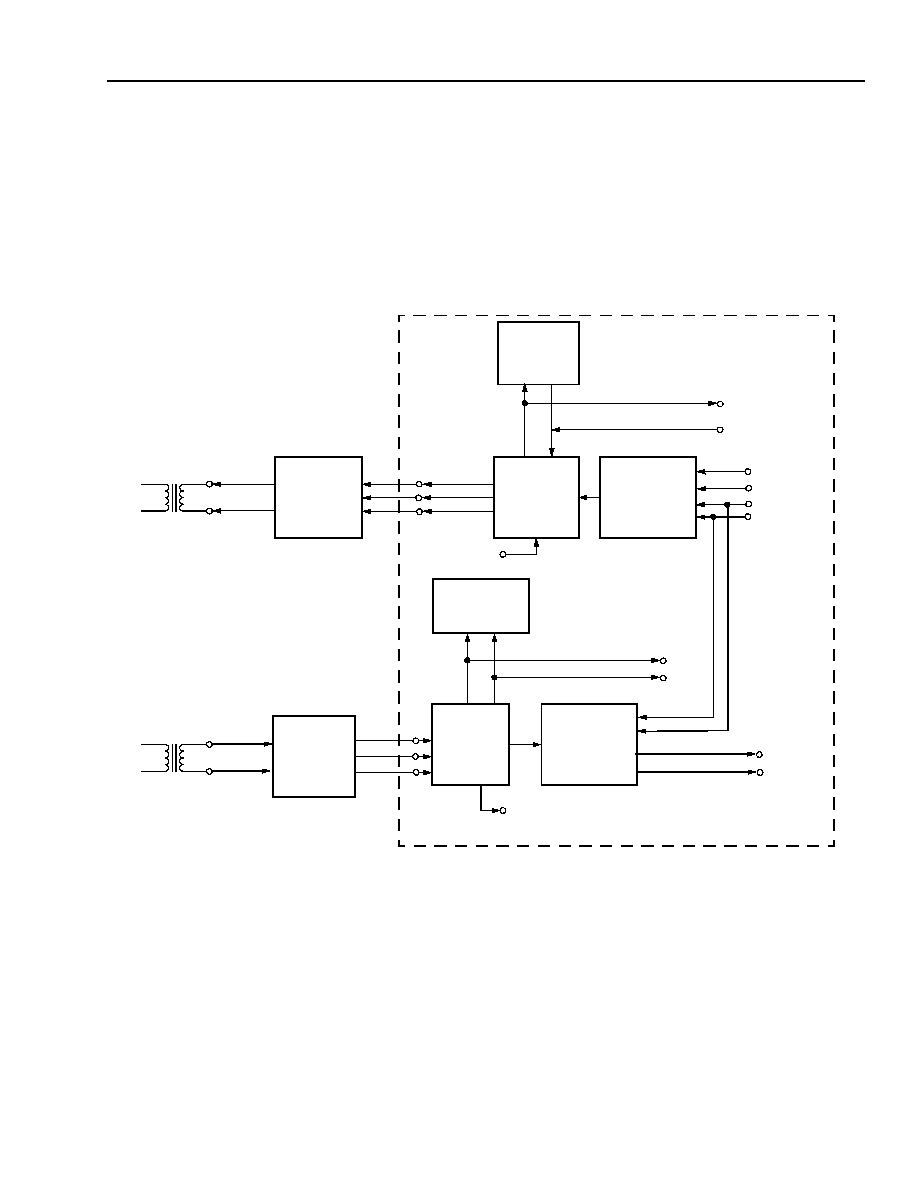
Lucent Technologies Inc.
29
Preliminary Data Sheet
October 2000
TFRA08C13 OCTAL T1/E1 Framer
Lucent Technologies Inc.
LIU-Framer Interface
LIU-Framer Physical Interface
The transmit framer-LIU interface for the TFRA08C13 consists of the TND, TPD, and TLCK pins. In normal opera-
tions, TND, TPD, and TLCK are driven from the transmit framer and are connected to an external transmit line inter-
face. The receive framer-LIU interface for the TFRA08C13 consists of the RPD, RND, and RLCK internal signals. In
normal operations, RND, RPD, and RLCK are sourced from an external receive line interface unit and are directly
connected to the receive framer. Figure 5 illustrates the interfaces of the transmit and receive framer units.
5-7169(F)
Figure 5. Block Diagram of Framer Line Interface
TTIP
TRING
EXTERNAL
INTERFACE
UNIT
TLCK
TND
TPD
TRANSMIT
FRAMER
TRANSMIT
HDLC
FACILITY DATA
LINK
INTERFACE
RECEIVE
CONCENTRATION
HIGHWAY
INTERFACE
TFDLCK
TFDL
RCHIDATA
CHICK
RECEIVE HDLC
FACILITY DATA
LINK INTERFACE
RECEIVE
FRAMER
RTIP
RRING
RECEIVE LINE
INTERFACE
UNIT
TRANSMIT
CONCENTRATION
HIGHWAY
INTERFACE
TCHIDATA
RFDLCK
RFDL
(XLIU)
(XFRMR)
(RCHI)
(XCHI)
(RFRMR)
(RLIU)
LINE INTERFACE
SYSTEM
PLLCK
RFRMCK
RLCK
RND
RPD
TRANSMIT LINE
RCHIDATAB
CHIFS
EXTERNAL
TCHIDATAB
INTERFACE
Preliminary Data Sheet
TFRA08C13 OCTAL T1/E1 Framer
October 2000
30
Lucent Technologies Inc.
Lucent Technologies Inc.
LIU-Framer Interface
(continued)
Figure 6 shows the timing requirements for the transmit and receive framer interfaces in the LIU-bypass mode.
5-4558(F).dr.1
Figure 6. Transmit Framer TLCK to TND, TPD and Receive Framer RND, RPD to RLCK Timing
162 ns
t1-DS1
648 ns
t1
t2r-f
t2f-r
t3
t4
t5
PLLCK
TLCK
TND, TPD
RLCK
RND, RPD
RFRMCK
t7 = RPD, RND HOLD FROM RISING RLCK = 40 ns
t6
t7
t8
t2r-f: t2f-r: PLLCK TO TLCK DELAY = 50 ns
t3-DS1 = 648 ns
t3-CEPT = 488 ns
t4 = TLCK TO VALID TPD, TND = 30 ns
t5-CEPT = 488 ns
t5-DS1 = 648 ns
t6 = RPD, RND SETUP TO RISING RLCK = 40 ns
t8r-f: t8f-r: RLCK TO RFRMCK DELAY = 50 ns
BIT 0 OF FRM_PR45
HFLF = 0
HFLF = 1
122 ns
t1-CEPT
488 ns
IS THE HFLF BIT

Lucent Technologies Inc.
31
Preliminary Data Sheet
October 2000
TFRA08C13 OCTAL T1/E1 Framer
Lucent Technologies Inc.
LIU-Framer Interface
(continued)
Line Encoding
Single Rail
The default line code is single-rail mode and single-rail function of the framer specified by FRM_PR8 bit 7 = 1,
bit 6 = 1, and bit 5 = 0. In this mode, the framer bipolar encoder/decoder is disabled and monitoring of received
BPV errors is done with the use of the RND input. When RND = 1, the BPV counter increments by one on the rising
edge of RLCK.
The transmit framer transmits data via the TPD output pin while TND is forced to a 0 state.
Dual Rail
In dual-rail mode, the dual-rail function of the framer is selected through FRM_PR8 bits 5--7. Bipolar encoding/
decoding is enabled in the framer. Noncoded/decoded data is exchanged between the LIU and framer via the RPD,
RND, RCLK, TPD, TND, and TCLK LIU-framer interface.
DS1: Alternate Mark Inversion (AMI)
The default line code used for T1 applications is alternate mark inversion (AMI). The coding scheme represents a 1
with a pulse or mark on the positive or negative rail and a 0 with no pulse on either rails. This scheme is shown in
Table 3.
Table 3. AMI Encoding
The T1 ones density rule states that: In every 24 bits of information to be transmitted, there must be at least three
pulses, and no more than 15 zeros may be transmitted consecutively.
Receive ones density is monitored by the receive line interface as per T1M1.3/93-005, ITU G.775, or TR-TSY-
000009.
The receive framer indicates excessive zeros upon detecting any zero string length greater than 15 contiguous
zeros (no pulses on either RPD or RND). Both excessive zeros and coding violations are indicated as bipolar viola-
tions.
DS1: Zero Code Suppression (ZCS)
Zero code suppression is a technique known as pulse stuffing in which the seventh bit of each time slot is stuffed
with a one. The line format (shown in Table 4) limits the data rate of each time slot from 64 kbits/s to 56 kbits/s.
The default ZCS format stuffs the seventh bit of those ALL-ZERO time slots programmed for robbed-bit signaling
(as defined in the signaling control registers with the F and G bits).
Input Bit Stream
1011
0000
0111
1010
AMI Data
≠0+≠
0000
0+≠+
≠0+0

Preliminary Data Sheet
TFRA08C13 OCTAL T1/E1 Framer
October 2000
32
Lucent Technologies Inc.
Lucent Technologies Inc.
LIU-Framer Interface
(continued)
The receive framer indicates a bipolar violation upon detecting a block of 15 consecutive 0s with no AMI encoding
(no pulses on either RPD or RND). When an internal bipolar violation and a violation of 15 consecutive 0s occur
simultaneously, only one violation is indicated.
Table 4. DS1 ZCS Encoding
DS1: Binary 8 Zero Code Suppression (B8ZS)
Clear channel transmission can be accomplished using binary 8 zero code suppression (B8ZS). Eight consecutive
0s are replaced with the B8ZS code. This code consists of two bipolar violations in bit position 4 and 7 and valid
bipolar marks in bit positions 5 and 8. The receiving end recognizes this code and replaces it with the original string
of eight 0s.
The receive framer indicates excessive zeros upon detecting a block of eight or more consecutive 0s. (no pulses on
either RPD or RND). Both excessive zeros and coding violations are indicated as bipolar violations.
Table 5 shows the encoding of a string of 0s using B8ZS. B8ZS is recommended when ESF format is used. V rep-
resents a violation of the bipolar rule and B represents an inserted pulse conforming to the AMI rule.
Table 5. DS1 B8ZS Encoding
* Bits 5--6 represent a bipolar violation pair. Bipolar violation with respect to the last previous 1 bit.
Input Bit Stream
00000000
01010000
00000000
00000000
ZCS Data (Framer Mode)
00000010
01010010
00000010
00000010
Default ZCS
00000010
01010000
00000000
(data time slot remains clear)
00000010
Bit Positions
1
2
3
4
5
6
7
8
--
--
--
1
2
3
4
5
6
7
8
Before B8ZS
0
0
0
0
0
0
0
0
1
0
1
0
0
0
0
0
0
0
0
After B8ZS*
0
0
0
V
B
0
V
B
B
0
B
0
0
0
V
B
0
V
B

Lucent Technologies Inc.
33
Preliminary Data Sheet
October 2000
TFRA08C13 OCTAL T1/E1 Framer
Lucent Technologies Inc.
LIU-Framer Interface
(continued)
CEPT: High-Density Bipolar of Order 3 (HDB3)
The line code used for CEPT is described in ITU Rec. G.703 Section 6.1 as high-density bipolar of order 3 (HDB3).
HDB3 uses a substitution code that acts on strings of four zeros. The substitute HDB3 codes are 000V and B00V,
where V represents a violation of the bipolar rule and B represents an inserted pulse conforming to the AMI rule
defined in ITU Rec. G.701, item 9004. The choice of the B00V or 000V is made so that the number of B pulses
between consecutive V pulses is odd. In other words, successive V pulses are of alternate polarity so that no direct
current (dc) component is introduced. The substitute codes follow each other if the string of zeros continues. The
choice of the first substitute code is arbitrary. A line code error consists of two pulses of the same polarity that is not
defined as one of the two substitute codes. Excessive zeros consists of any zero string length greater than four
contiguous zeros. Both excessive zeros and coding violations are indicated as bipolar violations. An example is
shown in Table 6.
Table 6. ITUHDB3 Coding
Input Bit Stream
1011
0000
01
0000
0000
0000
0000
HDB3-coded Data
1011
000V
01
000V
B00V
B00V
B00V
HDB3-coded Levels
≠0+≠
000≠
0+
000+
≠00≠
+00+
≠00≠
HDB3 with 5 Double BPVs
≠0+≠
≠000
0+
+00+
0≠ ≠ ≠
+00+
≠00≠
1-BPV
3-BPV
5-BPV
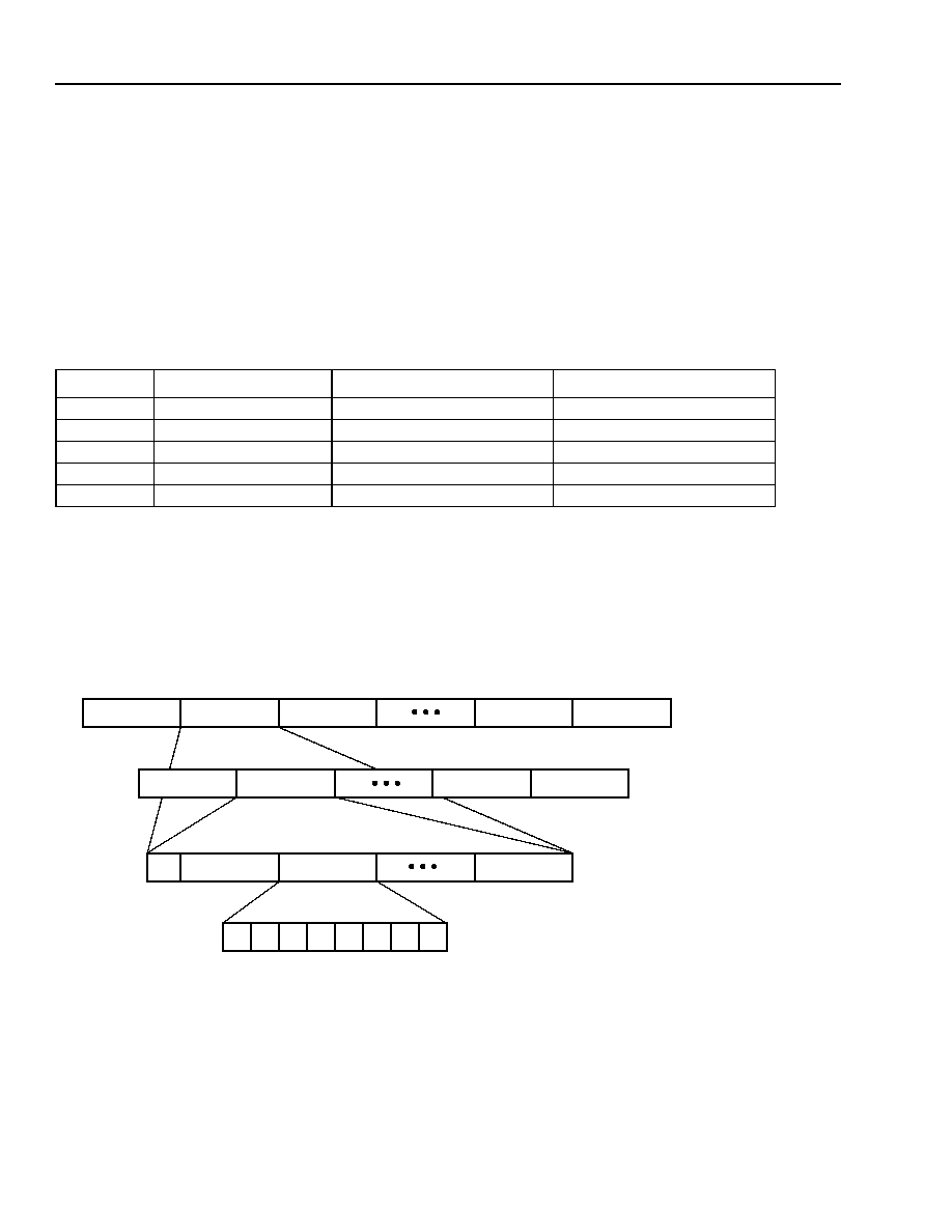
Preliminary Data Sheet
TFRA08C13 OCTAL T1/E1 Framer
October 2000
34
Lucent Technologies Inc.
Lucent Technologies Inc.
Frame Formats
The supported North American T1 framing formats are superframe (D4,
SLC
-96, and digital data service-DDS)
and extended superframe (ESF). The device can be programmed to support the ITU-CEPT-E1 basic format with
and without CRC-4 multiframe formatting. This section describes these framing formats.
T1 Framing Structures
T1 is a digital transmission system which multiplexes twenty-four 64 kbits/s time slots (DS0) onto a serial link. The
T1 system is the lowest level of hierarchy on the North American T-carrier system, as shown in Figure 7
Table 7. T-Carrier Hierarchy
Frame, Superframe, and Extended Superframe Definitions
Each time slot (DS0) is an assembly of 8 bits sampled every 125 µs. The data rate is 64 kbits/s and the sample rate
is 8 kHz. Time-division multiplexing 24 DS0 time slots together produces a 192-bit (24 DS0s) frame. A framing bit is
added to the beginning of each frame to allow for detection of frame boundaries and the transport of additional
maintenance information. This 193-bit frame, also referred to as a DS1 frame, is repeated every 125 µs to yield the
1.544 Mbits/s T1 data rate.DS1 frames are bundled together to form superframes or extended superframes.
5-4559(F).br.1
Figure 7. T1 Frame Structure
T Carrier
DS0 Channels
Bit Rate (Mbits/s)
Digital Signal Level
T1
24
1.544
DS1
T1-C
48
3.152
DS1C
T2
96
6.312
DS2
T3
672
44.736
DS3
T4
4032
274.176
DS4
FRAME 1
FRAME 2
FRAME 3
FRAME 24
FRAME 23
FRAME 1
FRAME 2
FRAME 11
FRAME 12
F BIT
TIME SLOT 1
TIME SLOT 2
TIME SLOT 24
1
2
3
4
5
6
7
8
24-FRAME EXTENDED
ESF = 3.0 ms
12-FRAME SUPERFRAME
SF = 1.5 ms
193-bit FRAME
DS1 = 125
µ
s
8-bit TIME SLOT
DS0 = 5.19
µ
s
SUPERFRAME

Lucent Technologies Inc.
35
Preliminary Data Sheet
October 2000
TFRA08C13 OCTAL T1/E1 Framer
Lucent Technologies Inc.
Frame Formats
(continued)
Transparent Framing Format
The transmit framer can be programmed to transparently transmit 193 bits of system data to the line. The system
interface must be programmed such that the stuffed time slots are 1, 5, 9, 13, 17, 21, 25, and 29 (FRM_PR43 bits
2--0 must be set to 000) and either transparent framing mode 1 or transparent framing mode 2 is enabled
(FRM_PR26 bit 3 or bit 4 must be set to 1).
In transparent mode 1 or mode 2, the transmit framer extracts from the receive system data bit 8 of time slot 1 and
inserts this bit into the framing bit position of the transmit line data. The other 7 bits of the receive system time slot
1 are ignored by the transmit framer. The receive framer will extract the F-bit (or 193rd bit) of the receive line data
and insert it into bit 7 of time slot 1 of the system data; the other bits of time slot 1 are set to 0.
Frame integrity is maintained in both the transmit and receive framer sections.
5-5989(F).b
Figure 8. T1 Transparent Frame Structure
In transparent framing mode 1, the receive framer is forced not to reframe on the receive line data. Other than
bipolar violations and unframed AIS monitoring, there is no processing of the receive line data. The receive framer
will insert the 193rd bit of the receive line data into bit 8 of time slot 1 of the transmit system data.
In transparent framing mode 2, the receive framer functions normally on receive line data. All normal monitoring of
receive line data is performed and data is passed to the transmit CHI as programmed. The receive framer will insert
the extracted framing bit of the receive line data into bit 8 of time slot 1 of the transmit system data. The remaining
bits in time slot 1 are set to 0.
TIME SLOT 1
(STUFF TIME SLOT)
32 TIME-SLOT CHI FRAME
TIME SLOT 2
TIME SLOT 3
TIME SLOT 31 TIME SLOT 32
0
0
0
0
0
0
0
F BIT
TRAMSMIT FRAMER'S
193-bit FRAME
DS1 = 125
µ
s
TIME SLOT 1
TIME SLOT 2
TIME SLOT 24
F BIT
SYSTEM INTERFACE CONTROL REGISTER BITS[2:0] = 000.
SYSTEM FRAME SYNC MASK REGISTER FRM_PR26 BIT 3 OR BIT 4 = 1.
FRAME INTEGRITY IS MAINTAINED WITH F BIT AND THE SYSTEM PAYLOAD.

Preliminary Data Sheet
TFRA08C13 OCTAL T1/E1 Framer
October 2000
36
Lucent Technologies Inc.
Lucent Technologies Inc.
Frame Formats
(continued)
D4 Frame Format
D4 superframe format consists of 12 DS1 frames. Table 8 shows the structure of the D4 superframe.
Table 8. D4 Superframe Format
1. Frame 1 is transmitted first.
2. Following
ANSI
T1.403, the bits are numbered 0--2315. Bit 0 is transmitted first. Bits in each DS0 time slot are numbered 1 through 8, and bit
1 of each DS0 is transmitted first.
3. The remote alarm forces bit 2 of each time slot to a 0-state when enabled. The Japanese remote alarm forces framing bit 12 (bit number
2123) to a 1-state when enabled.
4. Signaling option none uses bit 8 for traffic data.
5. Frames 6 and 12 contain the robbed-bit signaling information in bit 8 of each voice channel, when enabled.
The receive framer uses both the F
T
and F
S
framing bits during its frame alignment procedure.
Frame
Number
1
Framing Bits
Bit Used in Each Time Slot
Signaling Options
Bit
Number
2
Terminal
Frame F
T
Signal
Frame
F
S
Traffic
(All
Channels)
Remote
Alarm
3
Signaling
None
4
2-State
4-State
1
0
1
--
1--8
2
--
--
--
--
2
193
--
0
1--8
2
--
--
--
--
3
386
0
--
1--8
2
--
--
--
--
4
579
--
0
1--8
2
--
--
--
--
5
772
1
--
1--8
2
--
--
--
--
6
5
965
--
1
1--7
2
8
--
A
A
7
1158
0
--
1--8
2
--
--
--
--
8
1351
--
1
1--8
2
--
--
--
--
9
1544
1
--
1--8
2
--
--
--
--
10
1737
--
1
1--8
2
--
--
--
--
11
1930
0
--
1--8
2
--
--
--
--
12
5
2123
--
0
1--7
2
8
--
A
B

Lucent Technologies Inc.
37
Preliminary Data Sheet
October 2000
TFRA08C13 OCTAL T1/E1 Framer
Lucent Technologies Inc.
Frame Formats
(continued)
Digital Data Service (DDS) Frame Format
The superframe format for DDS is the same as that given for D4. DDS is intended to be used for data-only traffic,
and as such, the system should ensure that the framer is in the nonsignaling mode. DDS uses time slot 24 (FAS
channel) to transmit the remote frame alarm and data link bits. The format for time slot 24 is shown in Table 9. The
facility data link timing is shown in Figure 9 below.
Table 9. DDS Channel-24 Format
5-3910(F).cr.1
Figure 9. T7633 Facility Data Link Access Timing of the Transmit and Receive Framer Sections
SLC
-96 Frame Format
SLC
-96 superframe format consists of 12 DS1 frames similar to D4. The F
T
pattern is exactly the same as D4. The
F
S
pattern uses that same structure as D4 but also incorporates a 24-bit data link word as shown below.
5-6421(F)r.1
.
Figure 10.
SLC-
96 Frame Format
Time Slot 24 = 10111YD0
Y = (bit 6)
Remote frame alarm: 1 = no alarm state; 0 = alarm state
D = (bit 7)
Data link bits (8 kbits/s)
t8
t9
t9
t10
t11
t8: TFDLCK CYCLE =
t9: TFDL TO TFDLCK SETUP/HOLD = 40 ns
t10: RFDLCK CYCLE =
t11: RFDLCK TO RFDL DELAY = 40 ns
TFDLCK
TFDL
RFDLCK
RFDL
250
µ
s (ALL OTHER
MODES)
125
µ
s (DDS)
250
µ
s (ALL OTHER
MODES)
125
µ
s (DDS)
SLC
-96 36-FRAME D-bit SUPERFRAME INTERVAL
(72 DS1 FRAMES)
SSLC
-96 24-bit DATA LINK WORD
Fs =
FRAME
N
FRAME
N + 1
. . .
000111000111D
1
DDDDDDDDDDDDDDDDDDDDDDD
24
000111000111DDD . . .
FRAME
N + 2
FRAME
N + 3
FRAME
N + 4
FRAME
N + 5
FRAME
N + 6
FRAME
N + 7
FRAME
N + 8
FRAME
N ≠ 1

Preliminary Data Sheet
TFRA08C13 OCTAL T1/E1 Framer
October 2000
38
Lucent Technologies Inc.
Lucent Technologies Inc.
Frame Formats
(continued)
External TFDL Source. Data may be inserted and extracted from the
SLC
-96 data link from either the external
facility data link (TFDL) ports or the
SLC
-96 data stack. Source selection is controlled by FRM_PR21 bit 6 and
FRM_PR29 bit 5--bit 7.
The transmit framer synchronizes on TFDL = 000111000111 . . . and forces a superframe boundary based on this
pattern. When sourcing an external bit stream, it is the system's responsibility to ensure that TFDL data contain the
pattern of 000111000111 . . . . The D pattern sequence is shown in Table 10. Table 11 shows the encoding for the
line switch field.
Table 10.
SLC
-96 Data Link Block Format
Data Link Block
Bit Definition
Bit Value
D
1
(leftmost bit)
C
1
--concentrator bit
0 or 1
D
2
C
2
--concentrator bit
0 or 1
D
3
C
3
--concentrator bit
0 or 1
D
4
C
4
--concentrator bit
0 or 1
D
5
C
5
--concentrator bit
0 or 1
D
6
C
6
--concentrator bit
0 or 1
D
7
C
7
--concentrator bit
0 or 1
D
8
C
8
--concentrator bit
0 or 1
D
9
C
9
--concentrator bit
0 or 1
D
10
C
10
--concentrator bit
0 or 1
D
11
C
11
--concentrator bit
0 or 1
D
12
Spoiler bit 1
0
D
13
Spoiler bit 2
1
D
14
Spoiler bit 3
0
D
15
M
1
--maintenance bit
0 or 1
D
16
M
2
--maintenance bit
0 or 1
D
17
M
3
--maintenance bit
0 or 1
D
18
A1--alarm bit
0 or 1
D
19
A2--alarm bit
0 or 1
D
20
S
1
--line-switch bit
Defined in Table 11
D
21
S
2
--line-switch bit
Defined in Table 11
D
22
S
3
--line-switch bit
Defined in Table 11
D
23
S
4
--line-switch bit
Defined in Table 11
D
24
(rightmost bit)
Spoiler bit 4
1

Lucent Technologies Inc.
39
Preliminary Data Sheet
October 2000
TFRA08C13 OCTAL T1/E1 Framer
Lucent Technologies Inc.
Frame Formats
(continued)
Table 11.
SLC
-96 Line Switch Message Codes
Internal
SLC
-96 Stack Source. Optionally, a
SLC
-96 FDL stack may be used to insert and correspondingly extract
the FDL information in the
SLC
-96 frame format.
The transmit
SLC
-96 FDL bits are sourced from the transmit framer
SLC
-96 FDL stack. The
SLC
-96 FDL stack
(see FRM_PR31--FRM_PR35) consists of five 8-bit registers that contain the
SLC
-96 FS and D-bit information as
shown in Table 12. The transmit stack data is transmitted to the line when the stack enable mode is active in the
parameter registers FRM_PR21 bit 6 = 1 and FRM_PR29 bit 5--bit 7 = x10 (binary).
The receive
SLC
-96 stack data is received when the receive framer is in the superframe alignment state. In the
SLC
-96 mode, while in the loss of superframe alignment (LSFA) state, updating of the receive framer
SLC
-96 stack
is halted and neither the receive stack interrupt nor receive stack flag are asserted.
Table 12. Transmit and Receive
SLC
-96 Stack Structure
Bit 5--bit 0 of the first 2 bytes of the
SLC
-96 FDL stack in Table 12 are transmitted to the line as the
SLC
-96 F
S
sequence. Bit 7 of the third stack register is transmitted as the C
1
bit of the
SLC
-96 D sequence. The spoiler bits
(SPB1, SPB2, SPB3, and SPB4) are taken directly from the transmit stack. The protocol for accessing the
SLC
-96
stack information for the transmit and receive framer is described below. The transmit
SLC
-96 stack must be written
with valid data when transmitting stack data.
The device indicates that it is ready for an update of its transmit stack by setting register FRM_SR4 bit 5 (
SLC
-96
transmit FDL stack ready) high. At this time, the system has about 9 ms to update the stack. Data written to the
stack during this interval will be transmitted during the next
SLC
-96 superframe D-bit interval. By reading bit 5 in
register SR4, the system clears this bit so that it can indicate the next time the transmit stack is ready. If the trans-
mit stack is not updated, then the content of the stack is retransmitted to the line. The start of the
SLC
-96 36-frame
F
S
interval of the transmit framer is a function of the first 2 bytes of the
SLC
-96 transmit stack registers. These
bytes must be programmed as shown in Table 12. Programming any other state into these two registers disables
the proper transmission of the
SLC
-96 D bits. Once programmed correctly, the transmit
SLC
-96 D-bit stack is trans-
mitted synchronous to the transmit
SLC
-96 superframe structure.
On the receive side, the device indicates that it has received data in the receive FDL stack (registers FRM_SR54--
FRM_SR58) by setting bit 4 in register FRM_SR4 (
SLC
-96 receive FDL stack ready) high. The system then has
about 9 ms to read the content of the stack before it is updated again (old data lost). By reading bit 4 in register
FRM_SR4, the system clears this bit so that it can indicate the next time the receive stack is ready. As explained
above, the
SLC
-96 receive stack is not updated when superframe alignment is lost.
S
1
S
2
S
3
S
4
Code Definition
1
1
1
1
Idle
1
1
1
0
Switch line A receive
1
1
0
1
Switch line B transmit
1
1
0
0
Switch line C transmit
1
0
1
0
Switch line D transmit
0
1
0
1
Switch line B transmit and receive
0
1
0
0
Switch line B transmit and receive
0
0
1
0
Switch line B transmit and receive
Register Number Bit 7 (MSB)
Bit 6
Bit 5
Bit 4
Bit 3
Bit 2
Bit 1
Bit 0 (LSB)
1 (LSR)
0
0
0
0
0
1
1
1
2
0
0
0
0
0
1
1
1
3
C
1
C
2
C
3
C
4
C
5
C
6
C
7
C
8
4
C
9
C
10
C
11
SPB
1
= 0 SPB
2
= 1 SPB
3
= 0
M
1
M
2
5
M
3
A
1
A
2
S
1
S
2
S
3
S
4
SPB
4
= 1

Preliminary Data Sheet
TFRA08C13 OCTAL T1/E1 Framer
October 2000
40
Lucent Technologies Inc.
Lucent Technologies Inc.
Frame Formats
(continued)
Extended Superframe Format
The extended superframe format consists of 24 DS1 frames. The F bits are used for frame alignment, superframe
alignment, error checking, and facility data link transport. Table 13 shows the ESF frame format.
Table 13. Extended Superframe (ESF) Structure
1. Frame 1 is transmitted first.
2. The remote alarm is a repeated 1111111100000000 pattern in the DL when enabled.
3. Following
ANSI
T1.403, the bits are numbered 0--4361. Bit 0 is transmitted first. Bits in each DS0 time slot are numbered 1 through 8, and bit
1 of each DS0 is transmitted first.
4. The C
1
to C
6
bits are the cyclic redundancy check-6 (CRC-6) checksum bits calculated over the previous extended superframe.
5. Signaling option none uses bit 8 for traffic data.
6. Frames 6, 12, 18, and 24 contain the robbed-bit signaling information in bit 8 of each voice channel, when enabled.
The ESF format allows for in-service error detection and diagnostics on T1 circuits. ESF format consist of 24 fram-
ing bits: 6 for framing synchronization (2 kbits/s); 6 for error detection (2 kbits/s); and 12 for in-service monitoring
and diagnostics (4 kbits/s).
Frame
Number
1
Frame Bit
Bit Use in Each Time
Slot
Signaling Option
2
Bit
Number
3
F
E
D
L
CRC-6
4
Traffic
Signaling
None
5
2-State
4-State
16-State
1
0
--
D
--
1--8
--
--
--
--
--
2
193
--
--
C
1
1--8
--
--
--
--
--
3
386
--
D
--
1--8
--
--
--
--
--
4
579
0
--
--
1--8
--
--
--
--
--
5
772
--
D
--
1--8
--
--
--
--
--
6
6
965
--
--
C
2
1--7
8
--
A
A
A
7
1158
--
D
--
1--8
--
--
--
--
--
8
1351
0
--
--
1--8
--
--
--
--
--
9
1544
--
D
--
1--8
--
--
--
--
--
10
1737
--
--
C
3
1--8
--
--
--
--
--
11
1930
--
D
--
1--8
--
--
--
--
--
12
6
2123
1
--
--
1--7
8
--
A
B
B
13
2316
--
D
--
1--8
--
--
--
--
--
14
2509
--
--
C
4
1--8
--
--
--
--
--
15
2702
--
D
--
1--8
--
--
--
--
--
16
2895
0
--
--
1--8
--
--
--
--
--
17
3088
--
D
--
1--8
--
--
--
--
--
18
6
3281
--
--
C
5
1--7
8
--
A
A
C
19
3474
--
D
--
1--8
--
--
--
--
--
20
3667
1
--
--
1--8
--
--
--
--
--
21
3860
--
D
--
1--8
--
--
--
--
--
22
4053
--
--
C
6
1--8
--
--
--
--
--
23
4246
--
D
--
1--8
--
--
--
--
--
24
6
4439
1
--
--
1--7
8
--
A
B
D

Lucent Technologies Inc.
41
Preliminary Data Sheet
October 2000
TFRA08C13 OCTAL T1/E1 Framer
Lucent Technologies Inc.
Frame Formats
(continued)
Cyclic redundancy checking is performed over the entire ESF data payload (4,608 data bits, with all 24 framing bits
(F
E
, D
L
, CRC-6) set to 1 during calculations). The CRC-6 bits transmitted in ESF will be determined as follows:
s
The check bits, c1 through c6, contained in ESF(n + 1) will always be those associated with the contents of
ESF(n), the immediately preceding ESF. When there is no ESF immediately preceding, the check bits may be
assigned any value.
s
For the purpose of CRC-6 calculation only, every F bit in ESF(n) is set to 1. ESF(n) is altered in no other way.
s
The resulting 4632 bits of ESF(n) are used, in order of occurrence, to construct a polynomial in x such that the
first bit of ESF(n) is the coefficient of the term x
4631
and the last bit of ESF(n) is the coefficient of the term x
0
.
s
The polynomial is multiplied by the factor x
6
, and the result is divided, modulo 2, by the generator polynomial x
6
+ x + 1. The coefficients of the remainder polynomial are used, in order of occurrence, as the ordered set of
check bits, c1 through c6, that are transmitted in ESF(n + 1). The ordering is such that the coefficient of the term
x
5
in the remainder polynomial is check bit c1 and the coefficient of the term x
0
in the remainder polynomial is
check bit c6.
The ESF remote frame alarm consists of a repeated eight ones followed by eight 0s transmitted in the data link
position of the framing bits.
T1 Loss of Frame Alignment (LFA)
Loss of frame alignment condition for the superframe or the extended superframe formats is caused by the inability
of the receive framer to maintain the proper sequence of frame bits. The number of errored framing bits required to
detect a loss of frame alignment is given is Table 14.
Table 14. T1 Loss of Frame Alignment Criteria
The receive framer indicates the loss of frame and superframe conditions by setting the LFA and LSFA bits
(FRM_SR1 bit 0 and bit 1), respectively, in the status registers for the duration of the conditions. The local system
may give indication of its LFA state to the remote end by transmitting a remote frame alarm (RFA). In addition, in
the LFA state, the system may transmit an alarm indication signal (AIS) to the system interface.
Format
Number of Errored Framing Bits That Will Cause a Loss of Frame Alignment Condition
D4
2 errored frame bits (F
T
or F
S
) out of 4 consecutive frame bits if FRM_PR10 bit 2 = 1.
2 errored F
T
bits out of 4 consecutive F
T
bits if PRM_PR10 bit 2 = 0.
SLC
-96
2 errored frame bits (F
T
or F
S
) out of 4 consecutive frame bits if FRM_PR10 bit 2 = 1.
2 errored F
T
bits out of 4 consecutive F
T
bits if FRM_PR10 bit 2 = 0.
DDS: Frame
3 errored frame bits (F
T
or F
S
) or channel 24 FAS pattern out of 12 consecutive frame bits.
ESF
2 errored F
E
bits out of 4 consecutive F
E
bits or optionally 320 or more CRC-6 errored check-
sums within a one second interval if loss of frame alignment due to excessive CRC-6 errors is
enabled in FRM_PR9.

Preliminary Data Sheet
TFRA08C13 OCTAL T1/E1 Framer
October 2000
42
Lucent Technologies Inc.
Lucent Technologies Inc.
Frame Formats
(continued)
T1 Frame Recovery Alignment Algorithms
When in a loss of frame alignment state, the receive framer searches for a new frame alignment and forces its inter-
nal circuitry to this new alignment. The receive framer's synchronization circuit inhibits realignment in T1 framing
formats when repetitive data patterns emulate the T1 frame alignment patterns. T1 frame synchronization will not
occur until all frame sequence emulating patterns disappear and only one valid pattern exists. The loss of frame
alignment state will always force a loss of superframe alignment state. Superframe alignment is established only
after frame alignment has been determined in the D4 and
SLC
-96 frame format. Table 15 gives the requirements
for establishing T1 frame and superframe alignment.
Table 15. T1 Frame Alignment Procedures
Frame Format
Alignment Procedure
D4: Frame
Using the F
T
frame position as the starting point, frame alignment is established when 24 con-
secutive F
T
and F
S
frame bits, excluding the twelfth F
S
bit, (48 total frames) are received
error-free. Once frame alignment is established, then superframe alignment is determined.
D4: Superframe
After frame alignment is determined, two valid superframe bit sequences using the
F
S
bits must be received error-free to establish superframe alignment.
SLC
-96: Frame
Using the F
T
frame position as the starting point, frame alignment is established when 24 con-
secutive F
T
frame bits (48 total frames) are received error-free. Once frame alignment is
established, then superframe alignment is determined.
SLC
-96:
Superframe
After frame alignment is determined, superframe alignment is established on the first valid
superframe bit sequence 000111000111.
DDS: Frame
Using the F
T
frame position as the starting point, frame alignment is established when six
consecutive F
T
/F
S
frame bits and the DDS FAS in time slot 24 are received error-free. In the
DDS format, there is no search for a superframe structure.
ESF
Frame and superframe alignment is established simultaneously using the F
E
framing bit.
Alignment is established when 24 consecutive F
E
bits are received error-free. Once frame/
superframe alignment is established, the CRC-6 receive monitor is enabled.

Lucent Technologies Inc.
43
Preliminary Data Sheet
October 2000
TFRA08C13 OCTAL T1/E1 Framer
Lucent Technologies Inc.
Frame Formats
(continued)
T1 Robbed-Bit Signaling
To enable signaling, register FRM_PR44 bit 0 (TSIG) must be set to 0.
Robbed-bit signaling, used in either ESF or SF framing formats, robs the eighth bit of the voice channels of every
sixth frame. The signaling bits are designated A, B, C, and D, depending on the signaling format used. The robbed-
bit signaling format used is defined by the state of the F and G bits in the signaling registers (see DS1: Robbed-Bit
Signaling on page 61). The received channel robbed-bit signaling format is defined by the corresponding transmit
signaling F and G bits. Table 16 shows the state of the transmitted signaling bits as a function of the F and G bits.
Table 16. Robbed-Bit Signaling Options
* See register FRM_PR43 bit 3 and bit 4.
The robbed-bit signaling format for each of the 24 T1 transmit channels is programmed on a per-channel basis by
setting the F and G bits in the transmit signaling direction.
SLC
-96 9-State Signaling
SLC
-96 9-state signaling state is enabled by setting both the F and G bits in the signaling registers to the 0-state,
setting the
SLC
-96 signaling control register FRM_PR43 bit 3 to 1, and setting register FRM_PR44 bit 0 to 0. Table
17 shows the state of the transmitted signaling bits to the line as a function of the A-, B-, C-, and D-bit settings in
the transmit signaling registers. In Table 17 below, X indicates either a 1- or a 0-state, and T indicates a toggle,
transition from either 0 to 1 or 1 to 0, of the transmitted signaling bit.
In the line receive direction, this signaling mode functions identically to the preceding transmit path description.
Table 17.
SLC
-96 9-State Signaling Format
G
F
Robbed-Bit Signaling Format
Frame
6
12
18
24
0
0
ESF: 16-State
SLC
*: 9-State, 16-State
A
B
C
D
0
1
4-State
A
B
A
B
1
0
Data channel (no signaling)
PAYLOAD DATA
1
1
2-State
A
A
A
A
Transmit Signaling Register Settings
Transmit to the Line Signal Bits
SLC
-96 Signaling States
A
B
C
D
A = f(A, C)
B = f(B, D)
State 1
0
0
0
0
0
0
State 2
0
0
0
1
0
T
State 3
0
1
0
X
0
1
State 4
0
0
1
0
T
0
State 5
0
0
1
1
T
T
State 6
0
1
1
X
T
1
State 7
1
0
X
0
1
0
State 8
1
0
X
1
1
T
State 9
1
1
X
X
1
1

Preliminary Data Sheet
TFRA08C13 OCTAL T1/E1 Framer
October 2000
44
Lucent Technologies Inc.
Lucent Technologies Inc.
Frame Formats
(continued)
16-State Signaling
The default signaling mode while in
SLC
-96 framing is 16-state signaling.
SLC
-96 16-state signaling is enabled by
setting both the F and G bits in the signaling registers to the 0 state, setting the
SLC
-96 signaling control register
FRM_PR43 bit 3 and bit 4 to 0, and setting register FRM_PR44 bit 0 to 0. Table 18 shows the state of the transmit-
ted signaling bits to the line as a function of the A-, B-, C-, and D-bit settings in the transmit signaling registers. In
Table 18 below, under Transmit to the Line Signal Bits, A and B are transmitted into one
SLC
-96 12-frame signaling
superframe, while A' and B' are transmitted into the next successive
SLC
-96 12-frame signaling superframe.
In the line receive direction, this signaling mode functions identically to the preceding transmit path description.
The signaling mapping of this 16-state signaling mode is equivalent to the mapping of the
SLC
-96 9-state signaling
mode.
Table 18. 16-State Signaling Format
Transmit Signaling Register Settings
Transmit to the Line Signal Bits
SLC
-96 Signaling States
A
B
C
D
A
B
A'
B'
State 0
0
0
0
0
0
0
0
0
State 1
0
0
0
1
0
0
0
1
State 2
0
0
1
0
0
0
1
0
State 3
0
0
1
1
0
0
1
1
State 4
0
1
0
0
0
1
0
0
State 5
0
1
0
1
0
1
0
1
State 6
0
1
1
0
0
1
1
0
State 7
0
1
1
1
0
1
1
1
State 8
1
0
0
0
1
0
0
0
State 9
1
0
0
1
1
0
0
1
State 10
1
0
1
0
1
0
1
0
State 11
1
0
1
1
1
0
1
1
State 12
1
1
0
0
1
1
0
0
State 13
1
1
0
1
1
1
0
1
State 14
1
1
1
0
1
1
1
0
State 15
1
1
1
1
1
1
1
1
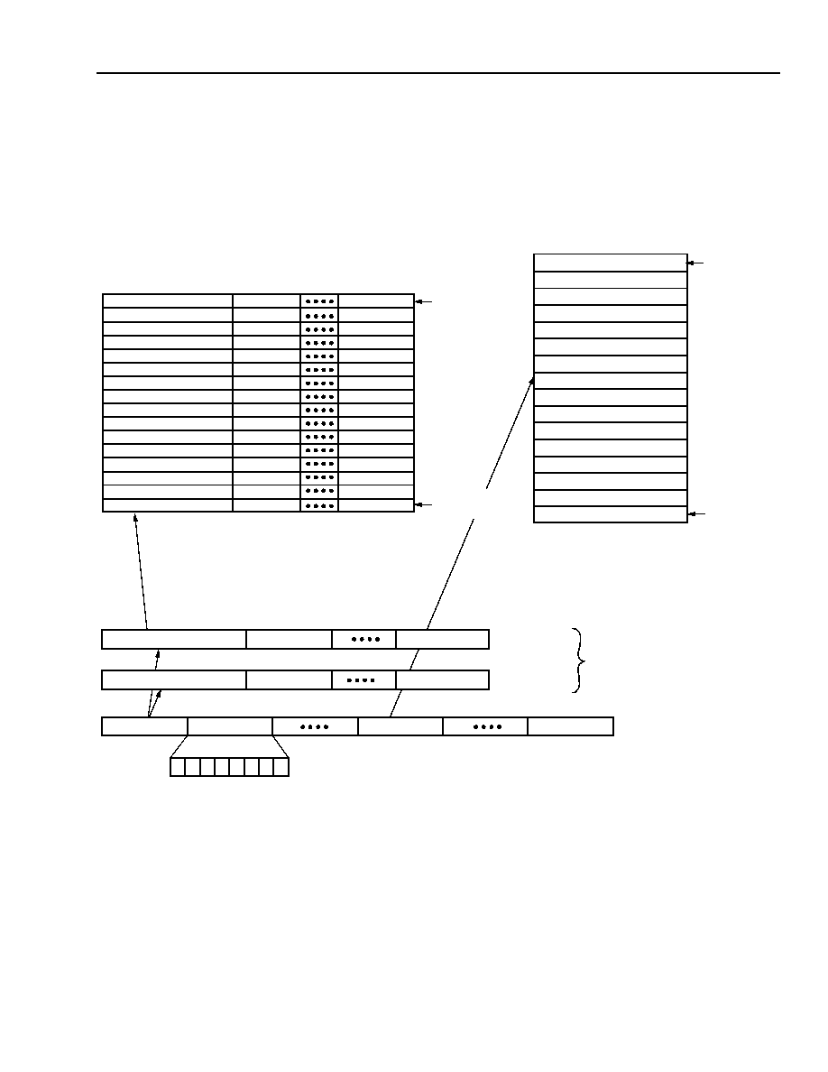
Lucent Technologies Inc.
45
Preliminary Data Sheet
October 2000
TFRA08C13 OCTAL T1/E1 Framer
Lucent Technologies Inc.
Frame Formats
(continued)
CEPT 2.048 Basic Frame, CRC-4 Time Slot 0, and Signaling Time Slot 16 Multiframe
Structures
As defined in TU Rec. G.704, the CEPT 2.048 frame, CRC-4 multiframe, and channel associated signaling multi-
frame structures are illustrated in Figure 11
5-4548(F).cr.1
Figure 11. ITU 2.048 Basic Frame, CRC-4 Multiframe, and Channel Associated Signaling
Multiframe Structures
0 1 A S
A4
S
A5
S
A6
S
A7
S
A8
C
1
0 0 1 1 0 1 1
C
2
0 0 1 1 0 1 1
0 1 A S
A4
S
A5
S
A6
S
A7
S
A8
C
3
0 0 1 1 0 1 1
1 1 A S
A4
S
A5
S
A6
S
A7
S
A8
C
4
0 0 1 1 0 1 1
0 1 A S
A4
S
A5
S
A6
S
A7
S
A8
C
1
0 0 1 1 0 1 1
1 1 A S
A4
S
A5
S
A6
S
A7
S
A8
C
2
0 0 1 1 0 1 1
1 1 A S
A4
S
A5
S
A6
S
A7
S
A8
C
3
0 0 1 1 0 1 1
E 1 A S
A4
S
A5
S
A6
S
A7
S
A8
C
4
0 0 1 1 0 1 1
E 1 A S
A4
S
A5
S
A6
S
A7
S
A8
TIME SLOT 1
TIME SLOT 1
TIME SLOT 1
TIME SLOT 1
TIME SLOT 1
TIME SLOT 1
TIME SLOT 1
TIME SLOT 1
TIME SLOT 1
TIME SLOT 1
TIME SLOT 1
TIME SLOT 1
TIME SLOT 1
TIME SLOT 1
TIME SLOT 1
TIME SLOT 1
TIME SLOT 31
TIME SLOT 31
TIME SLOT 31
TIME SLOT 31
TIME SLOT 31
TIME SLOT 31
TIME SLOT 31
TIME SLOT 31
TIME SLOT 31
TIME SLOT 31
TIME SLOT 31
TIME SLOT 31
TIME SLOT 31
TIME SLOT 31
TIME SLOT 31
TIME SLOT 31
FRAME 0 OF CRC-4
MULTIFRAME
TIME SLOT 0
TIME SLOT 1
TIME SLOT 16
TIME SLOT 31
Si 1 A S
A4
S
A5
S
A6
S
A7
S
A8
TIME SLOT 1
TIME SLOT 31
Si 0 0 1 1 0 1 1
TIME SLOT 1
TIME SLOT 31
FRAME 15 OF CRC-4
MULTIFRAME
FAS FRAME
NOT FAS FRAME
0 0 0 0 X
0
Y
M
X
1
X
2
1
2
3
4
5
6
7
8
8-bit TIME SLOT = 3.90625
µ
s
256-bit FRAME = 125
µ
s
PRIMARY BASIC FRAME
STRUCTURE
A
1
B
1
C
1
D
1
A
16
B
16
C
16
D
16
A
2
B
2
C
2
D
2
A
17
B
17
C
17
D
17
A
3
B
3
C
3
D
3
A
18
B
18
C
18
D
18
A
4
B
4
C
4
D
4
A
19
B
19
C
19
D
19
A
5
B
5
C
5
D
5
A
20
B
20
C
20
D
20
A
6
B
6
C
6
D
6
A
21
B
21
C
21
D
21
A
7
B
7
C
7
D
7
A
22
B
22
C
22
D
22
A
8
B
8
C
8
D
8
A
23
B
23
C
23
D
23
A
9
B
9
C
9
D
9
A
24
B
24
C
24
D
24
A
10
B
10
C
10
D
10
A
25
B
25
C
25
D
25
A
11
B
11
C
11
D
11
A
26
B
26
C
26
D
26
A
12
B
12
C
12
D
12
A
27
B
27
C
27
D
27
A
13
B
13
C
13
D
13
A
28
B
28
C
28
D
28
A
14
B
14
C
14
D
14
A
29
B
29
C
29
D
29
A
15
B
15
C
15
D
15
A
30
B
30
C
30
D
30
FRAME 0 TIME
CHANNEL ASSOCIATED
SIGNALING MULTIFRAME
IN TIME SLOT 16
CHANNEL NUMBERS REFER TO TELEPHONE
CHANNEL NUMBERS. TIME SLOTS 1 TO 15 AND
17 TO 31 ARE ASSIGNED TO TELEPHONE
CHANNELS NUMBERED FROM 1 TO 30.
FRAME 15
CRC-4 MULTIFRAME IN
TIME SLOT 0
TIME SLOT 16
MULTIFRAME
SLOT 16
MULTIFRAME

Preliminary Data Sheet
TFRA08C13 OCTAL T1/E1 Framer
October 2000
46
Lucent Technologies Inc.
Lucent Technologies Inc.
Frame Formats
(continued)
CEPT 2.048 Basic Frame Structure
The ITU Rec. G.704 Section 2.3.1 defined frame length is 256 bits, numbered 1 to 256. The frame repetition rate is
8 kHz. The allocation of bits numbered 1 to 8 of the frame is shown in Table 19.
Table 19. Allocation of Bits 1 to 8 of the FAS Frame and the NOT FAS Frame
The function of each bit in Table 19 is described below:
s
The Si bits are reserved for international use. A specific use for these bits is described in Table 20. ITU CRC-4
Multiframe Structure. If no use is realized, these bits should be fixed at 1 on digital paths crossing an interna-
tional border.
s
Bit 2 of the NOT FAS frames is fixed to 1 to assist in avoiding simulations of the frame alignment signal.
s
Bit 3 of the NOT FAS is the remote alarm indication (A bit). In undisturbed operation, this bit is set to 0; in alarm
condition, set to 1.
s
Bits 4--8 of the NOT FAS (Sa4--Sa8) may be recommended by ITU for use in specific point-to-point applica-
tions. Bit Sa4 may be used as a message-based data link for operations, maintenance, and performance moni-
toring. If the data link is accessed at intermediate points with consequent alterations to the Sa4 bit, the CRC-4
bits must be updated to retain the correct end-to-end path termination functions associated with the CRC-4 pro-
cedure. The receive framer does not implement the CRC-4 modifying algorithm described in ITU Rec. G.706
Annex C. Bits Sa4--Sa8, where these are not used, should be set to 1 on links crossing an international border.
s
MSB = most significant bit and is transmitted first.
s
LSB = least significant bit and is transmitted last.
Basic Frames
Bit 1 (MSB)
Bit 2
Bit 3
Bit 4
Bit 5
Bit 6
Bit 7
Bit 8 (LSB)
Frame Alignment Signal (FAS)
Si
0
0
1
1
0
1
1
Not Frame Alignment Signal
(NOT FAS)
Si
1
A
Sa4
Sa5
Sa6
Sa7
Sa8
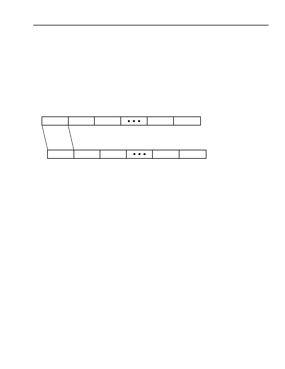
Lucent Technologies Inc.
47
Preliminary Data Sheet
October 2000
TFRA08C13 OCTAL T1/E1 Framer
Lucent Technologies Inc.
Frame Formats
(continued)
Transparent Framing Format
The transmit framer can be programmed to transparently transmit 256 bits of system data to the line. The transmit
framer must be programmed to either transparent framing mode 1 or transparent framing mode 2 (see Table 136.
Framer Reset and Transparent Mode Control Register (FRM_PR26) (Y7A)).
In transparent mode 1 or mode 2, the transmit framer transmits all 256 bits of the RCHI payload unmodified to the
line. Time slot 1 of the RCHI, determined by the CHIFS signal, is inserted into the FAS/NOT FAS time slot of the
transmit line interface.
Frame integrity is maintained in both the transmit and receive framer sections.
5-5988(F)
Figure 12. CEPT Transparent Frame Structure
In transparent framing mode 1, the receive framer is forced not to reframe on the receive line data. Other than
bipolar violations and unframed AIS monitoring, there is no processing of the receive line data. The entire receive
line payload is transmitted unmodified to the CHI.
In transparent framing mode 2, the receive framer functions normally on the receive line data. All normal monitoring
of receive line data is performed and data is transmitted to the CHI as programmed.
TIME SLOT 1
32 TIME-SLOT CHI FRAME
TIME SLOT 2
TIME SLOT 3
TIME SLOT 31 TIME SLOT 32
TIME SLOT 1
32 TIME-SLOT LINE FRAME
TIME SLOT 2
TIME SLOT 3
TIME SLOT 31 TIME SLOT 32

Preliminary Data Sheet
TFRA08C13 OCTAL T1/E1 Framer
October 2000
48
Lucent Technologies Inc.
Lucent Technologies Inc.
Frame Formats
(continued)
CEPT Loss of Basic Frame Alignment (LFA)
Frame alignment is assumed to be lost when the follow-
ing occurs :
s
As described in ITU Rec. G.706 Section 4.1.1, three
consecutive incorrect frame alignment signals have
been received.
s
So as to limit the effect of spurious frame alignment
signals, when bit 2 in time slot 0 in NOT FAS frames
has been received with an error on three consecutive
occasions.
s
Optionally, as described in ITU Rec. G.706 Section
4.3.2, by exceeding a count of >914 errored CRC-4
blocks out of 1000, with the understanding that a
count of
915 errored CRC blocks indicates false
frame alignment.
s
On demand via the control registers.
s
In the LFA state:
s
No additional FAS or NOT FAS errors are processed.
s
The received remote frame alarm (received A bit) is
deactivated.
s
All NOT FAS bit (Si bit, A bit, and Sa4 to Sa8 bits)
processing is halted.
s
Receive Sa6 status bits are set to 0.
s
Receive Sa6 code monitoring and counting is halted.
s
All receive Sa stack data updates are halted. The
receive Sa stack ready, register FRM_SR4 bit 6 and
bit 7, is set to 0. If enabled, the receive Sa stack
interrupt bit is set to 0.
s
Receive data link (RFDL) is set to 1 and RFDCLK
maintains previous alignment.
s
Optionally, the remote alarm indication (A = 1) may
be automatically transmitted to the line if register
FRM_PR27 bit 0 is set to 1.
s
Optionally, the alarm indication signal (AIS) may be
automatically transmitted to the system if register
FRM_PR19 bit 0 is set to 1.
s
If CRC-4 is enabled, loss of CRC-4 multiframe align-
ment is forced.
s
If CRC-4 is enabled, the monitoring and processing
of CRC-4 checksum errors is halted.
s
If CRC-4 is enabled, all monitoring and processing of
received E-bit information is halted.
s
If CRC-4 is enabled, the receive continuous E-bit
alarm is deactivated.
s
If CRC-4 is enabled, optionally, E bit = 0 is transmit-
ted to the line for the duration of loss of CRC-4 multi-
frame alignment if register FRM_PR28 bit 4 is set to
1.
s
If time slot 16 signaling is enabled, loss of the signal-
ing multiframe alignment is forced.
s
If time slot 16 signaling is enabled, updating of the
signaling data is halted.
CEPT Loss of Frame Alignment Recovery
Algorithm
The receive framer begins the search for basic frame
alignment one bit position beyond the position where
the LFA state was detected. As defined in ITU Rec.
G.706.4.1.2, frame alignment will be assumed to have
been recovered when the following sequence is
detected as follows:
s
For the first time, the presence of the correct frame
alignment signal in frame
n
.
s
The absence of the frame alignment signal in the fol-
lowing frame detected by verifying that bit 2 of the
basic frame is a 1 in frame
n
+ 1.
s
For the second time, the presence of the correct
frame alignment in the next frame,
n
+ 2.
Failure to meet the second or third bullet above will ini
tiate a new basic frame search in frame
n
+ 2.

Lucent Technologies Inc.
49
Preliminary Data Sheet
October 2000
TFRA08C13 OCTAL T1/E1 Framer
Lucent Technologies Inc.
Frame Formats
(continued)
CEPT Time Slot 0 CRC-4 Multiframe Structure
The CRC-4 multiframe is in bit 1 of each NOT FAS frame. As described in ITU Rec. G.704 Section 2.3.3.1, where
there is a need to provide additional protection against simulation of the frame alignment signal, and/or where there
is a need for an enhanced error monitoring capability, then bit 1 of each frame may be used for a cyclic redundancy
check-4 (CRC-4) procedure as detailed below. The allocation of bits 1--8 of time slot 0 of every frame is shown in
Table 20 for the complete CRC-4 multiframe.
Table 20. ITU CRC-4 Multiframe Structure
Notes:
C1 to C4 = cyclic redundancy check-4 (CRC-4) bits.
E = CRC-4 error indication bits.
Sa4 to Sa8 = spare bits.
A = remote frame alarm (RFA) bit (active-high); referred to as the A bit.
The CRC-4 multiframe consists of 16 frames numbered 0 to 15 and is divided into two eight-frame submultiframes
(SMF), designated SMF-I and SMF-II that signifies their respective order of occurrence within the CRC-4 multi-
frame structure. The SMF is the CRC-4 block size (2048 bits). In those frames containing the frame alignment sig-
nal (FAS), bit 1 is used to transmit the CRC-4 bits. There are four CRC-4 bits, designated C1, C2, C3, and C4 in
each SMF. In those frames not containing the frame alignment signal (NOT FAS), bit 1 is used to transmit the 6-bit
CRC-4 multiframe alignment signal and two CRC-4 error indication bits (E). The multiframe alignment signal is
defined in ITU Rec. G.704 Section 2.3.3.4, as 001011. Transmitted E bits should be set to 0 until both basic frame
and CRC-4 multiframe alignment are established. Thereafter, the E bits should be used to indicate received errored
submultiframes by setting the binary state of one E bit from 1 to 0 for each errored submultiframe. The received E
bits will always be taken into account, by the receive E-bit processor
*
, even when the SMF that contains them is
found to be errored. In the case where there exists equipment that does not use the E bits, the state of the E bits
should be set to a binary 1 state.
* The receive E-bit processor will halt the monitoring of the received E bit during the loss of CRC-4 multiframe alignment.
Multiframe
Submultiframe
(SMF)
Frame
Number
Bits
1
2
3
4
5
6
7
8
I
0
C1
0
0
1
1
0
1
1
1
0
1
A
Sa4
Sa5
Sa6
Sa7
Sa8
2
C2
0
0
1
1
0
1
1
3
0
1
A
Sa4
Sa5
Sa6
Sa7
Sa8
4
C3
0
0
1
1
0
1
1
5
1
1
A
Sa4
Sa5
Sa6
Sa7
Sa8
6
C4
0
0
1
1
0
1
1
7
0
1
A
Sa4
Sa5
Sa6
Sa7
Sa8
II
8
C1
0
0
1
1
0
1
1
9
1
1
A
Sa4
Sa5
Sa6
Sa7
Sa8
10
C2
0
0
1
1
0
1
1
11
1
1
A
Sa4
Sa5
Sa6
Sa7
Sa8
12
C3
0
0
1
1
0
1
1
13
E
1
A
Sa4
Sa5
Sa6
Sa7
Sa8
14
C4
0
0
1
1
0
1
1
15
E
1
A
Sa4
Sa5
Sa6
Sa7
Sa8

Preliminary Data Sheet
TFRA08C13 OCTAL T1/E1 Framer
October 2000
50
Lucent Technologies Inc.
Lucent Technologies Inc.
Frame Formats
(continued)
The CRC-4 word, located in submultiframe N, is the
remainder after multiplication by x
4
and then division
(modulo 2) by the generator polynomial x
4
+ x + 1, of
the polynomial representation of the submultiframe N ≠
1. Representing the contents of the submultiframe
check block as a polynomial, the first bit in the block,
i.e., frame 0, bit 1 or frame 8, bit 1, is taken as being the
most significant bit and the least significant bit in the
check block is frame 7 or frame 15, bit 256. Similarly,
C
1
is defined to be the most significant bit of the
remainder and C
4
the least significant bit of the remain-
der. The encoding procedure, as described in ITU Rec.
G.704 Section 2.3.3.5.2, follows:
s
The CRC-4 bits in the SMF are replaced by binary
0s.
s
The SMF is then acted upon the multiplication/divi-
sion process referred to above.
s
The remainder resulting from the multiplication/divi-
sion process is stored, ready for insertion into the
respective CRC-4 locations of the next SMF.
The decoding procedure, as described in ITU Rec.
G.704 Section 2.3.3.5.3, follows:
s
A received SMF is acted upon by the multiplication/
division process referred to above, after having its
CRC-4 bits extracted and replaced by 0s.
s
The remainder resulting from this division process is
then stored and subsequently compared on a bit-by-
bit basis with the CRC bits received in the next SMF.
s
If the remainder calculated in the decoder exactly
corresponds to the CRC-4 bits received in the next
SMF, it is assumed that the checked SMF is error-
free.
CEPT Loss of CRC-4 Multiframe Alignment
(LTS0MFA)
Loss of basic frame alignment forces the receive framer
into a loss of CRC-4 multiframe alignment state. This
state is reported by way of the status registers
FRM_SR1 bit 2. Once basic frame alignment is
achieved, a new search for CRC-4 multiframe align-
ment is initiated. During a loss of CRC-4 multiframe
alignment state the following occurs:
s
The CRC-4 error counter is halted.
s
The CRC-4 error monitoring circuit for errored sec-
onds and severely errored seconds is halted.
s
The received E-bit counter is halted.
s
The received E-bit monitoring circuit for errored sec-
onds and severely errored seconds at the remote
end interface is halted.
s
Receive continuous E-bit monitoring is halted.
s
All receive Sa6 code monitoring and counting func-
tions are halted.
s
The updating of the receive Sa stack is halted and
the receive Sa stack interrupt is deactivated.
s
Optionally, A = 1 may be automatically transmitted to
the line if register FRM_PR27 bit 2 is set to 1.
s
Optionally, E = 0 may be automatically transmitted to
the line if register FRM_PR28 bit 4 is set to 1.
s
Optionally, if LTS0MFA monitoring in the perfor-
mance counters is enabled, by setting registers
FRM_PR14 through FRM_PR17 bit 1 to 1, then
these counts are incremented once per second for
the duration of the LTS0MFA state.

Lucent Technologies Inc.
51
Preliminary Data Sheet
October 2000
TFRA08C13 OCTAL T1/E1 Framer
Lucent Technologies Inc.
Frame Formats
(continued)
CEPT Loss of CRC-4 Multiframe Alignment
Recovery Algorithms
Several optional algorithms exist in the receive framer.
These are selected through programming of register
FRM_PR9.
CRC-4 Multiframe Alignment Algorithm with 8 ms
Timer
The default algorithm is as described in ITU Rec.
G.706 Section 4.2. The recommendation states that if a
condition of assumed frame alignment has been
achieved, CRC-4 multiframe alignment is deemed to
have occurred if at least two valid CRC-4 multiframe
alignment signals can be located within 8 ms, the time
separating two CRC-4 multiframe signals being 2 ms or
a multiple of 2 ms. The search for the CRC-4 multi-
frame alignment signal is made only in bit 1 of NOT
FAS frames. If multiframe alignment cannot be
achieved within 8 ms, it is assumed that frame align-
ment is due to a spurious frame alignment signal and a
new parallel search for basic frame alignment is initi-
ated. The new search for the basic frame alignment is
started at the point just after the location of the
assumed spurious frame alignment signal. During this
parallel search for basic frame alignment, there is no
indication to the system of a receive loss of frame align-
ment (RLFA) state. During the parallel search for basic
frame alignment and while in primary basic frame align-
ment, data will flow through the receive framer to the
system interface as defined by the current primary
frame alignment. The receive framer will continuously
search for CRC-4 multiframe alignment.
CRC-4 Multiframe Alignment Algorithm with
100 ms Timer
The CRC-4 multiframe alignment with 100 ms timer
mode is enabled by setting FRM_PR9 to 0XXXX1X1
(binary). This CRC-4 multiframe reframe mode starts a
100 ms timer upon detection of basic frame alignment.
This is a parallel timer to the 8 ms timer. If CRC-4 multi-
frame alignment cannot be achieved within the time
limit of 100 ms due to the CRC-4 procedure not being
implemented at the transmitting side, then an indication
is given, and actions are taken equivalent to those
specified for loss of basic frame alignment, namely:
s
Optional automatic transmission of A = 1 to the line if
register FRM_PR27 bit 3 is set to 1.
s
Optional automatic transmission of E = 0 to the line if
register FRM_PR28 bit 5 is set to 1.
s
Optional automatic transmission of AIS to the system
if register FRM_PR19 bit 1 is set to 1.
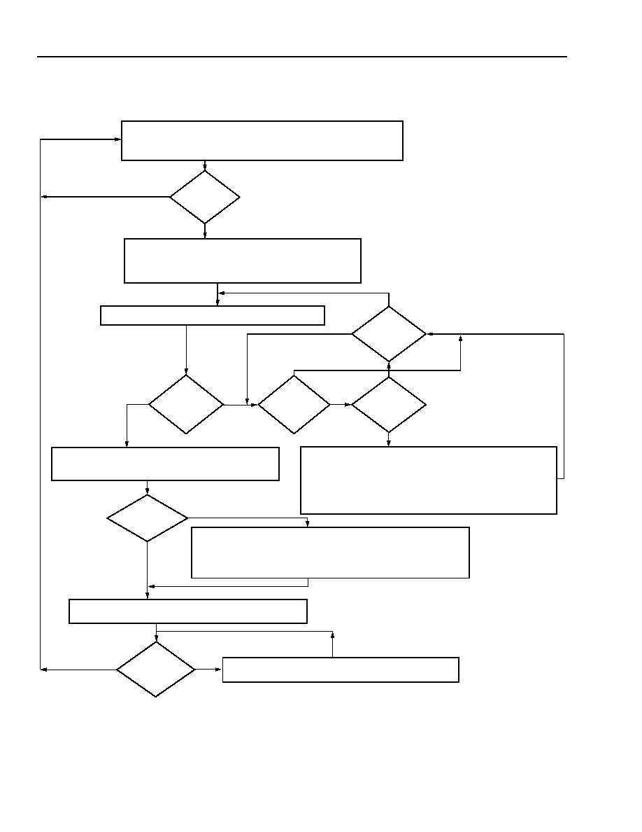
Preliminary Data Sheet
TFRA08C13 OCTAL T1/E1 Framer
October 2000
52
Lucent Technologies Inc.
Lucent Technologies Inc.
Frame Formats
(continued)
5-3909(F).er.2
Figure 13. Receive CRC-4 Multiframe Search Algorithm Using the 100 ms Internal Timer
∑ SET E BITS ACCORDING TO ITU REC. G.704, SECTION 2.3.3.4
OUT OF PRIMARY BFA:
∑ OPTIONALLY DISABLE TRAFFIC BY TRANSMITTING AIS TO THE SYSTEM
∑ OPTIONALLY TRANSMIT A = 1 AND E = 0 TO LINE
∑ INHIBIT INCOMING CRC-4 PERFORMANCE MONITORING
BFA SEARCH?
IN PRIMARY BFA:
∑ ENABLE TRAFFIC TO THE SYSTEM
∑ TRANSMIT A = 0 AND OPTIONALLY E = 0 TO THE LINE
∑ START 8 ms AND 100 ms TIMERS
∑ ENABLE PRIMARY BFA LOSS CHECKING PROCESS
CRC-4 MFA SEARCH (ITU REC. G.706, SECTION 4.2 -
NOTE 2)
CAN CRC-4
MFA BE FOUND
IN 8 ms?
PARALLEL
BFA SEARCH
100 ms
TIMER
ELAPSED?
YES
NO
NO
NO
YES
YES
ASSUME CRC-4 MULTIFRAME ALIGNMENT:
∑ CONFIRM PRIMARY BFA ASSOCIATED WITH CRC-4 MFA
∑ ADJUST PRIMARY BFA IF NECESSARY
SET 100 ms TIMER EXPIRATION STATUS BIT TO THE 1 STATE:
∑ OPTIONALLY TRANSMIT A BIT = 1 TO THE LINE INTERFACE FOR
THE DURATION OF LTS0MFA = 1
∑ OPTIONALLY TRANSMIT AIS TO THE SYSTEM INTERFACE FOR THE
START CRC-4 PERFORMANCE MONITORING:
∑ SET E BITS ACCORDING TO ITU REC. G.704, SECTION 2.3.3.4
CRC-4
COUNT > 914
IN 1 SECOND OR
CONTINUE CRC-4 PERFORMANCE MONITORING:
YES
YES
NO
NO
DURATION OF LTS0MFA = 1
IS 100 ms TRX = 1
?
YES
NO
SET INTERNAL 100 ms TIMER EXPIRATION STATUS BIT TO 0:
∑ IF TRANSMITTING A BIT = 1 TO THE LINE INTERFACE, TRANSMIT A BIT = 0
∑ IF TRANSMITTING AIS TO THE SYSTEM INTERFACE, ENABLE DATA
TRANSMISSION TO THE SYSTEM INTERFACE
LFA = 1?
GOOD?
IS
?
YES
NO
100 ms TRX = 1
INTERNAL
SET INTERNAL 100 ms TIMER EXPIRATION STATUS BIT TO 1:
PRIMARY
∑ IF TRANSMITTING E = 0 TO THE LINE INTERFACE, TRANSMIT E BIT = 1
∑ OPTIONALLY TRANSMIT E BIT = 0 TO THE LINE INTERFACE FOR
THE DURATION OF LTSOMFA = 1

Lucent Technologies Inc.
53
Preliminary Data Sheet
October 2000
TFRA08C13 OCTAL T1/E1 Framer
Lucent Technologies Inc.
Frame Formats
(continued)
CRC-4 Multiframe Alignment Search Algorithm with
400 ms Timer
The CRC-4 multiframe alignment with 400 ms timer
mode is enabled by setting FRM_PR9 to 0XXX1XX1
(binary). This receive CRC-4 multiframe reframe mode
is the modified CRC-4 multiframe alignment algorithm
described in ITU Rec. 706 Annex B, where it is referred
to as CRC-4-to-non-CRC-4 equipment interworking. A
flow diagram of this algorithm is illustrated in
Figure 14. When the interworking algorithm is enabled,
it supersedes the 100 ms algorithm described on
page 51 and in Figure 13. This algorithm assumes that
a valid basic frame alignment signal is consistently
present, but the CRC-4 multiframe alignment cannot be
achieved by the end of the total CRC-4 multiframe
alignment search period of 400 ms, if the distant end is
a non-CRC-4 equipment. In this mode, the following
consequent actions are taken:
s
An indication that there is no incoming CRC-4 multi-
frame alignment signal.
s
All CRC-4 processing on the receive 2.048 Mbits/s
signal is inhibited.
s
CRC-4 data is transmitted to the distant end with
both E bits set to 0.
This algorithm allows the identification of failure of
CRC-4 multiframe alignment generation/detection, but
with correct basic framing, when interworking between
each piece of equipment having the modified CRC-4
multiframe alignment algorithm.
As described in ITU Rec. G.706 Section B.2.3:
s
A 400 ms timer is triggered on the initial recovery of
the primary basic frame alignment.
s
The 400 ms timer reset if and only if:
-- The criteria for loss of basic frame alignment as
described in ITU Rec. G.706 Section 4.1.1 is
achieved.
-- If 915 out of 1000 errored CRC-4 blocks are
detected resulting in a loss of basic frame align-
ment as described in ITU Rec. G.706 Section
4.3.2.
-- On-demand reframe is requested.
-- The receive framer is programmed to the non-
CRC-4 mode.
s
The loss of basic frame alignment checking process
runs continuously, irrespective of the state of the
CRC-4 multiframe alignment process below it.
s
A new search for frame alignment is initiated if
CRC-4 multiframe alignment cannot be achieved in
8 ms, as described in ITU Rec. G.706 Section 4.2.
This new search for basic frame alignment will not
reset the 400 ms timer or invoke consequent actions
associated with loss of the primary basic frame align-
ment. In particular, all searches for basic frame align-
ment are carried out in parallel with, and
independent of, the primary basic frame loss check-
ing process. All subsequent searches for CRC-4 mul-
tiframe alignment are associated with each basic
framing sequence found during the parallel search.
s
During the search for CRC-4 multiframe alignment,
traffic is allowed through, upon, and to be synchro-
nized to, the initially determined primary basic frame
alignment.
s
Upon detection of the CRC-4 multiframe before the
400 ms timer elapsing, the basic frame alignment
associated with the CRC-4 multiframe alignment
replaces, if necessary, the initially determined basic
frame alignment.
s
If CRC-4 multiframe alignment is not found before
the 400 ms timer elapses, it is assumed that a condi-
tion of interworking between equipment with and
without CRC-4 capability exists and the actions
described above are taken.
s
If the 2.048 Mbits/s path is reconfigured at any time,
then it is assumed that the (new) pair of path termi-
nating equipment will need to re-establish the com-
plete framing process, and the algorithm is reset.

Preliminary Data Sheet
TFRA08C13 OCTAL T1/E1 Framer
October 2000
54
Lucent Technologies Inc.
Lucent Technologies Inc.
Frame Formats
(continued)
5-3909(F).fr.3
Figure 14. Receive CRC-4 Multiframe Search Algorithm for Automatic, CRC-4/Non-CRC-4 Equipment
Interworking as Defined by ITU (From ITU Rec. G.706, Annex B.2.2 - 1991)
∑ SET E BITS ACCORDING TO ITU REC. G.704, SECTION 2.3.3.4
OUT OF PRIMARY BFA:
∑ OPTIONALLY DISABLE TRAFFIC BY TRANSMITTING AIS TO THE SYSTEM
∑ OPTIONALLY TRANSMIT A BIT = 1 AND E BIT = 0 TO LINE
∑ INHIBIT INCOMING CRC-4 PERFORMANCE MONITORING
BFA SEARCH?
IN PRIMARY BFA:
∑ ENABLE TRAFFIC NOT TRANSMITTING AIS TO THE SYSTEM
∑ TRANSMIT A = 0 AND OPTIONALLY E = 0 TO THE LINE
∑ START 400 ms TIMER
∑ ENABLE PRIMARY BFA LOSS CHECKING PROCESS
CRC-4 MFA SEARCH (ITU REC. G.706, SECTION 4.2)
CAN CRC-4
MFA BE FOUND
IN 8 ms?
PARALLEL
BFA SEARCH
400 ms
TIMER
ELAPSED?
YES
NO
NO
NO
YES
YES
ASSUME CRC-4-TO-CRC-4 INTERWORKING:
∑ CONFIRM PRIMARY BFA ASSOCIATED WITH CRC-4 MFA
∑ ADJUST PRIMARY BFA IF NECESSARY
START CRC-4 PERFORMANCE MONITORING:
∑ SET E BITS ACCORDING TO ITU REC. G.704, SECTION 2.3.3.4
CRC-4
COUNT > 914
IN 1 SECOND OR
CONTINUE CRC-4 PERFORMANCE MONITORING:
YES
YES
NO
NO
?
∑ KEEP A = 0 IN OUTGOING CRC-4 DATA
ASSUME CRC-4-TO-NON-CRC-4 INTERWORKING:
∑ TRANSMIT A BIT = 0 TO THE LINE INTERFACE
∑ STOP INCOMING CRC-4 PROCESSING
∑ CONFIRM PRIMARY BFA
∑ TRANSMIT E BIT = 0 TO THE LINE INTERFACE
∑ INDICATE "NO CRC-4 MFA"
PRIMARY
LFA = 1?

Lucent Technologies Inc.
55
Preliminary Data Sheet
October 2000
TFRA08C13 OCTAL T1/E1 Framer
Lucent Technologies Inc.
Frame Formats
(continued)
CEPT Time Slot 16 Multiframe Structure
The TFRA08C13 supports two CEPT signaling modes: channel associated signaling (CAS) or per-channel signal-
ing (PCS0 and PCS1).
Channel Associated Signaling (CAS)
The channel associated signaling (CAS) mode utilizes time slot 16 of the FAS and NOT FAS frames. The CAS for-
mat is a multiframe consisting of 16 frames where frame 0 of the multiframe contains the multiframe alignment pat-
tern of four zeros in bits 1 through 4. Table 21 illustrates the CAS multiframe of time slot 16. The TFRA08C13 can
be programmed to force the transmitted line CAS multiframe alignment pattern to be transmitted in the FAS frame
by selecting the PCS0 option or in the NOT FAS frame by selecting the PCS1 option. Alignment of the transmitted
line CAS multiframe to the CRC-4 multiframe is arbitrary.
Table 21. ITU CEPT Time Slot 16 Channel Associated Signaling Multiframe Structure
Notes:
Frame 0 bits 1--4 define the time slot 16 multiframe alignment.
X0--X2 = time slot 16 spare bits defined in FRM_PR41 bit 0--bit 2.
Y
M
= yellow alarm, time slot 16 remote multiframe alarm (RMA) bit (1 = alarm condition).
Time Slot 16
Channel
Associated
Signaling
Multiframe
Frame
Number
Bit
1
2
3
4
5
6
7
8
0
0
0
0
0
X
0
Y
M
X
1
X
2
1
A
1
B
1
C
1
D
1
A
16
B
16
C
16
D
16
2
A
2
B
2
C
2
D
2
A
17
B
17
C
17
D
17
3
A
3
B
3
C
3
D
3
A
18
B
18
C
18
D
18
4
A
4
B
4
C
4
D
4
A
19
B
19
C
19
D
19
5
A
5
B
5
C
5
D
5
A
20
B
20
C
20
D
20
6
A
6
B
6
C
6
D
6
A
21
B
21
C
21
D
21
7
A
7
B
7
C
7
D
7
A
22
B
22
C
22
D
22
8
A
8
B
8
C
8
D
8
A
23
B
23
C
23
D
23
9
A
9
B
9
C
9
D
9
A
24
B
24
C
24
D
24
10
A
10
B
10
C
10
D
10
A
25
B
25
C
25
D
25
11
A
11
B
11
C
11
D
11
A
26
B
26
C
26
D
26
12
A
12
B
12
C
12
D
12
A
27
B
27
C
27
D
27
13
A
13
B
13
C
13
D
13
A
28
B
28
C
28
D
28
14
A
14
B
14
C
14
D
14
A
29
B
29
C
29
D
29
15
A
15
B
15
C
15
D
15
A
30
B
30
C
30
D
30

Preliminary Data Sheet
TFRA08C13 OCTAL T1/E1 Framer
October 2000
56
Lucent Technologies Inc.
Lucent Technologies Inc.
Frame Formats
(continued)
CEPT Loss of Time Slot 16 Multiframe Align-
ment (LTS16MFA)
Loss of basic frame alignment forces the receive framer
into a loss of time slot 16 signaling multiframe align-
ment state. In addition, as defined in ITU Rec. G.732
Section 5.2, time slot 16 signaling multiframe is
assumed lost when two consecutive time slot 16 multi-
frame 4-bit all-zero patterns is received with an error. In
addition, the time slot 16 multiframe is assumed lost
when, for a period of two multiframes, all bits in time
slot 16 are in state 0. This state is reported by way of
the status registers FRM_SR1 bit 1. Once basic frame
alignment is achieved, the receive framer will initiate a
search for the time slot 16 multiframe alignment. During
a loss of time slot 16 multiframe alignment state, the
following occurs:
s
The updating of the signaling data is halted.
s
The received control bits forced to the binary 1 state.
s
The received remote multiframe alarm indication sta-
tus bit is forced to the binary 0 state.
s
Optionally, the transmit framer can transmit to the
line the time slot 16 signaling remote multiframe
alarm if register FRM_PR41 bit 4 is set to 1.
s
Optionally, the transmit framer can transmit the alarm
indication signal (AIS) in the system transmit time
slot 16 data if register FRM_PR44 bit 6 is set to 1.
CEPT Loss of Time Slot 16 Multiframe Align-
ment Recovery Algorithm
The time slot 16 multiframe alignment recovery algo-
rithm is as described in ITU Rec. G.732 Section 5.2.
The recommendation states that if a condition of
assumed frame alignment has been achieved, time slot
16 multiframe alignment is deemed to have occurred
when the 4-bit time slot 16 multiframe pattern of 0000
is found in time slot 16 for the first time, and the preced-
ing time slot 16 contained at least one bit in the binary
1 state.
CEPT Time Slot 0 FAS/NOT FAS Control
Bits
FAS/NOT FAS Si- and E-Bit Source
The Si bit can be used as an 8 kbits/s data link to and
from the remote end, or in the CRC-4 mode, it can be
used to provide added protection against false frame
alignment. The sources for the Si bits that are transmit-
ted to the line are the following:
s
CEPT with no CRC-4 and FRM_PR28 bit 0 = 1: the
TSiF control bit (FRM_PR28 bit 1) is transmitted in
bit 1 of all FAS frames and the TSiNF control bit
(FRM_PR28 bit 2) is transmitted in bit 1 of all NOT
FAS frames.
s
The CHI system interface (CEPT with no CRC-4 and
FRM_PR28 bit 0 = 0)
*
.
s
This option requires the received system data (RCHI-
DATA) to maintain a biframe alignment pattern where
frames containing Si bit information for the NOT FAS
frames have bit 2 of time slot 0 in the binary 1 state
followed by frames containing Si bit information for
the FAS frames that have bit 2 of time slot 0 in the
binary 0 state. This ensures the proper alignment of
the Si received system data to the transmit line Si
data. Whenever this requirement is not met by the
system, the transmit framer will enter a loss of
biframe alignment condition (indication is given in the
status registers) and then search for the pattern; in
the loss of biframe alignment state, transmitted line
data is corrupted (only when the system interface is
sourcing Sa or Si data). When the transmit framer
locates a new biframe alignment pattern, an indica-
tion is given in the status registers and the transmit
framer resumes normal operations.
* Whenever bits (e.g., Si, Sa, etc.) are transmitted from the system
transparently, FRM_PR29 must first be momentarily written to
001xxxxx (binary). Otherwise, the transmit framer will not be able
to locate the biframe alignment.

Lucent Technologies Inc.
57
Preliminary Data Sheet
October 2000
TFRA08C13 OCTAL T1/E1 Framer
Lucent Technologies Inc.
CEPT Time Slot 0 FAS/NOT FAS Control
Bits
(continued)
s
CEPT with CRC-4
1
: manual transmission of E bit = 0:
-- If FRM_PR28 bit 0 = 0, then the TSiF bit
(FRM_PR28 bit 1) is transmitted in bit 1 of frame
13 (E bit) and the TSiNF bit (FRM_PR28 bit 2) is
transmitted in bit 1 of frame 15 (E bit).
-- If FRM_PR28 bit 0 = 1, then each time 0 is written
into TSiF (FRM_PR28 bit 1) one E bit = 0 is trans-
mitted in frame 13, and each time 0 is written into
TSiNF (FRM_PR28 bit 2) one E bit = 0 is transmit-
ted in frame 15.
s
CEPT with CRC-4
1
, automatic transmission of
E bit = 0:
-- Optionally, one transmitted E bit is set to 0 by the
transmit framer, as described in ITU Rec. G.704
Section 2.3.3.4, for each received errored CRC-4
submultiframe detected by the receive framer if
FRM_PR28 bit 3 = 1.
-- Optionally, as described in ITU Rec. G.704 Sec-
tion 2.3.3.4, both E bits are set to 0 while in a
received loss of CRC-4 multiframe alignment
state
2
if FRM_PR28 bit 4 = 1.
-- Optionally, when the 100 ms or 400 ms timer is
enabled and the timer has expired, as described
in ITU Rec. G.706 Section B.2.2, both E bits are
set to 0 for the duration of the loss of CRC-4 multi-
frame alignment state
2
if FRM_PR28 bit 5 = 1.
Otherwise, the E bits are transmitted to the line in the 1
state.
NOT FAS A-Bit (CEPT Remote Frame Alarm)
Sources
The A bit, as described in ITU Rec. G.704 Section
2.3.2, Table 4a/G.704, is the remote alarm indication
bit. In undisturbed conditions, this bit is set to 0 and
transmitted to the line. In the loss of frame alignment
(LFA) state, this bit may be set to 1 and transmitted to
the line as determined by register FRM_PR27. The A
bit is set to 1 and transmitted to the line for the following
conditions:
s
Setting the transmit A bit = 1 control bit by setting
register FRM_PR27 bit 7 to 1.
s
Optionally for the following alarm conditions as
selected through programming register FRM_PR27.
-- The duration of loss of basic frame alignment as
described in ITU Rec. G.706 Section 4.1.1
3
, or
ITU Rec. G.706 Section 4.3.2
4
if register
FRM_PR27 bit 0 = 1.
-- The duration of loss of CRC-4 multiframe align-
ment if register FRM_PR27 bit 2 = 1.
-- The duration of loss of signaling time slot 16 multi-
frame alignment if register FRM_PR27 bit 1 = 1.
-- The duration of loss of CRC-4 multiframe align-
ment after either the 100 ms or 400 ms timer
expires if register FRM_PR27 bit 3 = 1.
-- The duration of receive Sa6_8hex
5
if register
FRM_PR27 bit 4 = 1.
-- The duration of receive Sa6_Chex
5
if register
FRM_PR27 bit 5 = 1.
NOT FAS Sa-Bit Sources
6
The Sa bits, Sa4--Sa8, in the NOT FAS frame can be a
4 kbits/s data link to and from the remote end. The
sources and value for the Sa bits are as follows:
s
The Sa source register FRM_PR29 bit 0--bit 4 if
FRM_PR29 bit 7--bit 5 = 000 (binary) and
FRM_PR30 bit 4--bit 0 = 11111 (binary).
s
The facility data link external input (TFDL) if register
FRM_PR29 bit 7 = 1 and register FRM_PR21
bit 6 = 1.
s
The internal FDL-HDLC if register FRM_PR29
bit 7 = 1 and register FRM_PR21 bit 6 = 0.
s
The Sa transmit stack if register FRM_PR29
bit 7--bit 5 are set to 01x (binary).
1.
The receive E-bit processor will halt the monitoring of received E
bits during loss of CRC-4 multiframe alignment.
2. Whenever loss of frame alignment occurs, then loss of CRC-4
multiframe alignment is forced. Once frame alignment is estab-
lished, then and only then, is the search for CRC-4 multiframe
alignment initiated. The receive framer unit, when programmed for
CRC-4, can be in a state of LFA and LTS0MFA or in a state of
LTS0MFA only, but cannot be in a state of LFA only.
3. LFA is due to framing bit errors.
4. LFA is due to detecting 915 out of 1000 received CRC-4 errored
blocks.
5. See Table 29 . Sa6 Bit Coding Recognized by the Receive Framer,
for a definition of this Sa6 pattern.
6. Whenever bits (e.g., Si, Sa, etc.) are transmitted from the system
transparently, FRM_PR29 must first be momentarily written to
001xxxxx (binary). Otherwise, the transmit framer will not be able
to locate the biframe alignment.
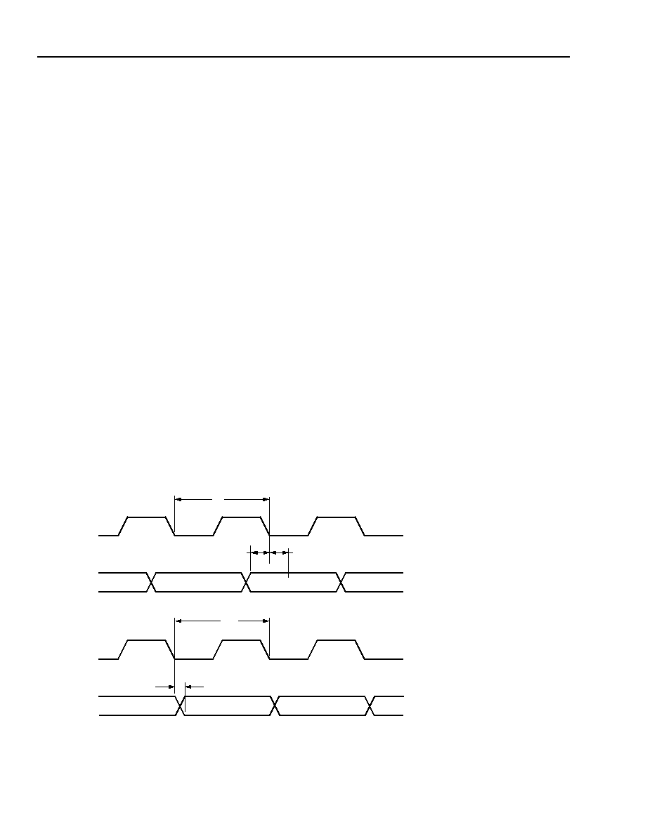
58
58
Lucent Technologies Inc.
Preliminary Data Sheet
TFRA08C13 OCTAL T1/E1 Framer
October 2000
Lucent Technologies Inc.
CEPT Time Slot 0 FAS/NOT FAS Control
Bits
(continued)
s
The CHI system interface if register FRM_PR29 bit
7--bit 5 are set to 001 (binary). This option requires
the received system data (RCHIDATA) to maintain a
biframe alignment pattern where (1) frames contain-
ing Sa bit information have bit 2 of time slot 0 in the
binary 1 state and (2) these NOT FAS frames are fol-
lowed by frames not containing Sa bit information,
the FAS frames, which have bit 2 of time slot 0 in the
binary 0 state. This ensures the proper alignment of
the Sa received system data to the transmit line Sa
data. Whenever this requirement is not met by the
system, the transmit framer will enter a loss of
biframe alignment condition indicated in the status
register, FRM_SR1 bit 4, and then search for the pat-
tern. In the loss of biframe alignment state, transmit-
ted line data is corrupted (only when the system
interface is sourcing Sa or Si data). When the trans-
mit framer locates a new biframe alignment pattern,
an indication is given in the status registers and the
transmit framer resumes normal operations.
The receive Sa data is present at the following:
s
The Sa received stack, registers FRM_SR54--
FRM_SR63, if the TFRA08C13 is programmed in the
Sa stack mode.
s
The system transmit interface.
The status of the received Sa bits and the received Sa
stack is available in status register FRM_SR4. The
transmit and receive Sa bit for the FDL can be selected
by setting register FRM_PR43 bit 0--bit 2 as shown in
Table 148.
Sa Facility Data Link Access
The data link interface may be used to source one of
the Sa bits. Access is controlled by registers
FRM_PR29, FRM_PR30, and FRM_PR43, see NOT
FAS Sa-Bit Sources on page 57. The receive Sa data is
always present at the receive facility data link output
pin, RFDL, along with a valid clock signal at the receive
facility clock output pin, RFDLCK. During a loss of
frame alignment (LFA) state, the RFDL signal is forced
to a 1 state while RFDLCK continues to toggle on the
previous frame alignment. When basic frame alignment
is found, RFDL is as received from the selected receive
Sa bit position and RFDLCK is forced (if necessary) to
the new alignment. The data rate for this access mode
is 4 kHz. The access timing for the transmit and receive
facility data is illustrated in Figure 15 below. During loss
of receive clock (LOFRMRLCK), RFDL and RFDLCK
are frozen in a state at the point of the LOFRMRLCK
being asserted.
5-3910(F).dr.1
Figure 15. Facility Data Link Access Timing of the Transmit and Receive Framer Sections
in the CEPT Mode
t8
t9
t9
t10
t11
t8: TFDLCK CYCLE = 250
µ
s
t9: TFDL TO TFDLCK SETUP/HOLD = 40 ns
t10: RFDLCK CYCLE = 250
µ
s
t11: RFDLCK TO RFDL DELAY = 40 ns
TFDLCK
TFDL
RFDLCK
RFDL

Lucent Technologies Inc.
59
Preliminary Data Sheet
October 2000
TFRA08C13 OCTAL T1/E1 Framer
Lucent Technologies Inc.
CEPT Time Slot 0 FAS/NOT FAS Control Bits
(continued)
NOT FAS Sa Stack Source and Destination
The transmit Sa4 to Sa8 bits may be sourced from the transmit Sa stack, registers FRM_PR31--FRM_PR40. The
Sa stack consists of ten 8-bit registers that contain 16 NOT FAS frames of Sa information as shown in Table 22.
The transmit stack data may be transmitted either in non-CRC-4 mode or in CRC-4 mode to the line.
The receive stack data, registers FRM_SR54--FRM_SR63, is valid in both the non-CRC-4 mode and the CRC-4
mode. In the non-CRC-4 mode while in the loss of frame alignment (LFA) state, updating of the receive Sa stack is
halted and the transmit and receive stack interrupts are deactivated. In the CRC-4 mode while in the loss of time
slot 0 multiframe alignment (LTS0MFA) state, updating of the receive Sa stack is halted and the transmit and
receive stack interrupts are deactivated.
Table 22. Transmit and Receive Sa Stack Structure
The most significant bit of the first byte is transmitted to the line in frame 1 of a double CRC-4 multiframe. The least
significant bit of the second byte is transmitted to the line in frame 31 of the double CRC-4 multiframe. The protocol
for accessing the Sa Stack information for the transmit and receive Sa4 to Sa8 bits is shown in Figure 16 and
described briefly below.
The device indicates that it is ready for an update of its transmit stack by setting register FRM_SR4 bit 7 (CEPT
transmit Sa stack ready) high. At this time, the system has about 4 ms to update the stack. Data written to the stack
during this interval will be transmitted during the next double CRC-4 multiframe. By reading register FRM_SR4
bit 7, the system clears this bit so that it can indicate the next time the transmit stack is ready. If the transmit stack
is not updated, then the content of the stack is retransmitted to the line. The 32-frame interval of the transmit framer
in the non-CRC-4 mode is arbitrary. Enabling transmit CRC-4 mode forces the updating of the internal transmit
stack at the end of the 32-frame CRC-4 double multiframe; the transmit Sa stack is then transmitted synchronous
to the transmit CRC-4 multiframe structure.
On the receive side, the TFRA08C13 indicates that it has received data in the receive Sa stack, register
FRM_SR54--FRM_SR63, by setting register FRM_SR4 bit 6 (CEPT receive Sa stack ready) high. The system
then has about 4 ms to read the contents of the stack before it is updated again (old data lost). By reading register
FRM_SR4 bit 6, the system clears this bit so that it can indicate the next time the receive stack is ready. The
receive framer always updates the content of the receive stack so unread data will be overwritten. The last 16 valid
Sa4 to Sa8 bits are always stored in the receive Sa stack on a double-multiframe boundary. The 32-frame interval
of the receive framer in the non-CRC-4 mode is arbitrary. Enabling the receive CRC-4 mode forces updating of the
receive Sa stack at the end of the 32-frame CRC-4 double multiframe. The receive Sa stack is received synchro-
nous to the CRC-4 multiframe structure.
Register
Number
Bit 7
(MSB)
Bit 6
Bit 5
Bit 4
Bit 3
Bit 2
Bit 1
+
Bit 0
(LSB)
1
Sa4-1
Sa4-3
Sa4-5
Sa4-7
Sa4-9
Sa4-11
Sa4-13
Sa4-15
2
Sa4-17
Sa4-19
Sa4-21
Sa4-23
Sa4-25
Sa4-27
Sa4-29
Sa4-31
3
Sa5-1
Sa5-3
Sa5-5
Sa5-7
Sa5-9
Sa5-11
Sa5-13
Sa5-15
4
Sa5-17
Sa5-19
Sa5-21
Sa5-23
Sa5-25
Sa5-27
Sa5-29
Sa5-31
5
Sa6-1
Sa6-3
Sa6-5
Sa6-7
Sa6-9
Sa6-11
Sa6-13
Sa6-15
6
Sa6-17
Sa6-19
Sa6-21
Sa6-23
Sa6-25
Sa6-27
Sa6-29
Sa6-31
7
Sa7-1
Sa7-3
Sa7-5
Sa7-7
Sa7-9
Sa7-11
Sa7-13
Sa7-15
8
Sa7-17
Sa7-19
Sa7-21
Sa7-23
Sa7-25
Sa7-27
Sa7-29
Sa7-31
9
Sa8-1
Sa8-3
Sa8-5
Sa8-7
Sa8-9
Sa8-11
Sa8-13
Sa8-15
10 Sa8-17
Sa8-19
Sa8-21
Sa8-23
Sa8-25
Sa8-27
Sa8-29
Sa8-31

Preliminary Data Sheet
TFRA08C13 OCTAL T1/E1 Framer
October 2000
60
Lucent Technologies Inc.
Lucent Technologies Inc.
CEPT Time Slot 0 FAS/NOT FAS Control Bits
(continued)
5-3911(F).c
Figure 16. Transmit and Receive Sa Stack Accessing Protocol
SYSTEM ACCESS Sa STACK (SASS) INTERVAL:
TRANSMIT FRAMER UNIT TRANSMITS TO THE LINE
THE DATA IN THE TRANSMIT Sa STACK WRITTEN DURING
THE PREVIOUS SASS INTERVAL.
THE SYSTEM CAN UPDATE THE TRANSMIT Sa STACK
REGISTERS FOR TRANSMISSION IN THE NEXT CRC-4
DOUBLE MULTIFRAME.
THE SYSTEM CAN READ THE RECEIVE Sa STACK REGISTERS
TO ACCESS THE Sa BITS EXTRACTED DURING THE PREVIOUS
VALID (IN MULTIFRAME ALIGNMENT) DOUBLE CRC-4
MULTIFRAME.
START OF CRC-4 DOUBLE MULTIFRAME:
∑ BASIC FRAME ALIGNMENT FOUND, OR,
∑ CRC-4 MULTIFRAME ALIGNMENT FOUND.
1)
2)
3)
31 FRAMES
SYSTEM ACCESS Sa STACK INTERVAL
CRC-4 DOUBLE MULTIFRAME
START FRAME 1 OF 32 IN DMF.
INTERNAL Sa STACK UPDATE INTERVAL
31 FRAMES
1-FRAME INTERVAL
CRC-4 DOUBLE MULTIFRAME: 32 FRAMES
SYSTEM ACCESS IS DISABLED DURING THIS INTERVAL:
THE INTERNAL TRANSMIT Sa STACK IS UPDATED
FROM THE FRAMER UNIT'S 10-byte TRANSMIT STACK CONTROL
REGISTERS DURING THIS 1-FRAME INTERVAL.
ACCESS TO THE STACK CONTROL REGISTERS IS DISABLED
DURING THIS 1-FRAME INTERVAL.
1)
2)
ONCE LOADED, THE INFORMATION IN THE INTERNAL TRANSMIT
Sa STACK IS TRANSMITTED TO THE LINE DURING THE NEXT
CRC-4 DOUBLE MULTIFRAME, ALIGNED TO THE CRC-4 MULTIFRAME.
IF THE TRANSMIT Sa STACK IS NOT UPDATED, THEN THE
CONTENT OF THE TRANSMIT Sa STACKS IS RETRANSMITTED
TO THE LINE.
THE SYSTEM READ-ONLY RECEIVE STACK IS UPDATED FROM
THE INTERNAL RECEIVE STACK INFORMATION REGISTERS.
IN NON-CRC-4 MODE, THE RECEIVE Sa STACK EXTRACTING
CIRCUITRY ASSUMES AN ARBITRARY DOUBLE 16-FRAME MULTIFRAME STRUCTURE
(32 FRAMES), AND DATA IS EXTRACTED ONLY IN THE FRAME ALIGNED STATE.
IN CRC-4 MODE, THE RECEIVE Sa STACK INFORMATION IS ALIGNED
TO A CRC-4 DOUBLE MULTIFRAME STRUCTURE (32 FRAMES), AND THE
DATA IS EXTRACTED ONLY IN CRC-4 MULTIFRAME ALIGNED STATE.
1 FRAME
3)
4)
5)
6)
7)
(DMF): 32 FRAMES

Lucent Technologies Inc.
61
Preliminary Data Sheet
October 2000
TFRA08C13 OCTAL T1/E1 Framer
Lucent Technologies Inc.
CEPT Time Slot 0 FAS/NOT FAS Control
Bits
(continued)
Interrupts indicating that the transmit Sa stack or the
receive Sa stack are ready for system access are avail-
able, see register FRM_SR4 bit 6 and bit 7.
CEPT Time Slot 16 X0--X2 Control Bits
Each of the three X bits in frame 0 of the time slot 16
multiframe can be used as a 0.5 kbits/s data link to and
from the remote end. The transmitted line X bits are
sourced from control register FRM_PR41 bit 0--bit 2.
In the loss of TS16 multiframe alignment (LTS16MFA)
state, receive X bits are set to 1 in status register
FRM_SR53.
Signaling Access
Signaling information can be accessed by three differ-
ent methods: transparently through the CHI, via the
control registers, or via the CHI associated signaling
mode.
Transparent Signaling
This mode is enabled by setting register FRM_PR44 bit
0 to 1.
Data at the received RCHIDATA interface passes
through the framer undisturbed. The framer generates
an arbitrary signaling multiframe in the transmit and
receive directions to facilitate the access of signaling
information at the system interface.
DS1: Robbed-Bit Signaling
Microprocessor Control Registers
To enable signaling, register FRM_PR44 bit 0 must be
set to 0 (default).
The information written into the F and G bits of the
transmit signaling registers, FRM_TSR0--
FRM_TSR23, define the robbed-bit signaling mode for
each channel for both the transmit and receive direc-
tions. The per-channel programming allows the system
to combine voice channels with data channels within
the same frame.
The receive-channel robbed-bit signaling mode is
always defined by the state of the F and G bits in the
corresponding transmit signaling registers for that
channel. The received signaling data is stored in the
receive signaling registers, FRM_RSR0--
FRM_RSR23, while receive framer is in both the frame
and superframe alignment states. Updating the receive
signaling registers can be inhibited on-demand, by set-
ting register FRM_PR44 bit 3 to 1, or automatically
when either a framing error event, a loss of frame, or
superframe alignment state is detected or a controlled
slip event occurs. The signaling inhibit state is valid for
at least 32 frames after any one of the following: a
framing errored event, a loss of frame and/or super-
frame alignment state, or a controlled slip event.
In the common channel signaling mode, data written in
the transmit signaling registers is transmitted in chan-
nel 24 of the transmit line bit stream. The F and G bits
are ignored in this mode. The received signaling data
from channel 24 is stored in receive signaling registers
FRM_RSR0--FRM_RSR23 for T1.
Associated Signaling Mode
This mode is enabled by setting register FRM_PR44 bit
2 to 1.
Signaling information in the associated signaling mode
(ASM) is allocated an 8-bit system time slot in conjunc-
tion with the payload data information for a particular
channel. The default system data rate in the ASM
mode is 4.096 Mbits/s. Each system channel consists
of an 8-bit payload time slot followed by its correspond-
ing 8-bit signaling time slot. The format of the signaling
byte is identical to that of the signaling registers.
In the ASM mode, writing the transmit signaling regis-
ters will corrupt the transmit signaling data. In the trans-
mit signaling register ASM (TSR-ASM) format, enabled
by setting register FRM_PR44 bit 2 and bit 5 to 1, the
system must write into the F and G bit
*
of the transmit
signaling registers to program the robbed-bit signaling
state mode of each DS0. The ABCD bits are sourced
from the RCHI ports when TSR-ASM mode is enabled.
* All other bits in the signaling registers are ignored, while the F and
G bits in the received RCHIDATA stream are ignored.

Preliminary Data Sheet
TFRA08C13 OCTAL T1/E1 Framer
October 2000
62
Lucent Technologies Inc.
Lucent Technologies Inc.
Signaling Access
(continued)
Table 23 illustrates the ASM time-slot format for valid channels.
Table 23. Associated Signaling Mode CHI 2-Byte Time-Slot Format for DS1 Frames
* X indicates bits that are undefined by the framer.
The identical sense of the received system P bit in the transmitted signaling data is echoed back to the system in the received
signaling information.
The DS1 framing formats require rate adaptation from the line-interface 1.544 Mbits/s bit stream to the system-
interface 4.096 Mbits/s bit stream. The rate adaptation results in the need for stuffed time slots on the system inter-
face. Table 24 illustrates the ASM format for T1 stuffed channels used by the TFRA08C13. The stuffed data byte
contains the programmable idle code in register FRM_PR23 (default = 7F (hex)), while the signaling byte is
ignored.
Table 24. Associated Signaling Mode CHI 2-Byte Time-Slot Format for Stuffed Channels
* X indicates bits which are undefined by the framer.
CEPT: Time Slot 16 Signaling
Microprocessor Control Registers
To enable signaling, register FRM_PR44 bit 0 must be set to 0 (default).
The information written into transmit signaling control registers FRM_TSR0--FRM_TSR31 define the state of the
ABCD bits of time slot 16 transmitted to the line.
The received signaling data from time slot 16 is stored in receive signaling registers FRM_RSR0--FRM_RSR31.
Associated Signaling Mode
Signaling information in the associated signaling mode (ASM), register FRM_PR44 bit 2 = 1, is allocated an 8-bit
system time slot in conjunction with the data information for a particular channel. The default system data rate in
the ASM mode is 4.096 Mbits/s. Each system channel consists of an 8-bit payload time slot followed by its associ-
ated 8-bit signaling time slot. The format of the signaling byte is identical to the signaling registers.
Table 25 illustrates the ASM time-slot format for valid CEPT E1 time slots
Table 25. Associated Signaling Mode CHI 2-Byte Time-Slot Format for CEPT
* In the CEPT formats, these bits are undefined.
The P bit is the parity-sense bit calculated over the 8 data bits, the ABCD (and E) bits, and the P bit. The identical sense of the received
system P bit in the transmitted signaling data is echoed back to the system in the received signaling information.
DS1: ASM CHI Time Slot
PAYLOAD DATA
SIGNALING INFORMATION*
1
2
3
4
5
6
7
8
A
B
C
D
X
F
G
P
ASM CHI Time Slot
PAYLOAD DATA
SIGNALING INFORMATION*
0
1
1
1
1
1
1
1
X
X
X
X
X
X
X
X
CEPT ASM CHI Time Slot
PAYLOAD DATA
SIGNALING INFORMATION
1
2
3
4
5
6
7
8
A
B
C
D
E
X
*
X
*
P
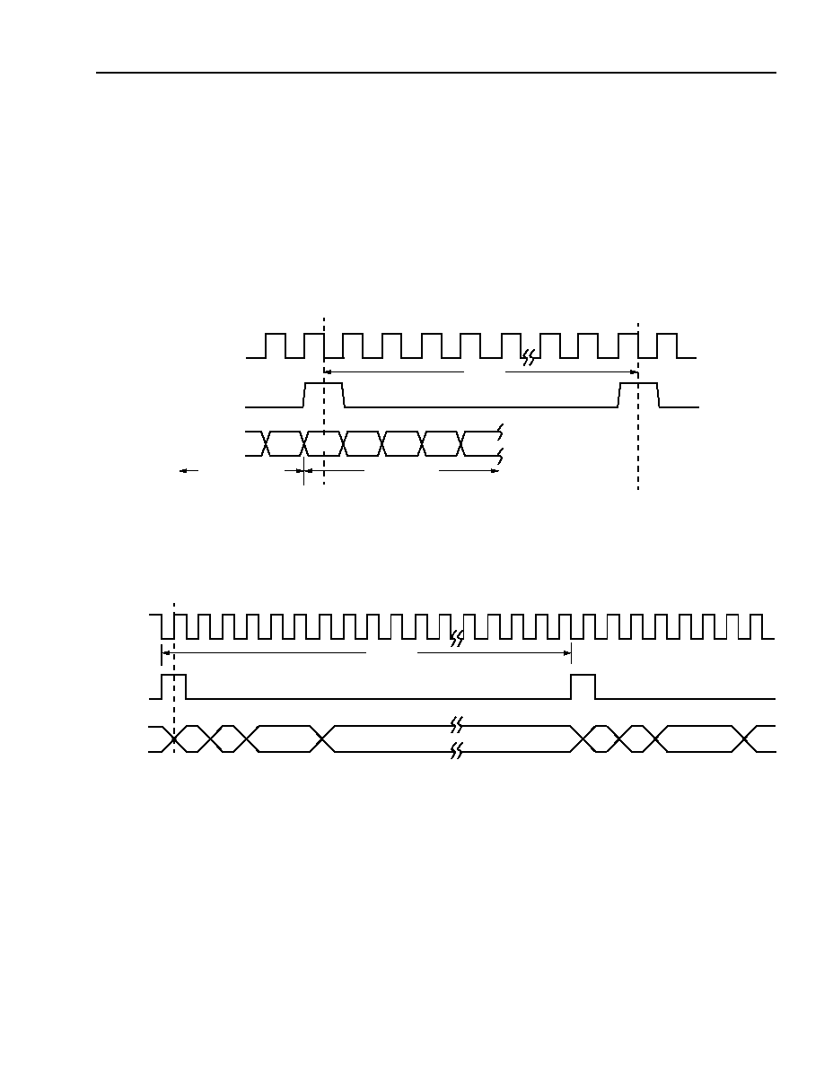
Lucent Technologies Inc.
63
Preliminary Data Sheet
October 2000
TFRA08C13 OCTAL T1/E1 Framer
Lucent Technologies Inc.
Auxiliary Framer I/O Timing
Transmit and receive timing and data signals are provided by terminals RFRMCK (receive framer clock), RFRM-
DATA (receive framer data), RFS (receive frame sync), RSSFS (receive framer signaling superframe sync), RCRC-
MFS (receive frame CRC-4 multiframe sync), TFS (transmit framer frame sync), TSSFS (transmit framer signaling
superframe sync), TCRCMFS (transmit framer CRC-4 multiframe sync).
The receive signals are synchronized to the recovered receive line clock, RLCK, and the transmit signals are syn-
chronized to the transmit line clock, TLCK. Note that TLCK must be phase locked to the CHI clock, CHICK, see
Table 2. Pin Descriptions, pin D18.
Detailed timing specifications for these signals are given in Figure 17--Figure 24.
5-6290(F)r.6
Figure 17. Timing Specification for RFRMCK, RFRMDATA, and RFS in DS1 Mode
5-6292(F)r.7
Figure 18. Timing Specification for TFS, TLCK, and TPD in DS1 Mode
RFRMCK
RFS
RFRMDATA
TIME SLOT 1
TIME SLOT 24
BIT 7
BIT 1
DATA VALID
BIT 0
125
µ
s
TLCK
TFS
TPD
TS1
125
µ
s
TS1
(SINGLE
RAIL)
TS2
TS24
F
BIT
BIT 0
(MSB)
F
BIT
BIT 0
(MSB)
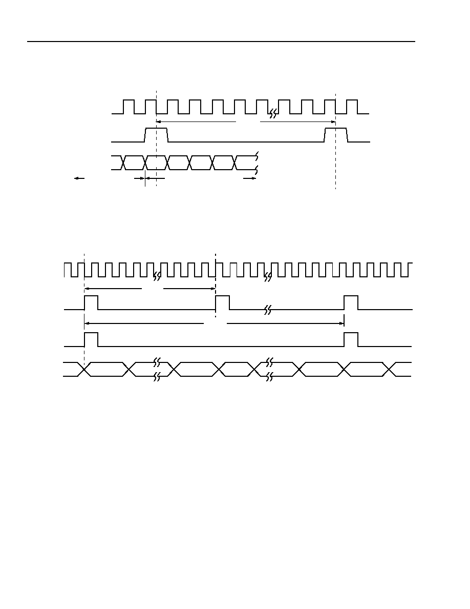
Preliminary Data Sheet
TFRA08C13 OCTAL T1/E1 Framer
October 2000
64
Lucent Technologies Inc.
Lucent Technologies Inc.
Auxiliary Framer I/O Timing
(continued)
5-6294(F)r.6
Figure 19. Timing Specification for RFRMCK, RFRMDATA, and RFS in CEPT Mode
5-6295(F)r.8
Figure 20. Timing Specification for RFRMCK, RFRMDATA, RFS, and RSSFS in CEPT Mode
RFRMCK
RFS
RFRMDATA
FAS/NFAS: TIME SLOT 0
TIME SLOT 31
BIT 7
BIT 1
DATA VALID
BIT 0
125
µ
s
RFRMCK
RFS
RSSFS
RFRMDATA
TS0 OF THE FRAME AFTER THE
FRAME CONTAINING THE
2 ms
SIGNALING MULTIFRAME
PATTERN (0000)
TS0 OF THE FRAME AFTER THE
FRAME CONTAINING THE
SIGNALING MULTIFRAME
PATTERN (0000)
125
µ
s
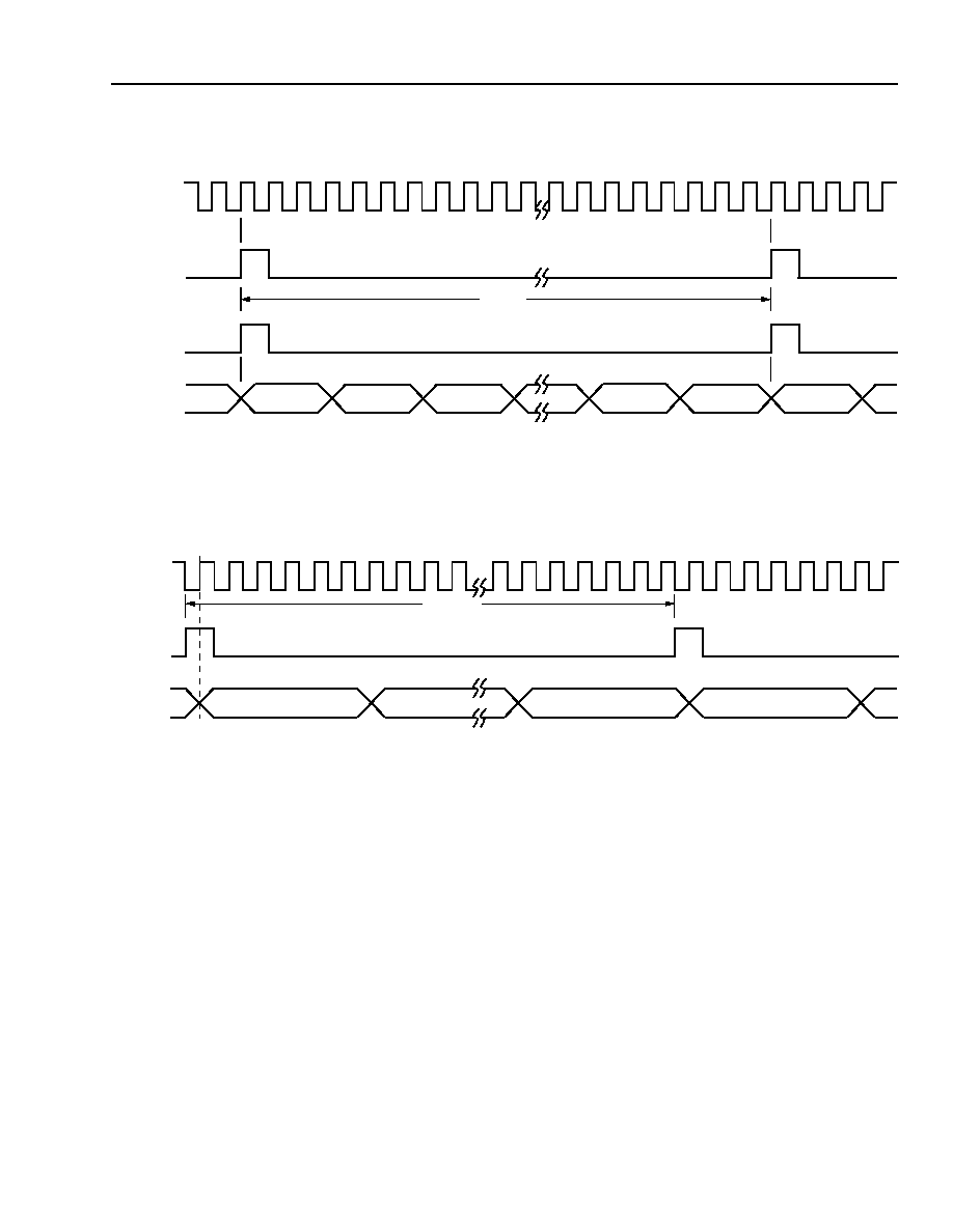
Lucent Technologies Inc.
65
Preliminary Data Sheet
October 2000
TFRA08C13 OCTAL T1/E1 Framer
Lucent Technologies Inc.
Auxiliary Framer I/O Timing
(continued)
5-6296(F)r.5
Figure 21. Timing Specification for RCRCMFS in CEPT Mode
5-6297(F)r.5
Figure 22. Timing Specification for TFS, TLCK, and TPD in CEPT Mode
RFRMCLK
RFS
RCRCMFS
RFRMDATA
TS0 OF FRAME #0
OF MULTIFRAME
TS0 OF FRAME #0
OF MULTIFRAME
2 ms
TLCK
TFS
TPD
TS0 OF FRAME X
125
µ
s
TS0 OF FRAME X + 1
(SINGLE
RAIL)
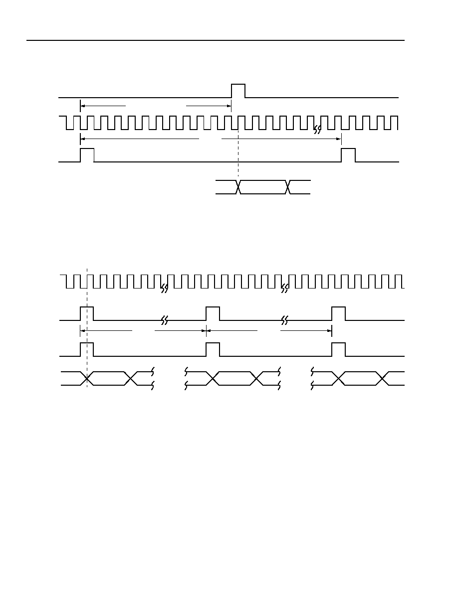
Preliminary Data Sheet
TFRA08C13 OCTAL T1/E1 Framer
October 2000
66
Lucent Technologies Inc.
Lucent Technologies Inc.
Auxiliary Framer I/O Timing
(continued)
5-6298(F)r.5
Figure 23. Timing Specification for TFS, TLCK, TPD, and TSSFS in CEPT Mode
5-6299(F)r.5
Figure 24. Timing Specification for TFS, TLCK, TPD, and TCRCMFS in CEPT Mode
TFS
TLCK
TSSFS
TPD
(SINGLE
TS0 OF THE FRAME
2 ms
11 CLOCK CYCLES
CONTAINING THE SIGNALING
MULTIFRAME PATTERN (0000)
RAIL)
TLCK
TFS
TCRCMFS
TPD
(SINGLE
TS0 OF FRAME #8
1 ms
OF MULTIFRAME
RAIL)
TS0 OF FRAME #0
OF MULTIFRAME
TS0 OF FRAME #0
OF MULTIFRAME
1 ms
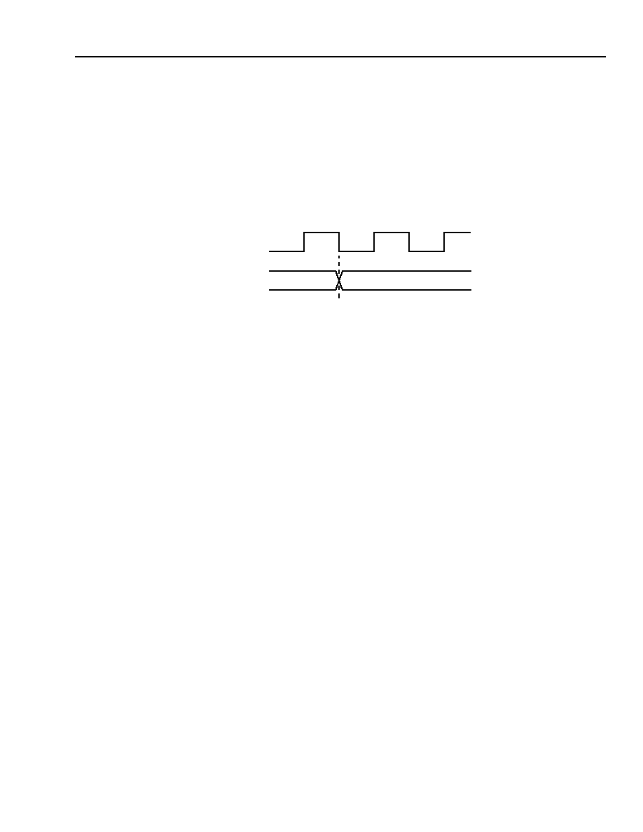
Lucent Technologies Inc.
67
Preliminary Data Sheet
October 2000
TFRA08C13 OCTAL T1/E1 Framer
Lucent Technologies Inc.
Alarms and Performance Monitoring
Interrupt Generation
A global interrupt (pin AD8) may be generated if enabled by register GREG1. This interrupt is clocked using chan-
nel 1 framer receive line clock (RLCK1). If RLCK1 is absent, the interrupt is clocked using RLCK2, the receive line
clock of channel 2. If both RLCK1 and RLCK2 are absent, clocking of interrupts is controlled by an interval
2.048 MHz clock generated from the CHI clock. Timing of the interrupt is shown in Figure 25. There is no relation
between MPCK (pin AE10) and the interrupt, i.e., MPCK maybe asynchronous with any of the other TFRA08C13
clocks.
5-6563(F).ar.1
Figure 25. Relation Between RLCK1 and Interrupt (Pin AD8)
Alarm Definition
The receive framer monitors the receive line data for alarm conditions and errored events, and then presents this
information to the system through the microprocessor interface status registers. The transmit framer, to a lesser
degree, monitors the receive system data and presents the information to the system through the microprocessor
interface status registers. Updating of the status registers is controlled by the receive line clock signal. When the
receive loss of clock monitor determines that the receive line clock signal is lost, the system clock is used to clock
the status registers and all status information should be considered corrupted.
Although the precise method of detecting or generating alarm and error signals differs between framing modes, the
functions are essentially the same. The alarm conditions monitored on the received line interface are:
s
Red alarm or the loss of frame alignment indication (FRM_SR1 bit 0). The red alarm indicates that the receive
frame alignment for the line has been lost and the data cannot be properly extracted. The red alarm is indicated
by the loss of frame condition for the various framing formats as defined in Table 26.
RLCK1
INTERRUPT
(PIN AD8)

Preliminary Data Sheet
TFRA08C13 OCTAL T1/E1 Framer
October 2000
68
Lucent Technologies Inc.
Lucent Technologies Inc.
Alarms and Performance Monitoring
(continued)
Table 26. Red Alarm or Loss of Frame Alignment Conditions
s
Yellow alarm or the remote frame alarm (FRM_SR1 bit 0). This alarm is an indication that the line remote end
is in a loss of frame alignment state. Indication of remote frame alarm (commonly referred to as a yellow alarm)
as for the different framing formats is shown in Table 27.
Table 27. Remote Frame Alarm Conditions
s
Blue alarm or the alarm indication signal (AIS). The alarm indication signal (AIS), sometimes referred to as the
blue alarm, is an indication that the remote end is out-of-service. Detection of an incoming alarm indication signal
is defined in Table 29.
Framing Format
Number of Errored Framing Bits That Will Cause a Red Alarm
(Loss of Frame Alignment) Condition
D4
2 errored frame bits (F
T
or F
S
) out of 4 consecutive frame bits if FRM_PR10 bit 2 = 1.
2 errored F
T
bits out of 4 consecutive F
T
bits if PRM_PR10 bit 2 = 0.
SLC
-96
2 errored frame bits (F
T
or F
S
) out of 4 consecutive frame bits if FRM_PR10 bit 2 = 1.
2 errored F
T
bits out of 4 consecutive F
T
bits if FRM_PR10 bit 2 = 0.
DDS: Frame
3 errored frame bits (F
T
or F
S
) or channel 24 FAS pattern out of 12 consecutive frame bits.
ESF
2 errored F
E
bits out of 4 consecutive F
E
bits or, optionally, 320 or more CRC6 errored
checksums within a one second interval if loss of frame alignment due to excessive CRC-6
errors is enabled in FRM_PR9.
CEPT
Three consecutive incorrect FAS patterns or three consecutive incorrect NOT FAS patterns;
or optionally, greater than 914 received CRC-4 checksum errors in a one second interval if
loss of frame alignment due to excessive CRC-6 errors is enabled in FRM_PR9.
Framing Format
Remote Frame Alarm Format
Superframe: D4
Bit 2 of all time slots in the 0 state.
Superframe: D4-Japanese
The twelfth (12th) framing bit in the 1 state in two out of three consecutive super-
frames.
Superframe: DDS
Bit 6 of time slot 24 in the 0 state.
Extended Superframe (ESF)
An alternating pattern of eight ones followed by eight 0s in the ESF data link.
CEPT: Basic Frame
Bit 3 of the NOT FAS frame in the 1 state in three consecutive frames.
CEPT: Signaling Multiframe
Bit 6 of the time slot 16 signaling frame in the 1 state.
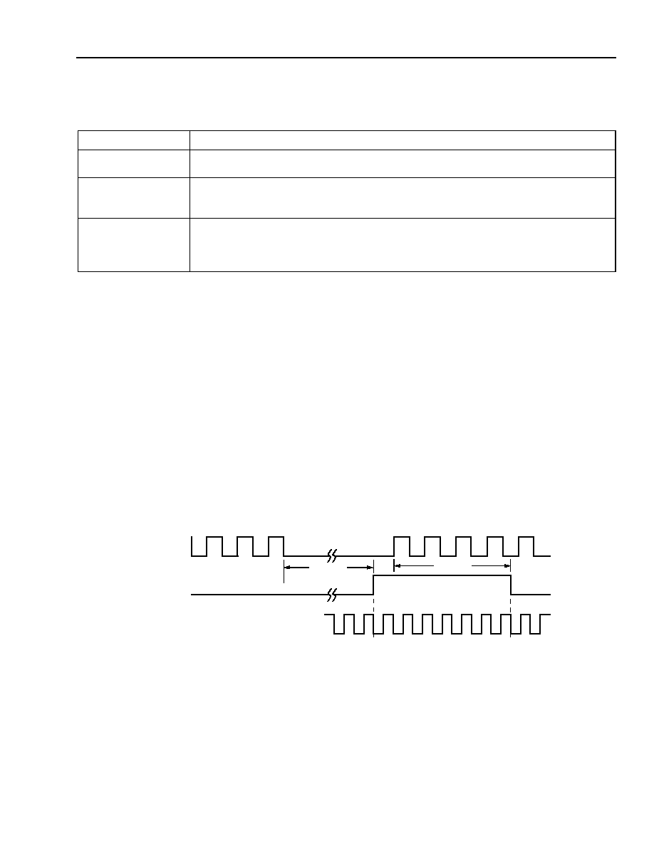
Lucent Technologies Inc.
69
Preliminary Data Sheet
October 2000
TFRA08C13 OCTAL T1/E1 Framer
Lucent Technologies Inc.
Alarms and Performance Monitoring
(continued)
Table 28. Alarm Indication Signal Conditions
s
The SLIP condition (FRM_SR3 bit 6 and bit 7). SLIP is defined as the state in which the receive elastic store
buffer's write address pointer from the receive framer and the read address pointer from the transmit concentra-
tion highway interface are equal
*
.
-- The negative slip (Slip-N) alarm indicates that the receive line clock (RLCK) - transmit CHI clock (CHICK)
monitoring circuit detects a state of overflow caused by RLCK and CHICK being out of phase-lock and the
period of the received frame being less than that of the system frame. One system frame is deleted.
-- The positive slip (Slip-P) alarm indicates the line clock (RLCK) - transmit CHI clock (CHICK) monitoring circuit
detects a state of underflow caused by RLCK and CHICK being out of phase-lock and the period of the
received frame being greater than that of the system frame. One system frame is repeated.
s
The loss of framer receive clock (LORLCK, pin G23). The LORLCK alarm is asserted high when an interval of
250 ms has expired with no transition of RLCK (pin see Table 2. Pin Descriptions) detected. The alarm is dis-
abled on the first transition of RLCK. Bit 0--bit 2 of global register 8 (GREG8) determine which framer sources
the LORLCK pin (see Table 69 Interrupt Status Register (FRM_SR0) (Y00)).
s
The loss of PLL clock (LOPLLCK, pin F25). LOPLLCK alarm is asserted high when an interval of 250 ms has
expired with no transition of PLLCK (pin see Table 2 . Pin Descriptions) detected. The alarm is disabled 250 µs
after the first transition of PLLCK. Timing for LOPLLCK is shown in Figure 26. Bit 0--bit 2 of global register 8
(GREG8) determine which framer sources the LOPLLCK pin (see Table 69).
5-6564(F).a
Figure 26. Timing for Generation of LOPLLCK (Pin F25)
* After a reset, the read and write pointers of the receive path elastic store will be set to a known state.
Framing Format
Remote Frame Alarm Format
T1
Loss of frame alignment occurs and the incoming signal has two or fewer zeros in each of
two consecutive double frame periods (386 bits).
CEPT ETSI
As described in ETSI ETS 300 233: May 1994, Section 8.2.2.4, loss of frame alignment
occurs and the framer receives a 512 bit period containing two or less binary zeros. This
is enabled by setting register FRM_PR10 bit 1 to 0.
CEPT ITU
As described in ITU Rec. G.775, the incoming signal has two or fewer zeros in each of
two consecutive double frame periods (512 bits). AIS is cleared if each of two consecutive
double frame periods contains three or more zeros or frame alignment signal (FAS) has
been found. This is enabled by setting register FRM_PR10 bit 1 to 1.
PLLCK
LOPLLCK
CHICK
250
µ
s
250
µ
s

Preliminary Data Sheet
TFRA08C13 OCTAL T1/E1 Framer
October 2000
70
Lucent Technologies Inc.
Lucent Technologies Inc.
Alarms and Performance Monitoring
(continued)
s
Received bipolar violation errors alarm, FRM_SR3
bit 0. This alarm indicates any bipolar decoding error
or detection of excessive zeros.
s
Received excessive CRC errors alarm, FRM_SR3
bit 3. In ESF, this alarm is asserted when 320 or
more CRC-6 checksum errors are detected within a
one second interval. In CEPT, this alarm is asserted
when 915 or more CRC-4 checksum errors are
detected within a one second interval.
s
The CEPT continuous E-bit alarm (CREBIT)
(FRM_SR2 bit 2). CREBIT is asserted when the
receive framer detects the following:
-- Five consecutive seconds where each 1 s interval
contains
991 received E bits = 0 events.
-- Simultaneously no LFA occurred.
-- Optionally, no remote frame alarm (A bit = 1) was
detected if register FRM_PR9 bit 0, bit 4, and bit 5
are set to 1.
-- Optionally, neither Sa6-F
hex
nor Sa6-E
hex
codes
were detected if register FRM_PR9 bit 0, bit 4,
and bit 6 are set to 1.
The 5 s timer is started when the following occurs:
-- CRC-4 multiframe alignment is achieved.
-- And optionally, A = 0 is detected if register
FRM_PR9 bit 0, bit 4, and bit 5 are set to 1.
-- And optionally, neither Sa6_F
hex
*
nor Sa6_E
hex
*
is
detected if register FRM_PR9 bit 0, bit 4, and bit 6
are set to 1.
The 5 s counter is restarted when the following
occurs:
-- LFA occurs, or
--
990 E bit = 0 events occur in 1 s, or
-- Optionally, an A bit = 1 is detected if register
FRM_PR9 bit 0, bit 4, and bit 5 are set to 1.
-- Optionally, a valid Sa6 pattern 1111 (binary) or
Sa6 pattern 1110 (binary) code was detected if
register FRM_PR9 bit 0, bit 4, and bit 6 are
set to 1.
This alarm is disabled during loss of frame alignment
(LFA) or loss of CRC-4 multiframe alignment
(LTS0MFA).
s
Failed state alarm or the unavailable state alarm,
FRM_SR5 bit 3 and bit 7 and FRM_SR6 bit 3 and bit
7. This alarm is defined as the unavailable state at
the onset of ten consecutive severely errored sec-
onds. In this state, the receive framer inhibits incre-
menting of the severely errored and errored second
counters for the duration of the unavailable state. The
receive framer deasserts the unavailable state condi-
tion at the onset of ten consecutive errored seconds
which were not severely errored.
s
The 4-bit Sa6 codes (FRM_SR2 bit 3--bit 7). Sa6
codes are asserted if three consecutive 4-bit pat-
terns have been detected. The alarms are disabled
when three consecutive 4-bit Sa6 codes have been
detected that are different from the pattern previously
detected. The receive framer monitors the Sa6 bits
for special codes described in ETSI ETS 300 233:
May 1994, Section 9.2. The Sa6 codes are defined in
Table 29 and Table 30. The Sa6 codes in Table 29
may be recognized as an asynchronous bit stream in
either non-CRC-4 or CRC-4 modes as long as the
receive framer is in the basic frame alignment state.
In the CRC-4 mode, the receive framer can optionally
recognize the received Sa6 codes in Table 29 syn-
chronously to the CRC-4 submultiframe structure as
long as the receive framer is in the CRC-4 multiframe
alignment state (synchronous Sa6 monitoring can be
enabled by setting register FRM_PR10 bit 1 to 1).
The Sa6 codes in Table 30 are only recognized syn-
chronously to the CRC-4 submultiframe and when
the receive framer is in CRC-4 multiframe alignment.
The detection of three (3) consecutive 4-bit patterns
are required to indicate a valid received Sa6 code.
The detection of Sa6 codes is indicated in status reg-
ister FRM_SR2 bit 3--bit 7. Once set, any three-nib-
ble (12-bit) interval that contains any other Sa6 code
will clear the current Sa6 status bit. Interrupts may be
generated by the Sa6 codes given in Table 29
* See Table 29, for the definition of this Sa6 pattern.

Lucent Technologies Inc.
71
Preliminary Data Sheet
October 2000
TFRA08C13 OCTAL T1/E1 Framer
Lucent Technologies Inc.
Alarms and Performance Monitoring
(continued)
Table 29. Sa6 Bit Coding Recognized by the Receive Framer
Table 30 defines the three 4-bit Sa6 codes that are always detected synchronously to the CRC-4 submultiframe
structure, and are only used for counting NT1 events.
Table 30. Sa6 Bit Coding of NT1 Interface Events Recognized by the Receive Framer
The reference points for receive CRC-4, E-bit, and Sa6 decoding are illustrated in Figure 27
Code
First Receive Bit (MSB)
Last Received Bit (LSB)
Sa6_8
hex
1
0
0
0
Sa6_A
hex
1
0
1
0
Sa6_C
hex
1
1
0
0
Sa6_E
hex
1
1
1
0
Sa6_F
hex
1
1
1
1
Code
First Receive Bit
(MSB)
Last Received Bit
(LSB)
Event at NT1
Counter Size
(bits)
Sa6_1
hex
0
0
0
1
E = 0
16
Sa6_2
hex
0
0
1
0
CRC-4 Error
16
Sa6_3
hex
0
0
1
1
CRC-4 Error & E = 0
This code will cause both
counters to increment.
--
Preliminary Data Sheet
TFRA08C13 OCTAL T1/E1 Framer
October 2000
72
Lucent Technologies Inc.
Lucent Technologies Inc.
Alarms and Performance Monitoring
(continued)
5-3913(F)r.8
Figure 27. The T and V Reference Points for a Typical CEPT E1 Application
s
CEPT auxiliary pattern alarm (AUXP) (FRM_SR1 bit 6). The received auxiliary alarm, register FRM_SR1 bit 6
(AUXP), is asserted when the receive framer is in the LFA state and has detected more than 253 10 (binary) pat-
terns for 512 consecutive bits. In a 512-bit interval, only two 10 (binary) patterns are allowable for the alarm to be
asserted and maintained. The 512-bit interval is a sliding window determined by the first 10 (binary) pattern
detected. This alarm is disabled when three or more 10 (binary) patterns are detected in 512 consecutive bits.
The search for AUXP is synchronized with the first alternating 10 (binary) pattern as shown in Table 31.
Table 31. AUXP Synchronization and Clear Sychronization Process
00
10
10
01
11
11
00
00
0
10
00
10
--
sync
--
--
--
clear sync
--
--
--
sync
. . .
. . .
NT2
E BIT = 0
NT1
ET
V REFERENCE
E BIT = 0, ERROR EVENT DETECTED AT THE NT1 REMOTE
CRC-4 ERRORS AT THE NT1
E BIT = 0, ERROR EVENT AT THE ET REMOTE
CRC-4 ERRORS AT THE ET,
CRC-4 ERRORS DETECTED FROM NT1 REMOTE, THEN SET Sa6 = 001X
E = 0 DETECTED FROM NT1 REMOTE, THEN SET Sa6 = 00X1
POINT
T REFERENCE
POINT
COUNT:
1) CRC ERRORS,
2) E = 0,
3) Sa6 = 001X, AND
4) Sa6 = 00X1
Sa6
CRC ERROR
DETECTED
CRC ERROR
DETECTED
(NT1 REMOTE)
E BIT = 0

Lucent Technologies Inc.
73
Preliminary Data Sheet
October 2000
TFRA08C13 OCTAL T1/E1 Framer
Lucent Technologies Inc.
Alarms and Performance Monitoring
(continued)
Event Counters Definition
The error events monitored in the receive framer's status registers are defined in Table 32 for the hardwired
(default) threshold values. The errored second and severely errored second threshold registers can be pro-
grammed through FRM_PR11--FRM_PR13 such that the errored and severely errored second counters function
as required by system needs. DS1 errors are reported in the ET Error registers, FRM_SR20 through FRM_SR35.
For the framer to correctly report coding and BPV errors, the LIU/Framer interface must be configured as dual rail
mode.
Table 32. Event Counters Definition
Error Event
Functional Mode
Definition
Counter Size
(bits)
Bipolar
Violations
(BPVs)
AMI
Any bipolar violation or 16 or more consecutive zeros
16
B8ZS
Any BPV, code violation, or any 8-bit interval with no
one pulse
CEPT HDB3
Any BPV, code violation, or any 4-bit interval with no
one pulse
Frame
Alignment Errors
(FERs)
SF: D4
Any F
T
or F
S
bit errors (FRM_PR10 bit 2 = 1) or any
F
T
bit errors (FRM_PR10 bit 2 = 0)
16
SF:
SLC
-96
Any F
T
or F
S
bit errors (FRM_PR10 bit 2 = 1) or any
F
T
bit errors (FRM_PR10 bit 2 = 0)
SF: DDS
Any F
T
, F
S
, or time slot 24 FAS bit error
ESF
Any F
E
bit error
CEPT
Any FAS (0011011) or NOT FAS (bit 2) bit error if
register FRM_PR10, bit 2 = 0.
Any FAS (0011011) bit error if register FRM_PR10,
bit 2 = 1.
CRC Checksum
Errors
ESF or CEPT with CRC
Any received checksum in error
16
Excessive CRC
Errors
ESF
320 checksum errors in a one second interval
NONE
CEPT with CRC
915 checksum errors in a one second interval
Received
E bits = 0
CEPT with CRC-4
E bits = 0 in frame 13 and frame 15
16
Errored Second
Events
All
Any one of the relevant error conditions enabled in
registers FRM_PR14--FRM_PR18 within a one
second interval
16
DS1: non-ESF
Any framing bit errors within a one second interval
DS1: ESF
Any CRC-6 errors within a one second interval
CEPT without CRC-4
Any framing errors within a one second interval
CEPT with CRC-4 (ET1) Any CRC-4 errors within a one second interval
CEPT with CRC-4
(ET1 remote)
Any E bit = 0 event within a one second interval
CEPT with CRC-4 (NT1) Any Sa6 = 001x (binary) code event within a one
second interval
CEPT with CRC-4
(NT1 remote)
Any Sa6 = 00x1 (binary) code event within a one
second interval

Preliminary Data Sheet
TFRA08C13 OCTAL T1/E1 Framer
October 2000
74
Lucent Technologies Inc.
Lucent Technologies Inc.
Alarms and Performance Monitoring
(continued)
Table 32. Event Counters Definition (continued)
The receive framer enters an unavailable state condition at the onset of ten consecutive severely errored second
events. When in the unavailable state, the receive framer deasserts the unavailable state alarms at the onset of ten
consecutive seconds which were not severely errored.
Error Event
Functional Mode
Definition
Counter Size
(bits)
Bursty Errored
Second Events
DS1: non-ESF
Greater than 1 but less than 8 framing bit errors
within a one second interval
16
DS1: ESF
Greater than 1 but less than 320 CRC-6 errors within
a one second interval
CEPT without CRC-4
Greater than 1 but less than 16 framing bit errors
within a one second interval
CEPT with CRC-4 (ET1) Greater than 1 but less than 915 CRC-4 errors within
a one second interval
CEPT with CRC-4 (ET1
remote)
Greater than 1 but less than 915 E bit = 0 events
within a one second interval
CEPT with CRC-4 (NT1) Greater than 1 but less than 915 Sa6=001x (binary)
code events within a one second interval
CEPT with CRC-4 (NT1
remote)
Greater than 1 but less than 915 Sa6=00x1 (binary)
code events within a one second interval
Severely Errored
Second Events
All
Any one of the relevant error conditions enabled in
registers FRM_PR14--FRM_PR18 within a one
second interval
16
DS1: non-ESF
8 or more framing bit errors within a one second
interval
DS1: ESF
320 or more CRC-6 errors within a one second
interval
CEPT with no CRC-4
16 or more framing bit errors within a one second
interval
CEPT with CRC-4 (ET1) 915 or more CRC-4 errors within a one second
interval
CEPT with CRC-4
(ET1 remote)
915 or more E bit = 0 events within a one second
interval
CEPT with CRC-4 (NT1) 915 or more Sa6=001x (binary) code events within a
one second interval
CEPT with CRC-4
(NT1 remote)
915 or more Sa6=00x1 (binary) code events within a
one second interval
Unavailable
Second Events
All
A one second period in the unavailable state
16

Lucent Technologies Inc.
75
Preliminary Data Sheet
October 2000
TFRA08C13 OCTAL T1/E1 Framer
Lucent Technologies Inc.
Alarms and Performance Monitoring
(continued)
Loopback and Transmission Modes
Primary Loopback Modes
Framer primary loopback mode is controlled by register
FRM_PR24. There are seven primary loopback and
transmission test modes supported:
s
Line loopback (LLB).
s
Board loopback (BLB).
s
Single time-slot system loopback (STSSLB).
s
Single time-slot line loopback (STSLLB).
s
CEPT nailed-up broadcast transmission (CNUBT).
s
Payload loopback (PLLB).
s
CEPT nailed-up connect loopback (CNUCLB).
The loopback and transmission modes are described in
detail below:
s
The LLB mode loops the receive line data and clock
back to the transmit line. The received data is pro-
cessed by the receive framer and transmitted to the
system interface. This mode can be selected by set-
ting register FRM_PR24 to 001xxxxx (binary).
s
The BLB mode loops the receive system data back
to the system after:
-- The transmit framer processes the data, and
-- The receive framer processes the data.
In the BLB mode, AIS is always transmitted to the line
interface. This mode can be selected by setting register
FRM_PR24 to 010xxxxx (binary).
s
The STSSLB mode loops one and only one received
system time slot back to the transmit system inter-
face. The selected looped back time-slot data is not
processed by either the transmit framer or the
receive framer. The selected time slot does not pass
through the receive elastic store buffer and therefore
will not be affected by system-AIS, RLFA conditions,
or controlled slips events. Once selected, the desired
time-slot position has the programmable idle code in
register FRM_PR22 transmitted to the line interface
one frame before implementing the loopback and for
the duration of the loopback. This mode can be
selected by setting register FRM_PR24 to
011A
4
A
3
A
2
A
1
A
0
, where A
4
A
3
A
2
A
1
A
0
is the binary
address of the selected time slot.
s
The STSLLB mode loops one and only one received
line time slot back to the transmit line. The selected
time-slot data is looped to the line after being pro-
cessed by the receive framer, and it passes through
the receive elastic store. The selected time slot has
the programmable idle code in register FRM_PR22
transmitted to the system interface one frame before
implementing the loopback and for the duration of the
loopback. In CEPT, selecting time slot 0 has the
effect of deactivating the current loopback mode
while no other action will be taken (time slot 0 will not
be looped back to the line and should not be cho-
sen). This mode can be selected by setting register
FRM_PR24 to 100A
4
A
3
A
2
A
1
A
0
, where A
4
A
3
A
2
A
1
A
0
is the binary address of the selected time slot.
s
The CNUBT mode transmits received-line time slot X
to the system in time slot X and time slot 0 (of the
next frame). Any time slot can be broadcast. This
mode can be selected by setting register FRM_PR24
to 101A
4
A
3
A
2
A
1
A
0
where A
4
A
3
A
2
A
1
A
0
is the binary
address of the selected time slot.
s
The PLLB mode loops the received line data and
clock back to the transmit line while inserting (replac-
ing) the facility data link in the looped back data. Two
variations of the payload loopback are available. In
the pass-through framing/CRC bit mode (chosen by
setting register FRM_PR24 to 111xxxxx (binary)),
the framing and CRC bits are looped back to the line
transmit data. In the regenerated framing/CRC bit
mode (chosen by setting register FRM_PR24 to
110xxxxx (binary) and register FRM_PR10 bit
3 to 0), the framing and CRC bits are regenerated by
the transmit framer. The payload loopback is only
available for ESF and CEPT modes.
s
The CNUCLB mode loops received system time slot
X back to the system in time slot 0. The selected time
slot is not routed through the receive elastic store
buffer and, therefore, will not be affected by system-
AIS, RLFA conditions, or controlled slips. Any time
slot can be looped back to the system. Time slot X
transmitted to the line is not affected by this loopback
mode. Looping received system time slot 0 has no
effect on time slot 0 transmitted to the line, i.e., the
transmit framer will always overwrite the FAS and
NOT FAS data in time slot 0 transmitted to the line.
This mode can be selected by setting register
FRM_PR24 to 110A
4
A
3
A
2
A
1
A
0
and register
FRM_PR10 bit 3 to 1, where A
4
A
3
A
2
A
1
A
0
is the
binary address of the selected time slot.

Preliminary Data Sheet
TFRA08C13 OCTAL T1/E1 Framer
October 2000
76
Lucent Technologies Inc.
Lucent Technologies Inc.
Alarms and Performance Monitoring
(continued)
Secondary Loopback Modes
There are two secondary loopback modes supported:
s
Secondary-single time-slot system loopback (S-STSSLB).
s
Secondary-single time-slot line loopback (S-STSLLB).
The loopbacks are described in detail below:
s
The secondary-STSSLB mode loops one and only one received system time slot back to the transmit system
interface. The selected time-slot data looped back is not processed by either the transmit framer or the receive
framer. The selected time slot does not pass through the receive elastic store buffer and therefore will not be
affected by system-AIS, RLFA conditions, or controlled slips events. Whenever the secondary loopback register
is programmed to the same time slot as the primary register, the primary loopback mode will control that time
slot. Once selected, the desired time-slot position has the programmable line idle code in register FRM_PR22
transmitted to the line interface one frame before implementing the loopback and for the duration of the loopback.
s
The secondary-STSLLB mode loops one and only one line time slot back to the line. The selected time slot data
is looped to the line after being processed by the receive framer and it passes through the receive elastic store.
The selected time slot has the programmable idle code in register FRM_PR22 transmitted to the system inter-
face one frame before implementing the loopback and for the duration of the loopback. In CEPT, selecting time
slot 0 has the effect of deactivating the current loopback mode while no other action will be taken (time slot 0 will
not be looped back to the line and should not be chosen in this mode).
Table 33 defines the deactivation of the two secondary loopback modes as a function of the activation of the pri-
mary loopback and test transmission modes.
Table 33. Summary of the Deactivation of SSTSSLB and SSTSLLB Modes as a Function of Activating the
Primary Loopback Modes
Primary Loopback Mode
Deactivation of S-STSSLB
Deactivation of S-STSLLB
STSSLB
If primary time slot = secondary
If primary time slot = secondary
STSLLB
If primary time slot = secondary
If primary time slot = secondary
BLB
Always
Always
CNUBT
If the secondary time slot is TS0 or if the
primary time slot = secondary
If primary time slot = secondary
LLB
Always
Always
NUCLB
If the secondary time slot is TS0 or if the
primary time slot = secondary
If primary time slot = secondary
PLLB
Always
Always
Lucent Technologies Inc.
77
Preliminary Data Sheet
October 2000
TFRA08C13 OCTAL T1/E1 Framer
Lucent Technologies Inc.
Alarms and Performance Monitoring
(continued)
Figure 28 illustrates the various loopback modes implemented by each framer unit.
5-3914(F).d
Figure 28. Loopback and Test Transmission Modes
FRAMER
FRAMER
LINE
ES
SYSTEM
(3) SINGLE TIME-SLOT SYSTEM LOOPBACK
FRAMER
LINE
ES
SYSTEM
(2) BOARD LOOPBACK
AIS
RECEIVE SYSTEM DATA
LINE
SYSTEM
(1) LINE LOOPBACK
IS IGNORED
INSERT ONLY TIME SLOT X
LINE
ES
SYSTEM
(4) SINGLE TIME-SLOT LINE LOOPBACK
TRANSMIT PROGRAMMABLE IDLE CODE
IN REGISTER FRM_PR22
LINE
ES
SYSTEM
(5) CEPT NAILED-UP BROADCAST TRANSMISSION
TRANSMIT LINE TS-X IN
SYSTEM TS-X AND SYSTEM TS-0
FRAMER
LINE
ES
SYSTEM
(7) CEPT NAILED-UP CONNECT LOOPBACK
LOOPBACK TS-X IN TS-0
TRANSMIT FRAMER
LINE
SYSTEM
(6) PAYLOAD LINE LOOPBACK
TRANSMIT PROGRAMMABLE LINE IDLE CODE
IN REGISTER FRM_PR22
LOOPBACK TS-X
IN OUTGOING SYSTEM TS-X
IN OUTGOING LINE TS-X

Preliminary Data Sheet
TFRA08C13 OCTAL T1/E1 Framer
October 2000
78
Lucent Technologies Inc.
Lucent Technologies Inc.
Alarms and Performance Monitoring
(continued)
Line Test Patterns
Test patterns may be transmitted to the line through either register FRM_PR20 or register FRM_PR69. Only one of
these sources may be active at the same time. Signaling must be inhibited while sending these test patterns.
Transmit Line Test Patterns--Using Register FRM_PR20
The transmit framer can be programmed through register FRM_PR20 to transmit various test patterns. These test
patterns, when enabled, overwrite the received CHI data. The test patterns available using register FRM_PR20
are:
s
The unframed-AIS pattern which consists of a continuous bit stream of ones (. . . 111111 . . .) enabled by setting
register FRM_PR20 bit 0 to 1.
s
The unframed-auxiliary pattern which consists of a continuous bit stream of alternating ones and 0s (. . .
10101010 . . .) enabled by setting register FRM_PR20 bit 1 to 1.
s
The quasi-random test signal, enabled by setting register FRM_PR20 bit 3 to 1, which consists of the following:
-- A pattern produced by means of a 20-stage shift register with feedback taken from the seventeenth and twen-
tieth stages via an exclusive-OR gate to the first stage. The output is taken from the twentieth stage and is
forced to a 1 state whenever the next 14 stages (19 through 6) are all 0. The pattern length is
1,048,575 or 2
20
≠ 1 bits. This pattern is described in detail in
AT&T Technical Reference 62411 [5] Appendix
and illustrated in Figure 29.
-- Valid framing bits.
-- Valid transmit facility data link (TFDL) bit information.
-- Valid CRC bits.
5-3915(F).dr.1
Figure 29. 20-Stage Shift Register Used to Generate the Quasi-Random Signal
s
The pseudorandom test pattern, enabled by setting register FRM_PR20 bit 2 to 1, which consists of:
-- A 2
15
≠ 1 pattern inserted in the entire payload (time slots 1--24 in DS1 and time slots 1--32 in CEPT), as
described by ITU Rec. 0.151 and illustrated in Figure 30.
-- Valid framing pattern.
-- Valid transmit facility data link (TFDL) bit data.
-- Valid CRC bits.
D
D-TYPE FLIP-FLOPS
#1
D
D
#2
#17
D
#18
D
D
#19
#20
A
B
C
XOR
#6
#19
NOR
#20
QUASI-RANDOM TEST OUTPUT
OR
Lucent Technologies Inc.
79
Preliminary Data Sheet
October 2000
TFRA08C13 OCTAL T1/E1 Framer
Lucent Technologies Inc.
Alarms and Performance Monitoring
(continued)
5-3915(F).er.1
Figure 30. 15-Stage Shift Register Used to Generate the Pseudorandom Signal
s
The idle code test pattern, enabled by setting register FRM_PR20 bit 6 to 1, which consists of the following:
-- The programmable idle code, programmed through register FRM_PR22, in time slots 1--24 in DS1 and 0--31
in CEPT.
-- Valid framing pattern.
-- Valid transmit facility data link (TFDL) bit data.
-- Valid CRC bits.
Transmit Line Test Patterns--Using Register FRM_PR69
Framed or unframed patterns indicated in Table 34 may be generated and sent to the line by register FRM_PR69
and by setting register FRM_PR20 to 00 (hex). Selection of transmission of either a framed or unframed test pat-
tern is made through FRM_PR69 bit 3. If one of the test patterns of register FRM_PR69 is enabled, a single bit
error can be inserted into the transmitted test pattern by toggling register FRM_PR69 bit 1 from 0 to 1.
Table 34. Register FRM_PR69 Test Patterns
Pattern
Register FRM_PR69
Bit 7 Bit 6
Bit 5
Bit 4
MARK (all ones AIS)
0
0
0
0
QRSS (2
20
≠ 1 with zero suppression)
0
0
0
1
2
5
≠ 1
0
0
1
0
63 (2
6
≠ 1)
0
0
1
1
511 (2
9
≠ 1)
0
1
0
0
511 (2
9
≠ 1) reversed
0
1
0
1
2047 (2
11
≠ 1)
0
1
1
0
2047 (2
11
≠ 1) reversed
0
1
1
1
2
15
≠ 1
1
0
0
0
2
20
≠ 1
1
0
0
1
2
20
≠ 1
1
0
1
0
2
23
≠ 1
1
0
1
1
1:1 (alternating)
1
1
0
0
D
XOR
D-TYPE FLIP-FLOPS
#1
D
D
#2
#3
D
#13
D
D
#14
#15
A
B
C
PSEUDORANDOM
TEST OUTPUT

Preliminary Data Sheet
TFRA08C13 OCTAL T1/E1 Framer
October 2000
80
Lucent Technologies Inc.
Lucent Technologies Inc.
Alarms and Performance Monitoring
(continued)
Receive Line Pattern Monitor--Using Register FRM_SR7
The receive framer pattern monitor continuously monitors the received line, detects the following fixed framed pat-
terns, and indicates detection in register FRM_SR7 bit 6 and bit 7.
s
The pseudorandom test pattern as described by ITU Rec. O.151 and illustrated in Figure 30. Detection of the
pattern is indicated by register FRM_SR7 bit 6 = 1.
s
The quasi-random test pattern described in
AT&T Technical Reference 62411[5] Appendix
and illustrated in Fig-
ure 29. Detection of the pattern is indicated by register FRM_SR7 bit 7 = 1.
In DS1 mode, the received 193 bit frame must consist of 192 bits of pattern plus 1 bit of framing information. In
CEPT mode, the received 256 bit frame must consist of 248 bits of pattern plus 8 bits (TS0) of framing information.
No signaling, robbed bit in the case of T1 and TS16 signaling in the case of CEPT, may be present for successful
detection of these two test patterns.
To establish lock to the pattern, 256 sequential bits must be received without error. When lock to the pattern is
achieved, the appropriate bit of register FRM_SR7 is set to a 1. Once pattern lock is established, the monitor can
withstand up to 32 single bit errors per frame without a loss of lock. Lock will be lost if more than 32 errors occur
within a single frame. When such a condition occurs, the appropriate bit of register FRM_SR7 is deasserted. The
monitor then resumes scanning for pattern candidates.
Receive Line Pattern Detector--Using Register FRM_PR70
Framed or unframed patterns indicated in Table 35 may be detected using register FRM_PR70. Detection of the
selected test pattern is indicated when register FRM_SR7 bit 4 is set to 1. Selection of a framed or unframed test
pattern is made through FRM_PR70 bit 3. Bit errors in the received test pattern are indicated when register
FRM_SR7 bit 5 = 1. The bit errors are counted and reported in registers FRM_SR8 and FRM_SR9, which are nor-
mally the BPV counter registers. (In this test mode, the BPV counter registers do not count BPVs but count only bit
errors in the received test pattern.)
Table 35. Register FRM_PR70 Test Patterns
Pattern
Register FRM_PR70
Bit 7 Bit 6
Bit 5
Bit 4
MARK (all ones AIS)
0
0
0
0
QRSS (2
20
≠ 1 with zero suppression)
0
0
0
1
2
5
≠ 1
0
0
1
0
63 (2
6
≠ 1)
0
0
1
1
511 (2
9
≠ 1)
0
1
0
0
511 (2
9
≠ 1) reversed
0
1
0
1
2047 (2
11
≠ 1)
0
1
1
0
2047 (2
11
≠ 1) reversed
0
1
1
1
2
15
≠ 1
1
0
0
0
2
20
≠ 1
1
0
0
1
2
20
≠ 1
1
0
1
0
2
23
≠ 1
1
0
1
1
1:1 (alternating)
1
1
0
0

Lucent Technologies Inc.
81
Preliminary Data Sheet
October 2000
TFRA08C13 OCTAL T1/E1 Framer
Lucent Technologies Inc.
Alarms and Performance Monitoring
(continued)
The pattern detector continuously monitors the received line for the particular pattern selected in register
FRM_PR70 bit 7--bit 4 (DPTRN). To establish detector lock to the pattern, 256 sequential bits must be detected.
Once the detector has locked onto the selected pattern, it will remain locked to the established alignment and count
all unexpected bits as single bit errors until register FRM_PR70 bit 2 (DBLKSEL) is set to 0.
To select a pattern or change the pattern to be detected, the following programming sequence must be followed:
s
DBLKSEL (register FRM_PR70 bit 2) is set to 0.
s
The new pattern to be detected is selected by setting register FRM_PR70 bit 7--bit 4 to the desired value.
s
DBLKSEL (register FRM_PR70 bit 2) is set to 1.

Preliminary Data Sheet
TFRA08C13 OCTAL T1/E1 Framer
October 2000
82
Lucent Technologies Inc.
Lucent Technologies Inc.
Alarms and Performance Monitoring
(continued)
Automatic and On-Demand Commands
Various alarms can be transmitted either automatically as a result of various alarm conditions or on demand. After
reset, all automatic transmissions are disabled. The user can enable the automatic or on-demand actions by set-
ting the proper bits in the automatic and on-demand action registers as identified below in Table 36. Table 37 shows
the programmable automatically transmitted signals and the triggering mechanisms for each. Table 37 shows the
on-demand commands.
Table 36. Automatic Enable Commands
Action
Trigger
Enabling Register Bit
Transmit Remote Frame Alarm
(RFA)
Loss of frame alignment (RLFA)
FRM_PR27 bit 0 = 1
Loss of CEPT time slot 16 multiframe
alignment (RTS16LMFA)
FRM_PR27 bit 1 = 1
Loss of CEPT time slot 0 multiframe
alignment (RTS0LMFA)
FRM_PR27 bit 2 = 1
Detection of the timer (100 ms or
400 ms) expiration due to loss of
CEPT multiframe alignment
FRM_PR27 bit 3 = 1
FRM_PR9 bit 7--bit 0 = 0xxxx1x1 or
0xxx1xx1
Detection of the CEPT RSa6 = 8 (hex)
code
FRM_PR27 bit 4 = 1
Detection of the CEPT RSa6 = C (hex)
code
FRM_PR27 bit 5 = 1
Transmit CEPT E Bit = 0
Detection of CEPT CRC-4 error
FRM_PR28 bit 3 = 1
RTS0LMFA
FRM_PR28 bit 4 = 1
Detection of the timer (100 ms or
400 ms) expiration due to loss of
CEPT multiframe alignment
FRM_PR28 bit 5 = 1
FRM_PR9 bit 7--bit 0 = 0xxxx1x1 or
0xxx1xx1
Transmit AIS to System
RLFA
FRM_PR19 bit 0 = 1
Detection of the timer (100 ms or
400 ms) expiration due to loss of
CEPT multiframe alignment
FRM_PR19 bit 1 = 1
FRM_PR9 bit 7--bit 0 = 0xxxx1x1 or
0xxx1xx1
Transmit CEPT Time Slot 16
Remote Multiframe Alarm to
Line
RTS16LMFA
FRM_PR41 bit 4 = 1
Transmit CEPT AIS in Time Slot
16 to System
RTS16LMFA
FRM_PR44 bit 6 = 1
Automatic Enabling of DS1 Line
Loopback On/Off
Line loopback on/off code
FRM_PR19 bit 4 = 1
Automatic Enabling of ESF FDL
Line Loopback On/Off
ESF line loopback on/off code
FRM_PR19 bit 6 = 1
Automatic Enabling of ESF FDL
Payload Loopback On/Off
ESF payload loopback on/off code
FRM_PR19 bit 7 = 1

Lucent Technologies Inc.
83
Preliminary Data Sheet
October 2000
TFRA08C13 OCTAL T1/E1 Framer
Lucent Technologies Inc.
Alarms and Performance Monitoring
(continued)
Table 37. On-Demand Commands
Type
Frame Format
Action
Enabling Register Bit
Transmit Remote Frame Alarm D4 (Japanese) F
S
bit in frame 12 = 1
FRM_PR27 bit 6 = 1
D4 (US)
Bit 2 of all time slots = 0
FRM_PR27 bit 7 = 1
DDS
Bit 6 in time slot 24 = 0
ESF
Pattern of 1111111100000000 in
the FDL F-bit position
CEPT
A bit = 1
Transmit Time Slot 16 Remote
Multiframe Alarm to the Line
CEPT
Time slot 16 remote alarm bit = 1
FRM_PR41 bit 5 = 1
Transmit Data Link AIS
(Squelch)
SLC
-96, ESF
Transmit data link bit = 1
FRM_PR21 bit 4 = 1
Transmit Line Test Patterns
All
Transmit test patterns to the line
interface
See Transmit Line Test
Patterns--Using Register
FRM_PR20 section on
page 78 and Transmit Line
Test Patterns--Using Reg-
ister FRM_PR69 section
on page 79.
Transmit System AIS
All
Transmits AIS to the system
FRM_PR19 bit 3 = 1
Transmit System Signaling AIS
(Squelch)
T1
Transmit ABCD = 1111 to the sys-
tem
FRM_PR44 bit 1 = 1
CEPT
Transmit AIS in system time slot 16 FRM_PR44 bit 7 = 1
Receive Signaling Inhibit
All
Suspend the updating of the
receive signaling registers
FRM_PR44 bit 3 = 1
Receive Framer Reframe
All
Force the receive framer to reframe FRM_PR26 bit 2 = 1
Transmit Line Time Slot 16
CEPT
Transmit AIS in time slot 16 to the
line
FRM_PR41 bit 6 = 1
Enable Loopback
All
Enables system and line loopbacks See Loopback and Trans-
mission Modes section on
page 75.
Framer Software Reset
All
The framer and FDL are placed in
the reset state for four RCLK clock
cycles. The framer parameter reg-
isters are forced to the default
value.
FRM_PR26 bit 0 = 1
Framer Software Restart
All
The framer and FDL are placed in
the reset state as long as this bit is
set to 1. The framer parameter reg-
isters are not changed from their
programmed values.
FRM_PR26 bit 1 = 1
84
Lucent Technologies Inc.
Preliminary Data Sheet
TFRA08C13 OCTAL T1/E1 Framer
October 2000
Lucent Technologies Inc.
Facility Data Link
Data may be extracted from and inserted into the facility data link in
SLC
-96, DDS, ESF, and CEPT framing for-
mats. In CEPT, any one of the Sa bits can be declared as the facility data link by programming register FRM_PR43
bit 0--bit 2. Access to the FDL is made through:
s
The FDL pins (RFDL, RFDLCK, TFDL, and TFDLCK). Figure 15 shows the timing of these signals.
s
The 64-byte FIFO of the FDL HDLC block. FDL information passing through the FDL HDLC Section may be
framed in HDLC format or passed through transparently.
5-3910(F).cr.1
Figure 31. TFRA08C13 Facility Data Link Access Timing of the Transmit and Receive Framer Sections
t8
t9
t9
t10
t11
t8: TFDLCK CYCLE =
t9: TFDL TO TFDLCK SETUP/HOLD = 40 ns
t10: RFDLCK CYCLE =
t11: RFDLCK TO RFDL DELAY = 40 ns
TFDLCK
TFDL
RFDLCK
RFDL
250
µ
s (ALL OTHER
MODES)
125
µ
s (DDS)
250
µ
s (ALL OTHER
MODES)
125
µ
s (DDS)
In the ESF frame format, automatic assembly and
transmission of the performance report message
(PRM) as defined in both
ANSI
T1.403-1995 and
Tel-
cordia Technologies
* TR-TSY-000194 Issue 1, 12--87
is managed by the receive framer and transmit FDL
sections. The
ANSI
T1.403-1995 bit-oriented data link
messages (BOM) can be transmitted by the transmit
FDL section and recognized and stored by the receive
FDL section.
Receive Facility Data Link Interface
Summary
A brief summary of the receive facility data link func-
tions is given below:
s
Bit-oriented message (BOM) operation. The
ANSI
T1.403-1995 bit-oriented data link messages are
recognized and stored in register FDL_SR3. The
number of times that an
ANSI
code must be received
for detection can be programmed from 1 to 10 by
writing to register FDL_PR0 bit 4-- bit 7. When a
valid
ANSI
code is detected, register FDL_SR0 bit 7
(FRANSI) is set.
s
HDLC operation. This is the default mode of opera-
tion when the FDL receiver is enabled (register
FDL_PR1 bit 2 = 1). The HDLC framer detects the
HDLC flags, checks the CRC bytes, and stores the
data in the FDL receiver FIFO (register FDL_SR4)
along with a status of frame (SF) byte.
s
HDLC operation with performance report mes-
sages (PRM). This mode is enabled by setting regis-
ter FDL_PR1 bit 2 and bit 6 to 1. In this case, the
receive FDL will store the 13 bytes of the PRM report
field in the FDL receive FIFO (register FDL_SR4)
along with a status of frame (SF) byte.
s
Transparent operation. Enabling the FDL and set-
ting register FDL_PR9 bit 6 (FTM) to 1 disables the
HDLC processing. Incoming data link bits are stored
in the FDL receive FIFO (register FDL_SR4).
*
Telcordia Technologies
is a registered trademark of Bell
Communications Research, Inc.

Lucent Technologies Inc.
85
Preliminary Data Sheet
October 2000
TFRA08C13 OCTAL T1/E1 Framer
Lucent Technologies Inc.
Facility Data Link
(continued)
s
Transparent operation with pattern match. Enabling the FDL and setting registers FDL_PR9 bit 5 (FMATCH)
and FDL_PR9 bit 6 (FTM) to 1 forces the FDL to start storing data in the FDL receive FIFO (register FDL_SR4)
only after the programmable match character defined in register FDL_PR8 bit 0--bit 7 has been detected. The
match character and all subsequent bytes are placed into the FDL receive FIFO.
The FDL interface to the receive framer is illustrated in Figure 32.
5-4560(F).ar.1
Figure 32. Block Diagram for the Receive Facility Data Link Interface
Receive
ANSI
T1.403 Bit-Oriented Messages (BOM)
s
The receive FDL monitor will detect any of the
ANSI
T1.403 ESF bit-oriented messages (BOMs) and generate an
interrupt, enabled by register FDL_PR6 bit 7, upon detection. Register FDL_SR0 bit 7 (FRANSI) is set to 1 upon
detection of a valid BOM and then cleared when read.
s
The received ESF FDL bit-oriented messages are received in the form 111111110X
0
X
1
X
2
X
3
X
4
X
5
0 (the left most
bit is received first). The bits designated as X are the defined
ANSI
ESF FDL code bits. These code bits are writ-
ten into the received
ANSI
FDL status register FDL_SR3 when the entire code is received.
s
The minimum number of times a valid code must be received before it is reported can be programmed from 1 to
10 using register FDL_PR0 bit 4--bit 7.
RECEIVE LINE
DATA
RECEIVE
FRAMER
LOSS OF FRAME
ALIGNMENT
RECEIVE FDL
DATA
EXTRACTER
RFDL
RFDLCK
RECEIVE
FACILITY DATA
ANSI T1.403-1995
BIT-ORIENTED DATA
LINK MESSAGES
MONITOR
ONE 8-bit REGISTER
IDENTIFYING THE ESF
BIT-ORIENTED CODE
TRANSPARENT
MICROPROCESSOR INTERFACE
RECEIVE FACILITY
DATA LINK FIFO
RECEIVE FACILITY
DATA LINK HDLC
RFDL
RFDLCK
64 8-bit LOCATIONS

Preliminary Data Sheet
TFRA08C13 OCTAL T1/E1 Framer
October 2000
86
Lucent Technologies Inc.
Lucent Technologies Inc.
Facility Data Link
(continued)
The received
ANSI
FDL status byte, register FDL_SR3, has the following format.
Table 38. Receive
ANSI
Code
Receive
ANSI
Performance Report Messages (PRM)
As defined in
ANSI
T1.403, the performance report messages consist of 15 bytes, starting and ending with an
HDLC flag. The receive framer status information consists of four pairs of octets, as shown in Table 39. Upon
detection of the PRM message, the receive FDL extracts the 13 bytes of the PRM report field and stores it in the
receive FDL FIFO along with the status of frame byte.
Table 39. Performance Report Message Structure*
* The rightmost bit (bit 1) is transmitted first for all fields except for the 2 bytes of the FCS that are transmitted
left most bit (bit 8) first.
The definition of each PRM field is shown in Table 40, and octet content is shown in Table 41.
B7
B6
B5
B4
B3
B2
B1
B0
0
0
X
5
X
4
X
3
X
2
X
1
X
0
Octet
Number
PRM B7 PRM B6 PRM B5 PRM B4 PRM B3 PRM B2 PRM B1 PRM B0
1
Flag
2
SAPI
C/R
EA
3
TEI
EA
4
Control
5
G3
LV
G4
U1
U2
G5
SL
G6
6
FE
SE
LB
G1
R
G2
Nm
Nl
7
G3
LV
G4
U1
U2
G5
SL
G6
8
FE
SE
LB
G1
R
G2
Nm
Nl
9
G3
LV
G4
U1
U2
G5
SL
G6
10
FE
SE
LB
G1
R
G2
Nm
Nl
11
G3
LV
G4
U1
U2
G5
SL
G6
12
FE
SE
LB
G1
R
G2
Nm
Nl
13--14
FCS
15
Flag

Lucent Technologies Inc.
87
Preliminary Data Sheet
October 2000
TFRA08C13 OCTAL T1/E1 Framer
Lucent Technologies Inc.
Facility Data Link
(continued)
Table 40. FDL Performance Report Message Field Definition
Table 41. Octet Contents and Definition
PRM Field
Definition
G1 = 1
CRC Error Event = 1
G2 = 1
1
<
CRC Error Event
5
G3 = 1
5
<
CRC Error Event
10
G4 = 1
10
<
CRC Error Event
100
G5 = 1
100
<
CRC Error Event
319
G6 = 1
CRC Error Event
320
SE = 1
Severely Errored Framing Event
1 (FE will = 0)
FE =1
Frame Synchronization Bit Error Event
1 (SE will = 0)
LV = 1
Line Code Violation Event
1
SL = 1
Slip Event
1
LB = 1
Payload Loopback Activated
U1, U2 = 0
Reserved
R = 0
Reserved (default value = 0)
Nm, Nl = 00,
01, 10, 11
One-Second Report Modulo 4 Counter
Octet
Number
Octet
Contents
Definition
1
01111110
Opening LAPD Flag
2
00111000
00111010
From CI: SAPI = 14, C/R = 0, EA = 0
From Carrier: SAPI = 14, C/R = 1, EA = 0
3
00000001
TEI = 0, EA = 1
4
00000011
Unacknowledged Frame
5, 6
Variable
Data for Latest Second (T)
7, 8
Variable
Data for Previous Second (T ≠ 1)
9, 10
Variable
Data for Earlier Second (T ≠ 2)
11, 12
Variable
Data for Earlier Second (T ≠ 3)
13, 14
Variable
CRC-16 Frame Check Sequence
15
01111110
Closing LAPD Flag

Preliminary Data Sheet
TFRA08C13 OCTAL T1/E1 Framer
October 2000
88
Lucent Technologies Inc.
Lucent Technologies Inc.
Facility Data Link
(continued)
Receive HDLC Mode
This is the default mode of the FDL. The receive FDL receives serial data from the receive framer, identifies HDLC
frames, reconstructs data bytes, provides bit destuffing as necessary, and loads parallel data in the receive FIFO.
The receive queue manager forms a status of frame (SF) byte for each HDLC frame and stores the SF byte in the
receive FDL FIFO (register FDL_SR4) after the last data byte of the associated frame. HDLC frames consisting of
n bytes will have n + 1 bytes stored in the receive FIFO. The frame check sequence bytes (CRC) of the received
HDLC frame are not stored in the receive FIFO. When receiving
ANSI
PRM frames, the frame check sequence
bytes are stored in the receive FIFO.
The SF byte has the following format.
Table 42. Receive Status of Frame Byte
Bit 7 of the SF status byte is the CRC status bit. A 1 indicates that an incorrect CRC was detected. A 0 indicates
the CRC is correct. Bit 6 of the SF status byte is the abort status. A 1 indicates the frame associated with this status
byte was aborted (i.e., the abort sequence was detected after an opening flag and before a subsequent closing
flag). An abort can also cause bits 7 and/or 4 to be set to 1. An abort is not reported when a flag is followed by
seven ones. Bit 5 is the FIFO overrun bit. A 1 indicates that a receive FIFO overrun occurred (the 64-byte FIFO size
was exceeded). Bit 4 is the FIFO bad byte count that indicates whether or not the bit count received was a multiple
of eight (i.e., an integer number of bytes). A 1 indicates that the bit count received after 0-bit deletion was not a mul-
tiple of eight, and a 0 indicates that the bit count was a multiple of eight. When a non-byte-aligned frame is
received, all bits received are present in the receive FIFO. The byte before the SF status byte contains less than
eight valid data bits. The HDLC block provides no indication of how many of the bits in the byte are valid. User
application programming controls processing of non-byte-aligned frames. Bit 3--bit 0 of the SF status byte are not
used and are set to 0. A good frame is implied when the SF status byte is 00 (hex).
Receive FDL FIFO
Whenever an SF byte is present in the receive FIFO, the end of frame registers FDL_SR0 bit 4 (FREOF) and
FDL_SR2 bit 7 (FEOF) bits are set. The receiver queue status (register FDL_SR2 bit 0--bit 6) bits report the num-
ber of bytes up to and including the first SF byte. If no SF byte is present in the receive FIFO, the count directly
reflects the number of data bytes available to be read. Depending on the FDL frame size, it is possible for multiple
frames to be present in the receive FIFO. The receive fill level indicator register FDL_PR6 bit 0--bit 5 (FRIL) can be
programmed to tailor the service time interval to the system. The receive FIFO full register FDL_SR0 bit 3 (FRF)
interrupt is set in the interrupt status register when the receive FIFO reaches the preprogrammed full position. An
FREOF interrupt is also issued when the receiver has identified the end of frame and has written the SF byte for
that frame. An FDL overrun interrupt register FDL_SR0 bit 5 (FROVERUN) is generated when the receiver needs
to write either status or data to the receive FIFO while the receive FIFO is full. An overrun condition will cause the
last byte of the receive FIFO to be overwritten with an SF byte indicating the overrun status. A receive idle register
FDL_SR0 bit 6 (FRIDL) interrupt is issued whenever 15 or more continuous ones have been detected.
RSF B7
RSF B6
RSF B5
RSF B4
RSF B3
RSF B2
RSF B1
RSF B0
BAD CRC
ABORT
RFIFO
OVERRUN
BAD BYTE
COUNT
0
0
0
0

Lucent Technologies Inc.
89
Preliminary Data Sheet
October 2000
TFRA08C13 OCTAL T1/E1 Framer
Lucent Technologies Inc.
Facility Data Link
(continued)
The receive queue status bits, register FDL_SR2 bit
0--bit 6 (FRQS), are updated as bytes are loaded into
the receive FIFO. The SF status byte is included in the
byte count. When the first SF status byte is placed in
the FIFO, register FDL_SR0 bit 4 (FREOF) is set to 1,
and the status freezes until the FIFO is read. As bytes
are read from the FIFO, the queue status decrements
until it reads 1. The byte read when register FDL_SR2
bit 0--bit 6 = 0000001 and the FREOF bit is 1 is the SF
status byte describing the error status of the frame just
read. Once the first SF status byte is read from the
FIFO, the FIFO status is updated to report the number
of bytes to the next SF status byte, if any, or the number
of additional bytes present. When FREOF is 0, no SF
status byte is currently present in the FIFO, and the
FRQS bits report the number of bytes present. As
bytes are read from the FIFO, the queue status decre-
ments with each read until it reads 0 when the FIFO is
totally empty. The FREOF bit is also 0 when the FIFO is
completely empty. Thus, the FRQS and FREOF bit pro-
vide a mechanism to recognize the end of 1 frame and
the beginning of another. Reading the FDL receiver
status register does not affect the FIFO buffers. In the
event of a receiver overrun, an SF status byte is written
to the receive FIFO. Multiple SF status bytes can be
present in the FIFO. The FRQS reports only the num-
ber of bytes to the first SF status byte. If FRQS is 0, do
not read the receive FIFO. A read will result in the cor-
ruption of receive FIFO.
To allow users to tailor receiver FIFO service intervals
to their systems, the receiver interrupt level bits in reg-
ister FDL_PR6 bit 0--bit 5 (FRIL) are provided. These
bits are coded in binary and determine when the
receiver full interrupt, register FDL_SR0 bit 3 (FRF), is
asserted. The interrupt pin transition can be masked by
setting register FDL_PR2 bit 3 (FRFIE) to 0. The value
programmed in the FRIL bits equals the total number of
bytes necessary to be present in the FIFO to trigger an
FRF interrupt. The FRF interrupt alone is not sufficient
to determine the number of bytes to read, since some
of the bytes may be SF status bytes. The FRQS bits
and FREOF bit allow the user to determine the number
of bytes to read. The FREOF interrupt can be the only
interrupt for the final frame of a group of frames, since
the number of bytes received to the end of the frame
cannot be sufficient to trigger an FRF interrupt.
Programming Note: Since the receiver writing to the
receive FIFO and the host reading from the receive
FIFO are asynchronous events, it is possible for a host
read to put the number of bytes in the receive FIFO just
below the programmed FRIL level and a receiver write
to put it back above the FRIL level. This causes a new
FRF interrupt, and has the potential to cause software
problems. It is recommended that during service of the
FRF interrupt, the FRF interrupt be masked FRFIE = 0,
and the interrupt register be read at the end of the ser-
vice routine, discarding any FRF interrupt seen, before
unmasking the FRF interrupt.
Receiver Overrun
A receiver overrun occurs if the 64-byte limit of the
receiver FIFO is exceeded, i.e., data has been received
faster than it has been read out of the receive FIFO.
Upon overrun, an SF status byte with the overrun bit
(bit 5) set to 1 replaces the last byte in the FIFO. The
SF status byte can have other error conditions present.
For example, it is unlikely the CRC is correct. Thus,
care should be taken to prioritize the possible frame
errors in the software service routine. The last byte in
the FIFO is overwritten with the SF status byte regard-
less of the type of byte (data or SF status) being over-
written. The overrun condition is reported in register
FDL_SR0 bit 5 and causes the interrupt pin to be
asserted if it is not masked (register FDL_PR2 bit 5
(FROVIE)). Data is ignored until the condition is
cleared and a new frame begins. The overrun condition
is cleared by reading register FDL_SR0 bit 5 and read-
ing at least 1 byte from the receive FIFO. Because mul-
tiple frames can be present in the FIFO, good frames
as well as the overrun frame can be present. The host
can determine the overrun frame by looking at the SF
status byte.

Preliminary Data Sheet
TFRA08C13 OCTAL T1/E1 Framer
October 2000
90
Lucent Technologies Inc.
Lucent Technologies Inc.
Facility Data Link
(continued)
Transmit Facility Data Link Interface
The FDL interface of the transmit framer is shown in Figure 33, indicating the priority of the FDL sources.
The remote frame alarm, enabled using register FRM_PR27, is given the highest transmission priority by the trans-
mit framer.
The
ANSI
T1.403-1995 bit-oriented data link message transmission is given priority over performance report mes-
sages and the automatic transmission of the performance report messages is given priority over FDL HDLC trans-
mission. Idle code is generated by the FDL unit when no other transmission is enabled.
The FDL transmitter is enabled by setting register FDL_PR1 bit 3 to 1.
5-4561(F).a
Figure 33. Block Diagram for the Transmit Facility Data Link Interface
Transmit
ANSI
T1.403 Bit-Oriented Messages (BOM)
When the
ANSI
BOM mode is enabled by setting register FDL_PR10 bit 7 to 1, the transmit FDL can send any of
the
ANSI
T1.403 ESF bit-oriented messages automatically through the FDL bit in the frame.
The transmit ESF FDL bit-oriented messages of the form 111111110X
0
X
1
X
2
X
3
X
4
X
5
0 are taken from the transmit
ANSI
FDL parameter register FDL_PR10 bit 0--bit 5. The ESF FDL bit-oriented messages will be repeated while
register FDL_PR10 bit 7 (FTANSI) is set to 1.
MICROPROCESSOR INTERFACE
TRANSMIT
FDL FIFO
RECEIVE
FRAMER
TRANSMIT FDL
HDLC FRAMER
TRANSMIT FDL
CLOCK GENERATOR
TRANSPARENT
TFDL
TFDLCK
TFDLCK
TRANSMIT
PERFORMANCE
REPORT MESSAGE
ASSEMBLER
TRANSMIT
ANSI
T1.403 FDL BIT
CODE
GENERATOR
FDL
IDLE CODE
GENERATOR
FDL
YELLOW
ALARM
TRANSMIT
FRAME
ASSEMBLER

Lucent Technologies Inc.
91
Preliminary Data Sheet
October 2000
TFRA08C13 OCTAL T1/E1 Framer
Lucent Technologies Inc.
Facility Data Link
(continued)
Transmit
ANSI
Performance Report Messages (PRM)
When the
ANSI
PRM mode is enabled by setting register FDL_PR1 bit 7 to 1, the transmit FDL assembles and
transmits the
ANSI
performance report message once every second.
After assembling the
ANSI
PRM message, the receive framer stores the current second of the message in regis-
ters FRM_SR62 and FRM_SR63 and transfers the data to the FDL transmit FIFO. After accumulating three sec-
onds (8 bytes) of the message, the FDL transmit block appends the header and the trailer (including the opening
and closing flags) to the PRM messages and transmits it to the framer for transmission to the line.
Table 39--Table 41 show the complete format of the PRM HDLC packet.
HDLC Operation
HDLC operation is the default mode of operation. The transmitter accepts parallel data from the transmit FIFO, con-
verts it to a serial bit stream, provides bit stuffing as necessary, adds the CRC-16 and the opening and closing
flags, and sends the framed serial bit stream to the transmit framer. HDLC frames on the serial link have the follow-
ing format.
Table 43. HDLC Frame Format
All bits between the opening flag and the CRC are considered user data bits. User data bits such as the address,
control, and information fields for LAPB or LAPD frames are fetched from the transmit FIFO for transmission. The
16 bits preceding the closing flag are the frame check sequence, cyclic redundancy check (CRC), bits.
Zero-Bit Insertion/Deletion (Bit Stuffing/Destuffing)
The HDLC protocol recognizes three special bit patterns: lags, aborts, and idles. These patterns have the common
characteristic of containing at least six consecutive ones. A user data byte can contain one of these special pat-
terns. Transmitter zero-bit stuffing is done on user data and CRC fields of the frame to avoid transmitting one of
these special patterns. Whenever five ones occur between flags, a 0 bit is automatically inserted after the fifth 1,
prior to transmission of the next bit. On the receive side, if five successive ones are detected followed by a 0, the 0
is assumed to have been inserted and is deleted (bit destuffing).
Opening Flag
User Data Field
Frame Check
Sequence (CRC)
Closing Flag
01111110
8 bits
16 bits
01111110

Preliminary Data Sheet
TFRA08C13 OCTAL T1/E1 Framer
October 2000
92
Lucent Technologies Inc.
Lucent Technologies Inc.
Facility Data Link
(continued)
Flags
*
All flags have the bit pattern 01111110 and are used for
frame synchronization. The FDL HDLC block automati-
cally sends two flags between frames. If the chip-con-
figuration register FDL_PR0 bit 1 (FLAGS) is cleared to
0, the ones idle byte (11111111) is sent between
frames if no data is present in the FIFO. If FLAGS is set
to 1, the FDL HDLC block sends continuous flags when
the transmit FIFO is empty. The FDL HDLC does not
transmit consecutive frames with a shared flag; there-
fore, two successive flags will not share the intermedi-
ate 0.
An opening flag is generated at the beginning of a
frame (indicated by the presence of data in the transmit
FIFO and the transmitter enable register FDL_PR1 bit
3 = 1). Data is transmitted per the HDLC protocol until
a byte is read from the FIFO while register FDL_PR3
bit 7 (FTFC) set to 1. The FDL HDLC block follows this
last user data byte with the CRC sequence and a clos-
ing flag.
The receiver recognizes the 01111110 pattern as a
flag. Two successive flags may or may not share the
intermediate 0 bit and are identified as two flags (i.e.,
both 011111101111110 and 0111111001111110 are
recognized as flags by the FDL HDLC block). When the
second flag is identified, it is treated as the closing flag.
As mentioned above, a flag sequence in the user data
or CRC bits is prevented by zero-bit insertion and dele-
tion. The HDLC receiver recognizes a single flag
between frames as both a closing and opening flag.
Aborts
An abort is indicated by the bit pattern of the sequence
01111111. A frame can be aborted by writing a 1 to
register FDL_PR3 bit 6 (FTABT). This causes the last
byte written to the transmit FIFO to be replaced with
the abort sequence upon transmission. Once a byte is
tagged by a write to FTABT, it cannot be cleared by
subsequent writes to register FDL_PR3. FTABT has
higher priority than FDL transmit frame complete
(FTFC), but FTABT and FTFC should never be set to 1
simultaneously since this causes the transmitter to
enter an invalid state requiring a transmitter reset to
clear. A frame should not be aborted in the very first
byte following the opening flag. An easy way to avoid
this situation is to first write a dummy byte into the
queue and then write the abort command to the queue.
When receiving a frame, the receiver recognizes the
abort sequence whenever it receives a 0 followed by
seven consecutive ones. The receive FDL unit will
abort a frame whenever the receive framer detects a
loss of frame alignment. This results in the abort bit,
and possibly the bad byte count bit and/or bad CRC
bits, being set in the status of frame status byte (see
Table 42) which is appended to the receive data queue.
All subsequent bytes are ignored until a valid opening
flag is received.
Idles
In accordance with the HDLC protocol, the HDLC block
recognizes 15 or more contiguous received ones as
idle. When the HDLC block receives 15 contiguous
ones, the receiver idle bit register FDL_SR0 bit 6
(RIDL) is set.
For transmission, the ones idle byte is defined as the
binary pattern 11111111 (FF (hex)). If the FLAGS con-
trol bit in register FDL_PR0 bit 1 is 0, the ones idle byte
is sent as the time-fill byte between frames. A time-fill
byte is sent when the transmit FIFO is empty and the
transmitter has completed transmission of all previous
frames. Frames are sent back-to-back otherwise.
CRC-16
For given user data bits, 16 additional bits that consti-
tute an error-detecting code (CRC-16) are added by
the transmitter. As called for in the HDLC protocol, the
frame check sequence bits are transmitted most signifi-
cant bit first and are bit stuffed. The cyclic redundancy
check (or frame check sequence) is calculated as a
function of the transmitted bits by using the ITU-T stan-
dard polynomial:
x
16
+ x
12
+ x
5
+ 1
The transmitter can be instructed to transmit a cor-
rupted CRC by setting register FDL_PR2 bit 7 (FTB-
CRC) to 1. As long as the FTBCRC bit is set, the CRC
is corrupted for each frame transmitted by logically flip-
ping the least significant bit of the transmitted CRC.
The receiver performs the same calculation on the
received bits after destuffing and compares the results
to the received CRC-16 bits. An error indication occurs
if, and only if, there is a mismatch.
* Regardless of the time-fill byte used, there always is an opening
and closing flag with each frame. Back-to-back frames are
separated by two flags.

Lucent Technologies Inc.
93
Preliminary Data Sheet
October 2000
TFRA08C13 OCTAL T1/E1 Framer
Lucent Technologies Inc.
Facility Data Link
(continued)
Transmit FDL FIFO
Transmit FDL data is loaded into the 64-byte transmit
FIFO via the transmit FDL data register, FDL_PR4. The
transmit FDL status register indicates how many addi-
tional bytes can be added to the transmit FIFO. The
transmit FDL interrupt trigger level register FDL_PR3
bit 0--bit 5 (FTIL) can be programmed to tailor service
time intervals to the system environment. The transmit-
ter empty interrupt bit is set in the FDL interrupt status
register FDL_SR0 bit 1 (FTEM) when the transmit
FIFO has sufficient empty space to add the number of
bytes specified in register FDL_PR3 bit 0--bit 5. There
is no interrupt indicated for a transmitter overrun that is
writing more data than empty spaces exist. Overrun-
ning the transmitter causes the last valid data byte writ-
ten to be repeatedly overwritten, resulting in missing
data in the frame.
Data associated with multiple frames can be written to
the transmit FIFO by the controlling microprocessor.
However, all frames must be explicitly tagged with a
transmit frame complete, register FDL_PR3 bit 7
(FTFC), or a transmit abort, register FDL_PR3 bit 6
(FTABT). The FTFC is tagged onto the last byte of a
frame written into the transmitter FIFO and instructs the
transmitter to end the frame and attach the CRC and
closing flag following the tagged byte. Once written, the
FTFC cannot be changed by another write to register
FDL_PR3. If FTFC is not written before the last data
byte is read out for transmission, an underrun occurs
(FDL_SR0 bit 2). When the transmitter has completed
a frame, with a closing flag or an abort sequence, reg-
ister FDL_SR0 bit 0 (FTDONE) is set to 1. An interrupt
is generated if FDL_PR2 bit 0 (FTDIE) is set to 1.
Sending 1-Byte Frames
Sending 1-byte frames with an empty transmit FIFO is
not recommended. If the FIFO is empty, writing two
data bytes to the FIFO before setting FTFC provides a
minimum of eight TFDLCK periods to set FTFC. When
1 byte is written to the FIFO, FTFC must be written
within 1 TFDLCK period to guarantee that it is effective.
Thus, 1-byte frames are subject to underrun aborts.
One-byte frames cannot be aborted with FTABT. Plac-
ing the transmitter in ones-idle mode, register
FDL_PR0 bit 1 (FLAGS) = 0, lessens the frequency of
underruns. If the transmit FIFO is not empty, then
1-byte frames present no problems.
Transmitter Underrun
After writing a byte to the transmit queue, the user has
eight TFDLCK cycles in which to write the next byte
before a transmitter underrun occurs. An underrun
occurs when the transmitter has finished transmitting
all the bytes in the queue, but the frame has not yet
been closed by setting FTFC. When a transmitter
underrun occurs, the abort sequence is sent at the end
of the last valid byte transmitted. A FTDONE interrupt
is generated, and the transmitter reports an underrun
abort until the interrupt status register is read.
Using the Transmitter Status and Fill Level
The transmitter-interrupt level bits, register FDL_PR3
bit 0--bit 5, allow the user to instruct the FDL HDLC
block to interrupt the host processor whenever the
transmitter has a predetermined number of empty loca-
tions. The number of locations selected determines the
time between transmitter empty, register FRM_SR0 bit
1 (FTEM), interrupts. The transmitter status bits, regis-
ter FDL_SR1, report the number of empty locations in
the FDL transmitter FIFO. The transmitter empty
dynamic bit, register FDL_SR1 bit 7 (FTED), like the
FTEM interrupt bit, is set to 1 when the number of
empty locations is less than or equal to the pro-
grammed empty level. FTED returns to 0 when the
transmitter is filled to above the programmed empty
level. Polled interrupt systems can use FTED to deter-
mine when they can write to the FDL transmit FIFO.
Transparent Mode
The FDL HDLC block can be programmed to operate in
the transparent mode by setting register FDL_PR9 bit 6
(FTRANS) to 1. In the transparent mode of operation,
no HDLC processing is performed on user data. The
transparent mode can be exited at any time by setting
FDL_PR9 bit 6 (FTRANS) to 0. It is recommended that
the transmitter be disabled when changing in and out of
transparent mode. The transmitter should be reset by
setting FDL_PR1 bit 5 (FTR) to 1 whenever the mode
is changed.

94
94
Lucent Technologies Inc.
Preliminary Data Sheet
TFRA08C13 OCTAL T1/E1 Framer
October 2000
Lucent Technologies Inc.
Facility Data Link
(continued)
In the transmit direction, the FDL HDLC takes data
from the transmit FIFO and transmits that data exactly
bit-for-bit on the TFDL interface. Transmit data is octet-
aligned to the first TFDLCK after the transmitter has
been enabled. The bits are transmitted least significant
bit first. When there is no data in the transmit FIFO, the
FDL HDLC either transmits all ones, or transmits the
programmed HDLC transmitter idle character (register
FDL_PR5) if register FDL_PR9 bit 6 (FMATCH) is set
to 1. To cause the transmit idle character to be sent
first, the character must be programmed before the
transmitter is enabled.
The transmitter empty interrupt, register FDL_SR0 bit 1
(FTEM), acts as in the HDLC mode. The transmitter-
done interrupt, register FDL_SR0 bit 0 (FTDONE), is
used to report an empty FDL transmit FIFO. The
FTDONE interrupt thus provides a way to determine
transmission end. Register FDL_SR0 bit 2 (FTUND-
ABT) interrupt is not active in the transparent mode.
In the receive direction, the FDL HDLC block loads
received data from the RFDL interface directly into the
receive FIFO bit-for-bit. The data is assumed to be
least significant bit first. If FMATCH register FDL_PR9
bit 6 is 0, the receiver begins loading data into the
receive FIFO beginning with the first RFDLCK detected
after the receiver has been enabled. If the FMATCH bit
is set to 1, the receiver does not begin loading data into
the FIFO until the receiver match character has been
detected. The search for the receiver match character
is in a sliding window fashion if register FDL_PR9 bit 4
(FALOCT) bit is 0 (align to octet), or only on octet
boundaries if FALOCT is set to 1. The octet boundary
is aligned relative to the first RFDLCK after the receiver
has been enabled. The matched character and all sub-
sequent bytes are placed in the receive FIFO. An FDL
receiver reset, register FDL_PR1 bit 4 (FRR) = 1,
causes the receiver to realign to the match character if
FMATCH is set to 1.
The receiver full (FRF) and receiver overrun
(FROVERUN) interrupts in register FDL_SR0 act as in
the HDLC mode. The received end of frame (FREOF)
and receiver idle (FRIDL) interrupts are not used in the
transparent mode. The match status (FMSTAT) bit is
set to 1 when the receiver match character is first rec-
ognized. If the FMATCH bit is 0, the FMSTAT
(FDL_PR9 bit 3) bit is set to 1 automatically when the
first bit is received, and the octet offset status bits
(FDL_PR9 bit 0--bit 2) read 000. If the FMATCH bit is
programmed to 1, the FMSTAT bit is set to 1 upon rec-
ognition of the first receiver match character, and the
octet offset status bits indicate the offset relative to the
octet boundary at which the receiver match character
was recognized. The octet offset status bits have no
meaning until the FMSTAT bit is set to 1. An octet offset
of 111 indicates byte alignment.
An interrupt for recognition of the match character can
be generated by setting the FRIL level to 1. Since the
matched character is the first byte written to the FIFO,
the FRF interrupt occurs with the writing of the match
character to the receive FIFO.
The operation of the receiver in transparent mode is
summarized in Table 44.
Table 44. Receiver Operation in Transparent Mode
Note:
The match bit (FMATCH) affects both the transmitter and the receiver. Care should be taken to correctly program both the transmit idle
character and the receive match character before setting FMATCH. If the transmit idle character is programmed to FF (hex), the FMATCH
bit appears to affect only the receiver.
FALOCT
FMATCH
Receiver Operation
X
0
Serial-to-parallel conversion begins with first RFDLCK after FRE, register
FDL_PR1 bit 2, is set. Data loaded to receive FIFO immediately.
0
1
Match user-defined character using sliding window. Byte aligns once character is
recognized. No data to receive FIFO until match is detected.
1
1
Match user-defined character, but only on octet boundary. Boundary based on
first RFDLCK after FRE, register FDL_PR1 bit 2, set. No data to receive FIFO
until match is detected.
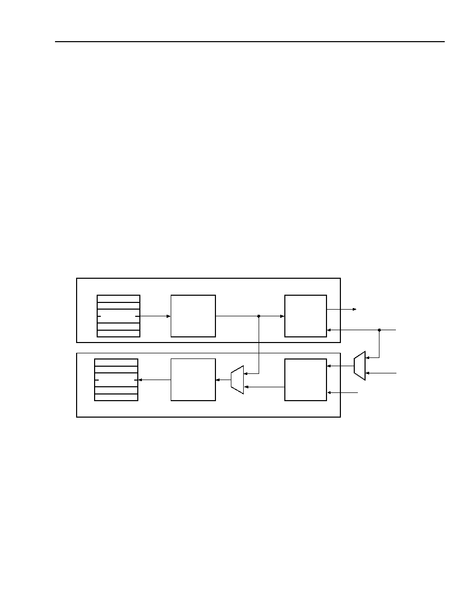
Lucent Technologies Inc.
95
Preliminary Data Sheet
October 2000
TFRA08C13 OCTAL T1/E1 Framer
Lucent Technologies Inc.
Facility Data Link
(continued)
Diagnostic Modes
Loopbacks
The serial link interface can operate in two diagnostic loopback modes: (1) local loopback and (2) remote loopback.
The local loopback mode is selected when register FDL_PR1 bit 1 (FLLB) is set to 1. The remote loopback is
selected when register FDL_PR1 bit 0 (FRLB) is set to 1. For normal traffic, i.e., to operate the transmitter and
receiver independently, the FLLP bit and the FRLB bits should both be cleared to 0. Local and remote loopbacks
cannot be enabled simultaneously.
In the local loopback mode:
s
TFDLCK clocks both the transmitter and the receiver.
s
The transmitter and receiver must both be enabled.
s
The transmitter output is internally connected to the receiver input.
s
The TFDL is active.
s
The RFDL input is ignored.
s
The communication between the transmit and receive FIFO buffers and the microprocessor continues normally.
5-4562(F)r.2
Figure 34. Local Loopback Mode
In the remote loopback mode:
s
Transmitted data is retimed with a maximum delay of 2 bits.
s
Received data is retransmitted on the TFDL.
The transmitter should be disabled. The receiver can be disabled or, if desired, enabled. Received data is sent as
usual to the receive FIFO if the receiver is enabled
XMIT HDLC FDL BLOCK
XMIT HDLC
FDL XMIT
INTERFACE
XMIT FIFO
RCVR FIFO
RCVR HDLC
FDL RCVR
INTERFACE
TFDL
TFDLCK
RFDLCK
RFDL
RCVR HDLC FDL BLOCK
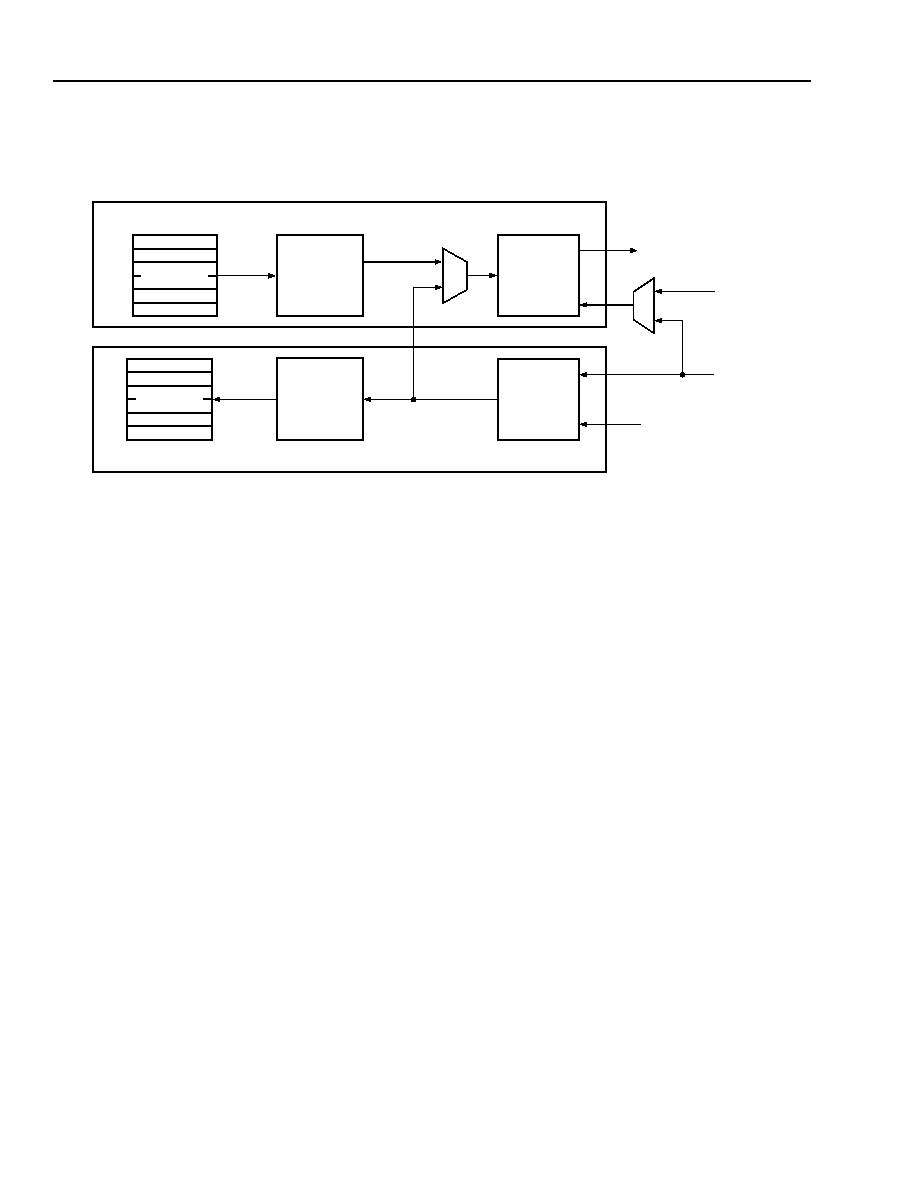
96
Lucent Technologies Inc.
Preliminary Data Sheet
TFRA08C13 OCTAL T1/E1 Framer
October 2000
Lucent Technologies Inc.
Facility Data Link
(continued)
5-4563(F)r.1
Figure 35. Remote Loopback Mode
XMIT HDLC FDL BLOCK
XMIT HDLC
FDL XMIT
INTERFACE
XMIT FIFO
RCVR FIFO
RCVR HDLC
FDL RCVR
INTERFACE
TFDL
TFDLCK
RFDLCK
RFDL
RCVR HDLC FDL BLOCK
Phase-Lock Loop Circuit
The TFRA08C13 allows for independent transmit path
and receive path clocking. The device provides outputs
to control variable clock oscillators on both the transmit
and receive paths. As such, the system may have both
the transmit and receive paths phase-locked to two
autonomous clock sources.
The block diagram of the TFRA08C13 phase detector
circuitry is shown in Figure 36. The TFRA08C13 uses
elastic store buffers (two frames) to accommodate the
transfer of data from the system interface clock rate of
2.048 Mbits/s to the line interface clock rate of either
1.544 Mbits/s or 2.048 Mbits/s. The transmit line side of
the TFRA08C13 does not have any mechanism to
monitor data overruns or underruns (slips) in its elastic
store buffer. This interface relies on the requirement
that the PLLCK clock signal (variable) is phase-locked
to the CHICK clock signal (reference). When this
requirement is not met, uncontrolled slips may occur in
the transmit elastic store buffer that would result in cor-
rupting data and no indication will be given. Typically, a
variable clock oscillator (VCXO) is used to drive the
PLLCK signal. The TFRA08C13 provides a phase error
signal (PLLCK-EPLL) that can be used to control the
VCXO PLLCK. The PLLCK-EPLL signal is generated
by monitoring the divided-down PLLCK (DIV-PLLCK)
and CHICK (DIV-CHICK) signals. The DIV-CHICK sig-
nal is used as the reference to determine the phase dif-
ference between DIV-CHICK and DIV-PLLCK. While
DIV-CHICK and DIVPLLCK are phase-locked, the
PLLCK-EPLL signal is in a high-impedance state. A
phase difference between DIV-CHICK and DIV-PLLCK
drives PLLCK-EPLL to either 3.3 V or 0 V. An appropri-
ate loop filter, for example, an RC circuit with R = 1 k
and C = 0.1 µF, is used to filter these PLLCK-EPLL
pulses to control the VCXO.
The system can force CHICK to be phase-locked to
RLCK by using RLCK as a reference signal to control a
VCXO that is sourcing the CHICK signal. The
TFRA08C13 uses the receive line signal (RLCK) as the
reference and the CHICK signal as the variable signal.
The TFRA08C13 provides a phase error signal
(CHICK-EPLL) that can be used to control the VCXO
generating CHICK. The CHICK-EPLL signal is gener-
ated by monitoring the divided-down CHICK signal
(DIV-CHICK) and RLCK (DIV-RLCK) signals. The DIV-
RLCK signal is used as the reference to determine the
phase difference between DIV-CHICK and DIV-RLCK.
While DIV-RLCK and DIV-CHICK are phase-locked, the
CHICK-EPLL signal is in a high-impedance state. A
phase difference between DIV-RLCK and DIV-CHICK
drives CHICK-EPLL to either 3.3 V or 0 V. An appropri-
ate loop filter, for example, an RC circuit with R = 1 k
and C = 0.1 µF, is used to filter these CHICK-EPLL
pulses to control the VCXO. In this mode, the
TFRA08C13 can be programmed to act as a master
timing source and is capable of generating the system
frame synchronization signal through the CHIFS pin
and setting FRM_PR45 bit 4 to 1.
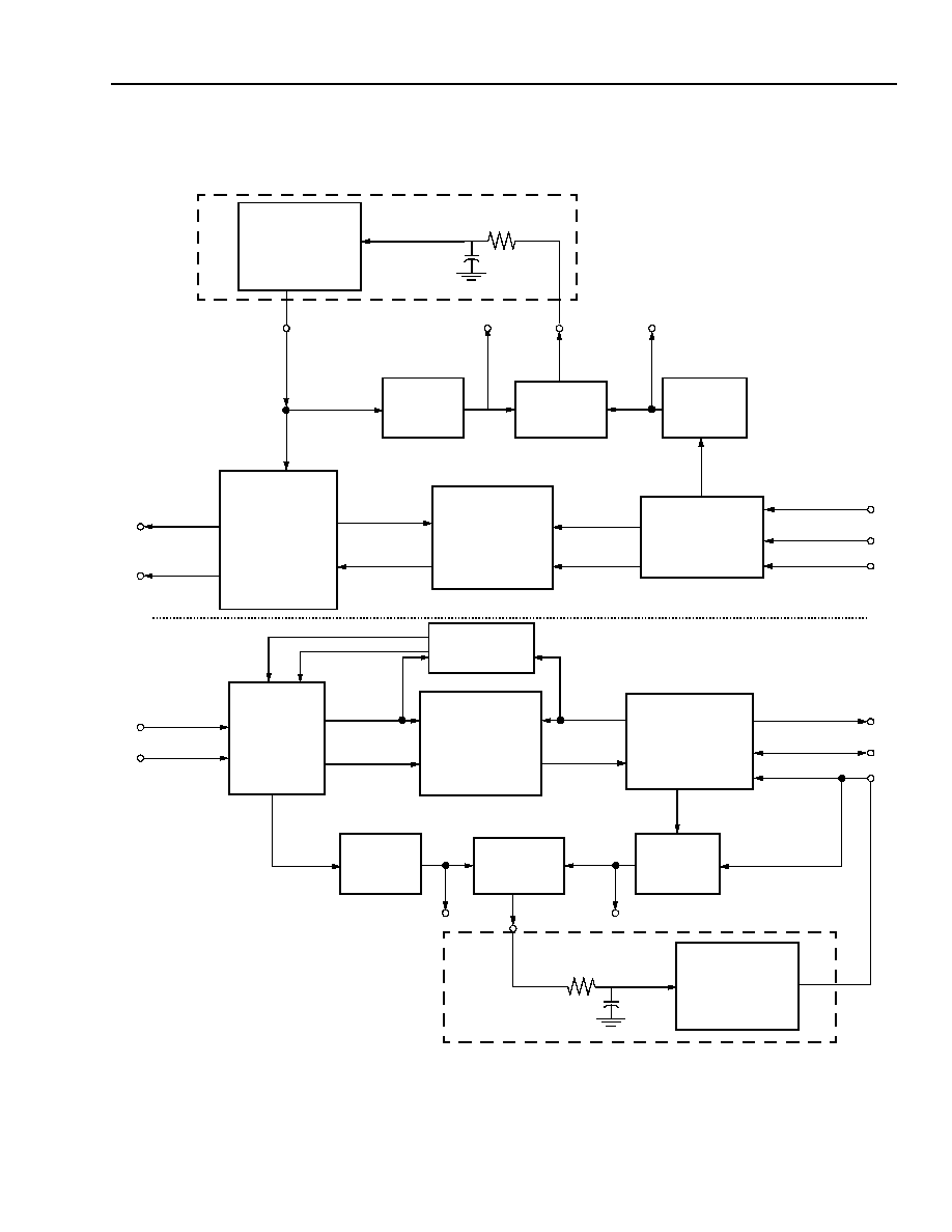
Lucent Technologies Inc.
97
Preliminary Data Sheet
October 2000
TFRA08C13 OCTAL T1/E1 Framer
Lucent Technologies Inc.
Phase-Lock Loop Circuit
(continued)
5-5268(F).a
Figure 36. TFRA08C13 Phase Detector Circuitry
TPD, TND
TLCK
TRANSMIT
FRAMER
RECEIVE
CONCENTRATION
HIGHWAY
INTERFACE
RCHIDATA
CHICK
CHIFS
TRANSMIT
CONCENTRATION
HIGHWAY
INTERFACE
RECEIVE
2-FRAME
ELASTIC STORE
BUFFER
RECEIVE
FRAMER
RPD, RND
RLCK
READ ADDRESS
TRANSMIT
2-FRAME
ELASTIC STORE
BUFFER
PLLCK
DIVIDER
CIRCUIT
INTERNAL_XLCK
PLLCK
DIV-PLLCK
DIGITAL
PHASE
DETECTOR
CHICK
DIVIDER
CIRCUIT
PLLCK-EPLL
DIV-CHICK
VOLTAGE-
CONTROLLED
CRYSTAL
OSCILLATOR
(VCXO)
CHICK
TCHIDATA
CHIFS
SYSTEM DATA
WRITE ADDRESS
SYSTEM DATA
READ ADDRESS
FACILITY DATA
WRITE ADDRESS
FACILITY DATA
SLIP
MONITOR
BUFFER OVERRUN
BUFFER UNDERRUN
RLCK
DIVIDER
CIRCUIT
DIGITAL
PHASE
DETECTOR
CHICK
DIVIDER
CIRCUIT
DIV-RLCK
DIV-CHICK
CHICK_EPLL
VOLTAGE-
CONTROLLED
CRYSTAL
OSCILLATOR
(VCXO)
INTERNAL_CHICK
INTERNAL_RLCK
INTERNAL_CHICK
EXTERNAL CIRCUIT
EXTERNAL CIRCUIT

Preliminary Data Sheet
TFRA08C13 OCTAL T1/E1 Framer
October 2000
98
Lucent Technologies Inc.
Lucent Technologies Inc.
Framer-System Interface
DS1 Modes
The DS1 framing formats require rate adaptation from
the 1.544 Mbits/s line interface bit stream to the system
interface which functions at multiples of a 2.048 Mbits/s
bit stream. The rate adaptation results in the need for
eight stuffed time slots on the system interface since
there are only 24 DS1 (1.544 Mbits/s) payload time
slots while there are 32 system (2.048 Mbits/s) time
slots. Placement of the stuffed time slots is defined by
register FRM_PR43 bit 0--bit 2.
CEPT Modes
The framer maps the line time slots into the corre-
sponding system time slot one-to-one. Framing time
slot 0, the FAS and NFAS bytes, are placed in system
time slot 0.
Receive Elastic Store
The receive interface between the framer and the sys-
tem CHI includes a 2-frame elastic store buffer to
enable rate adaptation. The receive line elastic store
buffer contains circuitry that monitors the read and
write pointers for potential data overrun and underrun
(slips) conditions. Whenever this slip circuitry deter-
mines that a slip may occur in the receive elastic store
buffer, it will adjust the read pointer such that a con-
trolled slip is performed. The controlled slip is imple-
mented by dropping or repeating a complete frame at
the frame boundaries. The occurrence of controlled
slips in the receive elastic store are indicated in the sta-
tus register FRM_SR3 bit 6 and bit 7.
Transmit Elastic Store
The transmit interface between the framer and the sys-
tem CHI includes a 2-frame elastic store buffer to
enable rate adaptation. The line transmit clock applied
to PLLCK[1--8] must be phase-locked to CHICK. No
indication of a slip in the transmit elastic store is given.
Concentration Highway Interface
Each framer has a dual, high-speed, serial interface to
the system known as the CHI. This flexible bus archi-
tecture allows the user to directly interface to other
Lucent components which use this interface, as well as
to
Mitel*
and
AMD
TDM highway interfaces, with no
glue logic. Configured via the highway control registers
FRM_PR45 through FRM_PR66, this interface can be
set up in a number of different configurations.
The following is a list of the CHI features:
s
Lucent Technologies standard interface for communi-
cation devices.
s
Two pairs of transmit and receive paths to carry data
in 8-bit time slots.
s
Programmable definition of highways through offset
and clock-edge options which are independent for
transmit and receive directions.
s
Programmable idle code substitution of received time
slots.
s
Programmable 3-state control of each transmit time
slot.
s
Independent transmit and receive framing signals to
synchronize each direction of data flow.
s
An 8 kHz frame synchronization signal internally
generated from the received line clock.
s
Compatible with
Mitel
and
AMD
PCM highways.
Supported is the optional configuration of the CHI
which presents the signaling information along with the
data in any framing modes when the device is pro-
grammed for the associated signaling mode (ASM).
This mode is discussed in the signaling section.
Data can be transmitted or received on either one of
two interface ports, called CHIDATA and CHIDATAB.
The user-supplied clock (CHICLK) controls the timing
on the transmit or receive paths. Individual time slots
are referenced to the frame synchronization (CHIFS)
pulse. Each frame consists of 32 time slots at a pro-
grammable data rate of 2.048 Mbits/s, 4.096 Mbits/s, or
8.192 Mbits/s requiring a clock (CHICK) of the same
rate. The clock and data rates of the transmit and
receive highways are programmed independently.
*
Mitel
is a registered trademark of Mitel Corporation.
AMD
is a registered trademark of Advanced Micro Devices, Inc.

Lucent Technologies Inc.
99
Preliminary Data Sheet
October 2000
TFRA08C13 OCTAL T1/E1 Framer
Lucent Technologies Inc.
Concentration Highway Interface
(continued)
Rate adaptation is required for all DS1 formats between
the 1.544 Mbits/s line rate and 2.048 Mbits/s,
4.966 Mbits/s, or 8.182 Mbits/s CHI rate. This is
achieved by means of stuffing eight idle time slots into
the existing twenty-four time slots of the T1 frame. Idle
time slots can occur every fourth time slot (starting in
the first, second, third, or fourth time slot) or be
grouped together at the end of the CHI frame as
described in register FRM_PR43 bit 0--bit 2. The posi-
tioning of the idle time slots is the same for transmit
and receive directions. Idle time slots contain the pro-
grammable code of register FRM_PR23. Unused time
slots can be disabled by forcing the TCHIDATA inter-
face to a high-impedance state for the interval of the
disabled time slots.
CHI Parameters
The CHI parameters that define the receive and transmit paths are given in Table 45.
Table 45. Summary of the TFRA08C13's Concentration Highway Interface Parameters
Name
Description
HWYEN
Highway Enable (FRM_PR45 bit 7). A 1 in this bit enables the transmit and receive
concentration highway interfaces. This allows the framer to be fully configured before
transmission to the highway. A 0 forces the idle code as defined in register
FRM_PR22, to be transmitted to the line in all payload time slots while TCHIDATA is
forced to a high-impedance state for all CHI transmitted time slots.
CHIMM
Concentration Highway Master Mode (PRM_PR45 bit 4). The default mode
CHIMM = 0 enables an external system frame synchronization signal (CHIFS) to
drive the transmit CHI. A 1 enables the transmit CHI to generate a system frame syn-
chronization signal from the receive line clock. The transmit CHI system frame syn-
chronization signal is generated on the CHIFS output pin. Applications using the
receive line clock as the reference clock signal of the system are recommended to
enable this mode and use the CHIFS signal generated by the framer. The receive CHI
path is not affected by this mode.
CHIDTS
CHI Double Time-Slot Mode (FRM_PR65 bit 1 and FRM_PR66 bit 1). CHIDTS
defines the 4.096 Mbits/s and 8.192 Mbits/s CHI modes. CHIDTS = 0 enables the 32
contiguous time-slot mode. This is the default mode. CHIDTS = 1 enables the double
time-slot mode in which the transmit CHI drives TCHIDATA for one time slot and then
3-states for the subsequent time slot, and the receive CHI latches data from RCHI-
DATA for one time slot and then ignores the following time slot and so on. CHIDTS = 1
allows two CHIs to interleave frames on a common bus.
TFE
Transmit Frame Edge (FRM_PR46 bit 3). TFE = 0 (or 1), CHIFS is sampled on the
falling (or rising) edge of CHICK. In CHIMM (CHI master mode), the CHIFS pin outputs
a transmit frame strobe to provide synchronization for TCHIDATA. When TFE = 1 (or
0), CHIFS is centered around rising (or falling) edge of CHICK. In this mode, CHIFS
can be used for receive data on RCHIDATA. The timing for CHIFS in CHIMM = 1 mode
is identical to the timing for CHIFS in CHIMM = 0 mode.
RFE
Receive Frame Edge (FRM_PR46 bit 7). RFE = 0 (or 1), CHIFS is sampled on the
falling (or rising) edge of CHICK.
CDRS0--CDRS1
CHI Data Rate (FRM_PR45 bit 2 and bit 3). Two-bit control for selecting the CHI data
rate. The default state (00) enables the 2.048 Mbits/s.
CDRS Bit:
2 3
CHI Data Rate
0 0
2.048 Mbits/s
0 1
4.096 Mbits/s
1 0
8.192 Mbits/s
1 1
Reserved

Preliminary Data Sheet
TFRA08C13 OCTAL T1/E1 Framer
October 2000
100
Lucent Technologies Inc.
Lucent Technologies Inc.
Name
Description
TCE
Transmitter Clock Edge (FRM_PR47 bit 6). TCE = 0 (or 1), TCHIDATA is clocked on
the falling (or rising) edge of CHICK.
RCE
Receiver Clock Edge (FRM_PR48 bit 6). RCE = 0 (or 1), RCHIDATA is latched on
the falling (or rising) edge of CHICK.
TTSE31--TTSE0
Transmit Time-Slot Enable 31--0 (FRM_PR49--FRM_PR52). These bits define
which transmit CHI time slots are enabled. A 1 enables the TCHIDATA or TCHIDATAB
time slot. A 0 forces the CHI transmit highway time slot to be 3-stated.
RTSE31--RTSE0
Receive Time-Slot Enable 31--0 (FRM_PR53--FRM_PR56). These bits define
which receive CHI time slots are enabled. A 1 enables the RCHIDATA or RCHDATAB
time slots. A 0 disables the time slot and transmits the programmable idle code of reg-
ister FRM_PR22 to the line interface.
THS31--THS0
Transmit Highway Select 31--0 (FRM_PR57--FRM_PR60). These bits define
which transmit CHI highway, TCHIDATA or TCHIDATAB, contains valid data for the
active time slot. A 0 enables TCHIDATA; a 1 enables the TCHIDATAB.
RHS31--RHS0
Receive Highway Select 31--0 (FRM_PR61--FRM_PR64). These bits define which
receive CHI highway, RCHIDATA or RCHIDATAB, contains valid data for the active
time slot. A 0 enables RCHIDATA; a 1 enables the RCHIDATAB.
TOFF2--TOFF0
Transmitter Bit Offset (FRM_PR46 bit 0--bit 2). These bits are used in conjunction
with the transmitter byte offset to define the beginning of the transmit frame. They
determine the offset relative to TCHIFS, for the first bit of transmit time slot 0. The off-
set is the number of CHICK cycles by which the first bit is delayed.
ROFF2--ROFF0
Receiver Bit Offset (FRM_PR46 bit 4--bit 6). These bits are used in conjunction
with the receiver byte offset to define the beginning of the receiver frame. They deter-
mine the offset relative to the RCHIFS, for the first bit of receive time slot 0. The offset
is the number of CHICK cycles by which the first bit is delayed.
TBYOFF6--TBYOFF0
Transmitter Byte Offset (FRM_PR47 bit 0--bit 5 and FRM_PR65 bit 0). These bits
determine the offset from the CHIFS to the beginning of the next frame on the trans-
mit highway. Note that in the ASM mode, a frame consists of 64 contiguous bytes;
whereas in other modes, a frame contains 32 contiguous bytes. Allowable offsets:
2.048 Mbits/s 0--31 bytes.
4.096 Mbits/s 0--63 bytes.
8.192 Mbits/s 0--127 bytes.
RBYOFF6--RBYOFF0
Receiver Byte Offset (FRM_PR48 bit 0--bit 5 and FRM_PR66 bit 0). These bits
determine the offset from CHIFS to the beginning of the receive CHI frame. Note that
in the ASM mode, a frame consists of 64 contiguous bytes; whereas in other modes,
a frame contains 32 contiguous bytes. Allowable offsets:
2.048 Mbits/s 0--31 bytes.
4.096 Mbits/s 0--63 bytes.
8.192 Mbits/s 0--127 bytes.
ASM
Associated Signaling Mode (FRM_PR44 bit 2). When enabled, the associate sig-
naling mode configures the CHI to carry both payload data and its associated signal-
ing information. Enabling this mode must be in conjunction with the programming of
the CHI data rate to either 4.048 Mbits/s or 8.096 Mbits/s. Each time slot consists of
16 bits where 8 bits are data and the remaining 8 bits are signaling information.
STS0--STS2
Stuffed Time Slots (FRM_PR43 bit 0--bit 2). Valid only in T1 framing formats, these 3
bits define the location of the eight stuffed CHI (unused) time slots.
Concentration Highway Interface
(continued)
Table 45. Summary of the TFRA08C13's Concentration Highway Interface Parameters (continued)
Lucent Technologies Inc.
101
Preliminary Data Sheet
October 2000
TFRA08C13 OCTAL T1/E1 Framer
Lucent Technologies Inc.
Concentration Highway Interface
(continued)
CHI Frame Timing
CHI Timing with CHIDTS Disabled
Figure 37 illustrates the CHI frame timing when CHIDTS is disabled (registers FRM_PR65 bit 1 (TCHIDTS) and
FRM_PR66 bit 1 (RCHDTS) = 0) and the CHI is not in the associated signaling mode (FRM_PR44
bit 2 (ASM) = 0). The frames are 125 ms long and consist of 32 contiguous time slots.
In DS1 frame modes, the CHI frame consists of 24 payload time slots and eight stuffed (unused) time slots.
In CEPT frame modes, the CHI frame consists of 32 payload time slots.
5-5269(F).ar.2
* The position of the stuffed time is controlled by register FRM_PR43 bit 0--bit 2.
Figure 37. Nominal Concentration Highway Interface Timing (for FRM_PR43 bit 0--bit 2 = 100 (Binary))
CHIFS
125
µ
s
TCHIDATA
FRAME 1
FRAME 1
FRAME 2
RCHIDATA
FRAME 2
8.192 Mbits/s CHI:
FRAME 1
FRAME 2
RCHIDATA
4.096 Mbits/s CHI:
2.048 Mbits/s CHI:
TCHIDATA
FRAME 1
FRAME 2
HIGH IMPEDANCE
HIGH IMPEDANCE
24 VALID TIME SLOTS
HIGH IMPEDANCE
FRAME 2
TCHIDATA
FRAME 2
RCHIDATA
DS1 FORMAT
FRAME 1
FRAME 2
2.048 Mbits/s CHI:
RCHIDATA
TCHIDATA
or
CEPT FORMAT
32 VALID TIME SLOTS
24 VALID TIME SLOTS
8 STUFFED
SLOTS*
FRAME 1

Preliminary Data Sheet
TFRA08C13 OCTAL T1/E1 Framer
October 2000
102
Lucent Technologies Inc.
Lucent Technologies Inc.
Concentration Highway Interface
(continued)
CHI Timing with CHIDTS Enabled
Figure 38 illustrates the CHI frame timing when CHIDTS is enabled (registers FRM_PR65 bit 1 (TCHIDTS) and
FRM_PR66 bit 1 (RCHIDTS) = 1) and ASM is disabled (register FRM_PR44 bit 2 (ASM) = 0). In the CHIDTS
mode, valid CHI payload time slots are alternated with high-impedance intervals of one time-slot duration. This
mode is valid only for 4.096 Mbits/s and 8.192 Mbits/s CHI rates.
5-6454(F)r.3
Figure 38. CHIDTS Mode Concentration Highway Interface Timing
CHIFS
125
µ
s
TCHIDATA
TS0
RCHIDATA
8.192 Mbits/s CHI
RCHIDATA
4.096 Mbits/s CHI
TCHIDATA
HIGH IMPEDANCE
TS1
TS2
TS3
TS0
TS1
TS2
TS3
TS31
TS0
TS31
TS0
FRAME 1
TIME
SLOT
8 bits
TIME
SLOT
FRAME 2
TS0
TS1
TS31
TS31
TS0
TS0
TS1
TS0
TS4
TS30
TS4
T30
TS2
TS30
TS2
TS30
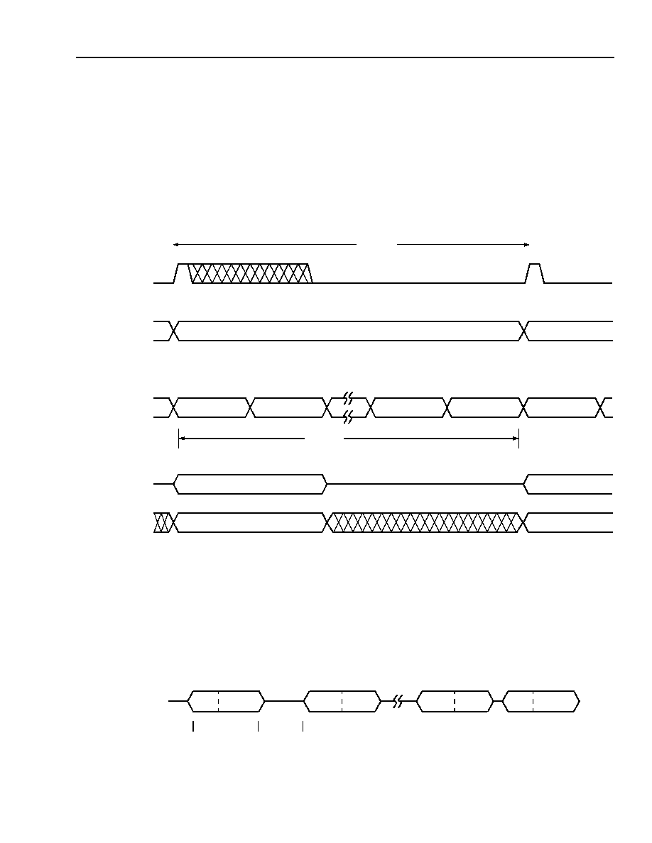
Lucent Technologies Inc.
103
Preliminary Data Sheet
October 2000
TFRA08C13 OCTAL T1/E1 Framer
Lucent Technologies Inc.
Concentration Highway Interface
(continued)
CHI Timing with Associated Signaling Mode Enabled
Figure 39 illustrates the CHI frame timing when the associated signaling mode is enabled (register FRM_PR44 bit
2 (ASM) = 1) and the CHIDTS mode is disabled (registers FRM_PR65 bit 1 (TCHIDTS) = 0 and FRM_PR66 bit 1
(RCHIDTS) = 0). The frames are 125 ms long and consist of 32 contiguous 16-bit time slots.
In DS1 frame formats, each frame consists of 24 time slots and eight stuffed time slots. Each time slot consists of
two octets.
In CEPT modes, each frame consists of 32 time slots. Each time slot consists of two octets.
5-5270(F).ar.3
Figure 39. Associated Signaling Mode Concentration Highway Interface Timing
CHI Timing with Associated Signaling Mode and CHIDTS Enabled
Figure 40 illustrates the CHI frame timing in the associated signaling mode (register FRM_PR44 bit 2 (ASM) = 1)
and CHIDTS enabled (registers FRM_PR65 bit 1 (TCHIDTS) = 1 and FRM_PR66 bit 1 (RCHIDTS) = 1).
5-6454(F).ar.2
* High-impedance state for TCHIDATA and not received (don't care) for RCHIDATA.
Figure 40. CHI Timing with ASM and CHIDTS Enabled
CHIFS
125
µ
s
FRAME 1
FRAME 2
8.192 Mbits/s CHI:
RCHIDATA
4.096 Mbits/s CHI:
TCHIDATA
FRAME 1
FRAME 1
FRAME 2
FRAME 2
HIGH IMPEDANCE
RCHIDATA
TCHIDATA
or
FRAME = 64 bytes: 32 DATA + 32 SIGNALING
DATA AND SIGNALING BYTES ARE INTERLEAVED
SIGNALING 0
DATA 0
SIGNALING 31
DATA 0
DATA 31
FRAME
DATA
SIGNALING
TS0
TS1
TS31
TS0
16 bits
1 TIME SLOT
16 bits
1 TIME SLOT
8.192 Mbits/s CHI WITH ASM (ASSOCIATED SIGNALING MODE) ENABLED
DATA
SIGNALING
TCHIDATA
OR
RCHIDATA
*
*
*
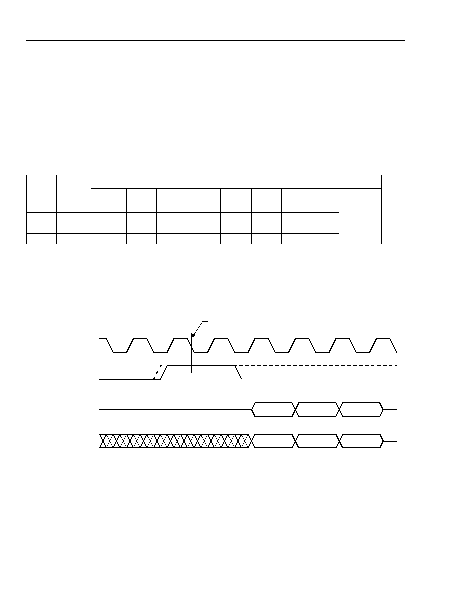
Preliminary Data Sheet
TFRA08C13 OCTAL T1/E1 Framer
October 2000
104
Lucent Technologies Inc.
Lucent Technologies Inc.
* The
ORCA
Series 3 FPGA data sheet contains more information on how to control these signals during start-up. The timing of DONE release
is controlled by one set of bit stream options, and the timing of the simultaneous release of all other configuration pins (and the activation of all
user I/Os) is controlled by a second set of options.
Concentration Highway Interface
(continued)
CHI Offset Programming
To facilitate bit offset programming, two additional internal parameters are introduced: CEX is defined as the clock
edge with which the first bit of time slot 0 is transmitted; CER is defined as the clock edge on which bit 0 of time slot
0 is latched. CEX and CER are counted relative to the edge on which the CHIFS signal is sampled. Values of CEX
and CER depend upon the values of the parameters described above.
The following table gives decimal values of CEX and CER for various values of TFE, RFE, TCE, RCE, TOFF[2:0],
and ROFF[2:0]. The byte (time slot) offsets are assumed to be zero in the following examples.
Table 46. Programming Values for TOFF[2:0] and ROFF[2:0] when CMS = 0
Figure 41 shows an example of the relative timing of CHI 2.048 Mbits/s data with the following parameters:
s
CMS = 0, TFE, RFE = 0.
s
TCE = 1, TOFF[2:0] = 000, TBYOFF[6:0] = 0000000.
s
RCE = 0, ROFF[2:0] = 000, RBYOFF[6:0] = 0000000.
5-2202(F).d
Figure 41. TCHIDATA and RCHIDATA to CHICK Relationship with CMS = 0
(CEX = 3 and CER = 4, Respectively)
RFE/
TFE
RCE/
TCE
ROFF[2:0] or TOFF[2:0]
000
001
010
011
100
101
110
111
CER
or
CEX
(decimal)
0
0
4
6
8
10
12
14
16
18
0
1
3
5
7
9
11
13
15
17
1
0
3
5
7
9
11
13
15
17
1
1
4
6
8
10
12
14
16
18
CHIFS IS SAMPLED ON THIS EDGE: FE = 0
1
2
3
4
5
6
7
8
BIT 0, TS 0
BIT 1, TS 0
BIT 2, TS 0
CEX = 3
CER = 4
BIT 0, TS 0
BIT 1, TS 0
BIT 2, TS 0
HIGH IMPEDANCE
RCHIDATA: RCE = 0
TCHIDATA: TCE = 1
CHIFS
CHICK
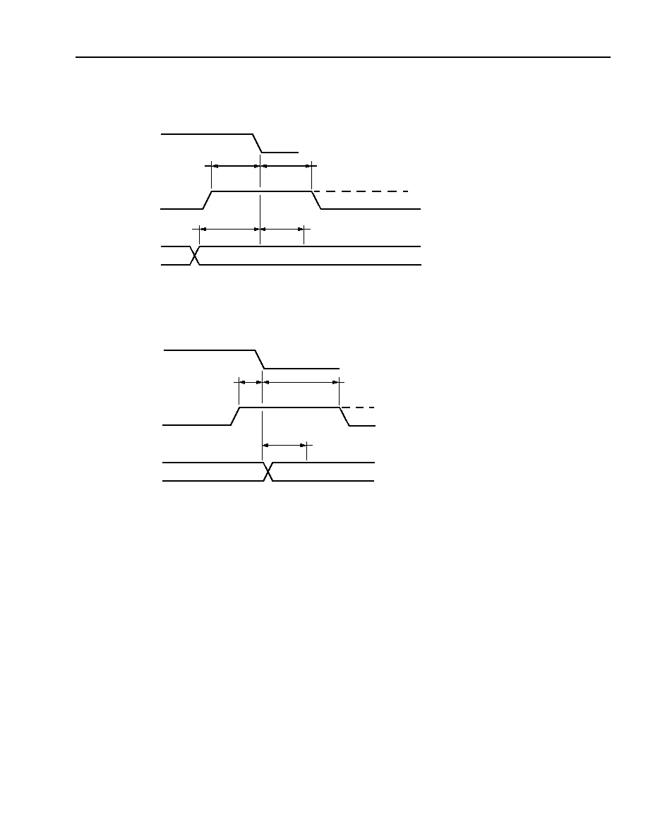
Lucent Technologies Inc.
105
Preliminary Data Sheet
October 2000
TFRA08C13 OCTAL T1/E1 Framer
Lucent Technologies Inc.
Concentration Highway Interface
(continued)
Figure 42 and Figure 43 illustrate the CHI timing.
5-3916(F).d
Note: For case illustrated, RFE = 0, and RCE = 0.
Figure 42. Receive CHI (RCHIDATA) Timing
5-3917(F).d
Note: For case illustrated, TFE = 0 and TCE = 0.
Figure 43. Transmit CHI (TCHIDATA) Timing
CHICLK
CHIFS
RCHIDATA
t14S
t14H
t14S: CHIFS SETUP = 30 ns min
t15H
t14H: CHIFS HOLD = 45 ns min
t15S: RCHIDATA SETUP = 25 ns min
t15S
t15S: RCHIDATA HOLD = 25 ns min
CHICLK
CHIFS
TCHIDATA
t14S
t14H
t14S: CHIFS SETUP = 35 ns min
t19
t14H: CHIFS HOLD = 45 ns min
t19: CHICK TO TCHIDATA DELAY = 25 ns max
JTAG Boundary-Scan Specification
Principle of the Boundary Scan
The boundary scan (BS) is a test aid for chip, module,
and system testing. The key aspects of BS are as fol-
lows:
s
Testing the connections between ICs on a particular
board.
s
Observation of signals to the IC pins during normal
operating functions.
s
Controlling the built-in-self-test (BIST) of an IC.
TFRA08C13 does not support BS-BIST.
Designed according to the
IEEE
Std. 1149.1-1990
standard, the BS test logic consists of a defined
interface: the test access port (TAP). The TAP is made
up of four signal pins assigned solely for test purposes.
The fifth test pin ensures that the test logic is initialized
asynchronously. The BS test logic also comprises a 16-
state TAP controller, an instruction register with a
decoder, and several test data registers (BS register,
BYPASS register, and IDCODE register). The main
component is the BS register that links all the chip pins
to a shift register by means of special logic cells. The
test logic is designed in such a way that it is operated
independently of the application logic of the
TFRA08C13 (the mode multiplexer of the BS output
cells may be shared). Figure 44 illustrates the block
diagram of the TFRA08C13's BS test logic.

Preliminary Data Sheet
TFRA08C13 OCTAL T1/E1 Framer
October 2000
106
Lucent Technologies Inc.
Lucent Technologies Inc.
JTAG Boundary-Scan Specification
(continued)
5-3923(F)r.4
Figure 44. Block Diagram of the TFRA08C13's Boundary-Scan Test Logic
BOUNDARY-SCAN REGISTER
TDI
TRST
TMS
TCK
TAP
CONTROLLER
INSTRUCTION
DECODER
OUT
TDO
IN
MUX
CHIP KERNEL
(UNAFFECTED BY BOUNDARY-SCAN TEST)
IDCODE REGISTER
BYPASS REGISTER
INSTRUCTION REGISTER

Lucent Technologies Inc.
107
Preliminary Data Sheet
October 2000
TFRA08C13 OCTAL T1/E1 Framer
Lucent Technologies Inc.
JTAG Boundary-Scan Specification
(continued)
Test Access Port Controller
The test access port controller is a synchronous sequence controller with 16 states. The state changes are preset
by the TMS, TCK, and TRST signals and by the previous state. The state changes always take place when the
TCK edge rises. Figure 45 shows the TAP controller state diagram.
5-3924(F)r.5
Figure 45. BS TAP Controller State Diagram
The value shown next to each state transition in Figure 45 represents the signal present at TMS at the time of a ris-
ing edge at TCK.
The description of the TAP controller states is given in
IEEE
Std. 1149.1-1990 Section 5.1.2 and is reproduced in
Table 49 and Table 50.
SELECT-DR
CAPTURE-DR
1
0
0
1
1
SHIFT-DR
EXIT1-DR
PAUSE-DR
0
1
EXIT2-DR
UPDATE-DR
1
1
0
0
0
0
TEST LOGIC
RESET
RUN TEST/
IDLE
1
0
SELECT-IR
CAPTURE-IR
1
0
0
1
1
SHIFT-IR
EXIT1-IR
PAUSE-IR
0
1
EXIT2-IR
UPDATE-IR
1
1
0
0
0
0
TRST = 0
0
1
1

Preliminary Data Sheet
TFRA08C13 OCTAL T1/E1 Framer
October 2000
108
Lucent Technologies Inc.
Lucent Technologies Inc.
JTAG Boundary-Scan Specification
(continued)
Table 47. TAP Controller States in the Data Register Branch
Table 48. TAP Controller States in the Instruction Register Branch
Name
Description
TEST LOGIC RESET
The BS logic is switched in such a way that normal operation of the ASIC is
adjusted. The IDCODE instruction is initialized by TEST LOGIC RESET. Irre-
spective of the initial state, the TAP controller has achieved TEST LOGIC
RESET after five control pulses at the latest when TMS = 1. The TAP controller
then remains in this state. This state is also achieved when TRST = 0.
RUN TEST/IDLE
Using the appropriate instructions, this state can activate circuit parts or initiate
a test. All of the registers remain in their present state if other instructions are
used.
SELECT-DR
This state is used for branching to the test data register control.
CAPTURE-DR
The test data is loaded in the test data register parallel to the rising edge of TCK
in this state.
SHIFT-DR
The test data is clocked by the test data register serially to the rising edge of
TCK in the state. The TDO output driver is active.
EXIT(1/2)-DR
This temporary state causes a branch to a subsequent state.
PAUSE-DR
The input and output of test data can be interrupted in this state.
UPDATE-DR
The test data is clocked into the second stage of the test data register parallel to
the falling edge of TCK in this state.
Name
Description
SELECT-IR
This state is used for branching to the instruction register control.
CAPTURE-IR
The instruction code 0001 is loaded in the first stage of the instruction register
parallel to the rising edge of TCK in this state.
SHIFT-IR
The instructions are clocked into the instruction register serially to the rising edge
of TCK in the state. The TDO output driver is active.
EXIT(1/2)-IR
This temporary state causes a branch to a subsequent state.
PAUSE-IR
The input and output of instructions can be interrupted in this state.
UPDATE-IR
The instruction is clocked into the second stage of the instruction register parallel
to the falling edge of TCK in this state.

Lucent Technologies Inc.
109
Preliminary Data Sheet
October 2000
TFRA08C13 OCTAL T1/E1 Framer
Lucent Technologies Inc.
JTAG Boundary-Scan Specification
(continued)
Instruction Register
The instruction register (IR) is 4 bits in length. Table 49 shows the BS instructions implemented by the
TFRA08C13.
Table 49. TFRA08C13's Boundary-Scan Instructions
Instruction
Code
Act. Register
TDI
TDO
Mode
Function
Output Defined Via
EXTEST
0000
Boundary Scan
TEST
Test external
connections
BS Register
IDCODE
0001
Identification
NORMAL
Read Manuf.
Register
Core Logic
HIGHZ
0100
BYPASS
X
3-state
Output--High Impedance
SAMPLE/PRELOAD
0101
Boundary Scan
NORMAL
Sample/load
Core Logic
BYPASS
1111
BYPASS
NORMAL
Min. shift path
Core Logic
EVERYTHING ELSE
--
BYPASS
X
--
Output--High Impedance
The instructions not supported in TFRA08C13 are
INTEST, RUNBIST, TOGGLE. A fixed binary 0001 pat-
tern (the 1 into the least significant bit) is loaded into
the IR in the capture-IR controller state. The IDCODE
instruction (binary 0001) is loaded into the IR during
the test-logic-reset controller state and at powerup.
The following is an explanation of the instructions sup-
ported by TFRA08C13 and their effect on the devices'
pins.
EXTEST
This instruction enables the path cells, the pins of the
ICs, and the connections between ASICs to be tested
via the circuit board. The test data can be loaded in the
chosen position of the BS register by means of the
SAMPLE/PRELOAD instruction. The EXTEST instruc-
tion selects the BS register as the test data register.
The data at the function inputs is clocked into the BS
register on the rising edge of TCK in the CAPTURE-DR
state. The contents of the BS register can be clocked
out via TDO in the SHIFT-DR state. The value of the
function outputs is solely determined by the contents of
the data clocked into the BS register and only changes
in the UPDATE-DR state on the falling edge of TCK.
DCODE
Information regarding the manufacturer's ID for Lucent,
the IC number, and the version number can be read out
serially by means of the IDCODE instruction. The
IDCODE register is selected, and the BS register is set
to normal mode in the UPDATE-IR state. The IDCODE
is loaded at the rising edge of TCK in the CAPTURE-
DR state. The IDCODE register is read out via TDO in
the SHIFT-DR state.
HIGHZ
All 3-statable outputs are forced to a high-impedance
state, and all bidirectional ports to an input state by
means of the HIGHZ instruction. The impedance of the
outputs is set to high in the UPDATE-IR state. The func-
tion outputs are only determined in accordance with
another instruction if a different instruction becomes
active in the UPDATE-IR state. The BYPASS register is
selected as the test data register. The HIGHZ instruc-
tion is implemented in a similar manner to that used for
the BYPASS instruction.
SAMPLE/PRELOAD
The SAMPLE/PRELOAD instruction enables all the
input and output pins to be sampled during operation
(SAMPLE) and the result to be output via the shift
chain. This instruction does not impair the internal logic
functions. Defined values can be serially loaded in the
BS cells via TDI while the data is being output (PRE-
LOAD).

Preliminary Data Sheet
TFRA08C13 OCTAL T1/E1 Framer
October 2000
110
Lucent Technologies Inc.
Lucent Technologies Inc.
JTAG Boundary-Scan Specification
(continued)
BYPASS
This instruction selects the BYPASS register. A minimal shift path exists between TDI and TDO. The BYPASS reg-
ister is selected after the UPDATE-IR. The BS register is in normal mode. A 0 is clocked into the BYPASS register
during CAPTURE-DR state. Data can be shifted by the BYPASS register during SHIFT-DR. The contents of the BS
register do not change in the UPDATE-DR state. Please note that a 0 that was loaded during CAPTURE-DR
appears first when the data is being read out.
Boundary-Scan Register
The boundary-scan register is a shift register, whereby one or more BS cells are assigned to every digital
TFRA08C13 pin (with the exception of the pins for the BS architecture, analog signals, and supply voltages). The
TFRA08C13's boundary-scan register bit-to-pin assignment is defined in the BSDL file, which is available upon
request. Please call 1-800-TECKFAX (1-800-832-5329).
BYPASS Register
The BYPASS register is a one-stage shift register that enables the shift chain to be reduced to one stage in the
TFRA08C13.
DCODE Register
The IDCODE register identifies the TFRA08C13 by means of a parallel, loadable, 32-bit shift register. The code is
loaded on the rising edge of TCK in the CAPTURE-DR state. The 32-bit data is organized into four sections as fol-
lows.
Table 50. IDCODE Register
3-State Procedures
The 3-state input participates in the boundary scan. It has a BS cell, but buffer blocking via this input is suppressed
for the EXTEST instruction. The 3-state input is regarded as a signal input that is to participate in the connection
test during EXTEST. The buffer blocking function should not be active during EXTEST to ensure that the update
pattern at the TFRA08C13 outputs does not become corrupted.
Version
Part Number
Manufacturer ID
1
Bits 31--28
Bits 27--12
Bits 11--1
Bit 0
0001
0111011000110100
00000011101
1

Lucent Technologies Inc.
111
Preliminary Data Sheet
October 2000
TFRA08C13 OCTAL T1/E1 Framer
Lucent Technologies Inc.
Microprocessor Interface
Overview
The TFRA08C13 device is equipped with a micropro-
cessor interface that can operate with most commer-
cially available microprocessors. The microprocessor
interface provides access to all the internal registers
through a 12-bit address bus and an 8-bit data bus.
Input MPMODE (pin AF9) is used to configure this
interface into one of two possible modes, as shown in
Table 51. The MPMODE setting selects the associated
set of control signals required to access a set of regis-
ters within the device.
The microprocessor interface can operate at speeds up
to 33 MHz in interrupt-driven or polled mode without
requiring any wait-states. For microprocessors operat-
ing at greater than 33 MHz, the RDY_DTACK output
(pin V26) may be used to introduce wait-states in the
read/write cycles.
In the interrupt-driven mode, one or more device
alarms will assert the INTERRUPT output (pin AD9)
once per alarm activation. After the microprocessor
identifies the source(s) of the alarm(s) (by reading the
global interrupt register) and reads the specific alarm
status registers, the INTERRUPT output will deassert.
In the polled mode, however, the microprocessor moni-
tors the various device alarm status by periodically
reading the alarm status registers within the
TFRA08C13 without the use of INTERRUPT. In both
interrupt and polled methods of alarm servicing, the
status registers within an identified block will clear on a
microprocessor read cycle only when the alarm condi-
tion within that block no longer exists; otherwise, the
alarm status register bit remains set.
The powerup default states for the line interface unit,
framer, and the HDLC blocks are discussed in their
respective sections. All read/write registers within
these blocks must be written by the microprocessor on
system start-up to guarantee proper device functional-
ity. Register addresses not defined in this data
sheet must not be written.
Details concerning the microprocessor interface con-
figuration modes, pinout definitions, clock specifica-
tions, register address map, I/O timing specifications,
and the I/O timing diagrams are described in the follow-
ing sections.
Microprocessor Configuration Modes
Table 51 highlights the two microprocessor modes controlled by the MPMODE input (pin AF9)
Table 51. Microprocessor Configuration Modes
* The DTACK signal is asynchronous to the MPCLK signal.
Mode
MPMODE
Generic Control, Data, and Output Pin Names
Mode 1
0
CS
,
AS
,
DS
, R/
W
, A[11:0], D[7:0], INTERRUPT,
DTACK
*
Mode 3
1
CS
,
ALE
,
RD
,
WR
, A[11:0], D[7:0], INTERRUPT, RDY

Preliminary Data Sheet
TFRA08C13 OCTAL T1/E1 Framer
October 2000
112
Lucent Technologies Inc.
Lucent Technologies Inc.
Microprocessor Interface
(continued)
Microprocessor Interface Pinout Definitions
The Mode [1 and 3] specific pin definitions are given in Table 52. Note that the microprocessor interface uses the
same set of pins in all modes.
Table 52. Mode [1 and 3] Microprocessor Pin Definitions
1. INTERRUPT output is synchronous to the internal clock source RLCK-LIU. If RLCK_LIU is absent, the reference clock for interrupt timing
becomes an interval 2.048 MHz clock derived from the CHI clock.
2. In the default (reset) mode, INTERRUPT is active-high. It can be made active-low by setting register GREG4 bit 6 to 1.
3. The DTACK output is asynchronous to MPCLK.
4. See Table 2. Pin Descriptions.
5. MPCLK is needed if RDY output is required to be synchronous to MPCLK.
Microprocessor Clock (MPCLK) Specifications
The microprocessor interface is designed to operate at clock speeds up to 16 MHz without requiring any wait-
states. Wait-states may be needed if higher microprocessor clock speeds are required. The microprocessor clock
(MPCLK, pin AE10) specification is shown in Table 53. This clock must be supplied only if the RDY (MODE 3) is
required to be synchronous to MPCLK.
Table 53. Microprocessor Input Clock Specifications
Configuration
Pin
Number
Device Pin
Name
Generic
Pin Name
Pin_Type
Assertion
Sense
Function
Mode 1
V24
WR_DS
DS
Input
Active-Low
Data Strobe
U26
RD_R/W
R/W
Input
--
Read/Write
R/W = 1 => Read
R/W = 0 => Write
U23
ALE_AS
AS
Input
Active-Low
Address Strobe
U25
CS
CS
Input
Active-Low
Chip Select
AD9
INTERRUPT
INTERRUPT
1
Output
Active-High/
Low
2
Interrupt
V26
RDY_DTACK
DTACK
3
Output
Active-Low
Data Acknowledge
Note 4
D[7:0]
D[7:0]
I/O
--
Data Bus
Note 4
A[11:0]
A[11:0]
Input
--
Address Bus
AE10
MPCLK
MPCLK
Input
--
Microprocessor Clock
Mode 3
V24
WR_DS
WR
Input
Active-Low
Write
U26
RD_R/W
RD
Input
Active-Low
Read
U23
ALE_AS
ALE
Input
Active-Low
Address Latch Enable
U25
CS
CS
Input
Active-Low
Chip Select
AD9
INTERRUPT
INTERRUPT
1
Output
Active-High/
Low
Interrupt
V26
RDY_DTACK
RDY
5
Output
Active-High
Ready
Note 4
D[7:0]
D[7:0]
I/O
--
Data Bus
Note 4
A[11:0]
A[11:0]
Input
--
Address Bus
AE10
MPCLK
MPCLK
Input
--
Microprocessor Clock
Name
Symbol
Period and
Tolerance
T
rise
Typ
T
fall
Typ
Duty Cycle
Unit
Min High
Min Low
MPCLK
t1
30 to 323
2
2
12
12
ns

Lucent Technologies Inc.
113
Preliminary Data Sheet
October 2000
TFRA08C13 OCTAL T1/E1 Framer
Lucent Technologies Inc.
Microprocessor Interface
(continued)
Microprocessor Interface Register Address Map
The register address space is divided into thirteen (13) contiguous banks of 512 addressable units each. Each
addressable unit is an 8-bit register. These register banks are labeled as REGBANK[0--12]. The register address
map table gives the address range of these register banks and their associated circuit blocks. REGBANK0 contains
the global registers which are common to all the circuit blocks on the TFRA08C13. REGBANK[1--8] are attached
to the framer circuit blocks. REGBANK[9--12] are attached to the FDL circuit blocks. The descriptions of the indi-
vidual register banks can be found in the appropriate sections of this document. In these descriptions, all
addresses are given in hexadecimal. Addresses out of the range specified by Table 54 must not be
addressed. If they are written, they must be written to 0. An inadvertent write to an out-of-range address
may be corrected by a device reset.
Table 54. TFRA08C13 Register Address Map
* Core registers are common to all circuit blocks on the TFRA08C13.
I/O Timing*
The I/O timing specifications for the microprocessor interface are given in Table 55. The microprocessor interface
pins are compatible with CMOS/TTL I/O levels. All outputs, except the data bus D[7:0], are rated for a capacitive
load of 50 pF. The D[7:0] outputs are rated for a 100 pF load.
* See
Product Advisory AY99-041
for more information.
Register Bank Label Start Address
(in Hex)
End Address
(in Hex)
Circuit Block Name
REGBANK0
000
008
Octal Global Registers
*
REGBANK1
200
2E0
2A6
2FF
Framer1
REGBANK2
300
3E0
3A6
3FF
Framer2
REGBANK3
400
4E0
4A6
4FF
Framer3
REGBANK4
500
5E0
5A6
5FF
Framer4
REGBANK5
600
6E0
6A6
6FF
Framer5
REGBANK6
700
7E0
7A6
7FF
Framer6
REGBANK7
800
8E0
8A6
8FF
Framer7
REGBANK8
900
9E0
9A6
9FF
Framer8
REGBANK9
A00
A20
A0E
A2F
Facility Data Link 1 (FDL1)
Facility Data Link 2 (FDL2)
REGBANK10
B00
B20
B0E
B2F
Facility Data Link 3 (FDL3)
Facility Data Link 4 (FDL4)
REGBANK11
C00
C20
C0E
C2F
Facility Data Link 5 (FDL5)
Facility Data Link 6 (FDL6)
REGBANK12
D00
D20
D0E
D2F
Facility Data Link 7 (FDL7)
Facility Data Link 8 (FDL8)

Preliminary Data Sheet
TFRA08C13 OCTAL T1/E1 Framer
October 2000
114
Lucent Technologies Inc.
Lucent Technologies Inc.
Microprocessor Interface
(continued)
Table 55. Microprocessor Interface I/O Timing Specifications
Note: The read and write timing diagrams for all four microprocessor interface modes are shown in Figure 46--Figure 49.
Symbol
Configuration
Parameter
Setup
(ns)
(Min)
Hold
(ns)
(Min)
Delay
(ns)
(Max)
t1
Mode 1
AS Asserted Width
--
10
--
t2
Address Valid to AS Deasserted
10
--
--
t3
AS Deasserted to Address Invalid
--
10
--
t4
--
--
--
--
t5
R/W Valid to Both CS and DS Asserted
40
--
--
t6
Address Valid and AS Asserted to DS Asserted (Read)
5
--
--
t7
CS Asserted to DTACK Low Impedance
--
--
12
t8
DS Asserted to DTACK Asserted
--
--
15
t9
DS Asserted to AD Low Impedance (Read)
--
--
19
t10
DTACK Asserted to Data Valid
--
--
25
t11
DS Deasserted to CS Deasserted (Read)
--
8
--
t12
DS Deasserted to R/W Invalid
--
5
--
t13
DS Deasserted to DTACK Deasserted
--
--
12
t14
CS Deasserted to DTACK High Impedance
--
--
10
t15
DS Deasserted to Data Invalid (Read)
--
5
--
t16
Address Valid and AS asserted to DS Asserted (Write)
10
--
--
t17
Data Valid to DS Asserted
10
--
--
t18
DS Deasserted to CS Deasserted (Write)
--
8
--
t19
DS Deasserted to Data Valid
--
10
--
t20
DS Asserted Width (Write)
--
10
--
t21
--
--
--
--
t22
--
--
--
--
t23
--
--
--
--
t24
--
--
--
--
t25
CS Asserted to DS Asserted (Write)
10
--
--

Lucent Technologies Inc.
115
Preliminary Data Sheet
October 2000
TFRA08C13 OCTAL T1/E1 Framer
Lucent Technologies Inc.
Microprocessor Interface
(continued)
Table 55. Microprocessor Interface I/O Timing Specifications (continued)
Note: The read and write timing diagrams for all four microprocessor interface modes are shown in Figure 46--Figure 49.
Symbol Configuration
Parameter
Setup
(ns)
(Min)
Hold
(ns)
(Min)
Delay
(ns)
(Max)
t31
Mode 3
ALE Asserted Width
--
10
--
t32
Address Valid to ALE Deasserted
10
--
--
t33
ALE Deasserted to Address Invalid
--
10
--
t34
CS Asserted to RD Asserted
5
--
--
t35
Address Valid and ALE Asserted to RD Asserted
5
--
--
t36
CS Asserted to RDY Low Impedance
--
--
12
t37
Rising Edge MPCK to RDY Asserted
--
--
15
t38
RD Asserted to AD Low Impedance
--
--
19
t39
RD Asserted to Data Valid
--
--
40
t40
RD Deasserted to CS Deasserted
--
5
--
t41
RD Deasserted to RDY Deasserted
--
--
15
t42
CS Deasserted to RDY High Impedance
--
--
10
t43
RD Deasserted to Data Invalid (High Impedance)
--
5
--
t44
CS Asserted to WR Asserted
6
--
--
t45
Address Valid and ALE Asserted to WR Asserted
10
--
--
t46
Data Valid to WR Asserted
10
--
--
t47
WR Deasserted to CS Deasserted
--
7
--
t48
WR Deasserted to RDY Deasserted
--
--
15
t49
WR Deasserted to Data Invalid
--
10
--
t50
RD Asserted Width
--
40
--
t51
WR Asserted Width
--
50
--
t52
--
--
--
--
t53
--
--
--
--
t54
--
--
--
--
t55
--
--
--
--

Preliminary Data Sheet
TFRA08C13 OCTAL T1/E1 Framer
October 2000
116
Lucent Technologies Inc.
Lucent Technologies Inc.
Microprocessor Interface
(continued)
5-6422(F).a
Figure 46. Mode 1--Read Cycle Timing (MPMODE = 0)
5-6423(F).a
Figure 47. Mode 1--Write Cycle Timing (MPMODE = 0)
D[0:7]
DTACK
DS
R/W
A[0:11]
AS
CS
t1
t2
t3
VALID ADDRESS
t5
t6
t7
t8
t10
t9
VALID DATA
t13
t15
t14
t12
t11
D[0:7]
DTACK
DS
R/W
A[0:11]
AS
CS
t1
t2
t3
VALID ADDRESS
t16
t25
t7
t8
t17
VALID DATA
t13
t19
t14
t12
t18
t5
t20
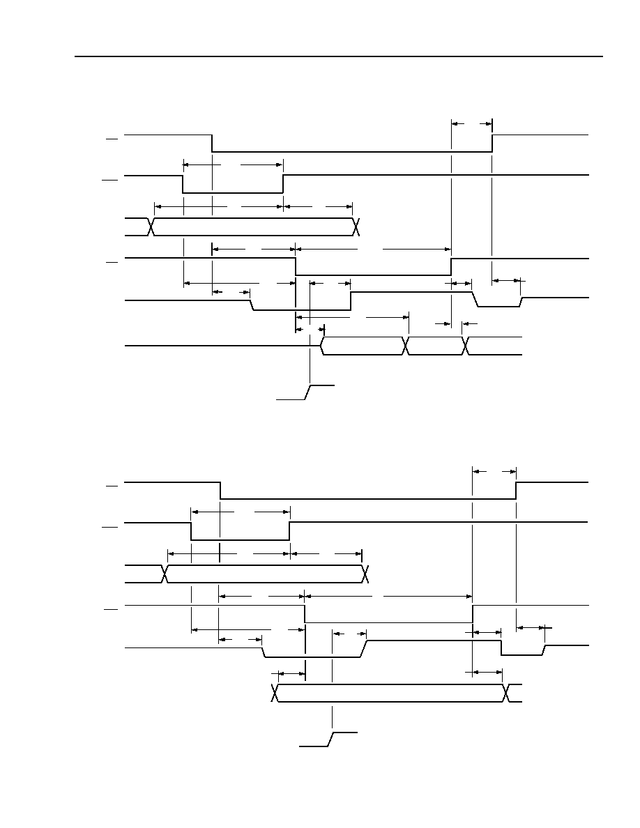
Lucent Technologies Inc.
117
Preliminary Data Sheet
October 2000
TFRA08C13 OCTAL T1/E1 Framer
Lucent Technologies Inc.
Microprocessor Interface
(continued)
5-6426(F).a
Figure 48. Mode 3--Read Cycle Timing (MPMODE = 1)
5-6427(F).a
Figure 49. Mode 3--Write Cycle Timing (MPMODE = 1)
MPCK
D[0:7]
RDY
RD
A[0:11]
ALE
CS
t31
t32
t33
VALID ADDRESS
t34
t50
t35
VALID DATA
t42
t41
t37
t36
t40
t39
t38
t43
MPCK
D[0:7]
RDY
WR
A[0:11]
ALE
CS
t31
t32
t33
VALID ADDRESS
t44
t51
t45
VALID DATA
t42
t37
t36
t47
t46
t48
t49

Preliminary Data Sheet
TFRA08C13 OCTAL T1/E1 Framer
October 2000
118
Lucent Technologies Inc.
Lucent Technologies Inc.
Reset
Both hardware and software resets are provided.
Hardware Reset (Pin C19)
Hardware reset is enabled by asserting RESET to 0. The device is in an inactive condition when RESET is 0, and
becomes active when RESET is returned to 1. Eight cycles of the LIU receive line clock, i.e., 5.2 µs for T1 or 3.9 µs
for E1, is required to guarantee a complete reset.
Hardware reset returns all framer and FDL registers to their default values, as listed in the individual register
descriptions and register maps, (Table 182--Table 186). Hardware reset results in a complete device reset includ-
ing a reset of the global registers.
Software Reset/Software Restart
Independent software reset for each functional block of the device is available. The framer may be reset through
register FRM_PR26 bit 0 (SWRESET), or placed in restart through FRM_PR26 bit 1 (SWRESTART). The FDL
receiver may be reset through register FDL_PR26 bit 1 (FRR), and the FDL transmitter may be reset through
FDL_PR1 bit 5 (FTR). The reset functions, framer SWRESET (framer software reset), FDL FRR (FDL receiver
reset), and FTR (FDL transmitter reset), reset the block and return all parameter/control registers for the block to
their default values. The restart function framer SWRESTART (framer software restart), resets the block but does
not alter the value of the parameter/control registers.
Interrupt Generation
An interrupt may be generated by any of the conditions reported in the status registers. For a bit (condition) in a sta-
tus register to create an interrupt, the corresponding interrupt enable bit must be set and the interrupt block enable
in the global register for the source block must be set, see Table 56 below. Once the source interrupt register is
read, the interrupt for that condition is deasserted.
Table 56. Status Register and Corresponding Interrupt Enable Register for Functional Blocks
Default for interrupt assertion is a logical 1 (high) value. But the assertion value and deasserted state is program-
mable through register GREG4 bit 4 and bit 6 and may take on the following state, see Table 57 below.
Table 57. Asserted Value and Deasserted State for GREG4 Bit 4 and Bit 6 Logic Combinations
Functional Block
Status Register
Interrupt Enable Register
Primary Block
GREG0
GREG1
Framer
FRM_SR0--FRM_SR7
FRM_PR0--FRM_PR7
Facility Data Link
FDL_SR0
FDL_PR2
Greg4
Interrupt (Pin AD-8)
Functionality
Bit 4
Bit 6
Asserted Value
Deasserted Value
0
0
High
Low
--
1
0
High
3-state
Wired-OR
0
1
Low
High
--
1
1
Low
3-state
Wired-AND

Lucent Technologies Inc.
119
Preliminary Data Sheet
October 2000
TFRA08C13 OCTAL T1/E1 Framer
Lucent Technologies Inc.
Register Architecture
Table 58 is an overview of the register architecture. The table is a summary of the register function and address.
Complete detail of each register is given in the following sections.
Table 58. Register Summary
* The most significant digit, designated by Y, is used to identify each framer (for framer 1--framer 8, Y = 2--9, respectively).
Register
Function
Register Address (hex)*
Channel 1--8
Global Registers
GREG0
Framer Block Interrupt Status
000
GREG1
Framer Block Interrupt Enable
001
GREG2
FDL Block Interrupt Status
002
GREG3
FDL Block Interrupt Enable
003
GREG4
Global Control
004
GREG5
Device ID and Version
005
GREG6
Device ID and Version
006
GREG7
Device ID and Version
007
GREG8
Global Control
008
GREG9
Global PLLCK Control
009
Framer Registers
Status Registers
FRM_SR0
Interrupt Status
Y00
FRM_SR1
Facility Alarm Condition
Y01
FRM_SR2
Remote End Alarm
Y02
FRM_SR3
Facility Errored Event
Y03
FRM_SR4
Facility Event
Y04
FRM_SR5
Exchange Termination and Exchange Termination Remote End
Interface Status
Y05
FRM_SR6
Network Termination and Network Termination Remote End
Interface Status
Y06
FRM_SR7
Facility Event
Y07
FRM_SR8,
FRM_SR9
Bipolar Violation Counter
Y08, Y09
FRM_SR10,
FRM_SR11
Framing Bit Error Counter
Y0A, Y0B
FRM_SR12,
FRM_SR13
CRC Error Counter
Y0C, Y0D
FRM_SR14,
FRM_SR15
E-bit Counter
Y0E, Y0F
FRM_SR16,
FRM_SR17
CRC-4 Error at NT1 from NT2 Counter
Y10, Y11
FRM_SR18,
FRM_SR19
E-bit at NT1 from NT2 Counter
Y12, Y13
FRM_SR20,
FRM_SR21
ET Errored Seconds Counter
Y14, Y15

Preliminary Data Sheet
TFRA08C13 OCTAL T1/E1 Framer
October 2000
120
Lucent Technologies Inc.
Lucent Technologies Inc.
Register Architecture
(continued)
Table 58. Register Summary (continued)
* The most significant digit, designated by Y, is used to identify each framer (for framer 1--framer 8, Y = 2--9, respectively).
Register
Function
Register Address (hex)*
Channel 1--8
Framer Registers (continued)
Status Registers (continued)
FRM_SR22,
FRM_SR23
ET Bursty Errored Seconds Counter
Y16, Y17
FRM_SR24,
FRM_SR25
ET Severely Errored Seconds Counter
Y18, Y19
FRM_SR26,
FRM_SR27
ET Unavailable Seconds Counter
Y1A, Y1B
FRM_SR28,
FRM_SR29
ET-RE Errored Seconds Counter
Y1C, Y1D
FRM_SR30,
FRM_SR31
ET-RE Bursty Errored Seconds Counter
Y1E, Y1F
FRM_SR32,
FRM_SR33
ET-RE Severely Errored Seconds Counter
Y20, Y21
FRM_SR34,
FRM_SR35
ET-RE Unavailable Seconds Counter
Y22, Y23
FRM_SR36,
FRM_SR37
NT1 Errored Seconds Counter
Y24, Y25
FRM_SR38,
FRM_SR39
NT1 Bursty Errored Seconds Counter
Y26, Y27
FRM_SR40,
FRM_SR41
NT1 Severely Errored Seconds Counter
Y28, Y29
FRM_SR42,
FRM_SR43
NT1 Unavailable Seconds Counter
Y2A, Y2B
FRM_SR44,
FRM_SR45
NT1-RE Errored Seconds Counter
Y2C, Y2D
FRM_SR46,
FRM_SR47
NT1-RE Bursty Errored Seconds Counter
Y2E, Y2F
FRM_SR48,
FRM_SR49
NT1-RE Severely Errored Seconds Counter
Y30, Y31
FRM_SR50,
FRM_SR51
NT1-RE Unavailable Seconds Counter
Y32, Y33
FRM_SR52
Receive NOT-FAS TS0
Y34
FRM_SR53
Received Sa
Y35
FRM_SR54--
FRM_SR63
SLC
-96 FDL/CEPT Sa Receive Stack
Y36--Y3F
Received Signaling Registers
FRM_RSR0--
FRM_RSR31
Received Signaling
Y40--Y5F

Lucent Technologies Inc.
121
Preliminary Data Sheet
October 2000
TFRA08C13 OCTAL T1/E1 Framer
Lucent Technologies Inc.
Register Architecture
(continued)
Table 58. Register Summary (continued)
* The most significant digit, designated by Y, is used to identify each framer (for framer 1--framer 8, Y = 2--9, respectively).
Register
Function
Register Address (hex)*
Channel 1--8
Framer Registers (continued)
Parameter/Control Registers
FRM_PR0--
FRM_PR7
Interrupt Group Enable
Y60--Y67
FRM_PR8
Framer Mode Option
Y68
FRM_PR9
Framer CRC Control Option
Y69
FRM_PR10
Alarm Filter
Y6A
FRM_PR11
Errored Second Threshold
Y6B
FRM_PR12,
FRM_PR13
Severely Errored Second Threshold
Y6C, Y6D
FRM_PR14
Errored Event Enable
Y6E
FRM_PR15
ET Remote End Errored Event Enable
Y6F
FRM_PR16
NT1 Errored Event Enable
Y70
FRM_PR17,
FRM_PR18
NT1 Remote End Errored Event Enable
Y71, Y72
FRM_PR19
Automatic AIS to the System and Automatic Loopback Enable
Y73
FRM_PR20
Transmit to the Line Command
Y74
FRM_PR21
Framer FDL Loopback Transmission Codes Command
Y75
FRM_PR22
Framer Transmit Line Idle Code
Y76
FRM_PR23
Framer Transmit System Idle Code
Y77
FRM_PR24
Primary Loopback Control
Y78
FRM_PR25
Secondary Loopback Control
Y79
FRM_PR26
System Frame Sync Mask Source
Y7A
FRM_PR27
Transmission of Remote Frame Alarm and CEPT Automatic
Transmission of A bit = 1 Control
Y7B
FRM_PR28
CEPT Automatic Transmission of E bit = 0
Y7C
FRM_PR29
Sa4--Sa8 Source
Y7D
FRM_PR30
Sa4--Sa8 Control
Y7E
FRM_PR31--
FRM_PR40
Sa Transmit Stack/
SLC
-96 Transmit Stack
Y7F--Y88
FRM_PR41
Si-bit Source
Y89
FRM_PR42
Frame Exercise
Y8A
FRM_PR43
System Interface Control
Y8B
FRM_PR44
Signaling Mode
Y8C
FRM_PR45
CHI Common Control
Y8D
FRM_PR46
CHI Common Control
Y8E
FRM_PR47
CHI Transmit Control
Y8F
FRM_PR48
CHI Receive Control
Y90

Preliminary Data Sheet
TFRA08C13 OCTAL T1/E1 Framer
October 2000
122
Lucent Technologies Inc.
Lucent Technologies Inc.
Register Architecture
(continued)
Table 58. Register Summary (continued)
* The most significant digit, designated by Y, is used to identify each framer (for framer 1--framer 8, Y = 2--9, respectively).
For FDL 1 and FDL 2, Y = A; for FDL 3 and FDL 4, Y = B; for FDL 5 and FDL 6, Y = C; for FDL 7 and FDL 8, Y = D.
Register
Function
Register Address (hex)*
Channel 1--8
Framer Registers (continued)
Parameter/Control Registers (continued)
FRM_PR49--
FRM_PR52
Transmit CHI Time-Slot Enable
Y91--Y94
FRM_PR53--
FRM_PR56
Receive CHI Time-Slot Enable
Y95--Y98
FRM_PR57--
FRM_PR60
CHI Transmit Highway Select
Y99--Y9C
FRM_PR61--
FRM_PR64
CHI Receive Highway Select
Y9D--YA0
FRM_PR65
CHI Transmit Control
YA1
FRM_PR66
CHI Receive Control
YA2
FRM_PR69
Auxiliary Pattern Generator Control
YA5
FRM_PR70
Auxiliary Pattern Detector Control
YA6
Transmit Signaling Registers
FRM_TSR0--
FRM_TSR31
Transmit Signaling
YE0--YF7
Facility Data Link Registers
FDL Parameter/Control Registers
Register Address (hex)
FDL 1
FDL 3
FDL 5
FDL 7
FDL 2
FDL 4
FDL 6
FDL 8
FDL_PR0
FDL Configuration Control
Y00
Y20
FDL_PR1
FDL Control
Y01
Y21
FDL_PR2
FDL Interrupt Mask Control
Y02
Y22
FDL_PR3
FDL Transmitter Configuration Control
Y03
Y23
FDL_PR4
FDL Transmitter FIFO
Y04
Y24
FDL_PR5
FDL Transmitter Mask
Y05
Y25
FDL_PR6
FDL Receive Interrupt Level Control
Y06
Y26
FDL_PR7
Not Assigned
--
--
FDL_PR8
FDL Receive Match Character
Y08
Y28
FDL_PR9
FDL Transparent Control
Y09
Y29
FDL_PR10
FDL Transmit
ANSI
ESF Bit Codes
Y0A
Y2A
FDL Status Registers
FDL_SR0
FDL Interrupt Status
Y0B
Y2B
FDL_SR1
FDL Transmitter Status
Y0C
Y2C
FDL_SR2
FDL Receiver Status
Y0D
Y2D
FDL_SR3
FDL
ANSI
Bit Codes Status
Y0E
Y2E
FDL_SR4
FDL Receive FIFO
Y07
Y27

Lucent Technologies Inc.
123
Preliminary Data Sheet
October 2000
TFRA08C13 OCTAL T1/E1 Framer
Lucent Technologies Inc.
Global Register Architecture
REGBANK0 contains the status and programmable control registers for all global functions. The address of these
registers is 000 (hex) to 009 (hex). These registers control the eight channels of the TFRA08C13.
The register bank architecture is shown in Table 59. The register bank consists of 8-bit registers classified as pri-
mary block interrupt status register, primary block interrupt enable register, global loopback control register, global
terminal control register, device identification register, and global internal interface control register.
Table 59. Global Register Set (0x000--0x009)
* The following section describes the global registers inTable 60--Table 67.
Global Register Structure
Framer Block Interrupt Status Register (GREG0)
A bit set to 1 indicates the block has recently generated an interrupt. This register is cleared on read.
Table 60. Framer Block Interrupt Status Register (GREG0) (000)
Global
Register
Address (hex)
Bit 7
Bit 6
Bit 5
Bit 4
Bit 3
Bit 2
Bit 1
Bit 0
000
FRMR8_I
NT
(0)
FRMR7_I
NT
(0)
FRMR6_I
NT
(0)
FRMR5_I
NT
(0)
FRMR4_I
NT
(0)
FRMR3_I
NT
(0)
FRMR2_I
NT
(0)
FRMR1_I
NT
(0)
001
FRMR8IE
(0)
FRMR7IE
(0)
FRMR6IE
(0)
FRMR5IE
(0)
FRMR4IE
(0)
FRMR3IE
(0)
FRMR2IE
(0)
FRMR1IE
(0)
002
FDL8_INT
(0)
FDL7_INT
(0)
FDL6_INT
(0)
FDL5_INT
(0)
FDL4_INT
(0)
FDL3_INT
(0)
FDL2_INT
(0)
FDL1_INT
(0)
003
FDL8IE
(0)
FDL7IE
(0)
FDL6IE
(0)
FDL5IE
(0)
FDL4E
(0)
FDL3IE
(0)
FDL2IE
(0)
FDL1IE
(0)
004
Reserved
(0)
IPC
(0)
Reserved
(0)
ITSC
(0)
Reserved
(0)
SECCTRL
0
(0)
SECCTRL
1
(0)
SECCTRL
2
(0)
005
1
1
1
1
1
0
0
0
006
0
0
0
0
0
0
1
1
007
0
0
0
0
0
0
0
1
008
Reserved
(0)
DIVMUX0
(0)
DIVMUX1
(0)
DIVMUX2
(0)
Reserved
(0)
LOMUX0
(0)
LOMUX1
(0)
LOMUX2
(0)
009
EIPLLCK8
(0)
EIPLLCK7
(0)
EIPLLCK6
(0)
EIPLLCK5
(0)
EIPLLCK4
(0)
EIPLLCK3
(0)
EIPLLCK2
(0)
EIPLLCK1
(0)
Bit
Symbol
Description
0
FRMR1_INT
Framer 1 Interrupt. A 1 indicates framer 1 generated an interrupt.
1
FRMR2_INT
Framer 2 Interrupt. A 1 indicates framer 2 generated an interrupt.
2
FRMR3_INT
Framer 3 Interrupt. A 1 indicates framer 3 generated an interrupt.
3
FRMR4_INT
Framer 4 Interrupt. A 1 indicates framer 4 generated an interrupt.
4
FRMR5_INT
Framer 5 Interrupt. A 1 indicates framer 5 generated an interrupt.
5
FRMR6_INT
Framer 6 Interrupt. A 1 indicates framer 6 generated an interrupt.
6
FRMR7_INT
Framer 7 Interrupt. A 1 indicates framer 7 generated an interrupt.
7
FRMR8_INT
Framer 8 Interrupt. A 1 indicates framer 8 generated an interrupt.

Preliminary Data Sheet
TFRA08C13 OCTAL T1/E1 Framer
October 2000
124
Lucent Technologies Inc.
Lucent Technologies Inc.
Global Register Structure
(continued)
Framer Block Interrupt Enable Register (GREG1)
This register enables the individual blocks to assert the interrupt pin high.
Table 61. Framer Block Interrupt Enable Register (GREG1) (001)
FDL Block Interrupt Status Enable Register (GREG2)
Table 62. FDL Block Interrupt Status Register (GREG2) (002)
FDL Block Interrupt Enable Register (GREG3)
This register enables the individual blocks to assert the interrupt pin high.
Table 63. FDL Block Interrupt Enable Register (GREG3) (003)
Bit
Symbol
Description
0
FRMR1IE
Framer 1 Interrupt Enable. A 1 enables framer 1 interrupts.
1
FRMR2IE
Framer 2 Interrupt Enable. A 1 enables framer 2 interrupts.
2
FRMR3IE
Framer 3 Interrupt Enable. A 1 enables framer 3 interrupts.
3
FRMR4IE
Framer 4 Interrupt Enable. A 1 enables framer 4 interrupts.
4
FRMR5IE
Framer 5 Interrupt Enable. A 1 enables framer 5 interrupts.
5
FRMR6IE
Framer 6 Interrupt Enable. A 1 enables framer 6 interrupts.
6
FRMR7IE
Framer 7 Interrupt Enable. A 1 enables framer 7 interrupts.
7
FRMR8IE
Framer 8 Interrupt Enable. A 1 enables framer 8 interrupts.
Bit
Symbol
Description
0
FDL1_INT
Facility Data Link 1 Interrupt. A 1 indicates FDL1 generated an interrupt.
1
FDL2_INT
Facility Data Link 2 Interrupt. A 1 indicates FDL2 generated an interrupt.
2
FDL3_INT
Facility Data Link 3 Interrupt. A 1 indicates FDL3 generated an interrupt.
3
FDL4_INT
Facility Data Link 4 Interrupt. A 1 indicates FDL4 generated an interrupt.
4
FDL5_INT
Facility Data Link 5 Interrupt. A 1 indicates FDL5 generated an interrupt.
5
FDL6_INT
Facility Data Link 6 Interrupt. A 1 indicates FDL6 generated an interrupt.
6
FDL7_INT
Facility Data Link 7 Interrupt. A 1 indicates FDL7 generated an interrupt.
7
FDL8_INT
Facility Data Link 8 Interrupt. A 1 indicates FDL8 generated an interrupt.
Bit
Symbol
Description
0
FDL1IE
Facility Data Link 1 Interrupt Enable. A 1 enables FDL 1 interrupts.
1
FDL2IE
Facility Data Link 2 Interrupt Enable. A 1 enables FDL 2 interrupts.
2
FDL3IE
Facility Data Link 3 Interrupt Enable. A 1 enables FDL 3 interrupts.
3
FDL4IE
Facility Data Link 4 Interrupt Enable. A 1 enables FDL 4 interrupts.
4
FDL5IE
Facility Data Link 5 Interrupt Enable. A 1 enables FDL 5 interrupts.
5
FDL6IE
Facility Data Link 6 Interrupt Enable. A 1 enables FDL 6 interrupts.
6
FDL7IE
Facility Data Link 7 Interrupt Enable. A 1 enables FDL 7 interrupts.
7
FDL8IE
Facility Data Link 8 Interrupt Enable. A 1 enables FDL 8 interrupts.

Lucent Technologies Inc.
125
Preliminary Data Sheet
October 2000
TFRA08C13 OCTAL T1/E1 Framer
Lucent Technologies Inc.
Global Register Structure
(continued)
Global Control Register (GREG4)
This register selects the source of the output second pulse (bit 0--bit 2), interrupt 3-state control (bit 4), and inter-
rupt polarity (bit 6).
Table 64. Global Control Register (GREG4) (004)
Device ID and Version Registers (GREG5--GREG7)
These bits define the device and version number of this framer circuit.
Table 65. Device ID and Version Registers (GREG5--GREG7) (005--007)
Bit
Symbol
Description
0
SECCTRL2 Second Output Control. These bits determine which framer is used to source the output
SECOND pin:
Bit 0 Bit 1 Bit 2
0
0
0:
FRAMER 1 sources the SECOND pin.
0
0
1:
FRAMER 2 sources the SECOND pin.
0
1
0:
FRAMER 3 sources the SECOND pin.
0
1
1:
FRAMER 4 sources the SECOND pin.
1
0
0:
FRAMER 5 sources the SECOND pin.
1
0
1:
FRAMER 6 sources the SECOND pin.
1
1
0:
FRAMER 7 sources the SECOND pin.
1
1
1:
FRAMER 8 sources the SECOND pin.
1
SECCTRL1
2
SECCTRL0
3
--
Reserved.
4
ITSC
INTERRUPT 3-State Control. This bit along with bit 6 in this register (polarity control)
allows the interrupt pin to be programmed for active HIGH, active LOW, wire-OR, or wire-
AND operation, as described below:
Bit 4 Bit 6
0
0
Programs the interrupt pin to be active HIGH (1-state) when there is an inter-
rupt condition and to be inactive LOW (0-state) when the condition goes away.
0
1
Programs the interrupt pin to be active LOW (0-state) when there is an inter-
rupt condition and to be inactive HIGH (1-state) when the condition goes
away.
1
0
Programs the interrupt pin to be active HIGH (1-state) when there is an inter-
rupt condition and to be inactive HIGH-Z (3-state) when the condition goes
away.
1
1
Programs the interrupt pin to be active LOW (0-state) when there is an inter-
rupt condition and to be inactive HIGH-Z (3-state) when the condition goes
away.
5
--
Reserved.
6
IPC
Interrupt Polarity Control. A 1 inverts the polarity of the interrupt pin (negative polarity).
7
--
Reserved.
Register
Bit 7
Bit 6
Bit 5
Bit 4
Bit 3
Bit 2
Bit 1
Bit 0
Device Code
GREG5
1
1
1
1
1
0
0
0
Device Code
GREG6
0
0
0
0
0
0
1
1
Version #
GREG7
0
0
0
0
0
0
1
0

Preliminary Data Sheet
TFRA08C13 OCTAL T1/E1 Framer
October 2000
126
Lucent Technologies Inc.
Lucent Technologies Inc.
Global Register Structure
(continued)
Global Control Register (GREG8)
Table 66. Global Control Register (GREG8) (008)
Bit
Symbol
Description
0
LOMUX2
Loss of Clock Output Control. These bits determine which framer is used to source
the output LORLCK and LOPLLCK pin:
Bit 0 Bit 1 Bit 2
0
0
0:
FRAMER 1 sources the LORLCK and LOPLLCK pins.
0
0
1:
FRAMER 2 sources the LORLCK and LOPLLCK pins.
0
1
0:
FRAMER 3 sources the LORLCK and LOPLLCK pins.
0
1
1:
FRAMER 4 sources the LORLCK and LOPLLCK pins.
1
0
0:
FRAMER 5 sources the LORLCK and LOPLLCK pins.
1
0
1:
FRAMER 6 sources the LORLCK and LOPLLCK pins.
1
1
0:
FRAMER 7 sources the LORLCK and LOPLLCK pins.
1
1
1:
FRAMER 8 sources the LORLCK and LOPLLCK pins.
1
LOMUX1
2
LOMUX0
3
--
Reserved.
4
DIVMUX2
Divide Clocks Output Control. These bits determine which framer is used to source
the output DIV-RLCK, DIV-PLLCK, DIV-CHICK, CHICK-EPLL, and PLLCK-EPLL pins:
Bit 0 Bit 1 Bit 2
0
0
0:
FRAMER 1 sources the DIV-RLCK, DIV-PLLCK, DIV-CHICK,
CHICK-EPLL and PLLCK-EPLL pins.
0
0
1:
FRAMER 2 sources the DIV-RLCK, DIV-PLLCK, DIV-CHICK,
CHICK-EPLL and PLLCK-EPLL pins.
0
1
0:
FRAMER 3 sources the DIV-RLCK, DIV-PLLCK, DIV-CHICK,
CHICK-EPLL and PLLCK-EPLL pins.
0
1
1:
FRAMER 4 sources the DIV-RLCK, DIV-PLLCK, DIV-CHICK,
CHICK-EPLL and PLLCK-EPLL pins.
1
0
0:
FRAMER 5 sources the DIV-RLCK, DIV-PLLCK, DIV-CHICK,
CHICK-EPLL and PLLCK-EPLL pins.
1
0
1:
FRAMER 6 sources the DIV-RLCK, DIV-PLLCK, DIV-CHICK,
CHICK-EPLL and PLLCK-EPLL pins.
1
1
0:
FRAMER 7 sources the DIV-RLCK, DIV-PLLCK, DIV-CHICK,
CHICK-EPLL and PLLCK-EPLL pins.
1
1
1:
FRAMER 8 sources the DIV-RLCK, DIV-PLLCK, DIV-CHICK,
CHICK-EPLL and PLLCK-EPLL pins.
5
DIVMUX1
6
DIVMUX0
7
--
Reserved.

Lucent Technologies Inc.
127
Preliminary Data Sheet
October 2000
TFRA08C13 OCTAL T1/E1 Framer
Lucent Technologies Inc.
Global Register Structure
(continued)
Global PLLCK Control Register (GREG9)
This register selectively enables/disables an individual transmit framer's internal clock synthesizer. setting all bits to
0 (the default condition) disables all transmit framer clock synthesizers, and allows an external source of PLLCK to
drive the transmit framers.
Table 67. Global PLLCK Control Register (GREG9) (009)
Bit
Symbol
Description
0
EIPLLCK1
Enable Transmit Framer 1's Internal PLLCK Clock Synthesizer.
1
EIPLLCK2
Enable Transmit Framer 2's Internal PLLCK Clock Synthesizer.
2
EIPLLCK3
Enable Transmit Framer 3's Internal PLLCK Clock Synthesizer.
3
EIPLLCK4
Enable Transmit Framer 4's Internal PLLCK Clock Synthesizer.
4
EIPLLCK5
Enable Transmit Framer 5's Internal PLLCK Clock Synthesizer.
5
EIPLLCK6
Enable Transmit Framer 6's Internal PLLCK Clock Synthesizer.
6
EIPLLCK7
Enable Transmit Framer 7's Internal PLLCK Clock Synthesizer.
7
EIPLLCK8
Enable Transmit Framer 8's Internal PLLCK Clock Synthesizer.
Framer Register Architecture
REGBANK1--REGBANK8 contain the status and pro-
grammable control registers for the framer and system
CHI interface channels FRM1--FRM8. The base
address for REGBANK1--REGBANK8 is Y00 (hex),
where Y = 2--9 for FRM1--FRM8, respectively. Within
these register banks, the bit map is identical for
FRM1--FRM8.
The framer registers are structures as shown in Table
68. Default values are given in the individual register
definition tables.
Table 68. Framer Status and Control Blocks
Address Range (Hexadecimal)
* The most significant digit, designated by Y, is used to identify each
framer (for framer 1--framer 8, Y = 2--9, respectively).
The complete register map for the framer is given in
Table 182--Table 186. The address of the registers is
shown in the table title with the most significant digit,
designated by Y, used to identify each framer (for
framer 1--framer 8, Y = 2--9, respectively).
All status registers are clocked with the internal framer
receive line clock (RFRMCK).
Bits in status registers FRM_SR1 and FRM_SR7 are
set at the onset of the condition and are cleared on
read when the given condition is no longer present.
These registers can generate interrupts if the corre-
sponding register bits are enabled in interrupt enable
registers FRM_PR0--FRM_PR7.
On all 16-bit counter registers (FRM_SR8--
FRM_SR51), both bytes are cleared only after reading
both bytes. These status registers are two byte register
pairs. These register pairs must be read in succession,
with the lower byte read first followed by a read of
higher byte. Once a read is initiated on one of the
bytes, the updating of that counter is disabled and
remains disabled until both bytes are read. All events
during this interval are lost. Updating of the counter
registers is stopped when all of the bits are set to 1.
Updating resumes after the registers are cleared on
read. These register pairs may be read in any order,
but they must be read in pairs, i.e., a read of 1 byte
must be followed immediately by a read of the remain-
ing byte of the pair.
Status registers FRM_SR0--FRM_SR63 are clear-on-
read (COR) registers. These registers are cleared by
the framer internal received line clock (RFRMCK). At
least two RFRMCK cycles (1.3 µs for DS1 and 1.0 µs
for CEPT) must be allowed between successive reads
of the same COR register to allow it to properly clear.
Framer Register Block
Status Registers (COR) (Y00--Y3F)*
Receive Signaling Registers (Y40--Y5F)*
Parameter (Configuration) Registers (Y60--YA6)*
Transmit Signaling Registers (YE0--YFF)*

Preliminary Data Sheet
TFRA08C13 OCTAL T1/E1 Framer
October 2000
128
Lucent Technologies Inc.
Lucent Technologies Inc.
Framer Register Architecture
(continued)
Framer Status/Counter Registers
Registers FRM_SR0--FRM_SR63 report the status of each framer. All are clear-on-read, read-only registers.
Interrupt Status Register (FRM_SR0)
The interrupt pin (INTERRUPT) goes active when a bit in this register and its associated interrupt enable bit in reg-
isters FRM_PR0--FRM_PR7 are set, and the interrupt for the framer block is enabled in register GREG1.
Table 69. Interrupt Status Register (FRM_SR0) (Y00)
Bit
Symbol
Description
0
FAC
Facility Alarm Condition. A 1 indicates a facility alarm occurred (go read FRM_SR1).
1
RAC
Remote Alarm Condition. A 1 indicates a remote alarm occurred (go read FRM_SR2).
2
FAE
Facility Alarm Event. A 1 indicates a facility alarm occurred (go read FRM_SR3 and
FRM_SR4).
3
ESE
Errored Second Event. A 1 indicates an errored second event occurred (go read
FRM_SR5, FRM_SR6, and FRM_SR7).
4
TSSFE
Transmit Signaling Superframe Event. A 1 indicates that a MOS superframe block
has been transmitted and the transmit signaling data buffers are ready for new data.
5
RSSFE
Receive Signaling Superframe Event. A 1 indicates that a MOS superframe block has
been received and the receive signaling data buffers must be read.
6
--
Reserved.
7
S96SR
SLC
-96 Stack Ready. A 1 indicates that either the transmit framer
SLC
-96 stack is
ready for more data or the receive framer
SLC
-96 stack contains new data.

Lucent Technologies Inc.
129
Preliminary Data Sheet
October 2000
TFRA08C13 OCTAL T1/E1 Framer
Lucent Technologies Inc.
Framer Register Architecture
(continued)
Facility Alarm Condition Register (FRM_SR1)
The bits in the facility alarm condition register (FRM_SR1) indicate alarm state of the receive framer section. Inter-
rupts from this register are generated once at the onset of the alarm condition. If the alarm condition is still present
at the time of the read, the bit will remain in the 1 state for the duration of the alarm condition. If the alarm condition
is no longer present at the time of the read, then the bit is cleared on read.
Table 70. Facility Alarm Condition Register (FRM_SR1) (Y01)
Bit
Symbol
Description
0
LFA
Loss of Frame Alignment. A 1 indicates the receive framer is in a loss of frame align-
ment and is currently searching for a new alignment.
1
LSFA
Loss of Signaling Superframe Alignment. A 1 indicates the receive framer is in a loss
of signaling superframe alignment in the DS1 framing formats. A search for a new sig-
naling superframe alignment starts once frame alignment is established.
LTS16MFA
Loss of Time Slot 16 Signaling Multiframe Alignment. A 1 indicates the receive framer is
in a loss of time slot 16 signaling multiframe alignment in the CEPT mode. A search for a
new time slot 16 signaling multiframe alignment starts once frame alignment is estab-
lished. This bit is 0 when the TFRA08C13 is programmed for the transparent signaling
mode, register FRM_PR44 bit 0 (TSIG) = 1.
2
LTSFA
Loss of Transmit Superframe Alignment. A 1 indicates superframe alignment pattern
in the transmit facility data link as defined for
SLC
-96 is lost. Only valid for
SLC
-96 mode.
This bit is 0 in all other DS1 modes.
LTS0MFA
Loss of Time Slot 0 CRC-4 Multiframe Alignment. A 1 indicates an absence of CRC-4
multiframe alignment after initial basic frame alignment is established. A 0 indicates
either CRC-4 checking is disabled or CRC-4 multiframe alignment has been success-
fully detected.
3
LFALR
Loss of Frame Alignment Since Last Read. A 1 indicates that the LFA state indicated
in bit 0 of this register is the same LFA state as the previous read.
4
LBFA
Loss of Biframe Alignment. A 1 indicates that the CEPT biframe alignment pattern
(alternating 10 in bit 2 of time slot 0 of each frame) in the receive system data is errored.
This alignment pattern is required when transmitting the Si or Sa bits transparently. Only
valid in the CEPT mode. This bit is 0 in all other modes.
5
RTS16AIS
Receive Time Slot 16 Alarm Indication Signal. A 1 indicates the receive framer
detected time slot 16 AIS in the CEPT mode. This bit is 0 in the DS1 modes.
6
AUXP
Auxiliary Pattern. A 1 indicates the detection of a valid AUXP (unframed 1010 . . . pat-
tern) in the CEPT mode. This bit is 0 in the DS1 modes.
7
AIS
Alarm Indication Signal. A 1 indicates the receive framer is currently receiving an AIS
pattern from its remote line end.

Preliminary Data Sheet
TFRA08C13 OCTAL T1/E1 Framer
October 2000
130
Lucent Technologies Inc.
Lucent Technologies Inc.
Framer Register Architecture
(continued)
Remote End Alarm Register (FRM_SR2)
A bit set to 1 indicates the receive framer has recently received the given alarm. Interrupts from this register are
generated once at the beginning of the alarm condition. If the alarm is still present at the time of the read, the bit
will remain in the 1 state for the duration of the alarm condition. If the alarm condition is no longer present at the
time of the read, then the bit is cleared on read.
Table 71. Remote End Alarm Register (FRM_SR2) (Y02)
Bit
Symbol
Description
0
RFA
Remote Framer Alarm. A 1 indicates the receive framer detected a remote frame (yel-
low) alarm.
1
RJYA
Remote Japanese Yellow Alarm. A 1 indicates the receive framer detected the Japa-
nese format remote frame alarm.
RTS16MFA
Remote Multiframe Alarm. A 1 indicates the receive framer detected a time slot 16
remote frame alarm in the CEPT mode.
2
CREBIT
Continuous Received E Bits. A 1 indicates the detection of a five-second interval con-
taining
991 E bit = 0 events in each second. This bit is 0 in the DS1 mode.
3
Sa6 = 8
Received Sa6 = 8. A 1 indicates the receive framer detected an Sa6 code equal to 1000.
This bit is 0 in the DS1 mode.
4
Sa6 = A
Received Sa6 = A. A 1 indicates the receive framer detected an Sa6 code equal to
1010. This bit is 0 in the DS1 mode.
5
Sa6 = C
Received Sa6 = C. A 1 indicates the receive framer detected an Sa6 code equal to
1100. This bit is 0 in the DS1 mode.
6
Sa6 = E
Received Sa6 = E. A 1 indicates the receive framer detected an Sa6 code equal to
1110. This bit is 0 in the DS1 mode.
7
Sa6 = F
Received Sa6 = F. A 1 indicates the receive framer detected an Sa6 code equal to 1111.
This bit is 0 in the DS1 mode.

Lucent Technologies Inc.
131
Preliminary Data Sheet
October 2000
TFRA08C13 OCTAL T1/E1 Framer
Lucent Technologies Inc.
Framer Register Architecture
(continued)
Facility Errored Event Register (FRM_SR3)
A bit set to 1 indicates the receive framer has recently received the given errored event.
Table 72. Facility Errored Event Register-1 (FRM_SR3) (Y03)
Bit
Symbol
Description
0
LFV
Line Format Violation. A 1 indicates the receive framer detected a bipolar line coding or
excessive zeros violation.
1
FBE
Frame-Bit Errored. A 1 indicates the receive framer detected a frame-bit or frame align-
ment pattern error.
2
CRCE
CRC Errored. A 1 indicates the receive framer detected CRC errors.
3
ECE
Excessive CRC Errors. A 1 indicates the receive framer detected an excessive CRC
errored condition. This bit is only valid in the ESF and CEPT with CRC-4 modes; other-
wise, it is 0.
4
REBIT
Received E Bit = 0. A 1 indicates the receive framer detected an E bit = 0 in either frame
13 or 15 of the time slot 0 of CRC-4 multiframe. This bit is 0 in the DS1 modes.
5
LCRCATMX
Lack of CRC-4 Multiframe Alignment Timer Expire Indication. A 1 indicates that
either the 100 ms or the 400 ms CRC-4 interworking timer expired. Active only immedi-
ately after establishment of the initial basic frame alignment. This bit is 0 in the DS1
modes.
6
SLIPO
Receive Elastic Store Slip: Buffer Overflow. A 1 indicates the receive elastic store per-
formed a control slip due to an elastic buffer overflow condition.
7
SLIPU
Receive Elastic Store Slip: Buffer Underflow. A 1 indicates the receive elastic store
performed a control slip due to an elastic buffer underflow condition.

Preliminary Data Sheet
TFRA08C13 OCTAL T1/E1 Framer
October 2000
132
Lucent Technologies Inc.
Lucent Technologies Inc.
Framer Register Architecture
(continued)
Table 73. Facility Event Register-2 (FRM_SR4) (Y04)
Bit
Symbol
Description
0
NFA
New Frame Alignment. A 1 indicates the receive framer established a new frame align-
ment which differs from the previous alignment.
1
SSFA
Signaling Superframe Alignment. A 1 indicates the receive framer has established the
signaling superframe alignment. In the SF modes (D4 and
SLC
-96) and CEPT modes,
this alignment is established only after primary frame alignment is determined.
2
LLBOFF
T1 Line Loopback Off Code Detect. A 1 indicates the receive framer detected the DS1
line loopback disable code in the payload. This code is defined in
AT&T Technical Refer-
ence 62411
as a framed 001 pattern where the frame bit is inserted into the pattern.
BFA
New Biframe Alignment Established. A 1 indicates the transmit framer has established
a biframe alignment for the transmission of transparent Si and or Sa bits from the system
data in the CEPT mode.
3
LLBON
T1 Line Loopback On Code Detect. A 1 indicates the receive framer detected the line
loopback enable code in the payload. This code is defined in
AT&T Technical Reference
62411
as a framed 00001 pattern where the frame bit is inserted into the pattern.
CMA
New CEPT CRC-4 Multiframe Alignment. A 1 indicates the CEPT CRC-4 multiframe
alignment in the receive framer has been established.
4
FDL-PLBON
ESF FDL Payload Loopback On Code Detect. A 1 indicates the receive framer
detected the line loopback enable code in the payload. This code is defined in
ANSI
T1.403-1995 as a 1111111100101000 pattern in the facility data link, where the leftmost
bit is the MSB.
SLC
RFSR
SLC
-96 Receive FDL Stack Ready. A 1 indicates that the receive FDL stack should be
read. This bit is cleared on read. Data in the receive FIFO must be read within 9 ms of
this interrupt. This bit is not updated during loss of frame or signaling superframe align-
ment.
5
FDL-PLBOFF ESF FDL Payload Loopback Off Code Detect. A 1 indicates the receive framer
detected the line loopback disable code in the payload. This code is defined in
ANSI
T1.403-1995 as a 1111111101001100 pattern in the facility data link, where the leftmost
bit is the MSB.
SLC
TFSR
SLC
-96 Transmit FDL Stack Ready. A 1 indicates that the transmit FDL stack is ready
for new data. This bit is cleared on read. Data written within 9 ms of this interrupt will be
transmitted in the next
SLC
-96 D-bit superframe interval.
6
FDL-LLBON
ESF FDL Line Loopback On Code Detect. A 1 indicates the receive framer detected
the line loopback enable code in the payload. This code is defined in
ANSI
T1.403-1995
as a 1111111101110000 pattern in the facility data link, where the leftmost bit is the
MSB.
RSaSR
CEPT Receive Sa Stack Ready. A 1 indicates that the receive Sa6 stack should be
read. This bit is clear on the first access to the Sa receive stack or at the beginning of
frame 0 of the CRC-4 double-multiframe. Data in the receive FIFO must be read within 4
ms of this interrupt. This bit is not updated during LFA.
7
FDL-LLBOFF ESF FDL Line Loopback Off Code Detect. A 1 indicates the receive framer detected
the line loopback disable code in the payload. This code is defined in
ANSI
T1.403-1995
as a 1111111100011100 pattern in the facility data link, where the leftmost bit is the
MSB.
TSaSR
CEPT Transmit Sa Stack Ready. A 1 indicates that the transmit Sa stack is ready for
new data. This bit is cleared on the first access to the Sa transmit stack or at the begin-
ning of frame 0 of the CRC-4 double multiframe. Data written within 4 ms of this interrupt
will be transmitted in the next CRC-4 double multiframe interval.

Lucent Technologies Inc.
133
Preliminary Data Sheet
October 2000
TFRA08C13 OCTAL T1/E1 Framer
Lucent Technologies Inc.
Framer Register Architecture
(continued)
The following registers are dedicated to the exchange termination and its remote end interface. The alarm condi-
tions to trigger errored seconds and severely errored seconds are defined in Table 32 and the ET and ET-RE
enable registers, FRM_PR14 and FRM_PR15. The thresholds are defined in registers FRM_PR11--FRM_PR13.
Table 74. Exchange Termination and Exchange Termination Remote End Interface Status
Register (FRM_SR5) (Y05)
Bit
Symbol
Description
0
ETES
ET Errored Second. A 1 indicates the receive framer detected an errored second at the
exchange termination (ET).
1
ETBES
ET Bursty Errored Second. A 1 indicates the receive framer detected a bursty errored
second at the ET.
2
ETSES
ET Severely Errored Second. A 1 indicates the receive framer detected a severely
errored second at the ET.
3
ETUAS
ET Unavailable State. A 1 indicates the receive framer has detected at least ten con-
secutive severely errored seconds. Upon detecting ten consecutive nonseverely errored
seconds, the receive framer will clear this bit. ITU Recommendation G.826 is used
resulting in a ten-second delay in the reporting of this condition.
4
ETREES
ET-RE Errored Second. A 1 indicates the receive framer detected an errored second at
the exchange termination remote end (ET-RE).
5
ETREBES
ET-RE Bursty Errored Second. A 1 indicates the receive framer detected a bursty
errored second at the ET-RE.
6
ETRESES
ET-RE Severely Errored Second. A 1 indicates the receive framer detected a severely
errored second at the ET-RE.
7
ETREUAS
ET-RE Unavailable State. A 1 indicates the receive framer has detected at least ten
consecutive severely errored seconds. Upon detecting ten consecutive nonseverely
errored seconds, the receive framer will clear this bit. ITU Recommendation G.826 is
used resulting in a ten-second delay in the reporting of this condition.

Preliminary Data Sheet
TFRA08C13 OCTAL T1/E1 Framer
October 2000
134
Lucent Technologies Inc.
Lucent Technologies Inc.
Framer Register Architecture
(continued)
The following status registers are dedicated to the NT1 and the NT1 remote end (NT1-RE) interface. The alarm
conditions to evaluate errored seconds and severely errored seconds are defined in Table 32
and the NT1 and
NT1-RE enable registers, FRM_PR16--FRM_PR18. The thresholds are defined in registers FRM_PR11--
FRM_PR13.
Table 75. Network Termination and Network Termination Remote End Interface Status
Register (FRM_SR6) (Y06)
Bit
Symbol
Description
0
NTES
NT Errored Second. A 1 indicates the receive framer detected an errored second at the
network termination (NT).
1
NTBES
NT Bursty Errored Second. A 1 indicates the receive framer detected a bursty errored
second at the NT.
2
NTSES
NT Severely Errored Second. A 1 indicates the receive framer detected a severely
errored second at the NT.
3
NTUAS
NT Unavailable State. A 1 indicates the receive framer has detected at least ten consec-
utive severely errored seconds. Upon detecting ten consecutive nonseverely errored sec-
onds, the receive framer will clear this bit. ITU Recommendation G.826 is used resulting
in a ten-second delay in the reporting of this condition.
4
NTREES
NT-RE Errored Second. A 1 indicates the receive framer detected an errored second at
the exchange termination remote end (ET-RE).
5
NTREBES
NT-RE Bursty Errored Second. A 1 indicates the receive framer detected a bursty
errored second at the ET-RE.
6
NTRESES
NT-RE Severely Errored Second. A 1 indicates the receive framer detected a severely
errored second at the NT-RE.
7
NTREUAS
NT-RE Unavailable State. A 1 indicates the receive framer has detected at least ten
consecutive severely errored seconds. Upon detecting ten consecutive nonseverely
errored seconds, the receive framer will clear this bit. ITU Recommendation G.826 is
used resulting in a ten-second delay in the reporting of this condition.

Lucent Technologies Inc.
135
Preliminary Data Sheet
October 2000
TFRA08C13 OCTAL T1/E1 Framer
Lucent Technologies Inc.
Framer Register Architecture
(continued)
Bit 0--bit 4 in this register are set high when the receive framer comes out of the unavailable state, while
bit 4--bit 7 report detection of the receive test patterns. Bits 4 and 5 are cleared only after register FRM_PR70
bit 2 is set to 0.
Table 76. Facility Event Register (FRM_SR7) (Y07)
* It is possible for one of these bits to be set to 1, if the received line data is all zeros.
Bipolar Violation Counter Register (FRM_SR8--FRM_SR9)
This register contains the 16-bit count of received bipolar violations, line code violations, or excessive zeros.
Table 77. Bipolar Violation Counter Registers (FRM_SR8--FRM_SR9) (Y08--Y09)
Frame Bit Errored Counter Register (FRM_SR10--FRM_SR11)
This register contains the 16-bit count of framing bit errors. Framing bit errors are not counted during loss of frame
alignment.
Table 78. Framing Bit Error Counter Registers (FRM_SR10--FRM_SR11) (Y0A--Y0B)
Bit
Symbol
Description
0
OUAS
Out of Unavailable State. A 1 indicates the receive framer detected ten consecutive
seconds that were not severely errored while in the unavailable state at the ET.
1
EROUAS
Out of Unavailable State at the ET-RE. A 1 indicates the receive framer detected ten
consecutive seconds that were not severely errored while in the unavailable state at the
ET-RE.
2
NT1OUAS
Out of Unavailable State at the NT1. A 1 indicates the receive framer detected ten con-
secutive seconds that were not severely errored while in the unavailable state at the NT.
3
NROUAS
Out of Unavailable State NT1-RE. A 1 indicates the receive framer detected ten con-
secutive seconds that were not severely errored while in the unavailable state at the NT-
RE.
4
DETECT
Test Pattern Detected. A 1 indicates the pattern detector has locked onto the pattern
specified by the PTRN configuration bits defined in register FRM_PR70.
5
PTRNBER
Test Pattern Bit Error. A 1 indicates the pattern detector has found one or more single
bit errors in the pattern that it is currently locked onto.
6
RPSUEDO
Receiving Pseudorandom Pattern. A 1 indicates the receive framer pattern monitor
circuit is currently detecting the 2
15
≠ 1 pseudorandom pattern*.
7
RQUASI
Receiving Quasi-Random Pattern. A 1 indicates the receive framer pattern monitor cir-
cuit is currently detecting the 2
20
≠ 1 quasi-random pattern*.
Register
Byte
Bit
Symbol
Description
FRM_SR8
MSB
7--0
BPV15--BPV8
BPVs Counter.
FRM_SR9
LSB
7--0
BPV7--BPV0
BPVs Counter.
Register
Byte
Bit
Symbol
Description
FRM_SR10
MSB
7--0
FBE15--FBE8
Frame Bit »rrored Counter.
FRM_SR11
LSB
7--0
FBE7--FBE0
Frame Bit Errored Counter.

Preliminary Data Sheet
TFRA08C13 OCTAL T1/E1 Framer
October 2000
136
Lucent Technologies Inc.
Lucent Technologies Inc.
Framer Register Architecture
(continued)
CRC Error Counter Register (FRM_SR12--FRM_SR13)
This register contains the 16-bit count of CRC errors. CRC errors are not counted during loss of CRC multiframe
alignment.
Table 79. CRC Error Counter Registers (FRM_SR12--FRM_SR13) (Y0C--Y0D)
E-Bit Counter Register (FRM_SR14--FRM_SR15)
This register contains the 16-bit count of received E bit = 0 events. E bits are not counted during loss of CEPT
CRC-4 multiframe alignment.
Table 80. E-Bit Counter Registers (FRM_SR14--FRM_SR15) (Y0E--Y0F)
CRC-4 Errors at NT1 from NT2 Counter Registers (FRM_SR16--FRM_SR17)
This register contains the 16-bit count of each occurrence of Sa6 code 001X, detected synchronously to the CEPT
CRC-4 multiframe.
Table 81. CRC-4 Errors at NT1 from NT2 Counter Registers (FRM_SR16--FRM_SR17) (Y10--Y11)
E Bit at NT1 from NT2 Counter Registers (FRM_SR18--FRM_SR19)
This register contains the 16-bit count of each occurrence of Sa6 code 00X1, detected synchronously to the CEPT
CRC-4 multiframe. E bits are not counted during loss of CEPT CRC-4 multiframe alignment.
Table 82. E Bit at NT1 from NT2 Counter (FRM_SR18--FRM_SR19) (Y12--Y13)
Register
Byte
Bit
Symbol
Description
FRM_SR12
MSB
7--0
CEC15--CEC8
CRC Errored Counter.
FRM_SR13
LSB
7--0
CEC7--CEC0
CRC Errored Counter.
Register
Byte
Bit
Symbol
Description
FRM_SR14
MSB
7--0
REC15--REC8
E-Bit Counter.
FRM_SR15
LSB
7--0
REC7--REC0
E-Bit Counter.
Register
Byte
Bit
Symbol
Description
FRM_SR16
MSB
7--0
CNT15--CNT8
CRC-4 Errors at NT1 Counter.
FRM_SR17
LSB
7--0
CNT7--CNT0
CRC-4 Errors at NT1 Counter.
Register
Byte
Bit
Symbol
Description
FRM_SR18
MSB
7--0
ENT15--ENT8
E Bit at NT1 Counter.
FRM_SR19
LSB
7--0
ENT7--ENT0
E Bit at NT1 Counter.

Lucent Technologies Inc.
137
Preliminary Data Sheet
October 2000
TFRA08C13 OCTAL T1/E1 Framer
Lucent Technologies Inc.
Framer Register Architecture
(continued)
The following status registers, FRM_SR20--FRM_SR51, contain the 16-bit count of errored seconds, bursty
errored seconds, severely errored seconds, and unavailable seconds at the ET, ET-RE, NT1, and NT1-RE termi-
nals. DS1 error conditions are reported in the ET Errored Registers FRM_SR20--FRM_SR35.
Table 83. ET Errored Seconds Counter (FRM_SR20--FRM_SR21) (Y14--Y15)
Table 84. ET Bursty Errored Seconds Counter (FRM_SR22--FRM_SR23) (Y16--Y17)
Table 85. ET Severely Errored Seconds Counter (FRM_SR24--FRM_SR25) (Y18--Y19)
Table 86. ET Unavailable Seconds Counter (FRM_SR26--FRM_SR27) (Y1A--Y1B)
Table 87. ET-RE Errored Seconds Counter (FRM_SR28--FRM_SR29) (Y1C--Y1D)
Table 88. ET-RE Bursty Errored Seconds Counter (FRM_SR30--FRM_SR31) (Y1E--Y1F)
Table 89. ET-RE Severely Errored Seconds Counter (FRM_SR32--FRM_SR33) (Y20--Y21)
Register
Byte
Bit
Symbol
Description
FRM_SR20
MSB
7--0
ETES15--ETES8
ET Errored Seconds Counter.
FRM_SR21
LSB
7--0
ETES7--ETES0
ET Errored Seconds Counter.
Register
Byte
Bit
Symbol
Description
FRM_SR22
MSB
7--0
ETBES15--ETBES8 ET Bursty Errored Seconds Counter.
FRM_SR23
LSB
7--0
ETBES7--ETBES0
ET Bursty Errored Seconds Counter.
Register
Byte
Bit
Symbol
Description
FRM_SR24
MSB
7--0
ETSES15--ETSES8 ET Severely Errored Seconds Counter.
FRM_SR25
LSB
7--0
ETSES7--ETSES0
ET Severely Errored Seconds Counter.
Register
Byte
Bit
Symbol
Description
FRM_SR26
MSB
7--0
ETUS15--ETUS8
ET Unavailable Seconds Counter Bits.
FRM_SR27
LSB
7--0
ETUS7--ETUS0
ET Unavailable Seconds Counter Bits.
Register
Byte
Bit
Symbol
Description
FRM_SR28
MSB
7--0
ETREES15--ETREES8 ET-RE Errored Seconds Counter.
FRM_SR29
LSB
7--0
ETREES7--ETREES0 ET-RE Errored Seconds Counter.
Register
Byte
Bit
Symbol
Description
FRM_SR30
MSB
7--0
ETREBES15--ETREBES8 ET-RE Bursty Errored Seconds Counter.
FRM_SR31
LSB
7--0
ETREBES7--ETREBES0 ET-RE Bursty Errored Seconds Counter.
Register
Byte
Bit
Symbol
Description
FRM_SR32
MSB
7--0
ETRESES15--ETRESES8 ET-RE Severely Errored Seconds Counter.
FRM_SR33
LSB
7--0
ETRESES7--ETRESES0 ET-RE Severely Errored Seconds Counter.

Preliminary Data Sheet
TFRA08C13 OCTAL T1/E1 Framer
October 2000
138
Lucent Technologies Inc.
Lucent Technologies Inc.
Framer Register Architecture
(continued)
Table 90. ET-RE Unavailable Seconds Counter (FRM_SR34--FRM_SR35) (Y22--Y23)
Table 91. NT1 Errored Seconds Counter (FRM_SR36--FRM_SR37) (Y24--Y25)
Table 92. NT1 Bursty Errored Seconds Counter (FRM_SR38--FRM_SR39) (Y26--Y27)
Table 93. NT1 Severely Errored Seconds Counter (FRM_SR40--FRM_SR41) (Y28--Y29)
Table 94. NT1 Unavailable Seconds Counter (FRM_SR42--FRM_SR43) (Y2A--Y2B)
Table 95. NT1-RE Errored Seconds Counter (FRM_SR44--FRM_SR45) (Y2C--Y2D)
Table 96. NT1-RE Bursty Errored Seconds Counter (FRM_SR46--FRM_SR47) (Y2E--Y2F)
Table 97. NT1-RE Severely Errored Seconds Counter (FRM_SR48--FRM_SR49) (Y30--Y31)
Register
Byte
Bit
Symbol
Description
FRM_SR34
MSB
7--0
ETREUS15--ETRESES8 ET-RE Unavailable Seconds Counter.
FRM_SR35
LSB
7--0
ETRESES7--ETRESES0 ET-RE Unavailable Seconds Counter.
Register
Byte
Bit
Symbol
Description
FRM_SR36
MSB
7--0
NTES15--NTES8
NT1 Errored Seconds Counter.
FRM_SR37
LSB
7--0
NTES7--NTES0
NT1 Errored Seconds Counter.
Register
Byte
Bit
Symbol
Description
FRM_SR38
MSB
7--0
NTBES15--NTBES8
NT1 Bursty Errored Seconds Counter.
FRM_SR39
LSB
7--0
NTBES7--NTBES0
NT1 Bursty Errored Seconds Counter.
Register
Byte
Bit
Symbol
Description
FRM_SR40
MSB
7--0
NTSES15--NTSES8
NT1 Severely Errored Seconds Counter.
FRM_SR41
LSB
7--0
NTSES7--NTSES0
NT1 Severely Errored Seconds Counter.
Register
Byte
Bit
Symbol
Description
FRM_SR42
MSB
7--0
NTUS15--NTUS8
NT1 Unavailable Seconds Counter Bits.
FRM_SR43
LSB
7--0
NTUS7--NTUS0
NT1 Unavailable Seconds Counter Bits.
Register
Byte
Bit
Symbol
Description
FRM_SR44
MSB
7--0
NTREES15--NTREES8
NT1-RE Errored Seconds Counter.
FRM_SR45
LSB
7--0
NTREES7--NTREES0
NT1-RE Errored Seconds Counter.
Register
Byte
Bit
Symbol
Description
FRM_SR46
MSB
7--0
NTREBES15--NTREBES8 NT1-RE Bursty Errored Seconds Counter.
FRM_SR47
LSB
7--0
NTREBES7--NTREBES0 NT1-RE Bursty Errored Seconds Counter.
Register
Byte
Bit
Symbol
Description
FRM_SR48
MSB
7--0
NTRESES15--NTRESES8 NT1-RE Severely Errored Seconds Counter.
FRM_SR49
LSB
7--0
NTRESES7--NTRESES0 NT1-RE Severely Errored Seconds Counter.

Lucent Technologies Inc.
139
Preliminary Data Sheet
October 2000
TFRA08C13 OCTAL T1/E1 Framer
Lucent Technologies Inc.
Framer Register Architecture
(continued)
Table 98. NT1-RE Unavailable Seconds Counter (FRM_SR50--FRM_SR51) (Y32--Y33)
Received NOT-FAS TS0 RSa Register (FRM_SR52)
This register contains the last (since last read) valid received RSa8-- RSa4 bits, A bit, and Si bit of NOT-FAS time
slot 0 and the Si bit of FAS time slot 0 while the receive framer was in basic frame alignment.
Table 99. Receive NOT-FAS TS0 Register (FRM_SR52) (Y34)
Received Sa Register (FRM_SR53)
This register contains the last (since last read) valid time slot 16 spare bits of the frame containing the time slot 16
signaling multiframe alignment. These bits are updated only when the receive framer is in signaling multiframe
alignment.
Table 100. Receive Sa Register (FRM_SR53) (Y35)
SLC-
96 FDL/CEPT Sa Receive Stack (FRM_SR54--FRM_SR63)
In the
SLC
-96 frame format, FRM_SR54 through FRM_SR58 contain the received
SLC
-96 facility data link data
block. When the framer is in a loss of frame alignment or loss of signaling superframe alignment, these registers
are not updated.
Note: The RSP[1:4] are the received spoiler bits.
Table 101
.
SLC-
96 FDL Receive Stack (FRM_SR54--FRM_SR63) (Y36--Y3F)
Register
Byte
Bit
Symbol
Description
FRM_SR50
MSB
7--0
NTREUS15--NTREUS8
NT1-RE Unavailable Seconds Counter Bits.
FRM_SR51
LSB
7--0
NTREUS7--NTREUS0
NT1-RE Unavailable Seconds Counter Bits.
Bit 7
Bit 6
Bit 5
Bit 4
Bit 3
Bit 2
Bit 1
Bit 0
NOT-FAS bit 1
(CEPT without CRC-4)
or
frame 15 E bit
(CEPT with CRC-4)
FAS bit 1
(CEPT without CRC-4)
or
frame 13 E bit
(CEPT with CRC-4)
A bit
Sa4
Sa5
Sa6
Sa7
Sa8
Bit 7
Bit 6
Bit 5
Bit 4
Bit 3
Bit 2
Bit 1
Bit 0
0
0
0
0
0
X2
X1
X0
Register
Bit 7
Bit 6
Bit 5
Bit 4
Bit 3
Bit 2
Bit 1
Bit 0
FRM_SR54
0
0
R-0
R-0
R-0
R-1
R-1
R-1
FRM_SR55
0
0
R-0
R-0
R-0
R-1
R-1
R-1
FRM_SR56
RC1
RC2
RC3
RC4
RC5
RC6
RC7
RC8
FRM_SR57
RC9
RC10
RC11
RSPB1 = 0 RSPB2 = 1 RSPB3 = 0
RM1
RM2
FRM_SR58
RM3
RA1
RA2
RS1
RS2
RS3
RS4
RSPB4 = 1
FRM_SR59--
FRM_SR61
0
0
0
0
0
0
0
0

Preliminary Data Sheet
TFRA08C13 OCTAL T1/E1 Framer
October 2000
140
Lucent Technologies Inc.
Lucent Technologies Inc.
Framer Register Architecture
(continued)
In the CEPT frame format, FRM_SR54 through FRM_SR63 contain the received Sa4 through Sa8 from the last
valid CRC-4 double-multiframe. In non-CRC-4 mode, these registers are only updated during a basic frame aligned
state. In CRC-4 mode, these registers are only updated during the CRC-4 multiframe alignment state.
Table 102. CEPT Sa Receive Stack (FRM_SR54--FRM_SR63) (Y36--Y3F)
The receive framer stores the current second of the
ANSI
Performance Report Message transmitted to the
remote end in registers FRM_SR62 and FRM_SR63. The structure of the PRM status registers is shown
in Table 103.
Table 103. Transmit Framer
ANSI
Performance Report Message Status Register Structure
Received Signaling Registers: DS1 Format
Table 104. Received Signaling Registers: DS1 Format (FRM_RSR0--FRM_RSR23) (Y40--Y58)
* Bit 6 and bit 5 of the DS1 receive signaling registers are copied from bit 6 and bit 5 of the DS1 transmit signaling registers.
Register
Bit 7
Bit 6
Bit 5
Bit 4
Bit 3
Bit 2
Bit 1
Bit 0
FRM_SR54
Sa4-1
Sa4-3
Sa4-5
Sa4-7
Sa4-9
Sa4-11
Sa4-13
Sa4-15
FRM_SR55
Sa4-17
Sa4-19
Sa4-21
Sa4-23
Sa4-25
Sa4-27
Sa4-29
Sa4-31
FRM_SR56
Sa5-1
Sa5-3
Sa5-5
Sa5-7
Sa5-9
Sa5-11
Sa5-13
Sa5-15
FRM_SR57
Sa5-17
Sa5-19
Sa5-21
Sa5-23
Sa5-25
Sa5-27
Sa5-29
Sa5-31
FRM_SR58
Sa6-1
Sa6-3
Sa6-5
Sa6-7
Sa6-9
Sa6-11
Sa6-13
Sa6-15
FRM_SR59
Sa6-17
Sa6-19
Sa6-21
Sa6-23
Sa6-25
Sa6-27
Sa6-29
Sa6-31
FRM_SR60
Sa7-1
Sa7-3
Sa7-5
Sa7-7
Sa7-9
Sa7-11
Sa7-13
Sa7-15
FRM_SR61
Sa7-17
Sa7-19
Sa7-21
Sa7-23
Sa7-25
Sa7-27
Sa7-29
Sa7-31
FRM_SR62
Sa8-1
Sa8-3
Sa8-5
Sa8-7
Sa8-9
Sa8-11
Sa8-13
Sa8-15
FRM_SR63
Sa8-17
Sa8-19
Sa8-21
Sa8-23
Sa8-25
Sa8-27
Sa8-29
Sa8-31
Transmit
Framer
PRM Status
Bytes
TSPRM B7
TSPRM B6
TSPRM B5
TSPRM B4
TSPRM B3
TSPRM B2
TSPRM B1
TSPRM B0
FRM_SR62
G3
LV
G4
U1
U2
G5
SL
G6
FRM_SR63
FE
SE
LB
G1
R
G2
Nm
Nl
Received Signal Registers
Bit 7
Bit 6
*
Bit 5
Bit 4
Bit 3
Bit 2
Bit 1
Bit 0
DS1 Received Signaling Registers (0--23)
P
G
F
X
D
C
B
A
Voice Channel with 16-State Signaling
X
0
0
X
D
C
B
A
Voice Channel with 4-State Signaling
X
0
1
X
X
X
B
A
Voice Channel with 2-State Signaling
X
1
1
X
X
X
X
A
Data Channel
X
1
0
X
X
X
X
X

Lucent Technologies Inc.
141
Preliminary Data Sheet
October 2000
TFRA08C13 OCTAL T1/E1 Framer
Lucent Technologies Inc.
Framer Register Architecture
(continued)
Receive Signaling Registers: CEPT Format
Table 105. Receive Signaling Registers: CEPT Format (FRM_RSR0--FRM_RSR31) (Y40--Y5F)
* In PSCO or PSC1 signaling mode, this bit is undefined.
Framer Parameter/Control Registers
Registers FRM_PR0--FRM_PR70 define the mode configuration of each framer. All are read/write registers.
These registers are initially set to a default value upon a hardware reset, which is indicated in the register definition.
Interrupt Group Enable Registers (FRM_PR0--FRM_PR7)
The bits in this register group enable the status registers FRM_SR0--FRM_SR7 to assert the interrupt pin. The
default value of these registers is 00 (hex).
FRM_PR0 is the primary interrupt group enable register which enables the event groups in interrupt status register
FRM_SR0. A bit set to 1 in this register enables the corresponding bit in the interrupt status register FRM_SR0 to
assert the interrupt pin.
FRM_PR1--FRM_PR7 are the secondary interrupt enable registers. A bit set to 1 in these registers enables the
corresponding bit in the status register to assert the interrupt pin.
Table 106. Summary of Interrupt Group Enable Registers (FRM_PR0--FRM_PR7) (Y60--Y67)
Receive Signal Registers
Bit 7
Bit 6--5
Bit 4
*
Bit 3
Bit 2
Bit 1
Bit 0
FRM_RSR1--FRM_RSR15
P
X
E[1:15]
D[1:15]
C[1:15]
B[1:15]
A[1:15]
FRM_RSR[17:31]
P
X
E[17:31]
D[17:31]
C[17:31]
B[17:31]
A[17:31]
Parameter/
Control
Register
Status
Register
Enabled
Status
Register
Bit 7
Status
Register
Bit 6
Status
Register
Bit 5
Status
Register
Bit 4
Status
Register
Bit 3
Status
Register
Bit 2
Status
Register
Bit 1
Status
Register
Bit 0
FRM_PR0
FRM_SR0
S96SR
Reserved
RSSFE
TSSFE
ESE
(read
FRM_SR5,
FRM_SR6,
and
FRM_SR7)
FAE
(read
FRM_SR3
and
FRM_SR4)
RAC
(read
FRM_SR2)
FAC
(read
FRM_SR1)
FRM_PR1
FRM_SR1
AIS
AUXP
RTS16AIS
LBFA
LFALR
LTSFA
(LTS0MFA)
LSFA
(LTS16MFA)
LFA
FRM_PR2
FRM_SR2
RSa6=F
RSa6=E
RSa6=C
RSa6=A
RSa6=8
CREBIT
RJYA
(RTS16MFA)
RFA
FRM_PR3
FRM_SR3
SLIPU
SLIPO
LCRCATMX
REBIT
ECE
CRCE
FBE
LFV
FRM_PR4
FRM_SR4 FDL_LLBOFF
(TSaSR)
FDL_LLBON
(RSaSR)
FDL_PLBOFF
(
SLC
TFSR)
FDL_PLBON
(
SLC
RFSR)
LLBON
(CMA)
LLBOFF
(BFA)
SSFA
CFA
FRM_PR5
FRM_SR5
ETREUAS
ETRESES
ETREBES
ETREES
ETUAS
ETSES
ETBES
ETES
FRM_PR6
FRM_SR6
NTREUAS
NTRESES
NTREBES
NTREES
NTUAS
NTSES
NTBES
NTES
FRM_PR7
FRM_SR7
RQUASI
RPSUEDO
PTRNBER
DETECT
NROUAS
NT1OUAS
EROUAS
OUAS

Preliminary Data Sheet
TFRA08C13 OCTAL T1/E1 Framer
October 2000
142
Lucent Technologies Inc.
Lucent Technologies Inc.
Framer Register Architecture
(continued)
Primary Interrupt Enable Register (FRM_PR0)
The default value of this register is 00 (hex).
Table 107. Primary Interrupt Group Enable Register (FRM_PR0) (Y60)
Secondary Interrupt Enable Registers (FRM_PR1--FRM_PR7)
A bit set to 1 in registers FRM_PR1--FRM_PR7 enables the generation of interrupts whenever the corresponding
bit in registers FRM_SR1--FRM_SR7 is set. The default value of these registers is 00 (hex).
Table 108. Interrupt Enable Register (FRM_PR1) (Y61)
Table 109. Interrupt Enable Register (FRM_PR2) (Y62)
Table 110. Interrupt Enable Register (FRM_PR3) (Y63)
Bit
Symbol
Description
0
SR1IE
Status Register 1 Interrupt Enable Bit. A 1 enables register FRM_SR1 event inter-
rupts.
1
SR2IE
Status Register 2 Interrupt Enable Bit. A 1 enables register FRM_SR2 event inter-
rupts.
2
SR34IE
Status Registers 3 and 4 Interrupt Enable Bit. A 1 enables registers FRM_SR3 and
FRM_SR4 event interrupts.
3
SR567IE
Status Registers 5, 6, and 7 Interrupt Enable Bit. A 1 enables registers FRM_SR5,
FRM_SR6, and FRM_SR7 event interrupts.
4
TSRIE
Transmit Signaling Ready Interrupt Enable Bit. A 1 enables interrupts when transmit
signaling buffers are ready (MOS mode).
5
RSRIE
Receive Signaling Ready Interrupt Enable Bit. A 1 enables interrupts when receive
signaling buffers are ready (MOS mode).
6
--
Reserved. Write to 0.
7
SLCIE
SLC
-96 Interrupt Enable Bit. A 1 enables interrupts when
SLC
-96 receive or transmit
stacks are ready.
Bit
Symbol
Description
0--7
SR1B0IE--
SR1B7IE
Status Register 1 Interrupt Enable. A 1 enables events monitored in register
FRM_SR1 to generate interrupts. Each bit position in this enable register corresponds to
the same bit position in the status register.
Bit
Symbol
Description
0--7
SR2B0IE--
SR2B7IE
Status Register 2 Interrupt Enable. A 1 enables events monitored in register
FRM_SR2 to generate interrupts. Each bit position in this enable register corresponds to
the same bit position in the status register.
Bit
Symbol
Description
0--7
SR3B0IE--
SR3B7IE
Status Register 3 Interrupt Enable. A 1 enables events monitored in register
FRM_SR3 to generate interrupts. Each bit position in this enable register corresponds to
the same bit position in the status register.

Lucent Technologies Inc.
143
Preliminary Data Sheet
October 2000
TFRA08C13 OCTAL T1/E1 Framer
Lucent Technologies Inc.
Framer Register Architecture
(continued)
Table 111. Interrupt Enable Register (FRM_PR4) (Y64)
Table 112. Interrupt Enable Register (FRM_PR5) (Y65)
Table 113. Interrupt Enable Register (FRM_PR6) (Y66)
Table 114. Interrupt Enable Register (FRM_PR7) (Y67)
Framer Mode Option Register (FRM_PR8)
The default value of this register is C0 (hex).
Table 115. Framer Mode Bits Decoding (FRM_PR8) (Y68)
Bit
Symbol
Description
0--7
SR4B0IE--
SR4B7IE
Status Register 4 Interrupt Enable. A 1 enables events monitored in register
FRM_SR4 to generate interrupts. Each bit position in this enable register corresponds to
the same bit position in the status register.
Bit
Symbol
Description
0--7
SR5B0IE--
SR5B7IE
Status Register 5 Interrupt Enable. A 1 enables events monitored in register
FRM_SR5 to generate interrupts. Each bit position in this enable register corresponds to
the same bit position in the status register.
Bit
Symbol
Description
0--7
SR6B0IE--
SR6B7IE
Status Register 6 Interrupt Enable. A 1 enables events monitored in register
FRM_SR6 to generate interrupts. Each bit position in this enable register corresponds to
the same bit position in the status register.
Bit
Symbol
Description
0--7
SR7B0IE--
SR7B7IE
Status Register 7 Interrupt Enable. A 1 enables events monitored in register
FRM_SR7 to generate interrupts. Each bit position in this enable register corresponds to
the same bit position in the status register.
FRM_PR8 Frame Format
Bit 7 Bit 6 Bit 5
Bit 4
FMODE
4
Bit 3
FMODE
3
Bit 2
FMODE
2
Bit 1
FMODE
1
Bit 0
FMODE
0
ESF
X
X
X
0
0
0
0
0
D4
X
X
X
0
0
0
0
1
DDS
X
X
X
0
0
0
1
0
DDS with FDL
X
X
X
0
0
0
1
1
SLC
-96
X
X
X
0
0
1
0
0
Transmit ESF Receive D4
X
X
X
1
0
0
0
0
Transmit D4 Receive ESF
X
X
X
1
0
0
0
1
CEPT with No CRC-4
PCS Mode 0
X
X
X
0
1
0
0
1
PCS Mode 1
X
X
X
0
1
0
1
0
CEPT with CRC-4
PCS Mode 1
X
X
X
0
1
1
0
1
PCS Mode 0
X
X
X
0
1
1
1
0

Preliminary Data Sheet
TFRA08C13 OCTAL T1/E1 Framer
October 2000
144
Lucent Technologies Inc.
Lucent Technologies Inc.
Framer Register Architecture
(continued)
Table 116. Line Code Option Bits Decoding (FRM_PR8) (Y68)
Framer CRC Control Option Register (FRM_PR9)
This register defines the CRC options for the framer. The default setting is 00 (hex).
Table 117. CRC Option Bits Decoding (FRM_PR9) (Y69)
Line Code Format
Bit 7
LC2
Bit 6
LC1
Bit 5
LC0
Bit 4
Bit 3
Bit 2
Bit 1
Bit 0
B8ZS (T/R)
0
0
0
X
X
X
X
X
ZCS (T/R)
0
0
1
X
X
X
X
X
HDB3 (T/R)
0
1
0
X
X
X
X
X
Single Rail (DEFAULT)
1
1
0
X
X
X
X
X
AMI (T/R)
0
1
1
X
X
X
X
X
B8ZS (T), AMI (R)
1
0
0
X
X
X
X
X
ZCS (T), B8ZS (R)
1
0
1
X
X
X
X
X
AMI (T), B8ZS (R)
1
1
1
X
X
X
X
X
FRM_PR9 CRC Options
Bit 7
Bit 6
Bit 5
Bit 4
Bit 3
Bit 2
Bit 1
Bit 0
Loss of Frame Alignment Due to Excessive CRC Errors
(ESF
320, CEPT
915 in a one-second interval)
0
X
X
X
X
X
1
1
CRC-4 with 100 ms Timer
0
X
X
X
X
1
X
1
CRC-4 Interworking Search with 400 ms Timer
0
X
X
X
1
X
X
1
CRC-4 with 990 REB Counter
0
X
X
1
X
X
X
1
CRC-4 with 990 REB Counter: A Bit = 1 Restart
0
X
1
1
X
X
X
1
CRC-4 with 990 REB Counter: Sa6-F or Sa6-E Restart
0
1
X
1
X
X
X
1
XCRC-4/R-NO CRC-4
1
X
X
X
X
X
X
0
X-NOCRC-4/RCRC4
1
X
X
X
X
X
X
1
CRC Default Mode (No CRC)
0
0
0
0
0
0
0
0

Lucent Technologies Inc.
145
Preliminary Data Sheet
October 2000
TFRA08C13 OCTAL T1/E1 Framer
Lucent Technologies Inc.
Framer Register Architecture
(continued)
Alarm Filter Register (FRM_PR10)
The bits in this register enable various control options. The default setting is 00 (hex).
Table 118. Alarm Filter Register (FRM_PR10) (Y6A)
Bit 6 and bit 7 of FRM_PR10 control the evaluation of the bursty errored parameter as defined in Table 119 below.
The EST parameter refers to the errored second threshold defined in register FRM_PR11. The SEST parameter
refers to the severely errored second threshold defined in registers FRM_PR12 and FRM_PR13
Table 119. Errored Event Threshold Definition
Bit
Symbol
Description
0
SSa6M
Synchronous Sa6 Monitoring. A 0 enables the asynchronous monitoring of the Sa6
codes relative to the receive CRC-4 submultiframe. A 1 enables synchronous monitoring
of the Sa6 pattern relative to the receive CRC-4 submultiframe.
1
AISM
AIS Detection Mode. A 0 enables the detection of received line AIS as described in
ETSI Draft prETS 300 233:1992. A 1 enables the detection of received line AIS as
described in ITU Rec. G.775.
2
FEREN
FER Enable (DS1 Only). A 0 enables only the detection of F
T
framing bit errors in D4
and
SLC
-96 modes. A 1 enables the detection of F
T
and F
S
framing bit errors.
NFFE
Not FAS Framing Bit Error Control (CEPT Only). A 0 enables the monitoring of
errored FAS and errored NOT FAS frames in the framing bit error counter, registers
FRM_SR10 and FRM_SR11. A 1 enables the monitoring of only errored FAS frames in
this error counter.
3
CNUCLBEN
CNUCLB Enable (CEPT Only). A 0 enables payload loopback with regenerated framing
and CRC bits in register FRM_PR24. A 1 enables CEPT nailed-up connect loopback in
register FRM_PR24.
4
--
Reserved. Set to 0.
5
RABF
Receive A-Bit Filter (CEPT Only). A 0 makes the occurrence of three consecutive
A bit = 1 events assert and three consecutive A bit = 0 events deassert the remote frame
alarm, register FRM_SR2 bit 0. A 1 enables the occurrence of a single A-bit event to
deassert the remote frame alarm.
Bit 7,
FRM_PR10
ESM1
Bit 6,
FRM_PR10
ESM0
Errored Second (ES)
Definition
Bursty Errored Second
(BES) Definition
Severely Errored
Second (SES)
Definition
0
0
Default values in Table 32.
0
1
ES = 1 when:
Errored events > EST
BES = 0
SES = 1 when:
Errored events > SEST
Other Combinations
Reserved.

Preliminary Data Sheet
TFRA08C13 OCTAL T1/E1 Framer
October 2000
146
Lucent Technologies Inc.
Lucent Technologies Inc.
Framer Register Architecture
(continued)
Errored Second Threshold Register (FRM_PR11)
This register defines the errored event threshold for an errored second (ES). A one-second interval with errors less
than the ES threshold value will not be detected as an errored second. Programming 00 (hex) into this register dis-
ables the errored second threshold monitor circuitry if register FRM_PR10 bit 6 = 1 and bit 7 = 0. The default value
of this register is 00 (hex).
Table 120. Errored Second Threshold Register (FRM_PR11) (Y6B)
Severely Errored Second Threshold Register (FRM_PR12--FRM_PR13)
This 16-bit register defines the errored event threshold for a severely errored second (SES). A one-second interval
with errors less than the SES threshold value is not a severely errored second. Programming 00 (hex) into these
two registers disables the severely errored second threshold monitor circuitry if register FRM_PR10 bit 6 = 1 and
bit 7 = 0. The default value of these registers is 00 (hex).
Table 121. Severely Errored Second Threshold Registers (FRM_PR12--FRM_PR13) (Y6C--Y6D)
ET1 Errored Event Enable Register (FRM_PR14)
These bits enable the errored events used to determine errored and severely errored seconds at the local ET inter-
face. ETSLIP, ETAIS, ETLMFA, and ETLFA are the SLIP, AIS, LMFA, and LFA errored events, respectively, as
referred to the local ET interface. A 1 in the bit position enables the corresponding errored event. The default value
of this register is 00 (hex).
Table 122. ET1 Errored Event Enable Register (FRM_PR14) (Y6E)
ET1 Remote End Errored Event Enable Register
*
(FRM_PR15)
These bits enable the errored events used to determine errored and severely errored seconds at the ET's remote
end interface. ETRESa6-F, ETRESa6-E, ETRESa6-8, ETRERFA, ETRESLIP, ETREAIS, ETRELMFA, and ETRELFA
are the Sa6-F, Sa6-E, Sa6-8, RFA, SLIP, AIS, LMFA, and LFA errored events, respectively, as referred to the ET
remote end interface. A 1 in the bit position enables the corresponding errored event. The default value of this reg-
ister is 00 (hex).
Table 123. ET1 Remote End Errored Event Enable Register (FRM_PR15) (Y6F)
* One occurrence of any one of these events causes an errored second count increment and a severely errored second count increment.
Register
Symbol
Description
FRM_PR11
EST7--EST0
ES Threshold Register.
Register
Symbol
Description
FRM_PR12
SEST15--SEST8
SES MSB Threshold Register.
FRM_PR13
SEST7--SEST0
SES LSB Threshold Register.
Register
Bit 7
Bit 6
Bit 5
Bit 4
Bit 3
Bit 2
Bit 1
Bit 0
FRM_PR14
0
0
0
0
ETSLIP
ETAIS
ETLMFA
ETLFA
Register
Bit 7
Bit 6
Bit 5
Bit 4
Bit 3
Bit 2
Bit 1
Bit 0
FRM_PR15 ETRESa6-F ETRESa6-E ETRESa6-8 ETRERFA ETRESLIP ETREAIS ETRELMFA ETRELFA

Lucent Technologies Inc.
147
Preliminary Data Sheet
October 2000
TFRA08C13 OCTAL T1/E1 Framer
Lucent Technologies Inc.
Framer Register Architecture
(continued)
NT1 Errored Event Enable Register
*
(FRM_PR16)
These bits enable the errored events used to determine errored and severely errored seconds at the network termi-
nation-1 interface. NTSa6-C, NTSa6-8, NTSLIP, NTAIS, NTLMFA, and NTLFA are the Sa6-C, Sa6-8, SLIP, AIS,
LMFA, and LFA errored events, respectively, as referred to the NT1 interface. A 1 in the bit position enables the cor-
responding errored event. The default value of this register is 00 (hex).
Table 124. NT1 Errored Event Enable Register (FRM_PR16) (Y70)
NT1 Remote End Errored Event Enable Register
*
(FRM_PR17--FRM_PR18)
These bits enable the errored events used to determine errored and severely errored seconds at the network termi-
nation-1 remote end interface. NTRERFA, NTRESLIP, NTREAIS, NTRELMFA, NTRELFA, NTRESa6-C, NTRESa6-
F, NTRESa6-E, and NTRESa6-8 are the RFA, SLIP, AIS, LMFA, LFA, Sa6-C, Sa6-F, Sa6-E, and Sa6-8 errored
events, respectively, as referred to the NT-1 remote end interface. The default value of this register is 00 (hex).
Table 125. NT1 Remote End Errored Event Enable Registers (FRM_PR17--FRM_PR18) (Y71--Y72)
Automatic AIS to the System and Automatic Loopback Enable Register
The default value of this register is 00 (hex).
Table 126. Automatic AIS to the System and Automatic Loopback Enable Register (FRM_PR19) (Y73)
* One occurrence of any one of these events causes an errored second count increment and a severely errored second count increment.
Register
Bit 7
Bit 6
Bit 5
Bit 4
Bit 3
Bit 2
Bit 1
Bit 0
FRM_PR16
NTSa6-C
0
NTSa6-8
0
NTSLIP
NTAIS
NTLMFA
NTLFA
Register
Bit 7
Bit 6
Bit 5
Bit 4
Bit 3
Bit 2
Bit 1
Bit 0
FRM_PR17
0
0
0
NTRERFA
NTRESLIP
NTREAIS
NTRELMFA
NTRELFA
FRM_PR18
0
0
0
0
NTRESa6-C NTRESa6-F NTRESa6-E
NTRESa6-8
Bit
Symbol
Description
0
ASAIS
Automatic System AIS. A 1 transmits AIS to the system whenever the receive framer is
in the loss of receive frame alignment (RLFA) state.
1
ASAISTMX
Automatic System AIS CEPT CRC-4 Timer Expiration. A 1 transmits AIS to the sys-
tem after the CRC-4 100 ms or 400 ms timer expires. AIS is transmitted for the duration
of the loss of CRC-4 multiframe alignment state.
2
--
Reserved. Set to 0.
3
TSAIS
Transmit System AIS. A 1 transmits AIS to the system.
4
ALLBE
Automatic Line Loopback Enable. A 1 enables the framer section to execute the DS1
line loopback on or off commands without system intervention.
5
--
Reserved. Set to 0.
6
AFDLLBE
Automatic FDL Line Loopback Enable. A 1 enables the framer section to execute a
line ESF FDL loopback on or off command without system intervention.
7
AFDPLBE
Automatic FDL Payload Loopback Enable. A 1 enables the framer section to execute
a payload ESF FDL loopback on or off command without system intervention.

Preliminary Data Sheet
TFRA08C13 OCTAL T1/E1 Framer
October 2000
148
Lucent Technologies Inc.
Lucent Technologies Inc.
Framer Register Architecture
(continued)
Automatic AIS to the System and Automatic Loopback Enable Register
The default value of this register is 00 (hex).
Table 127. Automatic AIS to the System and Automatic Loopback Enable Register (FRM_PR19) (Y73)
Transmit Test Pattern to the Line Enable Register
*
This register enables the transmit framer to transmit various test signals to the line interface. The default value of
this register is 00 (hex). Note that between enabling the transmission of line loopback on and off codes, this register
must be set to 00 (hex) (i.e., to enable transmission of line loopback on code and then off code, write into this reg-
ister 10 (hex), then 00 (hex), and finally 20 (hex)).
Table 128. Transmit Test Pattern to the Line Enable Register (FRM_PR20) (Y74)
* To transmit test signals using this register, registers FRM_PR69 and FRM_PR70 must be set to 00 (hex).
Bit
Symbol
Description
0
ASAIS
Automatic System AIS. A 1 transmits AIS to the system whenever the receive framer is
in the loss of receive frame alignment (RLFA) state.
1
ASAISTMX
Automatic System AIS CEPT CRC-4 Timer Expiration. A 1 transmits AIS to the sys-
tem after the CRC-4 100 ms or 400 ms timer expires. AIS is transmitted for the duration
of the loss of CRC-4 multiframe alignment state.
2
--
Reserved. Set to 0.
3
TSAIS
Transmit System AIS. A 1 transmits AIS to the system.
4
ALLBE
Automatic Line Loopback Enable. A 1 enables the framer section to execute the DS1
line loopback on or off commands without system intervention.
5
--
Reserved. Set to 0.
6
AFDLLBE
Automatic FDL Line Loopback Enable. A 1 enables the framer section to execute a
line ESF FDL loopback on or off command without system intervention.
7
AFDPLBE
Automatic FDL Payload Loopback Enable. A 1 enables the framer section to execute
a payload ESF FDL loopback on or off command without system intervention.
Bit
Symbol
Description
0
TUFAIS
Unframed AIS to Line Interface (All Ones Pattern).
1
TUFAUXP
Unframed AUXP to Line Interface in CEPT Mode (Alternating 010101 Unframed
Pattern).
2
TPRS
Transmit Pseudorandom Signal to Line Interface (2
15
≠ 1).
3
TQRS
Transmit Quasi-Random Signal to Line Interface (2
20
≠ 1) (
ANSI
T1.403).
4
TLLBON
Transmit Framed Payload Line Loopback On Code: 00001.
5
TLLBOFF
Transmit Framed Payload Line Loopback Off Code: 001.
6
TLIC
Transmit Line Idle Code of FRM_PR22. When this bit = 1, the line idle code of
FRM_PR22 is transmitted to the line in all time slots.
7
TICRC
Transmit Inverted CRC.

Lucent Technologies Inc.
149
Preliminary Data Sheet
October 2000
TFRA08C13 OCTAL T1/E1 Framer
Lucent Technologies Inc.
Framer Register Architecture
(continued)
Framer FDL Control Command Register (FRM_PR21)
The default value of this register is 00 (hex).
Table 129. Framer FDL Control Command Register (FRM_PR21) (Y75)
Framer Transmit Line Idle Code Register (FRM_PR22)
The value programmed in this register is transmitted as the line idle code. The default value is 7F (hex).
Table 130. Framer Transmit Line Idle Code Register (FRM_PR22) (Y76)
Framer System Stuffed Time-Slot Code Register (FRM_PR23)
The value programmed in this register is transmitted in the stuffed time slots on the CHI in the DS1 modes. The
default value is 7F (hex).
Table 131. Framer System Stuffed Time-Slot Code Register (FRM_PR23) (Y77)
Bit
Symbol
Description
0
--
Reserved. Must be set to 0.
1
--
Reserved. Must be set to 0.
2
--
Reserved. Must be set to 0.
3
--
Reserved. Must be set to 0.
4
TFDLLAIS
Transmit Facility Data Link AIS to the Line. A 1 sends AIS in the line side data link.
5
TFDLSAIS
Transmit Facility Data Link AIS to the System. A 1 sends AIS in the system data link
side.
6
TFDLC
Transmit FDL Control Bit. A 0 enables the transmission of the FDL bit from the internal
FDL-HDLC unit (default). A 1 enables the transmission of the FDL bit from the TFDL
input or from the internal transmit stack depending on the state of FRM_PR29
bit 5--bit 7. When the
SLC
-96 stack transmission is enabled (register FRM_PR26
bit 5--bit 7 = x10 (binary), the FDL bit is sourced from the
SLC
-96 transmit stack (regis-
ter FRM_PR31--FRM_PR35). Otherwise, it is sourced from TFDL.
7
TC/R=1
Transmit ESF_PRM C/R = 1 (TC/R = 1). A 0 transmits the ESF performance report mes-
sage with the C/R bit = 0. (See
ANSI
T1.403-1995 for the PRM structure and content.) A
1 transmits the ESF performance report message with the C/R bit = 1.
Bit
Symbol
Description
0--7
TLIC0--TLIC7
Transmit Line Idle Code 0--7. These 8 bits define the idle code transmitted to the
line.
Bit
Symbol
Description
0--7
SSTSC0--
SSTSC7
System Stuffed Time-Slot Code 0--7. These 8 bits define the idle code transmitted
in the stuffed time slots to the system CHI.

Preliminary Data Sheet
TFRA08C13 OCTAL T1/E1 Framer
October 2000
150
Lucent Technologies Inc.
Lucent Technologies Inc.
Framer Register Architecture
(continued)
Primary Loopback Mode Control and Time Slot Address (FRM_PR24)
This register contains the loopback mode control and the 5-bit address of the line or system time slot to be looped
back. The default value is 00 (hex) (no loopback).
Table 132. Primary Time-Slot Loopback Address Register (FRM_PR24) (Y78)
Table 133. Loopback Decoding of Bits LBC[2:0] in FRM_PR24, Bits 7--5
Bit
Symbol
Description
0--4
TSLBA0--
TSLBA4
Time-Slot Loopback Address.
5--7
LBC0--LBC2
Loopback Control Bits[2:0].
LBC2
LBC1
LBC0
Function
0
0
0
No Loopback.
0
0
1
Line Loopback (LLB). The received line data is looped back to the transmit line data.
0
1
0
Board Loopback (BLB). The received system data is looped back to the transmit
system data and AIS is sent as the line transmit data.
0
1
1
Single Time-Slot System Loopback (STSSLB). System CHI loopback of the time
slot selected by bit 4--bit 0. Idle code selected by FRM_PR22 is inserted in the line
payload in place of the looped back time slot.
1
0
0
Single Time-Slot Line Loopback (STSSLB). Line loopback of time slot selected by
bit 4--bit 0. Idle code selected by FRM_PR22 is inserted in the system CHI payload in
place of the looped back time slot.
1
0
1
CEPT Nailed-Up Broadcast Transmission (CNUBT). Time slot selected by
bit 4--bit 0 is transmitted normally and also placed into time slot 0.
1
1
0
Payload Line Loopback with Regenerated Framing and CRC Bits. This mode is
selected if FRM_PR10 bit 3 = 0. The received channelized-payload data is looped
backed to the line. The framing bits are generated within the transmit framer. The
regenerated framing information includes the F-bit pattern, the CRC checksum bit,
and the system's facility data link bit stream. This loopback mode can be used with
the CEPT framing mode. The entire time slot 0 data (FAS and NOT FAS) is regener-
ated by the transmit framer. The receive framer processes and monitors the incoming
line data normally in this loopback mode and transmits the formatted data to the sys-
tem in the normal format via the CHI.
CEPT Nailed-Up Connect Loopback (CNUCLB). The received system time slot
selected by this register bit 4--bit 0 is looped back to the system in time slot 0. This
mode is selected if FRM_PR10 bit 3 = 1.
1
1
1
Payload Line Loopback with Passthrough Framing and CRC Bits. The received
channelized/payload data, the CRC bits, and the frame alignment bits are looped
back to the line. The system's facility data link bit stream is inserted into the looped
back data and transmitted to the line. In ESF, the FDL bits are ignored when calculat-
ing the CRC-6 checksum. In CEPT, the FDL bits are included when calculating the
CRC-4 checksum, and as such this loopback mode generates CRC-4 errors back at
the remote end.

Lucent Technologies Inc.
151
Preliminary Data Sheet
October 2000
TFRA08C13 OCTAL T1/E1 Framer
Lucent Technologies Inc.
Framer Register Architecture
(continued)
Secondary Loopback Control and ID and Address (FRM_PR25)
This register allows for a second single-time-slot loopback mode. This loopback is valid if the secondary time slot
loopback address is different from the primary loopback address and the device is not in a line, board, or payload
loopback, see FRM_PR24. This register contains the secondary loopback mode control and the 5-bit address for
the secondary line or system time slot to be looped back to the line or system. The default value is 00 (hex) (no
loopback).
Table 134. Secondary Time-Slot Loopback Address Register (FRM_PR25) (Y79)
Table 135. Loopback Decoding of Bits LBC[1:0] in FRM_PR25, Bits 6--5
Bit
Symbol
Description
0--4
STSLBA0--STSLBA4
Secondary Time-Slot Loopback Address.
5--6
SLBC0--SLBC1
Secondary Loopback Control Bits[1:0].
7
--
Reserved. Write to 0.
LBC1
LBC0
Function
0
0
No Loopback.
0
1
Secondary Single Time-Slot System Loopback.
1
0
Secondary Single Time-Slot Line Loopback.
1
1
Reserved.

Preliminary Data Sheet
TFRA08C13 OCTAL T1/E1 Framer
October 2000
152
Lucent Technologies Inc.
Lucent Technologies Inc.
Framer Register Architecture
(continued)
Framer Reset and Transparent Mode Control Register (FRM_PR26)
The default value of this register is 00 (hex).
Table 136. Framer Reset and Transparent Mode Control Register (FRM_PR26) (Y7A)
Bits
Symbol
Description
0
SWRESET
Framer Software Reset. The framer and FDL sections are placed in the reset state for
four clock cycles of the frame internal line clock (RFRMCK). The parameter registers are
forced to the default values. This bit is self-cleared.
1
SWRESTART Framer Software Restart. The framer and FDL sections are placed in the reset state as
long as this bit is set to 1. The framer's parameter registers are not changed from their
programmed state. The FDL parameter registers are changed from their programmable
state. This bit must be cleared.
2
FRFRM
Framer Reframe. A 0-to-1 transition of this bit forces the receive framer into the loss of
frame alignment (LFA) state which forces a search of frame alignment. Subsequent
reframe commands must have this bit in the 0 state first.
3
TFM1
Transparent Framing Mode 1. A 1 forces the transmit framer to pass system data
unmodified to the line and the receive framer to pass line data unmodified to the system.
The receive framer is forced not to align to the input receive data.
DS1: register FRM_PR43 bit 2--bit 0 must be set to 000. The F bit is located in time slot
0, bit 7. The transmit framer extracts bit 7 of time slot 0 from RCHIDATA and places this
bit in the F-bit position of the transmit line data. The receive framer inserts the bit in the
F-bit position of the receive line data into time slot 0, bit 7 of the TCHIDATA.
CEPT: RCHIDATA time slot 0 is inserted into time slot 0 of the transmit line data. Receive
line time slot 0 is inserted into time slot 0 of TCHIDATA.
4
TFM2
Transparent Framing Mode 2. A 1 forces the transmit framer to pass system data
unmodified to the line. The receive framer functions normally as programmed.
DS1: register FRM_PR43 bit 2--bit 0 must be set to 000. The F bit is located in
time slot 0, bit 7. The transmit framer extracts bit 7 of time slot 0 from RCHIDATA and
places this bit in the F-bit position of the transmit line data.
CEPT: RCHIDATA time slot 0 is inserted into time slot 0 of the transmit line data.
5
SYSFSM
System Frame Sync Mask. A 1 masks the system frame synchronization signal in the
transmit framer section.
Note: The transmit framer must see at least one valid system synchronization pulse to
initialize its counts; afterwards, this bit may be set. For those applications that
have jitter on the transmit clock signal relative to the system clock signal, enable
this bit so that the jitter is isolated from the transmit framer.
6--7
--
Reserved. Write to 0.

Lucent Technologies Inc.
153
Preliminary Data Sheet
October 2000
TFRA08C13 OCTAL T1/E1 Framer
Lucent Technologies Inc.
Framer Register Architecture
(continued)
Automatic and Manual Transmission of the Remote Frame Alarm Control Register (FRM_PR27)
The default value of this register is 00 (hex).
Table 137. Transmission of Remote Frame Alarm and CEPT Automatic Transmission of A Bit = 1 Control
Register (FRM_PR27) (Y7B)
Bit
Symbol
Description
0
ARLFA
Automatic Remote Frame Alarm on LFA (ARLFA). A 1 transmits the remote frame
alarm to the line whenever the receive framer detects loss of frame alignment (RLFA).
1
AAB16LMFA
Automatic A Bit on LMFA (CEPT Only). A 1 transmits A = 1 to the line whenever the
receive framer detects loss of time slot 16 signaling multiframe alignment
(RTS16LMFA).
2
AAB0LMFA
Automatic A Bit on LMFA (CEPT Only). A 1 transmits A = 1 to the line whenever the
receive framer detects loss of time slot 0 multiframe alignment (RTS0LMFA).
3
ATMRX
Automatic A Bit on CRC-4 Multiframe Reframer Timer Expiration (CEPT Only). A 1
transmits A = 1 to the line when the receive framer detects the expiration of either the
100 ms or 400 ms timers due to loss of multiframe alignment.
4
AARSa6_8
Automatic A Bit on RSa6_8
(CEPT Only). A 1 transmits A = 1 to the line whenever the
receive framer detects the Sa6 = 1000 pattern.
5
AARSa6_C
Automatic A Bit on RSa6_C
(CEPT Only). A 1 transmits A = 1 to the line whenever the
receive framer detects the Sa6 = 1100 pattern.
6
TJRFA
Transmit D4 Japanese Remote Frame Alarm. A 1 transmits a valid Japanese remote
frame alarm for the D4 frame format.
7
TRFA
Transmit Remote Frame Alarm. A 1 transmits a valid remote frame alarm for the corre-
sponding frame format.

Preliminary Data Sheet
TFRA08C13 OCTAL T1/E1 Framer
October 2000
154
Lucent Technologies Inc.
Lucent Technologies Inc.
Framer Register Architecture
(continued)
Automatic and Manual Transmission of E Bit = 0 Control Register
The default value of this register is 00 (hex).
Table 138. CEPT Automatic Transmission of E Bit = 0 Control Register (FRM_PR28) (Y7C)
* Whenever bits (e.g., Si, Sa, etc.) are transmitted from the system transparently, FRM_PR29 must first be momentarily written to 001XXXXX
(binary). Otherwise, the transmit framer will not be able to locate the biframe alignment.
Sa4--Sa8 Source Register (FRM_PR29)
These bits contain the fixed transmit Sa bits and define the source of the Sa bits. The default value of this register
is 00 (hex).
Table 139. Sa4--Sa8 Source Register (FRM_PR29) (Y7D)
Bit
Symbol
Description
0
SIS,
Si-Bit Source. In CEPT with no CRC-4 mode, a 1 transmits TSiF and TSiNF in the Si bit
position to the line in FAS and NOT FAS, respectively. A 0, in non-CRC-4 mode, trans-
mits system Si data to the line transparently*.
T1E
Transmit One E = 0. In CEPT with CRC-4 mode, a 0 transmits E = TSiF in frame 13 and
E = TSiNF in frame 15. A 1 transmits one E bit = 0 for each write access to TSiF = 0 or
TSiNF = 0.
1
TSiF
Transmit Bit 1 in FAS. In CEPT with no CRC-4, this bit can be transmitted to the line in
bit 1 of the FAS. In CRC-4 mode, this bit is used for E-bit data in frame 13.
2
TSiNF
Transmit Bit 1 in NOT FAS. In CEPT with no CRC-4, this bit can be transmitted to the
line in bit 1 of the NOT FAS. In CRC-4 mode, this bit is used for E-bit data in frame 15.
3
ATERCRCE
Automatic Transmit E Bit = 0 for Received CRC-4 Errored Events. A 1 transmits
E = 0 to the line whenever the receive framer detects a CRC-4 errored checksum.
4
ATELTS0MFA Automatic Transmit E Bit = 0 for Received Loss of CRC-4 Multiframe Alignment. A
1 transmits E = 0 to the line whenever the receive framer detects a loss of CRC-4 multi-
frame alignment condition.
5
ATERTX
Automatic Transmit E Bit = 0 on Expiration of CEPT CRC-4 Loss of Multiframe
Timer. A 1 transmits E = 0 to the line whenever the receive framer detects the expiration
of either the 100 ms or 400 ms timer due to the loss of CRC-4 multiframe alignment.
6--7
--
These Bits Are Zero.
Bit
Symbol
Description
0--4
TSa4--TSa8
Transmit Sa4--Sa8 Bit.
5--7
SaS5--SaS7
Sa Source Control Bits[2:0].

Lucent Technologies Inc.
155
Preliminary Data Sheet
October 2000
TFRA08C13 OCTAL T1/E1 Framer
Lucent Technologies Inc.
Framer Register Architecture
(continued)
Table 140. Sa Bits Source Control for Bit 5--Bit 7 in FRM_PR29
* Whenever bits (e.g., Si, Sa, etc.) are transmitted from the system transparently, FRM_PR29 must first be momentarily written to 001XXXXX
(binary). Otherwise, the transmit framer will not be able to locate the biframe alignment.
Sa4--Sa8 Control Register (FRM_PR30)
In conjunction with FRM_PR29 bit 5--bit 7, these bits define the source of the individual Sa4--Sa8 bits. The
default value of this register is 00 (hex).
Table 141. Sa4--Sa8 Control Register (FRM_PR30) (Y7E)
SaS7
SaS6
SaS5
Function
1
0
0
A single Sa bit, selected in register FRM_PR43, is sourced from either the external
transmit facility data input port TFDL (FRM_PR21 bit 6 = 1) or from the internal FDL-
HDLC block (FRM_PR21 bit 6 = 0). The remaining Sa bits are sourced by this register
bit 0--bit 4 if enabled in register FRM_PR30, or transparently from the system inter-
face*.
1
0
1
A single Sa bit, selected in register FRM_PR43, is sourced from either the external
transmit facility data input port TFDL (FRM_PR21 bit 6 = 1) or from the internal FDL-
HDLC block (FRM_PR21 bit 6 = 0). The remaining Sa bits are transmitted transpar-
ently from the system interface*.
1
1
x
A single Sa bit, selected in register FRM_PR43, is sourced from either the external
transmit facility data input port TFDL (FRM_PR21 bit 6 = 1) or from the internal FDL-
HDLC block (FRM_PR21 bit 6 = 0). The remaining Sa bits are sourced from the trans-
mit Sa stack registers (FRM_PR31--FRM_PR40) if enabled in register FRM_PR30,
or transparently from the system interface*.
0
1
x
SLC
-96 Mode. Transmit
SLC
-96 stack and the
SLC
-96 interrupts are enabled. The
SLC
-96 FDL bits are sourced from the transmit
SLC
-96 stack, registers FRM_PR31--
FRM_PR40.
CEPT Mode. Transmit Sa stack and the Sa interrupts are enabled. The Sa bits are
sourced from the transmit Sa stack (FRM_PR31--FRM_PR40) if enabled in register
FRM_PR30, or transparently from the system interface*.
0
0
1
Sa[4:8] bits are transmitted from the system interface transparently through the
framer*.
0
0
0
Sa[4:8] bits are sourced by bit 0--bit 4 of this register if enabled in register
FRM_PR30, or transparently from the system interface*.
Bit
Symbol
Description
0--4
TESa4--TESa8
Transparent Enable Sa4--Sa8 Bit Mask. A 1 enables the transmission of the cor-
responding Sa bits from the Sa source register (FRM_PR29 bit 0--bit 4) or from the
transmit Sa stack. A 0 allows the corresponding Sa bit to be transmitted transpar-
ently from the system interface.
5--6
--
Reserved. Write to 0.
7
TDNF
Transmit Double NOT FAS System Time Slot. A 0 enables the transmission of the
FAS and NOT FAS on the TCHIDATA interface. A 1 enables the NOT FAS to be
transmitted twice on the TCHIDATA interface, and the received time slot 0 from the
RCHIDATA is assumed to carry NOT FAS data that is repeated twice.

Preliminary Data Sheet
TFRA08C13 OCTAL T1/E1 Framer
October 2000
156
Lucent Technologies Inc.
Lucent Technologies Inc.
Framer Register Architecture
(continued)
Sa Transmit Stack Register (FRM_PR31--FRM_PR40)
In CEPT frame format, registers FRM_PR31--FRM_PR40 are used to program the Sa bits in the CEPT multiframe
NOT-FAS words. If CRC-4 is enabled, this data is transmitted to the line synchronously to the CRC-4 multiframe.
The default value of these registers is 00 (hex).
Table 142. Sa Transmit Stack (FRM_PR31--FRM_PR40) (Y7F--Y88)
SLC
-96 Transmit Stack (FRM_PR31--FRM_PR40)
In
SLC
-96 frame format, registers FRM_PR31--FRM_PR35 are used to source the transmit facility data link bits in
the F
S
bit positions. The default value of these registers is 00 (hex).
Table 143
. SLC
-96 Transmit Stack (FRM_PR31--FRM_PR40) (Y7F--Y88)
In
SLC
-96 frame format, the bits in registers FRM_PR31--FRM_PR35 are transmitted using the format shown in
Table 144.
Table 144. Transmit
SLC
-96 FDL Format
Register
Bit 7
Bit 6
Bit 5
Bit 4
Bit 3
Bit 2
Bit 1
Bit 0
FRM_PR31
Sa4-1
Sa4-3
Sa4-5
Sa4-7
Sa4-9
Sa4-11
Sa4-13
Sa4-15
FRM_PR32
Sa4-17
Sa4-19
Sa4-21
Sa4-23
Sa4-25
Sa4-27
Sa4-29
Sa4-31
FRM_PR33
Sa5-1
Sa5-3
Sa5-5
Sa5-7
Sa5-9
Sa5-11
Sa5-13
Sa5-15
FRM_PR34
Sa5-17
Sa5-19
Sa5-21
Sa5-23
Sa5-25
Sa5-27
Sa5-29
Sa5-31
FRM_PR35
Sa6-1
Sa6-3
Sa6-5
Sa6-7
Sa6-9
Sa6-11
Sa6-13
Sa6-15
FRM_PR36
Sa6-17
Sa6-19
Sa6-21
Sa6-23
Sa6-25
Sa6-27
Sa6-29
Sa6-31
FRM_PR37
Sa7-1
Sa7-3
Sa7-5
Sa7-7
Sa7-9
Sa7-11
Sa7-13
Sa7-15
FRM_PR38
Sa7-17
Sa7-19
Sa7-21
Sa7-23
Sa7-25
Sa7-27
Sa7-29
Sa7-31
FRM_PR39
Sa8-1
Sa8-3
Sa8-5
Sa8-7
Sa8-9
Sa8-11
Sa8-13
Sa8-15
FRM_PR40
Sa8-17
Sa8-19
Sa8-21
Sa8-23
Sa8-25
Sa8-27
Sa8-29
Sa8-31
Register
Bit 7
Bit 6
Bit 5
Bit 4
Bit 3
Bit 2
Bit 1
Bit 0
FRM_PR31
0
0
X-0
X-0
X-0
X-1
X-1
X-1
FRM_PR32
0
0
X-0
X-0
X-0
X-1
X-1
X-1
FRM_PR33
XC
1
XC
2
XC
3
XC
4
XC
5
XC
6
XC
7
XC
8
FRM_PR34
XC
9
XC
10
XC
11
XSPB
1
= 0 XSPB
2
= 1 XSPB
3
= 0
XM
1
XM
2
FRM_PR35
XM
3
XA
1
XA
2
XS
1
XS
2
XS
3
XS
4
XSPB
4
= 1
FRM_PR36--
FRM_PR40
0
0
0
0
0
0
0
0
FS=
000111000111
XC1
XC2
XC3
XC4
XC5
XC6
XC7
XC8
XC9
XC10
XC11
XSPB1
XSPB2
XSPB3
XM1
XM2
XM3
XA1
XA2
XS1
XS2
XS3
XS4
XSPB4

Lucent Technologies Inc.
157
Preliminary Data Sheet
October 2000
TFRA08C13 OCTAL T1/E1 Framer
Lucent Technologies Inc.
Framer Register Architecture
(continued)
CEPT Time Slot 16 X-Bit Remote Multiframe Alarm and AIS Control Register (FRM_PR41)
The default value of this register is 00 (hex).
Table 145. CEPT Time Slot 16 X-Bit Remote Multiframe Alarm and AIS Control Register (FRM_PR41) (Y89)
Framer Exercise Register (FRM_PR42)
This register is used for exercising the device in test mode. Setting the framer exercise bits 0--5 as described in
Table 146 causes the specified error condition to be generated. In normal operation, it should be set to 00 (hex).
The default value of this register is 00 (hex).
Table 146. Framer Exercise Register (FRM_PR42) (Y8A)
Bit
Symbol
Description
0--2
TTS16X0--TTS16X2 Transmit Time Slot 16 X0--X2 Bits. The content of these bits are written into
CEPT signaling multiframe time slot 16 X bits.
3
XS
X-Bit Source. A 1 enables the TTS16X[2:0] bits to be written into CEPT time slot
16 signaling multiframe frame. A 0 transmits the X bits transparently.
4
ALTTS16RMFA
Automatic Line Transmit Time Slot 16 Remote Multiframe Alarm. A 1
enables the transmission of CEPT time slot 16 signaling remote multiframe alarm
when the receive framer is in the loss of CEPT signaling (RTS16LMFA) state.
5
TLTS16RMFA
Transmit Line Time Slot 16 Remote Multiframe Alarm. A 1 enables the trans-
mission of CEPT time slot 16 signaling remote multiframe alarm.
6
TLTS16AIS
Transmit Line Time Slot 16 AIS. A 1 enables the transmission of CEPT time
slot 16 alarm indication signal.
7
--
Reserved. Write to 0.
Bit
Description
FEX0--FEX5
Framer Exercise Bits 0--5 (FEX0--FEX5). See Table 147.
FEX6
FEX7
Pulse wide Interval.
0
0
1 s Pulse.
0
1
500 ms Pulse.
1
0
100 ms Pulse.
1
1
Reserved.

Preliminary Data Sheet
TFRA08C13 OCTAL T1/E1 Framer
October 2000
158
Lucent Technologies Inc.
Lucent Technologies Inc.
Framer Register Architecture
(continued)
Table 147. Framer Exercises, FRM_PR42 Bit 5--Bit 0 (Y8A)
Exercise
Type
FEX5 FEX4 FEX3 FEX2
FEX1 FEX0
Exercise
Framing
Format
Facility
Status
0
0
1
0
0
0
Line format violation.
All
CRC checksum error.
ESF or CEPT
Receive remote frame alarm.
D4 or ESF
0
0
1
0
0
1
Alarm indication signal detection.
All
Loss of frame alignment.
CEPT
Receive remote frame alarm.
Japanese D4
0
0
1
0
1
0
Time slot 0 1-bit shift.
CEPT
Transmit corrupt CRC.
ESF & CEPT
0
0
1
0
1
1
Frame-bit error & loss of frame
alignment.
All
Loss of time slot 16 multiframe
alignment.
CEPT
Remote frame alarm.
D4 & DDS
CRC bit errors.
ESF & CEPT
0
0
1
1
0
0
Frame-bit errors.
All
0
0
1
1
0
1
Frame-bit errors & loss of frame
alignment.
All
Loss of time slot 16 multiframe
alignment.
CEPT
0
0
1
1
1
0
Frame-bit error & loss of frame
alignment.
All
Change of frame alignment.
ESF, DDS, &
CEPT
Loss of time slot 16 multiframe
alignment.
CEPT
0
0
1
1
1
1
Excessive CRC checksum errors.
ESF & CEPT
0
0
0
0
0
0
No test mode activated.
--

Lucent Technologies Inc.
159
Preliminary Data Sheet
October 2000
TFRA08C13 OCTAL T1/E1 Framer
Lucent Technologies Inc.
Framer Register Architecture
(continued)
Table 147. Framer Exercises, FRM_PR42 Bit 5--Bit 0 (Y8A) (continued)
DS1 System Interface Control and CEPT FDL Source Control Register (FRM_PR43)
The default value of this register is 00 (hex).
Table 148. DS1 System Interface Control and CEPT FDL Source Control Register (FRM_PR43) (Y8B)
Exercise Type
FEX5 FEX4 FEX3
FEX2
FEX1
FEX0
Exercise
Framing
Format
Performance
Status
0
1
0
0
0
0
Errored second
All
0
1
0
0
0
1
Bursty errored second
0
1
0
0
1
0
Severely errored second
0
1
0
0
1
1
Severely errored second count
0
1
0
1
0
0
Unavailable state
0
1
0
1
0
1
Factory test
0
1
0
1
1
0
Increment status counters
SR6--SR14
0
1
0
1
1
1
Increment status counters
SR6--SR14
Status Counters
1
0
0
0
0
1
CRC error counter
All
1
0
0
0
1
0
Errored event counter
1
0
X
0
1
1
Errored second counter
1
0
0
1
0
0
Severely errored second counter
1
0
0
1
0
1
Unavailable second counter
1
0
0
1
1
0
Line format violation counter
1
0
0
1
1
1
Frame bit error counter
--
All other combinations
Reserved
--
Bit
Symbol
Description
0--2
STS0--STS2 In DS1 mode, bit 0--bit 2 program the positions of the stuffed time slots on the CHI. The
content of the stuffed time slot can be programmed using register FRM_PR23.
Bits 210
000 = SDDDSDDDSDDDSDDDSDDDSDDDSDDDSDDD
001 = DSDDDSDDDSDDDSDDDSDDDSDDDSDDDSDD
010 = DDSDDDSDDDSDDDSDDDSDDDSDDDSDDDSD
011 = DDDSDDDSDDDSDDDSDDDSDDDSDDDSDDDS
100 = DDDDDDDDDDDDDDDDDDDDDDDDSSSSSSSS
SaFDL0--
SaFDL2
In CEPT mode, bit 0--bit 2 program the Sa-bit source of the facility data link.
Bits 210
000: Sa4 = FDL
001: Sa5 = FDL
010: Sa6 = FDL
011: Sa7 = FDL
100: Sa8 = FDL
In both DS1 and CEPT modes, only the bit values shown above may be selected.
3
SSC
SLC
-96 Signaling Control (DS1 Only). A 1 enables the
SLC
-96 9-state signaling mode.
A 0 enables 16-state signaling in the
SLC
-96 framing mode.
4--7
--
Reserved. Write to 0.

Preliminary Data Sheet
TFRA08C13 OCTAL T1/E1 Framer
October 2000
160
Lucent Technologies Inc.
Lucent Technologies Inc.
Framer Register Architecture
(continued)
Signaling Mode Register (FRM_PR44)
This register programs various signaling modes. The default value is 00 (hex).
Table 149. Signaling Mode Register (FRM_PR44) (Y8C)
Bit
Symbol
Description
0
TSIG
Transparent Signaling. A 0 enables signaling information to be inserted into and
extracted from the data stream. The signaling source is either the signaling registers or
the system data (in the associated signaling mode). In DS1 modes, the choice of data or
voice channels assignment for each channel is a function of the programming of the F
and G bits in the transmit signaling registers. A 1 enables data to pass through the
device transparently. All channels are treated as data channels.
1
STOMP
Stomp Mode. A 0 allows the received signaling bits to pass through the receive signal-
ing circuit unmodified. In DS1 robbed-bit signaling modes, a 1 enables the receive sig-
naling circuit to replace (in those time slots programmed for signaling) all signaling bits
(in the receive line bit stream) with a 1, after extracting the valid signaling information. In
CEPT time slot 16 signaling modes, a 1 enables the received signaling circuit substitute
of the signaling combination of ABCD = 0000 to ABCD = 1111.
2
ASM
Associated Signaling Mode. A 1 enables the associate signaling mode which config-
ures the CHI to carry both data and its associated signaling information. Enabling this
mode must be in conjunction with the programming of the CHI data rate to 4.096 Mbits/s
or 8.192 Mbit/s. Each channel consists of 16 bits where 8 bits are data and the remaining
8 bits are signaling information.
3
RSI
Receive Signaling Inhibit. A 1 inhibits updating of the receive signaling buffer.
4
MOS
Message-Oriented Signaling. DS1: A 1 enables the channel 24 message-oriented
signaling mode.
5
TSR-ASM
TSR-ASM Mode (DS1 Only). In the DS1 mode, setting this bit and FRM_PR44 bit 2
(ASM) to 1 enables the transmit signaling register F and G bits to define the robbed-bit
signaling format while the ABCD bit information is extracted from the CHI interface. The
F and G bits are copied to the receive signaling block and are used to extract the signal-
ing information from the receive line.
6
ASTSAIS
Automatic System Transmit Signaling AIS (CEPT Only). A 1 transmits AIS in system
time slot 16 during receive loss of time slot 16 signaling multiframe alignment state.
7
TCSS
Transmit CEPT System Signaling Squelch (CEPT Only). AIS is transmitted in time
slot 16 of the transmit system data.

Lucent Technologies Inc.
161
Preliminary Data Sheet
October 2000
TFRA08C13 OCTAL T1/E1 Framer
Lucent Technologies Inc.
Framer Register Architecture
(continued)
CHI Common Control Register (FRM_PR45)
These bits define the common attributes of the CHI for TCHIDATA, TCHIDATAB, RCHIDATA, and RCHDATAB. The
default value of this register is 00 (hex).
Table 150. CHI Common Control Register (FRM_PR45) (Y8D)
Bit
Symbol
Description
0
HFLF
High-Frequency/Low-Frequency PLLCK Clock Mode. A 0 enables the low-frequency
PLLCK mode for the divide-down circuit in the internal phase-lock loop section (DS1
PLLCK = 1.544 MHz; CEPT PLLCK = 2.048 MHz). The divide-down circuit will produce
an 8 kHz signal on DIV-PLLCK, pin G25. A 1 enables the high-frequency PLLCK mode
for the divide-down circuit in the internal phase-lock loop section (DS1: PLLCK = 6.176
(4 x 1.544) MHz; CEPT: 8.192 (4 x 2.048) MHz). The divide-down circuit will produce a
32 kHz signal on DIV-PLLCK.
1
CMS
Concentration Highway Clock Mode. A 0 enables the CHI clock frequency and CHI
data rate to be equal. Function of CMS = 1 is reserved. This control bit affects both the
transmit and receive interfaces.
2--3
CDRS0--
CDRS1
Concentration Highway Interface Data Rate Select.
Bits
CHI Data Rate
2 3
0 0
2.048 Mbits/s
0 1
4.096 Mbits/s
1 0
8.192 Mbits/s
1 1
Reserved
4
CHIMM
Concentration Highway Master Mode. A 0 enables external system's frame synchroni-
zation signal (CHIFS) to drive the transmit path of the framer's concentration highway
interface. A 1 enables the framer's transmit concentration interface to generate a system
frame synchronization signal derived from the receive line interface. The framer's system
frame synchronization signal is generated on the CHIFS output pin. Applications using
the receive line clock as the reference clock signal of the system are recommended to
enable this mode and use the CHIFS signal generated by the framer. The receive CHI
path is not affected by this mode.
5--6
--
Reserved. Write to 0.
7
HWYEN
Highway Enable. A 1 in this bit position enables transmission to the concentration high-
way. This allows the TFRA08C13 to be fully configured before transmission to the high-
way. A 0 forces the idle code as defined in register FRM_PR22 to be transmitted to the
line in all payload time slots and the transmit CHI pin is forced to a high-impedance state
for all CHI transmitted time slots.

Preliminary Data Sheet
TFRA08C13 OCTAL T1/E1 Framer
October 2000
162
Lucent Technologies Inc.
Lucent Technologies Inc.
Framer Register Architecture
(continued)
CHI Common Control Register (FRM_PR46)
This register defines the common attributes of the transmit and receive CHI. The default value is 00 (hex).
Table 151. CHI Common Control Register (FRM_PR46) (Y8E)
CHI Transmit Control Register (FRM_PR47)
The default value of this register is 00 (hex).
Table 152. CHI Transmit Control Register (FRM_PR47) (Y8F)
CHI Receive Control Register (FRM_PR48)
The default value of this register is 00 (hex).
Table 153. CHI Receive Control Register (FRM_PR48) (Y90)
Bit
Symbol
Description
0--2
TOFF0--
TOFF2
Transmit CHI Bit Offset. These 3 bits define the bit offset from CHIFS for each transmit
time slot. The offset is the number of CHICK clock periods by which the first bit is
delayed from TCHIFS.
3
TFE
Transmit Frame Clock Edge. A 0 (1) enables the falling (rising) edge of CHICK to latch
in the frame synchronization signal, CHIFS.
4--6
ROFF0--
ROFF2
Receive CHI Bit Offset. These 3 bits define the bit offset from CHIFS for each received
time slot. The offset is the number of CHICK clock periods by which the first bit is
delayed from RCHIFS.
7
RFE
Received Frame Clock Edge. A 0 (1) enables the falling (rising) edge of CHICK to latch
in the frame synchronization signal, CHIFS.
Bit
Symbol
Description
0--5
TBYOFF0--
TBYOFF5
Transmit Byte Offset. Combined with FRM_PR65 bit 0 (TBYOFF6), these 6 bits define
the byte offset from CHIFS to the beginning of the next transmit CHI frame on
TCHIDATA.
6
TCE
Transmitter Clock Edge. A 1 (0) enables the rising (falling) edge of CHICK to clock out
data on TCHIDATA.
7
--
Reserved. Write to 0
Bit
Symbol
Description
0--5
RBYOFF0--
RBYOFF5
Receiver Byte Offset. Combined with FRM_PR66 bit 0 (RBYOFF6), these 6 bits define
the byte offset from CHIFS to the beginning of the next receive CHI frame on RCHIDATA.
6
RCE
Receiver Clock Edge. A 1 (0) enables the rising (falling) edge of CHICK to latch data
on RCHIDATA.
7
--
Reserved. Write to 0

Lucent Technologies Inc.
163
Preliminary Data Sheet
October 2000
TFRA08C13 OCTAL T1/E1 Framer
Lucent Technologies Inc.
Framer Register Architecture
(continued)
CHI Transmit Time-Slot Enable Registers (FRM_PR49--FRM_PR52)
These four registers define which transmit CHI time slots are enabled. A 1 enables the TCHIDATA or TCHIDATAB
time slot. A 0 forces the CHI transmit highway time slot to be 3-stated. The default value of this register is 00 (hex).
Table 154. CHI Transmit Time-Slot Enable Registers (FRM_PR49--FRM_PR52) (Y91--Y94)
CHI Receive Time-Slot Enable Registers (FRM_PR53--FRM_PR56)
These four registers define which receive CHI time slots are enabled. A 1 enables the RCHIDATA or RCHIDATAB
time slots. A 0 disables the time slot and transmits the programmable idle code of register FRM_PR22 to the line in
the corresponding time slot. The default value of this register is FF (hex).
Table 155. CHI Receive Time-Slot Enable Registers (FRM_PR53--FRM_PR56) (Y95--Y98)
CHI Transmit Highway Select Registers (FRM_PR57--FRM_PR60)
These four registers define which transmit CHI highway TCHIDATA or TCHIDATAB contains valid data for the active
time slot. A 0 enables TCHIDATA, and a 1 enables TCHIDATAB. The default value of this register is 00 (hex).
Table 156. CHI Transmit Highway Select Registers (FRM_PR57--FRM_PR60) (Y99--Y9C)
CHI Receive Highway Select Registers (FRM_PR61--FRM_PR64)
These four registers define which receive CHI highway RCHIDATA or RCHIDATAB contains valid data for the active
time slot. A 0 enables RCHIDATA and a 1 enables RCHIDATAB. The default value of these registers is 00 (hex).
Table 157. CHI Receive Highway Select Registers (FRM_PR61--FRM_PR64) (Y9D--YA0)
Register
Bit
Symbol
Description
FRM_PR49
7--0
TTSE31--TTSE24 Transmit Time-Slot Enable Bits 31--24.
FRM_PR50
7--0
TTSE23--TTSE16 Transmit Time-Slot Enable Bits 23--16.
FRM_PR51
7--0
TTSE15--TTSE8
Transmit Time-Slot Enable Bits 15--8.
FRM_PR52
7--0
TTSE7--TTSE0
Transmit Time-Slot Enable Bits 7--0.
Register
Bit
Symbol
Description
FRM_PR53
7--0
RTSE31--RTSE24 Receive Time-Slot Enable Bits 31--24.
FRM_PR54
7--0
RTSE23--RTSE16 Receive Time-Slot Enable Bits 23--16.
FRM_PR55
7--0
RTSE15--RTSE8 Receive Time-Slot Enable Bits 15--8.
FRM_PR56
7--0
RTSE7--RTSE0
Receive Time-Slot Enable Bits 7--0.
Register
Bit
Symbol
Description
FRM_PR57
7--0
THS31--THS24
Transmit Highway Select Bits 31--24.
FRM_PR58
7--0
THS23--THS16
Transmit Highway Select Bits 23--16.
FRM_PR59
7--0
THS15--THS8
Transmit Highway Select Bits 15--8.
FRM_PR60
7--0
THS7--THS0
Transmit Highway Select Bits 7--0.
Register
Bit
Symbol
Description
FRM_PR61
7--0
RHS31--RHS24
Receive Highway Select Bits 31--24.
FRM_PR62
7--0
RHS23--RHS16
Receive Highway Select Bits 23--16.
FRM_PR63
7--0
RHS15--RHS8
Receive Highway Select Bits 15--8.
FRM_PR64
7--0
RHS7--RHS0
Receive Highway Select Bits 7--0.

Preliminary Data Sheet
TFRA08C13 OCTAL T1/E1 Framer
October 2000
164
Lucent Technologies Inc.
Lucent Technologies Inc.
Framer Register Architecture
(continued)
CHI Transmit Control Register (FRM_PR65)
The default value of this register is 00 (hex).
Table 158. CHI Transmit Control Register (FRM_PR65) (YA1)
CHI Receive Control Register (FRM_PR66)
The default value of this register is 00 (hex).
Table 159. CHI Receive Control Register (FRM_PR66) (YA2)
Bit
Symbol
Description
0
TBYOFF6
Transmit CHI 64-Byte Offset. A 1 enables a 64-byte offset from CHIFS to the beginning
of the next transmit CHI frame on TCHIDATA. A 0 enables a 0-byte offset (if bit 0--bit 5
of FRM_PR47 = 0). Combing bit 0--bit 5 of FRM_PR47 with this bit allows programming
the byte offset from 0--127.
1
TCHIDTS
Transmit CHI Double Time-Slot Mode. A 1 enables the transmit CHI double time-slot
mode. In this mode, the CHI clock runs at twice the rate of TCHIDATA.
2--7
--
Reserved. Write to 0.
Bit
Symbol
Description
0
RBYOFF6
Receive CHI 64-Byte Offset. A 1 enables a 64-byte offset from CHIFS to the beginning of
the next receive CHI frame on RCHIDATA. A 0 enables a 0-byte offset (if bit 0--
bit 5 of FRM_PR48 = 0). Combing bit 0--bit 5 of FRM_PR48 with this bit allows program-
ming the byte offset from 0--127.
1
RCHIDTS
Receive CHI Double Time-Slot Mode. A 1 enables the transmit CHI double time-slot
mode. In this mode, the CHI clock runs at twice the rate of RCHIDATA.
2--7
--
Reserved. Write to 0.

Lucent Technologies Inc.
165
Preliminary Data Sheet
October 2000
TFRA08C13 OCTAL T1/E1 Framer
Lucent Technologies Inc.
Framer Register Architecture
(continued)
Reserved Parameter/Control Registers
Registers FRM_PR67 and FRM_PR68, addresses 6A3 and 6A4 or CA3 and CA4, are reserved. Write these regis-
ters to 0.
Auxiliary Pattern Generator Control Register (FRM_PR69)
The following register programs the auxiliary pattern generator in the transmit framer. The default value of this reg-
ister is 00 (hex).
Table 160. Auxiliary Pattern Generator Control Register (FRM_PR69) (YA5)*
* To generate test pattern signals using this register, register FRM_PR20 must be set to 00 (hex).
Bit
Symbol
Description
0
ITD
Invert Transmit Data. Setting this bit to 1 inverts the transmitted pattern.
1
TPEI
Test Pattern Error Insertion. Toggling this bit from a 0 to a 1 inserts a single bit error in
the transmitted test pattern.
2
GBLKSEL
Generator Block Select. Setting this bit to 1 enables the generation of test patterns in
this register.
3
GFRMSEL
Generator Frame Test Pattern. Setting this bit to 1 results in the generation of an
unframed pattern. A 0 results in a framed pattern (T1 and CEPT).
4--7
GPTRN0--
GPTRN3
Generator Pattern Select. These 4 bits select which random pattern is to be
transmitted.
Bits
7
6
5
4
0
0
0
0
0
0
0
1
0
0
1
0
0
0
1
1
0
1
0
0
0
1
0
1
0
1
1
0
0
1
1
1
1
0
0
0
1
0
0
1
1
0
1
0
1
0
1
1
1
1
0
0
Description
MARK (all ones) (AIS)
QRSS (2
20
≠ 1 with zero
suppression)
2
5
≠ 1
63 (2
6
≠ 1)
511 (2
9
≠ 1)
511 (2
9
≠ 1) reversed
2047 (2
11
≠ 1)
2047 (2
11
≠ 1) reversed
2
15
≠ 1
2
20
≠ 1
2
20
≠ 1
2
23
≠ 1
1:1 (alternating)
Generator
Polynomial
--
1+x
≠17
+x
≠20
1+x
≠3
+x
≠5
1+x
≠1
+x
≠6
1+x
≠5
+x
≠9
1+x
≠4
+x
≠9
1+x
≠9
+x
≠11
1+x
≠2
x
≠11
1+x
≠14
+x
≠15
1+x
≠3
+x
≠20
1+x
≠17
+x
≠20
1+x
≠18
+x
≠23
--
Standard
--
O.151
--
--
O.153
--
O.152
--
O.151
O.153
CB113/CB114
O.151
--

Preliminary Data Sheet
TFRA08C13 OCTAL T1/E1 Framer
October 2000
166
Lucent Technologies Inc.
Lucent Technologies Inc.
Framer Register Architecture
(continued)
Pattern Detector Control Register (FRM_PR70)
The following register programs the pattern detector in the receive framer. The default value of this register is
00 (hex). This register must be set to 00 (hex) before a pattern is selected or changed. This register must be set to
00 (hex) to clean register FRM_SR7. Once a selected pattern is detected, the detector remains locked to that align-
ment and all differences from the expected are reported an bit errors. Pattern-realignment can only occur following
a reset of this register, setting it to 00 (hex).
Table 161. Pattern Detector Control Register (FRM_PR70) (YA6)*
* To generate/detect test pattern signals using this register, register FRM_PR20 must be set to 00 (hex).
Bit
Symbol
Description
0
IRD
Invert Receive Data. Setting this bit to 1 enables the pattern detector to detect the
inverse of the selected pattern.
1
--
Reserved. Write to 0.
2
DBLKSEL
Detector Block Select. Setting this bit to 1 enables the detection of test patterns in this
register.
3
DUFTP
Detect Unframed Test Pattern. Setting this bit to 1 results in the search for an
unframed pattern. A 0 results in a search for a framed pattern (T1 and CEPT).
4--7
DPTRN0--
DPTRN3
Detector Pattern Select. These 4 bits select which random pattern is to be
Detected.
Bits
7
6
5
4
0
0
0
0
0
0
0
1
0
0
1
0
0
0
1
1
0
1
0
0
0
1
0
1
0
1
1
0
0
1
1
1
1
0
0
0
1
0
0
1
1
0
1
0
1
0
1
1
1
1
0
0
Description
MARK (all ones) (AIS)
QRSS (2
20
≠ 1 with zero
suppression)
2
5
≠ 1
63 (2
6
≠ 1)
511 (2
9
≠ 1)
511 (2
9
≠ 1) reversed
2047 (2
11
≠ 1)
2047 (2
11
≠ 1) reversed
2
15
≠ 1
2
20
≠ 1
2
20
≠ 1
2
23
≠ 1
1:1 (alternating)
Generator
Polynomial
--
1+x
≠17
+x
≠20
1+x
≠3
+x
≠5
1+x
≠1
+x
≠6
1+x
≠5
+x
≠9
1+x
≠4
+x
≠9
1+x
≠9
+x
≠11
1+x
≠2
x
≠11
1+x
≠14
+x
≠15
1+x
≠3
+x
≠20
1+x
≠17
+x
≠20
1+x
≠18
+x
≠23
--
Standard
--
O.151
--
--
O.153
--
O.152
--
O.151
O.153
CB113/CB114
O.151
--

Lucent Technologies Inc.
167
Preliminary Data Sheet
October 2000
TFRA08C13 OCTAL T1/E1 Framer
Lucent Technologies Inc.
Framer Register Architecture
(continued)
Transmit Signaling Registers: DS1 Format (FRM_TSR0--FRM_TSR23)
These registers program the transmit signaling registers for the DS1 and CEPT mode. The default value of these
registers is 00 (hex).
Table 162. Transmit Signaling Registers: DS1 Format (FRM_TSR0--FRM_TSR23) (YE0--YF7)
Transmit Signaling Registers: CEPT Format (FRM_TSR0--FRM_TSR31)
Table 163. Transmit Signaling Registers: CEPT Format (FRM_TSR0--FRM_TSR31) (YE0--YFF)
* In PCS0 or PCS1 signaling mode, this bit is undefined.
Transmit Signal Registers
Bit 7
Bit 6
Bit 5
Bit 4
Bit 3
Bit 2
Bit 1
Bit 0
DS1 Transmit Signaling Registers (0--23)
P
G
F
X
D
C
B
A
ESF Format: Voice Channel with 16-State Signaling
SLC
-96: 9-State Signaling (depending on the setting in
register FRM_PR43)
X
0
0
X
D
C
B
A
Voice Channel with 4-State Signaling
X
0
1
X
X
X
B
A
Voice Channel with 2-State Signaling
X
1
1
X
X
X
A
A
Data Channel (no signaling)
X
1
0
X
X
X
X
X
Transmit Signal Registers
Bit 7
Bit 6--5
Bit 4*
Bit 3
Bit 2
Bit 1
Bit 0
FRM_TSR1--FRM_TSR15
P
X
E[1:15]
D[1:15]
C[1:15]
B[1:15]
A[1:15]
FRM_TSR17--FRM_TSR31
P
X
E[17:31]
D[17:31]
C[17:31]
B[17:31]
A[17:31]

Preliminary Data Sheet
TFRA08C13 OCTAL T1/E1 Framer
October 2000
168
Lucent Technologies Inc.
Lucent Technologies Inc.
FDL Register Architecture
REGBANK9--REGBANK12 contain the status and programmable control registers for the facility data link chan-
nels FDL1--FDL8, respectively. The base address for REGBANK9 is A00 (hex), REGBANK10 is B00 (hex),
REGBANK11 is C00 (hex), and for REGBANK12 is D00 (hex). Within these register banks, the bit map is identical
for FDL1--FDL8.
The register bank architecture for FDL1--FDL8 is shown in Table 164. The register bank consists of 8-bit registers
classified as either (programmable) parameter registers or status registers. Default values are shown in parenthe-
ses.
Table 164. FDL Register Set ((A00--A0E); (A20--A2E); (B00--B0E); (B20--B2E) (C00--C0E); (C20--C2E);
(D00--D0E); (D20--D2E))
* For FDL 1 and FDL 2, Y = A; for FDL 3 and FDL 4, Y = B; for FDL 5 and FDL 6, Y = C; for FDL 7 and FDL 8, Y = D.
FDL
Register
Register
Address*
(hexadecimal)
Bit 7
Bit 6
Bit 5
Bit 4
Bit 3
Bit 2
Bit 1
Bit 0
FDL 1
FDL 3
FDL 5
FDL 7
FDL 2
FDL 4
FDL 6
FDL 8
FDL_PR0
Y00
Y20
FRANSIT3
(1)
FRANSIT2
(0)
FRANSIT1
(1)
FRANSIT0
(0)
Reserved
(0)
Reserved
(0)
FLAGS
(0)
FDINT
(0)
FDL_PR1
Y01
Y21
FTPRM
(0)
FRPF
(0)
FTR
(0)
FRR
(0)
FTE
(0)
FRE
(0)
FLLB
(0)
FRLB
(0)
FDL_PR2
Y02
Y22
FTBCRC
(0)
FRIIE
(0)
FROVIE
(0)
FREOFIE
(0)
FRFIE
(0)
FTUNDIE
(0)
FTEIE
(0)
FTDIE
(0)
FDL_PR3
Y03
Y23
FTFC
(0)
FTABT
(0)
FTIL5
(0)
FTIL4
(0)
FTIL3
(0)
FTIL2
(0)
FTIL1
(0)
FTIL0
(0)
FDL_PR4
Y04
Y24
FTD7
(0)
FTD6
(0)
FTD5
(0)
FTD4
(0)
FTD3
(0)
FTD2
(0)
FTD1
(0)
FTD0
(0)
FDL_PR5
Y05
Y25
FTIC7
(0)
FTIC6
(0)
FTIC5
(0)
FTIC4
(0)
FTIC3
(0)
FTIC2
(0)
FTIC1
(0)
FTIC0
(0)
FDL_PR6
Y06
Y26
FRANSIE
(0)
AFDLBPM
(0)
FRIL5
(0)
FRIL4
(0)
FRIL3
(0)
FRIL2
(0)
FRIL1
(0)
FRIL0
(0)
FDL_PR8
Y08
Y28
FRMC7
(0)
FRMC6
(0)
FRMC5
(0)
FRMC4
(0)
FRMC3
(0)
FRMC2
(0)
FRMC1
(0)
FRMC0
(0)
FDL_PR9
Y09
Y29
Reserved
(0)
FTM
(0)
FMATCH
(0)
FALOCT
(0)
FMSTAT
(0)
FOCTOF2
(0)
FOCTOF1
(0)
FOCTOF0
(0)
FDL_PR10
Y0A
Y2A
FTANSI
(0)
Reserved
(0)
FTANSI5
(0)
FTANSI4
(0)
FTANSI3
(0)
FTANSI2
(0)
FTANSI1
(0)
FTANSI0
(0)
FDL_SR0
Y0B
Y2B
FRANSI
FRIDL
FROVERUN
FREOF
FRF
FTUNDABT
FTEM
FTDONE
FDL_SR1
Y0C
Y2C
FTED
FTQS6
FTQS5
FTQS4
FTQS3
FTQS2
FTQS1
FTQS0
FDL_SR2
Y0D
Y2D
FREOF
FRQS6
FRQS5
FRQS4
FRQS3
FRQS2
FRQS1
FRQS0
FDL_SR3
Y0E
Y2E
0
0
X5
X4
X3
X2
X1
X0
FDL_SR4
Y07
Y27
FRD7
FRD6
FRD5
FRD4
FRD3
FRD2
FRD1
FRD0

Lucent Technologies Inc.
169
Preliminary Data Sheet
October 2000
TFRA08C13 OCTAL T1/E1 Framer
Lucent Technologies Inc.
FDL Parameter/Control Registers ((A00--A0E); (A20--A2E); (B00--B0E);
(B20--B2E) (C00--C0E); (C20--C2E); (D00--D0E); (D20--D2E))
These registers define the mode configuration of each framer unit. These registers are initially set to a default value
upon a hardware reset. These registers are all read/write registers.
Default states of all bits in this register group are also indicated in the parameter/control register map.
Table 165. FDL Configuration Control Register (FDL_PR0) (A00; A20; B00; B20; C00; C20; D00; D20)
* The FRANSIT bits (FDL_PR0 bits 4--7) must be changed only following an FDL reset or when the FDL is idle.
Table 166. FDL Control Register (FDL_PR1) (A01; A21; B01; B21; C01; C21; D01; D21)
Bit
Symbol
Description
0
FDINT
Dynamic Interrupt. FDINT = 0 causes multiple occurrences of the same event to gener-
ate a single interrupt before the interrupt bit is cleared by reading register FDL_SR0.
FDINT = 1 causes multiple interrupts to be generated. This bit should normally be set to
0.
1
FLAGS
Flags. FLAGS = 0 forces the transmission of the idle pattern (11111111) in the absence
of transmit FDL information. FLAGS = 1 forces the transmission of the fla g pattern
(01111110) in the absence of transmit FDL information. This bit resets to 0.
2--3
--
Reserved. Write to 0.
4--7
FRANSIT0--
FRANSIT3
Receive
ANSI
Bit Code Threshold. These bits define the number of ESF
ANSI
bit
codes needed for indicating a valid code. The default is ten (1010 (binary))*.
Bit
Symbol
Description
0
FRLB
Remote Loopback. FRLB = 1 loops the received facility data back to the transmit facility
data interface. This bit resets to 0.
1
FLLB
Local Loopback. FLLB = 1 loops transmit facility data back to the receive facility data
link interface. The receive facility data link information from the framer interface is
ignored. This bit resets to 0.
2
FRE
FDL Receiver Enable. FRE = 1 activates the FDL receiver. FRE = 0 forces the FDL
receiver into an inactive state. This bit resets to 0.
3
FTE
FDL Transmitter Enable. FTE = 1 activates the FDL transmitter. FTE = 0 forces the FDL
transmitter into an inactive state. This bit resets to 0.
4
FRR
FDL Receiver Reset. FRR = 1 generates an internal pulse that resets the FDL receiver.
The FDL receiver FIFO and related circuitry are cleared. The FREOF, FRF, FRIDL, and
OVERRUN interrupts are cleared. This bit resets to 0.
5
FTR
FDL Transmitter Reset. FTR = 1 generates an internal pulse that resets the FDL trans-
mitter. The FDL transmit FIFO and related circuitry are cleared. The FTUNDABT bit is
cleared, and the FTEM interrupt is set; the FTDONE bit is forced to 0 in the HDLC mode
and forced to 1 in the transparent mode. This bit resets to 0.
6
FRPF
FDL Receive PRM Frames. FRPF = 1 allows the receive FDL unit to write the entire
receive performance report message including the frame header and CRC data into the
receive FDL FIFO. This bit resets to 0.
7
FTPRM
Transmit PRM Enable. When this bit is set, the receive framer will write into the transmit
FDL FIFO its performance report message data. The current second of this data is
stored in the receive framer's status registers. The receive framer's PRM is transmitted
once per second. The PRM is followed by either idles or flags transmitted after the PRM.
When this bit is 0, the transmit FDL expects data from the microprocessor interface.

Preliminary Data Sheet
TFRA08C13 OCTAL T1/E1 Framer
October 2000
170
Lucent Technologies Inc.
Lucent Technologies Inc.
FDL Parameter/Control Registers ((A00--A0E); (A20--A2E); (B00--B0E);
(B20--B2E) (C00--C0E); (C20--C2E); (D00--D0E); (D20--D2E))
(continued)
Table 167. FDL Interrupt Mask Control Register (FDL_PR2) (A02; A22; B02; B22; C02; C22; D02; D22)
Bit
Symbol
Description
0
FTDIE
FDL Transmit-Done Interrupt Enable. When this interrupt enable bit is set, an
INTERRUPT pin transition is generated after the last bit of the closing flag or abort
sequence is sent. In the transparent mode (register FDL_PR9 bit 6 = 1), an INTERRUPT
pin transition is generated when the transmit FIFO is completely empty. FTDIE is cleared
upon reset.
1
FTEIE
FDL Transmitter-Empty Interrupt Enable. When this interrupt-enable bit is set, an
INTERRUPT pin transition is generated when the transmit FIFO has reached the pro-
grammed empty level (see register FDL_PR3). FTEIE is cleared upon reset.
2
FTUNDIE
FDL Transmit Underrun Interrupt Enable. When this interrupt-enable bit is set, an
INTERRUPT pin transition is generated when the transmit FIFO has underrun. FTUNDIE
is cleared upon reset and is not used in the transparent mode.
3
FRFIE
FDL Receiver-Full Interrupt Enable. When this interrupt-enable bit is set, an
INTERRUPT pin transition is generated when the receive FIFO has reached the pro-
grammed full level (see register FDL_PR6). FRFIE is cleared upon reset.
4
FREOFIE
FDL Receive End-of-Frame Interrupt Enable. When this interrupt-enable bit is set, an
INTERRUPT pin transition is generated when an end-of-frame is detected by the FDL
receiver. FREOFIE is cleared upon reset and is not used in the transparent mode.
5
FROVIE
FDL Receiver Overrun Interrupt Enable. When this interrupt-enable bit is set, an
INTERRUPT pin transition is generated when the receive FIFO overruns. FROVIE is
cleared upon reset.
6
FRIIE
FDL Receiver Idle-Interrupt Enable. When this interrupt-enable bit is set, an
INTERRUPT pin transition is generated when the receiver enters the idle state. FRIIR is
cleared upon reset and is not used in the transparent mode.
7
FTBCRC
FDL Transmit Bad CRC. Setting this bit to 1 forces bad CRCs to be sent on all transmit-
ted frames (for test purposes) until the FTBCRC bit is cleared to 0.

Lucent Technologies Inc.
171
Preliminary Data Sheet
October 2000
TFRA08C13 OCTAL T1/E1 Framer
Lucent Technologies Inc.
FDL Parameter/Control Registers ((A00--A0E); (A20--A2E); (B00--B0E);
(B20--B2E) (C00--C0E); (C20--C2E); (D00--D0E); (D20--D2E))
(continued)
Table 168. FDL Transmitter Configuration Control Register (FDL_PR3) (A03; A23; B03; B23; C03; C23; D03;
D23)
1. Do not set FTABT = 1 and FTFC = 1 at the same time.
Table 169. FDL Transmitter FIFO Register (FDL_PR4) (A04; A24; B04; B24; C04; C24; D04; D24)
Table 170. FDL Transmitter Idle Character Register (FDL_PR5) (A05; A25; B05; B25; C05; C25; D05; D25)
Bit
Symbol
Description
0--5
FTIL0--FTIL5 FDL Transmitter Interrupt Level. These bits specify the minimum number of empty
positions in the transmit FIFO which triggers a transmitter-empty (FTEM) interrupt.
Encoding is in binary; bit 0 is the least significant bit. A code of 001010 will generate an
interrupt when the transmit FIFO has ten or more empty locations. The code 000000
generates an interrupt when the transmit FIFO is empty. The number of empty transmit
FIFO locations is obtained by reading the transmit FDL status register FDL_SR1.
6
1
FTABT
FDL Transmitter Abort. FTABT = 1 forces the transmit FDL unit to abort the frame at the
last user data byte waiting for transmission. When the transmitter reads the byte tagged
with FTABT, the abort sequence (01111111) is transmitted in its place. A full byte is guar-
anteed to be transmitted. Once set for a specific data byte, the internal FTABT status
cannot be cleared by writing to this bit. Clearing this bit has no effect on a previously writ-
ten FTABT. The last value written to FTABT is available for reading.
7
1
FTFC
FDL Transmitter Frame Complete. FTFC = 1 forces the transmit FDL unit to terminate
the frame normally after the last user data byte is written to the transmit FIFO. The CRC
sequence and a closing flag are appended. FTFC should be set to 1 within 1 ms of writ-
ing the last byte of the frame in the transmit FIFO. When the transmit FIFO is empty, writ-
ing two data bytes to the FIFO before setting FTCF provides a minimum of 1 ms to write
FTFC = 1. Once set for a specific data byte, the internal FTFC status bit cannot be
cleared by writing to this bit. Clearing this bit has no effect on a previously written FTFC.
The last value written to FTFC is available for reading.
Bit
Symbol
Description
0--7
FTD0--FTD7 FDL Transmit Data. The user data to be transmitted via the FDL block are loaded
through this register.
Bit
Symbol
Description
0--7
FTIC0--FTIC7 FDL Transmitter Idle Character. This character is used only in transparent mode (regis-
ter FDL_PR9 bit 6 = 1). When the pattern match bit (register FDL_PR9 bit 5) is set to 1,
the FDL transmit unit sends this character whenever the transmit FIFO is empty. The
default is to send the ones idle character, but any character can be programmed by the
user.

Preliminary Data Sheet
TFRA08C13 OCTAL T1/E1 Framer
October 2000
172
Lucent Technologies Inc.
Lucent Technologies Inc.
FDL Parameter/Control Registers ((A00--A0E); (A20--A2E); (B00--B0E);
(B20--B2E) (C00--C0E); (C20--C2E); (D00--D0E); (D20--D2E))
(continued)
Table 171. FDL Receiver Interrupt Level Control Register (FDL_PR6) (A06; A26; B06; B26; C06; C26; D06;
D26)
Table 172. FDL Register FDL_PR7
Table 173. FDL Receiver Match Character Register (FDL_PR8) (A08; A28; B08; B28; C08; C28; D08; D28)
Bit
Symbol
Description
0--5
FRIL0--FRIL5 FDL Receive Interrupt Level. Bit 0--bit 5 define receiver FIFO full threshold value that
will generate the corresponding FRF interrupt. FRIL = 000000 forces the receive FDL
FIFO to generate an interrupt when the receive FIFO is completely full. FRIL = 001111
will force the receive FDL FIFO to generate an interrupt when the receive FIFO contains
15 or more bytes.
6
--
Reserved. Write to 0.
7
FRANSIE
FDL Receiver
ANSI
Bit Codes Interrupt Enable. If this bit is set to 1, an interrupt pin
condition is generated whenever a valid
ANSI
code is received.
Bit
Symbol
Description
0--7
--
Reserved.
Bit
Symbol
Description
0--7
FRMC0--
FRMC7
Receiver FDL Match Character. This character is used only in transparent mode (regis-
ter FDL_PR9 bit 6 = 1). When the pattern match bit (register FDL_PR9 bit 5) is set to 1,
the receive FDL unit searches the incoming bit stream for the receiver match character.
Data is loaded into the receive FIFO only after this character has been identified. The
byte identified as matching the receiver match character is the first byte loaded into the
receive FIFO. The default is to search for a flag, but any character can be programmed
by the user. The search for the receiver match character can be in a sliding window fash-
ion (register FDL_PR9 bit 4 = 0) or only on byte boundaries (register FDL_PR9 bit 4 = 1).

Lucent Technologies Inc.
173
Preliminary Data Sheet
October 2000
TFRA08C13 OCTAL T1/E1 Framer
Lucent Technologies Inc.
FDL Parameter/Control Registers ((A00--A0E); (A20--A2E); (B00--B0E);
(B20--B2E) (C00--C0E); (C20--C2E); (D00--D0E); (D20--D2E))
(continued)
Table 174. FDL Transparent Control Register (FDL_PR9) (A09; A29; B09; B29; C09; C29; D09; D29)
* The octet boundary is relative the first receive clock edge after the receiver has been enabled (ENR, FDL_PR1 bit 2 = 1).
Table 175. FDL Transmit
ANSI
ESF Bit Codes (FDL_PR10) (A0A; A2A; B0A; B2A; C0A; C2A; D0A; D2A)
Bit
Symbol
Description
0--2
FOCTOF0--
FOCTOF2
FDL Octet Offset (Read Only). These bits record the offset relative to the octet bound-
ary when the receive character was matched. The FOCTOF bits are valid when register
FDL_PR9 bit 3 (FMSTAT) is set to 1. A value of 111 (binary) indicates byte alignment.
3
FMSTAT
Match Status (Read Only). When this bit is set to 1 by the receive FDL unit, the receiver
match character has been recognized. The octet offset status bits (FDL_PR9 bit[2:0])
indicates the offset relative to the octet boundary* at which the receive character was
matched. If no match is being performed (register FDL_PR9 bit 5 = 0), the FMSTAT bit is
set to 1 automatically when the first byte is received, and the octet offset status bits (reg-
ister FDL_PR9 bit 0--bit 2) are set to 111 (binary).
4
FALOCT
Frame-Sync Align. When this bit is set to 1, the receive FDL unit searches for the
receive match character (FDL-PR8) only on an octet boundary. When this bit is 0, the
receive FDL unit searches for the receive match character in a sliding window fashion.
5
FMATCH
Pattern Match. FMATCH affects both the transmitter and receiver. When this bit is set to
1, the FDL does not load data into the receive FIFO until the receive match character
programmed in register FDL_PR8 has been detected. The search for the receive match
character is in a sliding window fashion if register FDL_PR9 bit 4 is 0, or only on octet
boundaries if register FDL_PR9 bit 4 is set to 1. When this bit is 0, the receive FDL unit
loads the matched byte and all subsequent data directly into the receive FIFO. On the
transmit side, when this bit is set to 1 the transmitter sends the transmit idle character
programmed into register FDL_PR5 when the transmit FIFO has no user data. The
default idle is to transmit the HDLC ones idle character (FF hexadecimal); however, any
value can be used by programming the transmit idle character register FDL_PR5. If this
bit is 0, the transmitter sends ones idle characters when the transmit FIFO is empty.
6
FTM
FDL Transparent Mode. When this bit is set to 1, the FDL unit performs no HDLC pro-
cessing on incoming or outgoing data.
7
--
Reserved. Write to 0.
Bit
Symbol
Description
0--5
FTANSI0--
FTANSI5
FDL ESF Bit-Oriented Message Data. The transmit ESF FDL bit messages are in the
form 111111110X
0
X
1
X
2
X
3
X
4
X
5
0, where the order of transmission is from left to right.
6
--
Reserved. Write to 0.
7
FTANSI
Transmit
ANSI
Bit Codes. When this bit is set to 1, the FDL unit will continuously trans-
mit the
ANSI
code defined using register FDL_PR10 bit 0--bit 5 as the ESF bit code
messages. This bit must stay high long enough to ensure the
ANSI
code is sent at least
10 times.

Preliminary Data Sheet
TFRA08C13 OCTAL T1/E1 Framer
October 2000
174
Lucent Technologies Inc.
Lucent Technologies Inc.
FDL Parameter/Control Registers ((A00--A0E); (A20--A2E); (B00--B0E);
(B20--B2E) (C00--C0E); (C20--C2E); (D00--D0E); (D20--D2E))
(continued)
Table 176. FDL Interrupt Status Register (Clear on Read) (FDL_SR0) (A0B; A2B; B0B; B2B; C0B; C2B;
D0B; D2B)
* If an FDL receive FIFO overrun occurs, as indicated by register FDL_SR0 bit 5 (FROVERUN) = 1, the FDL must be reset to restore proper
operation of the FIFO. Following an FDL receive FIFO overrun, data extracted prior to the required reset may be corrupted.
Bit
Symbol
Description
0
FTDONE
Transmit Done. This status bit is set to 1 when transmission of the current FDL frame
has been completed, either after the last bit of the closing flag or after the last bit of an
abort sequence. In the transparent mode (FDL_PR9 bit 6 = 1), this status bit is set when
the transmit FIFO is completely empty. A hardware interrupt is generated only if the cor-
responding interrupt-enable bit (FDL_PR2 bit 0) is set. This status bit is cleared to 0 by a
read of this register.
1
FTEM
Transmitter Empty. If this bit is set to 1, the FDL transmit FIFO is at or below the pro-
grammed depth. A hardware interrupt is generated only if the corresponding interrupt-
enable bit (FDL_PR2 bit 1) is set. If DINT (FDL_PR0 bit 0) is 0, this status bit is cleared
by a read of this register. If FDINT (FDL_PR0 bit 0) is set to 1, this bit actually represents
the dynamic transmit empty condition, and is cleared to 0 only when the transmit FIFO is
loaded above the programmed empty level.
2
FTUNDABT
FDL Transmit Underrun Abort. A 1 indicates that an abort was transmitted because of
a transmit FIFO underrun. A hardware interrupt is generated only if the corresponding
interrupt-enable bit (FDL_PR2 bit 2) is set. This status bit is cleared to 0 by a read of this
register. This bit must be cleared to 0 before further transmission of data is allowed. This
interrupt is not generated in the transparent mode.
3
FRF
FDL Receiver Full. This bit is set to 1 when the receive FIFO is at or above the pro-
grammed full level (FDL_PR6). A hardware interrupt is generated if the corresponding
interrupt-enable bit (FDL_PR2 bit 3) is set. If FDINT (FDL_PR0 bit 0) is 0, this status bit
is cleared to 0 by a read of this register. If FDINT (FDL_PR0 bit 0) is set to 1, then this bit
is cleared only when the receive FIFO is read (or emptied) below the programmed full
level*.
4
FREOF
FDL Receive End of Frame. This bit is set to 1 when the receiver has finished receiving
a frame. It becomes 1 upon reception of the last bit of the closing flag of a frame or the
last bit of an abort sequence. A hardware interrupt is generated only if the corresponding
interrupt-enable bit (FDL_PR2 bit 4) is set. This status bit is cleared to 0 by a read of this
register. This interrupt is not generated in the transparent mode.
5
FROVERUN
FDL Receiver Overrun. This bit is set to 1 when the receive FIFO has overrun its
capacity. A hardware interrupt is generated only if the corresponding interrupt-enable bit
(FDL_PR2 bit 5) is set. This status bit is cleared to 0 by a read of this register*.
6
FRIDL
FDL Receiver Idle. This bit is set to 1 when the FDL receiver is idle (i.e., 15 or more
consecutive ones have been received). A hardware interrupt is generated only if the cor-
responding interrupt-enable bit (FDL_PR2 bit 6) is set. This status bit is cleared to 0 by a
read of this register. This interrupt is not generated in the transparent mode.
7
FRANSI
FDL Receive
ANSI
Bit Codes. This bit is set to 1 when the FDL receiver recognizes a
valid T1.403 ESF FDL bit code. The receive
ANSI
bit code is stored in register
FDL_SR3. An interrupt is generated only if the corresponding interrupt enable of register
FDL_PR6 bit 7 = 1. This status bit is cleared to 0 by a read this register.

Lucent Technologies Inc.
175
Preliminary Data Sheet
October 2000
TFRA08C13 OCTAL T1/E1 Framer
Lucent Technologies Inc.
FDL Parameter/Control Registers ((A00--A0E); (A20--A2E); (B00--B0E);
(B20--B2E) (C00--C0E); (C20--C2E); (D00--D0E); (D20--D2E))
(continued)
Table 177. FDL Transmitter Status Register (FDL_SR1) (A0C; A2C; B0C; B2C; C0C; C2C; D0C; D2C)
* The count of FDL_SR1 bits 0--6 includes SF byte.
Table 178. FDL Receiver Status Register (FDL_SR2) (A0D; A2D; B0D; B2D; C0D; C2D; D0D; D2D)
* Immediately following an FDL reset, the value in bit 0--bit 6 of this status register is 0. After the initial read of the FDL receive FIFO, the value
in bit 0--bit 6 of this status register is the number of bytes, including SF byte, that may be read from the FIFO.
Received FDL
ANSI
Bit Codes Status Register (FDL_SR3)
The 6-bit code extracted from the
ANSI
code 111111110X
0
X
1
X
2
X
3
X
4
X
5
0 is stored in this register.
Table 179. Receive
ANSI
FDL Status Register (FDL_SR3) (A0E; A2E; B0E; B2E; C0E; C2E; D0E; D2E)
Receive FDL FIFO Register (FDL_SR4)
This FIFO stores the received FDL data. Only valid FIFO bytes indicated in register FDL_SR2 may be read. Read-
ing nonvalid FIFO locations or reading the FIFO when it is empty will corrupt the FIFO pointer and will require an
FDL reset to restore proper FDL operation.
Table 180. FDL Receiver FIFO Register (FDL_SR4) (A07; A27; B07; B27; C07; C27; D07; D27)
Bit
Symbol
Description
0--6
FTQS0--
FTQS6
FDL Transmit Queue Status. Bit 0--bit 6 indicate how many bytes can be added to the
transmit FIFO*. The bits are encoded in binary where bit 0 is the least significant bit.
7
FTED
FDL Transmitter Empty Dynamic. FTED = 1 indicates that the number of empty loca-
tions available in the transmit FIFO is greater than or equal to the value programmed in
the FTIL bits (FDL_PR3).
Bit
Symbol
Description
0--6
FRQS0--
FRQS6
FDL Receive Queue Status. Bit 0--bit 6 indicate how many bytes are in the receive
FIFO, including the first status of Frame (SF) byte. The bits are encoded in binary where
bit 0 is the least significant bit*.
7
FEOF
FDL End of Frame. When FEOF = 1, the receive queue status indicates the number of
bytes up to and including the first SF byte.
B7
B6
B5
B4
B3
B2
B1
B0
0
0
X5
X4
X3
X2
X1
X0
Bit
Symbol
Description
0--7
FRD0--FRD7 FDL Receive Data. The user data received via the FDL block are read through this reg-
ister.

Preliminary Data Sheet
TFRA08C13 OCTAL T1/E1 Framer
October 2000
176
Lucent Technologies Inc.
Lucent Technologies Inc.
Register Maps
Global Registers
Table 181. Global Register Set
Register
Clear on
Read
(COR)
Read (R)
Write (W)
Bit 7
Bit 6
Bit 5
Bit 4
Bit 3
Bit 2
Bit 1
Bit 0
Register
Address
(hex)
GREG0
COR
FRMR8_INT
(0)
FRMR7_INT
(0)
FRMR6_INT
(0)
FRMR5_INT
(0)
FRMR4_INT
(0)
FRMR3_INT
(0)
FRMR2_INT
(0)
FRMR1_INT
(0)
000
GREG1
R/W
FRMR8IE
(0)
FRMR7IE
(0)
FRMR6IE
(0)
FRMR5IE
(0)
FRMR4IE
(0)
FRMR3IE
(0)
FRMR2IE
(0)
FRMR1IE
(0)
001
GREG2
R/W
FDL8_INT
(0)
FDL7_INT
(0)
FDL6_INT
(0)
FDL5_INT
(0)
FDL4_INT
(0)
FDL3_INT
(0)
FDL2_INT
(0)
FDL1_INT
(0)
002
GREG3
R/W
FDL8IE
(0)
FDL7IE
(0)
FDL6IE
(0)
FDL5IE
(0)
FDL4E
(0)
FDL3IE
(0)
FDL2IE
(0)
FDL1IE
(0)
003
GREG4
R/W
Reserved
(0)
IPC
(0)
Reserved
(0)
ITSC
(0)
Reserved
(0)
SECCTRL0
(0)
SECCTRL1
(0)
SECCTRL2
(0)
004
GREG5
R
1
1
1
1
1
0
0
0
005
GREG6
R
0
0
0
0
0
0
1
1
006
GREG7
R
0
0
0
0
0
0
0
1
007
GREG8
R/W
Reserved
(0)
DIVMUX0
(0)
DIVMUX1
(0)
DIVMUX2
(0)
Reserved
(0)
LOMUX0
(0)
LOMUX1
(0)
LOMUX2
(0)
008
GREG9
R/W
EIPLLCK8
(0)
EIPLLCK7
(0)
EIPLLCK6
(0)
EIPLLCK5
(0)
EIPLLCK4
(0)
EIPLLCK3
(0)
EIPLLCK2
(0)
EIPLLCK1
(0)
009

Lucent Technologies Inc.
177
Preliminary Data Sheet
October 2000
TFRA08C13 OCTAL T1/E1 Framer
Lucent Technologies Inc.
Register Maps
(continued)
Framer Parameter/Control Registers (Read-Write)
The address of the registers is shown with the most significant digit, designated by Y, which is used to identify each
framer (for framer 1--framer 8, Y = 2--9, respectively).
Table 182. Framer Unit Status Register Map
Framer
Status
Clear on
Read (COR)
Read (R)
Write (W)
Bit 7
Bit 6
Bit 5
Bit 4
Bit 3
Bit 2
Bit 1
Bit 0
Register Address
(hex)
Framer 1--8
FRM_SR0
COR
S96SR
0
RSSFE
TSSFE
ESE
FAE
RAC
FAC
Y00
FRM_SR1
COR
AIS
AUXP
RTS16AIS
LBFA
LFALR
LTSFA
LTS0MFA
LSFA
LTS16MFA
LFA
Y01
FRM_SR2
COR
RSa6=F
RSa6=E
RSa6=C
RSa6=A
RSa6=8
CREBIT
RJYA
RTS16MFA
RFA
Y02
FRM_SR3
COR
SLIPU
SLIPO
LCRCATMX
REBIT
ECE
CRCE
FBE
LFV
Y03
FRM_SR4
COR
FDL-LLBOFF
TSaSR
FDL-LLBON
RSaSR
FDL-PLBOFF
FDL-PLBON
LLBON
CMA
LLBOFF
BFA
SSFA
NFA
Y04
FRM_SR5
COR
ETREUAS
ETRESES
ETREBES
ETREES
ETUAS
ETSES
ETBES
ETES
Y05
FRM_SR6
COR
NTREUAS
NTRESES
NTREBES
NTREES
NTUAS
NTSES
NTBES
NTES
Y06
FRM_SR7
COR
RQUASI
RPSEUDO
PTRNBER
DETECT
NROUAS
NT1OUAS
EROUAS
OUAS
Y07
FRM_SR8
COR
BPV15
BPV14
BPV13
BPV12
BPV11
BPV10
BPV9
BPV8
Y08
FRM_SR9
COR
BPV7
BPV6
BPV5
BPV4
BPV3
BPV2
BPV1
BPV0
Y09
FRM_SR10
COR
FE15
FE14
FE13
FE12
FE11
FE10
FE9
FE8
Y0A
FRM_SR11
COR
FE7
FE6
FE5
FE4
FE3
FE2
FE1
FE0
Y0B
FRM_SR12
COR
CEC15
CEC14
CEC13
CEC12
CEC11
CEC10
CEC9
CEC8
Y0C
FRM_SR13
COR
CEC7
CEC6
CEC5
CEC4
CEC3
CEC2
CEC1
CEC0
Y0D
FRM_SR14
COR
REC15
REC14
REC13
REC12
REC11
REC10
REC9
REC8
Y0E
FRM_SR15
COR
REC7
REC6
REC5
REC4
REC3
REC2
REC1
REC0
Y0F
FRM_SR16
COR
CNT15
CNT14
CNT13
CNT12
CNT11
CNT10
CNT9
CNT8
Y10
FRM_SR17
COR
CNT7
CNT6
CNT5
CNT4
CNT3
CNT2
CNT1
CNT0
Y11
FRM_SR18
COR
ENT15
ENT14
ENT13
ENT12
ENT11
ENT10
ENT9
ENT8
Y12
FRM_SR19
COR
ENT7
ENT6
ENT5
ENT4
ENT3
ENT2
ENT1
ENT0
Y13
FRM_SR20
COR
ETES15
ETES14
ETES13
ETES12
ETES11
ETES10
ETES9
ETES8
Y14
FRM_SR21
COR
ETES7
ETES6
ETES5
ETES4
ETES3
ETES2
ETES1
ETES0
Y15
FRM_SR22
COR
ETBES15
ETBES14
ETBES13
ETBES12
ETBES11
ETBES10
ETBES9
ETBES8
Y16
FRM_SR23
COR
ETBES7
ETBES6
ETBES5
ETBES4
ETBES3
ETBES2
ETBES1
ETBES0
Y17
FRM_SR24
COR
ETSES15
ETSES14
ETSES13
ETSES12
ETSES11
ETSES10
ETSES9
ETSES8
Y18
FRM_SR25
COR
ETSES7
ETSES6
ETSES5
ETSES4
ETSES3
ETSES2
ETSES1
ETSES0
Y19
FRM_SR26
COR
ETUS15
ETUS14
ETUS13
ETUS12
ETUS11
ETUS10
ETUS9
ETUS8
Y1A
FRM_SR27
COR
ETUS7
ETUS6
ETUS5
ETUS4
ETUS3
ETUS2
ETUS1
ETUS0
Y1B
FRM_SR28
COR
ETREES15
ETREES14
ETREES13
ETREES12
ETREES11
ETREES10
ETREES9
ETREES8
Y1C
FRM_SR29
COR
ETREES7
ETREES6
ETREES5
ETREES4
ETREES3
ETREES2
ETREES1
ETREES0
Y1D
FRM_SR30
COR
ETREBES15
ETREBES14
ETREBES13
ETREBES12
ETREBES11
ETREBES10
ETREBES9
ETREBES8
Y1E
FRM_SR31
COR
ETREBES7
ETREBES6
ETREBES5
ETREBES4
ETREBES3
ETREBES2
ETREBES1
ETREBES0
Y1F
FRM_SR32
COR
ETRESES15
ETRESES14
ETRESES13
ETRESES12
ETRESES11
ETRESES10
ETRESES9
ETRESES8
Y20
FRM_SR33
COR
ETRESES7
ETRESES6
ETRESES5
ETRESES4
ETRESES3
ETRESES2
ETRESES1
ETRESES0
Y21
FRM_SR34
COR
ETREUS15
ETREUS14
ETREUS13
ETREUS12
ETREUS11
ETREUS10
ETREUS9
ETREUS8
Y22
FRM_SR35
COR
ETREUS7
ETREUS6
ETREUS5
ETREUS4
ETREUS3
ETREUS2
ETREUS1
ETREUS0
Y23

Preliminary Data Sheet
TFRA08C13 OCTAL T1/E1 Framer
October 2000
178
Lucent Technologies Inc.
Lucent Technologies Inc.
Register Maps
(continued)
Table 182. Framer Unit Status Register Map (continued)
* Unbracketed contents are valid for DS1 modes. Bracketed contents, [], are valid for CEPT mode.
Framer
Status
Clear on
Read (COR)
Read (R)
Write (W)
Bit 7
Bit 6
Bit 5
Bit 4
Bit 3
Bit 2
Bit 1
Bit 0
Register Address
(hex)
Framer 1--8
FRM_SR36
COR
NTES15
NTES14
NTES13
NTES12
NTES11
NTES10
NTES9
NTES8
Y24
FRM_SR37
COR
NTES7
NTES6
NTES5
NTES4
NTES3
NTES2
NTES1
NTES0
Y25
FRM_SR38
COR
NTBES15
NTBES14
NTBES13
NTBES12
NTBES11
NTBES10
NTBES9
NTBES8
Y26
FRM_SR39
COR
NTBES7
NTBES6
NTBES5
NTBES4
NTBES3
NTBES2
NTBES1
NTBES0
Y27
FRM_SR40
COR
NTSES15
NTSES14
NTSES13
NTSES12
NTSES11
NTSES10
NTSES9
NTSES8
Y28
FRM_SR41
COR
NTSES7
NTSES6
NTSES5
NTSES4
NTSES3
NTSES2
NTSES1
NTSES0
Y29
FRM_SR42
COR
NTUS15
NTUS14
NTUS13
NTUS12
NTUS11
NTUS10
NTUS9
NTUS8
Y2A
FRM_SR43
COR
NTUS7
NTUS6
NTUS5
NTUS4
NTUS3
NTUS2
NTUS1
NTUS0
Y2B
FRM_SR44
COR
NTREES15
NTREES14
NTREES13
NTREES12
NTREES11
NTREES10
NTREES9
NTREES8
Y2C
FRM_SR45
COR
NTREES7
NTREES6
NTREES5
NTREES4
NTREES3
NTREES2
NTREES1
NTREES0
Y2D
FRM_SR46
COR
NTREBES15
NTREBES14
NTREBES13
NTREBES12
NTREBES11
NTREBES10
NTREBES9
NTREBES8
Y2E
FRM_SR47
COR
NTREBES7
NTREBES6
NTREBES5
NTREBES4
NTREBES3
NTREBES2
NTREBES1
NTREBES0
Y2F
FRM_SR48
COR
NTRESES15
NTRESES14
NTRESES13
NTRESES12
NTRESES11
NTRESES10
NTRESES9
NTRESES8
Y30
FRM_SR49
COR
NTRESES7
NTRESES6
NTRESES5
NTRESES4
NTRESES3
NTRESES2
NTRESES1
NTRESES0
Y31
FRM_SR50
COR
NTREUS15
NTREUS14
NTREUS13
NTREUS12
NTREUS11
NTREUS10
NTREUS9
NTREUS8
Y32
FRM_SR51
COR
NTREUS7
NTREUS6
NTREUS5
NTREUS4
NTREUS3
NTREUS2
NTREUS1
NTREUS0
Y33
FRM_SR52
COR
NFB1
[FI5E]
FBI
[FI3E]
A bit
Sa4
Sa5
Sa6
Sa7
Sa8
Y34
FRM_SR53
COR
0
0
0
0
0
RX2
RX1
RX0
Y35
FRM_SR54
*
COR
0
[Sa4-1]
0
[Sa4-3]
R-0
[Sa4-5]
R-0
[Sa4-7]
R-0
[Sa4-9]
R-1
[Sa4-11]
R-1
[Sa4-13]
R-1
[Sa4-15]
Y36
FRM_SR55
*
COR
0
[Sa4-17]
0
[Sa4-19]
R-0
[Sa4-21]
R-0
[Sa4-23]
R-0
[Sa4-25]
R-1
[Sa4-27]
R-1
[Sa4-29]
R-1
[Sa4-31]
Y37
FRM_SR56
*
COR
RC
1
[Sa5-1]
RC
2
[Sa5-3]
RC
3
[Sa5-5]
RC
4
[Sa5-7]
RC
5
[Sa5-9]
RC
6
[Sa5-11]
RC
7
[Sa5-13]
RC
8
[Sa5-15]
Y38
FRM_SR57
*
COR
RC
9
[Sa5-17]
RC
10
[Sa5-19]
RC
11
[Sa5-21]
RSPB
1
= 0
[Sa5-23]
RSPB
2
= 1
[Sa5-25]
RSPB
3
= 0
[Sa5-27]
RM
1
[Sa5-29]
RM
2
[Sa5-31]
Y39
FRM_SR58
*
COR
RM
3
[Sa6-1]
RA
1
[Sa6-3]
RA
2
[Sa6-5]
RS
1
[Sa6-7]
RS
2
[Sa6-9]
RS
3
[Sa6-11]
RS
4
[Sa613]
RSPB
4
= 1
[Sa6-15]
Y3A
FRM_SR59
*
COR
0
[Sa6-17]
0
[Sa6-19]
0
[Sa6-21]
0
[Sa6-23]
0
[Sa6-25]
0
[Sa6-27]
0
[Sa6-29]
0
[Sa6-31]
Y3B
FRM_SR60
*
COR
0
[Sa7-1]
0
[Sa7-3]
0
[Sa7-5]
0
[Sa7-7]
0
[Sa7-9]
0
[Sa7-11]
0
[Sa7-13]
0
[Sa7-15]
Y3C
FRM_SR61
*
COR
0
[Sa7-17]
0
[Sa7-19]
0
[Sa7-21]
0
[Sa7-23]
0
[Sa7-25]
0
[Sa7-27]
0
[Sa7-29]
0
[Sa7-31]
Y3D
FRM_SR62
*
COR
G3
[Sa8-1]
LV
[Sa8-3]
G4
[Sa8-5]
U1
[Sa8-7]
U2
[Sa8-9]
G5
[Sa8-11]
SL
[Sa8-13]
G6
[Sa8-15]
Y3E
FRM_SR63
*
COR
FE
[Sa8-17]
SE
[Sa8-19]
LB
[Sa8-21]
G1
[Sa8-23]
R
[Sa8-25]
G2
[Sa8-27]
Nm
[Sa8-29]
Nl
[Sa8-31]
Y3F

Lucent Technologies Inc.
179
Preliminary Data Sheet
October 2000
TFRA08C13 OCTAL T1/E1 Framer
Lucent Technologies Inc.
Register Maps
(continued)
Receive Framer Signaling Registers (Read-Only)
The address of the registers is shown with the most significant digit, designated by Y, which is used to identify each
framer (for framer 1--framer 8, Y = 2--9, respectively).
Table 183. Receive Signaling Registers Map
1. In the DS1 robbed-bit signaling modes, these bits are copied from the corresponding transmit signaling registers. In the CEPT signaling mo
des, these bits are in the 0-state and should be ignored.
2. In the DS1 signaling modes, these registers contain unknown data.
3. In DS1 4-state and 2-state signaling, these bits contain unknown data.
4. In DS1 2-state signaling, these bits contain unknown data.
5. In the CEPT signaling modes, the A-, B-, C-, D-, and P-bit information of these registers contains unknown data.
6. Signifies unknown data.
Receive
Signaling
Clear on Read
(COR)
Read (R)
Write (W)
Bit 7
Bit 6
1
Bit 5
1
Bit 4
2
Bit 3
3
Bit 2
3
Bit 1
4
Bit 0
Register Address
(hex)
Framer 1--8
FRM_RSR0
5
R
P
G_0
F_0
E_0
D_0
C_0
B_0
A_0
Y40
FRM_RSR1
R
P
G_1
F_1
E_1
D_1
C_1
B_1
A_1
Y41
FRM_RSR2
R
P
G_2
F_2
E_2
D_2
C_2
B_2
A_2
Y42
FRM_RSR3
R
P
G_3
F_3
E_3
D_3
C_3
B_3
A_3
Y43
FRM_RSR4
R
P
G_4
F_4
E_4
D_4
C_4
B_4
A_4
Y44
FRM_RSR5
R
P
G_5
F_5
E_5
D_5
C_5
B_5
A_5
Y45
FRM_RSR6
R
P
G_6
F_6
E_6
D_6
C_6
B_6
A_6
Y46
FRM_RSR7
R
P
G_7
F_7
E_7
D_7
C_7
B_7
A_7
Y47
FRM_RSR8
R
P
G_8
F_8
E_8
D_8
C_8
B_8
A_8
Y48
FRM_RSR9
R
P
G_9
F_8
E_8
D_8
C_8
B_8
A_8
Y49
FRM_RSR10
R
P
G_10
F_10
E_10
D_10
C_10
B_10
A_10
Y4A
FRM_RSR11
R
P
G_11
F_11
E_11
D_11
C_11
B_11
A_11
Y4B
FRM_RSR12
R
P
G_12
F_12
E_12
D_12
C_12
B_12
A_12
Y4C
FRM_RSR13
R
P
G_13
F_13
E_13
D_13
C_13
B_13
A_13
Y4D
FRM_RSR14
R
P
G_14
F_14
E_14
D_14
C_14
B_14
A_14
Y4E
FRM_RSR15
R
P
G_15
F_15
E_15
D_15
C_15
B_15
A_15
Y4F
FRM_RSR16
5
R
P
G_16
F_16
E_16
D_16
C_16
B_16
A_16
Y50
FRM_RSR17
R
P
G_17
F_17
E_17
D_17
C_17
B_17
A_17
Y51
FRM_RSR18
R
P
G_18
F_18
E_18
D_18
C_18
B_18
A_18
Y52
FRM_RSR19
R
P
G_19
F_19
E_19
D_19
C_19
B_19
A_19
Y53
FRM_RSR20
R
P
G_20
F_20
E_20
D_20
C_20
B_20
A_20
Y54
FRM_RSR21
R
P
G_21
F_21
E_21
D_21
C_21
B_21
A_21
Y55
FRM_RSR22
R
P
G_22
F_22
E_22
D_22
C_22
B_22
A_22
Y56
FRM_RSR23
R
P
G_23
F_23
E_23
D_23
C_23
B_23
A_23
Y57
FRM_RSR24
2
R
P
X
7
X
E_24
D_24
C_24
B_24
A_24
Y58
FRM_RSR25
2
R
P
X
X
E_25
D_25
C_25
B_25
A_25
Y59
FRM_RSR26
2
R
P
X
X
E_26
D_26
C_26
B_26
A_26
Y5A
FRM_RSR27
2
R
P
X
X
E_27
D_27
C_27
B_27
A_27
Y5B
FRM_RSR28
2
R
P
X
X
E_28
D_28
C_28
B_28
A_28
Y5C
FRM_RSR29
2
R
P
X
X
E_29
D_29
C_29
B_29
A_29
Y5D
FRM_RSR30
2
R
P
X
X
E_30
D_30
C_30
B_30
A_30
Y5E
FRM_RSR31
2
R
P
X
X
E_31
D_31
C_31
B_31
A_31
Y5F

Preliminary Data Sheet
TFRA08C13 OCTAL T1/E1 Framer
October 2000
180
Lucent Technologies Inc.
Lucent Technologies Inc.
Register Maps
(continued)
Framer Unit Parameter Register Map
The address of the registers is shown with the most significant digit, designated by Y, which is used to identify each
framer (for framer 1--framer 8, Y = 2--9, respectively).
Table 184. Framer Unit Parameter Register Map
* Definition in CEPT mode.
Framer
Control
Clear on
Read
(COR)
Read (R)
Write (W)
Bit 7
Bit 6
Bit 5
Bit 4
Bit 3
Bit 2
Bit 1
Bit 0
Register Address
(hex)
Framer 1--8
FRM_PR0
R/W
SLCIE
(0)
Reserved
(0)
RSRIE
(0)
TSRIE
(0)
SR567IE
(0)
SR34IE
(0)
SR2IE
(0)
SR1IE
(0)
Y60
FRM_PR1
R/W
SR1B7IE
(0)
SR1B6IE
(0)
SR1B5IE
(0)
SR1B4IE
(0)
SR1B3IE
(0)
SR1B2IE
(0)
SR1B1IE
(0)
SR1B0IE
(0)
Y61
FRM_PR2
R/W
SR2B7IE
(0)
SR2B6IE
(0)
SR2B5IE
(0)
SR2B4IE
(0)
SR2B3IE
(0)
SR2B2IE
(0)
SR2B1IE
(0)
SR2B0IE
(0)
Y62
FRM_PR3
R/W
SR3B7IE
(0)
SR3B6IE
(0)
SR3B5IE
(0)
SR3B4IE
(0)
SR3B3IE
(0)
SR3B2IE
(0)
SR3B1IE
(0)
SR3B0IE
(0)
Y63
FRM_PR4
R/W
SR4B7IE
(0)
SR4B6IE
(0)
SR4B5IE
(0)
SR4B4IE
(0)
SR4B3IE
(0)
SR4B2IE
(0)
SR4B1IE
(0)
SR4B0IE
(0)
Y64
FRM_PR5
R/W
SR5B7IE
(0)
SR5B6IE
(0)
SR5B5IE
(0)
SR5B4IE
(0)
SR5B3IE
(0)
SR5B2IE
(0)
SR5B1IE
(0)
SR5B0IE
(0)
Y65
FRM_PR6
R/W
SR6B7IE
(0)
SR6B6IE
(0)
SR6B5IE
(0)
SR6B4IE
(0)
SR6B3IE
(0)
SR6B2IE
(0)
SR6B1IE
(0)
SR6B0IE
(0)
Y66
FRM_PR7
R/W
SR7B7IE
(0)
SR7B6IE
(0)
SR7B5IE
(0)
SR7B4IE
(0)
SR7B3IE
(0)
SR7B2IE
(0)
SR7B1IE
(0)
SR7B0IE
(0)
Y67
FRM_PR8
R/W
LC2
(1)
LC1
(1)
LC0
(0)
FMODE4
(0)
FMODE3
(0)
FMODE2
(0)
FMODE1
(0)
FMODE0
(0)
Y68
FRM_PR9
R/W
CRCO7
(0)
CRCO6
(0)
CRCO5
(0)
CRCO4
(0)
CRCO3
(0)
CRCO2
(0)
CRCO1
(0)
CRCO0
(0)
Y69
FRM_PR10
R/W
ESM1
(0)
ESM0
(0)
RABF
(0)
Reserved
(0)
CNUCLBEN
(0)
FEREN
[NFFE]
*
(0)
AISM
(0)
SSa6M
(0)
Y6A
FRM_PR11
R/W
EST7
(0)
EST6
(0)
EST5
(0)
EST4
(0)
EST3
(0)
EST2
(0)
EST1
(0)
EST0
(0)
Y6B
FRM_PR12
R/W
SEST15
(0)
SEST14
(0)
SEST13
(0)
SEST12
(0)
SEST11
(0)
SEST10
(0)
SEST9
(0)
SEST8
(0)
Y6C
FRM_PR13
R/W
SEST7
(0)
SEST6
(0)
SEST5
(0)
SEST4
(0)
SEST3
(0)
SEST2
(0)
SEST1
(0)
SEST0
(0)
Y6D
FRM_PR14
R/W
0
0
0
0
ETSLIP
(0)
ETAIS
(0)
ETLMFA
(0)
ETLFA
(0)
Y6E
FRM_PR15
R/W
ETRESa6-F
(0)
ETRESa6-E
(0)
ETRESa6-8
(0)
ETRERFA
(0)
ETRESLIP
(0)
ETREAIS
(0)
ETRELMFA
(0)
ETRELFA
(0)
Y6F
FRM_PR16
R/W
NTSa6-C
(0)
0
NTSa6-8
(0)
0
NTSLIP
(0)
NTAIS
(0)
NTLMFA
(0)
NTLFA
(0)
Y70
FRM_PR17
R/W
0
0
0
NTRERFA
(0)
NTRESLIP
(0)
NTREAIS
(0)
NTRELMFA
(0)
NTRELFA
(0)
Y71
FRM_PR18
R/W
0
0
0
0
NTRESa6-C
(0)
NTRESa6-F
(0)
NTRESa6-E
(0)
NTRESa6-8
(0)
Y72
FRM_PR19
R/W
AFDPLBE
(0)
AFDLLBE
(0)
Reserved
(0)
ALLBE
(0)
TSAIS
(0)
Reserved
(0)
ASAISTMX
(0)
ASAIS
(0)
Y73
FRM_PR20
R/W
TICRC
(0)
TLIC
(0)
TLLBOFF
(0)
TLLBON
(0)
TQRS
(0)
TPRS
(0)
TUFAUXP
(0)
TUFAIS
(0)
Y74

Lucent Technologies Inc.
181
Preliminary Data Sheet
October 2000
TFRA08C13 OCTAL T1/E1 Framer
Lucent Technologies Inc.
Register Maps
(continued)
Table 184. Framer Unit Parameter Register Map (continued)
Framer
Control
Clear on
Read
(COR)
Read (R)
Write (W)
Bit 7
Bit 6
Bit 5
Bit 4
Bit 3
Bit 2
Bit 1
Bit 0
Register Address
(hex)
Framer 1--8
FRM_PR21
R/W
TC/R=1
(0)
TFDLC
(0)
TFDLSAIS
(0)
TFDLLAIS
(0)
Reserved
(0)
Reserved
(0)
Reserved
(0)
Reserved
(0)
Y75
FRM_PR22
R/W
TLIC7
(0)
TLIC6
(1)
TLIC5
(1)
TLIC4
(1)
TLIC3
(1)
TLIC2
(1)
TLIC1
(1)
TLIC0
(1)
Y76
FRM_PR23
R/W
SSTSC7
(0)
SSTSC6
(1)
SSTSC5
(1)
SSTSC4
(1)
SSTSC3
(1)
SSTSC2
(1)
SSTSC1
(1)
SSTSC0
(1)
Y77
FRM_PR24
R/W
LBC2
(0)
LBC1
(0)
LBC0
(0)
TSLBA4
(0)
TSLBA3
(0)
TSLBA2
(0)
TSLBA1
(0)
TSLBA0
(0)
Y78
FRM_PR25
R/W
Reserved
(0)
SLBC1
(0)
SLBC0
(0)
STSLBA4
(0)
STSLBA3
(0)
STSLBA2
(0)
STSLBA1
(0)
STSLBA0
(0)
Y79
FRM_PR26
R/W
Reserved
(0)
Reserved
(0)
SYSFSM
(0)
TFM2
(0)
TFM1
(0)
FRFRM
(0)
SWRESTART
(0)
SWRESET
(0)
Y7A
FRM_PR27
R/W
TRFA
(0)
TJRFA
(0)
AARSa6_C
(0)
AARSa6_8
(0)
ATMX
(0)
AAB0LMFA
(0)
AAB16LMFA
(0)
ARLFA
(0)
Y7B
FRM_PR28
R/W
0
0
ATERTX
(0)
ATELTS0MFA
(0)
ATECRCE
(0)
TSiNF
(0)
TSiF
(0)
SIS,
T1E
(0)
Y7C
FRM_PR29
R/W
SaS7
(0)
SaS6
(0)
SaS5
(0)
TSa8
(0)
TSa7
(0)
TSa6
(0)
TSa5
(0)
TSa4
(0)
Y7D
FRM_PR30
R/W
TDNF
(0)
Reserved
(0)
Reserved
(0)
TESa8
(0)
TESa7
(0)
TESa6
(0)
TESa5
(0)
TESa4
(0)
Y7E
FRM_PR31
R/W
0
Sa4-1
0
Sa4-3
X-0
Sa4-5
X-0
Sa4-7
X-0
Sa4-9
X-1
Sa4-11
X-1
Sa4-13
X-1
Sa4-15
Y7F
FRM_PR32
R/W
0
Sa4-17
0
Sa4-19
X-0
Sa4-21
X-0
Sa4-23
X-0
Sa4-25
X-1
Sa4-27
X-1
Sa4-29
X-1
Sa4-31
Y80
FRM_PR33
R/W
XC1
Sa5-1
XC2
Sa5-3
XC3
Sa5-5
XC4
Sa5-7
XC5
Sa5-9
XC6
Sa5-11
XC7
Sa5-13
XC8
Sa5-15
Y81
FRM_PR34
R/W
XC9
Sa5-17
XC10
Sa5-19
XC11
Sa5-21
XSPB1 = 0
Sa5-23
XSPB2 = 1
Sa5-25
XSPB3 = 0
Sa5-27
XM1
Sa5-29
XM2
Sa5-31
Y82
FRM_PR35
R/W
XM3
Sa6-1
XA1
Sa6-3
XA2
Sa6-5
XS1
Sa6-7
XS2
Sa6-9
XS3
Sa6-11
XS4
Sa613
XSPB4 = 1
Sa6-15
Y83
FRM_PR36
R/W
Sa6-17
Sa6-19
Sa6-21
Sa6-23
Sa6-25
Sa6-27
Sa6-29
Sa6-31
Y84
FRM_PR37
R/W
Sa7-1
Sa7-3
Sa7-5
Sa7-7
Sa7-9
Sa7-11
Sa7-13
Sa7-15
Y85
FRM_PR38
R/W
Sa7-17
Sa7-19
Sa7-21
Sa7-23
Sa7-25
Sa7-27
Sa7-29
Sa7-31
Y86
FRM_PR39
R/W
Sa8-1
Sa8-3
Sa8-5
Sa8-7
Sa8-9
Sa8-11
Sa8-13
Sa8-15
Y87
FRM_PR40
R/W
Sa8-17
Sa8-19
Sa8-21
Sa8-23
Sa8-25
Sa8-27
Sa8-29
Sa8-31
Y88
FRM_PR41
R/W
Reserved
(0)
TLTS16AIS
(0)
TLTS16RMFA
(0)
ALTTS16RMFA
(0)
XS
(0)
TTS16X2
(0)
TTS16X1
(0)
TTS16X0
(0)
Y89

Preliminary Data Sheet
TFRA08C13 OCTAL T1/E1 Framer
October 2000
182
Lucent Technologies Inc.
Lucent Technologies Inc.
Register Maps
(continued)
Table 184. Framer Unit Parameter Register Map (continued)
Framer
Control
Clear on
Read
(COR)
Read (R)
Write (W)
Bit 7
Bit 6
Bit 5
Bit 4
Bit 3
Bit 2
Bit 1
Bit 0
Register
Address
(hex)
Framer 1--8
FRM_PR42
R/W
FEX7
(0)
FEX6
(0)
FEX5
(0)
FEX4
(0)
FEX3
(0)
FEX2
(0)
FEX1
(0)
FEX0
(0)
Y8A
FRM_PR43
R/W
Reserved
(0)
Reserved
(0)
Reserved
(0)
Reserved
(0)
SSC
(0)
STS2
[SaFDL2]
(0)
STS1
[SaFDL1]
(0)
STS0
[SaFDL0]
(1)
Y8B
FRM_PR44
R/W
TCSS
(0)
ASTSAIS
(0)
TSR-ASM
(0)
MOS
(0)
RSI
(0)
ASM
(0)
STOMP
(0)
TSIG
(0)
Y8C
FRM_PR45
R/W
HWYEN
(0)
Reserved
(0)
Reserved
(0)
CHIMM
(0)
CDRS1
(0)
CDRS0
(0)
CMS
(0)
HFLF
(0)
Y8D
FRM_PR46
R/W
RFE
(0)
ROFF2
(0)
ROFF1
(0)
ROFF0
(0)
TFE
(0)
TOFF2
(0)
TOFF1
(0)
TOFF0
(0)
Y8E
FRM_PR47
R/W
Reserved
(0)
TCE
(0)
TBYOFF5
(0)
TBYOFF4
(0)
TBYOFF3
(0)
TBYOFF2
(0)
TBYOFF1
(0)
TBYOFF0
(0)
Y8F
FRM_PR48
R/W
Reserved
(0)
RCE
(0)
RBYOFF5
(0)
RBYOFF4
(0)
RBYOFF3
(0)
RBYOFF2
(0)
RBYOFF1
(0)
RBYOFF0
(0)
Y90
FRM_PR49
R/W
TTSE31
(0)
TTSE30
(0)
TTSE29
(0)
TTSE28
(0)
TTSE27
(0)
TTSE26
(0)
TTSE25
(0)
TTSE24
(0)
Y91
FRM_PR50
R/W
TTSE23
(0)
TTSE22
(0)
TTSE21
(0)
TTSE20
(0)
TTSE19
(0)
TTSE18
(0)
TTSE17
(0)
TTSE16
(0)
Y92
FRM_PR51
R/W
TTSE15
(0)
TTSE14
(0)
TTSE13
(0)
TTSE12
(0)
TTSE11
(0)
TTSE10
(0)
TTSE9
(0)
TTSE8
(0)
Y93
FRM_PR52
R/W
TTSE7
(0)
TTSE6
(0)
TTSE5
(0)
TTSE4
(0)
TTSE3
(0)
TTSE2
(0)
TTSE1
(0)
TTSE0
(0)
Y94
FRM_PR53
R/W
RTSE31
(0)
RTSE30
(0)
RTSE29
(0)
RTSE28
(0)
RTSE27
(0)
RTSE26
(0)
RTSE25
(0)
RTSE24
(0)
Y95
FRM_PR54
R/W
RTSE23
(0)
RTSE22
(0)
RTSE21
(0)
RTSE20
(0)
RTSE19
(0)
RTSE18
(0)
RTSE17
(0)
RTSE16
(0)
Y96
FRM_PR55
R/W
RTSE15
(0)
RTSE14
(0)
RTSE13
(0)
RTSE12
(0)
RTSE11
(0)
RTSE10
(0)
RTSE9
(0)
RTSE8
(0)
Y97
FRM_PR56
R/W
RTSE7
(0)
RTSE6
(0)
RTSE5
(0)
RTSE4
(0)
RTSE3
(0)
RTSE2
(0)
RTSE1
(0)
RTSE0
(0)
Y98
FRM_PR57
R/W
THS31
(0)
THS30
(0)
THS29
(0)
THS28
(0)
THS27
(0)
THS26
(0)
THS25
(0)
THS24
(0)
Y99
FRM_PR58
R/W
THS23
(0)
THS22
(0)
THS21
(0)
THS20
(0)
THS19
(0)
THS18
(0)
THS17
(0)
THS16
(0)
Y9A
FRM_PR59
R/W
THS15
(0)
THS14
(0)
THS13
(0)
THS12
(0)
THS11
(0)
THS10
(0)
THS9
(0)
THS8
(0)
Y9B
FRM_PR60
R/W
THS7
(0)
THS6
(0)
THS5
(0)
THS4
(0)
THS3
(0)
THS2
(0)
THS1
(0)
THS0
(0)
Y9C
FRM_PR61
R/W
RHS31
(0)
RHS30
(0)
RHS29
(0)
RHS28
(0)
RHS27
(0)
RHS26
(0)
RHS25
(0)
RHS24
(0)
Y9D
FRM_PR62
R/W
RHS23
(0)
RHS22
(0)
RHS21
(0)
RHS20
(0)
RHS19
(0)
RHS18
(0)
RHS17
(0)
RHS16
(0)
Y9E
FRM_PR63
R/W
RHS15
(0)
RHS14
(0)
RHS13
(0)
RHS12
(0)
RHS11
(0)
RHS10
(0)
RHS9
(0)
RHS8
(0)
Y9F
FRM_PR64
R/W
RHS7
(0)
RHS6
(0)
RHS5
(0)
RHS4
(0)
RHS3
(0)
RHS2
(0)
RHS1
(0)
RHS0
(0)
YA0
FRM_PR65
R/W
Reserved
(0)
Reserved
(0)
Reserved
(0)
Reserved
(0)
Reserved
(0)
Reserved
(0)
TCHIDTS
(0)
TBYOFF6
(0)
YA1
FRM_PR66
R/W
Reserved
(0)
Reserved
(0)
Reserved
(0)
Reserved
(0)
Reserved
(0)
Reserved
(0)
RCHIDTS
(0)
RBYOFF6
(0)
YA2
FRM_PR67
--
Reserved
Reserved
Reserved
Reserved
Reserved
Reserved
Reserved
Reserved
YA3
FRM_PR68
--
Reserved
Reserved
Reserved
Reserved
Reserved
Reserved
Reserved
Reserved
YA4
FRM_PR69
R/W
GPTRN3
(0)
GPTRN2
(0)
GPTRN1
(0)
GPTRN0
(0)
GFRMSEL
(0)
GBLKSEL
(0)
TPEI
(0)
ITD
(0)
YA5
FRM_PR70
R/W
DPTRN3
(0)
DPTRN2
(0)
DPTRN1
(0)
DPTRN0
(0)
DUFTP
(0)
DBLKSEL
(0)
reserved
(0)
IRD
(0)
YA6

Lucent Technologies Inc.
183
Preliminary Data Sheet
October 2000
TFRA08C13 OCTAL T1/E1 Framer
Lucent Technologies Inc.
Register Maps
(continued)
Transmit Signaling Registers (Read/Write)
The address of the registers is shown with the most significant digit, designated by Y, which is used to identify each
framer (for framer 1--framer 8, Y = 2--9, respectively).
Table 185. Transmit Signaling Registers Map
1. In the normal DS1 robbed-bit signaling modes, these bits define the corresponding receive channel signaling mode and are
copied into the received signaling registers. In the CEPT signaling modes, these bits are ignored.
2. These bits contain unknown data.
3. In DS1 4-state and 2-state signaling modes, these bits contain unknown data.
4. In DS1 2-state signaling mode, these bits contain unknown data.
5. In the CEPT signaling modes, the A-, B-, C-, D-, and P-bit information of these registers contains unknown data.
6. In the DS1 signaling modes, these registers contain unknown data.
7. Signifies known data.
Transmit
Signaling
Clear on
Read (COR)
Read (R)
Write (W)
Bit 7
Bit 6
1
Bit 5
1
Bit 4
2
Bit 3
3
Bit 2
3
Bit 1
4
Bit 0
Register Address
(hex)
Framer 1--8
FRM_TSR0
5
R/W
P
G_0
F_0
--
D_0
C_0
B_0
A_0
YE0
FRM_TSR1
R/W
P
G_1
F_1
--
D_1
C_1
B_1
A_1
YE1
FRM_TSR2
R/W
P
G_2
F_2
--
D_2
C_2
B_2
A_2
YE2
FRM_TSR3
R/W
P
G_3
F_3
--
D_3
C_3
B_3
A_3
YE3
FRM_TSR4
R/W
P
G_4
F_4
--
D_4
C_4
B_4
A_4
YE4
FRM_TSR5
R/W
P
G_5
F_5
--
D_5
C_5
B_5
A_5
YE5
FRM_TSR6
R/W
P
G_6
F_6
--
D_6
C_6
B_6
A_6
YE6
FRM_TSR7
R/W
P
G_7
F_7
--
D_7
C_7
B_7
A_7
YE7
FRM_TSR8
R/W
P
G_8
F_8
--
D_8
C_8
B_8
A_8
YE8
FRM_TSR9
R/W
P
G_9
F_8
--
D_8
C_8
B_8
A_8
YE9
FRM_TSR10
R/W
P
G_10
F_10
--
D_10
C_10
B_10
A_10
YEA
FRM_TSR11
R/W
P
G_11
F_11
--
D_11
C_11
B_11
A_11
YEB
FRM_TSR12
R/W
P
G_12
F_12
--
D_12
C_12
B_12
A_12
YEC
FRM_TSR13
R/W
P
G_13
F_13
--
D_13
C_13
B_13
A_13
YED
FRM_TSR14
R/W
P
G_14
F_14
--
D_14
C_14
B_14
A_14
YEE
FRM_TSR15
R/W
P
G_15
F_15
--
D_15
C_15
B_15
A_15
YEF
FRM_TSR16
5
R/W
P
G_16
F_16
--
D_16
C_16
B_16
A_16
YF0
FRM_TSR17
R/W
P
G_17
F_17
--
D_17
C_17
B_17
A_17
YF1
FRM_TSR18
R/W
P
G_18
F_18
--
D_18
C_18
B_18
A_18
YF2
FRM_TSR19
R/W
P
G_19
F_19
--
D_19
C_19
B_19
A_19
YF3
FRM_TSR20
R/W
P
G_20
F_20
--
D_20
C_20
B_20
A_20
YF4
FRM_TSR21
R/W
P
G_21
F_21
--
D_21
C_21
B_21
A_21
YF5
FRM_TSR22
R/W
P
G_22
F_22
--
D_22
C_22
B_22
A_22
YF6
FRM_TSR23
R/W
P
G_23
F_23
--
D_23
C_23
B_23
A_23
YF7
FRM_TSR24
6
R/W
P
X
7
X
--
D_24
C_24
B_24
A_24
YF8
FRM_TSR25
6
R/W
P
X
X
--
D_25
C_25
B_25
A_25
YF9
FRM_TSR26
6
R/W
P
X
X
--
D_26
C_26
B_26
A_26
YFA
FRM_TSR27
6
R/W
P
X
X
--
D_27
C_27
B_27
A_27
YFB
FRM_TSR28
6
R/W
P
X
X
--
D_28
C_28
B_28
A_28
YFC
FRM_TSR29
6
R/W
P
X
X
--
D_29
C_29
B_29
A_29
YFD
FRM_TSR30
6
R/W
P
X
X
--
D_30
C_30
B_30
A_30
YFE
FRM_TSR31
6
R/W
P
X
X
--
D_31
C_31
B_31
A_31
YFF

Preliminary Data Sheet
TFRA08C13 OCTAL T1/E1 Framer
October 2000
184
Lucent Technologies Inc.
Lucent Technologies Inc.
Register Maps
(continued)
Facility Data Link Parameter/Control and Status Registers (Read-Write)
Table 186. Facility Data Link Register Map
* For FDL 1 and FDL 2, Y = A; for FDL 3 and FDL 4, Y = B; for FDL 5 and FDL 6, Y = C; for FDL 7 and FDL 8, Y = D.
Transmit
Signaling
Clear on
Read
(COR)
Read (R)
Write (W)
Bit 7
Bit 6
Bit 5
Bit 4
Bit 3
Bit 2
Bit 1
Bit 0
Register
Address* (hex)
FDL 1
FDL 3
FDL 5
FDL 7
FDL 2
FDL 4
FDL 6
FDL 8
FDL_PR0
R/W
FRANSIT3
(1)
FRANSIT2
(0)
FRANSIT1
(1)
FRANSIT0
(0)
Reserved
(0)
Reserved
(0)
FLAGS
(0)
FDINT
(0)
Y00
Y20
FDL_PR1
R/W
FTPRM
(0)
FRPF
(0)
FTR
(0)
FRR
(0)
FTE
(0)
FRE
(0)
FLLB
(0)
FRLB
(0)
Y01
Y21
FDL_PR2
R/W
FTBCRC
(0)
FRIIE
(0)
FROVIE
(0)
FREOFIE
(0)
FRFIE
(0)
FTUNDIE
(0)
FTEIE
(0)
FTDIE
(0)
Y02
Y22
FDL_PR3
R/W
FTFC
(0)
FTABT
(0)
FTIL5
(0)
FTIL4
(0)
FTIL3
(0)
FTIL2
(0)
FTIL1
(0)
FTIL0
(0)
Y03
Y23
FDL_PR4
R/W
FTD7
(0)
FTD6
(0)
FTD5
(0)
FTD4
(0)
FTD3
(0)
FTD2
(0)
FTD1
(0)
FTD0
(0)
Y04
Y24
FDL_PR5
R/W
FTIC7
(0)
FTIC6
(0)
FTIC5
(0)
FTIC4
(0)
FTIC3
(0)
FTIC2
(0)
FTIC1
(0)
FTIC0
(0)
Y05
Y25
FDL_PR6
R/W
FRANSIE
(0)
Reserved
(0)
FRIL5
(0)
FRIL4
(0)
FRIL3
(0)
FRIL2
(0)
FRIL1
(0)
FRIL0
(0)
Y06
Y26
FDL_PR7
Reserved
Reserved
Reserved
Reserved
Reserved
Reserved
Reserved
Reserved
Reserved
--
--
FDL_PR8
R/W
FRMC7
(0)
FRMC6
(0)
FRMC5
(0)
FRMC4
(0)
FRMC3
(0)
FRMC2
(0)
FRMC1
(0)
FRMC0
(0)
Y08
Y28
FDL_PR9
R/W
Reserved
(0)
FTM
(0)
FMATCH
(0)
FALOCT
(0)
FMSTAT
(0)
FOCTOF2
(0)
FOCTOF1
(0)
FOCTOF
0
(0)
Y09
Y29
FDL_PR1
0
R/W
FTANSI
(0)
Reserved
(0)
FTANSI5
(0)
FTANSI4
(0)
FTANSI3
(0)
FTANSI2
(0)
FTANSI1
(0)
FTANSI0
(0)
Y0A
Y2A
FDL_SR0
COR
FRANSI
FRIDL
FROVERUN
FREOF
FRF
FTUNDAB
T
FTEM
FTDONE
Y0B
Y2B
FDL_SR1
R
FTED
FTQS6
FTQS5
FTQS4
FTQS3
FTQS2
FTQS1
FTQS0
Y0C
Y2C
FDL_SR2
R
FREOF
FRQS6
FRQS5
FRQS4
FRQS3
FRQS2
FRQS1
FRQS0
Y0D
Y2D
FDL_SR3
R
0
0
X5
X4
X3
X2
X1
X0
Y0E
Y2E
FDL_SR4
R
FRD7
(0)
FRD6
(0)
FRD5
(0)
FRD4
(0)
FRD3
(0)
FRD2
(0)
FRD1
(0)
FRD0
(0)
Y07
Y27

Lucent Technologies Inc.
185
Preliminary Data Sheet
October 2000
TFRA08C13 OCTAL T1/E1 Framer
Lucent Technologies Inc.
Absolute Maximum Ratings
Stresses in excess of the absolute maximum ratings can cause permanent damage to the device. These are abso-
lute stress ratings only. Functional operation of the device is not implied at these or any other conditions in excess
of those given in the operational sections of the data sheet. Exposure to absolute maximum ratings for extended
periods can adversely affect device reliability.
Operating Conditions
Handling Precautions
Although protection circuitry has been designed into this device, proper precautions should be taken to avoid expo-
sure to electrostatic discharge (ESD) during handling and mounting. Lucent employs a human-body model (HBM)
and charged-device model (CDM) for ESD-susceptibility testing and protection design evaluation. ESD voltage
thresholds are dependent on the circuit parameters used in the defined model. No industry-wide standard has
been adopted for the CDM. However, a standard HBM (resistance = 1500 W, capacitance = 100 pF) is widely used
and, therefore, can be used for comparison purposes. The HBM ESD threshold presented here was obtained by
using these circuit parameters.
Table 187. ESD Threshold Voltage
Parameter
Symbol
Min
Max
Unit
V
DD
Supply Voltage Range
V
DD
≠0.5
3.6
V
Power Dissipation (Total)
P
D
0.65
1.0
W
Maximum Voltage (Digital Pins)
--
--
5.5*
V
Minimum Voltage (Digital Pins) with Respect to GRND
--
≠0.5
--
V
Storage Temperature Range
T
stg
≠65
125
∞C
Ambient Operating Temperature Range
T
A
≠40
85
∞C
* This maximum rating only applies when the device is powered up with V
DD
.
Parameter
Symbol
Min
Typ
Max
Unit
Power Supply
V
DD
3.14
3.3
3.47
V
High-Level Input Voltage
V
IH
V
DD
≠ 1.0
--
5.25
V
Low-Level Input Voltage
V
IL
0
--
1.0
V
Ambient Temperature
T
A
≠40
--
85
∞C
Device
Voltage
TFRA08C13
>1000 V

Preliminary Data Sheet
TFRA08C13 OCTAL T1/E1 Framer
October 2000
186
Lucent Technologies Inc.
Lucent Technologies Inc.
Electrical Characteristics
Logic Interface Characteristics
Table 188. Logic Interface Characteristics (T
A
= ≠40 ∞C to +85 ∞C, V
DD
= 3.3 V ± 5%, V
SS
= 0)
* Sinking.
Sourcing.
Notes:
All buffers use CMOS levels.
All inputs are driven between 2.4 V and 0.4 V.
An internal pull-up is provided on the 3-STATE, RESET, DS1/CEPT, MPMODE, CS, MPCK, TDI, TCK, and TMS pins.
An internal pull-down is provided on the TRST pin.
Power Supply Bypassing
External bypassing is required for each power supply pin. A 0.1 µF capacitor must be connected between each
V
DD
and V
SS
, between V
DDD
and V
SSD
, and between V
DDA
and V
SSA
. The V
SS
, V
SSD
, and V
SSA
planes should be
separated, joining at a single point near the external ground connection. The need to reduce high-frequency cou-
pling into the analog supply (V
DDA
) and quiet digital supply (V
DDD
) may require inductive beads to be inserted
between these lines and the 3.3 V power plane.
Capacitors used for power supply bypassing should be placed as close as possible to the device pins.
Parameter
Symbol
Test Conditions
Min
Max
Unit
Input Leakage Current
All Inputs Except Pulled-
Up and Pulled-Down Pins
Pulled-Up Pins
Pulled-Down Pins
I
L
I
LPU
I
LPD
--
--
--
--
--
--
±10
80
185
µA
µA
µA
Output Voltage:
Low
High
V
OL
V
OH
I
OL
= ≠ 5.0 mA*
I
OH
= 5.0 mA
0
V
DD
≠ 1.0
0.5
V
DD
V
V
Input Capacitance
C
I
--
--
3.0
pF
Load Capacitance:
All Outputs Except D[7:0]
D[7:0]
C
L
C
L
--
--
--
--
50
100
pF
pF
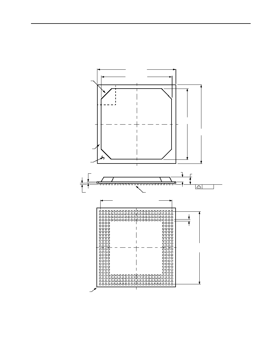
Lucent Technologies Inc.
187
Preliminary Data Sheet
October 2000
TFRA08C13 OCTAL T1/E1 Framer
Lucent Technologies Inc.
Outline Diagram
352-Pin PBGA
Dimensions are in millimeters.
5-4407(F).ar.4
0.56
±
0.06
1.17
±
0.05
2.33
±
0.21
SEATING PLANE
SOLDER BALL
0.60
±
0.10
0.20
PWB
MOLD
COMPOUND
35.00
+0.70
≠0.00
30.00
A1 BALL
IDENTIFIER ZONE
AF
AE
AD
AC
AB
AA
Y
W
V
U
T
R
G
25 SPACES @ 1.27 = 31.75
P
N
M
L
K
J
H
1 2 3 4 5 6 7 8 9 10
12
14
16
18
22
24
26
20
11 13
15
17
21
19
23
25
F
E
D
C
B
A
25 SPACES
A1 BALL
0.75
±
0.15
35.00
±
0.20
30.00
+0.70
≠0.00
±
0.20
@ 1.27 = 31.75
CORNER

Preliminary Data Sheet
TFRA08C13 OCTAL T1/E1 Framer
October 2000
Lucent Technologies Inc. reserves the right to make changes to the product(s) or information contained herein without notice. No liability is assumed as a result of their use or application. No
rights under any patent accompany the sale of any such product(s) or information.
ORCA is a registered trademark of Lucent Technologies Inc. Foundry is a trademark of Xilinx, Inc.
October 2000
DS00-190PDH (Replaces DS99-039T1E1)
INTERNET:
http://www.lucent.com/micro, or for FPGA information, http://www.lucent.com/orca
E-MAIL:
docmaster@micro.lucent.com
N. AMERICA:
Microelectronics Group, Lucent Technologies Inc., 555 Union Boulevard, Room 30L-15P-BA, Allentown, PA 18109-3286
1-800-372-2447, FAX 610-712-4106 (In CANADA: 1-800-553-2448, FAX 610-712-4106)
ASIA PACIFIC: Microelectronics Group, Lucent Technologies Singapore Pte. Ltd., 77 Science Park Drive, #03-18 Cintech III, Singapore 118256
Tel. (65) 778 8833, FAX (65) 777 7495
CHINA:
Microelectronics Group, Lucent Technologies (China) Co., Ltd., A-F2, 23/F, Zao Fong Universe Building, 1800 Zhong Shan Xi Road, Shanghai
200233 P. R. China Tel. (86) 21 6440 0468, ext. 325, FAX (86) 21 6440 0652
JAPAN:
Microelectronics Group, Lucent Technologies Japan Ltd., 7-18, Higashi-Gotanda 2-chome, Shinagawa-ku, Tokyo 141, Japan
Tel. (81) 3 5421 1600, FAX (81) 3 5421 1700
EUROPE:
Data Requests: MICROELECTRONICS GROUP DATALINE: Tel. (44) 7000 582 368, FAX (44) 1189 328 148
Technical Inquiries: GERMANY: (49) 89 95086 0 (Munich), UNITED KINGDOM: (44) 1344 865 900 (Ascot),
FRANCE: (33) 1 40 83 68 00 (Paris), SWEDEN: (46) 8 594 607 00 (Stockholm), FINLAND: (358) 9 3507670 (Helsinki),
ITALY: (39) 02 6608131 (Milan), SPAIN: (34) 1 807 1441 (Madrid)
Ordering Information
Device Code
Package
Temperature
Comcode
(Ordering Number)
TFRA08C13 - DB
352-Pin PBGA
≠40 ∞C to +85 ∞C
108269754