 | –≠–ª–µ–∫—Ç—Ä–æ–Ω–Ω—ã–π –∫–æ–º–ø–æ–Ω–µ–Ω—Ç: TLIU04C1 | –°–∫–∞—á–∞—Ç—å:  PDF PDF  ZIP ZIP |
Document Outline
- Features
- Applications
- Description
- Microprocessor Mode
- Direct Logic Control Mode
- Outline Diagram
- Ordering Information
- List of Figures
- Figure 1. TLIU04C1 Microprocessor Mode Pin Diagram
- Figure 2. TLIU04C1 Block Diagram, CMODE = 1 (Microprocessor Mode)
- Figure 3. Block Diagram of the Quad Line Interface Unit (Single Channel)
- Figure 4. DS1/T1 Receiver Jitter Accommodation Without Jitter Attenuator
- Figure 5. DS1/T1 Receiver Jitter Transfer Without Jitter Attenuator
- Figure 6. CEPT/E1 Receiver Jitter Accommodation Without Jitter Attenuator
- Figure 7. CEPT/E1 Receiver Jitter Transfer Without Jitter Attenuator
- Figure 8. DSX-1 Isolated Pulse Template
- Figure 9. ITU-T G.703 Pulse Template
- Figure 10. DS1/T1 Receiver Jitter Accommodation with Jitter Attenuator
- Figure 11. DS1/T1 Jitter Transfer of the Jitter Attenuator
- Figure 12. CEPT/E1 Receiver Jitter Accommodation with Jitter Attenuator
- Figure 13. CEPT/E1 Jitter Transfer of the Jitter Attenuator
- Figure 14. Line Termination Circuitry
- Figure 15. Mode 1ÑRead Cycle Timing (MPMODE = 0, MPMUX = 0)
- Figure 16. Mode 1ÑWrite Cycle Timing (MPMODE = 0, MPMUX = 0)
- Figure 17. Mode 2ÑRead Cycle Timing (MPMODE = 0, MPMUX = 1)
- Figure 18. Mode 2ÑWrite Cycle Timing (MPMODE = 0, MPMUX = 1)
- Figure 19. Mode 3ÑRead Cycle Timing (MPMODE = 1, MPMUX = 0)
- Figure 20. Mode 3ÑWrite Cycle Timing (MPMODE = 1, MPMUX = 0)
- Figure 21. Mode 4ÑRead Cycle Timing (MPMODE = 1, MPMUX = 1)
- Figure 22. Mode 4ÑWrite Cycle Timing (MPMODE = 1, MPMUX = 1)
- Figure 23. Interface Data Timing (ACM = 0)
- Figure 24. TLIU04C1 Direct Logic Control Mode Pin Diagram
- Figure 25. TLIU04C1 Block Diagram, CMODE = 0 (Direct Logic Mode)
- Figure 26. Block Diagram of the Quad Line Interface Unit (Single Channel)
- Figure 27. DS1/T1 Receiver Jitter Accommodation Without Jitter Attenuator
- Figure 28. DS1/T1 Receiver Jitter Transfer Without Jitter Attenuator
- Figure 29. CEPT/E1 Receiver Jitter Accommodation Without Jitter Attenuator
- Figure 30. CEPT/E1 Receiver Jitter Transfer Without Jitter Attenuator
- Figure 31. DSX-1 Isolated Pulse Template
- Figure 32. ITU-T G.703 Pulse Template
- Figure 33. DS1/T1 Receiver Jitter Accommodation with Jitter Attenuator
- Figure 34. DS1/T1 Jitter Transfer of the Jitter Attenuator
- Figure 35. CEPT/E1 Receiver Jitter Accommodation with Jitter Attenuator
- Figure 36. CEPT/E1 Jitter Transfer of the Jitter Attenuator
- Figure 37. Line Termination Circuitry
- Figure 38. Interface Data Timing (ACM = 0)
- List of Tables
- Contact Us

Advance Data Sheet, Rev. 2
April 1999
TLIU04C1 Quad T1/E1 Line Interface
Features
s
Selectable microprocessor or direct logic control
modes.
s
Quad T1/E1 line interface.
s
Hardware and software reset options.
s
3-state outputs.
s
0.35 µm CMOS technology.
s
Compliant with:
AT&T
CB119 (10/79)
Bellcore
TR-54016 (89)
TR-TSY-000170 (10/97)
TR-TSY-000009 (5/86)
GR-499-CORE (12/95)
GR-253-CORE (12/95)
ANSI
T1.102 (93)
T1.231 (93)
T1.403 (95)
ITU-T
G.703 (88)
G.704 (91)
G.706 (91)
G.732 (88)
G.735-9 (88)
G.775 (11/94)
G.823-4 (3/93)
G.826 (11/93)
I.431 (3/93)
ETSI
TBR 12 (12/93)
TBR 13 (1/96)
s
≠40 ∞C to +85 ∞C operating temperature range.
s
Fine-pitch (12.5 mil) surface-mount
package, 144-pin TQFP.
s
Transmitter includes transmit encoder (B8ZS or
HDB3), pulse shaping, and line driver.
s
Five pulse equalization settings for template com-
pliance at DSX cross connect.
s
Receive includes equalization, digital clock and
data recovery (immune to false lock), and receive
decoder (B8ZS or HDB3).
s
CEPT/E1 interference immunity as required by
G.703.
s
Transmit jitter <0.02 UI.
s
Receive generated jitter <0.05 UI.
s
Jitter attenuator selectable for use in transmit or
receive path. Jitter attenuation characteristics are
data pattern independent.
s
For use with 100
DS1 twisted-pair, 120
E1
twisted-pair, and 75
E1 coaxial cable.
s
Common part available for transmit/receive
transformers.
s
Analog LOS alarm for signals less than ≠18 dB for
greater than 1 ms or 10 bit symbol periods to
255 bit symbol periods (selectable).
s
Digital LOS alarm for 100 zeros (DS1) or 255 zeros
(CEPT).
s
Diagnostic loopback modes.
s
Low power consumption.
Applications
s
T1/E1 network performance monitoring
s
SONET/SDH multiplexers
s
Asynchronous multiplexers (M13)
s
Digital access cross connects (DACs)
s
Channel banks
s
Digital radio base stations, remote wireless mod-
ules
s
PBX interface

Advance Data Sheet, Rev. 2
TLIU04C1 Quad T1/E1 Line Interface
April 1999
2
Lucent Technologies Inc.
Table of Contents
Contents
Page
Features .................................................................................................................................................................. 1
Applications ............................................................................................................................................................. 1
Description............................................................................................................................................................... 8
Microprocessor Mode .............................................................................................................................................. 8
Overview .............................................................................................................................................................. 8
Pin Information ..................................................................................................................................................... 9
System Interface Pin Options............................................................................................................................. 14
Microprocessor Configuration Modes................................................................................................................. 14
Microprocessor Interface Pinout Definitions....................................................................................................... 15
Microprocessor Clock (MPCLK) Specifications.................................................................................................. 16
Internal Chip Select Function ............................................................................................................................. 16
Microprocessor Interface Register Architecture ................................................................................................. 17
Block Diagrams .................................................................................................................................................. 18
Data Recovery.................................................................................................................................................... 20
Jitter Accommodation and Jitter Transfer Without the Jitter Attenuator ............................................................. 20
Receiver Configuration Modes ........................................................................................................................... 20
Clock/Data Recovery Mode (CDR) ................................................................................................................. 20
Zero Substitution Decoding (CODE) ............................................................................................................... 20
Alternate Logic Mode (ALM) ........................................................................................................................... 21
Alternate Clock Mode (ACM) .......................................................................................................................... 21
RLIU Alarms.................................................................................................................................................... 21
DS1 Receiver Specifications .............................................................................................................................. 23
Frequency Response Curves ......................................................................................................................... 24
CEPT Receiver Specifications ........................................................................................................................... 26
Frequency Response Curves ......................................................................................................................... 27
Output Pulse Generation.................................................................................................................................... 29
Jitter.................................................................................................................................................................... 29
Zero Substitution Encoding (CODE) .................................................................................................................. 30
Alarm Indication Signal Generator (XAIS) ...................................................................................................... 30
Transmitter Alarms ............................................................................................................................................. 30
Loss of Transmit Clock (LOTC) Alarm ............................................................................................................ 30
Transmit Driver Monitor (TDM) Alarm ............................................................................................................. 30
DS1 Transmitter Pulse Template and Specifications ......................................................................................... 31
CEPT Transmitter Pulse Template and Specifications ...................................................................................... 33
Jitter Attenuator .................................................................................................................................................. 34
Generated (Intrinsic) Jitter .............................................................................................................................. 34
Jitter Transfer Function ................................................................................................................................... 35
Jitter Accommodation ..................................................................................................................................... 35
Jitter Attenuator Enable .................................................................................................................................. 36
Jitter Attenuator Receive Path Enable (JAR) .................................................................................................. 36
Jitter Attenuator Transmit Path Enable (JAT) ................................................................................................. 36
Frequency Response Curves ......................................................................................................................... 37
Loopbacks .......................................................................................................................................................... 41
Full Local Loopback (FLLOOP) ...................................................................................................................... 41
Remote Loopback (RLOOP) ........................................................................................................................... 41
Digital Local Loopback (DLLOOP) .................................................................................................................. 41
Powerdown (PWRDN)........................................................................................................................................ 42
Reset (
RESET
, SWRESET) ................................................................................................................................ 42

Advance Data Sheet, Rev. 2
April 1999
TLIU04C1 Quad T1/E1 Line Interface
3
Lucent Technologies Inc.
Table of Contents
(continued)
Contents
Page
Loss of XCLK Reference Clock (LOXC)............................................................................................................. 42
In-Circuit Testing and Driver High-Impedance State (ICT)................................................................................. 42
LIU Delay Values................................................................................................................................................ 42
Line Encoding/Decoding .................................................................................................................................... 43
Alternate Mark Inversion (AMI) ....................................................................................................................... 43
T1-Binary 8 Zero Code Suppression (B8ZS) .................................................................................................. 43
High-Density Bipolar of Order 3 (HDB3) ......................................................................................................... 43
Registers ............................................................................................................................................................ 44
Alarm Registers (0000, 0001) ......................................................................................................................... 44
Alarm Mask Registers (0010, 0011)................................................................................................................ 45
Global Control Registers (0100, 0101)............................................................................................................ 45
Channel Configuration and Control Registers (0110--1001, 1011, 1100)...................................................... 46
XCLK Reference Clock ...................................................................................................................................... 48
16x XCLK Reference Clock ............................................................................................................................ 48
Primary Line Rate XCLK Reference Clock and Internal Reference Clock Synthesizer .................................. 49
Power Supply Bypassing.................................................................................................................................... 49
Line Circuitry ...................................................................................................................................................... 50
Absolute Maximum Ratings................................................................................................................................ 51
Handling Precautions ......................................................................................................................................... 51
Operating Conditions.......................................................................................................................................... 51
Power Requirements.......................................................................................................................................... 52
Electrical Characteristics .................................................................................................................................... 52
Microprocessor Interface Timing ........................................................................................................................ 53
Data Interface Timing ......................................................................................................................................... 59
Direct Logic Control Mode ..................................................................................................................................... 60
Overview ............................................................................................................................................................ 60
Device Overview ................................................................................................................................................ 60
Pin Information ................................................................................................................................................... 61
System Interface Pin Options............................................................................................................................. 66
Block Diagrams .................................................................................................................................................. 67
Data Recovery.................................................................................................................................................... 69
Jitter Accommodation and Jitter Transfer Without the Jitter Attenuator ............................................................. 69
Receiver Configuration Modes ........................................................................................................................... 69
Clock/Data Recovery Mode (CDR) ................................................................................................................. 69
Zero Substitution Decoding (CODE) ............................................................................................................... 69
Alternate Logic Mode (ALM) ........................................................................................................................... 69
Alternate Clock Mode (ACM) .......................................................................................................................... 69
RLIU Alarms.................................................................................................................................................... 70
DS1 Receiver Specifications .............................................................................................................................. 72
Frequency Response Curves.......................................................................................................................... 73
CEPT Receiver Specifications ........................................................................................................................... 75
Frequency Response Curves.......................................................................................................................... 76
Output Pulse Generation.................................................................................................................................... 78
Jitter.................................................................................................................................................................... 78
Transmitter Configuration Modes ....................................................................................................................... 79
Zero Substitution Encoding (CODE) ............................................................................................................... 79
Alarm Indication Signal Generator (XAIS)....................................................................................................... 79
Loss of Transmit Clock (LOTC) Alarm ............................................................................................................ 79
Transmit Driver Monitor (TDM) Alarm ............................................................................................................. 79

Advance Data Sheet, Rev. 2
TLIU04C1 Quad T1/E1 Line Interface
April 1999
4
Lucent Technologies Inc.
Table of Contents
(continued)
Contents
Page
DS1 Transmitter Pulse Template ....................................................................................................................... 80
CEPT Transmitter Pulse Template..................................................................................................................... 81
Jitter Attenuator .................................................................................................................................................. 82
Generated (Intrinsic) Jitter .............................................................................................................................. 82
Jitter Transfer Function ................................................................................................................................... 83
Jitter Accommodation ..................................................................................................................................... 83
Jitter Attenuator Enable .................................................................................................................................. 84
Jitter Attenuator Receive Path Enable (JAR) .................................................................................................. 84
Jitter Attenuator Transmit Path Enable (JAT) ................................................................................................. 84
Frequency Response Curves ......................................................................................................................... 85
Loopbacks .......................................................................................................................................................... 89
Full Local Loopback (FLLOOP) ...................................................................................................................... 89
Remote Loopback (RLOOP) ........................................................................................................................... 89
Digital Local Loopback (DLLOOP) .................................................................................................................. 89
Powerdown (PWRDN)........................................................................................................................................ 89
Reset (
RESET
).................................................................................................................................................... 89
Loss of XCLK Reference Clock (LOXC)............................................................................................................. 89
In-Circuit Testing and Driver High-Impedance State (ICT)................................................................................. 89
LIU Delay Values................................................................................................................................................ 89
Line Encoding/Decoding .................................................................................................................................... 90
Alternate Mark Inversion (AMI) ....................................................................................................................... 90
T1-Binary 8 Zero Code Suppression .............................................................................................................. 90
High-Density Bipolar of Order 3 (HDB3) ......................................................................................................... 90
XCLK Reference Clock ...................................................................................................................................... 91
16x XCLK Reference Clock ............................................................................................................................ 91
Primary Line Rate XCLK Reference Clock and Internal Reference Clock Synthesizer .................................. 92
Power Supply Bypassing.................................................................................................................................... 93
Line Circuitry ...................................................................................................................................................... 94
Absolute Maximum Ratings................................................................................................................................ 95
Handling Precautions ......................................................................................................................................... 95
Operating Conditions.......................................................................................................................................... 95
Power Requirements.......................................................................................................................................... 96
Electrical Characteristics .................................................................................................................................... 96
Data Interface Timing ......................................................................................................................................... 97
Outline Diagram..................................................................................................................................................... 98
144-Pin TQFP ..................................................................................................................................................... 98
Ordering Information.............................................................................................................................................. 99

Advance Data Sheet, Rev. 2
April 1999
TLIU04C1 Quad T1/E1 Line Interface
5
Lucent Technologies Inc.
List of Figures
Figures
Page
Figure 1. TLIU04C1 Microprocessor Mode Pin Diagram.......................................................................................... 9
Figure 2. TLIU04C1 Block Diagram, CMODE = 1 (Microprocessor Mode) ............................................................ 18
Figure 3. Block Diagram of the Quad Line Interface Unit (Single Channel) ........................................................... 19
Figure 4. DS1/T1 Receiver Jitter Accommodation Without Jitter Attenuator .......................................................... 24
Figure 5. DS1/T1 Receiver Jitter Transfer Without Jitter Attenuator ...................................................................... 25
Figure 6. CEPT/E1 Receiver Jitter Accommodation Without Jitter Attenuator ....................................................... 27
Figure 7. CEPT/E1 Receiver Jitter Transfer Without Jitter Attenuator ................................................................... 28
Figure 8. DSX-1 Isolated Pulse Template .............................................................................................................. 31
Figure 9. ITU-T G.703 Pulse Template .................................................................................................................. 33
Figure 10. DS1/T1 Receiver Jitter Accommodation with Jitter Attenuator.............................................................. 37
Figure 11. DS1/T1 Jitter Transfer of the Jitter Attenuator....................................................................................... 38
Figure 12. CEPT/E1 Receiver Jitter Accommodation with Jitter Attenuator ........................................................... 39
Figure 13. CEPT/E1 Jitter Transfer of the Jitter Attenuator.................................................................................... 40
Figure 14. Line Termination Circuitry ..................................................................................................................... 50
Figure 15. Mode 1--Read Cycle Timing (MPMODE = 0, MPMUX = 0) ................................................................. 55
Figure 16. Mode 1--Write Cycle Timing (MPMODE = 0, MPMUX = 0) ................................................................. 55
Figure 17. Mode 2--Read Cycle Timing (MPMODE = 0, MPMUX = 1) ................................................................. 56
Figure 18. Mode 2--Write Cycle Timing (MPMODE = 0, MPMUX = 1) ................................................................. 56
Figure 19. Mode 3--Read Cycle Timing (MPMODE = 1, MPMUX = 0) ................................................................. 57
Figure 20. Mode 3--Write Cycle Timing (MPMODE = 1, MPMUX = 0) ................................................................. 57
Figure 21. Mode 4--Read Cycle Timing (MPMODE = 1, MPMUX = 1) ................................................................. 58
Figure 22. Mode 4--Write Cycle Timing (MPMODE = 1, MPMUX = 1) ................................................................. 58
Figure 23. Interface Data Timing (ACM = 0)........................................................................................................... 59
Figure 24. TLIU04C1 Direct Logic Control Mode Pin Diagram............................................................................... 61
Figure 25. TLIU04C1 Block Diagram, CMODE = 0 (Direct Logic Mode)................................................................ 67
Figure 26. Block Diagram of the Quad Line Interface Unit (Single Channel) ......................................................... 68
Figure 27. DS1/T1 Receiver Jitter Accommodation Without Jitter Attenuator ........................................................ 73
Figure 28. DS1/T1 Receiver Jitter Transfer Without Jitter Attenuator .................................................................... 74
Figure 29. CEPT/E1 Receiver Jitter Accommodation Without Jitter Attenuator ..................................................... 76
Figure 30. CEPT/E1 Receiver Jitter Transfer Without Jitter Attenuator ................................................................. 77
Figure 31. DSX-1 Isolated Pulse Template ............................................................................................................ 80
Figure 32. ITU-T G.703 Pulse Template ................................................................................................................ 81
Figure 33. DS1/T1 Receiver Jitter Accommodation with Jitter Attenuator.............................................................. 85
Figure 34. DS1/T1 Jitter Transfer of the Jitter Attenuator....................................................................................... 86
Figure 35. CEPT/E1 Receiver Jitter Accommodation with Jitter Attenuator ........................................................... 87
Figure 36. CEPT/E1 Jitter Transfer of the Jitter Attenuator.................................................................................... 88
Figure 37. Line Termination Circuitry ..................................................................................................................... 94
Figure 38. Interface Data Timing (ACM = 0)........................................................................................................... 97

Advance Data Sheet, Rev. 2
TLIU04C1 Quad T1/E1 Line Interface
April 1999
6
Lucent Technologies Inc.
List of Tables
Tables
Page
Table 1. Pin Descriptions....................................................................................................................................... 10
Table 2. System Interface Pin Mapping................................................................................................................. 14
Table 3. Microprocessor Configuration Modes...................................................................................................... 14
Table 4. MODE [1--4] Microprocessor Pin Definitions.......................................................................................... 15
Table 5. Microprocessor Input Clock Specifications.............................................................................................. 16
Table 6. LIU Register Bank ................................................................................................................................... 17
Table 7. Register Map for CODE Bits.................................................................................................................... 20
Table 8. Digital Loss of Signal Standard Select .................................................................................................... 22
Table 9. LOSSD and RCVAIS Control Configurations (Not Valid During Loopback Modes) ................................ 22
Table 10. DS1 RLIU Specifications ....................................................................................................................... 23
Table 11. CEPT RLIU Specifications..................................................................................................................... 26
Table 12. Equalizer/Rate Control .......................................................................................................................... 29
Table 13. Register Map for CODE Bits.................................................................................................................. 30
Table 14. DSX-1 Pulse Template Corner Points (from CB119) ............................................................................ 31
Table 15. DS1 Transmitter Specifications ............................................................................................................. 32
Table 16. CEPT Transmitter Specifications........................................................................................................... 34
Table 17. Loopback Control .................................................................................................................................. 41
Table 18. AMI Encoding ........................................................................................................................................ 43
Table 19. DS1 B8ZS Encoding.............................................................................................................................. 43
Table 20. ITU HDB3 Coding and DCPAT Binary Coding ...................................................................................... 43
Table 21. Alarm Registers ..................................................................................................................................... 44
Table 22. Alarm Mask Registers ........................................................................................................................... 45
Table 23. Global Control Register (0100).............................................................................................................. 45
Table 24. Global Control Register (0101).............................................................................................................. 46
Table 25. Channel Configuration Registers (0110--1001).................................................................................... 46
Table 26. Channel Configuration Register (1011) ................................................................................................. 47
Table 27. Control Register (1100) ......................................................................................................................... 47
Table 28. XCLK (16x, CLKS = 0) Timing Specifications ....................................................................................... 48
Table 29. XCLK (1x, CLKS = 1) Timing Specifications ......................................................................................... 49
Table 30. Termination Components by Application............................................................................................... 50
Table 31. Absolute Maximum Ratings................................................................................................................... 51
Table 32. ESD Threshold Voltage ......................................................................................................................... 51
Table 33. Recommended Operating Conditions ................................................................................................... 51
Table 34. Power Consumption .............................................................................................................................. 52
Table 35. Power Dissipation.................................................................................................................................. 52
Table 36. Logic Interface Characteristics .............................................................................................................. 52
Table 37. Microprocessor Interface I/O Timing Specifications .............................................................................. 53
Table 38. Data Interface Timing ............................................................................................................................ 59
Table 39. Pin Descriptions..................................................................................................................................... 62
Table 40. System Interface Pin Mapping............................................................................................................... 66
Table 41. Digital Loss of Signal Standard Select .................................................................................................. 70
Table 42. LOSSD and RCVAIS Control Configurations (Not Valid During Loopback Modes) .............................. 71
Table 43. DS1 RLIU Specifications ....................................................................................................................... 72
Table 44. CEPT RLIU Specifications..................................................................................................................... 75
Table 45. Equalizer/Rate Control .......................................................................................................................... 78
Table 46. DSX-1 Pulse Template Corner Points (from CB119) ............................................................................ 80
Table 47. DS1 Transmitter Specifications ............................................................................................................. 80
Table 48. CEPT Transmitter Specifications........................................................................................................... 82
Table 49. AMI Encoding ........................................................................................................................................ 90
Table 50. DS1 B8ZS Encoding.............................................................................................................................. 90

Advance Data Sheet, Rev. 2
April 1999
TLIU04C1 Quad T1/E1 Line Interface
7
Lucent Technologies Inc.
List of Tables
(continued)
Tables
Page
Table 51. ITU HDB3 Coding and DCPAT Binary Coding ...................................................................................... 90
Table 52. XCLK (16x, CLKS = 0) Timing Specifications........................................................................................ 91
Table 53. XCLK (1x, CLKS = 1) Timing Specifications.......................................................................................... 92
Table 54. XCLK Specifications .............................................................................................................................. 92
Table 55. Termination Components by Application............................................................................................... 94
Table 56. Absolute Maximum Ratings................................................................................................................... 95
Table 57. ESD Threshold Voltage ......................................................................................................................... 95
Table 58. Recommended Operating Conditions ................................................................................................... 95
Table 59. Power Consumption .............................................................................................................................. 96
Table 60. Power Dissipation .................................................................................................................................. 96
Table 61. Logic Interface Characteristics .............................................................................................................. 96
Table 62. Data Interface Timing ............................................................................................................................ 97

Advance Data Sheet, Rev. 2
TLIU04C1 Quad T1/E1 Line Interface
April 1999
8
Lucent Technologies Inc.
Description
The TLIU04C1 is a quad line interface containing four
line transmit and receive channels for use in both North
American (T1/DS1) and European (E1/CEPT) applica-
tions. The line interface unit has the same functions as
the Lucent T7698.
The device can operate in either of two modes, chosen
by the logic state of a control pin. A direct logic control
mode provides the ability to define the architecture, ini-
tiate loopbacks, and monitor alarms without connecting
to a microprocessor by setting the logic levels on con-
trol pins. The microprocessor mode uses a parallel
microprocessor interface to allow the user to configure
the device. The interface is compatible with many com-
mercially available microprocessors. The block dia-
grams of the microprocessor and direct logic modes
are shown in Figure 2 and Figure 25, respectively.
The block diagram of the line interface unit is shown in
Figure 3 on page 19 (it is repeated as Figure 26). The
line receiver performs clock and data recovery using a
fully integrated digital phase-locked loop. This digital
implementation prevents false lock conditions that are
common when recovering sparse data patterns with
analog phase-locked loops.
Equalization circuitry in the receiver provides a high
level of interference immunity. As an option, the raw
sliced data (no retiming) can be output on the receive
data pins. Transmit equalization is implemented with
low-impedance output drivers that provide shaped
waveforms to the transformer, guaranteeing template
conformance. The quad device will interface to the digi-
tal cross connect (DSX) at lengths of up to 655 ft. for
DS1 operation or to line impedances of 75
or 120
for CEPT operation.
A selectable jitter attenuator may be placed in the
receive signal path for low-bandwidth line-synchronous
applications, or it may be placed in the transmit path for
multiplexer applications where DS1/CEPT signals are
demultiplexed from higher rate signals. The jitter atten-
uator will perform the clock smoothing required on the
resulting demultiplexed gapped clock.
Microprocessor Mode
Overview
The TLIU04C1 device has the ability to operate in
either a microprocessor mode or a direct logic control
mode. The CMODE pin is used to determine the oper-
ating mode. To configure the device for microprocessor
mode, the CMODE pin is pulled high.
The device is equipped with a microprocessor interface
that can operate with most commercially available
microprocessors. Inputs MPMUX and MPMODE
(pins 108 and 110) are used to configure this interface
into one of four possible modes, as shown in Table 3.
The MPMUX setting selects either a multiplexed 8-bit
address/data bus (AD[7:0]) or a demultiplexed 4-bit
address bus (A[3:0]) and an 8-bit data bus (AD[7:0]).
The MPMODE setting selects the associated set of
control signals required to access a set of registers
within the device.
When the microprocessor interface is configured to
operate in the multiplexed address/data bus modes
(MPMUX = 1), the user has access to an internal chip
select function that allows the microprocessor to selec-
tively read/write a specific TLIU04C1 in a multiple
TLIU04C1 environment (see the Internal Chip Select
Function section, page 16).
The microprocessor interface can operate at speeds up
to 16.384 MHz in interrupt-driven or polled mode with-
out requiring any wait-states. For microprocessors
operating at greater than 16.384 MHz, the
RDY_DTACK output is used to introduce wait-states in
the read/write cycles.
In the interrupt-driven mode, one or more device
alarms will assert the active-high INT output (pin 114)
once per alarm activation. After the microprocessor
reads the alarm status registers, the INT output will
deassert. In the polled mode, however, the micropro-
cessor monitors the various device alarm status by
periodically reading the alarm status registers without
the use of INT. A variety of LIU mask controls are avail-
able for control of the INT pin.

Advance Data Sheet, Rev. 2
April 1999
TLIU04C1 Quad T1/E1 Line Interface
9
Lucent Technologies Inc.
Microprocessor Mode
(continued)
Pin Information
5-7728(F).a
Figure 1. TLIU04C1 Microprocessor Mode Pin Diagram
GNDD
VD
D
A
1
RT
I
P
1
RRING1
GND
A
1
RND
1
/
B
PV1
RP
D1
/
R
D
A
T
A
1
A2
A1
A0
VDDD
GNDD
NC
NC
TCLK2
TPD2/TDATA2
TND2
RCLK2/ALOS2
RPD2/RDATA2
RND2/BPV2
GNDA2
RRING2
RTIP2
VDDA2
GNDX2
TRING2
VDDX2
TTIP2
GNDX2
NC
RES
E
T
LO
X
C
XCL
K
VDD
D
GND
D
NC
36
37
GND
D
NC
NC
NC
NC
NC
NC
NC
GN
D
X
3
TT
I
P
3
VDD
X
3
T
R
ING3
GN
D
X
3
VD
D
A
3
RT
I
P
3
RRING3
GND
A
3
RND3
/BP
V
3
RPD3
/RD
A
T
A
3
RCL
K3
/
A
L
O
S3
T
ND3
TPD
3
/
T
D
A
T
A
3
TC
LK
3
NC
NC
NC
NC
NC
NC
NC
NC
NC
ICT
NC
38
39
40
41
42
43
44
45
46
47
48
49
50
51
52
53
54
55
56
57
58
59
60
61
62
63
64
65
66
67
68
69
70
71
72
35
34
33
32
31
30
29
28
27
26
25
24
23
22
21
20
19
18
17
16
15
14
13
12
11
10
9
8
7
6
5
4
3
2
1
73
74
75
76
77
78
79
80
81
82
83
84
85
86
87
88
89
90
91
92
93
94
95
96
97
98
99
100
101
102
103
104
105
106
107
108
MPMUX
WR_DS
MPCLK
NC
NC
NC
NC
GNDX4
TTIP4
VDDX4
TRING4
GNDX4
VDDA4
RTIP4
RRING4
GNDA4
RND4/BPV4
RPD4/RDATA4
TND4
RCLK4/ALOS4
TPD4/TDATA4
TCLK4
NC
NC
GNDD
VDDD
AD0
AD1
AD2
AD3
AD4
AD5
AD6
AD7
VDDD
GNDD
144
143
142
141
140
139
138
137
136
135
134
133
132
131
130
129
128
127
126
125
124
123
122
121
120
119
118
117
116
115
114
113
112
111
110
109
NC
GNDX1
TR
I
N
G
1
VDDX
1
TT
I
P
1
GNDX1
NC
NC
NC
NC
NC
NC
NC
GNDD
VDDD
CM
O
D
E
CL
KS
CL
KM
RD
Y_
DT
A
C
K
INT
CS
AL
E_
AS
RD
_R
/W
A3
NC
NC
NC
NC
VDDD
NC
TC
LK
1
TP
D
1
/
T
D
A
T
A
1
T
ND1
RC
L
K
1
/
AL
O
S
1
MP
M
O
D
E
GNDD
NC
NC

Advance Data Sheet, Rev. 2
TLIU04C1 Quad T1/E1 Line Interface
April 1999
10
Lucent Technologies Inc.
Microprocessor Mode
(continued)
Pin Information
(continued)
Table 1. Pin Descriptions
* I = input, O = output, I
u
indicates an input with internal pull-up; I
d
indicates an input with internal pull-down, P = power. Resistance value of all
internal pull-ups or pull-downs is 50 k
, unless otherwise specified.
Pin
Symbol
Type*
Name/Description
117
CLKS
I
d
XCLK Select. This pin selects either a 16x rate clock for XCLK (CLKS = 0)
or a primary line rate clock for XCLK (CLKS = 1).
116
CLKM
I
d
XCLK Mode. This pin must be set appropriately when using a primary line
rate clock for XCLK.
CEPT:
CLKM = 1.
DS1:
CLKM = 0.
118
CMODE
I
d
Chip Mode. This pin sets the chip mode for either direct logic mode or
microprocessor mode.
Microprocessor: CMODE = 1.
Direct Logic: CMODE = 0.
128, 132
25, 29,
56, 60,
97, 101
GND
X
[1--4]
P
Ground Reference for Line Drivers.
129, 28,
57, 100
TTIP[1--4]
O
Transmit Bipolar Tip. Positive bipolar transmit data to the analog line
interface.
130, 27,
58, 99
V
DDX
[1--4]
P
Power Supply for Line Drivers. The TLIU04C1 device requires a 5 V ± 5%
power supply on these pins.
131, 26,
59, 98
TRING[1--4]
O
Transmit Bipolar Ring. Negative bipolar transmit data to the analog line
interface.
133, 24,
61, 96
V
DDA
[1--4]
P
Power Supply for Analog Circuitry. The TLIU04C1 device requires a 5 V
± 5% power supply on these pins.
134, 23,
62, 95
RTIP[1--4]
I
Receive Bipolar Tip. Positive bipolar receive data from the analog line
interface.
135, 22,
63, 94
RRING[1--4]
I
Receive Bipolar Ring. Negative bipolar receive data from the analog line
interface.
136, 21,
64, 93
GND
A
[1--4]
P
Ground Reference for Analog Circuitry.
137, 20,
65, 92
RND/BPV[1--4]
O
Receive Negative Data. When in dual-rail (DUAL = 1: register 5, bit 4)
clock recovery mode (CDR = 1: register 5, bit 0), this signal is the received
negative NRZ data to the terminal equipment. When in data slicing mode
(CDR = 0), this signal is the raw sliced negative data of the front end.
Bipolar Violation. When in single-rail (DUAL = 0: register 5, bit 4) clock
recovery mode (CDR = 1: register 5, bit 0), and CODE = 1 (register 5, bit 3),
this signal is asserted high to indicate the occurrence of a code violation in
the receive data stream. A code violation is a bipolar violation that is not
part of a zero substitution code. If CODE = 0, this signal is asserted to
indicate the occurrence of a bipolar violation in the received data.

Advance Data Sheet, Rev. 2
April 1999
TLIU04C1 Quad T1/E1 Line Interface
11
Lucent Technologies Inc.
Microprocessor Mode
(continued)
Pin Information
(continued)
Table 1. Pin Descriptions (continued)
* I = input, O = output, I
u
indicates an input with internal pull-up; I
d
indicates an input with internal pull-down, P = power. Resistance value of all
internal pull-ups or pull-downs is 50 k
, unless otherwise specified.
Pin
Symbol
Type*
Name/Description
138, 19,
66, 91
RPD/RDATA
[1--4]
O
Receive Positive Data. When in dual-rail (DUAL = 1: register 5, bit 4) clock
recovery mode (CDR = 1: register 5, bit 0), this signal is the received positive
NRZ data to the terminal equipment. When in data slicing mode (CDR = 0),
this signal is the raw sliced positive data of the front end.
Receive Data. When in single-rail (DUAL = 0: register 5, bit 4) clock recovery
mode (CDR = 1: register 5, bit 0), this signal is the received NRZ data.
139, 18,
67, 90
RCLK/ALOS
[1--4]
O
Receive Clock. In clock recovery mode (CDR = 1: register 5, bit 0), this
signal is the recovered receive clock for the terminal equipment. The duty
cycle of RCLK is 50% ± 5%.
Analog Loss of Signal. In data slicing mode (CDR = 0: register 5, bit 0), this
signal is asserted high to indicate low amplitude receive data at the RTIP/
RRING inputs.
140, 17,
68, 89
TND[1--4]
I
Transmit Negative Data. This signal is the transmit negative NRZ data from
the terminal equipment.
141, 16,
69, 88
TPD/TDATA
[1--4]
I
Transmit Positive Data. When in dual-rail mode (DUAL = 1: register 5, bit 4),
this signal is the transmit positive NRZ data from the terminal equipment.
Transmit Data. When in single-rail mode (DUAL = 0: register 5, bit 4), this
signal is the transmit NRZ data from the terminal equipment.
142, 15,
70, 87
TCLK[1--4]
I
Transmit Clock. DS1 (1.544 MHz ± 32 ppm) or CEPT (2.048 MHz ±
50 ppm) clock signal from the terminal equipment.
110
MPMODE
I
Microprocessor Mode. When MPMODE = 1, the device uses the address
latch enable type microprocessor read/write protocol with separate read and
write controls. Setting MPMODE = 0 allows the device to use the address
strobe type microprocessor read/write protocol with a separate data strobe
and a combined read/write control.
108
MPMUX
I
Microprocessor Multiplex Mode. Setting MPMUX = 1 allows the
microprocessor interface to accept multiplexed address and data signals.
Setting MPMUX = 0 allows the microprocessor interface to accept
demultiplexed (separate) address and data signals.
107
WR_DS
I
Write (Active-Low). If MPMODE = 1 (pin 110), this pin is asserted low by the
microprocessor to initiate a write cycle.
Data Strobe (Active-Low). If MPMODE = 0 (pin 21), this pin becomes the
data strobe for the microprocessor. When R/W = 0 (pin 111) initiating a write,
a low applied to this pin latches the signal on the data bus into internal
registers.
111
RD_R/W
I
Read (Active-Low). If MPMODE = 1 (pin 110), this pin is asserted low by the
microprocessor to initiate a read cycle.
Read/Write. If MPMODE = 0 (pin 110), this pin is asserted high by the
microprocessor to initiate a read cycle or asserted low to initiate a write
cycle.

Advance Data Sheet, Rev. 2
TLIU04C1 Quad T1/E1 Line Interface
April 1999
12
Lucent Technologies Inc.
Microprocessor Mode
(continued)
Pin Information
(continued)
Table 1. Pin Descriptions (continued)
* I = input, O = output, I
u
indicates an input with internal pull-up; I
d
indicates an input with internal pull-down, P = power. Resistance value of all
internal pull-ups or pull-downs is 50 k
, unless otherwise specified.
Pin
Symbol
Type*
Name/Description
112
ALE_AS
I
Address Latch Enable. If MPMODE = 1 (pin 110), this pin becomes the
address latch enable for the microprocessor. When this pin transitions from
high to low, the address bus inputs are latched into the internal registers.
Address Strobe (Active-Low). If MPMODE = 0 (pin 110), this pin becomes
the address strobe for the microprocessor. When this pin transitions from
high to low, the address bus inputs are latched into the internal registers.
113
CS
I
u
Chip Select (Active-Low). This pin is asserted low by the microprocessor to
enable the microprocessor interface. If MPMUX = 1 (pin 108),
CS
can be
externally tied low to use the internal chip selection function. An internal
100 k
pull-up is on this pin.
114
INT
O
Interrupt. This pin is asserted high to indicate an interrupt produced by an
alarm condition in register 0 or 1. The activation of this pin can be masked by
various register bits.
115
RDY_DTACK
O
Ready. If MPMODE = 1 (pin 110), this pin is asserted high to indicate the
device has completed a read or write operation. This pin is in a 3-state
condition when CS (pin 113) is high.
Data Transfer Acknowledge (Active-Low). If MPMODE = 0 (pin 110), this
pin is asserted low to indicate the device has completed a read or write
operation.
1, 12,
37, 48,
73, 84,
109, 120
GND
D
P
Ground Reference for Microprocessor Interface and Digital Circuitry.
2, 11,
47, 74,
83, 119
V
DDD
P
Power Supply for Microprocessor Interface and Digital Circuitry. The
TLIU04C1 device requires a 5 V ± 5% power supply on these pins.
46
XCLK
I
u
Reference Clock. The clock signal used for clock and data recovery and
jitter attenuation. This clock must be ungapped and free of jitter.
For CLKS = 0, a 16x clock (for DS1, XCLK = 24.704 MHz ± 100 ppm and for
CEPT, XCLK = 32.768 MHz ± 100 ppm).
For CLKS = 1, a 1x clock (for DS1, XCLK = 1.544 MHz ± 100 ppm and for
CEPT, XCLK = 2.048 MHz ± 100 ppm).
To meet TBR 12/13 jitter accommodation requirements (JABW0 = 1), clock
tolerances must be ±20 ppm. An internal 100 k
pull-up is on this pin.
45
LOXC
O
Loss of XCLK. This pin is asserted high when the XCLK signal (pin 46) is
not present.
44
RESET
I
u
Hardware Reset (Active-Low). If
RESET
is forced low, all internal states in
the line interface paths are reset and data flow through each channel will be
momentarily disrupted. The
RESET
pin must be held low for a minimum of
10 µs.

Advance Data Sheet, Rev. 2
April 1999
TLIU04C1 Quad T1/E1 Line Interface
13
Lucent Technologies Inc.
Microprocessor Mode
(continued)
Pin Information
(continued)
Table 1. Pin Descriptions (continued)
Pin
Symbol
Type
*
* I = input, O = output, I
u
indicates an input with internal pull-up; I
d
indicates an input with internal pull-down, P = power. Resistance value of all
internal pull-ups or pull-downs is 50 k
, unless otherwise specified.
Name/Description
43
ICT
I
u
In-Circuit Test Control (Active-Low). If
ICT
is forced low, certain output pins
are placed in a high-impedance state. Which output pins are affected is
controlled by the ICTMODE bit (register 4, bit 3).
75--82
AD[7:0]
I/O
Microprocessor Interface Address/Data Bus. If MPMUX = 0 (pin 108),
these pins become the bidirectional, 3-statable data bus. If MPMUX = 1,
these pins become the multiplexed address/data bus. In this mode, only the
lower 4 bits (AD[3:0]) are used for the internal register addresses.
7--10
A[3:0]
I
Microprocessor Interface Address. If MPMUX = 0 (pin 108), these pins
become the address bus for the microprocessor interface registers. If
MPMUX = 1 (pin 108) and CS = 0 (pin 113), A3 (pin 7) can be externally tied
high to use the internal chip selection function. The state of A[2:0] determines
the address of the device. The device is addressed when the state of pins
AD[6:4] matches the device address of A[2:0]. If this function is not used,
A[3:0] must be externally tied low.
106
MPCLK
I
Microprocessor Interface Clock. Microprocessor interface clock rates from
twice the frequency of the line clock (3.088 MHz for DS1 operation,
4.096 MHz for CEPT operation) to 16.384 MHz are supported.

Advance Data Sheet, Rev. 2
TLIU04C1 Quad T1/E1 Line Interface
April 1999
14
Lucent Technologies Inc.
Microprocessor Mode
(continued)
System Interface Pin Options
The system interface can be configured to operate in a number of different modes. The different modes change the
functionality of the system interface pins, as shown in Table 2. Dual-rail or single-rail operation is possible using the
DUAL control bit (register 5, bit 4). Dual-rail mode is enabled when DUAL = 1; single-rail mode is enabled when
DUAL = 0. In dual-rail operation, data received from the line interface on RTIP and RRING appears on RPD and
RND at the system interface and data transmitted from the system interface on TPD and TND appears on TTIP and
TRING at the line interface. In single-rail operation, data received from the line interface on RTIP and RRING
appears on RDATA at the system interface and data transmitted from the system interface on TDATA appears on
TTIP and TRING at the line interface.
In both dual-rail and single-rail operation, the clock/data recovery mode is selectable via the CDR bit (register 5,
bit 0). When CDR = 1, the clock and data recovery is enabled and the system interface operates in a nonreturn-to-
zero (NRZ) digital format, recovering the clock and data from the incoming pulses. When CDR = 0, the clock and
data recovery is disabled and the system interface operates on unretimed sliced data in RZ data format. No clock is
recovered, freeing up the RCLK pin to be used to indicate an analog loss of signal (ALOS). If the incoming pulse
height falls below ≠18 dB, the ALOS pin is asserted high, and remains high until the signal rises above ≠14 dB.
In single-rail mode only, B8ZS/HDB3 encoding/decoding may be selected by setting the control bits properly (see
the Zero Substitution Decoding (CODE) section, page 20, and the Zero Substitution Encoding (CODE) section,
page 30). When a coding violations occurs, the BPV pin is asserted high.
Table 2. System Interface Pin Mapping
Microprocessor Configuration Modes
Table 3 highlights the four microprocessor modes controlled by the MPMUX and MPMODE inputs (pins 108 and
110).
Configuration
RCLK/
ALOS
RPD/
RDATA
RND/BPV
TPD/
TDATA
TND
Dual-rail with Clock Recovery (DUAL = 1,
CDR = 1)
RCLK
RPD
RND
TPD
TND
Dual-rail with Data Slicing (DUAL = 1, CDR = 0)
ALOS
RPD
RND
Single-rail with Clock Recovery (DUAL = 0,
CDR = 1)
RCLK
RDATA
BPV
TDATA
Not Used
Single-rail with Data Slicing (DUAL = 0, CDR = 0)
ALOS
RPD
RND
Table 3. Microprocessor Configuration Modes
Mode
MPMODE
MPMUX
Address/Data Bus
Generic Control, Data, and
Output Pin Names
MODE 1
0
0
deMUXed
CS
,
AS
,
DS
, R/
W
, A[3:0], AD[7:0], INT,
DTACK
MODE 2
0
1
MUXed
CS
,
AS
,
DS
, R
/W
, AD[7:0], INT,
DTACK
MODE 3
1
0
deMUXed
CS
, ALE,
RD
,
WR
, A[3:0], AD[7:0], INT, RDY
MODE 4
1
1
MUXed
CS
, ALE,
RD
,
WR
, AD[7:0], INT, RDY

Advance Data Sheet, Rev. 2
April 1999
TLIU04C1 Quad T1/E1 Line Interface
15
Lucent Technologies Inc.
Microprocessor Mode
(continued)
Microprocessor Interface Pinout Definitions
The MODE 1--MODE 4 specific pin definitions are given in Table 4. Note that the microprocessor interface uses
the same set of pins in all modes.
Table 4. MODE [1--4] Microprocessor Pin Definitions
Configuration
Pin
Number
Device Pin
Name
Generic
Pin Name
Pin Type
Assertion
Sense
Function
MODE 1
107
WR_DS
DS
Input
Active-Low
Data Strobe
111
RD_R/W
R/W
Input
--
Read/Write
R/W = 1 => Read
R/W = 0 => Write
112
ALE_AS
AS
Input
--
Address Strobe
113
CS
CS
Input
Active-Low
Chip Select
114
INT
INT
Output
Active-High
Interrupt
115
RDY_DTACK
DTACK
Output
Active-Low
Data Acknowledge
75--82
AD[7:0]
AD[7:0]
I/O
--
Data Bus
7--10
A[3:0]
A[3:0]
Input
--
Address Bus
106
MPCLK
MPCLK
Input
--
Microprocessor Clock
MODE 2
107
WR_DS
DS
Input
Active-Low
Data Strobe
111
RD_R/W
R/W
Input
--
Read/Write
R/W = 1 => Read
R/W = 0 => Write
112
ALE_AS
AS
Input
--
Address Strobe
113
CS
CS
Input
Active-Low
Chip Select
114
INT
INT
Output
Active-High
Interrupt
115
RDY_DTACK
DTACK
Output
Active-Low
Data Acknowledge
75--82
AD[7:0]
AD[7:0]
I/O
--
Address/Data Bus
106
MPCLK
MPCLK
Input
--
Microprocessor Clock
MODE 3
107
WR_DS
WR
Input
Active-Low
Write
111
RD_R/W
RD
Input
Active-Low
Read
112
ALE_AS
ALE
Input
--
Address Latch Enable
113
CS
CS
Input
Active-Low
Chip Select
114
INT
INT
Output
Active-High
Interrupt
115
RDY_DTACK
RDY
Output
Active-High
Ready
75--82
AD[7:0]
AD[7:0]
I/O
--
Data Bus
7--10
A[3:0]
A[3:0]
Input
--
Address Bus
106
MPCLK
MPCLK
Input
--
Microprocessor Clock
MODE 4
107
WR_DS
WR
Input
Active-Low
Write
111
RD_R/W
RD
Input
Active-Low
Read
112
ALE_AS
ALE
Input
--
Address Latch Enable
113
CS
CS
Input
Active-Low
Chip Select
114
INT
INT
Output
Active-High
Interrupt
115
RDY_DTACK
RDY
Output
Active-High
Ready
75--82
AD[7:0]
AD[7:0]
I/O
--
Address/Data Bus
106
MPCLK
MPCLK
Input
--
Microprocessor Clock

Advance Data Sheet, Rev. 2
TLIU04C1 Quad T1/E1 Line Interface
April 1999
16
Lucent Technologies Inc.
Microprocessor Mode
(continued)
Microprocessor Clock (MPCLK) Specifications
The microprocessor interface is designed to operate at clock speeds up to 16.384 MHz without requiring any wait-
states. Wait-states may be needed if higher microprocessor clock speeds are required. The microprocessor clock
(MPCLK, pin 106) specification is shown in Table 5. This clock must be supplied only if the RDY_DTACK and INT
outputs are required to be synchronous to MPCLK. Otherwise, the MPCLK pin must be connected to ground.
Internal Chip Select Function
When the microprocessor interface is configured to operate in the multiplexed address/data bus modes
(MPMUX = 1), the user has access to an internal chip select function. This function allows a microprocessor to
selectively read or write a specific TLIU04C1 device in a system of up to eight devices on the microprocessor bus.
Externally tying CS = 0 (pin 113) and A3 = 1 (pin 7) on every device enables the internal chip select function. Indi-
vidual device addresses are established by externally connecting the other three address pins, A[2:0] (pins 8, 9,
10), to a unique address value in the range of 000 through 111. In order for a device to respond to the register read
or write request from the microprocessor, the address data bus AD[6:4] (pins 76, 77, 78) must match the specific
address defined on A[2:0]. If
CS
and A3 pins are tied low, the internal chip select function is disabled and all
devices will respond to a microprocessor write request. However, if
CS
= 1, none of the devices will respond to the
microprocessor read/write request.
The I/O timing specifications for the microprocessor interface are given on page 53.
Table 5. Microprocessor Input Clock Specifications
Name
Period and
Tolerance
T
rise
Typ
T
fall
Typ
Duty Cycle
Unit
Min High
Min Low
MPCLK
61 to 323
5
5
27
27
ns

Advance Data Sheet, Rev. 2
April 1999
TLIU04C1 Quad T1/E1 Line Interface
17
Lucent Technologies Inc.
Microprocessor Mode
(continued)
Microprocessor Interface Register Architecture
The register bank architecture of TLIU04C1 consists of a register bank for the quad line interface unit. The register
bank consists of sixteen 8-bit registers comprising the alarm, control, and configuration registers for the quad line
interface unit.
Table 6 shows the register bank architecture.
Notes:
A numerical suffix appended to the bit name identifies the channel number.
Bits shown in parentheses indicate the state forced during a reset condition.
All registers must be configured by the user before the device can operate as required for the particular application.
Table 6. LIU Register Bank
Designation
Address
Bit 7
Bit 6
Bit 5
Bit 4
Bit 3
Bit 2
Bit 1
Bit 0
Alarm Registers (Read Only)
0
0000
LOTC2
TDM2
DLOS2
ALOS2
LOTC1
TDM1
DLOS1
ALOS1
1
0001
LOTC4
TDM4
DLOS4
ALOS4
LOTC3
TDM3
DLOS3
ALOS3
Alarm Mask Registers (Read/Write)
2
0010
MLOTC2
MTDM2
MDLOS2
MALOS2
MLOTC1
MTDM1
MDLOS1
MALOS1
3
0011
MLOTC4
MTDM4
MDLOS4
MALOS4
MLOTC3
MTDM3
MDLOS3
MALOS3
Global Control Registers (Read/Write)
4
0100
HIGHZ4 (1)
HIGHZ3 (1)
HIGHZ2 (1) HIGHZ1 (1) ICTMODE (0)
LOSSTD
SWRESET
(0)
GMASK (1)
5
0101
LOSSD
ACM
ALM
DUAL
CODE
JAT
JAR
CDR
Channel Configuration Registers (Read/Write)
6
0110
EQA1
EQB1
EQC1
LOOPA1
LOOPB1
XAIS1
MASK1
PWRDN1
7
0111
EQA2
EQB2
EQC2
LOOPA2
LOOPB2
XAIS2
MASK2
PWRDN2
8
1000
EQA3
EQB3
EQC3
LOOPA3
LOOPB3
XAIS3
MASK3
PWRDN3
9
1001
EQA4
EQB4
EQC4
LOOPA4
LOOPB4
XAIS4
MASK4
PWRDN4
10
1010
0
0
0
0
0
0
0
0
11
1011
0
CODE3
0
CODE4
0
0
0
0
12
1100
CODE1
CODE2
JABW0
(0)
PHIZALM
(0)
PRLALM
(0)
PFLALM
(0)
RCVAIS
(0)
ALTIMER
(0)
13
1101
0
0
0
0
0
0
0
0
14--15
1110--1111
RESERVED
Advance Data Sheet, Rev. 2
TLIU04C1 Quad T1/E1 Line Interface
April 1999
18
Lucent Technologies Inc.
Microprocessor Mode
(continued)
Block Diagrams
5-7822(F).ar.1
Figure 2. TLIU04C1 Block Diagram, CMODE = 1 (Microprocessor Mode)
TTIP[1--4]
TRING[1--4]
ICT
LOXC
QUAD
LINE
INTERFACE
UNIT
RTIP[1--4]
RRING[1--4]
QUAD
TRANSMIT
SECTION
QUAD
RECEIVE
SECTION
RESET
4
4
4
CLKS
4
4
4
MICRO-
INTERFACE
PROCESSOR
A[3:0]
AD[7:0]
RDY_DTACK
INT
WR_DS
ALE_AS
CS
MPMUX
MPMODE
MPCLK
RCLK[1--4]
RND[1--4]
RPD[1--4]
TPD[1--4]
TND[1--4]
TCLK[1--4]
CLOCK
MULTIPLIER
CLKM
XCLK
RD_R/W
Advance Data Sheet, Rev. 2
April 1999
TLIU04C1 Quad T1/E1 Line Interface
19
Lucent Technologies Inc.
Microprocessor Mode
(continued)
Block Diagrams
(continued)
The line interface block diagram is shown in Figure 3. For illustration purposes, only one of the four on-chip line
interfaces is shown. Pin names that apply to all four channels are followed by the designation [1--4].
5-4556(F).er.3
Figure 3. Block Diagram of the Quad Line Interface Unit (Single Channel)
RTIP[1--4]
RRING[1--4]
FLLOOP
(NO LIU AIS)
EQUALIZER
SLICERS
CLOCK AND
DATA
RECOVERY
DLOS
RND[1--4]
RPD[1--4]
RCLK[1--4]
DECODER
DLLOOP
RLOOP
TCLK[1--4]
TND[1--4]
JITTER
(RECEIVE PATH)
TPD[1--4]
FLLOOP
(DURING LIU AIS)
PULSE-
WIDTH
CONTROLLER
TDM
LOTC
PULSE
EQUALIZER
TRANSMIT
DRIVER
TTIP[1--4]
TRING[1--4]
LOSS OF
XCLK
MONITOR
DIVIDE BY 16
ALARM
SIGNAL (AIS)
ENCODER
ALOS
INDICATION
ATTENUATOR
JITTER
(TRANSMIT PATH)
ATTENUATOR
(CLOCK)
(DATA)
LOSS
OF
TCLK
LOXC
XCLK
16x
CLOCK
MULTIPLIER
CLKS
INTXCLK

Advance Data Sheet, Rev. 2
TLIU04C1 Quad T1/E1 Line Interface
April 1999
20
Lucent Technologies Inc.
Microprocessor Mode
(continued)
Data Recovery
The receive line interface unit (RLIU) format is bipolar
alternate mark inversion (AMI). The data rate tolerance
is ±130 ppm (DS1) or ±80 ppm (CEPT). The receiver
first restores the incoming data and detects analog loss
of signal. Subsequent processing is optional and
depends on the programmable device configuration
established within the microprocessor interface regis-
ters. The RLIU utilizes an equalizer to operate on line
length with up to 15 dB of loss at 772 kHz (DS1) or
13 dB loss at 1.024 MHz (CEPT). The signal is then
peak-detected and sliced to produce digital representa-
tions of the data.
Selectable clock and data recovery, digital loss of sig-
nal, jitter attenuation, and data decoding are per-
formed. For applications bypassing the clock and data
recovery function (CDR = 0), the receive digital output
format is unretimed sliced data (RZ positive and nega-
tive data). For clock and data recovery applications
(CDR = 1), the receive digital output format is non-
return-to-zero (NRZ) with selectable dual-rail or single-
rail system interface. The recovered clock (RCLK, pins
139, 18, 67, 90) is only provided when CDR = 1 (see
Table 2).
The clock is recovered by a digital phase-locked loop
that uses XCLK (pin 46) as a reference to lock to the
data rate component. Because the internal reference
clock is a multiple of the received data rate, the RCLK
output (pins 139, 18, 67, 90) will always be a valid DS1/
CEPT clock that eliminates false-lock conditions. Dur-
ing periods with no receive input signal, the free-run
frequency of RCLK is defined to be either XCLK/16 or
XCLK, depending on the state of CLKS (pin 117).
RCLK is always active with a duty-cycle centered at
50%, deviating by no more than ±5%. Valid data is
recovered within the first few bit periods after the appli-
cation of XCLK. The delay of the data through the
receive circuitry is approximately 1 to 14 bit periods,
depending on the CDR and CODE configurations.
Additional delay is introduced if the jitter attenuator is
selected for operation in the receive path (see the LIU
Delay Values section, page 42).
Jitter Accommodation and Jitter Transfer
Without the Jitter Attenuator
The RLIU is designed to accommodate large amounts
of input jitter. The RLIU's jitter performance exceeds
the requirements shown in the RLIU Specifications
tables (Table 10 and Table 11). Typical receiver perfor-
mance without the jitter attenuator in the path is shown
in Figure 4 through Figure 7. Jitter transfer is indepen-
dent of input ones density on the line interface.
Receiver Configuration Modes
Clock/Data Recovery Mode (CDR)
The clock/data recovery function in the receive path is
selectable via the CDR bit (register 5, bit 0). If CDR = 1,
the clock and data recovery function is enabled and
provides a recovered clock (RCLK) with retimed data
(RPD/RDATA, RND). If CDR = 0, the clock and data
recovery function is disabled, and the RZ data from the
slicers is provided over RPD and RND to the system. In
this mode, ALOS is available on the RCLK/ALOS pins,
and downstream functions selected by microprocessor
register 5 (JAR, ACM, LOSSD) are ignored.
Zero Substitution Decoding (CODE)
When single-rail operation is selected with DUAL = 0
(register 5, bit 4), the B8ZS/HDB3 decoding can be
selected. CODE = 1 selects the B8ZS/HDB3 decoding
operation in all four channels, regardless of the state of
the CODE[1--4] bits. The B8ZS/HDB3 decoding oper-
ation can be selected for individual channels indepen-
dently by setting CODE = 0 and programming
CODE[1--4] bits for the respective channels.
Note: Encoding and decoding are not independent.
Selecting B8ZS/HDB3 decoding in the receiver
selects B8ZS/HDB3 encoding in the transmitter.
Table 7. Register Map for CODE Bits
When decoding is selected for a given channel,
decoded receive data and code violations appear on
the RDATA and BPV pins, respectively. If coding is not
selected, receive data and any bipolar violations (such
as two consecutive ones of the same polarity) appear
on the RDATA and BPV pins, respectively.
Name
Location
Register
Bit
CODE
5
3
CODE1
12
7
CODE2
12
6
CODE3
11
6
CODE4
11
4

Advance Data Sheet, Rev. 2
April 1999
TLIU04C1 Quad T1/E1 Line Interface
21
Lucent Technologies Inc.
Microprocessor Mode
(continued)
Receiver Configuration Modes
(continued)
Alternate Logic Mode (ALM)
The alternate logic mode (ALM) control bit (register 5,
bit 5) selects the receive and transmit data polarity (i.e.,
active-high vs. active-low). If ALM = 0, the receiver cir-
cuitry (and transmit input) assumes the data to be
active-low polarity. If ALM = 1, the receiver circuitry
(and transmit input) assumes the data to be active-high
polarity. The ALM control is used in conjunction with
the ACM control (register 5, bit 6) to determine the
receive data retiming mode.
Alternate Clock Mode (ACM)
The alternate clock mode (ACM) control bit (register 5,
bit 6) selects the positive or negative clock edge of the
receive clock (RCLK) for receive data retiming. The
ACM control is used in conjunction with ALM
(register 5, bit 5) control to determine the receive data
retiming modes. If ACM = 1, the receive data is retimed
on the positive edge of the receive clock. If ACM = 0,
the receive data is retimed on the negative edge of the
receive clock. Note that this control does not affect the
timing relationship for the transmitter inputs. See
Figure 23 on page 59.
RLIU Alarms
Analog Loss of Signal (ALOS) Alarm. An analog sig-
nal detector monitors the receive signal amplitude and
reports its status in the analog loss of signal alarm bits
in registers 0 and 1. Analog loss of signal is indicated
(ALOS = 1) if the amplitude at the RRING and RTIP
inputs drops more than approximately 18 dB below the
nominal signal amplitude. The ALOS alarm condition
will clear when the receive signal amplitude returns to
greater than 14 dB below normal. In this way, the ALOS
circuitry provides 4 dB of hysteresis to prevent alarm
chattering. The ALOS alarm status bit will latch the
alarm and remain set until being cleared by a read
(clear on read). Upon the transition from ALOS = 0 to
ALOS = 1, a microprocessor interrupt will be generated
if the corresponding ALOS interrupt mask bit (MALOS;
registers 2 and 3, bits 0 and 4), the channel mask bit
(MASK; registers 6--9, bit 1), or the global mask bit
(GMASK; register 4, bit 0) is not set.
The time required to detect ALOS is selectable. When
ALTIMER = 0 (register 12, bit 0), ALOS is declared
between 1 ms and 2.6 ms after losing signal as
required by I.431(3/93) and ETS-300-233 (5/94). If
ALTIMER = 1, ALOS is declared between 10 and 255
bit symbol periods after losing signal as required by
G.775 (11/95). The timing is derived from the XCLK
clock. The detection time is independent of signal
amplitude before the loss condition occurs. Normally,
ALTIMER = 1 would be used only in CEPT mode since
no T1/DS1 standards require this mode. In T1/DS1
mode, this bit should normally be zero.
The behavior of the receiver LIU outputs under ALOS
conditions is dependent on the loss shutdown control
bit (LOSSD; register 5, bit 7) in conjunction with the
receive alarm indication select control bit (RCVAIS;
register 12, bit 1) as described in the Loss Shutdown
(LOSSD) and Receiver AIS (RCVAIS) section on
page 22.
Digital Loss of Signal (DLOS) Alarm. A digital loss of
signal (DLOS) detector guarantees the received signal
quality as defined in the appropriate ANSI, Bellcore,
and ITU standards. The digital loss of signal alarms are
reported in the alarm status registers 0 and 1. During
DS1 operation, digital loss of signal (DLOS = 1) is indi-
cated if 100 or more consecutive zeros occur in the
receive data stream. The DLOS condition is deacti-
vated when the average ones density of at least 12.5%
is received in 100 contiguous pulse positions. The
DLOS alarm status bit will latch the alarm and remain
set until being cleared by a read (clear on read). The
LOSSTD control bit (register 4, bit 2) selects the con-
formance protocols for the DLOS alarm indication per
Table 8. Setting LOSSTD = 1 adds an additional con-
straint that there are less than 15 consecutive zeros in
the DS1 data stream before DLOS is deactivated.

Advance Data Sheet, Rev. 2
TLIU04C1 Quad T1/E1 Line Interface
April 1999
22
Lucent Technologies Inc.
Microprocessor Mode
(continued)
Receiver Configuration Modes
(continued)
RLIU Alarms (continued)
During CEPT operation, DLOS is indicated when 255 or more consecutive zeros occur in the receive data stream.
The DLOS indication is deactivated when the average ones density of at least 12.5% is received in 255 contiguous
pulse positions. LOSSTD has no effect in CEPT mode.
Upon the transition from DLOS = 0 to DLOS = 1, a microprocessor interrupt will be generated if the corresponding
DLOS interrupt mask bit (MDLOS; registers 2 and 3, bits 1 and 5), the channel mask bit (MASK; registers 6--9,
bit 1) or the global mask bit (GMASK; register 4, bit 0) is not set.
The DLOS alarm may occur when FLLOOP is activated (see Loopbacks on page 41) due to the abrupt change in
signal level at the receiver input. Setting the FLLOOP alarm prevention, PFLALM = 1 (register 12, bit 2), prevents
the DLOS alarm from occurring when FLLOOP is activated by quickly resetting the receiver's internal peak detec-
tor. It will not prevent the DLOS alarm during the FLLOOP period but only avoids the alarm created by the signal
amplitude transient.
Loss Shutdown (LOSSD) and Receiver AIS (RCVAIS). The loss shutdown control bit (LOSSD; register 5, bit 7)
acts in conjunction with the receive alarm indication select (RCVAIS) control bit (register 12, bit 1) to place the digi-
tal outputs in a predetermined state when a digital loss of signal (DLOS) or analog loss of signal (ALOS) alarm
occurs.
If LOSSD = 0 and RCVAIS = 0, the RND, RPD, and RCLK outputs will be unaffected by the DLOS alarm condition.
However, when an ALOS alarm condition is indicated in the alarm status registers, the RPD and RND outputs are
forced to their inactive state (dependent on ALM state) and the RCLK free runs (based on XCLK frequency).
If LOSSD = 0, RCVAIS = 1, and a DLOS or an ALOS alarm condition is indicated in the alarm status registers, the
RPD and RND outputs will present an alarm indication signal (AIS, all ones) based on the free-running clock fre-
quency, and the RCLK free runs.
If LOSSD = 1, regardless of the state of RCVAIS, and a DLOS or an ALOS alarm condition is indicated in the alarm
status registers, the RPD and RND outputs are forced to their inactive state (dependent on ALM state) and the
RCLK free runs.
The RND, RPD, and RCLK signals will remain unaffected if any loopback (FLLOOP, RLOOP, DLLOOP) is activated
independent of LOSSD and RCVAIS settings.
The LOSSD and RCVAIS behavior is summarized in Table 9.
Table 8. Digital Loss of Signal Standard Select
LOSSTD
DS1 Mode
CEPT Mode
0
T1M1.3/93-005, ITU-T G.775
ITU-T G.775
1
TR-TSY-000009
ITU-T G.775
Table 9. LOSSD and RCVAIS Control Configurations (Not Valid During Loopback Modes)
LOSSD
RCVAIS
ALARM
RPD/RND
RCLK
0
0
ALOS
0 if ALM = 1, 1 if ALM = 0
Free Runs
0
0
DLOS
Normal Data
Recovered Clock
0
1
ALOS
AIS (all ones)
Free Runs
0
1
DLOS
AIS (all ones)
Free Runs
1
X
ALOS
0 if ALM = 1, 1 if ALM = 0
Free Runs
1
X
DLOS
0 if ALM = 1, 1 if ALM = 0
Free Runs

Advance Data Sheet, Rev. 2
April 1999
TLIU04C1 Quad T1/E1 Line Interface
23
Lucent Technologies Inc.
Microprocessor Mode
(continued)
Receiver Configuration Modes
(continued)
RLIU Alarms (continued)
RLIU Bipolar Violation (BPV) Alarm. The bipolar violation (BPV) alarm is used only in the single-rail mode of
operation. When B8ZS(DS1)/HDB3(CEPT) coding is not used (i.e., CODE = 0), any violations in the receive data
(such as two or more consecutive ones on a rail) are indicated on the RND/BPV outputs. When B8ZS(DS1)/
HDB3(CEPT) coding is used (i.e., CODE = 1), the HDB3/B8ZS code violations are reflected on the RND/BPV out-
puts.
DS1 Receiver Specifications
During DS1/T1 operation, the RLIU will perform as specified in Table 10.
Table 10. DS1 RLIU Specifications
Parameter
Min
Typ
Max
Unit
Spec
Analog Loss of Signal:
Threshold to Assert
Threshold to Clear
Hysteresis
Time to Assert (ALTIMER = 0)
17.5
13.5
--
1.0
18
14
4
--
23
17.5
--
2.6
dB
*
dB
*
dB
ms
* Below the nominal pulse amplitude of 3.0 V with the line circuitry specified (see Line Circuitry on page 50).
I.431
--
--
I.431
Receiver Sensitivity
Cable loss at 772 kHz.
11
15
--
dB
--
Jitter Transfer:
3 dB Bandwidth
Peaking
--
--
3.84
--
--
0.1
kHz
dB
Figure 5 on page 25
Figure 11 on page 38
Generated Jitter
--
0.04
0.05
UIp-p
GR-499-CORE
ITU-T G.824
Jitter Accommodation
--
--
--
--
Figure 4 on page 24
Figure 10 on page 37
Return Loss
:
51 kHz to 102 kHz
102 kHz to 1.544 MHz
1.544 MHz to 2.316 MHz
Using Lucent transformer 2795B and components listed in Table 30.
14
20
16
--
--
--
--
--
--
dB
dB
dB
--
--
--
Digital Loss of Signal:
Flag Asserted When Consecutive Bit
Positions Contain
Flag Deasserted When
Data Density Is and
Maximum Consecutive Zeros Are
100
12.5
--
--
--
--
--
--
--
--
15
99
zeros
% ones
zeros
zeros
ITU-T G.775,
T1M1.3/93-005
--
TR-TRY-000009
ITU-T G.775, T1M1.3/
93-005
Advance Data Sheet, Rev. 2
TLIU04C1 Quad T1/E1 Line Interface
April 1999
24
Lucent Technologies Inc.
Microprocessor Mode
(continued)
DS1 Receiver Specifications
(continued)
Frequency Response Curves
5-5260(F)r.7
Figure 4. DS1/T1 Receiver Jitter Accommodation Without Jitter Attenuator
0.1 UI
1.0 UI
10 UI
100 UI
10
100
1k
10k
1
28 UI
FREQUENCY (Hz)
100k
TYPICAL
(SUBJECT TO DEVICE CHARACTERIZATION)
(NON-SONET CAT II INTERFACES)
GR-499-CORE
I.431(DS1), G.824(DS1)
TR-TSY-000009 (DS1, MUXes)
GR-499/1244-CORE (CAT I INTERFACES)
T1.408/I.431(DS1)/G.824(DS1)
Advance Data Sheet, Rev. 2
April 1999
TLIU04C1 Quad T1/E1 Line Interface
25
Lucent Technologies Inc.
Microprocessor Mode
(continued)
DS1 Receiver Specifications
(continued)
Frequency Response Curves (continued)
5-5261(F)r.4
Figure 5. DS1/T1 Receiver Jitter Transfer Without Jitter Attenuator
60
40
20
0
1
10
100
1k
10k
50
30
10
100k
FREQUENCY (Hz)
J
I
T
T
E
R
OUT/
JI
TTE
R I
N
(
d
B
)
TYPICAL
(SUBJECT TO DEVICE CHARACTERIZATION)
GR-499-CORE
(NON-SONET CAT II TO CAT II)

Advance Data Sheet, Rev. 2
TLIU04C1 Quad T1/E1 Line Interface
April 1999
26
Lucent Technologies Inc.
Microprocessor Mode
(continued)
CEPT Receiver Specifications
During CEPT/E1 operation, the RLIU will perform as specified in Table 11.
Table 11. CEPT RLIU Specifications
Parameter
Min
Typ
Max
Unit
Spec
Analog Loss of Signal:
Threshold to Assert
Threshold to Clear
Hysteresis
Time to Assert (ALTIMER = 0)
Time to Assert (ALTIMER = 1)
17.5
13.5
--
1.0
10
18
14
4
--
--
23
17.5
--
2.6
255
dB
*
dB
*
dB
ms
UI
* Below the nominal pulse amplitude of 3.0 V with the line circuitry specified (see Line Circuitry on page 50).
I.431, ETSI 300 233
--
--
I.431, ETSI 300 233
G.775
Receiver Sensitivity
Cable loss at 1.024 MHz.
11
13.5
--
dB
--
Interference Immunity
:
Amount of cable loss for which the receiver will operate error-free in the presence of a ≠18 dB interference signal summing with the
intended signal source.
9
12
--
dB
ITU-T G.703
Jitter Transfer:
3 dB Bandwidth, Single Pole Roll Off
Peaking
--
--
5.1
--
--
0.5
kHz
dB
Figure 7 on page 28
Figure 13 on page 40
Generated Jitter
--
0.04
0.05
UIp-p
ITU-T G.823, I.431
Jitter Accommodation
--
--
--
--
Figure 6 on page 27
Figure 12 on page 39
Return Loss
ß
:
51 kHz to 102 kHz
102 kHz to 1.544 MHz
1.544 MHz to 2.316 MHz
ß Using Lucent transformer 2795D or 2795C and components listed in Table 30.
14
20
16
--
--
--
--
--
--
dB
dB
dB
ITU-T G.703
Digital Loss of Signal:
Flag Asserted When Consecutive Bit
Positions Contain
Flag Deasserted When Data Density is
(LOSSTD = 1)
255
12.5
--
--
--
--
zeros
%ones
--
ITU-T G.775

Advance Data Sheet, Rev. 2
April 1999
TLIU04C1 Quad T1/E1 Line Interface
27
Lucent Technologies Inc.
Microprocessor Mode
(continued)
CEPT Receiver Specifications
(continued)
Frequency Response Curves
5-5262(F)r.8
Figure 6. CEPT/E1 Receiver Jitter Accommodation Without Jitter Attenuator
0.1 UI
1.0 UI
10 UI
100 UI
10
100
1k
10k
1
37 UI
FREQUENCY (Hz)
G.823
100k
TYPICAL
(SUBJECT TO DEVICE CHARACTERIZATION)
G.823,ETSI-300-011A1
I.431(CEPT)/ETS-300-011
I.431(CEPT)/ETS-300-011
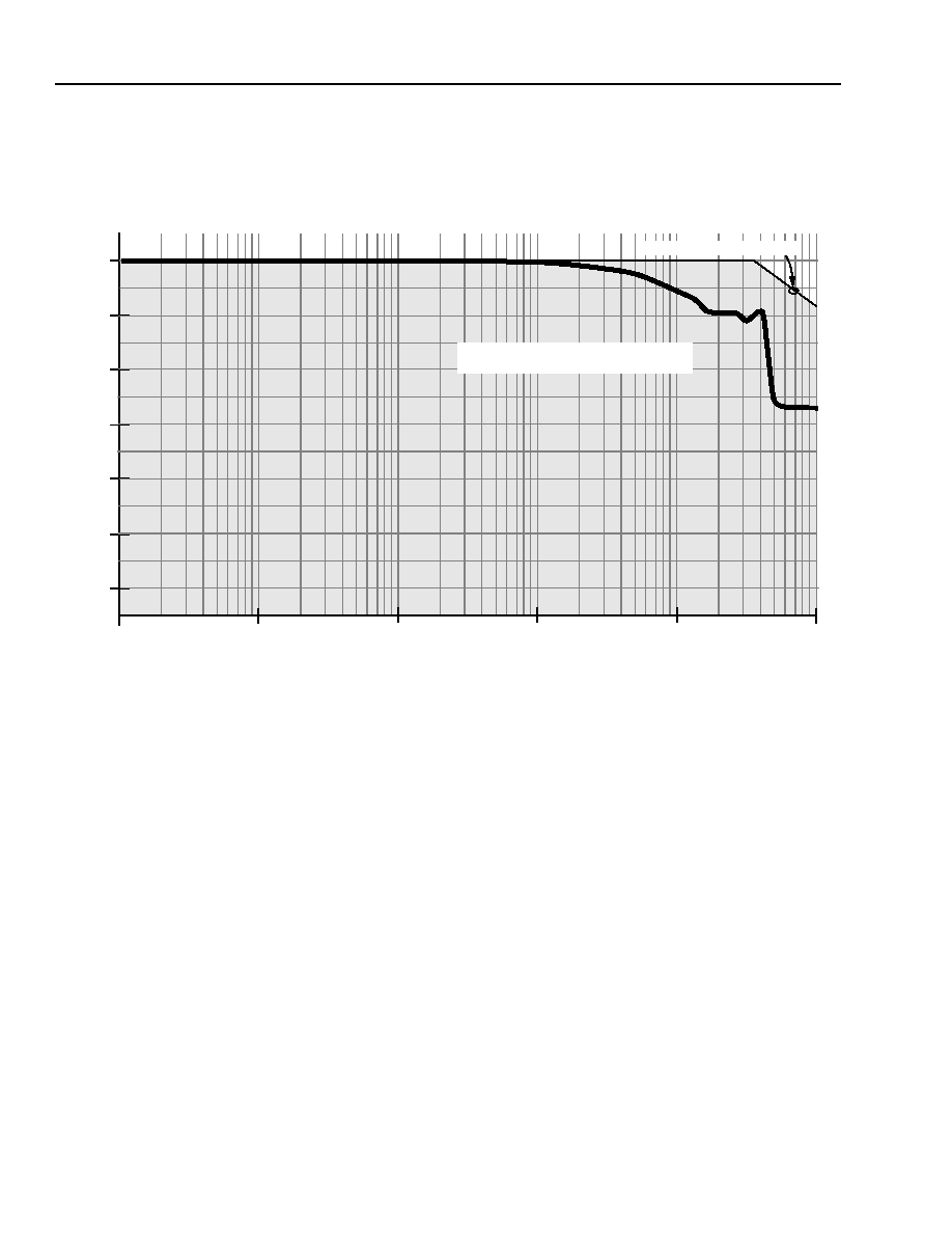
Advance Data Sheet, Rev. 2
TLIU04C1 Quad T1/E1 Line Interface
April 1999
28
Lucent Technologies Inc.
Microprocessor Mode
(continued)
CEPT Receiver Specifications
(continued)
Frequency Response Curves (continued)
5-5263(F)r.4
Figure 7. CEPT/E1 Receiver Jitter Transfer Without Jitter Attenuator
FREQUENCY (H
Z
)
J
I
TTE
R OUT/
J
ITT
ER
IN (
d
B
)
60
40
20
0
1
10
100
1k
10k
50
30
10
100k
TYPICAL
(SUBJECT TO DEVICE CHARACTERIZATION)
G.735-9 W/O JITTER REDUCER

Advance Data Sheet, Rev. 2
April 1999
TLIU04C1 Quad T1/E1 Line Interface
29
Lucent Technologies Inc.
Microprocessor Mode
(continued)
Output Pulse Generation
The transmitter accepts a clock with NRZ data in
single-rail mode (DUAL = 0: register 5, bit 4) or a clock
with positive and negative NRZ data in dual-rail mode
(DUAL = 1) from the system. The device converts this
data to a balanced bipolar signal (AMI format) with
optional B8ZS(DS1)/HDB3(CEPT) encoding and jitter
attenuation. Low-impedance output drivers produce
these pulses on the line interface. Positive ones are
output as a positive pulse on TTIP, and negative ones
are output as a positive pulse on TRING. Binary zeros
are converted to null pulses. The total delay of the data
from the system interface to the transmit driver is
approximately 3 to 11 bit periods, depending on the
code configuration (see the Zero Substitution Decoding
(CODE) section, page 20 and the Zero Substitution
Encoding (CODE) section, page 30).
Additional delay results if the jitter attenuator is
selected for use in the transmit path (see the LIU Delay
Values section).
Transmit pulse shaping is controlled by the on-chip
pulse-width controller and pulse equalizer. The pulse-
width controller produces high-speed timing signals to
accurately control the transmit pulse widths. This elimi-
nates the need for a tightly controlled transmit clock
duty cycle that is usually required in discrete imple-
mentations. The pulse equalizer controls the ampli-
tudes of the pulses. Different pulse equalizations are
selected through proper settings of EQA, EQB, and
EQC (registers 6--9, bits 5--7) as described in
Table 12.
Table 12. Equalizer/Rate Control
* In DS1 mode, the distance to the DSX for 22 gauge PIC (ABAM) cable is specified. Use the maximum cable loss figures for other cable types.
In CEPT mode, equalization is specified for coaxial or twisted-pair cable.
Loss measured at 772 kHz.
In 75
applications, Option 1 is recommended over Option 2 for lower device power dissipation. Option 2 allows for the same transformer as
used in CEPT 120
applications.
Jitter
The intrinsic jitter of the transmit path, i.e., the jitter at TTIP/TRING when no jitter is applied to TCLK (and the jitter
attenuator is not selected, JAT = 0), is typically 5 nsp-p and will not exceed 0.02 UIp-p.
EQA
EQB
EQC
Service
Clock
Rate
Transmitter Equalization*
Maximum
Cable Loss
Feet
Meters
dB
0
0
0
DS1
1.544 MHz
0 ft. to 131 ft.
0 m to 40 m
0.6
0
0
1
131 ft. to 262 ft.
40 m to 80 m
1.2
0
1
0
262 ft. to 393 ft.
80 m to 120 m
1.8
0
1
1
393 ft. to 524 ft.
120 m to 160 m
2.4
1
0
0
524 ft. to 655 ft.
160 m to 200 m
3.0
1
0
1
CEPT
2.048 MHz
75
(Option 2)
--
1
1
0
120
or 75
(Option 1)
--
1
1
1
Not Used
--
--
--

Advance Data Sheet, Rev. 2
TLIU04C1 Quad T1/E1 Line Interface
April 1999
30
Lucent Technologies Inc.
Microprocessor Mode
(continued)
Zero Substitution Encoding (CODE)
Zero substitution B8ZS/HDB3 encoding can be acti-
vated only in the single-rail system interface mode
(DUAL = 0). CODE = 1 selects the B8ZS/HDB3 encod-
ing operation in all four channels, regardless of the
state of the CODE[1--4] bits. The B8ZS/HDB3 encod-
ing operation can be selected for individual channels
independently by setting CODE = 0 and programming
CODE[1--4] bits for the respective channels.
Note: Encoding and decoding are not independent.
Selecting B8ZS/HDB3 encoding in the transmit-
ter selects B8ZS/HDB3 decoding in the receiver.
Table 13. Register Map for CODE Bits
When coding is selected for a given channel, data
transmitted from the system interface on TDATA (pins
141, 16, 69, 88) will be B8ZS/HDB3 encoded before
appearing on TTIP and TRING at the line interface.
Alarm Indication Signal Generator (XAIS)
When the transmit alarm indication signal control is set
(XAIS = 1) for a given channel (registers 6--9, bit 2), a
continuous stream of bipolar ones is transmitted to the
line interface. The TPD/TDATA and TND inputs are
ignored during this mode. The XAIS input is ignored
when a remote loopback (RLOOP) is selected using
loopback control bits (LOOPA and LOOPB; registers
6--9, bits 3 and 4). (See the Loopbacks section.)
The normal clock source for the AIS signal is TCLK. If
TCLK is not available (loss of TCLK detected), then the
AIS signal clock defaults to INTXCLK/16. INTXCLK is
either XCLK, or 16x XCLK, depending on the state of
the CLKS input pin. See Figure 3 on page 19, and
CLKS in Table 1, Pin Descriptions, on page 10. For any
of the above options, the clock tolerance must meet the
normal line transmission rates (DS1 1.544 MHz ±
32 ppm; CEPT 2.048 MHz ± 50 ppm).
Transmitter Alarms
Loss of Transmit Clock (LOTC) Alarm
A loss of transmit clock alarm (LOTC = 1; registers 0
and 1, bits 3 and 7) is indicated if any of the clocks in
the transmit path disappear. This includes loss of TCLK
input, loss of RCLK during remote loopback, loss of jit-
ter attenuator output clock (when enabled), or the loss
of clock from the pulse-width controller.
For all of these conditions, a core transmitter timing
clock is lost and no data can be driven onto the line.
Output drivers TTIP and TRING are placed in a high-
impedance state when this alarm condition is active.
The LOTC interrupt is asserted between 3 µs and
16 µs after the clock disappears, and deasserts imme-
diately after detecting the first clock edge. The LOTC
alarm status bit will latch the alarm and remain set until
being cleared by a read (clear on read). Upon the tran-
sition from LOTC = 0 to LOTC = 1, a microprocessor
interrupt will be generated if the corresponding LOTC
interrupt mask bit (MLOTC; registers 2 and 3, bits 3
and 7), the channel mask bit (MASK; registers 6--9,
bit 1), or the global mask bit (GMASK; register 4, bit 0)
is not set.
An LOTC alarm may occur when RLOOP is activated
and deactivated due to the phase transient that occurs
as TCLK switches its source to and from RCLK. Setting
the prevent RLOOP alarm bit (PRLALM = 1; LIU
register 12, bit 3) prevents the LOTC alarm from occur-
ring at the activation and deactivation of RLOOP but
allows the alarm to operate normally during the
RLOOP active period.
Transmit Driver Monitor (TDM) Alarm
The transmit driver monitor detects two conditions: a
nonfunctional link due to a fault on the primary of the
transmit transformer, or periods of no data transmis-
sion. The transmit driver monitor alarm (TDM; registers
0 and 1, bits 2 and 6) is the ORed function of both
faults and provides information about the integrity of
the transmit signal path.
The first monitoring function is provided to detect non-
functional links and protect the device from damage.
The alarm is set (TDM = 1) when one of the transmit-
ter's line drivers (TTIP or TRING) is shorted to power
supply or ground, or TTIP and TRING are shorted
together. Under these conditions, internal circuitry pro-
tects the device from damage and excessive power
supply current consumption by 3-stating the output
drivers. The monitor detects faults on the transformer
primary, but transformer secondary faults may not be
detected.
Name
Location
Register
Bit
CODE
5
3
CODE1
12
7
CODE2
12
6
CODE3
11
6
CODE4
11
4
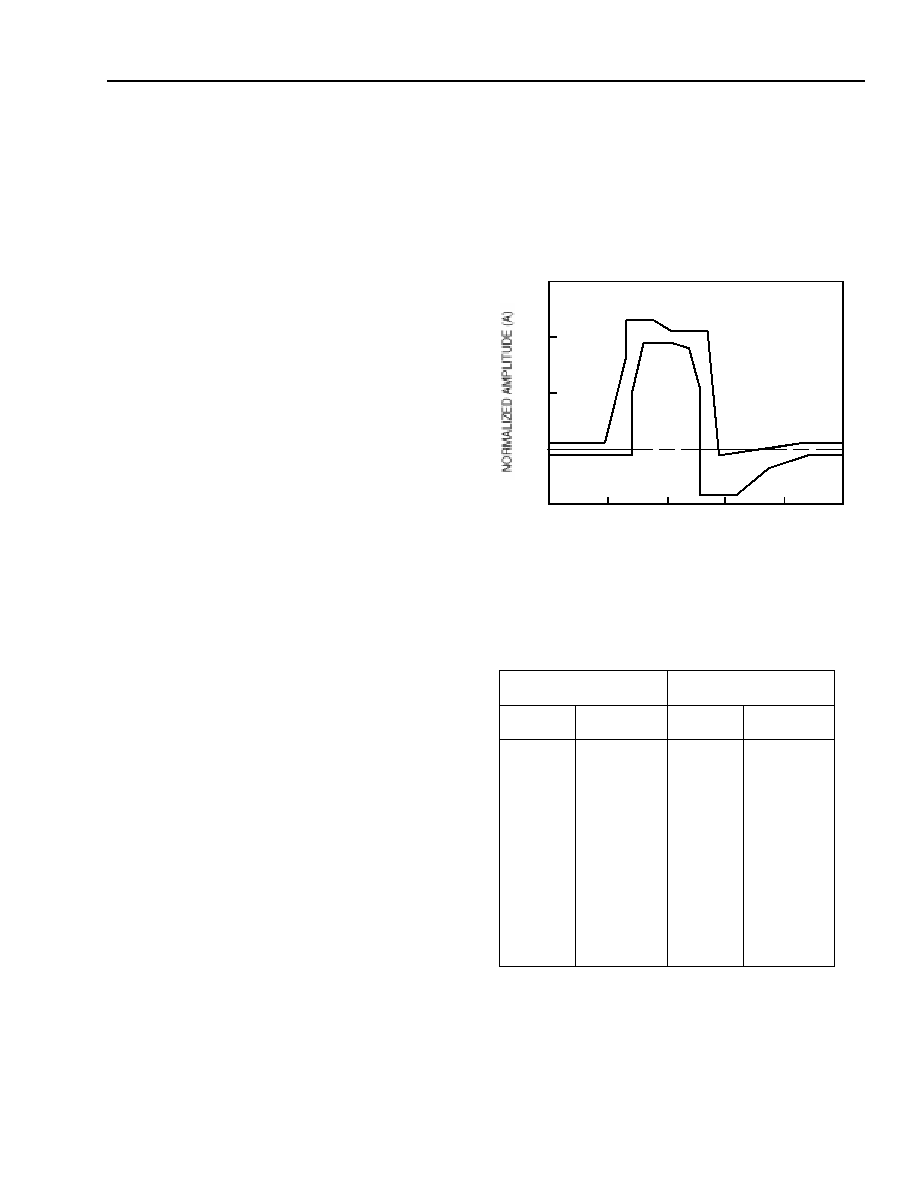
Advance Data Sheet, Rev. 2
April 1999
TLIU04C1 Quad T1/E1 Line Interface
31
Lucent Technologies Inc.
Microprocessor Mode
(continued)
Transmitter Alarms
(continued)
Transmit Driver Monitor (TDM) Alarm (continued)
The monitor operates by comparing the line pulses with
the transmit inputs. After 32 transmit clock cycles, the
transmitter is powered up in its normal operating mode.
The drivers attempt to correctly transmit the next data
bit. If the error persists, TDM remains active to elimi-
nate alarm chatter and the transmitter is internally pro-
tected for another 32 transmit clock cycles. This
process is repeated until the error condition is removed
and the TDM alarm is deactivated. The TDM alarm sta-
tus bit will latch the alarm and remain set until being
cleared by a read (clear on read).
The second monitoring function is to indicate periods of
no data transmission. The alarm is set (TDM = 1) when
32 consecutive zeros have been transmitted, and the
alarm condition is cleared on the detection of a single
pulse. Again, the TDM alarm status bit will latch the
alarm and remain set until being cleared by a read
(clear on read). This alarm condition does not alter the
state or functionality of the signal path.
Upon the transition from TDM = 0 to TDM = 1, a micro-
processor interrupt will be generated if the TDM inter-
rupt mask bit (MTDM; registers 2 and 3, bits 2 and 6) is
not set and the GMASK bit (register 4, bit 0) is not set.
A TDM alarm may occur when RLOOP is activated and
deactivated. If the prevent RLOOP alarm bit (PRLALM;
register 12, bit 3) is not set, then RLOOP may activate
an LOTC alarm, which will put the output drivers TTIP
and TRING in a high-impedance state as described in
Loss of Transmit Clock (LOTC) Alarm on page 30. The
high-impedance state of the drivers may, in turn, gener-
ate a TDM alarm. Setting the HIGHZ alarm prevention
PHIZALM = 1 (register 12, bit 4) prevents the TDM
alarm from occurring when the drivers are in a high-
impedance state.
DS1 Transmitter Pulse Template and Specifi-
cations
The DS1 pulse shape template is specified at the DSX
(defined by CB119 and ANSI T1.102) and is illustrated
in Figure 8. The device also meets the pulse template
specified by ITU-T G.703 (not shown).
5-1160(F)r.1
Figure 8. DSX-1 Isolated Pulse Template
Table 14. DSX-1 Pulse Template Corner Points
(from CB119)
Maximum Curve
Minimum Curve
ns
V
ns
V
0
250
325
325
425
500
675
725
1100
1250
--
--
0.05
0.05
0.80
1.15
1.15
1.05
1.05
≠0.07
0.05
0.05
--
--
0
350
350
400
500
600
650
650
800
925
1100
1250
≠0.05
≠0.05
0.50
0.95
0.95
0.90
0.50
≠0.45
≠0.45
≠0.20
≠0.05
≠0.05
1.0
0.5
0
≠0.5
0
250
500
750
1000
1250
TIME (ns)

Advance Data Sheet, Rev. 2
TLIU04C1 Quad T1/E1 Line Interface
April 1999
32
Lucent Technologies Inc.
Microprocessor Mode
(continued)
DS1 Transmitter Pulse Template and Specifications
(continued)
During DS1 operation, the TTIP and TRING pins will perform as specified in Table 15.
1. In accordance with the line circuitry described (see Line Circuitry on page 50).
2. Total power difference.
3. Measured in a 2 kHz band around the specified frequency.
4. Using Lucent transformer 2795B and components in Table 30.
5. Below the power at 772 kHz.
Table 15. DS1 Transmitter Specifications
Parameter
Min
Typ
Max
Unit
Spec
Output Pulse Amplitude at DSX
1
2.5
3.0
3.5
V
AT&T CB119,
ANSI T1.102
Output Pulse Width at Line Side of
Transformer
1
325
350
375
ns
Output Pulse Width at Device Pins
TTIP and TRING
1
330
350
370
ns
Positive/Negative Pulse Imbalance
2
--
0.1
0.4
dB
Power Levels
3, 4
:
772 kHz
1.544 MHz
5
12.6
29
--
39
17.9
--
dBm
dB
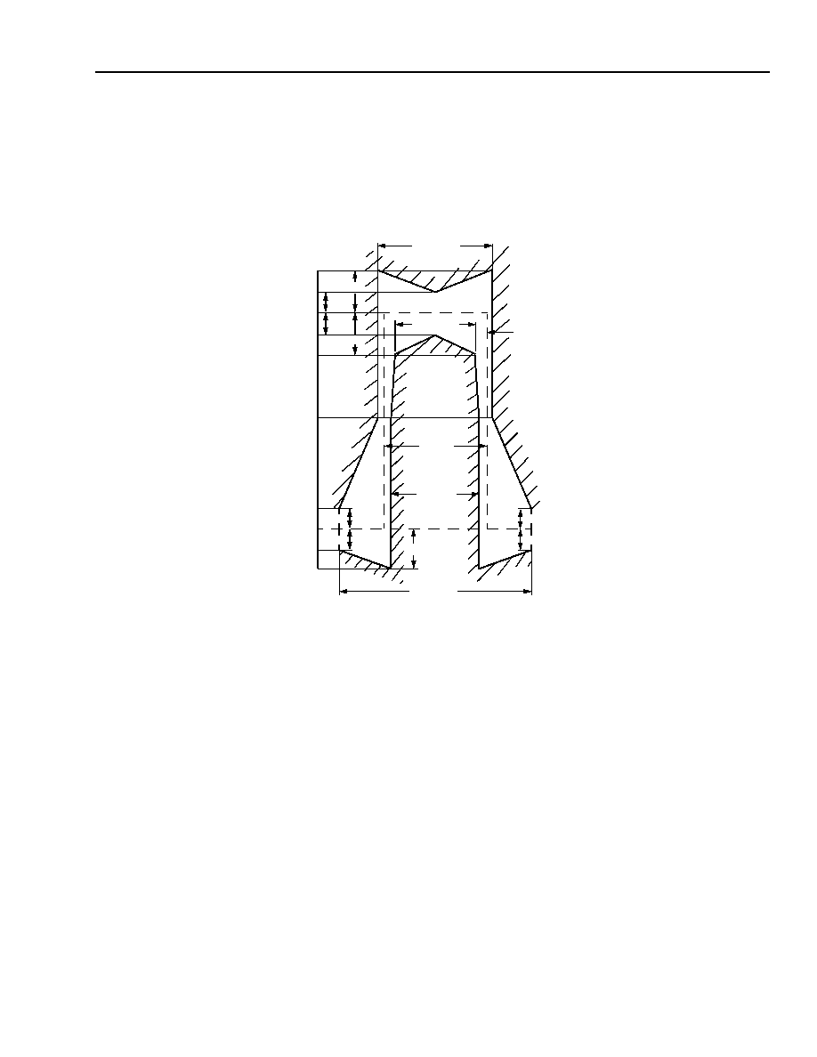
Advance Data Sheet, Rev. 2
April 1999
TLIU04C1 Quad T1/E1 Line Interface
33
Lucent Technologies Inc.
Microprocessor Mode
(continued)
CEPT Transmitter Pulse Template and Specifications
CEPT pulse shape template is specified at the system output (defined by ITU-T G.703) and is illustrated in
Figure 9.
5-3145(F)r.1
Figure 9. ITU-T G.703 Pulse Template
269 ns
(244 + 25)
219 ns
(244 ≠ 25)
244 ns
194 ns
(244 ≠ 50)
20%
488 ns
(244 + 244)
20%
20%
10%
10%
10%
10%
0%
50%
10%
V = 100%
10%
NOMINAL PULSE

Advance Data Sheet, Rev. 2
TLIU04C1 Quad T1/E1 Line Interface
April 1999
34
Lucent Technologies Inc.
Microprocessor Mode
(continued)
CEPT Transmitter Pulse Template and Specifications
(continued)
During CEPT operation, the transmitter tip/ring (TTIP/TRING pins) will perform as specified in Table 16.
Jitter Attenuator
A selectable jitter attenuator is provided for narrow-bandwidth jitter transfer function applications. When placed in
the LIU receive path, the jitter attenuator provides narrow-bandwidth jitter filtering for line synchronization. The jitter
attenuator can also be placed in the transmit path to provide clock smoothing for applications such as synchronous/
asynchronous demultiplexers. In these applications, TCLK will have an instantaneous frequency that is higher than
the data rate, and some periods of TCLK are suppressed (gapped) in order to set the average long-term TCLK fre-
quency to within the transmit line rate specification. The jitter attenuator will smooth the gapped clock.
Generated (Intrinsic) Jitter
Generated jitter is the amount of jitter appearing on the output port when the applied input signal has no jitter. The
jitter attenuator of this device outputs a maximum of 0.05 UIp-p intrinsic jitter.
Table 16. CEPT Transmitter Specifications
Parameter
Min
Typ
Max
Unit
Spec
Output Pulse Amplitude
*
:
75
120
* In accordance with the line circuitry described (see Line Circuitry on page 50), measured at the transformer secondary.
2.13
2.7
2.37
3.0
2.61
3.3
V
V
ITU-T G.703
Output Pulse Width at Line Side of
Transformer*
219
244
269
ns
Output Pulse Width at Device Pins TTIP
and TRING*
224
244
264
ns
Positive/Negative Pulse Imbalance:
Pulse Amplitude
Pulse Width
≠4
≠4
±1.5
±1
4
4
%
%
Zero Level (percentage of pulse
amplitude)
≠5
0
5
%
Return Loss
(120
):
51 kHz to 102 kHz
102 kHz to 2.048 MHz
2.048 MHz to 3.072 MHz
Using Lucent transformer 2795D or 2795C and components in Table 30.
9
15
11
--
--
--
--
--
--
dB
dB
dB
CH-PTT
Return Loss
(75
):
51 kHz to 102 kHz
102 kHz to 3.072 MHz
7
9
--
--
--
--
dB
dB
ETS 300 166:
1993

Advance Data Sheet, Rev. 2
April 1999
TLIU04C1 Quad T1/E1 Line Interface
35
Lucent Technologies Inc.
Microprocessor Mode
(continued)
Jitter Attenuator
(continued)
Jitter Transfer Function
The jitter transfer function describes the amount of jitter that is transferred from the input to the output over a range
of frequencies. The jitter attenuator exhibits a single-pole roll-off (20 dB/decade) jitter transfer characteristic that
has no peaking and a nominal filter corner frequency (3 dB bandwidth) of less than 4 Hz for DS1 operation and
approximately 10 Hz for CEPT operation. Optionally, a lower bandwidth of approximately 1.25 Hz can be selected
in CEPT operation by setting JABW0 = 1 (register 12, bit 5) for systems desiring compliance with ETSI-TBR12/13
jitter attenuation requirements. When configured to meet ETSI-TBR12/13, the clock connected to the XCLK input
must be
±
20 ppm. For a given frequency, different jitter amplitudes will cause a slight variation in attenuation
because of finite quantization effects. Jitter amplitudes of less than approximately 0.2 UI will have greater attenua-
tion than the single-pole roll-off characteristic. The jitter transfer curve is independent of data patterns. Typical jitter
transfer curves of the jitter attenuator are given in Figure 11 and Figure 13.
Jitter Accommodation
The minimum jitter accommodation of the jitter attenuator occurs when the XCLK frequency and the input clock's
long-term average frequency are at their extreme frequency tolerances. When the jitter attenuator is used in the
LIU transmit path, the minimum accommodation is 28 UIp-p at the highest jitter frequency of 15 kHz. Typical
receiver jitter accommodation curves including the jitter attenuator in the LIU receive path are given in Figure 10
and Figure 12.
When the jitter attenuator is placed in the data path, a difference between the XCLK/16 frequency and the incoming
line rate for receive applications, or the TCLK rate for transmit applications, will result in degraded low-
frequency jitter accommodation performance. The peak-to-peak jitter accommodation (JAp-p) for frequencies from
above the corner frequency of the jitter attenuator (fc) to approximately 100 Hz is given by the following equation:
where:
f
data
= 1.544 MHz for DS1 or 2.048 MHz for CEPT;
for JABW0 = 0, fc = 3.8 Hz for DS1 or 10 Hz for CEPT,
and for JABW0 = 1, fc = 1.25 Hz for CEPT;
f
xclk
= XCLK tolerance in ppm;
f
data
= data tolerance in ppm.
Note that for lower corner frequencies, the jitter accommodation is more sensitive to clock tolerance than for higher
corner frequencies. When JABW0 = 1 and the jitter attenuator is used in the receive data path, the tolerance on
XCLK should be tightened to ±20 ppm in order to meet the jitter accommodation requirements of TBR12/13 as
given in G.823 for line data rates of ±50 ppm.
JAp-p
64
2
f
xclk
f
data
≠
(
)
f
data
2
f
c
------------------------------------------------------------
≠
UI
=

Advance Data Sheet, Rev. 2
TLIU04C1 Quad T1/E1 Line Interface
April 1999
36
Lucent Technologies Inc.
Microprocessor Mode
(continued)
Jitter Attenuator
(continued)
Jitter Attenuator Enable
The jitter attenuator is selected using the JAR and JAT
bits (register 5, bits 1 and 2) of the microprocessor
interface. These control bits are global and affect all
four channels unless a given channel is in the power-
down mode (PWRDN = 1). Because there is only one
attenuator function in the device, selection must be
made between either the transmit or receive path. If
both JAT and JAR are activated at the same time, the
jitter attenuator will be disabled.
Note that the power consumption increases slightly on
a per-channel basis when the jitter attenuator is active.
If jitter attenuation is selected, a valid XCLK (pin 46)
signal must be available.
Jitter Attenuator Receive Path Enable (JAR)
When the jitter attenuator receive bit is set (JAR = 1),
the attenuator is enabled in the receive data path
between the clock/data recovery and the decoder (see
Figure 3 on page 19). Under this condition, the jitter
characteristics of the jitter attenuator apply for the
receiver. The receive path will then exhibit the jitter
characteristics shown in Figure 10 through Figure 13. If
CDR = 0 (register 5, bit 0), the JAR bit is ignored
because clock recovery will be disabled.
Jitter Attenuator Transmit Path Enable (JAT)
When the jitter attenuator transmit bit is set (JAT = 1),
the attenuator is enabled in the transmit data path
between the encoder and the pulse-width controller/
pulse equalizer (see Figure 3 on page 19). Under this
condition, the jitter characteristics of the jitter attenuator
apply for the transmitter. When JAT = 0, the encoder
outputs bypass the disabled attenuator and directly
enter the pulse-width controller/pulse equalizer. The
transmit path will then pass all jitter from TCLK to line
interface outputs TTIP/TRING.

Advance Data Sheet, Rev. 2
April 1999
TLIU04C1 Quad T1/E1 Line Interface
37
Lucent Technologies Inc.
Microprocessor Mode
(continued)
Jitter Attenuator
(continued)
Frequency Response Curves
5-5264(F)r.8
Figure 10. DS1/T1 Receiver Jitter Accommodation with Jitter Attenuator
0.1 UI
1.0 UI
10 UI
100 UI
10
100
1k
10k
1
28 UI
FREQUENCY (Hz)
100k
TR-TSY-000009 (DS1, MUXes)
GR-499/1244-CORE (CAT I INTERFACES)
I.431(DS1), G.824(DS1)
TYPICAL
(SUBJECT TO DEVICE CHARACTERIZATION)
(NON-SONET CAT II INTERFACES)
GR-499-CORE
T1.408/I.431(DS1)/G.824(DS1)
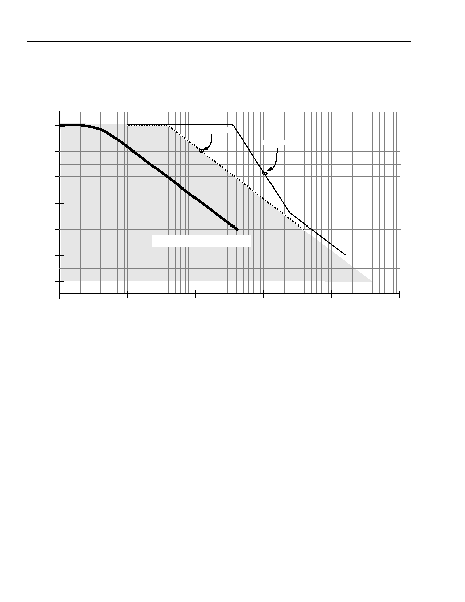
Advance Data Sheet, Rev. 2
TLIU04C1 Quad T1/E1 Line Interface
April 1999
38
Lucent Technologies Inc.
Microprocessor Mode
(continued)
Jitter Attenuator
(continued)
Frequency Response Curves (continued)
5-5265(F)r.4
Figure 11. DS1/T1 Jitter Transfer of the Jitter Attenuator
60
40
20
0
1
10
100
1k
10k
50
30
10
100k
FREQUENCY (Hz)
JIT
T
ER
OU
T
/
JIT
T
ER
IN
(dB)
TYPICAL
(SUBJECT TO DEVICE CHARACTERIZATION)
TR-TSY-000009
GR-253-CORE

Advance Data Sheet, Rev. 2
April 1999
TLIU04C1 Quad T1/E1 Line Interface
39
Lucent Technologies Inc.
Microprocessor Mode
(continued)
Jitter Attenuator
(continued)
Frequency Response Curves (continued)
5-5266(F)r.8
Figure 12. CEPT/E1 Receiver Jitter Accommodation with Jitter Attenuator
0.1 UI
1.0 UI
10 UI
100 UI
10
100
1k
10k
1
37 UI
FREQUENCY (Hz)
G.823
100k
TYPICAL
(SUBJECT TO DEVICE CHARACTERIZATION)
G.823,ETSI-300-011A1
I.431(CEPT)/ETS-300-011
I.431(CEPT)/ETS-300-011
JABW0 = 0
JABW0 = 1
Advance Data Sheet, Rev. 2
TLIU04C1 Quad T1/E1 Line Interface
April 1999
40
Lucent Technologies Inc.
Microprocessor Mode
(continued)
Jitter Attenuator
(continued)
Frequency Response Curves (continued)
5-5267(F)r.4
Figure 13. CEPT/E1 Jitter Transfer of the Jitter Attenuator
FREQUENCY (Hz)
JI
TT
ER O
U
T/J
IT
TE
R
IN
(
d
B)
60
40
20
0
1
10
100
1k
10k
50
30
10
100k
TYPICAL
(SUBJECT TO DEVICE CHARACTERIZATION)
JABW0 = 1
JABW0 = 0
ETSI TBR12/13
ETSI-300-011
I.431, G.735-9 WITH JITTER REDUCER
G.735-9 AT NATIONAL BOUNDARIES

Advance Data Sheet, Rev. 2
April 1999
TLIU04C1 Quad T1/E1 Line Interface
41
Lucent Technologies Inc.
Microprocessor Mode
(continued)
Loopbacks
The device has three independent loopback paths that are activated using LOOPA and LOOPB (registers 6--9, bits
3 and 4) as shown in Table 17. The locations of these loopbacks are illustrated in Figure 3 on page 19.
Table 17. Loopback Control
* During the transmit AIS condition, the looped data will be the transmitted data from the
system and not the all-ones signal.
Transmit AIS request is ignored.
Full Local Loopback (FLLOOP)
A full local loopback (FLLOOP) connects the transmit line driver input to the receiver analog front-end circuitry.
Valid transmit output data continues to be sent to the network. If the transmit AIS (all-ones signal) is sent to the net-
work, the looped data is not affected. The ALOS alarm continues to monitor the receive line interface signal while
DLOS monitors the looped data.
See Digital Loss of Signal (DLOS) Alarm section on page 21 regarding the behavior of the DLOS alarm upon acti-
vation of FLLOOP.
Remote Loopback (RLOOP)
A remote loopback (RLOOP) connects the recovered clock and retimed data to the transmitter at the system inter-
face and sends the data back to the line. The receiver front end, clock/data recovery, encoder/decoder (if enabled)
jitter attenuator (if enabled), and transmit driver circuitry are all exercised during this loopback. The transmit clock,
transmit data, and XAIS inputs are ignored. Valid receive output data continues to be sent to the system interface.
This loopback mode is very useful for isolating failures between systems.
See Loss of Transmit Clock (LOTC) Alarm and Transmit Driver Monitor (TDM) Alarm on page 30 regarding the
behavior of the LOTC and TDM alarms upon activation and deactivation of RLOOP.
Digital Local Loopback (DLLOOP)
A digital local loopback (DLLOOP) connects the transmit clock and data through the encoder/decoder pair to the
receive clock and data output pins at the system interface. This loopback is operational if the encoder/decoder pair
is enabled or disabled. The AIS signal can be transmitted without any effect on the looped signal.
Operation
Symbol
LOOPA
LOOPB
Normal
--
0
0
Full Local Loopback
FLLOOP*
0
1
Remote Loopback
RLOOP
1
0
Digital Local Loopback
DLLOOP
1
1

Advance Data Sheet, Rev. 2
TLIU04C1 Quad T1/E1 Line Interface
April 1999
42
Lucent Technologies Inc.
Microprocessor Mode
(continued)
Powerdown (PWRDN)
Each line interface channel has an independent power-
down mode controlled by PWRDN (registers 6--9,
bit 0). This provides power savings for systems that use
backup channels. If PWRDN = 1, the corresponding
channel will be in a standby mode, consuming only a
small amount of power. It is recommended that the
alarm registers for the corresponding channel be
masked with MASK = 1 (registers 6--9, bit 1) during
powerdown mode. If a line interface channel in power-
down mode needs to be placed into service, the chan-
nel should be turned on (PWRDN = 0) approximately
5 ms before data is applied.
Reset (RESET, SWRESET)
The device provides both a hardware reset (
RESET
;
pin 44) and a software reset (SWRESET; register 4,
bit 1) that are functionally equivalent. INT (pin 114) is
also cleared. The writable microprocessor interface
registers are not affected by reset, with the exception of
bits in register 4 (see the Global Control Registers
(0100, 0101) section). During a reset condition, data
transmission will be interrupted.
The reset condition is initiated by setting
RESET
= 0 or
SWRESET = 1 for a minimum of 10 µs. After releasing
the reset control (RESET = 1 or SWRESET = 0), the
device will stay in the reset condition for approximately
2.7 ms to ensure stabilization of the PLL. After leaving
the reset condition (with
RESET
= 1 or SWRESET = 0),
the bits in register 4 will be reset and may need to be
restored.
Loss of XCLK Reference Clock (LOXC)
The LOXC output (pin 45) is active when the XCLK ref-
erence clock (pin 46) is absent. The LOXC flag is
asserted a maximum of 16 µs after XCLK disappears,
and deasserts immediately after detecting the first
clock edge of XCLK.
During the LOXC alarm condition, the clock recovery
and jitter attenuator functions are automatically dis-
abled. Therefore, if CDR = 1 and/or JAR = 1, the RCLK,
RPD, RND, and DLOS outputs will be unknown. If CDR
= 0, there will be no effect on the receiver. If the jitter
attenuator is enabled in the transmit path (JAT = 1) dur-
ing this alarm condition, then a Loss of Transmit Clock
alarm, LOTC = 1, will also be indicated.
In-Circuit Testing and Driver High-Imped-
ance State (
ICT
)
The function of the
ICT
input (pin 43) is determined by
the ICTMODE bit (register 4, bit 3). If ICTMODE = 0
and
ICT
is activated (
ICT
= 0), then all output buffers
(TTIP, TRING, RCLK, RPD, RND, LOXC, RDY_
DTACK
,
INT, AD[7:0]) are placed in a high-impedance state. For
in-circuit testing, the
RESET
pin can be used to activate
ICTMODE = 0 without having to write the bit. If
ICTMODE = 1 and
ICT
= 0, then only the TTIP and
TRING outputs of all channels will be placed in a high-
impedance state. The TTIP and TRING outputs have a
limiting high-impedance capability of approximately
8 k
.
LIU Delay Values
The transmit coder has 5 UI delay whether it is in the
path or not and whether it is B8ZS or HDB3. Its delay is
only removed when in single-rail mode. The remainder
of the transmit path has 4.6 UI delay. The receive
decoder has 5 UI delay whether it is in the path or not
and whether it is B8ZS or HDB3. Its delay is only
removed when in single-rail mode or CDR = 0. The
AFE (equalizer plus slicer) delay is nearly 0 UI delay.
The jitter attenuator delay is nominally 33 UI but can be
2 UI--64 UI depending on the state. The DPLL used for
timing recovery has 8 UI delay.

Advance Data Sheet, Rev. 2
April 1999
TLIU04C1 Quad T1/E1 Line Interface
43
Lucent Technologies Inc.
Microprocessor Mode
(continued)
Line Encoding/Decoding
Alternate Mark Inversion (AMI)
The default line code used for T1 is alternate mark inversion (AMI). The coding scheme represents a 1 with a pulse
or mark on the positive or negative rail and a 0 with no pulse on either rails. This scheme is shown in Table 18.
Table 18. AMI Encoding
The T1 ones density rule requires that in every 24 bits of information to be transmitted, there must be at least three
pulses, and no more than 15 zeros may be transmitted consecutively.
AT&T Technical Reference 62411 for digital transmissions requires that in every 8 bits of information, at least one
pulse must be present.
T1-Binary 8 Zero Code Suppression (B8ZS)
Clear channel transmission can be accomplished using binary 8 zero code suppression (B8ZS). Eight consecutive
zeros are replaced with the B8ZS code. This code consists of two bipolar violations in bit positions 4 and 7 and
valid bipolar marks in bit positions 5 and 8. The receiving end recognizes this code and replaces it with the original
string of eight zeros. Table 19 shows the encoding of a string of zeros using B8ZS. B8ZS is recommended when
ESF format is used.
Table 19. DS1 B8ZS Encoding
High-Density Bipolar of Order 3 (HDB3)
The line code used for CEPT is described in ITU Rec. G.703 Section 6.1 as high-density bipolar of order 3 (HDB3).
HDB3 uses a substitution code that acts on strings of four zeros. The substitute HDB3 codes are 000V and B00V,
where V represents a violation of the bipolar rule and B represents as inserted pulse conforming to the AMI rule
defined in ITU Rec. G.701, item 9004. The choice of the B00V or 000V is made so that the number of B pulses
between consecutive V pulses is odd. In other words, successive V pulses are of alternate polarity so that no direct
current (dc) component is introduced. The substitute codes follow each other if the string of zeros continues. The
choice of the first substitute code is arbitrary. A line code error is defined as a bipolar violation and consists of two
pulses of the same polarity that is not defined as one of the two substitute codes. Coding violations are indicated as
bipolar violations. An example is shown in Table 20.
Table 20. ITU HDB3 Coding and DCPAT Binary Coding
Input Bit Stream
1011
0000
0111
1010
AMI Data
≠0+≠
0000
0+≠+
≠0+0
Bit Positions
1
2
3
4
5
6
7
8
--
--
--
1
2
3
4
5
6
7
8
Before B8ZS
0
0
0
0
0
0
0
0
1
0
1
0
0
0
0
0
0
0
0
After B8ZS
0
0
0
V
B
0
V
B
B
0
B
0
0
0
V
B
0
V
B
Input Bit Stream
1011
0000
01
0000
0000
0000
0000
HDB3-Coded Data
1011
000V
01
000V
B00V
B00V
B00V
HDB3-Coded Levels
≠0+≠
000≠
0+
000+
≠00≠
+00+
≠00≠

Advance Data Sheet, Rev. 2
TLIU04C1 Quad T1/E1 Line Interface
April 1999
44
Lucent Technologies Inc.
Microprocessor Mode
(continued)
Registers
As shown in Table 6 on page 17, the quad LIU registers consist of sixteen 8-bit registers (some of which are
reserved). Register 13 is an index register which must contain the value 00 to access the other 15 LIU registers.
Registers 0 and 1 are the alarm registers used for storing the various device alarm status and are read only. All
other registers are read/write. Registers 2 and 3 contain the individual mask bits for the alarms in registers 0 and 1.
Registers 4 and 5 are designated as the global control registers used to set up the functions for all four channels.
The channel configuration registers in registers 6 through 9 and register 12 are used to configure the individual
channel functions and parameters. Registers 10 and 11 must be cleared by the user after a powerup for proper
device operation; CODE3 and CODE4 may be set as desired. (See Table 26 on page 47.) Register 13 is the global
index register. Registers 14 and 15 are reserved for proprietary functions and must not be addressed during oper-
ation. The following sections describe these registers in detail.
Alarm Registers (0000, 0001)
The bits in the alarm registers represent the status of the transmitter and receiver alarms LOTC, TDM, DLOS, and
ALOS for all four channels as shown in Table 21. The alarm indicators are active-high and automatically clear on a
microprocessor read if the corresponding alarm condition no longer exists. Persistent alarm conditions will cause
the bit to remain set. These are read-only registers.
*The numerical suffix identifies the channel number.
Table 21. Alarm Registers
Bits
Symbol*
Description
Alarm Register (0)
0, 4
ALOS[1--2]
Analog loss of signal alarm for channels 1 and 2.
1, 5
DLOS[1--2]
Digital loss of signal alarm for channels 1 and 2.
2, 6
TDM[1--2]
Transmit driver monitor alarm for channels 1 and 2.
3, 7
LOTC[1--2]
Loss of transmit clock alarm for channels 1 and 2.
Alarm Register (1)
0, 4
ALOS[3--4]
Analog loss of signal alarm for channels 3 and 4.
1, 5
DLOS[3--4]
Digital loss of signal alarm for channels 3 and 4.
2, 6
TDM[3--4]
Transmit driver monitor alarm for channels 3 and 4.
3, 7
LOTC[3--4]
Loss of transmit clock alarm for channels 3 and 4.

Advance Data Sheet, Rev. 2
April 1999
TLIU04C1 Quad T1/E1 Line Interface
45
Lucent Technologies Inc.
Microprocessor Mode
(continued)
Registers
(continued)
Alarm Mask Registers (0010, 0011)
The bits in the alarm mask registers in Table 22 allow the microprocessor to selectively mask each channel alarm
and prevent it from generating an interrupt. The mask bits correspond to the alarm status bits in the alarm registers
and are active-high to disable the corresponding alarm from generating an interrupt. These registers are read/write
registers.
*The numerical suffix identifies the channel number.
Global Control Registers (0100, 0101)
The bits in the global control registers in Table 23 and Table 24 allow the microprocessor to configure the various
device functions over all the four channels. All the control bits (with the exception of LOSSTD and ICTMODE) are
active-high. These are read/write registers.
Table 22. Alarm Mask Registers
Bits
Symbol*
Description
Alarm Mask Register (2)
0, 4
MALOS[1--2]
Mask analog loss of signal alarm for channels 1 and 2.
1, 5
MDLOS[1--2]
Mask digital loss of signal alarm for channels 1 and 2.
2, 6
MTDM[1--2]
Mask transmit driver monitor alarm for channels 1 and 2.
3, 7
MLOTC[1--2]
Mask loss of transmit clock alarm for channels 1 and 2.
Alarm Mask Register (3)
0, 4
MALOS[3--4]
Mask analog loss of signal alarm for channels 3 and 4.
1, 5
MDLOS[3--4]
Mask digital loss of signal alarm for channels 3 and 4.
2, 6
MTDM[3--4]
Mask transmit driver monitor alarm for channels 3 and 4.
3, 7
MLOTC[3--4]
Mask loss of transmit clock alarm for channels 3 and 4.
Table 23. Global Control Register (0100)
Bits
Symbol
Description
Global Control Register (4)
0
GMASK
The GMASK bit globally masks all the channel alarms when GMASK = 1, pre-
venting all the receiver and transmitter alarms from generating an interrupt.
GMASK = 1 after a device reset.
1
SWRESET
The SWRESET provides the same function as the hardware reset. It is used
for device initialization through the microprocessor interface.
2
LOSSTD
The LOSSTD bit selects the conformance protocol for the DLOS receiver
alarm function.
3
ICTMODE
The ICTMODE bit changes the function of the ICT pin. ICTMODE = 0 after a
device reset.
4--7
HIGHZ[1--4]
A HIGHZ bit is available for each individual channel. When HIGHZ = 1, the
TTIP and TRING transmit drivers for the specified channel are placed in a
high-impedance state. HIGHZ [1--4] = 1 after a device reset.

Advance Data Sheet, Rev. 2
TLIU04C1 Quad T1/E1 Line Interface
April 1999
46
Lucent Technologies Inc.
Microprocessor Mode
(continued)
Registers
(continued)
Global Control Registers (0100, 0101) (continued)
Channel Configuration and Control Registers (0110--1001, 1011, 1100)
The control bits in the channel configuration registers in Table 25 are used to select equalization, loopbacks,
AIS generation, channel alarm masking, and the channel powerdown mode for each channel (1--4). The
PWRDN[1--4], MASK[1--4], and XAIS[1--4] bits are active-high. These are read/write registers.
Control bits for zero substitution coding for channels 1--4 are listed in Table 26 and Table 27.
* A numerical suffix identifies the channel number.
Channel suffix not shown in the description.
Table 24. Global Control Register (0101)
Bits
Symbol
Description
Global Control Register (5)
0
CDR
The CDR bit is used to enable and disable the clock/data recovery function.
1
JAR
The JAR is used to enable and disable the jitter attenuator function in the
receive path. The JAR and JAT control bits are mutually exclusive; i.e., either
JAR or the JAT control bit can be set, but not both.
2
JAT
The JAT is used to enable and disable the jitter attenuator function in the trans-
mit path. The JAT and JAR control bits are mutually exclusive; i.e., either JAT or
the JAR control bit should be set, but not both.
3
CODE
The CODE bit is used to enable the B8ZS/HDB3 zero substitution coding. It is
used in conjunction with the DUAL bit and is valid only for single-rail operation.
4
DUAL
The DUAL bit is used to select single or dual-rail mode of operation.
5
ALM
The ALM bit selects the transmit and receive data polarity (i.e., active-low or
active-high). The ALM and ACM bits are used together to determine the trans-
mit and receive data retiming modes.
6
ACM
The ACM bit selects the positive or negative edge of the receive clock (RCLK
[1--4]) for receive data retiming. The ACM and ALM bits are used together to
determine the transmit and receive data retiming modes.
7
LOSSD
The LOSSD bit selects the shutdown function for the digital loss of signal alarm
(DLOS).
Table 25. Channel Configuration Registers (0110--1001)
Bits
Symbol*
Description
Channel Configuration Registers (6--9)
0
PWRDN[1--4]
The PWRDN bit powers down a channel when not used.
1
MASK[1--4]
The MASK bit masks all interrupts for the channel.
2
XAIS[1--4]
The XAIS bit enables transmission of an all-ones signal to the line inter-
face.
3
4
LOOPB[1--4]
LOOPA[1--4]
The LOOPB and LOOPA bits select the channel loopback modes.
5
6
7
EQC[1--4],
EQB[1--4],
EQA[1--4]
The EQC, EQB, and EQA bits select the type of service (DS1 or CEPT)
and the associated transmitter cable equalization/termination imped-
ances.

Advance Data Sheet, Rev. 2
April 1999
TLIU04C1 Quad T1/E1 Line Interface
47
Lucent Technologies Inc.
Microprocessor Mode
(continued)
Registers
(continued)
Channel Configuration and Control Registers (0110--1001, 1011, 1100) (continued)
* A numerical suffix identifies the channel number.
Table 26. Channel Configuration Register (1011)
Bits
Symbol
*
* A numerical suffix identifies the channel number.
Description
Channel Configuration Register (11)
0--3
--
Reserved. Write to 0.
4
CODE4
The CODE4 bit selects B8ZS/HDB3 encoding (transmit) and decoding
(receive) in channel 4.
5
--
Reserved. Write to 0.
6
CODE3
The CODE3 bit selects B8ZS/HDB3 encoding (transmit) and decoding
(receive) in channel 3.
7
--
Reserved. Write to 0.
Table 27. Control Register (1100)
Bit
Symbol*
Description
Control Register (12)
0
ALTIMER
The ALTIMER bit is used to select the time required to declare ALOS. ALTIMER = 0
selects 1 ms--2.6 ms. ALTIMER = 1 selects 10 bit--255 bit periods.
1
RCVAIS
The RCVAIS bit selects the shutdown function for the receiver during analog loss of
signal alarm (ALOS). RCVAIS operates in conjunction with the LOSSD bit.
2
PFLALM
The PFLALM prevents the DLOS alarm from occurring during FLLOOP activation.
3
PRLALM
The PRLALM prevents the LOTC alarm from occurring during RLOOP activation/
deactivation.
4
PHIZALM
The PHIZALM prevents the TDM alarm from occurring when the driver is in a high-
impedance state.
5
JABW0
The JABW0 bit selects the lower bandwidth jitter attenuator option in CEPT mode.
6
CODE2
The CODE2 bit selects B8ZS/HDB3 encoding (transmit) and decoding (receive) in
channel 2.
7
CODE1
The CODE1 bit selects B8ZS/HDB3 encoding (transmit) and decoding (receive) in
channel 1.

Advance Data Sheet, Rev. 2
TLIU04C1 Quad T1/E1 Line Interface
April 1999
48
Lucent Technologies Inc.
Microprocessor Mode
(continued)
XCLK Reference Clock
The device requires an externally applied clock, XCLK (pin 46), for the clock and data recovery function and the jit-
ter attenuation option. XCLK must be a continuously active (i.e., ungapped, unjittered, and unswitched) and an
independent reference clock such as from an external system oscillator or system clock for proper operation. It
must not be derived from any recovered line clock (i.e., from RCLK or any synthesized frequency of RCLK).
XCLK may be supplied in one of four formats; 16x DS1, DS1, 16x CEPT, or CEPT. The format is selected globally
for the device by CLKS (pin 117) and CLKM (pin 116).
CLKS determines the relationship between the primary line data rate and the clock signal applied to XCLK. For
CLKS = 0, a clock at 16x the primary line data rate clock (24.704 MHz for DS1 and 32.768 MHz for CEPT) must be
applied to XCLK. For CLKS = 1, a primary line data rate clock (1.544 MHz for DS1 and 2.048 MHz for CEPT) must
be applied to XCLK.
The CLKS pin has an internal pull-down resistor allowing the pin to be left open, i.e., a no connect, in applications
using a 16x reference clock. The CLKS pin must be pulled up to V
DD
for applications using a primary line data rate
clock.
CLKM determines whether the clock synthesizer is operating in CEPT or DS1 mode when XCLK is a primary line
data rate clock. For CLKM = 0, the clock synthesizer operates in DS1 mode (1.544 MHz). For CLKM = 1, the clock
synthesizer operates in CEPT mode (2.048 MHz). The CLKM pin is ignored when CLKS = 0.
The CLKM pin has an internal pull-down resistor allowing the pin to be left open, i.e., a no connect, in applications
using a DS1 line rate reference clock. The CLKM pin must be pulled up to V
DD
for applications using a CEPT line
data rate clock.
16x XCLK Reference Clock
The specifications for XCLK using a 16x reference clock are defined in Table 28. The 16x reference clock is
selected when CLKS = 0.
Table 28. XCLK (16x, CLKS = 0) Timing Specifications
* When JABW0 = 1 and the jitter attenuator is used in the receive data path, the tolerance on XCLK should be tightened to ±20 ppm in order to
meet the jitter accommodation requirements of TBR12/13 as given in G.823 for line data rates of ±50 ppm.
If XCLK is used as the source for AIS (see Alarm Indication Signal Generator (XAIS) on page 30), it must meet the nominal transmission
specifications of 1.544 MHz ± 32 ppm for DS1 (T1) or 2.048 MHz ± 50 ppm for CEPT (E1).
Parameter
Value
Unit
Min
Typ
Max
Frequency:
DS1
CEPT
--
--
24.704
32.768
--
--
MHz
MHz
Range*,
≠100
--
100
ppm
Duty Cycle
40
--
60
%

Advance Data Sheet, Rev. 2
April 1999
TLIU04C1 Quad T1/E1 Line Interface
49
Lucent Technologies Inc.
Microprocessor Mode
(continued)
XCLK Reference Clock
(continued)
Primary Line Rate XCLK Reference Clock and Internal Reference Clock Synthesizer
In some applications, it is more desirable to provide a reference clock at the primary data rate. In such cases, the
LIU can utilize an internal 16x clock synthesizer allowing the XCLK pin to accept a primary data rate clock. The
specifications for XCLK using a primary rate reference clock are defined in Table 29.
Table 29. XCLK (1x, CLKS = 1) Timing Specifications
* When JABW0 = 1 and the jitter attenuator is used in the receive data path, the tolerance on XCLK should be tightened to ±20 ppm in order to
meet the jitter accommodation requirements of TBR12/13 as given in G.823 for line data rates of ±50 ppm.
If XCLK is used as the source for AIS (see Alarm Indication Signal Generator (XAIS) on page 30), it must meet the nominal transmission
specifications of 1.544 MHz ± 32 ppm for DS1 (T1) or 2.048 MHz ± 50 ppm for CEPT (E1).
The data rate reference clock and the internal clock synthesizer are selected when CLKS = 1. In this mode, a valid
and stable data rate reference clock must be applied to the XCLK pin before and during the time a hardware reset
is activated (RESET = 0). The reset must be held active for a minimum of two data rate clock periods to ensure
proper resetting of the clock synthesizer circuit. Upon the deactivation of the reset pin (RESET = 1), the LIU will
extend the reset condition internally for approximately 1/2(2
12
≠ 1) line clock periods, or 1.3 ms for DS1 and
1 ms for CEPT after the hardware reset pin has become inactive, allowing the clock synthesizer additional time to
settle. No activity such as microprocessor read/write should be performed during this period. The device will be
operational 2.7 ms after the deactivation of the hardware reset pin. Issuing an LIU software restart (LIU_REG2
bit 5 (RESTART) = 1) does not impact the clock synthesizer circuit.
Power Supply Bypassing
External bypassing is required for all channels. A 1.0 µF capacitor must be connected between V
DDX
and GND
X
. In
addition, a 0.1 µF capacitor must be connected between V
DDD
and GND
D
, and a 0.1 µF capacitor must be con-
nected between V
DDA
and GND
A
. Ground plane connections are required for GND
X
, GND
D
, and GND
A
. Power
plane connections are also required for V
DDX
and V
DDD
. The need to reduce high-frequency coupling into the ana-
log supply (V
DDA
) may require an inductive bead to be inserted between the power plane and the V
DDA
pin of every
channel.
Capacitors used for power supply bypassing should be placed as close as possible to the device pins for maximum
effectiveness.
Parameter
Value
Unit
Min
Typ
Max
Frequency:
DS1
CEPT
--
--
1.544
2.048
--
--
MHz
MHz
Range*,
≠100
--
100
ppm
Duty Cycle
40
--
60
%
Rise and Fall Times
(10%--90%)
--
--
5
ns

Advance Data Sheet, Rev. 2
TLIU04C1 Quad T1/E1 Line Interface
April 1999
50
Lucent Technologies Inc.
Microprocessor Mode
(continued)
Line Circuitry
The transmit and receive tip/ring connections provide a matched interface to the cable (i.e., terminating impedance
matches the characteristic impedance of the cable). The diagram in Figure 14 shows the appropriate external com-
ponents to interface to the cable for a single transmit/receive channel. The component values are summarized in
Table 30, based on the specific application.
5-3693(F).d
Figure 14. Line Termination Circuitry
Table 30. Termination Components by Application
Resistor tolerances are ±1%. Transformer turns ratio tolerances are ±2%.
1. Use Lucent 2795B transformer.
2. For CEPT 75
applications, Option 1 is recommended over Option 2 for lower device power dissipation. Option 2 increases power dissipa-
tion by 13 mW per channel when driving 50% ones data. Option 2 allows for the use of the same transformer as in CEPT 120
applica-
tions.
3. Use Lucent 2795D transformer.
4. Use Lucent 2795C transformer.
5. A ±5% tolerance is allowed for the transmit load termination, R
L
.
Symbol
Name
Cable Type
Unit
DS1
1
Twisted
Pair
CEPT 75
2
Coaxial
CEPT 120
4
Twisted Pair
Option 1
3
Option 2
4
C
C
Center Tap Capacitor
0.1
0.1
0.1
0.1
µ
F
R
P
Receive Primary Impedance
200
200
200
200
R
R
Receive Series Impedance
71.5
28.7
59
174
R
S
Receive Secondary Impedance
113
82.5
102
205
Z
EQ
Equivalent Line Termination
100
75
75
120
Tolerance
±4
±4 ±4
±4
%
R
T
Transmit Series Impedance
0
26.1
15.4
26.1
R
L
Transmit Load Termination
5
100
75
75
120
N
Transformer Turns Ratio
1.14
1.08
1.36
1.36
--
RTIP
RRING
TTIP
TRING
DEVICE
(1 CHANNEL)
R
L
R
S
R
R
R
R
RECEIVE DATA
R
P
Z
EQ
R
T
R
T
N:1
TRANSMIT DATA
TRANSFORMER
EQUIPMENT
INTERFACE
1:N
C
C

Advance Data Sheet, Rev. 2
April 1999
TLIU04C1 Quad T1/E1 Line Interface
51
Lucent Technologies Inc.
Microprocessor Mode
(continued)
Absolute Maximum Ratings
Stresses in excess of the absolute maximum ratings can cause permanent or latent damage to the device. These
are absolute stress ratings only. Functional operation of the device is not implied at these or any other conditions in
excess of those given in the operational sections of this device specification. Exposure to absolute maximum rat-
ings for extended periods can adversely affect device reliability.
Table 31. Absolute Maximum Ratings
Handling Precautions
Although protection circuitry has been designed into this device, proper precautions should be taken to avoid expo-
sure to electrostatic discharge (ESD) during handling and mounting. Lucent employs a human-body model (HBM)
and charged-device model (CDM) for ESD-susceptibility testing and protection design evaluation. ESD voltage
thresholds are dependent on the circuit parameters used in the defined model. No industry-wide standard has
been adopted for the CDM. However, a standard HBM (resistance = 1500
, capacitance = 100 pF) is widely used
and, therefore, can be used for comparison purposes. The HBM ESD threshold presented here was obtained by
using these circuit parameters.
Operating Conditions
Parameter
Min
Max
Unit
dc Supply Voltage
≠0.5
6.5
V
Storage Temperature
≠65
125
∞C
Maximum Voltage (digital pins) with Respect to V
DDD
--
0.5
V
Minimum Voltage (digital pins) with Respect to GND
D
≠0.5
--
V
Maximum Allowable Voltages (RTIP[1--4], RRING[1--4])
with Respect to V
DD
--
0.5
V
Minimum Allowable Voltages (RTIP[1--4], RRING[1--4])
with Respect to GND
≠0.5
--
V
Table 32. ESD Threshold Voltage
Device
Model
Voltage
TLIU04C1
HBM
TBD
CDM (corner pins)
TBD
CDM (noncorner pins)
TBD
Table 33. Recommended Operating Conditions
Parameter
Symbol
Min
Typ
Max
Unit
Ambient Temperature
T
A
≠40
--
85
∞C
Power Supply
V
DD
4.75
5.0
5.25
V

Advance Data Sheet, Rev. 2
TLIU04C1 Quad T1/E1 Line Interface
April 1999
52
Lucent Technologies Inc.
Microprocessor Mode
(continued)
Power Requirements
The majority of the power used by the TLIU04C1 device is used by the line drivers. Therefore, the power is very
dependent on data pattern and signal amplitude. The signal amplitude is a function of the transmit equalization in
DS1 mode. When configured for greater cable loss, the signal amplitude is greater at the output drivers, and thus
uses more power. For this reason, the power specification of Table 34 are given for various conditions. The typical
specification is for a quasi-random signal and the maximum specification is for a mark (all ones) pattern. The power
also varies somewhat for DS1 versus CEPT, so figures are given for both.
Table 34. Power Consumption
Power dissipation is the amount of power dissipated in the device. It is equal to the power drawn by the device
minus the power dissipated in the line.
Table 35. Power Dissipation
Electrical Characteristics
Parameter
Power
Unit
Typ
Max
CEPT
TBD
TBD
mW
DS1
TBD
TBD
mW
DS1 with Max Eq.
TBD
TBD
mW
Parameter
Power
Unit
Typ
Max
CEPT
TBD
TBD
mW
DS1
TBD
TBD
mW
DS1 with Max Eq.
TBD
TBD
mW
Table 36. Logic Interface Characteristics
Note: The following internal resistors are provided: 50 k
pull-up on the
ICT
and
RESET
pins, 50 k
pull-down on
the CLKS and CLKM pins, and 100 k
pull-up on the
CS
, and XCLK pins. This requires these input pins to
sink no more than 20 µA. The device uses TTL input and output buffers; all buffers are CMOS-compatible.
Parameter
Symbol
Test Conditions
Min
Max
Unit
Input Voltage:
Low
High
V
IL
V
IH
--
GND
D
2.1
0.8
V
DDD
V
V
Input Leakage
I
L
--
--
10
µA
Output Voltage:
Low
High
V
OL
V
OH
I
OL
= ≠5.0 mA
I
OH
= 5.0 mA
GND
D
V
DDD
≠ 0.5
0.4
V
DDD
V
V
Input Capacitance
C
I
--
--
3.0
pF
Load Capacitance
*
* 100 pF allowed for AD[7:0] (pins 75--82).
C
L
--
--
50
pF

Advance Data Sheet, Rev. 2
April 1999
TLIU04C1 Quad T1/E1 Line Interface
53
Lucent Technologies Inc.
Microprocessor Mode
(continued)
Microprocessor Interface Timing
The I/O timing specifications for the microprocessor interface are given in Table 37 and shown in Figures 15--22.
The microprocessor interface pins use CMOS I/O levels. All outputs, except the address/data bus AD[7:0], are
rated for a capacitive load of 50 pF. The AD[7:0] outputs are rated for a 100 pF load. The minimum read and write
cycle time is 200 ns for all device configurations.
The read and write timing diagrams for all four microprocessor interface modes are shown in Figures 15--22.
Table 37. Microprocessor Interface I/O Timing Specifications
Symbol
Configuration
Parameter
Setup
(ns)
(Min)
Hold
(ns)
(Min)
Delay
(ns)
(Max)
t1
Modes 1 and 2
AS Asserted Width
--
10
--
t2
Address Valid to AS Asserted
10
--
--
t3
AS Asserted to Address Invalid
--
10
--
t4
CS Asserted to AS Asserted
10
--
--
t5
R/W Valid to DS Asserted
5
--
--
t6
AS Asserted to DS Asserted
30
--
--
t7
CS Asserted to DTACK High
--
--
25
t8
DS Asserted to DTACK Asserted
--
--
20
t9
DS Asserted to Data Valid
--
--
50
t10
DS Deasserted to CS Deasserted
--
15
--
t11
DS Deasserted to R/W Invalid
--
5
--
t12
DS Deasserted to DTACK Deasserted
--
--
20
t13
CS Deasserted to DTACK High Impedance
--
--
10
t14
DS Deasserted to Data Invalid
--
5
--
t15
R/W Valid to DS Asserted
5
--
--
t16
AS Asserted to DS Asserted
10
--
--
t17
DS Asserted Width
--
5
--
t18
Data Valid to DS Asserted
5
--
--
t19
DS Deasserted to Data Invalid
--
10
--
t20
DS Asserted to DTACK Asserted
--
--
20
t21
Address Valid to AS Asserted
10
--
--
t22
AS Asserted to Address Invalid
--
10
--
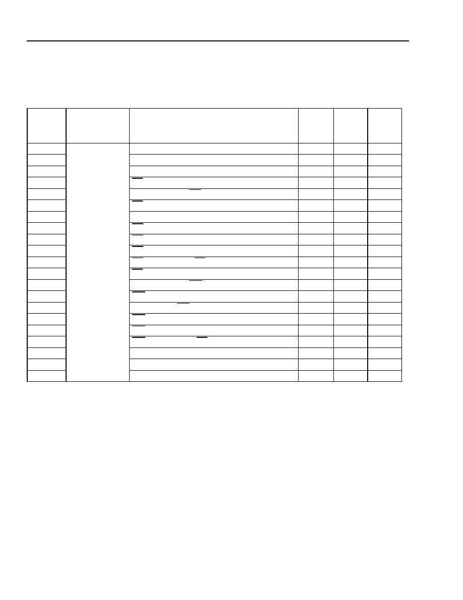
Advance Data Sheet, Rev. 2
TLIU04C1 Quad T1/E1 Line Interface
April 1999
54
Lucent Technologies Inc.
Microprocessor Mode
(continued)
Microprocessor Interface Timing
(continued)
Table 37. Microprocessor Interface I/O Timing Specifications (continued)
The read and write timing diagrams for all four microprocessor interface modes are shown in Figures 15--22.
Symbol
Configuration
Parameter
Setup
(ns)
(Min)
Hold
(ns)
(Min)
Delay
(ns)
(Max)
t23
Modes 3 and 4
ALE Asserted Width
--
10
--
t24
Address Valid to ALE Asserted
10
--
--
t25
ALE Asserted to Address Invalid
--
10
--
t26
CS Asserted to ALE Asserted
10
--
--
t27
ALE Asserted to RD Asserted
30
--
--
t28
CS Asserted to RDY Low
--
--
20
t29
Falling Edge of MPCLK to RDY Asserted
--
--
25
t30
RD Asserted to Data Valid
--
--
50
t31
RD Deasserted to Data Invalid
--
5
--
t32
RD Deasserted to RDY Deasserted
--
--
20
t33
RD Deasserted to CS Deasserted
--
15
--
t34
CS Deasserted to RDY High Impedance
--
--
10
t35
ALE Asserted to WR Asserted
10
--
--
t36
WR Asserted Width
--
5
--
t37
Data Valid to WR Asserted
5
--
--
t38
WR Deasserted to Data Invalid
--
10
--
t39
WR Deasserted to RDY Deasserted
--
--
20
t40
WR Deasserted to CS Deasserted
--
15
--
t41
Rising Edge of MPCLK to RDY Asserted
--
--
25
t42
Address Valid to ALE Asserted
10
--
--
t43
ALE Asserted to Address Invalid
--
10
--

Advance Data Sheet, Rev. 2
April 1999
TLIU04C1 Quad T1/E1 Line Interface
55
Lucent Technologies Inc.
Microprocessor Mode
(continued)
Microprocessor Interface Timing
(continued)
5-7192(F)r.2
Figure 15. Mode 1--Read Cycle Timing (MPMODE = 0, MPMUX = 0)
5-7193(F)r.3
Figure 16. Mode 1--Write Cycle Timing (MPMODE = 0, MPMUX = 0)
t4
t1
t3
t6
t5
t8
t7
t9
t14
t12
t13
t10
t11
VALID DATA
CS
AS
A[3:0]
R/W
DS
DTACK
AD[7:0]
t2
VALID ADDRESS
t4
t1
t3
t7
t19
t12
t13
t10
t11
VALID DATA
CS
AS
A[3:0]
R/W
DS
DTACK
AD[7:0]
t2
VALID ADDRESS
t16
t15
t17
t20
t18

Advance Data Sheet, Rev. 2
TLIU04C1 Quad T1/E1 Line Interface
April 1999
56
Lucent Technologies Inc.
Microprocessor Mode
(continued)
Microprocessor Interface Timing
(continued)
5-7194(F)r.3
Figure 17. Mode 2--Read Cycle Timing (MPMODE = 0, MPMUX = 1)
5-7195(F)r.4
Figure 18. Mode 2--Write Cycle Timing (MPMODE = 0, MPMUX = 1)
t4
t1
t7
t14
t12
t10
t11
VALID DATA
CS
AS
R/W
DS
DTACK
AD[7:0]
t13
VALID
ADDRESS
t6
t21
t22
t5
t9
t8
t4
t1
t7
t18
t19
t12
t10
t11
VALID DATA
CS
AS
R/W
DS
DTACK
AD[7:0]
t13
VALID
ADDRESS
t16
t17
t20
t21
t22
t15
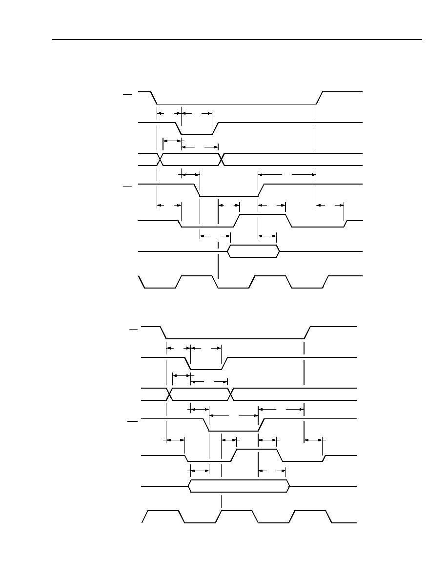
Advance Data Sheet, Rev. 2
April 1999
TLIU04C1 Quad T1/E1 Line Interface
57
Lucent Technologies Inc.
Microprocessor Mode
(continued)
Microprocessor Interface Timing
(continued)
5-7196(F)r.3
Figure 19. Mode 3--Read Cycle Timing (MPMODE = 1, MPMUX = 0)
5-7197(F)r.3
Figure 20. Mode 3--Write Cycle Timing (MPMODE = 1, MPMUX = 0)
CS
ALE
A[3:0]
RD
RDY
AD[7:0]
MPCLK
VALID ADDRESS
VALID DATA
t26
t23
t24
t25
t27
t28
t29
t30
t31
t32
t33
t34
CS
ALE
A[3:0]
WR
RDY
AD[7:0]
MPCLK
VALID ADDRESS
VALID DATA
t26
t23
t24
t25
t35
t28
t41
t37
t38
t39
t40
t34
t36

Advance Data Sheet, Rev. 2
TLIU04C1 Quad T1/E1 Line Interface
April 1999
58
Lucent Technologies Inc.
Microprocessor Mode
(continued)
Microprocessor Interface Timing
(continued)
5-7198(F)r.2
Figure 21. Mode 4--Read Cycle Timing (MPMODE = 1, MPMUX = 1)
5-7199(F)r.5
Figure 22. Mode 4--Write Cycle Timing (MPMODE = 1, MPMUX = 1)
CS
ALE
RD
RDY
AD[7:0]
MPCLK
VALID DATA
t26
t23
t27
t28
t29
t30
t31
t32
t34
t33
VALID
ADDRESS
t42
t43
CS
ALE
WR
RDY
AD[7:0]
MPCLK
VALID DATA
t26
t23
t35
t41
t37
t39
t34
t40
VALID
ADDRESS
t42
t36
t43
t38
t28
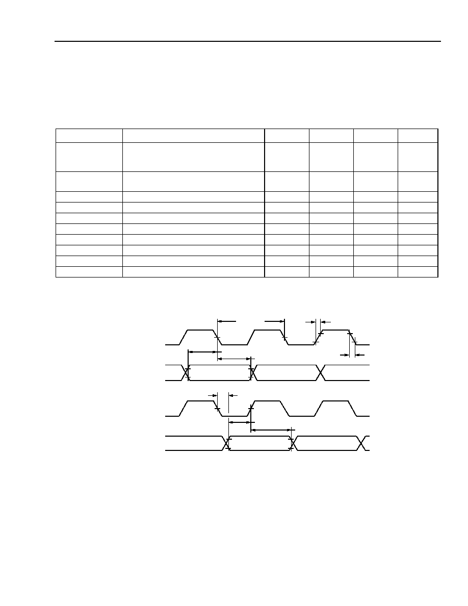
Advance Data Sheet, Rev. 2
April 1999
TLIU04C1 Quad T1/E1 Line Interface
59
Lucent Technologies Inc.
Microprocessor Mode
(continued)
Data Interface Timing
* Refers to each individual bit period for JAT = 0 applications.
Refers to each individual bit period for JAT = 1 applications using a gapped TCLK.
5-1156(F).br.3
* Invert RCLK for ACM = 1.
Figure 23. Interface Data Timing (ACM = 0)
Table 38. Data Interface Timing
Note: The digital system interface timing is shown in Figure 23 for ACM = 0. If ACM = 1, then the RCLK signal in
Figure 23 will be inverted.
Symbol
Parameter
Min
Typ
Max
Unit
tTCLTCL
Average TCLK Clock Period:
DS1
CEPT
--
--
647.7
488.0
--
--
ns
ns
tTDC
TCLK Duty Cycle*
TCLK Minimum High/Low Time
30
100
--
--
70
--
%
ns
tTDVTCL
Transmit Data Setup Time
50
--
--
ns
tTCLTDX
Transmit Data Hold Time
40
--
--
ns
tTCH1TCH2
Clock Rise Time (10%/90%)
--
--
40
ns
tTCL2TCL1
Clock Fall Time (90%/10%)
--
--
40
ns
tRCHRCL
RCLK Duty Cycle
45
50
55
%
tRDVRCH
Receive Data Setup Time
140
--
--
ns
tRCHRDX
Receive Data Hold Time
180
--
--
ns
tRCLRDV
Receive Propagation Delay
--
--
40
ns
TCLK-LIU
TPD-LIU
OR
TND-LIU
RCLK-LIU*
RPD-LIU
OR
RND-LIU
tTCH1TCH2
tTCL2TCL1
tTDVTCL
tTCLTDX
tRCLRDV
tRDVRCH
tRCHRDX
tTCLTCL

Advance Data Sheet, Rev. 2
TLIU04C1 Quad T1/E1 Line Interface
April 1999
60
Lucent Technologies Inc.
Direct Logic Control Mode
Overview
The TLIU04C1 device has the ability to operate in either a microprocessor mode or a direct logic control mode. The
CMODE pin is used to determine the operating mode. To configure the device for direct logic control mode, the
CMODE pin is pulled low.
The device is equipped with direct logic control of the line interface configuration and options so that connection to
a microprocessor is not required. Control of the various functions is accomplished by providing a logic high or low
at the control pins. Functions such as E1/T1 modes, equalizer settings, diagnostic loopbacks, test modes, system
interface timing and polarity, and standards compliance options are controlled in this manner. Alarm conditions are
also indicated by output levels directly on device pins.
Device Overview
The TLIU04C1 is a four-channel device. The LIUs convert bipolar line data pulses into logic level terminal data, with
options for timing for jitter attenuation, equalization, zero bit coding, loopbacks, and other functions.

Advance Data Sheet, Rev. 2
April 1999
TLIU04C1 Quad T1/E1 Line Interface
61
Lucent Technologies Inc.
Direct Logic Control Mode
(continued)
Pin Information
5-3684(F).b
Figure 24. TLIU04C1 Direct Logic Control Mode Pin Diagram
GNDD
VDD
A
1
RT
I
P
1
RRING1
GN
D
A
1
RND1
/
B
PV1
RPD1
/RD
A
T
A
1
DLOS2
TDM2
LOTC2
VDDD
GNDD
ALMT2
XAIS2
TCLK2
TPD2/TDATA2
TND2/CODE2
RCLK2
RPD2/RDATA2
RND2/BPV2
GNDA2
RRING2
RTIP2
VDDA2
GNDX2
TRING2
VDDX2
TTIP2
GNDX2
FLLOOP2
RE
SET
LO
X
C
XC
L
K
V
DDD
GNDD
PWRDN2
36
37
GNDD
P
W
RDN3
EQ
C3
EQ
B3
EQ
A3
DLLOOP
3
RLOOP
3
F
LLOOP
3
GNDX3
TT
I
P
3
V
DDX3
T
R
ING3
GNDX3
VDD
A
3
RT
I
P
3
RRING3
GND
A
3
RND3
/BP
V
3
RPD3
/RD
A
T
A
3
RCL
K3
T
ND3/CODE
3
TPD
3
/
T
D
A
T
A
3
TC
LK
3
XA
I
S
3
RLOOP2
DLLOOP2
EQB2
EQC2
RC
V
A
I
S
AL
TI
M
E
R
L
O
SST
D
LOS
S
D
ICT
AL
M
T
3
38
39
40
41
42
43
44
45
46
47
48
49
50
51
52
53
54
55
56
57
58
59
60
61
62
63
64
65
66
67
68
69
70
71
72
35
34
33
32
31
30
29
28
27
26
25
24
23
22
21
20
19
18
17
16
15
14
13
12
11
10
9
8
7
6
5
4
3
2
1
73
74
75
76
77
78
79
80
81
82
83
84
85
86
87
88
89
90
91
92
93
94
95
96
97
98
99
100
101
102
103
104
105
106
107
108
PWRDN4
EQC4
EQB4
EQA4
DLLOOP4
RLOOP4
FLLOOP4
GNDX4
TTIP4
VDDX4
TRING4
GNDX4
VDDA4
RTIP4
RRING4
GNDA4
RND4/BPV4
RPD4/RDATA4
TND4/CODE4
RCLK4
TPD4/TDATA4
TCLK4
XAIS4
ALMT4
GNDD
VDDD
LOTC4
TDM4
DLOS4
ALOS4
ALOS3
DLOS3
TDM3
LOTC3
VDDD
GNDD
14
4
14
3
14
2
14
1
14
0
13
9
13
8
13
7
13
6
13
5
13
4
13
3
13
2
13
1
13
0
12
9
12
8
12
7
12
6
12
5
12
4
12
3
12
2
12
1
12
0
11
9
11
8
11
7
11
6
11
5
11
4
11
3
11
2
11
1
11
0
10
9
AL
M
T
1
GNDX
1
T
R
ING1
V
DDX1
TT
I
P
1
GNDX
1
F
L
LOOP
1
RLOOP
1
DLLOOP
1
EQ
A1
EQ
B1
EQ
C
1
P
W
RDN1
GNDD
V
DDD
CM
ODE
CL
KS
CL
KM
AC
M
AL
M
NC
DU
AL
JA
T
ALOS2
ALOS1
DLOS1
TDM1
LOTC1
VDDD
XAI
S
1
TC
L
K
1
TP
D
1
/
T
D
A
T
A
1
T
ND1/CODE
1
RCL
K1
JA
R
GNDD
EQA2
JA
B
W
0

Advance Data Sheet, Rev. 2
TLIU04C1 Quad T1/E1 Line Interface
April 1999
62
Lucent Technologies Inc.
Direct Logic Control Mode
(continued)
Pin Information
(continued)
Table 39. Pin Descriptions
* I = input, O = output, I
u
indicates an input with internal pull-up; I
d
indicates an input with internal pull-down, P = power. Resistance value of all
internal pull-ups or pull-downs is 50 k
, unless otherwise specified.
Pin
Symbol
Type*
Qty
Name/Description
117
CLKS
I
d
1
XCLK Select. This pin selects either a 16x line rate clock for XCLK
(CLKS = 0) or a primary line rate clock for XCLK (CLKS = 1).
116
CLKM
I
d
1
XCLK Mode. This pin sets the mode when using a primary line rate
clock for XCLK.
CEPT: CLKM = 1
DS1:
CLKM = 0
130, 27,
58, 99
V
DDX
[1--4]
P
4
Power Supply for Line Drivers.
The device requires a 5 V
±
5%
power supply on these pins.
128, 132,
25, 29,
56, 60,
97, 101
GND
X
[1--4]
P
8
Ground Reference for Line Drivers.
129, 28,
57, 100
TTIP[1--4]
O
4
Transmit Bipolar Tip.
Positive bipolar transmit data to the analog
line interface.
131, 26,
59, 98
TRING[1--4]
O
4
Transmit Bipolar Ring.
Negative bipolar transmit data to the
analog line interface.
133, 24,
61, 96
V
DDA
[1--4]
P
4
Power Supply for Analog Circuitry.
The device requires a
5 V
±
5% power supply on these pins.
136, 21,
64, 93
GND
A
[1--4]
P
4
Ground Reference for Analog Circuitry.
134, 23,
62, 95
RTIP[1--4]
I
4
Receive Bipolar Tip.
Positive bipolar receive data from the analog
line interface.
135, 22,
63, 94
RRING[1--4]
I
4
Receive Bipolar Ring.
Negative bipolar receive data from the
analog line interface.
142, 15,
70, 87
TCLK[1--4]
I
4
Transmit Clock.
DS1 (1.544 MHz
±
32 ppm) or CEPT
(2.048 MHz
±
50 ppm) clock signal from the terminal equipment.
141, 16,
69, 88
TPD/
TDATA[1--4]
I
d
4
Transmit Data Positive Rail/Transmit Data.
If dual = 0, this pin is
used as 1.544 Mbits/s or 2.048 Mbits/s unipolar input data. If
dual = 1, this pin is used as the transmit data positive rail.
140, 17,
68, 89
TND/
CODE[1--4]
I
d
4
Transmit Data Negative Rail/Substitution Code Enable.
If
dual = 0, this pin is set to insert a B8ZS/HDB3 substitution code
(per EQA, EQB, EQC) on the transmit side and to remove the
substitution code on the receive side. If dual = 1, this pin is used as
the transmit data negative rail.
139, 18,
67, 90
RCLK[1--4]
O
4
Receive Clock.
This signal is the receive clock recovered from the
line data. The duty cycle of RCLK is 50%
±
5%.
138, 19,
66, 91
RPD/
RDATA[1--4]
O
4
Receive Data Positive Rail/Receive Data.
If dual = 0, this pin is
used as 1.544 Mbits/s or 2.048 Mbits/s unipolar output data with a
100% duty cycle. If dual = 1, this pin is used to receive data positive
rail.

Advance Data Sheet, Rev. 2
April 1999
TLIU04C1 Quad T1/E1 Line Interface
63
Lucent Technologies Inc.
Direct Logic Control Mode
(continued)
Pin Information
(continued)
Table 39. Pin Descriptions (continued)
* I = input, O = output, I
u
indicates an input with internal pull-up; I
d
indicates an input with internal pull-down, P = power. Resistance value of all
internal pull-ups or pull-downs is 50 k
, unless otherwise specified.
Only one loopback mode can be enabled at a time. Enabling more than one results in all being deactivated.
Pin
Symbol
Type*
Qty
Name/Description
137, 20,
65, 92
RND/
BPV[1--4]
O
4
Receive Data Negative Rail/Bipolar Violation.
If dual = 0 (single-
rail mode), this pin will be asserted (1 for ALM = 0, 0 for ALM = 1)
for one bit period after detection of a bipolar coding violation on the
receive analog data (RTIP, RRING). If dual = 1, this pin is used as
the receive data negative rail.
6, 7, 78,
79
ALOS[1--4]
O
4
Analog Loss of Signal (Active-Low).
This pin is asserted low
when the data signal at the receiver inputs falls below a threshold
level. The pin is deasserted high when the signal rises above
another, slightly higher threshold. The difference between these
threshold levels provides hysteresis to prevent alarm chatter.
5, 8, 77,
80
DLOS[1--4]
O
4
Digital Loss of Signal (Active-Low). Guarantees the receive
signal quality as defined in the appropriate ANSI, Bellcore, and ITU
standards. During DS1 operation, DLOS is asserted low if 100 or
more consecutive zeros occur in the receive data stream. In CEPT
operation, DLOS is asserted low when 255 or more consecutive
zeros occur in the receive data stream. The pin is deasserted high
when a ones density greater than 12.5% is detected over the 100 or
255 pulse positions.
4, 9, 76,
81
TDM[1--4]
O
4
Transmit Drive Monitor (Active-Low). Transmit driver monitor
detects two conditions: a nonfunctional link due to faults on the
primary of the transmit transformer, and periods of no data
transmission. TDM = 0 for active alarm.
3, 10, 75,
82
LOTC[1--4]
O
4
Loss of Transmit Clock (Active-Low).
LOTC = 0 when there is a
loss of any of the clocks in the transmit path including the TCLK
input, RCLK in remote loopback, jitter attenuator output clock (when
enabled), or the pulse-width controller clock.
45
LOXC
O
1
Loss of XCLK. This pin is asserted high when the XCLK signal is
not present.
144, 13,
72, 85
ALMT[1--4]
I
u
4
Alarm Test Enable (Active-Low).
For ALMT = 0, alarm pins are
forced as follows; DLOS = 0, ALOS = 0, TDM = 0, LOTC = 0, and
BPV = activate state per ALM. LOXC is forced high if ALMT is
asserted for all four channels. ALMT does not affect data
transmission.
127, 30,
55, 102
FLLOOP[1--4]
I
u
4
Full Local Loopback Enable (Active-Low).
This pin is cleared
for a full local loopback (transmit converter output to receive
converter input). Most of the transmit and receive analog circuitry is
exercised in this loopback.
126, 31,
54, 103
RLOOP[1--4]
I
u
4
Remote Loopback Enable (Active-Low).
This pin is cleared for a
remote loopback (DSX to DSX). In remote loopback, a high on
XAIS inserts the AIS signal on the transmit side.
125, 32,
53, 104
DLLOOP[1--4]
I
u
4
Digital Local Loopback Enable (Active-Low).
This pin is cleared
for a digital local loopback. Only the transmit and receive digital
sections are exercised in this loopback.

Advance Data Sheet, Rev. 2
TLIU04C1 Quad T1/E1 Line Interface
April 1999
64
Lucent Technologies Inc.
Direct Logic Control Mode
(continued)
Pin Information
(continued)
Table 39. Pin Descriptions (continued)
* I = input, O = output, I
u
indicates an input with internal pull-up; I
d
indicates an input with internal pull-down, P = power. Resistance value of all
internal pull-ups or pull-downs is 50 k
, unless otherwise specified.
Pin
Symbol
Type*
Qty
Name/Description
124, 33,
52, 105
EQA[1--4]
I
d
4
Equalizer Control A.
One of three control pins for selecting
transmit equalizers and DS1/CEPT mode. See Table 45.
123, 34,
51, 106
EQB[1--4]
I
d
4
Equalizer Control B.
One of three control pins for selecting
transmit equalizers and DS1/CEPT mode. See Table 45.
122, 35,
50, 107
EQC[1--4]
I
d
4
Equalizer Control C.
One of three control pins for selecting
transmit equalizers and DS1/CEPT mode. See Table 45.
46
XCLK
I
u
1
Reference Clock. A valid reference clock must be provided at this
input. XCLK must be an independent, continuously active, 50%
duty cycle, ungapped, and unjittered clock to guarantee device
performance specifications. XCLK has an internal 100 k
pull-up
resistor. See Table 54.
143, 14,
71, 86
XAIS[1--4]
I
d
4
Transmit AIS.
This pin is set to insert the alarm indication signal
(all ones) on the transmit line interface. This control has priority
over a remote loopback if both are operated simultaneously.
39
RCVAIS
I
d
1
Receive AIS.
This pin selects the shutdown function for the
receiver during analog and digital loss of signal. RCVAIS operates
in conjunction with LOSSD. See Table 42.
42
LOSSD
I
d
1
Loss of Signal Shutdown Control. This pin selects the shutdown
function for the receiver during analog and digital loss of signal.
LOSSD operates in conjunction with RCVAIS. See Table 42.
41
LOSSTD
I
d
1
Digital Loss of Signal Standard Selection. The LOSSTD pin
selects the standard that is followed to deactivate a digital loss of
signal in DS1 mode. For LOSSTD = 0, DLOS is deactivated when
the average ones density is at least 12.5% over 100 contiguous
pulse positions (T1M1.3/93-005, ITU-T G775). For LOSSTD = 1, an
additional constraint of less than 15 consecutive zeros is required
along with the 12.5% ones density (TR-TSY-000009). The LOSSTD
pin has no effect in CEPT mode, which requires 12.5% ones
density over 255 contiguous pulse positions (ITU-T G.775).
40
ALTIMER
I
d
1
Analog Loss of Signal Timer. This pin selects the time required to
detect an analog loss of signal. For ALTIMER = 0, ALOS is
declared between 1 ms and 2.6 ms after losing signal as required
by I.431(3/93) and ETSI-300-233 (5/94). For ALTIMER = 1, ALOS is
declared between 10 and 255 bit symbol periods after losing signal
as required by G.775 (11/95).
121, 36,
49, 108
PWRDN[1--4]
I
d
4
Powerdown Enable. When this pin is activated (PWRDN = 1), the
circuitry of the channel is put into a standby mode in which minimal
power is consumed.

Advance Data Sheet, Rev. 2
April 1999
TLIU04C1 Quad T1/E1 Line Interface
65
Lucent Technologies Inc.
Direct Logic Control Mode
(continued)
Pin Information
(continued)
Table 39. Pin Descriptions (continued)
* I = input, O = output, I
u
indicates an input with internal pull-up; I
d
indicates an input with internal pull-down, P = power. Resistance value of all
internal pull-ups or pull-downs is 50 k
, unless otherwise specified.
Pin
Symbol
Type*
Qty
Name/Description
111
JAT
I
d
1
Jitter Attenuator in the Transmit Path.
Setting JAT = 1 enables
the jitter attenuator in the transmit path for all four channels. Setting
JAT = 0 disables the jitter attenuator in the transmit path. If both
JAT = 1 and JAR = 1, the jitter attenuator is disabled.
110
JAR
I
d
1
Jitter Attenuator in the Receive Path.
Setting JAR = 1 enables
the jitter attenuator in the receive path for all four channels. Setting
JAR = 0 disables the jitter attenuator in the receive path. If both
JAT = 1 and JAR = 1, the jitter attenuator is disabled.
118
CMODE
I
d
1
Chip Mode. This pin sets the chip mode for either direct logic mode
or microprocessor mode.
Microprocessor: CMODE = 1
Direct Logic:
CMODE = 0
38
JABW0
I
d
1
Jitter Attenuator Bandwidth Adjust. Setting this pin selects the
lower bandwidth jitter attenuator option in CEPT mode, lowering the
bandwidth from 10 Hz to 1.25 Hz. When this option is used, XCLK
must be ±20 ppm. See Table 54.
114
ALM
I
d
1
Alternate Logic Mode (ALM).
If ALM = 0, the receiver circuitry
(and transmit input) assumes the data to be active-low polarity. If
ALM = 1, the data is assumed to be active-high polarity.
115
ACM
I
d
1
Alternate Clock Mode (ACM). The alternate clock mode control
pin selects the positive or negative clock edge of the receive clock
(RCLK) for receiver data retiming. For ACM = 1, the receive data is
retimed on the positive edge of the receive clock. When ACM = 0,
the receive data is retimed on the negative edge of the receive
clock. (This does not affect transmit clock timing.) See Figure 38.
112
DUAL
I
d
1
Dual-Rail Mode Select.
This pin is cleared (DUAL = 0) for single-
rail mode and set (DUAL = 1) for dual-rail mode.
44
RESET
I
u
1
Hardware Reset (Active-Low). If RESET is forced low, all internal
states in the transceiver paths are reset and data flow through each
channel will be momentarily disrupted. The RESET pin must be
held low for a minimum of 1 ms.
43
ICT
I
u
1
High-Impedance Mode (Active-Low). When ICT = 0, all output
buffers (TTIP, TRING, RCLK, RPD, RND, LOXC, LOTC, TDM,
DLOS, ALOS) are placed in a high-impedance state. TTIP and
TRING outputs have a limited high-impedance capability of
approximately 8 k
.
2, 11, 47,
74, 83,
119
V
DDD
P
6
Power Supply for Digital Circuitry.
1, 12, 37,
48, 73, 84,
109, 120
GND
D
P
8
Ground Reference for Digital Circuitry.
113
NC
--
1
No Connect.

Advance Data Sheet, Rev. 2
TLIU04C1 Quad T1/E1 Line Interface
April 1999
66
Lucent Technologies Inc.
Direct Logic Control Mode
(continued)
System Interface Pin Options
The system interface can be configured to operate in a number of different modes. The different modes change the
functionality of the system interface pins, as shown in Table 40. Dual-rail or single-rail operation is possible using
the DUAL control pin (pin 112). Dual-rail mode is enabled when DUAL = 1; single-rail mode is enabled when
DUAL = 0. In dual-rail operation, data received from the line interface on RTIP and RRING appears on RPD and
RND at the system interface and data transmitted from the system interface on TPD and TND appears on TTIP and
TRING at the line interface. In single-rail operation, data received from the line interface on RTIP and RRING
appears on RDATA at the system interface and data transmitted from the system interface on TDATA appears on
TTIP and TRING at the line interface.
In single-rail mode only, TND is not needed for data and is used for controlling the B8ZS/HDB3 encoding/decoding.
The coding may be selected by pulling the CODE pins high. RND is also not needed for data in single-rail mode,
and is used for indicating bipolar violations. When a coding violations occurs, the BPV pin is asserted according to
the ALM setting (pin 114).
Table 40. System Interface Pin Mapping
Configuration
RPD/RDATA
RND/BPV
TPD/TDATA
TND/CODE
Single-rail mode (DUAL = 0)
RDATA
BPV
TDATA
CODE
Dual-rail mode (DUAL = 1)
RPD
RND
TPD
TND
Advance Data Sheet, Rev. 2
April 1999
TLIU04C1 Quad T1/E1 Line Interface
67
Lucent Technologies Inc.
Direct Logic Control Mode
(continued)
Block Diagrams
5-7823(F)
Figure 25. TLIU04C1 Block Diagram, CMODE = 0 (Direct Logic Mode)
TTIP[1--4]
TRING[1--4]
QUAD
LINE
INTERFACE
UNIT
RTIP[1--4]
RRING[1--4]
QUAD
TRANSMIT
SECTION
QUAD
RECEIVE
SECTION
RESET
CLOCK
MULTIPLIER
XCLK
LOTC[1--4]
TDM[1--4]
DLOS[1--4]
ALOS[1--4]
XAIS[1--4]
ALMT[1--4]
PWRDN[1--4]
FLLOOP[1--4]
RLOOP[1--4]
EQA[1--4]
EQB[1--4]
EQC[1--4]
CLKS
CLKM
TCLK[1--4]
TPD[1--4]
ACM
ALM
DUAL
JAT
JAR
JABW0
RCVAIS
LOSSTD
LOSSD
ICT
LOXC
RCLK[1--4]
RND[1--4]
RPD[1--4]
ALTIMER
TND[1--4]
DLLOOP[1--4]
Advance Data Sheet, Rev. 2
TLIU04C1 Quad T1/E1 Line Interface
April 1999
68
Lucent Technologies Inc.
Direct Logic Control Mode
(continued)
Block Diagrams
(continued)
The line interface block diagram is shown in Figure 26. For illustration purposes, only one of the four on-chip line
interfaces is shown. Pin names that apply to all four channels are followed by the designation [1--4].
5-4556(F).er.3
Figure 26. Block Diagram of the Quad Line Interface Unit (Single Channel)
RTIP[1--4]
RRING[1--4]
FLLOOP
(NO LIU AIS)
EQUALIZER
SLICERS
CLOCK AND
DATA
RECOVERY
DLOS
RND[1--4]
RPD[1--4]
RCLK[1--4]
DECODER
DLLOOP
RLOOP
TCLK[1--4]
TND[1--4]
JITTER
(RECEIVE PATH)
TPD[1--4]
FLLOOP
(DURING LIU AIS)
PULSE-
WIDTH
CONTROLLER
TDM
LOTC
PULSE
EQUALIZER
TRANSMIT
DRIVER
TTIP[1--4]
TRING[1--4]
LOSS OF
XCLK
MONITOR
DIVIDE BY 16
ALARM
SIGNAL (AIS)
ENCODER
ALOS
INDICATION
ATTENUATOR
JITTER
(TRANSMIT PATH)
ATTENUATOR
(CLOCK)
(DATA)
LOSS
OF
TCLK
LOXC
XCLK
16x
CLOCK
MULTIPLIER
CLKS
INTXCLK

Advance Data Sheet, Rev. 2
April 1999
TLIU04C1 Quad T1/E1 Line Interface
69
Lucent Technologies Inc.
Direct Logic Control Mode
(continued)
Data Recovery
The receive line interface unit (RLIU) format is bipolar
alternate mark inversion (AMI). The data rate tolerance
is ±130 ppm (DS1) or ±80 ppm (CEPT). The receiver
first restores the incoming data and detects analog loss
of signal. Subsequent processing is optional and
depends on the programmable device configuration
established with the use of the direct logic control pins.
The RLIU utilizes an equalizer to operate on line length
with up to 15 dB of loss at 772 kHz (DS1) or 13 dB loss
at 1.024 MHz (CEPT). The signal is then peak-
detected and sliced to produce digital representations
of the data.
Clock and data recovery, digital loss of signal, jitter
attenuation, and data decoding are performed. The
receive digital output format is non-return-to-zero
(NRZ) with selectable dual-rail or single-rail system
interface.
The clock is recovered by a digital phase-locked loop
that uses XCLK as a reference to lock to the data rate
component. Because the internal reference clock is a
multiple of the received data rate, the RCLK output will
always be a valid DS1/CEPT clock that eliminates
false-lock conditions. During periods with no receive
input signal, the free-run frequency of RCLK is defined
to be either XCLK/16 or XCLK, depending on the state
of CLKS. RCLK is always active with a duty-cycle cen-
tered at 50%, deviating by no more than ±5%. Valid
data is recovered within the first few bit periods after
the application of XCLK. The delay of the data through
the receive circuitry is approximately 1 to 14 bit peri-
ods, depending on the CODE configurations. Additional
delay is introduced if the jitter attenuator is selected for
operation in the receive path (see the LIU Delay Values
section, page 89).
Jitter Accommodation and Jitter Transfer
Without the Jitter Attenuator
The RLIU is designed to accommodate large amounts
of input jitter. The RLIU's jitter performance exceeds
the requirements shown in the RLIU Specifications
tables (Table 43 and Table 44). Typical receiver perfor-
mance without the jitter attenuator in the path is shown
in Figure 27 through Figure 30. Jitter transfer is inde-
pendent of input ones density on the line interface.
Receiver Configuration Modes
Clock/Data Recovery Mode (CDR)
The clock/data recovery function in the receive path
can be bypassed by setting the FLLOOP, RLOOP and
DLLOOP pins for all channels low. Any other combina-
tion of the twelve loopback pins results in the clock and
data recovery function being enabled and providing a
recovered clock (RCLK) with retimed data (RPD/
RDATA, RND). If all twelve of the loopback pins are
asserted, the clock and data recovery function is dis-
abled, and the RZ data from the slicers is provided over
RPD and RND to the system. In this mode, down-
stream functions selected by the JAR, ACM, and
LOSSD pins are ignored.
Zero Substitution Decoding (CODE)
When single-rail operation is selected with DUAL = 0,
the B8ZS/HDB3 decoding can be selected. CODE[1--
4] pulled high selects the B8ZS/HDB3 decoding opera-
tion for each individual channel.
Note: Encoding and decoding are not independent.
Selecting B8ZS/HDB3 decoding in the receiver
selects B8ZS/HDB3 encoding in the transmitter.
When decoding is selected for a given channel,
decoded receive data and code violations appear on
the RDATA and BPV pins, respectively. If coding is not
selected, receive data and any bipolar violations (such
as two consecutive ones of the same polarity) appear
on the RDATA and BPV pins, respectively.
Alternate Logic Mode (ALM)
The alternate logic mode (ALM) control pin selects the
receive and transmit data polarity (i.e., active-high vs.
active-low). If ALM = 0, the receiver circuitry (and trans-
mit input) assumes the data to be active-low polarity. If
ALM = 1, the receiver circuitry (and transmit input)
assumes the data to be active-high polarity. The ALM
control is used in conjunction with the ACM control to
determine the receive data retiming mode.
Alternate Clock Mode (ACM)
The alternate clock mode (ACM) control pin selects the
positive or negative clock edge of the receive clock
(RCLK) for receive data retiming. The ACM control is
used in conjunction with the ALM control to determine
the receive data retiming modes. If ACM = 1, the
receive data is retimed on the positive edge of the
receive clock. If ACM = 0, the receive data is retimed
on the negative edge of the receive clock. Note that this
control does not affect the timing relationship for the
transmitter inputs. See Figure 38 on page 97.

Advance Data Sheet, Rev. 2
TLIU04C1 Quad T1/E1 Line Interface
April 1999
70
Lucent Technologies Inc.
Direct Logic Control Mode
(continued)
Receiver Configuration Modes
(continued)
RLIU Alarms
Analog Loss of Signal (ALOS) Alarm. An analog sig-
nal detector monitors the receive signal amplitude and
reports its status on the analog loss of signal alarm
pins. An analog loss of signal is indicated if the ampli-
tude at the RRING and RTIP inputs drops more than
approximately 18 dB below the nominal signal ampli-
tude. The ALOS alarm condition will clear when the
receive signal amplitude returns to greater than 14 dB
below normal. In this way, the ALOS circuitry provides
4 dB of hysteresis to prevent alarm chattering.
The time required to detect ALOS is selectable. When
ALTIMER = 0, ALOS is declared between 1 ms and
2.6 ms after losing signal as required by I.431(3/93)
and ETS-300-233 (5/94). If ALTIMER = 1, ALOS is
declared between 10 and 255 bit symbol periods after
losing signal as required by G.775 (11/95). The timing
is derived from the XCLK clock. The detection time is
independent of signal amplitude before the loss condi-
tion occurs. Normally, ALTIMER = 1 would be used only
in CEPT mode since no T1/DS1 standards require this
mode. In T1/DS1 mode, this pin should normally be
tied low.
The behavior of the receiver outputs under ALOS con-
ditions depends on the loss shutdown (LOSSD) control
pin in conjunction with the receiver AIS (RCVAIS) con-
trol pin as described in the Loss Shutdown (LOSSD)
and Receiver AIS (RCVAIS) section on page 71.
Digital Loss of Signal (DLOS) Alarm. A digital loss of
signal (DLOS) detector guarantees the received signal
quality as defined in the appropriate ANSI, Bellcore,
and ITU standards. The digital loss of signal alarms are
reported on the DLOS alarm pins. During DS1 opera-
tion, a digital loss of signal is indicated if 100 or more
consecutive zeros occur in the receive data stream.
The DLOS condition is deactivated when the average
ones density of at least 12.5% is received in 100 con-
tiguous pulse positions. The LOSSTD control bit
selects the conformance protocols for the DLOS alarm
indication per Table 41. Setting LOSSTD = 1 adds an
additional constraint that there are less than 15 con-
secutive zeros in the DS1 data stream before DLOS is
deactivated.
During CEPT operation, DLOS is indicated when 255
or more consecutive zeros occur in the receive data
stream. The DLOS indication is deactivated when the
average ones density of at least 12.5% is received in
255 contiguous pulse positions. LOSSTD has no effect
in CEPT mode.
Table 41. Digital Loss of Signal Standard Select
LOSSTD
DS1 Mode
CEPT Mode
0
T1M1.3/93-005, ITU-T G.775
ITU-T G.775
1
TR-TSY-000009
ITU-T G.775

Advance Data Sheet, Rev. 2
April 1999
TLIU04C1 Quad T1/E1 Line Interface
71
Lucent Technologies Inc.
Direct Logic Control Mode
(continued)
Receiver Configuration Modes
(continued)
RLIU ALARMS (continued)
Loss Shutdown (LOSSD) and Receiver AIS (RCVAIS). The loss shutdown control pin (LOSSD) acts in conjunc-
tion with the receiver AIS (RCVAIS) control pin to place the digital outputs in a predetermined state when a digital
loss of signal (DLOS) or analog loss of signal (ALOS) alarm occurs.
If LOSSD = 0 and RCVAIS = 0, the RND, RPD, and RCLK outputs will be unaffected by the DLOS alarm condition.
However, when an ALOS alarm condition exists, the RPD and RND outputs are forced to their inactive state
(dependent on ALM state) and the RCLK free runs (based on XCLK frequency).
If LOSSD = 0, RCVAIS = 1, and a DLOS or an ALOS alarm condition exists, the RPD and RND outputs will present
an alarm indication signal (AIS, all ones) based on the free-running clock frequency, and the RCLK free runs.
If LOSSD = 1, regardless of the state of RCVAIS, and a DLOS or an ALOS alarm condition exists, the RPD and
RND outputs are forced to their inactive state (dependent on ALM state) and the RCLK free runs.
The RND, RPD, and RCLK signals will remain unaffected if any loopback (FLLOOP, RLOOP, DLLOOP) is activated
independent of LOSSD and RCVAIS settings.
The LOSSD and RCVAIS behavior is summarized in Table 42.
RLIU Bipolar Violation (BPV) Alarm. The bipolar violation (BPV) alarm is used only in the single-rail mode of
operation. When B8ZS(DS1)/HDB3(CEPT) coding is not used (i.e., CODE[1--4] = 0), any violations in the receive
data (such as two or more consecutive ones on a rail) are indicated on the RND/BPV outputs. When B8ZS(DS1)/
HDB3(CEPT) coding is used (i.e., CODE[1--4] = 1), the HDB3/B8ZS code violations are reflected on the RND/
BPV outputs.
Table 42. LOSSD and RCVAIS Control Configurations (Not Valid During Loopback Modes)
LOSSD
RCVAIS
ALARM
RPD/RND
RCLK
0
0
ALOS
0 if ALM = 1, 1 if ALM = 0
Free Runs
0
0
DLOS
Normal Data
Recovered Clock
0
1
ALOS
AIS (all ones)
Free Runs
0
1
DLOS
AIS (all ones)
Free Runs
1
X
ALOS
0 if ALM = 1, 1 if ALM = 0
Free Runs
1
X
DLOS
0 if ALM = 1, 1 if ALM = 0
Free Runs

Advance Data Sheet, Rev. 2
TLIU04C1 Quad T1/E1 Line Interface
April 1999
72
Lucent Technologies Inc.
Direct Logic Control Mode
(continued)
DS1 Receiver Specifications
During DS1/T1 operation, the RLIU will perform as specified in Table 43.
Table 43. DS1 RLIU Specifications
Parameter
Min
Typ
Max
Unit
Spec
Analog Loss of Signal:
Threshold to Assert
Threshold to Clear
Hysteresis
Time to Assert (ALTIMER = 0)
17.5
13.5
--
1.0
18
14
4
--
23
17.5
--
2.6
dB
*
dB
*
dB
ms
* Below the nominal pulse amplitude of 3.0 V with the line interface circuitry specified (see Line Circuitry on page 94).
I.431
--
--
I.431
Receiver Sensitivity
Cable loss at 772 kHz.
11
15
--
dB
--
Jitter Transfer:
3 dB Bandwidth
Peaking
--
--
3.84
--
--
0.1
kHz
dB
Figure 28 on page 74
Figure 34 on page 86
Generated Jitter
--
0.04
0.05
UIp-p
GR-499-CORE
ITU-T G.824
Jitter Accommodation
--
--
--
--
Figure 27 on page 73
Figure 33 on page 85
Return Loss
:
51 kHz to 102 kHz
102 kHz to 1.544 MHz
1.544 MHz to 2.316 MHz
Using Lucent transformer 2795B and components listed in Table 55.
14
20
16
--
--
--
--
--
--
dB
dB
dB
--
--
--
Digital Loss of Signal:
Flag Asserted When Consecutive Bit
Positions Contain
Flag Deasserted When
Data Density Is
and Maximum Consecutive Zeros Are
100
12.5
--
--
--
--
--
--
--
--
15
99
zeros
% ones
zeros
zeros
ITU-T G.775,
T1M1.3/93-005
--
TR-TRY-000009
ITU-T G.775, T1M1.3/
93-005
Advance Data Sheet, Rev. 2
April 1999
TLIU04C1 Quad T1/E1 Line Interface
73
Lucent Technologies Inc.
Direct Logic Control Mode
(continued)
DS1 Receiver Specifications
(continued)
Frequency Response Curves
5-5260(F)r.7
Figure 27. DS1/T1 Receiver Jitter Accommodation Without Jitter Attenuator
0.1 UI
1.0 UI
10 UI
100 UI
10
100
1k
10k
1
28 UI
FREQUENCY (Hz)
100k
TYPICAL
(SUBJECT TO DEVICE CHARACTERIZATION)
(NON-SONET CAT II INTERFACES)
GR-499-CORE
I.431(DS1), G.824(DS1)
TR-TSY-000009 (DS1, MUXes)
GR-499/1244-CORE (CAT I INTERFACES)
T1.408/I.431(DS1)/G.824(DS1)
Advance Data Sheet, Rev. 2
TLIU04C1 Quad T1/E1 Line Interface
April 1999
74
Lucent Technologies Inc.
Direct Logic Control Mode
(continued)
DS1 Receiver Specifications
(continued)
Frequency Response Curves (continued)
5-5261(F)r.4
Figure 28. DS1/T1 Receiver Jitter Transfer Without Jitter Attenuator
60
40
20
0
1
10
100
1k
10k
50
30
10
100k
FREQUENCY (Hz)
J
I
TTE
R OUT/
J
ITT
ER
IN (
d
B
)
TYPICAL
(SUBJECT TO DEVICE CHARACTERIZATION)
GR-499-CORE
(NON-SONET CAT II TO CAT II)

Advance Data Sheet, Rev. 2
April 1999
TLIU04C1 Quad T1/E1 Line Interface
75
Lucent Technologies Inc.
Direct Logic Control Mode
(continued)
CEPT Receiver Specifications
During CEPT/E1 operation, the RLIU will perform as specified in Table 44.
Table 44. CEPT RLIU Specifications
Parameter
Min
Typ
Max
Unit
Spec
Analog Loss of Signal:
Threshold to Assert
Threshold to Clear
Hysteresis
Time to Assert (ALTIMER = 0)
Time to Assert (ALTIMER = 1)
17.5
13.5
--
1.0
10
18
14
4
--
--
23
17.5
--
2.6
255
dB
*
dB
*
dB
ms
UI
* Below the nominal pulse amplitude of 3.0 V with the line circuitry specified (see Line Interface Unit: Line Circuitry section).
I.431, ETSI 300 233
--
--
I.431, ETSI 300 233
G.775
Receiver Sensitivity
Cable loss at 1.024 MHz.
11
13.5
--
dB
--
Interference Immunity
:
Amount of cable loss for which the receiver will operate error-free in the presence of a ≠18 dB interference signal summing with the
intended signal source.
9
12
--
dB
ITU-T G.703
Jitter Transfer:
3 dB Bandwidth, Single Pole Roll Off
Peaking
--
--
5.1
--
--
0.5
kHz
dB
Figure 30 on page 77
Figure 36 on page 88
Generated Jitter
--
0.04
0.05
UIp-p
ITU-T G.823, I.431
Jitter Accommodation
--
--
--
--
Figure 29 on page 76
Figure 35 on page 87
Return Loss
ß
:
51 kHz to 102 kHz
102 kHz to 1.544 MHz
1.544 MHz to 2.316 MHz
ß Using Lucent transformer 2795D or 2795C and components listed in Table 55.
14
20
16
--
--
--
--
--
--
dB
dB
dB
ITU-T G.703
Digital Loss of Signal:
Flag Asserted When Consecutive Bit
Positions Contain
Flag Deasserted When Data Density is
(LOSSTD = 1)
255
12.5
--
--
--
--
zeros
%ones
--
ITU-T G.775
Advance Data Sheet, Rev. 2
TLIU04C1 Quad T1/E1 Line Interface
April 1999
76
Lucent Technologies Inc.
Direct Logic Control Mode
(continued)
CEPT Receiver Specifications
(continued)
Frequency Response Curves
5-5262(F)r.8
Figure 29. CEPT/E1 Receiver Jitter Accommodation Without Jitter Attenuator
0.1 UI
1.0 UI
10 UI
100 UI
10
100
1k
10k
1
37 UI
FREQUENCY (Hz)
G.823
100k
TYPICAL
(SUBJECT TO DEVICE CHARACTERIZATION)
G.823,ETSI-300-011A1
I.431(CEPT)/ETS-300-011
I.431(CEPT)/ETS-300-011
Advance Data Sheet, Rev. 2
April 1999
TLIU04C1 Quad T1/E1 Line Interface
77
Lucent Technologies Inc.
Direct Logic Control Mode
(continued)
CEPT Receiver Specifications
(continued)
Frequency Response Curves (continued)
5-5263(F)r.4
Figure 30. CEPT/E1 Receiver Jitter Transfer Without Jitter Attenuator
FREQUENCY (H
Z
)
JI
TTE
R OUT
/
J
I
T
T
ER
IN
(dB
)
60
40
20
0
1
10
100
1k
10k
50
30
10
100k
TYPICAL
(SUBJECT TO DEVICE CHARACTERIZATION)
G.735-9 W/O JITTER REDUCER

Advance Data Sheet, Rev. 2
TLIU04C1 Quad T1/E1 Line Interface
April 1999
78
Lucent Technologies Inc.
Direct Logic Control Mode
(continued)
Output Pulse Generation
The transmitter accepts a clock with NRZ data in single-rail mode (DUAL = 0) or a clock with positive and negative
NRZ data in dual-rail mode (DUAL = 1) from the system. The device converts this data to a balanced bipolar signal
(AMI format) with optional B8ZS(DS1)/HDB3(CEPT) encoding and jitter attenuation. Low-impedance output drivers
produce these pulses on the line interface. Positive ones are output as a positive pulse on TTIP, and negative ones
are output as a positive pulse on TRING. Binary zeros are converted to null pulses. The total delay of the data from
the system interface to the transmit driver is approximately 3 to 11 bit periods, depending on the code configuration
(see the Clock/Data Recovery Mode (CDR) section, page 69 and the Zero Substitution Encoding (CODE) section,
page 79).
Additional delay results if the jitter attenuator is selected for use in the transmit path (see the LIU Delay Values sec-
tion).
Transmit pulse shaping is controlled by the on-chip pulse-width controller and pulse equalizer. The pulse-width con-
troller produces high-speed timing signals to accurately control the transmit pulse widths. This eliminates the need
for a tightly controlled transmit clock duty cycle that is usually required in discrete implementations. The pulse
equalizer controls the amplitudes of the pulses. Different pulse equalizations are selected through proper settings
of the EQA, EQB, and EQC pins as described in Table 45.
Table 45. Equalizer/Rate Control
* In DS1 mode, the distance to the DSX for 22 gauge PIC (ABAM) cable is specified. Use the maximum cable loss figures for other cable types.
In CEPT mode, equalization is specified for coaxial or twisted-pair cable.
Loss measured at 772 kHz.
In 75
applications, Option 1 is recommended over Option 2 for lower device power dissipation. Option 2 allows for the same transformer as
used in CEPT 120
applications.
Jitter
The intrinsic jitter of the transmit path, i.e., the jitter at TTIP/TRING when no jitter is applied to TCLK (and the jitter
attenuator is not selected, JAT = 0), is typically 5 nsp-p and will not exceed 0.02 UIp-p.
EQA
EQB
EQC
Service
Clock
Rate
Transmitter Equalization*
Maximum
Cable Loss
Feet
Meters
dB
0
0
0
DS1
1.544 MHz
0 ft. to 131 ft.
0 m to 40 m
0.6
0
0
1
131 ft. to 262 ft.
40 m to 80 m
1.2
0
1
0
262 ft. to 393 ft.
80 m to 120 m
1.8
0
1
1
393 ft. to 524 ft.
120 m to 160 m
2.4
1
0
0
524 ft. to 655 ft.
160 m to 200 m
3.0
1
0
1
CEPT
2.048 MHz
75
(Option 2)
--
1
1
0
120
or 75
(Option 1)
--
1
1
1
Not Used
--
--
--

Advance Data Sheet, Rev. 2
April 1999
TLIU04C1 Quad T1/E1 Line Interface
79
Lucent Technologies Inc.
Direct Logic Control Mode
(continued)
Transmitter Configuration Modes
Zero Substitution Encoding (CODE)
Zero substitution B8ZS/HDB3 encoding can be acti-
vated only in the single-rail system interface mode
(DUAL = 0). The B8ZS/HDB3 encoding operation can
be selected for individual channels independently by
setting the CODE[1--4] pins high for the respective
channels.
Note: Encoding and decoding are not independent.
Selecting B8ZS/HDB3 encoding in the transmit-
ter selects B8ZS/HDB3 decoding in the receiver.
When coding is selected for a given channel, data
transmitted from the system interface on TDATA will be
B8ZS/HDB3 encoded before appearing on TTIP and
TRING at the line interface.
Alarm Indication Signal Generator (XAIS)
When the transmit alarm indication signal control pin is
set (XAIS[1--4] = 1) for a given channel, a continuous
stream of bipolar ones is transmitted to the line inter-
face. The TPD/TDATA and TND inputs are ignored dur-
ing this mode. The XAIS input is ignored when a
remote loopback is selected using loopback control pin
(RLOOP) transmitter alarms.
The normal clock source for the AIS signal is TCLK. If
TCLK is not available (loss of TCLK detected), then the
AIS signal clock defaults to INTXCLK/16. INTXCLK is
either XCLK, or 16x XCLK, depending on the state of
the CLKS input pin. See Figure 26 on page 68, and
CLKS in Table 39, Pin Descriptions, on page 62.
Loss of Transmit Clock (LOTC) Alarm
A loss of transmit clock alarm (LOTC[1--4]) is indicated
if any of the clocks in the transmit path disappear. This
includes loss of TCLK input, loss of RCLK during
remote loopback, loss of jitter attenuator output clock
(when enabled), or the loss of clock from the pulse-
width controller.
For all of these conditions, a core transmitter timing
clock is lost and no data can be driven onto the line.
Output drivers TTIP and TRING are placed in a high-
impedance state when this alarm condition is active.
The LOTC pin is asserted low between 3 µs and 16 µs
after the clock disappears, and deasserts immediately
after detecting the first clock edge.
Transmit Driver Monitor (TDM) Alarm
The transmit driver monitor detects two conditions: a
nonfunctional link due to a fault on the primary of the
transmit transformer, or periods of no data transmis-
sion. The transmit driver monitor alarm (TDM[1--4]) is
the ORed function of both faults and provides informa-
tion about the integrity of the transmit signal path.
The first monitoring function is provided to detect non-
functional links and protect the device from damage.
The alarm is set (TDM = 0) when one of the transmit-
ter's line drivers (TTIP or TRING) is shorted to power
supply or ground, or TTIP and TRING are shorted
together.
Under these conditions, internal circuitry protects the
device from damage and excessive power supply cur-
rent consumption by 3-stating the output drivers. The
monitor detects faults on the transformer primary, but
transformer secondary faults may not be detected.
The monitor operates by comparing the line pulses with
the transmit inputs. After 32 transmit clock cycles, the
transmitter is powered up in its normal operating mode.
The drivers attempt to correctly transmit the next data
bit. If the error persists, TDM remains active to elimi-
nate alarm chatter and the transmitter is internally pro-
tected for another 32 transmit clock cycles. This
process is repeated until the error condition is removed
and the TDM alarm is deactivated.
The second monitoring function is to indicate periods of
no data transmission. The alarm is set (TDM = 0) when
32 consecutive zeros have been transmitted and the
alarm condition is cleared on the detection of a single
pulse. This alarm condition does not alter the state or
functionality of the signal path.

Advance Data Sheet, Rev. 2
TLIU04C1 Quad T1/E1 Line Interface
April 1999
80
Lucent Technologies Inc.
Direct Logic Control Mode
(continued)
DS1 Transmitter Pulse Template
The DS1 pulse shape template is specified at the DSX
(defined by CB119 and ANSI T1.102) and is illustrated
in Figure 31. The device also meets the pulse template
specified by ITU-T G.703 (not shown).
5-1160(F)r.1
Figure 31. DSX-1 Isolated Pulse Template
Table 46. DSX-1 Pulse Template Corner Points
(from CB119)
1.0
0.5
0
≠0.5
0
250
500
750
1000
1250
TIME (ns)
Maximum Curve
Minimum Curve
ns
V
ns
V
0
250
325
325
425
500
675
725
1100
1250
--
--
0.05
0.05
0.80
1.15
1.15
1.05
1.05
≠0.07
0.05
0.05
--
--
0
350
350
400
500
600
650
650
800
925
1100
1250
≠0.05
≠0.05
0.50
0.95
0.95
0.90
0.50
≠0.45
≠0.45
≠0.20
≠0.05
≠0.05
During DS1 operation, the TTIP and TRING pins will perform as specified in Table 47.
1. In accordance with the line circuitry described (see Line Circuitry on page 94).
2. Total power difference.
3. Measured in a 2 kHz band around the specified frequency.
4. Using Lucent transformer 2795B and components in Table 55.
5. Below the power at 772 kHz.
Table 47. DS1 Transmitter Specifications
Parameter
Min
Typ
Max
Unit
Spec
Output Pulse Amplitude at DSX
1
2.5
3.0
3.5
V
AT&T CB119,
ANSI T1.102
Output Pulse Width at Line Side of
Transformer
1
325
350
375
ns
Output Pulse Width at Device Pins
TTIP and TRING
1
330
350
370
ns
Positive/Negative Pulse Imbalance
2
--
0.1
0.4
dB
Power Levels
3, 4
:
772 kHz
1.544 MHz
5
12.6
29
--
39
17.9
--
dBm
dB
Advance Data Sheet, Rev. 2
April 1999
TLIU04C1 Quad T1/E1 Line Interface
81
Lucent Technologies Inc.
Direct Logic Control Mode
(continued)
CEPT Transmitter Pulse Template
CEPT pulse shape template is specified at the system output (defined by ITU-T G.703) and is illustrated in
Figure 32.
5-3145(F)r.1
Figure 32. ITU-T G.703 Pulse Template
269 ns
(244 + 25)
219 ns
(244 ≠ 25)
244 ns
194 ns
(244 ≠ 50)
20%
488 ns
(244 + 244)
20%
20%
10%
10%
10%
10%
0%
50%
10%
V = 100%
10%
NOMINAL PULSE

Advance Data Sheet, Rev. 2
TLIU04C1 Quad T1/E1 Line Interface
April 1999
82
Lucent Technologies Inc.
Direct Logic Control Mode
(continued)
CEPT Transmitter Pulse Template
(continued)
During CEPT operation, the transmitter tip/ring (TTIP/TRING pins) will perform as specified in Table 48.
Jitter Attenuator
A selectable jitter attenuator is provided for narrow-bandwidth jitter transfer function applications. When placed in
the LIU receive path, the jitter attenuator provides narrow-bandwidth jitter filtering for line synchronization. The jitter
attenuator can also be placed in the transmit path to provide clock smoothing for applications such as synchronous/
asynchronous demultiplexers. In these applications, TCLK will have an instantaneous frequency that is higher than
the data rate, and some periods of TCLK are suppressed (gapped) in order to set the average long-term TCLK fre-
quency to within the transmit line rate specification. The jitter attenuator will smooth the gapped clock.
Generated (Intrinsic) Jitter
Generated jitter is the amount of jitter appearing on the output port when the applied input signal has no jitter. The
jitter attenuator of this device outputs a maximum of 0.05 UIp-p intrinsic jitter.
Table 48. CEPT Transmitter Specifications
Parameter
Min
Typ
Max
Unit
Spec
Output Pulse Amplitude
*
:
75
120
* In accordance with the line circuitry described (see Line Circuitry on page 94), measured at the transformer secondary.
2.13
2.7
2.37
3.0
2.61
3.3
V
V
ITU-T G.703
Output Pulse Width at Line Side of Transformer*
219
244
269
ns
Output Pulse Width at Device Pins TTIP and TRING
*
224
244
264
ns
Positive/Negative Pulse Imbalance:
Pulse Amplitude
Pulse Width
≠4
≠4
±1.5
±1
4
4
%
%
Zero Level (percentage of pulse amplitude)
≠5
0
5
%
Return Loss
(120
):
51 kHz to 102 kHz
102 kHz to 2.048 MHz
2.048 MHz to 3.072 MHz
Using Lucent transformer 2795D or 2795C and components in Table 30.
9
15
11
--
--
--
--
--
--
dB
dB
dB
CH-PTT
Return Loss
(75
):
51 kHz to 102 kHz
102 kHz to 3.072 MHz
7
9
--
--
--
--
dB
dB
ETS 300 166:
1993

Advance Data Sheet, Rev. 2
April 1999
TLIU04C1 Quad T1/E1 Line Interface
83
Lucent Technologies Inc.
Direct Logic Control Mode
(continued)
Jitter Attenuator
(continued)
Jitter Transfer Function
The jitter transfer function describes the amount of jitter that is transferred from the input to the output over a range
of frequencies. The jitter attenuator exhibits a single-pole roll-off (20 dB/decade) jitter transfer characteristic that
has no peaking and a nominal filter corner frequency (3 dB bandwidth) of less than 4 Hz for DS1 operation and
approximately 10 Hz for CEPT operation. Optionally, a lower bandwidth of approximately 1.25 Hz can be selected
in CEPT operation by setting JABW0 = 1 (register 12, bit 5) for systems desiring compliance with ETSI-TBR12/13
jitter attenuation requirements. When configured to meet ETSI-TBR12/13, the clock connected to the XCLK input
must be
±
20 ppm. For a given frequency, different jitter amplitudes will cause a slight variation in attenuation
because of finite quantization effects. Jitter amplitudes of less than approximately 0.2 UI will have greater attenua-
tion than the single-pole roll-off characteristic. The jitter transfer curve is independent of data patterns. Typical jitter
transfer curves of the jitter attenuator are given in Figure 34 and Figure 36.
Jitter Accommodation
The minimum jitter accommodation of the jitter attenuator occurs when the XCLK frequency and the input clock's
long-term average frequency are at their extreme frequency tolerances. When the jitter attenuator is used in the
LIU transmit path, the minimum accommodation is 28 UIp-p at the highest jitter frequency of 15 kHz. Typical
receiver jitter accommodation curves including the jitter attenuator in the LIU receive path are given in Figure 33
and Figure 35.
When the jitter attenuator is placed in the data path, a difference between the XCLK/16 frequency and the incoming
line rate for receive applications, or the TCLK rate for transmit applications, will result in degraded low-
frequency jitter accommodation performance. The peak-to-peak jitter accommodation (JAp-p) for frequencies from
above the corner frequency of the jitter attenuator (fc) to approximately 100 Hz is given by the following equation:
where:
f
data
= 1.544 MHz for DS1 or 2.048 MHz for CEPT;
for JABW0 = 0, fc = 3.8 Hz for DS1 or 10 Hz for CEPT,
and for JABW0 = 1, fc = 1.25 Hz for CEPT;
f
xclk
= XCLK tolerance in ppm;
f
data
= data tolerance in ppm.
Note that for lower corner frequencies, the jitter accommodation is more sensitive to clock tolerance than for higher
corner frequencies. When JABW0 = 1 and the jitter attenuator is used in the receive data path, the tolerance on
XCLK should be tightened to ±20 ppm in order to meet the jitter accommodation requirements of TBR12/13 as
given in G.823 for line data rates of ±50 ppm.
JAp-p
64
2
f
xclk
f
data
≠
(
)
f
data
2
f
c
------------------------------------------------------------
≠
UI
=

Advance Data Sheet, Rev. 2
TLIU04C1 Quad T1/E1 Line Interface
April 1999
84
Lucent Technologies Inc.
Direct Logic Control Mode
(continued)
Jitter Attenuator
(continued)
Jitter Attenuator Enable
The jitter attenuator is selected using the JAR and JAT
pins. These control pins are global and affect all four
channels unless a given channel is in the powerdown
mode (PWRDN = 1). Because there is only one attenu-
ator function in the device, selection must be made
between either the transmit or receive path. If both JAT
and JAR are activated at the same time, the jitter atten-
uator will be disabled.
Note that the power consumption increases slightly on
a per-channel basis when the jitter attenuator is active.
If jitter attenuation is selected, a valid XCLK signal
must be available.
Jitter Attenuator Receive Path Enable (JAR)
When the jitter attenuator receive bit is set (JAR = 1),
the attenuator is enabled in the receive data path
between the clock/data recovery and the decoder (see
Figure 26 on page 68). Under this condition, the jitter
characteristics of the jitter attenuator apply for the
receiver. When JAR = 0, the clock/data recovery out-
puts bypass the disabled attenuator and directly enter
the decoder function. The receive path will then exhibit
the jitter characteristics shown in Figure 27 through
Figure 30.
Jitter Attenuator Transmit Path Enable (JAT)
When the jitter attenuator transmit bit is set (JAT = 1),
the attenuator is enabled in the transmit data path
between the encoder and the pulse-width controller/
pulse equalizer (see Figure 26 on page 68). Under this
condition, the jitter characteristics of the jitter attenuator
apply for the transmitter. When JAT = 0, the encoder
outputs bypass the disabled attenuator and directly
enter the pulse-width controller/pulse equalizer. The
transmit path will then pass all jitter from TCLK to line
interface outputs TTIP/TRING.
Advance Data Sheet, Rev. 2
April 1999
TLIU04C1 Quad T1/E1 Line Interface
85
Lucent Technologies Inc.
Direct Logic Control Mode
(continued)
Jitter Attenuator
(continued)
Frequency Response Curves
5-5264(F)r.8
Figure 33. DS1/T1 Receiver Jitter Accommodation with Jitter Attenuator
0.1 UI
1.0 UI
10 UI
100 UI
10
100
1k
10k
1
28 UI
FREQUENCY (Hz)
100k
TR-TSY-000009 (DS1, MUXes)
GR-499/1244-CORE (CAT I INTERFACES)
I.431(DS1), G.824(DS1)
TYPICAL
(SUBJECT TO DEVICE CHARACTERIZATION)
(NON-SONET CAT II INTERFACES)
GR-499-CORE
T1.408/I.431(DS1)/G.824(DS1)
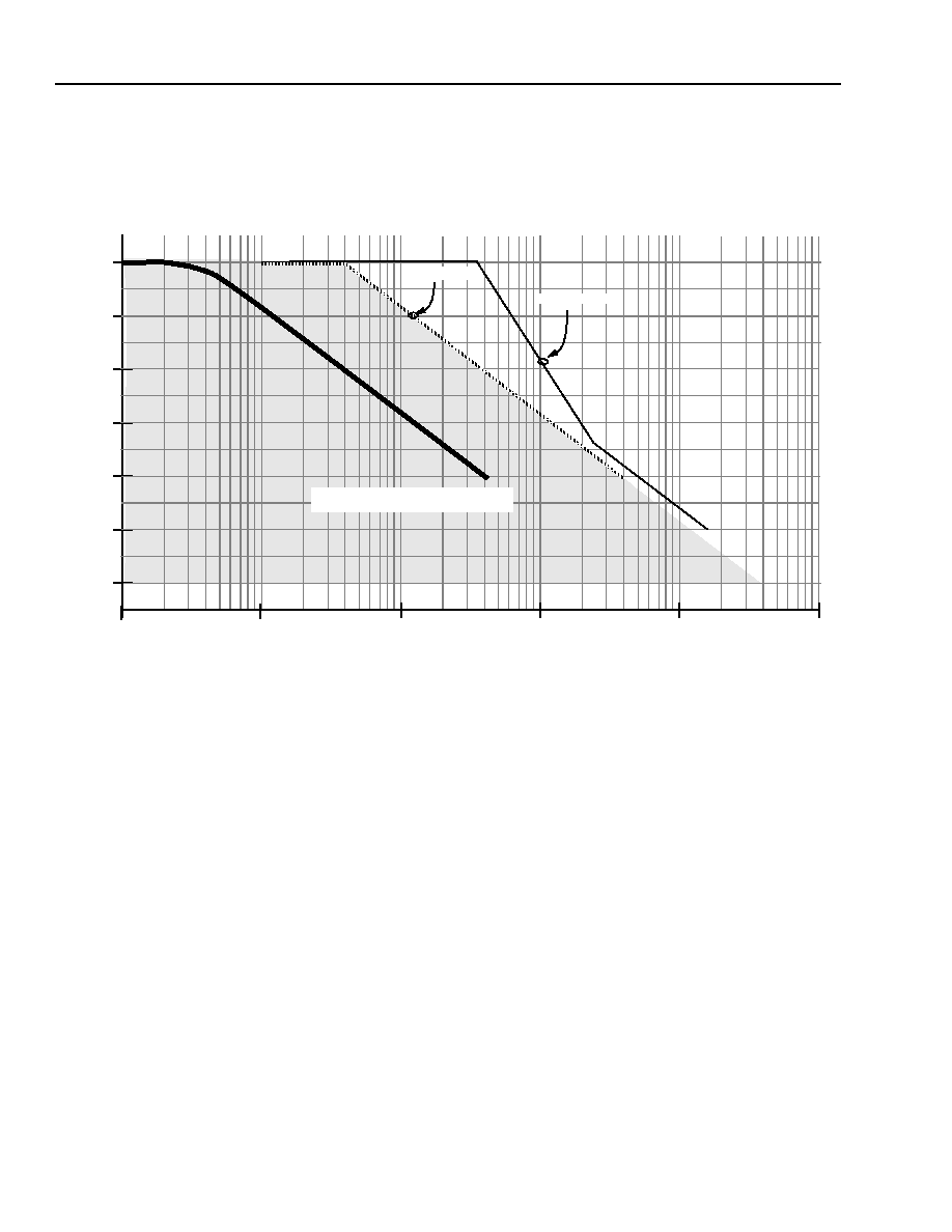
Advance Data Sheet, Rev. 2
TLIU04C1 Quad T1/E1 Line Interface
April 1999
86
Lucent Technologies Inc.
Direct Logic Control Mode
(continued)
Jitter Attenuator
(continued)
Frequency Response Curves (continued)
5-5265(F)r.4
Figure 34. DS1/T1 Jitter Transfer of the Jitter Attenuator
60
40
20
0
1
10
100
1k
10k
50
30
10
100k
FREQUENCY (Hz)
J
I
T
T
ER
OUT/
JI
TTE
R I
N
(
d
B)
TYPICAL
(SUBJECT TO DEVICE CHARACTERIZATION)
TR-TSY-000009
GR-253-CORE
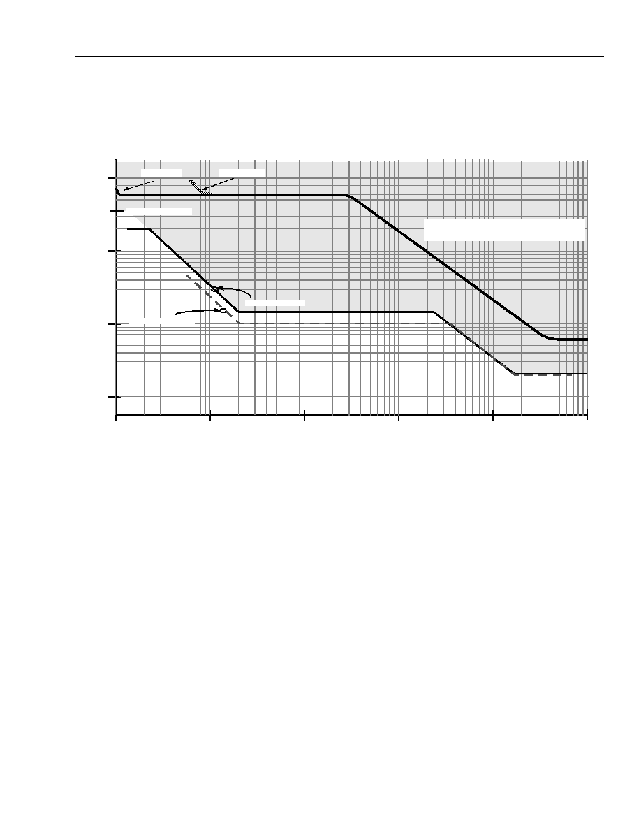
Advance Data Sheet, Rev. 2
April 1999
TLIU04C1 Quad T1/E1 Line Interface
87
Lucent Technologies Inc.
Direct Logic Control Mode
(continued)
Jitter Attenuator
(continued)
Frequency Response Curves (continued)
5-5266(F)r.8
Figure 35. CEPT/E1 Receiver Jitter Accommodation with Jitter Attenuator
0.1 UI
1.0 UI
10 UI
100 UI
10
100
1k
10k
1
37 UI
FREQUENCY (Hz)
G.823
100k
TYPICAL
(SUBJECT TO DEVICE CHARACTERIZATION)
G.823,ETSI-300-011A1
I.431(CEPT)/ETS-300-011
I.431(CEPT)/ETS-300-011
JABW0 = 0
JABW0 = 1

Advance Data Sheet, Rev. 2
TLIU04C1 Quad T1/E1 Line Interface
April 1999
88
Lucent Technologies Inc.
Direct Logic Control Mode
(continued)
Jitter Attenuator
(continued)
Frequency Response Curves (continued)
5-5267(F)r.4
Figure 36. CEPT/E1 Jitter Transfer of the Jitter Attenuator
FREQUENCY (Hz)
J
I
TTE
R OUT/
J
ITT
ER
IN (
d
B
)
60
40
20
0
1
10
100
1k
10k
50
30
10
100k
TYPICAL
(SUBJECT TO DEVICE CHARACTERIZATION)
JABW0 = 1
JABW0 = 0
ETSI TBR12/13
ETSI-300-011
I.431, G.735-9 WITH JITTER REDUCER
G.735-9 AT NATIONAL BOUNDARIES

Advance Data Sheet, Rev. 2
April 1999
TLIU04C1 Quad T1/E1 Line Interface
89
Lucent Technologies Inc.
Direct Logic Control Mode
(continued)
Loopbacks
The device has three independent loopback paths that
are activated using the FLLOOP, RLOOP, and DLLOOP
pins. The locations of these loopbacks are illustrated in
Figure 26.
Full Local Loopback (FLLOOP)
A full local loopback (FLLOOP) connects the transmit
line driver input to the receiver analog front-end cir-
cuitry. Valid transmit output data continues to be sent to
the network. If the transmit AIS (all-ones signal) is sent
to the network, the looped data is not affected. The
ALOS alarm continues to monitor the receive line inter-
face signal while DLOS monitors the looped data.
Remote Loopback (RLOOP)
A remote loopback (RLOOP) connects the recovered
clock and retimed data to the transmitter at the system
interface and sends the data back to the line. The
receiver front end, clock/data recovery, encoder/
decoder (if enabled) jitter attenuator (if enabled), and
transmit driver circuitry are all exercised during this
loopback. The transmit clock, transmit data, and XAIS
inputs are ignored. Valid receive output data continues
to be sent to the system interface. This loopback mode
is very useful for isolating failures between systems.
Digital Local Loopback (DLLOOP)
A digital local loopback (DLLOOP) connects the trans-
mit clock and data through the encoder/decoder pair to
the receive clock and data output pins at the system
interface. This loopback is operational if the encoder/
decoder pair is enabled or disabled. The AIS signal can
be transmitted without any effect on the looped signal.
Powerdown (PWRDN)
Each line interface channel has an independent power-
down mode controlled by PWRDN. This provides
power savings for systems that use backup channels. If
PWRDN = 1, the corresponding channel will be in a
standby mode, consuming only a small amount of
power. If a line interface channel in powerdown mode
needs to be placed into service, the channel should be
turned on (PWRDN = 0) approximately 5 ms before
data is applied.
Reset (RESET)
The device provides a hardware reset (
RESET
; pin 44).
When the device is in reset, all signal-path and alarm
monitor states are initialized to a known starting config-
uration. During a reset condition, data transmission will
be interrupted.
The reset condition is initiated by setting
RESET
= 0 for
a minimum of 10 µs. On coming out of the reset condi-
tion (RESET = 1), a time of at least 2.7 ms should be
allowed to ensure stabilization of the PLL.
Loss of XCLK Reference Clock (LOXC)
The LOXC output (pin 45) is active when the XCLK ref-
erence clock (pin 46) is absent. The LOXC flag is
asserted a maximum of 16 µs after XCLK disappears,
and deasserts immediately after detecting the first
clock edge of XCLK.
During the LOXC alarm condition, the clock recovery
and jitter attenuator functions are automatically dis-
abled. Therefore, if CDR = 1 and/or JAR = 1, the RCLK,
RPD, RND, and DLOS outputs will be unknown. If CDR
= 0, there will be no effect on the receiver. If the jitter
attenuator is enabled in the transmit path (JAT = 1) dur-
ing this alarm condition, then a loss of transmit clock
alarm, LOTC = 1, will also be indicated.
In-Circuit Testing and Driver High-Imped-
ance State (ICT)
The affect of asserting the
ICT
input (pin 43) is that all
output buffers (TTIP, TRING, RCLK, RPD, RND, LOXC,
RDY_
DTACK
, INT, AD[7:0]) are placed in a high-imped-
ance state. The TTIP and TRING outputs have a limit-
ing high-impedance capability of approximately 8 k
.
LIU Delay Values
The transmit coder has 5 UI delay whether it is in the
path or not and whether it is B8ZS or HDB3. Its delay is
only removed when in single-rail mode. The remainder
of the transmit path has 4.6 UI delay. The receive
decoder has 5 UI delay whether it is in the path or not
and whether it is B8ZS or HDB3. Its delay is only
removed when in single-rail mode or CDR = 0. The
AFE (equalizer plus slicer) delay is nearly 0 UI delay.
The jitter attenuator delay is nominally 33 UI but can be
2 UI--64 UI depending on the state. The DPLL used for
timing recovery has 8 UI delay.

Advance Data Sheet, Rev. 2
TLIU04C1 Quad T1/E1 Line Interface
April 1999
90
Lucent Technologies Inc.
Direct Logic Control Mode
(continued)
Line Encoding/Decoding
Alternate Mark Inversion (AMI)
The default line code used for T1 is alternate mark inversion (AMI). The coding scheme represents a 1 with a pulse
or mark on the positive or negative rail and a 0 with no pulse on either rails. This scheme is shown in Table 49.
Table 49. AMI Encoding
The T1 ones density rule requires that in every 24 bits of information to be transmitted, there must be at least three
pulses, and no more than 15 zeros may be transmitted consecutively.
AT&T Technical Reference 62411 for digital transmissions requires that in every 8 bits of information, at least one
pulse must be present.
T1-Binary 8 Zero Code Suppression
Clear channel transmission can be accomplished using Binary 8 Zero Code Suppression (B8ZS). Eight consecu-
tive zeros are replaced with the B8ZS code. This code consists of two bipolar violations in bit positions 4 and 7 and
valid bipolar marks in bit positions 5 and 8. The receiving end recognizes this code and replaces it with the original
string of eight zeros. Table 50 shows the encoding of a string of zeros using B8ZS. B8ZS is recommended when
ESF format is used.
Table 50. DS1 B8ZS Encoding
High-Density Bipolar of Order 3 (HDB3)
The line code used for CEPT is described in ITU Rec. G.703 Section 6.1 as high-density bipolar of order 3 (HDB3).
HDB3 uses a substitution code that acts on strings of four zeros. The substitute HDB3 codes are 000V and B00V,
where V represents a violation of the bipolar rule and B represents as inserted pulse conforming to the AMI rule
defined in ITU Rec. G.701, item 9004. The choice of the B00V or 000V is made so that the number of B pulses
between consecutive V pulses is odd. In other words, successive V pulses are of alternate polarity so that no direct
current (dc) component is introduced. The substitute codes follow each other if the string of zeros continues. The
choice of the first substitute code is arbitrary. A line code error is defined as a bipolar violation and consists of two
pulses of the same polarity that is not defined as one of the two substitute codes. Both excessive zeros and coding
violations are indicated as bipolar violations. An example is shown in Table 51.
Table 51. ITU HDB3 Coding and DCPAT Binary Coding
Input Bit Stream
1011
0000
0111
1010
AMI Data
≠0+≠
0000
0+≠+
≠0+0
Bit Positions
1
2
3
4
5
6
7
8
--
--
--
1
2
3
4
5
6
7
8
Before B8ZS
0
0
0
0
0
0
0
0
1
0
1
0
0
0
0
0
0
0
0
After B8ZS
0
0
0
V
B
0
V
B
B
0
B
0
0
0
V
B
0
V
B
Input Bit Stream
1011
0000
01
0000
0000
0000
0000
HDB3-Coded Data
1011
000V
01
000V
B00V
B00V
B00V
HDB3-Coded Levels
≠0+≠
000≠
0+
000+
≠00≠
+00+
≠00≠

Advance Data Sheet, Rev. 2
April 1999
TLIU04C1 Quad T1/E1 Line Interface
91
Lucent Technologies Inc.
Direct Logic Control Mode
(continued)
XCLK Reference Clock
The device requires an externally applied clock, XCLK (pin 46), for the clock and data recovery function and the jit-
ter attenuation option. XCLK must be a continuously active (i.e., ungapped, unjittered, and unswitched) and an
independent reference clock such as from an external system oscillator or system clock for proper operation. It
must not be derived from any recovered line clock (i.e., from RCLK or any synthesized frequency of RCLK).
XCLK may be supplied in one of four formats: 16x DS1, DS1, 16x CEPT, or CEPT. The format is selected globally
for the device by CLKS (pin 117) and CLKM (pin 116).
CLKS determines the relationship between the primary line data rate and the clock signal applied to XCLK. For
CLKS = 0, a clock at 16x the primary line data rate clock (24.704 MHz for DS1 and 32.768 MHz for CEPT) must be
applied to XCLK. For CLKS = 1, a primary line data rate clock (1.544 MHz for DS1 and 2.048 MHz for CEPT) must
be applied to XCLK.
The CLKS pin has an internal pull-down resistor allowing the pin to be left open, i.e., a no connect, in applications
using a 16x reference clock. The CLKS pin must be pulled up to V
DD
for applications using a primary line data rate
clock.
CLKM determines whether the clock synthesizer is operating in CEPT or DS1 mode when XCLK is a primary line
data rate clock. For CLKM = 0, the clock synthesizer operates in DS1 mode (1.544 MHz). For CLKM = 1, the clock
synthesizer operates in CEPT mode (2.048 MHz). The CLKM pin is ignored when CLKS = 0.
The CLKM pin has an internal pull-down resistor allowing the pin to be left open, i.e., a no connect, in applications
using a DS1 line rate reference clock. The CLKM pin must be pulled up to V
DD
for applications using a CEPT line
data rate clock.
16x XCLK Reference Clock
The specifications for XCLK using a 16x reference clock are defined in Table 52. The 16x reference clock is
selected when CLKS = 0.
Table 52. XCLK (16x, CLKS = 0) Timing Specifications
* When JABW0 = 1 and the jitter attenuator is used in the receive data path, the tolerance on XCLK should be tightened to ±20 ppm in order to
meet the jitter accommodation requirements of TBR12/13 as given in G.823 for line data rates of ±50 ppm.
If XCLK is used as the source for AIS (see Alarm Indication Signal Generator (XAIS) on page 79), it must meet the nominal transmission
specifications of 1.544 MHz ± 32 ppm for DS1 (T1) or 2.048 MHz ± 50 ppm for CEPT (E1).
Parameter
Value
Unit
Min
Typ
Max
Frequency:
DS1
CEPT
--
--
24.704
32.768
--
--
MHz
MHz
Range*,
≠100
--
100
ppm
Duty Cycle
40
--
60
%

Advance Data Sheet, Rev. 2
TLIU04C1 Quad T1/E1 Line Interface
April 1999
92
Lucent Technologies Inc.
Direct Logic Control Mode
(continued)
XCLK Reference Clock
(continued)
Primary Line Rate XCLK Reference Clock and Internal Reference Clock Synthesizer
In some applications, it is more desirable to provide a reference clock at the primary data rate. In such cases, the
LIU can utilize an internal 16x clock synthesizer allowing the XCLK pin to accept a primary data rate clock. The
specifications for XCLK using a primary rate reference clock are defined in Table 53.
Table 53. XCLK (1x, CLKS = 1) Timing Specifications
* When JABW0 = 1 and the jitter attenuator is used in the receive data path, the tolerance on XCLK should be tightened to ±20 ppm in order to
meet the jitter accommodation requirements of TBR12/13 as given in G.823 for line data rates of ±50 ppm.
If XCLK is used as the source for AIS (see Alarm Indication Signal Generator (XAIS) on page 79), it must meet the nominal transmission
specifications of 1.544 MHz ± 32 ppm for DS1 (T1) or 2.048 MHz ± 50 ppm for CEPT (E1).
The data rate reference clock and the internal clock synthesizer is selected when CLKS = 1. In this mode, a valid
and stable data rate reference clock must be applied to the XCLK pin before and during the time a hardware reset
is activated (RESET = 0). The reset must be held active for a minimum of two data rate clock periods to ensure
proper resetting of the clock synthesizer circuit. Upon the deactivation of the reset pin (RESET = 1), the LIU will
extend the reset condition internally for approximately 1/2(2
12
≠ 1) line clock periods, or 1.3 ms for DS1 and
1 ms for CEPT after the hardware reset pin has become inactive, allowing the clock synthesizer additional time to
settle. No activity such as microprocessor read/write should be performed during this period. The device will be
operational 2.7 ms after the deactivation of the hardware reset pin. Issuing an LIU software restart (LIU_REG2
bit 5 (RESTART) = 1) does not impact the clock synthesizer circuit.
The choices for XCLK are summarized in Table 54.
Table 54. XCLK Specifications
* To meet TBR 12/13 for jitter accommodation.
Parameter
Value
Unit
Min
Typ
Max
Frequency:
DS1
CEPT
--
--
1.544
2.048
--
--
MHz
MHz
Range*,
≠100
--
100
ppm
Duty Cycle
40
--
60
%
Rise and Fall Times
(10%--90%)
--
--
5
ns
CLKS
CLKM
JABW0*
Mode
Specifications
0
0
0
16x DS1
24.740 MHz ± 32 ppm
0
1
0
16x CEPT
32.768 MHz ± 50 ppm
0
1
1
16x CEPT
32.768 MHz ± 20 ppm
1
0
0
DS1
1.544 MHz ± 32 ppm
1
1
0
CEPT
2.048 MHz ± 50 ppm
1
1
1
CEPT
2.048 MHz ± 20 ppm

Advance Data Sheet, Rev. 2
April 1999
TLIU04C1 Quad T1/E1 Line Interface
93
Lucent Technologies Inc.
Direct Logic Control Mode
(continued)
Power Supply Bypassing
External bypassing is required for all channels. A 1.0 µF capacitor must be connected between V
DDX
and GND
X
. In
addition, a 0.1 µF capacitor must be connected between V
DDD
and GND
D
, and a 0.1 µF capacitor must be con-
nected between V
DDA
and GND
A
. Ground plane connections are required for GND
X
, GND
D
, and GND
A
. Power
plane connections are also required for V
DDX
and V
DDD
. The need to reduce high-frequency coupling into the ana-
log supply (V
DDA
) may require an inductive bead to be inserted between the power plane and the V
DDA
pin of every
channel.
Capacitors used for power supply bypassing should be placed as close as possible to the device pins for maximum
effectiveness.
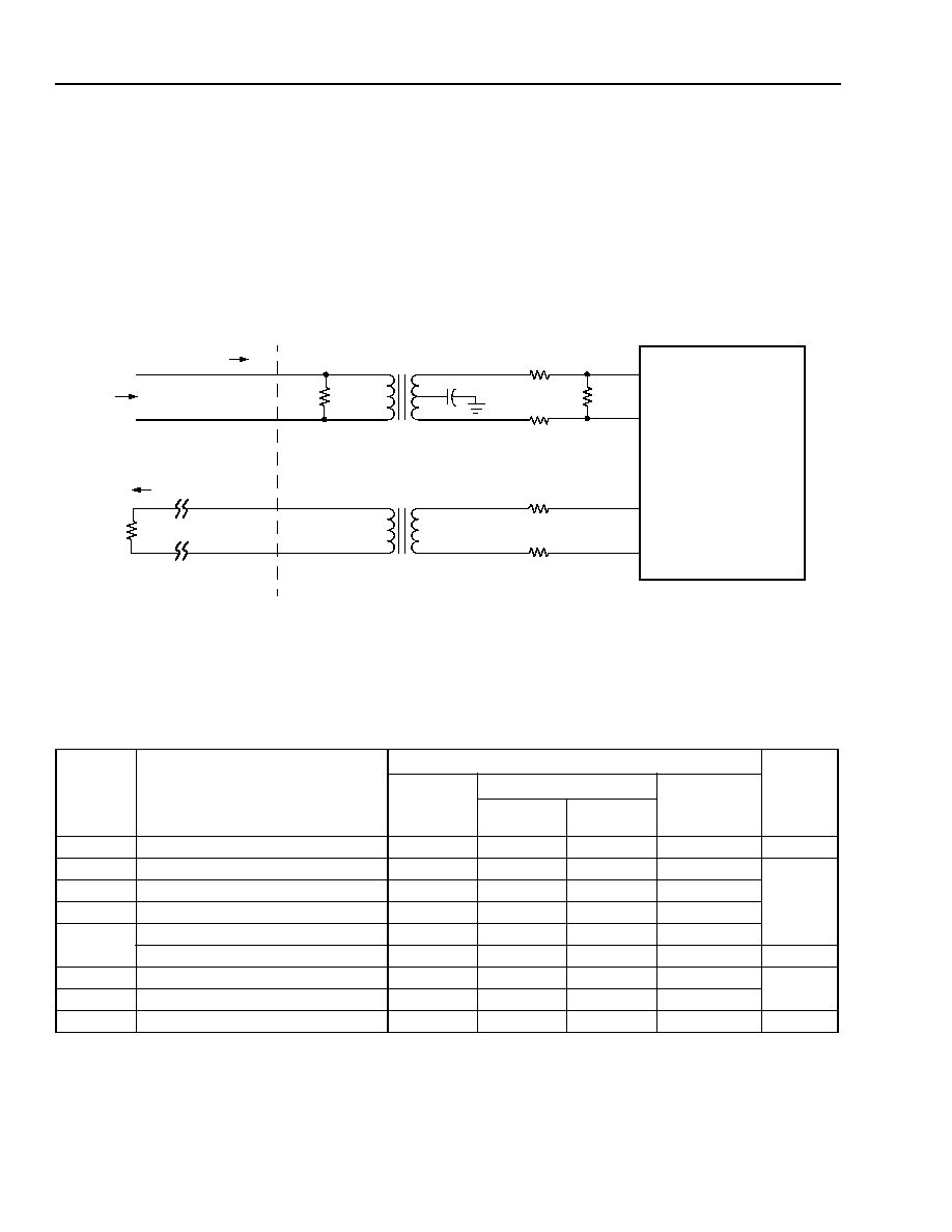
Advance Data Sheet, Rev. 2
TLIU04C1 Quad T1/E1 Line Interface
April 1999
94
Lucent Technologies Inc.
Direct Logic Control Mode
(continued)
Line Circuitry
The transmit and receive tip/ring connections provide a matched interface to the cable (i.e., terminating impedance
matches the characteristic impedance of the cable). The diagram in Figure 37 shows the appropriate external com-
ponents to interface to the cable for a single transmit/receive channel. The component values are summarized in
Table 55, based on the specific application.
5-3693(F).d
Figure 37. Line Termination Circuitry
Table 55. Termination Components by Application
Resistor tolerances are ±1%. Transformer turns ratio tolerances are ±2%.
1. Use Lucent 2795B transformer.
2. For CEPT 75
applications, Option 1 is recommended over Option 2 for lower device power dissipation. Option 2 increases power dissipa-
tion by 13 mW per channel when driving 50% ones data. Option 2 allows for the use of the same transformer as in CEPT 120
applica-
tions.
3. Use Lucent 2795D transformer.
4. Use Lucent 2795C transformer.
5. A ±5% tolerance is allowed for the transmit load termination, R
L
.
Symbol
Name
Cable Type
Unit
DS1
1
Twisted
Pair
CEPT 75
2
Coaxial
CEPT 120
4
Twisted Pair
Option 1
3
Option 2
4
C
C
Center Tap Capacitor
0.1
0.1
0.1
0.1
µ
F
R
P
Receive Primary Impedance
200
200
200
200
R
R
Receive Series Impedance
71.5
28.7
59
174
R
S
Receive Secondary Impedance
113
82.5
102
205
Z
EQ
Equivalent Line Termination
100
75
75
120
Tolerance
±4
±4 ±4
±4
%
R
T
Transmit Series Impedance
0
26.1
15.4
26.1
R
L
Transmit Load Termination
5
100
75
75
120
N
Transformer Turns Ratio
1.14
1.08
1.36
1.36
--
RTIP
RRING
TTIP
TRING
DEVICE
(1 CHANNEL)
R
L
R
S
R
R
R
R
RECEIVE DATA
R
P
Z
EQ
R
T
R
T
N:1
TRANSMIT DATA
TRANSFORMER
EQUIPMENT
INTERFACE
1:N
C
C

Advance Data Sheet, Rev. 2
April 1999
TLIU04C1 Quad T1/E1 Line Interface
95
Lucent Technologies Inc.
Direct Logic Control Mode
(continued)
Absolute Maximum Ratings
Stresses in excess of the absolute maximum ratings can cause permanent or latent damage to the device. These
are absolute stress ratings only. Functional operation of the device is not implied at these or any other conditions in
excess of those given in the operational sections of this device specification. Exposure to absolute maximum rat-
ings for extended periods can adversely affect device reliability.
Table 56. Absolute Maximum Ratings
Handling Precautions
Although protection circuitry has been designed into this device, proper precautions should be taken to avoid expo-
sure to electrostatic discharge (ESD) during handling and mounting. Lucent employs a human-body model (HBM)
and charged-device model (CDM) for ESD-susceptibility testing and protection design evaluation. ESD voltage
thresholds are dependent on the circuit parameters used in the defined model. No industry-wide standard has
been adopted for the CDM. However, a standard HBM (resistance = 1500
, capacitance = 100 pF) is widely used
and, therefore, can be used for comparison purposes. The HBM ESD threshold presented here was obtained by
using these circuit parameters.
Operating Conditions
Parameter
Min
Max
Unit
dc Supply Voltage
≠0.5
6.5
V
Storage Temperature
≠65
125
∞C
Maximum Voltage (digital pins) with Respect to V
DDD
--
0.5
V
Minimum Voltage (digital pins) with Respect to GND
D
≠0.5
--
V
Maximum Allowable Voltages (RTIP[1--4], RRING[1--4])
with Respect to V
DD
--
0.5
V
Minimum Allowable Voltages (RTIP[1--4], RRING[1--4])
with Respect to GND
≠0.5
--
V
Table 57. ESD Threshold Voltage
Device
Model
Voltage
TLIU04C1
HBM
TBD
CDM (corner pins)
TBD
CDM (noncorner pins)
TBD
Table 58. Recommended Operating Conditions
Parameter
Symbol
Min
Typ
Max
Unit
Ambient Temperature
T
A
≠40
--
85
∞C
Power Supply
V
DD
4.75
5.0
5.25
V

Advance Data Sheet, Rev. 2
TLIU04C1 Quad T1/E1 Line Interface
April 1999
96
Lucent Technologies Inc.
Direct Logic Control Mode
(continued)
Power Requirements
The majority of the power used by the TLIU04C1 device is used by the line drivers. Therefore, the power is very
dependent on data pattern and signal amplitude. The signal amplitude is a function of the transmit equalization in
DS1 mode. When configured for greater cable loss, the signal amplitude is greater at the output drivers, and thus
uses more power. For this reason, the power specification of Table 59 are given for various conditions. The typical
specification is for a quasi-random signal and the maximum specification is for a mark (all ones) pattern. The power
also varies somewhat for DS1 versus CEPT, so figures are given for both.
Table 59. Power Consumption
Power dissipation is the amount of power dissipated in the device. It is equal to the power drawn by the device
minus the power dissipated in the line.
Table 60. Power Dissipation
Electrical Characteristics
Parameter
Power
Unit
Typ
Max
CEPT
TBD
TBD
mW
DS1
TBD
TBD
mW
DS1 with Max Eq.
TBD
TBD
mW
Parameter
Power
Unit
Typ
Max
CEPT
TBD
TBD
mW
DS1
TBD
TBD
mW
DS1 with Max Eq.
TBD
TBD
mW
Table 61. Logic Interface Characteristics
Note: The following internal resistors are provided: 50 k
pull-up on the
ICT
and
RESET
pins, 50 k
pull-down on
the CLKS and CLKM pins, and 100 k
pull-up on the
CS
, and XCLK pins. This requires these input pins to
sink no more than 20 µA. The device uses TTL input and output buffers; all buffers are CMOS-compatible.
Parameter
Symbol
Test Conditions
Min
Max
Unit
Input Voltage:
Low
High
V
IL
V
IH
--
GND
D
2.1
0.8
V
DDD
V
V
Input Leakage
I
L
--
--
10
µA
Output Voltage:
Low
High
V
OL
V
OH
I
OL
= ≠5.0 mA
I
OH
= 5.0 mA
GND
D
V
DDD
≠ 0.5
0.4
V
DDD
V
V
Input Capacitance
C
I
--
--
3.0
pF
Load Capacitance
*
* 100 pF allowed for microprocessor mode AD[7:0] (pins 75--82).
C
L
--
--
50
pF
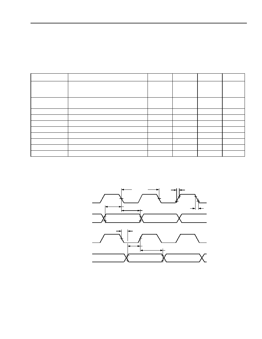
Advance Data Sheet, Rev. 2
April 1999
TLIU04C1 Quad T1/E1 Line Interface
97
Lucent Technologies Inc.
Direct Logic Control Mode
(continued)
Data Interface Timing
* Refers to each individual bit period for JAT = 0 applications.
Refers to each individual bit period for JAT = 1 applications using a gapped TCLK.
5-1156(F).br.3
* Invert RCLK for ACM = 1.
Figure 38. Interface Data Timing (ACM = 0)
Table 62. Data Interface Timing
Note: The digital system interface timing is shown in Figure 38 for ACM = 0. If ACM = 1, then the RCLK signal in
Figure 38 will be inverted.
Symbol
Parameter
Min
Typ
Max
Unit
tTCLTCL
Average TCLK Clock Period:
DS1
CEPT
--
--
647.7
488.0
--
--
ns
ns
tTDC
TCLK Duty Cycle*
TCLK Minimum High/Low Time
30
100
--
--
70
--
%
ns
tTDVTCL
Transmit Data Setup Time
50
--
--
ns
tTCLTDX
Transmit Data Hold Time
40
--
--
ns
tTCH1TCH2
Clock Rise Time (10%/90%)
--
--
40
ns
tTCL2TCL1
Clock Fall Time (90%/10%)
--
--
40
ns
tRCHRCL
RCLK Duty Cycle
45
50
55
%
tRDVRCH
Receive Data Setup Time
140
--
--
ns
tRCHRDX
Receive Data Hold Time
180
--
--
ns
tRCLRDV
Receive Propagation Delay
--
--
40
ns
TCLK-LIU
TPD-LIU
OR
TND-LIU
RCLK-LIU*
RPD-LIU
OR
RND-LIU
tTCH1TCH2
tTCL2TCL1
tTDVTCL
tTCLTDX
tRCLRDV
tRDVRCH
tRCHRDX
tTCLTCL
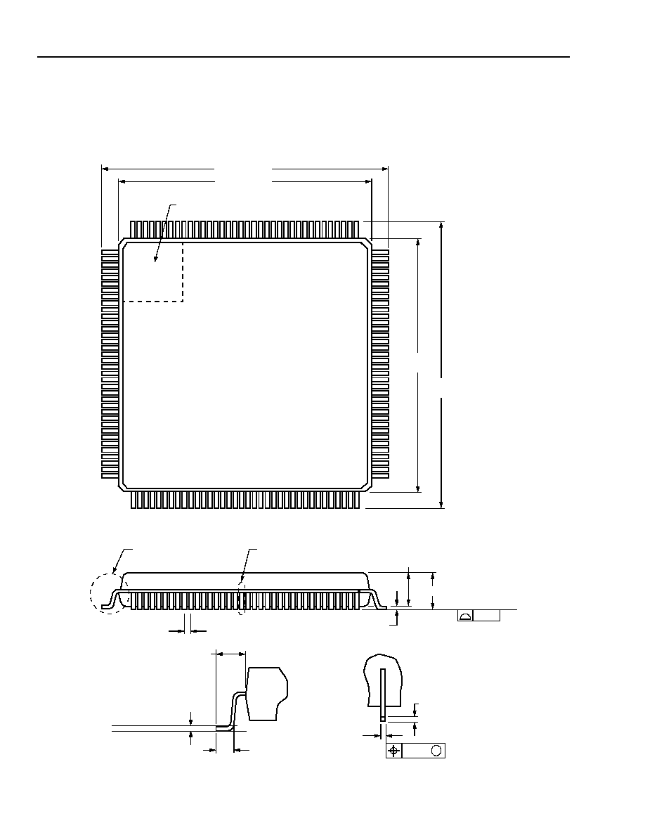
Advance Data Sheet, Rev. 2
TLIU04C1 Quad T1/E1 Line Interface
April 1999
98
Lucent Technologies Inc.
Outline Diagram
144-Pin TQFP
Dimensions are in millimeters.
5-3815(F)r.6
0.45/0.75
GAGE PLANE
SEATING PLANE
1.00 REF
0.25
0.19/0.27
0.08
M
0.106/0.200
1.60 MAX
SEATING PLANE
0.08
0.50 TYP
1.40
±
0.05
0.05/0.15
DETAIL A
DETAIL B
PIN #1 IDENTIFIER ZONE
20.00
±
0.20
22.00
±
0.20
109
144
1
36
37
72
73
108
20.00
±
0.20
22.00
±
0.20

Advance Data Sheet, Rev. 2
April 1999
TLIU04C1 Quad T1/E1 Line Interface
99
Lucent Technologies Inc.
Ordering Information
Device Code
Package
Temperature
Comcode (Ordering Number)
TLIU04C1
144-Pin TQFP
≠40 ∞C to +85 ∞C
108420761

Advance Data Sheet, Rev. 2
T7698 Quad T1/E1 Line Interface and Octal T1/E1 Monitor
April 1999
For additional information, contact your Microelectronics Group Account Manager or the following:
INTERNET:
http://www.lucent.com/micro
E-MAIL:
docmaster@micro.lucent.com
N. AMERICA:
Microelectronics Group, Lucent Technologies Inc., 555 Union Boulevard, Room 30L-15P-BA, Allentown, PA 18103
1-800-372-2447, FAX 610-712-4106 (In CANADA: 1-800-553-2448, FAX 610-712-4106)
ASIA PACIFIC: Microelectronics Group, Lucent Technologies Singapore Pte. Ltd., 77 Science Park Drive, #03-18 Cintech III, Singapore 118256
Tel. (65) 778 8833, FAX (65) 777 7495
CHINA:
Microelectronics Group, Lucent Technologies (China) Co., Ltd., A-F2, 23/F, Zao Fong Universe Building, 1800 Zhong Shan Xi Road, Shanghai
200233 P. R. China Tel. (86) 21 6440 0468, ext. 316, FAX (86) 21 6440 0652
JAPAN:
Microelectronics Group, Lucent Technologies Japan Ltd., 7-18, Higashi-Gotanda 2-chome, Shinagawa-ku, Tokyo 141, Japan
Tel. (81) 3 5421 1600, FAX (81) 3 5421 1700
EUROPE:
Data Requests: MICROELECTRONICS GROUP DATALINE: Tel. (44) 1189 324 299, FAX (44) 1189 328 148
Technical Inquiries: GERMANY: (49) 89 95086 0 (Munich), UNITED KINGDOM: (44) 1344 865 900 (Ascot),
FRANCE: (33) 1 40 45 77 00 (Paris), SWEDEN: (46) 8 594 607 00 (Stockholm), FINLAND: (358) 9 4354 2800 (Helsinki),
ITALY: (39) 02 6608131 (Milan), SPAIN: (34) 1 807 1441 (Madrid)
Lucent Technologies Inc. reserves the right to make changes to the product(s) or information contained herein without notice. No liability is assumed as a result of their use or application. No
rights under any patent accompany the sale of any such product(s) or information.
Copyright © 1999 Lucent Technologies Inc.
All Rights Reserved
April 1999
DS99-158T1E1-02 (Replaces DS99-158T1E1-01)