 | –≠–ª–µ–∫—Ç—Ä–æ–Ω–Ω—ã–π –∫–æ–º–ø–æ–Ω–µ–Ω—Ç: TMUX03155 | –°–∫–∞—á–∞—Ç—å:  PDF PDF  ZIP ZIP |
Document Outline
- Features
- Applications
- Description
- Nomenclature Assumptions
- Block Diagram
- Pin Information
- Mode Control Signals (See Register Description on page 54.)
- STS-1 Mode
- Transmit Direction Overview
- Receive Direction Overview
- Maintenance Functions
- Typical Uses
- Microprocessor Interface
- Absolute Maximum Ratings
- Handling Precautions
- Operating Conditions
- Electrical Characteristics
- Timing Characteristics
- Outline Diagram
- Ordering Information
- DS01-194PDH Replaces DS00-213TIC to Incorporate the Following Updates
- List of Figures
- List of Tables
- Table 1. Pin Descriptions for the 208-Pin SQFP Package
- Table 2. Input/Output Summary
- Table 3. Transmit Mode Control Signals
- Table 4. Receive Mode Control
- Table 5. Input Select Control
- Table 6. Expected STS-1/AU-3 Input Frame Format
- Table 7. STS-3 Output Overhead Format
- Table 8. STM-1 (AU-4) Output Overhead Format
- Table 9. STS-1/AU-3 Format and Overhead Control Summary
- Table 10. STS-1/AU-3 Output Select Control
- Table 11. Monitors Disabled During Failure Conditions
- Table 12. SFEBE Values
- Table 13. G1 ByteÑAU-4 Mode Only
- Table 14. PFEBE Values
- Table 15. Value Offset Load Values
- Table 16. Transport Overhead Byte AccessÑTransmit Direction
- Table 17. TTOAC Control Bits
- Table 18. STS-1/AU-3 Overhead Control
- Table 19. Transport Overhead Byte AccessÑReceive Direction
- Table 20. Microprocessor Configuration Modes
- Table 21. MODE [1Ñ4] Microprocessor Pin Definitions
- Table 22. Device-Level Register Map
- Table 23. Page 0ÑJ1 Byte Insert and Monitor
- Table 24. Page 1ÑError Counters
- Table 25. Page 2ÑBER Algorithm Parameters
- Table 26. Register 0 (RO)
- Table 27. Registers 1Ñ3 (RO)
- Table 28. Registers 4, 5: One-Shot Register 0 ∆ 1 (R/W)
- Table 29. Register 6: Scratch Register (R/W)
- Table 30. Registers 7Ñ15: Delta/Event (COR-RO)
- Table 31. Registers 16Ñ24: Mask Bits (R/W)
- Table 32. Registers 25Ñ51: State Bits (RO)
- Table 33. Register 52: Mode Control (R/W)
- Table 34. Register 53: Low-Speed Transmit Common Signals (R/W)
- Table 35. Register 54Ñ59: Transmit Low-Speed Port Input Control (R/W)
- Table 36. Registers 60, 61: Transmit High-Speed Clock/Port Control (R/W)
- Table 37. Register 62: Transmit High-Speed Control Signals (R/W)
- Table 38. Register 62, and Page 0, Registers 128Ñ191: Transmit High-Speed J1 Insert (R/W)
- Table 39. Register 62, 69: Transmit High-Speed Control Signals (R/W)
- Table 40. Register 62, 66: Transmit High-Speed Control Signals (R/W)
- Table 41. Registers 63Ñ65: Trace/Growth Bytes (R/W)
- Table 42. Register 66: Transmit F1 Data Byte (R/W)
- Table 43. Registers 67 and 68: K1 and K2 Insert Bytes (R/W)
- Table 44. Register 69: Transmit Sync Status Byte (R/W)
- Table 45. Register 70: Path Signal Trace Byte (R/W)
- Table 46. Register 71: Path User Channel Byte (R/W)
- Table 47. Register 72: Path Growth Byte (R/W)
- Table 48. Register 73: Tandem Connection Byte (R/W)
- Table 49. Register 74: Transmit High-Speed Line RDI Insertion Inhibit Bits (R/W)
- Table 50. Register 75: Transmit High-Speed Path RDI Insertion Inhibit Bits (R/W)
- Table 51. Register 76: Transmit High-Speed Error Insert Control Parameters (R/W)
- Table 52. Register 77: Transmit High-Speed Error Insert Control Parameters (R/W)
- Table 53. Register 78: Transmit High-Speed Error Insert (R/W)
- Table 54. Register 79: Receive/Transmit TOAC Control (R/W)
- Table 55. Registers 80, 81: Transmit TOAC Control (R/W)
- Table 56. Register 83, 84: Transmit High-Speed STS-3/STM-1 Output Frame Offset (R/W)
- Table 57. A1-1 Alignment Parameters
- Table 58. BITCNT Alignment Table
- Table 59. Register 85: Receive High/Low-Speed Port Control (R/W)
- Table 60. Register 86: Receive J1 and Receive Low-Speed Port Select Control (R/W)
- Table 61. Register 87: STS-1/AU-3 Receive Control Bits (R/W)
- Table 62. Register 88: STS-1/AU-3 Receive Low-Speed AIS Inhibit Control Bits (R/W)
- Table 63. Registers 88, 89: STS-1/AU-3 Loss of Signal Detector (R/W)
- Table 64. Register 90Ñ95: Continuous N Times Detect (CNTD) Values (R/W)
- Table 65. Register 95: Continuous N Times Detect (CNTD) B1 Control Bit (R/W)
- Table 66. Register 96: Test Pattern Drop Control and Status
- Table 67. Register 97: Test Pattern Drop Error Counter (RO)
- Table 68. Register 98: Receive Low-Speed Overhead Control Bits (R/W)
- Table 69. Register 99: Receive Low-Speed BIP Error Insert (R/W)
- Table 70. Registers 100Ñ102: Receive Low-Speed Overhead Control Bits (R/W)
- Table 71. Register 103: Receive Low-Speed L-RDI Inhibit Control (R/W)
- Table 72. Registers 104Ñ106: Receive Low-Speed C1 Byte (R/W)
- Table 73. Registers 107Ñ109: Receive Low-Speed F1 Byte (R/W)
- Table 74. Registers 110Ñ115: Receive Low-Speed K1, K2 Byte Insert (R/W)
- Table 75. Registers 116Ñ118: Receive Low-Speed Pass Control (R/W)
- Table 76. Register 127: Page Control Register (R/W)
- Table 77. Page 0 - Registers 128Ñ191: J1 Insert Parameters (R/W)
- Table 78. Page 0 - Registers 192Ñ255: J1 Monitor Bytes (RO)
- Table 79. Page 1 - Registers 128Ñ133: STS-1/AU-3 B1 BIP Error Counters (RO)
- Table 80. Page 1 - Registers 134Ñ140: STS-1/AU-3 B2 BIP Error Counters (RO)
- Table 81. Page 1 - Registers 141Ñ142: STS-3/STM-1 (AU-4) B1 Error Count (RO)
- Table 82. Page 1 - Registers 143Ñ145: STS-3/STM-1 (AU-4) B2 Error Count (RO)
- Table 83. Page 1 - Registers 146Ñ151: STS-3/STM-1 (AU-4) B3 Error Count (RO)
- Table 84. Page 1 - Registers 152Ñ163: STS-3/STM-1 (AU-4) Pointer Increment/Decrement Counter (RO)
- Table 85. Page 1 - Registers 164Ñ166: Receive High-Speed SFEBE Count (RO)
- Table 86. Page 1 - Registers 167Ñ172: Receive High-Speed Path FEBE Count (RO)
- Table 87. Page 2 - Register 131 (R/W)
- Table 88. Page 2 - Registers 128Ñ141 (R/W)
- Table 89. Page 2 - Register 145 (R/W)
- Table 90. Page 2 - Registers 142Ñ155 (R/W)
- Table 91. Microprocessor Interface I/O Timing Specifications
- Table 92. Recommended Operating Conditions
- Table 93. Power Measurements (VDD = 3.3 V, 23 ∞C)
- Table 94. Logic Interface Characteristics
- Table 95. LVDS Interface Characteristics
- Table 96. Input Clock Specifications
- Table 97. Input Timing Specifications
- Table 98. Output Clock Specifications
- Table 99. Output Timing Specifications
- Contact Us
Preliminary Data Sheet
April 2001
TMUX03155 STS-3/STM-1 (AU-4) Multiplexer/Demultiplexer
Features
I
Multiplexes three STS-1 signals into a SONET
STS-3 signal.
I
Multiplexes three AU-3 signals into an SDH STM-1
(AU-4) signal via a TUG-3 construction.
I
Demultiplexes three STS-1 signals from a SONET
STS-3 signal.
I
Demultiplexes three AU-3 signals from an SDH
STM-1 (AU-4) signal via a TUG-3 deconstruction.
I
High-speed microprocessor interface configurable
to operate with most commercial microprocessors.
I
Detects STS-3/STM-1 (AU-4) loss-of-signal (LOS)
conditions.
I
Detects STS-3/STM-1 (AU-4) out-of-frame and
loss-of-frame (OOF/LOF) conditions.
I
Provides an 8-bit bus interface at the STS-1/AU-3
rate.
I
Provides a bit serial, nibble-wide, or byte-wide
interface at STS-3/STM-1 (AU-4) rate.
I
Provides STS-3/STM-1 (AU-4) selectable scram-
bler/descrambler functions and B1/B2/B3 genera-
tion/detection.
I
Accepts bit rate, nibble rate, or byte rate high-
speed clocks (155.52 MHz, 38.88 MHz, or
19.44 MHz, respectively).
I
STS-3/STM-1 (AU-4) internal clock and data
recovery. Meets type B jitter tolerance of ITU-T
G.958. Accommodates 0.5 UI jitter up to 20 MHz.
155.52 MHz input reference clock for on-chip PLL.
Has on-chip PLL for clock synthesis, requiring only
one external resistor. No output clock drift in
absence of data transitions once lock is acquired.
I
STS-1 termination mode.
I
≠40 ∞C to +85 ∞C temperature range.
I
208-pin, shrink quad flat pack (SQFP) package.
I
Complies with GR-253-CORE (12/95), G.707
(3/96), G.783(1/94).
Applications
I
SONET/SDH line termination equipment.
I
SDH path origination and termination equipment.
I
SONET/SDH add/drop multiplexers.
I
SONET/SDH cross connects.
I
SONET/SDH test equipment.
Description
The TMUX03155 STS-3/STM-1 (AU-4) multiplexer
device provides three modes of operation: STS-3,
STM-1 (AU-4), and STS-1
modes. In STS-3 mode,
the TMUX03155 device provides all of the functions
necessary to multiplex and demultiplex up to three
STS-1 signals to/from a SONET STS-3 signal. In
AU-4 mode, the TMUX03155 provides the functional-
ity to multiplex and demultiplex up to three AU-3 sig-
nals to/from an STM-1 (AU-4) signal. In STS-1 mode,
the high-speed side of the TMUX03155 operates at
51.84 MHz and can be used for STS-1 termination
and for accessing transport overhead in the SONET
frame.
On the STS-3/STM-1 (AU-4) side, the device
can be configured for either a 1-bit serial data inter-
face, a 4-bit parallel (nibble-wide) data interface, or
an 8-bit parallel (byte-wide) data interface. This
allows the device to drive an OC3 optical signal
directly or to allow for modular growth in terminal or
add/drop applications. On the STS-1/AU-3 side, the
TMUX03155 device provides a bus mode that can
communicate with up to three STS-1/AU-3 devices at
19.44 Mbits/s. The TMUX03155 is designed to inter-
face with the Agere Systems Inc. TMPR28051
device, or equivalent, providing complete mapping/
unmapping from/to an STS-3/STM-1 (AU-4) signal
for up to 84 DS1 or 63 E1 signals.

Table of Contents
Contents
Page
2
Agere Systems Inc.
Preliminary Data Sheet
April 2001
TMUX03155 STS-3/STM-1 (AU-4) Multiplexer/Demultiplexer
Features ...................................................................................................................................................................1
Applications ..............................................................................................................................................................1
Description ................................................................................................................................................................1
Nomenclature Assumptions ......................................................................................................................................7
Block Diagram ..........................................................................................................................................................7
Pin Information .........................................................................................................................................................9
Summary of I/O Pins .........................................................................................................................................15
Mode Control Signals (See Register Description on page 54.) ..............................................................................16
STS-1 Mode ...........................................................................................................................................................16
Transmit Direction Overview ..................................................................................................................................17
STS-1/AU-3 Bus Mode Input Retiming ..............................................................................................................17
Input Select Control ...........................................................................................................................................17
STS-1/AU-3 Inputs ............................................................................................................................................17
Out-of-Frame (OOF) and Loss-of-Frame (LOF) Monitoring ..............................................................................18
Descramble Enable/Disable ..............................................................................................................................18
Monitor B1 and B2 Errors ..................................................................................................................................19
H4 Multiframe and Pointer Monitor (AU-4 Mode Only) ......................................................................................19
STS-3 Generate ................................................................................................................................................20
Transport Overhead Access Channel (TOAC) Insert ........................................................................................23
STS-3/STM-1 (AU-4) Scramble Enable ............................................................................................................23
STS-3/STM-1 (AU-4) B1, B2, and B3 BIP Generation ......................................................................................23
STS-3/STM-1 (AU-4) Loopback Control ............................................................................................................23
STS-3/STM-1 (AU-4) Output Interface ..............................................................................................................23
Receive Direction Overview ...................................................................................................................................23
Input Retime ......................................................................................................................................................24
Clock and Data Recovery ..................................................................................................................................24
STS-3/STM-1 (AU-4) Framing ...........................................................................................................................24
Loss of Signal ....................................................................................................................................................24
Loopback Select Logic ......................................................................................................................................25
RSTS-3/STM-1 (AU-4) Frame Synchronous Descrambling (SONET/SDH) .....................................................25
TOAC Drop ........................................................................................................................................................25
B1, B2, and B3 Checking ..................................................................................................................................25
Monitoring Functions .........................................................................................................................................25
Pointer Interpretation .........................................................................................................................................25
Data Demultiplex and Conversion (AU-4 Mode Only) .......................................................................................26
STS-1/AU-3 Output Byte Control ......................................................................................................................26
B1 and B2 Generate ..........................................................................................................................................26
STS-1/AU-3 Output Scramble ...........................................................................................................................27
Output Selection Logic ......................................................................................................................................27
Output Data Formatter ......................................................................................................................................27
Maintenance Functions ..........................................................................................................................................27
Maintenance Functions Disabled During Failure Conditions .............................................................................28
Common Maintenance and Control Functions ..................................................................................................28
Transmit Functions ............................................................................................................................................30
Receive Functions .............................................................................................................................................38
Typical Uses ...........................................................................................................................................................45
Section and Line Termination Multiplex ............................................................................................................45
Add/Drop Multiplex ............................................................................................................................................46
Digital Cross Connect ........................................................................................................................................46
Microprocessor Interface ........................................................................................................................................47
Overview ...........................................................................................................................................................47

Table of Contents
(continued)
Contents
Page
Agere Systems Inc.
3
Preliminary Data Sheet
April 2001
TMUX03155 STS-3/STM-1 (AU-4) Multiplexer/Demultiplexer
Microprocessor Configuration Modes ................................................................................................................47
Microprocessor Interface Pinout Descriptions ...................................................................................................47
Microprocessor Interface Register Architecture ................................................................................................49
Register Description ..........................................................................................................................................54
I/O Timing ........................................................................................................................................................101
Absolute Maximum Ratings ..................................................................................................................................106
Handling Precautions ...........................................................................................................................................106
Operating Conditions ............................................................................................................................................107
Electrical Characteristics ......................................................................................................................................108
Timing Characteristics ..........................................................................................................................................110
Operational Timing ..........................................................................................................................................110
Outline Diagram ....................................................................................................................................................117
208-Pin SQFP .................................................................................................................................................117
Ordering Information .............................................................................................................................................118
DS01-194PDH Replaces DS00-213TIC to Incorporate the Following Updates ...................................................118

List of Figures
Contents
Page
4
Agere Systems Inc.
Preliminary Data Sheet
April 2001
TMUX03155 STS-3/STM-1 (AU-4) Multiplexer/Demultiplexer
Figure 1. TMUX03155 Block Diagram ................................................................................................................... 8
Figure 2. Pinout of 208 SQFP Device ................................................................................................................... 9
Figure 3. SFEBE Location ................................................................................................................................... 33
Figure 4. Line Termination Multiplex ................................................................................................................... 45
Figure 5. Add/Drop Multiplex ............................................................................................................................... 46
Figure 6. Digital Cross Connect ........................................................................................................................... 46
Figure 7. MODE 1--Read Cycle Timing (MPMODE = 0, MPMUX = 0) ............................................................ 102
Figure 8. MODE 1--Write Cycle Timing (MPMODE = 0, MPMUX = 0) ............................................................. 102
Figure 9. MODE 2--Read Cycle Timing (MPMODE = 0, MPMUX = 1) ............................................................ 103
Figure 10. MODE 2--Write Cycle Timing (MPMODE = 0, MPMUX = 1) ........................................................... 103
Figure 11. MODE 3--Read Cycle Timing (MPMODE = 1, MPMUX = 0) .......................................................... 104
Figure 12. MODE 3--Write Cycle Timing (MPMODE = 1, MPMUX = 0) ........................................................... 104
Figure 13. MODE 4--Read Cycle Timing (MPMODE = 1, MPMUX = 1) .......................................................... 105
Figure 14. MODE 4--Write Cycle Timing (MPMODE = 1, MPMUX = 1) ........................................................... 105
Figure 15. Single-Ended Input Specification ..................................................................................................... 108
Figure 16. THSJ0J1V1I Signal Structure Definition ........................................................................................... 112
Figure 17. Interface Data Timing ....................................................................................................................... 115
Figure 18. Bus Interface Signals ....................................................................................................................... 116

List of Tables
Contents
Page
Agere Systems Inc.
5
Preliminary Data Sheet
April 2001
TMUX03155 STS-3/STM-1 (AU-4) Multiplexer/Demultiplexer
Table 1. Pin Descriptions for the 208-Pin SQFP Package .................................................................................. 10
Table 2. Input/Output Summary .......................................................................................................................... 15
Table 3. Transmit Mode Control Signals ............................................................................................................. 16
Table 4. Receive Mode Control ........................................................................................................................... 16
Table 5. Input Select Control ............................................................................................................................... 17
Table 6. Expected STS-1/AU-3 Input Frame Format .......................................................................................... 18
Table 7. STS-3 Output Overhead Format ........................................................................................................... 20
Table 8. STM-1 (AU-4) Output Overhead Format ............................................................................................... 21
Table 9. STS-1/AU-3 Format and Overhead Control Summary .......................................................................... 26
Table 10. STS-1/AU-3 Output Select Control ...................................................................................................... 27
Table 11. Monitors Disabled During Failure Conditions ...................................................................................... 28
Table 12. SFEBE Values ..................................................................................................................................... 33
Table 13. G1 Byte--AU-4 Mode Only ................................................................................................................. 34
Table 14. PFEBE Values ..................................................................................................................................... 34
Table 15. Value Offset Load Values .................................................................................................................... 36
Table 16. Transport Overhead Byte Access--Transmit Direction ....................................................................... 36
Table 17. TTOAC Control Bits ............................................................................................................................. 37
Table 18. STS-1/AU-3 Overhead Control ............................................................................................................ 42
Table 19. Transport Overhead Byte Access--Receive Direction ........................................................................ 44
Table 20. Microprocessor Configuration Modes .................................................................................................. 47
Table 21. MODE [1--4] Microprocessor Pin Definitions ...................................................................................... 47
Table 22. Device-Level Register Map ................................................................................................................. 49
Table 23. Page 0--J1 Byte Insert and Monitor .................................................................................................... 51
Table 24. Page 1--Error Counters ...................................................................................................................... 52
Table 25. Page 2--BER Algorithm Parameters .................................................................................................. 53
Table 26. Register 0 (RO) ................................................................................................................................... 54
Table 27. Registers 1--3 (RO) ............................................................................................................................ 54
Table 28. Registers 4, 5: One-Shot Register 0
1 (R/W) .................................................................................. 54
Table 29. Register 6: Scratch Register (R/W) ..................................................................................................... 55
Table 30. Registers 7--15: Delta/Event (COR-RO) ............................................................................................ 55
Table 31. Registers 16--24: Mask Bits (R/W) ..................................................................................................... 60
Table 32. Registers 25--51: State Bits (RO) ....................................................................................................... 62
Table 33. Register 52: Mode Control (R/W) ........................................................................................................ 64
Table 34. Register 53: Low-Speed Transmit Common Signals (R/W) ................................................................ 65
Table 35. Register 54--59: Transmit Low-Speed Port Input Control (R/W) ........................................................ 66
Table 36. Registers 60, 61: Transmit High-Speed Clock/Port Control (R/W) ...................................................... 67
Table 37. Register 62: Transmit High-Speed Control Signals (R/W) .................................................................. 68
Table 38. Register 62, and Page 0, Registers 128--191: Transmit High-Speed J1 Insert (R/W) ....................... 69
Table 39. Register 62, 69: Transmit High-Speed Control Signals (R/W) ............................................................ 69
Table 40. Register 62, 66: Transmit High-Speed Control Signals (R/W) ............................................................ 69
Table 41. Registers 63--65: Trace/Growth Bytes (R/W) ..................................................................................... 69
Table 42. Register 66: Transmit F1 Data Byte (R/W) .......................................................................................... 70
Table 43. Registers 67 and 68: K1 and K2 Insert Bytes (R/W) ........................................................................... 70
Table 44. Register 69: Transmit Sync Status Byte (R/W) ................................................................................... 70
Table 45. Register 70: Path Signal Trace Byte (R/W) ......................................................................................... 70
Table 46. Register 71: Path User Channel Byte (R/W) ....................................................................................... 70
Table 47. Register 72: Path Growth Byte (R/W) .................................................................................................. 70
Table 48. Register 73: Tandem Connection Byte (R/W) ..................................................................................... 71
Table 49. Register 74: Transmit High-Speed Line RDI Insertion Inhibit Bits (R/W) ............................................ 71
Table 50. Register 75: Transmit High-Speed Path RDI Insertion Inhibit Bits (R/W) ............................................ 71
Table 51. Register 76: Transmit High-Speed Error Insert Control Parameters (R/W) ......................................... 72

List of Tables
(continued)
Contents
Page
6
Agere Systems Inc.
Preliminary Data Sheet
April 2001
TMUX03155 STS-3/STM-1 (AU-4) Multiplexer/Demultiplexer
Table 52. Register 77: Transmit High-Speed Error Insert Control Parameters (R/W) ......................................... 73
Table 53. Register 78: Transmit High-Speed Error Insert (R/W) ......................................................................... 73
Table 54. Register 79: Receive/Transmit TOAC Control (R/W) .......................................................................... 74
Table 55. Registers 80, 81: Transmit TOAC Control (R/W) ................................................................................ 75
Table 56. Register 83, 84: Transmit High-Speed STS-3/STM-1 Output Frame Offset (R/W) ............................. 77
Table 57. A1-1 Alignment Parameters ................................................................................................................ 80
Table 58. BITCNT Alignment Table ..................................................................................................................... 80
Table 59. Register 85: Receive High/Low-Speed Port Control (R/W) ................................................................. 81
Table 60. Register 86: Receive J1 and Receive Low-Speed Port Select Control (R/W) ..................................... 82
Table 61. Register 87: STS-1/AU-3 Receive Control Bits (R/W) ......................................................................... 82
Table 62. Register 88: STS-1/AU-3 Receive Low-Speed AIS Inhibit Control Bits (R/W) .................................... 83
Table 63. Registers 88, 89: STS-1/AU-3 Loss of Signal Detector (R/W) ............................................................ 83
Table 64. Register 90--95: Continuous N Times Detect (CNTD) Values (R/W) ................................................. 83
Table 65. Register 95: Continuous N Times Detect (CNTD) B1 Control Bit (R/W) ............................................. 85
Table 66. Register 96: Test Pattern Drop Control and Status ............................................................................. 86
Table 67. Register 97: Test Pattern Drop Error Counter (RO) ............................................................................ 86
Table 68. Register 98: Receive Low-Speed Overhead Control Bits (R/W) ......................................................... 86
Table 69. Register 99: Receive Low-Speed BIP Error Insert (R/W) .................................................................... 87
Table 70. Registers 100--102: Receive Low-Speed Overhead Control Bits (R/W) ............................................ 87
Table 71. Register 103: Receive Low-Speed L-RDI Inhibit Control (R/W) .......................................................... 88
Table 72. Registers 104--106: Receive Low-Speed C1 Byte (R/W) .................................................................. 88
Table 73. Registers 107--109: Receive Low-Speed F1 Byte (R/W) ................................................................... 88
Table 74. Registers 110--115: Receive Low-Speed K1, K2 Byte Insert (R/W) .................................................. 88
Table 75. Registers 116--118: Receive Low-Speed Pass Control (R/W) ........................................................... 89
Table 76. Register 127: Page Control Register (R/W) ........................................................................................ 90
Table 77. Page 0 - Registers 128--191: J1 Insert Parameters (R/W) ................................................................ 90
Table 78. Page 0 - Registers 192--255: J1 Monitor Bytes (RO) ......................................................................... 90
Table 79. Page 1 - Registers 128--133: STS-1/AU-3 B1 BIP Error Counters (RO) ........................................... 90
Table 80. Page 1 - Registers 134--140: STS-1/AU-3 B2 BIP Error Counters (RO) ........................................... 91
Table 81. Page 1 - Registers 141--142: STS-3/STM-1 (AU-4) B1 Error Count (RO) ......................................... 91
Table 82. Page 1 - Registers 143--145: STS-3/STM-1 (AU-4) B2 Error Count (RO) ......................................... 91
Table 83. Page 1 - Registers 146--151: STS-3/STM-1 (AU-4) B3 Error Count (RO) ......................................... 92
Table 84. Page 1 - Registers 152--163: STS-3/STM-1 (AU-4) Pointer Increment/Decrement Counter (RO) .... 92
Table 85. Page 1 - Registers 164--166: Receive High-Speed SFEBE Count (RO) ........................................... 92
Table 86. Page 1 - Registers 167--172: Receive High-Speed Path FEBE Count (RO) ..................................... 93
Table 87. Page 2 - Register 131 (R/W) ............................................................................................................... 93
Table 88. Page 2 - Registers 128--141 (R/W) .................................................................................................... 94
Table 89. Page 2 - Register 145 (R/W) ............................................................................................................... 97
Table 90. Page 2 - Registers 142--155 (R/W) .................................................................................................... 97
Table 91. Microprocessor Interface I/O Timing Specifications .......................................................................... 101
Table 92. Recommended Operating Conditions ............................................................................................... 107
Table 93. Power Measurements (VDD = 3.3 V, 23 ◊C) .................................................................................... 107
Table 94. Logic Interface Characteristics .......................................................................................................... 108
Table 95. LVDS Interface Characteristics ......................................................................................................... 109
Table 96. Input Clock Specifications ................................................................................................................. 110
Table 97. Input Timing Specifications ................................................................................................................ 111
Table 98. Output Clock Specifications ............................................................................................................... 113
Table 99. Output Timing Specifications ............................................................................................................. 114

Agere Systems Inc.
7
Data Sheet
April 2001
TMUX03155 STS-3/STM-1 (AU-4) Multiplexer/Demultiplexer
Description
(continued)
Automatic receive monitoring functions can be config-
ured to provide an interrupt to the control system, or
the device can be operated in a polled mode.
Built-in loopback at both the STS-1/AU-3 and STS-3/
STM-1 (AU-4) interfaces provides maximum flexibility
for use in a number of SONET/SDH products including
path termination multiplexers, add/drop multiplexers,
and digital cross connects.
A high-speed microprocessor interface and full user
programmability on STS-1/AU-3 to STS-3/STM-1 (AU-
4) slot insertion and drop provide maximum flexibility
for I/O configuration.
Nomenclature Assumptions
Throughout this document, certain assumptions are
made about nomenclature. The transmission path that
outputs the STS-3/STM-1 (AU-4) signal is called the
transmit direction, while the transmission path that
receives the STS-3/STM-1 (AU-4) signal is referred to
as the receive path. The low-speed (LS) side of the
device transmits or receives the STS-1/AU-3 signals,
while the high-speed (HS) side of the device transmits
or receives the STS-3/STM-1 (AU-4) signal.
The LSB (least significant bit) of a byte is labeled 0 and
the MSB (most significant bit) is labeled N ≠ 1, where N
is the total number of bits in the word. A signal that
ends in [3--1][7:0] implies there are three separate sig-
nals, each containing 8 bits.
A control bit that has only one function causes that
function to be active when the control bit is set to a
logic 1. For example, setting RLSCLKINV, 0x57 to a
logic 1 causes the low-speed output clock to be
inverted. A control bit with two names performs the first
choice when set to a logic 0 and the second choice
when set to a logic 1. For example, TSONET_SDH,
0x34 when set to a logic 0 puts the transmit direction in
the SONET mode and when set to a logic 1 puts the
transmit direction in SDH mode.
Where necessary to avoid confusion, numbers may be
expressed using a format to specify their base. The fol-
lowing are examples:
I
9\D = 9 decimal.
I
0x04 = 04 hexadecimal.
I
11\B = 11 binary.
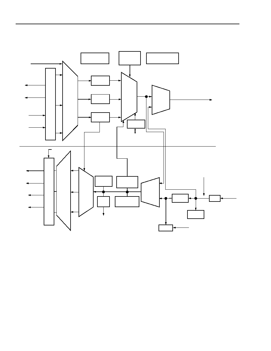
Block Diagram
In the transmit direction, the device outputs a clock and
sync and accepts bused data [7:0] and a parity signal
from up to three devices. The device outputs one data
bundle at the STS-3/STM-1 (AU-4) rate (clock, sync,
data [7:0], and parity bit). A local clock and optional
frame sync signal are needed for operation of the
device. A transport overhead access channel (TOAC)
is provided to allow overwriting of the transport over-
head bytes in the output STS-3/STM-1 (AU-4) frame.
In the receive direction, the device accepts one STS-3/
STM-1 (AU-4) bundle (clock, data, parity). Optional
clock and data recovery is available on the STS-3/
STM-1 (AU-4) receive input. The device also accepts a
loss-of-signal indication from an external source. The
device outputs three STS-1/AU-3 signals over a bus
interface (clock, data, J0 time, parity). The STS-3/STM-
1 (AU-4) input clock is used to clock this direction. A
transport overhead access channel is provided for
additional external monitoring of the incoming transport
overhead of the STS-3/STM-1 (AU-4) frame. A pointer
interpreter is provided to monitor path functions.
The device also has loopback capabilities at the STS-
1/AU-3 and STS-3/STM-1 (AU-4) interfaces. In addi-
tion, the device supports STS-1 termination. An 8-bit
microprocessor interface, JTAG control logic, and in-
circuit test capabilities are also provided.
8
Agere Systems Inc.
Data Sheet
April 2001
TMUX03155 STS-3/STM-1 (AU-4) Multiplexer/Demultiplexer
Block Diagram
(continued)
5-5294(F).ar.8
Figure 1. TMUX03155 Block Diagram
TOAC
DROP
3:1
MUX
LOGIC
SPE
GENERATE
1:3
DEMUX
LOGIC
LOOPBACK
SELECT
LOGIC
TRANSPORT
OVERHEAD
LOSS OF
CLOCK
BER
MONITOR
#1R
#2R
#3R
#1T, #2T, #3T
#1R, #2R, #3R
SELECT/
LOGIC
MULTI-
CAST
OVERHEAD
MONITOR
TOAC
INSERT
MICROPROCESSOR
LOCAL CLOCK
GENERATION
TRANSMIT DIRECTION
RECEIVE DIRECTION
S#1T
S#2T
S#3T
TLSCLKO
#1T
#2T
#3T
OVERHEAD
MONITOR
INTERFACE
OVERHEAD
MONITOR
BU
S
CO
N
T
RO
L
DROP
SELECT/
LOGIC
LOOPBACK
SELECT
LOGIC
ADD
TLSSPEO,
TLSPARI
TLSDATA[7:0]I
RLSCLKO
BU
S
CO
N
T
RO
L
RLSJ0TIMEO
RLSPARO
RLSDATA[7:0]O
TTOACCLKO (5.184 MH
Z
),
POINTER
INTERPRETER
AND PATH
MONITORS
LOS
FRAMER
RHSLOSEXTI
TTOACSYNCO (8 kH
Z
),
TTOACDATAI (5.184 Mbits/s)
TLSV1TIMEO
(19.44 MHz)
(19.44 MHz)
RTOACCLKO (5.184 MH
Z
),
RTOACSYNCO (8 kH
Z
),
RTOACDATAO (5.184 Mbits/s)
THSSCLKOT/C (155.52 MH
Z
),
THSSSYNCOT/C (8 kH
Z
),
THSSDATAOT/C (155.52 Mbits/s)
OR
RHSSCLKIT/C (155.52 MH
Z
)
RHSSDATAIT/C (155.52 Mbits/s)
OR
MULTI-
CAST
TLSC1J1V1TIMEO,
THSCLKO (38.88 MHz OR 19.44 MHz),
THSSYNCO (8 kH
Z
),
THSDATA[7:0]O (38.88 Mbits/s OR 19.44 Mbits/s),
RHSCLKI (38.88 MHz OR 19.44 MHz),
RHSDATA[7:0]I (38.88 Mbits/s OR 19.44 Mbits/s),
THSPARO (38.88 Mbits/s OR 19.44 Mbits/s)
RHSPARI (38.88 Mbits/s OR 19.44 Mbits/s)
CDR
Agere Systems Inc.
9
Data Sheet
April 2001
TMUX03155 STS-3/STM-1 (AU-4) Multiplexer/Demultiplexer
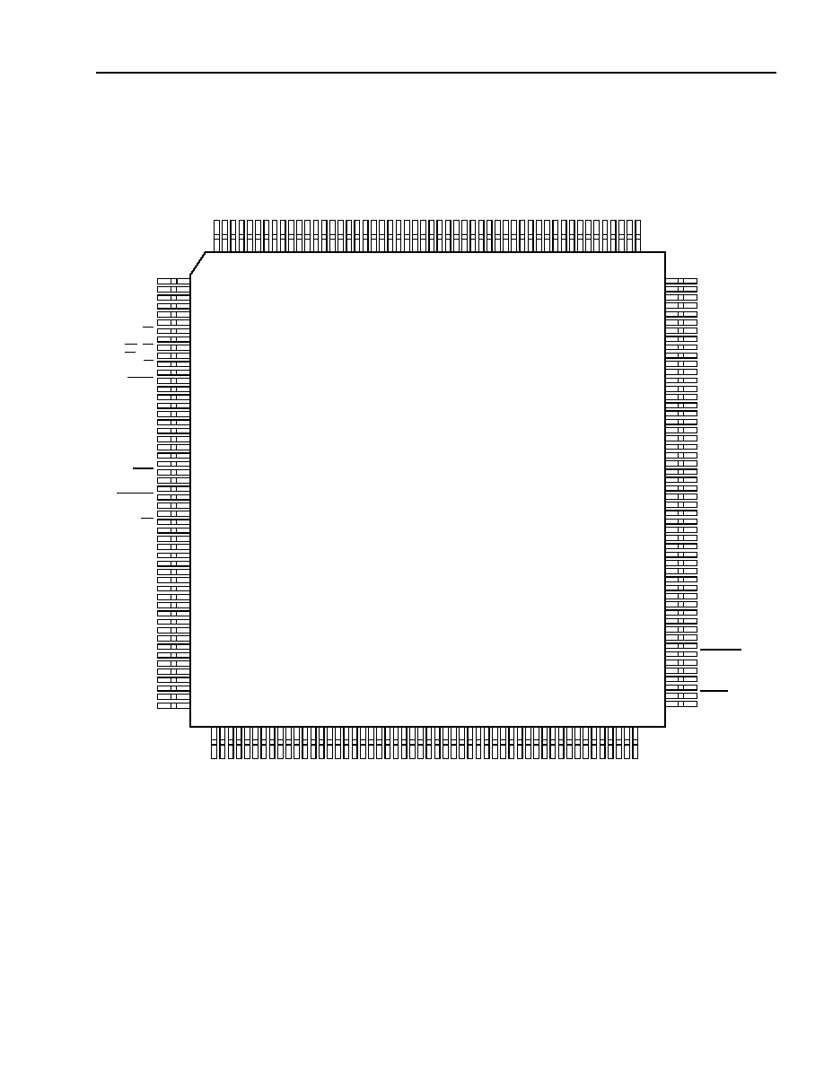
Pin Information
5-4873(F)
Figure 2. Pinout of 208 SQFP Device
The pin descriptions for the 208 SQFP package follow in Table 1 on page 10.
NC
VSS
MODE0
MODE1
VDD
REF5VTOL
THSJ0J1V1I
VSS
THSCLKI
VDD
LVDS_REFSEL
CTAP_THSSCLKI
VDD
THSSCLKIT
THSSCLKIC
CTAP_THSSJ0J1V1I
THSSJ0J1V1IT
THSSJ0J1V1IC
VDD
THSSCLKOT
THSSCLKOC
VSS
THSSSYNCOT
THSSSYNCOC
THSSDATAOT
THSSDATAOC
VDD
LVDS_REF10
LVDS_REF14
LVDS_RESHI
LVDS_RESLO
VSS
RHSSCLKIT
RHSSCLKIC
CTAP_RHSSCLKI
VDD
VSS
RHSSDATAIT
RHSSDATAIC
CTAP_RHSSDATAI
VDD
VSS
CDR_TSTMUXO
RCDR10K2GND
NC
RSTN_TST
THSCLKO
THSSYNCO
NC
NC
RESET
VSS
VSS
VSS
AD5
AD6
AD7
NC
CS
INT
WR_DS
RD_RW
ALE_AS
VDD
RDY_DTACK
MPMUX
MPMODE
MPMODE3ALE
VDD
NC
NC
TCLK
VSS
TDI
TMS
TRST
TDO
VDD
SCAN_EN
TEST_MODE
NC
ICT
VSS
REF5VTOL
NC
NC
NC
VDD
TTOACCLKO
TTOACSYNCO
TTOACDATAI
VDD
RTOACCLKO
RTOACSYNCO
RTOACDATAO
VDD
NC
NC
NC
NC
RHSLOSEXTI
RHSCLKI
VSS
NC
156
155
154
153
152
151
150
149
148
147
146
145
144
143
142
141
140
139
138
137
136
135
134
133
132
131
130
129
128
127
126
125
124
123
122
121
120
119
118
117
116
115
114
113
112
111
110
109
108
107
106
105
VS
S
VS
S
RHSP
A
RI
RHSDA
T
A
7
I
RHSDA
T
A
6
I
RHSDA
T
A
5
I
RHSDA
T
A
4
I
RHSDA
T
A
3
I
RHSDA
T
A
2
I
RHSDA
T
A
1
I
RHSDA
T
A
0
I
NC
VD
D
NC NC NC NC NC NC NC
VD
D
VS
S
NC NC NC NC
VS
S
VD
D
NC NC NC
VS
S
VD
D
NC NC NC NC NC NC NC
VD
D
T
H
SDA
T
A0
O
T
H
SDA
T
A1
O
T
H
SDA
T
A2
O
T
H
SDA
T
A3
O
T
H
SDA
T
A4
O
T
H
SDA
T
A5
O
T
H
SDA
T
A6
O
T
H
SDA
T
A7
O
T
H
SP
ARO VS
S
NC
53 54 55 56 57 58 59 60 61 62 63 64 65 66 67 68 69 70 71 72 73 74 75 76 77 78 79 80 81 82 83 84 85 86 87 88 89 90 91 92 93 94 95 96 97 98 99 100 101 102 103 104
NC VS
S
AD
4
AD
3
AD
2
AD
1
AD
0
A7 A6 A5 A4 A3 VD
D
A2 A1 A0 RL
SP
ARO
RE
SER
V
E
D
RL
SDA
T
A0
O
RL
SDA
T
A1
O
RL
SDA
T
A2
O
VS
S
RL
SDA
T
A3
O
RL
SDA
T
A4
O
RL
SDA
T
A5
O
RL
SDA
T
A6
O
VS
S
RL
SDA
T
A7
O
VD
D
RL
SCL
K
O
NC VS
S
RL
SJ0
T
IM
E
O
NC T
L
S
SPE
O
TL
SV
1
T
I
M
E
0
TL
SC
L
K
O
T
L
S
J
0
J
1V
1T
I
M
E
O
TL
SD
A
T
A7
I
TL
SD
A
T
A6
I
VD
D
TL
SD
A
T
A5
I
TL
SD
A
T
A4
I
TL
SD
A
T
A3
I
TL
SD
A
T
A2
I
TL
SD
A
T
A1
I
TL
SD
A
T
A0
I
TL
SP
AR
I
NC NC VS
S
VS
S
208 207 206 205 204 203 202 201 200 199 198 197 196 195 194 193 192 191 190 189 188 187 186 185 184 183 182 181 180 179 178 177 176 175 174 173 172 171 170 169 168 167 166 165 164 163 162 161 160 159 158 157
52
51
50
49
48
47
46
45
44
43
42
41
40
39
38
37
36
35
34
33
32
31
30
29
28
27
26
25
24
23
22
21
20
19
18
17
16
15
14
13
12
11
10
9
8
7
6
5
4
3
2
1

10
10
Agere Systems Inc.
Data Sheet
April 2001
TMUX03155 STS-3/STM-1 (AU-4) Multiplexer/Demultiplexer
Pin Information
(continued)
Table 1. Pin Descriptions for the 208-Pin SQFP Package
* Pin order follows symbol order, e.g., pin 170 refers to TLSDATA7I.
I = input, O = output, I/O = bidirectional signal, I
d
= input with internal pull-down (~20 kW), I
u
= input with internal pull-up (~100 kW), I
diff
or
O
diff
= differential input or output. All I/O not explicitly stated with a buffer type are 5 V compatible. They will tolerate 5 V at their inputs or out-
puts. LVDS = low-voltage differential signal.
Pin*
Symbol
Type
Name/Description
Transmit Direction Signals
143, 142
THSSCLKIT/C
I
diff
LVDS
Transmit High-Speed Serial Clock Input. The transmit clock can
either be 155.52 MHz (serial), 38.88 MHz (nibble), or 19.44 MHz
(byte).
145
CTAP_THSSCLKI
I
Center Tap for Transmit High-Speed Serial Clock Input. The cen-
ter tap input provides for center-tapped common-mode termination.
This input should be terminated through an external capacitor to
ground (approximately 0.1 µF).
140, 139
THSSJ0J1V1IT/C
I
diff
LVDS
Transmit High-Speed Serial Sync Input. The transmit sync signal
is active during J0 time (8 kHz), J11 time, and V11 time (2 kHz). This
signal is active-high and is optional. (See Figure 16 on page 112 for
details.)
141
CTAP_THSSJ0J1V1I
I
Center Tap for Transmit High-Speed Serial Sync Input. The cen-
ter tap input provides for center-tapped common-mode termination.
This input should be terminated through an external capacitor to
ground (approximately 0.1 µF).
148
THSCLKI
I
d
Transmit High-Speed Clock Input. The transmit clock can either be
38.88 MHz (nibble) or 19.44 MHz (byte).
150
THSJ0J1V1I
I
d
Transmit High-Speed Sync Input. The transmit sync signal is active
during J0 time (8 kHz), J11 time, and V11 time (2 kHz). This signal is
active-high and is optional.
172
TLSCLKO
O
Transmit Low-Speed Output Clock. The STS-1/AU-3 clock will be
19.44 MHz.
174
TLSSPEO
O
Transmit Low-Speed Synchronous Payload Envelope (SPE). The
STS-1/AU-3 SPE signal is low when the transport overhead is on the
input bus (TLSDATA[7:0]I). (See Figure 18 on page 116 for details.)
171
TLSJ0J1V1TIMEO
O
Transmit Low-Speed J0, J1, and V1 Time Signal. J0 time is
defined when TLSSPEO is a logic 0, TLSJ0J1V1TIMEO is a logic 1,
TLSV1TIMEO is a logic 0, and the J0 byte is on the input bus. J1 time
is defined when TLSSPEO is a logic 1, TLSJ0J1V1TIMEO is a logic
1, TLSV1TIMEO is a logic 0, and J11 is on the input bus. (See Figure
18 on page 116 for details.)
173
TLSV1TIMEO
O
Transmit Low-Speed V1 Time. This signal is active-high when the
current frame contains the V1 byte. V1 time is defined when
TLSSPEO is a logic 1, TLSJ0J1V1TIMEO is a logic 1, and
TLSV1TIMEO is a logic 1. (See Figure 18 on page 116 for details.)
170, 169,
167--162
TLSDATA[7:0]I
I
d
Transmit Low-Speed Data. TLSDATA7I is the most significant bit of
the input byte. (See Figure 18 on page 116 for details.)

Agere Systems Inc.
11
Data Sheet
April 2001
TMUX03155 STS-3/STM-1 (AU-4) Multiplexer/Demultiplexer
Pin Information
(continued)
Table 1. Pin Descriptions for the 208-Pin SQFP Package (continued)
* Pin order follows symbol order, e.g., pin 170 refers to TLSDATA7I.
I = input, O = output, I/O = bidirectional signal, I
d
= input with internal pull-down (~20 kW), I
u
= input with internal pull-up (~100 kW), I
diff
or
O
diff
= differential input or output. All I/O not explicitly stated with a buffer type are 5 V compatible. They will tolerate 5 V at their inputs or out-
puts. LVDS = low-voltage differential signal.
Pin*
Symbol
Type
Name/Description
Transmit Direction Signals (continued)
161
TLSPARI
I
u
Transmit Low-Speed Parity Bit. The STS-1/AU-3 parity input is
only defined for byte-wide data. The device can be provisioned to
receive either odd or even parity.
137, 136
THSSCLKOT/C
O
diff
LVDS
Transmit High-Speed Serial Clock. The STS-3/STM-1 (AU-4) clock
will be 155.52 MHz for serial output data; otherwise, this output is
placed in a high-impedance state.
134, 133
THSSSYNCOT/C
O
diff
LVDS
Transmit High-Speed Serial Sync. The STS-3/STM-1 (AU-4) 8 kHz
frame sync is coincident with the first or last bit of the frame.
132,131
THSSDATAOT/C
O
diff
LVDS
Transmit High-Speed Serial Data. If the device is operating in the
serial mode, then this output is used as the differential data pin. In
nibble or parallel output mode, this output is placed in a high-
impedance state.
110
THSCLKO
O
Transmit High-Speed Clock. The STS-3/STM-1 (AU-4) clock is
38.88 MHz for nibble data, or 19.44 MHz for byte-wide data.
109
THSSYNCO
O
Transmit High-Speed Sync. The STS-3/STM-1 (AU-4) 8 kHz frame
sync is coincident with the first or last nibble/byte of the frame.
101--94
THSDATA[7:0]O
O
Transmit High-Speed Data. Bit 7 is the most significant bit in nibble
or byte mode.
102
THSPARO
O
Transmit High-Speed Parity. The parity output is only defined for
nibble or byte-wide data. The device can be provisioned to source
either an odd or even parity bit.
STS-3/STM-1 (AU-4) Transport Overhead Access Channel (TOAC) Insert
37
TTOACCLKO
O
Transmit TOAC Clock. (5.184 MHz.)
38
TTOACSYNCO
O
Transmit TOAC Sync. (8 kHz.)
39
TTOACDATAI
I
d
Transmit TOAC Data. (5.184 Mbits/s.)

12
12
Agere Systems Inc.
Data Sheet
April 2001
TMUX03155 STS-3/STM-1 (AU-4) Multiplexer/Demultiplexer
Pin Information
(continued)
Table 1. Pin Descriptions for the 208-Pin SQFP Package (continued)
* Pin order follows symbol order, e.g., pin 170 refers to TLSDATA7I.
I = input, O = output, I/O = bidirectional signal, I
d
= input with internal pull-down (~20 kW), I
u
= input with internal pull-up (~100 kW), I
diff
or
O
diff
= differential input or output. All I/O not explicitly stated with a buffer type are 5 V compatible. They will tolerate 5 V at their inputs or out-
puts. LVDS = low-voltage differential signal.
Pin*
Symbol
Type
Name/Description
Receive Direction Signals
124, 123
RHSSCLKIT/C
I
diff
LVDS
Receive High-Speed Serial Clock Input. The STS-3/STM-1
(AU-4) serial clock is 155.52 MHz.
122
CTAP_RHSSCLKI
I
Center Tap for Receive High-Speed Serial Clock Input. The cen-
ter tap input provides for center-tapped common-mode termination.
This input should be terminated through an external capacitor to
ground (approximately 0.1 µF).
119, 118
RHSSDATAIT/C
I
diff
LVDS
Receive High-Speed Serial Data Input. The STS-3/STM-1 (AU-4)
serial data is 155.52 Mbits/s.
117
CTAP_RHSSDATAI
I
Center Tap for Receive High-Speed Serial Data Input. The center
tap input provides for center-tapped common-mode termination. This
input should be terminated through an external capacitor to ground
(approximately 0.1 µF).
113
RCDR10K2GND
I
Receive CDR Bias Resistor Input. Must be tied to ground, through
an external 10 k
±1% resistor.
50
RHSCLKI
I
d
Receive High-Speed Clock Input. The STS-3/STM-1 (AU-4) clock
is 38.88 MHz (nibble), or 19.44 MHz for byte-wide data.
56--63
RHSDATA[7:0]I
I
d
Receive High-Speed Data Inputs. Data bit 7 is the most significant
bit in nibble or byte mode.
55
RHSPARI
I
u
Receive High-Speed Input Parity. The parity input is only defined
for nibble- or byte-wide data. The device can be provisioned to
accept either odd or even parity.
49
RHSLOSEXTI
I
d
Receive High-Speed Loss of Signal. This is an active-high signal.
179
RLSCLKO
O
Receive STS-1/AU-3 Output Clock. The STS-1/AU-3 clock will be
19.44 MHz for byte-wide data (bus mode).
176
RLSJ0TIMEO
O
Receive STS1/AU-3 Output J0 Time. This signal will be active
(logic 1) each time the J0 byte is output.
181,
183--186,
188--190
RLSDATA[7:0]O
O
Receive STS-1/AU-3 Output Data. RLSDATA7O is the most signifi-
cant bit of the output byte.
192
RLSPARO
O
Receive STS-1/AU-3 Output Parity. The device can be provisioned
to source either an odd or even parity bit per byte transfer.
STS-3/STM-1 (AU-4) Transport Overhead Access Channel (TOAC) Drop
41
RTOACCLKO
O
Receive TOAC Clock. (5.184 MHz.)
42
RTOACSYNCO
O
Receive TOAC Sync. (8 kHz.)
43
RTOACDATAO
O
Receive TOAC Data. (5.184 Mbits/s.)

Agere Systems Inc.
13
Data Sheet
April 2001
TMUX03155 STS-3/STM-1 (AU-4) Multiplexer/Demultiplexer
Pin Information
(continued)
Table 1. Pin Descriptions for the 208-Pin SQFP Package (continued)
* Pin order follows symbol order, e.g., pin 170 refers to TLSDATA7I.
I = input, O = output, I/O = bidirectional signal, I
d
= input with internal pull-down (~20 kW), I
u
= input with internal pull-up (~100 kW), I
diff
or
O
diff
= differential input or output. All I/O not explicitly stated with a buffer type are 5 V compatible. They will tolerate 5 V at their inputs or out-
puts. LVDS = low-voltage differential signal.
Pin*
Symbol
Type
Name/Description
Mode/In-Circuit Test and Reset Control Inputs
30
ICT
I
u
In-Circuit Test Control (Active-Low). If
ICT
is forced low, certain
output pins are placed in the high-impedance state.
106
RESET
I
u
Hardware Reset (Active-Low). If
RESET
is forced low, all internal
states in the transceiver paths are reset and data flow through each
channel will be interrupted.
111
RSTN_TST
I
u
Test Reset (Active-Low). This pin is for test purposes only; it should
be left unconnected.
153, 154
MODE [1:0]
I
u
, I
d
Mode Control. Normal STS-3/STM-1 mode set MODE [1:0] = 10.
STS-1 mode set MODE [1:0] = 00
Microprocessor Interface
14
MPMUX
I
Microprocessor Multiplex Mode. Setting MPMUX = 1 allows the
microprocessor interface to accept the multiplexed address and data
signals. Setting MPMUX = 0 allows the microprocessor interface to
accept demultiplexed (separate) address and data signals.
15
MPMODE
I
Microprocessor Mode. When MPMODE = 1, the device uses the
address latch enable type microprocessor read/write protocol with
separate read and write controls. Setting MPMODE = 0 allows the
device to use the address strobe type microprocessor read/write pro-
tocol with a separate data strobe and a combined read/write control.
16
MPMODE3ALE
I
u
Microprocessor MODE3 ALE Enable. When the device is in
MODE3 (MPMODE = 1 and MPMUX = 0), the ALE signal can be
used to retime the address or the address bus can be used directly
without being retimed. This is an active-high signal.
9
WR_DS
I
Write (Active-Low). If MPMODE = 1, this pin is asserted low by the
microprocessor to initiate a write cycle.
Data Strobe (Active-Low). If MPMODE = 0, this pin becomes the
data strobe for the microprocessor. When R/W = 0 (write), a low
applied to this pin latches the signal on the data bus into internal reg-
isters.
11
ALE_AS
I
Address Latch Enable. If MPMODE = 1, this pin becomes the
address latch enable for the microprocessor. When this pin transi-
tions from high to low, the address bus inputs are latched into the
internal registers.
Address Strobe (Active-Low). If MPMODE = 0, this pin becomes
the address strobe for the microprocessor. When this pin transitions
from high to low, the address bus inputs are latched into the internal
registers.
10
RD_R/W
I
Read (Active-Low). If MPMODE = 1, this pin is asserted low by the
microprocessor to initiate a read cycle.
Read/Write. If MPMODE = 0, this pin is asserted high by the micro-
processor to indicate a read cycle or asserted low to indicate a write
cycle.

14
14
Agere Systems Inc.
Data Sheet
April 2001
TMUX03155 STS-3/STM-1 (AU-4) Multiplexer/Demultiplexer
Pin Information
(continued)
Table 1. Pin Descriptions for the 208-Pin SQFP Package (continued)
* Pin order follows symbol order, e.g., pin 170 refers to TLSDATA7I.
I = input, O = output, I/O = bidirectional signal, I
d
= input with internal pull-down (~20 kW), I
u
= input with internal pull-up (~100 kW), I
diff
or
O
diff
= differential input or output. All I/O not explicitly stated with a buffer type are 5 V compatible. They will tolerate 5 V at their inputs or out-
puts. LVDS = low-voltage differential signal.
Pin*
Symbol
Type
Name/Description
Microprocessor Interface (continued)
7
CS
I
u
Chip Select (Active-Low). This pin is asserted low by the micropro-
cessor to enable the microprocessor interface. If MPMUX = 1, an
internal 100 k
pull-up is on this pin.
8
INT
O
Interrupt. This pin is asserted high to indicate an interrupt produced
by an alarm condition. The activation of this pin can be masked by
the microprocessor by setting the appropriate mask bits.
13
RDY_DTACK
O
Ready. If MPMODE = 1, this pin is asserted high to indicate the
device has completed a read or write operation. This pin is in a high-
impedance state when CS is high.
Data Transfer Acknowledge (Active-Low). If MPMODE = 0, this
pin is asserted low to indicate the device has completed a read or
write operation.
5--3,
206--202
AD[7:0]
I/O
Microprocessor Interface Address/Data Bus. If MPMUX = 0,
these pins become the bidirectional, 3-state data bus. If MPMUX = 1,
these pins become the multiplexed address/data bus.
201--197,
195--193
A[7:0]
I
d
Microprocessor Interface Address. If MPMUX = 0, these pins
become the address bus for the microprocessor interface registers.
JTAG Signals
20
TCLK
I
u
JTAG Clock.
22
TDI
I
u
JTAG Input Data.
23
TMS
I
u
JTAG Mode Select.
24
TRST
I
u
JTAG Reset (Active-Low).
25
TDO
O
JTAG Output Data.
SCAN Specific Inputs
27
SCAN_EN
I
u
Scan Enable. Place device in scan mode (active-low).
28
TEST_MODE
I
d
Test Mode. Disable all clocks and async resets (active-high).
114
CDR_TSTMUX0
O
CDR Test Output. Test purpose only.
LVDS Control Signals
146
LVDS_REFSEL
I
u
LVDS Reference Select. If LVDS_REFSEL = 0, then use external
1.0 and 1.4 reference voltages. If LVDS_REFSEL = 1, then use inter-
nal references.
129
LVDS_REF10
I
1.0 V Reference for LVDS Buffers. This signal is optional.
128
LVDS_REF14
I
1.4 V Reference for LVDS Buffers. This signal is optional.
127
LVDS_RESHI
I
LVDS Resistor Pins. A 100
±1% resistor must be placed between
these two pins when using the LVDS buffers.
126
LVDS_RESLO
I
Agere Systems Inc.
15
Data Sheet
April 2001
TMUX03155 STS-3/STM-1 (AU-4) Multiplexer/Demultiplexer
Pin Information
(continued)
Table 1. Pin Descriptions for the 208-Pin SQFP Package (continued)
* Pin order follows symbol order, e.g., pin 170 refers to TLSDATA7I.
I = input, O = output, I/O = bidirectional signal, I
d
= input with internal pull-down (~20 kW), I
u
= input with internal pull-up (~100 kW), I
diff
or
O
diff
= differential input or output. All I/O not explicitly stated with a buffer type are 5 V compatible. They will tolerate 5 V at their inputs or out-
puts. LVDS = low-voltage differential signal.
Summary of I/O Pins
Pin*
Symbol
Type
Name/Description
Power and Ground Pins
1--2, 21
31, 51,
53--54,
74, 79, 84,
103, 105,
115, 120,
125, 135,
149, 155,
157--158,
177, 182,
187, 207
V
SS
I
Ground Reference.
12, 17, 26,
36, 40, 44,
65, 73, 80,
85, 93,
116, 121,
130, 138,
144, 147,
152, 168,
180, 196
V
DD
I
Power Supply for Digital Circuitry.
151, 32
REF5VTOL
I
5 V Tolerant Reference Voltage.
Table 2. Input/Output Summary
Type
Number of Pins
Input
Differential
8
Single Ended
57
Output
Differential
6
Single Ended
35
Bidirectional
8
Total Signal
114
No Connect (Reserved)
45
REF5VTOL
2
LVDS_REF10
1
LVDS_REF14
1
V
DD
21
V
SS
(GND)
24
Total Package
208 SQFP
16
16
Agere Systems Inc.
Data Sheet
April 2001
TMUX03155 STS-3/STM-1 (AU-4) Multiplexer/Demultiplexer
Mode Control Signals
(See Register Description on page 54.)
The device is controlled by four control signals: T/RSONET_SDH and T/RSTS3_AU4, 0x34. These signals control
the following:
I
The type of input signal to expect (low-speed (LS) side--STS-1/AU-3).
I
The expected high-speed (HS) input/output signal format--STS-3/STM-1 (AU-4), or STS-1.
I
The default byte value in the outgoing HS frame.
These provisioning signals are summarized in Table 3 and Table 4.
STS-1 Mode
In STS-1 mode, all other device functions remain the same as in STS-3/STM-1 mode; except, the device runs at
one-third the STS-3/STM-1 rate and operates on a single STS-1 frame. The high-speed side operates in the follow-
ing three modes: 1) as a 51.84 Mbits/s serial interface, 2) as a parallel 12.96 MHz nibble wide, 3) or as a 6.48 MHz
byte-wide interface. The low-speed STS-1/AU-3 side operates at 6.48 Mbytes/s and communicates with a single
STS-1/AU-3 device (TMPR28051). Since the TOAC interface provides access to the transport overhead in a single
STS-1 frame, its clock and data operate at 1.782 MHz, while the sync runs at 8 kHz. For STS-1 mode, set both
mode pins 153 and 154 to a logic 0, and set all mode control bits TSTS3_AU4, TSONET_SDH, RSTS3_AU4,
RSONET_SDH, 0x34, to a logic 0.
Table 3. Transmit Mode Control Signals
TSTS3_AU4
TSONET_SDH
Description
0 = STS-3
0 = SONET
1
1. SONET = OOF 0
1, 4 times detect; default output byte = 0x00.
Three STS-1 inputs multiplexed to an STS-3 output. Also used for
STS-1 mode. See STS-1 Mode section for details.
1 = AU-4
0 = SONET
*
Three AU-3 signals multiplexed to an STM-1 (AU-4) signal.
0 = STS-3
1 = SDH
2
2. SDH = OOF 0
1, 5 times detect; default output byte = 0xFF.
Three STS-1 inputs multiplexed to an STS-3 output.
1 = AU-4
1 = SDH
Three AU-3 signals multiplexed to an STM-1 (AU-4) signal.
Table 4. Receive Mode Control
RSTS3_AU4 RSONET_SDH
Description
0 = STS-3
0 = SONET
1
1. SONET = OOF 0
1, 4 times detect; default output byte = 0x00; ignore SS bits.
One STS-3 input demultiplexed to three STS-1 outputs. Also used
for STS-1 mode. See STS-1 Mode section for details.
1 = AU-4
0 = SONET
*
One STM-1 (AU-4) input demultiplexed to three AU-3 outputs.
0 = STS-3
1 = SDH
2
2. SDH = OOF 0
1, 5 times detect; default output byte = 0xFF; verify SS bits = 10.
One STS-3 input demultiplexed to three STS-1 outputs.
1 = AU-4
1 = SDH
One STM-1 (AU-4) input demultiplexed to three AU-3 outputs.

Agere Systems Inc.
17
Data Sheet
April 2001
TMUX03155 STS-3/STM-1 (AU-4) Multiplexer/Demultiplexer
Transmit Direction Overview
The following major functions are performed in the transmit direction: STS-1/AU-3 bus mode retiming, input select
control, STS-1/AU-3 inputs, out-of-frame (OOF) and loss-of frame (LOF) monitoring, descramble enable/disable,
monitor B1 and B2 errors, H4 multiframe and pointer monitor (AU-4 mode only), STS-3 generate, STM-1 (AU-4)
frame generation (AU-4 mode), transport overhead access channel (TOAC) insert, STS-3/STM-1 (AU-4) scramble
enable, STS-3/STM-1 (AU-4) loopback control, and STS-3/STM-1 (AU-4) output interface.
STS-1/AU-3 Bus Mode Input Retiming
The bus mode provides a single byte-wide bus and parity bit that is shared with up to three devices at
19.44 Mbits/s. The device will source a clock (19.44 MHz), synchronous payload envelope (SPE) indicator, J0J1V1
indicator, and V1 time indicator signals toward the downstream devices. These signals guarantee frame alignment
between all three STS-1/AU-3 inputs and H4 byte multiframe values (AU-4 mode). The V1 time signal can be dis-
abled under software control (TLSV1DISABLE, 0x35).
The clock can be inverted leaving the device (TLSCLKINV, 0x35). An odd/even parity bit (TLSVOEPAR, 0x35) is
verified per byte transfer (TLSPARE[3--1], TLSPARM[3--1], 0x07, 0x10).
Input Select Control
This function determines which signals are multiplexed to form the STS-3 signal. These control bits (TSEL[3--
1][2:0], 0x3A, 0x38, 0x36) allow loopback (STS-1/AU-3-R to STS-1/AU-3-T), input shuffle, and multicast opera-
tions to be possible. The selected STS-1/AU-3 inputs are labeled S#1T, S#2T, and S#3T in Figure 1.
STS-1/AU-3 Inputs
The SONET/SDH STS-1/AU-3 frame is comprised of 9 rows x 90 columns that repeat at an 8 kHz rate. Each col-
umn is 1-byte wide. The frame contains three columns of transport overhead, one column of path overhead, and
86 columns of payload. For column byte definitions, see Table 6 on page 18.
Table 5. Input Select Control
TSEL
[3--1][2:0]
Output
000 (0)
STS-1/AU-3 #1 Transmit
001 (1)
STS-1/AU-3 #2 Transmit
010 (2)
STS-1/AU-3 #3 Transmit
011 (3)
STS-1/AU-3 #1 Receive (Loopback)
STS3 Mode Only
100 (4)
STS-1/AU-3 #2 Receive (Loopback)
STS3 Mode Only
101 (5)
STS-1/AU-3 #3 Receive (Loopback)
STS3 Mode Only
110 (6)
STS-1/AU-3 #1 Transmit
111 (7)
STS-1/AU-3 #1 Transmit
18
18
Agere Systems Inc.
Data Sheet
April 2001
TMUX03155 STS-3/STM-1 (AU-4) Multiplexer/Demultiplexer
Transmit Direction Overview
(continued)
STS-1/AU-3 Inputs
(continued)
The 27 bytes of transport overhead from each STS-1/AU-3 input must be aligned* (A1-1, A1-2, A1-3 must all be
coincident from all three STS-1/AU-3 inputs) and are allocated as shown in Table 6
.
Monitored in STS-1 mode.
Monitored in AU-4 mode.
Note: X = don't care (payload).
The path overhead (POH) can start anywhere within the SPE and cannot be accessed in the STS-3 mode.
In the AU-4 mode, the pointer is fixed at 522\D; therefore, the J1 byte will always be in row 1, column 4. The H4
byte is the only valid byte in the POH and all other bytes are ignored.
Out-of-Frame (OOF) and Loss-of-Frame (LOF) Monitoring
The device monitors for out-of-frame (OOF) and loss-of-frame (LOF) states on each selected STS-1/AU-3 input
(TLSOOF[3--1], TLSOOFD[3--1], TLSOOFM[3--1], TLSLOF[3--1], TLSLOFD[3--1, TLSLOFM[3--1], 0x08,
0x11, 0x19). Each input will be considered out-of-frame until two successive framing patterns (0xF628) separated
in time by 125 µs occur without framing byte errors. Each selected STS-1/AU-3 input will be considered in frame
until five (SDH)/four (SONET) successive frames separated in time by 125 µs occur with errored framing patterns.
The device will be considered in the LOF state when an OOF condition persists for 24 consecutive frames (3 ms)
or clear when the OOF condition is inactive for 24 consecutive frames (3 ms) with the correct framing patterns
spaced 125 µs apart.
Descramble Enable/Disable
Each selected STS-1/AU-3 input can be descrambled (TLSDSCR[3--1], 0x3A, 0x38, 0x36) according to the
frame synchronous descrambling sequence 1 + x
6
+ x
7
. The sequence is reset to 1111111 at the beginning of the
byte following the C1 byte and descrambles all of the STS-1/AU-3 data except the A1, A2, and J0 bytes. Writing a
logic 1 to the appropriate bit causes the selected STS-1/AU-3 signal to be descrambled.
* Can be provided by the Agere TMPR28051 mapper device.
Table 6. Expected STS-1/AU-3 Input Frame Format
Transport Overhead
Payload
Col. 1
Col. 2
Col. 3
Col. 4
Col. 5--90
Row 1
A1
A2
J0
J1
X
Row 2
B1
E1
F1
B3
X
Row 3
D1
D2
D3
C2
X
Row 4
H1
H2
H3
G1
X
Row 5
B2
K1
K2
F2
X
Row 6
D4
D5
D6
H4
X
Row 7
D7
D8
D9
Z3
X
Row 8
D10
D11
D12
Z4
X
Row 9
S1
M0
E2
Z5
X

Agere Systems Inc.
19
Data Sheet
April 2001
TMUX03155 STS-3/STM-1 (AU-4) Multiplexer/Demultiplexer
Transmit Direction Overview
(continued)
Monitor B1 and B2 Errors
The device verifies B1 and B2 bit interleaved parity (BIP) values on each selected STS-1/AU-3 input. The device
will count BIP errors or block errors under software control (BITBLOCKCNT, TLSB1ECNT[3--1][15:0],
TLSB2ECNT[3--2][15:0], TLSB2ECNT1[17:0], 0x34, Page 1 - 0x80--0x85, Page 1 - 0x86--0x88,
Page 1 - 0x89--0x8C). These counters will update on LATCH_CNT, 0x04 and are large enough to store at least
1 second's worth of data.
H4 Multiframe and Pointer Monitor (AU-4 Mode Only)
In this mode, all three input signals are required to have pointer values (H1, H2) with the same fixed value of
522\D. This ensures the J1 byte starts in row 1, column 4. The H4[1:0] multiframe bits must be the same from all
inputs and equal to the internally expected value. This is required because the output STM-1 (AU-4) signal only
has one H4 byte. The device will synchronize its H4 internal expected value to a 1 after detecting an embedded
2 kHz sync in the local frame sync signal (THS(S)J0J1V1I(T/C)).
The device will declare a pointer match after two consecutive pointer values of 522\D are detected 125 µs apart. A
pointer mismatch will be declared after five successive frames separated in time by 125 µs occur with errored
pointer values (TLSPTRMIS[3--1], TLSPTRMISD[3--1], TLSPTRMISM[3--1], 0x1A, 0x09, 0x12).
The device will declare an H4 multiframe match after two consecutive H4 values match the expected value spaced
125 µs apart. An H4 multiframe mismatch will be declared after five successive frames separated in time by 125 µs
occur with H4 values not equal to the expected value (TLSH4MIS[3--1], TLSH4MISD[3--1],
TLSH4MISM[3--1], 0x1A, 0x09, 0x12).
20
20
Agere Systems Inc.
Data Sheet
April 2001
TMUX03155 STS-3/STM-1 (AU-4) Multiplexer/Demultiplexer
Transmit Direction Overview
(continued)
STS-3 Generate
The device will create the overhead according to Table 7. The POH byte locations are not fixed and cannot be
accessed.
* Access through transmit TOAC (see Table 17 on page 37).
Note: Bold type within the table is not defined in the standard and is labeled here for clarity.
The following values are assigned to the transmitted overhead bytes:
A1--11110110 (0xF6)
A2--00101000 (0x28)
J0--TJ0DINS[7:0], 0x3F
Z0-2--TZ02DINS[7:0], 0x40
Z0-3--TZ03DINS[7:0], 0x41
B1--Variable value (BIP-8 parity)
F1--Variable value TF1DINS[7:0], 0x42
H1-1, 2, 3--Passed through from respective STS-1
H2-1, 2, 3--Passed through from respective STS-1
H3-1, 2, 3--Passed through from respective STS-1
B2-1, 2, 3--Variable value (BIP-24)
K1--Variable value TAPSINS[12:5], 0x43, 0x44
K2--Variable value TAPSINS[4:0], TK2INS[2:0], 0x43, 0x44--RDI-L, AIS-L
S1--Variable value TS1DINS[7:0], 0x45
M1--Variable value (Section FEBE--Number of B2 Errors) TSFEBEINH, 0x3E
All bytes not specified above, either:
(1) Are set to the fixed stuff value (0x00 (SONET)).
(2) Are TOAC value-inserted.
(3) Have passed through from the selected STS-1 input, all under software control.
The variable values are described beginning on page 30 in the Maintenance Functions section of this document.
Table 7. STS-3 Output Overhead Format
STS-3 Overhead
Col. 1
Col. 2
Col. 3
Col. 4
Col. 5
Col. 6
Col. 7
Col. 8
Col. 9
Col.
10--270
Row 1
A1-1
A1-2
A1-3
A2-1
A2-2
A2-3
J0
Z0-2
Z0-3
Payload
Row 2
B1
B1-2*
B1-3*
E1*
E1-2*
E1-3*
F1*
F1-2*
F1-3*
Row 3
D1*
D1-2*
D1-3*
D2*
D2-2*
D2-3*
D3*
D3-2*
D3-3*
Row 4
H1-1
H1-2
H1-3
H2-1
H2-2
H2-3
H3-1
H3-2
H3-3
Row 5
B2-1
B2-2
B2-3
K1
K1-2*
K1-3*
K2
K2-2*
K2-3*
Row 6
D4*
D4-2*
D4-3*
D5*
D5-2*
D5-3*
D6*
D6-2*
D6-3*
Row 7
D7*
D7-2*
D7-3*
D8*
D8-2*
D8-3*
D9*
D9-2*
D9-3*
Row 8
D10*
D10-2*
D10-3*
D11*
D11-2*
D11-3*
D12*
D12-2*
D12-3*
Row 9
S1*
Z1-2*
Z1-3*
Z2-1*
Z2-2*
M1
E2*
E2-2*
E2-3*
Agere Systems Inc.
21
Data Sheet
April 2001
TMUX03155 STS-3/STM-1 (AU-4) Multiplexer/Demultiplexer
Transmit Direction Overview
(continued)
STM-1 (AU-4) Frame Generation (AU-4 Mode)
The device will create the overhead according to the following table. The path overhead bytes are created in this
mode. The three AU-3 inputs are converted to TUG-3 format and inserted into a VC-4 that is multiplexed into an
AU-4.
* Access through transmit TOAC (see Table 17 on page 37).
Note: Bold type within the table is not defined in the standard and is labeled here for clarity.
The following values are assigned to the transmitted overhead bytes:
A1--11110110 (0xF6)
A2--00101000 (0x28)
J0--Variable value TJ0DINS[7:0], 0x3F
Z0-2--Variable value TZ02DINS[7:0], 0x40
Z0-3--Variable value TZ03DINS[7:0], 0x41
B1--Variable value (BIP-8 Parity)
F1--Variable value TF1DINS[7:0], 0x42
H1-1--01101010
H2-1--00001010 (pointer value of 522\D)
Y--10011011 (NDF, SS, PTR)--Concatenation indication
1
--All ones pattern
H3-1, 2, 3--Default byte value (0xFF)
B2-1, 2, 3--Variable value BIP-24
K1--Variable value TAPSINS[12:5], 0x43, 0x44
K2--Variable value TAPSINS[4:0], TK2INS[2:0], 0x43, 0x44--RDI-L, AIS-L
S1--Variable value TS1DINS[7:0], 0x45
M1--Variable value (section FEBE--number of B2 errors) TSFEBEINH, 0x3E
Access through transmit TOAC.
Table 8. STM-1 (AU-4) Output Overhead Format
STM-1 (AU-4) Overhead
AU-4 Payload
Col. 1 Col. 2 Col. 3 Col. 4 Col. 5 Col. 6 Col. 7 Col. 8 Col. 9
POH
10
1
1
1
2
1
3
1
4
1
5
1
6
1
7
1
8
1
9
2
0
2
1
22--
270
Row 1
A1-1
A1-2
A1-3
A2-1
A2-2
A2-3
J0
Z0-2
Z0-3
J1
F
I
X
E
D
S
T
U
F
F
F
I
X
E
D
S
T
U
F
F
N
P
I
N
P
I
N
P
I
F
I
X
E
D
S
T
U
F
F
F
I
X
E
D
S
T
U
F
F
F
I
X
E
D
S
T
U
F
F
T
U
G
-
3
A
T
U
G
-
3
B
T
U
G
-
3
C
--
Row 2
B1
B1-2*
B1-3*
E1*
E1-2*
E1-3*
F1*
F1-2*
F1-3*
B3
--
Row 3
D1*
D1-2*
D1-3*
D2*
D2-2*
D2-3*
D3*
D3-2*
D3-3*
C2
--
Row 4
H1-1
Y
Y
H2-1
1*
1*
H3-1
H3-2
H3-3
G1
S
T
U
F
F
S
T
U
F
F
S
T
U
F
F
--
Row 5
B2-1
B2-2
B2-3
K1
K1-2*
K1-3*
K2
K2-2*
K2-3*
F2
--
Row 6
D4*
D4-2*
D4-3*
D5*
D5-2*
D5-3*
D6*
D6-2*
D6-3*
H4
--
Row 7
D7*
D7-2*
D7-3*
D8*
D8-2*
D8-3*
D9*
D9-2*
D9-3*
Z3
--
Row 8
D10*
D10-2* D10-3*
D11*
D11-2* D11-3*
D12*
D12-2* D12-3*
Z4
--
Row 9
S1*
Z1-2*
Z1-3*
Z2-1*
Z2-2*
M1
E2*
E2-2*
E2-3*
Z5
--

22
22
Agere Systems Inc.
Data Sheet
April 2001
TMUX03155 STS-3/STM-1 (AU-4) Multiplexer/Demultiplexer
Transmit Direction Overview
(continued)
STM-1 (AU-4) Frame Generation (AU-4 Mode)
(continued)
Path Bytes
J1--64-byte programmable sequence TJ1INS, 0x3E, TJ1DINS[64--1][7:0], 0x3E, 0x80--0xBF
B3--Variable value BIP-8
C2--TC2DINS[7:0], 0x46
G1[7:4]--REICNT (B3 errors from receive side) TPFEBEEINS, 0x4D
G1[3]--RDI indication TPRDIINS, 0x4B
G1[2:0]--Default value
F2--Variable value TF2DINS[7:0], 0x47
H4[1:0]--Position indicator (multiframe value (00\B to 11\B))
Z3--Variable value TZ3DINS[7:0], 0x48
Z4--Default value
Z5--Variable value TZ5DINS[7:0], 0x49
Fixed stuff = depends on TSONET_SDH, 0x34 value (SONET = 0x00, SDH = 0xFF)
NPI (null pointer indicator--byte 1, byte 2, and byte 3) = (10011011, 11100000, 11111111). NPI is generated for
compatibility with older devices.
All bytes not specified above, either:
(1) Are set to the fixed stuff value 0xFF (SDH).
(2) Are TOAC value inserted.
(3) Have passed through from the selected AU-3 input, all under user control.

Agere Systems Inc.
23
Data Sheet
April 2001
TMUX03155 STS-3/STM-1 (AU-4) Multiplexer/Demultiplexer
Transmit Direction Overview
(continued)
Transport Overhead Access Channel (TOAC) Insert
The device will allow the insertion of overhead data from the transmit TOAC under user control. (See TTOAC in the
Maintenance Functions section, page 36, for more details.)
STS-3/STM-1 (AU-4) Scramble Enable
Scrambling of the STS-3/ STM-1 (AU-4) signal is provisionable (THSSCR, 0x3D). A frame synchronous scram-
bling sequence 1 + x
6
+ x
7
is used. The sequence is reset to 1111111 at the beginning of the byte following the Z0-
3 byte and scrambles all of the STS-3/STM-1 (AU-4) data except all the A1, A2 and J0, Z0 bytes. Writing a logic 1
to this bit causes the signal to be scrambled.
STS-3/STM-1 (AU-4) B1, B2, and B3 BIP Generation
The device will generate a B1-BIP-8, B2-BIP-24, and a B3-BIP-8 (AU-4 mode only) on the output signal. Each BIP
calculator can be programmed to insert an inverted BIP value (THSB1ERRINS, THSB2ERRINS[3--1],
THSB3ERRINS, 0x4C).
STS-3/STM-1 (AU-4) Loopback Control
The output STS-3/STM-1 (AU-4) signal can be replaced by the receive STS-3/STM-1 (AU-4) signal under software
control (RHS2THSLB, 0x3D). The output format (bit, nibble, or byte) will be the same as the receive input format
not the transmit output port format.
Note: The transmit port type must be programmed to be the same as the receive input type.
STS-3/STM-1 (AU-4) Output Interface
The transmit STS-3/STM-1 (AU-4) output can either be serial at 155.52 Mbits/s, nibble at 38.88 Mbits/s, or byte at
19.44 Mbits/s. This is controlled by writing to THSPTYPE[1:0], 0x3C. The data is clocked out of the device on the
rising edge of the clock. This clock can be inverted leaving the device (THSCLKINV, 0x3C). When provisioned in
the parallel or nibble mode, an even or odd parity bit is generated per transfer (THSPAROEG, 0x3C). The output
sync can be programmed to be active on the first clock cycle of the frame (A1-1 coincident with sync) or the last
clock cycle of the frame (THSSA1orEND, 0x3C).
The output clock, sync, and data signals can be placed in a high-impedance state under user control (THSCHIZ =
1, THSSHIZ = 1, THSDHIZ = 1, 0x3D). Unused outputs in serial and nibble mode will be placed in a high-
impedance state automatically by the device.
Receive Direction Overview
The following functions are performed in the receive direction: input retime, clock and data recovery, STS-3/STM-1
(AU-4) framing, loss-of-signal detection, loopback select logic, RSTS-3/STM-1 (AU-4) frame synchronous
descrambling, TOAC drop, B1, B2, and B3 checking, monitoring functions, pointer interpretation, data demultiplex
and conversion (AU-4 mode only), STS-1/AU-3 output byte control, B1 and B2 generate, STS-1/AU-3 output
scramble, output selection logic, and output data formatter.

24
24
Agere Systems Inc.
Data Sheet
April 2001
TMUX03155 STS-3/STM-1 (AU-4) Multiplexer/Demultiplexer
Receive Direction Overview
(continued)
Input Retime
The device accepts either a serial 155.52 MHz-Mbits/s, nibble 38.88 MHz-Mbits/s, or byte parallel 19.44 MHz-
Mbits/s clock-data STS-3/STM-1 (AU-4) input. This is controlled by writing to RHSPTYPE[1:0], 0x55. The user can
configure which edge of the clock to use to retime the data. RHSEDGE, 0x55 = 1 uses the rising edge; RHSEDGE
= 0 uses the falling edge. If in nibble or parallel mode, an odd/even parity bit (RHSVOEPAR, 0x55) is verified per
transfer (RHSPARE, RHSPARM, 0x0A, 0x13), otherwise, this indicator is disabled.
Clock and Data Recovery
The device provides an optional clock and data recovery circuit (CDR) on the serial STS-3/STM-1(AU-4) input. The
CDR aligns the STS-3/STM-1 data signal to a local clock and then outputs a retimed data and clock signal. The
input data and local clock rates need not be synchronous. The CDR only works at the nominal 155 Mbits/s rate and
uses the high-speed transmit input clock (THSSCLKIT/C) as a reference for the local clock. The CDR is enabled by
the RHSPORCDRSEL bit, 0x57.
STS-3/STM-1 (AU-4) Framing
The device will frame on the input STS-3/STM-1 (AU-4) signal. The state of the framer (RHSOOF), as well as any
changes to this state (RHSOOFD, RHSOOFM, 0x0A, 0x13), will be reported. A loss-of-frame (RHSLOF, 0x1B)
state bit, as well as any changes to this state (RHSLOFD, RHSLOFM, 0x0A, 0x13), will be reported.
Framing Algorithm
The 32-bit (A1-2, A1-3, A2-1, A2-2) framing pattern will be used in the frame detection. The device will be consid-
ered out of frame until two successive framing patterns separated in time by 125 µs occur without framing byte
errors.
The device will be considered in frame until five (SDH)/four (SONET) successive frames separated in time by
125 µs occur with errored framing patterns. If the framer transitions to the out-of-frame state, the framer will remain
synchronized to the last known frame boundary or the latest detected unerrored framing pattern.
The device will be considered in the loss-of-frame state (LOF) when an OOF condition persists for 24 consecutive
frames (3 ms). The device will transition out of the LOF state after receiving 24 consecutive frames with the correct
framing patterns spaced 125 µs apart and the OOF condition is clear.
Loss of Signal
The device will detect a loss-of-signal condition by monitoring a unique input signal pin (RHSLOSEXTI) or detect-
ing a continuous all-zeros/all-ones pattern for 51.44 ns to 105 µs in 51.44 ns steps (LOSDETCNT[10:0], 0x58--
0x59) before data is descrambled. To recover from the LOS state receiving two consecutive frames with the correct
framing pattern spaced 125 µs apart without an incoming LOS all-zeros/ones pattern will cause an LOS state to be
cleared. This recovery applies to both internal and external LOS failure causes. The device will report this condition
to the microprocessor interface (RHSLOS, RHSLOSD, RHSLOSM, 0x1B, 0x0A, 0x13).

Agere Systems Inc.
25
Data Sheet
April 2001
TMUX03155 STS-3/STM-1 (AU-4) Multiplexer/Demultiplexer
Receive Direction Overview
(continued)
Loopback Select Logic
The device can be configured to loopback the transmit STS-3/STM-1 (AU-4) (THS2RHSLB = 1, 0x55) or accept
the local STS-3/STM-1 (AU-4) signal (THS2RHSLB = 0). While in the loopback mode, the RHSOOF, RHSLOF,
and RHSLOS (0x1B) state bits are inhibited from causing an alarm indication signal (AIS) from being generated on
the STS1/AU-3 output signals.
RSTS-3/STM-1 (AU-4) Frame Synchronous Descrambling (SONET/SDH)
The device will descramble the received SONET/SDH data (minus the first row of SOH) according to the frame
synchronous descrambling polynomial; specifically: f(x) = 1 + x
6
+ x
7
. Under software control, frame descrambling
can be disabled (RHSDSCR = 1, 0x55).
TOAC Drop
This channel drops all of the transport overhead bytes from the STS-3/STM-1 (AU-4) signal. (See RTOAC in the
Maintenance Functions section, page 44, for more details (RTOACCLKO, RTOACSYNCO, RTOACDATAO)).
B1, B2, and B3 Checking
The device will monitor the incoming B1, B2, and B3 values for errors. The error counts will be latched when the
LATCH_CNT signal transitions from a low to a high (RHSB1ECNT[15:0], RHSB2ECNT[17:0],
RHSB3ECNT[3--1][15:0], Page 1 - 0x8D--0x8E, Page 1 - 0x8F--0x91, Page 1 - 0x92--0x97). These counters
will either count bit or block errors (BITBLOCKCNT, 0x34).
Monitoring Functions
The following transport overhead and path overhead bytes are monitored for failures or changes in states ((J0,
Z0-2, Z0-3, F1, K1K2 (APS bytes), S1, M1), (J1,C2, G1, F2, H4, Z3, Z5)). The bit error rate of the incoming STS-3/
STM-1 (AU-4) signal is calculated to create signal fail and signal degrade indicators. (See Maintenance Functions
Disabled During Failure Conditions in the Maintenance Functions section, page 28, for more details.)
Pointer Interpretation
The device will evaluate the current pointer state for the normal state, Path AIS (PAIS) state, or loss-of-pointer
(LOP) conditions, as well as pointer increments and decrements (that are counted in RPTR_INC[3--1][10:0] and
RPTR_DEC[3--1][10:0] counters (0x98--0xA3), respectively). The current pointer state (RLOP[3--1],
RPAIS[3--1], 0x1C) and any changes in pointer condition (RLOPD[3--1], RLOPM[3--1], RPAISD[3--1],
RPAISM[3--1], 0x0B, 0x14), are reported to the control system. When the device is receiving a concatenated sig-
nal (STM-1(AU-3)), the RCONCATMODE, 0x55 bit must be set for the concatenation state machines
(CONCAT_STATE[3--2][1:0], 0x1C, 0x1D) on ports 2 and 3 to contribute to pointer evaluation.
This state machine implements the pointer interpretation algorithm described in ETS 300 417-1-1: January 1996 -
Annex B.
The number of consecutive conditions for invalid pointer and invalid concatenation indication are programmable
with a range 8--10 (CNTCIP_ICI[1:0], 0x5F).
26
26
Agere Systems Inc.
Data Sheet
April 2001
TMUX03155 STS-3/STM-1 (AU-4) Multiplexer/Demultiplexer
Receive Direction Overview
(continued)
Data Demultiplex and Conversion (AU-4 Mode Only)
The device will demultiplex the STS-3/STM-1 (AU-4) signal into three STS-1/AU-3 signals, respectively. In the
AU-4 mode, a conversion between the AU-4 payload format and the AU-3 payload format is performed. This
requires the location of the J1 byte to be known, while this is not the case in the STS-3 mode, where the high-
speed signal is byte demultiplexed and no format conversion occurs.
STS-1/AU-3 Output Byte Control
The output overhead bytes are controlled in one of four ways:
1. Errors can be inserted.
2. Values from the high-speed STS-3/STM-1 signal can be copied or set to the byte default.
3. Values can be inserted under software control.
4. Values can be inserted under hardware control.
Table 9 specifies the specific control allowed for each overhead byte. Table 18 in the Maintenance Functions sec-
tion provides details for selecting each control mode.
1.Error insert.
2.Input pass or default value.
3.Software overwrite.
4.Copy of the selected byte from the incoming STM-1 (AU-4) frame; otherwise, the bytes pass without being changed
(POH can start anywhere within the SPE).
5.Hardware overwrite.
Note: X = don't care (payload).
B1 and B2 Generate
The B1 and B2 values of the outgoing STS-1/AU-3 signal are calculated. An error can be inserted into the B1 and
B2 values on a per STS-1/AU-3 basis (RB1ERRINS[3--1], RB2ERRINS[3--1], 0x63).
Table 9. STS-1/AU-3 Format and Overhead Control Summary
Transport Overhead
Payload
Col. 1
Col. 2
Col. 3
Col. 4
Col. 5--90
Row 1
A1
A2
1
J0
3
J1
4
X
Row 2
B1
1
E1
2
F1
2, 3
B3
X
Row 3
D1
2
D2
2
D3
2
C2
4
X
Row 4
H1
1, 4
H2
1, 4
H3
4
G1
4
X
Row 5
B2
1
K1
1, 3
K2
1, 3
F2
4
X
Row 6
D4
2
D5
2
D6
2
H4
4
X
Row 7
D7
2
D8
2
D9
2
Z3
4
X
Row 8
D10
2
D11
2
D12
2
Z4
X
Row 9
S1
2
M0
1, 5
E2
2
Z5
4
X
Agere Systems Inc.
27
Data Sheet
April 2001
TMUX03155 STS-3/STM-1 (AU-4) Multiplexer/Demultiplexer
Receive Direction Overview
(continued)
STS-1/AU-3 Output Scramble
The device allows scrambling of the output signals on a per-output basis (RLSSCR[3--1], 0x57).
Output Selection Logic
The demultiplexed signals can be routed to any output port or can be multicast to more than one port. The control
bits (RSEL[3--1][1:0], 0x56) allow this to occur under software control. See Table 10.
Output Data Formatter
The device outputs one clock at 19.44 MHz, one J0 time signal, an 8-bit data bus, and an odd/even
(RPLSPAROEG, 0x57) parity bit. The bus can be shared with up to three other devices. Each device determines
its time slot using the J0 time signal. The byte coincident with the J0 time sync signal is always available for device
number 1. Subsequent bytes are available for device 2, device 3, and then device 1 again. The sense of the
19.44 MHz output clock can be inverted under user control (RLSCLKINV, 0x57).
Maintenance Functions
Maintenance functions are associated with monitoring signals and conditions in the device. This section is divided
into a common section, a transmit section, and a receive section.
Table 10. STS-1/AU-3 Output Select Control
RSEL
[3--1][1:0]
Output
00 (0)
STS-1/AU-3 #1 Receive
01 (1)
STS-1/AU-3 #2 Receive
10 (2)
STS-1/AU-3 #3 Receive
11 (3)
Undefined
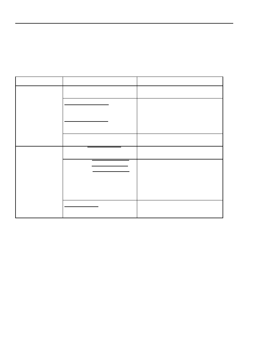
28
28
Agere Systems Inc.
Data Sheet
April 2001
TMUX03155 STS-3/STM-1 (AU-4) Multiplexer/Demultiplexer
Maintenance Functions
(continued)
Maintenance Functions Disabled During Failure Conditions
Several maintenance functions are disabled during failure conditions. These are listed in the following table. Event
and status information will be disabled and all BIP and far-end bit error (FEBE) counters will be held at 0.
Common Maintenance and Control Functions
The common section addresses maintenance functions that are common to both directions.
Device Reset
The device will provide a device reset function (RSTCTL, 0x04). This device reset will be initiated by a unique input
signal or by a command received through the control interface. A device reset will set all maintenance and control
registers to their default values. A device reset is service affecting.
Note: This signal must toggle from 0
1 0.
Composite Service Request
The device will provide a summary of the device monitoring conditions (INT, 0x00).
Mask Bit Operation
Mask bits will only inhibit the contribution of the event or delta bit contributing to the interrupt. The event or delta
bits will not be cleared if the corresponding mask bit is cleared. Delta and event bits clear-on-read.
Table 11. Monitors Disabled During Failure Conditions
Direction
Failure
Monitors Disabled
Transmit
TILOC (0x19)
Transmission path and all monitors dis-
abled
TLSOOF[3--1] and
TLSOOF_AISINH[3--1]
or
TLSLOF[3--1] and
TLSLOF_AISINH[3--1]
(0x19, 0x37, 0x39, 0x3B)
TLSB1ECNT[3--1][15:0],
TLSB2ECNT[1][17:0],
TLSB2ECNT[3--2][15:0]
(Page 1 - 0x80--0x8C)
RHSLOS or RHSLOF or RHSOOF
(0x1B)
SFEBE and PFEBE (AU-4 mode only)
insert (value set to 0)
Receive
RILOC and RRILOC_AISINH
(0x1B, 0x58)
Transmission path and all monitors dis-
abled
RHSLOS and RRHSLOS_AISINH or
RHSLOF and RRHSLOF_AISINH or
RHSOOF and RRHSOOF_AISINH
(0x1B, 0x58)
J0Z0MON, F1MON, APSMON, K2MON,
LRDIMON, LAISMON, RHSSF, RHSSD,
RHSB1ECNT[15:0], RHSB2ECNT[16:0],
RSFEBECNT[7:0],
RPFEBECNT[3--1][15:0],
and all path monitoring functions
(0x1B, 0xA6--0xAC, 0x8E)
(RPAIS[3:1] or RLOP[3:1]) and
PAISLOP_AISINH
(0x1C, 0x57)
All path monitoring functions:
J1, C2, B3, G1, F2, H4, Z3, Z5

Agere Systems Inc.
29
Data Sheet
April 2001
TMUX03155 STS-3/STM-1 (AU-4) Multiplexer/Demultiplexer
Maintenance Functions
(continued)
Common Maintenance and Control Functions
(continued)
Device Version and Device ID Number
The device will have a version number (DEVVER[7:0], 0x03). The version increments each time the device func-
tionality is changed, from the controller's perspective. The device ID (DEVID[15:0], 0x01--0x02) is a fixed pattern
used to identify the device by software.
Scratch Byte
The device will provide a 1-byte scratch register for the control interface to verify write capability to the device
(SCRATCH[7:0], 0x06).
Multibyte Registers
If a read value parameter register requires more than 8 bits, the device must prevent the value from changing
between 8-bit read commands. In these cases, the controller reads the lowest address byte first and transfers the
higher address bytes to a holding register where the value is held until the controller reads them. Similarly, if a
multibyte writable register is implemented, the controller writes the lowest address byte first, which is stored in a
holding register until the controller writes the highest address byte, and then all of the bytes take effect.
To simplify device design, the controller reads or writes all of the bytes of a multibyte register before reading or writ-
ing other registers so that the holding registers may be shared among all multibyte registers. This read/write oper-
ation is valid on all multibyte registers not controlled by the LATCH_CNT, 0x04 bit.
Update Counter Control
For performance monitoring purposes, there are a number of BIP, FEBE, and pointer interpreter increment/decre-
ment error counters in the receive/transmit section. All of these internal counters are comprised of a running error
counter and a hold register that present stable results to the microprocessor. The counts in all of the running
counters are latched to the hold registers when LATCH_CNT, 0x04 is written from a logic 0 to a logic 1. This zeros
all of the running counters. The results are held to be read by the microprocessor. All of the internal counters have
the ability to store more than 1 second's worth of counts, so as long as the LATCH_CNT occurs every second, or
faster, no counts will be lost. In case this doesn't happen, all of the running counters will hold their maximum value
rather than roll over to 0. The following counters
1
are affected by LATCH_CNT:
I
TLSB1ECNT[3--1][15:0], 0x08--0x85
I
TLSB2ECNT[1][17:0], 0x86--0x88
I
TLSB2ECNT[3--2][15:0], 0x89--0x8C
I
RHSB1ECNT[15:0], 0x8D--0x8E
I
RHSB2ECNT[17:0], 0x8F--0x91
I
RHSB3ECNT[3--1][15:0], 0x92--0x97
I
RPTR_INC[3--1[10:0], 0x98--0x9D
I
RPTR_DEC[3--1][10:0], 0x9E--0xA3
I
RSFEBECNT[17:0], 0xA4--0xA6
I
RPFEBECNT[3--1][15:0], 0xA7--0xAC
1 All addresses for these counters are in Page 1 registers.

30
30
Agere Systems Inc.
Data Sheet
April 2001
TMUX03155 STS-3/STM-1 (AU-4) Multiplexer/Demultiplexer
Maintenance Functions
(continued)
Common Maintenance and Control Functions
(continued)
Bit or Block Count
The device allows all counters, except the pseudorandom error counter, to either count the actual number of bit
errors or the number of blocks (a block equals one frame) that contain an error (BITBLOCKCNT, 0x34).
The section and path FEBE counters count the actual number of bit errors or the number of blocks that contain an
error (FEBEBITBLOCKCNT, 0x34).
Transmit Functions
The transmit section addresses maintenance functions that are unique to the transmit direction.
Parity (B1, B2, B3)
The device will perform a bit interleaved BIP-8 parity (B1) calculation and will write these bits into the B1 section
overhead byte. The device will perform a bit interleaved BIP-24 parity (B2) calculation and will write these bits into
the B2 line overhead byte. The device will perform a bit interleaved BIP-8 parity (B3) calculation and will write these
bits into the B3 path overhead byte (AU-4 mode only).
The device can perform a B1 (THSB1ERRINS, 0x4C), B2 (THSB2ERRINS[3--1], 0x4C), and B3
(THSB3ERRINS, 0x4C) parity byte inversion via microprocessor control.
A1, A2 Error Enable
The device will allow, under software control, from 1 to 32 continuous frames to have errored A1A2 patterns in the
outgoing frame (TA1A2ERRINS[4:0], 0x4D and TA1A2ERREN, 0x04).
Section Trace/Growth Byte Insert (J0/Z0)
The device inserts the data written into TJ0DINS[7:0], 0x3F, TZ02DINS[7:0], 0x40, and TZ03DINS[7:0], 0x41 into
the outgoing J0/Z0 bytes.
Fault Location Insert (F1)
Via microprocessor control of TF1INS, 0x3E and TF1DINS[7:0], 0x42, data information may be inserted into the
outgoing F1 byte. Direct microprocessor insert has higher priority than the TOAC insert control bit
(TTOAC_F1[1:0], 0x51).
Sync Status Byte Insert (S1)
Via microprocessor control of TS1INS, 0x3E and TS1DINS[7:0]0x45, data information may be inserted into the
outgoing S1 byte. Direct microprocessor insert has higher priority than the TOAC insert control bit
(TTOAC_Z1[1:0], 0x51).
Automatic Protection Switch (APS) Insertion (K1[7:0], K2[7:3])
The device writes the K1 and K2 bytes into the transmit K1 and K2 overhead bytes (TAPSINS[12:0], 0x43,
0x44). The K1 and K2[7:3] bits will only change when both values are valid. The TAPSINS[4:0], 0x44 byte is the
trigger for updating the APS bytes in the outgoing frame.

Agere Systems Inc.
31
Data Sheet
April 2001
TMUX03155 STS-3/STM-1 (AU-4) Multiplexer/Demultiplexer
Maintenance Functions
(continued)
Transmit Functions
(continued)
APS Babbling Test Control
Setting the TAPSBABLEINS, 0x4D register, via microprocessor control, forces the APS bytes (K1[7:0], K2[7:3]) to
an inconsistent state.
Line Remote Defect Indication (RDI-L) Insertion (K2[2:0] = 110)
The device will write Line RDI into the data signal using the following equation:
TLRDIINT =(RILOC AND TRILOC_LRDIINH) OR
(RHSLOS AND TRHSLOS_LRDIINH) OR
(RHSOOF AND TRHSOOF_LRDIINH) OR
(RHSLOF AND TRHSLOF_LRDIINH) OR
(RLAISMON AND TRLAISMON_LRDIINH) OR
(RHSSF AND TRHSSF_LRDIINH);
(See 0x1A, 0x1B, 0x1D, and 0x4A.)
Hardware insert of Line RDI will occur when TLRDIINT, 0x1A is active and the software insert control bit
(TLRDIINH, 0x4A) is disabled. User-provided data (TK2INS[2:0], 0x43) will be inserted into the K2[2:0] bits in the
STS-3/STM-1 (AU-4) frame when TLRDIINH = 0. The insertion of Line RDI consists of writing the pattern 110 into
the three LSBs of the K2 LOH byte.
Unequipped and AIS Generation (Automatic/Manual)
Line AIS or AU4-AIS or TUG-3 AIS can be generated automatically by the hardware under certain failure condi-
tions or via microprocessor control only. This is accomplished with the following equations and control signals:
FAILURE[3--1] =
((TLSOOF[3--1] AND TLSOOF_AISINH[3--1]) OR
(TLSLOF[3--1] AND TLSLOF_AISINH[3--1]))
H4PTRMIS[3--1] = ((TLSH4MIS[3--1] AND TLSH4MIS_AISINH[3--1]) OR
(TLSPTRMIS[3--1] AND (TLSPTRMIS_AISINH[3--1])) AND STS1_AU4;
AU-4 mode only
LAIS[3--1] =
TLS_LAISINS[3--1] OR FAILURE[3--1] OR H4PTRMIS[3--1];
AU4AISGen =
LAIS1 AND LAIS2 AND LAIS3;
(See 0x1A, 0x37, 0x39, 0x3B.)
Each alarm contribution that can cause AIS generation can be selectively inhibited. Line AIS is generated in the
STS-3 mode per STS-1 input when the appropriate FAILURE[3--1] or TLS_LAISINS[3--1] (software enable) sig-
nals are active. (Line overhead and the entire payload is set to an all-ones pattern.) In this mode, the
H4PTRMIS[3--1] contribution will always be 0. AU4-AIS generation will set all H1, H2, H3, and payload bytes to an
all-ones pattern in the output STM-1 (AU-4) signal. TUG-3 AIS generation will force all the data in the selected
TUG-3 signal to be set to an all-ones pattern.
In the STS-3 mode, an unequipped signal can be generated for any STS1 input under software control
(TLS_UNEQUIP[3--1], 0x3B, 0x39, 0x37 and (H1 = 0110SS00 AND H2 = 00000000)) and the selected payload is
set to 0). In AU-4 mode, the H1 and H2 bytes will not change from their default values and the entire payload will
be set to 0.
The SS bits will be set to the value written into register bits (TSS[1:0], 0x3E). AIS generation has higher priority
than unequipped signal generation.

32
32
Agere Systems Inc.
Data Sheet
April 2001
TMUX03155 STS-3/STM-1 (AU-4) Multiplexer/Demultiplexer
Maintenance Functions
(continued)
Transmit Functions
(continued)
H1 and H2 Corruption
Setting the TH1H2CRUPEN[3--1], 0x4E, register, via microprocessor control, allows the outgoing H1 and H2 val-
ues to be corrupted for each STS-1 channel. Either an invalid pointer or a continuous new data flag can be inserted
(TH1H2CRUPPorNDF, 0x4E).
Loss-of-Transmit Clock or Loss-of-Frame Sync
The device will detect a loss-of-transmit clock condition for the clock input in the transmit direction. Also, the device
was designed to detect a loss-of-frame sync for the frame sync input signal (Note, the loss-of-frame sync (TILOF)
feature is not supported in version 3 of the device). The state of TILOC and TILOF (0x19) along with any changes
to TILOCFD and TILOCFM (0x07 and 0x10) will be reported to the control system.
Transmit Clock Frequency Provisioning
The device must be provisioned (THSCLKTYPE[1:0], 0x3C) with the speed (155.52 MHz--bit, 38.88 MHz--
nibble, 19.44 MHz--byte) of the transmit clock. This information is needed to set the internal clock divider circuitry
and determine valid output port modes (e.g., a byte clock input cannot support a serial output port at
155.52 Mbits/s).
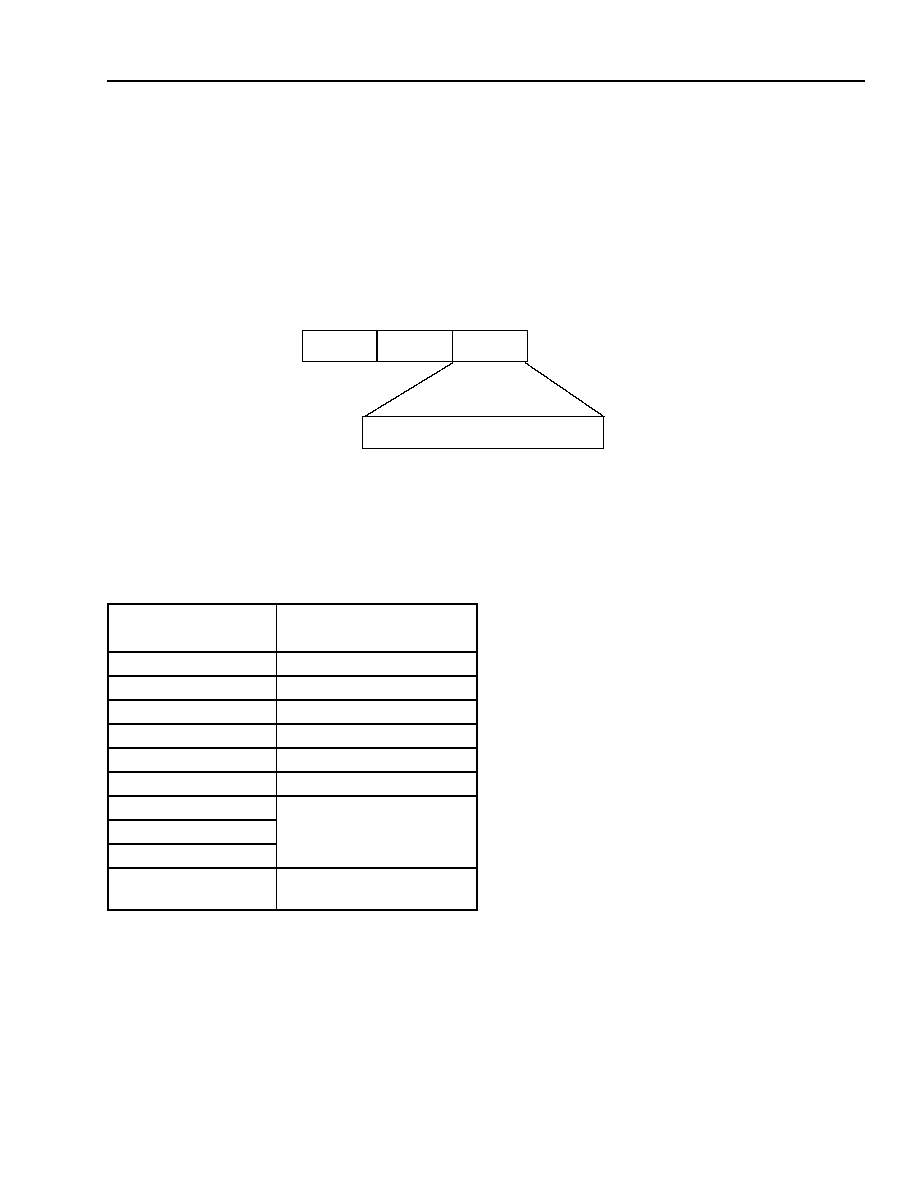
Agere Systems Inc.
33
Data Sheet
April 2001
TMUX03155 STS-3/STM-1 (AU-4) Multiplexer/Demultiplexer
Maintenance Functions
(continued)
Transmit Functions
(continued)
Section Far-End Bit Error (SFEBE)
The device will insert SFEBE in the transmitted M1 byte whenever there are bit errors in the received B2 bytes.
This function can be inhibited (TSFEBEINH, 0x3E) and the default value inserted, either all ones (SDH) or all zeros
(SONET). The device can insert a continuous error into the M1 byte under user control (TSFEBEEINS, 0x4D).
SFEBE will be inserted into the M1 byte as defined in Figure 3.
5-5295(F)
Figure 3. SFEBE Location
The values for SFEBE are summarized in Table 12.
Table 12. SFEBE Values
Section or Line FEBE Number of B2 Bit Errors in
the Receive Signal
00000000
0 (no errors)
00000001
1
00000010
2
. . .
. . .
00010111
23
00011000
24
00011001
No errors
. . .
11111110
11111111 (SDH)
00000000 (SONET)
Section FEBE not supported
(no errors)
Z2-1
Z2-2
M1
23 (MSB)
0 (LSB)
0 (LSB)
7 (MSB)
SECTION FEBE
34
34
Agere Systems Inc.
Data Sheet
April 2001
TMUX03155 STS-3/STM-1 (AU-4) Multiplexer/Demultiplexer
Maintenance Functions
(continued)
Transmit Functions
(continued)
Path - Trace Byte (J1)--AU-4 Mode Only
The device will continuously insert a 64-byte sequence (TJ1DINS[64--1][7:0], 0x80--0xBF) into the outgoing
STM-1 (AU-4) signal when the TJ1INS signal is active; otherwise, all zeros will be inserted into this byte.
Path - Signal Label Byte (C2)--AU-4 Mode Only
The device will allow data to be inserted into the outgoing C2 byte under software control (TC2DINS[7:0], 0x46).
Path - G1 Status Byte (PFEBE (REICNT))--AU-4 Mode Only
The G1 byte contains the PFEBE (B3 errors) as shown in Table 13.
The device will insert PFEBE in the transmitted G1 byte whenever there are bit errors in the received B3 byte. This
function can be inhibited (TPFEBEINH, 0x3E) and the default value inserted, either all ones (SDH) or all zeros
(SONET). The device can insert a continuous error into the G1 PFEBE[3:0] byte under user control (TPFEBEEINS,
0x4D).
The values for PFEBE are summarized in Table 14.
Table 13. G1 Byte--AU-4 Mode Only
MSB
(7)
6
5
4
3
2
1
LSB
(0)
PFEBE[3:0]
Valid values (0 to 8) all others
indicate no errors
RDI-P
111 (SDH) or
000 (SONET)
Table 14. PFEBE Values
Section or Line FEBE Number of B3 Bit Errors in
the Receive Signal
0000
0 (no errors)
0001
1
0010
2
. . .
. . .
0111
7
1000
8
1001
No errors
. . .
1111

Agere Systems Inc.
35
Data Sheet
April 2001
TMUX03155 STS-3/STM-1 (AU-4) Multiplexer/Demultiplexer
Maintenance Functions
(continued)
Transmit Functions
(continued)
Path - G1 Status Byte (RDI-P)--AU-4 Mode Only
The G1 byte contains the RDI-P bit as shown in Table 13.
Path RDI is inserted automatically under hardware control. Each failure contribution can be excluded from the gen-
eration equation by setting the appropriate inhibit bit.
TPRDIINT = ((RILOC AND TRILOC_PRDIINH), 0x4B, OR
(RHSLOS AND TRHSLOS_PRDIINH), 0x4B, OR
(RHSOOF AND TRHSOOF_PRDIINH), 0x4B, OR
(RHSLOF AND TRHSLOF_PRDIINH), 0x4B, OR
(RLAISMON AND TRLAISMON_PRDIINH), 0x4B, OR
(RPAIS1 AND TRPAIS1_PRDIINH), 0x4B, OR
(RLOP1 AND TRLOP1_PRDIINH), 0x4B, OR
TPRDIINS (software insert));
(See 0x1A, 0x1B, 0x4B.)
PRDI can be forced, via microprocessor control, by setting TPRDIINS to a logic 1.
Path - User Channel Byte (F2)--AU-4 Mode Only
Via microprocessor control of the (TF2DINS[7:0], 0x47), data information may be inserted into the outgoing F2
byte.
Path - Growth Byte (Z3)--AU-4 Mode Only
Via microprocessor control of the (TZ3DINS[7:0], 0x48), data information may be inserted into the outgoing Z3
byte.
Path - Tandem Connection Byte (Z5)--AU-4 Mode Only
Via microprocessor control of the (TZ5DINS[7:0], 0x49), data information may be inserted into the outgoing Z5
byte.
Pseudorandom Test Pattern Insert--AU-4 Mode Only
A pseudorandom test sequence can be inserted into any selected (TSTGEN_PSEL[1:0], 0x4E) TUG-3 within the
AU-4 signal. The pattern can be selected from the following two equations: Q23 + Q17 + 1 or Q15 + Q14 + 1
(TPAT23or15, 0x4E). A one shot is provided to inject eight (8) errors into the selected pseudorandom sequence
(TSTGENE8INS, 0x04). A value of zero in the TSTGEN_PSEL[1:0] register disables this function.
36
36
Agere Systems Inc.
Data Sheet
April 2001
TMUX03155 STS-3/STM-1 (AU-4) Multiplexer/Demultiplexer
Maintenance Functions
(continued)
Transmit Functions
(continued)
Output Offset
The device will output the STS-3/STM-1 (AU-4) frame a programmable number of clock cycles from the input
frame sync. These registers allow movement of the output frame with a granularity of one high-speed clock cycle.
The values programmed in (TLBITCNT[2:0], TLSTS1CNT[1:0], TLCOLCNT[6:0], TLROWCNT[3:0], 0x53, 0x54)
must be within the valid ranges for the mode selected (see Table 15). See Table 56 on page 77 for more details.
Transmit Transport Overhead Access Channel (TTOAC)
A transport overhead access channel (TOAC) is provided on-chip to provision the TOH portion of the outgoing
SDH or SONET frame. The TOAC consists of the following signals:
I
A 5.184 MHz clock signal, sourced by the device (TTOACCLKO, TTOAC_CLKINV).
I
A 5.184 Mbits/s data signal received by the device in the transmit direction (TTOACDATAI).
I
An 8 kHz synchronization signal (TTOACSYNCO), sourced by the device. The sync signal is normally low;
during the last clock period of each frame coincident with the least significant bit of the eighty-first byte or during
the first clock period of each frame coincident with the most significant bit of the first byte, the sync signal is high
(TTOACSA1orEND, 0x4F).
An inhibit signal is provided through the control interface to place the clock and sync signals in a high-impedance
state (TTOACINH, 0x4F).
The data signal is partitioned into frames of 81 bytes. The frame repetition rate is 8 kHz. Each byte consists of
8 bits that are received most significant bit first. The MSB of the first byte of each frame contains an odd/even parity
bit over the 648 bits of the previous frame. The remaining 7 bits of this byte are not specified.
Bytes shown in Table 16 summarize the access capabilities of the transmit TOAC. Bytes indicated in bold type are
not specified in the standard, but are labeled here for clarity. X symbols indicate don't cares.
Table 15. Value Offset Load Values
Mode
TLBITCNT[2:0]
TLSTS1CNT[1:0]
TLCOLCNT[6:0]
TLROWCNT[3:0]
BIT
0--7
0--2
0--89
0--8
NIBBLE
0--1
0--2
0--89
0--8
BYTE
0
0--2
0--89
0--8
Table 16. Transport Overhead Byte Access--Transmit Direction
OH Pty
X
X
X
X
X
X
X
X
X
B1-2
B1-3
E1
E1-2
E1-3
F1
F1-2
F1-3
D1
D1-2
D1-3
D2
D2-2
D2-3
D3
D3-2
D3-3
X
X
X
X
X
X
X
X
X
X
X
X
X
K1-2
K1-3
X
K2-2
K2-3
D4
D4-2
D4-3
D5
D5-2
D5-3
D6
D6-2
D6-3
D7
D7-2
D7-3
D8
D8-2
D8-3
D9
D9-2
D9-3
D10
D10-2
D10-3
D11
D11-2
D11-3
D12
D12-2
D12-3
S1
Z1-2
Z1-3
Z2
Z2-2
X
E2
E2-2
E2-3

Agere Systems Inc.
37
Data Sheet
April 2001
TMUX03155 STS-3/STM-1 (AU-4) Multiplexer/Demultiplexer
Maintenance Functions
(continued)
Transmit Functions
(continued)
OH Parity
An event indication is provided at the control interface if an overhead parity error occurs. Odd/even parity is
checked (TTOAC_OEPMON, TTOAC_PERRM, TTOAC_PERRE, 0x4F, 0x10, 0x07).
D1--D3, D4--D12, E1, E2, F1, Z1, Z2 Overhead Bytes
Table 17 summarizes the insertion options for the specified overhead bytes. The device allows (1) the default value
for unused SDH or SONET bytes to be inserted, or (2) the transmit TOAC values to be inserted, or (3) the received
STS-1/AU-3 value to be inserted into the outgoing STS-3 frame.
Table 17. TTOAC Control Bits
Overhead Bytes
Control Bits
1
1. See Address 0x50, 0x51 for control bits.
Values
00 (Default)
or 11
01
10
D1--D3
TTOAC_D1TO3[1:0]
SDH (1s) or
SONET (0s)
Default Values
TTOAC
Data
Pass Through
Associated
STS-1/AU-3
Data
D4--D12
TTOAC_D4TO12[1:0]
E1
TTOAC_E1[1:0]
E2
TTOAC_E2[1:0]
F1
TTOAC_F1[1:0]
S1, Z1-2, Z1-3
TTOAC_Z1[1:0]
Z2, Z2-2
TTOAC_Z2[1:0]
B1-2, B1-3
TTOAC_INS[1:0]
SDH (1s) or
SONET (0s)
Default
Values
TTOAC
Pass Through
Associated
STS-1/AU-3
Data
E1-2, E1-3
F1-2, F1-3
D1-2, 3 to D3-2, 3
K1-2, K1-3
K2-2, K2-3
D4-2, 3 to D12-2, 3
E2-2, E2-3

38
38
Agere Systems Inc.
Data Sheet
April 2001
TMUX03155 STS-3/STM-1 (AU-4) Multiplexer/Demultiplexer
Maintenance Functions
(continued)
Receive Functions
A number of the receive maintenance functions require a continuous N times detection (CNTD) of a signal to
change an alarm status. All of these continuous N times detect signals require not only that the monitored signal
be consistent for N consecutive frames, but also that the frame bytes, A1 and A2, be error free for all N frames
before the status can be updated. If there are any errors in the framing pattern, then the consecutive N times
detection counters must be reset to 0. N can range from 3 to 15. There is also a signal (CNTDB1SEL, 0x5F) that
will cause these continuous N times detection counters to be reset to 0 if there are any errors in the received B1
byte.
Continuous N Times Detect B1 Error Reset Enable
The following CNTD monitors are affected by this control bit (CNTDB1SEL):
1. AIS-L (K2[2:0] = 111)
2. RDI-L (K2[2:0] = 110)
3. K2MON (K2[2:0])
4. APSMON (K1[7:0], K02[7:3])
Receive Loss of Clock
The device will detect a receive loss-of-clock (RILOC, 0x1B) condition for the clock input and notify the control sys-
tem of any changes to this condition (RILOCD, 0x0A, and RILOCM, 0x13).
Insertion of Line AIS (Automatic/Manual)
The device will write Line AIS into each STS-1/AU-3 output signal if either the appropriate alarms occur or the soft-
ware insert bit is active.
LAIS_COMMON = ((RILOC AND RRILOC_AISINH) OR
(RRHSOOF AND RHSOOF_AISINH) OR
(RHSLOF AND RRHSLOF_AISINH) OR
(RHSLOS AND RRHSLOS_AISINH) OR
(LAISMON AND RRLAISMON_AISINH));
(See 0x1B, 0x58.)
If (RLAISINS[3--1] = 1 OR LAIS_COMMON = 1), then insert Line AIS on the selected output.
When a RILOC condition exists, the transmit clock is used to generate the Line AIS signal downstream, if possible.
Insertion of Path AIS (Automatic)
The device will write Path AIS into each STS-1/AU-3 output signal if the appropriate alarms occur.
PAIS_COMMON[3--1] = ((PAIS[3--1] OR LOP[3--1]) AND PAISLOP_AISINH)
If (PAIS_COMMON[3--1] = 1), then insert Path AIS on the appropriate output. (PAIS consists of writing all ones
into the H1, H2, H3 bytes, and into the entire payload.)
B1 BIP-8 Parity
The device will perform B1 (BIP-8) calculation and error checking in the receive path. The device will allow access
to the B1 errored bit/block (one block is equal to one frame) count (BITBLOCKCNT, 0x34, RHSB1ECNT[15:0],
0x8D-0x8E). This counter will update when LATCH_CNT transitions from a logic 0 to a logic 1.

Agere Systems Inc.
39
Data Sheet
April 2001
TMUX03155 STS-3/STM-1 (AU-4) Multiplexer/Demultiplexer
Maintenance Functions
(continued)
Receive Functions
(continued)
B2 BIP-24 Parity
The device will perform B2 (BIP-24) calculation and error checking. The device will allow access to the B2 errored
bit/block (one block is equal to one frame) count (BITBLOCKCNT, 0x34, RHSB2ECNT[16:0], Page 1 - 0x8F--
0x91). This counter will update when LATCH_CNT, 0x04 transitions from a logic 0 to a logic 1.
Signal Degrade BER Algorithm
A signal degrade state and change of state indication will be provided to the control interface (RHSSD, RHSSDD,
RHSSDM, 0x1B, 0x0A, 0x13). This bit error rate algorithm can operate on either B1 or B2 errors (SDB1B2SEL,
0x83). Signal degrade is declared when SDLSet[3:0], Page 2 - 0x83 or more bit errors in SDNsSet[18:0], Page
2 - 0x8E--0x90 and frames occur SDMSet[7:0], Page 2 - 0x84 times out of SDBSet[11:0], Page 2 - 0x85--0x86
blocks (one block is equal to one measurement period of SDNsSet[18:0] frames), and it is removed when less
than SDLClear[3:0], Page 2 - 0x8A bit errors in SDNsClear[18:0], Page 2 - 0x87--0x89 frames occur SDM-
Clear[7:0], Page 2 - 0x8B times out of SDBClear[11:0], Page 2 - 0x8C--0x8D blocks.
The above algorithm can detect bit error rates from 1 x 10
≠3
to 1 x 10
≠9
.
Signal Fail BER Algorithm
A signal fail state and change of state indication will be provided to the control interface (RHSSF, RHSSFD,
RHSSFM, 0x1B, 0x0A, 0x13). This bit error rate algorithm can operate on either B1 or B2 errors (SFB1B2SEL,
Page 2 - 0x91). Signal fail is declared when SFLSet[3:0], Page 2 - 0x91 or more bit errors in SFNsSet[18:0],
Page 2 - 0x8E--0x90 frames occur SFMSet[7:0], Page 2 - 0x92 times out of SFBSet[11:0], Page 2 - 0x93--0x94
blocks (one block is equal to one measurement period of SFNsSet[18:0] frames), and it is removed when less than
SFLClear[3:0], Page 2 - 0x98 bit errors in SFNsClear[18:0], Page 2 - 0x96--0x98 frames occur SFMClear[7:0],
Page 2 - 0x99 times out of SFBClear[11:0] Page 2 - 0x9A--0x9B blocks.
The above algorithm can detect bit error rates from 1 x 10
≠3
to 1 x 10
≠9
.
Section Trace (J0, Z0-2, Z0-3) Byte Monitoring
The device will monitor the section trace bytes (RJ0MON[7:0], RZ02MON[7:0], RZ03MON[7:0], RCDRLOC,
0x1E, 0x1F, 0x20, 0x1B) on the receive input. A new section trace value will be detected after CNTDJ0Z0[3:0],
0x5A and consecutive consistent occurrences of a new pattern in the section trace overhead bytes. Any changes
to these bytes will be reported to the control system (RJ0Z0MOND, RJ0Z0MONM, 0x0C, 0x15).
Fault Location Monitoring (F1MON)
The device will monitor the fault location byte (RF1MON0[7:0], 0x21) on the receive input. A new fault location
state will be detected after CNTDF1[3:0], 0x5A consecutive consistent occurrences of a new pattern in the F1
overhead byte. The device will also maintain a history of the previous valid F1 byte (RF1MON1[7:0], 0x22). Any
changes to this byte will be reported to the control system (RF1MOND, RF1MONM, 0x0C, 0x15).
Automatic Protection Switch (APS) Monitoring
The device will monitor the K1 byte and the K2 byte (5 MSBs only) on the input side of the device receive path
(RAPSMON[12:0], 0x23, 0x24). After CNTDAPS[3:0], 0x5B consecutive consistent occurrences of new K1 and
K2 bytes, the device will notify the control system (RAPSMOND, RAPSMONM, 0x0B, 0x14).

40
40
Agere Systems Inc.
Data Sheet
April 2001
TMUX03155 STS-3/STM-1 (AU-4) Multiplexer/Demultiplexer
Maintenance Functions
(continued)
Receive Functions
(continued)
APS Babbling Monitor
The device will monitor the APS bytes (K1[7:0], K2[7:3]) in the receive direction and report to the control interface
(RAPSBABLEE, RAPSBABLEM, 0x0C, 0x15) when the K1 bytes are inconsistent. Inconsistent APS bytes are
defined as CNTDAPSFRAME[3:0], 0x5C (Default = 12) successive frames, starting with the last frame containing
previously consistent code, where no CNTDAPS[3:0], 0x5B (Default = 3) consecutive frames contain identical
APS bytes.
Line AIS (AIS-L) Monitoring
The device will monitor line AIS on the receive input (RLAISMON, 0x1D). Line AIS will be detected after
CNTDK2[3:0], 0x5B consecutive occurrences of the AIS-L pattern (xxxxx111) in the K2 overhead byte. Any
changes to this byte will be reported to the control system (RLAISMOND, RLAISMONM, 0x0C, 0x15).
Line Remote Defect Indication (RDI-L) Monitoring
The device will monitor an RDI-L condition on the receive input (RLRDIMON, 0x1D). A Line RDI condition will be
detected after CNTDK2[3:0] consecutive occurrences of the Line RDI pattern (xxxxx110) in the K2 overhead byte.
Any changes to this byte will be reported to the control system (RLRDIMOND, RLRDIMONM, 0x0C, 0x15).
K2 Byte Monitoring
The device will monitor the K2 byte (3 LSBs only) on the input side of the receive direction (RK2MON[2:0], 0x23).
After CNTDK2[3:0], 0x5B consecutive consistent occurrences of new K2 bits, the device will notify the control sys-
tem (RK2MOND, RK2MONM, 0x0B, 0x14).
Sync Status (S1) Byte Monitoring
The device will monitor the sync trace byte (RS1MON[7:0], 0x25) on the receive input. A new sync trace value will
be detected after CNTDS1[3:0], 0x5C consecutive consistent occurrences of a new pattern in the overhead bytes.
Any changes to this byte will be reported to the control system (RS1MOND, RS1MONM, 0x0C, 0x15).
Section FEBE (M1) Monitoring
The device will monitor a Section FEBE condition (M1) on the receive input. The device will allow access to the
Section FEBE errored bit/block (one block is equal to one frame) count (FEBEBITBLOCKCNT, 0x34,
RSFEBECNT[17:0], Page 1 - 0x34, 0xA4, 0xA6). This counter will update when LATCH_CNT transitions from a
logic 0 to a logic 1.
AU-4 NPI (Null Pointer Indication) Monitoring
The device will monitor the three NPI values in the incoming STM-1(AU-4) signal. When five consecutive mis-
matches occur (any one of the three NPI values are in error) separated in time by 125 µs, the device will declare an
NPI mismatch condition. An NPI match condition is declared when two consecutive matches occur (all three NPI
values match), separated in time by 125 µs. The delta, mask, and state bits are RHSNPIMISD, RHSNPIMISM,
RHSNPIMIS, 0x0D, 0x16, 0x1D, respectively.

Agere Systems Inc.
41
Data Sheet
April 2001
TMUX03155 STS-3/STM-1 (AU-4) Multiplexer/Demultiplexer
Maintenance Functions
(continued)
Receive Functions
(continued)
STM-1(AU-4) H4 Multibyte Monitor
The device will monitor the path H4 byte for correct multibyte sequence. Each time the expected value mismatches
with the received value, an event indication is set. When a mismatch occurs, the device accepts the new value plus
1 as the expected value for the next frame. The event and mask bits are RHSH4MISE, RHSH4MISM, 0x0D, 0x16.
Path Trace Byte (J1) Monitoring
The device will monitor the path trace byte (RJ1MON[64--1][7:0], 0xC0--0xFF) on the receive input. Only one J1
byte can be monitored (J1PSELMON[1:0], 0x56) out of the three possible J1 bytes. The device will store a 64-byte
sequence and declare a mismatch each time the incoming value does not agree with the stored value (RJ1MISE,
RJ1MISM, 0x0C, 0x15).
Path Signal Label (C2) Monitoring
The device will monitor the C2 bytes on the receive input (RC2MON[3--1][7:0], 0x28, 0x27, 0x26). After
CNTDC2[3:0], 0x5D consecutive consistent occurrences of a new C2 byte, the device will notify the control system
(RC2MOND[3--1], RC2MONM[3--1], 0x0D, 0x16).
Path FEBE (G1) Byte Error Count
The device will monitor for a path FEBE condition (G1[7:4]) on the input signal. The device will allow access to the
path FEBE errored bit/block (one block is equal to one frame) count (FEBEBITBLOCKCNT,
RPFEBECNT[3--1][15:0], 0x34, 0xA7--0xAC). These counters will update when LATCH_CNT, 0x04 transitions
from a logic 0 to a logic 1.
Path RDI (Path Yellow (G1[3] or Enhanced Failure Code (G1[3:1])))
The device will monitor the G1 bytes for path yellow condition or for an enhanced failure code (RRDI_MPYorEFC,
0x55) on the receive input (RRDIP[3--1][2:0], 0x32, 0x33). After CNTDG1[3:0], 0x5D consecutive consistent
occurrences of a new G1 value, the device will notify the control system (RRDIPE[3--1], RRDIPM[3--1], 0x16).
Path User Channel (F2) Monitoring
The device will monitor the F2 byte (RF2MON[3--1][7:0], 0x29, 0x2A, 0x2B) on the receive input. A new value
will be detected after CNTDF2[3:0], 0x5E consecutive consistent occurrences of a new pattern in the overhead
bytes. Any change to this byte will be reported to the control system (RF2MOND[3--1], RF2MONM[3--1], 0x0E,
0x17).
Path Growth Byte (Z3) Monitoring
The device will monitor the Z3 bytes (RZ3MON[3--1][7:0], 0x2C, 0x2D, 0x2E) on the receive input. A new value
will be detected after CNTDZ3[3:0], 0x5E consecutive consistent occurrences of a new pattern in the overhead
bytes. Any change to this byte will be reported to the control system (RZ3MOND[3--1], RZ3MONM[3--1], 0x0E,
0x17).
Path Tandem Connection Byte (Z5) Monitoring
The device will monitor the Z5 bytes (RZ5MON[3--1][7:0], 0x31, 0x30, 0x2F) on the receive input. A new value
will be detected after CNTDZ5[3:0], 0x5F consecutive consistent occurrences of a new pattern in the overhead
bytes. Any change to this byte will be reported to the control system (RZ5MOND[3--1], RZ5MONM[3--1], 0x0F,
0x18).

42
42
Agere Systems Inc.
Data Sheet
April 2001
TMUX03155 STS-3/STM-1 (AU-4) Multiplexer/Demultiplexer
Maintenance Functions
(continued)
Receive Functions
(continued)
Test Pattern Drop (AU-4 Mode Only)
The device will monitor a pseudorandom pattern (RPAT23or15, 0x60) on a per TUG-3 basis
(RTSTDRP_PSEL[1:0], 0x60). The drop logic will provide an out-of-sync indication (RTSTDRP_OOS, 0x60) and
an error count (RTSTDRP_ECNT[7:0], 0x61). This counter will hold at its maximum value and is not affected by
the LATCH_CNT, 0x04 signal. The detector will transition to the in-sync-state after 32 consecutive matches occur.
The detector will transition from the in-sync-state to the out-of-sync state if 32 consecutive errors are detected.
STS-1/AU-3 Byte Error Insert or Overwrite Control
This section summarizes the output error and overwrite capabilities on a per STS1/AU-3 basis. All path overhead
bytes pass through from the input signal.
Table 18. STS-1/AU-3 Overhead Control
Control Signal per STS-1/
AU-3 Signal
Bytes
Affected/
Action
Action
RA1A2ERREN,
RA1A2ERRPEN[3--1],
RA1A2ERRINS[4:0]
(0x05, 0x62)
A1, A2
Error Insert
If (RA1A2ERREN = 0
1) then insert RA1A2ERRINS[4:0]
consecutive frame errors on the selected ports
(RA1A2ERRPEN[3--1]) else insert correct framing pattern.
RC1DINS[3--1][7:0]
(0x68, 0x69, 0x6A)
C1
Always insert values.
RB1ERRINS[3--1]
(0x63)
B1
Error Insert
1 = insert error, 0 = insert normal value.
R_E1_PASS[3--1]
(0x74)
E1
1 = pass input data, 0 = insert default value.
RF1INS[3--1]
RF1DINS[3--1][7:0],
R_F1_PASS[3--1]
(0x64, 0x6B--0x6D, 0x74)
F1
Software or
Pass
If (RF1INS = 1) then insert software value (RF1DINS) else if
(R_F1_PASS = 1) then pass input data
else set byte to the default value.
R_D1TOD3_PASS[3--1]
(0x75)
D1 to D3
1 = pass input data, 0 = insert default value.
RH1H2CRUPEN[3--1],
RH1H2CRUPPorNDF
(0x64)
H1, H2
Error Insert
If (RH1H2CRUPPorNDF = 0 AND RH1H2CRUPEN = 1) then
continuously corrupt the pointer value
else if (RH1H2CRUPPorNDF = 1 AND RH1H2CRUPEN = 1) then
continuously send NDF (1001) pattern
else pass input data.
RB2ERRINS[3--1]
(0x63)
B2
Error Insert
1 = insert error, 0 = insert normal value.
RAPSBABLEINS[3--1],
RAPSINS[3--1][12:0]
(0x66, 0x6E--0x73)
K1, K2[7:3]
Error or
Software
If (RAPSBABLEINS = 1) then
continuously insert a nonconsistent K1K2 value
else insert software value RAPSINS.
Agere Systems Inc.
43
Data Sheet
April 2001
TMUX03155 STS-3/STM-1 (AU-4) Multiplexer/Demultiplexer
Maintenance Functions
(continued)
Receive Functions
(continued)
Table 18. STS-1/AU-3 Overhead Control (continued)
Control Signal per STS-1/
AU-3 Signal
Bytes
Affected/
Action
Action
RLRDIINT[3--1]
RTILOC_LRDIINH,
RTLSLOF_LRDIINH[3--1],
RTLSOOF_LRDIINH[3--1],
RK2DINS[3--1][2:0]
(0x1D, 0x67, 0x6E, 0x70,
0x72)
K2[2:0]
Automatic/
Software
RLRDIINT[3--1] = (TILOC AND TILOC_LRDIINH) OR
(RTLSLOF[3--1] AND RTLSLOF_LRDIINH[3--1]) OR
(RTLSOOF[3--1] AND RTLSOOF_LRDIINH[3--1]);
1
If (all associated inhibit signals are active) then
insert software value RK2DINS[3--1][2:0]
else insert 110 pattern when RLRDIINT[3--1] is active
else insert 000 pattern.
1. Software enable when all hardware inhibit signals are 1.
R_D4TOD12_PASS[3--1]
(0x75)
D4 to D12
1 = pass input data, 0 = insert default value.
R_S1_PASS[3--1]
(0x76)
S1
1 = pass input data, 0 = insert default value.
RSFEBEINH[3--1]
RSFEBEERRINS[3--1]
(0x65)
M0
Automatic
or Error
Insert
If (RSFEBEINH = 1) then inhibit the insertion of B2 errors and set the
byte to the default value
else if (RSFEBEERRINS = 1) then insert an error into the output
byte
else output B2 errors per frame from the associated transmit input.
R_E2_PASS[3--1]
(0x76)
E2
1 = pass input data, 0 = insert default value.
44
44
Agere Systems Inc.
Data Sheet
April 2001
TMUX03155 STS-3/STM-1 (AU-4) Multiplexer/Demultiplexer
Maintenance Functions
(continued)
Receive Functions
(continued)
Receive Transport Overhead Access Channel (RTOAC)
A TOAC is provided on-chip to drop the TOH portion of the incoming SDH or SONET frame. The TOAC channel
consists of the following signals:
1. 5.184 MHz clock signal, sourced by the device (RTOACCLKO, RTOAC_CLKINV).
2. A 5.184 Mbits/s data signal, sourced by the device (RTOACDATAO).
3. An 8 kHz synchronization signal, sourced by the device. The sync signal is normally low; during the last clock
period of each frame coincident with the least significant bit of the eighty-first byte or coincident with the least
significant bit of the first byte, the sync signal can go high (RTOACS_A1orEND, 0x4F).
An inhibit signal is provided through the control interface to place the clock, data, and sync signal into a high-
impedance state (RTOACINH, 0x4F).
The data signal is partitioned into frames of 81 bytes. The frame repetition rate is 8 kHz. Each byte consists of
8 bits that are transmitted/received most significant bit first. The MSB of the first byte of each frame contains an
odd/even parity bit over the 648 bits of the previous frame. The remaining 7 bits of this byte are not specified.
Bytes shown in Table 19 summarize the access capabilities of the receive TOAC. Bytes indicated in bold type are
not specified in the standard, but are labeled here for clarity.
OH Parity
Even or odd parity can be inserted into the first bit of the MSB byte (RTOAC_OEPINS, 0x4F) of the TOAC outgo-
ing frame.
Table 19. Transport Overhead Byte Access--Receive Direction
OH Pty
A1-2
A1-3
A2-1
A2-2
A2-3
J0
Z0-2
Z0-3
B1
B1-2
B1-3
E1
E1-2
E1-3
F1
F1-2
F1-3
D1
D1-2
D1-3
D2
D2-2
D2-3
D3
D3-2
D3-3
H1-1
H1-2
H1-3
H2
H2-2
H2-3
H3
H3-2
H3-3
B2-1
B2-2
B2-3
K1
K1-2
K1-3
K2
K2-2
K2-3
D4
D4-2
D4-3
D5
D5-2
D5-3
D6
D6-2
D6-3
D7
D7-2
D7-3
D8
D8-2
D8-3
D9
D9-2
D9-3
D10
D10-2
D10-3
D11
D11-2
D11-3
D12
D12-2
D12-3
S1
Z1-2
Z1-3
Z2-1
Z2-2
M1
E2
E2-2
E2-3
Agere Systems Inc.
45
Data Sheet
April 2001
TMUX03155 STS-3/STM-1 (AU-4) Multiplexer/Demultiplexer
Typical Uses
Section and Line Termination Multiplex
Using the device without internal loopbacks results in a multiplex/demultiplex operation.
5-5296 (F)
Figure 4. Line Termination Multiplex
STS-3/STM-1 (AU-4) OUT
STS-1/AU-3 OUT
STS-3/STM-1 (AU-4) IN
CONTROL SIGNALS
TRANSMIT DIRECTION
RECEIVE DIRECTION
TOAC
DROP
3:1
MUX
LOGIC
SPE
GENERATE
1:3
DEMUX
LOGIC
FRAMER
OVERHEAD
TRANSPORT/PATH
MONITOR
SELECT/
LOGIC
MULTI-
CAST
OVERHEAD
MONITOR
TOAC
INSERT
MICROPROCESSOR
LOCAL CLOCK
GENERATION
BUS
OVERHEAD
MONITOR
INTERFACE
OVERHEAD
MONITOR
DROP
SELECT
ADD
CONTROL
STS-1/AU-3 IN
CONTROL SIGNALS
BUS
CONTROL
LOGIC

46
46
Agere Systems Inc.
Data Sheet
April 2001
TMUX03155 STS-3/STM-1 (AU-4) Multiplexer/Demultiplexer
Typical Uses
(continued)
Add/Drop Multiplex
Using the device with STS-1/AU-3 internal loopbacks results in an add/drop multiplex.
5-5297 (F)
Figure 5. Add/Drop Multiplex
Digital Cross Connect
Using the device with STS-3 internal loopback results in a digital cross connect.
5-5298 (F)
Figure 6. Digital Cross Connect
3:1
MUX
LOGIC
OVERHEAD
GENERATE
1:3
DEMUX
LOGIC
FRAMER
TRANSPORT
MONITOR
STS-3 IN
STS-3 OUT
ST
S-
1
/
AU-
3
I
N
ST
S-
1
/
AU-
3
O
U
T
SELECT/
MULTI-
CAST
LOGIC
DROP SELECT
RECEIVE DIRECTION
TRANSMIT DIRECTION
LOGIC
DROP SELECT
LOGIC
ADD
BUS
CONTROL
LOGIC
3:1
MUX
LOGIC
OVERHEAD
GENERATE
1:3
DEMUX
LOGIC
OVERHEAD
MONITOR
STS-1/AU-3 #1 IN
STS-1/AU-3 #2 IN
STS-1/AU-3 #3 IN
FRAMER
TRANSPORT
MONITOR
DROP
SELECT
LOGIC
STS-1/AU-3 #1 OUT
STS-1/AU-3 #2 OUT
STS-1/AU-3 #3 OUT
OVERHEAD
MONITOR
OVERHEAD
MONITOR
Agere Systems Inc.
47
Data Sheet
April 2001
TMUX03155 STS-3/STM-1 (AU-4) Multiplexer/Demultiplexer
Microprocessor Interface
Overview
The device is equipped with an asynchronous microprocessor interface that can operate with most commercially
available microprocessors. Inputs MPMUX and MPMODE are used to configure this interface into one of four pos-
sible modes. The MPMUX setting selects either a multiplexed 8-bit address/data bus (AD[7:0]) or a demultiplexed
8-bit address bus (A[7:0]) and an 8-bit data bus (AD[7:0]). The MPMODE setting selects the associated set of reg-
isters within the device.
Due to device flexibility, there are no default powerup or reset states. All read/write registers must be written by the
microprocessor on system start-up to guarantee proper device functionality. The microprocessor interface can
operate at speeds up to 32.768 MHz in interrupt-driven or polled modes without requiring any wait-states.
Microprocessor Configuration Modes
Table 20 highlights the four microprocessor modes controlled by the MPMUX and MPMODE inputs.
Table 20. Microprocessor Configuration Modes
* When the MPMODE3ALE input pin = 0, ALE is not used to retime the incoming address.
Microprocessor Interface Pinout Descriptions
The MODE [1--4] specific pin definitions are given in Table 21. Note that the microprocessor interface uses the
same set of pins in all modes.
Table 21. MODE [1--4] Microprocessor Pin Definitions
Mode
MPMODE
MPMUX
Address/Data Bus
Generic Control, Data and Output Pin Names
MODE 1
0
0
DeMUXed
CS, AS, DS, R/W, A[7:0], AD[7:0], INT, DTACK
MODE 2
0
1
MUXed
CS, AS, DS, R/W, AD[7:0], INT, DTACK
MODE 3*
1
0
DeMUXed
CS, ALE, RD, WR, A[7:0], AD[7:0], INT, RDY
MODE 4
1
1
MUXed
CS, ALE, RD, WR, AD[7:0], INT, RDY
Configuration
Device Pin
Name
Generic Pin
Name
Pin
Type
Assertion
Sense
Function
MODE 1
WR_DS
DS
Input
Active-Low Data Strobe
RD_R/W
R/W
Input
--
Read/Write
R/W = 1 for Read
R/W = 0 for Write
ALE_AS
AS
Input
--
Address Strobe
CS
CS
Input
Active-Low Chip Select
INT
INT
Output Active-High Interrupt
RDY_DTACK
DTACK
Output Active-Low Data Acknowledge
AD[7:0]
AD[7:0]
I/O
--
Data Bus
A[7:0]
A[7:0]
Input
--
Address Bus
48
48
Agere Systems Inc.
Data Sheet
April 2001
TMUX03155 STS-3/STM-1 (AU-4) Multiplexer/Demultiplexer
Microprocessor Interface
(continued)
Microprocessor Interface Pinout Descriptions
(continued)
Table 21. MODE [1--4] Microprocessor Pin Definitions (continued)
* Optional (MPMODE3ALE).
Configuration
Device Pin
Name
Generic Pin
Name
Pin
Type
Assertion
Sense
Function
MODE 2
WR_DS
DS
Input
Active-Low Data Strobe
RD_R/W
R/W
Input
--
Read/Write
R/W = 1 for Read
R/W = 0 for Write
ALE_AS
AS
Input
--
Address Strobe
CS
CS
Input
Active-Low Chip Select
INT
INT
Output
Active-
High
Interrupt
RDY_DTACK
DTACK
Output Active-Low Data Acknowledge
AD[7:0]
AD[7:0]
I/O
--
Address/Data Bus
MODE 3
WR_DS
WR
Input
Active-Low Write
RD_R/W
RD
Input
--
Read
ALE_AS
ALE*
Input
--
Address Latch
Enable
CS
CS
Input
Active-Low Chip Select
INT
INT
Output
Active-
High
Interrupt
RDY_DTACK
RDY
Output Active-Low Ready
AD[7:0]
AD[7:0]
I/O
--
Data Bus
A[7:0]
A[7:0]
Input
--
Address Bus
MODE 4
WR_DS
WR
Input
Active-Low Write
RD_R/W
RD
Input
--
Read
ALE_AS
ALE
Input
--
Address Latch
Enable
CS
CS
Input
Active-Low Chip Select
INT
INT
Output
Active-
High
Interrupt
RDY_DTACK
RDY
Output Active-Low Ready
AD[7:0]
AD[7:0]
I/O
--
Address/Data Bus

Agere Systems Inc.
49
Data Sheet
April 2001
TMUX03155 STS-3/STM-1 (AU-4) Multiplexer/Demultiplexer
Microprocessor Interface
(continued)
Microprocessor Interface Register Architecture
The register bank architecture of the microprocessor interface is shown in Table 22. Addresses referred to in this
section are given in decimal, with the hexadecimal representation in parentheses.
Table 22. Device-Level Register Map
* Shaded blocks are reserved for future or internal use.
Addr
D (Hex)
Bit Number--Device (ANSI)*
7 (1)
6 (2)
5 (3)
4 (4)
3 (5)
2 (6)
1 (7)
0 (8)
Common Fixed Parameters--Read Only (RO)
0(00)
INT
1(01)
DEVID[15:8] = 0x31
2(02)
DEVID[7:0] = 0x55
3(03)
DEVVER[7:0] = 0x00
One-Shot (0 to 1 Transition) Control Bit Parameters--Read/Write (R/W)
4(04)
TA1A2ERREN
TSTGENE8INS
SFCLEAR
SFSET
SDCLEAR
SDSET
RSTCTL
LATCH_CNT
5(05)
RA1A2ERREN
Controller Scratch Byte--R/W
6(06)
SCRATCH[7:0]
Delta and Event Parameters--COR-RO
7(07)
TILOCFD
TTOAC_PERRE
TLSPARE3
TLSPARE2
TLSPARE1
8(08)
TLSLOFD3
TLSLOFD2
TLSLOFD1
TLSOOFD3
TLSOOFD2
TLSOOFD1
9(09)
TLSH4MISD3
TLSH4MISD2
TLSH4MISD1
TLSPTRMISD3
TLSPTRMISD2
TLSPTRMISD1
10(0A)
RHSPARE
RHSSFD
RHSSDD
RHSLOSD
RHSLOFD
RHSOOFD
RILOCD
11(0B)
RAPSMOND
RK2MOND
RPAISD3
RPAISD2
RPAISD1
RLOPD3
RLOPD2
RLOPD1
12(0C)
RAPSBABLEE
RLRDIMOND
RLAISMOND
RJ1MISE
RS1MOND
RF1MOND
RJ0Z0MOND
13(0D)
RHSNPIMISD
RHSH4MISE
RRDIPD3
RRDIPD2
RRDIPD1
RC2MOND3
RC2MOND2
RC2MOND1
14(0E)
RZ3MOND3
RZ3MOND2
RZ3MOND1
RF2MOND3
RF2MOND2
RF2MOND1
15(0F)
RZ5MOND3
RZ5MOND2
RZ5MOND1
INTN Mask Parameters--R/W
16(10)
TILOCFM
TTOAC_PERRM
TLSPARM3
TLSPARM2
TSLSPARM1
17(11)
TLSLOFM3
TLSLOFM2
TLSLOFM1
TLSOOFM3
TLSOOFM2
TLSOOFM1
18(12)
TLSH4MISM3
TLSH4MISM2
TLSH4MISM1
TLSPTRMISM3
TLSPTRMISM2
TLSPTRMISM1
19(13)
RHSPARM
RHSSFM
RHSSDM
RHSLOSM
RHSLOFM
RHSOOFM
RILOCM
20(14)
RAPSMONM
RK2MONM
RPAISM3
RPAISM2
RPAISM1
RLOPM3
RLOPM2
RLOPM1
21(15)
RAPSBABLEM
RLRDIMONM
RLAISMONM
RJ1MISM
RS1MONM
RF1MONM
RJ0Z0MONM
22(16)
RHSNPIMISM
RHSH4MISM
RRDIPM3
RRDIPM2
RRDIPM1
RC2MONM3
RC2MONM2
RC2MONM1
23(17)
RZ3MONM3
RZ3MONM2
RZ3MONM1
RF2MONM3
RF2MONM2
RF2MONM1
24(18)
RZ5MONM3
RZ5MONM2
RZ5MONM1
State and Value Parameters--RO
25(19)
TILOC
TILOF TLSLOF3
TLSLOF2
TLSLOF1
TLSOOF3
TLSOOF2
TLSOOF1
26(1A)
TPRDIINT
TLRDIINT
TLSH4MIS3
TLSH4MIS2
TLSH4MIS1
TLSPTRMIS3
TLSPTRMIS2
TLSPTRMIS1
27(1B)
RCDRLOC
RHSSF
RHSSD
RHSLOSEXTI
RHSLOS
RHSLOF
RHSOOF
RILOC
28(1C)
CONCAT_STATE2[1:0]
RPAIS3
RPAIS2
RPAIS1
RLOP3
RLOP2
RLOP1
29(1D)
RHSNPIMIS
RLRDIMON
RLAISMON
CONCAT_STATE3[1:0]
RLRDIINT3
RLRDIINT2
RLRDIINT1
Receive Monitor Values--RO
30(1E)
RJ0MON[7:0]
31(1F)
RZ02MON[7:0]
32(20)
RZ03MON[7:0]
33(21)
RF1MON0[7:0]
34(22)
RF1MON1[7:0]
35(23)
RAPSMON[12:8]
RK2MON[2:0]
36(24)
RAPSMON[7:0]
37(25)
RS1MON[7:0]
38(26)
RC2MON1[7:0]
39(27)
RC2MON2[7:0]
40(28)
RC2MON3[7:0]
41(29)
RF2MON1[7:0]
42(2A)
RF2MON2[7:0]
50
50
Agere Systems Inc.
Data Sheet
April 2001
TMUX03155 STS-3/STM-1 (AU-4) Multiplexer/Demultiplexer
Microprocessor Interface
(continued)
Microprocessor Interface Register Architecture
(continued)
Table 22. Device-Level Register Map (continued)
* Shaded blocks are reserved for future or internal use.
Addr
D (Hex)
Bit Number--Device (ANSI)*
7 (1)
6 (2)
5 (3)
4 (4)
3 (5)
2 (6)
1 (7)
0 (8)
43(2B)
RF2MON3[7:0]
44(2C)
RZ3MON1[7:0]
45(2D)
RZ3MON2[7:0]
46(2E)
RZ3MON3[7:0]
47(2F)
RZ5MON1[7:0]
48(30)
RZ5MON2[7:0]
49(31)
RZ5MON3[7:0]
50(32)
RRDIP2[2:0]
RRDIP1[2:0]
51(33)
RRDIP3[2:0]
Mode Control
--
R/W
52(34)
RSONET_SDH
RSTS3_AU4
MODE [1:0] ≠ RO
FEBEBITBLOCKCNT
BITBLOCKCNT
TSONET_SDH
TSTS3_AU4
Low-Speed Transmit Common Control Signals
--
R/W
53(35)
TLSCLKINV
TLSV1DISABLE
TLSVOEPAR
Transmit Low-Speed Port 1 Input
--
R/W
54(36)
TSEL1[2:0]
TLSDSCR1
55(37)
TLS_UNEQUIP1
TLS_LAISINS1
TLSPTRMIS_AISINH1
TLSH4MIS_AISINH1
TLSLOF_AISINH1
TLSOOF_AISINH1
Transmit Low-Speed Port 2 Input
--
R/W
56(38)
TSEL2[2:0]
TLSDSCR2
57(39)
TLS_UNEQUIP2
TLS_LAISINS2
TLSPTRMIS_AISINH2
TLSH4MIS_AISINH2
TLSLOF_AISINH2
TLSOOF_AISINH2
Transmit Low-Speed Port 3 Input
--
R/W
58(3A)
TSEL3[2:0]
TLSDSCR3
59(3B)
TLS_UNEQUIP3
TLS_LAISINS3
TLSPTRMIS_AISINH3
TLSH4MIS_AISINH3
TLSLOF_AISINH3
TLSOOF_AISINH3
Transmit High-Speed Clock/Port Control
--
R/W
60(3C)
THSCLKSEL_DORS
THSPAROEG
THSSA1orEND
THSCLKINV
THSPTYPE[1:0]
THSCLKTYPE[1:0]
61(3D)
THSSCR
RHS2THSLB
THSCHIZ
THSSHIZ
THSDHIZ
Transmit High-Speed Control Signals
--
R/W
62(3E)
TSS[1:0]
TPFEBEINH
TSFEBEINH
TJ1INS
TS1INS
TF1INS
63(3F)
TJ0DINS[7:0]
64(40)
TZ02DINS[7:0]
65(41)
TZ03DINS[7:0]
66(42)
TF1DINS[7:0]
67(43)
TAPSINS[12:8]
TK2INS[2:0]
68(44)
TAPSINS[7:0]
69(45)
TS1DINS[7:0]
70(46)
TC2DINS[7:0]
71(47)
TF2DINS[7:0]
72(48)
TZ3DINS[7:0]
73(49)
TZ5DINS[7:0]
Transmit High-Speed Line RDI Insertion Inhibit Bits
--
R/W
74(4A)
TLRDIINH
TRHSSF_LRDIINH
TRLAISMON_LRDIINH
TRHSLOF_LRDIINH
TRHSOOF_LRDIINH
TRHSLOS_LRDIINH
TRILOC_LRDIINH
Transmit High-Speed Path RDI Insertion Inhibit Bits
--
R/W
75(4B)
TPRDIINS
TRLOP1_PRDIINH
TRPAIS1_PRDIINH
TRLAISMON_PRDIINH
TRHSLOF_PRDIINH
TRHSOOF_PRDIINH
TRHSLOS_PRDIINH
TRILOC_PRDIINH
Transmit High-Speed Error Insert Control Parameters
--
R/W
76(4C)
THSB3ERRINS
THSB2ERRINS[3--1]
THSB1ERRINS
77(4D)
TPFEBEEINS
TSFEBEEINS
TAPSBABLEINS
TA1A2ERRINS[4:0]
78(4E)
TH1H2CRUPEN[3--1]
TH1H2CRUPPorNDF
TPAT23or15
TSTGEN_PSEL[1:0]
Receive/Transmit TOAC Control
--
R/W
79(4F)
RTOAC_CLKINV
RTOACS_A1orEND
RTOAC_OEPINS
RTOACINH
TTOAC_CLKINV
TTOACSA1orEND
TTOAC_OEPMON
TTOACINH
80(50)
TTOAC_E2[1:0]
TTOAC_E1[1:0]
TTOAC_D4TO12[1:0]
TTOAC_D1TO3[1:0]
81(51)
TTOAC_INS[1:0]
TTOAC_Z2[1:0]
TTOAC_Z1[1:0]
TTOAC_F1[1:0]
Transmit High-Speed Output Offset Control
--
R/W
82(52)
--
TSTPHASE
UPDWN
CHOLD
CNTEN
BYPASS
CDR_TSTSHFTLD
CDR_TSTMODE
83(53)
TLBITCNT[2:0]
TLSTS1CNT[1:0]
TLCOLCNT[6:4]
84(54)
TLCOLCNT[3:0]
TLROWCNT[3:0]
Agere Systems Inc.
51
Data Sheet
April 2001
TMUX03155 STS-3/STM-1 (AU-4) Multiplexer/Demultiplexer
Microprocessor Interface
(continued)
Microprocessor Interface Register Architecture
(continued)
Table 22. Device-Level Register Map (continued)
* Shaded blocks are reserved for future or internal use.
Addr
D (Hex)
Bit Number--Device (ANSI)*
7 (1)
6 (2)
5 (3)
4 (4)
3 (5)
2 (6)
1 (7)
0 (8)
Receive High/Low-Speed Port Control
--
R/W
85(55)
THS2RHSLB
RHSDSCR
RCONCATMODE
RRDI_MPYorEFC
RHSVOEPAR
RHSEDGE
RHSPTYPE[1:0]
86(56)
J1PSELMON[1:0]
RSEL3[1:0]
RSEL2[1:0]
RSEL1[1:0]
87(57)
RLSSCR[3--1]
RHSPORCDRSEL
PAISLOP_AISINH
TLS2RLSLB
RLSCLKINV
RLSPAROEG
88(58)
RRLAISMON_AISINH
RRHSLOS_AISINH
RRHSLOF_AISINH
RRHSOOF_AISINH
RRILOC_AISINH
LOSDETCNT[10:8]
89(59)
LOSDETCNT[7:0]
Continuous N Times Detect Values
--
R/W
90(5A)
CNTDF1[3:0]
CNTDJ0Z0[3:0]
91(5B)
CNTDAPS[3:0]
CNTDK2[3:0]
92(5C)
CNTDAPSFRAME[3:0]
CNTDS1[3:0]
93(5D)
CNTDG1[3:0]
CNTDC2[3:0]
94(5E)
CNTDF2[3:0]
CNTDZ3[3:0]
95(5F)
CNTDB1SEL
RLOCINH
CNTCIP_ICI[1:0]
CNTDZ5[3:0]
Receive Test Pattern Drop
--
R/W, RO
96(60)
RTSTDRP_OOS
RPAT23or15
RTSTDRP_PSEL[1:0]
97(61)
RTSTDRP_ECNT[7:0]
Receive Low-Speed Output Overhead Control
--
R/W
98(62)
RA1A2ERRPEN[3--1]
RA1A2ERRINS[4:0]
99(63)
RB2ERRINS[3--1]
RB1ERRINS[3--1]
100(64)
RH1H2CRUPPorNDF
RH1H2CRUPEN[3--1]
RF1INS[3--1]
101(65)
RSFEBEERRINS[3--1]
RSFEBEINH[3--1]
102(66)
RLAISINS[3--1]
RAPSBABLEINS[3--1]
103(67)
RTILOC_LRDIINH
RTLSLOF_LRDIINH[3--1]
RTLSOOF_LRDIINH[3--1]
104(68)
RC1DINS1[7:0]
105(69)
RC1DINS2[7:0]
106(6A)
RC1DINS3[7:0]
107(6B)
RF1DINS1[7:0]
108(6C)
RF1DINS2[7:0]
109(6D)
RF1DINS3[7:0]
110(6E)
RAPSINS1[12:8]
RK2DINS1[2:0]
111(6F)
RAPSINS1[7:0]
112(70)
RAPSINS2[12:8]
RK2DINS2[2:0]
113(71)
RAPSINS2[7:0]
114(72)
RAPSINS3[12:8]
RK2DINS3[2:0]
115(73)
RAPSINS3[7:0]
116(74)
R_OVH_PASS
R_Z2_PASS
R_F1_PASS[3--1]
R_E1_PASS[3--1]
117(75)
R_Z1_PASS[3--2]
R_D4TOD12_PASS[3--1]
R_D1TOD3_PASS[3--1]
118(76)
R_E2_PASS[3--1]
R_S1_PASS[3--1]
119(77)--
126(7E)
127(7F)
PAGE[1:0]
Table 23. Page 0--J1 Byte Insert and Monitor
Addr
D (Hex)
Bit Number--Device (ANSI)
7 (1)
6 (2)
5 (3)
4 (4)
3 (5)
2 (6)
1 (7)
0 (8)
J1 Byte Transmit Insert
--
64 Bytes
--
R/W
128 (80)--
191 (BF)
TJ1DINS[64--1][7:0]
J1 Byte Receive Monitor
--
64 Bytes
--
RO
192
(C0)--255
(FF)
RJ1MON[64--1][7:0]
52
52
Agere Systems Inc.
Data Sheet
April 2001
TMUX03155 STS-3/STM-1 (AU-4) Multiplexer/Demultiplexer
Microprocessor Interface
(continued)
Microprocessor Interface Register Architecture
(continued)
* Shaded blocks are reserved for future or internal use.
Table 24. Page 1--Error Counters
Addr
D (Hex)
Bit Number--Device (ANSI)*
7 (1)
6 (2)
5 (3)
4 (4)
3 (5)
2 (6)
1 (7)
0 (8)
Transmit Low-Speed B1 and B2 Error Counts
--
RO
128(80)
TLSB1ECNT1[15:8]
129(81)
TLSB1ECNT1[7:0]
130(82)
TLSB1ECNT2[15:8]
131(83)
TLSB1ECNT2[7:0]
132(84)
TLSB1ECNT3[15:8]
133(85)
TLSB1ECNT3[7:0]
134(86)
TLSB2ECNT1[17:16]
135(87)
TLSB2ECNT1[15:8]
136(88)
TLSB2ECNT1[7:0]
137(89)
TLSB2ECNT2[15:8]
138(8A)
TLSB2ECNT2[7:0]
139(8B)
TLSB2ECNT3[15:8]
140(8C)
TLSB2ECNT3[7:0]
Receive High-Speed B1, B2, and B3 Error Counts
--
RO
141(8D)
RHSB1ECNT[15:8]
142(8E)
RHSB1ECNT[7:0]
143(8F)
RHSB2ECNT[17:16]
144(90)
RHSB2ECNT[15:8]
145(91)
RHSB2ECNT[7:0]
146(92)
RHSB3ECNT1[15:8]
147(93)
RHSB3ECNT1[7:0]
148(94)
RHSB3ECNT2[15:8]
149(95)
RHSB3ECNT2[7:0]
150(96)
RHSB3ECNT3[15:8]
151(97)
RHSB3ECNT3[7:0]
Receive High-Speed Pointer INCrement and DECrement Counters
--
RO
152(98)
RPTR_INC1[10:8]
153(99)
RPTR_INC1[7:0]
154(9A)
RPTR_INC2[10:8]
155(9B)
RPTR_INC2[7:0]
156(9C)
RPTR_INC3[10:8]
157(9D)
RPTR_INC3[7:0]
158(9E)
RPTR_DEC1[10:8]
159(9F)
RPTR_DEC1[7:0]
160(A0)
RPTR_DEC2[10:8]
161(A1)
RPTR_DEC2[7:0]
162(A2)
RPTR_DEC3[10:8]
163(A3)
RPTR_DEC3[7:0]
Receive High-Speed Section/Path FEBE Counts
--
RO
164(A4)
RSFEBECNT[17:16]
165(A5)
RSFEBECNT[15:8]
166(A6)
RSFEBECNT[7:0]
167(A7)
RPFEBECNT1[15:8]
168(A8)
RPFEBECNT1[7:0]
169(A9)
RPFEBECNT2[15:8]
170(AA)
RPFEBECNT2[7:0]
171(AB)
RPFEBECNT3[15:8]
172(AC)
RPFEBECNT3[7:0]
Agere Systems Inc.
53
Data Sheet
April 2001
TMUX03155 STS-3/STM-1 (AU-4) Multiplexer/Demultiplexer
Microprocessor Interface
(continued)
Microprocessor Interface Register Architecture
(continued)
* Shaded blocks are reserved for future or internal use.
Table 25. Page 2--BER Algorithm Parameters
Addr
D (Hex)
Bit Number--Device (ANSI)*
7 (1)
6 (2)
5 (3)
4 (4)
3 (5)
2 (6)
1 (7)
0 (8)
Signal Degrade Set/Clear Control Registers
--
R/W
128(80)
SDNsSet[18:16]
129(81)
SDNsSet[15:8]
130(82)
SDNsSet[7:0]
131(83)
SDB1B2SEL
SDLSet[3:0]
132(84)
SDMSet[7:0]
133(85)
SDBSet[15:8]
134(86)
SDBSet[7:0]
135(87)
SDNsClear[18:16]
136(88)
SDNsClear[15:8]
137(89)
SDNsClear[7:0]
138(8A)
SDLClear[3:0]
139(8B)
SDMClear[7:0]
140(8C)
SDBClear[15:8]
141(8D)
SDBClear[7:0]
Signal Fail Set/Clear Control Registers
--
R/W
142(8E)
SFNsSet[18:16]
143(8F)
SFNsSet[15:8]
144(90)
SFNsSet[7:0]
145(91)
SFB1B2SEL
SFLSet[3:0]
146(92)
SFMSet[7:0]
147(93)
SFBSet[15:8]
148(94)
SFBSet[7:0]
149(95)
SFNsClear[18:16]
150(96)
SFNsClear[15:8]
151(97)
SFNsClear[7:0]
152(98)
SFLClear[3:0]
153(99)
SFMClear[7:0]
154(9A)
SFBClear[15:8]
155(9B)
SFBClear[7:0]
156(9C)--
255(FF)
Invalid

54
54
Agere Systems Inc.
Data Sheet
April 2001
TMUX03155 STS-3/STM-1 (AU-4) Multiplexer/Demultiplexer
Microprocessor Interface
(continued)
Register Description
This section gives a brief description of each register bit and its functionality. All algorithms are described in the
main text of the document or in the maintenance section of the document. The abbreviations after each register
indicate if the register is read only (RO), clear-on-read (COR), or read/write (R/W).
Table 26. Register 0 (RO)
Table 27. Registers 1--3 (RO)
Table 28. Registers 4, 5: One-Shot Register 0
1 (R/W)
Address
Dec (Hex)
Bit
Name
Function
Reset
Default
0 (0x00)
0
INT
Interrupt. The active-high bit is a copy of the INT
pin. This bit is the ORing of all event and delta bits
(registers 0x07--0x0F). An event or delta bit
contribution can be inhibited from contributing to
this bit by setting the appropriate mask bit (see
Mask Bit Operation on page 28).
0
Address
Dec (Hex)
Bit
Name
Function
Reset
Default
1 (0x01)
7--0
DEVID[15:8]
Device ID. Upper device ID byte of the number
which uniquely identifies the device.
0x31
2 (0x02)
7--0
DEVID[7:0]
Device ID. Lower device ID byte of the number
which uniquely identifies the device.
0x55
3 (0x03)
7--0
DEVVER[7:0]
Device Version Number. Device version register
will change each time the device is changed.
0x03
Address
Dec (Hex)
Bit
Name
Function
Reset
Default
4 (0x04)
7
TA1A2ERREN
Transmit A1/A2 Error Enable. Inserts framing
errors into the output STS-3/STM-1 (AU-4) signal.
The number of consecutive errors is controlled by
TA1A2ERRINS[4:0], 0x4D.
0
4 (0x04)
6
TSTGENE8INS
Test Generation 8 Error Insert. Inserts eight errors
into the pseudorandom signal being inserted into
the selected TUG-3 signal.
0
4 (0x04)
5
SFCLEAR
Signal Fail Clear. Allows the signal fail algorithm to
be forced into the normal state.
0
4 (0x04)
4
SFSET
Signal Fail Set. Allows the signal fail algorithm to
be forced into the failed state.
0
4 (0x04)
3
SDCLEAR
Signal Degrade Clear. Allows the signal degrade
algorithm to be forced into the normal state.
0
4 (0x04)
2
SDSET
Signal Degrade Set. Allows the signal degrade
algorithm to be forced into the failed state.
0
Agere Systems Inc.
55
Data Sheet
April 2001
TMUX03155 STS-3/STM-1 (AU-4) Multiplexer/Demultiplexer
Microprocessor Interface
(continued)
Register Description
(continued)
Table 28. Registers 4, 5: One-Shot Register 0
1 (R/W) (continued)
Table 29. Register 6: Scratch Register (R/W)
Table 30. Registers 7--15: Delta/Event (COR-RO)
Address
Dec (Hex)
Bit
Name
Function
Reset
Default
4 (0x04)
1
RSTCTL
Reset Control (Software). Resets the device. This
reset has the same effect as the external RESET
pin. This is a service affecting action. All state
machines and registers bits will revert to their
default values.
0
4 (0x04)
0
LATCH_CNT
Latch Count. Causes all counters to latch their val-
ues and clear their internal counters, except the test
drop counter. These counters are large enough to
hold at least one second's worth of data.
0
5 (0x05)
7
RA1A2ERREN
Receive A1/A2 Error Enable. Inserts framing
errors into the respective output STS-1/AU-3 signal.
0
Address
Dec (Hex)
Bit
Name
Function
Reset
Default
6 (0x06)
7--0
SCRATCH [7:0]
Scratch Register. Allows the control system to
verify read and write operations to the device
without affecting device operation.
0x00
Address
Dec (Hex)
Bit
Name
Function
Reset
Default
7 (0x07)
7
TILOCFD
Transmit Input Loss of Clock and Frame Delta.
Delta bit indicates a change of state for the local
clock (TILOC, 0x19) or frame sync (TILOF, 0x19).
The delta bit clears when read. Its mask bit is
TILOCFM, 0x10.
Note: The TILOF state is not supported in version
3 of the device.
0
7 (0x07)
3
TTOAC_PERRE
Transmit Transport Overhead Access Channel
(TOAC) Parity Error Event. Event register
indicates a parity error was detected on the
incoming transmit section overhead access
channel. The bit will be cleared when read, but will
be set again if the condition persists. Its mask bit is
TTOAC_PERRM, 0x10.
0
7 (0x07)
2--0
TLSPARE[3--1]
Transmit Low-Speed Parity Error Event (Input
Port Number). Indicates a byte transfer parity error
on the respective STS-1/AU-3 input. These bits will
clear when read, but will be set again if the condi-
tion persists. Their mask bits are TLSPARM[3--1],
0x10.
000

56
56
Agere Systems Inc.
Data Sheet
April 2001
TMUX03155 STS-3/STM-1 (AU-4) Multiplexer/Demultiplexer
Microprocessor Interface
(continued)
Register Map
(continued)
Table 30. Registers 7--15: Delta/Event (COR-RO) (continued)
Address
Dec (Hex)
Bit
Name
Function
Reset
Default
8 (0x08)
5--3
TLSLOFD[3--1]
Transmit Low-Speed Loss-of-Frame Delta. Delta
bits indicate a change in state of the loss-of-frame
(TLSLOF[3--1], 0x19) monitor on each STS-1/AU-
3 input. The associated mask bits are
TLSLOFM[3--1], 0x10.
000
8 (0x08)
2--0
TLSOOFD[3--1]
Transmit Low-Speed Out-of-Frame Delta. Delta
bits indicate a change in state of the out-of-frame
(TLSOOF[3--1], 0x19) monitor on each STS-1/
AU-3 input. The associated mask bits are
TLSOOFM[3--1], 0x11.
000
9 (0x09)
5--3
TLSH4MISD[3--1]
Transmit Low-Speed H4 Mismatch Delta. Delta
bits indicate a change in state of the H4 multiframe
pointer mismatch (TLSH4MIS[3--1], 0x1A) monitor
on each AU-3 input. The associated mask bits are
TLSH4MISM[3--1], 0x12.
000
9 (0x09)
2--0
TLSPTRMISD[3--1]
Transmit Low-Speed Pointer Mismatch Delta.
Delta bits indicate a change in state of the pointer
value monitor (H1, H2) (TLSPTRMIS[3--1], 0x1A)
on each AU-3 input. The associated mask bits are
TLSPTRMISM[3--1], 0x12.
000
10 (0x0A)
7
RHSPARE
Receive High-Speed Parity Error Event. Event bit
indicates a parity error was detected on a nibble/
byte transfer on the STS-3/STM-1 (AU-4) input. Its
mask bit is RHSPARM, 0x13.
0
10 (0x0A)
6
RHSSFD
Receive High-Speed Signal Fail Delta. Receive
High-Speed Signal Degrade Delta. Delta bits are
set each time the signal fail and signal degrade
state values change (RHSSF, 0x1B, RHSSD,
0x1B), respectively. The associated mask bits are
RHSSFM, 0x13 and RHSSDM, 0x13.
0
10 (0x0A)
5
RHSSDD
0
10 (0x0A)
3
RHSLOSD
Receive High-Speed Loss-of-Signal Delta. Delta
bit indicates a change in state (RHSLOS,
RHSLOSEXTI, 0x1B) when a loss of signal is
detected. It clears on the incoming STS-3/STM-1
(AU-4) input. The RHSLOSEXTI is an external input
from a device pin. RHSLOS is an internal indicator
monitoring for a consecutive zero/ones pattern in
the unscrambled data input. Its mask bit is
RHSLOSM, 0x13.
0

Agere Systems Inc.
57
Data Sheet
April 2001
TMUX03155 STS-3/STM-1 (AU-4) Multiplexer/Demultiplexer
Microprocessor Interface
(continued)
Register Map
(continued)
Table 30. Registers 7--15: Delta/Event (COR-RO) (continued)
Address
Dec (Hex)
Bit
Name
Function
Reset
Default
10 (0x0A)
2
RHSLOFD
Receive High-Speed Loss-of-Frame. Delta bit
indicates a change in state (RHSLOF), 0x1B when
a loss of frame is detected. It clears on the incoming
STS-3/STM-1 (AU-4) input. Its mask bit is
RHSLOFM, 0x13.
0
10 (0x0A)
1
RHSOOFD
Receive High-Speed Out-of-Frame Delta. Delta
bit indicates a change in state (RHSOOF, 0x1B)
when an out of frame is detected. It clears on the
incoming STS-3/STM-1 (AU-4) input. Its mask bit is
RHSOOFM, 0x13.
0
10 (0x0A)
0
RILOCD
Receive Input Loss-of-Clock Delta. Delta bit indi-
cates a change in state (RILOC, 0x1B) of the
receive STS-3/STM-1 (AU-4) input clock. Its mask
bit is RILOCM, 0x13.
0
11 (0x0B)
7
RAPSMOND
Receive APS (K1, K2 bytes) Monitor Delta. Delta
bit indicates a change in state (RAPSMON[12:0],
0x23--24) when a new consistent value is detected
(CNTDAPS[3:0], 0x5B) in the incoming K1 and
K2[7:3] bits of the input STS-3/STM-1 (AU-4) frame.
Its mask bit is RAPSMONM, 0x14.
0
11 (0x0B)
6
RK2MOND
Receive K2 [2:0] Monitor Delta. This feature is not
supported in version 3 of the device.
0
11 (0x0B)
5--3
RPAISD[3--1]
Receive Path AIS Delta. Delta bit indicates a
change in state (RPAIS[3--1], 0x1C) when the
pointer state machines declare Path AIS (all ones in
the H1 and H2 bytes) on the receive STS-3/STM-1
(AU-4) signal. Its mask bit is RPAISM[3--1], 0x14.
Only port 1 information is valid in AU-4 mode.
000
11 (0x0B)
2--0
RLOPD[3--1]
Receive Loss-of-Pointer Delta. Delta bit indicates
a change in state (RLOP[3--1], 0x1C) when the
pointer state machines declare loss of pointer on
the receive STS-3/STM-1 (AU-4) signal. Its mask bit
is RLOPM[3--1], 0x14. Only port 1 information is
valid in AU-4 mode.
000

58
58
Agere Systems Inc.
Data Sheet
April 2001
TMUX03155 STS-3/STM-1 (AU-4) Multiplexer/Demultiplexer
Microprocessor Interface
(continued)
Register Map
(continued)
Table 30. Registers 7--15: Delta/Event (COR-RO) (continued)
Address
Dec (Hex)
Bit
Name
Function
Reset
Default
12 (0x0C)
7
RAPSBABLEE
Receive APS Babble Event. Event bit indicates
when an inconsistent APS value has been detected
CNTDAPS[3:0], 0x5B times in the incoming
CNTDAPSFRAME[3:0], 0x5C frames. Its mask bit
is RAPSBABLEM, 0x15.
0
12 (0x0C)
6
RLRDIMOND
Receive Line-RDI Monitor Delta. Delta bit indi-
cates a change in state (RLRDIMON, 0x1D) when
the pattern 110 is detected/not detected
CNTDK2[2:0], 0x1B consecutive times in the
incoming STS-3/STM-1 (AU-4) frame. Its mask bit
is RLRDIMONM, 0x15.
0
12 (0x0C)
5
RLAISMOND
Receive Line-AIS Monitor Delta. Delta bit indi-
cates a change in state (RLAISMON, 0x10) when
the pattern 111 is detected/not detected
CNTDK2[2:0], 0x5B consecutive times in the
incoming STS-3/STM-1 (AU-4) frame. Its mask bit
is
RLAISMONM, 0x15.
0
12 (0x0C)
3
RJ1MISE
Receive J1 Mismatch Event. Event bit indicates a
change in state in the received J1 64-byte
sequence (RJ1MON[64--1][7:0], 0xC0--0xFF). Its
mask bit is RJ1MISM, 0x15.
0
12 (0x0C)
2
RS1MOND
Receive S1 (Sync Status) Byte Monitor Delta.
Delta bit indicates a change in state (RS1MON[7:0],
0x25) when a consecutive and consistent new
value (CNTDS1[3:0], 0x5C) is detected in the
incoming S1 byte of the STS-3/STM-1 (AU-4)
frame. Its mask bit is RS1MONM, 0x15.
0
12 (0x0C)
1
RF1MOND
Receive F1 Byte Monitor Delta. Delta bit indicates
a change in state (RF1MON1[7:0], 0x22,
RF1MON0[7:0], 0x21) when a consecutive and
consistent new value (CNTDF1[3:0], 0x5A) is
detected in the incoming F1 byte of the STS-3/
STM-1 (AU-4) frame. State byte RF1MON0[7:0] is
the current new value, RF1MON1[7:0] is the previ-
ous F1 value. Its mask bit is RF1MONM, 0x15.
0

Agere Systems Inc.
59
Data Sheet
April 2001
TMUX03155 STS-3/STM-1 (AU-4) Multiplexer/Demultiplexer
Microprocessor Interface
(continued)
Register Map
(continued)
Table 30. Registers 7--15: Delta/Event (COR-RO) (continued)
Address
Dec (Hex)
Bit
Name
Function
Reset
Default
12 (0x0C)
0
RJ0Z0MOND
Receive Composite J0, Z0-2, Z0-3 Monitor Delta.
Delta bit indicates a change in state (RJ0MON[7:0],
0x1E, RZ02MON[7:0], 0x1F, RZ03MON[7:0], 0x20)
when a consecutive and consistent new value
(CNTDJ0Z0[3:0], 0x5A) is detected in the incoming
J0, Z0-2, Z0-3, bytes of the STS-3/STM-1 (AU-4)
frame. Its mask bit is RJ0Z0MONM, 0x15.
0
13 (0x0D)
7
RHSNPIMISD
Receive High-Speed Null Pointer Indicator (NPI)
Delta. Delta bit indicates a change in state
(RHSNPIMIS, 0x1D): a mismatch is declared when
five consecutive mismatches occur separated in
time by 125 µs in the received NPI value, a match is
declared when two consecutive valid NPI values
(byte 1 = 10011011, byte 2 = 11100000) are
received spaced 125 µs apart in the STM-1 (AU-4)
frame. Its mask bit is RHSNPIMISM, 0x16.
0
13 (0x0D)
6
RHSH4MISE
Receive High-Speed H4 Mismatch Event. Event
bit indicates when the received H4 value does not
agree with the expected value. The sequence 00,
01, 10, and 11 should repeat in consecutive frames.
When a mismatch occurs, the device will accept
that new value + 1 as the expected value for the
next frame. Its mask bit is RHSH4MISM, 0x16.
0
13 (0x0D)
5--3
RRDIPD[3--1]
Receive RDI-P (G1 Byte) Delta. Delta bit indicates
a change in state (RRDIP[3--1][2:0], 0x32--0x33)
when a consecutive and consistent new value
(CNTDG1[3:0], 0x5D) is detected in the incoming
G1[3:1] bits of the STS-3/STM-1 (AU-4) frame. Its
mask bit is RRDIPM[3--1], 0x16. The device will
either monitor G1 bit 3 as a path yellow
(RRDI_MPYorEFC = 0) or G1 bits 3 down to 1 as an
enhanced failure code (RRDI_MPYorEFC = 1)
under software control. Only port 1 information is
valid in AU-4 mode.
000

60
60
Agere Systems Inc.
Data Sheet
April 2001
TMUX03155 STS-3/STM-1 (AU-4) Multiplexer/Demultiplexer
Microprocessor Interface
(continued)
Register Map
(continued)
Table 30. Registers 7--15: Delta/Event (COR-RO) (continued)
Table 31. Registers 16--24: Mask Bits (R/W)
Address
Dec (Hex)
Bit
Name
Function
Reset
Default
13 (0x0D)
2--0
RC2MOND[3--1]
Receive C2 (Signal Label) Monitor Delta. Delta
bit indicates a change in state (RC2MON
[3--1][7:0], 0x26--28) when a consecutive and
consistent new value (CNTDC2[3:0], 0x5D) is
detected in the incoming C2 bytes of the STS-3/
STM-1 (AU-4) frame. Its mask bit is
RC2MONM[3--1], 0x16. Only port 1 information is
valid in AU-4 mode.
000
14 (0x0E)
5--3
RZ3MOND[3--1]
Receive Z3 (Growth) Monitor Delta. Delta bit indi-
cates a change in state (RZ3MON[3--1][7:0],
0x2C--2E) when a consecutive and consistent new
value (CNTDZ3[3:0], 0x5E) is detected in the
incoming Z3 bytes of the STS-3/STM-1 (AU-4)
frame. Its mask bit is RZ3MONM[3--1], 0x17. Only
port 1 information is valid in AU-4 mode.
000
14 (0x0E)
2--0
RF2MOND[3--1]
Receive F2 (User Channel) Monitor Delta. Delta
bit indicates a change in state (RF2MON[3--1][7:0],
0x29--2B) when a consecutive and consistent new
value (CNTDF2[3:0], 0x5E) is detected in the
incoming F2 bytes of the STS-3/STM-1 (AU-4)
frame. Its mask bit is RF2MONM[3--1], 0x17. Only
port 1 information is valid in AU-4 mode.
000
15 (0x0F)
2--0
RZ5MOND[3--1]
Receive Z5 (Tandem Connection) Monitor Delta.
Delta bit indicates a change in state (RZ5MON
[3--1][7:0], 0x31) when a consecutive and consis-
tent new value (CNTDZ5[3:0], 0x5F) is detected in
the incoming Z5 bytes of the STS-3/STM-1 (AU-4)
frame. Its mask bit is RZ5MONM[3--1], 0x18. Only
port 1 information is valid in AU-4 mode.
000
Address
Dec (Hex)
Bit
Name
Function
Reset
Default
16 (0x10)
7
TILOCFM
Transmit Input Loss-of-Clock and Frame
Mask. See (addr 0x07) for description.
0
16 (0x10)
3
TTOAC_PERRM
Transmit TOAC Parity Error Mask. See (addr
0x07) for description.
0
16 (0x10)
2--0
TLSPARM[3--1]
Transmit Low-Speed Parity Error Mask. See
(addr 0x07) for description.
000

Agere Systems Inc.
61
Data Sheet
April 2001
TMUX03155 STS-3/STM-1 (AU-4) Multiplexer/Demultiplexer
Microprocessor Interface
(continued)
Register Map
(continued)
Table 31. Registers 16--24: Mask Bits (R/W) (continued)
Address
Dec (Hex)
Bit
Name
Function
Reset
Default
17 (0x11)
5--3
TLSLOFM[3--1]
Transmit Low-Speed Loss-of-Frame Mask. See
(addr 0x08) for description.
000
17 (0x11)
2--0
TLSOOFM[3--1]
Transmit Low-Speed Out-of-Frame Mask. See
(addr 0x08) for description.
000
18 (0x12)
5--3
TLSH4MISM[3--1]
Transmit Low-Speed H4 Mismatch Mask. See
(addr 0x09) for description.
000
18 (0x12)
2--0
TLSPTRMISM[3--1]
Transmit Low-Speed Pointer Mismatch Mask.
See (addr 0x09) for description.
000
19 (0x13)
7
RHSPARM
Receive High-Speed Parity Error Mask. See
(addr 0x0A) for description.
0
19 (0x13)
6
RHSSFM
Receive High-Speed Signal Fail Mask. See (addr
0x0A) for description.
0
19 (0x13)
5
RHSSDM
Receive High-Speed Signal Degrade Mask. See
(addr 0x0A) for description.
0
19 (0x13)
3
RHSLOSM
Receive High-Speed Loss-of-Signal Mask. See
(addr 0x0A) for description.
0
19 (0x13)
2
RHSLOFM
Receive High-Speed Loss-of-Frame Mask. See
(addr 0x0A) for description.
0
19 (0x13)
1
RHSOOFM
Receive High-Speed Out-of-Frame Mask. See
(addr 0x0A) for description.
0
19 (0x13)
0
RILOCM
Receive Input Loss-of-Clock Mask. See (addr
0x0A) for description.
0
20 (0x14)
7
RAPSMONM
Receive APS Monitor Mask. See (addr 0x0B) for
description.
0
20 (0x14)
6
RK2MONM
Receive K2 Monitor Mask. See (addr 0x0B) for
description.
0
20 (0x14)
5--3
RPAISM[3--1]
Receive Path AIS Mask. See (addr 0x0B) for
description.
000
20 (0x14)
2--0
RLOPM[3--1]
Receive Loss-of-Pointer Mask. See (addr 0x0B)
for description.
000
21 (0x15)
7
RAPSBABLEM
Receive APS Babble Mask. See (addr 0x0C) for
description.
0
21 (0x15)
6
RLRDIMONM
Receive Line RDI Monitor Mask. See (addr 0x0C)
for description.
0
21 (0x15)
5
RLAISMONM
Receive Line AIS Monitor Mask. See (addr 0x0C)
for description.
0
21 (0x15)
2
RS1MONM
Receive S1 Monitor Mask. See (addr 0x0C) for
description.
0
21 (0x15)
3
RJ1MISM
Receive J1 Mismatch Mask. See (addr 0x0C) for
description.
0
21 (0x15)
1
RF1MONM
Receive F1 Monitor Mask. See (addr 0x0C) for
description.
0
21 (0x15)
0
RJ0Z0MONM
Receive J0, Z0-2, Z0-3 Monitor Mask. See (addr
0x0C) for description.
0
62
62
Agere Systems Inc.
Data Sheet
April 2001
TMUX03155 STS-3/STM-1 (AU-4) Multiplexer/Demultiplexer
Microprocessor Interface
(continued)
Register Map
(continued)
Table 31. Registers 16--24: Mask Bits (R/W) (continued)
Table 32. Registers 25--51: State Bits (RO)
Address
Dec (Hex)
Bit
Name
Function
Reset
Default
22 (0x16)
7
RHSNPIMISM
Receive High-Speed NPI Mismatch Mask. See
(addr 0x0D) for description.
0
22 (0x16)
6
RHSH4MISM
Receive High-Speed H4 Mismatch Mask. See
(addr 0x0D) for description.
0
22 (0x16)
5--3
RRDIPM[3--1]
Receive RDI-P Mask. See (addr 0x0D) for descrip-
tion.
000
22 (0x16)
2--0
RC2MONM[3--1]
Receive C2 Monitor Mask. See (addr 0x0D) for
description.
000
23 (0x17)
5--3
RZ3MONM[3--1]
Receive Z3 Monitor Mask. See (addr 0x0E) for
description.
000
23 (0x17)
2--0
RF2MONM[3--1]
Receive F2 Monitor Mask. See (addr 0x0E) for
description.
000
24 (0x18)
2--0
RZ5MONM[3--1]
Receive Z5 Monitor Mask. See (addr 0x0F) for
description.
000
Address
Dec (Hex)
Bit
Name
Function
Reset
Default
25 (0x19)
7
TILOC
Transmit Input Loss-of-Clock (State). See (addr
0x07) for description.
Unde-
fined.
25 (0x19)
6
TILOF
Transmit Input Loss-of-Frame (State). See (addr
0x07) for description.
Note: This feature is not supported in version 3 of
the device.
Unde-
fined.
25 (0x19)
5--3
TLSLOF[3--1]
Transmit Low-Speed Loss-of-Frame (State). See
(addr 0x08) for description.
111
25 (0x19)
2--0
TLSLOOF[3--1]
Transmit Low-Speed Out-of-Frame (State). See
(addr 0x08) for description.
111
26 (0x1A)
7
TPRDIINT
Transmit RDI-P Internal (State). State bit indicates
when Path RDI is active. (Valid only in AU-4 mode.)
1
26 (0x1A)
6
TLRDIINT
Transmit RDI-L Internal (State). State bit indicates
when Line RDI is active.
1
26 (0x1A)
5--3
TLSH4MIS[3--1]
Transmit Low-Speed H4 Mismatch (State). See
(addr 0x09) for description.
000
26 (0x1A)
2--0
TLSPTRMIS[3--1]
Transmit Low-Speed Pointer Mismatch (State).
See (addr 0x09) for description.
000
27 (0x1B)
7
RCDRLOC
Receive Clock Data Recovery Loss-of-Clock
(State). State bit indicates when the internal CDR
clock is missing. This is an active-high signal.
Unde-
fined.
27 (0x1B)
6
RHSSF
Receive High-Speed Signal Fail (State). See
(addr 0x0A) for description.
1
27 (0x1B)
5
RHSSD
Receive High-Speed Signal Degrade (State). See
(addr 0x0A) for description.
1

Agere Systems Inc.
63
Data Sheet
April 2001
TMUX03155 STS-3/STM-1 (AU-4) Multiplexer/Demultiplexer
Microprocessor Interface
(continued)
Register Map
(continued)
Table 32. Registers 25--51: State Bits (RO) (continued)
Address
Dec (Hex)
Bit
Name
Function
Reset
Default
27 (0x1B)
4
RHSLOSEXTI
Receive High-Speed Loss-of-Signal (External).
See (addr 0x0A) for description.
Input pin
value.
27 (0x1B)
3
RHSLOS
Receive High-Speed Loss-of-Signal (State). See
(addr 0x0A) for description.
1
27 (0x1B)
2
RHSLOF
Receive High-Speed Loss-of-Frame (State). See
(addr 0x0A) for description.
1
27 (0x1B)
1
RHSOOF
Receive High-Speed Out-of-Frame (State). See
(addr 0x0A) for description.
1
27 (0x1B)
0
RILOC
Receive Input Loss-of-Clock (State). See (addr
0x0A) for description.
Unde-
fined.
28 (0x1C)
5--3
RPAIS[3--1]
Receive Path AIS (State). See (addr 0x0B) for
description.
111
28 (0x1C)
2--0
RLOP[3--1]
Receive Loss-of-Pointer (State). See (addr 0x0B)
for description.
111
29 (0x1D)
7
RHSNPIMIS
Receive High-Speed NPI Mismatch (State). See
(addr 0x0D) for description.
1
29 (0x1D)
6
RLRDIMON
Receive RDI-L Monitor (State). See (addr 0x0C)
for description.
0
28 (0x1C)
29 (0x1D)
7--6
4--3
CONCAT_STATE
[2--3][1:0]
Concatenation Pointer State Machine State.
State bits indicate the state of the concatenation
state machine (LOPC = 10, AISC = 01,
CONC = 00). These values only have meaning in
the AU-4 mode and the RCONCATMODE bit (addr
0x55) set to the concatenation mode (1).
10
29 (0x1D)
5
RLAISMON
Receive AIS-L Monitor (State). State bit indicates
a consistent consecutive K2[2:0] value of 111 has
been detected (CNTDK1[3:0]) times.
0
29 (0x1D)
2--0
RLRDIINT[3--1]
Receive RDI-L Internal (State). State bits indicate
when Line RDI conditions are active on a per STS-
1/AU-3 basis in the device receive path.
111
30 (0x1E)
7--0
RJ0MON[7:0]
Receive J0 Monitor Value. See (addr 0x0C) for
description.
0x00
31 (0x1F)
7--0
RZ02MON[7:0]
Receive Z0-2 Monitor Value. See (addr 0x0C) for
description.
0x00
32 (0x20)
7--0
RZ03MON[7:0]
Receive Z0-3 Monitor Value. See (addr 0x0C) for
description.
0x00
33 (0x21)
7--0
RF1MON0[7:0]
Receive F1 Current Monitor Value. See (addr
0x0C) for description.
0x00
34 (0x22)
7--0
RF1MON1[7:0]
Receive F1 Previous Monitor Value. See (addr
0x0C) for description.
0x00
35 (0x23)
2--0
RK2MON[2:0]
Receive K2 Monitor Value. See (addr 0x0B) for
description.
000
64
64
Agere Systems Inc.
Data Sheet
April 2001
TMUX03155 STS-3/STM-1 (AU-4) Multiplexer/Demultiplexer
Microprocessor Interface
(continued)
Register Map
(continued)
Table 32. Registers 25--51: State Bits (RO) (continued)
Table 33. Register 52: Mode Control (R/W)
Address
Dec (Hex)
Bit
Name
Function
Reset
Default
35 (0x23)
36 (0x24)
7--3
7--0
RAPSMON[12:8]
RAPSMON[7:0]
Receive APS Monitor Value. See (addr 0x0B) for
description.
0000000
000000
37 (0x25)
7--0
RS1MON[7:0]
Receive S1 Monitor Value. See (addr 0x0C) for
description.
0x00
38 (0x26)
39 (0x27)
40 (0x28)
7--0
RC2MON[1--3][7:0]
Receive C2 Monitor Path Values. See (addr
0x0D) for description.
0x00
41 (0x29)
42 (0x2A)
43 (0x2B)
7--0
RF2MON[1--3][7:0]
Receive F2 Monitor Path Values. See (addr 0x0E)
for description.
0x00
44 (0x2C)
45 (0x2D)
46 (0x2E)
7--0
RZ3MON[1--3][7:0]
Receive Z3 Monitor Path Values. See (addr 0x0E)
for description.
0x00
47 (0x2F)
48 (0x30)
49 (0x31)
7--0
RZ5MON[1--3][7:0]
Receive Z5 Monitor Path Values. See (addr 0x0F)
for description.
0x00
50 (0x32)
50 (0x32)
51 (0x33)
5--3
2--0
2--0
RRDIP2[2:0]
RRDIP1[2:0]
RRDIP3[2:0]
Receive RDI-P Monitor Path Values (G1 Byte).
See (addr 0x0D) for description.
000
Address
Dec (Hex)
Bit
Name
Function
Reset
Default
52 (0x34)
7
RSONET_SDH
Receive SONET or SDH Mode. Control bit, when
set to a logic 0, puts the device receive path into the
SONET mode; otherwise, the device receive path
remains in SDH mode. For STS-1 mode, set both
RSONET_SDH and RSTS3_AU4 to a logic 0, and
tie the external mode control pins low.
0
52 (0x34)
6
RSTS3_AU4
Receive STS3 or AU4 Mode. Control bit, when set
to a logic 0, puts the device receive path into the
STS-3 mode (three STS-1 signals multiplexed into
an STS-3 signal); otherwise, AU-4 mode (three AU-
3 signals multiplexed into an STM-1 (AU-4) signal).
For STS-1 mode, set both RSONET_SDH and
RSTS3_AU4 to a logic 0, and tie the external mode
control pins low.
0
52 (0x34)
5--4
MODE [1:0]
Mode Value from External Pins (RO). Read-only
status bits allow monitoring of the external mode
control pins.
Must be
set to 10.

Agere Systems Inc.
65
Data Sheet
April 2001
TMUX03155 STS-3/STM-1 (AU-4) Multiplexer/Demultiplexer
Microprocessor Interface
(continued)
Register Map
(continued)
Table 33. Register 52: Mode Control (R/W) (continued)
Table 34. Register 53: Low-Speed Transmit Common Signals (R/W)
Address
Dec (Hex)
Bit
Name
Function
Reset
Default
52 (0x34)
3
FEBEBITBLOCKCNT
Far-End Block Error (FEBE) Bit or Block Count
(Control). Control bit, when set to a logic 0, causes
the FEBE counters to count bit errors; otherwise,
count block errors (a block equals one frame).
0
52 (0x34)
2
BITBLOCKCNT
Bit or Block Error Count (Control). Control bit,
when set to a logic 0, causes the counters to count
bit errors; otherwise, count block errors (a block
equals one frame).
0
52 (0x34)
1
TSONET_SDH
Transmit SONET or SDH. Control bit, when set to a
logic 0, puts the device transmit path into the
SONET mode; otherwise, SDH mode.
0
52 (0x34)
0
TSTS3_AU4
Transmit STS3 or AU4 Mode. Control bit, when set
to a logic 0, puts the device transmit path into the
STS-3 mode (STS-3 signal demultiplexed into three
STS-1 signals); otherwise, AU-4 mode (STM-1
(AU-4) signal demultiplexed into three AU-3 signals).
0
Address
Dec (Hex)
Bit
Name
Function
Reset
Default
53 (0x35)
2
TLSCLKINV
Transmit Low-Speed Clock Invert Control. Con-
trol bit, when set to a logic 1, causes the output clock
to be inverted; otherwise, do not invert the output
clock before leaving the device.
0
53 (0x35)
1
TLSV1DISABLE
Transmit Low-Speed V1 Disable Control. Control
bit, when set to a logic 1, disables the generation of
V1 time signal on the transmit low-speed bus inter-
face.
0
53 (0x35)
0
TLSVOEPAR
Transmit Low-Speed Verify Odd or Even Parity.
Control bit, when set to a logic 0, causes odd parity
to be verified per byte transfer per STS-1/AU-3
input; otherwise, even parity is verified.
0

66
66
Agere Systems Inc.
Data Sheet
April 2001
TMUX03155 STS-3/STM-1 (AU-4) Multiplexer/Demultiplexer
Microprocessor Interface
(continued)
Register Map
(continued)
Table 35. Register 54--59: Transmit Low-Speed Port Input Control (R/W)
Address
Dec (Hex)
Bit
Name
Function
Reset
Default
54 (0x36)
56 (0x38)
58 (0x3A)
7--5
TSEL[1--3][2:0]
Transmit Select Control. Control bits allow input
selection and loopback operation to occur on a per
STS-1/AU-3 input basis (see Table 5, Input Select
Control, on page 17).
010
001
000
54 (0x36)
56 (0x38)
58 (0x3A)
0
TLSDSCR[1--3]
Transmit Low-Speed Descramble Control. Con-
trol bit, when set to a logic 1, causes the selected
STS-1/AU-3 input signal to be descrambled.
0
55 (0x37)
57 (0x39)
59 (0x3B)
7
TLS_UNEQUIP[1--3]
Transmit Low-Speed Unequipped Insert Con-
trol. Control bit, when set to a logic 1, causes an
unequip signal to be generated in the selected
STS-1/AU-3 time slot in the STS-3/STM-1 (AU-4)
output signal; normal data is sent when set to a
logic 0. Only TLS_UNEQUIP1 is used in AU-4
mode.
0
55 (0x37)
57 (0x39)
59 (0x3B)
6
TLS_LAISINS[1--3]
Transmit Low-Speed Line AIS Insert Control.
Control bit, when set to a logic 1, causes an AIS
signal to be inserted into the selected STS-1/TUG-3
time slot in the STS-3/STM-1 (AU-4) output signal;
normal data is sent when set to a logic 0. Only
TLS_LAISINS1 is used in AU-4 mode.
0
55 (0x37)
57 (0x39)
59 (0x3B)
3
TLSPTRMIS_AISINH
[1--3]
Transmit Low-Speed Pointer Mismatch AIS
Inhibit Control. Control bit, when set to a logic 1,
causes the associated failure not to contribute to
the automatic insertion of AIS-L in the associated
output time slot; otherwise, allow the associated
alarm to contribute to the generation of AIS-L.
1
55 (0x37)
57 (0x39)
59 (0x3B)
2
TLSH4MIS_AISINH
[1--3]
Transmit Low-Speed H4 Mismatch AIS Inhibit
Control. Same as above.
1
55 (0x37)
57 (0x39)
59 (0x3B)
1
TLSLOF_AISINH[1--3] Transmit Low-Speed Loss-of-Frame AIS Inhibit
Control. Same as above.
1
55 (0x37)
57 (0x39)
59 (0x3B)
0
TLSOOF_AISINH[1--3] Transmit Low-Speed Out-of-Frame AIS Inhibit
Control. Same as above.
0

Agere Systems Inc.
67
Data Sheet
April 2001
TMUX03155 STS-3/STM-1 (AU-4) Multiplexer/Demultiplexer
Microprocessor Interface
(continued)
Register Map
(continued)
Table 36. Registers 60, 61: Transmit High-Speed Clock/Port Control (R/W)
Address
Dec (Hex)
Bit
Name
Function
Reset
Default
60 (0x3C)
7
THSCLKSEL_DorS
Transmit High-Speed Clock Select Differential
or Single-Ended Inputs. Control bit, when set to a
logic 0, selects the differential clock and sync inputs
(THSSCLKIT/C (pins 143, 142), THSSJ0J1V1IT/C
(pins 140, 139)) for driving the transmit direction of
the device; otherwise, the single-ended inputs
(THSCLKI, THSJ0J1V1I) are selected.
0
60 (0x3C)
6
THSPAROEG
Transmit High-Speed Parity Odd or Even Gener-
ation. Control bit, when set to a logic 0, causes odd
parity to be inserted in nibble/parallel mode per
clock transfer on the STS-3/STM-1 (AU-4) output; a
logic 1 causes even parity to be generated.
0
60 (0x3C)
5
THSSA1orEnd
Transmit High-Speed A1 or End Sync Align-
ment. Control bit, when set to a logic 0, causes the
output sync to be coincident with the first bit, nibble,
or byte of the outgoing frame; a logic 1 causes the
sync to be coincident with the last bit, nibble, or byte
of the frame.
0
60 (0x3C)
4
THSCLKINV
Transmit High-Speed Clock Invert. Control bit,
when set to a logic 1, causes the output clock to be
inverted, a logic 0 doesn't effect the clock.
0
60 (0x3C)
3--2
THSPTYPE[1:0]
Transmit High-Speed Port Type. Control bits con-
trol the type of output port (STS-3/STM-1 (AU-4):
00 = serial, 01 = nibble, 10 = byte mode).
00
60 (0x3C)
1--0
THSCLKTYPE[1:0]
Transmit High-Speed Clock Type. Control bits
control the type of transmit clock being provided to
the device: 00 = serial clock (155.52 MHz), 01 =
nibble clock (38.88 MHz), 10 = byte clock (19.44
MHz).
00

68
68
Agere Systems Inc.
Data Sheet
April 2001
TMUX03155 STS-3/STM-1 (AU-4) Multiplexer/Demultiplexer
Microprocessor Interface
(continued)
Register Map
(continued)
Table 36. Registers 60, 61: Transmit High-Speed Clock/Port Control (R/W) (continued)
Table 37. Register 62: Transmit High-Speed Control Signals (R/W)
Address
Dec (Hex)
Bit
Name
Function
Reset
Default
61 (0x3D)
7
THSSCR
Transmit High-Speed Scramble Enable. Control
bit, when set to a logic 1, causes the output STS-3/
STM-1 (AU-4) signal to be scrambled; the signal is
not scrambled if set to a logic 0.
0
61 (0x3D)
6
RHS2THSLB
Receive High-Speed to Transmit High-Speed
Loopback Control. Control bit, when set to a logic
1, causes the receive STS-3/STM-1 (AU-4) input
signal to be looped back to the transmit high-speed
output; loopback is disabled when set to a logic 0.
0
61 (0x3D)
2
THSCHIZ
Transmit High-Speed Clock High-Impedance
(Control). Control signal, when set to a logic 1,
causes the output STS-3/STM-1 (AU-4) clock to be
placed in a high-impedance state; a logic 0 enables
the output driver.
0
61 (0x3D)
1
THSSHIZ
Transmit High-Speed Sync High-Impedance
(Control). Control signal, when set to a logic 1,
causes the output STS-3/STM-1 (AU-4) sync signal
to be placed in a high-impedance state; a logic 0
enables the output driver.
0
61 (0x3D)
0
THSDHIZ
Transmit High-Speed Data High-Impedance
(Control). Control signal, when set to a logic 1,
causes the output STS-3/STM-1 (AU-4) data sig-
nals to be placed in a high-impedance state; a logic
0 enables the output drivers.
0
Address
Dec (Hex)
Bit
Name
Function
Reset
Default
62 (0x3E)
7--6
TSS[1:0]
Transmit SS (Bits). These bits are used in the
STS-1 mode to set the SS bits when an unequipped
signal is being generated.
00
62 (0x3E)
4
TPFEBEINH
Transmit Path FEBE Inhibit. Control bit, when set
to a logic 1, disables hardware insertion of Path
FEBE (B3 errors) in the outgoing STM-1 (AU-4)
frame G1 byte; a logic 0 enables hardware insertion
of PFEBE. Only valid in AU-4 mode.
0
62 (0x3E)
3
TSFEBEINH
Transmit Section FEBE Inhibit. Control bit, when
set to a logic 1, disables hardware insertion of Sec-
tion FEBE (B2 errors) in the outgoing STS-3/STM-1
frame M1 byte; a logic 0 enables hardware insertion
of SFEBE.
0

Agere Systems Inc.
69
Data Sheet
April 2001
TMUX03155 STS-3/STM-1 (AU-4) Multiplexer/Demultiplexer
Microprocessor Interface
(continued)
Register Map
(continued)
Table 38. Register 62, and Page 0, Registers 128--191: Transmit High-Speed J1 Insert (R/W)
Table 39. Register 62, 69: Transmit High-Speed Control Signals (R/W)
Table 40. Register 62, 66: Transmit High-Speed Control Signals (R/W)
Table 41. Registers 63--65: Trace/Growth Bytes (R/W)
Address
Dec (Hex)
Bit
Name
Function
Reset
Default
62 (0x3E)
2
TJ1INS
Transmit J1 Insert (Control). Control bit, when set
to a logic 1, inserts the 64-byte sequence
TJ1DINS[64 --1][7:0], Page 0, 0x80--BF into the
outgoing STS-3/STM-1 (AU-4) frame; a logic 0
inserts an all-zeros pattern (0x00 for all 64 bytes of
the J1DINS bytes). The TJ1DINS[64--1][7:0] val-
ues are unchanged.
0
Address
Dec (Hex)
Bit
Name
Function
Reset
Default
62 (0x3E)
1
TS1INS
Transmit S1 Insert (Control). Control bit, when set
to a logic 1, inserts the value in TS1DINS[7:0], 0x45
into the outgoing S1 byte in the STS-3/STM-1
(AU-4) frame; a logic 0 inserts the default value.
0
Address
Dec (Hex)
Bit
Name
Function
Reset
Default
62 (0x3E)
0
TF1INS
Transmit F1 Insert (Control). Control bit, when set
to a logic 1, inserts the value in TF1DINS[7:0], 0x42
into the outgoing F1 byte in the STS-3/STM-1
(AU-4) frame; a logic 0 inserts the default value.
0
Address
Dec (Hex)
Bit
Name
Function
Reset
Default
63 (0x3F)
7--0
TJ0DINS[7:0]
Transmit J0 Data Insert Value. Register value is
inserted into the STS-3/STM-1 (AU-4) output J0
byte.
0x01
64 (0x40)
7--0
TZ02DINS[7:0]
Transmit Z0-2 Data Insert Value. Register value is
inserted into the STS-3/STM-1 (AU-4) output Z0-2
byte.
0x02
65 (0x41)
7--0
TZ03DINS[7:0]
Transmit Z0-3 Data Insert Value. Register value is
inserted into the STS-3/STM-1 (AU-4) output Z0-3
byte.
0x03
70
70
Agere Systems Inc.
Data Sheet
April 2001
TMUX03155 STS-3/STM-1 (AU-4) Multiplexer/Demultiplexer
Microprocessor Interface
(continued)
Register Map
(continued)
Table 42. Register 66: Transmit F1 Data Byte (R/W)
Table 43. Registers 67 and 68: K1 and K2 Insert Bytes (R/W)
Table 44. Register 69: Transmit Sync Status Byte (R/W)
Table 45. Register 70: Path Signal Trace Byte (R/W)
Table 46. Register 71: Path User Channel Byte (R/W)
Table 47. Register 72: Path Growth Byte (R/W)
Address
Dec (Hex)
Bit
Name
Function
Reset
Default
66 (0x42)
7--0
TF1DINS[7:0]
Transmit F1 Data Insert Value. See (addr 0x3E)
for description.
0x00
Address
Dec (Hex)
Bit
Name
Function
Reset
Default
67 (0x43)
68 (0x44)
7--3
7--0
TAPSINS[12:8]
TAPSINS[7:0]
Transmit APS Data Insert Value. Register value is
inserted into the STS-3/STM-1 (AU-4) output
K1[7:0] and K2[7:3] bits.
0000000
000000
67 (0x43)
2--0
TK2INS[2:0]
Transmit K2 Data Insert Value. Register value is
inserted into the STS-3/STM-1 (AU-4) output
K2[2:0] bits.
000
Address
Dec (Hex)
Bit
Name
Function
Reset
Default
79 (0x45)
7--0
TS1DINS [7:0]
Transmit S1 Data Insert Value. See (addr 0x3E)
for description.
0x00
Address
Dec (Hex)
Bit
Name
Function
Reset
Default
70 (0x46)
7--0
TC2DINS [7:0]
Transmit C2 Data Insert Value. Register value is
inserted into the STM-1(AU-4) output C2 byte.
0x00
Address
Dec (Hex)
Bit
Name
Function
Reset
Default
71 (0x47)
7--0
TF2DINS [7:0]
Transmit F2 Data Insert Value. Register value is
inserted into the STM-1(AU-4) output F2 byte.
0x00
Address
Dec (Hex)
Bit
Name
Function
Reset
Default
72 (0x48)
7--0
TZ3DINS[7:0]
Transmit Z3 Data Insert Value. Register value is
inserted into the STM-1(AU-4) output Z3 byte.
0x00

Agere Systems Inc.
71
Data Sheet
April 2001
TMUX03155 STS-3/STM-1 (AU-4) Multiplexer/Demultiplexer
Microprocessor Interface
(continued)
Register Map
(continued)
Table 48. Register 73: Tandem Connection Byte (R/W)
Table 49. Register 74: Transmit High-Speed Line RDI Insertion Inhibit Bits (R/W)
Table 50. Register 75: Transmit High-Speed Path RDI Insertion Inhibit Bits (R/W)
Address
Dec (Hex)
Bit
Name
Function
Reset
Default
73 (0x49)
7--0
TZ5DINS[7:0]
Transmit Z5 Data Insert Value. Register value is
inserted into the STM-1(AU-4) output Z5 byte.
0x00
Address
Dec (Hex)
Bit
Name
Function
Reset
Default
74 (0x4A)
7
TLRDIINH
Transmit RDI-L Inhibit Control. Control bit, when
set to a logic 0, allows software to insert the
TK2INS[2:0] byte, 0x43 into the outgoing K2[2:0]
bits; otherwise, Line RDI 110 is inserted if the
appropriate alarms are active.
1
74 (0x4A)
5
TRHSSF_LRDIINH
Transmit Receive High-Speed Signal Fail L-RDI
Inhibit. Control bits, when set to a logic 1, causes
the associated failure not to contribute to the auto-
matic insertion of RDI-L; otherwise, the associated
alarm contributes to the generation of RDI-L.
0
74 (0x4A)
4
TRLAISMON_LRDIINH Transmit Receive Line AIS Path RDI Inhibit.
Same as above.
0
74 (0x4A)
3
TRHSLOF_LRDIINH
Transmit Receive High-Speed Loss-of-Frame
Line RDI Inhibit. Same as above.
1
74 (0x4A)
2
TRHSOOF_LRDIINH
Transmit Receive High-Speed Out-of-Frame
Line RDI Inhibit. Same as above.
0
74 (0x4A)
1
TRHSLOS_LRDIINH
Transmit Receive High-Speed Loss-of-Signal
Line RDI Inhibit. Same as above.
0
74 (0x4A)
0
TRILOC_LRDIINH
Transmit Receive Input Loss-of-Clock Line RDI
Inhibit. Same as above.
0
Address
Dec (Hex)
Bit
Name
Function
Reset
Default
75 (0x4B)
7
TPRDIINS
Transmit RDI-P Insert. Control bit, when set to a
logic 1, allows software to insert P-RDI into the out-
going G1[3] bit, AU-4 mode only; otherwise, insert
Path RDI under hardware control.
0
75 (0x4B)
6
TRLOP1_PRDIINH
Transmit Receive Loss-of-Pointer Path RDI
Inhibit. Control bits, when set to a logic 1, causes
the associated failure not to contribute to the auto-
matic insertion of RDI-P; otherwise, the associated
alarm contributes to the generation of RDI-P
(port 1, AU-4 mode only).
0
75 (0x4B)
5
TRPAIS1_PRDIINH
Transmit Receive Path AIS Path RDI Inhibit.
Same as above.
0
72
72
Agere Systems Inc.
Data Sheet
April 2001
TMUX03155 STS-3/STM-1 (AU-4) Multiplexer/Demultiplexer
Microprocessor Interface
(continued)
Register Map
(continued)
Table 50. Register 75: Transmit High-Speed Path RDI Insertion Inhibit Bits (R/W) (continued)
Table 51. Register 76: Transmit High-Speed Error Insert Control Parameters (R/W)
Address
Dec (Hex)
Bit
Name
Function
Reset
Default
75 (0x4B)
4
TRLAISMON_PRDIINH Transmit Receive Line AIS Path RDI Inhibit.
Same as above.
0
75 (0x4B)
3
TRHSLOF_PRDIINH
Transmit Receive High-Speed Loss-of-Frame
Path RDI Inhibit. Same as above.
1
75 (0x4B)
2
TRHSOOF_PRDIINH
Transmit Receive High-Speed Out-of-Frame
Path RDI Inhibit. Same as above.
0
75 (0x4B)
1
TRHSLOS_PRDIINH
Transmit Receive High-Speed Loss-of-
Signal Path RDI Inhibit. Same as above.
0
75 (0x4B)
0
TRILOC_PRDIINH
Transmit Receive Input Loss-of-Clock Path RDI
Inhibit. Same as above.
0
Address
Dec (Hex)
Bit
Name
Function
Reset
Default
76 (0x4C)
4
THSB3ERRINS
Transmit High-Speed B3 Error Insert. Control bit,
when set to a logic 1, causes the output B3 byte in
the outgoing STM-1 (AU-4) signal to be inverted.
0
76 (0x4C)
3--1
THSB2ERRINS[3--1]
Transmit High-Speed B2 Error Insert. Control bit,
when set to a logic 1, causes the output B2 bytes in
the outgoing STS-3/STM-1 (AU-4) signal to be
inverted.
000
76 (0x4C)
0
THSB1ERRINS
Transmit High-Speed B1 Error Insert. Control bit,
when set to a logic 1, causes the output B1 byte in
the outgoing STS-3/STM-1 (AU-4) signal to be
inverted.
0

Agere Systems Inc.
73
Data Sheet
April 2001
TMUX03155 STS-3/STM-1 (AU-4) Multiplexer/Demultiplexer
Microprocessor Interface
(continued)
Register Map
(continued)
Table 52. Register 77: Transmit High-Speed Error Insert Control Parameters (R/W)
Table 53. Register 78: Transmit High-Speed Error Insert (R/W)
Address
Dec (Hex)
Bit
Name
Function
Reset
Default
77 (0x4D)
7
TPFEBEEINS
Transmit Path FEBE Error Insert. Control bit,
when set to a logic 1, causes a continuous Path
FEBE error in the outgoing STM-1 (AU-4) signal;
otherwise, a normal Path FEBE value is sent.
0
77 (0x4D)
6
TSFEBEEINS
Transmit Section FEBE Error Insert. Control bit,
when set to a logic 1, causes a continuous Section
FEBE error in the outgoing STS-3/STM-1 (AU-4)
signal; otherwise, the normal Section FEBE value is
sent.
0
77 (0x4D)
5
TAPSBABLEINS
Transmit APS Babble Insert. Control bit, when set
to a logic 1, causes an inconsistent APS byte
(K1[7:0], K2[7:3]) to be inserted into the outgoing
STS-3/STM-1 (AU-4) frame.
0
77 (0x4D)
4--0
TA1A2ERRINS[4:0]
Transmit Frame Error Insert Value. These bits
specify the number of consecutive frames to be
inserted with a frame error (A1A2). This register is
used in conjunction with control bit TA1A2ERREN,
0x04.
0x0
Address
Dec (Hex)
Bit
Name
Function
Reset
Default
78 (0x4E)
7--5
TH1H2CRUPEN[3--1] Transmit H1 H2 Corrupt Enable. Control bits,
when set to a logic 1, cause the output H1 and H2
bytes of the STS-3/STM-1 (AU-4) signal to be cor-
rupted on a per STS-1 basis. In the AU-4 mode,
only control bit 1 is used.
000
78 (0x4E)
4
TH1H2CRUPPorNDF
Transmit H1 H2 Corrupt or NDF. Control bit, when
set to a logic 0, causes an invalid pointer to be
inserted into the output H1 and H2 bytes; otherwise,
a continuous NDF condition (1001) is sent.
0
78 (0x4E)
2
TPAT23or15
Transmit Test Pattern (2
23
≠ 1) or (2
15
≠ 1). Control
bit, when set to a logic 0, causes a Q23 + Q17 +1
pattern to be inserted; otherwise, generate a
Q15 + Q14 + 1 pattern.
0
78 (0x4E)
1--0
TSTGEN_PSEL[1:0]
Transmit Test Generation Port Select. Control
bits specify which TUG-3 the pseudorandom pat-
tern is inserted into: 00 disable, 01 = TUG-3 #1,
10 = TUG-3 #2, 11 = TUG-3 #3.
00

74
74
Agere Systems Inc.
Data Sheet
April 2001
TMUX03155 STS-3/STM-1 (AU-4) Multiplexer/Demultiplexer
Microprocessor Interface
(continued)
Register Map
(continued)
Table 54. Register 79: Receive/Transmit TOAC Control (R/W)
Address
Dec (Hex)
Bit
Name
Function
Reset
Default
79 (0x4F)
7
RTOAC_CLKINV
Receive TOAC Clock Invert Control. Control bit,
when set to a logic 1, forces the receive TOAC
clock to be inverted leaving the device; otherwise,
the clock is not inverted.
0
79 (0x4F)
6
RTOACS_A1orEND
Receive TOAC Sync A1 or Frame-End Align.
Control bit, when set to a logic 0, forces the output
8 kHz frame sync signal to be aligned with the first
bit of the frame; otherwise, align the output 8 kHz
frame sync with the last bit of the previous frame.
0
79 (0x4F)
5
RTOAC_OEPINS
Receive TOAC Odd or Even Parity Insert. Control
bit, when set to a logic 1, forces the output TOAC
parity bit to be even; otherwise, the parity is odd.
0
79 (0x4F)
4
RTOACINH
Receive TOAC Clock/Sync/Data Inhibit. Control
bit, when set to a logic 1, forces the receive TOAC
clock, sync, and data outputs to be placed in a high-
impedance state.
0
79 (0x4F)
3
TTOAC_CLKINV
Transmit TOAC Clock Invert Control. Control bit,
when set to a logic 1, forces the output clock to be
inverted leaving the device; otherwise, the clock is
not inverted.
0
79 (0x4F)
2
TTOACSA1orEND
Transmit TOAC Sync A1 or Frame-End Align.
Control bit, when set to a logic 0, forces the output
8 kHz frame sync signal to be aligned with the first
bit of the frame; otherwise, align the output 8 kHz
frame sync with the last bit of the previous frame.
0
79 (0x4F)
1
TTOAC_OEPMON
Transmit TOAC Odd or Even Parity Monitor.
Control bit, when set to a logic 1, forces the input
TOAC parity checker to check for odd parity; other-
wise, even parity is checked on the transmit TOAC
channel.
0
79 (0x4F)
0
TTOACINH
Transmit TOAC Clock and Sync Inhibit. Control
bit, when set to a logic 1, forces the transmit TOAC
clock and sync to be placed in a high-impedance
state.
0

Agere Systems Inc.
75
Data Sheet
April 2001
TMUX03155 STS-3/STM-1 (AU-4) Multiplexer/Demultiplexer
Microprocessor Interface
(continued)
Register Map
(continued)
Table 55. Registers 80, 81: Transmit TOAC Control (R/W)
Address
Dec (Hex)
Bit
Name
Function
Reset
Default
80 (0x50)
7--6
TTOAC_E2[1:0]
Transmit TOAC E2 Byte Control. Control bits,
when set to a logic 00 or 11, cause the default value
to be inserted into the E2 byte in the transmit STS-
3/STM-1 (AU-4) frame. Setting these control bits to
a logic 01 causes the TTOAC value to be inserted
into the E2 byte. Setting these control bits to a logic
10 causes the E2 value in the associated STS-1/
AU-3 to pass through unchanged.
00
80 (0x50)
5--4
TTOAC_E1[1:0]
Transmit TOAC E1 Byte Control. Control bits,
when set to a logic 00 or 11, cause the default value
to be inserted into the E1 byte in the transmit STS-
3/STM-1 (AU-4) frame. Setting these control bits to
a logic 01 causes the TTOAC value to be inserted
into the E1 byte. Setting these control bits to a logic
10 causes the E1 value in the associated STS-1/
AU-3 to pass through unchanged.
00
80 (0x50)
3--2
TTOAC_D4TO12[1:0]
Transmit TOAC D4 to D12 Byte Control. Control
bits, when set to a logic 00 or 11, cause the default
value to be inserted into the D4 to D12 bytes in the
transmit STS-3/STM-1 (AU-4) frame. Setting these
control bits to a logic 01 causes the TTOAC values
to be inserted into the D4 to D12 bytes, respec-
tively. Setting these control bits to a logic 10 causes
the D4 to D12 values in the associated STS-1/AU-3
to pass through unchanged.
00
80 (0x50)
1--0
TTOAC_D1TO3[1:0]
Transmit TOAC D1 to D12 Byte Control. Control
bits, when set to a logic 00 or 11, cause the default
value to be inserted into the D1 to D3 bytes in the
transmit STS-3/STM-1 (AU-4) frame. Setting these
control bits to a logic 01 causes the TTOAC values
to be inserted into the D1 to D3 bytes, respectively.
Setting these control bits to a logic 10 causes the
D1 to D3 values in the associated STS-1/AU-3 to
pass through unchanged.
00

76
76
Agere Systems Inc.
Data Sheet
April 2001
TMUX03155 STS-3/STM-1 (AU-4) Multiplexer/Demultiplexer
Microprocessor Interface
(continued)
Register Map
(continued)
Table 55. Registers 80, 81: Transmit TOAC Control (R/W) (continued)
Address
Dec (Hex)
Bit
Name
Function
Reset
Default
81 (0x51)
7--6
TTOAC_INS[1:0]
Transmit TOAC Byte Control. Control bits, when
set to a logic 00 or 11, cause the default value to be
inserted into all overhead bytes without specific
insert control bits in the transmit STS-3/STM-1
(AU-4) frame. Setting these control bits to a logic 01
causes the TTOAC value to be inserted into all
overhead bytes without specific insert control bits.
Setting these control bits to a logic 10 causes the
associated STS-1/AU-3 values to pass through
unchanged.
00
81 (0x51)
5--4
TTOAC_Z2[1:0]
Transmit TOAC Z2 Byte Control. Control bits,
when set to a logic 00 or 11, cause the default value
to be inserted into the Z2 byte in the transmit
STS-3/STM-1 (AU-4) frame. Setting these control
bits to a logic 01 causes the TTOAC value to be
inserted into the Z2 byte. Setting these control bits
to a logic 10 causes the Z2 value in the associated
STS-1/AU-3 to pass through unchanged.
00
81 (0x51)
3--2
TTOAC_Z1[1:0]
Transmit TOAC Z1 Byte Control. Control bits,
when set to a logic 00 or 11, cause the default value
to be inserted into the Z1 byte in the transmit
STS-3/STM-1 (AU-4) frame. Setting these control
bits to a logic 01 causes the TTOAC value to be
inserted into the Z1 byte. Setting these control bits
to a logic 10 causes the Z1 value in the associated
STS-1/AU-3 to pass through unchanged.
00
81 (0x51)
1--0
TTOAC_F1[1:0]
Transmit TOAC F1 Byte Control. Control bits,
when set to a logic 00 or 11, cause the default value
to be inserted into the F1 byte in the transmit
STS-3/STM-1 (AU-4) frame. Setting these control
bits to a logic 01 causes the TTOAC value to be
inserted into the F1 byte. Setting these control bits
to a logic 10 causes the F1 value in the associated
STS-1/AU-3 to pass through unchanged.
00
Agere Systems Inc.
77
Data Sheet
April 2001
TMUX03155 STS-3/STM-1 (AU-4) Multiplexer/Demultiplexer
Microprocessor Interface
(continued)
Register Map
(continued)
Table 56. Register 83, 84: Transmit High-Speed STS-3/STM-1 Output Frame Offset (R/W)
THS SYNC/DATA Alignment Equations and Tables
Equations for Sync Alignment:
x = Desired Row
y = Desired Column
R, C, S, B, rmult, and cmult (See Table 57, A1-1 Alignment Parameters.)
Equation 1.
(((x ∑ rmult) + (y ∑ cmult))/cmult) ∑ 1/90 = rowsub + colsub/90
Equation 2.
rparm = R ≠ rowsub
Equation 3.
cparm = C ≠ colsub
Equation 4.
If (x = 8) then
If (cparm = ≠2) then
TLROWCNT = 8
TLCOLCNT = 88
Else if (cparm = ≠1) then
TLROWCNT = 8
TLCOLCNT = 89
Else if (x ¶ 8) then
If (cparm = ≠2) then
TLROWCNT = rparm ≠ 1
TLCOLCNT = 88
Else if (cparm = ≠1) then
TLROWCNT = rparm ≠ 1
TLCOLCNT = 89
Address
Dec (Hex)
Bit
Name
Function
Reset
Default
83 (0x53)
7--5
TLBITCNT[2:0]
Transmit Load Bit Count. Allow the output STS-3/
STM-1 (AU-4) frame to have any relationship to the
input J0 frame sync pulse (THSSJ0J1V1I (T/C)).
The actual operation of these registers is listed
below.
000
83 (0x53)
84 (0x54)
3--0
7--4
TLCOLCNT[6:4]
TLCOLCNT[3:0]
Transmit Load Column Count. Same as above.
0000000
83 (0x53)
4--3
TLSTS1CNT[1:0]
Transmit Load STS1 Count. Same as above.
00
84 (0x54)
2--0
TLROWCNT[3:0]
Transmit Load Row Count. Same as above.
0000

78
78
Agere Systems Inc.
Data Sheet
April 2001
TMUX03155 STS-3/STM-1 (AU-4) Multiplexer/Demultiplexer
Microprocessor Interface
(continued)
Register Map
(continued)
Otherwise
TLROWCNT = rparm
TLCOLCNT = cparm
Equation 5.
If (THSCLKTYPE = BIT and THSPTYPE = BIT)
TLBITCNT = (selected bit from BITCNT Alignment Table, Table 58 on page 80.)
Otherwise
TLBITCNT = B
Equation 6.
If (THSCLKTYPE = BIT and THSPTYPE = BIT and B £ 7)
TLSTS1CNT = S ≠ 1 (i.e., 0
2, 1 0, 2 1)
If (STS #2) then
TLCOLCNT = TLCOLCNT ≠ 1
Else
TLCOLCNT = TLCOLCNT
If (y = 89 and STS #2 and TLROWCNT = 0) then
TLROWCNT = 8
Else if (y = 89 and STS #2) then
TLROWCNT = TLROWCNT ≠ 1
Else
TLROWCNT = TLROWCNT
Otherwise
TLSTS1CNT = S
Examples
1.
Align sync with D3, STS #1, THSCLKTYPE = BYTE, THSPTYPE = BYTE
x = 2, y = 2
(from Table 57, A1-1 Alignment Parameters)
(((2 ∑ 270) + (2 ∑ 3))/3) ∑ 1/90 = 2 + 2/90
(equation #1)
rparm = 8 ≠ 2 = 6
(equation #2)
cparm = 87 ≠ 2 = 85
(equation #3)
TLROWCNT = 6
(equation #4)
TLCOLCNT = 86
(equation #4)
TLBITCNT = 0
(equation #5)
TLSTS1CNT = 2
(equation #6)

Agere Systems Inc.
79
Data Sheet
April 2001
TMUX03155 STS-3/STM-1 (AU-4) Multiplexer/Demultiplexer
Microprocessor Interface
(continued)
Register Map
(continued)
2.
Align sync with row = 8, column = 89, STS #3
THSCLKTYPE = BYTE, THSPTYPE = BYTE
x = 8, y = 89
(from Table 57, A1-1 Alignment Parameters)
(((8 ∑ 270) + (89 ∑ 3))/3) ∑ 1/90 = 8 + 89/90
(equation #1)
rparm = 8 ≠ 8 = 0
(equation #2)
cparm = 87 ≠ 89 = ≠2
(equation #3)
TLROWCNT = 8
(equation #4)
TLCOLCNT = 88
(equation #4)
TLBITCNT = 0
(equation #5)
TLSTS1CNT = 0
(equation #6)
3.
Align sync with row = 5, column = 89, STS #3
THSCLKTYPE = NIBBLE, THSPTYPE = BYTE
x = 5, y = 89
(from Table 57, A1-1 Alignment Parameters)
(((5 ∑ 540) + (89 ∑ 6))/6) ∑ 1/90 = 5 + 89/90
(equation #1)
rparm = 8 ≠ 5 = 3
(equation #2)
cparm = 88 ≠ 89 = ≠1
(equation #3)
TLROWCNT = 3 ≠ 1 = 2
(equation #4)
TLCOLCNT = 89
(equation #4)
TLBITCNT = 0
(equation #5)
TLSTS1CNT = 1
(equation #6)
80
80
Agere Systems Inc.
Data Sheet
April 2001
TMUX03155 STS-3/STM-1 (AU-4) Multiplexer/Demultiplexer
Microprocessor Interface
(continued)
Register Map
(continued)
Table 57. A1-1 Alignment Parameters
* Aligns with MSN.
Table 58. BITCNT Alignment Table
Valid for THSCLKTYPE = THSPTYPE only.
THSCLKTYPE
THSPTYPE
STS #
R
C
S
B
rmult
cmult
BIT
BIT
BIT
BIT
BIT
BIT
1
2
3
8
8
8
89
89
88
1
0
2
7
7
7
2160
2160
2160
24
24
24
BIT
BIT
BIT
NIBBLE
NIBBLE
NIBBLE
1
2
3
8
8
8
89
89
88
1
0
2
6*
6*
6*
2160
2160
2160
24
24
24
BIT
BIT
BIT
BYTE
BYTE
BYTE
1
2
3
8
8
8
89
89
88
1
0
2
6
6
6
2160
2160
2160
24
24
24
NIBBLE
NIBBLE
NIBBLE
NIBBLE
NIBBLE
NIBBLE
1
2
3
8
8
8
88
88
88
2
1
0
1
1
1
540
540
540
6
6
6
NIBBLE
NIBBLE
NIBBLE
BYTE
BYTE
BYTE
1
2
3
8
8
8
88
88
88
2
1
0
1
1
1
540
540
540
6
6
6
BYTE
BYTE
BYTE
BYTE
BYTE
BYTE
1
2
3
8
8
8
87
87
87
2
1
0
0
0
0
270
270
270
3
3
3
MSB
LSB
A1-1 BYTE
A1 Bit 7
A1 Bit 6
A1 Bit 5
A1 Bit 4
A1 Bit 3
A1 Bit 2
A1 Bit 1
A1 Bit 0
BIT
B = 7
B = 0
B = 1
B = 2
B = 3
B = 4
B = 5
B = 6
NIBBLE
(MSN) B = 1
(LSN) B = 0
BYTE
B = 0

Agere Systems Inc.
81
Data Sheet
April 2001
TMUX03155 STS-3/STM-1 (AU-4) Multiplexer/Demultiplexer
Microprocessor Interface
(continued)
Register Map
(continued)
Table 59. Register 85: Receive High/Low-Speed Port Control (R/W)
Address
Dec (Hex)
Bit
Name
Function
Reset
Default
85 (0x55)
7
THS2RHSLB
Transmit High-Speed Receive High-Speed
Loopback Control. Control bit, when set to a logic
1, causes the transmit output STS-3/STM-1 (AU-4)
signal to be looped back to the receive input; other-
wise, the loopback is disabled.
0
85 (0x55)
6
RHSDSCR
Receive High-Speed Descramble Enable. Control
bit, when set to a logic 1, causes the input STS-3/
STM-1 (AU-4) signal to be descrambled; otherwise,
the signal is not descrambled.
0
85 (0x55)
5
RCONCATMODE
Receive Concatenation Mode. Control bit, when
set to a logic 1, causes the input pointer interpreter
to operate in concatenation mode. This mode is
most likely used in the AU-4 mode; otherwise, three
independent pointers are expected.
0
85 (0x55)
4
RRDI_MPYorEFC
Receive RDI Monitor Path Yellow or Enhanced
Failure Code. Control bit, when set to a logic 0,
causes the device to monitor path yellow in the
incoming G1 byte bit 3; otherwise, the device moni-
tors for an enhanced failure code in the G1 byte bits
3 down to 1.
0
85 (0x55)
3
RHSVOEPAR
Receive High-Speed Verify Odd or Even Parity.
Control bit when, set to a logic 0, causes odd parity
to be verified in nibble/parallel mode per clock
transfer on the STS-3/STM-1 (AU-4) input; other-
wise, even parity is verified.
0
85 (0x55)
2
RHSEDGE
Receive High-Speed Retime Edge Control. Con-
trol bit, when set to a logic 1, causes the STS-3/
STM-1 (AU-4) input data to be retimed on the posi-
tive edge; otherwise, the input STS-3/STM-1 (AU-4)
input data is retimed on the falling edge of the input
clock.
0
85 (0x55)
1--0
RHSPTYPE[1:0]
Receive High-Speed Port Type. Control bits are
used to control the type of output interface required:
00 = serial interface, 01 = nibble interface,
10 = byte-wide interface.
00

82
82
Agere Systems Inc.
Data Sheet
April 2001
TMUX03155 STS-3/STM-1 (AU-4) Multiplexer/Demultiplexer
Microprocessor Interface
(continued)
Register Map
(continued)
Table 60. Register 86: Receive J1 and Receive Low-Speed Port Select Control (R/W)
Table 61. Register 87: STS-1/AU-3 Receive Control Bits (R/W)
Address
Dec (Hex)
Bit
Name
Function
Reset
Default
86 (0x56)
7--6
J1PSELMON[1:0]
J1 Port Select Monitor Control. Control bits are
used to select which J1 byte will be monitored in the
received STS-3/STM-1 (AU-4) signal: 00 = port 1,
01 = port 2, 10 = port 3, 11 = undefined operation.
00
86 (0x56)
5--4
3--2
1--0
RSEL[3--1][1:0]
Receive Port Select Control. Control bits allow
receive output selection: 00 or 11 = port 1 selected,
01 = port 2 selected, 10 = port 3 selected.
10
01
00
Address
Dec (Hex)
Bit
Name
Function
Reset
Default
87 (0x57)
7--5
RLSSCR[3--1]
Receive Low-Speed Scrambler Enable. Control
bit, when set to a logic 1, causes the selected
STS-1/AU-3 output signal to be scrambled; other-
wise, the output signal is not scrambled.
000
87 (0x57)
4
RHSPorCDRSEL
Receive High-Speed Port or CDR Clock and
Data Select. Control bit, when set to a logic 0,
causes the differential receive clock and data inputs
(RHSSCLKIT/C, RHSSDATAIT/C) to be used in the
device receive path; otherwise, the outputs of the
CDR clock recovery block are used.
0
87 (0x57)
3
PAISLOP_AISINH
Path AIS or LOP AIS Inhibit. Control bit, when set
to a logic 0, causes state bits PAIS and LOP to con-
tribute to the generation of Path AIS; otherwise, the
state bits are inhibited from contributing to Path AIS
generation.
0
87 (0x57)
2
TLS2RLSLB
Transmit Low-Speed to Receive Low-Speed
Loopback. Control bit, when set to a logic 1,
causes the transmit STS-1/AU-3 input signals to be
looped back to the receive STS-1/AU-3 outputs;
otherwise, loopback is disabled.
0
87 (0x57)
1
RLSCLKINV
Receive Low-Speed Clock Invert Control. Con-
trol bit, when set to a logic 1, causes the output
clock to be inverted; otherwise, the output STS-1/
AU-3 receive clock is not inverted.
0
87 (0x57)
0
RLSPAROEG
Receive Low-Speed Parity Odd or Even Genera-
tion. Control bit, when set to a logic 1, forces the
output parity bit to be even; otherwise, the parity is
odd.
0
Agere Systems Inc.
83
Data Sheet
April 2001
TMUX03155 STS-3/STM-1 (AU-4) Multiplexer/Demultiplexer
Microprocessor Interface
(continued)
Register Map
(continued)
Table 62. Register 88: STS-1/AU-3 Receive Low-Speed AIS Inhibit Control Bits (R/W)
Table 63. Registers 88, 89: STS-1/AU-3 Loss of Signal Detector (R/W)
Table 64. Register 90--95: Continuous N Times Detect (CNTD) Values (R/W)
Address
Dec (Hex)
Bit
Name
Function
Reset
Default
88 (0x58)
7
RRLAISMON_AISINH
Receive Line AIS Monitor AIS Inhibit. Control
bits, when set to a logic 1, inhibit the associated
alarm from causing AIS generation; otherwise,
these allow the associated failure to cause AIS gen-
eration on all STS-1/AU-3 outputs.
0
88 (0x58)
6
RRHSLOS_AISINH
Receive High-Speed Loss-of-Signal AIS Inhibit.
Same as above.
0
88 (0x58)
5
RRHSLOF_AISINH
Receive High-Speed Loss-of-Frame AIS Inhibit.
Same as above.
1
88 (0x58)
4
RRHSOOF_AISINH
Receive High-Speed Out-of-Frame AIS Inhibit.
Same as above.
0
88 (0x58)
3
RRILOC_AISINH
Receive Input Loss-of-Clock AIS Inhibit. Same
as above.
0
Address
Dec (Hex)
Bit
Name
Function
Reset
Default
88 (0x58)
89 (0x59)
2--0
7--0
LOSDETCNT[10:8]
LOSDETCNT[7:0]
Loss-of-Signal Detection Count. Control bits are
the number of consecutive all-zeros/-ones pattern
detected to declare LOS state in the unscrambled
STS-3/STM-1 (AU-4) input frame. A value of 0x02D
equals 2.3 µs while a value of 0x798 equals 100 µs.
0x02D =
2.3 µs
Address
Dec (Hex)
Bit
Name
Function
Reset
Default
90 (0x5A)
7--4
CNTDF1[3:0]
Continuous N Times Detect for F1 Byte. Register
sets the number of CNTD occurrences of a consis-
tent F1 value in the incoming STS-3/STM-1 (AU-4)
frame. The valid range for this register is 0x3--0xF.
Invalid values will be mapped to a value of 0x3.
0x3
90 (0x5A)
3--0
CNTDJ0Z0[3:0]
Continuous N Times Detect for J0Z0 Bytes. Reg-
ister sets the number of CNTD occurrences of a
consistent J0, Z0-2, and Z0-3 values in the incom-
ing STS-3/STM-1 (AU-4) frame. The valid range for
this register is 0x3--0xF. Invalid values will be
mapped to a value of 0x3.
0x3

84
84
Agere Systems Inc.
Data Sheet
April 2001
TMUX03155 STS-3/STM-1 (AU-4) Multiplexer/Demultiplexer
Microprocessor Interface
(continued)
Register Map
(continued)
Table 64. Register 90--95: Continuous N Times Detect (CNTD) Values (R/W) (continued)
Address
Dec (Hex)
Bit
Name
Function
Reset
Default
91 (0x5B)
7--4
CNTDAPS[3:0]
Continuous N Times Detect for APS (K1,
K2[7:3]) Byte. Register sets the number of CNTD
occurrences of a consistent APS value in the
incoming STS-3/STM-1 (AU-4) frame. The valid
range for this register is 0x3--0xF. Invalid values
will be mapped to a value of 0x3.
0x3
91 (0x5B)
3--0
CNTDK2[3:0]
Continuous N Times Detect for K2[2:0] Byte.
Register sets the number of CNTD occurrences of a
consistent K2[2:0] value in the incoming STS-3/
STM-1 (AU-4) frame. The valid range for this regis-
ter is 0x3--0xF. Invalid values will be mapped to a
value of 0x3.
0x3
92 (0x5C)
7--4
CNTDAPSFRAME[3:0] Continuous N Times Detect for APS Frame Byte.
Register sets the number of CNTD frames that an
inconsistent APS value in the incoming STS-3/
STM-1 (AU-4) frame detects. This value is used in
the APS Babble algorithm. The valid range for this
register is 0x3--0xF. Invalid values will be mapped
to a value of 0x3.
0xC
92 (0x5C)
3--0
CNTDS1[3:0]
Continuous N Times Detect for S1 Byte. Register
sets the number of CNTD occurrences of a consis-
tent S1 value in the incoming STS-3/STM-1 (AU-4)
frame. The valid range for this register is 0x3--0xF.
Invalid values will be mapped to a value of 0x3.
0x3
93 (0x5D)
7--4
CNTDG1[3:0]
Continuous N Times Detect for G1 Byte. Register
sets the number of CNTD occurrences of a consis-
tent G1 value in the incoming STS-3/STM-1 (AU-4)
frame. The valid range for this register is 0x3--0xF.
Invalid values will be mapped to a value of 0x3.
0x3
93 (0x5D)
3--0
CNTDC2[3:0]
Continuous N Times Detect for C2 Byte. Register
sets the number of CNTD occurrences of a consis-
tent C2 value in the incoming STS-3/STM-1 (AU-4)
frame. The valid range for this register is 0x3--0xF.
Invalid values will be mapped to a value of 0x3.
0x3
94 (0x5E)
7--4
CNTDF2[3:0]
Continuous N Times Detect for F2 Byte. Register
sets the number of CNTD occurrences of a consis-
tent F2 value in the incoming STS-3/STM-1 (AU-4)
frame. The valid range for this register is 0x3--0xF.
Invalid values will be mapped to a value of 0x3.
0x3

Agere Systems Inc.
85
Data Sheet
April 2001
TMUX03155 STS-3/STM-1 (AU-4) Multiplexer/Demultiplexer
Microprocessor Interface
(continued)
Register Map
(continued)
Table 64. Register 90--95: Continuous N Times Detect (CNTD) Values (R/W) (continued)
Table 65. Register 95: Continuous N Times Detect (CNTD) B1 Control Bit (R/W)
Address
Dec (Hex)
Bit
Name
Function
Reset
Default
94 (0x5E)
3--0
CNTDZ3[3:0]
Continuous N Times Detect for Z3 Byte. Register
sets the number of CNTD occurrences of a consistent
Z3 value in the incoming STS-3/STM-1 (AU-4) frame.
The valid range for this register is 0x3--0xF. Invalid
values will be mapped to a value of 0x3.
0x3
95 (0x5F)
3--0
CNTDZ5[3:0]
Continuous N Times Detect for Z5 Byte. Register
sets the number of CNTD occurrences of a consistent
Z5 value in the incoming STS-3/STM-1 (AU-4) frame.
The valid range for this register is 0x3--0xF. Invalid
values will be mapped to a value of 0x3.
0x3
Address
Dec (Hex)
Bit
Name
Function
Reset
Default
95 (0x5F)
7
CNTDB1SEL
Continuous N Times Detect B1 Select. Control bit,
when set to a logic 1, causes the K2 byte CNTD mon-
itors to be reset whenever a B1 error occurs; other-
wise, B1 errors are ignored.
0
95 (0x5F)
6
RLOCINH
Receive Loss-of-Clock Inhibit. Control bit, when set
to a logic 1, inhibits the device receive path from
using the transmit high-speed clock during an RILOC,
0x1B condition (AIS generation); otherwise, automati-
cally switch to the transmit clock during a RILOC con-
dition.
0
95 (0x5F)
5--4
CNTCIP_ICI[1:0]
Continuous N Times Detect Invalid Pointer and
Invalid Concatenation Indication. Control bits are
the number of consecutive conditions for invalid
pointer and invalid concatenation indication (pointer
interpretation). Valid values are the following:
00 = 8\D, 01 = 9\D, 10 = 10\D, and 11 = 8\D.
00

86
86
Agere Systems Inc.
Data Sheet
April 2001
TMUX03155 STS-3/STM-1 (AU-4) Multiplexer/Demultiplexer
Microprocessor Interface
(continued)
Register Map
(continued)
Table 66. Register 96: Test Pattern Drop Control and Status
Table 67. Register 97: Test Pattern Drop Error Counter (RO)
Table 68. Register 98: Receive Low-Speed Overhead Control Bits (R/W)
Address
Dec (Hex)
Bit
Name
Function
Reset
Default
96 (0x60)
7
RTSTDRP_OOS
Receive Test Drop Out-of-Sync Indication (RO).
State bit, when at a logic 1, indicates the test pat-
tern is out of sync (OOS); a logic 0 indicates the test
pattern monitor is in sync and able to count bit
errors in the pseudorandom test pattern.
1
96 (0x60)
2
RPAT23or15
Receive Test Drop Pattern Detect (2
23
≠ 1) or
(2
15
≠ 1) (R/W). Control bit, when set to a logic 0,
causes a Q23 + Q17 + 1 pattern to be monitored;
otherwise, a Q15 + Q14 + 1 pattern is monitored.
0
96 (0x60)
1--0
RTSTDRP_PSEL[1:0]
Receive Test Drop Port Select Control (R/W).
Control bits specify which TUG-3 the pseudoran-
dom pattern is to be monitored: 00 disable,
01 = TUG-3 #1, 10 = TUG-3 #2, 11 = TUG-3 #3.
00
Address
Dec (Hex)
Bit
Name
Function
Reset
Default
97 (0x61)
7--0
RTSTDRP_ECNT[7:0] Receive Test Drop Error Count. Value counts the
number of errors received on the monitored pseu-
dorandom signal. This counter will hold at its maxi-
mum value.
0x00
Address
Dec (Hex)
Bit
Name
Function
Reset
Default
98 (0x62)
7--5
RA1A2ERRPEN[3--1] Receive A1A2 Error Insert Port Enables. Port
into which framing errors will be injected. The num-
ber of consecutive frames that contain errors is con-
trolled by RA1A2ERRINS[4:0] in the same register
in which the action takes place when
RA1A2ERREN, 0x04 transitions from a logic 0 to
logic 1.
000
98 (0x62)
4--0
RA1A2ERRINS[4:0]
Receive A1A2 Frame Error Insert. Same as
above.
0x1

Agere Systems Inc.
87
Data Sheet
April 2001
TMUX03155 STS-3/STM-1 (AU-4) Multiplexer/Demultiplexer
Microprocessor Interface
(continued)
Register Map
(continued)
Table 69. Register 99: Receive Low-Speed BIP Error Insert (R/W)
Table 70. Registers 100--102: Receive Low-Speed Overhead Control Bits (R/W)
Address
Dec (Hex)
Bit
Name
Function
Reset
Default
99 (0x63)
5--3
RB2ERRINS[3--1]
Receive B2 Error Insert Control. Control bit, when
set to a logic 1, causes the respective B2 byte in the
outgoing STS-1/AU-3 signal to be inverted.
000
99 (0x63)
2--0
RB1ERRINS[3--1]
Receive B1 Error Insert Control. Control bit, when
set to a logic 1, causes the respective B1 byte in the
outgoing STS-1/AU-3 signal to be inverted.
000
Address
Dec (Hex)
Bit
Name
Function
Reset
Default
100 (0x64)
6
RH1H2CRUPPorNDF
Receive H1 H2 Corrupt or NDF. Control bit, when
set to a logic 0, causes an invalid pointer to be
inserted into the output H1 and H2 bytes; otherwise,
a continuous NDF condition (1001) is forced in the
STS-1/AU-3 signal.
0
100 (0x64)
5--3
RH1H2CRUPEN[3--1] Receive H1 H2 Corrupt Enable. Control bits, when
set to a logic 1, causes the output H1 and H2 bytes
of the STS-1/AU-3 signal to be corrupted as con-
trolled by register bit RH1H2CRUPPorNDF in the
same register.
000
100 (0x64)
2--0
RF1INS[3--1]
Receive F1 Data Insert. Control bits, when set to a
logic 1, causes the RF1DINS[3--1][7:0], 0x6B--6D
values to be inserted into the respective output F1
bytes in the STS-1/AU-3 signals; otherwise, insert
the value set by the R_F1_PASS[3--1] control bit,
0x74.
000
101 (0x65)
5--3
RSFEBEERRINS[3--1] Receive Section FEBE Error Insert. Control bit,
when set to a logic 1, causes a Section FEBE (B2
Error value of 0x3) to be inserted into the STS-1/
AU-3 output signal; otherwise, an error is not
inserted.
000
101 (0x65)
2--0
RSFEBEINH[3--1]
Receive Section FEBE Hardware Inhibit. Control
bit, when set to a logic 1, inhibits the hardware
insert of Section FEBE in the STS-1/AU-3 output
signal; otherwise, the default value is inserted.
000
102 (0x66)
5--3
RLAISINS[3--1]
Receive Line AIS Insert. Control bit, when set to a
logic 1, forces L-AIS to be inserted into the outgoing
STS-1/AU-3 frame.
000
102 (0x66)
2--0
RAPSBABLEINS[3--1] Receive APS Babble Insert. Control bit, when set
to a logic 1, causes an inconsistent APS byte
(K1[7:0], K2[7:3]) to be inserted into the outgoing
STS-1/AU-3 frame.
000
88
88
Agere Systems Inc.
Data Sheet
April 2001
TMUX03155 STS-3/STM-1 (AU-4) Multiplexer/Demultiplexer
Microprocessor Interface
(continued)
Register Map
(continued)
Table 71. Register 103: Receive Low-Speed L-RDI Inhibit Control (R/W)
Table 72. Registers 104--106: Receive Low-Speed C1 Byte (R/W)
Table 73. Registers 107--109: Receive Low-Speed F1 Byte (R/W)
Table 74. Registers 110--115: Receive Low-Speed K1, K2 Byte Insert (R/W)
Address
Dec (Hex)
Bit
Name
Function
Reset
Default
103 (0x67)
6
RTILOC_LRDIINH
Receive Transmit Input Loss-of-Clock RDI-L
Inhibit. Control bits, when set to a logic 1, inhibit
the associated alarm from contributing to RDI-L
generation per STS-1/AU-3 frame.
0
103 (0x67)
5--3
RTLSLOF_LRDIINH[3--1]
Receive Transmit Low-Speed Loss-of-Frame
RDI-L Inhibit. Same as above.
111
103 (0x67)
2--0
RTLSOOF_LRDIINH[3--1]
Receive Transmit Low-Speed Out-of-Frame
RDI-L Inhibit. Same as above.
000
Address
Dec (Hex)
Bit
Name
Function
Reset
Default
104 (0x68)
105 (0x69)
106 (0x6A)
7--0
RC1DINS[1--3][7:0]
Receive C1 Data Insert. Register value is
inserted into the respective STS-1/AU-3 output
C1 byte.
0x00
Address
Dec (Hex)
Bit
Name
Function
Reset
Default
107 (0x6B)
108 (0x6C)
109 (0x6D)
7--0
RF1DINS[1--3][7:0]
Receive F1 Software Insert. Register value is
inserted into the respective STS-1/AU-3 output
F1 byte.
0x00
Address
Dec (Hex)
Bit
Name
Function
Reset
Default
110 (0x6E)
111 (0x6F)
7--3
7--0
RAPSINS1[12:8]
RAPSINS1[7:0]
Receive APS Insert. Register value is inserted
into the respective STS-1/AU-3 output K1 and
K2[7:3] bytes.
0x0000
112 (0x70)
113 (0x71)
7--3
7--0
RAPSINS2[12:8]
RAPSINS2[7:0]
114 (0x72)
115 (0x73)
7--3
7--0
RAPSINS3[12:8]
RAPSINS3[7:0]
110 (0x6E)
112 (0x70)
114 (0x72)
2--0
RK2DINS[3--1][2:0]
Receive K2 Data Insert. Register value is
inserted into the respective STS-1/AU-3 output
K2[2:0] bits.
000

Agere Systems Inc.
89
Data Sheet
April 2001
TMUX03155 STS-3/STM-1 (AU-4) Multiplexer/Demultiplexer
Microprocessor Interface
(continued)
Register Map
(continued)
Table 75. Registers 116--118: Receive Low-Speed Pass Control (R/W)
Address
Dec (Hex)
Bit
Name
Function
Reset
Default
116 (0x74)
5--3
R_F1_PASS[3--1]
Receive F1 Pass. Control bit, when set to a logic
1, allows the associated STS-3/STM-1 (AU-4) F1
byte to pass unchanged to the STS-1/AU-3 out-
put signal; otherwise, the default value is
inserted.
000
116 (0x74)
2--0
R_E1_PASS[3--1]
Receive E1 Pass. Control bit, when set to a logic
1, allows the associated STS-3/STM-1 (AU-4) E1
byte to pass unchanged to the STS-1/AU-3 out-
put signal; otherwise, the default value is
inserted.
000
117 (0x75)
5--3
R_D4TOD12_PASS[3--1] Receive D4 to D12 Pass. Control bit, when set
to a logic 1, allows the associated STS-3/STM-1
(AU-4) D4 to D12 bytes to pass unchanged to the
STS-1/AU-3 output signal; otherwise, the default
value is inserted.
000
117 (0x75)
2--0
R_D1TOD3_PASS[3--1] Receive D1 to D3 Pass. Control bit, when set to
a logic 1, allows the associated STS-3/
STM-1(AU-4) D1 to D3 bytes to pass unchanged
to the STS-1/AU-3 output signal; otherwise, the
default value is inserted.
000
118 (0x76)
5--3
R_E2_PASS[3--1]
Receive E2 Pass. Control bit, when set to a logic
1, allows the associated STS-3/STM-1 (AU-4) E2
byte to pass unchanged to the STS-1/AU-3 out-
put signal; otherwise, the default value is
inserted.
000
118 (0x76)
2--0
R_S1_PASS[3--1]
Receive S1 Pass. Control bit, when set to a logic
1, allows the associated STS-3/STM-1 (AU-4) S1
byte to pass unchanged to the STS-1/AU-3 out-
put signal; otherwise, the default value is
inserted.
000

90
90
Agere Systems Inc.
Data Sheet
April 2001
TMUX03155 STS-3/STM-1 (AU-4) Multiplexer/Demultiplexer
Microprocessor Interface
(continued)
Register Map
(continued)
Table 76. Register 127: Page Control Register (R/W)
Table 77. Page 0 - Registers 128--191: J1 Insert Parameters (R/W)
Table 78. Page 0 - Registers 192--255: J1 Monitor Bytes (RO)
Table 79. Page 1 - Registers 128--133: STS-1/AU-3 B1 BIP Error Counters (RO)
Address
Dec (Hex)
Bit
Name
Function
Reset
Default
127 (0x7F)
1--0
PAGE[1:0]
Page Number. Control bits select the page
accessed when an address greater than 128 is
accessed: 00 = Page 0 (J1 Byte Insert/Monitor),
01 = Page 1 (Error Counters), 10 = Page 2 (BER
Algorithm Parameters), 11 = Illegal Value.
00
Address
Dec (Hex)
Bit
Name
Function
Reset
Default
128 (0x80)--
191 (0xBF)
7--0
TJ1DINS[64--1][7:0]
Transmit J1 Data Insert. Registers allow a
64-byte sequence to be inserted into the J1 byte
of the STM-1(AU-4) output signal.
0x00
Address
Dec (Hex)
Bit
Name
Function
Reset
Default
192 (0xC0)--
255 (0xFF)
7--0
RJ1MON[64--1][7:0]
Receive J1 Monitor Data. Registers capture a
64-byte sequence from the selected
(J1PSELMON[1:0], 0x56) J1 byte of the STS-3/
STM-1 (AU-4) input signal.
0x00
Address
Dec (Hex)
Bit
Name
Function
Reset
Default
128 (0x80)--
133 (0x85)
7--0
TLSB1ECNT[1--3][15:8]
TLSB1ECNT[1--3][7:0]
Transmit Low-Speed B1 Error Count. These
are the B1 BIP error rate counters. These
counters can either count actual BIP errors or
block errors (BITBLOCKCNT, 0x34). These
counters hold at their maximum values and trans-
fer their internal counts to a holding register when
LATCH_CNT, 0x04 transitions from a logic 0 to 1.
0x0000

Agere Systems Inc.
91
Data Sheet
April 2001
TMUX03155 STS-3/STM-1 (AU-4) Multiplexer/Demultiplexer
Microprocessor Interface
(continued)
Register Map
(continued)
Table 80. Page 1 - Registers 134--140: STS-1/AU-3 B2 BIP Error Counters (RO)
Table 81. Page 1 - Registers 141--142: STS-3/STM-1 (AU-4) B1 Error Count (RO)
Table 82. Page 1 - Registers 143--145: STS-3/STM-1 (AU-4) B2 Error Count (RO)
Address
Dec (Hex)
Bit
Name
Function
Reset
Default
137 (0x89)--
140 (0x8C)
7--0
TLSB2ECNT[2--3][15:8]
TLSB2ECNT[2--3][7:0]
Transmit Low-Speed B2 Error Count Ports 2
and 3. These are the B2 BIP error rate counters.
These counters can either count actual BIP errors
or block errors (BITBLOCKCNT, 0x34). These
counters hold at their maximum values and trans-
fer their internal counts to a holding register when
LATCH_CNT, 0x04 transitions from a logic 0 to 1.
0x0000
134 (0x86)
135 (0x87)
136 (0x88)
1--0
7--0
7--0
TLSB2ECNT[1][17:16]
TLSB2ECNT[1][15:8]
TLSB2ECNT[1][7:0]
Transmit Low-Speed B2 Error Count Port 1.
Same as above.
0x00000
Address
Dec (Hex)
Bit
Name
Function
Reset
Default
141 (0x8D)
142 (0x8E)
7--0
RHSB1ECNT[15:8]
RHSB1ECNT[7:0]
Receive High-Speed B1 Error Count. Counts
the number of B1 errors in the received STS-3/
STM-1 (AU-4) frame. This counter can either
count actual BIP errors or block errors
(BITBLOCKCNT, 0x34). This counter holds at its
maximum value and transfers its internal count to
a holding register when LATCH_CNT, 0x04 tran-
sitions from a logic 0 to 1.
0x0000
Address
Dec (Hex)
Bit
Name
Function
Reset
Default
143 (0x8F)
144 (0x90)
145 (0x91)
1--0
7--0
7--0
RHSB2ECNT[17:16]
RHSB2ECNT[15:8]
RHSB2ECNT[7:0]
Receive High-Speed B2 Error Count. Counts
the number of B2 errors in the received STS-3/
STM-1 (AU-4) frame. This counter can either
count actual BIP errors or block errors
(BITBLOCKCNT, 0x34). This counter holds at its
maximum value and transfers its internal count to
a holding register when LATCH_CNT, 0x04 tran-
sitions from a logic 0 to 1.
0x00000
92
92
Agere Systems Inc.
Data Sheet
April 2001
TMUX03155 STS-3/STM-1 (AU-4) Multiplexer/Demultiplexer
Microprocessor Interface
(continued)
Register Map
(continued)
Table 83. Page 1 - Registers 146--151: STS-3/STM-1 (AU-4) B3 Error Count (RO)
Table 84. Page 1 - Registers 152--163: STS-3/STM-1 (AU-4) Pointer Increment/Decrement Counter (RO)
Table 85. Page 1 - Registers 164--166: Receive High-Speed SFEBE Count (RO)
Address
Dec (Hex)
Bit
Name
Function
Reset
Default
146 (0x92)--
151 (0x97)
7--0
RHSB3ECNT[1--3][15:8]
RHSB3ECNT[1--3][7:0]
Receive High-Speed B3 Error Count. Counts
the number of B3 errors in the receive STS-3/
STM-1 (AU-4) frame. Only counter value 1 is valid
in AU-4 mode. This counter can either count
actual BIP errors or block errors (BITBLOCKCNT,
0x34). This counter holds at its maximum value
and transfers its internal count to a holding regis-
ter when LATCH_CNT, 0x04 transitions from a
logic 0 to 1.
0x0000
Address
Dec (Hex)
Bit
Name
Function
Reset
Default
152 (0x98)
153 (0x99)
2--0
7--0
RPTR_INC1[10:8]
RPTR_INC1[7:0]
Receive Pointer Increment Count. Counts the
number of increments in the incoming pointer val-
ues. This counter holds at its maximum value and
transfers its internal count to a holding register
when LATCH_CNT, 0x04 transitions from a logic
0 to 1.
0x000
154 (0x9A)
155 (0x9B)
2--0
7--0
RPTR_INC2[10:8]
RPTR_INC2[7:0]
156 (0x9C)
157 (0x9D)
2--0
7--0
RPTR_INC3[10:8]
RPTR_INC3[7:0]
158 (0x9E)
159 (0x9F)
2--0
7--0
RPTR_DEC1[10:8]
RPTR_DEC1[7:0]
Receive Pointer Decrement Count. Counts the
number of decrements in the incoming pointer
values. This counter holds at its maximum value
and transfers its internal count to a holding regis-
ter when LATCH_CNT, 0x04 transitions from a
logic 0 to 1.
0x000
160 (0xA0)
161 (0xA1)
2--0
7--0
RPTR_DEC2[10:8]
RPTR_DEC2[7:0]
162 (0xA2)
163 (0xA3)
2--0
7--0
RPTR_DEC3[10:8]
RPTR_DEC3[7:0]
Address
Dec (Hex)
Bit
Name
Function
Reset
Default
164 (0xA4)
165 (0xA5)
166 (0xA6)
1--0
7--0
7--0
RSFEBECNT[17:16]
RSFEBECNT[15:8]
RSFEBECNT[7:0]
Receive Section FEBE Count. Counts the num-
ber of B2 errors received in the M1 byte of the
receive STS-3/STM-1 (AU-4) frame. This counter
can either count actual SFEBE errors or block
errors (FEBEBITBLOCKCNT, 0x34). This counter
holds at its maximum value and transfers its inter-
nal count to a holding register when LATCH_CNT,
0x04 transitions from a logic 0 to 1.
0x00000

Agere Systems Inc.
93
Data Sheet
April 2001
TMUX03155 STS-3/STM-1 (AU-4) Multiplexer/Demultiplexer
Microprocessor Interface
(continued)
Register Map
(continued)
Table 86. Page 1 - Registers 167--172: Receive High-Speed Path FEBE Count (RO)
Table 87. Page 2 - Register 131 (R/W)
Address
Dec (Hex)
Bit
Name
Function
Reset
Default
167 (0xA7)--
172 (0xAC)
7--0
RPFEBECNT[1--3][15:8]
RPFEBECNT[1--3][7:0]
Receive Path FEBE Count. Counts the number
of B3 errors received in the G1[7:4] bits of the
received STS-3/STM-1 (AU-4) frame. This
counter can either count actual PFEBE errors or
block errors (FEBEBITBLOCKCNT, 0x34). This
counter holds at its maximum value and transfers
its internal count to a holding register when
LATCH_CNT, 0x04 transitions from a logic 0 to 1.
0x0000
Address
Dec (Hex)
Bit
Name
Function
Reset
Default
131 (0x83)
7
SDB1B2SEL
Signal Degrade B1/B2 Error Count Select.
Control bit, when set to a logic 0, causes the sig-
nal degrade bit error rate algorithm to use B1
errors; otherwise, B2 errors are used to calculate
the error rate.
0

94
94
Agere Systems Inc.
Data Sheet
April 2001
TMUX03155 STS-3/STM-1 (AU-4) Multiplexer/Demultiplexer
Microprocessor Interface
(continued)
Register Map
(continued)
Table 88. Page 2 - Registers 128--141 (R/W)
Set parameters are used when RHSSD = 0, and the clear parameters are used when RHSSD = 1.
Note: The thresholds written by the control system shall be one less than the desired number, except for the
SDLSet/Clear[3:0] parameter.
Timing requirements:
When SDSET (0x04) is set to a 1, the device sets RHSSD = 1, clears all remaining internal variables and counters
of the RHSSD algorithm, and initializes the algorithm to enable recovery declaration.
When SDCLEAR (0x04) is set to a 1, the device sets RHSSD = 0, clears all remaining internal variables and
counters of the RHSSD algorithm and initializes the algorithm to enable failure declaration.
If SDSET OR SDCLEAR is cleared to 0, do nothing.
If SDSET AND SDCLEAR are simultaneously set to 1, do nothing.
BER algorithm:
while (SDL = 0) then
disable algorithm and set RHSSD, RHSSDD = 0.
Address
Dec (Hex)
Bit
Name
Function
Reset
Default
128 (0x80)
129 (0x81)
130 (0x82)
2--0
7--0
7--0
SDNsSet[18:16]
SDNsSet[15:8]
SDNsSet[7:0]
Signal Degrade Ns Set. Number of frames in a
monitoring block for RHSSD, 0x1B.
0x00000
131 (0x83)
3--0
SDLSet[3:0]
Signal Degrade L Set. Error threshold for deter-
mining if a monitoring block is bad.
0x0
132 (0x84)
7--0
SDMSet[7:0]
Signal Degrade M Set. Threshold of the number of
bad monitoring blocks in an observation interval. If
the number of bad blocks is above this threshold,
then RHSSD, 0x1B is set.
0x00
133 (0x85)
134 (0x86)
7--0
SDBSet[15:8]
SDBSet[7:0]
Signal Degrade B Set. Number of monitoring
blocks.
0x0000
135 (0x87)
136 (0x88)
137 (0x89)
2--0
7--0
7--0
SDNsClear[18:16]
SDNsClear[15:8]
SDNsClear[7:0]
Signal Degrade Ns Clear. Number of frames in a
monitoring block for RHSSD, 0x1B.
0x00000
138 (0x8A)
3--0
SDLClear[3:0]
Signal Degrade L Clear. Error threshold for deter-
mining if a monitoring block is bad.
0x0
139 (0x8B)
7--0
SDMClear[7:0]
Signal Degrade M Clear. Threshold of the number
of good monitoring blocks in an observation inter-
val. If the number of good blocks is above this
threshold, then RHSSD, 0x1B is cleared.
0x00
140 (0x8C)
141 (0x8D)
7--0
SDBClear[15:8]
SDBClear[7:0]
Signal Degrade B Clear. Number of monitoring
blocks.
0x0000

Agere Systems Inc.
95
Data Sheet
April 2001
TMUX03155 STS-3/STM-1 (AU-4) Multiplexer/Demultiplexer
Microprocessor Interface
(continued)
Register Map
(continued)
If (SDB1B2SEL = 0) then use B1 BIP errors in BERR algorithm else
use B2 BIP errors in BERR algorithm end if;
if (NEWFRAME) then
{
INCR (FRAMECNTR)
BIPERR = BIPERR + NEWERR
if (BIPERR > SDL) then
BIPERR = SDL
if (FRAMECNTR = SDNs) then -- Number of frames in monitoring block
{
RESET (FRAMECNTR)
if (BIPERR
SDL) then
BLOCK = 1
/* indicates bad monitoring period. */
else
BLOCK = 0
/* indicates good monitoring period. */
INCR (BTOTCNTR)
RESET (BIPERR)
If (RHSSD = 0) then
{
if (BLOCK = 1) then
{
INCR (BMONCNTR)
if (BMONCNTR
SDM) then
{
RHSSD = 1; RHSSDD = 1
RESET (BMONCNTR); RESET (BTOTCNTR)
}
}
else if (BTOTCNTR = SDB) then
}
RESET (BMONCNTR); RESET (BTOTCNTR)
}
}

96
96
Agere Systems Inc.
Data Sheet
April 2001
TMUX03155 STS-3/STM-1 (AU-4) Multiplexer/Demultiplexer
Microprocessor Interface
(continued)
Register Map
(continued)
if (RHSSD = 1) then
{
if (BLOCK = 0) then
{
INCR (BMONCNTR)
if (BMONCNTR
SDM) then
{
RHSSD = 0; RHSSDD = 1
RESET (BMONCNTR); RESET (BTOTCNTR)
}
}
else if (BTOTCNTR = SDB) then
{
RESET (BMONCNTR); RESET (BTOTCNTR)
}
}
}
}
WHERE:
NEWFRAME = checks for frame sync signal (internal) to reinitiate BER calculation.
FRAMECNTR = count of number of frames since the start of the latest monitoring period.
BIPERR = number of composite B1 or B2 errors so far in latest monitoring period.
NEWERR = number of composite B1 or B2 errors calculated in latest frame.
BLOCK = indication of good (0) or bad (1) latest monitoring period.
BTOTCNTR = count of current total number of monitoring periods (good or bad) in latest observation interval.
BMONCNTR = count of current number of:
bad monitoring periods in latest observation interval if RHSSD = 0,
good monitoring periods in latest observation interval if RHSSD = 1.
Agere Systems Inc.
97
Data Sheet
April 2001
TMUX03155 STS-3/STM-1 (AU-4) Multiplexer/Demultiplexer
Microprocessor Interface
(continued)
Register Map
(continued)
Table 89. Page 2 - Register 145 (R/W)
Table 90. Page 2 - Registers 142--155 (R/W)
The set parameters are used when RHSSF = 0, and the clear parameters are used when RHSSF = 1.
Note: The thresholds written by the control system shall be one less than the desired number, except for the
SFLSet/Clear[3:0] parameter.
Address
Dec (Hex)
Bit
Name
Function
Reset
Default
145 (0x91)
7
SFB1B2SEL
Signal Fail B1/B2 Error Count Select. Control bit,
when set to a logic 0, causes the signal fail bit error
rate algorithm to use B1 errors; otherwise, B2 errors
are used to calculate the error rate.
0
Address
Dec (Hex)
Bit
Name
Function
Reset
Default
142 (0x8E)
143 (0x8F)
144 (0x90)
2--0
7--0
7--0
SFNsSet[18:16]
SFNsSet[15:8]
SFNsSet[7:0]
Signal Fail Ns Set. Number of frames in a monitor-
ing block for RHSSF, 0x1B.
0x00000
145 (0x91)
3--0
SFLSet[3:0]
Signal Fail L Set. Error threshold for determining if
a monitoring block is bad.
0x0
146 (0x92)
7--0
SFMSet[7:0]
Signal Fail M Set. Threshold of the number of bad
monitoring blocks in an observation interval. If the
number of bad blocks is above this threshold, then
RHSSF, 0x1B is set.
0x00
147 (0x93)
148 (0x94)
7--0
SFBSet[15:8]
SFBSet[7:0]
Signal Fail B Set. Number of monitoring blocks.
0x0000
150 (0x96)
151 (0x97)
152 (0x98)
2--0
7--0
7--0
SFNsClear[18:16]
SFNsClear[15:8]
SFNsClear[7:0]
Signal Fail Ns Clear. Number of frames in a moni-
toring block for RHSSF, 0x1B.
0x00000
152 (0x98)
3--0
SFLClear[3:0]
Signal Fail L Clear. Error threshold for determining
if a monitoring block is bad.
0x0
153 (0x99)
7--0
SFMClear[7:0]
Signal Fail M Clear. Threshold of the number of
good monitoring blocks in an observation interval. If
the number of good blocks is above this threshold,
then RHSSF, 0x1B is cleared.
0x00
154 (0x9A)
155 (0x9B)
7--0
SFBClear[15:8]
SFBClear[7:0]
Signal Fail B Clear. Number of monitoring blocks.
0x0000

98
98
Agere Systems Inc.
Data Sheet
April 2001
TMUX03155 STS-3/STM-1 (AU-4) Multiplexer/Demultiplexer
Microprocessor Interface
(continued)
Register Map
(continued)
Timing requirements:
When SFSET is set to a 1, the device sets RHSSF = 1, clears all remaining internal variables and counters of the
RHSSF algorithm and initializes the algorithm to enable recovery declaration.
When SFCLEAR is set to a 1, set RHSSF = 0, clears all remaining internal variables and counters of the RHSSF
algorithm, and initializes the algorithm to enable failure declaration.
If SFSET OR SFCLEAR is cleared to a 0, do nothing.
If SFSET AND SFCLEAR are simultaneously set to a 1, do nothing.
BER algorithm:
While (SFL = 0) then
disable algorithm and set RHSSF, RHSSFD = 0.

Agere Systems Inc.
99
Data Sheet
April 2001
TMUX03155 STS-3/STM-1 (AU-4) Multiplexer/Demultiplexer
Microprocessor Interface
(continued)
Register Map
(continued)
if (SFB1B2SEL = 0) then use B1
BIP errors in BER algorithm else
use B2 BIP errors.
if (NEWFRAME) then
{
INCR (FRAMECNTR)
BIPERR = BIPERR + NEWERR
if (BIPERR > SFL) then
BIPERR = SFL
if (FRAMECNTR = SFNs) then
{
RESET (FRAMECNTR)
if (BIPERR
SFL) then
BLOCK = 1
/* indicates bad monitoring period. */
else
BLOCK = 0
/* indicates good monitoring period. */
INCR (BTOTCNTR)
RESET (BIPERR)
If (RHSSF = 0) then
{
if (BLOCK = 1) then
{
INCR (BMONCNTR)
if (BMONCNTR
SFM) then
{
RHSSF = 1; RHSSFD = 1
RESET (BMONCNTR); RESET (BTOTCNTR)
}
}
else if (BTOTCNTR = SFB3) then
}
RESET (BMONCNTR); RESET (BTOTCNTR)
}
}

100
100
Agere Systems Inc.
Data Sheet
April 2001
TMUX03155 STS-3/STM-1 (AU-4) Multiplexer/Demultiplexer
Microprocessor Interface
(continued)
Register Map
(continued)
if (RHSSF = 1) then
{
if (BLOCK = 0) then
{
INCR (BMONCNTR)
if (BMONCNTR
MSF) then
{
RHSSF = 0; RHSSFD = 1
RESET (BMONCNTR); RESET (BTOTCNTR)
}
}
else if (BTOTCNTR = BSF) then
{
RESET (BMONCNTR); RESET (BTOTCNTR)
}
}
}
}
Where:
NEWFRAME = checks for frame sync signal (internal) to reinitiate BER calculation.
FRAMECNTR = count of number of frames since the start of the latest monitoring period.
BIPERR = number of composite B2 errors so far in latest monitoring period.
NEWERR = number of composite B2 errors calculated in latest frame.
BLOCK = indication of good(0) or bad(1) latest monitoring period.
BTOTCNTR = count of current total number of monitoring periods (good or bad) in latest observation interval.
BMONCNTR = count of current number of:
bad monitoring periods in latest observation interval if RHSSF = 0,
good monitoring periods in latest observation interval if RHSSF = 1.
Agere Systems Inc.
101
Data Sheet
April 2001
TMUX03155 STS-3/STM-1 (AU-4) Multiplexer/Demultiplexer
Microprocessor Interface
(continued)
I/O Timing
The I/O timing specifications for the microprocessor interface are given in Table 92. The microprocessor interface
pins use CMOS I/O levels. All outputs, except the address/data bus AD[7:0], are rated for a capacitive load of
50 pF. The AD[7:0] outputs are rated for a 100 pF load. The minimum read and write cycle time is 200 ns for all
device configurations.
The read and write timing diagrams for all four microprocessor interface modes are shown in Figures 7--14.
Table 91. Microprocessor Interface I/O Timing Specifications
Symbol
Configuration
Parameter
Setup
(ns)
(Min)
Hold
(ns)
(Min)
Delay
(ns)
(Max)
t1
MODES 1 and 2
Address Valid to
AS
Asserted (Read, Write)
5
--
--
t2
AS
Asserted to Address Invalid (Read, Write)
--
10
--
t3
AS
Asserted to
DS
Asserted
0
--
--
t4
R/
W
High (Read) to
DS
Asserted
25
--
--
t5
DS
Asserted (Read, Write) to
DTACK
Asserted
--
--
20
t6
DTACK
Asserted to Data Valid (Read)
--
--
24
t7
DS
Asserted (Read) to Data Valid
--
--
44
t8
DS
Negated (Read, Write) to
AS
Negated
--
--
--
t9
DS
Negated (Read) to Data Invalid
--
--
15
t10
DS
Negated (Read) to
DTACK
Negated
--
--
15
t11
AS
(Read, Write) Asserted Width
--
55
--
t12
DS
(Read) Asserted Width
--
25
--
t13
AS
Asserted to R/
W
Low (Write)
7
--
--
t14
R/
W
Low (Write) to
DS
Asserted
20
--
--
t15
Data Valid to
DS
Asserted (Write)
7.5
--
--
t16
DS
Negated to
DTACK
Negated (Write)
--
--
20
t17
DS
Negated to Data Invalid (Write)
--
--
7.5
t18
DS
(Write) Asserted Width
--
30
--
t19
MODES 3 and 4
Address Valid to ALE Asserted Low (Read, Write)
15
--
--
t20
ALE Asserted Low (Read, Write) to Address Invalid
--
10
--
t21
ALE Asserted Low to
RD
Asserted (Read)
30
--
--
t22
RD
Asserted (Read) to Data Valid
--
--
90
t23
RD
Asserted (Read) to RDY Asserted
--
--
75
t24
RD
Negated to Data Invalid (Read)
--
--
15
t25
RD
Negated to RDY Negated (Read)
--
--
25
t26
ALE Asserted Low to
WR
Asserted (Write)
35
--
--
t27
CS
Asserted to RDY Asserted Low
--
--
16
t28
Data Valid to
WR
Asserted (Write)
25
--
--
t29
WR
Asserted (Write) to RDY Asserted
--
--
73
t30
WR
Negated to RDY Negated (Write)
--
--
22
t31
WR
Negated to Data Invalid
--
25
--
t32
ALE Asserted (Read, Write) Width
--
150
--
t33
RD
Asserted (Read) Width
--
100
--
t34
WR
Asserted (Write) Width
--
100
--
102
102
Agere Systems Inc.
Data Sheet
April 2001
TMUX03155 STS-3/STM-1 (AU-4) Multiplexer/Demultiplexer
Microprocessor Interface
(continued)
I/O Timing
(continued)
5-3685(F).br.4
Figure 7. MODE 1--Read Cycle Timing (MPMODE = 0, MPMUX = 0)
5-3686(F).br.5
Figure 8. MODE 1--Write Cycle Timing (MPMODE = 0, MPMUX = 0)
t6
t7
t5
DS
AS
CS
MINIMUM READ CYCLE
VALID ADDRESS
VALID DATA
A[7:0]
R/W
t2
t3
t10
t9
t8
t4
t12
AD[7:0]
DTACK
t11
t1
t14
t5
t15
DS
AS
CS
MINIMUM WRITE CYCLE
VALID ADDRESS
VALID DATA
A[7:0]
R/W
t2
t1
t13
t16
t17
t8
t18
AD[7:0]
DTACK
t11

Agere Systems Inc.
103
Data Sheet
April 2001
TMUX03155 STS-3/STM-1 (AU-4) Multiplexer/Demultiplexer
Microprocessor Interface
(continued)
I/O Timing
(continued)
5-3687(F)r.12
Figure 9. MODE 2--Read Cycle Timing (MPMODE = 0, MPMUX = 1)
5-3688(F)r.12
Figure 10. MODE 2--Write Cycle Timing (MPMODE = 0, MPMUX = 1)
t6
t7
t5
DS
AS
CS
MINIMUM READ CYCLE
VALID DATA
R/W
t3
t10
t9
t8
t4
t12
AD[7:0]
DTACK
t11
VALID
ADDRESS
VALID
ADDRESS
VALID
DATA
t2
t1
VALID
ADDRESS
VALID
ADDRESS
VALID DATA
VALID
DATA
CS
AS
R/W
DS
DTACK
AD[7:0]
MINIMUM WRITE CYCLE
t11
t14
t8
t18
t16
t1
t13
t5
t2
t15
t17
104
104
Agere Systems Inc.
Data Sheet
April 2001
TMUX03155 STS-3/STM-1 (AU-4) Multiplexer/Demultiplexer
Microprocessor Interface
(continued)
I/O Timing
(continued)
5-3689(F).b
* If ALE is not used, the A[7:0] address bus must be valid t21 ns before RD is asserted low, and stay valid t25 ns after RD rises.
Figure 11. MODE 3--Read Cycle Timing (MPMODE = 1, MPMUX = 0)
5-3690(F).dr.4
* If ALE is not used, the A[7:0] address bus must be valid t26 ns before WR is asserted low, and stay valid t31 ns after WR rises.
Figure 12. MODE 3--Write Cycle Timing (MPMODE = 1, MPMUX = 0)
MINIMUM READ CYCLE
t32
VALID ADDRESS
ALE*
CS
A[7:0]
RD
AD[7:0]
RDY
VALID DATA
t23
t25
t24
t22
t19
t27
t21
t20
t33
CS
ALE
*
A[7:0]
WR
AD[7:0]
RDY
MINIMUM WRITE CYCLE
t19
t32
t20
VALID ADDRESS
t28
t34
t26
t31
t29
t30
t27
VALID DATA
Agere Systems Inc.
105
Data Sheet
April 2001
TMUX03155 STS-3/STM-1 (AU-4) Multiplexer/Demultiplexer
Microprocessor Interface
(continued)
I/O Timing
(continued)
5-3691(F)r.12
Figure 13. MODE 4--Read Cycle Timing (MPMODE = 1, MPMUX = 1)
5-3692(F)r.13
Figure 14. MODE 4--Write Cycle Timing (MPMODE = 1, MPMUX = 1)
CS
ALE
RD
AD[7:0]
RDY
MINIMUM READ CYCLE
t32
t33
t22
t23
t25
t20
t27
t19
t21
t24
VALID
DATA
VALID DATA
VALID
ADDRESS
VALID
ADDRESS
CS
ALE
WR
AD[7:0]
RDY
VALID
DATA
VALID
ADDRESS
VALID
ADDRESS
VALID DATA
MINIMUM WRITE CYCLE
t32
t26
t34
t29
t27
t30
t31
t28
t20
t19
106
106
Agere Systems Inc.
Data Sheet
April 2001
TMUX03155 STS-3/STM-1 (AU-4) Multiplexer/Demultiplexer
Absolute Maximum Ratings
Stresses in excess of the absolute maximum ratings can cause permanent damage to the device. These are abso-
lute stress ratings only. Functional operation of the device is not implied at these or any other conditions in excess
of those given in the operational sections of the data sheet. Exposure to absolute maximum ratings for extended
periods can adversely affect device reliability.
Handling Precautions
Although protection circuitry has been designed into this device, proper precautions should be taken to avoid expo-
sure to electrostatic discharge (ESD) during handling and mounting. Agere employs a human-body model (HBM)
and charged-device model (CDM) for ESD-susceptibility testing and protection design evaluation. ESD voltage
thresholds are dependent on the circuit parameters used in the defined model. No industry-wide standard has
been adopted for the CDM. However, a standard HBM (resistance = 1500 W, capacitance = 100 pF) is widely used
and, therefore, can be used for comparison purposes. The HBM ESD threshold presented here was obtained by
using these circuit parameters:
Parameter
Symbol
Min
Max
Unit
dc Supply Voltage Range
V
DD
≠0.5
4.6
V
Power Dissipation
P
D
--
--
mW
Storage Temperature Range
T
stg
≠65
125
∞C
Ambient Operating Temperature Range
T
A
≠40
85
∞C
Maximum Voltage (digital input pins) with Respect to
REF5VTOL
--
--
0.3
V
Minimum Voltage (digital input pins) with Respect to
V
SS
--
≠0.3
--
V
Device
Voltage
TMUX03155
2500 V
Agere Systems Inc.
107
Data Sheet
April 2001
TMUX03155 STS-3/STM-1 (AU-4) Multiplexer/Demultiplexer
Operating Conditions
The following tables list the voltages required for proper operation of the TMUX03155 device, along with their toler-
ances.
Table 92. Recommended Operating Conditions
Parameter
Symbol
Min
Typ
Max
Unit
Power
V
DD
3.14 3.3 3.47
V
Ground
V
SS
--
0.0
--
V
Input Voltage, High
V
IH
--
V
DD
≠ 1.0
REF5VTOL
V
Input Voltage, Low
V
IL
--
V
SS
1.0
V
5 V Tolerant Reference Voltage
1
1. This input should be connected to 5.0 V when the device interfaces with 5 V and 3.3 V signals, or 3.3 V when the device only interfaces with
3.3 V signals.
REF5VTOL
4.75
5.0
5.25
V
3.3 V Tolerant Reference Voltage
*
3.14 3.3
3.47
V
1.0 V: LVDS Reference
2
2. Use internal reference voltages if LVDS_REFSEL = 0 or external voltage tolerance is > ±5%.
LVDS_REF10
--
1.0
--
V
1.4 V: LVDS Reference
LVDS_REF14
--
1.4
--
V
Table 93. Power Measurements (V
DD
= 3.3 V, 23
∞C)
Device Mode
Power
Unit
STS-3/AU-4 to/from
STS-1/AU-3
600
610
1
1. 85
∞C ambient temperature (not case temperature).
mW
STS-1/AU-3 to
STS-3/AU-4 Loopback
(THS2RHSLB = 1)
570
mW
Standby
550
mW
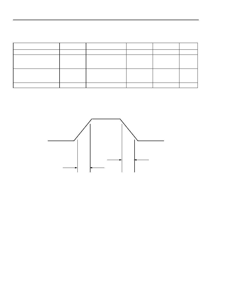
108
108
Agere Systems Inc.
Data Sheet
April 2001
TMUX03155 STS-3/STM-1 (AU-4) Multiplexer/Demultiplexer
Electrical Characteristics
* All outputs are 2 mA except TLSSPEO, TLSJ0J1VV1TIMEO, TLSV1TIMEO, THSSSYNCO, THSDATA[7:0]O, THSPARO, RLSJ0TIMEO,
RLSDATA[7:0]O, and RLSPARO which are 4 mA buffers.
The input specification for the remaining (nonbalanced) inputs are specified in Figure 15
.
See Operational Timing
on page 110
5-6032(F)r.2
Figure 15. Single-Ended Input Specification
Table 94. Logic Interface Characteristics
Parameter
Symbol
Test Conditions
Min
Max
Unit
Input Leakage
I
L
--
--
1.0
µA
Output Current*:
Low
High
I
OL
I
OH
--
--
--
2
2
mA
mA
Output Voltage:
Low
High
V
OL
V
OH
--
V
SS
V
DD
≠ 0.5
0.5
REF5VTOL
V
V
Input Capacitance
C
I
--
--
1.5
pF
V
IH
t
F
t
R
V
IL
Agere Systems Inc.
109
Data Sheet
April 2001
TMUX03155 STS-3/STM-1 (AU-4) Multiplexer/Demultiplexer
Electrical Characteristics
(continued)
Table 95. LVDS Interface Characteristics
3.3 V ± 5% V
DD
, 0--125
∞C, slow--fast process
.
* Buffer will not produce output transition when input is open-circuited.
Parameter
Symbol
Test Conditions
Min
Typ
Max
Unit
Input Buffer Parameters
Input Voltage Range, V
IA
or
V
IB
V
I
|V
GPD
| < 925 mV,
dc--1 MHz
0.0
1.2
2.4
V
Input Differential Threshold
V
IDTH
|V
GPD
| < 925 mV,
311 MHz
≠100
--
100
mV
Input Differential Hysteresis
V
HYST
(+V
IDTH
) ≠ (≠V
IDTH
)
--
--
--*
mV
Receiver Differential Input
Impedance
R
IN
With build-in termination,
center-tapped
80
100
120
Output Buffer Parameters
Output Voltage:
Low (V
OA
or
V
OB)
High (V
OA
or
V
OB)
V
OL
V
OH
R
LOAD
= 100
± 1%
R
LOAD
= 100
± 1%
--
0.925
--
1.475
--
V
V
Output Differential Voltage
|V
OD
|
R
LOAD
= 100
± 1%
0.25
--
0.40
V
Output Offset Voltage
V
OS
R
LOAD
= 100
± 1%
1.125
--
1.275
V
Output Impedance, Single Ended
R
O
V
CM
= 1.0 V and 1.4 V
40
50
60
R
O
Mismatch Between A and B
R
O
V
CM
= 1.0 V and 1.4 V
--
--
10
%
Change in Differential Voltage
Between Complementary States
|
V
OD
|
R
LOAD
= 100
± 1%
--
--
25
mV
Change in Output Offset Voltage
Between Complementary States
V
OS
R
LOAD
= 100
± 1%
--
--
25
mV
Output Current
I
SA,
I
SB
Driver shorted to V
SS
--
--
24
mA
Output Current
I
SAB
Drivers shorted together
--
--
12
mA

110
110
Agere Systems Inc.
Data Sheet
April 2001
TMUX03155 STS-3/STM-1 (AU-4) Multiplexer/Demultiplexer
Timing Characteristics
Operational Timing
The operational timing parameters can be grouped separately for clocks, inputs, and outputs. Table 96 lists the
input clock specifications for this device. The rise and fall times refer to the transition times from 10% to 90% of full
swing. (For definitions of the signal names, see the pin descriptions in Table 1, pages 10--15.)
Table 96. Input Clock Specifications
Symbol
Parameter
Signal Name
Min
Max
Unit
f
OP
Operating Frequency
THSSCLKIT/C
1
THSCLKI
RHSSCLKIT/C*
RHSCLK
TCLK
1. When the true and complement inputs are floating, the input buffer will not oscillate.
--
--
--
--
--
155.52 + 0.4%
38.88/19.44 + 1%
155.52 + 0.5%
38.88/19.44 + 1%
0.5--12 + 1%
MHz
MHz
MHz
MHz
MHz
t
CLKH
Clock Pulse High Time
THSSCLKIT/C*
THSCLKI
RHSSCLKIT/C*
RHSCLK
TCLK
2.5
11.0/22.0
2.5
11.0/22.0
30
--
--
--
--
--
ns
ns
ns
ns
ns
t
R
Rise Time
THSSCLKIT/C*
THSCLKI
RHSSCLKIT/C*
RHSCLK
TCLK
1.5
3.5
1.5
3.5
15
--
--
--
--
--
ns
ns
ns
ns
ns
t
F
Fall Time
THSSCLKIT/C*
THSCLKI
RHSSCLKIT/C*
RHSCLK
TCLK
1.5
3.5
1.5
3.5
15
--
--
--
--
--
ns
ns
ns
ns
ns
Agere Systems Inc.
111
Data Sheet
April 2001
TMUX03155 STS-3/STM-1 (AU-4) Multiplexer/Demultiplexer
Timing Characteristics
(continued)
Operational Timing
(continued)
The following table lists input setup and hold times and reference clocks. (See Figure 17, Interface Data Timing, on
page 115.)
Table 97. Input Timing Specifications
Input Name
Reference CLK
Setup Time
(t
SU
)
Hold Time
(t
H
)
Unit
Min
Max
Min
Max
Transmit Signals
THSSJ0J1V1IT/C*
THSSCLKIT/C
2.0
--
0.0
--
ns
THSJ0J1V1I
THSCLKI
2.0
0.0
--
ns
Transmit Low-Speed Signals
TLSDATA[7:0]I
TLSCLKO
5.0
--
0.0
--
ns
TLSPARI
TLSCLKO
5.0
--
0.0
--
ns
Transmit TOAC
TTOACDATAI
TTOACCLKO
10.0
--
10.0
--
ns
Receive Signals
RHSSDATAIT/C
1
1. When the true and complement inputs are floating, the input buffer will not oscillate.
RHSSCLKIT/C
2.0
--
0.0
--
ns
RHSDATA[7:0]I
RHSCLKI
5.0
--
0.0
--
ns
RHSPARI
RHSCLKI
5.0
--
0.0
--
ns
RHSLOSEXTI
NA
ASYNC
--
ASYNC
--
ns
JTAG and SCAN
TDI
TCLK
15
--
15
--
ns
TMS
TCLK
15
--
15
--
ns
TRST
NA
ASYNC
--
ASYNC
--
ns
SCAN_EN
NA
ASYNC
--
ASYNC
--
ns
TEST_MODE
NA
ASYNC
--
ASYNC
--
ns
Miscellaneous
MODE [1:0]
NA
ASYNC
--
ASYNC
--
ns
RESET
NA
ASYNC
--
ASYNC
--
ns
ICT
NA
ASYNC
--
ASYNC
--
ns
112
112
Agere Systems Inc.
Data Sheet
April 2001
TMUX03155 STS-3/STM-1 (AU-4) Multiplexer/Demultiplexer
Timing Characteristics
(continued)
Operational Timing
(continued)
The following diagram defines the signal structure of the input signal THSJ0J1V1I.
Figure 16. THSJ0J1V1I Signal Structure Definition
* O
p
t
i
onal.
MS
B
= m
o
st
s
i
gnif
i
cant
bit
,
m
o
st
s
i
g
n
i
f
icant
byt
e
,
res
pect
i
v
e
ly;
MS
N
=
mos
t
signif
i
ca
nt
ni
b
b
l
e
.
5
-
625
3 (F
)r.
2
FR
AM
E
SU
PER
FR
A
M
E
MS
B
T
H
SJ0J
1V1I
CLOCK
CY
CLE
S
TH
S
C
L
K
TY
PE
=
B
Y
TE
C
L
OC
K
(
1
9
.
4
4
M
H
z
)
24
30 CLO
C
K
CY
CLES
/
F
RA
ME
(125
µ
s)
FR
AM
E
SU
PER
FR
A
M
E
T
H
SJ0J
1V1I
CLOCK
CY
CLE
S
T
H
S
C
LKT
Y
PE
= N
I
B
B
LE
CLO
C
K
(38.
88
MHz)
48
60 CLO
C
K
CY
CLES
/
F
RA
ME
(125
µ
s)
J0
J1
V1*
J
0
J
1
J
0
J
1
J0
J1
V1*
J0
J1
FR
AM
E
SU
PER
FR
A
M
E
MS
B
T
H
SS
J0
J
1
V1
I
T
CLOCK
CY
CLE
S
1
1
23
23
19392
19416
T
H
SCLK
T
Y
PE
= BI
T
CLO
C
K (155.
52
M
H
z)
19440 CLO
C
K CYCLE
S
/
F
RAM
E
(125
µ
s)
12
3
19416
19416
11
23
23
12
3
1
2
3
500
µ
s
125
µ
s
125
µ
s
125
µ
s
125
µ
s
J0
J1
V1*
J
0
J
1
J
0
J
1
J0
J1
V1*
J0
J1
11
5
5
4848
4854
15
4854
4854
11
55
15
1
5
500
µ
s
125
µ
s
125
µ
s
125
µ
s
125
µ
s
MS
N
J0
J1
V1*
J
0
J
1
J
0
J
1
J0
J1
V1*
J0
J1
11
2
2
2424
2427
12
2427
2427
11
22
12
1
2
500
µ
s
125
µ
s
125
µ
s
125
µ
s
125
µ
s
1
1
1
Agere Systems Inc.
113
Data Sheet
April 2001
TMUX03155 STS-3/STM-1 (AU-4) Multiplexer/Demultiplexer
Timing Characteristics
(continued)
Operational Timing
(continued)
The output clock specifications are shown in Table 98.
Table 98. Output Clock Specifications
Signal Name Reference CLK
1
1. The specifications for the table are with all loopbacks disabled.
Frequency
2
2. The frequency percentages refer to the respective duty cycles.
Test
Conditions
Rise Time
Fall Time
Unit
t
R
t
F
Min
Max
Min
Max
TLSCLKO
THSSCLKIT/C or
THSCLKI
19.44 MHz ± 5% C
L
= 50 pF
--
3.5
--
3.5
ns
THSSCLKO
THSSCLKIT/C
155.52 MHz ±
3%
C
L
= 15 pF
--
1.5
--
1.5
ns
THSCLKO
THSSCLKIT/C or
THSCLKI
38.88 MHz ± 5%
or
19.44 MHz ± 5%
C
L
= 15 pF
--
3.5
--
3.5
ns
TTOACCLKO THSSCLKIT/C or
THSCLKI
5.184 MHz ± 5% C
L
= 15 pF
--
3.5
--
3.5
ns
RLSCLKO
RHSSCLKIT/C or
RHSCLKI or
Internal CDR
Clock
19.44 MHz ± 5% C
L
= 50 pF
--
3.5
--
3.5
ns
RTOACCLKO RHSSCLKIT/C or
RHSCLKI or
Internal CDR
Clock
5.184 MHz ± 5% C
L
= 15 pF
--
3.5
--
3.5
ns
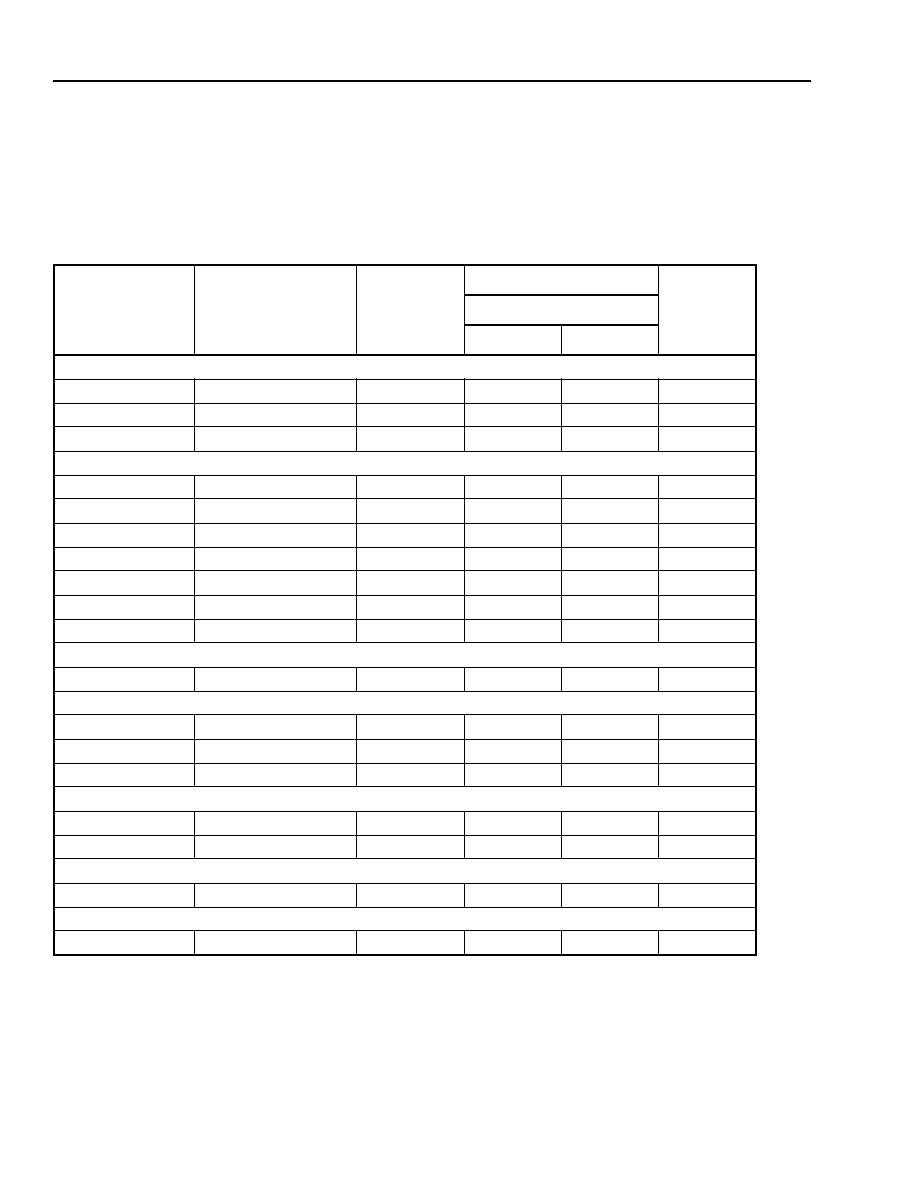
114
114
Agere Systems Inc.
Data Sheet
April 2001
TMUX03155 STS-3/STM-1 (AU-4) Multiplexer/Demultiplexer
Timing Characteristics
(continued)
Operational Timing
(continued)
The following table lists the propagation delay specifications for the outputs. (See Figure 17, Interface Data
Timing, on page 115. )
* Propagation delay skew, t
PLH
--t
PHL,
is ±200 ps.
Table 99. Output Timing Specifications
Output Name
Reference CLK
Test
Conditions
Propagation Delay
Unit
t
PD
Min Max
Transmit Low-Speed Signals
TLSSPEO
TLSCLKO
C
L
= 50 pF
4.0
12.0
ns
TLSJ0J1V1TIMEO
TLSCLKO
C
L
= 50 pF
4.0
12.0
ns
TLSV1TIMEO
TLSCLKO
C
L
= 50 pF
4.0
12.0
ns
Transmit High-Speed Signals
THSSCLKIT/C
THSSCLKOT/C
C
L
= 15 pF
0.0
6.4
ns
THSSSYNCOT/C*
THSSCLKOT/C
C
L
= 15 pF
0.6
2.9
ns
THSSDATAOT/C*
THSSCLKOT/C
C
L
= 15 pF
0.6
2.9
ns
THSSYNCO
THSCLKO
C
L
= 15 pF
3.0
6.0
ns
THSDATA[7:0]O
THSCLKO
C
L
= 15 pF
3.0
6.0
ns
THSPARO
THSCLKO
C
L
= 15 pF
3.0
6.0
ns
THSCLKI
THSCLKO
C
L
= 15 pF
3.0
7.8
ns
Transmit TOAC Signal
TTOACSYNCO
TTOACCLKO
C
L
= 15 pF
10.0
30.0
ns
Receive Low-Speed Signals
RLSJ0TIMEO
RLSCLKO
C
L
= 50 pF
4.0
12.0
ns
RLSDATA[7:0]O
RLSCLKO
C
L
= 50 pF
4.0
12.0
ns
RLSPARO
RLSCLKO
C
L
= 50 pF
4.0
12.0
ns
Receive TOAC Signals
RTOACSYNCO
RTOACCLKO
C
L
= 15 pF
10.0
30.0
ns
RTOACDATAO
RTOACCLKO
C
L
= 15 pF
10.0
30.0
ns
Serial Control Interface (SCI)
INTN
ASYNC
NA ASYNC
ASYNC
ns
JTAG and SCAN
TDO
TCLK
C
L
= 25 pF
3.0
20.0
ns
Agere Systems Inc.
115
Data Sheet
April 2001
TMUX03155 STS-3/STM-1 (AU-4) Multiplexer/Demultiplexer
Timing Characteristics
(continued)
Operational Timing
(continued)
A diagram of the digital system interface timing for setup and hold time input as well as propagation delay output
specifications are shown in Figure 17. The transmit and receive low-speed bus interfaces are shown in Figure 18.
5-5342(F)r.1
Figure 17. Interface Data Timing
CLOCK
DATA
CLOCK
DATA
t
SU
t
H
t
PD
116
116
Agere Systems Inc.
Data Sheet
April 2001
TMUX03155 STS-3/STM-1 (AU-4) Multiplexer/Demultiplexer
Timing Characteristics
(continued)
Operational Timing
(continued)
5-6255(F)r.5
* V1 time occurs once every 500 µs.
J0 time occurs once per frame (125 µs).
Figure 18. Bus Interface Signals
TLSSPEO
TLSJ0J1V1TIMEO
TLSV1TIMEO*
TLSDATA[7:0]I
RLSJ0TIMEO
RLSDATA[7:0]O
RECEIVE LOW-SPEED BUS INTERFACE SIGNALS
TRANSMIT LOW-SPEED BUS INTERFACE SIGNALS
J0-2
TLSCLKO
RLSCLKO
J0-1
J0-3
3 bytes
3 bytes
3 bytes
3 bytes
3 bytes
A1
A2
J0
J1
V1
A1-2
A2-2
J0-2
J1-2
V1-3
V1-2
V1-1
J1-1
J1-3
J0-3
J0-1
A2-1
A2-3
A1-1
A1-3
J0
3 bytes

Agere Systems Inc.
117
Data Sheet
April 2001
TMUX03155 STS-3/STM-1 (AU-4) Multiplexer/Demultiplexer
Outline Diagram
208-Pin SQFP
Dimensions are in millimeters.
5-2196(F)1.3r.14
DETAIL B
0.17/0.27
0.10
M
0.090/0.200
0.50/0.75
GAGE PLANE
SEATING PLANE
1.30 REF
0.25
DETAIL A
156
105
30.60 ± 0.20
157
208
1
52
53
104
28.00 ± 0.20
28.00
± 0.20
30.60
± 0.20
PIN #1 IDENTIFIER ZONE
4.10 MAX
0.08
3.40 ± 0.20
SEATING PLANE
0.25 MIN
0.50 TYP
DETAIL B
DETAIL A

118
118
Agere Systems Inc.
Data Sheet
April 2001
TMUX03155 STS-3/STM-1 (AU-4) Multiplexer/Demultiplexer
Ordering Information
DS01-194PDH Replaces DS00-213TIC to Incorporate the Following Updates
I
Version 1 advisory (AY00-002SONT) information incorporated into the datasheet.
I
Version ID register value changed to 3 (See Device Version and Device ID Number on page 29).
I
For AU-4 mode, the B3 error count register (REI-P) mechanism was changed so that the transmit clock has
enough time to sample the value for application on the outgoing G1[7:4] bits.
I
The transitioning in the loss of pointer (LOP) state was fixed for the NDF condition.
Device Code
Package
Temperature
Comcode
TMUX03155
208-Pin SQFP
≠40 ∞C to +85 ∞C
108126368-DB

Agere Systems Inc.
119
Data Sheet
April 2001
TMUX03155 STS-3/STM-1 (AU-4) Multiplexer/Demultiplexer
Notes

Agere Systems Inc. reserves the right to make changes to the product(s) or information contained herein without notice. No liability is assumed as a result of their use or application.
Copyright © 2001 Agere Systems Inc.
All Rights Reserved
Printed in U.S.A.
April 2001
DS01-194PDH (Replaces DS99-213TIC)
For additional information, contact your Agere Systems Account Manager or the following:
INTERNET:
http://www.agere.com
E-MAIL:
docmaster@micro.lucent.com
N. AMERICA: Agere Systems Inc., 555 Union Boulevard, Room 30L-15P-BA, Allentown, PA 18109-3286
1-800-372-2447, FAX 610-712-4106 (In CANADA: 1-800-553-2448, FAX 610-712-4106)
ASIA PACIFIC: Agere Systems Singapore Pte. Ltd., 77 Science Park Drive, #03-18 Cintech III, Singapore 118256
Tel. (65) 778 8833, FAX (65) 777 7495
CHINA:
Agere Systems (Shanghai) Co., Ltd., 33/F Jin Mao Tower, 88 Century Boulevard Pudong, Shanghai 200121 PRC
Tel. (86) 21 50471212, FAX (86) 21 50472266
JAPAN:
Agere Systems Japan Ltd., 7-18, Higashi-Gotanda 2-chome, Shinagawa-ku, Tokyo 141, Japan
Tel. (81) 3 5421 1600, FAX (81) 3 5421 1700
EUROPE:
Data Requests: DATALINE: Tel. (44) 7000 582 368, FAX (44) 1189 328 148
Technical Inquiries:GERMANY: (49) 89 95086 0 (Munich), UNITED KINGDOM: (44) 1344 865 900 (Ascot),
FRANCE: (33) 1 40 83 68 00 (Paris), SWEDEN: (46) 8 594 607 00 (Stockholm), FINLAND: (358) 9 3507670 (Helsinki),
ITALY: (39) 02 6608131 (Milan), SPAIN: (34) 1 807 1441 (Madrid)