 | –≠–ª–µ–∫—Ç—Ä–æ–Ω–Ω—ã–π –∫–æ–º–ø–æ–Ω–µ–Ω—Ç: TMXF28155 | –°–∫–∞—á–∞—Ç—å:  PDF PDF  ZIP ZIP |

Preliminary Data Sheet
May 2001
TMXF28155 Super Mapper
155/51 Mbits/s SONET/SDH x28/x21 DS1/E1
1 Features
s
Versatile IC supports 155/51 Mbits/s SONET/SDH
interface solutions for T3/E3, DS2, T1/E1/J1, and
DS0/E0/J0 applications.
s
Implementation supports both linear (1 + 1, unpro-
tected) and ring (UPSR) network topologies.
s
Provides full termination of up to 21 E1, 28 T1, or
28 J1.
s
Low power 3.3 V supply.
s
≠40
∞
C to +85 ∞C industrial temperature range.
s
456-pin ball grid array (PBGA) package.
s
Complies with
Bellcore*
, ITU,
ANSI
, ETSI and Jap-
anese TTC standards: GR-253-CORE, GR-499,
(ATT) TR-62411, ITU-T G.707, G.704, G.706, G.783,
G.962, G.964, G.965, Q.542, T1.105, JT-G704,
JT-G706, JT-G707, JT-I431-a, ETS 300 417-1-1,
ETS 300 011, T1.107, T1.404.
1.1 SONET/SDH Interface
s
Termination of a single 155 Mbits/s STS-3/STM-1 or
single 51 Mbits/s STS-1/STM-0.
s
Built-in clock and data recovery circuit at
155 Mbits/s STS-3/STM-1 interface (can be dese-
lected if external clock recovery is provided).
s
Supports overhead processing for all transport and
path overhead bytes.
s
Optional insertion and extraction of overhead bytes
via a serial transport overhead access channel. Con-
figurable as dedicated DCC channels.
s
Software controlled linear 1 + 1 protection via dedi-
cated interface to protection card.
s
Full path termination and SPE extraction/insertion.
s
SONET/SDH compliant condition and alarm report-
ing.
s
Built-in diagnostic loopback modes.
s
8 kHz line frame sync output.
*
Bellcore
is now
Telcordia Technologies
.
Telcordia Technologies
is a
trademark of Telcordia Technologies, Inc.
ANSI
is a registered trademark of American National Standards
Institute, Inc.
1.2 STS/STM Pointer Interpreter
s
Interprets STS/AU/TU-3 pointers.
s
Synchronizes 8 kHz frame and 2 kHz superframe to
system/shelf timing reference by setting the transmit
STS-3/STM-1 pointers to a fixed value of 522.
s
Monitors/terminates SPE path overhead.
1.3 Telecom Bus Interface
s
Telecom bus interface to mate devices including
clock, data[8], parity, SPE-, J0-, J1-, and V1 timing
indicator.
s
Line and path RDI and REI signals passed to mate
devices.
s
Three Super Mapper devices, two configured as
mate devices, provide full termination of an
STS-3/STM-1. A three-chip solution to terminate
84 DS1s/J1s or 63 E1s.
1.4 VT Termination/Generation (x28/x21)
s
Monitors/terminates VT path overhead for
28 VT1.5/TU-11 or 21 VT2/TU-12.
s
Synchronizes VT/TU SPE to system/shelf timing ref-
erence by setting the transmit VT/TU pointers to fixed
values for asynchronous mapping or by dynamically
changing the transmit VT/TU pointers for byte syn-
chronous mapping.
s
Fixed pointer generation in transmit side for asyn-
chronous mapping.
s
Dynamic pointer generation in transmit side for byte-
synchronous mapping.
1.5 Mapping/Multiplexing Modes (x28/x21)
s
Maps DS3 clear channel or framed signal into STS-1
or TUG-3.
s
Maps T1/E1/J1 into VT/TU (including DS1 into
TU-12).
s
Supports asynchronous, byte-synchronous, and bit-
synchronous mapping.

2
Agere Systems Inc.
TMXF28155 Super Mapper
Preliminary Data Sheet
155/51 Mbits/s SONET/SDH x28/x21 DS1/E1
May 2001
1 Features
(continued)
s
Supports UPSR applications via the dedicated ring
interface and an external tributary selector.
s
Supports all valid T1/E1/J1 multiplexing structures
into STS-1 and STS-3/STM-1:
-- STS-3/STS-1/SPE/VTG/VTx
-- STM-1/AU-3/TUG-2/TU-1x/VC-1x
-- STM-1/AU-4/TUG-3/TUG-2/TU-1x/VC-1x
s
Allows grooming of VTs/TUs in granularity of TUG-2s
within the STS-3/STM-1 signal.
s
Supports J2 trace identifier monitoring/insertion.
s
Configurable VT/TU slot selection for DS1, E1, and
J1 insertion and drop.
s
Automatic receive monitor functions include VT/TU
RDI-V, REI-V, BIP-2 errors, AIS-V, LOP-V.
s
Complies with GR-253-CORE, GR-499, ITU-T
G.707, G.704, G.783, T1.105, JT-G707, ETS 300
417-1-1.
1.6 M13 Features
s
Configurable multiplexer/demultiplexer for 28 DS1
signals, 21 E1 signals, or 7 DS2 signals to/from a
DS3 signal.
s
Operates in either M23 or C-bit parity mode.
s
Provisionable time slot selection for DS1, E1, and
DS2 insertion or drop.
s
Full alarm monitoring and generation (LOS, BPV,
EXZ, OOF, SEF, AIS, RAI, FEAC, P-bit and C-bit par-
ity errors, FEBE).
s
HDLC transmitter with 128-byte data buffer and
HDLC receiver with 128-byte data FIFO for the C-bit
parity path maintenance data link.
s
DS3, DS2, DS1, and E1 loopback and loopback
request generation.
s
Complies with T1.102, T1.107, T1.231, T1.403,
T1.404, GR 499, G.747, and G.775.
1.7 DS3/DS2/DS1/E1 Cross Connect
s
Highly configurable interconnect for up to 28 DS1 or
21 E1 signals to/from the framer, external pins, M13,
or VT mappers.
s
Supports up to seven DS2 signals to/from the exter-
nal pins or M13.
s
Sources may be broadcast, looped back, or routed
to/from a test-pattern generator or monitor.
s
Any DS1 or E1 channel may be routed through the
jitter attenuator.
s
DS3 may be configured for the M13 to interconnect
with the SPE, or external I/O to interconnect with the
M13 or SPE.
1.8 Jitter Attenuation
s
PLL-free receive operation using built-in digital jitter
attenuator (in VT/VC mode or M13 mode).
s
Configurable to meet jitter and MTIE requirements.
1.9 PDH Interfaces
s
One DS3, 7x DS2.
s
x28/x21 framed or unframed DS1 or E1 interfaces.
s
One additional dedicated protection channel for
DS2/DS1/E1.
1.10 T1/E1/J1 Framing Features (x28/x21)
s
x28/x21 T1/E1/J1 channels.
s
Line coding: B8ZS, HDB3, ZCS, AMI, and
CMI (JJ20-11).
s
T1 framing modes: ESF, D4,
SLC
Æ
-96, T1 DM DDS,
and SF (F
t
only).
s
E1 framing: G.704 basic and CRC-4 multiframe con-
sistent with G.706.
s
J1 framing modes: JESF (Japan).
s
Supports T1 and E1 unframed and transparent trans-
mission format.
s
T1 signaling modes: transparent;
register and system access for ESF 2-state, 4-state,
and 16-state; D4 2-state, 4-state, and 16-state;
SLC
-96 2-state, 4-state, and 16-state; J-ESF han-
dling groups maintenance and signaling; VT 1.5
SPE 2, 4, 16 state.
s
E1 signaling modes: transparent;
register and system access for entire TS16 multi-
frame structure as per ITU G.732.
s
Signaling debounce and change of state interrupt.
s
V5.2 Sa7 processing.

3
Agere Systems Inc.
Preliminary Data Sheet
TMXF28155 Super Mapper
May 2001
155/51 Mbits/s SONET/SDH x28/x21 DS1/E1
1 Features
(continued)
s
Alarm reporting and performance monitoring per
AT&T,
ANSI
, ITU-T, and ETSI standards.
s
Facility data link features:
-- HDLC or transparent access for either ESF or
DDS + FDL frame formats.
-- Register/stack access for
SLC
-96 transmit and re-
ceive data.
-- Extended superframe (ESF): automatic transmis-
sion of the ESF performance report messages
(PRM). Automatic transmission of the
ANSI
T1.403 ESF performance report messages. Auto-
matic detection and transmission of the
ANSI
T1.403 ESF FDL bit-oriented codes.
-- Register/stack access for all CEPT Sa-bits trans-
mit and receive data.
s
HDLC features:
-- HDLC or transparent mode.
-- Programmable logical channel assignment: any
time slot, any bit for ISDN D-channel, also inserts/
extracts C-channels for V5.1, V5.2 interfaces.
-- 64 logical channels in both transmit and receive di-
rection (any framing format).
-- Maximum channel data rate: 64 kbits/s.
-- Minimum channel data rate: 4 kbits/s (DS1-FDL or
E1 Sa bit).
-- 128-byte FIFO per channel in both transmit and re-
ceive direction.
-- Tx to Rx loopback supported.
s
System interfaces:
-- Concentration highway interface: Single clock and
frame sync signals; programmable clock rates at
2.048 MHz, 4.096 MHz, 8.192 MHz, and
16.384 MHz; programmable data rates at 2.048
Mbits/s,
4.096 Mbits/s, and 8.192 Mbits/s; programmable
clock edges and bit/byte offsets.
-- Parallel system bus interface at 19.44 MHz for
data and signaling: single clock and frame sync
signals.
-- Time-division multiplex data rate serial interface at
1.544 MHz or 2.048 MHz. Twenty-eight receive
data, clock, and frame sync signals. Twenty-eight
transmit data signals with a global clock and frame
sync.
-- Network serial multiplexed interface minimal pin
count serial interface at 51.84 MHz optimized for
data and IMA applications.
1.11 System Test and Maintenance
s
A variety of loopback modes implemented on
SONET/SDH side as well as on framer level.
s
Built-in test pattern generator and monitor config-
urable for simultaneously testing E1, DS1, DS2, and
DS3 (one channel each).
Microprocessor Interface
s
20-bit address and 16-bit data interface with 16 MHz
to 66 MHz read and write access.
s
Compatible with most industry-standard processors.
Chip Testing and Maintenance
s
IEEE
* 1149.1 JTAG boundary scan.
Interface to Other
Agere
ME Devices
Seamless interface to the following
Agere Systems'
devices:
s
TADM042G5.
*
IEEE
is a registered trademark of the Institute of Electrical and
Electronics Engineers, Inc.

4
Agere Systems Inc.
TMXF28155 Super Mapper
Preliminary Data Sheet
155/51 Mbits/s SONET/SDH x28/x21 DS1/E1
May 2001
Table of Contents
By Major Sections
Contents
Page
Features ...................................................................................................................................................................1
Product Description .................................................................................................................................................. 5
Preface ...................................................................................................................................................................5
Interface Specifications ............................................................................................................................................ 8
Pin Information .......................................................................................................................................................8
Electrical Characteristics ...................................................................................................................................... 33
Timing Characteristics ......................................................................................................................................... 37
Ordering Information ............................................................................................................................................ 61
Register Description ............................................................................................................................................... 62
Microprocessor Interface and Global Control and Status Registers .................................................................... 62
TMUX Registers ...................................................................................................................................................75
SPE Mapper Registers ...................................................................................................................................... 133
VT/TU Mapper Registers ................................................................................................................................... 153
M13/M23 MUX/DeMUX Registers ..................................................................................................................... 196
28-Channel Framer Registers ............................................................................................................................ 239
Cross Connect (XC) Registers ........................................................................................................................... 321
Digital Jitter Attenuation Controller Registers .................................................................................................... 331
Test-Pattern Generation/Detection Registers ..................................................................................................... 336
Functional Descriptions ........................................................................................................................................ 354
Microprocessor Interface Functional Description ...............................................................................................354
TMUX Functional Description ............................................................................................................................ 359
SPE Mapper Functional Description ..................................................................................................................396
VT/TU Mapper Functional Description ............................................................................................................... 425
M13/M23 MUX/DeMUX Block Functional Description ....................................................................................... 455
28-Channel Framer Block Functional Description .............................................................................................. 475
Cross Connect (XC) Block Functional Description ............................................................................................ 542
Digital Jitter Attenuation Controller Functional Description ................................................................................ 570
Test-Pattern Generation/Detection Functional Description ................................................................................ 574
Philosophies ....................................................................................................................................................... 582
Applications .......................................................................................................................................................... 588
Change History .................................................................................................................................................. 604

5
Agere Systems Inc.
Preliminary Data Sheet
TMXF28155 Super Mapper
May 2001
155/51 Mbits/s SONET/SDH x28/x21 DS1/E1
Product Description
2 Preface
Table of Contents
Contents
Page
1 Features ............................................................................................................................................................... 1
1.1 SONET/SDH Interface ................................................................................................................................... 1
1.2 STS/STM Pointer Interpreter ......................................................................................................................... 1
1.3 Telecom Bus Interface ................................................................................................................................... 1
1.4 VT Termination/Generation (x28/x21) ............................................................................................................ 1
1.5 Mapping/Multiplexing Modes (x28/x21) ......................................................................................................... 1
1.6 M13 Features ................................................................................................................................................. 2
1.7 DS3/DS2/DS1/E1 Cross Connect .................................................................................................................. 2
1.8 Jitter Attenuation ............................................................................................................................................ 2
1.9 PDH Interfaces ............................................................................................................................................... 2
1.10 T1/E1/J1 Framing Features (x28/x21) ......................................................................................................... 2
1.11 System Test and Maintenance .................................................................................................................... 3
2 Preface ................................................................................................................................................................. 5
2.1 Major Categories ............................................................................................................................................ 6
2.2 Naming Convention for Registers and Parameters ....................................................................................... 6
2.3 Overview ........................................................................................................................................................ 7
Figures
Page
Figure 1. Functional Diagram of Super Mapper ....................................................................................................... 7

6
Agere Systems Inc.
TMXF28155 Super Mapper
Preliminary Data Sheet
155/51 Mbits/s SONET/SDH x28/x21 DS1/E1
May 2001
2 Preface
(continued)
The objective of this data sheet is to define the func-
tionality of the Super Mapper for hardware and soft-
ware developers. The information contained in this data
sheet is preliminary, and may change without notice;
the reader must therefore ascertain that the latest ver-
sion is used when a product is under development.
The latest version of this data sheet can be accessed
at: http://www.lucent.com/micro/netcom/products/
pdh.html#super_mapper.
2.1 Major Categories
This data sheet is divided into six major categories with
sub-sections as follows:
s
Features
s
Product Description
-- Features
-- Preface
-- Overview
s
Interface Specifications
-- Pin Information
-- Electrical Characteristics
-- Timing Characteristics
-- Ordering Information
s
Register Descriptions
-- Microprocessor Interface Registers
-- TMUX Registers
-- SPE Mapper Registers
-- VT/UT Mapper Registers
-- M13/M23 MUX/deMUX Registers
-- 28-Channel Framer Registers
-- Cross Connect (XC) Registers
-- Digital Jitter Attenuation Registers
-- Test Pattern Generation/Detection Registers
s
Functional Descriptions
-- Microprocessor Interface Description
-- TMUX Registers Description
-- SPE Mapper Registers Description
-- VT/UT Mapper Registers Description
-- M13/M23 MUX/deMUX Registers Description
-- 28-Channel Framer Registers Description
-- Cross Connect (XC) Registers Description
-- Digital Jitter Attenuation Registers Description
-- Test Pattern Generation/Detection Registers De-
scription
s
Applications
-- Application Block Diagrams and Descriptions
2.2 Naming Convention for Registers and
Parameters
There are many provisioning registers for controlling
the Super Mapper. A naming convention for all regis-
ters and parameters (bit names) is followed throughout
this data sheet. A prefix is attached to the base name
of each register or parameter, depending on which
functional section the register or parameter is associ-
ated with:
s
SMPR_, for the Microprocessor Interface
s
TMUX_, for the TMUX
s
SPE_, for the SPE Mapper
s
VT_, for the VT/VC Mapper
s
M13_, for the M13/M23 MUX/deMUX
s
FRM_, for the 28-Channel Framer
s
XC_, for the Cross Connect
s
DJA_, for the Digital Jitter Attenuator
s
TPG_ and TPM_, for the Test-Pattern Generator/
Detection
A suffix is appended to the base name of three com-
mon parameters:
s
_IS, for interrupt signal.
s
_IM, for interrupt mask.
s
_SWRS, for software reset.

7
Agere Systems Inc.
Preliminary Data Sheet
TMXF28155 Super Mapper
May 2001
155/51 Mbits/s SONET/SDH x28/x21 DS1/E1
2 Preface
(continued)
2.3 Overview
The SONET/SDH Super Mapper device integrates the SONET/SDH line, path, and tributary termination functions
with M13 multiplex functions and the primary rate framing function. It is designed to drive an OC-3/STM-1 optical
signal directly or to allow for modular growth in terminal or add/drop applications.
It provides a versatile interface for all STS-3/STM-1 and STS-1 termination applications in point-to-point scenarios
and for ring applications. This chip can be used in tributary shelf applications for up to 28 T1 or J1 or 21 E1 line
cards providing all possible mappings into SONET/SDH. Because of the flexibility of the mappings, software
upgrades from M13 mapped connections to VT/TU mapped connections are possible. This device can also be
used for DS3/DS2 applications.
A single Super Mapper is capable of processing the aggregate bandwidth of one STS-1 or DS3. By communicating
to two other mate devices via the telecom bus interface, the Super Mapper is capable of terminating a full
STS-3/STM-1 signal.
5-8923(F)
Figure 1. Functional Diagram of Super Mapper
TMUX
SPE/
AU-3
MAPPER
M13
MUX
VT/VC
MAPPER
TEST
PATTERN
GEN/MON
FRAMER
BANK
DIGITAL
JITTER
ATTENUATOR
T1/E1
DS2
DS3
CROSS
CONNECT
OVERHEAD
STS-1/
STS-3
MSP
MPU INTERFACE
AND CONTROL
MPU INTERFACE
TELECOM BUS
MAPPING &
DS3
T1/E1/J1
SYSTEM INTERFACE
DS0/E0
DS1 (X29)
DS2 (X7)
DS1XCLK
DS1/E1
DS3/STS1
TPOAC
RPOAC
TTOAC
RTOAC
LOPOHOUT
LOPOHIN
TCB AND TDL
LINERX
LINETX
MISC
DS2AISCLK
SYS
TERMINATION
MULTIPLEXING
FRAMING
STM-1
AU-3
1 + 1
CLK
SYNC
RCB AND RDL
E1XCLK
(NSMI MODE)
(NSMI MODE)
/E1 (X22)
(XN)
BUS

8
Agere Systems Inc.
TMXF28155 Super Mapper
Preliminary Data Sheet
155/51 Mbits/s SONET/SDH x28/x21 DS1/E1
May 2001
Interface Specifications
3 Pin Information
Table of Contents
Contents
Page
3 Pin Information ..................................................................................................................................................... 8
3.1 456-Pin PBGA Pin Diagram ........................................................................................................................... 9
3.2 Pin Assignments ............................................................................................................................................ 9
3.3 Pin Descriptions ........................................................................................................................................... 15
3.3.1 High-speed I/O Pin Descriptions ........................................................................................................ 15
3.3.2 Protection Switch I/O Pin Description ................................................................................................ 16
3.3.3 Telecom Bus (Low-speed I/O) Pin Description .................................................................................. 16
3.3.4 TOAC and POAC ............................................................................................................................... 19
3.3.5 Miscellaneous Signals ........................................................................................................................ 20
3.3.6 DS3 Port ............................................................................................................................................. 20
3.3.7 M13 Multiplexer/Demultiplexer Receive Section ................................................................................ 22
3.3.8 Low-Order Path Overhead Access Channel ...................................................................................... 23
3.3.9 Framer PLL ........................................................................................................................................ 27
3.3.10 Test Pins .......................................................................................................................................... 30
3.4 Outline Diagram ........................................................................................................................................... 32
3.4.1 456-Pin PBGA .................................................................................................................................... 32
List of Figures
Figure 2. Pin Diagram of 456-Pin PBGA (Bottom View)........................................................................................... 9
Figure 3. Protection Switch..................................................................................................................................... 16
Figure 4. DS1/E1 to DXC Block Diagram ............................................................................................................... 23
List of Tables
Table 1. Pin Assignments for 456-Pin PBGA by Pin Number Order ....................................................................... 9
Table 2. Pin Assignments for 456-Pin PBGA by Signal Name .............................................................................. 12
Table 3. High-speed I/O Pin Descriptions ............................................................................................................. 15
Table 4. Protection Switch I/O Pin Description ...................................................................................................... 16
Table 5. Telecom Bus (Low-speed I/O) Pin Description ........................................................................................ 17
Table 6. TOAC and POAC .................................................................................................................................... 19
Table 7. Miscellaneous Signals ............................................................................................................................. 20
Table 8. DS3 Port .................................................................................................................................................. 21
Table 9. DS3 Port, C-Bit, and Datalink Access ..................................................................................................... 22
Table 10. M13 Multiplexer/Demultiplexer Receive Section ................................................................................... 22
Table 11. Low-Order Path Overhead Access Channel ......................................................................................... 23
Table 12. Multifunction System Interface Transmit Path Direction ........................................................................ 24
Table 13. Framer PLL ............................................................................................................................................ 27
Table 14. Microprocessor Interfaces ..................................................................................................................... 28
Table 15. General Purpose Interface .................................................................................................................... 29
Table 16. Test Pins ................................................................................................................................................ 30
Table 17. CDR Power ............................................................................................................................................ 30
Table 18. LVDS Control Pins ................................................................................................................................. 30
9
Agere Systems Inc.
Preliminary Data Sheet
TMXF28155 Super Mapper
May 2001
155/51 Mbits/s SONET/SDH x28/x21 DS1/E1
3 Pin Information
(continued)
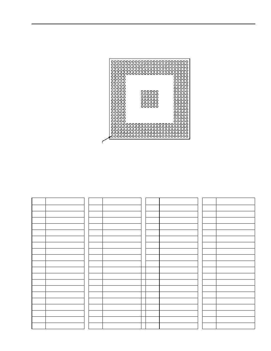
3.1 456-Pin PBGA Pin Diagram
5-8931(F)
Figure 2. Pin Diagram of 456-Pin PBGA (Bottom View)
3.2 Pin Assignments
r
Table 1. Pin Assignments for 456-Pin PBGA by Pin Number Order
Pin
Signal Name
Pin
Signal Name
Pin
Signal Name
Pin
Signal Name
A1
V
DD
A21
V
SS
B15
LINETXDATA2
C9
LINERXSYNC24
A2
V
SS
A22
VDD
B16
LINETXSYNC4
C10
LINERXCLK25
A3
LINERXDATA17
A23
LINETXSYNC12
B17
LINETXSYNC5
C11
LINERXCLK26
A4
LINERXDATA18
A24
LINETXSYNC13
B18
LINETXSYNC6
C12
LINERXCLK27
A5
V
DD
A25
V
SS
B19
LINETXCLK7
C13
LINERXDATA28
A6
V
SS
A26
V
DD
B20
LINETXDATA8
C14
LINETXSYNC2
A7
LINERXDATA21
B1
V
SS
B21
LINETXSYNC10
C15
LINETXCLK3
A8
LINERXSYNC23
B2
LINERXCLK15
B22
LINETXDATA10
C16
LINETXCLK4
A9
LINERXCLK24
B3
LINERXSYNC18
B23
LINETXDATA11
C17
LINETXCLK5
A10
V
DD
B4
LINERXSYNC19
B24
LINETXDATA12
C18
LINETXDATA6
A11
V
SS
B5
LINERXSYNC20
B25
LINETXCLK13
C19
LINETXSYNC8
A12
LINERXDATA27
B6
LINERXDATA20
B26
V
SS
C20
LINETXCLK9
A13
LINERXSYNC29
B7
LINERXSYNC22
C1
LINERXSYNC15
C21
LINETXCLK10
A14
LINETXDATA1
B8
LINERXCLK23
C2
LINERXDATA14
C22
LINETXCLK11
A15
LINETXSYNC3
B9
LINERXDATA24
C3
LINERXCLK17
C23
LINETXCLK12
A16
V
SS
B10
LINERXDATA25
C4
LINERXCLK18
C24
LINETXCLK14
A17
V
DD
B11
LINERXDATA26
C5
LINERXCLK19
C25
LINETXSYNC15
A18
LINETXCLK6
B12
LINERXSYNC28
C6
LINERXCLK20
C26
LINETXDATA14
A19
LINETXDATA7
B13
LINERXCLK29
C7
LINERXCLK21
D1
LINERXSYNC14
A20
LINETXSYNC9
B14
LINETXCLK1
C8
LINERXDATA22
D2
LINERXDATA13
AF
AE
AD
AC
AB
AA
Y
W
V
U
T
R
P
N
M
L
K
J
H
G
F
E
D
C
B
A
1
2
3
4
5
6
7
8
9
10
12
13
14
15
16
17
18
19
20
23
24
25
26
11
21
22
A1
BALL
CORNER

10
Agere Systems Inc.
TMXF28155 Super Mapper
Preliminary Data Sheet
155/51 Mbits/s SONET/SDH x28/x21 DS1/E1
May 2001
3 Pin Information
(continued)
Pin
Signal Name
Pin
Signal Name
Pin
Signal Name
Pin
Signal Name
D3
LINERXCLK14
E21
LINETXDATA13
J25
LINETXDATA21
N1
LINERXDATA3
D4
V
SS
E22
V
DD
J26
LINETXCLK21
N2
LINERXCLK3
D5
LINERXDATA19
E23
LINETXDATA16
K1
V
DD
N3
LINERXSYNC4
D6
LINERXSYNC21
E24
LINETXCLK16
K2
LINERXSYNC7
N4
LINERXSYNC3
D7
LINERXCLK22
E25
LINETXSYNC17
K3
LINERXCLK7
N5
SCAN_EN
D8
LINERXDATA23
E26
V
DD
K4
LINERXDATA6
N11
V
SS
D9
LINERXSYNC25
F1
V
SS
K5
LINERXSYNC16
N12
V
SS
D10
LINERXSYNC26
F2
LINERXSYNC12
K22
DS3NEGDATAIN
N13
V
SS
D11
LINERXSYNC27
F3
LINERXCLK12
K23
LINETXSYNC23
N14
V
SS
D12
LINERXCLK28
F4
LINERXDATA11
K24
LINETXCLK22
N15
V
SS
D13
LINERXDATA29
F5
LINERXDATA15
K25
LINETXDATA22
N16
V
SS
D14
LINETXSYNC1
F22
LINETXSYNC14
K26
V
DD
N22
DS3DATAOUTCLK
D15
LINETXCLK2
F23
LINETXSYNC18
L1
V
SS
N23
LINETXDATA26
D16
LINETXDATA3
F24
LINETXCLK17
L2
LINERXSYNC6
N24
LINETXDATA25
D17
LINETXDATA4
F25
LINETXDATA17
L3
LINERXCLK6
N25
LINETXCLK26
D18
LINETXDATA5
F26
V
SS
L4
LINERXDATA5
N26
LINETXSYNC26
D19
LINETXSYNC7
G1
LINERXSYNC11
L5
V
DD
P1
LINERXSYNC2
D20
LINETXCLK8
G2
LINERXDATA10
L11
V
SS
P2
LINERXCLK2
D21
LINETXDATA9
G3
LINERXCLK11
L12
V
SS
P3
LINERXDATA1
D22
LINETXSYNC11
G4
LINERXCLK10
L13
V
SS
P4
LINERXDATA2
D23
V
SS
G5
V
SS
L14
V
SS
P5
IDDQ
D24
LINETXCLK15
G22
V
SS
L15
V
SS
P11
V
SS
D25
LINETXSYNC16
G23
LINETXCLK19
L16
V
SS
P12
V
SS
D26
LINETXDATA15
G24
LINETXCLK18
L22
V
DD
P13
V
SS
E1
V
DD
G25
LINETXSYNC19
L23
LINETXSYNC24
P14
V
SS
E2
LINERXDATA12
G26
LINETXDATA18
L24
LINETXCLK23
P15
V
SS
E3
LINERXCLK13
H1
LINERXDATA9
L25
LINETXDATA23
P16
V
SS
E4
LINERXSYNC13
H2
LINERXCLK9
L26
V
SS
P22
DS3NEGDATAOUT
E5
V
DD
H3
LINERXSYNC10
M1
LINERXSYNC5
P23
LINETXSYNC27
E6
LINERXSYNC17
H4
LINERXSYNC9
M2
LINERXDATA4
P24
LINETXSYNC28
E7
V
SS
H5
LINERXDATA16
M3
LINERXCLK5
P25
LINETXCLK27
E8
TDLDATA
H22
RDLDATA
M4
LINERXCLK4
P26
LINETXDATA27
E9
TDLCLK
H23
LINETXDATA20
M5
SCAN_MODE
R1
RLSDATA7
E10
DS2AISCLK
H24
LINETXDATA19
M11
V
SS
R2
LINERXSYNC1
E11
V
DD
H25
LINETXCLK20
M12
V
SS
R3
RLSDATA6
E12
TCBDATA
H26
LINETXSYNC20
M13
V
SS
R4
LINERXCLK1
E13
TCBCLK
J1
LINERXCLK8
M14
V
SS
R5
TCK
E14
TCBSYNC
J2
LINERXSYNC8
M15
V
SS
R11
V
SS
E15
RCBDATA
J3
LINERXDATA8
M16
V
SS
R12
V
SS
E16
V
DD
J4
LINERXDATA7
M22
DS3POSDATAIN
R13
V
SS
E17
RCBCLK
J5
LINERXCLK16
M23
LINETXCLK25
R14
V
SS
E18
RCBSYNC
J22
DS3DATAINCLK
M24
LINETXCLK24
R15
V
SS
E19
RDLCLK
J23
LINETXSYNC22
M25
LINETXSYNC25
R16
V
SS
E20
V
SS
J24
LINETXSYNC21
M26
LINETXDATA24
R22
DS3POSDATAOUT
Table 1. Pin Assignments for 456-Pin PBGA by Pin Number Order (continued)

11
Agere Systems Inc.
Preliminary Data Sheet
TMXF28155 Super Mapper
May 2001
155/51 Mbits/s SONET/SDH x28/x21 DS1/E1
3 Pin Information
(continued)
Pin
Signal Name
Pin
Signal Name
Pin
Signal Name
Pin
Signal Name
R23
LINETXCLK28
W5
TMSN
AB19
RXDATAEN
AD11
RPSC155N
R24
LINETXCLK29
W22
TXDATAEN
AB20
V
DD
AD12
REF14
R25
LINETXDATA28
W23
DATA4
AB21
MODE2_PLL
AD13
TPSC155N
R26
LINETXSYNC29
W24
DATA7
AB22
V
DD
AD14
ECSEL
T1
V
SS
W25
DATA5
AB23
ADDR19
AD15
TSTSFTLD
T2
RLSDATA4
W26
DATA6
AB24
INTN
AD16
DS1XCLK
T3
RLSDATA3
Y1
TLSDATA2
AB25
DATA15
AD17
MPMODE
T4
RLSDATA5
Y2
TLSDATA3
AB26
V
DD
AD18
DSN
T5
VDD
Y3
TLSDATA1
AC1
RLSSYNC52
AD19
ADDR3
T11
V
SS
Y4
TLSDATA4
AC2
RLSC52
AD20
ADDR7
T12
V
SS
Y5
V
SS
AC3
TLSC52
AD21
ADDR10
T13
V
SS
Y22
V
SS
AC4
V
SS
AD22
VDDD_PLL
T14
V
SS
Y23
DATA8
AC5
TPOACSYNC
AD23
VSSS_PLL
T15
V
SS
Y24
DATA11
AC6
AUTO_AIS1
AD24
CLKIN_PLL
T16
V
SS
Y25
DATA9
AC7
RHSCP
AD25
ADDR16
T22
V
DD
Y26
DATA10
AC8
THSSYNCP
AD26
ADDR15
T23
LINETXDATA29
AA1
V
SS
AC9
VDDA_CDR
AE1
V
SS
T24
RSTN
AA2
TLSCLK
AC10
RPSC155P
AE2
TTOACDATA
T25
PMRST
AA3
TLSPAR
AC11
REF10
AE3
RPOACCLK
T26
V
SS
AA4
TLSDATA0
AC12
TPSC155P
AE4
TPOACCLK
U1
V
DD
AA5
RTOACSYNC
AC13
LOPOHCLKIN
AE5
LOSEXT
U2
RLSDATA1
AA22
ADDR13
AC14
LOPOHDATAIN
AE6
AUTO_AIS2
U3
RLSDATA0
AA23
DATA12
AC15
ETOGGLE
AE7
RHSDN
U4
RLSDATA2
AA24
DATA14
AC16
TSTMUX0
AE8
THSCN
U5
TDI
AA25
DATA13
AC17
E1XCLK
AE9
THSDN
U22
PHASEDETDOWN
AA26
V
SS
AC18
CSN
AE10
RPSD155N
U23
DTN
AB1
V
DD
AC19
ADDR0
AE11
CTAPTH
U24
PAR1
AB2
TLSSPE
AC20
ADDR4
AE12
RESLO
U25
PAR0
AB3
TLSV1
AC21
ADDR8
AE13
TPSD155N
U26
VDD
AB4
TLSJ0J1V1
AC22
ADDR12
AE14
BYPASS
V1
RLSSPE
AB5
V
DD
AC23
V
SS
AE15
EXDNUP
V2
RLSPAR
AB6
TTOACCLK
AC24
ADDR17
AE16
TSTMUX1
V3
RLSJ0J1V1
AB7
V
SS
AC25
APS_INTN
AE17
MPCLK
V4
RLSCLK
AB8
TRSTN
AC26
ADDR18
AE18
ADSN
V5
TDO
AB9
IC3STATEN
AD1
RTOACCLK
AE19
ADDR1
V22
PHASEDETUP
AB10
CTAPRH
AD2
TLSSYNC52
AE20
ADDR5
V23
DATA0
AB11
V
DD
AD3
RTOACDATA
AE21
ADDR9
V24
DATA3
AB12
VSSA_CDR
AD4
RPOACDATA
AE22
ADDR11
V25
DATA1
AB13
CTAPRP
AD5
TPOACDATA
AE23
VDDS_PLL
V26
DATA2
AB14
LOPOHVALIDIN
AD6
AUTO_AIS3
AE24
MODE1_PLL
W1
TLSDATA6
AB15
LOPOHCLKOUT
AD7
RHSFSYNCN
AE25
ADDR14
W2
TLSDATA7
AB16
V
DD
AD8
RHSCN
AE26
V
SS
W3
TLSDATA5
AB17
LOPOHDATAOUT
AD9
THSSYNCN
AF1
V
DD
W4
RLSV1
AB18
LOPOHVALIDOUT
AD10
RPSD155P
AF2
V
SS
Table 1. Pin Assignments for 456-Pin PBGA by Pin Number Order (continued)

12
Agere Systems Inc.
TMXF28155 Super Mapper
Preliminary Data Sheet
155/51 Mbits/s SONET/SDH x28/x21 DS1/E1
May 2001
3 Pin Information
(continued)
Pin
Signal Name
Pin
Signal Name
Pin
Signal Name
Pin
Signal Name
AF3
TTOACSYNC
AF9
THSDP
A15
TSTMODE
AF21
VSS
AF4
RPOACSYNC
AF10
V
DD
A16
V
SS
AF22
VDD
AF5
V
DD
AF11
V
SS
A17
V
DD
AF23
VSSA_PLL
AF6
V
SS
A12
REWSHI
A18
RWMN
AF24
MODE0_PLL
AF7
RHSDP
AF13
TPSD155P
A19
ADDR2
AF8
THSCP
AF14
TSTPHASE
AF20
ADDR6
Table 2. Pin Assignments for 456-Pin PBGA by Signal Name
Signal Name
Pin
Signal Name
Pin
Signal Name
Pin
Signal Name
Pin
ADDR0
AC19
CTAPRP
AB13
ECSEL
AD14
LINERXCLK24
A9
ADDR1
AE19
CTAPTH
AE11
ETOGGLE
AC15
LINERXCLK25
C10
ADDR2
AF19
DATA0
V23
EXDNUP
AE15
LINERXCLK26
C11
ADDR3
AD19
DATA1
V25
IC3STATEN
AB9
LINERXCLK27
C12
ADDR4
AC20
DATA2
V26
IDDQ
P5
LINERXCLK28
D12
ADDR5
AE20
DATA3
V24
INTN
AB24
LINERXCLK29
B13
ADDR6
AF20
DATA4
W23
LINERXCLK1
R4
LINERXDATA1
P3
ADDR7
AD20
DATA5
W25
LINERXCLK2
P2
LINERXDATA2
P4
ADDR8
AC21
DATA6
W26
LINERXCLK3
N2
LINERXDATA3
N1
ADDR9
AE21
DATA7
W24
LINERXCLK4
M4
LINERXDATA4
M2
ADDR10
AD21
DATA8
Y23
LINERXCLK5
M3
LINERXDATA5
L4
ADDR11
AE22
DATA9
Y25
LINERXCLK6
L3
LINERXDATA6
K4
ADDR12
AC22
DATA10
Y26
LINERXCLK7
K3
LINERXDATA7
J4
ADDR13
AA22
DATA11
Y24
LINERXCLK8
J1
LINERXDATA8
J3
ADDR14
AE25
DATA12
AA23
LINERXCLK9
H2
LINERXDATA9
H1
ADDR15
AD26
DATA13
AA25
LINERXCLK10
G4
LINERXDATA10
G2
ADDR16
AD25
DATA14
AA24
LINERXCLK11
G3
LINERXDATA11
F4
ADDR17
AC24
DATA15
AB25
LINERXCLK12
F3
LINERXDATA12
E2
ADDR18
AC26
DS1XCLK
AD16
LINERXCLK13
E3
LINERXDATA13
D2
ADDR19
AB23
DS2AISCLK
E10
LINERXCLK14
D3
LINERXDATA14
C2
ADSN
AE18
DS3DATAINCLK
J22
LINERXCLK15
B2
LINERXDATA15
F5
APS_INTN
AC25
DS3DATAOUTCLK
N22
LINERXCLK16
J5
LINERXDATA16
H5
AUTO_AIS1
AC6
DS3NEGDATAIN
K22
LINERXCLK17
C3
LINERXDATA17
A3
AUTO_AIS2
AE6
DS3NEGDATAOUT
P22
LINERXCLK18
C4
LINERXDATA18
A4
AUTO_AIS3
AD6
DS3POSDATAIN
M22
LINERXCLK19
C5
LINERXDATA19
D5
BYPASS
AE14
DS3POSDATAOUT
R22
LINERXCLK20
C6
LINERXDATA20
B6
CLKIN_PLL
AD24
DSN
AD18
LINERXCLK21
C7
LINERXDATA21
A7
CSN
AC18
DTN
U23
LINERXCLK22
D7
LINERXDATA22
C8
CTAPRH
AB10
E1XCLK
AC17
LINERXCLK23
B8
LINERXDATA23
D8
Table 1. Pin Assignments for 456-Pin PBGA by Pin Number Order (continued)

13
Agere Systems Inc.
Preliminary Data Sheet
TMXF28155 Super Mapper
May 2001
155/51 Mbits/s SONET/SDH x28/x21 DS1/E1
3 Pin Information
(continued)
Signal Name
Pin
Signal Name
Pin
Signal Name
Pin
Signal Name
Pin
LINERXDATA24
B9
LINETXCLK7
B19
LINETXDATA19
H24
LOPOHCLKOUT
AB15
LINERXDATA25
B10
LINETXCLK8
D20
LINETXDATA20
H23
LOPOHDATAIN
AC14
LINERXDATA26
B11
LINETXCLK9
C20
LINETXDATA21
J25
LOPOHDATAOUT
AB17
LINERXDATA27
A12
LINETXCLK10
C21
LINETXDATA22
K25
LOPOHVALIDIN
AB14
LINERXDATA28
C13
LINETXCLK11
C22
LINETXDATA23
L25
LOPOHVALIDOUT
AB18
LINERXDATA29
D13
LINETXCLK12
C23
LINETXDATA24
M26
LOSEXT
AE5
LINERXSYNC1
R2
LINETXCLK13
B25
LINETXDATA25
N24
MODE0_PLL
AF24
LINERXSYNC2
P1
LINETXCLK14
C24
LINETXDATA26
N23
MODE1_PLL
AE24
LINERXSYNC3
N4
LINETXCLK15
D24
LINETXDATA27
P26
MODE2_PLL
AB21
LINERXSYNC4
N3
LINETXCLK16
E24
LINETXDATA28
R25
MPCLK
AE17
LINERXSYNC5
M1
LINETXCLK17
F24
LINETXDATA29
T23
MPMODE
AD17
LINERXSYNC6
L2
LINETXCLK18
G24
LINETXSYNC1
D14
PAR0
U25
LINERXSYNC7
K2
LINETXCLK19
G23
LINETXSYNC2
C14
PAR1
U24
LINERXSYNC8
J2
LINETXCLK20
H25
LINETXSYNC3
A15
PHASEDETDOWN
U22
LINERXSYNC9
H4
LINETXCLK21
J26
LINETXSYNC4
B16
PHASEDETUP
V22
LINERXSYNC10
H3
LINETXCLK22
K24
LINETXSYNC5
B17
PMRST
T25
LINERXSYNC11
G1
LINETXCLK23
L24
LINETXSYNC6
B18
RCBCLK
E17
LINERXSYNC12
F2
LINETXCLK24
M24
LINETXSYNC7
D19
RCBDATA
E15
LINERXSYNC13
E4
LINETXCLK25
M23
LINETXSYNC8
C19
RCBSYNC
E18
LINERXSYNC14
D1
LINETXCLK26
N25
LINETXSYNC9
A20
RDLCLK
E19
LINERXSYNC15
C1
LINETXCLK27
P25
LINETXSYNC10
B21
RDLDATA
H22
LINERXSYNC16
K5
LINETXCLK28
R23
LINETXSYNC11
D22
REF10
AC11
LINERXSYNC17
E6
LINETXCLK29
R24
LINETXSYNC12
A23
REF14
AD12
LINERXSYNC18
B3
LINETXDATA1
A14
LINETXSYNC13
A24
RESHI
AF12
LINERXSYNC19
B4
LINETXDATA2
B15
LINETXSYNC14
F22
RESLO
AE12
LINERXSYNC20
B5
LINETXDATA3
D16
LINETXSYNC15
C25
RHSCN
AD8
LINERXSYNC21
D6
LINETXDATA4
D17
LINETXSYNC16
D25
RHSCP
AC7
LINERXSYNC22
B7
LINETXDATA5
D18
LINETXSYNC17
E25
RHSDN
AE7
LINERXSYNC23
A8
LINETXDATA6
C18
LINETXSYNC18
F23
RHSDP
AF7
LINERXSYNC24
C9
LINETXDATA7
A19
LINETXSYNC19
G25
RHSFSYNCN
AD7
LINERXSYNC25
D9
LINETXDATA8
B20
LINETXSYNC20
H26
RLSC52
AC2
LINERXSYNC26
D10
LINETXDATA9
D21
LINETXSYNC21
J24
RLSCLK
V4
LINERXSYNC27
D11
LINETXDATA10
B22
LINETXSYNC22
J23
RLSDATA0
U3
LINERXSYNC28
B12
LINETXDATA11
B23
LINETXSYNC23
K23
RLSDATA1
U2
LINERXSYNC29
A13
LINETXDATA12
B24
LINETXSYNC24
L23
RLSDATA2
U4
LINETXCLK1
B14
LINETXDATA13
E21
LINETXSYNC25
M25
RLSDATA3
T3
LINETXCLK2
D15
LINETXDATA14
C26
LINETXSYNC26
N26
RLSDATA4
T2
LINETXCLK3
C15
LINETXDATA15
D26
LINETXSYNC27
P23
RLSDATA5
T4
LINETXCLK4
C16
LINETXDATA16
E23
LINETXSYNC28
P24
RLSDATA6
R3
LINETXCLK5
C17
LINETXDATA17
F25
LINETXSYNC29
R26
RLSDATA7
R1
LINETXCLK6
A18
LINETXDATA18
G26
LOPOHCLKIN
AC13
RLSJ0J1V1
V3
Table 2. Pin Assignments for 456-Pin PBGA by Signal Name (continued)

14
Agere Systems Inc.
TMXF28155 Super Mapper
Preliminary Data Sheet
155/51 Mbits/s SONET/SDH x28/x21 DS1/E1
May 2001
3 Pin Information
(continued)
Signal Name
Pin
Signal Name
Pin
Signal Name
Pin
Signal Name
Pin
RLSPAR
V2
TLSPAR
AA3
V
DD
AB11
V
SS
N12
RLSSPE
V1
TLSSPE
AB2
V
DD
AB16
V
SS
N13
RLSSYNC52
AC1
TLSSYNC52
AD2
V
DD
AB22
V
SS
N14
RLSV1
W4
TLSV1
AB3
V
DD
AB26
V
SS
N15
RPOACCLK
AE3
TMSN
W5
V
DD
AF1
V
SS
N16
RPOACDATA
AD4
TPOACCLK
AE4
V
DD
AF5
V
SS
P11
RPOACSYNC
AF4
TPOACDATA
AD5
V
DD
AF10
V
SS
P12
RPSC155N
AD11
TPOACSYNC
AC5
V
DD
AF17
V
SS
P13
RPSC155P
AC10
TPSC155N
AD13
V
DD
AF22
V
SS
P14
RPSD155N
AE10
TPSC155P
AC12
V
DD
AF26
V
SS
P15
RPSD155P
AD10
TPSD155N
AE13
VDDA_CDR
AC9
V
SS
P16
RSTN
T24
TPSD155P
AF13
VDDD_PLL
AD22
V
SS
R11
RTOACCLK
AD1
TRSTN
AB8
VDDS_PLL
AE23
V
SS
R12
RTOACDATA
AD3
TSTMODE
AF15
V
SS
A2
V
SS
R13
RTOACSYNC
AA5
TSTMUX0
AC16
V
SS
A6
V
SS
R14
RWN
AF18
TSTMUX1
AE16
V
SS
A11
V
SS
R15
RXDATAEN
AB19
TSTPHASE
AF14
V
SS
A16
V
SS
R16
SCAN_EN
N5
TSTSFTLD
AD15
V
SS
A21
V
SS
T1
SCAN_MODE
M5
TTOACCLK
AB6
V
SS
A25
V
SS
T11
TCBCLK
E13
TTOACDATA
AE2
V
SS
B1
V
SS
T12
TCBDATA
E12
TTOACSYNC
AF3
V
SS
B26
V
SS
T13
TCBSYNC
E14
TXDATAEN
W22
V
SS
D4
V
SS
T14
TCK
R5
V
DD
A1
V
SS
D23
V
SS
T15
TDI
U5
V
DD
A5
V
SS
E7
V
SS
T16
TDLCLK
E9
V
DD
A10
V
SS
E20
V
SS
T26
TDLDATA
E8
V
DD
A17
V
SS
F1
V
SS
Y5
TDO
V5
V
DD
A22
V
SS
F26
V
SS
Y22
THSCN
AE8
V
DD
A26
V
SS
G5
V
SS
AA1
THSCP
AF8
V
DD
E1
V
SS
G22
V
SS
AA26
THSDN
AE9
V
DD
E5
V
SS
L1
V
SS
AB7
THSDP
AF9
V
DD
E11
V
SS
L11
V
SS
AB20
THSSYNCN
AD9
V
DD
E16
V
SS
L12
V
SS
AC4
THSSYNCP
AC8
V
DD
E22
V
SS
L13
V
SS
AC23
TLSC52
AC3
V
DD
E26
V
SS
L14
V
SS
AE1
TLSCLK
AA2
V
DD
K1
V
SS
L15
V
SS
AE26
TLSDATA0
AA4
V
DD
K26
V
SS
L16
V
SS
AF2
TLSDATA1
Y3
V
DD
L5
V
SS
L26
V
SS
AF6
TLSDATA2
Y1
V
DD
L22
V
SS
M11
V
SS
AF11
TLSDATA3
Y2
V
DD
T5
V
SS
M12
V
SS
AF16
TLSDATA4
Y4
V
DD
T22
V
SS
M13
V
SS
AF21
TLSDATA5
W3
V
DD
U1
V
SS
M14
V
SS
AF25
TLSDATA6
W1
V
DD
U26
V
SS
M15
VSSA_CDR
AB12
TLSDATA7
W2
V
DD
AB1
V
SS
M16
VSSA_PLL
AF23
TLSJ0J1V1
AB4
V
DD
AB5
V
SS
N11
VSSS_PLL
AD23
Table 2. Pin Assignments for 456-Pin PBGA by Signal Name (continued)

15
Agere Systems Inc.
Preliminary Data Sheet
TMXF28155 Super Mapper
May 2001
155/51 Mbits/s SONET/SDH x28/x21 DS1/E1
3 Pin Information
(continued)
3.3 Pin Descriptions
3.3.1 High-speed I/O Pin Descriptions
The high speed I/O consists of five LVDS signals (10 pins) that connect the Super Mapper to an external OC-3
optics device. It exchanges an STS-3 or STM-1 signal between the TMUX and an OC-3 transceiver. The Super
Mapper is capable of recovering a clock from the receive data, or can accept a clock recovered externally by the
optics device. If internal clock recovery is used, the Super Mapper uses THSCP/N as a reference.
The high-speed I/O may also run at 52.84 Mbits/s in applications that terminate an STS-1 or EC-1 signal. In this
case, the (electrical) line signals are typically terminated by a line interface unit (LIU) chip. The operating speed of
the high-speed I/O is determined by TMUX_RCV_TX_MODE.
Table 3. High-speed I/O Pin Descriptions
Pin
Symbol
Type
I/O
Description
AF7,
AE7
RHSDP
RHSDN
LVDS
I
Receive High-speed Data. 155.52 Mbits/s serial data input in STS-1 or
STM-1 format, or 51.84 Mbits/s data in STS-1 format. If RHSD is not used
(in a slave Super Mapper, for example) the P input should be pulled high
through a 1 k
resistor and the N input pulled low through a 1 k
resistor.
RHSD is typically provided by and OC-3 receiver, an STS-1 line interface
unit or an higher order (e.g. STS-12) demultiplexing chip.
AC7,
AD8
RHSCP
RHSCN
LVDS
I
Receive High-speed Clock. 155.52 or 51.84 MHz clock for STS-3 or
STS-1 input data. Typically supplied by an external OC-3 opto-electonic
device, or an STS-1/EC1 line interface unit, synchronous with RHSD. If
the internal clock recovery (CDR) feature is enabled, RHC is not required
and should be connected to through 1 k
resistors to V
DD
(RHCP input)
and V
SS
(RHCN input).
AF8,
AE8
THSCP
THSCN
LVDS
I
Transmit High-speed Clock. Transmit 155.52 MHz or 51.84 MHz clock.
Master clock for the transmit sections of the TMUX, telecom bus, SPE,
and VT mappers. THSC is also used as a reference clock for the receive
CDR, if it is being used.
AC8,
AD9
THSSYNCP
THSSYNCN
LVDS
I
Transmit High-speed Frame Synchronization. An optional input that
may be used to specify the position of the transmit STS-3, STM-1, or
STS-1 frame. THSSYNC marks the position of bit 1 of the A1 byte, i.e.,
the first bit of the overhead in the THSD output. If THSSYNC is not used,
the P input should be pulled high through a 1 k
resistor, and the N input
pulled low through a 1 k
resistor. A typical application for this pin may be
to synchronize a group of Super Mappers, so that their STS-3 outputs
may be multiplexed into an STS-12 signal.
AF9,
AE9
THSDP
THSDN
LVDS
O
Transmit High-speed Data. Transmit output for STS-3, STM-1, or STS-1
serial data. Typically connected to an OC-3 module or an LIU, if operating
in STS-1 mode. May also be connected to a higher order multiplexing
device, STS-12 for example.
16
Agere Systems Inc.
TMXF28155 Super Mapper
Preliminary Data Sheet
155/51 Mbits/s SONET/SDH x28/x21 DS1/E1
May 2001
3 Pin Information
(continued)
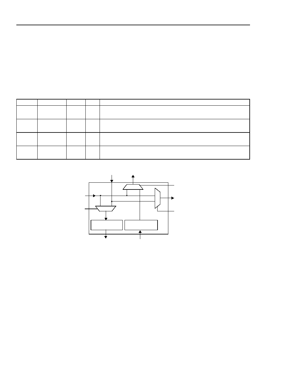
3.3.2 Protection Switch I/O Pin Description
The protection switch I/O provides additional copies of the high-speed interface signals so that various protection
schemes may be implemented. The protection interface may be used when the high-speed interface is operating in
both STS-3 and STS-1 modes. If the protection port is not used, the input clock and data may be left unconnected,
tied to power (P inputs), or ground (N inputs) through 1 k
resistors. Unused protection outputs should be left
unconnected.
Table 4. Protection Switch I/O Pin Description
Figure 3. Protection Switch
3.3.3 Telecom Bus (Low-speed I/O) Pin Description
The telecom bus on the Super Mapper is used for interconnecting STS-1 signals. It has two eight-bit data buses,
one for upstream data and one for downstream data, plus clock and frame indication signals for each bus. The tele-
com bus can operate at 19.44 MHz (space for three STS-1 signals) or 6.48 MHz (space for 1 STS-1 signal).
Super Mappers in OC-3 applications are typically connected together using the telecom bus, and the bus is config-
ured to operate at 19.44 MHz.
Pin
Symbol
Type
I/O
Description
AD10,
AE10
RPSD155P
RPSD155N
LVDS
I
Receive Protection Data. Receive side high-speed serial data input
from protection board.
AC10,
AD11
RPSC155P
RPSC155N
LVDS
I
Receive Protection Clock. Receive side high-speed clock input from
protection board.
AF13,
AE13
TPSD155P
TPSD155N
LVDS
O
Transmit Protection Data. Transmit side high-speed serial data output
to protection board.
AC12,
AD13
TPSC155P
TPSC155N
LVDS
O
Transmit Protection Clock. Transmit side high-speed clock output to
protection board.
STS-3 TRANSMIT
FRAMER
STS-3 RECEIVE
FRAMER
RPSMUXSEL1
HIGH-SPEED
PROTECTION
INPUTS
TPSMUXSEL2
HIGH-SPEED
PROTECTION
OUTPUTS
TPSMUXSEL3
HIGH-SPEED I/O

17
Agere Systems Inc.
Preliminary Data Sheet
TMXF28155 Super Mapper
May 2001
155/51 Mbits/s SONET/SDH x28/x21 DS1/E1
3 Pin Information
(continued)
Table 5. Telecom Bus (Low-speed I/O) Pin Description
Pin
Symbol
Type
I/O
Description
R1, R3, T4, T2,
T3, U4, U2, U3
RLSDATA[7:0]
--
I/O
Receive Low-speed Data (7:0), Parallel Data Bus. Used
to connect the downstream STS-1 signals from the master
to the slave devices. In master mode, RLSDATA is an out-
put bus, eight bits wide. It contains all the received data for
distribution to the two slave devices. Connect to
RLSDATA(7:0) on the slave devices. In slave mode, these
pins are inputs and should be connected to the
RLSDATA(7:0) outputs on the master. RLSDATA contains
three byte-interleaved STS-1 time slots. The slot used by
each SPE mapper in the slaves and the master device, is
determined by programing the SPE_RSTS3_TMSLOT reg-
ister bits.
V4
RLSCLK
--
I/O
Receive Low-speed Clock. This is a 19.44 MHz or
6.48 MHz clock for the receive low speed data bits. In
19.44 MHz master mode, this is a 19.44 MHz clock output
for distribution to the two slave devices. Connect to
RLSCLK on the slaves. RLSCLK is an input signal on slave
devices.
Note: As outputs, these pins have 6 mA drive capability.
V2
RLSPAR
--
I/O
Receive Low-speed Parity. Receive data parity bit, may be
configured for odd or even parity generated on
RLSDATA(7:0). The default is odd parity; it may be set to
even by setting bit 2 of the register at 0x4001B an output in
master mode and an input in slave mode. Connect the
RSLPAR (output) on the master to The RLSPAR (input)
pins on the slaves.
V1
RLSSPE
--
I/O
Receive Low-speed SPE Marker. Receive synchronous
payload envelope timing indicator. It is high, while there is
SPE data on the RLSDATA(7:0) output bus. Connect to
RLSSPE on the slaves. RLSSPE is an input on slave
devices.
V3
RLSJ0J1V1
--
I/O
Receive Low-speed J0/J1/V1 Marker. On the master
device, this is an output that is high while J0-1, J1
(1, 2 and 3) and V1 (1, 2 and 3) bytes are present on the
RLSDATA bus. Connect to RLSJ0J1V1 on the slaves, which
is an input.
W4
RLSV1
--
I/O
Receive Low-speed V1 Marker. Receive V1 timing indica-
tor. On the master this is an output that is high while the V1
bytes (1, 2 and 3) are present on RLSDATA(7:0) output bus.
Connect to RLSV1 on the slaves.

18
Agere Systems Inc.
TMXF28155 Super Mapper
Preliminary Data Sheet
155/51 Mbits/s SONET/SDH x28/x21 DS1/E1
May 2001
3 Pin Information
(continued)
Table 5. Telecom Bus (Low-speed I/O) Pin Description (continued)
Pin
Symbol
Type
I/O
Description
W2, W1, W3, Y4,
Y2, Y1, Y3, AA4
TLSDATAI[7:0]
--
I/O
Transmit Low-speed Data (7:0). This is a parallel data
bus. It is used to connect the upstream STS-1 signals from
the slave devices to the master device. In master mode,
TLSDATA is an input bus, eight bits wide. It contains all the
transmit STS-1 data from the slave devices. In slave mode,
these pins are outputs and should be connected to the
TLSDATA(7:0) inputs on the master. TLSDATA contains
three byte-interleaved STS-1 time slots. The slot used by
each SPE mapper in the slaves and the master device, is
determined by programing the SPE_TSTS3_TMSLOT reg-
ister bits.
AA2
TLSCLK
--
I/O
Transmit Low-speed Clock. This is a 19.44 MHz or
6.48 MHz clock for the TLSDATA(7:0) bits. TLSCLK is an
output on a master Super Mapper and an input on a slave.
Note: As outputs, these pins have 6 mA drive capability.
AA3
TLSPAR
--
I/O
Transmit Low-speed Parity. This parity bit is generated on
the TLSDATA(7:0) bits output from slave devices and input
to the master Super Mapper. May be configured for odd or
even parity generation or for checking.
AB2
TLSSPE
--
I/O
Transmit Low-speed SPE Marker. High while the STS-1
payloads are present on the TLSDATA(7:0) bus. Low while
the STS-1 overhead is present on the TLSDATA(7:0) bus.
An output from the master and input on the slaves.
AB4
TLSJ0J1V1
--
I/O
Transmit Low-speed J0/J1/V1 Marker. Transmit J0, J1, or
V1, timing indicator. High while the J0, J1 or V1 bits are
present on the TLSDATA(7:0) bus. An output on the master
and input on slaves.
AB3
TLSV1
--
I/O
Transmit Low-speed V1 Marker 3. Transmit V1 timing indi-
cator. High while the V1 bits are present on the
TLSDATA(7:0) bus. An output on the master and input on
slaves.
AC2
RLSC52
--
I/O
Receive Low-speed Clock. When in output (master)
mode, it is the receive side of the 51.84 MHz clock output,
synchronous to the receive high-speed input clock (data).
When in input (slave) mode, it receives a 51.84 MHz clock
input, synchronous to the receive high-speed input clock
(data).
Note: As outputs, these pins have 6 mA drive capability.
AC1
RLSSYNC52
--
I/O
Receive Low-speed Sync. When in output (master) mode,
it is the receive side frame sync output synchronous to a
51.84 MHz output. When in input mode, it is the receive
side frame sync input synchronous to a 51.84 MHz input.

19
Agere Systems Inc.
Preliminary Data Sheet
TMXF28155 Super Mapper
May 2001
155/51 Mbits/s SONET/SDH x28/x21 DS1/E1
3 Pin Information
(continued)
Table 5. Telecom Bus (Low-speed I/O) Pin Description (continued)
3.3.4 TOAC and POAC
The transport and path overhead access channels (TOAC and POAC) allow parts of the SONET/SDH overhead to
be examined externally (receive direction) or overwritten (transmit direction) through serial data ports. Each port
has clock and data lines and synchronization signal that marks the last bit of the frame so that the rest of the over-
head bytes can be identified.
The receive TOAC and POAC channels contain all of the respective overheads bytes. The transmit channels con-
tain space for all the overhead bytes, but whether they are actually transmitted depend on how the device is pro-
grammed. Some overhead bytes can not be modified; others may be modified only through the CPU port; some
may be modified only through the overhead access channels; and some may be modified either through the CPU
port, or through the overhead access channels.
Pin
Symbol
Type
I/O
Description
AC3
TLSC52
--
I/O
Transmit Low-speed Clock. When in output (master) mode,
it is the transmit side 51.84 MHz clock output synchronous to
transmit high-speed input clock. When in input mode, it
receives a 51.84 MHz clock input synchronous to transmit
high-speed input clock
Note: TLSCLK is used as the master clock for the T1/E1
framer and should therefore be provided even if the
TMUX SPE and VT mappers are not used.
AD2
TLSSYNC52
--
I/O
Transmit Low-speed Sync. When in output (master) mode,
it is the transmit side frame sync output synchronous to
51.84 MHz output. When in input (slave) mode, it receives the
transmit side frame sync input synchronous to 51.84 MHz
input.
Table 6. TOAC and POAC
Pin
Symbol
Type
I/O
Description
AD1
RTOACCLK
--
O
Receive TOAC Clock. Receive side serial access channel
clock output for the transport overhead bytes.
AD3
RTOACDATA
--
O
Receive TOAC Data. Receive side serial access channel
data output for the transport overhead bytes.
AA5
RTOACSYNC
--
O
Receive TOAC Synchronization. Receive side sync output
for TOAC channel. Active-high during the LSB of the last
byte.
AB6
TTOACCLK
--
O
Transmit TOAC Clock. Transmit side serial access channel
clock output for the transport overhead bytes.
AE2
TTOACDATA
--
I
Pull down
Transmit TOAC Data. Transmit side serial access channel
data input for the transport overhead bytes.
AF3
TTOACSYNC
--
O
Transmit TOAC Synchronization. Transmit side sync out-
put for TOAC channel. Active-high during the LSB of the last
byte.
Path Overhead Access Channel (POAC)
AE3
RPOACCLK
--
O
Receive POAC Clock. Receive side serial access channel
clock output for the path overhead bytes.
AD4
RPOACDATA
--
O
Receive POAC Data. Receive side serial access channel
data output for the path overhead bytes.

20
Agere Systems Inc.
TMXF28155 Super Mapper
Preliminary Data Sheet
155/51 Mbits/s SONET/SDH x28/x21 DS1/E1
May 2001
3 Pin Information
(continued)
3.3.5 Miscellaneous Signals
Table 7. Miscellaneous Signals
3.3.6 DS3 Port
If a DS3 output is required in a Super Mapper application and the DS3 signal has been recovered (demapped) from
an STS-1, then it is necessary to smooth the DS3 recovered clock. The DS3 clock extracted from the STS-1 clock
will have considerable jitter introduced when the SONET overhead is removed and pointer adjustments are made.
A phase locked loop is recommended for this purpose. The Super Mapper contains a phase comparator, that can
be used in conjunction with an external low-pass filter and voltage controlled crystal oscillator to implement the
PLL.
Pin
Symbol
Type
I/O
Description
AF4
RPOACSYNC
--
O
Receive POAC Synchronization. Receive side sync output
for POAC channel. Active-high during the last bit of the last
byte of the POAC frame.
AE4
TPOACCLK
--
O
Transmit POAC Clock. Transmit side serial access channel
clock output for the path overhead bytes.
AD5
TPOACDATA
--
I
Pull down
Transmit POAC Data. Transmit side serial access channel
data input for the path overhead bytes.
AC5
TPOACSYNC
--
O
Transmit POAC Synchronization. Transmit side sync out-
put for POAC channel. Active-high during the last bit of the
last byte.
Pin
Symbol
Type
I/O
Description
AE5
LOSEXT
--
I
Pull up
Loss of Signal External. External loss of signal input. If
external clock and data recovery is used on the high-speed
I/O port, it may be connected to this input which can be con-
figured to assert the LOS register bit normally associated
with the internal LOS detection in the internal CDR block. The
polarity of LOS may be programmed active-high or low.
AD6, AE6,
AC6
AUTO_AIS
--
I/O
AIS Enable (3:1). Control signal for automatic AIS insertion
on each STS1. The STS-1 AIS is applied down stream on the
telecom bus, i.e., it is an output from masters and an input to
slaves. Active-high.
Input when slave mode.
Output when master mode
If not used, leave open.
AD7
RHSFSYNCN
--
O
Receive High-speed Frame Synchronization. Receive side
frame sync output indicating the frame location of the high-
speed data input. May be used as a 8 kHz timing reference
for network synchronization to the receive high-speed data
input (STS-3 or STS-1).
Table 6. TOAC and POAC (continued)

21
Agere Systems Inc.
Preliminary Data Sheet
TMXF28155 Super Mapper
May 2001
155/51 Mbits/s SONET/SDH x28/x21 DS1/E1
3 Pin Information
(continued)
Table 8. DS3 Port
Pin
Symbol
Type
I/O
Description
V22
PHASEDETUP
--
O
Phase Detector Up. Phase error signal out to external filter
and VCXO. This output will generate an error signal when
the VCXO output is slower than the reference signal.
U22
PHASEDETDOWN
--
O
Phase Detector Down. Phase error signal out to external fil-
ter and VCXO. This output will generate an error signal when
the VCXO output is faster that the reference signal.
R22
DS3POSDATAOUT
--
O
Positive Data Output. Serial DS3 positive data out to LIU
when the DS3 output port is operating in dual rail-mode.
Nonreturn to zero DS3 data output when the DS3 output is
operating in single ended mode.
P22
DS3NEGDATAOUT
--
O
Negative Data Output. Serial DS3 negative data output to
LIU when the DS3 port is operating in dual rail mode. In sin-
gle rail mode, this output is not used and may be left uncon-
nected.
N22
DS3DATAOUTCLK
--
I
Pull
down
DS3 Data Out Clock. 44.736 MHz DS3 clock input. If the
Super Mapper is being used to map DS3 data to and from
STS-1, then this clock will be supplied by the external VCXO
that is associated with the DS3 clock recovery PLL. In other
DS3 modes (e.g., M13) this input will be supplied by an
external crystal oscillator, usually associated with a DS3 LIU.
If the DS3 port is not used, this input may be tied to ground
or left open, since it is equipped with an internal pull-down
resistor.
M22
DS3POSDATAIN
--
I
Pull
down
Positive Data Input. If the DS3 port is configured in dual-rail
mode, then this input is serial positive data from an external
DS3 LIU. If the DS3 port is configured in single-rail mode,
then this input is serial nonreturn-to zero data from the exter-
nal LIU.
K22
DS3NEGDATAIN
--
I
Pull
down
Negative Data In. In dual rail mode, this is negative data
from an external DS3 LIU. In single rail mode, it may be con-
nected to the bipolar violation output of the external DS3 LIU,
left unconnected, or tied to ground.
J22
DS3DATAINCLK
--
I
Pull
down
DS3 Data In Clock. This is a 44.736 MHz clock input from
the clock recovery in the external DS3 LIU.

22
Agere Systems Inc.
TMXF28155 Super Mapper
Preliminary Data Sheet
155/51 Mbits/s SONET/SDH x28/x21 DS1/E1
May 2001
3 Pin Information
(continued)
Table 9. DS3 Port, C-Bit, and Datalink Access
3.3.7 M13 Multiplexer/Demultiplexer Receive Section
Two groups of signals are defined in this section. The first group are reference clocks, used internally in the jitter
attenuation and AIS generation processes. Note that these are typically supplied by free-running crystal oscillators.
The outputs below provide access to the received C-bits and data link bits extracted from the received DS3 frame.
These operate in the same way if the source of the DS3 signal is from an SPE or from the external DS3 port.
Pin
Symbol
Type
I/O
Description
E14
TCBSYNC
--
O
Transmit C-Bit Sync. In the C-bit parity mode, 10 C-bits may
optionally be input for multiplexing into the transmit DS3 frame
through the TCBDATA input. The TCBSYNC output is low, except
during the rising edge of TCBCLK that is used to input C2.
E13
TCBCLK
--
O
Transmit C-Bit Clock. A gapped clock (nominally 93.983 kHz) for
accepting selected C-bits on input M13_CBDATA.
E12
TCBDATA
--
I
Pull down
Transmit C-Bit Data. In the C-bit parity mode, the network require-
ments bit (C2), and the unused C-bits (C4, C5, C6, C16, C17, C18,
C19, C20, and C21) may optionally be input for multiplexing into the
transmit DS3 frame through this input.
E9
TDLCLK
--
O
Transmit Data Link Clock. A gapped clock (nominally 28.195 kHz)
for accepting path maintenance data link C-bits on input TDLDATA.
E8
TDLDATA
--
I
Pull down
Transmit Data Link Data. The path maintenance data link C-bits
(C13, C14, and C15) may optionally be input for multiplexing into the
transmit DS3 frame through this input.
Table 10. M13 Multiplexer/Demultiplexer Receive Section
Pin
Symbol
Type
I/O
Description
AC17
E1XCLK
--
I
Pulldown
E1 Reference Clock. This clock is used as a reference for the jitter
attenuator when it is operating in the E1 mode. It must have a fre-
quency of 2.048 MHz, 32.768 MHz, or 65.536 MHz and a stability of
50 ppm. It is also used to generate an E1 AIS (all ones). May be left
unconnected, or tied to ground, if no E1 options are being used.
AD16
DS1XCLK
--
I
Pulldown
DS1 Reference Clock. This clock is used as a reference for the jitter
attenuator when it is operating in the DS1 or the J1 mode. It must
have a frequency of 1.544 MHz, 24.704 MHz, or 49.408 MHz and a
stability of ±32 ppm. This clock signal is also used to generate DS1
AIS signals. May be left unconnected or tied to ground, if not, no DS1
options are being used.
E10
DS2AISCLK
--
I
Pulldown
DS2 Reference Clock. A 6.312 MHz ±30 ppm input. In the M23
mode, this clock is used to generate DS2 AIS. May be left uncon-
nected or tied to ground if no DS2 options are being used. Note that
C-bit parity mode does no require a DS2 reference clock.
E18
RCBSYNC
--
O
Receive C-Bit Sync. Ten C-bits are output on RCD after they are
demultiplexed from the received DS3 signal. The RCS output is low,
except during the rising edge of RCD that is used to output C2.

23
Agere Systems Inc.
Preliminary Data Sheet
TMXF28155 Super Mapper
May 2001
155/51 Mbits/s SONET/SDH x28/x21 DS1/E1
3 Pin Information
(continued)
3.3.8 Low-Order Path Overhead Access Channel
Each VT has a low-order path overhead, and this interface allows access to all LOPOH bits for all VTs. Note that
the purpose of doing this is slightly different form the transport and path overhead access. These are used to cross
couple the bits between links in a protection scheme, rather than provide access for examination or modification of
the overhead, although that is possible too.
Table 11. Low-Order Path Overhead Access Channel
Figure 4. DS1/E1 to DXC Block Diagram
Pin
Symbol
Type
I/O
Description
E17
RCBCLK
--
O
Receive C-Bit Clock. A gapped clock (nominally 93.983 kHz) for out-
putting selected C-bits on RCD.
E15
RCBDATA
--
O
Receive C-Bit Data. The received network requirements bit (C2) and
the received unused C-bits (C4, C5, C6, C16, C17, C18, C19, C20,
and C21) are output after they are demultiplexed from the received
DS3 signal.
E19
RDLCLK
--
O
Receive Data Link Clock. A gapped clock (nominally 28.195 kHz)
for outputting path maintenance data link C-bits on RDLD.
H22
RDLDATA
--
O
Receive Data Link Data. The received path maintenance data link
C-bits (C13, C14, and C15) that are demultiplexed from the received
DS3 signal.
Pin
Symbol
Type
I/O
Description
Transmit Direction
AC13
LOPOHCLKIN
--
I Pull down 6.48 MHz Low Order Path Overhead Clock.
AC14
LOPOHDATAIN
--
I Pull down Low-Order Path Overhead Data. (O-bits, V5, J2,
Z6/N2, Z7, and K4 byte.)
AB14
LOPOHVALIDIN
--
I Pull down Valid LOPOH_DATA.
Receive Direction
AB15
LOPOHCLKOUT
--
O
6.48 MHz Low Order Path Overhead Clock.
AB17
LOPOHDATAOUT
--
O
Low-Order Path Overhead Data. (O-bits,V5, J2,
Z6/N2, Z7/K4 byte.)
AB18
LOPOHVALIDOUT
--
O
Valid VTMPR_LOPOH_DATA Output.
Table 10. M13 Multiplexer/Demultiplexer Receive Section (continued)
VT MAPPER
VT MAPPER
LOPOH
OUTPUTS
LOPOH
INPUTS
LOPOH
OUTPUTS
LOPOH
INPUTS
TELECOM BUS
DS1/E1 TO DXC

24
Agere Systems Inc.
TMXF28155 Super Mapper
Preliminary Data Sheet
155/51 Mbits/s SONET/SDH x28/x21 DS1/E1
May 2001
3 Pin Information
(continued)
Table 12. Multifunction System Interface Transmit Path Direction
Pin
Symbol
Type
I/O
Description
C13, A12,
B11, B10, B9,
D8, C8, A7,
B6, D5, A4,
A3, H5, F5,
C2, D2, E2,
F4, G2, H1,
J3, J4, K4, L4,
M2, N1, P4,
P3
LINERXDATA[28:1]
--
I
Pull down
Line Receive Data (28:1). Configurable inputs to the
internal cross connect. The use depends on the appli-
cation. Generally, these inputs are used for the received
positive-rail or single-rail DS1/E1 line data input. If oper-
ating in dual rail mode, the negative rail will be expected
on LINERXSYNC(28:1). Using dual rail mode implies
that the internal B8ZS or HDB3 decoders are enabled,
and line code violations can be detected and counted
inside the Super Mapper.
These data inputs may be assigned, using the cross
connect block, to the DS1 or E1 inputs on the VT map-
per, M13 or DS1/E1 framers. It is also possible to use
the inputs for DS2 data, in which case they may be
assigned to the M23 multiplexer inputs.
D13
LINERXDATA29
--
I
Pull down
Receive Data 29. Configurable input to the internal
cross connect. May be used as an additional line
receive data input, for a protection channel. Other pos-
sible uses are as follows:
Global transmit line clock input. Externally supplied
1.544 MHz or 2.048 MHz low jitter clock phase-locked
to the TDM system clock. Used for transmit line clock on
the DS1/E1 framers. This is not normally used, because
the DS1/E1 framer has a PLL which can generate a
1.544 MHz clock from the TDM system clock (CHI
clock). This applies in PSB and CHI modes.
Receive data input. If NSMI mode is used, this will be a
51.84 Mbits/s serial data input.
D12, C12,
C11, C10, A9,
B8, D7, C7,
C6, C5, C4,
C3, J5, B2,
D3, E3, F3,
G3, G4, H2,
J1, K3, L3,
M3, M4, N2,
P2, R4
LINERXCLK[28:1]
--
I/O
Pull down
Receive Clock (28:1). Configurable inputs/outputs to
the internal cross connect. Typically a line clock associ-
ated with the corresponding LINERXDATA input. It can
therefore be running at DS1, E1 or DS2 rate. The cross
connect is used to assign these inputs to the VT map-
per, M13 or DS1/E1 framers.
B13
LINERXCLK29
--
I/O
Pull down
Receive Clock 29. May be used as additional receive
clock input for a DS1/E1 protection channel. Also has
special use as a master clock. In CHI mode, it is the
receive clock input (2.048 MHz, 4.096 MHz, 8.192 MHz,
or 16.384 MHz). In PSB mode, it is the receive clock
input (19.44 MHz). In NSMI mode, it is the receive clock
output. (51.84 MHz).

25
Agere Systems Inc.
Preliminary Data Sheet
TMXF28155 Super Mapper
May 2001
155/51 Mbits/s SONET/SDH x28/x21 DS1/E1
3 Pin Information
(continued)
Pin
Symbol
Type
I/O
Description
B12, D11,
D10, D9, C9,
A8, B7, D6,
B5, B4, B3,
E6, K5, C1,
D1, E4, F2,
G1, H3, H4,
J2, K2, L2,
M1, N3, N4,
P1, R2
LINERXSYNC[28:1]
--
I
Line Receive Synchronous 28:1. Multifunction input.
Channel assignment may be configured through the
internal cross connect. Can be used as the negative rail
of a DS1/E1 signal in conjunction with LINERX-
DATA(28:1), when operating in dual-rail mode. In CHI
mode these inputs are used for receive TDM highways
that may run at 2.048, 4.096, or 8.192 Mbits/s. In paral-
lel system bus mode the receive system data bus inputs
are assigned to LINERXSYNC 16:1. The PSB is a 16-
bit wide bus that operates at 19.44 MHz.
A13
LINERXSYNC29
--
I/O
Line Receive Synchronous 29. Multifunction input.
Channel assignment may be configured through the
internal cross connect. Can be used as the negative rail
of a DS1/E1 signal in conjunction with LINERXDATA 29,
when operating in dual-rail mode.
In CHI and PSB modes this input is used as the receive
system frame synchronization input. In NSMI mode, it is
the receive frame sync output
R25, P26,
N23, N24,
M26, L25,
K25, J25,
H23, H24,
G26, F25,
E23, D26,
C26, E21,
B24, B23,
B22, D21,
B20, A19,
C18, D18,
D17, D16,
B15, A14
LINETXDATA[28:1]
--
I/O
Line Transmit Data (28:1) Configurable outputs from
the internal cross connect. Used for transmit positive-
rail or single-rail DS1/E1 line data outputs. May be con-
nected to the DS1/E1 outputs from the VT mapper, M13
MUX or DS1/E1 frame line outputs. May also be used
as a DS2 output.
T23
LINETXDATA29
--
O
Line Transmit Data 29. Configurable output from the
internal cross connect. An extra DS1 or E1 transmit port
that may be used for protection or as a timing reference
output.
Table 12. Multifunction System Interface Transmit Path Direction (continued)

26
Agere Systems Inc.
TMXF28155 Super Mapper
Preliminary Data Sheet
155/51 Mbits/s SONET/SDH x28/x21 DS1/E1
May 2001
3 Pin Information
(continued)
Pin
Symbol
Type
I/O
Description
R23, P25,
N25, M23,
M24, L24,
K24, J26,
H25, G23,
G24, F24,
E24, D24,
C24, B25,
C23, C22,
C21, C20,
D20, B19,
A18, C17,
C16, C15,
D15, B14
LINETXCLK[28:1]
--
I/O
Line Transmit Clock (28:1). Configurable outputs from
the internal cross connect. Can be used as the clock
signals for LINETXDATA(28:1) in DS1, E1, and DS2
modes.
R24
LINETXCLK29
--
I/O
Line Transmit Clock 29. Configurable output to the
internal cross connect for the protection or timing refer-
ence channel. Also used as the transmit global system
clock input for CHI (2.048 MHz, 4.096 MHz, 8.192 MHz,
or 16.384 MHz), PSB (19.44 MHz), and NSMI (51.84
MHz) modes.
P24, P23,
N26, M25,
L23, K23, J23,
J24, H26,
G25, F23,
E25, D25,
C25, F22,
A24, A23,
D22, B21,
A20, C19,
D19, B18,
B17, B16,
A15, C14,
D14
LINETXSYNC[28:1]
--
I/O
Line Transmit Synchronous (28:1). Configurable
inputs/outputs to the internal cross connect. An output
when used as the negative rail of a DS1 or E1 output
port operating in dual-rail mode. In CHI mode, these
pins may be used as output TDM highways. In PSB
mode, bits 16:1 are used for the transmit data bus, and
bits 28:17 are not used. These pins may also be used
as DS2 I/O to the M12 block as follows: 7:1--Tx data
out. 14:8--Tx clock in. 21:16--Rx data in. 28:22--Rx
clock in.
R26
LINETXSYNC29
--
I/O
Line Transmit Synchronous 29. Configurable input/
output to the internal cross connect. An output when
used as the negative rail of a DS1 or E1 output port
operating in dual-rail mode. In CHI and PSB modes, it is
used as the transmit system frame synchronization
input. In NSMI mode, it is the transmit system frame
sync output.
AB19
RXDATAEN
--
O
NSMI Receive Enable. Receive data enable for NSMI
mode.
W22
TXDATAEN
--
O
NMSI Transmit Enable. Transmit data enable for NSMI
mode.
Table 12. Multifunction System Interface Transmit Path Direction (continued)

27
Agere Systems Inc.
Preliminary Data Sheet
TMXF28155 Super Mapper
May 2001
155/51 Mbits/s SONET/SDH x28/x21 DS1/E1
3 Pin Information
(continued)
3.3.9 Framer PLL
The DS1/E1 framer has a phase-locked loop that may be used to generate a transmit line clock at 1.544 MHz or
2.048 MHz. The reference signal for this PLL may be chosen from a number of possible sources, all typically syn-
chronized to the system clock (CHI transmit/receive clock for example.) In order to ensure reliable performance
,this PLL has its own isolated power pins. The PLL also has a number of test control pins that are used for factory
testing only.
The PLL is active when framer bit PLL_BYPAS = 0. When PLL_BYPAS = 1, the PLL is bypassed and an external
clock at the system interface is used as the line clock. An example would be when the framers are programmed for
a CHI interface at 2.048 MHz and the frames are programmed for E1, the PLL may be bypassed and the CHI sys-
tem clock may be used as the line clock.
Table 13. Framer PLL
Pin
Symbol
Type
I/O
Description
AD22
VDDD_PLL
VDD
--
Digital VDD for PLL.
AE23
VDDS_PLL
VDD
--
Analog VDD for PLL.
AF23
VSSA_PLL
VSS
--
Analog VSS for PLL.
AD23
VSSS_PLL
VSS
--
Digital VSS for PLL.
AD24
CLKIN_PLL
--
I
Pull down
Clock In PLL. Phase locked-loop reference clock input. Fre-
quency should be consistent with the MODE_PLL pins in the
PLL Mode1 table below. A 1.544 MHz clock for DS1 transmit
outputs is generated synchronous to this clock.
AB21
MODE2_PLL
--
I/O
PLL Mode 2. Control bit that should be tied to the appropriate
state depending on the frequency of CLKIN_PLL consistent
with the PLL Mode1 table below. This pin is also used during
factory testing as an output.
AF24
MODE0_PLL
--
I
Pull down
PLL Mode 0. PLL control input 0.
AE24
MODE1_PLL
--
I
Pull down
PLL Mode 1. PLL control input 1. The PLL mode inputs should
be hardwired to the logic levels shown in the table below,
depending on the frequency of the reference supplied to
CLKIN_PLL.
Mode2
0
0
0
0
1
1
1
1
Mode1
0
0
1
1
0
0
1
1
Mode0
0
1
0
1
0
1
0
1
CLKIN_PLL
Reserved
51.84 MHz
26.624 MHz
19.44 MHz
16.348 MHz
8.194 MHz
4.096 MHz
2.048 MHz

28
Agere Systems Inc.
TMXF28155 Super Mapper
Preliminary Data Sheet
155/51 Mbits/s SONET/SDH x28/x21 DS1/E1
May 2001
3 Pin Information
(continued)
Table 14. Microprocessor Interfaces
Pin
Symbol
Type
I/O
Description
AE17
MPCLK
--
I
Processor Clock. This is the synchronous microprocessor
clock (when MPMODE=1). The maximum clock frequency is
66 MHz. This clock is required to properly sample address,
data, and control signals from the microprocessor in both
asynchronous and synchronous modes of operation. This
clock must be within the range of 16 MHz--66 MHz.
AD17
MPMODE
--
I
Control Port Mode. If the microprocessor interface is syn-
chronous, CPM should be set to 1. If the microprocessor
interface is asynchronous, CPM should be set to 0.
AC18
CSN
--
I
Pull up
Chip Select. Active-low chip select. For synchronous mode,
it should be stable beyond a certain setup time before the ris-
ing clock edge when AS is active. For asynchronous mode, it
should be stable before DS is asserted.
AE18
ADSN
--
I
Address Strobe. Active-low address strobe that is a 1 PCK
cycle wide pulse for synchronous mode and active for the
entire read/write cycle for asynchronous mode. Address bus
signals, A(19:0), are transparently latched into Super Mapper
when AS is low. The address bus should remain valid for the
duration of AS.
AF18
RWN
--
I
Read/Write Cycle Selection. RW is set high for a read oper-
ation, or set low for write operation.
AD18
DSN
--
I
Data Strobe. DS is not used for synchronous mode. For
asynchronous mode, write operation, DS becomes active
after data is stable. For read operation, it is similar to AS.
AB23, AC26,
AC24, AD25,
AD26, AE25,
AA22, AC22,
AE22, AD21,
AE21, AC21,
AD20, AF20,
AE20, AC20,
AD19, AF19,
AE19, AC19
ADDR[19:0]
--
I
Address (19:0). A19 is the most significant and A0 the least
significant bit for addressing all the internal SM registers dur-
ing CPU access cycles.
Note: The Super Mapper is little endian, the least significant
byte is stored in the lowest address and the most sig-
nificant byte is stored in the highest address. Care
must be exercised in connection to microprocessors
that use big-endian byte ordering.
AB25, AA24,
AA25, AA23,
Y24, Y26,
Y25, Y23,
W24, W26,
W25, W23,
V24, V26,
V25, V23
DATA[15:0]
--
I/O
Data (15:0). Data bus for all transfers between the CPU and
the internal SM registers. The pins are inputs during write
cycles and outputs during read cycles. DATA15 is the MSB
and DATA0 is the LSB.
U24, U25
PAR[1:0]
--
I/O
CPU Port Parity (1:0). Byte-wide parity bits for data. CPP[1]
is the parity for D[15:8] and CPP[0] is the parity for D[7:0].

29
Agere Systems Inc.
Preliminary Data Sheet
TMXF28155 Super Mapper
May 2001
155/51 Mbits/s SONET/SDH x28/x21 DS1/E1
3 Pin Information
(continued)
Table 15. General Purpose Interface
Pin
Symbol
Type
I/O
Description
U23
DTN
--
O
Open Drain
Data Transfer Acknowledge. In synchronous CPU mode,
DTA goes low at 4th cycle for write or 5th cycle for read,
resulting in a fixed 2 wait-states for writes and 3 wait-states
for reads. In asynchronous
µ
P mode, after qualification of AS
and DS by TLSC52 clock, DTA goes low for two TLSC52
clock cycles for writes and three TLSC52 clock cycles for
reads. DTA goes high, along with the rising edge of AS.
AB24
INTN
--
O
Open Drain
Interrupt. Super Mapper interrupt request, active-low. An
open drain output should be connected to an external pull-up
resistor.
AC25
APS_INTN
--
O
Open Drain
APS Interrupt. Automatic protection switch interrupt request,
active-low. An open drain output should be connected to an
external pull-up resistor.
Pin
Symbol
Type
I/O
Description
T24
RSTN
--
I
Pull up
Reset. Global reset, active-low. Initializes all internal registers
to their default state.
T25
PMRST
--
I/O
Pull down
Performance Monitor Reset. May be configured as an input
and then used to directly reset all the counters associated with
DS1/E1 performance monitoring. If an internal PM reset is
used, PMRST is configured as an output that indicates when a
PM reset occurred.
R5
TCK
--
I
Test Clock. This signal provides timing for the boundary scan
and TAP controller. This signal should be static, except during
boundary scan testing.
U5
TDI
--
I
Pull up
Test Data In. Data input for the boundary scan; sampled on
the rising edge of TCK.
W5
TMSN
--
I
Pull up
Test Mode Select (Active-Low). Controls boundary scan test
operations. TMS is sampled on the rising edge of TCK.
AB8
TRSTN
--
I
Pull down
Test Reset (Active-Low). This signal is an asynchronous
reset for the TAP controller.
V5
TDO
--
O
Test Data Out. Updated on the falling edge of TCK. The TDO
output is high impedance, except when scanning out test data.
AB9
IC3STATEN
--
I
Pull up
Global Output Enable. All output and bidirectional buffers will
be high impedance when this input is low. Normally pulled high
internally.
Table 14. Microprocessor Interfaces (continued)

30
Agere Systems Inc.
TMXF28155 Super Mapper
Preliminary Data Sheet
155/51 Mbits/s SONET/SDH x28/x21 DS1/E1
May 2001
3 Pin Information
(continued)
3.3.10 Test Pins
These pins are for factory test purposes only and must be connected as stated below for normal operation. They
are used to establish special configurations for testing, inserting test data, etc. For normal operation they should be
left unconnected; each is equipped with a pull-up or pull-down to the inactive (normal operation) state.
Table 16. Test Pins
Table 17. CDR Power
Pin
Symbol
Type
I/O
Description
N5
SCAN_EN
--
I
Pull down
Test Only. Scan enable (active-high).
M5
SCAN_MODE
--
I
Pull down
Test Only. Serial scan input for testing (active-high).
P5
IDDQ
--
I
Pull up
Test Only. I
DD
Q input (active-high).
AE14
BYPASS
--
I
Pull down
Test Only. Enables functional bypassing of the clock synthesis
with a test clock (active-high).
AF14
TSTPHASE
--
I
Pull down
Test Only. Controls bypass of 32 PLL-generated phases with
32 low-speed phases, generated by test logic (active-high).
AD14
ECSEL
--
I
Pull down
Test Only. Enables external test control of 155 MHz clock
phase selection through ETOGGLE and EXDNUP inputs
(active-high).
AC15
ETOGGLE
--
I
Pulldown
Test Only. Moves 155 MHz clock selection one phase per pos-
itive pulse > 20ns. Active + pulse.
AE15
EXDNUP
--
I
Pulldown
Test Only. Direction of phase changes.
0 = down
1 = up.
AF15
TSTMODE
--
I
Pulldown
Test Only. Enables CDR test mode.
AD15
TSTSFTLD
--
I
Pulldown
Test Only. Enables CDR test mode shift register.
AE16,
AC16
TSTMUX[1:0]
--
O
Test Only. CDR test mode output
Pin
Symbol
Type
I/O
Description
AC9
VDDA_CDR
--
I
Analog Power. Isolated analog power supply VDD for CDR.
AB12
VSSA_CDR
--
I
Analog Ground. Isolated analog power supply VSS for CDR.
Table 18. LVDS Control Pins
Pin
Symbol
Type
I/O
Description
AF12
AE12
RESHI
RESLO
--
I
Resistor 1, 2. A 100
1% resistor is should be connected between
these two pins as a reference for the LVDS input buffer termination.
AC11
REF10
--
I
Voltage Reference 1. 1.0 V reference voltage input.
AD12
REF14
--
I
Voltage Reference 2. 1.4 V reference voltage input.

31
Agere Systems Inc.
Preliminary Data Sheet
TMXF28155 Super Mapper
May 2001
155/51 Mbits/s SONET/SDH x28/x21 DS1/E1
3 Pin Information
(continued)
Pin
Symbol
Type
I/O
Description
AB10
CTAPRH
--
--
Center Tap 1. For RHSD P/N and RHSC P/N. Optional, 0.1
µ
F
capacitor connected between CTAP pin and ground, to improve the
common mode rejection of the LVDS input buffers.
AE11
CTAPTH
--
--
Center Tap 2. For THSD P/N and THSC P/N. Optional, 0.1
µ
F
capacitor connected between CTAP pin and ground, to improve the
common mode rejection of the LVDS input buffers.
AB13
CTAPRP
--
--
Center Tap 3. For RPSD155 P/N and RPSC155 P/N. Optional,
0.1
µ
F capacitor connected between CTAP pin and ground, to
improve the common mode rejection of the LVDS input buffers.
Table 18. LVDS Control Pins (continued)
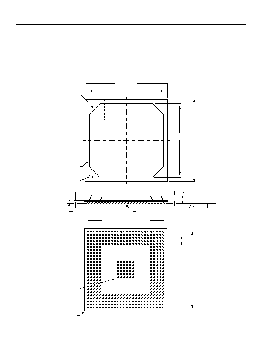
32
Agere Systems Inc.
TMXF28155 Super Mapper
Preliminary Data Sheet
155/51 Mbits/s SONET/SDH x28/x21 DS1/E1
May 2001
3 Pin Information
(continued)
3.4 Outline Diagram
3.4.1 456-Pin PBGA
Dimensions are in millimeters.
5-6216(F)r.1
0.56
±
0.06
1.17
±
0.05
2.33
±
0.21
SEATING PLANE
SOLDER BALL
0.60
±
0.10
0.20
PWB
MOLD
COMPOUND
35.00
±
0.20
35.00
±
0.20
+0.70
≠0.00
30.00
+0.70
≠0.00
30.00
A1 BALL
IDENTIFIER ZONE
AF
AE
AD
AC
AB
AA
Y
W
V
U
T
R
G
25 SPACES @ 1.27 = 31.75
P
N
M
L
K
J
H
1 2 3 4 5 6 7 8 9 10
12
14
16
18
22
24
26
20
11
13
15
17
21
19
23
25
F
E
D
C
B
A
CENTER ARRAY
FOR THERMAL
ENHANCEMENT
(OPTIONAL)
25 SPACES
@ 1.27 = 31.75
A1 BALL
CORNER
0.75
±
0.15

Preliminary Data Sheet
TMXF28155/51 Super Mapper
May 2001
155/51 Mbits/s SONET/SDH x28/x21 DS1/E1
33
Agere Systems Inc.
4 Electrical Characteristics
Table of Contents
Contents
Page
4 Electrical Characteristics .................................................................................................................................... 33
4.1 Absolute Maximum Ratings ......................................................................................................................... 34
4.2 Handling Precautions ................................................................................................................................... 34
4.3 Operating Conditions ................................................................................................................................... 34
4.4 Logic Interface Characteristics ..................................................................................................................... 35
4.5 LVDS Interface Characteristics .................................................................................................................... 36
List of Figures
Figure 5. Single-Ended Input Specification ............................................................................................................ 35
List of Tables
Table 19. Absolute Maximum Ratings ................................................................................................................... 34
Table 20. Handling Precaution .............................................................................................................................. 34
Table 21. Recommended Operating Conditions ................................................................................................... 34
Table 22. Logic Interface Characteristics .............................................................................................................. 35
Table 23. LVDS Interface Characteristics ............................................................................................................. 36

TMXF28155/51 Super Mapper
Preliminary Data Sheet
155/51 Mbits/s SONET/SDH x28/x21 DS1/E1
May 2001
34
Agere Systems Inc.
4 Electrical Characteristics
(continued)
4.1 Absolute Maximum Ratings
Stresses in excess of the absolute maximum ratings can cause permanent damage to the device. These are abso-
lute stress ratings only. Functional operation of the device is not implied at these or any other conditions in excess
of those given in the operational sections of the data sheet. Exposure to absolute maximum ratings for extended
periods can adversely affect device reliability.
4.2 Handling Precautions
Although protection circuitry has been designed into this device, proper precautions should be taken to avoid expo-
sure to electrostatic discharge (ESD) during handling and mounting. Agere employs a human-body model (HBM)
and charged-device model (CDM) for ESD-susceptibility testing and protection design evaluation. ESD voltage
thresholds are dependent on the circuit parameters used in the defined model. No industry-wide standard has
been adopted for the CDM. However, a standard HBM (resistance = 1500
, capacitance = 100 pF) is widely used
and, therefore, can be used for comparison purposes. The HBM ESD threshold presented here was obtained by
using these circuit parameters:
4.3 Operating Conditions
The following tables list the voltages required for proper operation of the TMXF28155 device, along with their toler-
ances.
Table 21. Recommended Operating Conditions
* Internal reference voltage is used if SMPR_LVDS_REF_SEL = 1 (
Table 70
); or else external voltage is used.
Table 19. Absolute Maximum Ratings
Parameter
Symbol
Min
Max
Unit
dc Supply Voltage Range
V
DD
≠0.5
4.6
V
Power Dissipation
P
D
--
--
mW
Storage Temperature Range
Tstg
≠65
125
∞C
Ambient Operating Temperature Range
T
A
≠40
85
∞C
Maximum Voltage (digital input pins)
--
--
5.25
V
Minimum Voltage (digital input pins)
--
≠0.3
--
V
Table 20. Handling Precaution
Device
Voltage
TMXF28155
2000 V
Parameter
Symbol
Min
Typ
Max
Unit
Power
V
DD
3.14 3.3 3.47
V
Ground
V
SS
--
0.0
--
V
Input Voltage, High
V
IH
V
DD
≠ 1.0
--
5.25
V
Input Voltage, Low
V
IL
V
SS
--
1.0
V
1.0 V, LVDS Reference*
LVDS_REF10
--
1.0
--
V
1.4 V:,LVDS Reference*
LVDS_REF14
--
1.4
--
V
Preliminary Data Sheet
TMXF28155/51 Super Mapper
May 2001
155/51 Mbits/s SONET/SDH x28/x21 DS1/E1
35
Agere Systems Inc.
4 Electrical Characteristics
(continued)
4.4 Logic Interface Characteristics
Table 22. Logic Interface Characteristics
The input specification for the remaining (nonbalanced) inputs are specified in
Figure 5
.
5-6032(F)r.2
Figure 5. Single-Ended Input Specification
Parameter
Symbol
Test Conditions
Min
Max
Unit
Input Leakage
I
L
--
--
1.0
µA
Output Current:
Low
High
I
OL
I
OH
--
--
--
--
2
2
mA
mA
Output Voltage:
Low
High
V
OL
V
OH
--
--
V
SS
V
DD
≠ 0.5
0.5
5.25
V
V
Input Capacitance
C
I
--
--
1.5
pF
V
IH
t
F
t
R
V
IL

TMXF28155/51 Super Mapper
Preliminary Data Sheet
155/51 Mbits/s SONET/SDH x28/x21 DS1/E1
May 2001
36
Agere Systems Inc.
4 Electrical Characteristics
(continued)
4.5 LVDS Interface Characteristics
3.3 V ± 5% V
DD
, 0--125
∞
C, slow--fast process.
Table 23. LVDS Interface Characteristics
.
* Buffer will not produce output transition when input is open-circuited.
Parameter
Symbol
Test Conditions
Min
Typ
Max
Unit
Input Buffer Parameters
Input Voltage Range, V
IA
or V
IB
V
I
|V
GPD
| < 925 mV, dc--1 MHz
0.0
1.2
2.4
V
Input Differential Threshold
V
IDTH
|V
GPD
| < 925 mV, 311 MHz
≠100
--
100
mV
Input Differential Hysteresis
V
HYST
(+V
IDTH
) ≠ (≠V
IDTH
)
--
--
--*
mV
Receiver Differential Input
Impedance
R
IN
With built-in termination,
center-tapped
80
100
120
Output Buffer Parameters
Output Voltage:
Low (V
OA
or V
OB
)
High (V
OA
or V
OB
)
V
OL
V
OH
R
LOAD
= 100
±1%
R
LOAD
= 100
±1%
--
0.925
--
--
1.475
--
V
V
Output Differential Voltage
|V
OD
|
R
LOAD
= 100
±1%
0.25
--
0.40
V
Output Offset Voltage
V
OS
R
LOAD
= 100
±1%
1.125
--
1.275
V
Output Impedance, Single Ended
R
O
V
CM
= 1.0 V and 1.4 V
40
50
60
R
O
Mismatch Between A and B
R
O
V
CM
= 1.0 V and 1.4 V
--
--
10
%
Change in Differential Voltage
Between Complementary
States
|
V
OD
|
R
LOAD
= 100
±1%
--
--
25
mV
Change in Output Offset Voltage
Between Complementary
States
V
OS
R
LOAD
= 100
±1%
--
--
25
mV
Output Current
I
SA
, I
SB
Driver shorted to V
SS
--
--
24
mA
Output Current
I
SAB
Drivers shorted together
--
--
12
mA

Preliminary Data Sheet
TMXF28155/51 Super Mapper
May 2001
155/51 Mbits/s SONET/SDH x28/x21 DS1/E1
37
Agere Systems Inc.
5 Timing Characteristics
Table of Contents
Contents
Page
5 Timing Characteristics ........................................................................................................................................ 37
5.1 TMUX Block Timing ..................................................................................................................................... 39
5.2 DS3 Timing .................................................................................................................................................. 43
5.3 M13 Timing .................................................................................................................................................. 44
5.4 VT Mapper Timing ....................................................................................................................................... 45
5.4.1 VT Mapper Lower-Order Path Overhead Interface Timing ................................................................. 45
5.5 Concentration Highway (CHI) Timing .......................................................................................................... 46
5.6 Parallel System Bus Timing ......................................................................................................................... 47
5.7 NSMI Timing Mode 1 ................................................................................................................................... 49
5.8 SMI Timing Mode 2 (8 pin) ........................................................................................................................... 49
5.9 Framer Only Mode Timing ........................................................................................................................... 51
5.10 Framer--LIU Mode Timing ........................................................................................................................ 53
5.11 Microprocessor Interface Timing ................................................................................................................ 54
5.11.1 Synchronous Mode .......................................................................................................................... 54
5.12 Asynchronous Mode .................................................................................................................................. 56
5.13 General Purpose Interface Timing ............................................................................................................. 60
6 Ordering Information............................................................................................................................................ 61
Figures
Page
Figure 6. Generic Clock Timing .............................................................................................................................. 39
Figure 7. Generic Interface Data Timing ................................................................................................................ 41
Figure 8. VT Mapper Transmit Path Overhead Detailed Timing ............................................................................ 45
Figure 9. VT Mapper Receive Path Overhead Detailed Timing ............................................................................. 45
Figure 10. CHI Transmit I/O Timing........................................................................................................................ 46
Figure 11. CHI Receive I/O Timing......................................................................................................................... 47
Figure 12. Parallel System Bus Interface Transmit I/O Timing............................................................................... 48
Figure 13. Parallel System Bus Interface Receive I/O Timing................................................................................ 48
Figure 14. Microprocessor Interface Synchronous Write Cycle (MPMODE (Pin AD17) = 1) ................................. 54
Figure 15. Microprocessor Interface Synchronous Read Cycle (MPMODE (Pin AD17) = 1) ................................. 55
Figure 16. Microprocessor Interface Asynchronous Write Cycle Description (MPMODE (Pin AC18) = 0) ............ 57
Figure 17. Microprocessor Interface Asynchronous Read Cycle (MPMODE (Pin AC18) = 0) ............................... 59
Tables
Page
Table 24. High-speed Input Clock Specifications .................................................................................................. 39
Table 25. Output Clock Specifications ................................................................................................................... 40
Table 26. Input Timing Specifications .................................................................................................................... 41
Table 27. Output Timing Specifications ................................................................................................................. 42
Table 28. DS3 Input Clock Specifications ............................................................................................................. 43
Table 29. Input Timing Specifications .................................................................................................................... 43
Table 30. Output Timing Specifications ................................................................................................................. 43
Table 31. M13 Clock Specifications ...................................................................................................................... 44
Table 32. Input Timing Specifications .................................................................................................................... 44
Table 33. Output Timing Specifications ................................................................................................................. 44
Table 34. VT Mapper Receive Path Overhead Detailed Timing ............................................................................ 45
Table 35. CHI Transmit Timing Characteristics ..................................................................................................... 46
Table 36. CHI Receive Timing Characteristics ...................................................................................................... 47
Table 37. PSB Interface Transmit Timing Characteristics ..................................................................................... 47

TMXF28155/51 Super Mapper
Preliminary Data Sheet
155/51 Mbits/s SONET/SDH x28/x21 DS1/E1
May 2001
38
Agere Systems Inc.
5 Timing Characteristics
(continued)
Table of Contents
(continued)
Tables
Page
Table 38. PSB Interface Receive Timing Characteristics ...................................................................................... 48
Table 39. NSMI (Mode 1) Input Clock Specifications ............................................................................................ 49
Table 40. Input Timing Specifications .................................................................................................................... 49
Table 41. Output Timing Specifications ................................................................................................................. 49
Table 42. SMI (Mode 2) Input Clock Specifications ............................................................................................... 49
Table 43. Input Timing Specifications .................................................................................................................... 50
Table 44. Output Timing Specifications ................................................................................................................. 50
Table 45. Framer Only Mode Clock Specifications ............................................................................................... 51
Table 46. Framer Mode Only Input Timing Specifications ..................................................................................... 52
Table 47. Framer Mode Only Output Timing Specifications .................................................................................. 52
Table 48. Framer--LIU Mode Clock Specifications ............................................................................................... 53
Table 49. Framer--LIU Mode Input Timing Specifications .................................................................................... 54
Table 50. Framer--LIU Mode Output Timing Specifications ................................................................................. 54
Table 51. Microprocessor Interface Synchronous Write Cycle Specifications ...................................................... 55
Table 52. Microprocessor Interface Synchronous Read Cycle Specifications ...................................................... 56
Table 53. Microprocessor Interface Asynchronous Write Cycle Specifications ..................................................... 58
Table 54. Microprocessor Interface Asynchronous Read Cycle Specifications .................................................... 60
Table 55. Input Timing Specifications .................................................................................................................... 60
Table 56. Output Timing Specifications ................................................................................................................. 61

Preliminary Data Sheet
TMXF28155/51 Super Mapper
May 2001
155/51 Mbits/s SONET/SDH x28/x21 DS1/E1
39
Agere Systems Inc.
5 Timing Characteristics
(continued)
5.1 TMUX Block Timing
The TMUX (STS-N/STM-1) timing parameters can be grouped separately for clocks, inputs, and outputs.
Table 24
shows the input clock specifications for this device. The rise and fall times refer to the transition times from 10% to
90% of full swing.
For definitions of the signal names, see the pin descriptions section at the beginning of this data sheet.
Table 24. High-speed Input Clock Specifications
Note: When the true and complement inputs are floating, the input buffer will not oscillate.
5-9077(F)
Figure 6. Generic Clock Timing
Symbol
Parameter
Signal Name
155 Clock
51 Clock
Unit
Min
Nom
Max
Min
Nom
Max
fCK
Operating
Frequency
THSCP/N
--
155.52
±
30 ppm
--
--
51.84
±
50 ppm
--
MHz
RHSCP/N
--
155.52
±
30 ppm
--
--
51.84
±
50 ppm
--
MHz
RPSC155P/N
--
155.52
±
30 ppm
--
MHz
tCK
Clock
Period
THSCP/N
--
6.43
±
0.4%
--
--
19.29
±
0.4%
--
ns
RHSCP/N
--
6.43
±
0.5%
--
--
19.29
±
0.5%
--
ns
RPSC155P/N
--
6.43
±
0.5%
--
--
ns
tCLKHI
Clock
Pulse High
Time
THSCP/N
2.5
--
3.9
7.8
--
11.6
ns
RHSCP/N
2.5
--
3.9
7.8
--
11.6
ns
RPSC155P/N
2.5
--
3.9
--
ns
tR
Rise Time
THSCP/N
--
--
1.5
--
--
5.0
ns
RHSCP/N
--
--
1.5
--
--
5.0
ns
RPSC155P/N
--
--
1.5
--
ns
tF
Fall Time
THSCP/N
--
--
1.5
--
--
5.0
ns
RHSCP/N
--
--
1.5
--
--
5.0
ns
RPSC155P/N
--
--
1.5
--
ns
t
CLKHI
t
F
t
R
t
CK

TMXF28155/51 Super Mapper
Preliminary Data Sheet
155/51 Mbits/s SONET/SDH x28/x21 DS1/E1
May 2001
40
Agere Systems Inc.
5 Timing Characteristics
(continued)
The output clock specifications are shown in
Table 25
, where the symbols match the waveform diagram above.
Table 25. Output Clock Specifications
* The specifications for the table are with all loopbacks disabled.
Note: Any of the telecom signals being used as inputs (slave Super Mapper) need to meet these same output
clock specifications.
Signal Name
Reference CLK*
Frequency
Clock Pulse High
Time (t
CLKHI)
Test
Condition
Max Rise
Time (t
R)
Max Fall
Time (t
F)
TLSCLK
THSCP/N
19.44 MHz
24.43--27.00 ns
C
L
= 50 pF
3.5 ns
3.5 ns
TTOACCLK
THSCP/N
5.184 MHz
91.62--101.3 ns
C
L
= 15 pF
3.5 ns
3.5 ns
RLSCLK
RHSCP/N or
Internal CDR Clock
19.44 MHz
24.43--27.00 ns
C
L
= 50 pF
3.5 ns
3.5 ns
RTOACCLK
RHSCP/N or
Internal CDR Clock
5.184 MHz
91.62--101.3 ns
C
L
= 15 pF
3.5 ns
3.5 ns
TPSC155P/N
THSCP/N
155.5 MHz
3.119--3.311 ns
C
L
= 15 pF
1.5 ns
1.5 ns
TPOACCLK
THSCP/N
5.184 MHz
91.62--101.3 ns
C
L
= 15 pF
3.5 ns
3.5 ns
RPOACCLK
RHSCP/N
5.184 MHz
91.62--101.3 ns
C
L
= 15 pF
3.5 ns
3.5 ns
TLSC52
THSCP/N
51.84 MHz
9.162--10.13 ns
C
L
= 30 pF
3.0 ns
3.0 ns
RLSC52
RHSCP/N
51.84 MHz
9.162--10.13 ns
C
L
= 30 pF
3.0 ns
3.0 ns
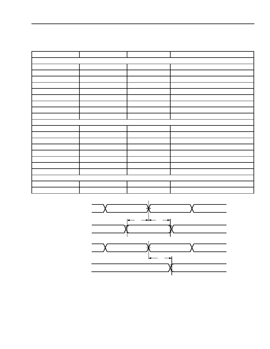
Preliminary Data Sheet
TMXF28155/51 Super Mapper
May 2001
155/51 Mbits/s SONET/SDH x28/x21 DS1/E1
41
Agere Systems Inc.
5 Timing Characteristics
(continued)
Table 26. Input Timing Specifications
Figure 7. Generic Interface Data Timing
Input Name
Reference CLK
Min Setup Time (t
S)
Min Hold Time (t
H)
Transmit Signals
THSSYNC
THSC
2.0 ns
0.0 ns
TLSDATA[7:0]
TLSCLK
5.0 ns
0.0 ns
TLSPAR
TLSCLK
5.0 ns
0.0 ns
TLSSPE
TLSCLK
5.0 ns
0.0 ns
TLSJ0J1V1
TLSCLK
5.0 ns
0.0 ns
TLSV1
TLSCLK
5.0 ns
0.0 ns
TLSSYNC52
TLSC52
4.0 ns
0.0 ns
TTOACDATA
TTOACCLK
10.0 ns
0.0 ns
TPOACDATA
TPOACCLK
10.0 ns
0.0 ns
Receive Signals
RHSDP/N
RHSCP/N
2.0 ns
0.0 ns
RPSD155P/N
RPSC155P/N
2.0 ns
0.0 ns
RLSDATA[7:0]
RLSCLK
5.0 ns
0.0 ns
RLSPAR
RLSCLK
5.0 ns
0.0 ns
RLSSPE
RLSCLK
5.0 ns
0.0 ns
RLSJ0J1V1
RLSCLK
5.0 ns
0.0 ns
RLSV1
RLSCLK
5.0 ns
0.0 ns
RLSSYNC52
RLSC52
4.0 ns
0.0 ns
Miscellaneous Signals
LOSEXT
NA
ASYNC
ASYNC
AUTO_AIS[3:1]
NA
ASYNC
ASYNC
CLOCK
DATA
CLOCK
DATA
t
SU
t
H
t
PD

TMXF28155/51 Super Mapper
Preliminary Data Sheet
155/51 Mbits/s SONET/SDH x28/x21 DS1/E1
May 2001
42
Agere Systems Inc.
5 Timing Characteristics
(continued)
Table 27. Output Timing Specifications
* Propagation delay skew, t
PLH
≠ t
PHL
, is ±200 ps.
Output Name
Reference CLK
Test
Conditions
Propagation Delay*
Unit
t
PD
Min
Max
Transmit Signals
THSDP/N
THSCP/N
C
L
= 15 pF
0.6
2.9
ns
TPSD155P/N
TPSC155P/N
C
L
= 15 pF
0.6
2.9
ns
TLSDATA[7:0]
TLSCLK
C
L
= 50 pF
4.0
12.0
ns
TLSPAR
TLSCLK
C
L
= 50 pF
4.0
12.0
ns
TLSSPE
TLSCLK
C
L
= 50 pF
4.0
12.0
ns
TLSJ0J1V1
TLSCLK
C
L
= 50 pF
4.0
12.0
ns
TLSV1
TLSCLK
C
L
= 50 pF
4.0
12.0
ns
TLSSYNC52
TLSC52
C
L
= 30 pF
0.0
6.0
ns
TTOACSYNC
TTOACCLK
C
L
= 15 pF
10.0
30.0
ns
TPOACSYNC
TPOACCLK
C
L
= 15 pF
10.0
30.0
ns
Receive Signals
RLSDATA[7:0]
RLSCLK
C
L
= 50 pF
4.0
12.0
ns
RLSPAR
RLSCLK
C
L
= 50 pF
4.0
12.0
ns
RLSSPE
RLSCLK
C
L
= 50 pF
4.0
12.0
ns
RLSJOJ1V1
RLSCLK
C
L
= 50 pF
4.0
12.0
ns
RLSVI
RLSCLK
C
L
= 50 pF
4.0
12.0
ns
RLSSYNC52
RLSC52
C
L
= 30 pF
0.0
6.0
ns
RTOACSYNC
RTOACCLK
C
L
= 15 pF
10.0
30.0
ns
RTOACDATA
RTOACCLK
C
L
= 15 pF
10.0
30.0
ns
RPOACSYNC
RPOACCLK
C
L
= 15 pF
10.0
30.0
ns
RPOACDATA
RPOACCLK
C
L
= 15 pF
10.0
30.0
ns
RHSFSYNCN
RLSCLK
C
L
= 30 pF
0.0
8.0
ns
Miscellaneous Signals
AUTO_AIS[3:1]
NA
--
ASYNC
ASYNC
--

Preliminary Data Sheet
TMXF28155/51 Super Mapper
May 2001
155/51 Mbits/s SONET/SDH x28/x21 DS1/E1
43
Agere Systems Inc.
5 Timing Characteristics
(continued)
5.2 DS3 Timing
Table 28. DS3 Input Clock Specifications
Table 29. Input Timing Specifications
Table 30. Output Timing Specifications
Symbol
Parameter
Signal Name
Min
Max
Unit
f
CK
Clock Frequency
DS3DATAINCLK
DS3DATAOUTCLK
--
--
44.736 MHz ±50 ppm
--
t
CK
Clock Period
DS3DATAINCLK
DS3DATAOUTCLK
--
--
22.353
22.353
ns
t
CLKHI
Clock Pulse High Time
DS3DATAINCLK
DS3DATAOUTCLK
6
6
16
16
ns
t
R
Rise Time
DS3DATAINCLK
DS3DATAOUTCLK
0
2
ns
t
F
Fall Time
DS3DATAINCLK
DS3DATAOUTCLK
0
2
ns
Input Name
Reference CLK
Min Setup Time (t
S)
Min Hold Time (t
H)
DS3POSDATAIN
DS3DATAINCLK
4
0
DS3NEGDATAIN
DS3DATAINCLK
4
0
Output Name
Reference CLK
Test Conditions
Propagation Delay t
PD
Unit
Min
Max
DS3POSDATAOUT
DS3DATAOUTCLK
C
L
= 15 pF
2
6
ns
DS3NEGDATAOUT
DS3DATAOUTCLK
C
L
= 15 pF
2
6
ns

TMXF28155/51 Super Mapper
Preliminary Data Sheet
155/51 Mbits/s SONET/SDH x28/x21 DS1/E1
May 2001
44
Agere Systems Inc.
5 Timing Characteristics
(continued)
5.3 M13 Timing
Table 31. M13 Clock Specifications
Table 32. Input Timing Specifications
Table 33. Output Timing Specifications
Symbol
Parameter
Signal Name
Min
Nom
Max
Unit
f
CK
Clock
Frequency
TCBCLK
TDLCLK
E1XCLK
DS1XCLK
DS2AISCLK
RCBCLK
RDLCLK
--
--
2.048
1.544
--
--
--
93.983 gapped
28.195 gapped
32.768
24.704
6.312
93.983
28.195
--
--
65.536
49.408
--
--
--
kHz
kHz
MHz
MHz
MHz
kHz
kHz
t
CLKHI
Clock Pulse
High Time
TCBCLK
TDLCLK
RCBCLK
RDLCLK
212.19
212.19
212.19
212.19
223.53
223.53
223.53
223.53
250.77
250.77
250.77
250.77
ns
t
R
Rise Time
TCBCLK
TDLCLK
E1XCLK
DS1XCLK
DS2AISCLK
RCBCLK
RDLCLK
0
0
0
0
0
0
0
--
--
--
--
--
--
--
3
3
3
3
3
3
3
ns
t
F
Fall Time
TCBCLK
TDLCLK
E1XCLK
DS1XCLK
DS2AISCLK
RCBCLK
RDLCLK
0
0
0
0
0
0
0
--
--
--
--
--
--
--
3
3
3
3
3
3
3
ns
Input Name
Reference CLK
Setup Time (t
S
)
Hold Time (t
H
)
Unit
Min
Max
Min
Max
TCBDATA
TCBCLK
50
--
0
--
ns
TDLDATA
TDLCLK
50
--
0
--
ns
Output Name
Reference CLK
Test Conditions
Propagation Delay t
PD
Unit
Min
Max
TCBSYNC
TCBCLK
C
L
= 15 pF
2
10
ns
RCBSYNC
RCBCLK
C
L
= 15 pF
2
10
ns
RCBDATA
RCBCLK
C
L
= 15 pF
2
10
ns
RDLDATA
RDLCLK
C
L
= 15 pF
2
10
ns
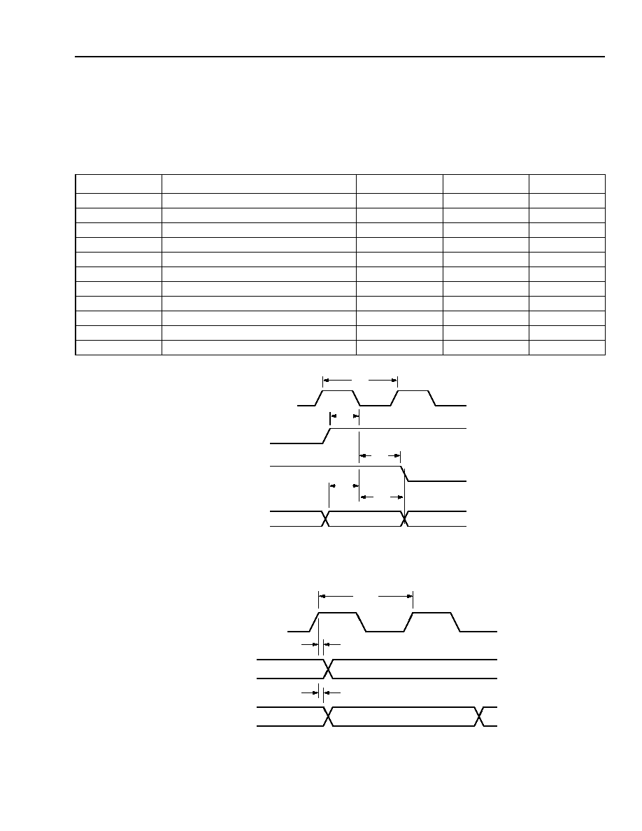
Preliminary Data Sheet
TMXF28155/51 Super Mapper
May 2001
155/51 Mbits/s SONET/SDH x28/x21 DS1/E1
45
Agere Systems Inc.
5 Timing Characteristics
(continued)
5.4 VT Mapper Timing
5.4.1 VT Mapper Lower-Order Path Overhead Interface Timing
Table 34. VT Mapper Receive Path Overhead Detailed Timing
5-9078(F)
Figure 8. VT Mapper Transmit Path Overhead Detailed Timing
5-9079(F)
Figure 9. VT Mapper Receive Path Overhead Detailed Timing
Symbol
Parameter
Min
Max
Unit
f
CK
Clock Frequency
6.48
6.48
MHz
t
CK
Clock Period
154
154
ns
t
CLKHI
Clock Pulse High Time
50
75
ns
t
R
Clock Rise Time
0
3
ns
t
F
Clock Fall Time
0
3
ns
t
SD
LOPOH Data Setup Time
5
--
ns
t
HD
LOPOH Data Hold Time
0
--
ns
t
SV
LOPOH Valid Signal Setup Time
5
--
ns
t
HV
LOPOH Valid Signal Hold Time
0
--
ns
t
PDV
Clock to LOPOH Valid Signal Out
0
5
ns
t
PDD
Clock to LOPOH Data Out
0
5
ns
L O PO H C LK IN
L O P O H VA L ID IN
L O P O H D ATA IN
t
HV
t
SV
t
SD
t
HD
t
C K
t
PDV
t
PDD
LOPOHCLKOUT
LOPOHVALIDOUT
LOPOHDATAOUT
t
CK

TMXF28155/51 Super Mapper
Preliminary Data Sheet
155/51 Mbits/s SONET/SDH x28/x21 DS1/E1
May 2001
46
Agere Systems Inc.
5 Timing Characteristics
(continued)
5.5 Concentration Highway (CHI) Timing
Table 35
and
Table 36
with
Figure 10
and
Figure 11
, respectively, illustrate the detailed CHI timing for clock, data,
and frame synchronization.
Table 35. CHI Transmit Timing Characteristics
* f
CK
can be either 2.048 MHz, 4.096 MHz, 8.192 MHz, or 16.384 MHz.
5-9080(F)
Figure 10. CHI Transmit I/O Timing
Symbol
Parameter
Min
Max
Unit
f
CK
Clock Frequency*
2.048
16.384
MHz
t
CK
Clock Period
488.2
61.04
ns
t
R
Clock Rise Time
0
3
ns
t
F
Clock Fall Time
0
3
ns
t
S
Frame Sync Setup Time
35
--
ns
t
H
Frame Sync Hold Time
0
--
ns
t
PD
Clock to CHI Data Delay
--
25
ns
LINETXCLK29
LINETXSYNC29
LINETXSYNC[28:1]
t
S
CLOCK
FRAME SYNC
DATA
t
H
t
CK
t
PD
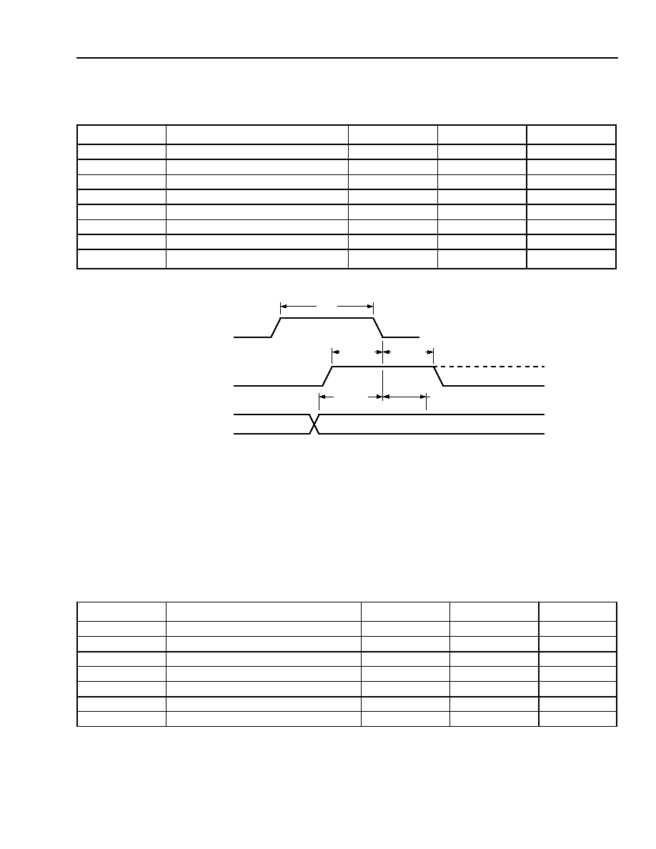
Preliminary Data Sheet
TMXF28155/51 Super Mapper
May 2001
155/51 Mbits/s SONET/SDH x28/x21 DS1/E1
47
Agere Systems Inc.
5 Timing Characteristics
(continued)
Table 36. CHI Receive Timing Characteristics
* f
CK
can be either 2.048 MHz, 4.096 MHz, 8.192 MHz, or 16.384 MHz.
5-9081(F)
Figure 11. CHI Receive I/O Timing
5.6 Parallel System Bus Timing
Table 37
and
Table 38
with
Figure 12
and
Figure 13
, respectively, show the transmit and receive timing. In the
transmit direction (to the system interface) the frame sync is sampled and the data is clocked out on the rising edge
of the clock. In the receive direction (from the switch) the data and frame sync are sampled on the rising edge of
the clock.
Table 37. PSB Interface Transmit Timing Characteristics
Symbol
Parameter
Min
Max
Unit
f
CK
Clock Frequency*
2.048
16.384
MHz
t
CK
Clock Period
488.2
61.04
ns
t
R
Clock Rise Time
0
3
ns
t
F
Clock Fall Time
0
3
ns
t
SSYNC
Frame Sync Setup Time
30
--
ns
t
HSYNC
Frame Sync Hold Time
0
--
ns
t
SDATA
CHI Data Setup Time
25
--
ns
t
HDATA
CHI Data Hold Time
0
--
ns
Symbol
Parameter
Min
Max
Unit
f
CK
Clock Frequency
19.44
19.44
MHz
t
CK
Clock Period
51.44
51.44
ns
t
R
Clock Rise Time
0
3
ns
t
F
Clock Fall Time
0
3
ns
t
S
Frame Sync Setup Time
8
--
ns
t
H
Frame Sync Hold Time
0
--
ns
t
PD
Clock to PSB Out Delay
3
10
ns
t
HDATA
LINERXCLK29
LINERXSYNC29
LINERXSYNC[28:1]
CLOCK
FRAME SYNC
DATA
t
SSYNC
t
HSYNC
t
SDATA
t
CK
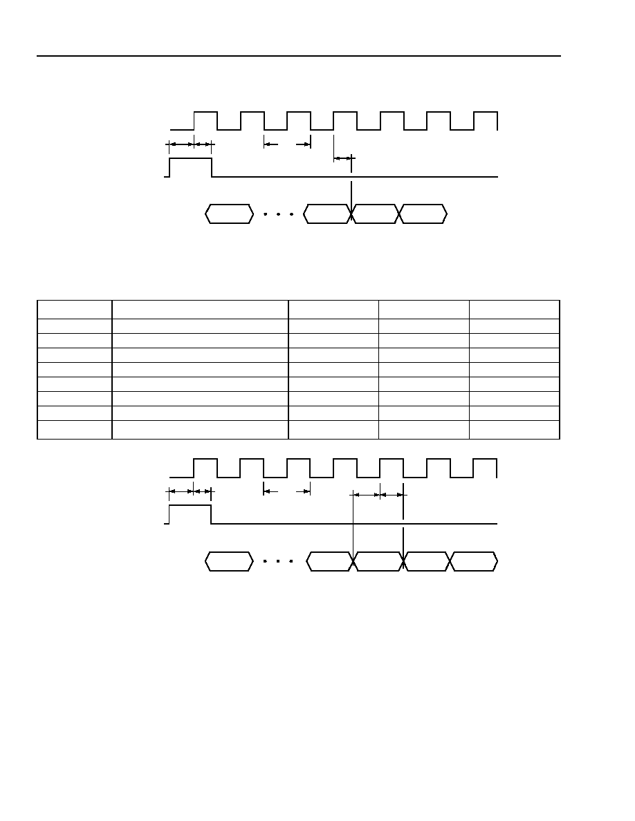
TMXF28155/51 Super Mapper
Preliminary Data Sheet
155/51 Mbits/s SONET/SDH x28/x21 DS1/E1
May 2001
48
Agere Systems Inc.
5 Timing Characteristics
(continued)
5-9082(F)
Figure 12. Parallel System Bus Interface Transmit I/O Timing
Table 38. PSB Interface Receive Timing Characteristics
5-9083(F)
Figure 13. Parallel System Bus Interface Receive I/O Timing
Symbol
Parameter
Min
Max
Unit
f
CK
Clock Frequency
19.44
19.44
MHz
t
CK
Clock Period
51.44
51.44
ns
t
R
Clock Rise Time
0
3
ns
t
F
Clock Fall Time
0
3
ns
t
SSYNC
Frame Sync Setup Time
8
--
ns
t
HSYNC
Frame Sync Hold Time
0
--
ns
t
SDATA
PSB to Clock Setup Time
8
--
ns
t
HDATA
PSB Hold Time from Clock
0
--
ns
DEV #0, TS #1, DEV #0, TS #1,
tPD
STUFFED TS
STUFFED TS
6 (3) STUFFED TS IN DS1 (E1)
tH
tS
LINETXCLK29
LINETXSYNC29
LINETXSYNC[16:1]
CLOCK
FRAME SYNC
DATA
LINK #0
LINK #1
tCK
DATA SAMPLED
tSDATA
tHDATA
DEV #0, TS #1,
DEV #0, TS #1,
STUFFED TS
STUFFED TS
tHSYNC
tSSYNC
LINERXCLK29
LINERXSYNC29
LINERXSYNC[16:1]
CLOCK
FRAME SYNC
DATA
LINK #0
LINK #1
tCK

Preliminary Data Sheet
TMXF28155/51 Super Mapper
May 2001
155/51 Mbits/s SONET/SDH x28/x21 DS1/E1
49
Agere Systems Inc.
5 Timing Characteristics
(continued)
5.7 NSMI Timing Mode 1 (6 Pin)
Table 39. NSMI (Mode 1) Input Clock Specifications
Table 40. Input Timing Specifications
Table 41. Output Timing Specifications
5.8 SMI Timing Mode 2 (8 Pin)
Table 42. SMI (Mode 2) Input Clock Specifications
Symbol
Parameter
Signal Name
Min
Nom
Max
Unit
t
CK
Clock
Frequency
LINE_TXCLK29
LINE_RXCLK29
--
--
51.84/44.736 ±50 ppm
51.84/44.736 ±50 ppm
--
--
MHz
MHz
t
CKHI
Clock Pulse
High Time
LINE_TXCLK29
LINE_RXCLK29
6
6
--
--
12
12
ns
ns
t
R
Rise Time
LINE_TXCLK29
LINE_RXCLK29
--
--
--
--
3
3
ns
ns
t
F
Fall Time
LINE_TXCLK29
LINE_RXCLK29
--
--
--
--
3
3
ns
ns
Input Name
Reference CLK
Setup Time (t
S
)
Hold Time (t
H
)
Unit
Min
Max
Min
Max
LINE_RXDATA29
LINE_RXCLK29
5
--
0
--
ns
LINE_RXSYNC29
LINE_RXCLK29
5
--
0
--
ns
Output Name
Reference CLK
Test Conditions
Propagation Delay t
PD
Unit
Min
Max
LINE_TXDATA29
LINE_TXCLK29
C
L
= 15 pF
0
3.5
ns
LINE_TXSYNC29
LINE_TXCLK29
C
L
= 15 pF
0
3.5
ns
RXDATAEN
LINE_TXCLK29
C
L
= 15 pF
0
3.5
ns
TXDATAEN
LINE_TXCLK29
C
L
= 15 pF
0
3.5
ns
Symbol
Parameter
Signal Name
Min
Nom
Max
Unit
t
CK
Clock
Period
LINE_TXCLK29
LINE_RXCLK29
RXDATAEN
44.736 MHz ±50 ppm
TBD
TBD
19.29
19.29
TBD
TBD
TBD
TBD
ns
ns
ns
t
CKHI
Clock Pulse
High Time
LINE_TXCLK29
LINE_RXCLK29
RXDATAEN
6
6
TBD
1/3 tck
1/3 or 1/2 tck
TBD
TBD
TBD
TBD
ns
ns
ns
t
R
Rise Time
LINE_TXCLK29
LINE_RXCLK29
RXDATAEN
0
0
0
--
--
--
3
3
3
ns
ns
ns
t
F
Fall Time
LINE_TXCLK29
LINE_RXCLK29
RXDATAEN
0
0
0
--
--
--
3
3
3
ns
ns
ns
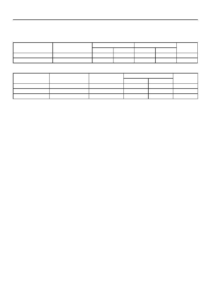
TMXF28155/51 Super Mapper
Preliminary Data Sheet
155/51 Mbits/s SONET/SDH x28/x21 DS1/E1
May 2001
50
Agere Systems Inc.
5 Timing Characteristics
(continued)
Table 43. Input Timing Specifications
Table 44. Output Timing Specifications
Input Name
Reference CLK
Setup Time (t
S
)
Hold Time (t
H
)
Unit
Min
Max
Min
Max
LINE_RXDATA29
LINE_RXCLK29
5
--
0
--
ns
LINE_RXSYNC29
LINE_RXCLK29
5
--
0
--
ns
Output Name
Reference CLK
Test Conditions
Propagation Delay t
PD
Unit
Min
Max
LINE_TXDATA29
LINE_TXCLK29
C
L
= TBD pF
0
3.5
ns
LINE_TXSYNC29
LINE_TXCLK29
C
L
= TBD pF
0
3.5
ns
TXDATAEN
RXDATAEN
C
L
= TBD pF
0
3.5
ns

Preliminary Data Sheet
TMXF28155/51 Super Mapper
May 2001
155/51 Mbits/s SONET/SDH x28/x21 DS1/E1
51
Agere Systems Inc.
5 Timing Characteristics
(continued)
5.9 Framer Only Mode Timing
Table 45. Framer Only Mode Clock Specifications
Symbol
Parameter
Signal Name
Min
Nom
Max
Unit
t
CK
Clock
Frequency
TLSC52
LINERXDATA29
LINERXCLK[28:1]
LINERXCLK29
LINETXCLK[28:1]
LINETXCLK29
≠50 ppm
≠130 ppm
≠50 ppm
≠130 ppm
≠50 ppm
≠50 ppm
≠50 ppm
≠50 ppm
≠130 ppm
≠50 ppm
≠50 ppm
≠50 ppm
≠50 ppm
51.84
1.544
or 2.048
1.544
2.048
or 4.096
or 8.192
or 16.384
1.544
or 2.048
or 4.096
or 8.192
or 16.384
50 ppm
130 ppm
50 ppm
130 ppm
50 ppm
50 ppm
50 ppm
50 ppm
130 ppm
50 ppm
50 ppm
50 ppm
50 ppm
MHz
MHz
MHz
MHz
MHz
MHz
MHz
MHz
MHz
MHz
MHz
MHz
MHz
t
CKHI
Clock Pulse
High Time
TLSC52
LINERXDATA29
LINERXCLK[28:1]
LINERXCLK29
LINETXCLK[28:1]
LINETXCLK29
6
TBD
TBD
TBD
TBD
TBD
TBD
TBD
TBD
TBD
TBD
TBD
TBD
TBD
TBD
TBD
TBD
TBD
TBD
TBD
TBD
TBD
TBD
TBD
TBD
TBD
12
TBD
TBD
TBD
TBD
TBD
TBD
TBD
TBD
TBD
TBD
TBD
TBD
ns
ns
ns
ns
ns
ns
ns
ns
ns
ns
ns
ns
ns
t
R
Rise Time
TLSC52
LINERXDATA29
LINERXCLK[28:1]
LINERXCLK29
LINETXCLK[28:1]
LINETXCLK29
0
0
0
0
0
0
0
0
0
0
0
0
0
--
--
--
--
--
--
--
--
--
--
--
--
--
3
3
3
3
3
3
3
3
3
3
3
3
3
ns
ns
ns
ns
ns
ns
ns
ns
ns
ns
ns
ns
ns

TMXF28155/51 Super Mapper
Preliminary Data Sheet
155/51 Mbits/s SONET/SDH x28/x21 DS1/E1
May 2001
52
Agere Systems Inc.
5 Timing Characteristics
(continued)
Table 45. Framer Only Mode Clock Specifications (continued)
Table 46. Framer Mode Only Input Timing Specifications
Table 47. Framer Mode Only Output Timing Specifications
Symbol
Parameter
Signal Name
Min
Nom
Max
Unit
t
F
Fall Time
TLSC52
LINERXDATA29
LINERXCLK[28:1]
LINERXCLK29
LINETXCLK[28:1]
LINETXCLK29
0
0
0
0
0
0
0
0
0
0
0
0
0
--
--
--
--
--
--
--
--
--
--
--
--
--
3
3
3
3
3
3
3
3
3
3
3
3
3
ns
ns
ns
ns
ns
ns
ns
ns
ns
ns
ns
ns
ns
Input Name
Reference CLK
Setup Time (t
S
)
Hold Time (t
H
)
Unit
Min
Max
Min
Max
LINERXDATA[28:1]
LINERXCLK[28:1]
25
--
0
--
ns
LINERXSYNC[28:1]
LINERXCLK[28:1]
30
--
0
--
ns
LINERXSYNC29
LINERXCLK29
30
--
0
--
ns
LINETXSYNC29
LINETXCLK29
35
--
0
--
ns
Output Name
Reference CLK
Test Conditions
Propagation Delay t
PD
Unit
Min
Max
LINETXDATA[28:1]
LINETXCLK[28:1]
C
L
= TBD pF
25
TBD
ns
LINETXDATA29
LINETXCLK29
C
L
= TBD pF
25
TBD
ns
LINETXSYNC[28:1]
LINETXCLK[28:1]
C
L
= TBD pF
TBD
TBD
ns

Preliminary Data Sheet
TMXF28155/51 Super Mapper
May 2001
155/51 Mbits/s SONET/SDH x28/x21 DS1/E1
53
Agere Systems Inc.
5 Timing Characteristics
(continued)
5.10 Framer--LIU Mode Timing
Table 48. Framer--LIU Mode Clock Specifications
Symbol
Parameter
Signal Name
Min
Nom
Max
Unit
t
CK
Clock
Frequency
TLSC52
LINERXCLK[28:1]
LINERXCLK29
LINETXCLK[28:1]
LINETXCLK29
TBD
TBD
TBD
TBD
TBD
TBD
TBD
TBD
TBD
TBD
TBD
51.84
TBD
2.048
or 4.096
or 8.192
or 16.384
TBD
or 2.048
or 4.096
or 8.192
or 16.384
TBD
TBD
TBD
TBD
TBD
TBD
TBD
TBD
TBD
TBD
TBD
MHz
TBD
MHz
MHz
MHz
MHz
TBD
MHz
MHz
MHz
MHz
t
CKHI
Clock Pulse
High Time
TLSC52
LINERXDATA29
LINERXCLK[28:1]
LINERXCLK29
LINETXCLK[28:1]
LINETXCLK29
TBD
TBD
TBD
TBD
TBD
TBD
TBD
TBD
TBD
TBD
TBD
TBD
TBD
TBD
TBD
TBD
TBD
TBD
TBD
TBD
TBD
TBD
TBD
TBD
TBD
TBD
TBD
TBD
TBD
TBD
TBD
TBD
TBD
TBD
TBD
TBD
TBD
TBD
TBD
ns
ns
ns
ns
ns
ns
ns
ns
ns
ns
ns
ns
ns
t
R
Rise Time
TLSC52
LINERXDATA29
LINERXCLK[28:1]
LINERXCLK29
LINETXCLK[28:1]
LINETXCLK29
0
0
0
0
0
0
0
0
0
0
0
0
0
--
--
--
--
--
--
--
--
--
--
--
--
--
3
3
3
3
3
3
3
3
3
3
3
3
3
ns
ns
ns
ns
ns
ns
ns
ns
ns
ns
ns
ns
ns
t
F
Fall Time
TLSC52
LINERXDATA29
LINERXCLK[28:1]
LINERXCLK29
LINETXCLK[28:1]
LINETXCLK29
0
0
0
0
0
0
0
0
0
0
0
0
0
--
--
--
--
--
--
--
--
--
--
--
--
--
3
3
3
3
3
3
3
3
3
3
3
3
3
ns
ns
ns
ns
ns
ns
ns
ns
ns
ns
ns
ns
ns

TMXF28155/51 Super Mapper
Preliminary Data Sheet
155/51 Mbits/s SONET/SDH x28/x21 DS1/E1
May 2001
54
Agere Systems Inc.
5 Timing Characteristics
(continued)
Table 49. Framer--LIU Mode Input Timing Specifications
Table 50. Framer--LIU Mode Output Timing Specifications
5.11 Microprocessor Interface Timing
5.11.1 Synchronous Mode
The synchronous microprocessor interface mode is selected when MPMODE (pin AD17) = 1. Interface timing for
the synchronous mode write cycle is given in
Figure 14
and in
Table 51
and for the read cycle in
Figure 15
and in
Table 52
.
Note:
In addition to the MPU_CLK, the VT mapper block also requires TLSC52,TLSSYNC52, RLSC52,
RLSSYNC52 signals to access specific portions of the register map. The user needs to make sure that the
VT_RDY bit is set before VT_MAPPER reads/writes can occur.
5-7659(F)a
Figure 14. Microprocessor Interface Synchronous Write Cycle (MPMODE (Pin AD17) = 1)
Input Name
Reference CLK
Setup Time (t
S
)
Hold Time (t
H
)
Unit
Min
Max
Min
Max
LINERXDATA[28:1]
LINERXCLK[28:1]
TBD
35
35
--
ns
LINERXDATA29
LINERXCLK29
TBD
35
35
--
ns
LINERXSYNC[28:1]
LINERXCLK[28:1]
TBD
35
35
--
ns
LINERXSYNC29
LINERXCLK29
TBD
35
35
--
ns
Output Name
Reference CLK
Test Conditions
Propagation Delay t
PD
Unit
Min
Max
LINETXDATA[28:1]
LINETXCLK[28:1]
C
L
= TBD pF
≠35
35
ns
LINETXDATA29
LINETXCLK29
C
L
= TBD pF
≠35
35
ns
LINETXSYNC[28:1]
LINETXCLK[28:1]
C
L
= TBD pF
≠35
35
ns
LINETXSYNC29
LINETXCLK29
C
L
= TBD pF
≠35
35
ns
MPCLK
ADDR[9:0]
CSN
ADSN
RWN
DATA[15:0]
DTN
(66 MHz MAX)
(INPUT)
tADSNVS
tWS
tDTNVPD
tWS
tCSNVS
tWS
tCLK
T1
T2
T3
Tn ≠ 2
Tn ≠ 1
Tn
tAIPD
tAPD
tAPD
tAPD
tAPD
tDTNIPD
HIGH Z
HIGH Z
tADSNVDTF
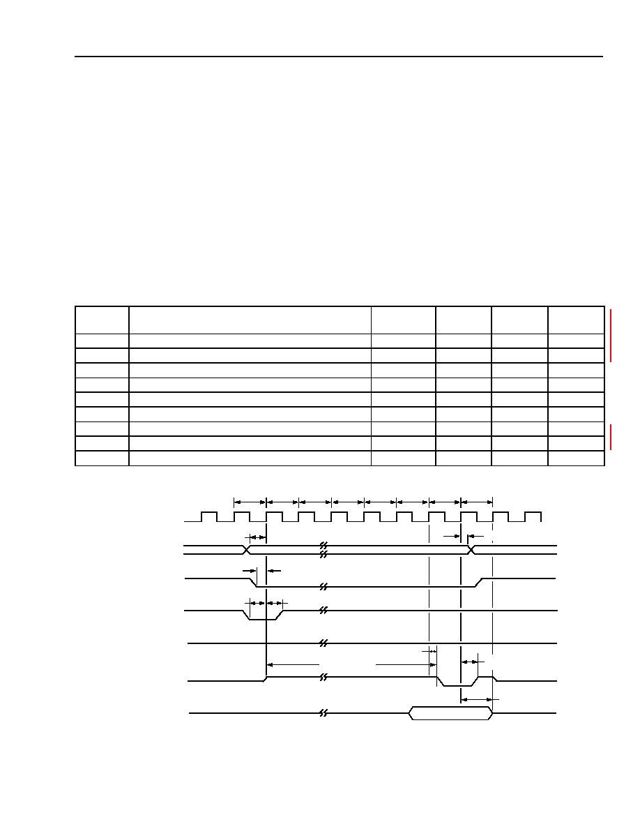
Preliminary Data Sheet
TMXF28155/51 Super Mapper
May 2001
155/51 Mbits/s SONET/SDH x28/x21 DS1/E1
55
Agere Systems Inc.
5 Timing Characteristics
(continued)
MPCLK
16 MHz minimum to 66 MHz maximum frequency.
ADDR [19:0] The address will be available throughout the entire cycle.
DATA[15:0]
Data will be available during cycle T1.
RWN (Input) The read (H) write (L) signal is always high except during a write cycle.
CSN (Input) Chip select is an active-low signal.
DTN (Output) Data transfer acknowledge is active-low for one clock and then driven high before entering a high-
impedance state. (This is done with an I/O pad using the input as feedback to qualify the 3-state
term.) DTN will become 3-stated when CSN is high. Typically DTN is active 4 or 5 MPCLK cycles
after ADSN is low.
ADSN (Input) Address strobe is active-low. ADSN must be 1 MPCLK clock period wide.
Table 51. Microprocessor Interface Synchronous Write Cycle Specifications
(
See Figure 14 on page 54
for the timing diagram.)
5-7660(F).a
Figure 15. Microprocessor Interface Synchronous Read Cycle (MPMODE (Pin AD17) = 1)
Symbol
Parameter
Setup (ns)
(Min)
Hold (ns)
(Min)
Delay (ns)
(Max)
Delay (ns)
(Min)
T
CLK
MPCLK 16 MHz Min--66 MHz Max Frequency
--
--
--
--
t
WS
ADDR, RWN, DATA (write) Valid to MPCLK
3.5
0
--
--
t
APD
MPCLK to ADDR, RWN, DATA, CSN
(write) Invalid
--
5
--
--
t
CSNVS
CSN Valid to MPCLK
3.5
0
--
--
t
ADSNVS
ADSN Valid to MPCLK
5.5
0
--
--
t
AIPD
MPCLK to ADSN Invalid
--
5
--
--
t
DTNVPD
MPCLK to DTN Valid
--
--
16
4
t
DTNIPD
MPCLK to DTN Invalid
--
--
16
4
T
ADSNVDTF
ADSN Valid to DT Falling
--
--
1000
--
MPCLK
ADDR[9:0]
CSN
ADSN
RWN
(66 MHz MAX)
tADSNSU
tSNIPD
tCSNSU
tAVS
T0
T1
T2
Tn ≠ 4
Tn ≠ 3
Tn ≠ 2
Tn ≠ 1
Tn
DTN
DATA[15:0]
(OUTPUT)
tDAIPD
tDVPD
tDIPD
tADSNVDTF
HIGH Z
HIGH Z
tAPD

TMXF28155/51 Super Mapper
Preliminary Data Sheet
155/51 Mbits/s SONET/SDH x28/x21 DS1/E1
May 2001
56
Agere Systems Inc.
5 Timing Characteristics
(continued)
MPCLK
16 MHz minimum to 66 MHz maximum frequency.
ADDR [19:0] The address will be available throughout the entire cycle, and must be stable before ADSN turns
high.
DATA [15:0]
Read data is stable in Tn ≠1.
RWN (Input) The read (H) write (L) signal is always high during the read cycle.
CSN (Input) Chip select is an active-low signal.
DTN (Output) Data transfer acknowledge on the host bus interface is initiated on T6. This signal is active for one
clock and then driven high before entering a high-impedance state. (This is done with an I/O pad
using the input as feedback to qualify the 3-state term.) DT will become 3-stated when CS is high.
Typically DTN is active 4 or 5 MPCLK cycles after ADSN is low.
ADSN (Input) Address strobe is active-low. ADSN must be one MPCLK clock period wide.
Table 52. Microprocessor Interface Synchronous Read Cycle Specifications
(
See Figure 15 on page 55
for the timing diagram.)
5.12 Asynchronous Mode
The asynchronous microprocessor interface mode is selected when MPMODE (pin AC18) = 0. Interface timing for
the asynchronous mode write cycle is given in
Figure 16
and in
Table 53
, and for the read cycle in
Figure 17
and in
Table 54
(see pages
59
--
60
).
Symbol
Parameter
Setup (ns)
(Min)
Hold (ns)
(Min)
Delay (ns)
(Max)
t
CLK
MPCLK 16 MHz Min--66 MHz Max Frequency
--
--
--
t
AVS
ADDR Valid to MPCLK
3.5
0
--
t
APD
MPCLK to ADDR Invalid
--
5
--
t
CSNSU
CSN Active to MPCLK
3.5
0
--
t
ADSNSU
ADSN Valid to MPCLK
5.5
0
--
t
SNIPD
MPCLK to ADSN Inactive
--
5
--
t
DVPD
MPCLK to DTN Valid
--
--
8
t
DIPD
MPCLK to DTN Invalid
--
--
8
t
DAIPD
MPCLK to DATA 3-state
--
--
8
t
ADSNVDTF
ADSN Valid to DT Falling
--
--
1000
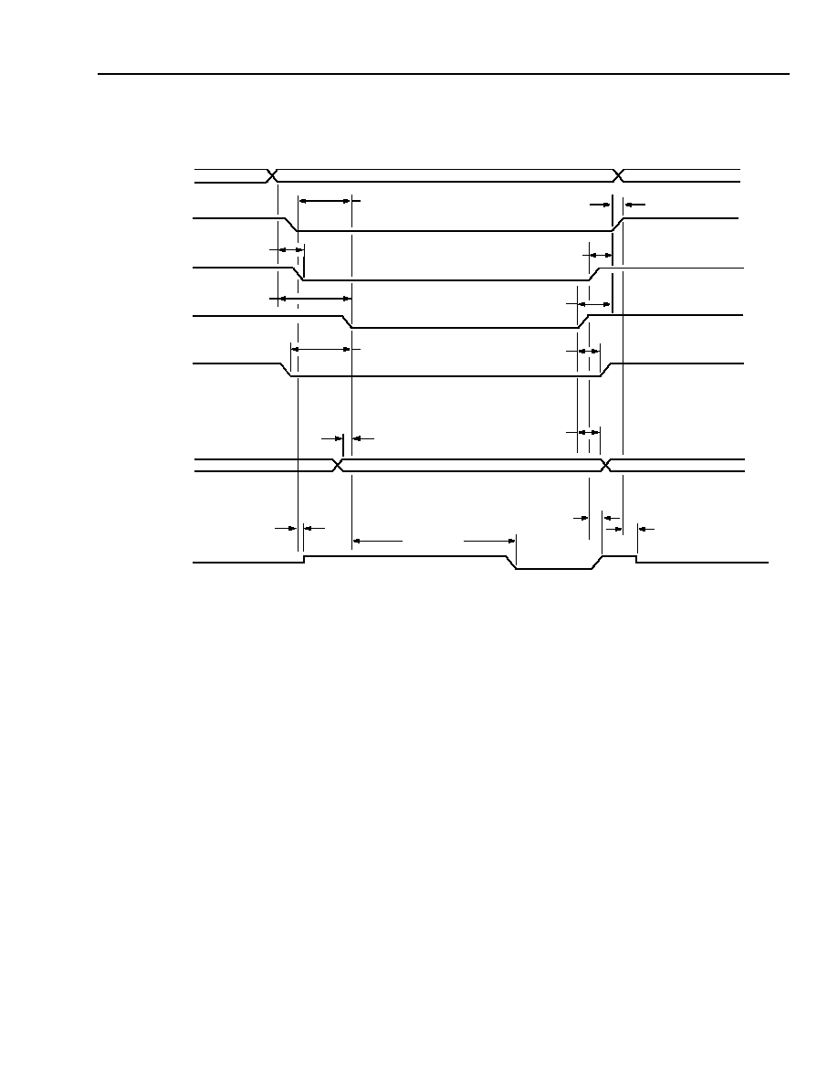
Preliminary Data Sheet
TMXF28155/51 Super Mapper
May 2001
155/51 Mbits/s SONET/SDH x28/x21 DS1/E1
57
Agere Systems Inc.
5 Timing Characteristics
(continued)
5-7661(F).ar.1
Figure 16. Microprocessor Interface Asynchronous Write Cycle Description (MPMODE (Pin AC18) = 0)
ADDR [19:0] Address is asynchronously passed from the host bus to the internal bus. The address will be avail-
able throughout the entire cycle.
DATA [15:0]
Write data is asynchronously passed from the host bus to the internal bus. Data will be available
throughout the entire cycle.
RWN (Input) The read (H) write (L) signal is always high except during a write cycle.
CSN (Input) Chip select is an active-low signal.
DTN (Output) Data transfer acknowledge (active-low). DTN is driven asynchronously based on the arrival of CSN.
DTN is driven high until the internal transaction is done. DTN is driven high again when either ADSN
or DSN is deasserted. DTN will become 3-stated when CSN is high.
ADSN (Input) Address strobe is active-low. ADSN must be a minimum of one MPCLK clock period wide.
DSN (Input) Data strobe is active-low.
ADDR[19:0]
CSN
ADSN
DSN
RWN
DATA[15:0]
DTN
(INPUT)
tAVADSF
tDVDSF
tCSFDTR
tDSFDTF
tADSRDTR
tCSRDT3
tDSRDI
tDSRRWR
tDSNRAI
tADSRAI
tAICSR
tRWFDSF
tAVDSF
HIGH Z
HIGH Z
tCSFDSF

TMXF28155/51 Super Mapper
Preliminary Data Sheet
155/51 Mbits/s SONET/SDH x28/x21 DS1/E1
May 2001
58
Agere Systems Inc.
5 Timing Characteristics
(continued)
Table 53. Microprocessor Interface Asynchronous Write Cycle Specifications
(
See Figure 16 on page 57
for the timing diagram.)
* Simulation results.
Falling edges of ADSN and DSN determine falling edge of DTN.
DTN fall is variable, depending on the block selected for access, and may be longer than the typical maximum specified.
ß Rising edge of ADSN determines rising edge of DTN.
Note: Specifications are valid for 50 MHz MPCLK with MPMODE = 0. Address strobe (ADSN) and chip select
(CSN) may be connected and driven from the same source. In this configuration, the setup and hold times
for ADSN must be satisfied.
Symbol
Parameter
Min Interval (ns)
Max Interval (ns)
t
CSFDSF
CSN Fall to DSN Fall
0
--
t
AICSR
ADDR Invalid to CSN Rise
0
--
t
AVADSF
ADDR Valid to ADSN Fall
0
--
t
ADSRAI
ADSN Rise to ADDR Invalid
0
--
t
AVDSF
ADDR Valid to DSN Fall
0
--
t
DSNRAI
DSN Rise to ADDR Invalid
0
--
t
RWFDSF
RWN Fall to DSN Fall
0*
--
t
DSRRWR
DSN Rise to RWN Rise
0*
--
t
DVDSF
DATA Valid to DSN Fall
0*
--
t
DSRDI
DSN Rise to DATA Invalid
0*
--
t
CSFDTR
CSN Fall to DTN Rise
20
--
t
DSFDTF
DSN Fall to DTN Fall
120
280
t
ADSRDTR
ADSN Rise to DTN Rise
20
ß
--
t
CSRDT3
CSN Rise to DTN 3-state
10
--

Preliminary Data Sheet
TMXF28155/51 Super Mapper
May 2001
155/51 Mbits/s SONET/SDH x28/x21 DS1/E1
59
Agere Systems Inc.
5 Timing Characteristics
(continued)
5-7662(F).ar.1
Figure 17. Microprocessor Interface Asynchronous Read Cycle (MPMODE (Pin AC18) = 0)
ADDR [19:0] Address is asynchronously passed from the host bus to the internal bus. The address will be avail-
able throughout the entire cycle.
DATA [15:0]
Read data on the internal bus is only valid for one clock cycle; therefore, a latch is necessary to meet
the correct timing on the host bus.
RWN (Input) The read (H) write (L) signal is always high during a read cycle.
CSN (Input) Chip select is an active-low signal.
DTN (Output) Data transfer acknowledge (active-low). DTN is driven asynchronously based on the arrival of CSN,
DSN, and ADSN. DTN is driven high while the internal bus transaction is in progress. There is no
need to provide synchronization to outgoing signals in this mode. DTN is driven high and then placed
in a high-impedance state when either ADSN or DSN is deasserted. DTN will become 3-stated when
CSN is high.
ADSN (Input) Address strobe is active-low.
DSN (Input) Data strobe is active-low.
ADDR[19:0]
CSN
ADSN
DSN
DTN
DATA[15:0]
tADSRD3
tCSRDT3
tADSRDTR
tCSFDSF
RWN
tAVADSF
tAVDSF
tAICSR
tADSRAI
tDSNRAI
tDTVDV
tDSFDTF
tCSFDTR
HIGH Z
HIGH Z
HIGH Z
HIGH Z

TMXF28155/51 Super Mapper
Preliminary Data Sheet
155/51 Mbits/s SONET/SDH x28/x21 DS1/E1
May 2001
60
Agere Systems Inc.
5 Timing Characteristics
(continued)
Table 54. Microprocessor Interface Asynchronous Read Cycle Specifications
(
See Figure 17 on page 59
for the timing diagram.)
Notes:
1 DSN can be asserted up to 20 ns (1 clk at 50 MHz) previous to CSN.
2 ADDR can be asserted up to 60 ns (3 clk at 50 MHz) into cycle from ASDN.
3 DTN fall is variable depending on the block selected for access and may be longer than typical maximum specified.
4 Leading edges of ADSN and DSN determine the falling edge of DTN.
5 Rising edge of ADSN determines the rising edge of DTN.
6 Data toggle 20 ns (1 clk at 50 MHz) previous to CSN.
Note: Specifications are valid for 50 MHz MPCLK with MPMODE = 0. Address strobe (ADSN) and chip select
(CSN) may be connected and driven from the same source. In this configuration, the setup and hold times
for ADSN must be satisfied.
5.13 General Purpose Interface Timing
Table 55. Input Timing Specifications
Symbol
Parameter
Min Interval (ns)
Max Interval (ns)
t
CSFDSF
CSN Fall to DSN Fall
0
1
--
t
AICSR
ADDR Invalid to CSN Rise
0
--
t
AVADSF
ADDR Valid to ADSN Fall
0
60
2
t
ADSRAI
ADSN Rise to ADDR Invalid
0
--
t
AVDSF
ADDR Valid to DSN Fall
0
--
t
DSNRAI
DSN Rise to ADDR Invalid
0
--
t
CSFDTR
CSN Fall to DTN Rise
20
--
t
DSFDTF
DSN Fall to DTN Fall
100
280
3, 4
t
ADSRDTR
ADSN Rise to DTN Rise
20
--
5
t
CSRDT3
CSN Rise to DTN 3-state
10
--
t
DTVDV
DTN Valid to DATA Valid
0
6
--
t
ADSRD3
ADSN Rise to DATA 3-state
20
--
Input Name
Reference CLK
Min Setup Time (t
S)
Min Hold Time (t
H)
JTAG Signals
TDI
TCLK
15.0 ns
2.0 ns
TMSN
TCLK
15.0 ns
2.0 ns
TRSTN
NA
ASYNC
ASYNC
SCAN_EN
NA
ASYNC
ASYNC
SCAN_MODE
NA
ASYNC
ASYNC
Miscellaneous Signals
RSTN
NA
ASYNC
ASYNC
PMRST
NA
ASYNC
ASYNC
IC3STATEN
NA
ASYNC
ASYNC
IDDQ
NA
ASYNC
ASYNC
Preliminary Data Sheet
TMXF28155/51 Super Mapper
May 2001
155/51 Mbits/s SONET/SDH x28/x21 DS1/E1
61
Agere Systems Inc.
5 Timing Characteristics
(continued)
Table 56. Output Timing Specifications
* Propagation delay skew, t
PLH
≠
t
PHL,
is ±200 ps.
6 Ordering Information
Output Name
Reference CLK
Test Conditions
Propagation Delay
*
(t
PD)
Unit
Min
Max
Transmit Signals
TDO
TLCK
C
L
= 25 pF
3.0
20.0
ns
Miscellaneous Signals
PMRST
NA
--
ASYNC
ASYNC
--
Device Code
Package
Temperature
Comcode
TMXF281553BAL-2-DB
456-pin PBGA
≠40 ∞C to 85 ∞C
108700055

62
Agere Systems Inc.
TMXF28155 Super Mapper
Preliminary Data Sheet
155/51 Mbits/s SONET/SDH x28/x21 DS1/E1
May 2001
Register Description
7 Microprocessor Interface and Global Control and Status Registers
Table of Contents
Contents
Page
7 Microprocessor Interface and Global Control and Status Registers ................................................................... 62
7.1 Super Mapper Global Control and Status Registers .................................................................................... 63
7.2 Microprocessor Interface Register Map ........................................................................................................ 73
Tables
Page
Table 57. SMPR_VCR, Super Mapper Version Control Register (RO) ................................................................. 63
Table 58. SMPR_SYMR[4], Super Mapper Symbol Register4 SMPR (RO) ......................................................... 63
Table 59. SMPR_SYMR[3], Super Mapper Symbol Register3 (RO) ..................................................................... 63
Table 60. SMPR_SYMR[2], Super Mapper Symbol Register2 (RO) ..................................................................... 63
Table 61. SMPR_SYMR[1], Super Mapper Symbol Register1 (RO) ..................................................................... 64
Table 62. SMPR_SYMR[0], Super Mapper Symbol Register0 (RO) ..................................................................... 64
Table 63. SMPR_ISR, Super Mapper Interrupt Status Register (RO) ................................................................... 64
Table 64. SMPR_IMR, Super Mapper Interrupt Mask Register (RW) ................................................................... 65
Table 65. SMPR_GTR, Global Trigger Register (RW) .......................................................................................... 66
Table 66. SMPR_MSRR, Block Software Reset Register (RW) ........................................................................... 66
Table 67. SMPR_GCR, Global Control Register (RW) ......................................................................................... 68
Table 68. SMPR_TSCR, TMUX, and SPEMPR Control Register (RW) ................................................................ 69
Table 69. SMPR_FCR, Framer Control Register (RW) ......................................................................................... 69
Table 70. SMPR_CLCR, CDR and LVDS Control Register (RW) ......................................................................... 70
Table 71. SMPR_CPCR, Clock and Power Control Register (RW) ...................................................................... 71
Table 72. SMPR_PMRCHR, PM Reset Count High Register (RW) ...................................................................... 71
Table 73. SMPR_PMRCLR, PM Reset Count Low Register (RW) ....................................................................... 72
Table 74. SMPR_SR, Scratch Register (RW) ....................................................................................................... 72
Table 75. SMPR_TX_LINE_EN1 ........................................................................................................................... 72
Table 76. Microprocessor Interface Register Map ................................................................................................. 73

63
Agere Systems Inc.
Preliminary Data Sheet
TMXF28155 Super Mapper
May 2001
155/51 Mbits/s SONET/SDH x28/x21 DS1/E1
7 Microprocessor Interface and Global Control and Status Registers
(continued)
7.1 Super Mapper Global Control and Status Registers
This section gives a brief description of each register bit and its functionality. The abbreviations after each register
indicate if the register is read only (RO), clear-on-read/clear-on-write (COR/COW), or read/write (R/W).
Table 57. SMPR_VCR, Super Mapper Version Control Register (RO)
Table 58. SMPR_SYMR[4], Super Mapper Symbol Register4 SMPR (RO)
Table 59. SMPR_SYMR[3], Super Mapper Symbol Register3 (RO)
Table 60. SMPR_SYMR[2], Super Mapper Symbol Register2 (RO)
Address
Bit
Name
Function
Reset Default
0x00000 15:11
--
Reserved.
0x0000
10:8
SMPR_VERSION[2:0] Super Mapper Version Number. SMPR version
register will change each time the device is changed.
7:0
SMPR_ID[7:0]
SMPR ID Number.
Address
Bit
Name
Function
Reset Default
0x00001
15:8
T
Super Mapper Symbol Bit.
0x544D
7:0
M
Super Mapper Symbol Bit.
Address
Bit
Name
Function
Reset Default
0x00002
15:8
X
Super Mapper Symbol Bit.
0x5846
7:0
F
Super Mapper Symbol Bit.
Address
Bit
Name
Function
Reset Default
0x00003
15:8
2
Super Mapper Symbol Bit.
0x3238
7:0
8
Super Mapper Symbol Bit.

64
Agere Systems Inc.
TMXF28155 Super Mapper
Preliminary Data Sheet
155/51 Mbits/s SONET/SDH x28/x21 DS1/E1
May 2001
7 Microprocessor Interface and Global Control and Status Registers
(continued)
Table 61. SMPR_SYMR[1], Super Mapper Symbol Register1 (RO)
Table 62. SMPR_SYMR[0], Super Mapper Symbol Register0 (RO)
Table 63. SMPR_ISR, Super Mapper Interrupt Status Register (RO)
Address
Bit
Name
Function
Reset Default
0x00004
15:8
1
Super Mapper Symbol Bit.
0x3135
7:0
5
Super Mapper Symbol Bit.
Address
Bit
Name
Function
Reset Default
0x00005
15:8
5
Super Mapper Symbol Bit.
0x350D
7:0
CR
Super Mapper Symbol Bit.
Address
Bit
Name
Function
Reset
Default
0x00008
15
SMPR_APS_IS
APS Interrupt. Active-high signal indicating an interrupt event
has occurred in the automatic protection switch (APS) block,
which is within the TMUX block.
0x0000
14:10
--
Reserved.
9
SMPR_PARITY_IS
Microprocessor Interface Data Bus Parity Error Interrupt.
Active-high signal indicating a µP data bus parity error has
occurred. Summary of errors detected in PAR[1] and PAR[0]
parity detectors.
8
SMPR_PMRESET_IS Performance Monitor Reset Interrupt. Active-high signal
indicating a 1 second event has occurred.
7
SMPR_TPG_IS
TPG Interrupt. Active-high signal indicating an interrupt event
has occurred in the test pattern generation block.
6
SMPR_DJA_IS
DJA Interrupt. Active-high signal indicating an interrupt event
has occurred in the digital jitter attenuation block.
5
SMPR_FRM_IS
FRM Interrupt. Active-high signal indicating an interrupt
event has occurred in the framer block. However, on device
powerup, this bit is erroneously set. A device initialization rou-
tine containing the following sequence should clear the inter-
rupt:
s
Power up the framer block by selecting one of the clock
options in address 0x00012.
s
Set and clear the framer software reset bit, bit of address
0x0000E.
s
Power down the framer block in address 0x00012.
4
SMPR_XC_IS
XC Interrupt. Active-high signal indicating an interrupt event
has occurred in the cross connect block.
3
SMPR_M13_IS
M13 Interrupt. Active-high signal indicating an interrupt event
has occurred in the M13 multiplexer/demultiplexer block.
2
SMPR_VTMPR_IS
VTMPR Interrupt. Active-high signal indicating an interrupt
event has occurred in the VT mapper block.
1
SMPR_SPEMPR_IS
SPEMPR Interrupt. Active-high signal indicating an interrupt
event has occurred in the SPE mapper block.
0
SMPR_TMUX_IS
TMUX Interrupt. Active-high signal indicating an interrupt
event has occurred in the TMUX block.

65
Agere Systems Inc.
Preliminary Data Sheet
TMXF28155 Super Mapper
May 2001
155/51 Mbits/s SONET/SDH x28/x21 DS1/E1
7 Microprocessor Interface and Global Control and Status Registers
(continued)
Table 64. SMPR_IMR, Super Mapper Interrupt Mask Register (RW)
Address
Bit
Name
Function
Reset
Default
0x00009
15
SMPR_APS_IM
APS Interrupt Mask. When this bit is set to 1, the composite
interrupt bit will be inhibited from contributing to the interrupt
pin APS_INTN.
0x83FF
14:10
--
Reserved.
9
SMPR_PARITY_IM
Microprocessor Interface Data Bus Parity Error Interrupt
Mask. When this bit is set to 1, the composite interrupt bit will
be inhibited from contributing to the interrupt pin INTN.
8
SMPR_PMRESET_IM Performance Monitor Reset Interrupt Mask. When this bit
is set to 1, the composite interrupt bit will be inhibited from
contributing to the interrupt pin INTN.
7
SMPR_TPG_IM
TPG Interrupt Mask. When this bit is set to 1, the composite
interrupt bit will be inhibited from contributing to the interrupt
pin INTN.
6
SMPR_DJA_IM
DJA Interrupt Mask. When this bit is set to 1, the composite
interrupt bit will be inhibited from contributing to the interrupt
pin INTN.
5
SMPR_FRM_IM
FRM Interrupt Mask. When this bit is set to 1, the composite
interrupt bit will be inhibited from contributing to the interrupt
pin INTN.
4
SMPR_XC_IM
XC Interrupt Mask. When this bit is set to 1, the composite
interrupt bit will be inhibited from contributing to the interrupt
pin INTN.
3
SMPR_M13_IM
M13 Interrupt Mask. When this bit is set to 1, the composite
interrupt bit will be inhibited from contributing to the interrupt
pin INTN.
2
SMPR_VTMPR_IM
VTMPR Interrupt Mask. When this bit is set to 1, the com-
posite interrupt bit will be inhibited from contributing to the
interrupt pin INTN.
1
SMPR_SPEMPR_IM
SPEMPR Interrupt Mask. When this bit is set to 1, the com-
posite interrupt bit will be inhibited from contributing to the
interrupt pin INTN.
0
SMPR_TMUX_IM
TMUX Interrupt Mask. When this bit is set to 1, the compos-
ite interrupt bit will be inhibited from contributing to the inter-
rupt pin INTN.

66
Agere Systems Inc.
TMXF28155 Super Mapper
Preliminary Data Sheet
155/51 Mbits/s SONET/SDH x28/x21 DS1/E1
May 2001
7 Microprocessor Interface and Global Control and Status Registers
(continued)
Table 65. SMPR_GTR, Global Trigger Register (RW)
Table 66. SMPR_MSRR, Block Software Reset Register (RW)
Address
Bit
Name
Function
Reset Default
0x0000D
15:10
--
Reserved.
0x0000
9
SMPR_BER_INSRT
Bit Error Rate Insertion. When this bit is set to 1,
this bit indicates to the Super Mapper that a bit error
has to be inserted in the appropriate frame.
8
SMPR_PMRESET
Performance Monitor Reset. When this bit is set to
1, the PMRESET signal will transition from a logic 0
to a logic 1 state. It will stay at a logic 1 state for a
minimum of 100 ns. (Self-clearing.)
7:1
--
Reserved.
0
SMPR_SWRS
Super Mapper Software Reset. When this bit is set
to 1, it will create a software reset of the device. This
reset has the same effect as the hardware reset. All
microprocessor registers are reset to their default
states and all internal data path state machine are
reset. (Self-clearing.)
Address
Bit
Name
Function
Reset
Default
0x0000E
15:8
--
Reserved.
0x0000
7
SMPR_TPG_SWRS
TPG Block Software Reset. When this bit is set to 1, it will
create a software reset for the test-pattern generation macro.
This reset has the same effects as the hardware reset and
chip-level software reset. All microprocessor registers within
the macro are reset to their default states. All internal data
path state machine within the block are also reset.
6
SMPR_DJA_SWRS
DJA Block Software Reset. When this bit is set to 1, it will
create a software reset for the digital jitter attenuation block.
This reset has the same effects as the hardware reset and
chip-level software reset. All microprocessor registers within
the macro are reset to their default states. All internal data
path state machine within the block are also reset.
5
SMPR_FRM_SWRS
FRM Block Software Reset. When this bit is set to 1, it will
create a software reset for the framer block. This reset has the
same effects as the hardware reset and chip-level software
reset. All microprocessor registers within the block are reset
to their default states. All internal data path state machine
within the block are also reset.

67
Agere Systems Inc.
Preliminary Data Sheet
TMXF28155 Super Mapper
May 2001
155/51 Mbits/s SONET/SDH x28/x21 DS1/E1
7 Microprocessor Interface and Global Control and Status Registers
(continued)
Table 66. SMPR_MSRR, Block Software Reset Register (RW) (continued)
Address
Bit
Name
Function
Reset
Default
0x0000E
4
SMPR_XC_SWRS
XC Block Software Reset. When this bit is set to 1, it will
create a software reset for the cross connect block. This
reset has the same effects as the hardware reset and chip-
level software reset. All microprocessor registers within the
block are reset to their default states. All internal data path
state machine within the block are also reset.
0x0000
3
SMPR_M13_SWRS
M13 Block Software Reset. When this bit is set to 1, it will
create a software reset for the M13 multiplexer/demulti-
plexer block. This reset has the same effects as the hard-
ware reset and chip-level software reset.
All microprocessor registers within the block are reset to
their default states. All internal data path state machine
within the block are also reset.
2
SMPR_VTMPR_SWRS
VTMPR Block Software Reset. When this bit is set to 1,
it will create a software reset for the VTMPR block. This
reset has the same effects as the hardware reset and
chip-level software reset. All microprocessor registers
within the block are reset to their default states. All inter-
nal data path state machine within the block are also
reset.
1
SMPR_SPEMPR_SWRS SPEMPR Block Software Reset. When this bit is set
to 1, it will create a software reset for the SPEMPR block.
This reset has the same effects as the hardware reset and
chip-level software reset. All microprocessor registers
within the block are reset to their default states. All internal
data path state machine within the block are also reset.
0
SMPR_TMUX_SWRS
TMUX Block Software Reset. When this bit is set to 1, it
will create a software reset for the TMUX block. This reset
has the same effects as the hardware reset and chip-level
software reset. All microprocessor registers within the
block are reset to their default states. All internal data path
state machine within the block are also reset.

68
Agere Systems Inc.
TMXF28155 Super Mapper
Preliminary Data Sheet
155/51 Mbits/s SONET/SDH x28/x21 DS1/E1
May 2001
7 Microprocessor Interface and Global Control and Status Registers
(continued)
Table 67. SMPR_GCR, Global Control Register (RW)
Address
Bit
Name
Function
Reset
Default
0x0000F 15:10
--
Reserved.
0x0000
9:8
SMPR_PMMODE[1:0]
Performance Monitor Mode:
00 = PMRST comes from external pin.
10 = PMRST comes from external pin.
01 = PMRST comes from internal 1 second counter.
Note:
Please see
Table 72
and
Table 73
.
11 = PMRST is software controlled using the
SMPR_PMREST register bit 8 (
Table 65 on
page 66
).
7:5
--
Reserved.
4
SMPR_PARITY_EVEN_ODD Even or Odd Parity Indication on the Microproces-
sor Data Bus. This bit controls the parity setting and
checking on the microprocessor data bus:
0 = Even parity on microprocessor byte data/parity bus.
1 = Odd parity on microprocessor byte data/parity bus.
3
SMPR_OH_DEFLT
Overhead Default. This bit controls the filling of the
unused overhead bytes:
0 = Filling the unused overhead bits with 0.
1 = Filling the unused overhead bits with 1.
2
SMPR_FXD_STFF_DEFLT
Fixed Stuff Default. This bit control the filling of the
fixed stuff bytes:
0 = Filling the fixed stuff bytes with 0.
1 = Filling the fixed stuff bytes with 1.
1
SMPR_COR_COW
Clear On Read or Clear On Write. This bit controls the
way clearing is performed on all delta and event bits in
all registers:
0 = The delta and event bit is cleared by writing a 1 to it.
Note: The clear-on-write (COW) feature does not apply
to all registers in the 28-channel framer block.
The only framer block register that has COW is
transmit FDL link register 8 (address 0x8LTD7).
All other registers in the framer block are only
clear-on-read.
1 = The delta and event bit is cleared when a micropro-
cessor read is performed on this delta and event bit.
0
SMPR_SAT_ROLLOVER
Saturate or Rollover. This bit controls if error counters
hold their values or rollover when they reach their maxi-
mum values.
0 = Error counters rollover when reaching maximum val-
ues.
1 = Error counters hold their values when reaching max-
imum values.

69
Agere Systems Inc.
Preliminary Data Sheet
TMXF28155 Super Mapper
May 2001
155/51 Mbits/s SONET/SDH x28/x21 DS1/E1
7 Microprocessor Interface and Global Control and Status Registers
(continued)
Table 68. SMPR_TSCR, TMUX, and SPEMPR Control Register (RW)
Table 69. SMPR_FCR, Framer Control Register (RW)
Address
Bit
Name
Function
Reset
Default
0x00010 15:4
--
Reserved.
0x0000
3
MPU_RHDZTHD_LB
Forces Received High-speed to Transmit High-
speed Data Loopback Prior to the CDR.
2
SMPR_RETIME_CLK_EDGE
Retime Clock Edge for the Received High-speed
Data. This bit controls on which clock edge, positive
or negative, the received high-speed data is to
retimed.
1 = The received data will be clocked into the device
on the negative clock edge.
0 = The received data will be clocked into the device
on the positive clock edge.
1
SMPR_TELECOMBUS_EDGE
Telecom Bus Edge. When the SPE mapper is
enabled to use a time slot on the telecom bus. This
bit selects the clock edge for the data signals trans-
mitted to the telecom bus during the selected time
slot.
0 = Clock telecom bus signals out on the falling edge.
1 = Clock telecom bus signals out on the rising edge.
0
SMPR_TMUX_MASTER_SLAVE SMPR/TMUX Master Slave. This bit controls if the
TMUX block in this Super Mapper is the master
device in the system module that this Super Mapper
is on, or if it is a slave device.
0 = This Super Mapper/TMUX is a slave device in
the module.
1 = This Super Mapper/TMUX is a master device in
the module.
Address
Bit
Name
Function
Reset
Default
0x00012
15:3
--
Reserved.
0x0000
2:0
SMPR_FRM_CLK_SEL[2:0] Framer Clock Selection. Selects the source of the
framer high-speed clock the selected clock needs to be
faster than the aggregate throughput of the framer block
for proper operation.
000 = Framer is powered down. No clock required.
001 = Framer receives TLSC52 (pin AC3) clock input
010 = Framer receives DS1XCLK (pin AD16) clock input.
011 = Framer receives E1XCLK (pin AC17) clock input.

70
Agere Systems Inc.
TMXF28155 Super Mapper
Preliminary Data Sheet
155/51 Mbits/s SONET/SDH x28/x21 DS1/E1
May 2001
7 Microprocessor Interface and Global Control and Status Registers
(continued)
Table 70. SMPR_CLCR, CDR, and LVDS Control Register (RW)
Address
Bit
Name
Function
Reset
Default
0x00013 15:11
--
Reserved. 0x000C
10
SMPR_MPU_CDR_MODE CDR Mode Selection. This bit controls the operating
mode of the internal CDR; whether it operates at
155 MHz or 51 MHz.
0 = 155 MHz mode.
1 = 51 MHz mode.
9
SMPR_MPU_CG_PWRDN PLL Powerdown Selection. This bit controls whether
the internal framer PLL is powered on or off.
0 = Internal PLL powered on.
1 = Internal PLL powered off.
8
SMPR_LVDS_REF_SEL
LVDS Reference Voltage Selection. This bit controls
which reference voltage, internal or external, is used to
power the LVDS buffers.
0 = External reference voltage is used.
1 = Internal reference voltage is used.
7:4
--
Reserved.
3
SMPR_RXPWRDN
CDR Channel Powerdown. This bit controls the power
to the CDR data channel.
0 = Channel is active, power is on.
1 = Channel is inactive, power to the channel is turned off.
2
SMPR_PLLPWRDN
CDR Phase-Lock Loop Powerdown. This bit controls
the power to the CDR PLL circuit.
0 = PLL is active, power to the PLL is turned on.
1 = PLL is inactive, power to the PLL is turned off.
1
SMPR_MRESET
CDR Master Reset. This bit is used for the CDR initial-
ization. It can also be used in test mode to reset test cir-
cuitry.
0 = No reset.
1 = Reset mode.
0
SMPR_CDR_SEL
CDR Selection. This bit controls if the TMUX receives
its high-speed receive clock and data from the on-chip
CDR block or from the pins (bypass the CDR).
0 = Bypass CDR. Receives clock and data directly from
pins.
1 = Use CDR. Receives clock and data through CDR.

71
Agere Systems Inc.
Preliminary Data Sheet
TMXF28155 Super Mapper
May 2001
155/51 Mbits/s SONET/SDH x28/x21 DS1/E1
7 Microprocessor Interface and Global Control and Status Registers
(continued)
Table 71. SMPR_CPCR, Clock and Power Control Register (RW)
Table 72. SMPR_PMRCHR, PM Reset Count High Register (RW)
Address
Bit
Name
Function
Reset
Default
0x00014
15:9
--
Reserved.
0x0000
8
SMPR_M13_TCLK
M13 MUX/Tx Clock Enable.
0 = M13 MUX/Tx clock is powered down and inactive.
1 = M13 MUX/Tx clock is powered up and active.
7
SMPR_M13_RCLK
M13 DeMUX Rx Clock Enable.
0 = M13 deMUX/Rx clock is powered down and inactive.
1 = M13 deMUX/Rx clock is powered up and active.
6
SMPR_DJA_CLK
Digital Jitter Attenuation Clock Enable.
0 = DJA DPLL is powered down and inactive.
1 = DJA DPLL is powered up and active.
5
SMPR_VTMPR_TCLK
VT Mapper Tx Clock Enable.
0 = VT mapper Tx clock is powered down and inactive.
1 = VT mapper Tx clock is powered up and active.
4
SMPR_VTMPR_RCLK
VT Mapper Rx Clock Enable.
0 = VT mapper Rx clock is powered and inactive.
1 = VT mapper Rx clock is powered up and active.
3
SMPR_SPEMPR_TCLK SPE Mapper Tx Clock Enable.
0 = SPE mapper Tx clock is powered down and inactive.
1 = SPE mapper Tx clock is powered up and active.
2
SMPR_SPEMPR_RCLK SPE Mapper Rx Clock Enable.
0 = SPE mapper Rx clock is powered down and inactive.
1 = SPE mapper Rx clock is powered up and active.
1
SMPR_TMUX_TCLK
TMUX Tx Clock Enable.
0 = TMUX Tx clock is powered down and inactive.
1 = TMUX Tx clock is powered up and active.
0
SMPR_TMUX_RCLK
TMUX Rx Clock Enable.
0 = TMUX Rx clock is powered down and inactive.
1 = TMUX Rx clock is powered up and active.
Address
Bit
Name
Function
Reset
Default
0x00016 15:11
--
Reserved.
0x01F8
10:0
SMPR_PMRESET_HIGH_COUNT[10:0] Performance Monitor Counter Preset. The
preset value of this register determines the
frequency of the internal PM counter. User
should preload an appropriate value based
on the microprocessor interface clock rate in
order to reach the desired PMRST rate.

72
Agere Systems Inc.
TMXF28155 Super Mapper
Preliminary Data Sheet
155/51 Mbits/s SONET/SDH x28/x21 DS1/E1
May 2001
7 Microprocessor Interface and Global Control and Status Registers
(continued)
Table 73. SMPR_PMRCLR, PM Reset Count Low Register (RW)
Table 74. SMPR_SR, Scratch Register (RW)
Table 75. SMPR_TX_LINE_EN1
Address
Bit
Name
Function
Reset
Default
0x00017
15:0 SMPR_PMRESET_LOW_COUNT[15:0] Performance Monitor Counter Preset.
The preset value of this register determines
the frequency of the internal PM counter.
User should preload an appropriate value
based on the microprocessor interface
clock rate in order to reach the desired
PMRST rate.
0x0000
Address
Bit
Name
Function
Reset
Default
0x0001F
15:0
SMPR_SCRATCH_REGISTER[15:0] Scratch Register. This register is for test
and diagnostics purpose.
Read/write operations can be performed on
all bits. No SMPR control and status will be
affected by any read/write operations to this
register.
0x0000
Address
Bit
Name
Function
Reset
Default
0x00018
15:0
SMPR_TX_LINE_EN[16:1]
3-State Control for LINETXDATA, LINETXCLK,
and LINETXSYNC Output Pins.
0x0000
0x00019
12:0
SMPR_TX_LINE_EN[29:17] 3-State Control for LINETXDATA, LINETXCLK,
and LINETXSYNC Output Pins.
0x0000
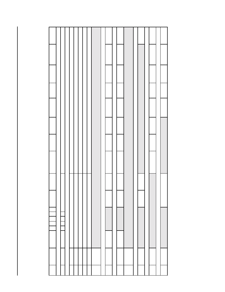
Preliminary Data Sheet
TMXF28155 Super Mapper
May 2001
155/51 Mbits/s SONET/SDH x28/x21 DS1/E1
73
Agere Systems Inc.
7 Microprocessor Interface and Global Control and Status Registers
(continued)
7.2 Microprocessor Interface Register Map
Table 76. Microprocessor Interface Register Map
Address
Symbol
Bit
15
Bit
14
Bit
13
Bit
12
Bit
11
Bit
10
Bit
9
Bit
8
Bit
7
Bit
6
Bit
5
Bit
4
Bit
3
Bit
2
Bit
1
Bit
0
Super Mapper Version Control Register--RO
0x00000
SMPR_VCR
0
0
0
0
0
SMPR_VERSION[2:0]
SMPR_ID[7:0]
Super Mapper Symbol Register--RO
0x00001 SMPR_SYMR4
0x54 = T
0x4D = M
0x00002 SMPR_SYMR3
0x58 = X
0x46 = F
0x00003 SMPR_SYMR2
0x32 = 2
0x38 = 8
0x00004 SMPR_SYMR1
0x31 = 1
0x35 = 5
0x00005 SMPR_SYMR0
0x35 = 5
0x0D = CR
0x00006
--
0x00007
--
Super Mapper Interrupt Status Register--RO
0x00008
SMPR_ISR
SMPR_APS_IS
SMPR_
PARITY_IS
SMPR_
PMRESET_IS
SMPR_TPG_IS
SMPR_DJA_IS
SMPR_FRM_
IS
SMPR_XC_IS
SMPR_M13_
IS
SMPR_VTMPR_
IS
SMPR_
SPEMPR_IS
SMPR_TMUX_
IS
Super Mapper Interrupt Mask Register--R/W
0x00009
SMPR_IMR
SMPR_APS_IM
SMPR_
PARITY_IM
SMPR_
PMRESET_IM
SMPR_TPG_IM
SMPR_DJA_
IM
SMPR_FRM_
IM
SMPR_XC_IM
SMPR_M13_
IM
SMPR_VTMPR_
IM
SMPR_
SPEMPR_IM
SMPR_TMUX_
IM
0x0000A
--
0x0000C
--
Global Trigger Register--R/W
0x0000D
SMPR_GTR
SMPR_BER_
INSRT
SMPR_
PMRESET
SMPR_SWRS
Block Software Reset Register--R/W
0x0000E
SMPR_MSRR
SMPR_TPG_SWRS
SMPR_DJA_
SWRS
SMPR_FRM_
SWRS
SMPR_XC_
SWRS
SMPR_M13_
SWRS
SMPR_VTMPR_
SWRS
SMPR_SPEMPR_
SWRS
SMPR_TMUX_
SWRS
Global Control Register (SMPR_GCR)--R/W
0x0000F
SMPR_GCR
SMPR_PMMODE[1:0]
SMPR_PARITY_
EVEN_ODD
SMPR_OH_
DEFLT
SMPR_FXD_
STFF_DEFLT
SMPR_COR_
COW
SMPR_SAT_
ROLLOVER
TMXF28155 Super Mapper
Preliminary Data Sheet
155/51 Mbits/s SONET/SDH x28/x21 DS1/E1
May 2001
74
Agere Systems Inc.
7 Microprocessor Interface and Global Control and Status Registers
(continued)
Table 76. Microprocessor Interface Register Map (continued)
Address
Symbol
Bit
15:11
Bit 10
Bit 9
Bit 8
Bit 7
Bit 6
Bit 5
Bit 4
Bit 3
Bit 2
Bit 1
Bit 0
TMUX and SPEMOR CONTROL Register--R/W
0x00010
SMPR_TSCR
MP0RH02THD_LB
SMPR_RETIME_
CLK_EDGE
SMPR_TELECOMBUS_
EDGE
SMPR_SMPR_TMUX_
MASTER_SLAVE
0x00011
--
FRAMER Control Register--R/W
0x00012
SMPR_FCR
SMPR_FRM_CLK_SEL[2:0]
CDR and LVDS Control Register--R/W
0x00013
SMPR_CLCR
--
SMPR_MPU_C
DR_MODE
SMPR_MPU_
CG_PWRDN
SMPR_LVDS_
REF_SEL
SMPR_RXPWRDN
SMPR_
PLLPWRDN
SMPR_MRESET
SMPR_CDR_SEL
Clock and Power Control Register--R/W
0x00014
SMPR_CPCR
SMPR_M13_
TXCLK
SMPR_M13_
RXCLK
SMPR_DJA_
CLK
SMPR_VTMPR_
TXCLK
SMPR_VTMPR_
RXCLK
SMPR_SPEMPR_
TXCLK
SMPR_SPEMPR_
RXCLK
SMPR_TMUX_
TXCLK
SMPR_TMUX_RXCLK
0x00015
--
PM Reset Count Register High--R/W
0x00016
SMPR_PMRCHR
SMPR_PMRESET_HIGH_COUNT[10:0]
PM Reset Count Register Low--R/W
0x00017
SMPR_PMRCLR
SMPR_PMRESET_LOW_COUNT[15:0]
0x00018
TX_LINE_EN1
TX_LINE_EN[16-1]
0x00019
TX_LINE_EN2
TX_LINE_EN[29-17]
Scratch Register--R/W
0x0001F
SMPR_SR
SMPR_SCRATCH_REGISTER[15:0]

Preliminary Data Sheet
TMXF28155/51 Super Mapper
May 2001
155/51 Mbits/s SONET/SDH x28/x21 DS1/E1
75
Agere Systems Inc.
8 TMUX Registers
Table of Contents
Contents
Page
8 TMUX Registers ................................................................................................................................................. 75
8.1 TMUX Register Descriptions ........................................................................................................................ 77
8.2 TMUX Register Map ................................................................................................................................... 124
Tables
Page
Table 77. TMUX_ID_R, TMUX Identification Register (RO) .................................................................................. 77
Table 78. TMUX_ONESHOT, TMUX One-Shot Register 0 to 1 (R/W) ................................................................. 77
Table 79. TMUX_RCV_TX_MODE, TMUX Receive/Transmit Mode (R/W) .......................................................... 77
Table 80. TMUX_TX_DLT, Delta/Event (COR/COW) ........................................................................................... 78
Table 81. TMUX_RPS_DLT, Delta/Event (COR/COW) ........................................................................................ 78
Table 82. TMUX_RHS_DLT, Delta/Event (COR/COW) ........................................................................................ 79
Table 83. TMUX_RPOH[1--3]_DLT, Delta/Event (COR/COW) ............................................................................ 81
Table 84. TMUX_TX_MSK, Mask Bits for INT Interrupt Signal (R/W) (Mask = 1, No Mask = 0) .......................... 87
Table 85. TMUX_RPS_MSK, Mask Bits for INT Interrupt Signal (R/W) (Mask = 1, No Mask = 0) ....................... 88
Table 86. TMUX_RHS_MSK, Mask Bits for INT Interrupt Signal (R/W) (Mask = 1, No Mask = 0) ....................... 88
Table 87. TMUX_RPOH[1--3]_MSK, Mask Bits for Interrupt Signal (R/W) (Mask = 1, No Mask = 0) .................. 89
Table 88. TMUX_APSINT_MSK, Mask Bits for APSINT Interrupt Signal (R/W) (Mask = 1, No Mask = 0) ........... 91
Table 89. TMUX_TX_STATE, State Parameters (RO) ......................................................................................... 91
Table 90. TMUX_RPS_STATE, State and Value Parameters (RO) ..................................................................... 91
Table 91. TMUX_RHS_STATE, State and Value Parameters (RO) ..................................................................... 92
Table 92. TMUX_RPOH[1--3]_STATE, State and Value Parameters (RO) ......................................................... 92
Table 93. TMUX_RHS_CTL, Receive High-speed Control Parameters (R/W) ..................................................... 94
Table 94. TMUX_RLS_BITBLK_CTL, Receive Low-speed Control Parameters (R/W) ........................................ 94
Table 95. TMUX_RLS_MODE_CTL, Receive Low-speed Control Parameters (R/W) .......................................... 95
Table 96. TMUX_RAISINH_CTL, Receive Low-speed Control Parameters (R/W) ............................................... 96
Table 97. TMUX_LOSDETCNT, Receive Low-speed Control Parameters (R/W) ................................................ 97
Table 98. TMUX_CNTD_TOH_[A--B], Continuous N-Times Detect Control Parameters (R/W) .......................... 98
Table 99. TMUX_CNTD_POH_[A--B], Continuous N-Times Detect Control Parameters (R/W) ......................... 99
Table 100. TMUX_C2EXP[1--2_3], Continuous N-Times Detect Control Parameters (R/W) ............................ 100
Table 101. TMUX_RF1MON, Receive Monitor Values (RO) .............................................................................. 100
Table 102. TMUX_RAPSMON, Receive Monitor Values (RO) ........................................................................... 100
Table 103. TMUX_RS1MON, Receive Monitor Values (RO) .............................................................................. 100
Table 104. TMUX_RPOHMON[1--3][A--D], Receive Monitor Values (RO) ....................................................... 101
Table 105. TMUX_TLS_CTL, Transmit Low-speed Control Parameters (R/W) .................................................. 102
Table 106. TMUX_THS_PORT_CTL, Transmit High-speed Port Control Parameters (R/W) ............................. 103
Table 107. TMUX_THS_TOH_CTL, Transmit High-speed Control Parameters (R/W) ....................................... 103
Table 108. TMUX_THS_POH[1--3]_CTL, Transmit High-speed Control Parameters (R/W) ............................. 105
Table 109. TMUX_TLRDI_CTL, Transmit High-speed Line RDI Control Parameters (R/W) .............................. 109
Table 110. TMUX_TPRDI_CTL, Transmit High-speed Path RDI Control Parameters (R/W) ............................. 109
Table 111. TMUX_TZ0_INS_VAL, Transmit TOH and POH Insert Values (R/W) .............................................. 110
Table 112. TMUX_TS1_F1_INS_VAL, Transmit TOH and POH Insert Values (R/W) ........................................ 110
Table 113. TMUX_TAPS_INS_VAL, Transmit TOH and POH Insert Values (R/W) ........................................... 110
Table 114. TMUX_TPOH[1--3]_INS_[A--C], Transmit TOH and POH Insert Values (R/W) ............................. 110
Table 115. TMUX_TBERINS_CTL, Transmit High-speed Error Insertion Control Parameters (R/W) ................ 112
Table 116. TMUX_THS_ERR_CTL, Transmit High-speed Error Insertion Control Parameters (R/W) ............... 113
Table 117. TMUX_TOAC_CTL, Receive/Transmit TOAC/POAC Control Parameters (R/W) ............................. 113
Table 118. TMUX_RPOAC_CTL, Receive/Transmit TOAC/POAC Control Parameters (R/W) .......................... 115
Table 119. TMUX_TFRAMEOFFSET, Transmit High-speed Offset Control Parameters (R/W) ......................... 116
Table 120. TMUX_SD_CTL[1--6], B1/B2 Signal Degrade Set/Clear Control Registers (R/W) .......................... 116

TMXF28155/51 Super Mapper
Preliminary Data Sheet
155/51 Mbits/s SONET/SDH x28/x21 DS1/E1
May 2001
76
Agere Systems Inc.
8 TMUX Registers
(continued)
Table of Contents
(continued)
Tables
Page
Table 121. TMUX_SF_CTL[1--6], B1/B2 Signal Fail Set/Clear Control Registers (R/W) ................................... 117
Table 122. TMUX_B3SD_CTL[1--6], B3 Signal Degrade Set/Clear Control Registers (R/W) ........................... 117
Table 123. TMUX_B3SF_CTL[1--6], B3 Signal Fail Set/Clear Control Registers (R/W) .................................... 118
Table 124. TMUX_B1ECNT, Receive B1 Error Counts (RO) .............................................................................. 118
Table 125. TMUX_B2ECNT_17_16 and TMUX_B2ECNT_15_0, Receive B2 Error Counts (RO) ..................... 119
Table 126. TMUX_B3ECNT[1--3], Receive B3 Error Counts (RO) .................................................................... 119
Table 127. TMUX_M1ECNT_17_16 and TMUX_M1ECNT_15_0, Receive M1 Error Counts (RO) ................... 120
Table 128. TMUX_G1ECNT[1--3], Receive G1 Error Counts (RO) ................................................................... 120
Table 129. TMUX_RPTR_INCCNT[1--3], Receive Pointer Increment Count (RO) ............................................ 121
Table 130. TMUX_RPTR_DECCNT[1--3], Receive Pointer Decrement Count (RO) ......................................... 121
Table 131. TMUX_RJ0EXPECTED[1--8], Expected J0 Byte Sequence (R/W) ................................................. 121
Table 132. TMUX_RJ0CAPTURED[1--8], Captured J0 Receive Value (RO) .................................................... 121
Table 133. TMUX_TJ0VALUE[1--8], J0 Byte Transmit Insert (R/W) .................................................................. 121
Table 134. TMUX_RJ1EXPECTED1_[1--32], Expected J1 Byte Value for Port 1 (R/W) ................................... 122
Table 135. TMUX_RJ1EXPECTED2_[1--32], Expected J1 Byte Value for Port 2 (R/W) ................................... 122
Table 136. TMUX_RJ1EXPECTED3_[1--32], Expected J1 Byte Value for Port 3 (R/W) ................................... 122
Table 137. TMUX_RJ1CAPTURED1_[1--32], Captured J1 Value for STS #1 (RO) .......................................... 122
Table 138. TMUX_RJ1CAPTURED2_[1--32], Captured J1 Value for STS #2 (RO) .......................................... 122
Table 139. TMUX_RJ1CAPTURED3_[1--32], Captured J1 Value for STS #3 (RO) .......................................... 123
Table 140. TMUX_TJ1VALUE_1[1--32], J1 Byte Transmit Insert for STS #1 (R/W) ......................................... 123
Table 141. TMUX_TJ1VALUE_2[1--32], J1 Byte Transmit Insert for STS #2 (R/W) ......................................... 123
Table 142. TMUX_TJ1VALUE_3[1--32], J1 Byte Transmit Insert for STS #3 (R/W) ......................................... 123
Table 143. TMUX Register Map .......................................................................................................................... 124

Preliminary Data Sheet
TMXF28155/51 Super Mapper
May 2001
155/51 Mbits/s SONET/SDH x28/x21 DS1/E1
77
Agere Systems Inc.
8 TMUX Registers
(continued)
8.1 TMUX Register Descriptions
This section provides a brief description of each register bit and its functionality. The abbreviations after each regis-
ter indicate if the register is read only (RO), clear-on-read/clear-on-write (COR/COW), or read/write (R/W).
Table 77. TMUX_ID_R, TMUX Identification Register (RO)
Table 78. TMUX_ONESHOT, TMUX One-Shot Register 0 to 1 (R/W)
Table 79. TMUX_RCV_TX_MODE, TMUX Receive/Transmit Mode (R/W)
Address
Bit
Name
Function
Reset Default
0x40000
15:11
--
Reserved. 0x0
10:8
TMUX_VERSION[2:0] Block Version Number. Block version register will
change each time the device is changed.
0x0
7:0
TMUX_ID[7:0]
Block ID Number. 0x04
Address
Bit
Name
Function
Reset Default
0x40002
15:8
--
Reserved. 0x00
7
TMUX_B3SFCLEAR
B3 Signal Fail Clear. Allows the signal fail algorithm
to be forced into the normal state.
0
6
TMUX_B3SFSET
B3 Signal Fail Set. Allows the signal fail algorithm
to be forced into the failed state.
0
5
TMUX_B3SDCLEAR B3 Signal Degrade Clear. Allows the signal
degrade algorithm to be forced into the normal state.
0
4
TMUX_B3SDSET
B3 Signal Degrade Set. Allows the signal degrade
algorithm to be forced into the degraded state.
0
3
TMUX_SFCLEAR
Signal Fail Clear. Allows the signal fail algorithm to
be forced into the normal state.
0
2
TMUX_SFSET
Signal Fail Set. Allows the signal fail algorithm to be
forced into the failed state.
0
1
TMUX_SDCLEAR
Signal Degrade Clear. Allows the signal degrade
algorithm to be forced into the normal state.
0
0
TMUX_SDSET
Signal Degrade Set. Allows the signal degrade
algorithm to be forced into the degraded state.
0
Address
Bit
Name
Function
Reset Default
0x40003
15:1
--
Reserved. 0x000
0
TMUX_STS1MODE
STS-1 Mode Control Bit. A 1 indicates that the
received and transmitted high-speed data is STS-1
data operating at 52 MHz. A 0 indicates that the
received and transmitted high-speed data operates
at 155 MHz.
0

TMXF28155/51 Super Mapper
Preliminary Data Sheet
155/51 Mbits/s SONET/SDH x28/x21 DS1/E1
May 2001
78
Agere Systems Inc.
8 TMUX Registers
(continued)
Table 80. TMUX_TX_DLT, Delta/Event (COR/COW)
Table 81. TMUX_RPS_DLT, Delta/Event (COR/COW)
Address
Bit
Name
Function
Reset
Default
0x40004
15:7
--
Reserved. 0x000
6:4
TMUX_TLSPARE[3:1] Transmit Low-speed Parity Error Event (Input Port Num-
ber). This event bit indicates a byte transfer parity error was
detected on the respective STS-1/AU-3 input. The mask bits
are TMUX_TLSPARM[3:1] (
Table 84
).
0
3
TMUX_TPOAC_PE
Transmit Path Overhead Access Channel (TPOAC) Par-
ity Error Event. This event bit indicates a parity error was
detected on the incoming transmit path overhead access
channel. The mask bit is TMUX_TPOAC_PM (
Table 84
).
0
2
TMUX_TTOAC_PE
Transmit Transport Overhead Access Channel (TTOAC)
Parity Error Event. This event bit indicates a parity error
was detected on the incoming transmit transport overhead
access channel. The mask bit is TMUX_TTOAC_PM
(
Table 84
).
0
1
TMUX_THSILOFD
Transmit High-speed Input Loss of Frame Delta. This
delta bit indicates a change of state for the transmit loss of
frame bit TMUX_THSILOF (
Table 89
). The mask bit is
TMUX_THSILOFM (
Table 84
).
0
0
TMUX_THSILOCD
Transmit High-speed Input Loss of Clock Delta. This
delta bit indicates a change of state for the transmit loss of
high-speed clock bit TMUX_THSILOC (
Table 89
). The mask
bit is TMUX_THSILOCM (
Table 84
).
0
Address
Bit
Name
Function
Reset
Default
0x40005
15:6
--
Reserved. 0x000
5
TMUX_RPSLOFD
Receive Protection High-speed Loss of Frame Delta. This
delta bit indicates a change in state of TMUX_RPSLOF
(
Table 90
). The mask bit is TMUX_RPSLOFM (
Table 85
).
0
4
TMUX_RPSOOFD
Receive Protection High-speed Out of Frame Delta. This
delta bit indicates a change in state of TMUX_RPSOOF
(
Table 90
). The mask bit is TMUX_RPSOOFM (
Table 85
).
0
3
TMUX_RPSILOCD
Receive Protection High-speed Loss of Input Clock
Delta. This delta bit indicates a change in state of the
TMUX_RPSILOC (
Table 90
) state bit. The mask bit is
TMUX_RPSILOCM (
Table 85
).
0
2
TMUX_RPSB2E
Receive Protection High-speed B2 Error Event. This event
bit indicates a B2 error was detected in the receive protection
input. The mask bit is TMUX_RPSB2M (
Table 85
).
0
1
TMUX_RPSLREIE
Receive Protection High-speed Line REI Event. This
event bit indicates a line REI error was detected in the
receive protection input. The mask bit is TMUX_RPSLREIM
(
Table 85
).
0
0
--
Reserved.
0

Preliminary Data Sheet
TMXF28155/51 Super Mapper
May 2001
155/51 Mbits/s SONET/SDH x28/x21 DS1/E1
79
Agere Systems Inc.
8 TMUX Registers
(continued)
Table 82. TMUX_RHS_DLT, Delta/Event (COR/COW)
Address
Bit
Name
Function
Reset Default
0x40006
15
--
Reserved.
0
14
TMUX_RS1BABE
Receive S1 Babble Event. This event bit indicates an
inconsistent S1 value is being received. The event is
triggered if TMUX_CNTDS1FRAME[3:0] (
Table 98
) con-
secutive frames pass without a validated message
occurring. The mask bit is TMUX_RS1BABM (
Table 86
).
0
13
TMUX_RS1MOND
Receive S1 Monitor Delta. This delta bit indicates a
change of state for TMUX_RS1MON[7:0] (
Table 103
). A
new S1 value is detected after TMUX_CNTDS1[3:0]
(
Table 98
) consecutive occurrences of a consistent new
value in the S1 byte. The mask bit is TMUX_RS1MONM.
0
12
TMUX_RLRDIMOND Receive Line RDI Monitor Delta. This delta bit indi-
cates a change in state for TMUX_RLRDIMON
(
Table 91
) when the pattern 110 is detected/not detected
TMUX_CNTDK2[3:0] (
Table 98
) consecutive times in the
incoming STS-3/STM-1 frame. The mask bit is
TMUX_RLRDIMONM (
Table 86
).
0
11
TMUX_RLAISMOND Receive Line AIS Monitor Delta. This delta bit indi-
cates a change in state for TMUX_RLAISMON
(
Table 91
) when the pattern 111 is detected/not detected
TMUX_CNTDK2[3:0] consecutive times in the incoming
STS-3/STM-1 frame. The mask bit is
TMUX_RLAISMONM (
Table 86
).
0
10
TMUX_RK2MOND
Receive K2 Monitor Delta. This delta bit indicates a
change in state for TMUX_K2MON[2:0] (
Table 102 on
page 100
). A new K2 value is detected after
TMUX_CNTDK2[3:0] consecutive occurrences of a con-
sistent new value in the three least significant bits of the
incoming K2 byte. Note that this delta bit may be coinci-
dent with TMUX_RLRDIMOND and
TMUX_RLAISMOND. The mask bit is
TMUX_RK2MONM (
Table 86
).
0
9
TMUX_RAPSBABE
Receive APS Babble Event. This event bit indicates
when an inconsistent APS value has been detected
TMUX_CNTDK1K2[3:0] (
Table 98
) times in the incoming
TMUX_CNTDK1K2FRAME[3:0] (
Table 98
) consecutive
frames. The mask bit is TMUX_RAPSBABM (
Table 86
on page88
).
0
8
TMUX_RAPSMOND
Receive APS Monitor Delta. This delta bit indicates a
change in state in the received APS value
TMUX_RAPSMON[12:0] (
Table 102
) when a new con-
sistent value is detected TMUX_CNTDK1K2[3:0] times
in the K1 and K2[7:3] bits. The mask bit is
TMUX_RAPSMONM (
Table 86
).
0

TMXF28155/51 Super Mapper
Preliminary Data Sheet
155/51 Mbits/s SONET/SDH x28/x21 DS1/E1
May 2001
80
Agere Systems Inc.
8 TMUX Registers
(continued)
Table 82. TMUX_RHS_DLT, Delta/Event (COR/COW) (continued)
Address
Bit
Name
Function
Reset Default
0x40006
7
TMUX_RF1MOND Receive F1 Monitor Delta. This delta bit indicates a
change in state of TMUX_RF1MON0[7:0] and
TMUX_RF1MON1[7:0] (
Table 101
) when a consistent
new value is detected in the incoming F1 byte for
TMUX_CNTDF1[3:0] (
Table 98
) continuous frames. The
current value is stored in TMUX_RF1MON0[7:0] and the
previous value is stored in TMUX_RF1MON0[7:0]. The
mask bit is TMUX_RF1MONM (
Table 86
).
0
6
TMUX_RTIMSD
Receive Section Trace Identifier Mismatch Delta. This
delta bit indicates a change in state in the received 16-
byte J0 sequence of bytes if the J0 mode is programmed
to receive a 16-byte sequence. The mask bit is
TMUX_RTIMSM (
Table 86
).
0
5
TMUX_RHSSFD
Receive High-speed Signal Fail BER Algorithm Delta.
This delta bit indicates a change of state for the signal fail
BER algorithm state bit TMUX_RHSSF (
Table 91
). The
mask bit for this delta bit is TMUX_RHSSFM (
Table 86
).
0
4
TMUX_RHSSDD
Receive High-speed Signal Degrade BER Algorithm
Delta. This delta bit indicates a change of state for the
signal degrade BER algorithm state bit TMUX_RHSSD
(
Table 91
). The mask bit is TMUX_RHSSDM (
Table 86
).
0
3
TMUX_RHSLOSD Receive High-speed Loss of Signal Delta. This delta
bit indicates a change in state of either TMUX_RHSLOS
(
Table 91
) or TMUX_RHSLOSEXTI (
Table 91
).
TMUX_RHSLOSEXTI is an external input from a device
pin. TMUX_RHSLOS is an internally generated state bit
based on monitoring for a consecutive 0/1s pattern in the
data input. The mask bit is TMUX_RHSLOSM (
Table 86
).
0
2
TMUX_RHSLOFD Receive High-speed Loss of Frame Delta. This delta
bit indicates a change in state of TMUX_RHSLOF
(
Table 91
). The mask bit is TMUX_RHSLOFM (
Table 86
).
0
1
TMUX_RHSOOFD Receive High-speed Out of Frame Delta. This delta bit
indicates a change in state of TMUX_RHSOOF
(
Table 91
). The mask bit is TMUX_RHSOOFM (
Table 86
).
0
0
TMUX_RHSILOCD Receive High-speed Loss of Input Clock Delta. This
delta bit indicates a change in state of the
TMUX_RHSILOC (
Table 91
) state bit. The mask bit is
TMUX_RHSILOCM (
Table 86
).
0

Preliminary Data Sheet
TMXF28155/51 Super Mapper
May 2001
155/51 Mbits/s SONET/SDH x28/x21 DS1/E1
81
Agere Systems Inc.
8 TMUX Registers
(continued)
Table 83. TMUX_RPOH[1--3]_DLT, Delta/Event (COR/COW)
Address
Bit
Name
Function
Reset
Default
0x40007
15
TMUX_RSFB3D1
Receive Path Signal Fail BER Algorithm Delta. This delta
bit indicates a change of state for the signal fail BER algo-
rithm state bit TMUX_RSFB31 (
Table 92
) at the path level for
port 1. Only port 1 information is valid in AU-4 mode and in
STS-1 mode. The mask bit is TMUX_RSFB3M1 (
Table 87
).
0
14
TMUX_RSDB3D1
Receive Path Signal Degrade BER Algorithm Delta. This
delta bit indicates a change of state for the signal fail BER
algorithm state bit TMUX_RSDB31 (
Table 92
) at the path
level for port 1. Only port 1 information is valid in AU-4 mode
and in STS-1 mode. The mask bit is TMUX_RSDB3M1
(
Table 87
).
0
13
TMUX_RUNEQPE1
Receive Path Unequipped Event. This event bit indicates
that the current value of the received C2 (signal label) byte,
TMUX_C2MON1[7:0] (
Table 104
), has a value 0x00, indicat-
ing unequipped payload on port 1. Only port 1 information is
valid in AU-4 mode and in STS-1 mode. The mask bit is
TMUX_RUNEQPM1 (
Table 87
).
0
12
TMUX_RPLMPE1
Receive Path Payload Label Mismatch Event. This event
bit indicates that the current value of the received C2 (signal
label) byte, TMUX_C2MON1[7:0], differs from the expected
C2 value, TMUX_C2EXP1[7:0] (
Table 100
) for port 1. Only
port 1 information is valid in AU-4 mode and in STS-1 mode.
The mask bit is TMUX_RPLMPM1 (
Table 87
).
0
11
TMUX_RN1MOND1
Receive N1 Monitor Delta. This delta bit indicates a change
in state in TMUX_N1MON1[7:0] (
Table 104
). The N1 current
value is updated when a consecutive and consistent value is
detected in the incoming N1 byte for TMUX_CNTDN1[3:0]
(
Table 99
) frames on port 1. Only port 1 information is valid
in AU-4 mode and in STS-1 mode. The mask bit is
TMUX_RN1MONM1 (
Table 87
).
0
10
TMUX_RK3MOND1
Receive K3 Monitor Delta. This delta bit indicates a change
in state in TMUX_K3MON1[7:0] (
Table 104
), which is
updated when a consecutive and consistent value is
detected in the incoming K3 byte for TMUX_CNTDK3[3:0]
(
Table 99
) frames on port 1. Only port 1 information is valid
in AU-4 mode and in STS-1 mode. The mask bit is
TMUX_RK3MONM1 (
Table 87
).
0
9
TMUX_RF3MOND1
Receive F3 (Path User Byte) Monitor Delta. This delta bit
indicates a change in state in TMUX_F3MON01[7:0]
(
Table 104
), which is updated when a consecutive and con-
sistent value is detected in the incoming F3 byte for
TMUX_CNTDF3[3:0] (
Table 99
) frames on port 1. Only port
1 information is valid in AU-4 mode and in STS-1 mode. The
mask bit is TMUX_RF3MONM1 (
Table 87
).
0

TMXF28155/51 Super Mapper
Preliminary Data Sheet
155/51 Mbits/s SONET/SDH x28/x21 DS1/E1
May 2001
82
Agere Systems Inc.
8 TMUX Registers
(continued)
Table 83. TMUX_RPOH[1--3]_DLT, Delta/Event (COR/COW) (continued)
Address
Bit
Name
Function
Reset
Default
0x40007
8
TMUX_RF2MOND1 Receive F2 (Path User Byte) Monitor Delta. This delta bit
indicates a change in state in TMUX_F2MON01[7:0]
(
Table 104
), which is updated when a consecutive and con-
sistent value is detected in the incoming F2 byte for
TMUX_CNTDF2[3:0] (
Table 99
) frames on port 1. Only port 1
information is valid in AU-4 mode and in STS-1 mode. The
mask bit is TMUX_RF2MONM1 (
Table 87
).
0
7
TMUX_RRDIPD1
Receive Path RDI (Remote Defect Indication) Monitor
Delta. This delta bit indicates a change in state in
TMUX_RDIPMON1[2:0] (
Table 104
)
that
occurs when a con-
secutive and consistent new value is detected in the incom-
ing G1[3:1] bits for TMUX_CNTDRDIP[3:0] (
Table 99
) frames
on port 1. The device monitors either G1 bit 3 or G1[3:1]
depending on TMUX_REPRDI_MODE (
Table 95
). Only port
1 information is valid in AU-4 mode and in STS-1 mode. The
mask bit is TMUX_RRDIPM1 (
Table 87
).
0
6
TMUX_RC2MOND1 Receive C2 (Signal Label) Monitor Delta. This delta bit
indicates a change in state in TMUX_C2MON1[7:0]
(
Table 104
), which is updated when a consecutive and con-
sistent value is detected in the incoming C2 byte for
TMUX_CNTDC2[3:0] (
Table 99
) frames on port 1. Only port
1 information is valid in AU-4 mode and in STS-1 mode. The
mask bit is TMUX_RC2MONM1 (
Table 87
).
0
5
TMUX_RTIMPD1
Receive Path Trace Identifier Mismatch Delta. This delta
bit indicates a change in state in the received 16-byte J1
sequence on port 1 if the J1 mode is programmed to receive
a 16-byte sequence. Only port 1 information is valid in AU-4
mode and in STS-1 mode. The mask bit is TMUX_RTIMPM1
(
Table 87
).
0
4
TMUX_RNDFE1
Receive New Data Flag Event. This event bit indicates that
the incoming pointer has the new data flag enabled, causing
a jump in the current pointer location for port 1. Only port 1
information is valid in AU-4 mode and in STS-1 mode. The
mask bit is TMUX_RNDFM1 (
Table 87
).
0
3
TMUX_RDECE1
Receive Pointer Decrement Event. This event bit indicates
that a valid incoming pointer decrement indication was
received on port 1. Only port 1 information is valid in AU-4
mode and in STS-1 mode. The mask bit is TMUX_RDECM1
(
Table 87
).
0
2
TMUX_RINCE1
Receive Pointer Increment Event. This event bit indicates
that a valid incoming pointer increment indication was
received on port 1. Only port 1 information is valid in AU-4
mode and in STS-1 mode. The mask bit is TMUX_RINCM1
(
Table 87
).
0

Preliminary Data Sheet
TMXF28155/51 Super Mapper
May 2001
155/51 Mbits/s SONET/SDH x28/x21 DS1/E1
83
Agere Systems Inc.
8 TMUX Registers
(continued)
Table 83. TMUX_RPOH[1--3]_DLT, Delta/Event (COR/COW) (continued)
Address
Bit
Name
Function
Reset
Default
0x4007
1
TMUX_RPAISD1
Receive Path AIS Delta. This delta bit indicates a change in
state of the TMUX_RPAIS1 (
Table 92
) state bit, which desig-
nates that the port 1 pointer interpreter is in the alarm indica-
tion signal state. Only port 1 information is valid in AU-4
mode and in STS-1 mode. The mask bit is TMUX_RPAISM1
(
Table 87
).
0
0
TMUX_RLOPD1
Receive Loss of Pointer Delta. This delta bit indicates a
change in state of the TMUX_RLOP1 (
Table 92
) state bit,
which designates that the port 1 pointer interpreter is in the
loss of pointer state. Only port 1 information is valid in AU-4
mode. The mask bit is TMUX_RLOPM1 (
Table 87
).
0
0x40008
15
TMUX_RSFB3D2
Receive Path Signal Fail BER Algorithm Delta. This delta
bit indicates a change of state for the signal fail BER algo-
rithm state bit TMUX_RSFB32 (
Table 92
) at the path level for
port 2. Only port 1 information is valid in AU-4 mode and in
STS-1 mode. The mask bit is TMUX_RSFB3M2 (
Table 87
).
0
14
TMUX_RSDB3D2
Receive Path Signal Degrade BER Algorithm Delta. This
delta bit indicates a change of state for the signal fail BER
algorithm state bit TMUX_RSDB32 (
Table 92
) at the path
level for port 2. Only port 1 information is valid in AU-4 mode
and in STS-1 mode. The mask bit is TMUX_RHSSDB3M2.
0
13
TMUX_RUNEQPD2
Receive Path Unequipped Delta. This delta bit indicates
that the current value of the received C2 (signal label) byte,
TMUX_C2MON2[7:0] (
Table 104
), has a value 0x00, indicat-
ing unequipped payload for port 2. Only port 1 information is
valid in AU-4 mode and in STS-1 mode.The mask bit is
TMUX_RUNEQPM2 (
Table 87
).
0
12
TMUX_RPLMPD2
Receive Path Payload Label Mismatch Delta. This event
bit indicates that the current value of the received C2 (signal
label) byte, TMUX_C2MON2[7:0], differs from the expected
C2 value, TMUX_C2EXP2[7:0] (
Table 100
) for port 2. Only
port 1 information is valid in AU-4 mode and in STS-1
mode.The mask bit is TMUX_RPLMPM2 (
Table 87
).
0
11
TMUX_RN1MOND2
Receive N1 Monitor Delta. This delta bit indicates a change
in state in TMUX_N1MON2[7:0] (
Table 104
). The N1 current
value is updated when a consecutive and consistent value is
detected in the incoming N1 byte for TMUX_CNTDN1[3:0]
(
Table 99
) frames on port 2. Only port 1 information is valid in
AU-4 mode and in STS-1 mode. The mask bit is
TMUX_RN1MONM2 (
Table 87
).
0
10
TMUX_RK3MOND2
Receive K3 Monitor Delta. This delta bit indicates a change
in state in TMUX_K3MON2[7:0] (
Table 104
), which is
updated when a consecutive and consistent value is
detected in the incoming K3 byte for TMUX_CNTDK3[3:0]
(
Table 99
) frames on port 2. Only port 1 information is valid in
AU-4 mode and in STS-1 mode. The mask bit is
TMUX_RK3MONM2 (
Table 87
).
0

TMXF28155/51 Super Mapper
Preliminary Data Sheet
155/51 Mbits/s SONET/SDH x28/x21 DS1/E1
May 2001
84
Agere Systems Inc.
8 TMUX Registers
(continued)
Table 83. TMUX_RPOH[1--3]_DLT, Delta/Event (COR/COW) (continued)
Address
Bit
Name
Function
Reset
Default
0x40008
9
TMUX_RF3MOND2 Receive F3 (Path User Byte) Monitor Delta. This delta bit indi-
cates a change in state in TMUX_F3MON02[7:0] (
Table 104
),
which is updated when a consecutive and consistent value is
detected in the incoming F3 byte for TMUX_CNTDF3[3:0]
(
Table 99
) frames on port 2. Only port 1 information is valid in
AU-4 mode and in STS-1 mode. The mask bit is
TMUX_RF3MONM2 (
Table 87
).
0
8
TMUX_RF2MOND2 Receive F2 (Path User Byte) Monitor Delta. This delta bit indi-
cates a change in state in TMUX_F2MON02[7:0] (
Table 104
),
which is updated when a consecutive and consistent value is
detected in the incoming F2 byte for TMUX_CNTDF2[3:0]
(
Table 99
) frames on port 2. Only port 1 information is valid in
AU-4 mode and in STS-1 mode. The mask bit is
TMUX_RF2MONM2 (
Table 87
).
0
7
TMUX_RRDIPD2
Receive Path RDI (Remote Defect Indication) Monitor Delta.
This delta bit indicates a change in state in
TMUX_RDIPMON2[2:0] (
Table 104
) which occurs when a con-
secutive and consistent new value is detected in the incoming
G1[3:1] bits for TMUX_CNTDRDIP[3:0] (
Table 99
) frames on
port 2. The device monitors either G1 bit 3 or G1[3:1] depending
on TMUX_REPRDI_MODE (
Table 95
). Only port 1 information
is valid in AU-4 mode and in STS-1 mode. The mask bit is
TMUX_RRDIPM2 (
Table 87
).
0
6
TMUX_RC2MOND2 Receive C2 (Signal Label) Monitor Delta. This delta bit indi-
cates a change in state in TMUX_C2MON2[7:0] (
Table 104
),
which is updated when a consecutive and consistent value is
detected in the incoming C2 byte for TMUX_CNTDC2[3:0]
(
Table 99
) frames on port 2. Only port 1 information is valid in
AU-4 mode and in STS-1 mode. The mask bit is
TMUX_RC2MONM2 (
Table 87
).
0
5
TMUX_RTIMPD2
Receive Path Trace Identifier Mismatch Delta. This delta bit
indicates a change in state in the received 16-byte J1 sequence
for port 2 if the J1 mode is programmed to receive a 16-byte
sequence. Only port 1 information is valid in AU-4 mode and in
STS-1 mode. The mask bit is TMUX_RTIMPM2 (
Table 87
).
0
4
TMUX_RNDFE2
Receive New Data Flag Event. This event bit indicates that the
incoming pointer has the new data flag enabled for port 2, caus-
ing a jump in the current pointer location. Only port 1 information
is valid in AU-4 mode and in STS-1 mode. The mask bit is
TMUX_RNDFM2 (
Table 87
).
0
3
TMUX_RDECE2
Receive Pointer Decrement Event. This event bit indicates
that a valid incoming pointer decrement indication was received
on port 2. Only port 1 information is valid in AU-4 mode and in
STS-1 mode. The mask bit is TMUX_RDECM2 (
Table 87
). How-
ever, increment and decrement event indication should be
ignored during loss-of-pointer (LOP) condition.
0

Preliminary Data Sheet
TMXF28155/51 Super Mapper
May 2001
155/51 Mbits/s SONET/SDH x28/x21 DS1/E1
85
Agere Systems Inc.
8 TMUX Registers
(continued)
Table 83. TMUX_RPOH[1--3]_DLT, Delta/Event (COR/COW) (continued)
Address
Bit
Name
Function
Reset
Default
0x40008
2
TMUX_RINCE2
Receive Pointer Increment Event. This event bit indicates
that a valid incoming pointer increment indication was
received on port 2. Only port 1 information is valid in AU-4
mode and in STS-1 mode. The mask bit is TMUX_RINCM2
(
Table 87
). However, increment and decrement event indica-
tion should be ignored during loss-of-pointer (LOP) condi-
tion.
0
1
TMUX_RPAISD2
Receive Path AIS Delta. This delta bit indicates a change in
state of the TMUX_RPAIS2 (
Table 92
) state bit, which desig-
nates that the port 2 pointer interpreter is in the alarm indica-
tion signal state. Only port 1 information is valid in AU-4
mode and in STS-1 mode. The mask bit is TMUX_RPAISM2
(
Table 87
).
0
0
TMUX_RLOPD2
Receive Loss of Pointer Delta. This delta bit indicates a
change in state of the TMUX_RLOP2 (
Table 92
) state bit,
which designates that the port 2 pointer interpreter is in the
loss of pointer state. Only port 1 information is valid in AU-4
mode. The mask bit is TMUX_RLOPM2 (
Table 87
).
0
0x40009
15
TMUX_RSFB3D3
Receive Path Signal Fail BER Algorithm Delta. This delta
bit indicates a change of state for the signal fail BER algo-
rithm state bit TMUX_RSFB32 (
Table 92
) at the path level for
port 3. Only port 1 information is valid in AU-4 mode and in
STS-1 mode. The mask bit is TMUX_RSFB3M3 (
Table 87
).
0
14
TMUX_RSDB3D3
Receive Path Signal Degrade BER Algorithm Delta. This
delta bit indicates a change of state for the signal fail BER
algorithm state bit TMUX_RSDB32 (
Table 92
) at the path
level for port 3. Only port 1 information is valid in AU-4 mode
and in STS-1 mode. The mask bit is TMUX_RSDB3M3
(
Table 87
).
0
13
TMUX_RUNEQPE3
Receive Path Unequipped Event. This event bit indicates
that the current value of the received C2 (signal label) byte,
TMUX_C2MON3[7:0] (
Table 104
), has a value 0x00, indicat-
ing unequipped payload for port 3. Only port 1 information is
valid in AU-4 mode and in STS-1 mode. The mask bit is
TMUX_RUNEQPM3 (
Table 87
).
0
12
TMUX_RPLMPE3
Receive Path Payload Label Mismatch Event. This event
bit indicates that the current value of the received C2 (signal
label) byte, TMUX_C2MON3[7:0], differs from the expected
C2 value, TMUX_C2EXP3[7:0] (
Table 100
) for port 3. Only
port 1 information is valid in AU-4 mode and in STS-1 mode.
The mask bit is TMUX_RPLMPM3 (
Table 87
).
0

TMXF28155/51 Super Mapper
Preliminary Data Sheet
155/51 Mbits/s SONET/SDH x28/x21 DS1/E1
May 2001
86
Agere Systems Inc.
8 TMUX Registers
(continued)
Table 83. TMUX_RPOH[1--3]_DLT, Delta/Event (COR/COW) (continued)
Address
Bit
Name
Function
Reset
Default
0x40009
11
TMUX_RN1MOND3 Receive N1 Monitor Delta. This delta bit indicates a change in
state in TMUX_N1MON3[7:0] (
Table 104
). The N1 current
value is updated when a consecutive and consistent value is
detected in the incoming N1 byte for TMUX_CNTDN1[3:0]
(
Table 99
) frames on port 3. Only port 1 information is valid in
AU-4 mode and in STS-1 mode. The mask bit is
TMUX_RN1MONM3 (
Table 87
).
0
10
TMUX_RK3MOND3 Receive K3 Monitor Delta. This delta bit indicates a change in
state in TMUX_K3MON3[7:0] (
Table 104
), which is updated
when a consecutive and consistent value is detected in the
incoming K3 byte for TMUX_CNTDK3[3:0] (
Table 99
) frames
on port 2. Only port 1 information is valid in AU-4 mode and in
STS-1 mode. The mask bit is TMUX_RK3MONM3 (
Table 87
).
0
9
TMUX_RF3MOND3 Receive F3 (Path User Byte) Monitor Delta. This delta bit
indicates a change in state in TMUX_F3MON03[7:0]
(
Table 104
), which is updated when a consecutive and consis-
tent value is detected in the incoming F3 byte for
TMUX_CNTDF3[3:0] (
Table 99
) frames on port 3. Only port 1
information is valid in AU-4 mode and in STS-1 mode. The
mask bit is TMUX_RF3MONM3 (
Table 87
).
0
8
TMUX_RF2MOND3 Receive F2 (Path User Byte) Monitor Delta. This delta bit
indicates a change in state in TMUX_F2MON03[7:0]
(
Table 104
), which is updated when a consecutive and consis-
tent value is detected in the incoming F2 byte for
TMUX_CNTDF2[3:0] (
Table 99
) frames on port 3. Only port 1
information is valid in AU-4 mode and in STS-1 mode. The
mask bit is TMUX_RF2MONM3 (
Table 87
).
0
7
TMUX_RDIPD3
Receive Path RDI (Remote Defect Indication) Monitor
Delta. This delta bit indicates a change in state in
TMUX_RDIPMON3[2:0] (
Table 104
) which occurs when a con-
secutive and consistent new value is detected in the incoming
G1[3:1] bits for TMUX_CNTDRDIP[3:0] (
Table 99
) frames on
port 3. The device monitors either G1 bit 3 or G1[3:1] depend-
ing on TMUX_REPRDI_MODE (
Table 95
). Only port 1 informa-
tion is valid in AU-4 mode and in STS-1 mode. The mask bit is
TMUX_RRDIPM3 (
Table 87
).
0
6
TMUX_RC2MOND3 Receive C2 (Signal Label) Monitor Delta. This delta bit indi-
cates a change in state in TMUX_C2MON3[7:0] (
Table 104
),
which is updated when a consecutive and consistent value is
detected in the incoming C2 byte for TMUX_CNTDC2[3:0]
(
Table 99
) frames on port 3. Only port 1 information is valid in
AU-4 mode and in STS-1 mode. The mask bit is
TMUX_RC2MONM3 (
Table 87
).
0
5
TMUX_RTIMPD3
Receive Path Trace Identifier Mismatch Delta. This delta bit
indicates a change in state in the received 16-byte J1 sequence
for port 3 if the J1 mode is programmed to receive a 16-byte
sequence. Only port 1 information is valid in AU-4 mode and in
STS-1 mode. The mask bit is TMUX_RTIMPM3 (
Table 87
).
0

Preliminary Data Sheet
TMXF28155/51 Super Mapper
May 2001
155/51 Mbits/s SONET/SDH x28/x21 DS1/E1
87
Agere Systems Inc.
8 TMUX Registers
(continued)
Table 83. TMUX_RPOH[1--3]_DLT, Delta/Event (COR/COW) (continued)
Note: In
Table 84
, the mask bits are set to suppress an interrupt when the corresponding event has occurred or
change in state has taken place.
Table 84. TMUX_TX_MSK, Mask Bits for INT Interrupt Signal (R/W) (Mask = 1, No Mask = 0)
Address
Bit
Name
Function
Reset
Default
0x40009
4
TMUX_RNDFE3
Receive New Data Flag Event. This event bit indicates that the
incoming pointer has the new data flag enabled, causing a jump
in the current pointer location for port 3. Only port 1 information
is valid in AU-4 mode and in STS-1 mode. The mask bit is
TMUX_RNDFM3 (
Table 87
).
0
3
TMUX_RDECE3
Receive Pointer Decrement Event. This event bit indicates
that a valid incoming pointer decrement indication was received
on port 3. Only port 1 information is valid in AU-4 mode and in
STS-1 mode. The mask bit is TMUX_RDECM3 (
Table 87
).
0
2
TMUX_RINCE3
Receive Pointer Increment Event. This event bit indicates that
a valid incoming pointer increment indication was received on
port 3. Only port 1 information is valid in AU-4 mode and in
STS-1 mode. The mask bit is TMUX_RINCM3 (
Table 87
).
0
1
TMUX_RPAISD3
Receive Path AIS Delta. This delta bit indicates a change in
state of the TMUX_RPAIS3 (
Table 92
) state bit, which desig-
nates that the port 3 pointer interpreter is in the alarm indication
signal state. Only port 1 information is valid in AU-4 mode and in
STS-1 mode. The mask bit is TMUX_RPAISM3 (
Table 87
).
0
0
TMUX_RLOPD3
Receive Loss of Pointer Delta. This delta bit indicates a
change in state of the TMUX_RLOP3 (
Table 92
) state bit, which
designates that the port 3 pointer interpreter is in the loss of
pointer state. Only port 1 information is valid in AU-4 mode. The
mask bit is TMUX_RLOPM3 (
Table 87
).
0
Address
Bit
Name
Function
Reset
Default
0x4000A
15:7
--
Reserved. 0x000
6:4
TMUX_TLSPARM[3:1] Transmit Low-speed Parity Error Mask (Input Port Num-
ber). See
Table 80
for description.
1
3
TMUX_TPOAC_PM
Transmit Path Overhead Access Channel (TPOAC) Par-
ity Error Mask. See
Table 80
for description.
1
2
TMUX_TTOAC_PM
Transmit Transport Overhead Access Channel (TTOAC)
Parity Error Mask. See
Table 80
for description.
1
1
TMUX_THSILOFM
Transmit High-speed Input Loss of Frame Mask. See
Table 80
for description.
1
0
TMUX_THSILOCM
Transmit High-speed Input Loss of Clock Mask. See
Table 80
for description.
1

TMXF28155/51 Super Mapper
Preliminary Data Sheet
155/51 Mbits/s SONET/SDH x28/x21 DS1/E1
May 2001
88
Agere Systems Inc.
8 TMUX Registers
(continued)
Note: In
Table 85
, the mask bits are set to suppress an interrupt when the corresponding event has occurred or
change in state has taken place.
Table 85. TMUX_RPS_MSK, Mask Bits for INT Interrupt Signal (R/W) (Mask = 1, No Mask = 0)
Note: In
Table 86
, the mask bits are set to suppress an interrupt when the corresponding event has occurred or
change in state has taken place.
Table 86. TMUX_RHS_MSK, Mask Bits for INT Interrupt Signal (R/W) (Mask = 1, No Mask = 0)
Address
Bit
Name
Function
Reset
Default
0x4000B
15:6
--
Reserved. 0x000
5
TMUX_RPSLOFM
Receive Protection High-speed Loss of Frame Mask. See
Table 81
for description.
1
4
TMUX_RPSOOFM Receive Protection High-speed Out of Frame Mask. See
Table 81
for description.
1
3
TMUX_RPSILOCM Receive Protection High-speed Loss of Input Clock Mask.
See
Table 81
for description.
1
2
TMUX_RPSB2M
Receive Protection High-speed B2 Error Mask. See
Table 81
for description.
1
1
TMUX_RPSLREIM Receive Protection High-speed Line REI Mask. See
Table 81
for description.
1
Address
Bit
Name
Function
Reset
Default
0x4000C
15
--
Reserved.
0
14
TMUX_RS1BABM
Receive S1 Babble Mask. See
Table 82
for description.
1
13
TMUX_RS1MONM
Receive S1 Monitor Mask. See
Table 82
for description.
1
12
TMUX_RLRDIMONM Receive Line RDI Monitor Mask. See
Table 82
for descrip-
tion.
1
11
TMUX_RLAISMONM Receive Line AIS Monitor Mask. See
Table 82
for descrip-
tion.
1
10
TMUX_RK2MONM
Receive K2 Monitor Mask. See
Table 82
for description.
1
9
TMUX_RAPSBABM
Receive APS Babble Mask. See
Table 82
for description.
1
8
TMUX_RAPSMONM Receive APS Monitor Mask. See
Table 82
for description.
1
7
TMUX_RF1MONM
Receive F1 Monitor Mask. See
Table 82
for description.
1
6
TMUX_RTIMSM
Receive Section Trace Identifier Mismatch Mask. See
Table 82
for description.
1
5
TMUX_RHSSFM
Receive High-speed Signal Fail BER Algorithm Mask.
See
Table 82
for description.
1
4
TMUX_RHSSDM
Receive High-speed Signal Degrade BER Algorithm
Mask. See
Table 82
for description.
1
3
TMUX_RHSLOSM
Receive High-speed Loss of Signal Mask. See
Table 82
for description.
1
2
TMUX_RHSLOFM
Receive High-speed Loss of Frame Mask. See
Table 82
for description.
1
1
TMUX_RHSOOFM
Receive High-speed Out of Frame Mask. See
Table 82
for
description.
1
0
TMUX_RHSILOCM
Receive High-speed Loss of Input Clock Mask. See
Table 82
for description.
1

Preliminary Data Sheet
TMXF28155/51 Super Mapper
May 2001
155/51 Mbits/s SONET/SDH x28/x21 DS1/E1
89
Agere Systems Inc.
8 TMUX Registers
(continued)
Note: In
Table 87
, the mask bits are set to suppress an interrupt when the corresponding event has occurred or
change in state has taken place.
Table 87. TMUX_RPOH[1--3]_MSK, Mask Bits for Interrupt Signal (R/W) (Mask = 1, No Mask = 0)
Address
Bit
Name
Function
Reset
Default
0x4000D
15
TMUX_RSFB3M1
Receive Path Signal Fail BER Algorithm Mask. See
Table 83
for description.
1
14
TMUX_RSDB3M1
Receive Path Signal Degrade BER Algorithm Mask. See
Table 83
for description.
1
13
TMUX_RUNEQPM1 Receive Path Unequipped Mask. See
Table 83
for description.
1
12
TMUX_RPLMPM1
Receive Path Payload Label Mismatch Mask. See
Table 83
for description.
1
11
TMUX_RN1MONM1 Receive N1 Monitor Mask. See
Table 83
for description.
1
10
TMUX_RK3MONM1 Receive K3 Monitor Mask. See
Table 83
for description.
1
9
TMUX_RF3MONM1 Receive F3 (Path User Byte) Monitor Mask. See
Table 83
for
description.
1
8
TMUX_RF2MONM1 Receive F2 (Path User Byte) Monitor Mask. See
Table 83
for
description.
1
7
TMUX_RRDIPM1
Receive Path RDI (Remote Defect Indication) Monitor Mask.
See
Table 83
for description.
1
6
TMUX_RC2MONM1 Receive C2 (Signal Label) Monitor Mask. See
Table 83
for
description.
1
5
TMUX_RTIMPM1
Receive Path Trace Identifier Mismatch Mask. See
Table 83
for description.
1
4
TMUX_RNDFM1
Receive New Data Flag Mask. See
Table 83
for description.
1
3
TMUX_RDECM1
Receive Pointer Decrement Mask. See
Table 83
for descrip-
tion.
1
2
TMUX_RINCM1
Receive Pointer Increment Mask. See
Table 83
for descrip-
tion.
1
1
TMUX_RPAISM1
Receive Path AIS Mask. See
Table 83
for description.
1
0
TMUX_RLOPM1
Receive Loss of Pointer Mask. See
Table 83
for description.
1
0x4000E
15
TMUX_RSFB3M2
Receive Path Signal Fail BER Algorithm Mask. See
Table 83
for description.
1
14
TMUX_RSDB3M2
Receive Path Signal Degrade BER Algorithm Mask. See
Table 83
for description.
1
13
TMUX_RUNEQPM2 Receive Path Unequipped Mask. See
Table 83
for description.
1
12
TMUX_RPLMPM2
Receive Path Payload Label Mismatch Mask. See
Table 83
for description.
1
11
TMUX_RN1MONM2 Receive N1 Monitor Mask. See
Table 83
for description.
1
10
TMUX_RK3MONM2 Receive K3 Monitor Mask. See
Table 83
for description.
1
9
TMUX_RF3MONM2 Receive F3 (Path User Byte) Monitor Mask. See
Table 83
for
description.
1
8
TMUX_RF2MONM2 Receive F2 (Path User Byte) Monitor Mask. See
Table 83
for
description.
1
7
TMUX_RRDIPM2
Receive Path RDI (Remote Defect Indication) Monitor Mask.
See
Table 83
for description.
1

TMXF28155/51 Super Mapper
Preliminary Data Sheet
155/51 Mbits/s SONET/SDH x28/x21 DS1/E1
May 2001
90
Agere Systems Inc.
8 TMUX Registers
(continued)
Note: In
Table 87
, the mask bits are set to suppress an interrupt when the corresponding event has occurred or
change in state has taken place.
Table 87. TMUX_RPOH[1--3]_MSK, Mask Bits for Interrupt Signal (R/W) (Mask = 1, No Mask = 0) (continued)
Address
Bit
Name
Function
Reset
Default
0x4000E
6
TMUX_RC2MONM2 Receive C2 (Signal Label) Monitor Mask. See
Table 83
for
description.
1
5
TMUX_RTIMPM2
Receive Path Trace Identifier Mismatch Mask. See
Table 83
for description.
1
4
TMUX_RNDFM2
Receive New Data Flag Mask. See
Table 83
for description.
1
3
TMUX_RDECM2
Receive Pointer Decrement Mask. See
Table 83
for
description.
1
2
TMUX_RINCM2
Receive Pointer Increment Mask. See
Table 83
for descrip-
tion.
1
1
TMUX_RPAISM2
Receive Path AIS Mask. See
Table 83
for description.
1
0
TMUX_RLOPM2
Receive Loss of Pointer Mask. See
Table 83
for description.
1
0x4000F
15
TMUX_RSFB3M3
Receive Path Signal Fail BER Algorithm Mask. See
Table 83
for description.
1
14
TMUX_RSDB3M3
Receive Path Signal Degrade BER Algorithm Mask. See
Table 83
for description.
1
13
TMUX_RUNEQPM3 Receive Path Unequipped Mask. See
Table 83
for descrip-
tion.
1
12
TMUX_RPLMPM3
Receive Path Payload Label Mismatch Mask. See
Table 83
for description.
1
11
TMUX_RN1MONM3 Receive N1 Monitor Mask. See
Table 83
for description.
1
10
TMUX_RK3MONM3 Receive K3 Monitor Mask. See
Table 83
for description.
1
9
TMUX_RF3MONM3 Receive F3 (Path User Byte) Monitor Mask. See
Table 83
for description.
1
8
TMUX_RF2MONM3 Receive F2 (Path User Byte) Monitor Mask. See
Table 83
for description.
1
7
TMUX_RRDIPM3
Receive Path RDI (Remote Defect Indication) Monitor
Mask. See
Table 83
for description.
1
6
TMUX_RC2MONM3 Receive C2 (Signal Label) Monitor Mask. See Table 83 for
description.
1
5
TMUX_RTIMPM3
Receive Path Trace Identifier Mismatch Mask. See
Table 83 for description.
1
4
TMUX_RNDFM3
Receive New Data Flag Mask. See Table 83 for description.
1
3
TMUX_RDECM3
Receive Pointer Decrement Mask. See Table 83 for
description.
1
2
TMUX_RINCM3
Receive Pointer Increment Mask. See Table 83 for descrip-
tion.
1
1
TMUX_RPAISM3
Receive Path AIS Mask. See Table 83 for description.
1
0
TMUX_RLOPM3
Receive Loss of Pointer Mask. See Table 83 for description.
1

Preliminary Data Sheet
TMXF28155/51 Super Mapper
May 2001
155/51 Mbits/s SONET/SDH x28/x21 DS1/E1
91
Agere Systems Inc.
8 TMUX Registers
(continued)
Note: In
Table 88
, the mask bits are set to suppress an interrupt when the corresponding event has occurred or
change in state has taken place.
Table 88. TMUX_APSINT_MSK, Mask Bits for APSINT Interrupt Signal (R/W) (Mask = 1, No Mask = 0)
Note: When state bits are set in
Table 89
, the corresponding function has occurred.
Table 89. TMUX_TX_STATE, State Parameters (RO)
Note: When state bits are set in
Table 90
, the corresponding function has occurred.
Table 90. TMUX_RPS_STATE, State and Value Parameters (RO)
Address
Bit
Name
Function
Reset
Default
0x40011
15:8
--
Reserved. 0x000
7
TMUX_RHSSF_APSM
Receive High-speed Signal Fail BER Algorithm
APSINT Mask. See
Table 82
for description.
1
6
TMUX_RHSSD_APSM
Receive High-speed Signal Degrade BER Algo-
rithm APSINT Mask. See
Table 82
for description.
1
5
TMUX_RAPSMON_APSM Receive APS Monitor APSINT Mask. See
Table 83
for description.
1
4
TMUX_RLAISMON_APSM Receive Line AIS Monitor APSINT Mask. See
Table 82
for description.
1
3
TMUX_RHSLOS_APSM
Receive High-speed Loss of Signal APSINT Mask.
See
Table 82
for description.
1
2
TMUX_RHSLOF_APSM
Receive High-speed Loss of Frame APSINT Mask.
See
Table 82
for description.
1
1
TMUX_RHSOOF_APSM
Receive High-speed Out of Frame APSINT Mask.
See
Table 82
for description.
1
0
TMUX_RHSILOC_APSM
Receive High-speed Loss of Input Clock APSINT
Mask. See
Table 82
for description.
1
Address
Bit
Name
Function
Reset
Default
0x40012
15:2
--
Reserved. 0x000
1
TMUX_THSILOF Transmit High-speed Input Loss of Frame State. See
Table 80
for description.
0
0
TMUX_THSILOC Transmit High-speed Input Loss of Clock State. See
Table 80
for description.
0
Address
Bit
Name
Function
Reset
Default
0x40013
15:6
--
Reserved. 0x000
5
TMUX_RPSLOF
Receive Protection High-speed Loss of Frame State. See
Table 81
for description.
0
4
TMUX_RPSOOF Receive Protection High-speed Out of Frame State. See
Table 81
for description.
0
3
TMUX_RPSILOC Receive Protection High-speed Loss of Input Clock State.
See
Table 81
for description.
0
2:0
--
Reserved. 000

TMXF28155/51 Super Mapper
Preliminary Data Sheet
155/51 Mbits/s SONET/SDH x28/x21 DS1/E1
May 2001
92
Agere Systems Inc.
8 TMUX Registers
(continued)
Note: When state bits are set in
Table 91
, the corresponding function has occurred.
Table 91. TMUX_RHS_STATE, State and Value Parameters (RO)
Note: When state bits are set in
Table 92
, the corresponding function has occurred.
Address
Bit
Name
Function
Reset
Default
0x40014
15:13
--
Reserved. 000
12
TMUX_RLRDIMON
Receive Line RDI Monitor State. See
Table 82
for
description.
0
11
TMUX_RLAISMON
Receive Line AIS Monitor State. See
Table 82
for
description.
0
10:8
--
Reserved. 000
7
TMUX_RHSLOSEXTI Reflects LOSEXT Pin (AE5) Input.
--
6
TMUX_RTIMS
Reflects Section-Level Trace Identifier Mismatch State.
--
5
TMUX_RHSSF
Receive High-speed Signal Fail BER Algorithm State.
See
Table 82
for description.
0
4
TMUX_RHSSD
Receive High-speed Signal Degrade BER Algorithm
State. See
Table 82
for description.
0
3
TMUX_RHSLOS
Receive High-speed Loss of Signal State. See
Table 82
for description.
0
2
TMUX_RHSLOF
Receive High-speed Loss of Frame State. See
Table 82
for description.
0
1
TMUX_RHSOOF
Receive High-speed Out of Frame State. See
Table 82
for description.
0
0
TMUX_RHSILOC
Receive High-speed Loss of Input Clock State. See
Table 82
for description.
0
Table 92. TMUX_RPOH[1--3]_STATE, State and Value Parameters (RO )
Address
Bit
Name
Function
Reset
Default
0x40015
15
TMUX_RSFB31
Receive Path Signal Fail BER Algorithm State.
See
Table 83
for description.
0
14
TMUX_RSDB31
Receive Path Signal Degrade BER Algorithm
State. See
Table 83
for description.
0
13
TMUX_RUNEQP1
Receive Path Unequipped State. See
Table 83
for description.
0
12
TMUX_RPLMP1
Receive Path Payload Label Mismatch State.
See
Table 83
for description.
0
11:6
--
Reserved. 0x00
5
TMUX_RTIMP1
Receive Path Trace Identifier Mismatch State.
See
Table 83
for description.
0
4:2
--
Reserved. 000
1
TMUX_RPAIS1
Receive Path AIS State. See
Table 83
for descrip-
tion.
0
0
TMUX_RLOP1
Receive Loss of Pointer State. See
Table 83
for
description.
0

Preliminary Data Sheet
TMXF28155 Super Mapper
May 2001
155/51 Mbits/s SONET/SDH x28/x21 DS1/E1
8 TMUX Registers
(continued)
93
Agere Systems Inc.
Address
Bit
Name
Function
Reset
Default
0x40016
15
TMUX_RSFB32
Receive Path Signal Fail BER Algorithm State.
See
Table 83
for description.
0
14
TMUX_RSDB32
Receive Path Signal Degrade BER Algorithm
State. See
Table 83
for description.
0
13
TMUX_RUNEQP2
Receive Path Unequipped State. See
Table 83
for description.
0
12
TMUX_RPLMP2
Receive Path Payload Label Mismatch State.
See
Table 83
for description.
0
11:6
--
Reserved. 0x000
5
TMUX_RTIMP2
Receive Path Trace Identifier Mismatch State.
See
Table 83
for description.
0
4
--
Reserved.
0
3:2
TMUX_CONCAT_STATE2[1:0] Concatenation Pointer State Machine State.
State bits indicate the state of the concatenation
state machine (LOPC = 10, AISC = 01,
CONC = 00) for port 2. These values only have
meaning in the AU-4 mode with the
TMUX_RCONCATMODE bit (
Table 95
) set to the
concatenation mode (1).
00
1
TMUX_RPAIS2
Receive Path AIS State. See
Table 83
for descrip-
tion.
0
0
TMUX_RLOP2
Receive Loss of Pointer State. See
Table 83
for
description.
0
0x40017
15
TMUX_RSFB33
Receive Path Signal Fail BER Algorithm State.
See
Table 83
for description.
0
14
TMUX_RSDB33
Receive Path Signal Degrade BER Algorithm
State. See
Table 83
for description.
0
13
TMUX_RUNEQP3
Receive Path Unequipped State. See
Table 83
for description.
0
12
TMUX_RPLMP3
Receive Path Payload Label Mismatch State.
See
Table 83
for description.
0
11:6
--
Reserved. 0x000
5
TMUX_RTIMP3
Receive Path Trace Identifier Mismatch State.
See
Table 83
for description.
0
4
--
Reserved.
0
3:2
TMUX_CONCAT_STATE3[1:0] Concatenation Pointer State Machine State.
State bits indicate the state of the concatenation
state machine (LOPC = 10, AISC = 01,
CONC = 00) for port 3. These values only have
meaning in the AU-4 mode and the
TMUX_RCONCATMODE bit (
Table 95
) set to the
concatenation mode (1).
00
1
TMUX_RPAIS3
Receive Path AIS State. See
Table 83
for descrip-
tion.
0
0
TMUX_RLOP3
Receive Loss of Pointer State. See
Table 83
for
description.
0
Table 92. TMUX_RPOH[1--3]_STATE, State and Value Parameters (RO) (continued)

TMXF28155/51 Super Mapper
Preliminary Data Sheet
155/51 Mbits/s SONET/SDH x28/x21 DS1/E1
May 2001
94
Agere Systems Inc.
8 TMUX Registers
(continued)
Table 93. TMUX_RHS_CTL, Receive High-speed Control Parameters (R/W)
Address
Bit
Name
Function
Reset Default
0x40019
15:4
--
Reserved. 0x000
3
TMUX_LOSEXT_LEVEL Controls External LOSEXT Polarity.
0 = active-low. 1 = active-high.
0
2
TMUX_RPSMUXSEL1
Receive Protection Switch Control. Control bit,
when set to a logic 1, causes the receive protec-
tion switch data and clock inputs to be selected;
otherwise, the normal receive high-speed data
input is selected.
0
1
TMUX_THS2RHSLB
Transmit High-speed to Receive High-speed
Loopback Control. Control bit, when set to a
logic 1, causes the transmit output STS-3/STM-1
(AU-4) signal to be looped back to the receive
input; otherwise, the loopback is disabled.
0
0
TMUX_RHSDSCR
Receive High-speed Descramble Enable. Con-
trol bit, when set to a logic 1, causes the input
STS-3/STM-1 (AU-4) signal to be descrambled;
otherwise, the signal is not descrambled.
0
Table 94. TMUX_RLS_BITBLK_CTL, Receive Low-speed Control Parameters (R/W)
Address
Bit
Name
Function
Reset Default
0x4001A
15:9
--
Reserved. 0x00
8:7
TMUX_RCV_SS_EXP[1:0] Expected Receive Pointer Size Bits Value.
Expected value of incoming pointer SS bits.
00
6
TMUX_RCV_SS_ENB
Receive Size Bits Enable. Control bit, when set to
a logic 0, causes the received size bits to be
ignored by the pointer interpreter; otherwise, the
received size bits must equal the expected size bits
or the received pointer value will be invalid.
0
5
--
Reserved.
0
4
TMUX_BITBLKG1
Receive Bit/Block Error Count Control. Control
bit, when set to a logic 0, causes the receive error
counter to count bit errors; otherwise, count block
errors (a block equals one frame).
0
3
TMUX_BITBLKM1
Receive Bit/Block Error Count Control. Control
bit, when set to a logic 0, causes the receive error
counter to count bit errors; otherwise, count block
errors (a block equals one frame).
0
2
TMUX_BITBLKB3
Receive Bit/Block Error Count Control. Control
bit, when set to a logic 0, causes the receive error
counter to count bit errors; otherwise, count block
errors (a block equals one frame).
0
1
TMUX_BITBLKB2
Receive Bit/Block Error Count Control. Control
bit, when set to a logic 0, causes the receive error
counter to count bit errors; otherwise, count block
errors (a block equals one frame).
0
0
TMUX_BITBLKB1
Receive Bit/Block Error Count Control. Control
bit, when set to a logic 0, causes the receive error
counter to count bit errors; otherwise, count block
errors (a block equals one frame).
0

Preliminary Data Sheet
TMXF28155/51 Super Mapper
May 2001
155/51 Mbits/s SONET/SDH x28/x21 DS1/E1
95
Agere Systems Inc.
8 TMUX Registers
(continued)
Table 95. TMUX_RLS_MODE_CTL, Receive Low-speed Control Parameters (R/W)
Address
Bit
Name
Function
Reset
Default
0x4001B
15:14
--
Reserved. 00
13
TMUX_RPAIS_INS
Receive Force Path AIS Insertion. Control bit, when
set to a logic 1, causes the receive low-speed signal to
carry PAIS as well as asserting all AUTO_AIS[1--3]
(pins AC6, AE6, and AD6) (
Table 3
) outputs.
0
12
TMUX_8ORMAJORITY
Receive Control Bit for Pointer Justifications. Con-
trol bit, when set to a logic 1, causes the pointer inter-
preter to accept an increment or decrement only if 8 out
of 10 bits are correct; otherwise, it will accept an incre-
ment or decrement based on majority vote only.
0
11
TMUX_SDB1B2SEL
Receive Signal Degrade Algorithm Input Selection.
Control bit, when set to a logic 1, causes the B2 errors
to contribute to the signal degrade calculation; other-
wise, the B1 error count is used.
0
10
TMUX_SFB1B2SEL
Receive Signal Fail Algorithm Input Selection. Con-
trol bit, when set to a logic, causes the B2 errors to con-
tribute to the signal degrade calculation; otherwise, the
B1 error count is used.
0
9:7
TMUX_J1MONMODE[2:0] Receive J1 Monitor Mode. There are six modes, as
defined in J1 monitor on
page 377
.
000
6:4
TMUX_J0MONMODE[2:0] Receive J0 Monitor Mode. There are six modes, as
defined in
Section 17.5.5 J0 Monitor on page 370
.
000
3
TMUX_S1MODE4
Receive S1 Monitor Mode. Control bit, when set to a
logic 1, causes the most significant nibble of the S1 byte
to be monitored; otherwise, the entire S1 byte is moni-
tored.
0
2
TMUX_RLSPAROEG
Receive Low-speed Parity Odd or Even Generation.
Control bit, when set to a logic 1, forces the output parity
bit to be even; otherwise, the parity is odd.
0
1
TMUX_RCONCATMODE Receive Concatenation Mode. Control bit, when set to
a logic 1, causes the input pointer interpreter to operate
in concatenation mode. This mode is most likely used in
AU-4 mode; otherwise, three independent pointers are
expected.
0
0
TMUX_REPRDI_MODE
Receive Enhanced Path RDI Mode. Control bit, when
set to a logic 1, causes the receive path RDI monitor to
monitor the enhanced (3-bit found in G1[3:1]) value of
path RDI; otherwise, a 1-bit value (G1[3]) is monitored.
0

TMXF28155/51 Super Mapper
Preliminary Data Sheet
155/51 Mbits/s SONET/SDH x28/x21 DS1/E1
May 2001
96
Agere Systems Inc.
8 TMUX Registers
(continued)
Table 96. TMUX_RAISINH_CTL, Receive Low-speed Control Parameters (R/W)
Address
Bit
Name
Function
Reset
Default
0x4001C
15
TMUX_R_M1_BIT7
Receive M1 MSB Mode. Control bit, when set to a logic
1, causes the most significant bit in the M1 byte to be
ignored for line REI accumulation; otherwise, the MSB is
included.
0
14
TMUX_RSDB3_AISINH
Receive B3 Signal Degrade AIS Inhibit. Control bit,
when set to a logic 1, inhibit the associated alarm from
causing the assertion of the AUTO_AIS output; other-
wise, the associated failure causes assertion of the cor-
responding AUTO_AIS output signal.
0
13
TMUX_RSFB3_AISINH
Receive B3 Signal Fail AIS Inhibit. Control bit, when
set to a logic 1, inhibit the associated alarm from causing
the assertion of the AUTO_AIS output; otherwise, the
associated failure causes assertion of the corresponding
AUTO_AIS output signal.
0
12:10 TMUX_RTIMP_AISINH[3:1] Receive Path Trace Identifier Mismatch AIS Inhibit
Bits. Control bits, when set to a logic 1, inhibit the asso-
ciated alarm from causing the assertion of the
AUTO_AIS output; otherwise, the associated failure
causes assertion of the corresponding AUTO_AIS output
signal.
0
9
TMUX_RUNEQP_AISINH
Receive Path Unequip AIS Inhibit. Control bit, when
set to a logic 1, inhibit the associated alarm from causing
the assertion of the AUTO_AIS output; otherwise, the
associated failure causes assertion of the corresponding
AUTO_AIS output signal.
0
8
TMUX_RPLMP_AISINH
Receive Path Payload Label Mismatch AIS Inhibit.
Control bit, when set to a logic 1, inhibit the associated
alarm from causing the assertion of the AUTO_AIS out-
put; otherwise, the associated failure causes assertion of
the corresponding AUTO_AIS output signal.
0
7
TMUX_RHSSD_AISINH
Receive High-speed Signal Degrade AIS Inhibit. Con-
trol bits, when set to a logic 1, inhibit the associated
alarm from causing AIS generation; otherwise, the asso-
ciated failure causes AIS generation on all STS-1/AU-3
outputs as well as the assertion of AUTO_AIS outputs.
0
6
TMUX_RHSSF_AISINH
Receive High-speed Signal Fail AIS Inhibit. Control
bits, when set to a logic 1, inhibit the associated alarm
from causing AIS generation; otherwise, the associated
failure causes AIS generation on all STS-1/AU-3 outputs
as well as the assertion of AUTO_AIS outputs.
0
5
TMUX_RPAISLOP_AISINH Receive Path AIS or LOP AIS Inhibit. Control bits,
when set to a logic 1, inhibit the associated alarm from
causing AIS generation; otherwise, the associated failure
causes AIS generation on all STS-1/AU-3 outputs as well
as the assertion of AUTO_AIS outputs.
0

Preliminary Data Sheet
TMXF28155/51 Super Mapper
May 2001
155/51 Mbits/s SONET/SDH x28/x21 DS1/E1
97
Agere Systems Inc.
8 TMUX Registers
(continued)
Table 96. TMUX_RAISINH_CTL, Receive Low-speed Control Parameters (R/W) (continued)
Table 97. TMUX_LOSDETCNT, Receive Low-speed Control Parameters (R/W)
Address
Bit
Name
Function
Reset
Default
0x4001C
4
TMUX_RLAISMON_AISINH Receive Line AIS Monitor AIS Inhibit. Control bit,
when set to a logic 1, inhibits the associated alarm
from causing AIS generation; otherwise, the associ-
ated failure causes AIS generation on all STS-1/AU-3
outputs as well as the assertion of AUTO_AIS out-
puts.
0
3
TMUX_RLOF_AISINH
Receive Loss-of-Frame AIS Inhibit. Control bit,
when set to a logic 1, inhibits the associated alarm
from causing AIS generation; otherwise, the associ-
ated failure causes AIS generation on all STS-1/AU-3
outputs as well as the assertion of AUTO_AIS out-
puts.
0
2
TMUX_ROOF_AISINH
Receive High-speed Out-of-Frame AIS Inhibit.
Control bit, when set to a logic 1, inhibits the associ-
ated alarm from causing AIS generation; otherwise,
the associated failure causes AIS generation on all
STS-1/AU-3 outputs as well as the assertion of
AUTO_AIS outputs.
0
1
TMUX_RHSLOS_AISINH
Receive High-speed Loss-of-Signal AIS Inhibit.
Control bit, when set to a logic 1, inhibits the associ-
ated alarm from causing AIS generation; otherwise,
the associated failure causes AIS generation on all
STS-1/AU-3 outputs as well as the assertion of
AUTO_AIS outputs.
0
0
TMUX_RILOC_AISINH
Receive Input Loss-of-Clock AIS Inhibit. Control
bit, when set to a logic 1, inhibits the associated alarm
from causing the assertion of the AUTO_AIS outputs;
otherwise, the associated failure causes assertion of
all AUTO_AIS output signals.
0
Address
Bit
Name
Function
Reset
Default
0x4001D
15:14
--
Reserved. 00
13:11
TMUX_FORCEC2DEF[2:0] Force TMUX_RPLMP Defects. These bits (one for
each STS-1 in an STS-3) will force TMUX_RPLMP
defects on certain conditions as shown in
Table 524
(STS Signal Label Defect Conditions).
000
10:0
TMUX_LOSDETCNT[10:0] Loss-of-Signal Detection Count. Control bits are the
number of consecutive all-0s/1s pattern detected to
declare LOS state in the unscrambled STS-3/STM-1
(AU-4) input frame. A value of 0x02D equals 2.3 µs
while a value of 0x798 equals 100 µs.
0x02D

TMXF28155/51 Super Mapper
Preliminary Data Sheet
155/51 Mbits/s SONET/SDH x28/x21 DS1/E1
May 2001
98
Agere Systems Inc.
8 TMUX Registers
(continued)
Table 98. TMUX_CNTD_TOH_[A--B], Continuous N-Times Detect Control Parameters (R/W)
Address
Bit
Name
Function
Reset
Default
0x4001E 15:12 TMUX_CNTDK1K2FRAME[3:0] Continuous N-Times Detect for APS Frame
Bytes. Sets the number of CNTD frames within
which an inconsistent APS value is detected in the
incoming STS-3/STM-1 (AU-4). This value is used in
the APS babble algorithm. The valid range for this
register is 0x3--0xF. Invalid values will be mapped to
a value of 0x3.
0xC
11:8
TMUX_CNTDK1K2[3:0]
Continuous N-Times Detect for APS (K1, K2[7:3])
Bytes. Sets the number of CNTD occurrences of a
consistent APS value in the incoming STS-3/STM-1
(AU-4) frame. The valid range for this register is
0x3--0xF. Invalid values will be mapped to a value of
0x3.
0x3
7:4
TMUX_CNTDF1[3:0]
Continuous N-Times Detect for F1 Byte. Sets the
number of CNTD occurrences of a consistent F1
value in the incoming STS-3/STM-1 (AU-4) frame.
The valid range for this register is 0x3--0xF. Invalid
values will be mapped to a value of 0x3.
0x3
3:0
TMUX_CNTDJ0[3:0]
Continuous N-Times Detect for J0 Byte. Sets the
number of CNTD occurrences of a consistent J0
value in the incoming STS-3/STM-1 (AU-4) frame.
The valid range for this register is 0x3--0xF. Invalid
values will be mapped to a value of 0x3.
0x3
0x4001F 15:14
--
Reserved. 00
13:12
TMUX_CTDLOPCNT[1:0]
Continuous N-Times Detect for Loss of Pointer
State. Control bits are the number of consecutive
conditions for invalid pointer and invalid concatena-
tion indication (pointer interpretation). Valid values
are the following: 00 = 8, 01 = 9, 10 = 10, and 11 = 8.
0x0
11:8
TMUX_CNTDS1FRAME[3:0]
Continuous N-Times Detect for S1 Frame Bytes.
Sets the number of CNTD frames within which an
inconsistent S1 value is detected in the incoming
STS-3/STM-1 (AU-4). This value is used in the S1
babble algorithm. The valid range for this register is
0x3--0xF. Invalid values will be mapped to a value of
0x3.
0x3
7:4
TMUX_CNTDS1[3:0]
Continuous N-Times Detect for S1 Byte. Sets the
number of CNTD occurrences of a consistent S1
value in the incoming STS-3/STM-1 (AU-4) frame.
The valid range for this register is 0x3--0xF. Invalid
values will be mapped to a value of 0x3.
0x3
3:0
TMUX_CNTDK2[3:0]
Continuous N-Times Detect for K2[2:0] Byte.
Sets the number of CNTD occurrences of a consis-
tent K2[2:0] value in the incoming STS-3/STM-1
(AU-4) frame. The valid range for this register is
0x3--0xF. Invalid values will be mapped to a value of
0x3.
0xC

Preliminary Data Sheet
TMXF28155/51 Super Mapper
May 2001
155/51 Mbits/s SONET/SDH x28/x21 DS1/E1
99
Agere Systems Inc.
8 TMUX Registers
(continued)
Table 99. TMUX_CNTD_POH_[A--B], Continuous N-Times Detect Control Parameters (R/W)
Address
Bit
Name
Function
Reset
Default
0x40020
15:12
TMUX_CNTDF2[3:0]
Continuous N-Times Detect for F2 Byte. Sets the num-
ber of CNTD occurrences of a consistent F2 value in the
incoming STS-3/STM-1 (AU-4) frame. The valid range for
this register is 0x3--0xF. Invalid values will be mapped to
a value of 0x3.
0x3
11:8
TMUX_CNTDRDIP[3:0] Continuous N-Times Detect for G1[3:1] Byte. Sets the
number of CNTD occurrences of a consistent G1[3:1]
value in the incoming STS-3/STM-1 (AU-4) frame. The
valid range for this register is 0x3--0xF. Invalid values will
be mapped to a value of 0x3.
0x3
7:4
TMUX_CNTDC2[3:0]
Continuous N-Times Detect for C2 Byte. Sets the num-
ber of CNTD occurrences of a consistent C2 value in the
incoming STS-3/STM-1 (AU-4) frame. The valid range for
this register is 0x3--0xF. Invalid values will be mapped to
a value of 0x3.
0x3
3:0
TMUX_CNTDJ1[3:0]
Continuous N-Times Detect for J1 Byte. Sets the num-
ber of CNTD occurrences of a consistent J1 value in the
incoming STS-3/STM-1 (AU-4) frame. The valid range for
this register is 0x3--0xF. Invalid values will be mapped to
a value of 0x3.
0x3
0x40021
15:13
--
Reserved. 000
12
TMUX_CTDB1SEL
Continuous N-Times AUTO AIS Select. Control bit,
when set to a logic 1, causes TOH CNTD counters to be
reset whenever the AUTO_AIS signal is asserted.
0
11:8
TMUX_CNTDN1[3:0]
Continuous N-Times Detect for N1 Byte. Sets the num-
ber of CNTD occurrences of a consistent N1 value in the
incoming STS-3/STM-1 (AU-4) frame. The valid range for
this register is 0x3--0xF. Invalid values will be mapped to
a value of 0x3.
0x3
7:4
TMUX_CNTDK3[3:0]
Continuous N-Times Detect for K3 Byte. Sets the num-
ber of CNTD occurrences of a consistent K3 value in the
incoming STS-3/STM-1 (AU-4) frame. The valid range for
this register is 0x3--0xF. Invalid values will be mapped to
a value of 0x3.
0x3
3:0
TMUX_CNTDF3[3:0]
Continuous N-Times Detect for F3 Byte. Sets the num-
ber of CNTD occurrences of a consistent F3 value in the
incoming STS-3/STM-1 (AU-4) frame. The valid range for
this register is 0x3--0xF. Invalid values will be mapped to
a value of 0x3.
0x3

TMXF28155/51 Super Mapper
Preliminary Data Sheet
155/51 Mbits/s SONET/SDH x28/x21 DS1/E1
May 2001
100
Agere Systems Inc.
8 TMUX Registers
(continued)
Table 100. TMUX_C2EXP[1--2_3], Continuous N-Times Detect Control Parameters (R/W)
Table 101. TMUX_RF1MON, Receive Monitor Values (RO)
Table 102. TMUX_RAPSMON, Receive Monitor Values (RO)
Table 103. TMUX_RS1MON, Receive Monitor Values (RO)
Address
Bit
Name
Function
Reset
Default
0x40022
15:8
--
Reserved. 0x00
7:0
TMUX_C2EXP1[7:0]
Expected C2 Byte for Port 1. Should be programmed to
contain expected signal label (C2) for port 1.
0x00
0x40023
15:8
TMUX_C2EXP3[7:0]
Expected C2 Byte for Port 3. Should be programmed to
contain expected signal label (C2) for port 3.
0x00
7:0
TMUX_C2EXP2[7:0]
Expected C2 Byte for Port 2. Should be programmed to
contain expected signal label (C2) for port 2.
0x00
Address Bit
Name
Function
Reset
Default
0x40024
15:8
TMUX_RF1MON1[7:0] Receive F1 Previous Monitor Value. See
Section 17.5.7
F1 Monitor on page 371
.
0x00
7:0
TMUX_RF1MON0[7:0] Receive F1 Current Monitor Value. See
Section 17.5.7
F1 Monitor on page 371
.
0x00
Address Bit
Name
Function
Reset
Default
0x40025
15:3
TMUX_
RAPSMON[12:0]
Receive APS Monitor Value. See
Section 17.5.9 Auto-
matic Protection Switch (APS) Monitor on page 371
.
0x00
2:0
TMUX_K2MON[2:0]
Receive K2 Monitor Value. See
Section 17.5.9 Automatic
Protection Switch (APS) Monitor on page 371
.
0x0
Address Bit
Name
Function
Reset
Default
0x40026
15:8
--
Reserved. 0x00
7:0
TMUX_RS1MON[7:0]
Receive S1 Monitor Value. See
Section 17.5.12 Sync
Status Monitor on page 372
.
0x00

Preliminary Data Sheet
TMXF28155/51 Super Mapper
May 2001
155/51 Mbits/s SONET/SDH x28/x21 DS1/E1
101
Agere Systems Inc.
8 TMUX Registers
(continued)
Table 104. TMUX_RPOHMON[1--3][A--D], Receive Monitor Values (RO)
Address Bit
Name
Function
Reset
Default
0x40027
15:11
--
Reserved. 0x00
10:8
TMUX_RDIPMON1[2:0] Receive Path RDI Monitor Value for Port 1. See RDI-P
Detection on
page 379
.
0x0
7:0
TMUX_C2MON1[7:0]
Receive C2 Monitor Value for Port 1. See Signal Label
C2 Byte Monitor on
page 378
.
0x00
0x40028
15:8
TMUX_F2MON11[7:0]
Receive F2 Previous Monitor Value for Port 1. See
Path User Byte F2 Monitor on
page 380
.
0x00
7:0
TMUX_F2MON01[7:0]
Receive F2 Current Monitor Value for Port 1. See Path
User Byte F2 Monitor on
page 380
.
0x00
0x40029
15:8
TMUX_F3MON11[7:0]
Receive F3 Previous Monitor Value for Port 1. See
Path User Byte F3 Monitor on
page 380
.
0x00
7:0
TMUX_F3MON01[7:0]
Receive F3 Current Monitor Value for Port 1. See Path
User Byte F3 Monitor on
page 380
.
0x00
0x4002A
15:8
TMUX_N1MON1[7:0]
Receive N1 Monitor Value for Port 1. See N1 Byte Mon-
itor on
page 381
.
0x00
7:0
TMUX_K3MON1[7:0]
Receive K3 Monitor Value for Port 1. See K3 Byte Mon-
itor on
page 381
.
0x00
0x4002B
15:11
--
Reserved. 0x00
10:8
TMUX_RDIPMON2[2:0] Receive Path RDI Monitor Value for Port 2. See RDI-P
Detection on
page 379
.
0x0
7:0
TMUX_C2MON2[7:0]
Receive C2 Monitor Value for Port 2. See Signal Label
C2 Byte Monitor on
page 378
.
0x00
0x4002C
15:8
TMUX_F2MON12[7:0]
Receive F2 Previous Monitor Value for Port 2. See
Path User Byte F2 Monitor on
page 380
.
0x00
7:0
TMUX_F2MON02[7:0]
Receive F2 Current Monitor Value for Port 2. See Path
User Byte F2 Monitor on
page 380
.
0x00
0x4002D
15:8
TMUX_F3MON12[7:0]
Receive F3 Previous Monitor Value for Port 2. See
Path User Byte F3 Monitor on
page 380
.
0x00
7:0
TMUX_F3MON02[7:0]
Receive F3 Current Monitor Value for Port 2. See Path
User Byte F3 Monitor on
page 380
.
0x00
0x4002E
15:8
TMUX_N1MON2[7:0]
Receive N1 Monitor Value for Port 2. See N1 Byte Mon-
itor on
page 381
.
0x00
7:0
TMUX_K3MON2[7:0]
Receive K3 Monitor Value for Port 2. See K3 Byte Mon-
itor on
page 381
.
0x00
0x4002F
15:11
--
Reserved. 0x00
10:8
TMUX_RDIPMON3[2:0] Receive Path RDI Monitor Value for Port 3. See RDI-P
Detection on
page 379
.
0x0
7:0
TMUX_C2MON3[7:0]
Receive C2 Monitor Value for Port 3. See Signal Label
C2 Byte Monitor on
page 378
.
0x00
0x40030
15:8
TMUX_F2MON13[7:0]
Receive F2 Previous Monitor Value for Port 3. See
Path User Byte F2 Monitor on
page 380
.
0x00
7:0
TMUX_F2MON03[7:0]
Receive F2 Current Monitor Value for Port 3. See Path
User Byte F2 Monitor on
page 380
.
0x00

TMXF28155/51 Super Mapper
Preliminary Data Sheet
155/51 Mbits/s SONET/SDH x28/x21 DS1/E1
May 2001
102
Agere Systems Inc.
8 TMUX Registers
(continued)
Table 104. TMUX_RPOHMON[1--3][A--D], Receive Monitor Values (RO) (continued)
Table 105. TMUX_TLS_CTL, Transmit Low-speed Control Parameters (R/W)
Address Bit
Name
Function
Reset
Default
0x40031
15:8
TMUX_F3MON13[7:0]
Receive F3 Previous Monitor Value for Port 3. See
Path User Byte F3 Monitor on
page 380
.
0x00
7:0
TMUX_F3MON03[7:0]
Receive F3 Current Monitor Value for Port 3. See Path
User Byte F3 Monitor on
page 380
.
0x00
0x40032
15:8
TMUX_N1MON3[7:0]
Receive N1 Monitor Value for Port 3. See N1 Byte Mon-
itor on
page 381
.
0x00
7:0
TMUX_K3MON3[7:0]
Receive K3 Monitor Value for Port 3. See K3 Byte Mon-
itor on
page 381
.
0x00
Address Bit
Name
Function
Reset
Default
0x40033
15:7
--
Reserved. 0x000
6:4
TMUX_TLS_UNEQP[3:1] Transmit Low-speed Unequipped Insert Control.
Control bit, when set to a logic 1, causes an unequip
signal to be generated in the selected STS-1/AU-3 time
slot in the STS-3/STM-1 (AU-4) output signal; normal
data is sent when set to a logic 0. Only
TMUX_TLS_UNEQP1 is used in AU-4 mode.
0
3:1
TMUX_TLS_PAISINS[3:1] Transmit Low-speed Path AIS Insert Control. Control
bit, when set to a logic 1, causes path AIS to be
inserted into the selected STS-1/TUG-3 time slot in the
STS-3/STM-1 (AU-4) output signal; normal data is sent
when set to a logic 0. Only TMUX_TLS_PAISINS1 is
used in AU-4 mode.
0
0
TMUX_TLSVOEPAR
Transmit Low-speed Verify Odd or Even Parity. Con-
trol bit, when set to a logic 0, causes odd parity to be
verified per byte transfer per STS-1/AU-3 input; other-
wise, even parity is verified.
0

Preliminary Data Sheet
TMXF28155/51 Super Mapper
May 2001
155/51 Mbits/s SONET/SDH x28/x21 DS1/E1
103
Agere Systems Inc.
8 TMUX Registers
(continued)
Table 106. TMUX_THS_PORT_CTL, Transmit High-speed Port Control Parameters (R/W)
Table 107. TMUX_THS_TOH_CTL, Transmit High-speed Control Parameters (R/W)
Address Bit
Name
Function
Reset
Default
0x40034
15:4
--
Reserved. 0x000
3
TMUX_TPSMUXSEL3 Transmit High-speed Protection MUX Selection. Control
bit, when set to a logic 1, causes the receive side working
input STS-3/STM-1 (AU-4) signal to be selected; otherwise,
the signal coming in from the transmit low-speed side (tele-
com bus) and POH MUX is selected. The output of this
MUX is sent to a transport overhead MUX and eventually
out the TPSD155P/N (pins AF13, AE13) and TPSC155P/N
(pins AC12, AD13) outputs.
0
2
TMUX_TPSMUXSEL2 Transmit High-speed Protection MUX Selection. Control
bit, when set to a logic 1, causes the receive side protection
input STS-3/STM-1 (AU-4) signal to be selected; otherwise,
the signal coming in from the transmit low-speed side (tele-
com bus) and POH MUX is selected. The output of this
MUX is sent to a transport overhead MUX and eventually
out the THSDP/N (pins AF9, AE9) output.
0
1
TMUX_RHS2THSLB
Receive High-speed to Transmit High-speed Loopback
Control. Control bit, when set to a logic 1, causes the
receive STS-3/STM-1(AU-4) input signal to be looped back
to the transmit high-speed output; loopback is disabled
when set to a logic 0.
0
0
TMUX_THSSCR
Transmit High-speed Scramble Enable. Control bit, when
set to a logic 1, causes the output STS-3/STM-1
(AU-4) signal to be scrambled; the signal is not scrambled if
set to a logic 0.
0
Address Bit
Name
Function
Reset
Default
0x40035
15:13
--
Reserved. 0x0
12
TMUX_TCONCATMODE Transmit a Concatenated Signal. Control bit, when set
to a logic 1, causes the outgoing STS-3/STM-1 signal to
be concatenated; otherwise, the outgoing signal is three
independent STS-1s (for a 155 MHz signal).
0
11
TMUX_TPREIRDISEL
Transmit MUX Selection Control for Outgoing Path
REI and RDI. Control bit, when set to a logic 1, causes
the path REI and RDI signals to be selected from the
protection board; otherwise, they are derived from the
receive side of the same TMUX.
0
10
TMUX_TLREIRDISEL
Transmit MUX Selection Control for Outgoing Line
REI and RDI. Control bit, when set to a logic 1, causes
the line REI and RDI signals to be selected from the pro-
tection board; otherwise, they are derived from the
receive side of the same TMUX.
0
9:8
TMUX_TSS[1:0]
Transmit SS (Bits). These bits are inserted into the out-
going pointer value (but not in the concatenation values).
00

TMXF28155/51 Super Mapper
Preliminary Data Sheet
155/51 Mbits/s SONET/SDH x28/x21 DS1/E1
May 2001
104
Agere Systems Inc.
8 TMUX Registers
(continued)
Table 107. TMUX_THS_TOH_CTL, Transmit High-speed Control Parameters (R/W) (continued)
Address Bit
Name
Function
Reset
Default
0x40035
7
TMUX_THSLREIINH Transmit Line REI Inhibit. Control bit, when set to a logic 1,
disables hardware insertion of line REI (B2 errors) in the outgo-
ing STM-1 (AU-4) frame M1 byte; a logic 0 enables hardware
insertion of line REI.
0
6
TMUX_THSLAISINS Transmit High-speed Line AIS Insertion. Control bit, when
set to a logic 1, causes line AIS to be inserted into the outgoing
STS-3/STM-1 (AU-4) signal; otherwise, line AIS is not sent.
0
5
TMUX_THSAPSINS Transmit APS Value Insert (Control). Control bit, when set to
a logic 1, inserts the value in TMUX_TAPSINS[12:0]
(
Table 113
) into the outgoing K1 and K2[7:3] bytes in the STS-
3/STM-1 (AU-4) frame; a logic 0 inserts the default value based
on SMPR_OH_DEFLT (
Table 67
).
0
4
TMUX_THSK2INS
Transmit K2[2:0] Insert (Control). Control bit, when set to a
logic 1, inserts the value in TMUX_TK2INS[2:0] (
Table 113
)
into the outgoing K2 byte in the STS-3/STM-1 (AU-4) frame; a
logic 0 inserts the default value based on SMPR_OH_DEFLT.
0
3
TMUX_THSS1INS
Transmit S1 Insert (Control). Control bit, when set to a
logic 1, inserts the value in TMUX_TS1INS[7:0] (
Table 112
)
into the outgoing S1 byte in the STS-3/STM-1 (AU-4) frame; a
logic 0 allows insertion from the TTOAC channel or a default
value.
0
2
TMUX_THSF1INS
Transmit F1 Insert (Control). Control bit, when set to a logic
1, inserts the value in TMUX_TF1INS[7:0] (
Table 112
) into the
outgoing S1 byte in the STS-3/STM-1 (AU-4) frame; a logic 0
allows insertion from the TTOAC channel or a default value.
0
1
TMUX_THSZ0INS
Transmit Z0-2 and Z0-3 Insert (Control). Control bit, when
set to a logic 1, inserts the values in TMUX_TZ02INS[7:0]
(
Table 111
) and TMUX_TZ03INS[7:0] (
Table 111
) into the out-
going Z0-2 and Z0-3 bytes in the STS-3/STM-1 (AU-4) frame; a
logic 0 inserts the default value based on SMPR_OH_DEFLT.
0
0
TMUX_THSJ0INS
Transmit J0 Insert (Control). Control bit, when set to a logic
1, inserts the 16-byte sequence TMUX_TJ0DINS[16--1][7:0]
(
Table 133
) into the outgoing STS-3/STM-1 (AU-4) frame; a
logic 0 inserts the default value based on SMPR_OH_DEFLT.
0

Preliminary Data Sheet
TMXF28155/51 Super Mapper
May 2001
155/51 Mbits/s SONET/SDH x28/x21 DS1/E1
105
Agere Systems Inc.
8 TMUX Registers
(continued)
Table 108. TMUX_THS_POH[1--3]_CTL, Transmit High-Speed Control Parameters (R/W)
Address Bit
Name
Function
Reset
Default
0x40036
15:9
--
Reserved. 0x00
8
TMUX_THSPREIINH1 Transmit Path REI Inhibit for Port 1. Control bit, when set to
a logic 1, disables hardware insertion of path REI (B3 errors)
in the outgoing STM-1 (AU-4) frame G1 byte; a logic 0
enables hardware insertion of path REI. Only port 1 control is
valid in AU-4 mode.
0
7
TMUX_TPOHTHRU1
Transmit High-speed Path Overhead Insertion from Low-
speed Input (Telecom Bus). Control bit, when set to a logic
1, causes all path overhead bytes, and H1, H2, and H3, to be
passed through from the low-speed telecom bus to the high-
speed output signal. Only port 1 control is valid in AU-4 mode.
0
6
TMUX_THSN1INS1
Transmit N1 Insert (Control) for Port 1. Control bit, when
set to a logic 1, inserts the value in TMUX_TN1INS1[7:0]
(
Table 114
) into the outgoing N1 byte in the STS-3/STM-1
(AU-4) frame; a logic 0 allows insertion from the TPOAC chan-
nel or a default value. Only port 1 control is valid in AU-4
mode.
0
5
TMUX_THSK3INS1
Transmit K3 Insert (Control) for Port 1. Control bit, when
set to a logic 1, inserts the value in TMUX_TK3INS1[7:0]
(
Table 114
) into the outgoing K3 byte in the STS-3/STM-1
(AU-4) frame; a logic 0 allows insertion from the TPOAC chan-
nel or a default value. Only port 1 control is valid in AU-4
mode.
0
4
TMUX_THSF3INS1
Transmit F3 Insert (Control) for Port 1. Control bit, when set
to a logic 1, inserts the value in TMUX_TF3INS1[7:0]
(
Table 114
) into the outgoing F3 byte in the STS-3/STM-1
(AU-4) frame; a logic 0 allows insertion from the TPOAC chan-
nel or a default value. Only port 1 control is valid in AU-4
mode.
0
3
TMUX_THSF2INS1
Transmit F2 Insert (Control) for Port 1. Control bit, when set
to a logic 1, inserts the value in TMUX_TF2INS1[7:0]
(
Table 114
) into the outgoing F2 byte in the STS-3/STM-1
(AU-4) frame; a logic 0 allows insertion from the TPOAC chan-
nel or a default value. Only port 1 control is valid in AU-4
mode.
0
2
TMUX_THSRDIPINS1 Transmit Path RDI Insert (Control) for Port 1. Control bit,
when set to a logic 1, inserts the value in
TMUX_TRDIPINS1[2:0] (
Table 114
) into the outgoing G1[3:1]
bits in the STS-3/STM-1 (AU-4) frame; a logic 0 allows inser-
tion from the TPOAC channel or a default value. Only port 1
control is valid in AU-4 mode.
0

TMXF28155/51 Super Mapper
Preliminary Data Sheet
155/51 Mbits/s SONET/SDH x28/x21 DS1/E1
May 2001
106
Agere Systems Inc.
8 TMUX Registers
(continued)
Table 108. TMUX_THS_POH[1--3]_CTL, Transmit High-Speed Control Parameters (R/W) (continued)
Address Bit
Name
Function
Reset
Default
0x40036
1
TMUX_THSC2INS1
Transmit C2 Insert (Control) for Port 1. Control bit, when
set to a logic 1, inserts the value in TMUX_TC2INS1[7:0]
(
Table 114
) into the outgoing C2 byte in the STS-3/STM-1
(AU-4) frame; a logic 0 allows insertion from the TPOAC chan-
nel or a default value. Only port 1 control is valid in AU-4
mode.
0
0
TMUX_THSJ1INS1
Transmit J1 Insert (Control) for Port 1. Control bit, when set
to a logic 1, inserts the 64-byte sequence
TMUX_TJ1DINS1[64--1][7:0] (
Table 140
) into the outgoing
STS-3/STM-1 (AU-4) frame; a logic 0 allows insertion from the
TPOAC channel or a default value. Only port 1 control is valid
in AU-4 mode.
0
0x40037
15:9
--
Reserved.
8
TMUX_THSPREIINH2 Transmit Path REI Inhibit for Port 2. Control bit, when set to
a logic 1, disables hardware insertion of path REI (B3 errors)
in the outgoing STS-3/STM-1 (AU-4) frame G1 byte; a logic 0
enables hardware insertion of path REI. Only port 1 control is
valid in AU-4 mode.
7
TMUX_TPOHTHRU2
Transmit High-speed Path Overhead Insertion from Low-
speed Input (Telecom Bus). Control bit, when set to a logic
1, causes all path overhead bytes for port 2 and, H1, H2, and
H3, to be passed through from the low-speed telecom bus to
the high-speed output signal. Only port 1 control is valid in
AU-4 mode.
6
TMUX_THSN1INS2
Transmit N1 Insert (Control) for Port 2. Control bit, when
set to a logic 1, inserts the value in TMUX_TN1INS2[7:0]
(
Table 114
) into the outgoing N1 byte in the STS-3/STM-1
(AU-4) frame; a logic 0 allows insertion from the TPOAC chan-
nel or a default value. Only port 1 control is valid in AU-4
mode.
5
TMUX_THSK3INS2
Transmit K3 Insert (Control) for Port 2. Control bit, when
set to a logic 1, inserts the value in TMUX_TK3INS2[7:0]
(
Table 114
) into the outgoing K3 byte in the STS-3/STM-1
(AU-4) frame; a logic 0 allows insertion from the TPOAC chan-
nel or a default value. Only port 1 control is valid in AU-4
mode.
4
TMUX_THSF3INS2
Transmit F3 Insert (Control) for Port 2. Control bit, when set
to a logic 1, inserts the value in TMUX_TF3INS2[7:0]
(Table 114) into the outgoing F3 byte in the STS-3/STM-1
(AU-4) frame; a logic 0 allows insertion from the TPOAC chan-
nel or a default value. Only port 1 control is valid in AU-4
mode.

Preliminary Data Sheet
TMXF28155/51 Super Mapper
May 2001
155/51 Mbits/s SONET/SDH x28/x21 DS1/E1
107
Agere Systems Inc.
8 TMUX Registers
(continued)
Table 108. TMUX_THS_POH[1--3]_CTL, Transmit High-Speed Control Parameters (R/W) (continued)
Address Bit
Name
Function
Reset
Default
0x40037
3
TMUX_THSF2INS2
Transmit F2 Insert (Control) for Port 2. Control bit, when set
to a logic 1, inserts the value in TMUX_TF2INS2[7:0]
(
Table 114
) into the outgoing F2 byte in the STS-3/STM-1
(AU-4) frame; a logic 0 allows insertion from the TPOAC chan-
nel or a default value. Only port 1 control is valid in AU-4
mode.
0
2
TMUX_THSRDIPINS2 Transmit Path RDI Insert (Control) for Port 2. Control bit,
when set to a logic 1, inserts the value in
TMUX_TRDIPINS2[2:0] (
Table 114
) into the outgoing G1[3:1]
bits in the STS-3/STM-1 (AU-4) frame; a logic 0 allows inser-
tion from the TPOAC channel or a default value. Only port 1
control is valid in AU-4 mode.
0
1
TMUX_THSC2INS2
Transmit C2 Insert (Control) for Port 2. Control bit, when
set to a logic 1, inserts the value in TMUX_TC2INS2[7:0]
(
Table 114
) into the outgoing C2 byte in the STS-3/STM-1
(AU-4) frame; a logic 0 allows insertion from the TPOAC chan-
nel or a default value. Only port 1 control is valid in AU-4
mode.
0
0
TMUX_THSJ1INS2
Transmit J1 Insert (Control) for Port 2. Control bit, when set
to a logic 1, inserts the 64-byte sequence
TMUX_TJ1DINS2[64--1][7:0] (
Table 141
) into the outgoing
STS-3/STM-1 (AU-4) frame; a logic 0 allows insertion from the
TPOAC channel or a default value. Only port 1 control is valid
in AU-4 mode.
0
0x40038
15:9
--
Reserved. 0x00
8
TMUX_THSPREIINH3 Transmit Path REI Inhibit for Port 3. Control bit, when set to
a logic 1, disables hardware insertion of path REI (B3 errors)
in the outgoing STS-3/STM-1 (AU-4) frame G1 byte; a logic 0
enables hardware insertion of path REI. Only port 1 control is
valid in AU-4 mode.
0
7
TMUX_TPOHTHRU3
Transmit High-speed Path Overhead Insertion from Low-
speed Input (Telecom Bus). Control bit, when set to a logic
1, causes all path overhead bytes for port 3, and H1, H2, and
H3, to be passed through from the low-speed telecom bus to
the high-speed output signal. Only port 1 control is valid in
AU-4 mode.
0
6
TMUX_THSN1INS3
Transmit N1 Insert (Control) for Port 3. Control bit, when
set to a logic 1, inserts the value in TMUX_TN1INS3[7:0]
(
Table 114
) into the outgoing N1 byte in the STS-3/STM-1
(AU-4) frame; a logic 0 allows insertion from the TPOAC chan-
nel or a default value. Only port 1 control is valid in
AU-4 mode.
0
5
TMUX_THSK3INS3
Transmit K3 Insert (Control) for Port 3. Control bit, when
set to a logic 1, inserts the value in TMUX_TK3INS3[7:0]
(
Table 114
) into the outgoing K3 byte in the STS-3/STM-1
(AU-4) frame; a logic 0 allows insertion from the TPOAC chan-
nel or a default value. Only port 1 control is valid in
AU-4 mode.
0

TMXF28155/51 Super Mapper
Preliminary Data Sheet
155/51 Mbits/s SONET/SDH x28/x21 DS1/E1
May 2001
108
Agere Systems Inc.
8 TMUX Registers
(continued)
Table 108. TMUX_THS_POH[1--3]_CTL, Transmit High-Speed Control Parameters (R/W) (continued)
Address Bit
Name
Function
Reset
Default
0x40038
4
TMUX_THSF3INS3
Transmit F3 Insert (Control) for Port 3. Control bit, when
set to a logic 1, inserts the value in TMUX_TF3INS3[7:0]
(
Table 114
) into the outgoing F3 byte in the STS-3/STM-1
(AU-4) frame; a logic 0 allows insertion from the TPOAC
channel or a default value. Only port 1 control is valid in
AU-4 mode.
0
3
TMUX_THSF2INS3
Transmit F2 Insert (Control) for Port 3. Control bit, when
set to a logic 1, inserts the value in TMUX_TF2INS3[7:0]
(
Table 114
) into the outgoing F2 byte in the STS-3/STM-1
(AU-4) frame; a logic 0 allows insertion from the TPOAC
channel or a default value. Only port 1 control is valid in
AU-4 mode.
0
2
TMUX_THSRDIPINS3 Transmit Path RDI Insert (Control) for Port 3. Control bit,
when set to a logic 1, inserts the value in
TMUX_TRDIPINS3[2:0] (
Table 114
) into the outgoing
G1[3:1] bits in the STS-3/STM-1 (AU-4) frame; a logic 0
allows insertion from the TPOAC channel or a default value.
Only port 1 control is valid in AU-4 mode.
0
1
TMUX_THSC2INS3
Transmit C2 Insert (Control) for Port 3. Control bit, when
set to a logic 1, inserts the value in TMUX_TC2INS3[7:0]
(
Table 114
) into the outgoing C2 byte in the STS-3/STM-1
(AU-4) frame; a logic 0 allows insertion from the TPOAC
channel or a default value. Only port 1 control is valid in
AU-4 mode.
0
0
TMUX_THSJ1INS3
Transmit J1 Insert (Control) for Port 3. Control bit, when
set to a logic 1, inserts the 64-byte sequence
TMUX_TJ1DINS3[64--1][7:0] (
Table 142
) into the outgoing
STS-3/STM-1 (AU-4) frame; a logic 0 allows insertion from
the TPOAC channel or a default value. Only port 1 control is
valid in AU-4 mode.
0

Preliminary Data Sheet
TMXF28155/51 Super Mapper
May 2001
155/51 Mbits/s SONET/SDH x28/x21 DS1/E1
109
Agere Systems Inc.
8 TMUX Registers
(continued)
Table 109. TMUX_TLRDI_CTL, Transmit High-Speed Line RDI Control Parameters (R/W)
Table 110. TMUX_TPRDI_CTL, Transmit High-Speed Path RDI Control Parameters (R/W)
Address Bit
Name
Function
Reset
Default
0x4003A
15:7
--
Reserved. 0x000
6
TMUX_TRHSSD_LRDIINH
Transmit Receive High-speed Signal
Degrade L-RDI Inhibit. Control bit, when
set to a logic 1, causes the associated fail-
ure not to contribute to the automatic inser-
tion of RDI-L; otherwise, the associated
alarm contributes to the generation of RDI-L.
0
5
TMUX_TRHSSF_LRDIINH
Transmit Receive High-speed Signal Fail
L-RDI Inhibit. Control bit, when set to a
logic 1, causes the associated failure not to
contribute to the automatic insertion of RDI-
L; otherwise, the associated alarm contrib-
utes to the generation of RDI-L.
0
4
TMUX_TRLAISMON_LRDIINH Transmit Receive Line AIS Line RDI
Inhibit. Same as above.
0
3
TMUX_TRHSLOF_LRDIINH
Transmit Receive High-speed Loss-of-
Frame Line RDI Inhibit. Same as above.
0
2
TMUX_TRHSOOF_LRDIINH
Transmit Receive High-speed Out-of-
Frame Line RDI Inhibit. Same as above.
0
1
TMUX_TRHSLOS_LRDIINH
Transmit Receive High-speed Loss-of-
Signal Line RDI Inhibit. Same as above.
0
0
TMUX_TRILOC_LRDIINH
Transmit Receive Input Loss-of-Clock
Line RDI Inhibit. Same as above.
0
Address Bit
Name
Function
Reset
Default
0x4003B 15:8
--
Reserved. 0x000
7:5
TMUX_TRTIM_PRDIINH[3:1] Transmit Receive Trace Identifier Mismatch Path RDI
Inhibit. When a 1, causes the associated failure not to
contribute to the automatic insertion of RDI-P; other-
wise, the associated alarm contributes to the generation
of RDI-P.
0
4
TMUX_TRUEQ_PRDIINH
Transmit Receive Unequipped Path RDI Inhibit.
When a 1, causes the associated failure not to contrib-
ute to the automatic insertion of RDI-P; otherwise, the
associated alarm contributes to the generation of RDI-P.
0
3
TMUX_TRPLM_PRDIINH
Transmit Receive Payload Label Mismatch Path RDI
Inhibit. When a 1, causes the associated failure not to
contribute to the automatic insertion of RDI-P; other-
wise, the associated alarm contributes to the generation
of RDI-P.
0
2
TMUX_TRLOP_PRDIINH
Transmit Receive Loss-of-Pointer RDI Inhibit. When
a 1, causes the associated failure not to contribute to
the automatic insertion of RDI-P; otherwise, the associ-
ated alarm contributes to the generation of RDI-P.
0
1
TMUX_TRPAIS_PRDIINH
Transmit Receive Path AIS RDI Inhibit. Same as
above.
0
0
TMUX_TEPRDI_MODE
Transmit Enhanced RDI Mode. When a 1, causes the
enhanced 3-bit path RDI value to be transmitted in
G1[3:1]; otherwise, a one-bit value (G1[3]) is sent.
0

TMXF28155/51 Super Mapper
Preliminary Data Sheet
155/51 Mbits/s SONET/SDH x28/x21 DS1/E1
May 2001
110
Agere Systems Inc.
8 TMUX Registers
(continued)
Table 111. TMUX_TZ0_INS_VAL, Transmit TOH and POH Insert Values (R/W)
Table 112. TMUX_TS1_F1_INS_VAL, Transmit TOH and POH Insert Values (R/W)
Table 113. TMUX_TAPS_INS_VAL, Transmit TOH and POH Insert Values (R/W)
Address Bit
Name
Function
Reset
Default
0x4003C
15:8
TMUX_TZ03INS[7:0]
Transmit Z0-3 Data Insert Value. Register value is
inserted into the STS-3/STM-1 (AU-4) output Z0-3 byte
if TMUX_THSZ0INS (
Table 107
) is asserted.
0x00
7:0
TMUX_TZ02INS[7:0]
Transmit Z0-2 Data Insert Value. Register value is
inserted into the STS-3/STM-1 (AU-4) output Z0-2 byte
if TMUX_THSZ0INS is asserted.
0x00
Address Bit
Name
Function
Reset
Default
0x4003D
15:8
TMUX_TS1INS[7:0]
Transmit S1 Data Insert Value. Register value is
inserted into the STS-3/STM-1 (AU-4) output S1 byte if
TMUX_THSS1INS (
Table 107
) is asserted.
0x00
7:0
TMUX_TF1INS[7:0]
Transmit F1 Data Insert Value. Register value is
inserted into the STS-3/STM-1 (AU-4) output F1 byte if
TMUX_THSF1INS (
Table 107
) is asserted.
0x00
Address Bit
Name
Function
Reset
Default
0x4003E
15:3
TMUX_TAPSINS[12:0] Transmit APS Data Insert Value. Register value is
inserted into the STS-3/STM-1 (AU-4) output K1[7:0] and
K2[7:3] bits if TMUX_THSAPSINS (
Table 107
) is asserted.
0x00
2:0
TMUX_TK2INS[2:0]
Transmit K2 Data Insert Value. Register value is inserted
into the STS-3/STM-1 (AU-4) output K2[2:0] bits if
TMUX_THSK2INS (
Table 107
) is asserted.
000
Table 114. TMUX_TPOH[1--3]_INS_[A--C], Transmit TOH and POH Insert Values (R/W)
Address
Bit
Name
Function
Reset
Default
0x4003F 15:11
--
Reserved. 0x00
10:8
TMUX_TRDIPINS1[2:0] Transmit Path RDI Data Insert Value for Port 1. Register
value is inserted into the STS-3/STM-1 (AU-4) output
G1[3:1] bits if TMUX_THSRDIPINS1 (
Table 108
) is
asserted, regardless of the value of TMUX_TEPRDI_MODE
(
Table 110
).
000
7:0
TMUX_TC2INS1[7:0]
Transmit C2 Data Insert Value for Port 1. Register value is
inserted into the STM-1(AU-4) output C2 byte if
TMUX_THSC2INS1 (
Table 108
) is asserted.
0x00
0x40040
15:8
TMUX_TF3INS1[7:0]
Transmit F3 Data Insert Value for Port 1. Register value is
inserted into the STM-1(AU-4) output F3 byte if
TMUX_THSF3INS1 (
Table 108
) is asserted.
0x00
0x40040
7:0
TMUX_TF2INS1[7:0]
Transmit F2 Data Insert Value for Port 1. Register value is
inserted into the STM-1(AU-4) output F2 byte if
TMUX_THSF2INS1 (
Table 108
) is asserted.
0x00

Preliminary Data Sheet
TMXF28155 Super Mapper
May 2001
155/51 Mbits/s SONET/SDH x28/x21 DS1/E1
8 TMUX Registers
(continued)
111
Agere Systems Inc.
Address
Bit
Name
Function
Reset
Default
0x40041
15:8
TMUX_TN1INS1[7:0]
Transmit N1 Data Insert Value for Port 1. Register value is
inserted into the STM-1(AU-4) output N1 byte if
TMUX_THSN1INS1 (
Table 108
) is asserted.
0x00
7:0
TMUX_TK3INS1[7:0]
Transmit K3 Data Insert Value for Port 1. Register value is
inserted into the STM-1(AU-4) output K3 byte if
TMUX_THSK3INS1 (
Table 108
) is asserted.
0x00
0x40042 15:11
--
Reserved. 0x00
10:8
TMUX_TRDIPINS2[2:0] Transmit Path RDI Data Insert Value for Port 2. Register
value is inserted into the STS-3/STM-1 (AU-4) output
G1[3:1] bits if TMUX_THSRDIPINS2 (
Table 108
) is
asserted, regardless of the value of
TMUX_TEPRDI_MODE.
000
7:0
TMUX_TC2INS2[7:0]
Transmit C2 Data Insert Value for Port 2. Register value is
inserted into the STM-1(AU-4) output C2 byte if
TMUX_THSC2INS1 is asserted.
0x00
0x40043
15:8
TMUX_TF3INS2[7:0]
Transmit F3 Data Insert Value for Port 2. Register value is
inserted into the STM-1(AU-4) output F3 byte if
TMUX_THSF3INS1 is asserted.
0x00
7:0
TMUX_TF2INS2[7:0]
Transmit F2 Data Insert Value for Port 2. Register value is
inserted into the STM-1(AU-4) output F2 byte if
TMUX_THSF2INS1 is asserted.
0x00
0x40044
15:8
TMUX_TN1INS2[7:0]
Transmit N1 Data Insert Value for Port 2. Register value is
inserted into the STM-1(AU-4) output N1 byte if
TMUX_THSN1INS1 (
Table 108
) is asserted.
0x00
7:0
TMUX_TK3INS2[7:0]
Transmit K3 Data Insert Value for Port 2. Register value is
inserted into the STM-1(AU-4) output K3 byte if
TMUX_THSK3INS1 (
Table 108
) is asserted.
0x00
0x40045 15:11
--
Reserved. 0x00
10:8
TMUX_TRDIPINS3[2:0] Transmit Path RDI Data Insert Value for Port 3. Register
value is inserted into the STS-3/STM-1 (AU-4) output
G1[3:1] bits if TMUX_THSRDIPINS3 (
Table 108
) is
asserted, regardless of the value of
TMUX_TEPRDI_MODE.
000
7:0
TMUX_TC2INS3[7:0]
Transmit C2 Data Insert Value for Port 3. Register value is
inserted into the STM-1(AU-4) output C2 byte if
TMUX_THSC2INS1 (
Table 108
) is asserted.
0x00
0x40046
15:8
TMUX_TF3INS3[7:0]
Transmit F3 Data Insert Value for Port 3. Register value is
inserted into the STM-1(AU-4) output F3 byte if
TMUX_THSF3INS1 (
Table 108
) is asserted.
0x00
7:0
TMUX_TF2INS3[7:0]
Transmit F2 Data Insert Value for Port 3. Register value is
inserted into the STM-1(AU-4) output F2 byte if
TMUX_THSF2INS1 (
Table 108
) is asserted.
0x00
0x40047
15:8
TMUX_TN1INS3[7:0]
Transmit N1 Data Insert Value for Port 3. Register value is
inserted into the STM-1(AU-4) output N1 byte if
TMUX_THSN1INS1 is asserted.
0x00
7:0
TMUX_TK3INS3[7:0]
Transmit K3 Data Insert Value for Port 3. Register value is
inserted into the STM-1(AU-4) output K3 byte if
TMUX_THSK3INS1 is asserted.
0x00
Table 114. TMUX_TPOH[1--3]_INS_[A--C], Transmit TOH and POH Insert Values (R/W) (continued)

TMXF28155/51 Super Mapper
Preliminary Data Sheet
155/51 Mbits/s SONET/SDH x28/x21 DS1/E1
May 2001
112
Agere Systems Inc.
8 TMUX Registers
(continued)
Table 115. TMUX_TBERINS_CTL, Transmit High-Speed Error Insertion Control Parameters (R/W)
Address Bit
Name
Function
Reset
Default
0x40048
15:13
--
Reserved. 0x0
12
TMUX_TPSLREIINS
Transmit Protection Signal Line REI Insert. Con-
trol bit, when set to a logic 1, causes one line REI
error in the outgoing protection STS-3/STM-1 (AU-4)
signal when there is a rising edge observed on the
SMPR_BER_INSRT (
Table 65
) input signal.
0
11
TMUX_TPSB2EIINS
Transmit Protection Signal B2 Error Insert. Con-
trol bit, when set to a logic 1, causes one B2 error in
the outgoing protection STS-3/STM-1 (AU-4) signal
when there is a rising edge observed on the
SMPR_BER_INSRT (
Table 65
) input signal.
0
10:8
TMUX_TPREIINS[3:1]
Transmit Path REI Error Insert. Control bit, when
set to a logic 1, causes one path REI error in the out-
going STS-3/STM-1 (AU-4) signal when there is a
rising edge observed on the SMPR_BER_INSRT
(
Table 65
) input signal. Only port 1 control is valid in
AU-4 mode.
0
7:5
TMUX_THSB3ERRINS[3:1]
Transmit High-speed B3 Error Insert. Control bit,
when set to a logic 1, causes the output B3 byte in
the outgoing STS-3/STM-1 (AU-4) signal to be
inverted when there is a rising edge observed on the
SMPR_BER_INSRT (
Table 65
) input signal. Only
port 1 control is valid in AU-4 mode.
0
4
TMUX_TLREIINS
Transmit High-speed Line REI Insert. Control bit,
when set to a logic 1, causes one line REI error in
the outgoing STS-3/STM-1 (AU-4) signal when there
is a rising edge observed on the
SMPR_BER_INSRT (Table 65) input signal.
0
3:1
TMUX_THSB2ERRINS[3:1]
Transmit High-speed B2 Error Insert. Control bit,
when set to a logic 1, causes the output B2 bytes in
the outgoing STS-3/STM-1 (AU-4) signal to be
inverted when there is a rising edge observed on the
SMPR_BER_INSRT (Table 65) input signal.
000
0
TMUX_THSB1ERRINS
Transmit High-speed B1 Error Insert. Control bit,
when set to a logic 1, causes the output B1 byte in
the outgoing STS-3/STM-1 (AU-4) signal to be
inverted when there is a rising edge observed on the
SMPR_BER_INSRT (Table 65) input signal.
0

Preliminary Data Sheet
TMXF28155/51 Super Mapper
May 2001
155/51 Mbits/s SONET/SDH x28/x21 DS1/E1
113
Agere Systems Inc.
8 TMUX Registers
(continued)
Table 116. TMUX_THS_ERR_CTL, Transmit High-Speed Error Insertion Control Parameters (R/W)
Address Bit
Name
Function
Reset
Default
0x40049
15:10
--
Reserved. 0x00
9
TMUX_TAPSBABINS
Transmit APS Babble Insert. When 1, causes an
inconsistent APS byte (K1[7:0], K2[7:3]) to be inserted
into the outgoing STS-3/STM-1 (AU-4) frame.
0
8:6
TMUX_TH1H2INVEN[3:1] Transmit H1 H2 Corrupt Enable. When 1, cause the
output H1 and H2 bytes of the STS-3/STM-1 (AU-4) sig-
nal to be corrupted on a per STS-1 basis. In the AU-4
mode, only control bit 1 is used.
000
5
TMUX_TH1H2INVORNDF Transmit H1 H2 Corrupt or NDF. When 0, causes an
invalid pointer to be inserted into the output H1 and H2
bytes; otherwise, a continuous NDF condition (1001) is
sent.
0
4:0
TMUX_TA2ERRINS[4:0]
Transmit Frame Error Insert Value. These bits specify
the number of consecutive frames to be inserted with a
frame error is inserted in the outgoing A2 byte. This
number of errored frames is sent each time a rising edge
is observed on the SMPR_BER_INSRT (
Table 65
) input
signal.
0x0
Table 117. TMUX_TOAC_CTL, Receive/Transmit TOAC/POAC Control Parameters (R/W )
Address Bit
Name
Function
Reset
Default
0x4004A
15
TMUX_RTOAC_D412MODE
Receive TOAC DCC4 to DCC12 Only Mode. When
1, causes the RTOAC data signal to carry only a par-
ity byte followed by DCC4 to DCC12 bytes. The clock
rate is 640 kHz. If this control bit is a logic 0 and
TMUX_RTOAC_D13MODE is a logic zero, then the
receive TOAC channel is in full access mode.
0
14
TMUX_RTOAC_D13MODE
Receive TOAC DCC1 to DCC3 Only Mode. When
1, causes the RTOAC data signal to carry only a par-
ity byte followed by DCC1 to DCC3 bytes. The clock
rate is 260 kHz. If this control bit is a logic 0 and
TMUX_RTOAC_D412MODE is a logic zero, then the
receive TOAC channel is in full access mode.
0
13
TMUX_RTOAC_OEPINS
Receive TOAC Odd or Even Parity Insert. When 1,
forces receive the output TOAC parity bit to be even;
otherwise, the parity is odd.
0
12:10
--
Reserved. 000
9
TMUX_TTOAC_D412MODE
Transmit TOAC DCC4 to DCC12 Only Mode.
When 1, causes DCC4 to DCC12 in the outgoing
frame to be inserted from the TTOAC channel. The
TTOAC clock rate is 640 kHz. If this control bit is a
logic 0 and TMUX_TTOAC_D13MODE is a logic
zero, then the transmit TOAC channel is in full
access mode.
0

TMXF28155 Super Mapper
Preliminary Data Sheet
155/51 Mbits/s SONET/SDH x28/x21 DS1/E1
May 2001
8 TMUX Registers
(continued)
114
Agere Systems Inc.
0x4004A
8
TMUX_TTOAC_D13MODE
Transmit TOAC DCC1 to DCC3 Only Mode.
When 1, causes DCC1 to DCC3 in the outgoing
frame to be inserted from the TTOAC channel. The
TTOAC clock rate is 260 kHz. If this control bit is a
logic 0 and TMUX_TTOAC_D13MODE is a logic
zero, then the transmit TOAC channel is in full
access mode.
0
7
TMUX_TTOAC_AVAIL
Transmit TOAC Available Byte Control. When 1,
causes the incoming TOAC values for undefined
bytes (bold-faced bytes in
Table 523
) to be inserted
into the outgoing STS-3/STM-1 frame. Otherwise,
their values depend on SMPR_OH_DEFLT
(
Table 67
).
0
6
TMUX_TTOAC_S1
Transmit TOAC S1 Byte Control. When 1, causes
the incoming TOAC S1 value to be inserted into the
S1 byte of the outgoing STS-3/STM-1 frame if the
TMUX_THSS1INS (
Table 107
) control bit is deas-
serted. If the S1 is not inserted from register control
or from the transmit TOAC channel, then its value
depends on SMPR_OH_DEFLT.
0
5
TMUX_TTOAC_F1
Transmit TOAC F1 Byte Control. When 1, causes
the incoming TOAC F1 value to be inserted into the
F1 byte of the outgoing STS-3/STM-1 frame if the
TMUX_THSF1INS (
Table 107
) control bit is desas-
serted. If the F1 is not inserted from register control
or from the transmit TOAC channel, then its value
depends on SMPR_OH_DEFLT.
0
4
TMUX_TTOAC_E2
Transmit TOAC E1 Byte Control. When 1, causes
the incoming TOAC E1 value to be inserted into the
E1 byte of the outgoing STS-3/STM-1 frame. Other-
wise, the E1 value depends on SMPR_OH_DEFLT.
0
3
TMUX_TTOAC_E1
Transmit TOAC E1 Byte Control. When 1, causes
the incoming TOAC E1 value to be inserted into the
E1 byte of the outgoing STS-3/STM-1 frame. Other-
wise, the E1 value depends on SMPR_OH_DEFLT.
0
2
TMUX_TTOAC_D4TO12
Transmit TOAC D4 to D12 Byte Control. When 1,
causes the TTOAC values to be inserted into the D4
to D12 bytes of the outgoing frame. If this control bit
is a logic zero, then the outgoing D4 to D12 values
depend on SMPR_OH_DEFLT.
0
1
TMUX_TTOAC_D1TO3
Transmit TOAC D1 to D3 Byte Control. When 1,
causes the TTOAC values to be inserted into the D1
to D3 bytes of the outgoing frame. If this control bit is
a logic zero, then the outgoing D1 to D3 values
depend on SMPR_OH_DEFLT.
0
0
TMUX_TTOAC_OEPMON
Transmit TOAC Odd or Even Parity Monitor. When
1, forces the input TOAC parity checker to check for
odd parity; otherwise, even parity is checked on the
transmit TOAC channel.
0
Table 117. TMUX_TOAC_CTL, Receive/Transmit TOAC/POAC Control Parameters (R/W) (continued)
Address Bit
Name
Function
Reset
Default

Preliminary Data Sheet
TMXF28155/51 Super Mapper
May 2001
155/51 Mbits/s SONET/SDH x28/x21 DS1/E1
115
Agere Systems Inc.
8 TMUX Registers
(continued)
Table 118. TMUX_RPOAC_CTL, Receive/Transmit TOAC/POAC Control Parameters (R/W)
Address
Bit
Name
Function
Reset
Default
0x4004B 15:14 TMUX_RPOAC_SEL[1:0] Receive POAC STS-1 Port Selection. Designates which
STS-1 inserts its path overhead bytes onto the receive
POAC channel. Values of 00 or 01 designate STS-1 #1, 10
designates STS-1 #2, 11 designates STS-1 #3.
00
13
TMUX_RPOAC_OEPINS Receive POAC Odd or Even Parity Insert. When 1,
forces receive the output POAC parity bit to be even; other-
wise, the parity is odd.
0
12:10
--
Reserved. 000
9:8
TMUX_TPOAC_SEL[1:0] Transmit POAC STS-1 Port Selection. Designates which
STS-1 obtains path overhead bytes from the transmit
POAC channel. Values of 00 or 01 designate STS-1 #1, 10
designates STS-1 #2, 11 designates STS-1 #3.
00
7
--
Reserved.
0
6
TMUX_TPOAC_N1
Transmit POAC N1 Byte Control. When 1, causes the
incoming POAC N1 value to be inserted into the N1 byte of
the selected TPOAC STS-1 if the corresponding
TMUX_THSN1INS (
Table 108
) control bit is desasserted.
If the N1 is not inserted from register control or from the
transmit POAC channel, then its value depends on
SMPR_OH_DEFLT (
Table 67
).
0
5
TMUX_TPOAC_K3
Transmit POAC K3 Byte Control. When 1, causes the
incoming POAC K3 value to be inserted into the K3 byte of
the selected TPOAC STS-1 if the corresponding
TMUX_THSK3INS (
Table 108
) control bit is desasserted.
If the K3 is not inserted from register control or from the
transmit POAC channel, then its value depends on
SMPR_OH_DEFLT.
0
4
TMUX_TPOAC_F3
Transmit POAC F3 Byte Control. When 1, causes the
incoming POAC F3 value to be inserted into the F3 byte of
the selected TPOAC STS-1 if the corresponding
TMUX_THSF3INS (
Table 108
) control bit is desasserted. If
the F3 is not inserted from register control or from the
transmit POAC channel, then its value depends on
SMPR_OH_DEFLT.
0
3
TMUX_TPOAC_F2
Transmit POAC F2 Byte Control. When 1, causes the
incoming POAC F2 value to be inserted into the F2 byte of
the selected TPOAC STS-1 if the corresponding
TMUX_THSF2INS (
Table 108
) control bit is desasserted. If
the F2 is not inserted from register control or from the
transmit POAC channel, then its value depends on
SMPR_OH_DEFLT (
Table 67
).
0

TMXF28155/51 Super Mapper
Preliminary Data Sheet
155/51 Mbits/s SONET/SDH x28/x21 DS1/E1
May 2001
116
Agere Systems Inc.
8 TMUX Registers
(continued)
Table 118. TMUX_RPOAC_CTL, Receive/Transmit TOAC/POAC Control Parameters (R/W) (continued)
Table 119. TMUX_TFRAMEOFFSET, Transmit High-Speed Offset Control Parameters (R/W)
)
Address
Bit
Name
Function
Reset
Default
0x4004B
2
TMUX_TPOAC_C2
Transmit POAC C2 Byte Control. When 1, causes
the incoming POAC C2 value to be inserted into the C2
byte of the selected TPOAC STS-1 if the correspond-
ing TMUX_THSC2INS (
Table 108
) control bit is desas-
serted. If the C2 is not inserted from register control or
from the transmit POAC channel, then its value
depends on SMPR_OH_DEFLT.
0
1
TMUX_TPOAC_J1
Transmit POAC J1 Byte Control. Control bit, when
set to a logic 1, causes the incoming POAC J1 value to
be inserted into the J1 byte of the selected TPOAC
STS-1 if the corresponding TMUX_THSJ1INS
(
Table 108
) control bit is desasserted. If the J1 is not
inserted from register control or from the transmit
POAC channel, then its value depends on
SMPR_OH_DEFLT.
0
0
TMUX_TPOAC_OEPMON Transmit TOAC Odd or Even Parity Monitor. Control
bit, when set to a logic 1, forces the input TOAC parity
checker to check for odd parity; otherwise, even parity
is checked on the transmit TOAC channel.
0
Address
Bit
Name
Function
Reset
Default
0x4004D
15:13
TMUX_TLBITCNT[2:0]
Transmit Load Bit Count. Allows the output
STS-3/STM-1 (AU-4) frame to have any relationship to
the input frame sync pulse (THSSJ0J1V1I).
000
12:11
TMUX_TLSTSCNT[1:0]
Transmit Load STS-1 Count. Same as above.
00
10:4
TMUX_TLCOLCNT[6:0]
Transmit Load Column Count. Same as above.
0000000
3:0
TMUX_TLROWCNT[3:0]
Transmit Load Row Count. Same as above.
0000
Table 120. TMUX_SD_CTL[1--6], B1/B2 Signal Degrade Set/Clear Control Registers (R/W)
Address Bit
Name
Function
Reset
Default
0x4004E
0x4004F
15:0
2:0
TMUX_SDNSSET[18:3]
TMUX_SDNSSET[2:0]
Signal Degrade Ns Set. Number of frames in a
monitoring block for signal degrade (SD).
0x00000
0x4004F
14:7
TMUX_SDMSET[7:0]
Signal Degrade M Set. Threshold of the number of bad
monitoring blocks in an observation interval. If the
number of bad blocks is above this threshold, then SD is
set.
0x00
6:3
TMUX_SDLSET[3:0]
Signal Degrade L Set. Error threshold for determining
if a monitoring block is bad.
0x0
0x40050
15:0
TMUX_SDBSET[15:0]
Signal Degrade B Set. Number of monitoring blocks.
0x0000
0x40051
0x40052
15:0
2:0
TMUX_SDNSCLEAR[18:3]
TMUX_SDNSCLEAR[2:0]
Signal Degrade Ns Clear. Number of frames in a
monitoring block for SD.
0x00000

Preliminary Data Sheet
TMXF28155 Super Mapper
May 2001
155/51 Mbits/s SONET/SDH x28/x21 DS1/E1
8 TMUX Registers
(continued)
117
Agere Systems Inc.
Table 121. TMUX_SF_CTL[1--6], B1/B2 Signal Fail Set/Clear Control Registers (R/W)
0x40052
0x40052
14:7
TMUX_SDMCLEAR[7:0]
Signal Degrade M Clear. Threshold of the number of
bad monitoring blocks in an observation interval. If the
number of bad blocks is below this threshold, then SD is
cleared.
0x00
6:3
TMUX_SDLCLEAR[3:0]
Signal Degrade L Clear. Error threshold for
determining if a monitoring block is bad.
0x0
0x40053
15:0
TMUX_SDBCLEAR[15:0]
Signal Degrade B Clear. Number of monitoring blocks.
0x0000
Address Bit
Name
Function
Reset
Default
0x40054
0x40055
15:0
2:0
TMUX_SFNSSET[18:3]
TMUX_SFNSSET[2:0]
Signal Fail Ns Set. Number of frames in a monitoring
block for signal fail (SF).
0x0000
0
0x40055
14:7
TMUX_SFMSET[7:0]
Signal Fail M Set. Threshold of the number of bad
monitoring blocks in an observation interval. If the
number of bad blocks is above this threshold, then SF is
set.
0x00
0x40055
6:3
TMUX_SFLSET[3:0]
Signal Fail L Set. Error threshold for determining if a
monitoring block is bad.
0x0
0x40056
15:0
TMUX_SFBSET[15:0]
Signal Fail B Set. Number of monitoring blocks.
0x0000
0x40057
0x40058
15:0
2:0
TMUX_SFNSCLEAR[18:3]
TMUX_SFNSCLEAR[2:0]
Signal Fail Ns Clear. Number of frames in a monitoring
block for SF.
0x0000
0
0x40058
14:7
TMUX_SFMCLEAR[7:0]
Signal Fail M Clear. Threshold of the number of bad
monitoring blocks in an observation interval. If the
number of bad blocks is below this threshold, then SF is
cleared.
0x00
0x40058
6:3
TMUX_SFLCLEAR[3:0]
Signal Fail L Clear. Error threshold for determining if a
monitoring block is bad.
0x0
0x40059
15:0
TMUX_SFBCLEAR[15:0]
Signal Fail B Clear. Number of monitoring blocks.
0x0000
Table 122. TMUX_B3SD_CTL[1--6], B3 Signal Degrade Set/Clear Control Registers (R/W)
Address Bit
Name
Function
Reset
Default
0x4005A
0x4005B
15:0
2:0
TMUX_B3SDNSSET[18:3]
TMUX_B3SDNSSET[2:0]
B3 Signal Degrade Ns Set. Number of frames in a
monitoring block for signal degrade (SD).
0x0000
0
0x4005B
14:7
TMUX_B3SDMSET[7:0]
B3 Signal Degrade M Set. Threshold of the number
of bad monitoring blocks in an observation interval. If
the number of bad blocks is above this threshold,
then SD is set.
0x00
0x4005B
6:3
TMUX_B3SDLSET[3:0]
B3 Signal Degrade L Set. Error threshold for
determining if a monitoring block is bad.
0x0
0x4005C
15:0
TMUX_B3SDBSET[15:0]
B3 Signal Degrade B Set. Number of monitoring
blocks.
0x0000
0x4005D
0x4005E
15:0
2:0
TMUX_B3SDNSCLEAR[18:3]
TMUX_B3SDNSCLEAR[2:0]
B3 Signal Degrade Ns Clear. Number of frames in a
monitoring block for SD.
0x0000
0
Table 120. TMUX_SD_CTL[1--6], B1/B2 Signal Degrade Set/Clear Control Registers (R/W) (continued)
Address Bit
Name
Function
Reset
Default

TMXF28155 Super Mapper
Preliminary Data Sheet
155/51 Mbits/s SONET/SDH x28/x21 DS1/E1
May 2001
8 TMUX Registers
(continued)
118
Agere Systems Inc.
Table 123. TMUX_B3SF_CTL[1--6], B3 Signal Fail Set/Clear Control Registers (R/W)
Table 124. TMUX_B1ECNT, Receive B1 Error Counts (RO)
0x4005E
14:7
TMUX_B3SDMCLEAR[7:0]
B3 Signal Degrade M Clear. Threshold of the
number of bad monitoring blocks in an observation
interval. If the number of bad blocks is below this
threshold, then SD is cleared.
0x00
6:3
TMUX_B3SDLCLEAR[3:0]
B3 Signal Degrade L Clear. Error threshold for
determining if a monitoring block is bad.
0x0
0x4005F
15:0
TMUX_B3SDBCLEAR[15:0]
B3 Signal Degrade B Clear. Number of monitoring
blocks.
0x0000
Address Bit
Name
Function
Reset
Default
0x40060
0x40061
15:0
2:0
TMUX_B3SFNSSET[18:3]
TMUX_B3SFNSSET[2:0]
B3 Signal Fail Ns Set. Number of frames in a
monitoring block for SF.
0x0000
0
0x40061
14:7
TMUX_B3SFMSET[7:0]
B3 Signal Fail M Set. Threshold of the number of
bad monitoring blocks in an observation interval. If
the number of bad blocks is above this threshold,
then SF is set.
0x00
0x40061
6:3
TMUX_B3SFLSET[3:0]
B3 Signal Fail L Set. Error threshold for
determining if a monitoring block is bad.
0x0
0x40062
15:0
TMUX_B3SFBSET[15:0]
B3 Signal Fail B Set. Number of monitoring blocks. 0x0000
0x40063
0x40064
15:0
2:0
TMUX_B3SFNSCLEAR[18:3]
TMUX_B3SFNSCLEAR[2:0]
B3 Signal Fail Ns Clear. Number of frames in a
monitoring block for SF.
0x0000
0
0x40064
14:7
TMUX_B3SFMCLEAR[7:0]
B3 Signal Fail M Clear. Threshold of the number of
bad monitoring blocks in an observation interval. If
the number of bad blocks is below this threshold,
then SF is cleared.
0x00
0x40064
6:3
TMUX_B3SFLCLEAR[3:0]
B3 Signal Fail L Clear. Error threshold for
determining if a monitoring block is bad.
0x0
0x40065
15:0
TMUX_B3SFBCLEAR[15:0]
B3 Signal Fail B Clear. Number of monitoring
blocks.
0x0000
Address Bit
Name
Function
Reset
Default
0x40066
15:0
TMUX_B1ECNT[15:0] Receive High-speed B1 Error Count. Counts the number
of B1 errors in the received STS-3/STM-1 (AU-4) frame.
This counter can either count actual BIP errors or block
errors; see TMUX_BITBLKB1 (
Table 95
). This counter
holds at its maximum value or rolls over depending on the
value of SMPR_SAT_ROLLOVER (
Table 67
) and transfers
its internal count to a holding register when
SMPR_PMRESET (
Table 65
) transitions from a logic 0 to 1.
0x0000
Table 122. TMUX_B3SD_CTL[1--6], B3 Signal Degrade Set/Clear Control Registers (R/W) (continued)
Address Bit
Name
Function
Reset
Default

Preliminary Data Sheet
TMXF28155/51 Super Mapper
May 2001
155/51 Mbits/s SONET/SDH x28/x21 DS1/E1
119
Agere Systems Inc.
8 TMUX Registers
(continued)
Table 125. TMUX_B2ECNT_17_16 and TMUX_B2ECNT_15_0, Receive B2 Error Counts (RO)
Table 126. TMUX_B3ECNT[1--3], Receive B3 Error Counts (RO)
Address Bit
Name
Function
Reset
Default
0x40067
15:2
--
Reserved. 0x000
0x40067--
0x40068
1:0
15:0
TMUX_B2ECNT[17:16]--
TMUX_B2ECNT[15:0]
Receive High-speed B2 Error Count. Counts the
number of B2 errors in the received STS-3/STM-1
(AU-4) frame. This counter can either count actual BIP
errors or block errors; see TMUX_BITBLKB2
(
Table 95
). This counter holds at its maximum value or
rolls over depending on the value of
SMPR_SAT_ROLLOVER and transfers its internal
count to a holding register when SMPR_PMRESET
transitions from a logic 0 to 1.
0x0000
0
Address Bit
Name
Function
Reset
Default
0x40069
15:0
TMUX_B3ECNT1[15:0] Receive High-speed B3 Error Count for Port 1. Counts
the number of B3 errors in the receive STS-3/STM-1
(AU-4) frame for port 1. Only counter value 1 is valid in
AU-4 mode. This counter can either count actual BIP errors
or block errors; see TMUX_BITBLKB3 (
Table 95
). This
counter holds at its maximum value or rolls over depending
on the value of SMPR_SAT_ROLLOVER (
Table 67
) and
transfers its internal count to a holding register when
SMPR_PMRESET (
Table 65
) transitions from a logic 0 to 1.
0x0000
0x4006A
15:0
TMUX_B3ECNT2[15:0] Receive High-speed B3 Error Count for Port 2. Counts
the number of B3 errors in the receive STS-3/STM-1
(AU-4) frame for port 2. Only counter value 1 is valid in
AU-4 mode. This counter can either count actual BIP errors
or block errors; see TMUX_BITBLKB3 (
Table 95
). This
counter holds at its maximum value or rolls over depending
on the value of SMPR_SAT_ROLLOVER and transfers its
internal count to a holding register when SMPR_PMRESET
transitions from a logic 0 to 1.
0x0000
0x4006B
15:0
TMUX_B3ECNT3[15:0] Receive High-speed B3 Error Count for Port 3. Counts
the number of B3 errors in the receive STS-3/STM-1
(AU-4) frame for port 3. Only counter value 1 is valid in
AU-4 mode. This counter can either count actual BIP errors
or block errors; see TMUX_BITBLKB3 (
Table 95
). This
counter holds at its maximum value or rolls over depending
on the value of SMPR_SAT_ROLLOVER and transfers its
internal count to a holding register when SMPR_PMRESET
transitions from a logic 0 to 1.
0x0000

TMXF28155/51 Super Mapper
Preliminary Data Sheet
155/51 Mbits/s SONET/SDH x28/x21 DS1/E1
May 2001
120
Agere Systems Inc.
8 TMUX Registers
(continued)
Table 127. TMUX_M1ECNT_17_16 and TMUX_M1ECNT_15_0, Receive M1 Error Counts (RO)
Table 128. TMUX_G1ECNT[1--3], Receive G1 Error Counts (RO)
Address Bit
Name
Function
Reset
Default
0x4006C
15:2
--
Reserved. 0x000
0x4006C--
0x4006D
1:0
15:0
TMUX_M1ECNT[17:16]--
TMUX_M1ECNT[15:0]
Receive Line REI Count. Counts the number of
errors received in the M1 byte of the receive
STS-3/STM-1 (AU-4) frame. This counter can either
count actual errors or block errors; see
TMUX_BITBLKM1 (
Table 95
). This counter holds at
its maximum value or rolls over depending on the
value of SMPR_SAT_ROLLOVER and transfers its
internal count to a holding register when
SMPR_PMRESET transitions from a logic 0 to 1.
0x00000
Address Bit
Name
Function
Reset
Default
0x4006E
15:0 TMUX_G1ECNT1[15:0] Receive Path REI Count for Port 1. Counts the number of
B3 errors received in the G1[7:4] bits of port 1 in the
received STS-3/STM-1 (AU-4) frame. This counter can
either count actual errors or block errors; see
TMUX_BITBLKB3 (
Table 95
). This counter holds at its max-
imum value or rolls over depending on the value of
SMPR_SAT_ROLLOVER (
Table 67
) and transfers its inter-
nal count to a holding register when SMPR_PMRESET
(
Table 65
) transitions from a logic 0 to 1.
0x0000
0x4006F
15:0 TMUX_G1ECNT2[15:0] Receive Path REI Count for Port 2. Counts the number of
B3 errors received in the G1[7:4] bits of port 2 in the
received STS-3/STM-1 (AU-4) frame. This counter can
either count actual errors or block errors; see
TMUX_BITBLKB3 (
Table 95
). This counter holds at its max-
imum value or rolls over depending on the value of
SMPR_SAT_ROLLOVER and transfers its internal count to
a holding register when SMPR_PMRESET transitions from
a logic 0 to 1.
0x0000
0x40070
15:0 TMUX_G1ECNT3[15:0] Receive Path REI Count for Port 3. Counts the number of
B3 errors received in the G1[7:4] bits of port 3 in the
received STS-3/STM-1 (AU-4) frame. This counter can
either count actual errors or block errors; see
TMUX_BITBLKB3 (
Table 95
). This counter holds at its max-
imum value or rolls over depending on the value of
SMPR_SAT_ROLLOVER and transfers its internal count to
a holding register when SMPR_PMRESET transitions from
a logic 0 to 1.
0x0000

Preliminary Data Sheet
TMXF28155/51 Super Mapper
May 2001
155/51 Mbits/s SONET/SDH x28/x21 DS1/E1
121
Agere Systems Inc.
8 TMUX Registers
(continued)
Table 129. TMUX_RPTR_INCCNT[1--3], Receive Pointer Increment Count (RO)
Table 130. TMUX_RPTR_DECCNT[1--3], Receive Pointer Decrement Count (RO)
Table 131. TMUX_RJ0EXPECTED[1--8], Expected J0 Byte Sequence (R/W)
Table 132. TMUX_RJ0CAPTURED[1--8], Captured J0 Receive Value (RO)
Table 133. TMUX_TJ0VALUE[1--8], J0 Byte Transmit Insert (R/W)
Address Bit
Name
Function
Reset
Default
0x40074--
0x40076
15:11
--
Reserved. 0x000
0x40074--
0x40076
10:0
TMUX_RPTR_INC1[10:0]--
TMUX_RPTR_INC3[10:0]
Receive Pointer Increment Count. Counts the
number of increments in the incoming pointer val-
ues. This counter holds at its maximum value or
rolls over depending on the value of
SMPR_SAT_ROLLOVER (
Table 67
) and transfers
its internal count to a holding register when
SMPR_PMRESET (
Table 65
) transitions from a
logic 0 to 1.
0x000
Address Bit
Name
Function
Reset
Default
0x40077--
0x40079
15:11
--
Reserved. 0x000
0x40077--
0x40079
10:0
TMUX_RPTR_DEC1[10:0]--
TMUX_RPTR_DEC3[10:0]
Receive Pointer Decrement Count. Counts the
number of decrements in the incoming pointer val-
ues. This counter holds at its maximum value or rolls
over depending on the value of
SMPR_SAT_ROLLOVER and transfers its internal
count to a holding register when SMPR_PMRESET
transitions from a logic 0 to 1.
0x000
Address Bit
Name
Function
Reset
Default
0x400A0--
0x400A7
15:0
TMUX_EXPJ0DMON[16--1][7:0]
Expected Receive J0 Value. Registers con-
tain either the programmed expected J0 16-
byte sequence or the previously captured J0
sequence, depending on the J0 mode.
0x0000
Address Bit
Name
Function
Reset
Default
0x400A8--
0x400AF
15:0 TMUX_J0DMON[16--1][7:0] Received J0 Value. Registers capture a 16-byte
sequence from the J0 byte of the receive input signal.
0x0000
Address Bit
Name
Function
Reset
Default
0x400B0--
0x400B7
15:0
TMUX_TJ0DINS[16--1][7:0] Transmit J0 Data Insert. Registers allow a 16-byte
sequence to be inserted into the J0 byte of the
STS-3/STM-1(AU-4) output signal.
0x0000

TMXF28155/51 Super Mapper
Preliminary Data Sheet
155/51 Mbits/s SONET/SDH x28/x21 DS1/E1
May 2001
122
Agere Systems Inc.
8 TMUX Registers
(continued)
Table 134. TMUX_RJ1EXPECTED1_[1--32], Expected J1 Byte Value for Port 1 (R/W)
Table 135. TMUX_RJ1EXPECTED2_[1--32], Expected J1 Byte Value for Port 2 (R/W)
Table 136. TMUX_RJ1EXPECTED3_[1--32], Expected J1 Byte Value for Port 3 (R/W)
Table 137. TMUX_RJ1CAPTURED1_[1--32], Captured J1 Value for STS #1 (RO)
Table 138. TMUX_RJ1CAPTURED2_[1--32], Captured J1 Value for STS #2 (RO)
Address Bit
Name
Function
Reset
Default
0x400E0--
0x400FF
15:0
TMUX_EXPJ1DMON1[64--1][7:0]
Expected Receive J1 Value for Port 1.
Registers contain either the programmed
expected J1 16-byte/64-byte sequence or the
previously captured J1 sequence, depending
on the J1 mode.
0x0000
Address Bit
Name
Function
Reset
Default
0x40100--
0x4011F
15:0
TMUX_EXPJ1DMON2[64--1][7:0]
Expected Receive J1 Value for Port 2. Reg-
isters contain either the programmed
expected J1 16-byte/64-byte sequence or the
previously captured J1 sequence, depending
on the J1 mode.
0x0000
Address
Bit
Name
Function
Reset
Default
0x40120--
0x4013F
15:0 TMUX_EXPJ1DMON3[64--1][7:0] Expected Receive J1 Value for Port 3. Regis-
ters contain either the programmed expected
J1 16-byte/64-byte sequence or the previously
captured J1 sequence, depending on the J1
mode.
0x0000
Address Bit
Name
Function
Reset
Default
0x40140--
0x4015F
15:0
TMUX_J1DMON1[64--1][7:0]
Receive J1 Monitor Data for Port 1. Registers
capture a 16-byte/64-byte sequence from the port
1, J1 byte of the STS-3/STM-1 (AU-4) input signal.
Only port 1 information is valid in AU-4 mode.
0x0000
Address Bit
Name
Function
Reset
Default
0x40160--
0x4017F
15:0
TMUX_J1DMON2[64--1][7:0]
Receive J1 Monitor Data for Port 2. Registers
capture a 64-byte sequence from the port 2, J1 byte
of the STS-3/STM-1 (AU-4) input signal. Only port 1
information is valid in AU-4 mode.
0x0000

Preliminary Data Sheet
TMXF28155/51 Super Mapper
May 2001
155/51 Mbits/s SONET/SDH x28/x21 DS1/E1
123
Agere Systems Inc.
8 TMUX Registers
(continued)
Table 139. TMUX_RJ1CAPTURED3_[1--32], Captured J1 Value for STS #3 (RO)
Table 140. TMUX_TJ1VALUE_1[1--32], J1 Byte Transmit Insert for STS #1 (R/W)
Table 141. TMUX_TJ1VALUE_2[1--32], J1 Byte Transmit Insert for STS #2 (R/W)
Table 142. TMUX_TJ1VALUE_3[1--32], J1 Byte Transmit Insert for STS #3 (R/W)
Address Bit
Name
Function
Reset
Default
0x40180--
0x4019F
15:0
TMUX_J1DMON3[64--1][7:0]
Receive J1 Monitor Data for Port 3. Registers
capture a 64-byte sequence from the port 3 J1
byte of the STS-3/STM-1 (AU-4) input signal.
Only port 1 information is valid in AU-4 mode.
0x0000
Address Bit
Name
Function
Reset
Default
0x401A0--
0x401BF
15:0 TMUX_TJ1DINS[64--1][7:0] Transmit J1 Data Insert for Port 1. Registers allow
a 64-byte sequence to be inserted into the port 1, J1
byte of the STS-3/STM-1(AU-4) output signal. Only
port 1 information is valid in AU-4 mode.
0x0000
Address Bit
Name
Function
Reset
Default
0x401C0--
0x401DF
15:0
TMUX_TJ1DINS2[64--1][7:0] Transmit J1 Data Insert for Port 2. Registers
allow a 64-byte sequence to be inserted into the
port 2, J1 byte of the STS-3/STM-1(AU-4) output
signal. Only port 1 information is valid in AU-4
mode.
0x0000
Address Bit
Name
Function
Reset
Default
0x401E0--
0x401FF
15:0
TMUX_TJ1DINS3[64--1][7:0]
Transmit J1 Data Insert for Port 3. Registers allow
a 64-byte sequence to be inserted into the port 2,
J1 byte of the STS-3/STM-1(AU-4) output signal.
Only port 1 information is valid in AU-4 mode.
0x0000
TMXF28155 Super Mapper
Preliminary Data Sheet
155/51 Mbits/s SONET/SDH x28/x21 DS1/E1
May 2001
124
Agere Systems Inc.
8 TMUX Registers
(continued)
8.2 TMUX Register Map
Table 143. TMUX Register Map
Note: The reset default of all reserved bits is 0. Shading denotes reserved bits.
Addr.
Symbol
Bit 15
Bit 14
Bit 13
Bit 12
Bit 11
Bit 10
Bit 9
Bit 8
Bit 7
Bit 6
Bit 5
Bit 4
Bit 3
Bit 2
Bit 1
Bit 0
ID and Version--RO
0x40000
TMUX_ID_
R
TMUX_VERSION[2:0]
TMUX_TMUX_ID[7:0] = 0X04
One-Shot (0 to 1 transition Control Bit Parameters--R/W
0x40002
TMUX_ON
ESHOT
TMUX_B3S
FCLEAR
TMUX_B3S
FSET
TMUX_B3S
DCLEAR
TMUX_B3S
DSET
TMUX_SFC
LEAR
TMUX_SFS
ET
TMUX_SD
CLEAR
TMUX_SD
SET
Receive/Transmit Mode--R/W
0x40003
TMUX_RC
V_TX_MO
DE
TMUX_STS
1MODE
Delta and Event Parameters--COR/COW
0x40004
TMUX_TX
_DLT
TMUX_TLS
PARE3
TMUX_TLS
PARE2
TMUX_TLS
PARE1
TMUX_TP
OAC_PE
TMUX_TTO
AC_PE
TMUX_THS
ILOFD
TMUX_THS
ILOCD
0x40005
TMUX_
RPS_
DLT
TMUX_RP
SLOFD
TMUX_RP
SOOFD
TMUX_RP
SILOCD
TMUX_RP
SB2E
TMUX_RP
SLREIE
0x40006
TMUX_RH
S_DLT
TMUX_RS
1BABE
TMUX_RS
1MOND
TMUX_RLRDI
MOND
TMUX_RLAI
SMOND
TMUX_RK2
MOND
TMUX_RAP
SBABE
TMUX_RAP
SMOND
TMUX_RF1
MOND
TMUX_RTI
MSD
TMUX_RH
SSFD
TMUX_RH
SSDD
TMUX_RH
SLOSD
TMUX_RH
SLOFD
TMUX_RH
SOOFD
TMUX_RH
SILOCD
0x40007
TMUX_RP
OH1_DLT
TMUX_RS
FB3D1
TMUX_RS
DB3D1
TMUX_RU
NEQPD1
TMUX_RPLM
PD1
TMUX_RN1
MOND1
TMUX_RK3
MOND1
TMUX_RF3
MOND1
TMUX_RF2
MOND1
TMUX_RR
DIPD1
TMUX_RC2
MOND1
TMUX_RTI
MPD1
TMUX_RN
DFE1
TMUX_RD
ECE1
TMUX_RIN
CE1
TMUX_RPA
ISD1
TMUX_RL
OPD1
0x40008
TMUX_RP
OH2_
DLT
TMUX_RS
FB3D2
TMUX_RS
DB3D2
TMUX_RU
NEQPD2
TMUX_RPLM
PD2
TMUX_RN1
MOND2
TMUX_RK3
MOND2
TMUX_RF3
MOND2
TMUX_RF2
MOND2
TMUX_RR
DIPD2
TMUX_RC2
MOND2
TMUX_RTI
MPD2
TMUX_RN
DFE2
TMUX_RD
ECE2
TMUX_RIN
CE2
TMUX_RPA
ISD2
TMUX_RL
OPD2
0x40009
TMUX_RP
OH3_DLT
TMUX_RS
FB3D3
TMUX_RS
DB3D3
TMUX_RU
NEQPD3
TMUX_RPLM
PD3
TMUX_RN1
MOND3
TMUX_RK3
MOND3
TMUX_RF3
MOND3
TMUX_RF2
MOND3
TMUX_RR
DIPD3
TMUX_RC2
MOND3
TMUX_RTI
MPD3
TMUX_RN
DFE3
TMUX_RD
ECE3
TMUX_RIN
CE3
TMUX_RPA
ISD3
TMUX_RL
OPD3
Interrupt Mask Parameters for INT Pin--R/W
0x4000A
TMUX_
TX_
MSK
TMUX_TLS
PARM3
TMUX_TLS
PARM2
TMUX_TLS
PARM1
TMUX_TP
OAC_PM
TMUX_TTO
AC_PM
TMUX_THS
ILOFM
TMUX_THS
ILOCM
0x4000B
TMUX_RP
S_MSK
TMUX_RP
SLOFM
TMUX_RP
SOOFM
TMUX_RP
SILOCM
TMUX_RP
SB2M
TMUX_RP
SLREIM
0x4000C
TMUX_RH
S_MSK
TMUX_RS
1BABM
TMUX_RS
1MONM
TMUX_RLRDI
MONM
TMUX_RLAI
SMONM
TMUX_RK2
MONM
TMUX_RAP
SBABM
TMUX_RAP
SMONM
TMUX_RF1
MONM
TMUX_RTI
MSM
TMUX_RH
SSFM
TMUX_RH
SSDM
TMUX_RH
SLOSM
TMUX_RH
SLOFM
TMUX_RH
SOOFM
TMUX_RH
SILOCM
0x4000D
TMUX_RP
OH1_MSK
TMUX_RS
FB3M1
TMUX_RS
DB3M1
TMUX_RU
NEQPM1
TMUX_RPLM
PM1
TMUX_RN1
MONM1
TMUX_RK3
MONM1
TMUX_RF3
MONM1
TMUX_RF2
MONM1
TMUX_RR
DIPM1
TMUX_RC2
MONM1
TMUX_RTI
MPM1
TMUX_RN
DFM1
TMUX_RD
ECM1
TMUX_RIN
CM1
TMUX_RPA
ISM1
TMUX_RL
OPM1
0x4000E
TMUX_RP
OH2_MSK
TMUX_RS
FB3M2
TMUX_RS
DB3M2
TMUX_RU
NEQPM2
TMUX_RPLM
PM2
TMUX_RN1
MONM2
TMUX_RK3
MONM2
TMUX_RF3
MONM2
TMUX_RF2
MONM2
TMUX_RR
DIPM2
TMUX_RC2
MONM2
TMUX_RTI
MPM2
TMUX_RN
DFM2
TMUX_RD
ECM2
TMUX_RIN
CM2
TMUX_RPA
ISM2
TMUX_RL
OPM2
0x4000F
TMUX_RP
OH3_MSK
TMUX_RS
FB3M3
TMUX_RS
DB3M3
TMUX_RU
NEQPM3
TMUX_RPLM
PM3
TMUX_RN1
MONM3
TMUX_RK3
MONM3
TMUX_RF3
MONM3
TMUX_RF2
MONM3
TMUX_RR
DIPM3
TMUX_RC2
MONM3
TMUX_RTI
MPM3
TMUX_RN
DFM3
TMUX_RD
ECM3
TMUX_RIN
CM3
TMUX_RPA
ISM3
TMUX_RL
OPM3
Interrupt Mask Parameters for APSINT Pin--R/W
0x40011
TMUX_AP
S_MSK
TMUX_RH
SSF_APSM
TMUX_
RHSSD_
APSM
TMUX_
RAPSMON
_APSM
TMUX_
RLAISMON
_APSM
TMUX_
RHSLOS_A
PSM
TMUX_
RHSLOF_A
PSM
TMUX_
RHSOOF_
APSM
TMUX_
RHSILOC_
APSM

Preliminary Data Sheet
TMXF28155 Super Mapper
May 2001
155/51 Mbits/s SONET/SDH x28/x21 DS1/E1
125
Agere Systems Inc.
8 TMUX Registers
(continued)
Table 143. TMUX Register Map (continued)
Note: The reset default of all reserved bits is 0. Shading denotes reserved bits.
Addr. Symbol Bit 15
Bit 14
Bit 13
Bit 12
Bit 11
Bit 10
Bit 9
Bit 8
Bit 7
Bit 6
Bit 5
Bit 4
Bit 3
Bit 2
Bit 1
Bit 0
State and Value Parameters--RO
0x40012
TMUX_TX_ST
ATE
TMUX_THS
ILOF
TMUX_THS
ILOC
0x40013
TMUX_RPS_
STATE
TMUX_RP
SLOF
TMUX_RP
SOOF
TMUX_RP
SILOC
0x40014
TMUX_RHS_
STATE
TMUX_RLR
DIMON
TMUX_RLA
ISMON
TMUX_RH
SLOSEXTI
TMUX_RTI
MS
TMUX_RH
SSF
TMUX_RH
SSD
TMUX_RH
SLOS
TMUX_RH
SLOF
TMUX_RH
SOOF
TMUX_RH
SILOC
0x40015
TMUX_RPOH
1_STATE
TMUX_RS
FB31
TMUX_RS
DB31
TMUX_RU
NEQP1
TMUX_RPL
MP1
TMUX_RTI
MP1
TMUX_RPA
IS1
TMUX_RL
OP1
0x40016
TMUX_RPOH
2_STATE
TMUX_RS
FB32
TMUX_RS
DB32
TMUX_RU
NEQP2
TMUX_RPL
MP2
TMUX_RTI
MP2
TMUX_CONCAT_STATE2
[1:0]
TMUX_RPA
IS2
TMUX_RL
OP2
0x40017
TMUX_RPOH
3_STATE
TMUX_RS
FB33
TMUX_RS
DB33
TMUX_RU
NEQP3
TMUX_RPL
MP3
TMUX_RTI
MP3
TMUX_CONCAT_STATE3
[1:0]
TMUX_RPA
IS3
TMUX_RL
OP3
Receive High-speed Control Parameters--R/W
0x40019
TMUX_RHS_
CTL
TMUX_LOS
EXT_LEVE
L
TMUX_RP
SMUXSEL1
TMUX_THS
2RHSLB
TMUX_RH
SDSCR
Receive Low-speed Control Parameters--R/W
0x4001A
TMUX_RLS_
BITBLK_CTL
TMUX_RCV_SS_EXP[1:0
]
TMUX_RC
V_SS_ENB
TMUX_BIT
BLKG1
TMUX_BIT
BLKM1
TMUX_BIT
BLKB3
TMUX_BIT
BLKB2
TMUX_BIT
BLKB1
0x4001B
TMUX_RLS_
MODE_CTL
TMUX_RPA
IS_INS
TMUX_8O
RMAJOR-
ITY
TMUX_SD
B1B2SEL
TMUX_SFB
1B2SEL
TMUX_J1MONMODE[2:0]
TMUX_J0MONMODE[2:0]
TMUX_S1
MODE4
TMUX_RLS
PAROEG
TMUX_
RCONCAT-
MODE
TMUX_
REPRDI_
MODE
0x4001C
TMUX_RAISI
NH_CTL
TMUX_R_
M1_BIT7
TMUX_
RSDB3_
AISINH
TMUX_RSF
B3_AISINH
TMUX_RTIMP_AISINH[3:1]
TMUX_
RUNEQP_
AISINH
TMUX_RPL
MP_AISINH
TMUX_
RHSSD_
AISINH
TMUX_
RHSSF_
AISINH
TMUX_
RPAISLOP
_AISINH
TMUX_
RLAISMON
_AISINH
TMUX_RL
OF_AISINH
TMUX_RO
OF_AISINH
TMUX_
RHSLOS_
AISINH
TMUX_RIL
OC_AISINH
0x4001D
TMUX_LOSD
ETCNT
TMUX_FORCEC2DEF[2:0]
TMUX_LOSDETCNT[10:0]
Continuous N-Times Detect Values --R/W
0x4001E
TMUX_CNTD
_TOH_A
TMUX_CNTDK1K2FRAME[3:0]
TMUX_CNTDK1K2[3:0]
TMUX_CNTDF1[3:0]
TMUX_CNTDJ0[3:0]
0x4001F
TMUX_CNTD
_TOH_B
TMUX_CTDLOPCNT[1:0]
TMUX_CNTDS1FRAME[3:0]
TMUX_CNTDS1[3:0]
TMUX_CNTDK2[3:0]
0x40020
TMUX_CNTD
_POH_A
TMUX_CNTDF2[3:0]
TMUX_CNTDRDIP[3:0]
TMUX_C2[3:0]
TMUX_CNTDJ1[3:0]
0x40021
TMUX_CNTD
_POH_B
TMUX_CT
DB1SEL
TMUX_CNTDN1[3:0]
TMUX_CNTDK3[3:0]
TMUX_CNTDF3[3:0]
0x40022
TMUX_C2EX
P1
TMUX_C2EXP1[7:0]
0x40023
TMUX_C2EX
P2_3
TMUX_C2EXP3[7:0]
TMUX_C2EXP2[7:0]
TMXF28155 Super Mapper
Preliminary Data Sheet
155/51 Mbits/s SONET/SDH x28/x21 DS1/E1
May 2001
126
Agere Systems Inc.
8 TMUX Registers
(continued)
Table 143. TMUX Register Map (continued)
Note: The reset default of all reserved bits is 0. Shading denotes reserved bits.
Addr. Symbol Bit 15
Bit 14
Bit 13
Bit 12
Bit 11
Bit 10
Bit 9
Bit 8
Bit 7
Bit 6
Bit 5
Bit 4
Bit 3
Bit 2
Bit 1
Bit 0
Receive Monitor Values--RO
0x40024
TMUX_RF1M
ON
TMUX_RF1MON1[7:0]
TMUX_RF1MON0[7:0]
0x40025
TMUX_RAPS
MON
TMUX_RAPSMON[12:0]
TMUX_K2MON[2:0]
0x40026
TMUX_RS1M
ON
TMUX_RS1MON[7:0]
0x40027
TMUX_RPOH
MON1A
TMUX_RDIPMON1[2:0]
TMUX_C2MON1[7:0]
0x40028
TMUX_RPOH
MON1B
TMUX_F2MON11[7:0]
TMUX_F2MON01[7:0]
0x40029
TMUX_RPOH
MON1C
TMUX_F3MON11[7:0]
TMUX_F3MON01[7:0]
0x4002A
TMUX_RPOH
MON1D
TMUX_N1MON1[7:0]
TMUX_K3MON1[7:0]
0x4002B
TMUX_RPOH
MON2A
TMUX_RDIPMON2[2:0]
TMUX_C2MON2[7:0]
0x4002C
TMUX_RPOH
MON2B
TMUX_F2MON12[7:0]
TMUX_F2MON02[7:0]
0x4002D
TMUX_RPOH
MON2C
TMUX_F3MON12[7:0]
TMUX_F3MON02[7:0]
0x4002E
TMUX_RPOH
MON2D
TMUX_N1MON2[7:0]
TMUX_K3MON2[7:0]
0x4002F
TMUX_RPOH
MON3A
TMUX_RDIPMON3[2:0]
TMUX_C2MON3[7:0]
0x40030
TMUX_RPOH
MON3B
TMUX_F2MON13[7:0]
TMUX_F2MON03[7:0]
0x40031
TMUX_RPOH
MON3C
TMUX_F3MON13[7:0]
TMUX_F3MON03[7:0]
0x40032
TMUX_RPOH
MON4D
TMUX_N1MON3[7:0]
TMUX_K3MON3[7:0]
Transmit Low-speed Control Parameters--R/W
0x40033
TMUX_TLS_C
TL
TMUX_TLS_UNEQP[3:1]
TMUX_TLS_PAISINS[3:1]
TMUX_TLS
VOEPAR
Transmit High-speed Port Control Parameters--R/W
0x40034
TMUX_THS_
PORT_CTL
TMUX_TPS
MUXSEL3
TMUX_TPS
MUXSEL2
TMUX_RH
S2THSLB
TMUX_THS
SCR

Preliminary Data Sheet
TMXF28155 Super Mapper
May 2001
155/51 Mbits/s SONET/SDH x28/x21 DS1/E1
127
Agere Systems Inc.
8 TMUX Registers
(continued)
Table 143. TMUX Register Map (continued)
Note: The reset default of all reserved bits is 0. Shading denotes reserved bits.
Addr. Symbol Bit 15
Bit 14
Bit 13
Bit 12
Bit 11
Bit 10
Bit 9
Bit 8
Bit 7
Bit 6
Bit 5
Bit 4
Bit 3
Bit 2
Bit 1
Bit 0
Transmit High-speed Control Parameters--R/W
0x40035
TMUX_THS_
TOH_CTL
TMUX_TC
ONCAT-
MODE
TMUX_TPR
EIRDISEL
TMUX_TLR
EIRDISEL
TMUX_TSS[1:0]
TMUX_THS
LREIINH
TMUX_THS
LAISINS
TMUX_THS
APSINS
TMUX_THS
K2INS
TMUX_THS
S1INS
TMUX_THS
F1INS
TMUX_THS
Z0INS
TMUX_THS
J0INS
0x40036
TMUX_THS_
POH1_CTL
TMUX_THS
PREIINH1
TMUX_TP
OHTHRU1
TMUX_THS
N1INS1
TMUX_THS
K3INS1
TMUX_THS
F3INS1
TMUX_THS
F2INS1
TMUX_THS
RDIPINS1
TMUX_THS
C2INS1
TMUX_THS
J1INS1
0x40037
TMUX_THS_
POH2_CTL
TMUX_THS
PREIINH2
TMUX_TP
OHTHRU2
TMUX_THS
N1INS2
TMUX_THS
K3INS2
TMUX_THS
F3INS2
TMUX_THS
F2INS2
TMUX_THS
RDIPINS2
TMUX_THS
C2INS2
TMUX_THS
J1INS2
0x40038
TMUX_THS_
POH3_CTL
TMUX_THS
PREIINH3
TMUX_TP
OHTHRU3
TMUX_THS
N1INS3
TMUX_THS
K3INS3
TMUX_THS
F3INS3
TMUX_THS
F2INS3
TMUX_THS
RDIPINS3
TMUX_THS
C2INS3
TMUX_THS
J1INS3
Transmit High-speed Line RDI Control Parameters--R/W
0x4003A
TMUX_TLRDI
_CTL
TMUX_TRS
D_LRDIINH
TMUX_TRS
F_LRDIINH
TMUX_TRL
AISMON_L
RDIINH
TMUX_TRL
OF_LRDIIN
H
TMUX_TR
OOF_LRDII
NH
TMUX_TRL
OS_LRDIIN
H
TMUX_TRI
LOC_LRDII
NH
Transmit High-speed Path RDI Control Parameters--R/W
0x4003B
TMUX_TPRDI
_CTL
TMUX_TIM_PRDIINH[3:1]
TMUX_TRU
EQ_PRDIIN
H
TMUX_TRP
LM_PRDIIN
H
TMUX_TRL
OP_PRDIIN
H
TMUX_TRP
AIS_PRDII
NH
TMUX_TEP
RDI_MODE
Transmit TOH and POH Insert Values--R/W
0x4003C
TMUX_TZ0_I
NS_VAL
TMUX_TZ03INS[7:0]
TMUX_TZ02INS[7:0]
0x4003D
TMUX_TS1_F
1_INS_VAL
TMUX_TS1INS[7:0]
TMUX_TF1INS[7:0]
0x4003E
TMUX_TAPS
_INS_VAL
TMUX_TAPSINS[12:0]
TMUX_TK2INS[2:0]
0x4003F
TMUX_TPOH
1_INS_A
TMUX_TRDIPINS1[2:0]
TMUX_TC2INS1[7:0]
0x40040
TMUX_TPOH
1_INS_B
TMUX_TF3INS1[7:0]
TMUX_TF2INS1[7:0]
0x40041
TMUX_TPOH
1_INS_C
TMUX_TN1INS1[7:0]
TMUX_TK3INS1[7:0]
0x40042
TMUX_TPOH
2_INS_A
TMUX_TRDIPINS2[2:0]
TMUX_TC2INS2[7:0]
0x40043
TMUX_TPOH
2_INS_B
TMUX_TF3INS2[7:0]
TMUX_TF2INS2[7:0]
0x40044
TMUX_TPOH
2_INS_C
TMUX_TN1INS2[7:0]
TMUX_TK3INS2[7:0]
0x40045
TMUX_TPOH
3_INS_A
TMUX_TRDIPINS3[2:0]
TMUX_TC2INS3[7:0]
0x40046
TMUX_TPOH
3_INS_B
TMUX_TF3INS3[7:0]
TMUX_TF2INS3[7:0]
0x40047
TMUX_TPOH
3_INS_C
TMUX_TN1INS3[7:0]
TMUX_TK3INS3[7:0]

TMXF28155 Super Mapper
Preliminary Data Sheet
155/51 Mbits/s SONET/SDH x28/x21 DS1/E1
May 2001
128
Agere Systems Inc.
8 TMUX Registers
(continued)
Table 143. TMUX Register Map (continued)
Note: The reset default of all reserved bits is 0. Shading denotes reserved bits.
Addr. Symbol Bit 15
Bit 14
Bit 13
Bit 12
Bit 11
Bit 10
Bit 9
Bit 8
Bit 7
Bit 6
Bit 5
Bit 4
Bit 3
Bit 2
Bit 1
Bit 0
Transmit High-speed Error Insertion Control Parameters--R/W
0x40048
TMUX_TBERI
NS_CTL
TMUX_TPS
LREIINS
TMUX_TPS
B2EINS
TMUX_TPREIINS[3:1]
TMUX_THSB3ERRINS[3:1]
TMUX_TLR
EIINS
TMUX_THSB2ERRINS[3:1]
TMUX_THS
B1ERRINS
0x40049
TMUX_THS_
ERR_CTL
TMUX_TAP
SBABINS
TMUX_TH1H2INVEN[3:1]
TMUX_TH1
H2INVORN
DF
TMUX_TA2ERRINS[4:0]
Receive/Transmit TOAC/POAC Control Parameters--R/W
0x4004A
TMUX_TOAC
_CTL
TMUX_RT
OAC_D412
MODE
TMUX_RT
OAC_D13
MODE
TMUX_
RTOAC_
OEPINS
TMUX_
TTOAC_
D412MODE
TMUX_
TTOAC_
D13MODE
TMUX_TTO
AC_AVAIL
TMUX_TTO
AC_S1
TMUX_TTO
AC_F1
TMUX_TTO
AC_E2
TMUX_TTO
AC_E1
TMUX_
TTOAC_
D4TO12
TMUX_TTO
AC_D1TO3
TMUX_
TTOAC_
OEPMON
0x4004B
TMUX_RPOA
C_CTL
TMUX_RPOAC_
SEL[1:0]
TMUX_
RPOAC_
OEPINS
TMUX_TPOAC_SEL[1:0]
TMUX_TP
OAC_N1
TMUX_TP
OAC_K3
TMUX_TP
OAC_F3
TMUX_TP
OAC_F2
TMUX_TP
OAC_C2
TMUX_TP
OAC_J1
TMUX_
TPOAC_
OEPMON
Transmit High-speed Offset Control Parameters --R/W
0x4004D
TMUX_TFRA
MEOFFSET
TMUX_TLBITCNT[2:0]
TMUX_TLSTSCNT[1:0]
TMUX_TLCOLCNT[6:0]
TMUX_TLROWCNT[3:0]
B1/B2 Signal Degrade Set/Clear Control Registers--R/W
0x4004E
TMUX_SD_C
TL1
TMUX_SDNSSET[18:3]
0x4004F
TMUX_SD_C
TL2
TMUX_SDMSET[7:0]
TMUX_SDLSET[3:0]
TMUX_SDNSSET[2:0]
0x40050
TMUX_SD_C
TL3
TMUX_SDBSET[15:0]
0x40051
TMUX_SD_C
TL4
TMUX_SDNSCLEAR[18:3]
0x40052
TMUX_SD_C
TL5
TMUX_SDMCLEAR[7:0]
TMUX_SDLCLEAR[3:0]
TMUX_SDNSCLEAR[2:0]
0x40053
TMUX_SD_C
TL6
TMUX_SDBCLEAR[15:0]
B1/B2 Signal Fail Set/Clear Control Registers--R/W
0x40054
TMUX_SF_C
TL1
TMUX_SFNSSET[18:3]
0x40055
TMUX_SF_C
TL2
TMUX_SFMSET[7:0]
TMUX_SFLSET[3:0]
TMUX_SFNSSET[2:0]
0x40056
TMUX_SF_C
TL3
TMUX_SFBSET[15:0]
0x40057
TMUX_SF_C
TL4
TMUX_SFNSCLEAR[18:3]
0x40058
TMUX_SF_C
TL5
TMUX_SFMCLEAR[7:0]
TMUX_SFLCLEAR[3:0]
TMUX_SFNSCLEAR[2:0]
0x40059
TMUX_SF_C
TL6
TMUX_SFBCLEAR[15:0]
Preliminary Data Sheet
TMXF28155 Super Mapper
May 2001
155/51 Mbits/s SONET/SDH x28/x21 DS1/E1
129
Agere Systems Inc.
8 TMUX Registers
(continued)
Table 143. TMUX Register Map (continued)
Note: The reset default of all reserved bits is 0. Shading denotes reserved bits.
Addr. Symbol Bit 15
Bit 14
Bit 13
Bit 12
Bit 11
Bit 10
Bit 9
Bit 8
Bit 7
Bit 6
Bit 5
Bit 4
Bit 3
Bit 2
Bit 1
Bit 0
B3 Signal Degrade Set/Clear Control Registers--R/W
0x4005A
TMUX_B3SD
_CTL1
TMUX_B3SDNSSET[18:3]
0x4005B
TMUX_B3SD
_CTL2
TMUX_B3SDMSET[7:0]
TMUX_B3SDLSET[3:0]
TMUX_B3SDNSSET[2:0]
0x4005C
TMUX_B3SD
_CTL3
TMUX_B3SDBSET[15:0]
0x4005D
TMUX_B3SD
_CTL4
TMUX_B3SDNSCLEAR[18:3]
0x4005E
TMUX_B3SD
_CTL5
TMUX_B3SDMCLEAR[7:0]
TMUX_B3SDLCLEAR[3:0]
TMUX_B3SDNSCLEAR[2:0]
0x4005F
TMUX_B3SD
_CTL6
TMUX_B3SDBCLEAR[15:0]
B3 Signal Fail Set/Clear Control Registers--R/W
0x40060
TMUX_B3SF_
CTL1
TMUX_B3SFNSSET[18:3]
0x40061
TMUX_B3SF_
CTL2
TMUX_B3SFMSET[7:0]
TMUX_B3SFLSET[3:0]
TMUX_B3SFNSSET[2:0]
0x40062
TMUX_B3SF_
CTL3
TMUX_B3SFBSET[15:0]
0x40063
TMUX_B3SF_
CTL4
TMUX_B3SFNSCLEAR[18:3]
0x40064
TMUX_B3SF_
CTL5
TMUX_B3SFMCLEAR[7:0]
TMUX_B3SFLCLEAR[3:0]
TMUX_B3SFNSCLEAR[2:0]
0x40065
TMUX_B3SF_
CTL6
TMUX_B3SFBCLEAR[15:0]

TMXF28155 Super Mapper
Preliminary Data Sheet
155/51 Mbits/s SONET/SDH x28/x21 DS1/E1
May 2001
130
Agere Systems Inc.
8 TMUX Registers
(continued)
Table 143. TMUX Register Map (continued)
Note: The reset default of all reserved bits is 0. Shading denotes reserved bits.
Addr. Symbol Bit 15
Bit 14
Bit 13
Bit 12
Bit 11
Bit 10
Bit 9
Bit 8
Bit 7
Bit 6
Bit 5
Bit 4
Bit 3
Bit 2
Bit 1
Bit 0
Receive B1, B2, B3, M1, G1, and N1 Error Counts--RO
0x40066
TMUX_B1EC
NT
TMUX_B1ECNT[15:0]
0x40067
TMUX_B2EC
NT_17_16
TMUX_B2ECNT[17:16]
0x40068
TMUX_B2EC
NT_15_0
TMUX_B2ECNT[15:0]
0x40069
TMUX_B3EC
NT1
TMUX_B3ECNT1[15:0]
0x4006A
TMUX_B3EC
NT2
TMUX_B3ECNT2[15:0]
0x4006B
TMUX_B3EC
NT3
TMUX_B3ECNT3[15:0]
0x4006C
TMUX_M1EC
NT_17_16
TMUX_M1ECNT[17:16]
0x4006D
TMUX_M1EC
NT_15_0
TMUX_M1ECNT[15:0]
0x4006E
TMUX_G1EC
NT1
TMUX_G1ECNT1[15:0]
0x4006F
TMUX_G1EC
NT2
TMUX_G1ECNT2[15:0]
0x40070
TMUX_G1EC
NT3
TMUX_G1ECNT3[15:0]
Receive Pointer Increment and Decrement Counts--RO
0x40074
TMUX_RPTR
_INCCNT1
TMUX_RPTR_INC1[10:0]
0x40075
TMUX_RPTR
_INCCNT2
TMUX_RPTR_INC2[10:0]
0x40076
TMUX_RPTR
_INCCNT3
TMUX_RPTR_INC3[10:0]
0x40077
TMUX_RPTR
_DECCNT1
TMUX_RPTR_DEC1[10:0]
0x40078
TMUX_RPTR
_DECCNT2
TMUX_RPTR_DEC2[10:0]
0x40079
TMUX_RPTR
_DECCNT3
TMUX_RPTR_DEC3[10:0]
Preliminary Data Sheet
TMXF28155 Super Mapper
May 2001
155/51 Mbits/s SONET/SDH x28/x21 DS1/E1
131
Agere Systems Inc.
8 TMUX Registers
(continued)
Table 143. TMUX Register Map (continued)
Note: The reset default of all reserved bits is 0. Shading denotes reserved bits.
Addr. Symbol Bit 15
Bit 14
Bit 13
Bit 12
Bit 11
Bit 10
Bit 9
Bit 8
Bit 7
Bit 6
Bit 5
Bit 4
Bit 3
Bit 2
Bit 1
Bit 0
Expected J0 Receive Value--R/W
0x400A0
--
0x400A7
TMUX_RJ0EX
PECTED
[1--8]
TMUX_EXPJ0DMON[2][7:0]
--
TMUX_EXPJ0DMON[16][7:0]
TMUX_EXPJ0DMON[1][7:0]
--
TMUX_EXPJ0DMON[15][7:0]
Captured J0 Receive Value--RO
0x400A8
--
0x400AF
TMUX_RJ0C
APTURED
[1--8]
TMUX_J0DMON[2][7:0]
--
TMUX_J0DMON[16][7:0]
TMUX_J0DMON[1][7:0]
--
TMUX_J0DMON[15][7:0]
J0 Byte Transmit Insert--R/W
0x400B0
--
0x400B7
TMUX_TJ0VA
LUE[1--8]
TMUX_TJ0DINS[2][7:0]
--
TMUX_TJ0DINS[16][7:0]
TMUX_TJ0DINS[1][7:0]
--
TMUX_TJ0DINS[15][7:0]
Expected J1 Receive Value for STS #1--R/W
0x400E0
--
0x400FF
TMUX_RJ1EX
PECTED_1
[1--32]
TMUX_EXPJ1DMON1[2][7:0]
--
TMUX_EXPJ1DMON1[64][7:0]
TMUX_EXPJ1DMON1[1][7:0]
--
TMUX_EXPJ1DMON1[63][7:0]
Expected J1 Receive Value for STS #2--R/W
0x40100
--
0x4011F
TMUX_RJ1EX
PECTED_2
[1--32]
TMUX_EXPJ1DMON2[2][7:0]
--
TMUX_EXPJ1DMON2[64][7:0]
TMUX_EXPJ1DMON2[1][7:0]
--
TMUX_EXPJ1DMON2[63][7:0]
Expected J1 Receive Value for STS #3--R/W
0x40120
--
0x4013F
TMUX_RJ1EX
PECTED_3
[1--32]
TMUX_EXPJ1DMON3[2][7:0]
--
TMUX_EXPJ1DMON3[64][7:0]
TMUX_EXPJ1DMON3[1][7:0]
--
TMUX_EXPJ1DMON3[63][7:0]
TMXF28155 Super Mapper
Preliminary Data Sheet
155/51 Mbits/s SONET/SDH x28/x21 DS1/E1
May 2001
132
Agere Systems Inc.
8 TMUX Registers
(continued)
Table 143. TMUX Register Map (continued)
Note: The reset default of all reserved bits is 0. Shading denotes reserved bits.
Addr. Symbol Bit 15
Bit 14
Bit 13
Bit 12
Bit 11
Bit 10
Bit 9
Bit 8
Bit 7
Bit 6
Bit 5
Bit 4
Bit 3
Bit 2
Bit 1
Bit 0
Captured J1 Receive Value for STS #1--RO
0x40140
--
0x4015F
TMUX_RJ1C
APTURED_1
[1--32]
TMUX_J1DMON1[2][7:0]
--
TMUX_J1DMON1[64][7:0]
TMUX_J1DMON1[1][7:0]
--
TMUX_J1DMON1[63][7:0]
Captured J1 Receive Value for STS #2--RO
0x40160
--
0x4017F
TMUX_RJ1C
APTURED_2
[1--32]
TMUX_J1DMON2[2][7:0]
--
TMUX_J1DMON2[64][7:0]
TMUX_J1DMON2[1][7:0]
--
TMUX_J1DMON2[63][7:0]
Captured J1 Receive Value for STS #3--RO
0x40180
--
0x4019F
TMUX_RJ1C
APTURED_3
[1--32]
TMUX_J1DMON3[2][7:0]
--
TMUX_J1DMON3[64][7:0]
TMUX_J1DMON3[1][7:0]
--
TMUX_J1DMON3[63][7:0]
J1 Byte Transmit Insert for STS #1--R/W
0x401A0
--
0x401BF
TMUX_TJ1VA
LUE_1
[1--32]
TMUX_TJ1DINS1[2][7:0]
--
TMUX_TJ1DINS1[64][7:0]
TMUX_TJ1DINS1[1][7:0]
--
TMUX_TJ1DINS1[63][7:0]
J1 Byte Transmit Insert for STS #2--R/W
0x401C0
--
0x401DF
TMUX_TJ1VA
LUE_2
[1--32]
TMUX_TJ1DINS2[2][7:0]
--
TMUX_TJ1DINS2[64][7:0]
TMUX_TJ1DINS2[1][7:0]
--
TMUX_TJ1DINS2[63][7:0]
J1 Byte Transmit Insert for STS #3--R/W
0x401E0
--
0x401FF
TMUX_TJ1VA
LUE_3
[1--32]
TMUX_TJ1DINS3[2][7:0]
--
TMUX_TJ1DINS3[64][7:0]
TMUX_TJ1DINS3[1][7:0]
--
TMUX_TJ1DINS3[63][7:0]

Preliminary Data Sheet
TMXF28155/51 Super Mapper
May 2001
155/51 Mbits/s SONET/SDH x28/x21 DS1/E1
133
Agere Systems Inc.
9 SPE Mapper Registers
Table of Contents
Contents
Page
9 SPE Mapper Registers ..................................................................................................................................... 133
9.1 SPE Mapper Register Descriptions ........................................................................................................... 134
9.2 SPE Mapper Register Map ........................................................................................................................ 149
Contents
Page
Table 144. SPE_VERSION_R, SPE Version and Identification Register (RO) ................................................... 134
Table 145. SPE_ONESHOT, One-Shot (R/W) .................................................................................................... 134
Table 146. SPE_EVENT1--SPE_EVENT3, SPE Deltas/Events (COR/COW) ................................................... 134
Table 147. SPE_MASK1--SPE_MASK3, Mask Bits (R/W) ................................................................................ 136
Table 148. SPE_STATE1--SPE_STATE2, Receive/Transmit State and Value Parameters (RO) .................... 137
Table 149. SPE_RAOH_CTL1--SPE_RAOH_CTL3, Receive Control for Alarm and OH Functions (R/W) ....... 138
Table 150. SPE_CNTD1--SPE_CNTD2, Continuous N-Times Detect Values (R/W) ........................................ 139
Table 151. SPE_ROHC2, Receive Overhead Expected Value for C2 Byte (R/W) ............................................. 140
Table 152. SPE_RMON1--SPE_RMON5, Receive Monitor Values (RO) .......................................................... 140
Table 153. SPE_MAP_CTL1--SPE_MAP_CTL3, Tx/Rx Control for Mapping Functions (R/W) ........................ 140
Table 154. SPE_TAOH_CTL1--SPE_TAOH_CTL3, Tx Control for Alarm/OH Functions (R/W) ....................... 143
Table 155. SPE_TRDIREI_CTL, Transmit Path RDI and REI Control Register (R/W) ....................................... 145
Table 156. SPE_TERRINS_CTL, Transmit Error Insertion Control (R/W) .......................................................... 145
Table 157. SPE_TOHINS1--SPE_TOHINS4, Transmit OH Insert Value (R/W) ................................................ 145
Table 158. SPE_SIGDEG_CTL1--SPE_SIGDEG_CTL6, Signal Degrade BER Algorithm Parameters (R/W) .. 146
Table 159. SPE_SIGFAIL_CTL1--SPE_SIGFAIL_CTL6, Signal Fail BER Algorithm Parameters (R/W) .......... 146
Table 160. SPE_ERRCNT1--SPE_ERRCNT6, B3, G1, Bipolar Violation, and Excess
Zero Error Count (RO) ....................................................................................................................... 147
Table 161. SPE_PTRCNT1--SPE_PTRCNT3, Receive Pointer Increment and Decrement Count (RO) .......... 147
Table 162. SPE_RJ1MON_R1--SPE_RJ1MON_R32, Receive J1 Monitor Values (RO) .................................. 147
Table 163. SPE_TJ1DINS_R1--SPE_TJ1DINS_R32, Transmit J1 Insert Values (R/W) ................................... 148
Table 164. SPE_RJ1DEXP_R1--SPE_RJ1DEXP_R32, Receive J1 Expected Values (R/W) ........................... 148
Table 165. SPE_SCRATCH_R, Scratch Pad (R/W) ........................................................................................... 148
Table 166. SPE Mapper Register Map ................................................................................................................ 149

TMXF28155/51 Super Mapper
Preliminary Data Sheet
155/51 Mbits/s SONET/SDH x28/x21 DS1/E1
May 2001
134
Agere Systems Inc.
9 SPE Mapper Registers
(continued)
9.1 SPE Mapper Register Descriptions
This section gives a brief description of each register bit and its functionality. The abbreviations after each register
indicate if the register is read only (RO), clear-on-read/clear-on-write (COR/COW), or read/write (R/W).
Table 144. SPE_VERSION_R, SPE Version and Identification Register (RO)
Table 145. SPE_ONESHOT, One-Shot (R/W)
Note: In Table 122, the mask bits for these delta and event bits are in
Table 147
, state bits are in
Table 148
, and
monitor values are in
Table 152
.
Address
Bit
Name
Function
Reset
Default
0x30000
15:11
--
Reserved. 0x00
10:8
SPE_VERSION[2:0] Block Version Number. Block version register will change
each time the device is changed.
0x0
7:0
SPEMPR_ID[7:0]
Block ID Number.
0x03
Address
Bit
Name
Function
Reset
Default
0x30002
15:5
--
Reserved. 0x000
4
SPE_BIPOL_ERR
Bipolar Violation Error. A single bipolar violation error for
DS3 output is transmitted each time this bit transitions from a
0 to 1.
0
3
SPE_SFCLEAR
Signal Fail Clear. Allows the signal fail algorithm to be forced
into the normal state.
0
2
SPE_SFSET
Signal Fail Set. Allows the signal fail algorithm to be forced
into the failed state.
0
1
SPE_SDCLEAR
Signal Degrade Clear. Allows the signal degrade algorithm
to be forced into the normal state.
0
0
SPE_SDSET
Signal Degrade Set. Allows the signal degrade algorithm to
be forced into the degraded state.
0
Table 146. SPE_EVENT1--SPE_EVENT3, SPE Deltas/Events (COR/COW)
Address
Bit
Name
Function
Reset
Default
0x30003
15:7
--
Reserved. 0x000
6
SPE_RDATA_PE
Received Data Parity Error Event. Event bit indicates a parity
error was detected on the incoming data.
0
5
SPE_TPOAC_PE
Transmit POAC Parity Error Event. Event bit indicates a parity
error was detected on the incoming POAC.
0
4
SPE_K3DMOND
K3 Data Monitor Delta Bit. The mask bit is SPE_K3DMONM.
0
3
SPE_N1DMOND
N1 Data Monitor Delta Bit. The mask bit is SPE_N1DMONM.
0
2
SPE_C2DMOND
C2 Data Monitor Delta Bit. The mask bit is SPE_C2DMONM.
0
1
SPE_F2DMOND
F2 Data Monitor Delta Bit. The mask bit is SPE_F2DMONM.
0
0
SPE_F3DMOND
F3 Data Monitor Delta Bit. The mask bit is SPE_F3DMONM.
0

Preliminary Data Sheet
TMXF28155 Super Mapper
May 2001
155/51 Mbits/s SONET/SDH x28/x21 DS1/E1
9 SPE Mapper Registers
(continued)
135
Agere Systems Inc.
0x30004 15:11
--
Reserved. 0x00
10
SPE_PRDIDMOND
Path RDI Delta. Delta bit indicates a change of state for the
path RDI state bit SPE_PRDIDMON. The delta bit is cleared
when read. The mask bit for this delta bit is
SPE_PRDIDMONM.
0
9
SPE_RNDFE
Pointer Interpreter New Data Flag Event Bit. The mask bit is
SPE_RNDFM.
0
8
SPE_RDECE
Pointer Interpreter Decrement Event Bit. The mask bit is
SPE_RDECM. However, increment and decrement event indi-
cations should be ignored during LOP condition.
0
7
SPE_RINCE
Pointer Interpreter Increment Event Bit. The mask bit is
SPE_RINCM. However, increment and decrement event indica-
tions should be ignored during LOP condition.
0
0x30004
6
SPE_RAISD
Delta Bit for the AIS Alarm Detect State Bit. The mask bit is
SPE_RAISM.
0
5
SPE_RLOPD
Delta Bit for the Loss of Pointer Alarm State Bit. The mask
bit is SPE_RLOPM.
0
4
SPE_SFB3D
Signal Fail BER Algorithm Delta. Indicates a change of state
for the signal fail BER algorithm state bit SFB3. This bit clears
when read. The mask bit is SPE_SFB3M.
0
3
SPE_SDB3D
Signal Degrade BER Algorithm Delta. Indicates a change of
state for the signal degrade BER algorithm state bit SDB3. This
bit clears when read. The mask bit is SPE_SDB3M.
0
2
SPE_RUNEQD
Delta Bit for the Unequipped Alarm State Bit. The mask bit is
SPE_RUNEQM.
0
1
SPE_RPLMD
Delta Bit for the Payload Label Mismatch Alarm State Bit.
The mask bit is SPE_RPLMM.
0
0
SPE_RTIMD
Trace Indicator Mismatch Event Bit (J1 Byte). The mask bit is
SPE_RTIMM.
0
0x30005
15
--
Reserved.
0
14
SPE_RSY52LOSD
Delta Bit for Loss of Sync 52 Signal from Telecom Bus.
0
13
SPE_RV1LOSD
Delta Bit for Loss of V1 Sync Signal from Telecom Bus.
0
12
SPE_RSPELOSD
Delta Bit for Loss of SPE Sync Signal from Telecom Bus.
0
11
SPE_RJ0J1V1LOSD Delta Bit for Loss of J0J1V1 Sync Signal from Telecom Bus.
0
10
SPE_RDS3LOCD
Delta Bit for Loss of DS3 External Clock from External Pin.
0
9
SPE_RC52LOCD
Delta Bit for Loss of 52 MHz Clock from Telecom Bus.
0
8
SPE_RLSLOCD
Delta Bit for Loss of 19 MHz Clock from Telecom Bus.
0
7
--
Reserved.
0
6
SPE_TSY52LOSD
Delta Bit for Loss of Sync 52 Signal from Telecom Bus.
0
5
SPE_TV1LOSD
Delta Bit for Loss of V1 Sync Signal from Telecom Bus.
0
4
SPE_TSPELOSD
Delta Bit for Loss of SPE Sync Signal from Telecom Bus.
0
3
SPE_TJ0J1V1LOSD Delta Bit for Loss of J0J1V1 Sync Signal from Telecom Bus.
0
2
SPE_TDS3LOCD
Delta Bit for Loss of DS3 External Clock from External Pin.
0
1
SPE_TC52LOCD
Delta Bit for Loss of 52 MHz Clock from Telecom Bus.
0
0
SPE_TLSLOCD
Delta Bit for Loss of 19 MHz Clock from Telecom Bus.
0
Table 146. SPE_EVENT1--SPE_EVENT3, SPE Deltas/Events (COR/COW) (continued)
Address
Bit
Name
Function
Reset
Default

TMXF28155/51 Super Mapper
Preliminary Data Sheet
155/51 Mbits/s SONET/SDH x28/x21 DS1/E1
May 2001
136
Agere Systems Inc.
9 SPE Mapper Registers
(continued)
Table 147. SPE_MASK1--SPE_MASK3, Mask Bits (R/W)
Address
Bit
Name
Function
Reset
Default
0x30006
15:7
--
Reserved. 000000
000
6
SPE_RDATA_PM
Received Data Parity Error Mask. Active-high.
1
5
SPE_TPOAC_PM
Transmit POAC Parity Error Mask. Active-high.
1
4
SPE_K3DMONM
K3 Data Monitor Mask Bit. Active-high. 1
3
SPE_N1DMONM
N1 Data Monitor Mask Bit. Active-high. 1
2
SPE_C2DMONM
1
C2 Data Monitor Mask Bit. Active-high.
1
SPE_F2DMONM
1
F2 Data Monitor Mask Bit. Active-high.
0
SPE_F3DMONM
F3 Data Monitor Mask Bit. Active-high. 1
0x30007 15:11
--
Reserved. 00000
10
SPE_PRDIDMONM
Path RDI Mask Bit. Active-high. 1
9
SPE_RNDFM
Pointer Interpreter New Data Flag Mask Bit. Active-high 1
8
SPE_RDECM
Pointer Interpreter Decrement Mask Bit. Active-high.
1
7
SPE_RINCM
Pointer Interpreter Increment Mask Bit. Active-high
1
6
SPE_RAISM
Mask Bit for the AIS Alarm Detect State Bit. Active-high. 1
5
SPE_RLOPM
Mask Bit for the Loss of Pointer Alarm State Bit. Active-
high.
1
4
SPE_SFB3M
Signal Fail Mask Bit. Active-high.
1
3
SPE_SDB3M
Signal Degrade Mask Bit. Active-high.
1
2
SPE_RUNEQM
Mask Bit for the Unequipped Alarm State Bit. Active-high. 1
1
SPE_RPLMM
Mask Bit for the Payload Label Mismatch Alarm State Bit.
Active-high.
1
0
SPE_RTIMM
Trace Indicator Mismatch Mask Bits. Active-high. 1
0x30008
15
--
Reserved.
0
14
SPE_RSY52LOSM
Mask Bit for Loss of Sync 52 Signal from Telecom Bus.
Active-high.
1
13
SPE_RV1LOSM
Mask Bit for Loss of V1 Sync Signal from Telecom Bus.
Active-high.
1
12
SPE_RSPELOSM
Mask Bit for Loss of SPE Sync Signal from Telecom Bus.
Active-high.
1
11
SPE_RJ0J1V1LOSM Mask Bit for Loss of J0J1V1 Sync Signal from Telecom
Bus. Active-high.
1
10
SPE_RDS3LOCM
Mask Bit for Loss of DS3 External Clock from External
PIN. Active-high.
1
9
SPE_RC52LOCM
Mask Bit for Loss of 52 MHz Clock from Telecom Bus.
Active-high.
1
8
SPE_RLSLOCM
Mask Bit for Loss of 19 MHz Clock from Telecom Bus.
Active-high.
1
7
--
Reserved.
0
6
SPE_TSY52LOSM
Mask Bit for Loss of Sync 52 Signal from Telecom Bus.
Active-high.
1

Preliminary Data Sheet
TMXF28155/51 Super Mapper
May 2001
155/51 Mbits/s SONET/SDH x28/x21 DS1/E1
137
Agere Systems Inc.
9 SPE Mapper Registers
(continued)
Table 147. SPE_MASK1--SPE_MASK3, Mask Bits (R/W) (continued)
Table 148. SPE_STATE1--SPE_STATE2, Receive/Transmit State and Value Parameters (RO)
Address
Bit
Name
Function
Reset
Default
0x30008
5
SPE_TV1LOSM
Mask Bit for Loss of V1 Sync Signal from Telecom Bus.
Active-high.
1
4
SPE_TSPELOSM
Mask Bit for Loss of SPE Sync Signal from Telecom
Bus. Active-high.
1
3
SPE_TJ0J1V1LOSM Mask Bit for Loss of J0J1V1 Sync Signal from Telecom
Bus. Active-high.
2
SPE_TDS3LOCM
Mask Bit for Loss of DS3 External Clock from External
PIN. Active-high.
1
1
SPE_TC52LOCM
Mask Bit for Loss of 52 MHz Clock from Telecom Bus.
Active-high.
1
0
SPE_TLSLOCM
Mask Bit for Loss of 19 MHz Clock from Telecom Bus.
Active-high.
1
Address
Bit
Name
Function
Reset
Default
0x30009
15:7
--
Reserved. 0x000
6
SPE_RAIS
Path AIS State Bit.
0
5
SPE_RLOP
Path Loss of Pointer State Bit.
0
4
SPE_SFB3
Signal Fail State Bit.
0
3
SPE_SDB3
Signal Degrade State Bit.
0
2
SPE_RUNEQ
Path Unequipped State Bit.
0
1
SPE_RPLM
Path Payload Label Mismatch State Bit.
0
0
SPE_RTIM
Path Trace Indicator Mismatch State Bit.
0
0x3000A
15
--
Reserved.
0
14
SPE_RSY52LOS
State Bit for Loss of Sync 52 Signal from Telecom Bus.
0
13
SPE_RV1LOS
State Bit for Loss of V1 Sync Signal from Telecom Bus.
0
12
SPE_RSPELOS
State Bit for Loss of SPE Sync Signal from Telecom Bus.
0
11
SPE_RJ0J1V1LOS
State Bit for Loss of J0J1V1 Sync Signal from Telecom
Bus.
0
10
SPE_RDS3LOC
State Bit for Loss of DS3 External Clock from External
PIN.
0
9
SPE_RC52LOC
State Bit for Loss of 52 MHz Clock from Telecom Bus.
0
8
SPE_RLSLOC
State Bit for Loss of 19 MHz Clock from Telecom Bus.
0
7
--
Reserved.
0
6
SPE_TSY52LOS
State Bit for Loss of Sync 52 Signal from Telecom Bus.
0
5
SPE_TV1LOS
State Bit for Loss of V1 Sync Signal from Telecom Bus.
0
4
SPE_TSPELOS
State Bit for Loss of SPE Sync Signal from Telecom Bus.
0
3
SPE_TJ0J1V1LOS
State Bit for Loss of J0J1V1 Sync Signal from Telecom
Bus.
0
2
SPE_TDS3LOC
State Bit for Loss of DS3 External Clock from External
Pin.
0
1
SPE_TC52LOC
State Bit for Loss of 52 MHz Clock from Telecom Bus.
0
0
SPE_TLSLOC
State Bit for Loss of 19 MHz Clock from Telecom Bus.
0

TMXF28155/51 Super Mapper
Preliminary Data Sheet
155/51 Mbits/s SONET/SDH x28/x21 DS1/E1
May 2001
138
Agere Systems Inc.
9 SPE Mapper Registers
(continued)
)
Table 149. SPE_RAOH_CTL1--SPE_RAOH_CTL3, Receive Control for Alarm and OH Functions (R/W)
Address
Bit
Name
Function
Reset
Default
0x3000B
15:8
--
Reserved. 0x00
7
SPE_RD_OEPAR
Received Data Odd/Even Parity Check. If 0, odd parity
check for received data; if 1, even parity check.
0
6:4
SPE_J1MONMODE[2:0]
J1 Monitoring Mode. There are four monitoring modes
as defined in the document.
000
3
SPE_RPRDI_MODE
Receive ERDI Mode. When 1, 3-bit enhanced ERDI
mode is supported; when 0, the 1-bit RDI mode is
supported.
0
2
SPE_G1BITBLKCNT
G1 Error Count in Bit or Block. When 0, G1(7:4)
check logic will count bit errors; otherwise, it counts
block errors.
0
1
SPE_B3BITBLKCNT
B3 Error Count in Bit or Block. When 0, B3 check
logic will count bit errors; otherwise, it counts block
errors.
0
0
SPE_RPOAC_OEPINS
Receive POAC Odd or Even Parity Insert. When 1,
the output POAC parity bit is even; otherwise, the parity
is odd.
0
0x3000C 15:12
--
Reserved. 0x0
11:10
SPE_CNTDLOPCNT[1:0]
Continuous N-Times Detect for Loss of Pointer. Two
bit programmable integration constant for the pointer
interpreter.
00
9
--
Reserved.
0
8
SPE_8ORMAJORITY
TU-3 Pointer Interpreter Mode Control. When 1, the
pointer interpreter transitions into the INC and DEC
states based on 8 of the 10 I and D bits. Otherwise, the
pointer interpreter transitions into the INC and DEC
states based on majority rule.
0
7
SPE_PAISINS
Path AIS Software Insertion. When 1, path AIS
insertion is enabled.
0
6
SPE_PAIS_AISINH
Path AIS State bit Inhibit Signal for Generating Path
AIS. When 1, the inhibit is on.
0
5
SPE_PAIS_LOPINH
Loss of Pointer Inhibit Signal for Generating Path
AIS. When 1, the inhibit is on.
0
4
SPE_PAIS_SFB3INH
Signal Fail Inhibit Signal for Generating Path AIS.
When 1, the inhibit is on.
0
3
SPE_PAIS_SDB3INH
Signal Degrade Inhibit Signal for Generating Path
AIS. When 1, the inhibit is on.
0
2
SPE_PAIS_UNEQINH
Path Unequipped Inhibit Signal for Generating Path
AIS. When 1, the inhibit is on.
0
1
SPE_PAIS_PLMINH
Path Label Mismatch Inhibit Signal for Generating
Path AIS. When 1, the inhibit is on.
0
0
SPE_PAIS_TIMINH
Path Trace Indicator Mismatch Inhibit Signal for
Generating Path AIS. When 1, the inhibit is on.
0

Preliminary Data Sheet
TMXF28155 Super Mapper
May 2001
155/51 Mbits/s SONET/SDH x28/x21 DS1/E1
9 SPE Mapper Registers
(continued)
139
Agere Systems Inc.
Table 150. SPE_CNTD1--SPE_CNTD2, Continuous N-Times Detect Values (R/W)
0x3000D
15:7
--
Reserved. 0x000
6
SPE_AIS_LOSSY52INH
Loss of Sync 52 State Bit Inhibit Signal for Generat-
ing Path AIS. When 1, the inhibit is on.
0
5
SPE_AIS_LOSV1INH
Loss of V1 Sync Inhibit Signal for Generating Path
AIS. When 1, the inhibit is on.
0
4
SPE_AIS_LOSSPEINH
Loss of SPE Sync Inhibit Signal for Generating Path
AIS. When 1, the inhibit is on.
0
3
SPE_AIS_LOSJ0J1V1INH Loss of J0J1V1 Sync Inhibit Signal for Generating
Path AIS. When 1, the inhibit is on.
0
2
SPE_AIS_LOCDS3INH
Loss of Ext DS3 Clock Inhibit Signal for Generating
Path AIS. When 1, the inhibit is on.
0
1
SPE_AIS_LOC52INH
Loss of 52 MHz Clock Inhibit Signal for Generating
Path AIS. When 1, the inhibit is on.
0
0
SPE_AIS_LOCINH
Loss of 19 MHz Clock Inhibit Signal for Generating
Path AIS. When 1, the inhibit is on.
0
Address
Bit
Name
Function
Reset
Default
0x3000F
15:12
SPE_CNTDC2[3:0]
Continuous N-Times Detect for C2 Byte. The valid range
for this register is 0x3--0xF. Invalid values will be mapped to
a value of 0x3.
0x3
11:8
SPE_CNTDF3[3:0]
Continuous N-Times Detect for F3 Byte. The valid range
for this register is 0x3--0xF. Invalid values will be mapped to
a value of 0x3.
0x3
7:4
SPE_CNTDF2[3:0]
Continuous N-Times Detect for F2 Byte. The valid range
for this register is 0x3--0xF. Invalid values will be mapped to
a value of 0x3.
0x3
3:0
SPE_CNTDJ1[3:0]
Continuous N-Times Detect for J1 Bytes. The valid range
for this register is 0x3--0xF. Invalid values will be mapped to
a value of 0x3.
0x3
0x30010
15:12
SPE_CNTDN1[3:0]
Continuous N-Times Detect for N1 Byte. The valid range
for this register is 0x3--0xF. Invalid values will be mapped to
a value of 0x3.
0x3
11:8
SPE_CNTDPRDI[3:0] Continuous N-Times Detect for G1 Byte. The valid range
for this register is 0x3--0xF. Invalid values will be mapped to
a value of 0x3.
0x3
7:4
SPE_CNTDK3[3:0]
Continuous N-Times Detect for K3[6:4] Byte. The valid
range for this register is 0x3--0xF. Invalid values will be
mapped to a value of 0x3.
0x3
3:0
--
Reserved. 0x0
Table 149. SPE_RAOH_CTL1--SPE_RAOH_CTL3, Receive Control for Alarm and OH Functions (R/W)
Address
Bit
Name
Function
Reset
Default

TMXF28155/51 Super Mapper
Preliminary Data Sheet
155/51 Mbits/s SONET/SDH x28/x21 DS1/E1
May 2001
140
Agere Systems Inc.
9 SPE Mapper Registers
(continued)
Table 151. SPE_ROHC2, Receive Overhead Expected Value for C2 Byte (R/W)
Table 152. SPE_RMON1--SPE_RMON5, Receive Monitor Values (RO)
Address
Bit
Name
Function
Reset
Default
0x30011
15:8
--
Reserved. 0x00
7:0
SPE_C2DEXP[7:0]
Programmable Expected Value for C2 Byte. The
programmed value is checked against the actual received
value to determine payload label mismatch error.
0x00
Address
Bit
Name
Function
Reset
Default
0x30012
15:3
--
Reserved. 0x000
2:0
SPE_PRDIDMON[2:0] Received Byte G1[3:1] Monitor Value.
0x0
0x30013
15:8
SPE_N1DMON[7:0]
Received Byte N1[7:0] Monitor Value.
0x00
7:0
SPE_K3DMON[7:0]
Received Byte K3[7:0] Monitor Value.
0x00
0x30014
15:8
SPE_F2DMON1[7:0]
Received Byte F2[7:0] Previous Monitor Value.
0x00
7:0
SPE_F2DMON0[7:0]
Received Byte F2[7:0] Current Monitor Value.
0x00
0x30015
15:8
SPE_F3DMON1[7:0]
Received Byte F3[7:0] Previous Monitor Value.
0x00
7:0
SPE_F3DMON0[7:0]
Received Byte F3[7:0] Current Monitor Value.
0x00
0x30016
15:8
--
Reserved. 0x00
7:0
SPE_C2DMON[7:0]
Received Byte C2[7:0] Monitor Value.
0x00
Table 153. SPE_MAP_CTL1--SPE_MAP_CTL3, Tx/Rx Control for Mapping Functions (R/W)
Address
Bit
Name
Function
Reset
Default
0x30018
15
SPE_T_STS1_MODE
Transmit STS-1 Mode. When 1, STS-1 mode is
selected for transmit data; when 0, STS-3/STM-1.
0
14
SPE_T_NSMI_MODE
Transmit Serial STS-1 SPE Mode. When 1, serial
data is accepted through an external serial interface
and mapped to STS-1 SPE.
0
13:12
SPE_TDS3SRCTYP[1:0]
Transmit DS3 Source Type. Two bit value selects one
of three DS3 input sources.
00 or 01 = DS3 data from M13 block.
10 = DS3 data from loopback (Rx to Tx).
11 = DS3 data from external clear channel.
00
11
SPE_T_VT_DS3
Transmit VT or DS3 Input. When 1, VT input data is
selected; when 0, DS3 input data is selected.
0
10
SPE_T_AU3_TUG3
Transmit AU-3/STS-1 or TUG-3 Mapping. When 1,
AU-3/STS-1 mapping is selected; when 0, TUG-3 map-
ping is selected.
0

Preliminary Data Sheet
TMXF28155 Super Mapper
May 2001
155/51 Mbits/s SONET/SDH x28/x21 DS1/E1
9 SPE Mapper Registers
(continued)
141
Agere Systems Inc.
0x30018
9:8
SPE_TSTS3TMSLOT[1:0] Transmit STS-3 Time-Slot Value. Two-bit value
selects one of three STS-1 time slots within an STS-3
in the transmit direction.
00 = No output.
01 = STS-1/TUG-3 data for slot 1 in STS-3/STM-1.
10 = STS-1/TUG-3 data for slot 2 in STS-3/STM-1.
11 = STS-1/TUG-3 data for slot 3 in STS-3/STM-1.
00
7
SPE_R_STS1_MODE
Receive STS-1 Mode. When 1, STS-1 mode is
selected for receive data. When 0, STS-3/STM-1.
0
6
SPE_R_NSMI_MODE
Receive Serial STS-1 SPE Mode. When 1, serial data
demapped from STS-1 SPE is sent out to an external
serial interface.
0
5:4
SPE_RDS3OUTTYP[1:0] Receive DS3 Output Type. Two-bit value selects one
of three DS3 output devices.
00 or 01 = DS3 data to M13 block.
10 = DS3 data to loopback (RX to TX).
11 = DS3 data to external clear channel.
00
3
SPE_R_VT_DS3
Receive VT or DS3 Output. When 1, VT data is out-
put; when 0, DS3 data is output.
0
2
SPE_R_AU3_TUG3
Receive AU-3/STS-1 or TUG-3 Demapping. When 1,
AU-3/STS-1 demapping is selected; when 0, TUG-3
demapping is selected.
0
1:0
SPE_RSTS3TMSLOT[1:0] Receive STS-3 Time Slot. Selects one of three STS-1
time slots within an STS-3/STM-1 frame in the receive
direction.
00 = No selection.
01 = STS-1/TUG-3 data from slot 1 in STS-3/STM-1.
10 = STS-1/TUG-3 data from slot 2 in STS-3/STM-1.
11 = STS-1/TUG-3 data from slot 3 in STS-3/STM-1.
00
0x30019
15:13
SPE_T_NSMI_BIT[2:0]
Transmit Serial Sync Position Within a Byte Bound-
ary. Selects one of eight positions for the bit sync of the
serial transmit data stream (previously known as the
NSMI interface data).
0x0
12:10
SPE_R_NSMI_BIT[2:0]
Receive Serial Sync Position Within a Byte Bound-
ary. Selects one of eight positions for the bit sync of the
serial receive data stream (previously known as the
NSMI interface data).
0x0
9:6
--
Reserved. 0x0
5
SPE_TDS3CLK_EDGE
External DS3 Clock Edge Select for DS3 Input Data
Retiming.
0 = Negative edge is selected.
1 = Positive edge is selected.
0x0
Table 153. SPE_MAP_CTL1--SPE_MAP_CTL3, Tx/Rx Control for Mapping Functions (R/W) (continued)
Address
Bit
Name
Function
Reset
Default

TMXF28155/51 Super Mapper
Preliminary Data Sheet
155/51 Mbits/s SONET/SDH x28/x21 DS1/E1
May 2001
142
Agere Systems Inc.
9 SPE Mapper Registers
(continued)
Table 153. SPE_MAP_CTL1--SPE_MAP_CTL3, Tx/Rx Control for Mapping Functions (R/W) (continued)
Address
Bit
Name
Function
Reset
Default
0x30019
4
SPE_PHDETUP_INV
Phase Detector Up Signal Invert. When 1, the phase
detector up signal required for an external PLL in DS3
mode, is inverted from its current phase.
0x0
3
SPE_PHDETDN_INV
Phase Detector Down Signal Invert. When 1, the
phase detector down signal required for an external
PLL in DS3 mode, is inverted from its current phase.
0x0
2
SPE_TDS3BPV_IN
Transmit DS3 BPV/Data In. When 1, DS3NEGDATAIN
(K22) input pin is used as external B3ZS bipolar viola-
tion indication instead of negative input pulse.
0x00
1
SPE_TDS3_BIPOLAR
Transmit DS3 Bipolar/Unipolar. When 1, the DS3
input is bipolar; when 0, the DS3 input is unipolar.
0x00
0
SPE_RDS3_BIPOLAR
Receive DS3 Bipolar/Unipolar. When 1, the DS3 out-
put is bipolar; when 0, the DS3 output is unipolar.
0x00
0x3001A
15
--
Reserved.
14:8
SPE_T_NSMI_COL[6:0]
Transmit Serial Sync Position. Selects one of
90 positions aligned with 90 SONET columns within
SONET row 9 for the bit sync of the serial transmit data
stream (previously known as the NSMI interface data).
0x0
7
--
Reserved.
6:0
SPE_R_NSMI_COL[6:0]
Receive Serial Sync Position. Selects one of 90 posi-
tions aligned with 90 SONET columns within SONET
row 9 for the bit sync of the serial transmit data stream
(previously known as the NSMI interface data).
0x0

Preliminary Data Sheet
TMXF28155/51 Super Mapper
May 2001
155/51 Mbits/s SONET/SDH x28/x21 DS1/E1
143
Agere Systems Inc.
9 SPE Mapper Registers
(continued)
Table 154. SPE_TAOH_CTL1--SPE_TAOH_CTL3, Tx Control for Alarm/OH Functions (R/W)
Address
Bit
Name
Function
Reset
Default
0x3001B 15:10
--
Reserved. 0x00
9
SPE_TD_OEPAR
Transmit Data Odd/Even Parity Generate. When 0, odd
parity is generated for transmit data; when 1, even parity is
generated.
00
8
SPE_ TREIRDISEL
REI and RDI Input Select. Control bit, when 1, inserts
REI/RDI value from the protected channel REI/RDI lines;
otherwise, the value is inserted from the direct feedback
(receive to transmit) lines.
0
7
SPE_TAISPINS
Force Path AIS in the Output. Active-high. 0
6
SPE_TN1INS
Transmit N1 Insert Control. Control bit, when 1, inserts
the value in SPE_TN1DINS[7:0] (
Table 157
) into the outgo-
ing N1 byte in the STS-1 frame; otherwise, the insert value
depends on SPE_TPOAC_N1 (
Table 154
) control bit.
1
5
SPE_TK3INS
Transmit K3 Insert Control. Control bit, when 1, inserts
the value in SPE_TK3DINS[7:0] (
Table 157
) into the outgo-
ing K3 bytes; otherwise, the insert value depends on
SPE_TPOAC_K3 (
Table 154
) control bit.
0
4
SPE_TH4INS
Transmit H4 Insert Control. Control bit, when 1, inserts
the overhead default value SMPR_OH_DEFLT (
Table 67
)
into the outgoing H4 bytes; otherwise, the insert value
depends on SPE_TPOAC_H4 (
Table 154
) control bit.
0
3
SPE_TF3INS
Transmit F3 Insert Control. Control bit, when 1, inserts
the value in SPE_TF3DINS[7:0] (
Table 157
) into the outgo-
ing F3 byte in the STS-1 frame; otherwise, the insert value
depends on SPE_TPOAC_F3 (
Table 154
) control bit.
1
2
SPE_TF2INS
Transmit F2 Insert Control. Control bit, when 1, inserts
the value in SPE_TF2DINS[7:0] (
Table 157
) into the outgo-
ing F2 byte in the STS-1 frame; otherwise, the insert value
depends on SPE_TPOAC_F2 (
Table 154
) control bit.
1
1
SPE_TC2INS
Transmit C2 Insert Control. Control bit, when 1, inserts
the value in SPE_TC2DINS[7:0] (
Table 157
) into the outgo-
ing C2 byte in the STS-1 frame; otherwise, the insert value
depends on SPE_TPOAC_C2 (
Table 154
) control bit.
1
0
SPE_TJ1INS
Transmit J1 Insert Control. Control bit, when 1, inserts
the value in SPE_TJ1DINS[1--64][7:0] (
Table 163
) into the
outgoing J1 bytes; otherwise, the insert value depends on
SPE_TPOAC_J1 (
Table 154
) control bit.
0
0x3001C
15:8
--
Reserved. 0x00
7
SPE_TPOAC_OEPMON Transmit POAC Odd or Even Parity Monitor. When 1,
even parity is checked for transmit POAC channels; other-
wise, odd parity is checked.
0
6
SPE_TPOAC_N1
Transmit POAC N1 Byte Control. Control bit, when 0, the
default value is inserted into the N1 byte in the transmit
frame. When 1, the TPOAC value is inserted in the N1 byte.
0

TMXF28155/51 Super Mapper
Preliminary Data Sheet
155/51 Mbits/s SONET/SDH x28/x21 DS1/E1
May 2001
144
Agere Systems Inc.
9 SPE Mapper Registers
(continued)
Table 154. SPE_TAOH_CTL1--SPE_TAOH_CTL3, Tx Control for Alarm/OH Functions (R/W) (continued)
Address
Bit
Name
Function
Reset
Default
0x3001C
5
SPE_TPOAC_K3
Transmit POAC K3 Byte Control. Control bit, when 0, the
default value is inserted into the K3 byte in the transmit
frame. When 1, the TPOAC value is inserted in the K3 byte.
0
4
SPE_TPOAC_H4
Transmit POAC H4 Byte Control. Control bit, when 0, the
default value is inserted into the H4 byte in the transmit
frame. When 1, the TPOAC value is inserted in the H4 byte.
0
3
SPE_TPOAC_F3
Transmit POAC F3 Byte Control. Control bit, when 0, the
default value is inserted into the F3 byte in the transmit
frame. When 1, the TPOAC value is inserted in the F3 byte.
0
2
SPE_TPOAC_F2
Transmit POAC F2 Byte Control. Control bit, when 0, the
default value is inserted into the F2 byte in the transmit
frame. When 1, the TPOAC value is inserted in the F2 byte.
0
1
SPE_TPOAC_C2
Transmit POAC C2 Byte Control. Control bit, when 0, the
default value is inserted into the C2 byte in the transmit
frame. When 1, the TPOAC value is inserted in the C2 byte.
0
0
SPE_TPOAC_J1
Transmit POAC J1 Byte Control. Control bit, when 0, the
default value is inserted into the J1 byte in the transmit
frame. When 1, the TPOAC value is inserted in the J1 byte.
0
0x3001D 15:8
SPE_NPI_BYTE2[7:0]
Transmit NPI Byte 2. Programmable value for NPI byte 2 to
be inserted into the NPI byte location.
0
7:0
SPE_NPI_BYTE1[7:0]
Transmit NPI Byte 1. Programmable value for NPI byte 1 to
be inserted into the NPI byte location.
0
0x3001E 15:8
--
Reserved. 0x00
7
SPE_TPRDIINS
Transmit RDI Software Insert. When 1, the value in
SPE_TG1DINS[3:1] is inserted into G1[3:1] in the transmit
frame; otherwise, hardware insert is enabled for RDI-P inser-
tion.
1
6
SPE_TTIM_PRDIINH
Transmit Trace Indicator Mismatch RDI Inhibit. Control
bit, when 1, the TIM failure will not contribute to the auto-
matic insertion of RDI-P; otherwise, the associated alarm
contributes to the generation of RDI-P.
0
5
SPE_TPLM_PRDIINH
Transmit Path Label Mismatch RDI Inhibit. Control bit,
when 1, the PLM failure will not contribute to the automatic
insertion of RDI-P; otherwise, the associated alarm contrib-
utes to the generation of RDI-P.
0
4
SPE_TUNEQ_PRDIINH Transmit Path Unequipped RDI Inhibit. Control bit, when
1, the unequipped failure will not contribute to the automatic
insertion of RDI-P; otherwise, the associated alarm contrib-
utes to the generation of RDI-P.
0
3
SPE_TLOP_PRDIINH
Transmit Loss of Pointer RDI Inhibit. Control bit, when 1,
the loss of pointer failure will not contribute to the automatic
insertion of RDI-P; otherwise, the associated alarm contrib-
utes to the generation of RDI-P.
0

Preliminary Data Sheet
TMXF28155/51 Super Mapper
May 2001
155/51 Mbits/s SONET/SDH x28/x21 DS1/E1
145
Agere Systems Inc.
9 SPE Mapper Registers
(continued)
Table 155. SPE_TRDIREI_CTL, Transmit Path RDI and REI Control Register (R/W)
Table 156. SPE_TERRINS_CTL, Transmit Error Insertion Control (R/W)
Table 157. SPE_TOHINS1--SPE_TOHINS4, Transmit OH Insert Value (R/W)
Address
Bit
Name
Function
Reset
Default
0x3001E
2
SPE_TPAIS_PRDIINH
Transmit Path AIS RDI Inhibit. Control bit, when 1, the
path AIS failure will not contribute to the automatic inser-
tion of RDI-P; otherwise, the associated alarm contrib-
utes to the generation of RDI-P.
0
1
SPE_TPRDI_MODE
Transmit PRDI Mode. When 1, 3-bit enhanced ERDI
mode is supported; when 0, the 1-bit RDI mode is
supported.
0
0
SPE_TREIP_INH
Transmit REI-P Inhibit. When 1, inhibits automatic inser-
tion of REI-P.
0
Address
Bit
Name
Function
Reset
Default
0x3001F
15:3
--
Reserved. 0x000
2
SPE_BERR_INS
Bit Error Insert Control Bit. When 1, bit errors will be
inserted on selected signals (whose error insert bits are set)
each time a pulse occurs on the BER_INS line.
0
1
SPE_TB3ERRINS
Transmit B3 Error Insertion. When 1, the B3 output will be
inverted.
0
0
SPE_TREIERRINS
Transmit G1 Error Insert. When 1, an error will be inserted
continuously into the outgoing G1[7:4] bits, until reset to 0.
0
Address
Bit
Name
Function
Reset
Default
0x30020
15:8
SPE_TF3DINS[7:0] Transmit F3 Byte Value. This value is inserted into the
transmit F3 byte.
0x00
7:0
SPE_TF2DINS[7:0] Transmit F2 Byte Value. This value is inserted into the
transmit F2 byte.
0x00
0x30021
15:8
SPE_TC2DINS[7:0] Transmit C2 Byte Value. This value is inserted into the
transmit C2 byte.
0x00
7:0
SPE_TK3DINS[7:0] Transmit K3 Byte Value. This value is inserted into the
transmit K3 byte.
0x00
0x30022
15:8
SPE_TG1DINS[7:0] Transmit G1 Byte Value. This value is inserted into the
transmit G1 byte.
0x00
7:0
SPE_TN1DINS[7:0] Transmit N1 Byte Value. This value is inserted into the
transmit N1 byte.
0x00
0x30023
15:8
--
Reserved. 0x00
7:0
SPE_TH4DINS[7:0] Transmit H4 Byte Value. This value is inserted into the
transmit H4 byte.
0x00

TMXF28155/51 Super Mapper
Preliminary Data Sheet
155/51 Mbits/s SONET/SDH x28/x21 DS1/E1
May 2001
146
Agere Systems Inc.
9 SPE Mapper Registers
(continued)
Table 158. SPE_SIGDEG_CTL1--SPE_SIGDEG_CTL6, Signal Degrade BER Algorithm Parameters (R/W)
Table 159. SPE_SIGFAIL_CTL1--SPE_SIGFAIL_CTL6, Signal Fail BER Algorithm Parameters (R/W)
Address
Bit
Name
Function
Reset
Default
0x30024
0x30025
15:0
2:0
SPE_SDNSSET[18:3]
SPE_SDNSSET[2:0]
Signal Degrade Ns Set. Number of frames in a
monitoring block for SD.
0x0000
0
0x30025
15
--
Reserved.
0
14:7
SPE_SDMSET[7:0]
Signal Degrade M Set. Threshold of the number of bad
monitoring blocks in an observation interval. If the
number of bad blocks is above this threshold, then signal
degrade (SD) is set.
0x00
6:3
SPE_SDLSET[3:0]
Signal Degrade L Set. Error threshold for determining a
bad monitoring block.
0x0
0x30026
15:0
SPE_SDBSET[15:0]
Signal Degrade B Set. Number of monitoring blocks.
0x0000
0x30027
0x30028
15:0
2:0
SPE_SDNSCLEAR[18:3]
SPE_SDNSCLEAR[2:0]
Signal Degrade Ns Clear. Number of frames in a
monitoring block for SD.
0x0000
0
0x30028
15
--
Reserved.
0
14:7
SPE_SDMCLEAR[7:0]
Signal Degrade M Clear. Threshold of the number of
bad monitoring blocks in an observation interval. If the
number of bad blocks is below this threshold, then SD is
cleared.
0x00
0x30028
6:3
SPE_SDLCLEAR[3:0]
Signal Degrade L Clear. Error threshold for determining
a bad monitoring block.
0x0
0x30029
15:0
SPE_SDBCLEAR[15:0]
Signal Degrade B Clear. Number of monitoring blocks.
0x0000
Address
Bit
Name
Function
Reset
Default
0x3002A
0x3002B
15:0
2:0
SPE_SFNSSET[18:3]
SPE_SFNSSET[2:0]
Signal Fail Ns Set. Number of frames in a monitoring
block for SF.
0x0000
0
0x3002B
15
--
Reserved.
0
14:7
SPE_SFMSET[7:0]
Signal Fail M Set. Threshold of the number of bad
monitoring blocks in an observation interval. If the
number of bad blocks is above this threshold, then signal
fail (SF) is set.
0x00
0x3002B
6:3
SPE_SFLSET[3:0]
Signal Fail L Set. Error threshold for determining a bad
monitoring block.
0x0
0x3002C
15:0
SPE_SFBSET[15:0]
Signal Fail B Set. Number of monitoring blocks.
0x0000
0x3002D
0x3002E
15:0
2:0
SPE_SFNSCLEAR[18:3]
SPE_SFNSCLEAR[2:0]
Signal Fail Ns Clear. Number of frames in a monitoring
block for SF.
0x0000
0
0x3002E
15
--
Reserved.
0
14:7
SPE_SFMCLEAR[7:0]
Signal Fail M Clear. Threshold of the number of bad
monitoring blocks in an observation interval. If the
number of bad blocks is below this threshold, then SF is
cleared.
0x00
0x3002E
6:3
SPE_SFLCLEAR[3:0]
Signal Fail L Clear. Error threshold for determining a
bad monitoring block.
0x0
0x3002F
15:0
SPE_SFBCLEAR[15:0]
Signal Fail B Clear. Number of monitoring blocks.
0x0000

Preliminary Data Sheet
TMXF28155/51 Super Mapper
May 2001
155/51 Mbits/s SONET/SDH x28/x21 DS1/E1
147
Agere Systems Inc.
9 SPE Mapper Registers
(continued)
Table 160. SPE_ERRCNT1--SPE_ERRCNT6, B3, G1, Bipolar Violation, and Excess Zero Error Count (RO)
Table 161. SPE_PTRCNT1--SPE_PTRCNT3, Receive Pointer Increment and Decrement Count (RO)
Table 162. SPE_RJ1MON_R1--SPE_RJ1MON_R32, Receive J1 Monitor Values (RO)
Address
Bit
Name
Function
Reset
Default
0x30030
15:0
SPE_B3ECNT[15:0]
B3 Error Count. The value of internal running counter is
transferred into this holding register coincident with the
end of a performance monitor interval.
0x0000
0x30031
15:0
SPE_G1ECNT[15:0]
G1 Error Count. The value of internal running counter is
transferred into this holding register coincident with the
end of a performance monitor interval.
0x0000
0x30033
0x30033
0x30034
15:8
7:0
15:0
--
SPE_BIPOL_CNT[23:16]
SPE_BIPOL_CNT[15:0]
Reserved.
Bipolar Coding Violation Occurrence Count. The
value of internal running counter is transferred into this
holding register coincident with the end of a
performance monitor interval.
0x0000
00
0x30035
0x30035
0x30036
15:8
7:0
15:0
--
SPE_EXZ_CNT[23:16]]
SPE_EXZ_CNT[15:0]
Reserved.
Excess Zero Occurrence Count. The value of internal
running counter is transferred into this holding register
coincident with the end of a performance monitor
interval.
0x0000
00
Address
Bit
Name
Function
Reset
Default
0x30037
15:10
--
Reserved. 0x00
9:0
SPE_STORED_PTR[9:0]
Stored TU-3 Pointer Location.
0x000
0x30038
15:11
--
Reserved. 0x00
10:0
SPE_RPTR_INC[10:0]
Pointer Increment Count from Pointer Interpreter
Block. The value of internal running counter is
transferred into this holding register coincident with
the end of a performance monitor interval.
0x000
0x30039
15:11
--
Reserved. 0x00
10:0
SPE_RPTR_DEC[10:0]
Pointer Decrement Count from Pointer
Interpreter Block. The value of internal running
counter is transferred into this holding register
coincident with the end of a performance monitor
interval.
0x000
Address
Bit
Name
Function
Reset
Default
0x30042
--
0x30061
15:0
SPE_RJ1DMON[1--64][7:0] Receive J1 Monitor Value. These registers capture
a 64-byte sequence from the J1 byte of each frame.
0x00

TMXF28155/51 Super Mapper
Preliminary Data Sheet
155/51 Mbits/s SONET/SDH x28/x21 DS1/E1
May 2001
148
Agere Systems Inc.
9 SPE Mapper Registers
(continued)
Table 163. SPE_TJ1DINS_R1--SPE_TJ1DINS_R32, Transmit J1 Insert Values (R/W)
Table 164. SPE_RJ1DEXP_R1--SPE_RJ1DEXP_R32, Receive J1 Expected Values (R/W)
Table 165. SPE_SCRATCH_R, Scratch Pad (R/W)
Address
Bit
Name
Function
Reset
Default
0x30062
--
0x30081
15:0
SPE_TJ1DINS[1--64][7:0]
Transmit J1 Insert Value. These registers allow a
64-byte sequence to be inserted into the J1 byte of
each frame.
0x00
Address
Bit
Name
Function
Reset
Default
0x30082
--
0x300A1
15:0
SPE_RJ1DEXP[1--64][7:0] Receive J1 Expected Value. These registers hold a
programmable 64-byte expected sequence for the J1
byte of each frame.
0x00
Address
Bit
Name
Function
Reset
Default
0x300A2
15:0
SPE_SCRATCH[15:0]
Scratch Register. Allows the control system to verify
read and write operations to the device without
affecting device operation.
0x0000
Preliminary Data Sheet
TMXF28155 Super Mapper
May 2001
155/51 Mbits/s SONET/SDH x28/x21 DS1/E1
149
Agere Systems Inc.
9 SPE Mapper Registers
(continued)
9.2 SPE Mapper Register Map
Note: In Table 166, the reset default of all reserved bits is 0. Shading denotes reserved bits.
Table 166. SPE Mapper Register Map
Address
Symbol
Bit 15
Bit 14
Bit 13
Bit 12
Bit 11
Bit 10
Bit 9
Bit 8
Bit 7
Bit 6
Bit 5
Bit 4
Bit 3
Bit 2
Bit 1
Bit 0
SPE Version and Identification Registers--RO
0x30000
SPE_
VERSION_R
SPE_VERSION[2:0]
SPEMPR_ID[7:0]
0x30001
--
One Shot (0 to 1 transition) Control Bit Parameters--R/W
0x30002
SPE_
ONESHOT
SPE_
BIPOL_ERR
SPE_
SFCLEAR
SPE_SFSET
SPE_
SDCLEAR
SPE_SDSET
Delta and Event Parameters--COR/COW
0x30003 SPE_EVENT1
SPE_
RDATA_PE
SPE_
TPOAC_PE
SPE_
K3DMOND
SPE_
N1DMOND
SPE_
C2DMOND
SPE_
F2DMOND
SPE_
F3DMOND
0x30004 SPE_EVENT2
SPE_PRDI
DMOND
SPE_RNDFE SPE_RDECE SPE_RINCE
SPE_RAISD SPE_RLOPD SPE_SFB3D SPE_SDB3D
SPE_
RUNEQD
SPE_RPLMD SPE_RTIMD
0x30005 SPE_EVENT3
SPE_RSY5
2LOSD
SPE_
RV1LOSD
SPE_RSPE
LOSD
SPE_RJ0J1
V1LOSD
SPE_RDS3
LOCD
SPE_
RC52LOCD
SPE_
RLSLOCD
SPE_
TSY52LOSD
SPE_
TV1LOSD
SPE_
TSPELOSD
SPE_TJ0J1V
1LOSD
SPE_
TDS3LOCD
SPE_
TC52LOCD
SPE_
TLSLOCD
Interrupt Mask Parameters for INT Pins--R/W
0x30006
SPE_MASK1
SPE_
RDATA_PM
SPE_
TPOAC_PM
SPE_
K3DMONM
SPE_
N1DMONM
SPE_
C2DMONM
SPE_
F2DMONM
SPE_
F3DMONM
0x30007
SPE_MASK2
SPE_PRDI
DMONM
SPE_RNDFM
SPE_
RDECM
SPE_RINCM
SPE_RAISM SPE_RLOPM SPE_SFB3M SPE_SDB3M
SPE_
RUNEQM
SPE_RPLMM SPE_RTIMM
0x30008
SPE_MASK3
SPE_RSY5
2LOSM
SPE_
RV1LOSM
SPE_RSPE
LOSM
SPE_RJ0J1
V1LOSM
SPE_RDS3
LOCM
SPE_
RC52LOCM
SPE_
RLSLOCM
SPE_
TSY52LOSM
SPE_
TV1LOSM
SPE_
TSPELOSM
SPE_TJ0J1V
1LOSM
SPE_
TDS3LOCM
SPE_
TC52LOCM
SPE_
TLSLOCM
State and Value Parameters--RO
0x30009
SPE_STATE1
SPE_RAIS
SPE_RLOP
SPE_SFB3
SPE_SDB3
SPE_RUNEQ
SPE_RPLM
SPE_RTIM
0x3000A
SPE_STATE2
SPE_
RSY52LOS
SPE_
RV1LOS
SPE_
RSPELOS
SPE_RJ0J1
V1LOS
SPE_
RDS3LOC
SPE_
RC52LOC
SPE_
RLSLOC
SPE_
TSY52LOS
SPE_
TV1LOS
SPE_
TSPELOS
SPE_
TJ0J1V1LOS
SPE_
TDS3LOC
SPE_
TC52LOC
SPE_
TLSLOC
Receive Control Parameters for Alarm and Overhead Functions--R/W
0x3000B
SPE_RAOH_
CTL1
SPE_RD_
OEPAR
SPE_J1MONMODE[2:0]
SPE_RPRDI
_MODE
SPE_G1BTB
LKCNT
SPE_B3BTB
LKCNT
SPE_RPOAC
_OEPINS
0x3000C
SPE_RAOH_
CTL2
SPE_CNTDLOPCNT[1:0]
SPE_8ORMA
JORITY
SPE_
PAISINS
SPE_PAIS_
AISINH
SPE_PAIS_
LOPINH
SPE_PAIS_
SFB3INH
SPE_PAIS_
SDB3INH
SPE_PAIS_
UNEQINH
SPE_PAIS_
PLMINH
SPE_PAIS_
TIMINH
0x3000D
SPE_RAOH_
CTL3
SPE_AIS_LO
SSY52INH
SPE_AIS_
LOSV1INH
SPE_AIS_LO
SSPEINH
SPE_AIS_LO
SJ0J1V1INH
SPE_AIS_
LOCDS3INH
SPE_AIS_
LOC52INH
SPE_AIS_
LOCINH
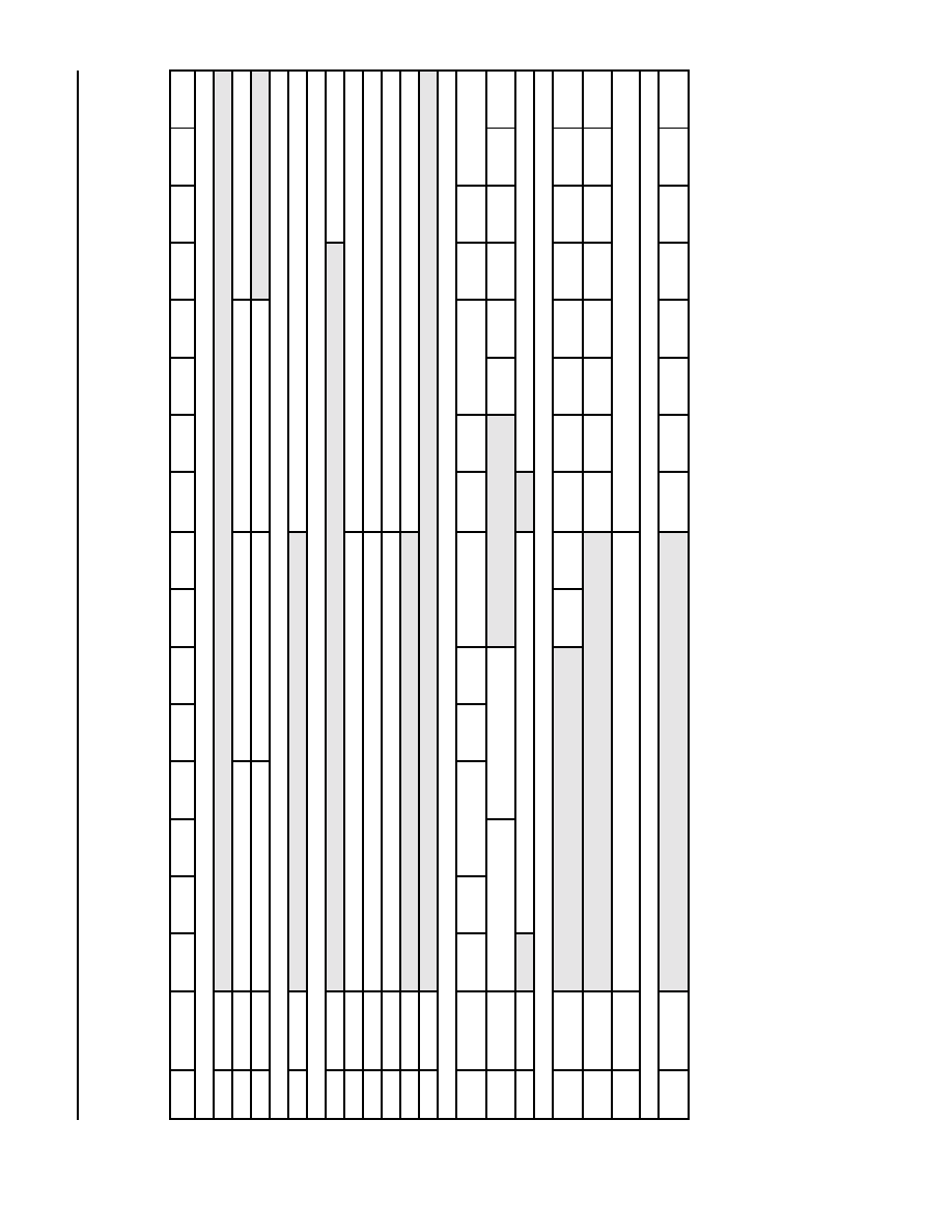
TMXF28155 Super Mapper
Preliminary Data Sheet
155/51 Mbits/s SONET/SDH x28/x21 DS1/E1
May 2001
150
Agere Systems Inc.
9 SPE Mapper Registers
(continued)
Table 166. SPE Mapper Register Map (continued)
Address
Symbol
Bit 15
Bit 14
Bit 13
Bit 12
Bit 11
Bit 10
Bit 9
Bit 8
Bit 7
Bit 6
Bit 5
Bit 4
Bit 3
Bit 2
Bit 1
Bit 0
Continuous N-Times Detect Values--R/W
0x3000E
--
0x3000F
SPE_CNTD1
SPE_CNTDC2[3:0]
SPE_CNTDF3[3:0]
SPE_CNTDF2[3:0]
SPE_CNTDJ1[3:0]
0x30010
SPE_CNTD2
SPE_CNTDN1[3:0]
SPE_CNTDPRDI[3:0]
SPE_CNTDK3[3:0]
Receive Overhead Expected Value for C2 Byte--R/W
0x30011
SPE_ROHC2
SPE_C2DEXP[7:0]
Receive Monitor Values--RO
0x30012
SPE_RMON1
SPE_PRDIDMON[2:0]
0x30013
SPE_RMON2
SPE_N1DMON[7:0]
SPE_K3DMON[7:0]
0x30014
SPE_RMON3
SPE_F2DMON1[7:0]
SPE_F2DMON0[7:0]
0x30015
SPE_RMON4
SPE_F3DMON1[7:0]
SPE_F3DMON0[7:0]
0x30016
SPE_RMON5
SPE_C2DMON[7:0]
0x30017
--
Transmit/Receive Control Parameters for Mapping Functions--R/W
0x30018
SPE_MAP_CTL1 SPE_T_ST
S1_MODE
SPE_T_NS
MI_MODE
SPE_TDS3SRCTYP[1:0]
SPE_T_
VT_DS3
SPE_T_
AU3_TUG3
SPE_TSTS3TMSLOT[1:0] SPE_R_STS
1_MODE
SPE_R_NS
MI_MODE
SPE_RDS3OUTTYP[1:0]
SPE_R_
VT_DS3
SPE_R_
AU3_TUG3
SPE_RSTS3TMSLOT[1:0]
0x30019
SPE_MAP_CTL2
SPE_T_NSMI_BIT[2:0]
SPE_R_NSMI_BIT[2:0]
SPE_TDS3
CLK_EDGE
SPE_PHDE
TUP_INV
SPE_PHDE
TDN_INV
SPE_TDS3
BPV_IN
SPE_TDS3
_BIPOLAR
SPE_RDS3
_BIPOLAR
0x3001A
SPE_MAP_CTL3
SPE_T_NSMI_COL[6:0]
SPE_R_NSMI_COL[6:0]
Transmit Control Parameters for Alarm and Overhead Functions--R/W
0x3001B
SPE_TAOH_
CTL1
SPE_TD_
OEPAR
SPE_TREIR
DISEL
SPE_
TAISPINS
SPE_
TN1INS
SPE_
TK3INS
SPE_
TH4INS
SPE_
TF3INS
SPE_
TF2INS
SPE_
TC2INS
SPE_
TJ1INS
0x3001C
SPE_TAOH_
CTL2
SPE_TPOA
C_OEPMON
SPE_
TPOAC_N1
SPE_
TPOAC_K3
SPE_
TPOAC_H4
SPE_
TPOAC_F3
SPE_
TPOAC_F2
SPE_
TPOAC_C2
SPE_
TPOAC_J1
0x3001D
SPE_TAOH_
CTL3
SPE_NPI_BYTE2[7:0]
SPE_NPI_BYTE1[7:0]
Transmit Path RDI and REI Control Parameters--R/W
0x3001E
SPE_TRDIREI_
CTL
SPE_TPRDII
NS
SPE_TTIM_
PRDIINH
SPE_TPLM
_PRDIINH
SPE_TUNE
Q_PRDIINH
SPE_TLOP
_PRDIINH
SPE_TPAIS
_PRDIINH
SPE_TPRDI
_MODE
SPE_TREIP
_INH
Preliminary Data Sheet
TMXF28155 Super Mapper
May 2001
155/51 Mbits/s SONET/SDH x28/x21 DS1/E1
151
Agere Systems Inc.
9 SPE Mapper Registers
(continued)
Table 166. SPE Mapper Register Map (continued)
Address
Symbol
Bit 15
Bit 14
Bit 13
Bit 12
Bit 11
Bit 10
Bit 9
Bit 8
Bit 7
Bit 6
Bit 5
Bit 4
Bit 3
Bit 2
Bit 1
Bit 0
Transmit Error Insertion Control Parameters--R/W
0x3001F
SPE_TERRINS_CTL
SPE_BERR_INS
SPE_TB3ERRINS SPE_TREIERRINS
Transmit OH Insert Value--R/W
0x30020
SPE_TOHINS1
SPE_TF3DINS[7:0]
SPE_TF2DINS[7:0]
0x30021
SPE_TOHINS2
SPE_TC2DINS[7:0]
SPE_TK3DINS[7:0]
0x30022
SPE_TOHINS3
SPE_TG1DINS[7:0]
SPE_TN1DINS[7:0]
0x30023
SPE_TOHINS4
SPE_TH4DINS[7:0]
Signal Degrade Set/Clear Control Registers--R/W
0x30024
SPE_SIGDEG_CTL1
SPE_SDNSSET[18:3]
0x30025
SPE_SIGDEG_CTL2
SPE_SDMSET[7:0]
SPE_SDLSET[3:0]
SPE_SDNSSET[2:0]
0x30026
SPE_SIGDEG_CTL3
SPE_SDBSET[15:0]
0x30027
SPE_SIGDEG_CTL4
SPE_SDNSCLEAR[18:3]
0x30028
SPE_SIGDEG_CTL5
SPE_SDMCLEAR[7:0]
SPE_SDLCLEAR[3:0]
SPE_SDNSCLEAR[2:0]
0x30029
SPE_SIGDEG_CTL6
SPE_SDBCLEAR[15:0]
Signal Fail Set/Clear Control Registers--R/W
0x3002A
SPE_SIGFAIL_CTL1
SPE_SFNSSET[18:3]
0x3002B
SPE_SIGFAIL_CTL2
SPE_SFMSET[7:0]
SPE_SFLSET[3:0]
SPE_SFNSSET[2:0]
0x3002C
SPE_SIGFAIL_CTL3
SPE_SFBSET[15:0]
0x3002D
SPE_SIGFAIL_CTL4
SPE_SFNSCLEAR[18:3]
0x3002E
SPE_SIGFAIL_CTL5
SPE_SFMCLEAR[7:0]
SPE_SFLCLEAR[3:0]
SPE_SFNSCLEAR[2:0]
0x3002F
SPE_SIGFAIL_CTL6
SPE_SFBCLEAR[15:0]
TMXF28155 Super Mapper
Preliminary Data Sheet
155/51 Mbits/s SONET/SDH x28/x21 DS1/E1
May 2001
152
Agere Systems Inc.
9 SPE Mapper Registers
(continued)
Table 166. SPE Mapper Register Map (continued)
Addr
Symbol
Bit 15
Bit 14
Bit 13
Bit 12
Bit 11
Bit 10
Bit 9
Bit 8
Bit 7
Bit 6
Bit 5
Bit 4
Bit 3
Bit 2
Bit 1
Bit 0
B3 and G1 Error Counts--RO
0x30030
SPE_ERRCNT1
SPE_B3ECNT[15:0]
0x30031
SPE_ERRCNT2
SPE_G1ECNT[15:0]
0x30032
--
Bipolar Violation and Excess Zero Counts for DS3--RO
0x30033
SPE_ERRCNT3
SPE_BIPOL_CNT[23:16]
0x30034
SPE_ERRCNT4
SPE_BIPOL_CNT[15:0]
0x30035
SPE_ERRCNT5
SPE_EXZ_CNT[23:16]
0x30036
SPE_ERRCNT6
SPE_EXZ_CNT[15:0]
Receive Pointer Increment and Decrement Counts--RO
0x30037
SPE_PTRCNT1
SPE_STORED_PTR[9:0]
0x30038
SPE_PTRCNT2
SPE_RPTR_INC[10:0]
0x30039
SPE_PTRCNT3
SPE_RPTR_DEC[10:0]
0x3003A
--
0x30041
--
J1 Byte Receive Monitor--RO
0x30042
--
0x30061
SPE_RJ1MON_R1
--
SPE_RJ1MON_R32
SPE_RJ1DMON[2][7:0]
--
SPE_RJ1DMON[64][7:0]
SPE_RJ1DMON[1][7:0]
--
SPE_RJ1DMON[63][7:0]
J1 Byte Transmit Insert--R/W
0x30062
--
0x30081
SPE_TJ1DINS_R1
--
SPE_TJ1DINS_R32
SPE_TJ1DINS[2][7:0]
--
SPE_TJ1DINS[64][7:0]
SPE_TJ1DINS[1][7:0]
--
SPE_TJ1DINS[63][7:0]
J1 Byte Expected Values--R/W
0x30082
--
0x300A1
SPE_RJ1DEXP_R1
--
SPE_RJ1DEXP_R32
SPE_RJ1DEXP[2][7:0]
--
SPE_RJ1DEXP[64][7:0]
SPE_RJ1DEXP[1][7:0]
--
SPE_RJ1DEXP[63][7:0]
Scratch Register--R/W
0x300A2
SPE_SCRATCH_R
SPE_SCRATCH[15:0]
0x300A3
--
0x301FF
--

Preliminary Data Sheet
TMXF28155/51 Super Mapper
May 2001
155/51 Mbits/s SONET/SDH x28/x21 DS1/E1
153
Agere Systems Inc.
10 VT/TU Mapper Registers
Table of Contents
Contents
Page
10 VT/TU Mapper Registers ................................................................................................................................ 153
10.1 VT/TU Mapper Register Descriptions ..................................................................................................... 154
10.2 VT/TU Mapper Register Map .................................................................................................................. 171
Tables
Page
Table 167. VT_VERSION_R, VT Mapper Ready, Version, and Identification (RO) ............................................ 154
Table 168. VT_GDELTA, VT Global Deltas (COR/COW) ................................................................................... 154
Table 169. VT_REVENT_DELTA[1--28], Receive Event and Delta Per Channel (COR/COW) ........................ 155
Table 170. VT_LOPOHFAIL_EVENT, Low-Order Path Overhead Failure Event (COR/COW) .......................... 155
Table 171. VT_TEVENT_DELTA[1--28], Transmit Event and Delta Per Channel (COR/COW) ........................ 156
Table 172. VT_GMASK, VT Global Masks (R/W) ............................................................................................... 156
Table 173. VT_RMASK[1--28], Receive Masks Per Channel (R/W) .................................................................. 157
Table 174. VT_LOPOHFAIL_MASK, Low-Order Path Overhead Failure Mask (R/W) ....................................... 158
Table 175. VT_TMASK[1--28], Transmit Masks Per Channel (R/W) ................................................................. 158
Table 176. VT_GSTATE, VT Global State (RO) ................................................................................................. 158
Table 177. VT_RSTATE[1--28], Receive State Per Channel (RO) .................................................................... 159
Table 178. VT_RAPSSTATE[1--28], Receive APS State Per Channel (RO) ..................................................... 159
Table 179. VT_TSTATE[1--28], Transmit State Per Channel (RO) ................................................................... 159
Table 180. VT_GCTL1, VT Global Control Register 1 (R/W) .............................................................................. 160
Table 181. VT_GCTL2, VT Global Control Register 2 (R/W) .............................................................................. 160
Table 182. VT_GCTL3, VT Global Control Register 3 (R/W) .............................................................................. 161
Table 183. VT_GCTL4, VT Global Control Register 4 (R/W) .............................................................................. 161
Table 184. VT_GCTL5, VT Global Control Register 5 (R/W) .............................................................................. 162
Table 185. VT_SIGDEG_CTL1, Signal Degrade Control Register 1 (R/W) ........................................................ 163
Table 186. VT_SIGDEG_CTL2, Signal Degrade Control Register 2 (R/W) ........................................................ 163
Table 187. VT_SIGDEG_CTL3, Signal Degrade Control Register 3 (R/W) ........................................................ 163
Table 188. VT_SIGDEG_CTL4, Signal Degrade Control Register 4 (R/W) ........................................................ 163
Table 189. VT_SIGDEG_CTL5, Signal Degrade Control Register 5 (R/W) ........................................................ 164
Table 190. VT_SIGDEG_CTL6, Signal Degrade Control Register 6 (R/W) ........................................................ 164
Table 191. VT_SIGDEG_CTL7, Signal Degrade Control Register 7 (R/W) ........................................................ 164
Table 192. VT_SIGFAIL_CTL1, Signal Fail Control Register 1 (R/W) ................................................................ 164
Table 193. VT_SIGFAIL_CTL2, Signal Fail Control Register 2 (R/W) ................................................................ 164
Table 194. VT_SIGFAIL_CTL3, Signal Fail Control Register 3 (R/W) ................................................................ 164
Table 195. VT_SIGFAIL_CTL4, Signal Fail Control Register 4 (R/W) ................................................................ 165
Table 196. VT_SIGFAIL_CTL5, Signal Fail Control Register 5 (R/W) ................................................................ 165
Table 197. VT_SIGFAIL_CTL6, Signal Fail Control Register 6 (R/W) ................................................................ 165
Table 198. VT_TCTL[1--28], Transmit Control Per Channel (R/W) ................................................................... 166
Table 199. VT_TTUOH_CTL[1--28], Transmit TU Overhead Control Per Channel (R/W) ................................. 167
Table 200. VT_TAPSRIVAL[1--28], Transmit APS and Remote Indication Per Channel (R/W) ........................ 167
Table 201. VT_TSWOW[1--28], Transmit Software Overwrite Per Channel (R/W) ........................................... 167
Table 202. VT_TSIG_CTL[1--28], Transmit Signaling Control Per Channel (R/W) ........................................... 168
Table 203. VT_J2BYTE_INS_R[1--28][1--16], J2 Insert Values Per Channel (R/W) ........................................ 168
Table 204. VT_RCTL[1--28], Receive Control Per Channel (R/W) .................................................................... 168
Table 205. VT_RTUOH_CTL[1--28], Receive TU Overhead Control Per Channel (RO) ................................... 169
Table 206. VT_RBIP2_CNT[1--28], Receive BIP-2 Error Count Per Channel (RO) .......................................... 169
Table 207. VT_RREIV_CNT[1--28], Receive REI-V Error Count Per Channel (RO) ......................................... 169
Table 208. VT_RPTR_CNT[1--28], Receive Pointer and Count Per Channel (RO) .......................................... 170
Table 209. VT_J2BYTE_EXP_R[1--28][1--16], J2 Expected Values Per Channel (R/W, RO) ......................... 170
Table 210. VT_THRES_CTL[1--28], Transmit Elastic Store Threshold Control (R/W) ...................................... 170
Table 211. VT/TU Mapper Register Map ............................................................................................................. 171

TMXF28155/51 Super Mapper
Preliminary Data Sheet
155/51 Mbits/s SONET/SDH x28/x21 DS1/E1
May 2001
154
Agere Systems Inc.
10 VT/TU Mapper Registers
(continued)
10.1 VT/TU Mapper Register Descriptions
The following tables describe the functions of all bits in the register map. For each address, the register bits are
indicated as either read/write (R/W) or read only (RO), and the value of the bits on reset is given.
Table 167. VT_VERSION_R, VT Mapper Ready, Version, and Identification (RO)
Table 168. VT_GDELTA, VT Global Deltas (COR/COW)
Address
Bit
Name
Function
Reset
Default
0x20000
15
VT_RDY
VT/TU Mapper Ready. A 1 indicates that the VT/TU map-
per is ready for microprocessor reads and writes.
0x0
14:11
--
Reserved. 0x0
10:8
VT_VERSION[2:0]
Block Version Number. These bits identify the version
number of the VT/TU mapper.
NA
7:0
VT_ID[7:0]
Block ID Number. VT_ID returns a fixed value (0x02)
when read.
0x02
Address
Bit
Name
Function
Reset
Default
0x20001
15:3
--
Reserved. 0x000
2
VT_SD_D
VT/TU Signal Degrade Delta Bit. Logic 1 indicates a
change in the signal degrade condition based on the inter-
nal bit error rate detector.
0x1
1
VT_SF_D
VT/TU Signal Fail Delta Bit. Logic 1 indicates a change
in the signal fail condition based on the internal bit error
rate detector.
0x1
0
VT_H4LOMF_D
H4 Mismatch Delta Bit. Logic 1 indicates a change in the
H4 loss of multiframe condition.
0x1

Preliminary Data Sheet
TMXF28155/51 Super Mapper
May 2001
155/51 Mbits/s SONET/SDH x28/x21 DS1/E1
155
Agere Systems Inc.
10 VT/TU Mapper Registers
(continued)
Table 169. VT_REVENT_DELTA[1--28], Receive Event and Delta Per Channel (COR/COW)
Table 170. VT_LOPOHFAIL_EVENT, Low-Order Path Overhead Failure Event (COR/COW)
Address
Bit
Name
Function
Reset
Default
0x20002
--
0x2001D
15
--
Reserved.
0
14
VT_RX_VTREI_E[1--28]
Receive REI-V Event Bit. Logic 1 indicates that
REI-V was received.
0x0
13
VT_RX_BIP2ERR_E[1--28] Receive BIP-2 Error Event Bit. Logic 1 indicates
that BIP-2 errors have been detected.
0x0
12
VT_RX_ESOVFL_E[1--28]
Receive Elastic Store Overflow Event Bit. Logic
one indicates an elastic store overflow.
0x0
11
VT_APS_D[1--28]
ERDI-V Delta Bit. Logic 1 indicates a VTAPS
change of value.
0x1
10
VT_ERDI_D[1--28]
ERDI-V Delta Bit. Logic 1 indicates an ERDI-V
change of value.
0x1
9
VT_RDI_D[1--28]
RDI-V Delta Bit. Logic 1 indicates an RDI-V
change of value.
0x1
8
VT_RFI_D[1--28]
RFI-V Delta Bit. Logic 1 indicates an RFI-V
change of value.
0x1
7
--
Reserved.
0
6
VT_LOPS_D[1--28]
VT Loss of Phase Sync Delta Bit. Logic 1 indi-
cates a change of VTLOPS state.
0x1
5
VT_J2TIM_D[1--28]
J2 Trace Identifier Mismatch. Logic 1 indicates a
change of J2TIM state.
0x1
4
VT_PLM_D[1--28]
VT Payload Label Mismatch Delta Bit. Logic 1
indicates a change of VTPLM state.
0x1
3
VT_UNEQ_D[1--28]
VT Unequip Delta Bit. Logic 1 indicates a change
of VTUNEQ state.
0x1
2
VT_SIZERR_D[1--28]
VT Size Error Delta Bit. Logic 1 indicates a
change of VTSIZERR state.
0x1
1
VT_AIS_D[1--28]
AIS-V Delta Bit. Logic 1 indicates a change of
VTAIS state.
0x0
0
VT_LOP_D[1--28]
LOP-V Delta Bit. Logic 1 indicates a change of
VTLOP state.
0x1
Address
Bit
Name
Function
Reset
Default
0x2001E
15:1
--
Reserved. 0x000
0
VT_LOPOH_FAIL_E
Low-Order Path Overhead Failure Event Bit. Logic 1
indicates that a failure has occurred on the LOPOH
serial access channel.
0x0

TMXF28155/51 Super Mapper
Preliminary Data Sheet
155/51 Mbits/s SONET/SDH x28/x21 DS1/E1
May 2001
156
Agere Systems Inc.
10 VT/TU Mapper Registers
(continued)
Table 171. VT_TEVENT_DELTA[1--28], Transmit Event and Delta Per Channel (COR/COW)
Table 172. VT_GMASK, VT Global Masks (R/W)
Address
Bit
Name
Function
Reset
Default
0x2001F
--
0x2003A
15:5
--
Reserved. 0x000
4
VT_TX_ESOVFL_E[1--28] Transmit Elastic Store Overflow Event Bit. Logic
1 indicates an elastic store overflow.
0x0
3
--
Reserved.
0
2
VT_LOFS_D[1--28]
Loss of Frame Sync Delta Bit. Logic 1 indicates a
change of VT_LOFS[1--28] (
Table 179
) state.
0x1
1
VT_TX_AIS_D[1--28]
Transmit AIS Delta Bit. Logic 1 indicates a change
of VT_TX_AIS[1--28] (
Table 179
) state.
0x0
0
VT_TX_LOC_D[1--28]
Transmit Loss of Clock Delta Bit. Logic 1 indi-
cates a change of VT_TX_LOC[1--28] (
Table 179
)
state.
0x1
Address
Bit
Name
Function
Reset
Default
0x2003B
15:3
--
Reserved. 0x000
2
VT_SD_M
VT/TU Signal Degrade Mask Bit. If set to a logic 1,
VT_SD_D (
Table 168
) will not contribute to the interrupt.
0x1
1
VT_SF_M
VT/TU Signal Fail Mask Bit. If set to a logic 1, VT_SF_D
(
Table 168
) will not contribute to the interrupt.
0x1
0
VT_H4LOMF_M
H4 Mismatch Mask Bit. If set to a logic 1,
VT_H4LOMF_D (
Table 168
) will not contribute to the
interrupt.
0x1

Preliminary Data Sheet
TMXF28155/51 Super Mapper
May 2001
155/51 Mbits/s SONET/SDH x28/x21 DS1/E1
157
Agere Systems Inc.
10 VT/TU Mapper Registers
(continued)
Table 173. VT_RMASK[1--28], Receive Masks Per Channel (R/W)
Note: The event and delta bits for these mask bits are in
Table 169
.
Address
Bit
Name
Function
Reset
Default
0x2003C
--
0x20057
15
--
Reserved.
0
14
VT_RX_VTREI_M[1--28]
Receive REI-V Mask Bit. If set to a logic 1,
VT_RX_VTREI_E[1--28] will not contribute to the inter-
rupt.
0x1
13
VT_RX_BIP2ERR_M[1--28] Receive BIP-2 Error Mask Bit. If set to a logic 1,
VT_RX_BIP2ERR_E[1--28] will not contribute to the
interrupt.
0x1
12
VT_RX_ESOVFL_M[1--28] Receive Elastic Store Overflow Mask Bit. If set to a
logic 1, VT_RX_ESOVFL_E[1--28] will not contribute to
the interrupt.
0x1
11
VT_APS_M[1--28]
VT APS Mask Bit. If set to a logic 1, VT_APS_D[1--28]
will not contribute to the interrupt.
0x1
10
VT_ERDI_M[1--28]
ERDI-V Mask Bit. If set to a logic 1, VT_ERDI_D[1--28]
will not contribute to the interrupt.
0x1
9
VT_RDI_M[1--28]
RDI-V Mask Bit. If set to a logic 1, VT_RDI_D[1--28] will
not contribute to the interrupt.
0x1
8
VT_RFI_M[1--28]
RFI-V Mask Bit. If set to a logic 1, VT_RFI_D[1--28] will
not contribute to the interrupt.
0x1
7
--
Reserved.
0
6
VT_LOPS_M[1--28]
VT Loss of Phase Sync Mask Bit. If set to a logic 1,
VT_LOPS_D[1--28] will not contribute to the interrupt.
0x1
5
VT_J2TIM_M[1--28]
J2 Mismatch Mask Bit. If set to a logic 1,
VT_J2TIM_D[1--28] will not contribute to the interrupt.
0x1
4
VT_PLM_M[1--28]
VT Payload Label Mismatch Mask Bit. If set to a logic
1, VT_PLM_D[1--28] will not contribute to the interrupt.
0x1
3
VT_UNEQ_M[1--28]
VT Unequip Mask Bit. If set to a logic 1,
VT_UNEQ_D[1--28] will not contribute to the interrupt.
0x1
2
VT_SIZERR_M[1--28]
VT Size Error Mask Bit. If set to a logic 1,
VT_SIZERR_D[1--28] will not contribute to the interrupt.
0x1
1
VT_AIS_M[1--28]
AIS-V Mask Bit. If set to a logic 1, VT_AIS_D[1--28] will
not contribute to the interrupt.
0x1
0
VT_LOP_M[1--28]
LOP-V Mask Bit. If set to a logic 1, VT_LOP_D[1--28]
will not contribute to the interrupt.
0x1

TMXF28155/51 Super Mapper
Preliminary Data Sheet
155/51 Mbits/s SONET/SDH x28/x21 DS1/E1
May 2001
158
Agere Systems Inc.
10 VT/TU Mapper Registers
(continued)
Table 174. VT_LOPOHFAIL_MASK, Low-Order Path Overhead Failure Mask (R/W)
Table 175. VT_TMASK[1--28], Transmit Masks Per Channel (R/W)
Table 176. VT_GSTATE, VT Global State (RO)
Address
Bit
Name
Function
Reset
Default
0x20058
15:1
--
Reserved. 0x000
0
VT_LOPOH_FAIL_M
Low-Order Path Overhead Failure Mask Bit. If set to a
logic 1, VT_LOPOH_FAIL_E (
Table 170
) will not contrib-
ute to the interrupt.
0x1
Address
Bit
Name
Function
Reset
Default
0x20059
--
0x20074
15:5
--
Reserved. 0x000
4
VT_TX_ESOVFL_M[1--28] Transmit Elastic Store Overflow Mask Bit. If set
to a logic 1, VT_TX_ESOVFL_E[1--28] (
Table 171
)
will not contribute to the interrupt.
0x1
3
RESERVED
Reserved.
0
2
VT_LOFS_M[1--28]
Loss of Frame Sync Mask Bit. If set to a logic 1,
VT_LOFS_D[1--28] (
Table 171
) will not contribute
to the interrupt.
0x1
1
VT_TX_AIS_M[1--28]
Transmit AIS Mask Bit. If set to a logic 1,
VT_TX_AIS_D[1--28] (
Table 171
) will not contrib-
ute to the interrupt.
0x1
0
VT_TX_LOC_M[1--28]
Transmit Loss of Clock Mask Bit. If set to a logic
1, VT_TX_LOC_D[1--28] (
Table 171
) will not con-
tribute to the interrupt.
0x1
Address
Bit
Name
Function
Reset
Default
0x20075
15:3
--
Reserved. 0x000
2
VT_SD
VT/TU Signal Degrade. Logic 1 indicates a signal
degrade condition on the selected channel.
0x1
1
VT_SF
VT/TU Signal Fail. Logic 1 indicates a signal fail condition
on the selected channel.
0x1
0
VT_H4LOMF
H4 Loss of Multiframe. Logic 1 indicates a loss of H4
multiframe alignment.
0x1

Preliminary Data Sheet
TMXF28155/51 Super Mapper
May 2001
155/51 Mbits/s SONET/SDH x28/x21 DS1/E1
159
Agere Systems Inc.
10 VT/TU Mapper Registers
(continued)
Table 177. VT_RSTATE[1--28], Receive State Per Channel (RO)
Table 178. VT_RAPSSTATE[1--28], Receive APS State Per Channel (RO)
Table 179. VT_TSTATE[1--28], Transmit State Per Channel (RO)
Address
Bit
Name
Function
Reset
Default
0x20076
--
0x20091
15:13
VT_ERDI[1--28][2:0]
Enhanced RDI-V Value. These bits are the stored ERDI-V
bits received in the Z7 byte.
0x000
12:10
VT_LAB[1--28][2:0]
VT Signal Label. These bits are the stored VT signal label
bits received in the V5 byte.
0x000
9
VT_RDI[1--28]
RDI-V Value. This bit is the accepted RDI-V bit received in
the V5 byte.
0x00
8
VT_RFI[1--28]
RFI-V Value. This bit is the accepted RFI-V bit received in
the V5 byte.
0x00
7
--
Reserved.
0
6
VT_LOPS[1--28]
VT Loss of Phase Sync. Logic 1 indicates a loss of P-bit
phase synchronization.
0x1
5
VT_J2TIM[1--28]
J2 Trace Identifier Mismatch. Logic 1 indicates a mis-
match between the expected trace and the detected trace.
0x1
4
VT_PLM[1--28]
VT Payload Label Mismatch. Logic 1 indicates PLM-V.
0x1
3
VT_UNEQ[1--28]
VT Unequip. Logic 1 indicates UNEQ-V.
0x1
2
VT_SIZERR[1--28]
VT Size Error. Logic 1 indicates a VT size error.
0x1
1
VT_AIS[1--28]
AIS-V. Logic 1 indicates AIS-V.
0x0
0
VT_LOP[1--28]
LOP-V. Logic 1 indicates LOP-V.
0x1
Address
Bit
Name
Function
Reset
Default
0x20092
--
0x200AD
15:4
--
Reserved. 0x000
3:0
VT_APS[1--28][3:0]
VT APS Value. These bits are the stored VT APS bits
received in the Z7/K4 byte.
0x0
Address
Bit
Name
Function
Reset
Default
0x200AE
--
0x200C9
15:3
--
Reserved. 0x000
2
VT_LOFS[1--28]
Loss of Frame Sync. Logic 1 indicates DS1/E1 loss of
frame sync.
0x1
1
VT_TX_AIS[1--28]
Transmit AIS. Logic 1 indicates DS1/E1 AIS.
0x0
0
VT_TX_LOC[1--28]
Transmit Loss of Clock. Logic 1 indicates DS1/E1 loss
of clock.
0x1

TMXF28155/51 Super Mapper
Preliminary Data Sheet
155/51 Mbits/s SONET/SDH x28/x21 DS1/E1
May 2001
160
Agere Systems Inc.
10 VT/TU Mapper Registers
(continued)
Table 180. VT_GCTL1, VT Global Control Register 1 (R/W)
Table 181. VT_GCTL2, VT Global Control Register 2 (R/W)
Address
Bit
Name
Function
Reset
Default
0x200CA
15
--
Reserved.
0
14:8
VT_RX_GRP_TYPE[6:0] Receive Group Type. VT/TU group type selection.
Logic 1 selects VT1.5/TU-11 and logic 0 selects
VT2/TU-12 group type. Group 1 is the LSB.
0x7F
7
--
Reserved.
0
6:0
VT_TX_GRP_TYPE[6:0] Transmit Group Type. VT/TU group type selection.
Logic 1 selects VT1.5/TU-11 and logic 0 selects
VT2/TU-12 group type. Group 1 is the LSB.
0x7F
Address
Bit
Name
Function
Reset
Default
0x200CB 15:11
--
Reserved. 0x00
10
VT_LOPS_AIS_INH
VT/TU Loss of Phase Sync. Contribution to AIS inhibit
control.
0x0
9
VT_J2TIM_ERDI_INH J2 Trace Identifier Mismatch. Contribution to ERDI
inhibit control.
0x0
8
VT_J2TIM_RDI_INH
J2 Trace Identifier Mismatch. Contribution to RDI inhibit
control.
0x0
7
VT_J2TIM_AIS_INH
J2 Trace Identifier Mismatch. Contribution to AIS inhibit
control.
0x0
6
VT_LOMF_AIS_INH
Loss of Multiframe. Contribution to AIS inhibit control.
0x0
5
VT_PLM_AIS_INH
Payload Label Mismatch. Contribution to AIS inhibit con-
trol.
0x0
4
VT_UNEQ_AIS_INH
UNEQ-V. Contribution to AIS inhibit control.
0x0
3
--
Reserved.
0
2
VT_UPSR
Unidirectional Path Switch Ring Mode Control. Logic 1
activates the UPSR mode of operation. When the device
is programmed for UPSR mode, the transmitted REI-V,
RDI-V, RFI-V, and ERDI-V are based on the receive condi-
tions. Otherwise, the transmitted LOPOH is a copy of the
received overhead bytes.
0x0
1
VT_8ORMAJORITY
VT Pointer Interpreter Mode Control. Logic 1 tells the
pointer interpreter to transition into the inc and dec states
based on 8 of the 10 I and D bits. Otherwise, the pointer
interpreter transitions into the inc and dec states based on
majority rule.
0x1
0
VT_BIT_BLOCK_CNT Performance Monitor Count Mode Control. Logic 1
activates BIP-2, TC-BIP-2, REI, and TC-CRC-7 counts
based on single bit errors. Otherwise, errors are counted
on a block basis.
0x1

Preliminary Data Sheet
TMXF28155/51 Super Mapper
May 2001
155/51 Mbits/s SONET/SDH x28/x21 DS1/E1
161
Agere Systems Inc.
10 VT/TU Mapper Registers
(continued)
Table 182. VT_GCTL3, VT Global Control Register 3 (R/W)
Table 183. VT_GCTL4, VT Global Control Register 4 (R/W)
Address
Bit
Name
Function
Reset
Default
0x200CC
15:8
--
Reserved. 0x00
7:4
VT_LOPS_NTIME[3:0] VT/TU Loss of Phase Sync NTIME Detection Control.
This nibble is programmed to provision the number of con-
secutive errored phase indications required to transition
into the VT_LOPS[1--28] (
Table 177
) state. Only valid in
byte synchronous mode.
Note: The valid range of values is 0x1--0xF. A value of
0x0 will be mapped to 0x1.
0x6
3:0
VT_H4_NTIME[3:0]
H4 Multiframe Indication NTIME Detection Control.
This nibble is programmed to provision the number of con-
secutive errored multiframe indications required to transi-
tion into the VT_H4LOMF (
Table 176
) state.
Note: The valid range of values is 0x1--0xF. A value of
0x0 will be mapped to 0x1.
0x6
Address
Bit
Name
Function
Reset
Default
0x200CD
15:11
VT_Z6_NTIME[3:0]
Z6 Byte Monitor NTIME Detection Control. This nibble
is programmed to provision the number of consecutive
consistent Z6 bytes required to accept a new value.
Note: The valid range of values is 0x1--0xF. A value of
0x0 will be mapped to 0x1.
0x3
11:8
VT_J2_NTIME[3:0]
J2 Byte Monitor NTIME Detection Control. This nibble
is programmed to provision the number of consecutive
consistent J2 sequences required for the J2 byte monitor
to transition in and out of J2TIM.
Note: The valid range of values is 0x1--0xF. A value of
0x0 will be mapped to 0x1.
0x3
7:4
VT_INV_NTIME[3:0]
Pointer Interpreter Invalid Pointer NTIME Detection
Control. This nibble is programmed to provision the
number of invalid pointers required for the pointer inter-
preter to go into the VT_LOP[1--28] (
Table 177
) state.
Note: The valid range of values is 0x1--0xF. A value of
0x0 will be mapped to 0x1.
0x8
3:0
VT_NDF_NTIME[3:0]
Pointer Interpreter NDF Pointer NTIME Detection
Control. This nibble is programmed to provision the
number of consecutive NDF pointers required for the
pointer interpreter to go into the VT_LOP state.
Note: The valid range of values is 0x1--0xF. A value of
0x0 will be mapped to 0x1.
0x8

TMXF28155/51 Super Mapper
Preliminary Data Sheet
155/51 Mbits/s SONET/SDH x28/x21 DS1/E1
May 2001
162
Agere Systems Inc.
10 VT/TU Mapper Registers
(continued)
Table 184. VT_GCTL5, VT Global Control Register 5 (R/W)
Address
Bit
Name
Function
Reset
Default
0x200CE 15:12
VT_APS_NTIME[3:0]
APS NTIME Detection Control. This nibble is programmed
to provision the number of consecutive consistent new values
required to accept a new VT_APS[1--28][3:0] (
Table 178
).
Note: The valid range of values is 0x1--0xF. A value of 0x0
will be mapped to 0x1.
0x3
11:8
VT_LAB_NTIME[3:0]
VT Signal Label NTIME Detection Control. This nibble is
programmed to provision the number of consecutive consis-
tent new values required to accept a new
VT_LAB[1--28][2:0] (
Table 177
).
Note: The valid range of values is 0x1--0xF. A value of 0x0
will be mapped to 0x1.
0x3
7:4
VT_ERDI_NTIME[3:0] ERDI-V NTIME Detection Control. This nibble is pro-
grammed to provision the number of consecutive consistent
new values required to accept a new VT_ERDI[1--28][2:0]
(
Table 177
).
Note: The valid range of values is 0x1--0xF. A value of 0x0
will be mapped to 0x1.
0x3
3:0
VT_RDI_NTIME[3:0]
RDI-V NTIME Detection Control. This nibble is pro-
grammed to provision the number of consecutive consistent
new values required to accept a new VT_RDI[1--28]
(
Table 177
).
Note: The valid range of values is 0x1--0xF. A value of 0x0
will be mapped to 0x1.
0x3

Preliminary Data Sheet
TMXF28155/51 Super Mapper
May 2001
155/51 Mbits/s SONET/SDH x28/x21 DS1/E1
163
Agere Systems Inc.
10 VT/TU Mapper Registers
(continued)
Table 185. VT_SIGDEG_CTL1, Signal Degrade Control Register 1 (R/W)
Table 186. VT_SIGDEG_CTL2, Signal Degrade Control Register 2 (R/W)
Table 187. VT_SIGDEG_CTL3, Signal Degrade Control Register 3 (R/W)
Table 188. VT_SIGDEG_CTL4, Signal Degrade Control Register 4 (R/W)
Address
Bit
Name
Function
Reset
Default
0x200CF 15:12
--
Reserved. 0x00
11
VT_SFCLEAR
VT Signal Fail Clear. Allows the signal fail algorithm to be
forced into the normal state. This is a one shot which is
activated by a 0 to 1 transition.
0x0
10
VT_SFSET
VT Signal Fail Set. Allows the signal fail algorithm to be
forced into the failed state. This is a one shot which is acti-
vated by a 0 to 1 transition.
0x0
9
VT_SDCLEAR
Signal Degrade Clear. Allows the signal degrade algo-
rithm to be forced into the normal state. This is a one shot
which is activated by a 0 to 1 transition.
0x0
8
VT_SDSET
Signal Degrade Set. Allows the signal degrade algorithm
to be forced into the failed state. This is a one shot which
is activated by a 0 to 1 transition.
0x0
7:5
--
Reserved. 000
4:0
VT_BER_CH_
SEL[4:0]
Bit Error Rate Monitor Channel Select. Selects which
channel (1--28/21) is being monitored by the internal
BER monitor. Valid inputs are 00001--11100.
0x00
Address
Bit
Name
Function
Reset
Default
0x200D0
15:0
VT_SDNSSET[18:3]
Signal Degrade Ns Set. Number of frames in a monitor-
ing block for SD.
0x0000
Address
Bit
Name
Function
Reset
Default
0x200D1
15
--
Reserved.
0
14:7
VT_SDMSET[7:0]
Signal Degrade M Set. Threshold of the number of bad
monitoring blocks in an observation interval. If the number
of bad blocks is above this threshold, then signal degrade
SD is set.
0x00
6:3
VT_SDLSET[3:0]
Signal Degrade L Set. Error threshold for determining if a
monitoring block is bad.
0x0
2:0
VT_SDNSSET[2:0]
Signal Degrade Ns Set. Number of frames in a monitor-
ing block for SD.
0x0
Address
Bit
Name
Function
Reset
Default
0x200D2
15:0
VT_SDBSET[15:0]
Signal Degrade B Set. Number of monitoring blocks.
0x0000

TMXF28155/51 Super Mapper
Preliminary Data Sheet
155/51 Mbits/s SONET/SDH x28/x21 DS1/E1
May 2001
164
Agere Systems Inc.
10 VT/TU Mapper Registers
(continued)
Table 189. VT_SIGDEG_CTL5, Signal Degrade Control Register 5 (R/W)
Table 190. VT_SIGDEG_CTL6, Signal Degrade Control Register 6 (R/W)
Table 191. VT_SIGDEG_CTL7, Signal Degrade Control Register 7 (R/W)
Table 192. VT_SIGFAIL_CTL1, Signal Fail Control Register 1 (R/W)
Table 193. VT_SIGFAIL_CTL2, Signal Fail Control Register 2 (R/W)
Table 194. VT_SIGFAIL_CTL3, Signal Fail Control Register 3 (R/W)
Address
Bit
Name
Function
Reset
Default
0x200D3
15:0
VT_SDNSCLEAR[18:3] Signal Degrade Ns Clear. Number of frames in a moni-
toring block for SD.
0x0000
Address
Bit
Name
Function
Reset
Default
0x200D4
15
--
Reserved.
0
14:7
VT_SDMCLEAR[7:0]
Signal Degrade M Clear. Threshold of the number of bad
monitoring blocks in an observation interval. If the number
of bad blocks is below this threshold, then SD is cleared.
0x00
6:3
VT_SDLCLEAR[3:0]
Signal Degrade L Clear. Error threshold for determining if
a monitoring block is bad.
0x0
2:0
VT_SDNSCLEAR[2:0] Signal Degrade Ns Clear. Number of frames in a moni-
toring block for SD.
0x0
Address
Bit
Name
Function
Reset
Default
0x200D5
15:0
VT_SDBCLEAR[15:0] Signal Degrade B Clear. Number of monitoring blocks.
0x0000
Address
Bit
Name
Function
Reset
Default
0x200D6 15:0 VT_SFNSSET[18:3] Signal Fail Ns Set. Number of frames in a monitoring block for SF. 0x0000
Address
Bit
Name
Function
Reset
Default
0x200D7
15
--
Reserved.
0
14:7
VT_SFMSET[7:0] Signal Fail M Set. Threshold of the number of bad monitoring
blocks in an observation interval. If the number of bad blocks is
above this threshold, then SF is set.
0x00
6:3
VT_SFLSET[3:0]
Signal Fail L Set. Error threshold for determining if a monitoring
block is bad.
0x0
2:0
VT_SFNSSET[2:0] Signal Fail Ns Set. Number of frames in a monitoring block for SF.
0x0
Address
Bit
Name
Function
Reset
Default
0x200D8
15:0
VT_SFBSET[15:0]
Signal Fail B Set. Number of monitoring blocks.
0x0000

Preliminary Data Sheet
TMXF28155/51 Super Mapper
May 2001
155/51 Mbits/s SONET/SDH x28/x21 DS1/E1
165
Agere Systems Inc.
10 VT/TU Mapper Registers
(continued)
Table 195. VT_SIGFAIL_CTL4, Signal Fail Control Register 4 (R/W)
Table 196. VT_SIGFAIL_CTL5, Signal Fail Control Register 5 (R/W)
Table 197. VT_SIGFAIL_CTL6, Signal Fail Control Register 6 (R/W)
Address
Bit
Name
Function
Reset
Default
0x200D9
15:0
VT_SFNSCLEAR[18:3]
Signal Fail Ns Clear. Number of frames in a monitoring
block for SF.
0x0000
Address
Bit
Name
Function
Reset
Default
0x200DA
15
--
Reserved.
0
14:7
VT_SFMCLEAR[7:0]
Signal Fail M Clear. Threshold of the number of bad
monitoring blocks in an observation interval. If the
number of bad blocks is below this threshold, then SF is
cleared.
0x00
6:3
VT_SFLCLEAR[3:0]
Signal Fail L Clear. Error threshold for determining if a
monitoring block is bad.
0x0
2:0
VT_SFNSCLEAR[2:0] Signal Fail Ns Clear. Number of frames in a monitoring
block for SF.
0x0
Address
Bit
Name
Function
Reset
Default
0x200DB
15:0
VT_SFBCLEAR[15:0]
Signal Fail B Clear. Number of monitoring blocks.
0x0000

TMXF28155/51 Super Mapper
Preliminary Data Sheet
155/51 Mbits/s SONET/SDH x28/x21 DS1/E1
May 2001
166
Agere Systems Inc.
10 VT/TU Mapper Registers
(continued)
Table 198. VT_TCTL[1--28], Transmit Control Per Channel (R/W)
Address
Bit
Name
Function
Reset
Default
0x200DC
--
0x200F7
15:13
--
Reserved. 0x0
12
VT_TX_ERDI_EN[1--28]
Transmit Path Enhanced RDI-V Enable. Logic one
enables enhanced RDI-V.
0x0
11
VT_ERDI_EN[1--28]
Enhanced RDI-V Source Selection. Logic one acti-
vates software overwrite of the ERDI-V bits of the Z7
byte. Otherwise, insertion is based on the LOPOH
serial channel or automatic generation.
0x0
10
VT_RDI_EN[1--28]
RDI-V Source Selection. Logic one activates software
overwrite of the RDI-V bit of the V5 byte. Otherwise,
insertion is based on the LOPOH serial channel or
automatic generation.
0x0
9
VT_RFI_EN[1--28]
RFI-V Source Selection. Logic one activates software
overwrite of the RFI-V bit of the V5 byte. If
VT_V5_INS[1--28] = 0 (
Table 199
) and the mapping is
set to byte synchronous DS1, a logic zero enables
automatic insertion of RFI-V. If VT_V5_INS[1--28] = 1,
a logic zero inserts RFI-V based on the LOPOH serial
channel.
0x0
8
VT_REI_EN[1--28]
REI-V Enable. Logic one activates automatic genera-
tion of REI-V. If VT_V5_INS[1--28] = 0, the generation
is based on the received BIP-2 errors. Otherwise,
insertion is based on the LOPOH serial channel.
0x0
7
--
Reserved.
0
6
VT_AIS_INS[1--28]
AIS-V Insertion Control. Logic one forces AIS-V to be
transmitted in the specified channel.
0x0
5
VT_TX_CLKEDGE[1--28] Transmit Path DS1/E1 Clock Edge Selection. Logic
one forces the DS1/E1 signals to be retimed using the
rising edge of the associated clock. Logic zero forces
the DS1/E1 signals to be retimed using the falling edge
of the associated clock.
0x0
4
VT_LB_SEL[1--28]
Tributary Loopback Selection. Logic one activates
tributary loopback.
0x0
3:0
VT_TX_MAPTYPE
[1--28][3:0]
Transmit Mapping Mode Control. See
Table 558
.
0x6

Preliminary Data Sheet
TMXF28155/51 Super Mapper
May 2001
155/51 Mbits/s SONET/SDH x28/x21 DS1/E1
167
Agere Systems Inc.
10 VT/TU Mapper Registers
(continued)
Table 199. VT_TTUOH_CTL[1--28], Transmit TU Overhead Control Per Channel (R/W)
Table 200. VT_TAPSRIVAL[1--28], Transmit APS and Remote Indication Per Channel (R/W)
Table 201. VT_TSWOW[1--28], Transmit Software Overwrite Per Channel (R/W)
Address
Bit
Name
Function
Reset
Default
0x200F8
--
0x20113
15:11
--
Reserved. 0x00
10:9
VT_O_INS[1--28][1:0]
O-Bit Insertion Control. See
Table 566 on page446
.
0x0
8:7
VT_Z7_INS[1--28][1:0] Z7 Byte Insertion Control. See
Table 565, Z7/K4 Over-
head Byte Insertion Modes Per Channel on page446
.
0x0
6:5
VT_Z6_INS[1--28][1:0] Z6 Byte Insertion Control. See
Table 564, Z6/N2 Over-
head Byte Insertion Modes Per Channel on page445
.
0x0
4:3
VT_J2_INS[1--28][1:0] J2 Byte Insertion Control. See
Table 563, J2 Overhead
Byte Insertion Modes Per Channel on page 445
.
0x0
2
VT_V5_INS[1--28]
V5 Byte Insertion Control. Logic one forces the V5 byte
to be programmed via the LOPOH serial channel. See
Table 559 on pag e443
.
0x0
1:0
VT_BIP2ERR_
INS[1--28][1:0]
BIP-2 Error Insertion Control. See
Table 560 on
page 443
.
0x0
Address
Bit
Name
Function
Reset
Default
0x20114
--
0x2012F
15:12
--
Reserved. 0x0
11:8
VT_APS_
INS[1--28][3:0]
APS Software Overwrite Value. This nibble is pro-
grammed to utilize APS bits in the Z7/K4 byte. This nibble
will be transmitted in bits 1:4 of the Z7/K4 byte.
0x0
7:5
--
Reserved. 0x0
4:2
VT_ERDI_
INS[1--28][2:0]
Enhanced RDI-V Software Overwrite Values. If
VT_ERDI_EN[1--28] (
Table 198
) is a logic one, these bits
are written into the ERDI-V locations of the Z7 byte.
0x0
1
VT_RDI_INS[1--28]
RDI-V Software Overwrite Values. If VT_RDI_EN[1--28]
(
Table 198
) is a logic one, this value will be written into the
RDI-V location of the V5 byte.
0x0
0
VT_RFI_INS[1--28]
RFI-V Software Overwrite Values. If VT_RFI_EN[1--28]
(
Table 198
) is a logic one, this value will be written into the
RFI-V location of the V5 byte.
0x0
Address
Bit
Name
Function
Reset
Default
0x20130
--
0x2014B
15:8
VT_OBIT_
INS[1--28][7:0]
Overhead Values for Software Overwrite in Asyn-
chronous Mappings. This byte is programmed to utilize
the overhead bits in asynchronous VT/TU mappings.
VT_OBIT_INS[7:4] will be transmitted in the byte follow-
ing J2 and VT_OBIT_INS[3:0] will be transmitted in the
byte following Z6/N2.
0x00
7:0
VT_Z6BYTE_
INS[1--28][7:0]
Z6 Software Overwrite Values. This byte is pro-
grammed into the outgoing Z6/N2 location when
VT_Z6_INS[1--28][1:0] (
Table 199
) = 01.
0x00

TMXF28155/51 Super Mapper
Preliminary Data Sheet
155/51 Mbits/s SONET/SDH x28/x21 DS1/E1
May 2001
168
Agere Systems Inc.
10 VT/TU Mapper Registers
(continued)
Table 202. VT_TSIG_CTL[1--28], Transmit Signaling Control Per Channel (R/W)
Table 203. VT_J2BYTE_INS_R[1--28][1--16], J2 Insert Values Per Channel (R/W)
Address
Bit
Name
Function
Reset
Default
0x2014C
--
0x20167
15:11
--
Reserved. 000000
10
VT_USE_FBIT[1--28]
Frame Bit Use Control. Logic one provisions
use of the F bit in the outgoing VT/TU. Other-
wise, the F bit is forced to the value of bit
SMPR_OH_DEFLT (
Table 67
) in the micropro-
cessor interface on the outgoing VT/TU.
0x1
9
VT_USE_PBIT[1--28]
Phase Bit Use Control. Logic one provisions
use of the P bits in the outgoing VT/TU. Other-
wise, the P bits are forced to the value of bit
SMPR_OH_DEFLT in the microprocessor inter-
face on the outgoing VT/TU.
0x1
8
VT_USE_SBIT[1--28]
Signaling Bit Use Control. Logic one provi-
sions use of the S bits in the outgoing VT/TU.
Otherwise, the S bits are forced to the value of
bit SMPR_OH_DEFLT in the microprocessor
interface on the outgoing VT/TU.
0x1
7:5
--
Reserved. 000
4:0
VT_TXSIG_CH_SEL[1--28][4:0]
Transmit Input Channel Selection. These bits
are programmed with the same value as the
cross connect for each individual channel. The
bits are only used in byte synchronous mode
and can be set to 0xXX for all other modes. If an
invalid value is programmed,
UNEQ-V will be transmitted in the specified
channel. Invalid decimal values are 0, 29, 30,
and 31.
0x00
Address
Bit
Name
Function
Reset
Default
0x20168
--
0x20327
15:8
--
Reserved. 0x00
7:0
VT_J2BYTE_
INS[1--28][1--16][7:0]
J2 Software Overwrite Values. These values are written
into the outgoing J2 byte when VT_J2_INS[1--28][1:0] = 01
(
Table 199
).
0x00
Table 204. VT_RCTL[1--28], Receive Control Per Channel (R/W)
Address
Bit
Name
Function
Reset
Default
0x20328
--
0x20343
15
VT_SF_ESF[1--28]
DS1 Frame Type for Byte Synchronous Mode. Logic
one provisions an SF frame format. Otherwise, an ESF
frame format is provisioned.
0x0
14
VT_WR_FBIT[1--28]
F-Bit Provisioning Control. See
Table 556, Rx Signal-
ing Behavior per Channel on page 439
.
0x0
13
VT_SYNC_PBIT[1--28]
P-Bit Provisioning Control. See
Table 556, Rx Signal-
ing Behavior per Channel on page 439
.
0x0

Preliminary Data Sheet
TMXF28155/51 Super Mapper
June 2001
155/51 Mbits/s SONET/SDH x28/x21 DS1/E1
10 VT/TU Mapper Registers
(continued)
169
Agere Systems Inc.
Table 205. VT_RTUOH_CTL[1--28], Receive TU Overhead Control Per Channel (RO)
Table 206. VT_RBIP2_CNT[1--28], Receive BIP-2 Error Count Per Channel (RO)
Table 207. VT_RREIV_CNT[1--28], Receive REI-V Error Count Per Channel (RO)
0x20328
--
0x20343
12:8
VT_RXSIG_CH_
SEL[1--28][4:0]
Receive Output Channel Selection. These bits are pro-
grammed with the same value as the cross connect for
each individual channel. The bits are only used in byte
synchronous mode and can be set to 0xXX for all other
modes. If an invalid value is programmed, UNEQ-V will
be transmitted in the specified channel. Invalid decimal
values are 0, 29, 30, and 31. See
Rx Signaling Behavior
per Channel on page 439
.
0x00
7:5
VT_J2MON_
MODE[1--28][2:0]
J2 Trace Monitoring Mode Control.
See J2 Byte Moni-
tor and Termination (J2MON) on page 438.
0x00
4
VT_RX_ERDI_EN[1--28] Receive Path Enhanced RDI-V Enable. Logic one
enables enhanced RDI-V.
0x0
3:0
VT_RX_
MAPTYPE[1--28][3:0]
Receive Demapping Mode Control. See
Table 555,
Receive VT/TU Demapping Selection on page 437
.
0x6
Address
Bit
Name
Function
Reset
Default
0x20344
--
0x2035F
15:8
VT_Z6_BYTE[1--28][7:0] Received Z6/N2 Byte Value. Accepted Z6/N2 value.
0x00
7:0
VT_OBITS[1--28][7:0]
Received O Bits Value. Accepted overhead bits in asyn-
chronous and bit synchronous modes. VT_OBITS[7:4]
are the O bits received in the byte following J2, and
VT_OBITS[3:0] are the O bits received in the byte follow-
ing Z6/N2.
0x00
Address
Bit
Name
Function
Reset
Default
0x20360
--
0x2037B
15:12
--
Reserved. 0x0
11:0
VT_BIP2ERR_
CNT[1--28][11:0]
BIP-2 Error Count. BIP-2 error count updated on a 0 to
1 transition of SMPR_PMRESET (
Table 65
).
0x000
Address
Bit
Name
Function
Reset
Default
0x2037C
--
0x20397
15:11
--
Reserved. 0x00
10:0
VT_REI_
CNT[1--28][10:0]
REI-V Error Count. REI-V error count updated on a 0 to 1
transition of SMPR_PMRESET.
0x000
Table 204. VT_RCTL[1--28], Receive Control Per Channel (R/W) (continued)
Address
Bit
Name
Function
Reset
Default

TMXF28155/51 Super Mapper
Preliminary Data Sheet
155/51 Mbits/s SONET/SDH x28/x21 DS1/E1
May 2001
170
Agere Systems Inc.
10 VT/TU Mapper Registers
(continued)
Table 208. VT_RPTR_CNT[1--28], Receive Pointer and Count Per Channel (RO)
Table 209. VT_J2BYTE_EXP_R[1--28][1--16], J2 Expected Values Per Channel (R/W, RO)
Address
Bit
Name
Function
Reset
Default
0x20398
--
0x203B3
15:8
VT_STORED_
PTR[1--28][7:0]
Store VT/TU Pointer Location. This value indicates the
stored location of the V5 byte within the VT/TU mapping.
0x00
7:4
VT_PTR_
DEC[1--28][3:0]
VT Pointer Decrement Count. VT pointer decrement
count updated on a 0 to 1 transition of
SMPR_PMRESET.
0x0
3:0
VT_PTR_
INC[1--28][3:0]
VT Pointer Increment Count. VT pointer increment
count updated on a 0 to 1 transition of
SMPR_PMRESET.
0x0
Address
Bit
Name
Function
Reset
Default
0x203B4
--
0x20573
15:8
VT_J2BYTE_
EXP[1--28][1--16][7:0]
J2 Expected Values. This value is programmed by the
user as an expected value for the J2 byte. The hardware
will compare this value to the incoming J2 sequence
when VT_J2MON_MODE[1--28][2:0] = 011 or 100
(
Table 204 on pag e168
).
0x00
7:0
VT_J2BYTE_
DET[1--28][1--16][7:0]
J2 Detected Values. Accepted J2 sequence or value.
0x00
Table 210. VT_THRES_CTL[1--28], Transmit Elastic Store Threshold Control (R/W)
Address
Bit
Name
Function
Reset
Default
0x20574
--
0x2058F
15
--
Reserved. 0x0
14:8
VT_HIGH_
THRES[1--28][6:0]
Transmit Elastic Store High Threshold. Programmable
threshold controlling positive justifications.
0x28
7
--
Reserved. 0x0
6:0
VT_LOW_
THRES[1--28][6:0]
Transmit Elastic Store Low Threshold. Programmable
threshold controlling negative justifications.
0x27

Preliminary Data Sheet
TMXF28155 Super Mapper
May 2001
155/51 Mbits/s SONET/SDH x28/x21 DS1/E1
171
Agere Systems Inc.
10 VT/TU Mapper Registers
(continued)
10.2 VT/TU Mapper Register Map
Table 211. VT/TU Mapper Register Map
Note: The reset default of all reserved bits is 0. Shading denotes reserved bits.
Address
Symbol
Bit 15
Bit 14
Bit 13
Bit 12
Bit 11
Bit 10
Bit 9
Bit 8
Bit 7
Bit 6
Bit 5
Bit 4
Bit 3
Bit 2
Bit 1
Bit 0
VT Mapper ID--RO
0x20000
VT_VERSION_R
VT_
RDY
VT_VERSION[2:0]
VT_ID[7:0]
VT Global Events--COR/COW
0x20001
VT_GDELETA
VT_SD_D
VT_SF_D
VT_H4LOMF_
D
Receive Delta and Event Parameters--COR/COW
0x20002
VT_REVENT_DELTA1
VT_RX_VTREI_E1
VT_RX_BIP2ERR_E1
VT_RX_ESOVFL_E1
VT_APS_D1
VT_ERDI_D1
VT_RDI_D1
VT_RFI_D1
VT_LOPS_D1
VT_J2TIM_D1
VT_PLM_D1
VT_UNEQ_D1
VT_SIZERR_D1
VT_AIS_D1
VT_LOP_D1
0x20003
VT_REVENT_DELTA2
VT_RX_VTREI_E2
VT_RX_BIP2ERR_E2
VT_RX_ESOVFL_E2
VT_APS_D2
VT_ERDI_D2
VT_RDI_D2
VT_RFI_D2
VT_LOPS_D2
VT_J2TIM_D2
VT_PLM_D2
VT_UNEQ_D2
VT_SIZERR_D2
VT_AIS_D2
VT_LOP_D2
0x20004
VT_REVENT_DELTA3
VT_RX_VTREI_E3
VT_RX_BIP2ERR_E3
VT_RX_ESOVFL_E3
VT_APS_D3
VT_ERDI_D3
VT_RDI_D3
VT_RFI_D3
VT_LOPS_D3
VT_J2TIM_D3
VT_PLM_D3
VT_UNEQ_D3
VT_SIZERR_D3
VT_AIS_D3
VT_LOP_D3
0x20005
VT_REVENT_DELTA4
VT_RX_VTREI_E4
VT_RX_BIP2ERR_E4
VT_RX_ESOVFL_E4
VT_APS_D4
VT_ERDI_D4
VT_RDI_D4
VT_RFI_D4
VT_LOPS_D4
VT_J2TIM_D4
VT_PLM_D4
VT_UNEQ_D4
VT_SIZERR_D4
VT_AIS_D4
VT_LOP_D4
0x20006
VT_REVENT_DELTA5
VT_RX_VTREI_E5
VT_RX_BIP2ERR_E5
VT_RX_ESOVFL_E5
VT_APS_D5
VT_ERDI_D5
VT_RDI_D5
VT_RFI_D5
VT_LOPS_D5
VT_J2TIM_D5
VT_PLM_D5
VT_UNEQ_D5
VT_SIZERR_D5
VT_AIS_D5
VT_LOP_D5
0x20007
VT_REVENT_DELTA6
VT_RX_VTREI_E6
VT_RX_BIP2ERR_E6
VT_RX_ESOVFL_E6
VT_APS_D6
VT_ERDI_D6
VT_RDI_D6
VT_RFI_D6
VT_LOPS_D6
VT_J2TIM_D6
VT_PLM_D6
VT_UNEQ_D6
VT_SIZERR_D6
VT_AIS_D6
VT_LOP_D6
0x20008
VT_REVENT_DELTA7
VT_RX_VTREI_E7
VT_RX_BIP2ERR_E7
VT_RX_ESOVFL_E7
VT_APS_D7
VT_ERDI_D7
VT_RDI_D7
VT_RFI_D7
VT_LOPS_D7
VT_J2TIM_D7
VT_PLM_D7
VT_UNEQ_D7
VT_SIZERR_D7
VT_AIS_D7
VT_LOP_D7
0x20009
VT_REVENT_DELTA8
VT_RX_VTREI_E8
VT_RX_BIP2ERR_E8
VT_RX_ESOVFL_E8
VT_APS_D8
VT_ERDI_D8
VT_RDI_D8
VT_RFI_D8
VT_LOPS_D8
VT_J2TIM_D8
VT_PLM_D8
VT_UNEQ_D8
VT_SIZERR_D8
VT_AIS_D8
VT_LOP_D8
0x2000A
VT_REVENT_DELTA9
VT_RX_VTREI_E9
VT_RX_BIP2ERR_E9
VT_RX_ESOVFL_E9
VT_APS_D9
VT_ERDI_D9
VT_RDI_D9
VT_RFI_D9
VT_LOPS_D9
VT_J2TIM_D9
VT_PLM_D9
VT_UNEQ_D9
VT_SIZERR_D9
VT_AIS_D9
VT_LOP_D9
0x2000B
VT_REVENT_DELTA10
VT_RX_VTREI_E10 VT_RX_BIP2ERR_E10 VT_RX_ESOVFL_E10 VT_APS_D10 VT_ERDI_D10 VT_RDI_D10 VT_RFI_D10
VT_LOPS_D10 VT_J2TIM_D10 VT_PLM_D10 VT_UNEQ_D10 VT_SIZERR_D10 VT_AIS_D10 VT_LOP_D10
0x2000C
VT_REVENT_DELTA11
VT_RX_VTREI_E11 VT_RX_BIP2ERR_E11 VT_RX_ESOVFL_E11 VT_APS_D11 VT_ERDI_D11 VT_RDI_D11 VT_RFI_D11
VT_LOPS_D11 VT_J2TIM_D11 VT_PLM_D11 VT_UNEQ_D11 VT_SIZERR_D11 VT_AIS_D11 VT_LOP_D11
0x2000D
VT_REVENT_DELTA12
VT_RX_VTREI_E12 VT_RX_BIP2ERR_E12 VT_RX_ESOVFL_E12 VT_APS_D12 VT_ERDI_D12 VT_RDI_D12 VT_RFI_D12
VT_LOPS_D12 VT_J2TIM_D12 VT_PLM_D12 VT_UNEQ_D12 VT_SIZERR_D12 VT_AIS_D12 VT_LOP_D12
0x2000E
VT_REVENT_DELTA13
VT_RX_VTREI_E13 VT_RX_BIP2ERR_E13 VT_RX_ESOVFL_E13 VT_APS_D13 VT_ERDI_D13 VT_RDI_D13 VT_RFI_D13
VT_LOPS_D13 VT_J2TIM_D13 VT_PLM_D13 VT_UNEQ_D13 VT_SIZERR_D13 VT_AIS_D13 VT_LOP_D13
0x2000F
VT_REVENT_DELTA14
VT_RX_VTREI_E14 VT_RX_BIP2ERR_E14 VT_RX_ESOVFL_E14 VT_APS_D14 VT_ERDI_D14 VT_RDI_D14 VT_RFI_D14
VT_LOPS_D14 VT_J2TIM_D14 VT_PLM_D14 VT_UNEQ_D14 VT_SIZERR_D14 VT_AIS_D14 VT_LOP_D14
0x20010
VT_REVENT_DELTA15
VT_RX_VTREI_E15 VT_RX_BIP2ERR_E15 VT_RX_ESOVFL_E15 VT_APS_D15 VT_ERDI_D15 VT_RDI_D15 VT_RFI_D15
VT_LOPS_D15 VT_J2TIM_D15 VT_PLM_D15 VT_UNEQ_D15 VT_SIZERR_D15 VT_AIS_D15 VT_LOP_D15
0x20011
VT_REVENT_DELTA16
VT_RX_VTREI_E16 VT_RX_BIP2ERR_E16 VT_RX_ESOVFL_E16 VT_APS_D16 VT_ERDI_D16 VT_RDI_D16 VT_RFI_D16
VT_LOPS_D16 VT_J2TIM_D16 VT_PLM_D16 VT_UNEQ_D16 VT_SIZERR_D16 VT_AIS_D16 VT_LOP_D16
0x20012
VT_REVENT_DELTA17
VT_RX_VTREI_E17 VT_RX_BIP2ERR_E17 VT_RX_ESOVFL_E17 VT_APS_D17 VT_ERDI_D17 VT_RDI_D17 VT_RFI_D17
VT_LOPS_D17 VT_J2TIM_D17 VT_PLM_D17 VT_UNEQ_D17 VT_SIZERR_D17 VT_AIS_D17 VT_LOP_D17
0x20013
VT_REVENT_DELTA18
VT_RX_VTREI_E18 VT_RX_BIP2ERR_E18 VT_RX_ESOVFL_E18 VT_APS_D18 VT_ERDI_D18 VT_RDI_D18 VT_RFI_D18
VT_LOPS_D18 VT_J2TIM_D18 VT_PLM_D18 VT_UNEQ_D18 VT_SIZERR_D18 VT_AIS_D18 VT_LOP_D18
0x20014
VT_REVENT_DELTA19
VT_RX_VTREI_E19 VT_RX_BIP2ERR_E19 VT_RX_ESOVFL_E19 VT_APS_D19 VT_ERDI_D19 VT_RDI_D19 VT_RFI_D19
VT_LOPS_D19 VT_J2TIM_D19 VT_PLM_D19 VT_UNEQ_D19 VT_SIZERR_D19 VT_AIS_D19 VT_LOP_D19
0x20015
VT_REVENT_DELTA20
VT_RX_VTREI_E20 VT_RX_BIP2ERR_E20 VT_RX_ESOVFL_E20 VT_APS_D20 VT_ERDI_D20 VT_RDI_D20 VT_RFI_D20
VT_LOPS_D20 VT_J2TIM_D20 VT_PLM_D20 VT_UNEQ_D20 VT_SIZERR_D20 VT_AIS_D20 VT_LOP_D20
0x20016
VT_REVENT_DELTA21
VT_RX_VTREI_E21 VT_RX_BIP2ERR_E21 VT_RX_ESOVFL_E21 VT_APS_D21 VT_ERDI_D21 VT_RDI_D21 VT_RFI_D21
VT_LOPS_D21 VT_J2TIM_D21 VT_PLM_D21 VT_UNEQ_D21 VT_SIZERR_D21 VT_AIS_D21 VT_LOP_D21
0x20017
VT_REVENT_DELTA22
VT_RX_VTREI_E22 VT_RX_BIP2ERR_E22 VT_RX_ESOVFL_E22 VT_APS_D22 VT_ERDI_D22 VT_RDI_D22 VT_RFI_D22
VT_LOPS_D22 VT_J2TIM_D22 VT_PLM_D22 VT_UNEQ_D22 VT_SIZERR_D22 VT_AIS_D22 VT_LOP_D22
0x20018
VT_REVENT_DELTA23
VT_RX_VTREI_E23 VT_RX_BIP2ERR_E23 VT_RX_ESOVFL_E23 VT_APS_D23 VT_ERDI_D23 VT_RDI_D23 VT_RFI_D23
VT_LOPS_D23 VT_J2TIM_D23 VT_PLM_D23 VT_UNEQ_D23 VT_SIZERR_D23 VT_AIS_D23 VT_LOP_D23
0x20019
VT_REVENT_DELTA24
VT_RX_VTREI_E24 VT_RX_BIP2ERR_E24 VT_RX_ESOVFL_E24 VT_APS_D24 VT_ERDI_D24 VT_RDI_D24 VT_RFI_D24
VT_LOPS_D24 VT_J2TIM_D24 VT_PLM_D24 VT_UNEQ_D24 VT_SIZERR_D24 VT_AIS_D24 VT_LOP_D24
0x2001A
VT_REVENT_DELTA25
VT_RX_VTREI_E25 VT_RX_BIP2ERR_E25 VT_RX_ESOVFL_E25 VT_APS_D25 VT_ERDI_D25 VT_RDI_D25 VT_RFI_D25
VT_LOPS_D25 VT_J2TIM_D25 VT_PLM_D25 VT_UNEQ_D25 VT_SIZERR_D25 VT_AIS_D25 VT_LOP_D25
0x2001B
VT_REVENT_DELTA26
VT_RX_VTREI_E26 VT_RX_BIP2ERR_E26 VT_RX_ESOVFL_E26 VT_APS_D26 VT_ERDI_D26 VT_RDI_D26 VT_RFI_D26
VT_LOPS_D26 VT_J2TIM_D26 VT_PLM_D26 VT_UNEQ_D26 VT_SIZERR_D26 VT_AIS_D26 VT_LOP_D26
0x2001C
VT_REVENT_DELTA27
VT_RX_VTREI_E27 VT_RX_BIP2ERR_E27 VT_RX_ESOVFL_E27 VT_APS_D27 VT_ERDI_D27 VT_RDI_D27 VT_RFI_D27
VT_LOPS_D27 VT_J2TIM_D27 VT_PLM_D27 VT_UNEQ_D27 VT_SIZERR_D27 VT_AIS_D27 VT_LOP_D27
0x2001D
VT_REVENT_DELTA28
VT_RX_VTREI_E28 VT_RX_BIP2ERR_E28 VT_RX_ESOVFL_E28 VT_APS_D28 VT_ERDI_D28 VT_RDI_D28 VT_RFI_D28
VT_LOPS_D28 VT_J2TIM_D28 VT_PLM_D28 VT_UNEQ_D28 VT_SIZERR_D28 VT_AIS_D28 VT_LOP_D28

TMXF28155 Super Mapper
Preliminary Data Sheet
155/51 Mbits/s SONET/SDH x28/x21 DS1/E1
May 2001
172
Agere Systems Inc.
10 VT/TU Mapper Registers
(continued)
Table 211. VT/TU Mapper Register Map (continued)
Address
Symbol
Bit 15
Bit 14
Bit 13
Bit 12
Bit 11
Bit 10
Bit 9
Bit 8
Bit 7
Bit 6
Bit 5
Bit 4
Bit 3
Bit 2
Bit 1
Bit 0
Transmit Delta and Event Parameters--COR/COW
0x2001E
VT_LOPOHFAIL_EVENT
VT_LOPOH_FAIL_
E
0x2001F
VT_TEVENT_DELTA1
VT_TX_ESOVFL_E1
VT_LOFS_D1
VT_TX_AIS_D1
VT_TX_LOC_D1
0x20020
VT_TEVENT_DELTA2
VT_TX_ESOVFL_E2
VT_LOFS_D2
VT_TX_AIS_D2
VT_TX_LOC_D2
0x20021
VT_TEVENT_DELTA3
VT_TX_ESOVFL_E3
VT_LOFS_D3
VT_TX_AIS_D3
VT_TX_LOC_D3
0x20022
VT_TEVENT_DELTA4
VT_TX_ESOVFL_E4
VT_LOFS_D4
VT_TX_AIS_D4
VT_TX_LOC_D4
0x20023
VT_TEVENT_DELTA5
VT_TX_ESOVFL_E5
VT_LOFS_D5
VT_TX_AIS_D5
VT_TX_LOC_D5
0x20024
VT_TEVENT_DELTA6
VT_TX_ESOVFL_E6
VT_LOFS_D6
VT_TX_AIS_D6
VT_TX_LOC_D6
0x20025
VT_TEVENT_DELTA7
VT_TX_ESOVFL_E7
VT_LOFS_D7
VT_TX_AIS_D7
VT_TX_LOC_D7
0x20026
VT_TEVENT_DELTA8
VT_TX_ESOVFL_E8
VT_LOFS_D8
VT_TX_AIS_D8
VT_TX_LOC_D8
0x20027
VT_TEVENT_DELTA9
VT_TX_ESOVFL_E9
VT_LOFS_D9
VT_TX_AIS_D9
VT_TX_LOC_D9
0x20028
VT_TEVENT_DELTA10
VT_TX_ESOVFL_E10
VT_LOFS_D10
VT_TX_AIS_D10
VT_TX_LOC_D10
0x20029
VT_TEVENT_DELTA11
VT_TX_ESOVFL_E11
VT_LOFS_D11
VT_TX_AIS_D11
VT_TX_LOC_D11
0x2002A
VT_TEVENT_DELTA12
VT_TX_ESOVFL_E12
VT_LOFS_D12
VT_TX_AIS_D12
VT_TX_LOC_D12
0x2002B
VT_TEVENT_DELTA13
VT_TX_ESOVFL_E13
VT_LOFS_D13
VT_TX_AIS_D13
VT_TX_LOC_D13
0x2002C
VT_TEVENT_DELTA14
VT_TX_ESOVFL_E14
VT_LOFS_D14
VT_TX_AIS_D14
VT_TX_LOC_D14
0x2002D
VT_TEVENT_DELTA15
VT_TX_ESOVFL_E15
VT_LOFS_D15
VT_TX_AIS_D15
VT_TX_LOC_D15
0x2002E
VT_TEVENT_DELTA16
VT_TX_ESOVFL_E16
VT_LOFS_D16
VT_TX_AIS_D16
VT_TX_LOC_D16
0x2002F
VT_TEVENT_DELTA17
VT_TX_ESOVFL_E17
VT_LOFS_D17
VT_TX_AIS_D17
VT_TX_LOC_D17
0x20030
VT_TEVENT_DELTA18
VT_TX_ESOVFL_E18
VT_LOFS_D18
VT_TX_AIS_D18
VT_TX_LOC_D18
0x20031
VT_TEVENT_DELTA19
VT_TX_ESOVFL_E19
VT_LOFS_D19
VT_TX_AIS_D19
VT_TX_LOC_D19
0x20032
VT_TEVENT_DELTA20
VT_TX_ESOVFL_E20
VT_LOFS_D20
VT_TX_AIS_D20
VT_TX_LOC_D20
0x20033
VT_TEVENT_DELTA21
VT_TX_ESOVFL_E21
VT_LOFS_D21
VT_TX_AIS_D21
VT_TX_LOC_D21
0x20034
VT_TEVENT_DELTA22
VT_TX_ESOVFL_E22
VT_LOFS_D22
VT_TX_AIS_D22
VT_TX_LOC_D22
0x20035
VT_TEVENT_DELTA23
VT_TX_ESOVFL_E23
VT_LOFS_D23
VT_TX_AIS_D23
VT_TX_LOC_D23
0x20036
VT_TEVENT_DELTA24
VT_TX_ESOVFL_E24
VT_LOFS_D24
VT_TX_AIS_D24
VT_TX_LOC_D24
0x20037
VT_TEVENT_DELTA25
VT_TX_ESOVFL_E25
VT_LOFS_D25
VT_TX_AIS_D25
VT_TX_LOC_D25
0x20038
VT_TEVENT_DELTA26
VT_TX_ESOVFL_E26
VT_LOFS_D26
VT_TX_AIS_D26
VT_TX_LOC_D26
0x20039
VT_TEVENT_DELTA27
VT_TX_ESOVFL_E27
VT_LOFS_D27
VT_TX_AIS_D27
VT_TX_LOC_D27
0x2003A
VT_TEVENT_DELTA28
VT_TX_ESOVFL_E28
VT_LOFS_D28
VT_TX_AIS_D28
VT_TX_LOC_D28
Preliminary Data Sheet
TMXF28155 Super Mapper
May 2001
155/51 Mbits/s SONET/SDH x28/x21 DS1/E1
173
Agere Systems Inc.
10 VT/TU Mapper Registers
(continued)
Table 211. VT/TU Mapper Register Map (continued)
Address
Symbol
Bit 15
Bit 14
Bit 13
Bit 12
Bit 11
Bit 10
Bit 9
Bit 8
Bit 7
Bit 6
Bit 5
Bit 4
Bit 3
Bit 2
Bit 1
Bit 0
VT Global Interrupt Masks--R/W
0x2003B
VT_GMASK
VT_SD_M
VT_SF_M
VT_H4LOMF_
M
Receive Interrupt Masks--R/W
0x2003C
VT_RMASK1
VT_RX_VTREI_M1
VT_RX_BIP2ERR_M1
VT_RX_ESOVFL_M1
VT_APS_M1
VT_ERDI_M1
VT_RDI_M1
VT_RFI_M1
VT_LOPS_M1
VT_J2TIM_M1
VT_PLM_M1
VT_UNEQ_M1
VT_SIZERR_M1
VT_AIS_M1
VT_LOP_M1
0x2003D
VT_RMASK2
VT_RX_VTREI_M2
VT_RX_BIP2ERR_M2
VT_RX_ESOVFL_M2
VT_APS_M2
VT_ERDI_M2
VT_RDI_M2
VT_RFI_M2
VT_LOPS_M2
VT_J2TIM_M2
VT_PLM_M2
VT_UNEQ_M2
VT_SIZERR_M2
VT_AIS_M2
VT_LOP_M2
0x2003E
VT_RMASK3
VT_RX_VTREI_M3
VT_RX_BIP2ERR_M3
VT_RX_ESOVFL_M3
VT_APS_M3
VT_ERDI_M3
VT_RDI_M3
VT_RFI_M3
VT_LOPS_M3
VT_J2TIM_M3
VT_PLM_M3
VT_UNEQ_M3
VT_SIZERR_M3
VT_AIS_M3
VT_LOP_M3
0x2003F
VT_RMASK4
VT_RX_VTREI_M4
VT_RX_BIP2ERR_M4
VT_RX_ESOVFL_M4
VT_APS_M4
VT_ERDI_M4
VT_RDI_M4
VT_RFI_M4
VT_LOPS_M4
VT_J2TIM_M4
VT_PLM_M4
VT_UNEQ_M4
VT_SIZERR_M4
VT_AIS_M4
VT_LOP_M4
0x20040
VT_RMASK5
VT_RX_VTREI_M5
VT_RX_BIP2ERR_M5
VT_RX_ESOVFL_M5
VT_APS_M5
VT_ERDI_M5
VT_RDI_M5
VT_RFI_M5
VT_LOPS_M5
VT_J2TIM_M5
VT_PLM_M5
VT_UNEQ_M5
VT_SIZERR_M5
VT_AIS_M5
VT_LOP_M5
0x20041
VT_RMASK6
VT_RX_VTREI_M6
VT_RX_BIP2ERR_M6
VT_RX_ESOVFL_M6
VT_APS_M6
VT_ERDI_M6
VT_RDI_M6
VT_RFI_M6
VT_LOPS_M6
VT_J2TIM_M6
VT_PLM_M6
VT_UNEQ_M6
VT_SIZERR_M6
VT_AIS_M6
VT_LOP_M6
0x20042
VT_RMASK7
VT_RX_VTREI_M7
VT_RX_BIP2ERR_M7
VT_RX_ESOVFL_M7
VT_APS_M7
VT_ERDI_M7
VT_RDI_M7
VT_RFI_M7
VT_LOPS_M7
VT_J2TIM_M7
VT_PLM_M7
VT_UNEQ_M7
VT_SIZERR_M7
VT_AIS_M7
VT_LOP_M7
0x20043
VT_RMASK8
VT_RX_VTREI_M8
VT_RX_BIP2ERR_M8
VT_RX_ESOVFL_M8
VT_APS_M8
VT_ERDI_M8
VT_RDI_M8
VT_RFI_M8
VT_LOPS_M8
VT_J2TIM_M8
VT_PLM_M8
VT_UNEQ_M8
VT_SIZERR_M8
VT_AIS_M8
VT_LOP_M8
0x20044
VT_RMASK9
VT_RX_VTREI_M9
VT_RX_BIP2ERR_M9
VT_RX_ESOVFL_M9
VT_APS_M9
VT_ERDI_M9
VT_RDI_M9
VT_RFI_M9
VT_LOPS_M9
VT_J2TIM_M9
VT_PLM_M9
VT_UNEQ_M9
VT_SIZERR_M9
VT_AIS_M9
VT_LOP_M9
0x20045
VT_RMASK10
VT_RX_VTREI_M10 VT_RX_BIP2ERR_M10 VT_RX_ESOVFL_M10 VT_APS_M10 VT_ERDI_M10
VT_RDI_M10
VT_RFI_M10
VT_LOPS_M10 VT_J2TIM_M10
VT_PLM_M10
VT_UNEQ_M10
VT_SIZERR_M10
VT_AIS_M10
VT_LOP_M10
0x20046
VT_RMASK11
VT_RX_VTREI_M11 VT_RX_BIP2ERR_M11 VT_RX_ESOVFL_M11 VT_APS_M11 VT_ERDI_M11
VT_RDI_M11
VT_RFI_M11
VT_LOPS_M11 VT_J2TIM_M11
VT_PLM_M11
VT_UNEQ_M11
VT_SIZERR_M11
VT_AIS_M11
VT_LOP_M11
0x20047
VT_RMASK12
VT_RX_VTREI_M12 VT_RX_BIP2ERR_M12 VT_RX_ESOVFL_M12 VT_APS_M12 VT_ERDI_M12
VT_RDI_M12
VT_RFI_M12
VT_LOPS_M12 VT_J2TIM_M12
VT_PLM_M12
VT_UNEQ_M12
VT_SIZERR_M12
VT_AIS_M12
VT_LOP_M12
0x20048
VT_RMASK13
VT_RX_VTREI_M13 VT_RX_BIP2ERR_M13 VT_RX_ESOVFL_M13 VT_APS_M13 VT_ERDI_M13
VT_RDI_M13
VT_RFI_M13
VT_LOPS_M13 VT_J2TIM_M13
VT_PLM_M13
VT_UNEQ_M13
VT_SIZERR_M13
VT_AIS_M13
VT_LOP_M13
0x20049
VT_RMASK14
VT_RX_VTREI_M14 VT_RX_BIP2ERR_M14 VT_RX_ESOVFL_M14 VT_APS_M14 VT_ERDI_M14
VT_RDI_M14
VT_RFI_M14
VT_LOPS_M14 VT_J2TIM_M14
VT_PLM_M14
VT_UNEQ_M14
VT_SIZERR_M14
VT_AIS_M14
VT_LOP_M14
0x2004A
VT_RMASK15
VT_RX_VTREI_M15 VT_RX_BIP2ERR_M15 VT_RX_ESOVFL_M15 VT_APS_M15 VT_ERDI_M15
VT_RDI_M15
VT_RFI_M15
VT_LOPS_M15 VT_J2TIM_M15
VT_PLM_M15
VT_UNEQ_M15
VT_SIZERR_M15
VT_AIS_M15
VT_LOP_M15
0x2004B
VT_RMASK16
VT_RX_VTREI_M16 VT_RX_BIP2ERR_M16 VT_RX_ESOVFL_M16 VT_APS_M16 VT_ERDI_M16
VT_RDI_M16
VT_RFI_M16
VT_LOPS_M16 VT_J2TIM_M16
VT_PLM_M16
VT_UNEQ_M16
VT_SIZERR_M16
VT_AIS_M16
VT_LOP_M16
0x2004C
VT_RMASK17
VT_RX_VTREI_M17 VT_RX_BIP2ERR_M17 VT_RX_ESOVFL_M17 VT_APS_M17 VT_ERDI_M17
VT_RDI_M17
VT_RFI_M17
VT_LOPS_M17 VT_J2TIM_M17
VT_PLM_M17
VT_UNEQ_M17
VT_SIZERR_M17
VT_AIS_M17
VT_LOP_M17
0x2004D
VT_RMASK18
VT_RX_VTREI_M18 VT_RX_BIP2ERR_M18 VT_RX_ESOVFL_M18 VT_APS_M18 VT_ERDI_M18
VT_RDI_M18
VT_RFI_M18
VT_LOPS_M18 VT_J2TIM_M18
VT_PLM_M18
VT_UNEQ_M18
VT_SIZERR_M18
VT_AIS_M18
VT_LOP_M18
0x2004E
VT_RMASK19
VT_RX_VTREI_M19 VT_RX_BIP2ERR_M19 VT_RX_ESOVFL_M19 VT_APS_M19 VT_ERDI_M19
VT_RDI_M19
VT_RFI_M19
VT_LOPS_M19 VT_J2TIM_M19
VT_PLM_M19
VT_UNEQ_M19
VT_SIZERR_M19
VT_AIS_M19
VT_LOP_M19
0x2004F
VT_RMASK20
VT_RX_VTREI_M20 VT_RX_BIP2ERR_M20 VT_RX_ESOVFL_M20 VT_APS_M20 VT_ERDI_M20
VT_RDI_M20
VT_RFI_M20
VT_LOPS_M20 VT_J2TIM_M20
VT_PLM_M20
VT_UNEQ_M20
VT_SIZERR_M20
VT_AIS_M20
VT_LOP_M20
0x20050
VT_RMASK21
VT_RX_VTREI_M21 VT_RX_BIP2ERR_M21 VT_RX_ESOVFL_M21 VT_APS_M21 VT_ERDI_M21
VT_RDI_M21
VT_RFI_M21
VT_LOPS_M21 VT_J2TIM_M21
VT_PLM_M21
VT_UNEQ_M21
VT_SIZERR_M21
VT_AIS_M21
VT_LOP_M21
0x20051
VT_RMASK22
VT_RX_VTREI_M22 VT_RX_BIP2ERR_M22 VT_RX_ESOVFL_M22 VT_APS_M22 VT_ERDI_M22
VT_RDI_M22
VT_RFI_M22
VT_LOPS_M22 VT_J2TIM_M22
VT_PLM_M22
VT_UNEQ_M22
VT_SIZERR_M22
VT_AIS_M22
VT_LOP_M22
0x20052
VT_RMASK23
VT_RX_VTREI_M23 VT_RX_BIP2ERR_M23 VT_RX_ESOVFL_M23 VT_APS_M23 VT_ERDI_M23
VT_RDI_M23
VT_RFI_M23
VT_LOPS_M23 VT_J2TIM_M23
VT_PLM_M23
VT_UNEQ_M23
VT_SIZERR_M23
VT_AIS_M23
VT_LOP_M23
0x20053
VT_RMASK24
VT_RX_VTREI_M24 VT_RX_BIP2ERR_M24 VT_RX_ESOVFL_M24 VT_APS_M24 VT_ERDI_M24
VT_RDI_M24
VT_RFI_M24
VT_LOPS_M24 VT_J2TIM_M24
VT_PLM_M24
VT_UNEQ_M24
VT_SIZERR_M24
VT_AIS_M24
VT_LOP_M24
0x20054
VT_RMASK25
VT_RX_VTREI_M25 VT_RX_BIP2ERR_M25 VT_RX_ESOVFL_M25 VT_APS_M25 VT_ERDI_M25
VT_RDI_M25
VT_RFI_M25
VT_LOPS_M25 VT_J2TIM_M25
VT_PLM_M25
VT_UNEQ_M25
VT_SIZERR_M25
VT_AIS_M25
VT_LOP_M25
0x20055
VT_RMASK26
VT_RX_VTREI_M26 VT_RX_BIP2ERR_M26 VT_RX_ESOVFL_M26 VT_APS_M26 VT_ERDI_M26
VT_RDI_M26
VT_RFI_M26
VT_LOPS_M26 VT_J2TIM_M26
VT_PLM_M26
VT_UNEQ_M26
VT_SIZERR_M26
VT_AIS_M26
VT_LOP_M26
0x20056
VT_RMASK27
VT_RX_VTREI_M27 VT_RX_BIP2ERR_M27 VT_RX_ESOVFL_M27 VT_APS_M27 VT_ERDI_M27
VT_RDI_M27
VT_RFI_M27
VT_LOPS_M27 VT_J2TIM_M27
VT_PLM_M27
VT_UNEQ_M27
VT_SIZERR_M27
VT_AIS_M27
VT_LOP_M27
0x20057
VT_RMASK28
VT_RX_VTREI_M28 VT_RX_BIP2ERR_M28 VT_RX_ESOVFL_M28 VT_APS_M28 VT_ERDI_M28
VT_RDI_M28
VT_RFI_M28
VT_LOPS_M28 VT_J2TIM_M28
VT_PLM_M28
VT_UNEQ_M28
VT_SIZERR_M28
VT_AIS_M28
VT_LOP_M28

TMXF28155 Super Mapper
Preliminary Data Sheet
155/51 Mbits/s SONET/SDH x28/x21 DS1/E1
May 2001
174
Agere Systems Inc.
10 VT/TU Mapper Registers
(continued)
Table 211. VT/TU Mapper Register Map (continued)
Address
Symbol
Bit 15
Bit 14
Bit 13
Bit 12
Bit 11
Bit 10
Bit 9
Bit 8
Bit 7
Bit 6
Bit 5
Bit 4
Bit 3
Bit 2
Bit 1
Bit 0
Transmit Interrupt Masks--R/W
0x20058
VT_LOPOHFAIL_MASK
VT_LOPOH_FAIL_
M
0x20059
VT_TMASK1
VT_TX_ESOVFL_M1
VT_LOFS_M1
VT_TX_AIS_M1
VT_TX_LOC_M1
0x2005A
VT_TMASK2
VT_TX_ESOVFL_M2
VT_LOFS_M2
VT_TX_AIS_M2
VT_TX_LOC_M2
0x2005B
VT_TMASK3
VT_TX_ESOVFL_M3
VT_LOFS_M3
VT_TX_AIS_M3
VT_TX_LOC_M3
0x2005C
VT_TMASK4
VT_TX_ESOVFL_M4
VT_LOFS_M4
VT_TX_AIS_M4
VT_TX_LOC_M4
0x2005D
VT_TMASK5
VT_TX_ESOVFL_M5
VT_LOFS_M5
VT_TX_AIS_M5
VT_TX_LOC_M5
0x2005E
VT_TMASK6
VT_TX_ESOVFL_M6
VT_LOFS_M6
VT_TX_AIS_M6
VT_TX_LOC_M6
0x2005F
VT_TMASK7
VT_TX_ESOVFL_M7
VT_LOFS_M7
VT_TX_AIS_M7
VT_TX_LOC_M7
0x20060
VT_TMASK8
VT_TX_ESOVFL_M8
VT_LOFS_M8
VT_TX_AIS_M8
VT_TX_LOC_M8
0x20061
VT_TMASK9
VT_TX_ESOVFL_M9
VT_LOFS_M9
VT_TX_AIS_M9
VT_TX_LOC_M9
0x20062
VT_TMASK10
VT_TX_ESOVFL_M10
VT_LOFS_M10
VT_TX_AIS_M10
VT_TX_LOC_M10
0x20063
VT_TMASK11
VT_TX_ESOVFL_M11
VT_LOFS_M11
VT_TX_AIS_M11
VT_TX_LOC_M11
0x20064
VT_TMASK12
VT_TX_ESOVFL_M12
VT_LOFS_M12
VT_TX_AIS_M12
VT_TX_LOC_M12
0x20065
VT_TMASK13
VT_TX_ESOVFL_M13
VT_LOFS_M13
VT_TX_AIS_M13
VT_TX_LOC_M13
0x20066
VT_TMASK14
VT_TX_ESOVFL_M14
VT_LOFS_M14
VT_TX_AIS_M14
VT_TX_LOC_M14
0x20067
VT_TMASK15
VT_TX_ESOVFL_M15
VT_LOFS_M15
VT_TX_AIS_M15
VT_TX_LOC_M15
0x20068
VT_TMASK16
VT_TX_ESOVFL_M16
VT_LOFS_M16
VT_TX_AIS_M16
VT_TX_LOC_M16
0x20069
VT_TMASK17
VT_TX_ESOVFL_M17
VT_LOFS_M17
VT_TX_AIS_M17
VT_TX_LOC_M17
0x2006A
VT_TMASK18
VT_TX_ESOVFL_M18
VT_LOFS_M18
VT_TX_AIS_M18
VT_TX_LOC_M18
0x2006B
VT_TMASK19
VT_TX_ESOVFL_M19
VT_LOFS_M19
VT_TX_AIS_M19
VT_TX_LOC_M19
0x2006C
VT_TMASK20
VT_TX_ESOVFL_M20
VT_LOFS_M20
VT_TX_AIS_M20
VT_TX_LOC_M20
0x2006D
VT_TMASK21
VT_TX_ESOVFL_M21
VT_LOFS_M21
VT_TX_AIS_M21
VT_TX_LOC_M21
0x2006E
VT_TMASK22
VT_TX_ESOVFL_M22
VT_LOFS_M22
VT_TX_AIS_M22
VT_TX_LOC_M22
0x2006F
VT_TMASK23
VT_TX_ESOVFL_M23
VT_LOFS_M23
VT_TX_AIS_M23
VT_TX_LOC_M23
0x20070
VT_TMASK24
VT_TX_ESOVFL_M24
VT_LOFS_M24
VT_TX_AIS_M24
VT_TX_LOC_M24
0x20071
VT_TMASK25
VT_TX_ESOVFL_M25
VT_LOFS_M25
VT_TX_AIS_M25
VT_TX_LOC_M25
0x20072
VT_TMASK26
VT_TX_ESOVFL_M26
VT_LOFS_M26
VT_TX_AIS_M26
VT_TX_LOC_M26
0x20073
VT_TMASK27
VT_TX_ESOVFL_M27
VT_LOFS_M27
VT_TX_AIS_M27
VT_TX_LOC_M27
0x20074
VT_TMASK28
VT_TX_ESOVFL_M28
VT_LOFS_M28
VT_TX_AIS_M28
VT_TX_LOC_M28
Preliminary Data Sheet
TMXF28155 Super Mapper
May 2001
155/51 Mbits/s SONET/SDH x28/x21 DS1/E1
175
Agere Systems Inc.
10 VT/TU Mapper Registers
(continued)
Table 211. VT/TU Mapper Register Map (continued)
Address
Symbol
Bit 15
Bit 14
Bit 13
Bit 12
Bit 11
Bit 10
Bit 9
Bit 8
Bit 7
Bit 6
Bit 5
Bit 4
Bit 3
Bit 2
Bit 1
Bit 0
Receive State Parameters--RO
0x20075
VT_GSTATE
VT_SD
VT_SF
VT_H4LOMF
0x20076
VT_RSTATE1
VT_ERDI(1)[2:0]
VT_LAB(1)[2:0]
VT_RDI(1)
VT_RFI1
VT_LOPS1
VT_J2TIM1
VT_PLM1
VT_UNEQ1
VT_SIZERR1
VT_AIS1
VT_LOP1
0x20077
VT_RSTATE2
VT_ERDI(2)[2:0]
VT_LAB(2)[2:0]
VT_RDI(2)
VT_RFI2
VT_LOPS2
VT_J2TIM2
VT_PLM2
VT_UNEQ2
VT_SIZERR2
VT_AIS2
VT_LOP2
0x20078
VT_RSTATE3
VT_ERDI(3)[2:0]
VT_LAB(3)[2:0]
VT_RDI(3)
VT_RFI3
VT_LOPS3
VT_J2TIM3
VT_PLM3
VT_UNEQ3
VT_SIZERR3
VT_AIS3
VT_LOP3
0x20079
VT_RSTATE4
VT_ERDI(4)[2:0]
VT_LAB(4)[2:0]
VT_RDI(4)
VT_RFI4
VT_LOPS4
VT_J2TIM4
VT_PLM4
VT_UNEQ4
VT_SIZERR4
VT_AIS4
VT_LOP4
0x2007A
VT_RSTATE5
VT_ERDI(5)[2:0]
VT_LAB(5)[2:0]
VT_RDI(5)
VT_RFI5
VT_LOPS5
VT_J2TIM5
VT_PLM5
VT_UNEQ5
VT_SIZERR5
VT_AIS5
VT_LOP5
0x2007B
VT_RSTATE6
VT_ERDI(6)[2:0]
VT_LAB(6)[2:0]
VT_RDI(6)
VT_RFI6
VT_LOPS6
VT_J2TIM6
VT_PLM6
VT_UNEQ6
VT_SIZERR6
VT_AIS6
VT_LOP6
0x2007C
VT_RSTATE7
VT_ERDI(7)[2:0]
VT_LAB(7)[2:0]
VT_RDI(7)
VT_RFI7
VT_LOPS7
VT_J2TIM7
VT_PLM7
VT_UNEQ7
VT_SIZERR7
VT_AIS7
VT_LOP7
0x2007D
VT_RSTATE8
VT_ERDI(8)[2:0]
VT_LAB(8)[2:0]
VT_RDI(8)
VT_RFI8
VT_LOPS8
VT_J2TIM8
VT_PLM8
VT_UNEQ8
VT_SIZERR8
VT_AIS8
VT_LOP8
0x2007E
VT_RSTATE9
VT_ERDI(9)[2:0]
VT_LAB(9)[2:0]
VT_RDI(9)
VT_RFI9
VT_LOPS9
VT_J2TIM9
VT_PLM9
VT_UNEQ9
VT_SIZERR9
VT_AIS9
VT_LOP9
0x2007F
VT_RSTATE10
VT_ERDI(10)[2:0]
VT_LAB(10)[2:0]
VT_RDI(10)
VT_RFI10
VT_LOPS10
VT_J2TIM10
VT_PLM10
VT_UNEQ10
VT_SIZERR10
VT_AIS10
VT_LOP10
0x20080
VT_RSTATE11
VT_ERDI(11)[2:0]
VT_LAB(11)[2:0]
VT_RDI(11)
VT_RFI11
VT_LOPS11
VT_J2TIM11
VT_PLM11
VT_UNEQ11
VT_SIZERR11
VT_AIS11
VT_LOP11
0x20081
VT_RSTATE12
VT_ERDI(12)[2:0]
VT_LAB(12)[2:0]
VT_RDI(12)
VT_RFI12
VT_LOPS12
VT_J2TIM12
VT_PLM12
VT_UNEQ12
VT_SIZERR12
VT_AIS12
VT_LOP12
0x20082
VT_RSTATE13
VT_ERDI(13)[2:0]
VT_LAB(13)[2:0]
VT_RDI(13)
VT_RFI13
VT_LOPS13
VT_J2TIM13
VT_PLM13
VT_UNEQ13
VT_SIZERR13
VT_AIS13
VT_LOP13
0x20083
VT_RSTATE14
VT_ERDI(14)[2:0]
VT_LAB(14)[2:0]
VT_RDI(14)
VT_RFI14
VT_LOPS14
VT_J2TIM14
VT_PLM14
VT_UNEQ14
VT_SIZERR14
VT_AIS14
VT_LOP14
0x20084
VT_RSTATE15
VT_ERDI(15)[2:0]
VT_LAB(15)[2:0]
VT_RDI(15)
VT_RFI15
VT_LOPS15
VT_J2TIM15
VT_PLM15
VT_UNEQ15
VT_SIZERR15
VT_AIS15
VT_LOP15
0x20085
VT_RSTATE16
VT_ERDI(16)[2:0]
VT_LAB(16)[2:0]
VT_RDI(16)
VT_RFI16
VT_LOPS16
VT_J2TIM16
VT_PLM16
VT_UNEQ16
VT_SIZERR16
VT_AIS16
VT_LOP16
0x20086
VT_RSTATE17
VT_ERDI(17)[2:0]
VT_LAB(17)[2:0]
VT_RDI(17)
VT_RFI17
VT_LOPS17
VT_J2TIM17
VT_PLM17
VT_UNEQ17
VT_SIZERR17
VT_AIS17
VT_LOP17
0x20087
VT_RSTATE18
VT_ERDI(18)[2:0]
VT_LAB(18)[2:0]
VT_RDI(18)
VT_RFI18
VT_LOPS18
VT_J2TIM18
VT_PLM18
VT_UNEQ18
VT_SIZERR18
VT_AIS18
VT_LOP18
0x20088
VT_RSTATE19
VT_ERDI(19)[2:0]
VT_LAB(19)[2:0]
VT_RDI(19)
VT_RFI19
VT_LOPS19
VT_J2TIM19
VT_PLM19
VT_UNEQ19
VT_SIZERR19
VT_AIS19
VT_LOP19
0x20089
VT_RSTATE20
VT_ERDI(20)[2:0]
VT_LAB(20)[2:0]
VT_RDI(20)
VT_RFI20
VT_LOPS20
VT_J2TIM20
VT_PLM20
VT_UNEQ20
VT_SIZERR20
VT_AIS20
VT_LOP20
0x2008A
VT_RSTATE21
VT_ERDI(21)[2:0]
VT_LAB(21)[2:0]
VT_RDI(21)
VT_RFI21
VT_LOPS21
VT_J2TIM21
VT_PLM21
VT_UNEQ21
VT_SIZERR21
VT_AIS21
VT_LOP21
0x2008B
VT_RSTATE22
VT_ERDI(22)[2:0]
VT_LAB(22)[2:0]
VT_RDI(22)
VT_RFI22
VT_LOPS22
VT_J2TIM22
VT_PLM22
VT_UNEQ22
VT_SIZERR22
VT_AIS22
VT_LOP22
0x2008C
VT_RSTATE23
VT_ERDI(23)[2:0]
VT_LAB(23)[2:0]
VT_RDI(23)
VT_RFI23
VT_LOPS23
VT_J2TIM23
VT_PLM23
VT_UNEQ23
VT_SIZERR23
VT_AIS23
VT_LOP23
0x2008D
VT_RSTATE24
VT_ERDI(24)[2:0]
VT_LAB(24)[2:0]
VT_RDI(24)
VT_RFI24
VT_LOPS24
VT_J2TIM24
VT_PLM24
VT_UNEQ24
VT_SIZERR24
VT_AIS24
VT_LOP24
0x2008E
VT_RSTATE25
VT_ERDI(25)[2:0]
VT_LAB(25)[2:0]
VT_RDI(25)
VT_RFI25
VT_LOPS25
VT_J2TIM25
VT_PLM25
VT_UNEQ25
VT_SIZERR25
VT_AIS25
VT_LOP25
0x2008F
VT_RSTATE26
VT_ERDI(26)[2:0]
VT_LAB(26)[2:0]
VT_RDI(26)
VT_RFI26
VT_LOPS26
VT_J2TIM26
VT_PLM26
VT_UNEQ26
VT_SIZERR26
VT_AIS26
VT_LOP26
0x20090
VT_RSTATE27
VT_ERDI(27)[2:0]
VT_LAB(27)[2:0]
VT_RDI(27)
VT_RFI27
VT_LOPS27
VT_J2TIM27
VT_PLM27
VT_UNEQ27
VT_SIZERR27
VT_AIS27
VT_LOP27
0x20091
VT_RSTATE28
VT_ERDI(28)[2:0]
VT_LAB(28)[2:0]
VT_RDI(28)
VT_RFI28
VT_LOPS28
VT_J2TIM28
VT_PLM28
VT_UNEQ28
VT_SIZERR28
VT_AIS28
VT_LOP28

TMXF28155 Super Mapper
Preliminary Data Sheet
155/51 Mbits/s SONET/SDH x28/x21 DS1/E1
May 2001
176
Agere Systems Inc.
10 VT/TU Mapper Registers
(continued)
Table 211. VT/TU Mapper Register Map (continued)
Address
Symbol
Bit 15
Bit 14
Bit 13
Bit 12
Bit 11
Bit 10
Bit 9
Bit 8
Bit 7
Bit 6
Bit 5
Bit 4
Bit 3
Bit 2
Bit 1
Bit 0
Receive APS Value Parameters--RO
0x20092
VT_RAPSSTATE1
VT_APS(1)[3:0]
0x20093
VT_RAPSSTATE2
VT_APS(2)[3:0]
0x20094
VT_RAPSSTATE3
VT_APS(3)[3:0]
0x20095
VT_RAPSSTATE4
VT_APS(4)[3:0]
0x20096
VT_RAPSSTATE5
VT_APS(5)[3:0]
0x20097
VT_RAPSSTATE6
VT_APS(6)[3:0]
0x20098
VT_RAPSSTATE7
VT_APS(7)[3:0]
0x20099
VT_RAPSSTATE8
VT_APS(8)[3:0]
0x2009A
VT_RAPSSTATE9
VT_APS(9)[3:0]
0x2009B
VT_RAPSSTATE10
VT_APS(10)[3:0]
0x2009C
VT_RAPSSTATE11
VT_APS(11)[3:0]
0x2009D
VT_RAPSSTATE12
VT_APS(12)[3:0]
0x2009E
VT_RAPSSTATE13
VT_APS(13)[3:0]
0x2009F
VT_RAPSSTATE14
VT_APS(14)[3:0]
0x200A0
VT_RAPSSTATE15
VT_APS(15)[3:0]
0x200A1
VT_RAPSSTATE16
VT_APS(16)[3:0]
0x200A2
VT_RAPSSTATE17
VT_APS(17)[3:0]
0x200A3
VT_RAPSSTATE18
VT_APS(18)[3:0]
0x200A4
VT_RAPSSTATE19
VT_APS(19)[3:0]
0x200A5
VT_RAPSSTATE20
VT_APS(20)[3:0]
0x200A6
VT_RAPSSTATE21
VT_APS(21)[3:0]
0x200A7
VT_RAPSSTATE22
VT_APS(22)[3:0]
0x200A8
VT_RAPSSTATE23
VT_APS(23)[3:0]
0x200A9
VT_RAPSSTATE24
VT_APS(24)[3:0]
0x200AA
VT_RAPSSTATE25
VT_APS(25)[3:0]
0x200AB
VT_RAPSSTATE26
VT_APS(26)[3:0]
0x200AC
VT_RAPSSTATE27
VT_APS(27)[3:0]
0x200AD
VT_RAPSSTATE28
VT_APS(28)[3:0]
Preliminary Data Sheet
TMXF28155 Super Mapper
May 2001
155/51 Mbits/s SONET/SDH x28/x21 DS1/E1
177
Agere Systems Inc.
10 VT/TU Mapper Registers
(continued)
Table 211. VT/TU Mapper Register Map (continued)
Address
Symbol
Bit 15
Bit 14
Bit 13
Bit 12
Bit 11
Bit 10
Bit 9
Bit 8
Bit 7
Bit 6
Bit 5
Bit 4
Bit 3
Bit 2
Bit 1
Bit 0
Transmit State Parameters--RO
0x200AE
VT_TSTATE1
VT_LOFS1
VT_TX_AIS1
VT_TX_LOC1
0x200AF
VT_TSTATE2
VT_LOFS2
VT_TX_AIS2
VT_TX_LOC2
0x200B0
VT_TSTATE3
VT_LOFS3
VT_TX_AIS3
VT_TX_LOC3
0x200B1
VT_TSTATE4
VT_LOFS4
VT_TX_AIS4
VT_TX_LOC4
0x200B2
VT_TSTATE5
VT_LOFS5
VT_TX_AIS5
VT_TX_LOC5
0x200B3
VT_TSTATE6
VT_LOFS6
VT_TX_AIS6
VT_TX_LOC6
0x200B4
VT_TSTATE7
VT_LOFS7
VT_TX_AIS7
VT_TX_LOC7
0x200B5
VT_TSTATE8
VT_LOFS8
VT_TX_AIS8
VT_TX_LOC8
0x200B6
VT_TSTATE9
VT_LOFS9
VT_TX_AIS9
VT_TX_LOC9
0x200B7
VT_TSTATE10
VT_LOFS10
VT_TX_AIS10 VT_TX_LOC10
0x200B8
VT_TSTATE11
VT_LOFS11
VT_TX_AIS11 VT_TX_LOC11
0x200B9
VT_TSTATE12
VT_LOFS12
VT_TX_AIS12 VT_TX_LOC12
0x200BA
VT_TSTATE13
VT_LOFS13
VT_TX_AIS13 VT_TX_LOC13
0x200BB
VT_TSTATE14
VT_LOFS14
VT_TX_AIS14 VT_TX_LOC14
0x200BC
VT_TSTATE15
VT_LOFS15
VT_TX_AIS15 VT_TX_LOC15
0x200BD
VT_TSTATE16
VT_LOFS16
VT_TX_AIS16 VT_TX_LOC16
0x200BE
VT_TSTATE17
VT_LOFS17
VT_TX_AIS17 VT_TX_LOC17
0x200BF
VT_TSTATE18
VT_LOFS18
VT_TX_AIS18 VT_TX_LOC18
0x200C0
VT_TSTATE19
VT_LOFS19
VT_TX_AIS19 VT_TX_LOC19
0x200C1
VT_TSTATE20
VT_LOFS20
VT_TX_AIS20 VT_TX_LOC20
0x200C2
VT_TSTATE21
VT_LOFS21
VT_TX_AIS21 VT_TX_LOC21
0x200C3
VT_TSTATE22
VT_LOFS22
VT_TX_AIS22 VT_TX_LOC22
0x200C4
VT_TSTATE23
VT_LOFS23
VT_TX_AIS23 VT_TX_LOC23
0x200C5
VT_TSTATE24
VT_LOFS24
VT_TX_AIS24 VT_TX_LOC24
0x200C6
VT_TSTATE25
VT_LOFS25
VT_TX_AIS25 VT_TX_LOC25
0x200C7
VT_TSTATE26
VT_LOFS26
VT_TX_AIS26 VT_TX_LOC26
0x200C8
VT_TSTATE27
VT_LOFS27
VT_TX_AIS27 VT_TX_LOC27
0x200C9
VT_TSTATE28
VT_LOFS28
VT_TX_AIS28 VT_TX_LOC28

TMXF28155 Super Mapper
Preliminary Data Sheet
155/51 Mbits/s SONET/SDH x28/x21 DS1/E1
May 2001
178
Agere Systems Inc.
10 VT/TU Mapper Registers
(continued)
Table 211. VT/TU Mapper Register Map (continued)
Address
Symbol
Bit 15
Bit 14
Bit 13
Bit 12
Bit 11
Bit 10
Bit 9
Bit 8
Bit 7
Bit 6
Bit 5
Bit 4
Bit 3
Bit 2
Bit 1
Bit 0
VT Global Control Parameters--R/W
0x200CA
VT_GCTL1
VT_RX_GRP_TYPE[6:0]
VT_TX_GRP_TYPE[6:0]
0x200CB
VT_GCTL2
VT_LOPS_AIS
_INH
VT_J2TIM_ER
DI_INH
VT_J2TIM_RDI
_INH
VT_J2TIM_AIS
_INH
VT_LOMF_AIS
_INH
VT_PLM_AIS_I
NH
VT_UNEQ_AIS
_INH
VT_UPSR
VT_8ORMAJO
RITY
VT_BIT_BLO
CK_CNT
0x200CC
VT_GCTL3
VT_LOPS_NTIME[3:0]
VT_H4_NTIME[3:0]
0x200CD
VT_GCTL4
VT_Z6_NTIME[3:0]
VT_J2_NTIME[3:0]
VT_INV_NTIME[3:0]
VT_NDF_NTIME[3:0]
0x200CE
VT_GCTL5
VT_APS_NTIME[3:0]
VT_LAB_NTIME[3:0]
VT_ERDI_NTIME[3:0]
VT_RDI_NTIME[3:0]
Signal Degrade Control--R/W
0x200CF
VT_SIGDEG_
CTL1
VT_SFCLEAR
VT_SFSET
VT_SDCLEAR
VT_SDSET
VT_BER_CH_SEL[4:0]
0x200D0
VT_SIGDEG_
CTL2
VT_SDNSSET[18:3]
0x200D1
VT_SIGDEG_
CTL3
VT_SDMSET[7:0]
VT_SDLSET[3:0]
VT_SDNSSET[2:0]
0x200D2
VT_SIGDEG_
CTL4
VT_SDBSET[15:0]
0x200D3
VT_SIGDEG_
CTL5
VT_SDNSCLEAR[18:3]
0x200D4
VT_SIGDEG_
CTL6
VT_SDMCLEAR[7:0]
VT_SDLCLEAR[3:0]
VT_SDNSCLEAR[2:0]
0x200D5
VT_SIGDEG_
CTL7
VT_SDBCLEAR[15:0]
Signal Fail Control--R/W
0x200D6
VT_SIGFAIL_
CTL1
VT_SFNSSET[18:3]
0x200D7
VT_SIGFAIL_
CTL2
VT_SFMSET[7:0]
VT_SFLSET[3:0]
VT_SFNSSET[2:0]
0x200D8
VT_SIGFAIL_
CTL3
VT_SFBSET[15:0]
0x200D9
VT_SIGFAIL_
CTL4
VT_SFNSCLEAR[18:3]
0x200DA
VT_SIGFAIL_
CTL5
VT_SFMCLEAR[7:0]
VT_SFLCLEAR[3:0]
VT_SFNSCLEAR[2:0]
0x200DB
VT_SIGFAIL_
CTL6
VT_SFBCLEAR[15:0]
Preliminary Data Sheet
TMXF28155 Super Mapper
May 2001
155/51 Mbits/s SONET/SDH x28/x21 DS1/E1
179
Agere Systems Inc.
10 VT/TU Mapper Registers
(continued)
Table 211. VT/TU Mapper Register Map (continued)
Address
Symbol
Bit 15
Bit 14
Bit 13
Bit 12
Bit 11
Bit 10
Bit 9
Bit 8
Bit 7
Bit 6
Bit 5
Bit 4
Bit 3
Bit 2
Bit 1
Bit 0
Transmit Control Parameters--R/W
0x200DC
VT_TCTL1
VT_TX_ERDI_EN1
VT_ERDI_EN1
VT_RDI_EN1
VT_RFI_EN1
VT_REI_EN1
VT_AIS_INS1
VT_TX_CLKEDGE1
VT_LB_SEL1
VT_TX_MAPTYPE(1)[3:0]
0x200DD
VT_TCTL2
VT_TX_ERDI_EN2
VT_ERDI_EN2
VT_RDI_EN2
VT_RFI_EN2
VT_REI_EN2
VT_AIS_INS2
VT_TX_CLKEDGE2
VT_LB_SEL2
VT_TX_MAPTYPE(2)[3:0]
0x200DE
VT_TCTL3
VT_TX_ERDI_EN3
VT_ERDI_EN3
VT_RDI_EN3
VT_RFI_EN3
VT_REI_EN3
VT_AIS_INS3
VT_TX_CLKEDGE3
VT_LB_SEL3
VT_TX_MAPTYPE(3)[3:0]
0x200DF
VT_TCTL4
VT_TX_ERDI_EN4
VT_ERDI_EN4
VT_RDI_EN4
VT_RFI_EN4
VT_REI_EN4
VT_AIS_INS4
VT_TX_CLKEDGE4
VT_LB_SEL4
VT_TX_MAPTYPE(4)[3:0]
0x200E0
VT_TCTL5
VT_TX_ERDI_EN5
VT_ERDI_EN5
VT_RDI_EN5
VT_RFI_EN5
VT_REI_EN5
VT_AIS_INS5
VT_TX_CLKEDGE5
VT_LB_SEL5
VT_TX_MAPTYPE(5)[3:0]
0x200E1
VT_TCTL6
VT_TX_ERDI_EN6
VT_ERDI_EN6
VT_RDI_EN6
VT_RFI_EN6
VT_REI_EN6
VT_AIS_INS6
VT_TX_CLKEDGE6
VT_LB_SEL6
VT_TX_MAPTYPE(6)[3:0]
0x200E2
VT_TCTL7
VT_TX_ERDI_EN7
VT_ERDI_EN7
VT_RDI_EN7
VT_RFI_EN7
VT_REI_EN7
VT_AIS_INS7
VT_TX_CLKEDGE7
VT_LB_SEL7
VT_TX_MAPTYPE(7)[3:0]
0x200E3
VT_TCTL8
VT_TX_ERDI_EN8
VT_ERDI_EN8
VT_RDI_EN8
VT_RFI_EN8
VT_REI_EN8
VT_AIS_INS8
VT_TX_CLKEDGE8
VT_LB_SEL8
VT_TX_MAPTYPE(8)[3:0]
0x200E4
VT_TCTL9
VT_TX_ERDI_EN9
VT_ERDI_EN9
VT_RDI_EN9
VT_RFI_EN9
VT_REI_EN9
VT_AIS_INS9
VT_TX_CLKEDGE9
VT_LB_SEL9
VT_TX_MAPTYPE(9)[3:0]
0x200E5
VT_TCTL10
VT_TX_ERDI_EN10
VT_ERDI_EN10
VT_RDI_EN10
VT_RFI_EN10
VT_REI_EN10
VT_AIS_INS10
VT_TX_CLKEDGE10
VT_LB_SEL10
VT_TX_MAPTYPE(10)[3:0]
0x200E6
VT_TCTL11
VT_TX_ERDI_EN11
VT_ERDI_EN11
VT_RDI_EN11
VT_RFI_EN11
VT_REI_EN11
VT_AIS_INS11
VT_TX_CLKEDGE11
VT_LB_SEL11
VT_TX_MAPTYPE(11)[3:0]
0x200E7
VT_TCTL12
VT_TX_ERDI_EN12
VT_ERDI_EN12
VT_RDI_EN12
VT_RFI_EN12
VT_REI_EN12
VT_AIS_INS12
VT_TX_CLKEDGE12
VT_LB_SEL12
VT_TX_MAPTYPE(12)[3:0]
0x200E8
VT_TCTL13
VT_TX_ERDI_EN13
VT_ERDI_EN13
VT_RDI_EN13
VT_RFI_EN13
VT_REI_EN13
VT_AIS_INS13
VT_TX_CLKEDGE13
VT_LB_SEL13
VT_TX_MAPTYPE(13)[3:0]
0x200E9
VT_TCTL14
VT_TX_ERDI_EN14
VT_ERDI_EN14
VT_RDI_EN14
VT_RFI_EN14
VT_REI_EN14
VT_AIS_INS14
VT_TX_CLKEDGE14
VT_LB_SEL14
VT_TX_MAPTYPE(14)[3:0]
0x200EA
VT_TCTL15
VT_TX_ERDI_EN15
VT_ERDI_EN15
VT_RDI_EN15
VT_RFI_EN15
VT_REI_EN15
VT_AIS_INS15
VT_TX_CLKEDGE15
VT_LB_SEL15
VT_TX_MAPTYPE(15)[3:0]
0x200EB
VT_TCTL16
VT_TX_ERDI_EN16
VT_ERDI_EN16
VT_RDI_EN16
VT_RFI_EN16
VT_REI_EN16
VT_AIS_INS16
VT_TX_CLKEDGE16
VT_LB_SEL16
VT_TX_MAPTYPE(16)[3:0]
0x200EC
VT_TCTL17
VT_TX_ERDI_EN17
VT_ERDI_EN17
VT_RDI_EN17
VT_RFI_EN17
VT_REI_EN17
VT_AIS_INS17
VT_TX_CLKEDGE17
VT_LB_SEL17
VT_TX_MAPTYPE(17)[3:0]
0x200ED
VT_TCTL18
VT_TX_ERDI_EN18
VT_ERDI_EN18
VT_RDI_EN18
VT_RFI_EN18
VT_REI_EN18
VT_AIS_INS18
VT_TX_CLKEDGE18
VT_LB_SEL18
VT_TX_MAPTYPE(18)[3:0]
0x200EE
VT_TCTL19
VT_TX_ERDI_EN19
VT_ERDI_EN19
VT_RDI_EN19
VT_RFI_EN19
VT_REI_EN19
VT_AIS_INS19
VT_TX_CLKEDGE19
VT_LB_SEL19
VT_TX_MAPTYPE(19)[3:0]
0x200EF
VT_TCTL20
VT_TX_ERDI_EN20
VT_ERDI_EN20
VT_RDI_EN20
VT_RFI_EN20
VT_REI_EN20
VT_AIS_INS20
VT_TX_CLKEDGE20
VT_LB_SEL20
VT_TX_MAPTYPE(20)[3:0]
0x200F0
VT_TCTL21
VT_TX_ERDI_EN21
VT_ERDI_EN21
VT_RDI_EN21
VT_RFI_EN21
VT_REI_EN21
VT_AIS_INS21
VT_TX_CLKEDGE21
VT_LB_SEL21
VT_TX_MAPTYPE(21)[3:0]
0x200F1
VT_TCTL22
VT_TX_ERDI_EN22
VT_ERDI_EN22
VT_RDI_EN22
VT_RFI_EN22
VT_REI_EN22
VT_AIS_INS22
VT_TX_CLKEDGE22
VT_LB_SEL22
VT_TX_MAPTYPE(22)[3:0]
0x200F2
VT_TCTL23
VT_TX_ERDI_EN23
VT_ERDI_EN23
VT_RDI_EN23
VT_RFI_EN23
VT_REI_EN23
VT_AIS_INS23
VT_TX_CLKEDGE23
VT_LB_SEL23
VT_TX_MAPTYPE(23)[3:0]
0x200F3
VT_TCTL24
VT_TX_ERDI_EN24
VT_ERDI_EN24
VT_RDI_EN24
VT_RFI_EN24
VT_REI_EN24
VT_AIS_INS24
VT_TX_CLKEDGE24
VT_LB_SEL24
VT_TX_MAPTYPE(24)[3:0]
0x200F4
VT_TCTL25
VT_TX_ERDI_EN25
VT_ERDI_EN25
VT_RDI_EN25
VT_RFI_EN25
VT_REI_EN25
VT_AIS_INS25
VT_TX_CLKEDGE25
VT_LB_SEL25
VT_TX_MAPTYPE(25)[3:0]
0x200F5
VT_TCTL26
VT_TX_ERDI_EN26
VT_ERDI_EN26
VT_RDI_EN26
VT_RFI_EN26
VT_REI_EN26
VT_AIS_INS26
VT_TX_CLKEDGE26
VT_LB_SEL26
VT_TX_MAPTYPE(26)[3:0]
0x200F6
VT_TCTL27
VT_TX_ERDI_EN27
VT_ERDI_EN27
VT_RDI_EN27
VT_RFI_EN27
VT_REI_EN27
VT_AIS_INS27
VT_TX_CLKEDGE27
VT_LB_SEL27
VT_TX_MAPTYPE(27)[3:0]
0x200F7
VT_TCTL28
VT_TX_ERDI_EN28
VT_ERDI_EN28
VT_RDI_EN28
VT_RFI_EN28
VT_REI_EN28
VT_AIS_INS28
VT_TX_CLKEDGE28
VT_LB_SEL28
VT_TX_MAPTYPE(28)[3:0]

TMXF28155 Super Mapper
Preliminary Data Sheet
155/51 Mbits/s SONET/SDH x28/x21 DS1/E1
May 2001
180
Agere Systems Inc.
10 VT/TU Mapper Registers
(continued)
Table 211. VT/TU Mapper Register Map (continued)
Address
Symbol
Bit 15
Bit 14
Bit 13
Bit 12
Bit 11
Bit 10
Bit 9
Bit 8
Bit 7
Bit 6
Bit 5
Bit 4
Bit 3
Bit 2
Bit 1
Bit 0
Transmit TU OH Control Parameters--R/W
0x200F8
VT_TTUOH_CTL1
VT_O_INS(1)[1:0]
VT_Z7_INS(1)[1:0]
VT_Z6_INS(1)[1:0]
VT_J2_INS(1)[1:0]
VT_V5_INS1
VT_BIP2ERR_INS(1)[1:0]
0x200F9
VT_TTUOH_CTL2
VT_O_INS(2)[1:0]
VT_Z7_INS(2)[1:0]
VT_Z6_INS(2)[1:0]
VT_J2_INS(2)[1:0]
VT_V5_INS2
VT_BIP2ERR_INS(2)[1:0]
0x200FA
VT_TTUOH_CTL3
VT_O_INS(3)[1:0]
VT_Z7_INS(3)[1:0]
VT_Z6_INS(3)[1:0]
VT_J2_INS(3)[1:0]
VT_V5_INS3
VT_BIP2ERR_INS(3)[1:0]
0x200FB
VT_TTUOH_CTL4
VT_O_INS(4)[1:0]
VT_Z7_INS(4)[1:0]
VT_Z6_INS(4)[1:0]
VT_J2_INS(4)[1:0]
VT_V5_INS4
VT_BIP2ERR_INS(4)[1:0]
0x200FC
VT_TTUOH_CTL5
VT_O_INS(5)[1:0]
VT_Z7_INS(5)[1:0]
VT_Z6_INS(5)[1:0]
VT_J2_INS(5)[1:0]
VT_V5_INS5
VT_BIP2ERR_INS(5)[1:0]
0x200FD
VT_TTUOH_CTL6
VT_O_INS(6)[1:0]
VT_Z7_INS(6)[1:0]
VT_Z6_INS(6)[1:0]
VT_J2_INS(6)[1:0]
VT_V5_INS6
VT_BIP2ERR_INS(6)[1:0]
0x200FE
VT_TTUOH_CTL7
VT_O_INS(7)[1:0]
VT_Z7_INS(7)[1:0]
VT_Z6_INS(7)[1:0]
VT_J2_INS(7)[1:0]
VT_V5_INS7
VT_BIP2ERR_INS(7)[1:0]
0x200FF
VT_TTUOH_CTL8
VT_O_INS(8)[1:0]
VT_Z7_INS(8)[1:0]
VT_Z6_INS(8)[1:0]
VT_J2_INS(8)[1:0]
VT_V5_INS8
VT_BIP2ERR_INS(8)[1:0]
0x20100
VT_TTUOH_CTL9
VT_O_INS(9)[1:0]
VT_Z7_INS(9)[1:0]
VT_Z6_INS(9)[1:0]
VT_J2_INS(9)[1:0]
VT_V5_INS9
VT_BIP2ERR_INS(9)[1:0]
0x20101
VT_TTUOH_CTL10
VT_O_INS(10)[1:0]
VT_Z7_INS(10)[1:0]
VT_Z6_INS(10)[1:0]
VT_J2_INS(10)[1:0]
VT_V5_INS10
VT_BIP2ERR_INS(10)[1:0]
0x20102
VT_TTUOH_CTL11
VT_O_INS(11)[1:0]
VT_Z7_INS(11)[1:0]
VT_Z6_INS(11)[1:0]
VT_J2_INS(11)[1:0]
VT_V5_INS11
VT_BIP2ERR_INS(11)[1:0]
0x20103
VT_TTUOH_CTL12
VT_O_INS(12)[1:0]
VT_Z7_INS(12)[1:0]
VT_Z6_INS(12)[1:0]
VT_J2_INS(12)[1:0]
VT_V5_INS12
VT_BIP2ERR_INS(12)[1:0]
0x20104
VT_TTUOH_CTL13
VT_O_INS(13)[1:0]
VT_Z7_INS(13)[1:0]
VT_Z6_INS(13)[1:0]
VT_J2_INS(13)[1:0]
VT_V5_INS13
VT_BIP2ERR_INS(13)[1:0]
0x20105
VT_TTUOH_CTL14
VT_O_INS(14)[1:0]
VT_Z7_INS(14)[1:0]
VT_Z6_INS(14)[1:0]
VT_J2_INS(14)[1:0]
VT_V5_INS14
VT_BIP2ERR_INS(14)[1:0]
0x20106
VT_TTUOH_CTL15
VT_O_INS(15)[1:0]
VT_Z7_INS(15)[1:0]
VT_Z6_INS(15)[1:0]
VT_J2_INS(15)[1:0]
VT_V5_INS15
VT_BIP2ERR_INS(15)[1:0]
0x20107
VT_TTUOH_CTL16
VT_O_INS(16)[1:0]
VT_Z7_INS(16)[1:0]
VT_Z6_INS(16)[1:0]
VT_J2_INS(16)[1:0]
VT_V5_INS16
VT_BIP2ERR_INS(16)[1:0]
0x20108
VT_TTUOH_CTL17
VT_O_INS(17)[1:0]
VT_Z7_INS(17)[1:0]
VT_Z6_INS(17)[1:0]
VT_J2_INS(17)[1:0]
VT_V5_INS17
VT_BIP2ERR_INS(17)[1:0]
0x20109
VT_TTUOH_CTL18
VT_O_INS(18)[1:0]
VT_Z7_INS(18)[1:0]
VT_Z6_INS(18)[1:0]
VT_J2_INS(18)[1:0]
VT_V5_INS18
VT_BIP2ERR_INS(18)[1:0]
0x2010A
VT_TTUOH_CTL19
VT_O_INS(19)[1:0]
VT_Z7_INS(19)[1:0]
VT_Z6_INS(19)[1:0]
VT_J2_INS(19)[1:0]
VT_V5_INS19
VT_BIP2ERR_INS(19)[1:0]
0x2010B
VT_TTUOH_CTL20
VT_O_INS(20)[1:0]
VT_Z7_INS(20)[1:0]
VT_Z6_INS(20)[1:0]
VT_J2_INS(20)[1:0]
VT_V5_INS20
VT_BIP2ERR_INS(20)[1:0]
0x2010C
VT_TTUOH_CTL21
VT_O_INS(21)[1:0]
VT_Z7_INS(21)[1:0]
VT_Z6_INS(21)[1:0]
VT_J2_INS(21)[1:0]
VT_V5_INS21
VT_BIP2ERR_INS(21)[1:0]
0x2010D
VT_TTUOH_CTL22
VT_O_INS(22)[1:0]
VT_Z7_INS(22)[1:0]
VT_Z6_INS(22)[1:0]
VT_J2_INS(22)[1:0]
VT_V5_INS22
VT_BIP2ERR_INS(22)[1:0]
0x2010E
VT_TTUOH_CTL23
VT_O_INS(23)[1:0]
VT_Z7_INS(23)[1:0]
VT_Z6_INS(23)[1:0]
VT_J2_INS(23)[1:0]
VT_V5_INS23
VT_BIP2ERR_INS(23)[1:0]
0x2010F
VT_TTUOH_CTL24
VT_O_INS(24)[1:0]
VT_Z7_INS(24)[1:0]
VT_Z6_INS(24)[1:0]
VT_J2_INS(24)[1:0]
VT_V5_INS24
VT_BIP2ERR_INS(24)[1:0]
0x20110
VT_TTUOH_CTL25
VT_O_INS(25)[1:0]
VT_Z7_INS(25)[1:0]
VT_Z6_INS(25)[1:0]
VT_J2_INS(25)[1:0]
VT_V5_INS25
VT_BIP2ERR_INS(25)[1:0]
0x20111
VT_TTUOH_CTL26
VT_O_INS(26)[1:0]
VT_Z7_INS(26)[1:0]
VT_Z6_INS(26)[1:0]
VT_J2_INS(26)[1:0]
VT_V5_INS26
VT_BIP2ERR_INS(26)[1:0]
0x20112
VT_TTUOH_CTL27
VT_O_INS(27)[1:0]
VT_Z7_INS(27)[1:0]
VT_Z6_INS(27)[1:0]
VT_J2_INS(27)[1:0]
VT_V5_INS27
VT_BIP2ERR_INS(27)[1:0]
0x20113
VT_TTUOH_CTL28
VT_O_INS(28)[1:0]
VT_Z7_INS(28)[1:0]
VT_Z6_INS(28)[1:0]
VT_J2_INS(28)[1:0]
VT_V5_INS28
VT_BIP2ERR_INS(28)[1:0]
Preliminary Data Sheet
TMXF28155 Super Mapper
May 2001
155/51 Mbits/s SONET/SDH x28/x21 DS1/E1
181
Agere Systems Inc.
10 VT/TU Mapper Registers
(continued)
Table 211. VT/TU Mapper Register Map (continued)
Address
Symbol
Bit 15
Bit 14
Bit 13
Bit 12
Bit 11
Bit 10
Bit 9
Bit 8
Bit 7
Bit 6
Bit 5
Bit 4
Bit 3
Bit 2
Bit 1
Bit 0
Transmit APS and Remote Indication--R/W
0x20114
VT_TAPSRIVAL1
VT_APS_INS(1)[3:0]
VT_ERDI_INS(1)[2:0]
VT_RDI_INS1
VT_RFI_INS1
0x20115
VT_TAPSRIVAL2
VT_APS_INS(2)[3:0]
VT_ERDI_INS(2)[2:0]
VT_RDI_INS2
VT_RFI_INS2
0x20116
VT_TAPSRIVAL3
VT_APS_INS(3)[3:0]
VT_ERDI_INS(3)[2:0]
VT_RDI_INS3
VT_RFI_INS3
0x20117
VT_TAPSRIVAL4
VT_APS_INS(4)[3:0]
VT_ERDI_INS(4)[2:0]
VT_RDI_INS4
VT_RFI_INS4
0x20118
VT_TAPSRIVAL5
VT_APS_INS(5)[3:0]
VT_ERDI_INS(5)[2:0]
VT_RDI_INS5
VT_RFI_INS5
0x20119
VT_TAPSRIVAL6
VT_APS_INS(6)[3:0]
VT_ERDI_INS(6)[2:0]
VT_RDI_INS6
VT_RFI_INS6
0x2011A
VT_TAPSRIVAL7
VT_APS_INS(7)[3:0]
VT_ERDI_INS(7)[2:0]
VT_RDI_INS7
VT_RFI_INS7
0x2011B
VT_TAPSRIVAL8
VT_APS_INS(8)[3:0]
VT_ERDI_INS(8)[2:0]
VT_RDI_INS8
VT_RFI_INS8
0x2011C
VT_TAPSRIVAL9
VT_APS_INS(9)[3:0]
VT_ERDI_INS(9)[2:0]
VT_RDI_INS9
VT_RFI_INS9
0x2011D
VT_TAPSRIVAL10
VT_APS_INS(10)[3:0]
VT_ERDI_INS(10)[2:0]
VT_RDI_INS10
VT_RFI_INS10
0x2011E
VT_TAPSRIVAL11
VT_APS_INS(11)[3:0]
VT_ERDI_INS(11)[2:0]
VT_RDI_INS11
VT_RFI_INS11
0x2011F
VT_TAPSRIVAL12
VT_APS_INS(12)[3:0]
VT_ERDI_INS(12)[2:0]
VT_RDI_INS12
VT_RFI_INS12
0x20120
VT_TAPSRIVAL13
VT_APS_INS(13)[3:0]
VT_ERDI_INS(13)[2:0]
VT_RDI_INS13
VT_RFI_INS13
0x20121
VT_TAPSRIVAL14
VT_APS_INS(14)[3:0]
VT_ERDI_INS(14)[2:0]
VT_RDI_INS14
VT_RFI_INS14
0x20122
VT_TAPSRIVAL15
VT_APS_INS(15)[3:0]
VT_ERDI_INS(15)[2:0]
VT_RDI_INS15
VT_RFI_INS15
0x20123
VT_TAPSRIVAL16
VT_APS_INS(16)[3:0]
VT_ERDI_INS(16)[2:0]
VT_RDI_INS16
VT_RFI_INS16
0x20124
VT_TAPSRIVAL17
VT_APS_INS(17)[3:0]
VT_ERDI_INS(17)[2:0]
VT_RDI_INS17
VT_RFI_INS17
0x20125
VT_TAPSRIVAL18
VT_APS_INS(18)[3:0]
VT_ERDI_INS(18)[2:0]
VT_RDI_INS18
VT_RFI_INS18
0x20126
VT_TAPSRIVAL19
VT_APS_INS(19)[3:0]
VT_ERDI_INS(19)[2:0]
VT_RDI_INS19
VT_RFI_INS19
0x20127
VT_TAPSRIVAL20
VT_APS_INS(20)[3:0]
VT_ERDI_INS(20)[2:0]
VT_RDI_INS20
VT_RFI_INS20
0x20128
VT_TAPSRIVAL21
VT_APS_INS(21)[3:0]
VT_ERDI_INS(21)[2:0]
VT_RDI_INS21
VT_RFI_INS21
0x20129
VT_TAPSRIVAL22
VT_APS_INS(22)[3:0]
VT_ERDI_INS(22)[2:0]
VT_RDI_INS22
VT_RFI_INS22
0x2012A
VT_TAPSRIVAL23
VT_APS_INS(23)[3:0]
VT_ERDI_INS(23)[2:0]
VT_RDI_INS23
VT_RFI_INS23
0x2012B
VT_TAPSRIVAL24
VT_APS_INS(24)[3:0]
VT_ERDI_INS(24)[2:0]
VT_RDI_INS24
VT_RFI_INS24
0x2012C
VT_TAPSRIVAL25
VT_APS_INS(25)[3:0]
VT_ERDI_INS(25)[2:0]
VT_RDI_INS25
VT_RFI_INS25
0x2012D
VT_TAPSRIVAL26
VT_APS_INS(26)[3:0]
VT_ERDI_INS(26)[2:0]
VT_RDI_INS26
VT_RFI_INS26
0x2012E
VT_TAPSRIVAL27
VT_APS_INS(27)[3:0]
VT_ERDI_INS(27)[2:0]
VT_RDI_INS27
VT_RFI_INS27
0x2012F
VT_TAPSRIVAL28
VT_APS_INS(28)[3:0]
VT_ERDI_INS(28)[2:0]
VT_RDI_INS28
VT_RFI_INS28
TMXF28155 Super Mapper
Preliminary Data Sheet
155/51 Mbits/s SONET/SDH x28/x21 DS1/E1
May 2001
182
Agere Systems Inc.
10 VT/TU Mapper Registers
(continued)
Table 211. VT/TU Mapper Register Map (continued)
Address
Symbol
Bit 15
Bit 14
Bit 13
Bit 12
Bit 11
Bit 10
Bit 9
Bit 8
Bit 7
Bit 6
Bit 5
Bit 4
Bit 3
Bit 2
Bit 1
Bit 0
Transmit Software Overwrite Parameters--R/W
0x20130
VT_TSWOW1
VT_OBIT_INS(1)[7:0]
VT_Z6BYTE_INS(1)[7:0]
0x20131
VT_TSWOW2
VT_OBIT_INS(2)[7:0]
VT_Z6BYTE_INS(2)[7:0]
0x20132
VT_TSWOW3
VT_OBIT_INS(3)[7:0]
VT_Z6BYTE_INS(3)[7:0]
0x20133
VT_TSWOW4
VT_OBIT_INS(4)[7:0]
VT_Z6BYTE_INS(4)[7:0]
0x20134
VT_TSWOW5
VT_OBIT_INS(5)[7:0]
VT_Z6BYTE_INS(5)[7:0]
0x20135
VT_TSWOW6
VT_OBIT_INS(6)[7:0]
VT_Z6BYTE_INS(6)[7:0]
0x20136
VT_TSWOW7
VT_OBIT_INS(7)[7:0]
VT_Z6BYTE_INS(7)[7:0]
0x20137
VT_TSWOW8
VT_OBIT_INS(8)[7:0]
VT_Z6BYTE_INS(8)[7:0]
0x20138
VT_TSWOW9
VT_OBIT_INS(9)[7:0]
VT_Z6BYTE_INS(9)[7:0]
0x20139
VT_TSWOW10
VT_OBIT_INS(10)[7:0]
VT_Z6BYTE_INS(10)[7:0]
0x2013A
VT_TSWOW11
VT_OBIT_INS(11)[7:0]
VT_Z6BYTE_INS(11)[7:0]
0x2013B
VT_TSWOW12
VT_OBIT_INS(12)[7:0]
VT_Z6BYTE_INS(12)[7:0]
0x2013C
VT_TSWOW13
VT_OBIT_INS(13)[7:0]
VT_Z6BYTE_INS(13)[7:0]
0x2013D
VT_TSWOW14
VT_OBIT_INS(14)[7:0]
VT_Z6BYTE_INS(14)[7:0]
0x2013E
VT_TSWOW15
VT_OBIT_INS(15)[7:0]
VT_Z6BYTE_INS(15)[7:0]
0x2013F
VT_TSWOW16
VT_OBIT_INS(16)[7:0]
VT_Z6BYTE_INS(16)[7:0]
0x20140
VT_TSWOW17
VT_OBIT_INS(17)[7:0]
VT_Z6BYTE_INS(17)[7:0]
0x20141
VT_TSWOW18
VT_OBIT_INS(18)[7:0]
VT_Z6BYTE_INS(18)[7:0]
0x20142
VT_TSWOW19
VT_OBIT_INS(19)[7:0]
VT_Z6BYTE_INS(19)[7:0]
0x20143
VT_TSWOW20
VT_OBIT_INS(20)[7:0]
VT_Z6BYTE_INS(20)[7:0]
0x20144
VT_TSWOW21
VT_OBIT_INS(21)[7:0]
VT_Z6BYTE_INS(21)[7:0]
0x20145
VT_TSWOW22
VT_OBIT_INS(22)[7:0]
VT_Z6BYTE_INS(22)[7:0]
0x20146
VT_TSWOW23
VT_OBIT_INS(23)[7:0]
VT_Z6BYTE_INS(23)[7:0]
0x20147
VT_TSWOW24
VT_OBIT_INS(24)[7:0]
VT_Z6BYTE_INS(24)[7:0]
0x20148
VT_TSWOW25
VT_OBIT_INS(25)[7:0]
VT_Z6BYTE_INS(25)[7:0]
0x20149
VT_TSWOW26
VT_OBIT_INS(26)[7:0]
VT_Z6BYTE_INS(26)[7:0]
0x2014A
VT_TSWOW27
VT_OBIT_INS(27)[7:0]
VT_Z6BYTE_INS(27)[7:0]
0x2014B
VT_TSWOW28
VT_OBIT_INS(28)[7:0]
VT_Z6BYTE_INS(28)[7:0]
Preliminary Data Sheet
TMXF28155 Super Mapper
May 2001
155/51 Mbits/s SONET/SDH x28/x21 DS1/E1
183
Agere Systems Inc.
10 VT/TU Mapper Registers
(continued)
Table 211. VT/TU Mapper Register Map (continued)
Address
Symbol
Bit 15
Bit 14
Bit 13
Bit 12
Bit 11
Bit 10
Bit 9
Bit 8
Bit 7
Bit 6
Bit 5
Bit 4
Bit 3
Bit 2
Bit 1
Bit 0
Transmit Signaling Control Parameters--R/W
0x2014C
VT_TSIG_CTL1
VT_USE_FBIT1
VT_USE_PBIT1
VT_USE_SBIT1
VT_TXSIG_CH_SEL(1)[4:0]
0x2014D
VT_TSIG_CTL2
VT_USE_FBIT2
VT_USE_PBIT2
VT_USE_SBIT2
VT_TXSIG_CH_SEL(2)[4:0]
0x2014E
VT_TSIG_CTL3
VT_USE_FBIT3
VT_USE_PBIT3
VT_USE_SBIT3
VT_TXSIG_CH_SEL(3)[4:0]
0x2014F
VT_TSIG_CTL4
VT_USE_FBIT4
VT_USE_PBIT4
VT_USE_SBIT4
VT_TXSIG_CH_SEL(4)[4:0]
0x20150
VT_TSIG_CTL5
VT_USE_FBIT5
VT_USE_PBIT5
VT_USE_SBIT5
VT_TXSIG_CH_SEL(5)[4:0]
0x20151
VT_TSIG_CTL6
VT_USE_FBIT6
VT_USE_PBIT6
VT_USE_SBIT6
VT_TXSIG_CH_SEL(6)[4:0]
0x20152
VT_TSIG_CTL7
VT_USE_FBIT7
VT_USE_PBIT7
VT_USE_SBIT7
VT_TXSIG_CH_SEL(7)[4:0]
0x20153
VT_TSIG_CTL8
VT_USE_FBIT8
VT_USE_PBIT8
VT_USE_SBIT8
VT_TXSIG_CH_SEL(8)[4:0]
0x20154
VT_TSIG_CTL9
VT_USE_FBIT9
VT_USE_PBIT9
VT_USE_SBIT9
VT_TXSIG_CH_SEL(9)[4:0]
0x20155
VT_TSIG_CTL10
VT_USE_FBIT10
VT_USE_PBIT10
VT_USE_SBIT10
VT_TXSIG_CH_SEL(10)[4:0]
0x20156
VT_TSIG_CTL11
VT_USE_FBIT11
VT_USE_PBIT11
VT_USE_SBIT11
VT_TXSIG_CH_SEL(11)[4:0]
0x20157
VT_TSIG_CTL12
VT_USE_FBIT12
VT_USE_PBIT12
VT_USE_SBIT12
VT_TXSIG_CH_SEL(12)[4:0]
0x20158
VT_TSIG_CTL13
VT_USE_FBIT13
VT_USE_PBIT13
VT_USE_SBIT13
VT_TXSIG_CH_SEL(13)[4:0]
0x20159
VT_TSIG_CTL14
VT_USE_FBIT14
VT_USE_PBIT14
VT_USE_SBIT14
VT_TXSIG_CH_SEL(14)[4:0]
0x2015A
VT_TSIG_CTL15
VT_USE_FBIT15
VT_USE_PBIT15
VT_USE_SBIT15
VT_TXSIG_CH_SEL(15)[4:0]
0x2015B
VT_TSIG_CTL16
VT_USE_FBIT16
VT_USE_PBIT16
VT_USE_SBIT16
VT_TXSIG_CH_SEL(16)[4:0]
0x2015C
VT_TSIG_CTL17
VT_USE_FBIT17
VT_USE_PBIT17
VT_USE_SBIT17
VT_TXSIG_CH_SEL(17)[4:0]
0x2015D
VT_TSIG_CTL18
VT_USE_FBIT18
VT_USE_PBIT18
VT_USE_SBIT18
VT_TXSIG_CH_SEL(18)[4:0]
0x2015E
VT_TSIG_CTL19
VT_USE_FBIT19
VT_USE_PBIT19
VT_USE_SBIT19
VT_TXSIG_CH_SEL(19)[4:0]
0x2015F
VT_TSIG_CTL20
VT_USE_FBIT20
VT_USE_PBIT20
VT_USE_SBIT20
VT_TXSIG_CH_SEL(20)[4:0]
0x20160
VT_TSIG_CTL21
VT_USE_FBIT21
VT_USE_PBIT21
VT_USE_SBIT21
VT_TXSIG_CH_SEL(21)[4:0]
0x20161
VT_TSIG_CTL22
VT_USE_FBIT22
VT_USE_PBIT22
VT_USE_SBIT22
VT_TXSIG_CH_SEL(22)[4:0]
0x20162
VT_TSIG_CTL23
VT_USE_FBIT23
VT_USE_PBIT23
VT_USE_SBIT23
VT_TXSIG_CH_SEL(23)[4:0]
0x20163
VT_TSIG_CTL24
VT_USE_FBIT24
VT_USE_PBIT24
VT_USE_SBIT24
VT_TXSIG_CH_SEL(24)[4:0]
0x20164
VT_TSIG_CTL25
VT_USE_FBIT25
VT_USE_PBIT25
VT_USE_SBIT25
VT_TXSIG_CH_SEL(25)[4:0]
0x20165
VT_TSIG_CTL26
VT_USE_FBIT26
VT_USE_PBIT26
VT_USE_SBIT26
VT_TXSIG_CH_SEL(26)[4:0]
0x20166
VT_TSIG_CTL27
VT_USE_FBIT27
VT_USE_PBIT27
VT_USE_SBIT27
VT_TXSIG_CH_SEL(27)[4:0]
0x20167
VT_TSIG_CTL28
VT_USE_FBIT28
VT_USE_PBIT28
VT_USE_SBIT28
VT_TXSIG_CH_SEL(28)[4:0]
TMXF28155 Super Mapper
Preliminary Data Sheet
155/51 Mbits/s SONET/SDH x28/x21 DS1/E1
May 2001
184
Agere Systems Inc.
10 VT/TU Mapper Registers
(continued)
Table 211. VT/TU Mapper Register Map (continued)
Address
Symbol
Bit 15
Bit 14
Bit 13
Bit 12
Bit 11
Bit 10
Bit 9
Bit 8
Bit 7
Bit 6
Bit 5
Bit 4
Bit 3
Bit 2
Bit 1
Bit 0
Channel 1 Transmit J2 Value Parameters--R/W
0x20168
--
0x20177
VT_J2BYTE_INS_R[1][1]
--
VT_J2BYTE_INS_R[1][16]
VT_J2BYTE_INS(1)(1)[7:0]
--
VT_J2BYTE_INS(1)(16)[7:0]
Channel 2 Transmit J2 Value Parameters--R/W
0x20178
--
0x20187
VT_J2BYTE_INS_R[2][1]
--
VT_J2BYTE_INS_R[2][16]
VT_J2BYTE_INS(2)(1)[7:0]
--
VT_J2BYTE_INS(2)(16)[7:0]
Channel 3 Transmit J2 Value Parameters--R/W
0x20188
--
0x20197
VT_J2BYTE_INS_R[3][1]
--
VT_J2BYTE_INS_R[3][16]
VT_J2BYTE_INS(3)(1)[7:0]
--
VT_J2BYTE_INS(3)(16)[7:0]
Channel 4 Transmit J2 Value Parameters--R/W
0x20198
--
0x201A7
VT_J2BYTE_INS_R[4][1]
--
VT_J2BYTE_INS_R[4][16]
VT_J2BYTE_INS(4)(1)[7:0]
--
VT_J2BYTE_INS(4)(16)[7:0]
Channel 5 Transmit J2 Value Parameters--R/W
0x201A8
--
0x201B7
VT_J2BYTE_INS_R[5][1]
--
VT_J2BYTE_INS_R[5][16]
VT_J2BYTE_INS(5)(1)[7:0]
--
VT_J2BYTE_INS(5)(16)[7:0]
Channel 6 Transmit J2 Value Parameters--R/W
0x201B8
--
0x201C7
VT_J2BYTE_INS_R[6][1]
--
VT_J2BYTE_INS_R[6][16]
VT_J2BYTE_INS(6)(1)[7:0]
--
VT_J2BYTE_INS(6)(16)[7:0]
Channel 7 Transmit J2 Value Parameters--R/W
0x201C8
--
0x201D7
VT_J2BYTE_INS_R[7][1]
--
VT_J2BYTE_INS_R[7][16]
VT_J2BYTE_INS(7)(1)[7:0]
--
VT_J2BYTE_INS(7)(16)[7:0]
Channel 8 Transmit J2 Value Parameters--R/W
0x201D8
--
0x201E7
VT_J2BYTE_INS_R[8][1]
--
VT_J2BYTE_INS_R[8][16]
VT_J2BYTE_INS(8)(1)[7:0]
--
VT_J2BYTE_INS(8)(16)[7:0]
Channel 9 Transmit J2 Value Parameters--R/W
0x201E8
--
0x201F7
VT_J2BYTE_INS_R[9][1]
--
VT_J2BYTE_INS_R[9][16]
VT_J2BYTE_INS(9)(1)[7:0]
--
VT_J2BYTE_INS(9)(16)[7:0]
Channel 10 Transmit J2 Value Parameters--R/W
0x201F8
--
0x20207
VT_J2BYTE_INS_R[10][1]
--
VT_J2BYTE_INS_R[10][16]
VT_J2BYTE_INS(10)(1)[7:0]
--
VT_J2BYTE_INS(10)(16)[7:0]
Channel 11 Transmit J2 Value Parameters--R/W
0x20208
--
0x20217
VT_J2BYTE_INS_R[11][1]
--
VT_J2BYTE_INS_R[11][16]
VT_J2BYTE_INS(11)(1)[7:0]
--
VT_J2BYTE_INS(11)(16)[7:0]

Preliminary Data Sheet
TMXF28155 Super Mapper
May 2001
155/51 Mbits/s SONET/SDH x28/x21 DS1/E1
185
Agere Systems Inc.
10 VT/TU Mapper Registers
(continued)
Table 211. VT/TU Mapper Register Map (continued)
Address
Symbol
Bit 15
Bit 14
Bit 13
Bit 12
Bit 11
Bit 10
Bit 9
Bit 8
Bit 7
Bit 6
Bit 5
Bit 4
Bit 3
Bit 2
Bit 1
Bit 0
Channel 12 Transmit J2 Value Parameters--R/W
0x20218
--
0x20227
VT_J2BYTE_INS_R[12][1]
--
VT_J2BYTE_INS_R[12][16]
VT_J2BYTE_INS(12)(1)[7:0]
--
VT_J2BYTE_INS(12)(16)[7:0]
Channel 13 Transmit J2 Value Parameters--R/W
0x20228
--
0x20237
VT_J2BYTE_INS_R[13][1]
--
VT_J2BYTE_INS_R[13][16]
VT_J2BYTE_INS(13)(1)[7:0]
--
VT_J2BYTE_INS(13)(16)[7:0]
Channel 14 Transmit J2 Value Parameters--R/W
0x20238
--
0x20247
VT_J2BYTE_INS_R[14][1]
--
VT_J2BYTE_INS_R[14][16]
VT_J2BYTE_INS(14)(1)[7:0]
--
VT_J2BYTE_INS(14)(16)[7:0]
Channel 15 Transmit J2 Value Parameters--R/W
0x20248
--
0x20257
VT_J2BYTE_INS_R[15][1]
--
VT_J2BYTE_INS_R[15][16]
VT_J2BYTE_INS(15)(1)[7:0]
--
VT_J2BYTE_INS(15)(16)[7:0]
Channel 16 Transmit J2 Value Parameters--R/W
0x20258
--
0x20267
VT_J2BYTE_INS_R[16][1]
--
VT_J2BYTE_INS_R[16][16]
VT_J2BYTE_INS(16)(1)[7:0]
--
VT_J2BYTE_INS(16)(16)[7:0]
Channel 17 Transmit J2 Value Parameters--R/W
0x20268
--
0x20277
VT_J2BYTE_INS_R[17][1]
--
VT_J2BYTE_INS_R[17][16]
VT_J2BYTE_INS(17)(1)[7:0]
--
VT_J2BYTE_INS(17)(16)[7:0]
Channel 18 Transmit J2 Value Parameters--R/W
0x20278
--
0x20287
VT_J2BYTE_INS_R[18][1]
--
VT_J2BYTE_INS_R[18][16]
VT_J2BYTE_INS(18)(1)[7:0]
--
VT_J2BYTE_INS(18)(16)[7:0]
Channel 19 Transmit J2 Value Parameters--R/W
0x20288
--
0x20297
VT_J2BYTE_INS_R[19][1]
--
VT_J2BYTE_INS_R[19][16]
VT_J2BYTE_INS(19)(1)[7:0]
--
VT_J2BYTE_INS(19)(16)[7:0]
Channel 20 Transmit J2 Value Parameters--R/W
0x20298
--
0x202A7
VT_J2BYTE_INS_R[20][1]
--
VT_J2BYTE_INS_R[20][16]
VT_J2BYTE_INS(20)(1)[7:0]
--
VT_J2BYTE_INS(20)(16)[7:0]
Channel 21 Transmit J2 Value Parameters--R/W
0x202A8
--
0x202B7
VT_J2BYTE_INS_R[21][1]
--
VT_J2BYTE_INS_R[21][16]
VT_J2BYTE_INS(21)(1)[7:0]
--
VT_J2BYTE_INS(21)(16)[7:0]
Channel 22 Transmit J2 Value Parameters--R/W
0x202B8
--
0x202C7
VT_J2BYTE_INS_R[22][1]
--
VT_J2BYTE_INS_R[22][16]
VT_J2BYTE_INS(22)(1)[7:0]
--
VT_J2BYTE_INS(22)(16)[7:0]
TMXF28155 Super Mapper
Preliminary Data Sheet
155/51 Mbits/s SONET/SDH x28/x21 DS1/E1
May 2001
186
Agere Systems Inc.
10 VT/TU Mapper Registers
(continued)
Table 211. VT/TU Mapper Register Map (continued)
Address
Symbol
Bit 15
Bit 14
Bit 13
Bit 12
Bit 11
Bit 10
Bit 9
Bit 8
Bit 7
Bit 6
Bit 5
Bit 4
Bit 3
Bit 2
Bit 1
Bit 0
Channel 23 Transmit J2 Value Parameters--R/W
0x202C8
--
0x202D7
VT_J2BYTE_INS_R[23][1]
--
VT_J2BYTE_INS_R[23][16]
VT_J2BYTE_INS(23)(1)[7:0]
--
VT_J2BYTE_INS(23)(16)[7:0]
Channel 24 Transmit J2 Value Parameters--R/W
0x202D8
--
0x202E7
VT_J2BYTE_INS_R[24][1]
--
VT_J2BYTE_INS_R[24][16]
VT_J2BYTE_INS(24)(1)[7:0]
--
VT_J2BYTE_INS(24)(16)[7:0]
Channel 25 Transmit J2 Value Parameters--R/W
0x202E8
--
0x202F7
VT_J2BYTE_INS_R[25][1]
--
VT_J2BYTE_INS_R[25][16]
VT_J2BYTE_INS(25)(1)[7:0]
--
VT_J2BYTE_INS(25)(16)[7:0]
Channel 26 Transmit J2 Value Parameters--R/W
0x202F8
--
0x20307
VT_J2BYTE_INS_R[26][1]
--
VT_J2BYTE_INS_R[26][16]
VT_J2BYTE_INS(26)(1)[7:0]
--
VT_J2BYTE_INS(26)(16)[7:0]
Channel 27 Transmit J2 Value Parameters--R/W
0x20308
--
0x20317
VT_J2BYTE_INS_R[27][1]
--
VT_J2BYTE_INS_R[27][16]
VT_J2BYTE_INS(27)(1)[7:0]
--
VT_J2BYTE_INS(27)(16)[7:0]
Channel 28 Transmit J2 Value Parameters--R/W
0x20318
--
0x20327
VT_J2BYTE_INS[28][1]
--
VT_J2BYTE_INS[28][16]
VT_J2BYTE_INS(28)(1)[7:0]
--
VT_J2BYTE_INS(28)(16)[7:0]
Preliminary Data Sheet
TMXF28155 Super Mapper
May 2001
155/51 Mbits/s SONET/SDH x28/x21 DS1/E1
187
Agere Systems Inc.
10 VT/TU Mapper Registers
(continued)
Table 211. VT/TU Mapper Register Map (continued)
Address
Symbol
Bit 15
Bit 14
Bit 13
Bit 12
Bit 11
Bit 10
Bit 9
Bit 8
Bit 7
Bit 6
Bit 5
Bit 4
Bit 3
Bit 2
Bit 1
Bit 0
Receive Control Parameters--R/W
0x20328
VT_RCTL1
VT_SF_ESF1
VT_WR_FBIT1
VT_SYNC_PBIT1
VT_RXSIG_CH_SEL(1)[4:0]
VT_J2MON_MODE(1)[2:0]
VT_RX_ERDI_EN1
VT_RX_MAPTYPE(1)[3:0]
0x20329
VT_RCTL2
VT_SF_ESF2
VT_WR_FBIT2
VT_SYNC_PBIT2
VT_RXSIG_CH_SEL(2)[4:0]
VT_J2MON_MODE(2)[2:0]
VT_RX_ERDI_EN2
VT_RX_MAPTYPE(2)[3:0]
0x2032A
VT_RCTL3
VT_SF_ESF3
VT_WR_FBIT3
VT_SYNC_PBIT3
VT_RXSIG_CH_SEL(3)[4:0]
VT_J2MON_MODE(3)[2:0]
VT_RX_ERDI_EN3
VT_RX_MAPTYPE(3)[3:0]
0x2032B
VT_RCTL4
VT_SF_ESF4
VT_WR_FBIT4
VT_SYNC_PBIT4
VT_RXSIG_CH_SEL(4)[4:0]
VT_J2MON_MODE(4)[2:0]
VT_RX_ERDI_EN4
VT_RX_MAPTYPE(4)[3:0]
0x2032C
VT_RCTL5
VT_SF_ESF5
VT_WR_FBIT5
VT_SYNC_PBIT5
VT_RXSIG_CH_SEL(5)[4:0]
VT_J2MON_MODE(5)[2:0]
VT_RX_ERDI_EN5
VT_RX_MAPTYPE(5)[3:0]
0x2032D
VT_RCTL6
VT_SF_ESF6
VT_WR_FBIT6
VT_SYNC_PBIT6
VT_RXSIG_CH_SEL(6)[4:0]
VT_J2MON_MODE(6)[2:0]
VT_RX_ERDI_EN6
VT_RX_MAPTYPE(6)[3:0]
0x2032E
VT_RCTL7
VT_SF_ESF7
VT_WR_FBIT7
VT_SYNC_PBIT7
VT_RXSIG_CH_SEL(7)[4:0]
VT_J2MON_MODE(7)[2:0]
VT_RX_ERDI_EN7
VT_RX_MAPTYPE(7)[3:0]
0x2032F
VT_RCTL8
VT_SF_ESF8
VT_WR_FBIT8
VT_SYNC_PBIT8
VT_RXSIG_CH_SEL(8)[4:0]
VT_J2MON_MODE(8)[2:0]
VT_RX_ERDI_EN8
VT_RX_MAPTYPE(8)[3:0]
0x20330
VT_RCTL9
VT_SF_ESF9
VT_WR_FBIT9
VT_SYNC_PBIT9
VT_RXSIG_CH_SEL(9)[4:0]
VT_J2MON_MODE(9)[2:0]
VT_RX_ERDI_EN9
VT_RX_MAPTYPE(9)[3:0]
0x20331
VT_RCTL10
VT_SF_ESF10
VT_WR_FBIT10
VT_SYNC_PBIT10
VT_RXSIG_CH_SEL(10)[4:0]
VT_J2MON_MODE(10)[2:0]
VT_RX_ERDI_EN10
VT_RX_MAPTYPE(10)[3:0]
0x20332
VT_RCTL11
VT_SF_ESF11
VT_WR_FBIT11
VT_SYNC_PBIT11
VT_RXSIG_CH_SEL(11)[4:0]
VT_J2MON_MODE(11)[2:0]
VT_RX_ERDI_EN11
VT_RX_MAPTYPE(11)[3:0]
0x20333
VT_RCTL12
VT_SF_ESF12
VT_WR_FBIT12
VT_SYNC_PBIT12
VT_RXSIG_CH_SEL(12)[4:0]
VT_J2MON_MODE(12)[2:0]
VT_RX_ERDI_EN12
VT_RX_MAPTYPE(12)[3:0]
0x20334
VT_RCTL13
VT_SF_ESF13
VT_WR_FBIT13
VT_SYNC_PBIT13
VT_RXSIG_CH_SEL(13)[4:0]
VT_J2MON_MODE(13)[2:0]
VT_RX_ERDI_EN13
VT_RX_MAPTYPE(13)[3:0]
0x20335
VT_RCTL14
VT_SF_ESF14
VT_WR_FBIT14
VT_SYNC_PBIT14
VT_RXSIG_CH_SEL(14)[4:0]
VT_J2MON_MODE(14)[2:0]
VT_RX_ERDI_EN14
VT_RX_MAPTYPE(14)[3:0]
0x20336
VT_RCTL15
VT_SF_ESF15
VT_WR_FBIT15
VT_SYNC_PBIT15
VT_RXSIG_CH_SEL(15)[4:0]
VT_J2MON_MODE(15)[2:0]
VT_RX_ERDI_EN15
VT_RX_MAPTYPE(15)[3:0]
0x20337
VT_RCTL16
VT_SF_ESF16
VT_WR_FBIT16
VT_SYNC_PBIT16
VT_RXSIG_CH_SEL(16)[4:0]
VT_J2MON_MODE(16)[2:0]
VT_RX_ERDI_EN16
VT_RX_MAPTYPE(16)[3:0]
0x20338
VT_RCTL17
VT_SF_ESF17
VT_WR_FBIT17
VT_SYNC_PBIT17
VT_RXSIG_CH_SEL(17)[4:0]
VT_J2MON_MODE(17)[2:0]
VT_RX_ERDI_EN17
VT_RX_MAPTYPE(17)[3:0]
0x20339
VT_RCTL18
VT_SF_ESF18
VT_WR_FBIT18
VT_SYNC_PBIT18
VT_RXSIG_CH_SEL(18)[4:0]
VT_J2MON_MODE(18)[2:0]
VT_RX_ERDI_EN18
VT_RX_MAPTYPE(18)[3:0]
0x2033A
VT_RCTL19
VT_SF_ESF19
VT_WR_FBIT19
VT_SYNC_PBIT19
VT_RXSIG_CH_SEL(19)[4:0]
VT_J2MON_MODE(19)[2:0]
VT_RX_ERDI_EN19
VT_RX_MAPTYPE(19)[3:0]
0x2033B
VT_RCTL20
VT_SF_ESF20
VT_WR_FBIT20
VT_SYNC_PBIT20
VT_RXSIG_CH_SEL(20)[4:0]
VT_J2MON_MODE(20)[2:0]
VT_RX_ERDI_EN20
VT_RX_MAPTYPE(20)[3:0]
0x2033C
VT_RCTL21
VT_SF_ESF21
VT_WR_FBIT21
VT_SYNC_PBIT21
VT_RXSIG_CH_SEL(21)[4:0]
VT_J2MON_MODE(21)[2:0]
VT_RX_ERDI_EN21
VT_RX_MAPTYPE(21)[3:0]
0x2033D
VT_RCTL22
VT_SF_ESF22
VT_WR_FBIT22
VT_SYNC_PBIT22
VT_RXSIG_CH_SEL(22)[4:0]
VT_J2MON_MODE(22)[2:0]
VT_RX_ERDI_EN22
VT_RX_MAPTYPE(22)[3:0]
0x2033E
VT_RCTL23
VT_SF_ESF23
VT_WR_FBIT23
VT_SYNC_PBIT23
VT_RXSIG_CH_SEL(23)[4:0]
VT_J2MON_MODE(23)[2:0]
VT_RX_ERDI_EN23
VT_RX_MAPTYPE(23)[3:0]
0x2033F
VT_RCTL24
VT_SF_ESF24
VT_WR_FBIT24
VT_SYNC_PBIT24
VT_RXSIG_CH_SEL(24)[4:0]
VT_J2MON_MODE(24)[2:0]
VT_RX_ERDI_EN24
VT_RX_MAPTYPE(24)[3:0]
0x20340
VT_RCTL25
VT_SF_ESF25
VT_WR_FBIT25
VT_SYNC_PBIT25
VT_RXSIG_CH_SEL(25)[4:0]
VT_J2MON_MODE(25)[2:0]
VT_RX_ERDI_EN25
VT_RX_MAPTYPE(25)[3:0]
0x20341
VT_RCTL26
VT_SF_ESF26
VT_WR_FBIT26
VT_SYNC_PBIT26
VT_RXSIG_CH_SEL(26)[4:0]
VT_J2MON_MODE(26)[2:0]
VT_RX_ERDI_EN26
VT_RX_MAPTYPE(26)[3:0]
0x20342
VT_RCTL27
VT_SF_ESF27
VT_WR_FBIT27
VT_SYNC_PBIT27
VT_RXSIG_CH_SEL(27)[4:0]
VT_J2MON_MODE(27)[2:0]
VT_RX_ERDI_EN27
VT_RX_MAPTYPE(27)[3:0]
0x20343
VT_RCTL28
VT_SF_ESF28
VT_WR_FBIT28
VT_SYNC_PBIT28
VT_RXSIG_CH_SEL(28)[4:0]
VT_J2MON_MODE(28)[2:0]
VT_RX_ERDI_EN28
VT_RX_MAPTYPE(28)[3:0]

TMXF28155 Super Mapper
Preliminary Data Sheet
155/51 Mbits/s SONET/SDH x28/x21 DS1/E1
May 2001
188
Agere Systems Inc.
10 VT/TU Mapper Registers
(continued)
Table 211. VT/TU Mapper Register Map (continued)
Address
Symbol
Bit 15
Bit 14
Bit 13
Bit 12
Bit 11
Bit 10
Bit 9
Bit 8
Bit 7
Bit 6
Bit 5
Bit 4
Bit 3
Bit 2
Bit 1
Bit 0
Receive TU Overhead--RO
0x20344
VT_RTUOH_CTL1
VT_Z6_BYTE(1)[7:0]
VT_OBITS(1)[7:0]
0x20345
VT_RTUOH_CTL2
VT_Z6_BYTE(2)[7:0]
VT_OBITS(2)[7:0]
0x20346
VT_RTUOH_CTL3
VT_Z6_BYTE(3)[7:0]
VT_OBITS(3)[7:0]
0x20347
VT_RTUOH_CTL4
VT_Z6_BYTE(4)[7:0]
VT_OBITS(4)[7:0]
0x20348
VT_RTUOH_CTL5
VT_Z6_BYTE(5)[7:0]
VT_OBITS(5)[7:0]
0x20349
VT_RTUOH_CTL6
VT_Z6_BYTE(6)[7:0]
VT_OBITS(6)[7:0]
0x2034A
VT_RTUOH_CTL7
VT_Z6_BYTE(7)[7:0]
VT_OBITS(7)[7:0]
0x2034B
VT_RTUOH_CTL8
VT_Z6_BYTE(8)[7:0]
VT_OBITS(8)[7:0]
0x2034C
VT_RTUOH_CTL9
VT_Z6_BYTE(9)[7:0]
VT_OBITS(9)[7:0]
0x2034D
VT_RTUOH_CTL10
VT_Z6_BYTE(10)[7:0]
VT_OBITS(10)[7:0]
0x2034E
VT_RTUOH_CTL11
VT_Z6_BYTE(11)[7:0]
VT_OBITS(11)[7:0]
0x2034F
VT_RTUOH_CTL12
VT_Z6_BYTE(12)[7:0]
VT_OBITS(12)[7:0]
0x20350
VT_RTUOH_CTL13
VT_Z6_BYTE(13)[7:0]
VT_OBITS(13)[7:0]
0x20351
VT_RTUOH_CTL14
VT_Z6_BYTE(14)[7:0]
VT_OBITS(14)[7:0]
0x20352
VT_RTUOH_CTL15
VT_Z6_BYTE(15)[7:0]
VT_OBITS(15)[7:0]
0x20353
VT_RTUOH_CTL16
VT_Z6_BYTE(16)[7:0]
VT_OBITS(16)[7:0]
0x20354
VT_RTUOH_CTL17
VT_Z6_BYTE(17)[7:0]
VT_OBITS(17)[7:0]
0x20355
VT_RTUOH_CTL18
VT_Z6_BYTE(18)[7:0]
VT_OBITS(18)[7:0]
0x20356
VT_RTUOH_CTL19
VT_Z6_BYTE(19)[7:0]
VT_OBITS(19)[7:0]
0x20357
VT_RTUOH_CTL20
VT_Z6_BYTE(20)[7:0]
VT_OBITS(20)[7:0]
0x20358
VT_RTUOH_CTL21
VT_Z6_BYTE(21)[7:0]
VT_OBITS(21)[7:0]
0x20359
VT_RTUOH_CTL22
VT_Z6_BYTE(22)[7:0]
VT_OBITS(22)[7:0]
0x2035A
VT_RTUOH_CTL23
VT_Z6_BYTE(23)[7:0]
VT_OBITS(23)[7:0]
0x2035B
VT_RTUOH_CTL24
VT_Z6_BYTE(24)[7:0]
VT_OBITS(24)[7:0]
0x2035C
VT_RTUOH_CTL25
VT_Z6_BYTE(25)[7:0]
VT_OBITS(25)[7:0]
0x2035D
VT_RTUOH_CTL26
VT_Z6_BYTE(26)[7:0]
VT_OBITS(26)[7:0]
0x2035E
VT_RTUOH_CTL27
VT_Z6_BYTE(27)[7:0]
VT_OBITS(27)[7:0]
0x2035F
VT_RTUOH_CTL28
VT_Z6_BYTE(28)[7:0]
VT_OBITS(28)[7:0]
Preliminary Data Sheet
TMXF28155 Super Mapper
May 2001
155/51 Mbits/s SONET/SDH x28/x21 DS1/E1
189
Agere Systems Inc.
10 VT/TU Mapper Registers
(continued)
Table 211. VT/TU Mapper Register Map (continued)
Address
Symbol
Bit 15
Bit 14
Bit 13
Bit 12
Bit 11
Bit 10
Bit 9
Bit 8
Bit 7
Bit 6
Bit 5
Bit 4
Bit 3
Bit 2
Bit 1
Bit 0
Receive BIP-2 Error Count Values--RO
0x20360
VT_RBIP2_CNT1
VT_BIP2ERR_CNT(1)[11:0]
0x20361
VT_RBIP2_CNT2
VT_BIP2ERR_CNT(2)[11:0]
0x20362
VT_RBIP2_CNT3
VT_BIP2ERR_CNT(3)[11:0]
0x20363
VT_RBIP2_CNT4
VT_BIP2ERR_CNT(4)[11:0]
0x20364
VT_RBIP2_CNT5
VT_BIP2ERR_CNT(5)[11:0]
0x20365
VT_RBIP2_CNT6
VT_BIP2ERR_CNT(6)[11:0]
0x20366
VT_RBIP2_CNT7
VT_BIP2ERR_CNT(7)[11:0]
0x20367
VT_RBIP2_CNT8
VT_BIP2ERR_CNT(8)[11:0]
0x20368
VT_RBIP2_CNT9
VT_BIP2ERR_CNT(9)[11:0]
0x20369
VT_RBIP2_CNT10
VT_BIP2ERR_CNT(10)[11:0]
0x2036A
VT_RBIP2_CNT11
VT_BIP2ERR_CNT(11)[11:0]
0x2036B
VT_RBIP2_CNT12
VT_BIP2ERR_CNT(12)[11:0]
0x2036C
VT_RBIP2_CNT13
VT_BIP2ERR_CNT(13)[11:0]
0x2036D
VT_RBIP2_CNT14
VT_BIP2ERR_CNT(14)[11:0]
0x2036E
VT_RBIP2_CNT15
VT_BIP2ERR_CNT(15)[11:0]
0x2036F
VT_RBIP2_CNT16
VT_BIP2ERR_CNT(16)[11:0]
0x20370
VT_RBIP2_CNT17
VT_BIP2ERR_CNT(17)[11:0]
0x20371
VT_RBIP2_CNT18
VT_BIP2ERR_CNT(18)[11:0]
0x20372
VT_RBIP2_CNT19
VT_BIP2ERR_CNT(19)[11:0]
0x20373
VT_RBIP2_CNT20
VT_BIP2ERR_CNT(20)[11:0]
0x20374
VT_RBIP2_CNT21
VT_BIP2ERR_CNT(21)[11:0]
0x20375
VT_RBIP2_CNT22
VT_BIP2ERR_CNT(22)[11:0]
0x20376
VT_RBIP2_CNT23
VT_BIP2ERR_CNT(23)[11:0]
0x20377
VT_RBIP2_CNT24
VT_BIP2ERR_CNT(24)[11:0]
0x20378
VT_RBIP2_CNT25
VT_BIP2ERR_CNT(25)[11:0]
0x20379
VT_RBIP2_CNT26
VT_BIP2ERR_CNT(26)[11:0]
0x2037A
VT_RBIP2_CNT27
VT_BIP2ERR_CNT(27)[11:0]
0x2037B
VT_RBIP2_CNT28
VT_BIP2ERR_CNT(28)[11:0]

TMXF28155 Super Mapper
Preliminary Data Sheet
155/51 Mbits/s SONET/SDH x28/x21 DS1/E1
May 2001
190
Agere Systems Inc.
10 VT/TU Mapper Registers
(continued)
Table 211. VT/TU Mapper Register Map (continued)
Address
Symbol
Bit 15
Bit 14
Bit 13
Bit 12
Bit 11
Bit 10
Bit 9
Bit 8
Bit 7
Bit 6
Bit 5
Bit 4
Bit 3
Bit 2
Bit 1
Bit 0
Receive REI-V Count Values--RO
0x2037C
VT_RREIV_CNT1
VT_REI_CNT(1)[10:0]
0x2037D
VT_RREIV_CNT2
VT_REI_CNT(2)[10:0]
0x2037E
VT_RREIV_CNT3
VT_REI_CNT(3)[10:0]
0x2037F
VT_RREIV_CNT4
VT_REI_CNT(4)[10:0]
0x20380
VT_RREIV_CNT5
VT_REI_CNT(5)[10:0]
0x20381
VT_RREIV_CNT6
VT_REI_CNT(6)[10:0]
0x20382
VT_RREIV_CNT7
VT_REI_CNT(7)[10:0]
0x20383
VT_RREIV_CNT8
VT_REI_CNT(8)[10:0]
0x20384
VT_RREIV_CNT9
VT_REI_CNT(9)[10:0]
0x20385
VT_RREIV_CNT10
VT_REI_CNT(10)[10:0]
0x20386
VT_RREIV_CNT11
VT_REI_CNT(11)[10:0]
0x20387
VT_RREIV_CNT12
VT_REI_CNT(12)[10:0]
0x20388
VT_RREIV_CNT13
VT_REI_CNT(13)[10:0]
0x20389
VT_RREIV_CNT14
VT_REI_CNT(14)[10:0]
0x2038A
VT_RREIV_CNT15
VT_REI_CNT(15)[10:0]
0x2038B
VT_RREIV_CNT16
VT_REI_CNT(16)[10:0]
0x2038C
VT_RREIV_CNT17
VT_REI_CNT(17)[10:0]
0x2038D
VT_RREIV_CNT18
VT_REI_CNT(18)[10:0]
0x2038E
VT_RREIV_CNT19
VT_REI_CNT(19)[10:0]
0x2038F
VT_RREIV_CNT20
VT_REI_CNT(20)[10:0]
0x20390
VT_RREIV_CNT21
VT_REI_CNT(21)[10:0]
0x20391
VT_RREIV_CNT22
VT_REI_CNT(22)[10:0]
0x20392
VT_RREIV_CNT23
VT_REI_CNT(23)[10:0]
0x20393
VT_RREIV_CNT24
VT_REI_CNT(24)[10:0]
0x20394
VT_RREIV_CNT25
VT_REI_CNT(25)[10:0]
0x20395
VT_RREIV_CNT26
VT_REI_CNT(26)[10:0]
0x20396
VT_RREIV_CNT27
VT_REI_CNT(27)[10:0]
0x20397
VT_RREIV_CNT28
VT_REI_CNT(28)[10:0]

Preliminary Data Sheet
TMXF28155 Super Mapper
May 2001
155/51 Mbits/s SONET/SDH x28/x21 DS1/E1
191
Agere Systems Inc.
10 VT/TU Mapper Registers
(continued)
Table 211. VT/TU Mapper Register Map (continued)
Address
Symbol
Bit 15
Bit 14
Bit 13
Bit 12
Bit 11
Bit 10
Bit 9
Bit 8
Bit 7
Bit 6
Bit 5
Bit 4
Bit 3
Bit 2
Bit 1
Bit 0
Receive VT Pointer and Count Values--RO
0x20398
VT_RPTR_CNT1
VT_STORED_VTPTR(1)[7:0]
VT_PTR_DEC(1)[3:0]
VT_PTR_INC(1)[3:0]
0x20399
VT_RPTR_CNT2
VT_STORED_VTPTR(2)[7:0]
VT_PTR_DEC(2)[3:0]
VT_PTR_INC(2)[3:0]
0x2039A
VT_RPTR_CNT3
VT_STORED_VTPTR(3)[7:0]
VT_PTR_DEC(3)[3:0]
VT_PTR_INC(3)[3:0]
0x2039B
VT_RPTR_CNT4
VT_STORED_VTPTR(4)[7:0]
VT_PTR_DEC(4)[3:0]
VT_PTR_INC(4)[3:0]
0x2039C
VT_RPTR_CNT5
VT_STORED_VTPTR(5)[7:0]
VT_PTR_DEC(5)[3:0]
VT_PTR_INC(5)[3:0]
0x2039D
VT_RPTR_CNT6
VT_STORED_VTPTR(6)[7:0]
VT_PTR_DEC(6)[3:0]
VT_PTR_INC(6)[3:0]
0x2039E
VT_RPTR_CNT7
VT_STORED_VTPTR(7)[7:0]
VT_PTR_DEC(7)[3:0]
VT_PTR_INC(7)[3:0]
0x2039F
VT_RPTR_CNT8
VT_STORED_VTPTR(8)[7:0]
VT_PTR_DEC(8)[3:0]
VT_PTR_INC(8)[3:0]
0x203A0
VT_RPTR_CNT9
VT_STORED_VTPTR(9)[7:0]
VT_PTR_DEC(9)[3:0]
VT_PTR_INC(9)[3:0]
0x203A1
VT_RPTR_CNT10
VT_STORED_VTPTR(10)[7:0]
VT_PTR_DEC(10)[3:0]
VT_PTR_INC(10)[3:0]
0x203A2
VT_RPTR_CNT11
VT_STORED_VTPTR(11)[7:0]
VT_PTR_DEC(11)[3:0]
VT_PTR_INC(11)[3:0]
0x203A3
VT_RPTR_CNT12
VT_STORED_VTPTR(12)[7:0]
VT_PTR_DEC(12)[3:0]
VT_PTR_INC(12)[3:0]
0x203A4
VT_RPTR_CNT13
VT_STORED_VTPTR(13)[7:0]
VT_PTR_DEC(13)[3:0]
VT_PTR_INC(13)[3:0]
0x203A5
VT_RPTR_CNT14
VT_STORED_VTPTR(14)[7:0]
VT_PTR_DEC(14)[3:0]
VT_PTR_INC(14)[3:0]
0x203A6
VT_RPTR_CNT15
VT_STORED_VTPTR(15)[7:0]
VT_PTR_DEC(15)[3:0]
VT_PTR_INC(15)[3:0]
0x203A7
VT_RPTR_CNT16
VT_STORED_VTPTR(16)[7:0]
VT_PTR_DEC(16)[3:0]
VT_PTR_INC(16)[3:0]
0x203A8
VT_RPTR_CNT17
VT_STORED_VTPTR(17)[7:0]
VT_PTR_DEC(17)[3:0]
VT_PTR_INC(17)[3:0]
0x203A9
VT_RPTR_CNT18
VT_STORED_VTPTR(18)[7:0]
VT_PTR_DEC(18)[3:0]
VT_PTR_INC(18)[3:0]
0x203AA
VT_RPTR_CNT19
VT_STORED_VTPTR(19)[7:0]
VT_PTR_DEC(19)[3:0]
VT_PTR_INC(19)[3:0]
0x203AB
VT_RPTR_CNT20
VT_STORED_VTPTR(20)[7:0]
VT_PTR_DEC(20)[3:0]
VT_PTR_INC(20)[3:0]
0x203AC
VT_RPTR_CNT21
VT_STORED_VTPTR(21)[7:0]
VT_PTR_DEC(21)[3:0]
VT_PTR_INC(21)[3:0]
0x203AD
VT_RPTR_CNT22
VT_STORED_VTPTR(22)[7:0]
VT_PTR_DEC(22)[3:0]
VT_PTR_INC(22)[3:0]
0x203AE
VT_RPTR_CNT23
VT_STORED_VTPTR(23)[7:0]
VT_PTR_DEC(23)[3:0]
VT_PTR_INC(23)[3:0]
0x203AF
VT_RPTR_CNT24
VT_STORED_VTPTR(24)[7:0]
VT_PTR_DEC(24)[3:0]
VT_PTR_INC(24)[3:0]
0x203B0
VT_RPTR_CNT25
VT_STORED_VTPTR(25)[7:0]
VT_PTR_DEC(25)[3:0]
VT_PTR_INC(25)[3:0]
0x203B1
VT_RPTR_CNT26
VT_STORED_VTPTR(26)[7:0]
VT_PTR_DEC(26)[3:0]
VT_PTR_INC(26)[3:0]
0x203B2
VT_RPTR_CNT27
VT_STORED_VTPTR(27)[7:0]
VT_PTR_DEC(27)[3:0]
VT_PTR_INC(27)[3:0]
0x203B3
VT_RPTR_CNT28
VT_STORED_VTPTR(28)[7:0]
VT_PTR_DEC(28)[3:0]
VT_PTR_INC(28)[3:0]
TMXF28155 Super Mapper
Preliminary Data Sheet
155/51 Mbits/s SONET/SDH x28/x21 DS1/E1
May 2001
192
Agere Systems Inc.
10 VT/TU Mapper Registers
(continued)
Table 211. VT/TU Mapper Register Map (continued)
Address
Symbol
Bit 15
Bit 14
Bit 13
Bit 12
Bit 11
Bit 10
Bit 9
Bit 8
Bit 7
Bit 6
Bit 5
Bit 4
Bit 3
Bit 2
Bit 1
Bit 0
Channel 1 Receive J2 Expected/Monitor Values--R/W, RO
0x203B4
--
0x203C3
VT_J2BYTE_EXP_R[1][1]
--
VT_J2BYTE_EXP_R[1][16]
VT_J2BYTE_EXP(1)(1)[7:0]
--
VT_J2BYTE_EXP(1)(16)[7:0]
VT_J2BYTE_DET(1)(1)[7:0]
--
VT_J2BYTE_DET(1)(16)[7:0]
Channel 2 Receive J2 Expected/Monitor Values--R/W, RO
0x203C4
--
0x203D3
VT_J2BYTE_EXP_R[2][1]
--
VT_J2BYTE_EXP_R[2][16]
VT_J2BYTE_EXP(2)(1)[7:0]
--
VT_J2BYTE_EXP(2)(16)[7:0]
VT_J2BYTE_DET(2)(1)[7:0]
--
VT_J2BYTE_DET(2)(16)[7:0]
Channel 3 Receive J2 Expected/Monitor Values--R/W, RO
0x203D4
--
0x203E3
VT_J2BYTE_EXP_R[3][1]
--
VT_J2BYTE_EXP_R[3][16]
VT_J2BYTE_EXP(3)(1)[7:0]
--
VT_J2BYTE_EXP(3)(16)[7:0]
VT_J2BYTE_DET(3)(1)[7:0]
--
VT_J2BYTE_DET(3)(16)[7:0]
Channel 4 Receive J2 Expected/Monitor Values--R/W, RO
0x203E4
--
0x203F3
VT_J2BYTE_EXP_R[4][1]
--
VT_J2BYTE_EXP_R[4][16]
VT_J2BYTE_EXP(4)(1)[7:0]
--
VT_J2BYTE_EXP(4)(16)[7:0]
VT_J2BYTE_DET(4)(1)[7:0]
--
VT_J2BYTE_DET(4)(16)[7:0]
Channel 5 Receive J2 Expected/Monitor Values--R/W, RO
0x203F4
--
0x20403
VT_J2BYTE_EXP_R[5][1]
--
VT_J2BYTE_EXP_R[5][16]
VT_J2BYTE_EXP(5)(1)[7:0]
--
VT_J2BYTE_EXP(5)(16)[7:0]
VT_J2BYTE_DET(5)(1)[7:0]
--
VT_J2BYTE_DET(5)(16)[7:0]
Channel 6 Receive J2 Expected/Monitor Values--R/W, RO
0x20404
--
0x20413
VT_J2BYTE_EXP_R[6][1]
--
VT_J2BYTE_EXP_R[6][16]
VT_J2BYTE_EXP(6)(1)[7:0]
--
VT_J2BYTE_EXP(6)(16)[7:0]
VT_J2BYTE_DET(6)(1)[7:0]
--
VT_J2BYTE_DET(6)(16)[7:0]
Channel 7 Receive J2 Expected/Monitor Values--R/W, RO
0x20414
--
0x20423
VT_J2BYTE_EXP_R[7][1]
--
VT_J2BYTE_EXP_R[7][16]
VT_J2BYTE_EXP(7)(1)[7:0]
--
VT_J2BYTE_EXP(7)(16)[7:0]
VT_J2BYTE_DET(7)(1)[7:0]
--
VT_J2BYTE_DET(7)(16)[7:0]
Channel 8 Receive J2 Expected/Monitor Values--R/W, RO
0x20424
--
0x20433
VT_J2BYTE_EXP_R[8][1]
--
VT_J2BYTE_EXP_R[8][16]
VT_J2BYTE_EXP(8)(1)[7:0]
--
VT_J2BYTE_EXP(8)(16)[7:0]
VT_J2BYTE_DET(8)(1)[7:0]
--
VT_J2BYTE_DET(8)(16)[7:0]
Channel 9 Receive J2 Expected/Monitor Values--R/W, RO
0x20434
--
0x20443
VT_J2BYTE_EXP_R[9][1]
--
VT_J2BYTE_EXP_R[9][16]
VT_J2BYTE_EXP(9)(1)[7:0]
--
VT_J2BYTE_EXP(9)(16)[7:0]
VT_J2BYTE_DET(9)(1)[7:0]
--
VT_J2BYTE_DET(9)(16)[7:0]
Channel 10 Receive J2 Expected/Monitor Values--R/W, RO
0x20444
--
0x20453
VT_J2BYTE_EXP_R[10][1]
--
VT_J2BYTE_EXP_R[10][16]
VT_J2BYTE_EXP(10)(1)[7:0]
--
VT_J2BYTE_EXP(10)(16)[7:0]
VT_J2BYTE_DET(10)(1)[7:0]
--
VT_J2BYTE_DET(10)(16)[7:0]
Channel 11 Receive J2 Expected/Monitor Values--R/W, RO
0x20454
--
0x20463
VT_J2BYTE_EXP_R[11][1]
--
VT_J2BYTE_EXP_R[11][16]
VT_J2BYTE_EXP(11)(1)[7:0]
--
VT_J2BYTE_EXP(11)(16)[7:0]
VT_J2BYTE_DET(11)(1)[7:0]
--
VT_J2BYTE_DET(11)(16)[7:0]
Preliminary Data Sheet
TMXF28155 Super Mapper
May 2001
155/51 Mbits/s SONET/SDH x28/x21 DS1/E1
193
Agere Systems Inc.
10 VT/TU Mapper Registers
(continued)
Table 211. VT/TU Mapper Register Map (continued)
Address
Symbol
Bit 15
Bit 14
Bit 13
Bit 12
Bit 11
Bit 10
Bit 9
Bit 8
Bit 7
Bit 6
Bit 5
Bit 4
Bit 3
Bit 2
Bit 1
Bit 0
Channel 12 Receive J2 Expected/Monitor Values--R/W, RO
0x20464
--
0x20473
VT_J2BYTE_EXP_R[12][1]
--
VT_J2BYTE_EXP_R[12][16]
VT_J2BYTE_EXP(12)(1)[7:0]
--
VT_J2BYTE_EXP(12)(16)[7:0]
VT_J2BYTE_DET(12)(1)[7:0]
--
VT_J2BYTE_DET(12)(16)[7:0]
Channel 13 Receive J2 Expected/Monitor Values--R/W, RO
0x20474
--
0x20483
VT_J2BYTE_EXP_R[13][1]
--
VT_J2BYTE_EXP_R[13][16]
VT_J2BYTE_EXP(13)(1)[7:0]
--
VT_J2BYTE_EXP(13)(16)[7:0]
VT_J2BYTE_DET(13)(1)[7:0]
--
VT_J2BYTE_DET(13)(16)[7:0]
Channel 14 Receive J2 Expected/Monitor Values--R/W, RO
0x20484
--
0x20493
VT_J2BYTE_EXP_R[14][1]
--
VT_J2BYTE_EXP_R[14][16]
VT_J2BYTE_EXP(14)(1)[7:0]
--
VT_J2BYTE_EXP(14)(16)[7:0]
VT_J2BYTE_DET(14)(1)[7:0]
--
VT_J2BYTE_DET()14(16)[7:0]
Channel 15 Receive J2 Expected/Monitor Values--R/W, RO
0x20494
--
0x204A3
VT_J2BYTE_EXP_R[15][1]
--
VT_J2BYTE_EXP_R[15][16]
VT_J2BYTE_EXP(15)(1)[7:0]
--
VT_J2BYTE_EXP(15)(16)[7:0]
VT_J2BYTE_DET(15)(1)[7:0]
--
VT_J2BYTE_DET(15)(16)[7:0]
Channel 16 Receive J2 Expected/Monitor Values--R/W, RO
0x204A4
--
0x204B3
VT_J2BYTE_EXP_R[16][1]
--
VT_J2BYTE_EXP_R[16][16]
VT_J2BYTE_EXP(16)(1)[7:0]
--
VT_J2BYTE_EXP(16)(16)[7:0]
VT_J2BYTE_DET(16)(1)[7:0]
--
VT_J2BYTE_DET(16)(16)[7:0]
Channel 17 Receive J2 Expected/Monitor Values--R/W, RO
0x204B4
--
0x204C3
VT_J2BYTE_EXP_R[17][1]
--
VT_J2BYTE_EXP_R[17][16]
VT_J2BYTE_EXP(17)(1)[7:0]
--
VT_J2BYTE_EXP(17)(16)[7:0]
VT_J2BYTE_DET(17)(1)[7:0]
--
VT_J2BYTE_DET(17)(16)[7:0]
Channel 18 Receive J2 Expected/Monitor Values--R/W, RO
0x204C4
--
0x204D3
VT_J2BYTE_EXP_R[18][1]
--
VT_J2BYTE_EXP_R[18][16]
VT_J2BYTE_EXP(18)(1)[7:0]
--
VT_J2BYTE_EXP(18)(16)[7:0]
VT_J2BYTE_DET(18)(1)[7:0]
--
VT_J2BYTE_DET(18)(16)[7:0]
Channel 19 Receive J2 Expected/Monitor Values--R/W, RO
0x204D4
--
0x204E3
VT_J2BYTE_EXP_R[19][1]
--
VT_J2BYTE_EXP_R[19][16]
VT_J2BYTE_EXP(19)(1)[7:0]
--
VT_J2BYTE_EXP(19)(16)[7:0]
VT_J2BYTE_DET(19)(1)[7:0]
--
VT_J2BYTE_DET(19)(16)[7:0]
Channel 20 Receive J2 Expected/Monitor Values--R/W, RO
0x204E4
--
0x204F3
VT_J2BYTE_EXP_R[20][1]
--
VT_J2BYTE_EXP_R[20][16]
VT_J2BYTE_EXP(20)(1)[7:0]
--
VT_J2BYTE_EXP(20)(16)[7:0]
VT_J2BYTE_DET(20)(1)[7:0]
--
VT_J2BYTE_DET(20)(16)[7:0]
Channel 21 Receive J2 Expected/Monitor Values--R/W, RO
0x204F4
--
0x20503
VT_J2BYTE_EXP_R[21][1]
--
VT_J2BYTE_EXP_R[21][16]
VT_J2BYTE_EXP(21)(1)[7:0]
--
VT_J2BYTE_EXP(21)(16)[7:0]
VT_J2BYTE_DET(21)(1)[7:0]
--
VT_J2BYTE_DET(21)(16)[7:0]
Channel 22 Receive J2 Expected/Monitor Values--R/W, RO
0x20504
--
0x20513
VT_J2BYTE_EXP_R[22][1]
--
VT_J2BYTE_EXP_R[22][16]
VT_J2BYTE_EXP(22)(1)[7:0]
--
VT_J2BYTE_EXP(22)(16)[7:0]
VT_J2BYTE_DET(22)(1)[7:0]
--
VT_J2BYTE_DET(22)(16)[7:0]
TMXF28155 Super Mapper
Preliminary Data Sheet
155/51 Mbits/s SONET/SDH x28/x21 DS1/E1
May 2001
194
Agere Systems Inc.
10 VT/TU Mapper Registers
(continued)
Table 211. VT/TU Mapper Register Map (continued)
Address
Symbol
Bit 15
Bit 14
Bit 13
Bit 12
Bit 11
Bit 10
Bit 9
Bit 8
Bit 7
Bit 6
Bit 5
Bit 4
Bit 3
Bit 2
Bit 1
Bit 0
Channel 23 Receive J2 Expected/Monitor Values--R/W, RO
0x20514
--
0x20523
VT_J2BYTE_EXP_R[23][1]
--
VT_J2BYTE_EXP_R[23][16]
VT_J2BYTE_EXP(23)(1)[7:0]
--
VT_J2BYTE_EXP(23)(16)[7:0]
VT_J2BYTE_DET(23)(1)[7:0]
--
VT_J2BYTE_DET(23)(16)[7:0]
Channel 24 Receive J2 Expected/Monitor Values--R/W, RO
0x20524
--
0x20533
VT_J2BYTE_EXP_R[24][1]
--
VT_J2BYTE_EXP_R[24][16]
VT_J2BYTE_EXP(24)(1)[7:0]
--
VT_J2BYTE_EXP(24)(16)[7:0]
VT_J2BYTE_DET(24)(1)[7:0]
--
VT_J2BYTE_DET(24)(16)[7:0]
Channel 25 Receive J2 Expected/Monitor Values--R/W, RO
0x20534
--
0x20543
VT_J2BYTE_EXP_R[25][1]
--
VT_J2BYTE_EXP_R[25][16]
VT_J2BYTE_EXP(25)(1)[7:0]
--
VT_J2BYTE_EXP(25)(16)[7:0]
VT_J2BYTE_DET(25)(1)[7:0]
--
VT_J2BYTE_DET(25)(16)[7:0]
Channel 26 Receive J2 Expected/Monitor Values--R/W, RO
0x20544
--
0x20553
VT_J2BYTE_EXP_R[26][1]
--
VT_J2BYTE_EXP_R[26][16]
VT_J2BYTE_EXP(26)(1)[7:0]
--
VT_J2BYTE_EXP(26)(16)[7:0]
VT_J2BYTE_DET(26)(1)[7:0]
--
VT_J2BYTE_DET(26)(16)[7:0]
Channel 27 Receive J2 Expected/Monitor Values--R/W, RO
0x20554
--
0x20563
VT_J2BYTE_EXP_R[27][1]
--
VT_J2BYTE_EXP_R[27][16]
VT_J2BYTE_EXP(27)(1)[7:0]
--
VT_J2BYTE_EXP(27)(16)[7:0]
VT_J2BYTE_DET(27)(1)[7:0]
--
VT_J2BYTE_DET(27)(16)[7:0]
Channel 28 Receive J2 Expected/Monitor Values--R/W, RO
0x20564
--
0x20573
VT_J2BYTE_EXP_R[28][1]
--
VT_J2BYTE_EXP_R[28][16]
VT_J2BYTE_EXP(28)(1)[7:0]
--
VT_J2BYTE_EXP(28)(16)[7:0]
VT_J2BYTE_DET(28)(1)[7:0]
--
VT_J2BYTE_DET(28)(16)[7:0]
Preliminary Data Sheet
TMXF28155 Super Mapper
May 2001
155/51 Mbits/s SONET/SDH x28/x21 DS1/E1
195
Agere Systems Inc.
10 VT/TU Mapper Registers
(continued)
Table 211. VT/TU Mapper Register Map (continued)
Note: Registers from 0x20590 to 0x20969 are reserved and should not be read.
Address
Symbol
Bit 15
Bit 14
Bit 13
Bit 12
Bit 11
Bit 10
Bit 9
Bit 8
Bit 7
Bit 6
Bit 5
Bit 4
Bit 3
Bit 2
Bit 1
Bit 0
Transmit Elastic Store Threshold Control--R/W
0x20574
VT_THRES_CTL1
VT_HIGH_THRES(1)[6:0]
VT_LOW_THRES(1)[6:0]
0x20575
VT_THRES_CTL2
VT_HIGH_THRES(2)[6:0]
VT_LOW_THRES(2)[6:0]
0x20576
VT_THRES_CTL3
VT_HIGH_THRES(3)[6:0]
VT_LOW_THRES(3)[6:0]
0x20577
VT_THRES_CTL4
VT_HIGH_THRES(4)[6:0]
VT_LOW_THRES(4)[6:0]
0x20578
VT_THRES_CTL5
VT_HIGH_THRES(5)[6:0]
VT_LOW_THRES(5)[6:0]
0x20579
VT_THRES_CTL6
VT_HIGH_THRES(6)[6:0]
VT_LOW_THRES(6)[6:0]
0x2057A
VT_THRES_CTL7
VT_HIGH_THRES(7)[6:0]
VT_LOW_THRES(7)[6:0]
0x2057B
VT_THRES_CTL8
VT_HIGH_THRES(8)[6:0]
VT_LOW_THRES(8)[6:0]
0x2057C
VT_THRES_CTL9
VT_HIGH_THRES(9)[6:0]
VT_LOW_THRES(9)[6:0]
0x2057D
VT_THRES_CTL10
VT_HIGH_THRES(10)[6:0]
VT_LOW_THRES(10)[6:0]
0x2057E
VT_THRES_CTL11
VT_HIGH_THRES(11)[6:0]
VT_LOW_THRES(11)[6:0]
0x2057F
VT_THRES_CTL12
VT_HIGH_THRES(12)[6:0]
VT_LOW_THRES(12)[6:0]
0x20580
VT_THRES_CTL13
VT_HIGH_THRES(13)[6:0]
VT_LOW_THRES(13)[6:0]
0x20581
VT_THRES_CTL14
VT_HIGH_THRES(14)[6:0]
VT_LOW_THRES(14)[6:0]
0x20582
VT_THRES_CTL15
VT_HIGH_THRES(15)[6:0]
VT_LOW_THRES(15)[6:0]
0x20583
VT_THRES_CTL16
VT_HIGH_THRES(16)[6:0]
VT_LOW_THRES(16)[6:0]
0x20584
VT_THRES_CTL17
VT_HIGH_THRES(17)[6:0]
VT_LOW_THRES(17)[6:0]
0x20585
VT_THRES_CTL18
VT_HIGH_THRES(18)[6:0]
VT_LOW_THRES(18)[6:0]
0x20586
VT_THRES_CTL19
VT_HIGH_THRES(19)[6:0]
VT_LOW_THRES(19)[6:0]
0x20587
VT_THRES_CTL20
VT_HIGH_THRES(20)[6:0]
VT_LOW_THRES(20)[6:0]
0x20588
VT_THRES_CTL21
VT_HIGH_THRES(21)[6:0]
VT_LOW_THRES(21)[6:0]
0x20589
VT_THRES_CTL22
VT_HIGH_THRES(22)[6:0]
VT_LOW_THRES(22)[6:0]
0x2058A
VT_THRES_CTL23
VT_HIGH_THRES(23)[6:0]
VT_LOW_THRES(23)[6:0]
0x2058B
VT_THRES_CTL24
VT_HIGH_THRES(24)[6:0]
VT_LOW_THRES(24)[6:0]
0x2058C
VT_THRES_CTL25
VT_HIGH_THRES(25)[6:0]
VT_LOW_THRES(25)[6:0]
0x2058D
VT_THRES_CTL26
VT_HIGH_THRES(26)[6:0]
VT_LOW_THRES(26)[6:0]
0x2058E
VT_THRES_CTL27
VT_HIGH_THRES(27)[6:0]
VT_LOW_THRES(27)[6:0]
0x2058F
VT_THRES_CTL28
VT_HIGH_THRES(28)[6:0]
VT_LOW_THRES(28)[6:0]

TMXF28155/51 Super Mapper
Preliminary Data Sheet
155/51 Mbits/s SONET/SDH x28/x21 DS1/E1
May 2001
196
Agere Systems Inc.
11 M13/M23 MUX/DeMUX Registers
Table of Contents
Contents
Page
11 M13/M23 MUX/DeMUX Registers .................................................................................................................. 196
11.1 M13 Block Register Descriptions ............................................................................................................ 198
11.2 M13 Register Map .................................................................................................................................. 228
Tables
Page
Table 212. M13_ID_R, M13 Block Identification (RO) ......................................................................................... 198
Table 213. M13_VERSION_R, M13 Version (RO) .............................................................................................. 198
Table 214. M13_DELTA1, Delta (RO) ................................................................................................................. 199
Table 215. M13_DELTA2, Delta (RO)................................................................................................................. 200
Table 216. M13_DELTA3, Delta (RO)................................................................................................................. 200
Table 217. M13_DELTA4, Delta (RO) ................................................................................................................. 201
Table 218. M13_DELTA5, Delta (RO) ................................................................................................................. 202
Table 219. M13_MASK1, Mask (R/W) ................................................................................................................ 202
Table 220. M13_MASK2, Mask (R/W) ................................................................................................................ 203
Table 221. M13_MASK3, Mask (R/W) ................................................................................................................ 203
Table 222. M13_MASK4, Mask (R/W) ................................................................................................................ 204
Table 223. M13_MASK5, Mask (R/W) ................................................................................................................ 205
Table 224. M13_DS3_STATUS1, Status (RO) ................................................................................................... 205
Table 225. M13_DS3_STATUS2, Status (RO) ................................................................................................... 206
Table 226. M13_XC_DS2_LOCD_R, DS2 Loss of Clock Delta (RO) ................................................................. 206
Table 227. M13_XC_DS2_AIS_DETD_R, DS2 Alarm Indication Signal Detection Delta (RO) .......................... 206
Table 228. M13_DS2_OOFD_R, DS2 Out of Frame Delta (RO) ........................................................................ 207
Table 229. M13_DS2_LOFD_R, DS2 Loss of Frame Delta (RO) ....................................................................... 207
Table 230. M13_DS2_AIS_DETD_R, DS2 Alarm Indication Signal Detect Delta (RO) ...................................... 207
Table 231. M13_DS2_RAI_DETD_R, DS2 Remote Alarm Indication Detection Delta (RO) .............................. 207
Table 232. M13_DS2_LB_DETD_R, DS2 Loopback Detect Delta (RO) ............................................................. 208
Table 233. M13_DS2_RSV_RCVD_R, DS2 Receive Reserved Bit Delta (RO) .................................................. 208
Table 234. M13_DS2DMX_LOCD_R, DS2 DeMUX Loss of Clock Delta (RO) ................................................... 208
Table 235. M13_DS1_LOCD_R[1--4], DS1 Loss of Clock Delta Registers (RO) .............................................. 208
Table 236. M13_DS1_AIS_DETD_R[1--4], DS1 Alarm Indication Signal Delta Registers (RO) ........................ 209
Table 237. M13_DS1_LB_DETD_R[1--4], DS1 Loopback Detect Delta Registers (RO) ................................... 209
Table 238. M13__XC_DS2_LOC_R, DS2 Loss of Clock Status (RO) ................................................................ 209
Table 239. M13_XC_DS2_AIS_DET_R, DS2 Alarm Indication Signal Detect Status (RO) ................................ 209
Table 240. M13_DS2_OOF_R, DS2 Out of Frame Status (RO) ......................................................................... 210
Table 241. M13_DS2_LOF_R, DS2 Loss of Frame Status (RO) ........................................................................ 210
Table 242. M13_DS2_AIS_DET_R, DS2 Alarm Indication Signal Detect Status (RO) ....................................... 210
Table 243. M13_DS2_RAI_DET_R, DS2 Remote Alarm Indication Detect Status (RO) .................................... 210
Table 244. M13_DS2_LB_DET_R, DS2 Loopback Detect Status (RO) ............................................................. 211
Table 245. M13_DS2_RSV_RCV_R, DS2 Receive Reserved Bit Delta Status (RO) ......................................... 211
Table 246. M13_DS2DMX_LOC_R, DS2 DeMUX Loss of Clock Status (RO) ................................................... 211
Table 247. M13_DS1_LOC_R[1--4], DS1 Loss of Clock Status Registers (RO) ............................................... 211
Table 248. M13_DS1_AIS_DET_R[1--4], DS1 Alarm Indication Signal Detect Status Registers (RO) ............. 212
Table 249. M13_DS1_LB_DET_R[1--4], DS1 Loopback Detect Status Registers (RO) .................................... 212
Table 250. M13_DS1_FEAC_LB_DETD_R[1--4], DS1 Far-End Alarm and Control Loopback Detect Delta
Registers (RO) ................................................................................................................................... 213
Table 251. M13_DS1_FEAC_LB_DET_R[1--4], DS1 Far-End Alarm and Control Loopback Detect
Status Registers (RO) ....................................................................................................................... 213
Table 252. M13_RFEAC_CODE_R, Receive Far-End Alarm and Control Code Status (RO) ............................ 214

Preliminary Data Sheet
TMXF28155/51 Super Mapper
May 2001
155/51 Mbits/s SONET/SDH x28/x21 DS1/E1
197
Agere Systems Inc.
11 M13/M23 MUX/DeMUX Registers
(continued)
Table of Contents
(continued)
Tables
Page
Table 253. M13_RDL_STATUS, Receive Data-Link Status (RO) ....................................................................... 214
Table 254. M13_RDL_DATA_R, Receive Data-Link Data (RO) ......................................................................... 214
Table 255. M13_RDL_FRAME_SIZE_R, Receive Data-Link Frame Size (RO) .................................................. 214
Table 256. M13_RHDLC_STATUS_R, Receive High-Level Data-Link Control Status (RO) .............................. 215
Table 257. M13_DS2_FORCE_OOF_R, DS2 Force Out of Frame (One Shot R/W) .......................................... 215
Table 258. M13_CONTROL1, Control 1 (One Shot R/W) ................................................................................... 215
Table 259. M13_CONTROL2, Control 2 (R/W) ................................................................................................... 215
Table 260. M13_CONTROL3, Control 3 (R/W) .................................................................................................. 216
Table 261. M13_SP_OFFSET_R, Sync Pulse Offset (R/W) ............................................................................... 216
Table 262. M13_SP_D_OFFSET_R, Sync Pulse D Offset (R/W) ....................................................................... 216
Table 263. M13_M12_MUX_CONTROL1_R[1--7], M12 MUX CONTROL 1 Registers [1--7] (R/W) ................ 217
Table 264. M13_M12_MUX_CONTROL2_R[1--7], M12 MUX CONTROL 2 Registers [1--7] (R/W) ................ 217
Table 265. M13_DS2_RAI_SEND_R, DS2 Remote Alarm Indication Send (R/W) ............................................. 217
Table 266. M13_DS2_RSV_SEND_R, DS2 Reserve Bit Send (R/W) ................................................................ 217
Table 267. M13_DS2_MPINV_R, DS2 M Frame Alignment or Parity Error (R/W) ............................................. 218
Table 268. M13_DS2_FINV_R, DS2 Frame Error (R/W) .................................................................................... 218
Table 269. M13_DS2_P_BER_R, Parity Bit Error Rate (R/W) ............................................................................ 218
Table 270. M13_DS2M12_EDGE_R, DS2 M12 Edge (R/W) .............................................................................. 218
Table 271. M13_DS2_FORCE_AIS_R, DS2 Force Alarm Indication Signal (R/W) ............................................ 218
Table 272. M13_M12_DEMUX_CONTROL1_R[1--7], M12 DeMUX Control 1 Registers [1--7] (R/W) ............ 219
Table 273. M13_M12_DEMUX_CONTROL2_R[1--7], M12 DeMUX Control 2 Registers [1--7] (R/W) ............ 219
Table 274. M13_M12_DEMUX_CONTROL3, DS2 M12 DeMUX Control 3 (R/W) ............................................. 219
Table 275. M13_DMDS2_EDGE_R, DS2 Edge for M12 DeMUX (R/W) ............................................................. 220
Table 276. M13_DS3_CONTROL1, DS3 Control 1 (R/W) .................................................................................. 220
Table 277. M13_DS3_CONTROL2, DS3 Control 2 (R/W) .................................................................................. 221
Table 278. M13_TFEAC_CONTROL, Tx FEAC Control (R/W) ........................................................................... 221
Table 279. M13_THDLC_CONTROL1, Tx HDLC Control 1 (R/W) ..................................................................... 222
Table 280. M13_THDLC_CONTROL2, Tx HDLC Control 2 (R/W) ..................................................................... 222
Table 281. M13_DS2_LB_REQ_R, DS2 Loopback Request (R/W) ................................................................... 222
Table 282. M13_SEL_DS2_LB_R, Select DS2 Loopback (R/W) ........................................................................ 223
Table 283. M13_RDS2_EDGE_R[1--2], Rx DS2 Edge Registers [1--2](R/W) .................................................. 223
Table 284. M13_DS2_OUT_IDLE_R, DS2 Output Idle (R/W) ............................................................................ 223
Table 285. M13_DS2_OUT_AIS_R, DS2 Output Alarm Indication Signal (R/W) ................................................ 223
Table 286. M13_TDS2_EDGE_R, Tx DS2 Edge (R/W) ...................................................................................... 224
Table 287. M13_RDL_CONTROL, RDL Control (R/W) ....................................................................................... 224
Table 288. M13_PM_CNT_ACT_R, Performance Counter (RO) ........................................................................ 224
Table 289. M13_DS3_FERR_CNT_R[1--2], DS3 F-Bit Error Registers (RO) .................................................... 224
Table 290. M13_DS3_FEBE_CNT_R[1--2], DS3 Far-End Block Error Registers (RO) ..................................... 225
Table 291. M13_DS3_CPERR_CNT_R[1--2], DS3 C-Bit Parity Error Registers (RO) ...................................... 225
Table 292. M13_DS3_PERR_CNT_R[1--2], DS3 P-Bit Error Registers (RO) ................................................... 225
Table 293. M13_DS2_PERR_CNT[7--1]_R[1--2], P-Bit Error Counter Status Registers (RO) ......................... 225
Table 294. M13_DS2_FERR_CNT[7--1]_R, F-Bit Error Counter Status Registers (RO) ................................... 226
Table 295. M13_BPV_CNT_R[1--3], Bipolar Violation Counter Status Registers (RO) ..................................... 226
Table 296. M13_EXZ_CNT_R[1--3], Bipolar Violation Counter Status Registers (RO) ..................................... 227
Table 297. M13_TDL_BUFFER_R, Tx Data-Link Buffer Control (R/W) .............................................................. 227
Table 298. M13_TDL_0DATA_R[0--63], Tx Data for Path Maintenence Data-Link Buffer 0 Registers
(64 Bytes x 8 Bits) (R/W) ................................................................................................................... 227
Table 299. M13_TDL_1DATA_R[0--63], Tx Data for Path Maintenence Data-Link Buffer 1 Registers
(64 Bytes x 8 Bits) (R/W) ................................................................................................................... 227
Table 300. Register Address Map ....................................................................................................................... 228

TMXF28155/51 Super Mapper
Preliminary Data Sheet
155/51 Mbits/s SONET/SDH x28/x21 DS1/E1
May 2001
198
Agere Systems Inc.
11 M13/M23 MUX/DeMUX Registers
(continued)
11.1 M13 Block Register Descriptions
The following tables describe the functions of all bits. For each address, the register bits are indicated as either
read/write (R/W) or read only (RO), and the value of the bits on reset is given.
Table 212. M13_ID_R, M13 Block Identification (RO)
Table 213. M13_VERSION_R, M13 Version (RO)
Address
Bit
Name
Function
Reset
Default
0x10000
15:8
--
Reserved. 0x00
7:0
M13_ID[7:0]
The M13_ID_R register returns a fixed value (0x01) when read.
0x01
Address
Bit
Name
Function
Reset
Default
0x10001
15:3
--
Reserved. 0x000
2:0
M13_VERSION[2:0]
These bits identify the version number of the M13.
0x0

Preliminary Data Sheet
TMXF28155/51 Super Mapper
May 2001
155/51 Mbits/s SONET/SDH x28/x21 DS1/E1
199
Agere Systems Inc.
11 M13/M23 MUX/DeMUX Registers
(continued)
Table 214. M13_DELTA1, Delta (RO)
Address
Bit
Name
Function
Reset
Default
0x10004
15:8
--
Reserved. 0x00
7
M13_RDL_IDLED
This delta bit is set if M13_RDL_IDLE (
Table 224
)
changes state. It can be programmed to be either clear
on read (COR) or clear on write (COW), and it is not set
to 1 again until another state transition occurs.
0
6
M13_DS3_LOFD
This delta bit is set if M13_DS3_LOF (
Table 224
)
changes state. It can be programmed to be either clear
on read (COR) or clear on write (COW), and it is not set
to 1 again until another state transition occurs.
0
5
M13_DS3_OOFD
This delta bit is set if M13_DS3_OOF (
Table 224
)
changes state. It can be programmed to be either clear
on read (COR) or clear on write (COW), and it is not set
to 1 again until another state transition occurs.
0
4
M13_DS3_C1_DETD
This delta bit is set if M13_DS3_C1_DET (
Table 224
)
changes state. It is cleared when read, and it is not set to
1 again until another state transition occurs.
0
3
M13_DS3_RAI_DETD
This delta bit is set if M13_DS3_RAI_DET (
Table 224
)
changes state. It can be programmed to be either clear
on read (COR) or clear on write (COW), and it is not set
to 1 again until another state transition occurs.
0
2
M13_DS3_AISPAT_DETD
This delta bit is set if M13_DS3_AISPAT_DET
(
Table 224
) changes state. It can be programmed to be
either clear on read (COR) or clear on write (COW), and it
is not set to 1 again until another state transition occurs.
0
1
M13_DS3_IDLEPAT_DETD This delta bit is set if M13_DS3_IDLEPAT_DET
(
Table 224
) changes state. It can be programmed to be
either clear on read (COR) or clear on write (COW), and it
is not set to 1 again until another state transition occurs.
0
0
M13_DS3_CBZ_DETD
This delta bit is set if M13_DS3_CBZ_DET (
Table 224
)
changes state. It can be programmed to be either clear
on read (COR) or clear on write (COW), and it is not set
to 1 again until another state transition occurs.
0

TMXF28155/51 Super Mapper
Preliminary Data Sheet
155/51 Mbits/s SONET/SDH x28/x21 DS1/E1
May 2001
200
Agere Systems Inc.
11 M13/M23 MUX/DeMUX Registers
(continued)
Table 215. M13_DELTA2, Delta (RO)
Table 216. M13_DELTA3, Delta (RO)
Address
Bit
Name
Function
Reset
Default
0x10005
15:8
--
Reserved. 0x00
7
M13_DS1_LB_SD
This delta bit summarizes the state of
M13_DS1_LB_DETD[28:1] (
Table 237
) bits.
0
6
M13_DS1_AIS_SD
This delta bit is set if any M13_DS1_AIS_DETD[28:1]
(
Table 236
) bit is high.
0
5
M13_DS1_LOC_SD
This delta bit is set if any M13_DS1_LOCD[28:1]
(
Table 235
) bit is high.
0
4
M13_RDS3_SEFD
This delta bit is set if M13_RDS3_SEF (
Table 225
)
changes state. It can be programmed to be either clear on
read (COR) or clear on write (COW), and it is not set to 1
again until another state transition occurs.
0
3
M13_RDS3_ALL1_DETD This delta bit is set if M13_RDS3_ALL1_DET (
Table 225
)
changes state. It can be programmed to be either clear on
read (COR) or clear on write (COW), and it is not set to 1
again until another state transition occurs.
0
2
M13_RDS3_LOSD
This delta bit is set if M13_RDS3_LOS (
Table 225
)
changes state. It can be programmed to be either clear on
read (COR) or clear on write (COW), and it is not set to 1
again until another state transition occurs.
0
1
M13_TDS3_LOCD
This delta bit is set if M13_TDS3_LOC (
Table 225
)
changes state. It can be programmed to be either clear on
read (COR) or clear on write (COW), and it is not set to 1
again until another state transition occurs.
0
0
M13_RDS3_LOCD
This delta bit is set if M13_RDS3_LOC (
Table 225
)
changes state. It can be programmed to be either clear on
read (COR) or clear on write (COW), and it is not set to 1
again until another state transition occurs.
0
Address
Bit
Name
Function
Reset
Default
0x10006
15:8
--
Reserved.
0x00
7
M13_DS2_RSV_SD
This delta bit is high if any M13_DS2_RSV_RCVD[7:1]
(
Table 233
) bit is high.
0
6
M13_DS2_LB_SD
This delta bit summarizes the state of
M13_DS2_LB_DETD[7:1] (
Table 232
).
0
5
M13_DS2_RAI_SD
This delta bit summarizes the state of
M13_DS2_RAI_DETD[7:1] (
Table 231
).
0
4
M13_DS2_AIS_SD
This delta bit summarizes the state of
M13_DS2_AIS_DETD[7:1] (
Table 230
).
0
3
M13_DS2_LOF_SD
This delta bit is high if any M13_DS2_LOFD[7:1] (
Table 229
)
bit is high.
0
2
M13_DS2_OOF_SD
This delta bit is high if any M13_DS2_OOFD[7:1]
(
Table 228
) bit is high.
0
1
M13_XC_DS2_AIS_SD
This delta bit is set if any M13_XC_DS2_AIS_DETD[7:1]
(
Table 227
) bit is high.
0
0
M13_XC_DS2_LOC_SD This delta bit is set if any M13_XC_DS2_LOCD[7:1]
(
Table 226
) bit is high.
0

Preliminary Data Sheet
TMXF28155/51 Super Mapper
May 2001
155/51 Mbits/s SONET/SDH x28/x21 DS1/E1
201
Agere Systems Inc.
11 M13/M23 MUX/DeMUX Registers
(continued)
Table 217. M13_DELTA4, Delta (RO)
Address
Bit
Name
Function
Reset
Default
0x10007
15:8
--
Reserved.
0x00
7
M13_TFEAC_DONE
This bit is set when the M13 completes transmission of a
sequence of FEAC control code. It can be programmed to
be either clear on read (COR) or clear on write (COW), and it
is not set to 1 again until the event reoccurs.
0
6
M13_TDL_DONE
This bit is set when the M13 completes transmission of a
data-link frame. It can be programmed to be either clear on
read (COR) or clear on write (COW), and it is not set to 1
again until the event reoccurs.
0
5
M13_TDL_BUF1_INT
This bit is set when the device completes transmission of
M13_TDL_1DATA63[7:0] (
Table 299
) (the last byte of buffer
1). It can be programmed to be either clear on read (COR) or
clear on write (COW), and it is not set to 1 again until the
event reoccurs.
0
4
M13_TDL_BUF0_INT
This bit is set when the device completes transmission of
M13_TDL_0DATA63[7:0] (
Table 298
) (the last byte of buffer
0). It can be programmed to be either clear on read (COR) or
clear on write (COW), and it is not set to 1 again until the
event reoccurs.
0
3
M13_RDL_FIFO_AFD
This delta bit is set if M13_RDL_FIFO_AF (
Table 225
)
changes state. It can be programmed to be either clear on
read (COR) or clear on write (COW), and it is not set to 1
again until another state transition occurs.
0
2
M13_RDL_FRM_INT
This bit indicates that a new data-link frame closing flag or
an abort byte has been received. It can be programmed to
be either clear on read (COR) or clear on write (COW), and it
is not set to 1 again until the event reoccurs.
0
1
M13_RFEAC_ALM_INT This bit indicates that a new DS3 FEAC alarm codeword has
been received. The new codeword is available in register
M13_RFEAC_CODE_R (
Table 252
). For loopback code-
words, the appropriate M13_DS1_FEAC_LB_DETx
(
Table 251
) and M13_DS3_FLB_DET (
Table 251
) bits in reg-
isters 0x2F through 0x32 will be set or cleared. It can be pro-
grammed to be either clear on read (COR) or clear on write
(COW), and it is not set to 1 again until the event reoccurs.
0
0
M13_RFEAC_LB_INT
This bit indicates that a new DS3 FEAC loopback codeword
has been received. The new codeword is available in regis-
ter M13_RFEAC_CODE_R. For loopback codewords, the
appropriate M13_DS1_FEAC_LB_DETx and
M13_DS3_FLB_DET bits will be set or cleared. It can be
programmed to be either clear on read (COR) or clear on
write (COW), and it is not set to 1 again until the event reoc-
curs.
0

TMXF28155/51 Super Mapper
Preliminary Data Sheet
155/51 Mbits/s SONET/SDH x28/x21 DS1/E1
May 2001
202
Agere Systems Inc.
11 M13/M23 MUX/DeMUX Registers
(continued)
Table 218. M13_DELTA5, Delta (RO)
Table 219. M13_MASK1, Mask (R/W)
Address
Bit
Name
Function
Reset
Default
0x10008
15:2
--
Reserved. 0x0000
1
M13_DS2DMX_LOC_SD This delta bit is set if any M13_DS2DMX_LOCD[7:0]
(
Table 234
) bit register is high.
0
0
M13_RDL_FIFO_UFD
This delta bit is set if bit M13_RDL_FIFO_UF (
Table 225
)
changes state. It can be programmed to be either clear on
read (COR) or clear on write (COW), and it is not set to 1
again until another state transition occurs.
0
Address
Bit
Name
Function
Reset
Default
0x1000A 15:8
--
Reserved. 0x00
7
M13_RDL_IDLEM
Setting this mask bit high prevents the delta
M13_RDL_IDLED (
Table 214
) from causing the block
output interrupt (INT) to be active.
1
6
M13_DS3_LOFM
Setting this mask bit high prevents the delta
M13_DS3_LOFD (
Table 214
) from causing the block out-
put INT to be active.
1
5
M13_DS3_OOFM
Setting this mask bit high prevents the delta
M13_DS3_OOFD (
Table 214
) from causing the block
output INT to be active.
1
4
M13_DS3_C1_DETM
Setting this mask bit high prevents the delta
M13_DS3_C1_DETD (
Table 214
) from causing the block
output INT to be active.
1
3
M13_DS3_RAI_DETM
Setting this mask bit high prevents the delta
M13_DS3_RAI_DETD (
Table 214
) from causing the
block output INT to be active.
1
2
M13_DS3_AISPAT_DETM
Setting this mask bit high prevents the delta
M13_DS3_AISPAT_DETD (
Table 214
) from causing the
block output INT to be Active.
1
1
M13_DS3_IDLEPAT_DETM Setting this mask bit high prevents the delta
M13_DS3_IDLEPAT_DETD (
Table 214
) from causing the
block output INT to be active.
1
0
M13_DS3_CBZ_DETM
Setting this mask bit high prevents the delta
M13_DS3_CBZ_DETD (
Table 214
) from causing the
block output INT to be active.
1

Preliminary Data Sheet
TMXF28155/51 Super Mapper
May 2001
155/51 Mbits/s SONET/SDH x28/x21 DS1/E1
203
Agere Systems Inc.
11 M13/M23 MUX/DeMUX Registers
(continued)
Table 220. M13_MASK2, Mask (R/W)
Address
Bit
Name
Function
Reset
Default
0x1000B 15:8
--
Reserved. 0x00
7
M13_DS1_LB_SM
Setting this mask bit high prevents the summary delta
M13_DS1_LB_SD (
Table 215
) from causing the block out-
put interrupt (INT) to be active.
1
6
M13_DS1_AIS_SM
Setting this mask bit high prevents the summary delta
M13_DS1_AIS_SD (
Table 215
) from causing the block out-
put INT to be active.
1
5
M13_DS1_LOC_SM
Setting this mask bit high prevents the summary delta
M13_DS1_LOC_SD (
Table 215
) from causing the block
output INT to be active.
1
4
M13_RDS3_SEFM
Setting this mask bit high prevents the delta
M13_RDS3_SEFD (
Table 215
) from causing the block out-
put INT to be active.
1
3
M13_RDS3_ALL1_DETM Setting this mask bit high prevents the delta
M13_RDS3_ALL1_DETD (
Table 215
) from causing the
block output INT to be active.
1
2
M13_RDS3_LOSM
Setting this mask bit high prevents the delta
M13_RDS3_LOSD (
Table 215
) from causing the block out-
put INT to be active.
1
1
M13_TDS3_LOCM
Setting this mask bit high prevents the delta
M13_TDS3_LOCD (
Table 215
) from causing the block out-
put INT to be active.
1
0
M13_RDS3_LOCM
Setting this mask bit high prevents the delta
M13_RDS3_LOCD (
Table 215
) from causing the block out-
put INT to be active.
1
Table 221. M13_MASK3, Mask (R/W)
Address
Bit
Name
Function
Reset
Default
0x1000C 15:8
--
Reserved. 0x00
7
M13_DS2_RSV_SM
Setting this mask bit high prevents the summary delta
M13_DS2_RSV_SD (
Table 216
) from causing the block out-
put interrupt (INT) to be active.
1
6
M13_DS2_LB_SM
Setting this mask bit high prevents the summary delta
M13_DS2_LB_SD (
Table 216
) from causing the block out-
put INT to be active.
1
5
M13_DS2_RAI_SM
Setting this mask bit high prevents the summary delta
M13_DS2_RAI_SD (
Table 216
) from causing the block out-
put INT to be active.
1
4
M13_DS2_AIS_SM
Setting this mask bit high prevents the summary delta
M13_DS2_AIS_SD (
Table 216
) from causing the block out-
put INT to be active.
1
3
M13_DS2_LOF_SM
Setting this mask bit high prevents the summary delta
M13_DS2_LOF_SD (
Table 216
) from causing the block out-
put INT to be active.
1

TMXF28155/51 Super Mapper
Preliminary Data Sheet
155/51 Mbits/s SONET/SDH x28/x21 DS1/E1
May 2001
11 M13/M23 MUX/DeMUX Registers
(continued)
204
Agere Systems Inc.
0x1000C
2
M13_DS2_OOF_SM
Setting this mask bit high prevents the summary delta
M13_DS2_OOF_SD (
Table 216
) from causing the block
output INT to be active.
1
1
M13_XC_DS2_AIS_SM Setting this mask bit high prevents the summary delta
M13_XC_DS2_AIS_SD (
Table 216
) from causing the block
output INT to be active.
1
0
M13_XC_DS2_LOC_SM Setting this mask bit high prevents the summary delta
M13_XC_DS2_LOC_SD (
Table 216
) from causing the block
output INT to be active.
1
Table 222. M13_MASK4, Mask (R/W)
Address
Bit
Name
Function
Reset
Default
0x1000D 15:8
--
Reserved. 0x00
7
M13_TFEAC_DONEM
Setting this mask bit high prevents M13_TFEAC_DONE
(
Table 217
) from causing the block output interrupt (INT) to
be active.
1
6
M13_TDL_DONEM
Setting this mask bit high prevents M13_TDL_DONE
(
Table 217
) from causing the block output INT to be active.
1
5
M13_TDL_BUF1_INTM
Setting this mask bit high prevents M13_TDL_BUF1_INT
(
Table 217
) from causing the block output INT to be active.
1
4
M13_TDL_BUF0_INTM
Setting this mask bit high prevents M13_TDL_BUF0_INT
(
Table 217
) from causing the block output INT to be active.
1
3
M13_RDL_FIFO_AFM
Setting this mask bit high prevents M13_RDL_FIFO_AFD
(
Table 217
) from causing the block output INT to be active.
1
2
M13_RDL_FRM_INTM
Setting this mask bit high prevents M13_RDL_FRM_INT
(
Table 217
) from causing the block output INT to be active.
1
1
M13_RFEAC_ALM_INTM Setting this mask bit high prevents
M13_RFEAC_ALM_INT (
Table 217
) from causing the block
output INT to be active.
1
0
M13_RFEAC_LB_INTM
Setting this mask bit high prevents M13_RFEAC_LB_INT
(
Table 217
) from causing the block output INT to be active.
1
Table 221. M13_MASK3, Mask (R/W) (continued)
Address
Bit
Name
Function
Reset
Default

Preliminary Data Sheet
TMXF28155/51 Super Mapper
May 2001
155/51 Mbits/s SONET/SDH x28/x21 DS1/E1
205
Agere Systems Inc.
11 M13/M23 MUX/DeMUX Registers
(continued)
Table 223. M13_MASK5, Mask (R/W)
Address
Bit
Name
Function
Reset
Default
0x1000E 15:2
--
Reserved. 000000
000000
00
1
M13_DS2DMX_LOC_SM Setting this mask bit high prevents the summary delta
M13_DS2DMX_LOC_SD (
Table 218
) from causing the
block output interrupt (INT) to be active.
1
0
M13_RDL_FIFO_UFM
Setting this mask bit high prevents M13_RDL_FIFO_UFD
(
Table 218
) from causing the block output INT to be active.
1
Table 224. M13_DS3_STATUS1, Status (RO)
Address
Bit
Name
Function
Reset
Default
0x1000F
15:8
--
Reserved. 0x00
7
M13_RDL_IDLE
This bit is set if 15 consecutive ones are received on the
path maintenance data link. it is cleared when a flag byte is
received.
1
6
M13_DS3_LOF
This bit is set if M13_DS3_OOF is high continuously for
28 frame periods (approximately 3 ms). Once set,
M13_DS3_LOF is not cleared until M13_DS3_OOF is con-
tinuously low for 28 frame periods.
0
5
M13_DS3_OOF
The DS3 framer out-of-frame state bit. (See DS3 Framer
on
page 469
) This bit is high while out-of-frame.
1
4
M13_DS3_C1_DET
This bit is set if the first C bit of each DS3 frame is received
high for 8 consecutive frames. Once M13_DS3_C1_DET is
set, 3 consecutive frames with C1 = 0 must be received
before it is cleared.
0
3
M13_DS3_RAI_DET
If both X bits in 2 consecutive frames are received as 0, the
M13 sets this bit to 1. Once it is set, it is not cleared until
both X bits in 2 consecutive frames are received as 1.
0
2
M13_DS3_AISPAT_DET
The 4704 information bits in each M frame are checked for
the presence of the AIS (1010) pattern. A pattern detection
bit is set if fewer than 5 pattern errors are received in each
of 2 consecutive frames. Once a bit is set, it is not cleared
until at least 16 pattern errors are received in each of
2 consecutive frames.
0
1
M13_DS3_IDLEPAT_DET The 4704 information bits in each M frame are checked for
the presence of the idle (1100) pattern. A pattern detection
bit is set if fewer than 5 pattern errors are received in each
of 2 consecutive frames. Once a bit is set, it is not cleared
until at least 16 pattern errors are received in each of
2 consecutive frames.
0
0
M13_DS3_CBZ_DET
This bit is set if every C bit in 3 consecutive DS3 frames is
0. It is cleared if the three C bits in a single
M-subframe are all 1.
0

TMXF28155/51 Super Mapper
Preliminary Data Sheet
155/51 Mbits/s SONET/SDH x28/x21 DS1/E1
May 2001
206
Agere Systems Inc.
11 M13/M23 MUX/DeMUX Registers
(continued)
Table 225. M13_DS3_STATUS2, Status (RO)
Table 226. M13_XC_DS2_LOCD_R, DS2 Loss of Clock Delta (RO)
Table 227. M13_XC_DS2_AIS_DETD_R, DS2 Alarm Indication Signal Detection Delta (RO)
Address
Bit
Name
Function
Reset
Default
0x10010
15:7
--
Reserved. 000000
000
6
M13_RDL_FIFO_UF
This bit is 1 if the receive HDLC FIFO is underflow.
0
5
M13_RDL_FIFO_AF
This bit is 1 if the number of unread bytes in the receive
HDLC FIFO is greater than the fill-up level set by bits
M13_RDL_FILL[1:0] (
Table 287
).
0
4
M13_RDS3_SEF
This bit is 1 if there are three or more F-bit errors in
16 consecutive F bits. It is not terminated until the signal is
in-frame and there are less than three F-bit errors in 16 con-
secutive F bits.
1
3
M13_RDS3_ALL1_DET This bit is 1 if the input data is 0 for fewer than 9 out of
8192 clock periods.
0
2
M13_RDS3_LOS
This bit is 1 if there are 175 ±75 contiguous pulse positions
with no pulses of either positive or negative polarity at the
DS3 Input. An LOS is cleared upon detecting an average
pulse density of at least 33% over a period of
175 ±75 contiguous pulse positions, starting with the receipt
of a pulse.
0
1
M13_TDS3_LOC
This bit is 1 if the SMPR_TDS3CLK
signal fails to have tran-
sitions for at least 10 periods of SMPR_RDS3CLK. A single
transition on SMPR_TDS3CLK resets this bit.
0
0
M13_RDS3_LOC
This bit is 1 if the SMPR_RDS3CLK signal fails to have tran-
sitions for at least 10 periods of SMPR_TDS3CLK. A single
transition on SMPR_RDS3CLK resets this bit.
0
Address
Bit
Name
Function
Reset
Default
0x10011
15:7
--
Reserved. 0x000
6:0
M13_XC_DS2_
LOCD[7:1]
These individual delta bits are set as the result of the corre-
sponding state bits M13_XC_DS2_LOC[7:1] (
Table 238
) transi-
tioning either from 0 to 1 or from 1 to 0. They can be
programmed to be either clear on read (COR) or clear on write
(COW), and they are not set to 1 again until the event reoccurs.
0x00
Address
Bit
Name
Function
Reset
Default
0x10012
15:7
--
Reserved. 0x000
6:0
M13_XC_DS2_
AIS_DETD[7:1]
These individual delta bits are set as the result of the corre-
sponding state bits M13_XC_DS2_AIS_DET[7:1]
(
Table 239
) transitioning either from 0 to 1 or from 1 to 0.
They can be programmed to be either clear on read (COR)
or clear on write (COW), and they are not set to 1 again until
the event reoccurs.
0x00

Preliminary Data Sheet
TMXF28155/51 Super Mapper
May 2001
155/51 Mbits/s SONET/SDH x28/x21 DS1/E1
207
Agere Systems Inc.
11 M13/M23 MUX/DeMUX Registers
(continued)
Table 228. M13_DS2_OOFD_R, DS2 Out of Frame Delta (RO)
Table 229. M13_DS2_LOFD_R, DS2 Loss of Frame Delta (RO)
Table 230. M13_DS2_AIS_DETD_R, DS2 Alarm Indication Signal Detect Delta (RO)
Table 231. M13_DS2_RAI_DETD_R, DS2 Remote Alarm Indication Detection Delta (RO)
Address
Bit
Name
Function
Reset
Default
0x10013
15:7
--
Reserved. 0x000
6:0
M13_DS2_OOFD[7:1] These individual delta bits are set as the result of the corre-
sponding state bits M13_DS2_OOF[7:1] (
Table 240
) transition-
ing either from 0 to 1 or from 1 to 0. Delta bits can be
programmed to be either clear on read (COR) or clear on write
(COW), and they are not set to 1 again until the event reoc-
curs.
0x00
Address
Bit
Name
Function
Reset
Default
0x10014
15:7
--
Reserved. 0x000
6:0
M13_DS2_LOFD[7:1] These individual delta bits are set as the result of the corre-
sponding state bits M13_DS2_LOF[7:1] (
Table 241
) transition-
ing either from 0 to 1 or from 1 to 0. They can be programmed
to be either clear on read (COR) or clear on write (COW), and
they are not set to 1 again until the event reoccurs.
0x00
Address
Bit
Name
Function
Reset
Default
0x10015
15:7
--
Reserved. 0x000
6:0
M13_DS2_AIS_
DETD[7:1]
These individual delta bits are set as the result of the corre-
sponding state bits M13_DS2_AIS_DET[7:1] (
Table 242
) tran-
sitioning either from 0 to 1 or from 1 to 0. Delta bits can be
programmed to be either clear on read (COR) or clear on write
(COW), and they are not set to 1 again until the event reoc-
curs.
0x00
Address
Bit
Name
Function
Reset
Default
0x10016
15:7
--
Reserved. 0x000
6:0
M13_DS2_
RAI_DETD[7:1]
These individual delta bits are set as the result of the corre-
sponding state bits M13_DS2_RAI_DET[7:1] (
Table 243
) tran-
sitioning either from 0 to 1 or from 1 to 0. Delta bits can be
programmed to be either clear on read (COR) or clear on write
(COW), and they are not set to 1 again until the event reoc-
curs.
0x00

TMXF28155/51 Super Mapper
Preliminary Data Sheet
155/51 Mbits/s SONET/SDH x28/x21 DS1/E1
May 2001
208
Agere Systems Inc.
11 M13/M23 MUX/DeMUX Registers
(continued)
Table 232. M13_DS2_LB_DETD_R, DS2 Loopback Detect Delta (RO)
Table 233. M13_DS2_RSV_RCVD_R, DS2 Receive Reserved Bit Delta (RO)
Table 234. M13_DS2DMX_LOCD_R, DS2 DeMUX Loss of Clock Delta (RO)
Table 235. M13_DS1_LOCD_R[1--4], DS1 Loss of Clock Delta Registers (RO)
Address
Bit
Name
Function
Reset
Default
0x10017
15:7
--
Reserved. 0x000
6:0
M13_DS2_LB_
DETD[7:1]
These individual delta bits are set as the result of the corre-
sponding state bits M13_DS2_LB_DET[7:1] (
Table 244
) transi-
tioning either from 0 to 1 or from 1 to 0. Delta bits can be
programmed to be either clear on read (COR) or clear on write
(COW), and they are not set to 1 again until the event reoc-
curs.
0x00
Address
Bit
Name
Function
Reset
Default
0x10018
15:7
--
Reserved. 0x000
6:0
M13_DS2_RSV_
RCVD[7:1]
These individual delta bits are set as the result of the corre-
sponding state bits M13_DS2_RSV_RCV[7:1] (
Table 245
)
transitioning either from 0 to 1 or from 1 to 0. Delta bits can be
programmed to be either clear on read (COR) or clear on write
(COW), and they are not set to 1 again until the event reoc-
curs. (G.747).
0x00
Address
Bit
Name
Function
Reset
Default
0x10019
15:7
--
Reserved. 0x000
6:0
M13_DS2DMX_
LOCD[7:1]
These individual delta bits are set as the result of the corre-
sponding state bits M13_DS2DMX_LOC[7:1] (
Table 246
) tran-
sitioning either from 0 to 1 or from 1 to 0. Delta bits can be
programmed to be either clear on read (COR) or clear on write
(COW), and they are not set to 1 again until the event reoc-
curs.
0x00
Address
Bit
Name
Function
Reset
Default
0x1001E
15:4
--
Reserved. 0x000
0x1001F--
0x10021
15:8
--
Reserved. 0x00
0x1001E
0x1001F
0x10020
0x10021
3:0
7:0
7:0
7:0
M13_DS1_LOCD[28:25]
M13_DS1_LOCD[24:17]
M13_DS1_LOCD[16:9]
M13_DS1_LOCD[8:1]
These individual delta bits are set as the result of the
corresponding state bits M13_DS1_LOC[28:1]
(
Table 247
) transitioning either from 0 to 1 or from 1 to
0. Delta bits can be programmed to be either clear on
read (COR) or clear on write (COW), and they are not
set to 1 again until the event reoccurs.
0x00

Preliminary Data Sheet
TMXF28155/51 Super Mapper
May 2001
155/51 Mbits/s SONET/SDH x28/x21 DS1/E1
209
Agere Systems Inc.
11 M13/M23 MUX/DeMUX Registers
(continued)
Table 236. M13_DS1_AIS_DETD_R[1--4], DS1 Alarm Indication Signal Delta Registers (RO)
Table 237. M13_DS1_LB_DETD_R[1--4], DS1 Loopback Detect Delta Registers (RO)
Table 238. M13__XC_DS2_LOC_R, DS2 Loss of Clock Status (RO)
Table 239. M13_XC_DS2_AIS_DET_R, DS2 Alarm Indication Signal Detect Status (RO)
Address
Bit
Name
Function
Reset
Default
0x10022
15:4
--
Reserved. 0x000
0x10023--
0x10025
15:8
--
Reserved. 0x00
0x10022
0x10023
0x10024
0x10025
3:0
7:0
7:0
7:0
M13_DS1_AIS_DETD[28:25]
M13_DS1_AIS_DETD[24:17]
M13_DS1_AIS_DETD[16:9]
M13_DS1_AIS_DETD[8:1]
These individual delta bits are set as the result of the
corresponding state bits M13_DS1_AIS_DET[28:1]
(
Table 248
) transitioning either from 0 to 1 or from 1
to 0. Delta bits can be programmed to be either clear
on read (COR) or clear on write (COW), and they are
not set to 1 again until the event reoccurs.
0x00
Address
Bit
Name
Function
Reset
Default
0x10026
15:4
--
Reserved. 0x000
0x10027--
0x10029
15:8
--
Reserved. 0x00
0x10026
0x10027
0x10028
0x10029
3:0
7:0
7:0
7:0
M13_DS1_LB_DETD[28:25]
M13_DS1_LB_DETD[24:17]
M13_DS1_LB_DETD[16:9]
M13_DS1_LB_DETD[8:1]
These individual delta bits are set as the result of the
corresponding state bits M13_DS1_LB_DET[28:1]
(
Table 249
) transitioning either from 0 to 1 or From 1
to 0. Delta bits can be programmed to be either clear
on read (COR) or clear on write (COW), and they are
not set to 1 again until the event reoccurs.
0x00
Address
Bit
Name
Function
Reset
Default
0x1002F
15:7
--
Reserved. 0x000
6:0
M13_XC_DS2_
LOC[7:1]
A logic 1 of M13_XC_DS2_LOCy bit indicates that loss of
clock is detected on the DS2 clock input.
0x00
Address
Bit
Name
Function
Reset
Default
0x10030
15:7
--
Reserved. 0x000
6:0
M13_XC_DS2_
AIS_DET[7:1]
The M13_XC_DS2_AIS_DETy bit is set high if the input
XC_DS2M23DATAy is 0 for fewer than 5 clock cycles in each
of two consecutive 840 clock periods, And cleared if there are
more than four zeros in each of two consecutive 840-bit peri-
ods.
0x00

TMXF28155/51 Super Mapper
Preliminary Data Sheet
155/51 Mbits/s SONET/SDH x28/x21 DS1/E1
May 2001
210
Agere Systems Inc.
11 M13/M23 MUX/DeMUX Registers
(continued)
Table 240. M13_DS2_OOF_R, DS2 Out of Frame Status (RO)
Table 241. M13_DS2_LOF_R, DS2 Loss of Frame Status (RO)
Table 242. M13_DS2_AIS_DET_R, DS2 Alarm Indication Signal Detect Status (RO)
Table 243. M13_DS2_RAI_DET_R, DS2 Remote Alarm Indication Detect Status (RO)
Address
Bit
Name
Function
Reset
Default
0x10031
15:7
--
Reserved. 000000
000
6:0
M13_DS2_OOF[7:1]
This register contains the state bits for the DS2 framers. A 1
indicates out-of-frame.
0x7F
Address
Bit
Name
Function
Reset
Default
0x10032
15:7
--
Reserved.
--
6:0
M13_DS2_LOF[7:1]
The M13_DS2_LOFy bit is set if M13_DS2_OOFy (
Table 240
)
is high continuously for 28 DS3 frame periods (approximately
3 ms). Once set, M13_DS2_LOFy is not cleared until
M13_DS2_OOFy is continuously low for 28 DS3 frame peri-
ods. DS3 frame periods are not counted while M13_DS3_OOF
= 1 (
Table 224
).
0x00
Address
Bit
Name
Function
Reset
Default
0x10033
15:7
--
Reserved. 0x000
6:0
M13_DS2_AIS_
DET[7:1]
The M13_DS2_AIS_DETy bit is set high if the input to the yth
M12 demultiplexer is logic 0 for fewer than 5 clock cycles in
each of two consecutive 840 clock periods and cleared if there
are more than four zeros in each of two consecutive 840-bit
periods.
0x00
Address
Bit
Name
Function
Reset
Default
0x10034
15:7
--
Reserved. 0x000
6:0
M13_DS2_RAI_
DET[7:1]
The M13_DS2_RAI_DETy bit changes state only after the X bit
in the DS1 mode (M13_DS1_E1Ny = 1 (
Table 263
)), or the
RAI bit in the E1 mode is received as the same value for four
consecutive DS2 frames. DS2 frame periods are not counted
while M13_DS3_OOF = 1 (
Table 224
). In the DS1 mode,
M13_DS2_RAI_DETy is set to the inverse of the X bit. In the
E1 mode, it is set equal to the RAI bit.
0x00

Preliminary Data Sheet
TMXF28155/51 Super Mapper
May 2001
155/51 Mbits/s SONET/SDH x28/x21 DS1/E1
211
Agere Systems Inc.
11 M13/M23 MUX/DeMUX Registers
(continued)
Table 244. M13_DS2_LB_DET_R, DS2 Loopback Detect Status (RO)
Table 245. M13_DS2_RSV_RCV_R, DS2 Receive Reserved Bit Delta Status (RO)
Table 246. M13_DS2DMX_LOC_R, DS2 DeMUX Loss of Clock Status (RO)
Table 247. M13_DS1_LOC_R[1--4], DS1 Loss of Clock Status Registers (RO)
Address
Bit
Name
Function
Reset
Default
0x10035
15:7
--
Reserved. 0x000
6:0
M13_DS2_LB_
DET[7:1]
In the M23 mode (M13_M23_CBP = 1 (
Table 260
)), the C bits
in each received DS3 M-subframe are checked for loopback
requests. If the third C bit differs from the first and second C
bits in the yth M-subframe for 5 successive DS3 frames,
M13_DS2_LB_DETy is set to 1. M13_DS2_LB_DETy is
cleared when the third C bit does not differ from the first two C
bits in subframe y for 5 successive DS3 frames. In the C-bit
parity mode, M13_DS2_LB_DETy is fixed at 0.
0x00
Address
Bit
Name
Function
Reset
Default
0x10036
15:7
--
Reserved. 0x000
6:0
M13_DS2_RSV_
RCV[7:1]
The M13_DS2_RSV_RCVy bit changes state only after the
reserved bit in the E1 mode (M13_DS1_E1Ny = 0) is received
as the same value for 4 consecutive DS2 frames. DS2 frame
periods are not counted while M13_DS3_OOF = 1. It is set
equal to the reserved bit.
0x00
Address
Bit
Name
Function
Reset
Default
0x10037
15:7
--
Reserved. 0x000
6:0
M13_DS2DMX_
LOC[7:1]
A logic 1 of M13_DS2DMX_LOCy bit indicates that loss of
clock is detected on the DS2 clock input, XC_DS2DMXCLKy.
0x00
Address
Bit
Name
Function
Reset
Default
0x1003C
0x1003D
0x1003E
0x1003F
0x1003C
0x1003D
0x1003E
0x1003F
15:4
15:8
15:8
15:8
3:0
7:0
7:0
7:0
--
--
--
--
M13_DS1_LOC[28:25]
M13_DS1_LOC[24:17]
M13_DS1_LOC[16:9]
M13_DS1_LOC[8:1]
Reserved.
Reserved.
Reserved.
Reserved.
The M13_DS1_LOCx bits indicate when loss of clock is
detected on a low-speed clock input, XC_DS1CLKx.
0x000
0x00
0x00
0x00
0x0
0x00
0x00
0x00

TMXF28155/51 Super Mapper
Preliminary Data Sheet
155/51 Mbits/s SONET/SDH x28/x21 DS1/E1
May 2001
212
Agere Systems Inc.
11 M13/M23 MUX/DeMUX Registers
(continued)
Table 248. M13_DS1_AIS_DET_R[1--4], DS1 Alarm Indication Signal Detect Status Registers (RO)
Table 249. M13_DS1_LB_DET_R[1--4], DS1 Loopback Detect Status Registers (RO)
Address
Bit
Name
Function
Reset
Default
0x10040
0x10041
0x10042
0x10043
0x10040
0x10041
0x10042
0x10043
15:4
15:8
15:8
15:8
3:0
7:0
7:0
7:0
--
--
--
--
M13_DS1_AIS_DET[28:25]
M13_DS1_AIS_DET[24:17]
M13_DS1_AIS_DET[16:9]
M13_DS1_AIS_DET[8:1]
Reserved.
Reserved.
Reserved.
Reserved.
The M13_DS1_AIS_DETx bits indicate when AIS is
detected on a low-speed data input, XC_DS1DATAx.
0x000
0x00
0x00
0x00
0x0
0x00
0x00
0x00
Address
Bit
Name
Function
Reset
Default
0x10044
0x10045
0x10046
0x10047
0x10044
0x10045
0x10046
0x10047
15:4
15:8
15:8
15:8
3:0
7:0
7:0
7:0
--
--
--
--
M13_DS1_LB_DET[28:25]
M13_DS1_LB_DET[24:17]
M13_DS1_LB_DET[16:9]
M13_DS1_LB_DET[8:1]
Reserved.
Reserved.
Reserved.
Reserved.
The M13_DS1_LB_DETx bits indicate when a loopback
request has been received through inversion of the third
C bit in received DS2 frames.
0x000
0x00
0x00
0x00
0x0
0x00
0x00
0x00

Preliminary Data Sheet
TMXF28155/51 Super Mapper
May 2001
155/51 Mbits/s SONET/SDH x28/x21 DS1/E1
213
Agere Systems Inc.
11 M13/M23 MUX/DeMUX Registers
(continued)
Table 250. M13_DS1_FEAC_LB_DETD_R[1--4], DS1 Far-End Alarm and Control Loopback Detect Delta
Registers (RO)
Table 251. M13_DS1_FEAC_LB_DET_R[1--4], DS1 Far-End Alarm and Control Loopback Detect Status
Registers (RO)
Address
Bit
Name
Function
Reset
Default
0x10049
0x10049
0x10049
0x1004A
0x1004B
0x1004C
0x10049
0x1004A
0x1004B
0x1004C
15:8
7
6:4
15:8
15:8
15:8
3:0
7:0
7:0
7:0
--
M13_DS3_FLB_DETD
--
--
--
--
M13_DS1_FEAC_LB_DETD[28:25]
M13_DS1_FEAC_LB_DETD[24:17]
M13_DS1_FEAC_LB_DETD[16:9]
M13_DS1_FEAC_LB_DETD[8:1]
Reserved.
This delta bit is set if M13_DS3_FLB_DET
(
Table 251
) changes state. It can be pro-
grammed to be either clear on read (COR) or
clear on write (COW), and it is not set to 1
again until another state transition occurs.
Reserved.
Reserved.
Reserved.
Reserved.
These individual delta bits are set as the
result of the corresponding state bits
M13_DS1_FEAC_LB_DET[28:1] (
Table 251
)
transitioning either from 0 to 1 or from 1 to 0.
Delta bits can be programmed to be either
clear on read (COR) or clear on write
(COW), and they are not set to 1 again until
the event reoccurs.
0x00
0x0
000
0x00
0x00
0x00
0x0
0x00
0x00
0x00
Address
Bit
Name
Function
Reset
Default
0x1004D
0x1004D
0x1004D
0x1004E
0x1004F
0x10050
0x1004D
0x1004E
0x1004F
0x10050
15:8
7
6:4
15:8
15:8
15:8
3:0
7:0
7:0
7:0
--
M13_DS3_FLB_DET
--
--
--
--
M13_DS1_FEAC_LB_DET[28:25]
M13_DS1_FEAC_LB_DET[24:17]
M13_DS1_FEAC_LB_DET[16:9]
M13_DS1_FEAC_LB_DET[8:1]
Reserved.
When an FEAC loopback activate codeword for
DS3 is received four consecutive times, the bit is
set high. The bit is cleared when a loopback deacti-
vate codeword is received four consecutive times.
Reserved.
Reserved.
Reserved.
Reserved.
When an FEAC loopback activate codeword for
DS1 is received four consecutive times, the appro-
priate bit(s) is set high. The bit(s) is cleared when a
loopback deactivate codeword for that channel(s) is
received four consecutive times.
0x00
0
000
0x00
0x00
0x00
0x0
0x00
0x00
0x00

TMXF28155/51 Super Mapper
Preliminary Data Sheet
155/51 Mbits/s SONET/SDH x28/x21 DS1/E1
May 2001
214
Agere Systems Inc.
11 M13/M23 MUX/DeMUX Registers
(continued)
Table 252. M13_RFEAC_CODE_R, Receive Far-End Alarm and Control Code Status (RO)
Table 253. M13_RDL_STATUS, Receive Data-Link Status (RO)
Table 254. M13_RDL_DATA_R, Receive Data-Link Data (RO)
Table 255. M13_RDL_FRAME_SIZE_R, Receive Data-Link Frame Size (RO)
Address
Bit
Name
Function
Reset
Default
0x10051
15:6
--
Reserved. 000000
0000
5:0
M13_RFEAC_CODE[5:0]
When the same codeword is received through the FEAC
channel four consecutive times, the M13 will set
M13_RFEAC_CODE[5:0] = x5x4x3x2x1x0, where the
received FEAC codeword is 0x5x4x3x2x1x0 0 11111111,
and it is received right to left.
0x3F
Address
Bit
Name
Function
Reset
Default
0x10052 15:5
--
Reserved. 0x000
4
M13_RDL_FLAG
This bit is high if the closing flag or an abort byte has been
received.
0
3
M13_RDL_ABORT
This bit is high if the frame was ended with an abort byte
rather than a closing flag.
0
2
M13_RDL_NOT_BYTE This bit is set if the number of bits in the frame (after removal
of stuffed zeros) is not a multiple of 8.
0
1
M13_RDL_OVFL
This bit is set if at least 1 byte of the frame was overwritten by
a byte from a succeeding frame before being read.
0
0
M13_RDL_FCS_ERR
This bit is set if the CRC-16 check fails and M13_RDL_FCS =
1 (
Table 287
).
0
Address
Bit
Name
Function
Reset
Default
0x10053
15:8
--
Reserved. 0x00
7:0
M13_RDL_DATA[7:0] Bytes received via the path maintenance data link are stored
in a 128-byte FIFO. They can be read out of the FIFO through
this register, M13_RDL_DATA_R. On reset, the FIFO is emp-
tied, and reading from this register returns an undetermined
value.
0xXX
Address
Bit
Name
Function
Reset
Default
0x10054
15:7
--
Reserved. 0x000
6:0
M13_RDL_FRAME_
SIZE[6:0]
The number of bytes in the frame modulo-128 is indicated by
this register. This is the number of bytes from the frame that
have been written into the FIFO, not the number of bytes
remaining in the FIFO. All bytes between the opening flag and
the FCS bytes are included (unless M13_RDL_FCS
(
Table 287
) is low, in which case the FCS bytes are included in
the count).
0x00

Preliminary Data Sheet
TMXF28155/51 Super Mapper
May 2001
155/51 Mbits/s SONET/SDH x28/x21 DS1/E1
215
Agere Systems Inc.
11 M13/M23 MUX/DeMUX Registers
(continued)
Table 256. M13_RHDLC_STATUS_R, Receive High-Level Data-Link Control Status (RO)
Table 257. M13_DS2_FORCE_OOF_R, DS2 Force Out of Frame (One Shot R/W)
Table 258. M13_CONTROL1, Control 1 (One Shot R/W)
Address
Bit
Name
Function
Reset
Default
0x10055
15:8
--
Reserved. 0x00
7:0
M13_RHDLC_
STATUS[7:0]
This register provides information on the earliest HDLC frame
still in the FIFO. A value of 1 in bit 7 indicates that the closing
flag or an abort byte for the current frame has been received; a
1 in bit 6 indicates the current frame is corrupted; bits 5 to 1
indicate the size of the current frame modulo-32; and bit 0 is
set to 1 if there are less than 32 bytes of the earliest frame left
in the FIFO.
0x00
Address
Bit
Name
Function
Reset
Default
0x10059
15:7
--
Reserved. 0x000
6:0
M13_DS2_FORCE_
OOF[7:1]
When M13_DS2_FORCE_OOFy transitions from 0 to 1, the
DS2 framer in M12 demultiplexer Y is forced out of frame.
0x00
Address
Bit
Name
Function
Reset
Default
0x1005A 15:3
--
Reserved. 0x000
2
M13_RDL_FRM_CLR
If M13_RDL_FRM_CLR is set to 1, the portion of the earli-
est frame still in the receive HDLC FIFO will be deleted.
The user must reset M13_RDL_FRM_CLR before another
frame can be deleted. If M13_RDL_FRM_CLR is set before
the closing flag of the frame currently being read from the
FIFO has been received, all subsequent bytes of the frame
will be discarded without being written into the FIFO.
0
1
M13_DS3_FORCE_OOF When this bit transitions from 0 to 1, the DS3 framer is
forced out-of-frame.
0
0
M13_BIPOL_ERR
A single bipolar violation error is transmitted each time this
bit transitions from 0 to 1.
0
Table 259. M13_CONTROL2, Control 2 (R/W)
Address
Bit
Name
Function
Reset
Default
0x1005C 15:8
--
Reserved. 0x00
7
M13_BPV_IN
If this bit is 1, the SMPR_RDS3NEG_BPV input is used as an
external B3ZS bipolar violation indication instead of a negative
input pulse.
0
6
M13_LOOP_TIME
The M23 multiplexer uses the SMPR_TDS3CLK if this bit is 0,
otherwise, the SMPR_RDS3CLK is used.
0
5
M13_LOOP_T_TO_R Setting this bit to 1 causes the M23 MUX output to be looped
back to the M23 DEMUX input.
0
4
M13_LOOP_R_TO_T Setting this bit to 1 causes the received DS3 input to be
looped back to the transmit DS3 output.
0

TMXF28155/51 Super Mapper
Preliminary Data Sheet
155/51 Mbits/s SONET/SDH x28/x21 DS1/E1
May 2001
11 M13/M23 MUX/DeMUX Registers
(continued)
216
Agere Systems Inc.
Table 260. M13_CONTROL3, Control 3 (R/W)
Table 261. M13_SP_OFFSET_R, Sync Pulse Offset (R/W)
Table 262. M13_SP_D_OFFSET_R, Sync Pulse D Offset (R/W)
0x1005C
3
M13_AUTO_AIS_LOF If this bit is 1, the M13 will automatically insert AIS in all DS2
outputs of the M23 demultiplexer when M13_DS3_LOF = 1
(
Table 224
), and it will automatically insert AIS in all DS1 or E1
outputs of M12 demultiplexer
Y
when M13_DS2_LOFy = 1
(
Table 241
).
1
2
M13_AUTO_AIS_OOF If this bit is 1, the M13 will automatically insert AIS in all DS2
outputs of the M23 demultiplexer when M13_DS3_OOF = 1
(
Table 224
), and it will automatically insert AIS in all DS1 or E1
outputs of M12 demultiplexer Y when M13_DS2_OOFy = 1
(
Table 240
).
1
1
M13_AUTO_FLB
If this bit Is 1, the device will automatically loop the received
DS3 input to the transmit DS3 output when
M13_DS3_FLB_DET = 1 (
Table 251
), and it will automatically
select DS1/E1 output
x
from an M12 demultiplexer in place of
the DS1/E1 output from input selector
x
when
M13_DS1_FEAC_LB_DETx = 1 (
Table 251
).
0
0
M13_AUTO_LB
When M13_AUTO_LB = 1, loopback of DS1 channel x is acti-
vated if M13_DS1_LB_DETx = 1 (
Table 249
).
0
Address
Bit
Name
Function
Reset
Default
0x1005D 15:2
--
Reserved. 0x0000
1
M13_M23_CBP
If this Bit Is 1, the M13 Operates in the M23 mode. Other-
wise, it is in the C-Bit Parity Mode.
0
0
M13_BIPOLAR
The M13 Performs B3ZS Encoding And Decoding if this
Bit is High.
0
Address
Bit
Name
Function
Reset
Default
0x1005E 15:8
--
Reserved. 0x00
7:0
M13_NSMI_SP_
OFFSET[7:0]
The Register Determines the Offset Value (0--255) for the
Transmit NSMI sync Pulse ahead of the M1 Bit In a DS3
Frame.
0x00
Address
Bit
Name
Function
Reset
Default
0x1005F
15:8
--
Reserved. 0x00
7:0
M13_NSMI_SP_D_
OFFSET[7:0]
The Register Determines the Offset Value (0--255) for the
Receive NSMI Sync Pulse ahead of the M1 Bit In a DS3
Frame.
0x00
Table 259. M13_CONTROL2, Control 2 (R/W) (continued)
Address
Bit
Name
Function
Reset
Default

Preliminary Data Sheet
TMXF28155/51 Super Mapper
May 2001
155/51 Mbits/s SONET/SDH x28/x21 DS1/E1
217
Agere Systems Inc.
11 M13/M23 MUX/DeMUX Registers
(continued)
Table 263. M13_M12_MUX_CONTROL1_R[1--7], M12 MUX CONTROL 1 Registers [1--7] (R/W)
Table 264. M13_M12_MUX_CONTROL2_R[1--7], M12 MUX CONTROL 2 Registers [1--7] (R/W)
Table 265. M13_DS2_RAI_SEND_R, DS2 Remote Alarm Indication Send (R/W)
Table 266. M13_DS2_RSV_SEND_R, DS2 Reserve Bit Send (R/W)
Address
Bit
Name
Function
Reset
Default
0x10060
0x10062
0x10064
0x10066
0x10068
0x1006A
0x1006C
15:8
--
Reserved. 0x00
7:6
M13_M12_
MODE[1--7][1:0]
00 = The M12 MUX Operates as the First Stage Of M13
Multiplexing. The DS1/E1 clocks are inputs to the block.
01 = The M12 MUX operates as an independent multiplexer.
The DS1/E1 clocks are inputs to the block.
10 = The M12 MUX operates as an independent multiplexer.
The DS1/E1 clocks are outputs from the block.
11 = The M12 is idle.
00
5
M13_MUXCH2_4_
INV[1--7]
If these bits are 1, the second and fourth DS1 inputs to the
M12 multiplexers are inverted before they are MUXed into DS2
signals.
1
4
M13_DS1_E1N[1--7] If these bits are 1, the M12 multiplexers operate on DS1
inputs; otherwise, they operate on E1 inputs.
1
3:0
M13_DS1_LB_
REQ[1:28]
If these bits are 1, the third C bit for DS1 or E1 channels is
inverted in the generated DS2 frames to indicate loopback
requests.
0x0
Address
Bit
Name
Function
Reset
Default
0x10061
0x10063
0x10065
0x10067
0x10069
0x1006B
0x1006D
15:8
--
Reserved. 0x00
7:4
M13_SEL_DS1_
LB[1:28]
A 1 in these bits will force DeMUXed DS1 or E1 signals to be
looped back.
0x0
3:0
M13_RDS1_
EDGE[1:28]
A 1 in these bits means that the received DS1/E1 signals are
retimed by the rising edge of the associated clocks; a logic 0
means that the data is retimed by the falling edge.
0x0
Address
Bit
Name
Function
Reset
Default
0x1006E 15:7
--
Reserved. 0x000
6:0
M13_DS2_RAI_
SEND[7:1]
The Remote Alarm Indication is Activated if These Bits are
Set to 1.
0x00
Address
Bit
Name
Function
Reset
Default
0x1006F
15:7
--
Reserved. 0x000
6:0
M13_DS2_RSV_
SEND[7:1]
In the E1 Mode, the Reserved Bit Of DS2 is set to the Value
of These Bits.
0x00

TMXF28155/51 Super Mapper
Preliminary Data Sheet
155/51 Mbits/s SONET/SDH x28/x21 DS1/E1
May 2001
218
Agere Systems Inc.
11 M13/M23 MUX/DeMUX Registers
(continued)
Table 267. M13_DS2_MPINV_R, DS2 M Frame Alignment or Parity Error (R/W)
Table 268. M13_DS2_FINV_R, DS2 Frame Error (R/W)
Table 269. M13_DS2_P_BER_R, Parity Bit Error Rate (R/W)
Table 270. M13_DS2M12_EDGE_R, DS2 M12 Edge (R/W)
Table 271. M13_DS2_FORCE_AIS_R, DS2 Force Alarm Indication Signal (R/W)
Address
Bit
Name
Function
Reset
Default
0x10070
15:7
--
Reserved. 0x000
6:0
M13_DS2_
MPINV[7:1]
These Bits Determine whether the DS2 M frame Alignment
Signals in the DS1 Mode, or the DS2 Parity Bits In the E1
Mode are Generated in Error.
0x00
Address
Bit
Name
Function
Reset
Default
0x10071
15:7
--
Reserved. 0x000
6:0
M13_DS2_FINV[7:1]
These Bits Determine whether the DS2 M-Subframe Align-
ment Signals in the DS1 Mode, or the Frame Alignment
Signal in the E1 Mode are Generated in Error.
0x00
Address
Bit
Name
Function
Reset
Default
0x10072
15:7
--
Reserved. 0x000
6:0
M13_DS2_P_
BER[7:1]
The DS2 Parity Bits in the E1 Mode Immediately Following
Each 0 to 1 Transition of the Input SMPR_BER_INSRT
(
Table 65
) are Inverted if these Register Bits are Set to 1.
0x00
Address
Bit
Name
Function
Reset
Default
0x10073
15:7
--
Reserved. 0x000
6:0
M13_DS2M12_
EDGE[7:1]
A 1 in these Bits Means that the Output DS2 Signals From
M12 MUXs are Retimed by the Rising Edge of the Associ-
ated Clocks; A 0 Means that the Data is Retimed by the
Falling Edge.
0x00
Address
Bit
Name
Function
Reset
Default
0x10074
15:7
--
Reserved. 0x000
6:0
M13_DS2_FORCE_
AIS[7:1]
A 1 in these Bits Means that the Output DS2 Signals From
M12 MUXs are Forced to be AIS (All Ones).
0x00

Preliminary Data Sheet
TMXF28155/51 Super Mapper
May 2001
155/51 Mbits/s SONET/SDH x28/x21 DS1/E1
219
Agere Systems Inc.
11 M13/M23 MUX/DeMUX Registers
(continued)
Table 272. M13_M12_DEMUX_CONTROL1_R[1--7], M12 DeMUX Control 1 Registers [1--7] (R/W)
Table 273. M13_M12_DEMUX_CONTROL2_R[1--7], M12 DeMUX Control 2 Registers [1--7] (R/W)
Table 274. M13_M12_DEMUX_CONTROL3, DS2 M12 DeMUX Control 3 (R/W)
Address
Bit
Name
Function
Reset
Default
0x1007B
0x1007D
0x1007F
0x10081
0x10083
0x10085
0x10087
15:8
--
Reserved. 0x00
7:6
M13_M12DMX_
MODE[1--7][1:0]
00 = The M12 DeMUX Receives DS2 Signal From the M23
DeMUX.
01 = The M12 deMUX operates as an independent demulti-
plexer.
10/11 = The M12 deMUX is idle and outputs are held low.
00
5
M13_DEMUXCH2_
4_INV[1--7]
The Second and Fourth DS1 Outputs from the M12 Demul-
tiplexers are Inverted if these Bits are 1.
1
4
M13_OUT_
TYPE[1--7]
Each DS1/E1 Output Selector Number, x, can be
Expressed as Either 4y ≠ 3, 4y ≠ 2, 4y ≠ 1, or 4y, where y
Ranges From 1 to 7. For a given y, the 4 selectors in the
group output DS1 signals if M13_OUT_TYPEy = 1, or E1 sig-
nals if M13_OUT_TYPEy = 0.
1
3:0
M13_TDS1_
EDGE[28:1]
The Transmit DS1/E1 Signals are Retimed by the Rising
Edge of the Associated Clocks if these Bits are Set High;
Otherwise, the Data is Retimed By the Falling Edge.
0xF
Address
Bit
Name
Function
Reset
Default
0x1007C
0x1007E
0x10080
0x10082
0x10084
0x10086
0x10088
15:4
--
Reserved. 0x000
3:0
M13_DS1_OUT_
AIS[28:1]
A logic 1 of these bits will cause the corresponding DS1 output
all ones AIS.
0x0
Address
Bit
Name
Function
Reset
Default
0x10089
15:2
--
Reserved. 0x0000
1
M13_DS2_MODE
This Bit Controls the DS2 Framing Algorithm In the DS1
Mode Only. Out of frame is declared if the F bits contain two
errors in 4 bits if M13_DS2_MODE = 0, or at least 1 F-bit error
in four consecutive M-subframe pairs if M13_DS2_MODE = 1.
0
0
M13_DS2_FERR_
MODE
This Bit Controls Frame Error Counting for the M12
Demultiplexers in the E1 Mode Only. If this bit is 0, the frame
error counters increment for each frame alignment signal bit
error. Otherwise, the counter increments once for each frame
alignment signal that contains at least 1 bit error.
0

TMXF28155/51 Super Mapper
Preliminary Data Sheet
155/51 Mbits/s SONET/SDH x28/x21 DS1/E1
May 2001
220
Agere Systems Inc.
11 M13/M23 MUX/DeMUX Registers
(continued)
Table 275. M13_DMDS2_EDGE_R, DS2 Edge for M12 DeMUX (R/W)
Table 276. M13_DS3_CONTROL1, DS3 Control 1 (R/W)
Address
Bit
Name
Function
Reset
Default
0x1008A 15:7
--
Reserved. 0x000
6:0
M13_DMDS2_
EDGE[7:1]
A logic 1 of these bits means that the input DS2 signals to M12
demultiplexers are retimed by the rising edge of the associated
clocks; a logic 0 means that the data is retimed by the falling
edge.
0x00
Address
Bit
Name
Function
Reset
Default
0x10092
15:8
--
Reserved. 0x00
7
M13_DS3_FINV
For testing purposes, this bit is high to allow the F bit to be
generated with errors.
0
6
M13_DS3_MINV
For testing purposes, this bit is high to allow the M bit to
be generated with errors.
0
5
M13_DS3_PINV
For testing purposes, this bit is high to allow the P Bit to
be generated with errors.
0
4
M13_DS3_FORCE_AIS
This bit causes the M13 to generate DS3 AIS in place of
the transmit DS3 signal from the M23 multiplexer.
0
3
M13_DS3_FORCE_IDLE
This bit causes the M13 to generate DS3 idle (unless
M13_DS3_FORCE_AIS (
Table 276
) is also set) in place
of the transmit DS3 signal from the M23 multiplexer.
0
2
M13_TDS3_FORCE_ALL1 This bit causes the M13 to generate unframed all ones
DS3 output.
0
1
M13_M23CLK_MODE
If this bit is 1, DS2 clocks associated with DS2 signals
being MUXed into DS3 are outputs from the block; other-
wise, they are inputs to the block.
0
0
--
Reserved.
0

Preliminary Data Sheet
TMXF28155/51 Super Mapper
May 2001
155/51 Mbits/s SONET/SDH x28/x21 DS1/E1
221
Agere Systems Inc.
11 M13/M23 MUX/DeMUX Registers
(continued)
Table 277. M13_DS3_CONTROL2, DS3 Control 2 (R/W)
Table 278. M13_TFEAC_CONTROL, Tx FEAC Control (R/W)
Address
Bit
Name
Function
Reset
Default
0x10093
15:7
--
Reserved. 0x000
6
M23_STUFF_MODE
A Logic 0 on this Bit Will Cause the M23 Stuffing to be
Determined by the External Stuff Request; Otherwise,
Fixed Stuffing is Used.
0
5
M13_NSMI_MODE
A Logic 1 of this Bit will Enable M13 to Receive and Out-
put Ds3 Payload Through a Serial Link.
0
4
M13_DS3_P_BER
The P Bits and, in CBP Mode, the CP Bits in the DS3
Frame Immediately Following Each 0 to 1 Transition of the
Input SMPR_BER_INSERT (
Table 65
), are Inverted if this
Bit is Set to 1.
0
3
M13_CBIT2_ACT
This Bit is Used Only in the C-Bit Parity Mode. In this
mode, if it is 0, the second c-bit of each ds3 frame, c2, Is Set
To 1. Otherwise, the transmit value of C2 is input through pin
TCBDATA (E12).
0
2
M13_UNUSED_ACT
This Bit is Used Only in the C-Bit Parity Mode. In this
mode, if it is 0, the unused C bits of each DS3 frame (the
fourth through sixth and the sixteenth through twenty-first) are
set to 1. Otherwise, the transmit values of these bits are input
through pin TCBDATA (E12).
0
1
M13_DS3_RAI_SEND The Transmitted DS3 X Bits are Set to the Inverse of this
Bit During Normal Transmission.
0
0
M13_FEBE_ERR
This Bit is Used to Force Errors in the Transmitted DS3
FEBE Indication. If the Bit is Set, all DS3 Frames are
Transmitted with the FEBE Bits Set to 000.
0
Address
Bit
Name
Function
Reset
Default
0x10094 15:8
--
Reserved. 0x00
7:6
M13_TFEAC_CTL[1:0]
The User Can Provision the M13 to Transmit Continuous
Ones by Setting M13_TFEAC_CTL to 00.
0x0
5:0
M13_TFEAC_CODE[5:0] FEAC Signals. TFEAC signals are transmitted continuously
by setting M13_TFEAC_CTL to 01, and M13_TFEAC_CODE
= x5x4x3x2x1x0, where x5x4x3x2x1x0 Is the appropriate
value for the alarm or status codeword.
In order to activate a loopback, the user may set
M13_TFEAC_CTL = 11, And M13_TFEAC_CODE =
x5x4x3x2x1x0, where x5x4x3x2x1x0 Is the Appropriate value
for the loopback codeword. The M13 will then transmit 10 rep-
etitions of the activate codeword, 0 000111 0 11111111, fol-
lowed by 10 repetitions of 0 x5x4x3x2x1x0 0 11111111. After
transmitting this 40 octet sequence, it will set
M13_TFEAC_DONE (
Table 217
) to 1.
In order to deactivate a loopback, the user may set
M13_TFEAC_CTL = 10, and M13_TFEAC_CODE =
x5x4x3x2x1x0, where x5x4x3x2x1x0 is the appropriate value
for the loopback codeword. The M13 will then transmit 10 rep-
etitions of the deactivate codeword, 0 011100 0 11111111, fol-
lowed by 10 repetitions of 0 x5x4x3x2x1x0 0 11111111. After
transmitting this 40 octet sequence, it will set
M13_TFEAC_DONE to 1.
0x00

TMXF28155/51 Super Mapper
Preliminary Data Sheet
155/51 Mbits/s SONET/SDH x28/x21 DS1/E1
May 2001
222
Agere Systems Inc.
11 M13/M23 MUX/DeMUX Registers
(continued)
Table 279. M13_THDLC_CONTROL1, Tx HDLC Control 1 (R/W)
Table 280. M13_THDLC_CONTROL2, Tx HDLC Control 2 (R/W)
Table 281. M13_DS2_LB_REQ_R, DS2 Loopback Request (R/W)
Address
Bit
Name
Function
Reset
Default
0x10095
15:6
--
Reserved. 0x000
5
M13_TDL_BUF1_END
If this Bit is 0, all Bytes from HDLC Buffer 1 and at Least
One Byte from HDLC Buffer 0 are Transmitted. If it is 1,
bytes from buffer 1 are transmitted sequentially up to and
including the byte set by M13_TDL_BYTE_END[5:0]
(
Table 280
).
0
4
M13_TDL_BUF0_END
If this Bit is 0, all Bytes from HDLC Buffer 0 and at Least
One Byte from HDLC Buffer 1 are Transmitted. If it is 1,
bytes from buffer 0 are transmitted sequentially up to and
including the byte set by M13_TDL_BYTE_END[5:0].
0
3
M13_TDL_ACT
If the Data Link is not Used, the User Should set
M13_TDL_ACT to 0, Which Causes all Ones to be Trans-
mitted. Otherwise, this bit should be set to 1.
0
2
M13_TDL_NTRNL
If M13_TDL_NTRNL = 0, the Data Transmitted on the
Data Link Comes Directly from the M13 Input Pin TDL-
DATA (E8); Otherwise (M13_TDL_NTRNL = 1), the Data
Link is Controlled by the Internal HDLC Transmitter. This
bit is valid only when M13_TDL_ACT = 1 (
Table 279
).
0
1
M13_TDL_NTRNL_ACT Once M13_TDL_NTRNL_ACT is Set to 1, the HDLC
Transmitter Begins Transmitting the First Byte of the
First Data Buffer Following the Completion of the Next
Flag Byte. The user may abort the transmission of an HDLC
frame by clearing M13_TDL_NTRNL_ACT to 0 prior to com-
pleting transmission of the last byte from the data buffers. If
so, the HDLC controller will stop transmission from the buff-
ers and send an abort byte (01111111). The abort byte will
then be followed by flag bytes until M13_TDL_NTRNL_ACT
is again set to 1, starting transmission of a new frame.
0
0
M13_TDL_FCS
If M13_TDL_FCS = 1, the HDLC Controller Appends the
Two-Byte ITU-T FCS with the Necessary Zero Stuffing
Before Sending the Closing Flag; Otherwise, no FCS
Bytes will be Transmitted.
1
Address
Bit
Name
Function
Reset
Default
0x10096
15:6
--
Reserved. 0x000
5:0
M13_TDL_BYTE_
END[5:0]
These Bits Define the Position of the Last Byte to be
Transmitted from the Buffer.
0x00
Address
Bit
Name
Function
Reset
Default
0x10097
15:7
--
Reserved. 0x000
6:0
M13_DS2_LB_
REQ[7:1]
If M13_DS2_LB_REQy = 1, the Third C Bit in the yth DS3
M-Subframe is Transmitted as the Inverse of the First Two
C Bits (Which Indicates a Loopback Request for DS2
Channel y).
0x00

Preliminary Data Sheet
TMXF28155/51 Super Mapper
May 2001
155/51 Mbits/s SONET/SDH x28/x21 DS1/E1
223
Agere Systems Inc.
11 M13/M23 MUX/DeMUX Registers
(continued)
Table 282. M13_SEL_DS2_LB_R, Select DS2 Loopback (R/W)
Table 283. M13_RDS2_EDGE_R[1--2], Rx DS2 Edge Registers [1--2](R/W)
Table 284. M13_DS2_OUT_IDLE_R, DS2 Output Idle (R/W)
Table 285. M13_DS2_OUT_AIS_R, DS2 Output Alarm Indication Signal (R/W)
Address
Bit
Name
Function
Reset
Default
0x10098
15:7
--
Reserved. 0x000
6:0
M13_SEL_DS2_
LB[7:1]
If M13_SEL_DS2_LBy = 1, the DS2 Signal from Time Slot y
in the Received DS3 Signal is Looped Back into Time
Slot y of the Transmitted DS3 Signal.
0x00
Address
Bit
Name
Function
Reset
Default
0x10099
15:7
--
Reserved. 0x000
6:0
M13_RDS2_
EDGE[7:1]
A logic 1 of these Bits Means that the Received DS2 Sig-
nals are Retimed by the Rising Edge of the Associated
Clocks. A logic 0 means that the data is retimed by the falling
edge. When used in the demand clocking mode of the M23
mapping, M13_RDS2_EDGE[7:1] = 1 should be set if the
delay from the output clock to the incoming data (the maximum
should be less than 8 STS-1 clock cycles) is less than 4 STS-1
clock cycles; otherwise, M13_RDS2_EDGE[7:1] = 0 should be
used.
0x00
0x1009A 15:7
--
Reserved. 0x000
6:0
M13_DS2ALCO_
RTM_EDGE[7:1]
In the Demand Clocking Mode of the M23 Mapping, this
Register Provides an Extra Clock Edge Selection Capabil-
ity, in Addition to M13_RDS2_EDGE[7:1], for Retiming
Input DS2 Data. It should normally be set to logic 1 (default).
A logic 0 is suggested only to be used with
M13_RDS2_EDGE[7:1] = 0 when necessary.
0x7F
Address
Bit
Name
Function
Reset
Default
0x1009E 15:7
--
Reserved. 0x000
6:0
M13_DS2_OUT_
IDLE[7:1]
If M13_DS2_OUT_IDLEy = 1, the Output from DS2 Output
Selection Block y is Held Low.
0x00
Address
Bit
Name
Function
Reset
Default
0x1009F
15:7
--
Reserved. 0x000
6:0
M13_DS2_OUT_
AIS[7:1]
If M13_DS2_OUT_IDLEy = 0 (
Table 284
), a Logic 1 of this
Bit Causes DS2 AIS to be Output From the DS2 Output
Selector y; Otherwise, the DS2 Signal From Time Slot y in
the Received DS3 Signal will be Output.
0x00

TMXF28155/51 Super Mapper
Preliminary Data Sheet
155/51 Mbits/s SONET/SDH x28/x21 DS1/E1
May 2001
224
Agere Systems Inc.
11 M13/M23 MUX/DeMUX Registers
(continued)
Table 286. M13_TDS2_EDGE_R, Tx DS2 Edge (R/W)
Table 287. M13_RDL_CONTROL, RDL Control (R/W)
Table 288. M13_PM_CNT_ACT_R, Performance Counter (RO)
Table 289. M13_DS3_FERR_CNT_R[1--2], DS3 F-Bit Error Registers (RO)
Address
Bit
Name
Function
Reset
Default
0x100A0 15:7
--
Reserved. 000000
000
6:0
M13_TDS2_EDGE[7:1] A logic 1 of these Bits Means that the Transmit DS2 Sig-
nals are Retimed by the Rising Edge of the Associated
Clocks. A logic 0 means that the data is retimed by the falling
edge.
0x7F
Address
Bit
Name
Function
Reset
Default
0x100A1 15:5
--
Reserved. 0x000
4:3
M13_RDL_FILL[1:0]
00 = sets the receive HDLC FIFO fill level to 16 bytes.
01 = sets the receive HDLC FIFO fill level to 32 bytes.
10 = sets the receive HDLC FIFO fill level to 64 bytes.
11 = sets the receive HDLC FIFO fill level to 96 bytes.
The M13_RDL_FIFO_AF (
Table 225
) bit is set if the buffer
reaches the fill level.
00
2
M13_RDL_FCS
If M13_RDL_FCS = 1, the FCS Bytes will be Checked at
HDLC Receiver. Otherwise, the FCS is not checked and the
last 2 bytes of the HDLC frame are written into the FIFO.
1
1
M13_DS3_MODE
This Bit Controls the DS3 Framing Algorithm. Out-of-frame is
declared if the F bits contain 3 errors in 16 bits if
M13_DS3_MODE = 0, or at least 1 F-bit error in four consecu-
tive M-subframes if M13_DS3_MODE = 1.
0
0
M13_RDS3_EDGE
A logic 1 of this Bit Means that the Received DS3 Data is
Retimed by the Rising Edge of the Associated Clock. A
logic 0 means the data is retimed by the falling edge.
0
Address
Bit
Name
Function
Reset
Default
0x100A5 15:1
--
Reserved. 0x0000
0
M13_PM_CNT_ACT
This Bit Returns a 0 When Read if all Performance
Counter Values are 0; Otherwise, it's Set to 1.
0
Address
Bit
Name
Function
Reset
Default
0x100A6 15:4
--
Reserved. 0x000
0x100A7 15:8
--
Reserved. 0x00
0x100A6
0x100A7
3:0
7:0
M13_DS3_FERR_CNT[11:8]
M13_DS3_FERR_CNT[7:0]
This Register Holds the Results from a Counter
that Increments each Time an Error is Detected in
Either a DS3 F Bit, or M Bit.
0x0
0x00

Preliminary Data Sheet
TMXF28155/51 Super Mapper
May 2001
155/51 Mbits/s SONET/SDH x28/x21 DS1/E1
225
Agere Systems Inc.
11 M13/M23 MUX/DeMUX Registers
(continued)
Table 290. M13_DS3_FEBE_CNT_R[1--2], DS3 Far-End Block Error Registers (RO)
Table 291. M13_DS3_CPERR_CNT_R[1--2], DS3 C-Bit Parity Error Registers (RO)
Table 292. M13_DS3_PERR_CNT_R[1--2], DS3 P-Bit Error Registers (RO)
Address
Bit
Name
Function
Reset
Default
0x100A8 15:6
--
Reserved. 0x000
0x100A9 15:8
--
Reserved. 0x00
0x100A8
0x100A9
5:0
7:0
M13_DS3_FEBE_CNT[13:8]
M13_DS3_FEBE_CNT[7:0]
This Register Holds the Results from a Counter
that Accumulates FEBE Error Indications (1 Error
Indication for each DS3 Frame with at Least One
FEBE Bit Equal to Zero).
0x00
0x00
Address
Bit
Name
Function
Reset
Default
0x100AA 15:6
--
Reserved. 0x000
0x100AB 15:8
--
Reserved. 0x00
0x100AA
0x100AB
5:0
7:0
M13_DS3_CPERR_CNT[13:8]
M13_DS3_CPERR_CNT[7:0]
This Register is Used Only in the C-Bit Parity
Mode. It indicates the number of frames with two or
more C-bit parity errors.
0x00
0x00
Address
Bit
Name
Function
Reset
Default
0x100AC 15:6
--
Reserved. 0x000
0x100AD 15:8
--
Reserved. 0x00
0x100AC
0x100AD
5:0
7:0
M13_DS3_PERR_CNT[13:8]
M13_DS3_PERR_CNT[7:0]
This Register Indicates the Number of Frames
with at Least One P Bit that Disagrees with the
Parity of the Previous Frame.
0x00
0x00
Table 293. M13_DS2_PERR_CNT[7--1]_R[1--2], P-Bit Error Counter Status Registers (RO)
Address
Bit
Name
Function
Reset
Default
0x100B2
0x100B3
0x100B4
0x100B5
0x100B6
0x100B7
0x100B8
0x100B9
0x100BA
0x100BB
0x100BC
0x100BD
0x100BE
0x100BF
15:5
15:8
15:5
15:8
15:5
15:8
15:5
15:8
15:5
15:8
15:5
15:8
15:5
15:8
--
Reserved. 0x000

TMXF28155/51 Super Mapper
Preliminary Data Sheet
155/51 Mbits/s SONET/SDH x28/x21 DS1/E1
May 2001
11 M13/M23 MUX/DeMUX Registers
(continued)
226
Agere Systems Inc.
Table 294. M13_DS2_FERR_CNT[7--1]_R, F-Bit Error Counter Status Registers (RO)
Table 295. M13_BPV_CNT_R[1--3], Bipolar Violation Counter Status Registers (RO)
0x100B2
0x100B3
4:0
7:0
M13_DS2_PERR_CNT7[12:8]
M13_DS2_PERR_CNT7[7:0]
These Registers are Used by M12 Demulti-
plexers that Operate in the G.747 (E1)
mode. They indicate the number of received
DS2 frames with P-bit errors.
0x00
0x00
0x100B4
0x100B5
4:0
7:0
M13_DS2_PERR_CNT6[12:8]
M13_DS2_PERR_CNT6[7:0]
0x00
0x00
0x100B6
0x100B7
4:0
7:0
M13_DS2_PERR_CNT5[12:8]
M13_DS2_PERR_CNT5[7:0]
0x00
0x00
0x100B8
0x100B9
4:0
7:0
M13_DS2_PERR_CNT4[12:8]
M13_DS2_PERR_CNT4[7:0]
0x00
0x00
0x100BA
0x100BB
4:0
7:0
M13_DS2_PERR_CNT3[12:8]
M13_DS2_PERR_CNT3[7:0]
0x00
0x00
0x100BC
0x100BD
4:0
7:0
M13_DS2_PERR_CNT2[12:8]
M13_DS2_PERR_CNT2[7:0]
0x00
0x00
0x100BE
0x100BF
4:0
7:0
M13_DS2_PERR_CNT1[12:8]
M13_DS2_PERR_CNT1[7:0]
0x00
0x00
Address
Bit
Name
Function
Reset
Default
0x100C6
--
0x100CC
15:8
--
Reserved. 0x00
0x100C6
--
0x100CC
7:0
M13_DS2_FERR_CNT[7--1][7:0]
These Registers Hold the Results From DS2
Frame Alignment Signal Error Counters. In the
DS1 mode, these counters increment each time
an error is detected in either an F bit or M bit. In
the E1 mode, the counters increment either for
each frame alignment signal bit error
(if M13_DS2_FERR_MODE (
Table 274
) is 0), or
once for each frame alignment signal that con-
tains at least one bit error
(if M13_DS2_FERR_MODE = 1).
0x00
Address
Bit
Name
Function
Reset
Default
0x100CD
--
0x100CF
15:8
--
Reserved. 0x00
0x100CD
--
0x100CF
7:0
M13_BPV_CNT[23:0]
This Register is Only Used In the DS3 Bipolar
Mode. It holds the results from a counter that incre-
ments each time a received B3ZS bipolar coding
violation is detected.
0x00
Table 293. M13_DS2_PERR_CNT[7--1]_R[1--2], P-Bit Error Counter Status Registers (RO) (continued)
Address
Bit
Name
Function
Reset
Default

Preliminary Data Sheet
TMXF28155/51 Super Mapper
May 2001
155/51 Mbits/s SONET/SDH x28/x21 DS1/E1
227
Agere Systems Inc.
11 M13/M23 MUX/DeMUX Registers
(continued)
Table 296. M13_EXZ_CNT_R[1--3], Bipolar Violation Counter Status Registers (RO)
Table 297. M13_TDL_BUFFER_R, Tx Data-Link Buffer Control (R/W)
Table 298. M13_TDL_0DATA_R[0--63], Tx Data for Path Maintenance Data-Link Buffer 0 Registers
(64 Bytes x 8 Bits) (R/W)
Table 299. M13_TDL_1DATA_R[0--63], Tx Data for Path Maintenance Data-Link Buffer 1 Registers
(64 Bytes x 8 Bits) (R/W)
Address
Bit
Name
Function
Reset
Default
0x100D0
--
0x100D2
15:8
--
Reserved. 0x00
0x100D0
--
0x100D2
7:0
M13_EXZ_CNT[23:0] This Register is only Used in the DS3 Bipolar Mode. It
holds the results from a counter that increments each time an
excessive zeros string is detected.
0x00
Address
Bit
Name
Function
Reset
Default
0x100FF 15:1
--
Reserved. 0x0000
0
M13_TDL_BUFFER If this Bit is 0, Data Written to Registers
M13_TDL_0DATA_R[0--63] Address 0x10100--0x1013F
(
Table 297
) is Stored in the Path Maintenance Data-Link
Buffer 0. Otherwise, the data is written to buffer 1.
0
Address
Bit
Name
Function
Reset
Default
0x10100
--
0x1013F
15:8
--
Reserved. 0x00
0x10100
--
0x1013F
7:0
M13_TDL_
0DATA[0--63][7:0]
This 64-Byte Buffer for the Transmit Path Maintenance
Data Link is Accessible when M13_TDL_BUFFER = 0
(
Table 297
). On reset, reading from these registers returns an
undetermined value.
0xXX
Address
Bit
Name
Function
Reset
Default
0x10100
--
0x1013F
15:8
--
Reserved. 0x00
0x10100
--
0x1013F
7:0
M13_TDL_
1DATA[0--63][7:0]
This 64-Byte Buffer for the Transmit Path Maintenance
Data Link is Accessible when M13_TDL_BUFFER = 1. On
reset, reading from these registers returns an undetermined
value.
0xXX

Preliminary Data Sheet
TMXF28155 Super Mapper
May 2001
155/51 Mbits/s SONET/SDH x28/x21 DS1/E1
228
Lucent Technologies Inc.
11 M13/M23 MUX/DeMUX Registers
(continued)
11.2 M13 Register Map
Table 300. Register Address Map
Note: The reset default of all reserved bits is 0. Shading denotes reserved bits.
Addr
Symbol
Bits [15:8]
Bit 7
Bit 6
Bit 5
Bit 4
Bit 3
Bit 2
Bit 1
Bit 0
Block-level Status--RO
0x10000
M13_ID_R
M13_ID[7:0]
0x10001
M13_VERSION_R
M13_VERSION[2:0]
0x10002
0x10003
--
DS3 Deltas, Summary Deltas, FEAC, and DL Interrupts--RO
0x10004
M13_DELTA1
M13_RDL_IDLED
M13_DS3_LOFD
M13_DS3_OOFD
M13_DS3_C1_DETD
M13_DS3_RAI_DETD
M13_DS3_AISPAT_DETD M13_DS3_IDLEPAT_DETD M13_DS3_CBZ_DETD
0x10005
M13_DELTA2
M13_DS1_LB_SD
M13_DS1_AIS_SD
M13_DS1_LOC_SD
M13_RDS3_SEFD
M13_RDS3_ALL1_DETD
M13_RDS3_LOSD
M13_TDS3_LOCD
M13_RDS3_LOCD
0x10006
M13_DELTA3
M13_DS2_RSV_SD
M13_DS2_LB_SD
M13_DS2_RAI_SD
M13_DS2_AIS_SD
M13_DS2_LOF_SD
M13_DS2_OOF_SD
M13_XC_DS2_AIS_SD
M13_XC_DS2_LOC_SD
0x10007
M13_DELTA4
M13_TFEAC_DONE
M13_TDL_DONE
M13_TDL_BUF1_INT
M13_TDL_BUF0_INT
M13_RDL_FIFO_AFD
M13_RDL_FRM_INT
M13_RFEAC_ALM_INT
M13_RFEAC_LB_INT
0x10008
M13_DELTA5
M13_DS2DMX_LOC_SD
M13_RDL_FIFO_UFD
0x10009
--
Interrupt Masks--R/W
0x1000A
M13_MASK1
M13_RDL_IDLEM
M13_DS3_LOFM
M13_DS3_OOFM
M13_DS3_C1_DETM
M13_DS3_RAI_DETM
M13_DS3_AISPAT_DETM M13_DS3_IDLEPAT_DETM M13_DS3_CBZ_DETM
0x1000B
M13_MASK2
M13_DS1_LB_SM
M13_DS1_AIS_SM
M13_DS1_LOC_SM
M13_RDS3_SEFM
M13_RDS3_ALL1_DETM
M13_RDS3_LOSM
M13_TDS3_LOCM
M13_RDS3_LOCM
0x1000C
M13_MASK3
M13_DS2_RSV_SM
M13_DS2_LB_SM
M13_DS2_RAI_SM
M13_DS2_AIS_SM
M13_DS2_LOF_SM
M13_DS2_OOF_SM
M13_XC_DS2_AIS_SM
M13_XC_DS2_LOC_SM
0x1000D
M13_MASK4
M13_TFEAC_DONEM
M13_TDL_DONEM
M13_TDL_BUF1_INTM M13_TDL_BUF0_INTM
M13_RDL_FIFO_AFM
M13_RDL_FRM_INTM
M13_RFEAC_ALM_INTM
M13_RFEAC_LB_INTM
0x1000E
M13_MASK5
M13_DS2DMX_LOC_SM
M13_RDL_FIFO_UFM
DS3 Status--RO
0x1000F M13_DS3_STATUS1
M13_RDL_IDLE
M13_DS3_LOF
M13_DS3_OOF
M13_DS3_C1_DET
M13_DS3_RAI_DET
M13_DS3_AISPAT_DET
M13_DS3_IDLEPAT_DET
M13_DS3_CBZ_DET
0x10010 M13_DS3_STATUS2
M13_RDL_FIFO_UF
M13_RDL_FIFO_AF
M13_RDS3_SEF
M13_RDS3_ALL1_DET
M13_RDS3_LOS
M13_TDS3_LOC
M13_RDS3_LOC
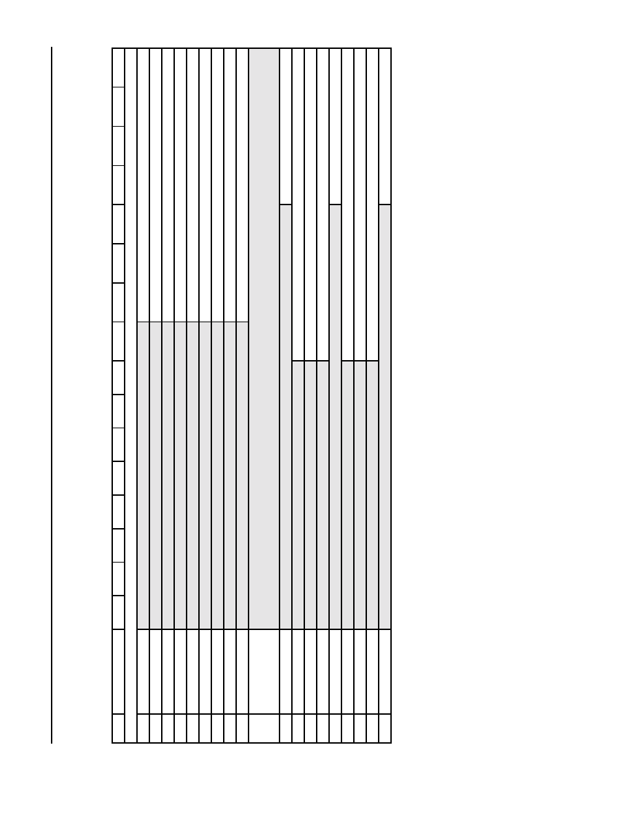
TMXF28155 Super Mapper
Preliminary Data Sheet
155/51 Mbits/s SONET/SDH x28/x21 DS1/E1
May 2001
229
Lucent Technologies Inc.
11 M13/M23 MUX/DeMUX Registers
(continued)
Table 300. Register Address Map (continued)
Addr
Symbol
Bit 15
Bit 14
Bit 13
Bit 12
Bit 11
Bit 10
Bit 9
Bit 8
Bit 7
Bit 6
Bit 5
Bit 4
Bit 3
Bit 2
Bit 1
Bit 0
Individual DS2 and DS1 Deltas--RO
0x10011
M13_XC_DS2_LOCD_R
M13_XC_DS2_LOCD[7:1]
0x10012 M13_XC_DS2_AIS_DETD_R
M13_XC_DS2_AIS_DETD[7:1]
0x10013
M13_DS2_OOFD_R
M13_DS2_OOFD[7:1]
0x10014
M13_DS2_LOFD_R
M13_DS2_LOFD[7:1]
0x10015
M13_DS2_AIS_DETD_R
M13_DS2_AIS_DETD[7:1]
0x10016
M13_DS2_RAI_DETD_R
M13_DS2_RAI_DETD[7:1]
0x10017
M13_DS2_LB_DETD_R
M13_DS2_LB_DETD[7:1]
0x10018
M13_DS2_RSV_RCVD_R
M13_DS2_RSV_RCVD[7:1]
0x10019
M13_DS2DMX_LOCD_R
M13_DS2DMX_LOCD[7:1]
0x1001A
--
0x1001D
--
0x1001E
M13_DS1_LOCD_R1
M13_DS1_LOCD[28:25]
0x1001F
M13_DS1_LOCD_R2
M13_DS1_LOCD[24:17]
0x10020
M13_DS1_LOCD_R3
M13_DS1_LOCD[16:9]
0x10021
M13_DS1_LOCD_R4
M13_DS1_LOCD[8:1]
0x10022
M13_DS1_AIS_DETD_R1
M13_DS1_AIS_DETD[28:25]
0x10023
M13_DS1_AIS_DETD_R2
M13_DS1_AIS_DETD[24:17]
0x10024
M13_DS1_AIS_DETD_R3
M13_DS1_AIS_DETD[16:9]
0x10025
M13_DS1_AIS_DETD_R4
M13_DS1_AIS_DETD[8:1]
0x10026
M13_DS1_LB_DETD_R1
M13_DS1_LB_DETD[28:25]
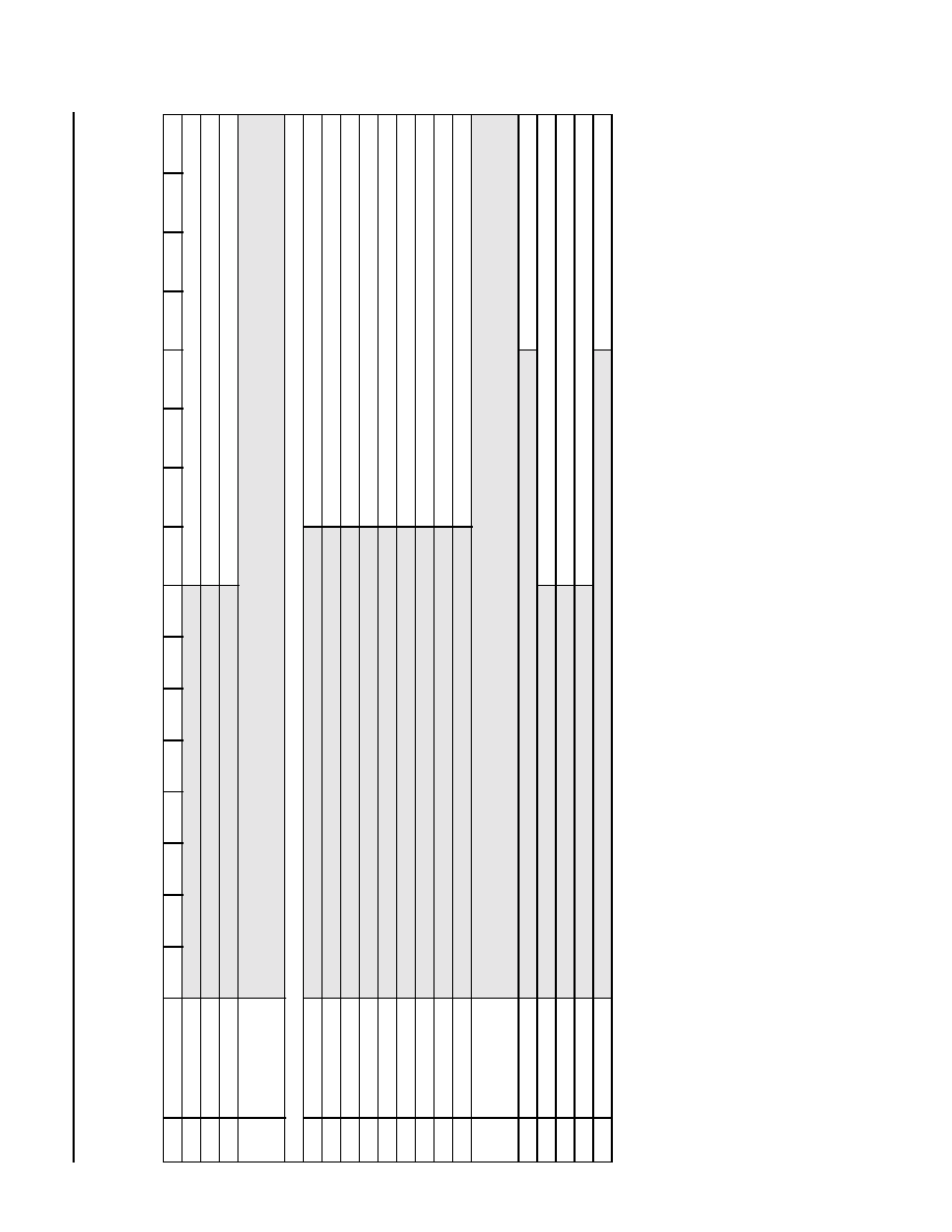
Preliminary Data Sheet
TMXF28155 Super Mapper
May 2001
155/51 Mbits/s SONET/SDH x28/x21 DS1/E1
230
Lucent Technologies Inc.
11 M13/M23 MUX/DeMUX Registers
(continued)
Table 300. Register Address Map (continued)
Addr
Symbol
Bit 15
Bit 14
Bit 13
Bit 12
Bit 11
Bit 10
Bit 9
Bit 8
Bit 7
Bit 6
Bit 5
Bit 4
Bit 3
Bit 2
Bit 1
Bit 0
0x10027
M13_DS1_LB_DETD_R2
M13_DS1_LB_DETD[24:17]
0x10028
M13_DS1_LB_DETD_R3
M13_DS1_LB_DETD[16:9]
0x10029
M13_DS1_LB_DETD_R4
M13_DS1_LB_DETD[8:1]
0x1002A
--
0x1002E
--
DS2 and DS1 Status--RO
0x1002F
M13_XC_DS2_LOC_R
M13_XC_DS2_LOC[7:1]
0x10030 M13_XC_DS2_AIS_DET_R
M13_XC_DS2_AIS_DET[7:1]
0x10031
M13_DS2_OOF_R
M13_DS2_OOF[7:1]
0x10032
M13_DS2_LOF_R
M13_DS2_LOF[7:1]
0x10033
M13_DS2_AIS_DET_R
M13_DS2_AIS_DET[7:1]
0x10034
M13_DS2_RAI_DET_R
M13_DS2_RAI_DET[7:1]
0x10035
M13_DS2_LB_DET_R
M13_DS2_LB_DET[7:1]
0x10036
M13_DS2_RSV_RCV_R
M13_DS2_RSV_RCV[7:1]
0x10037
M13_DS2DMX_LOC_R
M13_DS2DMX_LOC[7:1]
0x10038
--
0x1003B
--
0x1003C
M13_DS1_LOC_R1
M13_DS1_LOC[28:25]
0x1003D
M13_DS1_LOC_R2
M13_DS1_LOC[24:17]
0x1003E
M13_DS1_LOC_R3
M13_DS1_LOC[16:9]
0x1003F
M13_DS1_LOC_R4
M13_DS1_LOC[8:1]
0x10040
M13_DS1_AIS_DET_R1
M13_DS1_AIS_DET[28:25]
TMXF28155 Super Mapper
Preliminary Data Sheet
155/51 Mbits/s SONET/SDH x28/x21 DS1/E1
May 2001
231
Lucent Technologies Inc.
11 M13/M23 MUX/DeMUX Registers
(continued)
Table 300. Register Address Map (continued)
Addr
Symbol
Bit 15
Bit 14
Bit 13
Bit 12
Bit 11
Bit 10
Bit 9
Bit 8
Bit 7
Bit 6
Bit 5
Bit 4
Bit 3
Bit 2
Bit 1
Bit 0
0x10041
M13_DS1_AIS_DET_R2
M13_DS1_AIS_DET[24:17]
0x10042
M13_DS1_AIS_DET_R3
M13_DS1_AIS_DET[16:9]
0x10043
M13_DS1_LB_DET_R4
M13_DS1_AIS_DET[8:1]
0x10044
M13_DS1_LB_DET_R1
M13_DS1_LB_DET[28:25]
0x10045
M13_DS1_LB_DET_R2
M13_DS1_LB_DET[24:17]
0x10046
M13_DS1_LB_DET_R3
M13_DS1_LB_DET[16:9]
0x10047
M13_DS1_LB_DET_R4
M13_DS1_LB_DET[8:1]
0x10048
--
FEAC Loopback Individual Deltas--RO
0x10049 M13_DS1_FEAC_LB_DETD_R1
M13_DS3_FLB_DETD
M13_DS1_FEAC_LB_DETD[28:25]
0x1004A M13_DS1_FEAC_LB_DETD_R2
M13_DS1_FEAC_LB_DETD[24:17]
0x1004B M13_DS1_FEAC_LB_DETD_R3
M13_DS1_FEAC_LB_DETD[16:9]
0x1004C M13_DS1_FEAC_LB_DETD_R4
M13_DS1_FEAC_LB_DETD[8:1]
FEAC
Status,
RDL Sta-
tus, and
RDL
FIFO--
RO
0x1004D
M13_DS1_FEAC_LB_DET_R1
M13_DS3_FLB_DET
M13_DS1_FEAC_LB_DET[28:25]
0x1004E
M13_DS1_FEAC_LB_DET_R2
M13_DS1_FEAC_LB_DET[24:17]
0x1004F
M13_DS1_FEAC_LB_DET_R3
M13_DS1_FEAC_LB_DET[16:9]
0x10050
M13_DS1_FEAC_LB_DET_R4
M13_DS1_FEAC_LB_DET[8:1]
0x10051
M13_RFEAC_CODE_R
M13_RFEAC_CODE[5:0]
Preliminary Data Sheet
TMXF28155 Super Mapper
May 2001
155/51 Mbits/s SONET/SDH x28/x21 DS1/E1
232
Lucent Technologies Inc.
11 M13/M23 MUX/DeMUX Registers
(continued)
Table 300. Register Address Map (continued)
Addr
Symbol
Bit 15 Bit 14 Bit 13 Bit 12 Bit 11 Bit 10 Bit 9 Bit 8
Bit 7
Bit 6
Bit 5
Bit 4
Bit 3
Bit 2
Bit 1
Bit 0
0x10052
M13_RDL_STATUS
M13_RDL_FLAG M13_RDL_ABOR
T
M13_RDL_NOT_
BYTE
M13_RDL_OVFL M13_RDL_FCS_
ERR
0x10053
M13_RDL_DATA_R
M13_RDL_DATA[7:0]
0x10054
M13_RDL_FRAME_SIZE_R
M13_RDL_FRAME_SIZE[6:0]
0x10055
M13_RHDLC_STATUS_R
M13_RHDLC_STATUS[7:0]
0x10056
--
0x10058
--
One Shot Signals--R/Wl
0x10059
M13_DS2_FORCE_OOF_R
M13_DS2_FORCE_OOF[7:1]
0x1005A
M13_CONTROL1
M13_RDL_FRM_
CLR
M13_DS3_FORC
E_OOF
M13_BIPOL_ER
R
0x1005B
--
Block-level Controls--R/W
0x1005C
M13_CONTROL2
M13_BPV_IN M13_LOOP_TIME M13_LOOP_T_T
O_R
M13_LOOP_R_T
O_T
M13_AUTO_AIS_
LOF
M13_AUTO_AIS_
OOF
M13_AUTO_FLB
M13_AUTO_LB
0x1005D
M13_CONTROL3
M13_M23_CBP
M13_BIPOLAR
0x1005E
M13_SP_OFFSET_R
M13_SP__OFFSET[7:0]
0x1005F
M13_SP_D_OFFSET_R
M13_SP_D_OFFSET[7:0]
M12 MUX's Control--R/W
0x10060 M13_M12_MUX_CONTROL1_R1
M13_M12_MODE1[1:0]
M13_MUXCH2_4
_INV1
M13_DS1_E1N1
M13_DS1_LB_REQ[4:1]
0x10061 M13_M12_MUX_CONTROL2_R1
M13_SEL_DS1_LB[4:1]
M13_RDS1_EDGE[4:1]
0x10062 M13_M12_MUX_CONTROL1_R2
M13_M12_MODE2[1:0]
M13_MUXCH2_4
_INV2
M13_DS1_E1N2
M13_DS1_LB_REQ[8:5]
0x10063 M13_M12_MUX_CONTROL2_R2
M13_SEL_DS1_LB[8:5]
M13_RDS1_EDGE[8:5]
0x10064 M13_M12_MUX_CONTROL1_R3
M13_M12_MODE3[1:0]
M13_MUXCH2_4
_INV3
M13_DS1_E1N3
M13_DS1_LB_REQ[12:9]
TMXF28155 Super Mapper
Preliminary Data Sheet
155/51 Mbits/s SONET/SDH x28/x21 DS1/E1
May 2001
233
Lucent Technologies Inc.
11 M13/M23 MUX/DeMUX Registers
(continued)
Table 300. Register Address Map (continued)
Addr
Symbol
Bit 15 Bit 14 Bit 13 Bit 12 Bit 11 Bit 10
Bit 9
Bit 8
Bit 7
Bit 6
Bit 5
Bit 4
Bit 3
Bit 2
Bit 1
Bit 0
0x10065 M13_M12_MUX_CONTROL2_R3
M13_SEL_DS1_LB[12:9]
M13_RDS1_EDGE[12:9]
0x10066 M13_M12_MUX_CONTROL1_R4
M13_M12_MODE4[1:0]
M13_MUXCH2_4_INV4
M13_DS1_E1N4
M13_DS1_LB_REQ[16:13]
0x10067 M13_M12_MUX_CONTROL2_R4
M13_SEL_DS1_LB[16:13]
M13_RDS1_EDGE[16:13]
0x10068 M13_M12_MUX_CONTROL1_R5
M13_M12_MODE5[1:0]
M13_MUXCH2_4_INV5
M13_DS1_E1N5
M13_DS1_LB_REQ[20:17]
0x10069 M13_M12_MUX_CONTROL2_R5
M13_SEL_DS1_LB[20:17]
M13_RDS1_EDGE[20:17]
0x1006A M13_M12_MUX_CONTROL1_R6
M13_M12_MODE6[1:0]
M13_MUXCH2_4_INV6
M13_DS1_E1N6
M13_DS1_LB_REQ[24:21]
0x1006B M13_M12_MUX_CONTROL2_R6
M13_SEL_DS1_LB[24:21]
M13_RDS1_EDGE[24:21]
0x1006C M13_M12_MUX_CONTROL1_R7
M13_M12_MODE7[1:0]
M13_MUXCH2_4_INV7
M13_DS1_E1N7
M13_DS1_LB_REQ[28:25]
0x1006D M13_M12_MUX_CONTROL2_R7
M13_SEL_DS1_LB[28:25]
M13_RDS1_EDGE[28:25]
0x1006E
M13_DS2_RAI_SEND_R
M13_DS2_RAI_SEND[7:1]
0x1006F
M13_DS2_RSV_SEND_R
M13_DS2_RSV_SEND[7:1]
0x10070
M13_DS2_MPINV_R
M13_DS2_MPINV[7:1]
0x10071
M13_DS2_FINV_R
M13_DS2_FINV[7:1]
0x10072
M13_DS2_P_BER_R
M13_DS2_P_BER[7:1]
0x10073
M13_DS2M12_EDGE_R
M13_DS2M12_EDGE[7:1]
0x10074
M13_DS2_FORCE_AIS_R
M13_DS2_FORCE_AIS[7:1]
0x10075
--
0x1007A
--
Preliminary Data Sheet
TMXF28155 Super Mapper
May 2001
155/51 Mbits/s SONET/SDH x28/x21 DS1/E1
234
Lucent Technologies Inc.
11 M13/M23 MUX/DeMUX Registers
(continued)
Table 300. Register Address Map (continued)
Addr
Symbol
Bit 15 Bit 14 Bit 13 Bit 12 Bit 11 Bit 10 Bit 9 Bit 8
Bit 7
Bit 6
Bit 5
Bit 4
Bit 3
Bit 2
Bit 1
Bit 0
M12 DeMUX's Control--R/W
0x1007B M13_M12_DEMUX_CONTROL1_R1
M13_M12DMX_MODE1[1:0] M13_DEMUXCH2_4_
INV1
M13_OUT_TYPE1
M13_TDS1_EDGE[4:1]
0x1007C M13_M12_DEMUX_CONTROL2_R1
M13_DS1_OUT_AIS[4:1]
0x1007D M13_M12_DEMUX_CONTROL1_R2
M13_M12DMX_MODE2[1:0] M13_DEMUXCH2_4_
INV2
M13_OUT_TYPE2
M13_TDS1_EDGE[8:5]
0x1007E M13_M12_DEMUX_CONTROL2_R2
M13_DS1_OUT_AIS[8:5]
0x1007F M13_M12_DEMUX_CONTROL1_R3
M13_M12DMX_MODE3[1:0] M13_DEMUXCH2_4_
INV3
M13_OUT_TYPE3
M13_TDS1_EDGE[12:9]
0x10080 M13_M12_DEMUX_CONTROL2_R3
M13_DS1_OUT_AIS[12:9]
0x10081 M13_M12_DEMUX_CONTROL1_R4
M13_M12DMX_MODE4[1:0] M13_DEMUXCH2_4_
INV4
M13_OUT_TYPE4
M13_TDS1_EDGE[16:13]
0x10082 M13_M12_DEMUX_CONTROL2_R4
M13_DS1_OUT_AIS[16:13]
0x10083 M13_M12_DEMUX_CONTROL1_R5
M13_M12DMX_MODE5[1:0] M13_DEMUXCH2_4_
INV5
M13_OUT_TYPE5
M13_TDS1_EDGE[20:17]
0x10084 M13_M12_DEMUX_CONTROL2_R5
M13_DS1_OUT_AIS[20:17]
0x10085 M13_M12_DEMUX_CONTROL1_R6
M13_M12DMX_MODE6[1:0] M13_DEMUXCH2_4_
INV6
M13_OUT_TYPE6
M13_TDS1_EDGE[24:21]
0x10086 M13_M12_DEMUX_CONTROL2_R6
M13_DS1_OUT_AIS[24:21]
0x10087 M13_M12_DEMUX_CONTROL1_R7
M13_M12DMX_MODE7[1:0] M13_DEMUXCH2_4_
INV7
M13_OUT_TYPE7
M13_TDS1_EDGE[28:25]
0x10088 M13_M12_DEMUX_CONTROL2_R7
M13_DS1_OUT_AIS[28:25]
0x10089
M13_M12_DEMUX_CONTROL3
M13_DS2_MODE M13_DS2_FERR_MODE
TMXF28155 Super Mapper
Preliminary Data Sheet
155/51 Mbits/s SONET/SDH x28/x21 DS1/E1
May 2001
235
Lucent Technologies Inc.
11 M13/M23 MUX/DeMUX Registers
(continued)
Table 300. Register Address Map (continued)
Address
Symbol
Bit 15 Bit 14 Bit 13 Bit 12 Bit 11 Bit 10 Bit 9 Bit 8
Bit 7
Bit 6
Bit 5
Bit 4
Bit 3
Bit 2
Bit 1
Bit 0
0x1008A
M13_DMDS2_EDGE_R
M13_DMDS2_EDGE[7:1]
0x1008B
--
0x10091
--
M23 MUX Controls--R/W
0x10092
M13_DS3_CONTROL1
M13_DS3_FINV M13_DS3_MINV
M13_DS3_PINV
M13_DS3_FORCE
_AIS
M13_DS3_FORCE
_IDLE
M13_TDS3_
FORCE_ALL1
M13_M23CLK_
MODE
0x10093
M13_DS3_CONTROL2
M13_NSMI_MODE M13_DS3_P_BER M13_CBIT2_ACT M13_UNUSED_AC
T
M13_DS3_RAI_
SEND
M13_FEBE_ERR
0x10094
M13_TFEAC_CONTROL
M13_TFEAC_CTL[1:0]
M13_TFEAC_CODE[5:0]
0x10095 M13_THDLC_CONTROL1
M13_TDL_BUF1_
END
M13_TDL_BUF0_
END
M13_TDL_ACT
M13_TDL_NTRNL
M13_TDL_
NTRNL_ACT
M13_TDL_FCS
0x10096 M13_THDLC_CONTROL2
M13_TDL_BYTE_END[5:0]
0x10097
M13_DS2_LB_REQ_R
M13_DS2_LB_REQ[7:1]
0x10098
M13_SEL_DS2_LB_R
M13_SEL_DS2_LB[7:1]
0x10099
M13_RDS2_EDGE_R1
M13_RDS2_EDGE[7:1]
0x1009A
M13_RDS2_EDGE_R2
M13_DS2ALCO_RTM_EDGE[7:1]
0x1009B
--
0x1009D
--
M23 DeMUX Controls--R/W
0x1009E
M13_DS2_OUT_IDLE_R
M13_DS2_OUT_IDLE[7:1]
0x1009F
M13_DS2_OUT_AIS_R
M13_DS2_OUT_AIS[7:1]
0x100A0
M13_TDS2_EDGE_R
M13_TDS2_EDGE[7:1]
0x100A1
M13_RDL_CONTROL
M13_RDL_FILL[1:0]
M13_RDL_FCS
M13_DS3_MODE M13_RDS3_EDGE
0x100A2
--
0x100A4
--
Preliminary Data Sheet
TMXF28155 Super Mapper
May 2001
155/51 Mbits/s SONET/SDH x28/x21 DS1/E1
236
Lucent Technologies Inc.
11 M13/M23 MUX/DeMUX Registers
(continued)
Table 300. Register Address Map (continued)
Address
Symbol
Bit 15
Bit 14
Bit 13
Bit 12
Bit 11
Bit 10
Bit 9
Bit 8
Bit 7
Bit 6
Bit 5
Bit 4
Bit 3
Bit 2
Bit 1
Bit 0
Performance Monitoring Counters--RO
0x100A5
M13_PM_CNT_ACT_R
M13_PM_C
NT_ACT
0x100A6
M13_DS3_FERR_CNT_R1
M13_DS3_FERR_CNT[11:8]
0x100A7
M13_DS3_FERR_CNT_R2
M13_DS3_FERR_CNT[7:0]
0x100A8
M13_DS3_FEBE_CNT_R1
M13_DS3_FEBE_CNT[13:8]
0x100A9
M13_DS3_FEBE_CNT_R2
M13_DS3_FEBE_CNT[7:0]
0x100AA M13_DS3_CPERR_CNT_R1
M13_DS3_CPERR_CNT[13:8]
0x100AB M13_DS3_CPERR_CNT_R2
M13_DS3_CPERR_CNT[7:0]
0x100AC
M13_DS3_PERR_CNT_R1
M13_DS3_PERR_CNT[13:8]
0x100AD
M13_DS3_PERR_CNT_R2
M13_DS3_PERR_CNT[7:0]
0x100AE
--
0x100B1
--
0x100B2 M13_DS2_PERR_CNT7_R1
M13_DS2_PERR_CNT7[12:8]
0x100B3 M13_DS2_PERR_CNT7_R2
M13_DS2_PERR_CNT7[7:0]
0x100B4 M13_DS2_PERR_CNT6_R1
M13_DS2_PERR_CNT6[12:8]
0x100B5 M13_DS2_PERR_CNT6_R2
M13_DS2_PERR_CNT6[7:0]
0x100B6 M13_DS2_PERR_CNT5_R1
M13_DS2_PERR_CNT5[12:8]
0x100B7 M13_DS2_PERR_CNT5_R2
M13_DS2_PERR_CNT5[7:0]
0x100B8 M13_DS2_PERR_CNT4_R1
M13_DS2_PERR_CNT4[12:8]
0x100B9 M13_DS2_PERR_CNT4_R2
M13_DS2_PERR_CNT4[7:0]
0x100BA M13_DS2_PERR_CNT3_R1
vDS2_PERR_CNT3[12:8]
0x100BB M13_DS2_PERR_CNT3_R2
M13_DS2_PERR_CNT3[7:0]
TMXF28155 Super Mapper
Preliminary Data Sheet
155/51 Mbits/s SONET/SDH x28/x21 DS1/E1
May 2001
237
Lucent Technologies Inc.
11 M13/M23 MUX/DeMUX Registers
(continued)
Table 300. Register Address Map (continued)
Address
Symbol
Bit 15
Bit 14
Bit 13
Bit 12
Bit 11
Bit 10
Bit 9
Bit 8
Bit 7
Bit 6
Bit 5
Bit 4
Bit 3
Bit 2
Bit 1
Bit 0
0x100BC M13_DS2_PERR_CNT2_R1
M13_DS2_PERR_CNT2[12:8]
0x100BD M13_DS2_PERR_CNT2_R2
M13_DS2_PERR_CNT2[7:0]
0x100BE M13_DS2_PERR_CNT1_R1
M13_DS2_PERR_CNT1[12:8]
0x100BF M13_DS2_PERR_CNT1_R2
M13_DS2_PERR_CNT1[7:0]
0x100C0
--
0x100C5
--
0x100C6 M13_DS2_FERR_CNT7_R
M13_DS2_FERR_CNT7[7:0]
0x100C7 M13_DS2_FERR_CNT6_R
M13_DS2_FERR_CNT6[7:0]
0x100C8 M13_DS2_FERR_CNT5_R
M13_DS2_FERR_CNT5[7:0]
0x100C9 M13_DS2_FERR_CNT4_R
M13_DS2_FERR_CNT4[7:0]
0x100CA M13_DS2_FERR_CNT3_R
M13_DS2_FERR_CNT3[7:0]
0x100CB M13_DS2_FERR_CNT2_R
M13_DS2_FERR_CNT2[7:0]
0x100CC M13_DS2_FERR_CNT1_R
M13_DS2_FERR_CNT1[7:0]
0x100CD
M13_BPV_CNT_R1
M13_BPV_CNT[23:16]
0x100CE
M13_BPV_CNT_R2
M13_BPV_CNT[15:8]
0x100CF
M13_BPV_CNT_R3
M13_BPV_CNT[7:0]
0x100D0
M13_EXZ_CNT_R1
M13_EXZ_CNT[23:16]
0x100D1
M13_EXZ_CNT_R2
M13_EXZ_CNT[15:8]
0x100D2
M13_EXZ_CNT_R3
M13_EXZ_CNT[7:0]
0x100D3
--
0x100FE
--
Preliminary Data Sheet
TMXF28155 Super Mapper
May 2001
155/51 Mbits/s SONET/SDH x28/x21 DS1/E1
238
Lucent Technologies Inc.
11 M13/M23 MUX/DeMUX Registers
(continued)
Table 300. Register Address Map (continued)
Address
Symbol
Bit 15
Bit 14
Bit 13
Bit 12
Bit 11
Bit 10
Bit 9
Bit 8
Bit 7
Bit 6
Bit 5
Bit 4
Bit 3
Bit 2
Bit 1
Bit 0
TDL Buffer Selection--R/W
0x100FF
M13_TDL_BUFFER_R
M13_TDL_B
UFFER
TDL Buffers--R/W
When M13_TDL_BUFFER = 0
0x10100
--
0x1013F
M13_TDL_0DATA_R[0--63]
M13_TDL_0DATA[0--63][7:0]
When M13_TDL_BUFFER = 1
0x10100
--
0x1013F
M13_TDL_1DATA_R[0--63]
M13_TDL_1DATA[0--63][7:0]
0x10140
--
0x101FF
--

Preliminary Data Sheet
TMXF28155/51 Super Mapper
May 2001
155/51 Mbits/s SONET/SDH x28/x21 DS1/E1
239
Agere Systems Inc.
12 28-Channel Framer Registers
Table of Contents
Contents
Page
12 28-Channel Framer Registers ........................................................................................................................ 239
12.1 Framer Global Register Descriptions ..................................................................................................... 243
12.2 Arbiter (Framer) Global Registers .......................................................................................................... 245
12.3 Performance Monitor Global Registers .................................................................................................. 247
12.4 HDLC Global Configuration and Status Registers .................................................................................. 253
12.5 System Interface Global Registers ......................................................................................................... 257
12.6 Signaling Global Registers ..................................................................................................................... 262
12.7 Frame Formatter (Transmit Framer) Global Register ............................................................................. 266
12.8 Facility Data Link Global Registers ......................................................................................................... 267
12.9 Super Mapper Framer Per Link Configuration and Status Registers ..................................................... 267
12.9.1 Signaling Per Link Registers ........................................................................................................ 267
12.10 Performance Monitor Per Link Registers .............................................................................................. 273
12.11 Receive Facility Data Link Configuration and Status Registers ........................................................... 288
12.12 Transmit Facility Data Link Configuration and Status Registers .......................................................... 290
12.13 System Interface, Arbiter, and Frame Formatter Mapping ................................................................... 292
12.14 System Interface Per Link Registers .................................................................................................... 293
12.15 Arbiter Framer Per Link Registers ........................................................................................................ 295
12.16 Frame Formatter Per Link Registers .................................................................................................... 300
12.17 Line Decoder/Encoder Per Link Registers ........................................................................................... 302
12.18 Line Encoder/Decoder Per Link Registers ........................................................................................... 303
12.19 HDLC Per Channel Configuration and Status Registers ...................................................................... 304
12.20 28-Channel Framer Block Register Map .............................................................................................. 311
Tables
Page
Table 301. FRM_SFGR1, Superframer Global Register 1 (R/W) ........................................................................ 243
Table 302. FRM_SFGR2, Superframer Global Register 2 (R/W) ........................................................................ 244
Table 303. FRM_SFGR3, Superframer Global Register 3 (RO) ......................................................................... 245
Table 304. FRM_SFGSR4, Superframer Global Register 4 (R/W) ..................................................................... 245
Table 305. FRM_FGR1, Framer Global Register 1 (R/W) .................................................................................. 245
Table 306. FRM_FGR2, Framer Global Register 2 (R/W) .................................................................................. 246
Table 307. FRM_FGR3, Framer Global Register 3 (R/W) .................................................................................. 246
Table 308. FRM_FGR4, Framer Global Register 4 (COR) ................................................................................. 246
Table 309. FRM_FGR5, Framer Global Register 5 (COR) ................................................................................. 247
Table 310. FRM_PMGR1_B, Performance Monitor Global Register 1_B (R/W) ................................................ 247
Table 311. FRM_PMGR1, Performance Monitor Global Register 1 (COR) ........................................................ 247
Table 312. FRM_PMGR2, Performance Monitor Global Register 2 (COR) ........................................................ 248
Table 313. FRM_PMGR3, Performance Monitor Global Register 3 (R/W) ......................................................... 248
Table 314. FRM_PMGR4, Performance Monitor Global Register 4 (R/W) ......................................................... 249
Table 315. FRM_PMGR5, Performance Monitor Global Register 5--PMGR5 (R/W) ......................................... 249
Table 316. FRM_PMGR6, Performance Monitor Global Register 6 (R/W) ......................................................... 249
Table 317. FRM_PMGR7, Performance Monitor Global Register 7 (R/W) ......................................................... 249
Table 318. FRM_PMGR8, Performance Monitor Global Register 8 (R/W) ......................................................... 250
Table 319. FRM_PMGR9, Performance Monitor Global Register 9 (R/W) ......................................................... 250
Table 320. FRM_PMGR10, Performance Monitor Global Register 10 (R/W) ..................................................... 250
Table 321. FRM_PMGR11, Performance Monitor Global Register 11 (R/W) ..................................................... 250
Table 322. FRM_PMGR12, Performance Monitor Global Register 12 (R/W) ..................................................... 251
Table 323. FRM_PMGR13, Performance Monitor Global Register 13 (R/W) ..................................................... 251
Table 324. FRM_PMGR14, Performance Monitor Global Register 14 (R/W) ..................................................... 252

TMXF28155/51 Super Mapper
Preliminary Data Sheet
155/51 Mbits/s SONET/SDH x28/x21 DS1/E1
May 2001
240
Agere Systems Inc.
12 28-Channel Framer Registers
(continued)
Table of Contents
(continued)
Tables
Page
Table 325. FRM_PMGR15, Performance Monitor Global Register 15 (R/W) ..................................................... 252
Table 326. FRM_PMGR16, Performance Monitor Global Register 16 (R/W) ..................................................... 252
Table 327. FRM_HGR1, Transmit HDLC Global Register 1 (R/W) ..................................................................... 253
Table 328. FRM_HGR2, Transmit HDLC Global Register 2 (R/W) ..................................................................... 253
Table 329. FRM_HGR3, Transmit HDLC Global Register 3 (R/W) ..................................................................... 253
Table 330. FRM_HGR4, Transmit HDLC Global Register 4 (R/W) ..................................................................... 253
Table 331. FRM_HGR5, Transmit HDLC Global Register 5 (R/W) ..................................................................... 254
Table 332. FRM_HGR6, Transmit HDLC Global Register 6 (R/W) ..................................................................... 254
Table 333. FRM_HGR7, Transmit HDLC Global Register 7 (R/W) ..................................................................... 254
Table 334. FRM_HGR8, Transmit HDLC Global Register 8 (R/W) ..................................................................... 254
Table 335. FRM_HGR9, Transmit HDLC Global Register 9 (R/W) ..................................................................... 254
Table 336. FRM_HGR10, Transmit HDLC Global Register 10 (R/W) ................................................................. 255
Table 337. FRM_HGR11, Transmit HDLC Global Register 11 (RO) .................................................................. 255
Table 338. FRM_HGR12, Transmit HDLC Global Register 12 (R/W) ................................................................. 255
Table 339. FRM_HGR13, Transmit HDLC Global Register 13 (R/W) ................................................................. 255
Table 340. FRM_HGR14, Transmit HDLC Global Register 14 (R/W) ................................................................. 255
Table 341. FRM_HGR15, Receive HDLC Global Register 15 (R/W) .................................................................. 255
Table 342. FRM_HGR16, Receive HDLC Global Register 16 (R/W) .................................................................. 256
Table 343. FRM_HGR17, Receive HDLC Global Register 17 (R/W) .................................................................. 256
Table 344. FRM_HGR18, Receive HDLC Global Register 18 (R/W) .................................................................. 256
Table 345. FRM_HGR19, Receive HDLC Global Register 19 (R/W) .................................................................. 256
Table 346. FRM_HGR20, Receive HDLC Global Register 20 (R/W) .................................................................. 256
Table 347. FRM_SYSGR1, System Interface Global Register 1 (R/W) .............................................................. 257
Table 348. FRM_SYSGR2, System Interface Global Register 2 (R/W) .............................................................. 258
Table 349. FRM_SYSGR3, System Interface Global Register 3 (R/W) .............................................................. 259
Table 350. FRM_SYSGR4, System Interface Global Register 4 (R/W) .............................................................. 259
Table 351. FRM_SYSGR5, System Interface Global Register 5 (R/W) .............................................................. 259
Table 352. FRM_SYSGR6, System Interface Global Register 6 (COR) ............................................................. 259
Table 353. FRM_SYSGR7, System Interface Global Register 7 (COR) ............................................................. 260
Table 354. FRM_SYSGR8, System Interface Global Register 8 (R/W) .............................................................. 260
Table 355. FRM_SYSGR9, System Interface Global Register 9 (R/W) .............................................................. 260
Table 356. FRM_SYSGR10--FRM_SYSGR14, System Interface Global Register 10--14 (R/W) .................... 261
Table 357. FRM_SYSGR15, System Interface Global Register 15 (COR) ......................................................... 261
Table 358. FRM_SYSGR16, System Interface Global Register 16 (R/W) .......................................................... 261
Table 359. FRM_SGR1, Receive Signaling Global Register 1 (R/W) ................................................................. 262
Table 360. FRM_SGR2, Receive Signaling Global Register 2 (R/W) ................................................................. 262
Table 361. FRM_SGR3, Receive Signaling Global Register 3 (R/W) ................................................................. 263
Table 362. FRM_SGR4, Receive Signaling Global Register 4 (RO) ................................................................... 263
Table 363. FRM_SGR5, Receive Signaling Global Register 5 (RO) ................................................................... 263
Table 364. FRM_SGR6, Receive Signaling Global Register 6 .......................................................................... 264
Table 365. FRM_SGR7, Receive Signaling Global Register 7 (R/W) ................................................................. 264
Table 366. FRM_SGR8, Transmit Signaling Global Register 8 (R/W) ................................................................ 265
Table 367. FRM_FFGR1, Transmit Framer Global Register 1 (R/W) ................................................................. 266
Table 368. FRM_FDLGR1, Receive Facility Data Link Global Register 1 (R/W) ................................................ 267
Table 369. FRM_FDLGR2, Transmit Facility Data Link Global Register 2 (R/W) ............................................... 267
Table 370. Receive Path Signaling Register Addressing Map ............................................................................ 267
Table 371. Receive Path Signaling Registers Address Indexing ........................................................................ 267
Table 372. FRM_RSLR0--FRM_RSLR31, Receive Signaling Link Registers 0--31 (R/W) ............................... 268
Table 373. FRM_RSLR32, Receive Signaling Link Register 32 (COR) .............................................................. 269

Preliminary Data Sheet
TMXF28155/51 Super Mapper
May 2001
155/51 Mbits/s SONET/SDH x28/x21 DS1/E1
241
Agere Systems Inc.
12 28-Channel Framer Registers
(continued)
Table of Contents
(continued)
Tables
Page
Table 374. FRM_RSLR33, Receive Signaling Link Register 33 (R/W) ............................................................... 269
Table 375. Transmit Path Signaling Register Addressing Map ........................................................................... 270
Table 376. Transmit Path Signaling Registers Address Indexing ....................................................................... 270
Table 377. FRM_TSLR0--FRM_TSLR31, Transmit Signaling Link Registers 0--31 (R/W) .............................. 271
Table 378. FRM_TSLR32, Transmit Signaling Link Register 32 (R/W) .............................................................. 272
Table 379. FRM_TSLR33, Transmit Signaling Link Register 33 (COR) ............................................................. 273
Table 380. Performance Monitor Per Link Register Addressing Map ................................................................. 273
Table 381. Performance Monitor Per Link Register Address Indexing ................................................................ 274
Table 382. FRM_PMLR1, Performance Monitor Link Register 1 (R/W) .............................................................. 274
Table 383. FRM_PMLR2, Performance Monitor Link Register 2 (R/W) .............................................................. 274
Table 384. FRM_PMLR3, Performance Monitor Link Register 3 (R/W) .............................................................. 275
Table 385. FRM_PMLR4, Performance Monitor Link Register 4 (COR) ............................................................. 275
Table 386. FRM_PMLR5, Performance Monitor Link Register 5 (COR) ............................................................. 282
Table 387. FRM_PMLR6, Performance Monitor Link Register 6 (COR) ............................................................. 284
Table 388. FRM_PMLR7, Performance Monitor Link Register 7 (COR) ............................................................. 284
Table 389. FRM_PMLR8, Performance Monitor Link Register 8 (COR) ............................................................. 285
Table 390. FRM_PMLR9, Performance Monitor Link Register 9 (COR) ............................................................. 285
Table 391. FRM_PMLR10, Performance Monitor Link Register 10 (COR) ......................................................... 285
Table 392. FRM_PMLR11, Performance Monitor Link Register 11 (COR) ......................................................... 285
Table 393. FRM_PMLR12, Performance Monitor Link Register 12 (COR) ......................................................... 285
Table 394. FRM_PMLR13, Performance Monitor Link Register 13 (COR) ......................................................... 286
Table 395. FRM_PMLR14, Performance Monitor Link Register 14 (COR). ........................................................ 287
Table 396. FRM_PMLR15, Performance Monitor Link Register 15 (COR) ......................................................... 287
Table 397. FRM_PMLR16, Performance Monitor Link Register 16 (COR) ......................................................... 287
Table 398. FRM_PMLR17, Performance Monitor Link Register 17 (COR) ......................................................... 287
Table 399. FRM_PMLR18, Performance Monitor Link Register 18 (COR) ......................................................... 287
Table 400. FRM_PMLR19, Performance Monitor Link Register 19 (COR) ......................................................... 288
Table 401. FRM_PMLR20, Performance Monitor Link Register 20 (COR) ......................................................... 288
Table 402. Receive Facility Data Link Register Addressing Map ........................................................................ 288
Table 403. Receive Path Facility Data Link Registers Address Indexing ............................................................ 289
Table 404. FRM_RFDLLR1--FRM_RFDLLR5, Receive FDL Link Registers 1--5 (RO) ................................... 289
Table 405. FRM_RFDLLR6, Receive FDL Link Register 6 (R/W) ....................................................................... 289
Table 406. FRM_RFDLLR7, Receive FDL Link Register 7 (RO) ........................................................................ 289
Table 407. FRM_RFDLLR8, Receive FDL Link Register 8 (COR) ...................................................................... 290
Table 408. FRM_RFDLLR9, Receive FDL Link Register 9 (R/W) ....................................................................... 290
Table 409. Transmit Facility Data Link Register Addressing Map ....................................................................... 290
Table 410. Transmit Path Facility Data Link Registers Address Indexing ........................................................... 290
Table 411. FRM_TFDLLR1--FRM_TFDLR5, Transmit FDL Link Registers 1--5 (COR) ................................... 290
Table 412. FRM_TFDLLR6, Transmit FDL Link Register 6 (R/W) ...................................................................... 291
Table 413. FRM_TFDLLR7, Transmit FDL Link Register 7 (R/W) ...................................................................... 291
Table 414. FRM_TFDLLR8, Transmit FDL Link Register 8 (RO/COW) .............................................................. 292
Table 415. FRM_TFDLLR9, Transmit FDL Link Register 9 (R/W) ...................................................................... 292
Table 416. System Interface, Arbiter, and Frame Formatter Link Register Addressing Map .............................. 292
Table 417. System Interface, Arbiter, and Frame Formatter Link Register Address Indexing ............................ 293
Table 418. FRM_SYSLR1, System Interface Link Register 1 (R/W) ................................................................... 293
Table 419. FRM_SYSLR2, System Interface Link Register 2 (R/W) ................................................................... 294
Table 420. FRM_SYSLR3--FRM_SYSLR6, System Interface Link Registers 3--6 (R/W) ................................ 294
Table 421. FRM_ARLR1, Arbiter Link Register 1 (R/W) ..................................................................................... 295
Table 422. FRM_ARLR2, Arbiter Link Register 2 (R/W) ..................................................................................... 296

TMXF28155/51 Super Mapper
Preliminary Data Sheet
155/51 Mbits/s SONET/SDH x28/x21 DS1/E1
May 2001
242
Agere Systems Inc.
12 28-Channel Framer Registers
(continued)
Table of Contents
(continued)
Tables
Page
Table 423. FRM_ARLR3, Arbiter Link Register 3 (R/W) ..................................................................................... 299
Table 424. FRM_FFLR1, Frame Formatter Link Register 1 (R/W) ..................................................................... 300
Table 425. FRM_FFLR2, Frame Formatter Link Register 2 (R/W) ..................................................................... 301
Table 426. Line Decoder Per LInk Register Addressing Map ............................................................................. 302
Table 427. Line Decoder Per Link Registers Address Indexing .......................................................................... 302
Table 428. Line Encoder Per Link Register Addressing Map .............................................................................. 302
Table 429. Line Encoder Per Link Registers Address Indexing .......................................................................... 302
Table 430. FRM_LDLR1, Line Decoder Link Register 1 (R/W) ........................................................................... 303
Table 431. FRM_LDLR2, Line Encoder Link Register 2 (R/W) ........................................................................... 303
Table 432. HDLC Per Channel Register Addressing Map .................................................................................. 304
Table 433. FRM_HCR1, Transmit HDLC Channel Register 1 (R/W) .................................................................. 304
Table 434. FRM_HCR2, Transmit HDLC Channel Register 2 (R/W) .................................................................. 304
Table 435. FRM_HCR3, Transmit HDLC Channel Register 3 (R/W) .................................................................. 305
Table 436. FRM_HCR4, Transmit HDLC Channel Register 4 (RO) .................................................................... 306
Table 437. FRM_HCR5, Transmit HDLC Channel Register 5 (R/W) .................................................................. 306
Table 438. FRM_HCR6, Transmit HDLC Channel Register 6 (WO) ................................................................... 307
Table 439. FRM_HCR7, Transmit HDLC Channel Register 7 (RO) .................................................................... 307
Table 440. FRM_HCR8, Receive HDLC Channel Register 8 (R/W) ................................................................... 307
Table 441. FRM_HCR9, Receive HDLC Channel Register 9 (R/W) ................................................................... 307
Table 442. FRM_HCR10, Receive HDLC Channel Register 10 (R/W) ............................................................... 308
Table 443. FRM_HCR11, Receive HDLC Channel Register 11 (RO) ................................................................. 308
Table 444. FRM_HCR12, Receive HDLC Channel Register 12 (R/W) ............................................................... 309
Table 445. FRM_HCR13, Receive HDLC Channel Register 13 (RO) ................................................................. 310
Table 446. FRM_HGR14, Receive HDLC Channel Register 14 (COR) .............................................................. 310
Table 447. Framer Register Map ......................................................................................................................... 311

Preliminary Data Sheet
TMXF28155/51 Super Mapper
May 2001
155/51 Mbits/s SONET/SDH x28/x21 DS1/E1
243
Agere Systems Inc.
12 28-Channel Framer Registers
(continued)
12.1 Framer Global Register Descriptions
Table 301. FRM_SFGR1, Superframer Global Register 1 (R/W)
Address
Bit
Name
Function
Reset Default
0x80000
15
FRM_SW_TRN
Superframer Configuration Modes.
0 = Transport mode.
1 = Switching mode.
0
14:13
FRM_LC_
CNTRL[1:0]
Line Encoder/Decoder Control.
00 = Line encoder and line decoder blocks are not used in
either the framer Tx or Rx paths. This setting is used in the
following switching modes:
s
STS-3/STS-1/DS3/DS2 to CHI/parallel system bus/SMI.
s
STS-3/STS-1/DS3 to line data rate mode.
01 = Line decoder is used in the Rx path and line encoder is
used in the Tx path. This setting is used in the framer-only
switching modes:
s
DS1 to CHI/parallel system bus/SMI channelized.
10 = Line decoder is used in the Tx path and line encoder is
used in the Rx path. This setting is used in the following
transport modes:
s
DS1 to DS2/DS3/STS-1/STS-3.
11 = Reserved.
00
12
FRM_LOOP_
TIMING
Loop Timing.
0 = Superframer is programmed for normal mode.
1 = Superframer is programmed for loop timing; i.e., all received
line clocks are looped back to the corresponding transmit
line clocks.
0
11
FRM_DS1_
CEPTN
DS1/CEPT Terminal Count.
0 = Superframer is programmed for CEPT mode, which has a
maximum of 21 operational links. Links 22 to 28 are
disabled.
1 = Superframer is programmed for DS1 mode, which has a
maximum of 28 operational links.
Note: For fewer links or DS1/CEPT mixed modes, use
FRM_TC_EN and FRM_TC[7:0] (
Table 306
) parame-
ters to select an accurate link count.
1
10
FRM_PLL_
BYPAS
PLL Bypass.
0 = Internal PLL is used to generate the line clock in the
transmit path.
1 = The PLL is bypassed. External line clock is required in this
mode.
0
9:1
--
Reserved. Must write to 0.
0
0
FRM_LG_BUF_
MODE
HDLC Buffer Mode.
0 = HDLC channel buffers are configured for 128-byte storage.
Up to 64 (32) channels can be supported in the switching
(transport) mode.
1 = HDLC channel buffers are combined for 512-byte storage.
Up to 16 (8) channels can be supported in the switching
(transport) mode.
0

TMXF28155/51 Super Mapper
Preliminary Data Sheet
155/51 Mbits/s SONET/SDH x28/x21 DS1/E1
May 2001
244
Agere Systems Inc.
12 28-Channel Framer Registers
(continued)
Table 302. FRM_SFGR2, Superframer Global Register 2 (R/W)
Address
Bit
Name
Function
Reset
Default
0x80001 15:14
--
Reserved. Must write to 0.
0
13
FRM_TP_SIG_PWDN Transmit Path Receive Signaling Powerdown. When set
to 0, the transmit path receive signaling block for the trans-
port mode is powered down.
1
12
FRM_RP_SIG_PWDN Receive Path Transmit Signaling Powerdown. When set
to 0, the receive path transmit signaling block for the trans-
port mode is powered down.
1
11
FRM_TP_RDL_PWDN Transmit Path Receive Datalink Powerdown. When set to
0, the transmit path receive data link block for the transport
mode is powered down.
1
10
FRM_RP_TDL_PWDN Receive Path Transmit Datalink Powerdown. When set to
0, the receive path transmit data link block for the transport
mode is powered down.
1
9
FRM_TP_RH_PWDN
Transmit Path Receive HDLC Powerdown. When set to 0,
the transmit path receive HDLC block for the transport mode
is powered down.
1
8
FRM_RP_TH_PWDN
Receive Path Transmit HDLC Powerdown. When set to 0,
the receive path transmit HDLC block for the transport mode
is powered down.
1
7
FRM_TS_PWDN
Transmit Path System Block Powerdown. When set to 0,
the transmit path system block is powered down.
1
6
FRM_RS_PWDN
Receive Path System Block Powerdown. When set to 0,
the receive path system block is powered down.
1
5
FRM_TP_PM_PWDN
Transmit Path Performance Monitor Powerdown. When
set to 0, the transmit path performance monitor block is pow-
ered down.
1
4
FRM_RP_FF_PWDN
Receive Path Frame Formatter Powerdown. When set to
0, the receive path frame formatter block is powered down.
1
3
FRM_TP_RA_PWDN
Transmit Path Receive Aligner Powerdown. When set to
0, the transmit path receive aligner block is powered down.
1
2:0
--
Reserved. Must write to 0.
0

Preliminary Data Sheet
TMXF28155/51 Super Mapper
May 2001
155/51 Mbits/s SONET/SDH x28/x21 DS1/E1
245
Agere Systems Inc.
12 28-Channel Framer Registers
(continued)
Table 303. FRM_SFGR3, Superframer Global Register 3 (RO)
Table 304. FRM_SFGSR4, Superframer Global Register 4 (R/W)
12.2 Arbiter (Framer) Global Registers
Table 305. FRM_FGR1, Framer Global Register 1 (R/W)
Address
Bit
Name
Function
Reset
Default
0x80002
15
FRM_RP_SIG
A 1 indicates the change of signaling state FIFO contains
state change information.
0
14
FRM_AR_IS
A 1 indicates the FRM_AR_IS block has generated an
interrupt.
0
13
FRM_TP_RDL_IS
A 1 indicates the FRM_TP_RDL_IS block has generated
an interrupt.
0
12
FRM_TP_TDL_IS
A 1 indicates the FRM_TP_TDL_IS block has generated
an interrupt.
0
11
FRM_RH_IS
A 1 indicates the FRM_RH_IS block has generated an
interrupt.
0
10
FRM_TH_IS
A 1 indicates the FRM_TH_IS block has generated an
interrupt
0
9
FRM_TS_IS
A 1 indicates the FRM_TS_IS block has generated an
interrupt.
0
8
FRM_RS_IS
A 1 indicates the FRM_RS_IS block has generated an
interrupt.
0
7
FRM_TP_PM_IS
A 1 indicates the FRM_TP_PM_IS block has generated
an interrupt.
0
6
FRM_RP_PM_IS
A 1 indicates the FRM_RP_PM_IS block has generated
an interrupt.
0
5
FRM_RP_RDL_IS
A 1 indicates the FRM_RP_RDL_IS block has generated
an interrupt.
0
4
FRM_RP_TDL_IS
A 1 indicates the FRM_RP_TDL_IS block has generated
an interrupt.
0
3:0
--
Reserved. Reads 0.
0
Address
Bit
Name
Function
Reset
Default
0x80003
15
--
Reserved. Must write to 0.
0
14:12
FRM_VERSION[2:0] Superframer Version Number.
000
11:0
--
Reserved. Must write to 0.
0x000
Address
Bit
Name
Function
Reset
Default
0x80010
15:8
--
Reserved. Must write to 0.
000000000
7:0
FRM_TO[7:0] Time-Out Count. The number of frames to wait before
declaring a time out. See FRM_OPT[1:0] (
Table 422
). The
default is 40 frames (5 ms).
00101000

TMXF28155/51 Super Mapper
Preliminary Data Sheet
155/51 Mbits/s SONET/SDH x28/x21 DS1/E1
May 2001
246
Agere Systems Inc.
12 28-Channel Framer Registers
(continued)
Table 306. FRM_FGR2, Framer Global Register 2 (R/W)
Table 307. FRM_FGR3, Framer Global Register 3 (R/W)
Table 308. FRM_FGR4, Framer Global Register 4 (COR)
Address
Bit
Name
Function
Reset
Default
0x80011
15
FRM_TC_EN Terminal Count Enable.
0 = Terminal count disabled use defaults.
1 = Terminal count enabled.
0
14:8
--
Reserved. Must write to 0.
0000000
7:0
FRM_TC[7:0] Terminal Count. When enabled, the link counter will count
from 1 to the terminal count. The terminal count determines
the number of links available for use. The operational links are
link 1 to the link determined by the terminal count. By default,
the count is determined by the option bit, FRM_DS1_CEPTN
(
Table 301
). In an application, where there is a mix of DS1
and CEPT links or a small number of links, the terminal count
may be set by enabling FRM_TC_EN and setting the terminal
count, FRM_TC[7:0].
00000000
Address
Bit
Name
Function
Reset
Default
0x80012
15
FRM_TPSSE_IM Transmit Path System Synchronization Error Interrupt
Mask. A transmit path system synchronization error inter-
rupt is generated when synchronization is lost between
the receive system interface and the transmit path line
clock. FRM_TPSSE_IM is a global mask for the interrupt
status from each link. The individual link transmit path
system error interrupt status bits, FRM_TPSSEI[28:1] are
summarized in FRM_AR_IS bit 14 of FRM_SFGR3
(
Table 303
).
0 = Allows any synchronization error, as reported in the
synchronization status registers, to generate an interrupt.
1 = Masks any synchronization error, as reported in the
synchronization status registers, from generating an inter-
rupt.
1
14:0
--
Reserved. Must write to 0.
000000000
000000
Address
Bit
Name
Function
Reset
Default
0x80014
15:0
FRM_TPSSEI[16:1] Transmit Path System Synchronization Error Inter-
rupt.
1 = Indicates a transmit path system synchronization
error on links 16 to 1.
00X0000

Preliminary Data Sheet
TMXF28155/51 Super Mapper
May 2001
155/51 Mbits/s SONET/SDH x28/x21 DS1/E1
247
Agere Systems Inc.
12 28-Channel Framer Registers
(continued)
Table 309. FRM_FGR5, Framer Global Register 5 (COR)
12.3 Performance Monitor Global Registers
Table 310. FRM_PMGR1_B, Performance Monitor Global Register 1_B (R/W)
* P = 0x0 for the receive path, and P = 0x1 for the transmit path.
Table 311. FRM_PMGR1, Performance Monitor Global Register 1 (COR)
* P = 0x0 for the receive path, and P = 0x1 for the transmit path.
Address
Bit
Name
Function
Reset
Default
0x80015
15:12
--
Reserved. Must write to 0.
000
11:0
FRM_TPSSEI[28:17] Transmit Path System Synchronization Error Inter-
rupt.
1 = Indicates a transmit path system synchronization
error on links 28 to 17.
000000000
000
Address*
Bit
Name
Function
Reset
Default
0x80P20
15
FRM_SEC_SEL
Framer PMRESET Source. The source of the performance
monitoring interval (generally one second) may be selected to
be internal to the framer block or external to the framer block.
0 = External.
1 = Internal.
0
14:13
--
Reserved. Must write to 0.
000
12:0
FRM_CT125[12:0] Framer Terminal Count. This is the terminal count for an inter-
nal 125
µ
s timer that is multiplied by 8000 to determine the inter-
nal performance monitoring interval. This count is based on the
TDM clock speed. The default count is based on a 51.84 MHz
clock. This terminal count is calculated by the following equa-
tion.
Timer terminal count = (125
µ
s)(f
TDM clock
).
0x1950
Address*
Bit
Name
Function
Reset
Default
0x80P30
15:2
--
Reserved. Must write to 0.
0x0000
1
FRM_DETECT
Test-Pattern Detect. A 1 indicates the pattern detector has
locked onto the pattern specified by the FRM_PTRN_SEL[3:0]
(
Table 324
) configuration bits. There is only one test-pattern
detector. See O.151 Section 2. Both framed and unframed test-
pattern generation/detection are supported.
0
0
FRM_PTRNBER Test-Pattern Bit Error. A 1 indicates the receive framer pattern
detector has found one or more single-bit errors in the pattern
that it is currently locked on to. There is only one test-pattern
BER counter for all links.
0

TMXF28155/51 Super Mapper
Preliminary Data Sheet
155/51 Mbits/s SONET/SDH x28/x21 DS1/E1
May 2001
248
Agere Systems Inc.
12 28-Channel Framer Registers
(continued)
Table 312. FRM_PMGR2, Performance Monitor Global Register 2 (COR)
* P = 0x0 for the receive path, and P = 0x1 for the transmit path.
Table 313. FRM_PMGR3, Performance Monitor Global Register 3 (R/W)
* P = 0x0 for the receive path, and P = 0x1 for the transmit path.
FRM_RACFRM_RDC Standard.
Address*
Bit
Name
Function
Reset
Default
0x80P31
15:0
FRM_TPERR_CT[15:0] Test Pattern Error Count Register. This register con-
tains the 16-bit count of test-pattern errors.
0
Address*
Bit
Name
Function
Reset
Default
0x80P32
15:14
--
Reserved. Must write to 0.
00
13:11
FRM_RAC[2:0]
CEPT Mode RAI Activation Count
.
001
10:8
FRM_RDC[2:0]
CEPT Mode RAI Deactivation Count
. RAC and RDC
can be set to meet various standards.
001
7
FRM_FSFBEEN
F
S
Frame Bit Error Enable. Allows a signaling frame (F
S
)
bit error to set the FBE status bit, FRM_FBE (
Table 386
).
In DDS, a 0 means do not count TS24 framing and F
S
as
FBEs; a 1 means count TS24 framing and Fs as FBEs.
0 = F
S
bit errors disabled.
1 = F
S
bit errors enabled.
0
6
FRM_CMFRFEN
CEPT Multiframe Reframe Enable.
0 = CEPT CRC-4 multiframe reframe disabled.
1 = CEPT CRC-4 multiframe reframe enabled. A research
for multiframe alignment is initiated upon a loss of CEPT
CRC-4 multiframe alignment.
0
5
FRM_CRCRFEN
CRC Reframe Enable.
0 = CRC errors do not cause a reframe or LOF condition.
1 = The receive performance monitor will force a reframe
and LOF condition on excessive CRC errors.
1
4:3
FRM_CEPTAISM[1:0] CEPT AIS Mode.
00 = Option 0: G.775 section I.2; G.965 section 16.1.2.
01 = Option 1: G.775 section 5.2.
10 = Option 2: G.775 section I.2.
11 = Option 3: G.775 section I.2.
01
2
FRM_DS1AISM
DS1 AIS Mode.
0 = Option 0: T1.231 section 6.1.2.2.3, T1.403 section H,
G.775 section 5.4.
1 = Option 1: G.775 section I.2.
1
1
FRM_ESFRAIM
ESF RAI Mode.
0 = Alternating eight ones followed by eight zeros.
1 = All ones.
0
0
FRM_RAICLR
Clear RAI on Reception of DS1 Idle Signal.
0 = Ignore DS1 idle signal for RAI clearing.
1 = Clear failure on reception of DS1 idle signal:
ANSI
T1.231 section 6.2.2.2.1.
0

Preliminary Data Sheet
TMXF28155/51 Super Mapper
May 2001
155/51 Mbits/s SONET/SDH x28/x21 DS1/E1
249
Agere Systems Inc.
12 28-Channel Framer Registers
(continued)
Table 314. FRM_PMGR4, Performance Monitor Global Register 4 (R/W)
* P = 0x0 for the receive path, and P = 0x1 for the transmit path.
Table 315. FRM_PMGR5, Performance Monitor Global Register 5--PMGR5 (R/W)
* P = 0x0 for the receive path, and P = 0x1 for the transmit path.
Table 316. FRM_PMGR6, Performance Monitor Global Register 6 (R/W)
* P = 0x0 for the receive path, and P = 0x1 for the transmit path.
Table 317. FRM_PMGR7, Performance Monitor Global Register 7 (R/W)
These bits enable the errored events used to determine errored and severely errored seconds in the DS1 modes.
* P = 0x0 for the receive path, and P = 0x1 for the transmit path.
Address*
Bit
Name
Function
Reset
Default
0x80P33
15:0
FRM_SFSEST[15:0] SF Severely Errored Second Threshold for All SF Format-
ted Channels.
Note: A bursty errored second will be recorded if the number
of events is greater than the errored second threshold
but less than the severely errored second threshold.
There is a separate threshold for ESF and SF because
of the bit error provisioning in ESF (F
t
or F
s
).
0x0140
Address*
Bit
Name
Function
Reset
Default
0x80P34
15:0
FRM_DCT[15:0]
DS1 Excessive CRC Threshold--Default 320. This register
sets the one second CRC threshold at which an excessive CRC
error condition is reported and the one second CRC threshold at
which a reframe may be forced.
0x0140
Address*
Bit
Name
Function
Reset
Default
0x80P35
15:0
FRM_ESFSEST[15:0] ESF Severely Errored Second Threshold for All ESF
Formatted Channels. A bursty errored second will be
recorded if the number of events is greater than the errored
second threshold but less than the severely errored second
threshold.
0x0140
Address*
Bit
Name
Function
Reset
Default
0x80P36
15:9
--
Reserved. Must write to 0.
0x00
8
FRM_DSEF DS1 Severely Errored Frame Enable. See FRM_SEFS (
Table 400
).
0
7
FRM_DLFA DS1 Loss of Frame Alignment Enable.
0
6
FRM_DRFA DS1 Remote Frame Alarm Enable.
0
5
FRM_DSLIP DS1 Slip Enable.
0
4
FRM_DLOS DS1 Loss of Signal Enable.
0
3
FRM_DAIS
DS1 Alarm Indication Signal Enable.
0
2
FRM_DCRC DS1 CRC-6 Error Enable.
0
1
FRM_DFS
DS1 Fs Framing Bit Error Enable (SF Only).
0
0
FRM_DFT
DS1 Ft Framing Bit Error Enable (SF and ESF).
0

TMXF28155/51 Super Mapper
Preliminary Data Sheet
155/51 Mbits/s SONET/SDH x28/x21 DS1/E1
May 2001
250
Agere Systems Inc.
12 28-Channel Framer Registers
(continued)
Table 318. FRM_PMGR8, Performance Monitor Global Register 8 (R/W)
* P = 0x0 for the receive path, and P = 0x1 for the transmit path.
Table 319. FRM_PMGR9, Performance Monitor Global Register 9 (R/W)
* P = 0x0 for the receive path, and P = 0x1 for the transmit path.
Table 320. FRM_PMGR10, Performance Monitor Global Register 10 (R/W)
These bits enable the errored events used to determine errored and severely errored seconds in the CEPT modes.
* P = 0x0 for the receive path, and P = 0x1 for the transmit path.
Table 321. FRM_PMGR11, Performance Monitor Global Register 11 (R/W)
* P = 0x0 for the receive path, and P = 0x1 for the transmit path.
Address*
Bit
Name
Function
Reset
Default
0x80P37
15:0
FRM_CCT[15:0]
CEPT Excessive CRC Threshold--Default 915. This register
sets the one second CRC threshold at which an excessive CRC
error condition is reported and the one second CRC threshold at
which a reframe may be forced.
0x0393
Address*
Bit
Name
Function
Reset
Default
0x80P38
15:0 FRM_CSEST[15:0] CEPT Severely Errored Second Threshold for All CEPT
Formatted Channels.
0x0000
Address*
Bit
Name
Function
Reset
Default
0x80P39
15
FRM_CSA6_F
CEPT Sa6 = F Enable and Sa5 = 1. (Reception of AIS.)
1
14
FRM_CSA6_E
CEPT Sa6 = E Enable and Sa5 = 1. (FC3 and FC4.)
1
13
FRM_CSA6_C
CEPT Sa6 = C Enable and Sa5 = 1. (LOS/LFA.)
1
12
FRM_CSA6_8
CEPT Sa6 = 8 Enable and Sa5 = 1. (Loss of power.)
1
11
FRM_CSA6_1X CEPT Sa6 = 001x Event Enable.
1
10
FRM_CSA6_X1 CEPT Sa6 = 00x1 Event Enable.
1
9
FRM_CEBIT
CEPT E bit = 0 Event Enable.
1
8
FRM_CLMFA
CEPT Loss of Multiframe Alignment Enable.
1
7
FRM_CLFA
CEPT Loss of Frame Alignment Enable.
1
6
FRM_CRFA
CEPT Remote Frame Alarm Enable.
1
5
FRM_CSLIP
CEPT Slip Enable.
1
4
FRM_CLOS
CEPT Loss of Signal Enable.
1
3
FRM_CAIS
CEPT Alarm Indication Signal Enable.
1
2
FRM_CCRC
CEPT CRC-4 Error Enable.
1
1
FRM_CNOTFAS CEPT Non-FAS Bit Error Enable.
1
0
FRM_CFAS
CEPT FAS Bit Error Enable.
1
Address*
Bit
Name
Function
Reset
Default
0x80P3A
15:0
FRM_CRET[15:0] Continuous Received E-Bit Threshold--Default 991. This
register sets the five second continuous E-bit threshold for set-
ting the CRE bit status indication.
0x03DF

Preliminary Data Sheet
TMXF28155/51 Super Mapper
May 2001
155/51 Mbits/s SONET/SDH x28/x21 DS1/E1
251
Agere Systems Inc.
12 28-Channel Framer Registers
(continued)
Table 322. FRM_PMGR12, Performance Monitor Global Register 12 (R/W)
* P = 0x0 for the receive path, and P = 0x1 for the transmit path.
Table 323. FRM_PMGR13, Performance Monitor Global Register 13 (R/W)
* P = 0x0 for the receive path, and P = 0x1 for the transmit path.
Address* Bit
Name
Function
Reset
Default
0x80P3B
15
FRM_CRAI_AIS
Send RAI Upon Detection of AIS Enable in CEPT Mode.
0
14
FRM_CRAI_OOF
Send RAI Upon Detection of OOF Enable in CEPT Mode.
0
13
FRM_CRAI_LOS
Send RAI Upon Detection of LOS Enable in CEPT Mode.
0
12
FRM_CRAI_SA6EQC
Send RAI Upon Detection of Sa6 = (0xC) Enable in CEPT
Mode.
0
11
FRM_CRAI_SA6EQ8
Send RAI Upon Detection of Sa6 = (0x8) Enable in CEPT
Mode.
0
10
FRM_CRAI_CRCTX
Send RAI Upon Detection of CRCTX Enable in CEPT
Mode.
0
9
FRM_CRAI_LTS0MFA
Send RAI Upon Detection of LTS0MFA Enable in CEPT
Mode.
0
8
FRM_CRAI_LTS16MFA Send RAI Upon Detection of LTS16MFA Enable in CEPT
Mode.
0
7
FRM_CRAI_8MSEX
Send RAI Upon Detection of 8 ms Timer Expiration
Enable in CEPT Mode.
0
6:3
--
Reserved. Must write to 0.
0
2
FRM_DSRAI_LOS
Send RAI Upon Detection of LOS Enable in DS1 Mode.
0
1
FRM_DSRAI_OOF
Send RAI Upon Detection of OOF Enable in DS1 Mode.
0
0
FRM_DSRAI_AIS
Send RAI Upon Detection of AIS Enable in DS1 Mode.
0
Address*
Bit
Name
Function
Reset
Default
0x80P3C
15:4
--
Reserved. Must write to 0.
0x000
3
FRM_CFBE_MODE
CEPT FBE Mode.
0 = Count only FBEs received in FAS frame.
1 = Count FBEs received in both FAS and NOTFAS
frames.
0
2
FRM_CEBIT_LTS0MFA Set E Bits Upon Detection of LTS0MFA Enable (CEPT
Only).
0
1
FRM_CEBIT_ESMF
Set E Bits Upon Detection of an Errored CEPT_CRC4
SMF (Submultiframe) Enable.
0
0
FRM_CEBIT_CRCTX
Set E Bits Upon Detection of CRCTX Enable (CEPT
Only).
0

TMXF28155/51 Super Mapper
Preliminary Data Sheet
155/51 Mbits/s SONET/SDH x28/x21 DS1/E1
May 2001
252
Agere Systems Inc.
12 28-Channel Framer Registers
(continued)
Table 324. FRM_PMGR14, Performance Monitor Global Register 14 (R/W)
* P = 0x0 for the receive path, and P = 0x1 for the transmit path.
Table 325. FRM_PMGR15, Performance Monitor Global Register 15 (R/W)
* P = 0x0 for the receive path, and P = 0x1 for the transmit path.
Table 326. FRM_PMGR16, Performance Monitor Global Register 16 (R/W)
* P = 0x0 for the receive path, and P = 0x1 for the transmit path.
Address*
Bit
Name
Function
Reset
Default
0x80P3D
15:12
--
Reserved. Must write to 0.
0x0
11
FRM_PTRN_EN
Enables the Detector Circuitry. FRM_PTRN_LNK[4:0]
should be set to 1 before enabling the detection circuitry.
0
10
FRM_PTRN_INV
Receive Pattern Normal/Invert Mode. Selects whether to
check for the selected pattern or its inverse.
0 = Selected pattern.
1 = Inverse.
0
9
FRM_PTRN_FRMT
Receive Pattern Framed/Unframed Mode. Selects moni-
toring for either framed or unframed test pattern.
0 = Unframed.
1 = Framed.
0
8:4
FRM_PTRN_LNK[4:0] Pattern Detector Link Select. 5-bit link selection to indi-
cate which link to monitor for test patterns.
0
3:0
FRM_PTRN_SEL[3:0] Receive Pattern Select.
0000 = Pattern detector deactivate.
0001 = MARK (all ones AIS).
0010 = QRSS (2
20
≠ 1 with zero suppression).
0011 = 2
5
≠ 1.
0100 = 63(2
6
≠ 1).
0101 = 511(2
9
≠ 1) (V.52).
0110 = 2
9
≠ 1.
0111 = 2047(2
11
≠ 1) (O.151).
1000 = 2
11
≠ 1 (reversed).
1001 = 2
15
≠ 1 (O.151).
1010 = 2
20
≠ 1 (V.57).
1011 = 2
20
≠ 1 (CB113/CB114).
1100 = 2
23
≠ 1 (O.151).
1101 = 1:1 (alternating).
0x00
Address*
Bit
Name
Function
Reset
Default
0x80P3E
15:0
FRM_LN_IS[16:1] Per-Link PM Summary Interrupts for Links 16 Down to 1.
0x0000
Address*
Bit
Name
Function
Reset
Default
0x80P3F
15:12
--
Reserved. Must write to 0.
0x0
11:0
FRM_LN_IS[28:17] Per-Link PM Summary Interrupts for Links 28 Down to 17.
0x000

Preliminary Data Sheet
TMXF28155/51 Super Mapper
May 2001
155/51 Mbits/s SONET/SDH x28/x21 DS1/E1
253
Agere Systems Inc.
12 28-Channel Framer Registers
(continued)
12.4 HDLC Global Configuration and Status Registers
Table 327. FRM_HGR1, Transmit HDLC Global Register 1 (R/W)
Table 328. FRM_HGR2, Transmit HDLC Global Register 2 (R/W)
Table 329. FRM_HGR3, Transmit HDLC Global Register 3 (R/W)
Table 330. FRM_HGR4, Transmit HDLC Global Register 4 (R/W)
Address
Bit
Name
Function
Reset
Default
0x80140
15:10
--
Reserved. Must write to 0.
0x00
9:0
FRM_HTTHRSH0[9:0] HDLC Transmit FIFO Threshold 0. These bits indicate
the threshold levels for the Tx FIFOs. When a channel is
enabled and the number of bytes in its FIFO decrements
to this value, its FRM_HTTHRSH (
Table 436
) bit is set
(optionally causes interrupt). FRM_HTTHRSH0[9:0] or
FRM_HTTHRSH1[9:0] is selected on a per-channel basis
with the FRM_HTTHRSEL (
Table 436
) parameter.
0x000
Address
Bit
Name
Function
Reset
Default
0x80141
15:10
--
Reserved. Must write to 0.
0x00
9:0
FRM_HTTHRSH1[9:0] HDLC Transmit FIFO Threshold 1. These bits indicate
the threshold levels for the Tx FIFOs. When a channel is
enabled and the number of bytes in its FIFO decrements
to this value, its FRM_HTTHRSH bit is set (optionally
causes interrupt). FRM_HTTHRSH0[9:0] or
FRM_HTTHRSH1[9:0] is selected on a per-channel basis
with the FRM_HTTHRSEL (
Table 436
) parameter.
0x000
Address
Bit
Name
Function
Reset
Default
0x80142
15:8
--
Reserved. Must write to 0.
0x00
7:0
FRM_TXICHAR0[7:0] Transparent Mode Transmit Idle Char 0. These bits are
used in transparent mode. They represent the first 8-bit pat-
tern the transmitter should send when there is no data
available in the FIFO. One of the four patterns can be
selected on a per-channel basis with the
FRM_HXPIDLE[1:0] (
Table 436
) parameter.
0x00
Address
Bit
Name
Function
Reset
Default
0x80143
15:8
--
Reserved. Must write to 0.
0x00
7:0
FRM_TXICHAR1[7:0] Transparent Mode Transmit Idle Char 1. These bits are
used in transparent mode. They represent the second 8-bit
pattern the transmitter will send when there is no data avail-
able in the FIFO. One of the four patterns can be selected
on a per-channel basis with the FRM_HXPIDLE[1:0]
(
Table 436
) parameter.
0x00

TMXF28155/51 Super Mapper
Preliminary Data Sheet
155/51 Mbits/s SONET/SDH x28/x21 DS1/E1
May 2001
254
Agere Systems Inc.
12 28-Channel Framer Registers
(continued)
Table 331. FRM_HGR5, Transmit HDLC Global Register 5 (R/W)
Table 332. FRM_HGR6, Transmit HDLC Global Register 6 (R/W)
Table 333. FRM_HGR7, Transmit HDLC Global Register 7 (R/W)
Table 334. FRM_HGR8, Transmit HDLC Global Register 8 (R/W)
Table 335. FRM_HGR9, Transmit HDLC Global Register 9 (R/W)
Address
Bit
Name
Function
Reset
Default
0x80144
15:8
--
Reserved. Must write to 0.
0x00
7:0
FRM_TXICHAR2[7:0] Transparent Mode Transmit Idle Char 2. These bits
are used in transparent mode. They represent the third
8-bit pattern the transmitter will send when there is no
data available in the FIFO. One of the four patterns can
be selected on a per-channel basis with the
FRM_HXPIDLE[1:0] (
Table 435
) parameter.
0x00
Address
Bit
Name
Function
Reset
Default
0x80145
15:8
--
Reserved. Must write to 0.
0x00
7:0
FRM_TXICHAR3[7:0] Transparent Mode Transmit Idle Char 3. These bits
are used in transparent mode. They represent the fourth
8-bit pattern the transmitter will send when there is no
data available in the FIFO. One of the four patterns can
be selected on a per-channel basis with the
FRM_HXPIDLE[1:0] (
Table 435
) parameter.
0x00
Address
Bit
Name
Function
Reset
Default
0x80146
15:5
--
Reserved. Must write to 0.
0x000
4:0
FRM_FCNT0[4:0] HDLC Flag Count 0. These values are the number of addi-
tional idle flags to be sent between HDLC packets. One of
the four values can be selected on a per-channel basis with
the FRM_CFLAGS[1:0] (
Table 435
) parameter.
00000
Address
Bit
Name
Function
Reset
Default
0x80147
15:5
--
Reserved. Must write to 0.
0x000
4:0
FRM_FCNT1[4:0] HDLC Flag Count 1. These values are the number of addi-
tional idle flags to be sent between HDLC packets. One of
the four values can be selected on a per-channel basis with
the FRM_CFLAGS[1:0] parameter.
00000
Address
Bit
Name
Function
Reset
Default
0x80148
15:5
--
Reserved. Must write to 0.
0x000
4:0
FRM_FCNT2[4:0] HDLC Flag Count 2. These values are the number of addi-
tional idle flags to be sent between HDLC packets. One of
the four values can be selected on a per-channel basis with
the FRM_CFLAGS[1:0] (
Table 435
) parameter.
00000

Preliminary Data Sheet
TMXF28155/51 Super Mapper
May 2001
155/51 Mbits/s SONET/SDH x28/x21 DS1/E1
255
Agere Systems Inc.
12 28-Channel Framer Registers
(continued)
Table 336. FRM_HGR10, Transmit HDLC Global Register 10 (R/W)
Table 337. FRM_HGR11, Transmit HDLC Global Register 11 (
RO
)
Table 338. FRM_HGR12, Transmit HDLC Global Register 12 (R/W)
Table 339. FRM_HGR13, Transmit HDLC Global Register 13 (R/W)
Table 340. FRM_HGR14, Transmit HDLC Global Register 14 (R/W)
Table 341. FRM_HGR15, Receive HDLC Global Register 15 (R/W)
Address
Bit
Name
Function
Reset
Default
0x80149
15:5
--
Reserved. Must write to 0.
0x000
4:0
FRM_FCNT3[4:0]
HDLC Flag Count 3. These values are the number of
additional idle flags to be sent between HDLC packets.
One of the four values can be selected on a per-channel
basis with the FRM_CFLAGS[1:0] parameter.
00000
Address
Bit
Name
Function
Reset
Default
0x8014A
15:0
FRM_TH_IS[15:0]
Transmit HDLC Interrupt Summary. This bitmap
shows what channels have interrupts. This register
maps channels 15--0 to bits 15:0.
0x0000
Address
Bit
Name
Function
Reset
Default
0x8014B
15:0
FRM_TH_IS[31:16]
Transmit HDLC Interrupt Summary. This bitmap
shows what channels have interrupts. This register
maps channels 31--16 to bits 15:0.
0x0000
Address
Bit
Name
Function
Reset
Default
0x8014C
15:0
FRM_TH_IS[47:32]
Transmit HDLC Interrupt Summary. This bitmap
shows what channels have interrupts. This register
maps channels 47--32 to bits 15:0.
0x0000
Address
Bit
Name
Function
Reset
Default
0x8014D
15:0
FRM_TH_IS[63:48]
Transmit HDLC Interrupt Summary. This bitmap
shows what channels have interrupts. This register
maps channels 63--48 to bits 15:0.
0x0000
Address
Bit
Name
Function
Reset
Default
0x80040
15:10
--
Reserved. Must write to 0.
0x00
9:0
FRM_HRTHRSH0[9:0] Indicates the Threshold Levels for the Rx FIFOs.
When a channel is enabled and its FIFO count incre-
ments to this value, its FRM_HRTHRSH (
Table 443
)
status bit is set. FRM_HRTHRSH0 or
FRM_HRTHRSH1 is selected on a per-channel basis
with the FRM_RTHRSEL (
Table 442
) parameter.
0x000

TMXF28155/51 Super Mapper
Preliminary Data Sheet
155/51 Mbits/s SONET/SDH x28/x21 DS1/E1
May 2001
256
Agere Systems Inc.
12 28-Channel Framer Registers
(continued)
Table 342. FRM_HGR16, Receive HDLC Global Register 16 (R/W)
Table 343. FRM_HGR17, Receive HDLC Global Register 17 (R/W)
Table 344. FRM_HGR18, Receive HDLC Global Register 18 (R/W)
Table 345. FRM_HGR19, Receive HDLC Global Register 19 (R/W)
Table 346. FRM_HGR20, Receive HDLC Global Register 20 (R/W)
Address
Bit
Name
Function
Reset
Default
0x80041
15:10
--
Reserved. Must write to 0.
0x00
9:0
FRM_HRTHRSH1[9:0] Indicates the Threshold Levels for the Rx FIFOs.
When a channel is enabled and its FIFO count incre-
ments to this value, its FRM_HRTHRSH status bit is
set. FRM_HRTHRSH0[9:0] or FRM_HRTHRSH1[9:0]
is selected on a per-channel basis with the
FRM_RTHRSEL (
Table 442
) parameter.
0x000
Address
Bit
Name
Function
Reset
Default
0x80042
15:0
FRM_RH_IS[15:0]
Receive HDLC Interrupt Summary. This bitmap
shows what channels have interrupts. This register
maps channels 15--0 to bits 15:0.
0
Address
Bit
Name
Function
Reset
Default
0x80043
15:0
FRM_RH_IS[31:16]
Receive HDLC Interrupt Summary. This bitmap
shows what channels have interrupts. This register
maps channels 31--16 to bits 15:0.
0
Address
Bit
Name
Function
Reset
Default
0x80044
15:0
FRM_RH_IS[47:32]
Receive HDLC Interrupt Summary. This bitmap
shows what channels have interrupts. This register
maps channels 47--32 to bits 15:0.
0
Address
Bit
Name
Function
Reset
Default
0x80045
15:0
FRM_RH_IS[63:48]
Receive HDLC Interrupt Summary. This bitmap
shows what channels have interrupts. This register
maps channels 63--48 to bits 15:0.
0

Preliminary Data Sheet
TMXF28155/51 Super Mapper
May 2001
155/51 Mbits/s SONET/SDH x28/x21 DS1/E1
257
Agere Systems Inc.
12 28-Channel Framer Registers
(continued)
12.5 System Interface Global Registers
Table 347. FRM_SYSGR1, System Interface Global Register 1 (R/W)
Address
Bit
Name
Function
Reset
Default
0x80050
15:12
FRM_SYSMOD[3:0] System Interface Mode Associated Signaling Mode.
0000 = 2.048 Mbits/s CHI.
0001 = 4.096 Mbits/s CHI.
0010 = 8.192 Mbits/s CHI.
0100 = 19.44 Mbits/s PSB (device 0 mode).
0101 = 19.44 Mbits/s PSB (device 1 mode).
0110 = 19.44 Mbits/s PSB (device 2 mode).
1000 = SMI.
All others: Reserved.
0000
11
FRM_ASM
System Interface Mode Associated Signaling Mode.
0 = CHI is configured to carry payload data only.
In PSB mode, transmit signaling is 3-stated, and receive sig-
naling ignored.
1 = CHI is configured to carry both payload data and signaling
information. Each time slot consists of 16 bits where 8 bits are
data and the remaining 8 bits are signaling information. CHI
must be programmed for 4.096 Mbits/s or 8.192 Mbits/s
modes.
In PSB mode, transmit signaling is driven and receive signaling
is forwarded to the signaling block.
0
10
FRM_CMS
CHI Clock Mode. This bit is only applicable in the CHI mode.
Otherwise, it should be set to 0.
0 = CHI clock and CHI data have the same rate.
1 = CHI clock is twice the rate of CHI data.
0
9
FRM_CHIDTS
CHI Dual Time-Slot Mode. This bit is only applicable in the
CHI 4.096 Mbits/s (no ASM) and 8.192 Mbits/s (without ASM)
modes.
0 = Enables 32 contiguous time slots.
1 = Enables double time slot mode in which the transmit CHI
drives data for one time slot and 3-states for the subsequent
time slot.
0
8
FRM_STUFFL/
FRM_LNKSTART
Stuff Position/Link Start. CHI modes only: determines the
position of the stuffed time slots in conjunction with the byte off-
set.
0 = SDDDSDDDSDDDS.. . . . . . . (TS0--TS31).
1 = SDDDDDD. . . . . . . SSSSSSS (TS0--TS31).
NSMI modes only: this bit determines how links are numbered
on the NSMI. Internally, links are numbered starting at 1.
0 = NSMI link numbering starts at 0.
1 = NSMI link numbering starts at 1.
1

TMXF28155/51 Super Mapper
Preliminary Data Sheet
155/51 Mbits/s SONET/SDH x28/x21 DS1/E1
May 2001
258
Agere Systems Inc.
12 28-Channel Framer Registers
(continued)
Table 347. FRM_SYSGR1, System Interface Global Register 1 (R/W) (continued)
Table 348. FRM_SYSGR2, System Interface Global Register 2 (R/W)
Address
Bit
Name
Function
Reset
Default
0x80050
7
FRM_AISLFA
System AIS on Loss of Frame Alignment.
0 = No action.
1 = System AIS is transmitted when the receive framer or the mapper
loss of frame alignment (MFA for DS1, BFA for CEPT) is detected.
0
6
FRM_AISCRCT System AIS on CEPT Timer Expiration.
0 = No action.
1 = System AIS is transmitted when the receive framer loss of multiframe
alignment timer expiration is detected. (CEPT only.)
0
5
FRM_DNOTFAS CEPT Dual Not FAS. This bit is applicable in all system modes.
0 = FAS and NOTFAS time slots are transmitted to the system. The
receive system interface expects both FAS and NOTFAS time slots.
1 = NOTFAS is transmitted twice to the system (in the NOTFAS and FAS
time slots). The receive system expects time slots 0 to carry
NOTFAS that is repeated twice.
0
4
FRM_TFSCKE
System Interface Transmit Frame Sync Clock Edge Select.
0 = Transmit frame sync is sampled on the falling edge of transmit clock.
1 = Transmit frame sync is sampled on the rising edge of transmit clock.
In PSB mode, this bit also determines the clock edge used to drive
data. The sampling point of transmit frame sync defines the zero off-
set for CHI mode.
0
3
FRM_FSPOL
Frame Sync Polarity.
0 = Transmit and receive frame sync is active low.
1 = Transmit and receive frame sync is active-high.
0
2:0
--
Reserved. Must write to 0.
0
Address
Bit
Name
Function
Reset
Default
0x80051
15
FRM_HWYENA
Transmit System Interface Highway Enable.
0 = Transmit data is forced into a high-impedance state for all
transmitted time slots. Receive system ignores receive data and
inserts the idle code in all time slots transmitted to the line. This
allows the framer to be fully configured before transmission.
1 = Transmit and receive data is enabled.
0
14
FRM_RSTDONE
(Read Only)
Framer Reset Status.
0 = Indicates internal reset is still in process.
1 = Indicates internal reset is complete.
Generally, the FRM_HWYENA bit should not be set to1 until this bit
reads 1.
0
13:0
--
Reserved. Must write to 0.
0

Preliminary Data Sheet
TMXF28155/51 Super Mapper
May 2001
155/51 Mbits/s SONET/SDH x28/x21 DS1/E1
259
Agere Systems Inc.
12 28-Channel Framer Registers
(continued)
Table 349. FRM_SYSGR3, System Interface Global Register 3 (R/W)
Table 350. FRM_SYSGR4, System Interface Global Register 4 (R/W)
Table 351. FRM_SYSGR5, System Interface Global Register 5 (R/W)
Table 352. FRM_SYSGR6, System Interface Global Register 6 (COR)
Address
Bit
Name
Function
Reset
Default
0x80052
15:8
FRM_STUFF[7:0] Stuffed Time-Slot Code.
7F
7:0
FRM_IDLE[7:0]
CHI Time-Slot Loopback Idle Code.
7F
Address
Bit
Name
Function
Reset
Default
0x80053
15
FRM_STSSLB
CHI Time Slot System Loopback
0 = No action.
1 = Receive CHI time slot is looped back to the system.
Idle code, FRM_IDLE[7:0] (
Table 349
), is inserted in place
of the looped back time slot to the line.
0
14
FRM_STSLLB
CHI Time-Slot Line Loop Back.
0 = No action.
1 = Transmit CHI time slot is looped back to the line. Idle
code, FRM_IDLE[7:0], is inserted in place of the looped
back time slot to the system.
0
13
--
Reserved. Must write to 0.
0
12:8
FRM_TSLBA[4:0] CHI Time-Slot Loopback Address.
00000
7:5
--
Reserved. Must write to 0.
0
4:0
FRM_TSLBL[4:0] CHI Time-Slot Loopback Link Number.
00000
Address
Bit
Name
Function
Reset
Default
0x80054
15
FRM_TS_DPAR Transmit PSB Data Parity. This bit is only applicable in the
parallel system bus mode. Otherwise, it should be set to
zero.
0 = Odd data parity is transmitted by the system.
1 = Even data parity is transmitted by the system.
0
14
FRM_TS_SPAR Transmit Signaling Parity. This bit applies to the signaling
information in the parallel system bus mode. It also deter-
mines the parity for CHI ASM mode. Otherwise, it should be
set to 0.
0 = Odd signaling parity is transmitted by the system.
1 = Even signaling parity is transmitted by the system.
0
13:0
--
Reserved. Must write to 0.
0
Address
Bit
Name
Function
Reset
Default
0x80055
15:0
--
Reserved. Must write to 0.
0x0000

TMXF28155/51 Super Mapper
Preliminary Data Sheet
155/51 Mbits/s SONET/SDH x28/x21 DS1/E1
May 2001
260
Agere Systems Inc.
12 28-Channel Framer Registers
(continued)
Table 353. FRM_SYSGR7, System Interface Global Register 7 (COR)
Table 354. FRM_SYSGR8, System Interface Global Register 8 (R/W)
Table 355. FRM_SYSGR9, System Interface Global Register 9 (R/W)
Address
Bit
Name
Function
Reset
Default
0x80056
15:1
--
Reserved. Must write to 0.
0x0
0
FRM_TPSB_FS_IS
Transmit PSB Frame Sync Error Interrupt. A 1 indi-
cates a frame sync error was detected in PSB mode.
The frame sync was either detected when it should
not have been (misplaced) or was not detected when
it should have (missing). This bit is cleared on read/
write unless the condition that set it still exists after
the read.
0
Address
Bit
Name
Function
Reset
Default
0x80057
15:1
--
Reserved. Must write to 0.
0
0
FRM_PSB_FS_IM
Transmit PSB Frame Sync Interrupt Mask. A 1 pre-
vents the FRM_TPSB_FS_IS (
Table 353
) status from
causing an interrupt. A 0 allows the interrupt.
1
Address
Bit
Name
Function
Reset
Default
0x80150
15
FRM_RS_DPAR Receive PSB Data Parity Select. This bit is only applicable in
the parallel system bus interface mode. Otherwise, it should
be set to 0.
0 = Odd data parity is expected by the receive system.
1 = Even data parity is expected by the receive system.
0
14
FRM_RS_SPAR Receive Signaling Parity Select. This bit applies to the sig-
naling information in the parallel system bus mode. It also
determines the parity for CHI ASM mode. Otherwise, it should
be set to 0.
0 = Odd signaling parity is expected by the receive system.
1 = Even signaling parity is expected by the receive system.
0
13
FRM_RFSCKE
System Interface Receive Frame Sync Clock Edge Select.
0 = Receive frame sync (and data) is sampled on the falling
edge of receive clock.
1 = Receive frame sync (and data) is sample on the rising
edge of receive clock.
In parallel system bus mode, this bit also determines the clock
edge used to sample data.
In CHI mode, the sample point of frame sync defines the zero
offset for the CHI.
0
12:0
--
Reserved. Must write to 0.
0

Preliminary Data Sheet
TMXF28155/51 Super Mapper
May 2001
155/51 Mbits/s SONET/SDH x28/x21 DS1/E1
261
Agere Systems Inc.
12 28-Channel Framer Registers
(continued)
Table 356. FRM_SYSGR10--FRM_SYSGR14, System Interface Global Register 10--14 (R/W)
Table 357. FRM_SYSGR15, System Interface Global Register 15 (COR)
Table 358. FRM_SYSGR16, System Interface Global Register 16 (R/W)
Address
Bit
Name
Function
Reset
Default
0x80151
--
0x80155
15:0
--
Reserved. Must write to 0.
0x0000
Address
Bit
Name
Function
Reset
Default
0x80156
15
FRM_DPAR_IS
Data Parity Interrupt. In PSB mode, a 1 indicates a data parity
error was detected. This bit is cleared on read unless the con-
dition that set it still exists after the read.
0
14
FRM_SPAR_IS
Signaling Parity Interrupt. In PSB mode, a 1 indicates a sig-
naling parity error was detected. In CHI ASM mode, a 1 indi-
cates a parity error was detected.
This bit is cleared on read unless the condition that set it still
exists after the read.
0
13:1
--
Reserved. Must write to 0.
0
0
FRM_PSB_FS_IS
Receive PSB frame Sync Interrupt. A 1 indicates a frame
sync error was detected in PSB mode. The frame sync was
either detected when it should not have been (misplaced) or
was not detected when it should have (missing). This bit is
cleared on read unless the condition that set it still exists after
the read.
0
Address
Bit
Name
Function
Reset
Default
0x80157
15
FRM_DPAR_IM
Data Parity Interrupt Mask. A 1 prevents the FRM_DPAR_IS
status from causing an interrupt. A 0 allows the interrupt.
1
14
FRM_SPAR_IM
Signaling Parity Interrupt Mask. A 1 prevents the
FRM_SPAR_IS status from causing an interrupt. A 0 allows the
interrupt.
1
13:1
--
Reserved. Must write to 0.
0
0
FRM_PSB_FS_IM
Receive PSB frame Sync Interrupt Mask. A 1 prevents the
FRM_PSB_FS_IS status from causing an interrupt. A 0 allows
the interrupt.
1

TMXF28155/51 Super Mapper
Preliminary Data Sheet
155/51 Mbits/s SONET/SDH x28/x21 DS1/E1
May 2001
262
Agere Systems Inc.
12 28-Channel Framer Registers
(continued)
12.6 Signaling Global Registers
Table 359. FRM_SGR1, Receive Signaling Global Register 1 (R/W)
Table 360. FRM_SGR2, Receive Signaling Global Register 2 (R/W)
Address
Bit
Name
Function
Reset
Default
0x80060
15
FRM_R_TSAISHG
System AIS for Handling Groups. When set to 1, this
configuration bit forces AIS to the system interface for
those signaling bits which correspond to a handling group,
which is out of alignment. A 0 disables this feature. This
feature is only applied to those links which are enabled for
byte sync mapping and handling groups using the per-link
signaling configuration registers.
0
14:10
FRM_R_LINKCNT[4:0] Receive Link Count. Indicates the number of links ser-
viced by the signaling block. This value should be set to 28
when the Super Mapper is interfacing with only DS1 links;
it should be set to the actual number of links active for
mixed mode applications.
28
9
--
Reserved. Must write to 0.
0
8:6
FRM_TEST_BIT[2:0]
Test Bits.
000
5:2
--
Reserved. Must write to 0.
0
1
FRM_R_AFZFBE
Automatic Signaling Freeze on Framing Bit Errors. Set
to 1 in order to freeze signaling register updates based on
framing bit errors.
0
0
--
Reserved. Must write to 0.
Address
Bit
Name
Function
Reset
Default
0x80061
15
FRM_R_SCOSEN Receive Signaling Change of State FIFO Enable. When set
to 1, this configuration bit enables the maintenance of the sig-
naling change of state FIFO. When set to 0, no entries will be
made into the FIFO. This bit applies to all of the links. If an
individual time slot is programmed for no signaling, then no
entries will be made for that time slot. Also, if the signaling
source in the receive path is set to host, then no entries will be
made for that time slot.
0
14:10
--
Reserved. Must write to 0.
0
9:0
FRM_R_
SCOSDTH[9:0]
Receive Signaling Change of State FIFO Depth Threshold.
This number can be programmed from 0 to 672. If the number
of entries in the signaling change of state FIFO exceeds the
value programmed here, then the associated interrupt status
bit will be set.
0

Preliminary Data Sheet
TMXF28155/51 Super Mapper
May 2001
155/51 Mbits/s SONET/SDH x28/x21 DS1/E1
263
Agere Systems Inc.
12 28-Channel Framer Registers
(continued)
Table 361. FRM_SGR3, Receive Signaling Global Register 3 (R/W)
Table 362. FRM_SGR4, Receive Signaling Global Register 4 (RO)
Table 363. FRM_SGR5, Receive Signaling Global Register 5 (RO)
Address
Bit
Name
Function
Reset
Default
0x80062
15:0
FRM_
R_SCOSTTH[15:0]
Receive Signaling Change of State FIFO Timer Threshold.
This number can be programmed from 0 to 0xFFFF. The value
indicates the number of 125 µs increments that the timer
counts before interrupting the processor. The associated inter-
rupt status bit will be set only if there are valid entries in the
FIFO. When set to 0, the timer is disabled and no interrupt will
be generated. The maximum timer setting is 8 s.
0x0000
Address
Bit
Name
Function
Reset
Default
0x80063
15:14
FRM_
R_COSFIFOS[1:0]
Receive Signaling Change of State FIFO Status. These
bits are located at the address for the signaling change of
state FIFO. These status bits have the following definitions:
01 = The entry being read is the last valid entry.
11 = The entry being read is not the last valid entry.
00 = The entry being read is not valid and should be ignored.
0
13:9
FRM_
R_COSFIFOL[4:0]
COS Link Number. These bits are located at the address for
the signaling change of state FIFO. This number indicates
the particular link from which a signaling change of state has
been detected.
0
8:4
FRM_
R_COSFIFOTS[4:0]
COS Time-Slot Number. These bits are located at the
address for the signaling change of state FIFO. This number
indicates the particular time slot in which a signaling change
of state has been detected.
0
3:0
FRM_
R_COSFIFOSIG[3:0]
New Signaling Code. These bits are located at the address
for the signaling change of state FIFO. This value indicates
the new signaling state received.
0
Address
Bit
Name
Function
Reset
Default
0x80064
15:1
--
Reserved.
0X0000
0
FRM_
R_COSDTHS
Receive Signaling Change of State FIFO Depth Threshold
Overflow Status. This status bit reflects the actual depth of the
FIFO entries as compared to the threshold programmed by the
host. When set to 1, the threshold is currently exceeded. When
set to 0, the number of FIFO entries is less than the programmed
threshold.
0

TMXF28155/51 Super Mapper
Preliminary Data Sheet
155/51 Mbits/s SONET/SDH x28/x21 DS1/E1
May 2001
264
Agere Systems Inc.
12 28-Channel Framer Registers
(continued)
Table 364. FRM_SGR6, Receive Signaling Global Register 6
Table 365. FRM_SGR7, Receive Signaling Global Register 7 (R/W)
Address
Bit
Name
Function
Reset
Default
0x80065
15:3
--
Reserved. Reads 0.
0
2
FRM_R_COSDTHI Receive Signaling Change of State FIFO Depth Threshold
Overflow Interrupt. This interrupt status bit will be set when
the programmed threshold for the FIFO capacity has been
exceeded. This interrupt bit can be reset based on a clear-on-
read protocol, which is provisioned in the Super Mapper global
registers.
0
1
FRM_R_COSTTHI Receive Signaling Change of State FIFO Timer Threshold
Interrupt. This interrupt status bit will be set when the pro-
grammed interrupt timer has expired and there are valid entries
in the FIFO to be processed. This interrupt bit can be reset
based on a clear-on-read protocol, which is provisioned in the
Super Mapper global registers.
0
0
FRM_R_COSOFI
Receive Signaling Change of State FIFO Overflow Inter-
rupt. This interrupt status bit will be set when the signaling
change of state FIFO overflows. The contents of the FIFO will
be lost and programmed threshold for the FIFO capacity has
been exceeded. This interrupt bit can be reset based on a
clear-on-read protocol, which is provisioned in the Super Map-
per global registers.
0
Address
Bit
Name
Function
Reset
Default
0x80066
15:3
--
Reserved. Reads 0.
0
2
FRM_
R_COSDTHM
Receive Signaling Change of State FIFO Depth Threshold
Overflow Interrupt Mask. The corresponding interrupt status bit
will cause a processor interrupt if this bit is set to 0. The corre-
sponding interrupt status bit will be masked from causing a pro-
cessor interrupt if this bit is set to 1.
1
1
FRM_
R_COSTTHM
Receive Signaling Change of State FIFO Timer Threshold
Interrupt Mask. The corresponding interrupt status bit will cause
a processor interrupt if this bit is set to 0. The corresponding
interrupt status bit will be masked from causing a processor inter-
rupt if this bit is set to 1.
1
0
FRM_
R_COSOFM
Receive Signaling Change of State FIFO Overflow Interrupt
Mask. The corresponding interrupt status bit will cause a proces-
sor interrupt if this bit is set to 0. The corresponding interrupt sta-
tus bit will be masked from causing a processor interrupt if this bit
is set to 1.
1

Preliminary Data Sheet
TMXF28155/51 Super Mapper
May 2001
155/51 Mbits/s SONET/SDH x28/x21 DS1/E1
265
Agere Systems Inc.
12 28-Channel Framer Registers
(continued)
Table 366. FRM_SGR8, Transmit Signaling Global Register 8 (R/W)
Address
Bit
Name
Function
Reset
Default
0x80160
15
--
Reserved. Must write to 0.
0
14:10 FRM_T_LINKCNT[4:0] Transmit Link Count. Indicates the number of links ser-
viced by the signaling block. This value should be set to 28
when the Super Mapper is interfacing with only DS1 links; it
should be set to the actual number of links active for mixed
mode applications.
28
9:6
--
Reserved. Must write to 0.
0000
5
FRM_T_SUBZERO
Substitute Zero. A 1 forces signaling data to be 0000 for
those time slots which have a signaling state mode of no
signaling. This only applies to the signaling data transferred
to the VT mapper.
0
4
FRM_T_FAS_NOTFAS FAS/NOTFAS Transmission. Used to force alignment of
the CEPT TS16 multiframe to a FAS or NOTFAS frame. A 0
indicates alignment to a FAS frame. A 1 indicates alignment
to a NOTFAS frame.
0
3:2
--
Reserved. Must write to 0.
00
1
FRM_T_AFZFBE
Automatic Signaling Freeze on Framing Bit Errors. Set
to 1 in order to freeze signaling register updates based on
framing bit errors.
0
0
--
Reserved. Must write to 0.
0

TMXF28155/51 Super Mapper
Preliminary Data Sheet
155/51 Mbits/s SONET/SDH x28/x21 DS1/E1
May 2001
266
Agere Systems Inc.
12 28-Channel Framer Registers
(continued)
12.7 Frame Formatter (Transmit Framer) Global Register
Table 367. FRM_FFGR1, Transmit Framer Global Register 1 (R/W)
Address
Bit
Name
Function
Reset
Default
0x80170
15
FRM_TXFSOOF
Transmit Frame Sync when Out-Of-Frame Valid in
Transport Modes Only.
0 = Do not transmit FS when out-of-frame. (FS is
present when in frame.)
1 = Transmit an arbitrary FS when out-of-frame.
0
14:12
--
Reserved. Must write to 0.
0
11
FRM_PTRN_EN
Transmit Pattern.
0 = Pattern generator off.
1 = Pattern generator on.
0
10
FRM_PTRN_INV
Transmit Pattern Normal/Invert Mode.
This bit inverts the pattern.
0 = Normal.
1 = Invert.
0
9
FRM_PTRN_FRMT
Transmit Pattern Framed/Unframed Mode.
This bit selects either a framed (1) or unframed (0) pat-
tern.
0
8:4
FRM_PTRN_LNK[4:0] Pattern Generator Link Select.
5-bit link selection to indicate link for pattern insertion.
00001
3:0
FRM_PTRN_SEL[3:0]
Transmit Pattern Select.
0000 = Pattern generator deactivated.
0001 = MARK (all ones AIS).
0010 = QRSS (2
20
≠ 1 with zero suppression).
0011 = 2
5
≠ 1.
0100 = 63 (2
65
≠ 1).
0101 = 511(2
9
≠ 1) (V.52).
0110 = 2
9
≠ 1.
0111 = 2047 (2
11
≠ 1) (O.151).
1000 = 2
11
≠ 1 (reversed).
1001 = 2
15
≠ 1 (O.151).
1010 = 2
20
≠ 1 (V.57).
1011 = 2
20
≠ 1 (CB113/CB114).
1100 = 2
23
≠ 1 (O.151).
1101 = 1:1 (alternating).
1110 = Reserved.
1111 = Reserved.
0000

Preliminary Data Sheet
TMXF28155/51 Super Mapper
May 2001
155/51 Mbits/s SONET/SDH x28/x21 DS1/E1
267
Agere Systems Inc.
12 28-Channel Framer Registers
(continued)
12.8 Facility Data Link Global Registers
Table 368. FRM_FDLGR1, Receive Facility Data Link Global Register 1 (R/W)
Table 369. FRM_FDLGR2, Transmit Facility Data Link Global Register 2 (R/W)
12.9 Super Mapper Framer Per Link Configuration and Status Registers
12.9.1 Signaling Per Link Registers
Table 370. Receive Path Signaling Register Addressing Map
* L and R represent hexidecimal digits used for absolute addressing in
Table 372
,
Table 373
, and
Table 374
.
Table 371. Receive Path Signaling Registers Address Indexing
Read: for link 1, the hexidecimal digit L is 0x0 and the hexidecimal digit R is 0x2.
Address
Bit
Name
Function
Reset
Default
0x80090
15:0
--
Reserved. Must write to 0.
0x0000
Address
Bit
Name
Function
Reset
Default
0x801A1
15:0
--
Reserved. Must write to 0.
0x0000
Address Pins (ADDR15--ADDR0)
15
14
13
12
11
10
9
8
7
6
5
4
3
2
1
0
0
0
LNK4 LNK3 LNK2 LNK1 LNK0 RXP = 0
0
SIG6
SIG5
SIG4
SIG3
SIG2
SIG1
SIG0
L*
R*
--
Link
L
R
Link
L
R
Link
L
R
Link
L
R
1
0x0
0x2
8
0x1
0x0
16
0x2
0x0
24
0x3
0x0
2
0x0
0x4
9
0x1
0x2
17
0x2
0x2
25
0x3
0x2
3
0x0
0x6
10
0x1
0x4
18
0x2
0x4
26
0x3
0x4
4
0x0
0x8
11
0x1
0x6
19
0x2
0x6
27
0x3
0x6
5
0x0
0xA
12
0x1
0x8
20
0x2
0x8
28
0x3
0x8
6
0x0
0xC
13
0x1
0xA
21
0x2
0xA
--
--
--
7
0x0
0xE
14
0x1
0xC
22
0x2
0xC
--
--
--
--
--
--
15
0x1
0xE
23
0x2
0xE
--
--
--

TMXF28155/51 Super Mapper
Preliminary Data Sheet
155/51 Mbits/s SONET/SDH x28/x21 DS1/E1
May 2001
268
Agere Systems Inc.
12 28-Channel Framer Registers
(continued)
Table 372. FRM_RSLR0--FRM_RSLR31, Receive Signaling Link Registers 0--31 (R/W)
* See
Table 371
for values of L and R.
Notes:Bit 0 = A, bit 1 = B, bit 2 = C, bit 3 = D, bit 5 = F, and bit 6 = G.
Register includes the following bits: F, G--selects 2, 4, 16 or no state signaling mode; A, B, C, D--signaling data.
For DS1 links, address locations 1 through 24 will contain valid data.
For CEPT links, locations 1 through 15 and 17 through 31 will contain valid data. Writes from the system interface to address 0 and 16 will
be accepted and stored in signaling registers.
Address*
Bit
Name
Function
Reset
Default
0x8LR00
6:0
FRM_RPSR0[6:0] Time Slot 0 Receive Signaling Data.
0000000
0x8LR01
6:0
FRM_RPSR1[6:0] Time Slot 1 Receive Signaling Data.
0000000
0x8LR02
6:0
FRM_RPSR2[6:0] Time Slot 2 Receive Signaling Data.
0000000
0x8LR03
6:0
FRM_RPSR3[6:0] Time Slot 3 Receive Signaling Data.
0000000
0x8LR04
6:0
FRM_RPSR4[6:0] Time Slot 4 Receive Signaling Data.
0000000
0x8LR05
6:0
FRM_RPSR5[6:0] Time Slot 5 Receive Signaling Data.
0000000
0x8LR06
6:0
FRM_RPSR6[6:0] Time Slot 6 Receive Signaling Data.
0000000
0x8LR07
6:0
FRM_RPSR7[6:0] Time Slot 7 Receive Signaling Data.
0000000
0x8LR08
6:0
FRM_RPSR8[6:0] Time Slot 8 Receive Signaling Data.
0000000
0x8LR09
6:0
FRM_RPSR9[6:0] Time Slot 9 Receive Signaling Data.
0000000
0x8LR0A
6:0
FRM_RPSR10[6:0] Time Slot 10 Receive Signaling Data.
0000000
0x8LR0B
6:0
FRM_RPSR11[6:0] Time Slot 11 Receive Signaling Data.
0000000
0x8LR0C
6:0
FRM_RPSR12[6:0] Time Slot 12 Receive Signaling Data.
0000000
0x8LR0D
6:0
FRM_RPSR13[6:0] Time Slot 13 Receive Signaling Data.
0000000
0x8LR0E
6:0
FRM_RPSR14[6:0] Time Slot 14 Receive Signaling Data.
0000000
0x8LR0F
6:0
FRM_RPSR15[6:0] Time Slot 15 Receive Signaling Data.
0000000
0x8LR10
6:0
FRM_RPSR16[6:0] Time Slot 16 Receive Signaling Data.
0000000
0x8LR11
6:0
FRM_RPSR17[6:0] Time Slot 17 Receive Signaling Data.
0000000
0x8LR12
6:0
FRM_RPSR18[6:0] Time Slot 18 Receive Signaling Data.
0000000
0x8LR13
6:0
FRM_RPSR19[6:0] Time Slot 19 Receive Signaling Data.
0000000
0x8LR14
6:0
FRM_RPSR20[6:0] Time Slot 20 Receive Signaling Data.
0000000
0x8LR15
6:0
FRM_RPSR21[6:0] Time Slot 21 Receive Signaling Data.
0000000
0x8LR16
6:0
FRM_RPSR22[6:0] Time Slot 22 Receive Signaling Data.
0000000
0x8LR17
6:0
FRM_RPSR23[6:0] Time Slot 23 Receive Signaling Data.
0000000
0x8LR18
6:0
FRM_RPSR24[6:0] Time Slot 24 Receive Signaling Data.
0000000
0x8LR19
6:0
FRM_RPSR25[6:0] Time Slot 25 Receive Signaling Data.
0000000
0x8LR1A
6:0
FRM_RPSR26[6:0] Time Slot 26 Receive Signaling Data.
0000000
0x8LR1B
6:0
FRM_RPSR27[6:0] Time Slot 27 Receive Signaling Data.
0000000
0x8LR1C
6:0
FRM_RPSR28[6:0] Time Slot 28 Receive Signaling Data.
0000000
0x8LR1D
6:0
FRM_RPSR29[6:0] Time Slot 29 Receive Signaling Data.
0000000
0x8LR1E
6:0
FRM_RPSR30[6:0] Time Slot 30 Receive Signaling Data.
0000000
0x8LR1F
6:0
FRM_RPSR31[6:0] Time Slot 31 Receive Signaling Data.
0000000

Preliminary Data Sheet
TMXF28155/51 Super Mapper
May 2001
155/51 Mbits/s SONET/SDH x28/x21 DS1/E1
269
Agere Systems Inc.
12 28-Channel Framer Registers
(continued)
Table 373. FRM_RSLR32, Receive Signaling Link Register 32 (COR)
* See
Table 371
for values of L and R.
Address*
Bit
Name
Function
Reset
Default
0x8LR20
15:12
FRM_R_HGAIS[3:0] HG AIS Detection. Indicates the detection of AIS in the
corresponding HG.
0000
11:8
FRM_R_HGA[3:0]
HG Alignment. Indicates the alignment status for the cor-
responding HG. A 0 indicates no alignment. A 1 indicates
alignment for the corresponding group.
0000
7:4
FRM_R_HGRDI[3:0] HG RDI. Indicates the detection of three consecutive
zeros in the Sp bit position of the corresponding HG.
0000
3
FRM_R_TS16A
Time Slot 16 Multiframe Alignment Status. A 0 indi-
cates that currently, time slot 16 multiframe alignment is
not established. A1 indicates that currently, time slot 16
multiframe alignment has been established.
0
2
FRM_R_TS16AIS
Time Slot 16 AIS Detection Status. If time slot 16 multi-
frame alignment is lost, this bit will reflect the detection of
AIS in time slot 16.
0
1:0
--
Reserved. Must write to 0.
0
Table 374. FRM_RSLR33, Receive Signaling Link Register 33 (R/W)
Address*
Bit
Name
Function
Reset
Default
0x8LR21
15
FRM_R_FZCON
Freeze Conversion. When set to1, this enables the conver-
sion of certain signaling codes when the signaling buffers
have been frozen. The code translation is 00 to 01 and 0000
to 0101 for 4-state and 16-state signaling, respectively.
0
14:9
--
Reserved. Must write to 0.
0
8
FRM_R_SIGI
Signaling Insertion. A 1 enables the insertion of signaling
data into the Tx line. A 0 disables the insertion of signaling
data into the Tx line. This bit is valid in the Rx path only when
in transport mode; otherwise, it should be set to 0.
0
7
FRM_R_RXSTOMP
Rx Path Stomping. For DS1 links, this bit indicates to stomp
all robbed bit signaling on voice time slots on the correspond-
ing link. Stomping of time slot 16 for CEPT links is performed
in the system interface block.
1 = Will enable stomping.
0 = Will disable stomping for the corresponding link.
6
--
Reserved. Must write to 0.
5
FRM_R_SIGDEB
Signaling Debounce.This bit enables signal debounce on
signaling when extracted from the Rx line.
0
4
FRM_R_HGEN
Handling Group Enable. When set to 1 in combination with
selecting the source of signaling data to be the VT mapper,
this indicates to the signaling block that the signaling for this
link is byte sync mapped and uses the handling group format.
0
3
FRM_R_MSIGFZ
Manual Signaling Freeze. Used to manually halt the signal-
ing register updates when the source of signaling data is
either the VT mapper or when the signaling is extracted from
the Rx line. A 1 halts the updates.
0

TMXF28155/51 Super Mapper
Preliminary Data Sheet
155/51 Mbits/s SONET/SDH x28/x21 DS1/E1
June 2001
270
Agere Systems Inc.
TMXF28155/51 Super Mapper
Preliminary Data Sheet
155/51 Mbits/s SONET/SDH x28/x21 DS1/E1
May 2001
12 28-Channel Framer Registers
(continued)
* See
Table 371
for values of L and R.
Table 375. Transmit Path Signaling Register Addressing Map
* L and T represent hexidecimal digits used for absolute addressing in
Table 377
,
Table 378
, and
Table 379
.
Read: for link 1 (pertaining to
Table 376
), the hexidecimal digit L is 0x0 and the hexidecimal digit T is 0x3 .
Table 376. Transmit Path Signaling Registers Address Indexing
0x8LR21
2
FRM_R_FGSRC
F and G Source. Indicates which entity will be the source for
the F and G values used in handling the ABCD bits.
0 = Host programmed.
1 = Implied by the Tx path ASM.
The Tx path option can only be selected when the Tx path is
configured with an ASM CHI or parallel system bus interface.
Also, the Tx path option can only be selected when the Rx
path is extracting data from the receive line interface vs. byte
sync VT mapped mode.
0
1:0
FRM_R_SIGSRC[1:0] Signaling Data Source. Indicates which of the entities will be
the source for the ABCD bits.
00 = Signaling programmed by the host.
01 = Signaling extracted from the Rx line.
10 = Signaling read from VT mapper in byte sync mode (valid
only for DS1).
00
Address Pins (ADDR15--ADDR0)
15
14
13
12
11
10
9
8
7
6
5
4
3
2
1
0
0
0
LNK4 LNK3 LNK2 LNK1 LNK0
TXP=1
0
SIG6
SIG5
SIG4
SIG3
SIG2 SIG1
SIG0
L*
T*
--
Link
L
T
Link
L
T
Link
L
T
Link
L
T
1
0x0
0x3
8
0x1
0x1
16
0x2
0x1
24
0x3
0x1
2
0x0
0x5
9
0x1
0x3
17
0x2
0x3
25
0x3
0x3
3
0x0
0x7
10
0x1
0x5
18
0x2
0x5
26
0x3
0x5
4
0x0
0x9
11
0x1
0x7
19
0x2
0x7
27
0x3
0x7
5
0x0
0xB
12
0x1
0x9
20
0x2
0x9
28
0x3
0x9
6
0x0
0xD
13
0x1
0xB
21
0x2
0xB
--
--
--
7
0x0
0xF
14
0x1
0xD
22
0x2
0xD
--
--
--
--
--
--
15
0x1
0xF
23
0x2
0xF
--
--
--
Table 374. FRM_RSLR33, Receive Signaling Link Register 33 (R/W) (continued)
Address*
Bit
Name
Function
Reset
Default

Preliminary Data Sheet
TMXF28155/51 Super Mapper
May 2001
155/51 Mbits/s SONET/SDH x28/x21 DS1/E1
271
Agere Systems Inc.
12 28-Channel Framer Registers
(continued)
Table 377. FRM_TSLR0--FRM_TSLR31, Transmit Signaling Link Registers 0--31 (R/W)
* See
Table 376
for values of L and T.
Notes:Bit 0 = A, bit 1 = B, bit 2 = C, bit 3 = D, bit 5 = F, and bit 6 = G.
Register includes the following bits: F, G--selects 2, 4, 16 or no state signaling mode; A, B, C, D--signaling data.
For DS1 links, address locations 1 through 24 will contain valid data.
For CEPT links, locations 1 through 15 and 17 through 31 will contain valid data. Writes from the system interface to address 0 and 16 will
be accepted and stored in signaling registers. For CEPT links, inserted time slot 16 X bits are written to locates 0.
Address*
Bit
Name
Function
Reset
Default
0x8LT00
6:0
FRM_TPSR0[6:0]
Time Slot 0 Transmit Signaling Data.
0000000
0x8LT01
6:0
FRM_TPSR1[6:0]
Time Slot 1 Transmit Signaling Data.
0000000
0x8LT02
6:0
FRM_TPSR2[6:0]
Time Slot 2 Transmit Signaling Data.
0000000
0x8LT03
6:0
FRM_TPSR3[6:0]
Time Slot 3 Transmit Signaling Data.
0000000
0x8LT04
6:0
FRM_TPSR4[6:0]
Time Slot 4 Transmit Signaling Data.
0000000
0x8LT05
6:0
FRM_TPSR5[6:0]
Time Slot 5 Transmit Signaling Data.
0000000
0x8LT06
6:0
FRM_TPSR6[6:0]
Time Slot 6 Transmit Signaling Data.
0000000
0x8LT07
6:0
FRM_TPSR7[6:0]
Time Slot 7 Transmit Signaling Data.
0000000
0x8LT08
6:0
FRM_TPSR8[6:0]
Time Slot 8 Transmit Signaling Data.
0000000
0x8LT09
6:0
FRM_TPSR9[6:0]
Time Slot 9 Transmit Signaling Data.
0000000
0x8LT0A
6:0
FRM_TPSR10[6:0] Time Slot 10 Transmit Signaling Data.
0000000
0x8LT0B
6:0
FRM_TPSR11[6:0] Time Slot 11 Transmit Signaling Data.
0000000
0x8LT0C
6:0
FRM_TPSR12[6:0] Time Slot 12 Transmit Signaling Data.
0000000
0x8LT0D
6:0
FRM_TPSR13[6:0] Time Slot 13 Transmit Signaling Data.
0000000
0x8LT0E
6:0
FRM_TPSR14[6:0] Time Slot 14 Transmit Signaling Data.
0000000
0x8LT0F
6:0
FRM_TPSR15[6:0] Time Slot 15 Transmit Signaling Data.
0000000
0x8LT10
6:0
FRM_TPSR16[6:0] Time Slot 16 Transmit Signaling Data.
0000000
0x8LT11
6:0
FRM_TPSR17[6:0] Time Slot 17 Transmit Signaling Data.
0000000
0x8LT12
6:0
FRM_TPSR18[6:0] Time Slot 18 Transmit Signaling Data.
0000000
0x8LT13
6:0
FRM_TPSR19[6:0] Time Slot 19 Transmit Signaling Data.
0000000
0x8LT14
6:0
FRM_TPSR20[6:0] Time Slot 20 Transmit Signaling Data.
0000000
0x8LT15
6:0
FRM_TPSR21[6:0] Time Slot 21 Transmit Signaling Data.
0000000
0x8LT16
6:0
FRM_TPSR22[6:0] Time Slot 22 Transmit Signaling Data.
0000000
0x8LT17
6:0
FRM_TPSR23[6:0] Time Slot 23 Transmit Signaling Data.
0000000
0x8LT18
6:0
FRM_TPSR24[6:0] Time Slot 24 Transmit Signaling Data.
0000000
0x8LT19
6:0
FRM_TPSR25[6:0] Time Slot 25 Transmit Signaling Data.
0000000
0x8LT1A
6:0
FRM_TPSR26[6:0] Time Slot 26 Transmit Signaling Data.
0000000
0x8LT1B
6:0
FRM_TPSR27[6:0] Time Slot 27 Transmit Signaling Data.
0000000
0x8LT1C
6:0
FRM_TPSR28[6:0] Time Slot 28 Transmit Signaling Data.
0000000
0x8LT1D
6:0
FRM_TPSR29[6:0] Time Slot 29 Transmit Signaling Data.
0000000
0x8LT1E
6:0
FRM_TPSR30[6:0] Time Slot 30 Transmit Signaling Data.
0000000
0x8LT1F
6:0
FRM_TPSR31[6:0] Time Slot 31 Transmit Signaling Data.
0000000

TMXF28155/51 Super Mapper
Preliminary Data Sheet
155/51 Mbits/s SONET/SDH x28/x21 DS1/E1
May 2001
272
Agere Systems Inc.
12 28-Channel Framer Registers
(continued)
Table 378. FRM_TSLR32, Transmit Signaling Link Register 32 (R/W)
* See
Table 376
for values of L and T.
Address*
Bit
Name
Function
Reset
Default
0x8LT21
15
--
Reserved. Must write to 0.
0
14
FRM_T_ATS16RFA
Automatic TS16 Remote Frame Alarm. Enables automatic
transmission of a 1 in the Y-bit position in the transmit path
when the receive path has lost TS16 alignment.
0
13
--
Reserved. Must write to 0.
0
12
FRM_T_ASPLB
Automatic Sp Loopback. When set, the Sp bit transmitted
for each individual HG will be set to 0 when the HG align-
ment is lost in the Rx path. Each Sp in the Tx path corre-
sponds to the same HG in the Rx path.
0
11
FRM_T_MSP
Manual Sp. Used to manually force the transmission of a 0
in each of the Sp bits of the HGs on each link.
0
10
FRM_T_ZCSM
Zero Code Suppression Mode. When set to 1, the signal-
ing block will give an indication to the frame formatter for
each of the data channels. This indication should disable the
zero-code suppression for the associated time slot. Signal-
ing insertion must be enabled for FRM_T_ZCSM to take
effect. FRM_T_ZCSM will not work when byte sync mapping
is enabled.
0
9
FRM_T_VTSIGE
VT Signaling Enable. A 1 enables the transport of signaling
to the VT mapper from the programmed signaling source in
byte sync mode. Byte sync mode cannot be enabled in con-
junction with signaling insertion (bit 8, FRM_T_SIGI). The
robbed-bit positions can be stomped while in byte sync
mode but no signaling data can be inserted.
0
8
FRM_T_SIGI
Signaling Insertion. A 1 enables the insertion of signaling
data into the Tx line. A 0 disables the insertion of signaling
data into the Tx line.
0
7
--
Reserved. Must write to 0.
0
6
FRM_T_TXSTOMP
Tx Path Stomping. For DS1 links, this bit indicates to stomp
all robbed-bit signaling on voice time slots on the corre-
sponding link to 0. Stomping time slot 16 for CEPT links is
done by inserting all ones using the signaling registers. A 1
will enable stomping. A 0 will disable stomping for the corre-
sponding link.
0
5
--
Reserved. Must write to 0.
0
4
FRM_T_HGEN
Handling Group Enable. When set to 1 in combination with
(bit 9, FRM_T_VTSIGE), this bit indicates to the signaling
block that the signaling for this link is byte sync mapped and
uses the handling group format.
0
3
FRM_T_MSIGFZ
Manual Signaling Freeze. Used to manually halt the signal-
ing register updates when the source of signaling data is
either the Rx system or the Rx line. A 1 halts the updates.
0

Preliminary Data Sheet
TMXF28155/51 Super Mapper
May 2001
155/51 Mbits/s SONET/SDH x28/x21 DS1/E1
273
Agere Systems Inc.
12 28-Channel Framer Registers
(continued)
Table 378. FRM_TSLR32, Transmit Signaling Link Register 32 (R/W) (continued)
* See
Table 376
for values of L and T.
Table 379. FRM_TSLR33, Transmit Signaling Link Register 33 (COR)
* See
Table 376
for values of L and T.
12.10 Performance Monitor Per Link Registers
The following tables describe the functions of all bits in the register map. Counters are programmable to either roll-
over or saturate, and may be programmed to clear on read.
Registers are only provisionable to clear-on-read (COR).
For each address, the register bits are identified as either read/write (R/W) or read only (RO), and the value of the
bits on reset are given.
Table 380. Performance Monitor Per Link Register Addressing Map
* L and P represent hexidecimal digits used for absolute addressing in
Table 382
through
Table 401
.
Address*
Bit
Name
Function
Reset
Default
0x8LT21
2
FRM_T_FGSRC
F and G Source. Indicates which entity will be the source for
the F and G values used in handling the ABCD bits.
0 = Host programmed.
1 = Sourced from the Rx system interface.
The F and G programming can be implied by the system
interface only when using the ASM CHI or the parallel sys-
tem interface.
0
1:0
FRM_T_SIGSRC[1:0] Signaling Data Source. Indicates which of the entities will
be the source for the ABCD bits.
00 = Signaling programmed by the host.
01 = Signaling extracted from the Rx line.
10 = Signaling received from the system interface.
00
Address*
Bit
Name
Function
Reset
Default
0x8LT20
15:4
--
Reserved. Must write to 0.
0x000
3
FRM_T_TS16A
Time Slot 16 Multiframe Alignment Status. A 0 indicates
that currently, time slot 16 multiframe alignment is not estab-
lished. A1 indicates that currently, time slot 16 multiframe
alignment has been established.
0
2
FRM_T_TS16AIS Time Slot 16 AIS Detection Status. If time slot 16 multi-
frame alignment is lost, this bit will reflect the detection of AIS
in time slot 16.
0
1:0
--
Reserved. Must write to 0.
00
Address Pins (ADDR15--ADDR0)
15
14
13
12
11
10
9
8
7
6
5
4
3
2
1
0
0
0
LNK4
LNK3
LNK2
LNK1
LNK0
RXP = 0
TXP = 1
1
0
PM5 PM4 PM3 PM2 PM1 PM0
L*
P*
--

TMXF28155/51 Super Mapper
Preliminary Data Sheet
155/51 Mbits/s SONET/SDH x28/x21 DS1/E1
May 2001
274
Agere Systems Inc.
12 28-Channel Framer Registers
(continued)
Table 381. Performance Monitor Per Link Register Address Indexing
Read: for link 1 on the receive path, the hexidecimal digit L is 0x0 and the hexidecimal digit P is 0x2.
Table 382. FRM_PMLR1, Performance Monitor Link Register 1 (R/W)
* See
Table 381
for values of L and P.
Table 383. FRM_PMLR2, Performance Monitor Link Register 2 (R/W)
* See
Table 381
for values of L and P.
Link
L
P
Link
L
P
Link
L
P
Link
L
P
Receive Path (P is even)
1
0x0
0x2
8
0x1
0x0
16
0x2
0x0
24
0x3
0x0
2
0x0
0x4
9
0x1
0x2
17
0x2
0x2
25
0x3
0x2
3
0x0
0x6
10
0x1
0x4
18
0x2
0x4
26
0x3
0x4
4
0x0
0x8
11
0x1
0x6
19
0x2
0x6
27
0x3
0x6
5
0x0
0xA
12
0x1
0x8
20
0x2
0x8
28
0x3
0x8
6
0x0
0xC
13
0x1
0xA
21
0x2
0xA
--
--
--
7
0x0
0xE
14
0x1
0xC
22
0x2
0xC
--
--
--
--
--
--
15
0x1
0xE
23
0x2
0xE
--
--
--
Transmit Path (P is odd))
1
0x0
0x3
8
0x1
0x1
16
0x2
0x1
24
0x3
0x1
2
0x0
0x5
9
0x1
0x3
17
0x2
0x3
25
0x3
0x3
3
0x0
0x7
10
0x1
0x5
18
0x2
0x5
26
0x3
0x5
4
0x0
0x9
11
0x1
0x7
19
0x2
0x7
27
0x3
0x7
5
0x0
0xB
12
0x1
0x9
20
0x2
0x9
28
0x3
0x9
6
0x0
0xD
13
0x1
0xB
21
0x2
0xB
--
--
--
7
0x0
0xF
14
0x1
0xD
22
0x2
0xD
--
--
--
--
--
--
15
0x1
0xF
23
0x2
0xF
--
--
--
Address*
Bit
Name
Function
Reset
Default
0x8LP80
15:0
FRM_PM_IM4[15:0]
Performance Monitoring Register FRM_PMLR4 Inter-
rupt Mask. A 1 masks the corresponding status bit in the
interrupt status registers (
Table 386
) from generating an
interrupt. A 0 allows an interrupt to be generated.
0xFFFF
Address*
Bit
Name
Function
Reset
Default
0x8LP81
15:0
FRM_PM_IM5[15:0]
Performance Monitor Register FRM_PMLR5 Interrupt
Mask. A 1 masks the corresponding status bit in interrupt
status registers (
Table 386
) from generating an interrupt. A
0 allows an interrupt to be generated.
0xFFFF

Preliminary Data Sheet
TMXF28155/51 Super Mapper
May 2001
155/51 Mbits/s SONET/SDH x28/x21 DS1/E1
275
Agere Systems Inc.
12 28-Channel Framer Registers
(continued)
Table 384. FRM_PMLR3, Performance Monitor Link Register 3 (R/W)
* See
Table 381
for values of L and P.
Address*
Bit
Name
Function
Reset
Default
0x8LP82
15:11
--
Reserved. Must write to 0.
00000
10:7
FRM_MHGALIGN[3:0] Handling Group Alignment Interrupt Mask. A 1 masks
the corresponding status bit in the interrupt status register
(
Table 400
) from generating an interrupt. A 0 allows an
interrupt to be generated.
0xF
6
FRM_MSEFS
Severely Errored Frame Interrupt Mask. A 1 masks the
corresponding status bit in the interrupt status register
(
Table 400
) from generating an interrupt. A 0 allows an
interrupt to be generated.
1
5
FRM_MFE
CEPT Functional Element Status Interrupt Mask. A 1
masks any and all of the FE status bits in
Table 394
and
Table 395
from generating an interrupt. A 0 allows an
interrupt to be generated.
1
4:0
FRM_PM_IM6[15:0]
Performance Monitor Register FRM_PMLR6 Interrupt
Mask. A 1 masks the corresponding status bit in the inter-
rupt status register (
Table 387
) from generating an inter-
rupt. A 0 allows an interrupt to be generated.
0x001F
Table 385. FRM_PMLR4, Performance Monitor Link Register 4 (COR)
Address*
Bit
Name
Function
Reset
Default
0x8LP83
15
FRM_SLIPO
Receive Elastic Store Slip Overflow. A 1 indicates that the
receive elastic store performed a control slip due to an elastic
store overflow condition. This signal is set when the error occurs
and is cleared when it is read, if there is not another error during
the read.
0
14
FRM_SLIPU
Receive Elastic Store Slip Underflow. A 1 indicates that the
receive elastic store performed a control slip due to an elastic
store underflow condition. This signal is set when the error
occurs and is cleared when it is read, if there is not another
error during the read.
0
13
FRM_OOF
Out Of Frame. A 1 indicates that the receive framer has lost
frame alignment and is currently searching for a new frame
alignment.
Section 21.6.1 Loss of Frame Alignment Criteria on
page 488
lists the loss of frame criteria for the framing bit.
(T1.231 section 6.1.2.2.1, G.706 section 4.1). Excessive
(exceeding the provisionable CRC error count) CRC errors may
optionally cause a reframe.
In ESF or J-ESF, more than 320 CRC-6 errors in 1 second
result in loss of frame alignment. The CRC error count is provi-
sionable.
In the CEPT CRC-4 multiframe formats, more than 915 CRC-4
errors in 1 second result in loss of frame alignment. (G.706 sec-
tion 4.3.2). The CRC error count is provisionable.
0

TMXF28155/51 Super Mapper
Preliminary Data Sheet
155/51 Mbits/s SONET/SDH x28/x21 DS1/E1
June 2001
276
Agere Systems Inc.
TMXF28155/51 Super Mapper
Preliminary Data Sheet
155/51 Mbits/s SONET/SDH x28/x21 DS1/E1
May 2001
12 28-Channel Framer Registers
(continued)
* See
Table 381
for values of L and P.
0x8LP83
12
FRM_LSFA
Loss of Signaling Frame Alignment. DS1: A 1 indicates that
the receive framer is in a loss of signaling superframe alignment
in the
SLC
-96 framing format. This bit is a 0 in all other DS1
framing modes.
SLC
-96 signaling alignment is assumed to have
been lost when multiframe alignment is lost.
CEPT: A 1 indicates that the loss of the CEPT time slot 16
channel associated signaling multiframe structure. CEPT time
slot 16 multiframe alignment is assumed lost when two consec-
utive time slot 16 multiframe alignment patterns (0000) are
received in error, or when time slot 16 is all zeros for one or two
multiframes. Time slot 16 multiframe alignment is assumed to
have occurred when the first time slot 16 multiframe alignment
pattern is found in time slot 16 and optionally, the preceding
time slot 16 contained at least one. (G.732 section 5.2; O.162
section 2.1.3.) This is the time slot 16 align input from the sig-
naling block.
0
11
FRM_OAIS
Other Alarm Indication Signals. DS1 AIS-CI: A 1 indicates the
receive framer detected alarm indication signal customer instal-
lation (AIS-CI). AIS-CI is a repetitive pattern with a 1.26 s
period. It consists of 1.11 s of unframed all ones interleaved
with 0.15 s of all ones modified by the AIS-CI signature pattern.
The AIS signature pattern is 01111100 11111111 (transmitted
right-to-left at 386-bit intervals). It takes 4 ms to detect AIS-CI.
(T1.231 section D.1.3.)
CEPT RTS16AIS: A 1 indicates the receive framer detected
time slot 16 AIS. Time slot 16 AIS is defined to be fewer than
three zeros in each of two consecutive time slot 16 multiframe
periods, (G775 section 5.1.1). This is the time slot 16 AIS input
from the signaling block.
0
Table 385. FRM_PMLR4, Performance Monitor Link Register 4 (COR) (continued)
Address*
Bit
Name
Function
Reset
Default

Preliminary Data Sheet
TMXF28155/51 Super Mapper
May 2001
155/51 Mbits/s SONET/SDH x28/x21 DS1/E1
277
Agere Systems Inc.
12 28-Channel Framer Registers
(continued)
Table 385. FRM_PMLR4, Performance Monitor Link Register 4 (COR) (continued)
* See
Table 381
for values of L and P.
Address*
Bit
Name
Function
Reset
Default
0x8LP83
10
FRM_AIS
Alarm Indication Signal. A 1 indicates the framer is currently
receiving an AIS pattern or receiving an AIS indication on the
TDM bus from the mapper.
DS1: Option 0: AIS occurs upon detection of an unframed sig-
nal with a ones density of at least 99.9% for a time between
3 ms and 75 ms. AIS is removed if the signal does not meet the
99.9% ones density or the unframed criteria for a period
between 3 ms and 75 ms. (
ANSI
T1.231 section 6.1.2.2.3,
T1.403 section H, G.775 section 5.4.)
Option 1: AIS is detected if the signal has one or less zeros in
24 frames (3 ms/4632 bits). AIS is removed if the signal has two
or more zeros in 24 frames. (
ANSI
G.775 section I.2.)
CEPT: Option 0:AIS is detected when loss of frame alignment
occurs and there are two or less zeros in a double frame period
(512 bits per double frame period). AIS is cleared on receipt of a
signal not conforming to the AIS defect criteria. (
ANSI
G.775
section I.2; G.965 section 16.1.2.)
Option 1: AIS is detected when there are two or fewer zeros in
each of two consecutive double frame periods (512 bits per
double frame period). AIS is cleared when each of two consecu-
tive double frame periods contain three or more zeros or the
frame alignment signal (FAS) is found. (
ANSI
G.775 section
5.2.)
Option 2: AIS is detected when there are three or less zeros in a
four frame period (0.5 ms/1024 bits) and the signal is out of
frame. AIS is cleared if there are four or more zeros in a four-
frame period or the signal is in frame alignment. (
ANSI
G.775
section I.2.)
Option 3: AIS is detected when there are one or fewer zeros in
each of two consecutive double frame periods (512 bits per
double frame period) and the FAS is not detected. AIS is
cleared when each of two consecutive double frame periods
contain three or more zeros or the frame alignment signal (FAS)
is found. (
ANSI
G.775 section I.2.)
0

TMXF28155/51 Super Mapper
Preliminary Data Sheet
155/51 Mbits/s SONET/SDH x28/x21 DS1/E1
May 2001
278
Agere Systems Inc.
12 28-Channel Framer Registers
(continued)
Table 385. FRM_PMLR4, Performance Monitor Link Register 4 (COR) (continued)
* See
Table 381
for values of L and P.
Address*
Bit
Name
Function
Reset
Default
0x8LP83
9
FRM_ORAI
Other Remote Alarm Indication. A 1 indicates the receive
framer detected an other remote (yellow) alarm. This bit is a 0 in
the modes not indicated below. This bit is set when the alarm is
detected, and is cleared on a read of this register if the alarm is
not detected during the read.
J-D4 RJYA: The frame bit in frame 12 is a 1 two out of three
consecutive times.
ESF, J-ESF RAI-CI:
Option 0: A 1 indicates the receive framer detected remote
alarm indication customer installation (RAI-CI) in the ESF data
link. RAI-CI is a repetitive pattern with a 1.08 second period. It
consists of 0.99 s of the unscheduled message 00000000
11111111 (RAI in the data link) interleaved with
0.09 s of the RAI-CI signature pattern. The RAI-CI signature
pattern is 00111110 11111111 (transmitted right-to-left). (
ANSI
T1.231 section D.1.2.)
Option 1: A 1 indicates the receive framer detected RAI-CI in
the ESF data link. RAI-CI is a repetitive pattern with a 1.08 sec-
ond period. It consists of 0.99 s of all ones (RAI in the data link)
interleaved with 0.09 s of the RAI-CI signature pattern. The RAI-
CI signature pattern is 00111110 11111111 (transmitted right-
to-left). (
ANSI
T1.231 section D.1.2.)
CEPT RTS16MFA: Bit 6 of time slot 16 of signaling frame 0 is a
1 for three consecutive occurrences. The alarm is considered
inactive when bit 6 of time slot 16 of signaling frame 0 is 1 in
less than two consecutive occasions. This is true if time slot 16
is not carrying a payload, e.g., common channel signaling. If
time slot 16 is used for common channel signaling, bit 6 will be
continuously 1. In this case, it will be possible to inhibit the
remote alarm to prevent false alarm conditions. (O.162 section
2.1.5.) This is the y-bit input from the signaling block.
0

Preliminary Data Sheet
TMXF28155/51 Super Mapper
May 2001
155/51 Mbits/s SONET/SDH x28/x21 DS1/E1
279
Agere Systems Inc.
12 28-Channel Framer Registers
(continued)
Table 385. FRM_PMLR4, Performance Monitor Link Register 4 (COR) (continued)
* See
Table 381
for values of L and P.
Address*
Bit
Name
Function
Reset
Default
0x8LP83
8
FRM_RAI
Remote Alarm Indication. A 1 indicates the receive framer
detected a remote (yellow) alarm or detected an RAI indication
on the TDM bus from the mapper.
D4: Bit 2 of all time slots is a 0 for one frame. (
ANSI
T1.403 sec-
tion 9.1.)
DDS: Bit 6 of time slot 24 is a 0 for 12 frames.
ESF: Option 0: An alternating pattern of eight ones followed by
eight zeros in the ESF data link for 10 consecutive times. (
ANSI
T1.403 section 9.1.)
Option 1: A pattern of all ones in the ESF data link for 10 con-
secutive times.
CEPT Basic Frame: RAI is activated when bit 3 of the NOTFAS
frame is 1 RAC consecutive times. RAI is deactivated when bit 3
of the NOTFAS frame is a 0 RDC consecutive times. RAI activa-
tion count (RAC) and RAI deactivation count (RDC) are provi-
sionable in
Section Table 313. FRM_PMGR3, Performance
Monitor Global Register 3 (R/W) on page 248
.
Option 0: Bit 3 of the NOTFAS frame is a 1 one consecutive
time. RAI is inactive when bit 3 is set to a 0.
Option 1: RAI is set on three consecutive ones and deactivated
on three consecutive zeros.
Option 2: Bit 3 of the NOTFAS frame is a 1 four consecutive
times. RAI is inactive when bit 3 is set to a 1 in less than two
consecutive occasions. (O.162 section 2.1.4.)
Option 3: RAI is set on five consecutive ones and deactivated
on five consecutive zeros. (ETS 300.417-1-1.)
CEPT CRC-4 Multiframe: Reception of 1 bit A with a content of
1. (G.965 section 16.1.2)
0
7
FRM_SA600X1E
Sa6 = 00x1 Event. This bit indicates detection of an Sa6 = 00x1
event. The Sa6 code is detected synchronously to the CRC-4
multiframe and is not counted during loss of CRC-4 multiframe
alignment. This detection is not qualified by Sa5 = 1, unlike bits
6 and 8 of
Section Table 394. FRM_PMLR13, Performance
Monitor Link Register 13 (COR) on page 286
.
0
6
FRM_SA6001XE
Sa6 = 001x Event. This bit indicates detection of an Sa6 = 001x
event. The Sa6 code is detected synchronously to the CRC-4
multiframe and is not counted during loss of CRC-4 multiframe
alignment. This detection is not qualified by Sa5 = 1, unlike bits
7 and 8 of
Table 394
.
0

TMXF28155/51 Super Mapper
Preliminary Data Sheet
155/51 Mbits/s SONET/SDH x28/x21 DS1/E1
May 2001
280
Agere Systems Inc.
12 28-Channel Framer Registers
(continued)
* See
Table 381
for values of L and P.
Table 385. FRM_PMLR4, Performance Monitor Link Register 4 (COR) (continued)
Address*
Bit
Name
Function
Reset
Default
0x8LP83
5
FRM_CRCTX
CRC-4 Multiframe Alignment Timer Expired. A 1 indicates
that either the 100 ms or the 400 ms interworking timer expired.
It is only active immediately after basic frame alignment is found
in CEPT CRC-4 modes. This signal is set when the error
occurs, and is cleared when it is read if there is not another
error during the read.
0
4
FRM_LTS0MFA
Loss of Time Slot 0 CRC-4 Multiframe Alignment. A 1 indi-
cates the absence of CRC-4 multiframe alignment. This bit is
set when basic frame alignment has been found and multiframe
alignment is being searched for, or when multiframe alignment
is lost but basic frame alignment remains good, or when multi-
frame alignment is lost.
Note: This is a stored version of the status. It is cleared after
one good multiframe bit is seen.
CRC-4 multiframe alignment is assumed lost when there are
three consecutive errors in the CRC-4 multiframe alignment bits
(bit 0 of not-FAS frames 1, 3, 5, 7, 9, and 11). Loss of CRC-4
multiframe alignment may optionally cause a research for CRC-
4 multiframe alignment without affecting the current basic frame
alignment.
CEPT with CRC-4 only. In all other modes, this bit is a 0.
0
3
FRM_TS0MFABE Time Slot 0 Multiframe Alignment Signal Bit Error. A 1
indicates that the receive framer detected an error in the CRC-4
multiframe alignment signal. A 0 indicates no errors. Bit 0 of
NOTFAS frames (1, 3, 5, 7, 9, and 11).
0
2
FRM_SES
Severely Errored Second (G.826 Annex B). A 1 indicates the
receive framer detected a severely errored second. The events
that can cause an errored second are provisionable for DS1
links in
Table 317
and for CEPT links in
Table 320
. The severely
errored second threshold is provisionable; DS1-SF links in
Table 314 on page249
, DS1-ESF links in
Table 316 on
page 249
and CEPT links in
Table 319
.
0

Preliminary Data Sheet
TMXF28155/51 Super Mapper
May 2001
155/51 Mbits/s SONET/SDH x28/x21 DS1/E1
281
Agere Systems Inc.
12 28-Channel Framer Registers
(continued)
Table 385. FRM_PMLR4, Performance Monitor Link Register 4 (COR) (continued)
* See
Table 381
for values of L and P.
Address*
Bit
Name
Function
Reset
Default
0x8LP83
1
FRM_BES
Bursty Errored Second. A 1 indicates the receive framer
detected a bursty errored second. The events that can cause an
errored second are provisionable for DS1 links in
Table 317 on
page 249
and for CEPT links in
Table 320 on page 250
. The
severely errored second threshold is provisionable; DS1-SF
links in
Table 314 on page249
, DS1-ESF links in
Table 316 on
page 249
and CEPT links in
Table 319 on page250
.
BES is not valid in any CEPT mode.
Note: The SES threshold must always be greater than the ES
threshold because BES lies in between (i.e., ES < BES <
SES).
0
0
FRM_ES
Errored Second (G.826 Annex B). A 1 indicates the receive
framer detected an errored second. The events that can cause
an errored second are provisionable for DS1 links in
Section
Table 317. FRM_PMGR7, Performance Monitor Global Register
7 (R/W) on page 249
and for CEPT links in
Section Table 320.
FRM_PMGR10, Performance Monitor Global Register 10 (R/W)
on page 250
.
0

TMXF28155/51 Super Mapper
Preliminary Data Sheet
155/51 Mbits/s SONET/SDH x28/x21 DS1/E1
May 2001
282
Agere Systems Inc.
12 28-Channel Framer Registers
(continued)
Table 386. FRM_PMLR5, Performance Monitor Link Register 5 (COR)
* See
Table 381
for values of L and P.
Address*
Bit
Name
Function
Reset
Default
0x8LP84
15:14
--
Reserved. Must write to 0.
0
13
FRM_LFV
Line Format Violation. A 1 indicates the receive framer detected
a bipolar line coding or excessive zeros violation. The perfor-
mance monitor counts all pulses on the BPV signal from the frame
aligner block. This signal is set when the error occurs and is
cleared when it is read, if there is not another error during the
read. (G.703 Annex A and O.161 section 2.)
0
12
FRM_FBE
Frame-Bit Errored. A 1 indicates the receive framer detected a
frame bit or frame alignment pattern error. For SF formats, either
F
T
, or F
T
and F
S
bits are used and are programmable. This signal
is set when the error occurs and is cleared when it is read, if there
is not another error during the read. In DDS, F
T
and F
S
are always
counted as FBEs. The PMON is, however, configurable as to
whether TS24 is also counted as a FBE. In CEPT, FAS words can
only generate one FBE.
0
11
FRM_CRCE
CRC Errored. A 1 indicates the receive framer detected a CRC
error. It is the occurrence of a received CRC code that is not iden-
tical to the locally calculated code. This signal is set when the error
occurs and is cleared when it is read, if there is not another error
during the read. This signal is only valid in ESF(G.704 section A.1)
and CEPT CRC-4 (G.704 section A.3) modes.
0
10
FRM_ECRCE
Excessive CRC Errors. A 1 indicates the receive framer detected
an excessive CRC error condition. This signal is set when the
error occurs and is cleared when it is read, if there is not another
error during the read. This signal is only valid in ESF and CEPT
CRC-4 modes. The CRC error count is provisionable. In ESF, an
excessive CRC error is defined as
320 CRC errors in one sec-
ond. In CEPT, an excessive CRC error is defined as
915 CRC
errors in one second.
0
9
FRM_REBIT
Received E Bit = 0. A 1 indicates the receive framer detected an
E bit = 0 in the CEPT CRC-4 modes. This signal is set when the
error occurs and is cleared when it is read if there is not another
error during the read. This signal is only valid in CEPT CRC-4
modes.
0
8
FRM_CREBIT Continuous Received E Bits. A 1 indicates the detection of a five
second interval containing
991 E bit = 0 events in each second.
The E-bit error count is provisionable. The defaults of 991 are
shown.
0
7
FRM_LTFA
Loss of Transmit Frame Alignment. DS1: Always 0.
CEPT FRM_LTFA: A 1 indicates that the CEPT biframe alignment
pattern (alternating 0, 1 in bit 2 of time slot 0) received from the
system is in error. This alignment pattern is required when trans-
mitting the Si or Sa bits transparently. Detection of this condition
may optionally be disabled.
0
6
FRM_NFA
New Frame Alignment. A 1 indicates the receive framer has
reframed.
0

Preliminary Data Sheet
TMXF28155/51 Super Mapper
May 2001
155/51 Mbits/s SONET/SDH x28/x21 DS1/E1
283
Agere Systems Inc.
12 28-Channel Framer Registers
(continued)
Table 386. FRM_PMLR5, Performance Monitor Link Register 5 (COR) (continued)
* See
Table 381
for values of L and P.
Address*
Bit
Name
Function
Reset
Default
0x8LP84
5
FRM_SA7LID
Sa7 Link Identification. A 1 indicates that a sequence was found
such that two out of three Sa7 bits are 0. (G.965 section 16.1.2.)
0
4
FRM_LLBON
Line Loopback On Code Detect. A 1 indicates the receive framer
detected the DS1 line loopback enable code. The activation signal
consists of repetitions on the pattern 00001 with the framing bits
replacing the pattern bits. (T1.403 section 9.3.1.1.) Only applica-
ble in DS1 SF formats.
0
3
FRM_LLBOFF Line Loopback Off Code Detect. A 1 indicates the receive framer
detected the DS1 line loopback disable code. The deactivation sig-
nal consists of repetitions on the pattern 001 with the framing bits
replacing the pattern bits. (T1.403 section 9.3.1.2.) Only applica-
ble in DS1 SF formats.
0
2
FRM_AUXP
Auxiliary Pattern. DS1 IDLEID: Each of the 24 time slots in a
frame contain the DS1 idle signal, 00010111. (T1.231 section
6.4.8.)
CEPT AUXP: A 1 indicates the detection of a valid auxiliary pat-
tern (unframed 10 . . . pattern) in the CEPT mode. When in loss of
frame alignment state, an auxiliary pattern is detected when more
than 255 10 patterns are detected in a 512-bit interval. The alarm
is disabled when three or more non-10 patterns are detected in a
512-bit interval. The search for AUXP is synchronized to the first
alternating 10 pattern found. (ETS 300 233 section 8.2.2.2, O.151
section 2.4.)
0
0x8LP84
1
FRM_LOS
Loss of Signal. A 1 indicates that the receive line decoder has
detected a loss of signal condition. This status is only valid in the
dual-rail mode of operation.
DS1: Loss of signal occurs when, for 100 contiguous pulse posi-
tions, there are no pulses of either the positive or negative polarity
at the line interface. The loss of signal defect is removed upon
detecting 13 pulses over 100 pulse positions following the receipt
of a pulse, and there is no 100 pulse position interval where there
were no pulses. (T1.231 section 6.1.2.1.1, G.775 section 4.3.)
CEPT: Loss of signal occurs when, for 100 consecutive pulse
positions, there are no pulses of either the positive or negative
polarity at the line interface. The loss of signal defect is removed
when there are pulses in a 100 consecutive pulse position period
(G.775 section 4.2.). Note that the defect is set and cleared at the
end defined sample period.
0
0
FRM_BOMR
Bit Oriented Message Received. A 1 indicates a BOM has been
received in the ESF data link bits and FRM_RBOM[7:0]
(
Table 399
) should be read. A BOM is defined in
ANSI
T1.403 as a
0xxxxxx0 11111111 pattern (received right-to-left) repeated
10 consecutive times. The 0xxxxxx0 pattern is saved in the
FRM_RBOM[7:0] register (
Table 399 on page287
) upon the
10th occurrence of the BOM message.
0

TMXF28155/51 Super Mapper
Preliminary Data Sheet
155/51 Mbits/s SONET/SDH x28/x21 DS1/E1
May 2001
284
Agere Systems Inc.
12 28-Channel Framer Registers
(continued)
Table 387. FRM_PMLR6, Performance Monitor Link Register 6 (COR)
* See
Table 381
for values of L and P.
Table 388. FRM_PMLR7, Performance Monitor Link Register 7 (COR)
* See
Table 381
for values of L and P.
Address*
Bit
Name
Function
Reset
Default
0x8LP85
15:5
--
Reserved.
0
4
FRM_FDL_RAI
ESF_FDL_RAI/Yellow Alarm. A 1 indicates the receive
framer detected the ESF_FDL_RAI/yellow alarm code in the
payload. This code is defined in
ANSI
T1.403-1995 as a
00000000 11111111 pattern in the facility data link (received
right-to-left). This signal is set when the pattern is detected
(10 consecutive times) and is cleared when it is read if the pat-
tern is no longer being detected.
0
3
FRM_FDL_PLBON
ESF_FDL Payload Loopback Enable. A 1 indicates the
receive framer detected the ESF_FDL payload loopback
enable code in the payload. This code is defined in
ANSI
T1.403-1995 as a 00010100 11111111 pattern in the
facility data link (received right-to-left). This signal is set when
the pattern is detected (10 consecutive times) and is cleared
when it is read if the pattern is no longer being detected. This
could also be set by FF_PLB (manual PLB indication) input.
0
2
FRM_FDL_PLBOFF ESF_FDL Payload Loopback Disable. A 1 indicates the
receive framer detected the ESF_FDL payload loopback dis-
able code in the payload. This code is defined in
ANSI
T1.403-1995 as a 00110010 11111111 pattern in the
facility data link (received right-to-left). This signal is set when
the pattern is detected (10 consecutive times) and is cleared
when it is read if the pattern is no longer being detected.
0
1
FRM_FDL_LLBON
ESF_FDL Line Loopback Enable. A 1 indicates the receive
framer detected the ESF_FDL line loopback enable code in
the payload. This code is defined in
ANSI
T1.403-1995 as a
00001110 11111111 pattern in the facility data link (received
right-to-left). This signal is set when the pattern is detected
(10 consecutive times) and is cleared when it is read if the pat-
tern is no longer being detected.
0
0
FRM_FDL_LLBOFF ESF_FDL Line Loopback Disable. A 1 indicates the receive
framer detected the ESF_FDL line loopback disable code in
the payload. This code is defined in
ANSI
T1.403-1995 as a
00111000 11111111 pattern in the facility data link (received
right-to-left). This signal is set when the pattern is detected
(10 consecutive times) and is cleared when it is read if the pat-
tern is no longer being detected.
0
Address*
Bit
Name
Function
Reset
Default
0x8LP86
15:0
FRM_BPV[15:0]
Bipolar Violation Counter. This register contains the 16-bit
count of received bipolar violations, line code violations, and
excessive zeros.
0x0

Preliminary Data Sheet
TMXF28155/51 Super Mapper
May 2001
155/51 Mbits/s SONET/SDH x28/x21 DS1/E1
285
Agere Systems Inc.
12 28-Channel Framer Registers
(continued)
Table 389. FRM_PMLR8, Performance Monitor Link Register 8 (COR)
* See
Table 381
for values of L and P.
Table 390. FRM_PMLR9, Performance Monitor Link Register 9 (COR)
* See
Table 381
for values of L and P.
Table 391. FRM_PMLR10, Performance Monitor Link Register 10 (COR)
* See
Table 381
for values of L and P.
Table 392. FRM_PMLR11, Performance Monitor Link Register 11 (COR)
* See
Table 381
for values of L and P.
Table 393. FRM_PMLR12, Performance Monitor Link Register 12 (COR)
* See
Table 381
for values of L and P.
Address*
Bit
Name
Function
Reset Default
0x8LP87
15:0 FRM_FBEC[15:0] Frame Bit Error Counter.
DS1: This register contains the 16-bit count of received
framing bit errors. Framing bit errors are not counted dur-
ing loss of frame alignment. (T1.231 section 6.1.1.2.2.)
CEPT: This register contains the 16-bit count of received
frame alignment signal errors. Optionally, bit 2 of non-FAS
frames can be counted.
Note: A FAS with errors in two or more bit positions is
only counted once.
0x0
Address*
Bit
Name
Function
Reset Default
0x8LP88
15:0 FRM_CEC[15:0] CRC Error Counter. This register contains the 16-bit count
of received CRC errors. CRC errors are not counted during
loss of CRC multiframe alignment.
0x0
Address*
Bit
Name
Function
Reset Default
0x8LP89
15:0 FRM_REC[15:0] Receive E-bit Counter. This register contains the 16-bit
count of received E bit = 0 events. E bit = 0 events are not
counted during loss of CEPT CRC-4 multiframe alignment.
0x0
Address*
Bit
Name
Function
Reset Default
0x8LP8A
15:0
FRM_CETE[15:0] Sa6 = 00x1 Event Counter. This register contains the
16-bit count of received Sa6 = 00x1 events. The Sa6
code is detected synchronously to the CRC-4 multiframe
and is not counted during loss of CRC-4 multiframe align-
ment. This detection is not qualified by Sa5 = 1.
0x0000
Address*
Bit
Name
Function
Reset Default
0x8LP8B
15:0
FRM_CENT[15:0] Sa6 = 001x Event Counter. This register contains the
16-bit count of received Sa6 = 001x events. The Sa6 code
is detected synchronously to the CRC-4 multiframe and is
not counted during loss of CRC-4 multiframe alignment.
This detection is not qualified by Sa5 = 1.
0x0000

TMXF28155/51 Super Mapper
Preliminary Data Sheet
155/51 Mbits/s SONET/SDH x28/x21 DS1/E1
May 2001
286
Agere Systems Inc.
12 28-Channel Framer Registers
(continued)
The register in
Table 394
provides a status indication of functional elements (FE) exchanged between the access
digital section and the exchange termination (ET) as defined in ETS 300 233 section 9.3 and Table 2. These are
decoded from the A, Sa5, and Sa6 bits. The Sa6 code words are synchronized to the CRC-4 multiframe.
Table 394. FRM_PMLR13, Performance Monitor Link Register 13 (COR)
* See
Table 381
for values of L and P.
Address*
Bit
Name
Function
(A, SA5, SA6[1:4])
Reset
Default
0x8LP8C
15:14
--
Reserved. Must write to 0.
00
13
FRM_FE_OP Defect FCET in the ET or FCDLd in the Digital Link Between V3
and V3 or Defect FCDLu Between the V3 and V3. AIS.
0
12
FRM_FE_N
Reception of AIS at V3 Reference Point of LT and FC4 Simulta-
neously. (0, 1, 1111.)
0
11
FRM_FE_M
Reception of AIS at V3 Reference Point of LT (Reaction to FCDL
or FCET). (1, 1, 1111.)
0
10
FRM_FE_L
LOS at Line Side of LT (FC1). AUXP.
0
9
FRM_FE_K
Loss of Power at NT1 and LOS/LFA at TE Simultaneously. (1, 1,
1000.)
0
8
FRM_FE_I
Loss of Power at NTT. (0, 1, 1000.)
0
7
FRM_FE_H
Simultaneous FC3 and FC4. (0, 1, 1110.)
0
6
FRM_FE_G
LOS/LFA at T Reference Point of NT1. (0, 1, 1100.)
0
5
FRM_FE_F
LOS/LFA at V3 Reference Point of ET. (1, 0, 0000.)
0
4
FRM_FE_E
LOS at Line Side of NT1 or at V3 Reference Point of LT Only. (1,
1, 1110.)
0
3
FRM_FE_D
LOS/LFA at TE. (1, 1, 00xx.)
0
2
FRM_FE_C
Unintentional Loopback. (x, 0, xxxx.)
0
1
FRM_FE_B
Normal Operation of the ET. (x, 0, 0000.)
0
0
FRM_FE_A
Normal Operation of the DS. (x, 1, 00xx.)
0

Preliminary Data Sheet
TMXF28155/51 Super Mapper
May 2001
155/51 Mbits/s SONET/SDH x28/x21 DS1/E1
287
Agere Systems Inc.
12 28-Channel Framer Registers
(continued)
The register in
Table 395
provides a status indication of functional elements (FE) exchanged between the access
digital section and the exchange termination (ET) as defined in ETS 300 233 section 9.3 and Tables 3 and 4 .
Table 395. FRM_PMLR14, Performance Monitor Link Register 14 (COR)
* See
Table 381
for values of L and P.
Table 396. FRM_PMLR15, Performance Monitor Link Register 15 (COR)
* See
Table 381
for values of L and P.
Table 397. FRM_PMLR16, Performance Monitor Link Register 16 (COR)
* See
Table 381
for values of L and P.
Table 398. FRM_PMLR17, Performance Monitor Link Register 17 (COR)
* See
Table 381
for values of L and P.
Table 399. FRM_PMLR18, Performance Monitor Link Register 18 (COR)
* See
Table 381
for values of L and P.
Address*
Bit
Name
Function
(A, S
a5
, S
a6[1:4]
, E)
Reset
Default
0x8LP8D
15:9
--
Reserved. Must write to 0.
0x000
8
FRM_FE_Y
Simultaneous Occurrence of FE_W and FE_X. (x, 1, 0011, x.)
0
7
FRM_FE_X
CRC Error Detected at T Reference Point of NT1. (x, 1, 0010, x.)
0
6
FRM_FE_W CRC Error Reported from TE. (x, 1, 0001, x.)
0
5
FRM_FE_V
CRC Error Information from ET. (x, 0, 0000, 0.)
0
4
FRM_FE_U
CRC Error Report from NT1 Line Side. (x, 1, xxxx, 0.)
0
3
FRM_FE_T
Loopback Release Command. (x, 0, 0000, x.)
0
2
FRM_FE_S
Loopback Acknowledge. (1, 0, xxxx, x.)
0
1
FRM_FE_R
Loopback 2 Command. (1, 0, 1010, x.)
0
0
FRM_FE_Q
Loopback 1 Command. (1, 0, 1111, x.)
0
Address*
Bit
Name
Function
Reset
Default
0x8LP8E
15:0
FRM_ESC[15:0] Errored Second Counter. This register contains the 16-bit count
of errored seconds.
0x0000
Address*
Bit
Name
Function
Reset
Default
0x8LP8F
15:0
FRM_BESC[15:0] Bursts Errored Second Counter. This register contains the
16-bit count of bursty errored seconds.
0x0000
Address*
Bit
Name
Function
Reset
Default
0x8LP90
15:0
FRM_SESC[15:0]
Severely Errored Second Counter. This register contains the
16-bit count of severely errored seconds.
0x0000
Address*
Bit
Name
Function
Reset
Default
0x8LP91
15:8
--
Reserved. Must write to 0.
0x00
7:0
FRM_RBOM[7:0] Received Bit-Oriented Message (0xxxxxx0). Note that only
storing the 8 bits that contain actual data, the first eight ones are
not stored.
0x00
TMXF28155/51 Super Mapper
Preliminary Data Sheet
155/51 Mbits/s SONET/SDH x28/x21 DS1/E1
May 2001
288
Agere Systems Inc.
12 28-Channel Framer Registers
(continued)
Table 400. FRM_PMLR19, Performance Monitor Link Register 19 (COR)
This register applies to the receive path only.
* See
Table 381
for values of L and P.
Table 401. FRM_PMLR20, Performance Monitor Link Register 20 (COR)
* See
Table 381
for values of L and P.
12.11 Receive Facility Data Link Configuration and Status Registers
Table 402. Receive Facility Data Link Register Addressing Map
* L and R represent hexidecimal digits used for absolute addressing in
Table 404
through
Table 408
.
Address*
Bit
Name
Function
Reset
Default
0x8LP92
15:5
--
Reserved. Must write to 0.
0x000
4:1
FRM_HGALIGN[3:0] Indicates HG Alignment for the Associated HG on Each
Link. The status will be given for a particular link any time
that link appears on the TDM bus. A 1 in any bit position indi-
cates that alignment has been achieved. 0 indicates align-
ment is lost or handling groups are disabled.
0000
0
FRM_SEFS
Severely Errored Frame Status. (See
ANSI
T1.403
9.4.2.2.2 for ESF and T1.231 6.1.2.2.2 for SF.)
0
Address*
Bit
Name
Function
Reset
Default
0x8LP93
15:13
--
Reserved. Must write to 0.
000
12:7
FRM_G[6:1] PRM Message Bit G6--G1.
0
6
FRM_SE
PRM Message Bit SE.
0
5
FRM_FE
PRM Message Bit FE.
0
4
FRM_LV
PRM Message Bit LV.
0
3
FRM_SL
PRM Message Bit SL.
0
2
FRM_LB
PRM Message Bit LB.
0
1
FRM_N1
PRM Message Bit N1.
0
0
FRM_N0
PRM Message Bit N0.
0
Address Pins (ADDR15--ADDR0)
15
14
13
12
11
10
9
8
7
6
5
4
3
2
1
0
0
0
LNK4
LNK3
LNK2
LNK1
LNK0
RXP = 0
1
1
0
0
RDL3 RDL2 RDL1 RDL0
L*
R*
--

Preliminary Data Sheet
TMXF28155/51 Super Mapper
May 2001
155/51 Mbits/s SONET/SDH x28/x21 DS1/E1
289
Agere Systems Inc.
12 28-Channel Framer Registers
(continued)
Table 403. Receive Path Facility Data Link Registers Address Indexing
Read: for link 1, the hexidecimal digit L is 0x0 and the hexidecimal digit R is 0x2.
Table 404. FRM_RFDLLR1--FRM_RFDLLR5, Receive FDL Link Registers 1--5 (RO)
* See
Table 403
for values of L and R.
Table 405. FRM_RFDLLR6, Receive FDL Link Register 6 (R/W)
* See
Table 403
for values of L and R.
Table 406. FRM_RFDLLR7, Receive FDL Link Register 7 (RO)
* See
Table 403
for values of L and R.
Link
L
R
Link
L
R
Link
L
R
Link
L
R
1
0x0
0x2
8
0x1
0x0
16
0x2
0x0
24
0x3
0x0
2
0x0
0x4
9
0x1
0x2
17
0x2
0x2
25
0x3
0x2
3
0x0
0x6
10
0x1
0x4
18
0x2
0x4
26
0x3
0x4
4
0x0
0x8
11
0x1
0x6
19
0x2
0x6
27
0x3
0x6
5
0x0
0xA
12
0x1
0x8
20
0x2
0x8
28
0x3
0x8
6
0x0
0xC
13
0x1
0xA
21
0x2
0xA
--
--
--
7
0x0
0xE
14
0x1
0xC
22
0x2
0xC
--
--
--
--
--
--
15
0x1
0xE
23
0x2
0xE
--
--
--
Address*
Bit
Name
Function
Reset
Default
0x8LRC0
15:0
FRM_RXS0[15:0]
Rx Stack Data 0.
0x0
0x8LRC1
15:0
FRM_RXS1[15:0]
Rx Stack Data 1.
0x0
0x8LRC2
15:0
FRM_RXS2[15:0]
Rx Stack Data 2.
0x0
0x8LRC3
15:0
FRM_RXS3[15:0]
Rx Stack Data 3.
0x0
0x8LRC4
15:0
FRM_RXS4[15:0]
Rx Stack Data 4.
0x0
Address*
Bit
Name
Function
Reset
Default
0x8LRC5
15:1
--
Reserved. Must write to 0.
0x0
0
FRM_RXCRCSM
CEPT CRC-4 Stack Mode. When set to 0, the Sa bits will
be stored based on multiframe alignment. If multiframe
alignment is lost, the stack will not be made available to the
host. When set to 1, the Sa bits will be stored based on an
arbitrary multiframe alignment when only basic frame
alignment can be established.
0
Address*
Bit
Name
Function
Reset
Default
0x8LRC6
15:1
--
Reserved. Reads 0.
0x0
0
FRM_RXSA Rx Stack Available. A 1 indicates that the Rx stack is available
for reading. 0 indicates that the stack is being updated and
should not be read. In order to prevent a mix of old and new
data being read the host should verify that this bit is set to 1
before continuing to read the stack.
0

TMXF28155/51 Super Mapper
Preliminary Data Sheet
155/51 Mbits/s SONET/SDH x28/x21 DS1/E1
May 2001
290
Agere Systems Inc.
12 28-Channel Framer Registers
(continued)
Table 407. FRM_RFDLLR8, Receive FDL Link Register 8 (COR)
* See
Table 403
for values of L and R.
Table 408. FRM_RFDLLR9, Receive FDL Link Register 9 (R/W)
* See
Table 403
for values of L and R.
12.12 Transmit Facility Data Link Configuration and Status Registers
Table 409. Transmit Facility Data Link Register Addressing Map
* L and R represent hexidecimal digits used for absolute addressing in
Table 411
through
Table 415
.
Table 410. Transmit Path Facility Data Link Registers Address Indexing
Read: for link 1, the hexidecimal digit L is 0x0 and the hexidecimal digit T is 0x3.
Table 411. FRM_TFDLLR1--FRM_TFDLR5, Transmit FDL Link Registers 1--5 (COR)
* See
Table 410
for values of L and T.
Address*
Bit
Name
Function
Reset
Default
0x8LRC7
15:1
--
Reserved. Reads 0.
0x0
0
FRM_RXSR_IS Rx Stack Ready Interrupt. A 1 indicates that the Rx stack has
been filled with data following the format of the associated link.
0
Address*
Bit
Name
Function
Reset
Default
0x8LRC8
15:1
--
Reserved. Must write to 0.
0x0
0
FRM_MRXSR Mask Rx Stack Ready Interrupt. A 1 masks the Rx stack
ready interrupt.
1
Address Pins (ADDR15--ADDR0)
15
14
13
12
11
10
9
8
7
6
5
4
3
2
1
0
0
0
LNK4
LNK3
LNK2
LNK1
LNK0
TXP = 1
1
1
0
1
TDL3
TDL2
TDL1 TDL0
L*
T*
--
Link
L
T
Link
L
T
Link
L
T
Link
L
T
1
0x0
0x3
8
0x1
0x1
16
0x2
0x1
24
0x3
0x1
2
0x0
0x5
9
0x1
0x3
17
0x2
0x3
25
0x3
0x3
3
0x0
0x7
10
0x1
0x5
18
0x2
0x5
26
0x3
0x5
4
0x0
0x9
11
0x1
0x7
19
0x2
0x7
27
0x3
0x7
5
0x0
0xB
12
0x1
0x9
20
0x2
0x9
28
0x3
0x9
6
0x0
0xD
13
0x1
0xB
21
0x2
0xB
--
--
--
7
0x0
0xF
14
0x1
0xD
22
0x2
0xD
--
--
--
--
--
--
15
0x1
0xF
23
0x2
0xF
--
--
--
Address*
Bit
Name
Function
Reset Default
0x8LTD0
15:0
FRM_TXS0[15:0]
Tx Stack Data 0.
0x0000
0x8LTD1
15:0
FRM_TXS1[15:0]
Tx Stack Data 1.
0x0000
0x8LTD2
15:0
FRM_TXS2[15:0]
Tx Stack Data 2.
0x0000
0x8LTD3
15:0
FRM_TXS3[15:0]
Tx Stack Data 3.
0x0000
0x8LTD4
15:0
FRM_TXS4[15:0]
Tx Stack Data 4.
0x0000

Preliminary Data Sheet
TMXF28155/51 Super Mapper
May 2001
155/51 Mbits/s SONET/SDH x28/x21 DS1/E1
291
Agere Systems Inc.
12 28-Channel Framer Registers
(continued)
Table 412. FRM_TFDLLR6, Transmit FDL Link Register 6 (R/W)
* See
Table 410
for values of L and T.
Table 413. FRM_TFDLLR7, Transmit FDL Link Register 7 (R/W)
* See
Table 410
for values of L and T.
Address*
Bit
Name
Function
Reset
Default
0x8LTD5
15:8
--
Reserved. Must write to 0.
0x0
7
FRM_SA8SC
Sa8 Source Control. A 1 indicates that Sa8 is sourced from this
block. 0 indicates that Sa8 is sourced from the framer Sa stack.
0
6
FRM_SA7SC
Sa7 Source Control. A 1 indicates that Sa7 is sourced from this
block. 0 indicates that Sa7 is sourced from the framer Sa stack.
0
5
FRM_SA6SC
Sa6 Source Control. A 1 indicates that Sa6 is sourced from this
block. 0 indicates that Sa6 is sourced from the framer Sa stack.
0
4
FRM_SA5SC
Sa5 Source Control. A 1 indicates that Sa5 is sourced from this
block. 0 indicates that Sa5 is sourced from the framer Sa stack.
0
3
FRM_SA4SC
Sa4 Source Control. A 1 indicates that Sa4 is sourced from this
block. 0 indicates that Sa4 is sourced from the framer Sa stack.
0
2
FRM_TXCRCSM CEPT CRC-4 Stack Mode. When set to 0, the Sa bits will be
transmitted based on being active. If MFA is lost, the stack will
not be transmitted. When set to 1, the Sa bits will be transmitted
based on BFA only.
0
1
FRM_ASRC
Alignment Source. A 1 indicates that the MFA and BFA will be
used to determine if a BOM or stack is transmitted. A 0 indicates
that, when enabled for insertion, BOMs and stacks will be
inserted whenever the TDM data is requested.
0
0
FRM_DS1I
DS1 Insertion. A 1 enables this block to insert the contents of
the stack into the associated DS1 link. For
SLC
-96 links, D bits
will be inserted given the associated stack format. For DDS
links, data-link bits will be inserted given the associated stack
format. For other DS1 link types, this bit has no effect. A 0 dis-
ables this block from inserting D bits or data link bits into the
associated link.
0
Address*
Bit
Name
Function
Reset
Default
0x8LTD6 15:7
--
Reserved. Must write to 0.
0x000
6
FRM_BOME
Transmit Bit Oriented Message Enable. A 1 indicates that the
BOM message register has been initialized and should be transmit-
ted on the data link of the ESF frame. The pattern will continue to
be transmitted until the enable is removed. When set to 0, the BOM
transmission will stop immediately without completing the current
pattern transmission or without completing the series of 10 pat-
terns.
0
5:0
FRM_TBOM[5:0] Transmit Bit Oriented Message. Indicates the contents of the
BOM to be transmitted when enabled with FRM_BOME. A pattern
of 111110 implies a BOM of 0111110011111111 with the right
most bit being transmitted first.
0
TMXF28155/51 Super Mapper
Preliminary Data Sheet
155/51 Mbits/s SONET/SDH x28/x21 DS1/E1
May 2001
292
Agere Systems Inc.
12 28-Channel Framer Registers
(continued)
Table 414. FRM_TFDLLR8, Transmit FDL Link Register 8 (RO/COW)
* See
Table 410
for values of L and T.
Table 415. FRM_TFDLLR9, Transmit FDL Link Register 9 (R/W)
* See
Table 410
for values of L and T.
12.13 System Interface, Arbiter, and Frame Formatter Mapping
Table 416. System Interface, Arbiter, and Frame Formatter Link Register Addressing Map
* L and P represent hexidecimal digits used for absolute addressing in
Table 419
through
Table 425
.
Address*
Bit
Name
Function
Reset
Default
0x8LTD7
15:2
--
Reserved. Must write to 0.
0000000
0000000
1
FRM_BOMC_IS BOM Complete Interrupt. (Clear on write.) A 1 indicates that the
BOM register contents have been transmitted 10 times over the
data link of the ESF frame.
0
0
FRM_TXSE_IS
Tx Stack Empty Interrupt. (Clear on write.) A 1 indicates that
the Tx stack is empty. 0 indicates that the host has finished
updating the stack. The Tx data link block sets this bit when the
stack is empty and needs to be filled if the D bits or Sa bits
require changing. If the stack is not refilled, the old data will be
retransmitted.The new data can be written anytime without inter-
fering with the current transmission. The stack needs to be
updated within 9 ms for a
SLC-
96 link or 4 ms for a CEPT link in
order for the new information to be transmitted in the next double
multiframe.
1
Address*
Bit
Name
Function
Reset
Default
0x8LTD8
15:2
--
Reserved. Must write to 0.
0000000
0000000
1
FRM_BOMC_IM Mask BOM Complete Interrupt. A 1 masks the BOM complete
interrupt, FRM_BOMC.
1
0
FRM_TXSE_IM Mask Tx Stack Empty Interrupt. A 1 masks the Tx stack empty
interrupt, FRM_TXSE.
1
Address Pins (ADDR15--ADDR0)
15
14
13
12
11
10
9
8
7
6
5
4
3
2
1
0
0
0
LNK4
LNK3
LNK2
LNK1
LNK0
RXP=0/TXP=1
1
1
1
0
0
SYS2 SYS1 SYS0
L*
P*
--

Preliminary Data Sheet
TMXF28155/51 Super Mapper
May 2001
155/51 Mbits/s SONET/SDH x28/x21 DS1/E1
293
Agere Systems Inc.
12 28-Channel Framer Registers
(continued)
Table 417. System Interface, Arbiter, and Frame Formatter Link Register Address Indexing
Read: for link 1 on the receive path, the hexidecimal digit L is 0x0 and the hexidecimal digit P is 0x2.
12.14 System Interface Per Link Registers
Table 418. FRM_SYSLR1, System Interface Link Register 1 (R/W)
* See
Table 417
for values of L and P.
Link
L
P
Link
L
P
Link
L
P
Link
L
P
Receive Path (P is even)
1
0x0
0x2
8
0x1
0x0
16
0x2
0x0
24
0x3
0x0
2
0x0
0x4
9
0x1
0x2
17
0x2
0x2
25
0x3
0x2
3
0x0
0x6
10
0x1
0x4
18
0x2
0x4
26
0x3
0x4
4
0x0
0x8
11
0x1
0x6
19
0x2
0x6
27
0x3
0x6
5
0x0
0xA
12
0x1
0x8
20
0x2
0x8
28
0x3
0x8
6
0x0
0xC
13
0x1
0xA
21
0x2
0xA
--
--
--
7
0x0
0xE
14
0x1
0xC
22
0x2
0xC
--
--
--
--
--
--
15
0x1
0xE
23
0x2
0xE
--
--
--
Transmit Path (P is odd))
1
0x0
0x3
8
0x1
0x1
16
0x2
0x1
24
0x3
0x1
2
0x0
0x5
9
0x1
0x3
17
0x2
0x3
25
0x3
0x3
3
0x0
0x7
10
0x1
0x5
18
0x2
0x5
26
0x3
0x5
4
0x0
0x9
11
0x1
0x7
19
0x2
0x7
27
0x3
0x7
5
0x0
0xB
12
0x1
0x9
20
0x2
0x9
28
0x3
0x9
6
0x0
0xD
13
0x1
0xB
21
0x2
0xB
--
--
--
7
0x0
0xF
14
0x1
0xD
22
0x2
0xD
--
--
--
--
--
--
15
0x1
0xF
23
0x2
0xF
--
--
--
Address*
Bit
Name
Function
Reset
Default
0x8LPE0
15
--
Reserved. Must write to 0.
0
14:8
FRM_BYOFF[6:0] CHI Byte Offset. This bit is only applicable in the CHI mode. 0000000
7
--
Reserved. Must write to 0.
0
6:4
FRM_OFF[2:0]
CHI Bit Offset.
000
3:2
--
Reserved. Must write to 0.
0
1
FRM_HALFOFF
Half Bit Offset. When set to 1, an offset of 1/2 bit is added to
offsets.
0
0
FRM_QUAROFF
Quarter Bit Offset. When set to 1, an offset of 1/4 bit is
added to the offsets. CHI CMS mode only.
0

TMXF28155/51 Super Mapper
Preliminary Data Sheet
155/51 Mbits/s SONET/SDH x28/x21 DS1/E1
May 2001
294
Agere Systems Inc.
12 28-Channel Framer Registers
(continued)
Table 419. FRM_SYSLR2, System Interface Link Register 2 (R/W)
This register applies to the receive path only, inserted in the transmit system interface on demand.
* See
Table 417
for values of L and P.
* See
Table 417
for values of L and P.
Address*
Bit
Name
Function
Reset
Default
0x8LPE1
15
FRM_CEPTMAIS
Transmit CEPT TS16 AIS.
0 = No action.
1 = Time slot 16 is forced to all ones.
0
14
FRM_CEPTAAIS
Transmit CEPT TS16 AIS on Loss of MFA.
0 = No action.
1 = Time slot 16 is forced to all ones when time slot 16 mul-
tiframe alignment is lost.
0
13
FRM_MANAIS
Transmit System AIS.
0 = No action.
1 = Transmit system AIS to the system.
0
12
FRM_CEPTSTMP
Transmit System CEPT TS16 Stomp.
0 = No action.
1 = If upper or lower nibble of time slot 16 is 0000 then it is
changed to 1111 toward the transmit system interface.
0
11:0
--
Reserved. Must write to 0.
0x000
Table 420. FRM_SYSLR3--FRM_SYSLR6, System Interface Link Registers 3--6 (R/W)
Address*
Bit
Name
Function
Reset
Default
0x8LPE2
15:0
--
Reserved. Must write to 0.
0x0000
0x8LPE3
15:0
--
Reserved. Must write to 0.
0x0000
0x8LPE4
15:0
--
Reserved. Must write to 0.
0x0000
0x8LPE5
15:0
--
Reserved. Must write to 0.
0x0000

Preliminary Data Sheet
TMXF28155/51 Super Mapper
May 2001
155/51 Mbits/s SONET/SDH x28/x21 DS1/E1
295
Agere Systems Inc.
12 28-Channel Framer Registers
(continued)
12.15 Arbiter Framer Per Link Registers
Table 421. FRM_ARLR1, Arbiter Link Register 1 (R/W)
* See
Table 417
for values of L and P.
Address*
Bit
Name
Function
Reset
Default
0x8LPF0
15
FRM_LNK_ENA
Link Enable.
0 = Link is disabled.
1 = Link is enabled.
1
14
FRM_LNK_TRANSP
Transparent Mode Selection.
Switching:
0 = The link is in a nontransparent mode. (Regenerate
framing bits and CRC bits.)
1 = The link is in transparent mode. (Flow through
framing bits and CRC bits.)
Transport:
0 = Nontransparent mode (regenerate CRC bits and
flow through framing bits).
1 = Transparent mode (flow through framing bits and
CRC bits).
0
13
FRM_LNK_RESTARTN
Restart Link.
0 = Restart the link.
1 = Normal operational mode for the link.
0
12
FRM_LNK_REFRAME
Force Reframe.
0 = Normal operational mode for the link.
1 = Link is forced to reframe.
0
11:10
--
Reserved. Must write to 0.
0
9
FRM_ICKEDGE
Input Clock Edge Selection.
0 = Sample data on rising edge of input clock.
1 = Sample data on falling edge of input clock.
0
8:0
--
Reserved. Must write to 0.
000

TMXF28155/51 Super Mapper
Preliminary Data Sheet
155/51 Mbits/s SONET/SDH x28/x21 DS1/E1
May 2001
296
Agere Systems Inc.
12 28-Channel Framer Registers
(continued)
Table 422. FRM_ARLR2, Arbiter Link Register 2 (R/W)
* See
Table 417
for values of L and P.
Address*
Bit
Name
Function
Reset
Default
0x8LPF1
15
FRM_ESF_CRC_EN
CRC Framing Enable.
DS1 Modes: ESF CRC framing algorithm enable:
0 = ESF CRC framing disabled.
1 = ESF CRC framing enabled. (Enables inclusion of CRC
in the frame search algorithm.)
CEPT Modes: CRC-4 Multiframe:
0 = Multiframe reframe disabled.
1 = Multiframe reframe enabled. (Enables the inclusion of
the following criteria to the CEPT loss of multiframe crite-
ria. Three consecutive multiframe alignment pattern bit
errors will cause a search for a new multiframe alignment.
Basic frame alignment is not lost.)
0
14
FRM_FAST
Fast Frame Mode.
DS1 Modes:
0 = Disable quick frame recovery.
1 = Enable quick frame recovery as follows:
D4 and J-D4: 36 fewer frame bits are checked.
SLC-96: Eighteen fewer F
T
bits are checked during the
search for F
T
framing.
DDS: No change.
CEPT Modes:
0 = Disable quick frame recovery.
1 = This bit enables the (n + 2) framing research algorithm
as defined in the note in Recommendation G.706 section
4.1.2. When an FAS is found in frame n, frame (n + 1) is
checked to ensure that it is a non-FAS frame and frame
(n + 2) is checked for FAS. Failure to meet either of these
conditions results in a new search in frame (n + 2).
0

Preliminary Data Sheet
TMXF28155/51 Super Mapper
May 2001
155/51 Mbits/s SONET/SDH x28/x21 DS1/E1
297
Agere Systems Inc.
12 28-Channel Framer Registers
(continued)
Table 422. FRM_ARLR2, Arbiter Link Register 2 (R/W) (continued)
* See
Table 417
for values of L and P.
Address*
Bit
Name
Function
Reset
Default
0x8LPF1
13:12
FRM_OPT[1:0]
Frame Options.
DS1 Mode:
00 = The frame aligner will not frame up until all mimics
are gone.
01 = Time-out algorithm is enabled. A counter is started
when, for the first time, one of the 193-bit positions con-
tains a sequence long enough to declare frame but is pre-
vented from doing so by the presence of a mimic. The
provisionable counter sets a time limit for mimics to go
away. If there are still mimics, a candidate bit position that
has met the minimum framing requirements is chosen and
frame alignment is made to that position. See
FRM_TO[7:0] (
Table 305
).
Others reserved.
CEPT Mode:
00 = No change.
01 = Enables an extra NOTFAS frame check. This can
prevent frame alignment on PRBS patterns which contain
a pseudoframing pattern. The CEPT framing sequence
now becomes:
Find FAS (n).
Verify NOTFAS frame (n + 1).
Verify second FAS in frame (n + 2).
Verify second NOTFAS frame (n + 3).
Others reserved.
0
11
FRM_FBE_MODE
DDS FBE Mode.
0 = Allows two FBEs to be detected in a frame in DDS
mode. One FBE for the frame bit (F
T
and F
S
) and one
FBE for the time slot 24 frame alignment signal.
1 = Only 1 FBE is detected in a frame in DDS mode.
0

TMXF28155/51 Super Mapper
Preliminary Data Sheet
155/51 Mbits/s SONET/SDH x28/x21 DS1/E1
May 2001
298
Agere Systems Inc.
12 28-Channel Framer Registers
(continued)
Table 422. FRM_ARLR2, Arbiter Link Register 2 (R/W) (continued)
* See
Table 417
for values of L and P.
Address*
Bit
Name
Function
Reset
Default
0x8LPF1
10:8
FRM_LF_CRT[2:0]
Loss of Frame Criteria.
DS1 Mode:
000 = 2 errored framing bits out of 4 F
T
and F
S
bits.
001 = 2 errored framing bits out of 5 F
T
and F
S
bits.
010 = 2 errored framing bits out of 6 F
T
and F
S
bits.
011 = 3 errored framing bits out of 12 F
T
, Fs, and channel
24 FAS bits (DDS only).
100 = 2 errored framing bits out of 4 F
T
bits only.
101 = 2 errored framing bits out of 5 F
T
bits only.
110 = 2 errored framing bits out of 6 F
T
bits only.
111 = 4 errored framing bits out of 12 F
T
, F
S
, and channel
24 FAS bits (DDS only).
CEPT Mode:
000 = 3 consecutive errored FAS patterns.
x01 = 3 consecutive errored FAS patterns or 3 consecu-
tive errored NOTFAS bits (bit 2).
x10 = 3 consecutive errored frames (FAS and NOTFAS).
Others reserved.
0
7
--
Reserved. Must write to 0.
0
6
FRM_AUTO_AIS
Auto AIS.
0 = Auto AIS is disabled.
1 = Auto AIS is enabled.
When auto AIS is enabled, the receive arbiter data is
forced to 1 when out of frame.
0
5:4
FRM_RAIL3_DEC[1:0] Third Rail Option.
00 = Third input signal to the frame aligner is ignored.
01 = Third input is bipolar violations (in the CMI mode,
CRVs are also included on the RBPV input, but not
passed through the frame aligner).
10 = Third rail is frame sync used to indicate time slot
alignment. The multiframe alignment is determined by the
frame sync.
11 = Third rail is frame sync used to indicate framing bit
position. Multiframe alignment is searched for expedited
by the frame sync.
0

Preliminary Data Sheet
TMXF28155/51 Super Mapper
May 2001
155/51 Mbits/s SONET/SDH x28/x21 DS1/E1
299
Agere Systems Inc.
12 28-Channel Framer Registers
(continued)
Table 422. FRM_ARLR2, Arbiter Link Register 2 (R/W) (continued)
* See
Table 417
for values of L and P.
Table 423. FRM_ARLR3, Arbiter Link Register 3 (R/W)
This register applies to the transmit path only.
* See
Table 417
for values of L and P.
Address*
Bit
Name
Function
Reset
Default
0x8LPF1
3:0
FRM_MODE[3:0]
Framing Mode.
0000 = Nonalign 256 bit.
0001 = CEPT basic frame.
0010 = CEPT with CRC-4 and 100 ms timer.
0011 = CMI.
0100 = CEPT with CRC-4 and 400 ms timer.
0101 = Reserved. (Future J2 - G.704.)
0110 = Reserved. (Future J2 - NTT Y.)
0111 = Reserved.
1000 = Nonalign 193 bits.
1001 = SF (FT bits only).
1010 = J-ESF.
1011 = ESF.
1100 = D4.
1101 = J-D4 (SF with Japanese Yellow Alarm).
1110 = DDS.
1111 = SLC-96.
1011
Address*
Bit
Name
Function
Reset Default
0x8LPF2
15
FRM_TP_CK_
SRC_EN
Framer Transmit Path Clock Source Enable.
0 = FRM_TP_CK_SRC bit is disabled. FRM_SW_TRN
(
Table 301
) bit controls clock source.
1 = FRM_TP_CK_SRC bit is enabled. FRM_SW_TRN bit
is ignored.
Transmit path clock and data is selected with bits
FRM_TP_CK_SRC and FRM_TP_DD_SRC.
0
14
FRM_TP_CK_
SRC
Transmit Path Clock Source.
0 = Transmit clock comes from the frame aligner (transport
applications).
1 = Transmit clock comes from the system interface
(switching applications).
1
13
FRM_TP_DD_
SRC
Transmit Path Default Data Source.
0 = Transmit data comes from the frame aligner (transport
applications).
1 = Transmit data comes from the system interface (switch-
ing applications).
1
12:1
--
Reserved. Must write to 0.
0000
0
FRM_SYSFSM
System Frame Sync Mask. A 1 masks the system frame
synchronization signal in the transmit framer formatter.
Note: For those applications that have jitter on the transmit
clock signal relative to the system clock signal,
enable this bit so that the jitter is isolated from the
transmit framer.

TMXF28155/51 Super Mapper
Preliminary Data Sheet
155/51 Mbits/s SONET/SDH x28/x21 DS1/E1
May 2001
300
Agere Systems Inc.
12 28-Channel Framer Registers
(continued)
12.16 Frame Formatter Per Link Registers
Table 424. FRM_FFLR1, Frame Formatter Link Register 1 (R/W)
* See
Table 417
for values of L and P.
Address*
Bit
Name
Function
Reset
Default
0x8LPF4
15:12
--
Reserved. Must write to 0.
0000
11
FRM_ESFRAMD
ESF Remote Alarm Indicator Mode.
0 = Data link remote alarm sequence is 1111 1111 0000 0000.
1 = Data link remote alarm is all ones.
0
10:8
FRM_ZCSMD[2:0] Zero Code Suppression Modes.
000 = ZCS off.
001 = Set bit 6 (numbered 0--7) of all time slots.
011 = Set bit 6 of all 0-byte time slots.
101 = Set bit 6 of all voice time slots.
111 = Set bit 6 of all 0-byte voice time slots.
110 = Set 0-byte time slots to 1001 1000.
100, 010 = Reserved.
(Signaling F and G bits identify voice time slots.)
000
7
--
Reserved. Must write to 0.
0
6
FRM_OCKEDGE
Output Clock Edge Selection.
0 = Data clocked out on rising clock edge.
1 = Data clocked out on falling clock edge.
0
5:4
--
Reserved. Must write to 0.
0
3
FRM_AUTOPLB
Automatic Payload Loopback (ESF Framing Only).
0 = Ignore received payload loopback requests.
1 = Automatically start payload loopback when payload loop-
back signal is received.
0
2
FRM_AUTOLLB
Automatic Line Loopback (SF and ESF Framing Only).
0 = Ignore received line loopback requests.
1 = Automatically start line loopback when line loopback signal
is received.
0
1
FRM_AUTOEBIT
Automatic E-Bit Insertion (CEPT Framing Only).
0 = Ignore E-bit insertion requests from PM.
1 = Automatically insert E bits when indicated by PM.
0
0
FRM_AUTORAI
Automatic RAI Insertion.
0 = Ignore RAI insertion requests from PM.
1 = Automatically insert RAI when indicated by PM.
0

Preliminary Data Sheet
TMXF28155/51 Super Mapper
May 2001
155/51 Mbits/s SONET/SDH x28/x21 DS1/E1
301
Agere Systems Inc.
12 28-Channel Framer Registers
(continued)
Table 425. FRM_FFLR2, Frame Formatter Link Register 2 (R/W)
* See
Table 417
for values of L and P.
Address*
Bit
Name
Function
Reset
Default
0x8LPF5
15:14 FRM_TXLBMD[1:0] Transmit Loopback Modes.
00 = Loopbacks off.
01 = Line loopback.
10 = Payload line loopback pass through. (The received pay-
load data, the CRC bits, and the frame alignment bits are
loopback to the line. The data link bits are inserted.)
11 = Payload line loopback regenerate. (The received pay-
load data is looped back to the line. The CRC bits, the frame
alignment bits, and data link bits are regenerated and
inserted.)
00
13:10
--
Reserved. Must write to 0.
0000
9
FRM_TXLLBOFF
Transmit D4 SF Line Loopback Off Code.
0 = Do not transmit the D4 SF line loopback off code.
1 = Transmit the D4 SF line loopback off code. (Repeated 001
patterns with the framing bits overwriting the pattern T1.403
section 9.3.1.2.)
0
8
FRM_TXLLBON
Transmit D4 SF Line Loopback On Code.
0 = Do not transmit the D4 SF line loopback on code.
1 = Transmit the D4 SF line loopback on code. (Repeated
00001 patterns with the framing bits overwriting the pattern
T1.403 section 9.3.1.1.)
0
7:6
--
Reserved. Must write to 0.
0
5
FRM_TXIID
Transmit DS1 Idle ID (Fixed pattern defined inT1.403 sec-
tion D.2).
0 = On demand idle ID off.
1 = On demand idle ID on (send idle ID).
0
4
FRM_TXAUXP
Transmit AUXP.
0 = On demand AUXP off.
1 = On demand AUXP on (send AUXP).
0
3
FRM_TXRAICI
Transmit RAI-CI (ESF modes only).
0 = On demand RAI-CI off.
1 = On demand RAI-CI on (send RAI-CI).
0
2
FRM_TXRAI
Transmit RAI.
0 = On demand RAI off.
1 = On demand RAI on (send RAI).
0
1
FRM_TXAISCI
Transmit AIS-CI (ESF modes only).
0 = On demand AIS-CI off.
1 = On demand AIS-CI on (send AIS-CI).
0
0
FRM_TXAIS
Transmit AIS.
0 = On demand AIS off.
1 = On demand AIS on (send AIS).
0

TMXF28155/51 Super Mapper
Preliminary Data Sheet
155/51 Mbits/s SONET/SDH x28/x21 DS1/E1
May 2001
302
Agere Systems Inc.
12 28-Channel Framer Registers
(continued)
12.17 Line Decoder/Encoder Per Link Registers
Table 426. Line Decoder Per LInk Register Addressing Map
* L and R represent hexadecimal digits used for absolute addressing in
Table 411
through
Table 415
.
Table 427. Line Decoder Per Link Registers Address Indexing
Read: for link 1, the hexadecimal digit L is 0x0 and the hexadecimal digit T is 0x3.
Table 428. Line Encoder Per Link Register Addressing Map
* L and R represent hexadecimal digits used for absolute addressing in
Table 404
through
Table 408
.
Table 429. Line Encoder Per Link Registers Address Indexing
Read: for link 1, the hexadecimal digit L is 0x0 and the hexidecimal digit R is 0x2.
Address Pins (ADDR15--ADDR0)
15
14
13
12
11
10
9
8
7
6
5
4
3
2
1
0
0
0
LNK4
LNK3
LNK2
LNK1
LNK0
TXP=1
1
1
1
1
1
1
0
0
L*
T*
--
Link
L
T
Link
L
T
Link
L
T
Link
L
T
1
0x0
0x3
8
0x1
0x1
16
0x2
0x1
24
0x3
0x1
2
0x0
0x5
9
0x1
0x3
17
0x2
0x3
25
0x3
0x3
3
0x0
0x7
10
0x1
0x5
18
0x2
0x5
26
0x3
0x5
4
0x0
0x9
11
0x1
0x7
19
0x2
0x7
27
0x3
0x7
5
0x0
0xB
12
0x1
0x9
20
0x2
0x9
28
0x3
0x9
6
0x0
0xD
13
0x1
0xB
21
0x2
0xB
--
--
--
7
0x0
0xF
14
0x1
0xD
22
0x2
0xD
--
--
--
--
--
--
15
0x1
0xF
23
0x2
0xF
--
--
--
Address Pins (ADDR15--ADDR0)
15
14
13
12
11
10
9
8
7
6
5
4
3
2
1
0
0
0
LNK4
LNK3
LNK2
LNK1
LNK0
RXP = 0
1
1
1
1
1
1
0
0
L*
R*
--
Link
L
R
Link
L
R
Link
L
R
Link
L
R
1
0x0
0x2
8
0x1
0x0
16
0x2
0x0
24
0x3
0x0
2
0x0
0x4
9
0x1
0x2
17
0x2
0x2
25
0x3
0x2
3
0x0
0x6
10
0x1
0x4
18
0x2
0x4
26
0x3
0x4
4
0x0
0x8
11
0x1
0x6
19
0x2
0x6
27
0x3
0x6
5
0x0
0xA
12
0x1
0x8
20
0x2
0x8
28
0x3
0x8
6
0x0
0xC
13
0x1
0xA
21
0x2
0xA
--
--
--
7
0x0
0xE
14
0x1
0xC
22
0x2
0xC
--
--
--
--
--
--
15
0x1
0xE
23
0x2
0xE
--
--
--

Preliminary Data Sheet
TMXF28155/51 Super Mapper
May 2001
155/51 Mbits/s SONET/SDH x28/x21 DS1/E1
303
Agere Systems Inc.
12 28-Channel Framer Registers
(continued)
12.18 Line Encoder/Decoder Per Link Registers
Table 430. FRM_LDLR1, Line Decoder Link Register 1 (R/W)
* See
Table 427
for values of L and T.
Table 431. FRM_LDLR2, Line Encoder Link Register 2 (R/W)
* See
Table 429
for values of L and R.
Address
*
Bit
Name
Function
Reset
Default
0x8LTFC
15:6
--
Reserved. Must write to 0.
0x000
5
FRM_EXCZERO
Line Format Violation Option.
0 = Excessive zeros are not included in bipolar viola-
tions.
1 = Excessive zeros are included in bipolar violations.
0
4
FRM_RLCLK_EDGE
Receive Line Clock Edge Select.
0 = Data and bipolar violations are latched in on the pos-
itive edge of the receive line interface clock (RLCLK).
1 = Data and bipolar violations are latched in on the neg-
ative edge of the receive line interface clock (RLCLK0).
0
3
--
Reserved. Must write to 0.
0
2:0
FRM_LD_MODE[2:0] Line Decoder Mode.
000 = Single rail (CMI use single rail).
001 = HDB3.
010 = B8ZS.
011 = AMI.
100 = Reserved.
101 = Reserved.
110 = Reserved.
111 = Reserved.
000
Address
*
Bit
Name
Function
Reset
Default
0x8LRFC
15:5
--
Reserved. Must write to 0.
0x000
4
FRM_TLCLK_EDGE
Transmit Line Clock Edge Select.
0 = Data and frame sync are latched out on the positive
edge of the transmit line interface clock (TL_CLK).
1 = Data and frame sync are latched out on the negative
edge of the transmit line interface clock (TL_CLK).
0
3
--
Reserved. Must write to 0.
0
2:0
FRM_LE_MODE[2:0] Line Encoder Mode.
000 = Single rail (CMI use single rail).
001 = HDB3.
010 = B8ZS.
011 = AMI.
100 = Reserved.
101 = Reserved.
110 = Reserved.
111 = Reserved.
000

TMXF28155/51 Super Mapper
Preliminary Data Sheet
155/51 Mbits/s SONET/SDH x28/x21 DS1/E1
May 2001
304
Agere Systems Inc.
12 28-Channel Framer Registers
(continued)
12.19 HDLC Per Channel Configuration and Status Registers
Table 432. HDLC Per Channel Register Addressing Map
* H and P represent hexidecimal digits used for absolute addressing in
Table 433
through
Table 446
.
Table 433. FRM_HCR1, Transmit HDLC Channel Register 1 (R/W)
* See
Table 432
for mapping of H and P.
Table 434. FRM_HCR2, Transmit HDLC Channel Register 2 (R/W)
* See
Table 432
for mapping of H and P .
Address Pins (ADDR15--ADDR0)
15
14
13
12
11
10
9
8
7
6
5
4
3
2
1
0
0
1
HDLC Channels 1--64 (000000--111111)
RXP= 0/
TXP = 1
0
0
0
Per Channel Register
HDL9
HDL8
HDL7
HDL6 HDL5 HDL4
HDL3
HDL2
HDL1
HDL0
H*
P*
--
Address*
Bit
Name
Function
Reset
Default
0x8HP80
15:13
--
Reserved. Must write to 0.
000
12:8
FRM_TTIMESLOT[4:0] Transmit HDLC Time-Slot.
These bits indicate (in binary) the time slot number
assigned to this channel.
0x0
7:0
FRM_TBIT_IM[7:0]
Transmit HDLC Bit Assignment.
These bits indicate which bits of a time slot are to be
assigned to this channel (1 = bit assigned).
In loopback mode, set as follows:
00000000 = slowest (~6 kbits/s at 52MHz)
10000000 = faster (~2x above)
11000000 = faster still (~4x slowest rate)
. . . .
11111111 = fastest (~1.5 Mbits/s at 52MHz)
Note: If running a mix of loopback and nonloopback
channels, the loopback speed should not be set
faster than 11100000.
0x00
Address*
Bit
Name
Function
Reset
Default
0x8HP81 15:14
FRM_TFRAME_
SEL[1:0]
Transmit HDLC Frame Select.
These bits are encoded to select odd and/or even num-
bered frames assigned to this channel.
00 = No data selected.
01 = Data to even frames selected (F
S
, FAS).
10 = Data to odd frames selected (F
T
, NOTFAS, ESF-DL).
11 = Data to all (even and odd) frames selected.
00
13:5
--
Reserved. Must write to 0.
0x000
4:0
FRM_TLINK[4:0]
Transmit HDLC Link Select.
These bits indicate (in binary) the link number assigned to
this channel.
00000

Preliminary Data Sheet
TMXF28155/51 Super Mapper
May 2001
155/51 Mbits/s SONET/SDH x28/x21 DS1/E1
305
Agere Systems Inc.
12 28-Channel Framer Registers
(continued)
* See
Table 432
for mapping of H and P .
Table 435. FRM_HCR3, Transmit HDLC Channel Register 3 (R/W )
Address*
Bit
Name
Function
Reset
Default
0x8HP82
15
FRM_THC_RESET
Transmit HDLC Reset. When this bit is 1, the channel is
held in reset.
This clears status for the channel, disables the channel,
and clears the FIFO for the channel.
0
14
FRM_TENABL
Transmit HDLC Enable. When this bit is 0, and written to
1, the channel is reinitialized and enabled. When this bit is
1, and written to 0, no further data will be transmitted and
any partial data being serialized will be lost. The channel
is disabled.
The user should reset the FIFO to prevent partial packets
from being transmitted once re-enabled. Writing the same
value as currently programmed has no effect.
0
13:11
--
Reserved. Must write to 0.
000
Bits
10:0
, 3, 1:0 can only be written as the channel is being enabled, (i.e., bit 14 held 0 and is now being
written to 1).
0x8HP82
10:9
FRM_CFLAGS[1:0]
Closing Flags. Only valid in HDLC mode. These bits
select one of four values (00 = FRM_FCNT0[4:0],
01 = FRM_FCNT1[4:0], 10 = FRM_FCNT2[4:0],
11 = FRM_FCNT3[4:0] (
Table 333
--
Table 336
)). This
value indicates the number of additional closing flags
inserted after an HDLC packet (e.g., if FRM_FCNT2[4:0]
is selected and it is set to 00100, then five flags are
inserted).
00
8
FRM_PRMEN
PRM Enable. When 1, this channel is enabled to send
PRM packets automatically. When 0, this feature is dis-
abled. (Bit only for channels 1--28, or else reserved.)
When enabled, PRMs will not be sent until all four sec-
onds of PRM information are valid.
0
7
FRM_TLOOP
HDLC Controller Loopback. When this bit is set to 1, the
channel will operate in loopback mode. When 0, the chan-
nel operates normally.
Note: The corresponding Rx channel should be enabled
before enabling the Tx channel for loopback.
0
6
FRM_C_R
PRM C/R Bit. This bit is inserted as the C/R bit when
sending a PRM packet on this channel. (Bit only for chan-
nels 0--27, or else reserved.)
0
5
FRM_HTTHRSEL
Transmit Threshold Select. This bit selects which of the
two programmable FIFO threshold values to use for this
channel (0 selects FRM_HTTHRSH0 (
Table 327
), 1
selects FRM_HTTHRSH1 (
Table 328
)).
0
4
FRM_IFCS
FCS Insert. Only valid in HDLC mode. When 0, this bit
indicates the FCS at the end of an HDLC packet should
be inserted. A 1 indicates that the internally computed
FCS will not be inserted at the end of the packet.
0

TMXF28155/51 Super Mapper
Preliminary Data Sheet
155/51 Mbits/s SONET/SDH x28/x21 DS1/E1
May 2001
306
Agere Systems Inc.
12 28-Channel Framer Registers
(continued)
Table 435. FRM_HCR3, Transmit HDLC Channel Register 3 (R/W) (continued)
* See
Table 432
for mapping of H and P.
Table 436. FRM_HCR4, Transmit HDLC Channel Register 4 (RO)
* See
Table 432
for mapping of H and P.
Table 437. FRM_HCR5, Transmit HDLC Channel Register 5 (R/W)
* See
Table 432
for mapping of H and P .
Address*
Bit
Name
Function
Reset
Default
0x8HP82
3
FRM_HTIDLE
HDLC Idle Select. Only valid in HDLC mode. This bit indicates
the idle fill character when the Tx FIFO is empty. A 0 means fill
with flags (01111110). A 1 means fill with idle (11111111).
0
2
FRM_HTMODE
Transmit Channel Mode Select. A 0 indicates the channel is
in HDLC mode. A 1 indicates the channel is in transparent
mode.
0
1:0
FRM_HXPIDLE[1:0] Transparent Idle Mode Character Select. Only valid in trans-
parent mode. These bits indicate one of the four possible 8-bit
patterns to be sent when the Tx FIFO is empty.
(00 selects TXICHAR0 (
Table 329
), 01 selects TXICHAR1
(
Table 330
), etc.)
00
Address*
Bit
Name
Function
Reset
Default
0x8HP83
15:3
--
Reserved. Reads 0.
0x000
2
FRM_HTUND
Transmit FIFO Underrun. A 1 indicates this channel has
run out of data in the middle of an HDLC packet. In trans-
parent mode, it simply means the channel has run out of
data.
0
1
FRM_HTDONE
Transmit Done. A 1 indicates a complete packet has been
sent on this channel.
0
0
FRM_HTTHRSH Transmit FIFO Threshold Interrupt. A 1 indicates this
channels FIFO level has dropped below the programmed
threshold value.
0
Address*
Bit
Name
Function
Reset
Default
0x8HP84
15:3
--
Reserved. Must write to 0.
0x0
2
FRM_MHTUND
Transmit FIFO Underrun Interrupt Mask. A 1 masks the
corresponding channel's FRM_HTUND status from caus-
ing an interrupt.
0
1
FRM_MHTDONE Transmit Done Interrupt Mask. A 1 masks the corre-
sponding channel's FRM_HTDONE status from causing
an interrupt.
0
0
FRM_MHTTHRSH Transmit FIFO Threshold Interrupt Mask. A 1 masks the
corresponding channel's FRM_HTTHRSH status from
causing an interrupt.
0

Preliminary Data Sheet
TMXF28155/51 Super Mapper
May 2001
155/51 Mbits/s SONET/SDH x28/x21 DS1/E1
307
Agere Systems Inc.
12 28-Channel Framer Registers
(continued)
Table 438. FRM_HCR6, Transmit HDLC Channel Register 6 (WO)
* See
Table 432
for mapping of H and P.
Table 439. FRM_HCR7, Transmit HDLC Channel Register 7 (
RO
)
* See
Table 432
for mapping of H and P.
Table 440. FRM_HCR8, Receive HDLC Channel Register 8 (R/W)
* See
Table 432
for mapping of H and P.
Table 441. FRM_HCR9, Receive HDLC Channel Register 9 (R/W)
* See
Table 432
for mapping of H and P .
Address*
Bit
Name
Function
Reset
Default
0x8HP85
15:10
--
Reserved. Must write to 0.
0x00
9:8
FRM_HTFUNC[1:0] Transmit Data Function. These two bits indicate the
action to be taken by writing this register:
00 = Add DATA to the Tx FIFO (non-EOP).
01 = Add DATA to the Tx FIFO as EOP data (i.e., last byte
of packet).
10 = Abort last incomplete data packet in FIFO. (If written
after an EOP byte, this may abort the previous packet.)
11 = Reserved.
00
7:0
FRM_HTDATA[7:0] Transmit Data Register. When FRM_HTFUNC[1:0] = 00
or 01, then these bits contain a byte of data to be written to
the FIFO.
0x00
Address*
Bit
Name
Function
Reset Default
0x8HP86 15:10
--
Reserved. Must write to 0.
0x0
9:0
FRM_HTCOUNT[9:0] Transmit FIFO Byte Count. These bits indicate
the number of bytes available to be filled in the Tx
FIFO for the specific channel.
x80 (x200 in large
buffer mode)
Address*
Bit
Name
Function
Reset
Default
0x8HP00
15:13
--
Reserved. Must write to 0.
000
12:8
FRM_RTIMESLOT[4:0] Received HDLC Time Slot. These bits indicate (in
binary) the time slot number assigned to this channel.
00000
7:0
FRM_RBIT_IM[7:0]
Received HDLC Bit Assignment. These bits indicate
which bits of a time slot are to be assigned to this
channel (1 = bit assigned).
0x00
Address*
Bit
Name
Function
Reset
Default
0x8HP01 15:14
FRM_RFRAME_
SEL[1:0]
Receive HDLC Frame Select. These bits are encoded to
select odd and/or even numbered frames assigned to this
channel.
00 = No data selected. (Use for loopback mode.)
01 = Data from even frames selected (Fs, FAS).
10 = Data from odd frames selected (F
T
, NOTFAS, ESF-DL).
11 = Data from all (even and odd) frames selected.
000
13:5
--
Reserved. Must write to 0.
0x0
4:0
FRM_RLINK[4:0]
Receive HDLC Link Select. These bits indicate (in binary)
the link number assigned to this channel.
00000

TMXF28155/51 Super Mapper
Preliminary Data Sheet
155/51 Mbits/s SONET/SDH x28/x21 DS1/E1
May 2001
308
Agere Systems Inc.
12 28-Channel Framer Registers
(continued)
Table 442. FRM_HCR10, Receive HDLC Channel Register 10 (R/W)
* See
Table 432
for mapping of H and P.
Table 443. FRM_HCR11, Receive HDLC Channel Register 11 (RO)
* See
Table 432
for mapping of H and P .
Address*
Bit
Name
Function
Reset
Default
0x8HP02
15
FRM_RHC_RESET Receive HDLC Reset. When this bit is 1, the channel is
held in reset.
0
14
--
Reserved. Must write to 0.
0
13
FRM_RENABL
Receive HDLC Enable. When this bit is 0 and written to 1,
the channel is reinitialized (i.e., HDLC searching for open-
ing flag, transparent searching for alignment character if so
programmed) and enabled. When this bit is 1 and written to
0, any current HDLC packet will be aborted and the chan-
nel disabled. Writing the same value as currently pro-
grammed has no effect.
0
12
--
Reserved. Must write to 0.
0
Bits 11:0 can only be written as the channel is being enabled, (i.e., bit 13 held 0 and is now being
written to 1).
11
FRM_RTHRSEL
Receive FIFO Threshold Select. This bit selects which of
the two programmable FIFO threshold values to use for this
channel. (0 selects FRM_HRTHRSH0[9:0] (
Table 341
), 1
selects FRM_HRTHRSH1[9:0] (
Table 342
)).
0
10
FRM_RFCS
Receive FCS Option. Only valid in HDLC mode. When 1,
this bit indicates the FCS at the end of an HDLC packet
should be removed. A 0 indicates it should kept as part of
the packet.
0
9
FRM_HRMODE
Receive Channel Mode Select. A 0 indicates the channel
is in HDLC mode. A 1 indicates the channel is in transpar-
ent mode.
0
8
FRM_BYTAL
Byte Alignment. This bit is only used in transparent mode
(forced to 1 in HDLC mode). A 0 indicates no byte align-
ment is done by the receiver. A 1 indicates that byte align-
ment will be done by the receiver once the
FRM_MATCH[7:0] code is found.
0
7:0
FRM_MATCH[7:0]
Transparent Mode Pattern Match. Only valid in transpar-
ent mode with byte alignment. These bits indicate the pat-
tern to match to begin receiving transparent data (forced to
ones in HDLC mode).
0x0
Address*
Bit
Name
Function
Reset
Default
0x8HP03
15:4
--
Reserved. Reads 0.
0x000
3
FRM_RIDLE
Receive Channel Idle. A 1 indicates this channel has been
detected as idle.
0
2
FRM_OVR
Receive FIFO Overflow. A 1 indicates this channel's FIFO
has overflowed.
0
1
FRM_EOP
End of Packet. A 1 indicates an end-of-packet has been
detected on this channel.
0
0
FRM_HRTHRSH Receive FIFO Threshold Interrupt. A 1 indicates this
channel's FIFO has exceeded the programmed threshold
value.
0

Preliminary Data Sheet
TMXF28155/51 Super Mapper
May 2001
155/51 Mbits/s SONET/SDH x28/x21 DS1/E1
309
Agere Systems Inc.
12 28-Channel Framer Registers
(continued)
Table 444. FRM_HCR12, Receive HDLC Channel Register 12 (R/W)
* See
Table 432
for mapping of H and P .
Address*
Bit
Name
Function
Reset
Default
0x8HP04
15:4
--
Reserved. Must write to 0.
0x000
3
FRM_MIDLE
Receive Channel Idle Interrupt Mask. A 1 masks this
channel's idle detection interrupt.
1
2
FRM_MOVR
Receive FIFO Overflow Interrupt Mask. A 1 masks this
channel's FIFO overflow interrupt.
1
1
FRM_MEOP
End of Packet Interrupt Mask. A 1 masks this channel's
end-of-packet interrupt.
1
0
FRM_MHRTHRSH Receive FIFO Threshold Interrupt Mask. A 1 masks this
channel's exceeded FIFO threshold interrupt.
1

TMXF28155/51 Super Mapper
Preliminary Data Sheet
155/51 Mbits/s SONET/SDH x28/x21 DS1/E1
May 2001
310
Agere Systems Inc.
12 28-Channel Framer Registers
(continued)
Table 445. FRM_HCR13, Receive HDLC Channel Register 13 (RO)
* See
Table 432
for mapping of H and P.
Table 446. FRM_HGR14, Receive HDLC Channel Register 14 (COR)
* See
Table 432
for mapping of H and P .
Address*
Bit
Name
Function
Reset
Default
0x8HP05
15:11
--
Reserved. Reads 0.
00000
10
FRM_HMDA
More Data Available. A 1 indicates that if the FIFO is
read again, valid data will be returned. A 0 indicates no
more data is available.
0
9
FRM_HRVALID
Receive FIFO Valid Data. A 1 indicates the information
read from the FIFO is valid. A 0 indicates the FIFO was
empty and no information was available.
0
8
FRM_HRTYPE
Receive FIFO Data Type. A 0 indicates
FRM_HR_DATA[7:0] is data. A 1 indicates
FRM_HR_DATA[7:0] is status information.
0
7:0
FRM_HR_DATA[7:0] Receive FIFO Data. When FRM_HRTYPE = 0, these bits
contain a byte of data. When FRM_HRTYPE = 1, the bits
are defined below.
0
7
FRM_HOVR
FIFO Overflow. A 1 indicates the FIFO overflowed.
0
6
FRM_HEOP
End of Packet. A 1 indicates end of packet (normal
packet).
0
5
FRM_HCRCERR
HDLC CRC Error. A 1 indicates a CRC error was
detected.
0
4
FRM_HABRT
HDLC Abort. A 1 indicates an abort was received.
0
3
FRM_HIDL
HDLC Idle. A 1 indicates idle (as defined by HDLC proto-
col) condition detected.
0
2:0
FRM_HBIT[2:0]
Complete Byte Status. 111 indicates the last data
received was a complete byte.
These bits should be ignored if EOP is 0.
0
Address*
Bit
Name
Function
Reset
Default
0x8HP06
15:10
--
Reserved. Must write to 0.
0x00
9:0
FRM_HRCOUNT[9:0] Receive FIFO Byte Count. These bits indicate the
number of valid bytes contained in the Rx FIFO for the
specific channel.
0x000
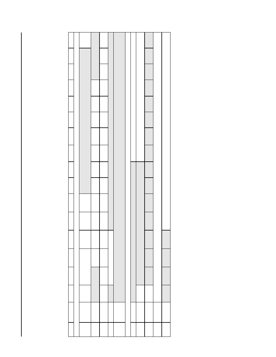
Preliminary Data Sheet
TMXF28155 Super Mapper
May 2001
155/51 Mbits/s SONET/SDH x28/x21 DS1/E1
311
Agere Systems Inc.
12 28-Channel Framer Registers
(continued)
12.20 28-Channel Framer Block Register Map
Table 447. Framer Register Map
Note: The reset default of all reserved bits is 0. Shading denotes reserved bits.
Address
Symbol
Bit 15
Bit 14
Bit 13
Bit 12
Bit 11
Bit 10
Bit 9
Bit 8
Bit 7
Bit 6
Bit 5
Bit 4
Bit 3
Bit 2
Bit 1
Bit 0
Superframer Global Registers--R/W
0x80000
FRM_SFGR1
FRM_
SW_TRN
FRM_LC_CNTRL[1:0]
FRM_LOOP_
TIMING
FRM_DS1_
CEPTN
FRM_PLL_
BYPAS
FRM_
LG_BUF_M
ODE
0x80001
FRM_SFGR2
FRM_TP_
SIG_PWDN
FRM_RP_
SIG_PWDN
FRM_TP_
RDL_PWDN
FRM_RP_
TDL_PWDN
FRM_TP_R
H_PWDN
FRM_RP_T
H_PWDN
FRM_TS_
PWDN
FRM_RS_
PWDN
FRM_TP_P
M_PWDN
FRM_RP_F
F_PWDN
FRM_TP_
RA_PWDN
0x80002
FRM_SFGR3
(RO)
0
FRM_AR_IS
FRM_TP_
RDL_IS
FRM_TP_
TDL_IS
FRM_RH_IS
FRM_TH_IS
FRM_TS_
IS
FRM_RS_
IS
FRM_TP_
PM_IS
FRM_RP_
PM_IS
FRM_RP_R
DL_IS
FRM_RP_T
DL_IS
0
0
0
0
0x80003
FRM_SFGR4
FRM_VERSION[2:0]
0x80004
--
0x80009
--
Arbiter (Framer) Global Registers--R/W
0x80010
FRM_FGR1
FRM_TO[7:0]
0x80011
FRM_FGR2
FRM_TC_
EN
FRM_TC[7:0]
0x80012
FRM_FGR3
FRM_
TPSSE_IM
0x80014
FRM_FGR4
(COR)
FRM_TPSSEI[16:1]
0x80015
FRM_FGR5
(COR)
FRM_TPSSEI[28:17]

TMXF28155 Super Mapper
Preliminary Data Sheet
155/51 Mbits/s SONET/SDH x28/x21 DS1/E1
May 2001
312
Agere Systems Inc.
12 28-Channel Framer Registers
(continued)
Table 447. Framer Register Map (continued)
Address
Symbol
Bit 15
Bit 14
Bit 13
Bit 12
Bit 11
Bit 10
Bit 9
Bit 8
Bit 7
Bit 6
Bit 5
Bit 4
Bit 3
Bit 2
Bit 1
Bit 0
Performance Monitor Global Registers--R/W
0x80P20
FRM_PMGR1_
B
FRM_
SEC_SEL
FRM_CT125[11:0]
0x80P30
FRM_PMGR1
(COR)
FRM_
DETECT
FRM_
PTRNBER
0x80P31
FRM_PMGR2
FRM_TPERR_CT[15:0]
0x80P32
FRM_PMGR3
FRM_RAC[2:0]
FRM_RDC[2:0]
FRM_
FSFBEEN
FRM_
CMFRFEN
FRM_
CRCRFEN
FRM_CEPTAISM[1:0]
FRM_
DS1AISM
FRM_
ESFRAIM
FRM_
RAICLR
0x80P33
FRM_PMGR4
FRM_SFSEST[15:0]
0x80P34
FRM_PMGR5
FRM_DCT[15:0]
0x80P35
FRM_PMGR6
FRM_ESFSEST[15:0]
0x80P36
FRM_PMGR7
FRM_
DSEF
FRM_DLFA
FRM_DRFA
FRM_
DSLIP
FRM_
DLOS
FRM_DAIS
FRM_
DCRC
FRM_DFS
FRM_DFT
0x80P37
FRM_PMGR8
FRM_CCT[15:0]
0x80P38
FRM_PMGR9
FRM_CSEST[15:0]
0x80P39
FRM_PMGR10
FRM_
CSA6_F
FRM_
CSA6_E
FRM_
CSA6_C
FRM_
CSA6_8
FRM_
CSA6_1X
FRM_
CSA6_X1
FRM_
CEBIT
FRM_
CLMFA
FRM_CLFA
FRM_CRFA
FRM_
CSLIP
FRM_
CLOS
FRM_CAIS
FRM_
CCRC
FRM_
CNOTFAS
FRM_
CFAS
0x80P3A
FRM_PMGR11
FRM_CRET[15:0]
0x80P3B
FRM_PMGR12
FRM_
CRAI_AIS
FRM_
CRAI_OOF
FRM_
CRAI_LOS
FRM_CRAI_S
A6EQC
FRM_CRAI_
SA6EQ8
FRM_CRAI_C
RCTX
FRM_CRAI
_LTS0MFA
FRM_CRAI
_LTS16MFA
FRM_CRAI_
8MSEX
FRM_DSR
AI_LOS
FRM_DSR
AI_OOF
FRM_DSR
AI_AIS
0x80P3C FRM_PMGR13
FRM_CFBE
_MODE
FRM_
CEBIT_
LTS0MFA
FRM_
CEBIT_
ESMF
FRM_
CEBIT_
CRCTX
0x80P3D FRM_PMGR14
FRM_PTRN_
EN
FRM_PTRN_
INV
FRM_PTRN
_FRMT
FRM_PTRN_LNK[4:0]
FRM_PTRN_SEL[3:0]
0x80P3E
FRM_PMGR15
FRM_LN_IS[16:1]
0x80P3F
FRM_PMGR16
FRM_LN_IS[28:17]
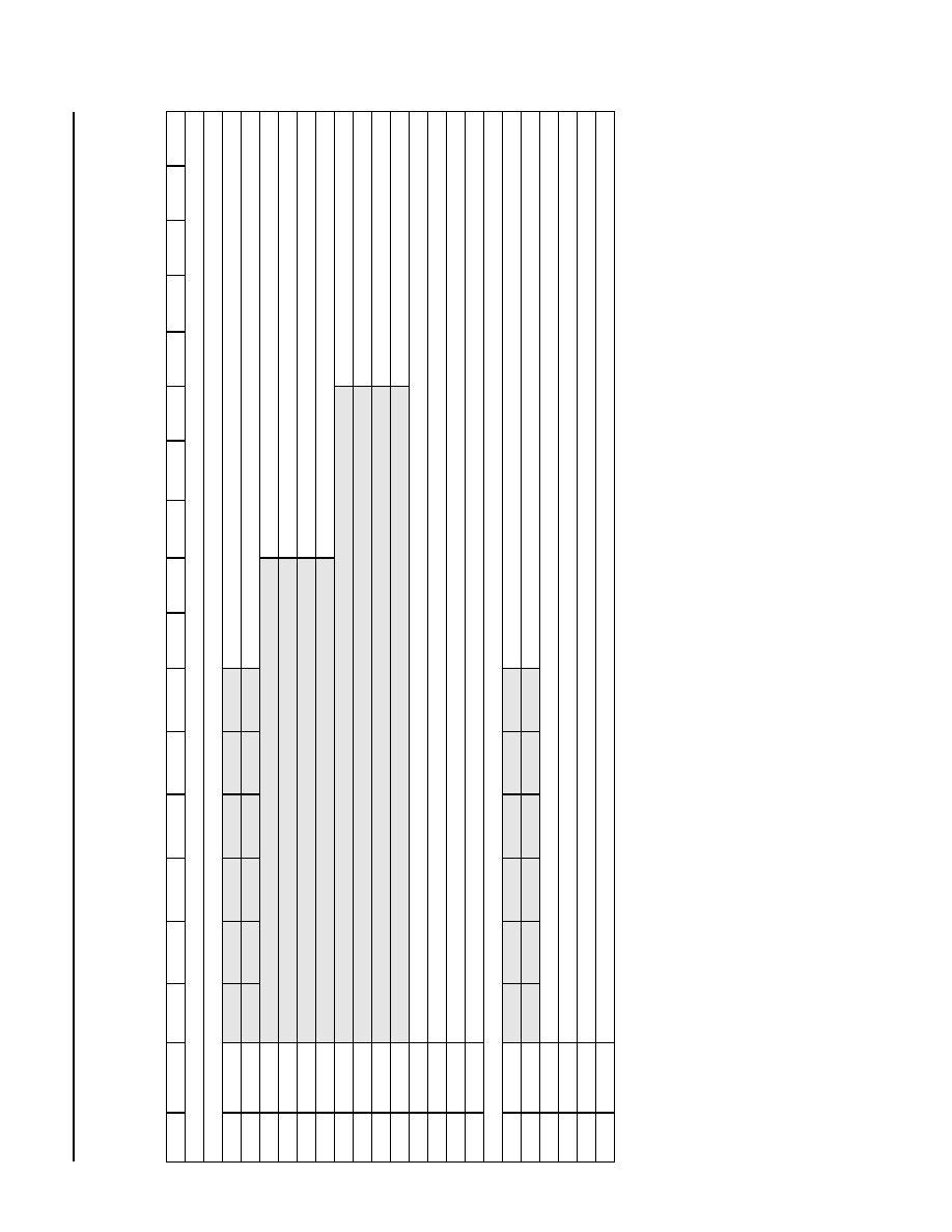
Preliminary Data Sheet
TMXF28155 Super Mapper
May 2001
155/51 Mbits/s SONET/SDH x28/x21 DS1/E1
313
Agere Systems Inc.
12 28-Channel Framer Registers
(continued)
Table 447. Framer Register Map (continued)
Address
Symbol
Bit 15
Bit 14
Bit 13
Bit 12
Bit 11
Bit 10
Bit 9
Bit 8
Bit 7
Bit 6
Bit 5
Bit 4
Bit 3
Bit 2
Bit 1
Bit 0
HDLC Global Configuration and Status Registers--R/W
Transmit HDLC Global Registers
0x80140
FRM_HGR1
FRM_HTTHRSH0[9:0]
0x80141
FRM_HGR2
FRM_HTTHRSH1[9:0]
0x80142
FRM_HGR3
FRM_TXICHAR0[7:0]
0x80143
FRM_HGR4
FRM_TXICHAR1[7:0]
0x80144
FRM_HGR5
FRM_TXICHAR2[7:0]
0x80145
FRM_HGR6
FRM_TXICHAR3[7:0]
0x80146
FRM_HGR7
FRM_FCNT0[4:0]
0x80147
FRM_HGR8
FRM_FCNT1[4:0]
0x80148
FRM_HGR9
FRM_FCNT2[4:0]
0x80149
FRM_HGR10
FRM_FCNT3[4:0]
0x8014A
FRM_HGR11
FRM_TH_IS[15:0]
0x8014B
FRM_HGR12
FRM_TH_IS[31:16]
0x8014C
FRM_HGR13
FRM_TH_IS[47:32]
0x8014D
FRM_HGR14
FRM_TH_IS[63:48]
Receive HDLC Global Registers
0x80040
FRM_HGR15
FRM_HRTHRSH0[9:0]
0x80041
FRM_HGR16
FRM_HRTHRSH1[9:0]
0x80042
FRM_HGR17
FRM_RH_IS[15:0]
0x80043
FRM_HGR18
FRM_RH_IS[31:16]
0x80044
FRM_HGR19
FRM_RH_IS[47:32]
0x80045
FRM_HGR20
FRM_RH_IS[63:48]
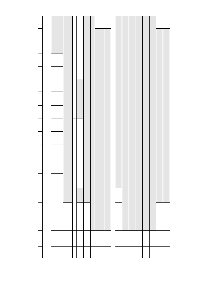
TMXF28155 Super Mapper
Preliminary Data Sheet
155/51 Mbits/s SONET/SDH x28/x21 DS1/E1
May 2001
314
Agere Systems Inc.
12 28-Channel Framer Registers
(continued)
Table 447. Framer Register Map (continued)
Address
Symbol
Bit 15
Bit 14
Bit 13
Bit 12
Bit 11
Bit 10
Bit 9
Bit 8
Bit 7
Bit 6
Bit 5
Bit 4
Bit 3
Bit 2
Bit 1
Bit 0
System Interface Global Registers--R/W
Receive System Interface Global Registers
0x80050
FRM_SYSGR1
FRM_SYSMOD[3:0]
FRM_ASM
FRM_CMS
FRM_
CHIDTS
FRM_
STUFFL or
FRM_
LNKSTART
FRM_
AISLFA
FRM_
AISCRCT
FRM_
DNOTFAS
FRM_
TFSCKE
FRM_
FSPOL
0x80051
FRM_SYSGR2 FRM_HWYE
NA
FRM_RSTDO
NE (read
only)
0x80052
FRM_SYSGR3
FRM_STUFF[7:0]
FRM_IDLE[7:0]
0x80053
FRM_SYSGR4
FRM_
STSSLB
FRM_
STSLLB
FRM_TSLBA[4:0]
FRM_TLSBL[4:0]
0x80054
FRM_SYSGR5
FRM_TS_
DPAR
FRM_TS_
SPAR
0x80055
FRM_SYSGR6
0x80056
FRM_SYSGR7
FRM_TPSB
_FS_IS
(COR)
0x80057
FRMSYSGR8
FRM_PSB_
FS_IM
Transmit System Interface Global Registers
0x80150
FRM_SYSGR9
FRM_RS_
DPAR
FRM_RS_
SPAR
FRM_
RFSCKE
0x80151
FRM_SYSGR1
0
0x80152
FRM_SYSGR1
1
0x80153
FRM_SYSGR1
2
0x80154
FRM_SYSGR1
3
0x80155
FRM_SYSGR1
4
0x80156
FRM_SYSGR1
5
FRM_
DPAR_IS
FRM_
SPAR_IS
FRM_PSB_
FS_IS
0x80157
FRM_SYSGR1
6
FRM_
DPAR_IM
FRM_
SPAR_IM
FRM_PSM
_FS_IM

Preliminary Data Sheet
TMXF28155 Super Mapper
May 2001
155/51 Mbits/s SONET/SDH x28/x21 DS1/E1
315
Agere Systems Inc.
12 28-Channel Framer Registers
(continued)
Table 447. Framer Register Map (continued)
Address
Symbol
Bit 15
Bit 14
Bit 13
Bit 12
Bit 11
Bit 10
Bit 9
Bit 8
Bit 7
Bit 6
Bit 5
Bit 4
Bit 3
Bit 2
Bit 1
Bit 0
Signaling Global Registers--R/W
0x80060
FRM_SGR1
FRM_R_
TSAISHG
FRM_R_LINKCNT[4:0]
FRM_TEST_BIT[2:0]
FRM_R_
AFZFBE
0x80061
FRM_SGR2
FRM_R_
SCOSEN
FRM_R_SCOSDTH[9:0]
0x80062
FRM_SGR3
FRM_R_SCOSTTH[15:0]
0x80063
FRM_SGR4
(RO)
FRM_R_COSFIFO[1:0]
FRM_R_COSFIFOL[4:0]
FRM_R_COSFIFOTS[4:0]
FRM_R_COSFIFOSIG[3:0]
0x80064
FRM_SGR5
(RO)
?
?
?
?
?
?
?
?
?
?
?
?
?
?
?
FRM_R_
COSDTHS
0x80065
FRM_SGR6
(COR)
0
0
0
0
0
0
0
0
0
0
0
0
0
FRM_R_
COSDTHI
FRM_R_
COSTTHI
FRM_R_
COSOFI
0x80066
FRM_SGR7
0
0
0
0
0
0
0
0
0
0
0
0
0
FRM_R_C
OSDTHM
FRM_R_
COSTTHM
FRM_R_
COSOFM
0x80160
FRM_SGR8
FRM_T_LINKCNT[4:0]
FRM_T_
SUBZERO
FRM_T_FA
S_NOTFAS
FRM_T_
AFZFBE
Frame Formatter Global Register--R/W
0x80170
FRM_FFGR1
FRM_
TXSOOF
FRM_
PTRN_EN
FRM_
PTRN_INV
FRM_PTRN
_FRMT
FRM_PTRN_LNK[4:0]
FRM_PTRN_SEL[3:0]
Facility Data Link Global Registers--R/W
0x80090
FRM_FDLGR1
0x801A1
FRM_FDLGR2
TMXF28155 Super Mapper
Preliminary Data Sheet
155/51 Mbits/s SONET/SDH x28/x21 DS1/E1
May 2001
316
Agere Systems Inc.
12 28-Channel Framer Registers
(continued)
Table 447. Framer Register Map (continued)
Address
Symbol
Bit 15
Bit 14
Bit 13
Bit 12
Bit 11
Bit 10
Bit 9
Bit 8
Bit 7
Bit 6
Bit 5
Bit 4
Bit 3
Bit 2
Bit 1
Bit 0
Receive Signaling Link Registers--R/W
See Table 370 for Values of L and R in the Register Address Field
0x8LR00
FRM_RSLR0
FRM_RPSR0[6:0]
0x8LR01
FRM_RSLR1
FRM_RPSR1[6:0]
0x8LR02
FRM_RSLR2
FRM_RPSR2[6:0]
0x8LR03
FRM_RSLR3
FRM_RPSR3[6:0]
0x8LR04
FRM_RSLR4
FRM_RPSR4[6:0]
0x8LR05
FRM_RSLR5
FRM_RPSR5[6:0]
0x8LR06
FRM_RSLR6
FRM_RPSR6[6:0]
0x8LR07
FRM_RSLR7
FRM_RPSR7[6:0]
0x8LR08
FRM_RSLR8
FRM_RPSR8[6:0]
0x8LR09
FRM_RSLR9
FRM_RPSR9[6:0]
0x8LR0A
FRM_RSLR10
FRM_RPSR10[6:0]
0x8LR0B
FRM_RSLR11
FRM_RPSR11[6:0]
0x8LR0C
FRM_RSLR12
FRM_RPSR12[6:0]
0x8LR0D
FRM_RSLR13
FRM_RPSR13[6:0]
0x8LR0E
FRM_RSLR14
FRM_RPSR14[6:0]
0x8LR0F
FRM_RSLR15
FRM_RPSR15[6:0]
0x8LR10
FRM_RSLR16
FRM_RPSR16[6:0]
0x8LR11
FRM_RSLR17
FRM_RPSR17[6:0]
0x8LR12
FRM_RSLR18
FRM_RPSR18[6:0]
0x8LR13
FRM_RSLR19
FRM_RPSR19[6:0]
0x8LR14
FRM_RSLR20
FRM_RPSR20[6:0]
0x8LR15
FRM_RSLR21
FRM_RPSR21[6:0]
0x8LR16
FRM_RSLR22
FRM_RPSR22[6:0]
0x8LR17
FRM_RSLR23
FRM_RPSR23[6:0]
0x8LR18
FRM_RSLR24
FRM_RPSR24[6:0]
0x8LR19
FRM_RSLR25
FRM_RPSR25[6:0]
0x8LR1A
FRM_RSLR26
FRM_RPSR26[6:0]
0x8LR1B
FRM_RSLR27
FRM_RPSR27[6:0]
0x8LR1C
FRM_RSLR28
FRM_RPSR28[6:0]
0x8LR1D
FRM_RSLR29
FRM_RPSR29[6:0]
0x8LR1E
FRM_RSLR30
FRM_RPSR30[6:0]
0x8LR1F
FRM_RSLR31
FRM_RPSR31[6:0]
0x8LR21
FRM_RSLR32
FRM_R_
FZCON
FRM_R_
SIGI
FRM_R_
RXSTOMP
FRM_R_
SIGDEB
FRM_R_
HGEN
FRM_R_
MSIGFZ
FRM_R_
FGSRC
FRM_R_SIGSRC[1:0]
0x8LR20
FRM_RSLR33
FRM_R_HGAIS[3:0]
FRM_R_HGA[3:0]
FRM_R_HGRDI[3:0]
FRM_R_
TS16A
FRM_R_
TS16AIS

Preliminary Data Sheet
TMXF28155 Super Mapper
May 2001
155/51 Mbits/s SONET/SDH x28/x21 DS1/E1
317
Agere Systems Inc.
12 28-Channel Framer Registers
(continued)
Table 447. Framer Register Map (continued)
Address
Symbol
Bit 15
Bit 14
Bit 13
Bit 12
Bit 11
Bit 10
Bit 9
Bit 8
Bit 7
Bit 6
Bit 5
Bit 4
Bit 3
Bit 2
Bit 1
Bit 0
Transmit Signaling Link Registers--R/W
See Table 375 for Values of L and T in the Register Address Field
0x8LT00
FRM_TSLR0
FRM_TPSR0[6:0]
0x8LT01
FRM_TSLR1
FRM_TPSR1[6:0]
0x8LT02
FRM_TSLR2
FRM_TPSR2[6:0]
0x8LT03
FRM_TSLR3
FRM_TPSR3[6:0]
0x8LT04
FRM_TSLR4
FRM_TPSR4[6:0]
0x8LT05
FRM_TSLR5
FRM_TPSR5[6:0]
0x8LT06
FRM_TSLR6
FRM_TPSR6[6:0]
0x8LT07
FRM_TSLR7
FRM_TPSR7[6:0]
0x8LT08
FRM_TSLR8
FRM_TPSR8[6:0]
0x8LT09
FRM_TSLR9
FRM_TPSR9[6:0]
0x8LT0A
FRM_TSLR10
FRM_TPSR10[6:0]
0x8LT0B
FRM_TSLR11
FRM_TPSR11[6:0]
0x8LT0C
FRM_TSLR12
FRM_TPSR12[6:0]
0x8LT0D
FRM_TSLR13
FRM_TPSR13[6:0]
0x8LT0E
FRM_TSLR14
FRM_TPSR14[6:0]
0x8LT0F
FRM_TSLR15
FRM_TPSR15[6:0]
0x8LT10
FRM_TSLR16
FRM_TPSR16[6:0]
0x8LT11
FRM_TSLR17
FRM_TPSR17[6:0]
0x8LT12
FRM_TSLR18
FRM_TPSR18[6:0]
0x8LT13
FRM_TSLR19
FRM_TPSR19[6:0]
0x8LT14
FRM_TSLR20
FRM_TPSR20[6:0]
0x8LT15
FRM_TSLR21
FRM_TPSR21[6:0]
0x8LT16
FRM_TSLR22
FRM_TPSR22[6:0]
0x8LT17
FRM_TSLR23
FRM_TPSR23[6:0]
0x8LT18
FRM_TSLR24
FRM_TPSR24[6:0]
0x8LT19
FRM_TSLR25
FRM_TPSR25[6:0]
0x8LT1A
FRM_TSLR26
FRM_TPSR26[6:0]
0x8LT1B
FRM_TSLR27
FRM_TPSR27[6:0]
0x8LT1C
FRM_TSLR28
FRM_TPSR28[6:0]
0x8LT1D
FRM_TSLR29
FRM_TPSR29[6:0]
0x8LT1E
FRM_TSLR30
FRM_TPSR30[6:0]
0x8LT1F
FRM_TSLR31
FRM_TPSR31[6:0]
0x8LT21
FRM_TSLR32
FRM_T_
ATS16RFA
FRM_T_
ASPLB
FRM_T_MSP
FRM_T_
ZCSM
FRM_T_
VTSIGE
FRM_T_
SIGI
FRM_T_
TXSTOMP
FRM_T_
HGEN
FRM_T_
MSIGFZ
FRM_T_
FGSRC
FRM_T_SIGSRC[1:0]
0x8LT20
FRM_TSLR33
FRM_T_
TS16A
FRM_T_
TS16AIS
TMXF28155 Super Mapper
Preliminary Data Sheet
155/51 Mbits/s SONET/SDH x28/x21 DS1/E1
May 2001
318
Agere Systems Inc.
12 28-Channel Framer Registers
(continued)
Table 447. Framer Register Map (continued)
Address
Symbol
Bit 15
Bit 14
Bit 13
Bit 12
Bit 11
Bit 10
Bit 9
Bit 8
Bit 7
Bit 6
Bit 5
Bit 4
Bit 3
Bit 2
Bit 1
Bit 0
Performance Monitor Link Registers--COR
See Table 381 for Values of L and P in the Register Address Field
0x8LP80
FRM_PMLR1
(R/W)
FRM_PM_IM4[15:0]
0x8LP81
FRM_PMLR2
(R/W)
FRM_PM_IM5[15:0]
0x8LP82
FRM_PMLR3
(R/W)
FRM_MHGALIGN[3:0]
FRM_
MSEFS
FRM_MFE
FRM_PM_IM6[4:0]
0x8LP83
FRM_PMLR4
FRM_SLIPO FRM_SLIPU
FRM_OOF
FRM_LSFA
FRM_OAIS
FRM_AIS
FRM_ORAI
FRM_RAI
FRM_
SA600X1E
FRM_
SA6001XE
FRM_
CRCTX
FRM_
LTS0MFA
FRM_
TS0MFABE
FRM_SES
FRM_BES
FRM_ES
0x8LP84
FRM_PMLR5
FRM_LFV
FRM_FBE
FRM_CRCE FRM_ECRCE
FRM_
REBIT
FRM_
CREBIT
FRM_LTFA
FRM_NFA
FRM_
SA7LID
FRM_
LLBON
FRM_
LLBOFF
FRM_AUX
P
FRM_LOS
FRM_
BOMR
0x8LP85
FRM_PMLR6
FRM_
FDL_RAI
FRM_FDL_
PLBON
FRM_FDL_
PLBOFF
FRM_FDL_
LLBON
FRM_FDL_
LLBOFF
0x8LP86
FRM_PMLR7
FRM_BPV[15:0]
0x8LP87
FRM_PMLR8
FRM_FBEC[15:0]
0x8LP88
FRM_PMLR9
FRM_CEC[15:0]
0x8LP89
FRM_PMLR10
FRM_REC[15:0]
0x8LP8A
FRM_PMLR11
FRM_CETE[15:0]
0x8LP8B
FRM_PMLR12
FRM_CENT[15:0]
0x8LP8C
FRM_PMLR13
FRM_FE_OP
FRM_FE_N
FRM_FE_M
FRM_FE_L
FRM_FE_K FRM_FE_I
FRM_FE_H
FRM_FE_G FRM_FE_F FRM_FE_E FRM_FE_D FRM_FE_C FRM_FE_B FRM_FE_A
0x8LP8D
FRM_PMLR14
FRM_FE_Y FRM_FE_X
FRM_FE_W FRM_FE_V FRM_FE_U FRM_FE_T FRM_FE_S FRM_FE_R FRM_FE_Q
0x8LP8E
FRM_PMLR15
FRM_ESC[15:0]
0x8LP8F
FRM_PMLR16
FRM_BESC[15:0]
0x8LP90
FRM_PMLR17
FRM_SESC[15:0]
0x8LP91
FRM_PMLR18
FRM_RBOM[7:0]
0x8LP92
FRM_PMLR19
FRM_HGALIGN[3:0]
FRM_SEFS
0x8LP93
FRM_PMLR20
FRM_G6
FRM_G5
FRM_G4
FRM_G3
FRM_G2
FRM_G1
FRM_SE
FRM_FE
FRM_LV
FRM_SL
FRM_LB
FRM_N1
FRM_N0

Preliminary Data Sheet
TMXF28155 Super Mapper
May 2001
155/51 Mbits/s SONET/SDH x28/x21 DS1/E1
319
Agere Systems Inc.
12 28-Channel Framer Registers
(continued)
Table 447. Framer Register Map (continued)
Address
Symbol
Bit 15
Bit 14
Bit 13
Bit 12
Bit 11
Bit 10
Bit 9
Bit 8
Bit 7
Bit 6
Bit 5
Bit 4
Bit 3
Bit 2
Bit 1
Bit 0
Receive FDL Link Registers--R/W
See Table 403 for Values of L and R in the Register Address Field
0x8LRC0
FM_RFDLLR1
FRM_RXS0[15:0]
0x8LRC1
FM_RFDLLR2
FRM_RXS1[15:0]
0x8LRC2
FM_RFDLLR3
FRM_RXS2[15:0]
0x8LRC3
FM_RFDLLR4
FRM_RXS3[15:0]
0x8LRC4
FM_RFDLLR5
FRM_RXS4[15:0]
0x8LRC5
FM_RFDLLR6
FRM_RXC
RCSM
0x8LRC6
FM_RFDLLR7
0
0
0
0
0
0
0
0
0
0
0
0
0
0
0
FRM_
RXSA
0x8LRC7
FM_RFDLLR8
0
0
0
0
0
0
0
0
0
0
0
0
0
0
0
FRM_
RXSR_IS
0x8LRC8
FM_RFDLLR9
FRM_
RXSR_IM
Transmit FDL Link Registers--R/W
See Table 410 for Values of L and T in the Register Address Field
0x8LTD0
FM_TFDLLR1
FRM_TXS0[15:0]
0x8LTD1
FM_TFDLLR2
FRM_TXS1[15:0]
0x8LTD2
FM_TFDLLR3
FRM_TXS2[15:0]
0x8LTD3
FM_TFDLLR4
FRM_TXS3[15:0]
0x8LTD4
FM_TFDLLR5
FRM_TXS4[15:0]
0x8LTD5
FM_TFDLLR6
FRM_
ABITSRC
FRM_
MBITSRC
FRM_
SBITSRC
FRM_
CBITSRC
FRM_
SA8SC
FRM_
SA7SC
FRM_
SA6SC
FRM_
SA5SC
FRM_
SA4SC
FRM_
TXCRCSM
FRM_
ASRC
FRM_DS1I
0x8LTD6
FM_TFDLLR7
FRM_BOME
FRM_TBOM[5:0]
0x8LTD7
FM_TFDLLR8
(RO/COW)
FRM_
BOMC_IS
FRM_
TXSE_IS
0x8LTD8
FM_TFDLLR9
FRM_
BOMC_IM
FRM_
TXSE_IM
System Interface Link Registers--R/W
See Table 417 for Values of L and P in the Register Address Field
0x8LPE0
FRM_SYSLR1
FRM_BYOFF[6:0]
FRM_OFF[2:0]
FRM_
HALFOFF
FRM_
QUAROFF
0x8LPE1
FRM_SYSLR2 FRM_CEPT
MAIS
FRM_CEPTA
AIS
FRM_MANAI
S
FRM_CEPTS
TMP
0x8LPE2
FRM_SYSLR3
0x8LPE3
FRM_SYSLR4
0x8LPE4
FRM_SYSLR5
0x8LPE5
FRM_SYSLR6

TMXF28155 Super Mapper
Preliminary Data Sheet
155/51 Mbits/s SONET/SDH x28/x21 DS1/E1
May 2001
320
Agere Systems Inc.
12 28-Channel Framer Registers
(continued)
Table 447. Framer Register Map (continued)
Address
Symbol
Bit 15
Bit 14
Bit 13
Bit 12
Bit 11
Bit 10
Bit 9
Bit 8
Bit 7
Bit 6
Bit 5
Bit 4
Bit 3
Bit 2
Bit 1
Bit 0
Arbiter Link Registers--R/W
See Table 417 for Values of L and T in the Register Address Field
0x8LPF0
FRM_ARLR1
FRM_
LNK_ENA
FRM_LNK_
TRANSP
FRM_LNK_
RESTARTN
FRM_LNK_
REFRAME
FRM_
ICKEDGE
0x8LPF1
FRM_ARLR2
FRM_ESF_
CRC_EN
FRM_FAST
FRM_OPT[1:0]
FRM_FBE_
MODE
FRM_LF_CRT[2:0]
FRM_AUTO
_AIS
FRM_RAIL3_DEC[1:0]
FRM_MODE[3:0]
0x8LPF2
FRM_ARLR3
FRM_TP_C
K_SRC_EN
FRM_TP_
CK_SRC
FRM_TP_
DD_SRC
Frame Formatter Link Registers--R/W
See Table 417 for Values of L and T in the Register Address Field
0x8LPF4
FRM_FFLR1
FRM_
ESFRAMD
FRM_ZCSMD[2:0]
FRM_
OCKEDGE
FRM_
AUTOPLB
FRM_
AUTOLLB
FRM_
AUTOEBIT
FRM_
AUTORAI
0x8LPF5
FRM_FFLR2
FRM_TXLBMD[1:0]
FRM_
TXLLBOFF
FRM_
TXLLBON
FRM_TXIID
FRM_
TXAUXP
FRM_
TXRAICI
FRM_
TXRAI
FRM_
TXAISCI
FRM_
TXAIS
Line Decoder/Encoder Link Registers--R/W
See Table 427 and Tabl e429 for Values of L and T in the Register Address Field
0x8TPFC
FRM_LDLR1
FRM_
EXCZERO
FRM_RLCL
K_EDGE
FRM_LD_MODE[2:0]
0x8LPFD
FRM_LDLR2
FRM_TLCL
K_EDGE
FRM_LE_MODE[2:0]
HDLC Channel Registers--R/W
See Table 432 for Mapping of H and P in the Register Address Field
Transmit HDLC Channel Registers
0x8HP80
FRM_HCR1
FRM_TTIMESLOT[4:0]
FRM_TBIT_IM[7:0]
0x8HP81
FRM_HCR2
FRM_TFRAME_SEL[1:0]
FRM_TLINK[4:0]
0x8HP82
FRM_HCR3
FRM_THC_
RESET
FRM_
TENABL
FRM_CFLAGS[1:0]
FRM_
PRMEN
FRM_
TLOOP
FRM_C_R
FRM_
HTTHRSEL
FRM_IFCS
FRM_
HTIDLE
FRM_
HTMODE
FRM_HXPIDLE[1:0]
0x8HP83
FRM_HCR4
(RO)
0
0
0
0
0
0
0
0
0
0
0
0
0
FRM_
HTUND
FRM_
HTDONE
FRM_
HTTHRSH
0x8HP84
FRM_HCR5
FRM_
MHTUND
FRM_
MHTDONE
FRM_MHT
THRSH
0x8HP85
FRM_HCR6
(WO)
FRM_HTFUNC[1:0]
FRM_HTDATA[7:0]
0x8HP86
FRM_HCR7
FRM_HTCOUNT[9:0]
Receive HDLC Channel Registers
0x8HP00
FRM_HCR8
FRM_RTIMESLOT[4:0]
FRM_RBIT_IM[7:0]
0x8HP01
FRM_HCR9
FRM_RFRAME_SEL[1:0]
FRM_RLINK[4:0]
0x8HP02
FRM_HCR10
FRM_RHC_
RESET
FRM_
RENABL
FRM_
RTHRSEL
FRM_RFCS
FRM_
HRMODE
FRM_
BYTAL
FRM_MATCH[7:0]
0x8HP03
FRM_HCR11
(RO)
0
0
0
0
0
0
0
0
0
0
0
0
FRM_
RIDLE
FRM_OVR
FRM_EOP
FRM_
HRTHRSH
0x8HP04
FRM_HCR12
FRM_
MIDLE
FRM_
MOVR
FRM_
MEOP
FRM_MHR
THRSH
0x8HP05
FRM_HCR13
(RO)
0
0
0
0
0
FRM_HMDA
FRM_
HRVALID
FRM_
HRTYPE
FRM_HR_DATA[7:0]
FRM_HOVR FRM_HEOP
FRM_
HCRCERR
FRM_
HABRT
FRM_HIDL
FRM_HBIT[2:0]
0x8HP06
FRM_HCR14
(COR)
FRM_HRCOUNT[9:0]

Preliminary Data Sheet
TMXF28155/51 Super Mapper
May 2001
155/51 Mbits/s SONET/SDH x28/x21 DS1/E1
321
Agere Systems Inc.
13 Cross Connect (XC) Registers
Table of Contents
Contents
Page
13 Cross Connect (XC) Registers ....................................................................................................................... 321
13.1 Cross Connect Register Descriptions ..................................................................................................... 322
13.2 Cross Connect Register Map ................................................................................................................. 328
Tables
Page
Table 448. XC_ID_R, XC Global Register 1 (RO) ............................................................................................... 322
Table 449. XC_CHI_MODE1_R, XC System Interface Global Register 1 (R/W) ................................................ 322
Table 450. XC_CHI_MODE2_R, XC System Interface Global Register 2 (R/W) ................................................ 322
Table 451. XC_PIND_SRC[1--15], XC1 External I/O TXDATA and TXCLK Source Configuration (R/W) ......... 323
Table 452. XC_FRP_SRC[1--14], XC1 Framer Receive Path Data Source Configuration (R/W) ..................... 323
Table 453. XC_M13_SRC[1--14], XC1 M13 Data Source Configuration (R/W) ................................................. 323
Table 454. XC_VT_SRC[1--14], XC1 VT Mapper Source Configuration (R/W) ................................................. 324
Table 455. XC_DJA_SRC[1--14], XC1 Digital Jitter Attenuator Source Configuration (R/W) ............................ 324
Table 456. XC_FTP_SRC[1--14], XC1 Framer Transmit Path Data Source Configuration (R/W) ..................... 324
Table 457. XC_FRS_SRC[1--14], XC1 Framer Receive System Interface Source Configuration (R/W) .......... 324
Table 458. XC_TPM_SRC[1--4], XC1 Test-Pattern Monitor Source Configuration (R/W) ................................. 325
Table 459. XC2_M12_SRC[1--7], XC2 M12 DS2 Clock and Data Source Configuration (R/W) ........................ 325
Table 460. XC2_M23_SRC[1--7], XC2 M23 DS2 Data Source Configuration (R/W) ......................................... 325
Table 461. XC2_TPM_SRC, XC2 Test-Pattern Monitor Source Configuration (R/W) ........................................ 326
Table 462. XC_MISC, XC Global Register 2 (R/W) ............................................................................................ 326
Table 463. XC3_TPM_SRC, XC3 Test-Pattern Monitor Source Configuration (R/W) ........................................ 326
Table 464. XC3_MDS3_SRC, XC3 DS3 Source Configuration (R/W) ................................................................ 327
Table 465. XC_PINS_SRC[1--15], XC1 External I/O TXSYNC Source Configuration (R/W) ............................ 327
Table 466. XC_ALCO_SRC[1--15], XC1 External I/O RXCLK Clock Out Source Configuration (R/W) ............. 327
Table 467. Register Address Map ....................................................................................................................... 328

TMXF28155/51 Super Mapper
Preliminary Data Sheet
155/51 Mbits/s SONET/SDH x28/x21 DS1/E1
May 2001
322
Agere Systems Inc.
13 Cross Connect (XC) Registers
(continued)
13.1 Cross Connect Register Descriptions
Table 448. XC_ID_R, XC Global Register 1 (RO)
Table 449. XC_CHI_MODE1_R, XC System Interface Global Register 1 (R/W)
Table 450. XC_CHI_MODE2_R, XC System Interface Global Register 2 (R/W)
DS1/E1 crosspoint connectivity is determined by a set of source identifiers (SOURCE_IDs), one for each channel
leaving the crosspoint switch. A DS1/E1 SOURCE_ID is therefore defined as follows:
Address Bit
Name
Function
Reset
Default
0x50000
15:11
--
Reserved.
0x0005
10:8
XC_VERSION[2:0]
Version. These bits identify the version number of the XC.
7:0
XC_ID[7:0]
XC_ID. XC_ID register returns a fixed value (0x05) when
read.
Address Bit
Name
Function
Reset
Default
0x5000E
15:3
--
Reserved.
0x0000
2
--
Reserved. Must write to 0.
1
XC_SYNC_FOR_DATA Sync For Data. This bit should set to 1 if the transmit sys-
tem interface is in use (CHI, PSB, and NSMI). Setting this
bit allows the external I/O pins LINETXSYNC[29--1] to
output transmit system data. Otherwise, set to 0.
0
XC_SI_CHI
PSB/CHI. This bit should be set to 1 if the transmit system
interface is in PSB mode; otherwise, 0 in CHI mode.
Address
Bit
Name
Function
Reset
Default
0x5000F
15:14
--
Reserved.
0x0000
13:0
XC_CHI_MODE
[1--7][1:0]
CHI Mode. The 28 transmit system links are broken down
into seven groups of four. Each group is controlled by two
bits XC_CHI_MODE[1--7][1:0]. XC_CHI_MODE[1--7][1:0]
controls the group of links 4i ≠ 3, 4i ≠ 2, 4i ≠ 1, and 4i, where
i = 1 to 7. The definition of CHI_MODE[1--7][1:0] is as fol-
lows:
00 = All four links within the group are normal outputs at
2 Mbits/s or 4 Mbits/s.
01 = Links 4i ≠ 3 and 4i ≠ 2 are normal outputs; links 4i ≠ 1
and 4i are combined into a single output on 4i; and out-
put 4i ≠ 1 is used as T1/E1 line output.
10 = Links 4i ≠ 1 and 4i are combined into a single output on
4i; links 4i ≠ 3 and 4i ≠ 2 are combined into a single out-
put on 4i ≠ 2; and outputs 4i ≠ 1 and 4i ≠ 3 are used as
T1/E1 line outputs.
11 = All four links are combined into a single output on 4i;
and the other three outputs are used as T1/E1 line out-
puts.
Bit
7
6
5
4
3
2
1
0
SOURCE_ID
SOURCE_BLOCK[2:0]
CHANNEL_ID[4:0]

Preliminary Data Sheet
TMXF28155/51 Super Mapper
May 2001
155/51 Mbits/s SONET/SDH x28/x21 DS1/E1
323
Agere Systems Inc.
13 Cross Connect (XC) Registers
(continued)
The SOURCE_BLOCK is defined as:
The CHANNEL_ID typically ranges from 1 to 28 (29 for external). Values 0, 30, and 31 (and usually 29 as well) are
unused. The above definition is valid for XC_PDATA[1--29], XC_RP_RDATA[1--28], XC_MDS1DATA[1--29]
(
Table 453
), XC_VDATA[1--28] (
Table 454
), XC_SYNC[1--29] (
Table 465
), and XC_ALCO[1--29] (
Table 466
).
Table 452. XC_FRP_SRC[1--14], XC1 Framer Receive Path Data Source Configuration (R/W)
Table 453. XC_M13_SRC[1--14], XC1 M13 Data Source Configuration (R/W)
Index
Block Identifier
Index
Block Identifier
000
TPG (Test-Pattern Generator)/Special
100
VTMPR (VT Mapper)
001
PIN (External I/O)
101
DJA (Jitter Attenuator)
010
FRM TP (Superframer)
110
FRM RP (Framer Line Interface)
011
M13 (M13 MUX)
111
FRM TS (Framer System Interface)
Table 451. XC_PIND_SRC[1--15], XC1 External I/O TXDATA and TXCLK Source Configuration (R/W)
Address
Bit
Name
Function
Reset
Default
0x50010
--
0x5001D
15:8
XC_PDATA
[2, 4, . . . 28][7:0]
(SOURCE_ID)
Source Identifier for External I/O Pin LINETXDATA and
LINETXCLK Connection. External I/O DS1/E1 data and
clock (even channels).
0x1E
(invalid)
0x5001E
15:8
--
Reserved.
0x00
0x50010
--
0x5001E
7:0
XC_PDATA
[1, 3, . . . 29][7:0]
(SOURCE_ID)
Source Identifier for External I/O Pin LINETXDATA and
LINETXCLK Connection. External I/O DS1/E1 data and
clock (odd channels).
Note: External I/O has 29 channels.
0x1E
(invalid)
Address
Bit
Name
Function
Reset
Default
0x50020
--
0x5002D
15:8
XC_RP_RDATA
[2, 4, . . . 28][7:0]
(SOURCE_ID)
Source Identifier for Framer Receive Path Connection.
Framer receive path DS1/E1 input signals RP_RDATA,
RP_RCLK, RP_RFS, RP_AIS, and RP_RAI (even channels).
0xFF
(invalid)
0x50020
--
0x5002D
7:0
XC_RP_RDATA
[1, 3, . . . 27][7:0]
(SOURCE_ID)
Source Identifier for Framer Receive Path Connection.
Framer receive path DS1/E1 input signals RP_RDATA,
RP_RCLK, RP_RFS, RP_AIS, and RP_RAI (odd channels).
0xFF
(invalid)
Address
Bit
Name
Function
Reset
Default
0x50030
--
0x5003D
15:8
XC_MDS1DATA
[2, 4, . . . 28][7:0]
(SOURCE_ID)
Source Identifier for M13 MUX Connection. M13 DS1/E1
data and clock inputs (even channels). Also for stuff request
inputs if operating in LOW_CLOCK_OUT mode.
0xFF
(invalid)
0x50030
--
0x5003D
7:0
XC_MDS1DATA
[1, 3, . . . 27][7:0]
(SOURCE_ID)
Source Identifier for M13 MUX Connection. M13 DS1/E1
data and clock inputs (odd channels). Also for stuff request
inputs if operating in LOW_CLOCK_OUT mode.
0xFF
(invalid)

TMXF28155/51 Super Mapper
Preliminary Data Sheet
155/51 Mbits/s SONET/SDH x28/x21 DS1/E1
May 2001
324
Agere Systems Inc.
13 Cross Connect (XC) Registers
(continued)
Table 454. XC_VT_SRC[1--14], XC1 VT Mapper Source Configuration (R/W)
Table 455. XC_DJA_SRC[1--14], XC1 Digital Jitter Attenuator Source Configuration (R/W)
Table 456. XC_FTP_SRC[1--14], XC1 Framer Transmit Path Data Source Configuration (R/W)
Table 457. XC_FRS_SRC[1--14], XC1 Framer Receive System Interface Source Configuration (R/W)
Address
Bit
Name
Function
Reset
Default
0x50040
--
0x5004D
15:8
XC_VDATA
[2, 4, . . . 28][7:0]
(SOURCE_ID)
Source Identifier for VT Mapper Connection. VT mapper
DS1/E1 data, clock, sync, and RAI inputs (even channels).
0xFF
(invalid)
0x50040
--
0x5004D
7:0
XC_VDATA
[1, 3, . . . 27][7:0]
(SOURCE_ID)
Source Identifier for VT Mapper Connection. VT mapper
DS1/E1 data, clock, sync, and RAI inputs (odd channels).
0xFF
(invalid)
Address
Bit
Name
Function
Reset
Default
0x50050
--
0x5005D
15:8
XC_JDATA
[2, 4, . . . 28][7:0]
(SOURCE_ID)
Source Identifier for Jitter Attenuator Connection. DJA
DS1/E1 data, clock, pointer adjustment, and autoAIS inputs
(even channels).
0xFF
(invalid)
0x50050
--
0x5005D
7:0
XC_JDATA
[1, 3, . . . 27][7:0]
(SOURCE_ID)
Source Identifier for Jitter Attenuator Connection. DJA
DS1/E1 data, clock, pointer adjustment, and autoAIS inputs
(odd channels).
0xFF
(invalid)
Address
Bit
Name
Function
Reset
Default
0x50060
--
0x5006D
15:8
XC_TP_RDATA
[2, 4, . . . 28][7:0]
(SOURCE_ID)
Source Identifier for Framer Transmit Path Connection.
Framer transmit path DS1/E1 input signals (even channels).
0xFF
(invalid)
0x50060
--
0x5006D
7:0
XC_TP_RDATA
[1, 3, . . . 27][7:0]
(SOURCE_ID)
Source Identifier for Framer Transmit Path Connection.
Framer transmit path DS1/E1 input signals (odd channels).
0xFF
(invalid)
Address
Bit
Name
Function
Reset
Default
0x50070
--
0x5007D
15:8
XC_RS_D
[2, 4, . . . 28][7:0]
(SOURCE_ID)
Source Identifier for Framer Receive System Interface
Connection. Framer receive system (RS) data input (even
channels).
0x00
(invalid)
0x50070
--
0x5007D
7:0
XC_RS_D
[1, 3, . . . 27][7:0]
(SOURCE_ID)
Source Identifier for Framer Receive System Interface
Connection. Framer receive system (RS) data input (odd
channels).
0x00
(invalid)

Preliminary Data Sheet
TMXF28155/51 Super Mapper
May 2001
155/51 Mbits/s SONET/SDH x28/x21 DS1/E1
325
Agere Systems Inc.
13 Cross Connect (XC) Registers
(continued)
Table 458. XC_TPM_SRC[1--4], XC1 Test-Pattern Monitor Source Configuration (R/W)
The DS2 crosspoint's connectivity is determined by a smaller set of source2 identifiers (SOURCE2_IDs), one for
each channel leaving the DS2 crosspoint switch XC2. A DS2 SOURCE2_ID is therefore defined as follows:
The SOURCE2_BLOCK is defined as follows:
The CHANNEL2_ID typically ranges from 1 to 7. For test data (SOURCE2_BLOCK = 0), value 4 represents the
DS2 test pattern. For DS2 signals routed from external pins to the input of M23 MUX or TPM, the CHANNEL2_ID
can range from 1 to 29.
Table 459. XC2_M12_SRC[1--7], XC2 M12 DS2 Clock and Data Source Configuration (R/W)
Table 460. XC2_M23_SRC[1--7], XC2 M23 DS2 Data Source Configuration (R/W)
Address
Bit
Name
Function
Reset
Default
0x50080
15:8
--
Reserved. 0x00
7:0
XC_TPM_DS1_DATA[7:0]
(SOURCE_ID)
Source Identifier for TPM DS1 Data Pattern. Source
identifier for test-pattern monitor (TPM) DS1 test channel
inputs.
0xFF
(invalid)
0x50081
15:8
--
Reserved. 0x00
7:0
XC_TPM_DS1_IDLE[7:0]
(SOURCE_ID)
Source Identifier for TPM DS1 Idle Pattern. Source
identifier for TPM DS1 idle channel inputs.
0xFF
(invalid)
0x50082
15:8
--
Reserved. 0x00
7:0
XC_TPM_E1_DATA[7:0]
(SOURCE_ID)
Source Identifier for TPM E1 Data Pattern. Source
identifier for TPM E1 test channel inputs.
0xFF
(invalid)
0x50083
15:0
--
Reserved. 0x0000
Bit
7
6
5
4
3
2
1
0
SOURCE2_ID
0
SOURCE2_BLOCK[1:0]
CHANNEL2_ID[4:0]
Index
Block2 Identifier
00
TPG (DS2 Test-Pattern Generator)
01
M13:M12 MUX
10
M13:M23 DeMUX
11
External I/O
Address
Bit
Name
Function
Reset
Default
0x50090
--
0x50096
15:8
XC2_DS2M12CLK
[1--7][7:0]
(SOURCE_ID)
Source Identifier for High-speed DS2 Clock Input to
M12 Multiplexers Connection. DS2 clock input to M12
multiplexers. Refer to M12 MUX section for more details.
0x0040
(invalid)
0x50090
--
0x50096
7:0
XC2_M21[1--7][7:0]
(SOURCE_ID)
Source Identifier for High-speed DS2 Data and Clock
Connection. DS2 data and clock inputs to M12 demulti-
plexers. Refer to M12 deMUX section for more details.
Address
Bit
Name
Function
Reset
Default
0x500A0
--
0x500A6
15:8
--
Reserved.
0x0040
(invalid)
7:0
XC2_MDS2M23DATA
[1--7][7:0]
(SOURCE2_ID)
Source Identifier for M23 Input DS2 Signals Connec-
tion. When SOURCE2_BLOCK = 11, CHANNEL2_ID
can range from 1 to 29.

TMXF28155/51 Super Mapper
Preliminary Data Sheet
155/51 Mbits/s SONET/SDH x28/x21 DS1/E1
May 2001
326
Agere Systems Inc.
13 Cross Connect (XC) Registers
(continued)
Table 461. XC2_TPM_SRC, XC2 Test-Pattern Monitor Source Configuration (R/W)
Table 462. XC_MISC, XC Global Register 2 (R/W)
Table 463. XC3_TPM_SRC, XC3 Test-Pattern Monitor Source Configuration (R/W)
Address
Bit
Name
Function
Reset
Default
0x500A8
15:8
--
Reserved.
0x0000
(invalid)
7:0
XC2_TSOURCE_ID[7:0] XC2 TPM Source Connection. Source2 identifier for TPM
DS2 test data. When external I/O is selected
(SOURCE2_BLOCK = 11), CHANNEL2_ID can range
from 1 to 29.
Address
Bit
Name
Function
Reset
Default
0x500C0
15:6
--
Reserved.
0
5
XC_DS2ALCOEN
M23 DS2 Clock Out. Setting this bit to 1 enables DS2 low
clock-out mode from M23. Setting this bit to 0 selects the nor-
mal DS2 clock and data input mode.
0
4
XC_DS1ALCOEN
M12/M13 DS1 Clock Out. Setting this bit to 1 enables DS1
low clock-out mode from M12/M13. Setting this bit to 0 selects
the normal DS1 clock and data input mode.
0
3
XC_RPOAC_EN
Receive POAC Enable. Setting this bit to 1 enables RPOAC
channel output and 0 to disable.
0
2
XC_TPOAC_EN
Transmit POAC Enable. Setting this bit to 1 enables TPOAC
channel output and 0 to disable.
0
1
XC_RSTS1_TUG3
Receive POAC Channel Select. Selector for TMUX (logic 1)/
SPEMPR (logic 0) receive POAC channel.
0
0
XC_TSTS1_TUG3
Transmit POAC Channel Select. Selector for TMUX (logic 1)/
SPEMPR (logic 0) transmit POAC channel.
0
Address
Bit
Name
Function
Reset
Default
0x500D3 15:8
--
Reserved.
0x0000
7
--
Reserved. Must write to 0.
6:5
XC3_TSOURCE_ID[1:0] TPG/TPM DS3 Source. Source identifier for TPM DS3 test
data.
00 = TPM receives DS3 from external pins.
01 = TPG and TPM are connected to M13 through NSMI
interface.
10 = TPM receives DS3 from SPE.
11 = Reserved.
4:0
--
Reserved. Must write to 0.

Preliminary Data Sheet
TMXF28155/51 Super Mapper
May 2001
155/51 Mbits/s SONET/SDH x28/x21 DS1/E1
327
Agere Systems Inc.
13 Cross Connect (XC) Registers
(continued)
Table 464. XC3_MDS3_SRC, XC3 DS3 Source Configuration (R/W)
Table 465. XC_PINS_SRC[1--15], XC1 External I/O TXSYNC Source Configuration (R/W)
Table 466. XC_ALCO_SRC[1--15], XC1 External I/O RXCLK Clock Out Source Configuration (R/W)
Address
Bit
Name
Function
Reset
Default
0x500D4
15:2
--
Reserved.
0x0000
1:0
XC3_SOURCE_ID[1:0] DS3 Level Connections. This register defines the connec-
tivity at DS3 level among external I/O, M13, and SPE.
00 = M13 inputs/outputs DS3 through external pins.
01 = M13 and SPE pass data to each other.
10 = SPE inputs/outputs DS3 through external pins and M13
is used as a monitor for the transmit DS3.
11 = SPE inputs/outputs DS3 through external pins and M13
is used as a monitor for the receive DS3.
Address
Bit
Name
Function
Reset
Default
0x500E0
--
0x500ED
15:8
XC_SYNC
[2, 4, . . . 28][7:0]
(SOURCE_ID)
Source Identifier for External I/O Pin LINETXSYNC. (Even
channels.) In the LIU mode, these registers must be pro-
grammed the same as XC_PIND_SRC[1--15] (
Table 451
)
registers; in the system interface mode (CHI, PSB, and framer
only), these registers will be programmed separately to
ensure the system data output properly.
0xFF
(invalid)
0x500EE
15:8
--
Reserved.
0x00
0x500E0
--
0x500EE
7:0
XC_SYNC
[1, 3, . . . 29][7:0]
(SOURCE_ID)
Source Identifier for External I/O Pin LINETXSYNC (Odd
channels).
Note: External I/O has 29 channels.
0xFF
(invalid)
Address
Bit
Name
Function
Reset
Default
0x500F0
--
0x500FD
15:8
XC_ALCO
[2, 4, . . . 28][7:0]
(SOURCE_ID)
Source Identifier for External I/O Pin LINERXCLK when
Operating in Low Clock Output Mode. (Either DS1/E1 or
DS2.) For DS1/E1 channels, the programmed value of these
registers should be consistent with those of registers
XC_PIND_SRC[1--15] (
Table 451
) to ensure that clock and
data for the same channel always will be routed together;
while for DS2 channels, the value of these registers should
match those of registers XC2_M23_SRC[1--7] (
Table 460
)
(even channels).
0xFF
(invalid)
0x500FE
15:8
--
Reserved.
0x00
0x500F0
--
0x500FE
7:0
XC_ALCO
[1, 3, . . . 29][7:0]
(SOURCE_ID)
Source Identifier for External I/O Pin LINERXCLK when
Operating in Low Clock Output Mode. (Either DS1/E1 or
DS2.) For DS1/E1 channels, the programmed value of these
registers should be consistent with those of registers
XC_PIND_SRC[1--15] (
Table 451
) to ensure that clock and
data for the same channel will always be routed together;
while for DS2 channels, the value of these registers should
match those of registers XC2_M23_SRC[1--7] (odd chan-
nels).
Note: External I/O has 29 channels.
0xFF
(invalid)

TMXF28155 Super Mapper
Preliminary Data Sheet
155/51 Mbits/s SONET/SDH x28/x21 DS1/E1
May 2001
328
Agere Systems Inc.
13 Cross Connect (XC) Registers
(continued)
13.2 Cross Connect Register Map
Table 467. Register Address Map
Note: The reset default of all reserved bits is 0. Shading denotes reserved bits.
Addr
Symbol
Bit 15
Bit 14
Bit 13
Bit 12
Bit 11
Bit 10
Bit 9
Bit 8
Bit 7
Bit 6
Bit 5
Bit 4
Bit 3
Bit 2
Bit 1
Bit 0
Cross Connect Global--RO
0x50000
XC_ID_R
XC_VERSION[2:0]
XC_ID[7:0]
0x50001
--
0x5000D
--
Framer System Interface Control--R/W
0x5000E XC_CHI_MODE1_
R
0
XC_SYNC_
FOR_DATA
XC_SI_CHI
0x5000F XC_CHI_MODE2_
R
XC_CHI_MODE7[1:0]
XC_CHI_MODE6[1:0]
XC_CHI_MODE5[1:0]
XC_CHI_MODE4[1:0]
XC_CHI_MODE3[1:0]
XC_CHI_MODE2[1:0]
XC_CHI_MODE1[1:0]
DS1/E1 Crosspoint Configuration--R/W
External I/O (LINETXDATA[1--29] and LINETXCLK[1--29] Pins) Data and Clock Output Selects
0x50010
--
0x5001D
XC_PIND_SRC[1--
14]
XC_PDATA[2, 4, 6, 8, 10, 12, 14, 16, 18, 20, 22, 24, 26, 28][7:0] Source_ID
XC_PDATA[1, 3, 5, 7, 9, 11, 13, 15, 17, 19, 21, 23, 25, 27][7:0] Source_ID
0x5001E XC_PIND_SRC15
XC_PDATA29[7:0] Source_ID
0x5001F
--
DS1/E1 Crosspoint Configuration--R/W
Framer Receive Path Selects
0x50020
--
0x5002D
XC_FRP_SRC[1--
14]
XC_RP_RDATA[2, 4, 6, 8, 10, 12, 14, 16, 18, 20, 22, 24, 26, 28][7:0] Source_ID
XC_RP_RDATA[1, 3, 5, 7, 9, 11, 13, 15, 17, 19, 21, 23, 25, 27][7:0] Source_ID
0x5002E
0x5002F
DS1/E1 Crosspoint Configuration--R/W
M13 MUX Selects
0x50030
--
0x5003D
XC_M13_SRC[1--
14]
XC_MDS1DATA[2, 4, 6, 8, 10, 12, 14, 16, 18, 20, 22, 24, 26, 28][7:0] Source_ID
XC_MDS1DATA[1, 3, 5, 7, 9, 11, 13, 15, 17, 19, 21, 23, 25, 27][7:0] Source_ID
0x5003E
0x5003F
DS1/E1 Crosspoint Configuration--R/W
VT Mapper Selects
0x50040
--
0x5004D
XC_VT_SRC[1--
14]
XC_VDATA[2, 4, 6, 8, 10, 12, 14, 16, 18, 20, 22, 24, 26, 28][7:0] Source_ID
XC_VDATA[1, 3, 5, 7, 9, 11, 13, 15, 17, 19, 21, 23, 25, 27][7:0] Source_ID
0x5004E
0x5004F
Preliminary Data Sheet
TMXF28155 Super Mapper
May 2001
155/51 Mbits/s SONET/SDH x28/x21 DS1/E1
329
Agere Systems Inc.
13 Cross Connect (XC) Registers
(continued)
Table 467. Register Address Map (continued)
Addr
Symbol
Bit 15
Bit 14
Bit 13
Bit 12
Bit 11
Bit 10
Bit 9
Bit 8
Bit 7
Bit 6
Bit 5
Bit 4
Bit 3
Bit 2
Bit 1
Bit 0
DS1/E1 Crosspoint Configuration--R/W
Jitter Attenuation Selects
0x50050
--
0x5005D
XC_DJA_SRC[1--
14]
XC_JDATA[2, 4, 6, 8, 10, 12, 14, 16, 18, 20, 22, 24, 26, 28][7:0] Source_ID
XC_JDATA[1, 3, 5, 7, 9, 11, 13, 15, 17, 19, 21, 23, 25, 27][7:0] Source_ID
0x5005E
--
0x5005F
--
DS1/E1 Crosspoint Configuration--R/W
Framer Transmit Path Selects
0x50060
--
0x5006D
XC_FTP_SRC[1--
14]
XC_TP_RDATA[2, 4, 6, 8, 10, 12, 14, 16, 18, 20, 22, 24, 26, 28][7:0] Source_ID
XC_TP_RDATA[1, 3, 5, 7, 9, 11, 13, 15, 17, 19, 21, 23, 25, 27][7:0] Source_ID
0x5006E
--
0x5006F
--
DS1/E1 Crosspoint Configuration--R/W
Framer RS (System Interface) Selects
0x50070
--
0x5007D
XC_FRS_SRC[1--
14]
XC_RS_D[2, 4, 6, 8, 10, 12, 14, 16, 18, 20, 22, 24, 26, 28][7:0] Source_ID
XC_RS_D[1, 3, 5, 7, 9, 11, 13, 15, 17, 19, 21, 23, 25, 27][7:0] Source_ID
0x5007E
--
0x5007F
--
Test-Pattern Monitor (TPM) Inputs
0x50080
XC_TPM_SRC1
XC_TPM_DS1_DATA[7:0] Source_ID
0x50081
XC_TPM_SRC2
XC_TPM_DS1_IDLE[7:0] Source_ID
0x50082
XC_TPM_SRC3
XC_TPM_E1_DATA[7:0] Source_ID
0x50083
XC_TPM_SRC4
0x50084
-
0x5008F
--
DS2 Crosspoint Configuration--R/W
M12 MUX/DeMUX Selects
0x50090
--
0x50096
XC2_M12_SRC[1--
7]
XC2_DS2M12CLK[1--7][7:0] Source_ID
XC2_M21_[1--7][7:0] Source_ID
0x50097
--
0x5009F
--

TMXF28155 Super Mapper
Preliminary Data Sheet
155/51 Mbits/s SONET/SDH x28/x21 DS1/E1
May 2001
330
Agere Systems Inc.
13 Cross Connect (XC) Registers
(continued)
Table 467. Register Address Map (continued)
Addr
Symbol
Bit 15
Bit 14
Bit 13
Bit 12
Bit 11
Bit 10
Bit 9
Bit 8
Bit 7
Bit 6
Bit 5
Bit 4
Bit 3
Bit 2
Bit 1
Bit 0
DS2 Crosspoint Configuration--R/W
M23 MUX Selects
0x500A0
--
0x500A6
XC2_M23_SRC[1--
7]
XC2_MDS2M23DATA[1--7][7:0] Source2_ID
0x500A7
--
DS2 Crosspoint Configuration--R/W
Test-Pattern Monitor (TPM) Inputs
0x500A8
XC2_TPM_SRC
XC2_TSOURCE_ID[7:0] Data Source2_ID
0x500A9
--
0x500BF
--
Miscellaneous
0x500C0
XC_MISC
XC_DS2
ALCOEN
XC_DS1
ALCOEN
XC_RPOAC
_EN
XC_TPOAC
_EN
XC_RSTS1_
TUG3
XC_TSTS1_
TUG3
0x500C1
--
0x500D2
--
DS3 Crosspoint Configuration--R/W
0x500D3
XC3_TPM_SRC
0
XC3_TSOURCE_ID[1:0]
0
0
0
0
0
0x500D4 XC3_MDS3_SRC
XC3_SOURCE_ID[1:0]
0x500D5
--
0x500DF
--
DS1/E1 Crosspoint Configuration--R/W
External I/O (LINETXSYNC Pins) Sync Selects
0x500E0
--
0x500ED
XC_PINS_SRC[1--
14]
XC_SYNC[2, 4, 6, 8, 10, 12, 14, 16, 18, 20, 22, 24, 26, 28][7:0] SOURCE ID
XC_SYNC[1, 3, 5, 7, 9, 11, 13, 15, 17, 19, 21, 23, 25, 27][7:0] SOURCE_ID
0x500EE XC_PINS_SRC15
XC_SYNC29[7:0] SOURCE_ID
0x500EF
--
DS1/E1 Crosspoint Configuration--R/W
Low Clock Out Selects
0x500F0
--
0x500FD
XC_ALCO_SRC[1
--14]
XC_ALCO[2, 4, 6, 8, 10, 12, 14, 16, 18, 20, 22, 24, 26, 28][7:0] Source_ID
XC_ALCO[1, 3, 5, 7, 9, 11, 13, 15, 17, 19, 21, 23, 25, 27][7:0] Source_ID
0x500FE XC_ALCO_SRC15
XC_ALCO29 Source_ID
0x500FF
--

Preliminary Data Sheet
TMXF28155 Super Mapper
May 2001
155/51 Mbits/s SONET/SDH x28/x21 DS1/E1
331
Agere Systems Inc.
14 Digital Jitter Attenuation Controller Registers
Table of Contents
Contents
Page
14 Digital Jitter Attenuation Controller Registers ................................................................................................. 331
14.1 Digital Jitter Attenuation Controller Register Descriptions ....................................................................... 332
14.2 Digital Jitter Attenuation Controller Register Map ................................................................................... 335
Tables
Page
Table 468. DJA_VERSION, DJA Version and Identification (RO) .......................................................................332
Table 469. DJA_EVENT1--DJA_EVENT2, Loss of Clock and Overflow/Underflow Delta
(COR/COW) .......................................................................................................................................332
Table 470. DJA_MASK1--DJA_MASK2, Loss of Clock and Overflow/Underflow Masks (R/W) .........................332
Table 471. DJA_STATE1--DJA_STATE2, Loss of Clock and VT Pointer Adjustment Indicators
(R/W) ..................................................................................................................................................333
Table 472. DJA_E1GAINH--DJA_E1GAINL, E1 Accumulator Gain Threshold (R/W) ........................................333
Table 473. DJA_DS1GAINH--DJA_DS1GAINL, DS1 Accumulator Gain Threshold (R/W) ................................333
Table 474. DJA_E1SCALE, E1 Scale Factor (R/W) ............................................................................................333
Table 475. DJA_DS1SCALE, DS1 Scale Factor (R/W) .......................................................................................333
Table 476. DJA_E1PTRH--DJA_E1PTRL, E1 First-Order Loop Counter (R/W) ...............................................334
Table 477. DJA_DS1PTRH--DJA_DS1PTRL, DS1 First-Order Loop Counter (R/W) ........................................334
Table 478. DJA_DS1SELH--DJA_DS1SELL, DS1 E1 Mode Select (R/W) .......................................................334
Table 479. DJA_CLK_CTL1--DJA_CLK_CTL4, Reference Clock Rate and Edge Transitions (R/W) ...............334
Table 480. DJA Register Map ..............................................................................................................................335

TMXF28155 Super Mapper
Preliminary Data Sheet
155/51 Mbits/s SONET/SDH x28/x21 DS1/E1
May 2001
332
Agere Systems Inc.
14 Digital Jitter Attenuation Controller Registers
(continued)
14.1 Digital Jitter Attenuation Controller Register Descriptions
This section gives a brief description of each register bit and its functionality. The abbreviations after each register
indicate if the register is read only (RO), clear-on-read/clear-on-write (COR/COW), or read/write (R/W).
Table 468. DJA_VERSION, DJA Version and Identification (RO)
Table 469. DJA_EVENT1--DJA_EVENT2, Loss of Clock and Overflow/Underflow Delta
(COR/COW)
Table 470. DJA_MASK1--DJA_MASK2, Loss of Clock and Overflow/Underflow Masks (R/W)
Address
Bit
Name
Function
Reset
Default
0x70000
15:11
--
Reserved. 00000
10:8
DJA_VERSION[2:0]
Block Version Number. Block version register
will change each time the device is changed.
0x0
7:0
DJA_ID[7:0]
Block ID Number. 0x7
Address
Bit
Name
Function
Reset
Default
0x70003
15
DJA_G_DS1_DLT
G_PIN_DS1XCLK Loss of Clock Delta.
0
14
DJA_DS1_DLT
PIN_DS1XCLK Loss of Clock Delta.
0
13
DJA_G_E1_DLT
G_PIN_E1XCLK Loss of Clock Delta.
0
12
DJA_E1_DLT
PIN_E1XCLK Loss of Clock Delta.
0
0x70003
0x70004
11:0
15:0
DJA_ESOVFL[28:17]
DJA_ESOVFL[16:1]
Elastic Store Overflow/Underflow Event.
0x0
Address
Bit
Name
Function
Reset
Default
0x70006
15
DJA_G_DS1_MSK
G_PIN_DS1XCLK Loss of Clock Indication
Mask.
1
14
DJA_DS1_MSK
PIN_DS1XCLK Loss of Clock Indication
Mask.
1
13
DJA_G_E1_MSK
G_PIN_E1XCLK Loss of Clock Indication
Mask.
1
12
DJA_E1_MSK
PIN_E1XCLK Loss of Clock Indication Mask.
1
0x70006
0x70007
11:0
15:0
DJA_ESOVFL_MSK[28:17]
DJA_ESOVFL_MSK[16:1]
Elastic Store Over/Underflow Indication
Mask.
0xFFFFFFF

Preliminary Data Sheet
TMXF28155 Super Mapper
May 2001
155/51 Mbits/s SONET/SDH x28/x21 DS1/E1
333
Agere Systems Inc.
14 Digital Jitter Attenuation Controller Registers
(continued)
Table 471. DJA_STATE1--DJA_STATE2, Loss of Clock and VT Pointer Adjustment Indicators
(R/W)
Table 472. DJA_E1GAINH--DJA_E1GAINL, E1 Accumulator Gain Threshold (R/W)
Table 473. DJA_DS1GAINH--DJA_DS1GAINL, DS1 Accumulator Gain Threshold (R/W)
Table 474. DJA_E1SCALE, E1 Scale Factor (R/W)
Table 475. DJA_DS1SCALE, DS1 Scale Factor (R/W)
Address
Bit
Name
Function
Reset
Default
0x70009
15
DJA_G_DS1LOC
G_PIN_DS1XCLK Loss of Clock Indication. (1 = LOC.)
0
14
DJA_DS1LOC
PIN_DS1XCLK Loss of Clock Indication. (1 = LOC.)
0
13
DJA_G_E1LOC
G_PIN_E1XCLK Loss of Clock Indication. (1 = LOC.)
0
12
DJA_E1LOC
PIN_E1XCLK Loss of Clock Indication. (1 = LOC.)
0
0x7000A
15:11
11:0
15:0
--
DJA_PTRADJS[28:17]
DJA_PTRADJS[16:1]
Reserved.
VT Pointer Adjustment Indicator State. When this state
is high, the associated PLL has experienced a VT pointer
adjustment within the last PTRADJCNT register specified
time interval.
0
Address
Bit
Name
Function
Reset
Default
0x7000B
0x7000C
15:11
10:0
15:0
--
DJA_E1GAIN[26:16]
DJA_E1GAIN[15:0]
Reserved.
E1 Gain. Accumulator gain threshold at which a
clock adjustment takes place for E1 signals (see
Table 622, PLL Bandwidth Control Parameters
on page573
).
0x7FFFFFF
Address
Bit
Name
Function
Reset
Default
0x7000D
0x7000E
15:11
10:0
15:0
--
DJA_DS1GAINTHR[26:16]
DJA_DS1GAINTHR[15:0]
Reserved.
DS1 Gain. Accumulator gain threshold at which
a clock adjustment takes place for DS1 signals
(see
Table 622
).
0x7FFFFFF
Address
Bit
Name
Function
Reset
Default
0x7000F
15:0
DJA_E1SCALE[15:0]
E1 Scale. Scale factor that controls clock adjust-
ment rates for E1 signals (see
Table 622
).
0xFFFF
Address
Bit
Name
Function
Reset
Default
0x70010
15:0
DJA_DS1SCALE[15:0]
DS1 Scale. Scale factor that controls clock
adjustment rates for DS1 signals (see
Table 622
).
0xFFFF

TMXF28155 Super Mapper
Preliminary Data Sheet
155/51 Mbits/s SONET/SDH x28/x21 DS1/E1
May 2001
334
Agere Systems Inc.
14 Digital Jitter Attenuation Controller Registers
(continued)
Table 476. DJA_E1PTRH--DJA_E1PTRL, E1 First-Order Loop Counter (R/W)
Table 477. DJA_DS1PTRH--DJA_DS1PTRL, DS1 First-Order Loop Counter (R/W)
Table 478. DJA_DS1SELH--DJA_DS1SELL, DS1 E1 Mode Select (R/W)
Table 479. DJA_CLK_CTL1--DJA_CLK_CTL4, Reference Clock Rate and Edge Transitions (R/W)
Address
Bit
Name
Function
Reset
Default
0x70011
0x70012
15:5
4:0
15:0
--
DJA_E1PTRADJCNT[20:16]
DJA_E1PTRADJCNT[15:0]
Reserved.
E1 First-Order Loop Count. Count value that
determines the amount of time spent as a first-
order loop following a VT pointer adjustment in
E1 mode (see
Table 623, First-Order Mode Dura-
tion Control on page573
).
0x177000
Address
Bit
Name
Function
Reset
Default
0x70013
0x70014
15:5
4:0
15:0
--
DJA_DS1PTRADJCNT[20:16]
DJA_DS1PTRADJCNT[15:0]
Reserved.
DS1 First-Order Loop Count. Count value that
determines the amount of time spent as a first-
order loop following a VT pointer adjustment in
DS1 mode (see
Table 623
).
0x11AB70
Address
Bit
Name
Function
Reset
Default
0x70015
0x70016
15:12
11:0
15:0
--
DJA_DS1SEL[28:17]
DJA_DS1SEL[16:1]
Reserved.
DS1 E1 Mode Select. Control signal that deter-
mines the operating mode of each jitter attenua-
tion block (1 = DS1, 0 = E1).
0xFFFFFFF
Address
Bit
Name
Function
Reset
Default
0x70017
15:14
--
Reserved.
13:12
DJA_BLUECLKD1[1:0]
Reference Clock Rate. Control signal that indi-
cates that the input XCLK runs at 32 X (11) or
16 X (01) the line rate or exactly the line rate
(00).
111
0x70017
0x70018
11:0
15:0
DJA_TXEDGE[28:17]
DJA_TXEDGE[16:1]
Transmit Edge Select. Control signal that deter-
mines on which edge of the clock the output
DS1/E1 data transitions (1 = rising edge).
0xFFFFFFF
0x70019
0x7001A
15:12
11:0
15:0
--
DJA_RXEDGE[28:17]
DJA_RXEDGE[16:1]
Reserved.
Receive Edge Select. Control signal that deter-
mines on which edge of the clock the input
DS1/E1 data is retimed (1 = rising edge).
0xFFFFFFF
Preliminary Data Sheet
TMXF28155 Super Mapper
May 2001
155/51 Mbits/s SONET/SDH x28/x21 DS1/E1
335
Agere Systems Inc.
14 Digital Jitter Attenuation Controller Registers
(continued)
14.2 Digital Jitter Attenuation Controller Register Map
The register bank architecture of the microprocessor interface is shown in
Table 76 on page73
.
Table 480. DJA Register Map
Note: The reset default of all reserved bits is 0. Shading denotes reserved bits.
Addr
Symbol
Bit 15
Bit 14
Bit 13
Bit 12
Bit 11
Bit 10
Bit 9
Bit 8
Bit 7
Bit 6
Bit 5
Bit 4
Bit 3
Bit 2
Bit 1
Bit 0
ID and Interrupt Registers (RO)
0x70000
DJA_VERSION
DJA_VERSION[2:0]
DJA_ID[7:0]
0x70001
0x70002
--
Delta and Event Parameters (COR/COW)
0x70003
DJA_EVENT1
DJA_G_DS1DLT
DJA_G_E1DLT
DJA_DS1DLT
DJA_E1DLT
DJA_ESOVFL[28:17]
0x70004
DJA_EVENT2
ESOVFL[16:1]
0x70005
--
Interrupt Mask Parameters for INT Pins (R/W)
0x70006
DJA_MASK1
DJA_G_DS1MSK
DJA_G_E1MS
K
DJA_DS1MS
K
DJA_E1MSK
DJA_ESOVFL[28:17]
0x70007
DJA_MASK2
ESOVFL[16:1]
0x70008
--
State and Value Parameters (RO)
0x70009
DJA_STATE1
DJA_G_DS1LOC
DJA_G_E1LO
C
DJA_DS1LOC
DJA_E1LOC
DJA_PTRADJS[28:17]
0x7000A
DJA_STATE2
DJA_PTRADJS[16:1]
Control Parameters for PLL Bandwidth and Mode (R/W)
0x7000B
DJA_E1GAINH
DJA_E1GAIN[26:16]
0x7000C
DJA_E1GAINL
DJA_E1GAIN[15:0]
0x7000D
DJA_DS1GAINH
DJA_DS1GAIN[26:16]
0x7000E
DJA_DS1GAINH
DJA_DS1GAIN[15:0]
0x7000F
DJA_E1SCALE
DJA_E1SCALE[15:0]
0x70010
DJA_DS1SCAL
E
DJA_DS1SCALE[15:0]
0x70011
DJA_E1PTRH
DJA_E1PTRADJCNT[20:16]
0x70012
DJA_E1PTRL
DJA_E1PTRADJCNT[15:0]
0x70013
DJA_DS1PTRH
DJA_DS1PTRADJCNT[20:16]
0x70014
DJA_DS1PTRL
DJA_DS1PTRADJCNT[15:0]
0x70015
DJA_DS1SELH
DJA_DS1SEL[28:17]
0x70016
DJA_DS1SELL
DJA_DS1SEL[16:1]
0x70017
DJA_TXEDGEH
DJA_BLUECLKD[1:0]
DJA_TXEDGE[28:17]
0x70018
DJA_TXEDGEL
DJA_TXEDGE[16:1]
0x70019
DJA_RXEDGEH
DJA_RXEDGE[28:17]
0x7001A
DJA_RXEDGEL
DJA_RXEDGE[16:1]
0x7001B
--
0x700FF
--

TMXF28155/51 Super Mapper
Preliminary Data Sheet
155/51 Mbits/s SONET/SDH x28/x21 DS1/E1
May 2001
336
Agere Systems Inc.
15 Test-Pattern Generation/Detection Registers
Table of Contents
Contents
Page
15 Test-Pattern Generation/Detection Registers ................................................................................................. 336
15.1 Test-Pattern Generation/Detection Register Descriptions ...................................................................... 337
15.2 Test-Pattern Generation/Detection Register Map .................................................................................. 350
Tables
Page
Table 481. TPG_ID, Status Register (RO) .......................................................................................................... 337
Table 482. TPG_ISRC_OOFD, Delta Register (RO) ........................................................................................... 337
Table 483. TPG_ISRC_OOSD, Delta Register (RO) .......................................................................................... 337
Table 484. TPG_ISRC_BERE, Event Register (RO) .......................................................................................... 338
Table 485. TPG_ISRC_FERE, Event Register (RO) ........................................................................................... 338
Table 486. TPG_ISRC_BPVE, Event Register (RO) ........................................................................................... 338
Table 487. TPG_ISRC_AISD, Delta Register (RO) ............................................................................................. 339
Table 488. TPG_ISRC_CRCE, Event Register (RO) .......................................................................................... 339
Table 489. TPG_IMSK_OOFD, Register (R/W) .................................................................................................. 339
Table 490. TPG_IMSK_OOSD, Register (R/W) .................................................................................................. 339
Table 491. TPG_IMSK_BERE, Register (R/W) ................................................................................................... 340
Table 492. TPG_IMSK_FERE, Register (R/W) ................................................................................................... 340
Table 493. TPG_IMSK_BPV, Register (R/W) ..................................................................................................... 340
Table 494. TPG_IMSK_AISD, Register (R/W) .................................................................................................... 341
Table 495. TPG_IMSK_CRCE, Register (R/W) .................................................................................................. 341
Table 496. TPG_VAL_OOF, Register (RO) ........................................................................................................ 341
Table 497. TPG_VAL_OOS, Register (RO) ........................................................................................................ 342
Table 498. TPG_VAL_AIS, Register (RO) .......................................................................................................... 342
Table 499. TPG_VAL_FER, Register (RO) ......................................................................................................... 342
Table 500. TPG_VAL_CRCE, Register (RO) ...................................................................................................... 343
Table 501. TPG_BER_INSRT, Register (R/W) ................................................................................................... 343
Table 502. TPG_FER_INSRT, Register (R/W) ................................................................................................... 343
Table 503. TPG_CRCE_INSRT, Register (R/W) ................................................................................................ 343
Table 504. TPG_ESFDL_TX, Register (R/W) ..................................................................................................... 344
Table 505. TPG_E1SA_TX12, Register (R/W) .................................................................................................... 344
Table 506. TPG_E1SA_TX34, Register (R/W) .................................................................................................... 344
Table 507. TPG_CONFIG0, Register (R/W) ....................................................................................................... 345
Table 508. TPG_CONFIG2, Register (R/W) ....................................................................................................... 346
Table 509. TPG_CONFIG4, Register (R/W) ....................................................................................................... 347
Table 510. TPG_CONFIG5, Register (R/W) ....................................................................................................... 348
Table 511. TPG_USER, Register (R/W) ............................................................................................................. 348
Table 512. TPM_USER, Register (R/W) ............................................................................................................. 348
Table 513. TPG_BERCNT0, Register (RO) ........................................................................................................ 348
Table 514. TPG_BERCNT2, Register (RO) ........................................................................................................ 349
Table 515. TPG_BERCNT4, Register (RO) ........................................................................................................ 349
Table 516. TPG_BERCNT5, Register (RO) ........................................................................................................ 349
Table 517. TPM_ESFDL_RX, Register (RO) ...................................................................................................... 349
Table 518. TPM_E1SA_RX12, Register (RO) ..................................................................................................... 349
Table 519. TPM_E1SA_RX34, Register (RO) ..................................................................................................... 349
Table 520. Test-Pattern Generation/Detection Register Map ............................................................................. 350

Preliminary Data Sheet
TMXF28155/51 Super Mapper
May 2001
155/51 Mbits/s SONET/SDH x28/x21 DS1/E1
337
Agere Systems Inc.
15 Test-Pattern Generation/Detection Registers
(continued)
15.1 Test-Pattern Generation/Detection Register Descriptions
The following tables describe the functions of all bits in the microprocessor register map. For each address, the
register bits are indicated as either read/write (R/W) or read only (RO), and the value of the bits on reset is given.
Table 481. TPG_ID, Status Register (RO)
Table 482. TPG_ISRC_OOFD, Delta Register (RO)
Table 483. TPG_ISRC_OOSD, Delta Register (RO)
Address
Bit
Name
Function
Reset
Default
0x60000
15
TPG_READY
This bit signifies that TPG reset/initialization is complete. 1
14:11
--
Reserved. 0x0
10:8
TPG_
VERSION[2:0]
These bits identify the version number of the TPG.
0x0
7:0
TPG_ID[7:0]
TPG_ID returns a fixed value (0x06) when read.
0x06
Address
Bit
Name
Function
Reset
Default
0x60004
15:3
--
Reserved. 0x0000
2
TPM_OOF2D
This bit is set when the TPM monitor E1 test signal out-of-frame
detector changes state (transitions).
0
1
--
Reserved. 0
0
TPM_OOF0D
This bit is set when the TPM monitor DS1 test signal out-of-frame
detector changes state (transitions).
0
Address
Bit
Name
Function
Reset
Default
0x60005
15:6
--
Reserved. 0x000
5
TPM_OOS5D
This bit is set when the TPM monitor DS3 test signal out-of-sync
detector changes state (transitions).
0
4
TPM_OOS4D
This bit is set when the TPM monitor DS3 test signal out-of-sync
detector changes state (transitions).
0
3
--
Reserved. 0
2
TPM_OOS2D
This bit is set when the TPM monitor E1 test signal out-of-sync
detector changes state (transitions).
0
1
--
Reserved. 0
0
TPM_OOS0D
This bit is set when the TPM monitor DS1 test signal out-of-sync
detector changes state (transitions).
0

TMXF28155/51 Super Mapper
Preliminary Data Sheet
155/51 Mbits/s SONET/SDH x28/x21 DS1/E1
May 2001
338
Agere Systems Inc.
15 Test-Pattern Generation/Detection Registers
(continued)
Table 484. TPG_ISRC_BERE, Event Register (RO)
Table 485. TPG_ISRC_FERE, Event Register (RO)
Table 486. TPG_ISRC_BPVE, Event Register (RO)
Address
Bit
Name
Function
Reset
Default
0x60006
15:6
--
Reserved. 0x000
5
TPM_BERE5
This bit is set when the TPM monitor determines that the incom-
ing DS3 test signal has a single bit error.
0
4
TPM_BERE4
This bit is set when the TPM monitor determines that the incom-
ing DS2 test signal has a single bit error.
0
3
--
Reserved. 0
2
TPM_BERE2
This bit is set when the TPM monitor determines that the incom-
ing E1 test signal has a single bit error.
0
1
--
Reserved. 0
0
TPM_BERE0
This bit is set when the TPM monitor determines that the incom-
ing DS1 test signal has a single bit error.
0
Address
Bit
Name
Function
Reset
Default
0x60007
15:3
--
Reserved. 0x000
2
TPM_FERE2
This bit is set when the TPM monitor determines that the incom-
ing E1 test signal has a framing error.
0
1
--
Reserved. 0
0
TPM_FERE0
This bit is set when the TPM monitor determines that the incom-
ing DS1 test signal has a framing error.
0
Address
Bit
Name
Function
Reset
Default
0x60008
15:3
--
Reserved. 0x0000
2
TPM_BPVE2
This bit is set when the TPM monitor determines that the incom-
ing E1 test signal has a bipolar violation error.
0
1
--
Reserved. 0
0
TPM_BPVE0
This bit is set when the TPM monitor determines that the incom-
ing DS1 test signal has a bipolar violation error.
0

Preliminary Data Sheet
TMXF28155/51 Super Mapper
May 2001
155/51 Mbits/s SONET/SDH x28/x21 DS1/E1
339
Agere Systems Inc.
15 Test-Pattern Generation/Detection Registers
(continued)
Table 487. TPG_ISRC_AISD, Delta Register (RO)
Table 488. TPG_ISRC_CRCE, Event Register (RO)
Table 489. TPG_IMSK_OOFD, Register (R/W)
Table 490. TPG_IMSK_OOSD, Register (R/W)
Address
Bit
Name
Function
Reset
Default
0x60009
15:6
--
Reserved. 0x000
5
TPM_AIS5D
This bit is set when the TPM monitors DS3 test signal AIS detec-
tor changes state (transitions).
0
4
TPM_AIS4D
This bit is set when the TPM monitors DS2 test signal AIS detec-
tor changes state (transitions).
0
3
--
Reserved. 0
2
TPM_AIS2D
This bit is set when the TPM monitors E1 test signal AIS detector
changes state (transitions).
0
1
--
Reserved. 0
0
TPM_AIS0D
This bit is set when the TPM monitors DS1 test signal AIS detec-
tor changes state (transitions).
0
Address
Bit
Name
Function
Reset
Default
0x6000A
15:3
--
Reserved. 0x000
2
TPM_CRCE2
This bit is set when the TPM monitors E1 CRC errors.
0
1
--
Reserved. 0
0
TPM_CRCE0
This bit is set when the TPM monitors DS1 CRC errors.
0
Address
Bit
Name
Function
Reset
Default
0x60010
15:3
--
Reserved. 0x000
2
TPM_OOF2DM
This mask bit is set to suppress an interrupt when the TPM moni-
tor E1 test signal out-of-frame indicator changes.
1
1
--
Reserved. 0
0
TPM_OOF0DM
This mask bit is set to suppress an interrupt when the TPM moni-
tor DS1 test signal out-of-frame indicator changes.
1
Address
Bit
Name
Function
Reset
Default
0x60011
15:6
--
Reserved. 0x000
5
TPM_OOS5DM
This mask bit is set to suppress an interrupt when the TPM moni-
tor DS3 test signal out-of-sync indicator changes.
1
4
TPM_OOS4DM
This mask bit is set to suppress an interrupt when the TPM moni-
tor DS2 test signal out-of-sync indicator changes.
1
3
--
Reserved. 0
2
TPM_OOS2DM
This mask bit is set to suppress an interrupt when the TPM moni-
tor E1 test signal out-of-sync indicator changes.
1
1
--
Reserved. 0
0
TPM_OOS0DM
This mask bit is set to suppress an interrupt when the TPM moni-
tor DS1 test signal out-of-sync indicator changes.
1

TMXF28155/51 Super Mapper
Preliminary Data Sheet
155/51 Mbits/s SONET/SDH x28/x21 DS1/E1
May 2001
340
Agere Systems Inc.
15 Test-Pattern Generation/Detection Registers
(continued)
Table 491. TPG_IMSK_BERE, Register (R/W)
Table 492. TPG_IMSK_FERE, Register (R/W)
Table 493. TPG_IMSK_BPV, Register (R/W)
Address
Bit
Name
Function
Reset
Default
0x60012
15:6
--
Reserved. 0x000
5
TPM_BERE5M
This mask bit is set to suppress an interrupt when the TPM moni-
tor determines that the incoming DS3 test signal has a bit error.
1
4
TPM_BERE4M
This mask bit is set to suppress an interrupt when the TPM moni-
tor determines that the incoming DS2 test signal has a bit error.
1
3
--
Reserved. 0
2
TPM_BERE2M
This mask bit is set to suppress an interrupt when the TPM moni-
tor determines that the incoming E1 test signal has a bit error.
1
1
--
Reserved. 0
0
TPM_BERE0M
This mask bit is set to suppress an interrupt when the TPM moni-
tor determines that the incoming DS1 test signal has a bit error.
1
Address
Bit
Name
Function
Reset
Default
0x60013
15:3
--
Reserved. 0x0000
2
TPM_FERE2M
This mask bit is set to suppress an interrupt when the TPM moni-
tor determines that the E1 test signal has a framing error.
1
1
--
Reserved. 0
0
TPM_FERE0M
This mask bit is set to suppress an interrupt when the TPM moni-
tor determines that the DS1 test signal has a framing error.
1
Address
Bit
Name
Function
Reset
Default
0x60014
15:3
--
Reserved. 0x0000
2
TPM_BPV2M
This mask bit is set to suppress an interrupt when the TPM moni-
tor determines that the E1 test signal has a bipolar violation error.
1
1
--
Reserved. 0
0
TPM_BPV0M
This mask bit is set to suppress an interrupt when the TPM moni-
tor determines that the DS1 test signal has a bipolar violation
error.
1

Preliminary Data Sheet
TMXF28155/51 Super Mapper
May 2001
155/51 Mbits/s SONET/SDH x28/x21 DS1/E1
341
Agere Systems Inc.
15 Test-Pattern Generation/Detection Registers
(continued)
Table 494. TPG_IMSK_AISD, Register (R/W)
Table 495. TPG_IMSK_CRCE, Register (R/W)
Table 496. TPG_VAL_OOF, Register (RO)
Address
Bit
Name
Function
Reset
Default
0x60015
15:6
--
Reserved. 0x000
5
TPM_AIS5DM
This mask bit is set to suppress an interrupt when the TPM moni-
tor DS3 test signal AIS indicator changes.
1
4
TPM_AIS4DM
This mask bit is set to suppress an interrupt when the TPM moni-
tor DS2 test signal AIS indicator changes.
1
3
--
Reserved. 0
2
TPM_AIS2DM
This mask bit is set to suppress an interrupt when the TPM moni-
tor E1 test signal AIS indicator changes.
1
1
--
Reserved. 0
0
TPM_AIS0DM
This mask bit is set to suppress an interrupt when the TPM moni-
tor DS1 test signal AIS indicator changes.
1
Address
Bit
Name
Function
Reset
Default
0x60016
15:3
--
Reserved. 0x0000
2
TPM_CRCE2M
This mask bit is set to suppress an interrupt when the TPM moni-
tor detects an E1 test signal CRC-4 error.
1
1
--
Reserved. 0
0
TPM_CRCE0M
This mask bit is set to suppress an interrupt when the TPM moni-
tor detects a DS1 test signal CRC-6 error.
1
Address
Bit
Name
Function
Reset
Default
0x60020
15:3
--
Reserved. 0x0000
2
TPM_OOF2
This status bit is set whenever the TPM E1 test monitor has
encountered an out-of-frame condition.
1
1
--
Reserved. 0
0
TPM_OOF0
This status bit is set whenever the TPM DS1 test monitor has
encountered an out-of-frame condition.
1

TMXF28155/51 Super Mapper
Preliminary Data Sheet
155/51 Mbits/s SONET/SDH x28/x21 DS1/E1
May 2001
342
Agere Systems Inc.
15 Test-Pattern Generation/Detection Registers
(continued)
Table 497. TPG_VAL_OOS, Register (RO)
Table 498. TPG_VAL_AIS, Register (RO)
Table 499. TPG_VAL_FER, Register (RO)
Address
Bit
Name
Function
Reset
Default
0x60021
15:6
--
Reserved. 0x000
5
TPM_OOS5
This status bit is set whenever the TPM DS3 test monitor has
encountered an out-of-sync condition.
1
4
TPM_OOS4
This status bit is set whenever the TPM DS2 test monitor has
encountered an out-of-sync condition.
1
3
--
Reserved. 0
2
TPM_OOS2
This status bit is set whenever the TPM E1 test monitor has
encountered an out-of-sync condition.
1
1
--
Reserved. 0
0
TPM_OOS0
This status bit is set whenever the TPM DS1 test monitor has
encountered an out-of-sync condition.
1
Address
Bit
Name
Function
Reset
Default
0x60022
15:6
--
Reserved. 0x000
5
TPM_AIS5
This status bit is set whenever the TPM DS3 test monitor has
encountered an AIS condition.
0
4
TPM_AIS4
This status bit is set whenever the TPM DS2 test monitor has
encountered an AIS condition.
0
3
--
Reserved. 0
2
TPM_AIS2
This status bit is set whenever the TPM E1 test monitor has
encountered an AIS condition.
0
1
--
Reserved. 0
0
TPM_AIS0
This status bit is set whenever the TPM DS1 test monitor has
encountered an AIS condition.
0
Address
Bit
Name
Function
Reset
Default
0x60023
15:3
--
Reserved. 0x0000
2
TPM_FER2
This status bit is set whenever the TPM E1 test monitor has
encountered an FER condition.
0
1
--
Reserved. 0
0
TPM_FER0
This status bit is set whenever the TPM DS1 test monitor has
encountered an FER condition.
0

Preliminary Data Sheet
TMXF28155/51 Super Mapper
May 2001
155/51 Mbits/s SONET/SDH x28/x21 DS1/E1
343
Agere Systems Inc.
15 Test-Pattern Generation/Detection Registers
(continued)
Table 500. TPG_VAL_CRCE, Register (RO)
Table 501. TPG_BER_INSRT, Register (R/W)
Table 502. TPG_FER_INSRT, Register (R/W)
Table 503. TPG_CRCE_INSRT, Register (R/W)
Address
Bit
Name
Function
Reset
Default
0x60024
15:3
--
Reserved. 0x0000
2
TPG_CRCEINS2 This bit is set when the user desires to inject a single CRC error
into the E1 test signal (via 0 to 1 transition).
0
1
--
Reserved. 0
0
TPG_CRCEINS0 This bit is set when the user desires to inject a single CRC error
into the DS1 test signal (Via 0 to 1 transition).
0
Address
Bit
Name
Function
Reset
Default
0x60028
15
TPG_BER_EN
This bit, when set, allows automatic bit error insertion by the
microprocessor.
0
14:6
--
Reserved. 0x000
5
TPG_BERINS5
This bit is set when the user desires to inject a single bit error into
the DS3 test signal via SMPR_BER_INSRT (
Table 65,
SMPR_GTR, Global Trigger Register (RW) on pag e66
).
0
4
TPG_BERINS4
This bit is set when the user desires to inject a single bit error into
the DS2 test signal via SMPR_BER_INSRT.
0
3
--
Reserved. 0
2
TPG_BERINS2
This bit is set when the user desires to inject a single bit error into
the E1 test signal via SMPR_BER_INSRT.
0
1
--
Reserved. 0
0
TPG_BERINS0
This bit is set when the user desires to inject a single bit error into
the DS1 test signal via SMPR_BER_INSRT.
0
Address
Bit
Name
Function
Reset
Default
0x60029
15:3
--
Reserved. 0x0000
2
TPG_FERINS2
This bit injects a single framing error into the E1 test signal (via 0
to 1 transition).
0
1
--
Reserved. 0
0
TPG_FERINS0
This bit injects a single framing error into the DS1 test signal (via
0 to 1 transition).
0
Address
Bit
Name
Function
Reset
Default
0x6002A
15:3
--
Reserved. 0x0000
2
TPG_
CRC4EINS2
This bit is set when the user desires to inject a single CRC-4 error
into the E1 test signal (via 0 to 1 transition).
0
1
--
Reserved. 0
0
TPG_
CRC6EINS0
This bit is set when the user desires to inject a single
CRC-6 error Into the DS1 test signal (via 0 to 1 transition).
0

TMXF28155/51 Super Mapper
Preliminary Data Sheet
155/51 Mbits/s SONET/SDH x28/x21 DS1/E1
May 2001
344
Agere Systems Inc.
15 Test-Pattern Generation/Detection Registers
(continued)
Table 504. TPG_ESFDL_TX, Register (R/W)
Table 505. TPG_E1SA_TX12, Register (R/W)
Table 506. TPG_E1SA_TX34, Register (R/W)
Address
Bit
Name
Function
Reset
Default
0x6002C
15:0 TPG_ESFDL[15:0] Data-Link Field to be Sent with Each DS1 Idle Frame. 0x7E7E
Address
Bit
Name
Function
Reset
Default
0x6002E
15:13
--
Reserved.
0x0
12:8
TPG_E1SA2[4:0] Sa (spare bits [8:4]) to be Sent with E1 Idle Frame.
0x00
7:5
--
Reserved.
0x0
4:0
TPG_E1SA1[4:0] Sa (spare bits [8:4]) to be Sent with E1 Idle Frame.
0x00
Address
Bit
Name
Function
Reset
Default
0x6002F
15:13
--
Reserved.
0x0
12:8
TPG_E1SA4[4:0] Sa (spare bits [8:4]) to be Sent with E1 Test Frame.
0x00
7:5
--
Reserved.
0x0
4:0
TPG_E1SA3[4:0] Sa (spare bits [8:4]) to be Sent with E1 Test Frame.
0x00

Preliminary Data Sheet
TMXF28155/51 Super Mapper
May 2001
155/51 Mbits/s SONET/SDH x28/x21 DS1/E1
345
Agere Systems Inc.
15 Test-Pattern Generation/Detection Registers
(continued)
Table 507. TPG_CONFIG0, Register (R/W)
Address
Bit
Name
Function
Reset
Default
0x60030
15:13
TPM_SEQ0[2:0]
These bits select the test pattern to be monitored by the TPG on
the DS1 test input.
000
12
TPM_TPINV0
This bit, if set, inverts the received data for DS1 test signals.
0
11
TPG_TPINV0
This bit, if set, inverts the transmitted data for DS1 test signals.
0
10
TPM_EDGE0
This bit, if set, selects the rising edge of XC_TCLK[0] for use as
the retiming clock edge; or else selects falling edge.
1
9
TPG_EDGE0
This bit, if set, selects the rising edge of TPG_CLK[0] for use as
the transmit clock edge; or else selects falling edge.
1
8
TPG_TPM_
ESF_0
This bit selects extended superframe mode for DS1 Test signals.
0
7:6
TPG_TPM_
CODE0[1:0]
Don't Use Line Coding/decoding when 00.
Use HDB3 coding/decoding when 01.
Use B8ZS coding/decoding when 10.
Use AMI coding/decoding when 11.
This code is common to the generator and monitor sides.
00
5
TPM_FRAME0
This bit is set to select a framed DS1 Test pattern in the monitor.
0
4
TPG_FINV0
If this bit is set, the frame bit in the 12th frame of each superframe
is inverted in the DS1 test pattern.
0
3
TPG_FRAME0
This bit is set to select a framed DS1 test pattern in the genera-
tor.
0
2:0
TPG_SEQ0[2:0]
These Bits Select the Test Pattern to be Generated and
Transmitted by the TPG on the DS1 Test Output.
000 = PRBS15
001 = PRBS20
010 = QRSS
011 = PRBS23
100 = Alternating
01
101 = All ones
110 = Unused
111 = User defined
000

TMXF28155/51 Super Mapper
Preliminary Data Sheet
155/51 Mbits/s SONET/SDH x28/x21 DS1/E1
May 2001
346
Agere Systems Inc.
15 Test-Pattern Generation/Detection Registers
(continued)
Table 508. TPG_CONFIG2, Register (R/W)
Address
Bit
Name
Function
Reset
Default
0x60032
15:13
TPM_SEQ2[2:0]
These Bits Select the Test Pattern to be Monitored by the
TPG on the E1 Test Input.
000
12
TPM_TPINV2
This Bit, if Set, Inverts the Received Data for E1 Test Signals.
0
11
TPG_TPINV2
This Bit, if Set, Inverts the Transmitted Data for E1 Test Sig-
nals.
0
10
TPM_EDGE2
This Bit, if Set, Selects the Rising Edge of XC_TCLK[2] for
Use as the Retiming Clock Edge; or Else Selects Falling
Edge.
1
9
TPG_EDGE2
This Bit, if Set, Selects the Rising Edge of TPG_CLK[2] for
Use as the Transmit Clock Edge; or Else Selects Falling
Edge.
1
8
TPG_TPM_
CRC4_EN2
This Bit, if Set, Enables CRC-4 Insertion if E1 Framing is
Selected.
This bit is common to the generator and monitor sides.
0
7:6
TPG_TPM_
CODE2[1:0]
Don't uSe Line Coding/decoding when 00.
Use HDB3 coding/decoding when 01.
Use B8ZS coding/decoding when 10.
Use AMI coding/decoding when 11.
This code is common to the generator and monitor sides.
00
5
TPM_FRAME2
This Bit is Set to Select a Framed E1 Test Pattern.
0
4
TPG_FINV2
If this Bit is Set, the Frame Alignment Sequence (Normally
0011011) is Transmitted with the Last Bit Inverted (0011010).
0
3
TPG_FRAME2
This Bit is Set to Select a Framed E1 Test Pattern.
0
2:0
TPG_SEQ2[2:0]
These Bits Select the Test Pattern to Be Generated and
Transmitted by the TPG on the E1 Test Output
(TPG_DATA[2]).
000 = PRBS15
001 = PRBS20
010 = QRSS
011 = PRBS23
100 = Alternating
01
101 = All ones
110 = Unused
111 = User defined
000

Preliminary Data Sheet
TMXF28155/51 Super Mapper
May 2001
155/51 Mbits/s SONET/SDH x28/x21 DS1/E1
347
Agere Systems Inc.
15 Test-Pattern Generation/Detection Registers
(continued)
Table 509. TPG_CONFIG4, Register (R/W)
Address
Bit
Name
Function
Reset
Default
0x60034
15:13
TPM_SEQ4[2:0]
These Bits Select the Test Pattern to be Monitored by the
TPG on the DS2 Test Input.
000
12
TPM_TPINV4
This Bit, if Set, Inverts the Received Data for DS2 Test Sig-
nals.
0
11
TPG_TPINV4
This Bit, if Set, Inverts the Transmitted Data for DS2 Test Sig-
nals.
0
10
TPM_EDGE4
This Bit, if Set, Selects the Rising Edge of XC_TCLK[4] for
Use as the Retiming Clock Edge; or Else Selects Falling
Edge.
1
9
TPG_EDGE4
This Bit, if Set, Selects the Rising Edge of TPG_CLK[4] for
Use as the Transmit Clock Edge; or Else Selects Falling
Edge.
1
2:0
TPG_SEQ4[2:0]
These Bits Select the Test Pattern to be Generated and
Transmitted by the TPG on the DS2 Output (TPG_DATA[4]).
000 = PRBS15
001 = PRBS20
010 = QRSS
011 = PRBS23
100 = Alternating
01
101 = All ones
110 = Unused
111 = User defined
0

TMXF28155/51 Super Mapper
Preliminary Data Sheet
155/51 Mbits/s SONET/SDH x28/x21 DS1/E1
May 2001
348
Agere Systems Inc.
15 Test-Pattern Generation/Detection Registers
(continued)
Table 510. TPG_CONFIG5, Register (R/W)
Table 511. TPG_USER, Register (R/W)
Table 512. TPM_USER, Register (R/W)
Table 513. TPG_BERCNT0, Register (RO)
Address
Bit
Name
Function
Reset
Default
0x60035
15:13
TPM_SEQ5[2:0]
These Bits Select the Test Pattern to be Monitored by the
TPG on the DS3 Test Input.
000
12
TPM_TPINV5
This Bit, if Set, Inverts the Received Data for DS3 Test Sig-
nals.
0
11
TPG_TPINV5
This Bit, if Set, Inverts the Transmitted Data for DS3 Test Sig-
nals.
0
10
TPM_EDGE5
This Bit, if Set, Selects the Rising Edge of XC_TCLK[5] for
Use as the Retiming Clock Edge; or Else Selects Falling
Edge.
1
9
TPG_EDGE5
This Bit, if Set, Selects the Rising Edge of TPG_CLK[5] for
Use as the Transmit Clock Edge; or Else Selects Falling
Edge.
1
8:3
--
Reserved.
--
2:0
TPG_SEQ5[2:0]
These Bits Select the Test Pattern to be Generated and
Transmitted by the TPG on the DS3 Output (TPG_DATA[5]).
000 = PRBS15
001 = PRBS20
010 = QRSS
011 = PRBS23
100 = Alternating
01
101 = All ones
110 = Unused
111 = User defined
0
Address
Bit
Name
Function
Reset
Default
0x60036
15:0
TPG_USER[15:0] User Programmed Test Pattern Generator Data. 0xDEAD
Address
Bit
Name
Function
Reset
Default
0x60037
15:0
TPM_USER[15:0] User Programmed Test Pattern Monitor Data. 0xBEEF
Address
Bit
Name
Function
Reset
Default
0x60040
15:0
TPM_CNT0[15:0] This Field Holds the Current Counter Value for DS1 Test Pat-
tern Bit Errors as Detected by the TPM.
0x0000

Preliminary Data Sheet
TMXF28155/51 Super Mapper
May 2001
155/51 Mbits/s SONET/SDH x28/x21 DS1/E1
349
Agere Systems Inc.
15 Test-Pattern Generation/Detection Registers
(continued)
Table 514. TPG_BERCNT2, Register (RO)
Table 515. TPG_BERCNT4, Register (RO)
Table 516. TPG_BERCNT5, Register (RO)
Table 517. TPM_ESFDL_RX, Register (RO)
Table 518. TPM_E1SA_RX12, Register (RO)
Table 519. TPM_E1SA_RX34, Register
(RO)
Address
Bit
Name
Function
Reset
Default
0x60042
15:0
TPM_CNT2[15:0] This Field Holds the Current Counter Value for E1 Test Pat-
tern Bit Errors as Detected by the TPM.
0x0000
Address
Bit
Name
Function
Reset
Default
0x60044
15:0
TPM_CNT4[15:0] This Field Holds the Current Counter Value for DS2 Test Pat-
tern Bit Errors as Detected by the TPM.
0x0000
Address
Bit
Name
Function
Reset
Default
0x60045
15:0
TPM_CNT5[15:0] This Field Holds the Current Counter Value for DS3 Test Pat-
tern Bit Errors as Detected by the TPM.
0x0000
Address
Bit
Name
Function
Reset
Default
0x6004C
15:0
TPM_
ESFDL[15:0]
Data-Link Field Received from Last DS1 Idle Frame. 0x0000
Address
Bit
Name
Function
Reset
Default
0x6004E
15:13
--
Reserved.
0x0
12:8
TPM_E1SA2[4:0] Sa (spare bits [4:8]) Received from E1 Frame. 0x00
7:5
--
Reserved.
0x0
4:0
TPM_E1SA1[4:0] Sa (spare bits [4:8]) Received from E1 Frame. 0x00
Address
Bit
Name
Function
Reset
Default
0x6004F
15:13
--
Reserved. 0x0
12:8
TPM_E1SA4[4:0] Sa (spare bits [4:8]) Received from E1 Frame. 0x00
7:5
--
Reserved. 0x0
4:0
TPM_E1SA3[4:0] Sa (spare bits [4:8]) Received from E1 Frame. 0x00
TMXF28155 Super Mapper
Preliminary Data Sheet
155/51 Mbits/s SONET/SDH x28/x21 DS1/E1
May 2001
350
Agere Systems Inc.
15 Test-Pattern Generation/Detection Registers
(continued)
15.2 Test-Pattern Generation/Detection Register Map
Table 520. Test-Pattern Generation/Detection Register Map
Note: The reset default of all reserved bits is 0. Shading denotes reserved bits.
Address
Symbol
Bit 15
Bit 14
Bit 13
Bit 12
Bit 11
Bit 10
Bit 9
Bit 8
Bit 7
Bit 6
Bit 5
Bit 4
Bit 3
Bit 2
Bit 1
Bit 0
Block-Level Status--RO
0x60000
TPG_ID
TPG_
READY
0
0
0
0
TPG_VERSION[2:0]
TPG_ID[7:0]
0x60001
--
0x60003
--
TPM Interrupt Sources (Deltas and Events)--RO
0x60004
TPG_ISRC_
OOFD
TPM_
OOF2D
TPM_
OOF0D
0x60005
TPG_ISRC_
OOSD
TPM_
OOS5D
TPM_
OOS4D
TPM_
OOS2D
TPM_
OOS0D
0x60006
TPG_ISRC_
BERE
TPM_
BERE5
TPM_
BERE4
TPM_
BERE2
TPM_
BERE0
0x60007
TPG_ISRC_
FERE
TPM_
FERE2
TPM_
FERE0
0x60008
TPG_ISRC_
BPVE
TPM_
BPV2
TPM_
BPV0
0x60009
TPG_ISRC_
AISDE
TPM_
AIS5D
TPM_
AIS4D
TPM_
AIS2D
TPM_
AIS0D
0x6000A
TPG_ISRC_
CRCE
TPM_
CRCE2
TPM_
CRCE0
0x6000B
--
0x6000F
--
TPM Interrupt Masks--R/W and Edge Controls
0x60010
TPG_IMSK_
OOFD
TPM_
OOF2DM
TPM_
OOF0DM
0x60011
TPG_IMSK_
OOSD
TPM_
OOS5DM
TPM_
OOS4DM
TPM_
OOS2DM
TPM_
OOS0DM
0x60012
TPG_IMSK_
BERE
TPM_
BERE5M
TPM_
BERE4M
TPM_
BERE2M
TPM_
BERE0M
0x60013
TPG_IMSK_
FERE
TPM_
FERE2M
TPM_
FERE0M
0x60014
TPG_IMSK_
BPV
TPM_
BPV2M
TPM_
BPV0M
0x60015
TPG_IMSK_
AISD
TPM_
AIS5DM
TPM_
AIS4DM
TPM_
AIS2DM
TPM_
AIS0DM

Preliminary Data Sheet
TMXF28155 Super Mapper
May 2001
155/51 Mbits/s SONET/SDH x28/x21 DS1/E1
351
Agere Systems Inc.
15 Test-Pattern Generation/Detection Registers
(continued)
Table 520. Test-Pattern Generation/Detection Register Map (continued)
Address
Symbol
Bit 15
Bit 14
Bit 13
Bit 12
Bit 11
Bit 10
Bit 9
Bit 8
Bit 7
Bit 6
Bit 5
Bit 4
Bit 3
Bit 2
Bit 1
Bit 0
0x60016
TPG_IMSK_
CRCE
TPM_
CRCE2M
TPM_
CRCE0M
0x60017
--
0x6001F
--
TPM State and Value Parameters--RO
0x60020
TPG_VAL_
OOF
TPM_
OOF2
TPM_
OOF0
0x60021
TPG_VAL_
OOS
TPM_
OOS5
TPM_
OOS4
TPM_
OOS2
TPM_
OOS0
0x60022
TPG_VAL_
AIS
TPM_
AIS5
TPM_
AIS4
TPM_
AIS2
TPM_
AIS0
0x60023
TPG_VAL_
FER
TPM_
FER2
TPM_
FER0
0x60024
TPG_VAL_
CRCE
TPG_CR
CEINS2
TPG_CR
CEINS0
0x60025
--
0x60027
--
TPG Error Insert Enables--R/W
(Error injection triggered by SMPR_BER_INSRT (
Table 65, SMPR_GTR, Global Trigger Register (RW) on page 66
))
0x60028
TPG_BER_
INSRT
TPG_
BER_EN
TPG_
BERINS5
TPG_
BERINS4
TPG_
BERINS2
TPG_
BERINS0
TPG Error Insert Triggers (rising edge)--R/W
0x60029
TPG_FER_
INSRT
TPG_
FERINS2
TPG_
FERINS0
0x6002A
TPG_CRCE_
INSRT
TPG_
CRC4EIN
S2
TPG_
CRC6EIN
S0
0x6002B
--
TPG (Transmit) ESF Data Link and E1 SA-Bits Contents--R/W
0x6002C
TPG_
ESFDL_TX
TPG_ESFDL[15:0]
0x6002D
--
0x6002E
TPG_E1SA_
TX12
TPG_E1SA2[4:8]
TPG_E1SA1[4:8]
0x6002F
TPG_E1SA_
TX34
TPG_E1SA4[4:8]
TPG_E1SA3[4:8]
TMXF28155 Super Mapper
Preliminary Data Sheet
155/51 Mbits/s SONET/SDH x28/x21 DS1/E1
May 2001
352
Agere Systems Inc.
15 Test-Pattern Generation/Detection Registers
(continued)
Table 520. Test-Pattern Generation/Detection Register Map (continued)
Address
Symbol
Bit 15
Bit 14
Bit 13
Bit 12
Bit 11
Bit 10
Bit 9
Bit 8
Bit 7
Bit 6
Bit 5
Bit 4
Bit 3
Bit 2
Bit 1
Bit 0
TPG/TPM Configuration--R/W
(Test Channels Only)
0x60030
TPG_
CONFIG0
TPM_SEQ0[2:0]
TPM_
TPINV0
TPG_
TPINV0
TPM_
EDGE0
TPG_
EDGE0
TPG_
TPM_
ESF_0
TPG_TPM_
CODE0[1:0]
TPM_
FRAME0
TPG_
FINV0
TPG_
FRAME0
TPG_
SEQ0[2:0]
0x60031
--
0x60032
TPG_
CONFIG2
TPM_
SEQ2[2:0]
TPM_
TPINV2
TPG_
TPINV2
TPM_
EDGE2
TPG_
EDGE2
TPG_
TPM_
CRC4_
EN2
TPG_TPM_
CODE2[1:0]
TPM_
FRAME2
TPG_
FINV2
TPG_
FRAME2
TPG_SEQ2[2:0]
0x60033
--
0x60034
TPG_
CONFIG4
TPM_SEQ4[2:0]
TPM_
TPINV4
TPG_
TPINV4
TPM_
EDGE4
TPG_
EDGE4
TPG_SEQ4[2:0]
0x60035
TPG_
CONFIG5
TPM_SEQ5[2:0]
TPM_
TPINV5
TPG_
TPINV5
TPM_
EDGE5
TPG_
EDGE5
TPG_SEQ5[2:0]
0x60036
TPG_USER
TPG_USER[15:0]
0x60037
TPM_USER
TPM_USER[15:0]
0x60038
--
0x6003F
--
TPM Bit Error Counters--RO
(see also PMRST (
Table 3, High-speed I/O Pin Descriptions on
page 29
), SMPR_SAT_ROLLOVER and SMPR_COR_COW (
Table 67, SMPR_GCR, Global Control Register (RW) on page 68
))
0x60040
TPG_
BERCNT0
TPM_CNT0[15:0]
0x60041
--
0x60042
TPG_
BERCNT2
TPM_CNT2[15:0]
0x60043
--
0x60044
TPG_
BERCNT4
TPM_CNT4[15:0]
0x60045
TPG_
BERCNT5
TPM_CNT5[15:0]
0x60046
--
0x6004B
--

Preliminary Data Sheet
TMXF28155 Super Mapper
May 2001
155/51 Mbits/s SONET/SDH x28/x21 DS1/E1
353
Agere Systems Inc.
15 Test-Pattern Generation/Detection Registers
(continued)
Table 520. Test-Pattern Generation/Detection Register Map (continued)
Address
Symbol
Bit 15
Bit 14
Bit 13
Bit 12
Bit 11
Bit 10
Bit 9
Bit 8
Bit 7
Bit 6
Bit 5
Bit 4
Bit 3
Bit 2
Bit 1
Bit 0
TPM Received DS1-ESF Data Link and E1 Sa-Bits Contents--RO
0x6004C
TPM_
ESFDL_RX
TPM_ESFDL0[15:0]
0x6004D
--
0x6004E
TPM_E1SA_
RX12
TPM_E1SA2[4:8]
TPM_E1SA1[4:8]
0x6004F
TPM_E1SA_
RX34
TPM_E1SA4[4:8]
TPM_E1SA3[4:8]
0x60050
--
0x600FF
--

354
Agere Systems Inc.
TMXF28155 Super Mapper
Preliminary Data Sheet
155/51 Mbits/s SONET/SDH x28/x21 DS1/E1
May 2001
Functional Descriptions
16 Microprocessor Interface Functional Description
Table of Contents
Contents
Page
16 Microprocessor Interface Functional Description ........................................................................................... 354
16.1 Introduction ............................................................................................................................................. 355
16.2 Features ................................................................................................................................................. 355
16.3 Microprocessor Interface ........................................................................................................................ 355
16.4 MPU Block Diagram ............................................................................................................................... 356
16.5 Super Mapper Register Address Mapping ............................................................................................. 356
16.6 Performance Monitoring (PM) Counters Operation ................................................................................ 356
16.7 Super Mapper Global Interrupt Status and Control ................................................................................ 358
16.8 Global Control ......................................................................................................................................... 358
Figures
Page
Figure 18. Microprocessor Interface..................................................................................................................... 356
Figure 19. PM Reset Counter ............................................................................................................................... 357
Figure 20. PM Reset Signal Generation ............................................................................................................... 357
Tables
Page
Table 521. Super Mapper Register Address Mapping ........................................................................................ 356

355
Agere Systems Inc.
Preliminary Data Sheet
TMXF28155 Super Mapper
May 2001
155/51 Mbits/s SONET/SDH x28/x21 DS1/E1
16 Microprocessor Interface Functional Description
(continued)
16.1 Introduction
The Super Mapper microprocessor interface consists of a 20-bit address and a 16-bit data bus. In addition, this
block contains global control and status registers. These registers include the summary of interrupt status of major
functional blocks and the control to enable them or power them down.
16.2 Features
s
20-bit address/16-bit data bus microprocessor interface.
s
Synchronous (16 MHz to 66 MHz)/asynchronous microprocessor interface modes.
s
Microprocessor data bus parity monitoring.
s
Summary of interrupts from major functional blocks/maskable.
s
Separate device interrupt outputs for automatic protection switch and the Super Mapper global interrupt.
s
Global configuration of network performance monitoring counters operation.
s
Global software resets.
s
Global enabling and powering down of major functional blocks.
s
Miscellaneous global configuration and control.
16.3 Microprocessor Interface
This device is equipped with a generic 20-bit address/16-bit data microprocessor interface that allows operation
with most commercially available microprocessors. Device input pin MPMODE (pin AD17) is used to configure this
interface into one of two possible modes (synchronous or asynchronous). In synchronous mode (MPMODE = 1),
the microprocessor interface can operate at speeds from 16 MHz up to 66 MHz. In asynchronous mode
(MPMODE = 0), a 16 MHz to 66 MHz clock is required on the MPCLK (pin AE17) pin for proper operation.
Two parity detectors are provided for the microprocessor data bus, one for the higher-order byte and one for the
lower-order byte. The parity sense is programmed as even or odd with register bit SMPR_PARITY_EVEN_ODD
(
Table 67 on page68
). The composite status of both parity detectors is indicated in register bit SMPR_PARITY_IS
(
Table 63 on page64
). The interrupt from this status indicator may be masked with register bit SMPR_PARITY_IM
(
Table 64 on page65
). A bad parity event does not inhibit a data transfer. The microprocessor interface is fully
functional without parity supplied by the host processor.
The interrupt status from each of the major blocks, the automatic protection switch, and the microprocessor data
bus parity are summarized in
Table 63 on page 64
. Each interrupt is maskable with the complementary bit set in
the interrupt mask register, see
Table 64 on page65
.
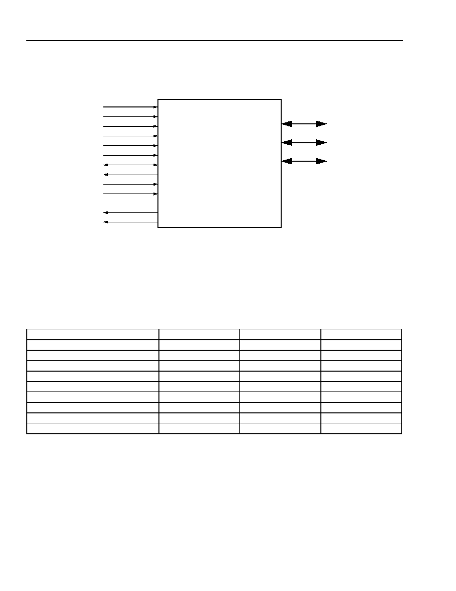
356
Agere Systems Inc.
TMXF28155 Super Mapper
Preliminary Data Sheet
155/51 Mbits/s SONET/SDH x28/x21 DS1/E1
May 2001
16 Microprocessor Interface Functional Description
(continued)
16.4 MPU Block Diagram
5-9039(F)r.2
Figure 18. Microprocessor Interface
16.5 Super Mapper Register Address Mapping
Each of the Super Mapper's major functional blocks is selected with an address mapping of the highest order nib-
ble, device pins ADDR[19:16], and allocated a 16-bit address range, pins ADDR[15:0], as defined in
Table 521
.
Table 521. Super Mapper Register Address Mapping
16.6 Performance Monitoring (PM) Counters Operation
PM counters are error counters or other statistics counters. In general, two internal registers are needed to imple-
ment a PM counter: a running count register (1), maintained by the core logic, which is incremented by 1, every
time an error (or statistics event) happens. At a defined interval, one second for example, the content of the running
counter is transferred to a holding register (2), while the running count register is reset to 0 and starts to count
anew. The count holding register holds the data that microprocessor actually reads.
ADDR[19:16]
Block ID
Block Name
ADDR
0000
0
TOP
[15:0]
0001
1
M13
[15:0]
0010
2
VTMPR
[15:0]
0011
3
SPEMPR
[15:0]
0100
4
TMUX
[15:0]
0101
5
XC
[15:0]
0110
6
TPG
[15:0]
0111
7
DJA
[15:0]
1000
8
FRAMER
[15:0]
MPCLK
ADDR[19:0]
CSN
ADSN
DSN
RWN
DATA[15:0]
DTN
MPMODE
INTN
APS_INTN
INTERNAL
ADDRESS
INTERNAL
DATA
INTERNAL
CONTROL
PAR[1:0]

357
Agere Systems Inc.
Preliminary Data Sheet
TMXF28155 Super Mapper
May 2001
155/51 Mbits/s SONET/SDH x28/x21 DS1/E1
16 Microprocessor Interface Functional Description
(continued)
5-9040(F)r.3
Figure 19. PM Reset Counter
The PM counter control signal controls the transfer and reset of all performance monitoring registers (collecting
events/statistics). The source of this signal is configurable and can come from external pin (PMRST pin T25), an
internal timer, or be controlled by software, depending on the SMPR_PMMODE[1:0] bits (
Table 67
, bits 9:8),
described as follows:
SMPR_PMMODE[1:0] = 00, 10: PM counter control is sourced from external pin PMRST.
SMPR_PMMODE[1:0] = 01: PM counter control is sourced from internal 1 second timer. Writing a logic one to the
SMPR_PMRESET bit (
Table 65
, bit 8) will reset the timer so that a transition occurs on the internal PM counter
control signal within 10 MPCLK clock cycles. The timer is based on the period of the MPCLK and the programmed
value of the registers in
Table 72
and
Table 73
. Once initially reset and synchronized, the PM counter reset interval
is determined by the combined delay of the programmed registers. The device pin, PMRST, is enabled as an out-
put.
SMPR_PMMODE[1:0] = 11: The PM counter control signal is software controlled. Writing a logic one to the
SMPR_PMRESET bit will cause a PM reset within 10 MPCLK cycle times after writing. This pulse will be
100 cycles high and 100 cycles low at the MPCLK frequency. During this 200 cycle time, writing to PM bit will have
no effect. The device pin, PMRST, is enabled as an output.
5-9931(F)
Figure 20. PM Reset Signal Generation
PM COUNT EVENT
RUNNING
HOLDING
MPU READABLE
MPUCLK
MPU READ HOLDING
REGISTER
(ONE PER BLOCK)
COUNTER
COUNTER
PM COUNT EVENT CLOCK
RESET
PM COUNTER CONTROL
PM COUNTER
BUFFERED
ENABLE
MPUCLK
DELAY
1/2 SECOND
COUNTERS
SMPR_PMRESET_HIGH_COUNT
SMPR_PMRESET_LOW_COUNT
SMPR_PMMODE
(REGISTER SMPR_GCR bits[9:8])
SMPR_PMRESET
(REGISTER SMPR_GTR bit 8)
FREE RUNNING
(SMPR_PMMODE[1:0] = 01)
SOFTWARE CONTROLLED
(SMPR_PMMODE[1:0] = 11)
EXTERNAL
(SMPR_PMMODE[1:0] = 00, 10)
MPUCLK
OUTPUT ENABLED
SMPR_PMMODE[1:0] = 01, 11
OUTPUT DISABLED
SMPR_PMMODE[1:0] = 00, 10
PMRST (TO BLOCKS)
PMRSTO
PMRSTI
MPU BLOCK

358
Agere Systems Inc.
TMXF28155 Super Mapper
Preliminary Data Sheet
155/51 Mbits/s SONET/SDH x28/x21 DS1/E1
May 2001
16 Microprocessor Interface Functional Description
(continued)
16.7 Super Mapper Global Interrupt Status and Control
The Super Mapper provides two hardware interrupt output pins: one global (INTN pin AB24) and one for the
SONET automatic protection switching (APS_INTN pin AC25). Both interrupt pins are active-low and are open-
drain outputs to allow a wired OR with complementary devices.
Interrupt status for major functional blocks are summarized in
Table 63
and maskable in
Table 64
.
16.8 Global Control
Several registers in this block provide global control of Super Mapper features. The register descriptions are self-
explanatory, but some highlights are listed as follows:
s
Global enabling and powering down of major functional blocks is shown in
Table 71 SMPR_CPCR, Clock and
Power Control Register (RW) on page 71
.
s
Software resets for major functional blocks are shown in
Table 66 SMPR_MSRR, Block Software Reset Register
(RW) on page66
.
s
Global reset of the Super Mapper is controlled with SMPR_SWRS, bit 8 in
Table 65 SMPR_GTR, Global Trigger
Register (RW) on page 66
.

Preliminary Data Sheet
TMXF28155/51 Super Mapper
May 2001
155/51 Mbits/s SONET/SDH x28/x21 DS1/E1
359
Agere Systems Inc.
17 TMUX Functional Description
Table of Contents
Contents
Page
17 TMUX Functional Description ......................................................................................................................... 359
17.1 TMUX Introduction .................................................................................................................................. 361
17.2 TMUX Features ...................................................................................................................................... 361
17.3 TMUX Receive Path Overview ............................................................................................................... 362
17.3.1 Receive Line Framer and Transport Overhead Termination ....................................................... 362
17.3.2 Receive Transport Overhead Monitor and RTOAC Drop ............................................................ 362
17.3.3 Receive MSP 1 + 1 Payload Switch ............................................................................................. 363
17.3.4 Receive Pointer Interpreter .......................................................................................................... 363
17.3.5 Receive High-Order Path Overhead Termination and RPOAC Drop .......................................... 363
17.3.6 Receive Byte Interleave Demultiplexer ........................................................................................ 363
17.3.7 Receive Telecom Bus .................................................................................................................. 363
17.4 TMUX Transmit Path Overview .............................................................................................................. 364
17.4.1 Transmit Telecom Bus ................................................................................................................. 364
17.5 Receive Direction (Receive Path from Sonet Global/SDH) .................................................................... 368
17.5.1 Input Clock and Loss-of-Signal Monitoring .................................................................................. 369
17.5.2 High-Speed Loopback Select Logic ............................................................................................. 369
17.5.3 Frame Alignment--STS-3/STM-1 (AU-4) Framing or STS-1 Framing ......................................... 369
17.5.4 B1 BIP-8 Check ........................................................................................................................... 369
17.5.5 J0 Monitor .................................................................................................................................... 370
17.5.6 Descrambler ................................................................................................................................. 370
17.5.7 F1 Monitor .................................................................................................................................... 371
17.5.8 B2 BIP-8 Check ........................................................................................................................... 371
17.5.9 Automatic Protection Switch (APS) Monitor ................................................................................. 371
17.5.10 K2 Monitor, AIS-L and RDI-L Detect .......................................................................................... 371
17.5.11 M1 REI-L Detect ........................................................................................................................ 372
17.5.12 Sync Status Monitor ................................................................................................................... 372
17.5.13 Receive Transport Overhead Access Channel (RTOAC) .......................................................... 372
17.5.14 MSP 1 + 1 Payload Switch ......................................................................................................... 374
17.5.15 Pointer Interpreter ...................................................................................................................... 374
17.5.16 Path Monitoring Functions ......................................................................................................... 377
17.6 Transmit Direction (Transmit Path to SONET/SDH Line) ....................................................................... 386
17.6.1 Transmit Side Telecom Bus Interface .......................................................................................... 386
17.6.2 Transmit Path and Transport Overhead Insertion Diagram ......................................................... 386
17.6.3 POAC Insert ................................................................................................................................. 388
17.6.4 AIS Path Generation .................................................................................................................... 389
17.6.5 J1 Insert Control ........................................................................................................................... 389
17.6.6 B3 BIP-8 Calculation and Insert ................................................................................................... 389
17.6.7 C2 Signal Label Byte Insert ......................................................................................................... 389
17.6.8 Path RDI (RDI-P) Insert ............................................................................................................... 390
17.6.9 REI-P: G1(7:4) Insert ................................................................................................................... 390
17.6.10 F2 Byte Insert ............................................................................................................................. 391
17.6.11 H4 Insert Control ........................................................................................................................ 391
17.6.12 F3 Byte Insert ............................................................................................................................. 391
17.6.13 K3 Byte Insert ............................................................................................................................ 391
17.6.14 N1 Byte Insert ............................................................................................................................ 391
17.6.15 MSP 1 + 1 Payload Switch ......................................................................................................... 391
17.6.16 Transmit Transport Overhead Access Channel (TTOAC) ......................................................... 391
17.6.17 Sync Status Byte (S1) Insert ...................................................................................................... 393
17.6.18 REI-L: M1 Insert ......................................................................................................................... 393

TMXF28155/51 Super Mapper
Preliminary Data Sheet
155/51 Mbits/s SONET/SDH x28/x21 DS1/E1
May 2001
360
Agere Systems Inc.
17 TMUX Functional Description
(continued)
Table of Contents
(continued)
Contents
Page
17.6.19 APS Value and K2 Insert Control Parameters ........................................................................... 393
17.6.20 Criteria for Insert Line RDI ......................................................................................................... 394
17.6.21 Line AIS Generation ................................................................................................................... 394
17.6.22 B2 BIP-8 Calculation and Insert ................................................................................................. 394
17.6.23 F1 Byte Insert ............................................................................................................................. 394
17.6.24 B1 Generate and Error Insert ..................................................................................................... 395
17.6.25 Scrambler ................................................................................................................................... 395
17.6.26 J0 Insert Control ......................................................................................................................... 395
17.6.27 Z0-2, Z0-3 Insert Control ............................................................................................................ 395
17.6.28 A2 Error Insert ............................................................................................................................ 395
Figures
Page
Figure 21. TMUX RTOAC Timing Diagram .......................................................................................................... 362
Figure 22. TMUX TTOAC and RTOAC Timing Diagram ...................................................................................... 365
Figure 23. High-Level TMUX Interconnect ........................................................................................................... 365
Figure 24. Detailed Block Diagram of the TMUX .................................................................................................. 366
Figure 25. Receive Direction Functional Block Diagram ...................................................................................... 367
Figure 26. Pointer Interpretation State Diagram................................................................................................... 374
Figure 27. Receive Low-Speed Bus Interface Signals for STS-3/STM-1 Signals ................................................ 385
Figure 28. Transmit Low-Speed Bus Interface Signals for STS-3/STM-1 Signals ............................................... 386
Figure 29. Transmit Direction POH and TOH Insertion Diagram ......................................................................... 387
Tables
Page
Table 522. Receive TOAC Modes ....................................................................................................................... 373
Table 523. Transport Overhead Byte Access--Receive Direction ...................................................................... 373
Table 524. STS Signal Label Defect Conditions ................................................................................................. 379
Table 525. STS-1 P-REI Interpretation ................................................................................................................ 380
Table 526. Signal Degrade (SD) Parameters ...................................................................................................... 382
Table 527. Signal Fail Parameters ...................................................................................................................... 383
Table 528. Signal Fail or Signal Degrade Recommended Programming Values ................................................ 384
Table 529. Path Overhead Byte Access .............................................................................................................. 384
Table 530. Path Overhead Byte Access--Transmit Direction ............................................................................. 388
Table 531. TPOAC Control Bits ........................................................................................................................... 389
Table 532. RDI-P Defects for Enhanced RDI-P Mode ........................................................................................ 390
Table 533. Transmit TOAC Modes ...................................................................................................................... 392
Table 534. Transmit Transport Overhead Byte Full Access Mode ...................................................................... 392
Table 535. TTOAC Control Bits in Full Access Mode .......................................................................................... 393

Preliminary Data Sheet
TMXF28155/51 Super Mapper
May 2001
155/51 Mbits/s SONET/SDH x28/x21 DS1/E1
361
Agere Systems Inc.
17 TMUX Functional Description
(continued)
17.1 TMUX Introduction
The TMUX multiplexer block implements SDH/SONET-compliant, byte-interleave multiplexing/demultiplexing, over-
head insertion and termination, multiplex section protection (MSP) 1 + 1 switch capability, and serializer/deserial-
izer for 155.52 Mbits/s and 51.84 Mbits/s traffic.
As shown in
Figure 23 on page 365
, the TMUX provides three modes of operation: STS-3 mode, STM-1 mode, and
STS-1 mode. In STS-3 mode, the TMUX implements the functions necessary to multiplex and demultiplex up to
three STS-1 signals to/from a SONET STS-3 signal. In STM-1 (VC-4) mode, the TMUX provides the functionality to
multiplex and demultiplex up to three TUG-3 signals to/from an STM-1(VC-4) signal. The device can also build/
extract up to three AU-3 signals to/from an STM-1(VC-3) stream. In STS-1 mode, the TMUX implements the func-
tions necessary to interface a single STS-1 to/from an external serial link.
On the high-speed side or line side, the block can be configured for either a 155.52 Mbits/s (STS-3/STM-1) or
51.84 Mbits/s (STS-1) serial data interface. On the low-speed side or tributary side, the TMUX provides a byte-wide
bus that can communicate with up to three STS-1/TUG-3/AU-3 devices at a 19.44 MHz rate. If single STS-1 mode
is employed, the bus rate will be 6.48 MHz. The TMUX therefore provides complete multiplexing/demultiplexing
to/from an STS-3/STM-1 signal for up to 84 DS1, 84 JT1, or 63 E1 signals. In STS-1 mode, the TMUX provides
multiplexing/demultiplexing for up to 28 DS1, 28 JT1, or 21 E1 streams. In STS-3/STM-1 mode, the TMUX from
only one device is required. The TMUX in other connected devices may be powered down to reduce consumed
power. This architecture allows flexible and modular growth in equipment capacity for both 51.84 Mbits/s and
155.52 Mbits/s links.
17.2 TMUX Features
s
Multiplexes three STS-1 signals into a SONET STS-3 signal.
s
Multiplexes three VC-3 signals into an SDH STM-1 (AU-4) signal via a TUG-3 construction.
s
Multiplexes three VC-3 signals into an SDH STM-1 (AU-3) signal.
s
Demultiplexes three STS-1 signals from a SONET STS-3 signal.
s
Demultiplexes three VC-3 signals from an SDH STM-1 (AU-4) signal via a TUG-3 deconstruction.
s
Demultiplexes three VC-3 signals from an SDH STM-1 (AU-3) signal.
s
Provides STS-1-only mode for receive and transmit directions.
s
Provides complete functionality for SDH MSP 1 + 1 protection switching.
s
Detects STS-3/STM-1 loss-of-signal (LOS) conditions.
s
Detects STS-3/STM-1 out-of-frame and loss-of-frame (OOF/LOF) conditions.
s
Provides an 8-bit parallel bus interface that can accommodate up to three STS-1/AU-3s.
s
Provides STS-3/STM-1/STS-1 selectable scrambler/descrambler functions and B1/B2/B3 generation/detection.
s
Provides STS-3/STM-1/STS-1 pointer interpretation. Detects AIS-P and LOP.
s
Complies with GR-253-CORE, T1.105, G.707, G.783, G.806, G.821, and ETSI 417-1-1.

TMXF28155/51 Super Mapper
Preliminary Data Sheet
155/51 Mbits/s SONET/SDH x28/x21 DS1/E1
May 2001
362
Agere Systems Inc.
17 TMUX Functional Description
(continued)
17.3 TMUX Receive Path Overview
A detailed drawing of the TMUX receive path is provided in the bottom half of
Figure 24 on page366
. For the
receive path, the TMUX implements two serial inputs for both the work and protect streams of an MSP 1 + 1 net-
work interface. Synchronous data (SDH/SONET) framers are implemented to frame on the incoming receive data
streams. One or both may be employed depending on system architecture. The incoming traffic is converted from
serial to byte-wide parallel. The transport overhead bytes of the incoming traffic are monitored and dropped via the
receive path TOAC drop interface. A multiplexer implements the receive MSP 1 + 1 payload switch and only one of
the incoming streams is passed to the downstream processing blocks. The pointer interpreter passes pointer infor-
mation to the 1:3 demultiplexer logic, and bus control circuitry provides functions necessary to manage traffic on
the telecom bus drop interface which drops traffic from up to three STS-1/TUG-3 paths on the TMUX receive path.
The path overhead bytes are monitored by the path overhead monitor and are dropped via the receive path POAC
drop interface.
17.3.1 Receive Line Framer and Transport Overhead Termination
Input receive data is received at the TMUX synchronous data framer from the high-speed line interface block. The
framer performs a multitude of functions including frame alignment (STS-3/STM-1 or STS-1), B1 BIP-8 check,
J0 byte monitoring, descrambling, F1 byte monitoring, B2 BIP-8 check, automatic protection switch (APS) and K2
byte monitoring, AIS-L and RDI-L detection, M1 byte REI-L detection, S1 byte sync status monitoring, and receive
transport overhead access channel (RTOAC) drop. The states of the framer as well as all state changes are
reported, and, if not masked, cause an interrupt. The B1 and B2 byte parity check supports bit and block modes.
The TMUX implements internal performance monitor counters. These counters can count up to one second worth
of BIP errors. The counters operate in either a saturation mode, such that the maximum value is retained once
reached, or in a rollover mode. These counters should be optimally read (and cleared) at least once per second.
The J0 monitor supports non-framed, SONET-framed, and SDH-framed 16-byte sequences as well as single
J0 byte monitoring mode. APS monitoring is performed on bytes K1[7:0] and K2[7:3]. The value of each is stored
and changes are reported. Bits [2:0] of the K2 byte are monitored independently. Line AIS (AIS-L/MS-AIS) and
RDI-L/MS-RDI are monitored separately and changes are reported. This AIS-L/MS-AIS and RDI-L/MS-RDI infor-
mation is also sent to the protection device for add/drop multiplex (ADM) applications. The M1 byte monitor oper-
ates either in bit or block mode and allows access to the REI-L/MS-REI errored bit count. The S1 byte can be
monitored in two modes: as an entire 8-bit word or as one 4-bit nibble (bits 7 to 4). Continuous N-times detection
counters are implemented for these monitoring functions. All automatic receive monitoring functions can be config-
ured to provide an interrupt to the control system, or the device can be operated in a polled mode.
17.3.2 Receive Transport Overhead Monitor and RTOAC Drop
The receive RTOAC provides access to all of the line section overhead bytes. Even or odd parity is calculated over
all bytes. It has a data rate of 5.184 Mbits/s and consists of a clock, data, and an 8 kHz sync pulse. In an alternate
operating mode, the data communication channel bytes D1--D3 or D4--D12 may transmit a serial 192 kbits/s or a
576 kbits/s data stream onto the RTOAC drop channel.
0783(F)
Figure 21. TMUX RTOAC Timing Diagram
rtoac clk
rtoac sync
rtoac data

Preliminary Data Sheet
TMXF28155/51 Super Mapper
May 2001
155/51 Mbits/s SONET/SDH x28/x21 DS1/E1
363
Agere Systems Inc.
17 TMUX Functional Description
(continued)
17.3.3 Receive MSP 1 + 1 Payload Switch
Output from both receive framer blocks provides the input to the MSP 1 + 1 payload switch.This portion of the
TMUX implements a payload 1 + 1 protection switch. In the receive direction, this occurs prior to pointer interpreta-
tion. If the protection switch is activated, then the data is selected from the receive protection interface rather than
from the high-speed input path. Only the selected input traffic is provided downstream to the pointer interpreter.
The interface consists of a 155.52 MHz or 51.84 MHz clock, data, and sync pulse.
17.3.4 Receive Pointer Interpreter
The pointer interpreter is implemented via a state machine which implements the pointer interpretation algorithm
described in ETS 300 417-1-1: January 1996 -Annex B. The pointer interpreter evaluates the current pointer state
for the normal state, path AIS state, or LOP conditions, as well as pointer increments and decrements. The current
pointer state and any changes in pointer condition are reported to the control system. The number of consecutive
frames for invalid pointer and invalid concatenation indication is fixed at nine.
17.3.5 Receive High-Order Path Overhead Termination and RPOAC Drop
Path overhead (POH) termination is performed in the receive path on either all three STS-1s or on the VC-4 POH
only. The receive POH circuitry includes: J1 byte monitoring, B3 byte BIP-8 checking, C2 byte signal label monitor-
ing, REI-P and RDI-P detection, H4 byte multiframe monitoring; F2, F3, and K3 byte APS monitoring, N1 byte tan-
dem connection monitoring (TCM), signal degrade BER and signal fail BER detection; receive path overhead
access channel (RPOAC) drop, and AIS-P/HO-AIS insertion and automatic AIS generation (with individual inhibit).
The J1 monitor provides five modes of operation for a programmable length (1 byte to 64 bytes) of the trace identi-
fier. These five modes are comprised of: cyclic checking against the last received sequence, compare against a
programmed sequence, SONET framing mode, SDH framing mode, and consecutive consistent occurrences of a
new pattern. B3 is monitored either in bit or block mode. Provisionable N-times detection counters are implemented
for the C2, F2, F3, N1, and K3 bytes. The K3 APS byte and N1 TCM byte can be monitored as an entire 8-bit word
or two 4-bit nibbles.
The receive RPOAC provides access to all the path overhead bytes. Even or odd parity is calculated over all bytes.
The RPOAC has a data rate of 9 bytes per 8 kHz frame and consists of clock, data, and an 8 kHz sync pulse.
17.3.6 Receive Byte Interleave Demultiplexer
The byte interleave demultiplexer accepts serial traffic and demultiplexes that information into one (STS-1 mode) or
three (STS-3/STM-1 mode) traffic streams for input via the telecom bus to the VT/VC mapper. The demultiplexer
takes the bytes in the order they are presented and places that traffic onto the telecom bus.
17.3.7 Receive Telecom Bus
The TMUX can communicate with up to three SPE mappers via the telecom bus interface. In typical applications,
since one SPE mapper is included in the Super Mapper device, two external SPE mappers reside on the telecom
bus. The bus operates at 19.44 MHz for STS-3/STM-1 modes and at 6.48 MHz for STS-1 mode. In the receive
direction, the Super Mapper outputs one parallel clock at 19.44 MHz, three sync signals (SPE, J0J1V1, and V1), an
8-bit data bus, and an odd/even parity bit. The data bus carries either three STS-1/TUG-3 signals, each in their own
time slot, or it carries one STS-1 signal. A 51.84 MHz low-speed clock and sync signal is also output from this cir-
cuit.

TMXF28155/51 Super Mapper
Preliminary Data Sheet
155/51 Mbits/s SONET/SDH x28/x21 DS1/E1
May 2001
364
Agere Systems Inc.
17 TMUX Functional Description
(continued)
17.4 TMUX Transmit Path Overview
The TMUX transmit path is depicted in the top half of
Figure 24 on page366
. The transmit path of the TMUX imple-
ments the inverse function to the receive path. Transmit input traffic at the telecom bus interface from up to three
STS-1/TUG-3 paths is managed via the transmit path bus control circuitry. Transmit traffic, alarms, or unequipped
indication information is inserted as needed depending on the status and provisioning of the device. The 3:1 multi-
plexer provides byte interleave multiplexing of the incoming traffic and insertion of the path overhead bytes. A serial
path provides input for the transmit protection traffic and the framer and serial-to-parallel converter formats this traf-
fic for input to the transmit MSP 1 + 1 payload switch. The selected output from the transmit MSP 1 + 1 switch is
input to the transport overhead insert block and the parallel to serial converter sends a serial stream to the device
output. The TMUX transmit path provides path overhead byte insertion and transport overhead byte insertion via
the respective POAC insert and TOAC insert interfaces.
Local clock and frame generation control circuitry is implemented in the TMUX for controlling the STS-1, STS-3,
and STM-1 termination and generation functions. Internal loopbacks in the TMUX provide near-end line loopback
and far-end line loopback capability.
17.4.1 Transmit Telecom Bus
The transmit side of Super Mapper drives a clock and three sync signals (SPE, J0J1V1, and V1) onto the telecom
bus. These signals control when the internal SPE mapper or one of the mate devices talks on the data bus.
Because it is on the receive side, the transmit telecom bus operates at 19.44 MHz for STS-3/STM-1 modes and at
6.48 MHz for STS-1 mode. The TMUX communicates with up to three VT/VC mappers, via an 8-bit data word and
an odd/even parity bit from the telecom bus. The data consists of the STS-1/TUG-3 from up to three mappers; each
in its own time slot, or it carries one single STS-1 signal. A 51.84 MHz low-speed clock and sync are also output.
Transmit High-Order Path Overhead Generation and TPOAC Insert. In the transmit direction, J1 path trace byte
insertion, B3 byte calculation and insertion, C2 signal label byte insertion, REI-P and RDI-P insertion; F2 byte
insertion, H4 multiframe byte insertion, F3 path user byte insertion, K3 byte insertion, N1 byte insertion, and AIS-P
insertion via POAC or software control is supported. The transmit TPOAC allows insertion of all overhead bytes
other than the B3 byte, which is automatically calculated. Even or odd parity is checked over all bytes. Bytes which
are not enabled for insertion are set to an all-ones or all-zeros stuff value. Transport path overhead bytes are added
to the payload stream during multiplexing in the byte interleave multiplexer.
Transmit Byte Interleave Multiplexer. In STS-3/STM-1 mode, the transmit byte interleave multiplexer block multi-
plexes up to three STS-1/TUG3 signals to form a SONET/SDH STS-3/STM-1 structured signal. The STS-3/STM-1
multiplexer function processes the input bytes in the order in which they are presented on the transmit telecom bus
and multiplexes these bytes into a single high-speed stream. Grooming of the VTs/VCs is performed in the SPE
mapper of each of the three devices. High-order path overhead bytes are interleaved with the data traffic during the
byte interleave multiplexing.
Transmit Payload Framer and MSP 1 + 1 Payload Switch. In the transmit direction, the MSP 1 + 1 switch func-
tion incorporates dual MSP 1 + 1 payload switch structures. In operation, the traffic from the transmit byte inter-
leave multiplexer are presented to both MSP 1 + 1 payload switches. The output of the signal from the 3:1 multiplex
is broadcast to both switch paths, and the output of the receive payload framers is also input respectively to one of
the two switch paths. For normal operation, one of the two outputs from the two MSP 1 + 1 blocks is selected. The
path from the receive framer to the MSP switch structures provides a means to perform far-end loopback.
Transmit Transport Overhead Generation and TTOAC Insert. The transmit transport overhead generator per-
forms TTOAC byte insertion, sync status byte (S1) insertion, M0/M1--REI-L insertion, K1 and K2 byte insertion,
AIS-L insertion, B2 byte calculation and insertion, F1 byte insertion, B1 byte generation and error insertion, scram-
bling, J0 byte insertion control, and A2 byte error insertion. All insert control functions that are inhibited will insert
optionally either an all-zeros or an all-ones word.
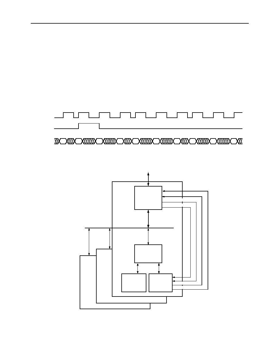
Preliminary Data Sheet
TMXF28155/51 Super Mapper
May 2001
155/51 Mbits/s SONET/SDH x28/x21 DS1/E1
365
Agere Systems Inc.
17 TMUX Functional Description
(continued)
The transmit TTOAC allows the users to insert the following overhead bytes: E1, F1, D1--D3, D4--D12, S1, and
E2. Even or odd parity is checked over all bytes. Bytes which are not enabled for insertion are set to an all-ones or
all-zeros stuff value.
The data communication channels D1--D3 or D4--D12 may also be received via the TTOAC interface. In this
mode, the TTOAC channel will comprise a serial 192 kbits/s or a 576 kbits/s data stream.
The insertion (overwrite by TOAC) of programmed S1, F1, J0, Z0-2, and Z0-3 bytes can be enabled via registers.
Automatic insertion of M0/M1 may also be inhibited via registers. A protection switch selects the REI-L value for
insertion to be taken from the protection board rather than from the receive side. The entire APS value or K2[2:0]
can be inserted via writable registers. Automatic RDI insertion is supported with individual inhibit for each contribu-
tor. A protection switch selects the RDI-L value for insertion to be taken from the protection board rather than from
the receive side. B1 and B2 BIP-8 values are calculated and inserted. Both values can be optionally inverted.
0784(F)
Figure 22. TMUX TTOAC and RTOAC Timing Diagram
5-9004(F)
Figure 23. High-Level TMUX Interconnect
ttoac clk
ttoac sync
ttoac data
TMUX
SPE
TELECOM BU S
V T /T U
M A PP E R
M 13
T U G -2
D S 3
MAPPER
S T S-1 /T U G -3
(T IM E S L O T # 1 )
S T S -1 /T U G -3
(T IM E SL O T # 2 )
S T S -1 /T U G -3
(T IM E SL O T # 3 )
S T S -3 /ST M -1
O R ST S -1
D EV IC E # 1
D E VIC E # 2
D E VIC E #3
HIGH-SPEED
S O N E T /SD H IN T E R F A C E
V T M PR R D I_ P , R E I_ P
V T M PR R D I_ L , R E I_ L
T M U X R D I_ L , R EI_ L
T M U X R D I_ P , RE I_ P

TMXF28155/51 Super Mapper
Preliminary Data Sheet
155/51 Mbits/s SONET/SDH x28/x21 DS1/E1
May 2001
366
Agere Systems Inc.
17 TMUX Functional Description
(continued)
5-9005(F)r.1
Figure 24. Detailed Block Diagram of the TMUX
PATH RDI
POAC
DROP
1:3
DEMUX
LOGIC
MSP 1+1
STS#1
STS#2
STS#3
TOAC
INSERT
TRANSMIT DIRECTION
RECEIVE DIRECTION
STS#3
TLSCLK
P A IS , UE Q
INS ER T
BU
S
CO
NT
RO
L
TLSPAR
TLSDATA[7:0]
RLSCLK
BU
S
CO
NT
RO
L
RLSPAR
RLSDATA[7:0]
TTOACCLKO,
POINTER
INTERPRETER
TTOACSYNCO,
TTOACDATI
TLSV1
(19.44 MHz)
(19.44 MHz)
RTPOACSYNC,
RTPOACDATA
THSD
RLSJ0J1V1
RLSV1
RLSSPE
TLSJ0J1V1
TLSSPE
TLSSYNC52
TLSCLK52
RLSSYNC52
RLSCLK52
TOH
MONITOR
TOAC
DROP
RTOACCLK,
RTOACSYNC,
RTOACDATA
POAC
INSERT
TPOACCLK,
TPOACSYNC,
TPOACDATA
POH
MONITOR
STM-1
TOH
STS#2 PAIS, UEQ
IN S ER T
STS#1 PAIS, UEQ
INSERT
FRAMER
PAYLOAD
SWITCH 1
AND S/P
3:1
AND
POH
INSERT
MUX
LOGIC
PATH REI
INSERT
MSP 1+1
PAYLOAD
SWITCH 2
LINE RDI
LINE REI
P/S
VTMPR RDI_L, REI_L
VTMPR RDI_P,
AUTO_AISO[1--3]
RHSC
RPSD155
FRAMER,
S/P, AND
RPSC155
TPSC155
RHSD
B2 ERR
INSERT,
MSP 1+1
PAYLOAD
SWITC H 3
TPSD155
P/S
L-REI INS
B2 MON,
LOC, OOF,
LOF, B2E
LOC, OOF,
LOF, B2E
L-REI MON
LOCAL CLOCK
GENERATION
THSC
THSSYNC
AND FRAME
RPSC155
RPSSYNC155 (FROM RECEIVE SIDE)
TPSMUXSEL2
RPSSYNC155
TIMING SIGNALS TO T
X
SIDE
RTPOACCLK,
REI_P
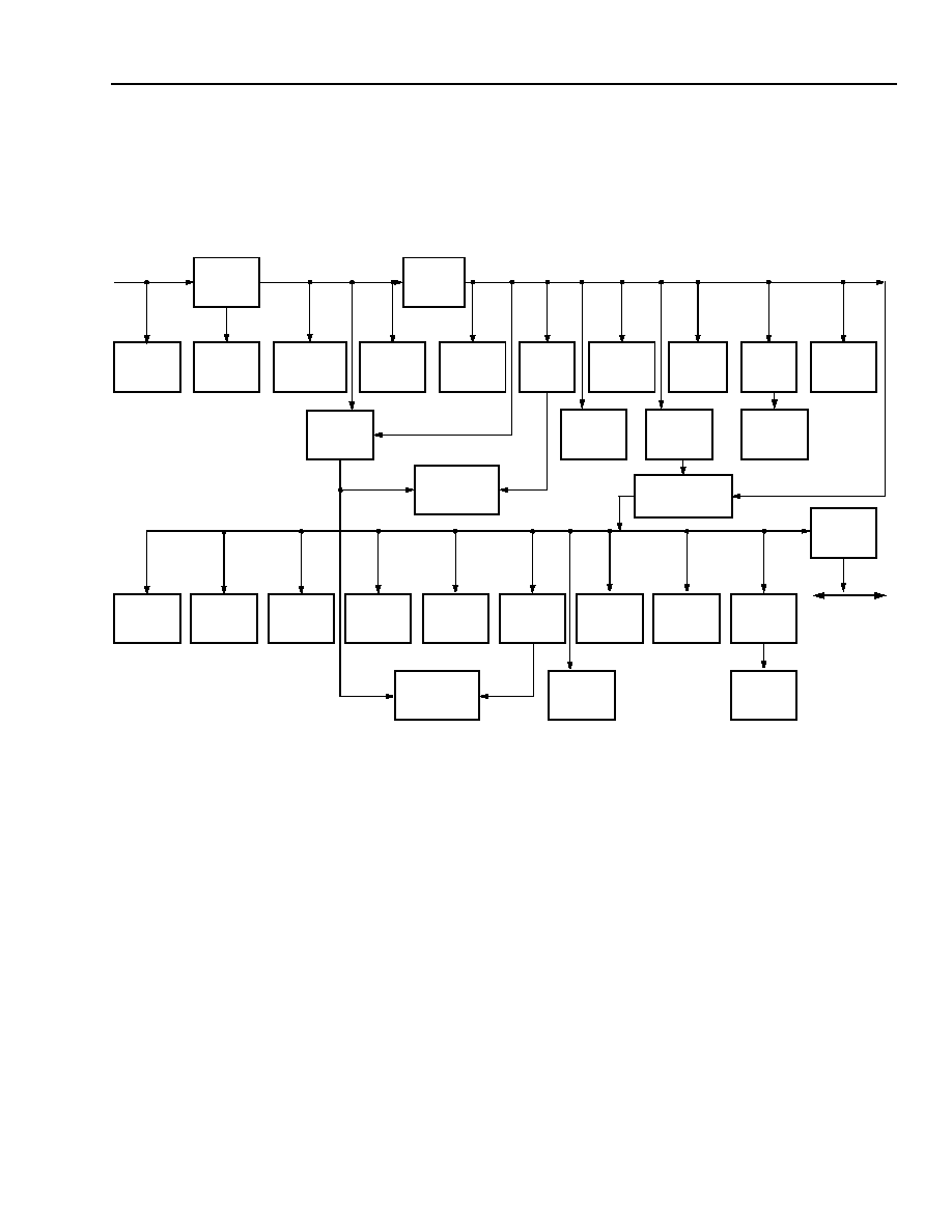
Preliminary Data Sheet
TMXF28155/51 Super Mapper
May 2001
155/51 Mbits/s SONET/SDH x28/x21 DS1/E1
367
Agere Systems Inc.
17 TMUX Functional Description
(continued)
The following block diagram describes the receive side transport overhead functions. Data is received from the
high-speed interface at 155 Mbits/s (51.84 Mbits/s for STS-1 mode) and the output is driven onto the low-speed
telecom bus in a parallel format. The TOH receive side functional blocks are shown in
Figure 25
.
5-9006(F)r.2
Figure 25. Receive Direction Functional Block Diagram
INSERT
C2
MONITOR
B3
BIP N
K3
CHECK
G1
RDI-P
G1
REI-L
DETECT
APS
MONITOR
B3
K3
DETECT
G1
G1
N1
C2
POAC
DROP
RECEIVE DATA
REI
COUNTER
G1
AIS-P
BER
ALGORITHM
FRAME
DESCR-
AMBLER
B1
BIP-8
J0
MONITOR
LOS
CHECK
F1
MONITOR
B2
BIP N
K1/K2
CHECK
AIS-L
RDI-L
M1
REI-L
SYNC
MONITOR
DETECT
APS
MONITOR
B2
K1
K2
DETECT
K2
M1
S1
STATUS
B1
DETECTOR
J0
F1
TOAC
DROP
LOF
MONITOR
OOF
ALIGN
MONITOR
INPUT
REI
COUNTER
M1
BER
ALGORITHM
J1
MONITOR
J1
F3
MONITOR
F3
F2
MONITOR
F2
MONITOR
H1, H2, H3
INTERPRETER
POINTER
TELECOM BUS
N1
MONITOR

TMXF28155/51 Super Mapper
Preliminary Data Sheet
155/51 Mbits/s SONET/SDH x28/x21 DS1/E1
May 2001
368
Agere Systems Inc.
17 TMUX Functional Description
(continued)
17.5 Receive Direction (Receive Path from Sonet Global/SDH)
All functions supported by the TMUX in the receive direction are summarized here:
s
Input clock monitoring and loss-of-signal monitoring
s
High-speed loopback
s
Frame alignment
s
Receive side frame sync output
s
B1 BIP-8 check
s
J0 monitor
s
Descrambler
s
F1 monitor
s
B2 BIP-8 check
s
APS (automatic protection switch) monitor
s
K2 monitor, AIS-L and RDI-L detect
s
M1 REI-L detect
s
Sync status monitor
s
Receive transport overhead access channel (RTOAC)
s
MSP 1 + 1 payload switch
s
Pointer interpreter
s
J1 monitor
s
B3 BIP-8 check
s
Signal label C2 byte monitor
s
RDI-P detect
s
REI-P detect
s
Path user byte F2 monitor
s
H4 multiframe indicator
s
Path user byte F3 monitor
s
K3 byte monitor
s
N1 tandem connection byte monitor
s
Signal degrade BER algorithm
s
Signal fail BER algorithm
s
Path overhead access channel (POAC) drop
s
AIS-P insertion and AUTO_AISO[1--3] generation
s
Receive side telecom bus interface

Preliminary Data Sheet
TMXF28155/51 Super Mapper
May 2001
155/51 Mbits/s SONET/SDH x28/x21 DS1/E1
369
Agere Systems Inc.
17 TMUX Functional Description
(continued)
17.5.1 Input Clock and Loss-of-Signal Monitoring
The TMUX detects and reports the loss of the 155 MHz input clock for STS-3 mode and the loss of the
51.84 MHz clock for STS-1 mode with register bits TMUX_RHSILOC--state (
Table 91, starting on page92
),
TMUX_RHSILOCD--delta state (
Table 91, starting on page 92
), TMUX_RHSILOCM--interrupt mask (
Table 91,
starting on page 92
). LOC is determined by a stuck high or stuck low for a time greater than 10 µs and uses the
microprocessor clock as its reference.
The TMUX will detect and report a loss-of-signal condition with register bits TMUX_RHSLOS--state (
Table 91 on
page 92
), TMUX_RHSLOSD--delta state (
Table 91, starting on pag e92
), TMUX_RHSLOSM--interrupt mask
(
Table 86 on page88
), by monitoring the external input signal pin, LOSEXT (pin AE5), or detecting a continuous
all-zeros/ones pattern for 51.44 ns to 105 µs in 51.44 ns steps before data is descrambled. The detection time is
determined by the value programmed in register bits, TMUX_LOSDETCNT[10:0] (
Table 97 on pag e97
). The LOS
state will clear after reception of two consecutive receive frames with the correct framing pattern spaced 125 µs
apart without an incoming LOS all-zeros/ones pattern. This recovery applies to both internal and external LOS fail-
ure causes.
17.5.2 High-Speed Loopback Select Logic
The device can be configured to loopback the transmit STS-3/STM-1 (AU-4) TMUX_THS2RHSLB = 1 (
Table 93 on
page 94
) or accept the local STS-3/STM-1 (AU-4) signal TMUX_THS2RHSLB = 0.
17.5.3 Frame Alignment--STS-3/STM-1 (AU-4) Framing or STS-1 Framing
The device will frame on the incoming signal. The state of the framer, out of frame (OOF) (register bit
TMUX_RHSOOF, see
Table 91 on page92
) as well as any changes to this state (register bits TMUX_RHSOOFD--
delta state, see
Table 91, starting on pag e92
and TMUX_RHSOOFM--interrupt mask; see
Table 86 on page88
)
will be reported.
The 32-bit (A1-2, A1-3, A2-1, and A2-2) framing pattern will be used in the frame detection for the
STS-3/STM-1 case and a 16-bit pattern will be used for the STS-1 case. The device will be considered out of frame
until two successive framing patterns separated in time by 125 µs occur without framing byte errors.
The device will be considered in frame until five
successive frames, separated in time by 125 µs, occur with errored
framing patterns. If the framer transitions to the out of frame state, the framer will remain synchronized to the last
known frame boundary or the latest detected unerrored framing pattern.
A loss of frame (LOF) (register bit TMUX_RHSLOF; see
Table 91 on page 92
) state bit as well as any changes to
this state (register bits TMUX_RHSLOFD--delta state, see
Table 91, starting on page92
, TMUX_RHSLOFM--
interrupt mask; see
Table 86 on page88
) will be reported. These state and mask and delta bits are the same for
both types of input data, STS-3/STM-1 or STS-1.
The device will be considered in the LOF state when an OOF condition persists for 24 consecutive frames (3 ms).
The device will transition out of the LOF state after receiving 24 consecutive frames with the correct framing pat-
terns spaced 125 µs apart and the OOF condition is clear.
17.5.4 B1 BIP-8 Check
A BIP-8 even parity will be computed over all the incoming bits of the STS-3/STM-1 frame (STS-1 frame in STS-1
mode), which are scrambled (except for the bits in the A1, A2, and J0/Z0 bytes) and compared to the B1 byte
received in the next frame.
The total number of B1 BIP-8 bit errors (raw count), or block errors (as determined by register bit
TMUX_BITBLKB1; see
Table 95 on page 95
), are counted. Upon the assertion of the performance monitor control
signal as configured in the microprocessor interface block, the raw count will be reset to zero and the value trans-
ferred to a 16-bit counter for B1 error counts B1ECNT[15:0] (
Table 124 on pag e118
).

TMXF28155/51 Super Mapper
Preliminary Data Sheet
155/51 Mbits/s SONET/SDH x28/x21 DS1/E1
May 2001
370
Agere Systems Inc.
17 TMUX Functional Description
(continued)
In case of overflow, depending on the value programmed in the microprocessor interface register bit
SMPR_SAT_ROLLOVER (
Table 67 SMPR_GCR, Global Control Register (RW) on page 68
), the B1 error counter
will either roll over or saturate at the maximum value until cleared.
17.5.5 J0 Monitor
J0 (section trace overhead) monitoring is done via register bits TMUX_J0MONMODE[2:0] (
Table 95 on pag e95
).
This J0 monitoring has six different monitoring modes, as follows:
s
TMUX_J0MONMODE[2:0] = 000: the TMUX latches the value of the J0 byte every frame for a total of
16 bytes into registers TMUX_J0DMON[16--1][7:0]; see
Table 132 on page121
. The TMUX compares the
incoming J0 byte with the next expected value (the expected value is obtained by cycling through the previously
stored 16 received bytes in round-robin fashion) and, if different, setting the section trace identifier mismatch
state register bit, TMUX_RTIMS, see
Table 91 on page92
. Any change to TMUX_RTIMS will be reported via
delta and interrupt register bits TMUX_RTIMSD; see
Table 82, starting on pag e79
and TMUX_RTIMSM; see
Table 86 on page88
.
s
TMUX_J0MONMODE[2:0] = 001: this is the SONET framing mode. The hardware looks for a 0x0A character to
indicate that the next byte is the first byte of the path trace message. The J0 byte message is continuously writ-
ten into TMUX_J0DMON[1--16][7:0] registers with the first byte residing at the first address. If any received byte
does not match the previously received byte for its location, then the state register bit, TMUX_RTIMS, is set. Any
change to RTIMS will be reported via delta and interrupt mask register bits TMUX_RTIMSD and
TMUX_RTIMSM.
s
TMUX_J0MONMODE[2:0] = 010: this is the SDH framing mode. The hardware looks for the byte with the most
significant bit (MSB) set to one, which indicates that the next byte is the second byte of the message. The rest of
operation is the same as in SONET framing mode.
s
TMUX_J0MONMODE[2:0] = 011: a new J0 byte (TMUX_J0DMON[1][7:0]) will be detected after the number of
consecutive consistent occurrences of a new pattern in the J0 overhead byte as determined by the values in reg-
isters TMUX_CNTDJ0[3:0]; see
Table 98 on page98
. Any changes to this byte are reported via delta and inter-
rupt mask registers TMUX_RTIMSD and TMUX_RTIMSM. The TMUX_RTIMSD delta bit in this mode indicates a
change in state for the TMUX_J0DMON[1][7:0] byte and the state register bit, TMUX_RTIMS, is not used.
s
TMUX_J0MONMODE[2:0] = 100: the user will program the 16 expected values of J0 in the SONET frame into
registers TMUX_EXPJ0DMON[1--16][7:0]; see
Table 131 on page 121
. The first expected byte, the byte follow-
ing the 0x0A character, is written into the first location TMUX_J0DMON[1][7:0]. The TMUX compares the incom-
ing J0 sequence with the stored expected value and sets the state register bit, TMUX_RTIMS (
Table 91 on
page 92
), if they are different. Any change to TMUX_RTIMS is reported via register bits TMUX_RTIMSD (delta
state) and TMUX_RTIMSM (interrupt mask).
s
TMUX_J0MONMODE[1:0] = 101: the user will program the 16 expected values of J0 in the SDH frame in regis-
ters TMUX_EXPJ0DMON[1--16][7:0]. The first byte of the message has the MSB set to 1. The TMUX compares
the incoming J0 sequence with the stored expected value, setting the state register bit, TMUX_RTIMS, if they are
different. Any change to TMUX_RTIMS will be reported via register bits TMUX_RTIMSD (delta state) and
TMUX_RTIMSM (interrupt mask).
s
TMUX_J0MONMODE[1:0] = 110 and 111 are currently undefined.
17.5.6 Descrambler
A frame synchronous descrambler of length 127 and generating polynomial x
7
+ x
6
+ 1 will descramble the entire
STS-3/STM-1 (or STS-1) signal except for the first row of overhead. The scrambler will be set to 1111111 on the
first byte following the last section overhead byte in the first row (i.e., after byte J0 for STS-1). The descrambler
operates in a byte-wide mode.
The frame descrambler can be enabled or disabled using register bit TMUX_RHSDSCR (
Table 93 on page94
).

Preliminary Data Sheet
TMXF28155/51 Super Mapper
May 2001
155/51 Mbits/s SONET/SDH x28/x21 DS1/E1
371
Agere Systems Inc.
17 TMUX Functional Description
(continued)
17.5.7 F1 Monitor
The TMUX monitors the fault location byte TMUX_RF1MON0[7:0] (
Table 101 on page 100
). A new fault location
state will be detected after the number of consecutive consistent occurrences of a new pattern in the F1 overhead
byte as determined by the value programmed in TMUX_CNTDF1[3:0] (
Table 98 on pag e98
).
The TMUX maintains a history of the previous, valid F1 byte in TMUX_RF1MON1[7:0] (
Table 101 on pag e100
),
and any changes will be reported via TMUX_RF1MOND (delta state) (
Table 82, starting on pag e79
) and
TMUX_RF1MONM-- (interrupt mask) (
Table 86 on page88
).
This continuous N-times detection counter will be reset to 0 upon the transition of the framer into the out of frame
state.
17.5.8 B2 BIP-8 Check
A B2 BIP-8 even parity is computed over all the incoming bits (except for the nine section overhead bytes) of the
STS-1 frame after descrambling, and compared to the B2 byte received in the next frame. The total number of B2
BIP-8 bit errors (raw count), or block errors (as determined by TMUX_BITBLKB2;
Table 94 on page 94
), is counted.
Upon the assertion of the performance monitor control signal as configured in the microprocessor interface, the raw
count will be reset to zero and the value transferred to an 18-bit holding register for B2 error counts
(TMUX_B2ECNT[17:0]; see
Table 125 on page119
). In case of overflow, depending on the value programmed in
the microprocessor interface register bit SMPR_SAT_ROLLOVER (
Table 67 on pag e68
), the B2 error counter will
either roll over or saturate at the maximum value until cleared.
17.5.9 Automatic Protection Switch (APS) Monitor
The TMUX monitors the receive APS value (the K1 byte, and the five most significant bits of the K2 byte) and
stores this value in TMUX_RAPSMON[12:0] (
Table 102 on page100
). This register is updated after the reception
of a programmed number of identical consecutive frames as determined by the value in TMUX_CNTDK1K2[3:0]
(
Table 98 on page98
). Whenever the contents of TMUX_RAPSMON[12:0] changes, a delta bit,
TMUX_RAPSMOND will be set (
Table 82, starting on page 79
) and the interrupt can be masked using
TMUX_RAPSMONM (
Table 86 on pag e88
). This indication also contributes to a separate device interrupt indica-
tion specifically intended for automatic protection switching.
The TMUX monitors this same 13-bit APS value (K1[7:0], K2[7:3]) in the receive direction and reports when the
APS value is inconsistent, using TMUX_RAPSBABE--Receive APS Babble Event (
Table 82 on pag e79
) and
TMUX_RAPSBABM--Receive APS Babble Mask (
Table 86 on page 88
). Inconsistent APS bytes are defined as
the number of successive frames of ASP data where no frames satisfy the criteria for updating the
TMUX_RAPSMON register (
Table 102 on page100
). The number of inconsistent frames allowed before reporting
is programmed in TMUX_CNTDK1K2FRAME[3:0] (default = 12, see
Table 98 on page98
). This continuous N-
times detection counter will be reset to 0 upon the transition of the framer into the out-of-frame state or upon the
detection of a B1 error.
17.5.10 K2 Monitor, AIS-L and RDI-L Detect
The three least significant bits of K2 are independently monitored and the current value is stored in
TMUX_K2MON[2:0] (
Table 102 on page100
). The register will be updated after the programmed number of con-
secutive identical K2[2:0] bits. This number is programmed by the value in TMUX_CNTDK2[3:0] (
Table 98 on
page 98
). Whenever the contents of TMUX_K2MON[2:0] changes, a delta bit, TMUX_RK2MOND will be set
(
Table 82, starting on page79
), and the interrupt can be masked using TMUX_RK2MONM (
Table 86 on pag e88
).
The TMUX monitors for line AIS (AIS-L/MS-AIS) in the K2[2:0] bits (K2[2:0] = 111). When line AIS is detected,
TMUX_RLAISMON (
Table 91 on page92
) will be set to 1 after a number of consecutive occurrences of line AIS as
determined by the value programmed in TMUX_CNTDK2[3:0]. Once set, AIS-L will be cleared after a number of
consecutive frames of no line AIS as determined by this same value in TMUX_CNTDK2[3:0].

TMXF28155/51 Super Mapper
Preliminary Data Sheet
155/51 Mbits/s SONET/SDH x28/x21 DS1/E1
May 2001
372
Agere Systems Inc.
17 TMUX Functional Description
(continued)
Any change to TMUX_RLAISMON will be reported in TMUX_RLAISMOND (
Table 82, starting on page 79
) and the
interrupt can be masked using TMUX_RLAISMONM (
Table 86 on page 88
).
The TMUX monitors for a remote defect indication (RDI-L/MS-RDI) condition in the K2[2:0] bits (K2[2:0] = 110) .A
line RDI condition will be detected and TMUX_RLRDIMON (
Table 91 on page92
) will be set to 1 after a number of
consecutive occurrences of RDI as determined by the value in TMUX_CNTDK2[3:0]. Once set, RDI-L will be
cleared after a number of consecutive frames of no RDI as determined by this same value programmed in
TMUX_CNTDK2[3:0]. Any change to TMUX_RLRDIMON, will be reported in TMUX_RLRDIMOND (
Table 82, start-
ing on page79
) and the interrupt can be masked using TMUX_RLRDIMONM (
Table 86 on page 88
). This continu-
ous N-times detection counter will be reset to 0 upon the transition of the framer into the out-of-frame state.
17.5.11 M1 REI-L Detect
One byte (M1) is allocated for use as a line remote error indication function (REI-L). For STS-3/STM-1 signals, all
eight bits of the M1 byte are allocated for REI-L information. The REI-L value reflects the error count detected by
the line terminating equipment (LTE) (using the line BIP-8 code) back to its peer LTE. For STS-3/STM-1 signals, the
value of the error count can be up to 24. A value of 25 and above will be interpreted as no errors. If
TMUX_R_M1_BIT7 (
Table 96 on pag e96
) is 1, then the most significant bit of the byte is ignored.
The TMUX allows access to the accumulated M1-REI errored bit count from the M1 byte via TMUX_M1ECNT[17:0]
(
Table 126 on page 119
). The counter will count in bit or block mode, depending upon the value of
TMUX_BITBLKM1 (
Table 94 on page94
). At the selected performance monitor (PM) interval, the value of the inter-
nal running raw counter is placed into a holding register, TMUX_M1ECNT[17:0], and then cleared. Depending on
the value of SMPR_SAT_ROLLOVER (
Table 67 on pag e68
) in the microprocessor interface, the internal counter
will either roll over or saturate at its maximum value until cleared.
17.5.12 Sync Status Monitor
The S1 byte is allocated for synchronization status. S1 bits [7:4] are used to convey a 4-bit code of which only six
patterns are defined with the remaining codes reserved for quality levels defined by individual administrations.
The S1 byte can be monitored in two modes: (1) as an entire 8-bit word or (2) as one 4-bit nibble (bits [7:4]), as pro-
grammed by TMUX_S1MODE4 (
Table 95 on page 95
).
s
TMUX_S1MODE4 = 0 the associated state, delta, and mask registers are TMUX_RS1MON[7:0] (
Table 103 on
page 100
), TMUX_RS1MOND (
Table 82, starting on page79
), and TMUX_RS1MONM (
Table 86 on page 88
),
respectively.
s
TMUX_S1MODE4 = 1 the associated state, delta, and mask registers are TMUX_RS1MON[7:4],
TMUX_RS1MOND, and TMUX_RS1MONM.
A new value will be detected after a programmed number of consecutive occurrences of a consistent new value in
the incoming S1 byte as determine by the value in TMUX_CNTDS1[3:0] (
Table 98 on page98
). A maskable event,
TMUX_RS1BABE (
Table 82, starting on page79
), is set if a programmed number of consecutive frames pass with-
out a validated message occurring as determined by the value in TMUX_CNTDS1FRAME[3:0] (
Table 98
).
In 8-bit mode, the entire value is monitored for an inconsistent value, while in 4-bit mode, only the most significant
nibble is monitored for an inconsistent value. This continuous N-times detection counter will be reset to 0 upon the
transition of the framer into the out-of-frame state.
17.5.13 Receive Transport Overhead Access Channel (RTOAC)
A transport overhead access channel (TOAC) is provided on-chip to drop the transport overhead (TOH) portion of
the incoming SDH or SONET frame. The TOAC channel supports three modes of operation based on the configu-
ration of TMUX_RTOAC_D13MODE and TMUX_RTOAC_D412MODE (
Table 117 on page113
).

Preliminary Data Sheet
TMXF28155/51 Super Mapper
May 2001
155/51 Mbits/s SONET/SDH x28/x21 DS1/E1
373
Agere Systems Inc.
17 TMUX Functional Description
(continued)
The TOAC channel consists of the following signals:
s
A clock signal sourced by the device pin, RTOACCLK (external output pin AD1). The clock frequency depends on
the values of TMUX_RTOAC_D13MODE and TMUX_RTOAC_D412MODE. See
Table 522
below.
s
A data signal out of RTOACDATA (external output pin AD3). The data rate and the values transmitted depend on
the values of TMUX_RTOAC_D13MODE and TMUX_RTOAC_D412MODE. See
Table 522
below.
s
An 8 kHz synchronization signal, out to output pin, RTOACSYNC (external output pin AA5). The sync signal is
normally low. During the last clock period of each frame coincident with the least significant bit of the last byte
(the eighty-first byte for all TOH modes), the sync signal is driven high.
Receive TOAC DCC1--DCC3 Mode. In this mode, DCC bytes 1 to 3 are transmitted serially on the data pin. The
clock rate is 192 KHz. The data bytes are transmitted MSB first, and the data bytes are driven out in sequential
order: DCC1, DCC2, and DCC3. The data signal is partitioned into frames of 3 bytes with a repetition rate of 8 kHz.
Receive TOAC DCC4--DCC12 Mode. In this mode, DCC bytes 4 --12 are transmitted serially on the data output.
The clock rate is 576 KHz. The data bytes are transmitted MSB first, and the data bytes are driven out in sequential
order: DCC4, DCC5, DCC6, DCC7, DCC8, DCC9, DCC10, DCC11, and DCC12. The data signal is partitioned into
frames of 9 bytes. The frame repetition rate is 8 kHz.
Receive TOAC Full TOH Access Mode. In this mode, the data signal is partitioned into frames of 81 bytes. The
frame repetition rate is 8 kHz. Each byte consists of 8 bits that are transmitted/received most significant bit first.
The MSB of the first byte of each frame contains an odd/even parity bit over the 648 bits of the previous frame. The
remaining 7 bits of this byte are not specified.
Bytes shown in
Table 523
below summarize the access capabilities of the receive TAOC in full access mode. The
transport overhead bytes shown in this table are always dropped by the receive side. There is programmability on
the transmit side regarding the insertion of these bytes. Bytes indicated in bold type are not specified in the stan-
dard, but are available on the receive TOAC data signal.
Table 522. Receive TOAC Modes
TOAC Mode
TMUX_RTOAC_D13MODE
Value
TMUX_RTOAC_D412MODE
Value
Number of Data
Bytes per Frame
Clock Rate
DCC1--DCC3
1
X
3
192 KHz
DCC4--DCC12
0
1
9
576 KHz
Full TOH Mode
0
0
81
5.184 MHz
Table 523. Transport Overhead Byte Access--Receive Direction
OH Parity
A1-2
A1-3
A2-1
A2-2
A2-3
J0
Z0-2
Z0-3
B1
B1-2
B1-3
E1
E1-2
E1-3
F1
F1-2
F1-3
D1
D1-2
D1-3
D2
D2-2
D2-3
D3
D3-2
D3-3
H1-1
H1-2
H1-3
H2
H2-2
H2-3
H3
H3-2
H3-3
B2-1
B2-2
B2-3
K1
K1-2
K1-3
K2
K2-2
K2-3
D4
D4-2
D4-3
D5
D5-2
D5-3
D6
D6-2
D6-3
D7
D7-2
D7-3
D8
D8-2
D8-3
D9
D9-2
D9-3
D10
D10-2
D10-3
D11
D11-2
D11-3
D12
D12-2
D12-3
S1
Z1-2
Z1-3
Z2-1
Z2-2
M1
E2
E2-2
E2-3
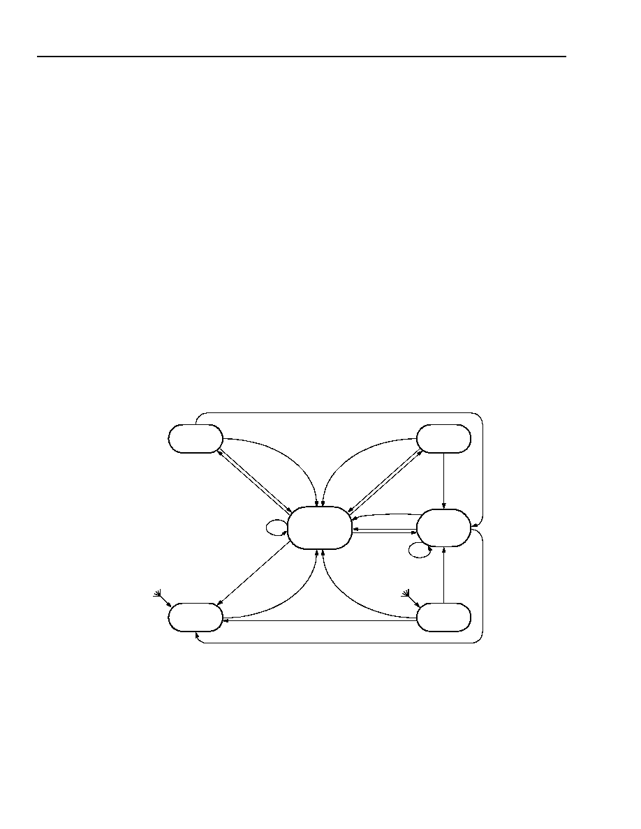
TMXF28155/51 Super Mapper
Preliminary Data Sheet
155/51 Mbits/s SONET/SDH x28/x21 DS1/E1
May 2001
374
Agere Systems Inc.
17 TMUX Functional Description
(continued)
Receive TOAC--OH Parity. Even or odd parity can be inserted into the first bit of the MSB byte of the TOAC out-
going frame by programming TMUX_RTOAC_OEPINS (
Table 117 on pag e113
).
17.5.14 MSP 1 + 1 Payload Switch
The TMUX supports a payload 1 + 1 protection switch. In the receive direction, this occurs prior to pointer interpre-
tation. If TMUX_RPSMUXSEL1 = 1 (
Table 93
), then the input receive data and clock are selected from the protec-
tion path: device pins RPSD155P/N (pins AD10/AE10) and RPSC155P/N (pins AC10/AD11), rather than from the
normal (working) path device pins, RHSDP/N (pins AF7/AE7) and RHSCP/N (pins AC7/AD8).
17.5.15 Pointer Interpreter
The STS-3/STM-1 pointer interpreter logic block performs all necessary functions to support STS-3/STM-1, as well
as STS-1, pointer interpretation. The pointer interpreter operates as one machine in STM-1 mode and as three
independent machines in STS-3 mode. The following features are implemented:
s
The pointer interpreter consists of the following states:
-- LOP: loss of pointer
-- AIS: alarm indiction signal (all ones in H1 and H2)
-- NDF: new data flag enabled (1001,0001,1101,1011, and 1000)
-- NORM: normal (disabled NDF, normal pointer)
-- INC: increment (inverted I bits)
-- DEC: decrement (inverted D bits)
* This state diagram is based on the ETS-417-1-1 pointer interpretation state diagram (Figure B.1). Transitions of eight invalid pointers from the
INC, DEC, and NDF states into the LOP state have been added.
5-9007(F)
Figure 26. Pointer Interpretation State Diagram
NORM
DEC
INC
NDF
AIS
LOP
FROM ALL STATES
8 INVALID POINTERS
FROM ALL STATES
3 NEW POINTERS
INCREMENT
DECREMENT
8 NDF ENABLE
NDF ENABLE
NDF ENABLE
NDF
NDF
NDF
3 ANY
3 ANY
3 NEW POINTERS
3 NEW POINTERS
3 ANY POINTERS
3 NEW POINTERS
8 INVALID
8 INVALID POINTERS*
INDICATION
INDICATION
3 AIS INDICATIONS
ENABLE
ENABLE
POINTERS
POINTERS
POINTERS
ENABLE

Preliminary Data Sheet
TMXF28155/51 Super Mapper
May 2001
155/51 Mbits/s SONET/SDH x28/x21 DS1/E1
375
Agere Systems Inc.
17 TMUX Functional Description
(continued)
s
The pointer interpreter transitions into the LOP state based on the following conditions:
-- Continuous NDF. If NDF (1001, 0001, 1101, 1011, and 1000) is received in 8, 9, or 10 consecutive frames, as
determined by the value in TMUX_CTDLOPCNT[1:0] (
Table 98 on page98
), then LOP will be declared.
-- Invalid pointer values. If 8, 9, or 10 consecutive frames (determined by TMUX_CTDLOPCNT[1:0]) are received
with a pointer that is not a normal value, NDF, AIS, increment, or decrement, then LOP will be declared.
s
The pointer interpreter will transition out of the LOP state based on the following conditions:
-- Following three consecutive frames with all ones in the H1 and H2 bytes, the pointer interpreter will transition
from the LOP state into the AIS state.
-- Following three new consecutive, consistent, and valid pointers, the pointer interpreter will transition from the
LOP state into the NORM state.
-- The pointer interpreter
will not transition from the LOP state into the NDF state.
s
The pointer interpreter will transition into the AIS state based on the following conditions:
-- Following three consecutive frames with all ones in the H1 and H2 bytes, AIS will be declared.
s
The pointer interpreter will transition out of the AIS state based on the following conditions:
-- Following three new consecutive, consistent, and valid pointers, the pointer interpreter will transition from the
AIS state into the NORM state.
-- Following eight consecutive invalid pointers, the pointer interpreter will transition from the AIS state into the
LOP state.
-- If NDF is enabled on the incoming H1 and H2 bytes, the pointer interpreter will transition from the AIS state
into the NDF state.
s
The pointer interpreter will transition into the NDF state based on the following condition:
-- If NDF is enabled on the incoming H1 and H2 bytes, the pointer interpreter will transition from the NORM,
NDF, AIS, INC, and DEC states into the NDF state.
s
The pointer interpreter will transition out of the NDF state based on the following conditions:
-- Continuous NDF. If NDF (1001, 0001, 1101, 1011, and 1000) is received for eight consecutive frames, the
pointer interpreter will transition from the NDF state into the LOP state.
-- Following any three consecutive, consistent, and valid pointers, the pointer interpreter will transition from the
NDF state into the NORM state.
-- Following three consecutive frames with all ones in the H1 and H2 bytes, the pointer interpreter will transition
from the NDF state into the AIS state.
-- Following three new, consecutive, consistent, and valid pointers, the pointer interpreter will transition from the
NDF state into the NORM state.
-- Following eight consecutive invalid pointers, the pointer interpreter will transition from the NDF state into the
LOP state.
s
The pointer interpreter will transition into the NORM state based on the following conditions:
-- Following three new consecutive, consistent, and valid pointers, the pointer interpreter will transition into the
NORM state.
-- Following any three consecutive, consistent, and valid pointers, the pointer interpreter will transition into the
NORM state, i.e., transitioning from the INC, DEC, and NDF states.

TMXF28155/51 Super Mapper
Preliminary Data Sheet
155/51 Mbits/s SONET/SDH x28/x21 DS1/E1
May 2001
376
Agere Systems Inc.
17 TMUX Functional Description
(continued)
s
The pointer interpreter will transition out of the NORM state based on the following conditions:
-- Following eight consecutive invalid pointers, the pointer interpreter will transition from the NORM state into
the LOP state.
-- If NDF is enabled on the incoming H1 and H2 bytes, the pointer interpreter will transition from the NORM
state into the NDF state.
-- Following three consecutive frames with all ones in the H1 and H2 bytes, the pointer interpreter will transition
from the NORM state into the AIS state.
-- When operating in the 8 of 10 mode, controlled by TMUX_8ORMAJORITY = 1 (
Table 95 on page95
), if 8 of
the 10 I and D bits are correct for a pointer decrement on the incoming H1 and H2 bytes, the pointer inter-
preter will transition from the NORM state into the DEC state. Otherwise, if 3 of the 5 I bits and 3 of the 5 D
bits are correct for a pointer decrement on the incoming H1 and H2 bytes, the pointer interpreter will transition
from the NORM state into the DEC state.
-- When operating in the 8 of 10 mode (TMUX_8ORMAJORITY = 1), if 8 of the 10 I and D bits are correct for a
pointer increment on the incoming H1 and H2 bytes, the pointer interpreter will transition from the NORM
state into the INC state. Otherwise, if 3 of the 5 I bits and 3 of the 5 D bits are correct for a pointer increment
on the incoming H1 and H2 bytes, the pointer interpreter will transition from the NORM state into the INC
state.The pointer interpreter will transition into the INC state based on the following conditions:
-- When operating in the 8 of 10 mode (TMUX_8ORMAJORITY = 1), if 8 of the 10 I and D bits are correct for a
pointer increment on the incoming H1 and H2 bytes, the pointer interpreter will transition into the INC state.
Otherwise, if 3 of the 5 I bits and 3 of the 5 D bits are correct for a pointer increment on the incoming H1 and
H2 bytes, the pointer interpreter will transition into the INC state.
s
The pointer interpreter will transition out of the INC state based on the following conditions:
-- If NDF is enabled on the incoming H1 and H2 bytes, the pointer interpreter will transition from the INC state
into the NDF state.
-- Following three consecutive frames with all ones in the H1 and H2 bytes, the pointer interpreter will transition
from the INC state into the AIS state.
-- Following three new consecutive, consistent, and valid pointers, the pointer interpreter will transition from the
INC state into the NORM state.
-- Following any three consecutive, consistent, and valid pointers, the pointer interpreter will transition from the
INC state into the NORM state.
-- Following eight consecutive invalid pointers, the pointer interpreter will transition from the INC state into the
LOP state.
s
The pointer interpreter will transition into the DEC state based on the following conditions:
-- When operating in the 8 of 10 mode (TMUX_8ORMAJORITY = 1), if 8 of the 10 I and D bits are correct for a
pointer decrement on the incoming H1 and H2 bytes, the pointer interpreter will transition into the DEC state.
Otherwise, if 3 of the 5 I bits and 3 of the 5 D bits are correct for a pointer decrement on the incoming H1 and
H2 bytes, the pointer interpreter will transition into the DEC state.
s
The pointer interpreter will transition out of the DEC state based on the following conditions:
-- If NDF is enabled on the incoming H1 and H2 bytes, the pointer interpreter will transition from the DEC state
into the NDF state.
-- Following three consecutive frames with all ones in the H1 and H2 bytes, the pointer interpreter will transition
from the DEC state into the AIS state.
-- Following three new consecutive, consistent, and valid pointers, the pointer interpreter will transition from the
DEC state into the NORM state.
-- Following any three consecutive, consistent, and valid pointers, the pointer interpreter will transition from the
DEC state into the NORM state.
-- Following eight consecutive invalid pointers, the pointer interpreter will transition from the DEC state into the
LOP state.

Preliminary Data Sheet
TMXF28155/51 Super Mapper
May 2001
155/51 Mbits/s SONET/SDH x28/x21 DS1/E1
377
Agere Systems Inc.
17 TMUX Functional Description
(continued)
s
Pointer increments and decrements will be counted and presented to the microprocessor as follows:
-- Pointer increments and decrements will be monitored and counted internally.
-- The internal and latched counts will be forced to clear (0x00) if TMUX_RLOP[3--1] = 1 (
Table 92 on page 92
)
or TMUX_RPAIS[3--1] = 1 (
Table 92
), where [3--1] designates the tributary number.
-- Upon the configured performance monitoring interval, raw counts are transferred to holding registers for
pointer increments (TMUX_RPTR_INC[1--3][10:0] (
Table 129 on page121
)) and decrements
TMUX_RPTR_DEC[1--3][10:0] (
Table 130
), allowing access by the microprocessor. The raw counters will
reset (to 0x00).
-- Depending on the value of SMPR_SAT_ROLLOVER (
Table 67 on page68
) in the microprocessor interface
block, the internal running counts saturate at their maximum value or rollover.
-- However, increment and decrement event indications should be ignored during LOP station.
s
The current pointer state is read from TMUX_RLOP[3--1] and TMUX_RPAIS[3--1]. Any changes in pointer con-
dition are read from the delta state bits TMUX_RLOPD[3--1] and TMUX_RPAISD[3--1] (
Table 83
). The associ-
ated interrupt mask bits are TMUX_RLOPM[3--1] (
Table 87 on page89
) and TMUX_RPAISM[3--1] (
Table 87
).
When the device is receiving a concatenated signal (STM-1(AU-3)), the receive concatenation mode register bit,
TMUX_RCONCATMODE (
Table 95 on page 95
), must be set for the concatenation state machines (register bits
TMUX_CONCAT_STATE[3--2][1:0] (
Table 92 on page92
)) on ports 2 and 3 to contribute to pointer evaluation.
This state machine implements the pointer interpretation algorithm described in ETS 300 417-1-1: January 1996
- Annex B.
17.5.16 Path Monitoring Functions
The following sections describe the path monitoring functions. For STM-1 signals, the values corresponding to
STS-1 #1 are the relevant signals. For STS-3 input data, there are three versions of each path monitor, one corre-
sponding to each STS-1. The mode bits are applied to the monitors of all three STS-1s.
J1 Monitor. J1 (path trace) monitoring has six different monitoring modes controlled by TMUX_J1MONMODE[2:0]
(
Table 95 on page95
). The J1 monitoring mode for all three STS-1s within an STS-3 signal is the same.
s
TMUX_J1MONMODE[2:0] = 000: The TMUX latches the value of the J1 byte every frame for a total of 64 bytes
in TMUX_J1DMON[1--3][1--64][7:0] (
Table 137 on page122
,
Table 138
, and
Table 139
). The TMUX compares
the incoming J1 byte with the next expected value (the expected value is obtained by cycling through the previ-
ous stored 64 received bytes in round-robin fashion) and setting the path trace identifier state register bit(s),
TMUX_RTIMP[1--3] (
Table 92 on page92
), if different. Any change to the path trace identifier is reported in
TMUX_RTIMPD[1--3] (
Table 83
), with interrupt mask bits, TMUX_RTIMPM[1--3] (
Table 87 on page89
).
s
TMUX_J1MONMODE[2:0] = 001: This is the SONET framing mode. The hardware looks for the 0x0A character
to indicate that the next byte is the first byte of the path trace message. The J1 byte message is continuously
written into registers, TMUX_J1DMON[1--3][1--64][7:0], with the first byte residing at the first address. If any
received byte does not match the previously received byte for its location, then the state bit(s),
TMUX_RTIMP[1--3], is set. Any change to the path trace identifier is reported in TMUX_RTIMPD[1--3], with
interrupt masks bits, TMUX_RTIMPM[1--3].
s
TMUX_J1MONMODE[2:0] = 010: This is the SDH framing mode. The hardware looks for the byte with the MSB
set to one, which indicates that the next byte is the second byte of the message. The rest of operation is the
same as in SONET framing mode, except that there are 16 bytes instead of 64.
s
TMUX_J1MONMODE[2:0] = 011: A new J1 byte (TMUX_J1DMON[1][7:0]) will be detected after a number of
consecutive consistent occurrences of a new pattern (determined by the value in TMUX_CNTDJ1[3:0] (
Table 99
on pag e99
)) in the J1 overhead byte. Any changes to this byte must be reported in TMUX_RTIMPD[1--3], with
the interrupt mask bits, TMUX_RTIMPM[1--3]. The delta bit(s) in this mode indicate a change in state for the
TMUX_J1DMON[1][7:0] byte, and the state bits, TMUX_RTIMP[1--3], are not used.

TMXF28155/51 Super Mapper
Preliminary Data Sheet
155/51 Mbits/s SONET/SDH x28/x21 DS1/E1
May 2001
378
Agere Systems Inc.
17 TMUX Functional Description
(continued)
s
TMUX_J1MONMODE[1:0] = 100: The user will program the 64 expected values of J1 in
TMUX_EXPJ1DMON[1--3][1--64][7:0] (
Table 134 on page122
,
Table 135
, and
Table 136
), in SONET framing
mode, where the first expected byte, the byte following the 0x0A character, is written into the first location of
TMUX_EXPJ1DMON[1][7:0]. The TMUX will compare the incoming J1 sequence with the stored expected value,
setting the path trace identifier state bit(s), TMUX_RTIMP[1--3] if they are different. Any change to the path trace
identifier is reported in TMUX_RTIMPD[1--3], with interrupt mask bits, TMUX_RTIMPM[1--3].
s
TMUX_J1MONMODE[1:0] = 101: The user will program the 16 expected values of J1 in
EXPJ1DMON[1--16][7:0] in SDH framing mode, where the first byte of the message has the MSB set to 1. The
TMUX compares the incoming J1 sequence with the stored expected value, setting the state register bit(s),
TMUX_RTIMP[1--3], if they are different. Any change to path trace identifier is reported in register bits,
TMUX_RTIMPD[1--3], with interrupt mask bits, TMUX_RTIMPM[1--3].
s
TMUX_J1MONMODE[1:0] = 110 and 111 are currently undefined.
B3 BIP-8 Check. A B3 BIP-8 even parity is computed over all the incoming synchronous payload envelope bits of
the STS-3/STM-1/STS-1 signal after descrambling, and compared to the B3 byte received in the next frame. The
total number of B3 BIP-8 bit errors (raw count), or block errors (as determined by TMUX_BITBLKB3 (
Table 95 on
page 95
), is counted. Upon the configured performance monitor (PM) interval, the value of the internal running
counter is placed into holding registers TMUX_B3ECNT[1--3][15:0] (
Table 126 on page119
) and then cleared.
Depending on the value of SMPR_SAT_ROLLOVER (
Table 67 on pa ge68
) in the microprocessor interface block,
the internal counter will either roll over or stay at its maximum value until cleared.
Signal Label C2 Byte Monitor. The C2 byte per STS-1/STM-1 is stored in TMUX_C2MON[1--3][7:0] (
Table 104
on page101
). Each register will be updated after a number, determined by the value in TMUX_CNTDC2[3:0]
(
Table 99 on pag e99
), of consecutive frames of identical C2 bytes for a given STS-1/STM-1, i.e., the 8-bit pattern
must be identical for a programmed number frames prior to updating the C2 register. Any change to C2 byte moni-
tor is reported via the corresponding delta and mask register bits, TMUX_RC2MOND[1--3] (
Table 83
) and
TMUX_RC2MONM[1--3] (
Table 87 on pag e89
).
In addition, there are programmable expected value(s) for the C2 bytes of each STS-1/STM-1 in
TMUX_C2EXP[1--3][7:0] (
Table 100 on page100
). If the current value of a C2 byte in TMUX_C2MON[1--3][7:0]
does not equal the expected C2 value in TMUX_C2EXP[1--3][7:0]), then a payload label mismatch defect may be
declared for that STS-1/STM-1 in TMUX_RPLMP[1--3] (
Table 92 on page92
). Also, if the current value of a
C2 byte is all 0s, then the corresponding unequipped defect is declared in TMUX_RUNEQP[1--3] (
Table 92
).
Note: The payload label mismatch and unequipped defects are mutually exclusive and unequipped takes priority.
The following table describes the conditions for generating payload label mismatch (TMUX_RPLMP[1--3]) and
unequipped defects (TMUX_RUNEQP).

Preliminary Data Sheet
TMXF28155/51 Super Mapper
May 2001
155/51 Mbits/s SONET/SDH x28/x21 DS1/E1
379
Agere Systems Inc.
17 TMUX Functional Description
(continued)
Table 524. STS Signal Label Defect Conditions
TMUX_FORCEC2DEF[2:0] will force path payload label mismatch defects on those conditions that are shown on
in
Table 524
above.
The continuous N-times detection counter(s) will be reset to 0 upon the transition of the framer into the out of frame
state.
RDI-P Detection. A remote defect indication-path (RDI-P) signal indicates to STS path terminating equipment
(PTE) that its peer STS PTE has detected a defect on the signal that it originated. The TMUX supports a 1-bit
RDI-P code as well as a 3-bit enhanced RDI-P code; the mode is selectable using the TMUX_REPRDI_MODE
(
Table 95 on page95
). If TMUX_REPRDI_MODE = 0, then the 1-bit code is supported, and if
TMUX_REPRDI_MODE = 1, then the 3-bit enhanced path RDI code is supported.
The TMUX monitors for a 1-bit RDI-P code in G1[3] or a 3-bit enhanced remote defect indication (RDI-P) condition
in G1[3:1]. The current value of the path RDI state will be detected after a number of consecutive occurrences
determined by the value in TMUX_CNTDRDIP[3:0] (
Table 99 on page 99
). The current value(s) will be stored in
TMUX_RDIPMON[1--3][2:0]] (
Table 104 on page 101
), for nonenhanced RDI-P mode, and the current value(s) will
be stored in TMUX_RDIPMON[1--3][2:0], for enhanced RDI-P mode. Any change to TMUX_RDIPMON[1--3][2:0]
will be reported in TMUX_RRDIPD[1--3] with interrupt mask bits,TMUX_RRDIPM[1--3] (
Table 87 on page89
).
The continuous N-times detection counter(s) will be reset to 0 upon the transition of the framer into the out of frame
state.
REI-P Detection. Bits [7:4] of the G1 byte are allocated for use as a path remote error indication function (REI-P).
s
For STS-1 and STM-1 signals, bits [7:4] of the G1 byte are allocated for REI-P which conveys the error count
detected by the PTE (using the path BIP-8 code B3) back to its peer PTE as shown in
Table 525
.
Provisioned STS PTE
Functionality, Expected C2
Received Payload Label
(C2 in hex)
Defect
TMUX_FORCEC2DEF = 1
(
Table 97
)
Any Equipped Functionality
Unequipped (00)
TMUX_RUNEQP
No Change
Any Equipped Functionality
Equipped--Nonspecific (01)
None
No Change
Equipped--Nonspecific
Any Value (02 to E0, FD to FE)
None
No Change
Any Payload Specific Code
The Same Payload Specific
Code (02 to E0, FD to FE)
None
No Change
Any Payload Specific Code
A Different Payload Specific
Code (02 to E0, FD to FE)
TMUX_RPLMP
No Change
Equipped--Nonspecific (01) or
VT-Structured STS-1 (02)
PDI, 1 to 27 VTx Defects
(E1 to FB)
None
TMUX_RPLMP
Any Payload Specific Code
Except VT-Structured
STS-1 (02)
PDI, 1 to 27 VTx Defects
(E1 to FB)
TMUX_RPLMP
No Change
Any Equipped Functionality
PDI, 28 VT1.5 Defects or 1
Non-VT Payload Defect (FC)
None
TMUX_RPLMP
Any Equipped Functionality
Reserved (FF)
None
TMUX_RPLMP

TMXF28155/51 Super Mapper
Preliminary Data Sheet
155/51 Mbits/s SONET/SDH x28/x21 DS1/E1
May 2001
380
Agere Systems Inc.
17 TMUX Functional Description
(continued)
Table 525. STS-1 P-REI Interpretation
The TMUX allows access to the G1-REI errored bit count for each STS-1/STM-1 in TMUX_G1ECNT[1--3][15:0]
(
Table 128 on page 120
), which is the accumulated error count from G1[3:0] byte of the STS-1/STM-1 signal. The
counter(s) will count in bit or block mode, depending on the value of TMUX_BITBLKG1 (
Table 95 on page95
).
Upon the configured performance monitor (PM) interval, the value of the internal running counter is placed into the
holding registers TMUX_G1ECNT[1--3][15:0] and then cleared. Depending on the value of
SMPR_SAT_ROLLOVER (
Table 67 on pag e68
) in the microprocessor interface block, the internal counter will
either roll over or stay at its maximum value until cleared.
Path User Byte F2 Monitor. The TMUX monitors the path user channel in the F2 byte of each STS-1/STM-1. The
F2 byte(s) will be stored in TMUX_F2MON0[1--3][7:0] (
Table 104, starting on page 101
). Each register will be
updated after a number of consecutive frames of identical F2[7:0] as determined by the value in
TMUX_CNTDF2[3:0] (
Table 99 on page 99
). That is, the 8-bit pattern must be identical for the programmed number
of frames prior to updating the F2 register. Any change to F2 monitor registers will be reported in
TMUX_RF2MOND[1--3] (
Table 83
), with interrupt mask bits, TMUX_RF2MONM[1--3] (
Table 87 on page89
). The
TMUX also maintains a history of the previous valid F2 byte in TMUX_F2MON1[1--3][7:0] (
Table 104
). The contin-
uous N-times detection counter(s) will be reset to 0 upon the transition of the framer into the out of frame state.
H4 Multiframe Indicator. The H4 byte is allocated for use as a mapping specific indicator byte. For VT-structured
SPEs, this byte is used as a multiframe indicator.
The TMUX passes the H4 byte of each STS-1 onto the low-speed telecom bus so that it can be monitored by the
VT mapper block. The TMUX also indicates when the H4 byte(s) has a value of 0x01 by asserting the RLSV1 out-
put pin (pin number W4) on the telecom bus during that frame.
Note: The three H4 bytes of an STS-3 signal can occur at any time with respect to one another within a frame.
Path User Byte F3 Monitor. The TMUX monitors the second path user channel in the F3 byte for each
STS-1/STM-1. The F3 byte(s) for each STS-1/STM-1 is stored in TMUX_F3MON0[1--3][7:0] (
Table 104 on
page 101
). Each register will be updated after a number determined by the value in TMUX_CNTDF3[3:0] (
Table 99
on pag e99
) of consecutive frames of identical F3[7:0] monitor bytes on that particular STS-1. That is, the 8-bit pat-
tern must be identical for the programmed number of frames prior to updating the F3 register.
G1[7:4] Code
Code Interpretation
0000
0 (no errors)
0001
1
0010
2
0011
3
0100
4
0101
5
0110
6
0111
7
1000
8
1001
0 (no errors)
. . .
. . .
1111
0 (no errors)

Preliminary Data Sheet
TMXF28155/51 Super Mapper
May 2001
155/51 Mbits/s SONET/SDH x28/x21 DS1/E1
381
Agere Systems Inc.
17 TMUX Functional Description
(continued)
Any change to F3 byte monitor registers is reported in TMUX_RF3MOND[1--3] (
Table 83
), with interrupt mask bits,
TMUX_RF3MONM[1--3] (
Table 87 on page89
).
The TMUX also maintains a history of the previous valid F3 byte in TMUX_F3MON1[1--3][7:0] (
Table 104 on
page 101
). The continuous N-times detection counter(s) will be reset to 0 upon the transition of the framer into the
out of frame state.
K3 Byte Monitor. The TMUX monitors the K3 byte for each STS-1/STM-1. The K3 byte(s) are stored in
TMUX_K3MON[1--3][7:0] (
Table 104
). Each register will be updated after a number determined by the value in
TMUX_CNTDK3[3:0] (
Table 99 on page99
) of consecutive frames of identical K3[7:0] for that particular
STS-1/STM-1. That is, the 8-bit pattern must be identical for a number of frames prior to updating the K3 register.
Any change to K3 monitor registers is reported in TMUX_RK3MOND[1--3] (
Table 83
), with interrupt mask bits,
TMUX_RK3MONM[1--3] (
Table 87 on page89
). The continuous N-times detection counter(s) will be reset to 0
upon the transition of the framer into the out of frame state.
N1 Byte Monitor. The TMUX monitors the N1 byte for each STS-1/STM-1. The N1 byte(s) are stored in
TMUX_N1MON[1--3][7:0] (
Table 104 on page101
). Each register will be updated after a number determined by
the value in TMUX_CNTDN1[3:0] (
Table 99 on page 99
) of consecutive frames of identical N1[7:0] for that particu-
lar STS-1/STM-1. That is, the 8-bit pattern must be identical for a number of frames prior to updating the N1 regis-
ter. Any change to N1 monitor registers will be reported in TMUX_RN1MOND[1--3] (
Table 83
), with interrupt mask
bits, TMUX_RN1MONM[1--3] (
Table 87 on page89
). The continuous N-times detection counter(s) will be reset to
0 upon the transition of the framer into the out of frame state.
Signal Degrade BER Algorithm. A signal degrade state in register bit TMUX_RHSSD (
Table 91 on page 92
) and
change of state indication is reported in register bit, TMUX_RHSSDD (
Table 82, starting on page79
), with the
interrupt mask bit, TMUX_RHSSDM (
Table 87 on page 89
). This bit error rate algorithm can operate on either B1 or
B2 errors, determined by the value of TMUX_SDB1B2SEL (
Table 95 on page95
). Each B3 monitor has an inde-
pendent signal degrade function as well in TMUX_RSDB3[1--3] (
Table 92 on page92
).
Declaring the signal degrade state requires the definition of two measurement windows, a monitoring block consist-
ing of a number of frames in TMUX_SDNSSET[18:0] (
Table 120 on page116
) and a measurement interval consist-
ing of a number of monitoring blocks in TMUX_SDBSET[11:0] (
Table 120
). A block is determined bad when the
number of bit errors equals or exceeds a threshold set in TMUX_SDLSET[3:0] (
Table 120
). Signal degrade is
declared when a number of bad monitoring blocks equals or exceeds the threshold in TMUX_SDMSET[7:0]
(
Table 526
) for the measurement interval.
Clearing the signal degrade state requires the definition of two measurement windows, a monitoring block consist-
ing of a number of frames in TMUX_SDNSCLEAR[18:0] (
Table 120
) and a measurement interval consisting of a
number of monitoring blocks in TMUX_SDBCLEAR[11:0] (
Table 120
). A block is determined good when the num-
ber of bit errors is less than a threshold set in TMUX_SDLCLEAR[3:0] (
Table 120
). Signal degrade is cleared when
a number of good monitoring blocks equals or exceeds the threshold in TMUX_SDMCLEAR[7:0] (
Table 120
) for the
measurement interval.
The set parameters are used when the signal degrade state is clear, and the clear parameters are used when the
signal degrade state is declared.
The signal degrade state may be forced to the declared state with TMUX_SDSET (
Table 78 on page 77
) and forced
to the cleared state with TMUX_SDCLEAR (
Table 78
). One shot signal must be provided to force the BER algo-
rithm into the failed state or normal state, respectively.
The algorithm described above can detect bit error rates from 1 x 10
≠3
to 1 x 10
≠9
.

TMXF28155/51 Super Mapper
Preliminary Data Sheet
155/51 Mbits/s SONET/SDH x28/x21 DS1/E1
May 2001
382
Agere Systems Inc.
17 TMUX Functional Description
(continued)
Table 526. Signal Degrade (SD) Parameters
Note: The thresholds written by the control system will be one less than the desired number, except for the TMUX_SDLSET[3:0] and
TMUX_SDLCLEAR[3:0] parameters.
Signal Fail BER Algorithm. A signal degrade state in register bit TMUX_RHSSF (
Table 91
) and change of state
indication is reported in register bit, TMUX_RHSSFD (
Table 82, starting on page79
), with the interrupt mask bit,
TMUX_RHSSFM (
Table 86 on page88
). This bit error rate algorithm can operate on either B1 or B2 errors
selected with register bit, TMUX_SDB1B2SEL (
Table 95 on pag e95
). Each B3 monitor has its own bit error rate
algorithm as well with the failure indicated in TMUX_RSFB3[1--3] (
Table 92 on pag e92
).
Declaring the signal degrade state requires the definition of two measurement windows, a monitoring block consist-
ing of a number of frames in TMUX_SFNSSET[18:0] (
Table 121 on page117
) and a measurement interval consist-
ing of a number of monitoring blocks in TMUX_SFBSET[11:0] (
Table 121
). A block is determined bad when the
number of bit errors equals or exceeds a threshold set in TMUX_SFLSET[3:0] (
Table 121
). Signal degrade is
declared when a number of bad monitoring blocks equals or exceeds the threshold in TMUX_SFMSET[7:0]
(
Table 121
) for the measurement interval.
Clearing the signal degrade state requires the definition of two measurement windows, a monitoring block consist-
ing of a number of frames in TMUX_SFNSCLEAR[18:0] (
Table 121
) and a measurement interval consisting of a
number of monitoring blocks in TMUX_SFBCLEAR[11:0] (
Table 121
). A block is determined good when the num-
ber of bit errors is less than a threshold set in TMUX_SFLCLEAR[3:0] (
Table 121
).
Name
Function
TMUX_SDNSSET[18:0] (
Table 120
)
Signal Degrade Ns Set. Number of frames in a monitoring block for SD.
TMUX_SDLSET[3:0] (
Table 120
)
Signal Degrade L Set. Error threshold for determining if a monitoring
block is bad.
TMUX_SDMSET[7:0] (
Table 120
)
Signal Degrade M Set. Threshold of the number of bad monitoring blocks
in an observation interval. If the number of bad blocks is below this thresh-
old, then SD is cleared.
TMUX_SDBSET[15:0] (
Table 120
)
Signal Degrade B Set. Number of monitoring blocks in a measurement
interval.
TMUX_SDNSCLEAR[18:0]
(
Table 120
)
Signal Degrade Ns Clear. Number of frames in a monitoring block for
SD.
TMUX_SDLCLEAR[3:0] (
Table 120
)
Signal Degrade L Clear. Error threshold for determining if a monitoring
block is bad.
TMUX_SDMCLEAR[7:0] (
Table 120
)
Signal Degrade M Clear. Threshold of the number of bad monitoring
blocks in an observation interval. If the number of bad blocks is below this
threshold, then SD is cleared.
TMUX_SDBCLEAR[15:0] (
Table 120
) Signal Degrade B Clear. Number of monitoring blocks in a measurement
interval.
TMUX_SDSET (
Table 78
)
Signal Degrade Set. Allows the signal degrade algorithm to be forced
into the failed state (active 0 to 1).
TMUX_SDCLEAR (
Table 78
)
Signal Degrade Clear. Allows the signal degrade algorithm to be forced
into the normal state (active 0 to 1).
TMUX_SDB1B2SEL (
Table 95
)
Signal Degrade B1/B2 Error Count Select. Control bit, when set to a
logic 0, causes the signal fail bit error rate algorithm to use B1 errors; oth-
erwise, B2 errors are used to calculate the error rate.
TMUX_RHSSD (
Table 91
)
Signal Degrade BER Algorithm State Bit.
TMUX_RHSSDD (
Table 82
)
Signal Degrade BER Algorithm Delta Bit.
TMUX_RHSSDM (
Table 86
)
Signal Degrade BER Algorithm Mask Bit.

Preliminary Data Sheet
TMXF28155/51 Super Mapper
May 2001
155/51 Mbits/s SONET/SDH x28/x21 DS1/E1
383
Agere Systems Inc.
17 TMUX Functional Description
(continued)
Signal degrade is cleared when a number of good monitoring blocks equals or exceeds the threshold in
TMUX_SFMCLEAR[7:0] (
Table 121
) for the measurement interval.
The set parameters are used when the signal fail state is clear, and the clear parameters are used when the signal
fail state is declared.
The signal degrade state may be forced to the declared state with TMUX_SFSET (
Table 78
) and forced to the
cleared state with TMUX_SFCLEAR (
Table 78
). One shot signal must be provided to force the BER algorithm into
the failed state or normal state, respectively.
The above algorithm can detect bit error rates from 1 x 10
≠3
to 1 x 10
≠9
.
Table 527. Signal Fail Parameters
Note: The thresholds written by the control system will be one less than the desired number, except for the TMUX_SFLSET[3:0] and
TMUX_SFLCLEAR[3:0] parameters.
Name
Function
TMUX_SFNSSET[18:0] (
Table 121
)
Signal Fail Ns Set. Number of frames in a monitoring block for SF.
TMUX_SFLSET[3:0] (
Table 121
)
Signal Fail L Set. Error threshold for determining if a monitoring block is
bad.
TMUX_SFMSET[7:0] (
Table 121
)
Signal Fail M Set. Threshold of the number of bad monitoring blocks in
an observation interval. If the number of bad blocks is below this thresh-
old, then SF is cleared.
TMUX_SFBSET[15:0] (
Table 121
)
Signal Fail B Set. Number of monitoring blocks.
TMUX_SFNSCLEAR[18:0]
(
Table 121
)
Signal Fail Ns Clear. Number of frames in a monitoring block for SF.
TMUX_SFLCLEAR[3:0] (
Table 121
)
Signal Fail L Clear. Error threshold for determining if a monitoring block
is bad.
TMUX_SFMCLEAR[7:0] (
Table 121
)
Signal Fail M Clear. Threshold of the number of bad monitoring blocks in
an observation interval. If the number of bad blocks is below this thresh-
old, then SF is cleared.
TMUX_SFBCLEAR[15:0] (
Table 121
) Signal Fail B Clear. Number of monitoring blocks.
TMUX_SFB1B2SEL (
Table 95
)
Signal Fail B1/B2 Error Count Select. Control bit, when set to a logic 0,
causes the signal fail bit error rate algorithm to use B1 errors; when set to
a logic 1, causes the signal fail bit error rate algorithm to use B2 errors.
TMUX_SFSET (
Table 78
)
Signal Fail Set. Allows the signal degrade algorithm to be forced into the
failed state (active 0 to 1).
TMUX_SFCLEAR (
Table 78
)
Signal Fail Clear. Allows the signal degrade algorithm to be forced into
the normal state. (active 0 to 1).
TMUX_RHSSF (
Table 91
)
Signal Fail BER Algorithm State Bit.
TMUX_RHSSFD (
Table 82
)
Signal Fail BER Algorithm Delta Bit.
TMUX_RHSSFM (
Table 86
)
Signal Fail BER Algorithm Mask Bit.

TMXF28155/51 Super Mapper
Preliminary Data Sheet
155/51 Mbits/s SONET/SDH x28/x21 DS1/E1
May 2001
384
Agere Systems Inc.
17 TMUX Functional Description
(continued)
Path Overhead Access Channel (POAC) Drop. The TMUX provides one path overhead access channel (POAC
output channel). The TMUX can receive up to three STS-1 signals. There are two register bits,
TMUX_RPOAC_SEL[1:0] (
Table 118 on page 115
), to designate which STS-1s POH will be dropped onto the
POAC channel. TMUX_RPOAC_SEL[1:0] = 01 designates STS-1 #1, TMUX_RPOAC_SEL[1:0] = 10 designates
STS-1 #2, and TMUX_RPOAC_SEL[1:0] = 11 designates STS-1 #3. TMUX_RPOAC_SEL[1:0] = 00 designates
that the RPOAC channel is not driven by the TMUX.
The POAC channel consists of the following signals:
s
A 576 kHz inverted clock signal sourced by the TMUX (RPOACCLK, pin AE3).
s
A 576 kbits/s data signal sourced by the TMUX (RPOACDATA, pin AD4).
s
An 8 kHz synchronization signal, sourced by the TMUX (RPOACSYNC, pin AF4). The sync signal is normally
low. During the last clock period of each frame coincident with the least significant bit of the last byte, the sync
signal is high.
The data signal is partitioned into frames of 9 bytes. The frame repetition rate is 8 kHz. Each byte consists of 8 bits
that are transmitted/received most significant bit first. The MSB of the second byte of each frame contains an
odd/even parity bit over the 72 bits of the previous frame. The remaining 7 bits of this byte are not specified.
Bytes shown in
Table 529
summarize the access capabilities of the receive POAC.
Table 529. Path Overhead Byte Access
Even or odd parity can be inserted into the first bit of the MSB byte of the POAC outgoing frame. Parity is selected
with TMUX_RPOAC_OEPINS (
Table 118 on page115
).
AIS-P Insertion and AUTO_AISO Generation. Upon detecting certain failure conditions, the TMUX asserts the
external output signals named AUTO_AIS[1--3] (pins AD6, AE6, and AC6). The AUTO_AIS[1--3] signals, one per
STS-1, also informs the other blocks within the Super Mapper to insert AIS downstream due to detected failures.
The following conditions can cause AUTO_AISO[1--3] signals to be asserted: line AIS, LOC (STS-1 mode only),
LOS, LOF, OOF, LOP-P, SF (B1, B2, or B3), SD (B1, B2, or B3), payload label mismatch, or payload unequipped.
Each condition can be individually inhibited from contributing to the internal AUTO_AISO[1--3] signals. For concat-
enated signals (STS-3c or STM-1), all AUTO_AISO[1--3] signals should be driven coincidentally. In STS-3 mode,
each STS-1 signal has a corresponding AUTO_AISO signal.
Table 528. Signal Fail
or
Signal Degrade Recommended Programming Values
Set
Threshold
NsSet
LSet
MSet
BSet
Clear
Threshold
NsClear
LClear
MClear
BClear
1x10
≠3
0x00001
0x5
0x3D
0x003D
1x10
≠4
0x00001
0x6
0x03
0x0007
1x10
≠4
0x00006
0x8
0x03
0x0007
1x10
≠5
0x00006
0x2
0x03
0x0007
1x10
≠5
0x00030
0x6
0x03
0x0007
1x10
≠6
0x00030
0x2
0x03
0x0007
1x10
≠6
0x001E0
0x6
0x03
0x0007
1x10
≠7
0x001E0
0x2
0x03
0x0007
1x10
≠7
0x01275
0x6
0x04
0x0009
1x10
≠8
0x01275
0x2
0x04
0x0009
1x10
≠8
0x0B5A4
0x6
0x04
0x0009
1x10
≠9
0x0B5A4
0x2
0x03
0x0009
1x10
≠9
0x3F7A0
0x4
0x05
0x0013
1x10
≠10
0x3F7A0
0x2
0x02
0x000F
J1
POH Parity
C2
G1
F2
H4
F3
K3
N1
Preliminary Data Sheet
TMXF28155/51 Super Mapper
May 2001
155/51 Mbits/s SONET/SDH x28/x21 DS1/E1
385
Agere Systems Inc.
17 TMUX Functional Description
(continued)
The following boolean expression is the criteria for AUTO_AIS and send path AIS. The expressions represent com-
binations of signal status states register bits and inhibit state register bits that form the criteria.
Criteria for AUTO_AISO<n> =
((TMUX_RLAISMON AND TMUX_RLAISMON_AISINH AND TMUX_RPSMUXSEL) OR
(TMUX_RILOC AND TMUX_RILOC_AISINH AND TMUX_RPSMUXSEL) OR
(TMUX_RHSLOS AND TMUX_RHSLOS_AISINH AND TMUX_RPSMUXSEL) OR
(TMUX_RHSLOF AND TMUX_RHSLOF_AISINH) OR
(TMUX_RHSOOF AND TMUX_RHSOOF_AISINH) OR
(TMUX_RLOP<n> AND TMUX_RLOP_AISINH) OR
(TMUX_RHSSF AND TMUX_RHSSF_AISINH AND TMUX_RPSMUXSEL) OR
(TMUX_RHSSD AND TMUX_RHSSD_AISINH AND TMUX_RPSMUXSEL) OR
(TMUX_RSFB3<n> AND TMUX_RSFB3_AISINH) OR
(TMUX_RSDB3<n> AND TMUX_RSDB3_AISINH) OR
(TMUX_RPLMP<n> AND TMUX_RHPLMP_AISINH) OR
(TMUX_RUNEQP<n> AND TMUX_RUNEQP_AISINH) OR
(TMUX_RTIMP<n> AND TMUX_RTIMP_AISINH) OR
(TMUX_RPAIS_INS))
In addition to generating the external AUTO_AIS signal, the TMUX can insert path AIS into the received signal prior
to driving it onto the low-speed telecom bus. The conditions for sending path AIS include some of the above condi-
tions. The same inhibit bits are used as above. Note that the above AUTO_AISO[1--3] signal generation is on a per
STS-1 basis, while sending path AIS occurs on the complete STS-3/STM-1 signal (or STS-1 for STS-1 only mode).
Criteria for Send Path AIS =
((TMUX_RLAISMON AND TMUX_RLAISMON_AISINH AND TMUX_RPSMUXSEL) OR
(TMUX_RHSLOS AND TMUX_RHSLOS_AISINH AND TMUX_RPSMUXSEL) OR
(TMUX_RHSLOF AND TMUX_RHSLOF_AISINH) OR
(TMUX_RHSOOF AND TMUX_RHSOOF_AISINH) OR
(TMUX_RLOP<n> AND TMUX_RLOP_AISINH) OR
(TMUX_RHSSF AND TMUX_RHSSF_AISINH AND TMUX_RPSMUXSEL) OR
(TMUX_RHSSD AND TMUX_RHSSD_AISINH AND TMUX_RPSMUXSEL) OR
(TMUX_RPAIS_INS))
Receive Side Telecom Bus Interface. The TMUX outputs one parallel clock (RLSCLK, pin V4), three sync signals
(RLSSPE, RLSJ0J1V1, and RLSV1; pin numbers V1, V3, and W4), an 8-bit data bus (RLSDATA[7:0], pins R1, R3,
T4, T2, T3, U4, U2, and U3), and an odd/even (RLSPAR, pin V2) parity signal. The data bus carries either three
STS-1/TUG-3 signals, each in their own time slot, or it carries one STS-1 signal where the parallel clock operates
at 6.48 MHz instead of 19.44 MHz.
5-9008(F)
Figure 27. Receive Low-Speed Bus Interface Signals for STS-3/STM-1 Signals
A1-1 A1-2 A1-3 A2-1
A2-3 J0-1 J0-2 J0-3 J1-1 J1-2 J1-3 V1-1 V1-2 V1-3
A2-2
A1
A2
J0
J1
V1
3 BYTES
3 BYTES
3 BYTES
3 BYTES
3 BYTES
RLSSPE
RLSJ0J1V1
RLSV1
RLSDATA[7:0]
RLSCLK
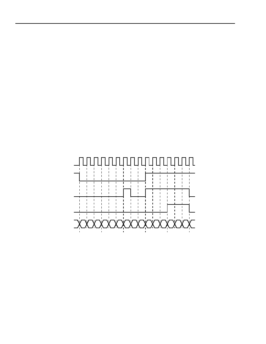
TMXF28155/51 Super Mapper
Preliminary Data Sheet
155/51 Mbits/s SONET/SDH x28/x21 DS1/E1
May 2001
386
Agere Systems Inc.
17 TMUX Functional Description
(continued)
17.6 Transmit Direction (Transmit Path to SONET/SDH Line)
All functions supported by TMUX in the transmit direction are summarized below:
s
Transmit side telecom bus interface
s
Path overhead access channel (POAC) insert
s
Path overhead insertion functions
s
MSP 1 + 1 payload switch
s
Transport overhead access channel (TOAC) insert
s
Section and line overhead insertion functions
17.6.1 Transmit Side Telecom Bus Interface
The TMUX transmit side drives a parallel clock (TLSCLK, pin AA2) and three sync signals (TLSSPE, TLSJ0J1V1,
and TLSV1; pins AB2, AB4, and AB3) onto the telecom bus. From these sync signals, the SPE mappers can deter-
mine when to drive data onto the bus. The TMUX receives an 8-bit data bus (TLSDATA[7:0], pins W2, W1, W3, Y4,
Y2, Y1, Y3, and AA4), and an odd/even (TLSPAR, pin AA3) parity signal from the telecom bus. The data consists of
the SPE for up to 3 STS-1s.
The parallel clock operates at 19.44 MHz for STS-3/STM-1 modes and at 6.48 MHz for STS-1 mode.
5-9009(F)
Figure 28. Transmit Low-Speed Bus Interface Signals for STS-3/STM-1 Signals
17.6.2 Transmit Path and Transport Overhead Insertion Diagram
The transmit block consists of two overhead insertion sections. The first section inserts the path overhead (POH)
bytes into the payload data to create an STS-3/STM-1/STS-1 SPE. After POH insertion, there is an MSP 1 + 1 pro-
tection switch on the payload. After the switch selection is made, the transport overhead bytes are added to the
SPE to generate a complete SONET/SDH frame.
A1-1 A1-2 A1-3 A2-1
A2-3 J0-1 J0-2 J0-3 J1-1 J1-2 J1-3 V1-1 V1-2 V1-3
A2-2
A1
A2
J0
J1
V1
3 BYTES
3 BYTES
3 BYTES
3 BYTES
3 BYTES
TLSSPE
TLSJ0J1V1
TLSV1
TLSDATA[7:0]
TLSCLK
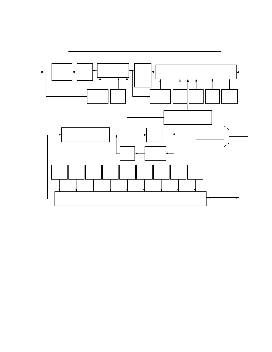
Preliminary Data Sheet
TMXF28155/51 Super Mapper
May 2001
155/51 Mbits/s SONET/SDH x28/x21 DS1/E1
387
Agere Systems Inc.
17 TMUX Functional Description
(continued)
5-9010(F)r.2
Figure 29. Transmit Direction POH and TOH Insertion Diagram
The first section, which is the path overhead section, is broken down into the following functional parts:
s
J1 path trace insert
s
B3 calculation and insert
s
C2 signal label insert
s
REI-P and RDI-P insert
s
Path user byte F2 insert
s
H4 multiframe insert
s
Path user byte F3 insert
s
K3 insert
s
Tandem connection byte N1 insert
s
AIS-P Insert
SCRAM.
INSERT
INSERT
AIS
MSOH
INSERT LINE/MSOH
F1
B2
GENERATE
K1/K2
RDI-L
M0
REI-L
SYNC
APS
B2
K1
K2
INSERT
K2
M0
S1
STATUS
B1
F1
SECTION/RSOH
INSERT J0
A1/A2
TRANSMIT PATH TO SONET/SDH LINE (TRANSMIT DIRECTION)
TRANSMIT DATA
TOAC INSERT
D4--D12 AND E2
B1, E1, F1, D1--3 INSERT
H4
INSERT
F2
INSERT
F3
INSERT
J1
INSERT
N1
INSERT
C2
INSERT
H4
G1
REI-P
INSERT
G1
RDI-P
INSERT
K3
APS
INSERT
N1
C2
F3
F2
K3
G1
G1
J1
INSERT
AIS-P
POAC INSERT
F2, F3, C2, N1, AND J1
INSERT PATH OVERHEAD BYTES
INSERT
TELECOM BUS
TRANSMIT PROTECTION
MSP 1+1
SWITCH
SWITCH BUS DATA
[2:0]
B1
GENERATE
B3
GENERATE
B3
INSERT

TMXF28155/51 Super Mapper
Preliminary Data Sheet
155/51 Mbits/s SONET/SDH x28/x21 DS1/E1
May 2001
388
Agere Systems Inc.
17 TMUX Functional Description
(continued)
The second section after the switch, the transport overhead section, is broken down into the following functional
parts:
s
TOAC insert
s
Sync status byte (S1) insert
s
M0/M1--REI-L Insert
s
K1 and K2 insert
s
AIS-L insert
s
B2 calculation and insert
s
F1 byte insert
s
B1 generate and error insert
s
Scrambler
s
J0 insert control
s
A2 error insert
All insert control functions that are inhibited will insert all zeros or all ones, depending on the value of microproces-
sor register bit, SMPR_OH_DEFLT (
Table 67 on pag e68
).
17.6.3 POAC Insert
One path overhead access channel (POAC) is provided on-chip to provision the path overhead (POH) portion of
the outgoing frame. The TMUX transmits up to three STS-1s. The register bits TMUX_TPOAC_SEL[1:0] (
Table 118
on page115
) designate which STS-1s POH is inserted from the transmit POAC channel.
TMUX_TPOAC_SEL[1:0] = 00 designates no TMUX_TPOAC insertion, TMUX_TPOAC_SEL[1:0] = 01 designates
STS-1 #1, TMUX_TPOAC_SEL[1:0] = 10 designates STS-1 #2, and TMUX_TPOAC_SEL[1:0] = 11 designates
STS-1 #3.
A POAC channel consists of the following signals:
s
A 576 kHz inverted clock signal sourced by the TMUX (TPOACCLK, pin AE4).
s
A 576 kbits/s serial data signal received by the TMUX in the transmit direction (TPOACDATA, pin AD5).
An 8 kHz synchronization signal (TPOACSYNC, pin AC5), sourced by the TMUX. The sync signal is normally low.
During the last clock period of each frame, coincident with the least significant bit of the eighth byte, the sync signal
is high.
The data signal is partitioned into frames of 9 bytes. The frame repetition rate is 8 kHz. Each byte consists of 8 bits
that are transmitted/received most significant bit first. The MSB of the first byte of each frame contains an odd/even
parity bit over the 72 bits of the previous frame. The remaining 7 bits of this byte are not specified. The B3, G1, and
H4 transmit path overhead bytes are not provisionable via the POAC channel.
Bytes shown in
Table 530
summarize the access capabilities of the transmit POAC channel. X indicates a don't
care.
Table 530. Path Overhead Byte Access--Transmit Direction
J1
X
F3
POH Parity
F2
K3
C2
X
N1

Preliminary Data Sheet
TMXF28155/51 Super Mapper
May 2001
155/51 Mbits/s SONET/SDH x28/x21 DS1/E1
389
Agere Systems Inc.
17 TMUX Functional Description
(continued)
An event indication TMUX_TPOAC_PE (
Table 80 on page78
), interrupt mask bit TMUX_TPOAC_PM (
Table 84 on
page 87
), is provided to indicate parity errors for the POAC channel. Odd (logic 0)/even (logic 1) parity is checked
and is configured with TMUX_TPOAC_OEPMON (
Table 117 on page113
).
Table 531
summarizes the insertion options for the specified overhead bytes for POAC. The TMUX allows a fixed
default value (all zeros or all ones) to be inserted on the corresponding POAC value. All control signals are active-
high.
Table 531. TPOAC Control Bits
17.6.4 AIS Path Generation
Path AIS is specified as all ones in the entire STS-1 signal before scrambling, excluding the transport overhead
(section and line overhead).
Path AIS can be inserted for each STS-1 in the STS-3 using register bits, TMUX_TLS_PAISINS[3:1] (
Table 105 on
page 102
).
17.6.5 J1 Insert Control
A 64-byte sequence stored in TMUX_TJ1DINS[1--3][1--64][7:0] (
Table 140 on page123
,
Table 141
, and
Table 142
), will be inserted into the outgoing J1 byte if TMUX_THSJ1INS (
Table 108 on page105
) is set to 1. Oth-
erwise, the associated POAC value is inserted when TMUX_TPOAC_J1 (
Table 118 on page 115
) is a logic 1, or
the default value is inserted when TMUX_TPOAC_J1 is logic 0.
17.6.6 B3 BIP-8 Calculation and Insert
The B3 bytes are allocated for a path overhead error monitoring function. This function will be a bit interleaved par-
ity 8 code (BIP-8) using even parity. The BIP-8 is computed before scrambling over all bits of the previous STS-1
frame except for the first three columns consisting of the section and line overhead and is placed in byte B3 of the
current frame, also before scrambling.
A bit error rate can be inserted on any B3 byte with TMUX_THSB3ERRINS[1--3] (
Table 115 on page112
) and
microprocessor interface block SMPR_BER_INSRT (
Table 65 on page 66
) bit. When TMUX_THSB3ERRINS[1--3]
is asserted, the corresponding B3 byte is inverted each time the SMPR_BER_INSRT bit is asserted.
17.6.7 C2 Signal Label Byte Insert
When TMUX_THSC2INS[1--3] = 1 (
Table 108 on page 105
), the value in TMUX_TC2INS[1--3][7:0] (
Table 124 on
page 118
) is inserted into the C2 byte of the outgoing signal. Otherwise, the associated POAC value is inserted
when TMUX_TPOAC_C2 = 1 (
Table 118 on page115
). If both TMUX_THSC2INS and TMUX_TPOAC_C2 = 0,
then the value inserted depends on the microprocessor interface block, SMPR_OH_DEFLT (
Table 67 on page68
)
bit value. If SMPR_OH_DEFLT = 0, then all 0s are inserted. If SMPR_OH_DEFLT = 1, then all ones are inserted.
Overhead Bytes
Register Control Bits
Values
0 (Default Value)
1
J1
TMUX_TPOAC_J1 (
Table 118
)
SMPR_OH_DEFLT
(00000000/11111111)
TPOAC
Data
C2
TMUX_TPOAC_C2 (
Table 118
)
F2
TMUX_TPOAC_F2 (
Table 118
)
F3
TMUX_TPOAC_F3 (
Table 118
)
K3
TMUX_TPOAC_K3 (
Table 118
)
N1
TMUX_TPOAC_N1 (
Table 118
)

TMXF28155/51 Super Mapper
Preliminary Data Sheet
155/51 Mbits/s SONET/SDH x28/x21 DS1/E1
May 2001
390
Agere Systems Inc.
17 TMUX Functional Description
(continued)
17.6.8 Path RDI (RDI-P) Insert
When TMUX_THSRDIPINS = 1 (
Table 108 on page 105
), then data from TMUX_TRDIPINS[1--3][2:0] (
Table 114
on page110
) is written into the corresponding three STS-1 G1 byte output bits (G1[3:1]). For STS-3 mode, each
STS-1 signal carries its own G1 value. For STM-1 mode, only TMUX_TRDIPINS1[2:0] is written into the first
STS-1 location. When TMUX_THSRDIPINS = 0, hardware insert is enabled for RDI-P insertion. Each defect contri-
bution to the RDI-P outgoing code can be inhibited. There are two modes supported for path RDI insertion. One
mode conforms to the earlier one-bit version of the standard. The other mode, enhanced RDI-P mode, uses a 3-bit
RDI-P code and conforms to the current version of the standard. When TMUX_TEPRDI_MODE = 0 (
Table 110 on
page 109
), the TMUX sends a 3-bit code that conforms to the earlier 1-bit version of the standards. If
TMUX_TEPRDI_MODE = 1, the TMUX will send a 3-bit code conforming to the current enhanced path RDI encod-
ing. Note that for non-enhanced RDI-P mode, the relevant defects are AIS-P and LOP-P. For enhanced RDI-P
mode, the relevant defects are AIS-P, LOP-P, PLM-P, and UNEQ-P.
When a failure condition exists that will cause RDI-P to be generated via hardware, the generation of RDI-P must
last for at least 20 frames before clearing, even if the original failure cause has cleared in less than 20 frames.
Table 532
describes the encoding of the path RDI defects.
Table 532. RDI-P Defects for Enhanced RDI-P Mode
The TMUX provides a protection switch MUX for RDI-P insertion. The MUX is controlled by TMUX_TPREIRDISEL
(
Table 107 on page 103
). If TMUX_TPREIRDISEL = 1, then the RDI-P value for insertion is taken from the value on
the protection board rather than from the receive side of the same TMUX.
17.6.9 REI-P: G1(7:4) Insert
Four bits of the G1 byte G1(7:4) are allocated for use as path remote error indication (REI). For STS-1 signals and
for STM-1 signals, these bits convey the count (in the range of 0 to 8) of interleaved bit blocks that have been
detected in error by the BIP-8 (B3) detector on the received signal.
The automatic insertion of path REI can be inhibited on an STS-1 basis by programming the corresponding register
bits TMUX_TPREIINS[1:3] (
Table 115
) to 1. For STM-1 mode, only TMUX_TPREIINS[1] is relevant. If the register
bit(s) TMUX_TPREIINS[1:3] are programmed to 1, then one error is inserted into the G1 byte for that particular
STS-1(s) each time the microprocessor interface block SMPR_BER_INSRT (
Table 65 on page66
) bit is asserted.
The TMUX provides a protection switch MUX for REI-P insertion. The MUX is controlled by TMUX_TPREIRDISEL
(
Table 107 on page 103
). If TMUX_TPREIRDISEL = 1, then the REI-P value for insertion is taken from the value on
the protection board rather than from the receive side of the same TMUX.
G1
Triggers
Bit 3
Bit 2
Bit 1
0
0
0
No defects (nonenhanced RDI-P mode).
0
0
1
No defects (enhanced RDI-P mode).
0
1
0
LCD-P, PLM-P (LCD-P not supported in Super Mapper).
0
1
1
No defects (nonenhanced RDI-P mode).
1
0
0
AIS-P, LOP-P (nonenhanced RDI-P mode).
1
0
1
AIS-P, LOP-P (enhanced RDI-P mode).
1
1
0
TIM-P, UNEQ-P (enhanced RDI-P mode).
1
1
1
AIS-P, LOP-P (nonenhanced RDI-P mode).

Preliminary Data Sheet
TMXF28155/51 Super Mapper
May 2001
155/51 Mbits/s SONET/SDH x28/x21 DS1/E1
391
Agere Systems Inc.
17 TMUX Functional Description
(continued)
17.6.10 F2 Byte Insert
When TMUX_THSF2INS = 1 (
Table 108 on page 105
), the value in TMUX_TF2INS[1--3][7:0] (
Table 114 on
page 110
) is inserted into the outgoing signal. Otherwise, the associated POAC value is inserted when
TMUX_TPOAC_F2 = 1 (
Table 118 on page115
). If both TMUX_THSF2INS and TMUX_TPOAC_F2 = 0, then the
value inserted depends on the value of microprocessor interface block SMPR_OH_DEFLT (
Table 67 on pag e68
)
bit. If SMPR_OH_DEFLT = 0, then all 0s are inserted. If SMPR_OH_DEFLT = 1, then all ones are inserted.
17.6.11 H4 Insert Control
A 4-byte sequence (0, 1, 2, and 3) will be inserted into the outgoing H4 bytes. Note that the assertion of pin TLSV1
(pin AB3) occurs after the J1 byte(s) during the frame where the H4 count equals one.
17.6.12 F3 Byte Insert
When TMUX_THSF3INS = 1 (
Table 108
), the value in TMUX_TF3INS[1--3][7:0] (
Table 114 on page110
) is
inserted into the outgoing signal. Otherwise, the associated POAC value is inserted when TMUX_TPOAC_F3 = 1
(
Table 118 on page 115
). If both TMUX_THSF3INS and TMUX_TPOAC_F3 = 0, then the value inserted depends
on the value of microprocessor interface block SMPR_OH_DEFLT (
Table 67 on page68
) bit. If SMPR_OH_DEFLT
= 0, then all 0s are inserted. If SMPR_OH_DEFLT = 1, then all ones are inserted.
17.6.13 K3 Byte Insert
When TMUX_THSK3INS = 1 (
Table 108 on page105
), the value in TMUX_TK3INS[1--3][7:0] (
Table 114
) is
inserted into the outgoing signal. Otherwise, the associated POAC value is inserted when TMUX_TPOAC_K3 = 1
(
Table 118 on page 115
). If both TMUX_THSK3INS and TMUX_TPOAC_K3 = 0, then the value inserted depends
on the value of microprocessor interface block SMPR_OH_DEFLT (
Table 67
) bit. If SMPR_OH_DEFLT = 0, then all
0s are inserted. If SMPR_OH_DEFLT = 1, then all ones are inserted.
17.6.14 N1 Byte Insert
When TMUX_THSN1INS = 1 (
Table 108 on page 105
), the value in TMUX_TN1INS[1--3][7:0] (
Table 114 on
page 110
) is inserted into the outgoing signal. Otherwise, the associated POAC value is inserted when
TMUX_TPOAC_N1 = 1 (
Table 118
). If both TMUX_THSN1INS and TMUX_TPOAC_N1 = 0, then the value inserted
depends on the value of microprocessor interface block SMPR_OH_DEFLT (
Table 67 on page68
) bit. If
SMPR_OH_DEFLT = 0, then all 0s are inserted. If SMPR_OH_DEFLT = 1, then all ones are inserted.
17.6.15 MSP 1 + 1 Payload Switch
For the working transmit high-speed data output (THSDP/N, pins AF9/AE9), it is possible to select the normal
transmit path low-speed data by setting TMUX_TPSMUXSEL2 = 0 (
Table 106 on page 103
) or the receive-side
protection input data by setting TMUX_TPSMUXSEL2 = 1. Note that if the receive-side protection input is selected,
then the local clock and frame sync are generated based on the receive-side protection inputs as well.
To create the transmit high-speed protection outputs (TPSD155P/N and TPSC155P/N; pins AF13/AE13 and
AC12/AD13), it is possible to select the normal transmit path low-speed input data with TMUX_TPSMUXSEL3 = 0
(
Table 106 on page 103
) or the receive-side working inputs with TMUX_TPSMUXSEL3 = 1.
Note: Clocks and timing signals are selected by TMUX_TPSMUXSEL3 as well as the parallel data.
17.6.16 Transmit Transport Overhead Access Channel (TTOAC)
The TMUX provides a transmit transport overhead access channel (TTOAC) to provision the TOH portion of the
outgoing frame. The TTOAC channel supports three modes of operation based on values in
TMUX_TTOAC_D13MODE and TMUX_TTOAC_D412MODE (
Table 117 on page113
).

TMXF28155/51 Super Mapper
Preliminary Data Sheet
155/51 Mbits/s SONET/SDH x28/x21 DS1/E1
May 2001
392
Agere Systems Inc.
17 TMUX Functional Description
(continued)
The TTOAC channel consists of the following signals:
s
A data signal received by the TMUX in the transmit direction (TTOACDATA, pin AE2). The data bytes per frame
received depend on the values of TMUX_TTOAC_D13MODE and TMUX_TTOAC_D412MODE. See
Table 533
below.
s
A clock signal sourced by the TMUX (TTOACCLK, pin AB6). The clock frequency depends on the values of
TMUX_TTOAC_D13MODE and TMUX_TTOAC_D412MODE. See
Table 533
below.
s
An 8 kHz synchronization signal (TTOACSYNC, pin AF3) is sourced by the TMUX. This sync signal is normally
low; during the last clock period of each frame, coincident with the least significant bit of the last byte, the sync
signal is high.
Table 533. Transmit TOAC Modes
Transmit TOAC--DCC1 through DCC3 Mode. In this mode, DCC bytes 1 to 3 are received serially on the data
pin. The clock rate is 192 kHz. The data bytes are received MSB first, and the sequence of data bytes is DCC1,
DCC2, and DCC3. The data signal is partitioned into frames of 3 bytes. The frame repetition rate is 8 kHz.
Transmit TOAC--DCC4 through DCC12 Mode. In this mode, DCC bytes 4 to 12 are received serially on the data
output. The clock rate is 576 kHz. The data bytes are received MSB first, and the sequence of data bytes is DCC4,
DCC5, DCC6, DCC7, DCC8, DCC9, DCC10, DCC11, and DCC12. The data signal is partitioned into frames of
9 bytes. The frame repetition rate is 8 kHz.
Transmit TOAC--Full TOH Access Mode. In this mode, where TMUX_TTOAC_D13MODE = 0 and
TMUX_TTOAC_D412MODE = 0 (
Table 117 on page113
), the data signal (TTOACDATA, pin AE2) is partitioned
into frames of 81 bytes. The frame repetition rate is 8 kHz. Each byte consists of 8 bits that are transmitted/received
most significant bit first. The MSB of the first byte of each frame contains an odd/even parity bit over the 648 bits of
the previous frame. The remaining 7 bits of this byte are not specified.
Bytes shown in
Table 534
summarize the access capabilities of the transmit TOAC. This table describes the possi-
ble bytes in the outgoing frame that can be provisioned from the values on the TOAC channel. There are additional
mode bits described in
Table 535
that must be programmed to allow insertion from the TOAC channel. Bytes indi-
cated in bold type below are not specified in the standard, but are available for insertion into the outgoing frame via
the register bit, TMUX_TTOAC_AVAIL (
Table 117
). An X in
Table 534
indicates bytes that are don't cares; the val-
ues of these bytes in the outgoing transmit frame are not related to the values on the TTOAC channel.
Table 534. Transmit Transport Overhead Byte Full Access Mode
TOAC Mode
TMUX_TTOAC_
D13MODE Value
TMUX_TTOAC_
D412MODE Value
Data Bytes per
Frame
Clock Rate
DCC1--DCC3
1
X
3
192 kHz
DCC4--DCC12
0
1
9
576 kHz
Full TOH mode
0
0
81
5.184 MHz
OH Parity
X
X
X
X
X
X
X
X
X
B1-2
B1-3
E1
E1-2
E1-3
F1
F1-2
F1-3
D1
D1-2
D1-3
D2
D2-2
D2-3
D3
D3-2
D3-3
X
X
X
X
X
X
X
X
X
X
X
X
X
K1-2
K1-3
X
K2-2
K2-3
D4
D4-2
D4-3
D5
D5-2
D5-3
D6
D6-2
D6-3
D7
D7-2
D7-3
D8
D8-2
D8-3
D9
D9-2
D9-3
D10
D10-2
D10-3
D11
D11-2
D11-3
D12
D12-2
D12-3
S1
Z1-2
Z1-3
Z2
Z2-2
X
E2
E2-2
E2-3

Preliminary Data Sheet
TMXF28155/51 Super Mapper
May 2001
155/51 Mbits/s SONET/SDH x28/x21 DS1/E1
393
Agere Systems Inc.
17 TMUX Functional Description
(continued)
Table 535
summarizes the insertion options for the specified overhead bytes for TOAC in full TOH access mode.
The TMUX allows a default value (all zeros if microprocessor interface block SMPR_OH_DEFLT = 0 (
Table 67 on
page 68
), and all ones if SMPR_OH_DEFLT = 1) to be inserted on the corresponding TOAC value. All control sig-
nals are active-high.
Table 535. TTOAC Control Bits in Full Access Mode
An event indication must be provided to indicate parity errors for the TOAC channel. Odd or even parity is checked
depending on TMUX_TTOAC_OEPMON (
Table 117 on page 113
); 0 selects odd parity and 1 selects even parity. A
parity error is reported in status register bit TMUX_TTOAC_PE (
Table 80 on pag e78
), and the interrupt is
maskable with TMUX_TTOAC_PM (
Table 84 on page87
).
17.6.17 Sync Status Byte (S1) Insert
When TMUX_THSS1INS = 1 (
Table 107 on page 103
), the value in TMUX_TS1INS[7:0] (
Table 112 on page 110
) is
inserted into the S1 byte of the outgoing signal; otherwise, the associated TOAC value is inserted when
TMUX_TTOAC_S1 = 1 (
Table 117 on pag e113
). If both TMUX_THSS1INS and TMUX_TTOAC_S1 are a logic 0,
then the value inserted depends on the value of the microprocessor interface block SMPR_OH_DEFLT (
Table 67
on page68
) bit. If SMPR_OH_DEFLT = 0, then all zeros are inserted. If SMPR_OH_DEFLT = 1, then all ones are
inserted.
17.6.18 REI-L: M1 Insert
For STS-3/STM-1 modes, the M1 byte is allocated for use as a line remote error indication (REI). For STS-1, bits 0
to 3 of the M0 byte are used. The M0 or M1 bytes convey the count of interleaved bit blocks that have been
detected in error by the line BIP-8 (B2) detector on the received signal.
This function can be inhibited by asserting TMUX_THSLREIINH (
Table 107 on page103
). A bit error in the M0/M1
byte can be inserted under user control. When TMUX_TLREIINS (
Table 115 on page112
) is asserted the corre-
sponding M0 or M1 byte will indicate one error each time the microprocessor interface block SMPR_BER_INSRT
(
Table 65
) bit is asserted.
The TMUX provides a protection switch MUX for REI-L insertion, controlled by TMUX_TLREIRDISEL (
Table 107
).
If TMUX_TLREIRDISEL = 1, then the REI-L value for insertion is taken from the value on the protection board
rather than from the receive side of the same TMUX.
17.6.19 APS Value and K2 Insert Control Parameters
When TMUX_THSAPSINS = 1 (
Table 107
), the K1 byte and the five most significant bits of the K2 byte are written
from TMUX_TAPSINS[12:0] (
Table 113
). When TMUX_THSAPSINS = 0, either all 0s or all ones will be written,
depending on the value of microprocessor interface block SMPR_OH_DEFLT (
Table 67
) bit.
Overhead Bytes
Register Control Bits
Value of the Register Control Bits
0 (Default Value)
1
E1
TMUX_TTOAC_E1 (
Table 117
)
SMPR_OH_DEFLT
(00000000 or 11111111)
TOAC Data
F1
TMUX_TTOAC_F1 (
Table 117
)
D1--D3
TMUX_TTOAC_D1TO3 (
Table 117
)
D4--D12
TMUX_TTOAC_D4TO12 (
Table 117
)
S1
TMUX_TTOAC_S1 (
Table 117
)
E2
TMUX_TTOAC_E2 (
Table 117
)
All remaining bytes
in
Table 534
TMUX_TTOAC_AVAIL (
Table 117
)

TMXF28155/51 Super Mapper
Preliminary Data Sheet
155/51 Mbits/s SONET/SDH x28/x21 DS1/E1
May 2001
394
Agere Systems Inc.
17 TMUX Functional Description
(continued)
An APS babbling test is controlled with TMUX_TAPSBABINS (
Table 116 on page113
). Setting
TMUX_TAPSBABINS = 1 forces the K1[7:0], K2[7:3) to an inconsistent state; no three consecutive values are con-
tinuously the same.
When the transmit K2 software insert bit TMUX_THSK2INS = 1 (
Table 107 on page103
), data from bits
TMUX_TK2INS[2:0] (
Table 113 on page110
) is written into the K2[2:0] output bits. When TMUX_THSK2INS = 0,
hardware insertion of RDI-L is enabled.
17.6.20 Criteria for Insert Line RDI
Hardware insertion of line RDI is generated using the following equation. Each defect contribution to line RDI can
be individually inhibited.
(TMUX_RILOC AND TMUX_TRILOC_LRDIINH) OR
(TMUX_RHSLOS AND TMUX_TRLOS_LRDIINH) OR
(TMUX_RHSLOF AND TMUX_TRLOF_LRDIINH) OR
(TMUX_RHSOOF AND TMUX_TROOF_LRDIINH) OR
(TMUX_RLAISMON AND TMUX_TRLAISMON_LRDIINH) OR
(TMUX_RHSSF AND TMUX_TRSF_LRDIINH) OR
(TMUX_RHSSD AND TMUX_TRSD_LRDIINH)
When a failure condition exists that will cause RDI-L to be generated, the generation of RDI-L must last for at least
20 frames before clearing, even if the original failure cause has cleared in less than 20 frames.
The TMUX provides a protection switch MUX for RDI-L insertion. The MUX is controlled by TMUX_TLREIRDISEL
(
Table 107
). If TMUX_TLREIRDISEL = 1, then the RDI-L value for insertion is taken from the value on the protec-
tion board rather than from the receive side of the same TMUX.
17.6.21 Line AIS Generation
Line AIS is specified as all ones in the entire STS/STM signal before scrambling, excluding the section overhead.
Line AIS can be generated by setting TMUX_THSLAISINS = 1 (
Table 107
).
17.6.22 B2 BIP-8 Calculation and Insert
The B2 byte is allocated for a line overhead error monitoring function. This function will be a bit interleaved parity-8
code (BIP-8) using even parity. The BIP-8 is computed before scrambling, over all the bits of the previous STS-1
frame (except for the 9 bytes of section overhead) and is placed in byte B2 of the current frame also before scram-
bling.
A bit error rate can be inserted on any B2 byte. When bit(s) TMUX_THSB2ERRINS[1--3] (
Table 115 on page112
)
is (are) asserted, the corresponding B2 byte is inverted each time the microprocessor interface block
SMPR_BER_INSRT (
Table 65 on page66
) bit is asserted.
17.6.23 F1 Byte Insert
When TMUX_THSF1INS = 1 (
Table 107 on page 103
), the value in TMUX_TF1INS[7:0] (
Table 112 on page 110
) is
inserted into the F1 byte of the outgoing signal. Otherwise, the associated TOAC value is inserted when
TMUX_TTOAC_F1 = 1 (
Table 117 on page113
). If both TMUX_THSF1INS and TMUX_TTOAC_F1 = 0, then the
value inserted depends on the value of microprocessor interface block SMPR_OH_DEFLT (
Table 67 on page 68
)
bit. If SMPR_OH_DEFLT = 0, then all 0s are inserted. If SMPR_OH_DEFLT = 1, then all ones are inserted.

Preliminary Data Sheet
TMXF28155/51 Super Mapper
May 2001
155/51 Mbits/s SONET/SDH x28/x21 DS1/E1
395
Agere Systems Inc.
17 TMUX Functional Description
(continued)
17.6.24 B1 Generate and Error Insert
The section bit interleaved parity code (BIP-8) byte (even parity) is used to check for transmission errors over a
section. Its value is calculated over all bits in the previous frame after scrambling and placed in the B1 byte of time
slot 1 before scrambling.
A bit error rate can be inserted on the B1 byte. When TMUX_THSB1ERRINS = 1 (
Table 115 on page 112
), the B1
byte is inverted each time the microprocessor interface block SMPR_BER_INSRT (
Table 65 on page66
) bit is
asserted.
17.6.25 Scrambler
The outgoing frame will be scrambled with the frame synchronous scrambler of length 127 and generating polyno-
mial x
7
+ x
6
+ 1. The entire STS/STM signal will be scrambled except for the first row of overhead. The scrambler
will be set to 1111111 on the first byte following the last overhead byte in the first row.
For test purposes, the scrambler will be disabled when TMUX_THSSCR = 0 (
Table 106 on page 103
).
17.6.26 J0 Insert Control
A 16-byte sequence stored in TMUX_TJ0DINS[1--16][7:0] (
Table 133 on page121
) will be inserted into the outgo-
ing J0 byte if TMUX_THSJ0INS = 1 (
Table 107 on pag e103
). If TMUX_THSJ0INS = 0, then the value inserted
depends on the value of microprocessor interface block SMPR_OH_DEFLT (
Table 67
) bit. If SMPR_OH_DEFLT =
0, then all 0s are inserted. If SMPR_OH_DEFLT = 1, then all ones are inserted.
17.6.27 Z0-2, Z0-3 Insert Control
The 2 bytes, Z0-2 and Z0-3, that follow J0 are not scrambled. If TMUX_THSZ0INS = 1 (
Table 107
), then the values
stored in TMUX_TZ02INS[7:0] (
Table 111 on pag e110
) and TMUX_TZ03INS[7:0] (
Table 111
) will be inserted. If
TMUX_THSZ0INS = 0, then the value inserted depends on the value of microprocessor interface block
SMPR_OH_DEFLT bit. If SMPR_OH_DEFLT = 0, then all zeros are inserted. If SMPR_OH_DEFLT = 1, then all
ones are inserted.
17.6.28 A2 Error Insert
The TMUX allows, under software control, from 1 to 32 continuous frames to have an inverted A2-1 (0x28 to 0xD7)
pattern in the outgoing frame. The value in TMUX_TA2ERRINS[4:0] (
Table 106
) specifies the number of frames to
insert errors into while assertion of microprocessor interface block, SMPR_BER_INSRT bit, starts the error inser-
tion process.

TMXF28155/51 Super Mapper
Preliminary Data Sheet
155/51 Mbits/s SONET/SDH x28/x21 DS1/E1
May 2001
396
Agere Systems Inc.
18 SPE Mapper Functional Description
Table of Contents
Contents
Page
18 SPE Mapper Functional Description ............................................................................................................... 396
18.1 Introduction ............................................................................................................................................. 398
18.2 Features ................................................................................................................................................. 398
18.3 SPE Mapper Functional Block Diagrams ............................................................................................... 399
18.4 TUG-2 to AU-3/STS-1 SPE Mapping (Used in North American Systems) ............................................. 402
18.5 TUG-2 to TUG-3 Mapping (Used in ITU/ETSI Standard Based Systems) ............................................. 402
18.6 DS3 to AU-3/STS-1 SPE Mapping (Used in
Telcordia
/
ANSI
Standards Based Systems) ..................... 403
18.7 DS3 to TUG-3 Mapping (Used in ITU/ETSI Standard Based Systems) ................................................. 403
18.8 SPE Mapper Basic Configuration ........................................................................................................... 403
18.9 DS3 Configuration .................................................................................................................................. 403
18.9.1 DS3 M13 ...................................................................................................................................... 404
18.9.2 DS3 Loopback Channel ............................................................................................................... 404
18.9.3 DS3 Clear Channel from External Pins ........................................................................................ 404
18.10 Phase Detector for External DS3 PLL .................................................................................................. 404
18.11 Serial STS-1 SPE Channel (NSMI) ...................................................................................................... 405
18.12 TMUX Interface to the SPE Mapper ..................................................................................................... 406
18.13 PATH Termination Block ...................................................................................................................... 406
18.13.1 Pointer Interpretation Block ....................................................................................................... 407
18.14 SPE Mapper Receive Direction Requirements ..................................................................................... 410
18.14.1 Loss of Clock and Loss of Sync Monitors ................................................................................. 411
18.14.2 J1 Monitor .................................................................................................................................. 411
18.14.3 B3 BIP-8 Check ......................................................................................................................... 412
18.14.4 Signal Label C2 Byte Monitor .................................................................................................... 412
18.14.5 Path User Byte F2 Monitor ........................................................................................................ 413
18.14.6 Path User Byte F3 Monitor ........................................................................................................ 414
18.14.7 N1 Monitor ................................................................................................................................. 414
18.14.8 K3 Byte Monitor ......................................................................................................................... 415
18.14.9 AIS-P and RDI-P Detect ............................................................................................................ 415
18.14.10 REI-P Detect ........................................................................................................................... 416
18.14.11 Signal Degrade BER Algorithm ............................................................................................... 416
18.14.12 Signal Fail BER Algorithm ....................................................................................................... 417
18.14.13 POAC Drop ............................................................................................................................. 418
18.14.14 Insertion of AIS-P .................................................................................................................... 419
18.15 Transmit Direction (to SONET/SDH Line) ............................................................................................ 420
18.15.1 PATH Insertion Block ................................................................................................................ 420
18.15.2 Loss of Clock and Loss of Sync Detectors ................................................................................ 421
18.15.3 J1 Byte Insert ............................................................................................................................ 421
18.15.4 B3 BIP-8 Calculation and Insert ................................................................................................ 421
18.15.5 C2 Signal Label Byte Insert ....................................................................................................... 421
18.15.6 REI-P G1(7:4) Insert .................................................................................................................. 421
18.15.7 Path RDI (RDI-P) Insert ............................................................................................................. 422
18.15.8 F2 Byte Insert ............................................................................................................................ 422
18.15.9 H4 Insert Control ....................................................................................................................... 422
18.15.10 F3 Byte Insert .......................................................................................................................... 422
18.15.11 K3 Insert Control Parameters .................................................................................................. 422
18.15.12 N1 Insert Control Parameters .................................................................................................. 423
18.16 POAC Insert ......................................................................................................................................... 423
18.17 AIS Path Generation ............................................................................................................................. 424

Preliminary Data Sheet
TMXF28155/51 Super Mapper
May 2001
155/51 Mbits/s SONET/SDH x28/x21 DS1/E1
397
Agere Systems Inc.
18 SPE Mapper Functional Description
(continued)
Table of Contents
(continued)
Figures
Page
Figure 30. SPE Mapper Block with Connections to External Pins and Other Blocks in the Device ..................... 399
Figure 31. Basic Functional Flow of the SPE Mapper Transmit Section .............................................................. 400
Figure 32. Basic Functional Flow of the SPE Mapper Receive Section ............................................................... 401
Figure 33. STS-1 NSMI Receive Operation ......................................................................................................... 405
Figure 34. STS-1 NSMI Transmit Operation ........................................................................................................ 406
Figure 35. Receive Direction Path Termination Block .......................................................................................... 407
Figure 36. Pointer Interpretation State Diagram................................................................................................... 408
Figure 37. Transmit Direction Path Insertion Block .............................................................................................. 420
Tables
Page
Table 536. J1 Monitor .......................................................................................................................................... 412
Table 537. STS Signal Label Defect Conditions ................................................................................................. 412
Table 538. C2MON Processing ........................................................................................................................... 413
Table 539. F2 Monitor ......................................................................................................................................... 414
Table 540. F3 Monitor ......................................................................................................................................... 414
Table 541. N1 Monitor ......................................................................................................................................... 414
Table 542. K3 Monitor ......................................................................................................................................... 415
Table 543. AIS-P and RDI-P Detect .................................................................................................................... 415
Table 544. STS-1 P-REI Interpretation ................................................................................................................ 416
Table 545. Signal Degrade Parameters .............................................................................................................. 417
Table 546. Signal Fail Parameters ...................................................................................................................... 418
Table 547. Path Overhead Byte Access .............................................................................................................. 419
Table 548. RDI-P Defects for Enhanced RDI-P Mode ........................................................................................ 422
Table 549. Path Overhead Byte Access--Transmit Direction ............................................................................. 423
Table 550. TPOAC Control Bits .......................................................................................................................... 424

TMXF28155/51 Super Mapper
Preliminary Data Sheet
155/51 Mbits/s SONET/SDH x28/x21 DS1/E1
May 2001
398
Agere Systems Inc.
18 SPE Mapper Functional Description
(continued)
18.1 Introduction
This section describes the functions of the SPE mapper block.
The SPE mapper is highly configurable; it can operate in two different modes, as an AU-3/STS-1 mapper or as a
TUG-3 mapper. In both modes, it can map/demap data from/to either the VT mapper block, the M13 MUX/deMUX
block, the DS3 clear channel, or the DS3 loopback channel.
The SPE mapper supports numerous automatic monitoring functions. It can provide interrupts to the control sys-
tem, or it can be operated in a polled mode.
Additionally, this block has a built-in auxiliary channel known as the path overhead access channel (POAC). This
channel is mainly used for path overhead insertion and drop functions.
18.2 Features
s
The SPE mapper accepts/delivers TUG-2 data from/to the VT mapper. The TUG-2 data is mapped/demapped
either to/from an AU-3/STS-1 signal for the North American digital systems or to/from a TUG-3 signal for the
European digital systems.
s
Flexibility down to TUG-2 level is provided for choosing which TUG-2s (between 1 and 7) are mapped into which
TUG-3s (between 1 and 3) for generating STM-1 signals. Similarly, any TUG-2s (up to 7) may be dropped/termi-
nated from the 21 TUG-2s of an STM-1 signal.
s
The SPE mapper accepts/delivers DS3 data from/to the M13 MUX/deMUX. The DS3 data is mapped/demapped
either to/from an AU-3/STS-1 signal for the North American digital systems or to/from a TUG-3 signal for the
European digital systems.
s
The SPE mapper accepts/delivers a clear DS3 signal at 44.736 Mbits/s rate. The clear DS3 signal is mapped/
demapped essentially the same way as M13 signal described above.
s
The SPE mapper has a DS3 loopback circuit placed for the functions of demapping and remapping a DS3 signal.
It is particularly useful in cases where a DS3 signal mapped as an AU-3/STS-1 signal is needed to be remapped
as a TUG-3 signal or vice versa.
s
The SPE mapper supports a path overhead access channel more commonly known as the POAC channel.
Seven path overhead bytes namely J1, C2, F2, H4, F3, K3, and N1 may be inserted/dropped through this chan-
nel. This channel works as the master which means that this channel provides a clock in both transmit and
receive directions and POH data may be inserted by the user on the transmit side or dropped by the block in the
receive side.
s
Path overhead byte B3 (BIP error) generation/detection and programmable BIP-2 bit error rate insertion.
s
Programmable clear on read/clear on write registers.
s
Signal fail and signal degrade indicators available to report bit error rates above a certain programmable thresh-
old.
s
Capable of detecting/inserting alarm indication signals (AIS), remote defect indication signals (RDI) and remote
error indication signals (REI).
s
Numerous monitoring functions provided on all the TUG-3 path overhead bytes.
s
Supports unidirectional path switch ring (UPSR) applications.
s
N1 tandem connection support is provided.
s
Complies with GR-253-CORE, T1.105, ITU-T G.707, ITU-T G.831, G.783, ETS 300 417-1-1.

Preliminary Data Sheet
TMXF28155/51 Super Mapper
May 2001
155/51 Mbits/s SONET/SDH x28/x21 DS1/E1
399
Agere Systems Inc.
18 SPE Mapper Functional Description
(continued)
18.3 SPE Mapper Functional Block Diagrams
5-9065(F)
Figure 30. SPE Mapper Block with Connections to External Pins and Other Blocks in the Devic e
VT
MICRO INTERFACE
SPE MAPPER
DS3DATAINCLK
DS3DATAOUTCLK
DS3NEGDATAIN
PHASEDETUP
PHASEDETDOWN
DS3NEGDATAOUT
AUTO_AIS,
TPOAC
DS3POSDATAOUT
DS3POSDATAIN
REI
DS3
AUTO_AIS
DATA, CLK, SYNC
TRANSMIT
RECEIVE
TELECOM
BUS
CLK, DATA
RPOAC
TRANSMIT
RECEIVE
CLK, DATA
TRANSMIT
RECEIVE
TRANSMIT
PATH OVERHEAD
INSERT
POAC CHANNEL
TELECOM
BUS
RDI, REI
MAPPER
TRANSMIT
SECTION
VT
MAPPER
RECEIVE
SECTION
M13
MAPPER
TRANSMIT
SECTION
M13
MAPPER
RECEIVE
SECTION
DS3
CLEAR INPUT
TRANSMIT
PINS
DS3
CLEAR INPUT
RECEIVE
PINS
RECEIVE
PATH OVERHEAD
EXTRACT
POAC CHANNEL
TMUX
RECEIVE
SECTION
TMUX
TRANSMIT
SECTION
DATA, CLK, SYNC
DATA, CLK,
CONTROL
DATA, CLK,
CONTROL
LOOPBACK
RDI
TRANSMIT
SECTION
SPE MAPPER
RECEIVE
SECTION
MISC SIGNALS
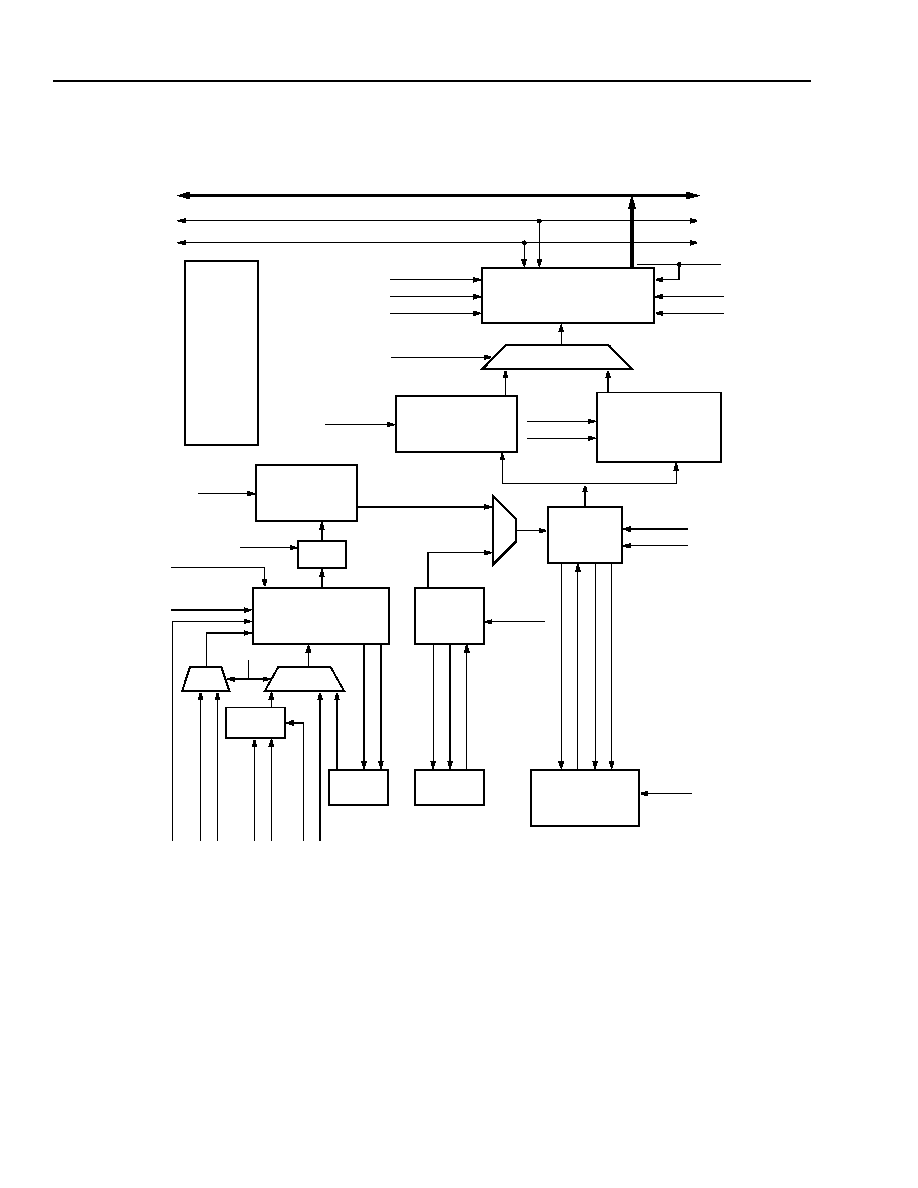
TMXF28155/51 Super Mapper
Preliminary Data Sheet
155/51 Mbits/s SONET/SDH x28/x21 DS1/E1
May 2001
400
Agere Systems Inc.
18 SPE Mapper Functional Description
(continued)
5-9066(F)
Figure 31. Basic Functional Flow of the SPE Mapper Transmit Section
TELECOM BUS DATA[7:0], CLOCK, PARITY, SYNC (19.44 MHz OR 6.48 MHz)
TO/FROM TMUX TRANSMIT SIDE
D
S
3 _E
X
T
_C
LK
D
S
3
PO
S_
D
A
T
A
51.84 MHz CLOCK FROM TMUX
51.84 MHz CLOCK, CONTROL FROM TMUX
B3ZS
M13
DS
3
DA
T
A
DS
3
CL
K
DS
3
CL
K
_
E
N
DS3 INPUT CONTROL &
VT/TU
FIFO
DS3
TUG-2
PATH
T
U
G
-
2_D
A
T
A
SY
N
C
_
V1
CL
K
_
6
M
Hz
MUX
TUG-3 MAPPER
AU-3 MAPPER
MUX
TUG-3 OR AU-3
MUX
MICRO-
C-3
TUG-2
MU
X
L
O
O
PBA
C
K
_
C
L
K
L
O
O
P
BAC
K
_
D
A
T
A
T
X
_
P
O
A
CDA
T
A
TX
_
P
O
A
C
S
Y
N
C
T
X
_
P
O
A
CINH
T
X
_
P
O
A
CCL
K
O
PATH OVERHEAD
LO
O
P
B
A
C
K
_
C
LK
_E
N
DS
3
NE
G
_
DA
T
A
STS3_TIMESLOT
AU3_TUG3
VT_DS3
AU3_TUG3
AU3_TUG3
AU3_TUG3
VT_DS3
VT_DS3
VT_DS3
TD
S
3
_
B
I
P
O
L
A
R
DS3_SRC_TYPE
DS3_SRC_TYPE
VT_DS3
VT_DS3
VT_DS3
84 x 9 bytes
84 x 9 bytes
84 x 9
85 x 9 bytes
87 x 9 bytes
87 x 9 bytes
87 x 9 bytes
TU11_TU12
TUG2_NO[2:0]
TUG3_NO[1:0]
AU3_TUG3
VT_DS3
M
P
UCL
K
D
S
3C
LK
TELECOM BUS
OUTPUT (87 x 9 bytes)
CONTROL CIRCUITRY
ADD 1 COLUMN
OF FIXED STUFFING &
TU-3 PTR BYTES
ADD 2 COLUMNS
OF FIXED STUFFING
OVERHEAD
INSERTION
INSERT
POAC CHANNEL
MAPPER
MAPPER
DECODE
SERIAL-TO-PARALLEL
CONVERSION
INPUT
CONTROL
MAPPED AS
CONTAINER C-3
INTERFACE
CLOCK
bytes
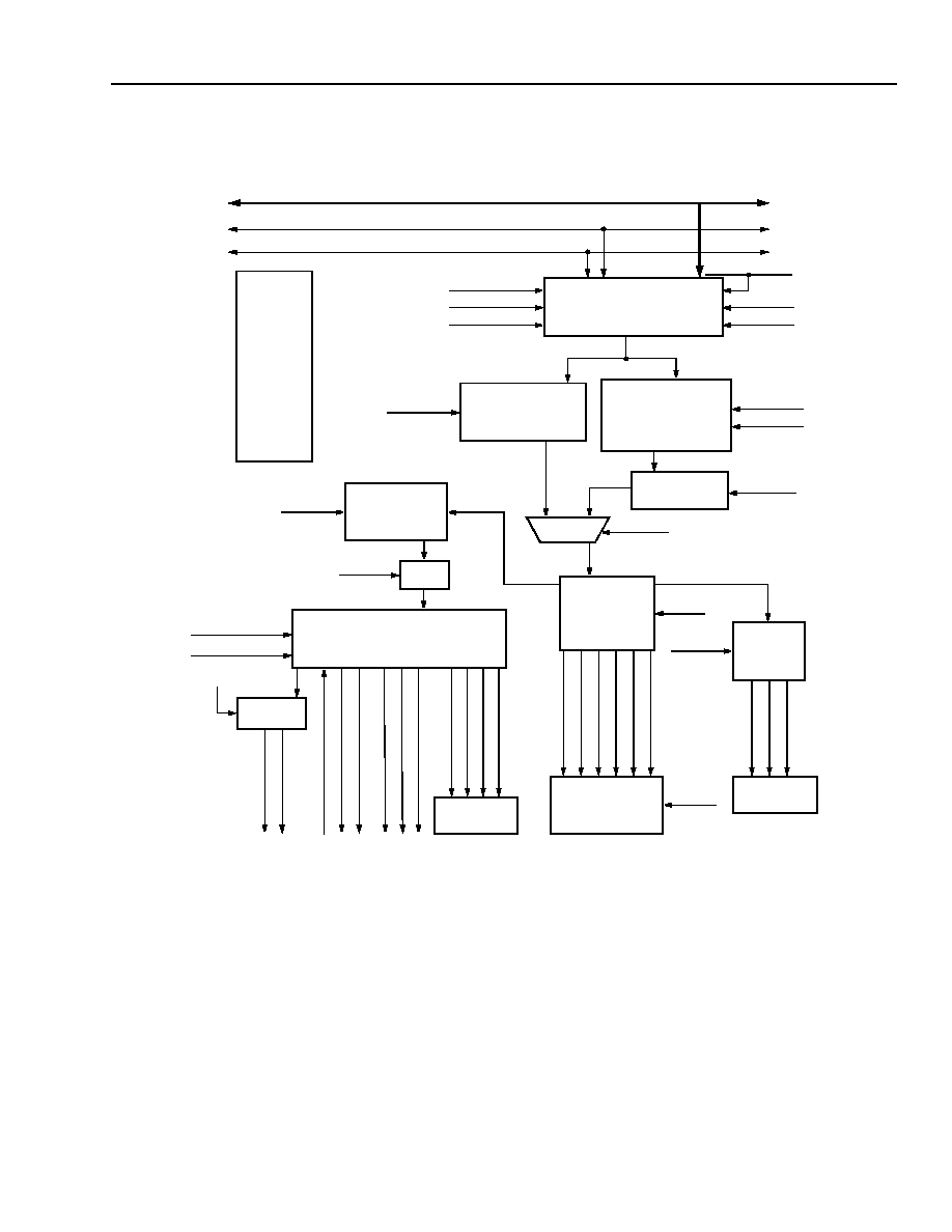
Preliminary Data Sheet
TMXF28155/51 Super Mapper
May 2001
155/51 Mbits/s SONET/SDH x28/x21 DS1/E1
401
Agere Systems Inc.
18 SPE Mapper Functional Description
(continued)
5-9067(F)r.1
Figure 32. Basic Functional Flow of the SPE Mapper Receive Section
TELECOM BUS DATA[7:0], CLOCK, PARITY, SYNC (19.44 MHz OR 6.48 MHz)
FROM TMUX RECEIVE SIDE
D
S
3 _E
X
T
_C
LK
DS
3
P
O
S
_
DA
T
A
51.84 MHz CLOCK, CONTROL FROM TMUX
AUTO AIS SIGNAL FROM TMUX
B3ZS
M13
DS
3
DA
T
A
DS
3
CL
K
DS
3
CL
K
_
E
N
DS3 OUTPUT CONTROL &
VT/TU
FIFO
C-3
TUG-2
PATH
TU
G
-
2
_
D
A
TA
S
Y
NC_
V
1
CL
K
_
6
M
Hz
TUG-3 DEMAPPER
AU-3 DEMAPPER
TUG-3 OR AU-3
MICRO
C-3
TUG-2
RX
_
P
O
A
CS
Y
NCO
RX
_
P
O
A
CCINH
RX
_
P
O
A
CS
I
N
H
RX
_
P
O
A
CDA
T
A
O
PATH OVERHEAD
DS
3
NE
G
_
DA
T
A
STS3_TIMESLOT
VT_DS3
AU3_TUG3
AU3_TUG3
AU3_TUG3
VT_DS3
VT_DS3
VT_DS3
DS3CLK
VT_DS3
VT_DS3
VT_DS3
84 x 9 bytes
84 x 9
85 x 9 bytes
87 x 9 bytes
87 x 9 bytes
TU11_TU12
TUG2_NO[2:0]
TUG3_NO[1:0]
AU3_TUG3
VT_DS3
TELECOM BUS
INPUT (87 x 9 BYTES)
CONTROL CIRCUITRY
REMOVE 1 COLUMN
OF FIXED STUFFING &
TU-3 PTR BYTES
REMOVE 2 COLUMNS
OF FIXED STUFFING
OVERHEAD
EXTRACTION/
EXTRACT
POAC CHANNEL
DEMAPPER
DEMAPPER
ENCODER
PARALLEL-TO-SERIAL
CONVERSION
OUTPUT
CONTROL
DE MAPPED AS
AS DS3
INTERFACE
CLOCK
bytes
DS3
TERMINATION
POINTER
INTERPRETER
MUX
85 x 9 bytes
VT_DS3
RX
_
P
O
A
CCL
K
O
RX
_
P
O
A
CDINH
85 x 9 bytes
VC-3
DS3_OUT_TYPE
DS3_BIPOLAR
PH
A
SE_
D
E
T
_
U
P
P
H
AS
E_
D
E
T
_
D
O
W
N
D
S
3 _LO
O
P
B
A
C
K
_
D
A
T
A
D
S
3 _LO
O
P
B
A
C
K
_C
LK
LO
O
P
B
A
C
K
_C
L
K
_E
N
T
U
G
3
M
P
R_
DS
3
_
A
IS
M
P
UCL
K

TMXF28155/51 Super Mapper
Preliminary Data Sheet
155/51 Mbits/s SONET/SDH x28/x21 DS1/E1
May 2001
402
Agere Systems Inc.
18 SPE Mapper Functional Description
(continued)
The SPE mapper basically interfaces to three other blocks within the Super Mapper device:
s
The VT mapper.
s
The M13 MUX/deMUX.
s
The TMUX.
The interface between the SPE mapper and the VT mapper consists of clock, parallel data, sync, and control type
interfaces and is completely internal to the Super Mapper device.
The interface between the SPE mapper and the M13 MUX/deMUX consists of a serial clock, serial data, and clock
enable type interface and is also completely internal to the Super Mapper device.
The interface between the SPE mapper and the TMUX consists of the telecom bus and every signal that flows
between these two blocks is also brought in/out through external device pins connected to the telecom bus.
As outlined in the features, the SPE mapper can map/demap seven TUG-2 or a DS3 to/from AU3/STS-1 or TUG-3.
Each TUG-2 assembled/disassembled by the VT mapper consist of three TU-12 (E1) or four TU-11 (DS1) virtual
tributaries.
The following is a brief description of the supported standards based mappings. For greater details, please refer to
the appropriate standard.
18.4 TUG-2 to AU-3/STS-1 SPE Mapping (Used in North American Systems)
A TUG-2 payload capacity, which is 9 rows by 12 columns or 108 bytes, may contain four TU-11s or three TU-12s
byte interleavingly multiplexed.
The 27-byte capacity of a TU-11 is equivalent to three-column capacity in an STS-1 frame of 125 µs. Four TU-11s
are byte interleavingly multiplexed into a TUG-2 payload capacity which has a capacity of 12 columns. Seven
TUG-2s can then be byte interleavingly multiplexed into the payload capacity of a VC-3. The VC-3 has a structure
of 9 rows by 85 columns: one column is VC-3 path overhead and the other 84 columns are seven TUG-2s evenly
distributed within the payload. Two columns of fixed stuffing are then added to the payload to build the complete
STS-1 SPE frame of 9 rows by 87 columns.
The 36-byte capacity of a TU-12 is equivalent to four-column capacity in an STS-1 frame of 125 µs. Three TU-12s
are byte interleavingly multiplexed into a TUG-2 payload capacity which has a capacity of 12 columns. Seven
TUG-2s can then be byte interleavingly multiplexed into the payload capacity of a VC-3. The VC-3 has a structure
of 9 rows by 85 columns: one column is VC-3 path overhead and the other 84 columns are seven TUG-2s evenly
distributed within the payload. Two columns of fixed stuffing are then added to the payload to build the complete
STS-1 SPE frame of nine rows by 87 columns.
18.5 TUG-2 to TUG-3 Mapping (Used in ITU/ETSI Standard Based Systems)
A TUG-2 payload capacity, which is nine rows by 12 columns or 108 bytes, may contain four TU-11s or three
TU-12s byte interleavingly multiplexed.
The 27-byte capacity of a TU-11 is equivalent to three-column capacity in an STM-1 frame of 125 µs. Four TU-11s
are byte interleavingly multiplexed into a TUG-2 payload capacity which has a capacity of 12 columns. Seven
TUG-2s can then be byte interleavingly multiplexed into the payload capacity of a TUG-3. The TUG-3 has a struc-
ture of nine rows by 86 columns: one column of NPI (null pointer indication) plus fixed stuffing bytes, one column of
fixed stuffing and the other 84 columns are seven TUG-2s evenly distributed within the TUG-3 payload.
The 36-byte capacity of a TU-12 is equivalent to four-column capacity in an STM-1 frame of 125 µs. Three TU-12s
are byte interleaving multiplexed into a TUG-2 payload capacity which has a capacity of 12 columns. Seven
TUG-2s can then be byte interleavingly multiplexed into the payload capacity of a TUG-3.

Preliminary Data Sheet
TMXF28155/51 Super Mapper
May 2001
155/51 Mbits/s SONET/SDH x28/x21 DS1/E1
403
Agere Systems Inc.
18 SPE Mapper Functional Description
(continued)
The TUG-3 has a structure of 9 rows by 86 columns: one column of null pointer indication (NPI) plus fixed stuffing
bytes, one column of fixed stuffing, and the other 84 columns are seven TUG-2s evenly distributed within the
TUG-3 payload.
18.6 DS3 to AU-3/STS-1 SPE Mapping (Used in
Telcordia
/
ANSI
Standards Based Systems)
DS3 is an asynchronous signal with a rate of 44.736 Mbits/s. This payload with other information bits (total
3.648 Mbits/s) is used to form the container C-3 (48.384 Mbits/s) which occupies 84 columns of an STS-1 frame.
One column of path overhead bytes is added to the C-3 container to make a VC-3. Finally, two columns of fixed
stuffing (column numbers 30 and 59) are added to VC-3 to form an STS-1 SPE (87 columns).
Stuffing (S bits) is used to rate adapt the DS3 payload to the SPE. Nine stuffing S bits are included in the C-3 con-
tainer. When no stuffing is used, the STS-1 SPE can accommodate a rate of 44.712 Mbits/s. When all nine stuffing
S bits are used, the STS-1 SPE can accommodate 44.784 Mbits/s. Since the DS3 coming from the M13 has a
nominal rate of 44.736 Mbits/s, stuffing is used for every third row of an STS-1 frame; or in other words, three S bits
per 125 µs are used for stuffing to achieve the DS3 rate.
18.7 DS3 to TUG-3 Mapping (Used in ITU/ETSI Standard Based Systems)
DS3 is an asynchronous signal with a rate of 44.736 Mbits/s. This payload with other information bits (total
3.648 Mbits/s) is used to form the container C-3 (48.384 Mbits/s) which occupies 84 columns of an STM-1 frame.
One column of path overhead bytes are added to the C-3 container to make a VC-3 (85 columns). Now a TUG-3
signal consists of 86 columns by 9 rows, therefore 3 bytes of TU-3 pointer (H1, H2, and H3 bytes) are placed on
rows 1 through 3 of the newly added column and fixed stuffing bits are placed on the remaining rows. Thus, a
TUG-3 frame of 9 rows by 86 columns is formed. Three TUG-3s are byte interleavingly multiplexed by the TMUX to
form an STM-1 signal.
Stuffing (S bits) is used to rate adapt the DS3 payload to the TUG-3. Nine stuffing Sbits are included in the C-3
container. When no stuffing is used, the TUG-3 payload can accommodate a rate of 44.712 Mbits/s. When all nine
stuffing S bits are used, the TUG-3 payload can accommodate 44.784 Mbits/s. Since the DS3 coming from the
M13 has a nominal rate of 44.736 Mbits/s, stuffing is used for every third row of a TUG-3 frame; or in other words,
three S bits per 125 µs are used for stuffing to achieve the DS3 rate.
18.8 SPE Mapper Basic Configuration
SPE mapper configuration programming is provided through registers SPE_MAP_CTL1--SPE_MAP_CTL3
(
Table 153 on page 140
).
When mapping to a STS-3/STM-1 rate, the SPE mapper requires configuration to select one of the three time slots
on the telecom bus that interfaces the TMUX. The register bits for selection are SPE_TSTS3TMSLOT[1:0] and
SPE_RSTS3TMSLOT[1:0] (
Table 153
).
Selection of AU-3/STS-1 or TUG-3 mapping is provided through bits SPE_T_AU3_TUG3 and SPE_R_AU3_TUG3
(
Table 153
).
TUG-2 (virtual tributary) or DS3 data is selected with bits, SPE_T_AU3_TUG3 and SPE_R_AU3_TUG3.
18.9 DS3 Configuration
The SPE mapper is configured to select the source and destination of the DS3 signals. The configuration is deter-
mined with register bits, SPE_TDS3SRCTYP[1:0] and SPE_RDS3OUTTYP[1:0] (
Table 153
). DS3 source/destina-
tion may be selected as loopback, external device pins, or M13.

TMXF28155/51 Super Mapper
Preliminary Data Sheet
155/51 Mbits/s SONET/SDH x28/x21 DS1/E1
May 2001
404
Agere Systems Inc.
18 SPE Mapper Functional Description
(continued)
18.9.1 DS3 M13
The SPE mapper is configured to/from the M13 MUX/deMUX as the source/destination of data by setting bits,
SPE_TDS3SRCTYP[1:0] = SPE_RDS3OUTTYP[1:0] = 00 or 01.
18.9.2 DS3 Loopback Channel
The DS3 loopback circuit is placed in the SPE mapper to allow demapping and remapping of a DS3 signal.
When SPE_TDS3SRCTYP[1:0] = SPE_RDS3OUTTYP[1:0] = 10, the SPE mapper extracts the asynchronous DS3
data and clock from the received payload. The recovered DS3 is looped back to the transmit path and either
mapped as AU-3/STS-1 SPE signal for the North American digital systems or mapped as TUG-3 for the European
digital systems. It is particularly useful in cases where a DS3 signal mapped as an AU-3/STS-1 signal is needed to
be remapped as a TUG-3 signal or vice versa.
18.9.3 DS3 Clear Channel from External Pins
The SPE mapper is configured for a DS3 signal at 44.736 MHz rate from external device pins by setting
SPE_TDS3SRCTYP[1:0] = SPE_RDS3OUTTYP[1:0] = 11.
The DS3 data can either be unipolar or bipolar. Unipolar data and clock is selected (device pins DS3POSDATAIN,
DS3DATAINCLK, DS3POSDATAOUT, and DS3DATAOUTCLK (pins M22, J22, R22, and N22, respectively)) when
bits SPE_TDS3_BIPOLAR and SPE_RDS3_BIPOLAR = 0 (
Table 153
). Bipolar data and clock is selected (device
pins DS3POSDATAIN, DS3NEGDATAIN, DS3DATAINCLK, DS3POSDATAOUT, DS3NEGDATAOUT, and
DS3DATAOUTCLK (pins M22, K22, J22, R22, P22, and N22, respectively)) when bits SPE_TDS3_BIPOLAR and
SPE_RDS3_BIPOLAR = 1.
When bipolar data is selected for the transmit path (SPE_TDS3_BIPOLAR = 1), the data received from the external
pins is expected to be B3ZS encoded. A B3ZS decoder is used to recover the DS3 data prior to being mapped into
a container.
The B3ZS decoder also checks for bipolar coding violations. The SPE mapper contains a counter that increments
on each occurrence of a received bipolar coding violation (BPV). It also monitors the occurrence of excessive zeros
(EXZ), which is defined as any zero string length equal to or greater than three. These are part of the performance
monitoring counters that can be sampled and simultaneously reset. Their last sampled values are available through
SPE_BIPOL_CNT[23:0] and SPE_EXZ_CNT[23:0] (
Table 160
).
When bipolar data is selected for the receive path (SPE_RDS3_BIPOLAR = 1), the data out from the external pins
will be B3ZS encoded. A single bipolar violation may be inserted in the data when SPE_BIPOL_ERR is asserted
(
Table 145
).
The clock edge for sampling the transmit path data (device pin DS3DATAINCLK (pin J22)) is selected with
SPE_TDS3CLK_EDGE (
Table 153
).
18.10 Phase Detector for External DS3 PLL
The receive section of the SPE mapper has a phase detector circuit built inside the device. This phase detector cir-
cuit generates the necessary up and down signals (device pins PHASEDETUP and PHASEDETDOWN (pins V22
and U22, respectively)) for an external phase-lock loop (PLL) circuit to generate a smooth DS3 clock at
44.736 MHz rate.
The logic sense of the phase detector up and down outputs may be inverted with bits SPE_PHDETUP_INV
(
Table 153
) and SPE_PHDETDN_INV, respectively.

Preliminary Data Sheet
TMXF28155/51 Super Mapper
May 2001
155/51 Mbits/s SONET/SDH x28/x21 DS1/E1
405
Agere Systems Inc.
18 SPE Mapper Functional Description
(continued)
18.11 Serial STS-1 SPE Channel (NSMI)
The SPE mapper has the capability of accepting a clear serial STS-1 SPE signal at 51.84 MHz rate. The intent is to
map/demap the network serial multiplexed interface (NSMI) interface data.
The receive section of the SPE mapper outputs a serial data at 51.84 MHz rate, a clock enable signal inhibited dur-
ing overhead insertion times, and a sync signal whose position within the STS-1 frame is programmable to a cer-
tain extent (is programmable to occupy any STS-1 column position (numbers 0--89) within a fixed row (# 8)),
through bits SPE_R_NSMI_BIT[2:0] (
Table 153
) and SPE_R_NSMI_COL[6:0] (
Table 153
).
The transmit section of the SPE mapper inputs serial data at 51.84 MHz rate, outputs a clock enable signal inhib-
ited during overhead insertion times and a sync signal whose position within the STS-1 frame is programmable to a
certain extent (is programmable to occupy any STS-1 column position (numbers 0--89) within a fixed row (#8)),
through bits, SPE_T_NSMI_BIT[2:0] and SPE_T_NSMI_COL[6:0] (
Table 153
).
The STS-1 SPE data is then mapped as AU-3 signal for the North American digital systems.
0786(F)(F)
Figure 33. STS-1 NSMI Receive Operation
UNUSED
VARIABLE
LINE_RXCLK29
RXDATAEN
RXSYNC (OPTIONAL)
LINE_RXDATA29

TMXF28155/51 Super Mapper
Preliminary Data Sheet
155/51 Mbits/s SONET/SDH x28/x21 DS1/E1
May 2001
406
Agere Systems Inc.
18 SPE Mapper Functional Description
(continued)
0785(F)(F)
Figure 34. STS-1 NSMI Transmit Operation
18.12 TMUX Interface to the SPE Mapper
The SPE mapper sends/receives data mapped as an AU-3/STS-1 SPE signal or as a TUG-3 signal to/from the
TMUX. The interface required for this exchange of data, clock, and control signals is called the high-speed telecom
bus. The high-speed telecom bus is accessible from external pins so that the TMUX can send/receive data to/from
other external Super Mapper devices in the system. The TMUX can byte interleavingly multiplex three STS-1s or
three TUG-3 signals, receiving through the telecom bus, to form one STS-3 or STM-1 signal, respectively.
The high-speed telecom bus consists of a byte-wide data bus running at 19.44 Mbits/s for STS-3/STM-1 mode, or
6.48 Mbits/s for STS-1 stand-alone mode. It also consists of a parity bit line, a clock line which is 19.44 MHz or
6.48 MHz depending on STS-3/STM-1 or STS-1 mode, respectively; one sync line and two sync control lines. The
sync line outputs the J0, J1, and V1 time slot signals of the STS-3/STM-1 frame and the two sync control signals
distinguishes between the three sync bytes. The sync signals are used to synchronize the byte counters in the SPE
mapper, and the information is also passed along to the VT mapper for synchronizing the V1 counters.
The TMUX also provides through the external pins one 51.84 MHz serial clock and one clock control signal which
synchronizes the 51.84 MHz to the J0 byte of the STS-3/STM-1 frame. This serial clock is required for the M13
MUX/deMUX because of its serial mode of working.
In the case where the SPE mapper has to drive the telecom bus in the transmit side, there is a 3-state control sig-
nal (active-high) which is an output from the SPE mapper. This signal enables the 3-state drivers on the high-speed
telecom bus at the time period when the clock is low.
18.13 PATH Termination Block
The path termination block of the SPE mapper is shown below. The block consists of a pointer interpreter which
monitors the TU-3 pointer bytes H1, H2, and H3, and interprets the beginning of the path overhead bytes for the
TUG-3 frames. After monitoring and terminating the path overhead bytes, the TUG-3 payload is passed on to the
output blocks.
UNUSED
VARIABLE
LINE_TXCLK29
TXDATAEN
TXSYNC (OPTIONAL)
LINE_TXDATA29
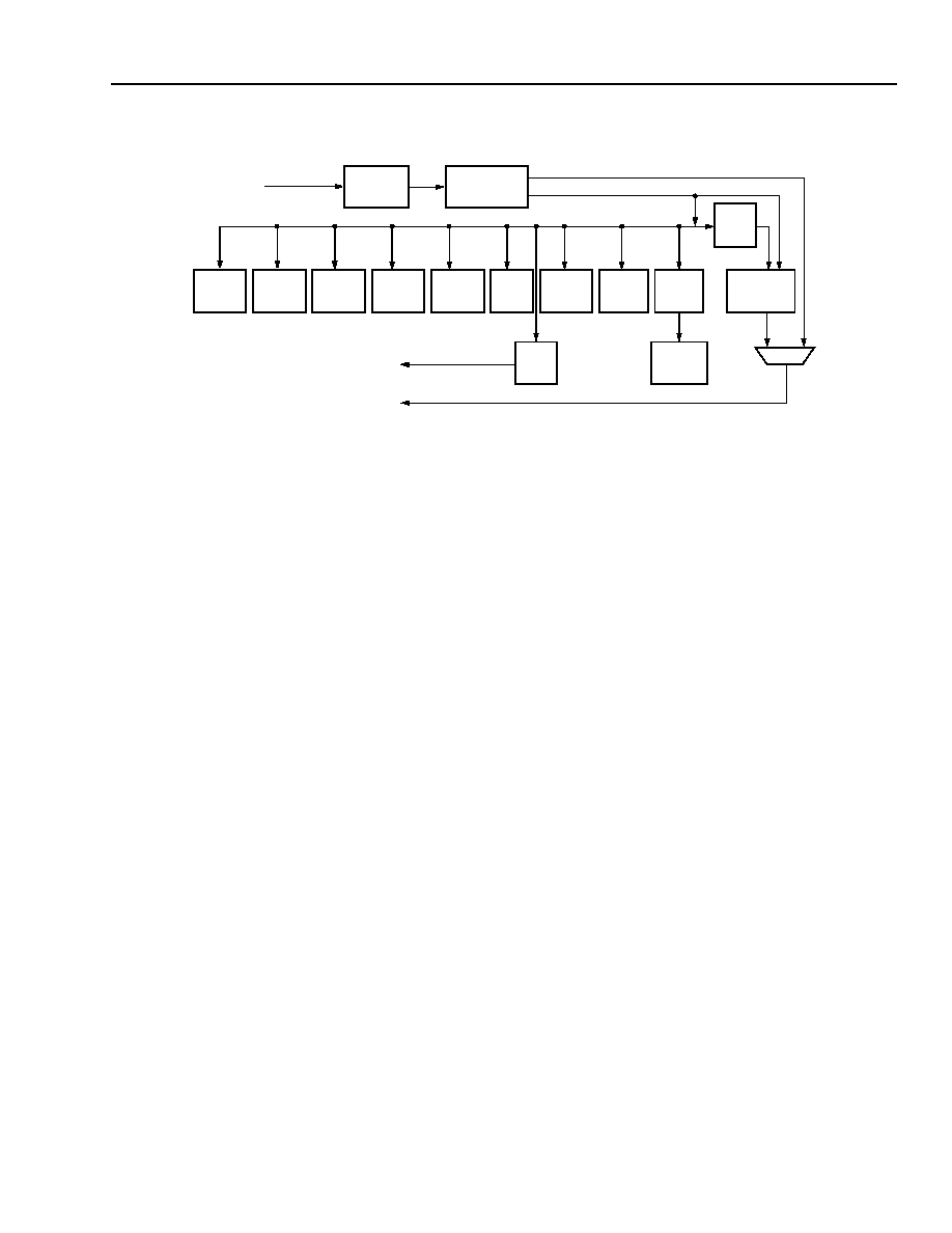
Preliminary Data Sheet
TMXF28155/51 Super Mapper
May 2001
155/51 Mbits/s SONET/SDH x28/x21 DS1/E1
407
Agere Systems Inc.
18 SPE Mapper Functional Description
(continued)
5-9068(F)
Figure 35. Receive Direction Path Termination Block
18.13.1 Pointer Interpretation Block
The TUG-3 pointer interpreter logic block performs all necessary functions to support TU-3 pointer interpretation.
The following features are implemented:
s
The pointer interpreter consists of the following states:
-- LOP-TU3--loss of pointer
-- AIS-TU3--TUG-3-AIS (all ones in H1 and H2)
-- NDF--NDF enabled (1001, 0001, 1101, 1011, 1000)
-- NORM--normal (disabled NDF, normal pointer)
-- INC--increment (inverted I bits)
-- DEC--decrement (inverted D bits)
The SPE mapper includes event or change of state indicators for pointer interpreter states except the NORM state.
States NDF, DEC, and INC are reported with event status bits SPE_RNDFE (
Table 146 on page134
),
SPE_RDECE (
Table 146
), and SPE_RINCE (
Table 146
), respectively. States AIS and LOP are reported with
change of state (delta) status bits SPE_RAISD (
Table 146
) and SPE_RLOPD (
Table 146
), respectively. Interrupts
for each event or delta state may be masked with bits SPE_RNDFM, SPE_RDECM, SPE_RINCM, SPE_RAISM,
and SPE_RLOPM (all in
Table 147 on page136
).
INSERT
B3
K3
AIS-P
G1
B3
K3
G1
G1
N1
C2
POAC
G1
J1
F3
F2
F2
H1, H2, H3
POINTER
PATH
POAC DATA
TUG-3 DATA
VC-3 DATA
TUG-2 DATA
PAYLOAD DATA TO OUTPUT BLOCKS
MUX
MONITOR
INTERPRETER
MONITOR
F3
MONITOR
C2
MONITOR
J1
MONITOR
N1
MONITOR
BIP N
CHECK
APS
MONITOR
RDI-P
DETECT
REI-L
DETECT
AIS-P
TERMINATE
REI
COUNTER
DROP
TMXF28155/51 Super Mapper
Preliminary Data Sheet
155/51 Mbits/s SONET/SDH x28/x21 DS1/E1
May 2001
408
Agere Systems Inc.
18 SPE Mapper Functional Description
(continued)
5-9007(F)
* This state diagram is based on the ETS 417-1-1 pointer interpretation state diagram (Figure B.1). Transitions of eight invalid pointers from the
INC, DEC, and NDF states into the LOP state have been added.
Figure 36. Pointer Interpretation State Diagram
s
The pointer interpreter transitions into the LOP-TU3 state based on the following conditions:
-- Continuous NDF. If NDF (1001, 0001, 1101, 1011, 1000) is received for the number of consecutive frames
(determined by the value programmed in bits SPE_CNTDLOPCNT[1:0] (
Table 149
)), then LOP-TU3 is de-
clared.
-- Invalid pointer values. If the number of consecutive frames (determined by the value programmed in
SPE_CNTDLOPCNT[1:0]) are received with a pointer that is not a normal value, NDF, AIS-TU3, increment, or
decrement, then LOP-TU3 is declared.
s
The pointer interpreter transitions out of the LOP-TU3 state based on the following conditions:
-- Following three consecutive frames with all ones in the H1 and H2 bytes the pointer interpreter transitions from
the LOP-TU3 state into the AIS-TU3 state.
-- Following three new consecutive, consistent, valid pointers the pointer interpreter transitions from the
LOP-TU3 state into the NORM state.
-- The pointer interpreter
will not
transition from the LOP-TU3 state into the NDF state.
s
The pointer interpreter transitions into the AIS-TU3 state based on the following conditions:
-- Following three consecutive frames with all ones in the H1 and H2 bytes AIS-TU3 is declared.
s
The pointer interpreter transitions out of the AIS-TU3 state based on the following conditions:
-- Following three new consecutive, consistent, valid pointers the pointer interpreter transitions from the AIS-TU3
state into the NORM state.
-- Following the number of consecutive invalid pointers (determined by the value programmed in
SPE_CNTDLOPCNT[1:0]) the pointer interpreter transitions from the AIS-TU3 state into the LOP-TU3 state.
-- If NDF is enabled on the incoming H1 and H2 bytes, the pointer interpreter transitions from the AIS-TU3 state
into the NDF state.
NORM
DEC
INC
NDF
AIS
LOP
FROM ALL STATES
8 INVALID POINTERS
FROM ALL STATES
3 NEW POINTERS
INCREMENT
DECREMENT
8 NDF ENABLE
NDF ENABLE
NDF ENABLE
NDF
NDF
NDF
3 ANY
3 ANY
3 NEW POINTERS
3 NEW POINTERS
3 ANY POINTERS
3 NEW POINTERS
8 INVALID
8 INVALID POINTERS*
INDICATION
INDICATION
3 AIS INDICATIONS
ENABLE
ENABLE
POINTERS
POINTERS
POINTERS
ENABLE

Preliminary Data Sheet
TMXF28155/51 Super Mapper
May 2001
155/51 Mbits/s SONET/SDH x28/x21 DS1/E1
409
Agere Systems Inc.
18 SPE Mapper Functional Description
(continued)
s
The pointer interpreter transitions into the NDF state based on the following conditions:
-- If NDF is enabled on the incoming H1 and H2 bytes, the pointer interpreter transitions from the NORM, NDF,
AIS, INC, and DEC states into the NDF state.
s
The pointer interpreter transitions out of the NDF state based on the following conditions:
-- Continuous NDF. If NDF (1001, 0001, 1101, 1011, 1000) is received for the number of consecutive frames
(determined by the value programmed in SPE_CNTDLOPCNT[1:0] (
Table 149
)), the pointer interpreter tran-
sitions from the NDF state into the LOP-TU3 state.
-- Following any three consecutive, consistent, and valid pointers, the pointer interpreter transitions from the NDF
state into the NORM state.
-- Following three consecutive frames with all ones in the H1 and H2 bytes, the pointer interpreter transitions from
the NDF state into the AIS-TU3 state.
-- Following three new, consecutive, consistent, and valid pointers, the pointer interpreter transitions from the
NDF state into the NORM state.
-- Following the number of consecutive invalid pointers (determined by the value programmed in
SPE_CNTDLOPCNT[1:0]), the pointer interpreter transitions from the NDF state into the LOP-TU3 state.
s
The pointer interpreter transitions into the NORM state based on the following conditions:
-- Following three new consecutive, consistent, and valid pointers, the pointer interpreter transitions into the
NORM state.
-- Following any three consecutive, consistent, and valid pointers, the pointer interpreter transitions into the
NORM state. i.e., transitioning from the INC, DEC, and NDF states.
s
The pointer interpreter transitions out of the NORM state based on the following conditions:
-- Following the number of consecutive invalid pointers (determined by the value programmed in
SPE_CNTDLOPCNT[1:0]), the pointer interpreter transitions from the NORM state into the LOP-TU3 state.
-- If NDF is enabled on the incoming H1 and H2 bytes, the pointer interpreter transitions from the NORM state
into the NDF state.
-- Following three consecutive frames with all ones in the H1 and H2 bytes, the pointer interpreter transitions from
the NORM state into the AIS-TU3 state.
-- When operating in the 8 of 10 mode (SPE_8ORMAJORITY = 1 (
Table 149
)), if 8 of the 10 I and D bits are
correct for a pointer decrement on the incoming H1 and H2 bytes the pointer interpreter transitions from the
NORM state into the DEC state. Otherwise, if 3 of the 5 I bits and 3 of the 5 D bits are correct for a pointer
decrement on the incoming H1 and H2 bytes, the pointer interpreter transitions from the NORM state into the
DEC state.
-- When operating in the 8 of 10 mode (SPE_8ORMAJORITY = 1), if 8 of the 10 I and D bits are correct for a
pointer increment on the incoming H1 and H2 bytes, the pointer interpreter transitions from the NORM state
into the INC state. Otherwise, if 3 of the 5 I bits and 3 of the 5 D bits are correct for a pointer increment on the
incoming H1 and H2 bytes, the pointer interpreter transitions from the NORM state into the INC state.
s
The pointer interpreter transitions into the INC state based on the following conditions:
-- When operating in the 8 of 10 mode (SPE_8ORMAJORITY = 1), if 8 of the 10 I and D bits are correct for a
pointer increment on the incoming H1 and H2 bytes the pointer interpreter transitions into the INC state. Oth-
erwise, if 3 of the 5 I bits and 3 of the 5 D bits are correct for a pointer increment on the incoming H1 and H2
bytes, the pointer interpreter transitions into the INC state.
s
The pointer interpreter transitions out of the INC state based on the following conditions:
-- If NDF is enabled on the incoming H1 and H2 bytes, the pointer interpreter transitions from the INC state into
the NDF state.
-- Following three consecutive frames with all ones in the H1 and H2 bytes, the pointer interpreter transitions from
the INC state into the AIS-TU3 state.
-- Following three new consecutive, consistent, and valid pointers, the pointer interpreter transitions from the INC
state into the NORM state.
-- Following any three consecutive, consistent, and valid pointers, the pointer interpreter transitions from the INC
state into the NORM state.
-- Following the number of consecutive invalid pointers (determined by the value programmed in
SPE_CNTDLOPCNT[1:0] (
Table 149
)), the pointer interpreter transitions from the INC state into the LOP-TU3
state.

TMXF28155/51 Super Mapper
Preliminary Data Sheet
155/51 Mbits/s SONET/SDH x28/x21 DS1/E1
May 2001
410
Agere Systems Inc.
18 SPE Mapper Functional Description
(continued)
s
The pointer interpreter transitions into the DEC state based on the following conditions:
-- When operating in the 8 of 10 mode (SPE_8ORMAJORITY = 1 (
Table 149
)), if 8 of the 10 I and D bits are
correct for a pointer decrement on the incoming H1 and H2 bytes, the pointer interpreter transitions into the
DEC state. Otherwise, if 3 of the 5 I bits and 3 of the 5 D bits are correct for a pointer decrement on the incoming
H1 and H2 bytes the pointer interpreter transitions into the DEC state.
s
The pointer interpreter transitions out of the DEC state based on the following conditions:
-- If NDF is enabled on the incoming H1 and H2 bytes, the pointer interpreter transitions from the DEC state into
the NDF state.
-- Following three consecutive frames with all ones in the H1 and H2 bytes, the pointer interpreter transitions from
the DEC state into the AIS-TU3 state.
-- Following three new consecutive, consistent, and valid pointers, the pointer interpreter transitions from the
DEC state into the NORM state.
-- Following any three consecutive, consistent, and valid pointers, the pointer interpreter transitions from the DEC
state into the NORM state.
-- Following the number of consecutive invalid pointers (determined by the value programmed in
SPE_CNTDLOPCNT[1:0]), the pointer interpreter transitions from the DEC state into the LOP-TU3 state.
s
Pointer increments and decrements will be counted and presented to the microprocessor as follows:
-- Pointer increments and decrements will be monitored and counted internally.
-- The internal and latched counts will be forced to 0x00 if device pin AUTO_AIS (AC6, AE6, and AD6) = 1 (from
TMUX), bit SPE_RLOP = 1 (
Table 148
), or bit SPE_RAIS = 1 (
Table 148
).
-- Latched counts, SPE_RPTR_INC[10:0] (
Table 161
) and SPE_RPTR_DEC[10:0] (
Table 161
), will be updated
coincident with the end of a performance monitor interval.
-- The internal counters will reset to 0x00 coincident with the end of a performance monitor interval.
-- If SMPR_SAT_ROLLOVER = 1 (
Table 67
), the internal running counts will hold at their maximum value. Oth-
erwise, the counts will roll over.
-- However, increment and decrement event indications should be ignored during LOP state.
s
LOP-TU3 (TU-3 path LOP) and AIS-TU3 (TU-3 path AIS) will be detected and reported to the microprocessor.
Both the LOP-TU3 and AIS-TU3 conditions will contribute to the AUTO AIS control signal from the SPE mapper
to the VT mapper. Any change in state of SPE_RLOP (
Table 148
) or SPE_RAIS (
Table 148
) will be reported to
the microprocessor via SPE_RLOPD (
Table 146
) and SPE_RAISD (
Table 146
). Unless the appropriate mask bit
is set (SPE_RLOPM/SPE_RAISM (
Table 147
)), SPE_RLOPD = 1 or SPE_RAISD = 1 will generate an interrupt.
s
The current TU-3 pointer value is stored in SPE_STORED_PTR[9:0] (
Table 161
).
18.14 SPE Mapper Receive Direction Requirements
All monitoring functions supported by the SPE mapper in the receive direction are summarized here:
s
Loss of CLOCK and loss of sync monitors
s
J1 monitor
s
B3 BIP-8 check
s
C2 signal label monitor
s
F2 monitor
s
F3 monitor
s
N1 monitor
s
K3 monitor
s
AIS-P and RDI-P detect
s
REI-P detect
s
Signal degrade BER algorithm
s
Signal fail BER algorithm
s
Path overhead access channel (POAC) drop
s
Insertion of AIS-P

Preliminary Data Sheet
TMXF28155/51 Super Mapper
May 2001
155/51 Mbits/s SONET/SDH x28/x21 DS1/E1
411
Agere Systems Inc.
18 SPE Mapper Functional Description
(continued)
Whenever the continuous N-times detect signals are defined, they require not only that the monitored signal be
consistent for N consecutive frames, but also that the frame bytes be error free for all N frames before the status
can be updated. If there are any errors in the framing pattern, then the consecutive N-times detection counters
must be reset to 0. N can range from 1 to 15. Programming a CNTD block with any value less than 1 will set the
CNTD to 1 time detect.
18.14.1 Loss of Clock and Loss of Sync Monitors
The SPE mapper detects and reports loss of the input clocks state for RLSCLK (pin V4) (19 MHz clock) in bit
SPE_RLSLOC (
Table 148 on page 137
), RLSC52 (pin AC2) (52 MHz clock) in bit SPE_RC52LOC (
Table 148
), and
DS3DATAINCLK (pin J22) (DS3 external clock) in bit SPE_RDS3LOC (
Table 148
), as determined by stuck high or
stuck low for time T. The detection time T will be greater than 10 µs but less than 125 µs. The function uses the
microprocessor clock as its reference. The device will report changes in the states using bits, SPE_RLSLOCD
(
Table 146 on page 134
), SPE_RC52LOCD (
Table 146
), and SPE_RDS3LOCD (
Table 146
); interrupt mask bits
SPE_RLSLOCM (
Table 147
), SPE_RC52LOCM (
Table 147
), and SPE_RDS3LOCM (
Table 147 on page136
),
respectively.
The SPE mapper will detect loss-of-sync conditions for the telecom bus sync signals. The states are reported in the
bits, SPE_RSY52LOS (
Table 148
), SPE_RJ0J1V1LOS (
Table 148
), SPE_RSPELOS (
Table 148
), and
SPE_RV1LOS (
Table 148
). The device will report changes in the states in bits SPE_RSY52LOSD (
Table 146
),
SPE_RJ0J1V1LOSD (
Table 146
), SPE_RSPELOSD (
Table 146
), SPE_RV1LOSD (
Table 146
); interrupt mask bits
SPE_RSY52LOSM (
Table 147
), SPE_RJ0J1V1LOSM (
Table 147
), SPE_RSPELOSM (
Table 147
), and
SPE_RV1LOSM (
Table 147
), respectively.
18.14.2 J1 Monitor
J1 (path trace) monitoring has six different monitoring modes controlled by bits SPE_J1MONMODE[2:0]
(
Table 149
):
s
SPE_J1MONMODE[2:0] = 000: the SPE mapper will latch the value of the J1 byte every frame for a total
64 bytes in SPE_RJ1DMON[1--64][7:0] (
Table 162
). The SPE mapper compares the incoming J1 byte with the
next expected value (the expected value is obtained by cycling through the previous stored 64 received bytes in
round-robin fashion) and setting the path trace identifier state bit, SPE_RTIM (
Table 148
), if different. Any change
in state is reported in bit, SPE_RTIMD (
Table 146
), using interrupt mask bit SPE_RTIMM (
Table 147
). CRC is not
checked by the hardware.
s
SPE_J1MONMODE[2:0] = 001: this is the SONET framing mode. The hardware looks for
0x0D and then the
0x0DA characters
to indicate that the next byte is the first byte of the path trace message. The J1 byte message
is continuously written into SPE_RJ1DMON[1--64][7:0] with the first byte residing at the first address. If any
received byte does not match the previously received byte for its location, then the state bit SPE_RTIM is set.
Any change in state is reported in bit SPE_RTIMD, using interrupt mask bit SPE_RTIMM.
s
SPE_J1MONMODE[2:0] = 010: this is the SDH framing mode. The hardware looks for the byte with the most sig-
nificant bit (MSB) set to one, which indicates that the next byte is the second byte of the message. The rest of
operation is the same as in SONET framing mode.
s
SPE_J1MONMODE[2:0] = 011: a new J1 byte (SPE_RJ1DMON[1][7:0]) will be detected after a number of con-
secutive consistent occurrences (SPE_CNTDJ1[3:0] (
Table 150
)) of a new pattern in the J1 overhead byte. Any
changes to this byte is reported in bit SPE_RTIMD, using interrupt mask bit SPE_RTIMM. The delta bit in this
mode indicates a change in state for the J1 byte, and the bit SPE_RTIM is not used.
s
SPE_J1MONMODE[2:0] = 100: the user will program the 64 expected values of J1 in registers,
SPE_RJ1DEXP[1--64][7:0] (
Table 164
), in SONET framing mode, where the first expected byte, the byte follow-
ing the 0x0A character, is written into the first register location, SPE_RJ1DEXP[1][7:0]. The SPE mapper com-
pares the incoming J1 sequence with the stored expected value, setting the SPE_RTIM state bit if they are
different. Any changes in the state is reported in bit SPE_RTIMD, using interrupt mask bit SPE_RTIMM.

TMXF28155/51 Super Mapper
Preliminary Data Sheet
155/51 Mbits/s SONET/SDH x28/x21 DS1/E1
May 2001
412
Agere Systems Inc.
18 SPE Mapper Functional Description
(continued)
s
SPE_J1MONMODE[2:0] = 101: the user will program the 16 expected values of J1 in
SPE_RJ1DEXP[1--16][7:0] in SDH framing mode, where the first byte of the message has the MSB set to 1.
The SPE mapper compares the incoming J1 sequence with the stored expected value, setting the state bit,
SPE_RTIM if they're different. Any change in state is reported in bit SPE_RTIMD, using interrupt mask bit
SPE_RTIMM.
s
SPE_J1MONMODE[1:0] = 110 and 111 are currently undefined.
s
Unless bit PAIS_TIMINH (
Table 149
) is set, bit SPE_RTIMD contributes to the AUTO AIS control signal from the
SPE mapper to the VT mapper).
s
Unless mask bit SPE_RTIMM is set, bit SPE_RTIMD can generate an interrupt.
Table 536. J1 Monitor
18.14.3 B3 BIP-8 Check
A B3 BIP-8 even parity is computed over all the incoming bits of the TUG-3 frame, after descrambling, and com-
pared to the B3 byte received in the next frame. The total number of B3 BIP-8 bit errors (raw count) or block errors
is counted (selected through SPE_B3BITBLKCNT (
Table 149
)). Upon a performance monitor (PM) interval, the
internal running counter is placed into SPE_B3ECNT[15:0] (
Table 160
) and then cleared. Depending on the value
of microprocessor bit SMPR_SAT_ROLLOVER (
Table 67
), the internal counter will roll over or stay at its maximum
value until cleared.
18.14.4 Signal Label C2 Byte Monitor
Table 537. STS Signal Label Defect Conditions
Name
Function
SPE_J1MONMODE[2:0] (
Table 149
)
J1 Monitoring Type.
SPE_RJ1DEXP[1--64][7:0] (
Table 164
)
J1 Expected Data Storage (64/1 Byte).
SPE_RJ1DMON[1--64][7:0] (
Table 162
)
J1 Received Data Storage (64/1 Byte).
SPE_CNTDJ1[3:0] (
Table 150
)
Continuous Times Detect Value.
SPE_RTIM (
Table 148
)
J1 Mismatch State Bit.
SPE_RTIMD (
Table 146
)
J1 Mismatch Delta Bit, Active-High.
SPE_RTIMM (
Table 147
)
J1 Mismatch Mask Bit, Active-High.
Provisioned STS PTE
Functionality, Expected C2
Received Payload Label
(C2 in hex)
Defect
TMUX_FORCEC2DEF = 1
(
Table 97
)
Any Equipped Functionality
Unequipped (00)
TMUX_RUNEQP
No Change
Any Equipped Functionality
Equipped--Nonspecific (01)
None
No Change
Equipped--Nonspecific
Any Value (02 to E0, FD to FE)
None
No Change
Any Payload Specific Code
The Same Payload Specific
Code (02 to E0, FD to FE)
None
No Change
Any Payload Specific Code
A Different Payload Specific
Code (02 to E0, FD to FE)
TMUX_RPLMP
No Change
Equipped--Nonspecific (01) or
VT-Structured STS-1 (02)
PDI, 1 to 27 VTx Defects
(E1 to FB)
None
TMUX_RPLMP
Any Payload Specific Code
Except VT-Structured
STS-1 (02)
PDI, 1 to 27 VTx Defects
(E1 to FB)
TMUX_RPLMP
No Change
Any Equipped Functionality
PDI, 28 VT1.5 Defects or 1
Non-VT Payload Defect (FC)
None
TMUX_RPLMP
Any Equipped Functionality
Reserved (FF)
None
TMUX_RPLMP

Preliminary Data Sheet
TMXF28155/51 Super Mapper
May 2001
155/51 Mbits/s SONET/SDH x28/x21 DS1/E1
413
Agere Systems Inc.
18 SPE Mapper Functional Description
(continued)
The C2 byte is stored in SPE_C2DMON[7:0] (
Table 152 on page140
). This is updated after a number of consecu-
tive frames (determined by the value programmed in SPE_CNTDC2[3:0] (
Table 150 on page139
)) of identical C2
bytes, i.e., the 8-bit pattern must be identical for the number of frames in the programmed SPE_CNTDC2[3:0] prior
to updating SPE_C2DMON[7:0].
Whenever the contents of the C2 byte monitor SPE_C2DMON[7:0] changes, a delta bit SPE_C2DMOND
(
Table 146 on page 134
) is set and bit SPE_C2DMONM (
Table 147 on page136
) is the interrupt mask bit.
The SPE mapper maintains a programmable expected value of the C2 byte in SPE_C2DEXP[7:0] (
Table 151 on
page 140
). If the current value of the C2 byte (SPE_C2DMON[7:0]) does not equal the expected C2 value
(C2DEXP[7:0]), then a payload label mismatch (PLM-P) defect is declared and reported in SPE_RPLM
(
Table 148
). The change in PLM-P state is reported in SPE_RPLMD (
Table 146
) with an interrupt mask bit
SPE_RPLMM (
Table 147
).
Also if the current value of the C2 byte (SPE_C2DMON[7:0]) is all 0s, then an unequipped (UNEQ-P) defect is
declared and reported in SPE_RUNEQ (
Table 148
). The change in UNEQ-P state is reported in SPE_RUNEQD
(
Table 146
) with an interrupt mask SPE_RUNEQM (
Table 147
).
Table 538. C2MON Processing
18.14.5 Path User Byte F2 Monitor
The SPE mapper monitors the path user channel in the F2 byte. The current value of the F2 byte is stored in
SPE_F2DMON0[7:0] (
Table 152
) after a number of consecutive frames (determined by the value programmed in
SPE_CNTDF2[3:0] (
Table 150
)) of identical F2 byte has been received, i.e., the 8-bit pattern must be identical for a
number of frames equal to the value of SPE_CNTDF2[3:0] prior to updating SPE_F2DMON0[7:0].
Whenever the contents of the F2 byte monitor (SPE_F2DMON0[7:0]) changes, a delta bit SPE_F2DMOND
(
Table 146
) is set. The interrupt mask is SPE_F2DMONM (
Table 147
).
The SPE mapper maintains a history of the previous valid F2 byte in SPE_F2DMON1[7:0] (
Table 152
).
Name
Function
SPE_C2DMON[7:0] (
Table 152
)
C2 Current Data Monitor.
SPE_C2DEXP[7:0] (
Table 151
)
Expected Value of C2 Byte.
SPE_CNTDC2[3:0] (
Table 150
)
Continuous Times Detect Count Value for C2.
SPE_C2DMOND (
Table 146
)
C2 Data Monitor Event Bit.
SPE_C2DMONM (
Table 147
)
C2 Data Monitor Mask Bit.
SPE_RPLM (
Table 148
)
Payload Label Mismatch State.
SPE_RPLMD (
Table 146
)
Payload Label Mismatch Delta Bit.
SPE_RPLMM (
Table 147
)
Payload Label Mismatch Mask Bit.
SPE_RUNEQ (
Table 148
)
Unequipped Path State.
SPE_RUNEQD (
Table 146
)
Unequipped Path Delta Bit.
SPE_RUNEQD (
Table 147
)
Unequipped Path Mask Bit.
TMXF28155/51 Super Mapper
Preliminary Data Sheet
155/51 Mbits/s SONET/SDH x28/x21 DS1/E1
May 2001
414
Agere Systems Inc.
18 SPE Mapper Functional Description
(continued)
Table 539. F2 Monitor
18.14.6 Path User Byte F3 Monitor
The SPE mapper monitors the second path user channel in the F3 byte. The current value of the F3 byte is stored
in SPE_F3DMON0[7:0] (
Table 152 on page140
) after a number of consecutive frames (determined by the value
programmed in SPE_CNTDF3[3:0] (
Table 150
)) of identical F3 bytes has been received, i.e., the 8-bit pattern must
be identical for a number of frames, determined by SPE_CNTDF3[3:0], prior to updating SPE_F3DMON0[7:0].
Whenever the contents of the F3 byte monitor (SPE_F3DMON0[7:0]) changes, a delta bit SPE_F3DMOND
(
Table 146
) is set. The interrupt mask is in register bit SPE_F3DMONM (
Table 147
).
The SPE mapper maintains a history of the previous valid F3 byte in SPE_F3DMON1[7:0] (
Table 152
).
Table 540. F3 Monitor
18.14.7 N1 Monitor
The SPE mapper stores the current value of the N1 byte in SPE_N1DMON[7:0] (
Table 152
). This is updated after a
number of consecutive frames (determined by the value programmed in bits SPE_CNTDN1[3:0] (
Table 150
)) of
identical N1 bytes, i.e., the 8-bit pattern must be identical for a number frames determined by the value in register
bits SPE_CNTDN1[3:0] prior to updating the N1 register.
Whenever the contents of the N1 byte monitor (SPE_N1DMON[7:0]) changes, a delta bit SPE_N1DMOND
(
Table 146
) is set. The interrupt generated by SPE_N1DMOND can be masked off by SPE_N1DMONM
(
Table 147
).
Table 541. N1 Monitor
Name
Function
SPE_F2DMON0[7:0] (
Table 152
)
Fault Location Current Consistent Value.
SPE_F2DMON1[7:0] (
Table 152
)
Fault Location Previous Consistent Value.
SPE_CNTDF2[3:0] (
Table 150
)
Continuous N-Times Detect (3--15).
SPE_F2DMOND (
Table 146
)
F2 Data Monitor Delta Bit.
SPE_F2DMONM (
Table 147
)
F2 Data Monitor Mask Bit.
Name
Function
SPE_F3DMON0[7:0] (
Table 152
)
User Channel Current Consistent Value.
SPE_F3DMON1[7:0] (
Table 152
)
User Channel Previous Consistent Value.
SPE_CNTDF3[3:0] (
Table 150
)
Continuous N-Times Detect (3--15).
SPE_F3DMOND (
Table 146
)
F3 Data Monitor Delta Bit.
SPE_F3DMONM (
Table 147
)
F3 Data Monitor Mask Bit.
Name
Function
SPE_N1DMON[7:0] (
Table 152
)
Fault Location Current Consistent Value.
SPE_CNTDN1[3:0] (
Table 150
)
Continuous N-Times Detect (3--15).
SPE_N1DMOND (
Table 146
)
N1 Data Monitor Delta Bit.
SPE_N1DMONM (
Table 147
)
N1 Data Monitor Mask Bit.
Preliminary Data Sheet
TMXF28155/51 Super Mapper
May 2001
155/51 Mbits/s SONET/SDH x28/x21 DS1/E1
415
Agere Systems Inc.
18 SPE Mapper Functional Description
(continued)
18.14.8 K3 Byte Monitor
The SPE mapper stores the current value of the K3 byte in SPE_K3DMON[7:0] (
Table 152 on pag e140
). This is
updated after a number of consecutive frames (determined by the value programmed in bits SPE_CNTDK3[3:0]
(
Table 150 on page139
)) of identical K3 bytes, i.e., the 8-bit pattern must be identical for a number of frames deter-
mined by the value of SPE_CNTDK3[3:0] prior to updating the K3 register.
Whenever the contents of the K3 byte monitor (SPE_K3DMON[7:0]) changes, a delta bit SPE_K3DMOND
(
Table 146 on page 134
) is set. The interrupt generated by SPE_K3DMOND can be masked off by the
SPE_K3DMONM (
Table 147 on page 136
).
Table 542. K3 Monitor
18.14.9
AIS-P and
RDI-P Detect
The SPE mapper monitors for path AIS in the H1 and H2 bytes (all H1 and H2 bits = 1) of the TUG-3 pointer. When
path AIS is detected, SPE_RAIS (
Table 148 on page137
) will be set to 1 after three consecutive occurrences. Any
changes to SPE_RAIS will be reported in SPE_RAISD (
Table 146 on page134
) and the interrupt can be masked,
using SPE_RAISM (
Table 147 on page136
).
A remote defect indication-path (RDI-P) signal indicates to STS PTE that its peer STS PTE has detected a defect
on the signal that it originated. The SPE mapper supports both the single bit RDI-P and the 3-bit enhanced RDI-P;
the mode is selectable using bit SPE_RPRDI_MODE (
Table 149 on page138
). When SPE_RPRDI_MODE = 0,
1-bit code is supported and when SPE_RPRDI_MODE = 1, 3-bit enhanced RDI-P code is supported. Three bits of
the G1 byte (G1[3:1]) are reserved for the RDI-P signal.
The SPE mapper monitors for a 1-bit RDI-P code in G1[3] bit or a 3-bit enhanced remote defect indication (RDI-P)
condition in the G1[3:1] bits and stores the current value in bits SPE_PRDIDMON[2:0] (
Table 152 on page140
).
The current value is updated after a number of consecutive frames (determined by the value of bits
SPE_CNTDPRDI[3:0] (
Table 150
)) of identical G1[3:1], i.e., the 3-bit pattern must be identical for a number of
frames, determined by the value of SPE_CNTDPRDI[3:0] prior to updating SPE_PRDIDMON[2:0].
Whenever the contents of SPE_PRDIDMON[2:0] changes, a delta bit SPE_PRDIDMOND (
Table 146 on page 134
)
is set. The interrupt generated by SPE_PRDIDMOND can be masked off by SPE_PRDIDMONM (
Table 147
).
Table 543. AIS-P and RDI-P Detect
Name
Function
SPE_K3DMON[7:0] (
Table 152
)
Fault Location Current Consistent Value.
SPE_CNTDK3[3:0] (
Table 150
)
Continuous N-Times Detect (3--15).
SPE_K3DMOND (
Table 146
)
K3 Data Monitor Delta Bit.
SPE_K3DMONM (
Table 147
)
K3 Data Monitor Mask Bit.
Name
Function
SPE_CNTDPRDI[3:0] (
Table 150
)
Continuous Times Detect Count Value for G1[3:1] Bits (3--15).
SPE_PRDIDMOND (
Table 146
)
Path RDI Delta Bit.
SPE_PRDIDMONM (
Table 147
)
Path RDI Mask Bit.

TMXF28155/51 Super Mapper
Preliminary Data Sheet
155/51 Mbits/s SONET/SDH x28/x21 DS1/E1
May 2001
416
Agere Systems Inc.
18 SPE Mapper Functional Description
(continued)
18.14.10 REI-P Detect
Bits 7 through 4 of the G1 byte are allocated for use as a path remote error indication function (REI-P).
s
For STS-1 signals, bits 7 through 4 of the G1 byte are allocated for REI-P which conveys the error count detected
by the PTE (using the path BIP-8 code B3) back to its peer PTE as follows.
Table 544. STS-1 P-REI Interpretation
The SPE mapper provides a counter to accumulate G1-REI errored bit count in SPE_G1ECNT[15:0] (
Table 160 on
page 147
) from G1[7:4]. This counter will hold at its maximum value or roll over (depending on the value of micro-
processor bit SMPR_SAT_ROLLOVER (
Table 67 on page 68
)) and update upon the performance monitoring inter-
val.
18.14.11 Signal Degrade BER Algorithm
A signal degrade state bit is SPE_SDB3 (
Table 148 on page 137
) with a change of state indication reported in delta
bit SPE_SDB3D (
Table 146 on page134
) and the interrupt mask bit is SPE_SDB3M (
Table 147
). This bit error rate
algorithm operates on B3 errors.
Declaring the signal degrade state requires the definition of two measurement windows. A monitoring block con-
sisting of a number of frames, Ns (SPE_SDNSSET[18:0] (
Table 158 on page 146
)), and a measurement interval
consisting of a number of monitoring blocks, B (SPE_SDBSET[11:0] (
Table 158
)). A block is determined bad when
the number of bit errors equals or exceeds a threshold, L (SPE_SDLSET[3:0] (
Table 158
)). Signal degrade is
declared when a number of bad monitoring blocks equals or exceeds the threshold, M (SPE_SDMSET[7:0]
(
Table 158
)), for the measurement interval.
Clearing the signal degrade state requires the definition of two measurement windows. A monitoring block consist-
ing of a number of frames, Ns (SPE_SDNSCLEAR[18:0] (
Table 158
)), and a measurement interval consisting of a
number of monitoring blocks, B (SPE_SDBCLEAR[11:0] (
Table 158
)). A block is determined good when the num-
ber of bit errors is less than a threshold, L (SPE_SDLCLEAR[3:0] (
Table 158
)). Signal degrade is cleared when a
number of good monitoring blocks equals or exceeds the threshold, M (SPE_SDMCLEAR[7:0] (
Table 158
)), for the
measurement interval.
The set parameters are used when the signal degrade state is clear, and the clear parameters are used when the
signal degrade state is declared.
The signal degrade state may be forced to the declared state with bit SPE_SDSET (
Table 145 on page134
) and
forced to the cleared state with bit SPE_SDCLEAR (
Table 145
). The controls are provided to force the BER algo-
rithm into the failed state or normal state, respectively.
The above algorithm can detect bit error rates from 1 x 10
≠3
to 1 x 10
≠9
.
G1[7:4] Code
Code Interpretation
0000
0 (no errors)
0001
1
0010
2
0011
3
0100
4
0101
5
0110
6
0111
7
1000
8
1001--1111
0 (no errors)

Preliminary Data Sheet
TMXF28155/51 Super Mapper
May 2001
155/51 Mbits/s SONET/SDH x28/x21 DS1/E1
417
Agere Systems Inc.
18 SPE Mapper Functional Description
(continued)
Table 545. Signal Degrade Parameters
Note: The threshold written by the control system is one less than the desired number, except for the SPE_SDLSET[3:0]/SDLCLEAR[3 :0]
parameter.
18.14.12 Signal Fail BER Algorithm
A signal fail state is reported by bit SPE_SFB3 (
Table 148 on pag e137
) and change of state in bit SPE_SFB3D
(
Table 146
) with the interrupt mask bit SPE_SFB3M (
Table 147
). This bit error rate algorithm operates on B3 errors.
Declaring the signal fail state requires the definition of two measurement windows, a monitoring block consisting of
a number of frames, Ns (SPE_SFNSSET[18:0] (
Table 159 on page146
)), and a measurement interval consisting
of a number of monitoring blocks, B (SPE_SFBSET[15:0] (
Table 159
)). A block is determined to be bad when the
number of bit errors equals or exceeds a threshold, L (SPE_SFLSET[3:0] (v)). Signal fail is declared when the
number of bad monitoring blocks equals or exceeds the threshold, M (SPE_SFMSET[7:0] (
Table 159
)), for the
measurement interval.
Clearing the signal fail state requires the definition of two measurement windows, a monitoring block consisting of a
number of frames, Ns (SPE_SFNSCLEAR[18:0] (
Table 159
)), and a measurement interval consisting of a number
of monitoring blocks, B (SPE_SFBCLEAR[11:0] (v)). A block is determined to be good when the number of bit
errors is less than a threshold, L (SPE_SFLCLEAR[3:0] (
Table 159
)). Signal fail is cleared when a number of good
monitoring blocks equals or exceeds the threshold, M (SPE_SFMCLEAR[7:0] (v)), for the measurement interval.
The set parameters are used when the signal fail state is clear, and the clear parameters are used when the signal
fail state is declared.
The signal fail state may be forced to the declared state with bit SPE_SFSET (
Table 145 on page134
) and forced
to the cleared state with bit SPE_SFCLEAR (
Table 145
).
The above algorithm can detect bit error rates from 1 x 10
≠3
to 1 x 10
≠9
.
Name
Function
SPE_SDNSSET[18:0] (
Table 158
)
Signal Degrade Ns Set. Number of frames in a monitoring block for SD.
SPE_SDLSET[3:0] (
Table 158
)
Signal Degrade L Set. Error threshold for determining if a monitoring
block is bad.
SPE_SDMSET[7:0] (
Table 158
)
Signal Degrade M Set. Threshold of the number of bad monitoring blocks
in an observation interval. If the number of bad blocks is below this thresh-
old, then SD is cleared.
SPE_SDBSET[15:0] (
Table 158
)
Signal Degrade B Set. Number of monitoring blocks in a measurement
interval.
SPE_SDNSCLEAR[18:0] (
Table 158
) Signal Degrade Ns Clear. Number of frames in a monitoring block for SD.
SPE_SDLCLEAR[3:0] (
Table 158
)
Signal Degrade L Clear. Error threshold for determining if a monitoring
block is bad.
SPE_SDMCLEAR[7:0] (
Table 158
)
Signal Degrade M Clear. Threshold of the number of bad monitoring
blocks in an observation interval. If the number of bad blocks is below this
threshold, then SD is cleared.
SPE_SDBCLEAR[15:0] (
Table 158
)
Signal Degrade B Clear. Number of monitoring blocks in a measurement
interval.
SPE_SDSET (
Table 145
)
Signal Degrade Set. Allows the signal degrade algorithm to be forced into
the failed state (active 0 to 1).
SPE_SDCLEAR (
Table 145
)
Signal Degrade Clear. Allows the signal degrade algorithm to be forced
into the normal state (active 0 to 1).
SPE_SDB3 (
Table 148
)
Signal Degrade BER Algorithm State Bit.
SPE_SDB3D (
Table 146
)
Signal Degrade BER Algorithm Delta Bit.
SPE_SDB3M (
Table 147
)
Signal Degrade BER Algorithm Mask Bit.

TMXF28155/51 Super Mapper
Preliminary Data Sheet
155/51 Mbits/s SONET/SDH x28/x21 DS1/E1
May 2001
418
Agere Systems Inc.
18 SPE Mapper Functional Description
(continued)
Table 546. Signal Fail Parameters
Note: The threshold written by the control system is one less than the desired number, except for the SPE_SFLSET[3:0]/SFLCLEAR[3 :0]
parameter.
18.14.13 POAC Drop
The SPE mapper accommodates one path overhead access channel (POAC output channel).
The POAC channel consists of the following signals:
s
A 576 kHz inverted clock signal sourced by the TMUX (RPOACCLK, pin AE3).
s
A 576 kbits/s data signal sourced by the TMUX (RPOACDATA, pin AD4).
s
An 8 kHz synchronization signal, sourced by the TMUX (RPOACSYNC, pin AF4). The sync signal is normally
low; during the last clock period of each frame coincident with the least significant bit of the last byte, the sync
signal is high.
The data signal is partitioned into frames of 9 bytes. The frame repetition rate is 8 kHz. Each byte consists of 8 bits
that are transmitted/received most significant bit first (MSB). The MSB of the second byte of each frame contains
an odd/even parity bit over the 72 bits of the previous frame. The remaining 7 bits of this byte are not specified.
Bytes shown in
Table 547
summarize the access capabilities of the receive POAC.
Name
Function
SPE_SFNSSET[18:0] (
Table 159
)
Signal Fail Ns Set. Number of frames in a monitoring block for SF.
SPE_SFLSET[3:0] (
Table 159
)
Signal Fail L Set. Error threshold for determining if a monitoring block is
bad.
SPE_SFMSET[7:0] (
Table 159
)
Signal Fail M Set. Threshold of the number of bad monitoring blocks in
an observation interval. If the number of bad blocks is below this thresh-
old, then SF is cleared.
SPE_SFBSET[15:0] (
Table 159
)
Signal Fail B Set. Number of monitoring blocks.
SPE_SFNSCLEAR[18:0] (
Table 159
) Signal Fail Ns Clear. Number of frames in a monitoring block for SF.
SPE_SFLCLEAR[3:0] (
Table 159
)
Signal Fail L Clear. Error threshold for determining if a monitoring block
is bad.
SPE_SFMCLEAR[7:0] (
Table 159
)
Signal Fail M Clear. Threshold of the number of bad monitoring blocks in
an observation interval. If the number of bad blocks is below this thresh-
old, then SF is cleared.
SPE_SFBCLEAR[15:0] (
Table 159
)
Signal Fail B Clear. Number of monitoring blocks.
SPE_SFSET (
Table 145
)
Signal Fail Set. Allows the signal degrade algorithm to be forced into the
failed state (active 0 to 1).
SPE_SFCLEAR (
Table 145
)
Signal Fail Clear. Allows the signal degrade algorithm to be forced into
the normal state (active 0 to 1).
SPE_SFB3 (
Table 148
)
Signal Fail BER Algorithm State Bit.
SPE_SFB3D (
Table 146
)
Signal Fail BER Algorithm Delta Bit.
SPE_SFB3M (
Table 147
)
Signal Fail BER Algorithm Mask Bit.

Preliminary Data Sheet
TMXF28155/51 Super Mapper
May 2001
155/51 Mbits/s SONET/SDH x28/x21 DS1/E1
419
Agere Systems Inc.
18 SPE Mapper Functional Description
(continued)
Table 547. Path Overhead Byte Access
Even or odd parity can be inserted into the first bit of the second byte of the POAC outgoing frame. Parity is
selected with register bit, SPE_RPOAC_OEPINS (
Table 149 on page138
).
18.14.14 Insertion of AIS-P
The SPE mapper automatically generates AIS path (AIS-P) when:
s
The pointer interpreter declares the receive AIS state (SPE_RAIS in
Table 148 on page137
) or receive loss of
pointer state (SPE_RLOP (
Table 148
)) and the appropriate inhibit signals are inactive.
s
AIS is requested by signals from the TMUX interface.
s
AIS is forced by setting bit SPE_PAISINS (
Table 149
).
s
Any one of the loss-of-clock or loss-of-sync bits are active and their corresponding inhibit bits are inactive.
s
Any of bits SPE_RUNEQ, SPE_RPLM, and SPE_RTIM (all are in
Table 148
) are active, and the appropriate
inhibit signals are inactive.
Criteria for PATH_AIS_GENERATE =
((SPE_RLOP AND (SPE_PAIS_LOPINH)) OR
(SPE_RAIS AND (SPE_PAIS_AISINH)) OR
(SPE_RUNEQ AND (SPE_PAIS_UNEQINH)) OR
(SPE_RPLM AND (SPE_PAIS_PLMINH)) OR
(SPE_RTIM AND (SPE_PAIS_TIMINH)) OR
(SPE_SFB3 AND (SPE_PAIS_SFB3INH)) OR
(SPE_SDB3 AND (SPE_PAIS_SDB3INH)) OR
(SPE_RSY52LOS AND (SPE_AIS_LOSSY52INH)) OR
(SPE_RV1LOS AND (SPE_AIS_LOSV1INH)) OR
(SPE_RSPELOS AND (SPE_AIS_LOSSPEINH)) OR
(SPE_RJ0J1V1LOS AND (SPE_AIS_LOSJ0J1V1INH)) OR
(SPE_RDS3LOC AND (SPE_AIS_LOCDS3INH)) OR
(SPE_RC52LOC AND (SPE_AIS_LOC52INH)) OR
(SPE_RLSLOC AND (SPE_AIS_LOCINH)) OR
SPE_PAISINS OR
RAUTO_AIS (signal from TMUX))
The SPE mapper starts/stops generating AIS-P within 125 µs of the detection/absence of a failure condition.
AIS-P consists of writing all ones into the H1, H2, and H3 bytes and into the entire payload.
J1
POH Parity
C2
G1
F2
H4
F3
K3
N1

TMXF28155/51 Super Mapper
Preliminary Data Sheet
155/51 Mbits/s SONET/SDH x28/x21 DS1/E1
May 2001
420
Agere Systems Inc.
18 SPE Mapper Functional Description
(continued)
18.15 Transmit Direction (to SONET/SDH Line)
The transmit block inserts the path overhead (POH) bytes to the payload data and outputs an STS-1 SPE or a
TUG-3 payload as required.
The transmit section is broken down into the following functional parts:
s
Loss of clock and loss of sync detectors
s
N1 insert
s
K3 insert
s
Path user byte F3 insert
s
Path user byte F2 insert
s
AIS-P insert
s
REI-P insert
s
RDI-P insert
s
C2 signal label insert
s
B3 calculation and insert
s
J1 path trace insert
All insert control functions that are inhibited will insert all zeros or all ones into the outgoing bytes depending on the
value of microprocessor register bit SMPR_OH_DEFLT (
Table 67
).
18.15.1 PATH Insertion Block
The path overhead insertion block of the SPE mapper is shown below. The block computes and inserts the B3 BIP
error bytes and the rest of the path overhead bytes to form a TUG-3 frame.
5-9069(F)
Figure 37. Transmit Direction Path Insertion Bloc k
H4
INSERT
K3
N1
C2
F3
F2
K3
G1
G1
J1
INSERT
AIS-P
B3
POAC INSERT
B3
INSERT PATH OVERHEAD BYTES
MU
X
TO TMUX INTERFACE
BLOCK
VC-3 DATA
TUG-3 DATA
J1
APS
INSERT
G1
RDI-P
INSERT
G1
REI-P
INSERT
INSERT
N1
INSERT
C2
INSERT
F3
INSERT
F2
INSERT H4
FIXED VAL
GENERATE
INSERT
F2, F3, C2, N1, AND J1

Preliminary Data Sheet
TMXF28155/51 Super Mapper
May 2001
155/51 Mbits/s SONET/SDH x28/x21 DS1/E1
421
Agere Systems Inc.
18 SPE Mapper Functional Description
(continued)
18.15.2 Loss of Clock and Loss of Sync Detectors
The SPE mapper detects and reports the loss of the input clocks for the transmit telecom bus clock, device pin
TLSCLK (AA2), in bit SPE_TLSLOC (
Table 148 on page137
); the 51.84 MHz transmit low-speed clock, device pin
TLSC52 (AC3), in bit SPE_TC52LOC (
Table 148
), and the external DS3 clock, device pin DS3DATAINCLK (J22), in
bit SPE_TDS3LOC (
Table 148
). Loss of clock is determined by stuck high or stuck low for time T. The detection
time T will be greater than 10 µs but less than 125 µs. The function uses the microprocessor clock as its reference.
The device will report a change in the loss of clock state for the monitored clocks using bits SPE_TLSLOCD
(
Table 146 on page 134
), SPE_TC52LOCD (
Table 146
), and SPE_TDS3LOCD (
Table 146
), respectively. The
microprocessor interrupt may be masked using bits SPE_TLSLOCM (
Table 147 on pag e136
), SPE_TC52LOCM
(
Table 147
), and SPE_TDS3LOCM (
Table 147
), respectively.
The SPE mapper detects loss-of-sync conditions for the telecom bus sync signals, device pins TLSSYNC52 (AD2),
TLSJ0J1V1 (AB4), TLSSPE (AB2), and TLSV1 (AB3). The loss of sync states are reported in bits
SPE_TSY52LOS (
Table 148
), SPE_TJ0J1V1LOS (
Table 148
), SPE_TSPELOS (
Table 148
), and SPE_TV1LOS
(
Table 148
), respectively. The device will report a change in the loss of sync state for the monitored sync signals in
bits SPE_TSY52LOSD (
Table 146
), SPE_TJ0J1V1LOSD (
Table 146
), SPE_TSPELOSD (
Table 146
), and
SPE_TV1LOSD (
Table 146
), respectively. The microprocessor interrupt may be masked using bits
SPE_TSY52LOSM (
Table 147
), SPE_TJ0J1V1LOSM (
Table 147
), SPE_TSPELOSM (
Table 147
), and
SPE_TV1LOSM (
Table 147
), respectively.
18.15.3 J1 Byte Insert
A 64-byte sequence stored in SPE_TJ1DINS[1--64][7:0] (
Table 163 on page 148
) will be inserted into the outgoing
J1 byte when bit SPE_TJ1INS = 1 (
Table 154 on page143
); otherwise, the associated POAC value is inserted
when bit SPE_TPOAC_J1 = 1 (
Table 154
) or the default value, determined by the value of microprocessor bit
SMPR_OH_DEFLT (
Table 67 on pag e68
), is inserted when SPE_TPOAC_J1 = 0.
The CRC for the J1 trace has to be programmed into the J1 bytes by the user.
18.15.4 B3 BIP-8 Calculation and Insert
The B3 bytes are allocated for path overhead error monitoring function. This function is a bit interleaved parity 8
code (BIP-8) using even parity. The BIP-8 is computed before scrambling over all bits of the previous AU-3/TUG-3
frame, and is placed in byte B3 of the current frame also before scrambling. When enabled with control bit,
SPE_TB3ERRINS (
Table 156
), a single B3 byte can be inverted each time bit SPE_BERR_INS (
Table 156
) is
asserted.
18.15.5 C2 Signal Label Byte Insert
When bit SPE_TC2INS = 1 (
Table 154
), the value in SPE_TC2DINS[7:0] (
Table 157
) is inserted into the outgoing
C2 byte; otherwise, insert the associated POAC value when SPE_TPOAC_C2 = 1 (
Table 154
) or insert the default
value determined by the microprocessor bit SMPR_OH_DEFLT when bit SPE_TPOAC_C2 = 0.
18.15.6 REI-P G1(7:4) Insert
Four bits of the G1 byte G1(7:4) are allocated for use as a path remote error indication (REI). For AU-3/TUG-3 sig-
nals, these bits convey the count (in the range of 0 to 8) of interleaved bit blocks that have been detected in error by
the BIP-8 (B3) detector on the received signal.
This function can be inhibited with bit SPE_TREIP_INH (
Table 155
) and the value in SPE_TG1DINS[7:4]
(
Table 157
) is inserted in G1(7:4) bits.
A continuous error in the G1 byte can be transmitted using control bit
SPE_TREIERRINS (
Table 156
). A value of 0x03 will be inserted when SPE_TREIERRINS = 1, subject to
SPE_BERR_INS and SMPR_BER_INSRT being enabled.

TMXF28155/51 Super Mapper
Preliminary Data Sheet
155/51 Mbits/s SONET/SDH x28/x21 DS1/E1
May 2001
422
Agere Systems Inc.
18 SPE Mapper Functional Description
(continued)
18.15.7 Path RDI (RDI-P) Insert
When transmit RDI software insert control bit SPE_TPRDIINS = 1 (
Table 155
), data from SPE_TG1DINS[3:1]
(
Table 157
) is written into the G1[3:1] output bits. When SPE_TPRDIINS = 0, hardware insert is enabled for RDI-P
insertion. Each defect contribution to the RDI-P outgoing code can be inhibited. There are two modes supported for
path RDI Insertion. One mode conforms to the earlier 1-bit version of the standard. The other mode, enhanced
RDI-P mode, uses a 3-bit RDI-P code and conforms to the current version of the standard. When the mode selec-
tion bit SPE_TPRDI_MODE = 0 (
Table 155
), the SPE mapper sends a 3-bit code that conforms to the earlier 1-bit
version of the standards. When SPE_TPRDI_MODE = 1, the SPE mapper sends a 3-bit code conforming to the
current enhanced path RDI encoding. Note that for nonenhanced RDI-P mode, the relevant defects are AIS-P and
LOP-P. For enhanced RDI-P mode, the relevant defects are AIS-P, LOP-P, TIM-P, PLM-P, and UNEQ-P,
and TIM-P
.
When a failure condition exists that will cause RDI-P to be generated via hardware, the generation of RDI-P must
last for at least 20 frames before clearing, even if the original failure cause has cleared in less than 20 frames.
The following table describes the encoding of the path-RDI defects.
Table 548. RDI-P Defects for Enhanced RDI-P Mode
18.15.8 F2 Byte Insert
When control bit SPE_TF2INS = 1 (
Table 154
), insert the value in SPE_TF2DINS[7:0] (
Table 157
) in the outgoing
F2 byte; otherwise, insert the associated POAC value when bit SPE_TPOAC_F2 = 1 (
Table 154
) or insert the
default value determined by the microprocessor bit SMPR_OH_DEFLT (
Table 67
) when SPE_TPOAC_F2 = 0.
18.15.9 H4 Insert Control
When control bit SPE_TH4INS = 1 (v), insert the value in SPE_TH4DINS[7:0] (
Table 157
) in the outgoing H4 byte;
otherwise, insert the associated POAC value when bit SPE_TPOAC_H4 = 1 (
Table 154
) or insert the default value
determined by the microprocessor bit SMPR_OH_DEFLT when SPE_TPOAC_H4 = 0.
18.15.10 F3 Byte Insert
When control bit SPE_TF3INS = 1 (
Table 154
), insert the value in SPE_TF3DINS[7:0] (
Table 157
) in the outgoing
F3 byte; otherwise, insert the associated POAC value when bit SPE_TPOAC_F3 = 1 (
Table 154
) or insert the
default value determined by the microprocessor bit SMPR_OH_DEFLT (
Table 67
) when SPE_TPOAC_F3 = 0.
18.15.11 K3 Insert Control Parameters
When control bit SPE_TK3INS = 1 (
Table 154
), insert the value in SPE_TK3DINS[7:0] (
Table 157
) in the outgoing
K3 byte; otherwise, insert the associated POAC value when bit SPE_TPOAC_K3 = 1 (
Table 154
) or insert the
default value determined by the microprocessor bit SMPR_OH_DEFLT when SPE_TPOAC_K3 = 0.
G1
Triggers
Bit 3
Bit 2
Bit 1
0
0
0
No defects (nonenhanced RDI-P mode)
0
0
1
No defects (enhanced RDI-P mode)
0
1
0
LCD-P, PLM-P (LCD-P not supported in Super Mapper)
0
1
1
No defects (nonenhanced RDI-P mode)
1
0
0
AIS-P, LOP-P (nonenhanced RDI-P mode)
1
0
1
AIS-P, LOP-P (enhanced RDI-P mode)
1
1
0
TIM-P, UNEQ-P (enhanced RDI-P mode)
1
1
1
AIS-P, LOP-P (nonenhanced RDI-P mode)

Preliminary Data Sheet
TMXF28155/51 Super Mapper
May 2001
155/51 Mbits/s SONET/SDH x28/x21 DS1/E1
423
Agere Systems Inc.
18 SPE Mapper Functional Description
(continued)
18.15.12 N1 Insert Control Parameters
When control bit SPE_TN1INS = 1 (
Table 154
), insert the value in SPE_TN1DINS[7:0] (
Table 157
) in the outgoing
N1 byte; otherwise, insert the associated POAC value when bit SPE_TPOAC_N1 = 1 (
Table 154
) or insert the
default value determined by the microprocessor bit SMPR_OH_DEFLT when SPE_TPOAC_N1 = 0.
18.16 POAC Insert
One overhead access channel (POAC) is provided on-chip to provision the path overhead portion of the outgoing
frame. A POAC channel consists of the following signals:
s
A 576 kHz inverted clock signal sourced by the SPE mapper (TPOACCLK, pin AE4).
s
A 576 kbits/s data signal received by the SPE mapper in the transmit direction (TPOACDATA, pin AD5).
s
An 8 kHz synchronization signal (TPOACSYNC, pin AC5), sourced by the SPE mapper. The sync signal is nor-
mally low; during the first clock period of each frame coincident with the most significant bit of the first byte, the
sync signal is high.
The data signal is partitioned into frames of 9 bytes. The frame repetition rate is 8 kHz. Each byte consists of 8 bits
that are transmitted/received most significant bit first. The MSB of the second byte of each frame contains an odd/
even parity bit over the 72 bits of the previous frame. The remaining 7 bits of this byte are not specified. The POAC
input has full access to all the path overhead bytes of the STS-1 frame. Bytes shown in the table below summarize
the access capabilities of the transmit POAC channel.
Table 549. Path Overhead Byte Access--Transmit Direction
An event indication is provided to indicate parity errors for the POAC channel. Monitoring of odd or even parity is
selected with bit SPE_TPOAC_OEPMON (
Table 154 on page143
). Parity errors are reported with bit
SPE_TPOAC_PE (
Table 146
). The interrupt can be masked with bit SPE_TPOAC_PM (
Table 147 on page136
).
Table 550
summarizes the insertion options for the specified overhead bytes for POAC. The SPE mapper allows a
predefined default value determined by the value of the microprocessor bit SMPR_OH_DEFLT (
Table 67
) to be
inserted on the corresponding POAC value.
J1
POH Parity
C2
G1
F2
H4
F3
K3
N1

TMXF28155/51 Super Mapper
Preliminary Data Sheet
155/51 Mbits/s SONET/SDH x28/x21 DS1/E1
May 2001
424
Agere Systems Inc.
18 SPE Mapper Functional Description
(continued)
Table 550. TPOAC Control Bits
18.17 AIS Path Generation
Path AIS is specified as all ones in the entire STS-1 SPE/TUG-3 frame. Path AIS can be forced by setting bit
SPE_TAISPINS = 1 (
Table 154 on page143
).
Overhead Bytes
Control Bits
(
Table 154
)
Values
0 (Default Value)
1
J1
SPE_TPOAC_J1
SMPR_OH_DEFLT
TPOAC Data
H4
SPE_TPOAC_H4
F2
SPE_TPOAC_F2
F3
SPE_TPOAC_F3
C2
SPE_TPOAC_C2
K3
SPE_TPOAC_K3
N1
SPE_TPOAC_N1

Preliminary Data Sheet
TMXF28155/51 Super Mapper
May 2001
155/51 Mbits/s SONET/SDH x28/x21 DS1/E1
425
Agere Systems Inc.
19 VT/TU Mapper Functional Description
Table of Contents
Contents
Page
19 VT/TU Mapper Functional Description ........................................................................................................... 425
19.1 VT/TU Mapper Introduction .................................................................................................................... 427
19.2 VT/TU Mapper Features ......................................................................................................................... 427
19.3 VT/TU Mapper Functional Block Diagram .............................................................................................. 428
19.4 VT/TU Mappings ..................................................................................................................................... 430
19.5 VT/TU Locations ..................................................................................................................................... 431
19.6 VT/TU Mapper Receive Path Description ............................................................................................... 432
19.7 VT Demultiplexer (VTDEMUX) ............................................................................................................... 432
19.8 VT Pointer Interpreter (VTPI) .................................................................................................................. 432
19.9 VT Termination (VTTERM) ..................................................................................................................... 435
19.9.1 V5 Termination ............................................................................................................................. 435
19.9.2 Z6/N2 Termination ....................................................................................................................... 436
19.9.3 Z7/K4 Termination ....................................................................................................................... 436
19.9.4 Payload Termination .................................................................................................................... 437
19.10 Output Signal Selection (OUTSEL) ...................................................................................................... 437
19.11 J2 Byte Monitor and Termination (J2MON) .......................................................................................... 438
19.12 Receive Signaling (RX_VTSIG) ............................................................................................................ 439
19.13 Receive Lower-Order Path Overhead (RX_LOPOH) ........................................................................... 440
19.14 VT/TU Mapper Transmit Path Requirements ....................................................................................... 440
19.14.1 Input Selector (INSEL) .............................................................................................................. 441
19.14.2 Transmit Elastic Store (TES) ..................................................................................................... 442
19.14.3 Virtual Tributary Generator (VTGEN) ........................................................................................ 442
19.14.4 Pointer Generation .................................................................................................................... 442
19.14.5 VT Multiplexer (VTMUX) ........................................................................................................... 450
19.14.6 Transmit Signaling (TX_VTSIG) ................................................................................................ 450
19.14.7 Transmit Lower Path Overhead (TX_LOPOH) .......................................................................... 450
19.15 VT Mapper System Interface Timing .................................................................................................... 451
19.15.1 VT Mapper DS1/E1 Receive Interface (to System Interface) .................................................... 451
19.15.2 VT Mapper DS1/E1 Transmit Interface (from System Interface) ............................................... 452
19.16 VT Mapper Lower-Order Path Overhead Interface Timing ................................................................... 452
19.16.1 VT Mapper Receive Path Overhead Interface Description ....................................................... 452
19.16.2 VT Mapper Transmit Path Overhead Interface Description ...................................................... 453
Figures
Page
Figure 38. VT Mapper Interface Diagram ............................................................................................................. 428
Figure 39. VT Mapper Functional Block Diagram................................................................................................. 429
Figure 40. Pointer Interpretation State Diagram................................................................................................... 433
Figure 41. DS1 Mode Gapped Clocking Scheme................................................................................................. 451
Figure 42. E1 Mode Gapped Clocking Scheme ................................................................................................... 451
Figure 43. DS1 Interface ...................................................................................................................................... 451
Figure 44. E1 Interface ......................................................................................................................................... 452
Figure 45. VT Mapper Receive Path Overhead Serial Access Channel .............................................................. 452
Figure 46. VT Mapper Transmit Path Overhead Serial Access Channel ............................................................. 453

TMXF28155/51 Super Mapper
Preliminary Data Sheet
155/51 Mbits/s SONET/SDH x28/x21 DS1/E1
May 2001
426
Agere Systems Inc.
19 VT/TU Mapper Functional Description
(continued)
Table of Contents
(continued)
Tables
Page
Table 551. VT2/TU-12 Payload Mapping ............................................................................................................ 430
Table 552. VT1.5/TU-11 Payload Mapping ......................................................................................................... 430
Table 553. VT2/TU-12 Locations ......................................................................................................................... 431
Table 554. VT1.5/TU-11 Locations ...................................................................................................................... 431
Table 555. Receive VT/TU Demapping Selection ............................................................................................... 437
Table 556. Rx Signaling Behavior per Channel ................................................................................................... 439
Table 557. Data Type Header Definitions ........................................................................................................... 440
Table 558. Transmit VT/TU Mapping Selection per Channel, VT_TX_MAPTYPE[1--28][3:0] ........................... 441
Table 559. V5 Overhead Byte Format ................................................................................................................. 443
Table 560. BIP-2 Error Insertion Modes .............................................................................................................. 443
Table 561. RDI-V, RFI-V, and REI-V Automatic Generation ............................................................................... 444
Table 562. VT Signal Label Definition ................................................................................................................. 445
Table 563. J2 Overhead Byte Insertion Modes Per Channel .............................................................................. 445
Table 564. Z6/N2 Overhead Byte Insertion Modes Per Channel ........................................................................ 445
Table 565. Z7/K4 Overhead Byte Insertion Modes Per Channel ........................................................................ 446
Table 566. O-Bit Insertion Modes Per Channel ................................................................................................... 446
Table 567. Asynchronous VT1.5 ......................................................................................................................... 447
Table 568. Bit Synchronous VT1.5 ...................................................................................................................... 447
Table 569. Byte Synchronous VT1.5 ................................................................................................................... 447
Table 570. Asynchronous VT2 ............................................................................................................................ 448
Table 571. Bit Synchronous VT2 ......................................................................................................................... 448
Table 572. Byte Synchronous VT2 ...................................................................................................................... 448
Table 573. VC-11 to TU-12 Conversion .............................................................................................................. 449
Table 574. Framing Byte Generation Per Channel ............................................................................................. 450

Preliminary Data Sheet
TMXF28155/51 Super Mapper
May 2001
155/51 Mbits/s SONET/SDH x28/x21 DS1/E1
427
Agere Systems Inc.
19 VT/TU Mapper Functional Description
(continued)
19.1 VT/TU Mapper Introduction
This section describes the requirements of the SONET/SDH virtual tributary payload mapping block. This block
supports the following mappings:
s
28 asynchronous, byte synchronous, or bit synchronous DS1 signals into seven virtual tributary groups (VTGs).
s
28 asynchronous, byte synchronous, or bit synchronous DS1 signals into seven tributary unit groups (TUG-2s).
s
28 asynchronous, byte synchronous, or bit synchronous J1 signals into seven virtual tributary groups (VTGs).
s
28 asynchronous, byte synchronous, or bit synchronous J1 signals into seven tributary unit groups (TUG-2s).
s
21 asynchronous, byte synchronous, or bit synchronous E1 signals into seven tributary unit groups (TUG-2s).
s
Any valid DS1/E1 combination resulting in mixed VTGs and TUG-2s.
Additionally, this block has two auxiliary channels: one for DS1/E1 signaling insertion and drop, and another for
low-order path overhead (LOPOH) insertion and drop. Control inputs and outputs for each internal block are speci-
fied, along with appropriate control register bit definitions.
19.2 VT/TU Mapper Features
s
Maps T1/E1/J1 into VT/TU structures:
-- T1 into VT1.5/TU-11/TU-12.
-- J1 into VT1.5/TU-11/TU-12.
-- E1 into VT2/TU-12.
s
Supports asynchronous, byte synchronous, and bit synchronous mappings.
s
Supports automatic generation or microprocessor overwrite of one bit RDI and one bit RFI.
s
Supports automatic generation or microprocessor overwrite of enhanced RDI.
s
Supports ADM applications via tributary loopback and tributary pointer processing.
s
Supports unidirectional path switch ring (UPSR) applications via low-order path overhead access channel.
s
Supports five J2 trace identifier modes.
s
Programmable BIP-2 error insertion.
s
Monitors BIP-2 bit error rate.
s
Programmable clear-on-read/clear-on-write registers.
s
Supports automatic AIS generation for downstream devices.
s
VC-BIP-2, VC-REI one second error counters.
s
Programmable saturation or rollover of internal counters.
s
Complies with GR-253-CORE, G.707, T1.105, G.704, G.783, JT-G707, GR-499, ETS 300 417-1-1.
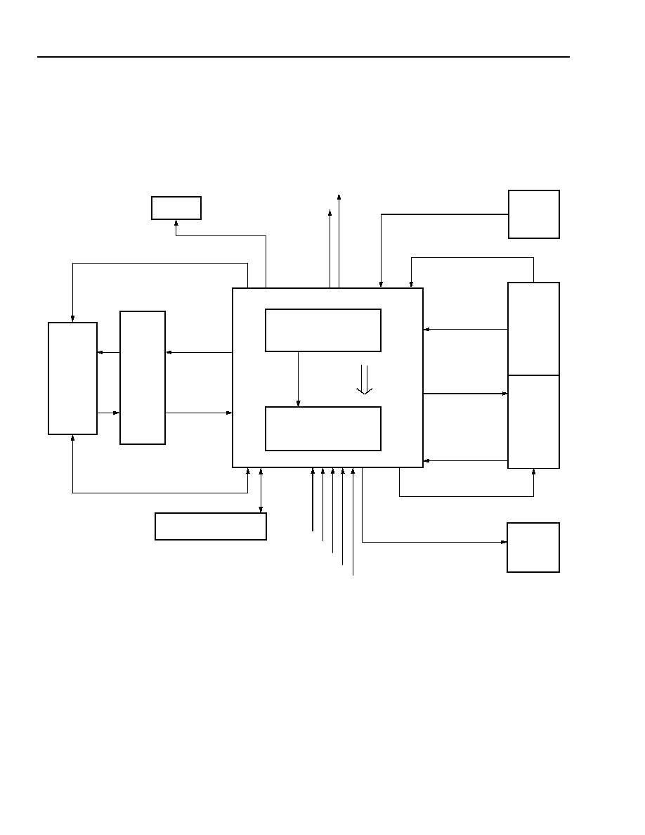
TMXF28155/51 Super Mapper
Preliminary Data Sheet
155/51 Mbits/s SONET/SDH x28/x21 DS1/E1
May 2001
428
Agere Systems Inc.
19 VT/TU Mapper Functional Description
(continued)
19.3 VT/TU Mapper Functional Block Diagram
The following block diagram shows a high-level view of the VT/TU mapper block and the interface to the T1/E1
framer, cross connect, SPE mapper (SPEMPR), digital jitter attenuator (DJA), and control (microprocessor inter-
face).
5-9011(F)r.2
Figure 38. VT Mapper Interface Diagram
DATA
RECEIVE
TRANSMIT
RECEIVE VT/TU MAPPER
TRANSMIT VT/TU MAPPER
FRAMER
[28:1]
LOPOHDATAOUT
LOPOHDATAIN
TRIBUTARY
LOPOHCLKIN
CROSS
CONNECT
DJA
CONTROL INTERFACE
DS1XCLK
E1XCLK
LOPOHVALIDOUT
LOPOHVALIDIN
RDI-V
REI-V
RX PATH SIGNALING
TX PATH SIGNALING
SPEMPR RDI, REI
TUG3 RDI, REI
TRANSMIT
RECEIVE
LOOPBACK
TMUX
TMUX
DATA CLOCK
FSYNC ALARM
[28:1]
DATA CLOCK
FSYNC ALARM
RDI, REI PATH, AND LINE ALARMS
RDI, REI PATH, AND LINE ALARMS
DATA CLOCK
CLOCK CONTROL
ALARM CONTROL
SPE
SPEMPR
SPE
SPEMPR
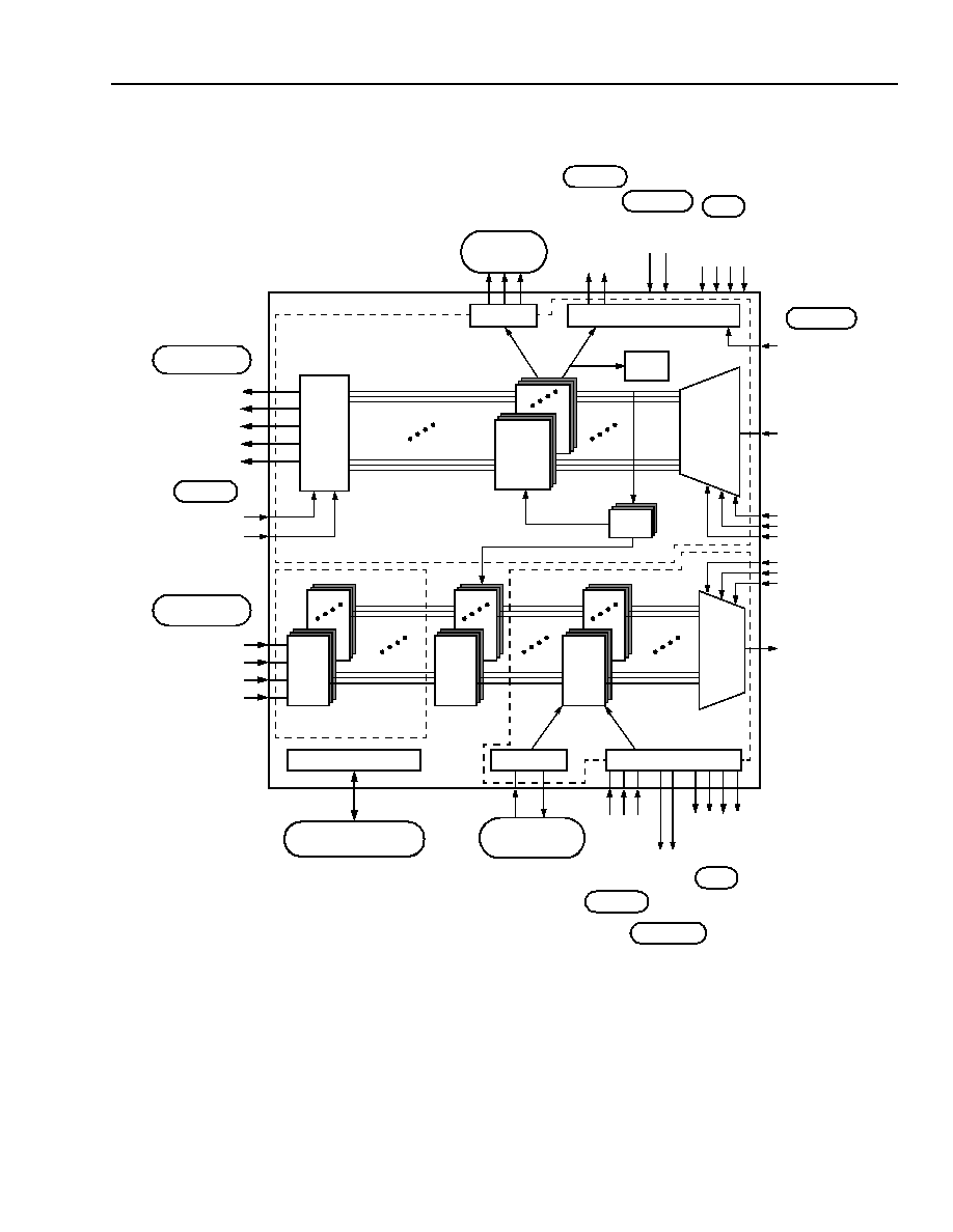
Preliminary Data Sheet
TMXF28155/51 Super Mapper
May 2001
155/51 Mbits/s SONET/SDH x28/x21 DS1/E1
429
Agere Systems Inc.
19 VT/TU Mapper Functional Description
(continued)
5-9012(F)
Figure 39. VT Mapper Functional Block Diagram
TES
SOFTWARE REGISTERS
L
O
P
O
HDA
T
A
IN
L
O
P
O
HDA
T
A
O
U
T
L
O
PO
H
C
L
KI
N
VTRXDATA[7:0]
RX_EN
V1TIME
VTTXDATA[7:0]
DATA[28:1]
CLK[28:1]
FSYNC[28:1]
DATA[28:1]
CLK[28:1]
FSYNC[28:1]
CLK7M_RX
CLK7M_TX
J1TIME
DS1XCLK
E1XCLK
L
O
PO
H
V
AL
I
D
I
N
L
O
PO
H
V
AL
I
D
O
U
T
INSEL
AUTO_AIS[28:1]
VTPI
RX_LOPOH
J2MON
VTTERM
OUTSEL
VTDEMUX
RX_V TS IG
VT LOOPBACK (VTLBSEL = 1)
VTGEN
TX_VTSIG
TX_LOPOH
VTMUX
T
U
G
3_RE
I[3:0]
T
U
G
3_RDI[2:0]
RDI_
L
RDI[2:0]
R
E
I_L[4:0]
RE
I[3:0]
RDI[2
:0]
RE
I[3:0]
RDI_
L
RDI_P
[2
:0]
R
E
I_L[
4:0]
R
E
I_P
[
3:0]
J0TIME
RAI[28:1]
RAI[28:1]
16-BIT MICROPROCESSOR
TX_EN
DEVICE I/O
TRANSMIT PATH
DS1/E1 TO
RECEIVE PATH
DEVICE I/O
DEVICE I/O
SPE MAPPER
TMUX
SPE MAPPER
TMUX
DS1/E1 FROM
SIGNALING TO
FRAMERS
x28
SPE MAPPER
CROSS CONNECT
CROSS CONNECT
X28
X28
X28
X28
INTERFACE
SIGNALING FROM
FRAMERS
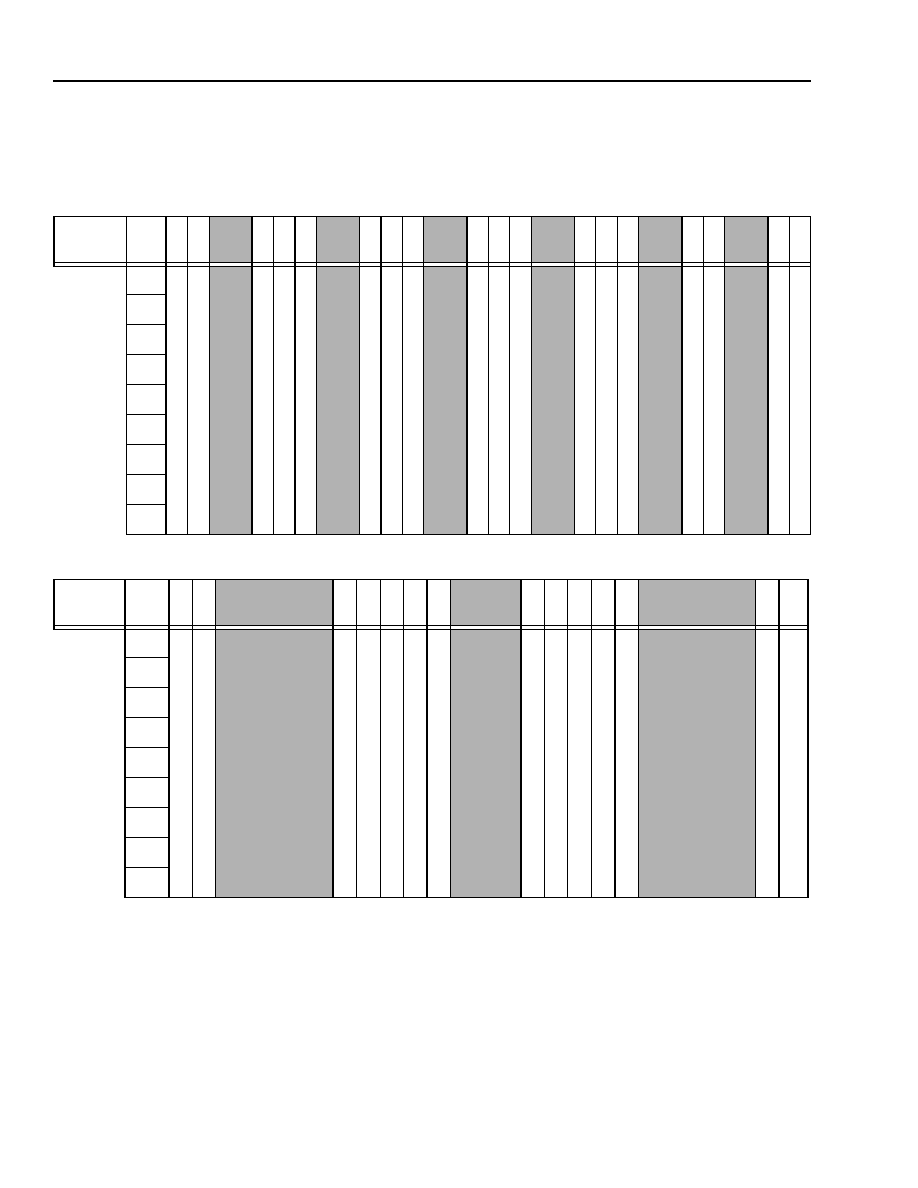
TMXF28155/51 Super Mapper
Preliminary Data Sheet
155/51 Mbits/s SONET/SDH x28/x21 DS1/E1
May 2001
430
Agere Systems Inc.
19 VT/TU Mapper Functional Description
(continued)
19.4 VT/TU Mappings
Table 551. VT2/TU-12 Payload Mapping
Table 552. VT1.5/TU-11 Payload Mapping
Column
X
1 2
∑ ∑ ∑
2
0
2
1
2
2
∑ ∑ ∑
2
8
X 2
9
∑ ∑ ∑
4
1
4
2
4
3
∑ ∑ ∑
5
6
X 5
7
∑ ∑ ∑
6
3
6
4
∑ ∑ ∑
8
3
8
4
J1
V
T
2
#
1
V
T
2
#
2
∑ ∑ ∑
V
T
2
#
2
0
V
T
2
#
2
1
V
T
2
#
1
∑ ∑ ∑
V
T
2
#
7
F
I
X
E
D
S
T
U
F
F
V
T
2
#
8
∑ ∑ ∑
V
T
2
#
2
0
V
T
2
#
2
1
V
T
2
#
1
∑ ∑ ∑
V
T
2
#
1
4
F
I
X
E
D
S
T
U
F
F
V
T
2
#
1
5
∑ ∑ ∑
V
T
2
#
2
1
V
T
2
#
1
∑ ∑ ∑
V
T
2
#
2
0
V
T
2
#
2
1
B3
C2
G1
F2
H4
Z3
Z4
Z5
Column
X
1
2
∑ ∑ ∑
2
7
2
8
X 2
9
3
0
∑ ∑ ∑
5
5
5
6
X
5
7
5
8
∑ ∑ ∑
8
3
8
4
J1
V
T
1
.
5
#
1
V
T
1
.
5
#
2
∑ ∑ ∑
v
T
1
.
5
#
2
7
V
T
1
.
5
#
2
8
F
I
X
E
D
S
T
U
F
F
V
T
1
.
5
#
1
V
T
1
.
5
#
2
∑ ∑ ∑
V
T
1
.
5
#
2
7
V
T
1
.
5
#
2
8
F
I
X
E
D
S
T
U
F
F
V
T
1
.
5
#
1
V
T
1
.
5
#
2
∑ ∑ ∑
V
T
1
.
5
#
2
7
V
T
1
.
5
#
2
8
B3
C2
G1
F2
H4
Z3
Z4
Z5

Preliminary Data Sheet
TMXF28155/51 Super Mapper
May 2001
155/51 Mbits/s SONET/SDH x28/x21 DS1/E1
431
Agere Systems Inc.
19 VT/TU Mapper Functional Description
(continued)
19.5 VT/TU Locations
Table 553. VT2/TU-12 Locations
* This column is for the I/O of the VTMPR. The cross connect can be
provisioned to map any external E1 to any VT2.
See VT2/TU-12 Payload Mapping on page 430.
Table 554. VT1.5/TU-11 Locations
* This column is for the I/O of the VTMPR. The cross connect can be
provisioned to map any external DS1 to any VT1.5.
See VT1.5/TU-11 Payload Mapping on page 430.
VTG
VT
E1*
Columns
1
1
1
1, 22, 43, 64
2
1
2
2, 23, 44, 65
3
1
3
3, 24, 45, 66
4
1
4
4, 25, 46, 67
5
1
5
5, 26, 47, 68
6
1
6
6, 27, 48, 69
7
1
7
7, 28, 49, 70
1
2
8
8, 29, 50, 71
2
2
9
9, 30, 51, 72
3
2
10
10, 31, 52, 73
4
2
11
11, 32, 53, 74
5
2
12
12, 33, 54, 75
6
2
13
13, 34, 55, 76
7
2
14
14, 35, 56, 77
1
3
15
15, 36, 57, 78
2
3
16
16, 37, 58, 79
3
3
17
17, 38, 59, 80
4
3
18
18, 39, 60, 81
5
3
19
19, 40, 61, 82
6
3
20
20, 41, 62, 83
7
3
21
21, 42, 63, 84
VTG
VT
DS1*
Columns
1
1
1
1, 29, 57
2
1
2
2, 30, 58
3
1
3
3, 31, 59
4
1
4
4, 32, 60
5
1
5
5, 33, 61
6
1
6
6, 34, 62
7
1
7
7, 35, 63
1
2
8
8, 36, 64
2
2
9
9, 37, 65
3
2
10
10, 38, 66
4
2
11
11, 39, 67
5
2
12
12, 40, 68
6
2
13
13, 41, 69
7
2
14
14, 42, 70
1
3
15
15, 43, 71
2
3
16
16, 44, 72
3
3
17
17, 45, 73
4
3
18
18, 46, 74
5
3
19
19, 47, 75
6
3
20
20, 48, 76
7
3
21
21, 49, 77
1
4
22
22, 50, 78
2
4
23
23, 51, 79
3
4
24
24, 52, 80
4
4
25
25, 53, 81
5
4
26
26, 54, 82
6
4
27
27, 55, 83
7
4
28
28, 56, 84

TMXF28155/51 Super Mapper
Preliminary Data Sheet
155/51 Mbits/s SONET/SDH x28/x21 DS1/E1
May 2001
432
Agere Systems Inc.
19 VT/TU Mapper Functional Description
(continued)
19.6 VT/TU Mapper Receive Path Description
This section describes all necessary functions of the receive logic (see
Figure 39
, right to left):
s
Virtual tributary demultiplexor (VTDEMUX)
s
Virtual tributary pointer interpreter (VTPI)
s
Virtual tributary terminator (VTTERM)
s
Output selector (OUTSEL)
s
J2 16-byte sequence monitor (J2MON)
s
Receive VT/TU signaling (RX_VTSIG)
s
Receive low-order path overhead (RX_LOPOH)
19.7 VT Demultiplexer (VTDEMUX)
The VTDEMUX logic block (in
Figure 39 on page429
) will perform all necessary functions to decode which virtual
tributary (VT) is active on the data bus.
This block monitors the H4 byte and frames on the H4 multiframe indication. In frame (VT_H4LOMF = 0
(
Table 176
)) will be declared following two consecutive, nonerrored multiframe indications. A multiframe indication
consists of four consecutive frames containing a (00, 01, 10, 11) pattern in the two LSBs of the H4 byte. Once
framed, H4 loss of multiframe (VT_H4LOMF = 1) will be declared following the number of consecutive mismatches
in the H4 multiframe indication programmed into bits VT_H4_NTIME[3:0] (
Table 182
). Loss of H4 multiframe align-
ment will generate AIS downstream. A change in H4 multiframe alignment is indicated by bit VT_H4LOMF_D
(
Table 168
) and will generate an interrupt unless the mask is set (VT_H4LOMF_M = 1 (
Table 180
)).
Bits VT_RX_GRP_TYPE[6:0] (
Table 180
) are programmed to determine whether the incoming tributary is a
VT1.5/TU-11 or a VT2/TU-12.
See
Table 551
through
Table 554
on
page 430
through
page 431
for VT/TU mapping formats.
19.8 VT Pointer Interpreter (VTPI)
The VTPI logic block (in
Figure 39 on page429
) will perform all necessary functions to support VT/TU pointer inter-
pretation. The following features are implemented:
The pointer interpreter consists of the following states:
s
Loss of pointer (LOP-V)
s
VT-AIS (AIS-V) (all ones in V1 and V2)
s
NDF enabled (NDF) (1001, 0001, 1101, 1011, 1000)
s
Normal (NORM) (disabled NDF, normal pointer)
s
Increment (INC) (inverted I bits)
s
Decrement (DEC) (inverted D bits)
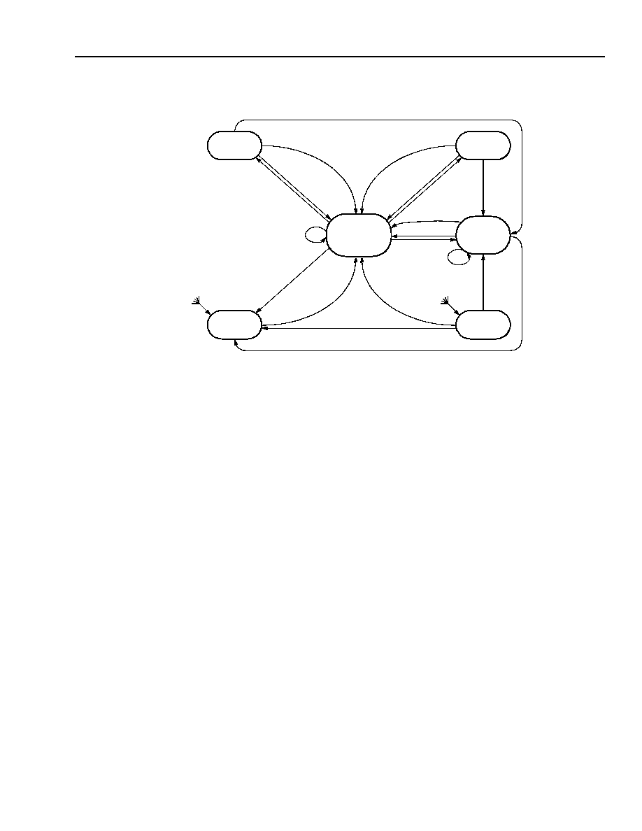
Preliminary Data Sheet
TMXF28155/51 Super Mapper
May 2001
155/51 Mbits/s SONET/SDH x28/x21 DS1/E1
433
Agere Systems Inc.
19 VT/TU Mapper Functional Description
(continued)
5-9007(F)
* This state diagram is based on the ETS 417-1-1 pointer interpretation state diagram (Figure B.1). Transitions of eight invalid pointers from the
INC, DEC, and NDF states into the LOP state have been added.
Figure 40. Pointer Interpretation State Diagram
s
The pointer interpreter will transition into the LOP-V state based on the following conditions:
-- Continuous NDF. If NDF (1001, 0001, 1101, 1011, 1000) is received for the number of consecutive super-
frames programmed in bits VT_NDF_NTIME[3:0] (
Table 183
), then LOP-V will be declared.
-- Invalid pointer values. If the number of consecutive superframes programmed in register bits
VT_INV_NTIME[3:0] (
Table 183
) are received with a pointer that is not a normal value, NDF, AIS-V, increment,
or decrement, then LOP-V will be declared. The SS bits contribute to an invalid pointer indication.
s
The pointer interpreter will transition out of the LOP-V state based on the following conditions:
-- Following three consecutive superframes with all ones in the V1 and V2 bytes the pointer interpreter will tran-
sition from the LOP-V state into the AIS-V state.
-- Following three new consecutive, consistent, and valid pointers the pointer interpreter will transition from the
LOP-V state into the NORM state.
-- The pointer interpreter
does not transition from the LOP-V state into the NDF state.
s
The pointer interpreter will transition into the AIS-V state based on the following conditions:
-- Following three consecutive superframes with all ones in the V1 and V2 bytes AIS-V will be declared.
s
The pointer interpreter will transition out of the AIS-V state based on the following conditions:
-- Following three new consecutive, consistent, and valid pointers the pointer interpreter will transition from the
AIS-V state into the NORM state.
-- Following the number of consecutive invalid pointers programmed in bits VT_INV_NTIME[3:0], the pointer in-
terpreter will transition from the AIS-V state into the LOP-V state.
-- If NDF is enabled on the incoming V1 and V2 bytes, the pointer interpreter will transition from the AIS-V state
into the NDF state.
*
NORM
DEC
INC
NDF
AIS
LOP
FROM ALL STATES
8 INVALID POINTERS
FROM ALL STATES
3 NEW POINTERS
INCREMENT
DECREMENT
8 NDF ENABLE
NDF ENABLE
NDF ENABLE
NDF
NDF
NDF
3 ANY
3 ANY
3 NEW POINTERS
3 NEW POINTERS
3 ANY POINTERS
3 NEW POINTERS
8 INVALID
8 INVALID POINTERS*
INDICATION
INDICATION
3 AIS INDICATIONS
ENABLE
ENABLE
POINTERS
POINTERS
POINTERS
ENABLE

TMXF28155/51 Super Mapper
Preliminary Data Sheet
155/51 Mbits/s SONET/SDH x28/x21 DS1/E1
May 2001
434
Agere Systems Inc.
19 VT/TU Mapper Functional Description
(continued)
s
The pointer interpreter will transition into the NDF state based on the following conditions:
-- If NDF is enabled on the incoming V1 and V2 bytes, the pointer interpreter will transition from the NORM, NDF,
AIS, INC, and DEC states into the NDF state.
s
The pointer interpreter will transition out of the NDF state based on the following conditions:
-- Continuous NDF. If NDF (1001, 0001, 1101, 1011, 1000) is received for the number of consecutive super-
frames programmed in bits VT_NDF_NTIME[3:0] (
Table 183
), the pointer interpreter will transition from the
NDF state into the LOP-V state.
-- Following any three consecutive, consistent, and valid pointers, the pointer interpreter will transition from the
NDF state into the NORM state.
-- Following three consecutive superframes with all ones in the V1 and V2 bytes, the pointer interpreter will tran-
sition from the NDF state into the AIS-V state.
-- Following three new consecutive, consistent, and valid pointers, the pointer interpreter will transition from the
NDF state into the NORM state.
-- Following the number of consecutive invalid pointers programmed in bits VT_INV_NTIME[3:0] (
Table 183
), the
pointer interpreter will transition from the NDF state into the LOP-V state.
s
The pointer interpreter will transition into the NORM state based on the following conditions:
-- Following three new consecutive, consistent, and valid pointers, the pointer interpreter will transition into the
NORM state.
-- Following any three consecutive, consistent, and valid pointers, the pointer interpreter will transition into the
NORM state. i.e., transitioning from the INC, DEC, and NDF states.
s
The pointer interpreter will transition out of the NORM state based on the following conditions:
-- Following the number of consecutive invalid pointers programmed in bits VT_INV_NTIME[3:0], the pointer in-
terpreter will transition from the NORM state into the LOP-V state.
-- If NDF is enabled on the incoming V1 and V2 bytes, the pointer interpreter will transition from the NORM state
into the NDF state.
-- Following three consecutive superframes with all ones in the V1 and V2 bytes, the pointer interpreter will tran-
sition from the NORM state into the AIS-V state.
-- When operating in the 8 of 10 mode (VT_8ORMAJORITY = 1 (
Table 181
)), if 8 of the 10 I and D bits are correct
for a pointer decrement on the incoming V1 and V2 bytes, the pointer interpreter will transition from the NORM
state into the DEC state. Otherwise, if 3 of the 5 I bits and 3 of the 5 D bits are correct for a pointer decrement
on the incoming V1 and V2 bytes, the pointer interpreter will transition from the NORM state into the DEC state.
-- When operating in the 8 of 10 mode (VT_8ORMAJORITY = 1), if 8 of the 10 I and D bits are correct for a pointer
increment on the incoming V1 and V2 bytes, the pointer interpreter will transition from the NORM state into the
INC state. Otherwise, if 3 of the 5 I bits and 3 of the 5 D bits are correct for a pointer increment on the incoming
V1 and V2 bytes, the pointer interpreter will transition from the NORM state into the INC state.
s
The pointer interpreter will transition into the INC state based on the following conditions:
-- When operating in the 8 of 10 mode (VT_8ORMAJORITY = 1), if 8 of the 10 I and D bits are correct for a pointer
increment on the incoming V1 and V2 bytes, the pointer interpreter will transition into the INC state. Otherwise,
if 3 of the 5 I bits and 3 of the 5 D bits are correct for a pointer increment on the incoming V1 and V2 bytes, the
pointer interpreter will transition into the INC state.
s
The pointer interpreter will transition out of the INC state based on the following conditions:
-- If NDF is enabled on the incoming V1 and V2 bytes, the pointer interpreter will transition from the INC state into
the NDF state.
-- Following three consecutive superframes with all ones in the V1 and V2 bytes, the pointer interpreter will tran-
sition from the INC state into the AIS-V state.
-- Following three new consecutive, consistent, and valid pointers, the pointer interpreter will transition from the
INC state into the NORM state.
-- Following any three consecutive, consistent, and valid pointers, the pointer interpreter will transition from the
INC state into the NORM state.
-- Following the number of consecutive invalid pointers programmed in bits VT_INV_NTIME[3:0], the pointer in-
terpreter will transition from the INC state into the LOP-V state.

Preliminary Data Sheet
TMXF28155/51 Super Mapper
May 2001
155/51 Mbits/s SONET/SDH x28/x21 DS1/E1
435
Agere Systems Inc.
19 VT/TU Mapper Functional Description
(continued)
s
The pointer interpreter will transition into the DEC state based on the following conditions:
-- When operating in the 8 of 10 mode (VT_8ORMAJORITY = 1 (
Table 181
)), if 8 of the 10 I and D bits are correct
for a pointer decrement on the incoming V1 and V2 bytes, the pointer interpreter will transition into the DEC
state. Otherwise, if 3 of the 5 I bits and 3 of the 5 D bits are correct for a pointer decrement on the incoming V1
and V2 bytes, the pointer interpreter will transition into the DEC state.
s
The pointer interpreter will transition out of the DEC state based on the following conditions:
-- If NDF is enabled on the incoming V1 and V2 bytes, the pointer interpreter will transition from the DEC state
into the NDF state.
-- Following three consecutive superframes with all ones in the V1 and V2 bytes, the pointer interpreter will tran-
sition from the DEC state into the AIS-V state.
-- Following three new consecutive, consistent, and valid pointers, the pointer interpreter will transition from the
DEC state into the NORM state.
-- Following any three consecutive, consistent, and valid pointers, the pointer interpreter will transition from the
DEC state into the NORM state.
-- Following the number of consecutive invalid pointers programmed in bits VT_INV_NTIME[3:0] (
Table 183
), the
pointer interpreter will transition from the DEC state into the LOP-V state.
Pointer increments and decrements are monitored and counted internally. The performance monitoring reset signal
transfers the count to the holding registers for pointer increment (VT_PTR_INC[1--28][3:0] (
Table 208
)), and
pointer decrement (VT_PTR_DEC[1--28][3:0] (
Table 208
)) for microprocessor read and resets the running count
registers to 0. When SMPR_SAT_ROLLOVER = 1 (
Table 67
), the internal running counts will hold at their maxi-
mum value. Otherwise, the counts will roll over. The running count and holding register counts will be forced to 0, if
the SPE mapper is requesting AUTO AIS or VT_LOP[1--28] = 1 (loss of pointer) (
Table 177
) or VT_AIS[1--28] = 1
(VT AIS) (
Table 177
) (or VT_H4LOMF = 1 (loss of H4 multiframe alignment) (
Table 176
)).
LOP-V (VT_LOP) and AIS-V (VT_AIS) will be detected and reported to the microprocessor. Both the LOP-V and
AIS-V conditions will contribute to the VT/TU mapper automatic AIS generation that is driven over a 28-bit internal
output bus to the cross connect (XC). Any change in state of VT_LOP or VT_AIS will be reported to the micropro-
cessor via VT_LOP_D[1--28] and VT_AIS_D[1--28] (
Table 169
). Unless the appropriate mask bit is set
(VT_LOP_M[1--28] or VT_AIS_M[1--28]) (
Table 173
), VT_LOP_D[1--28] = 1 or VT_AIS_D[1--28] = 1 will gener-
ate an interrupt.
A check for VT/TU size mismatches is performed by comparing the expected VT/TU size bits (VT1.5 = 11,
VT2 = 10) with the actual received SS bits in the V1 byte. After three consecutive mismatches, size errors will be
reported with bit VT_SIZERR[1--28] (
Table 177
). Any change in state of VT_SIZERR[1--28] will be reported with
bit VT_SIZERR_D[1--28] (
Table 169
). Unless the VT_SIZERR_M[1--28] (
Table 173
) mask bit is set,
VT_SIZERR_D[1--28] = 1 will generate an interrupt.
The accepted pointer is stored and accessible by the microprocessor.
This block supports tributary loopback.
19.9 VT Termination (VTTERM)
The VTTERM logic block (in
Figure 39
) will perform all necessary functions to support complete VT/TU termination.
The following features are implemented.
19.9.1 V5 Termination
The V5 byte is checked for BIP-2 errors. If BIP-2 errors are detected, REI-V is transmitted in the V5 byte of the cor-
responding transmit VT, if enabled by bit VT_REI_EN[1--28] = 1 (
Table 198
). BIP-2 errors and reception of REI-V
in the V5 byte is counted on a per-superframe basis. BIP-2 errors can counted on either a bit or block basis
selected by bit, VT_BIT_BLOCK_CNT (1 = bit, 0 = block) (
Table 181
).

TMXF28155/51 Super Mapper
Preliminary Data Sheet
155/51 Mbits/s SONET/SDH x28/x21 DS1/E1
May 2001
436
Agere Systems Inc.
19 VT/TU Mapper Functional Description
(continued)
BIP-2 errors and REI-V reception are monitored and counted internally. The performance monitoring reset signal
transfers the count to the holding registers for BIP-2 error count (VT_BIP2ERR_CNT[1--28][11:0];
Table 206
), and
REI-V count (VT_REI_CNT[1--28][10:0] (
Table 207
)) for microprocessor read, and resets the running count regis-
ters to 0. When SMPR_SAT_ROLLOVER = 1 (
Table 67
), the internal running counts will hold at their maximum
value. Otherwise, the counts will roll over. The running count and holding register counts will be forced to 0, if the
SPE mapper is requesting AUTO AIS, VT_LOP[1--28] = 1 (loss of pointer), VT_AIS[1--28] = 1 (VT AIS)
(
Table 177
) or VT_H4LOMF = 1 (loss of H4 multiframe alignment) (
Table 176
).
The V5 byte will be checked for received RFI-V via VT_RFI[1--28] bits (
Table 177
). New values will be latched into
the register after the number of consecutive values programmed in bits VT_RDI_NTIME[3:0] (
Table 184
) have been
received. A VT_RFI[1--28] change of state is reported by bit VT_RFI_D[1--28] (
Table 169
). When operating in the
DS1 byte synchronous mode, RFI-V = 1 will force DS1 RAI downstream to the framer. Unless the VT_RFI_M mask
bit (
Table 173
) is set, VT_RFI_D[1--28] = 1 will generate and cause an interrupt.
When operating in normal RDI-V mode (VT_RX_ERDI_EN[1--28] = 1 (
Table 204, starting on page168
)), the V5
byte will be checked for received RDI-V and reported via VT_RDI[1--28] bits (
Table 177
). New values will be
latched to this register after VT_RDI_NTIME[3:0] consecutive values have been received. A VT_RDI[1--28]
change of state is reported via VT_RDI_D[1--28] (
Table 169
). Unless the VT_RDI_M[1--28] (
Table 173
) mask bit
is set, VT_RDI_D[1--28] = 1 will generate and cause an interrupt.
When operating in enhanced RDI-V mode (VT_RX_ERDI_EN[1--28] = 0 (
Table 204, starting on page168
)), the
V5 byte will be checked for received RDI-V and reported via VT_RDI[1--28] bit (
Table 177
). New values will be
latched to this register after VT_ERDI_NTIME[3:0] (
Table 184
) consecutive ERDI-V values (V5 bit 8 and Z7 bits
5--7) have been received. A VT_ERDI[1--28][2:0] change of state is reported via VT_ERDI_D[1--28] (
Table 169
).
Unless the VT_ERDI_M[1--28] mask bit (
Table 173
) is set, VT_ERDI_D[1--28] = 1 will generate and cause an
interrupt.
The V5 byte VT/TU signal label will be monitored and reported to the microprocessor using bits
VT_LAB[1--28][2:0] (
Table 177
). New values will be latched to the microprocessor after the number of consecutive
values programmed in bits VT_LAB_NTIME[3:0] (
Table 184
) have been received. An all zeros signal label will set
bit VT_UNEQ[1--28] (
Table 177
). Any change in state of VT_UNEQ[1--28] will be reported to the microprocessor
via bit VT_UNEQ_D[1--28] (
Table 169
). Unless the VT_UNEQ_M[1--28] (
Table 173
) mask bit is set,
VT_UNEQ_D[1--28] = 1 will generate an interrupt. VT_UNEQ[1--28] will contribute to automatic AIS generation.
The latched signal label will be compared to the expected signal label. If the expected signal label is 001 or if
VT_UNEQ[1--28] is detected, the detection of PLM-V is disabled. Otherwise, any mismatch is reported to the
microprocessor via bit VT_PLM[1--28] (
Table 177
). Any change in state of VT_PLM[1--28] will be reported to the
microprocessor via bit VT_PLM_D[1--28] (
Table 169
). Unless the VT_PLM_M[1--28] mask bit is set (
Table 173
),
VT_PLM_D[1--28] = 1 will generate an interrupt.
19.9.2 Z6/N2 Termination
For SONET applications, the Z6 byte is monitored and presented to the microprocessor using bits
VT_Z6_BYTE[1--28][7:0] (
Table 205
) for growth and monitoring purposes only. The Z6 byte is updated to when
three consecutive consistent bytes are received. N2 is defined for tandem connection applications per
ETS 300 417-1-1 and ITU-T G.707/G.783. Low-order tandem connection is not supported.
19.9.3 Z7/K4 Termination
This termination will support enhanced RDI when bit VT_RX_ERDI_EN[1--28] = 1(
Table 204, starting on
page 168
). The Z7/K4[3:1] byte will be monitored and reported to the microprocessor with bits
VT_ERDI[1--28][2:0] (
Table 177
). New values will be latched to the microprocessor after the number of consecu-
tive values programmed in register bits VT_ERDI_NTIME[3:0] (
Table 184
) have been received. A change of state is
reported using bit VT_ERDI_D[1--28] (
Table 169
). Unless the VT_ERDI_M[1--28] (
Table 173
) mask bit is set,
VT_ERDI_D[1--28] = 1 will generate an interrupt.

Preliminary Data Sheet
TMXF28155/51 Super Mapper
May 2001
155/51 Mbits/s SONET/SDH x28/x21 DS1/E1
437
Agere Systems Inc.
19 VT/TU Mapper Functional Description
(continued)
The Z7/K4[7:4] byte will be monitored and reported to the microprocessor via bits VT_APS[1--28][3:0] (
Table 178
).
New values will be latched to the microprocessor after the number of consecutive values programmed in bits
VT_APS_NTIME[3:0] (
Table 184
) have been received. A change of state is reported using bit VT_APS_D[1--28]
(
Table 169
). Unless the VT_APS_M[1--28] (
Table 173
) mask bit is set, VT_APS_D[1--28] = 1 will generate an
interrupt.
19.9.4 Payload Termination
Payload termination will support asynchronous, byte synchronous, and bit synchronous demappings for SONET
VT1.5s and VT2s per
Bellcore
GR-253 and ANSI T1.105.
Payload termination will support asynchronous, byte synchronous, and bit synchronous demappings for
SDH TU11s and TU12s per ITU-T G.707 and ETS 300 417-4-1.
Demapping modes are selected with bits VT_RX_MAPTYPE[1--28][3:0] (
Table 204, starting on page168
), as
defined in
Table 555
.
Table 555. Receive VT/TU Demapping Selection
The payload termination provides an elastic store for rate adoption. An elastic store overflow is indicated in bit
VT_RX_ESOVFL_D[1--28] (
Table 169
). Unless the VT_RX_ESOVFL_M[1--28] mask bit is set (
Table 173
),
VT_RX_ESOVFL_D[1--28] = 1 will generate an interrupt.
When an overflow condition exists, the read/write count will be forced to the center of the FIFO. The FIFO is 64 bits
deep.
The payload termination circuitry will generate a gapped DS1/E1 clock (VT_TERM_CLK).
Figure 41
and
Figure 42
on page451
describe the DS1 and E1 gapped clocking schemes, respectively. A frame sync is generated and
transmitted from the device coincident with the frame bit for DS1 and the MSB of time slot 0 for E1 when demap-
ping a byte synchronous payload.
19.10 Output Signal Selection (OUTSEL)
The OUTSEL logic block (in
Figure 39 on page429
) will perform all necessary functions to overwrite the outgoing
DS1/E1 signals with the appropriate AIS clock, data, and frame synchronization.
VT_RX_MAPTYPE[1--28][3:0] (See
Table 204.
)
Description
0
0
0
0
Asynchronous VT1.5/TU-11 (DS1 output)
0
0
0
1
Asynchronous VT2/TU-12 (E1 output)
0
0
1
0
Byte synchronous VT1.5/TU-11 (DS1 output)
0
0
1
1
Byte synchronous VT2/TU-12 (E1 output)
0
1
0
0
Bit synchronous VT1.5/TU-11 (DS1 output)
0
1
0
1
Bit synchronous VT2/TU-12 (E1 output)
0110--0111
Undefined, generates AIS
1
0
0
0
Asynchronous VT2/TU-12 (DS1 output)
1
0
0
1
Byte synchronous VT2/TU-12 (DS1 output)
1
0
1
0
Bit synchronous VT2/TU-12 (DS1 output)
1011--1111
Undefined, generates AIS

TMXF28155/51 Super Mapper
Preliminary Data Sheet
155/51 Mbits/s SONET/SDH x28/x21 DS1/E1
May 2001
438
Agere Systems Inc.
19 VT/TU Mapper Functional Description
(continued)
VT/TU mapper automatic AIS, which is driven over a 28-bit internal output bus to the cross connect (XC), is gener-
ated according to the following equation:
SPEMPR_AUTO_AIS
or
VT_LOP[1--28]
or
VT_AIS[1--28]
or
(VT_H4LOMF and (VT_LOMF_AIS_INH))
or
(VT_UNEQ[1--28] and (VT_UNEQ_AIS_INH))
or
(VT_PLM[1--28] and (VT_PLM_AIS_INH))
or
(VT_J2TIM[1--28] and (VT_J2TIM_AIS_INH))
or
(VT_LOPS[1--28] and VT_LOPS_AIS_INH))
The output of the VT/TU mapper receive path will be as shown in
Figure 43 on page451
and
Figure 44 on
page 452
.
19.11 J2 Byte Monitor and Termination (J2MON)
The J2MON logic block (in
Figure 39 on page429
) will perform all necessary functions to monitor the incoming J2
trace identifier. The following features are implemented:
s
J2 monitoring will support five different monitoring modes defined by VT_J2MON_MODE[1--28][2:0]
Table 204
on pag e168
:
-- VT_J2MON_MODE[1--28][2:0] = 000: this mode captures an incoming 16-byte sequence and stores it in
VT_J2BYTE_DET[1--28][1--16][7:0] (
Table 209
). TIM-V is disabled for this mode.
-- VT_J2MON_MODE[1--28][2:0] = 001: this mode captures an incoming 16-byte sequence with SDH framing
and stores it in VT_J2BYTE_DET[1--28][1--16][7:0]. TIM-V is disabled for this mode.
-- VT_J2MON_MODE[1--28][2:0] = 010: this mode captures a constant 1-byte sequence and stores it in
VT_J2BYTE_DET[1--28][1][7:0]. TIM-V is disabled for this mode.
-- VT_J2MON_MODE[1--28][2:0] = 011: this mode monitors a 16-byte sequence with SDH framing and com-
pares it to a programmable expected value. The expected value is programmed by the user using register bits
VT_J2BYTE_EXP[1--28][1--16][7:0] (
Table 209
). The hardware frames by looking for the byte with the MSB
set to one, which indicates that the next byte is the second byte of the message. CRC is verified based on the
value programmed in VT_J2BYTE_EXP[1--28][1--16][7:0]. TIM-V is enabled for this mode.
-- VT_J2MON_MODE[1--28][2:0] = 100: this mode monitors a constant 1-byte sequence and compares it to an
programmable expected value. The expected value is programmed by the user using register bits
VT_J2BYTE_EXP[1--28][1][7:0]. TIM-V is enabled for this mode.
s
Trace identifier mismatch (TIM-V) will be detected following the number of consecutively errored sequences
(1-byte or 16-byte sequences) programmed in bits,
VT_
J2_NTIME[3:0] (
Table 183
), and reported to the micro-
processor via bit VT_J2TIM[1--28] (
Table 177
). If TIM-V is detected, the J2 byte monitor will transition into the
capture mode and start searching for two consecutive consistent 1-byte or 16-byte sequences. Once two con-
secutive consistent sequences are detected, the J2 byte monitor will transition into the monitor mode and start
searching for the number of consecutive mismatches programmed in register bits
VT_
J2_NTIME[3:0], on a per
1-byte or 16-byte sequence basis.
Once the hardware finds synchronization (
VT_
J2TIM[1--28] = 0), the new
sequence is latched into
VT_
J2BYTE_DET[1--28][1--16][7:0] (
Table 209
). The synchronization algorithm used
will not allow single bit errors to pass through to
VT_
J2BYTE_DET[1--28][1--16][7:0].

Preliminary Data Sheet
TMXF28155/51 Super Mapper
May 2001
155/51 Mbits/s SONET/SDH x28/x21 DS1/E1
439
Agere Systems Inc.
19 VT/TU Mapper Functional Description
(continued)
s
Unless bit
VT_
J2TIM_AIS_INH (
Table 181
) is set to a 1,
VT_
J2TIM[1--28] will contribute to automatic AIS gen-
eration.
s
Any change in state of
VT_
J2TIM[1--28][1--16][7:0] will be reported in bit
VT_
J2TIM_D[1--28] (
Table 169
).
Unless the
VT_
J2TIM_M[1--28] (
Table 173
) mask bit is set,
VT_
J2TIM_D[1--28] = 1 will generate an interrupt.
19.12 Receive Signaling (RX_VTSIG)
The RX_VTSIG logic block (in
Figure 39 on page429
) will perform all necessary functions to extract and transmit
the received signaling bits when operating in DS1 byte-synchronous mode. The following features are imple-
mented:
s
The signaling is sent to the appropriate framer link selected by bits VT_RXSIG_CH_SEL[1--28][4:0] (
Table 204
).
VT_RXSIG_CH_SEL[1--28][4:0] is a necessary duplication of the routing information programmed within the
cross connect (XC) block.
s
When VT_SYNC_PBIT[1--28] = 1 (
Table 204 on page168
), the RX_VTSIG block will synchronize to the incom-
ing VT/TU phase indication (P1, P0). Otherwise, VT_LOPS[1--28] (
Table 177
) and VT_LOPS_D[1--28]
(
Table 169
) will be forced to 0.
s
P-bit phase synchronization (VT_LOPS[1--28] = 0) is declared following two consecutive nonerrored multi-
frames (48 frames). Loss of phase synchronization (VT_LOPS[1--28] = 1) is declared following the number of
consecutive errored multiframes programmed in bits VT_LOPS_NTIME[3:0] (
Table 182
). Any change in
VT_LOPS[1--28] state will be detected and reported to the microprocessor with bit VT_LOPS_D[1--28].
s
If the loss of phase synchronization (VT_LOPS[1--28] = 1) condition exists and VT_LOPS_AIS_INH = 0, DS1
AIS is transmitted downstream and the signaling bits will be forced to the value in SMPR_OH_DEFLT (
Table 67
)
in the MPU block. Otherwise (VT_LOPS[1--28] = 0), the VT_RX_VTSIG logic block will behave as described in
Table 556
below.
s
Unless VT_LOPS_M[1--28] (
Table 173
) mask bit is set, VT_LOPS_D[1--28] will generate an interrupt.
s
See
Table 556
below for signaling behavior based on the receive status and control.
Table 556. Rx Signaling Behavior per Channel
* If the P1 and P0 bits are not used for phase indication and the F bit is not passed transparently, the F bit is overwritten with the appropriate SF
or ESF framing pattern based on a random starting position. Robbed-bit signaling will not be accessible under such a condition.
When operating in the ESF mode, the Ft bits will be overwritten with the ESF frame and the C and M bits passed transparently.
VT_SYNC_PBIT
[1--28]
(
Table 204
)
VT_WR_FBIT
[1--28]
(
Table 204
)
VT_SF_ESF
[1--28]
(
Table 204
)
VT_LOPS
[1--28]
(
Table 177
)
Action
0
0
X
X
Pass F-bit transparently.
0
1
0*
X
Overwrite outgoing F bit with ESF pattern.
0
1
1
X
Overwrite outgoing F bit with SF pattern.
1
1
0
0
Overwrite outgoing F bit with ESF pattern.
1
1
1
0
Overwrite outgoing F bit with SF pattern.
1
X
X
1
Transmit DS1 AIS downstream.
TMXF28155/51 Super Mapper
Preliminary Data Sheet
155/51 Mbits/s SONET/SDH x28/x21 DS1/E1
May 2001
440
Agere Systems Inc.
19 VT/TU Mapper Functional Description
(continued)
19.13 Receive Lower-Order Path Overhead (RX_LOPOH)
The RX_LOPOH logic block (in
Figure 39 on page429
) will perform all necessary functions to store and transmit
the overhead associated with each VT/TU, specifically, V5, J2, Z6/N2, Z7/K4, and the O bits. The following features
will be implemented:
s
V5, J2, Z6/N2, Z7/K4, and the 0 bits, on a per VT basis, are stored for one complete superframe and transmitted
during the next superframe. REI and RDI values received from the SPEMPR and TMUX are stored on a per-
frame basis and transmitted during the next frame. REI and RDI values are latched during the A1 time of the of
the received SONET frame.
s
When operating in UPSR mode (bit VT_UPSR = 1 (
Table 173
)), REI, RDI, and ERDI values in the V5 and Z7
bytes will be modified based on the receive status. See
Table 561 on page444
for automatic generation require-
ments.
s
The REI and RDI received from the SPEMPR and TMUX blocks is the first data type transmitted in each frame
as a burst of 34 bits on the rising edge of the SPE mapper Rx clock (6.48 MHz). All other data types are transmit-
ted as a burst of 224 bits on the rising edge of the SPE mapper Rx clock.
Note: The number of valid bits transmitted is dependent upon the VT/TU group types. i.e., full VT2 equals 168 bits.
s
The first frame of the four frame multiframe contains data types 001, 010, 011, and 100, respectively. The second
frame of the multiframe contains data types 001, 101, and 110, respectively. The remaining frames contain only
data type 001. Data type headers will be defined as shown in
Table 557
below.
All data types must be transmitted within 500 µs.
Table 557. Data Type Header Definitions
* All overhead bytes will be transmitted from MSB to LSB.
O bits are received in the byte following J2 and the byte following Z6/N2 in asynchronous mode. The O bits will be transmitted in the order of
which they are received within a VT, starting with the MSB of the nibble following the J2 byte.
Figure 45 on pag e452
, contains the RX_LOPOH block serial channel format and timing.
19.14 VT/TU Mapper Transmit Path Requirements
This section describes all necessary functions of the transmit logic (see
Figure 39 on page429
, left to right).
s
Input selector (INSEL)
s
Transmit elastic store (TES)
s
Virtual tributary generator (VTGEN)
s
Virtual tributary multiplexer (VTMUX)
s
Transmit DS1/E1 signaling (TX_VTSIG)
s
Transmit low-order path overhead (TX_LOPOH)
Header
Description
0
0
0
Reserved.
0
0
1
TMUX and SPE mapper RDI/REI.
0
1
0
V5 byte, 28/21 bytes starting with VT 1*.
0
1
1
J2 byte, 28/21 bytes starting with VT 1.
1
0
0
Z6/N2 byte, 28/21 bytes starting with VT 1.
1
0
1
Z7/K4 byte, 28/21 bytes starting with VT 1.
1
1
0
O bits, 28/21 bytes starting with VT 1
.
1
1
1
Reserved. Data will be ignored.

Preliminary Data Sheet
TMXF28155/51 Super Mapper
May 2001
155/51 Mbits/s SONET/SDH x28/x21 DS1/E1
441
Agere Systems Inc.
19 VT/TU Mapper Functional Description
(continued)
19.14.1 Input Selector (INSEL)
The INSEL logic block (in
Figure 39 on page429
) will perform loss of clock (LOC), AIS, and loss of frame sync
detection. The following features will be implemented:
s
The incoming DS1/E1 signal will be retimed immediately using the selected DS1/E1 clock edge
(VT_TX_CLKEDGE[1--28] (
Table 198
)). If VT_TX_CLKEDGE[1--28] = 1, the rising edge of the incoming
DS1/E1 CLOCK is used to retime the signal; otherwise, the falling edge is used.
s
The incoming DS1/E1 signals will be checked for a digital loss of clock (LOC) condition and reported with bit
VT_TX_LOC[1--28] (
Table 179
). Any change in state of VT_TX_LOC[1--28] will be reported to the microproces-
sor via bit VT_TX_LOC_D[1--28] (
Table 171
). Unless the VT_TX_LOC_M[1--28] (
Table 175
) mask bit is set,
VT_TX_LOC_D = 1 will generate an interrupt.
s
If LOC is detected (VT_TX_LOC[1--28] = 1), DS1/E1 AIS will be inserted in the appropriate transmit path VT.
DS1/E1 AIS consists of a valid VT/TU pointer, valid VT/TU overhead, and an all ones payload.
s
In the byte-synchronous mode, the incoming DS1/E1 frame sync is monitored for the loss of frame sync condi-
tion (LOFS) and reported in bit VT_LOFS[1--28] (
Table 179
). In frame sync, (VT_LOFS[1--28] = 0) is declared
following three consecutive valid frame sync pulses (375 µs). Loss of frame sync (VT_LOFS[1--28] = 1) is
declared following six consecutive frame sync mismatches (750 µs). Any change in state of VT_LOFS[1--28] will
be reported in bit VT_LOFS_D[1--28] (
Table 171
). Unless the VT_LOFS_M[1--28] (
Table 175
) mask bit is set,
VT_LOFS_D[1--28] = 1 will generate an interrupt.
s
If LOFS is detected (VT_LOFS[1--28] = 1), AIS-V is inserted in the appropriate VT location. AIS-V consists of
writing an all ones pattern into the entire VT, including V1~4.
s
The incoming DS1/E1 signal will be checked for the AIS condition and reported in bit VT_TX_AIS[1--28]
(
Table 179
). Any change in state of VT_TX_AIS[1--28] is reported in bit VT_TX_AIS_D[1--28] (
Table 171
).
Unless the VT_TX_AIS_M[1--28] (
Table 175
) mask bit is set, VT_TX_AIS_D[1--28] = 1 will generate an inter-
rupt.
s
If the incoming data is DS1, AIS will be declared if there are less than nine zeros out of 8192 clock periods. If the
incoming data is E1, AIS will be declared if there are less than three zeros in each of two consecutive 512-bit
periods and cleared when each of two consecutive 512-bit periods contain more than two zeros.
Transmit mapping modes are shown in
Table 558
below.
Table 558. Transmit VT/TU Mapping Selection per Channel, VT_TX_MAPTYPE[1--28][3:0]
VT_TX_MAPTYPE[1--28][3:0] (See
Table 198
.)
Description
0
0
0
0
Asynchronous VT1.5/TU-11 (DS1 input).
0
0
0
1
Asynchronous VT2/TU-12 (E1 input).
0
0
1
0
Byte synchronous VT1.5/TU-11 (DS1 input).
0
0
1
1
Byte synchronous VT2/TU-12 (E1 input).
0
1
0
0
Bit synchronous VT1.5/TU-11 (DS1 input).
0
1
0
1
Bit synchronous VT2/TU-12 (E1 input).
0110--0111
Undefined, generates VT1.5/TU-11 UNEQ-V.
1
0
0
0
Asynchronous VT2/TU-12 (DS1 input).
1
0
0
1
Byte synchronous VT2/TU-12 (DS1 input).
1
0
1
0
Bit synchronous VT2/TU-12 (DS1 input).
1011--1111
Undefined, generates VT2/TU-12 UNEQ-V.

TMXF28155/51 Super Mapper
Preliminary Data Sheet
155/51 Mbits/s SONET/SDH x28/x21 DS1/E1
May 2001
442
Agere Systems Inc.
19 VT/TU Mapper Functional Description
(continued)
19.14.2 Transmit Elastic Store (TES)
The TES logic block (in
Figure 39 on pag e429
) will perform all functions necessary to synchronize the incoming
DS1/E1 or VT1.5/VT2 signals to the local STS-1/STS-3 clock.
s
This logic block will support the following modes of operation:
-- Asynchronous, bit synchronous, and byte synchronous mapping from DS1/E1 input.
-- Asynchronous, bit synchronous, and byte synchronous mapping from loopback VT1.5/VT2 input.
The TES logic block has programmable stuffing thresholds. The value programmed in the VT_HIGH_THRES[6:0]
(
Table 210
) controls positive justification. The value programmed in the VT_LOW_THRES[6:0] (
Table 210
) controls
negative justification. The recommended values for nontributary loopback (VT_LB_SEL[1--28] = 0 (
Table 198
)) are
VT_HIGH_THRES[6:0] = 0x28 and VT_LOW_THRES[6:0] = 0x27. Otherwise (VT_LB_SEL[1--28] = 1), the rec-
ommended values are VT_HIGH_THRES[6:0] = 0x05 and VT_LOW_THRES[6:0] = 0x04.
The TES logic block monitors for elastic store overflow conditions and reports with bit VT_TX_ESOVFL_E[1--28]
(
Table 171
). Unless the VT_TX_ESOVFL_M[1--28] (
Table 175
) mask bit is set, VT_TX_ESOVFL_E[1--28] = 1 will
generate and interrupt.
19.14.3 Virtual Tributary Generator (VTGEN)
The VTGEN logic block (in
Figure 39 on page429
) performs all functions necessary to map all possible DS1/E1
inputs to the appropriate VT/TU structure. This includes VT/TU pointer generation, positive/negative stuffing,
VT/TU overhead generation/insertion and DS1/E1 data insertion. The following features will be implemented:
s
This logic block will support the following modes of operation:
-- Asynchronous
-- Byte synchronous
-- Bit synchronous
19.14.4 Pointer Generation
s
The pointer generator will support the following features when operating in asynchronous or bit synchronous
mode:
-- If transmit AIS-V is not requested, the following requirements apply:
1. A fixed pointer value of decimal 78 is generated for VT1.5/TU-11 mappings.
2. A fixed pointer value of decimal 105 is generated for VT2/TU-12 mappings.
3. The VT size field will be set to binary 11 for VT1.5/TU-11 mappings.
4. The VT size field will be set to binary 10 for VT2/TU-12 mappings.
5. The new data flag (NDF) set to binary 0110 for VT1.5/VT2 mappings.
6. V3 and V4 is set to the selected overhead default (SMPR_OH_DEFLT (
Table 67
) in the microprocessor inter-
face block) for all mappings:
-- If transmit AIS-V is requested, V1~V4 will be forced to 0xFF.
-- Bit stuffing, using the C and S bits, will be performed based on the fullness of the elastic store.
s
The pointer generation will support the following features when operating in byte synchronous mode:
-- If transmit AIS-V is not requested, the following requirements apply:
1. The pointer value is generated based on the location of the incoming frame sync for VT1.5/VT2 mappings.
2. The VT size field is set to 11 for VT1.5/TU-11 mappings.
3. The VT size field is set to 10 for VT2/TU-12 mappings.
4. The new data flag (NDF) is set to 0110 for normal VT1.5/VT2 mappings. If a NDF is requested, the NDF will
be set to 1001 (binary).

Preliminary Data Sheet
TMXF28155/51 Super Mapper
May 2001
155/51 Mbits/s SONET/SDH x28/x21 DS1/E1
443
Agere Systems Inc.
19 VT/TU Mapper Functional Description
(continued)
5. If an increment is requested, the pointer bytes, V1 and V2, are programmed with the I-bits inverted. The
pointer action byte, V3, will be programmed to the selected default (microprocessor bit
SMPR_FXD_STFF_DEFLT (
Table 67
)), as well as the byte directly following V3. However, when incrementing
from 139 to 0 for VT2 mapping, the pointer generator sends out NDF-V indication with the correct pointer (0)
instead of the increment indication.
6. If a decrement is requested, the pointer bytes, V1 and V2, will be programmed with the D bits inverted. The
pointer action byte, V3, will be programmed to actual customer data. However, when decrementing from 0 to
139 for VT2 mapping, the pointer generator sends out NDF-V indication with the correct pointer (139) instead
of the decrement indication.
7. The V4 byte will be programmed to the selected overhead default (microprocessor bit SMPR_OH_DEFLT) for
all mappings.
-- If transmit AIS-V is requested, V1~V4 will be forced to 0xFF.
Overhead Byte Generation (V5, J2, Z6/N2, Z7/K4, and O bits). This portion of the VTGEN logic block will gener-
ate and insert the V5, J2, Z6/N2, and Z7/K4 overhead bytes into the appropriate virtual tributary. O bits are only
accessible in the asynchronous and bit synchronous modes.
V5 Overhead Byte Format/Generation. The V5 overhead byte will be mapped as defined in
Table 559
.
Table 559. V5 Overhead Byte Format
The following features are supported:
s
When operating in tributary loopback mode (bit VT_LB_SEL[1--28] = 1 (
Table 198
)), all bits are simply passed
through transparently.
s
When operating in UPSR mode VT_V5_INS[1--28] = 1 (
Table 199
), only a new BIP-2 and signal label is gener-
ated and inserted while all other bits are programmed from the received LOPOH serial access channel storage.
BIP-2 will be automatically calculated and inserted. The signal label is determined based on bits
VT_TX_MAPTYPE[1--28][3:0] (
Table 198
) and automatically inserted.
s
AIS-V is forced by setting bit, VT_AIS_INS[1--28] (
Table 198
) to a 1. AIS-V consists of overwriting the entire VT,
including V1~4, with all ones.
s
Bits VT_TX_MAPTYPE[1--28][3:0] may be programmed to insert an UNEQ-V signal label. See
Table 562, VT
Signal Label Definition on page445
.
s
User-controlled bits VT_BIP2ERR_INS[1--28][1:0] (
Table 199
) will force BIP-2 errors for troubleshooting pur-
poses. See
Table 560
below for error insertion modes.
Table 560. BIP-2 Error Insertion Modes
Bit 1
Bit 2
Bit 3
Bit 4
Bit 5
Bit 6
Bit 7
Bit 8
BIP-2
REI-V
RFI-V
SIGNAL LABEL
RDI-V
VT_BIP2ERR_INS[1--28][1:0] (See
Table 199
.)
Action
00
No BIP-2 errors inserted.
01
Insert continuous BIP-2 errors.
10
Insert BIP-2 errors based on microprocessor register bit
SMPR_BER_INSRT (
Table 65
).
11
No BIP-2 errors inserted.

TMXF28155/51 Super Mapper
Preliminary Data Sheet
155/51 Mbits/s SONET/SDH x28/x21 DS1/E1
May 2001
444
Agere Systems Inc.
19 VT/TU Mapper Functional Description
(continued)
s
When operating in UPSR mode VT_V5_INS[1--28] = 1, REI-V is set to the value in the received LOPOH serial
access channel storage when enabled by bit, VT_REI_EN[1--28] =1 (
Table 198
). When operating in normal
mode VT_V5_INS[1--28] = 0, REI-V is set to 1 for any detected BIP-2 errors in the corresponding received VT
when enabled by bit, VT_REI_EN = 1. Otherwise, the REI-V bit is set to 0.
s
RFI-V is supported. Manual control of the RFI-V bit is enabled with bit VT_RFI_EN[1--28] = 1 (
Table 198
). The
RFI-V bit is programmed with the value of bit VT_RFI_INS[1--28] (
Table 200
). When VT_RFI_EN[1--28] = 0 and
operating in UPSR mode VT_V5_INS[1--28] = 1, RFI-V is set to the value in the received LOPOH serial access
channel storage. Otherwise, RFI-V is automatically generated and inserted as defined in
Table 561 on page 444
.
When operating in byte synchronous mode, RFI-V is also based on the incoming DS1 RAI from the framer.
s
One bit RDI-V is supported when bit VT_TX_ERDI_EN[1--28] = 0 (
Table 198
). Manual control of the RDI-V bit is
enabled with bit VT_RDI_EN[1--28] =1 (
Table 198
). The RDI_V bit is programed with the value of bit
VT_RDI_INS[1--28] (
Table 200
). When VT_RDI_EN[1--28] = 0 and operating in UPSR mode
VT_V5_INS[1--28] = 1 (
Table 199
), RDI-V is set to the value in the received LOPOH serial access channel stor-
age. Otherwise, RDI-V is automatically generated and inserted as defined in
Table 561
below.
s
Enhanced RDI will be supported when bit VT_TX_ERDI_EN[1--28] = 1. Manual control of the ERDI bits 5, 6,
and 7 of the Z7 byte is enabled with bit VT_ERDI_EN[1--28] = 1 (
Table 198
). The ERDI bits, in bit positions 5, 6,
and 7 of the Z7 byte are programed with the value of bits VT_ERDI_INS[1--28][2:0] (
Table 200
), respectively.
When VT_ERDI_EN[1--28] = 0 and operating in UPSR mode VT_V5_INS[1--28] = 1 (
Table 199
), ERDI-V is set
to the value in the received LOPOH serial access channel storage. Otherwise, bits 5, 6, and 7 of the Z7 byte are
automatically generated and inserted as defined in
Table 561
below.
Table 561. RDI-V, RFI-V, and REI-V Automatic Generation
Remote Error Indication
REI-V
Anomaly/defect.
0
No BIP-2 errors detected.
1
BIP-2 errors detected.
One Bit Remote Failure Indication
RFI-V
Anomaly/defect.
0
No alarms.
1
AIS-V, LOP-V, UNEQ-V, PLM-V or automatic AIS detected from SPEMPR.
One Bit Remote Defect Indication
RDI-V
Anomaly/defect.
0
No alarms.
1
AIS-V, LOP-V, UNEQ-V, or TIM-V.
Enhanced Remote Defect Indication (
Bellcore
GR-253)
RDI-V
(V5 bit 8)
RDI-V
(Z7 bit 5)
RDI-V
(Z7 bit 6)
RDI-V
(Z7 bit 7)
Anomaly/defect
0
0
0
1
No defects.
0
0
1
0
PLM-V (VT payload mismatch).
1
1
0
1
AIS-V or LOP-V.
1
1
1
0
UNEQUIP-V or TIM-V.

Preliminary Data Sheet
TMXF28155/51 Super Mapper
May 2001
155/51 Mbits/s SONET/SDH x28/x21 DS1/E1
445
Agere Systems Inc.
19 VT/TU Mapper Functional Description
(continued)
s
The signal label will be automatically generated based on bits VT_TX_MAPTYPE[1--28][3:0] (
Table 198
). The
values supported are defined in
Table 562
.
J2 Overhead Byte Insertion. Three modes of programming the J2 byte as defined in
Table 563
will be supported.
Table 563. J2 Overhead Byte Insertion Modes Per Channel
Z6/N2 Overhead Byte Insertion. The modes of programming the Z6/N2 byte, defined in
Table 564
are supported.
Table 564. Z6/N2 Overhead Byte Insertion Modes Per Channel
Table 562. VT Signal Label Definition
V5(5)
V5(6)
V5(7)
Description
0
0
0
Unequipped
0
0
1
Equipped Nonspecific
0
1
0
Asynchronous DS1
0
1
0
Asynchronous E1
0
1
1
Bit synchronous DS1
0
1
1
Bit synchronous E1
1
0
0
Byte synchronous DS1
1
0
0
Byte synchronous E1
Others
Undefined
VT_J2_INS[1--28][1:0]
(See
Table 199
.)
Insertion Mode
00
Default based on SMPR_OH_DEFLT (
Table 67
).
01
Microprocessor insert (VT_J2BYTE_INS[1--28][1--16][7:0] (
Table 203
)).
10
LOPOH serial access channel insert.
11
Default based on SMPR_OH_DEFLT.
VT_Z6_INS[1--28][1:0]
(See
Table 199
.)
Insertion Mode
00
Default based on SMPR_OH_DEFLT.
01
Insert from bits VT_Z6BYTE_INS[1--28][7:0] (
Table 201
).
10
LOPOH serial access channel insert.
11
Reserved.

TMXF28155/51 Super Mapper
Preliminary Data Sheet
155/51 Mbits/s SONET/SDH x28/x21 DS1/E1
May 2001
446
Agere Systems Inc.
19 VT/TU Mapper Functional Description
(continued)
Z7/K4 Overhead Byte Insertion. Three modes of programming the Z7/K4 APS bits are supported and controlled
by register bits VT_Z7_INS[1--28][1:0] (
Table 199
) as defined in
Table 565
.
Table 565. Z7/K4 Overhead Byte Insertion Modes Per Channel
Note: When bits Z7_INS[1--28] [1:0] = 01, the APS bits in the Z7/K4 byte (bits 1:4) are based on
VT_APS_INS[1--28][3:0] (
Table 200
) , while Z7/K4 bits 5 :7 are either automatically inserted (when
VT_ERDI_EN[1--28] = 0 (
Table 198
)and VT_TX_ERDI_EN[1--28] = 1 (
Table 198
) ) or inserted based on
VT_ERDI_INS[1--28][2:0] (
Table 200
) (when VT_ERDI_EN[1--28] = 1). In all other modes, all bits are over-
written.
O-bit Insertion (Asynchronous/Bit Synchronous Modes Only). Three modes of programming the O bits,
defined in
Table 566
will be supported.
Table 566. O-Bit Insertion Modes Per Channel
VT Mappings. Detailed mapping formats are shown in
Table 567
through
Table 573
, where:
I = information bit.
O = overhead bit.
R = fixed stuff bit.
P = phase bit.
S = signaling bit.
F = frame bit.
S1, S2 = stuff bits.
C1, C2 = stuff indication bits.
V5 = VT overhead byte.
J2 = VT path trace byte.
Z6/N2 = growth/tandem byte.
Z7/K4 = ERDI/APS byte.
V1, V2 = pointer bytes.
V3 = pointer action byte.
V4 = reserved.
VT_Z7_INS[1--28][1:0]
(See
Table 199
.)
Insertion Mode
00
Default based on microprocessor bits SMPR_OH_DEFLT (
Table 67
).
01
Insert from bits VT_APS_INS[1--28][3:0] (
Table 200
) and
VT_ERDI_INS[1--28][2:0] (
Table 200
).
10
LOPOH serial access channel insert.
11
Default based on microprocessor bits SMPR_OH_DEFLT.
VT_O_INS[1--28][1:0]
(See
Table 199
.)
Insertion Mode
00
Default based on microprocessor bits SMPR_OH_DEFLT.
01
Insert from bits VT_OBIT_INS[1--28][7:0] (
Table 201
).
10
LOPOH serial access channel insert.
11
Default based on microprocessor bits SMPR_OH_DEFLT.

Preliminary Data Sheet
TMXF28155/51 Super Mapper
May 2001
155/51 Mbits/s SONET/SDH x28/x21 DS1/E1
447
Agere Systems Inc.
19 VT/TU Mapper Functional Description
(continued)
Table 567. Asynchronous VT1.5
* R--value based on
SMPR_FXD_STFF_DEFLT (
Table 67
).
Table 568. Bit Synchronous
VT1.5
* R--value based on
SMPR_FXD_STFF_DEFLT (
Table 67
).
Table 569. Byte Synchronous
VT1.5
* R--value based on
SMPR_FXD_STFF_DEFLT (
Table 67
).
V1
V5
RRRRRRIR*
Byte 1
.
.
Byte 24
V2
J2
C1C2OOOOIR
Byte 1
.
.
Byte 24
V3
Z6/N2
C1C2OOOOIR
Byte 1
:
Byte 24
V4
Z7/K4
C1C2RRRS1S2R
Byte 1
.
.
Byte 24
V1
V5
10RRRRIR*
Byte 1
.
.
.
Byte 24
V2
J2
10OOOOIR
Byte 1
.
.
.
Byte 24
V3
Z6/N2
10OOOOIR
Byte 1
.
.
.
Byte 24
V4
Z7/K4
10RRRRIR
Byte 1
.
.
.
Byte 24
V1
V5
P1P0S1S2S3S4FR*
Byte 1
.
.
.
Byte 24
V2
J2
P1P0S1S2S3S4FR
Byte 1
.
.
.
Byte 24
V3
Z6/N2
P1P0S1S2S3S4FR
Byte 1
.
.
.
Byte 24
V4
Z7/K4
P1P0S1S2S3S4FR
Byte 1
.
.
.
Byte 24

TMXF28155/51 Super Mapper
Preliminary Data Sheet
155/51 Mbits/s SONET/SDH x28/x21 DS1/E1
May 2001
448
Agere Systems Inc.
19 VT/TU Mapper Functional Description
(continued)
Table 570. Asynchronous VT2
* R--value based on
SMPR_FXD_STFF_DEFLT (
Table 67
).
Table 571. Bit Synchronous VT2
* R--value based on
SMPR_FXD_STFF_DEFLT (
Table 67
).
Table 572. Byte Synchronous
VT2
* R--value based on
SMPR_FXD_STFF_DEFLT (
Table 67
).
V1
V5
RRRRRRRR*
Byte 1
.
.
.
Byte 32
RRRRRRRR
V2
J2
C1C2OOOORR
Byte 1
.
.
.
Byte 32
RRRRRRRR
V3
Z6/N2
C1C2OOOORR
Byte 1
.
.
.
Byte 32
RRRRRRRR
V4
Z7/K4
C1C2RRRRRS1
S2 Byte 1[6:0]
.
.
.
Byte 32
RRRRRRRR
V1
V5
10RRRRRR*
Byte 1
.
.
.
Byte 32
RRRRRRRR
V2
J2
10OOOORR
Byte 1
.
.
.
Byte 32
RRRRRRRR
V3
Z6/N2
10OOOORR
Byte 1
.
.
.
Byte 32
RRRRRRRR
V4
Z7/K4
10RRRRRR
Byte 1
.
.
.
Byte 32
RRRRRRRR
V1
V5
P1P0RRRRRR*
R
Channels 1--15
Superframer
Alignment/Signal
Channels 16--30
RRRRRRRR
V2
J2
P1P0RRRRRR
Ra
Channels 1--15
Superframer
Alignment/Signal
Channels 16--30
RRRRRRRR
V3
Z6/N2
P1P0RRRRRR
Ra
Channels 1--15
Superframer
Alignment/Signal
Channels 16--30
RRRRRRRR
V4
Z7/K4
P1P0RRRRRR
Ra
Channels 1--15
Superframer
Alignment/Signal
Channels 16--30
RRRRRRRR

Preliminary Data Sheet
TMXF28155/51 Super Mapper
May 2001
155/51 Mbits/s SONET/SDH x28/x21 DS1/E1
449
Agere Systems Inc.
19 VT/TU Mapper Functional Description
(continued)
Table 573. VC-11 to TU-12 Conversion
* R--value based on SMPR_FXD_STFF_DEFLT (
Table 67
).
V1/V2/V3/V4
V5/J2/Z6/Z7
RRRRRRIR/
P1P0S1S2S3S4FR*
Fixed stuff/even parity
Byte 1
Byte 2
Byte 3
Fixed stuff/even parity
Byte 4
Byte 5
Byte 6
Fixed stuff/even parity
Byte 7
Byte 8
Byte 9
Fixed stuff/even parity
:
:
:
Fixed stuff/even parity
Byte 16
Byte 17
Byte 18
Fixed stuff/even parity
Byte 19
Byte 20
Byte 21
Fixed stuff/even parity
Byte 22
Byte 23
Byte 24
Fixed stuff/even parity
TMXF28155/51 Super Mapper
Preliminary Data Sheet
155/51 Mbits/s SONET/SDH x28/x21 DS1/E1
May 2001
450
Agere Systems Inc.
19 VT/TU Mapper Functional Description
(continued)
19.14.5 VT Multiplexer (VTMUX)
The VTMUX logic block (in
Figure 39 on page429
) performs all functions necessary to place the appropriate VT
data onto the outgoing mapper transmit path data bus.
Bits VT_TX_GRP_TYPE[6:0] (
Table 180
) are programmed to determine whether the outgoing tributary is a
VT1.5/TU-11 or a VT2/TU-12.
See
Table 551
through
Table 554
on
page 430
through
page 431
for VT/TU mapping formats.
19.14.6 Transmit Signaling (TX_VTSIG)
The TX_VTSIG logic block (in
Figure 39 on page429
) will perform all necessary functions to retrieve the signaling
phase and data from the framer and insert it into the outgoing VT/TU.
Note: This block is only enabled when operating in the byte synchronous mode.
s
The signaling is received from the appropriate framer link selected with the value programmed in bits
VT_TXSIG_CH_SEL[1--28][4:0] (
Table 202
). VT_TXSIG_CH_SEL[1--28][4:0] is a necessary duplication of the
routing information programmed within the cross connect (XC) block.
s
The TX_VTSIG block determines whether the phase and signaling bits are to be used in the VT/TU mapping. If
the phase or signaling bits are not being used (VT_USE_PBIT[1--28] = 0, VT_USE_SBIT[1--28] = 0
(
Table 202
)), they will be set to SMPR_FXD_STFF_DEFLT (
Table 67
) in the microprocessor interface block.
Stomping of the F bit is controlled by VT_USE_FBIT[1--28] = 0 (
Table 202
). Refer to
Table 574
below for pro-
gramming signaling inserting.
Table 574. Framing Byte Generation Per Channel
* X--value based on SMPR_OH_DEFLT (
Table 67
), R--value based on SMPR_FXD_STFF_DEFLT (
Table 67
).
19.14.7 Transmit Lower Path Overhead (TX_LOPOH)
The TX_LOPOH logic block (in
Figure 39 on page 429
) performs all necessary functions to receive and store the
low-order path overhead as well as the REI and RDI values from the external LOPOH serial access channel. The
following functions are supported:
s
The TX_LOPOH logic block retimes all incoming signals on the falling edge of the external input pin
LOPOHCLKIN (AC13).
s
The source of the external inputs LOPOHDATAIN (AC14), LOPOHVALIDIN, and LOPOHCLKIN is required to
hold the LOPOHVALIDIN at 0 for a minimum of eight LOPOHCLKIN cycles. The TX_LOPOH logic block monitors
the incoming LOPOHVALIDIN and detects failure conditions. A failure exists if there are less than eight
LOPOHCLKIN cycles between a falling edge of LOPOHVALIDIN and the next rising edge, or if the internal bit
counter reaches its maximum count, for the active data type, and LOPOHVALIDIN does not transition to 0.
VT_USE_FBIT[1--28]
(See
Table 202
.)
VT_USE_PBIT[1--28]
(See
Table 202
.)
VT_USE_SBIT[1--28]
(See
Table 202
.)
Action
0
0
0
VT/TU frame byte* = XXXXXXXR
0
0
1
VT/TU frame byte* = XXS1S2S3S4XR
0
1
0
VT/TU frame byte* = P1P0XXXXXR
0
1
1
VT/TU frame byte* = P1P0S1S2S3S4XR
1
0
0
VT/TU frame byte* = XXXXXXFR
1
0
1
VT/TU frame byte* = XXS1S2S3S4FR
1
1
0
VT/TU frame byte* = P1P0XXXXFR
1
1
1
VT/TU frame byte* = P1P0S1S2S3S4FR
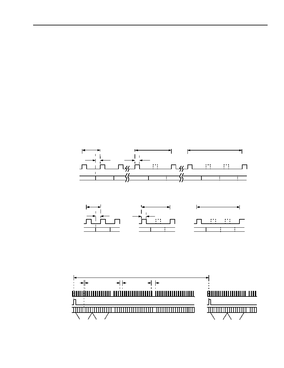
Preliminary Data Sheet
TMXF28155/51 Super Mapper
May 2001
155/51 Mbits/s SONET/SDH x28/x21 DS1/E1
451
Agere Systems Inc.
19 VT/TU Mapper Functional Description
(continued)
s
The first three bits received, following a rising edge of external input pin LOPOHVALIDIN (AB14), defines the
data type on the incoming stream. Data types are defined in
Table 557, Data Type Header Definitions on
page 440
.
s
LOPOH failure is reported in bit VT_LOPOH_FAIL_E (
Table 170
). If an LOPOH failure exists (indicated by
VT_LOPOH_FAIL_E = 1), the incoming data will be ignored. Unless the mask bit VT_LOPOH_FAIL_M
(
Table 174
) is set, VT_LOPOH_FAIL_E = 1 will generate an interrupt.
Figure 46 on pag e453
contains the TX_LOPOH block serial channel format and timing.
19.15 VT Mapper System Interface Timing
19.15.1 VT Mapper DS1/E1 Receive Interface (to System Interface)
Figure 41
and
Figure 42
show the minimum, typical, and maximum gaps of the clock and data out of the VT map-
per for DS1 and E1. An asymmetric VT/TU mapper clock (VTMPR_RCLK)
is derived from an internal 6.48 MHz
clock. The rising edge of this VT mapper clock is delayed by one 6.48 MHz clock cycle with respect to the data
(VTMPR_RDATA) and is one cycle in width.
5-8986(F)r.2
Figure 41. DS1 Mode Gapped Clocking Scheme
5-8987(F)r.2
Figure 42. E1 Mode Gapped Clocking Scheme
Figure 43
and
Figure 44
show a typical frame of VT mapper output. The VT mapper 8 kHz frame sync output
(VTMPR_RFSYNC) is coincident with the DS1 frame-bit position and with the MSB of E1 time slot 0.
Note: The VT mapper 8 kHz frame sync is only transmitted for byte synchronous mappings.
5-8988(F)r.1
* Maximum gap between rising clock edges = 1848 ns.
Figure 43. DS1 Interface
VTMPR_RCLK
VTMPR_RDATA
1232 ns
1848 ns
616 ns
154 ns
154 ns
VTMPR_RCLK
VTMPR_RDATA
462 ns
924 ns
1386 ns
154 ns
154 ns
VTMPR_RCLK
VTMPR_RDATA
VTMPR_RFSYNC
DS0 #1
DS0 #2
F
DS0 #1
DS0 #2
F
125
µ
s
154 ns
616 ns
1232 ns*
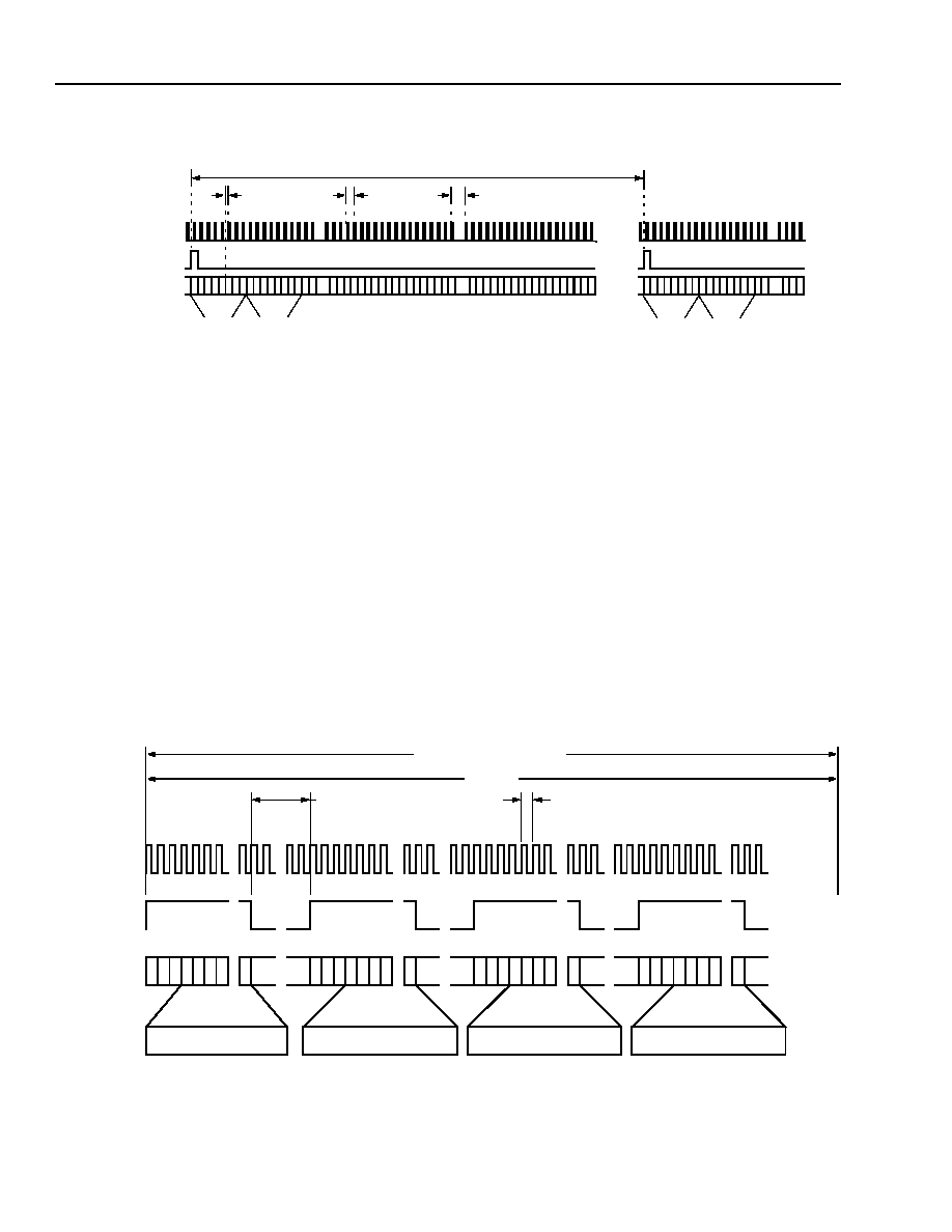
TMXF28155/51 Super Mapper
Preliminary Data Sheet
155/51 Mbits/s SONET/SDH x28/x21 DS1/E1
May 2001
452
Agere Systems Inc.
19 VT/TU Mapper Functional Description
(continued)
5-8989(F)r.1
* Maximum gap between rising clock edges = 1386 ns.
Figure 44. E1 Interface
19.15.2 VT Mapper DS1/E1 Transmit Interface (from System Interface)
The VT mapper input clock and data will meet the timing requirements of G.703, 1.544 MHz ± 50 ppm and
2.048 MHz ± 50 ppm. The VT mapper will accommodate up to ± 200 ppm to allow operation under maintenance or
trouble conditions. The clock edge to retime the data is programmable with VT_TX_CLKEDGE[1--28] bit
(
Table 198
). The receive data is clocked on the rising edge when VT_TX_CLKEDGE[1--28] = 1 and the falling
edge when VT_TX_CLKEDGE[1--28] = 0.
See
VT Mapper Timing on page 45
for VT mapper interface and clock timing numbers.
19.16 VT Mapper Lower-Order Path Overhead Interface Timing
19.16.1 VT Mapper Receive Path Overhead Interface Description
Figure 45
contains the VT mapper receive path overhead serial channel format and timing.
5-8327(F)r.2
Figure 45. VT Mapper Receive Path Overhead Serial Access Channel
VTMPR_RCLK
VTMPR_RDATA
VTMPR_RFSYNC
TS #0
TS #1
TS #1
TS #1
125
µ
s
154 ns
462 ns
924 ns*
TMUX/SPEMPR RDI/REI
VTMPR VT#1--28 V5(MSB≠>LSB)
VTMPR VT#1--28 J2(MSB≠>LSB)
VTMPR VT#1--28 Z6(MSB≠>LSB)
FRAME #1 OF MULTIFRAME
125
µ
s
MINIMUM OF 8 CYCLES
154 ns
LOPOHCLKOUT
LOPOHVALIDOUT
LOPOHDATAOUT
0 0 1
0 1 0
0 1 1
1 0 0
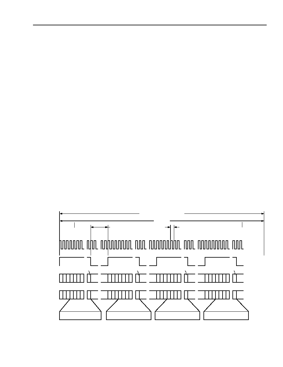
Preliminary Data Sheet
TMXF28155/51 Super Mapper
May 2001
155/51 Mbits/s SONET/SDH x28/x21 DS1/E1
453
Agere Systems Inc.
19 VT/TU Mapper Functional Description
(continued)
The Super Mapper provides access to all necessary functions associated the receive path overhead for each
VT/TU, specifically V5, J2, Z6/N2, Z7/K4, and the O bits. The following features are supported:
s
V5, J2, Z6/N2, Z7/K4, and the O bits, on a per VT basis, will be stored for one complete superframe and transmit-
ted out on external output pin LOPOHDATAOUT (AB17) during the next superframe. REI and RDI values
received from the SPE mapper and TMUX will be stored on a per-frame basis and transmitted during the next
frame. REI and RDI values will be latched during the A1 time of the of the received SONET frame.
s
When operating in unidirectional path switch ring (UPSR) mode (VT_UPSR = 1 (
Table 181
)), REI, RDI and ERDI
values in the V5 and Z7 bytes will be modified based on the receive status. See
Table 557, Data Type Header
Definitions on pag e440
, for automatic generation requirements.
s
Each data type out of LOPOHDATAOUT will be transmitted serially as a burst of 227 bits (VT1.5 mode) or
171 bits (VT2 mode) on the rising edge of the clock, LOPOHCLKOUT, which is driven out on external pin AB15.
The REI and RDI received from the SPE mapper and TMUX will be transmitted serially as a burst of 37 bits on
the rising edged of the clock, LOPOHCLKOUT.
s
The LOPOHVALIDOUT signal (driving external output pin AB18) is set to 1 when valid data is being transmitted.
s
Following transmission of any complete data type LOPOHVALIDOUT is held at 0 for at least eight
LOPOHCLKOUT cycles.
s
The first 3 bits transmitted, following a rising edge of LOPOHVALIDOUT, make up the data type header. Data
type 001 will be the first data type transmitted in each frame. V5, J2, and Z6 are transmitted respectively in the
first frame of the superframe. Z7 and the O bits are transmitted respectively in the second frame of the super-
frame. Note that the LOPOHDATAOUT data types are only transmitted in the first and second frames of the four
frame multiframe.
s
All data types must be transmitted within 500 µs.
19.16.2 VT Mapper Transmit Path Overhead Interface Description
Figure 46
contains the VT mapper transmit path overhead serial channel format and timing.
5-8329(F)r.2
Figure 46. VT Mapper Transmit Path Overhead Serial Access Channel
TMUX/SPEMPR RDI/REI
VTMPR VT#1--28 V5(MSB≠>LSB)
VTMPR VT#1--28 J2(MSB≠>LSB)
VTMPR VT#1--28 Z6(MSB≠>LSB)
FRAME #1 OF MULTIFRAME
125
µ
s
MINIMUM OF 8 CYCLES
154 ns
LOPOHCLKIN
LOPOHVALIDIN
LOPOHDATAIN
LOPOH BITCNT
0 1 2
37
0 1 2
226
0 1 2
226
0 1 2
226
0 0 1
0 1 0
0 1 1
1 0 0

TMXF28155/51 Super Mapper
Preliminary Data Sheet
155/51 Mbits/s SONET/SDH x28/x21 DS1/E1
May 2001
454
Agere Systems Inc.
19 VT/TU Mapper Functional Description
(continued)
The VT mapper transmit path overhead will perform all necessary functions for the low-order path overhead as well
as the REI and RDI values from the internal SPE mapper and TMUX blocks. The following are supported:
s
The interface clocks all incoming signals on the falling edge of external input LOPOHCLKIN (pin AC13).
s
The first 3 bits received, following a rising edge of external input pin LOPOHVALIDIN (AB14), will define the data
type on the incoming stream. Data types are defined in
Table 557, Data Type Header Definitions on page 440
.
s
The source of the external input LOPOHDATAIN (AC14), LOPOHVALIDIN, and LOPOHCLKIN signals is required
to hold the LOPOHVALIDIN at 0 for a minimum of eight LOPOHCLKIN cycles. The VT mapper will monitor the
incoming LOPOHVALIDIN and detect failure conditions. A failure exists if there are less than eight LOPOHCLKIN
cycles between a falling edge of LOPOHVALIDIN and the next rising edge, or if the LOPOH bit count
(LOPOH BITCNT) reaches its maximum count for the active data type and LOPOHVALIDIN does not transition
to 0.
s
LOPOH failure is reported in bit VT_LOPOH_FAIL_E (
Table 170
). If a failure exists (VT_LOPOH_FAIL_E = 1),
the incoming data will be ignored and unless the mask bit, VT_LOPOH_FAIL_M (
Table 174
), is set, the LOPOH
failure will generate an interrupt.
s
The VT mapper logic block will latch new REI and RDI values for the TMUX and SPE mapper during the A1 time
of the SONET/SDH frame.
The timing figures in this section are functional timing diagrams. See
VT Mapper Timing on page 45
for VT mapper
interface and clock timing numbers.

Preliminary Data Sheet
TMXF28155/51 Super Mapper
May 2001
155/51 Mbits/s SONET/SDH x28/x21 DS1/E1
455
Agere Systems Inc.
20 M13/M23 MUX/DeMUX Block Functional Description
Table of Contents
Contents
Page
20 M13/M23 MUX/DeMUX Block Functional Description .................................................................................... 455
20.1 M13 Introduction ..................................................................................................................................... 456
20.2 Features ................................................................................................................................................. 456
20.2.1 M13 Applications .......................................................................................................................... 456
20.3 Block Diagrams ...................................................................................................................................... 457
20.4 M13 Functional Description .................................................................................................................... 460
20.5 M13 Multiplexing Path ............................................................................................................................ 460
20.5.1 M12 Multiplexers .......................................................................................................................... 460
20.5.2 DS1/E1 Interface .......................................................................................................................... 460
20.5.3 Loopback Select .......................................................................................................................... 461
20.5.4 DS1/E1 FIFOs .............................................................................................................................. 461
20.6 DS2 Frame Generation .......................................................................................................................... 461
20.6.1 DS1 Mode .................................................................................................................................... 461
20.6.2 E1 Mode ....................................................................................................................................... 462
20.7 M23 Multiplexer ...................................................................................................................................... 463
20.7.1 DS2 Interface ............................................................................................................................... 463
20.7.2 DS2 Select Logic ......................................................................................................................... 463
20.7.3 Overhead Bit Generation (GR-499) ............................................................................................. 463
20.7.4 M23 Mode ................................................................................................................................... 464
20.7.5 C-Bit Parity Mode ......................................................................................................................... 464
20.7.6 FEAC ........................................................................................................................................... 465
20.7.7 FEBE ............................................................................................................................................ 466
20.7.8 Terminal-to-Terminal Path Maintenance Data Link ..................................................................... 466
20.8 AIS/Idle Insertion .................................................................................................................................... 467
20.9 B3ZS Encoder (GR-499) ........................................................................................................................ 467
20.10 DS3 R-to-T Loopback ........................................................................................................................... 468
20.10.1 DS3 Transmit Path Interface ..................................................................................................... 468
20.11 M13/M23 Demultiplexer ........................................................................................................................ 468
20.11.1 DS3 LOC and LOS .................................................................................................................... 468
20.11.2 DS3 T-to-R Loopback ................................................................................................................ 469
20.11.3 M23 Demultiplexer ..................................................................................................................... 469
20.11.4 M12 Demultiplexers ................................................................................................................... 472
20.11.5 DS1 Mode .................................................................................................................................. 472
20.11.6 E1 Mode ..................................................................................................................................... 473
20.11.7 Output Select Logic .................................................................................................................... 474
Figures
Page
Figure 47. M13 Block Diagram............................................................................................................................. 457
Figure 48. M12 Functional Block Diagram ........................................................................................................... 458
Figure 49. M23 Functional Block Diagram ........................................................................................................... 459
Figure 50. DS3 NSMI Transmit Operation............................................................................................................ 462
Figure 51. DS3 NSMI Receive Operation............................................................................................................. 462
Tables
Page
Table 575. C-Bit Parity Description and Transmit Value ..................................................................................... 465

TMXF28155/51 Super Mapper
Preliminary Data Sheet
155/51 Mbits/s SONET/SDH x28/x21 DS1/E1
May 2001
456
Agere Systems Inc.
20 M13/M23 MUX/DeMUX Block Functional Description
(continued)
20.1 M13 Introduction
The M13 block is a highly configurable multiplexer/demultiplexer. It can operate as an M13 in either the C-bit parity
or M23 mode, a mixed M13/M23, or an M23.
In the C-bit parity mode, the M13 provides a far-end alarm and control (FEAC) code generator and receiver, an
HDLC transmitter and receiver, and automatic far-end block error (FEBE) generation and detection.
Each internal M12 MUX/deMUX and the M23 MUX/deMUX may be configured to operate as independent MUX/
deMUX.
The M13 supports numerous automatic monitoring functions. It can provide an interrupt to the control system, or it
can be operated in a polled mode.
20.2 Features
s
Configurable multiplexer/demultiplexer for up to 28 DS1 signals, 21 E1 signals, or 7 DS2 signals to/from a DS3
signal.
s
M23 or C-bit parity mode operation.
s
Seven configurable independent M12 multiplexer/demultiplexers for up to 28 DS1 signals or 21 E1 signals
to/from 7 DS2 signals.
s
Provisionable time slot selection for DS1, E1, and DS2 insertion or drop.
s
DS3 multiplexer capable of generating alarm indication signal (AIS), remote alarm indicator (RAI), idle, far-end
alarm and control (FEAC), and far-end block error (FEBE) signals.
s
Automatic DS3 receive monitor that detects loss of signal (LOS), bipolar violation (BPV), excessive zeros (EXZ),
out of frame (OOF), severely errored frame (SEF), AIS, RAI, FEAC codes, P-bit parity errors, C-bit parity errors,
and FEBE indications.
s
HDLC transmitter with 128-byte data buffer and HDLC receiver with 128-byte data FIFO for the C-bit parity path
maintenance data link.
s
DS3, DS2, DS1, and E1 loopback and loopback request generation.
s
Complies with T1.102, T1.107, T1.231, T1.403, T1.404, GR-499, G.747, and G.775.
20.2.1 M13 Applications
s
M13 and M23 multiplexers.
s
M13 multiplexers supporting G.747 format.
s
Independent M12 multiplexers.
s
Digital access cross connects (DACS).
s
DS1/E1/DS2 broadcast.

Preliminary Data Sheet
TMXF28155/51 Super Mapper
May 2001
155/51 Mbits/s SONET/SDH x28/x21 DS1/E1
457
Agere Systems Inc.
20 M13/M23 MUX/DeMUX Block Functional Description
(continued)
20.3 Block Diagrams
The following diagram illustrates the high-level interface between M13 block and other functional blocks.
5-9013(F)r.1
Figure 47. M13 Block Diagram
M13 MULTIPLEXER
M13 DEMULTIPLEXER
CROSS
CONNECT
CONTROL INTERFACE
DS
1
X
CL
K
DS
2
A
I
S
CL
K
DS1/E1/DS2
LOOPBACK
DS3
LOOPBACK
E1
X
C
L
K
M13 AUTOAIS
SMPR_TDS3CLK
SMPR_TDS3CLK_EN
M13_DS3CLK
M13_DS3NEG
SMPR_RDS3CLK
SMPR_RDS3CLK_EN
SMPR_DS3NEG_BPV
SPEMPR_AUTOAIS
R
C
BSYN
C
RCB
CL
K
RCB
D
A
T
A
RDL
CL
K
RDL
D
A
T
A
T
C
BSYN
C
TC
B
C
L
K
TC
B
D
A
T
A
TD
L
C
L
K
TD
L
D
A
T
A
SMPR_DS3POS_DAT
M13_DS3POS_DATA
NS
M
I
_
R
E
L
A
T
E
D
D
N
S
M
I
_
R
EL
A
T
ED
DEVICE I/O
DEVICE I/O
SPE
CROSS
CONNECT
DS3
DS1/E1
DS2
MAPPER
DEVICE I/O
M12 DS1 DATA/
M23 DS2 DATA/
M12 DS2 DATA/CLOCK
CLOCK/STFREQ
CLOCK/STFREQ
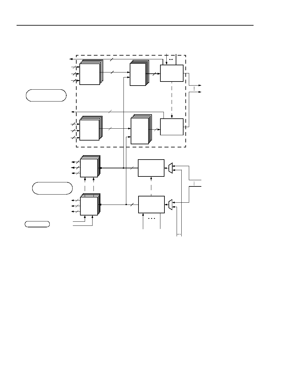
TMXF28155/51 Super Mapper
Preliminary Data Sheet
155/51 Mbits/s SONET/SDH x28/x21 DS1/E1
May 2001
458
Agere Systems Inc.
20 M13/M23 MUX/DeMUX Block Functional Description
(continued)
5-9014(F)r.1
Figure 48. M12 Functional Block Diagram
XC_DS1DATA[1--4]
M12 MUX
#1
DS1XCLK
M12 MUX
#7
DS1/E1
LOC & AIS
MONITOR
#[1--4]
M13_DS1DATA[1--4]
M13_DS1DATA[25--28]
XC_DS1CLK[25--28]
XC_DS1CLK[1--4]
M13_DS1CLK[1--4]
M13_DS1CLK[25--28]
E1XCLK
XC_DS1STFREQ[25--28]
M13_AUTOAIS[1--4]
M13_AUTOAIS[25--28]
XC_DS1STFREQ[1--4]
M13_DS1M12CLK[1--4]
DS1/E1
LOC & AIS
MONITOR
#[25--28]
DS1/E1
LB
SELECT
#[1--4]
M13_DS1M12CLK[25--28]
XC_DS1DATA[25--28]
4
OUTPUT
SELECT
#[1--4]
DS1/E1
OUTPUT
SELECT
#[25--28]
DS1/E1
DS1/E1
LB
SELECT
#[25--28]
M12 DEMUX
#1
XC_DS2DMXCLK[1--7]
XC_DS2M12CLK[1--7]
XC_DS2DMXDATA[1--7]
M13_DS2M12DATA[1--7]
M13_M12DS2DATA[1--7]
DEVICE I/O
DS1/E1 FROM
CROSS CONNECT
DS1/E1 TO
CROSS CONNECT
M12 DEMUX
#7
4
4
4
4
4
4
4
4
4
4
4
4
4
4
4
4
4
4
4
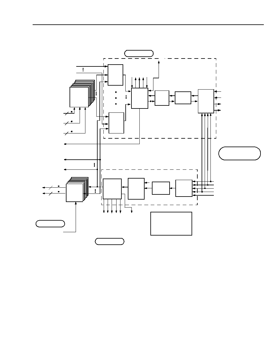
Preliminary Data Sheet
TMXF28155/51 Super Mapper
May 2001
155/51 Mbits/s SONET/SDH x28/x21 DS1/E1
459
Agere Systems Inc.
20 M13/M23 MUX/DeMUX Block Functional Description
(continued)
5-9015(F)
Figure 49. M23 Functional Block Diagram
M13_DS3NEG
SMPR_RDS3NEG_BPV
DS2
SELECT
#1
TC
BD
A
T
A
TD
L
D
ATA
RDL
DA
T
A
RCB
DA
T
A
DS3
LOOP-
BACK
SELECT
DS3
LOOP-
BACK
SELECT
AIS/
IDLE
INSERT
TC
BC
L
K
TC
BS
YN
C
TD
L
C
L
K
RDL
CL
K
R
C
BSYN
C
RCB
CL
K
SMPR_RDS3CLK
SMPR_RDS3CLK_EN
SMPR_TDS3CLK
M23
MUX
B3ZS
ENCODE
SPEMPR_AUTOAIS
M23
DEMUX
B3ZS
DECODE
LOC &
DETECT
LOS
MICROPROCESSOR
INTERFACE AND
REGISTER MAP
M13_M12DS2
D
N
S
M
I
_
R
EL
ATED
DS3
LOOP-
BACK
SELECT
M23
DEMUX
B3ZS
DECODE
DS2 LOC
& AIS
MONITOR
#[1--7]
XC_DS2M23
XC_DS2M23
XC_DS2ST
DS2AISCLK
M13_DS2
M13_DS2
OUTPUT
SELECT
#[1--7]
DS2
M13_DS2M12
M13_DS2M23
SMPR_TDS3CLK_EN
M13_DS3POS_DATA
SMPR_RDS3POS_DATA
DEVICE I/O
DEVICE I/O
DS2
SELECT
#7
7
DEVICE I/O
N
S
M
I
_
R
E
L
AT
ED
7
DATA[1--7]
DATA[1--7]
CLK[1--7]
FREQ[1--7]
CLK[1--7]
DATA[1--7]
DATA[1--7]
CLK[1--7]
7
7
7
DS3 FROM/TO
CROSSCONNECT

TMXF28155/51 Super Mapper
Preliminary Data Sheet
155/51 Mbits/s SONET/SDH x28/x21 DS1/E1
May 2001
460
Agere Systems Inc.
20 M13/M23 MUX/DeMUX Block Functional Description
(continued)
20.4 M13 Functional Description
In the descriptions below, some of the register bits exist for each of the DS1, E1, or DS2 signals. The names of
these register bits have a lower case x or a y suffix to show that there are actually 28 or 7 of them, respectively.
20.5 M13 Multiplexing Path
There are seven M12 multiplexers and one M23 multiplexer on the transmit side of this M13 block and all of them
can operate independently. Twenty-eight DS1 inputs in groups of four, or twenty-one E1 input signals in groups of
three can feed into individual M12 MUXs, while the M23 MUX can take DS2 signals from outputs of M12 MUXs, or
direct DS2 inputs, or loopback deMUXed DS2s.
20.5.1 M12 Multiplexers
M12 multiplexers have four operation modes provisionable through M13_M12_MODEy[1:0] (
Table 263
):
s
M13_M12_MODEy[1:0] = 00: the M12 operates as the first stage of M13 multiplexing. It takes 4 DS1s
(M13_DS1_E1Ny = 1(
Table 263
)) or 3 E1s (M13_DS1_E1Ny = 0) and MUXes into a DS2 signal which will be fed
into the M23 MUX. In this mode, the DS1/E1 clocks are independent inputs to the block. There should be no valid
DS2 input (XC_DS2M23DATAy). This is the default mode.
s
M13_M12_MODEy[1:0] = 01: the M12 operates as an independent multiplexer. It takes 4 DS1s
(M13_DS1_E1Ny = 1) or 3 E1s (M13_DS1_E1Ny = 0) and MUXes into a DS2 signal which will be sent directly to
the DS2 output (M13_DS2M12DATAy) of the block and not be passed to M23 MUX input. In this mode, the
DS1/E1 clocks are independent inputs to the block and a DS2 input clock (XC_DS2M12CLKy) is required.
s
M13_M12_MODEy[1:0] = 10: the M12 operates as an independent multiplexer. It takes 4 DS1s (register bit
M13_DS1_E1Ny = 1) or 3 E1s (register bit M13_DS1_E1Ny = 0) and MUXes into a DS2 signal which will be sent
directly to the DS2 output (M13_DS2M12DATAy) of the block and not be passed to M23 MUX input. In this mode,
the associated DS1/E1 clocks are outputs from the block and derived from the DS2 input clock
(XC_DS2M12CLKy).
s
M13_M12_MODEy[1:0] = 11: the M12 is idle. The output from this M12 multiplexer will be held low.
20.5.2 DS1/E1 Interface
The incoming DS1/E1 clock signals (XC_DS1CLK[28--1]) are first checked for activity or loss of clock (LOC). This
is reported to the microprocessor via bits M13_DS1_LOC[28:1] (
Table 247
). Once LOC is detected, AIS will be
inserted into the associated DS1/E1 channel using the clock from external pins, DS1XCLK/E1XCLK (AD16/AC17)
(
Table 3
).
The incoming DS1/E1 data signals are retimed immediately by the associated clocks. The edge of the clocks that is
used to retime the data is user provisionable to either the rising edge (M13_RDS1_EDGEx = 1 (
Table 264
)) or fall-
ing edge (M13_RDS1_EDGEx = 0).
After being retimed, the incoming data stream is checked for AIS. When the input is DS1, the M13 will declare AIS
if the input data is logic 0 for fewer than 9 out of 8192 clock periods (T1.231). When the input is E1, AIS is declared
if there are less than 3 zeros in each of two consecutive 512-bit periods and cleared when each of two consecutive
512-bit periods contains more than 2 zeros (G.775). If AIS is detected on any of the DS1/E1 inputs
(XC_DS1DATA[28--1]), the associated M13_DS1_AIS_DET[28:1] (
Table 248
) bit is set.

Preliminary Data Sheet
TMXF28155/51 Super Mapper
May 2001
155/51 Mbits/s SONET/SDH x28/x21 DS1/E1
461
Agere Systems Inc.
20 M13/M23 MUX/DeMUX Block Functional Description
(continued)
20.5.3 Loopback Select
DS1/E1 loopback selectors allow DS1 or E1 received within the DS2 or DS3 inputs from the deMUX path to be
looped back. This loopback can be performed automatically if M13_AUTO_FLB (
Table 259
) or M13_AUTO_LB
(
Table 259
) bits are set. Regardless of the state of M13_AUTO_FLB and M13_AUTO_LB, the user can force a DS1
or E1 loopback by setting M13_SEL_DS1_LBx (
Table 264
) to 1.
When M13_AUTO_LB = 1, loopback of channel x is activated if M13_DS1_LB_DETx = 1 (
Table 249
) (see
Section
20.11.4 M12 Demultiplexers on page 472
). In the C-bit parity mode, automatic loopback can also be activated as a
result of receiving a loopback request through the far-end alarm and control (FEAC) channel. Such a request is
indicated by status bit M13_DS1_FEAC_LB_DETx (
Table 251
) (see
Section 20.7.6 FEAC on page 465
). If status
bit M13_DS1_FEAC_LB_DETx = 1 and M13_AUTO_FLB = 1, loopback of channel x is activated.
20.5.4 DS1/E1 FIFOs
When M13_M12_MODEy[1] = 0 (
Table 263
), the 4 selected DS1 or 3 selected E1 signals for each M12 MUX are
fed into single bit 16-word-deep FIFOs that are used to synchronize the selected signals to the DS2 frame genera-
tion clock. The DS2/DS3 transmit clock (XC_DS2M12CLKy) is used to derive the clock source for DS2 frame gen-
eration blocks. In the C-bit parity mode, all DS2 stuff opportunities are used, which produces a nominal 6.306 MHz
DS2 clock. In the M23 mode, the DS2 stuffing ratio is fixed such that the DS2 clock is nominally 6.312 MHz.
The fill level of each FIFO determines the need for bit stuffing its DS1/E1 input. This block allows the M13 to accept
DS1/E1 signals with nominal frequency offsets of ±130 ppm and up to 5 unit intervals peak jitter.
When operating in M13_M12_MODEy[1:0] = 10 mode, the FIFOs are not used.
20.6 DS2 Frame Generation
Each M12 MUX generates a DS2 frame either from 4 DS1 signals multiplexed as specified in T1.107 and GR-499-
CORE when M13_DS1_E1Ny = 1 (
Table 263
), or from 3 E1 signals multiplexed using the format specified in ITU-T
recommendation G.747 when M13_DS1_E1Ny = 0.
When M13_M12_MODEy[1:0] = 01/10 (
Table 263
), each M12 MUX is operating independently. In this case, the
output DS2 signals are retimed by the associated clocks. The edge of the clocks that is used to retime the data is
user provisionable to either the rising edge (M13_DS2M12_EDGEy (
Table 275
) = 1) or falling edge
(M13_DS2M12_EDGEy = 0). The AIS signal can be inserted into any DS2 output by setting
M13_DS2_FORCE_AISy (
Table 271
) to 1.
20.6.1 DS1 Mode
In the DS1 mode, the 4 signals interleaved to generate the y
th
DS2 signal are the outputs from DS1/E1 loopback
selectors 4y ≠ 3, 4y ≠ 2, 4y ≠ 1, and 4y. Bits multiplexed into the second and fourth channels (from selectors 4y ≠ 2
and 4y) are inverted before being interleaved (T1.107) when bit M13_MUXCH2_4_INVy = 1 (
Table 263
).
Loopback requests for a DS1 channel are indicated by inverting the third C bit for that channel (T1.107). This is
done when bit M13_DS1_LB_REQx is set to 1 (
Table 263
). The 4 M13_DS1_LB_REQx bits that affect the y
th
DS2
are 4y ≠ 3, 4y ≠ 2, 4y ≠ 1, and 4y.
The X bit is set to the inverse of the remote alarm indication (RAI) bit (T1.107) M13_DS2_RAI_SENDy (
Table 265
).
For testing purposes, the M frame alignment signal (normally 011) is generated with the last bit inverted (010) if
M13_DS2_MPINVy is set (
Table 267
), and the M-subframe alignment signal (01) is generated as (00) if
M13_DS2_FINVy is set (
Table 268
).

TMXF28155/51 Super Mapper
Preliminary Data Sheet
155/51 Mbits/s SONET/SDH x28/x21 DS1/E1
May 2001
462
Agere Systems Inc.
20 M13/M23 MUX/DeMUX Block Functional Description
(continued)
20.6.2 E1 Mode
In the E1 mode, the 3 signals interleaved to generate the y
th
DS2 signal are the outputs from DS1/E1 loopback
selectors 4y ≠ 3, 4y ≠ 2, and 4y ≠ 1.
Although it is not part of the G.747 standard, loopback requests for an E1 channel can be indicated as in the DS1
mode by inverting the third C bit for that channel. This is done if the M13_DS1_LB_REQx bit is set. The 3
M13_DS1_LB_REQx bits that affect the y
th
DS2 are 4y ≠ 3, 4y ≠ 2, and 4y ≠ 1.
The remote alarm indication (RAI) bit and the reserved bit are set to the value of M13_DS2_RAI_SENDy and
M13_DS2_RSV_SENDy register bits, (
Table 266
) respectively (G.747).
For testing purposes, the frame alignment signal (normally 111010000 as specified in G.747) is generated with the
last bit inverted (111010001) if M13_DS2_FINVy is set, and the parity bit is inverted if M13_DS2_MPINVy is set.
The first parity bit after a 0 to 1 transition of SMPR_BER_INSRT (
Table 65
) is also inverted if M13_DS2_P_BERy is
set to 1 (
Table 269
).
0781(F)
Figure 50. DS3 NSMI Transmit Operation
0782(F)
Figure 51. DS3 NSMI Receive Operation
UNUSED
FRAME BIT
VARIABLE
LINE_TXCLK29
TXDATAEN
TXSYNC (OPTIONAL)
LINE_TXDATA29
DS3POSDATAOUT
UNUSED
FRAME BIT
VARIABLE
LINE_RXCLK29
RXDATAEN
RXSYNC (OPTIONAL)
LINE_RXDATA29
DS3POSDATAOUT

Preliminary Data Sheet
TMXF28155/51 Super Mapper
May 2001
155/51 Mbits/s SONET/SDH x28/x21 DS1/E1
463
Agere Systems Inc.
20 M13/M23 MUX/DeMUX Block Functional Description
(continued)
20.7 M23 Multiplexer
The M23 multiplexer generates a transmit DS3 frame and fills the information bits in the frame with data either from
the 7 DS2 select blocks when M13_NSMI_MODE = 0 (
Table 277
) or from the serial payload input XC_NSMI_DATA
(when M13_NSMI_MODE = 1). It generates the frame using either the SMPR_TDS3CLK or the SMPR_RDS3CLK
input clocks. In the receive loop timing mode (M13_LOOP_TIME = 1 (
Table 259
)), the received clock,
SMPR_RDS3CLK, is selected. Otherwise, SMPR_TDS3CLK is used for DS3 frame generation. SMPR_TDS3CLK
is monitored for loss of clock, which is reported through bit M13_TDS3_LOC (
Table 225
).
The serial data interface, when enabled (M13_NSMI_MODE = 1), generates a clock M13_NSMI_CLK and an
enable M13_NSMI_EN for accepting DS3 payload data XC_NSMI_DATA. A sync pulse, in reference to and ahead
of the first M bit within a DS3 frame, is also generated. The offset from the sync pulse to the first M bit is program-
mable through bits M13_NSMI_SP_OFFSET[7:0] (
Table 261
).
The M23 MUX can be provisioned to operate in either the M23 mode (M13_M23_CBP = 1 (
Table 260
)) or the C-bit
parity mode (M13_M23_CBP = 0).
An unframed all ones data stream is generated if M13_TDS3_FORCE_ALL1 is set to 1 (
Table 276
).
20.7.1 DS2 Interface
The clocks associated with input DS2 signals can be either inputs to the M23 MUX (M13_M23CLK_MODE = 0
(
Table 276
)) or outputs from the M23 MUX (M13_M23CLK_MODE = 1).The incoming DS2 clock signals are
checked for activity or loss of clock (LOC). This is reported to the microprocessor via bits M13_XC_DS2_LOC[7:1]
(
Table 238
). In case LOC is detected, AIS will be inserted into the associated DS2 channel using DS2AISCLK
(pin E10).
The incoming DS2 data signals (XC_DS2M23DATA[7--1]) are retimed immediately by the associated clocks. The
edge of the clocks that is used to retime the data is user provisionable to either the rising edge
(M13_RDS2_EDGEy = 1 (
Table 283
)) or falling edge (M13_RDS2_EDGEy = 0).
After being retimed, the incoming data stream is checked for AIS. The M13 will declare AIS if the input data is 0 for
fewer than 5 clock cycles in each of two consecutive 840 clock periods. The AIS is not cleared until there are more
than 4 zeros in each of two consecutive 840-bit periods (G.775). If AIS is detected on any of DS2 inputs, the asso-
ciated M13_XC_DS2_AIS_DET[7:1] bit is set (
Table 239
).
20.7.2 DS2 Select Logic
The selection of DS2 signal source for each DS2 time slot is controlled by M13_AUTO_LB (
Table 259
),
M13_DS2_LB_DETy (
Table 244
), M13_SEL_DS2_LBy (
Table 282
), and M13_M12_MODEy (
Table 263
) bits.
When M13_AUTO_LB = 1 and M13_DS2_LB_DETy = 1, the DS2 signal from time slot y in the received DS3 signal
is looped back into time slot y of the transmitted DS3 signal (see C-Bit Processing on
page 470
). The user can also
force a loopback by setting M13_SEL_DS2_LBy to 1. DS2 loopback should not be done in the C-bit parity mode.
If a loopback is not active, the DS2 signal selector is controlled by bits M13_M12_MODEy[1:0]. If register bits
M13_M12_MODEy[1:0] = 00, the output of M12 multiplexer y is chosen for the y
th
DS2 time slot in the transmitted
DS3 signal; otherwise, the input DS2 signal XC_DS2M23DATAy is selected for the y
th
DS2 time slot in the transmit-
ted DS3 signal.
20.7.3 Overhead Bit Generation (GR-499)
For testing purposes the F bits, M bits, and P bits can be generated with errors. The frame alignment signal (F-bit
pattern that is normally 1001) is generated with the last bit inverted (1000) if M13_DS3_FINV (
Table 276
) is set.
The multiframe alignment signal (M-bit pattern that is normally 010) is generated as (011) if M13_DS3_MINV
(
Table 276
) is set.

TMXF28155/51 Super Mapper
Preliminary Data Sheet
155/51 Mbits/s SONET/SDH x28/x21 DS1/E1
May 2001
464
Agere Systems Inc.
20 M13/M23 MUX/DeMUX Block Functional Description
(continued)
The parity bits (P bits) are generated as odd rather than the normal even parity if M13_DS3_PINV (
Table 276
) is
set. Both P bits within the first DS3 frame after a 0 to 1 transition of SMPR_BER_INSRT (
Table 65
) are also
inverted if M13_DS3_P_BERy (
Table 277
) is set to 1.
The X bits are set to the inverse of the remote alarm indication (RAI) bit (GR-499) M13_DS3_RAI_SEND
(
Table 277
).
C-bit transmission is a function of whether the M13 MUX/deMUX is in the M23 mode or the C-bit parity mode.
20.7.4 M23 Mode
Please refer to M13_M23_CBP = 1 in
Table 260
.
The information bits in the DS3 frame are drawn from the 7 DS2
select blocks. If M13_M23CLK_MODE = 0 (
Table 276
) and a select block is in the loopback or direct DS2 input
state, the selected DS2 must be synchronized to the DS3 frame generation clock. To do this, the M13 contains
7 DS2 FIFOs each with a depth of 8. The fill level of each FIFO determines the need for bit stuffing its DS2 input.
When M13_M23CLK_MODE = 0 and DS2 select blocks are not in the loopback or direct DS2 input state, the
selected DS2s are generated using the DS3 frame generation clock. In this case, a fixed stuffing ratio is used for
the DS2s in order to produce a nominal 6.312 MHz DS2 clock rate.
When M13_M23CLK_MODE = 1, the FIFOs are not used and DS2 stuff request inputs (XC_DS2STFREQ[7--1])
will determine when stuff bits are needed.
The three C bits in each M-subframe of the DS3 frame are stuff indication bits. If the stuff opportunity bit in an M
subframe is filled by a DS2 bit, the first and second C bits in that M-subframe are transmitted as zeros. If the stuff
opportunity bit in an M-subframe is filled with a stuff bit, the first and second C bits in that M-subframe are transmit-
ted as ones.
The third C bit in each M-subframe is normally transmitted with the same value as the first and second C bits. How-
ever, if M13_DS2_LB_REQy = 1 (
Table 281
), the third C bit is transmitted as the inverse of the first two C bits
(which indicates a loopback request for DS2 channel y).
20.7.5 C-Bit Parity Mode
Please refer to M13_M23_CBP = 0 in
Table 260
.
The M23 MUX can operate in the C-bit parity mode under the fol-
lowing two circumstances:
s
When M13_M23CLK_MODE = 0 and 28 DS1 or 21 E1 signals are being MUXed into the DS3.
s
When M13_M23CLK_MODE = 1 and 7 DS2 signals are being MUXed into the DS3.
In the C-bit parity mode, every DS2 stuffing opportunity is filled with a stuff bit. Because stuffing is not used for syn-
chronization, the selected DS2s cannot come directly from the M13 inputs, and the selected DS2s cannot be
looped back from the M23 demultiplexer. The 21 C bits in each DS3 frame are not required as stuffing indicators.
Their use is described in
Table 575 on page 465
.

Preliminary Data Sheet
TMXF28155/51 Super Mapper
May 2001
155/51 Mbits/s SONET/SDH x28/x21 DS1/E1
465
Agere Systems Inc.
20 M13/M23 MUX/DeMUX Block Functional Description
(continued)
Table 575. C-Bit Parity Description and Transmit Value
20.7.6 FEAC
The third C bit of each DS3 frame provides a far-end alarm and control (FEAC) signal. The use of this signal and
FEAC code words are defined in T1.107 and GR-499-CORE.
When the FEAC signal is not active, it is transmitted continuously as a 1. The user can provision the M13 to trans-
mit continuous ones by setting M13_TFEAC_CTL[1:0] to 00 (
Table 278
).
Active FEAC signals consist of repeating 16-bit code words of the form 0 x5x4x3x2x1x0 0 11111111, where xi can
be a 1 or a 0. The code words are transmitted right to left one bit each DS3 frame for 16 consecutive frames.
Alarm and Status Signals. EAC alarm and status signals should be transmitted continuously for the duration of
the condition being reported, or for a minimum of 10 repetitions of the code word. FEAC signals are transmitted
continuously by setting M13_TFEAC_CTL[1:0] to 01, and M13_TFEAC_CODE[5:0] to x5x4x3x2x1x0 (
Table 278
),
where x5x4x3x2x1x0 is the appropriate value for the alarm or status code word.
Control Signals. EAC control signals are defined for activating or deactivating a loopback. Code words for loop-
back activation, deactivation, and specifying the type of loopback can be transmitted using the same method as
described above for alarm and status signals. Alternatively, the user may provision the M13 to automatically send
the activate or deactivate commands.
In order to activate a loopback, the user may set M13_TFEAC_CTL[1:0] to 11, and M13_TFEAC_CODE[5:0] to
x5x4x3x2x1x0, where x5x4x3x2x1x0 is the appropriate value for the loopback code word. The M13 will then trans-
mit 10 repetitions of the activate code word, 0 000111 0 11111111 followed by 10 repetitions of
0x5x4x3x2x1x0 0 11111111. After transmitting this 40 octet sequence, it will set M13_TFEAC_DONE to 1
(
Table 217
).
In order to deactivate a loopback, the user may set M13_TFEAC_CTL[1:0] to 10, and M13_TFEAC_CODE[5:0] to
x5x4x3x2x1x0, where x5x4x3x2x1x0 is the appropriate value for the loopback code word. The M13 will then trans-
mit 10 repetitions of the deactivate code word, 0 011100 0 11111111, followed by 10 repetitions of
0x5x4x3x2x1x0 0 11111111. After transmitting this 40 octet sequence, it will set M13_TFEAC_DONE to 1.
C-Bit Number
Description
Transmit Value
C1
C-Bit Parity Identification
1.
C2
Network Requirements Bit
If M13_CBIT2_ACT = 0 (
Table 277
), the C2 bit is set to 1.
If M13_CBIT2_ACT = 1, the transmit value of C2 is input
through pin TCBDATA (E12).
C3
Far-End Alarm and Control (FEAC) See FEAC below.
C4--C6,
C16--C21
Unused
If M13_UNUSED_ACT = 0 (
Table 277
), all are transmitted
as 1.
If M13_UNUSED_ACT = 1, the transmit values are input
through pin TCBDATA (E12).
C7--C9
CP Bits (path DS3 parity)
Set to the same value as the P bits.
C10--C12
Far-End Block Error (FEBE) Bits
See
Section 20.7.7 FEBE on page 466
.
C13--C15
Terminal-to-Terminal Data Link
See
Section 20.7.8 Terminal-to-Terminal Path Maintenance
Data Link on page 466
.

TMXF28155/51 Super Mapper
Preliminary Data Sheet
155/51 Mbits/s SONET/SDH x28/x21 DS1/E1
May 2001
466
Agere Systems Inc.
20 M13/M23 MUX/DeMUX Block Functional Description
(continued)
20.7.7 FEBE
C bits 10, 11, and 12 provide a far-end block error (FEBE) indication. Each frame of the received DS3 signal is
checked for errors in the F-bit or M-bit framing sequences and for errors in the CP-bit path parity. If no errors are
found, the FEBE bits are set to 111 in the next transmitted DS3 frame. If one or more errors are detected, the FEBE
bits are transmitted as 000. The user can force the transmission of FEBE error indications by setting
M13_FEBE_ERR to 1 (
Table 277
). This causes all DS3 frames to be transmitted with the FEBE bits set to 000,
regardless of whether or not errors were detected in the received DS3 signal.
20.7.8 Terminal-to-Terminal Path Maintenance Data Link
C bits 13, 14, and 15 can be used as a 28.2 kbit/s data link. If the data link is not used, the user should set
M13_TDL_ACT to 0 (
Table 279
), which causes all ones to be transmitted. When M13_TDL_ACT = 1 and
M13_TDL_NTRNL = 0 (
Table 279
), the data transmitted on this link comes directly from the M13 input pin, pin
TDLDATA (E8). Otherwise (M13_TDL_ACT = 1 and M13_TDL_NTRNL = 1), the data link is controlled by the inter-
nal HDLC transmitter.
HDLC Transmitter. The internal HDLC transmitter circuitry is composed of two 64-byte data buffers (registers
M13_TDL_0DATA_R[0--63] (
Table 298
) and M13_TDL_1DATA_R[0--63] (
Table 299
)), a CRC-16 frame check
sequence (FCS) generator, and control circuits. The HDLC transmitter continually outputs flag bytes (01111110)
with MSB first until the user sets M13_TDL_NTRNL_ACT to 1 (
Table 279
). Following the completion of the next flag
byte, the HDLC transmitter begins transmitting the first byte of the first data buffer (register
M13_TDL_0DATA_R[0]), which should be filled by the user with the first byte of the address field. (For LAPD mes-
sages, this byte contains the service access point identifier, the command/response bit, and a zero extended
address bit.)
Bytes from the data buffer are transmitted least significant bit (LSB) first (GR-499). The HDLC controller inserts a 0
after any sequence of five consecutive ones in the data buffer to prevent the occurrence of a flag pattern prior to the
closing flag.
Buffer Usage. The number of bytes transmitted from the data buffers before completing the frame is controlled as
follows. M13_TDL_BUF0_END (
Table 279
) and M13_TDL_BUF1_END (
Table 279
) are two bits which indicate
whether or not the final buffer byte to be transmitted is currently in buffer 0 or buffer 1. While bytes from buffer 0 are
being transmitted, the HDLC controller checks the value of M13_TDL_BUF0_END bit. If it is 0, all bytes from buffer
0 and at least one byte from buffer 1 are transmitted. If it is 1, bytes from buffer 0 are transmitted sequentially up to
and including byte K, where M13_TDL_BYTE_END[5:0] = K (
Table 280
).
Similarly, the number of bytes transmitted from buffer 1 is controlled by the value of M13_TDL_BUF1_END and
M13_TDL_BYTE_END[5:0] bits. Bytes are transmitted alternately from buffer 0 and buffer 1 until bit
M13_TDL_BUF[0, 1]_END = 1 for the active transmission buffer and the value of bits M13_TDL_BYTE_END[5:0] is
equal to the byte number being transmitted.
When the HDLC controller completes transmission of register M13_TDL_0DATA_R[63] (the last byte of buffer 0),
the interrupt bit M13_TDL_BUF0_INT is set to 1 (
Table 217
). Similarly, the interrupt bit M13_TDL_BUF1_INT
(
Table 217
) is set after the last byte of buffer 1 is transmitted. These bits indicate that the corresponding buffer has
been emptied and is available for refilling.
The user may abort the transmission of an HDLC frame by clearing M13_TDL_NTRNL_ACT to 0 prior to complet-
ing transmission of the last byte from the data buffers. If so, the HDLC controller will stop transmission from the
buffers and send an abort byte (01111111) transmitted MSB first. The abort byte will then be followed by flag bytes
until M13_TDL_NTRNL_ACT is again set to 1, starting transmission of a new frame.

Preliminary Data Sheet
TMXF28155/51 Super Mapper
May 2001
155/51 Mbits/s SONET/SDH x28/x21 DS1/E1
467
Agere Systems Inc.
20 M13/M23 MUX/DeMUX Block Functional Description
(continued)
FCS Generation. Once the last buffer byte is transmitted, the HDLC controller either transmits a closing flag byte
(when M13_TDL_FCS = 0 (
Table 279
)), or it first appends the 2-byte ITU-T FCS with the necessary zero stuffing
before sending the closing flag (when M13_TDL_FCS = 1). In either case, the HDLC controller sets
M13_TDL_DONE (
Table 217
) to 1 after the transmission of the frame is complete. For testing purposes, the user
can send corrupted FCS bytes by clearing M13_TDL_FCS to 0 and filling the last 2 bytes in the buffer with an incor-
rect CRC value.
LAPD Example. T1.107 defines three standard LAPD messages that may be transmitted on the path maintenance
data link. After the opening flag, each of these messages contains 79 bytes of address, control, and information.
These are followed by the 2-byte FCS and the closing flag.
To transmit one of these messages using the internal HDLC transmitter, the microprocessor should first set
M13_TDL_ACT (
Table 279
) to 1, M13_TDL_NTRNL (
Table 279
) to 1, and M13_TDL_NTRNL_ACT (
Table 279
) to
0. This causes the continuous generation of flag bytes.
The microprocessor may then fill buffer 0 with the first 64 bytes of the message and fill bytes 0 through 14 of buffer
1 with the last 15 bytes prior to the FCS of the message. By setting M13_TDL_BUF0_END (
Table 279
) to 0,
M13_TDL_BUF1_END (
Table 279
) to 1, and M13_TDL_BYTE_END[5:0] (
Table 280
) to 001110, the microproces-
sor can indicate that 79 buffer bytes are to be transmitted.
The microprocessor can then set M13_TDL_FCS to 1 and M13_TDL_NTRNL_ACT to 1. This will cause the inter-
nal HDLC transmitter to send the 79 buffer bytes, append the FCS and closing flag, set M13_TDL_DONE to 1, and
resume continuous flag transmission.
If the same LAPD message is to be transmitted later without first having transmitted a different message, the micro-
processor only needs to toggle M13_TDL_NTRNL_ACT to 0 and back to 1, as the values of the other control
parameters and the buffer bytes are not modified by the internal HDLC transmitter.
20.8 AIS/Idle Insertion
The AIS/idle insertion block can be provisioned to operate in the normal mode (M13_DS3_FORCE_AIS = 0
(
Table 276
) and M13_DS3_FORCE_IDLE = 0 (
Table 276
)), generate DS3 AIS (M13_DS3_FORCE_AIS = 1) or
generate DS3 idle (M13_DS3_FORCE_AIS = 0 and M13_DS3_FORCE_IDLE = 1).
In the normal mode, data from the M23 multiplexer is passed unchanged to the B3ZS encoder block.
During AIS insertion (M13_DS3_FORCE_AIS = 1), the generated DS3 frame is altered by overwriting the informa-
tion bits with an alternating 1010 . . . pattern, starting with a 1 after each overhead bit. In addition, the X bits are
overwritten with ones, and the C bits are overwritten with all zeros (T1.107 and T1.404).
During idle signal generation (M13_DS3_FORCE_AIS = 0 and M13_DS3_FORCE_IDLE = 1), the information bits
are overwritten with 11001100 . . ., starting with 11 after each overhead bit. The X bits are overwritten with ones. In
the M23 mode (M13_M23_CBP = 1 (
Table 260
)), the C bits are overwritten with all zeros. In the C-bit parity mode,
the C bits are passed unchanged (T1.107 and T1.404).
20.9 B3ZS Encoder (GR-499)
The transmit DS3 device output can either be in the form of unipolar data (M13_DS3POS_DATA when
M13_BIPOLAR = 0 (
Table 260
)) or positive data, and negative data (M13_DS3POS_DATA, and M13_DS3NEG
when M13_BIPOLAR = 1). If M13_BIPOLAR = 1, the DS3 data is B3ZS encoded with M13_DS3POS_DATA = 1
indicating a positive pulse and M13_DS3NEG = 1 indicating a negative pulse.
The B3ZS encoder block accepts data output from the M23 multiplexer and when M13_BIPOLAR = 1, performs
coding as follows: for each input data bit that is a 1, the encoder outputs a 1 (or pulse) on either its positive or neg-
ative output. The positive or negative output is chosen such that the resulting pulse is opposite in polarity to the last
nonzero output.

TMXF28155/51 Super Mapper
Preliminary Data Sheet
155/51 Mbits/s SONET/SDH x28/x21 DS1/E1
May 2001
468
Agere Systems Inc.
20 M13/M23 MUX/DeMUX Block Functional Description
(continued)
For each input data bit that is a 0, the encoder outputs zeros on both its positive and negative outputs, unless doing
so would cause three consecutive output periods of positive and negative zeros. In the latter case, the three con-
secutive input zeros are output as either [00V] or [B0V], where B is a pulse on either the positive or negative output
that is opposite in polarity to the last non-zero output, and V is a pulse that is the same polarity as the last nonzero
output. The choice of [00V] or [B0V] is made so that the polarity of consecutive V-pulses alternates (which is equiv-
alent to forcing the number of B-pulses between successive V-pulses to be odd).
When M13_BIPOLAR = 1, the user can force errors in the bipolar coding by setting M13_BIPOL_ERR (
Table 258
)
to 1. When this is done, the M13 transmits the next 1 as a bipolar violation.
20.10 DS3 R-to-T Loopback
The received DS3 signal can be looped directly back to the transmit DS3 output. If either M13_LOOP_R_TO_T = 1
(
Table 260
), or both M13_AUTO_FLB = 1 (
Table 259
) and M13_DS3_FLB_DET = 1 (
Table 251
) (see
Section
20.7.6 FEAC on page 465
), the loopback is activated. (During loopback, the SMPR_RDS3POS_DATA and
SMPR_RDS3NEG_BPV input signals are looped to the M13_DS3POS_DATA and M13_DS3NEG outputs, respec-
tively.)
20.10.1 DS3 Transmit Path Interface
When cross connected to the DS3 device pins, the DS3 data out DS3POSDATAOUT (pin R22) and
DS3NEGDATAOUT (pin P22) is clocked out on the falling edge of DS3DATAOUTCLK (pin N22).
If the M13 DS3 interface is optioned for loop timing (M13_LOOP_TIME = 1), the DS3 data is clocked out on the ris-
ing edge of DS3DATAINCLK (pin J22).
20.11 M13/M23 Demultiplexer
20.11.1 DS3 LOC and LOS
SMPR_RDS3CLK is monitored for loss of clock, which is reported through bit M13_RDS3_LOC (
Table 225
). The
user can configure which edge of SMPR_RDS3CLK retimes the data (M13_RDS3_EDGE = 1 (
Table 287
) selects
the rising edge; M13_RDS3_EDGE = 0 selects the falling edge).
The receive DS3 signal is also checked for loss of signal (LOS), which is reported through bit M13_RDS3_LOS
(
Table 225
). An LOS defect, according to T1.231, is the occurrence of 175 ±75 contiguous pulse positions with no
pulses of either positive or negative polarity at the DS3 input. An LOS defect is terminated upon detecting an aver-
age pulse density of at least 33% over a period of 175 ±75 contiguous pulse positions starting with the receipt of a
pulse. An LOS defect will not be terminated if, at the end of the pulse-position interval, any subintervals of 100
pulse positions containing no pulses of either polarity were observed (T1.231).
B3ZS Decoder.
The receive DS3 device input can either be in the form of unipolar clock and data
(SMPR_RDS3CLK and SMPR_RDS3POS_DATA when M13_BIPOLAR = 0 (
Table 260 on pag e216
)) or unipolar
clock, positive data, and negative data (SMPR_RDS3CLK, SMPR_RDS3POS_DATA, and SMPR_RDS3NEG_BPV
when M13_BIPOLAR = 1 and M13_BPV_IN = 0 (
Table 259
)) or unipolar clock, data, and bipolar violation indication
(external input) (SMPR_RDS3CLK, SMPR_RDS3POS_DATA, and SMPR_RDS3NEG_BPV when
M13_BIPOLAR = 0 and M13_BPV_IN = 1). When M13_BIPOLAR = 0, the received DS3 data and clock are
passed directly to the M23 demultiplexer. When M13_BIPOLAR = 0 and M13_BPV_IN = 1, the received DS3 data
and clock are passed to the M23 demultiplexer while the bipolar violation indication is forwarded to the internal BPV
counter for performance monitoring (B3ZS decoder is not used). When M13_BIPOLAR = 1 and M13_BPV_IN = 0,
the received SMPR_RDS3POS_DATA and SMPR_RDS3NEG_BPV data inputs are first B3ZS decoded.

Preliminary Data Sheet
TMXF28155/51 Super Mapper
May 2001
155/51 Mbits/s SONET/SDH x28/x21 DS1/E1
469
Agere Systems Inc.
20 M13/M23 MUX/DeMUX Block Functional Description
(continued)
The B3ZS decoder block performs decoding as follows. For each clock period that both SMPR_RDS3POS_DATA
and SMPR_RDS3NEG_BPV are 0 (no pulse), the decoder outputs a 0. For each clock period that either
SMPR_RDS3POS_DATA or SMPR_RDS3NEG_BPV is 1 (pulse), the decoder determines whether or not the pulse
is part of a zero substitution (ZS) sequence. A ZS sequence is [00V] or [B0V], where B is a pulse on either the pos-
itive or negative input that is opposite in polarity to the last nonzero input, and V is a pulse that is the same polarity
as the last nonzero input.
If the received pulse is not part of a ZS sequence, the decoder outputs a 1. Otherwise, the decoder outputs three
consecutive zeros in place of the received ZS sequence.
The B3ZS decoder also checks for bipolar coding violations. Bipolar coding violations are defined as received
V-pulses that are not opposite in polarity to the last V-pulse or are not immediately preceded by a 0, or received
zeros that are immediately preceded by two other zeros.
The M13 contains a counter that increments on each occurrence of a received bipolar coding violation (BPV). It
also monitors the occurrence of excessive zeros (EXZ), which is defined as any zero string length equal to or
greater than 3 (T1.231). These are part of the performance monitoring counters that can be sampled and simulta-
neously reset (see DS3 Performance Monitors on
page 472
). Their last sampled values are available in registers
M13_BPV_CNT_R[1--3] (
Table 295
) and M13_EXZ_CNT_R[1--3] (
Table 296
).
20.11.2 DS3 T-to-R Loopback
The M13 can be configured to loopback the internal transmit DS3 from the output of the M23 MUX
(M13_LOOP_T_TO_R = 1 (
Table 259
)) or accept the received DS3 signal after B3ZS decoding
(M13_LOOP_T_TO_R = 0) and send it into the M23 deMUX block.
20.11.3 M23 Demultiplexer
The M23 demultiplexer will take the received DS3 signal and either deMUX it into 7 DS2 data streams or strip off
the overhead bits and send payload out through the NSMI serial interface when M13_NSMI_MODE (
Table 277
) =
1.
The serial data interface, when enabled (M13_NSMI_MODE = 1), generates a clock M13_DNSMI_CLK and an
enable M13_DNSMI_EN for outputting DS3 payload data M13_DNSMI_DATA. A sync pulse M13_DNSMI_SYNC,
in reference to and ahead of the first M bit within a DS3 frame, is also generated. The offset from the sync pulse to
the first M bit is programmable through bits M13_D_SP_OFFSET[7:0] (
Table 262
).
In the case of the received DS3 signal being deMUXed into 7 DS2s, those DS2s can be sent out of the device, or
looped back to the transmit side, or passed to M12 demultiplexers for further breakdown into DS1s/E1s.
DS3 Framer. After being B3ZS decoded, the incoming DS3 data stream is checked for the presence of unframed
all ones. If the input data is 0 for fewer than 9 out of 8192 clock periods, bit M13_RDS3_ALL1_DET (
Table 225
) will
be set.
The M23 demultiplexer determines if the input signal contains valid DS3 framing. This is done in two stages by first
finding a bit position that matches the frame alignment pattern (F bits), and then locating the multiframe alignment
signal (M bits). After a matching F-bit sequence is found, in-frame is declared (M13_DS3_OOF = 0 (
Table 224
))
when correct M bits are received for three consecutive M frames (T1.231). The maximum average reframe time is
0.5 ms in the presence of a bit error rate of 10
≠3
.
Once the deMUX is in-frame, the received frame bits are monitored for out-of-frame. Out-of-frame is declared
(M13_DS3_OOF = 1) when too many errors are received in either the F bits (three errors in 16 bits when
M13_DS3_MODE = 0 (
Table 287
), or at least 1 F-bit error in each of
four
consecutive M-subframes when
M13_DS3_MODE = 1) or the M bits (at least 1 error in each of
three
consecutive M frames) (T1.231). For testing
purposes, the user may also force the framer out-of-frame by setting M13_DS3_FORCE_OOF (
Table 258
) to 1.

TMXF28155/51 Super Mapper
Preliminary Data Sheet
155/51 Mbits/s SONET/SDH x28/x21 DS1/E1
May 2001
470
Agere Systems Inc.
20 M13/M23 MUX/DeMUX Block Functional Description
(continued)
The traditional algorithm for declaring out-of-frame (three errors in 16 F bits) results in false out-of-frame approxi-
mately every 30 seconds when the received bit error rate is 10
≠3
. By waiting for four consecutive M-subframes with
F bit errors before declaring out-of-frame (M13_DS3_MODE = 1), the M13 normally stays in frame for over an hour
when the bit error rate is 10
≠3
.
The M13_DS3_LOF (
Table 224
) bit is set if bit M13_DS3_OOF is high continuously for 28 frame periods (approxi-
mately 3 ms). Once set, M13_DS3_LOF is not cleared until M13_DS3_OOF is continuously low for 28 frame peri-
ods.
The user can provision the M13 to automatically output AIS if either bit M13_DS3_OOF = 1 (by setting
M13_AUTO_AIS_OOF (
Table 259
) to 1), or M13_DS3_LOF = 1 (by setting M13_AUTO_AIS_LOF to 1).
The received DS3 frames are also checked for severely errored frames (SEF). An SEF defect is the occurrence of
three or more F-bit errors in 16 consecutive F bits and is reported through bit M13_RDS3_SEF (
Table 225
). An
SEF defect is terminated when the signal is in-frame and there are less than three F-bit errors in 16 consecutive
F bits.
AIS, Idle, and RAI Detection. Each M frame, the 4704 information bits are checked for the presence of the AIS
(1010) or idle (1100) pattern. In order to detect these patterns in the presence of a high error rate, AIS
(M13_DS3_AISPAT_DET = 1 (
Table 224
)) or idle (M13_DS3_IDLEPAT_DET = 1 (
Table 224
)) pattern detection is
declared if fewer than five pattern errors are received in each of two consecutive frames. Once AIS or idle is
declared, these bits are not cleared until at least 16 pattern errors are received in each of 2 consecutive frames
(T1.231).
In addition to the fixed information bit patterns, AIS and idle signals are transmitted with all C bits set to 0 and both
X bits set to 1. These conditions are monitored by the M13 and reported in bits M13_DS3_CBZ_DET (
Table 224
)
and M13_DS3_RAI_DET (
Table 224
).
If every C bit in three consecutive DS3 frames is 0, the M13 sets M13_DS3_CBZ_DET to 1. If the three C bits in a
single M-subframe are all 1, M13_DS3_CBZ_DET is cleared. If both X bits in two consecutive frames are received
as 0, the device sets M13_DS3_RAI_DET to 1. Once M13_DS3_RAI_DET is set, it is not cleared until both X bits
in two consecutive frames are received as 1.
The user may wish to declare AIS or idle based on a combination of some or all of the following bits:
M13_DS3_CBZ_DET, M13_DS3_RAI_DET, and M13_DS3_AISPAT_DET or M13_DS3_IDLEPAT_DET.
C-Bit Processing. The M13 can be provisioned to operate in either the M23 mode (M13_M23_CBP = 1
(
Table 260
)) or the C-bit parity mode (M13_M23_CBP = 0). In the M23 mode, the C bits in each M-subframe are
interpreted as stuff indicator bits, and they are checked for loopback requests. If the third C bit differs from the first
and second C bits in the y
th
M-subframe for 5 successive DS3 frames, M13_DS2_LB_DETy (
Table 244
) is set to 1.
The M13_DS2_LB_DETy bit is cleared when the third C bit does not differ from the first two C bits in subframe y for
five successive DS3 frames.
The first C bit of each frame, C1, provides C-bit parity identification. If for eight consecutive frames it is received as
a 1, the M13 sets M13_DS3_C1_DET (
Table 224
) to 1. Once M13_DS3_C1_DET bit is set, three consecutive
frames with
C1 = 0 must be received before it is cleared.
The RCBDATA (pin E15) output provides access to the received C2, C4, C5, C6, and C16 through C21 C bits. The
received data link bits, C13 through C15, are output as a serial stream on RDLDATA pin (H22).
FEAC. In the C-bit parity mode, the third C bit of each DS3 frame, C3, is monitored for FEAC signals. Active FEAC
signals consist of repeating 16-bit code words of the form 0 x5x4x3x2x1x0 0 11111111, where xi can be a 1 or a 0,
and the bits are received right-to-left. The same code word must be received four consecutive times before it is
accepted.
When a code word is accepted, the action taken by the M13 depends on the value of x5x4x3x2x1x0, which may be
an alarm indication, a loopback activation, or a loopback deactivation.

Preliminary Data Sheet
TMXF28155/51 Super Mapper
May 2001
155/51 Mbits/s SONET/SDH x28/x21 DS1/E1
471
Agere Systems Inc.
20 M13/M23 MUX/DeMUX Block Functional Description
(continued)
The values of M13_DS1_FEAC_LB_DETx and M13_DS3_FLB_DET bits are not changed if an activate or deacti-
vate control signal is accepted, but the next code word to be accepted is not a channel indication control signal
(010011, 011011, or 100001 through 111100).
Alarm, Status, or Unassigned Signals. If a FEAC signal is accepted that is not a loopback activate (000111),
deactivate (011100), or channel indication (010011, 011011, or 100001 through 111100) signal, the M13 will set
bits M13_RFEAC_CODE[5:0] = x5x4x3x2x1x0 and M13_RFEAC_ALM_INT (
Table 217
) to 1.
Control Signals. EAC control signals are defined for activating or deactivating a loopback. If a loopback activate
(000111), deactivate (011100), or channel indication (010011, 011011, or 100001 through 111100) is accepted,
the M13 will set bits M13_RFEAC_CODE[5:0] (
Table 252
) = x5x4x3x2x1x0 and M13_RFEAC_LB_INT (
Table 217
)
to 1.
If a loopback activate (000111), followed by the all-DS1 channels indication (010011) is accepted, the device sets
all M13_DS1_FEAC_LB_DETx (
Table 251
) bits. All M13_DS1_FEAC_LB_DETx bits are cleared if a loopback
deactivate (011100), followed by the all-DS1 channels indication, is accepted.
If a loopback activate (000111), followed by the DS3 indication (011011) is accepted, the device sets the
M13_DS3_FLB_DET (
Table 251
) bit. The M13_DS3_FLB_DET bit is cleared if a loopback deactivate (011100), fol-
lowed by the DS3 indication, is accepted.
Similarly, if the M13 accepts an activate or deactivate control signal followed by a DS1 channel indication (100001
through 111100), it sets or clears the M13_DS1_FEAC_LB_DETx bit, where x is equal to the binary value of
x5x4x3x2x1x0.
Terminal-to-Terminal Path Maintenance Data Link. C bits 13, 14, and 15 can be used as a 28.2 kbit/s data link.
These bits are available directly at device output pin RDLDATA (H22). The M13 also contains an internal HDLC
receiver for processing the received data link bits.
HDLC Receiver. The internal HDLC receiver circuitry is composed of a 128-byte FIFO, a CRC-16 frame check
sequence (FCS) error detector, and control circuits.
The HDLC receiver searches for flag bytes (01111110) and processes the bits received between flag bytes as fol-
lows. The receiver removes zeros that immediately follow any sequence of five consecutive ones. Sequences of
8 bits after zero destuffing are grouped into bytes and written into the FIFO.
As bytes are received, the CRC-16 value, based on the ITU-T polynomial, is calculated. When the closing flag is
received, the receiver checks that the received FCS in the final 2 bytes matches the calculated CRC-16. If
M13_RDL_FCS = 1 (
Table 287
) and the FCS does not match, M13_RDL_FCS_ERR (
Table 253
) is set. If
M13_RDL_FCS = 0, M13_RDL_FCS_ERR is held reset at 0. M13_RDL_FCS bit also determines whether or not
the final 2 bytes of the frame are written into the FIFO. They are written into the FIFO only when
M13_RDL_FCS = 0.
The receiver allows frames to be sent back-to-back with the closing flag of one frame shared as the opening flag of
the next frame. If fewer than three complete destuffed bytes are received between flag bytes, the receiver ignores
the data and writes nothing into the FIFO.
FIFO Usage. The FIFO is large enough to hold one full and two partial standard DS3 LAPD frames of 79 bytes. In
case shorter frames are being transmitted, the M13 can keep track of up to four frames in the FIFO that have not
been read.
The receive data-link frame interrupt bit, M13_RDL_FRM_INT (
Table 217
), is set when a frame closing flag or an
abort byte is received. The M13_RDL_FIFO_UF (
Table 225
) bit is set if the buffer underflows, and the
M13_RDL_FIFO_AF (
Table 225
) bit is set if the buffer reaches a provisionable fill level. The fill level can be set to
16 bytes (M13_RDL_FILL[1:0] = 00 (
Table 287
)), 32 bytes (M13_RDL_FILL[1:0] = 01), 64 bytes
(M13_RDL_FILL[1:0] = 10), or 96 bytes (M13_RDL_FILL[1:0] = 11).
The user may read bytes from the FIFO through register M13_RDL_DATA_R (
Table 254
). The portion of the earli-
est frame still in the FIFO can be deleted by setting M13_RDL_FRM_CLR (
Table 258
) to 1. (This is normally done
to purge a corrupted or aborted frame.) The user must reset M13_RDL_FRM_CLR before another frame can be
deleted. If M13_RDL_FRM_CLR is set before the closing flag of the frame currently being read from the FIFO has
been received, all subsequent bytes of the frame will be discarded without being written into the FIFO.

TMXF28155/51 Super Mapper
Preliminary Data Sheet
155/51 Mbits/s SONET/SDH x28/x21 DS1/E1
May 2001
472
Agere Systems Inc.
20 M13/M23 MUX/DeMUX Block Functional Description
(continued)
Frame Status and Error Reporting. The M13 provides information on the earliest frame still in the FIFO through
status register M13_RHDLC_STATUS_R (
Table 256
).
The status register has 1 bit to indicate whether or not the closing flag (or an abort byte) for the current frame has
been received, 1 bit to indicate if the current frame is corrupted, 5 bits to indicate the size of the current frame mod-
ulo-32, and 1 bit to indicate whether or not there are less than 32 bytes of the earliest frame left in the FIFO.
There are
four
ways in which the M13 can identify that the current frame has been corrupted. The frame may have
been aborted (M13_RDL_ABORT = 1 (
Table 253
)), it may have failed the CRC check
(M13_RDL_FCS_ERR = 1 (
Table 253
)), the number of bits between opening and closing flags may not have been
a multiple of 8 (M13_RDL_NOT_BYTE = 1 (
Table 253
)), or it may have been overwritten before being read from the
FIFO (M13_RDL_OVFL = 1 (
Table 253
)). Also, there is a separate bit M13_RDL_FLAG (
Table 253
) to indicate
whether or not the closing flag (or an abort byte) for the current frame has been received.
The size of the current frame modulo-128 (including FCS bytes only if M13_RDL_FCS = 0 (
Table 287
)) is indicated
by register M13_RDL_FRAME_SIZE_R (
Table 255
).
DS3 Performance Monitors. For performance monitoring purposes, there are a number of error counters in the
M13. All of these internal counters are comprised of a running error counter and a hold register that presents stable
results to the microprocessor. The counts in all of the running counters are latched to the hold registers and the
running counters cleared with the configured internal performance monitor reset signal.
The latched results are then held to be read by the microprocessor. All of the internal counters have the ability to
store more than the maximum possible count in a one second interval for a bit error rate of 10
≠3
. As long as the per-
formance monitor reset occurs at least once every second, no counts will be lost. In case this doesn't happen, all of
the running counters will either hold their maximum value or roll over to zero, depending on the control signal input
SMPR_SAT_ROLLOVER (
Table 67
).
Within the M23 demultiplexer, there are four performance monitoring counters. M13_DS3_FERR_CNT[11:0]
(
Table 289
) increments each time an error is detected in either an F bit or M bit, and M13_DS3_PERR_CNT[13:0]
(
Table 292
) increments if at least one of the P bits disagrees with the parity of the previous frame. In the C-bit parity
mode only, M13_DS3_CPERR_CNT[13:0] (
Table 291
) counts frames with at least two of the three C-bit parity bits
indicating an error, and M13_DS3_FEBE_CNT[13:0] (
Table 290
) accumulates FEBE error indications (1 error indi-
cation for each DS3 frame with at least one FEBE bit equal to zero).
20.11.4 M12 Demultiplexers
Each M12 demultiplexer outputs either 4 DS1 signals from the DS2 frame as specified in GR-499-CORE (when
M13_DS1_E1Ny = 1 (
Table 263
)), or three E1 signals from the DS2 format specified in ITU-T Recommendation
G.747 (when M13_DS1_E1Ny = 0). In the DS1 mode, the demultiplexed second and fourth channels are inverted
before being sent to the output selectors when M13_DEMUXCH2_4_INVy = 1 (
Table 272
).
Each M12 DeMUX can be programmed independently to receive DS2 signal either from M23 deMUX (when
M13_M12DMX_MODEy[1:0] = 00 (
Table 272
)) or direct DS2 input XC_DS2DMXDATAy (when
M13_M12DMX_MODEy[1:0] = 01). In the latter case, an input DS2 clock XC_DS2DMXCLKy is also required.
When M13_M12DMX_MODEy[1:0] = 10/11, the M12 demultiplexer is idle and the outputs are held low.
The DS2 signal is monitored for AIS, which is declared (M13_DS2_AIS_DETy = 1 (
Table 242
)) if the demultiplexer
input is 0 for fewer than five clock cycles in each of two consecutive 840 clock periods, and cleared if there are
more than 4 zeros in each of two consecutive 840-bit periods (G.775).
20.11.5 DS1 Mode
Framer. The M12 demultiplexers determine if the input signal contains valid DS2 framing. This is done in two
stages by first finding a bit position that matches the M-subframe alignment pattern (F bits), and then locating the M
frame alignment signal (M bits). After a matching F-bit sequence is found, in-frame is declared (M13_DS2_OOFy =
0 (
Table 240
)) when correct M bits are received for three consecutive M frames. The maximum average reframe
time is 2.5 ms in the presence of a bit error rate of 10
≠3
.

Preliminary Data Sheet
TMXF28155/51 Super Mapper
May 2001
155/51 Mbits/s SONET/SDH x28/x21 DS1/E1
473
Agere Systems Inc.
20 M13/M23 MUX/DeMUX Block Functional Description
(continued)
Once the deMUX is in-frame, the received frame bits are monitored for out-of-frame. Out-of-frame is declared
(M13_DS2_OOFy = 1) if too many errors are received in either the F bits (two errors in 4 bits when
M13_DS2_MODE = 0 (
Table 274
), or at least one F-bit error in four consecutive M-subframe pairs when
M13_DS2_MODE = 1) or the M-bits (at least one error in three consecutive M frames). For testing purposes, the
user may also force the framer out-of-frame by setting M13_DS2_FORCE_OOFy (
Table 257
) to 1.
The traditional algorithm for declaring out-of-frame (two errors in 4 F bits) results in false out-of-frame approxi-
mately every 5 seconds when the bit error rate is 10
≠3
. By waiting for four consecutive errored M-subframe pairs
(containing 4-F bits) before declaring out-of-frame (M13_DS2_MODE = 1), the M13 normally stays in frame for
over 4four days when the bit error rate is 10
≠3
.
Overhead Processing. The C bits for each DS1 channel are checked for loopback requests. If the third C bit dif-
fers from the first and second C bits in the zth M-subframe for five successive DS2 frames, M13_DS1_LB_DETx
(
Table 249
) is set to 1, where x = (4y ≠ 4 + z). M13_DS1_LB_DETx is cleared when the third C bit does not differ
from the first two C bits in the zth M-subframe for five successive DS2 frames.
If the X bit in four consecutive frames is received as 0, the M13 sets M13_DS2_RAI_DETy (
Table 243
) to 1. Once
M13_DS2_RAI_DETy is set, it is not cleared until the X bit is received as 1 in four consecutive frames.
20.11.6 E1 Mode
Framer. The M12 demultiplexers determine if the input signal contains a valid frame format as specified in ITU-T
recommendation G.747. Frame alignment is declared (M13_DS2_OOFy = 0 (
Table 240
)) when a correct frame
alignment signal is received for three consecutive frames. The maximum average reframe time is 0.5 ms in the
presence of a bit error rate of 10
≠3
. Out-of-frame is declared (M13_DS2_OOFy = 1) if the frame alignment signal
contains at least 1-bit error for four consecutive frames. For testing purposes, the user may also force the framer
out-of-frame by setting M13_DS2_FORCE_OOFy (
Table 257
) to 1.
Overhead Processing. The C bits for each E1 channel are checked for loopback requests. If the third Cz bit differs
from the first and second Cz bits for five successive frames, M13_DS1_LB_DETx (
Table 249
) is set to 1, where
x = (4y ≠ 4 + z). M13_DS1_LB_DETx is cleared when the third Cz bit does not differ from the first two Cz bits for
five successive frames.
If the RAI bit in four consecutive frames is received as 1, the M13 sets M13_DS2_RAI_DETy to 1 (
Table 243
). Once
M13_DS2_RAI_DETy is set, it is not cleared until the RAI bit is received as 0 in four consecutive frames. The
received reserved bit is reported through the M13_DS2_RSV_RCVy (
Table 245
), which is updated only when a
new value is received in four consecutive frames.
Loss of Frame and Automatic AIS Insertion. The M13_DS2_LOFy (
Table 241
) bit is set when M13_DS2_OOFy
is high continuously for 28 DS3 frame periods (approximately 3 ms). Once set, M13_DS2_LOFy is not cleared until
M13_DS2_OOFy is continuously low for 28 DS3 frame periods.
The user can provision the M13 to automatically output AIS if either bit M13_DS2_OOFy = 1 (by setting
M13_AUTO_AIS_OOF to 1), or M13_DS2_LOFy = 1 (by setting M13_AUTO_AIS_LOF to 1).
DS2 Performance Monitors. Within each M12 demultiplexer, there are two performance monitoring counters.
These counters are cleared and read as described above (see DS3 Performance Monitors on
page 472
).
Registers M13_DS2_FERR_CNT[7--1]_R (
Table 294
) count errors in the frame alignment signal. In the DS1
mode, M13_DS2_FERR_CNTy (
Table 294
) increments each time an error is detected in either an F bit or M bit. In
the E1 mode, this counter increments either for each frame alignment signal bit error (when
M13_DS2_FERR_MODE = 0 (
Table 274
)), or once for each frame alignment signal that contains at least one bit
error (when M13_DS2_FERR_MODE = 1).
In the E1 mode only, registers M13_DS2_PERR_CNT[7--1]_R[1--2] (
Table 293
) count errors in P bits.

TMXF28155/51 Super Mapper
Preliminary Data Sheet
155/51 Mbits/s SONET/SDH x28/x21 DS1/E1
May 2001
474
Agere Systems Inc.
20 M13/M23 MUX/DeMUX Block Functional Description
(continued)
20.11.7 Output Select Logic
DS2 Output Selection. The M23 demultiplexer outputs are fed into seven DS2 output selection logic blocks. This
allows the M13 to output the demultiplexed DS2 signals or insert AIS.
Each selector is identified by a number y that ranges from one to seven and corresponds directly to M13 outputs
M13_DS2DATA[7--1]. The outgoing DS2 signals are retimed by an associated clock, M13_DS2CLK[7--1]. The
edge of the clocks that is used to retime the data is provisionable to either the rising edge (M13_TDS2_EDGE = 1
(
Table 294
)) or falling edge (M13_TDS2_EDGE = 0).
The output from each selection block is controlled by the values of bits M13_DS2_OUT_IDLEy (
Table 284
) and
M13_DS2_OUT_AISy (
Table 285
).
s
Output is held low when M13_DS2_OUT_IDLEy = 1; otherwise, the deMUXed DS2 signal is output when
M13_DS2_OUT_AISy = 0 and DS2 AIS is output when M13_DS2_OUT_AISy = 1.
The all ones DS2 AIS signal is also output under all failure conditions at DS3 level which require automatic AIS
insertion at DS2 level.
DS1/E1 Output Selection. The M12 demultiplexer outputs are fed into 28 DS1/E1 output selection logic blocks.
This allows the M13 to output the demultiplexed DS1/E1 (M13_DS1_OUT_AISx = 0 (
Table 273
)), or insert AIS
(M13_DS1_OUT_AISx = 1). The all ones AIS signal is also output under all failure conditions at DS3 or DS2 level
which require automatic AIS insertion at DS1/E1 level.
Each selector is identified by a number x that ranges from 1 to 28 and corresponds directly to a block output
M13_DS1DATA[28--1]. The outgoing DS1 and/or E1 signals are retimed by an associated clock,
M13_DS1CLK[28--1]. The edge of the clock that is used to retime the data is provisionable to either the rising
edge (M13_TDS1_EDGEx = 1 (
Table 272
)) or falling edge (M13_TDS1_EDGEx = 0).
Each output selector number, x can be expressed as either 4y ≠ 3, 4y ≠ 2, 4y ≠ 1, or 4y, where y ranges from 1 to
7. For a given y, the 4 selectors in the group output DS1 signals when M13_OUT_TYPEy = 1 (
Table 272
), or E1
signals when M13_OUT_TYPEy = 0. In either of these modes, the four selectors in the group are controlled by the
2-bit values OUTSELx, where x = 4y ≠ 3, 4y ≠ 2, 4y ≠ 1, and 4y.
When M13_OUT_TYPEy = 0, the output of selector 4y is held low.

Preliminary Data Sheet
TMXF28155/51 Super Mapper
May 2001
155/51 Mbits/s SONET/SDH x28/x21 DS1/E1
475
Agere Systems Inc.
21 28-Channel Framer Block Functional Description
Table of Contents
Contents
Page
21 28-Channel Framer Block Functional Description .......................................................................................... 475
21.1 28-Channel Framer Introduction ............................................................................................................. 479
21.1.1 DS0/E0 Switching Applications .................................................................................................... 479
21.2 Transport Applications ............................................................................................................................ 482
21.3 Framer-to-Line Interface Unit Physical Interface .................................................................................... 485
21.3.1 Line Interface References/Standards .......................................................................................... 485
21.3.2 Frame Formats ............................................................................................................................ 485
21.3.3 Transmit Framer Functions .......................................................................................................... 486
21.3.4 Framing References/Standards ................................................................................................... 486
21.4 DS1 Transparent Framing Format .......................................................................................................... 486
21.5 CEPT 2.048 Basic Frame Structure Transparent Framing Format ........................................................ 487
21.6 Receive Framer Nonalignment Mode (DS1/E1) ..................................................................................... 488
21.6.1 Loss of Frame Alignment Criteria ................................................................................................ 488
21.7 Frame Alignment Criteria ........................................................................................................................ 489
21.8 Receive and Transmit Signaling Processor ............................................................................................ 489
21.8.1 Signaling Introduction and Feature Description ........................................................................... 489
21.8.2 Signaling References/Standards ................................................................................................. 490
21.9 Receive Signaling Per-Link Feature Provisioning .................................................................................. 490
21.9.1 Signaling State Mode Source Selection ....................................................................................... 491
21.9.2 Signaling State Mode Selection ................................................................................................... 491
21.9.3 Signaling Source Selection .......................................................................................................... 491
21.9.4 Signaling Destination Selection ................................................................................................... 492
21.10 Optional Receive Signaling Features Provisioned for Each Link ......................................................... 494
21.10.1 Support of DS1 Robbed-Bit Stomping ....................................................................................... 494
21.10.2 Support of CEPT Time-Slot 16 Stomping .................................................................................. 494
21.10.3 Support of Signaling Debounce ................................................................................................. 494
21.10.4 Support of Japanese Handling Groups ..................................................................................... 494
21.11 Receive Signaling Global Feature Provisioning ..................................................................................... 494
21.11.1 Link Count Selection ................................................................................................................. 495
21.12 Other Receive Signaling Global Features .............................................................................................. 495
21.12.1 Support of Automatic Signaling Freeze on Framing Bit Errors .................................................. 495
21.12.2 Support of Change of Signaling State FIFO .............................................................................. 495
21.13 Receive Signaling Interrupts .................................................................................................................. 496
21.13.1 Maintenance of the Change of Signaling State FIFO Status Bits .............................................. 496
21.13.2 Maintenance of Handling Group Related Status Bits ................................................................ 496
21.14 Transmit Signaling Per-Link Feature Provisioning ................................................................................. 497
21.14.1 Signaling State Mode Source Selection .................................................................................... 497
21.14.2 Signaling State Mode Selection ................................................................................................ 498
21.14.3 Signaling Source Selection ....................................................................................................... 498
21.14.4 Signaling Destination Selection ................................................................................................. 500
21.15 Optional Transmit Signaling Features Provisioned for Each Link .......................................................... 501
21.15.1 Support of Automatic Maintenance of the Time-Slot 16 Remote Frame Alarm ........................ 501
21.15.2 Support of DS1 Robbed-Bit Stomping ....................................................................................... 501
21.15.3 Support of CEPT Time-Slot 16 Stomping .................................................................................. 501
21.15.4 Support of Signaling Debounce ................................................................................................. 501
21.15.5 Support of Japanese Handling Groups ..................................................................................... 501
21.15.6 Support of Zero-Code Suppression ........................................................................................... 501
21.16 Transmit Signaling Global Feature Provisioning .................................................................................... 502
21.16.1 Link-Count Selection ................................................................................................................. 502
21.17 Other Transmit Signaling Global Features ............................................................................................. 502
21.17.1 Support of Automatic Signaling Freeze on Framing Bit Errors .................................................. 502

TMXF28155/51 Super Mapper
Preliminary Data Sheet
155/51 Mbits/s SONET/SDH x28/x21 DS1/E1
May 2001
476
Agere Systems Inc.
21 28-Channel Framer Block Functional Description
(continued)
Table of Contents
(continued)
Contents
Page
21.17.2 Support of Byte Sync SONET Mapping .................................................................................... 502
21.18 Transmit Signaling Status Registers ...................................................................................................... 502
21.18.1 Maintenance of CEPT Related Status Bits ................................................................................ 502
21.19 Performance Monitoring Functional Integration into Superframer ......................................................... 503
21.20 Performance Report Message ............................................................................................................... 506
21.21 Performance Monitoring References/Standards .................................................................................... 508
21.22 Facility Data Link .................................................................................................................................... 508
21.22.1 Facility Data Link References/Standards .................................................................................. 508
21.22.2 Receive Data Link Functional Description ................................................................................. 509
21.22.3
SLC
-96 Superframe Receive Data Link .................................................................................... 509
21.22.4 DDS Receive Data Link Stack ................................................................................................... 509
21.22.5 CEPT; CEPT CRC-4 (100 ms); CEPT CRC-4 (400 ms) Multiframe Sa Bits Receive Stack ..... 510
21.22.6 Receive Data Link Stack Idle Modes ......................................................................................... 511
21.22.7 Receive Data Link Stack Pointer ............................................................................................... 511
21.22.8 Transmit Facility Data Link Functional Description ................................................................... 513
21.22.9
SLC
-96 Superframe Transmit Data Link ................................................................................... 513
21.22.10 DDS Transmit Data Link Stack ................................................................................................ 514
21.22.11 Transmit ESF Data Link Bit-Oriented Messages ..................................................................... 515
21.22.12 CEPT, CEPT Multiframe Transmit Data Link Sa bits Stack .................................................... 515
21.22.13 Transmit Data Link Stack Idle Modes ...................................................................................... 516
21.22.14
SLC
-96, DDS, or CEPT ESF Frame Alignment ...................................................................... 516
21.23 HDLC Functional Description ................................................................................................................. 517
21.24 HDLC Operation .................................................................................................................................... 517
21.24.1 Zero-Bit Insertion/Deletion (Bit Stuffing/Destuffing) ................................................................... 517
21.24.2 Flags .......................................................................................................................................... 517
21.24.3 Aborts ........................................................................................................................................ 518
21.24.4 Receive IDLES .......................................................................................................................... 518
21.24.5 CRC ........................................................................................................................................... 518
21.24.6 HDLC Mode ............................................................................................................................... 519
21.24.7 Receive HDLC Transparent Mode ............................................................................................ 519
21.24.8 Receive HDLC ........................................................................................................................... 519
21.24.9 Receive HDLC Features ........................................................................................................... 519
21.24.10 Transmit HDLC FIFO Features ............................................................................................... 520
21.25 Framer Phase-Lock Loop (PLL) ............................................................................................................. 522
21.25.1 Framer Timing Selection ........................................................................................................... 523
21.26 System Interface .................................................................................................................................... 523
21.26.1 System Interface Introduction .................................................................................................... 523
21.26.2 System Interface References/Standards ................................................................................... 524
21.26.3 Transmit/Receive System Interface Features ........................................................................... 524
21.26.4 Double NOTFAS System Time-Slot (FRM_DNOTFAS (Table 347)) Mode .............................. 524
21.26.5 Transparent Mode ..................................................................................................................... 525
21.26.6 Loopbacks ................................................................................................................................. 525
21.26.7 System AIS ................................................................................................................................ 525
21.26.8 Slip Detection ............................................................................................................................ 526
21.26.9 The Concentration Highway (CHI) Mode .................................................................................. 526
21.26.10 Nominal CHI Timing ................................................................................................................ 526
21.26.11 CHI Timing with CHI Double Time-Slot Timing (CHIDTS) Mode Enabled .............................. 528
21.26.12 CHI Timing with Associated Signaling Mode Enabled ............................................................ 529
21.26.13 ASM 2-Byte Time-Slot Format ................................................................................................ 529
21.26.14 CEPT: Time-Slot 16 Signaling ASM 2-Byte Time-Slot Format ................................................ 530
21.26.15 CHI Offset Programming ......................................................................................................... 530

Preliminary Data Sheet
TMXF28155/51 Super Mapper
May 2001
155/51 Mbits/s SONET/SDH x28/x21 DS1/E1
477
Agere Systems Inc.
21 28-Channel Framer Block Functional Description
(continued)
Table of Contents
(continued)
Contents
Page
21.26.16 The Parallel Bus System Interface Mode ................................................................................ 532
21.26.17 Distributed Stuffing: DS1 ......................................................................................................... 533
21.26.18 Distributed Stuffing: E1 ............................................................................................................ 535
21.26.19 Drive to 3-State and 3-State to Drive Timing ........................................................................... 536
21.27 Serial Multiplex Interface ........................................................................................................................ 536
21.27.1 Signals (6-Pin Mode) ................................................................................................................. 537
21.27.2 Signals (8-Pin Mode) ................................................................................................................. 537
21.27.3 Timing Diagrams ....................................................................................................................... 538
21.27.4 Time-Slot Sequencing ............................................................................................................... 539
21.27.5 Timing Between Transmit and Receive ..................................................................................... 539
21.28 Superframer Host Interface .................................................................................................................... 540
21.28.1 Superframer Register Addressing ............................................................................................. 540
21.29 Superframer Register Addressing .......................................................................................................... 541
21.29.1 Per Link Register Sections in Table 609 ................................................................................... 542
Figures
Page
Figure 52. Switching Application of the Super Mapper ......................................................................................... 479
Figure 53. Super Mapper Switching Configuration ............................................................................................... 480
Figure 54. Super Mapper Switching Mode for Framer in DS0 Interface (Parallel or Serial) Configuration
(The Optional Byte-Synchronous VT Mapping Path Is Shown) .......................................................... 481
Figure 55. Transport Application of the Super Mapper......................................................................................... 482
Figure 56. Super Mapper Transport Configuration ............................................................................................... 483
Figure 57. Super Mapper Transport (with Intrusive Performance Monitoring) Mode
(The Optional Byte-Synchronous VT Mapping Path Is Shown) .......................................................... 484
Figure 58. DS1 Transparent Frame Structure ...................................................................................................... 486
Figure 59. CEPT Transparent Frame Structure ................................................................................................... 487
Figure 60. HG Alignment Algorithm ...................................................................................................................... 497
Figure 61. Rx Data Link Block Diagram ............................................................................................................... 511
Figure 62. Stack Available and Stack Ready Bit Formatting ................................................................................ 512
Figure 63. Tx Data Link Block Diagram................................................................................................................ 516
Figure 64. Receive HDLC Block Diagram ............................................................................................................ 519
Figure 65. Transmit HDLC FIFO Block Diagram .................................................................................................. 520
Figure 66. Framer PLL ......................................................................................................................................... 522
Figure 67. Framer Block Transmit Path Timing Selection .................................................................................... 523
Figure 68. System Loopbacks .............................................................................................................................. 525
Figure 69. CHI Mode of the Transmit System Interface ....................................................................................... 526
Figure 70. Nominal Concentration Highway Interface Timing .............................................................................. 527
Figure 71. CHIDTS Mode Concentration Highway Interface Timing .................................................................... 528
Figure 72. Associated Signaling Mode Concentration Highway Interface Timing ................................................ 529
Figure 73. TCHIDATA and RCHIDATA to CHICK Relationship with FRM_CMS = 0 (CEX = 3 and CER = 4,
Respectively) ....................................................................................................................................... 531
Figure 74. CHI TCHIDATA and RCHIDATA to CHICK Relationship with FRM_CMS = 1
(CEX = 3 and CER = 6, Respectively) ................................................................................................ 532
Figure 75. Parallel Bus System Interface Mode of the Transmit System Interface .............................................. 532
Figure 76. Parallel Bus System Interface Turnaround Timing .............................................................................. 536
Figure 77. Signals (6-Pin Mode) ........................................................................................................................... 537
Figure 78. Signals (8-Pin Mode) ........................................................................................................................... 537
Figure 79. Network Serial Multiplexed Interface (Single Octet)............................................................................ 538
Figure 80. Network Serial Multiplexed Interface (Multiple Octets)........................................................................ 539

TMXF28155/51 Super Mapper
Preliminary Data Sheet
155/51 Mbits/s SONET/SDH x28/x21 DS1/E1
May 2001
478
Agere Systems Inc.
21 28-Channel Framer Block Functional Description
(continued)
Table of Contents
(continued)
Tables
Page
Table 576. Frame Alignment Criteria ................................................................................................................... 489
Table 577. Receive Signaling Link Registers 0--31 Bit Description ................................................................... 491
Table 578. Receive Signaling Link Registers 0--31 G-Bit and F-Bit Description ................................................ 491
Table 579. Receive Signaling Link Registers 0--31 DS1/CEPT/CMI Data ......................................................... 493
Table 580. Receive Signaling Link Registers 0--31 Expected Data ................................................................... 494
Table 581. Signaling Receive Global Register 3, Bit Definition ........................................................................... 495
Table 582. Transmit Signaling Link Registers 0--31 Bit Description .................................................................. 498
Table 583. Transmit Signaling Link Registers 0--31 G-Bit and F-Bit Description ............................................... 498
Table 584. Transmit Signaling Link Registers 0--31 DS1/CEPT/CMI Data ........................................................ 499
Table 585. Transmit Signaling Link Registers 0--31 Expected Data .................................................................. 500
Table 586. Performance Monitor Functional Descriptions ................................................................................... 503
Table 587. Performance Report Message Format .............................................................................................. 507
Table 588. Performance Report Message Field Definition .................................................................................. 507
Table 589. Shared Rx Stack Format for SLC-96 Frames .................................................................................... 509
Table 590. Shared Rx FDL Stack Format for DDS Frames ................................................................................ 510
Table 591. Shared Rx Stack Format for CEPT Frames ...................................................................................... 510
Table 592. Shared Tx FDL Stack Format for SLC-96 Frames ............................................................................ 513
Table 593. Shared Tx FDL Stack Format for DDS Frames ................................................................................. 514
Table 594. Shared Tx Stack Format for CEPT Frame ........................................................................................ 515
Table 595. HDLC Frame Format ......................................................................................................................... 517
Table 596. Performance Report Message Structure ........................................................................................... 521
Table 597. Clock Mode Programming for PLL Mode Device Pins ...................................................................... 522
Table 598. Associated Signaling Mode CHI 2-Byte Time-Slot Format for DS1 Frames ..................................... 529
Table 599. Associated Signaling Mode CHI 2-Byte Time-Slot Format for Stuffed Channels .............................. 530
Table 600. Associated Signaling Mode CHI 2-Byte Time-Slot format for CEPT ................................................. 530
Table 601. Programming Values for FRM_TOFF[2:0] and FRM_ROFF[2:0] when FRM_CMS = 0 .................... 530
Table 602. Programming Values for FRM_TOFF[2:0] when FRM_CMS = 1 ...................................................... 530
Table 603. Programming Values for FRM_ROFF[2:0] when FRM_CMS = 1 ...................................................... 530
Table 604. Parallel System Bus Interface Time-Slot Arrangement for DS1 ........................................................ 534
Table 605. Parallel System Bus Interface Time-Slot Arrangement for E1 ........................................................... 535
Table 606. PSB System I/O Definition ................................................................................................................. 535
Table 607. Serial ID ............................................................................................................................................. 538
Table 608. Current Number of Global and per Link/Channel Registers for Each Block ...................................... 540
Table 609. Framer Addressing Map for the Global and Per Link/Channel Registers of the Superframer ........... 541
Preliminary Data Sheet
TMXF28155/51 Super Mapper
May 2001
155/51 Mbits/s SONET/SDH x28/x21 DS1/E1
479
Agere Systems Inc.
21 28-Channel Framer Block Functional Description
(continued)
21.1 28-Channel Framer Introduction
The next two sections describe the switching and transport mode of the superframer. The framer can be configured
into two basic modes: DS0/E0 switching mode and DS1/E1 transport/monitoring mode.
21.1.1 DS0/E0 Switching Applications
The switching application of the Super Mapper/superframer is shown in
Figure 52
and
Figure 53
. The system inter-
face is either a parallel interface (e.g., system telecom bus interface) or a serial system interface (e.g., CHI) that
transmits or receives framed (channelized) or unframed (unchannelized) DS0/E0 time slots.
In the transmit line direction (Tx, to the mapper), the framer receives data from the DS0/E0 switch through the sys-
tem interface and sends this data (framed or unframed) to the mapper section via the internal DS1 cross connect
block. The data consists of data, clock, and frame sync.
In the receive line direction (Rx), the mapper sends the line data and clock (through the internal DS1 cross con-
nect) to the framer block. The framer then takes this data and transmits it to a DS0/E0 switch through the system
interface. Links provisioned for extended superframe format (ESF) can automatically generate and send perfor-
mance message reports (PRMs) from the Rx path performance monitor through a Tx path HDLC channel assigned
to the facility data link in the transmit line path.
5-8924(F)r.1
Figure 52. Switching Application of the Super Mapper
FRAMER
MAPPER
PM
FRAMER
MAPPER
PM
FRAMER
MAPPER
PM
FRAMER
MAPPER
PM
FRAMER
MAPPER
PM
FRAMER
MAPPER
PM
SUPER MAPPER #1
SUPER MAPPER #1
SUPER MAPPER #2
SUPER MAPPER #2
SUPER MAPPER #3
SUPER MAPPER #3
MAPPER
TELECOM
BUS
STS-3
SYSTEM
INTERFACE
SYSTEM
INTERFACE
DS0/E0
SWITCH
DS0/E0
SWITCH
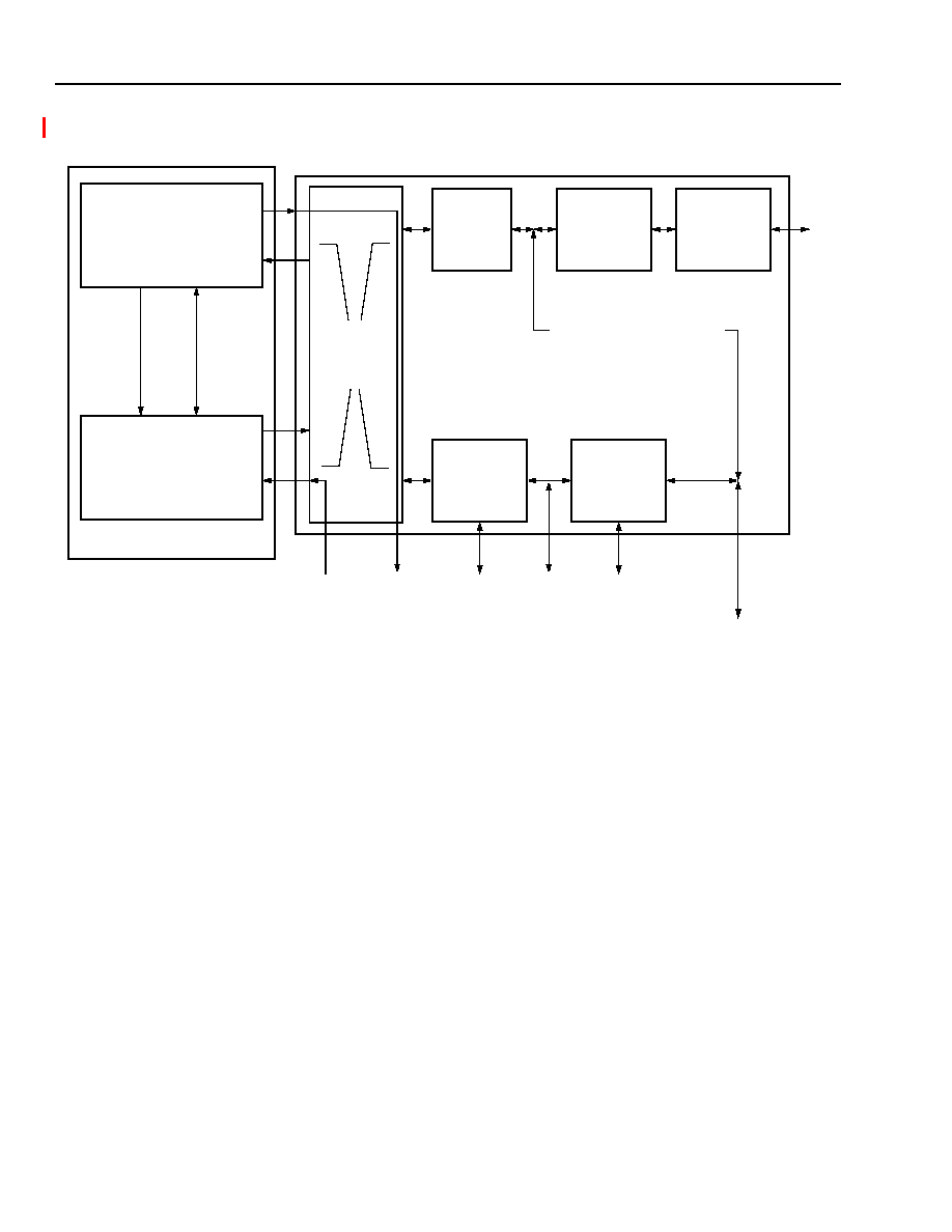
TMXF28155/51 Super Mapper
Preliminary Data Sheet
155/51 Mbits/s SONET/SDH x28/x21 DS1/E1
May 2001
480
Agere Systems Inc.
21 28-Channel Framer Block Functional Description
(continued)
5-9017(F)r.1
Figure 53. Super Mapper Switching Configuration
FRAMER
RECEIVE LINE TO TRANSMIT
SYSTEM PATH
(Rx PATH)
FRAMER RECEIVE SYSTEM
TO TRANSMIT LINE PATH
(Tx PATH)
SUPER MAPPER: FRAMER
FD
L
PR
M
s
L
O
O
PBAC
KS
RFS
1
,
RCLK
1
,
RDATA
28
TFS
1
,
TCLK
1
,
TDATA
28
SYSTEM INTERFACE
DS0 I/O
DS2 I/O
DS3 I/O SONET/SDH DS3
MAPPED I/O
DS3 OR T1/E1 TO STS-1
MAPPED OUTPUT
(HIGH-SPEED TELECOM BUS)
M12
MULTIPLEXER
DS3 MAPPER
8-bit DATA + 1-bit PARITY
VT/VC
MAPPER
VC-4
MULTIPLEXER
STM-1
MULTPLEXER
MAPPER
TO
FRAMER
DS1 CROSS
CONNECT

Preliminary Data Sheet
TMXF28155/51 Super Mapper
May 2001
155/51 Mbits/s SONET/SDH x28/x21 DS1/E1
481
Agere Systems Inc.
21 28-Channel Framer Block Functional Description
(continued)
Figure 54
shows the framer block in a switching application. The framer system interface for the transmit path is
labelled receive and the receive path is labelled transmit. This may seem an error but is chosen based on estab-
lished, historical naming convention.
5-9018(F)
Figure 54. Super Mapper Switching Mode for Framer in DS0 Interface (Parallel or Serial) Configuration (The
Optional Byte-Synchronous VT Mapping Path Is Shown)
V
T
M
APP
ER
:
BYT
E-SYNCHRO
NO
US RO
BBED-B
I
T
S
I
GNA
L
I
N
G RE
CE
I
V
E
D
A
T
A
R
E
C
E
IVE SIG
N
AL
IN
G
D
A
T
A
(T
O
SI
G
N
A
L
IN
G
R
E
G
I
ST
ER
S)
V
T
M
APP
ER
:
BYT
E-SYNCHRO
NO
US RO
BBED-B
I
T
SI
G
N
AL
I
N
G
TR
A
N
SM
IT D
A
T
A
RE
CE
I
V
E
HDL
C
RE
CE
I
V
E
FA
C
I
L
I
T
Y
DA
T
A
L
I
N
K
SU
PER
M
APPER
VT M
A
PPER
IN
T
E
R
F
A
C
E
Rx L
INE
DECODE
R
RE
CE
I
V
E
FR
A
M
E
AL
IG
N
E
R
SI
G
N
AL
I
N
G
PR
O
C
ESSO
R
(E
X
T
RA
CT
I
O
N)
TR
AN
S
M
I
T
SYST
EM
IN
T
E
R
F
A
C
E
TFS
1
, TCL
K
1
, TDA
TA
28
SI
G
N
A
L
I
N
G
P
R
OCE
S
S
OR
(I
NS
ER
T
I
O
N
)
RE
CE
I
V
E
S
YSTE
M
IN
T
E
R
F
A
C
E
T
R
AN
SM
IT
FA
C
I
L
I
T
Y
D
A
T
A
LI
N
K
TR
AN
S
M
I
T
FR
AM
E
FO
R
M
A
T
T
E
R
Tx L
IN
E
ENCODE
R
SU
PER
M
APPER
M1
2
M
U
L
T
IPL
EXER
IN
T
E
R
F
A
C
E
Rx
P
A
T
H
T
x
PAT
H
ESF PR
M
P
A
T
H
TF
S
1
, T
C
L
K
1
, T
D
A
T
A
8
,
T
D
ATA
_
PA
R
I
T
Y
A
1
T
S
I
G
NA
L
I
NG
8
,
T
S
I
G
NA
L
I
NG_
P
A
R
I
T
Y
A
1
RFS
1
, RCL
K
1
, RD
ATA
28
RF
S
1
,
RCL
K
1
, R
D
A
T
A
8
,
R
D
AT
A
_
PA
R
I
T
Y
A
1
R
S
I
G
NA
L
I
NG
8
,
R
S
I
G
NA
L
I
NG_
P
A
R
I
T
Y
A
1
SYSTEM
INT
ER
FA
CE
PARA
LL
EL
DS
0 BU
S
SYSTEM
INT
ER
FA
CE
SER
IAL
DS
0 BU
S
SU
PER
M
APP
ER
:
FR
AM
ER
T
R
AN
SM
IT
SIG
N
AL
IN
G
D
A
T
A
(E
XTR
A
C
T
ED
FR
O
M
SY
STEM
I
N
TER
F
A
C
E
S
O
R
SI
G
N
AL
I
N
G
R
E
G
I
S
T
ER
S)
P
E
R
F
O
RM
A
NCE
MO
N
I
T
O
R
TR
AN
SM
IT
HDL
C
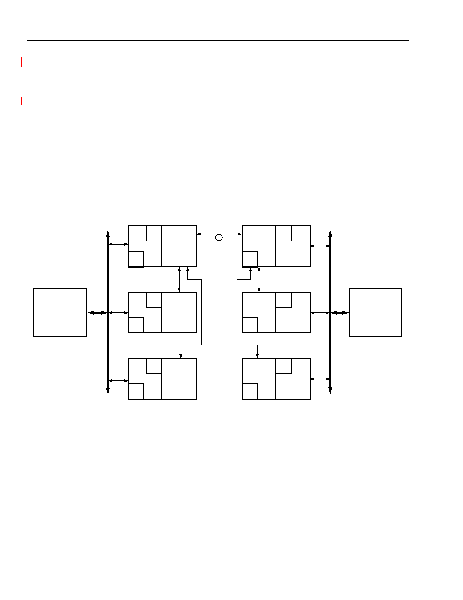
TMXF28155/51 Super Mapper
Preliminary Data Sheet
155/51 Mbits/s SONET/SDH x28/x21 DS1/E1
May 2001
482
Agere Systems Inc.
21 28-Channel Framer Block Functional Description
(continued)
21.2 Transport Applications
The transport application of the Super Mapper is depicted in
Figure 55, Figure 56
, and
Figure 57
. The Super Map-
per interfaces with LIUs at the DS1/E1 rate in this mode. The data is either framed or unframed DS1s. In the trans-
mit path direction (Tx, to the mapper), the framer receives framed or unframed DS1/E1 data from its line interface
and sends this line data and clock (via the DS1 cross connect) to the mapper block. The framer can be provi-
sioned to frame align the data prior to sending it to the mapper section. The framer can be provisioned for perfor-
mance monitoring on the data and in ESF mode transmit PRMs back to its line interface.
In the receive path direction (Rx), the mapper sends the line data and clock (through the DS1 cross connect) to the
framer block. This data may be framed or unframed DS1/E1 data. The framer can be provisioned to frame align
the data and transmit a frame sync signal in addition to the data and clock. The framer can be provisioned for per-
formance monitoring on the data. In ESF mode, it can automatically generate and send PRMs back to the mapper
interface.
5-8925(F)r.1
Figure 55. Transport Application of the Super Mapper
FRAMER
MAPPER
PM
FRAMER
MAPPER
PM
FRAMER
MAPPER
PM
FRAMER
MAPPER
PM
FRAMER
MAPPER
PM
FRAMER
MAPPER
PM
SUPER MAPPER #1
SUPER MAPPER #1
SUPER MAPPER #2
SUPER MAPPER #2
SUPER MAPPER #3
SUPER MAPPER #3
MAPPER
TELECOM
BUS
STS-3
LINE
INTERFACE
LINE
INTERFACE
PM
PM
PM
PM
PM
PM
T1/E1
LINE INTERFACE
UNIT
(T7690 OR T7698)
T1/E1
LINE INTERFACE
UNIT
(T7690 OR T7698)

Preliminary Data Sheet
TMXF28155/51 Super Mapper
May 2001
155/51 Mbits/s SONET/SDH x28/x21 DS1/E1
483
Agere Systems Inc.
21 28-Channel Framer Block Functional Description
(continued)
5-9020(F)r.1
Figure 56. Super Mapper Transport Configuration
FRAMER
DS1 RECEIVE LINE PATH
PERFORMANCE MONITORING
(Rx PATH)
DS1 TRANSMIT LINE PATH
PERFORMANCE MONITORING
(Tx PATH)
SUPER MAPPER: FRAMER
FD
L
PR
M
s
L
O
O
PBA
C
K
S
MAPPER-
TO-
FRAMER I/O
CROSS
CONNECT
VT/VC
MAPPER
VC-4
MULTIPLEXER
STM-1
MULTIPLEXER
8-bit DATA + 1-bit PARITY
DS3
MAPPER
M12
MULTIPLEXER
DS2 I/O
DS3 I/O
SONET/SDH DS3
MAPPED I/O
RLCK
28
,
RPD
28
,
TLCK
28
,
LINE INTERFACE
DS1 I/O
TPD
28
,
TND
28
RND
28
DS3 OR T1/E1 TO STS-1
MAPPED OUTPUT
(HIGH-SPEED TELECOM BUS)
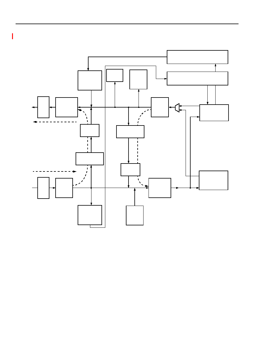
TMXF28155/51 Super Mapper
Preliminary Data Sheet
155/51 Mbits/s SONET/SDH x28/x21 DS1/E1
May 2001
484
Agere Systems Inc.
21 28-Channel Framer Block Functional Description
(continued)
5-9021(F)r.2
Figure 57. Super Mapper Transport (with Intrusive Performance Monitoring) Mode (The Optional Byte-
Synchronous VT Mapping Path Is Shown)
RECEIVE
SIGNALING
PROCESSOR
R
X
SIGNALING DATA
(TO SIGNALING REGISTERS)
RECEIVE
HDLC
RECEIVE
FACILITY
DATA
LINK
RECEIVE
FRAME
ALIGNER
VT MAPPER:
BYTE-SYNCHRONOUS ROBBED-BIT
SIGNALING RECEIVE DATA
VT MAPPER:
BYTE-SYNCHRONOUS ROBBED-BIT
SIGNALING TRANSMIT DATA
SUPER MAPPER
VT MAPPER
INTERFACE
SUPER MAPPER
M12
MULTIPLEXER
INTERFACE
ESF PRM PATH
PERFORMANCE
MONITOR
TRANSMIT
FRAME
FORMATTER
TRANSMIT
HDLC
TRANSMIT
FRAME
FORMATTER
RECEIVE
FRAME
ALIGNER
TRANSMIT
HDLC
PERFORMANCE
MONITOR
ESF PRM PATH
T
X
PATH
SIGNALING
PROCESSOR
TRANSMIT
FACILITY
DATA
LINK
TRANSMIT SIGNALING DATA
SUPER MAPPER: FRAMER
R
X
PATH
T
X
PATH
T
X
LIN
E
E
NCO
DE
R
R
X
LIN
E
DE
CO
DE
R
RL
CK
28
, RP
D
28
, RND
28
TL
C
K
28
, T
P
D
28
, T
N
D
28

Preliminary Data Sheet
TMXF28155/51 Super Mapper
May 2001
155/51 Mbits/s SONET/SDH x28/x21 DS1/E1
485
Agere Systems Inc.
21 28-Channel Framer Block Functional Description
(continued)
21.3 Framer-to-Line Interface Unit Physical Interface
The framer-LIU interface of the Super Mapper framer consists of 28 groups of six connections. The internal DS1
cross connect must be configured to connect the framer-LIU interface through the multifunction system interface to
external T1/E1 line interface devices. The six connections for each framer are TND, TPD, and TLCK driven from the
transmit framer (receive path) and RPD, RND, and RCLK (transmit path) sourced from the external line interface
device. The connections can optionally be from/to the protected switch. See
Table 3 on page 15
for the external pin
names that correspond to the desired six connections.
The line interface may operate in single-rail or dual-rail mode. The default mode of the line encoder is single-rail
(FRM_LD_MODE[2:0] = 000 (
Table 430
), FRM_LE_MODE[2:0] = 000 (
Table 431
)). In this mode, the input signals
are passed transparently through the line encoder.
In single rail mode, the link's framer internal bipolar line encoder/decoder is disabled and monitoring of received
line format violation is accomplished with the use of the RND input. When RND = 1 on the rising edge of RLCK, the
line format violation FRM_BPV[15:0] (
Table 388
) counter increments by one. The link's transmit framer transmits
data via the TPD output pin while TND is forced to a 0 state.
In dual rail mode, the internal line encoder/decoder and monitoring are enabled. The line code may be selected by
provisioning FRM_LD_MODE[2:0] and FRM_LE_MODE[2:0]:
1. Alternate Mark Inversion (AMI).
2. High-Density Bipolar of Order 3--G.703, A.1 (HDB3).
3. Binary 8 Zero Code Suppression--G.703, A.2 (B8ZS).
Line format violations due to excessive zeros will be optionally monitored as follows:
1. B8ZS--8 consecutive zeros cause a violation.
2. HDB3--4 consecutive zeros cause a violation.
21.3.1 Line Interface References/Standards
1. ITU-T Recommendation G.703, Physical/Electrical Characteristics of Hierarchical Digital Interfaces;1991.
2. ANSI T1.403-1995, Network-to-Customer Installation - DS1 Metallic Interface; March 21, 1995.
21.3.2 Frame Formats
The 28 superframers support the following frame formats:
1. DS1 superframe D4.
2. DS1 superframe J-D4 with Japanese remote alarm.
3. DS1 superframe DDS.
4. DS1 superframe
SLC
-96.
5. DS1 extended superframe (ESF).
6. Japanese extended superframe J-ESF (J1 standard with different CRC-6 algorithm).
7. Nonalign DS1 (transparent 193 bits).
8. CEPT basic frame {ITU G.706}.
9. CEPT CRC-4 multiframe with 100 ms timer {ITU G.706}.
10. CEPT CRC-4 multiframe with 400 ms timer (automatic CRC-4/nonCRC-4 equipment interworking) {ITU G.706
Annex B}.
11. Nonalign E1 (transparent 256 bits).
12. 2.048 coded mark inversion (CMI) coded interface (TTC Standards JJ-20.11).
13. 6.312 Mbits/s interface (ITU G.704/NTT J2).
TMXF28155/51 Super Mapper
Preliminary Data Sheet
155/51 Mbits/s SONET/SDH x28/x21 DS1/E1
May 2001
486
Agere Systems Inc.
21 28-Channel Framer Block Functional Description
(continued)
21.3.3 Transmit Framer Functions
1. Transmits alarm indication signal (AIS) to the line automatically and on demand.
2. Transmits AIS-CI to the line automatically and on demand.
3. Transmits remote alarm indication (RAI) to the line automatically and on demand. Conditions for transmitting
RAI include; loss of received frame alignment, CEPT loss of received time slot 0 multiframe alignment, CEPT
CRC-4 timer expiration, CEPT loss of received time slot 16 signaling multiframe alignment, CEPT received Sa6
equals 8, and received Sa6 equals C.
4. Transmits RAI-CI to the line automatically and on demand.
5. Transmits auxiliary test pattern (AUXP) to the line automatically and on demand.
6. Transmits CEPT E bits based received CRC-4 errors.
7. Support the CEPT double not-FAS system mode.
8. Transmits a PRBS test pattern to the line on demand.
9. Transmits line loopback on and off codes to the line on demand (T1.403 section 9.3.1).
10. In transport mode, when not in frame alignment, to optionally send AIS or transparently pass data.
21.3.4 Framing References/Standards
1.
ANSI
T1.403, 1997.
2. ITU-T Recommendation G.703, Physical/Electrical Characteristics of Hierarchical Digital Interfaces; 1991.
3. ITU-T Recommendation G.704, Synchronous Frame Structures used at 1554, 6312, 2048, 8488 and
44736 kbits/s Hierarchical Levels; July 1995.
4. ITU-T Recommendation G.706, Frame Alignment and Cyclic Redundancy Check (CRC) Procedures Relating to
Basic Frame Structures defined in Recommendation G.704; 1991.
5. TTC Standard JT-G704, Synchronous Frame Structures used at 1554, 6312, 2048, 8488 and 44736 kbits/s Hier-
archical Levels; July 1995.
21.4 DS1 Transparent Framing Format
The transmit framer can be programmed to transparently transmit 193 bits of CHI system data to the line.
When configured for transparent framing, the transmit framer extracts from the receive CHI system data bit 8 of
time slot 1 and inserts this bit into the framing bit position of the transmit line data. The other 7 bits of the receive
system time slot 1 are ignored by the transmit framer. The receive framer will extract the framing bit (or 193rd bit) of
the receive line data and insert it into bit 8 of time slot 1 of the CHI system data. The other bits of time slot 1 are set
to 0.
Frame integrity is maintained in both the transmit and receive framer sections.
5-5989(F).ar.1
Figure 58. DS1 Transparent Frame Structur e
TIME-SLOT 1
(STUFF TIME-SLOT)
32 TIME-SLOT CHI FRAME
TIME-SLOT 2
TIME-SLOT 3
TIME-SLOT 31 TIME-SLOT 32
0
0
0
0
0
0
0
F BIT
TRAMSMIT FRAMER'S
193-bit FRAME
DS1 = 125
µ
s
TIME-SLOT 1 TIME-SLOT 2
TIME-SLOT 24
F BIT
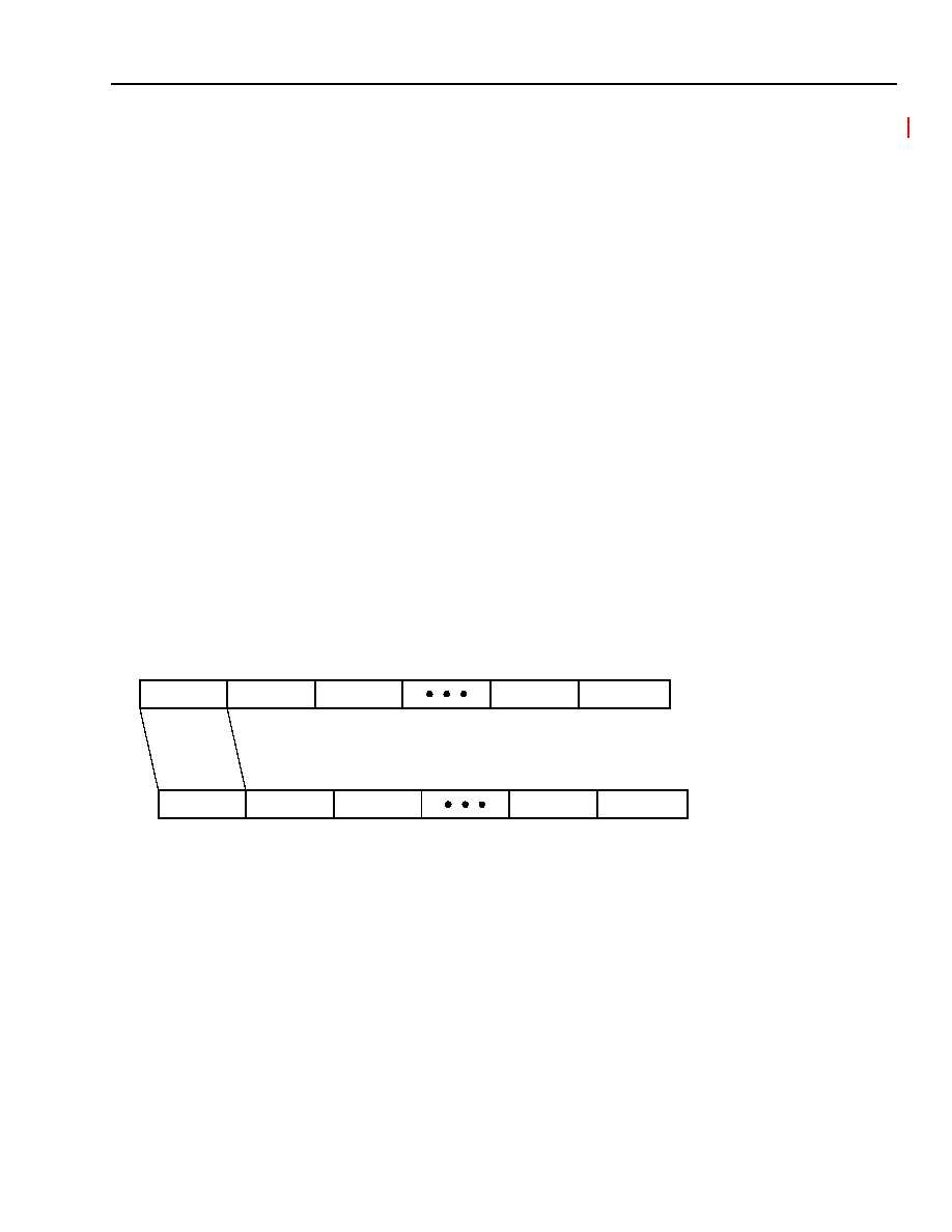
Preliminary Data Sheet
TMXF28155/51 Super Mapper
May 2001
155/51 Mbits/s SONET/SDH x28/x21 DS1/E1
487
Agere Systems Inc.
21 28-Channel Framer Block Functional Description
(continued)
In transparent framing mode 1, the receive framer is forced not to reframe on the receive line data. Other than bipo-
lar violations and unframed AIS monitoring there is no processing of the receive line data. The receive framer will
insert the 193rd bit of the receive line data into bit 8 of time slot 1 of the transmit system data.
Bit 8 of time slot 1 of the receive system interface is inserted as the 193rd data bit into the transmit line data.
Transparent framing mode 1 is selected by setting FRM_LNK_TRANSP (
Table 421
) to 1 and FRM_MODE[3:0]
(
Table 422
) to 1000 (nonalign 193rd bit).
In transparent framing mode 2, the receive framer functions normally on receive line data. All normal monitoring of
receive line data is performed and data is passed to the transmit CHI as programmed. The receive framer will
insert the extracted framing bit of the receive line data into bit 8 of time slot 1 of the transmit system data. The
remaining bits in time slot 1 are set to 0.
Bit 8 of time slot 1 of the receive system interface is inserted in the transmit line framing bit position.
Transparent framing mode 2 is selected by setting FRM_LNK_TRANSP (
Table 421
) to 1 and selecting the appro-
priate framing mode with FRM_MODE[3:0] (
Table 422
).
21.5 CEPT 2.048 Basic Frame Structure Transparent Framing Format
The transmit framer can be programmed to transparently transmit 256 bits of CHI system data to the line. The
transmit framer must be programmed to transparent framing mode 1 .
In transparent mode, the transmit framer transmits all 256 bits of the system payload unmodified to the line. Time
slot 1 of the CHI system interface, determined by the system frame sync signal, is inserted into the FAS/NOTFAS
time slot of the transmit line interface.
Frame integrity is maintained in both the transmit and receive framer sections.
5-5988(F)
Figure 59. CEPT Transparent Frame Structure
In transparent framing mode 1, the receive framer is forced not to reframe on the receive line data. Other than bipo-
lar violations and unframed AIS monitoring, there is no processing of the receive line data. The entire receive line
payload is transmitted unmodified to the CHI.
Transparent framing mode 1 is selected by setting FRM_LNK_TRANSP (
Table 421
) to 1 and FRM_MODE[3:0]
(
Table 422
) to 0000 (non-align 256th bit).
In transparent framing mode 2, the receive framer functions normally on the receive line data. All normal monitoring
of receive line data is performed and data is transmitted to the CHI as programmed.
Transparent framing mode 2 is selected by setting FRM_LNK_TRANSP (
Table 421
) to 1 and selecting the appro-
priate framing mode with FRM_MODE[3:0] (
Table 422
).
TIME-SLOT 1
32 TIME-SLOT CHI FRAME
TIME -SLOT 2 TIME-SLOT 3
TIME-SLOT 31 TIME-SLOT 32
TIME-SLOT 1
32 TIME-SLOT LINE FRAME
TIME-SLOT 2
TIME-SLOT 3
TIME-SLOT 31 TIME-SLOT 32

TMXF28155/51 Super Mapper
Preliminary Data Sheet
155/51 Mbits/s SONET/SDH x28/x21 DS1/E1
May 2001
488
Agere Systems Inc.
21 28-Channel Framer Block Functional Description
(continued)
21.6 Receive Framer Nonalignment Mode (DS1/E1)
In the non-align framing modes the receive frame aligner does not frame to the receive line data. Other than bipolar
violations, AIS, and AUXP monitoring, there is no processing of the receive line data. The entire receive line frame
is given unmodified to the system interface.
21.6.1 Loss of Frame Alignment Criteria
There are two criteria for declaring loss of frame: frame bit errors and CRC errors.
Frame Bit Errors.
1. T1: two frame bit errors out of 4 frame bits (F
T
and F
S
bits checked).
2. T1: two frame bit errors out of 5 frame bits (F
T
and F
S
bits checked).
3. T1: two frame bit errors out of 6 frame bits (F
T
and F
S
bits checked).
4. T1: three frame bit errors out of 12 frame bits--DDS only (F
T
, F
S
, and time slot 24 F bits).
5. T1: two frame bit errors out of 4 frame bits (only F
T
bits checked).
6. T1: two frame bit errors out of 5 frame bits (only F
T
bits checked).
7. T1: two frame bit errors out of 6 frame bits (only F
T
bits checked).
8. T1: four frame bit errors out of 12 frame bits--DDS only (F
T
, F
S
and time slot 24 FAS pattern).
9. E1: three consecutive incorrect frame alignment signals.
10. E1: three consecutive incorrect frame alignment signals or three consecutive incorrect non-FAS frames as indi-
cated by bit 2 in time slot 0 in frames not containing the frame alignment signal.
11. E1: 3 consecutive incorrect FAS or non-FAS frames.
12. 2.048 Mbits/s CMI: 2 consecutive missing code rule violations (CRVs).
CRC Errors.
The use of CRC errors to declare loss of frame is optional. CRC errors are monitored in the performance monitor
block.
In DS1 mode, ESF, and J-ESF formats only, N or more CRC-6 errors in a 1 second interval results in loss of frame
alignment. N is provisionable. N defaults to 320 in DS1 mode.
In CEPT mode N, or more, CRC-4 errors in a 1 second interval results in loss of frame alignment. N is provision-
able. N defaults to 915 in CEPT modes.

Preliminary Data Sheet
TMXF28155/51 Super Mapper
May 2001
155/51 Mbits/s SONET/SDH x28/x21 DS1/E1
489
Agere Systems Inc.
21 28-Channel Framer Block Functional Description
(continued)
21.7 Frame Alignment Criteria
Table 576
describes the frame alignment criteria for the formats supported by the superframer.
Table 576. Frame Alignment Criteria
21.8 Receive and Transmit Signaling Processor
21.8.1 Signaling Introduction and Feature Description
The signaling processor, which is duplicated in the receive and transmit paths, moves signaling data to and from
the following interfaces:
s
T1/E1/J1/CMI line interface
s
System interface
s
VT mapper interface
s
Host interface
The following frame types are supported when processing signaling to and from the line interface (no special provi-
sioning is needed for the signaling processor to distinguish between these frame types):
s
DS1: ESF; J-ESF; D4; J-D4 (2-, 4-, or 16-state mode)
s
CEPT Basic Frame; CEPT CRC-4 (100 ms); CEPT CRC-4 (400 ms)
s
CMI
Frame Format
Alignment Procedure
SF
Frame alignment is established when six consecutive error-free superframes are
received. Only the F
T
framing bits are checked (36 bits checked).
D4 and J-D4
Frame alignment is established when six consecutive error-free superframes are
received (72 bits checked in D4, 66 bits checked in J-D4).
DDS
Frame alignment is established when six consecutive error-free frames are
received (42 bits checked: F
T
, F
S
, and time slot 24).
SLC
-96
The F
T
frame position is established when four consecutive error-free superframes
are received (24 F
T
bits checked). After establishing the F
T
frame position,
SLC
-96
superframe alignment is established on the first valid F
S
sequence of
000111000111. All the while the F
T
frame position must remain error free.
ESF and J-ESF
Frame alignment is established when three consecutive error-free superframes are
received (18 bits checked).
CEPT Basic Frame
Uses the strategy outlined in G.706 paragraph 4.1.2.
CEPT CRC-4 100 ms Timer
Uses the strategy outlined in G.706 paragraphs 4.1.2 and 4.2.
CEPT CRC-4 400 ms Timer
Uses the strategy outlined in G.706 paragraph 4.1.2 and ANNEX B.
2.048 Mbits/s CMI Coded
Interface
Frame alignment is established on the first detection of the CRV violation. Multi-
frame alignment is achieved the first time the 01111111 multiframe alignment pat-
tern is detected.

TMXF28155/51 Super Mapper
Preliminary Data Sheet
155/51 Mbits/s SONET/SDH x28/x21 DS1/E1
May 2001
490
Agere Systems Inc.
21 28-Channel Framer Block Functional Description
(continued)
The following system bus modes are supported (no special provisioning is needed for the signaling processor to
distinguish between these system bus modes):
s
Parallel system bus
s
CHI bus in ASM mode
The VT mapper interface in the signaling processor supports VT1.5, VT 2 byte sync mapping, as well as VC-11
byte sync mapping using handling groups.
The host can read the signaling data extracted from the line, system, or VT mapper interface at any time. The
transmit signaling processor can be configured so that the host provides the signaling data to be forwarded to the
line, system, or VT mapper interface.
Other signaling features include:
s
Debounce on all signaling data extracted from the line interface or the VT mapper interface.
s
Host interrupt upon change of signaling state in the receive path.
s
Signaling extraction inhibit based on frame alignment and framing bit errors.
s
Stomping of DS1 robbed-bit signaling positions.
s
Support of zero-code suppression on the line interface in the transmit path.
s
Superframe signaling integrity. No signaling data transmitted will be a mix of old and new due to a mid super-
frame update of signaling information.
21.8.2 Signaling References/Standards
s
ITU Rec. G.704 10/98 CEPT Multiframe Signaling Structure
s
ITU Rec. G.775 10/98 CEPT TS16 AIS Detection, Remote Alarm Detection
s
ITU Rec. G.732 1998 CEPT Time-Slot 16 mfa, Time-Slot 16 rfa
s
ITU Rec. O.162 10/92 CEPT Time-Slot 16 rfa Detection
s
T1.403 1995 Robbed-Bit Signaling
s
TTC JJ-20.11 CMI Coded Interface
s
ANSI
T1.105 SONET Payload Mapping
s
Telcordia
GF-253-CORE SONET Transport Systems
s
ITU Rec G.707 10/98 Network Node Interface for SDH
s
TTC JT G.704 Japanese Synchronous Frame Structures
21.9 Receive Signaling Per-Link Feature Provisioning
The receive signaling processor requires the provisioning of four items for each link in order to enable signaling
extraction and delivery:
1. Signaling state mode source (host or Rx CHI interface).
2. Signaling state mode (2-, 4-, and 16-state mode or no-signaling).
3. Signaling source (receive line, VT mapper, or host interface).
4. Signaling destination (transmit system or transmit line interface).
Preliminary Data Sheet
TMXF28155/51 Super Mapper
May 2001
155/51 Mbits/s SONET/SDH x28/x21 DS1/E1
491
Agere Systems Inc.
21 28-Channel Framer Block Functional Description
(continued)
21.9.1 Signaling State Mode Source Selection
The signaling state mode source is selected by programming FRM_R_FGSRC in
Table 374, FRM_RSLR33,
Receive Signaling Link Register 33 (R/W) on page 269
, bit 2. The typical application will select the host for pro-
gramming the state mode. If so, the host will have to program the state mode for all of the time slots on each of the
links. The default state mode selected is 16-state signaling.
It is possible for the state mode to be set by the values received on the CHI bus by the receive system interface. In
this mode, the signaling processor will constantly monitor those values and update the state mode for each of the
time slots on each link.
21.9.2 Signaling State Mode Selection
The signaling state mode for each time slot is selected by programming bits 5 and 6 of FRM_RSLR0--
FRM_RSLR31, Receive Signaling Link Registers 0--31 (R/W) in
Table 372 on page 268
for each link. The bit defi-
nition for each of those 32 registers is shown below.
Table 577. Receive Signaling Link Registers 0--31 Bit Description
The signaling state mode definitions are shown in the table below.
Table 578. Receive Signaling Link Registers 0--31 G-Bit and F-Bit Description
The signaling state mode for DS1 type links should be set to match the function of each time slot. The signaling
state mode does not apply to CEPT type links and the value must be kept in the reset state which is 00. The signal-
ing state mode for CMI type links must be set to 11.
The 16-state mode, which is the state mode selected out of reset, can be used on SF type DS1 links in order to
detect a toggle code. In this case, signaling will be collected over two superframes and stored as a 4-bit code.
When programming the state mode for each time slot, the host can also program the D, C, B, and A bits in the
same register. Doing this will determine the default code forwarded to the transmit system or the transmit line inter-
face before the first valid signaling code has been extracted from the receive line or VT mapper interface.
Each of the links and time slots is completely independent from one another with respect to the signaling state
mode selection. Any combination is acceptable.
21.9.3 Signaling Source Selection
The signaling source is selected by programming FRM_R_SIGSRC in
Table 374, FRM_RSLR33, Receive Signal-
ing Link Register 33 (R/W) on page 269
, bits [1:0]. If the source selected is the receive line interface, the receive
signaling processor will start extracting data from the receive line and store valid signaling codes into the D, C, B,
and A locations of FRM_RSLR0--FRM_RSLR31, Receive Signaling Link Registers 0--31 (R/W),
Table 372 on
page 268
for each of the links.
The receive signaling processor will automatically determine the link type and extract the correct signaling bit posi-
tions from each link. The receive signaling processor can simultaneously service any combination of CEPT, DS1,
and CMI type links. The receive signaling processor will extract robbed-bit signaling from DS1 links, common chan-
nel signaling from CEPT links, and time slot 0 signaling from CMI links compliant with the following standards.
Bit 6
Bit 5
Bit 4
Bit 3
Bit 2
Bit 1
Bit 0
G
F
--
D
C
B
A
G and F
Signaling State Mode Selected
00
16 state (reset state)
01
4 state
10
no signaling
11
2 state

TMXF28155/51 Super Mapper
Preliminary Data Sheet
155/51 Mbits/s SONET/SDH x28/x21 DS1/E1
May 2001
492
Agere Systems Inc.
21 28-Channel Framer Block Functional Description
(continued)
s
ITU Rec G.704 10/98 CEPT multiframe signaling structure
s
T1.403 1995 robbed-bit signaling
s
TTC JJ-20.11 CMI coded interface
If the VT mapper is transporting byte sync mapped DS1 links into SONET frames, then the signaling source should
be set to VT mapper interface. In that case, the receive signaling processor will start collecting valid signaling
codes from the VT mapper and store them into the D, C, B, and A locations of FRM_RSLR0--FRM_RSLR31,
Receive Signaling Link Registers 0--31 (R/W),
Table 372 on page 268
for each of the links.
If the VT mapper is the source of signaling, data will be extracted based on the standards listed below.
s
ANSI
T1.105SONET payload mapping
s
Bellcore
GF-253-CORE SONET transport systems
s
ITU Rec G.707 10/98 network node interface for SDH
If the VT mapper is transporting byte sync mapped CEPT links into SONET frames, then the signaling source
should be set to the receive line interface. In that case, the receive signaling processor will extract the entire time
slot 16 multiframe and store that information into FRM_RSLR0--FRM_RSLR31, receive signaling link registers
0--31 (R/W) for each of the links.
If the signaling source is set to be the host, the host may write to FRM_RSLR0--FRM_RSLR31, receive signaling
link registers 0--31 (R/W) and those values will be forwarded to the selected destination. The host mode can also
be used to manually freeze signaling. When the source is switched from receive line to host, for example, the exist-
ing signaling codes will be held until modified by the host or until the signaling source is switched back to the
receive line interface. If the host mode is used to manually freeze signaling, then the signaling debounce feature
must be enabled. To enable signaling debounce set FRM_R_SIGDEB in
Table 374, FRM_RSLR33, Receive Sig-
naling Link Register 33 (R/W) on page 269
, bits 5 to 1.
Each of the links is completely independent from one another with respect to the signaling source selection. Any
combination of receive line, VT mapper, and host is acceptable.
21.9.4 Signaling Destination Selection
There are three destinations for the signaling extracted from the receive line or VT mapper interface:
1. Transmit system interface.
2. Transmit line interface.
3. FRM_RSLR0--FRM_RSLR31, receive signaling link registers 0--31 (R/W),
Table 372 on page268
.
The signaling extracted from the receive line or VT mapper interface will automatically be delivered to the transmit
system interface when the framer section of the Super Mapper is programmed for switch mode. This is done by set-
ting FRM_SW_TRN in FRM_SFGR1, Superframer Global Register 1 (R/W),
Table 301 on pag e243
, bits 15 to 1.
The system interface will need to be configured for ASM mode in order for the signaling to be transmitted on the
PSB or CHI buses. ASM mode is controlled by FRM_SYSGR1, System Interface Global Register 1 (R/W),
Table 347 on page257
bit 11.
The signaling extracted from the VT mapper interface can be inserted into the transmit line interface when the
framer section of the Super Mapper is programmed for transport mode. This is done by setting FRM_SW_TRN in
FRM_SFGR1, Superframer Global Register 1 (R/W),
Table 301 on page243
, bits 15 to 0, and by setting
FRM_R_SIGI in
Table 374, FRM_RSLR33, Receive Signaling Link Register 33 (R/W) on page 269
, bit 8 to 1. The
signaling will be inserted based on the programming of state modes of each time slot.
The receive signaling processor cannot provide data to the transmit system and the transmit line interface on differ-
ent links simultaneously.
Signaling extracted from the VT mapper or receive line interface will always be available in FRM_RSLR0--
FRM_RSLR31, Receive Signaling Link Registers 0--31 (R/W),
Table 372 on page268
for each link. The host can
read these registers regardless of whether or not the signaling is forwarded to the transmit system or transmit line
interface. Receive Signaling Link Registers 0--31 DS1/CEPT/CMI Data,
Table 577 on page 491
shows the position
of the data in those 32 registers for each of the receive line formats.

Preliminary Data Sheet
TMXF28155/51 Super Mapper
May 2001
155/51 Mbits/s SONET/SDH x28/x21 DS1/E1
493
Agere Systems Inc.
21 28-Channel Framer Block Functional Description
(continued)
Table 579. Receive Signaling Link Registers 0--31 DS1/CEPT/CMI Data
For CEPT links, the entire time slot 16 multiframe is stored in FRM_RSLR0--FRM_RSLR31, receive signaling link
registers 0--31 (R/W),
Table 372 on page268
. The spare bits X[2:0] and the time slot 16 remote frame alarm Y bit
are stored in RSLR0. When time slot 16 multiframe alignment is lost, X[2:0] will automatically be set to 111 and the
Y bit will be set to 0.
The format of the data stored in FRM_RSLR0--FRM_RSLR31, Receive Signaling Link Registers 0--31 (R/W),
Table 372 on page 268
also depends on the signaling state mode selected for each time slot as shown in
Table 580
.
RSLR Address
RSLR Bit[6:0] (DS1)
RSLR Bit[6:0] (CEPT)
RSLR Bit[6:0] (CMI)
0
--
000 X0 Y X1 X2
--
1
GF0 DCBA (Channel 1)
000 DCBA (Channel 1)
110 DCBA (Channel 1)
2
GF0 DCBA (Channel 2)
000 DCBA (Channel 2)
110 DCBA (Channel 2)
3
GF0 DCBA (Channel 3)
000 DCBA (Channel 3)
110 DCBA (Channel 3)
4
GF0 DCBA (Channel 4)
000 DCBA (Channel 4)
110 DCBA (Channel 4)
5
GF0 DCBA (Channel 5)
000 DCBA (Channel 5)
110 DCBA (Channel 5)
6
GF0 DCBA (Channel 6)
000 DCBA (Channel 6)
110 DCBA (Channel 6)
7
GF0 DCBA (Channel 7)
000 DCBA (Channel 7)
110 DCBA (Channel 7)
8
GF0 DCBA (Channel 8)
000 DCBA (Channel 8)
110 DCBA (Channel 8)
9
GF0 DCBA (Channel 9)
000 DCBA (Channel 9)
110 DCBA (Channel 9)
10
GF0 DCBA (Channel 10)
000 DCBA (Channel 10)
110 DCBA (Channel 10)
11
GF0 DCBA (Channel 11)
000 DCBA (Channel 11)
110 DCBA (Channel 11)
12
GF0 DCBA (Channel 12)
000 DCBA (Channel 12)
110 DCBA (Channel 12)
13
GF0 DCBA (Channel 13)
000 DCBA (Channel 13)
110 DCBA (Channel 13)
14
GF0 DCBA (Channel 14)
000 DCBA (Channel 14)
110 DCBA (Channel 14)
15
GF0 DCBA (Channel 15)
000 DCBA (Channel 15)
110 DCBA (Channel 15)
16
GF0 DCBA (Channel 16)
--
--
17
GF0 DCBA (Channel 17)
000 DCBA (Channel 17)
110 DCBA (Channel 17)
18
GF0 DCBA (Channel 18)
000 DCBA (Channel 18)
110 DCBA (Channel 18)
19
GF0 DCBA (Channel 19)
000 DCBA (Channel 19)
110 DCBA (Channel 19)
20
GF0 DCBA (Channel 20)
000 DCBA (Channel 20)
110 DCBA (Channel 20)
21
GF0 DCBA (Channel 21)
000 DCBA (Channel 21)
110 DCBA (Channel 21)
22
GF0 DCBA (Channel 22)
000 DCBA (Channel 22)
110 DCBA (Channel 22)
23
GF0 DCBA (Channel 23)
000 DCBA (Channel 23)
110 DCBA (Channel 23)
24
GF0 DCBA (Channel 24)
000 DCBA (Channel 24)
110 DCBA (Channel 24)
25
--
000 DCBA (Channel 25)
110 DCBA (Channel 25)
26
--
000 DCBA (Channel 26)
110 DCBA (Channel 26)
27
--
000 DCBA (Channel 27)
110 DCBA (Channel 27)
28
--
000 DCBA (Channel 28)
110 DCBA (Channel 28)
29
--
000 DCBA (Channel 29)
110 DCBA (Channel 29)
30
--
000 DCBA (Channel 30)
110 DCBA (Channel 30)
31
--
000 DCBA (Channel 31)
110 DCBA (Channel 31)

TMXF28155/51 Super Mapper
Preliminary Data Sheet
155/51 Mbits/s SONET/SDH x28/x21 DS1/E1
May 2001
494
Agere Systems Inc.
21 28-Channel Framer Block Functional Description
(continued)
Table 580. Receive Signaling Link Registers 0--31 Expected Data
If the state mode is 4 state or 2 state, then the unused bits will be set to 0.
21.10 Optional Receive Signaling Features Provisioned for Each Link
21.10.1 Support of DS1 Robbed-Bit Stomping
The DS1 robbed-bit positions of voice time slots will be set to 1 in the payload when FRM_R_RXSTOMP in
FRM_RSLR33, Receive Signaling Link Register 33 (R/W),
Table 374 on page 269
, bit 7 is set to 1. The robbed-bit
positions in the payload will be stomped; however, the signaling will be transmitted untouched by the system inter-
face.
21.10.2 Support of CEPT Time Slot 16 Stomping
Stomping of time slot 16 for CEPT links is enabled in the system interface block.The Super Mapper can also be
configured to transmit AIS on the system bus in time slot 16 when the signaling block loses time slot 16 alignment.
The configuration bits related to these two features are located in the FRM_SYSLR2, System Interface Link Regis-
ter 2 (R/W),
Table 419 on page 294
. When using these features, the signaling codes forwarded to the transmit sys-
tem bus will continue to reflect the contents of FRM_RSLR0--FRM_RSLR31, Receive Signaling Link Registers
0--31 (R/W),
Table 372 on pag e268
.
21.10.3 Support of Signaling Debounce
If programmed to do so, the signaling extracted from the selected source will be debounced. This implies that a
valid signaling code would have to be detected twice before it is updated in FRM_RSLR0--FRM_RSLR31, Receive
Signaling Link Registers 0--31 (R/W),
Table 372 on page268
. This feature is enabled by setting FRM_R_SIGDEB
in FRM_RSLR33, Receive Signaling Link Register 33 (R/W),
Table 374 on page269
, bit 5.
21.10.4 Support of Japanese Handling Groups
If the signaling is transported by the VT mapper within four handling groups compliant to the Japanese standard,
TTC JT G.704, then FRM_R_HGEN in FRM_RSLR33, Receive Signaling Link Register 33 (R/W),
Table 374 on
page 269
, bit 4 must be set to 1. The signaling state mode must be set to either 2 state or no-signaling when using
handling groups.
If the signaling transported by the VT mapper uses handling groups, then the status of the handling group align-
ment can be transmitted across the system interface. The transmission of this status is enabled by setting
FRM_R_TSAISHG in FRM_SGR1, Receive Signaling Global Register 1 (R/W),
Table 359 on page 262
, bits 15 to
1. This mode forces the signaling data for the channels contained in each handling group to 1 if HG alignment has
not been achieved by the receive signaling processor. For example, if HG2 is unaligned then the A bit for time slots
2, 6, 10, 14, 18, and 22 forwarded to the system would be forced to 1.
21.11 Receive Signaling Global Feature Provisioning
The receive signaling processor requires the provisioning of one global item in order to enable signaling extraction
and delivery.
s
Link count (number of active receive links).
Signaling State Mode
Bit 6
Bit 5
Bit 4
Bit 3
Bit 2
Bit 1
Bit 0
16 state
0
0
0
D
C
B
A
4 state
0
1
0
0
0
B
A
2 state
1
1
0
0
0
0
A

Preliminary Data Sheet
TMXF28155/51 Super Mapper
May 2001
155/51 Mbits/s SONET/SDH x28/x21 DS1/E1
495
Agere Systems Inc.
21 28-Channel Framer Block Functional Description
(continued)
21.11.1 Link Count Selection
The link count is specified by programming FRM_R_LINKCNT[4:0] in FRM_SGR1, receive signaling global register
1 (R/W),
Table 359 on page262
, bits [14:10]. The reset value is 28, which is appropriate for a 28 link DS1 applica-
tion. A value of 21 is appropriate for a 21 link CEPT application. If the application mixes DS1 and CEPT links or the
TDM clock supplied to the framer section is less than 51.84 MHz, this value should match the terminal count set in
FRM_FGR2, framer global register 2 (R/W),
Table 306 on page246
, bits [7:0].
21.12 Other Receive Signaling Global Features
21.12.1 Support of Automatic Signaling Freeze on Framing Bit Errors
By default, signaling extraction from a particular link will halt when the appropriate alignment has been lost. In order
to guarantee that signaling freeze takes place as soon as possible, FRM_R_AFZFBE in FRM_SGR1, Receive Sig-
naling Global Register 1 (R/W),
Table 359 on pa ge262
, bit 1 must set to 1. When enabled, FRM_R_AFZFBE halts
signaling extraction for 32 frames upon detection of a frame bit error. This configuration bit is applicable to DS1,
CEPT, and CMI type frames and for signaling extracted from the receive line or the VT mapper interface. When
FRM_R_AFZFBE is enabled, the receive signaling debounce feature must also be enabled. The FRM_R_SIGDEB
feature is enabled in FRM_RSLR33, Receive Signaling Link Register 33 (R/W),
Table 374 on pag e269
, bit 5.
21.12.2 Support of Change of Signaling State FIFO
Signaling can be terminated in the framer section of the Super Mapper by polling FRM_RSLR0--FRM_RSLR31,
Receive Signaling Link Registers 0--31 (R/W),
Table 372 on page 268
for each link. An alternative method is to
enable the operation of a signaling change of state FIFO. In doing so, the host will be interrupted when there have
been signaling state changes which need to be processed. In order to enable the operation of the signaling change
of state FIFO, set FRM_R_SCOSEN in FRM_SGR2, Receive Signaling Global Register 2 (R/W),
Table 360 on
page 262
, bit 15 to 1.
The FIFO is located at signaling receive global register 3. The word read by the host has the following format.
Table 581. Signaling Receive Global Register 3, Bit Definition
The data read by the host indicates the link number (L[4:0]), time slot number (TS[4:0]) and the signaling informa-
tion for a time slot whose value has changed. The word read by the host will also indicate whether or not the entry
is valid (V = 1) and whether or not there are more entries yet to be read (M = 1). A word with V set to 0 indicates
that the FIFO is empty. The signaling code presented will reflect the associated GF value programmed by the host.
The unused signaling bits will be set to 0. For example, if the time slot is programmed for 4-state signaling, the D
and C bits will be set to 0. The A and B bit will identify the valid signaling code.
This feature can be used in combination with any other feature (i.e., debounce).
When the change of state FIFO is enabled, the host will be interrupted when one of two conditions is satisfied. If
the number of entries in the FIFO exceed the threshold programmed by the host or if there are valid entries to be
processed and the signaling interrupt timer has expired, then the host will be interrupted.
The host sets the FIFO depth threshold by programming FRM_R_SCOSDTH[9:0] in FRM_SGR2, Receive Signal-
ing Global Register 2 (R/W), bits [9:0]. The depth of the FIFO is 672, which is sufficient to store an entry for every
time slot processed by the 28-link framer. The timer interval is selected by programming FRM_R_SCOSTTH[15:0]
in FRM_SGR3, Receive Signaling Global Register 3 (R/W),
Table 361 on page 263
, bits [15:0]. The timer incre-
ments are 125 µs and the maximum interval possible is 8 s. The default setting for the depth and timer threshold is
0, which results in the host being interrupted whenever an entry is made into the FIFO.
If the FIFO overflows, the processor will immediately be interrupted. The current contents of the FIFO will be lost
however, subsequent entries will be stored normally.
The host can poll the change of state FIFO without the use of interrupts.
Bit 15 Bit 14 Bit 13 Bit 12 Bit 11 Bit 10 Bit 9 Bit 8 Bit 7 Bit 6 Bit 5 Bit 4 Bit 3 Bit 2 Bit 1 Bit 0
M
V
L4
L3
L2
L1
L0
TS4
TS3
TS2
TS1
TS0
D
C
B
A

TMXF28155/51 Super Mapper
Preliminary Data Sheet
155/51 Mbits/s SONET/SDH x28/x21 DS1/E1
May 2001
496
Agere Systems Inc.
21 28-Channel Framer Block Functional Description
(continued)
21.13 Receive Signaling Interrupts
There are three interrupts which are maintained in the receive signaling processor, which are located in
FRM_SGR7, receive signaling global register 7 (R/W),
Table 365 on page264
. The three interrupts reflect the sta-
tus of the change of signaling state FIFO. These interrupt bits can be reset based on a clear-on-read protocol,
which is provisioned in the Super Mapper global registers.
s
Threshold overflow interrupt. This bit is set to 1 when the programmed threshold for the FIFO capacity has been
exceeded.
s
Interrupt timer interrupt. This bit is set to 1 when the programmed interrupt timer has expired and there are valid
entries in the FIFO to be processed.
s
FIFO overflow interrupt. This bit is set to 1 when the FIFO overflows.
There are mask bits associated with each of the three interrupt status bits which are located in FRM_SGR7,
receive signaling global register 7 (R/W).
21.13.1 Maintenance of the Change of Signaling State FIFO Status Bits
There is one bit which reflects the status of the change of signaling state FIFO. The location of this status bit is in
FRM_SGR5, receive signaling global register 5 (RO),
Table 363 on page263
.
s
FIFO depth threshold overflow status. This bit is set to 1 when the programmed threshold for the FIFO capacity
has been exceeded.
21.13.2 Maintenance of Handling Group Related Status Bits
There are three bits which reflect the status of the handling groups extracted from the VT mapper interface. There
are four handling groups on each link therefore there will be three copies of the following bits for each link. The
location of these status bits are in FRM_RSLR33, Receive Signaling Link Register 33 (R/W),
Table 374 on
page 269
.
s
Loss of HG alignment. Alignment uses the 0101010 . . . framing pattern and follows the alignment algorithm
shown in
Figure 60 on page497
.
s
AIS detection within each handling group (AIS detection 48 consecutive ones, AIS loss any two zeros).
s
RDI detection within each handling group (RDI detection is the presence of three consecutive zeros in the Sp bit
position).
Preliminary Data Sheet
TMXF28155/51 Super Mapper
May 2001
155/51 Mbits/s SONET/SDH x28/x21 DS1/E1
497
Agere Systems Inc.
21 28-Channel Framer Block Functional Description
(continued)
5-9024(F)r.1
Figure 60. HG Alignment Algorithm
21.14 Transmit Signaling Per-Link Feature Provisioning
The transmit signaling processor requires the provisioning of four items for each link to enable signaling extraction
and delivery.
s
Signaling State Mode Source (host or Rx CHI interface)
s
Signaling State Mode (2-, 4-, and 16-state mode or no-signaling)
s
Signaling Source (receive line, receive system, or host interface)
s
Signaling Destination (VT mapper or transmit line interface)
21.14.1 Signaling State Mode Source Selection
The signaling state mode source is selected by programming FRM_T_FGSRC in FRM_TSLR32, Transmit Signal-
ing Link Register 32 (R/W),
Table 378 on pag e272
, bit 2. The typical application will select the host for program-
ming the state mode. If so, the host will have to program the state mode for all of the time slots on each link.
RESET
n = 1
S
X
(n) = 0 AND
S
X
(n + 8) = 1 AND
S
X
(n + 16) = 0 AND
S
X
(n + 24) = 1
NO
YES
LOF FOR HG
X
n = n + 1
n = n + 32
S
X
(n) = 0 AND
S
X
(n + 8) = 1 AND
S
X
(n + 16) = 0 AND
S
X
(n + 24) = 1
NO
NO
n = n + 25
YES
n = n + 16
YES
n = n + 32
MFA FOR HG
X
S
X
- INDICATES S bits FROM VT MAPPER (S1, 2, 3, 4)
n - INDICATES THE SEQUENCE OF EACH S
X
bit RECEIVED
HG
X
- INDICATES THE HG (HG1, 2, 3, 4) ASSOCIATED
WITH THE CORRESPONDING S bit (S1, 2, 3, 4)
LOF FOR HG
X
TMXF28155/51 Super Mapper
Preliminary Data Sheet
155/51 Mbits/s SONET/SDH x28/x21 DS1/E1
May 2001
498
Agere Systems Inc.
21 28-Channel Framer Block Functional Description
(continued)
It is possible for the state mode to be implied by the values received on the CHI or PSB bus by the receive system
interface. In this mode, the signaling processor will constantly monitor those values and update the state mode for
each of the time slots on each link.
21.14.2 Signaling State Mode Selection
The signaling state mode is selected by programming bits 5 and 6 in FRM_TSLR0--FRM_TSLR31, Transmit Sig-
naling Link Registers 0--31 (R/W),
Table 372 on pag e268
for each link. The bit definition for each of those 32 reg-
isters is illustrated below.
Table 582. Transmit Signaling Link Registers 0--31 Bit Description
The signaling state mode definitions are illustrated in the table below.
Table 583. Transmit Signaling Link Registers 0--31 G-Bit and F-Bit Description
The signaling state mode for DS1 type links should be set to match the function of each time slot. The signaling
state mode does not apply to CEPT type links and the value must be kept in the reset state which is 00. The signal-
ing state mode for CMI type links must be set to 11.
The sixteen state mode, which is the state mode selected out of reset, can be used on SF-type DS1 links in order
to detect a toggle code. In this case, signaling will be collected over two superframes and stored as a 4-bit code.
When programming the state mode for each time slot, the host can also program the DCBA bits in the same regis-
ter. Doing this will determine the default code forwarded to the transmit line or the transmit VT mapper interface
before the first valid signaling code has been extracted from the receive line or receive system interface.
Each of the links and time slots is completely independent from one another with respect to the signaling state
mode selection. Any combination is acceptable.
21.14.3 Signaling Source Selection
There are three sources for signaling in the transmit path.
s
Transmit Signaling Link Registers 0--31 (host programmed)
s
Receive System Interface
s
Receive Line Interface
The signaling source is selected by programming FRM_T_SIGSRC[1:0] in FRM_TSLR32, transmit signaling link
register 32 (R/W),
Table 373 on page269
, bits [1:0]. If the source of signaling is the host, then the transmit signal-
ing link registers 0--31 must be programmed with valid signaling.
Table 584 on pag e499
, shows the organization
of signaling data in those registers for the different types of links .
Bit 6
Bit 5
Bit 4
Bit 3
Bit 2
Bit 1
Bit 0
G
F
--
D
C
B
A
G and F
Signaling State Mode Selected
00
16 state (reset state)
01
4 state
10
No signaling
11
2 state

Preliminary Data Sheet
TMXF28155/51 Super Mapper
May 2001
155/51 Mbits/s SONET/SDH x28/x21 DS1/E1
499
Agere Systems Inc.
21 28-Channel Framer Block Functional Description
(continued)
Table 584. Transmit Signaling Link Registers 0--31 DS1/CEPT/CMI Data
For CEPT links, the entire time slot 16 multiframe is sourced from the transmit signaling link registers
(TSLR) 0--31.
The time slot 16 multiframe alignment pattern is transmitted from TSLR 16. That location must be written to 0 if the
correct time slot 16 multiframe alignment pattern is to be transmitted. The reset value of all TSLR locations is 0.
The spare bits (X2, X1, and X0) and the time slot 16 remote frame alarm (Y bit) to be transmitted must be written by
the host into TSLR0. If the source of signaling is the receive system interface and the X or Y bits must be changed,
then switch the signaling source back to host temporarily, write the new values, and then switch the signaling
source back to the receive system interface.
If the source of signaling is the host, only the relevant bits need be written in each transmit signaling link register.
The format of the data written in each transmit signaling link register depends on the signaling state mode selected
for each time slot as shown in
Table 585
.
TSLR Address
TSLR Bit[6:0] (DS1)
TSLR Bit[6:0] (CEPT)
TSLR Bit[6:0] (CMI)
0
--
000 X2 X1 Y X0
--
1
GF0 DCBA (Channel 1)
000 DCBA (Channel 1)
110 DCBA (Channel 1)
2
GF0 DCBA (Channel 2)
000 DCBA (Channel 2)
110 DCBA (Channel 2)
3
GF0 DCBA (Channel 3)
000 DCBA (Channel 3)
110 DCBA (Channel 3)
4
GF0 DCBA (Channel 4)
000 DCBA (Channel 4)
110 DCBA (Channel 4)
5
GF0 DCBA (Channel 5)
000 DCBA (Channel 5)
110 DCBA (Channel 5)
6
GF0 DCBA (Channel 6)
000 DCBA (Channel 6)
110 DCBA (Channel 6)
7
GF0 DCBA (Channel 7)
000 DCBA (Channel 7)
110 DCBA (Channel 7)
8
GF0 DCBA (Channel 8)
000 DCBA (Channel 8)
110 DCBA (Channel 8)
9
GF0 DCBA (Channel 9)
000 DCBA (Channel 9)
110 DCBA (Channel 9)
10
GF0 DCBA (Channel 10)
000 DCBA (Channel 10)
110 DCBA (Channel 10)
11
GF0 DCBA (Channel 11)
000 DCBA (Channel 11)
110 DCBA (Channel 11)
12
GF0 DCBA (Channel 12)
000 DCBA (Channel 12)
110 DCBA (Channel 12)
13
GF0 DCBA (Channel 13)
000 DCBA (Channel 13)
110 DCBA (Channel 13)
14
GF0 DCBA (Channel 14)
000 DCBA (Channel 14)
110 DCBA (Channel 14)
15
GF0 DCBA (Channel 15)
000 DCBA (Channel 15)
110 DCBA (Channel 15)
16
GF0 DCBA (Channel 16)
000 0000
--
17
GF0 DCBA (Channel 17)
000 DCBA (Channel 17)
110 DCBA (Channel 17)
18
GF0 DCBA (Channel 18)
000 DCBA (Channel 18)
110 DCBA (Channel 18)
19
GF0 DCBA (Channel 19)
000 DCBA (Channel 19)
110 DCBA (Channel 19)
20
GF0 DCBA (Channel 20)
000 DCBA (Channel 20)
110 DCBA (Channel 20)
21
GF0 DCBA (Channel 21)
000 DCBA (Channel 21)
110 DCBA (Channel 21)
22
GF0 DCBA (Channel 22)
000 DCBA (Channel 22)
110 DCBA (Channel 22)
23
GF0 DCBA (Channel 23)
000 DCBA (Channel 23)
110 DCBA (Channel 23)
24
GF0 DCBA (Channel 24)
000 DCBA (Channel 24)
110 DCBA (Channel 24)
25
--
000 DCBA (Channel 25)
110 DCBA (Channel 25)
26
--
000 DCBA (Channel 26)
110 DCBA (Channel 26)
27
--
000 DCBA (Channel 27)
110 DCBA (Channel 27)
28
--
000 DCBA (Channel 28)
110 DCBA (Channel 28)
29
--
000 DCBA (Channel 29)
110 DCBA (Channel 29)
30
--
000 DCBA (Channel 30)
110 DCBA (Channel 30)
31
--
000 DCBA (Channel 31)
110 DCBA (Channel 31)

TMXF28155/51 Super Mapper
Preliminary Data Sheet
155/51 Mbits/s SONET/SDH x28/x21 DS1/E1
May 2001
500
Agere Systems Inc.
21 28-Channel Framer Block Functional Description
(continued)
Table 585. Transmit Signaling Link Registers 0--31 Expected Data
The host mode can also be used to manually freeze signaling. For example, if the source is switched from receive
system to host, the existing signaling codes will be held until modified by the host or the signaling source is
switched back to the receive system. If the host mode is used to manually freeze signaling when the actual source
is the receive line interface, then signaling debounce must be enabled. Signaling debounce is enabled by setting
T_SIGDEB in the transmit signaling link register, bit 5 to 1.
If the signaling source is set to the receive system interface, the transmit signaling processor will copy exactly what
is extracted from the bus into the D, C, B, and A locations of the transmit signaling link registers 0--31 for each of
the links.
The system interface will need to be configured for ASM mode in order for the signaling to be received on the PSB
or CHI buses. ASM mode is controlled by FRM_ASM in FRM_SYSGR1, System Interface Global Register 1
(R/W),
Table 347 on page 257
, bit 11.
If the signaling source is set to the receive line interface, the transmit signaling processor will start extracting data
from the receive line and store valid signaling codes into the D, C, B, and A locations of the transmit signaling link
registers 0--31 for each of the links.
The transmit signaling processor will automatically determine the link type and extract the correct signaling bit posi-
tions from each link. The transmit signaling processor can simultaneously service any combination of CEPT, DS1,
and CMI type links. The transmit signaling processor will extract robbed-bit signaling from DS1 links, common
channel signaling from CEPT links, and time slot 0 signaling from CMI links compliant with the following standards.
s
ITU Rec G.704 10/98 CEPT Multiframe Signaling Structure
s
T1.403 1995 Robbed-Bit Signaling
s
TTC JJ-20.11 CMI Coded Interface
The transmit signaling processor can accommodate any combination of CEPT, DS1, and CMI type links when the
signaling source is set to the receive system interface.
The transmit signaling processor cannot extract signaling from the receive system and the receive line interface on
different links simultaneously.
21.14.4 Signaling Destination Selection
There are two destinations for transmit path signaling.
s
Transmit Line Interface
s
VT Mapper Interface
The signaling extracted from the receive system or programmed by the host will be inserted into the transmit line if
FRM_T_SIGI in FRM_TSLR32, Transmit Signaling Link Register 32 (R/W),
Table 378 on page272
, bit 8, is set to
1. The transmit signaling processor will automatically detect the format of each link and insert the signaling accord-
ingly. In the case of DS1, no signaling will be inserted for those time slots whose signaling state mode is set to no-
signaling (G bit and F bit = 10). In the case of CEPT, the entire time slot 16 multiframe is supplied from the transmit
signaling link registers 0--31.
The signaling programmed by the host or extracted from the receive system or line interface can be transported by
the VT mapper by setting FRM_T_VTSIGE in FRM_TSLR32, Transmit Signaling Link Register 32 (R/W), bit 9,
to 1.
Signaling State Mode
Bit 6
Bit 5
Bit 4
Bit 3
Bit 2
Bit 1
Bit 0
16 state
0
0
--
D
C
B
A
4 state
0
1
--
--
--
B
A
2 state
1
1
--
--
--
--
A

Preliminary Data Sheet
TMXF28155/51 Super Mapper
May 2001
155/51 Mbits/s SONET/SDH x28/x21 DS1/E1
501
Agere Systems Inc.
21 28-Channel Framer Block Functional Description
(continued)
The signaling will be byte sync mapped based on the standards listed below.
s
ANSI
T1.105 SONET Payload Mapping
s
Telcordia
GF-253-CORE SONET Transport Systems
s
ITU Rec G.707 10/98 Network Node Interface for SDH
21.15 Optional Transmit Signaling Features Provisioned for Each Link
21.15.1 Support of Automatic Maintenance of the Time-Slot 16 Remote Frame Alarm
For CEPT links, the time slot 16 remote frame alarm (Y bit) can be automatically maintained in the transmit path by
setting FRM_T_ATS16RFA in FRM_TSLR32, Transmit Signaling Link Register 32 (R/W),
Table 378 on pag e272
,
bit 14, to 1. In that case, the Y bit transmitted will reflect the TS16 multiframe alignment status in the receive path.
Bit 1 in the transmit signaling link register 0 will be ignored. If the receive path time slot 16 alignment for a particular
link is lost, then the corresponding Y bit in the transmit path will be set to 1.
21.15.2 Support of DS1 Robbed-Bit Stomping
The DS1 robbed-bit positions of voice time slots will be set to 0 in the payload when FRM_T_TXSTOMP in
FRM_TSLR32, Transmit Signaling Link Register 32 (R/W), bit 7 is set to 1. This feature is a programmable option
required for byte sync mapping.
21.15.3 Support of CEPT Time-Slot 16 Stomping
Stomping of time slot 16 for CEPT links can by accomplished by setting the source of signaling to be the host and
then programming the transmit signaling link registers 0--31 to all ones.
21.15.4 Support of Signaling Debounce
If programmed to do so, the signaling extracted from the receive line interface will be debounced. This implies that
a valid signaling code would have to be detected twice before it is updated in the transmit signaling link registers
0--31. This feature is enabled by setting FRM_T_SIGDEB in FRM_TSLR32, Transmit Signaling Link Register 32
(R/W), bit 5 to a 1.
21.15.5 Support of Japanese Handling Groups
If the signaling is transported by the VT mapper within four handling groups compliant to the Japanese standard,
TTC JT G.704, then FRM_T_HGEN in FRM_TSLR32, Transmit Signaling Link Register 32 (R/W), bit 4, must be set
to 1. The signaling state mode will be assumed to be 2-state signaling, and the value programed into the GF bits of
the transmit signaling link registers 0--31 will be ignored.
By default, the transmit signaling processor will drive the Sp bit of each handling group on each link to 1.This bit
can be manually forced to 0 for all the handling groups within a link by setting FRM_T_MSP in FRM_TSLR32,
Transmit Signaling Link Register 32 (R/W), bit 11, to 1. The Sp bit can be automatically maintained by setting
FRM_T_ASPLB in FRM_TSLR32, Transmit Signaling Link Register 32 (R/W), bit 12, to 1. In that case, the Sp bits
in the transmit path will reflect the corresponding handling group alignment in the receive path. For example, if HG2
on link 3 is the only HG out of alignment on that link, then the Sp bit transmitted to the VT mapper for HG2 will be
set to 0. The Sp bit for HG 1, 3, and 4 will be set to 1.
21.15.6 Support of Zero-Code Suppression
If the frame formatter is configured to perform zero-code suppression, then FRM_T_ZCSM in FRM_TSLR32,
Transmit Signaling Link Register 32 (R/W), bit 10, must be set to 1. Zero-code suppression in the frame formatter is
enabled by programming FRM_ZCSMD[2:0] in FRM_FFLR1, Frame Formatter Link Register 1 (R/W),
Table 424 on
page 300
, bits [10:8].

TMXF28155/51 Super Mapper
Preliminary Data Sheet
155/51 Mbits/s SONET/SDH x28/x21 DS1/E1
May 2001
502
Agere Systems Inc.
21 28-Channel Framer Block Functional Description
(continued)
21.16 Transmit Signaling Global Feature Provisioning
The transmit signaling processor requires the provisioning of one global item in order to enable signaling extraction
and delivery.
s
Link Count (number of active transmit links).
21.16.1 Link-Count Selection
The link count is specified by programming FRM_T_LINKCNT[4:0] in FRM_SGR8, transmit signaling global regis-
ter 8 (R/W),
Table 366 on page265
, bits [14:10]. The reset value is 28, which is appropriate for a 28 link DS1 appli-
cation. A value of 21 is appropriate for a 21 link CEPT application. If the application mixes DS1 and CEPT links or
the TDM clock supplied to the framer is less than 51.84 MHz, this value should match the terminal count
(FRM_TC[7:0]) set in FRM_FGR2, framer global register 2 (R/W),
Table 306 on page246
, bits [7:0].
21.17 Other Transmit Signaling Global Features
21.17.1 Support of Automatic Signaling Freeze on Framing Bit Errors
This feature is valid when extracting signaling from the receive line interface (transport mode). By default, signaling
extraction from a particular receive line will halt when the appropriate alignment has been lost. In order to guaran-
tee that signaling freeze takes place as soon as possible, FRM_T_AFZFBE in FRM_SGR8, Transmit Signaling
Global Register 8 (R/W), bit 1, must be set to 1. When enabled, FRM_T_AFZFBE halts signaling extraction for 32
frames upon detection of a frame bit error. When FRM_T_AFZFBE is enabled, the transmit signaling debounce
feature must also be enabled. The FRM_T_SIGDEB feature is enabled in FRM_TSLR32, Transmit Signaling Link
Register 32 (R/W), bit 5.
21.17.2 Support of Byte Sync SONET Mapping
A provisionable feature related to SONET byte sync mapping requires that those time slots which are configured
for no-signaling should have a signaling value of 0 transported by the VT mapper. This feature can be enabled by
setting FRM_T_SUBZERO in FRM_SGR8, Transmit Signaling Global Register 8 (R/W), bit 5, to 1. In that case,
those time slots with a signaling state mode of no-signaling (GF = 10) will automatically forward a value of 0 to the
VT mapper.
21.18 Transmit Signaling Status Registers
There are two status values which are maintained for each of the links.
21.18.1 Maintenance of CEPT Related Status Bits
There are 2 bits which reflect the status of the CEPT time slot 16 signaling multiframe. These status bits are valid
when the source of signaling is set to be the receive line interface (transport mode). The location of these status
bits is in FRM_TSLR33, Transmit Signaling Link Register 33 (COR),
Table 379 on page273
.
s
The receive signaling register searches for AIS in time slot 16 when time slot 16 alignment is lost. The status of
this search is maintained.
s
The status of TS16 multiframe alignment is maintained.

Preliminary Data Sheet
TMXF28155/51 Super Mapper
May 2001
155/51 Mbits/s SONET/SDH x28/x21 DS1/E1
503
Agere Systems Inc.
21 28-Channel Framer Block Functional Description
(continued)
21.19 Performance Monitoring Functional Integration into Superframer
The framer monitors the recovered line data for alarm conditions and errored events, and then presents this infor-
mation to the system through the microprocessor registers. To a lesser degree of importance, the framer also mon-
itors the receive system data when in the switching mode and presents the information to the system through the
microprocessor registers.
In the transport mode, both directions are monitored for alarm conditions and error events.
Table 586
shows the functions provided by the performance monitor function, identifies the associated status regis-
ter bits and event counter register, and establishes the functions validity in particular framing modes.
Table 586. Performance Monitor Functional Descriptions
Function
Description
Register or Bit Name
Valid Framing
Modes for
Functions
1
Performance report messages (PRMs) as per G.704
section 2.1.3.1.3.3, G.963, T1.231 section 6.3, and
T1.403 section 9.4.2.
--
ESF and J-ESF
only
2
Provides status for errored seconds, bursty errored
seconds, severely errored seconds, and at ET, ET-
RE, NT, and NT-RE.
--
All modes
3
Maintains a count of errored seconds, bursty errored
seconds, severely errored seconds, and at the ET.
--
All modes
4
Provides a status indication for a loss of signaling
frame alignment condition.
FRM_LSFA (
Table 385
)
All modes
5
Provides a status indication for an out-of-frame con-
dition.
FRM_OOF (
Table 385
)
All modes
6
Provides a status indication for a loss of time slot 0
CRC-4 multiframe alignment.
FRM_LTS0MFA
(
Table 385
)
CEPT CRC-4 only
7
Provides a status indication for a time slot 0 CRC-4
multiframe alignment signal bit error.
FRM_TS0MFABE
(
Table 385
)
CEPT CRC-4 only
8
Provides a status indication for auxiliary pattern
detection.
FRM_AUXP (
Table 386
)
CEPT CRC-4 only
9
Provides a status indication for detection of the DS1
idle signal.
FRM_IDLEID (
Table 386
)
All modes except
CEPT CRC-4
10
Provides a status indication for detection of an alarm
indication signal.
FRM_AIS (
Table 385
)
All modes
11
Provides a status indication for detection of an alarm
indication signal at the customer installation (AIS-CI).
FRM_OAIS (
Table 385
)
All modes except
CEPT-CRC4
12
Provides a status indication for detection of remote
alarm indication.
FRM_RAI (
Table 385
)
All modes
13
Provides a status indication for detection of remote
alarm indication at the customer installation (RAI-CI).
FRM_ORAI (
Table 385
)
ESF and J-ESF
only
14
Provides a status indication for detection of time slot
16 AIS (FRM_R_TS16AIS (
Table 373
)).
FRM_OAIS (
Table 385
)
CEPT CRC-4 only
15
Provides a status indication for detection of remote
multiframe alarm in time slot 16 (RTS16MFA).
FRM_ORAI (
Table 385
)
CEPT CRC-4 only
16
Provides a status indication for the loss of CEPT
biframe alignment (LBFA).
FRM_LTFA (
Table 386
)
CEPT CRC-4 only

TMXF28155/51 Super Mapper
Preliminary Data Sheet
155/51 Mbits/s SONET/SDH x28/x21 DS1/E1
May 2001
504
Agere Systems Inc.
21 28-Channel Framer Block Functional Description
(continued)
Table 586. Performance Monitor Functional Descriptions (continued)
Function
Description
Register or Bit
Name
Valid Framing
Modes for
Functions
17
Provides a status indication for detection of remote Japanese
yellow alarm (RJYA).
FRM_ORAI
(
Table 385
)
J-D4 only
18
Provides a status indication for continuous E-bit reception.
FRM_CREBIT
(
Table 386
)
CEPT CRC-4 only
19
Provides a status indication for detection of Sa6 states.
FRM_SA6
(
Table 394
)
CEPT CRC-4 only
20
Provides a status indication for detection of line format viola-
tions.
FRM_LFV
(
Table 386
)
All modes
21
Provides a status indication for detection of frame bit errors.
FRM_FBE
(
Table 386
)
All modes
22
Provides a status indication for detection of CRC errors.
FRM_CRCE
(
Table 386
)
ESF, J-ESF, and
CEPT CRC-4 only
23
Provides a status indication for detection of excessive CRC
errors.
FRM_ECRCE
(
Table 386
)
ESF, J-ESF, and
CEPT CRC-4 only
24
Provides a status indication for detection of an E bit equal to 0.
FRM_REBIT
(
Table 386
)
CEPT CRC-4 only
25
Provides a status indication for expiration of CRC-4 multiframe
alignment timer.
FRM_CRCTX
(
Table 385
)
CEPT CRC-4 only
26
Provides a status indication for new frame alignment.
FRM_NFA
(
Table 386
)
All modes
27
Provides a status indication for detection of Sa7 link identifica-
tion code.
FRM_SA7LID
(
Table 386
)
CEPT CRC-4 only
28
Provides a status indication for detection of an SF line loop-
back on code.
FRM_LLBON
(
Table 386
)
SF only
29
Provides a status indication for detection of an SF line loop-
back off code.
FRM_LLBOFF
(
Table 386
)
SF only
30
Provides a status indication for detection of an overflow in the
receive elastic store.
FRM_SLIPO
(
Table 385
)
All modes
31
Provides a status indication for detection of an underflow in the
receive elastic store.
FRM_SLIPU
(
Table 385
)
All modes
32
Provides a status indication for detection of loss of signal.
FRM_LOS
(
Table 386
)
All modes
33
Maintains a count of received CRC errors.
FRM_CEC
(
Table 390
)
ESF/J-ESF and
CEPT CRC-4 only
34
Maintains a count of received bipolar violations, line code vio-
lations, and excessive zeros.
FRM_BPV
(
Table 388
)
All modes
35
Provides a status indication for detection of a bit-oriented mes-
sage in the ESF data link bits.
FRM_BOMR
(
Table 386
)
ESF only
36
Provides a status indication of a test pattern detector lock.
FRM_DETECT
(
Table 311
)
All modes
37
Provides a status indication for detection of a test-pattern bit
error.
FRM_PTRNBER
(
Table 311
)
All modes

Preliminary Data Sheet
TMXF28155/51 Super Mapper
May 2001
155/51 Mbits/s SONET/SDH x28/x21 DS1/E1
505
Agere Systems Inc.
21 28-Channel Framer Block Functional Description
(continued)
Table 586. Performance Monitor Functional Descriptions (continued)
Function
Description
Register or Bit
Name
Valid Framing
Modes for
Functions
38
Provides a status indication for detection of an ESF-FDL
RAI/yellow alarm code.
FRM_FDL_RAI
(
Table 387
)
ESF only
39
Provides a status indication for detection of the ESF-FDL
payload loopback enable code.
FRM_FDL_PLBON
(
Table 387
)
ESF only
40
Provides a status indication for detection of the ESF-FDL
payload loopback disable code.
FRM_FDL_PLBOFF
(
Table 387
)
ESF only
41
Provides a status indication for detection of the ESF-FDL
line loopback enable code.
FRM_FDL_LLBON
(
Table 387
)
ESF only
42
Provides a status indication for detection of the ESF-FDL
line loopback disable code.
FRM_FDL_LLBOFF
(
Table 387
)
ESF only
43
Maintains a 16-bit count of received framing bit errors.
FRM_FBEC
(
Table 389
)
All modes
44
Maintains a 16-bit count of received E bit = 0 events.
FRM_REC
(
Table 391
)
CEPT CRC-4 only
45
Maintains a 16-bit count of received Sa6 = 00x1 events.
FRM_CETE
(
Table 392
)
CEPT CRC-4 only
46
Maintains a 16-bit count of received Sa6 = 001x events.
FRM_CENT
(
Table 393
)
CEPT CRC-4 only
47
Provides a status indication for detection of an (A, Sa5,
Sa6[1:4]) = (x, x, AIS).
FRM_FE_OP
(
Table 394
)
CEPT CRC-4 only
48
Provides a status indication for detection of an (A, Sa5,
Sa6[1:4]) = (0, 1, 1111).
FRM_FE_N
(
Table 394
)
CEPT CRC-4 only
49
Provides a status indication for detection of an (A, Sa5,
Sa6[1:4]) = (1, 1, 1111).
FRM_FE_M
(
Table 394
)
CEPT CRC-4 only
50
Provides a status indication for detection of an (A, Sa5,
Sa6[1:4]) = (x, x, AUXP).
FRM_FE_L
(
Table 394
)
CEPT CRC-4 only
51
Provides a status indication for detection of an (A, Sa5,
Sa6[1:4]) = (1, 1, 1000).
FRM_FE_K
(
Table 394
)
CEPT CRC-4 only
52
Provides a status indication for detection of an (A, Sa5,
Sa6[1:4]) = (0, 1, 1000).
FRM_FE_I
(
Table 394
)
CEPT CRC-4 only
53
Provides a status indication for detection of an (A, Sa5,
Sa6[1:4]) = (0, 1, 1110).
FRM_FE_H
(
Table 394
)
CEPT CRC-4 only
54
Provides a status indication for detection of an (A, Sa5,
Sa6[1:4]) = (0, 1, 1100).
FRM_FE_G
(
Table 394
)
CEPT CRC-4 only
55
Provides a status indication for detection of an (A, Sa5,
Sa6[1:4]) = (1, 0, 0000).
FRM_FE_F
(
Table 394
)
CEPT CRC-4 only
56
Provides a status indication for detection of an (A, Sa5,
Sa6[1:4]) = (1, 1, 1110).
FRM_FE_E
(
Table 394
)
CEPT CRC-4 only
57
Provides a status indication for detection of an (A, Sa5,
Sa6[1:4]) = (1, 1, 00xx).
FRM_FE_D
(
Table 394
)
CEPT CRC-4 only
58
Provides a status indication for detection of an (A, Sa5,
Sa6[1:4]) = (x, 0, xxxx).
FRM_FE_C
(
Table 394
)
CEPT CRC-4 only

TMXF28155/51 Super Mapper
Preliminary Data Sheet
155/51 Mbits/s SONET/SDH x28/x21 DS1/E1
May 2001
506
Agere Systems Inc.
21 28-Channel Framer Block Functional Description
(continued)
Table 586. Performance Monitor Functional Descriptions (continued)
21.20 Performance Report Message
The performance monitor block monitors for errored second events and generates the one-second data for the
extended superframe (ESF) performance report message (PRM) (G.704 section 2.1.3.1.3.3, G.963, T1.231 sec-
tion 6.3, and T1.403 section 9.4.2.). The form of the PRM message is shown in
Table 587
below. The definition of
the fields is given in
Table 588
.
Function
Description
Register or Bit
Name
Valid Framing
Modes for
Functions
59
Provides a status indication for detection of an (A, Sa5,
Sa6[1:4]) = (x, 0, 0000).
FRM_FE_B
(
Table 394
)
CEPT CRC-4 only
60
Provides a status indication for detection of an (A, Sa5,
Sa6[1:4]) = (x, 1, 00xx).
FRM_FE_A
(
Table 394
)
CEPT CRC-4 only
61
Provides a status indication for detection of an (A, Sa5,
Sa6[1:4], E) = (x, 1, 0011, x).
FRM_FE_Y
(
Table 395
)
CEPT CRC-4 only
62
Provides a status indication for detection of an (A, Sa5,
Sa6[1:4], E) = (x, 1, 0010, x).
FRM_FE_X
(
Table 395
)
CEPT CRC-4 only
63
Provides a status indication for detection of an (A, Sa5,
Sa6[1:4], E) = (x, 1, 0001, x).
FRM_FE_W
(
Table 395
)
CEPT CRC-4 only
64
Provides a status indication for detection of an (A, Sa5,
Sa6[1:4], E) = (x, 0, 0000, 0).
FRM_FE_V
(
Table 395
)
CEPT CRC-4 only
65
Provides a status indication for detection of an (A, Sa5,
Sa6[1:4], E) = (x, 1, xxxx, 0).
FRM_FE_U
(
Table 395
)
CEPT CRC-4 only
66
Provides a status indication for detection of an (A, Sa5,
Sa6[1:4], E) = (x, 0, 0000, x).
FRM_FE_T
(
Table 395
)
CEPT CRC-4 only
67
Provides a status indication for detection of an (A, Sa5,
Sa6[1:4], E) = (1, 0, xxxx, x).
FRM_FE_S
(
Table 395
)
CEPT CRC-4 only
68
Provides a status indication for detection of an (A, Sa5,
Sa6[1:4], E) = (1, 0, 1010, x).
FRM_FE_R
(
Table 395
)
CEPT CRC-4 only
69
Provides a status indication for detection of an (A, Sa5,
Sa6[1:4], E) = (1, 0, 1111, x).
FRM_FE_Q
(
Table 395
)
CEPT CRC-4 only
70
Provides storage for bit-oriented messages.
FRM_RBOM[7:0]
(
Table 399
)
ESF only
71
Provides an indication to frame aligner (does not have to be
stored) to reframe (in CEPT and ESF modes) based on CRC
errors and to re-establish multiframe alignment (in CEPT)
based on bit 0 of the NOTFAS frames (except 15 and 17).
--
CEPT, ESF/J-
ESF, J2 only
72
Provides indication to frame formatter to set RAI.
--
All modes
73
Provides indication to frame formatter to set AIS.
--
All modes
74
Provides indication to frame formatter to set E bits.
--
CEPT CRC-4 only
75
Provides status indication of parallel bus system interface
mode data and signaling parity errors.
FRM_DPARERR,
FRM_SPARERR
(
Table 394
)
Parallel bus sys-
tem interface
mode only, moni-
tor all the time

Preliminary Data Sheet
TMXF28155/51 Super Mapper
May 2001
155/51 Mbits/s SONET/SDH x28/x21 DS1/E1
507
Agere Systems Inc.
21 28-Channel Framer Block Functional Description
(continued)
The superframer performance monitor block outputs fields G1--G6, FE, SE, LV, SL, and LB. The remaining fields
are generated in the HDLC block.
A severely errored frame (SEF) defect is determined by examining contiguous time windows for frame bit errors. In
ESF, the window size is 3 ms, and only the frame pattern sequence bits are checked. An SEF defect occurs when
two or more frame bit errors in a window are detected. An SEF defect is terminated when the signal is in frame and
there are less than two frame bit errors in a window.
Table 587. Performance Report Message Format
Table 588. Performance Report Message Field Definition
Octet Number
PRM B7
PRM B6
PRM B5
PRM B4
PRM B3
PRM B2
PRM B1
PRM B0
1
Flag
2
SAPI
C/R
EA
3
TEI
EA
4
Control
5
G3
LV
G4
U1
U2
G5
SL
G6
6
FE
SE
LB
G1
R
G2
Nm
NI
7
G3
LV
G4
U1
U2
G5
SL
G6
8
FE
SE
LB
G1
R
G2
Nm
NI
9
G3
LV
G4
U1
U2
G5
SL
G6
10
FE
SE
LB
G1
R
G2
Nm
NI
11
G3
LV
G4
U1
U2
G5
SL
G6
12
FE
SE
LB
G1
R
G2
Nm
NI
13--14
FCS
15
FLAG
Field
Definition
G1 = 1
CRC Error Event = 1
G2 = 1
1 < CRC Error Event
5
G3 = 1
5 < CRC Error Event
10
G4 = 1
10 < CRC Error Event
100
G5 = 1
100 < CRC Error Event
319
G6 = 1
CRC Error Event
320
SE = 1
Severely Errored Framing Event
1 (FE will = 0)
FE = 1
Frame Synchronization Bit Error Event
1 (SE will = 0)
LV = 1
Line Code Violation Event
1 (BPV
1 or EXZ
1)
SL = 1
Slip Event
1
LB = 1
Payload Loopback Activated
U1, U2 = 0
Reserved
R = 0
Reserved (default value = 0)
Nm, NI = 00, 01, 10, 11
One Second Report Modulo 4 Counter

TMXF28155/51 Super Mapper
Preliminary Data Sheet
155/51 Mbits/s SONET/SDH x28/x21 DS1/E1
May 2001
508
Agere Systems Inc.
21 28-Channel Framer Block Functional Description
(continued)
21.21 Performance Monitoring References/Standards
s
ANSI
T1.231-1997, Digital Hierarchy--Layer 1 In-Service Digital Transmission Performance Monitoring.
s
ANSI
T1-403-1995, Network-to-Customer Installation--DS1 Metallic Interface.
s
ETS 300 233 Integrated Services Digital Network (ISDN); Access digital section for ISDN primary rate;
May 1994.
s
ETS 300 417-1-1 Transmission and Multiplexing (TM); Generic functional requirement for Synchronous Digital
Hierarchy (SDH) equipment; Part 1-1: Generic processes and performance; January 1996.
s
ITU-T Recommendation G.703, Physical/Electrical Characteristics of Hierarchical Digital Interfaces; 1991.
s
ITU-T Recommendation G.704, Synchronous Frame Structures used at 1554, 6312, 2048, 8488 and
44736 kbits/s Hierarchical Levels; July 1995.
s
ITU-T Recommendation G.706, Frame Alignment and Cyclic Redundancy Check (CRC) Procedures Relating to
Basic Frame Structures defined in Recommendation G.704; 1991.
s
ITU-T Recommendation G.732, Characteristics of Primary PCM Multiplex Equipment Operating at 2048 kbits/s;
1993.
s
ITU-T Recommendation G.733, Characteristics of Primary PCM Multiplex Equipment Operating at 1544 kbits/s;
1993.
s
ITU-T Recommendation G.775, Loss of Signal (LOS) and Alarm Indication Signal (AIS) Defect Detection and
Clearance Criteria; November 1994.
s
ITU-T Recommendation G.826, Error performance parameters and objectives for international, constant bit rate
digital paths at or above the primary rate; August 1996.
s
ITU-T Recommendation G.963, Access Digital Section for ISDN Primary Rate at 1544 kbits/s; March 1993.
s
ITU-T Recommendation G.964, V-Interfaces at the Digital Local Exchange (LE) - V5.1 Interface (based on
2048 kbits/s) for the Support of Access Network (AN); June 1994.
s
ITU-T Recommendation G.965, V-Interfaces at the Digital Local Exchange (LE) - V5.2 Interface (based on
2048 kbits/s) for the Support of Access Network (AN); March 1995.
s
ITU-T Recommendation O.151, Error Performance Measuring Equipment Operating at the Primary Rate and
Above; October, 1992.
s
ITU-T Recommendation O.152, Error Performance Measuring Equipment for Bit Rates of 64 kbits/s and
N X 64 kbits/s; October, 1992.
s
ITU-T Recommendation O.153, Basic Parameters for the Measurement of Error Performance at Bit Rates Below
the Primary Rate; October, 1992.
s
ITU-T Recommendation O.161, In-Service Code Violation Monitors for Digital Systems; 1993.
s
ITU-T Recommendation O.162, Equipment to Perform In-Service Monitoring on 2048, 8448, 34 368 and
139 264 kbits/s Signals; October, 1992.
s
ITU-T Recommendation O.163, Equipment to Perform In-Service Monitoring on 1544 kbits/s Signals; October,
1992.
s
TTC Standard JT-G704, Synchronous Frame Structures used at 1554, 6312, 2048, 8488 and 44736 kbits/s Hier-
archical Levels; July 1995.
21.22 Facility Data Link
21.22.1 Facility Data Link References/Standards
ANSI
T1.403-1995--Bit-Oriented Messages (BOM).

Preliminary Data Sheet
TMXF28155/51 Super Mapper
May 2001
155/51 Mbits/s SONET/SDH x28/x21 DS1/E1
509
Agere Systems Inc.
21 28-Channel Framer Block Functional Description
(continued)
21.22.2 Receive Data Link Functional Description
This block extracts facility data links bits and stores them in a microprocessor access register bank:
s
D bits from the
SLC
-96 multisuperframe.
s
Sa bits from time slot 0 in CEPT basic and CRC-4 multiframes.
s
Data link bits from DDS frames.
The respective bits will always be extracted from the framed aligned receive line payload and stored in the facility
data link stack regardless of other configuration bits. The processor will have control of being alerted to stack
updates through the interrupt mask registers.
All frame types:
s
Support clear-on-read status and interrupt bits based on the setting of the input select signal.
21.22.3
SLC
-96 Superframe Receive Data Link
s
Delineates the
SLC
-96 data link in the Fs signaling frame, extracts the 24 D bits, and stores in the internal mem-
ory stack.
s
Provides interrupt for stack ready.
s
Provides host access to stack using processor clock.
s
Supports loss of frame status.
Both basic frame alignment and multiframe alignment must be established before the data can be assumed valid.
The
SLC
-96 Fs bits are stored in the Rx stack as follows.
Table 589. Shared Rx Stack Format for
SLC
-96 Frames
* The value held in the bits left blank should be ignored by the host.
When the entire stack has been filled, the host is notified using the Rx stack ready interrupt. After the Rx stack
ready interrupt bit is set, the host has approximately 9 ms to read the stack.
21.22.4 DDS Receive Data Link Stack
s
Extracts data link bit (bit 6) from time slot 24 and stores into stack.
s
Provides interrupt for stack ready.
s
Provides host access to stack using processor clock to provide fast access.
s
Supports loss of frame status.
DDS frames are numbered 1 through 12 with the data link bits located in bit 6 of time slot 24 in every frame. Only
basic frame alignment must be established for the data link bits to be extracted.
The DDS stack is stored in the shared Rx stack as follows.
Word
15
14
13
12
11
10
9
8
7
6
5
4
3
2
1
0
0
0
0
0
1
1
1
0
0
0
1
1
1
0
0
0
0
1*
C1
C2
C3
C4
C5
C6
C7
C8
C9
C10
C11 SB1
0
0
0
0
2*
SB2
SB3
M1
M2
M3
A1
A2
S1
S2
S3
S4
SB4
0
0
0
0
3*
0
0
0
0
0
0
0
0
0
0
0
0
0
0
0
0
4*
0
0
0
0
0
0
0
0
0
0
0
0
0
0
0
0

TMXF28155/51 Super Mapper
Preliminary Data Sheet
155/51 Mbits/s SONET/SDH x28/x21 DS1/E1
May 2001
510
Agere Systems Inc.
21 28-Channel Framer Block Functional Description
(continued)
Table 590. Shared Rx FDL Stack Format for DDS Frames
Starting at every superframe boundary, the data link bits are stored in an internal copy of the shared Rx stack. As
the data link bits are accumulated, the data link bits from the first superframe are stored in word 0. The frame
aligner block will give an indication of loss of frame alignment, which is used by the data link block to determine if
the data link bits collected are invalid. In this case, they will not be made available to the system.
When the entire stack has been filled (three superframes), the host is notified using the Rx stack ready interrupt.
After the Rx stack ready interrupt bit is set, the host has approximately 4.5 ms to read the stack.
21.22.5 CEPT; CEPT CRC-4 (100 ms); CEPT CRC-4 (400 ms) Multiframe Sa Bits Receive Stack
s
Extracts two multiframes of Sa bits from CEPT links and stores them in internal memory.
s
Supports loss of frame status.
s
Provides host access to the stack using the processor clock.
s
Provides interrupt for stack ready.
CEPT frames are numbered 0 through 15 with the Sa bits located in time slot 0 of the odd numbered frames. The
Sa bits can only be extracted from CEPT links when the proper alignment has been established.
For basic CEPT frames, the Sa bits will be extracted given the arbitrary alignment selected by the frame aligner
block when basic frame alignment is established. For CEPT CRC-4 links, the Sa bits will be extracted based on the
alignment determined by the frame aligner block when multiframe frame alignment is established.
Optionally, the Sa bits will be extracted from CEPT CRC-4 links only after basic frame alignment is established
(RxCRCSM).
The Sa bits are stored in the stack as follows:
Table 591. Shared Rx Stack Format for CEPT Frames
It takes two multiframes to fill the Rx stack; bit 15 is received first. The frame aligner block will give an indication of
loss of frame alignment which is used by the data link block to determine if the Sa bits collected are invalid. In this
case, they will not be made available to the system.
When the entire stack has been filled, the host is notified using the Rx stack ready interrupt. After the Rx stack
ready interrupt bit is set, the host has approximately 4 ms to read the stack.
Word
15
14
13
12
11
10
9
8
7
6
5
4
3
2
1
0
0
D1
D2
D3
D4
D5
D6
D7
D8
D9
D10
D11
D12
--
--
--
--
1
D1
D2
D3
D4
D5
D6
D7
D8
D9
D10
D11
D12
--
--
--
--
2
D1
D2
D3
D4
D5
D6
D7
D8
D9
D10
D11
D12
--
--
--
--
3
--
--
--
--
--
--
--
--
--
--
--
--
--
--
--
--
4
--
--
--
--
--
--
--
--
--
--
--
--
--
--
--
--
Word
15
14
13
12
11
10
9
8
7
6
5
4
3
2
1
0
0
SA41 SA43 SA45 SA47 SA49 SA411 SA413 SA415 SA41 SA43 SA45 SA47 SA49 SA411 SA413 SA415
1
SA51 SA53 SA55 SA57 SA59 SA511 SA513 SA515 SA51 SA53 SA55 SA57 SA59 SA511 SA513 SA515
2
SA61 SA63 SA65 SA67 SA69 SA611 SA613 SA615 SA61 SA63 SA65 SA67 SA69 SA611 SA613 SA615
3
SA71 SA73 SA75 SA77 SA79 SA711 SA713 SA715 SA71 SA73 SA75 SA77 SA79 SA711 SA713 SA715
4
SA81 SA83 SA85 SA87 SA89 SA811 SA813 SA815 SA81 SA83 SA85 SA87 SA89 SA811 SA813 SA815

Preliminary Data Sheet
TMXF28155/51 Super Mapper
May 2001
155/51 Mbits/s SONET/SDH x28/x21 DS1/E1
511
Agere Systems Inc.
21 28-Channel Framer Block Functional Description
(continued)
21.22.6 Receive Data Link Stack Idle Modes
No data link stack features for the following frame formats:
s
D4
s
J-D4
s
ESF
s
J-ESF
s
J2
s
CMI
21.22.7 Receive Data Link Stack Pointer
The stack pointer maintains two pointers: an internal pointer and a host pointer. The pointer identifies which stack
is active for the host and which stack is active for the internal logic. These pointers will always point to opposite
stacks. When the TDM interface block is writing Sa bits or D bits to the stack, then the internal pointer may be
selecting the upper stack. In this case, the host pointer is selecting the lower stack for the host reads. At the begin-
ning of each double multiframe or each superframe, a pointer switch takes place. This switch takes place during the
time in which the host is prevented from accessing the stack for a particular link.
A stack pointer is maintained for each of the links individually.
5-9025(F)r.1
Figure 61. Rx Data Link Block Diagram
RE CE IVE
SY STE M
INT ER FACE
TD M ID
TD M DA TA
TD M IN TE RFA CE
S HA RE D
R
X
LO W ER
INT ER NA L
IN TE RN AL BU S
STA CK FU LL
C EPT A ND
S LC-96
D ATA
R
X
TR AN SM IT
STA CK
PO IN TER
D AT A LINK INT ERR U PT
S HA RE D
R
X
U PP ER
HO ST
R EG IST ERS
PR OC ES SO R
LINE
SY STE M
FRA M ER
S TAC K
S TAC K
CLO C K
FD L
C LO CK
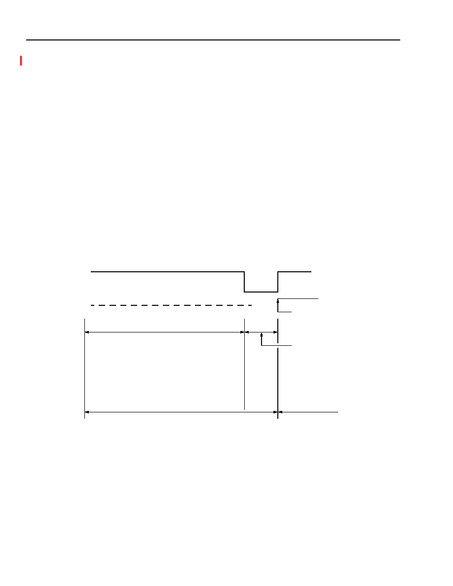
TMXF28155/51 Super Mapper
Preliminary Data Sheet
155/51 Mbits/s SONET/SDH x28/x21 DS1/E1
May 2001
512
Agere Systems Inc.
21 28-Channel Framer Block Functional Description
(continued)
Receive Stack Host Interface. Host access to the shared system stack will be managed using a stack availability
status bit. This bit reflects the stack availability status for each individual port. The host will use this status bit for
each port to determine when the stack is available for reading. Each stack is made unavailable only to enable a
window for the data link block to update the system stack. The window will be large enough so that any small
amount of overlap will not allow the possibility of a collision.
D, Sa, or DDS data link bits are collected over the multiple frame time periods appropriate for each frame type. The
stack is available for reading during that entire time period except for the last frame. During that one frame time, the
internal stack will be switched to the system stack. The stack will be made accessible once the transfer is done,
after which the Rx stack ready status bit will be set.
If the host is managing the stack via interrupts from the data link block and the interrupt can be serviced within
8.8 ms for
SLC
-96, 3.8 ms for CEPT, or 4.3 ms for DDS, then the host simply reads the stack. If the host is polling
the Rx stack ready status and reading the stack arbitrarily, then the host is required to read the Rx stack available
status bit FRM_RXSA (
Table 406
) which corresponds to the respective port. If that bit is set to 1, then the host can
access the corresponding stack locations. If that bit is set to 0, the host should poll on that bit until it changes.
Stack Available and Stack Ready Bit Formats. As described above, when the stack has been filled, the stack
available bit goes high. One or two frames before the stack is about to be filled, the stack available bit goes low and
stays low for one or two frames. This prevents the host from reading when a pointer switch is about to happen, pre-
venting the host from getting the data mixed. The stack ready bit is set to 1, also, when the stack has been filled.
The host clears this bit.
Figure 62
shows the dynamics of these bits.
5-9026(F)r.1
Figure 62. Stack Available and Stack Ready Bit Formatting
Receive Stack Pointer. The stack pointer maintains two pointers: an internal pointer and a host pointer. The
pointer identifies which stack is active for the host and which stack is active for the internal logic. These pointers will
always point to opposite stacks. When the TDM interface block is writing Sa bits or D bits to the stack, then the
internal pointer may be selecting the upper stack. In this case, the host pointer is selecting the lower stack for the
host reads. At the beginning of each double multiframe or each superframe, a pointer switch takes place. This
switch takes place during the time in which the host is prevented from accessing the stack for a particular link.
A stack pointer is maintained for each of the links individually.
Sa bit
Sr bit
DDS: 35 FRAMES (4.4 ms)
1 FRAME
SLC
-96: 70 FRAMES (8.75 ms)
2 FRAMES
CEPT: 30 FRAMES (3.75 ms)
2 FRAMES
ONE STACK OF DATA
NEXT STACK
STACK NOT AVAILABLE
SET HIGH HERE
(HOST CLEARS THIS BIT WHENEVER)
(0.125 ms)
(0.25 ms)
(0.25 ms)

Preliminary Data Sheet
TMXF28155/51 Super Mapper
May 2001
155/51 Mbits/s SONET/SDH x28/x21 DS1/E1
513
Agere Systems Inc.
21 28-Channel Framer Block Functional Description
(continued)
21.22.8 Transmit Facility Data Link Functional Description
This block performs the transmission of D bits into
SLC
-96 superframes, SA bits into CEPT multiframes, and data
link bits into DDS frames.
For
SLC
-96 frames, the D bits are always sourced from this block when the block is enabled for insertion
(FRM_DS1I (
Table 412
)). The D-bit delineator bits (
SLC
-96 Fs frame) are also sourced from this block and stored
in the stack with the D bits.
For CEPT frames, the Sa bits are sourced from either the Sa stack or outside of the data link block. The data link
block only responds with valid data when selected by the Sa source control bits (FRM_SA4SC--FRM_SA8SC
(
Table 412
)).
For DDS frames, the data link bits are always sourced from this block when this block is enabled for insertion
(FRM_DS1I).
This block also provides the capability to transmit BOMs in the data link channel of ESF links.
All frame types:
s
Support clear-on-read status and interrupt bits based on the setting of the input select signal.
21.22.9
SLC
-96 Superframe Transmit Data Link
s
Provides storage for D bits and delineator bits for transmission on
SLC
-96 links.
s
Provides interrupt for stack empty.
s
Provides host access to stack using processor clock.
s
Performs retransmission of stack when update is yet to be performed.
When enabled for insertion, this block will always source the D bits to any
SLC
-96 Tx link. The delineator bits (
SLC
-
96 Fs frame), which bound the 24 D bits, are also sourced from this block.
The 12-frame
SLC
-96 superframe is composed of a terminal frame (F
T
) alternating with a subframe that consists of
a combined signaling (F
S
) frame and data link. The subframe shares establishing the signaling frame (F
S
) and
SLC
-96 data link. The FDL stack bits are inserted into the signaling and data link subframe position in the super-
frame. Seventy-two superframes are required to deliver the 24 D bits and 12-bit delineator. The front-end delineator
is 00111, which is followed by 24 D bits and trailed by 0001110. The alignment of the F
S
bits within the superframe
is determined and indicated by the frame aligner block.
The
SLC
-96 F
S
bits are stored in the shared Tx stack as shown in
Table 592
.
Table 592. Shared Tx FDL Stack Format for
SLC
-96 Frames
* The value held in the bits left blank should be ignored by the host.
The transmission of the
SLC
-96 stack will take 9 ms to complete, during which time the host should refill the system
stack if the D bits need to change.
Near the beginning of each
SLC
-96 superframe, the Tx data link block will determine whether a new set of D bits is
available to be transmitted.
Word
15
14
13
12
11
10
9
8
7
6
5
4
3
2
1
0
0
0
0
0
1
1
1
0
0
0
1
1
1
0
0
0
0
1*
C1
C2
C3
C4
C5
C6
C7
C8
C9
C10
C11
SB1
0
0
0
0
2*
SB2 SB3
M1
M2
M3
A1
A2
S1
S2
S3
S4
SB4
0
0
0
0
3*
0
0
0
0
0
0
0
0
0
0
0
0
0
0
0
0
4*
0
0
0
0
0
0
0
0
0
0
0
0
0
0
0
0

TMXF28155/51 Super Mapper
Preliminary Data Sheet
155/51 Mbits/s SONET/SDH x28/x21 DS1/E1
May 2001
514
Agere Systems Inc.
21 28-Channel Framer Block Functional Description
(continued)
The host will indicate this state by resetting the Tx stack empty bit,
FRM_TXSE_IS
(
Table 414
). If this is the case,
the new D bits will be transmitted; otherwise, the previous D bits will be retransmitted. If the Tx stack empty bit was
0 at the beginning of the
SLC
-96 superframe, then the bit will be set to 1, indicating a request for new D bits.
When enabled using the FRM_ASRC (
Table 412
) bit, the D bits should only be inserted when the proper alignment
has been reached. For
SLC
-96, both terminal (F
T
) and signaling (F
S
) frames need to be valid. This condition effects
the insertion of D bits and the reporting of stack empty to the host.
Before enabling a link for the
SLC
-96 format or enabling this block for insertion, the host should initialize the stack
and set the Tx stack empty bit to 0. If not, the data link block will transmit the reset state of the stack, which is arbi-
trary.
21.22.10 DDS Transmit Data Link Stack
s
Provides three superframes of data link bit storage for transmission on DDS links.
s
Provides interrupt for stack empty.
s
Performs retransmission of stack when update has yet to be performed.
s
Provides host access to stack using processor clock to provide fast access.
If enabled for insertion, this block will always source the DDS data link bits to any DDS Tx link. DDS superframes
are 12 frames with the data link bits located in bit number 6 of time slot 24 of every frame. Thirty-six frames of data
link bits are stored in the stack.
The DDS stack is stored in the shared Tx stack as follows.
Table 593. Shared Tx FDL Stack Format for DDS Frames
* The value held in the bits left blank should be ignored by the host.
Transmission of the DDS stack will take 4.5 ms to complete, during which time the host should refill the system
stack if the data link bits need to change.
Near the beginning of every third DDS superframe, the Tx data link block will determine whether a new set of data
link bits is available to be transmitted. The host will indicate this state by resetting the Tx stack empty bit. If this is
the case, the new data link bits will be transmitted; otherwise, the previous data link bits will be retransmitted. If the
Tx stack empty bit was 0 at the beginning of the set of superframes, then the bit will be set to 1, indicating a request
for new data link bits.
When enabled, using the FRM_ASRC bit, the Sa bits should only be inserted when the proper alignment has been
reached. For DDS links, only terminal frame (F
T
) is required for insertion. This condition affects the insertion of data
link bits and the reporting of stack empty to the host.
Before enabling a link for the DDS format or enabling this block for insertion, the host should initialize the stack and
set the Tx stack empty bit to 0. If not, the data link block will transmit the reset state of the stack, which is arbitrary .
Word
15
14
13
12
11
10
9
8
7
6
5
4
3
2
1
0
0*
D1
D2
D3
D4
D5
D6
D7
D8
D9
D10
D11
D12
--
--
--
--
1*
D1
D2
D3
D4
D5
D6
D7
D8
D9
D10
D11
D12
--
--
--
--
2
D1
D2
D3
D4
D5
D6
D7
D8
D9
D10
D11
D12
--
--
--
--
3
--
--
--
--
--
--
--
--
--
--
--
--
--
--
--
--
4
--
--
--
--
--
--
--
--
--
--
--
--
--
--
--
--

Preliminary Data Sheet
TMXF28155/51 Super Mapper
May 2001
155/51 Mbits/s SONET/SDH x28/x21 DS1/E1
515
Agere Systems Inc.
21 28-Channel Framer Block Functional Description
(continued)
21.22.11 Transmit ESF Data Link Bit-Oriented Messages
s
Provides capability to transmit bit-oriented messages.
When enabled through a configuration bit (FRM_BOME (
Table 413
)), bit-oriented messages will be transmitted on
the data link channel of the frame bit for ESF links. The ESF superframe is numbered 1 through 24 with the data
link channel transmitted in the odd numbered frames (4 kbits/s).
The BOM is a 16-bit message defining an alarm or command and response action, and sent repeatedly for a
period of time determined by the event. The message consists of eight ones, a 0, a 6-bit code to identify the alarm
or action, and a 0 (1111_1111_0 in front and 0 behind the 6-bit code).
The message can occur at any point in the extended superframe without respect to boundaries. The exact mes-
sage to be sent will reflect what has been programmed into a register (FRM_TBOM{5:0] (
Table 413
) bits). The
BOM format is as follows:
0 X X X _ X X X 0 _ 1111_1111: (right-most bit being transmitted first).
When the BOM pattern is enabled, it will be transmitted until disabled. When disabled, the pattern will cease to be
transmitted immediately.
A BOM status bit will indicate when the pattern has been sent 10 times. That status bit will be reset on read.
When enabled using the FRM_ASRC (
Table 412
) bit, the BOMs should only be inserted when the proper alignment
has been reached. For ESF links, both BFA and MFA are required for insertion. This condition affects the insertion
of BOMs bits and the reporting of stack empty to the host.
21.22.12 CEPT, CEPT Multiframe Transmit Data Link Sa bits Stack
s
Provides two multiframes of Sa-bit storage for transmission on CEPT links.
s
Provides interrupt for stack empty.
s
Performs retransmission of stack when update has yet to be performed.
s
Provides capability to source Sa bits from blocks other than the data link block.
s
Provides host access to stack using processor clock to provide fast access.
This block will always present the Sa bits stored in the Tx stack to the TDM data stream. The data valid signal will
reflect the programming of the Sa source control bits (FRM_SA4SC--FRM_SA8SC,
Table 412
). In CEPT, the Sa
bits are located in time slot 0 of the NOTFAS frames (odd -numbered frames). CEPT multiframe format frames are
numbered 0 through 15 with the Sa bits located in time slot 0 of the odd numbered frames (NOTFAS frames).
The Sa bits are stored in the Tx stack as follows.
Table 594. Shared Tx Stack Format for CEPT Frame
Transmission of the Sa stack will take 4 ms, during which time the host should refill the system stack if the Sa bits
need to change.
Near the beginning of each CEPT double multiframe, the Tx data link block will determine whether a new set of Sa
bits is available to be transmitted. The host will indicate this state by resetting the Tx stack empty bit. If this is the
case, the new Sa bits will be transmitted; otherwise, the previous Sa bits will be retransmitted.
Word
15
14
13
12
11
10
9
8
7
6
5
4
3
2
1
0
0
SA41 SA43 SA45 SA47 SA49 SA411 SA413 SA415 SA41 SA43 SA45 SA47 SA49 SA411 SA413 SA415
1
SA51 SA53 SA55 SA57 SA59 SA511 SA513 SA515 SA51 SA53 SA55 SA57 SA59 SA511 SA513 SA515
2
SA61 SA63 SA65 SA67 SA69 SA611 SA613 SA615 SA61 SA63 SA65 SA67 SA69 SA611 SA613 SA615
3
SA71 SA73 SA75 SA77 SA79 SA711 SA713 SA715 SA71 SA73 SA75 SA77 SA79 SA711 SA713 SA715
4
SA81 SA83 SA85 SA87 SA89 SA811 SA813 SA815 SA81 SA83 SA85 SA87 SA89 SA811 SA813 SA815

TMXF28155/51 Super Mapper
Preliminary Data Sheet
155/51 Mbits/s SONET/SDH x28/x21 DS1/E1
May 2001
516
Agere Systems Inc.
21 28-Channel Framer Block Functional Description
(continued)
If the Tx stack empty bit was 0 at the beginning of the CEPT double multiframe, then the bit will be set to 1, indicat-
ing a request for new Sa bits.
When enabled using the FRM_ASRC (
Table 412
) bit, the SA bits should only be inserted when the proper align-
ment has been reached. For CEPT links, only BFA is required for insertion. For CEPT CRC-4 links, both BFA and
MFA need to be valid. This affects the insertion of Sa bits and the reporting of stack empty to the host. There is
another configuration bit FRM_TXCRCSM (
Table 412
) which allows the CEPT CRC-4 links to insert when only BFA
is active (FRM_TXCRCSM).
Before enabling a link for CEPT format, the host should initialize the stack and set the Tx stack empty bit to 0. If not,
the data link block will transmit the reset state of the stack which is arbitrary.
21.22.13 Transmit Data Link Stack Idle Modes
s
D4
s
J-D4
s
J2
s
CMI
s
No data link features
21.22.14
SLC
-96, DDS, or CEPT ESF Frame Alignment
For CEPT, DDS, or
SLC
-96 frames, loss of frame alignment is not an issue since the framer is the source of time
slot 0 or the F bits. Once a link is enabled, the frame sequence always starts at the beginning.
In the case of the system being the source of multiframe alignment, the data link block will simply deliver what is
requested.
5-9027(F)r.1
Figure 63. Tx Data Link Block Diagram
TR A N SM IT
S YS TE M
IN TE R FA C E
T D M ID
T DM D AT A
TD M IN T ER F AC E
D A TA /
VALID
IN TE R N AL B U S
T
X
R
X
S TA C K
D AT A L IN K IN T ER R U PT
S H A RE D
R
X
S TA C K
RE A D R EQ U E ST LO G IC
R EA D AR B ITR A TIO N L O G IC
H O S T
R E G IST ER S
W RITE
R E Q U ES T
FD L
PR O C E SS O R
S YS TE M
T
X
S TA CK
R EA D
R EQ U E S T
TR AN S FE R
R E Q U ES T
S TA C K W R ITE
S TA CK R E AD
S Y ST EM
LIN E
F RA M E R
C LO C K
C LO C K

Preliminary Data Sheet
TMXF28155/51 Super Mapper
May 2001
155/51 Mbits/s SONET/SDH x28/x21 DS1/E1
517
Agere Systems Inc.
21 28-Channel Framer Block Functional Description
(continued)
21.23 HDLC Functional Description
The Super Mapper framer is capable of inserting and extracting HDLC data to and from multiple logical channels.
The system may specify any bit as an HDLC channel. For ESF, DDS, and CEPT framing formats, the facility data
link (FDL) bit may be programmed as a logical HDLC channel. Multiple bits within a time slot may be concatenated
to form a logical HDLC channel. The maximum number of bits in a logical channel is 8 bits (all within a single time
slot) and corresponds to a maximum data rate of 64 kbits/s. Multiple logical HDLC channels may be assigned to a
single payload time slot.
Received data from a HDLC channel is placed into a 128-byte FIFO. Transmit HDLC channels are read from a sep-
arate 128-byte FIFO.
Once the HDLC channels are defined and the HDLC is enabled, the framer extracts and inserts the HDLC frames
in these channels. The function of the receive and transmit HDLC sections will be described separately.
21.24 HDLC Operation
This section describes the standard HDLC functions performed by the framer's HDLC block. The HDLC transmitter
accepts parallel data from the transmit FIFO, converts it to a serial bit stream, provides bit stuffing as necessary,
adds the CRC and the opening and closing flags, and sends the framed serial bit stream to the transmit framer.
The HDLC receiver unit receives time slot data from the receive framer, identifies frames for proper format, recon-
structs data bytes, provides bit destuffing as necessary, and loads parallel data in the receive FIFO. HDLC frames
on the serial link have the following format.
Table 595. HDLC Frame Format
All bits between the opening flag and the CRC are considered user payload. User payload data such as the
address, control, and information fields are fetched from the transmit FIFO for transmission. Received user payload
data is stored in the receive FIFO buffers. The 16 bits preceding the closing flag are the frame check sequence or
cyclic redundancy check (CRC) bits.
21.24.1 Zero-Bit Insertion/Deletion (Bit Stuffing/Destuffing)
The HDLC protocol recognizes three special bit patterns: flags, aborts, and idles. These patterns have the common
characteristic of containing at least six consecutive ones. A user data byte can contain one of these special pat-
terns. Transmitter zero-bit stuffing is done on user data and CRC fields of the frame to avoid transmitting one of
these special patterns. Whenever five ones occur between flags, a 0 bit is automatically inserted after the fifth 1,
prior to transmission of the next bit. On the receive side, if five successive ones are detected followed by a 0, the 0
is assumed to have been inserted and is deleted (bit destuffing).
21.24.2 Flags
All flags* have the bit pattern 01111110 and are used for frame synchronization. The framer's HDLC block auto-
matically sends one flag at the beginning of each frame. If the FRM_HTIDLE (
Table 435
) bit is cleared to 0, the
FLAG byte (01111110) is continuously sent between frames if no data is present in the FIFO. If the FRM_HTIDLE
bit is set to 1, the HDLC block sends continuous FRM_IDLE (
Table 349
) bytes (11111111) when the transmit FIFO
is empty. Once there is data in the transmit FIFO, an opening flag is sent, followed by the frame. During transmis-
sion, two successive flags will not share the intermediate 0.
* Regardless of the time-fill byte used, there always is an opening and closing flag with each frame. Back-to-back frames are separated by two
flags.
Opening Flag
User Data Field
Frame Check Sequence (CRC)
Closing Flag
01111110
8 bits (multiple of 8 bits)
16 bits
01111110

TMXF28155/51 Super Mapper
Preliminary Data Sheet
155/51 Mbits/s SONET/SDH x28/x21 DS1/E1
May 2001
518
Agere Systems Inc.
21 28-Channel Framer Block Functional Description
(continued)
An opening flag is always generated at the beginning of a frame (indicated by the presence of data in the transmit
FIFO and the transmitter enabled). FRM_CFLAGS[1:0] (
Table 435
) determines which FRM_FCNT[0--3][4:0]
parameter to use. The FRM_FCNT[0--3][4:0] parameters define the number of idle flags that are sent between
HDLC packets. Data is transmitted per the HDLC protocol until a byte is read from the FIFO with Tx HDLC register
bits FRM_HTFUNC[1:0] (
Table 438
) = 01 set. The HDLC block follows this byte with the CRC sequence and a clos-
ing flag.
The HDLC receiver recognizes the 01111110 pattern as a flag. Two successive flags may or may not share the
intermediate 0 bit and are identified as two flags (i.e., both 011111101111110 and 0111111001111110 are recog-
nized by the HDLC block). When another flag is identified, it is treated as the closing flag. As mentioned above, a
flag sequence in the user data or FCS fields is prevented by zero-bit insertion and deletion.
21.24.3 Aborts
The bit pattern of the abort sequence is 01111111, with 0 transmitted first. A frame can be aborted by writing set-
ting Tx HDLC register bits FRM_HTFUNC[1:0] = 01. This causes the last byte written to the transmit FIFO to be fol-
lowed by the abort sequence upon transmission. Once a byte is tagged by a write to Tx HDLC register bits
FRM_HTFUNC[1:0] = 01, it cannot be cleared by subsequent writes.
When receiving a frame, the receiver recognizes the abort sequence whenever it receives a 0 followed by seven
consecutive ones. This status results in the abort bit, and possibly the bad byte count bit and/or bad CRC bits,
being set in the status of frame status byte which is appended to the receive data queue. The last bytes of user
data are assumed to be CRC bits and are placed in the queue in the regular HDLC mode. All subsequent
FRM_IDLE or flag bytes are ignored until a valid opening flag is received.
21.24.4 Receive IDLES
In accordance with the HDLC protocol, the HDLC block recognizes 15 or more contiguous received ones as idle.
When the HDLC block receives 15 contiguous ones, the receiver FRM_IDLE[7:0] bit, idle is set.
21.24.5 CRC
For a given frame of bits, 16 additional bits that constitute an error-detecting code are added by the transmitter. As
called for in the HDLC protocol, the frame check sequence bits are transmitted most significant bit first and are bit
stuffed. The cyclic redundancy check (or frame check sequence) is calculated as a function of the transmitted bits
by using the ITU-T standard polynomial:
x
16
+ x
12
+ x
5
+ 1
At the other end, the receiver performs the same calculation on the received bits after destuffing and compares the
results to an expected result. An error occurs if, and only if, there is a mismatch.
The transmitter can be instructed to transmit a corrupted CRC by setting the transmit bad CRC bit DXBCRC
(DCI-DCR-1-B6). As long as the DXBCRC bit is set, the CRC is corrupted for each frame transmitted by logically
flipping the least significant bit of the transmitted CRC.
The receiver calculates and verifies the CRC for an incoming frame. The result of the CRC check is reported in bit
7 of the status of frame byte, which is placed in the receive FIFO after the last data byte of the frame. The CRC is
stored in the FIFO at all times.
Preliminary Data Sheet
TMXF28155/51 Super Mapper
May 2001
155/51 Mbits/s SONET/SDH x28/x21 DS1/E1
519
Agere Systems Inc.
21 28-Channel Framer Block Functional Description
(continued)
21.24.6 HDLC Mode
The receive queue manager forms a status of frame (SF) word for each HDLC frame and stores the SF word in the
receive HDLC FIFO after the last data byte of the associated frame. HDLC frames that include the payload and the
frame check sequence (FCS) bytes and consists of n bytes will have n + 1 bytes stored in the receive FIFO. The
FCS bytes of the received HDLC frame are stored into the receive FIFO.
21.24.7 Receive HDLC Transparent Mode
The receive FIFO receives data from the receive framer and directly stores this data information bit-for-bit, least
significant bit first.
If the FRM_MODE[3:0] (
Table 422
) and FRM_MATCH[7:0] (
Table 442
) bits are set, the receive HDLC FIFO will
load data only after the matched pattern has been detected. The search for the match character is in a sliding win-
dow fashion and data is aligned accordingly. The octet is aligned relative to the first HDLC clock after frame align-
ment is established. The match character and all subsequent bytes are placed into the receive FIFO. A receive
reset command causes the receive to realign to the match character if enabled.
21.24.8 Receive HDLC
Data is presented to the TDM to channel conversion block from the TDM bus (see
Figure 64
below). This block
determines which, if any, channel the data belongs to. When data is found that belongs to a channel, it is sent to the
HDLC serial to parallel block. This block buffers up bits into bytes and does HDLC processing on channels so pro-
grammed. When a valid byte of data (or status) has been grouped together for a specific channel, that data is then
sent to the FIFOs interrupt block. Here, the data is further buffered in separate FIFOs for each channel where data
can be read by the microprocessor.
5-9028(F)r.1
Figure 64. Receive HDLC Block Diagram
21.24.9 Receive HDLC Features
s
In transparent mode, bits are simply gathered into bytes with the option of waiting for an initial provisionable 8-bit
pattern to be detected before starting.
s
In HDLC mode, incoming data is correctly formatted and packetized according to the HDLC standard.
s
In HDLC mode, aborted packets, idle status, and CRC errors are checked for and reported.
TDM TO
CHANNEL
CONVERSION
HDLC
SERIAL-TO-PARALLEL
CHAN
ENABLE
TDM BUS
µ
P DATA
µ
P ADDR
µ
P CNTL
FIFOs/
INTERRUPTS
CHAN
DATA
TYPE
VALID
8
INTS.
LOOPBACK
FROM T
X
DATA
1
INTERNAL
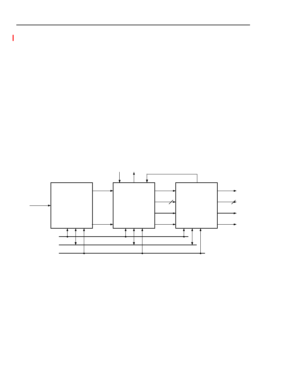
TMXF28155/51 Super Mapper
Preliminary Data Sheet
155/51 Mbits/s SONET/SDH x28/x21 DS1/E1
May 2001
520
Agere Systems Inc.
21 28-Channel Framer Block Functional Description
(continued)
s
128 bytes of FIFO buffering for each channel with the ability to interrupt on end of packet (EOP), exceed pro-
grammable FIFO threshold or FIFO overrun.
s
Each channel has independent reset and enable. Reset will reset all state machines, disable the channel, reset
FIFO pointers, and clear pending interrupts. Disabling a channel will reset the state machine but not affect the
FIFO pointers or interrupts.
s
Any channel can be programmed to run from any combination of bits from any one time slot of either odd or even
(or both) frame numbers of any link.
s
A loopback mode (from transmit HDLC, through HDLC to FIFO) is supported.
s
Channels will not operate if the corresponding link/framer goes out of frame (function is equivalent to channel
disabled).
s
Data is ignored if the link/framer is not in basic frame alignment.
s
Upon selection from the top level, the 128 bytes of FIFO per-channel can be converted into 512 bytes of FIFO,
with a quarter of the channels.
Data received from the receive framer is stored in the appropriate channel receive FIFO. In the HDLC mode, the
receiver also places a status of frame byte in the receive FIFO for every complete frame received. The receive
HDLC channel FIFO register bits FRM_HRCOUNT[9:0] (
Table 446
) report the number of bytes available for this
particular channel since the last byte received by the HDLC receive block regardless of how many bytes were read
by the host. The host loads the data from the RFIFO of the various channels through the microprocessor interface.
5-9029(F)r.1
Figure 65. Transmit HDLC FIFO Block Diagram
21.24.10 Transmit HDLC FIFO Features
s
In transparent mode, simply transform the data to a serial output.
s
In HDLC mode, correctly format and packetize the outgoing data bits.
s
In HDLC mode, sends normal packets (close with flag) or abort packets (via command or absence of data).
s
Provide 128 bytes of FIFO buffering for each channel with ability to interrupt on packet done, below programma-
ble FIFO threshold or underrun (FIFO empty in middle of packet).
s
Each channel has independent reset and enable. Reset will reset all state machines, disable the channel, reset
FIFO pointers, and clear pending interrupts. Disabling a channel will reset the state machine but not affect the
FIFO pointers or interrupts.
TDM TO
CHANNEL
CONVERSION
FIFOs/
INTERRUPTS
CHAN
DATA
ENABLE
TDM BUS
µ
P DATA
µ
P ADDR
µ
P CNTL
HDLC/
PARALLEL-TO-
SERIAL
CHAN
DATA
TYPE
VALID
8
ACK/UNDERFLOW
LOOPEN
TDMEN
CHAN
INTS.
PRM
INFO
1
Preliminary Data Sheet
TMXF28155/51 Super Mapper
May 2001
155/51 Mbits/s SONET/SDH x28/x21 DS1/E1
521
Agere Systems Inc.
21 28-Channel Framer Block Functional Description
(continued)
s
Any channel can be programmed to run for any combination of bits for any one time slot of either odd or even (or
both) frame numbers of any link.
s
A local loopback is supported. (From transmit FIFO through the HDLC back to the receive FIFO.)
s
The PRM data is received from the framer performance monitoring block approximately once per second per
link. If the link is enabled to send PRM data, then the PRM packet will be sent as the next packet on that link. The
PRM packet contains data for the current and three previous seconds. The format of the PRM packet is shown in
Table 587, Performance Report Message Format on page 507
.
Table 596. Performance Report Message Structure
In
Table 596
, the flags (octet 1 and 15) are normal HDLC flags (note that the CFLAGS bit must be programmed to
1 to force nonshared flags), SAPI = 001110, C/R is programmable, EA = 0 in octet 2 and 1 in octet 3, TEI =
0000000, Control = 00000011. Octets 5 and 6 contain the most recent data received from the performance monitor
(except U1, U2, R = 0 always). Octets 7 and 8 contain the same data from the previous second. Octets 9 and 10
contain data from the second before that (antepenultimate second) and octets 11 and 12 contain data for the sec-
ond before that. The FCS is automatically generated by the HDLC.
The data normally received from the performance monitor will be initialized to all zeros.
Transmit HDLC data is loaded into the channel transmit FIFO (TFIFO) via the Tx HDLC channel data bits
FRM_HTDATA[7:0] (
Table 438
). Multiframes can be placed in the Tx HDLC FIFO. In HDLC mode, the final byte of
each frame is marked by writing the Tx HDLC FRM_HTFUNC[1:0] (
Table 438
) bits to the appropriate value. The
transmit HDLC channel count register indicates how many additional bytes can be added to the Tx HDLC FIFO.
The transmitter empty (Tx HDLC FRM_HTTHRSH (
Table 436
)) interrupt bit is set in the HDLC interrupt status reg-
ister when the TFIFO is below the number of bytes specified in the threshold registers.
A Tx HDLC FRM_HTDONE interrupt occurs for each HDLC frame completed.
In HDLC mode, an Tx HDLC FRM_HTUND (
Table 436
) interrupt is generated if the transmitter underruns. There is
no interrupt indicated for a transmitter overrun that is writing more data than empty spaces exist. Overrunning
transmitter data is ignored which results in missing data in the frame.
Octet Number
PRM B7
PRM B6
PRM B5
PRM B4
PRM B3
PRM B2
PRM B1
PRM B0
1
FLAG
2
SAPI
C/R
EA
3
TEI
EA
4
Control
5
G3
LV
G4
U1
U2
G5
SL
G6
6
FE
SE
LB
G1
R
G2
Nm
NI
7
G3
LV
G4
U1
U2
G5
SL
G6
8
FE
SE
LB
G1
R
G2
Nm
NI
9
G3
LV
G4
U1
U2
G5
SL
G6
10
FE
SE
LB
G1
R
G2
Nm
NI
11
G3
LV
G4
U1
U2
G5
SL
G6
12
FE
SE
LB
G1
R
G2
Nm
NI
13--14
FCS
15
FLAG
TMXF28155/51 Super Mapper
Preliminary Data Sheet
155/51 Mbits/s SONET/SDH x28/x21 DS1/E1
May 2001
522
Agere Systems Inc.
21 28-Channel Framer Block Functional Description
(continued)
21.25 Framer Phase-Lock Loop (PLL)
The Super Mapper incorporates an internal PLL to generate transmit path line clocks for the framers at DS1, and
E1 from an external system clock (device pin CLKIN_PLL (AD24)).
The external system clock is multiplied by an analog phase-locked loop (PLL) and fractionally divided down to
obtain the required line clock frequencies.
5-9075(F)
Figure 66. Framer PLL
The PLL may be programmed for eight different external system clocks with the device pins: MODE2_PLL (AB21)
(MSB), MODE1_PLL (AE24), and MODE0_PLL (AF24) (LSB), as shown in
Table 597
below.
Table 597. Clock Mode Programming for PLL Mode Device Pins
The PLL is used when framer bit PLL_BYPAS = 0 (
Table 301
). When PLL_BYPAS = 1, the PLL is bypassed and an
external clock at the system interface is used as the line clock. An example would be when the framers are pro-
grammed for a CHI interface at 2.048 MHz and the frames are programmed for E1, the PLL may be bypassed and
the CHI system clock may be used as the line clock.
The PLL may be powered down when not in use with microprocessor register bit SMPR_MPU_CG_PWRDN
(
Table 70
) set to 1.
Clock Select MODE2_PLL, MODE1_PLL, MODE0_PLL
System Clock Frequency (MHz) CLKIN_PLL
000
Reserved (do not use)
001
51.84
010
26.624
011
19.44
100
16.384
101
8.192
110
4.096
111
2.048
C L K IN _ P L L
M O D E 2_ P L L
M O D E 1_ P L L
M O D E 0_ P L L
A N A L O G P LL
A N D
F R AC T IO N A L D IV ID E R
M P U R EG IST ER B IT
M P U _ C G _ P W R D N
C L O C K S T O
F R A M E R BL O C K
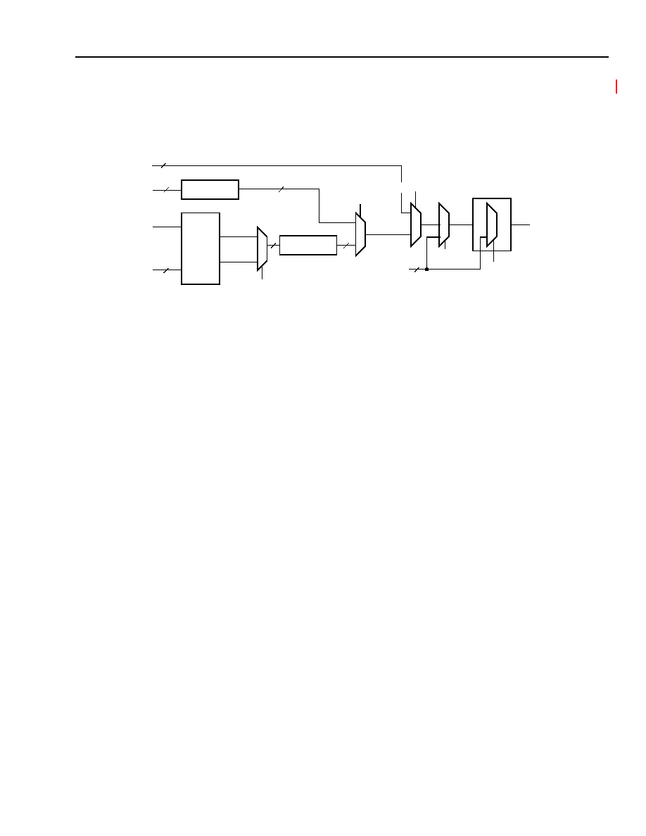
Preliminary Data Sheet
TMXF28155/51 Super Mapper
May 2001
155/51 Mbits/s SONET/SDH x28/x21 DS1/E1
523
Agere Systems Inc.
21 28-Channel Framer Block Functional Description
(continued)
21.25.1 Framer Timing Selection
The following diagram shows the framer timing selection.
5-9076(F)r.1
Figure 67. Framer Block Transmit Path Timing Selection
Legend for
Figure 67
:
Device pins:
s
CLKIN_PLL (AD24)--system clock into PLL.
s
MODE2_PLL (AB21)--PLL input clock frequency select pins.
s
MODE1_PLL (AE24).
s
MODE0_PLL (AF24).
Framer register bits:
s
FRM_MODE[3:0] (
Table 422
)--framing mode select (per link).
s
FRM_PLL_BYPAS (
Table 301
)--transmit path clock select from PLL or external system interface (global).
s
FRM_SW_TRN (
Table 301
)--switching or transport mode select (global).
Framer internal signals:
s
tp_rclk--transmit path receive clock.
s
tp_tclk--transmit path transmit clock.
s
rs_gtclk--receive system global transmit clock (LINERXDATA[29] device pin D13).
s
rp_rclk--receive path receive clock
21.26 System Interface
21.26.1 System Interface Introduction
The system interface of Super Mapper can be programed for several modes of operation:
Concentration Highway (CHI) Mode. This is the system interface on Agere's current framers. It can be pro-
grammed to operate at 2.048 MHz, 4.096 MHz, 8.192 MHz, or 16.384 MHz clock rates (data rates up to
8.192 Mbits/s only). In this mode, a pair of global system clock and system frame sync (one for the transmit and
one for the receive direction) are required. This interface can be used, for example, to interface with the TSI device.
DS1
E1
PLL
CLKIN_PLL
MODE2_PLL
MODE1_PLL
MODE0_PLL
BUFFER x28
28
rs_gtclk
28
tp_rclk[1--28]
tp_tclk[1--128]
FRM_MODE[1--28][3:0]
FRM_PLL_BYPAS
FRAME
FORMATTER
BUFFER x28
1
28
TRANSMIT PATH
FRM_SW_TRN[1--28]
1
3
rp_rclk_[1:28]
28
FRM_LOOP
TIMING
1
0
1
0
0
1
0
1
0
1
FRM_TXLBMD[1:0]
FRM_AUTOPLB
FRM_AUTOLLB

TMXF28155/51 Super Mapper
Preliminary Data Sheet
155/51 Mbits/s SONET/SDH x28/x21 DS1/E1
May 2001
524
Agere Systems Inc.
21 28-Channel Framer Block Functional Description
(continued)
Parallel Bus System Interface Mode. This interface consists of a 17-bit wide parallel bus operating at
19.44 Mbits/s, 9 bits of which form a byte of data and a data parity bit while the other 8 bits contain the signaling
and control information. A clock and frame sync are expected in both the receive and transmit directions. For a
28-link device, only 1/3 of the bytes are populated. In the transmit direction the unpopulated bytes are 3-stated,
while in the receive direction they are ignored. Three 28-link devices (Super Mappers) can be connected in parallel
to the telecom bus for implementing an STS-3 (STM-1) rate interface.
Note: The Tx system is defined as the interface that sends data out of the chip and toward the system (non-
SONET) interface. The Rx system receives data from the system. These designations are opposite of the
path definitions for the Super Mapper.
21.26.2 System Interface References/Standards
s
ITU G.783 characteristics of synchronous digital hierarchy (SDH) equipment functional blocks.
s
ITU Q.511 exchange interfaces towards other exchanges.
21.26.3 Transmit/Receive System Interface Features
The features supported in the system interface are summarized below:
s
Data rates of 2.048 Mbits/s, 4.096 Mbits/s, 8.192 Mbits/s, and 19.44 Mbyte/s.
s
Clock rates of 2.048 MHz, 4.096 MHz, 8.192 MHz, 16.384 MHz, and 19.44 MHz.
s
A global input clock and frame sync (CHI and parallel bus system interface modes).
s
Byte offset--2.048 Mbits/s, 0--31 bytes.
s
Byte offset--4.096 Mbits/s, 0--63 bytes.
s
Byte offset--8.192 Mbits/s, 0--127 bytes.
s
Bit offset (CHI mode).
s
1/2-bit offset (CHI mode).
s
1/4-bit offset (CHI CMS mode).
s
Clock mode select (CMS) (CHI mode).
s
Associated signaling mode (ASM) (CHI mode).
s
Double time slot mode, CHIDTS (CHI mode).
s
Double NOTFAS system time slot, FRM_DNOTFAS (
Table 347
) (CHI and parallel bus system interface modes).
s
Sampled clock edge for transmit system frame sync (CHI mode).
s
Global programmable stuffed time slot position in DS1 mode (CHI mode).
s
Global programmable stuffed byte in DS1 mode (CHI and parallel bus system interface modes).
s
Global single time slot loopback address for system or line.
s
Programmable automatic system AIS (loss of frame alignment).
s
Programmable automatic system AIS (CEPT CRC-4 multiframe alignment timer expiration).
s
On-demand transmission of system AIS.
s
Programmable even/odd parity generation (parallel bus system interface mode).
21.26.4 Double NOTFAS System Time-Slot (FRM_DNOTFAS (
Table 347
)) Mode
This mode is applicable to the CHI and parallel bus system interface modes. In the default case
(FRM_DNOTFAS = 0 (
Table 347
)), both the FAS and NOTFAS time slots are transmitted by the transmit system
interface and expected by the receive system interface.

Preliminary Data Sheet
TMXF28155/51 Super Mapper
May 2001
155/51 Mbits/s SONET/SDH x28/x21 DS1/E1
525
Agere Systems Inc.
21 28-Channel Framer Block Functional Description
(continued)
Setting FRM_DNOTFAS to 1 enables the NOTFAS time slot to be transmitted twice on the transmit system inter-
face in the NOTFAS and FAS time slot (TS0) positions. Similarly, the receive system interface assumes time slot 0
to carry NOTFAS data that is repeated twice.
21.26.5 Transparent Mode
This mode is only used in the CHI mode. In the transparent DS1 mode, the transmit system interface inserts the
193rd bit of the DS1 frame in bit 7 (LSB) of the first stuffed time slot. The receive system interface takes bit 7 of the
first stuffed time slot and inserts it into the framing bit position (193rd bit on the TDM data bus).
In the transparent E1 mode, the transmit system maps 32 received time slots into the CHI time slots. Similarly, the
receive system maps the CHI time slots into the TDM bus time slots. The transmit frame formatter inserts TS0 of
the CHI (FAS/NOTFAS) into the TS0 of the frame based on the biframe alignment.
21.26.6 Loopbacks
Two forms of loopbacks are supported: single time slot system loopback (STSSLB) and single time slot line loop-
back (STSLLB), as shown in
Figure 68
below. When FRM_STSSLB = 1 (
Table 350
), a single time slot from the
receive system interface selected using the configuration parameter FRM_TSLBA[4:0] (
Table 350
), is looped back
to the system. The idle code, programmable using the configuration registers (FRM_IDLE[7:0] (
Table 349
)), is
transmitted to the line in place of the looped back time slot.
When FRM_STSLLB = 1 (
Table 350
), a single time slot from the transmit system interface selected using the con-
figuration parameter FRM_TSLBA[4:0], is looped back to the line. The programmable idle code is transmitted to the
system in place of the looped back time slot.
5-9030(F)r.1
Figure 68. System Loopbacks
21.26.7 System AIS
The transmit system interface transmits AIS automatically to the system on the following conditions:
s
Loss of frame alignment in the frame aligner or the mapper block (provisionable using a configuration register
bit).
s
CEPT CRC-4 multiframe alignment timer expiration (provisionable using a configuration register bit).
On-demand AIS can also be sent to the system by setting the configuration register bit for the particular link
(FRM_MANAIS (
Table 419
)).
SYSTEM
LINE
ES
SINGLE TIME-SLOT SYSTEM LOOPBACK
SYSTEM
LINE
ES
SINGLE TIME-SLOT LINE LOOPBACK
ES = ELASTIC STORE
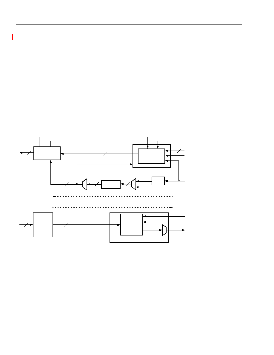
TMXF28155/51 Super Mapper
Preliminary Data Sheet
155/51 Mbits/s SONET/SDH x28/x21 DS1/E1
May 2001
526
Agere Systems Inc.
21 28-Channel Framer Block Functional Description
(continued)
21.26.8 Slip Detection
Controlled slips are performed on frame boundaries. Elastic store slip overflow and underflow is monitored with sta-
tus bits FRM_SLIPO and FRM_SLIPU (
Table 393 on page285
). In the case of an underflow, an entire frame is
repeated. In the case of an overflow, an entire frame in skipped.
21.26.9 The Concentration Highway (CHI) Mode
This is the system interface on Agere's framers. It can be programmed to operate at 2.048 MHz, 4.096 MHz,
8.192 MHz, or 16.384 MHz clock rates (data rates up to 8.192 Mbits/s only). In this mode, a pair of global system
clock and system frame sync (one for the transmit and one for the receive direction) is required. The offset between
the frame sync and bit 0 of time slot 0 is programmable in this mode.
Figure 70
below shows the transmit system
interface operating in the CHI mode. The data path (shown in bold arrows) passes through the slip buffer. Slips in
the form of buffer overflows or underflows are detected and reported in this mode. This interface can be used, for
example, to interface with the time slot interchange (TSI) device.
5-9032(F)
Figure 69. CHI Mode of the Transmit System Interface
21.26.10 Nominal CHI Timing
Figure 70
illustrates nominal CHI frame timing. Double time slot mode (CHIDTS) and associated signaling mode
(ASM) is disabled. The frames are 125
µ
s long and consist of 32 contiguous time slots when the 2.048 MHz data
rate mode is selected.
In DS1 frame modes, the CHI frame consists of 24 payload time slots and eight stuffed (unused) time slots.
In CEPT frame modes, the CHI frame consists of 32 payload time slots:
TCHIDATA--output data to system.
RCHIDATA--input data to system.
TCHIFS--transmit CHI frame sync.
RCHIFS--receive CHI frame sync.
TS_D[28:1]
FRAME
SLIP
TS_GFS
TS_GCLK
RS_GCLK
RS_GTCLK
TCLK
RS_D[28:1]
RS_G
TDM
PLL
FANOUT
1
28
28
FRAME
RATE
TFS
28
TDM
TRANSMIT PATH
RECEIVE PATH
TRANSMIT SYSTEM
RECEIVE SYSTEM
FORMATTER
ADAPTATION
BUFFER
ALIGNER
BUFFER
TO
CROSSCONNCT
BLOCK (XC)
Preliminary Data Sheet
TMXF28155/51 Super Mapper
May 2001
155/51 Mbits/s SONET/SDH x28/x21 DS1/E1
527
Agere Systems Inc.
21 28-Channel Framer Block Functional Description
(continued)
5-8978(F)
* The position of the stuffed time is controlled by register bit FRM_STUFFL (
Table 347
). FRM_STUFF = 1 is shown.
Figure 70. Nominal Concentration Highway Interface Timing
TCHIFS/
125
µ
s
TCHIDATA
FRAME 1
FRAME 1
FRAME 2
RCHIDATA
FRAME 2
8.192 Mbits/s CHI:
FRAME 1
FRAME 2
RCHIDATA
4.096 Mbits/s CHI:
2.048 Mbits/s CHI:
TCHIDATA
FRAME 1
FRAME 2
HIGH IMPEDANCE
HIGH IMPEDANCE
24 VALID TIME-SLOTS
FRAME 2
TCHIDATA
FRAME 2
RCHIDATA
DS1 FORMAT
FRAME 1
FRAME 2
2.048 Mbits/s CHI:
RCHIDATA
TCHIDATA
or
CEPT FORMAT
32 VALID TIME-SLOTS
24 VALID TIME-SLOTS
7 STUFFED
SLOTS*
FRAME 1
RCHIFS
1 STUFFED SLOT

TMXF28155/51 Super Mapper
Preliminary Data Sheet
155/51 Mbits/s SONET/SDH x28/x21 DS1/E1
May 2001
528
Agere Systems Inc.
21 28-Channel Framer Block Functional Description
(continued)
21.26.11 CHI Timing with CHI Double Time-Slot Timing (CHIDTS) Mode Enabled
Figure 71
illustrates the CHI frame timing when CHIDTS is enabled (bit FRM_CHIDTS (
Table 347
)) and ASM is
disabled (bit FRM_ASM (
Table 347
)). In the CHIDTS mode, valid CHI payload time slots are alternated with high-
impedance intervals of one time slot duration. This mode is valid only for 4.096 Mbits/s and 8.192 Mbits/s CHI
rates.
5-8979(F)
Figure 71. CHIDTS Mode Concentration Highway Interface Timing
TCHIFS/
125
µ
s
TCHIDATA
TS0
RCHIDATA
8.192 Mbits/s CHI
RCHIDATA
4.096 Mbits/s CHI
TCHIDATA
HIGH IMPEDANCE
TS1
TS2
TS3
TS0
TS1
TS2
TS3
TS31
TS0
TS31
TS0
FRAME 1
TIME
SLOT
8 bits
TIME
SLOT
FRAME 2
TS0
TS1
TS31
TS31
TS0
TS0
TS1
TS0
TS4
TS30
TS4
T30
TS2
TS30
TS2
TS30
RCHIFS
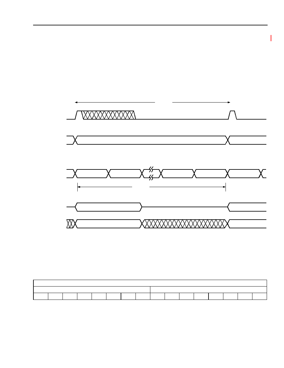
Preliminary Data Sheet
TMXF28155/51 Super Mapper
May 2001
155/51 Mbits/s SONET/SDH x28/x21 DS1/E1
529
Agere Systems Inc.
21 28-Channel Framer Block Functional Description
(continued)
21.26.12 CHI Timing with Associated Signaling Mode Enabled
Figure 72
illustrates the CHI frame timing when the associated signaling mode is enabled (bit FRM_ASM
(
Table 347
)) and the CHIDTS mode is disabled (bit FRM_CHIDTS (
Table 347
)). The frames are 125
µ
s long and
consist of 32 contiguous 16-bit time slots when the 4.096 MHz CHI data rate mode is selected.
In DS1 frame formats, each frame consists of 24 time slots and 8 stuffed time slots. Each time slot consists of two
octets.
In CEPT modes, each frame consists of 32 time slots. Each time slot consists of two octets.
5-8980(F)
Figure 72. Associated Signaling Mode Concentration Highway Interface Timing
21.26.13 ASM 2-Byte Time-Slot Format
Table 598
illustrates the ASM time slot format for valid channels.
Table 598. Associated Signaling Mode CHI 2-Byte Time-Slot Format for DS1 Frames
* X indicates bits that are undefined by the framer
The identical sense of the received system P bit in the transmitted signaling data is echoed back to the system in the received signaling infor-
mation.
The DS1 framing formats require rate adoption from the line-interface 1.544 Mbits/s bitstream to the system-inter-
face 4.096 Mbits/s bitstream. The rate adoption results in the need for stuffed time slots on the system interface.
Table 599
illustrates the ASM format for T1 stuffed channels. The stuffed data and signaling bytes contain the pro-
grammable idle code in register FRM_STUFF[] (default = 7F (hex)).
DS1: ASM CHI Time-Slot
Payload Data
Signaling Information*
1
2
3
4
5
6
7
8
A
B
C
D
X
F
G
P
TCHIFS/
125
µ
s
FRAME 1
FRAME 2
8.192 Mbits/s CHI:
RCHIDATA
4.096 Mbits/s CHI:
TCHIDATA
FRAME 1
FRAME 1
FRAME 2
FRAME 2
HIGH IMPEDANCE
RCHIDATA
TCHIDATA
or
FRAME = 64 bytes: 32 DATA + 32 SIGNALING
DATA AND SIGNALING BYTES ARE INTERLEAVED
SIGNALING 0
DATA 0
SIGNALING 31
DATA 0
DATA 31
FRAME
RCHIFS
TMXF28155/51 Super Mapper
Preliminary Data Sheet
155/51 Mbits/s SONET/SDH x28/x21 DS1/E1
May 2001
530
Agere Systems Inc.
21 28-Channel Framer Block Functional Description
(continued)
Table 599. Associated Signaling Mode CHI 2-Byte Time-Slot Format for Stuffed Channels
* The default stuff byte is shown.
21.26.14 CEPT: Time-Slot 16 Signaling ASM 2-Byte Time-Slot Format
Table 600
illustrates the ASM time slot format for valid CEPT E1 time slots.
Table 600. Associated Signaling Mode CHI 2-Byte Time-Slot format for CEPT
* In the CEPT formats, these bits are undefined.
The P bit is the parity-sense bit calculated over the 8 data bits, the ABCD bits, and the P bit. The identical
parity-sense
of the received system
Pbit in the transmitted signaling data is echoed back to the system in the received signaling information
21.26.15 CHI Offset Programming
To facilitate bit offset programming, two parameters are introduced: CEX is defined as the clock edge with which
the first bit of time slot 0 is transmitted; CER is defined as the clock edge on which bit 0 of time slot 0 is latched.
CEX and CER are counted relative to the edge on which the CHIFS signal is sampled. Values of CEX and CER
depend upon the values of the parameters described below.
The following three tables give decimal values of CEX and CER for various values of FRM_CMS (
Table 347
),
FRM_TFSCKE (
Table 347
), FRM_RFSCKE (
Table 355
), FRM_TOFF[2:0] (
Table 418
), and FRM_ROFF[2:0]
(
Table 418
). The byte (time slot) offsets are assumed to be zero in the following examples.
Table 601. Programming Values for FRM_TOFF[2:0] and FRM_ROFF[2:0] when FRM_CMS = 0
Table 602. Programming Values for FRM_TOFF[2:0] when FRM_CMS = 1
Table 603. Programming Values for FRM_ROFF[2:0] when FRM_CMS = 1
ASM CHI Time-Slot
Payload Data*
Signaling Information*
0
1
1
1
1
1
1
1
0
1
1
1
1
1
1
1
CEPT ASM CHI Time-Slot
Payload Data
Signaling Information
1
2
3
4
5
6
7
8
A
B
C
D
X*
X*
X*
P
FRM_TFSCKE/
FRM_RFSCKE
FRM_ROFF[2:0] or FRM_TOFF[2:0]
000
001
010
011
100
101
110
111
CER or
CEX
(decimal)
0
0
2
4
6
8
10
12
14
1
0
2
4
6
8
10
12
14
FRM_TFSCKE
FRM_TOFF[2:0]
000
001
010
011
100
101
110
111
CEX
(decimal)
0
0
4
8
12
16
20
24
28
1
0
4
8
12
16
20
24
28
FRM_RFSCKE
FRM_ROFF[2:0]
000
001
010
011
100
101
110
111
CER
(decimal)
0
0
4
8
12
16
20
24
28
1
0
4
8
12
16
20
24
28

Preliminary Data Sheet
TMXF28155/51 Super Mapper
May 2001
155/51 Mbits/s SONET/SDH x28/x21 DS1/E1
531
Agere Systems Inc.
21 28-Channel Framer Block Functional Description
(continued)
The offset is further determined by the use of four bits FRM_THALFOFF, FRM_RHALFOFF, FRM_TQUAROFF,
and FRM_RQUAROFF (
Table 418
). When the CHI clock and data rate are the same (FRM_CMS = 0), setting
FRM_THALFOFF and FRM_RHALFOFF bits will increase the clock edge offset, CEX and CER, by one. When the
CHI clock is twice the data rate (FRM_CMS = 1), setting the FRM_THALFOFF and FRM_RHALFOFF bits will
increase the clock edge offset by two, and setting the FRM_TQUAROFF and FRM_RQUAROFF bits will increase
the clock offset by one.
The byte offsets FRM_TBYOFF[6:0] and FRM_RBYOFF[6:0] (
Table 418
) increment the offset one byte at a time.
When FRM_CMS = 0, the offset will increment by 16 clock edges; when FRM_CMS = 1, the offset will increment by
32 clock edges.
Figure 73
shows an example of the relative timing of CHI 2.048 Mbits/s data with the following parameters:
s
FRM_CMS = 0, FRM_TFSCKE, FRM_RFSCKE = 0, FRM_TQUAROFF = 0, FRM_RQUAROFF = 0.
s
FRM_THALFOFF = 1, FRM_TOFF[2:0] = 001, FRM_TBYOFF[6:0] = 0000000.
s
FRM_RHALFOFF = 0, FRM_ROFF[2:0] = 010, FRM_RBYOFF[6:0] = 0000000.
5-8983(F)
Figure 73. TCHIDATA and RCHIDATA to CHICK Relationship with FRM_CMS = 0 (CEX = 3 and CER = 4,
Respectively)
Figure 74
shows an example of the relative timing of CHI 2.048 Mbits/s data with the following parameters:
s
FRM_CMS = 1, FRM_TFSCKE = 0, FRM_RFSCKE = 0.
s
FRM_THALFOFF = 1, FRM_TQUAROFF = 1, FRM_TOFF[2:0] = 000, FRM_TBYOFF[6:0] = 0000000.
s
FRM_RHALFOFF = 1, FRM_RQUAROFF = 0, FRM_ROFF[2:0] = 001, FRM_RBYOFF[6:0] = 0000000.
CHI FRAME SYNC IS SAMPLED ON THE FALLING EDGE
1
2
3
4
5
6
7
8
BIT 0, TS 0
BIT 1, TS 0
BIT 2, TS 0
CEX = 3
CER = 4
BIT 0, TS 0
BIT 1, TS 0
BIT 2, TS 0
HIGH IMPEDANCE
RCHIDATA
TCHIDATA
TCHIFS/
TCHICK/
RCHICK
RCHIFS

TMXF28155/51 Super Mapper
Preliminary Data Sheet
155/51 Mbits/s SONET/SDH x28/x21 DS1/E1
May 2001
532
Agere Systems Inc.
21 28-Channel Framer Block Functional Description
(continued)
5-8984(F)
Figure 74. CHI TCHIDATA and RCHIDATA to CHICK Relationship with FRM_CMS = 1 (CEX = 3 and CER = 6,
Respectively)
The timing figures shown are functional timing diagrams. See
Section 5.5 Concentration Highway (CHI) Timing on
page 46
in the Timing Characteristics section of this data sheet for CHI interface and clock timing parameter spec-
ifications.
21.26.16 The Parallel Bus System Interface Mode
This interface consists of a 16-bit wide parallel bus operating at 19.44 Mbyte/s, nine bits of which form a byte of
data and a data parity bit while the other eight bits contain the signaling and control information (A, B, C, and D sig-
naling bits, F and G signaling state bits, P parity bit, and a don't care bit). A clock and frame sync are expected in
both the receive and transmit directions.
Figure 75
, below, shows the transmit system interface in the parallel bus
system interface mode. The timing specifications for this interface are in the
Section 5.6 Parallel System Bus Tim-
ing on page 47
in the Timing Characteristics section of this data sheet. The offset between the frame sync and data
is fixed in this mode.
5-9037(F)
Figure 75. Parallel Bus System Interface Mode of the Transmit System Interfac e
CHI FRAME SYNC IS SAMPLED ON THE FALLING EDGE
1
2
3
4
5
6
7
8
BIT 0, TS 0
BIT 1, TS 0
CEX = 3
CER = 6
BIT 0, TS 0
HIGH IMPEDANCE
RCHIDATA
TCHIDATA
TCHIFS/
TCHICK/
BIT 1, TS 0
RCHICK
RCHIFS
TS_D[16:1]
FRAME
SLIP
TS_GFS
TS_GCLK
28
RS_GCLK
RS_GTCLK
TCLK
RS_D[16:1]
RS_GFS
TDM
PLL
FANOUT
1
28
28
FRAME
RATE
TFS
28
TDM
TRANSMIT SYSTEM
RECEIVE SYSTEM
FORMATTER
ADAPTATION
BUFFER
ALIGNER
BUFFER

Preliminary Data Sheet
TMXF28155/51 Super Mapper
May 2001
155/51 Mbits/s SONET/SDH x28/x21 DS1/E1
533
Agere Systems Inc.
21 28-Channel Framer Block Functional Description
(continued)
At 19.44 MHz, the parallel bus system interface has 2430 clocks per 8 ms frame. To transfer 84 DS1s or 63 E1s
requires only 2016 clocks. The difference is made up by inserting stuffs onto the bus every so often. Since multiple
devices (three) will drive the bus, the stuff positions are also used to greatly simplify the timing when switching from
one device to another. Both DS1 and E1 use the same general method to drive the bus which is:
s
Send some stuffs, then device 0 sends TS0 for link 1 ≠ n, then
s
Send some stuffs, then device 1 sends TS0 for link 1 ≠ n, then
s
Send some stuffs, then device 2 sends TS0 for link 1 ≠ n, then
s
Send some stuffs, then device 0 sends TS1 for link 1 ≠ n, then
s
Etc.
21.26.17 Distributed Stuffing: DS1
For DS1, the parallel bus system interface time slot arrangement is as follows:
Six stuff TSs | device 0, link 0--27 | six stuff TSs | device 1, link 0--27 | five* stuff TSs | device 2, link 0--2 |, etc.
Where * means in TSs 1, 5, 9, 13, 17, 21 six stuff time slots are inserted instead of five.
Hence: total time slots = (6 + 28 + 6 + 28 + 5 + 28) * 24 TSs + 6 extra stuff TSs = 2430 TSs.

TMXF28155/51 Super Mapper
Preliminary Data Sheet
155/51 Mbits/s SONET/SDH x28/x21 DS1/E1
May 2001
534
Agere Systems Inc.
21 28-Channel Framer Block Functional Description
(continued)
Table 604 shows the distribution of the time slots and stuffing in the STM-1 frame for the DS1 mode.
Table 604. Parallel System Bus Interface Time-Slot Arrangement for DS1
Link Number (R = stuffed time slot)
TS1
DEV0
R
R
R
R
R
R
1
2
3
4
5
6
7
8
9
10 11 12 13 14 15 16 17 18 19 20 21 22 23 24 25 26 27 28
DEV1
R
R
R
R
R
R
1
2
3
4
5
6
7
8
9
10 11 12 13 14 15 16 17 18 19 20 21 22 23 24 25 26 27 28
DEV2
R
R
R
R
R
R
1
2
3
4
5
6
7
8
9
10 11 12 13 14 15 16 17 18 19 20 21 22 23 24 25 26 27 28
TS2
DEV0
R
R
R
R
R
R
1
2
3
4
5
6
7
8
9
10 11 12 13 14 15 16 17 18 19 20 21 22 23 24 25 26 27 28
DEV1
R
R
R
R
R
R
1
2
3
4
5
6
7
8
9
10 11 12 13 14 15 16 17 18 19 20 21 22 23 24 25 26 27 28
DEV2
--
R
R
R
R
R
1
2
3
4
5
6
7
8
9
10 11 12 13 14 15 16 17 18 19 20 21 22 23 24 25 26 27 28
TS3
DEV0
R
R
R
R
R
R
1
2
3
4
5
6
7
8
9
10 11 12 13 14 15 16 17 18 19 20 21 22 23 24 25 26 27 28
DEV1
R
R
R
R
R
R
1
2
3
4
5
6
7
8
9
10 11 12 13 14 15 16 17 18 19 20 21 22 23 24 25 26 27 28
DEV2
--
R
R
R
R
R
1
2
3
4
5
6
7
8
9
10 11 12 13 14 15 16 17 18 19 20 21 22 23 24 25 26 27 28
TS4
DEV0
R
R
R
R
R
R
1
2
3
4
5
6
7
8
9
10 11 12 13 14 15 16 17 18 19 20 21 22 23 24 25 26 27 28
DEV1
R
R
R
R
R
R
1
2
3
4
5
6
7
8
9
10 11 12 13 14 15 16 17 18 19 20 21 22 23 24 25 26 27 28
DEV2
--
R
R
R
R
R
1
2
3
4
5
6
7
8
9
10 11 12 13 14 15 16 17 18 19 20 21 22 23 24 25 26 27 28
TS5
DEV0
R
R
R
R
R
R
1
2
3
4
5
6
7
8
9
10 11 12 13 14 15 16 17 18 19 20 21 22 23 24 25 26 27 28
DEV1
R
R
R
R
R
R
1
2
3
4
5
6
7
8
9
10 11 12 13 14 15 16 17 18 19 20 21 22 23 24 25 26 27 28
DEV2
R
R
R
R
R
R
1
2
3
4
5
6
7
8
9
10 11 12 13 14 15 16 17 18 19 20 21 22 23 24 25 26 27 28
TS6
DEV0
R
R
R
R
R
R
1
2
3
4
5
6
7
8
9
10 11 12 13 14 15 16 17 18 19 20 21 22 23 24 25 26 27 28
DEV1
R
R
R
R
R
R
1
2
3
4
5
6
7
8
9
10 11 12 13 14 15 16 17 18 19 20 21 22 23 24 25 26 27 28
DEV2
--
R
R
R
R
R
1
2
3
4
5
6
7
8
9
10 11 12 13 14 15 16 17 18 19 20 21 22 23 24 25 26 27 28
TS7
DEV0
R
R
R
R
R
R
1
2
3
4
5
6
7
8
9
10 11 12 13 14 15 16 17 18 19 20 21 22 23 24 25 26 27 28
DEV1
R
R
R
R
R
R
1
2
3
4
5
6
7
8
9
10 11 12 13 14 15 16 17 18 19 20 21 22 23 24 25 26 27 28
DEV2
--
R
R
R
R
R
1
2
3
4
5
6
7
8
9
10 11 12 13 14 15 16 17 18 19 20 21 22 23 24 25 26 27 28
TS8
DEV0
R
R
R
R
R
R
1
2
3
4
5
6
7
8
9
10 11 12 13 14 15 16 17 18 19 20 21 22 23 24 25 26 27 28
DEV1
R
R
R
R
R
R
1
2
3
4
5
6
7
8
9
10 11 12 13 14 15 16 17 18 19 20 21 22 23 24 25 26 27 28
DEV2
--
R
R
R
R
R
1
2
3
4
5
6
7
8
9
10 11 12 13 14 15 16 17 18 19 20 21 22 23 24 25 26 27 28
. . .
Repeat TS5-TS8 Format For TS9--TS12, TS13--TS16, TS17--TS20
. . .
TS21
DEV0
R
R
R
R
R
R
1
2
3
4
5
6
7
8
9
10 11 12 13 14 15 16 17 18 19 20 21 22 23 24 25 26 27 28
DEV1
R
R
R
R
R
R
1
2
3
4
5
6
7
8
9
10 11 12 13 14 15 16 17 18 19 20 21 22 23 24 25 26 27 28
DEV2
R
R
R
R
R
R
1
2
3
4
5
6
7
8
9
10 11 12 13 14 15 16 17 18 19 20 21 22 23 24 25 26 27 28
TS22
DEV0
R
R
R
R
R
R
1
2
3
4
5
6
7
8
9
10 11 12 13 14 15 16 17 18 19 20 21 22 23 24 25 26 27 28
DEV1
R
R
R
R
R
R
1
2
3
4
5
6
7
8
9
10 11 12 13 14 15 16 17 18 19 20 21 22 23 24 25 26 27 28
DEV2
--
R
R
R
R
R
1
2
3
4
5
6
7
8
9
10 11 12 13 14 15 16 17 18 19 20 21 22 23 24 25 26 27 28
TS23
DEV0
R
R
R
R
R
R
1
2
3
4
5
6
7
8
9
10 11 12 13 14 15 16 17 18 19 20 21 22 23 24 25 26 27 28
DEV1
R
R
R
R
R
R
1
2
3
4
5
6
7
8
9
10 11 12 13 14 15 16 17 18 19 20 21 22 23 24 25 26 27 28
DEV2
--
R
R
R
R
R
1
2
3
4
5
6
7
8
9
10 11 12 13 14 15 16 17 18 19 20 21 22 23 24 25 26 27 28
TS24
DEV0
R
R
R
R
R
R
1
2
3
4
5
6
7
8
9
10 11 12 13 14 15 16 17 18 19 20 21 22 23 24 25 26 27 28
DEV1
R
R
R
R
R
R
1
2
3
4
5
6
7
8
9
10 11 12 13 14 15 16 17 18 19 20 21 22 23 24 25 26 27 28
DEV2
--
R
R
R
R
R
1
2
3
4
5
6
7
8
9
10 11 12 13 14 15 16 17 18 19 20 21 22 23 24 25 26 27 28
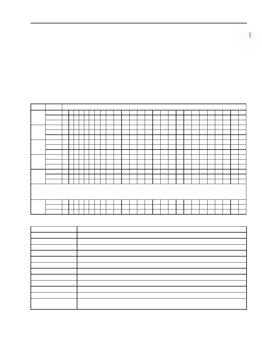
Preliminary Data Sheet
TMXF28155/51 Super Mapper
May 2001
155/51 Mbits/s SONET/SDH x28/x21 DS1/E1
535
Agere Systems Inc.
21 28-Channel Framer Block Functional Description
(continued)
21.26.18 Distributed Stuffing: E1
For E1, the parallel bus system interface time slot arrangement is as follows:
Five* stuff TSs | device 0, link 0--20 | four stuff TSs | device 1, link 0--20 | four stuff TSs | device 2,
link 0--20 |, etc.
Where * means in TS 0 three stuff time slots are inserted instead of five.
Hence: total time slots = (5 + 21 + 4 + 21 + 4 +21) * 32 TSs ≠ 2 TSs skipped in TS 0 = 2430 TSs.
Table 605
shows the distribution of the time slots and stuffing in the STM-1 frame for the E1 mode.
Table 605. Parallel System Bus Interface Time-Slot Arrangement for E1
Table 606. PSB System I/O Definition
Link number (R = stuffed time slot)
TS0
DEV0
--
-- R
R
R
1
2
3
4
5
6
7
8
9
10
11
12
13
14
15
16
17
18
19
20
21
DEV1
--
R
R
R
R
1
2
3
4
5
6
7
8
9
10
11
12
13
14
15
16
17
18
19
20
21
DEV2
--
R
R
R
R
1
2
3
4
5
6
7
8
9
10
11
12
13
14
15
16
17
18
19
20
21
TS1
DEV0
R
R
R
R
R
1
2
3
4
5
6
7
8
9
10
11
12
13
14
15
16
17
18
19
20
21
DEV1
--
R
R
R
R
1
2
3
4
5
6
7
8
9
10
11
12
13
14
15
16
17
18
19
20
21
DEV2
--
R
R
R
R
1
2
3
4
5
6
7
8
9
10
11
12
13
14
15
16
17
18
19
20
21
TS2
DEV0
R
R
R
R
R
1
2
3
4
5
6
7
8
9
10
11
12
13
14
15
16
17
18
19
20
21
DEV1
--
R
R
R
R
1
2
3
4
5
6
7
8
9
10
11
12
13
14
15
16
17
18
19
20
21
DEV2
--
R
R
R
R
1
2
3
4
5
6
7
8
9
10
11
12
13
14
15
16
17
18
19
20
21
TS3
DEV0
R
R
R
R
R
1
2
3
4
5
6
7
8
9
10
11
12
13
14
15
16
17
18
19
20
21
DEV1
--
R
R
R
R
1
2
3
4
5
6
7
8
9
10
11
12
13
14
15
16
17
18
19
20
21
DEV2
--
R
R
R
R
1
2
3
4
5
6
7
8
9
10
11
12
13
14
15
16
17
18
19
20
21
TS4
DEV0
R
R
R
R
R
1
2
3
4
5
6
7
8
9
10
11
12
13
14
15
16
17
18
19
20
21
DEV1
--
R
R
R
R
1
2
3
4
5
6
7
8
9
10
11
12
13
14
15
16
17
18
19
20
21
DEV2
--
R
R
R
R
1
2
3
4
5
6
7
8
9
10
11
12
13
14
15
16
17
18
19
20
21
. . .
Repeat TS4 Format For TS5
--
TS30
. . .
TS31
DEV0
R
R
R
R
R
1
2
3
4
5
6
7
8
9
10
11
12
13
14
15
16
17
18
19
20
21
DEV1
--
R
R
R
R
1
2
3
4
5
6
7
8
9
10
11
12
13
14
15
16
17
18
19
20
21
DEV2
--
R
R
R
R
1
2
3
4
5
6
7
8
9
10
11
12
13
14
15
16
17
18
19
20
21
Name
Definition
TS_D[ ], RS_D[] [16:9] Time Slot Data [msb:lsb]
TS_D[ ], RS_D[] [8]
Data Parity
TS_D[ ], RS_D[] [7]
Signaling A-bit
TS_D[ ], RS_D[] [6]
Signaling B-bit
TS_D[ ], RS_D[] [5]
Signaling C-bit
TS_D[ ], RS_D[] [4]
Signaling D-bit
TS_D[ ], RS_D[] [3]
Signaling F-bit
TS_D[ ], RS_D[] [2]
Signaling G-bit
TS_D[ ], RS_D[] [1]
Signaling Parity
TS_GCLK, RS_GCLK System Global Clock [19.44 MHz]
TS_GFS, RS_GFS
System Frame Sync
RS_GTCLK
External Global Transmit Line Clock (CEPT-2.048 MHz, T1-1.544 MHz). Only required if
internal framer PLL is not used.
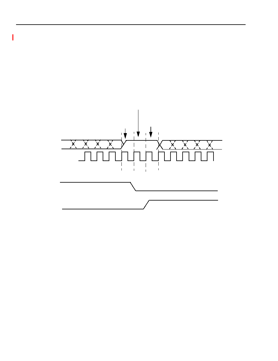
TMXF28155/51 Super Mapper
Preliminary Data Sheet
155/51 Mbits/s SONET/SDH x28/x21 DS1/E1
May 2001
536
Agere Systems Inc.
21 28-Channel Framer Block Functional Description
(continued)
21.26.19 Drive to 3-State and 3-State to Drive Timing
The minimum number of stuff time slots is 3 (in the E1 mode). This allows enough time to switch the bus between
devices. The device on the bus can drive the bus high for one extra clock cycle to ensure a fast rise time. The
device then 3-states while the bus is pulled high, using a pull-up resistor. Optionally, the next device starts driving
early for one clock cycle to ensure that there is minimal delay between the clock and data outputs (the turn-on
delay of the buffer is eliminated by turning on the buffer one clock cycle early). The timing for the case of three stuff
time slots is shown in the
Figure 76
. (In the receive direction from the switch, we assume the stuff time slots are
driven to 1.)
5-8992(F)
Figure 76. Parallel Bus System Interface Turnaround Timing
See
Section 5.6 Parallel System Bus Timing on page 47
in the Timing Characteristics section of this data sheet for
PSB receive and transmit interface and clock timing parameter specifications.
21.27 Serial Multiplex Interface
The network serial multiplexed interface (NSMI) provides a no-slip capability for transfer of multiple framed DS1s
and/or E1s from one device to another using a very narrow interface. A no-slip interface is widely used in datacom
and IMA applications. There are two NSMI interface modes of operation requiring either six or eight signals to be
used.
Mode 1 uses six primary signals. The six primary signals are composed of three transmit and three receive signals.
The transmit signals are LINETXCLK29 (R24), LINETXDATA29 (T23), and LINETXSYNC29 (R26). The receive
signals are LINERXCLK29 (B13), LINERXDATA29 (D13), and LINERXSYNC29 (A13). Each group of three signals
provide clock, data, and control information.
The data and link number specified by the LINETXDATA29 and LINETXSYNC29 will be received in the same order
by the receive side of the Super Mapper after traversing the switch side of the system.
DEV 1 MAY DRIVE
DEV 0, LINK 0-N
PULLED HIGH
USING A PULL-UP
DEV 0 DRIVES
HIG H FOR ONE
EXTR A CLO CK
DEV 1, LINK 0-N
HIGH ONE CLOCK
CYCLE EARLY
R
R
R
MINIMUM OF 3 STUFF TIME-SLOTS
CYCLE
SYS DATA[I]
SYS CLK
DEV 0 ENA
DRIVE
HIGH-IMPEDANCE
DEV 1 ENA
HIGH-IMPEDANCE
DRIVE

Preliminary Data Sheet
TMXF28155/51 Super Mapper
May 2001
155/51 Mbits/s SONET/SDH x28/x21 DS1/E1
537
Agere Systems Inc.
21 28-Channel Framer Block Functional Description
(continued)
21.27.1 Signals (6-Pin Mode)
5-9100(F)r.2
Figure 77. Signals (6-Pin Mode)
s
LINERXCLK29 (B13)--Output of the switch, which is the LINETXCLK29, delayed.
s
LINERXDATA29 (D13)--Serial data sent out of the switch. The MSB is sent out first and at the same time, the
first bit (start bit) of the LINERXSYNC29 is sent out.
s
LINERXSYNC29 (A13)--The control data, otherwise known as the serial ID (SID), is generated by the switch.
s
LINETXCLK29 (R24)--Clock signal generated by the Super Mapper.
s
LINETXDATA29 (T23)--Serial data sent out of the Super Mapper. The MSB is sent out first and at the same time
the first bit (start bit) of the LINETXSYNC29 is sent out.
s
LINETXSYNC29 (R26)--The control data, otherwise known as the serial ID (SID), is generated by the Super
Mapper.
Mode 2 uses the same six primary signals as mode 1, along with two additional transmit signals. Signal RXDA-
TAEN (AB19) is a clock signal generated by the Super Mapper. Signal TXDATAEN (W22) contains control data in
the same format as the LINETXSYNC29 (R26) and LINERXSYNC29 (A13) signals. These two extra transmit sig-
nals from the Super Mapper specify data links and data requested on the Super Mapper NSMI receive ports. This
allows the Super Mapper to receive links and data independent from those transmitted by the Super Mapper.
21.27.2 Signals (8-Pin Mode)
5-9101(F)r.2
Figure 78. Signals (8-Pin Mode)
S U P E R
M A P P E R
R E C E IV E
S M I
T R A N S M IT
IN T E R F A C E
S W IT C H
T R A N S M IT
R E C E IV E
L IN E R X C L K 2 9
L IN E R X D A T A 2 9
L IN E R X S Y N C 2 9
L IN E T X C L K 2 9
L IN E T X D A T A 2 9
L IN E T X S Y N C 2 9
S U P ER
M AP P E R
R E C E IVE
S M I
T R A N S M IT
IN T E R F A C E
SW IT C H
T R A N S M IT
R EC EIV E
LIN E R X C L K 29
L IN E R X D A T A2 9
LIN E R X S YN C 2 9
L IN ET XC LK 2 9
LIN E T X D A T A 2 9
L IN E T XS Y N C 2 9
E X T R A
R EC EIV E
EX T R A
T R A N S M IT
R X D A T A E N
T XD AT A EN

TMXF28155/51 Super Mapper
Preliminary Data Sheet
155/51 Mbits/s SONET/SDH x28/x21 DS1/E1
May 2001
538
Agere Systems Inc.
21 28-Channel Framer Block Functional Description
(continued)
s
LINERXCLK29 (B13)--Output of the switch, which is the LINETXCLK29, delayed.
s
LINERXDATA29 (D13)--Serial data sent out of the switch. The MSB is sent out first and at the same time, the
first bit (start bit) of the LINE_RXSYNC29 is sent out.
s
LINERXSYNC29 (A13)--The control data, otherwise known as the serial ID (SID), is generated by the switch.
s
LINETXCLK29 (R24)--Clock signal generated by the Super Mapper.
s
LINETXDATA29 (T23)--Serial data sent out of the Super Mapper. The MSB is sent out first and at the same time
the first bit (start bit) of the LINETXSYNC29 is sent out.
s
LINETXSYNC29 (R26)--The control data, otherwise known as the serial ID (SID), is generated by the Super
Mapper.
s
RXDATAEN (AB19)--Clock signal generated by the Super Mapper.
s
TXDATAEN (W22)--The control data, otherwise known as the serial ID (SID), is generated by the Super Mapper.
21.27.3 Timing Diagrams
s
Single Octet
-- Data is sent out on the LINETXDATA29 (T23) line serially with the MSB of the data first. The MSB is driven at
the same time the START bit of the LINETXSYNC29 (R26) signal is driven.
-- Following the START bit, the FSYNC bit of the SID is driven. After the FSYNC bit, the LSB of the LINKNUMBER
is sent. Once the MSB of the LINKNUMBER is driven, the final bit of the SID is sent. This final bit is a reserved
bit and must be 0.
5-8990(F)r.2
Figure 79. Network Serial Multiplexed Interface (Single Octet)
Table 607. Serial ID
s
Multiple Octets
-- Single octets of data can be sent out consecutively. Any number of clocks can separate octets. During the time
when octets are separated, the LINETXSYNC29 line must be driven with a 1.
Name
Bit
Description
START
0
Start Bit.
0 = Start an octet. Bits 1 to 7 follow.
1 = Do not start an octet. Next bit is another bit 0.
FSYNC
1
Frame Sync Bit. Indicates whether the current byte corresponds to the first
byte in the frame or not.
0 = Not the first byte.
1 = First byte.
LINKNUMBER[5:0]
6:2
Link Number. These bits indicate the link number of received/transmitted
data.
--
7
Reserved. Must write to 0.
START
fSYNC
LINKNUMBER[5:0]
SERIAL DATA
MSB
LSB
LSB
MSB
LINETXCLK29
LINETXDATA29
LINETXSYNC29
RESERVED

Preliminary Data Sheet
TMXF28155/51 Super Mapper
May 2001
155/51 Mbits/s SONET/SDH x28/x21 DS1/E1
539
Agere Systems Inc.
21 28-Channel Framer Block Functional Description
(continued)
5-9102(F)r.1
Figure 80. Network Serial Multiplexed Interface (Multiple Octets)
21.27.4 Time-Slot Sequencing
s
Link numbers--28 link numbers, numbered 1 to 28 in T1 mode, and 1 to 21 for E1 mode.
Note: Link numbers can start at 0 by setting FRM_LNKSTART (
Table 347
) bit 8 at address 0x80050 to 0. This will
cause the link numbers for T1 to be numbered 0--27 and for E1, 0--20.
s
In T1 mode, each of the 28 links has 24 time slots and should be numbered 1 to 24.
s
In E1 mode, each of the 21 links has 32 time slots and should be numbered 0 to 31.
s
The FSYNC (
Table 607
) bit indicates that the data for the link is in the first time slot for that frame (time slot 1 in
T1 and time slot 0 in E1 mode).
s
Link data is sent out in any order. It is totally unpredictable. Time slots are sent in order and it is the job of the
switch to keep track of which time slot it receives.
Note: The order of the links sent out is in relation to the order in which the Super Mapper framer receives the links.
Thus it is possible, for example, to receive all the time slots for link 5 and then start the next frame of data for
link 5 before link 10 completes its frame.
The minimum and maximum time between successive time slots on a link is calculated below for both DS1
and E1, using an NSMI bus clock of 51.84 MHz (19.3 ns clock period).
DS1:
Max time = (1 link time slot interval) + (27 links * 8 bits * NSMI clk period) + (1 link bit time).
Max time = 5.2 µs + (27 * 8 * 19.3 ns) + (648 ns) = 10 µs.
Min time = (1 link time slot interval) ≠ (27 links * 8 bits * NSMI clk period).
Min time = 5.2 µs ≠ (27 * 8 * 19.3 ns) = 1.0 µs.
E1:
Max time = (1 link time slot interval) + (20 links * 8 bits * NSMI clk period).
Max time = 3.9 µs + (20 * 8 * 19.3 ns) = 7.0 µs.
Min time = (1 link time slot interval) ≠ (20 links * 8 bits * NSMI clk period).
Min time = 3.9 µs ≠ (20 * 8 * 19.3 ns) = 0.8 µs.
21.27.5 Timing Between Transmit and Receive
6-Pin Mode. The Super Mapper sends out the data and link information through the transmit signals. While it
sends data, it also expects data to be sent back for the same link number and time slot. The only requirement the
Super Mapper has is that it receives data at a constant time interval every time. For example, at clock 1 data and
link information was sent to the switch. Then at clock 16, data was sent back to the Super Mapper. Thus, the time
taken to send data back was 15 clocks. During this time, the next link and data were sent to the switch at clock 9,
the Super Mapper must receive the second data requested at clock 24. The time interval must be constant. It
doesn't matter how long, but it must be constant.
START
SERIAL DATA
MSB
LSB
SERIAL DATA
SERIAL DATA
START
START
LINETXCLK29
LINETXDATA29
LINETXSYNC29

TMXF28155/51 Super Mapper
Preliminary Data Sheet
155/51 Mbits/s SONET/SDH x28/x21 DS1/E1
May 2001
540
Agere Systems Inc.
21 28-Channel Framer Block Functional Description
(continued)
8-Pin Mode. As in the 6-pin mode, the Super Mapper sends data and link information through the transmit signals.
However, in the 8-pin mode, it requests data through the extra transmit signals. The data is then expected to be
sent back for the same link number and time slot on the Super Mapper's receive signals. As in the 6-pin mode, the
only requirement is that it receives data at a constant time interval.
21.28 Superframer Host Interface
21.28.1 Superframer Register Addressing
Table 608 summarizes the current number of global and per link/channel registers for each block.
Table 608. Current Number of Global and per Link/Channel Registers for Each Block
All of the block global registers will be combined with the top global register. Each block will receive a global select
and a per link/per channel select.
The block addressing is summarized below. An extra bit is used for future growth of global and link/channel regis-
ters.
Table 609
describes the addressing scheme. Bit 14 is used to indicate whether a link or HDLC channel is selected
(0 selects link and global registers; 1 selects HDLC registers). When an HDLC channel is to be addressed, bits
B13--B8 indicate the HDLC channel numbers 0--63 (000000--111111), bit B7 indicates the transmit or receive
paths, and bits B3--B0 indicate the register number. When a link is selected, bits B13--B9 indicate the link num-
bers 1--28 (00001--11100), and bit B8 indicates the transmit and receive paths for the link. Bits B7--B0 indicate
the block and register number, as shown in Framer Addressing Map for the Global and Per Link/Channel Registers
of the Superframer,
Table 609 on page 541
. Global registers are selected by setting B14--B9 = 000000, selecting
a block using bits B7--B4, and selecting a register using bits B3--B0.
Block
Global
Per Link/Per Channel
TOP
1
0/0
AR
0
2/0
RXP FF
0
2/0
TXP FF
0
2/0
RXP PM
15
19/0
TXP PM
15
19/0
RXP SYS
5
3/0
TXP SYS
1
2/0
RXP HDLC
6
0/8
TXP HDLC
6
0/8
RXP DL
0
9/0
TXP DL
0
9/0
RXP SIG
1
41/0
TXP SIG
1
36/0
RXP LC
0
1/0
TXP LC
0
1/0

Preliminary Data Sheet
TMXF28155/51 Super Mapper
May 2001
155/51 Mbits/s SONET/SDH x28/x21 DS1/E1
541
Agere Systems Inc.
21 28-Channel Framer Block Functional Description
(continued)
21.29 Superframer Register Addressing
Table 609 below summarizes the address map for the global and per link/channel registers of the superframer:
Table 609. Framer Addressing Map for the Global and Per Link/Channel Registers of the Superframer
21.29.1 Per Link Register Sections in Table 609
SIG = Signaling (see
Section 12.9.1 Signaling Per Link Registers on page 267
).
PM = Performance Monitor (see
Section 12.3 Performance Monitor Global Registers on page 247
).
RDL = Receive (Facility) Data Link (see
Section 12.11 Receive Facility Data Link Configuration and Status Registers on
page 288
).
TDL = Transmit (Facility) Data Link (see
Section 12.12 Transmit Facility Data Link Configuration and Status Registers on
page 290
).
SYS = System Interface (see
Section 12.13 System Interface, Arbiter, and Frame Formatter Mapping on page 292
).
AR = Arbiter (Framer) (see
Section 12.2 Arbiter (Framer) Global Registers on page 245
).
FF = Frame Formatter (Transmit Framer) (see
Section 12.16 Frame Formatter Per Link Registers on page 300
).
LC = Line Encoder/Decoders (see
Section 12.18 Line Encoder/Decoder Per Link Registers on page 303
); RXP = 0 for
the line encoder and TXP = 1 for the line decoder.
HDLC = High-Level Data Link Control (see
Section 12.19 HDLC Per Channel Configuration and Status Registers on
page 304
); RXP = 0 for the receive HDLC and TXP = 1 for the transmit HDLC.
RXP = High-Level Data Link Control (see
Table 432 on page304
) RXP = 0 for the receive HDLC and TXP = 1 for the
transmit HLDLC.
Address Pins (ADDR15--ADDR0)
15
14
13
12
11
10
9
8
7
6
5
4
3
2
1
0
0
Framer Global Registers
0
0
0
0
0
0
RXP=0/
TXP=1
0
0
0
0
Superframer Global
0
0
0
1
AR (Framer)
0
0
1
0
Performance Monitor
0
0
1
1
Performance Monitor
0
1
0
0
HDLC
0
1
0
1
System Interface
0
1
1
0
Signaling
0
1
1
1
Frame Formatter
(Transmit Framer)
1
0
0
0
Reserved
1
0
0
1
Receive Data Link
1
0
1
0
Transmit Data Link
1
Others
Reserved
0
Links 1--28 (00001--11100)
Framer Functional Register Addresses
LNK4 LNK3 LNK2 LNK1
LNK0
0
SIG6
SIG5
SIG4
SIG3
SIG2
SIG1
SIG0
1
0
PM5
PM4
PM3
PM2
PM1
PM0
1
1
0
0
RDL3
RDL2
RDL1
RDL0
1
1
0
1
TDL3
TDL2
TDL1
TDL0
1
1
1
0
0
SYS2
SYS1
SYS0
1
1
1
1
0
0
AR1
AR0
1
1
1
1
0
1
FF1
FF0
1
1
1
1
1
0
Res.
Res.
1
1
1
1
1
1
LC1
LC0
1
HDLC Channels 1--64 (000000--111111)
RXP=0/
TXP=1
0
0
0
Per Channel Register
HDL9 HDL8 HDL7 HDL6
HDL5
HDL4
HDL3
HDL2
HDL1
HDL0

TMXF28155/51 Super Mapper
Preliminary Data Sheet
155/51 Mbits/s SONET/SDH x28/x21 DS1/E1
May 2001
542
Agere Systems Inc.
22 Cross Connect (XC) Block Functional Description
Table of Contents
Contents
Page
22 Cross Connect (XC) Block Functional Description ......................................................................................... 542
22.1 Cross Connect Introduction .................................................................................................................... 544
22.2 Cross Connect Features ......................................................................................................................... 544
22.3 Cross Connect Block Diagram ............................................................................................................... 545
22.3.1 Framer to Cross Connect Overview ............................................................................................ 546
22.3.2 External I/O to Cross Connect Overview ..................................................................................... 547
22.4 Cross Connect Connectivity Overview ................................................................................................... 548
22.5 DS1/E1 Cross Connect .......................................................................................................................... 549
22.5.1 DS1/E1 Connectivity Matrix ......................................................................................................... 550
22.5.2 DS1/E1 Register Definition .......................................................................................................... 550
22.6 Notes on the DS1 Cross Connect .......................................................................................................... 552
22.6.1 DS1/E1 TPG ................................................................................................................................ 552
22.6.2 M13 DS1/E1 Interface ................................................................................................................. 552
22.6.3 VT Mapper DS1/E1 Interface ...................................................................................................... 553
22.6.4 Digital Jitter Attenuator (DJA) Interface ....................................................................................... 553
22.6.5 Framer System Interface ............................................................................................................. 554
22.6.6 Framer System Interface--PSB .................................................................................................. 555
22.6.7 Framer System Interface--CHI ................................................................................................... 555
22.6.8 Framer System Interface--NSMI ................................................................................................ 557
22.7 DS2 Connectivity .................................................................................................................................... 557
22.7.1 M13 DS2 Interface (DS2 Cross Connect) ................................................................................... 558
22.7.2 M12 MUX (Transmit Path) ........................................................................................................... 558
22.7.3 M12 DeMUX (Receive Path) ........................................................................................................ 560
22.7.4 M23 DeMUX (Receive Path) ....................................................................................................... 561
22.7.5 M23 MUX (Transmit Path) ........................................................................................................... 562
22.8 DS3 Connectivity .................................................................................................................................... 564
22.8.1 DS3 TPG/TPM Cross Connect .................................................................................................... 565
22.8.2 DS3 Basic Cross Connect ........................................................................................................... 566
22.8.3 NSMI Cross Connect ................................................................................................................... 567
22.9 Transmit and Receive Path Overhead Access Channel I/O Configuration ............................................ 568
Figures
Page
Figure 81. Cross Connect Block Diagram ............................................................................................................ 545
Figure 82. Framer and Cross Connect ................................................................................................................. 546
Figure 83. DS1 Cross Connect Interface.............................................................................................................. 549
Figure 84. DS1E1 External I/O to M13 ................................................................................................................. 552
Figure 85. Framer Line Interface Cross Connect ................................................................................................. 554
Figure 86. Framer System Interface--Parallel System Bus (PSB) ...................................................................... 555
Figure 87. Framer System Interface--Concentration Highway Interface (CHI) ................................................... 556
Figure 88. DS2 Cross Connect Interface.............................................................................................................. 557
Figure 89. M12 MUX DS2 Output Cross Connect................................................................................................ 559
Figure 90. M12 DeMUX Input DS2 Cross Connect .............................................................................................. 561
Figure 91. M23 DeMUx DS2 Output Cross Connect ............................................................................................ 562
Figure 92. M23 MUX DS2 Input Cross Connect................................................................................................... 563
Figure 93. DS3 Cross Connect............................................................................................................................. 564
Figure 94. DS3 Test-Pattern Cross Connect........................................................................................................ 565
Figure 95. DS3 Basic Cross Connect ................................................................................................................... 566
Figure 96. NSMI Interface Cross Connect............................................................................................................ 568
Figure 97. TPOAC and RPOAC Cross Connect .................................................................................................. 569

Preliminary Data Sheet
TMXF28155/51 Super Mapper
May 2001
155/51 Mbits/s SONET/SDH x28/x21 DS1/E1
543
Agere Systems Inc.
Tables
Page
Table 610. Multifunction System Interface Programmable I/O ............................................................................ 547
Table 611. DS3 Interface Programmable I/O ...................................................................................................... 548
Table 612. Transmit and Receive POAC Programmable I/O .............................................................................. 548
Table 613. Connectivity Within the Cross Connect Block ................................................................................... 548
Table 614. DS1/E1 Signal Connectivity Matrix .................................................................................................... 550
Table 615. Special XC_PDATA Source IDs for Source Block = 0 ....................................................................... 551
Table 616. Special XC_SYNC Source IDs for Source Block = 0 ......................................................................... 551
Table 617. Special XC_ALCO Source IDs for Source Block = 0 ......................................................................... 551
Table 618. Configuration of the Control Group .................................................................................................... 556
Table 619. XC_PDATA Source IDs for LINETXDATA Routing with Source Block = 111 ................................... 559
Table 620. XC_PDATA Source IDs for LINETXCLK Routing with Source Block = 111 ...................................... 559
Table 621. DS3 Connectivity ............................................................................................................................... 564

TMXF28155/51 Super Mapper
Preliminary Data Sheet
155/51 Mbits/s SONET/SDH x28/x21 DS1/E1
May 2001
544
Agere Systems Inc.
22 Cross Connect (XC) Block Functional Description
(continued)
22.1 Cross Connect Introduction
The cross connect block is a highly configurable crosspoint switch for internal DS1/E1/DS2/DS3 signal connections
in the Super Mapper. The cross connect allows flexible configuration of the Super Mapper's internal blocks to sup-
port a variety of applications. The internal 28-channel framer, VT mapper, SPE mapper, M13, digital jitter attenua-
tor, and test-pattern generator/monitor blocks or external device I/O pins can be interconnected with the
independent, nonblocking signal routing of the cross connect block.
22.2 Cross Connect Features
s
Configurable crosspoint interconnect for up to 28 DS1 signals or 21 E1 signals to/from the framer (or external
pins), and the same number of signal channels to/from the M13 and VT mapper. Also supports up to seven DS2
signals to/from the external pins or M12 MUXes, connecting to the M13 MUX M23 block. Also connects one DS3
signal to/from the external NSMI interface to the SPE, M13, or TPG blocks. Any mix of DS1, E1, DS2, or DS3 sig-
nals may be interconnected.
s
Any transmitter (signal source) may be connected to any receiver (signal destination) in the DS1/E1 cross con-
nect. Multicast or broadcast operation (one port to many) is supported.
s
Jitter attenuation may also be inserted in-line on any DS1/E1 channel. (Note: Cascading of jitter attenuators is
not allowed.)
s
Standard network loopback or straight away facility testing is supported for DS1/E1 and DS3. Any source or
transmitter may be replaced by a test-pattern generator capable of injecting idle, standards based pseudoran-
dom bit sequence test patterns, or AIS (blue) alarm. Any sink or receiver may be replaced by a test-pattern mon-
itor, which can detect/count bit errors in a pseudorandom test sequence, or loss of frame, or loss of sync.
s
Loopbacks may be configured to sectionalize a circuit for identifying faults or misconfiguration during out of ser-
vice maintenance.
s
Fast alarm channels are supported for VT mapper or M13 to framer interconnects for alarm indication signal (AIS
or blue alarm) and VT mapper only for remote alarm indicator (RAI or yellow alarm). This feature reduces the
propagation delay of the alarms by eliminating multiple integration of alarm conditions.
s
Supports M12, M23 or C-bit parity, M13, or VT group modes of operation.
s
Supports framer-only, transport (framer LIU, M13, and VT mapper), and switching (CHI and PSB) modes of oper-
ation.
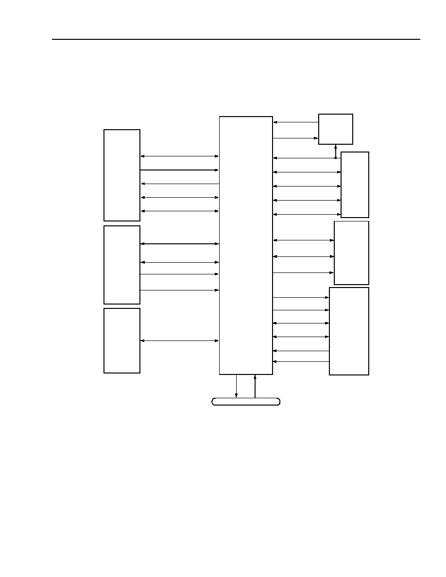
Preliminary Data Sheet
TMXF28155/51 Super Mapper
May 2001
155/51 Mbits/s SONET/SDH x28/x21 DS1/E1
545
Agere Systems Inc.
22 Cross Connect (XC) Block Functional Description
(continued)
22.3 Cross Connect Block Diagram
The following diagram illustrates the high-level interface between the XC block and other functional blocks.
5-9180(F)r.5
Figure 81. Cross Connect Block Diagram
CROSS
CONNECT
CONTROL INTERFACE
M12_DS2_DATA/CLK
DS3_DATA/CLK
DS1_DATA/CLK/STFREQ
M23_DS2_DATA/CLK/STFREQ
DS1_DATA/CLK/FSYNC
AUTOAIS
RAI
M13
VT
MAPPER
DS1_DATA/CLK/FSYNC
RAI
28
DS1_DATA/CLK/FSYNC
TEST
GEN/MON
TPM
TPG
EXT.
I/O
DS1_STFREQ
AUTOAIS
DS1_DATA/CLK
ATTENUATOR
DIGITAL
PTRADJ
PTRADJ
AUTOAIS
T/R_POAC
DS3_DATA/CLK
DS1_E1 DS2_AISCLK
DS1_AISCLK
E1_AISCLK
JITTER
PIN
(XC)
DS2_DATA/CLK
AUTOAIS
SPE
MAPPER
DS3_DATA/CLK
CHANNEL
FRAMER
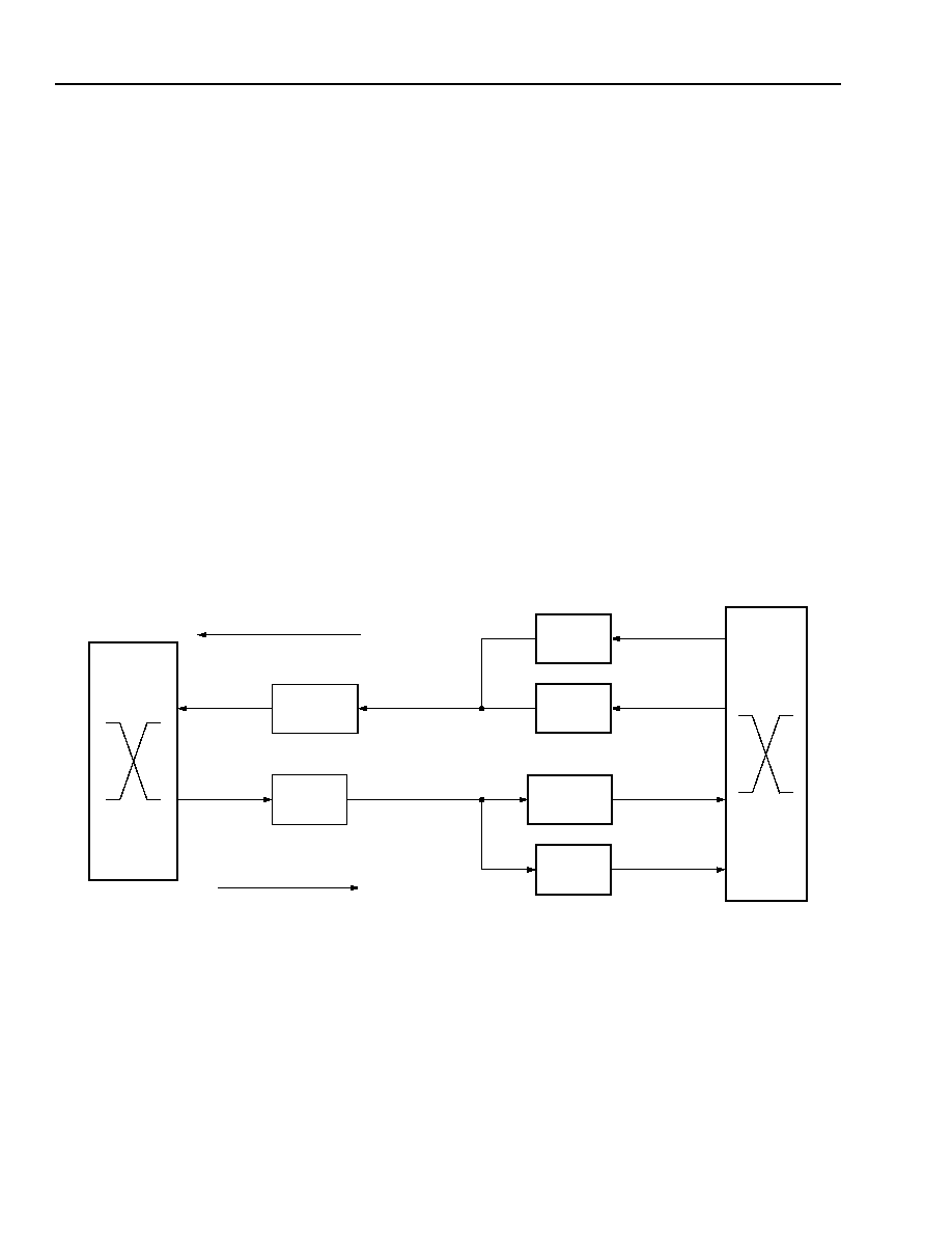
TMXF28155/51 Super Mapper
Preliminary Data Sheet
155/51 Mbits/s SONET/SDH x28/x21 DS1/E1
May 2001
546
Agere Systems Inc.
22 Cross Connect (XC) Block Functional Description
(continued)
The cross connect can functionally be divided into three major sections: XC1 for DS1(E1), XC2 for DS2, and XC3
for DS3. Each section can be configured to establish interconnects between major functional blocks or connect
blocks to external I/O to establish an application. The DS1 and DS2 cross connects can establish the order of the
circuits to be multiplexed and demultiplexed in the transmission hierarchy. In addition, a programmable MUX is pro-
vided for selecting the path overhead access channel connection.
Literally hundreds of signals are interconnected. The cross connect is designed to simplify the configuration by
defining a set of sources and destinations. Signals such as data, clock, alarm, and control associated with an iden-
tified source and destination are bundled to simplify the cross connect configuration. Establishing a connection in
the configuration registers will interconnect the source group of signals to the destination group of signals.
It is important to note that the configuration information is not shared between major blocks. For example, a virtual
tributary is interconnected between the VT mapper and the framer. The cross connect can establish the intercon-
nect for data and clock and intelligently establish the proper interconnects for alarms and control. The framer block
and VT mapper are required to be properly configured for operation as a DS1 or E1 and selection of clock edge to
properly sample the data.
A brief overview of the framer block and the device external I/O pins is useful prior to a detailed description of the
cross connect block.
22.3.1 Framer to Cross Connect Overview
The framer block interface to the cross connect is subdivided into six defined interfaces for each of the 28 framers
as shown in
Figure 82
. A brief explanation follows for establishing path and interconnect definition.
5-9181(F)
Figure 82. Framer and Cross Connect
FRM_TP_T, FRM_TP_R--Transmit and receive interfaces for the framer transmit path (TP).
FRM_RP_T, FRM_RP_R--Transmit and receive interfaces for the framer receive path (RP).
FRM_RS--Framer receive system interface (RS).
FRM_TS--Framer transmit system interface (TS).
Note: The receive system interface is associated with the transmit path and the transmit system interface is asso-
ciated with the receive path. The system interface definitions have been assigned based on historical con-
vention.
RP FRAME
ALIGNER
RP FRAME
FORMATTER
TP FRAME
ALIGNER
TP FRAME
FORMATTER
RECEIVE
SYSTEM
TRANSMIT
SYSTEM
FRM_RS
FRM_TP_R
FRM_TP_T
FRM_RP_R
FRM_RP_T
FRM_TS
TRANSMIT PATH
RECEIVE PATH
CROSS
CONNECT
CROSS
CONNECT

Preliminary Data Sheet
TMXF28155/51 Super Mapper
May 2001
155/51 Mbits/s SONET/SDH x28/x21 DS1/E1
547
Agere Systems Inc.
22 Cross Connect (XC) Block Functional Description
(continued)
The path designations assigned to the framer are consistent with established network definitions. Signals multi-
plexed up into the digital hierarchy from the transmit path. Signals demultiplexed from the digital hierarchy comprise
the receive path.
In switching applications, concentration highway interface (CHI) or parallel system bus (PSB) signals will enter
through the external I/O and are cross connected to the receive system interface (top right side of
Figure 82
). The
signals will traverse the framer through the transmit path frame formatter and are cross connected to the internal
multiplexers/mappers (top left side of
Figure 82
). Signals demultiplexed from DS3 or demapped from SONET are
cross connected to the receive path frame aligner (bottom left side of
Figure 82
) traverse the framer, and are cross
connected from the transmit system interface to the external I/O pins (bottom right side of
Figure 82
).
In transport mode, line interface (LIU) signals will enter through the external I/O and are cross connected to the
transmit path frame aligner interface (top right side of
Figure 82
). The signals will traverse the framer through the
transmit path frame formatter and are cross connected to the internal multiplexers/mappers (top left side of
Figure 82
). Signals demultiplexed from DS3 or demapped from SONET are cross connected to the receive path
frame aligner (bottom left side of
Figure 82
) traverse the framer, and are cross connected from the receive path
frame formatter to the external I/O pins (bottom right side of
Figure 82
) on to the LIUs.
Most applications will cross connect the framer interfaces FRM_TP_T and FRM_RP_R to the M13 MUX or VT
mapper. The framer interfaces FRM_RP_T and FRM_TP_R or the system interfaces FRM_TS and FRM_RS will
be cross connected to the external I/O of the multifunction system interface.
22.3.2 External I/O to Cross Connect Overview
The cross connect defines the connectivity of device pins associated with the DS3 (6 pins), STS-1 POAC (6 pins),
and the multifunction system interface (174 pins). Therefore, the cross connect plays a very large role in configur-
ing the functionality of the Super Mapper from the applications viewpoint.
The multifunction system interface device pins connectivity may be configured to support DS1/E1 (LIU and serial
data/clock/sync), DS2 interfaces, channelized (DS0), and multiplexed system interfaces (CHI, PSB, or NSMI).
Table 610. Multifunction System Interface Programmable I/O
Pin Symbol
Input/Output (I/O)
Pin
LINERXDATA[1--28]
I
C13, A12, B11, B10, B9, D8, C8, A7, B6, D5, A4, A3, H5, F5, C2,
D2, E2, F4, G2, H1, J3, J4, K4, L4, M2, N1, P4, P3
LINERXDATA[29]
I/O
D13
LINERXCLK[1--29]
I/O
D12, C12, C11, C10, A9, B8, D7, C7, C6, C5, C4, C3, J5, B2, D3,
E3, F3, G3, G4, H2, J1, K3, L3, M3, M4, N2, P2, R4
LINERXSYNC[1--28]
I
B12, D11, D10, D9, C9, A8, B7, D6, B5, B4, B3, E6, K5, C1, D1, E4,
F2, G1, H3, H4, J2, K2, L2, M1, N3, N4, P1, R2
LINERXSYNC29
I/O
A13
LINETXDATA[1--29]
O
R25, P26, N23, N24, M26, L25, K25, J25, H23, H24, G26, F25,
E23, D26, C26, E21, B24, B23, B22, D21, B20, A19, C18, D18,
D17, D16, B15, A14, T23
LINETXCLK[1--28]
I/O
R23, P25, N25, M23, M24, L24, K24, J26, H25, G23, G24, F24,
E24, D24, C24, B25, C23, C22, C21, C20, D20, B19, A18, C17,
C16, C15, D15, B14
LINETXCLK[29]
I/O
R24
LINETXSYNC[1--29]
I/O
P24, P23, N26, M25, L23, K23, J23, J24, H26, G25, F23, E25, D25,
C25, F22, A24, A23, D22, B21, A20, C19, D19, B18, B17, B16, A15,
C14, D14, R26

TMXF28155/51 Super Mapper
Preliminary Data Sheet
155/51 Mbits/s SONET/SDH x28/x21 DS1/E1
May 2001
548
Agere Systems Inc.
22 Cross Connect (XC) Block Functional Description
(continued)
The DS3 external device pins may be configured to provide DS3 access to the M13, test-pattern generator, or SPE
mapper.
Table 611. DS3 Interface Programmable I/O
The SONET path overhead access channel (POAC) is configurable for access to the SPE mapper or TMUX.
Table 612. Transmit and Receive POAC Programmable I/O
22.4 Cross Connect Connectivity Overview
Table 613 below describes the connectivity within the cross connect block.
Table 613. Connectivity Within the Cross Connect Block
Notes:
1. Framer, M13, and VT mapper have limited self-loopback capability (no reordering).
2. RAI paths and frame sync paths supported.
3. Framer also has limited test-pattern capability.
4. Auto-AIS paths (fast AIS) supported.PTRADJ paths supported.
5. PTRADJ paths supported
6. Jitter attenuator reordering or cascading (chaining) not expected.
7. Reference clock sources from DJA used by TPG.
8. Prohibited for DS3.
Pin Symbol
Input/Output
Pin
DS3POSDATAIN
I
M22
DS3NEGDATAIN
I
K22
DS3DATAINCLK
I
J22
DS3POSDATAOUT
O
R22
DS3NEGDATAOUT
O
P22
DS3DATAOUTCLK
I
N22
Pin Symbol
Input/Output
Pin
RPOACCLK
O
AE3
RPOACDATA
O
AD4
RPOACSYNC
O
AF4
TPOACCLK
O
AE4
TPOACDATA
I
AD5
TPOACSYNC
O
AC5
Destination
Source
External
I/O
Framer
RP_R
Framer
TP_R
Framer
RS
M13
Mapper
VT
Mapper
Jitter
Attenuation
TPM
SPE
External I/O
&
%
%
%
%
%
%
T
NSMI
Framer TP_T
%
T&
X
X
%
%
2
%
T
3
X
Framer RP_T
%
X
T&
X
X
%
%
T
X
Framer TS
%
X
X
T&
X
X
X
X
X
M13 MUX
%
%
4
X
X
X
1
&
%
%
4
T
DS
3
VT Mapper
%
%
2, 4
%
X
%
X
1
&
%
4, 5
T
X
Jitter Attenuation
J
J
J
X
J
J
X
6
J T
7
X
TPG
T
T
T
X
T
T
T
SELF
8
X
SPE
NSMI/DS3
X
X
X
DS3
X
X
T
X

Preliminary Data Sheet
TMXF28155/51 Super Mapper
May 2001
155/51 Mbits/s SONET/SDH x28/x21 DS1/E1
549
Agere Systems Inc.
22 Cross Connect (XC) Block Functional Description
(continued)
The symbols in
Table 613
and
Table 614
are as follows:
Symbols:
% = Primary (expected) modes of operation.
X = Unsupported mode.
T = Test mode.
SELF = TPG->TPM self-test mode.
J = Jitter-attenuated signal mode.
& = Represents loopback path.
NSMI = NSMI mode only.
22.5 DS1/E1 Cross Connect
5-9182(F)r.5
Figure 83. DS1 Cross Connect Interface
CROSS
CONNECT
CONTROL INTERFACE
VT
MAPPER
VTMPR (SOURCE_ID = 100)
(XC1)
TPG (SOURCE_ID = 000)
TPG
DJA_DS1/E1/DS2_AISCLK
REF CLKS
DJA
FRM_RP (SOURCE_ID = 110)
FRM_RP_T
FRM_TP (SOURCE_ID = 010)
FRM_TP_T
M13 (SOURCE_ID = 011)
EXT (SOURCE_ID = 001)
EXT I/O
VT
MAPPER
TPM
DJA
FRM_TP_R
FRM_RP_R
M13
XC_VDATA[1--28][7:0]
TPM[DS1 DATA,
XC_T_DS1/E1CLK
2
XC_JDATA[1--28][7:0]
XC_TP_RDATA[1--28][7:0]
XC_RP_RDATA[1--28][7:0]
XC_MDS1DATA[1--28][7:0]
XC_SYNC[1--29][7:0]
FRM_TS (SOURCE_ID = 111)
FRM_TS
FRM_RS
XC_RS_D[1--28][7:0]
M13
PIN
EXT I/O
PIN
SOURCE
DESTINATION
XC_PDATA[1--29][7:0]
LINERXCLK[1--29]
LINETXDATA[1--29]
LINETXSYNC[1--29]
XC_ALCO[1--29][7:0]
LINETXCLK[1--29]
DS1 IDLE, E1 DATA]
DJA (SOURCE_ID = 101)

TMXF28155/51 Super Mapper
Preliminary Data Sheet
155/51 Mbits/s SONET/SDH x28/x21 DS1/E1
May 2001
550
Agere Systems Inc.
22 Cross Connect (XC) Block Functional Description
(continued)
22.5.1 DS1/E1 Connectivity Matrix
DS1/E1 signal connectivity matrix
Table 614
below is a subset of
Table 613, Connectivity Within the Cross Connect
Block on page 548
excluding the last row and column.
Table 614. DS1/E1 Signal Connectivity Matrix
Note: See
Table 613, Connectivity Within the Cross Connect Block on page548
for symbol and footnote descrip-
tions.
Each box represents a set of 28 or more output bundles from the cross connect (XC) block. A bundle consists of
three standard data path signals [normally DATA, CLK, and FS or STFREQ], plus, in many cases, AUTOAIS, and,
in some cases, RAI or PTRADJ signals.
22.5.2 DS1/E1 Register Definition
For every valid output signal (bundle) from the cross connect, one input signal (bundle) to the cross connect is
steered to the destination, first via a block select (one of 8) and then via a channel select (one of 28, except exter-
nal I/O, which is one of 29). Therefore, each box in
Table 614
also represents 32 8-bit source identifiers in the reg-
ister map.
Note: By specifying on a per-output basis, collisions are avoided and broadcast/multicast options are preserved
(that is, multiple outputs may share the same source identifier). For E1 signals, only 3 out of 4 channels are
used (channel numbers that are even multiples of four are typically disallowed).
The crosspoint's connectivity is determined by a set of source identifiers (SOURCE_IDs), one for each channel
leaving the crosspoint switch. A DS1/E1 (XC1) SOURCE_ID is therefore defined as follows:
The SOURCE_BLOCK[2:0] is defined as:
The CHANNEL_ID typically ranges from 1 to 28 (29 for EXT). Values 0, 30, and 31 (and usually 29 as well) are
unused.
Destination
Source
External
I/O
Framer
RP_R
Framer
TP_R
Framer
RS
M13
Mapper
VT
Mapper
Jitter
Attenuation
TPM
External I/O
&
%
%
%
%
%
%
T
Framer TP_T
%
T &
X
X
%
%
2
%
T
3
Framer RP_T
%
X
T &
X
X
%
%
T
Framer TS
%
X
X
T &
X
X
X
X
M13 MUX
%
%
4
X
X
X
1
&
%
%
4
T
VT Mapper
%
%
2, 4
%
X
%
X
1
&
%
4, 5
T
Jitter Attenuation
J
J
J
X
J
J
X
6
J T
7
TPG
T
T
T
X
T
T
T
SELF
Bit
7
6
5
4
3
2
1
0
SOURCE_ID
SOURCE_BLOCK[2:0]
CHANNEL_ID[4:0]
Index
Block Identifier
Index
Block Identifier
000
TPG (Test-Pattern Generator)/Special
100
VTMPR (VT Mapper)
001
EXT (External I/O)
101
DJA (Jitter Attenuator)
010
FRM TP (Superframer)
110
FRM RP (Framer Line Interface)
011
M13 (M13 MUX)
111
FRM TS (Framer System Interface)

Preliminary Data Sheet
TMXF28155/51 Super Mapper
May 2001
155/51 Mbits/s SONET/SDH x28/x21 DS1/E1
551
Agere Systems Inc.
22 Cross Connect (XC) Block Functional Description
(continued)
The 000 index (TPG/special) has a separate, independent mapping to allow for DS2, DS3, or special connections
to the external pins as defined in the following tables. The above definitions cover registers:
XC_PIND_SRC[1--15] (
Table 451
), XC_FRP_SRC[1--14] (
Table 452
), XC_M13_SRC[1--14] (
Table 453
),
XC_VT_SRC[1--14] (
Table 454
), XC_DJA_SRC[1--14] (
Table 455
), XC_FTP_SRC[1--14] (
Table 456
),
XC_FRS_SRC[1--14] (
Table 457
), XC_PINS_SRC[1--15] (
Table 465
), XC_ALCO_SRC[1--15] (
Table 466
), and
XC_TPM_SRC[1--4] (
Table 458
).
Table 615. Special XC_PDATA Source IDs for Source Block = 0
* For the 29th pin only.
Table 616. Special XC_SYNC Source IDs for Source Block = 0
* For the 29th pin only.
Table 617. Special XC_ALCO Source IDs for Source Block = 0
Since register information is generally not shared between other blocks and the XC block, the user is responsible
for correct programming of the crosspoint. That is, the user must ensure the consistency of the designation of DS1
(or J1) vs. E1 channels. Also, in the configuration of the M13 MUX, the user must ensure the correct allocation of
DS1/E1 vs. DS2 channels, as well as coordinating the designation or ordering of DS2 channels within the DS3 (in
the independent M12 MUX mode).
Blk Ch.
Description
Blk Ch.
Description
Blk Ch.
Description
Blk Ch.
Description
0
0
TEST: DS1
0
8
Reserved
0
16
DS2 AIS
0
24
M13 NSMI*
1
TEST: DS1 Idle
9
Reserved
17
M23_DMX_DS2_1
25
SPE NSMI*
2
TEST: E1
10
Reserved
18
M23_DMX_DS2_2
26
FRM NSMI*
3
Reserved
11
Reserved
19
M23_DMX_DS2_3
27
Reserved
4
TEST: DS2
12
Reserved
20
M23_DMX_DS2_4
28
Reserved
5
Reserved
13
Reserved
21
M23_DMX_DS2_5
29
Reserved
6
Reserved
14
Reserved
22
M23_DMX_DS2_6
30
Reserved
7
Reserved
15
Reserved
23
M23_DMX_DS2_7
31
Reserved
Blk Ch.
Description
Blk Ch.
Description
Blk Ch.
Description
Blk Ch. Description
0
0
TEST: DS1
0
8
Reserved
0
16
DS2 AIS
0
24
M13 NSMI*
1
TEST: DS1 Idle
9
M12_DS2_OUT_1
17
M23_DMX_DS2_1
25
SPE NSMI*
2
TEST: E1
10
M12_DS2_OUT_2
18
M23_DMX_DS2_2
26
FRM NSMI*
3
Reserved
11
M12_DS2_OUT_3
19
M23_DMX_DS2_3
27
Reserved
4
TEST: DS2
12
M12_DS2_OUT_4
20
M23_DMX_DS2_4
28
Reserved
5
Reserved
13
M12_DS2_OUT_5
21
M23_DMX_DS2_5
29
Reserved
6
Reserved
14
M12_DS2_OUT_6
22
M23_DMX_DS2_6
30
Reserved
7
Reserved
15
M12_DS2_OUT_7
23
M23_DMX_DS2_7
31
Reserved
Blk Ch.
Description
Blk Ch.
Description
Blk Ch.
Description
Blk Ch.
Description
0
0
Reserved
0
8
Reserved
0
16
Reserved
0
24
Reserved
1
Reserved
9
Reserved
17
M23_DS2CLKO_1
25
Reserved
2
Reserved
10
Reserved
18
M23_DS2CLKO_2
26
Reserved
3
Reserved
11
Reserved
19
M23_DS2CLKO_3
27
Reserved
4
Reserved
12
Reserved
20
M23_DS2CLKO_4
28
Reserved
5
Reserved
13
Reserved
21
M23_DS2CLKO_5
29
Reserved
6
Reserved
14
Reserved
22
M23_DS2CLKO_6
30
Reserved
7
Reserved
15
Reserved
23
M23_DS2CLKO_7
31
Reserved

TMXF28155/51 Super Mapper
Preliminary Data Sheet
155/51 Mbits/s SONET/SDH x28/x21 DS1/E1
May 2001
552
Agere Systems Inc.
22 Cross Connect (XC) Block Functional Description
(continued)
22.6 Notes on the DS1 Cross Connect
22.6.1 DS1/E1 TPG
DS1 test signals are available at any XC1 output channel by specifying value 000 in the SOURCE_ID field. The
CHANNEL_ID field is set to zero for standard DS1 test-data patterns and one for DS1 (framed) idle data.
E1 test signals are available at any XC1 output channel by specifying value 0 in the SOURCE_ID field. The
CHANNEL_ID field is set to two for standard E1 test-data patterns.
22.6.2 M13 DS1/E1 Interface
The user configures the M13 DS1(E1) connections from the crosspoint by loading the appropriate SOURCE_IDs
into the M13 crosspoint configuration registers.
The user may connect any valid DS1 or E1 (XC1 input) signal bundle from the framer, VT mapper, external I/O,
TPG, or DJA to any M13 input configured as a DS1 or E1 input. Each of the 28 possible M13 (DS1) or 21 possible
E1(J1) inputs may be assigned a XC1 source ID for the corresponding XC_MDS1DATA[1--28][7:0] (
Table 453
)
byte in the XC_M13_SRC[1--14] configuration registers. Since register information is not shared between the M13
block and the XC1 block, the user is responsible for correct programming of the crosspoint by ensuring the consis-
tency of the designation of M13 vs. M12/M23 channels, as well as coordinating the designation of DS1 vs. E1(J1)
channels.
The cross connect block automatically supports independent signal paths for alarm indicator signal (AIS) on chan-
nels between the M13 and the framer.
The XC1 supports a mode where the M13 block provides the DS1/E1 clock out for data to be multiplexed in from
the external I/O device pins as depicted in
Figure 84 on page 552
. DS1/E1 low clock out mode is enabled with reg-
ister bit XC_DS1ALCOEN = 1(
Table 462
). In this mode, the appropriate DS1 or E1 level clock is routed to the LIN-
ERXCLK[1--29] device pin by programming the corresponding
XC_ALCO[1--29][7:0] byte in registers XC_ALCO_SRC[1--15] with the M13 SOURCE_ID = 011 and the channel
ID of the selected M13 channel. The LINERXCLK[1--29] clock output is used to clock in data from the associated
LINERXDATA[1--29] device pin and a stuff request input from the LINERXSYNC[1--29] device pin. In this mode,
the M12 stuff time is determined externally.
5-9183(F)r.2
Figure 84. DS1E1 External I/O to M13
M13
XC
EXTERNAL I/O
M13_DS1_DATA
M13_DS1_CLOCK
M13_DS1_CLOCK
M13_DS1_STUFF
LINERXDATA
LINERXCLK
LINERXSYNC
XC_MDS1DATA[1--28][7:0]
XC_ALCO[1--29][7:0]
REQUEST
BUNDLED SIGNALS
EXT I/O--SOURCE_ID = 001
XC1
SOURCE_ID = 011
REGISTER BIT XC_DS1ALCOEN
0 = DS1 EXTERNAL CLOCK IN
1 = DS1 M13 DEMUX CLOCK OUT
CHANNEL_ID = 1 TO 29
(DEMUX FROM M13)
--PIN SELECT
CHANNEL_ID FROM 1 TO 29

Preliminary Data Sheet
TMXF28155/51 Super Mapper
May 2001
155/51 Mbits/s SONET/SDH x28/x21 DS1/E1
553
Agere Systems Inc.
22 Cross Connect (XC) Block Functional Description
(continued)
22.6.3 VT Mapper DS1/E1 Interface
The user configures the VT mapper DS1/E1 connections from the crosspoint by loading the appropriate
SOURCE_IDs into the VT mapper crosspoint configuration registers.
The user may connect any valid DS1 or E1 signal bundle from the M13 MUX, framer, external I/O, TPG, or DJA
blocks to any VT mapper input. Each of the 28 possible DS1 or 21 possible E1 inputs may be assigned a XC1
source ID for the corresponding XC_VDATA[1--28][7:0] (
Table 454
) byte in the XC_VT_SRC[1--14] configuration
registers. The user must ensure the consistency of the designation of DS1(J1) vs. E1 channels and block interface
parameters.
The cross connect block automatically supports independent signal paths for remote alarm indication (RAI), alarm
indicator signal (AIS), frame sync (byte synchronous mode only), and signaling (out of band signaling) on channels
between the VT mapper and the framer.
22.6.4 Digital Jitter Attenuator (DJA) Interface
The DJA block consists of up to 28 DS1 jitter attenuator channels or up to 21 E1 jitter attenuation channels. The
DS1 or E1 channels are cross connected from the VT mapper, M13 MUX, framer, external I/O interface, or test
interface and the DJA outputs are returned to the crosspoint switch for cross connect to the destination. Test sig-
nals from the TPG will not require jitter attenuation, although this capability exits. The crosspoint cannot chain jitter
attenuators together serially (that is, DJA to DJA paths are not supported).
The user configures the DJA DS1(E1) outputs from the crosspoint by loading the appropriate SOURCE_IDs into
the DJA crosspoint configuration registers.
The user may connect any valid DS1 or E1 signal bundle from the external I/O pin, M13, VT mapper, framer, or
TPG blocks to any DJA input. Each of the 28 possible DS1 (J1) or 21 possible E1 inputs may be assigned a XC1
source ID for the corresponding XC_JDATA[1--28][7:0] (
Table 455
) byte in the XC_DJA_SRC[1--14] configuration
registers. The user must ensure the consistency of the designation of DS1(J1) vs. E1 channels.
The cross connect is provided with DS1 and E1 reference clocks from the DJA block. These 1X clocks are derived
from external AIS clock inputs, and are made available to the test-pattern generator block for use as the test-
pattern source clocks. The DJA block is responsible for the correct assignment of reference clocks to jitter attenua-
tion channels.
When a channel from the VT mapper is cross connected to a DJA channel, the bundled signals include receive
pointer adjustment information. For all other sources, the pointer adjustment signal is not required and is disabled.
Framer Interface
The framer block can pass through a total bandwidth of one DS3. This may be formed from 28 DS1s or 21 E1s or
any mix where a group of four adjacent DS1 channels may be substituted by three E1s. The DS1 or E1 channels
can be cross connected to the M13 MUX, VT mapper, external I/O interface, or test interface. The framer block pro-
vides extensive per link loopback capability based on DS1/E1 standards.
As previously stated, special channels for AIS, RAI, frame sync, and signaling are enabled when the framer is
cross connected to the VT mapper.
The framer presents six interfaces to the cross connect as shown in
Figure 82 on page546
. Although somewhat
flexible, most applications will cross connect the framer interfaces
FRM_TP_T (XC1--source ID = 010) and FRM_RP_R (XC1--destination = XC_RP_RDATA[1--28][7:0]
(
Table 452
)) to the M13 MUX or VT mapper. If desired, the digital jitter attenuators may be inserted in this connec-
tion.
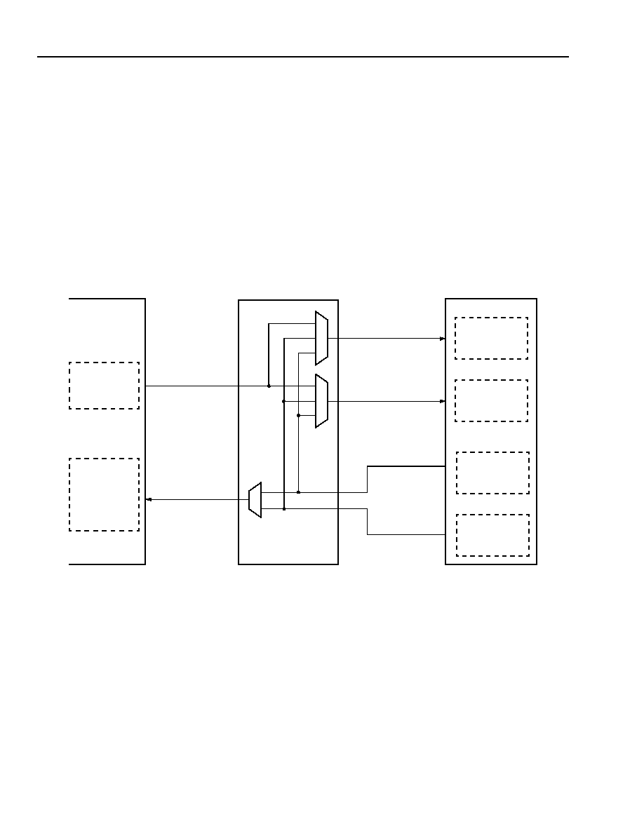
TMXF28155/51 Super Mapper
Preliminary Data Sheet
155/51 Mbits/s SONET/SDH x28/x21 DS1/E1
May 2001
554
Agere Systems Inc.
22 Cross Connect (XC) Block Functional Description
(continued)
An example of an exception to this rule is the framer only application where the Super Mapper is used as a block of
28 framers with a CHI system interface. The 28 framers would interface line interface units with FRM_TP_T and
FRM_RP_R and the system with FRM_TS and FRM_RS entirely through the multifunction system interface device
pins.
Either end of the framer block may be configured to interface to line interface units as shown in
Figure 85 on
page 554
. In a framer only application, the FRM_TP_T and FRM_RP_R framer block interfaces with the LIUs. The
FRM_RP_T and FRM_TP_R framer block interfaces the LIUs in a transport application. If a dual-rail or bipolar LIU
interface is desired, the sync line is used as the negative-rail data.
The user configures the framer block connectivity by simply loading the appropriate source IDs into the
XC_TP_RDATA[1--28][7:0] (
Table 456
), XC_RP_RDATA[1--28][7:0], and XC_RS_D[1--28][7:0] (
Table 457
) bytes
of the framer crosspoint configuration registers: XC_FTP_SRC[1--28][7:0], XC_FRP_SRC[1--28][7:0], and
XC_FRS_SRC[1--28][7:0], respectively.
5-9184(F)r.1
Figure 85. Framer Line Interface Cross Connect
22.6.5 Framer System Interface
The framer system interface FRM_TS/FRM_RS consists of bundles of data, clock, and/or sync/miscellany, that
may only be connected to the device external I/O pins. The system interface operates as the parallel system bus
(PSB), concentration highway (CHI), or network serial multiplexed interface (NSMI). Note that not all pins are used
in these configurations. The user should exercise caution in mixing the usage of the external pins between system
interface TS/RS usage and any other use.
Two register bits, XC_SI_CHI and XC_SYNC_FOR_DATA (
Table 449
), and a group of seven 2-bit parameters
XC_CHI_MODE[1--7][1:0] (
Table 450
) are used to assist with the configuration of the system interface.
FRM
XC
EXTERNAL I/O
LINERXDATA
LINERXCLK
LINERXSYNC
LINETXDATA
LINETXCLK
LINETXSYNC
FRM_TP_TCLK
FRM_TP_TDATA
FRM_TP_TFS
XC_TP_RDATA
XC_TP_RCLK
XC_TP_RFS
XC_TP_RDATA[1--28][7:0]
3x29
3x28
3x29
3x28
3x28
3x28
XC_RP_RDATA[1--28][7:0]
XC_PDATA[1--29][7:0]
XC_SYNC[1--29][7:0]
FRM_TP_R
FRM_RP_R
FRM_TP_T
FRM_RP_T
XC1
XC_RP_RDATA
XC_RP_RCLK
XC_RP_RFS
FRM_RP_TCLK
FRM_RP_TDATA
FRM_RP_TFS
Preliminary Data Sheet
TMXF28155/51 Super Mapper
May 2001
155/51 Mbits/s SONET/SDH x28/x21 DS1/E1
555
Agere Systems Inc.
22 Cross Connect (XC) Block Functional Description
(continued)
22.6.6 Framer System Interface--PSB
The framer system interface is configured for the parallel system bus as depicted in
Figure 86 on page555
. Pro-
gram bit XC_SI_CHI = 1 to select the PSB mode, and bit XC_SYNC_FOR_DATA = 1 to allow the connecting of
transmit system data outputs to the LINETXSYNC[1--29] pins. The programming of the XC_CHI_MODE[1--7][1:0]
bits is not required.
The PSB configuration is completed by programming appropriate source IDs into the XC_RS_D[1--28][7:0]
(
Table 457
) and XC_SYNC[1--29] (
Table 465
) bytes of the XC_FRS_SRC[1--14] (
Table 457
) and
XC_PINS_SRC[1--14] (
Table 465
) XC1 crosspoint configuration registers.
5-9185(F)r.2
Figure 86. Framer System Interface--Parallel System Bus (PSB)
22.6.7 Framer System Interface--CHI
The framer system interface is configured for CHI operation as shown in
Figure 87 on page556
. Program bit
XC_SI_CHI = 0 (
Table 449
) to select the CHI mode, and bit XC_SYNC_FOR_DATA = 1 (
Table 449
) to allow the
connecting of transmit system data outputs to the LINETXSYNC[1--29] pins.
The concentration highway interface can operate at data rates of 2.048 Mbits/s, 4.096 Mbits/s, and 8.192 Mbits/s.
The CHI interface allows a single system interface to support combining 2 or 4 DS1/E1s at 4.096 Mbits/s and
8.192 Mbits/s, respectively. Therefore, the 28-channel framer block may result in as many as 28 CHIs or as few as
7 combined CHIs or a mix as determined by the specific needs of the application.
EXTERNAL I/O
XC
FRM_TS/FRM_RS
LINETXSYNC[4--1]
LINETXSYNC29
LINERXSYNC[16--1]
LINERXSYNC29
LINERXDATA29
LINERXCLK29
LINETXCLK29
TS_D[16--1]
RS_D[16--1]
TS_GCLK
TS_GFS
RS_GCLK
RS_GFS
RS_GTCLK
LINETXSYNC[16--13]
XC_RS_D[1--28][7:0]
XC_SI_CHI = 1
XC_CHI_MODE[1--7][1:0] = 00
XC_SYNC_FOR_DATA = 1
XC_SYNC[1--29][7:0]
XC1
FRAMER SYSTEM INTERFACE
AS PSB
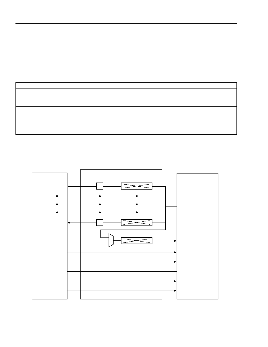
TMXF28155/51 Super Mapper
Preliminary Data Sheet
155/51 Mbits/s SONET/SDH x28/x21 DS1/E1
May 2001
556
Agere Systems Inc.
22 Cross Connect (XC) Block Functional Description
(continued)
In addition to configuring the framers for the CHI mode, 7 CHI mode parameters in the cross connect block require
configuration. The parameters are designated XC_CHI_MODE[1--7][1:0] (
Table 450
). The parameters divide the
28-framer CHI system interfaces, LINETXSYNC[1--29], into seven groups of four, LINETXSYNC[1--4], . . . ,
LINETXSYNC[25--28]. Each XC_CHI_MODE[1--7][1:0] parameter consists of 2 bits for configuration of the con-
trol group see
Table 618 on page 556
.
Table 618. Configuration of the Control Group
For example, XC_CHI_MODE[4][1:0] = 01 configures LINETXSYNC[13] and LINETXSYNC[14] as individual
2.048 Mbits/s CHIs and combines LINETXSYNC[16] and LINETXSYNC[15] into a 4.096 Mbits/s output on
LINETXSYNC[16]. The LINETXSYNC[15] output can be used for T1/E1 line sync output.
5-9186(F)r.3
* See
Table 450
.
Figure 87. Framer System Interface--Concentration Highway Interface (CHI)
XC_CHI_MODE[1--7][1:0]
Description
00
All four links within the group are normal outputs at 2 Mbits/s or 4 Mbits/s.
01
Links 4i ≠ 3 and 4i ≠ 2 are normal outputs; links 4i ≠ 1 and 4i are combined into a
single output on 4i; output 4i ≠ 1 is used as T1/E1 line output, where i = 1 to 7.
10
Links 4i ≠ 1 and 4i are combined into a single output on 4i; links 4i ≠ 3 and 4i ≠ 2 are
combined into a single output on 4i ≠ 2; outputs 4i ≠ 1 and 4i ≠ 3 are used as T1/E1
line outputs.
11
All four links are combined into a single output on 4i; the other three outputs are
used as T1/E1 line outputs.
EXTERNAL I/O
XC
FRM_TS/FRM_RS
LINETXSYNC[4--1]
LINETXSYNC29
LINERXSYNC[28--1]
LINERXSYNC29
LINERXDATA29
LINERXCLK29
LINETXCLK29
TS_D[28--1]
RS_D[28--1]
TS_GCLK
TS_GFS
RS_GCLK
RS_GFS
RS_GTCLK
LINETXSYNC[28--25]
XC_RS_D[1--28][7:0]
XC_SI_CHI = 0
XC_CHI_MODE[1--7][1:0] = *
XC_SYNC_FOR_DATA = 1
XC_SYNC[1--29][7:0]
XC1
AS CHI
FRAMER SYSTEM INTERFACE
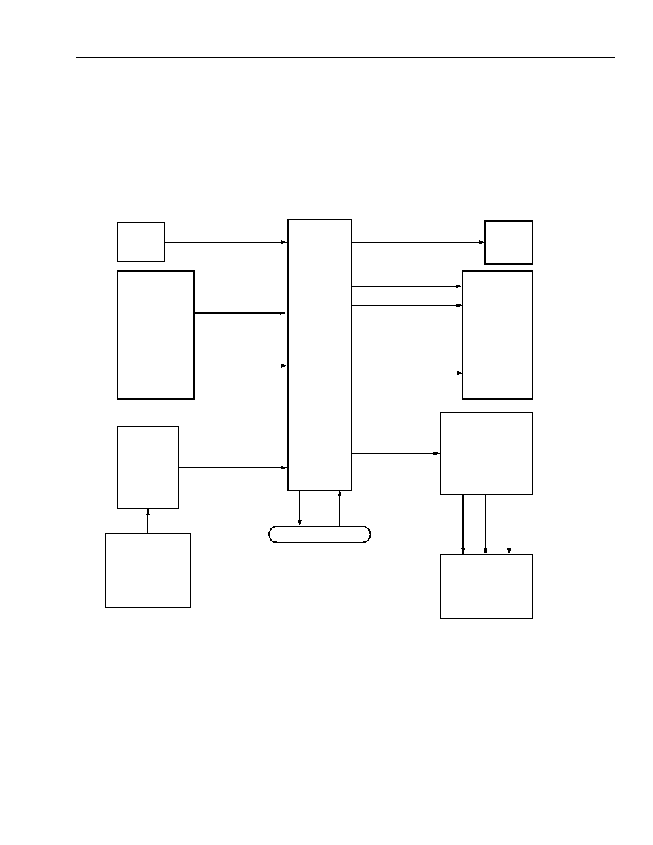
Preliminary Data Sheet
TMXF28155/51 Super Mapper
May 2001
155/51 Mbits/s SONET/SDH x28/x21 DS1/E1
557
Agere Systems Inc.
22 Cross Connect (XC) Block Functional Description
(continued)
22.6.8 Framer System Interface--NSMI
The network serial multiplexed interface (NSMI) connectivity is described in the DS3 cross connect connectivity
section and is shown in
Figure 96 on page568
.
22.7 DS2 Connectivity
5-9187(F)r.2
Figure 88. DS2 Cross Connect Interface
The DS2 cross connect is used when the application requires the M13 and needs external I/O or maintenance for
DS2 signals. The DS2 cross connect provides full-split access at the DS2 level. Otherwise, the registers may be
programmed to the default values.
CROSS
CONNECT
CONTROL INTERFACE
TPG_DS2
MAPPER
M13
XC2_M21_[1--7][7:0]
M13:M12MUX
XC2
TPG
DS2
M12_DS2_IN
M23
TPM
TPM_DS2
M13:M23DEMUX
XC2_MDS2M23DATA[1--7][7:0]
XC2_DS2M12CLK[1--7][7:0]
EXT I/O
PIN
MAPPER
M13
M12_DS2_OUT
M23
M12_DS2_OUT
EXT I/O
LINETXSYNC[1--29]
LINERXDATA[1--29]
LINERXCLK[1--29]
LINERXSYNC[1--29]
XC1
CROSS
CONNECT
DS1
XC1
CROSS
CONNECT
DS1
EXT I/O
PIN
LINETXSYNC[1--29]
LINETXDATA[1--29]
LINETXCLK[[1--29]
LINERXCLK[1--29]
XC_PDATA[1--29][7:0]
XC_ALCO[1--29][7:0]
(SOURCE_ID = 000)
(SOURCE_ID = 000)
ALL ACCESS TO EXTERNAL I/O PINS IS
THROUGH THE DS1/E1 CROSS CONNECT
USING A SOURCE_ID = 000
SOURCE
DESTINATION
(SOURCE_ID = 00)
(SOURCE_ID = 01)
(SOURCE_ID = 10)
(SOURCE_ID = 11)
XC_SYNC[1--29][7:0]
(SOURCE_ID = 000)

TMXF28155/51 Super Mapper
Preliminary Data Sheet
155/51 Mbits/s SONET/SDH x28/x21 DS1/E1
May 2001
558
Agere Systems Inc.
22 Cross Connect (XC) Block Functional Description
(continued)
The cross connect block supports DS2 mapping to/from the M13 MUX, TPG/TPM, and external pin I/O. Here, the
available sources are the M12 MUX or the M23 deMUX, a set of external I/O pins, or the test-pattern generator.
The DS2 crosspoint's connectivity is determined by a smaller set of source 2 identifiers (SOURCE2_IDs), as
defined in the following table (covering registers XC2_M23_SRC[1--7] (
Table 460
) and XC2_TPM_SRC
(
Table 461
)):
The SOURCE2_BLOCK is defined as follows:
The CHANNEL2_ID typically ranges from 1 to 7. For test data from the TPG, the SOURCE2_BLOCK is set to 0
and the CHANNEL2_ID value four represents the DS2 test pattern. For DS2 signals routed from external pins to
the input of M23 MUX or TPM, the CHANNEL2_ID can range from 1 to 29. The above DS2 source ID definition
covers registers beginning with XC2.
Note: For certain DS2 signals routed to external pins, the XC1 cross connect is used and a special SOURCE_ID
(block 0) is programmed:
The SOURCE2_ID is defined as in
Table 615
to
Table 617
. The user must ensure consistency between the use of
M13 vs. M12/M23 channels and external I/O channels.
22.7.1 M13 DS2 Interface (DS2 Cross Connect)
The DS2 full split access results in four sets of DS2 signals that can be routed through cross connect, essentially
providing access to the path between the seven M12 MUX/deMUXs and the M23 MUX/deMUX.
22.7.2 M12 MUX (Transmit Path)
The M12 MUX assembles three E1s or four DS1s into a DS2. The DS2 output data is clocked out by an external
DS2 rate clock as shown in
Figure 89
.
The DS2 rate clock is routed from an external pin, LINETXSYNC[14--8], through the cross connect to the M12, by
programming the XC2_DS2M12CLK[1--7][7:0] (
Table 459
) bytes in the DS2 cross connect registers
XC2_M12_SRC[1--7] (
Table 459
) with a source2 ID = 11 (external I/O) and a channel select of 1 to 7. The channel
select value of 1 to 7 selects the clock from pins LINETXSYNC[8] to LINETXSYNC[14], respectively.
The DS2 data is routed through the DS1 cross connect to the external pins, LINETXSYNC[7--1], by programming
the XC_SYNC[1--29] (
Table 465
) bytes in the XC_PINS_SRC[1--14] DS1 cross connect registers with a source
ID = 000 and a channel select as defined in
Table 616
. A channel select value of 9 to 15 selects the external pin
LINETXSYNC[1] to LINETXSYNC[7], respectively.
Bit
7
6
5
4
3
2
1
0
SOURCE2_ID
0
SOURCE2_BLOCK[1:0]
CHANNEL2_ID[4:0]
Index
Block2 Identifier
00
TPG (DS2 Test-Pattern Generator)
01
M13:M12 MUX
10
M13:M23 DeMUX
11
External I/O
Bit
7
6
5
4
3
2
1
0
SOURCE2_ID
0
0
0
CHANNEL2_ID[4:0]
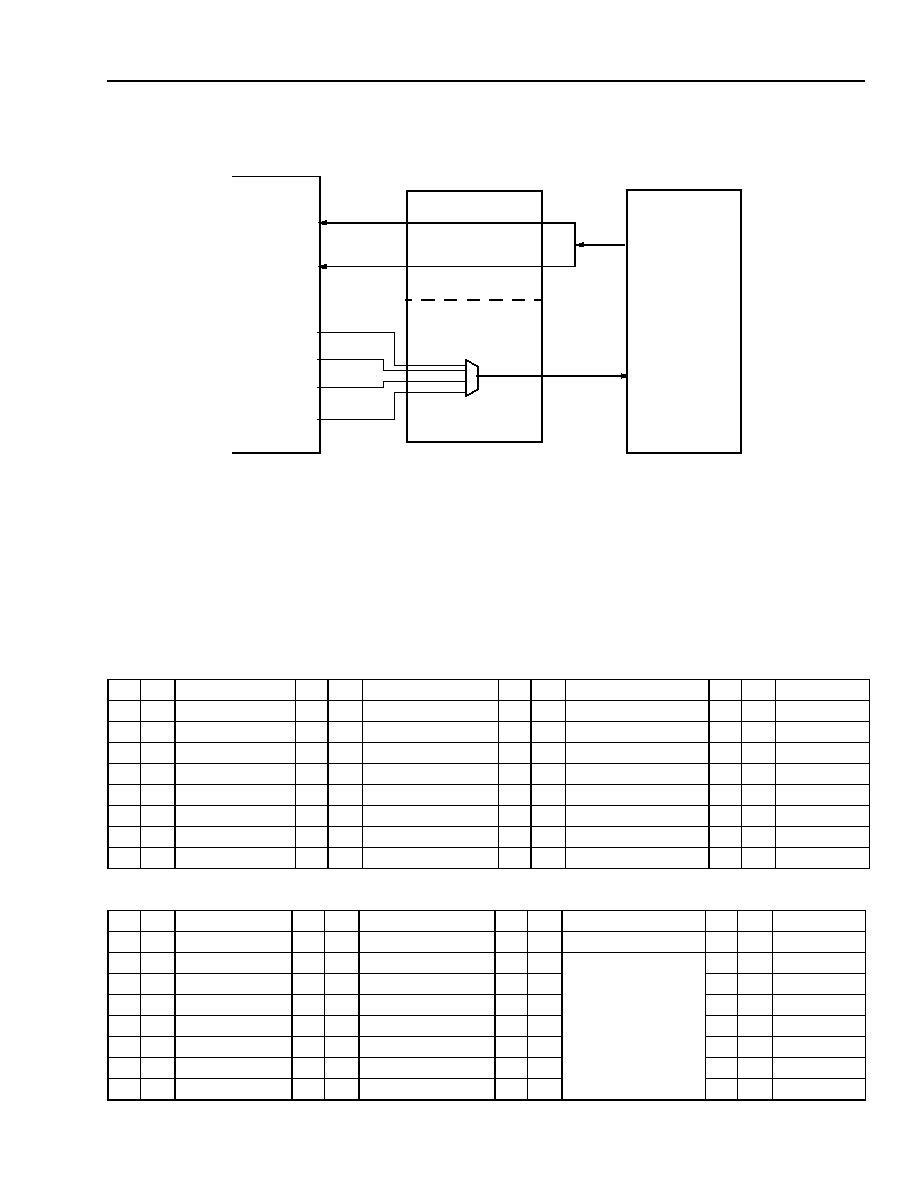
Preliminary Data Sheet
TMXF28155/51 Super Mapper
May 2001
155/51 Mbits/s SONET/SDH x28/x21 DS1/E1
559
Agere Systems Inc.
22 Cross Connect (XC) Block Functional Description
(continued)
5-9188(F)r.3
Figure 89. M12 MUX DS2 Output Cross Connect
There is another way to route DS2 signals for M12 MUX's through LINETXDATA and LINETXCLK pins, if available,
by setting the block ID of XC_PDATA_Source_ID to 111 (refer to the Table on
page 550
). This configuration is capa-
ble of supporting DS2 demand clocking operation. In DS2 demand clocking mode, the LINETXCLK pins act as out-
puts; otherwise, they are input pins carrying incoming DS2 clocks. Depending on the clocking scheme, the channel
ID can be set up based on the following tables.
Table 619. XC_PDATA Source IDs for LINETXDATA Routing with Source Block = 111
Table 620. XC_PDATA Source IDs for LINETXCLK Routing with Source Block = 111
I/O Ch.
Description
I/O Ch.
Description
I/O Ch.
Description
I/O Ch. Description
O
0
Reserved
O
8
Reserved
O
16
Reserved
O
24
Reserved
O
1
M12_DS2DAT_1
O
9
M12_DS2DAT_1
O
17
M12_DS2DAT_1
O
25
Reserved
O
2
M12_DS2DAT_2
O
10
M12_DS2DAT_2
O
18
M12_DS2DAT_2
O
26
Reserved
O
3
M12_DS2DAT_3
O
11
M12_DS2DAT_3
O
19
M12_DS2DAT_3
O
27
Reserved
O
4
M12_DS2DAT_4
O
12
M12_DS2DAT_4
O
20
M12_DS2DAT_4
O
28
Reserved
O
5
M12_DS2DAT_5
O
13
M12_DS2DAT_5
O
21
M12_DS2DAT_5
O
29
Reserved
O
6
M12_DS2DAT_6
O
14
M12_DS2DAT_6
O
22
M12_DS2DAT_6
O
30
Reserved
O
7
M12_DS2DAT_7
O
15
M12_DS2DAT_7
O
23
M12_DS2DAT_7
O
31
Reserved
I/O Ch.
Description
I/O Ch.
Description
I/O Ch.
Description
I/O Ch. Description
O
0
Reserved
O
8
Reserved
O
16
Reserved
O
24
Reserved
O
1
DS2_AISCLK
O
9
DM12_DS2CLK_1
I
17
M12_DS2CLK[7:1]
input through
LINETXCLK pins,
the actual routings
are determined by
XC2_DS2M12CLK
SOURCE ID
O
25
Reserved
O
2
DS2_AISCLK
O
10
DM12_DS2CLK_2
I
18
O
26
Reserved
O
3
DS2_AISCLK
O
11
DM12_DS2CLK_3
I
19
O
27
Reserved
O
4
DS2_AISCLK
O
12
DM12_DS2CLK_4
I
20
O
28
Reserved
O
5
DS2_AISCLK
O
13
DM12_DS2CLK_5
I
21
O
29
Reserved
O
6
DS2_AISCLK
O
14
DM12_DS2CLK_6
I
22
O
30
Reserved
O
7
DS2_AISCLK
O
15
DM12_DS2CLK_7
I
23
O
31
Reserved
M13
XC
EXTERNAL I/O
M12_DS2_DATA_OUT
XC2_DS2M12CLK
LINETXSYNC[7--1]
LINETXSYNC[14--8]
XC2_DS2M12CLK[1--7][7:0]
XC_SYNC[1--29][7:0]
SOURCE_ID = 000
XC1
XC2
CHANNEL_ID 9 TO 15
LINETXDATA[29--1]
LINERXCLK[29--1]
DS2_AISCLK
XC_DATA[1--29][7:0]
SOURCE_ID = 111
CHANNEL_ID 1TO 7
LINETXCLK[29--1]

TMXF28155/51 Super Mapper
Preliminary Data Sheet
155/51 Mbits/s SONET/SDH x28/x21 DS1/E1
May 2001
560
Agere Systems Inc.
22 Cross Connect (XC) Block Functional Description
(continued)
The register XC2_DS2M12CLK SOURCE ID is defined as:
The register can be programmed to route DS2 clocks from various sources based on the following table:
22.7.3 M12 DeMUX (Receive Path)
The M12 deMUX disassembles a DS2 into three E1s or four DS1s. The routing of DS2 data and clocks to M12
DeMUX is controlled by the register XC2_M21_SRC[1:7] which are defined as:
The routings are based on the following table.
When bits 7--5 of XC2_M21_SRC set to 100, the user also needs to set bits 7--5 of the related register
XC_ALCO_SOURCE_ID(I) to 001 as well as the appropriate channel value to ensure the demand clocking opera-
tion.
The DS2 input has six connection options as shown in
Figure 90 on page561
.
The external I/O inputs for DS2 clock and data are cross connected by programming bytes, XC2_M21[1--7][7:0]
(
Table 459
) in configuration registers XC2_M12_SRC[1--7], with a source2 ID = 11 and a channel select of 1 to 7.
The channel select value of 1 to 7 selects DS2 data from device pins LINETXSYNC[15] to LINETXSYNC[21] and
selects DS2 clock from LINETXSYNC[22] to LINETXSYNC[28], respectively.
A DS2 signal loopback may be performed for the M12 MUX/deMUX by programming the XC2_M21[1--7][7:0]
(
Table 459
) byte in the XC2_M12_SRC[1--7] registers with a source2 ID = 01 and a channel select of 1 to 7. Cross
connecting among the seven channels is supported. For example, the output of M12 MUX 1 may be connected to
the input of M12 deMUX 5.
The TPG may be cross connected to the M12 deMUX DS2 inputs by programming the XC2_M21[1--7][7:0] byte in
the XC2_M12_SRC[1--7] registers with a source2 ID = 00 and a channel ID = 4. The connection is not useful
because the DS2 pattern generator is limited to sending unframed pseudorandom data patterns that cannot be
demultiplexed into DS1s or E1s.
Bit
7
6
5
4
3
2
1
0
SOURCE2_ID
0
SRC2_BLK[2:0]
CHANNEL2_ID[4:0]
SRC2_BLK
CHANNEL2_ID
Function
00
1 to 7
DS2 Clocks Sourced from LINETXSYNC[8:14]
01
1 to 29
DS2 Clocks Sourced from LINETXCLK[1:29]
10
1 to 29
DS2 Clocks Sourced from LINERXCLK[1:29]
11
Don't care
DS2 Clocks Sourced from PIN_DS2_AISCLK
Bit
7
6
5
4
3
2
1
0
SOURCE2_ID
SRC2_BLK[2:0]
CHANNEL2_ID[4:0]
SRC2_BLK
CHANNEL2_ID
Function
000
4
DS2DATA/CLK from TPG
001
1 to 7
DS2DATA/CLK from M12 MUX
010
1 to 7
DS2DATA/CLK from M23 DEMUX
011
1 to 7
DS2DATA/CLK from Pin LINETXSYNC[21:15]/LINETXSYNC[28:22]
100
1 to 29
DS2DATA/CLK from Pin LINERXDATA[29:1]/PIN_DS2_AISCLK
101
1 to 29
DS2DATA/CLK from Pin LINERXDATA/CLK[29:1]
Others
Don't care
Not Valid
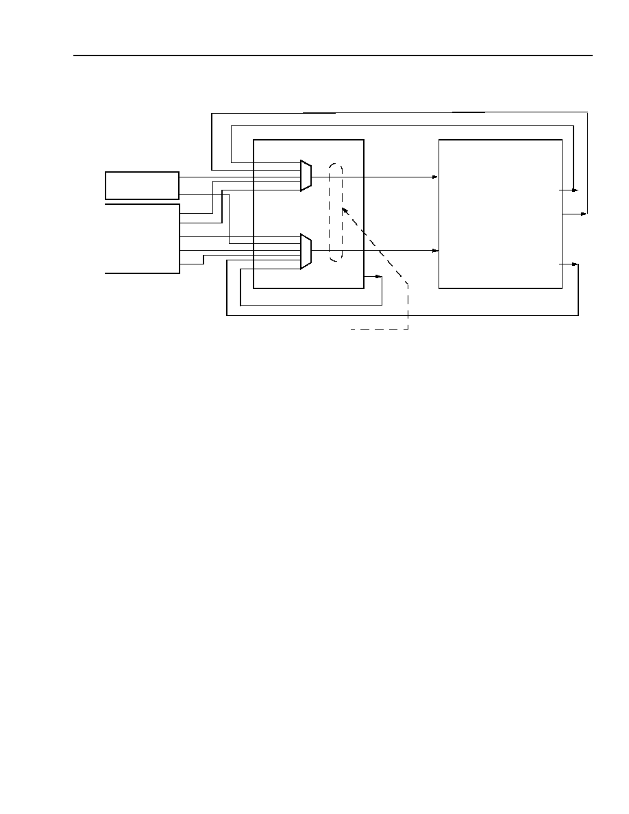
Preliminary Data Sheet
TMXF28155/51 Super Mapper
May 2001
155/51 Mbits/s SONET/SDH x28/x21 DS1/E1
561
Agere Systems Inc.
22 Cross Connect (XC) Block Functional Description
(continued)
5-9189(F)r.3
Figure 90. M12 DeMUX Input DS2 Cross Connect
22.7.4 M23 DeMUX (Receive Path)
The M23 deMUX disassembles a DS3 into 7 DS2 signals. The M23 deMUX can cross connect DS2 data and clock
out to external pins and/or the test-pattern monitor as shown in
Figure 91
.
The M23 DS2 data and clock are connected to external I/O by programming the XC_PDATA[1--29] (
Table 451 on
page 323
) bytes in the DS1 cross connect registers XC_PIND_SRC[1--15] with a source ID = 000 and a channel
select value from
Table 615
. The channel select value of 17 to 23 (decimal) routes DS2 data out from DS2 deMUX
1 to 7 to the external I/O pins LINETXDATA[1--29] and LINETXCLK[1--29] as selected by programming one of the
29 XC_PDATA[1--29] bytes.
For example, to connect the DS2 data and clock outputs from M23 deMUX 4 to the LINETXDATA[19] and
LINETXCLK[19] device pins, program the XC_PDATA19 byte in register XC_PIND_SRC10 (
Table 451
) for a source
ID = 000 (binary) and a channel ID = 20 (decimal) XC_PDATA19 = 00010100 (binary).
The demultiplexed DS2 may be connected to the test-pattern monitor (TPM) by programming the
XC2_TSOURCE_ID (
Table 461
) byte in register XC2_TPM_SRC with a source ID of 10 and a channel select value
of 1 to 7 corresponding to the deMUXed output to monitor. The TPM is limited to receiving unframed pseudoran-
dom data patterns.
M13
XC
EXTERNAL I/O
DM12_DS2_DATA
DM12_DS2_CLOCK
LINETXSYNC[21--15]
LINETXSYNC[28--22]
TPG
TPG_DATA[4]
TPG_CLK[4]
XC_DS2M12CLK[1--7][7:0]
M12_DS2_DATA
XC2_M21_[1--7][7:0]
BUNDLED SIGNALS
TPG--SOURCE_ID = 000
CHANNEL_ ID = 4--DS2 DATA
M13:M12 MUX (DS2 FROM M12)--SOURCE_ID = 001
CHANNEL_ID = 1 TO 7
CHANNEL_ID = 1 TO 29
LINERXDATA/DS2_AISCLK--SOURCE_ID = 100
DM23_DS2_DATA
DM23_DS2_CLK
LINERXDATA[29--1]
LINERXCLK[29--1]
DS2_AISCLK
M13:M23 DEMUX --SOURCE_ID = 010
CHANNEL_ID = 1 TO 7
CHANNEL_ID = 1 TO 7
LINETXSYNC --SOURCE_ID = 011
CHANNEL_ID = 1 TO 29
LINERXDATA/CLK--SOURCE_ID = 101
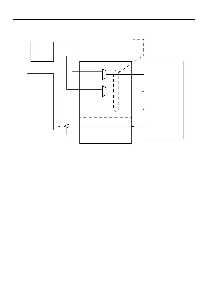
TMXF28155/51 Super Mapper
Preliminary Data Sheet
155/51 Mbits/s SONET/SDH x28/x21 DS1/E1
May 2001
562
Agere Systems Inc.
22 Cross Connect (XC) Block Functional Description
(continued)
5-9190(F)r.3
* = Channel ID
from
Table 615
.
Figure 91. M23 DeMUX DS2 Output Cross Connect
22.7.5 M23 MUX (Transmit Path)
The M23 MUX assembles seven DS2s into a DS3 signal. The routing of the DS2 data and clock inputs to the M23
MUX is shown in
Figure 92
. Two modes of operation are available and selected with bit XC_DS2ALCOEN
(
Table 462
). The first mode routes DS2 data and clock from device inputs to the M23 (XC_DS2ALCOEN = 0). The
second mode cross connects a DS2 clock out to an external I/O pin that is used by the external application to pro-
vide DS2 data and a stuff request to the Super Mapper input pins for the M23 (XC_DS2ALCOEN = 1). The first
mode determines the appropriate standards based stuff times internally, ignoring the external stuff request, and the
second mode determines the stuff times from the external application.
The DS2 data, clock, and stuff request inputs to the M23 are cross connected by programming
XC2_MDS2M23DATA[1--7] (
Table 460
) bytes in XC2_M23_SRC[1--7] registers with the source ID = 11 and a
channel select value of 1 to 29. The channel select value of 1 to 29 selects the data, clock, and stuff request signals
from the external I/O device pins LINERXDATA[1--29], LINERXCLK[1--29], and LINERXSYNC[1--29], respec-
tively.
For example, to cross connect DS2 data from LINERXDATA[6], DS2 clock from LINERXCLK[6], and stuff request
from LINERXSYNC[6] to the inputs of M23 number 3, program the XC2_MDS2M23DATA3 byte in register
XC2_M23_SRC3, with a source ID = 11 and a channel select = 6. XC2_MDS2M23DATA3 = 01100110 (binary).
If XC_DS2ALCOEN = 1, the cross connect for the DS2 clock output must be programmed into XC_ALCO[1--29]
byte in the XC_ALCO_SRC[1--15] registers. The source ID = 000 and the channel ID select has a value between
17 and 23 (decimal) to select DS2 DeMUX 1 to 7, respectively.
M13
XC
EXTERNAL I/O
M23_DS2_DATA
M23_DS2_CLOCK
M23_DS2_CLOCK_OUT
M23_DS2_STUFF
LINERXDATA
LINERXCLK
LINERXSYNC
XC2 MDS2M23DATA[1--7][7:0]
XC_ALCO[1--29][7:0]
TPG
TPG_DATA[4]
TPG_CLK[4]
REQUEST
BUNDLED SIGNALS
TPG--SOURCE_ID = 00
CHANNEL_ID = 4--DS2 DATA
CHANNEL_ID = 5--DS2 IDLE
EXT I/O--SOURCE_ID = 11
XC2
XC1
SOURCE_ID = 000
REGISTER BIT XC_DS2ALCOEN
0 = DS2 EXTERNAL CLOCK IN
1 = DS2 M23 DEMUX CLOCK OUT
CHANNEL_ID = 1 TO 29--
(DEMUX FROM DS3)
CHANNEL_ID =*
PIN SELECT
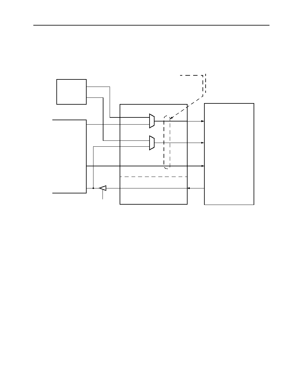
Preliminary Data Sheet
TMXF28155/51 Super Mapper
May 2001
155/51 Mbits/s SONET/SDH x28/x21 DS1/E1
563
Agere Systems Inc.
22 Cross Connect (XC) Block Functional Description
(continued)
For the above example, the XC_ALCO6 byte in register XC_ALCO_SRC3 (
Table 466
), would be programmed with
a source ID = 000 and a channel select = 19. This will output a DS2 clock from M23 DeMUX 3 to LINERXCLK[6].
XC_ALCO6 = 00010011 (binary).
5-9191(F)r.2
* Channel ID from
Table 617
.
Figure 92. M23 MUX DS2 Input Cross Connect
M13
XC
EXTERNAL I/O
M23_DS2_DATA
M23_DS2_CLOCK
M23_DS2_CLOCK_OUT
M23_DS2_STUFF
LINERXDATA
LINERXCLK
LINERXSYNC
XC2 MDS2M23DATA[ ]
XC_ALCO[ ]
TPG
TPG_DATA[4]
TPG_CLK[4]
REQUEST
BUNDLED SIGNALS
TPG--SOURCE_ID = 00
CHANNEL_ID = 4--DS2 DATA
CHANNEL_ID = 5--DS2 IDLE
EXT I/O--SOURCE_ID = 11
XC2
XC1
SOURCE_ID = 000
REGISTER BIT XC_DS2ALCOEN
0 = DS2 EXTERNAL CLOCK IN
1 = DS2 M23 DEMUX CLOCK OUT
CHANNEL_ID = 1 TO 29--
(DERIVED FROM DS3)
CHANNEL_ID =*
PIN SELECT

TMXF28155/51 Super Mapper
Preliminary Data Sheet
155/51 Mbits/s SONET/SDH x28/x21 DS1/E1
May 2001
564
Agere Systems Inc.
22 Cross Connect (XC) Block Functional Description
(continued)
22.8 DS3 Connectivity
5-9192(F)r.1
Figure 93. DS3 Cross Connect
The cross connect block also supports DS3 mapping to/from the SPE mapper and the M13 MUX, to dedicated
external pins (PIN). There is also an external NSMI I/O channel, which transfers DS3 data as well. In both cases
(standard and NSMI), the available sources are the M13 DeMUX or the SPE mapper, a set of external I/O pins, or
the test-pattern generator. The DS3 crosspoint's connectivity is determined by an even smaller set of source3 iden-
tifiers.
Table 621. DS3 Connectivity
Note: DS3 external I/O is supported by dedicated pins. NSMI uses the multifunction system interface.
The symbols in
Table 621
are defined below:
% = Primary (expected) modes of operation.
X = Unsupported mode.
& = represents loopback path.
NSMI = NSMI mode only.
T = Test mode.
Destination Source
External I/O
M13 MUX
TPM
SPE
External I/O
&
%
T
NSMI/DS3
M13 MUX
%
X
T
DS3
TPG
T
T
X
X
SPE
NSMI/DS3
DS3
T
X
CROSS
CONNECT
TEST
GEN
EXT.
I/O
XC3
TPG
DS3
PIN
TEST
MON
TPM
SPE
MAPPER
SPE
MAPPER
M13
MAPPER
M13
MAPPER
PIN_DS3POSDATAIN
PIN_DS3NEGDATAIN
PIN_DS3DATAINCLK
TX
RX
PIN_DS3POSDATAOUT
PIN_DS3NEGDATAOUT
PIN_DS3DATAOUTCLK
PD+
PD≠
(CLEAR
CHANNEL)
MUX
DEMUX
PIN_RLSC52
PIN_TLSC52
SPE_DS3_AIS
PIN_DS3POSDATAIN
PIN_DS3NEGDATAIN
PIN_DS3DATAINCLK
SPE HAS DIRECT
(FROM HS TELECOM BUS)
(FROM HS TELECOM BUS)
(TO M13)
INPUTS FROM PINS
EXT.
I/O
PIN
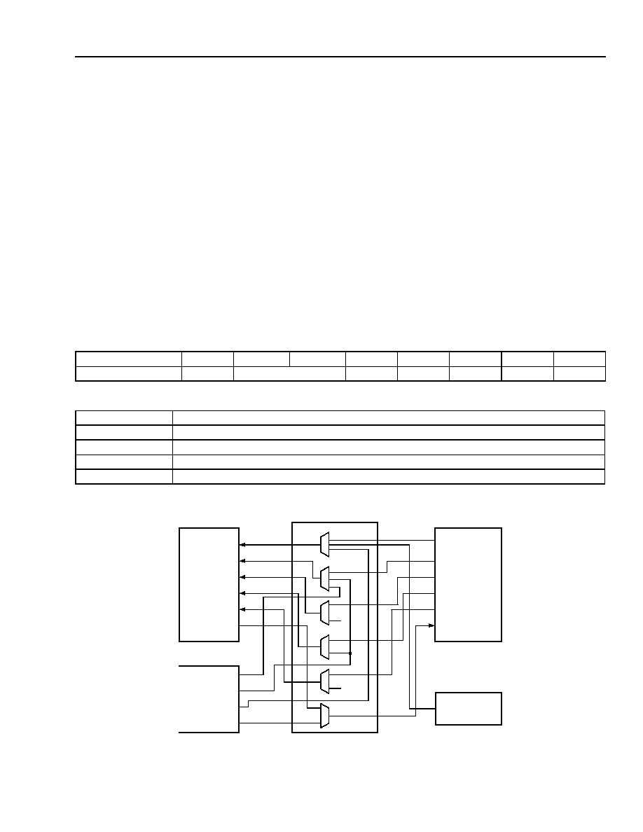
Preliminary Data Sheet
TMXF28155/51 Super Mapper
May 2001
155/51 Mbits/s SONET/SDH x28/x21 DS1/E1
565
Agere Systems Inc.
22 Cross Connect (XC) Block Functional Description
(continued)
The DS3/NSMI connectivity is established through a combination of DS3 specific MUXs controlled by registers
XC3_TPM_SRC (
Table 463
) and XC3_MDS3_SRC (
Table 464
) and special cases of the DS1 cross connects con-
trolled by XC_PDATA[1--29] (
Table 451
) and XC_SYNC[1--29] (
Table 465
) bytes in the XC_PIND_SRC[1--15]
(
Table 451
) and XC_PINS_SRC[1--14] (
Table 465
) registers to accommodate the NSMI connectivity from the mul-
tifunction system interface to the SPE mapper or M13.
Description of the DS3 connectivity will be presented in three sections: the test-pattern generator/monitor
(TPG/TPM), the DS3 basic connect, and the NSMI.
22.8.1 DS3 TPG/TPM Cross Connect
The DS3 test signals are routed through the XC3 crosspoint by programming register XC3_TPM_SRC as shown in
Figure 94
. For DS3 test signals, the TPG does not supply the source clock. Instead, a source clock and a clock
enable are provided from another block via the XC3 crosspoint. The TPG/TPM provide unframed test data that may
be connected to the SPE block for clear channel testing. For framed DS3 test data, the TPG/TPM are connected to
the NSMI interface in the M13 block and the M13 block DS3 interface provides the framed DS3 signal for test pur-
poses.
The DS3 TPG/TPM crosspoint's connectivity is determined by a set of source3 identifiers (source3_IDs) for bits 5
and 6 of XC3_TSOURCE_ID in register XC3_TPM_SRC as defined in the following tables:
where XC3_TSOURCE_ID is defined as follows:
* DS3 unframed single rail (unipolar) non-return-to-zero (NRZ) data.
5-9193(F)
Figure 94. DS3 Test-Pattern Cross Connect
Bit
7
6
5
4
3
2
1
0
XC3_TSOURCE_ID
0
XC3_TSOURCE_ID
0
0
0
0
0
Index (Bits [6:5])
Block3 Identifier
00
TPM receives DS3 from external pin*.
01
TPG and TPM are connected to M13 through NSMI interface.
10
TPM receives DS3 from SPE.
11
Reserved.
TPG/TPM
XC
M13
SPE
EXTERNAL I/O
XC_TDATA
XC3_TPMCLK
XC3_TPMCLKEN
XC3_TPGCLK
XC3_TPGCLKEN
TPG_DATA
M13_NSMI_CLK
M13_NSMI_EN
XC3_NSMI_DATA
M13_DNSMI_CLK
M13_DNSMI_EN
M13_DNSMI_DATA
DS3POS_DATA_RX
DS3DATAOUTCLK
DS3POSDATAIN
DS3DATAINCLK
LINERXDATA[29]
1
1
XC3_TSOURCE_ID
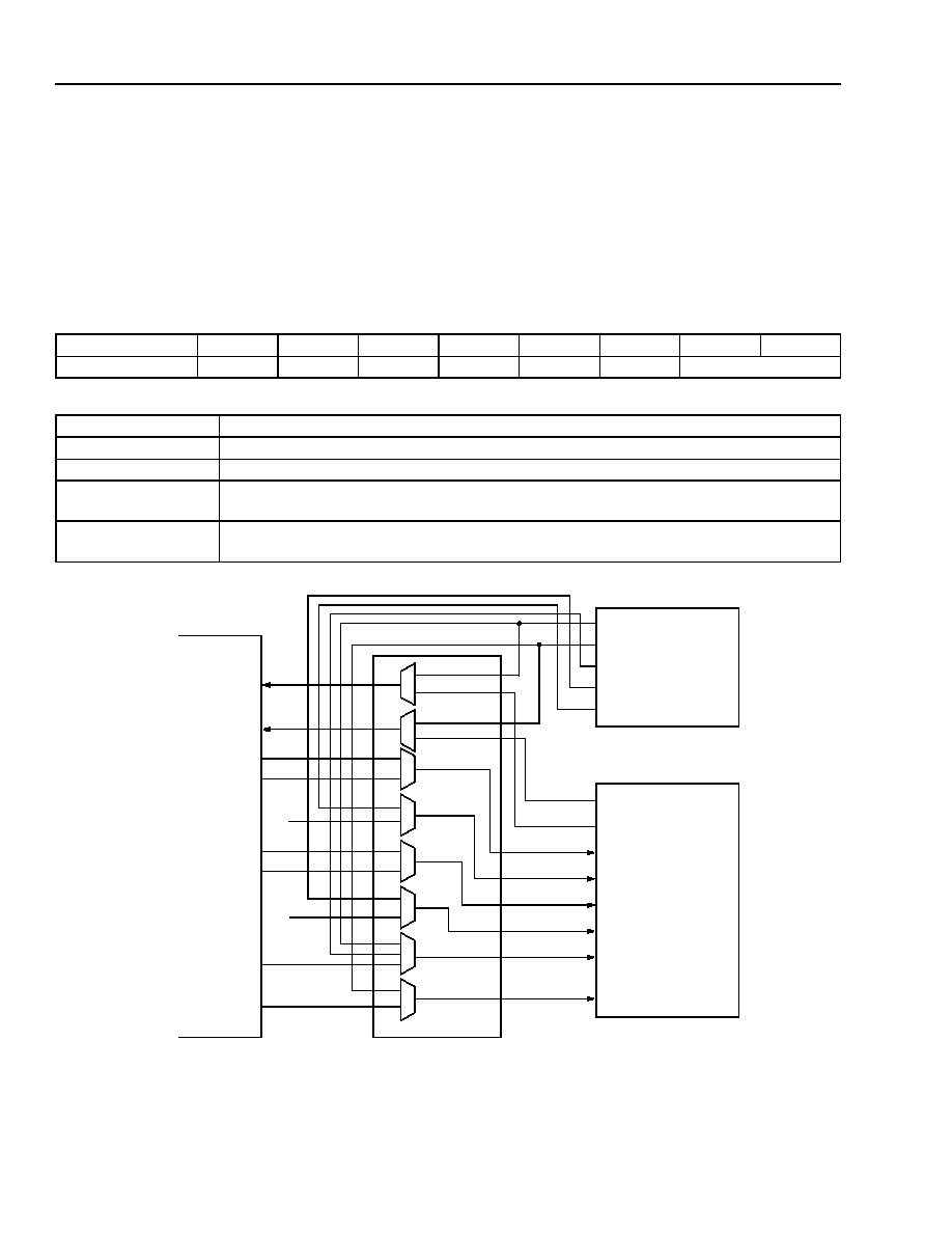
TMXF28155/51 Super Mapper
Preliminary Data Sheet
155/51 Mbits/s SONET/SDH x28/x21 DS1/E1
May 2001
566
Agere Systems Inc.
22 Cross Connect (XC) Block Functional Description
(continued)
22.8.2 DS3 Basic Cross Connect
The DS3 basic cross connect interconnects DS3 signals between the DS3 dedicated external I/O pins, the SPE
mapper, and the M13 by programming bits XC3_SOURCE_ID in register XC3_MDS3_SRC (
Table 464
) as shown
in
Figure 95 on page 566
. The DS3 dedicated external I/O pins DS3DATAINCLK (J22), DS3POSDATAIN (M22),
and DS3NEGDATAIN (K22) are directly connected to the SPE mapper; cross connect is not required (see SPE
mapper bits SPE_TDS3SRCTYP[1:0] and SPE_RDS3OUTTYP[1:0] (
Table 152
)). The DS3 basic crosspoint's con-
nectivity is determined by a set of source3 identifiers (source3_IDs) for bits 1 and 0 of XC3_SOURCE_ID in regis-
ter XC3_MDS3_SRC as defined in the following tables:
The XC3_SOURCE_ID is defined as follows:
5-9194(F)r.1
Figure 95. DS3 Basic Cross Connect
Bit
7
6
5
4
3
2
1
0
XC3_SOURCE_ID
0
0
0
0
0
0
XC3_SOURCE_ID
Index (Bits [1:0])
Block3 Identifier
00
M13 inputs/outputs DS3 through external I/O pins.
01
M13 and SPE are interconnected.
10
SPE inputs/outputs DS3 through external pins and M13 is used as a monitor for the trans-
mit path DS3.
11
SPE inputs/outputs DS3 through external pins and M13 is used as a monitor for the
receive path DS3.
M13_DS3NEG
M13DS3POS_DATA
SMPR_TDS3CLK
SMPR_TDS3CLKEN
SMPR_RDS3CLK
SMPR_RDS3CLKEN
SMPR_RDS3POS_DATA
SMPR_RDS3NEG_BPV
DS3POSDATAOUT
DS3NEGDATAOUT
DS3DATAOUTCLK
DS3POSDATAIN
DS3NEGDATAIN
DS3DATAINCLK
SPEMPR_CE_M13_RX
SPEMPR_M13DATA
SPEMPR_CE_M13_TX
DS3NEG_DATA_RX
DS3POS_DATA_RX
TLSC52
RLSC52
1
1
SPE
M13
EXTERNAL I/O
XC
XC3_SOURCE_ID
Preliminary Data Sheet
TMXF28155/51 Super Mapper
May 2001
155/51 Mbits/s SONET/SDH x28/x21 DS1/E1
567
Agere Systems Inc.
22 Cross Connect (XC) Block Functional Description
(continued)
22.8.3 NSMI Cross Connect
The Super Mapper cross connect supports interconnection of the network serial multiplexed interface (NSMI) to the
SPE mapper, M13 MUX/deMUX, or the NSMI system interface of the framer block as shown in
Figure 96
. The
cross connects are controlled by programming the XC_PDATA[29] (
Table 451
) and XC_SYNC[29] (
Table 465
)
bytes in registers XC_PIND_SRC15 and XC_PINS_SRC15. As previously discussed, the TPG/TPM can
send/receive data using the NSMI interface of the M13. Only the framer block can disassemble the NSMI payload
into DS0 channels and signaling. Connectivity to the M13 and SPE mapper is for transport in a proprietary format
only.
The NSMI crosspoint's connectivity to the multifunction interface external I/O is determined by a set of XC1 source
identifiers (SOURCE_IDs). The NSMI connectivity is defined as a special with the source ID = 000 for
XC_PDATA[29] and XC_SYNC[29] bytes in registers XC_PIND_SRC15 and XC_PINS_SRC15, with a
CHANNEL_ID restricted to 5, 24, 25, or 26 (see
Table 615
and
616
):
The channel ID is defined as:
Bit
7
6
5
4
3
2
1
0
SOURCE_ID
0
0
0
CHANNEL_ID[4:0]
CHANNEL_ID Binary (Decimal)
Connectivity
00101 (5)
DS3 Test Pattern
11000 (24)
M13--NSMI
11001 (25)
SPE--NSMI
11010 (26)
Framers--NSMI
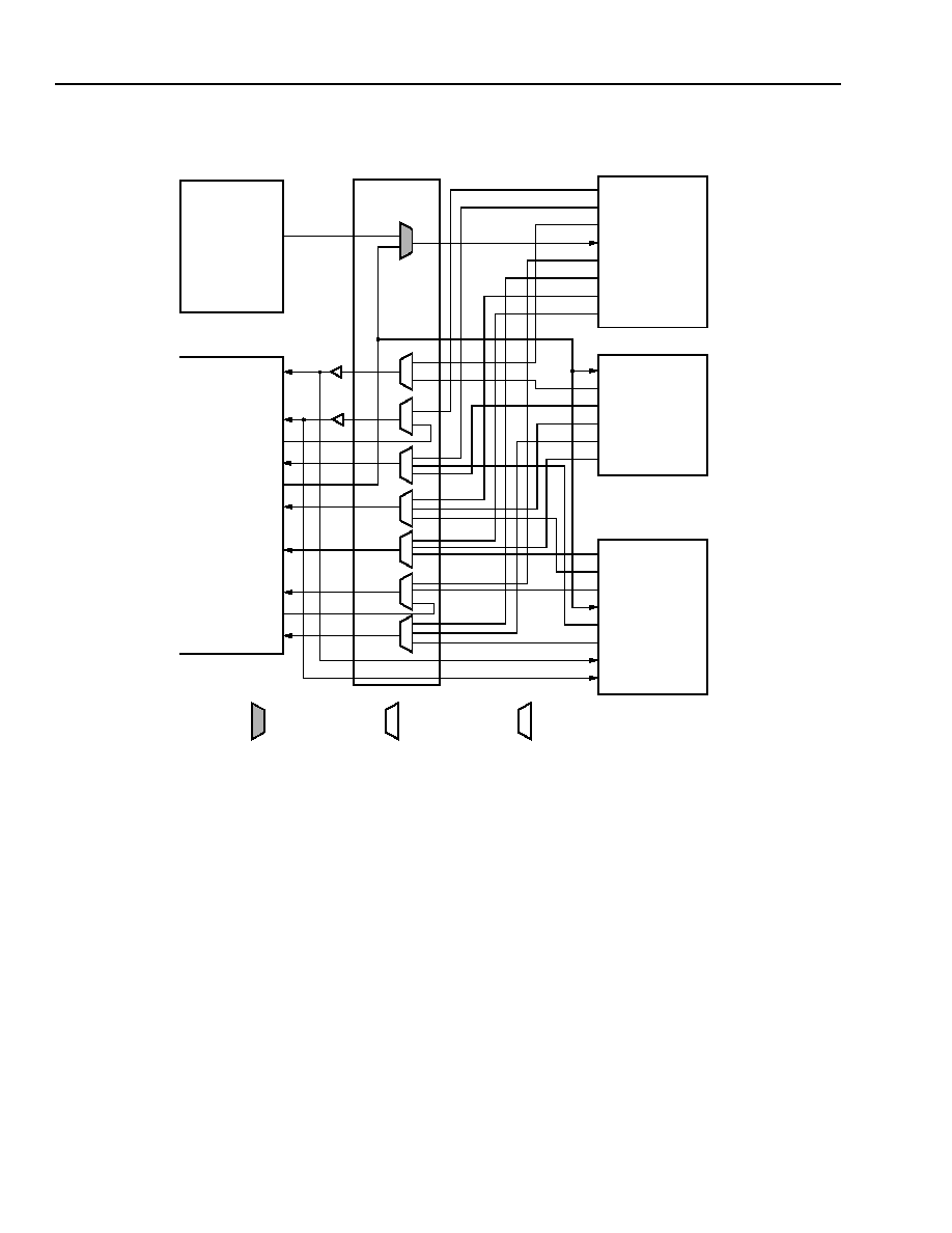
TMXF28155/51 Super Mapper
Preliminary Data Sheet
155/51 Mbits/s SONET/SDH x28/x21 DS1/E1
May 2001
568
Agere Systems Inc.
22 Cross Connect (XC) Block Functional Description
(continued)
5-9195(F)r.1
Figure 96. NSMI Interface Cross Connect
22.9 Transmit and Receive Path Overhead Access Channel I/O Configuration
The cross connect allows selection of transmit and receive POAC channels from either the TMUX block or SPE
mapper to the external I/O pins as shown in
Figure 97
.
An output enable and a select register bit is provided for transmit and receive POAC. The transmit POAC clock and
sync output signals are enabled with bit XC_TPOAC_EN (
Table 462
) and the source, SPE Mapper or TMUX block,
is selected with register bit XC_TSTS1_TUG3 (
Table 462
). The receive POAC clock, data, and sync output signals
are enabled with bit XC_RPOAC_EN (
Table 462
) and the source, SPE mapper or TMUX block, is selected with bit
XC_RSTS1_TUG3 (
Table 462
).
M13
SPE
FRM
XC
EXTERNAL I/O
M13_NSMI_CLK
M13_NSMI_EN
M13_NSMI_SYNC
XC3_NSMI_DATA
M13_DNSMI_CLK
M13_DNSMI_EN
M13_DNSMI_SYNC
M13_DNSMI_DATA
TPG
TPG_DATA
LINETXSYNC[29]
LINETXDATA[29]
LINETXCLK[29]
TXDATAEN
LINERXDATA[29]
LINERXCLK[29]
LINERXSYNC[29]
RXDATAEN
SPE_DNSMI_DATA
SPE_DNSMI_CLKEN
SPE_DNSMI_SYNC
XCP_NSMI_DATA
SPE_NSMI_CLKEN
SPE_NSMI_SYNC
TSMI_D
TSMI_CTL
TSMI_CLK
RSMI_D
RSMI_CTLI
RSMI_CLKI
RSMI_CLKO
RSMI_CTLO
RLSC52
TLSC52
XC3_TSOURCE_ID[1:0]
XC_SYNC[1--29][7:0]
XC_PDATA[1--29][7:0]
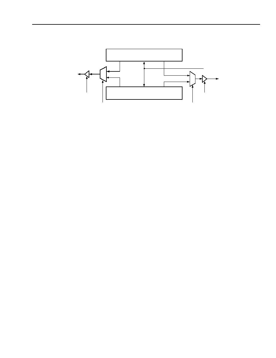
Preliminary Data Sheet
TMXF28155/51 Super Mapper
May 2001
155/51 Mbits/s SONET/SDH x28/x21 DS1/E1
569
Agere Systems Inc.
22 Cross Connect (XC) Block Functional Description
(continued)
5-9196(F)
Figure 97. TPOAC and RPOAC Cross Connect
SPE MAPPER
TMUX
RPOACCLK
RPOACSYNC
RPOACDATA
TPOACCLK
TPOACSYNC
TPOACDATA
RSTS1_TUG3
TSTS1_TUG3
TPOAC_EN
RPOAC_EN
EXT I/O
EXT I/O
1
0
1
0

TMXF28155/51 Super Mapper
Preliminary Data Sheet
155/51 Mbits/s SONET/SDH x28/x21 DS1/E1
May 2001
570
Agere Systems Inc.
23 Digital Jitter Attenuation Controller Functional Description
Table of Contents
Contents
Page
23 Digital Jitter Attenuation Controller Functional Description ............................................................................ 570
23.1 Introduction ............................................................................................................................................. 571
23.2 Features ................................................................................................................................................. 571
23.3 Functional Block Diagram of the DJA Block ........................................................................................... 572
23.4 Digital Jitter Attenuation Controller Operation ........................................................................................ 572
23.4.1 PLL Bandwidth and Damping Factor Control .............................................................................. 573
23.4.2 PLL Order Control ....................................................................................................................... 573
23.4.3 DS1/E1 Clock Edge Control ........................................................................................................ 573
Figures
Page
Figure 98. DJA Block with I/O Connections to Other Blocks in the Device .......................................................... 571
Figure 99. Basic Functional Flow of the DJA Block .............................................................................................. 572
Tables
Page
Table 622. PLL Bandwidth Control Parameters .................................................................................................. 571
Table 623. First-Order Mode Duration Control .................................................................................................... 571
Preliminary Data Sheet
TMXF28155/51 Super Mapper
May 2001
155/51 Mbits/s SONET/SDH x28/x21 DS1/E1
571
Agere Systems Inc.
23 Digital Jitter Attenuation Controller Functional Description
(continued)
23.1 Introduction
This section describes the functions of the digital jitter attenuator (DJA) controller used in the Super Mapper device.
The DJA controller contains 28 DJA blocks. Each DJA block can operate in two different modes, as a DS1 or an E1
jitter attenuator. In both modes, the DJA blocks can be provisioned to operate as a second-order PLL always, or it
can switch to act as a first-order PLL during VT pointer adjustments to help meet MTIE requirements. The block will
also insert the proper AIS signal if the primary block AIS control input is active. The PLL bandwidth can be set over
a wide range to accommodate a number of different system constraints.
23.2 Features
s
The DJA block accepts/delivers DS1/E1 clock, data, and AIS indications from/to the cross connect block.
s
AIS in will cause the correct AIS clock to be inserted, and the AIS indication will be passed back to the cross con-
nect.
s
The DJA blocks operate in the second-order PLL mode under normal conditions. The DJA blocks can be provi-
sioned to enter the first-order PLL mode following VT level pointer adjustments. The period of time in the first-
order mode is provisionable via registers.
s
The PLL bandwidth is provisionable between 0.1 Hz and 0.5 Hz. The damping factor for these bandwidths varies
between 2 and 0.5.
Figure 98
shows the DJA block with I/O connections to other blocks within the Super Mapper device.
5-8955(F)r.3
Figure 98. DJA Block with I/O Connections to Other Blocks in the Device
CR OSS
M IC R O IN TER FAC E
DIGIT AL
XC _JD ATA[28:1]
XC _JC LK[28:1]
XC _JPTR ADJ[28:1]
D JA_D ATA[28:1]
D S1_AISC LK
XC _JAIS[28:1]
D JA_C LK[28:1]
E1_XCLK
D S1_XC LK
E1_AISCLK
JITTER
AT TEN UAT OR
C ON NEC T
C ONT RO L
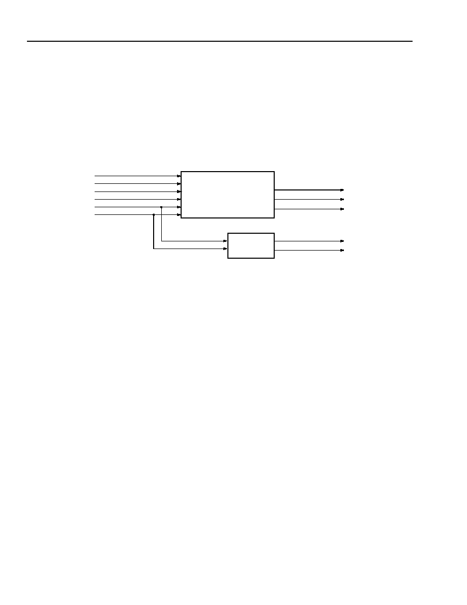
TMXF28155/51 Super Mapper
Preliminary Data Sheet
155/51 Mbits/s SONET/SDH x28/x21 DS1/E1
May 2001
572
Agere Systems Inc.
23 Digital Jitter Attenuation Controller Functional Description
(continued)
23.3 Functional Block Diagram of the DJA Block
The functional view of the DJA block, along with interconnections to the other blocks within the Super Mapper
device, are shown in the
Figure 99
.
The DJA block interfaces only to the cross connect and microprocessor interface blocks within the Super Mapper
device. The input interface between the DJA block and the cross connect block consists of clock, serial data, VT
pointer adjustment indication, and AIS insert indication. The output interface consists of clock, serial data, and AIS
insert indication as well as the DS1 and E1 AIS clocks for use by other blocks within the device.
5-8956(F)r.1
Figure 99. Basic Functional Flow of the DJA Block
23.4 Digital Jitter Attenuation Controller Operation
The digital jitter attenuation (DJA) controller is comprised of 28 DJA blocks. The DJA_SEL line rate control register
(
Table 478
) is used to determine if the block is operating in the DS1 or E1 mode (1 = DS1, 0 = E1).
The DJA controller requires a reference clock running at 16 or 32 times the line rate of the signal requiring jitter
attenuation. This reference clock should be driven on one of the external input signals DS1XCLK or E1XCLK (see
Table 3, High-speed I/O Pin Descriptions on page15
under the M13 MUX/DEMUX block receive path section).
Each jitter attenuator block receives a clock, data, pointer adjust control, and an AIS control signal input. If the AIS
control signal is active (high) on any time slot, then the AIS clock generation block (see
Figure 99
) of the DJA sim-
ply divides the correct line clock (XC_JCLKx) by 16 or 32 (via the DJA_BLUECLKD register shown in
Table 479
,
independent of being in DS1 or E1 mode), sends this divided clock (DS1_AISCLK or E1_AISCLK) to the cross con-
nect, and transmits the data signal (DJA_DATA) as a continuous logic 1.
Even with the digital PLL portion of the DJA turned off (via the P_DJA_CLK_EN register, see
Table 71 on page71
,
the AIS clock generation block will still generate the correct DS1_AISCLK or E1_AISCLK signals.
Each DJA block has a 64-bit elastic store. These elastic stores are monitored for both underflow and overflow con-
ditions. Both of these conditions contribute to the DJA_ESOVFL parameter, which can be unmasked to contribute
to an interrupt DJA_ESOVFL[28:1] (
Table 469
). In the event of an elastic store overflow, the elastic store will re-
center itself.
The block monitors DS1XCLK (DJA_DS1LOC and DJA_G_DS1LOC) and E1XCLK (DJA_E1LOC and
DJA_G_E1LOC) for loss of clock (LOC indication,
Table 471
) and change of loss of clock state (LOC delta,
Table 469
). The DJA_DS1LOC and DJA_E1LOC parameters are controlled by LOC events detected at the AIS
clock generation block, while the DJA_G_DS1LOC and DJA_G_E1LOC parameters are controlled by LOC events
detected at the DPLL. All loss of clock indications can contribute to a DJA interrupt. These interrupts can be
unmasked by writing zeros to the registers in
Table 470, DJA_MASK1--DJA_MASK2, Loss of Clock and Overflow/
Underflow Masks (R/W) on page 332
.
XC_JAISx
JITTER
XC_JCLKx
XC_JDATAx
XC_JPTRADJx
E1_XCLK
DJA_CLKx
DJA_DATAx
BLOCK REPEATED 28 TIMES
DS1_XCLK
AIS CLOCK
DS1_AISCLK
E1_AISCLK
ATTENUATION
BLOCK
GENERATION
DJA_AUTOAISx

Preliminary Data Sheet
TMXF28155/51 Super Mapper
May 2001
155/51 Mbits/s SONET/SDH x28/x21 DS1/E1
573
Agere Systems Inc.
23 Digital Jitter Attenuation Controller Functional Description
(continued)
23.4.1 PLL Bandwidth and Damping Factor Control
Two programmable terms are used to set the second-order loop damping factor and natural frequency. These
terms are the gain threshold, set by registers DJA_E1GAIN[26:0] (
Table 472
) and DJA_DS1GAIN[26:0]
(
Table 473
), and scale value, set by registers DJA_E1SCALE[15:0] (
Table 474
) and DJA_DS1SCALE[15:0]
(
Table 475
). Some values of damping factor (d) and natural frequency (
n) are listed below. The GAIN and SCALE
values in decimal and hexadecimal terms to achieve these parameter values are listed in
Table 622
.
Table 622. PLL Bandwidth Control Parameters
23.4.2 PLL Order Control
Under normal conditions the DJA blocks operate in the second-order PLL mode. This operation attempts to keep
the elastic store at the center of its range. However, following a VT pointer adjustment, it may be desirable to have
the DJA blocks operate in the first-order mode. This is because the maximum timing interval error (MTIE)
specification (GR-253, requirement R5-132) doesn't allow for any peaking. The second-order loop has a certain
amount of peaking in its transient response that the first-order loop eliminates. The amount of time that the block
operates in the first-order mode is programmable between 0 ms and 1 second.
This operation is accomplished by loading a count value into registers DJA_E1PTRADJCNT[20:0] or
DJA_DS1PTRADJCNT[20:0] (
Table 476
,
Table 477
). The value in this register is loaded into a counter whenever a
VT pointer adjustment takes place. The counter decrements every XCLK/16 or XCLK/32 clock period until it
reaches 0. While the count is nonzero, the block operates in the first-order mode. By default, the
DJA_E1PTRADJCNT or DJA_DS1PTRADJCNT value is 0, so the block never switches into the first-order mode
until programmed to do so. Some example time period durations and the corresponding decimal and hexadecimal
DJA_E1PTRADJCNT and DJA_DS1PTRADJCNT values are listed in
Table 623
.
Table 623. First-Order Mode Duration Control
23.4.3 DS1/E1 Clock Edge Control
The active edges on both the input and the output DS1/E1 signals are selectable via registers in
Table 479,
DJA_CLK_CTL1--DJA_CLK_CTL4, Reference Clock Rate and Edge Transitions (R/W) on page 334
.
DJA_TXEDGE[28:1] (
Table 479
) controls the edge that the data transitions on when leaving the DJA (1 = rising
edge). DJA_RXEDGE[28:1] controls the edge that the data transitions on when retimed into the DJA (1 = rising
edge).
d
n
E1_SCALE
E1_GAIN
DS1_SCALE
DS1_GAIN
dec
hex
dec
hex
dec
hex
dec
hex
0.5
0.45
2,829 0xB0D
8,005,638 0x7A2806
2,133 0x855
4,549,825 0x456CC1
0.75 0.325
5,876 0x16F4
15,348,087
0xEA3177
4,430 0x114E
8,722,740 0x851934
1.0
0.25
10,186 0x27CA
25,938,267 0x18BC95B
7,679 0x1DFF
14,741,431
0xE0EFB7
1.5
0.175
21,827
0x5543
52,935,238
0x327BA46
16,455
0x4047
30,084,553
0x1CB0DC9
2.0
0.125
40,743 0x9F27
104,000,000
0x632EA00
30,716 0x77FC
58,965,723 0x383BEDB
Duration
E1 Mode
DS1 Mode
--
dec
hex
dec
hex
250 ms
512,000
0xC800
386,000
0x96C8
500 ms
1,024,000
0xFA000
77,200
0x12D90
750 ms
1,536,000
0x177000
1,158,000
0x11AB70
1 s
2,048,000
0x1F4000
1,544,000
0x178F40

TMXF28155/51 Super Mapper
Preliminary Data Sheet
155/51 Mbits/s SONET/SDH x28/x21 DS1/E1
May 2001
574
Agere Systems Inc.
24 Test-Pattern Generation/Detection Functional Description
Table of Contents
Contents
Page
24 Test-Pattern Generation/Detection Functional Description ............................................................................ 574
24.1 Test-Pattern Generator Introduction ....................................................................................................... 575
24.2 Features ................................................................................................................................................. 575
24.3 Applications ............................................................................................................................................ 575
24.4 Block Diagram ........................................................................................................................................ 576
24.5 Functional Descriptions .......................................................................................................................... 576
24.5.1 Test-Pattern Generation .............................................................................................................. 576
24.5.2 TPG Clock Source ....................................................................................................................... 577
24.5.3 TPG Transmit Edge Select .......................................................................................................... 577
24.5.4 TPG Test-Pattern Framing .......................................................................................................... 577
24.5.5 DS1 TPG Framing ....................................................................................................................... 577
24.5.6 E1 TPG Framing ......................................................................................................................... 577
24.5.7 DS2 TPG Framing ....................................................................................................................... 578
24.5.8 DS3 TPG Framing ....................................................................................................................... 578
24.5.9 Line Encoding/Decoding ............................................................................................................. 578
24.5.10 TPG Test-Pattern Sequences ................................................................................................... 578
24.5.11 TPG Idle Generator ................................................................................................................... 579
24.5.12 TPG Error Insertion ................................................................................................................... 579
24.5.13 TPG Interrupts ........................................................................................................................... 579
24.5.14 Test-Pattern Monitor (TPM) ....................................................................................................... 579
24.5.15 TPM Channel Selection ............................................................................................................. 579
24.5.16 TPM Clock Edge and Data Polarity Selection ........................................................................... 579
24.6 TPM Framing Acquisition and Synchronization ...................................................................................... 579
24.6.1 DS1/E1 ........................................................................................................................................ 579
24.6.2 TPM Error Detection and Counting ............................................................................................. 580
24.6.3 TPM Interrupts ............................................................................................................................. 581
24.7 Microprocessor Interface ........................................................................................................................ 581
24.7.1 Microprocessor Interface Register Map ...................................................................................... 581
Figures
Page
Figure 100. TPG Block Interface Block Diagram.................................................................................................. 576
Tables
Page
Table 624. TPG Framing Controls (TPG_FRAMEx = 1) ..................................................................................... 577
Table 625. TPG Test-Pattern Sequences ........................................................................................................... 578
Table 626. TPM Interrupts ................................................................................................................................... 581

Preliminary Data Sheet
TMXF28155/51 Super Mapper
May 2001
155/51 Mbits/s SONET/SDH x28/x21 DS1/E1
575
Agere Systems Inc.
24 Test-Pattern Generation/Detection Functional Description
(continued)
24.1 Test-Pattern Generator Introduction
The TPG block is a configurable set of test-pattern generators and monitors for the Super Mapper. For mainte-
nance and troubleshooting operations, TPG feeds one or more T1/E1/DS2 test signals (via data, clock, and FS sig-
nal paths) to the crosspoint switch (XC block). The XC block can redistribute or broadcast these signals to any valid
channel in the framer, external I/O, M13 mapper, DJA, or VT mapper blocks. Similarly, any channel arriving at the
XC may be routed to the test monitor. The TPG can also generate DS3 test signals for use via the M13 and SPE
blocks. Single bit-errors can be detected and counted at each monitor.
The test-pattern generator and associated monitors receive configuration and setup information from the micropro-
cessor control interface. Once the rate and data format are chosen, the test generator outputs are fed to the cross-
point (XC). The crosspoint can map the test signals to any valid DS1/E1/DS2 channel in the device, or to a special
set of test monitor channels in the TPG block (for loopback testing of the test generator/monitor pair). The monitor
waits for the expected test pattern and (after a brief synchronization operation) continually checks the data stream
for bit errors. Optionally, a single data-bit or framing-bit error may be generated via a global SMPR_BER_INSRT
(
Table 65, SMPR_GTR, Global Trigger Register (RW) on page66
) control signal, in order to confirm the correct
detectability of such an error as it traverses the crosspoint and other system elements.
Simultaneous testing of DS1, E1, DS2, and DS3 signals is supported (one test channel at each rate plus one idle
channel at DS1). The DL (DS1-ESF data link) and E1 Sa (spare) bit fields are read/writable under software control,
allowing for additional system testing control.
Test monitors can automatically detect/count data-bit errors and detect framing-bit or CRC errors in a pseudoran-
dom test sequence, or loss of frame or loss of sync. The TPG can provide an interrupt to the control system, or it
can be operated in a polled mode.
24.2 Features
s
Configurable test-pattern generator: DS1, E1, DS2, and DS3 formats.
s
Pseudorandom bit sequence (PRBS, also known as pseudonoise or PN sequences) based on maximal-length
feedback shift register sequences; PN codes selectable from the following options: QRSS, PRBS15, PRBS20,
PRBS23, ALT_01, ALL_ONES, USER pattern (16 bits, repeating).
s
The DS1 and E1 test patterns can be transmitted either unframed or as the payload of a framed signal as defined
in ITU-T Recommendation O.150 (see TPG_FRAMEx signals (
Table 507
and
Table 508
)).
s
Single bit-errors or framing-errors may be injected into any test pattern, under register control.
s
Any sink or receiving channel may be replaced by a test-pattern monitor, which can detect and count bit errors or
misconfigurations, and/or detect idle conditions or AIS.
s
Data link (DS1-ESF DL) and SSM (E1 multiframe Sa) fields read/writable.
s
Supports all Super Mapper modes of operation.
s
Complies with T1.107, T1.231, T1.403, G.703, G.704, O.150.
24.3 Applications
s
Super Mapper self-test, crosspoint verification.
s
Built-in link and system testing support.
s
Flexible multicast/broadcast capabilities.
s
Programmable error insertion.
s
Idle or test-pattern (DS1 only) generation for each channel.
s
Idle or test-pattern (DS1 only) bit error or activity monitoring for each channel.

TMXF28155/51 Super Mapper
Preliminary Data Sheet
155/51 Mbits/s SONET/SDH x28/x21 DS1/E1
May 2001
576
Agere Systems Inc.
24 Test-Pattern Generation/Detection Functional Description
(continued)
24.4 Block Diagram
The following diagram illustrates the high-level interface between the TPG block and other functional blocks.
5-9178(F)r.3
Figure 100. TPG Block Interface Block Diagram
24.5 Functional Descriptions
24.5.1 Test-Pattern Generation
The test-pattern generator has five groups of output signals. These outputs consist of two signal groups for DS1
and one signal group each for E1, DS2, and DS3 clock rates. Each of these groups can be provisioned, indepen-
dently, in various ways. Each DS1/E1 signal group consists of a clock, the data stream, and a frame-sync signal (if
needed in a byte-synchronous environment). The DS2 signal group consists of clock and data. The DS3 signal
group consists of data, clock, and clock enable. Each rate supports full-payload test patterns data signals and DS1
also supports continuous idle data signals.
TPG
TEST
GEN/MON
XC
CROSS
CONNECT
DS1/E1/DS2/DS3 SOURCE CLOCKS
(DS1) DATA/CLK/SYNC
(DS1) IDLE/CLK/SYNC
(E1) DATA/CLK/SYNC
(DS2) DATA/CLK
[DS3} DATA/CLK/CLKEN
(TPG_DS1) DATA/CLK/SYNC
(TPG_DS1) IDLE/CLK/SYNC
(TPG_E1) DATA/CLK/SYNC
(TPG_DS2) DATA/CLK
(TPG_DS3) DATA/CLK/CLKEN
CONTROL INTERFACE
4
3
3
3
2
3
3
3
3
3
3

Preliminary Data Sheet
TMXF28155/51 Super Mapper
May 2001
155/51 Mbits/s SONET/SDH x28/x21 DS1/E1
577
Agere Systems Inc.
24 Test-Pattern Generation/Detection Functional Description
(continued)
24.5.2 TPG Clock Source
The Super Mapper TPG uses four source clocks provided by the cross connect as input at the appropriate rate to
generate the test patterns. These are shown in
Figure 100, TPG Block Interface Block Diagram on page 576
as
being supplied by the XC block, except the DS3 clock (which is provided via the XC3 crosspoint by the M13 or SPE
block).
24.5.3 TPG Transmit Edge Select
The edge of the clock TPG_CLKx that is used to source the data is provisionable to either the rising edge
TPG_EDGEx = 1 (
Tables 507
,
508
,
509
, and
510
) or the falling edge TPG_EDGEx = 0 for each of the five test-pat-
tern sources.
24.5.4 TPG Test-Pattern Framing
The test pattern can be transmitted either unframed or as the payload of a framed signal as defined in ITU-T Rec-
ommendation O.150. The DS1 continuous-idle signal is always framed. The test-pattern framing is determined by
the TPG_FRAMEx register values (
Table 507
and
Table 508
): 0 represents an unframed signal, while 1 represents
a test-pattern embedded in a framed signal. Additionally, a TPG_ESF bit (
Table 507
) determines if extended super-
frame operation is enabled (DS1 only).
Table 624. TPG Framing Controls (TPG_FRAMEx = 1)
The DS1 idle data signal is always superframe (SF) framed. The associated SYNC signal is generated but may
safely be ignored if not used.
24.5.5 DS1 TPG Framing
For DS1 signals, the frame bit in the 12th frame of each superframe is inverted if TPG_FINV0 = 1 (
Table 507
and
Table 508
).
For ESF modes, the transmitted data-link pattern is a continuous repeat of the contents of the TPG_ESFDL[15:0]
(
Table 504
). Each ESF superframe is also checked for CRC-6 errors per
ANSI
T1.403. These CRC errors may be
injected via TPG_CRC6EINSx register bits (
Table 503
). A single CRC-6 error event is generated each time that the
TPG_CRC6EINSx bit transitions from 0 to 1.
24.5.6 E1 TPG Framing
For E1 signals, the frame alignment signal (normally 0011011) is transmitted with the last bit inverted (0011010) if
TPG_FINV = 1 (
Table 507
and
Table 508
).
Each transmitted E1 multiframe contains a CRC-4 cyclic redundancy check mechanism per Recommendation
G.704 Section 2.3. CRC-4 errors may be injected via TPG_CRC4EINSx register bits (
Table 503
). A single CRC-4
error event is generated each time that the TPG_CRC4EINSx bit transitions from 0 to 1.
Index
Data Rate
Framing
(x)
--
SF (TPG_ESF = 0)
ESF (TPG_ESF = 1)
0
DS1
Transparent mode (test sequence bits
in signaling bit positions)
User-settable data-link pattern CRC-6
generate/check
1
Continuous idle
NA
2
E1
E1 with common channel signaling, CRC-4
4
DS2
Unframed PRBS sequence
5
DS3
DS3--gated PRBS sequence (framing via M13)

TMXF28155/51 Super Mapper
Preliminary Data Sheet
155/51 Mbits/s SONET/SDH x28/x21 DS1/E1
May 2001
578
Agere Systems Inc.
24 Test-Pattern Generation/Detection Functional Description
(continued)
The transmitted Sa bits (designated as spares in G.704) are a continuous repeat of the contents of the
TPG_E1SAx[4:8] registers (
Table 505
and
Table 506
). These bits are synchronized to the CRC-4 frame. Referring
to Table 5B in G.704, the E1SA1[4:8] bits are the SA bits in SMF 1 and 9, the E1SA2[4:8] bits are the Sa bits in
SMF 3 and 11, etc.
24.5.7 DS2 TPG Framing
The DS2 generator provides an unframed DS2 rate test sequence.
24.5.8 DS3 TPG Framing
For DS3 test signals, the TPG provides a raw PN sequence on TPG_DATA[5] using the enabled clock.
24.5.9 Line Encoding/Decoding
For DS1 and E1 test signals, the TPG may be provisioned to transmit and receive AMI coded signals
TPG_TPM_CODEx (
Table 507
and
Table 508
). The signals can be uncoded, B8ZS coded, HDB3 coded, or AMI
coded. If coding is selected, it is active for both transmit and receive paths. For coded signals, the DATA inputs/out-
puts become the positive rails and the sync inputs/outputs become the negative rails.
24.5.10 TPG Test-Pattern Sequences
The test-pattern bit sequence generated on the nonidle TPG_DATAx lines is determined by the TPG_SEQm[2:0]
(
Table 507
,
508
,
509
, and
510
) register values, where m is the rate index (0 = DS1, 2 = E1, 4 = DS2,
and 5 = DS3). One of seven sequences presently may be selected for transmission within the framed or unframed
test pattern on the corresponding even TPG_DATAx lines (the odd lines are connected to idle generators). Each
datastream also has an associated clock TPG_CLKx and frame-sync signal TPG_FSx (x even, except DS2).
TPG_SEQm[2:0] values are described in the following table:
The polarity of the output data stream may also be provisioned to normal TPG_TPINVx = 0 (
Table 507
,
508
,
509
,
and
510
) or inverted TPG_TPINVx = 1.
Table 625. TPG Test-Pattern Sequences
TPG_SEQm
Test Pattern
000
PRBS15. 2
15
≠ 1 PN sequence specified in O.150. This sequence is generated by a 15-stage
shift register whose 14th and 15th stages are added and fed back to the first stage. The output of
the last stage is inverted (which yields a sequence with up to 15 consecutive zeros) to produce
the transmitted sequence.
001
PRBS20. 2
20
≠ 1 PN sequence. This sequence is generated by a 20-stage shift register whose
17th and 20th stages are added and fed back to the first stage. The transmitted test sequence is
normally the noninverted output of the last (20th) stage.
010
QRSS. 2
20
≠ 1 PN sequence with zero-suppression as specified in O.150. This sequence is gen-
erated by a 20-stage shift register whose 17th and 20th stages are added and fed back to the first
stage. The transmitted test sequence is normally the non-inverted output of the last (20th) stage,
but the test sequence is forced high if the outputs of stages 6 through 19 are low.
011
PRBS23. 2
23
≠ 1 PN sequence.
100
ALT_01. Alternating sequence of ones and zeros.
101
ALL_ONES. All-ones sequence.
Note: If unframed, an AIS signal is generated.
110
Reserved.
111
User-Defined. Continuously repeating 16-bit pattern from TPG_USER[15:0] (
Table 511
).

Preliminary Data Sheet
TMXF28155/51 Super Mapper
May 2001
155/51 Mbits/s SONET/SDH x28/x21 DS1/E1
579
Agere Systems Inc.
24 Test-Pattern Generation/Detection Functional Description
(continued)
24.5.11 TPG Idle Generator
The TPG has one output dedicated to providing a valid, SF framed DS1 idle data pattern. This datastream also has
an associated clock TPG_CLKx and frame-sync signal TPG_SYNCx (x odd). This pattern is specified in detail in
T1.403 for DS1.
24.5.12 TPG Error Insertion
A single bit error is injected into the test sequence each time that the global control signal SMPR_BER_INSRT
(
Table 65, SMPR_GTR, Global Trigger Register (RW) on page66
) transitions from 0 to 1 while the associated
enable bit TPG_BERINSx (
Table 501
) is set to 1.
Similarly, for framed signals, a single framing bit error may be injected into the test sequence each time that the
TPG_FERINSx (
Table 502
) bit transitions from 0 to 1.
For certain types of framed signals (that is, DS1 ESF and E1 multiframe), cyclic-redundancy check (CRC) errors
may be injected into the test sequence. A single error insertion event is triggered each time that the
TPG_CRCEINSx (
Table 500
) (for DS1-ESF) or TPG_CRC4EINSx (
Table 503
) (for E1) register bit toggles
from 0 to 1.
24.5.13 TPG Interrupts
There are no interrupts from the TPG at the current time.
24.5.14 Test-Pattern Monitor (TPM)
The test-pattern monitor TPM sub-block contains four self-synchronizing detectors that are provisioned to search
for a particular test pattern (one each for signal at DS1, E1, DS2, and DS3). Each of the four monitor blocks
searches for the framed or unframed sequence at that rate, as determined by the values of TPM_FRAMEx
(
Table 507
and
Table 508
) and TPM_SEQm[2:0] (
Table 507
,
508
,
509
, and
510
) register bits (defined similarly to
the corresponding TPG register bits).
24.5.15 TPM Channel Selection
In normal operation, the user connects one of the available DS1, E1, DS2, or DS3 signals to the corresponding
TPM input by configuring the cross connect (XC).
24.5.16 TPM Clock Edge and Data Polarity Selection
The edge of the clocks XC_TCLKx that is used to acquire the test data is provisionable to either the rising edge
TPM_EDGEx = 1 (
Table 507
,
508
,
509
, and
510
) or the falling edge TPM_EDGEx = 0 for each of the four test-pat-
tern monitors. The polarity of the input data stream may also be provisioned to normal TPM_TPINVx = 0
(
Table 507
,
508
,
509
, and
510
) or inverted TPM_TPINVx = 1.
24.6 TPM Framing Acquisition and Synchronization
24.6.1 DS1/E1
For framed data streams TPM_FRAMEx = 1 (
Table 507
and
Table 508
), the monitor searches for the appropriate
frame sequence in the selected signal. If no frame is found, TPM_OOFx (
Table 496
) is set. The TPM_OOFx condi-
tion (status) signals default to 1, indicating an out-of-frame condition.

TMXF28155/51 Super Mapper
Preliminary Data Sheet
155/51 Mbits/s SONET/SDH x28/x21 DS1/E1
May 2001
580
Agere Systems Inc.
24 Test-Pattern Generation/Detection Functional Description
(continued)
A TPM_OOFxD (
Table 482
) signal detects and latches delta events (changes or transitions) in the TPM_OOFx sig-
nal. The TPM_OOFxD signal is reset to 0 based on the SMPR_COR_COW (
Table 67, SMPR_GCR, Global Control
Register (RW) on pag e68
) global control signal: if SMPR_COR_COW is set, event or delta signals are cleared on
any microprocessor read of the event or delta register. If SMPR_COR_COW is 0, each event or delta signal must
be written with a 1 to clear it. The TPM_OOFxD signal, if asserted, will generate an interrupt unless the corre-
sponding mask bit TPM_OOFxDM (
Table 489
) is set.
Also, synchronization is checked for the designated test patterns. If the TPM monitor detects 32 consecutive
matches in its input sequence, the corresponding TPM_OOSx (
Table 497
) is cleared. Similarly, if the TPM detects
four or more consecutive mismatches in the input sequence, the corresponding TPM_OOSx is set. The
TPM_OOSx condition (status) signals default to 1, indicating an out-of-sync condition.
A TPM_OOSxD (
Table 483
) signal detects and latches delta events (changes or transitions) in the TPM_OOSx sig-
nal. The TPM_OOSxD signal is reset to 0 based on the SMPR_COR_COW global control signal: if
SMPR_COR_COW is set, delta signals are cleared on any microprocessor read of the delta register. If
SMPR_COR_COW is 0, each delta signal must be written with a 1 to clear it. The TPM_OOSxD signal, if asserted,
will generate an interrupt unless the corresponding mask bit TPM_OOSxDM (
Table 490
) is set.
DS2 (x = 4). The DS2 monitor checks for synchronization of the unframed PRBS signals, and for bit errors as
above.
DS3 (x = 5).
The DS3 monitor checks for synchronization of the unframed PRBS signals, and for bit errors as
above.
24.6.2 TPM Error Detection and Counting
TPM Bit Errors. While in sync, each data monitor detects and counts the number of times that the input sequence
differs from the expected sequence in a 16-bit counter (one per rate). Detection of a bit error causes the TPM to
latch a 1 into the TPM_BEREx (
Table 490
) event register bit. Clearing of this latched event is determined by the
SMPR_COR_COW global control signal (if set, the event is automatically cleared on read, otherwise a 1 must be
written to the TPM_BEREx register bit to clear it). If the interrupt is enabled (not masked) via TPM_BERMx
(
Table 491
) mask bits, then this event will trigger an interrupt.
The error counters accumulate TPM_BEREx events in a set of active counters. The active counter values are
transferred to registers upon assertion of global control signal SMPR_PMRESET (
Table 65, SMPR_GTR, Global
Trigger Register (RW) on page66
). The counter values may be read via the microprocessor control interface via
registers called TPM_CNTx[15:0] (Tables
513
,
514
,
515
, and
516
). The active counters will roll over or saturate at
the terminal count depending on global control signal SMPR_SAT_ROLLOVER (
Table 67, SMPR_GCR, Global
Control Register (RW) on page68
). The counters will clear on read if the global control signal SMPR_COR_COW
is set; otherwise, the counter values are not affected by reads and instead must be cleared by explicit writes. The
global control signals SMPR_PMRESET, SMPR_SAT_ROLLOVER, and SMPR_COR_COW operate on all six test
channels; there are no separate controls per rate or mode.
TPM Framing Errors. Framing-bit errors TPM_FEREx (
Table 485
) events are detected when TPM_FRAMEx is 1
but not counted. The event is latched and may be used to trigger a (maskable) interrupt, or may be polled (the error
assertion will last between one and 24 frame intervals). The interrupt mask bit is called TPM_FERExM (
Table 492
).
The global control signal SMPR_COR_COW determines if the TPM_FEREx event is cleared on read or write.
TPM CRC Errors. Cyclic redundancy check (CRC) errors TPM_CRCEx (
Table 488
) are detected when
TPM_FRAMEx (
Table 507
and
Table 508
) is 1 but not counted. CRC-6 errors are valid only for DS1 extended
super-frame (ESF) test patterns. CRC-4 errors are valid only for E1 multiframe test patterns. Each CRC error event
is latched and may be used to trigger a (maskable) interrupt, or may be polled (the error assertion will last between
1 and 24 frame intervals).
CRC-6 errors (DS1-ESF only) are detected via TPM_CRCE0. Interrupts are managed via TPM_CRCE0M
(
Table 495
) bit. The global control signal SMPR_COR_COW (
Table 67, SMPR_GCR, Global Control Register (RW)
on page68
) determines if the TPM_CRCE0 event is cleared on read or write.

Preliminary Data Sheet
TMXF28155/51 Super Mapper
May 2001
155/51 Mbits/s SONET/SDH x28/x21 DS1/E1
581
Agere Systems Inc.
24 Test-Pattern Generation/Detection Functional Description
(continued)
CRC-4 errors (E1 multiframe only) are detected via TPM_CRCE2. Interrupts are managed via TPM_CRCE2M
(
Table 495
) bits. The global control signal SMPR_COR_COW determines if the TPM_CRCE2 event is cleared on
read or write.
TPM Data AIS Detection. If an active data monitor detects AIS (i.e., detects all ones in the data signal), the corre-
sponding register bit TPM_AISx (
Table 498
) is asserted (default = 0, no AIS). A TPM_AISxD (
Table 487
) signal
detects and latches delta events (changes or transitions) in the TPM_AISx signal. The TPM_AISxD signal is reset
to 0 based on the SMPR_COR_COW global control signal: if SMPR_COR_COW is set, event or delta signals are
cleared on any microprocessor read of the event or delta register. If SMPR_COR_COW is 0, each event or delta
signal must be written with a 1 to clear it. The TPM_AISxD signal, if asserted, will trigger an interrupt unless the
corresponding interrupt mask bit TPM_AISxDM (
Table 494
) is set.
TPM DS1-ESF Data Link. For DS1 extended super frame (ESF) test patterns, the received data link field contents
are presented to software via registers entitled TPM_ESFDL[15:0] (
Table 504
).
TPM E1 Sa-Bits Field. For E1 framed test patterns, the received Sa bits are presented to software via registers
entitled TPM_E1SAx[4:8] (
Table 518
and
Table 519
).
24.6.3 TPM Interrupts
The TPM block is capable of generating the following (maskable) interrupts:
Table 626. TPM Interrupts
The microprocessor interface may also read the current condition (status) of TPM framing, synchronization, or AIS
detection via the TPM_OOFx (
Table 496
), TPM_OOSx (
Table 497
), and TPM_AISx (
Table 498
) indicators directly.
24.7 Microprocessor Interface
24.7.1 Microprocessor Interface Register Map
The register map of the microprocessor interface is shown in
Table 76, Microprocessor Interface Register Map on
page 73
. All addresses referred to in this section are given in hexadecimal notations in the first column of the table.
Event
Int_Name
Int_Mask_Name
Description
OOFx Change
TPM_OOFxD (
Table 482
) TPM_OOFxDM (
Table 489
)
TPM Out-of-Frame Delta
OOSx Change TPM_OOSxD (
Table 483
) TPM_OOSxDM (
Table 490
)
TPM Out-of-Sync Delta
BER
TPM_BEREx (
Table 484
)
TPM_BERExM (
Table 491
)
TPM Single Bit Error
FER
TPM_FEREx (
Table 485
)
TPM_FERExM (
Table 492
)
TPM Framing Error
CRC Error
TPM_CRCEx (
Table 488
) TPM_CRCExM (
Table 495
) TPM CRC Error (DS1, ESF, or E1 only)
AISx Change
TPM_AISxD (
Table 487
)
TPM_AISxDM (
Table 494
)
TPM AIS Delta

TMXF28155/51 Super Mapper
Preliminary Data Sheet
155/51 Mbits/s SONET/SDH x28/x21 DS1/E1
May 2001
582
Agere Systems Inc.
25 Philosophies
Table of Contents
Contents
Page
25 Philosophies ................................................................................................................................................... 582
25.1 Clocking and Power Management Philosophy ....................................................................................... 583
25.2 Maintenance Philosophy ........................................................................................................................ 583
Figures
Page
Figure 101. Clock and Power Shutdown Diagram................................................................................................ 583
Tables
Page
Table 627. Maintenance Tasks Supported by the SMPR .................................................................................... 584
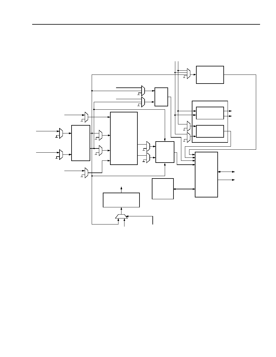
Preliminary Data Sheet
TMXF28155/51 Super Mapper
May 2001
155/51 Mbits/s SONET/SDH x28/x21 DS1/E1
583
Agere Systems Inc.
25 Philosophies
(continued)
25.1 Clocking and Power Management Philosophy
5-8977(F)
Figure 101. Clock and Power Shutdown Diagram
25.2 Maintenance Philosophy
The Super Mapper maintenance philosophy follows the SONET NE maintenance criteria specified by GR-253-
CORE.
The various functions that are used to perform the following maintenance tasks are addressed:
s
Trouble detection
s
Trouble or repair verification
s
Trouble sectionalization
s
Trouble isolation
s
Restoration
TMUX
SPE/
M13
TEST
DJA
FRAMER
T1/E1
CROSS
MPU INTERFACE
155 MHz Tx
155 MHz Rx
51.84
TXCK
RXCK
51.84
TXCK
RXCK
44.736 MHz
44.736 MHz
6.48
6.48
TXCK
RXCK
DS1XCLK
E1XCLK
MPU_CLK
MPCLK
DS1_AISCLK
E1_AISCLK
DPLL
AIS CLOCK
LINERXCLK
LINETXCLK
VT/VC
MPMODE
19.44 MHz
19.44 MHz
19.44
51.84
51.84
19.44
(TO ALL BLOCKS)
PATTERN
GEN/MON
AND CONTROL
MUX
DS2
DS3
CONNECT
MAPPER
(x28)
GENERATION
16 MHz--66 MHz
[29:1]
[29:1]
BANK
MHx
MHz
MHz
MHz
AU-3
MAPPER

TMXF28155/51 Super Mapper
Preliminary Data Sheet
155/51 Mbits/s SONET/SDH x28/x21 DS1/E1
May 2001
584
Agere Systems Inc.
25 Philosophies
(continued)
The following tables show how the Super Mapper handles its maintenance tasks.
Table 627. Maintenance Tasks Supported by the SMPR
Maintenance Tasks
Support by
SMPR
Generation
(Blocks Responsible)
Detection
(Blocks Responsible)
Alarm Surveillance
Directly Detected Defects and Failure
Loss of Signal (LOS)
Supported
TMUX
TMUX, M13
Loss of Frame (LOF)
Supported
TMUX
TMUX, M13
Loss of Pointer (LOP)
Supported
TMUX
TMUX, SPEMPR,
VTMPR
Equipment Failures
NA
--
--
Loss of Synchronization
Supported
--
TMUX, VTMPR
APS Troubles:
Protection Switching Byte Failure
Channel Mismatch Failure
APS Mode Mismatch Failure
Far-End Protection-Line Failure
Supported
TMUX
TMUX
DCC Failure
--
TMUX
TMUX (partial support)
Signal Label Mismatch:
STS Payload Label Mismatch
STS Path Unequipped
VT Payload Label Mismatch
VT Path Unequipped
Supported
Supported
Supported
Supported
TMUX, SPEMPR
TMUX, SPEMPR
--
VTMPR
TMUX, SPEMPR
TMUX, SPEMPR
VTMPR
VTMPR
Alarm Indication Signal (AIS)
Line AIS (AIS-L)
Supported
TMUX
TMUX
STS Path AIS (AIS-P)
Supported
TMUX, SPEMPR
TMUX, SPEMPR
VT Path AIS (AIS-V)
Supported
VTMPR
VTMPR
DSn AIS
Supported
TPG, M13, FRAMER,
VTMPR
TPG, M13, FRAMER,
VTMPR
Remote Defect Indication (RDI) and Remote Failure Indication (RFI)
Line Remote Defect Indication (RDI-L) and
Remote Failure Indication (RFI-L)
Supported
TMUX
TMUX
STS Path Remote Defect Indication (RDI-P)
and Remote Failure Indication (RDI-P)
Supported
TMUX, SPEMPR
TMUX, SPEMPR
VT Path Remote Defect Indication (RDI-V)
and Remote Failure Indication (RFI-V)
Supported
VTMPR
VTMPR
DSn RDI and RAI Signals
Supported
M13, FRAMER
M13, FRAMER
Payload Defect Indication (PDI)
STS Payload Defect Indication (PDI-P)
Supported
TMUX, SPEMPR
TMUX, SPEMPR
VT Payload Defect Indication (PDI-V)
NA
--
--
Maintenance Signals for Other Mappings
NA
--
--
Trunking
NA
--
--
Alarm-Related Events
Supported
All blocks to meet the signal-
ing and timing requirements
--

Preliminary Data Sheet
TMXF28155/51 Super Mapper
May 2001
155/51 Mbits/s SONET/SDH x28/x21 DS1/E1
585
Agere Systems Inc.
25 Philosophies
(continued)
Table 627. Maintenance Tasks Supported by the SMPR (continued)
Maintenance Tasks
Support by
SMPR
Generation
(Blocks Responsible)
Detection
(Blocks Responsible)
Control of Alarm Processing
Alarm Level Designations
NA
--
--
Signal Failure/Single Message
NA
--
--
Independent Failures
NA
--
--
Retrieval of NE Condition
NA
--
--
Provisioning of Alarm Levels
NA
--
--
Clear Messages
NA
--
--
Noninstrusive Detection of Defects and
Declaration of Failures
NA
--
--
Performance Monitoring
General Accumulation and Thresholding Criteria
Physical Layer PM
Physical Layer Parameters
Supported
--
TMUX, SPEMPR, M13
Physical Layer PM Criteria
Supported
--
SPEMPR, M13
Section Layer PM
Section Layer Parameters
Supported
TMUX
TMUX
Section Layer PM Criteria
Supported
TMUX
TMUX
Line Layer PM
Near-end Line Layer Parameters
Supported
TMUX
TMUX
Far-end Line Layer Parameters
Supported
TMUX
TMUX
Line Layer PM Criteria
Supported
TMUX
TMUX
STS Path Layer PM
Near-end STS Path Layer Parameters
Supported
TMUX, SPEMPR
TMUX, SPEMPR
Far-end STS Path Layer Parameters
Supported
TMUX, SPEMPR
TMUX, SPEMPR
STS Path Layer PM Criteria
Supported
TMUX, SPEMPR
TMUX, SPEMPR

TMXF28155/51 Super Mapper
Preliminary Data Sheet
155/51 Mbits/s SONET/SDH x28/x21 DS1/E1
May 2001
586
Agere Systems Inc.
25 Philosophies
(continued)
Table 627. Maintenance Tasks Supported by the SMPR (continued)
Maintenance Tasks
Support by
SMPR
Generation
(Blocks Responsible)
Detection
(Blocks Responsible)
VT Path Layer PM
Near-end VT Path Layer Parameters
Supported
VTMPR
VTMPR
Far-end VT Path Layer Parameters
Supported
VTMPR
VTMPR
VT Path Layer PM Criteria
Supported
VTMPR
VTMPR
Monitoring at DSn Interfaces
Supported
TPG, M13, FRAMER
TPG, M13, FRAMER
PM During Troubles
NA
--
--
Intermediate-Path PM
NA
--
--
Testing Process
Test Access
Fiber Access
NA
--
--
SONET Signal Test Access
NA
--
--
Digital Test Access
Supported
TPG
TPG
Diagnostics
Physical Layer
--
--
--
Section Layer
Supported
TMUX
TMUX
Signal Identification:
STS Path Trace
STS and VT Path Signal Label
Supported
TMUX
TMUX, SPEMPR, VTMPR
TMUX
TMUX, SPEMPR,
VTMPR
Error Monitoring
Supported
ALL BLOCKS
ALL BLOCKS
Loopbacks
SONET Terminal Loopbacks
Supported
TMUX
--
SONET Facility Loopbacks
Supported
VTMPR, TMUX, SPEMPR
--
DSn Loopbacks
Supported
M13, FRAMER
--

Preliminary Data Sheet
TMXF28155/51 Super Mapper
May 2001
155/51 Mbits/s SONET/SDH x28/x21 DS1/E1
Agere Systems Inc.
587
Applications
26 Applications
Table of Contents
Contents
Page
26 Applications ..................................................................................................................................................... 587
26.1 Application Diagrams .............................................................................................................................. 588
26.2 High-Speed Line Interfaces and Clock and Data Recovery ................................................................... 589
26.2.1 Receive Direction ......................................................................................................................... 589
26.2.2 Transmit Direction ......................................................................................................................... 589
26.3 Multiplex Section Protection (MSP 1 + 1) ............................................................................................... 589
26.3.1 Pointer Interpreter ........................................................................................................................ 589
26.4 Path Termination Function ..................................................................................................................... 590
26.5 STS-3/STM-1 MUX-DeMUX ................................................................................................................... 591
26.6 Telecom Bus Interface--Interfacing to Mate Devices ............................................................................ 591
26.7 SPE/AU-3 Mapper (DS3 Mapper) .......................................................................................................... 591
26.8 VT/VC Mapper ........................................................................................................................................ 592
26.8.1 Receive Direction ......................................................................................................................... 592
26.8.2 Transmit Direction ........................................................................................................................ 593
26.9 M13/M23 Multiplexer .............................................................................................................................. 593
26.9.1 Receive Direction ......................................................................................................................... 593
26.9.2 Transmit Direction ........................................................................................................................ 594
26.10 Cross Connect Block ............................................................................................................................ 594
26.11 Digital Jitter Attenuator ......................................................................................................................... 595
26.12 Test Pattern Generator ......................................................................................................................... 595
26.13 28-Channel Framer .............................................................................................................................. 596
26.14 Line Decoder/Encoder .......................................................................................................................... 601
26.15 Receive Frame Aligner/Transmit Frame Formatter .............................................................................. 601
26.16 Receive Performance Monitor .............................................................................................................. 601
26.17 Signaling Processor .............................................................................................................................. 602
26.18 Facility Data Link (FDL) Processor ....................................................................................................... 602
26.19 HDLC Unit ............................................................................................................................................ 603
26.20 System Interface.....................................................................................................................................603
27 Change History ............................................................................................................................................... 604
Figures
Page
Figure 102. Switching Application of the Super Mapper....................................................................................... 588
Figure 103. Transport Application of the Super Mapper ....................................................................................... 588
Figure 104. Super Mapper Switching Mode for Framer in Concentration Highway
Interface (CHI) Configuration............................................................................................................. 596
Figure 105. Super Mapper Switching Mode for Framer in Parallel System Bus Configuration ............................ 597
Figure 106. Super Mapper Switching Mode CHI Configuration with Byte-Synchronous VT Mapping Enabled ... 598
Figure 107. Super Mapper Byte-Synchronous Transport Mode: Passive Performance Monitoring ..................... 599
Figure 108. Super Mapper Byte-Synchronous Transport Mode: Intrusive Performance Monitoring.................... 600
Tables
Page
Table 628. Change History .................................................................................................................................... 604
588
Agere Systems Inc.
TMXF28155/51 Super Mapper
Preliminary Data Sheet
155/51 Mbits/s SONET/SDH x28/x21 DS1/E1
May 2001
26 Applications
(continued)
26.1 Application Diagrams
5-8924(F)r.1
Figure 102. Switching Application of the Super Mapper
5-8925(F)r.1
Figure 103. Transport Application of the Super Mapper
FRAMER
MAPPER
PM
FRAMER
MAPPER
PM
FRAMER
MAPPER
PM
FRAMER
MAPPER
PM
FRAMER
MAPPER
PM
FRAMER
MAPPER
PM
SUPER MAPPER #1
SUPER MAPPER #1
SUPER MAPPER #2
SUPER MAPPER #2
SUPER MAPPER #3
SUPER MAPPER #3
MAPPER
TELECOM
BUS
STS-3
SYSTEM
INTERFACE
SYSTEM
INTERFACE
DS0/E0
SWITCH
DS0/E0
SWITCH
FRAMER
MAPPER
PM
FRAMER
MAPPER
PM
FRAMER
MAPPER
PM
FRAMER
MAPPER
PM
FRAMER
MAPPER
PM
FRAMER
MAPPER
PM
SUPER MAPPER #1
SUPER MAPPER #1
SUPER MAPPER #2
SUPER MAPPER #2
SUPER MAPPER #3
SUPER MAPPER #3
MAPPER
TELECOM
BUS
STS-3
LINE
INTERFACE
LINE
INTERFACE
PM
PM
PM
PM
PM
PM
T1/E1
LINE INTERFACE
UNIT
(T7690 OR T7698)
T1/E1
LINE INTERFACE
UNIT
(T7690 OR T7698)

Preliminary Data Sheet
TMXF28155/51 Super Mapper
May 2001
155/51 Mbits/s SONET/SDH x28/x21 DS1/E1
Agere Systems Inc.
589
26 Applications
(continued)
26.2 High-Speed Line Interfaces and Clock and Data Recovery
In the receive direction, the Super Mapper accepts either a differential serial data signal at 155.52 Mbits/s
(STS-3/STM-1 mode) or a serial STS-1 clock and data at 51.84 MHz (STS-1 mode). For the STS-1 case, the input
is retimed with the input clock. A clock and data recovery circuit is used for the 155 Mbits/s case with the high-
speed transmit input clock as the clock reference. In the event that external clock and data recovery is provided,
this feature can be bypassed. The clock and date circuit can be used for recovering clock at 51 MHz, but a
155 MHz clock reference must still be supplied.
On the transmit side, in STS-3/STM-1 mode, the Super Mapper receives a differential 155.52 MHz transmit clock
and transmit frame sync signal and outputs a differential serial data signal. In STS-1 mode, it receives a
51.84 MHz transmit clock and frame sync signal and outputs serial data.
Loss of input clock or recovered clock is detected, as well as a loss-of-signal condition, by monitoring an external
signal pin or internally an all-zeros/ones pattern.
Built-in loopbacks at both high-speed interfaces provide maximum flexibility for maintenance testing.
26.2.1 Receive Direction
Terminating the transport overhead (TOH), the Super Mapper performs frame alignment (STS-3/STM-1 or STS-1),
B1 BIP-8 check, J0 monitoring, descrambling, F1 monitoring, B2 BIP-8 check, APS and K2 monitoring, AIS-L and
RDI-L detection, M1 REI-L detection, S1 sync status monitoring, and transport overhead access channel (RTOAC)
drop.
The states of the framer as well as all state changes are reported, and, if not masked, cause an interrupt.
The B1 and B2 parity check supports bit and block mode. The counters count up to one second worth of BIP
errors. They stay at their maximum value in case of overflow or rollover and should be read (and cleared) at least
once per second.
The J0 monitor supports nonframed, SONET-framed, and SDH-framed 16-byte
sequences as well as single
J0 byte monitoring modes.
APS monitoring is performed on K1[7:0] and K2[7:3]. The value is stored and changes are reported. Bits [2:0] of
the K2 byte are monitored independently.
Line AIS (AIS-L/MS-AIS) and remote defect indication (RDI-L/MS-RDI) are monitored separately and changes are
reported. This information is also sent to the protection device for ADM applications.
The M1 monitor operates either in bit or block mode and allows accessing of the remote error indication
(REI-L/MS-REI) errored bit count.
The S1 byte can be monitored in two modes: as an entire 8-bit word or as one 4-bit nibble (bits 7 to 4).
Continuous N times detection counters are implemented for these monitoring functions. All automatic receive mon-
itoring functions can be configured to provide an interrupt to the control system, or the device can be operated in a
polled mode.
The receive transport overhead access channel (RTOAC) provides access to all of the line section overhead bytes.
Even or odd parity is calculated over all bytes. It has a data rate of 5.184 Mbits/s and consists of a clock, data, and
an 8 kHz sync pulse. Alternatively, only the data communication channels D1--D3 or D4--D12 may transmit a
serial 192 kbits/s or a 576 kbits/s data stream.
26.2.2 Transmit Direction
In the transmit direction, the Super Mapper performs transmit transport overhead access channel (TTOAC) inser-
tion, sync status byte (S1) insertion, M0/M1--REI-L insertion, K1 and K2 insertion, AIS-L insertion, B2 calculation
and insertion, F1 byte insertion, B1 generation and error insertion, scrambler, J0 insert control, and A2 error inser-
tion.

590
Agere Systems Inc.
TMXF28155/51 Super Mapper
Preliminary Data Sheet
155/51 Mbits/s SONET/SDH x28/x21 DS1/E1
May 2001
26 Applications
(continued)
All insert control functions that are inhibited will optionally insert either all zeros or all ones. The TTOAC allows the
users to insert the following overhead bytes: E1, F1, D1--D3, D4--D12, S1, and E2. Even or odd parity is checked
over all bytes. Bytes which are not enabled for insertion are set to an all-ones or all-zeros stuff value. The Super
Mapper sources a clock and an 8 kHz sync pulse and receives the data at a data rate of 5.184 Mbits/s. Alterna-
tively, only the data communication channels D1--D3 or D4--D12 may receive a serial 192 kbits/s or a 576 kbits/s
data stream.
The insertion (overwrite of TTOAC) of programmed S1, F1, J0, Z0-2, and Z0-3 bytes can be enabled.
Automatic insertion of M0/M1 may be inhibited. A protection switch selects the REI-L value for insertion to be taken
from the protection board rather than from the receive side.
The entire APS value or K2[2:0] can be inserted via microprocessor control. Automatic RDI insertion is supported
with individual inhibit for each contributor. A protection switch selects the RDI-L value for insertion to be taken from
the protection board rather than from the receive side.
B1 and B2 BIP-8 values are calculated and inserted; both values can be inverted.
26.3 Multiplex Section Protection (MSP 1 + 1)
The TMUX block supports a payload 1 + 1 protection switch. In the receive direction, this occurs prior to pointer
interpretation. If the protection switch is activated, then the data is selected from the receive protection interface
rather than from the high-speed input path.
In the transmit direction, the signal is broadcast to the high-speed output path and the protection interface.
The interface consists of a 155.52 MHz or 51.84 MHz clock, data, and sync pulse in each direction.
26.3.1 Pointer Interpreter
This state machine implements the pointer interpretation algorithm described in ETS 300 417-1-1: January 1996--
Annex B.
The pointer interpreter evaluates the current pointer state for the normal state, path AIS state, or LOP (loss of
pointer) conditions, as well as pointer increments and decrements. The current pointer state and any changes in
pointer condition are reported to the control system. The number of consecutive frames for invalid pointer and
invalid concatenation indication is fixed at nine.
26.4 Path Termination Function
The path termination function is performed on either all three STS-1s or on the VC-4 POH only.
It includes on the receive side: J1 monitoring, B3 BIP-8 checking, C2 signal label monitoring, REI-P and RDI-P
detection, H4 multiframe monitoring; F2, F3, and K3 automatic protection switch monitoring, N1 tandem connection
monitoring, signal degrade BER and signal fail BER detection; path overhead access channel (RPOAC) drop,
AIS-P/HO-AIS insertion, and automatic AIS generation (with individual inhibit).
The J1 monitor provides five modes of operation on a programmable length (1 byte--64 bytes) of the trace identi-
fier: cyclic checking against the last received sequence, compare against a programmed sequence, SONET fram-
ing mode, SDH framing mode, and consecutive consistent occurrences of a new pattern.
B3 is monitored either in bit or block mode. Provisionable N-times detection counters are implemented for C2, F2,
F3, N1, and K3 bytes. The K3 APS byte and N1 TCM byte can be monitored as an entire 8-bit word or two 4-bit nib-
bles.
The receive path overhead access channel (RPOAC) provides access to all the path overhead bytes. Even or odd
parity is calculated over all bytes. It has a data rate of 8 bytes per 8 kHz frame and consists of clock, data, and an
8 kHz sync pulse.

Preliminary Data Sheet
TMXF28155/51 Super Mapper
May 2001
155/51 Mbits/s SONET/SDH x28/x21 DS1/E1
Agere Systems Inc.
591
26 Applications
(continued)
In the transmit direction, J1 path trace insertion, B3 calculation and insertion, C2 signal label insertion, REI-P and
RDI-P insertion; F2 insertion, H4 multiframe insertion, F3 path user byte insertion, K3 insertion, N1 byte insertion,
and AIS-P insertion via POAC or software control is supported.
The transmit path overhead access channel (TPOAC) allows the insertion of all overhead bytes besides B3 which
is automatically calculated. Even or odd parity is checked over all bytes. Bytes which are not enabled for insertion
are set to an all-ones or all-zeros stuff value. The Super Mapper sources a clock and an 8 kHz sync pulse and
receives the data at a rate of 8 bytes per 8 kHz frame.
26.5 STS-3/STM-1 MUX-DeMUX
The STS-3/STM-1 (AU-4) multiplexer provides three modes of operation: STS-3, AU-4, and STS-1.
In STS-3 mode, the block multiplexes and demultiplexes up to three STS-1 signals to/from a SONET STS-3 signal.
In AU-4 mode, it provides the functionality to MUX/deMUX up to three AU-3 signals to/from a STM-1 (AU-4) signal.
In STS-1 mode, it provides the functions to generate and terminate a single STS-1 signal.
The STS-3/STM-1 MUX function takes the bytes in the order they are present on the telecom bus and multiplexes
them into the high-speed signal. Grooming of the VTs/VCs is performed in the SPE mapper of each of the three
devices.
26.6 Telecom Bus Interface
--
Interfacing to Mate Devices
The Super Mapper can communicate with up to three mate devices via a telecom bus interface. The bus operates
at 19.44 MHz for STS-3/STM-1 modes and at 6.48 MHz for STS-1 mode.
In the receive direction, the Super Mapper outputs one parallel clock at 19.44 MHz, three sync signals (SPE,
J0J1V1, and V1), an 8-bit data bus, and an odd/even parity bit. The data bus carries either three STS-1/TUG-3 sig-
nals, each in their own time slot, or it carries one STS-1 signal. It also outputs a 51.84 MHz low-speed clock and
sync.
The transmit side of Super Mapper drives a clock and three sync signals (SPE, J0J1V1, and V1) onto the telecom
bus. These signals control when the internal SPE mapper or one of the mate devices drives the data bus. The
Super Mapper receives an 8-bit data bus and an odd/even parity bit from the telecom bus. The data consists of the
SPE for up to three STS-1s. Also, a 51.84 MHz low-speed clock and sync are output.
26.7 SPE/AU-3 Mapper (DS3 Mapper)
The SPE mapper block is a highly configurable mapper. It operates either as an AU-3/STS-1 mapper or as a
TUG-3 mapper. In both modes, it maps/demaps data from/to either the VT mapper, the M13 MUX/deMUX, the DS3
clear channel, or the DS3 loopback channel. The SPE mapper supports numerous automatic monitoring functions
and provides interrupts to the control system, or it can be operated in a polled mode.
In TU mapping mode, the SPE mapper provides flexibility down to TUG-2 level for choosing which TUG-2s
(out of 7) are mapped/dropped into/from which TUG-3s (between 1 and 3) for generating STM-1 signals. This
allows grooming of the VTs/TUs on the STM-1 level (over all three devices). In a full STM-1 application, with two
other devices sitting on the telecom bus, care has to be taken for the provisioning of the time slots when each block
drives the telecom bus.
In DS3 mapping mode, the SPE mapper block accepts/delivers structured DS3 data from/to the M13 block or a
clear DS3 signal at 44.736 Mbits/s rate and maps/demaps it asynchronously into/from the STS-1 SPE or a TU-3.
The DS3 mapper generates a fixed pointer value of 522.

592
Agere Systems Inc.
TMXF28155/51 Super Mapper
Preliminary Data Sheet
155/51 Mbits/s SONET/SDH x28/x21 DS1/E1
May 2001
26 Applications
(continued)
On the receive side, pointer interpretation is performed detecting LOP, AIS, NDF, NORM, INC, and DEC. A DS3
loopback mode allows demapping and remapping of a DS3 signal. It is particularly useful in cases where a DS3
signal mapped as an AU-3/STS-1 signal is needed to be remapped as a TU-3 signal or vice versa. B3ZS encoding/
decoding is included.
The same path overhead monitoring functions as described above are implemented in this block.
This block also connects to the path overhead access channel (POAC) to insert/drop the path overhead bytes J1,
C2, F2, H4, F3, K3, and N1 into the STS-1 SPE or VC-3.
The SPE mapper
supports unidirectional path switch ring (UPSR) applications as well as N1 tandem connection
function.
The SPE mapper
complies with GR-253-CORE, T1.105, ITU-T G.707, ITU-T G.831, G.783, and ETS 300 417-1-1.
26.8 VT/VC Mapper
The VT/VC mapper maps any valid combination of DS1 and E1 signals into a stream at a rate of 51.84 Mbits/s
(STS-1 or AU-3). The mapping methods (VT1.5, VT2, and VT group in ANSI nomenclature; TU-11, TU-12, and
TUG-2 in ITU nomenclature) are analogous. The VT/VC mapper supports the following mappings:
s
28 asynchronous, byte- or bit-synchronous DS1 signals are mapped into seven VT groups or TUG-2s.
s
28 asynchronous, byte- or bit-synchronous J1 signals are mapped into seven VT groups or TUG-2s.
s
21 asynchronous, byte- or bit-synchronous E1 signals are mapped into seven VT groups or TUG-2s.
s
Maps T1 into VT1.5/TU-11/TU-12, J1 into VT1.5/TU-11/TU-12, and E1 into VT2/TU-12.
ADM and unidirectional path switch ring (UPSR) applications are supported via tributary loopback, tributary pointer
processing, and low-order path overhead access channel.
The VT/VC mapper
supports automatic generation or microprocessor overwrite 1-bit RDI, enhanced RDI, 1-bit RFI,
automatic downstream AIS generation, and five J2 trace identifier modes.
The VT/VC mapper
complies with GR-253-CORE, G.707, T1.105, G.704, G.783, JT-G707, GR-499, and ETS 300
417-1-1.
26.8.1 Receive Direction
In the receive direction, the VT mapper terminates the data stream it receives from the SPE mapper. It demulti-
plexes the AU-3/TUG-3 into the VTs/TUs and checks the H4 multiframe alignment. Pointer interpreters for up to
28 VTs/TUs detect LOP, AIS, NDF, NORM, INC, and DEC on each channel.
The low-order path termination includes V5 byte termination, J2 path trace, Z6/N2 tandem connection, Z7/K4
enhanced RDI and low-order APS monitor, and the payload termination for asynchronous, byte- or bit-synchronous
signals. The V5 byte termination performs BIP-2 check (bit- or block-mode), REI count, RFI and RDI detection, sig-
nal label monitor, and automatic AIS insertion (which can be inhibited). The J2 monitor supports four different
modes as follows:
s
Cyclic check
s
SONET framing mode
s
SDH framing mode
s
Single byte check.
In byte-synchronous modes, the receive demapper generates a frame sync to indicate the DS1 frame bit or the
MSB of the E1 time slot 0. Additionally, it provides the framer access to the received signaling bits. Output of the VT
mapper is a DS1/J1/E1 signal with a gapped clock. It can be overwritten with AIS automatically or upon micropro-
cessor request.

Preliminary Data Sheet
TMXF28155/51 Super Mapper
May 2001
155/51 Mbits/s SONET/SDH x28/x21 DS1/E1
Agere Systems Inc.
593
26 Applications
(continued)
26.8.2 Transmit Direction
In the transmit direction, the VT mapper gets a clock, data, and frame sync from the cross connect. The input is
retimed and checked for a digital loss of clock (LOC), an AIS condition, and low zeros-density. In byte-synchronous
mode, the input signal is additionally checked for loss of frame sync (LOFS).
A transmit elastic store synchronizes the incoming DS1/J1/E1 signals to the local STS-1 clock. In asynchronous
and bit-synchronous mode, it works as a bit-oriented (64-bit) FIFO, and in byte-synchronous mode, as a bytewide
(8-byte) buffer using a V5 byte marker bit (8--bit). Overflow or underflow conditions are monitored and reported.
In asynchronous and bit-synchronous mode, a fixed VT pointer of 78 (VT1.5/TU-11) and 105 (VT2/TU-12) is gener-
ated and the payload is mapped into the container using positive/null/negative bit stuffing mechanism (C- and
S bits). In bit-synchronous mode, the bit stuffing mechanism is disabled. In byte-synchronous mode, a dynamic VT
pointer value is generated using the V5 marker implementing NORM, NDF, INC, and DEC pointers.
The VT POH generation comprises V5 byte with BIP2-generation, AIS-, signal label-, UNEQ-insertion, automatic
REI-, RFI-, RDI-, and enhanced RDI-generation (
Bellcore
, ITU-T), J2 path trace insertion via microprocessor,
Z6/N2 byte insertion, and Z7/K4 byte insertion via microprocessor or low-order path overhead (LOPOH) access
channel.
The data stream is synchronized to the received 2 kHz sync pulse and multiplexed to form the STS-1/AU-3 signal,
which is then output to the SPE mapper.
When operating in byte-synchronous mode, the phase and signaling bits from the framer are stored and inserted
into the mapped frame.
26.9 M13/M23 Multiplexer
The M13 is a highly configurable multiplexer/demultiplexer. It can operate as an M13 in either the C-bit parity or
M23 mode, a mixed M13/M23, or an M23. In the C-bit parity mode, the M13 provides a far-end alarm and control
(FEAC) code generator and receiver, an HDLC transmitter and receiver, and automatic far-end block error (FEBE)
generation.
Each internal M12 MUX/deMUX and the M23 MUX/deMUX may be configured to operate as independent
MUXs/deMUXs. 28 DS1 inputs in groups of four or 21 E1 input signals in groups of three can feed into individual
M12 MUXs, while the M23 MUX can take DS2 signals from outputs of M12 MUXs, or direct DS2 inputs, or loop-
back deMUXed DS2s.
The M13 supports numerous automatic monitoring functions. It can provide an interrupt to the control system, or it
can be operated in a polled mode.
The M13
complies with T1.102, T1.107, T1.231, T1.403, T1.404, GR-499, G.747, and G.775.
26.9.1 Receive Direction
The receive DS3 is monitored for loss of clock and checked for loss of signal (LOS) according to T1.231. The B3ZS
decoder accepts either unipolar clock and data or unipolar clock, positive and negative data. It also checks for bipo-
lar coding violations. The transmit DS3 can be looped back into the receive side after B3ZS decoding.
The M23 demultiplexer checks for valid DS3 framing by finding the frame alignment pattern (F bits), and then locat-
ing the multi frame alignment signal (M bits). Each M frame, the data stream is checked for the presence of the AIS
(1010) or idle (1100) pattern.
C bits 13, 14, and 15 can be used as a 28.2 kbits/s data link and are available directly at device output via an inter-
nal HDLC receiver. It is composed of a 128-byte FIFO, a CRC-16 frame check sequence (FCS) error detector, and
control circuits.

594
Agere Systems Inc.
TMXF28155/51 Super Mapper
Preliminary Data Sheet
155/51 Mbits/s SONET/SDH x28/x21 DS1/E1
May 2001
26 Applications
(continued)
Within the M23 demultiplexer, there are four performance monitoring counters for F- or M-bit, P-bit, E-bit parity, and
FEBE errors. Each M12 demultiplexer contains two performance monitoring counters.
26.9.2 Transmit Direction
The incoming DS1/E1 clocks are first checked for activity or loss of clock (LOC). The data signals are retimed and
checked for AIS and activity. DS1/E1 loopback selectors allow DS1 or E1 received within the DS2 or DS3 inputs
from the deMUX path to be looped back. This loopback can be performed automatically or the user can force a
DS1 or E1 loopback.
The four DS1 or three E1 signals for each M12 MUX are fed into single bit 16-word-deep FIFOs to synchronize the
signals to the DS2 frame generation clock. The fill level of each FIFO determines the need for bit stuffing its
DS1/E1 input. The M13 can handle DS1/E1 signals with nominal frequency offsets of ±130 ppm and up to five unit
intervals peak jitter. The DS2/DS3 transmit clock is used to derive the clock source for DS2 frame generation.
The M23 multiplexer generates a transmit DS3 frame, and fills the information bits in the frame with data from the
seven DS2 select blocks. The M23 MUX can be provisioned to operate in either the M23 mode or the C-bit parity
mode. It contains seven DS2 FIFOs each with a depth of 8. The fill level of each FIFO determines the need for bit
stuffing its DS2 input.
The transmit DS3 output can either be in the form of unipolar clock and data or unipolar clock, positive and negative
data. The DS3 data is B3ZS encoded and can be looped back from the receive DS3 input.
26.10 Cross Connect Block
The cross connect (XC) is a highly configurable nonblocking crosspoint switch for DS1/E1/DS2 signals, configura-
tion of DS3 signal paths, and configuration of the path overhead access I/O. The cross connect plays a major role
in configuring the interconnection of major function blocks to satisfy an application's implementation.
The cross connect provides the flexibly to tie DS1/E1/DS2 channels from the framer or external pins to the M13
mapper or to the VT mapper. It is also capable of multicast or broadcast operation (one port to many), handling
injected test patterns, idles, or alarm conditions to any channel, and can provide system loopback testing support.
Jitter attenuation may also be inserted in-line on any DS1/E1 channel.
The cross connect can interconnect up to 28 individual DS1/E1 channels between the framer, M13 multiplexer, VT
mapper, jitter attenuator, or external I/O. The external I/O pins support an application dependent mix of up to
29 T1/E1 interfaces (one dedicated protection channel), seven DS2 interfaces, or one of four available framer sys-
tem interfaces.
The cross connect supports an independent signal path for remote alarm indication (RAI), alarm indication signal
(AIS), and byte-synchronous frame sync signals on channels between the VT mapper or M13 and the framer.
Receive pointer adjustment information is routed to the jitter attenuator block for each channel originating in the VT
mapper.
The cross connect has independent DS2 interfaces for the M12 and M23 blocks of the M13 MUX. Full split access
to the external I/O device pins provides the capability to add, drop, or rearrange the DS2 signals within the M13.
For DS3 signals, the cross connect supports configuration of interconnects between the M13 and the SPE, or
external I/O interconnection to the M13 or SPE, or insertion/monitoring of DS3 test patterns from the test-pattern
generator block.
The test-pattern generator block (TPG) provides test signals and it monitors inputs (TPM) for signals to and from
the cross connect. The TPG can generate a set of test signals or idles at DS1, E1, DS2, or DS3 rates. There is only
one test pattern generator and monitor per signal rate.
Device pins for the path overhead access channel may be configured to connect to the SPE mapper or TMUX
blocks.

Preliminary Data Sheet
TMXF28155/51 Super Mapper
May 2001
155/51 Mbits/s SONET/SDH x28/x21 DS1/E1
Agere Systems Inc.
595
26 Applications
(continued)
26.11 Digital Jitter Attenuator
The digital jitter attenuator (DJA) contains 28 copies of the digital jitter attenuator block. These digital jitter attenua-
tor blocks can operate in two different modes, as a DS1 or as an E1 jitter attenuator.
In both modes, the digital jitter attenuator can be provisioned to always operate as a second-order PLL, or it can
switch to a act as a first-order PLL during VT pointer adjustments to help meet MTIE requirements. The period of
time in the first-order mode is provisionable. The PLL bandwidth is provisionable between 0.1 Hz and 0.5 Hz and
the damping factor for these bandwidths varies between 2 and 0.5 to accommodate a number of different system
constraints.
The block will also insert the proper AIS signal if the primary block AIS control input is active.
26.12 Test Pattern Generator
The test pattern generator and monitor (TPG and TPM) is a set of configurable test pattern generators and moni-
tors for local self-test, maintenance, and troubleshooting operations.
The TPG feeds one or more T1/E1/DS2 test signals (via data, clock, and FS or AIS signal paths) to the crosspoint
switch which can redistribute or broadcast these signals to any valid channel in the framer, external I/O, M13 map-
per, or VT mapper blocks. The TPG can also generate DS3 test signals.
Any channel arriving at the cross connect may be routed to the test monitor. The test monitors can automatically
detect/count bit errors in a pseudorandom test sequence, loss of frame, or loss of sync. The TPM can provide an
interrupt to the control system, or it can be operated in a polled mode.
Simultaneous testing of DS1, E1, DS2, and DS3 signals is supported (one channel each).
Supported test patterns are: pseudorandom bit sequence (PRBS15, PRBS20), alternating zeroes/ones, and an all-
ones pattern.
The test pattern can be transmitted either unframed or as the payload of a framed signal, as defined in ITU-T rec-
ommendation O.150.
Single bit-errors may be injected into any test pattern, under register control.
596
Agere Systems Inc.
TMXF28155/51 Super Mapper
Preliminary Data Sheet
155/51 Mbits/s SONET/SDH x28/x21 DS1/E1
May 2001
26 Applications
(continued)
26.13 28-Channel Framer
The block diagrams of the 28 T1/21E1-channel framer in the switching application in the CHI, parallel system bus,
and CHI with byte-synchronous VT mapping, are shown in
Figure 104
,
Figure 105
, and
Figure 106
(only the major
functional blocks are shown). The block diagrams of the 28 T1/21E1-channel framers in the transport application
are shown in
Figure 107
and
Figure 108
(only the major functional blocks are shown).
5-8926(F)
Figure 104. Super Mapper Switching Mode for Framer in Concentration Highway Interface (CHI)
Configuration
SIGNALING
PROCESSOR
(EXTRACTION)
RECEIVE
FACILITY DATA
LINK
RECEIVE
HDLC
TRANSMIT
SYSTEM
INTERFACE
RECEIVE
FRAME
ALIGNER
TRANSMIT
FRAME
FORMATTER
TRANSMIT
FACILITY DATA
LINK
SIGNAL
PROCESSOR
(INSERTION)
RECEIVE
SYSTEM
INTERFACE
MAPPER
TO
FRAMER
DS1
CROSS
CONNECT
ESF PRM PATH
SUPER MAPPER: FRAMER
SUPER MAPPER
M12 MULTIPLEXER
INTERFACE
SUPER MAPPER
VT MAPPER
INTERFACE
T
F
S
1
, T
C
LK
1, T
D
A
T
A
2
8
DS
0
INT
E
RF
A
C
E
RF
S
1
, RCL
K
1
, RDA
T
A
2
8
PERFORMANCE
MONITOR
TRANSMIT
HDLC
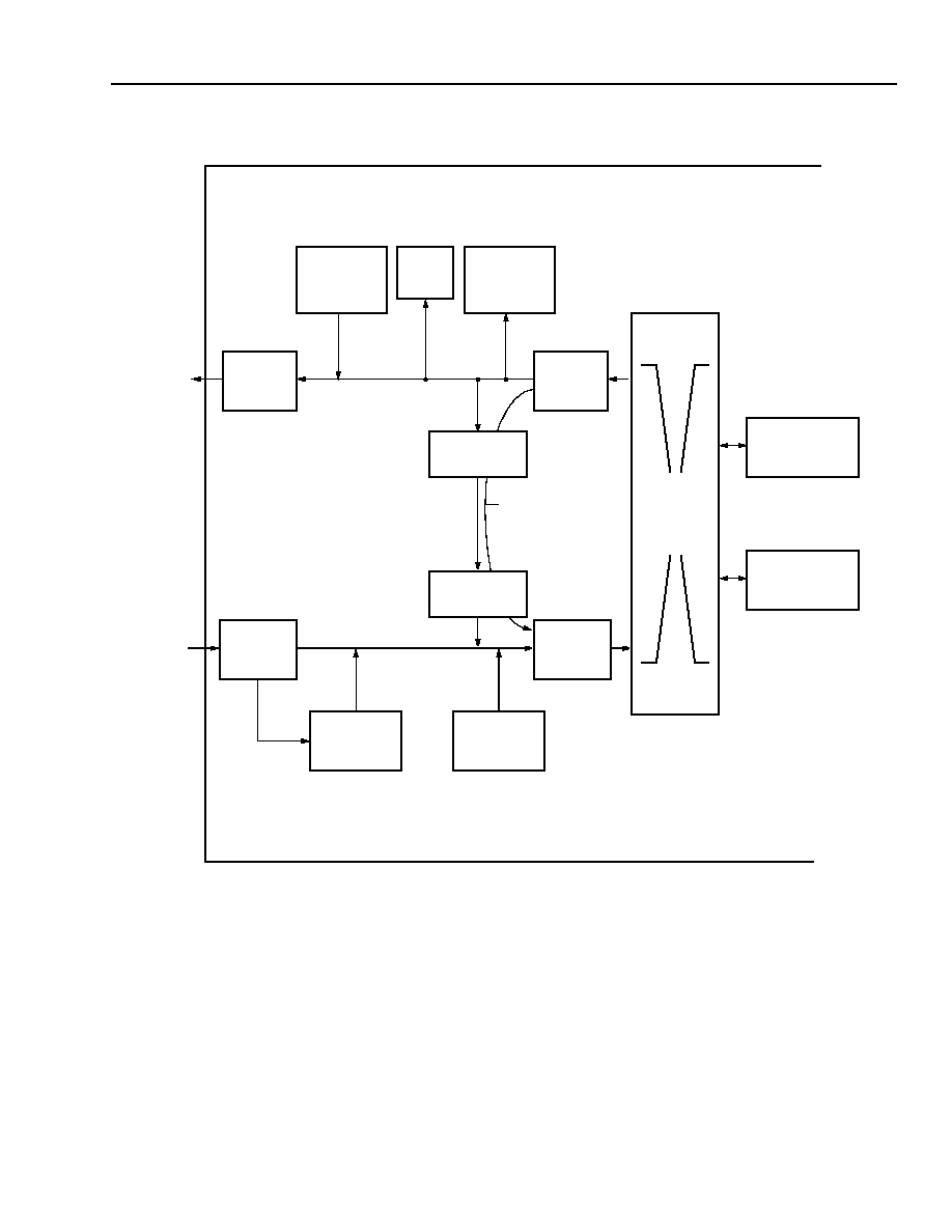
Preliminary Data Sheet
TMXF28155/51 Super Mapper
May 2001
155/51 Mbits/s SONET/SDH x28/x21 DS1/E1
Agere Systems Inc.
597
26 Applications
(continued)
5-8927(F)
Figure 105. Super Mapper Switching Mode for Framer in Parallel System Bus Configuration
SIGNALING
PROCESSOR
(EXTRACTION)
RECEIVE
FACILITY DATA
LINK
RECEIVE
HDLC
TRANSMIT
SYSTEM
INTERFACE
RECEIVE
FRAME
ALIGNER
TRANSMIT
FRAME
FORMATTER
TRANSMIT
FACILITY DATA
LINK
SIGNAL
PROCESSOR
(INSERTION)
RECEIVE
SYSTEM
INTERFACE
MAPPER
TO
FRAMER
DS1
CROSS
CONNECT
ESF PRM PATH
SUPER MAPPER: FRAMER
SUPER MAPPER
M12 MULTIPLEXER
INTERFACE
SUPER MAPPER
VT MAPPER
INTERFACE
DS
0
PERFORMANCE
MONITOR
TRANSMIT
HDLC
INT
E
RF
A
C
E
TFS
1
,
TC
L
K
1
,
T
D
A
T
A
8
,
T
D
AT
A
_
PA
R
I
T
Y
A1
,
T
S
I
G
N
A
L
I
N
G
8
,
T
S
IG
NA
L
I
NG
_
P
A
R
IT
Y
A
1
RF
S
1
, RCL
K
1
, RDA
T
A
8
,
RDA
T
A
_
P
A
R
IT
Y
A
1
,
RS
IG
NA
L
I
NG
8
,
RS
IG
NA
L
I
NG
_
P
A
R
IT
Y
A
1
598
Agere Systems Inc.
TMXF28155/51 Super Mapper
Preliminary Data Sheet
155/51 Mbits/s SONET/SDH x28/x21 DS1/E1
May 2001
26 Applications
(continued)
In the byte-sync mode, the frame sync and signaling (VT SPE) information are also passed to the mapper. In the
receive direction, the mapper block provides the line data, line clock, frame sync (byte-sync mode), and signaling
information (byte-sync mode) to the superframer. Performance reports, in the form of HDLC packets (PRMs), are
sent from the receive performance monitor block to the transmit HDLC block.
5-8928(F)
Figure 106. Super Mapper Switching Mode CHI Configuration with Byte-Synchronous VT Mapping Enabled
SIGNALING
PROCESSOR
(EXTRACTION)
RECEIVE
FACILITY DATA
LINK
RECEIVE
HDLC
TRANSMIT
SYSTEM
INTERFACE
RECEIVE
FRAME
ALIGNER
TRANSMIT
FRAME
FORMATTER
TRANSMIT
FACILITY DATA
LINK
SIGNAL
PROCESSOR
(INSERTION)
RECEIVE
SYSTEM
INTERFACE
MAPPER
TO
FRAMER
DS1
CROSS
CONNECT
ESF PRM PATH
SUPER MAPPER: FRAMER
SUPER MAPPER
M12 MULTIPLEXER
INTERFACE
SUPER MAPPER
VT MAPPER
INTERFACE
DS
0
PERFORMANCE
MONITOR
TRANSMIT
HDLC
INT
E
RF
A
C
E
TF
S
1
,
TC
L
K
1
,
TD
A
T
A
2
8
RF
S
1
, RCL
K
1
, RDA
T
A
2
8
VT MAPPER:
BYTE-SYNCHRONOUS
ROBBED-BIT SIGNALING
RECEIVE DATA
RECEIVE SIGNALING DATA
(TO SIGNALING REGISTERS)
SIGNALING STOMP
DATA
VT MAPPER:
BYTE-SYNCHRONOUS
ROBBED-BIT SIGNALING
TRANSMIT DATA
TRANSMIT SIGNALING DATA
(EXTRACTED FROM SYSTEM
OF SIGNALING REGISTERS)
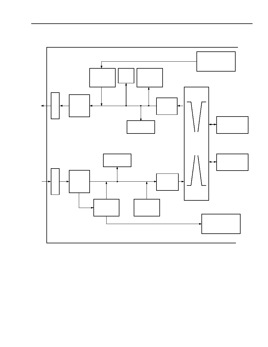
Preliminary Data Sheet
TMXF28155/51 Super Mapper
May 2001
155/51 Mbits/s SONET/SDH x28/x21 DS1/E1
Agere Systems Inc.
599
26 Applications
(continued)
5-8929(F)
Figure 107. Super Mapper Byte-Synchronous Transport Mode: Passive Performance Monitoring
SIGNALING
PROCESSOR
(TRANSMIT)
RECEIVE
FACILITY DATA
LINK
RECEIVE
HDLC
TRANSMIT
FRAME
FORMATTER
RECEIVE
FRAME
ALIGNER
TRANSMIT
FRAME
FORMATTER
TRANSMIT
FACILITY DATA
LINK
SIGNALING
PROCESSOR
(RECEIVE)
MAPPER
TO
FRAMER
DS1
CROSS
CONNECT
SUPER MAPPER: PERFORMANCE MONITORING FRAMER
SUPER MAPPER
M12 MULTIPLEXER
INTERFACE
SUPER MAPPER
VT MAPPER
INTERFACE
DS
1
PERFORMANCE
MONITOR
INT
E
RF
A
C
E
R
C
L
K
2
8
, RP
D2
8
,
RND2
8
T
C
LK
28, T
P
D
28, T
N
D
2
8
VT MAPPER:
BYTE-SYNCHRONOUS
ROBBED-BIT SIGNALING
RECEIVE DATA
SIGNALING STOMP
DATA
VT MAPPER:
BYTE-SYNCHRONOUS
ROBBED-BIT SIGNALING
TRANSMIT DATA
PERFORMANCE
MONITOR
LIN
E
E
NCO
DE
R
LI
N
E
DE
CO
DE
R
(LINE
INTERFACE)
RECEIVE
FRAME
ALIGNER
(LINE
INTERFACE)
600
Agere Systems Inc.
TMXF28155/51 Super Mapper
Preliminary Data Sheet
155/51 Mbits/s SONET/SDH x28/x21 DS1/E1
May 2001
26 Applications
(continued)
5-8930(F)r.3
Figure 108. Super Mapper Byte-Synchronous Transport Mode: Intrusive Performance Monitoring
SIGNALING
PROCESSOR
(TRANSMIT)
RECEIVE
FACILITY DATA
LINK
RECEIVE
HDLC
RECEIVE
FRAME
ALIGNER
TRANSMIT
FRAME
FORMATTER
TRANSMIT
FACILITY DATA
LINK
SIGNALING
PROCESSOR
(RECEIVE)
MAPPER
TO
FRAMER
DS1
CROSS
CONNECT
SUPER MAPPER: PERFORMANCE MONITORING FRAMER
SUPER MAPPER
M12 MULTIPLEXER
INTERFACE
SUPER MAPPER
VT MAPPER
INTERFACE
VT MAPPER:
BYTE-SYNCHRONOUS
ROBBED-BIT SIGNALING
RECEIVE DATA
SIGNALING STOMP
DATA
VT MAPPER:
BYTE-SYNCHRONOUS
ROBBED-BIT SIGNALING
TRANSMIT DATA
TRANSMIT
HDLC
TRANSMIT
HDLC
PERFORMANCE
MONITOR
PERFORMANCE
MONITOR
INTRUSIVE
PERFORMANCE
MONITOR
DS
1
INT
E
RF
A
C
E
RCL
K
28
, RP
D
28
, RND
28
TC
L
K
28
, T
P
D
28
, T
N
D
28
TRANSMIT
FRAME
FORMATTER
LIN
E
LIN
E
(LINE
INTERFACE)
RECEIVE
FRAME
ALIGNER
(LINE
INTERFACE)

Preliminary Data Sheet
TMXF28155/51 Super Mapper
May 2001
155/51 Mbits/s SONET/SDH x28/x21 DS1/E1
Agere Systems Inc.
601
26 Applications
(continued)
26.14 Line Decoder/Encoder
The line decoder/encoder supports either single-rail or dual-rail transmission. In dual-rail mode, the line codes sup-
ported are as follows:
s
Alternate mark inversion (AMI).
s
DS1 binary 8 zero code suppression (B8ZS).
s
ITU-CEPT high-density bipolar of order 3 (HDB3).
In the single-rail mode, a line interface unit (LIU) decodes/encodes the data.
In the dual-rail mode, loss of signal in monitored.
In the case of coded mark inversion (CMI) coding (Japanese TTC standard JJ-20.11), the LIU decodes the data,
indicating both the CMI coding rule violations (CRVs) and line coding violations as bipolar violations. (In the CMI
mode, the framer is in the single-rail mode.)
26.15 Receive Frame Aligner/Transmit Frame Formatter
The receive frame aligner and transmit frame formatter support the following frame formats:
s
D4 superframe.
s
SF D4 superframe: F
T
framing only.
s
J-D4 superframe with Japanese remote alarm.
s
DDS.
s
SLC
-96.
s
ESF.
s
J-ESF (J1 standard with different CRC-6 algorithm).
s
Non-align DS1 (193 bits--clear channel).
s
CEPT basic frame (ITU G.706).
s
CEPT CRC-4 multiframe with 100 ms timer (ITU G.706).
s
CEPT CRC-4 multiframe with 400 ms timer (automatic CRC-4/nonCRC-4 equipment interworking) (ITU G.706
Annex B).
s
Non-align E1 (256 bits--clear channel).
s
2.048 coded mark inversion (CMI) coded interface (TTC standards JJ-20.11).
26.16 Receive Performance Monitor
The receive framer monitors the following alarms: loss of receive clock, loss of signal, loss of frame, alarm indica-
tion signal (AIS), remote frame alarms, and remote multiframe alarms. These alarms are detected as defined by
the appropriate
ANSI
, AT&T, ITU, and ETSI standards.
Performance monitoring as specified by AT&T,
ANSI
, and ITU is provided through counters monitoring bipolar vio-
lation, frame bit errors, CRC errors, errored events, errored seconds, bursty errored seconds, and severely errored
seconds.
In-band loopback activation and deactivation codes can be transmitted to the line via the payload or the facility data
link. In-band loopback activation and deactivation codes in the payload or the facility data link are detected.

602
Agere Systems Inc.
TMXF28155/51 Super Mapper
Preliminary Data Sheet
155/51 Mbits/s SONET/SDH x28/x21 DS1/E1
May 2001
26 Applications
(continued)
26.17 Signaling Processor
The signaling processor supports the following modes:
s
Superframe (D4,
SLC
-96): 2-state, 4-state, and 16-state.
s
VT 1.5 SPE: 2-state, 4-state, and 16-state.
s
Extended superframe: 2-state, 4-state, and 16-state.
s
CEPT: common channel signaling (CCS) (TS-16).
s
Transparent (pass through) signaling.
s
J-ESF handling groups.
Signaling features supported per channel are as follows:
s
Signaling debounce.
s
Signaling freeze.
s
Signaling interrupt upon change of state.
s
Associated signaling mode (ASM).
s
Signaling inhibit.
s
Signaling stomp.
In the DS1 robbed-bit signaling modes, voice and data channels are programmable. The entire payload can be
forced into a data-only (no signaling channels) mode, i.e., transparent mode by programming one control bit.
Signaling access can be through the on-chip signaling registers or the system interface. Data and its associated
signaling information can be accessed through the system in either DS1 or CEPT-E1 modes.
26.18 Facility Data Link (FDL) Processor
The bit-oriented ESF data-link messages defined in
ANSI
T1.403 are monitored by the receive facility data link unit.
The transmit facility data link unit overrides the FDL-FIFO for the transmission of the bit-oriented ESF data-link
messages defined in
ANSI
T1.403-1995.
The FDL processor extracts and stores data link bits from three different frame types as follows:
s
D bits and delineator bits from the
SLC
-96 multi-superframe.
s
Data link bits from DDS frames (bit 6 of time slot 24).
s
Two multiframes of Sa[4:8] bits from time slot 0 in CEPT basic and CRC-4 multiframes.
The respective bits will always be extracted from frame-aligned frames and stored in a stack. The processor will
have control of being alerted to stack updates through the interrupt mask registers.
The transmit FDL block performs the transmission of D bits into
SLC
-96 superframes, Sa-bits in CEPT frames, and
D bits in DDS frames.
s
In
SLC
-96 frames, the D and delineator bits are always sourced from this block when the block is enabled for
insertion.
s
In DDS frames, the data link bits are always sourced from this block when this block is enabled for insertion. This
block also provides the capability to transmit BOMs in the data link channel of ESF links.
s
In CEPT frames, the Sa bits are sourced from either the Sa stack within this block or from the system interface.
The data link block only responds with valid data when selected by the Sa source control bits.

Preliminary Data Sheet
TMXF28155/51 Super Mapper
May 2001
155/51 Mbits/s SONET/SDH x28/x21 DS1/E1
Agere Systems Inc.
603
26 Applications
(continued)
26.19 HDLC Unit
The HDLC processor formats the HDLC packets for insertion into the programmable channels. A channel can be
any number of bits (1 to 8) from a time slot.
The maximum number of channels is 64. The maximum channel bit rate is 64 kbits/s. The minimum channel bit rate
is 4 kbits/s. Each channels is allocated 128 bytes of storage.
HDLC processing of data on the facility data link (PRMs, Sa bits, or otherwise) is implemented by assigning the
FDL bit position to a logic HDLC channel.
26.20 System Interface
The system interface block provides a programmable interface. It can be configured to work in four different modes.
s
Concentration highway interface (serial time division multiplex interface).
-- Global frame sync.
-- Global clock: 2.048 MHz, 4.096 MHz, 8.192 MHz, or 16.384 MHz.
-- 28 transmit and receive data ports; data rates: 2.048 Mbits/s, 4.096 Mbits/s, or 8.192 Mbits/s.
s
Parallel system bus (parallel time-division multiplex interface/transmit and receive).
-- Global frame sync.
-- Global clock: 19 MHz.
-- Data rate: 19 MHz.
-- 8 bits of data + associated parity bit.
-- 4 bits of signaling + 2 bits of signaling control + 1 bit of parity.
s
Time-division multiplex data rate serial interface.
-- 28 receive frame sync (per port).
-- 28 receive clock: 1.544 Mbits/s or 2.048 Mbits/s (per port).
-- 28 receive ports.
-- One transmit frame sync.
-- One transmit clock: 1.544 Mbits/s or 2.048 Mbits/s.
-- 28 transmit ports.
s
Network serial multiplexed bus.
-- 6- or 8-pin serial interface.
-- Transmit and receive clock and data at 51.84 MHz.
-- Accommodates 1 DS3 of throughput.
-- Provides a minimal pin count interface for data and inverse multiplexing for ATM (IMA) applications without slip
buffers.
-- Three modes of operation: framer--NSMI payload assembled/disassembled into DS1/E1s; M13--proprietary
transport format with DS3 framing; SPE--proprietary transport format mapped into an STS-1/AU-3.

604
Agere Systems Inc.
TMXF28155/51 Super Mapper
Preliminary Data Sheet
155/51 Mbits/s SONET/SDH x28/x21 DS1/E1
May 2001
Change History
The organization of this data sheet (DS01-167PDH) has radically changed. While the contents have undergone
minimal changes (listed below), the various sections have been rearranged and section numbers have been
installed to make navigating throughout the document easier.
An overall table of contents has been added towards the front of the document, and in front of each section a table
of content has been added.
The entire Preface Section has been rewritten; no change bars have been installed.
The
Pin Descriptions, starting on page 15
, has been revised and more tables have been added to that section. The
pin numbers and pin names, however, have not been changed; no change bars have been installed.
Red change bars have been installed for all content-specific changes. Any additions, or deletions, have been high-
lighted in red.
Any references to tables, figures, sections, or pages have been highlighted in blue.
Changes to format (such as grammar, punctuation, new paragraphs etc.) have not been highlighted.
Navigating Through an Acrobat Document
If the reader displays this document in Acrobat Reader, clicking on any blue reference will bring the reader to that
reference point. Clicking on the back arrow (Go to previous View) in the toolbar of the Acrobat Reader, will bring the
reader back to the starting point.
For example: clicking on the 3 below, will bring the reader to page 3, which is the first change of this document.
Clicking on the back arrow (in Acrobat Reader) will bring the reader back to this page (pa ge604).
All changes from the previous version (DS01-078PDH) are listed in the following table:
Table 628. Change History
Page
Page
Page
3
305
7
307
424
34
310
439
51
333
464
54
345
468
55
346
469
61
347
472
68
348
482
82
384
503
114
405
514
217
406
530
219
411
549
226
412
564
248
415
592
255
421
593
272
422

Preliminary Data Sheet
TMXF28155/51 Super Mapper
May 2001
155/51 Mbits/s SONET/SDH x28/x21 DS1/E1
Agere Systems Inc.
605

Agere Systems Inc. reserves the right to make changes to the product(s) or information contained herein without notice. No liability is assumed as a result of their use or application.
SLC is a
registered trademark of Agere Systems Inc.
Copyright © 2001 Agere Systems Inc.
All Rights Reserved
Printed in U.S.A.
June 2001
DS01-167PDH (replaces DS01-078PDH)
For additional information, contact your Agere Systems Account Manager or the following:
INTERNET:
http://www.agere.com
E-MAIL:
docmaster@micro.lucent.com
N. AMERICA:
Agere Systems Inc., 555 Union Boulevard, Room 30L-15P-BA, Allentown, PA 18109-3286
1-800-372-2447, FAX 610-712-4106 (In CANADA: 1-800-553-2448, FAX 610-712-4106)
ASIA PACIFIC: Agere Systems Singapore Pte. Ltd., 77 Science Park Drive, #03-18 Cintech III, Singapore 118256
Tel. (65) 778 8833, FAX (65) 777 7495
CHINA:
Agere Systems (Shanghai) Co., Ltd., 33/F Jin Mao Tower, 88 Century Boulevard Pudong, Shanghai 200121 PRC
Tel. (86) 21 50471212, FAX (86) 21 50472266
JAPAN:
Agere Systems Japan Ltd., 7-18, Higashi-Gotanda 2-chome, Shinagawa-ku, Tokyo 141, Japan
Tel. (81) 3 5421 1600 , FAX (81) 3 5421 1700
EUROPE:
Data Requests: DATALINE: Tel. (44) 7000 582 368, FAX (44) 1189 328 148
Technical Inquiries: GERMANY: (49) 89 95086 0 (Munich), UNITED KINGDOM: (44) 1344 865 900 (Ascot),
FRANCE: (33) 1 40 83 68 00 (Paris), SWEDEN: (46) 8 594 607 00 (Stockholm), FINLAND: (358) 9 3507670 (Helsinki),
ITALY: (39) 02 6608131 (Milan), SPAIN: (34) 1 807 1441 (Madrid)