 | –≠–ª–µ–∫—Ç—Ä–æ–Ω–Ω—ã–π –∫–æ–º–ø–æ–Ω–µ–Ω—Ç: TMXF84622 | –°–∫–∞—á–∞—Ç—å:  PDF PDF  ZIP ZIP |

Advance Data Sheet, Rev. 2
July 2001
TMXF84622 155 Mbits/s/622 Mbits/s Interface
SONET/SDH x84/x63 Ultramapper
1 Features
s
Versatile IC supports 622 Mbits/s/155 Mbits/s
SONET/SDH interface solutions for T3/E3, DS2,
T1/E1/J1, and DS0/E0/J0 applications.
s
Implementation supports both linear (1 + 1, unpro-
tected) and ring (UPSR) network topologies.
s
Provides full termination of up to 63 (21 x 3) E1,
84 (28 x 3) T1, or 84 (28 x 3) J1.
s
Low 3.3 V power supply.
s
≠40
∞
C to +85 ∞C industrial temperature range.
s
700-pin ball grid array (PBGA) package.
s
Complies with Telecordia Technologies*, ITU,
ANSI
, ETSI, and Japanese TTC standards: GR-
253-CORE, GR-499, (ATT) TR-62411, ITU-T
G.707, G.704, G.706, G.783, G.962, G.964,
G.965, Q.542, T1.105, JT-G704, JT-G706, JT-
G707, JT-I431-a, ETS 300 417-1-1, ETS 300 011,
T1.107, T1.404.
SONET/SDH Interface
s
Termination of a single 622 Mbits/s STS-12/STM-4
or single 155 Mbits/s STS-3/STM-1.
s
Built-in clock and data recovery circuit at
622 Mbits/s STS-12/STM-4 interface.
s
Supports overhead processing for all transport and
path overhead bytes.
s
Optional insertion and extraction of overhead bytes
via a serial transport overhead access channel.
Configurable as dedicated DCC channels.
s
Software controlled linear 1 + 1 protection via dedi-
cated interface to protection card.
s
Full path termination and SPE extraction/insertion.
s
SONET/SDH compliant condition and alarm
reporting.
s
Built-in diagnostic loopback modes.
s
8 kHz line frame synchronizing output.
* Telecordia Technologies is a trademark of Telecordia Technolo-
gies Inc.
ANSI is a registered trademark of American National Standards
Institute, Inc.
PDH Interfaces
s
6
DS3, 21 x DS2,
or 6 E3
, 12 x E2.
s
Twenty-one framed or unframed DS1 or E1 inter-
faces.
s
Two additional protection
channels for DS2/DS1/
E1.
STS/STM Pointer Interpreter
s
Interprets STS/AU/TU-3 pointers.
s
Synchronizes 8 kHz frame and 2 kHz superframe
to system-shelf-timing reference by setting the
transmit STS-3/STM-1 pointers to a fixed value
of 522
with an adjustable frame location.
s
Monitors/terminates SPE path overhead.
STS3 Serial Interconnect
s
Serial interface to mate devices.
s
4 Ultramapper devices, 3 configured as mate
devices, provide full termination of an STS-12/
STM-4. A 4 chip solution to terminate
336 DS1s/J1s or 252 E1s.
VT Termination/Generation 84/63 (3x28/21)
s
Supports TIM-V generation and termination for all
84/63 (3x28/21) VT/TU signals.
s
Synchronizes VT/TU SPE to system-shelf-timing
reference by setting the transmit VT/TU pointers to
fixed values for asynchronous mapping or by
dynamically changing the transmit VT/TU pointers
for byte synchronous mapping.
s
Fixed pointer generation in transmit side for asyn-
chronous mapping.
s
Dynamic pointer generation in transmit side for
byte-synchronous mapping.

2
2
Agere Systems Inc.
Advance Data Sheet, Rev. 2
July 2001
SONET/SDH x84/x63 Ultramapper
TMXF84622 155 Mbits/s/622 Mbits/s Interface
Features
(continued)
Mapping/Multiplexing Modes 84/63 (3x28/21)
s
Maps DS3 clear channel or framed signal into STS-1
or TUG-3.
s
Maps T1/E1/J1
into
VT/TU structures.
s
Maps T1
into
VT1.5/TU-11/TU-12.
s
Maps J1
into
VT1.5/TU-11/TU-12.
s
Maps E1
into
VT2/TU-12.
s
Supports asynchronous, byte-synchronous, and bit-
synchronous mapping.
s
Supports UPSR applications via the dedicated ring
interface and an external tributary selector.
s
Supports all valid T1/E1/J1 multiplexing structures
into STS-1 and STS-3/STM-1.
s
STS-3/STS-1/SPE/VTG/VTx.
s
STM-1/AU-3/TUG-2/TU-1x/VC-1x.
s
STM-1/AU-4/TUG-3/TUG-2/TU-1x/VC-1x.
s
Allows grooming of VTs/TUs in granularity of TUG-2s
within the STS-3/STM-1 signal.
s
Supports J2 trace identifier monitoring/insertion.
s
Configurable VT/TU slot selection for DS1, E1, J1
insertion and drop.
s
Automatic receive monitor functions include VT/TU
RDI-V, REI-V, BIP-2 errors, AIS-V, LOP-V.
s
Complies with GR-253-CORE, GR-499, ITU-T
G.707, G.704, G.783, T1.105, JT-G707, ETS 300
417-1-1.
M13 Features (3)
s
Configurable multiplexer/demultiplexer for
28 DS1 signals, 21 E1 signals, or 7 DS2 signals to/
from a DS3 signal.
s
Operates in either M23 or C-bit parity mode.
s
Provisionable time-slot selection for DS1, E1, and
DS2 insertion or drop.
s
Full alarm monitoring and generation (LOS, BPV,
EXZ, OOF, SEF, AIS, RAI, FEAC, P-bit and C-bit par-
ity errors, FEBE).
s
HDLC transmitter with 128-byte data buffer and
HDLC receiver with 128-byte data FIFO for the C-bit
parity path maintenance data link.
s
DS3, DS2, DS1, and E1 loopback and loopback
request generation.
s
Complies with T1.102, T1.107, T1.231, T1.403,
T1.404, GR 499, G.747, and G.775.
E13 Features (3)
s
Configurable multiplexer/demultiplexer for up to
16 E1 signals, or 4 E2 signals to/from an E3 signal.
s
Independently configurable 4 E12 multiplexer/demul-
tiplexers for up to 16 E1 signals to/from 4 E2 signals.
s
Provisionable time-slot selection for E1, E2 insertion,
or drop via the cross connect macro.
s
E12 multiplexers capable of generating alarm indica-
tion signal (AIS) and remote alarm indicator (RAI)
signals.
s
E23 multiplexer capable of generating AIS and RAI
signals.
s
Configurable HDB3 encoder/decoder for E3 output/
input.
s
E1 and E2 transmit path monitors that detect loss of
clock (LOC) and AIS.
s
E2 receive path monitor that detects LOC, AIS, and
RAI.
s
E3 receive monitor that detects loss of signal (LOS),
LOC, bipolar violation (BPV), AIS, and RAI.
s
E3 and E2 loopback modes.
s
Complies with ITU's G.703, G.742, G.751, and
G.775.
DS3/DS2/DS1/E1 Cross Connect Features
s
Configurable crosspoint interconnect for up to 28 x 3
DS1 signals or 21 x 3 E1 signals to/from the framer,
30 external pins, and 28 x 3 signal channels to/from
the M13 and VT mapper. Also supports up to 7 x 3
DS2 signals to/from the external pins or M12 MUXes,
connecting to the M13 MUX M23 block.
s
Connects six clear channel DS3, E3, and STS-1 sig-
nals from the external pins to the M13, E13,
SPE_mapper, and STS1-LT.
s
Also connects three unchannelized DS3 and E3 sig-
nal to/from the external NSMI interface to the SPE,
M13, E13, framer, or TPG blocks.
s
The three NSMI
pins can also be shared for STS-1
LT
.
s
Any mix of 168 DS1, E1 signals may be intercon-
nected. Any of the available DS1/E1 signal sources
may be connected to any of 168 signal destinations
in the DS1/E1 cross connect. Multicast or broadcast
operation (one port to many) is supported for up to
168 channels. Also, any channel n at the source can
be connected to its corresponding destination chan-
nel n, where n ranges from 1 to 84 for most sources
and destinations.

Agere Systems Inc.
3
Advance Data Sheet, Rev. 2
July 2001
SONET/SDH x84/x63 Ultramapper
TMXF84622 155 Mbits/s/622 Mbits/s Interface
Features
(continued)
s
Any mix of DS2, DS3, or E3 signals may be intercon-
nected.
s
Cross connect allows 16 x 3 E1 signals to/from E13
modules to framer, M13, VT mapper, and external
pins.
s
There are 4 x 3 E2 signals to/from E13 to external
pins, TPG generator/monitor.
s
There are 3 E3 signals to/from the E13 block to
external pins, TPG generator/monitor, and SPE map-
per.
s
Jitter attenuation may also be inserted in-line on any
DS1/E1 channel. (Note that cascading of jitter atten-
uators is not allowed.)
s
Standard network loopback or straightaway facility
testing is supported for DS1/E1 and DS3/E3. Any
source or transmitter may be replaced by a test-pat-
tern generator capable of injecting idle standards-
based pseudorandom bit sequence test patterns, or
AIS (blue) alarm. Any sink or receiver may be
replaced by a test-pattern monitor, which can detect/
count bit errors in a pseudorandom test sequence, or
loss of frame or loss of synchronization.
s
One to any loopback is supported for up to
168 channels in DS1/E1 channels in blocks VT map-
per, M13, E13, and framer. One-to-one loopback is
supported in all DS1/E1 channels. One-to-one loop-
back for DS3/E3/STS-1 channels in blocks M13,
E13, and SPE mapper.
s
Loopbacks may be configured to sectionalize a cir-
cuit for identifying faults or misconfiguration during
out of service maintenance.
s
Fast alarm channels are supported for VT mapper,
E13, or M13 to framer interconnects for alarm indica-
tion signal (AIS or blue alarm), and VT mapper only
for remote alarm indicator (RAI or yellow alarm). This
feature reduces the propagation delay of the alarms
by eliminating multiple integration of alarm condi-
tions.
s
Supports framer-only, transport (framer LIU, M13,
E13, and VT mapper), and switching (CHI and PSB)
modes of operation.
s
TOAC outputs are available in DS1/E1 framed format
at any destination. Any DS1/E1 channel can be used
as TOAC inputs.
DS1/E1 Digital Jitter Attenuation Features
s
PLL-free receive operation using built-in digital jitter
attenuator (in VT/VC mode or M13 mode).
s
Configurable to meet jitter and MTIE requirements.
DS3/E3 Digital Jitter Attenuation Features
s
The PLL bandwidth, damping factor, and sampling
rates are programmable.
s
The DJA macro accepts/delivers DS3/E3 clock and
data from/to the cross connect macrocell.
T1/E1/J1 Framing Features 84/63 (3x28/21)
s
28/21 T1/E1/J1 channels.
s
Line coding: B8ZS, HDB3, ZCS, AMI, and
CMI (JJ20-11).
s
T1 framing modes: ESF, D4, SLC
Æ
-96, T1 DM DDS,
and SF (F
t
only).
s
E1 framing: G.704 basic and CRC-4 multiframe con-
sistent with G.706.
s
J1 framing modes: JESF (Japan).
s
Supports T1 and E1 unframed and transparent trans-
mission format.
s
T1 signaling modes: transparent; register and sys-
tem access for ESF 2-state, 4-state, and 16-state;
D4 2-state, 4-state, and 16-state; SLC-96 2-state,
4-state, and 16-state; J-ESF handling groups mainte-
nance and signaling; VT 1.5 SPE 2-, 4-, 16-state.
s
E1 signaling modes: transparent; register and sys-
tem access for entire TS16 multiframe structure as
per ITU G.732.
s
Signaling debounce and change of state interrupt.
s
V5.2 Sa7 processing.
s
Alarm reporting and performance monitoring per
AT&T, ANSI, ITU-T, and ETSI standards.
s
Facility data link features:
-- HDLC or transparent access for either ESF or
DDS+ FDL frame formats.
-- Register/stack access for SLC-96 transmit and
receive data.
-- Extended superframe (ESF): automatic transmis-
sion of the ESF performance report messages
(PRM). Automatic transmission of the ANSI
T1.403 ESF performance report messages.
Automatic detection and transmission of the ANSI
T1.403 ESF FDL bit-oriented codes.
-- Register/stack access for all CEPT Sa-bits trans-
mit and receive data.
s
HDLC features:
-- HDLC or transparent mode.
-- Programmable logical channel assignment: any
time slot, any bit for ISDN D-channel, also inserts/
extracts C-channels for V5.1, V5.2 interfaces.
-- 64 logical channels in both transmit and receive
direction (any framing format).

4
4
Agere Systems Inc.
Advance Data Sheet, Rev. 2
July 2001
SONET/SDH x84/x63 Ultramapper
TMXF84622 155 Mbits/s/622 Mbits/s Interface
Features
(continued)
-- Maximum channel data rate: 64 kbits/s.
-- Minimum channel data rate: 4 kbits/s (DS1-FDL or
E1 Sa-bit).
-- 128-byte FIFO per channel in both transmit and
receive direction.
-- Tx to Rx loopback supported.
s
System interfaces:
-- Concentration highway interface.
-- Single clock and frame synchronizing signals;
programmable clock rates at 2.048 MHz,
4.096 MHz, 8.192 MHz, and 16.384 MHz;
programmable data rates at 2.048 Mbits/s,
4.096 Mbits/s, and 8.192 Mbits/s;
programmable clock edges and bit/byte offsets.
-- Parallel system bus interface at 19.44 MHz for
data and signaling: single clock and frame syn-
chronizing signals.
-- Time-division multiplex data rate serial interface at
1.544 MHz or 2.048 MHz. Twenty-eight receive
data, clock, and frame synchronizing signals.
Twenty-eight transmit data signals with a global
clock and frame synchronization.
-- Network serial multiplexed interface
(NSMI)
mini-
mal pin count serial interface at 51.84 MHz opti-
mized for data and IMA applications.
MPU Features
s
21-bit address/16-bit data bus microprocessor inter-
face.
s
Synchronous (16 MHz to 66 MHz)/asynchronous
microprocessor interface modes.
s
Microprocessor data bus parity monitoring.
s
Summary of 2 level priority interrupts from major
functional blocks/maskable.
s
Separate device interrupt outputs for automatic pro-
tection switch and the Ultramapper global interrupt.
s
Global configuration of network performance moni-
toring counters operation.
s
Global software resets.
s
Global enabling and powering down of major func-
tional blocks.
s
Miscellaneous global configuration and control.
SPEMPR Features
s
The SPE mapper accepts/delivers TUG-2 data from/
to the VT mapper. The TUG-2 data is mapped/
demapped either to/from an AU-3/STS-1 signal for
the North American digital systems or to/from a
TUG-3 signal for the ITU-based systems.
s
The SPE mapper accepts/delivers DS3 data from/to
the M13 MUX/deMUX. The DS3 data is mapped/
demapped either to/from an AU-3/STS-1 signal for
the North American digital systems or to/from a
TUG-3 signal for the ITU-based systems.
s
The SPE mapper accepts/delivers a clear DS3 signal
at 44.736 Mbits/s rate. The clear DS3 signal is
mapped/demapped essentially the same way as
M13 signal described above.
s
The SPE mapper accepts/delivers E3 data from/to
the E13 MUX/deMUX. The E3 data is mapped/
demapped either to/from an AU-3/STS-1 signal for
the North American digital systems or to/from a
TUG-3 signal for the ITU-based systems.
s
The SPE mapper accepts/delivers a clear E3 signal
at 34.368 Mbits/s rate. The clear E3 signal is
mapped/demapped essentially the same way as E13
signal described above.
s
The SPE mapper has a DS3/E3 loopback circuit
placed for the functions of demapping and remap-
ping a DS3/E3 signal. It is particularly useful in cases
where a DS3/E3 signal mapped as an AU-3/STS-1
signal has to be remapped as a TUG-3 signal or vice
versa.
s
The SPE mapper supports a path overhead access
channel more commonly known as the POAC chan-
nel. Seven path overhead bytes namely J1, C2, F2,
H4, F3, K3, and N1 may be inserted/dropped
through this channel. This channel works as the
master, which means that this channel provides a
clock in both transmit and receive directions and
POH data may be inserted by the user on the trans-
mit side or dropped by the block in the receive side.
s
Path overhead byte B3 (BIP error) generation/detec-
tion and programmable BIP-8 bit error rate insertion.
s
Programmable clear on read/clear on write registers.
s
Signal fail and signal degrade indicators available to
report bit error rates above a certain programmable
threshold.

Agere Systems Inc.
5
Advance Data Sheet, Rev. 2
July 2001
SONET/SDH x84/x63 Ultramapper
TMXF84622 155 Mbits/s/622 Mbits/s Interface
Features
(continued)
s
Capable of detecting/inserting alarm indication sig-
nals (AIS), remote defect indication signals (RDI),
and remote error indication signals (REI).
s
Numerous monitoring functions provided on all the
TUG-3 path overhead bytes.
s
Supports unidirectional path switch ring (UPSR)
applications.
s
N1 tandem connection support is provided.
s
The TUG3 pointer processor can be used for an add/
drop multiplexer.
s
Complies with GR-253-CORE, T1.105, ITU-T G.707,
ITU-T G.831, G.783, ETS 300 417-1-1.
STS12 Pointer Processor Features
s
SONET and SDH compliant.
s
Configurable STS-3/STM-1 or STS-12/STM-4 mode.
s
Supporting an arbitrary mix of STS-1 and STS3c trib-
utaries, and SDH equivalents.
s
Complies with GR-253-CORE, T1.105, G.707,
G.783, G.806, G.821, and ETSI 417-1-1.
STS1LT Features
s
Supports standard SPE mappings for sub-STS-1
payloads (VT mapped: 28 DS1, 28 J1, or 21 E1 sig-
nals).
s
Supports standard SPE mappings for STS-1 pay-
loads ( DS3).
s
Detects STS-1 loss-of-signal (LOS) conditions.
s
Detects STS-1 out-of-frame and loss-of-frame (OOF/
LOF) conditions.
s
Provides an 8-bit parallel bus interface for an STS-1
signal.
s
Provides STS-1 selectable scrambler/descrambler
functions and B1/B2/B3 generation/detection.
s
Provides STS-1 pointer interpretation. Detects AIS-P
and LOP.
s
Provides STS-1 pointer processing.
s
Complies with GR-253-CORE, T1.105, G.707,
G.783, G.826, G.821, and ETSI 417-1-1.
STS1 XC Features
s
Configurable connection for up to 6 STS1 signals
from 6 SPE mapper transmit blocks to any 1 up to
3 STS1 slots of any 1 of 4 TMUX transmit interfaces.
Clock and control signals are provided by the TMUX
transmit interfaces and data is supplied by the SPE
mapper transmit blocks.
s
Configurable connection for up to 3 STS1 signals
from 3 STS1LT PP blocks to any 1 up to 3 STS1 slots
of any 1 of 4 TMUX transmit interfaces. Clock and
control signals are provided by the TMUX transmit
interfaces and data is supplied by the STS1LT
receive blocks.
s
Configurable connection for up to 12 STS1 signals
from the STS12PP transmit block to any 1 up to
3 STS1 slots of any 1 of 4 TMUX transmit interfaces.
Clock and control signals are provided by the TMUX
transmit interfaces and data is supplied by the
STS12PP transmit blocks.
s
Configurable connection for up to 9 STS1 signals
from 3 CDR receive blocks to any 1 up to 3 STS1
slots of any 1 of 4 TMUX transmit interfaces. Clock
and control signals are provided by the TMUX trans-
mit interfaces and data is supplied by the CDR
receive blocks.
s
Configurable connection for up to 3 STS1 signals
from 6 SPE mapper transmit blocks to any 1 of
3 STS1LT transmit blocks. Clock and control signals
are provided by the STS1LT transmit block and data
is supplied by the SPE mapper transmit block.
s
Configurable connection for up to 3 STS1 signals
from any 1 up to 3 STS1 slots of any 1 of 4 TMUX
receive interfaces to any 1 of 3 STS1LT transmit
blocks. Data is provided by the TMUX receive inter-
faces for this transfer.
s
Configurable connection for up to 9 STS1 signals
from any 1 up to 3 STS1 slots of any 1 of 4 TMUX
receive interfaces to any 1 of 3 CDR transmit blocks.
Clock, control signals, and data are provided by the
TMUX receive interfaces for this transfer.
s
Configurable connection for up to 3 STS1 signals
from 3 STS1LT receive blocks to any 1 of 6 SPE
mapper receive blocks. Clock, control signals, and
data are provided by the STS1LT receive block for
this transfer.
s
Configurable connection for up to 6 STS1 signals
from any 1 up to 3 STS1 slots of any 1 of 4 TMUX
receive interfaces to any 1 of 6 SPE mapper receive
blocks. Clock, control signals, and data are provided
by the TMUX receive interfaces for this transfer.
s
Loss of clock detectors on three serial 155 MHz clock
inputs from three CRD RX blocks and one serial
155 MHz clock input from CDR TX block.

6
6
Agere Systems Inc.
Advance Data Sheet, Rev. 2
July 2001
SONET/SDH x84/x63 Ultramapper
TMXF84622 155 Mbits/s/622 Mbits/s Interface
Features
(continued)
s
LOF detection, OOF detection, REI monitoring, RDI
monitoring, and B2 error detection is performed on
the three serial 155 Mbits/s data inputs from the CDR
receive blocks.
s
REI and RDI are generated from the received data
and sent to the transmit side for insertion in the trans-
mitted serial 155 Mbits/s data.
s
B2 is calculated and inserted in the transmitted serial
data. B2 error insertion is allowed.
TMUX Features
s
Multiplexes twelve STS-1 signals or four STS-3c sig-
nals into a SONET STS-12 signal.
s
Multiplexes three STS-1 signals into a SONET
STS-3 signal.
s
Multiplexes four STM-1 (AU-4 or 3xAU-3) signals into
an SDH STM-4 signal.
s
Multiplexes three VC-3 signals into an SDH STM-1
(3xAU-3) signal.
s
Multiplexes three VC-3 signals into an SDH STM-1
(AU-4) signal via a TUG-3 construction.
s
Demultiplexes twelve STS-1 signals or four STS-3c
signals from a SONET STS-12 signal.
s
Demultiplexes three STS-1 signals from a SONET
STS-3 signal.
s
Demultiplexes four STM-1 (AU-4 or 3xAU-3) signals
from an SDH STM-4.
s
Demultiplexes three VC-3 signals from an SDH STM-
1 (3xAU-3) signal.
s
Demultiplexes three VC-3 signals from an SDH STM-
1 (AU-4) signal via a TUG-3 deconstruction.
s
Provides STS1-only mode for receive and transmit
directions.
s
Provides complete functionality for SDH MSP 1 + 1
protection switching.
s
Provides SONET/SDH loss-of-signal (LOS), out-of-
frame (OOF) and loss-of-frame (LOF) detection.
s
Provides STS-12/STM-4/STS-3/STM-1/STS1 select-
able scrambler/descrambler functions.
s
Provides STS-12/STM-4/STS-3/STM-1/STS1 B1/B2/
B3 generation/detection.
s
Provides STS-12/STM-1/STS-3/STM-1/STS1/
pointer interpretation.
s
Complies with GR-253-CORE, T1.105, G.707,
G.783, G.806, G.821, and ETSI 417-1-1.
VT/TU Features
s
Maps T1/E1/J1 into VT/TU structures:
-- T1 into VT1.5/TU-11/TU-12.
-- J1 into VT1.5/TU-11/TU-12.
-- E1 into VT2/TU-12.
s
Maps VC-11/VC-12 into VTG/TUG-2 structures:
-- VC-11 into VT1.5/TU-11/TU-12/VTG/TUG-2.
-- VC-12 into VT2/TU-12/VTG/TUG-2.
s
Supports asynchronous, byte synchronous, and bit
synchronous mappings.
s
Supports automatic generation or microprocessor
overwrite of one bit RDI-V and one bit RFI-V.
s
Supports automatic generation or microprocessor
overwrite of enhanced RDI-V.
s
Supports ADM applications with tributary loopback
and tributary pointer processing.
s
Supports unidirectional path switch ring (UPSR)
applications with a low-order path overhead access
channel.
s
Supports TIM-V generation and termination for all
28/21 VT/TU signals.
s
Supports BIP-V BER insertion and detection.
s
Supports fast AIS generation for downstream
devices.
s
Supports one second error counters for BIP-V and
REI-V.
s
Complies with GR-253-CORE, G.707, T1.105,
G.704, G.783, JT-G707, GR-499, ETS 300 417-1-1.
Test Pattern Generator Features
s
Configurable test pattern generator: DS1, E1, DS2,
E3, DS3, and STS1 formats.
s
Pseudorandom bit sequence (PRBS, also known as
pseudonoise or PN sequences) based on maximal-
length feedback shift register sequences; PN codes
selectable from the following options: QRSS,
PRBS15, PRBS20, PRBS23, ALT_01, ALL_ONES,
USER pattern (16 bits, repeating).
s
The test pattern can be transmitted either unframed
or as the payload of a framed signal as defined in
ITU-T.
s
Single bit errors or framing errors may be injected
into any test pattern, under register control.
s
Any sink or receiving channel may be replaced by a
test pattern monitor, which can detect and count bit
errors or misconfigurations, and/or detect idle condi-
tions or AIS.

Agere Systems Inc.
7
Advance Data Sheet, Rev. 2
July 2001
SONET/SDH x84/x63 Ultramapper
TMXF84622 155 Mbits/s/622 Mbits/s Interface
Features
(continued)
s
DataLink (DS1-ESF DL) and SSM (E1 multiframe
Sa) fields read/writable.
s
Supports all Ultramapper modes of operation.
s
Complies with T1.107, T1.231, T1.403, G.703,
G.704, O.150.
CDR Features
s
Receives data at OC-12/STS-12 (622.08 Mbits/s)
data rate.
s
Single low-voltage power supply.
s
155.52 MHz or 77.76 MHz input reference clock for
on-chip PLL.
s
On-chip PLL for clock synthesis, requiring only one
external resistor, generating 16 phases, providing
resolution of ~100 ps.
s
PLL bypass mode for functional test.
s
Modular design to incorporate n = 2 to 16 channels.
s
Meets type B jitter tolerance specification of ITU-T
Recommendation G.958.
s
No output clock drift in absence of data transitions
once lock is acquired.
s
Built-in test features.
System Test and Maintenance
s
A variety of loopback modes implemented on
SONET/SDH side as well as on framer level.
s
Built-in test pattern generator and monitor config-
urable for simultaneously testing E1, DS1, DS2, E3,
DS3, and STS1 (one channel each).
Microprocessor Interface
s
21-bit address and 16-bit data interface with 16 MHz
to 66 MHz read and write access.
s
Compatible with most industry-standard processors.
Chip Testing and Maintenance
s
IEEE * 1149.1 JTAG boundary scan.
Interface to Other Agere Devices
Seamless interface to the following Agere Systems
devices:
s
TADM042G5
s
Super Mapper
* IEEE is a registered trademark of the Institute of Electrical and
Electronics Engineers, Inc

8
8
Agere Systems Inc.
Advance Data Sheet, Rev. 2
July 2001
SONET/SDH x84/x63 Ultramapper
TMXF84622 155 Mbits/s/622 Mbits/s Interface
2 The SONET/SDH Ultramapper
2.1 Overview
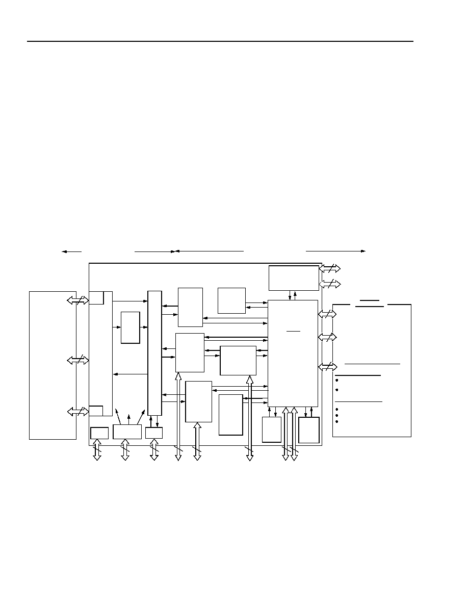
The SONET/SDH Ultramapper device integrates the SONET/SDH line, path, and tributary termination functions
with M13/E13 multiplex functions and the primary rate framing function. It is designed to drive either an OC-12/
STM-4 or OC-3/STM-1 optical signal directly or to allow for modular growth in terminal or add/drop applications.
The Ultramapper provides a versatile interface for all STS-12/STM-4, STS-3/STM-1, and STS-1 termination appli-
cations in point-to-point scenarios and for ring applications. This chip can be used in tributary shelf applications for
up to 84 T1 or J1 or 63 E1 line cards, providing all possible mappings into SONET/SDH, because of the flexibility of
the mappings, software upgrades from M13/E13 mapped connections to VT/TU mapped connections are possible.
This device can also be used for DS3/E3/DS2 applications.
A single Ultramapper is capable of processing the aggregate bandwidth of one STS-3/STM-1 to 84/63 DS1/E1s.
Further, a single Ultramapper can process the aggregate bandwidth of two STS-3/STM-1s, terminated as an STS-
12/STM-4, to six DS3/E3s. Additionally, a single Ultramapper can function as an STS-12/STS-3/STM-4/STM-1
add-drop MUX by terminating up to three STS-1/STM-0 channels or one AU-4 channel and using the internal
pointer processors to forward any nonterminated channels. By communicating to three other mate devices via the
serial STS-3/STM-1 link interface, it is capable of terminating a full STS-12/STM-4 signal.
2351(F)
Figure 1. Functional Diagram of Ultramapper
5
S
T
S
X
C
STSPP
CDR
CDR
FRM
X84/X63
DS1/J1/E1
TPG/TPM
(X3)
X28/X21
VTMPR
(X3)
M13/E13
MUX
X6
DS3/E3
DJA
X84/X63
DS1/E1
DJA
JTAG
MPU
CDR
STS1LT
(X3)
SPEMPR
(X3)
(0--2)
SPEMPR
(X3)
(3--5)
MRXC
DS1/J1/E1
VT/TU
DS2/E2
DS3/E3
TMUX
STS12/
STM4/
STS3/
STM1
4
11
4
HIGH-SPEED IF
622 Mbits/STS12/
STM4
155 Mbits/STS-3/
STM-1
CLOCK/SYNC
MSP 1 + 1
622 Mbits/STS12/
STM4
155 Mbits/STS-3/
49
14
JTAG IF
MPU IF
(X3)
STS3/STM1
MATE
INTERCONNECT
6
6
6
6
6
(X3)
(X3)
DS3/E3 PLL IF
(OPTIONAL)
LOPOH
(SUPPORTS UPSR)
TOAC POAC
42
RX/TX CLKS AND SYNC
8
PLL INTERFACE
SYSTEM
INTERFACES
(X6) DS3/E3
(X3) STS1
24
(X3) NSMI
(X3) STS1
204
SHARED LOW-SPEED I/O
SWITCHING MODES:
PSB (X16--X48/X63 DS1/J1/E1
X2016 DS0/E0
CHI (X42--X2016 DS0/E0
TRANSPORT MODES:
DS1/J1/E1 (X30--x28/x21 + PROT.
DS2/E2 (X30--x21/x12 + PROT.
VT/TU/(X30--X28/X21 + PROT.
5
X12/X4 SONET/SDH
ADM FRONT END
X8/X63 PDH
TRIBUTARY TERMINATION
STM-1

Agere Systems Inc.
9
Advance Data Sheet, Rev. 2
July 2001
SONET/SDH x84/x63 Ultramapper
TMXF84622 155 Mbits/s/622 Mbits/s Interface
2 The SONET/SDH Ultramapper
(continued)
2.2 Application Diagrams
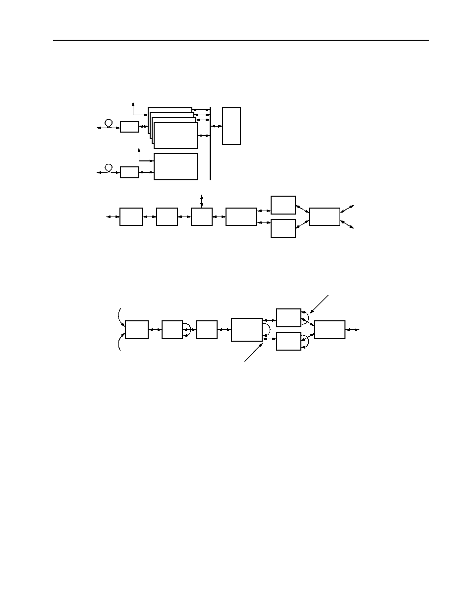
1938 (F)
Figure 2. Switching Application of the Ultramapper
1939 (F)
Figure 3. Transport Application of the Ultramapper
ULTRA
MAPPER
2417
2417
ULTRA
MAPPERS
TSI
TDM BUS
MUX
PP
XC
SPE/AU3
MAP
M13
MUX
VT/TU
MAP
T1/E1
FRAMER
DS0/E0
(CHI OR PSB)
DS1/E1
(PSB OR NSMI)
DS1/E1
DS3/E3
TO MATE
DEVICES
MUX
PP
XC
SPE/AU3
MAP
M13
MUX
VT/TU
MAP
T1/E1
FRAMER
DS3/E3
NONTERMINATED DS1/E1s
OR VT/TUs LOOPED BACK
DS1/E1
PM
VT/TU
NONTERMINATED TUG-3s
LOOPED BACK

10
10
Agere Systems Inc.
Advance Data Sheet, Rev. 2
July 2001
SONET/SDH x84/x63 Ultramapper
TMXF84622 155 Mbits/s/622 Mbits/s Interface
2 The SONET/SDH Ultramapper
(continued)
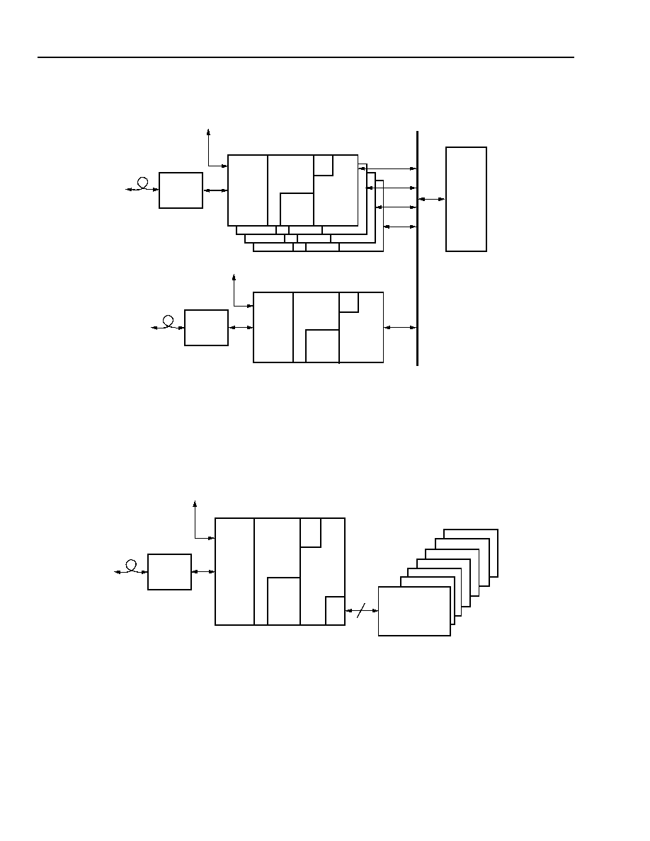
1084 (F)
Note: In this application, 84/63 DS1/E1s per Ultramapper can be MUXed to a total of three DS3/E3 and then mapped to STS-1/AU-3, STS-3/
STM-1, or STS-12/STM-4 as desired. Alternatively, 84/63 DS1/E1s per Ultramapper can be mapped to 84.63 VT/TU and then mapped to
STS-1/AU-3, STS-3/STM-1, or STS-12/STM-4 as desired.
Figure 4. Switching Application: Four Ultramappers Terminating STS-12/STM-4; One Ultramapper
Terminating STS-3/STM-1
1081 (F)
Note: Possible application would be add-drop of 28/21 T1/E1s to/from STS-12/STM-4/STS-3/STM-1.
Figure 5. Transport Application: Ultramapper Terminating 28/21 T1/E1s Directly to LIUs in Transport Mode
28/21
M13
OHP
MPR
FRMR
PM
M13
OHP
MPR
FRMR
PM
M13
OHP
MPR
FRMR
PM
MSP 1 + 1
M13
OHP
OPTICS
1417
MPR
FRMR
PM
DS0
E0
SWITCH
SYSTEM BUS
INTERFACE
UMPR #1, #2, #3, #4
M13
OHP
OPTICS
1417
MPR
FRMR
PM
MSP 1 + 1
MSP 1 + 1
M13
OHP
OPTICS
1417
MPR
PM
FRMR
PM
28/21
T1/E1
TLIU04C1
OPTICS
1417

Agere Systems Inc.
11
Advance Data Sheet, Rev. 2
July 2001
SONET/SDH x84/x63 Ultramapper
TMXF84622 155 Mbits/s/622 Mbits/s Interface
2 The SONET/SDH Ultramapper
(continued)
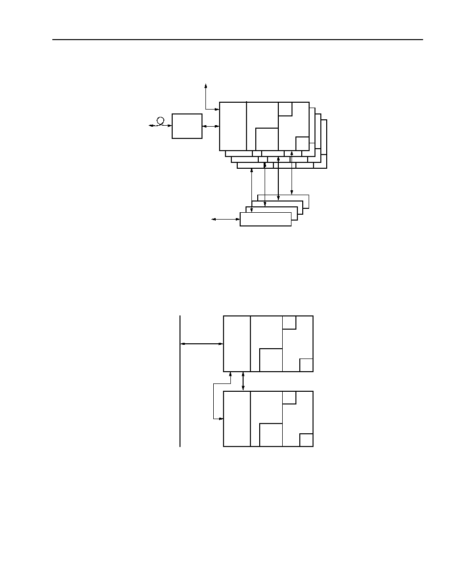
1085 (F)
Note: In this application, up to three DS3, E3, or EC1 per Ultramapper can be deMUXed to 84/63 DS1/E1, mapped to 84/63 VT/TU, and then
mapped to STS-1/AU-3, STS-3/STM-1, or STS-12/STM-4 as desired.
Figure 6. TransMUX Application: Four Ultramappers Mapping Clear Channel DS3/E3/EC-1 to VT/TU and
Terminating as STS-12/STM-4
1083 (F)
Note: In this application, up to three DS3 or E3 embedded in STS-1/AU-3 per Ultramapper can be deMUXed to 84/63 DS1/E1, mapped to 84/63
VT/TU, and then mapped to STS-1/AU-3. Simultaneously, up to 84/63 VT/TU embedded in STS-1/AU-3 per Ultramapper can be
demapped to 84/63 DS1/E1, then multiplexed to
3 DS3 or E3 embedded in STS-1/AU-3.
Figure 7. Portless TransMUX Application: Two Ultramappers Required for STS-12/STM-4 to Map 6 x STS-1
(DS3 MApped) to/from 6 x STS-1 (VT Mapped)
M13
OHP
MPR
FRMR
PM
PM
M13
OHP
MPR
FRMR
PM
PM
M13
OHP
MPR
FRMR
PM
PM
MSP 1 + 1
OPTICS
1417
UMPR #1, #2, #3, #4
M13
OHP
MPR
FRMR
PM
PM
DS3/E3 LIU
DS3/E3/STS1
M13
OHP
MPR
PM
FRMR
PM
SWITCH
BACKPLANE
M13
OHP
MPR
PM
FRMR
PM
1 x STS3
3 x STS1
UMPR #1
STS12/STM4
UMPR #2

12
12
Agere Systems Inc.
Advance Data Sheet, Rev. 2
July 2001
SONET/SDH x84/x63 Ultramapper
TMXF84622 155 Mbits/s/622 Mbits/s Interface
2 The SONET/SDH Ultramapper
(continued)
1086 (F)
Note: In this application, each Ultramapper maps six clear channels DS3s or E3s (any combination) through the SPE/AU-3 mapper to STS-1s
or TUG-3s. Utilizing the mate interface, one Ultramapper provides an STS-12/STM-4 termination.
Figure 8. DS3/E3 Mapped to SONET/SDH-2 Ultramappers Mapping 12 DS3/E3 into STS-1s or TUGs and
Ultimately to STS-12/STM-4
1082 (F)
Note: Using the DS1/E1 framers, DS3/E3 framers, and the M13 MUX, the Ultramapper can be used to MUX up to 84/63 T1/E1s to three DS3/
E3s.
Figure 9. M13 MUX and Framing Application: 84/63 DS1/E1 (NSMI System Bus) MUXed to Three DS3/E3
M13
OHP
MPR
FRMR
PM
M13
OHP
OPTICS
1417
MPR
FRMR
PM
PM
DS3/E3 LIUs
6
6
DS3/E3 LIUs
M13
OHP
MPR
PM
FRMR
PM
DS1/E1 3x
SYSTEM BUS
(x28/x21)
(NSMI MODE)
INTERFACE

Agere Systems Inc.
13
Advance Data Sheet, Rev. 2
July 2001
SONET/SDH x84/x63 Ultramapper
TMXF84622 155 Mbits/s/622 Mbits/s Interface
2 The SONET/SDH Ultramapper
(continued)
2.3 High-Speed Line Interfaces and Clock and Data Recovery
In the receive direction, the Ultramapper accepts either a differential serial data signal at 155.52 Mbits/s (STS-3/
STM-1 mode) or a serial STS-1 clock and data at 51.84 MHz (STS-1 mode). For the STS-1 case, the input is
retimed with the input clock. A clock and data recovery circuit is used for the 155 Mbits/s case with the high-speed
transmit input clock as the clock reference. In the event that external clock and data recovery is provided, this fea-
ture can be bypassed. The clock and date circuit can be used for recovering clock at 51 MHz, but a 155 MHz clock
reference must still be supplied.
On the transmit side, in STS-3/STM-1 mode, the Ultramapper receives a differential 155.52 MHz transmit clock and
transmit frame synchronizing signal and outputs a differential serial data signal. In STS-1 mode, it receives a
51.84 MHz transmit clock and frame synchronizing signal and outputs serial data.
Loss of input clock or recovered clock is detected, as well as a loss-of-signal condition, by monitoring an external
signal pin or an internal an all-zeros/ones pattern.
Built-in loopbacks at both high-speed interfaces provide maximum flexibility for maintenance testing.
2.3.1 Receive Direction
Terminating the transport overhead (TOH), the Ultramapper performs frame alignment (STS-3/STM-1 or STS-1),
B1 BIP-8 check, J0 monitoring, descrambling, F1 monitoring, B2 BIP-8 check, APS and K2 monitoring, AIS-L and
RDI-L detection, M1 REI-L detection, S1 synchronization status monitoring, and transport overhead access chan-
nel (RTOAC) drop.
The states of the framer as well as all state changes are reported, and, if not masked, cause an interrupt.
The B1 and B2 parity check supports bit and block mode. The counters count up to one second worth of BIP
errors. They stay at their maximum value in case of overflow or rollover and should be read (and cleared) at least
once per second.
The J0 monitor supports nonframed, SONET-framed, and SDH-framed 16-byte sequences, as well as single
J0 byte monitoring modes.
APS monitoring is performed on K1[7:0] and K2[7:3]. The value is stored and changes are reported. Bits [2:0] of
the K2 byte are monitored independently.
Line AIS (AIS-L/MS-AIS) and remote defect indication (RDI-L/MS-RDI) are monitored separately and changes are
reported. This information is also sent to the protection device for ADM applications.
The M1 monitor operates either in bit or block mode and allows accessing of the remote error indication (REI-L/
MS-REI) errored bit count.
The S1 byte can be monitored in two modes: as an entire 8-bit word or as one 4-bit nibble (bits 7:4).
Continuous N times detection counters are implemented for these monitoring functions. All automatic receive mon-
itoring functions can be configured to provide an interrupt to the control system, or the device can be operated in a
polled mode.
The receive transport overhead access channel (RTOAC) provides access to all of the line section overhead bytes.
Even or odd parity is calculated over all bytes. It has a data rate of 5.184 Mbits/s and consists of a clock, data, and
an 8 kHz synchronizing pulse. Alternatively, only the data communication channels D1:D3 or D4:D12 may transmit
a serial 192 kbits/s or a 576 kbits/s data stream.

14
14
Agere Systems Inc.
Advance Data Sheet, Rev. 2
July 2001
SONET/SDH x84/x63 Ultramapper
TMXF84622 155 Mbits/s/622 Mbits/s Interface
2 The SONET/SDH Ultramapper
(continued)
2.3.2 Transmit Direction
In the transmit direction, the Ultramapper performs transmit transport overhead access channel (TTOAC) insertion,
synchronizing status byte (S1) insertion, M0/M1--REI-L insertion, K1 and K2 insertion, AIS-L insertion, B2 calcula-
tion and insertion, F1 byte insertion, B1 generation and error insertion, scrambler, J0 insert control, and A2 error
insertion. All insert control functions that are inhibited will optionally insert either all zeros or all ones. The TTOAC
allows the users to insert the following overhead bytes: E1, F1, D1:D3, D4:D12, S1, and E2. Even or odd parity is
checked over all bytes. Bytes which are not enabled for insertion are set to an all-ones or all-zeros stuff value. The
Ultramapper sources a clock and an 8 kHz synchronizing pulse and receives the data at a data rate of
5.184 Mbits/s. Alternatively, only the data communication channels D1--D3 or D4--D12 may receive a serial
192 kbits/s or a 576 kbits/s data stream.
The insertion (overwrite of TTOAC) of programmed S1, F1, J0, Z0-2, and Z0-3 bytes can be enabled.
Automatic insertion of M0/M1 may be inhibited. A protection switch selects the REI-L value for insertion to be taken
from the protection board rather than from the receive side.
The entire APS value or K2[2:0] can be inserted via microprocessor control. Automatic RDI insertion is supported
with individual inhibit for each contributor. A protection switch selects the RDI-L value for insertion to be taken from
the protection board rather than from the receive side.
B1 and B2 BIP-8 values are calculated and inserted. Both values can be inverted.
2.4 Multiplex Section Protection (MSP 1 + 1)
The TMUX block supports a payload 1 + 1 protection switch. In the receive direction, this occurs prior to pointer
interpretation. If the protection switch is activated, then the data is selected from the receive protection interface
rather than from the high-speed input path.
In the transmit direction, the signal is broadcast to the high-speed output path and the protection interface.
The interface consists of a 155.52 MHz or 51.84 MHz clock, data, and synchronizing pulse in each direction.
2.4.1 Pointer Interpreter
This state machine implements the pointer interpretation algorithm described in ETS 300 417-1-1: January 1996--
Annex B.
The pointer interpreter evaluates the current pointer state for the normal state, path AIS state, or LOP (loss of
pointer) conditions, as well as pointer increments and decrements. The current pointer state and any changes in
pointer condition are reported to the control system. The number of consecutive frames for invalid pointer and
invalid concatenation indication is fixed at nine.
2.4.2 Path Termination Function
The path termination function is performed on either all three STS-1s or on the VC-4 POH only.
It includes on the receive side: J1 monitoring, B3 BIP-8 checking, C2 signal label monitoring, REI-P and RDI-P
detection, H4 multiframe monitoring; F2, F3, and K3 automatic protection switch monitoring, N1 tandem connection
monitoring, signal degrade BER and signal fail BER detection; path overhead access channel (RPOAC) drop,
AIS-P/HO-AIS insertion, and automatic AIS generation (with individual inhibit).
The J1 monitor provides five modes of operation on a programmable length (1 byte--64 bytes) of the trace identi-
fier: cyclic checking against the last received sequence, comparing against a programmed sequence, SONET
framing mode, SDH framing mode, and consecutive consistent occurrences of a new pattern.

Agere Systems Inc.
15
Advance Data Sheet, Rev. 2
July 2001
SONET/SDH x84/x63 Ultramapper
TMXF84622 155 Mbits/s/622 Mbits/s Interface
2 The SONET/SDH Ultramapper
(continued)
B3 is monitored either in bit or block mode. Provisionable N-times detection counters are implemented for C2, F2,
F3, N1, and K3 bytes. The K3 APS byte and N1 TCM byte can be monitored as an entire 8-bit word or two 4-bit nib-
bles.
The receive path overhead access channel (RPOAC) provides access to all the path overhead bytes. Even or odd
parity is calculated over all bytes. It has a data rate of 8 bytes per 8 kHz frame and consists of clock, data, and an
8 kHz synchronizing pulse.
In the transmit direction, J1 path trace insertion, B3 calculation and insertion, C2 signal label insertion, REI-P and
RDI-P insertion; F2 insertion, H4 multiframe insertion, F3 path user byte insertion, K3 insertion, N1 byte insertion,
and AIS-P insertion via POAC or software control is supported.
The transmit path overhead access channel (TPOAC) allows the insertion of all overhead bytes besides B3 which
is automatically calculated. Even or odd parity is checked over all bytes. Bytes which are not enabled for insertion
are set to an all-ones or all-zeros stuff value. The Ultramapper sources a clock and an 8 kHz synchronizing pulse
and receives the data at a rate of 8 bytes per 8 kHz frame.
2.5 STS-3/STM-1 Overhead Termination and Pointer Processing
The information on overhead termination and pointer processing is not available at this time.
2.6 STS-3/STM-1 MUX-DeMUX
The STS-3/STM-1 (AU-4) multiplexer provides three modes of operation: STS-3, AU-4, and STS-1.
In STS-3 mode, the block multiplexes and demultiplexes up to three STS-1 signals to/from a SONET STS-3 signal.
In AU-4 mode, it provides the functionality to MUX/deMUX up to three AU-3 signals to/from a STM-1 (AU-4) signal.
In STS-1 mode, it provides the functions to generate and terminate a single STS-1 signal.
The STS-3/STM-1 MUX function takes the bytes in the order they are present on the telecom bus and multiplexes
them into the high-speed signal. Grooming of the VTs/VCs is performed in the SPE mapper of each of the three
devices.
2.7 STS-3 Serial Interconnect
The information on the STS-3 serial interconnect is not available at this time.
2.8 STS-12/STM-4 Pointer Processor
The information on the STS-12/STM-4 pointer processor is not available at this time.
2.9 STS-3/STM-1 Interface to Mate Devices
The Ultramapper can communicate with up to three mate devices via STS-3/STM-1 interfaces. One Ultramapper is
provisioned as a master and the other three are provisioned as slaves. This provides for full external termination of
the STS-12/STM-4 payload.

16
16
Agere Systems Inc.
Advance Data Sheet, Rev. 2
July 2001
SONET/SDH x84/x63 Ultramapper
TMXF84622 155 Mbits/s/622 Mbits/s Interface
2 The SONET/SDH Ultramapper
(continued)
2.10 SPE/AU-3 Mapper (DS3 Mapper)
The SPE mapper block is a highly configurable mapper. It operates either as an AU-3/STS-1 mapper or as a TUG-
3 mapper. In both modes, it maps/demaps data from/to either the VT mapper, the M13 MUX/deMUX, the DS3 clear
channel, or the DS3 loopback channel. The SPE mapper supports numerous automatic monitoring functions and
provides interrupts to the control system, or it can be operated in a polled mode. In TU mapping mode, the SPE
mapper provides flexibility down to TUG-2 level for choosing which TUG-2s (out of 7) are mapped/dropped
into/from which TUG-3s (between 1 and 3) for generating STM-1 signals. This allows grooming of the VTs/TUs on
the STM-1 level (over all three devices). In a full STM-1 application, with two other devices sitting on the telecom
bus, care has to be taken for the provisioning of the time slots when each block drives the telecom bus.
In DS3 mapping mode, the SPE mapper block accepts/delivers structured DS3 data from/to the M13 block or a
clear DS3 signal at 44.736 Mbits/s rate and maps/demaps it asynchronously into/from the STS-1 SPE or a TU-3.
The DS3 mapper generates a fixed pointer value of 522. On the receive side, pointer interpretation is performed
detecting LOP, AIS, NDF, NORM, INC, and DEC. A DS3 loopback mode allows demapping and remapping of a
DS3 signal. It is particularly useful in cases where a DS3 signal mapped as an AU-3/STS-1 signal is needed to be
remapped as a TU-3 signal or vice versa. B3ZS encoding/decoding is included.
The same path overhead monitoring functions (as described above) are implemented in this block.
This block also connects to the path overhead access channel (POAC) to insert/drop the path overhead bytes J1,
C2, F2, H4, F3, K3, and N1 into the STS-1 SPE or VC-3.
Supports unidirectional path switch ring (UPSR) applications as well as N1 tandem connection function.
Complies with GR-253-CORE, T1.105, ITU-T G.707, ITU-T G.831, G.783, and ETS 300 417-1-1.
2.11 VT/TU Mapper
The VT/TU mapper maps any valid combination of DS1 and E1 signals into a stream at a rate of 51.84 Mbits/s
(STS-1 or AU-3). The mapping methods (VT1.5, VT2, and VT group in ANSI nomenclature; TU-11, TU-12, and
TUG-2 in ITU nomenclature) are analogous. The VT/VC mapper supports the following mappings:
s
84 asynchronous, byte-, or bit-synchronous DS1 signals are mapped into seven VT groups or TUG-2s.
s
84 asynchronous, byte-, or bit-synchronous J1 signals are mapped into seven VT groups or TUG-2s.
s
63 asynchronous, byte-, or bit-synchronous E1 signals are mapped into seven VT groups or TUG-2s.
s
Maps T1 into VT1.5/TU-11/TU-12, J1 into VT1.5/TU-11/TU-12, and E1 into VT2/TU-12.
ADM and unidirectional path switch ring (UPSR) applications are supported via tributary loopback, tributary pointer
processing, and low-order path overhead access channel.
Supports automatic generation or microprocessor overwrite 1-bit RDI, enhanced RDI, 1-bit RFI, automatic down-
stream AIS generation, and five J2 trace identifier modes.
Complies with GR-253-CORE, G.707, T1.105, G.704, G.783, JT-G707, GR-499, and ETS 300 417-1-1.
2.11.1 Receive Direction
In the receive direction, the VT mapper terminates the data stream it receives from the SPE mapper. It demulti-
plexes the AU-3/TUG-3 into the VTs/TUs and checks the H4 multiframe alignment. Pointer interpreters for up to
84 VTs/TUs detect LOP, AIS, NDF, NORM, INC, and DEC on each channel.

Agere Systems Inc.
17
Advance Data Sheet, Rev. 2
July 2001
SONET/SDH x84/x63 Ultramapper
TMXF84622 155 Mbits/s/622 Mbits/s Interface
2 The SONET/SDH Ultramapper
(continued)
The low-order path termination includes V5 byte termination, J2 path trace, Z6/N2 tandem connection, Z7/K4
enhanced RDI and low-order APS monitor, and the payload termination for asynchronous, byte- or bit-synchronous
signals. The V5 byte termination performs BIP-2 check (bit- or block-mode), REI count, RFI and RDI detection, sig-
nal label monitor, and automatic AIS insertion (which can be inhibited). The J2 monitor supports four different
modes as follows:
s
Cyclic check
s
SONET framing mode
s
SDH framing mode
s
Single byte check
In byte-synchronous modes, the receive demapper generates a frame synchronization signal to indicate the DS1
frame bit or the MSB of the E1 time-slot 0. Additionally, it provides the framer access to the received signaling bits.
Output of the VT mapper is a DS1/J1/E1 signal with a gapped clock. It can be overwritten with AIS automatically or
upon microprocessor request.
2.11.2 Transmit Direction
In the transmit direction, the VT mapper gets a clock, data, and frame synchronization signal from the cross con-
nect. The input is retimed and checked for a digital loss of clock (LOC), an AIS condition, and low zeros density. In
byte-synchronous mode, the input signal is additionally checked for loss of frame synchronization (LOFS).
A transmit elastic store synchronizes the incoming DS1/J1/E1 signals to the local STS-1 clock. In asynchronous
and bit-synchronous mode, it works as a bit-oriented (64-bit) FIFO, and in byte-synchronous mode as a byte-wide
(8-byte) buffer using a V5 byte marker bit (8-bit). Overflow or underflow conditions are monitored and reported.
In asynchronous and bit-synchronous mode, a fixed VT pointer of 78 (VT1.5/TU-11) and 105 (VT2/TU-12) is gener-
ated and the payload is mapped into the container using positive/null/negative bit stuffing mechanism (C- and
S-bits). In bit-synchronous mode, the bit stuffing mechanism is disabled. In byte-synchronous mode, a dynamic VT
pointer value is generated using the V5 marker implementing NORM, NDF, INC, and DEC pointers.
The VT POH generation comprises V5 byte with BIP2-generation, AIS-, signal label-, UNEQ-insertion, automatic
REI-, RFI-, RDI-, and enhanced RDI-generation (Bellcore*, ITU-T), J2 path trace insertion via microprocessor,
Z6/N2 byte insertion, and Z7/K4 byte insertion via microprocessor or low-order path overhead (LOPOH) access
channel.
The data stream is synchronized to the received 2 kHz synchronization pulse and multiplexed to form the
STS-1/AU-3 signal, which is then output to the SPE mapper.
When operating in byte-synchronous mode, the phase and signaling bits from the framer are stored and inserted
into the mapped frame.
2.12 M13/M23 Multiplexer
The M13 is a highly-configurable multiplexer/demultiplexer. It can operate as an M13 in either the C-bit parity or
M23 mode, a mixed M13/M23, or an M23. In the C-bit parity mode, the M13 provides a far-end alarm and control
(FEAC) code generator and receiver, an HDLC transmitter and receiver, and automatic far-end block error (FEBE)
generation.
* Bellcore is now Telecordia TEchnologies, Inc.

18
18
Agere Systems Inc.
Advance Data Sheet, Rev. 2
July 2001
SONET/SDH x84/x63 Ultramapper
TMXF84622 155 Mbits/s/622 Mbits/s Interface
2 The SONET/SDH Ultramapper
(continued)
Each internal M12 MUX/deMUX and the M23 MUX/deMUX may be configured to operate as independent
MUXs/deMUXs. 84 DS1 inputs in groups of four or 63 E1 input signals in groups of three can feed into individual
M12 MUXs, while the M23 MUX can take DS2 signals from outputs of M12 MUXs, or direct DS2 inputs, or loopback
deMUXed DS2s.
The M13 supports numerous automatic monitoring functions. It can provide an interrupt to the control system or it
can be operated in a polled mode.
Complies with T1.102, T1.107, T1.231, T1.403, T1.404, GR-499, G.747, and G.775.
2.12.1 Receive Direction
The receive DS3 is monitored for loss of clock and checked for loss of signal (LOS) according to T1.231. The B3ZS
decoder accepts either unipolar clock and data or unipolar clock, positive and negative data. It also checks for bipo-
lar coding violations. The transmit DS3 can be looped back into the receive side after B3ZS decoding. The M23
demultiplexer checks for valid DS3 framing by finding the frame alignment pattern (F bits), and then locating the
multiframe alignment signal (M bits). During each M frame, the data stream is checked for the presence of the AIS
(1010) or idle (1100) pattern.
C bits 13, 14, and 15 can be used as a 28.2 kbits/s data link and are available directly at device output via an inter-
nal HDLC receiver. The receiver is composed of a 128-byte FIFO, a CRC-16 frame check sequence (FCS) error
detector, and control circuits.
Within the M23 demultiplexer, there are four performance monitoring counters for F- or M-bit, P-bit, E-bit parity, and
FEBE errors. Each M12 demultiplexer contains two performance monitoring counters.
2.12.2 Transmit Direction
The incoming DS1/E1 clocks are first checked for activity or loss of clock (LOC). The data signals are retimed and
checked for AIS and activity. DS1/E1 loopback selectors allow DS1 or E1 received within the DS2 or DS3 inputs
from the deMUX path to be looped back. This loopback can be performed automatically or the user can force a
DS1 or E1 loopback.
The four DS1 or three E1 signals for each M12 MUX are fed into single-bit, 16-word-deep FIFOs to synchronize the
signals to the DS2 frame generation clock. The fill level of each FIFO determines the need for bit stuffing its
DS1/E1 input. The M13 can handle DS1/E1 signals with nominal frequency offsets of ±130 ppm and up to five unit
intervals peak jitter. The DS2/DS3 transmit clock is used to derive the clock source for DS2 frame generation.
The M23 multiplexer generates a transmit DS3 frame, and fills the information bits in the frame with data from the
seven DS2 select blocks. The M23 MUX can be provisioned to operate in either the M23 mode or the C-bit parity
mode. It contains seven DS2 FIFOs each with a depth of 8. The fill level of each FIFO determines the need for bit
stuffing its DS2 input.
The transmit DS3 output can either be in the form of unipolar clock and data or unipolar clock, positive and negative
data. The DS3 data is B3ZS encoded and can be looped back from the receive DS3 input.
2.13 E13/E23 Multiplexer
The information on the E13/E23 multiplexer is not available at this time.

Agere Systems Inc.
19
Advance Data Sheet, Rev. 2
July 2001
SONET/SDH x84/x63 Ultramapper
TMXF84622 155 Mbits/s/622 Mbits/s Interface
2 The SONET/SDH Ultramapper
(continued)
2.14 Cross Connect Block
The cross connect (XC) is a highly configurable nonblocking crosspoint switch for DS1/E1/DS2 signals, configura-
tion of DS3 signal paths, and configuration of the path overhead access I/O. The cross connect plays a major role
in configuring the interconnection of major function blocks to satisfy an application's implementation.
The cross connect provides the flexibly to tie DS1/E1/DS2 channels from the framer or external pins to the M13
mapper or to the VT mapper. It is also capable of multicast or broadcast operation (one port to many), handling
injected test patterns, idles, or alarm conditions to any channel, and can provide system loopback testing support.
Jitter attenuation may also be inserted in-line on any DS1/E1 channel.
The cross connect can interconnect up to 84 individual DS1/E1 channels between the framer, M13 multiplexer, VT
mapper, jitter attenuator, or external I/O. The external I/O pins support an application dependent mix of up to
29 T1/E1 interfaces (one dedicated protection channel), seven DS2 interfaces, or one of four available framer sys-
tem interfaces.
The cross connect supports an independent signal path for remote alarm indication (RAI), alarm indication signal
(AIS), and byte-synchronous frame synchronizing signals on channels between the VT mapper or M13 and the
framer. Receive pointer adjustment information is routed to the jitter attenuator block for each channel originating in
the VT mapper.
The cross connect has independent DS2 interfaces for the M12 and M23 blocks of the M13 MUX. Full split access
to the external I/O device pins provides the capability to add, drop, or rearrange the DS2 signals within the M13.
For DS3 signals, the cross connect supports configuration of interconnects between the M13 and the SPE, or
external I/O interconnection to the M13 or SPE, or insertion/monitoring of DS3 test patterns from the test-pattern
generator block.
The test-pattern generator block (TPG) provides test signals and monitors inputs (TPM) for signals to and from the
cross connect. The TPG can generate a set of test signals or idles at DS1, E1, DS2, or DS3 rates. There is only
one test pattern generator and monitor per signal rate.
Device pins for the path overhead access channel may be configured to connect to the SPE mapper or TMUX
blocks.
2.15 DS1 Digital Jitter Attenuator
The digital jitter attenuator (DJA) contains 28 copies of the digital jitter attenuator block. These digital jitter attenua-
tor blocks can operate in two different modes, as a DS1 or as an E1 jitter attenuator.
In both modes, the digital jitter attenuator can be provisioned to always operate as a second-order PLL, or it can
switch to a act as a first-order PLL during VT pointer adjustments to help meet MTIE requirements. The period of
time in the first-order mode is provisionable. The PLL bandwidth is provisionable between 0.1 Hz and 0.5 Hz, and
the damping factor for these bandwidths varies between 2 and 0.5 to accommodate a number of different system
constraints.
The block will also insert the proper AIS signal if the primary block AIS control input is active.
2.16 DS3 Digital Jitter Attenuator
The information on the DS3 digital jitter attenuator is not available at this time.

20
20
Agere Systems Inc.
Advance Data Sheet, Rev. 2
July 2001
SONET/SDH x84/x63 Ultramapper
TMXF84622 155 Mbits/s/622 Mbits/s Interface
2 The SONET/SDH Ultramapper
(continued)
2.17 Test Pattern Generator
The test pattern generator and monitor (TPG and TPM) is a set of configurable test pattern generators and moni-
tors for local self-test, maintenance, and troubleshooting operations.
The TPG feeds one or more T1/E1/DS2 test signals (via data, clock, and FS or AIS signal paths) to the crosspoint
switch which can redistribute or broadcast these signals to any valid channel in the framer, external I/O, M13 map-
per, or VT mapper blocks. The TPG can also generate DS3 test signals.
Any channel arriving at the cross connect may be routed to the test monitor. The test monitors can automatically
detect/count bit errors in a pseudorandom test sequence, loss of frame, or loss of synchronization. The TPM can
provide an interrupt to the control system or it can be operated in a polled mode.
Simultaneous testing of DS1, E1, DS2, and DS3 signals is supported (one channel each).
Supported test patterns are: pseudorandom bit sequence (PRBS15, PRBS20), alternating zeros/ones, and an all-
ones pattern.
The test pattern can be transmitted either unframed or as the payload of a framed signal, as defined in ITU-T Rec-
ommendation O.150.
Single bit-errors may be injected into any test pattern, under register control.
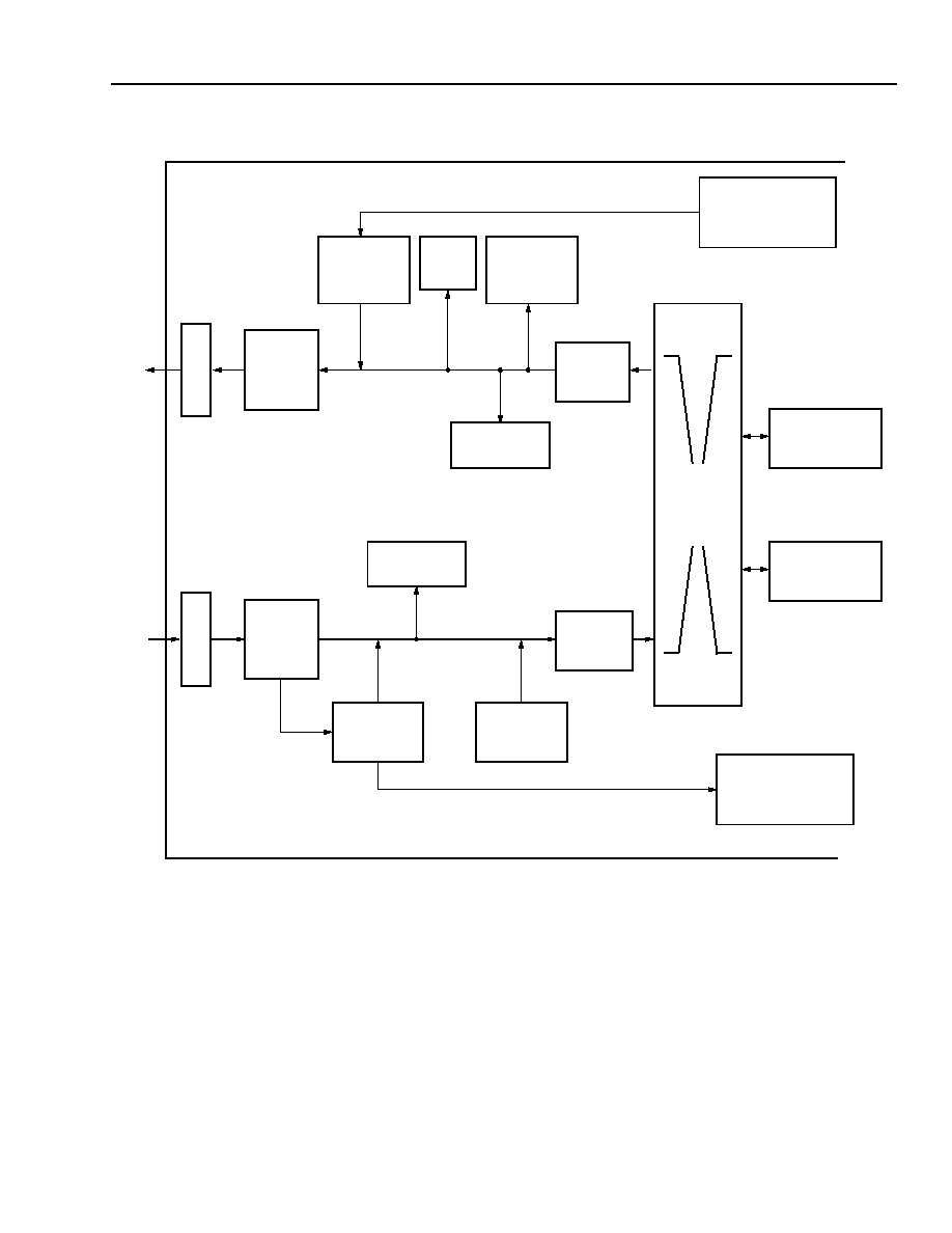
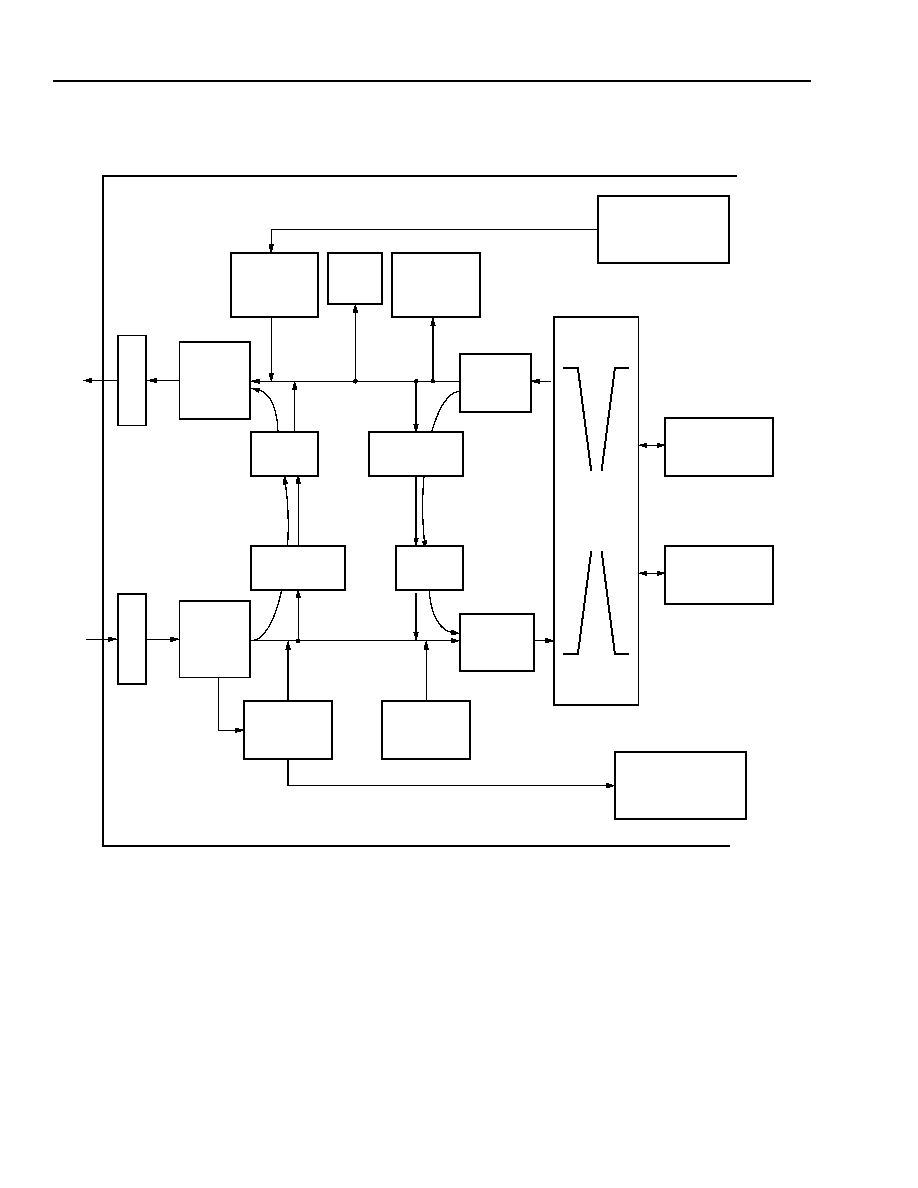
2.18 28-Channel Framer
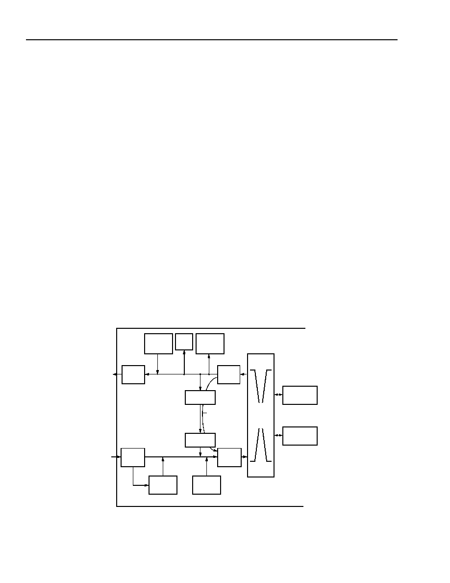
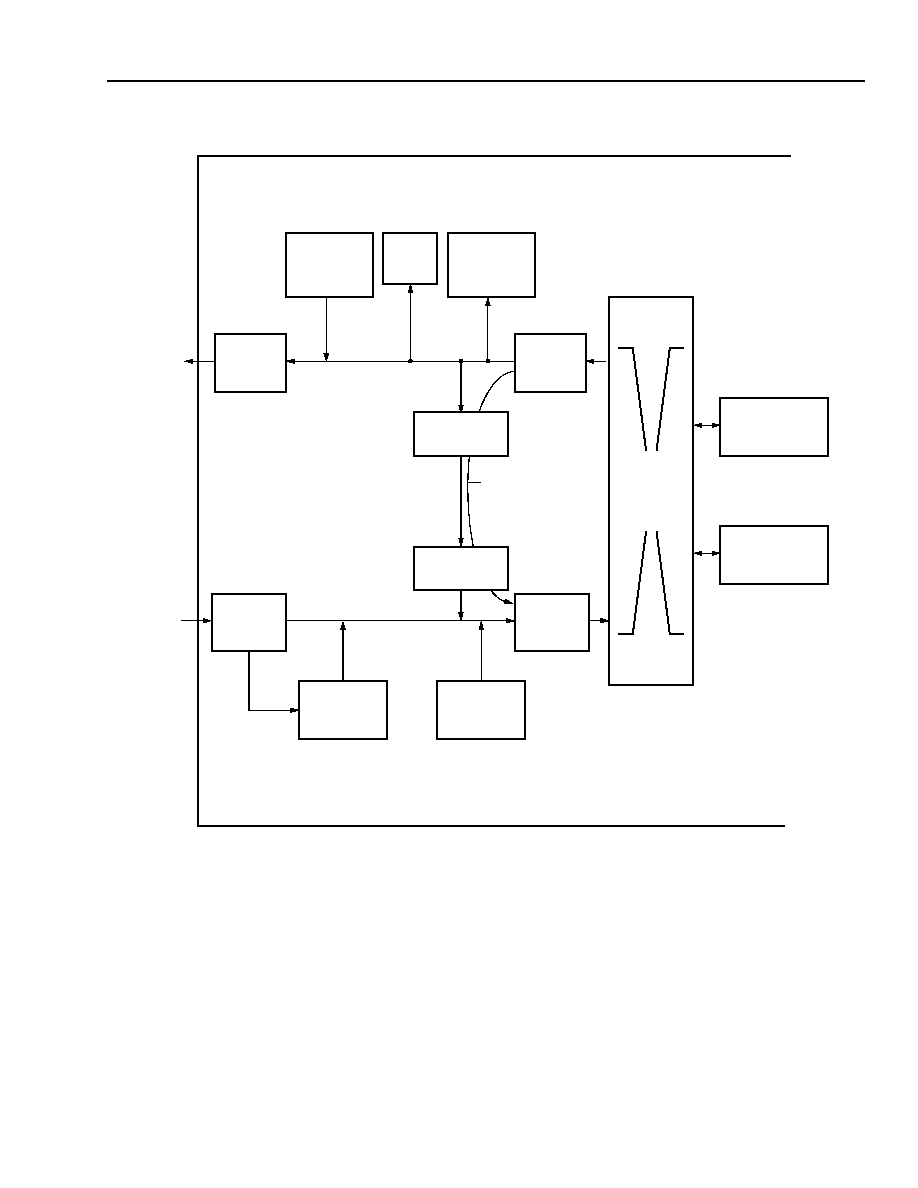
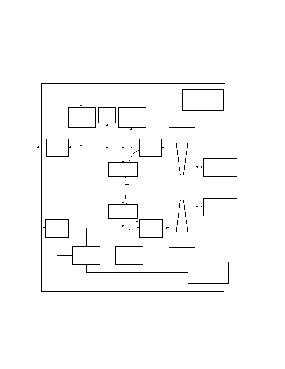
The block diagrams of the 84 T1/63E1-channel framer in the switching application in the CHI, parallel system bus,
and CHI with byte-synchronous VT mapping, are shown in Figure 10, Figure 11, and Figure 12 (only the major
functional blocks are shown). The block diagrams of the 84 T1/63E1-channel framers in the transport application
are shown in Figure 13 and Figure 14 (only the major functional blocks are shown).
5-8926.a (F)
Figure 10. Ultramapper Switching Mode for Framer in Concentration Highway Interface (CHI) Configuration
SIGNALING
PROCESSOR
(EXTRACTION)
RECEIVE
FACILITY DATA
LINK
RECEIVE
HDLC
TRANSMIT
SYSTEM
INTERFACE
RECEIVE
FRAME
ALIGNER
TRANSMIT
FRAME
FORMATTER
TRANSMIT
FACILITY DATA
LINK
SIGNAL
PROCESSOR
(INSERTION)
RECEIVE
SYSTEM
INTERFACE
MAPPER
TO
FRAMER
DS1
CROSS
CONNECT
ESF PRM PATH
ULTRAMAPPER: FRAMER
ULTRAMAPPER
M12 MULTIPLEXER
INTERFACE
ULTRAMAPPER
VT MAPPER
INTERFACE
TF
S1, TC
LK1,
TD
ATA28
DS
0
I
N
T
E
RF
A
C
E
RF
S1
,
RC
L
K
1
,
RDA
T
A
2
8
PERFORMANCE
MONITOR
TRANSMIT
HDLC

Agere Systems Inc.
21
Advance Data Sheet, Rev. 2
July 2001
SONET/SDH x84/x63 Ultramapper
TMXF84622 155 Mbits/s/622 Mbits/s Interface
2 The SONET/SDH Ultramapper
(continued)
5-8927.a (F)
Figure 11. Ultramapper Switching Mode for Framer in Parallel System Bus Configuration
SIGNALING
PROCESSOR
(EXTRACTION)
RECEIVE
FACILITY DATA
LINK
RECEIVE
HDLC
TRANSMIT
SYSTEM
INTERFACE
RECEIVE
FRAME
ALIGNER
TRANSMIT
FRAME
FORMATTER
TRANSMIT
FACILITY DATA
LINK
SIGNAL
PROCESSOR
(INSERTION)
RECEIVE
SYSTEM
INTERFACE
MAPPER
TO
FRAMER
DS1
CROSS
CONNECT
ESF PRM PATH
ULTRAMAPPER: FRAMER
ULTRAMAPPER
M12 MULTIPLEXER
INTERFACE
ULTRAMAPPER
VT MAPPER
INTERFACE
DS0
PERFORMANCE
MONITOR
TRANSMIT
HDLC
INT
E
RF
A
C
E
TFS
1,
TC
L
K
1
,
T
D
ATA8
,
T
D
A
T
A
_
P
A
R
IT
Y
A
1
,
T
S
IGNA
L
IN
G8,
T
S
IGNA
L
IN
G_P
A
R
IT
Y
A
1
RF
S1
, RCL
K1
,
RDAT
A
8
,
RDAT
A
_
P
ARI
T
YA1
, RS
I
G
NAL
I
NG
8
,
RS
IGN
A
L
ING_
P
A
RI
T
Y
A
1

22
22
Agere Systems Inc.
Advance Data Sheet, Rev. 2
July 2001
SONET/SDH x84/x63 Ultramapper
TMXF84622 155 Mbits/s/622 Mbits/s Interface
2 The SONET/SDH Ultramapper
(continued)
In the byte-synchronization mode, the frame synchronization and signaling (VT SPE) information are also passed
to the mapper. In the receive direction, the mapper block provides the line data, line clock, frame synchronization
(byte-synchronization mode), and signaling information (byte-synchronization mode) to the Ultra Framer. Perfor-
mance reports, in the form of HDLC packets (PRMs), are sent from the receive performance monitor block to the
transmit HDLC block.
5-8928.a (F)
Figure 12. Ultramapper Switching Mode CHI Configuration with Byte-Synchronous VT Mapping Enabled
SIGNALING
PROCESSOR
(EXTRACTION)
RECEIVE
FACILITY DATA
LINK
RECEIVE
HDLC
TRANSMIT
SYSTEM
INTERFACE
RECEIVE
FRAME
ALIGNER
TRANSMIT
FRAME
FORMATTER
TRANSMIT
FACILITY DATA
LINK
SIGNAL
PROCESSOR
(INSERTION)
RECEIVE
SYSTEM
INTERFACE
MAPPER
TO
FRAMER
DS1
CROSS
CONNECT
ESF PRM PATH
ULTRAMAPPER: FRAMER
ULTRAMAPPER
M12 MULTIPLEXER
INTERFACE
ULTRAMAPPER
VT MAPPER
INTERFACE
DS0
PERFORMANCE
MONITOR
TRANSMIT
HDLC
INT
E
RF
A
C
E
T
F
S1
,
T
C
L
K
1
,
TDAT
A2
8
RF
S1
, RCL
K1
, RDAT
A
2
8
VT MAPPER:
BYTE-SYNCHRONOUS
ROBBED-bit SIGNALING
RECEIVE DATA
RECEIVE SIGNALING DATA
(TO SIGNALING REGISTERS)
SIGNALING STOMP
DATA
VT MAPPER:
BYTE-SYNCHRONOUS
ROBBED-bit SIGNALING
TRANSMIT DATA
TRANSMIT SIGNALING DATA
(EXTRACTED FROM SYSTEM
OF SIGNALING REGISTERS)

Agere Systems Inc.
23
Advance Data Sheet, Rev. 2
July 2001
SONET/SDH x84/x63 Ultramapper
TMXF84622 155 Mbits/s/622 Mbits/s Interface
2 The SONET/SDH Ultramapper
(continued)
5-8929.a (F)
Figure 13. Ultramapper Byte-Synchronous Transport Mode: Passive Performance Monitoring
SIGNALING
PROCESSOR
(TRANSMIT)
RECEIVE
FACILITY DATA
LINK
RECEIVE
HDLC
TRANSMIT
FRAME
FORMATTER
RECEIVE
FRAME
ALIGNER
TRANSMIT
FRAME
FORMATTER
TRANSMIT
FACILITY DATA
LINK
SIGNALING
PROCESSOR
(RECEIVE)
MAPPER
TO
FRAMER
DS1
CROSS
CONNECT
ULTRAMAPPER: PERFORMANCE MONITORING FRAMER
ULTRAMAPPER
M12 MULTIPLEXER
INTERFACE
ULTRAMAPPER
VT MAPPER
INTERFACE
DS1
PERFORMANCE
MONITOR
INT
E
RF
A
C
E
RCL
K2
8
,
RPD2
8
,
RND2
8
TC
L
K
28
,
TPD
2
8,
TN
D
2
8
VT MAPPER:
BYTE-SYNCHRONOUS
ROBBED-bit SIGNALING
RECEIVE DATA
SIGNALING STOMP
DATA
VT MAPPER:
BYTE-SYNCHRONOUS
ROBBED-bit SIGNALING
TRANSMIT DATA
PERFORMANCE
MONITOR
LIN
E
ENCODER
LI
N
E
DECO
DE
R
(LINE
INTERFACE)
RECEIVE
FRAME
ALIGNER
(LINE
INTERFACE)

24
24
Agere Systems Inc.
Advance Data Sheet, Rev. 2
July 2001
SONET/SDH x84/x63 Ultramapper
TMXF84622 155 Mbits/s/622 Mbits/s Interface
2 The SONET/SDH Ultramapper
(continued)
5-8930.a (F)
Figure 14. Ultramapper Byte-Synchronous Transport Mode: Intrusive Performance Monitoring
SIGNALING
PROCESSOR
(TRANSMIT)
RECEIVE
FACILITY DATA
LINK
RECEIVE
HDLC
RECEIVE
FRAME
ALIGNER
TRANSMIT
FRAME
FORMATTER
TRANSMIT
FACILITY DATA
LINK
SIGNALING
PROCESSOR
(RECEIVE)
MAPPER
TO
FRAMER
DS1
CROSS
CONNECT
ULTRAMAPPER: PERFORMANCE MONITORING FRAMER
ULTRAMAPPER
M12 MULTIPLEXER
INTERFACE
ULTRAMAPPER
VT MAPPER
INTERFACE
VT MAPPER:
BYTE-SYNCHRONOUS
ROBBED-bit SIGNALING
RECEIVE DATA
SIGNALING STOMP
DATA
VT MAPPER:
BYTE-SYNCHRONOUS
ROBBED-bit SIGNALING
TRANSMIT DATA
TRANSMIT
HDLC
TRANSMIT
HDLC
PERFORMANCE
MONITOR
PERFORMANCE
MONITOR
INTRUSIVE
PERFORMANCE
MONITOR
DS1
IN
T
E
R
F
A
C
E
RCL
K
28
, RP
D
28
,
RND
28
TC
L
K
28
, T
P
D
28
, T
N
D
28
TRANSMIT
FRAME
FORMATTER
LI
N
E
LIN
E
(LINE
INTERFACE)
RECEIVE
FRAME
ALIGNER
(LINE
INTERFACE)

Agere Systems Inc.
25
Advance Data Sheet, Rev. 2
July 2001
SONET/SDH x84/x63 Ultramapper
TMXF84622 155 Mbits/s/622 Mbits/s Interface
2 The SONET/SDH Ultramapper
(continued)
2.19 Line Decoder/Encoder
s
The line decoder/encoder supports either single-rail or dual-rail transmission. In dual-rail mode, the line codes
supported are as follows.
s
Alternate mark inversion (AMI).
s
DS1 binary 8 zero code suppression (B8ZS).
s
ITU-CEPT high-density bipolar of order 3 (HDB3).
In the single-rail mode, a line interface unit (LIU) decodes/encodes the data.
In the dual-rail mode, loss of signal is monitored.
In the case of coded mark inversion (CMI) coding (Japanese TTC standard JJ-20.11), the LIU decodes the data,
indicating both the CMI coding rule violations (CRVs) and line coding violations as bipolar violations. (In the CMI
mode, the framer is in the single-rail mode.)
2.20 Receive Frame Aligner/Transmit Frame Formatter
The receive frame aligner and transmit frame formatter support the following frame formats:
s
D4 Ultraframe.
s
SF D4 Ultraframe: F
T
framing only.
s
J-D4 Ultraframe with Japanese remote alarm.
s
DDS.
s
SLC-96.
s
ESF.
s
J-ESF (J1 standard with different CRC-6 algorithm).
s
Nonalign DS1 (193 bits--clear channel).
s
CEPT basic frame (ITU G.706).
s
CEPT CRC-4 multiframe with 100 ms timer (ITU G.706).
s
CEPT CRC-4 multiframe with 400 ms timer (automatic CRC-4/non-CRC-4 equipment interworking) (ITU G.706
Annex B).
s
Nonalign E1 (256 bits--clear channel).
s
2.048 coded mark inversion (CMI) coded interface (TTC standards JJ-20.11).
2.20.1 Receive Performance Monitor
The receive framer monitors the following alarms: loss of receive clock, loss of signal, loss of frame, alarm indica-
tion signal (AIS), remote frame alarms, and remote multiframe alarms. These alarms are detected as defined by
the appropriate ANSI, AT&T, ITU, and ETSI standards.
Performance monitoring as specified by AT&T, ANSI, and ITU is provided through counters monitoring bipolar vio-
lation, frame bit errors, CRC errors, errored events, errored seconds, bursty errored seconds, and severely errored
seconds.
In-band loopback activation and deactivation codes can be transmitted to the line via the payload or the facility data
link. In-band loopback activation and deactivation codes in the payload or the facility data link are detected.

26
26
Agere Systems Inc.
Advance Data Sheet, Rev. 2
July 2001
SONET/SDH x84/x63 Ultramapper
TMXF84622 155 Mbits/s/622 Mbits/s Interface
2 The SONET/SDH Ultramapper
(continued)
2.21 Signaling Processor
The signaling processor supports the following modes:
s
Ultraframe (D4, SLC-96): 2-state, 4-state, and 16-state.
s
VT 1.5 SPE: 2-state, 4-state, and 16-state.
s
Extended Ultraframe: 2-state, 4-state, and 16-state.
s
CEPT: common channel signaling (CCS) (TS-16).
s
Transparent (pass through) signaling.
s
J-ESF handling groups.
Signaling features supported per channel are as follows:
s
Signaling debounce.
s
Signaling freeze.
s
Signaling interrupt upon change of state.
s
Associated signaling mode (ASM).
s
Signaling inhibit.
s
Signaling stomp.
In the DS1 robbed-bit signaling modes and voice and data channels are programmable. The entire payload can be
forced into a data-only (no signaling channels) mode, i.e., transparent mode by programming one control bit.
Signaling access can be through the on-chip signaling registers or the system interface. Data and its associated
signaling information can be accessed through the system in either DS1 or CEPT-E1 modes.
2.22 Facility Data Link (FDL) Processor
The bit-oriented ESF data-link messages defined in ANSI T1.403 are monitored by the receive facility data link unit.
The transmit facility data link unit overrides the FDL-FIFO for the transmission of the bit-oriented ESF data-link
messages defined in ANSI T1.403-1995.
The FDL processor extracts and stores data link bits from three different frame types as follows:
s
D bits and delineator bits from the SLC-96 multi-Ultraframe.
s
Data link bits from DDS frames (bit 6 of time-slot 24).
s
Two multiframes of Sa[4:8] bits from time slot 0 in CEPT basic and CRC-4 multiframes.
The respective bits will always be extracted from frame-aligned frames and stored in a stack. The processor will
have control of being alerted to stack updates through the interrupt mask registers.
The transmit FDL block performs the transmission of D bits into SLC-96 Ultraframes, Sa-bits in CEPT frames, and
D bits in DDS frames.
s
In SLC-96 frames, the D and delineator-bits are always sourced from this block when the block is enabled for
insertion.
s
In DDS frames, the data link bits are always sourced from this block when this block is enabled for insertion. This
block also provides the capability to transmit BOMs in the data link channel of ESF links.
s
In CEPT frames, the Sa-bits are sourced from either the Sa stack within this block or from the system interface.
The data link block only responds with valid data when selected by the Sa source control bits.

Agere Systems Inc.
27
Advance Data Sheet, Rev. 2
July 2001
SONET/SDH x84/x63 Ultramapper
TMXF84622 155 Mbits/s/622 Mbits/s Interface
2 The SONET/SDH Ultramapper
(continued)
2.23 HDLC Unit
The HDLC processor formats the HDLC packets for insertion into the programmable channels. A channel can be
any number of bits (1 to 8) from a time slot.
The maximum number of channels is 64. The maximum channel bit rate is 64 kbits/s. The minimum channel bit rate
is 4 kbits/s. Each channel is allocated 128 bytes of storage.
HDLC processing of data on the facility data link (PRMs, Sa bits, or otherwise) is implemented by assigning the
FDL bit position to a logic HDLC channel.
2.24 System Interface and Transport Modes
The system interface block provides a programmable interface. It can be configured to work in the following four dif-
ferent modes:
s
Concentration highway interface (serial time division multiplex interface):
-- Global frame synchronization.
-- Global clock: 2.048 MHz, 4.096 MHz, 8.192 MHz, or 16.384 MHz.
-- 84 transmit and receive data ports; data rates 2.048 Mbits/s, 4.096 Mbits/s, 8.192 Mbits/s, or
16.384 Mbits/s
.
s
Parallel system bus (parallel time-division multiplex interface/transmit and receive):
-- Global frame synchronization.
-- Global clock: 19 MHz.
-- Data rate: 19 MHz.
-- 8 bits of data + associated parity bit.
-- 4 bits of signaling + 2 bits of signaling control + 1 bit of parity.
s
Time-division multiplex data rate serial interface:
-- 28 receive frame synchronization (per port).
-- 28 receive clock: 1.544 Mbits/s or 2.048 Mbits/s (per port).
-- 28 receive ports.
-- One transmit frame synchronization.
-- One transmit clock: 1.544 Mbits/s or 2.048 Mbits/s.
-- 28 transmit ports.
s
Network serial multiplexed bus:
-- 6- or 8-pin serial interface.
-- Transmit and receive clock and data at 51.84 MHz.
-- Accommodates one DS3 of throughput.
-- Provides a minimal pin count interface for data and inverse multiplexing for ATM (IMA) applications without slip
buffers.
-- Three modes of operation:
Framer--NSMI payload assembled/disassembled into DS1/E1s.
M13--proprietary transport format with DS3 framing.
SPE--proprietary transport format mapped into an STS-1/AU-3.

28
TMXF84622 155 Mbits/s/622 Mbits/s Interface
Advance Data Sheet, Rev. 2
SONET/SDH x84/x63 Ultramapper
July 2001
3
Pi
n I
n
f
o
rmat
i
on
F
i
g
u
r
e 15. 700
Pin
P
B
G
A

Agere Systems Inc.
29
Advance Data Sheet, Rev. 2
July 2001
SONET/SDH x84/x63 Ultramapper
TMXF84622 155 Mbits/s/622 Mbits/s Interface
3 Pin Information
(continued)
3.1 Introduction
Table 1 lists pin descriptions including the pin, symbol (or signal name), type, I/O, and description. Table 2, starting
on page 44, lists just the pin and symbol, sorted by pin number order. Table 3, starting on page 52, lists pins and
symbol names, sorted by symbol name order.
Table 1. Pin Descriptions
* O
1
indicates external pull-up recommended (unused or system required),
I/O
2
indicates external pull-down recommended (unused or system required),
I
D
; I/O
D
indicate internal pull-down,
I
U
indicates internal pull-up.
Pin
Symbol
Type
I/O*
Description
TMUX Block
High-Speed Receive I/O (4)
AM5
RHSDP
LVDS
I
622/155 Mbits/s STS-12/STS-3 Input Data. Input for optional
clock and data recovery (CDR). LVDS input.
AM6
RHSDN
AN4
RHSCP
LVDS
I
155 MHz Clock for STS-3 Input Data. LVDS input.
AN5
RHSCN
High-Speed Transmit I/O (7)
AP6
THSCP
LVDS
I
Transmit 622/155 MHz Clock and Reference Clock for
CDR (optional). LVDS input.
AP7
THSCN
AP4
THSCOP
LVDS
O
Output 622/155 MHz Clock. LVDS output.
AP5
THSCON
AL15
THSSYNC
--
I/O
Transmit 8K Frame Sync for STS-12/STM-4, or STS-3/
STM-1Mode. If the register MPU_MASTER_SLAVE= 1,
THSSYNC is an output, otherwise, THSSYNC is an input.
AN7
THSDP
LVDS
O
Transmit Output Data for STS-12, STM-4, or STS-3 Mode.
LVDS output.
AN8
THSDN
Protection Switch I/O (8)
AM8
RPSDP
LVDS
I
Receive Side 622/155 Mbits/s Serial Data Input from Pro-
tection Board.
AM9
RPSDN
AN10
RPSCP
LVDS
I
Receive Side 155 MHz Clock Input from Protection Board.
AN11
RPSCN
AP10
TPSDP
LVDS
O
Transmit Side 622/155 Mbits/s Serial Data Output to Pro-
tection Board.
AP11
TPSDN
AP8
TPSCP
LVDS
O
Transmit Side 622/155 MHz Clock Output to Protection
Board.
AP9
TPSCN

30
30
Agere Systems Inc.
Advance Data Sheet, Rev. 2
July 2001
SONET/SDH x84/x63 Ultramapper
TMXF84622 155 Mbits/s/622 Mbits/s Interface
3 Pin Information
(continued)
Table 1. Pin Descriptions (continued)
* O
1
indicates external pull-up recommended (unused or system required),
I/O
2
indicates external pull-down recommended (unused or system required),
I
D
; I/O
D
indicate internal pull-down,
I
U
indicates internal pull-up.
Pin
Symbol
Type
I/O*
Description
TMUX Block (continued)
STS3/STM1 Mate Interconnect (14)
AP17, AP15,
AP13
RLSDATAP[3:1]
LVDS
O
155 Mbit/s STS-3/STM-1 Output Data. LVDS output.
AP18, AP16,
AP14
RLSDATAN[3:1]
AN17, AN15,
AN13
TLSDATAP[3:1]
LVDS
I
155 Mbit/s STS-3/STM-1 Input Data. Input for clock and
Data Recovery (CDR). LVDS input.
AN18, AN16,
AN14
TLSDATAN[3:1]
AK15
RLSCLK
--
O
19.44 MHz Receive Side Byte CLK.
AL14
TLSCLK
--
O
19.44 MHz Transmit Side Byte CLK.
LVDS Control Pins (8)
AP3
RESHI
--
I
External 100
Resistor Pin 1.
Note: A 100 W 1% resistor is required between RESHI and
RESLO pins as a reference for the LVDS input buffer
termination.
AJ8
RESLO
--
I
External 100
Resistor Pin 2. See note in RESHI pin.
AJ6
REF10
--
I
External 1 V Reference Voltage Pin.
AK6
REF14
--
I
External 1.4 V Reference Voltage Pin.
AK8
CTAPRH
--
--
LVDS Buffer Terminator Center Tap for RHSDP/N and
RHSCP/N. Optional, 0.1 µF capacitor connected between
CTAP pin and ground, to improve the common mode rejec-
tion of the LVDS input buffers.
AJ9
CTAPTH
--
--
LVDS Buffer Terminator Center Tap for THSCP/N and
THSSYNNP/N. Optional, 0.1 µF capacitor connected
between CTAP pin and ground, to improve the common
mode rejection of the LVDS input buffers.
AK9
CTAPRP
--
--
LVDS Buffer Terminator Center Tap for RPSDP/N and
RPSCP/N. Optional, 0.1 µF capacitor connected between
CTAP pin and ground, to improve the common mode rejec-
tion of the LVDS input buffers.
AJ13
CTAPTL
--
--
LVDS Buffer Terminator Center Tap for TLSDATAP/N.
Optional, 0.1 µF capacitor connected between CTAP pin and
ground, to improve the common mode rejection of the LVDS
input buffers.

Agere Systems Inc.
31
Advance Data Sheet, Rev. 2
July 2001
SONET/SDH x84/x63 Ultramapper
TMXF84622 155 Mbits/s/622 Mbits/s Interface
3 Pin Information
(continued)
Table 1. Pin Descriptions (continued)
* O
1
indicates external pull-up recommended (unused or system required),
I/O
2
indicates external pull-down recommended (unused or system required),
I
D
; I/O
D
indicate internal pull-down,
I
U
indicates internal pull-up.
Pin
Symbol
Type
I/O*
Description
TMUX Block (continued)
TOAC Input and Output Channels (6)
AM17
RTOACCLK
--
O
Receive Side Serial Access Channel Clock Output for the
Transport Overhead Bytes.
AJ17
RTOACDATA
--
O
Receive Side Serial Access Channel Data Output for the
Transport Overhead Bytes.
AM18
RTOACSYNC
--
O
Receive Side Sync Output for TOAC Channel. Active-high
during the LSB of the last byte.
AL18
TTOACCLK
--
O
Transmit Side Serial Access Channel Clock Output for
the Transport Overhead Bytes.
AP19
TTOACDATA
--
I
D
Transmit Side Serial Access Channel Data Input for the
Transport Overhead Bytes.
AK18
TTOACSYNC
--
O
Transmit Side Sync Output for TOAC Channel. Active-high
during the LSB of the last byte.
POAC Input and Output Channels (6)
AN19
RPOACCLK
--
O
Receive Side Serial Access Channel Clock Output for the
Path Overhead Bytes. This pin can be individually 3-stated.
AJ18
RPOACDATA
--
O
Receive Side Serial Access Channel Data Output for the
Path Overhead Bytes. This pin can be individually 3-stated.
AP20
RPOACSYNC
--
O
Receive Side Sync Output for POAC Channel. Active-high
during the LSB of the last byte. This pin can be individually
3-stated.
AN20
TPOACCLK
--
O
Transmit Side Serial Access Channel Clock Output for
the Path Overhead Bytes. This pin can be individually
3-stated.
AJ19
TPOACDATA
--
I
D
Transmit Side Serial Access Channel Data Input for the
Path Overhead Bytes.
AM20
TPOACSYNC
--
O
Transmit Side Sync Output for POAC Channel. Active-
high during the LSB of the last byte. This pin can be individu-
ally
3-stated.
Miscellaneous Signals (2)
AN21
LOSEXT
--
I
U
External Loss of Signal Input.
AJ20
RHSFSYNCN
--
O
Receive Side Frame Sync Output Indicating the Frame
Location of the High-Speed Data Input.

32
32
Agere Systems Inc.
Advance Data Sheet, Rev. 2
July 2001
SONET/SDH x84/x63 Ultramapper
TMXF84622 155 Mbits/s/622 Mbits/s Interface
3 Pin Information
(continued)
Table 1. Pin Descriptions (continued)
* O
1
indicates external pull-up recommended (unused or system required),
I/O
2
indicates external pull-down recommended (unused or system required),
I
D
; I/O
D
indicate internal pull-down,
I
U
indicates internal pull-up.
Pin
Symbol
Type
I/O*
Description
SPE Mapper Block
External PLL Control (12)
AL1, AJ2,
AH2, AF5,
AE6, AG2
PHASEDETUP[6:1]
--
O
Phase Detector Up Signal Out to External PLL Cir-
cuit if SPEMPR Outputs DS3/E3 Data Without
Going Through Internal DS3/E3DJA.
If TSTMODE is high, these pin used for TSTMUX[5:0]
(test mode output).
AJ3, AJ1,
AK1, AF6,
AG5, AG3
PHASEDETDOWN[6:1]
--
O
Phase Detector Down Signal Out to External PLL
Circuit if SPEMPR outputs DS3/E3 Data Without
Going Through Internal DS3/E3DJA.
If TSTMODE is high, PHASEDETDOWN[4-1] used for
TSTMUX[9:6] (test mode output).
Multirate Cross Connect Block
DS3/E3/STS1 Output (24)
AF2, AD5,
AE1, AD1,
AA5, AB2
DS3POSDATAOUT[6:1
]
--
O
Serial DS3/E3/STS1 Positive Data Out to External
Circuit.
AF3, AC6,
AF1, AD2,
AA6, AB1
DS3NEGDATAOUT[6:1
]
--
O
Serial DS3/E3 Negative Data Out to External Cir-
cuit.
AD6, AG1,
AD3, AC3,
AC2, Y6
DS3DATAOUTCLK[6:1]
--
I
D
44.736 MHz DS3/34.368 MHz E3/51.84 MHz
STS1Clock in from External Circuit.
AH1, AE2,
AC5, AB6,
AC1, AA3
DS3RXCLKOUT[6:1]
--
O
44.736 MHz DS3/34.368 MHz E3/51.84 MHz STS1
CLOCK out to External Circuit.
DS3/E3/STS1 Input (18)
AA1, Y2,
W6, V3, U3,
T2
DS3POSDATAIN[6:1]
--
I
D
Serial DS3/E3/STS1 Positive Data from External
Device.
AA2, Y1, V6,
V5, U2, T1
DS3NEGDATAIN[6:1]
--
I
D
Serial DS3/E3 Negative Data or Bipolar Violation
Input from External Device.
Y5, Y3, W2,
W1, V2, U5
DS3DATAINCLK[6:1]
--
I
D
44.736 MHz DS3/34.368 MHz E3/51.84 MHz STS1
Clock In from External Device.

Agere Systems Inc.
33
Advance Data Sheet, Rev. 2
July 2001
SONET/SDH x84/x63 Ultramapper
TMXF84622 155 Mbits/s/622 Mbits/s Interface
3 Pin Information
(continued)
Table 1. Pin Descriptions (continued)
* O
1
indicates external pull-up recommended (unused or system required),
I/O
2
indicates external pull-down recommended (unused or system required),
I
D
; I/O
D
indicate internal pull-down,
I
U
indicates internal pull-up.
Transmit path convention is toward the high-speed fiber output. Note that LINERX signals are labeled Receive, as seen from the cross con-
nect perspective.
Pin
Symbol
Type I/O*
Description
Multifunction System Interface
Note: Pin functional descriptions are representative configurations. Configuration is limited by the I/O definition
and the flexibility of the internal cross-connect.
LINE Transmit Path Direction (60)
A3, F8, B5, A4,
B6, B7, E9,
F10, B8, A7,
B9, E11, B10,
E12, A10, F13,
A11, F14, E14,
C14, F15, E15,
C15, B15, F17,
A16, C17, B18,
E18, B19
LINERXDATA[30:1]
--
I
D
Configurable Inputs to the Internal Cross Connect.
Transport Modes:
Framer--LIU: Received positive-rail or single-rail DS1/E1
line data input (sourced from an external LIU).
M12 or E12: Normally used as receive DS1/E1 data input. If
DS1/E1's come from internal source, these pins may also be
used as DS2/E2 inputs.
VT Mapper: Receive DS1/E1/VC data input.
M23 or E23: Receive DS2/E2 data input. Up to 21 DS2/12
E2 signals may be assigned to any of the 30 LINERXDATA
inputs.
E6, B4, C5, C6,
E8, A5, F9, A6,
C8, F11, C9,
A8, F12, A9,
C11, B11, C12,
B12, A12, B13,
A13, B14, A14,
F16, A15, B16,
E17, B17, C18,
A19
LINERXCLK[30:1]
--
I/O
D
Configurable Inputs to the Internal Cross Connect.
Transport Modes:
Framer--LIU: Receive DS1/E1 line clock input
M12 or E12: Normally used as receive DS1/E1 line clock
input (unless for demand clocking mode in which they are
used as clock outputs). If DS1/E1 signals come from internal
source, these pins may carry DS2/E2 clk input.
VT Mapper: Receive DS1/E1/VC line clock input
M23 or E23: Receive DS2/E2 clock input/output. Up to
21 DS2/12 E2 signals may be assigned to any of the 30 LIN-
ERXCLK inputs.

34
34
Agere Systems Inc.
Advance Data Sheet, Rev. 2
July 2001
SONET/SDH x84/x63 Ultramapper
TMXF84622 155 Mbits/s/622 Mbits/s Interface
3 Pin Information
(continued)
Table 1. Pin Descriptions (continued)
* O
1
indicates external pull-up recommended (unused or system required),
I/O
2
indicates external pull-down recommended (unused or system required),
I
D
; I/O
D
indicate internal pull-down,
I
U
indicates internal pull-up.
Receive path convention is away from the high-speed fiber output. Note that LINETX signals are labeled "Transmit," as seen from the cross
connect perspective.
Pin
Symbol
Type
I/O*
Description
Multi-Function System Interface (continued)
LINE Receive Path Direction (60)
A23, B23,
C23, B24,
C24, A26,
F23, A27,
C26, F24,
C27, A29,
F26, A30,
E27, C29,
C30, B31,
E29, E30,
C34, H29,
E33, D34,
F33,G33,
J30, K29,
H33, G34
LINETXDATA[30:1]
--
O
Configurable Outputs from the Internal Cross Connect
and Can Be Individually 3-stated.
Transport modes:
Framer--LIU: Transmit positive-rail or single-rail DS1/E1 line
data output (to an external LIU).
M12 or E12 or VT Mapper: Transmit DS1/E1/VC/DS2/E2 data
output.
M23 or E23: Transmit DS2/E2 data output. Up to 21 DS2/12
E2 signals may be assigned to any of the 30 LINETXDATA
outputs.
E21, F21,
A24, F22,
A25, E23,
B25, E24,
B26, A28,
B27, F25,
E26, B28,
B29, A31,
B30, F27,
A32, F29,
F30, D33,
E32, F32,
H30, E34,
J29, F34,
H32, L29
LINETXCLK[30:1]
--
I/O
Configurable Inputs/Outputs from the Internal Cross
Connect and Can Be Individually 3-Stated.
Transport mode:
Framer--LIU: Transmit DS1/E1 line clock output.
M12 or E12 or VT mapper: Transmit DS1/E1/VC line clock
output. If, in M12/E12 mode, DS1/E1 signals don't go out of
the device, these pins may carry DS2 clock input/output for
M12/E12 deMUX.
M23 or E23: Transmit DS2/E2 clock input/output. Up to
21 DS2/12 E2 signals may be assigned to any of the 30
LINETXCLK outputs.

Agere Systems Inc.
35
Advance Data Sheet, Rev. 2
July 2001
SONET/SDH x84/x63 Ultramapper
TMXF84622 155 Mbits/s/622 Mbits/s Interface
3 Pin Information
(continued)
Table 1. Pin Descriptions (continued)
* O
1
indicates external pull-up recommended (unused or system required),
I/O
2
indicates external pull-down recommended (unused or system required),
I
D
; I/O
D
indicate internal pull-down,
I
U
indicates internal pull-up.
Transmit path convention is toward the high-speed fiber output. Note that CHIRX signals are labeled "Receive," as seen from the cross con-
nect perspective.
Pin
Symbol
Type
I/O*
Description
Multifunction System Interface (continued)
CHI Transmit PATH Direction (45 total, last 3 not indexed)
J32, J33,
H34, L30,
M29, K33,
J34, M30,
L32, K34,
L33, N29,
M32, L34,
M33, P29,
M34, P30,
N33, P32,
N34, R29,
P33, R30,
P34, R32,
T29, R33,
R34, U29,
T33, T34,
U30, U32,
U33, V33,
V32, V30,
W34, W33,
V29, Y34
CHIRXDATA[42:1]
--
I
Configurable Inputs to the Internal Cross Connect.
Switching modes:
CHI:
Receive system data or data and signaling input at
2.048 Mbits/s, 4.096 Mbits/s, 8.192 Mbits/s, or 16.384 Mbits/s.
Parallel system bus:
CHIRXDATA[16:1]: Receive system data bus input is assigned to
the first 16 inputs (19.44 Mbits/s). MSB--CHIRXDATA[16]
through LSB to CHIRXDATA[1].
CHIRXDATA[42:17]: Not used in PSB mode only.
Transport modes:
Framer--LIU: CHIRXDATA[30:1] Received negative-rail
DS1/E1 line data input or 8k frame sync input.
M12 or E12: not used.
VT Mapper: 8 k SYNC for DS1/E1 or 2 k sync signal for VC.
M23 or E23: Stuff request input in demand clocking mode.
Y32
CHIRXGTCLK
--
I
CHI: global transmit line clock input. Externally supplied
1.544 MHz for DS1 and 2.048 MHz low jitter clock phase-locked
to the receive CHI system clock (optional).
Parallel system bus: global transmit line clock input. Externally
supplied 1.544 MHz for DS1 and 2.048 MHz low jitter clock
phase-locked to the parallel system bus receive clock (optional).
W29
CHIRXGCLK
--
I
CHI: receive global system clock input (4.096 MHz, 8.192 MHz,
or 16.384 MHz).
Parallel system bus: Receive global clock input (19.44 MHz).
Y33
CHIRXGFS
--
I
CHI: Receive system frame sync input.
Parallel system bus: Receive system frame sync input.

36
36
Agere Systems Inc.
Advance Data Sheet, Rev. 2
July 2001
SONET/SDH x84/x63 Ultramapper
TMXF84622 155 Mbits/s/622 Mbits/s Interface
3 Pin Information
(continued)
Table 1. Pin Descriptions (continued)
* O
1
indicates external pull-up recommended (unused or system required),
I/O
2
indicates external pull-down recommended (unused or system required),
I
D
; I/O
D
indicate internal pull-down, I
U
indicates internal pull-up.
Receive path convention is away from the high-speed fiber output. Note that CHITX signals are labeled Transmit, as seen from the cross con-
nect perspective.
Pin
Symbol
Type I/O*
Description
Multifunction System Interface (continued)
CHI Receive Path Direction (44 total, last 2 not indexed)
AA33, Y29,
AB34,
AA32,
AB33,
AA30,
AC34,
AA29,
AC33,
AD34,
AC32,
AB29,
AD33,
AE34,
AD32,
AC30,
AF34, AE33,
AC29,
AD30,
AG34,
AF33, AF32,
AH34,
AD29,
AG33,
AG32,
AE29, AJ34,
AF30, AF29,
AH33,
AK34, AJ33,
AG30,
AM34,
AJ30, AJ29,
AK29,
AP32,
AN31, AJ27
CHITXDATA[42:1]
--
I/O Configurable Outputs from the Internal Cross Connect.
Switching modes:
CHI: Transmit system data or data and signaling output
(2.048 Mbits/s, 4.096 Mbits/s, 8.192 Mbits/s, or 16.384 Mbits/s).
Parallel system bus:
CHITXDATA[16:1]: Transmit system data bus output is restricted
to the first 16 outputs (19.44 Mbits/s). MSB--
CHITXDATA[16] through LSB to CHITXDATA[1].
CHITXDATA[42:17]: Not used in PSB mode only.
Transport modes:
Framer--LIU: Transmit negative-rail DS1/E1 line data output or
8 K frame sync output.
VT mapper: 8 K sync output for DS1/E1 or 2 K sync output for VC.
M12:
CHITXDATA [7:1]: Carry DS2 data output from the M12 MUX.
CHITXDATA [14:8]: Carry DS2 clock input/output of the M12 MUX.
CHITXDATA [21:15]: Carry DS2 data input to the M12 deMUX.
CHITXDATA [28:22]: Carry DS2 clock input to the M12 deMUX.
AA34
CHITXGFS
--
I
CHI: Transmit system frame sync input.
Parallel system bus: Transmit system frame sync input.
Y30
CHITXGCLK
--
I
Switching Modes: CHI: Transmit global system clock input
(4.096 MHz, 8.192 MHz, or 16.384 MHz).
Parallel system bus: Transmit global clock input (19.44 MHz).

Agere Systems Inc.
37
Advance Data Sheet, Rev. 2
July 2001
SONET/SDH x84/x63 Ultramapper
TMXF84622 155 Mbits/s/622 Mbits/s Interface
3 Pin Information
(continued)
Table 1. Pin Descriptions (continued)
* O
1
indicates external pull-up recommended (unused or system required),
I/O
2
indicates external pull-down recommended (unused or system required),
I
D
; I/O
D
indicate internal pull-down,
I
U
indicates internal pull-up.
Transmit path convention is toward the high-speed fiber output. Note that CHIRX signals are labeled Receive, as seen from the cross connect
perspective.
Receive path convention is away from the high-speed fiber output. Note that CHITX signals are labeled Transmit, as seen from the cross con-
nect perspective.
Pin
Symbol
Type I/O*
Description
NSMI Transmit Path Direction (12)
AP28, AK24,
AK23
NSMIRXDATA[3:1]
--
I
NSMI Receive Data Inputs or STS-1 Receive Data Inputs
for STS1LTs.
AJ24, AP27,
AP26
NSMIRXCLK[3:1]
--
I/O NSMI Receive Clock Input (51.84 MHz) for FRM or Transmit
Clock Output for M13 or SPE. These pins can also carry
STS-1 Rx clock inputs for STS1LTs.
AN27, AN26,
AN25
NSMIRXSYNC[3:1]
--
I/O NSMI Receive System Frame Sync Input for FRM or Trans-
mit Control Signal for M13 or SPE. They may also carry
STS-1 transmit clock inputs for STS1LTs.
AM27,
AM26, AJ23
RXDATAEN[3:1]
--
O
Receive Data Enable for NSMI Mode.
NSMI Receive Path Direction (12)
AP31, AN28,
AJ25
NSMITXDATA[3:1]
--
O
NSMI Transmit Data Outputs or STS-1 Tx Data Outputs
from STS1LTs.
AM29,
AP30, AP29
NSMITXCLK[3:1]
--
O
NSMI Transmit Clock Output or STS-1 Tx Clock Outputs
from STS1LTs.
AN30, AN29,
AK26
NSMITXSYNC[3:1]
--
O
Transmit System Frame Sync Output.
AM30,
AK27, AJ26
TXDATAEN[3:1]
--
O
Transmit Data Enable for NSMI Mode.

38
38
Agere Systems Inc.
Advance Data Sheet, Rev. 2
July 2001
SONET/SDH x84/x63 Ultramapper
TMXF84622 155 Mbits/s/622 Mbits/s Interface
3 Pin Information
(continued)
Table 1. Pin Descriptions (continued)
* O
1
indicates external pull-up recommended (unused or system required),
I/O
2
indicates external pull-down recommended (unused or system required),
I
D
; I/O
D
indicate internal pull-down,
I
U
indicates internal pull-up.
Pin
Symbol
Type
I/O*
Description
M13/E13 Mux/DeMUX Block
Receive (DeMUX) Direction (6)
AP21
E1XCLK
--
I
D
E1 X Clock. This clock signal is used to generate E1 AIS
(all 1s). It must be 2.048 MHz ± 50 ppm, or x16, x32 of
2.048 MHz.
AK20
DS1XCLK
--
I
D
DS1 X Clock. This clock signal is used to generate DS1
AIS (all 1s). It must be 1.544 MHz ± 32 ppm, or x16, x32 of
1.544 MHz.
R1
DS2AISCLK
--
I
D
DS2 AIS Clock. A 6.312 MHz ± 30 ppm clock input used as
DS2 AIS clock or DS2 data output clock.
VC11 AIS Clock. A 1.664 MHz input. In the VTMPR mode,
this clock is used to generate VC11 AIS.
U6
E2AISCLK
--
I
D
E2 AIS Clock. A 8.448 MHz ± 30 ppm clock input used as
E2 AIS clock or E2 data output clock.
VC12 AIS Clock. A 2.224 MHz input. In the VTMPR mode,
this clock is used to generate VC12 AIS.
A21
DS3XCLK
--
I
D
DS3 X Clock. A 44.736 MHz ± 20 ppm clock input for DS3
DJA.
F18
E3XCLK
--
I
D
E3 X Clock. A 34.768 MHz ± 20 ppm clock input for E3
DJA.
VT Mapper Block
Transmit Direction (3)
B22
LOPOHCLKIN
--
I
D
Low-Order Path Overhead Clock.
C21
LOPOHDATAIN
--
I
D
Low-Order Path Overhead Data (O-Bits, V5, J2, Z6/N2,
Z7, and K4 Byte).
A22
LOPOHVALIDIN
--
I
D
Valid LOPOHDATAIN.
Receive Direction (3)
F20
LOPOHCLKOUT
--
O
Low-Order Path Overhead Clock.
B21
LOPOHDATAOUT
--
O
Low-Order Path Overhead Data (Line and Path REI and
RDI, O-Bits, V5, J2, Z6/N2, and Z7/K4 Byte).
E20
LOPOHVALIDOUT
--
O
Valid LOPOHDATAOut.

Agere Systems Inc.
39
Advance Data Sheet, Rev. 2
July 2001
SONET/SDH x84/x63 Ultramapper
TMXF84622 155 Mbits/s/622 Mbits/s Interface
3 Pin Information
(continued)
Table 1. Pin Descriptions (continued)
* O
1
indicates external pull-up recommended (unused or system required),
I/O
2
indicates external pull-down recommended (unused or system required),
I
D
; I/O
D
indicate internal pull-down,
I
U
indicates internal pull-up.
Pin
Symbol
Type
I/O*
Description
Framer PLL (4)
AJ32
CLKIN_PLL
--
I
D
PLL Clock Input.
AL33
CG_PLLCLKOUT
--
O
Clock generation for Framer 3.3 V PLL.
AK30
MODE2_PLL
--
I
D
PLL Control Input for Mode 2/Testmode Output.
AG29
MODE0_PLL
--
I
D
PLL Control Input for Mode 0.
AK32
MODE1_PLL
--
I
D
PLL Control Input for Mode 1.
Microprocessor Interface (49)
F5
MPCLK
--
I
Synchronous Microprocessor Clock (when MPMODE = 1).
The maximum clock frequency is 66 MHz. This clock is required
to properly sample address, data, and control signals from the
microprocessor in both asynchronous and synchronous modes
of operation. This clock must be within the range of 16 MHz to
66 MHz.
F6
MPMODE
--
I
Microprocessor Mode Select. If the microprocessor interface
is synchronous, MPMODE should be set to 1. If the micropro-
cessor interface is asynchronous, MPMODE should be set to 0.
C1
CSN
--
I
U
Chip Select (Active-Low). For synchronous mode, it should be
stable beyond a certain setup time before the rising clock edge
when ADSN is active. For asynchronous mode, it should be sta-
ble before DSN is asserted.
D2
ADSN
--
I
Address Strobe (Active-Low). Active-low address strobe that
is a one MPCLK cycle wide pulse for synchronous mode and
active for the entire read/write cycle for asynchronous mode.
Address bus signals, ADDR(20:0), are transparently latched into
Ultramapper when ADSN is low. The address bus should
remain valid for the duration of ADSN.
H6
RWN
--
I
Read/Write Cycle Selection. RWN is set high for a read opera-
tion, or set low for write operation.
E3
DSN
--
I
Data Strobe (Active-Low). DSN is not used for synchronous
mode. For asynchronous mode, write operation, DSN becomes
active after data is stable. For read operation, it is similar to
ADSN.

40
40
Agere Systems Inc.
Advance Data Sheet, Rev. 2
July 2001
SONET/SDH x84/x63 Ultramapper
TMXF84622 155 Mbits/s/622 Mbits/s Interface
3 Pin Information
(continued)
Table 1. Pin Descriptions (continued)
* O
1
indicates external pull-up recommended (unused or system required),
I/O
2
indicates external pull-down recommended (unused or system required),
I
D
; I/O
D
indicate internal pull-down,
I
U
indicates internal pull-up.
Pin
Symbol
Type
I/O*
Description
Microprocessor Interface (continued) (49)
K2, M6, L5,
H1, J2, J3,
G1, L6, H2,
H3, K6, F1,
J5, J6, G2,
E1, F2, H5,
D1, F3, E2
ADDR[20:0]
--
I
21-Bit Address Bus, for 16-Bit Data Bus. The address bus sig-
nals are latched transparently when ADSN is low.
ADDR20--MSB.
ADDR0--LSB.
Note: The Ultramapper is little-endian, the least significant byte is
stored in the lowest address and the most significant byte is
stored in the highest address. Care must be exercised in
connection to microprocessors that use big-endian byte
ordering.
R6, N1, P3,
N2, P5, M1,
P6, M2, L1,
M3, N6, L2,
K1, L3, M5, J1
DATA[15:0]
--
I/O
16-Bit Data Bus. Device inputs for write operation and outputs for
read operation.
DATA15--MSB.
DATA0--LSB.
R5, P2
PAR[1:0]
--
I/O
Data Parity. Byte-wide parity bits for data. PAR[1] is the parity for
DATA[15:8] and PAR[0] is the parity for DATA[7:0].
P1
DTN
--
Open
Drain
O
1
Data Transfer Acknowledge. In synchronous microprocessor
mode, the delay associated with DTN going low depends on the
Ultramapper block being accessed, the address within that block,
and the operating mode. In asynchronous microprocessor mode,
after qualification of ADSN and DSN by TLSC52 clock, DTN going
low depends on the Ultramapper block being accessed, the
address within that block, and the operating mode. Under all con-
ditions the user should wait until DTN is asserted before starting
the next operation. DTN goes high along with the rising edge of
ADSN.
R3
HP_INTN
--
Open
Drain
O
1
Ultramapper High Priority Interrupt Request (Active-Low).
T6
LP_INTN
--
Open
Drain
O
1
Ultramapper Low Priority Interrupt Request (Active-Low).
R2
APS_INTN
--
Open
Drain
O
1
Automatic Protection Switch (APS) Interrupt Request
(Active-Low).

Agere Systems Inc.
41
Advance Data Sheet, Rev. 2
July 2001
SONET/SDH x84/x63 Ultramapper
TMXF84622 155 Mbits/s/622 Mbits/s Interface
3 Pin Information
(continued)
Table 1. Pin Descriptions (continued)
* O
1
indicates external pull-up recommended (unused or system required),
I/O
2
indicates external pull-down recommended (unused or system required),
I
D
; I/O
D
indicate internal pull-down,
I
U
indicates internal pull-up.
Pin
Symbol
Type
I/O*
Description
General Purpose Interface (13)
AP22
RSTN
--
I
U
Chip Reset (Active-Low).
AM21
PMRST
--
I/O
D
Performance Monitor Reset.
AN22
TCK
--
I
JTAG Test Clock. This signal provides timing for test opera-
tions.
AK21
TDI
--
I
U
JTAG Test Data In. JTAG test data input signal, sampled on
the rising edge of TCK.
AP23
TMS
--
I
U
JTAG Test Mode Select. Controls test operations. TMS is
sampled on the rising edge of TCK.
AJ21
TRST
--
I
U
JTAG Test Reset (Active-Low). This signal provides an
asynchronous reset.
AN23
TDO
--
O
JTAG Test Data Out. JTAG test data output signal is updated
on the falling edge of TCK. The TDO output is 3-stated
except when scanning out test data.
AP24
IC3STATEN
--
I
U
Disable Output Capability of all Bidirectional and 3-State
Output Buffers (Active-Low).
AM23
SCK1
--
I
D
(Test Only.) Scan Clock 1.
AJ22
SCK2
--
I
D
(Test Only.) Scan Clock 2.
AN24
SCAN_EN
--
I
D
(Test Only.) Scan Enable (Active-High).
AP25
SCANMODE
--
I
D
(Test Only.) Serial Scan Input for Testing (Active-High).
AM24
I
DD
Q
--
I
D
(Test Only.) I
DD
Q Input (Active-High).
CDR Interface (7)
AJ15
BYPASS
--
I
D
(Test Only.) Enables functional bypassing of the clock syn-
thesis with a test clock. Active-high.
AJ14
TSTPHASE
--
I
D
(Test Only.) Controls bypass of 32 PLL-generated phases
with 32 low-speed phases, generated by test logic. Active-
high.
AM15
ECSEL
--
I
D
(Test Only.) Enables external test control of 155 MHz clock
phase selection through ETOGGLE and EXDNUP inputs.
Active-high.
AJ16
ETOGGLE
--
I
D
(Test Only.) Moves 155 MHz clock selection one phase per
positive pulse > 20 ns. Active + pulse.
AL17
EXDNUP
--
I
D
(Test Only.) Direction of phase change.
0 = down; 1 = up.
AK17
TSTMODE
--
I
D
(Test Only.) Enables test mode for CDR and PLLs.
AM14
TSTSFTLD
--
I
D
(Test Only.) Enables CDR test mode shift register.

42
42
Agere Systems Inc.
Advance Data Sheet, Rev. 2
July 2001
SONET/SDH x84/x63 Ultramapper
TMXF84622 155 Mbits/s/622 Mbits/s Interface
3 Pin Information
(continued)
Table 1. Pin Descriptions (continued)
* O
1
indicates external pull-up recommended (unused or system required),
I/O
2
indicates external pull-down recommended (unused or system required),
I
D
; I/O
D
indicate internal pull-down,
I
U
indicates internal pull-up.
Pin
Symbol
Type
I/O*
Description
No Connects
AK2
NC
--
--
No connect.
AK3
NC
--
--
No connect.
AG6
NC
--
--
No connect.
AL2
NC
--
--
No connect.
AM1
NC
--
--
No connect.
AJ5
NC
--
--
No connect.
AK5
NC
--
--
No connect.
E5
NC
--
--
No connect.
Power And Ground Signals
CDR 1 & 2 Pins (4)
AK12
V
SS
A_CDR1
--
I
Analog V
SS
for CDR 1.
AK11
V
DD
15A_CDR1
--
I
1.5 V analog V
DD
for CDR 1.
AJ10
V
DD
15A_CDR2
--
I
1.5 V analog V
DD
for CDR 2.
AJ12
V
SS
A_CDR2
--
I
Analog V
SS
for CDR 2.
X4PLL Pins (2)
AK14
V
DD
15A_X4PLL
--
I
1.5 V analog V
DD
for the times four PLL.
AJ11
V
SS
A_X4PLL
--
I
Analog V
SS
for the times four PLL.
Framer PLL Pins (2)
AK33
V
DD
33A_SFPLL
--
I
Analog 3.3 V V
DD
for the Framer PLL.
AL34
V
SS
A_SFPLL
--
I
Analog ground for the Framer PLL.
DS3/E3 PLL Pins (4)
C20
V
DD
15A_DS3PLL
--
I
1.5 V analog V
DD
for the DS3 PLL.
F19
V
SS
A_DS3PLL
--
I
Analog V
SS
for the DS3 PLL.
B20
V
DD
15A_E3PLL
--
I
1.5 V analog V
DD
for the E3 PLL.
A20
V
SS
A_E3PLL
--
I
Analog V
SS
for the E3 PLL.

Agere Systems Inc.
43
Advance Data Sheet, Rev. 2
July 2001
SONET/SDH x84/x63 Ultramapper
TMXF84622 155 Mbits/s/622 Mbits/s Interface
3 Pin Information
(continued)
Table 1. Pin Descriptions (continued)
* O
1
indicates external pull-up recommended (unused or system required),
I/O
2
indicates external pull-down recommended (unused or system required),
I
D
; I/O
D
indicate internal pull-down,
I
U
indicates internal pull-up.
Pin
Symbol
Type
I/O*
Description
Common V
DD
15 Pins (96)
AA16, AA17, AA18, AA19, AA28, AA7,
AB16, AB17, AB18, AB19, AB28, AB7,
AC28, AC7, AD28, AD7, AE28, AE7,
AF28, AF7, AH10, AH11, AH12, AH13,
AH14, AH15, AH16, AH19, AH20,
AH21, AH22, AH23, AH24, AH25,
AH26, AH9, G10, G11, G12, G13, G14,
G15, G16, G19, G20, G21, G22, G23,
G24, G25, G26, G9, J28, J7, K28, K7,
L28, L7, M28, M7, N16, N17, N18,
N19, N28, N7, P16, P17, P18, P19,
P28, P7, R28, R7, T13, T14, T21, T22,
T28, T7, U13, U14, U21, U22, V13,
V14, V21, V22, W13, W14, W21, W28,
W7, Y28, Y7, W22
V
DD
15
--
--
Common power signals for 1.5 V V
DD
.
Power And Ground Signals (continued)
Common V
DD
33 Pins (66)
A2, A33, AA4, AC31, AD4, AF31,
AG28, AG4, AG7, AH17, AH18, AH27,
AH8, AJ31, AK4, AL12, AL21, AL24,
AL27, AL30, AL6, AL9, AM2, AM33,
AN1, AN3, AN32, AN34, AP2, AP33,
B1, B3, B32, B34, C2, C33, D11, D14,
D17, D20, D23, D26, D29, D5, D8,
E31, F4, G17, G18, G27, G8, H28,
H31, H7, J4, L31, M4, P31, R4, U28,
U31, U7, V28, V4, V7, Y31
V
DD
33
--
--
Common power signals for 3.3 V V
DD
.
Common V
SS
Pins (90)
A1, A17, A18, A34, AA13, AA14, AA21,
AA22, AA31, AB13, AB14, AB21,
AB22, AC4, AD31, AF4, AG31, AJ4,
AK31, AL11, AL20, AL23, AL26, AL29,
AL5, AL8, AM11, AM12, AM3, AM32,
AN12, AN2, AN33, AN6, AN9, AP1,
AP12, AP34, B2, B33, C3, C32, D12,
D15, D18, D21, D24, D27, D30, D6,
D9, E4, F31, H4, J31, L4, M31, N13,
N14, N21, N22, P13, P14, P21, P22,
P4, R31, T16, T17, T18, T19, U1, U16,
U17, U18, U19, U34, U4, V1, V16, V17,
V18, V19, V31, V34, W16, W17, W18,
W19, Y4
V
SS
--
--
Common ground signals.

44
44
Agere Systems Inc.
Advance Data Sheet, Rev. 2
July 2001
3 Pin Information
(continued)
TMXF84622 155 Mbits/s/622 Mbits/s Interface
SONET/SDH x84/x63 Ultramapper
Table 2. Pin Assignments for 700-Pin PBGA by Pin Number Order
Pin
Signal Name
Pin
Signal Name
A1
V
SS
AA18
V
DD
15
A2
V
DD
33
AA19
V
DD
15
A3
LINERXDATA[30]
AA21
V
SS
A4
LINERXDATA[27]
AA22
V
SS
A5
LINERXCLK[25]
AA28
V
DD
15
A6
LINERXCLK[23]
AA29
CHITXDATA[35]
A7
LINERXDATA[21]
AA30
CHITXDATA[37]
A8
LINERXCLK[19]
AA31
V
SS
A9
LINERXCLK[17]
AA32
CHITXDATA[39]
A10
LINERXDATA[16]
AA33
CHITXDATA[42]
A11
LINERXDATA[14]
AA34
CHITXGFS
A12
LINERXCLK[12]
AB1
DS3NEGDATAOUT[1]
A13
LINERXCLK[10]
AB2
DS3POSDATAOUT[1]
A14
LINERXCLK[8]
AB6
DS3RXCLKOUT[3]
A15
LINERXCLK[6]
AB7
V
DD
15
A16
LINERXDATA[5]
AB13
V
SS
A17
V
SS
AB14
V
SS
A18
V
SS
AB16
V
DD
15
A19
LINERXCLK[1]
AB17
V
DD
15
A20
V
SS
A_E3PLL
AB18
V
DD
15
A21
DS3XCLK
AB19
V
DD
15
A22
LOPOHVALIDIN
AB21
V
SS
A23
LINETXDATA[30]
AB22
V
SS
A24
LINETXCLK[28]
AB28
V
DD
15
A25
LINETXCLK[26]
AB29
CHITXDATA[31]
A26
LINETXDATA[25]
AB33
CHITXDATA[38]
A27
LINETXDATA[23]
AB34
CHITXDATA[40]
A28
LINETXCLK[21]
AC1
DS3RXCLKOUT[2]
A29
LINETXDATA[19]
AC2
DS3DATAOUTCLK[2]
A30
LINETXDATA[17]
AC3
DS3DATAOUTCLK[3]
A31
LINETXCLK[15]
AC4
V
SS
A32
LINETXCLK[12]
AC5
DS3RXCLKOUT[4]
A33
V
DD
33
AC6
DS3NEGDATAOUT[5]
A34
V
SS
AC7
V
DD
15
AA1
DS3POSDATAIN[6]
AC28
V
DD
15
AA2
DS3NEGDATAIN[6]
AC29
CHITXDATA[24]
AA3
DS3RXCLKOUT[1]
AC30
CHITXDATA[27]
AA4
V
DD
33
AC31
V
DD
33
AA5
DS3POSDATAOUT[2]
AC32
CHITXDATA[32]
AA6
DS3NEGDATAOUT[2]
AC33
CHITXDATA[34]
AA7
V
DD
15
AC34
CHITXDATA[36]
AA13
V
SS
AD1
DS3POSDATAOUT[3]
AA14
V
SS
AD2
DS3NEGDATAOUT[3]
AA16
V
DD
15
AD3
DS3DATAOUTCLK[4]

Agere Systems Inc.
45
Advance Data Sheet, Rev. 2
July 2001
SONET/SDH x84/x63 Ultramapper
TMXF84622 155 Mbits/s/622 Mbits/s Interface
3 Pin Information
(continued)
AA17
V
DD
15
AD4
V
DD
33
AD5
DS3POSDATAOUT[5]
AG34
CHITXDATA[22]
AD6
DS3DATAOUTCLK[6]
AH1
DS3RXCLKOUT[6]
AD7
V
DD
15
AH2
PHASEDETUP[4]
AD28
V
DD
15
AH8
V
DD
33
AD29
CHITXDATA[18]
AH9
V
DD
15
AD30
CHITXDATA[23]
AH10
V
DD
15
AD31
V
SS
AH11
V
DD
15
AD32
CHITXDATA[28]
AH12
V
DD
15
AD33
CHITXDATA[30]
AH13
V
DD
15
AD34
CHITXDATA[33]
AH14
V
DD
15
AE1
DS3POSDATAOUT[4]
AH15
V
DD
15
AE2
DS3RXCLKOUT[5]
AH16
V
DD
15
AE6
PHASEDETUP[2]
AH17
V
DD
33
AE7
V
DD
15
AH18
V
DD
33
AE28
V
DD
15
AH19
V
DD
15
AE29
CHITXDATA[15]
AH20
V
DD
15
AE33
CHITXDATA[25]
AH21
V
DD
15
AE34
CHITXDATA[29]
AH22
V
DD
15
AF1
DS3NEGDATAOUT[4]
AH23
V
DD
15
AF2
DS3POSDATAOUT[6]
AH24
V
DD
15
AF3
DS3NEGDATAOUT[6]
AH25
V
DD
15
AF4
V
SS
AH26
V
DD
15
AF5
PHASEDETUP[3]
AH27
V
DD
33
AF6
PHASEDETDOWN[3]
AH33
CHITXDATA[11]
AF7
V
DD
15
AH34
CHITXDATA[19]
AF28
V
DD
15
AJ1
PHASEDETDOWN[5]
AF29
CHITXDATA[12]
AJ2
PHASEDETUP[5]
AF30
CHITXDATA[13]
AJ3
PHASEDETDOWN[6]
AF31
V
DD
33
AJ4
V
SS
AF32
CHITXDATA[20]
AJ5
NC
AF33
CHITXDATA[21]
AJ6
REF10
AF34
CHITXDATA[26]
AJ8
RESLO
AG1
DS3DATAOUTCLK[5]
AJ9
CTAPTH
AG2
PHASEDETUP[1]
AJ10
V
DD
15A_CDR2
AG3
PHASEDETDOWN[1]
AJ11
V
SS
A_X4PLL
AG4
V
DD
33
AJ12
V
SS
A_CDR2
AG5
PHASEDETDOWN[2]
AJ13
CTAPRL
AG6
NC
AJ14
TSTPHASE
AG7
V
DD
33
AJ15
BYPASS
AG28
V
DD
33
AJ16
ETOGGLE
AG29
MODE0_PLL
AJ17
RTOACDATA
AG30
CHITXDATA[8]
AJ18
RPOACDATA
AG31
V
SS
AJ19
TPOACDATA
Table 2. Pin Assignments for 700-Pin PBGA by Pin Number Order (continued)
Pin
Signal Name
Pin
Signal Name

46
46
Agere Systems Inc.
Advance Data Sheet, Rev. 2
July 2001
3 Pin Information
(continued)
TMXF84622 155 Mbits/s/622 Mbits/s Interface
SONET/SDH x84/x63 Ultramapper
AG32
CHITXDATA[16]
AJ20
RHSFSYNCN
AG33
CHITXDATA[17]
AJ21
TRSTN
AJ22
SCK2
AL12
V
DD
33
AJ23
RXDATAEN[1]
AL14
TLSCLK
AJ24
NSMIRXCLK[3]
AL15
THSSYNC
AJ25
NSMITXDATA[1]
AL17
EXDNUP
AJ26
TXDATAEN[1]
AL18
TTOACCLK
AJ27
CHITXDATA[1]
AL20
V
SS
AJ29
CHITXDATA[5]
AL21
V
DD
33
AJ30
CHITXDATA[6]
AL23
V
SS
AJ31
V
DD
33
AL24
V
DD
33
AJ32
CLKIN_PLL
AL26
V
SS
AJ33
CHITXDATA[9]
AL27
V
DD
33
AJ34
CHITXDATA[14]
AL29
V
SS
AK1
PHASEDETDOWN[4]
AL30
V
DD
33
AK2
NC
AL33
CG_PLLCLKOUT
AK3
NC
AL34
V
SS
A_SFPLL
AK4
V
DD
33
AM1
NC
AK5
NC
AM2
V
DD
33
AK6
REF14
AM3
V
SS
AK8
CTAPRH
AM5
RHSDP
AK9
CTAPRP
AM6
RHSDN
AK11
V
DD
15A_CDR1
AM8
RPSDP
AK12
V
SS
A_CDR1
AM9
RPSDN
AK14
V
DD
15A_X4PLL
AM11
V
SS
AK15
RLSCLK
AM12
V
SS
AK17
TSTMODE
AM14
TSTSFTLD
AK18
TTOACSYNC
AM15
ECSEL
AK20
DS1XCLK
AM17
RTOACCLK
AK21
TDI
AM18
RTOACSYNC
AK23
NSMIRXDATA[1]
AM20
TPOACSYNC
AK24
NSMIRXDATA[2]
AM21
PMRST
AK26
NSMITXSYNC[1]
AM23
SCK1
AK27
TXDATAEN[2]
AM24
IDDQ
AK29
CHITXDATA[4]
AM26
RXDATAEN[2]
AK30
MODE2_PLL
AM27
RXDATAEN[3]
AK31
V
SS
AM29
NSMITXCLK[3]
AK32
MODE1_PLL
AM30
TXDATAEN[3]
AK33
V
DD
33A_SFPLL
AM32
V
SS
AK34
CHITXDATA[10]
AM33
V
DD
33
AL1
PHASEDETUP[6]
AM34
CHITXDATA[7]
AL2
NC
AN1
V
DD
33
AL5
V
SS
AN2
V
SS
AL6
V
DD
33
AN3
V
DD
33
Table 2. Pin Assignments for 700-Pin PBGA by Pin Number Order (continued)
Pin
Signal Name
Pin
Signal Name

Agere Systems Inc.
47
Advance Data Sheet, Rev. 2
July 2001
SONET/SDH x84/x63 Ultramapper
TMXF84622 155 Mbits/s/622 Mbits/s Interface
3 Pin Information
(continued)
AL8
V
SS
AN4
RHSCP
AL9
V
DD
33
AN5
RHSCN
AL11
V
SS
AN6
V
SS
AN7
THSDP
AP18
RLSDATAN[3]
AN8
THSDN
AP19
TTOACDATA
AN9
V
SS
AP20
RPOACSYNC
AN10
RPSCP
AP21
E1XCLK
AN11
RPSCN
AP22
RSTN
AN12
V
SS
AP23
TMS
AN13
TLSDATAP[1]
AP24
IC3STATEN
AN14
TLSDATAN[1]
AP25
SCANMODE
AN15
TLSDATAP[2]
AP26
NSMIRXCLK[1]
AN16
TLSDATAN[2]
AP27
NSMIRXCLK[2]
AN17
TLSDATAP[3]
AP28
NSMIRXDATA[3]
AN18
TLSDATAN[3]
AP29
NSMITXCLK[1]
AN19
RPOACCLK
AP30
NSMITXCLK[2]
AN20
TPOACCLK
AP31
NSMITXDATA[3]
AN21
LOSEXT
AP32
CHITXDATA[3]
AN22
TCK
AP33
V
DD
33
AN23
TDO
AP34
V
SS
AN24
SCAN_EN
B1
V
DD
33
AN25
NSMIRXSYNC[1]
B2
V
SS
AN26
NSMIRXSYNC[2]
B3
V
DD
33
AN27
NSMIRXSYNC[3]
B4
LINERXCLK[29]
AN28
NSMITXDATA[2]
B5
LINERXDATA[28]
AN29
NSMITXSYNC[2]
B6
LINERXDATA[26]
AN30
NSMITXSYNC[3]
B7
LINERXDATA[25]
AN31
CHITXDATA[2]
B8
LINERXDATA[22]
AN32
V
DD
33
B9
LINERXDATA[20]
AN33
V
SS
B10
LINERXDATA[18]
AN34
V
DD
33
B11
LINERXCLK[15]
AP1
V
SS
B12
LINERXCLK[13]
AP2
V
DD
33
B13
LINERXCLK[11]
AP3
RESHI
B14
LINERXCLK[9]
AP4
THSCOP
B15
LINERXDATA[7]
AP5
THSCON
B16
LINERXCLK[5]
AP6
THSCP
B17
LINERXCLK[3]
AP7
THSCN
B18
LINERXDATA[3]
AP8
TPSCP
B19
LINERXDATA[1]
AP9
TPSCN
B20
V
DD
15A_E3PLL
AP10
TPSDP
B21
LOPOHDATAOUT
AP11
TPSDN
B22
LOPOHCLKIN
AP12
V
SS
B23
LINETXDATA[29]
AP13
RLSDATAP[1]
B24
LINETXDATA[27]
Table 2. Pin Assignments for 700-Pin PBGA by Pin Number Order (continued)
Pin
Signal Name
Pin
Signal Name

48
48
Agere Systems Inc.
Advance Data Sheet, Rev. 2
July 2001
3 Pin Information
(continued)
TMXF84622 155 Mbits/s/622 Mbits/s Interface
SONET/SDH x84/x63 Ultramapper
AP14
RLSDATAN[1]
B25
LINETXCLK[24]
AP15
RLSDATAP[2]
B26
LINETXCLK[22]
AP16
RLSDATAN[2]
B27
LINETXCLK[20]
AP17
RLSDATAP[3]
B28
LINETXCLK[17]
B29
LINETXCLK[16]
D23
V
DD
33
B30
LINETXCLK[14]
D24
V
SS
B31
LINETXDATA[13]
D26
V
DD
33
B32
V
DD
33
D27
V
SS
B33
V
SS
D29
V
DD
33
B34
V
DD
33
D30
V
SS
C1
CSN
D33
LINETXCLK[9]
C2
V
DD
33
D34
LINETXDATA[7]
C3
V
SS
E1
ADDR[5]
C5
LINERXCLK[28]
E2
ADDR[0]
C6
LINERXCLK[27]
E3
DSN
C8
LINERXCLK[22]
E4
V
SS
C9
LINERXCLK[20]
E5
NC
C11
LINERXCLK[16]
E6
LINERXCLK[30]
C12
LINERXCLK[14]
E8
LINERXCLK[26]
C14
LINERXDATA[11]
E9
LINERXDATA[24]
C15
LINERXDATA[8]
E11
LINERXDATA[19]
C17
LINERXDATA[4]
E12
LINERXDATA[17]
C18
LINERXCLK[2]
E14
LINERXDATA[12]
C20
V
DD
15A_DS3PLL
E15
LINERXDATA[9]
C21
LOPOHDATAIN
E17
LINERXCLK[4]
C23
LINETXDATA[28]
E18
LINERXDATA[2]
C24
LINETXDATA[26]
E20
LOPOHVALIDOUT
C26
LINETXDATA[22]
E21
LINETXCLK[30]
C27
LINETXDATA[20]
E23
LINETXCLK[25]
C29
LINETXDATA[15]
E24
LINETXCLK[23]
C30
LINETXDATA[14]
E26
LINETXCLK[18]
C32
V
SS
E27
LINETXDATA[16]
C33
V
DD
33
E29
LINETXDATA[12]
C34
LINETXDATA[10]
E30
LINETXDATA[11]
D1
ADDR[2]
E31
V
DD
33
D2
ADSN
E32
LINETXCLK[8]
D5
V
DD
33
E33
LINETXDATA[8]
D6
V
SS
E34
LINETXCLK[5]
D8
V
DD
33
F1
ADDR[9]
D9
V
SS
F2
ADDR[4]
D11
V
DD
33
F3
ADDR[1]
D12
V
SS
F4
V
DD
33
D14
V
DD
33
F5
MPCLK
D15
V
SS
F6
MPMODE
Table 2. Pin Assignments for 700-Pin PBGA by Pin Number Order (continued)
Pin
Signal Name
Pin
Signal Name

Agere Systems Inc.
49
Advance Data Sheet, Rev. 2
July 2001
SONET/SDH x84/x63 Ultramapper
TMXF84622 155 Mbits/s/622 Mbits/s Interface
3 Pin Information
(continued)
D17
V
DD
33
F8
LINERXDATA[29]
D18
V
SS
F9
LINERXCLK[24]
D20
V
DD
33
F10
LINERXDATA[23]
D21
V
SS
F11
LINERXCLK[21]
F12
LINERXCLK[18]
G33
LINETXDATA[5]
F13
LINERXDATA[15]
G34
LINETXDATA[1]
F14
LINERXDATA[13]
H1
ADDR[17]
F15
LINERXDATA[10]
H2
ADDR[12]
F16
LINERXCLK[7]
H3
ADDR[11]
F17
LINERXDATA[6]
H4
V
SS
F18
E3XCLK
H5
ADDR[3]
F19
V
SS
A_DS3PLL
H6
RWN
F20
LOPOHCLKOUT
H7
V
DD
33
F21
LINETXCLK[29]
H28
V
DD
33
F22
LINETXCLK[27]
H29
LINETXDATA[9]
F23
LINETXDATA[24]
H30
LINETXCLK[6]
F24
LINETXDATA[21]
H31
V
DD
33
F25
LINETXCLK[19]
H32
LINETXCLK[2]
F26
LINETXDATA[18]
H33
LINETXDATA[2]
F27
LINETXCLK[13]
H34
CHIRXDATA[40]
F29
LINETXCLK[11]
J1
DATA[0]
F30
LINETXCLK[10]
J2
ADDR[16]
F31
V
SS
J3
ADDR[15]
F32
LINETXCLK[7]
J4
V
DD
33
F33
LINETXDATA[6]
J5
ADDR[8]
F34
LINETXCLK[3]
J6
ADDR[7]
G1
ADDR[14]
J7
V
DD
15
G2
ADDR[6]
J28
V
DD
15
G8
V
DD
33
J29
LINETXCLK[4]
G9
V
DD
15
J30
LINETXDATA[4]
G10
V
DD
15
J31
V
SS
G11
V
DD
15
J32
CHIRXDATA[42]
G12
V
DD
15
J33
CHIRXDATA[41]
G13
V
DD
15
J34
CHIRXDATA[36]
G14
V
DD
15
K1
DATA[3]
G15
V
DD
15
K2
ADDR[20]
G16
V
DD
15
K6
ADDR[10]
G17
V
DD
33
K7
V
DD
15
G18
V
DD
33
K28
V
DD
15
G19
V
DD
15
K29
LINETXDATA[3]
G20
V
DD
15
K33
CHIRXDATA[37]
G21
V
DD
15
K34
CHIRXDATA[33]
G22
V
DD
15
L1
DATA[7]
G23
V
DD
15
L2
DATA[4]
Table 2. Pin Assignments for 700-Pin PBGA by Pin Number Order (continued)
Pin
Signal Name
Pin
Signal Name

50
50
Agere Systems Inc.
Advance Data Sheet, Rev. 2
July 2001
3 Pin Information
(continued)
TMXF84622 155 Mbits/s/622 Mbits/s Interface
SONET/SDH x84/x63 Ultramapper
G24
V
DD
15
L3
DATA[2]
G25
V
DD
15
L4
V
SS
G26
V
DD
15
L5
ADDR[18]
G27
V
DD
33
L6
ADDR[13]
L7
V
DD
15
P13
V
SS
L28
V
DD
15
P14
V
SS
L29
LINETXCLK[1]
P16
V
DD
15
L30
CHIRXDATA[39]
P17
V
DD
15
L31
V
DD
33
P18
V
DD
15
L32
CHIRXDATA[34]
P19
V
DD
15
L33
CHIRXDATA[32]
P21
V
SS
L34
CHIRXDATA[29]
P22
V
SS
M1
DATA[10]
P28
V
DD
15
M2
DATA[8]
P29
CHIRXDATA[27]
M3
DATA[6]
P30
CHIRXDATA[25]
M4
V
DD
33
P31
V
DD
33
M5
DATA[1]
P32
CHIRXDATA[23]
M6
ADDR[19]
P33
CHIRXDATA[20]
M7
V
DD
15
P34
CHIRXDATA[18]
M28
V
DD
15
R1
DS2AISCLK
M29
CHIRXDATA[38]
R2
APS_INTN
M30
CHIRXDATA[35]
R3
HP_INTN
M31
V
SS
R4
V
DD
33
M32
CHIRXDATA[30]
R5
PAR[1]
M33
CHIRXDATA[28]
R6
DATA[15]
M34
CHIRXDATA[26]
R7
V
DD
15
N1
DATA[14]
R28
V
DD
15
N2
DATA[12]
R29
CHIRXDATA[21]
N6
DATA[5]
R30
CHIRXDATA[19]
N7
V
DD
15
R31
V
SS
N13
V
SS
R32
CHIRXDATA[17]
N14
V
SS
R33
CHIRXDATA[15]
N16
V
DD
15
R34
CHIRXDATA[14]
N17
V
DD
15
T1
DS3NEGDATAIN[1]
N18
V
DD
15
T2
DS3POSDATAIN[1]
N19
V
DD
15
T6
LP_INTN
N21
V
SS
T7
V
DD
15
N22
V
SS
T13
V
DD
15
N28
V
DD
15
T14
V
DD
15
N29
CHIRXDATA[31]
T16
V
SS
N33
CHIRXDATA[24]
T17
V
SS
N34
CHIRXDATA[22]
T18
V
SS
P1
DTN
T19
V
SS
P2
PAR[0]
T21
V
DD
15
Table 2. Pin Assignments for 700-Pin PBGA by Pin Number Order (continued)
Pin
Signal Name
Pin
Signal Name

Agere Systems Inc.
51
Advance Data Sheet, Rev. 2
July 2001
SONET/SDH x84/x63 Ultramapper
TMXF84622 155 Mbits/s/622 Mbits/s Interface
3 Pin Information
(continued)
P3
DATA[13]
T22
V
DD
15
P4
V
SS
T28
V
DD
15
P5
DATA[11]
T29
CHIRXDATA[16]
P6
DATA[9]
T33
CHIRXDATA[12]
P7
V
DD
15
T34
CHIRXDATA[11]
U1
V
SS
V28
V
DD
33
U2
DS3NEGDATAIN[2]
V29
CHIRXDATA[2]
U3
DS3POSDATAIN[2]
V30
CHIRXDATA[5]
U4
V
SS
V31
V
SS
U5
DS3DATAINCLK[1]
V32
CHIRXDATA[6]
U6
E2AISCLK
V33
CHIRXDATA[7]
U7
V
DD
33
V34
V
SS
U13
V
DD
15
W1
DS3DATAINCLK[3]
U14
V
DD
15
W2
DS3DATAINCLK[4]
U16
V
SS
W6
DS3POSDATAIN[4]
U17
V
SS
W7
V
DD
15
U18
V
SS
W13
V
DD
15
U19
V
SS
W14
V
DD
15
U21
V
DD
15
W16
V
SS
U22
V
DD
15
W17
V
SS
U28
V
DD
33
W18
V
SS
U29
CHIRXDATA[13]
W19
V
SS
U30
CHIRXDATA[10]
W21
V
DD
15
U31
V
DD
33
W22
V
DD
15
U32
CHIRXDATA[9]
W28
V
DD
15
U33
CHIRXDATA[8]
W29
CHIRXGCLK
U34
V
SS
W33
CHIRXDATA[3]
V1
V
SS
W34
CHIRXDATA[4]
V2
DS3DATAINCLK[2]
Y1
DS3NEGDATAIN[5]
V3
DS3POSDATAIN[3]
Y2
DS3POSDATAIN[5]
V4
V
DD
33
Y3
DS3DATAINCLK[5]
V5
DS3NEGDATAIN[3]
Y4
V
SS
V6
DS3NEGDATAIN[4]
Y5
DS3DATAINCLK[6]
V7
V
DD
33
Y6
DS3DATAOUTCLK[1]
V13
V
DD
15
Y7
V
DD
15
V14
V
DD
15
Y28
V
DD
15
V16
V
SS
Y29
CHITXDATA[41]
V17
V
SS
Y30
CHITXGCLK
V18
V
SS
Y31
V
DD
33
V19
V
SS
Y32
CHIRXGTCLK
V21
V
DD
15
Y33
CHIRXGFS
V22
V
DD
15
Y34
CHIRXDATA[1]
Table 2. Pin Assignments for 700-Pin PBGA by Pin Number Order (continued)
Pin
Signal Name
Pin
Signal Name

52
52
Agere Systems Inc.
Advance Data Sheet, Rev. 2
July 2001
3 Pin Information
(continued)
TMXF84622 155 Mbits/s/622 Mbits/s Interface
SONET/SDH x84/x63 Ultramapper
Table 3. Pin Assignments for 700-Pin PBGA by Signal Name Order
Signal Name
Pin
Signal Name
Pin
ADDR[0]
E2
CHIRXDATA[20]
P33
ADDR[1]
F3
CHIRXDATA[21]
R29
ADDR[2]
D1
CHIRXDATA[22]
N34
ADDR[3]
H5
CHIRXDATA[23]
P32
ADDR[4]
F2
CHIRXDATA[24]
N33
ADDR[5]
E1
CHIRXDATA[25]
P30
ADDR[6]
G2
CHIRXDATA[26]
M34
ADDR[7]
J6
CHIRXDATA[27]
P29
ADDR[8]
J5
CHIRXDATA[28]
M33
ADDR[9]
F1
CHIRXDATA[29]
L34
ADDR[10]
K6
CHIRXDATA[30]
M32
ADDR[11]
H3
CHIRXDATA[31]
N29
ADDR[12]
H2
CHIRXDATA[32]
L33
ADDR[13]
L6
CHIRXDATA[33]
K34
ADDR[14]
G1
CHIRXDATA[34]
L32
ADDR[15]
J3
CHIRXDATA[35]
M30
ADDR[16]
J2
CHIRXDATA[36]
J34
ADDR[17]
H1
CHIRXDATA[37]
K33
ADDR[18]
L5
CHIRXDATA[38]
M29
ADDR[19]
M6
CHIRXDATA[39]
L30
ADDR[20]
K2
CHIRXDATA[40]
H34
ADSN
D2
CHIRXDATA[41]
J33
APS_INTN
R2
CHIRXDATA[42]
J32
BYPASS
AJ15
CHIRXGCLK
W29
CG_PLLCLKOUT
AL33
CHIRXGFS
Y33
CHIRXDATA[1]
Y34
CHIRXGTCLK
Y32
CHIRXDATA[2]
V29
CHITXDATA[1]
AJ27
CHIRXDATA[3]
W33
CHITXDATA[2]
AN31
CHIRXDATA[4]
W34
CHITXDATA[3]
AP32
CHIRXDATA[5]
V30
CHITXDATA[4]
AK29
CHIRXDATA[6]
V32
CHITXDATA[5]
AJ29
CHIRXDATA[7]
V33
CHITXDATA[6]
AJ30
CHIRXDATA[8]
U33
CHITXDATA[7]
AM34
CHIRXDATA[9]
U32
CHITXDATA[8]
AG30
CHIRXDATA[10]
U30
CHITXDATA[9]
AJ33
CHIRXDATA[11]
T34
CHITXDATA[10]
AK34
CHIRXDATA[12]
T33
CHITXDATA[11]
AH33
CHIRXDATA[13]
U29
CHITXDATA[12]
AF29
CHIRXDATA[14]
R34
CHITXDATA[13]
AF30
CHIRXDATA[15]
R33
CHITXDATA[14]
AJ34
CHIRXDATA[16]
T29
CHITXDATA[15]
AE29
CHIRXDATA[17]
R32
CHITXDATA[16]
AG32
CHIRXDATA[18]
P34
CHITXDATA[17]
AG33
CHIRXDATA[19]
R30
CHITXDATA[18]
AD29

Agere Systems Inc.
53
Advance Data Sheet, Rev. 2
July 2001
SONET/SDH x84/x63 Ultramapper
TMXF84622 155 Mbits/s/622 Mbits/s Interface
3 Pin Information
(continued)
CHITXDATA[19]
AH34
DATA[12]
N2
CHITXDATA[20]
AF32
DATA[13]
P3
CHITXDATA[21]
AF33
DATA[14]
N1
CHITXDATA[22]
AG34
DATA[15]
R6
CHITXDATA[23]
AD30
DS1XCLK
AK20
CHITXDATA[24]
AC29
DS2AISCLK
R1
CHITXDATA[25]
AE33
DS3DATAINCLK[1]
U5
CHITXDATA[26]
AF34
DS3DATAINCLK[2]
V2
CHITXDATA[27]
AC30
DS3DATAINCLK[3]
W1
CHITXDATA[28]
AD32
DS3DATAINCLK[4]
W2
CHITXDATA[29]
AE34
DS3DATAINCLK[5]
Y3
CHITXDATA[30]
AD33
DS3DATAINCLK[6]
Y5
CHITXDATA[31]
AB29
DS3DATAOUTCLK[1]
Y6
CHITXDATA[32]
AC32
DS3DATAOUTCLK[2]
AC2
CHITXDATA[33]
AD34
DS3DATAOUTCLK[3]
AC3
CHITXDATA[34]
AC33
DS3DATAOUTCLK[4]
AD3
CHITXDATA[35]
AA29
DS3DATAOUTCLK[5]
AG1
CHITXDATA[36]
AC34
DS3DATAOUTCLK[6]
AD6
CHITXDATA[37]
AA30
DS3NEGDATAIN[1]
T1
CHITXDATA[38]
AB33
DS3NEGDATAIN[2]
U2
CHITXDATA[39]
AA32
DS3NEGDATAIN[3]
V5
CHITXDATA[40]
AB34
DS3NEGDATAIN[4]
V6
CHITXDATA[41]
Y29
DS3NEGDATAIN[5]
Y1
CHITXDATA[42]
AA33
DS3NEGDATAIN[6]
AA2
CHITXGCLK
Y30
DS3NEGDATAOUT[1]
AB1
CHITXGFS
AA34
DS3NEGDATAOUT[2]
AA6
CLKIN_PLL
AJ32
DS3NEGDATAOUT[3]
AD2
CSN
C1
DS3NEGDATAOUT[4]
AF1
CTAPRH
AK8
DS3NEGDATAOUT[5]
AC6
CTAPRL
AJ13
DS3NEGDATAOUT[6]
AF3
CTAPRP
AK9
DS3POSDATAIN[1]
T2
CTAPTH
AJ9
DS3POSDATAIN[2]
U3
DATA[0]
J1
DS3POSDATAIN[3]
V3
DATA[1]
M5
DS3POSDATAIN[4]
W6
DATA[2]
L3
DS3POSDATAIN[5]
Y2
DATA[3]
K1
DS3POSDATAIN[6]
AA1
DATA[4]
L2
DS3POSDATAOUT[1]
AB2
DATA[5]
N6
DS3POSDATAOUT[2]
AA5
DATA[6]
M3
DS3POSDATAOUT[3]
AD1
DATA[7]
L1
DS3POSDATAOUT[4]
AE1
DATA[8]
M2
DS3POSDATAOUT[5]
AD5
DATA[9]
P6
DS3POSDATAOUT[6]
AF2
DATA[10]
M1
DS3RXCLKOUT[1]
AA3
DATA[11]
P5
DS3RXCLKOUT[2]
AC1
Table 3. Pin Assignments for 700-Pin PBGA by Signal Name Order (continued)
Signal Name
Pin
Signal Name
Pin

54
54
Agere Systems Inc.
Advance Data Sheet, Rev. 2
July 2001
3 Pin Information
(continued)
TMXF84622 155 Mbits/s/622 Mbits/s Interface
SONET/SDH x84/x63 Ultramapper
DS3RXCLKOUT[3]
AB6
LINERXCLK[29]
B4
DS3RXCLKOUT[4]
AC5
LINERXCLK[30]
E6
DS3RXCLKOUT[5]
AE2
LINERXDATA[1]
B19
DS3RXCLKOUT[6]
AH1
LINERXDATA[2]
E18
DS3XCLK
A21
LINERXDATA[3]
B18
DSN
E3
LINERXDATA[4]
C17
DTN
P1
LINERXDATA[5]
A16
E1XCLK
AP21
LINERXDATA[6]
F17
E2AISCLK
U6
LINERXDATA[7]
B15
E3XCLK
F18
LINERXDATA[8]
C15
ECSEL
AM15
LINERXDATA[9]
E15
ETOGGLE
AJ16
LINERXDATA[10]
F15
EXDNUP
AL17
LINERXDATA[11]
C14
HP_INTN
R3
LINERXDATA[12]
E14
IC3STATEN
AP24
LINERXDATA[13]
F14
IDDQ
AM24
LINERXDATA[14]
A11
LINERXCLK[1]
A19
LINERXDATA[15]
F13
LINERXCLK[2]
C18
LINERXDATA[16]
A10
LINERXCLK[3]
B17
LINERXDATA[17]
E12
LINERXCLK[4]
E17
LINERXDATA[18]
B10
LINERXCLK[5]
B16
LINERXDATA[19]
E11
LINERXCLK[6]
A15
LINERXDATA[20]
B9
LINERXCLK[7]
F16
LINERXDATA[21]
A7
LINERXCLK[8]
A14
LINERXDATA[22]
B8
LINERXCLK[9]
B14
LINERXDATA[23]
F10
LINERXCLK[10]
A13
LINERXDATA[24]
E9
LINERXCLK[11]
B13
LINERXDATA[25]
B7
LINERXCLK[12]
A12
LINERXDATA[26]
B6
LINERXCLK[13]
B12
LINERXDATA[27]
A4
LINERXCLK[14]
C12
LINERXDATA[28]
B5
LINERXCLK[15]
B11
LINERXDATA[29]
F8
LINERXCLK[16]
C11
LINERXDATA[30]
A3
LINERXCLK[17]
A9
LINETXCLK[1]
L29
LINERXCLK[18]
F12
LINETXCLK[2]
H32
LINERXCLK[19]
A8
LINETXCLK[3]
F34
LINERXCLK[20]
C9
LINETXCLK[4]
J29
LINERXCLK[21]
F11
LINETXCLK[5]
E34
LINERXCLK[22]
C8
LINETXCLK[6]
H30
LINERXCLK[23]
A6
LINETXCLK[7]
F32
LINERXCLK[24]
F9
LINETXCLK[8]
E32
LINERXCLK[25]
A5
LINETXCLK[9]
D33
LINERXCLK[26]
E8
LINETXCLK[10]
F30
LINERXCLK[27]
C6
LINETXCLK[11]
F29
Table 3. Pin Assignments for 700-Pin PBGA by Signal Name Order (continued)
Signal Name
Pin
Signal Name
Pin

Agere Systems Inc.
55
Advance Data Sheet, Rev. 2
July 2001
SONET/SDH x84/x63 Ultramapper
TMXF84622 155 Mbits/s/622 Mbits/s Interface
3 Pin Information
(continued)
LINERXCLK[28]
C5
LINETXCLK[12]
A32
LINETXCLK[13]
F27
LINETXDATA[27]
B24
LINETXCLK[14]
B30
LINETXDATA[28]
C23
LINETXCLK[15]
A31
LINETXDATA[29]
B23
LINETXCLK[16]
B29
LINETXDATA[30]
A23
LINETXCLK[17]
B28
LOPOHCLKIN
B22
LINETXCLK[18]
E26
LOPOHCLKOUT
F20
LINETXCLK[19]
F25
LOPOHDATAIN
C21
LINETXCLK[20]
B27
LOPOHDATAOUT
B21
LINETXCLK[21]
A28
LOPOHVALIDIN
A22
LINETXCLK[22]
B26
LOPOHVALIDOUT
E20
LINETXCLK[23]
E24
LOSEXT
AN21
LINETXCLK[24]
B25
LP_INTN
T6
LINETXCLK[25]
E23
MODE0_PLL
AG29
LINETXCLK[26]
A25
MODE1_PLL
AK32
LINETXCLK[27]
F22
MODE2_PLL
AK30
LINETXCLK[28]
A24
MPCLK
F5
LINETXCLK[29]
F21
MPMODE
F6
LINETXCLK[30]
E21
NC
AK2
LINETXDATA[1]
G34
NC
AK3
LINETXDATA[2]
H33
NC
AG6
LINETXDATA[3]
K29
NC
AL2
LINETXDATA[4]
J30
NC
AM1
LINETXDATA[5]
G33
NC
AJ5
LINETXDATA[6]
F33
NC
AK5
LINETXDATA[7]
D34
NC
AK30
LINETXDATA[8]
E33
NC
E5
LINETXDATA[9]
H29
NSMIRXCLK[1]
AP26
LINETXDATA[10]
C34
NSMIRXCLK[2]
AP27
LINETXDATA[11]
E30
NSMIRXCLK[3]
AJ24
LINETXDATA[12]
E29
NSMIRXDATA[1]
AK23
LINETXDATA[13]
B31
NSMIRXDATA[2]
AK24
LINETXDATA[14]
C30
NSMIRXDATA[3]
AP28
LINETXDATA[15]
C29
NSMIRXSYNC[1]
AN25
LINETXDATA[16]
E27
NSMIRXSYNC[2]
AN26
LINETXDATA[17]
A30
NSMIRXSYNC[3]
AN27
LINETXDATA[18]
F26
NSMITXCLK[1]
AP29
LINETXDATA[19]
A29
NSMITXCLK[2]
AP30
LINETXDATA[20]
C27
NSMITXCLK[3]
AM29
LINETXDATA[21]
F24
NSMITXDATA[1]
AJ25
LINETXDATA[22]
C26
NSMITXDATA[2]
AN28
LINETXDATA[23]
A27
NSMITXDATA[3]
AP31
LINETXDATA[24]
F23
NSMITXSYNC[1]
AK26
LINETXDATA[25]
A26
NSMITXSYNC[2]
AN29
Table 3. Pin Assignments for 700-Pin PBGA by Signal Name Order (continued)
Signal Name
Pin
Signal Name
Pin

56
56
Agere Systems Inc.
Advance Data Sheet, Rev. 2
July 2001
3 Pin Information
(continued)
TMXF84622 155 Mbits/s/622 Mbits/s Interface
SONET/SDH x84/x63 Ultramapper
LINETXDATA[26]
C24
NSMITXSYNC[3]
AN30
PAR[0]
P2
RXDATAEN[2]
AM26
PAR[1]
R5
RXDATAEN[3]
AM27
PHASEDETDOWN[1]
AG3
SCAN_EN
AN24
PHASEDETDOWN[2]
AG5
SCANMODE
AP25
PHASEDETDOWN[3]
AF6
SCK1
AM23
PHASEDETDOWN[4]
AK1
SCK2
AJ22
PHASEDETDOWN[5]
AJ1
TCK
AN22
PHASEDETDOWN[6]
AJ3
TDI
AK21
PHASEDETUP[1]
AG2
TDO
AN23
PHASEDETUP[2]
AE6
THSCN
AP7
PHASEDETUP[3]
AF5
THSCON
AP5
PHASEDETUP[4]
AH2
THSCOP
AP4
PHASEDETUP[5]
AJ2
THSCP
AP6
PHASEDETUP[6]
AL1
THSDN
AN8
PMRST
AM21
THSDP
AN7
REF10
AJ6
THSSYNC
AL15
REF14
AK6
TLSCLK
AL14
RESHI
AP3
TLSDATAN[1]
AN14
RESLO
AJ8
TLSDATAN[2]
AN16
RHSCN
AN5
TLSDATAN[3]
AN18
RHSCP
AN4
TLSDATAP[1]
AN13
RHSDN
AM6
TLSDATAP[2]
AN15
RHSDP
AM5
TLSDATAP[3]
AN17
RHSFSYNCN
AJ20
TMS
AP23
RLSCLK
AK15
TPOACCLK
AN20
RLSDATAN[1]
AP14
TPOACDATA
AJ19
RLSDATAN[2]
AP16
TPOACSYNC
AM20
RLSDATAN[3]
AP18
TPSCN
AP9
RLSDATAP[1]
AP13
TPSCP
AP8
RLSDATAP[2]
AP15
TPSDN
AP11
RLSDATAP[3]
AP17
TPSDP
AP10
RPOACCLK
AN19
TRSTN
AJ21
RPOACDATA
AJ18
TSTMODE
AK17
RPOACSYNC
AP20
TSTPHASE
AJ14
RPSCN
AN11
TSTSFTLD
AM14
RPSCP
AN10
TTOACCLK
AL18
RPSDN
AM9
TTOACDATA
AP19
RPSDP
AM8
TTOACSYNC
AK18
RSTN
AP22
TXDATAEN[1]
AJ26
RTOACCLK
AM17
TXDATAEN[2]
AK27
RTOACDATA
AJ17
TXDATAEN[3]
AM30
RTOACSYNC
AM18
V
DD
15
AA16
Table 3. Pin Assignments for 700-Pin PBGA by Signal Name Order (continued)
Signal Name
Pin
Signal Name
Pin

Agere Systems Inc.
57
Advance Data Sheet, Rev. 2
July 2001
SONET/SDH x84/x63 Ultramapper
TMXF84622 155 Mbits/s/622 Mbits/s Interface
3 Pin Information
(continued)
RWN
H6
V
DD
15
AA17
RXDATAEN[1]
AJ23
V
DD
15
AA18
V
DD
15
AA19
V
DD
15
G23
V
DD
15
AA28
V
DD
15
G24
V
DD
15
AA7
V
DD
15
G25
V
DD
15
AB16
V
DD
15
G26
V
DD
15
AB17
V
DD
15
G9
V
DD
15
AB18
V
DD
15
J28
V
DD
15
AB19
V
DD
15
J7
V
DD
15
AB28
V
DD
15
K28
V
DD
15
AB7
V
DD
15
K7
V
DD
15
AC28
V
DD
15
L28
V
DD
15
AC7
V
DD
15
L7
V
DD
15
AD28
V
DD
15
M28
V
DD
15
AD7
V
DD
15
M7
V
DD
15
AE28
V
DD
15
N16
V
DD
15
AE7
V
DD
15
N17
V
DD
15
AF28
V
DD
15
N18
V
DD
15
AF7
V
DD
15
N19
V
DD
15
AH10
V
DD
15
N28
V
DD
15
AH11
V
DD
15
N7
V
DD
15
AH12
V
DD
15
P16
V
DD
15
AH13
V
DD
15
P17
V
DD
15
AH14
V
DD
15
P18
V
DD
15
AH15
V
DD
15
P19
V
DD
15
AH16
V
DD
15
P28
V
DD
15
AH19
V
DD
15
P7
V
DD
15
AH20
V
DD
15
R28
V
DD
15
AH21
V
DD
15
R7
V
DD
15
AH22
V
DD
15
T13
V
DD
15
AH23
V
DD
15
T14
V
DD
15
AH24
V
DD
15
T21
V
DD
15
AH25
V
DD
15
T22
V
DD
15
AH26
V
DD
15
T28
V
DD
15
AH9
V
DD
15
T7
V
DD
15
G10
V
DD
15
U13
V
DD
15
G11
V
DD
15
U14
V
DD
15
G12
V
DD
15
U21
V
DD
15
G13
V
DD
15
U22
V
DD
15
G14
V
DD
15
V13
V
DD
15
G15
V
DD
15
V14
V
DD
15
G16
V
DD
15
V21
V
DD
15
G19
V
DD
15
V22
V
DD
15
G20
V
DD
15
W13
Table 3. Pin Assignments for 700-Pin PBGA by Signal Name Order (continued)
Signal Name
Pin
Signal Name
Pin

58
58
Agere Systems Inc.
Advance Data Sheet, Rev. 2
July 2001
3 Pin Information
(continued)
TMXF84622 155 Mbits/s/622 Mbits/s Interface
SONET/SDH x84/x63 Ultramapper
V
DD
15
G21
V
DD
15
W14
V
DD
15
G22
V
DD
15
W21
V
DD
15
W28
V
DD
33
C2
V
DD
15
W7
V
DD
33
C33
V
DD
15
Y28
V
DD
33
D11
V
DD
15
Y7
V
DD
33
D14
V
DD
15
W22
V
DD
33
D17
V
DD
15A_CDR1
AK11
V
DD
33
D20
V
DD
15A_CDR2
AJ10
V
DD
33
D23
V
DD
15A_DS3PLL
C20
V
DD
33
D26
V
DD
15A_E3PLL
B20
V
DD
33
D29
V
DD
15A_X4PLL
AK14
V
DD
33
D5
V
DD
33
A2
V
DD
33
D8
V
DD
33
A33
V
DD
33
E31
V
DD
33
AA4
V
DD
33
F4
V
DD
33
AC31
V
DD
33
G17
V
DD
33
AD4
V
DD
33
G18
V
DD
33
AF31
V
DD
33
G27
V
DD
33
AG28
V
DD
33
G8
V
DD
33
AG4
V
DD
33
H28
V
DD
33
AG7
V
DD
33
H31
V
DD
33
AH17
V
DD
33
H7
V
DD
33
AH18
V
DD
33
J4
V
DD
33
AH27
V
DD
33
L31
V
DD
33
AH8
V
DD
33
M4
V
DD
33
AJ31
V
DD
33
P31
V
DD
33
AK4
V
DD
33
R4
V
DD
33
AL12
V
DD
33
U28
V
DD
33
AL21
V
DD
33
U31
V
DD
33
AL24
V
DD
33
U7
V
DD
33
AL27
V
DD
33
V28
V
DD
33
AL30
V
DD
33
V4
V
DD
33
AL6
V
DD
33
V7
V
DD
33
AL9
V
DD
33
Y31
V
DD
33
AM2
V
DD
33A_SFPLL
AK33
V
DD
33
AM33
V
SS
A1
V
DD
33
AN1
V
SS
A17
V
DD
33
AN3
V
SS
A18
V
DD
33
AN32
V
SS
A34
V
DD
33
AN34
V
SS
AA13
V
DD
33
AP2
V
SS
AA14
V
DD
33
AP33
V
SS
AA21
V
DD
33
B1
V
SS
AA22
Table 3. Pin Assignments for 700-Pin PBGA by Signal Name Order (continued)
Signal Name
Pin
Signal Name
Pin

Agere Systems Inc.
59
Advance Data Sheet, Rev. 2
July 2001
SONET/SDH x84/x63 Ultramapper
TMXF84622 155 Mbits/s/622 Mbits/s Interface
3 Pin Information
(continued)
V
DD
33
B3
V
SS
AA31
V
DD
33
B32
V
SS
AB13
V
DD
33
B34
V
SS
AB14
V
SS
AB21
V
SS
J31
V
SS
AB22
V
SS
L4
V
SS
AC4
V
SS
M31
V
SS
AD31
V
SS
N13
V
SS
AF4
V
SS
N14
V
SS
AG31
V
SS
N21
V
SS
AJ4
V
SS
N22
V
SS
AK31
V
SS
P13
V
SS
AL11
V
SS
P14
V
SS
AL20
V
SS
P21
V
SS
AL23
V
SS
P22
V
SS
AL26
V
SS
P4
V
SS
AL29
V
SS
R31
V
SS
AL5
V
SS
T16
V
SS
AL8
V
SS
T17
V
SS
AM11
V
SS
T18
V
SS
AM12
V
SS
T19
V
SS
AM3
V
SS
U1
V
SS
AM32
V
SS
U16
V
SS
AN12
V
SS
U17
V
SS
AN2
V
SS
U18
V
SS
AN33
V
SS
U19
V
SS
AN6
V
SS
U34
V
SS
AN9
V
SS
U4
V
SS
AP1
V
SS
V1
V
SS
AP12
V
SS
V16
V
SS
AP34
V
SS
V17
V
SS
B2
V
SS
V18
V
SS
B33
V
SS
V19
V
SS
C3
V
SS
V31
V
SS
C32
V
SS
V34
V
SS
D12
V
SS
W16
V
SS
D15
V
SS
W17
V
SS
D18
V
SS
W18
V
SS
D21
V
SS
W19
V
SS
D24
V
SS
Y4
V
SS
D27
V
SS
A_CDR1
AK12
V
SS
D30
V
SS
A_CDR2
AJ12
V
SS
D6
V
SS
A_DS3PLL
F19
V
SS
D9
V
SS
A_E3PLL
A20
V
SS
E4
V
SS
A_SFPLL
AL34
Table 3. Pin Assignments for 700-Pin PBGA by Signal Name Order (continued)
Signal Name
Pin
Signal Name
Pin

60
60
Agere Systems Inc.
Advance Data Sheet, Rev. 2
July 2001
3 Pin Information
(continued)
TMXF84622 155 Mbits/s/622 Mbits/s Interface
SONET/SDH x84/x63 Ultramapper
V
SS
F31
V
SS
A_X4PLL
AJ11
V
SS
H4
--
--
Table 3. Pin Assignments for 700-Pin PBGA by Signal Name Order (continued)
Signal Name
Pin
Signal Name
Pin

Agere Systems Inc.
61
Advance Data Sheet, Rev. 2
July 2001
SONET/SDH x84/x63 Ultramapper
TMXF84622 155 Mbits/s/622 Mbits/s Interface
Notes

Agere Systems Inc. reserves the right to make changes to the product(s) or information contained herein without notice. No liability is assumed as a result of their use or application. ORCA is
a registered trademark of Agere Systems Inc. Foundry is a trademark of Xilinx, Inc.
Copyright © 2001 Agere Systems Inc.
All Rights Reserved
Printed in U.S.A.
July 2001
DS01-245BBAC (Replaces DS01-207BBAC)
For additional information, contact your Agere Systems Account Manager or the following:
INTERNET:
http://www.agere.com
E-MAIL:
docmaster@micro.lucent.com
N. AMERICA:
Agere Systems Inc., 555 Union Boulevard, Room 30L-15P-BA, Allentown, PA 18109-3286
1-800-372-2447, FAX 610-712-4106 (In CANADA: 1-800-553-2448, FAX 610-712-4106)
ASIA PACIFIC: Agere Systems Singapore Pte. Ltd., 77 Science Park Drive, #03-18 Cintech III, Singapore 118256
Tel. (65) 778 8833, FAX (65) 777 7495
CHINA:
Agere Systems (Shanghai) Co., Ltd., 33/F Jin Mao Tower, 88 Century Boulevard Pudong, Shanghai 200121 PRC
Tel. (86) 21 50471212, FAX (86) 21 50472266
JAPAN:
Agere Systems Japan Ltd., 7-18, Higashi-Gotanda 2-chome, Shinagawa-ku, Tokyo 141, Japan
Tel. (81) 3 5421 1600, FAX (81) 3 5421 1700
EUROPE:
Data Requests: DATALINE: Tel. (44) 7000 582 368, FAX (44) 1189 328 148
Technical Inquiries: GERMANY: (49) 89 95086 0 (Munich), UNITED KINGDOM: (44) 1344 865 900 (Ascot),
FRANCE: (33) 1 40 83 68 00 (Paris), SWEDEN: (46) 8 594 607 00 (Stockholm), FINLAND: (358) 9 3507670 (Helsinki),
ITALY: (39) 02 6608131 (Milan), SPAIN: (34) 1 807 1441 (Madrid)
