
Product Brief
June 2001
TPAT640 High-Speed Switching
Protocol Independent ATM Layer Processor (PI-ATM)
Introduction
The protocol independent ATM layer processor
(PI-ATM) is part of the Agere Systems high-speed
switching family of devices. It provides a highly inte-
grated, innovative, and complete VLSI solution for
implementing the ATM layer processing functionality/
core of a cell (e.g., ATM) switching system port at
OC-48c rate. The device enables the construction of
high-performance, feature-rich, and cost-effective
switches that are scalable over a wide range of
switching capacities.
This document discusses the TPAT640 PI-ATM
device.
Features
s
Provides full-duplex ATM layer processing with
OC-48c aggregate capacity.
s
Supports a sustained throughput of 6.25 Mcells/s
(greater than OC-48c) at 133 MHz.
s
Manages up to 64 MPHY ports using an enhanced
UTOPIA 3 interface.
s
Supports a variety of physical port configurations
(e.g., OC-48c, quad OC-12c, 16 OC-3c, 48 DS-3).
s
Provides transmit and receive interface to
PI-Sched:
-- Supports high-speed LVDS physical interface.
-- Supports PI-ATM cell format.
s
Supports up to 1M virtual connections in each
direction with scalable external memory:
-- Manages virtual connection parameter table in
external memory.
-- Facilitates connection management via a
high-performance microprocessor port.
s
Performs user network interface (UNI) and network
network interface (NNI) functions.
-- Performs three level ingress connection look up.
-- Supports VC and VP switching.
-- Supports user, nonuser, OAM, and RM cell rec-
ognition.
s
Provides ITU-T I.610 compliant operations, admin-
istration, and maintenance (OAM) functions:
-- Supports F4 and F5 connection endpoint, seg-
ment endpoint, and intermediate point configu-
rations.
-- Optionally performs fault management (FM)
defect alarming, loopback (LB), and continuity
checking (CC) on all connections.
-- Optionally performs performance monitoring
(PM) on up to 511 flows with on-chip data
collection.
-- Supports activation/deactivation (AD), system
management and automatic protection switch-
ing (APS) cells through insertion and capture.
s
Performs ITU and ATM Forum TM 4.1 compliant
policing with dual GCRA instances.
s
Policing can be optionally performed on a per-con-
nection basis for all connections.
s
Provides partial packet discard (PPD) policing
mode for AAL5 connections.
s
Optionally performs frame-based policing
(F-GCRA) with actual or virtual tagging and maxi-
mum frame size check to support guaranteed
frame rate (GFR) service.
s
Performs available bit rate (ABR) backward
resource management (RM) cell consolidation for
up to 4K multicast branch points on ingress and
egress.
s
Performs egress ATM header translation.
s
Performs egress mapping of 128 logical ports to
64 MPHY ports.
s
Provides backpressure flow control to egress
PI-ATM device for each logical port.
s
Maintains a variety of per-connection, per-port,
and per-device statistics counters.

2
2
Agere Systems Inc.
Product Brief
June 2001
High-Speed Switching ATM Layer Processor (PI-ATM)
TPAT640
Features
(continued)
s
Provides an enhanced services interface (ESI) to
support operation of an optional external device for
additional statistics.
s
Provides a 32-bit wide, 33 MHz PCI target interface
with interrupt capabilities.
s
Supports high-speed read and write direct memory
access (DMA) capability for cell insertion and
extraction.
s
Facilitates circuit board testing with on-chip IEEE*
boundary scan.
s
Fabricated as a low-power, monolithic IC in 0.16
�
m
1.5 V CMOS technology with 3.3 V TTL-level
compatible I/O.
s
Available in a 792-pin LBGA1 package.
Applications
s
ATM/IP/MPLS switches.
s
Routers.
s
X-DSL systems.
s
DLC systems.
s
Add-drop multiplex equipment.
s
Access multiplexers.
s
PBX.
s
Wireless infrastructure equipment.
s
VP rings.
* IEEE is a registered trademark of the Institute of Electrical and
Electronics Engineers, Inc.
Agere Systems Inc.
3
Product Brief
June 2001
High-Speed Switching ATM Layer Processor (PI-ATM)
TPAT640
Description
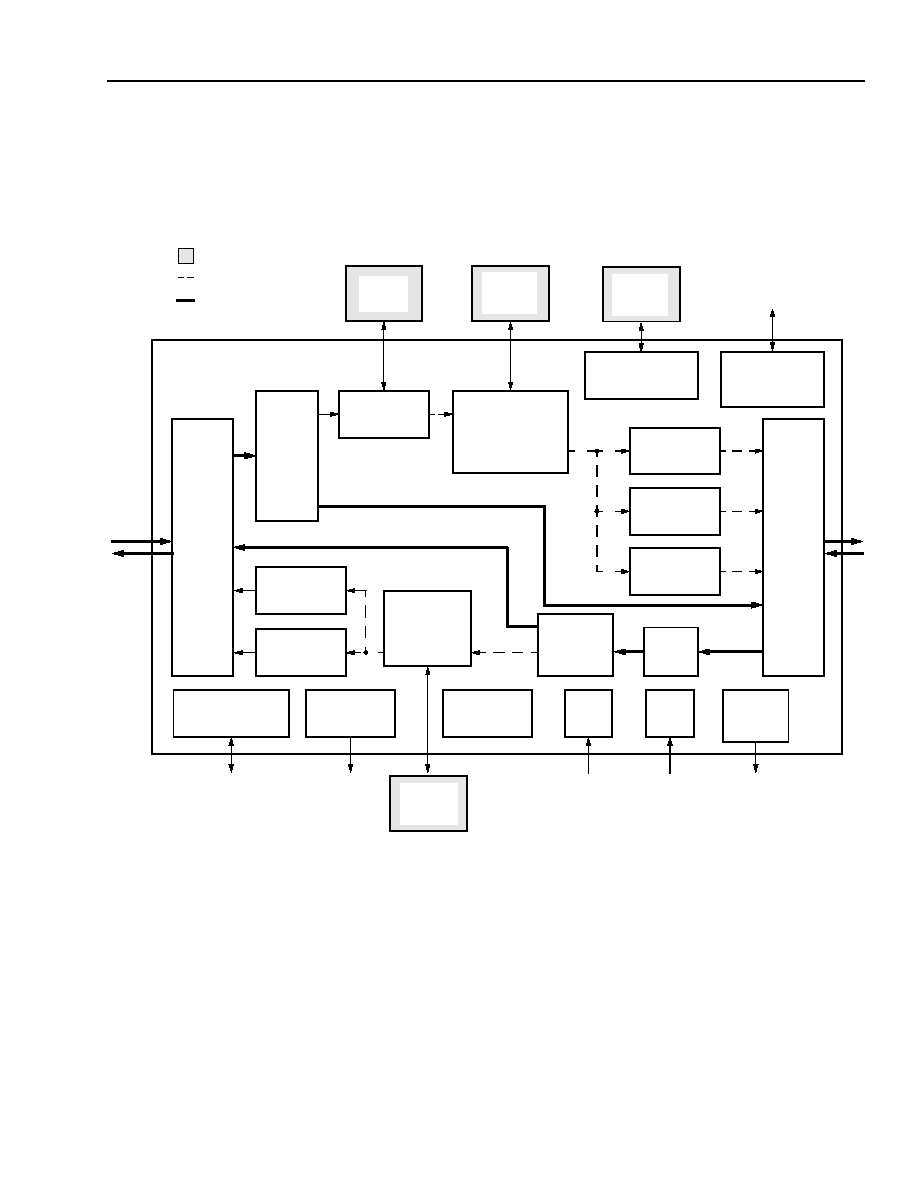
Block Diagram
Figure 1 presents a high-level block diagram of the TPAT640. Each of the internal blocks is briefly described in the
sections that follow.
5-9198(F)r.1
Figure 1. TPAT640 Block Diagram
UTOPIA Interface (UMI)
The UTOPIA interface block controls the transfer of ATM cells between the PI-ATM and multiple physical layer
devices (MPHYs) connected to it, via two full-duplex UTOPIA master interfaces and one full-duplex UTOPIA slave
interface. The master interfaces support one UTOPIA level 3 compatible interface operating independently at up to
104 MHz or two UTOPIA level 2 compatible interfaces operating independently at up to 52 MHz.
The UTOPIA interface block supports linear aggregation of ATM traffic up to 2.4 Gbits/s. Each UTOPIA interface
can be enabled independently. Receive parity checking can be enabled or disabled. Transmit parity generation can
be configured as odd or even. Each transmit interface can be configured to internally loopback cells to its receive
interface independently for diagnostic purposes.
iBWM
INGRESS
BANDWIDTH
MANAGER
LRI
INGRESS
HEADER LOOKUP
iVCT
INGRESS
VIRTUAL CONNECTION
TABLE MANAGER
UMI
UTOPIA
INTERFACE
eOAM
EGRESS
OAM PROCESSOR
eABR
EGRESS
ABR PROCESSOR
MPI
MICROPROCESSOR
TCT
TIME COUNTER
DFT
DESIGN FOR
TESTABILITY
ESI
ENHANCED
SERVICE
RST
RESET
WCD
WORLD
SCI
PI-SCHED
INTERFACE
UPC
POLICING
iOAM
INGRESS
OAM PROCESSOR
iABR
INGRESS
ABR PROCESSOR
eBWM
EGRESS
BANDWIDTH
MANAGER
eVCT
EGRESS
VIRTUAL
TABLE MANAGER
VSF
SUPPORT
FIFO
CNT
STATISTIC COUNTERS
JTG
TEST ACCESS PORT
AND
SYSTEM
TEST
UTOPIA
T
O
/F
ROM
M
P
HY DEV
I
C
E
S
MICROPROCESSOR
SYNCHRONIZATION
PULSE
SYSTEM RESET
SYSTEM CLOCK
ADJUNCT
DEVICE
T
O
/F
RO
M
PI-
S
HE
D I
C
DRIVER
CLOCK
INTERFACE
I/F
CONNECTION
SCAN CONTROLLER
EVCRAM
EGRESS
VC TABLES
MEMORY
SCRAM
STATISTIC
COUNTERS
MEMORY
IVCRAM
INGRESS
VC TABLES
MEMORY
LKRAM
LOOKUP
MEMORY
ZBT SSRAM
HEADER
CELL

4
4
Agere Systems Inc.
Product Brief
June 2001
High-Speed Switching ATM Layer Processor (PI-ATM)
TPAT640
Description
(continued)
The UTOPIA level 3 interface can be independently
configured to operate in 32-bit, 16-bit, or 8-bit mode,
with a standard or extended cell format and its own
contiguous UTOPIA poll address range to support up
to 62 MPHY devices.
For special cells (OAM and RM), the UTOPIA interface
block also checks (on receive) and inserts (on transmit)
the payload CRC-10 field.
Bandwidth Management (iBWM/eBWM)
The ingress/egress bandwidth management block mul-
tiplexes all cell sources together to produce a single
cell stream for subsequent processing. There are two
classes of cell sources: external and internal. External
cell sources are comprised of the interface termination
FIFOs. Internal cell sources include OAM cell insertion
FIFOs and microprocessor insertion FIFO. The band-
width management block organizes time slots into
external or internal and provides different cell selection
policies for them. The resulting ingress/egress cell
stream is processed by subsequent downstream
blocks.
Connection Lookup (LRI)
The connection look-up block performs ingress ATM
layer header processing. It maps the ingress port
address, VPI and VCI into one of the 1M virtual con-
nections supported by the PI-ATM. ATM cell recogni-
tion is also performed to identify idle/unassigned, user,
non-user, RM, and OAM cells. Cells with invalid lookup
will be discarded and the headers will be captured in
the ingress invalid cell FIFO.
Virtual Connection Table Management
(iVCT/eVCT)
The PI-ATM supports up to 1M virtual connections on
ingress and egress, using a virtual connection table.
Each (ingress and egress) connection table entry can
be configured as VP or VC switched. Each virtual path
supported by the PI-ATM requires one connection table
entry (configured as VP switched) which contains the
F4 OAM information for the VP. An additional connec-
tion table entry is required for each VC switched con-
nection within the VP. A VC switched connection table
entry contains F5 OAM information for the connection.
Each connection table entry contains a VP and VC
pointer. For VP switched connections, the VP pointer is
used to link all the VP entries together. The VC pointer
is used to link all the VC switched connections bundled
within the VP. For a VC switched connection table
entry, the VP pointer is used to locate the bundling VP.
The VC pointer is used to link all the VC switched con-
nections bundled in the same VP together.
For each arriving ingress and egress cell, the PI-ATM
performs a connection table access for the associated
connection. If the connection is VC switched, the bun-
dling VP connection is also accessed to support F4
OAM processing. An additional access is available to
support a periodic background process (for OAM and
policing) as well as microprocessor access to the con-
nection table.
The background process periodically accesses each
VP using the VP pointer chain. For each VP, it
accesses each bundled VC using the VC pointer chain.
Every connection table entry is accessed once each
0.5 s.
OAM Processing (iOAM/eOAM)
The OAM processing block can perform ITU-T I.610
compliant fault management (defect indication, loop-
back and continuity check) on all 1M connections. It
also performs performance monitoring on up to 511
flows (bidirectional performance monitoring on a con-
nection requires two flows) with on-chip data collection.
Each entry in the PI-ATM's ingress and egress virtual
connection table can be configured as a connection
end-point, segment source point, and/or segment sink
point for the termination of the appropriate F4 and F5
OAM cells.
When a fault is detected, the OAM background process
will generate downstream end-to-end AIS cells once
per second when the current connection is not config-
ured as a connection end point. The OAM background
process will generate upstream end-to-end RDI cells
once per second when the current connection is config-
ured as a connection end point.
Generation of continuity check cells can be globally
configured to conditionally insert CC cells (in the
absence of user cells for one second) or uncondition-
ally insert CC cells (once per second).
Forward loopback cells must be inserted under soft-
ware control. Backward loopback cells are captured by
the OAM unit. Detection and loopback of forward cells
at the appropriate connection or segment endpoint (or
optionally an intermediate point) is performed by the
OAM unit.

Agere Systems Inc.
5
Product Brief
June 2001
High-Speed Switching ATM Layer Processor (PI-ATM)
TPAT640
Description
(continued)
Performance monitoring and data collection are sup-
ported using an on-chip PM table. A PM table exists on
both ingress and egress. Up to 511 PM flows can be
simultaneously active. Connections are linked to an
active PM flow by assigning a non-null PM table index.
Activation/deactivation and system management cells
can be inserted and captured.
Policing (UPC)
Policing can be enabled or disabled on a per-connec-
tion basis. Two different policing configurations are
supported on a per-connection basis: normal (cell)
mode and GFR mode. A monitor mode can also be
enabled or disabled on a per-connection basis, which
prevents cell/frame discard independent of the policing
result. The range of policed rates supported extends
from 320 bits/s (1 cell/s) to a maximum rate of
2.685 Gbits/s.
In normal mode, the policing unit implements two
instances of the generic cell rate algorithm (GCRA) for
each connection to police cells for conformance to their
negotiated traffic contracts. It uses the virtual schedul-
ing algorithm outlined in ITU-T I.371 to determine con-
formance. The type of cell policed (none, CLP0, CLP1,
or all) and the policing action (drop nonconforming
cells, tag nonconforming cells, tag nonconforming
CLP0, and drop nonconforming CLP1, tag uncondition-
ally) can be independently configured for each GCRA
instance. This provides a wide variety of policing con-
figurations including all of the conformance definitions
specified in ATM Forum Traffic Management Specifica-
tion Version 4.1. A frame-based policing option can be
enabled or disabled on a per-connection basis which
causes all user cells to be discarded up to, but not
including, the next AAL5 end-of-frame cell after a polic-
ing cell discard. The operation of the two GCRA
instances can be made independent on a per-connec-
tion basis.
In GFCR mode, the policing unit implements two
instances of the frame generic cell rate algorithm
(F-GCRA) for each connection to police frames for con-
formance to their negotiated traffic contracts. F-GCRA
is used to test the first cell for conformance and pro-
cess the entire frame based on the first cells conform-
ance. The type of frame policed (none, CLP0, CLP1,
all) and the policing action (drop nonconforming
frames, tag nonconforming frames, virtually tag non-
conforming frames, tag unconditionally) can be inde-
pendently configured for each F-GCRA instance. In
addition, the policing unit performs a maximum frame
size check against a user configured maximum value.
User cells in excess of the maximum frame size are
discarded (excluding the AAL5 end-of-frame cell).
ABR Multicast Consolidation (iABR/eABR)
The ingress/egress ABR processing block performs
consolidation of backward ABR RM cells for up to 4K
multicast connections. Only one backward RM cell is
passed for each forward RM cell flowing in the opposite
path of the connection. The explicit rate (ER), CI, and
NI fields of the consolidated RM cells are merged into
the backward RM cell, which is allowed to pass.
PI-Sched Transmit/Receive Interface (SCI)
The transmit interface controls the transmission of cells
to the PI-Sched device. The transmit interface can be
configured to generate correct or incorrect cell error
checking codes for diagnostic purposes.
The receive interface controls the reception of cells
from the PI-Sched device. The receive interface
checks the incoming cells error checking code and
reports violations.
Subport FIFO (VSF)
The egress virtual subport FIFO block stores cells des-
tined for each subport and generates backpressure
information to the PI-Sched device via the ingress cell
header.
Header Translation
On egress, the ATM header's VPI (VP switching) or
VPI/VCI (VC switching) is translated using information
in the virtual connection table. The GFC field (for UNI
applications) can also be optionally translated or
passed.
Microprocessor Interface and Configuration
Registers (MPI)
The microprocessor interface block provides a simple,
synchronous, 33 MHz, 32-bit PCI target interface with
maskable interrupts. This allows an external processor
to access the PI-ATM for configuration, maintenance,
statistics, internal and external memory reads and
writes, as well as interrupt services. This block also
contains the global configuration registers.

Product Brief
June 2001
High-Speed Switching ATM Layer Processor (PI-ATM)
TPAT640
Agere Systems Inc. reserves the right to make changes to the product(s) or information contained herein without notice. No liability is assumed as a result of their use or application.
Copyright � 2001 Agere Systems Inc.
All Rights Reserved
Printed in U.S.A.
June 2001
PN00-036ATM
For additional information, contact your Agere Systems Account Manager or the following:
INTERNET:
http://www.agere.com
E-MAIL:
docmaster@micro.lucent.com
N. AMERICA:
Agere Systems Inc., 555 Union Boulevard, Room 30L-15P-BA, Allentown, PA 18109-3286
1-800-372-2447, FAX 610-712-4106 (In CANADA: 1-800-553-2448, FAX 610-712-4106)
ASIA PACIFIC: Agere Systems Singapore Pte. Ltd., 77 Science Park Drive, #03-18 Cintech III, Singapore 118256
Tel. (65) 778 8833, FAX (65) 777 7495
CHINA:
Agere Systems (Shanghai) Co., Ltd., 33/F Jin Mao Tower, 88 Century Boulevard Pudong, Shanghai 200121 PRC
Tel. (86) 21 50471212, FAX (86) 21 50472266
JAPAN:
Agere Systems Japan Ltd., 7-18, Higashi-Gotanda 2-chome, Shinagawa-ku, Tokyo 141, Japan
Tel. (81) 3 5421 1600, FAX (81) 3 5421 1700
EUROPE:
Data Requests: DATALINE: Tel. (44) 7000 582 368, FAX (44) 1189 328 148
Technical Inquiries: GERMANY: (49) 89 95086 0 (Munich), UNITED KINGDOM: (44) 1344 865 900 (Ascot),
FRANCE: (33) 1 40 83 68 00 (Paris), SWEDEN: (46) 8 594 607 00 (Stockholm), FINLAND: (358) 9 3507670 (Helsinki),
ITALY: (39) 02 6608131 (Milan), SPAIN: (34) 1 807 1441 (Madrid)
Description
(continued)
Enhanced Services Interface (ESI)
The enhanced services interface (ESI) block imple-
ments a 16-bit parallel interface between the PI-ATM
and an optional external device to support value-added
enhanced services. The PI-ATM reports a rich set of
events through this interface to support the implemen-
tation of off-chip statistics and diagnosis functions in
the external device.
Statistics Counters (CNT)
The statistics counters block maintains on-chip
per-device, per-port, and global error statistics, and
provides an interface for the microprocessor to access
the external per-connection statistics counters.
Time Counter (TCT)
The global time counter block generates all the signals
that are necessary for internal event synchronization. It
also generates the external synchronization pulse
GTSYNC.
World Clock (WCD)
The world clock driver block generates all of the clocks
needed in the PI-ATM, as well as the output PI-Sched
clocks and the ESI clock.
Reset Driver (RST)
The reset driver synchronizes an externally applied,
active-low, asynchronous reset pulse, and generates
all of the signals needed to reset the internal blocks of
the PI-ATM. Reset is applied synchronously on each of
the internal clock domains of the PI-ATM.
Design for Testability (DFT)
The design for testability block contains the built-in self
test (BIST) control circuit for the on-chip memories in
the PI-ATM.
JTAG Test Access Port (JTG)
The PI-ATM incorporates logic to support a standard
5-pin test access port (TAP), compatible with the IEEE
1149.1 standard (JTAG), used for boundary scan. TAP
contains instruction registers, data registers, and con-
trol logic. It is controlled externally by a JTAG bus mas-
ter. The TAP provides a board-level test capability for
the PI-ATM.