 | –≠–ª–µ–∫—Ç—Ä–æ–Ω–Ω—ã–π –∫–æ–º–ø–æ–Ω–µ–Ω—Ç: TRCV0110G | –°–∫–∞—á–∞—Ç—å:  PDF PDF  ZIP ZIP |

Data Sheet
March 28, 2002
TRCV0110G 10 Gbits/s Limiting Amplifier
Clock Recovery, 1:16 Data Demultiplexer
Features
s
Integrated limiting amplifier with 8 mV sensitivity at
1 x 10
≠10
bit error rate (BER)
s
Integrated clock recovery and 1:16 data demulti-
plexer (deMUX)
s
Supports standard OC-192/STM-64 data rate of
9.9532 Gbits/s up through forward error correction
(FEC) rate of 10.709 Gbits/s as well as Ethernet
rate of 10.3 Gbits/s
s
Single 3.3 V power supply
s
Additional high-speed data input for system loop-
back operation
s
Standard low-voltage differential signaling (LVDS)
deMUX data and clock outputs
s
CMOS I/Os compatible with LVTTL signaling
s
Available in a 177-ball CBGA package
s
Jitter tolerance compliant with the following:
-- Telcordia TechnologiesTM GR-253 CORE
-- ITU-T G.825
-- ITU-T G.958
Applications
s
SONET/SDH optical modules
s
SONET/SDH line termination equipment
s
SONET/SDH test equipment
s
Ethernet 10 Gbit physical layer applications
Description
The Agere Systems Inc. TRCV0110G device
integrates a limiting amplifier combined with a clock
recovery circuit that feeds a data deMUX for use in
10 Gbits/s high-speed communications systems.
Additional features include an auxiliary clock output
and a reference clock input that can be either divided
by 16 or divided by 64. The TRCV0110G can be
operated within the standard OC192/STM64 data
rate of 9.9532 GHz and the FEC rate of 10.7092
Gbits/s.

Table of Contents
Contents
Page
2
Agere Systems Inc.
Data Sheet
March 28, 2002
Clock Recovery, 1:16 Data Demultiplexer
TRCV0110G 10 Gbits/s Limiting Amplifier
Features .................................................................................................................................................................... 1
Applications ............................................................................................................................................................... 1
Description................................................................................................................................................................. 1
Block Diagram......................................................................................................................................................... 3
Ball Information.......................................................................................................................................................... 4
CBGA Diagram ....................................................................................................................................................... 4
Ball Assignments .................................................................................................................................................... 5
Ball Description ....................................................................................................................................................... 7
Functional Overview ................................................................................................................................................ 11
FEC Rate Support ................................................................................................................................................... 11
High-Speed Data Inputs .......................................................................................................................................... 11
Limiting Amplifier Operation .................................................................................................................................. 11
Loopback Data Input............................................................................................................................................. 12
Clock Recovery Operation....................................................................................................................................... 12
CDR Input Jitter Tolerance ...................................................................................................................................... 13
PLL Lock Indication ................................................................................................................................................. 14
Demultiplexer Operation.......................................................................................................................................... 16
Demultiplexer Data Mute (MUTEDMXN) .............................................................................................................. 16
CK622P/N Output Mute (MUTE622N) .................................................................................................................. 16
CKOP/N Output Frequency Select (FREQCKO) .................................................................................................. 16
CKOP/N Output Mute (MUTECKON) ...................................................................................................................16
Reset (RESETN)................................................................................................................................................... 16
Absolute Maximum Ratings.....................................................................................................................................17
Handling Precautions .............................................................................................................................................. 17
Recommended Operating Conditions ..................................................................................................................... 17
Electrical Characteristics ......................................................................................................................................... 18
LVDS, CMOS, and CML Input and Output Pins ................................................................................................... 18
Timing Characteristics ............................................................................................................................................. 20
Output Timing ....................................................................................................................................................... 20
Reference Frequency (REFCLKP/N, REFFREQ) (Standard SONET Rate)......................................................... 21
Reference Frequency (REFCLKP/N, REFFREQ) (FEC Rate) ............................................................................. 21
Reference Frequency (REFCLKP/N, REFFREQ) (Ethernet Rate) ....................................................................... 21
Packaging Characteristics ....................................................................................................................................... 22
Package Crush Characteristics............................................................................................................................. 22
CBGA Package Information .................................................................................................................................. 22
PWB Design Information....................................................................................................................................... 22
Assembly Information ...........................................................................................................................................23
Reference Materials.............................................................................................................................................. 23
Package Diagram--177-Ball CBGA (Bottom View) .............................................................................................. 24
Ordering Information................................................................................................................................................ 25
Agere Systems Inc.
3
Data Sheet
March 28, 2002
Clock Recovery, 1:16 Data Demultiplexer
TRCV0110G 10 Gbits/s Limiting Amplifier
Description
(continued)
Block Diagram
0363.a(F)
Note: Diagram is representative of device functionality and conceptual signal flow. Internal implementation details may be different than shown.
Figure 1. TRCV0110G Block Diagram
TO DIGITAL LOGIC
D0P
D0N
D1P
D1N
D15P
D15N
CKOP
CKON
REFCLKP
REFCLKN
PHASE/
VCO
1
:
1
6
DEM
U
L
T
I
P
L
EXER
CHARGE
LFP
LFN
OUT
P
UT
REG
I
ST
ER
RESETN
MUTECKON
MUTEDMXN
ENLBDN
LCKLOSSN
MUTECKO
DIVIDE
SAMPLER
CIRCUIT
FREQ./
LOCK
PUMP
BY 16
0
1
1
0
DATAP
DATAN
0
1
LBDP
LBDN
RREFLVDS
RREFVCO
REFFREQ
FREQCKO
DIVIDE
BY 1
OR
DIVIDE
BY 4
CK622P
CK622N
MUTE622N
0
1
RECOVERED
DATA
RECOVERED
CLOCK
RREFCP
DETECT
FECN
LA
ACM
4
Agere Systems Inc.
Data Sheet
March 28, 2002
Clock Recovery, 1:16 Data Demultiplexer
TRCV0110G 10 Gbits/s Limiting Amplifier
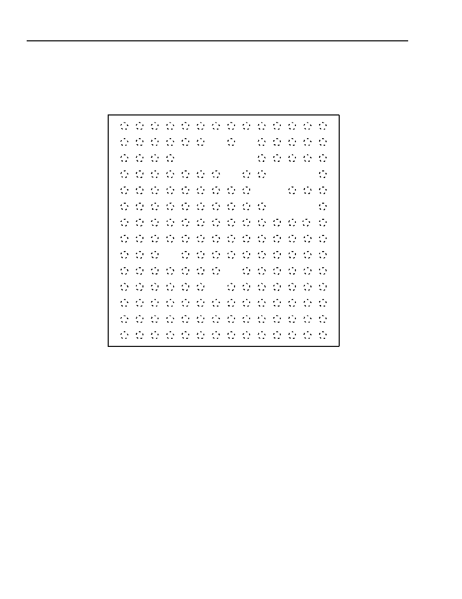
Ball Information
CBGA Diagram
0641.a(F)
Figure 2. Ball Diagram of 177-Ball CBGA
D
E
F
G
H
J
K
L
N
P
C
B
A
M
2
3
4
5
6
7
8
9
10
11
12
13
14
1
TOP VIEW

Agere Systems Inc.
5
Data Sheet
March 28, 2002
Clock Recovery, 1:16 Data Demultiplexer
TRCV0110G 10 Gbits/s Limiting Amplifier
Ball Information
(continued)
Ball Assignments
Table 1. Ball Assignments for 177-Ball CBGA by Ball Number Order
Note: -- refers to no ball. A ball has been removed for routing purposes.
Ball
Signal Name
Ball
Signal Name
Ball
Signal Name
Ball
Signal Name
A1
GND
C1
ENLBDN
E1
D1N
G1
D2P
A2
V
CCD
C2
RREFLVDS
E2
D1P
G2
GND
A3
FECN
C3
V
CCD
E3
GND
G3
GND
A4
REFFREQ
C4
GND
E4
GND
G4
GND
A5
FREQCKO
C5
--
E5
GND
G5
GND
A6
GND
C6
--
E6
GND
G6
GND
A7
DATAN
C7
--
E7
GND
G7
GND
A8
GND
C8
--
E8
GND
G8
GND
A9
DATAP
C9
--
E9
GND
G9
GND
A10
GND
C10
V
CCLA
E10
--
G10
V
CCA
A11
GND
C11
V
CCD
E11
--
G11
V
CCD
A12
GND
C12
GND
E12
GND
G12
V
CCA
A13
GND
C13
GND
E13
GND
G13
GND
A14
GND
C14
GND
E14
GND
G14
GND
B1
MUTEDMXN
D1
D0N
F1
GND
H1
D2N
B2
RESETN
D2
D0P
F2
GND
H2
GND
B3
LCKLOSSN
D3
GND
F3
GND
H3
GND
B4
MUTECKON
D4
V
CCD
F4
V
CCD
H4
V
CCD
B5
MUTE622N
D5
GND
F5
GND
H5
V
CCD
B6
GND
D6
V
CCD
F6
GND
H6
GND
B7
--
D7
V
CCLA
F7
GND
H7
GND
B8
GND
D8
--
F8
GND
H8
GND
B9
--
D9
ACM
F9
GND
H9
GND
B10
GND
D10
GND
F10
GND
H10
GND
B11
GND
D11
--
F11
--
H11
V
CCA
B12
GND
D12
--
F12
--
H12
GND
B13
GND
D13
--
F13
--
H13
GND
B14
GND
D14
LBDP
F14
LBDN
H14
RREFCP

6
Agere Systems Inc.
Data Sheet
March 28, 2002
Clock Recovery, 1:16 Data Demultiplexer
TRCV0110G 10 Gbits/s Limiting Amplifier
Ball Information
(continued)
Ball Assignments
(continued)
Table 1. Ball Assignments for 177-Ball CBGA by Ball Number Order (continued)
Note: -- refers to no ball. A ball has been removed for routing purposes.
Ball
Signal Name
Ball
Signal Name
Ball
Signal Name
Ball
Signal Name
J1
D3P
K8
--
M1
D4N
N8
D13N
J2
GND
K9
GND
M2
D5P
N9
D14N
J3
GND
K10
GND
M3
GND
N10
CKON
J4
--
K11
GND
M4
D7N
N11
CK622N
J5
GND
K12
GND
M5
GND
N12
REFCLKN
J6
GND
K13
GND
M6
D10N
N13
GND
J7
GND
K14
LFP
M7
D12P
N14
GND
J8
V
CCD
L1
D4P
M8
GND
P1
GND
J9
GND
L2
GND
M9
D15N
P2
GND
J10
GND
L3
GND
M10
GND
P3
D6N
J11
V
CCD
L4
D7P
M11
GND
P4
D8N
J12
V
CCA
L5
GND
M12
GND
P5
D9N
J13
GND
L6
GND
M13
GND
P6
D11P
J14
LFN
L7
--
M14
GND
P7
D11N
K1
D3N
L8
GND
N1
GND
P8
D13P
K2
GND
L9
D15P
N2
D5N
P9
D14P
K3
GND
L10
GND
N3
D6P
P10
CKOP
K4
GND
L11
GND
N4
D8P
P11
CK622P
K5
V
CCD
L12
GND
N5
D9P
P12
REFCLKP
K6
GND
L13
GND
N6
D10P
P13
GND
K7
V
CCD
L14
RREFVCO
N7
D12N
P14
GND
Agere Systems Inc.
7
Data Sheet
March 28, 2002
Clock Recovery, 1:16 Data Demultiplexer
TRCV0110G 10 Gbits/s Limiting Amplifier
Ball Information
(continued)
Ball Description
Note: In Table 2, when operating the TRCV0110G device at the OC-192/STM-64 rate, 10 Gbits/s should be
interpreted as 9.95328 Gbits/s. When operating the TRCV0110G device at the RS FEC OC-192/STM-64
rate, 10 Gbits/s should be interpreted as 10.709 Gbits/s. When operating the TRCV0110G device at the
Ethernet rate, 10 Gbits/s should be interpreted as 10.3125 Gbits/s.
Table 2. Ball Descriptions--10 Gbits/s and Related Signals
Ball
Symbol
*
* Differential pins are indicated by the P and N suffixes. For nondifferential pins, N at the end of the symbol name designates active-low.
Type
I = input, O = output. I
u
= an internal pull-up resistor on this pin, I
d
= an internal pull-down resistor on this pin, I
t
= an internal termination
resistance of 50
on this pin.
Level
Name/Description
A9
A7
DATAP
DATAN
I
t
High-speed
Analog
Limiting Amp Input for 10 Gbits/s CML. Primary data input.
Note: This data input will scale when operating at different
rates.
D14
F14
LBDP
LBDN
I
t
CML
Loopback Data Input for 10 Gbits/s CML. Use this input for
system loopback data.
Note: This data input will scale when operating at different
rates.
A3
FECN
I
u
CMOS
FEC Rate (Active-Low). Selects between two operating rate
ranges within the OC-192/STM-64 rate of 9.9532 GHz and
the FEC rate of 10.7092 GHz.
0 = Will extend the operating range out to the FEC rate of
10.7092 GHz.
1 or no connection = OC-192/STM-64 rate of 9.9532 GHz to
the Ethernet rate of 10.3 GHz.
Note: An input and output SONET/SDH clock and data rates
will scale when operating at different rates.
C1
ENLBDN
I
u
CMOS
Enable LBDP/N Inputs (Active-Low). Selects LBDP/N as
data source rather than primary data input.
0 = Select LBDP/N.
1 or no connection = Select DATAP/N.
L14
RREFVCO
I
Analog
Resistor Reference VCO. VCO bias reference resistor.
Connect a 1.2 k
resistor to V
CCA
.
H14
RREFCP
I
Analog
Resistor Reference Charge Pump. Charge pump bias
resistor. Connect a 1.2 k
resistor to V
CCA
.
B3
LCKLOSSN
O
CMOS
Loss of Lock (Active-Low).
0 = Phase-locked loop (PLL) out of lock.
K14
J14
LFP
LFN
O
Analog
Loop Filter PLL. Connect LFP and LFN to loop filter (see
Figure 5 on page 12).
8
Agere Systems Inc.
Data Sheet
March 28, 2002
Clock Recovery, 1:16 Data Demultiplexer
TRCV0110G 10 Gbits/s Limiting Amplifier
Ball Information
(continued)
Ball Description
(continued)
Note: In Table 3, when operating the TRCV0110G device at the OC-192/STM-64 rate, 155 Mbits/s should be
interpreted as 155.52 Mbits/s. When operating the TRCV0110G device at the RS FEC OC-192/STM-64
rate, 155 Mbits/s should be interpreted as 167.33 Mbits/s.
Table 3. Ball Descriptions--622.08 Mbits/s and Related Signals
Ball
Symbol
*
* Differential pins are indicated by the P and N suffixes. For nondifferential pins, N at the end of the symbol name designates active-low.
Type
I = input, O = output. I
u
= an internal pull-up resistor on this pin, I
d
= an internal pull-down resistor on this pin, I
t
= an internal termination
resistance of 50
on this pin.
Level
Name/Description
L9
D15P
O
LVDS
Data Output (622 Mbits/s). 622 Mbits/s differential data output.
D15 is the most significant bit and is the first received on the
DATAP/N or LBDP/N input.
Note: This data rate will scale when operating at different rates.
M9
D15N
O
LVDS
P9
D14P
O
LVDS
N9
D14N
O
LVDS
P8
D13P
O
LVDS
N8
D13N
O
LVDS
M7
D12P
O
LVDS
N7
D12N
O
LVDS
P6
D11P
O
LVDS
P7
D11N
O
LVDS
N6
D10P
O
LVDS
M6
D10N
O
LVDS
N5
D9P
O
LVDS
P5
D9N
O
LVDS
N4
D8P
O
LVDS
P4
D8N
O
LVDS
L4
D7P
O
LVDS
M4
D7N
O
LVDS
N3
D6P
O
LVDS
P3
D6N
O
LVDS
M2
D5P
O
LVDS
N2
D5N
O
LVDS
L1
D4P
O
LVDS
M1
D4N
O
LVDS
J1
D3P
O
LVDS
K1
D3N
O
LVDS
G1
D2P
O
LVDS
H1
D2N
O
LVDS
E2
D1P
O
LVDS
E1
D1N
O
LVDS
D2
D0P
O
LVDS
D1
D0N
O
LVDS

Agere Systems Inc.
9
Data Sheet
March 28, 2002
Clock Recovery, 1:16 Data Demultiplexer
TRCV0110G 10 Gbits/s Limiting Amplifier
Ball Information
(continued)
Ball Description
(continued)
Table 3. Ball Descriptions--622.08 Mbits/s and Related Signals (continued)
Ball
Symbol
*
* Differential pins are indicated by the P and N suffixes. For nondifferential pins, N at the end of the symbol name designates active-low.
Type
I = input, O = output. I
u
= an internal pull-up resistor on this pin, I
d
= an internal pull-down resistor on this pin, I
t
= an internal termination
resistance of 50
on this pin.
Level
Name/Description
B1
MUTEDMXN
I
u
CMOS
Mute DeMUX Parallel Output Data (Active-Low). Forces all
demultiplexer output data D[15:0] to a logic-low level.
0 = Demultiplexer output muted.
1 or no connection = Normal operation.
B5
MUTE622N
I
u
CMOS
Mute CK622P/N Clock Output (Active-Low). Forces
CK622P/N to logic low when MUTE622N is active.
0 = Muted.
1 or no connection = Enabled.
A5
FREQCKO
I
u
CMOS
CKO Frequency Select. Selects 155 MHz or 622 MHz clock
frequency on CLKOP/N.
0 = 155 MHz CKOP/N.
1 or no connection = 622 MHz CKOP/N.
B4
MUTECKON
I
u
CMOS
Mute CKOP/N Clock Output (Active-Low). Forces CKOP/N
to logic low when MUTECKON is active.
0 = Muted.
1 or no connection = Enabled.
A4
REFFREQ
I
u
CMOS
Reference Frequency Select. Sets clock and data recovery
(CDR) PLL to accept 155 MHz, or 622 MHz reference
frequency on REFCLKP/N.
0 = 155 MHz REFCLKP/N.
1 or no connection = 622 MHz REFCLKP/N.
P12
N12
REFCLKP
REFCLKN
I
LVDS
Reference Clock Input (155 MHz, or 622 MHz).
Note: This clock frequency must scale when operating at
different rates.
P11
N11
CK622P
CK622N
O
LVDS
Recovered Clock Output (622 MHz). 622 MHz recovered
differential clock output. Pins are active but forced to
differential logic low when MUTE622N = 0.
Note: This clock frequency will scale when operating at
different rates.
P10
N10
CKOP
CKON
O
LVDS
Recovered Clock Output (155 MHz or 622 MHz).
Selectable 155 MHz or 622 MHz recovered differential clock
output. Pins are active but forced to differential logic low
when MUTECKON = 0.
Note: These clock frequencies will scale when operating at
different rates. Use the FREQCKO pin to select the
frequency.
C2
RREFLVDS
I
Analog
Resistor Reference LVDS. LVDS bias reference resistor.
Connect a 1.5 k
resistor to V
CCD
.
D9
ACM
I
Analog
Amplifier Common Mode. Input amplifier common bias
point. Place a 0.047 µF RF bypass capacitor to GND.

10
Agere Systems Inc.
Data Sheet
March 28, 2002
Clock Recovery, 1:16 Data Demultiplexer
TRCV0110G 10 Gbits/s Limiting Amplifier
Ball Information
(continued)
Ball Description
(continued)
Table 4. Ball Descriptions--Reset
Table 5. Ball Descriptions--Power
Note: V
CCLA,
V
CCA
, and V
CCD
have the same dc value, which is represented as V
CC
unless otherwise specified.
However, high-frequency filtering is suggested between the individual connections to a common supply.
Ball
Symbol
*
* Differential pins are indicated by the P and N suffixes. For non-differential pins, N at the end of the symbol name designates active-low.
Type
I = input, O = Output. I
u
= an internal pull-up resistor on this pin, I
d
= an internal pull-down resistor on this pin, I
t
= an internal termination
resistance of 50
on this pin.
Level
Name/Description
B2
RESETN
I
u
CMOS
Reset (Active-Low). Resets all synchronous logic. During a
reset, the true data outputs are in the low state and the
barred data outputs are in the high state. Reset must be held
active low for a minimum of 500 ns while the internal
oscillator is active.
0 = Reset.
1 or no connection = Normal operation.
Ball
Symbol
*
* Differential pins are indicated by the P and N suffixes. For nondifferential pins, N at the end of the symbol name designates active-low.
Type
I = input, O = output. I
u
= an internal pull-up resistor on this pin, I
d
= an internal pull-down resistor on this pin, I
t
= an internal termination
resistance of 50
on this pin.
Level
Name/Description
G10, G12, H11, J12
V
CCA
I
Power
Analog Power Supply (3.3 V).
C10, D7
V
CCLA
I
Power
Limiting Amp Analog Power Supply (3.3 V).
A2, C3, C11, D4, D6,
F4, G11, H4, H5, J8,
J11, K5, K7
V
CCD
I
Power
Digital Power Supply (3.3 V).
A1, A6, A8, A10--A14,
B6, B8, B10--B14, C4,
C12--C14, D3, D5,
D10, E3--E9,
E12--E14,
F1--F3,
F5--F10,
G2--G9, G13, G14,
H2, H3, H6--H10, H12,
H13, J2, J3, J5--J7,
J9, J10, J13, K2--K4,
K6, K9--K13, L2, L3,
L5, L6, L8, L10--L13,
M3, M5, M8,
M10--M14, N1, N13,
N14, P1, P2, P13, P14
GND
I
Ground
Ground.
Agere Systems Inc.
11
Data Sheet
March 28, 2002
Clock Recovery, 1:16 Data Demultiplexer
TRCV0110G 10 Gbits/s Limiting Amplifier
Functional Overview
The TRCV0110G performs the data detection, clock recovery, and 1:16 demultiplexing operations required to
support 10 Gbits/s
1
OC-192/STM-64 applications compliant with Telcordia Technologies and ITU standards. One
of two high-speed inputs can be selected as the data source. A PLL recovers the clock which is used to retime the
data. A 1:16 data demultiplexer performs the serial-to-parallel conversion and generates 16 parallel outputs at a
622 Mbits/s. The parallel output data is aligned to a 622 MHz clock derived from the 10 GHz recovered clock.
FEC Rate Support
The TRCV0110G will support both the normal OC-192/STM-64 rate of 9.9532 GHz and the forward error
correction (FEC) rate of 10.7092 GHz. The FECN pin selects the rate range at which the part is operated.
Throughout this document, the specifications are given in terms of the normal operating rate only. All frequency-
based specifications are to be multiplied by the appropriate scaling factor when not operating at the OC-192/
STM64 rate. All time-based specifications, with the exception of electrical signal rise and fall times, are also to be
multiplied by the appropriate scaling factor. For example, a reference clock would need to be applied at
167.33 MHz or 669.32 MHz (a multiplication factor of 255/237) for the parallel data interface to operate at
669.32 MHz when FECN = 0.
High-Speed Data Inputs
Limiting Amplifier Operation
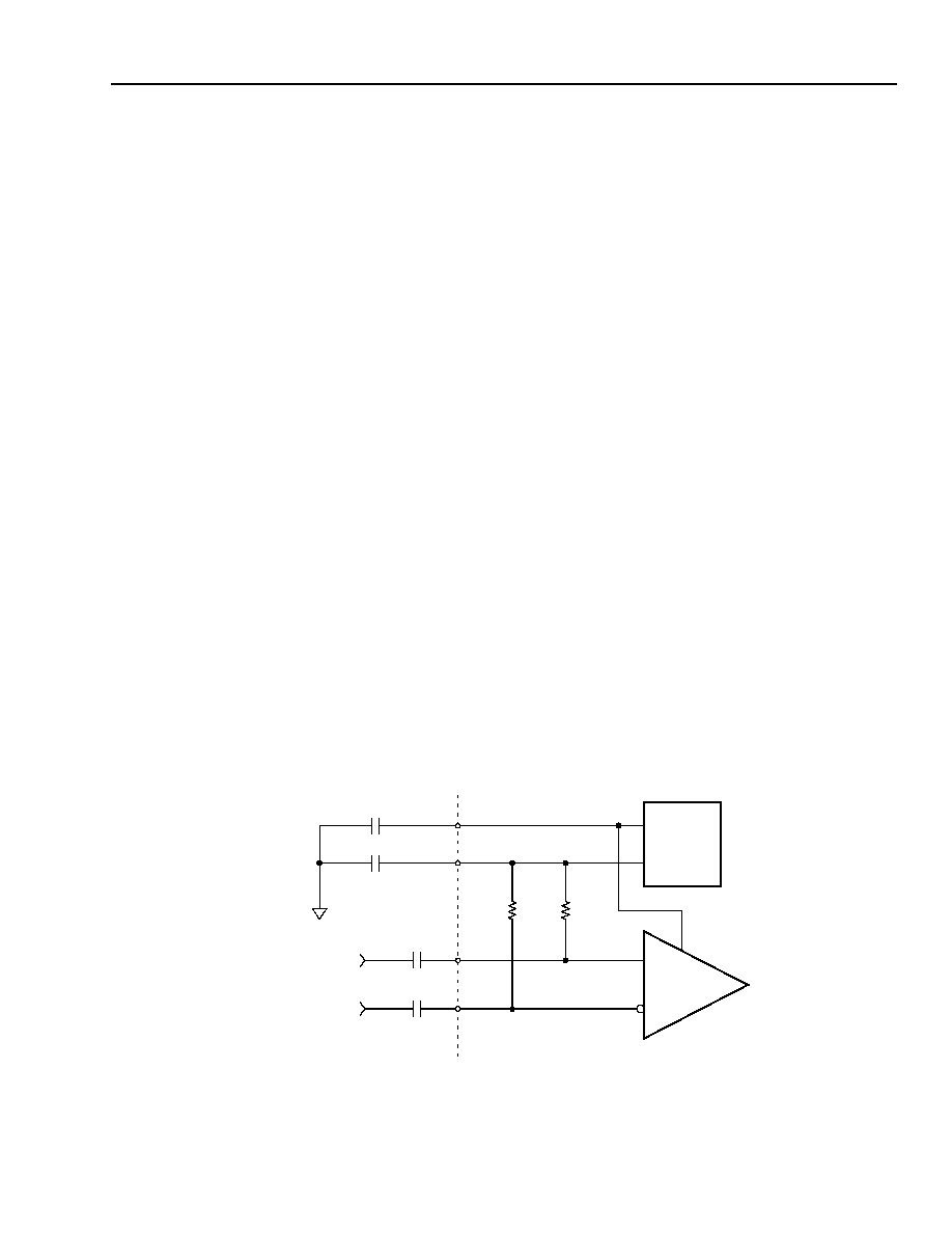
The TRCV0110G data input circuit contains a limiting amplifier that has approximately 40 dB of voltage gain. As
shown in Figure 3, the DATAP/N inputs should be ac-coupled. These ac-coupling capacitors are typically included
inside the optical receiver package. For applications requiring ac-coupling external to the O/E device, insert low
ESR 0.047
µ
F capacitors in the transmission line path. These capacitors should be chosen such that their size is
similar to the transmission line width in order to minimize the parasitic effects of larger than necessary pad sizes.
The 50
transmission lines are terminated with on-chip 50
resistors. The ACM pin should be connected with a
low inductance, low ESR 0.047
µ
F capacitor to ground. This capacitor provides an RF bypass for common-mode
noise that may be present on the data input pins. This capacitor as well as V
CCLA
decoupling capacitors should be
mounted as close as possible to the device package to avoid excess board trace inductance. Please refer to
Table 13 on page 18
,
for input sensitivity and other critical input specifications.
0364.a(F)
Figure 3. Data Input Circuit
1. The OC-192/STM-64 data rate of 9.95328 Gbits/s is typically approximated as 10 Gbits/s in this document when referring to the application
rate. Similarly, the low-speed parallel interface data rate of 622.08 Mbits/s is typically approximated as 622 Mbits/s. The exact frequencies
are used only when necessary for clarity.
50
50
INPUT
DATAP
DATAN
ACM
0.047
µ
F
0.047
µ
F
FROM
TIA
LIMITING
AMPLIFIER
BIAS
0.047
µ
F
0.1
µ
F
V
CCLA
12
Agere Systems Inc.
Data Sheet
March 28, 2002
Clock Recovery, 1:16 Data Demultiplexer
TRCV0110G 10 Gbits/s Limiting Amplifier
High-Speed Data Inputs
(continued)
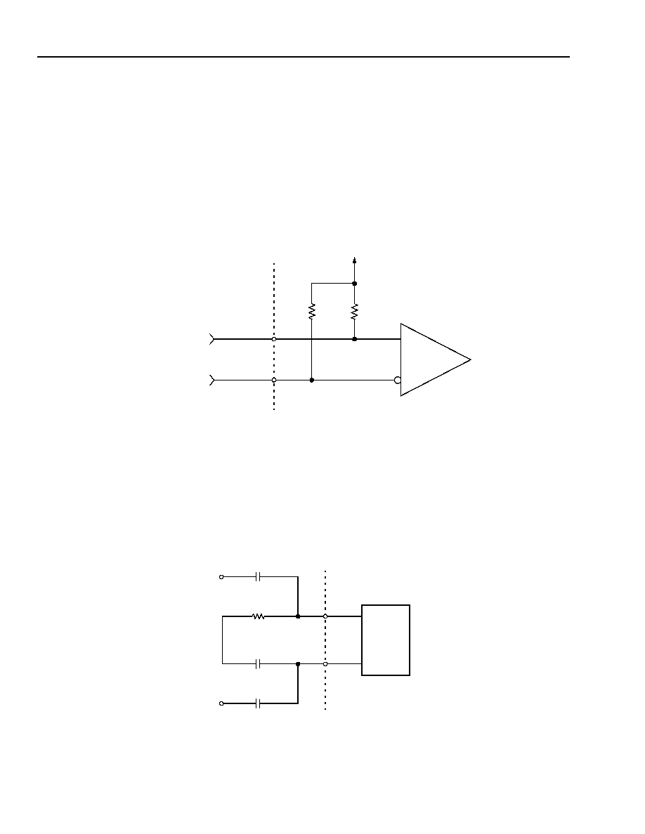
Loopback Data Input
The second high-speed input in the TRCV0110G is for system loopback operation. When mated with Agere's
TTRN0110G, the high-speed loopback data output can be direct coupled into the TRCV0110G loopback data input
pins LBDP and LBDN. During this mode of operation, parallel low-speed data coming from the users application
(typically a line card or transponder module) can be serialized through the TTRN0110G and redirected through the
high-speed loopback data input port of the TRCV0110G. The TRCV0110G would then recover the clock and dese-
rialize the data to be received by the users application. The loopback data flow is controlled by the ENLBDN pins
on both devices.
0366.a(F)
Figure 4. Loopback Data Input Circuit
Clock Recovery Operation
The clock and data recovery (CDR) circuit uses a PLL to extract the clock and retime the 10 Gbits/s data. The
TRCV0110G uses an external loop filter that is described below in Figure 5. A 622 MHz clock derived from the
recovered clock is available as an output at CK622P/N. A 622 MHz or 155 MHz clock derived from the recovered
clock is available as an auxiliary output at CKOP/N.
2245(F)
Figure 5. TRCV0110G Loop Filter
LBDP
50
50
V
CCD
LBDN
FROM TTRN0110G
LOOPBACK OUTPUTS
LOOPBACK
INPUT
160
V
CCA
5 pF
V
CCA
5 pF
0.01
µ
F
PLL
LFP
LFN
Agere Systems Inc.
13
Data Sheet
March 28, 2002
Clock Recovery, 1:16 Data Demultiplexer
TRCV0110G 10 Gbits/s Limiting Amplifier
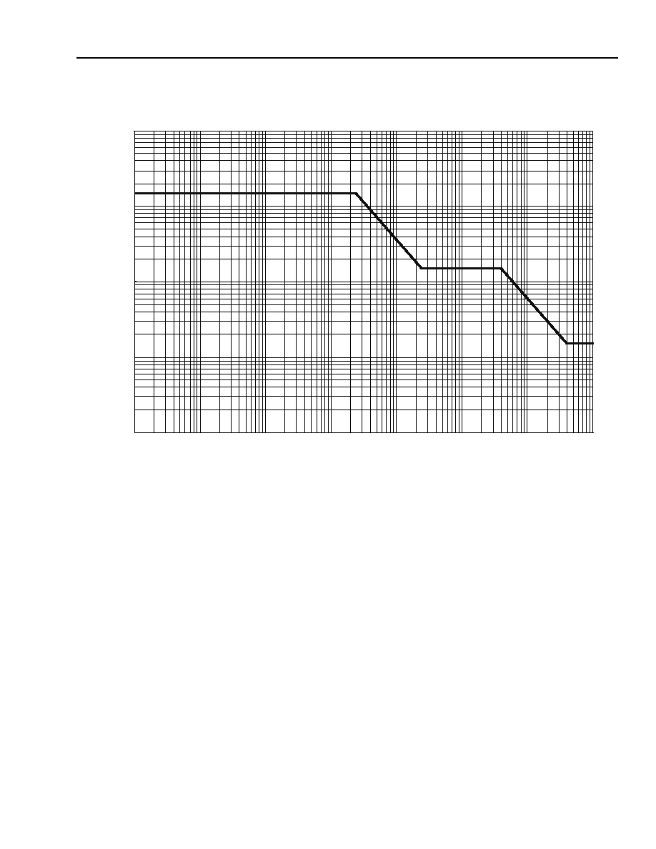
CDR Input Jitter Tolerance
0365.a(F)
Figure 6. Receive Jitter Tolerance Mask
0.01
0.1
1
10
100
0.001
0.01
0.1
1
10
100
1000
10000
Modulation Frequency (KHz)
M
odul
ati
o
n
A
m
p
l
i
t
ude
(
U
I)
14
Agere Systems Inc.
Data Sheet
March 28, 2002
Clock Recovery, 1:16 Data Demultiplexer
TRCV0110G 10 Gbits/s Limiting Amplifier
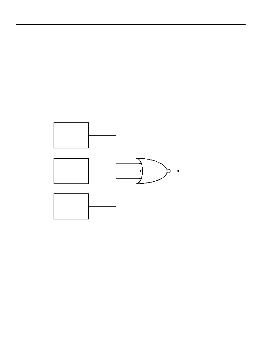
Lock Detect
By the behavior of the LCKLOSSN pin the user can identify three possible lost-of-lock scenarios. If desired, the
user can configure the TRCV0110G to lock directly to the REFCLK input during any of these conditions. See the
TRCV0110G LCKLOSSN application note.
s
The TRCV0110G contains a frequency detect circuit that compares the frequency of the internal VCO to the
REFCLK. LCKLOSSN transitions low if the frequencies differ by approximately +/-400ppm.
s
The TRCV0110G contains a LOS detect circuit that monitors the amplitude of the incoming serial data.
LCKLOSSN transitions low if the amplitude of the incoming data signal falls below an internal preset threshold.
s
The TRCV0110G contains a Transition detect circuit that monitors for transitions occuring on the LBD inputs.
LCKLOSSN transitions low if no transitions appear on the LBD inputs.
Note: This mode of detection is only valid when dc coupling the loopback inputs.
2246(F)
Figure 7. LCKLOSSN Modes of Operation
FREQUENCY
DETECTOR
LOSA
DETECTOR
TRANSITION
DETECTOR
LCKLOSSN
Agere Systems Inc.
15
Data Sheet
March 28, 2002
Clock Recovery, 1:16 Data Demultiplexer
TRCV0110G 10 Gbits/s Limiting Amplifier
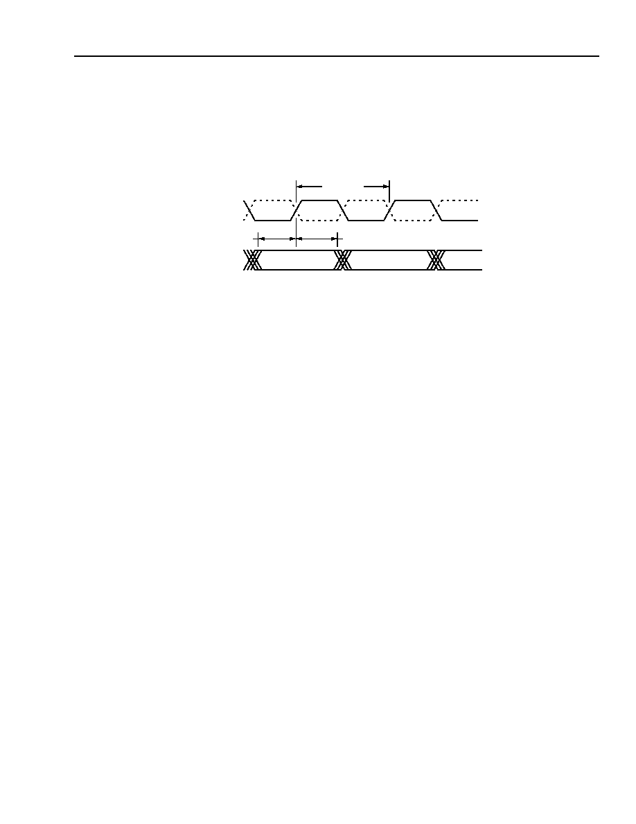
Demultiplexer Operation
The serial 10 Gbits/s data is clocked into a 1:16 demultiplexer by the recovered 10 GHz clock. The demultiplexed
parallel data is retimed with a 622 MHz clock that is derived from the recovered clock. The relationship between
the serial input data and the parallel D[15:0] bits is given in Figure 8. D15 is the bit that was received first in time in
the serial input data stream.
0367.a(F)
Figure 8. DeMUX Clock to Output Data Relationship
Demultiplexer Data Mute (MUTEDMXN)
Setting the MUTEDMXN = 0 mutes the data going into the demultiplexer and forces all zeros to appear at the par-
allel outputs D[15:0].
CK622P/N Output Mute (MUTE622N)
The 622 MHz clock output CK622P/N can be forced to logic low by setting MUTE622N, which is an active-low
CMOS input with a pull-up resistor. A ground or logic low applied to MUTE622N mutes the CK622P/N output.
CKOP/N Output Frequency Select (FREQCKO)
Either a 155 MHz or 622 MHz clock output can be selected on the CKOP/N pins. A ground or logic low applied to
FREQCKO selects a 155 MHz clock to appear on the CKO output. A logic high or no connection selects a 622
MHz clock to appear on the CKO output.
CKOP/N Output Mute (MUTECKON)
The clock output CKOP/N can be forced to logic low by setting MUTECKON, which is an active-low CMOS input
with a pull-up resistor. A ground or logic low applied to MUTECKPN mutes the CKOP/N output.
Reset (RESETN)
The RESETN signal must be held active low for a minimum of 500 ns when the internal VCO is active and running,
in order for the internal logic to be completely reset.
CK622P/N
D[15:0]P/N
DATA 1
tDD1
tDD2
tPERIOD
DATA 3
DATA 2

16
Agere Systems Inc.
Data Sheet
March 28, 2002
Clock Recovery, 1:16 Data Demultiplexer
TRCV0110G 10 Gbits/s Limiting Amplifier
Absolute Maximum Ratings
Stresses in excess of the absolute maximum ratings can cause permanent damage to the device. These are abso-
lute stress ratings only. Functional operation of the device is not implied at these or any other conditions in excess
of those given in the operational sections of the data sheet. Exposure to absolute maximum ratings for extended
periods can adversely affect device reliability.
Table 6. Absolute Maximum Ratings
Handling Precautions
Although protection circuitry has been designed into this device, proper precautions should be taken to avoid expo-
sure to electrostatic discharge (ESD) during handling and mounting. Agere Systems employs a human-body model
(HBM) and charged-device model (CDM) for ESD-susceptibility testing and protection design evaluation. ESD volt-
age thresholds are dependent on the circuit parameters used in the defined model. No industrywide standard has
been adopted for the CDM. However, a standard HBM (resistance = 1500
, capacitance = 100 pF) is widely used
and, therefore, can be used for comparison purposes.
Table 7. Handling Precautions
Note: All LVDS, CMOS, and analog pins (except high-speed and ACM) have an ESD HBM threshold of
2,000 V.
Recommended Operating Conditions
Recommended operating conditions apply unless otherwise specified.
Table 8. Recommended Operating Conditions
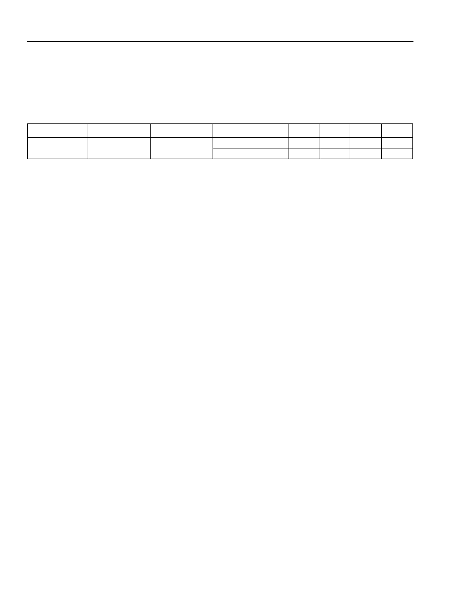
Parameter
Min
Max
Unit
Power Supply Voltage
GND ≠ 0.5
V
CC
+ 0.5
V
Storage Temperature
≠40
125
∞C
Pin Voltage
GND ≠ 0.5
V
CC
+ 0.5
V
Device
Voltage
Type
TRCV0110G
100 V
HBM (human-body model)
100 V
CDM (charged-device model)
Parameter
Symbol
Min
Typ
Max
Unit
Power Supply Voltage (dc)
V
CC
3.135
3.30
3.465
V
Temperature:
Case
T
C
0
25
85
∞C
Power Dissipation
P
D
--
2.1
2.65
W
Agere Systems Inc.
17
Data Sheet
March 28, 2002
Clock Recovery, 1:16 Data Demultiplexer
TRCV0110G 10 Gbits/s Limiting Amplifier
Electrical Characteristics
LVDS, CMOS, and CML Input and Output Pins
Table 9. LVDS dc Output Pin Characteristics
Table 10. LVDS Input Pin Characteristics
Applicable
Pins
Symbol
Parameter
Conditions
Min
Typ
Max
Unit
D[15:0]P/N,
CKOP/N
CK622P/N
V
OH
Output Voltage High
R
LOAD
= 100
± 1%
--
--
1475
mV
V
OL
Output Voltage Low
R
LOAD
= 100
± 1%
925
--
--
mV
|V
OD
|
Output Differential Volt-
age
R
LOAD
= 100
± 1%
250
--
400
mV
V
OS
Output Offset Voltage
R
LOAD
= 100
± 1%
1125
--
1275
mV
R
O
Differential Output
Impedance
V
CM
= 1.0 V and 1.4 V
80
100
120
R
O
R
O
Mismatch Between
A & B
V
CM
= 1.0 V and 1.4 V
--
--
20
%
|
V
OD
|
Change in V
OD
Between
Logic 0 and Logic 1
R
LOAD
= 100
± 1%
--
--
25
mV
|
Vos|
Change in V
OS
Between
Logic 0 and Logic 1
R
LOAD
= 100
± 1%
--
--
25
mV
I
SA
, I
SB
Output Current
Driver shorted
to GND
--
--
24
mA
I
SAB
Output Current
Drivers shorted
together
--
--
12
mA
|I
XA
|,|I
XB
| Power-off Leakage
--
--
--
--
*
* This leakage parameter is not specified due to EDS clamp diode conducting current during forward bias test.
This voltage is measured on each P/N output.
mA
Applicable
Pins
Symbol
Parameter
Conditions
Min
Typ
Max
Unit
REFCLKP/N
V
CM
Input Common Mode Voltage
Range
Avg(V
IA
,V
IB
)
0
1200
2400
mV
V
DIFF
Input Peak Differential voltage
|V
IA
≠ V
IB
|
100
--
800
mV
V
HYST
Threshold Hysteresis
*
* Buffer will not produce output transitions when input is open-circuited.
(+V
ID
) ≠ (≠V
ID
)
25
--
--
mV
R
IN
Differential Input Impedance
Looser than ICORE/IEEE
Æ
spec of ±10
.
f = 622.08 MHz
80
100
120

18
Agere Systems Inc.
Data Sheet
March 28, 2002
Clock Recovery, 1:16 Data Demultiplexer
TRCV0110G 10 Gbits/s Limiting Amplifier
Electrical Characteristics
(continued)
LVDS, CMOS, and CML Input and Output Pins
(continued)
Table 11. CMOS Input Pin Characteristics
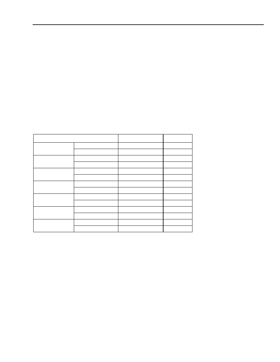
Table 12. CMOS Output Pin Characteristics
Table 13. CML Input Characteristics
Note: The typical input sensitivity is measured at nominal V
CC
and temperature.
Applicable
Pins
Symbol
Parameter
Conditions
Min
Max
Unit
RESETN,
FECN,
ENLBDN,
REFFREQ,
MUTEDMXN,
FREQCKO
MUTECKON,
MUTE622N,
TESTN
V
IH
Input Voltage High
--
V
CC
≠ 1.0
V
CC
V
V
IL
Input Voltage Low
--
GND
1.0
V
I
IH
Input Current High Leakage
V
IN
= V
CC
--
10
µ
A
I
IL
Input Current Low Leakage
V
IN
= GND
≠225
--
µ
A
Applicable
Pins
Symbol
Parameter
Conditions
Min
Max
Unit
LCKLOSSN
V
OH
Output Voltage High
I
OH
= ≠4.0 mA
V
CC
≠ 0.5
V
CC
V
V
OL
Output Voltage Low
I
OL
= 4.0 mA
GND
0.5
V
C
l
Output Load Capacitance
--
--
15
pF
Applicable
Pins
Symbol
Parameter
Conditions
Min
Typ
Max
Unit
DATAP/N
V
AMP1
Single-Ended Input
Amplitude
Data pattern
PRBS 31
15
--
1000
*
* 1000 mV on both input pins.
mV
V
AMP2
Minimum Input Sen-
sitivity
--
8
15
mV
R
LOSS
Input Return Loss
At 10 GHz
12
12
--
dB
R
LOSS
Input Return Loss:
At <7 GHz
15
15
--
dB
LBDP/N
V
IL
Input Voltage Low
Data pattern
PRBS 31
V
CCD
≠ 1
V
CC
≠ 0.4
--
V
V
IH
Input Voltage High
--
V
CCD
V
CCD
+ 0.3
V
V
AMP1
Differential Input
Amplitude
100
400
--
mV
R
LOSS
Input Return Loss
At 10 GHz
12
12
--
dB
R
LOSS
Input Return Loss
At <7 GHz
15
15
--
dB

Agere Systems Inc.
19
Data Sheet
March 28, 2002
Clock Recovery, 1:16 Data Demultiplexer
TRCV0110G 10 Gbits/s Limiting Amplifier
Timing Characteristics
Note that all timing diagrams involving differential signals represent the positive signal as a solid line and the neg-
ative signal as a dashed line. This is especially important when referencing the rising or falling edge of a differential
signal.
Output Timing
The timing relationships between the output 622 MHz clock CK622P/N and the output demultiplexer data
D[15:0]P/N are shown in Figure 9.
0367.a(F)
Figure 9. DeMUX Transmit Timing with CK622
Table 14. LVDS Output Pin ac Timing Characteristics
Applicable
Pins
Symbol
Parameter
Conditions
*
* All signals differential, Z
LOAD
= 100
± 1%.
Min
Typ
Max
Unit
CKOP/N
t
DC
Duty Cycle
--
40
50
60
%
t
PERIOD0
Period
FREQCKO = 0
--
6.4
--
ns
t
PERIOD1
Period
FREQCKO = 1
--
1.6
--
ns
t
RISEC1
Clock V
OD
(20%--80%)
--
100
--
300
ps
t
FALLC1
Clock V
OD
(20%--80%)
--
100
--
300
ps
V
AMP
Single Ended Output Amplitude
--
200
--
500
mV
CK622P/N
t
DC
Duty Cycle
--
40
50
60
%
t
PERIOD2
Period
--
--
1.6
--
ns
t
RISEC2
Clock V
OD
(20%--80%)
--
100
--
300
ps
t
FALLC2
Clock V
OD
(20%--80%)
--
100
--
300
ps
V
AMP
Single Ended Output Amplitude
--
200
--
500
mV
D[15:0]P/N
t
DD1
Time Delay from Clock Edge to
Data Edge
Rising clock edge
leads data
0.5
0.7
0.9
ns
t
DD2
Rising clock edge lags
data
0.7
0.9
1.1
ns
t
RISED
Data V
OD
(20%--80%)
--
200
--
450
ps
t
FALLD
Data V
OD
(20%--80%)
--
200
--
450
ps
t
SKEW1
Differential Skew
--
--
--
70
ps
t
SKEW2
Channel to Channel
As defined by the IEEE standard 1596.3-1996.
Measured differentially
--
--
150
ps
V
AMP
Single Ended Output Amplitude
--
200
--
500
mV
CK622P/N
D[15:0]P/N
DATA 1
tDD1
tDD2
tPERIOD
DATA 3
DATA 2
20
Agere Systems Inc.
Data Sheet
March 28, 2002
Clock Recovery, 1:16 Data Demultiplexer
TRCV0110G 10 Gbits/s Limiting Amplifier
Timing Characteristics
(continued)
Output Timing
The following diagram and specs are from the 10Gb MSA document. You will notice the TRCV0110G device specs
compared to the 300-pin 10 Gbit MSA spec's in the data table.
Figure 10. Output Data/Clock Phase
Table 15. Output Data/Clock Phase
Parameter
Description
Min
Typ
Max
Min
TRCV0110G
Typ
TRCV0110G
Max
TRCV0110G
Unit
TO
Clock Period
--
1.608
--
--
1.6
--
ns
TW/TO
Duty Cycle
0.45
--
0.55
0.4
--
0.6
ns
Tr, Tf
20--80% Rise/Fall
Times
--
--
300
--
--
300 (Clock)
ps
450 (Data)
Tcq-min,
Tcq-max
Data/Clock Skew
--
--
250/250
--
--
200/200
ps
TO
TW
V
CROSS
V
CROSS
V
CROSS
DATA INVALID WINDOW
RxPOCLKP
Tcq_min
Tcq_max
V
SWING
RxD
OUT
P/N
Agere Systems Inc.
21
Data Sheet
March 28, 2002
Clock Recovery, 1:16 Data Demultiplexer
TRCV0110G 10 Gbits/s Limiting Amplifier
Timing Characteristics
(continued)
Reference Frequency (REFCLKP/N, REFFREQ) (Standard SONET Rate)
The device requires a 155.52 MHz or 622.08 MHz differential LVDS reference clock input to aid in frequency
acquisition and loss-of-lock detection.
Table 16. OC-192 Reference Clock Characteristics
Reference Frequency (REFCLKP/N, REFFREQ) (FEC Rate)
The device requires a (255/237) x 155.52 MHz or (255/237) x 622.08 MHz differential LVDS reference clock input
to aid in frequency acquisition and loss-of-lock detection.
Table 17. FEC Reference Clock Characteristics
Reference Frequency (REFCLKP/N, REFFREQ) (Ethernet Rate)
The device requires a 161 MHz or 644 MHz differential LVDS reference clock input to aid in frequency acquisition
and loss-of-lock detection.
Table 18. Ethernet Reference Clock Characteristics
Applicable
Pins
Symbol
Parameter
Conditions
Min
Typ
Max
Unit
REFCLKP/N
--
Frequency
REFFREQ = 0
--
155.52
--
MHz
REFFREQ = 1
--
622.08
--
MHz
Duty Cycle
--
40
50
60
%
Reference Frequency
Tolerance
*
* Includes effects of power supply variation, temperature, electrical loading, and aging.
--
--
150
--
ppm
Applicable
Pins
Symbol
Parameter
Conditions
Min
Typ
Max
Unit
REFCLKP/N
--
Frequency
REFFREQ = 0
--
167.3316
--
MHz
REFFREQ = 1
--
669.3265
--
MHz
Duty Cycle
--
40
50
60
%
Reference Frequency
Tolerance
*
* Includes effects of power supply variation, temperature, electrical loading, and aging.
--
--
150
--
ppm
Applicable
Pins
Symbol
Parameter
Conditions
Min
Typ
Max
Unit
REFCLKP/N
--
Frequency
REFFREQ = 0
--
161
--
MHz
REFFREQ = 1
--
644
--
MHz
Duty Cycle
--
40
50
60
%
Reference Frequency
Tolerance
*
* Includes effects of power supply variation, temperature, electrical loading, and aging.
--
--
150
--
ppm
22
Agere Systems Inc.
Data Sheet
March 28, 2002
Clock Recovery, 1:16 Data Demultiplexer
TRCV0110G 10 Gbits/s Limiting Amplifier
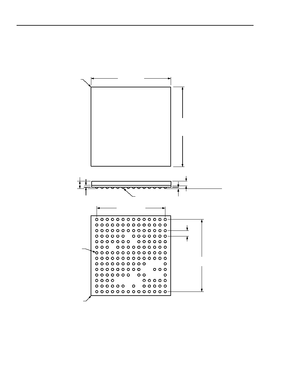
Packaging Characteristics
Package Crush Characteristics
Table 19. Crush Specifications
Additional test information available on request.
CBGA Package Information
The package used for the TRCV0110G devices is a ceramic ball grid array (CBGA). The substrate is 99.6%
alumina (Al2O3) material. The standoff height is accomplished by using 0.013 in. diameter copper silver (CuAg)
balls, which are attached using a eutectic braze to the thin film metal pads on the substrate. After brazing the balls
have a diameter at the braze fillet of 0.016 in. (at the interface of the ball and substrate), but still maintain their
height of 0.013 in. for standoff height.
PWB Design Information
The layout of the bare PWB should use a 0.016 in. diameter pad. The pad should be defined by the copper and not
by solder mask. (The only copper leading away from the pad should be the trace connected to it; the pad should
not be part of a large ground plane unless only connected to the ground plane by a single trace.) Avoid placement
of vias in the pads used for ball attachment on the PWB. Vias should be connected by a trace (or tear dropped)
with a sufficient dam of solder mask to prevent solder from wicking into the via and away from the ball/PWB solder
joint.
The stencil opening should be designed at 0.016 in. as well, to match up with the CBGA pads.
Device Code
Package
Dimensions
Conditions
Min
Typ
Max
Unit
TRCV0110G
177-ball CBGA
14 mm x 14 mm
Without pad
--
25
--
lbs
With pad (0.040 in.)
--
25
--
lbs
Agere Systems Inc.
23
Data Sheet
March 28, 2002
Clock Recovery, 1:16 Data Demultiplexer
TRCV0110G 10 Gbits/s Limiting Amplifier
Packaging Characteristics
(continued)
Assembly Information
Note: Each assembly process will have its own idiosyncrasies, due to product design, materials differences and
equipment variations. Assembly information provided here is a beginning point from which the assembly
process engineer should apply their knowledge and experience to obtain optimal results.
It is recommended that the stencil thickness be set at 0.006 in. for a starting point. After trials with the recom-
mended stencil opening size, stencil thickness, and process specific solder paste, a visual inspection should be
done to assure a proper fillet and wetting is obtained for each ball. The reflowed solder fillet should resemble a
cylindrical column from the PWB to the center of the ball.
The reflow profile should be determined using a known set point for the oven such as the Joint Electron Device
Engineering Council (JEDEC) profile. The JEDEC profile is defined as the following parameters:
Table 20. JEDEC Profile
Belt speed = 28 in./min.
A representative sample of the product (fitted with multiple thermocouples and a data logger) should be run
through the oven to determine the optimum profile. The temperature of the CBGA device should not exceed
225 ∞C, and only be above the liquidus of the solder alloy (typically 180 ∞C) for less than 60 s.
Reference Materials
For further information, the user may wish to consult some of the many references that are available on the techni-
cal market today for CBGA assembly. The following are suggested for more detailed information, but there are
many others too:
s
Ceramic Ball Grid Array Surface Mount Assembly and Rework, IBM Document #APD-SBSC-101.0, Cindy Milk-
ovich, Lisa Jimarez, IBM Corporation, 1701 North Street, Endicott, NY 13760, (800) 925-3157
s
Ball Grid Array Technology, John Lau (Editor), ISBN 0-07-036608-X, McGraw-Hill, Inc., 1221 Avenue of the
Americas, New York, NY 10020
ZONE
Temp
Unit
1
Upper
140
∞
C
Lower
140
∞
C
2
Upper
150
∞
C
Lower
150
∞
C
3
Upper
150
∞
C
Lower
150
∞
C
4
Upper
180
∞
C
Lower
180
∞
C
5
Upper
180
∞
C
Lower
180
∞
C
6
Upper
205
∞
C
Lower
205
∞
C
7
Upper
245
∞
C
Lower
245
∞
C
24
Agere Systems Inc.
Data Sheet
March 28, 2002
Clock Recovery, 1:16 Data Demultiplexer
TRCV0110G 10 Gbits/s Limiting Amplifier
Packaging Characteristics
(continued)
Package Diagram--177-Ball CBGA (Bottom View)
Note: Dimensions are in millimeters. Tolerance is ±0.076 mm unless otherwise noted.
0628(F)
A1 BALL
CORNER
D
E
F
G
H
J
K
L
N
P
C
B
A
13 SPACES
@ 1.00 = 13.00
1.00 TYP
A1 BALL
IDENTIFIER ZONE
SEATING PLANE
SOLDER BALL
13 SPACES
@ 1.00 = 13.00
1.143 REF
M
1
2
3
4
5
6
7
8
9
10 11 12 13 14
1.885
0.330
±
0.051 TYP
0.3734
±
0.0013
14.00
±
0.080
14.00
±
0.080
0.330
±
0.051
TYP DIA
SQR
SQR

Agere Systems Inc.
25
Data Sheet
March 28, 2002
Clock Recovery, 1:16 Data Demultiplexer
TRCV0110G 10 Gbits/s Limiting Amplifier
Ordering Information
Device Code
Package
Temperature (T
C
)
Comcode
(Ordering Number)
TRCV0110G
177-ball CBGA
0--85
108698499

Telcordia Technologies is a trademark of Telcordia Technologies Inc.
National and National Semiconductor are registered trademarks of National Semiconductor Corporation.
IEEE is a registered trademark of The institute of Electrical and Electronics Engineers, Inc.
Copyright © 2002 Agere Systems Inc.
All Rights Reserved
March 28, 2002
DS02-061HSPL (Replaces DS01-235HSPL)
Agere Systems Inc. reserves the right to make changes to the product(s) or information contained herein without notice. No liability is assumed as a result of their use or application.
For additional information, contact your Agere Systems Account Manager or the following:
INTERNET:
http://www.agere.com
E-MAIL:
docmaster@agere.com
N. AMERICA:
Agere Systems Inc., 555 Union Boulevard, Room 30L-15P-BA, Allentown, PA 18109-3286
1-800-372-2447, FAX 610-712-4106 (In CANADA: 1-800-553-2448, FAX 610-712-4106)
ASIA:
Agere Systems Hong Kong Ltd., Suites 3201 & 3210-12, 32/F, Tower 2, The Gateway, Harbour City, Kowloon
Tel. (852) 3129-2000, FAX (852) 3129-2020
CHINA: (86) 21-5047-1212 (Shanghai), (86) 10-6522-5566 (Beijing), (86) 755-695-7224 (Shenzhen)
JAPAN: (81) 3-5421-1600 (Tokyo), KOREA: (82) 2-767-1850 (Seoul), SINGAPORE: (65) 6778-8833, TAIWAN: (886) 2-2725-5858 (Taipei)
EUROPE:
Tel. (44) 7000 624624, FAX (44) 1344 488 045