Product Brief
May 2001
TRCV0112G
12 Gbit/s Limiting Amp, Clock Recovery, 1:16 Data Demultiplexer
Features
I
Integrated limiting amplifier with 40 dB of voltage
gain.
I
Fully integrated clock recovery, 1:16 data demulti-
plexer.
I
Supports OC-192/STM-64 (standard and multiple
FEC rates) and 10GE data rates. Allows for two
separate frequency ranges of operation:
-- 9.95328 GHz through 10.70922 GHz
-- 12.0 GHz through 12.5 GHz
I
Single 3.3 V power supply.
I
Additional high-speed data input for system loop-
back operation.
I
Standard LVDS deMUX data and clock outputs.
I
CMOS I/O compatible with LVTTL signaling.
I
Available in a 177-pin BGA package.
I
Jitter tolerance compliant with:
-- Telcordia Technologies * GR-1377 CORE
-- ITU-T G.825
-- ITU-T G.958
I
Fully compatible with OIF99.102.5 specification.
Applications
I
SONET/SDH optical modules.
I
SONET/SDH line termination equipment.
I
SONET/SDH test equipment.
I
Ethernet 10G physical layer applications.
* Telcordia Technologies is a registered trademark of Bell Commu-
nications Research, Inc.
Description
The Agere Systems Inc. TRCV0112G device inte-
grates a limiting amplifier combined with a clock
recovery circuit that feeds a data demultiplexer for
use in 12 Gbit/s high-speed communications sys-
tems. Additional features include an auxiliary clock
output and a reference clock input that can be either
˜16 or ˜64. The device will operate in two frequency
ranges 9.95328 Gbit/s through 10.70922 Gbit/s or
12 Gbit/s through 12.5 Gbit/s. The higher rate is pin
selectable.
Functional Overview
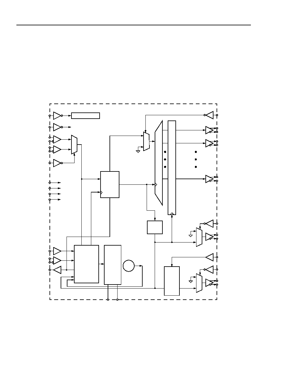
The TRCV0112G performs the data detection, clock
recovery, and 1:16 demultiplexing operations
required to support 10 Gbits/s
OC-192/STM-64
applications compliant with Telcordia Technologies
and ITU standards. One of two high-speed inputs
can be selected as the data source. A PLL recovers
the clock which is used to retime the data. A 1:16
data demultiplexer performs the serial-to-parallel
conversion and generates 16 parallel outputs at
622 Mbits/s. The parallel output data is aligned to a
622 MHz clock derived from the 10 GHz recovered
clock.
FEC Rate Support
The TRCV0112G will support the rates of
9.95328 GHz through the rate of 10.70922 GHz
(FECN = 1) and higher FEC rates of 12.0 GHz
through 12.5 GHz (FECN = 0). The FECN pin
selects between VCO ranges of 9.95328 GHz
through 10.70922 GHz and 12.0 GHz through
12.5 GHz. All frequency-based specifications are to
be multiplied by (rate/9.95328 GHz) when operating
at higher frequency rates.
The OC-192/STM-64 data rate of 9.95328 Gbits/s is typically
approximated as 10 Gbits/s in this document when referring to
the application rate. Similarly, the low-speed parallel interface
data rate of 622.08 Mbits/s is typically approximated as
622 Mbits/s. The exact frequencies are used only when neces-
sary for clarity.

2
Agere Systems Inc.
Product Brief
May 2001
12 Gbit/s Limiting Amp, Clock Recovery, 1:16 Data Demultiplexer
TRCV0112G
Functional Overview
(continued)
FEC Rate Support
(continued)
All time-based specifications, with the exception of electrical signal rise and fall times, are to be multiplied by
(9.95328 GHz/rate). At nonstandard FEC rates, the reference clock would need to be applied at
(rate/9.95328 GHz) ◊ 155.52 MHz or (rate/9.95328 GHz) ◊ 622.08 MHz and the paralled data interface would
operate at (rate/9.95328 GHz) ◊ 622.08 MHz.
Block diagram
0363 (F)
Figure 1. TRCV0112G Block Diagram
TO DIGITAL LOGIC
D0P
D0N
D1P
D1N
D15P
D15N
CKOP
CKON
REFCLKP
REFCLKN
DATA
VCO
1:
16 D
E
MULTIPL
E
X
E
R
CHARGE
LFP
LFN
OUTPUT REGISTER
RESETN
MUTECKON
ACM
MUTEDMXN
MUTEDMX
ENLBDN
LCKLOSSN
MUTECKO
DIVIDE
SAMPLER
CIRCUIT
PHASE/FREQ.
DETECTION
PUMP
BY 16
0
1
1
0
FECN
TO VCO
DATAP
DATAN
0
1
LBDP
LBDN
RREFLVDS
RREFVCO
REFFREQ
FREQCKO
DIVIDE
BY 1
OR
DIVIDE
BY 4
CK622P
CK622N
MUTE622N
MUTE622
1
0
RECOVERED
DATA
RECOVERED
CLOCK
RREFCP

Agere Systems Inc. reserves the right to make changes to the product(s) or information contained herein without notice. No liability is assumed as a result of their use or application.
Copyright © 2001 Agere Systems Inc.
All Rights Reserved
Printed in U.S.A.
May 2001
PB01-127HSPL
For additional information, contact your Agere Systems Account Manager or the following:
INTERNET:
http://www.agere.com
E-MAIL:
docmaster@micro.lucent.com
N. AMERICA: Agere Systems Inc., 555 Union Boulevard, Room 30L-15P-BA, Allentown, PA 18109-3286
1-800-372-2447, FAX 610-712-4106 (In CANADA: 1-800-553-2448, FAX 610-712-4106)
ASIA PACIFIC: Agere Systems Singapore Pte. Ltd., 77 Science Park Drive, #03-18 Cintech III, Singapore 118256
Tel. (65) 778 8833, FAX (65) 777 7495
CHINA:
Agere Systems (Shanghai) Co., Ltd., 33/F Jin Mao Tower, 88 Century Boulevard Pudong, Shanghai 200121 PRC
Tel. (86) 21 50471212, FAX (86) 21 50472266
JAPAN:
Agere Systems Japan Ltd., 7-18, Higashi-Gotanda 2-chome, Shinagawa-ku, Tokyo 141, Japan
Tel. (81) 3 5421 1600, FAX (81) 3 5421 1700
EUROPE:
Data Requests: DATALINE: Tel. (44) 7000 582 368, FAX (44) 1189 328 148
Technical Inquiries:GERMANY: (49) 89 95086 0 (Munich), UNITED KINGDOM: (44) 1344 865 900 (Ascot),
FRANCE: (33) 1 40 83 68 00 (Paris), SWEDEN: (46) 8 594 607 00 (Stockholm), FINLAND: (358) 9 3507670 (Helsinki),
ITALY: (39) 02 6608131 (Milan), SPAIN: (34) 1 807 1441 (Madrid)


