
Preliminary Data Sheet
August 2000
TRCV012G5 (2.5 Gbits/s) and TRCV012G7 (2.5 Gbits/s and 2.7 Gbits/s)
Limiting Amplifier, Clock Recovery, 1:16 Data Demultiplexer
Features
s
TRCV012G5 supports OC-48/STM-16 data rate
s
TRCV012G7 supports:
-- OC-48/STM-16 data rate
-- RS (255, 239) forward error correction (FEC)
OC-48/STM-16 data rate
s
Fully-integrated limiting amplifier, clock recovery,
1:16 data demultiplexer
s
No reference clock required for CDR
s
2.5 Gbits/s data output and 2.5 GHz recovered
clock output available for wavelength division
multiplex (WDM) or regenerator applications
s
Programmable limiting amplifier offset
s
Programmable data sampling phase
s
Additional CML serial data input for system
loopback
s
Parity bit generation
s
Analog and digital loss of signal (LOS) indicators
s
Optional demultiplexer powerdown mode
conserves power
s
Single 3.3 V supply
s
Available in either MBIC 025 BiCMOS technology
or lower-power MBIC 025 silicon germanium
BiCMOS technology
s
High-speed LVPECL digital I/O
s
Jitter tolerance, transfer, and generation compliant
with the following:
--
Telcordia Technologies
* GR-253
-- ITU-T G.825
-- ITU-T G.958
s
Loss of signal compliant with the following:
--
Telcordia Technologies
GR-253
*
Telcordia Technologies
is a registered trademark of Bell Com-
munications Research, Inc.
Applications
s
SONET/SDH line termination equipment
s
SONET/SDH add/drop multiplexers
s
SONET/SDH cross connects
s
SONET/SDH test equipment
Description
The Lucent Technologies Microelectronics Group
TRCV012G5 operates at the OC-48/STM-16 data
rate of 2.5 Gbits/s. The TRCV012G7 device operates
at either 2.5 Gbits/s or the RS FEC OC-48/STM-16
data rate of 2.7 Gbits/s. For clarity, this data sheet
refers to the TRCV012G5 serial data rate as
2.5 Gbits/s and the parallel data and reference clock
frequency as 155 MHz. (The precise rates are
2.48832 Gbits/s and 155.52 MHz.) When using the
TRCV012G7 at the FEC rate, the 2.5 Gbits/s data
rate should be interpreted as 2.7 Gbits/s and the par-
allel and clock frequency should be interpreted as
166 MHz. (The precise rates are 2.66606 Gbits/s and
166.62 MHz.)
The devices contain a limiting amplifier with 30 dB
gain, a clock and data recovery PLL with high-speed
serial clock and data outputs, and a 1:16 demulti-
plexer with differential PECL data and clock outputs.
The device provides improved optical receiver perfor-
mance when used in optically amplified systems due
to a direct slice adjust input pin and a 6 ps adjust-
ment capability in the slicing decision time. Both
devices are available in either BiCMOS or in SiGe
BiCMOS technology for lower power operation.

TRCV012G5 and TRCV012G7
Preliminary Data Sheet
Limiting Amplifier, Clock Recovery, 1:16 Data Demultiplexer
August 2000
2
Lucent Technologies Inc.
Table of Contents
Contents
Page
Features .................................................................................................................................................................... 1
Applications ............................................................................................................................................................... 1
Description................................................................................................................................................................. 1
Pin Information .......................................................................................................................................................... 4
Functional Overview ................................................................................................................................................ 10
Limiting Amplifier ..................................................................................................................................................... 10
Limiting Amplifier Operation.................................................................................................................................. 10
Clock and Data Recovery (CDR)............................................................................................................................. 11
Clock Recovery Operation .................................................................................................................................... 11
Clock Recovery PLL Loop Filter ........................................................................................................................... 11
CDR Acquisition Time...........................................................................................................................................11
CDR Generated Jitter ...........................................................................................................................................11
CDR Input Jitter Tolerance ................................................................................................................................... 12
CDR Jitter Transfer ............................................................................................................................................... 12
Clock Recovery Jitter Tolerance and Jitter Transfer Specifications...................................................................... 13
Data Path Configuration Option (ENDATAN) ....................................................................................................... 14
High-Speed Serial Clock and Data Output Enables (ENCK2G5N, END2G5N).................................................... 14
High-Speed Serial Data Output Mute (MUTE2G5N) ............................................................................................ 14
Data and CDR Configuration Options (REFSELN, INLOSN, MUTEDMXN)......................................................... 14
Decision Circuit--Adjustable Sampling Time (ASTREF, AST[4:0])......................................................................... 15
Loss of Signal Detection.......................................................................................................................................... 16
Digital Loss of Signal (LOSDN)............................................................................................................................. 16
Analog Loss of Signal (LOSAN, PRG_LOSA) ......................................................................................................16
Demultiplexer Operation.......................................................................................................................................... 17
Parity Generation (PARITYP/N)............................................................................................................................ 17
Demultiplexer Powerdown (PDDMXN) ................................................................................................................. 17
Demultiplexer Data Mute (MUTEDMXN) .............................................................................................................. 17
CK155P/N Low-Speed Output Mute (MUTE155N)...............................................................................................17
CML Output Structure (Used on Pins D2G5P/N, CK2G5P/N)................................................................................. 18
Choosing the Value of the External CML Reference Resistors (RREF1, RREF2) ............................................... 18
Absolute Maximum Ratings.....................................................................................................................................19
Handling Precautions .............................................................................................................................................. 19
Operating Conditions............................................................................................................................................... 19
Electrical Characteristics ......................................................................................................................................... 20
Limiting Amplifier Specifications ........................................................................................................................... 20
Optional Reference Frequency (REFCLKP/N) Specifications .............................................................................. 20
LVPECL, CMOS, CML Input and Output Pins ......................................................................................................21
Timing Characteristics ............................................................................................................................................. 23
Output Timing ....................................................................................................................................................... 23
Outline Diagram....................................................................................................................................................... 25
128-Pin QFP ......................................................................................................................................................... 25
Board Installation Recommendations ...................................................................................................................26
Thermal Considerations (MBIC 025 BiCMOS and MBIC 025 SiGe BiCMOS) ..................................................... 26
Ordering Information................................................................................................................................................ 27
DS00-234HSPL Replaces DS00-154HSPL to Incorporate the Following Updates................................................. 27
Preliminary Data Sheet
TRCV012G5 and TRCV012G7
August 2000
Limiting Amplifier, Clock Recovery, 1:16 Data Demultiplexer
3
Lucent Technologies Inc.
Description
(continued)
Additional features include a user-programmable threshold for generating analog loss of signal (LOS) alarms, a
digital LOS transition detector, an optional reference clock input that can maintain synchronization with no data
input signal present, and a loopback data input. To reduce power consumption, the demultiplexer unit, high-speed
serial recovered data and clock output, low-speed clock, and low-speed demultiplexer clock output can be inde-
pendently powered down in applications where they are not required.
The device may be used with the TTRN012G5 or TTRN012G7 transmit synthesizer and multiplexer.
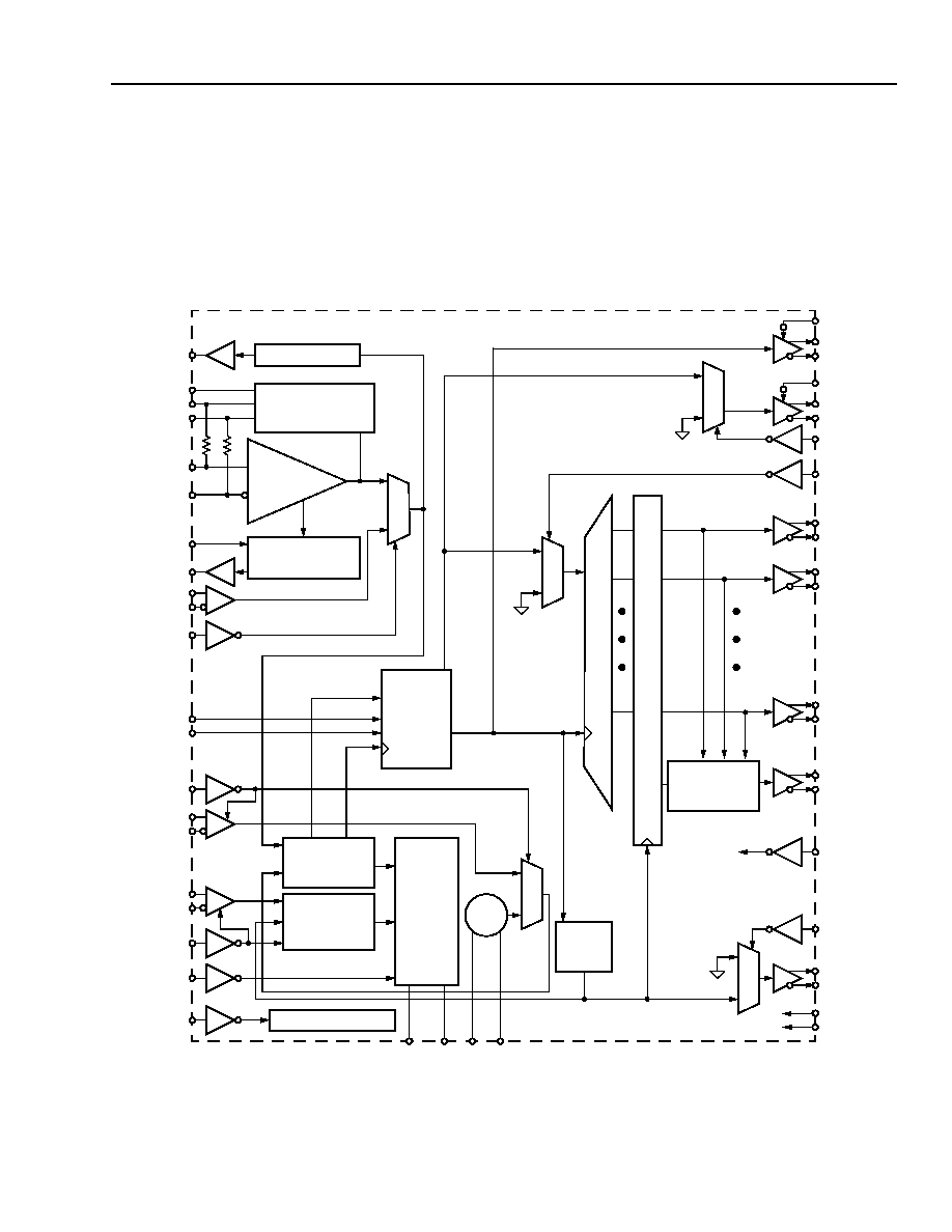
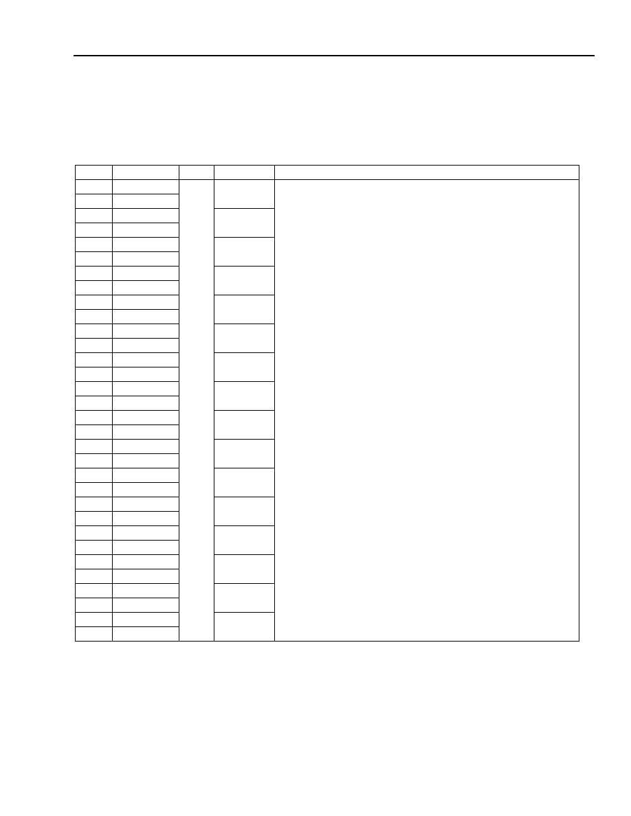
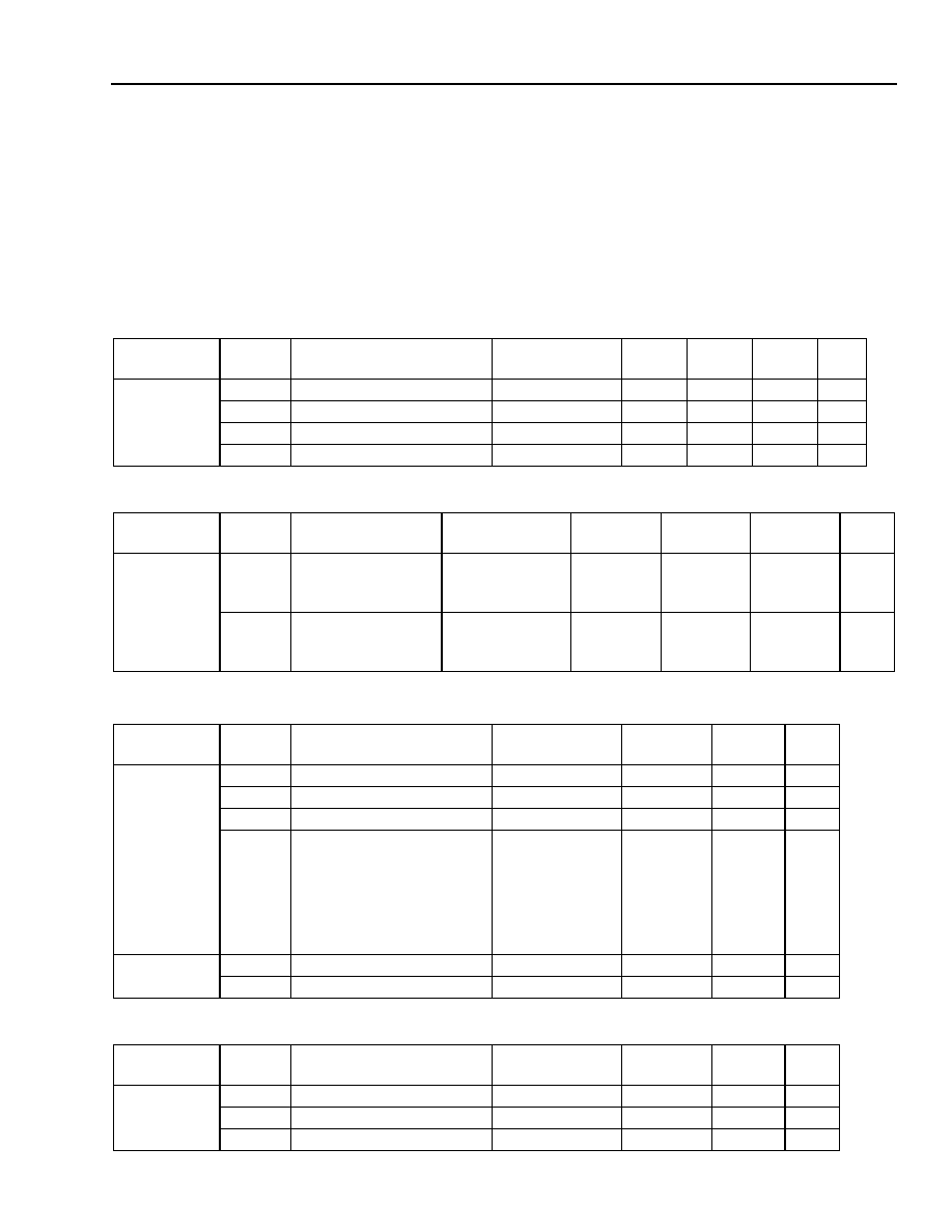
5-8067(F)r.2
Note: Diagram is representative of device functionality and conceptual signal flow. Internal implementation details may be different than shown.
Figure 1. Functional Block Diagram
LOSS OF DATA
D0P
D0N
D1P
D1N
D15P
D15N
PARITYP
CK155P
CK155N
REFCLKP
REFCLKN
LOSAN
LIMITING
DATA
VCO
1
:
16 DEMULTI
P
LE
X
E
R
PARITY
OFFSET CANCEL
END2G5N
VTHN
VTHP
LAINN
LAINP
CHARGE
LFP
LFN
PARITYN
OUTP
UT RE
GIS
TE
R
LOSDN
INLOSN
MUTE155N
CK2G5P
CK2G5N
ENCK2G5N
PRG_LOSA
ASTREF
RESETN
TO DIGITAL LOGIC
LOSS OF SIGNAL
DATAP
DATAN
ENDATCK
MUTEDMXN
MUTEDMX
INLOS
SLADJ
PDDMXN
PDDMX
ENDATAN
END
A
T
A
REFSELN
MUTE155
DIVIDE
D2G5P
D2G5N
MUTE2G5
MUTE2G5N
REFERENCE
AST[4:0]
SAMPLER
DATCKP
DATCKN
ENDATCKN
R
E
CO
V
E
RE
D D
A
T
A
VCP VCN
RREF1
RREF2
&
SLICE ADJUST
AMPLIFIER
0
1
CIRCUIT
1
0
PHASE/FREQ.
DETECTION
PUMP
PHASE/FREQ.
DETECTION
BY 16
0
1
0
1
GENERATOR
1
0
R
E
CO
V
E
RE
D CLOCK
TRCV012G5 and TRCV012G7
Preliminary Data Sheet
Limiting Amplifier, Clock Recovery, 1:16 Data Demultiplexer
August 2000
4
Lucent Technologies Inc.
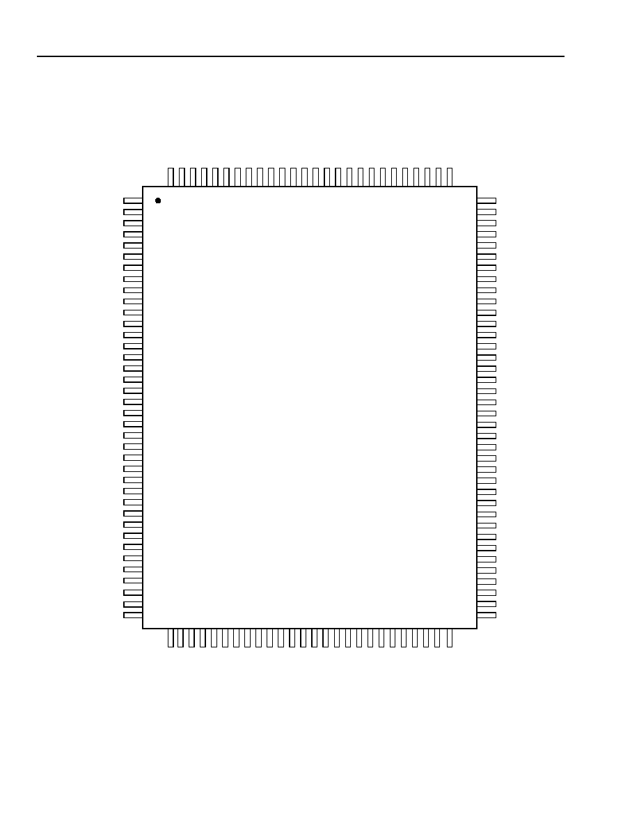
Pin Information
5-8071(F)r.5
Figure 2. Pin Diagram of 128-Pin QFP (Top View)
1
2
3
5
4
6
7
9
8
18
10
11
13
12
14
15
17
16
19
20
22
21
23
24
26
25
35
27
28
30
29
31
32
34
33
36
37
38
39
41
40
42
43
45
44
54
46
47
49
48
50
51
53
52
55
56
58
57
59
60
62
61
63
64
100
99
98
96
97
95
94
92
93
83
91
90
88
89
87
86
84
85
82
81
79
80
78
77
75
76
66
74
73
71
72
70
69
67
68
65
12
8
12
7
12
6
12
4
12
5
12
3
12
2
12
0
12
1
11
1
11
9
11
8
11
6
11
7
11
5
11
4
11
2
11
3
11
0
10
9
10
7
10
8
10
6
10
5
10
3
10
4
102
101
GND
GND
GND
GND
GND
GND
GND
GND
GND
V
CCLA
VTHN
GND
LAINN
GND
LAINP
GND
VTHP
V
CCLA
SLADJ
PRG_LOSA
V
CCLA
V
CCA
V
CCA
GND
GND
VCP
LFP
LFN
VCN
GND
NC
GND
NC
NC
V
CCA
V
CCA
V
CCD
GND
AST0
AST1
AST2
AST3
AST4
D15N
GND
GND
GND
D3N
D3P
V
CCD
D4N
D4P
D5N
D5P
V
CCD
D6N
D6P
D7N
D7P
V
CCD
D8N
D8P
D9N
D9P
GND
D10N
D10P
V
CCD
D11N
D11P
D12N
D12P
V
CCD
D13N
D13P
D14N
D14P
V
CCD
D2
P
D1
P
D2
N
D1
N
V
CCD
D0
N
D0
P
GND
V
CCD
CK2
G
5
N
CK2
G
5
P
D2
G5
N
GND
GND
D2
G5
P
V
CCD
DAT
A
N
V
CCD
DA
T
A
P
DAT
C
KP
DAT
C
KN
V
CCD
RREF
1
RREF
2
ASTREF
D15P
C
K
15
5N
C
K
15
5P
V
CCD
PARI
T
Y
N
REF
C
L
K
N
V
CCD
REF
C
L
K
P
V
CCD
MU
TE
15
5N
REF
SEL
N
RESET
N
PDDM
XN
MU
TE
D
M
X
N
MU
TE
2G
5N
LO
S
D
N
LO
S
A
N
END2
G
5
N
INL
O
S
N
ENCK2
G
5
N
ENDAT
C
KN
NC
ENDAT
A
N
V
CCD
PARI
T
Y
P
Preliminary Data Sheet
TRCV012G5 and TRCV012G7
August 2000
Limiting Amplifier, Clock Recovery, 1:16 Data Demultiplexer
5
Lucent Technologies Inc.
Pin Information
(continued)
Note: In Table 1, when operating the TRCV012G7 device at the OC-48/STM-16 rate, 2.5 Gbits/s should be inter-
preted as 2.48832 Gbits/s. When operating the TRCV012G7 device at the RS FEC OC-48/STM-16 rate,
2.5 Gbits/s should be interpreted as 2.66606 Gbits/s. (A similar interpretation should be made for 2.5 GHz.)
Table 1. Pin Descriptions--2.5 Gbits/s and Related Signals
* Differential pins are indicated by the P and N suffixes. For nondifferential pins, N at the end of the symbol name designates active-low.
I = input, O = output. I
u
= an internal pull-up resistor on this pin, I
d
= an internal pull-down resistor on this pin, I
t
= an internal termination
resistance of 50
on this pin.
Pin
Symbol*
Type
Level
Name/Description
30
LAINP
I
Analog
Limiting Amplifier Inputs (2.5 Gbits/s).
ac coupling required.
32
LAINN
50
D2G5P
O
CML
Data Output (2.5 Gbits/s NRZ). 2.5 Gbits/s differential data
output.
s
Pins are high impedance when END2G5N = 1.
s
Pins are active but forced to differential logic low when
MUTE2G5N = 0.
51
D2G5N
122
END2G5N
I
u
CMOS
Enable D2G5P/N Data Outputs (Active-Low).
0 = D2G5P/N buffer enabled
1 or no connection = D2G5P/N buffer powered off
118
MUTE2G5N
I
u
CMOS
Mute D2G5P/N Data Output (Active-Low).
0 = muted
1 or no connection = normal data
53
CK2G5P
O
CML
Recovered Clock Output (2.5 GHz). 2.5 GHz recovered differen-
tial clock output. Pins are high impedance when ENCK2G5N = 1.
54
CK2G5N
123
ENCK2G5N
I
u
CMOS
Enable CK2G5P/N Clock Output (Active-Low).
0 = CK2G5P/N buffer enabled
1 or no connection = CK2G5P/N buffer powered off
41
RREF1
I
Analog
Resistor Reference 1. CML current bias reference resistor. (See
Table 16, page 22 for values.)
40
RREF2
I
Analog
Resistor Reference 2. CML bias reference resistor. Place a
1.5 k
resistor to V
CCD
.
28
VTHP
I
Analog
Voltage Threshold Adjust Input. This input is for monitoring
purposes only and should be left open (see Figure 3 on page 10).
34
VTHN
26
SLADJ
I
Analog
Slice Level Adjustment. Adjusts slice level for the limiting amp
(see Figure 3 on page 10).
119
LOSAN
O
Open Drain Loss of Analog Signal (Active-Low).
25
PRG_LOSA
I
Analog
Programming Voltage for LOSA Threshold. Programming
voltage is scaled (see Figure 7 on page 16).
120
LOSDN
O
Open Drain Loss of Digital Data (Active-Low).
121
INLOSN
I
u
CMOS
Input Loss of Signal (Active-Low). Forces VCO to decrease to
its minimum frequency.
0 = force VCO low
1 or no connection = normal operation
18
LFP
O
Analog
Loop Filter PLL. Connect LFP to VCP, and LFN to VCN.
17
LFN
19
VCP
I
Analog
VCO Control. Connect VCP to LFP, and VCN to LFN.
16
VCN
TRCV012G5 and TRCV012G7
Preliminary Data Sheet
Limiting Amplifier, Clock Recovery, 1:16 Data Demultiplexer
August 2000
6
Lucent Technologies Inc.
Pin Information
(continued)
Table 1. Pin Descriptions--2.5 Gbits/s and Related Signals (continued)
* Differential pins are indicated by the P and N suffixes. For nondifferential pins, N at the end of the symbol name designates active-low.
I = input, O = output. I
u
= an internal pull-up resistor on this pin, I
d
= an internal pull-down resistor on this pin, I
t
= an internal termination resis-
tance of 50
on this pin.
Pin
Symbol*
Type
Level
Name/Description
43
DATCKP
I
t
CML
Clock Input for DATAP/N. Buffer is powered down when
ENDATCKN = 1.
44
DATCKN
124
ENDATCKN
I
u
CMOS
External DATCKP/N Clock Select (Active-Low). Selects
external DATCKP/N clock to demultiplexer.
0 = select DATCKP/N
1 or no connection = select VCO clock
46
DATAP
I
t
CML
Data Input for CML. Use this input for system loopback
data when LAINP/N is used.
47
DATAN
125
ENDATAN
I
u
CMOS
Enable DATAP/N Inputs (Active-Low). Selects DATAP/N
as data source rather than limiting amplifier output.
0 = select DATAP/N
1 or no connection = select LAINP/N
37
ASTREF
I
Analog
Adjustable Sampling Circuit Reference Resistor.
Connect a 2.1 k
resistor to V
CCA
.
2
AST4
I
d
CMOS
Adjustable Sampling Time Control Inputs. AST[4:0]
allows introduction of an offset into the sampling time. The
most significant bit (A4) is the sign bit and bits A[3:0]
represent the magnitude. (See the Decision Circuit--
Adjustable Sampling Time (ASTREF, AST[4:0]) section,
page 15.)
A4 is the polarity bit as follows:
1 = advance
0 = delay sampling point
AST[3:0] provides adjustments in steps (increments or
decrements) of 6.25 ps in the sampling instant.
3
AST3
4
AST2
5
AST1
6
AST0
Preliminary Data Sheet
TRCV012G5 and TRCV012G7
August 2000
Limiting Amplifier, Clock Recovery, 1:16 Data Demultiplexer
7
Lucent Technologies Inc.
Pin Information
(continued)
Note: In Table 2, when operating the TRCV012G7 device at the OC-48/STM-16 rate, 155 Mbits/s should be inter-
preted as 155.52 Mbits/s. When operating the TRCV012G7 device at the RS FEC OC-48/STM-16 rate,
155 Mbits/s should be interpreted as 166.62 Mbits/s. (A similar interpretation should be made for 155 MHz.)
Table 2. Pin Descriptions--155.52 Mbits/s and Related Signals
* Differential pins are indicated by the P and N suffixes. For nondifferential pins, N at the end of the symbol name designates active-low.
I = input, O = output. I
u
= an internal pull-up resistor on this pin, I
d
= an internal pull-down resistor on this pin, I
t
= an internal termination
resistance of 50
on this pin.
Pin
Symbol*
Type
Level
Name/Description
101
D15P
O
LVPECL
Data Output (155 Mbits/s). 155 Mbits/s differential data output.
D15 is the most significant bit and is the first received on the
LAINP/N or DATAP/N input.
When PDDMXN = 0, data outputs can be left floating to reduce
power consumption.
100
D15N
98
D14P
LVPECL
97
D14N
96
D13P
LVPECL
95
D13N
93
D12P
LVPECL
92
D12N
91
D11P
LVPECL
90
D11N
88
D10P
LVPECL
87
D10N
85
D9P
LVPECL
84
D9N
83
D8P
LVPECL
82
D8N
80
D7P
LVPECL
79
D7N
78
D6P
LVPECL
77
D6N
75
D5P
LVPECL
74
D5N
73
D4P
LVPECL
72
D4N
70
D3P
LVPECL
69
D3N
63
D2P
LVPECL
62
D2N
61
D1P
LVPECL
60
D1N
58
D0P
LVPECL
57
D0N
TRCV012G5 and TRCV012G7
Preliminary Data Sheet
Limiting Amplifier, Clock Recovery, 1:16 Data Demultiplexer
August 2000
8
Lucent Technologies Inc.
Pin Information
(continued)
Table 2. Pin Descriptions--155.52 Mbits/s and Related Signals (continued)
* Differential pins are indicated by the P and N suffixes. For nondifferential pins, N at the end of the symbol name designates active-low.
I = input, O = output. I
u
= an internal pull-up resistor on this pin, I
d
= an internal pull-down resistor on this pin, I
t
= an internal termination resis-
tance of 50
on this pin.
Pin
Symbol*
Type
Level
Name/Description
115
PDDMXN
I
u
CMOS
Powerdown Demultiplexer Circuit (Active-Low).
0 = demultiplexer powered off, D[15:0]P/N and PARITYP/N
are high-impedance
1 or no connection = demultiplexer powered on
117
MUTEDMXN
I
u
CMOS
Mute Data to Demultiplexer Circuit (Active-Low).
0 = mute data
1 or no connection = normal data
108
CK155P
O
LVPECL
Recovered Clock Output (155 MHz).
155 MHz recovered differential clock output. Pins are active
but forced to differential logic low when MUTE155N = 0.
107
CK155N
114
MUTE155N
I
u
CMOS
Mute CK155P/N Clock Output (Active-Low). Forces
CK155P/N to logic low when MUTE155N is active.
0 = muted
1 or no connection = enabled
105
PARITYP
O
LVPECL
Parity Input Over Data (D[15:0]). Active only when
PDDMXN = 1.
104
PARITYN
111
REFCLKP
I
LVPECL
Reference Clock Input (155 MHz). This clock is optional. If
applying the REFCLKP/N, set the REFCLKP/N to one of
the following frequencies:
s
155.52 MHz if using the TRCV012G5, or the
TRCV012G7 at the 0C-48/STM-16 rate of 2.48832 GHz.
s
166.62 MHz if using the TRCV012G7 at the RS FEC
0C-48/STM-16 rate of 2.66606 GHz.
110
REFCLKN
113
REFSELN
I
u
CMOS
Reference Select to PLL. Selects LAINP/N or DATAP/N, or
REFCLKP/N as the input to the CDR PLL.
0 = select REFCLKP/N
1 or no connection = select LAINP/N or DATAP/N
Preliminary Data Sheet
TRCV012G5 and TRCV012G7
August 2000
Limiting Amplifier, Clock Recovery, 1:16 Data Demultiplexer
9
Lucent Technologies Inc.
Pin Information
(continued)
Table 3. Pin Descriptions--Global Signal
* Differential pins are indicated by the P and N suffixes. For nondifferential pins, N at the end of the symbol name designates active-low.
I = input, O = output. I
u
= an internal pull-up resistor on this pin, I
d
= an internal pull-down resistor on this pin, I
t
= an internal termination resis-
tance of 50
on this pin.
Table 4. Pin Descriptions--Power and No-Connect Signals
Note: V
CCA,
V
CCLA,
and V
CCD
have the same dc value, which is represented as V
CC
unless otherwise specified.
However, high-frequency filtering is suggested between the individual supplies.
* Differential pins are indicated by the P and N suffixes. For nondifferential pins, N at the end of the symbol name designates active-low.
I = input, O = output. I
u
= an internal pull-up resistor on this pin, I
d
= an internal pull-down resistor on this pin, I
t
= an internal termination resis-
tance of 50
on this pin.
Pin
Symbol*
Type
Level
Name/Description
116
RESETN
I
u
CMOS
Reset (Active-Low). Resets all synchronous logic. During
a reset, the true data outputs are in the low state and the
barred data outputs are in the high state.
0 = reset
1 or no connection = normal operation
Pin
Symbol*
Type
Level
Name/Description
9, 10, 22, 23
V
CCA
I
Power
Analog Power Supply (3.3 V).
24, 27, 35
V
CCLA
I
Power
Limiting Amplifier Power Supply (3.3 V).
8, 42, 45, 48,
56, 59, 71, 76,
81, 89, 94, 99,
106, 109, 112,
127
V
CCD
I
Power
Digital Power Supply (3.3 V).
13, 15, 20, 21
29, 31, 33
1, 7, 36, 38,
39, 49, 52, 55,
64--68, 86,
102, 103, 128
GND
I
Ground
Ground.
11, 12, 14, 126
NC
No Connection. These pins must be left open.
TRCV012G5 and TRCV012G7
Preliminary Data Sheet
Limiting Amplifier, Clock Recovery, 1:16 Data Demultiplexer
August 2000
10
Lucent Technologies Inc.
Functional Overview
The Lucent Technologies Microelectronics Group TRCV012G5 operates at the OC-48/STM-16 data rate of
2.5 Gbits/s.* The TRCV012G7 device operates at either 2.5 Gbits/s or the RS FEC OC-48/STM-16 data rate of
2.7 Gbits/s. The device performs the data detection, clock recovery, and 1:16 demultiplexing operations required to
support 2.5 Gbits/s applications compliant with
Telcordia Technologies
and ITU standards. A differential limiting
amplifier with an adjustable threshold amplifies the 2.5 Gbits/s serial data waveform from an off-chip transimped-
ance amplifier (TIA). Alternatively, a CML logic level input can be selected as the data source. A PLL recovers the
clock which is used to retime the data. The decision sampling phase can be adjusted for optimal system perfor-
mance. The 2.5 Gbits/s serial data and the 2.5 GHz recovered clock signal are available at CML outputs, or alter-
natively, they can be disabled or the data can be muted. A 1:16 data demultiplexer performs the serial-to-parallel
conversion and generates 16 parallel outputs at a 155 Mbits/s rate as well as a parity indicator. The parallel output
data is aligned to a 155 MHz clock derived from the 2.5 GHz recovered clock. Loss of analog signal (LOSA) and
loss of digital transitions (LOSD) are indicated. A 155 MHz reference clock may optionally be applied to serve as a
frequency reference when data timing is lost.
Limiting Amplifier
Limiting Amplifier Operation
The limiting amplifier receives the input serial 2.5 Gbits/s data waveform from a transimpedance amplifier interface.
The limiting amplifier inputs are internally terminated with 50
resistors to ensure high input return loss perfor-
mance. The signal is amplified with a small signal gain of approximately 30 dB to a saturation level of approxi-
mately 800 mVp-p in order to provide a digital waveform to the clock and data recovery PLL. Full limiting is
guaranteed for inputs of 15 mVp-p or greater on each input rail (30 mVp-p differential). If the input signal level is
below a user-configurable threshold for a sufficiently long period of time, the LOSA signal is asserted. (For more
detail on the LOSA functions, see the Analog Loss of Signal (LOSAN, PRG_LOSA) section on page 16.)
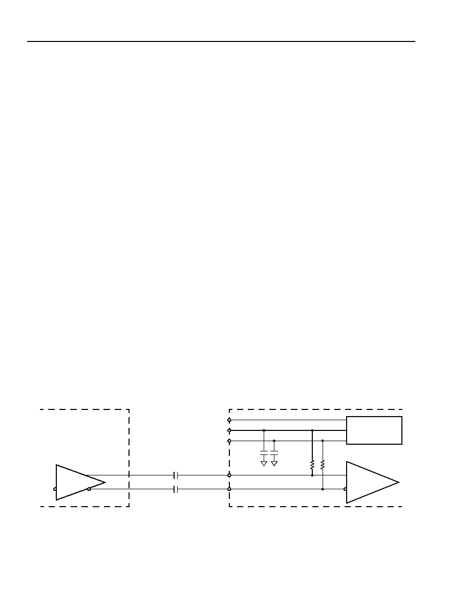
A typical interface between the lightwave receiver and the limiting amplifier is shown in Figure 3.
Note: It is recommended to use a differential interface from the lightwave receiver device with ac coupling.
The slicing level can be adjusted by varying the voltage on the SLADJ pin within Ī300 mV of V
CC
/2. This feature
can be used to improve BER performance in optical receivers and optical amplifier systems. The relationship
between the external voltage and the slicing level is given in Table 9 on page 20. If the voltage at this pin is tied
below 0.5 V, the external slice adjustment is disabled and only the internal offset cancellation feature is active. The
user should connect the SLADJ pin to GND if the slice adjust feature is not needed. The limiting amplifier will per-
form in accordance with the specifications shown in Table 9.
5-8068(F)
Figure 3. Typical TIA to Limiting Amplifier Interface
* The OC-48/STM-16 data rate of 2.48832 Gbits/s is typically approximated as 2.5 Gbits/s in this document when referring to the application
rate. The RS FEC OC-48/STM-16 data rate is 2.66606 Gbits/s and is approximated as 2.7 Gbits/s in this document. Similarly, the OC-3/
STM-1 data rate of 155.52 Mbits/s is typically approximated as 155 Mbits/s, and the RS FEC OC-3/STM-1 data rate of 166.62 Mbits/s is
approximated as 166 Mbits/s. The exact frequencies are used only when necessary for clarity.
LIMITING
OFFSET CANCEL
VTHN
VTHP
LAINN
LAINP
TIA
LIGHTWAVE RECEIVER
50
50
0.047
Ķ
F
0.047
Ķ
F
0.1
Ķ
F
0.1
Ķ
F
SLADJ
&
SLICE ADJUST
AMPLIFIER
DEVICE
Preliminary Data Sheet
TRCV012G5 and TRCV012G7
August 2000
Limiting Amplifier, Clock Recovery, 1:16 Data Demultiplexer
11
Lucent Technologies Inc.
Clock and Data Recovery (CDR)
Clock Recovery Operation
The CDR circuit uses a PLL to extract the clock and retime the 2.5 Gbits/s data. The 2.5 Gbits/s data and the
2.5 GHz recovered clock are available as outputs, as well as a 155 MHz clock derived from the recovered clock.
Clock Recovery PLL Loop Filter
A typical loop filter that meets the OC-48 jitter transfer template is shown in Figure 4. Connect the filter compo-
nents and also connect LFP to VCP and connect LFN to VCN. The component values can be varied to adjust the
loop dynamic response (see Table 5).
Table 5. Clock Recovery Loop Filter Component Values
* Capacitor C1 should be either ceramic or nonpolar.
5-8061(F).a
Figure 4. Clock Recovery PLL Loop Filter Components
CDR Acquisition Time
The limiting amplifier plus CDR will acquire phase/frequency lock within 10 ms after powerup and a valid SONET
signal or a 2
23
≠ 1 PRBS data signal is applied.
CDR Generated Jitter
The limiting amplifier plus CDR's generated jitter performance meets the requirements shown in Table 6. These
specifications apply to the jitter generated at the 2.5 Gbits/s recovered clock pins (CK2G5P/N) when the following
occur: no jitter is present on the input, the limiting amplifier's input signal is within the valid level range given in
Table 9 on page 20, and the data sequence is a valid OC-48 SONET/SDH signal.
Table 6. Clock and Data Recovery Generated Jitter Specifications
* This denotes the device specification for system SONET/SDH compliance when the loop filter in Table 5 and Figure 4 is used.
Components
Values for 2 MHz Loop Bandwidth
C1*
0.47
Ķ
F Ī 10%
C2, C3
10 pF Ī 20%
R1
82.5
Ī 5%
R2
100 k
Ī 5%
Parameter
Typical
Max
(Device)*
Unit
Generated Jitter (p-p):
Measured with 12 kHz to 20 MHz Bandpass Filter
0.06
0.10
UIp-p
Generated Jitter (rms):
Measured with 12 kHz to 20 MHz Bandpass Filter
0.008
0.01
UIrms
C
3
C
2
C
1
R
1
LFN/VCN
LFP/VCP
R
2

TRCV012G5 and TRCV012G7
Preliminary Data Sheet
Limiting Amplifier, Clock Recovery, 1:16 Data Demultiplexer
August 2000
12
Lucent Technologies Inc.
Clock and Data Recovery (CDR)
(continued)
CDR Input Jitter Tolerance
The limiting amplifier plus CDR's jitter tolerance performance meets the requirement shown in Figure 5 on page 13
when the limiting amplifier's input signal is within the valid level range given in Table 9 on page 20, the loop filter in
Figure 4 is used, and the data sequence is a valid OC-48 SONET/SDH signal.
CDR Jitter Transfer
Using the loop filter in Figure 4, the CDR's jitter transfer performance meets the requirement shown in Figure 6
when the input jitter magnitude is within the jitter tolerance requirements given in Figure 5 and the data sequence is
a valid OC-48 SONET/SDH signal. This specification applies to the jitter transferred from the limiting amplifier's
input to the 2.5 Gbits/s recovered clock pins (CK2G5P/N).
Preliminary Data Sheet
TRCV012G5 and TRCV012G7
August 2000
Limiting Amplifier, Clock Recovery, 1:16 Data Demultiplexer
13
Lucent Technologies Inc.
Clock and Data Recovery (CDR)
(continued)
Clock Recovery Jitter Tolerance and Jitter Transfer Specifications
5-8069(F)r.1
Figure 5. Receiver Jitter Tolerance
5-8062(F)r.2
Figure 6. Receiver Jitter Transfer
0.01 UI
0.1 UI
1 UI
10 UI
100
1k
10k
100k
10
FREQUENCY (Hz)
1M
100 UI
10M
(6 kHz, 1.5 UIp-p)
(100 kHz, 1.5 UIp-p)
(600 Hz, 15 UIp-p)
(1 MHz, 0.15 UIp-p)
(10 Hz, 15 UIp-p)
60
40
20
0
1k
10k
100k
1M
10M
50
30
10
100M
FREQUENCY (Hz)
J
I
TTE
R OUT/
J
ITT
ER
IN (
d
B
)
(2 MHz, 0.1 dB)

TRCV012G5 and TRCV012G7
Preliminary Data Sheet
Limiting Amplifier, Clock Recovery, 1:16 Data Demultiplexer
August 2000
14
Lucent Technologies Inc.
Clock and Data Recovery (CDR)
(continued)
Data Path Configuration Option (ENDATAN)
Either the limiting amplifier (LAINP/N) or a CML logic level input (DATAP/N) can be selected as the source of the
2.5 Gbits/s data signal. The DATAP/N input can be used if the limiting amplifier is not needed, or it can be used as
a system loopback path when the limiting amplifier is the normal data path. If the limiting amplifier is not used in
normal operation, the LAINP/N pins should be grounded through a series ac coupling of 0.1
Ķ
F.
High-Speed Serial Clock and Data Output Enables (ENCK2G5N, END2G5N)
Separate output enables are provided for the 2.5 GHz recovered clock output (CK2G5P/N) and the 2.5 Gbits/s
data output (D2G5P/N). These enables are active-low CMOS inputs with internal pull-up resistors. A ground or
logic low applied to the pin enables the corresponding output. When disabled, the pins should be either left floating,
or be connected to a load which returns to V
CC
. The high-speed serial clock and data outputs must not be con-
nected directly to ground when they are disabled.
High-Speed Serial Data Output Mute (MUTE2G5N)
The 2.5 Gbits/s data output (D2G5P/N) may be forced to a logic-low state using MUTE2G5N. This may be desir-
able if the quality of the input data is suspect, as may be the case under LOSA or LOSD conditions. MUTE2G5N is
an active-low CMOS input.
Data and CDR Configuration Options (REFSELN, INLOSN, MUTEDMXN)
A 155 MHz clock (REFCLKP/N) may optionally be provided as a frequency reference to the clock recovery PLL in
order to control the recovered clock frequency when data timing is lost, as may be the case under LOSA or LOSD
conditions. If REFCLKP/N is provided, REFSELN can be used to select REFCLKP/N as the frequency reference to
the clock recovery PLL.
The INLOSN pin will force the VCO to decrease to its minimum frequency. This will prevent the VCO frequency
from drifting to a high value during invalid signal conditions. INLOSN may be used to limit the recovered clock fre-
quency in systems that do not provide a REFCLKP/N signal.
The MUTEDMXN pin will force logic-low data into the demultiplexer, and therefore, keep all demultiplexer outputs
in the logic-low state. MUTEDMXN will not affect the operation of the CDR circuits. This may be desirable if the
quality of the input data is suspect as may be the case under LOSA or LOSD conditions.
The user may utilize the REFSELN, INLOSN, and MUTEDMXN pins in any combination to achieve the desired
response under LOS conditions.
Preliminary Data Sheet
TRCV012G5 and TRCV012G7
August 2000
Limiting Amplifier, Clock Recovery, 1:16 Data Demultiplexer
15
Lucent Technologies Inc.
Decision Circuit--Adjustable Sampling Time (ASTREF, AST[4:0])
The adjustable sampling time (AST) feature allows a deliberate time offset to be introduced for the data recovery
sampling instant relative to the recovered clock. The sampling instant is normally set by the clock recovery phase-
locked loop (PLL) to be midway between the mean values of adjacent NRZ data polarity transitions, which pro-
vides an ideal setup and hold time margin of one half the data period. By setting the AST[4:0] control bits, the user
may shift the instant at which the PLL's recovered clock samples the receive data eye. The AST[4] bit acts as a
polarity setting, AST[3] represents the most significant magnitude bit, and AST[0] represents the least significant
magnitude bit. Since this results in two decoded zero time offset states, AST[4:0] = 00000 is used to disable the
sampling offset feature entirely and will result in traditionally defined midpoint sampling, whereas AST[4:0] = 10000
will also result in midpoint sampling by using the AST feature in its zero time offset condition. With AST[4] set to a
logic high, increasing the AST[3:0] hexadecimal code causes the sampling point to monotonically advance in time;
with AST[4] set to a logic low, the sample time is delayed more as AST[3:0] increases. The ASTREF pin should be
tied to the positive power supply through a low-capacitance 1%, 2.1 k
resistor. This provides a stable reference
resistor to the AST circuitry
.
The AST control bit configurations and corresponding offset times are shown in Table 7
.
Table 7. Adjustable Sampling Time (AST) Control Code
Note: When operating the TRCV012G7 at the FEC rate, the 6.25 ps
step should be scaled down by 7%.
AST[4:0]
Time Offset
(ps)
AST[4:0]
Time Offset
(ps)
01111
≠93.75
10000
0.00
01110
≠87.50
10001
6.25
01101
≠81.25
10010
12.50
01100
≠75.00
10011
18.75
01011
≠68.75
10100
25.00
01010
≠62.50
10101
31.25
01001
≠56.25
10110
37.50
01000
≠50.00
10111
43.75
00111
≠43.75
11000
50.00
00110
≠37.50
11001
56.25
00101
≠31.25
11010
62.50
00100
≠25.00
11011
68.75
00011
≠18.75
11100
75.00
00010
≠12.50
11101
81.25
00001
≠6.25
11110
87.50
00000
0.00
11111
93.75
TRCV012G5 and TRCV012G7
Preliminary Data Sheet
Limiting Amplifier, Clock Recovery, 1:16 Data Demultiplexer
August 2000
16
Lucent Technologies Inc.
Loss of Signal Detection
The loss of signal circuits are used to detect the conditions of low input signal level or no data transitions at the
input. The LOSDN and LOSAN signals can be processed and/or filtered to meet various system-dependent
requirements on declaring loss of signal.
Digital Loss of Signal (LOSDN)
The LOSDN signal alarm is set when no transitions appear in the data path for more than 2.3
Ķ
s. The LOSDN sig-
nal will become active before 100
Ķ
s of no transitions has occurred. When ac coupling the 2.5 Gbits/s data to the
high gain limiting amplifier, in the presence of no significant amplitude data transitions, noise at the limiting ampli-
fier's input may be amplified and appear to be a data transition. This may change the state of LOSDN.
Analog Loss of Signal (LOSAN, PRG_LOSA)
Low signal levels are detected by the limiting amplifier with an optional user-programmable analog loss of signal
(LOSA) threshold. As shown in Figure 7, applying a voltage to the PRG_LOSA pin will adjust the LOSA trip point.
When the voltage on PRG_LOSA is 0 V, LOSAN will never be active even if the level at the limiting amplifier input
is zero. When the voltage on PRG_LOSA is greater than approximately 1 V and less than 2 V, LOSAN will always
be active regardless of the signal level at the limiting amplifier input. If the voltage of the PRG_LOSA pin exceeds
2 V, the threshold defaults to approximately 12 mVp-p differential. This voltage can be adjusted while monitoring
the BER of the system, and is typically set to activate LOSAN for input levels corresponding to a BER of just above
10
≠3
. LOSAN will not be asserted unless the alarm condition exists for at least 2.3
Ķ
s. The LOSAN pin will be de-
asserted when the input level becomes greater than the LOSA threshold by an amount corresponding to 1 dB (typ-
ical) optical power input. The input resistance of the PRG_LOSA pin is typically 50 k
, so a resistor voltage divider
between V
CC
and ground may be used to set the PRG_LOSA level if the V
CC
tolerance and variability is adequate.
5-8070(F)r.2
Figure 7. Typical LOSA Threshold vs. PRG_LOSA Voltage vs. Data Pattern
45
40
35
30
25
20
15
10
5
0
0.0
0.5
0.1
0.2
0.3
0.4
0.6
0.7
0.8
0.9
1.0
PROGRAM VOLTAGE
V
IN
(
m
V
p
-p) AT
W
H
I
CH
L
O
S
A
ACT
I
VAT
E
S
DATA PATTERN
1/1
PRBS
8/8
Preliminary Data Sheet
TRCV012G5 and TRCV012G7
August 2000
Limiting Amplifier, Clock Recovery, 1:16 Data Demultiplexer
17
Lucent Technologies Inc.
Demultiplexer Operation
The serial 2.5 Gbits/s data is clocked into a 1:16 demultiplexer by the recovered 2.5 GHz clock. The demultiplexed
parallel data is retimed with a 155 MHz clock that is derived from the recovered clock. The relationship between
the serial input data and the parallel D[15:0] bits is given in Figure 8. D15 is the bit that was received first in time in
the serial input data stream.
5-8063(F).a
Figure 8. Serial Input to Parallel Output Data Relationship
Parity Generation (PARITYP/N)
The parity pin (PARITYP/N) is a logic 0 when the number of 1s in the 16-bit output register is an even number, and
the parity pin is a logic 1 when the number of 1s in the output register is an odd number.
Demultiplexer Powerdown (PDDMXN)
The entire demultiplexer and parity generator functionality can be powered down for systems requiring only the
2.5 GHz clock and data outputs. Setting PDDMXN = 0 powers down the demultiplexer and parity generation func-
tions as well as the CK155P/N output clock signal. When PDDMXN = 0, the D[15:0] and PARITYP/N pins should
be left unconnected.
Demultiplexer Data Mute (MUTEDMXN)
Setting the MUTEDMXN = 0 mutes the data going into the demultiplexer and forces all zeros to appear at the par-
allel outputs (D[15:0]).
CK155P/N Low-Speed Output Mute (MUTE155N)
The 155 MHz low-speed clock output (CK155P, CK155N) can be forced to logic low by setting MUTE155N, which
is an active-low CMOS input with an internal pull-up resistor. A ground or logic low applied to MUTE155N mutes
the CK155P/N output.
D15
D14
D1
D0
D15
TIME
(D15 RECEIVED FIRST)
(D0 RECEIVED LAST)
(MSB)
(LSB)
TRCV012G5 and TRCV012G7
Preliminary Data Sheet
Limiting Amplifier, Clock Recovery, 1:16 Data Demultiplexer
August 2000
18
Lucent Technologies Inc.
CML Output Structure (Used on Pins D2G5P/N, CK2G5P/N)
The CML architecture is essentially a current-steering mechanism combined with an amplifier. This makes the out-
put swing of the signal a function of the termination resistor and the programmable output current. The user should
connect external termination resistors from the CML output pins to V
CC
. The on-chip, 100
pull-up resistors pro-
vide a dc path when using an ac-coupled load.
The voltage swing of a CML signal is typically 400 mV, half that of ECL/PECL. The lower pulse amplitude reduces
noise transients, crosstalk, and EMI. It also uses half the amount of current through the termination resistors. The
schematic of a typical CML output structure is shown in Figure 9.
5-8065(F)r.2
Figure 9. Typical CML Output Structure
Choosing the Value of the External CML Reference Resistors (RREF1, RREF2)
The flexibility of the CML interface permits certain parameters to be customized for a particular application. The
RREF1 resistor controls the CML output driver current source. Adjusting this tail
current and termination resistors
will allow signal amplitude control (see the CML output specifications for limitations, page 22 and page 24) and
flexibility in termination schemes.
With RREF2 set to 1.5 k
, the equation for the CML output current is the following:
Iout = (18)*(1.21)/RREF1
The CML outputs have on-chip 100
load resistors to V
CC
in order to accommodate capacitive ac coupling. With
a 50
1% load, the effective load resistance will be 33.33
Ī 6%. For a 400 mV voltage swing into the 50
load,
set RREF1 to 1.8 k
. For a 600 mV voltage swing, set RREF1 to 1.2 k
. In both cases, RREF2 remains fixed at a
value of 1.5 k
.
DEVICE-INTERNAL CML OUTPUT BUFFER CIRCUIT
EXTERNAL OUTPUT TERMINATION
V
CC
V
CC
50
50
V
CC
V
CC
100
100
VREF
18X
V
CC
RREF1
RREF2
+
≠
I
OUT
I
OUT
Preliminary Data Sheet
TRCV012G5 and TRCV012G7
August 2000
Limiting Amplifier, Clock Recovery, 1:16 Data Demultiplexer
19
Lucent Technologies Inc.
Absolute Maximum Ratings
Stresses in excess of the absolute maximum ratings can cause permanent damage to the device. These are abso-
lute stress ratings only. Functional operation of the device is not implied at these or any other conditions in excess
of those given in the operational sections of the data sheet. Exposure to absolute maximum ratings for extended
periods can adversely affect device reliability.
Handling Precautions
Although protection circuitry has been designed into this device, proper precautions should be taken to avoid expo-
sure to electrostatic discharge (ESD) during handling and mounting. Lucent employs a human-body model (HBM)
and charged-device model (CDM) for ESD-susceptibility testing and protection design evaluation. ESD voltage
thresholds are dependent on the circuit parameters used in the defined model. No industrywide standard has been
adopted for the CDM. However, a standard HBM (resistance = 1500
, capacitance = 100 pF) is widely used and,
therefore, can be used for comparison purposes:
Operating Conditions
Table 8. Recommended Operating Conditions
Parameter
Min
Max
Unit
Power Supply Voltage (V
CC
)
--
4.0
V
Storage Temperature
≠40
125
įC
Pin Voltage
GND ≠ 0.5
V
CC
+ 0.5
V
Device
Voltage
TRCV012G5
200 V
TRCV012G7
200 V
Parameter
Symbol
Min
Typ
Max
Unit
Power Supply (dc voltage)
--
3.135
3.3
3.465
V
Ground
--
--
--
--
V
Input Voltage:
Low
High
V
IL
V
IH
(See Table 11,
Table 13,
Table 15.)
(See Table 11,
Table 13,
Table 15.)
(See Table 11,
Table 13,
Table 15.)
V
V
Temperature:
Ambient
Junction
T
A
≠40
--
85
įC
--
0
--
125
įC
Power Dissipation:
MBIC 025 BiCMOS
MBIC 025 SiGe BiCMOS
P
D
P
D
--
--
2.5
1.45
3.43
1.73
W
W
TRCV012G5 and TRCV012G7
Preliminary Data Sheet
Limiting Amplifier, Clock Recovery, 1:16 Data Demultiplexer
August 2000
20
Lucent Technologies Inc.
Electrical Characteristics
Limiting Amplifier Specifications
Table 9. Limiting Amplifier Characteristics
Optional Reference Frequency (REFCLKP/N) Specifications
The CDR operates without any reference clock. However, a reference clock input is available should the user want
to maintain the CDR frequency lock without any data input.
s
When using the TRCV012G5 device, a 155.52 MHz differential LVPECL clock can be applied to the
REFCLKP/N input.
s
When using the TRCV012G7 device at the OC-48/STM-16 rate, a 155.52 MHz differential LVPECL clock can be
applied to the REFCLKP/N input.
s
When using the TRCV012G7 device at the RS FEC OC-48/STM-16 rate, a 166.62 MHz differential LVPECL
clock can be applied to the REFCLKP/N input.
Table 10 provides the characteristics of the REFCLKP/N input.
Table 10. Reference Frequency Characteristics
* Includes effects of power supply variation, temperature, electrical loading, and aging. The Ī20 ppm tolerance is
required to meet SONET/SDH requirements if the reference frequency is used for system clocking when timing
recovery is lost.
Specified range is to be compatible with environmental specification of TRCV012G5 or TRCV012G7. Applications
requiring a reduced temperature range may specify the reference frequency oscillator accordingly.
Parameter
Min
Typical
Max
Unit
Data Input Level for Full Amplifier Limiting
(differential input)
30
--
1200
mVp-p
Small-signal Gain
26
30
32
dB
Small-signal Bandwidth
3
--
--
GHz
Input Referred Wideband Noise
(dc--2.5 GHz)
--
--
170
Ķ
Vrms
Input Return Loss (LAINP/LAINN pins):
100 MHz--2 GHz
2 GHz--3 GHz
--
--
--
--
≠20
≠15
dB
dB
Input Slice Level Adjustment
--
0.01*(SLADJ ≠ V
CC
/2)
--
V
SLADJ Input Range
V
CC
/2 ≠ 0.3
--
V
cc
/2 + 0.3
V
Slice Feature Disable Voltage (SLADJ)
--
--
0.5
V
Parameter
Min
Typ
Max
Unit
Reference Frequency (REFCLKP/N)
--
155.52
--
MHz
--
166.62
--
MHz
Reference Frequency Tolerance*
≠20
--
20
ppm
Duty Cycle
40
--
60
%
Temperature
≠40
--
85
įC
Supply Voltage
3.10
--
3.60
V
Preliminary Data Sheet
TRCV012G5 and TRCV012G7
August 2000
Limiting Amplifier, Clock Recovery, 1:16 Data Demultiplexer
21
Lucent Technologies Inc.
Electrical Characteristics
(continued)
LVPECL, CMOS, CML Input and Output Pins
Notes:
1. For Table 11 through Table 18, V
CC
= 3.3 V Ī 5%, T
A
= ≠40 įC to +85 įC; these tables apply to both MBIC 025
BiCMOS and MBIC 025 SiGe BiCMOS technologies.
2. For more information on interpreting CML specifications, see the CML Output Structure (Used on Pins
D2G5P/N, CK2G5P/N) section on page 18.
Table 11. LVPECL Input Pin Characteristics
Table 12. LVPECL Output Pin Characteristics
Table 13. CMOS Input Pin Characteristics
Table 14. Open Drain Output Pin Characteristics
Applicable
Pins
Symbol
Parameter
Conditions
Min
Typ
Max
Unit
REFCLKP/N
V
IH
Input Voltage High
Referred to V
CC
≠1165
--
≠880
mV
V
IL
Input Voltage Low
Referred to V
CC
≠1810
--
≠1475
mV
I
IH
Input Current High Leakage
V
IN
= V
IH
(max)
--
--
20
Ķ
A
I
IL
Input Current Low Leakage
V
IN
= V
IL
(min)
5
--
--
Ķ
A
Applicable
Pins
Symbol
Parameter
Conditions
Min
Typ
Max
Unit
D[15:0]P/N,
PARITYP/N,
CK155P/N
V
OH
Output Voltage High
Load = 50
connected to
V
CC
≠ 2.0 V
V
CC
≠ 1.31
V
CC
≠ 1.20
V
CC
≠ 0.90
V
V
OL
Output Voltage Low
Load = 50
connected to
V
CC
≠ 2.0 V
V
CC
≠ 1.95
V
CC
≠ 1.88
V
CC
≠ 1.80
V
Applicable
Pins
Symbol
Parameter
Conditions
Min
Max
Unit
END2G5N,
ENCK2G5N,
RESETN,
ENDATAN,
ENDATCKN,
REFSELN,
MUTEDMXN,
PDDMXN,
MUTE155N,
MUTE2G5N
V
IH
Input Voltage High
--
V
CC
≠ 1.0
V
CC
V
V
IL
Input Voltage Low
--
GND
1.0
V
I
IH
Input Current High Leakage
V
IN
= V
CC
--
10
Ķ
A
I
IL
Input Current Low Leakage
V
IN
= GND
≠225
--
Ķ
A
AST[4:0]
I
IH
Input Current High Leakage
V
IN
= V
CC
--
225
Ķ
A
I
IL
Input Current Low Leakage
V
IN
= GND
≠10
--
Ķ
A
Applicable
Pins
Symbol
Parameter
Conditions
Min
Max
Unit
LOSAN,
LOSDN
V
OH
Output Voltage High
R
L
5 k
V
CC
≠ 0.5
V
CC
V
V
OL
Output Voltage Low
R
L
5 k
GND
0.5
V
C
l
Output Load Capacitance
--
--
30
pF
TRCV012G5 and TRCV012G7
Preliminary Data Sheet
Limiting Amplifier, Clock Recovery, 1:16 Data Demultiplexer
August 2000
22
Lucent Technologies Inc.
Electrical Characteristics
(continued)
LVPECL, CMOS, CML Input and Output Pins
(continued)
Table 15. CML Input Pin dc Characteristics
Table 16. CML Output Pin dc Characteristics
* Applies when RREF1 = 1 k
.
Applies when RREF1 = 1.8 k
.
Applies when RREF1 = 6 k
.
Applicable
Pins
Symbol
Parameter
Conditions
Min
Typ
Max
Unit
DATAP/N,
DATCKP/N
V
IL
Input Voltage Low
--
--
V
CC
≠ 0.4
--
V
V
IH
Input Voltage High
--
V
CC
--
V
Applicable
Pins
Symbol
Parameter
Conditions
Min*
Typ
Max
Unit
D2G5P/N,
CK2G5P/N
V
OL
Output Voltage Low
RREF2 = 1.5 k
R
L
= 50
All signals
differential
V
CC
≠ 1.2
V
CC
≠ 0.4
--
V
V
OH
Output Voltage High
--
V
CC
V
CC
+ 0.3
V
I
OL
Output Current Low
3.6
12
18
mA
I
OH
Output Current High
--
0
1
Ķ
A
Preliminary Data Sheet
TRCV012G5 and TRCV012G7
August 2000
Limiting Amplifier, Clock Recovery, 1:16 Data Demultiplexer
23
Lucent Technologies Inc.
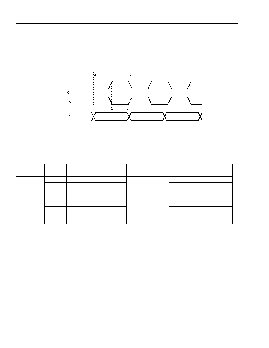
Timing Characteristics
Output Timing
The timing relationships between the 155 MHz or 166 MHz output clock (CK155P/N) and the output demultiplexer
data (D[15:0]P/N) and the output parity (PARITYP/N) are shown in Figure 10.
5-7726(F).fr.4
Figure 10. Transmit Timing Waveform with 155 MHz or 166 MHz Clock
The 155 MHz or 166 MHz output clock and data signals from Figure 10 are characterized in Table 17.
Table 17. LVPECL Output Pin ac Timing Characteristics
Applicable
Pins
Symbol
Parameter
Conditions
Min
Typ
Max
Unit
CK155P/N
--
Duty Cycle
All signals
differential
48
50
52
%
t
PERIOD
155.52 MHz Clock Period
--
6.43
--
ns
166.62 MHz Clock Period
--
6.00
--
ns
D[15:0]P/N,
PARITYP/N,
CK155P/N
t
DD1
Time Delay from Clock Edge
to D[15:0]P/N Edge
2.9
3.2
3.9
ns
t
DD2
Time Delay from Clock Edge
to PARITYP/N Edge
3.3
4.0
4.7
ns
t
RISE
,
t
FALL
Rise, Fall Times:
20%--80%
200
500
800
ps
t
SKEW
Transition Skew Rise to Fall
≠100
0
100
ps
OUTPUT
CK155P
CK155N
OUTPUTS
D[15:0]P/N
DATA 1
t
PERIOD
DATA 2
DATA 3
PARITY 1
PARITY 2
PARITY 3
PARITYP/N
t
DD2
t
DD1
TRCV012G5 and TRCV012G7
Preliminary Data Sheet
Limiting Amplifier, Clock Recovery, 1:16 Data Demultiplexer
August 2000
24
Lucent Technologies Inc.
Timing Characteristics
(continued)
Output Timing
(continued)
The timing relationship between the 2.5 GHz or 2.7 GHz output clock (CK2G5P/N) and the 2.5 Gbits/s or
2.7 Gbits/s output data (D2G5P/N) is shown in Figure 11.
5-7726(F).er.4
Figure 11. Transmit Timing Waveform with 2.5 GHz or 2.7 GHz Clock
The 2.5 GHz or 2.7 GHz output clock and data signals from Figure 11 are characterized in Table 18.
Table 18. CML Output Pin ac Timing Characteristics
Applicable
Pins
Symbol
Parameter
Conditions
Min
Typ
Max
Unit
CK2G5P/N
--
Duty Cycle
RREF1 = 1.8 k
RREF2 = 1.5 k
R
L
= 50
All signals
differential
40
50
60
%
t
PERIOD
2.48832 GHz Clock Period
--
402
--
ps
2.66606 GHz Clock Period
--
375
--
ps
D2G5P/N,
CK2G5P/N
t
DD
Time Delay from Clock Edge
to D2G5P/N Edge
151
201
251
ps
t
RISE
,
t
FALL
Rise, Fall Times:
20%--80%
50
80
120
ps
t
SKEW
Transition Skew Rise to Fall
≠10
0
10
ps
OUTPUT
CK2G5P
CK2G5N
OUTPUT
D2G5P/N
DATA 1
t
PERIOD
DATA 2
DATA 3
t
DD
Preliminary Data Sheet
TRCV012G5 and TRCV012G7
August 2000
Limiting Amplifier, Clock Recovery, 1:16 Data Demultiplexer
25
Lucent Technologies Inc.
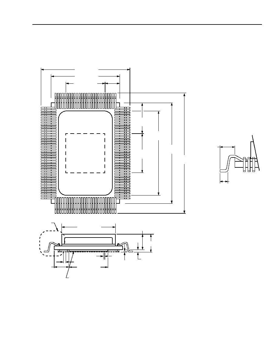
Outline Diagram
128-Pin QFP
Dimensions are in millimeters.
5-8416(F)r.2
3.30 (REF)
0.50 (TYP)
2.80 (REF)
1
38
65
102
103
128
17.20
Ī
0.20
19.86
Ī
0.10
64
39
1
LU
CENT
C
ode
N
a
m
e
Y
Y
WWL
XXX
XXK
NV
0.38 (REF)
DETAIL A
11.43
Ī
0.18
23.20
Ī
0.20
13.89
Ī
0.10
8.13 (REF)
2.89
(REF)
17.52
Ī
0.18
8.13
(REF)
0.20
Ī
0.06
0.000 TO 0.100
8.13 (REF)
2.89
(REF)
(8.13)
2
x 0.305 HEAT SINK
5.87
(REF)
0.800
Ī
0.150
1.600
Ī
0.150
DETAIL A
TRCV012G5 and TRCV012G7
Preliminary Data Sheet
Limiting Amplifier, Clock Recovery, 1:16 Data Demultiplexer
August 2000
26
Lucent Technologies Inc.
Outline Diagram
(continued)
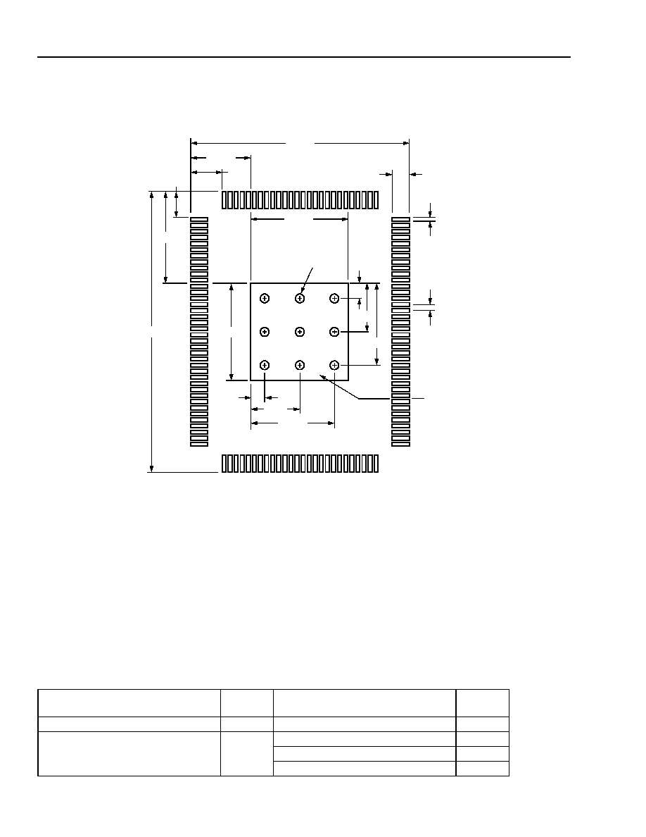
Board Installation Recommendations
5-9862 (F)r.1
Figure 12. Heat Sink Ground Pattern
Thermal Considerations (MBIC 025 BiCMOS and MBIC 025 SiGe BiCMOS)
The TRCV012G5 and TRCV012G7 devices use a square heat sink on the bottom of the package for heat dissipa-
tion. This heat sink is planar with the lead surface which contacts the board. For optimum heat transfer, the heat
sink should be soldered to the application board using the suggested footprint shown above. Depending on the
application more heat sinking may be required.
Note: Certain precautions must be taken when using solder. For installation using a constant temperature solder,
temperatures of under 300 įC may be employed for periods of time up to 5 seconds, maximum. For installa-
tion with a soldering iron (battery operated or non-switching only), the soldering tip temperature should not
be greater than 300 įC and the soldering time for each lead must not exceed 5 seconds.
Table 19. Thermal Resistance
Parameter
Symbol
Conditions
Unit
(įC/W)
Thermal resistance, junction to board
JB
No air flow, device soldered to board
11.5
Thermal resistance, junction to
ambient
JA
100 lfpm, device soldered to board
18
300 lfpm, device soldered to board
15.6
500 lfpm, device soldered to board
14.6
0.705
0.193
0.100
0.012
0.060
0.100
0.311
0.941
0.320
0.050
0.160
0.160
0.270
0.270
0.050
HEAT SINK
TYP
Ý0.032
0.320
GROUND
PATTERN
0.019685
Preliminary Data Sheet
TRCV012G5 and TRCV012G7
August 2000
Limiting Amplifier, Clock Recovery, 1:16 Data Demultiplexer
27
Lucent Technologies Inc.
Ordering Information
DS00-234HSPL Replaces DS00-154HSPL to Incorporate the Following Updates
1. Added a second technology, MBIC 025 SiGe BiCMOS, to the data sheet.
2. Page 8, REFCLKP/N pins, corrected definition.
3. Page 11, Table 5, updated C1, R1, and R2 values in Clock Recovery Loop Filter Component Values.
4. Page 19, Absolute Maximum Ratings, added maximum power supply value of 4.0 V.
5. Page 19, Handling Precautions, corrected ESD threshold value from TBD to
200 V.
6. Page 19, Table 8, corrected BiCMOS power dissipation from TBD to 3.43 W in Recommended Operating Con-
ditions; added MBIC 025 SiGe BiCMOS power dissipation values.
7. Page 19, Table 8, added junction temperature in Recommended Operating Conditions.
8. Page 21, Table 12, corrected values in LVPECL Output Pin Characteristics.
9. Page 23, Table 17, updated minimum duty cycle from 40% to 48%, maximum duty cycle from 60% to 52%, and
tDD1 minimum value from 2.5 ns to 2.9 ns in LVPECL Output Pin ac Timing Characteristics.
10. Page 26, added the section Board Installation Recommendations and Thermal Considerations (MBIC 025
BiCMOS and MBIC 025 SiGe BiCMOS).
11. Page 27, Ordering Information, added MBIC 025 SiGe BiCMOS comcodes.
Device Code
Package
Temperature
Comcode
(Ordering Number)
TRCV012G5:
TRCV012G5 (BiCMOS)
TRCV012G53XE1 (SiGe BiCMOS)
128-pin QFP
128-pin QFP
≠40 įC to +85 įC
≠40 įC to +85 įC
108419953
108700675
TRCV012G7:
TRCV012G7 (BiCMOS)
TRCV012G73XE1 (SiGe BiCMOS)
128-pin QFP
128-pin QFP
≠40 įC to +85 įC
≠40 įC to +85 įC
108560343
108700683
--
--
--
--

TRCV012G5 and TRCV012G7
Preliminary Data Sheet
Limiting Amplifier, Clock Recovery, 1:16 Data Demultiplexer
August 2000
Lucent Technologies Inc. reserves the right to make changes to the product(s) or information contained herein without notice. No liability is assumed as a result of their use or application. No
rights under any patent accompany the sale of any such product(s) or information.
Copyright © 2000 Lucent Technologies Inc.
All Rights Reserved
August 2000
DS00-234HSPL (Replaces DS00-154HSPL)
For additional information, contact your Microelectronics Group Account Manager or the following:
INTERNET:
http://www.lucent.com/micro
E-MAIL:
docmaster@micro.lucent.com
N. AMERICA:
Microelectronics Group, Lucent Technologies Inc., 555 Union Boulevard, Room 30L-15P-BA, Allentown, PA 18109-3286
1-800-372-2447, FAX 610-712-4106 (In CANADA: 1-800-553-2448, FAX 610-712-4106)
ASIA PACIFIC: Microelectronics Group, Lucent Technologies Singapore Pte. Ltd., 77 Science Park Drive, #03-18 Cintech III, Singapore 118256
Tel. (65) 778 8833, FAX (65) 777 7495
CHINA:
Microelectronics Group, Lucent Technologies (China) Co., Ltd., A-F2, 23/F, Zao Fong Universe Building, 1800 Zhong Shan Xi Road, Shanghai
200233 P. R. China Tel. (86) 21 6440 0468, ext. 325, FAX (86) 21 6440 0652
JAPAN:
Microelectronics Group, Lucent Technologies Japan Ltd., 7-18, Higashi-Gotanda 2-chome, Shinagawa-ku, Tokyo 141, Japan
Tel. (81) 3 5421 1600, FAX (81) 3 5421 1700
EUROPE:
Data Requests: MICROELECTRONICS GROUP DATALINE: Tel. (44) 7000 582 368, FAX (44) 1189 328 148
Technical Inquiries: GERMANY: (49) 89 95086 0 (Munich), UNITED KINGDOM: (44) 1344 865 900 (Ascot),
FRANCE: (33) 1 40 83 68 00 (Paris), SWEDEN: (46) 8 594 607 00 (Stockholm), FINLAND: (358) 9 3507670 (Helsinki),
ITALY: (39) 02 6608131 (Milan), SPAIN: (34) 1 807 1441 (Madrid)