Data Sheet, Revision 3
September 21, 2005
TSI-1
1k x 1k Time-Slot Interchanger
1 Introduction
The last issue of this data sheet was August 31, 2005. A change history is included in Section
11 Change History on page
61
. Red change bars have been installed on all text, figures, and tables that were added or changed. All changes to the text
are highlighted in red. Changes within figures, and the figure title itself, are highlighted in red, if feasible. Formatting or
grammatical changes have not been highlighted. Deleted sections, paragraphs, figures, or tables will be specifically
mentioned.
This document consists of two major sections:
The
TSI-1
device hardware description. This section contains ball information, operating conditions, dc electrical charac-
teristics, timing diagrams, ac characteristics, and packaging information.
The
TSI-1
device register description. This section contains register information.
1.1 Related Documents
The documentation package for this device consists of the following documents:
The TSI-1 1k x 1k Time-Slot Interchanger Product Brief, the TSI Family Selection Guide, the TSI-1 1k x 1k Time-Slot
Interchanger Data Sheet (this document), and the TSI-1 Time-Slot Interchanger System Design Guide.
These documents are available on the public website shown below.
If the reader displays this document using Acrobat Reader
�
, clicking on any blue text will bring the reader to that reference
point.
To access related documents, including the documents mentioned above, please go to the following public website, or con-
tact your Agere representative (see the last page of this document).
http://www.agere.com/telecom/time_slot_interchangers.html
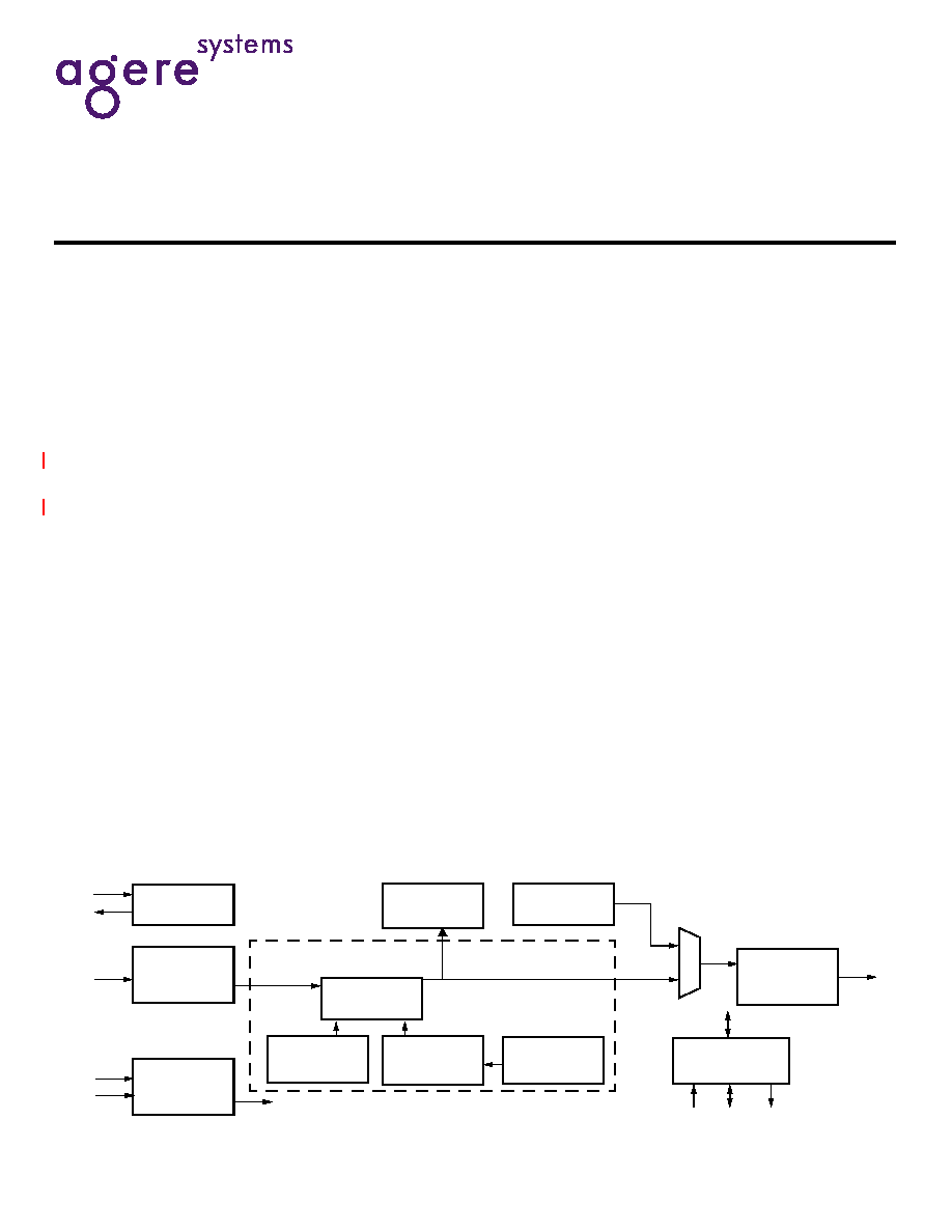
1.2 Block Diagram and High-Level Interface Definition
Figure 1-1. Block Diagram and High-Level Interface Definition
TEST ACCESS
PORT
READ ADDRESS
COUNTER
CONNECTION
STORE
WRITE ADDRESS
COUNTER
DATA
STORE
MICROPROCESSOR
INTERFACE
TRANSMIT
CHI
TEST PATTERN
GENERATOR
TEST PATTERN
MONITOR
CLOCK
GENERATOR
RECEIVE
CHI
16
16
1k x 1k
Switch Fabric

TSI-1
Data Sheet, Revision 3
1k x 1k Time-Slot Interchanger
September 21, 2005
Table of Contents
Contents
Page
2
2
Agere Systems Inc.
1 Introduction .........................................................................................................................................................................1
1.1 Related Documents .....................................................................................................................................................1
1.2 Block Diagram and High-Level Interface Definition .....................................................................................................1
2 Ball Information ...................................................................................................................................................................7
2.1 Top View Ball Diagram ................................................................................................................................................7
2.2 Package Ball Assignments ..........................................................................................................................................8
2.3 Package Ball Matrix ...................................................................................................................................................10
2.3.1 Top View ..........................................................................................................................................................10
2.3.2 Bottom View .....................................................................................................................................................11
2.4 Ball Types ..................................................................................................................................................................12
2.5 Ball Definitions ...........................................................................................................................................................12
3 Operating Conditions and Reliability ................................................................................................................................15
3.1 Absolute Maximum Ratings .......................................................................................................................................15
3.2 Recommended Operating Conditions .......................................................................................................................15
3.3 Handling Precautions ................................................................................................................................................15
3.4 Thermal Parameters (Definitions and Values) ...........................................................................................................16
3.5 Power Consumption ..................................................................................................................................................17
4 dc Electrical Characteristics .............................................................................................................................................18
5 Timing Diagrams and ac Characteristics ..........................................................................................................................19
6 Register Description .........................................................................................................................................................31
6.1 Device Addressing Notes ..........................................................................................................................................31
6.2 Acronyms Used .........................................................................................................................................................31
6.3 Address Map .............................................................................................................................................................31
6.4 Register Summary .....................................................................................................................................................32
6.5 Global Control Registers ...........................................................................................................................................34
6.6 Connection Store Generator Registers .....................................................................................................................39
6.7 Test Pattern Generator and Monitor Registers ..........................................................................................................44
6.8 Concentration Highway Configuration Registers .......................................................................................................48
7 Switch Fabric Control .......................................................................................................................................................54
8 Connection Store ..............................................................................................................................................................58
9 Outline Diagrams ..............................................................................................................................................................60
10 Ordering Information .......................................................................................................................................................61
11 Change History ...............................................................................................................................................................61
11.1 Navigating Through an Adobe Acrobat Document ..................................................................................................61

Data Sheet, Revision 3
TSI-1
September 21, 2005
1k x 1k Time-Slot Interchanger
Table of Contents
(continued)
Contents
Page
Agere Systems Inc.
3
Table 2-1. Package Ball Assignments in Signal Name Order.................................................................................................8
Table 2-2. Package Ball Assignments (Top View) ................................................................................................................10
Table 2-3. Package Ball Assignments (Bottom View)........................................................................................................... 11
Table 2-4. Ball Types ............................................................................................................................................................12
Table 2-5. Timing Port ..........................................................................................................................................................12
Table 2-6. Transmit and Receive Concentration Highways ..................................................................................................12
Table 2-7. Control Port..........................................................................................................................................................13
Table 2-8. Initialization and Test Access...............................................................................................................................13
Table 2-9. Power Balls..........................................................................................................................................................14
Table 3-1. Absolute Maximum Ratings .................................................................................................................................15
Table 3-2. Operating Conditions ...........................................................................................................................................15
Table 3-3. ESD Tolerance.....................................................................................................................................................15
Table 3-4. Thermal Parameter Values ..................................................................................................................................16
Table 3-5. Power Consumption ............................................................................................................................................17
Table 4-1. CMOS Inputs .......................................................................................................................................................18
Table 4-2. CMOS Outputs ....................................................................................................................................................18
Table 4-3. CMOS Bidirectionals (DATA[15:0]) ......................................................................................................................18
Table 5-1. CHICLK Timing Specifications.............................................................................................................................19
Table 5-2. MPUCLK Timing Specifications ...........................................................................................................................19
Table 5-3. CMOS Output ac Timing Specification * ..............................................................................................................20
Table 5-4. CHI Interface Timing ............................................................................................................................................21
Table 5-5. CHI 3-State Output Control..................................................................................................................................27
Table 5-6. Microprocessor Port Timing--Read Cycle...........................................................................................................28
Table 5-7. Microprocessor Port Timing--Write Cycle ...........................................................................................................29
Table 6-1. Address Map........................................................................................................................................................31
Table 6-2. Global Registers ..................................................................................................................................................32
Table 6-3. Connection Store Generator Registers................................................................................................................32
Table 6-4. Test Pattern Generator and Monitor Registers ....................................................................................................33
Table 6-5. Concentration Highway Configuration Registers .................................................................................................33
Table 6-6. Switch Fabric Control...........................................................................................................................................33
Table 6-7. Connection Store .................................................................................................................................................34
Table 6-8. Reserved Registers .............................................................................................................................................34
Table 6-9. Version_Control (Read Only)...............................................................................................................................34
Table 6-10. Chip_Identity (Read Only) .................................................................................................................................34
Table 6-11. Summary_Interrupt_Status (Read Only)............................................................................................................35
Table 6-12. Summary_Interrupt_Mask (Read/Write) ............................................................................................................35
Table 6-13. CPU_Access_Error (CORWN) ..........................................................................................................................36
Table 6-14. CPU_Access_Error_Mask (Read/Write)............................................................................................................36
Table 6-15. Global_Control (Read/Write) .............................................................................................................................37
Table 6-16. PLL_Control (Read/Write) .................................................................................................................................38
Table 6-17. Power_Control (Read/Write)..............................................................................................................................38
Table 6-18. Invalid_Address_Trap (Read Only)....................................................................................................................38
Table 6-19. Scratch_Register (Read/Write)..........................................................................................................................38
Table 6-20. Reserved_0 (Read/Write) ..................................................................................................................................39
Table 6-21. CSG_Control (Read/Write) ................................................................................................................................39
Table 6-22. CSG_Status (Read Only)...................................................................................................................................40
Table 6-23. CSG_Starting_Address (Read/Write) ................................................................................................................40
Table 6-24. CSG_Ending_Address (Read/Write) .................................................................................................................40
Table 6-25. CSG_Write_Enable_Low (Read/Write)..............................................................................................................40
Table 6-26. CSG_Write_Enable_High (Read/Write).............................................................................................................40
Table 6-27. CSG_Seed_Low (Read/Write)...........................................................................................................................41
Table 6-28. CSG_Seed_High (Read/Write)..........................................................................................................................41

TSI-1
Data Sheet, Revision 3
1k x 1k Time-Slot Interchanger
September 21, 2005
Table of Contents
(continued)
Tables
Page
4
4
Agere Systems Inc.
Table 6-29. CSG_OR_Mask_Low (Read/Write) ...................................................................................................................41
Table 6-30. CSG_OR_Mask_High (Read/Write) ..................................................................................................................41
Table 6-31. CSG_AND_Mask_Low (Read/Write).................................................................................................................42
Table 6-32. CSG_AND_Mask_High (Read/Write) ................................................................................................................42
Table 6-33. CS_Stream_Control (Read/Write) .....................................................................................................................42
Table 6-34. CSG_Configuration (Read/Write) ......................................................................................................................43
Table 6-35. TPG_Configuration (Read/Write).......................................................................................................................44
Table 6-36. TPG_User_Pattern (Read/Write).......................................................................................................................44
Table 6-37. TPM_Configuration (Read/Write) ......................................................................................................................45
Table 6-38. TPM_User_Pattern (Read/Write).......................................................................................................................45
Table 6-39. TPM_Error_Count (Sat/Roll*) ............................................................................................................................46
Table 6-40. TPG_Inject_Error_Count (Write Only) ...............................................................................................................46
Table 6-41. TPG_Data_Invert_Mask (Read/Write) ...............................................................................................................46
Table 6-42. TPM_Status (Read Only)...................................................................................................................................47
Table 6-43. TPM_Status_Mask (Read/Write) .......................................................................................................................47
Table 6-44. Receive_CHI_Configuration (Read/Write).........................................................................................................48
Table 6-45. Receive_CHI_Status (CORWN) Receive_CHI_Status (CORWN).....................................................................48
Table 6-46. Receive_CHI_Status_Mask (Read/Write)..........................................................................................................49
Table 6-47. Receive_CHI_Global_Configuration (Read/Write) ............................................................................................49
Table 6-48. Transmit_CHI_Configuration (Read/Write) ........................................................................................................50
Table 6-49. Transmit_CHI_Status (CORWN) .......................................................................................................................51
Table 6-50. Transmit_CHI_Status_Mask (Read/Write).........................................................................................................51
Table 6-51. Transmit_CHI_Global_Configuration (Read/Write)............................................................................................52
Table 6-52. Receive_CHI_Time_Slot_Offset (Read/Write)...................................................................................................53
Table 6-53. Transmit_CHI_Time_Slot_Offset (Read/Write)..................................................................................................53
Table 7-1. SF_Status (CORWN)...........................................................................................................................................54
Table 7-2. SF_Status_Mask (Read/Write) ............................................................................................................................54
Table 7-3. Data_Store_Time_Slot_Capture_Select (Read/Write).........................................................................................55
Table 7-4. Data_Store_Captured_Data (Read Only) ............................................................................................................55
Table 7-5. Connection_Store_Parity_Error_Address_Trap (CORWN) .................................................................................56
Table 7-6. Receive_Link_Offset (Read Only) .......................................................................................................................56
Table 7-7. Transmit_Link_Offset (Read/Write) .....................................................................................................................56
Table 7-8. Wide_Mode_Control (Read/Write).......................................................................................................................57
Table 8-1. Low_Control_Word (Read/Write).........................................................................................................................58
Table 8-2. High_Control_Word (Read/Write) ........................................................................................................................59
Table 10-1. Ordering Information..........................................................................................................................................61

Data Sheet, Revision 3
TSI-1
September 21, 2005
1k x 1k Time-Slot Interchanger
Table of Contents
(continued)
Figures
Page
Agere Systems Inc.
5
Figure 1-1. Block Diagram and High-Level Interface Definition..............................................................................................1
Figure 2-1. Package Diagram (Top View) ..............................................................................................................................7
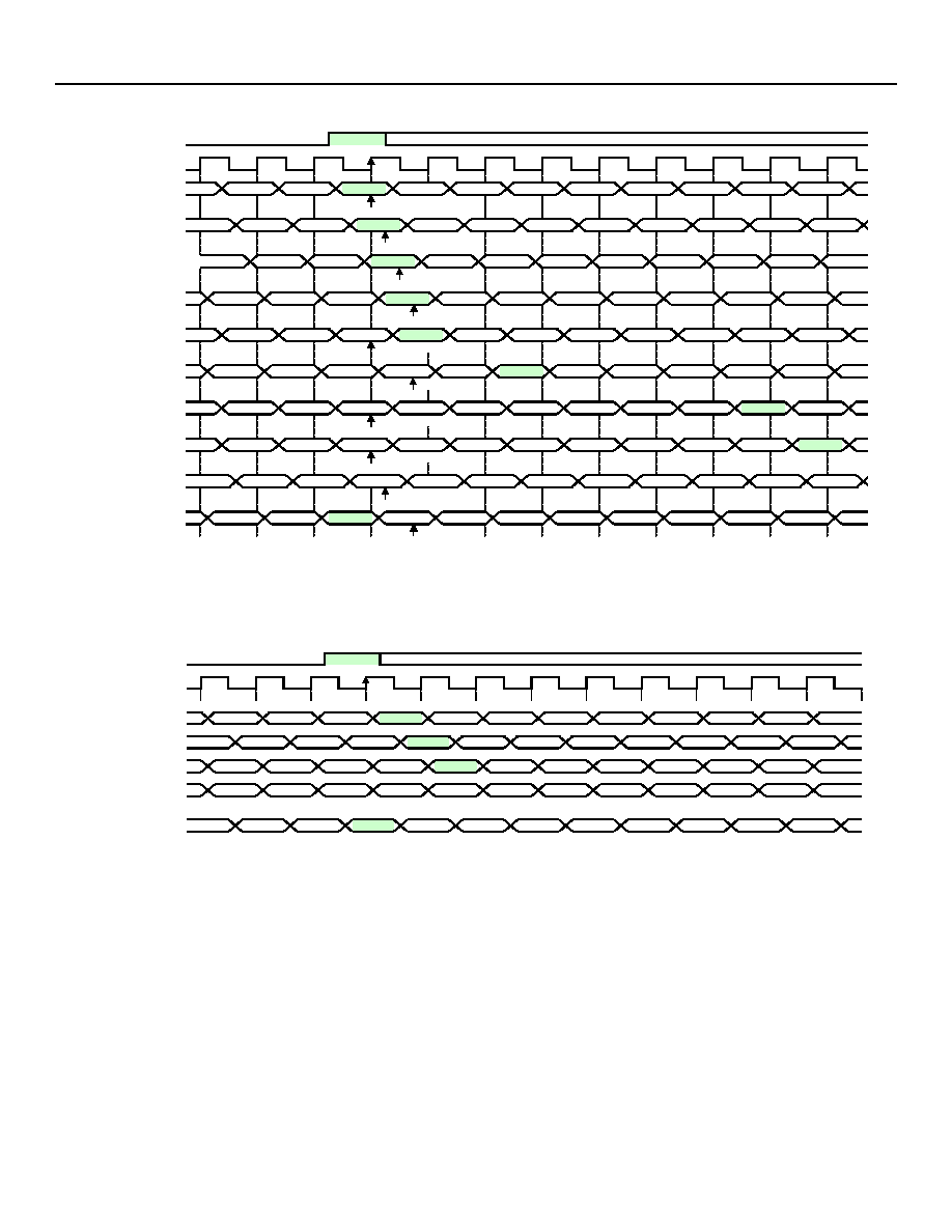
Figure 5-1. CHICLK Timing Specifications ...........................................................................................................................19
Figure 5-2. MPUCLK Timing Specifications .........................................................................................................................19
Figure 5-3. ac Timing Specification ......................................................................................................................................20
Figure 5-4. CHI Interface Timing ..........................................................................................................................................21
Figure 5-5. Typical Receive CHI Timing with 16.384 Mbits/s Data and 16.384 MHz CHICLK.............................................22
Figure 5-6. Transmit CHI Timing with 16.384 Mbits/s Data and 16.384 MHz CHICLK ........................................................22
Figure 5-7. Typical Receive CHI Timing with 8.192 Mbits/s Data and 16.384 MHz CHICLK...............................................23
Figure 5-8. Transmit CHI Timing with 8.192 Mbits/s Data and 16.384 MHz CHICLK ..........................................................23
Figure 5-9. Typical Receive CHI Timing with 4.096 Mbits/s Data and 16.384 MHz CHICLK...............................................24
Figure 5-10. Transmit CHI Timing with 4.096 Mbits/s Data and 16.384 MHz CHICLK ........................................................24
Figure 5-11. Typical Receive CHI Timing with 2.048 Mbits/s Data and 16.384 MHz CHICLK.............................................25
Figure 5-12. Transmit CHI Timing with 2.048 Mbits/s Data and 16.384 MHz CHICLK ........................................................25
Figure 5-13. Typical Receive CHI Timing with 8.192 Mbits/s Data and 8.192 MHz CHICLK...............................................26
Figure 5-14. Transmit CHI Timing with 8.192 Mbits/s Data and 8.192 MHz CHICLK ..........................................................26
Figure 5-15. CHI 3-State Output Control ..............................................................................................................................27
Figure 5-16. Microprocessor Port Timing--Read Cycle .......................................................................................................28
Figure 5-17. Microprocessor Port Timing--Write Cycle .......................................................................................................29
Figure 6-1. Transmit CHI Configuration (R/W) .....................................................................................................................50

TSI-1
Data Sheet, Revision 3
1k x 1k Time-Slot Interchanger
September 21, 2005
6
6
Agere Systems Inc.
Hardware Description

Data Sheet, Revision 3
TSI-1
September 21, 2005
1k x 1k Time-Slot Interchanger
Agere Systems Inc.
7
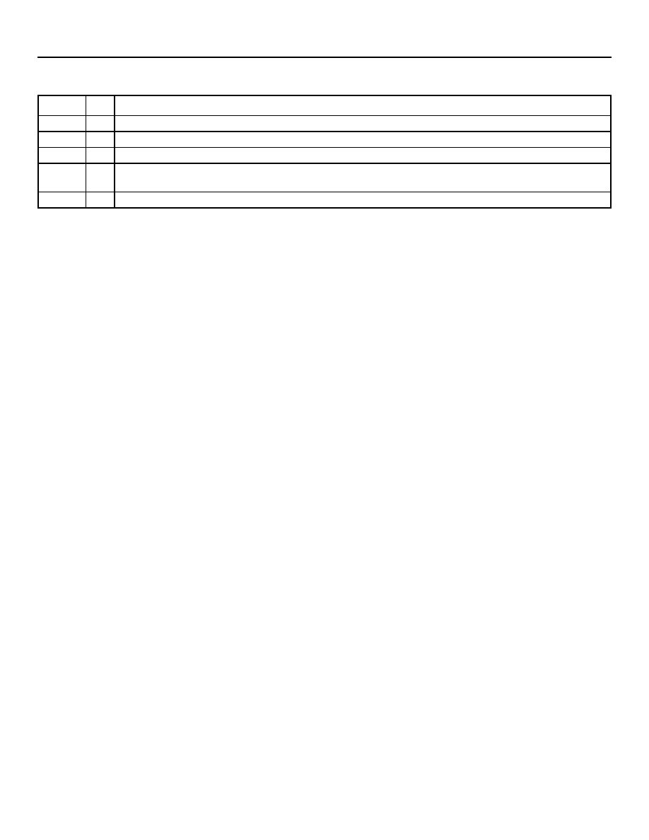
2 Ball Information
2.1 Top View Ball Diagram
The device is housed in a 240-ball plastic ball grid array. Figure 2-1 shows the ball arrangement viewed from the top of the
package. The balls are spaced on a 1.0 mm pitch.
Figure 2-1. Package Diagram (Top View)
B
C
A
E
F
D
H
J
G
L
M
K
P
R
N
U
V
T
2
3
1
5
6
4
8
7
10
11
9
13
14
12
16
15
17
18
TSI-1
Data Sheet, Revision 3
1k x 1k Time-Slot Interchanger
September 21, 2005
8
8
Agere Systems Inc.
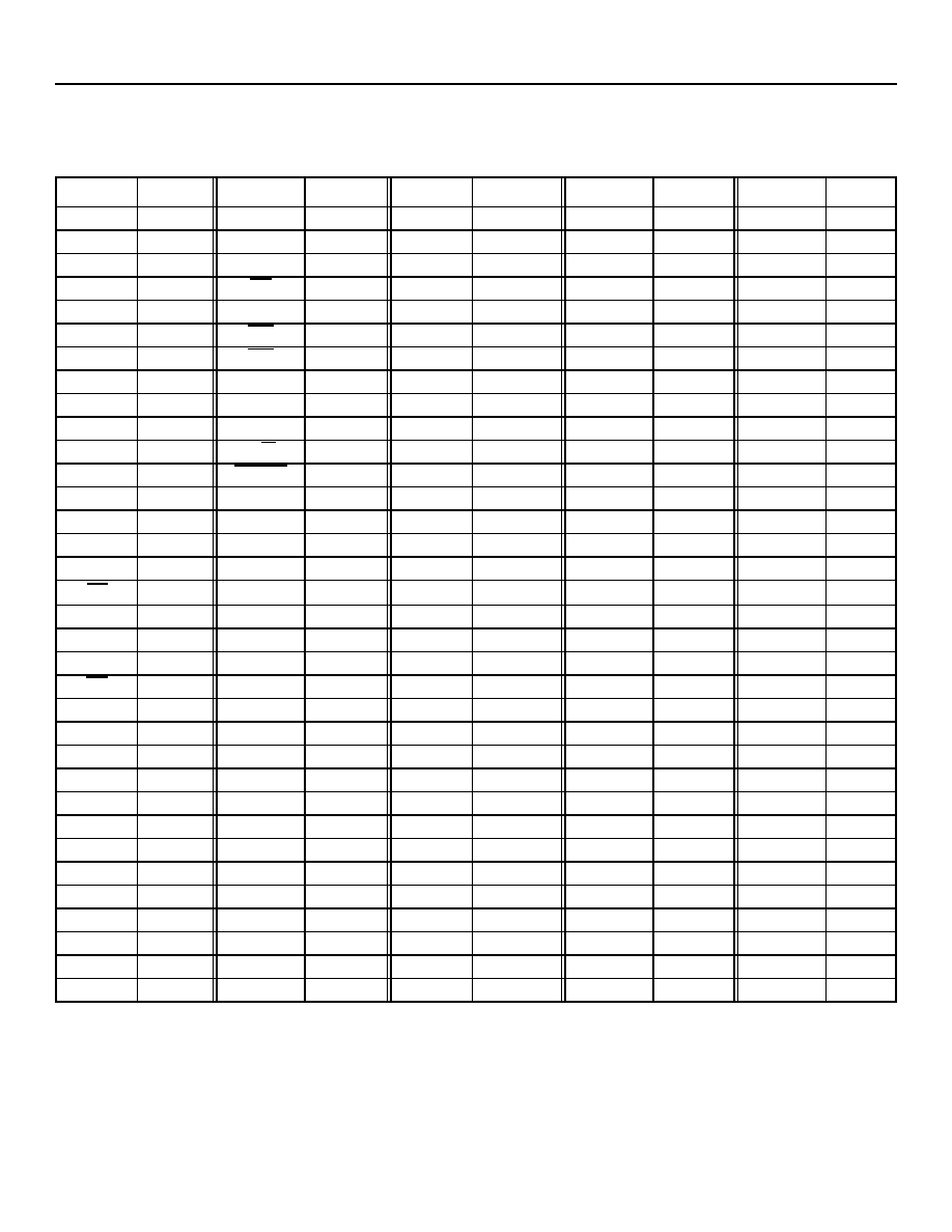
2.2 Package Ball Assignments
Table 2-1. Package Ball Assignments in Signal Name Order
Symbol
Ball Symbol
Ball
Symbol
Ball
Symbol
Ball
Symbol
Ball
ADDR00
A17
DATA13
P18
RXD11
V7
TXD08
F1
V
DD15
D13
ADDR01
A16
DATA14
P17
RXD12
T8
TXD09
G3
V
DD15
D14
ADDR02
A15
DATA15
P16
RXD13
U8
TXD10
G2
V
DD15
G4
ADDR03
A14
DT
H17
RXD14
V8
TXD11
G1
V
DD15
H4
ADDR04
A13
FSYNC
T11
RXD15
U9
TXD12
H2
V
DD15
L4
ADDR05
A12
HIZ
R17
NC
V9
TXD13
H1
V
DD15
M4
ADDR06
A11
INT
H16
NC
V10
TXD14
J2
V
DD15
R7
ADDR07
A10
MPUCLK
K15
NC
U10
TXD15
J1
V
DD15
R8
ADDR08
A9
PAR0
R18
NC
V11
NC
K1
V
DD15
R11
ADDR09
A8
PAR1
P15
NC
U11
NC
K2
V
DD15
R12
ADDR10
A7
R/W
J17
NC
V12
NC
L1
V
DD33
C9
ADDR11
A6
RESET
H15
NC
U12
NC
L2
V
DD33
C10
ADDR12
A5
RSV1
F17
NC
V13
NC
M1
V
DD33
C17
ADDR13
A4
RSV2
F18
NC
U13
NC
M2
V
DD33
D9
ADDR14
A3
RSV3
E15
NC
V14
NC
N1
V
DD33
D10
ADDR15
A2
RSV4
E16
NC
U14
NC
N2
V
DD33
E3
AS
J16
RSV5
E17
NC
V15
NC
N3
V
DD33
F3
CHICLK
R16
RSV6
D17
NC
U15
NC
P1
V
DD33
F15
CKSPD0
E18
RSV7
B18
NC
T15
NC
P2
V
DD33
H3
CKSPD1
D16
RSV8
C18
NC
V16
NC
R1
V
DD33
J3
CS
J18
RSV9
D18
NC
U16
NC
R2
V
DD33
K16
DATA00
K18
RSV10
T18
TCK
G17
NC
T1
V
DD33
P3
DATA01
K17
RSV11
V17
TDI
G16
NC
T2
V
DD33
R3
DATA02
L18
RXD00
V2
TDO
G18
NC
U1
V
DD33
T5
DATA03
L17
RXD01
U3
TMS
G15
V
DD15
C5
V
DD33
T6
DATA04
L16
RXD02
V3
TRSTN
H18
V
DD15
C6
V
DD33
T9
DATA05
M18
RXD03
U4
TXD00
B1
V
DD15
C7
V
DD33
T10
DATA06
M17
RXD04
V4
TXD01
C2
V
DD15
C12
V
DD33
T14
DATA07
M16
RXD05
U5
TXD02
C1
V
DD15
C13
V
DD33
T17
DATA08
M15
RXD06
V5
TXD03
D2
V
DD15
C14
V
DDPLL
R14
DATA09
N18
RXD07
U6
TXD04
D1
V
DD15
D5
NC
K3
DATA10
N17
RXD08
V6
TXD05
E2
V
DD15
D6
NC
T4
DATA11
N16
RXD09
T7
TXD06
E1
V
DD15
D7
V
SS
A1
DATA12
N15
RXD10
U7
TXD07
F2
V
DD15
D12
V
SS
A18
Data Sheet, Revision 3
TSI-1
September 21, 2005
1k x 1k Time-Slot Interchanger
Agere Systems Inc.
9
Symbol
Ball Symbol
Ball
Symbol
Ball
Symbol
Ball
Symbol
Ball
V
SS
B2
V
SS
C8
V
SS
J9
V
SS
R4
V
SS
B3
V
SS
C11
V
SS
J10
V
SS
R5
V
SS
B4
V
SS
C15
V
SS
J11
V
SS
R6
V
SS
B5
V
SS
C16
V
SS
J15
V
SS
R9
V
SS
B6
V
SS
D3
V
SS
K4
V
SS
R10
V
SS
B7
V
SS
D4
V
SS
K8
V
SS
R15
V
SS
B8
V
SS
D8
V
SS
K9
V
SS
T3
V
SS
B9
V
SS
D11
V
SS
K10
V
SS
T12
V
SS
B10
V
SS
D15
V
SS
K11
V
SS
T13
V
SS
B11
V
SS
E4
V
SS
L3
V
SS
T16
V
SS
B12
V
SS
F4
V
SS
L8
V
SS
U2
V
SS
B13
V
SS
F16
V
SS
L9
V
SS
U17
V
SS
B14
V
SS
H8
V
SS
L10
V
SS
U18
V
SS
B15
V
SS
H9
V
SS
L11
V
SS
V1
V
SS
B16
V
SS
H10
V
SS
L15
V
SS
V18
V
SS
B17
V
SS
H11
V
SS
M3
V
SSPLL
R13
V
SS
C3
V
SS
J4
V
SS
N4
V
SS
C4
V
SS
J8
V
SS
P4
Table 2-1. Package Ball Assignments in Signal Name Order (continued)

TSI-1
1k x 1k Time-Slot Interchanger
Data Sheet, Revision 3
September 21, 2005
10
Agere Systems Inc.
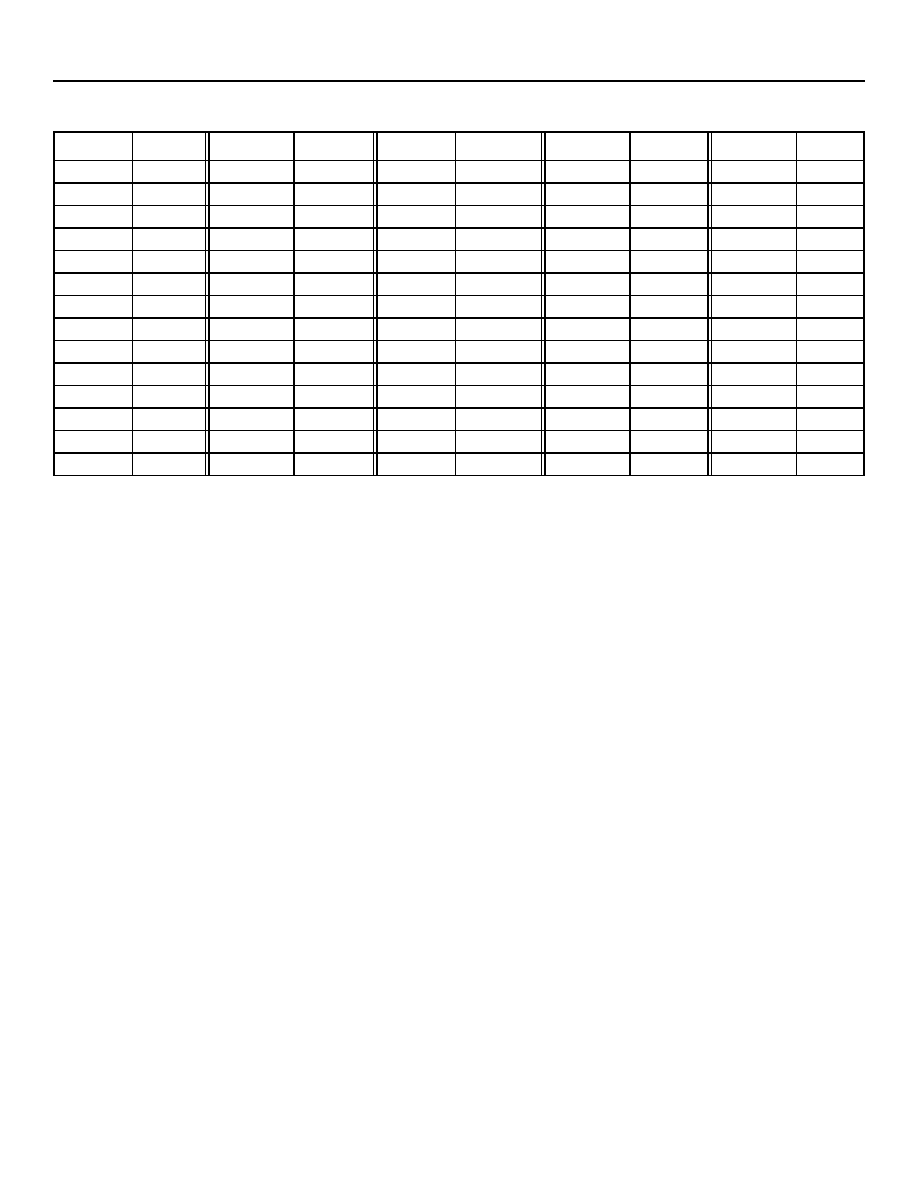
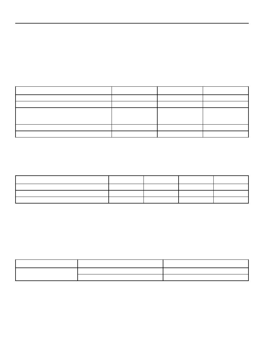
2.3 Package Ball Matrix
2.3.1 Top View
Table 2-2. Package Ball Assignments (Top View)
1
2
3
4
5
6
7
8
9
10
11
12
13
14
15
16
17
18
A
V
SS
ADDR15 ADDR14 ADDR13 ADDR12 ADDR11 ADDR10 ADDR09 ADDR08 ADDR07 ADDR06 ADDR05 ADDR04 ADDR03
ADDR02
ADDR01
ADDR00
V
SS
B
TXD00
V
SS
V
SS
V
SS
V
SS
V
SS
V
SS
V
SS
V
SS
V
SS
V
SS
V
SS
V
SS
V
SS
V
SS
V
SS
V
SS
RSV7
C
TXD02
TXD01
V
SS
V
SS
V
DD15
V
DD15
V
DD15
V
SS
V
DD33
V
DD33
V
SS
V
DD15
V
DD15
V
DD15
V
SS
V
SS
V
DD33
RSV8
D
TXD04
TXD03
VSS
VSS
VDD15
VDD15
VDD15
VSS
VDD33
VDD33
V
SS
V
DD15
V
DD15
V
DD15
V
SS
CKSPD1
RSV6
RSV9
E
TXD06
TXD05
VDD33
VSS
--
--
--
--
--
--
--
--
--
--
RSV3
RSV4
RSV5
CKSPD0
F
TXD08
TXD07
VDD33
VSS
--
--
--
--
--
--
--
--
--
--
V
DD33
V
SS
RSV1
RSV2
G
TXD11
TXD10
TXD09
VDD15
--
--
--
--
--
--
--
--
--
--
TMS
TDI
TCK
TDO
H
TXD13
TXD12
VDD33
VDD15
--
--
--
VSS
VSS
VSS
V
SS
--
--
--
RESET
INT
DT
TRSTN
J
TXD15
TXD14
VDD33
VSS
--
--
--
VSS
VSS
VSS
V
SS
--
--
--
V
SS
AS
R/W
CS
K
NC
NC
NC
VSS
--
--
--
VSS
VSS
VSS
V
SS
--
--
--
MPUCLK
V
DD33
DATA01
DATA00
L
NC
NC
VSS
VDD15
--
--
--
VSS
VSS
VSS
V
SS
--
--
--
V
SS
DATA04
DATA03
DATA02
M
NC
NC
VSS
VDD15
--
--
--
--
--
--
--
--
--
--
DATA08
DATA07
DATA06
DATA05
N
NC
NC
NC
VSS
--
--
--
--
--
--
--
--
--
--
DATA12
DATA11
DATA10
DATA09
P
NC
NC
VDD33
VSS
--
--
--
--
--
--
--
--
--
--
PAR1
DATA15
DATA14
DATA13
R
NC
NC
VDD33
VSS
VSS
VSS
VDD15
VDD15
VSS
VSS
V
DD15
V
DD15
V
SSPLL
V
DDPLL
V
SS
CHICLK
HIZ
PAR0
T
NC
NC
VSS
NC
VDD33
VDD33
RXD09
RXD12
VDD33
VDD33
FSYNC
V
SS
V
SS
V
DD33
NC
V
SS
V
DD33
RSV10
U
NC
VSS
RXD01
RXD03
RXD05
RXD07
RXD10
RXD13
RXD15
NC
NC
NC
NC
NC
NC
NC
V
SS
V
SS
V
VSS
RXD00
RXD02
RXD04
RXD06
RXD08
RXD11
RXD14
NC
NC
NC
NC
NC
NC
NC
NC
RSV11
V
SS

Data Sheet, Revision 3
September 21, 2005
TSI-1
1k x 1k Time-Slot Interchanger
Agere Systems Inc.
11
2.3.2 Bottom View
Table 2-3. Package Ball Assignments (Bottom View)
1
2
3
4
5
6
7
8
9
10
11
12
13
14
15
16
17
18
V
VSS
RXD00
RXD02
RXD04
RXD06
RXD08
RXD11
RXD14
NC
NC
NC
NC
NC
NC
NC
NC
RSV11
V
SS
U
NC
VSS
RXD01
RXD03
RXD05
RXD07
RXD10
RXD13
RXD15
NC
NC
NC
NC
NC
NC
NC
V
SS
V
SS
T
NC
NC
VSS
NC
VDD33
VDD33
RXD09
RXD12
VDD33
VDD33
FSYNC
V
SS
V
SS
V
DD33
NC
V
SS
V
DD33
RSV10
R
NC
NC
VDD33
VSS
VSS
VSS
VDD15
VDD15
VSS
VSS
V
DD15
V
DD15
V
SSPLL
V
DDPLL
V
SS
CHICLK
HIZ
PAR0
P
NC
NC
VDD33
VSS
--
--
--
--
--
--
--
--
--
--
PAR1
DATA15
DATA14
DATA13
N
NC
NC
NC
VSS
--
--
--
--
--
--
--
--
--
--
DATA12
DATA11
DATA10
DATA09
M
NC
NC
VSS
VDD15
--
--
--
--
--
--
--
--
--
--
DATA08
DATA07
DATA06
DATA05
L
NC
NC
VSS
VDD15
--
--
--
VSS
VSS
VSS
V
SS
--
--
--
V
SS
DATA04
DATA03
DATA02
K
NC
NC
NC
VSS
--
--
--
VSS
VSS
VSS
V
SS
--
--
--
MPUCLK
V
DD33
DATA01
DATA00
J
TXD15
TXD14
VDD33
VSS
--
--
--
VSS
VSS
VSS
V
SS
--
--
--
V
SS
AS
R/W
CS
H
TXD13
TXD12
VDD33
VDD15
--
--
--
VSS
VSS
VSS
V
SS
--
--
--
RESET
INT
DT
TRSTN
G
TXD11
TXD10
TXD09
VDD15
--
--
--
--
--
--
--
--
--
--
TMS
TDI
TCK
TDO
F
TXD08
TXD07
VDD33
VSS
--
--
--
--
--
--
--
--
--
--
V
DD33
V
SS
RSV1
RSV2
E
TXD06
TXD05
VDD33
VSS
--
--
--
--
--
--
--
--
--
--
RSV3
RSV4
RSV5
CKSPD0
D
TXD04
TXD03
VSS
VSS
VDD15
VDD15
VDD15
VSS
VDD33
VDD33
V
SS
V
DD15
V
DD15
V
DD15
V
SS
CKSPD1
RSV6
RSV9
C
TXD02
TXD01
V
SS
V
SS
V
DD15
V
DD15
V
DD15
V
SS
V
DD33
V
DD33
V
SS
V
DD15
V
DD15
V
DD15
V
SS
V
SS
V
DD33
RSV8
B
TXD00
V
SS
V
SS
V
SS
V
SS
V
SS
V
SS
V
SS
V
SS
V
SS
V
SS
V
SS
V
SS
V
SS
V
SS
V
SS
V
SS
RSV7
A
V
SS
ADDR15 ADDR14 ADDR13 ADDR12 ADDR11 ADDR10 ADDR09 ADDR08 ADDR07 ADDR06 ADDR05 ADDR04 ADDR03
ADDR02
ADDR01
ADDR00
V
SS
TSI-1
Data Sheet, Revision 3
1k x 1k Time-Slot Interchanger
September 21, 2005
12
12
Agere Systems Inc.
2.4 Ball Types
This table describes each type of input, output, and I/O ball used in the device.
2.5 Ball Definitions
This section describes the function of each of the device balls. The balls are listed by ball name. The static parameters (drive
currents, switching thresholds, etc.) for each ball type (input, output, etc.) are described in
Table 4-1 on page 18
through
Table 4-3
.
Table 2-4. Ball Types
Type Label
Description
I
CMOS input, TTL switching thresholds.
I pd
CMOS input, TTL switching thresholds with internal pull-down resistor.
I pu
CMOS input, TTL switching thresholds with internal pull-up resistor.
O
CMOS output.
O od
Open-drain output.
I/O
Bidirectional ball. CMOS input with TTL switching thresholds and CMOS output.
P
Power and ground.
Table 2-5. Timing Port
Ball Name Type
Name/Description
FSYNC
I
Frame Synchronization. This signal indicates the beginning of a 125 �s frame event (8 kHz). The
FSYNC ball can be programmed as active-low or active-high, but its polarity is the same for all
concentration highway interfaces (CHI). FSYNC can be sampled on either the positive or negative
edge of CHICLK. Time-slot numbers and bit offsets for each CHI are assigned relative to the detection
of FSYNC.
CHICLK
I
Clock. This is the master synchronous clock for the transmit and receive concentration highways. The
frequency can be 8.192 MHz or 16.384 MHz. It must be at least as fast as the highest CHI data rate.
CKSPD0
I
Clock Speed. Static control input that should be tied according to the frequency of CHICLK. If CHICLK
is connected to an 8.192 MHz source, CKSPD0 should be tied to V
SS
. If CHICLK is connected to a
16.384 MHz source, CKSPD0 should be tied to V
DD33
.
CKSPD1
I pd Clock Speed. Reserved, leave disconnected. 20 k
pull-down resistor.
Table 2-6. Transmit and Receive Concentration Highways
Ball Name Type
Name/Description
RXD[15:0] I pd Receive Data [15:0]. Receive concentration highways. These are serial, synchronous data streams,
which may be individually programmed to operate at 2.048 Mbits/s, 4.096 Mbits/s, 8.192 Mbits/s, or
16.384 Mbits/s. They carry 32, 64, 128, or 256 time slots (respectively) each occupying eight
contiguous bits. 20 k
pull-down resistor.
TXD[15:0]
O
Transmit Data [15:0]. These are output concentration highway data streams with data rate options
identical to the RXD inputs.

Data Sheet, Revision 3
TSI-1
September 21, 2005
1k x 1k Time-Slot Interchanger
Agere Systems Inc.
13
Table 2-7. Control Port
Ball Name Type
Name/Description
MPUCLK
I
Processor Clock. This clock is used to sample address, data, and control signals from the
microprocessor. This clock must be within the range of 0 MHz--66 MHz. Required for operation.
CS
I
Chip Select. Active-low chip select. This input is held low for the duration of any read or write access
to the device. Required for operation.
AS
I
Address Strobe. Active-low address strobe that is one MPUCLK cycle wide at the start of a
microprocessor access cycle to the device. This is used to initiate a microprocessor access. Required
for operation.
R/W
I
Read/Write. Cycle selection. R/W is set high during a read cycle, or set low for a write cycle.
Required for operation.
ADDR[15:0] I pu Address [15:0]. ADDR[15] is the most significant bit and ADDR[0] is the least significant bit for
addressing all the internal registers during microprocessor access cycles. All addresses are 16-bit
word addresses; therefore, in a typical application ADDR[0] of the device would be connected to
address bit 1 of a byte addressable system address bus. Required for operation. 200 k
pull-up
resistor.
Note: The device is little-endian; the least significant byte is stored in the lowest address and the
most significant byte is stored in the highest address. Care must be exercised when
connecting to microprocessors that use big-endian byte ordering.
DATA[15:0]
I/O Data [15:0]. Data bus for all transfers between the microprocessor and the internal registers. The
balls are inputs during write cycles and outputs during read cycles. DATA[15] is the most significant
bit, and DATA[0] is the least significant bit. Required for operation.
PAR[1:0]
I/O Control Port Parity [1:0]. Byte-wide parity bits for data. PAR[1] is the parity for DATA[15:8], and
PAR[0] is the parity for DATA[7:0]. The parity sense (even or odd) is application programmable via a
register bit in the device. Not required for operation.
DT
O
Data Transfer Acknowledge. Active-low for one MPUCLK cycle. Indicates that data has been written
during write cycles or that data is valid during read cycles. High impedance when CS is a 1 and driven
when CS is 0. Required for operation.
INT
O od Interrupt. This output is asserted low to indicate that an interrupt condition has occurred. This signal
remains active-low until the interrupt status register has been cleared or masked.
Table 2-8. Initialization and Test Access
Ball Name Type
Name/Description
RESET
I pu Reset. Global reset, active-low. Initializes all internal registers to their default state. The reset occurs
asynchronously, but RESET should be held low for at least two CHICLK periods. 20 k
pull-up resistor.
TCK
I pu Test Clock. This signal provides timing for the boundary-scan and test access port (TAP) controller.
Should be static, except during boundary-scan testing. 20 k
pull-up resistor.
TDI
I pu Test Data In. Data input for the boundary-scan. Sampled on the rising edge of TCK. 20 k
pull-up
resistor.
TMS
I pu Test Mode Select (Active-Low). Controls boundary-scan test operations. TMS is sampled on the rising
edge of TCK. 20 k
pull-up resistor.
TRSTN
I pd Test Reset (Active-Low). This signal is an asynchronous reset for the TAP controller. 20 k
pull-down
resistor.
TDO
O
Test Data Out. Updated on the falling edge of TCK. The TDO output is high impedance except when
scanning out test data.
HIZ
I pu Output Enable. All output and bidrectional buffers will be high-impedance when this input is low unless
boundary scan is enabled (TRSTN = 1). 20 k
pull-up resistor.
RSV[11:1]
-- Reserved [11:1]. These balls are used by Agere Systems during the manufacturing process; they must
be left unconnected.
TSI-1
Data Sheet, Revision 3
1k x 1k Time-Slot Interchanger
September 21, 2005
14
14
Agere Systems Inc.
Table 2-9. Power Balls
Symbol Type
Name/Description
V
DD33
P
I/O Power. Power supply balls for the I/O pads (3.3 V � 5%).
V
DD15
P
Core Power. Power supply balls for the core (1.5 V � 5%).
V
SS
P
Ground. Common ground balls for 3.3 V and 1.5 V supplies.
V
DDPLL
P
PLL Power. 1.5 V power supply for the internal phase-locked loop. Must include local 0.01 �F capacitor to
V
SSPLL
.
V
SSPLL
P
PLL Ground. Isolated ground for the internal phase-locked loop.
Data Sheet, Revision 3
TSI-1
September 21, 2005
1k x 1k Time-Slot Interchanger
Agere Systems Inc.
15
3 Operating Conditions and Reliability
3.1 Absolute Maximum Ratings
Stresses in excess of the absolute maximum ratings can cause permanent damage to the device. These are absolute
stress ratings only. Functional operation of the device is not implied at these or any other conditions in excess of those
given in the operational sections of the data sheet. Exposure to absolute maximum ratings for extended periods can
adversely affect device reliability.
3.2 Recommended Operating Conditions
Table 3-2 lists the voltages, along with the tolerances, that are required for proper operation of the device.
3.3 Handling Precautions
Although electrostatic discharge (ESD) protection circuitry has been designed into this device, proper precautions must be
taken to avoid exposure to ESD and electrical overstress (EOS) during all handling, assembly, and test operations. Agere
employs both a human-body model (HBM) and a charged-device model (CDM) qualification requirement in order to deter-
mine ESD-susceptibility limits and protection design evaluation. ESD voltage thresholds are dependent on the circuit param-
eters used in each of the models, as defined by JEDEC's JESD22-A114 (HBM) and JESD22-C101 (CDM) standards.
Table 3-1. Absolute Maximum Ratings
Parameter
Min
Max
Unit
Supply Voltage (V
DD33
)
�0.5
4.2
V
Supply Voltage (V
DD15
)
�0.5
1.8
V
Input Voltage:
TXD[15:0]
All Other Inputs
�0.5
�0.3
5.5
V
DD33
+ 0.3
V
V
Storage Temperature
�40
125
�C
Junction Temperature
--
125
�C
Table 3-2. Operating Conditions
Parameter
Min
Typ
Max
Unit
Supply Voltage (V
DD33
)
3.14
3.3
3.47
V
Supply Voltage (V
DD15
)
1.4
1.5
1.6
V
Ambient Temperature
�40
--
85
�C
Table 3-3. ESD Tolerance
Device
Voltage
Type
TSI-1
2,000 V
HBM (human-body model)
500 V
CDM (charged-device model)

TSI-1
Data Sheet, Revision 3
1k x 1k Time-Slot Interchanger
September 21, 2005
16
16
Agere Systems Inc.
3.4 Thermal Parameters (Definitions and Values)
System and circuit board level performance depends not only on device electrical characteristics, but also on device thermal
characteristics. The thermal characteristics frequently determine the limits of circuit board or system performance, and they
can be a major cost adder or cost avoidance factor. When the die temperature is kept below 125 �C, temperature-activated
failure mechanisms are minimized. The thermal parameters that Agere provides for its packages help the chip and system
designer choose the best package for their applications, including allowing the system designer to thermally design and in-
tegrate their systems.
It should be noted that all the parameters listed below are affected, to varying degrees, by package design (including paddle
size) and choice of materials, the amount of copper in the test board or system board, and system airflow.
JA
- Junction to Air Thermal Resistance
JA
is a number used to express the thermal performance of a part under JEDEC standard natural convection conditions.
JA
is calculated using the following formula:
JA
= (T
J
� T
amb
) / P; where P = power
JMA
- Junction to Moving Air Thermal Resistance
JMA
is effectively identical to
JA
but represents performance of a part mounted on a JEDEC four layer board inside a wind
tunnel with forced air convection.
JMA
is reported at airflows of 200 LFPM and 500 LFPM (linear feet per minute), which
roughly correspond to 1 m/s and 2.5 m/s (respectively).
JMA
is calculated using the following formula:
JMA
= (T
J
� T
amb
) / P
JC
- Junction to Case Thermal Resistance
JC
is the thermal resistance from junction to the top of the case. This number is determined by forcing nearly 100% of the
heat generated in the die out the top of the package by lowering the top case temperature. This is done by placing the top
of the package in contact with a copper slug kept at room temperature using a liquid refrigeration unit.
JC
is calculated using
the following formula:
JC
= (T
J
� T
C
) / P
JB
- Junction to Board Thermal Resistance
JB
is the thermal resistance from junction to board. This number is determined by forcing the heat generated in the die out
of the package through the leads or balls by lowering the board temperature and insulating the package top. This is done
using a special fixture, which keeps the board in contact with a water chilled copper slug around the perimeter of the package
while insulating the package top.
JB
is calculated using the following formula:
JB
= (T
J
� T
B
) / P
JT
- Junction Temperature to Case Temperature
JT
correlates the junction temperature to the case temperature. It is generally used by the customer to infer the junction
temperature while the part is operating in their system. It is not considered a true thermal resistance.
JT
is calculated using
the following formula:
JT
= (T
J
� T
C
) / P
Table 3-4. Thermal Parameter Values
Parameter
Temperature �C/Watt
JA
25.1
JMA
(1 m/s)
21.4
JMA
(2.5 m/s)
18.8
JC
5.8
JB
13.0

Data Sheet, Revision 3
TSI-1
September 21, 2005
1k x 1k Time-Slot Interchanger
Agere Systems Inc.
17
3.5 Power Consumption
Table 3-5. Power Consumption
Supply Voltage
Typ
*
* MPUCLK = 66 MHz, CHICLK = 16.384 MHz, TA = 25 �C, all CHIs active, all outputs loaded with 50 pF.
Max
V
DD33
100 mW at 3.3 V
150 mW at 3.47 V
V
DD15
275 mW at 1.5 V
325 mW at 1.6 V

TSI-1
Data Sheet, Revision 3
1k x 1k Time-Slot Interchanger
September 21, 2005
18
18
Agere Systems Inc.
4 dc Electrical Characteristics
This section describes all the static parameters associated with all the ball types used in the device.
* Excludes current due to pull-up or pull-down resistors.
Table 4-1. CMOS Inputs
Parameter
Symbol
Conditions
Min
Typ
Max
Unit
Input Leakage Current
I
IL
V
SS
< V
IN
< V
DD33
--
--
1*
�A
High-input Voltage
V
IH
--
2.0
--
V
DD33
+ 0.3
V
Low-input Voltage
V
IL
--
�0.3
--
0.8
V
Input Capacitance
C
I
--
--
2.5
--
pF
Table 4-2. CMOS Outputs
Parameter
Symbol
Conditions
Min
Typ
Max
Unit
Output Voltage Low
V
OL
I
OL
= �10 mA
--
--
0.4
V
Output Voltage High
V
OH
I
OL
= 10 mA
2.4
--
--
V
Output Current Low
I
OL
--
--
--
10
mA
Output Current High
I
OH
--
--
--
10
mA
Output Capacitance
C
O
--
--
3
--
pF
HIZ Output Leakage Current
I
OZ
--
--
--
10
�A
Table 4-3. CMOS Bidirectionals (DATA[15:0])
Parameter
Symbol
Conditions
Min
Typ
Max
Unit
Leakage Current
I
L
V
SS
< V
IN
< V
DD33
--
--
11
�A
High-input Voltage
V
IH
--
2.0
--
V
DD33
+ 0.3
V
Low-input Voltage
V
IL
--
�0.3
--
0.8
V
Biput Capacitance
C
IB
--
--
5.0
--
pF
Output Voltage Low
V
OL
I
OL
= �10 mA
--
--
0.4
V
Output Voltage High
V
OH
I
OL
= 10 mA
2.4
--
--
V
Data Sheet, Revision 3
TSI-1
September 21, 2005
1k x 1k Time-Slot Interchanger
Agere Systems Inc.
19
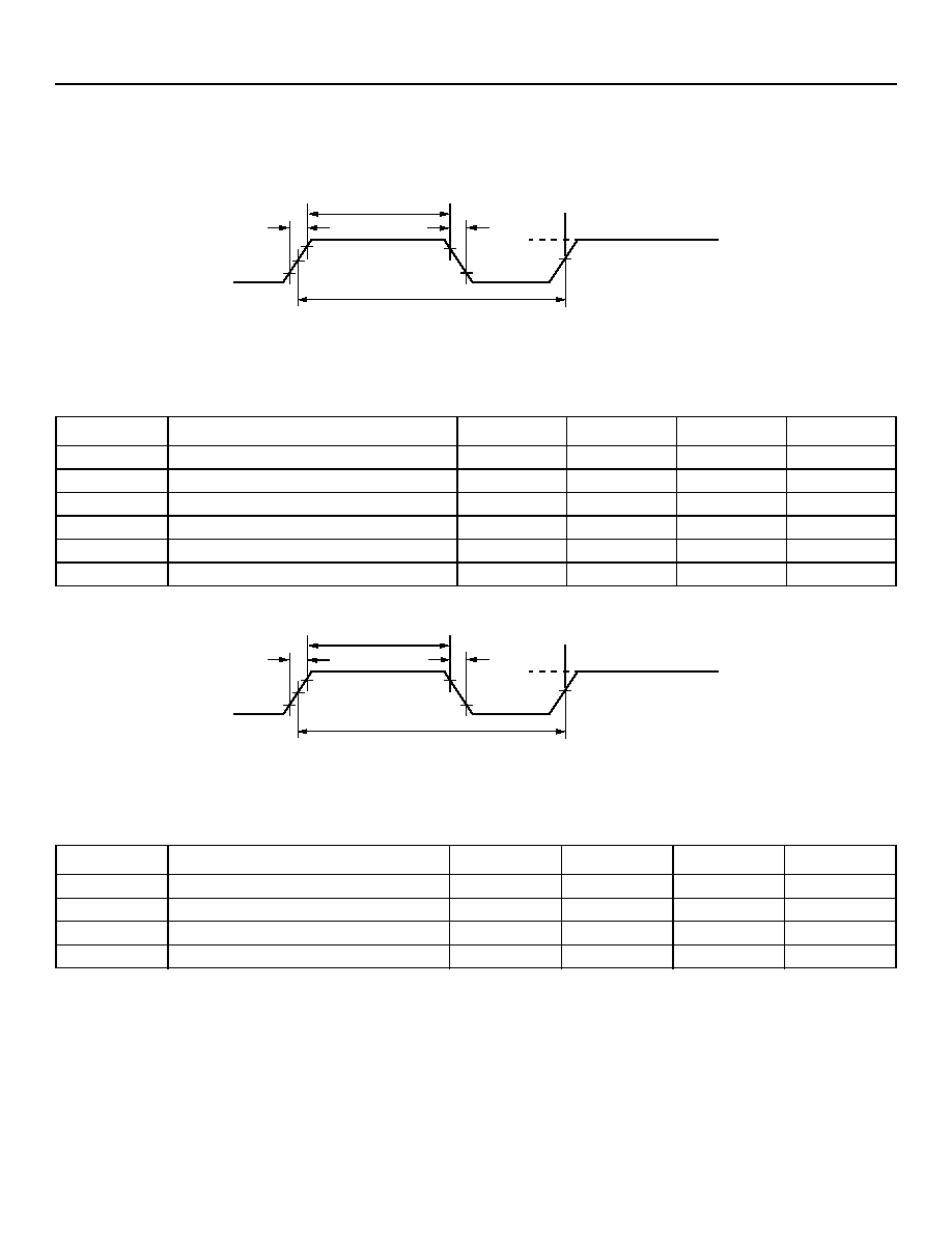
5 Timing Diagrams and ac Characteristics
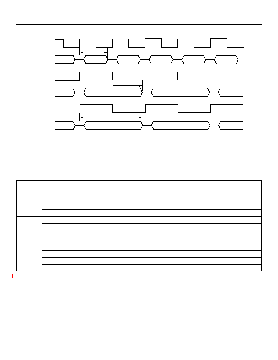
Figure 5-1 and Figure 5-2 describe the timing specifications for the input clocks
Figure 5-1. CHICLK Timing Specifications
* V
IH
to V
IH
or V
IL
to V
IL
.
Figure 5-2. MPUCLK Timing Specifications
* V
IH
to V
IH
or V
IL
to V
IL
.
Table 5-1. CHICLK Timing Specifications
Parameter
Description
Min
Typ
Max
Unit
t
1
CHICLK Rise Time
--
2
7
ns
t
2
CHICLK Width (8.192 MHz)*
48.84
--
73.24
ns
t
2
CHICLK Width (16.384 MHz)*
24.42
--
36.62
ns
t
3
CHICLK Fall Time
--
2
7
ns
t
4
CHICLK Period (8.192 MHz)
--
122.07
--
ns
t
4
CHICLK Period (16.384 MHz)
--
61.03
--
ns
Table 5-2. MPUCLK Timing Specifications
Parameter
Description
Min
Typ
Max
Unit
t
5
MPUCLK Rise Time
--
2
7
ns
t
6
MPUCLK Width*
6.06
--
--
ns
t
7
MPUCLK Fall Time
--
2
7
ns
t
8
MPUCLK Period
15.2
--
--
ns
t
1
V
DD33
V
IL
V
IH
V
IH
V
IL
t
3
t
4
50%
t
2
t
5
V
DD33
V
IL
V
IH
V
IH
V
IL
t
7
t
8
50%
t
6
TSI-1
Data Sheet, Revision 3
1k x 1k Time-Slot Interchanger
September 21, 2005
20
20
Agere Systems Inc.
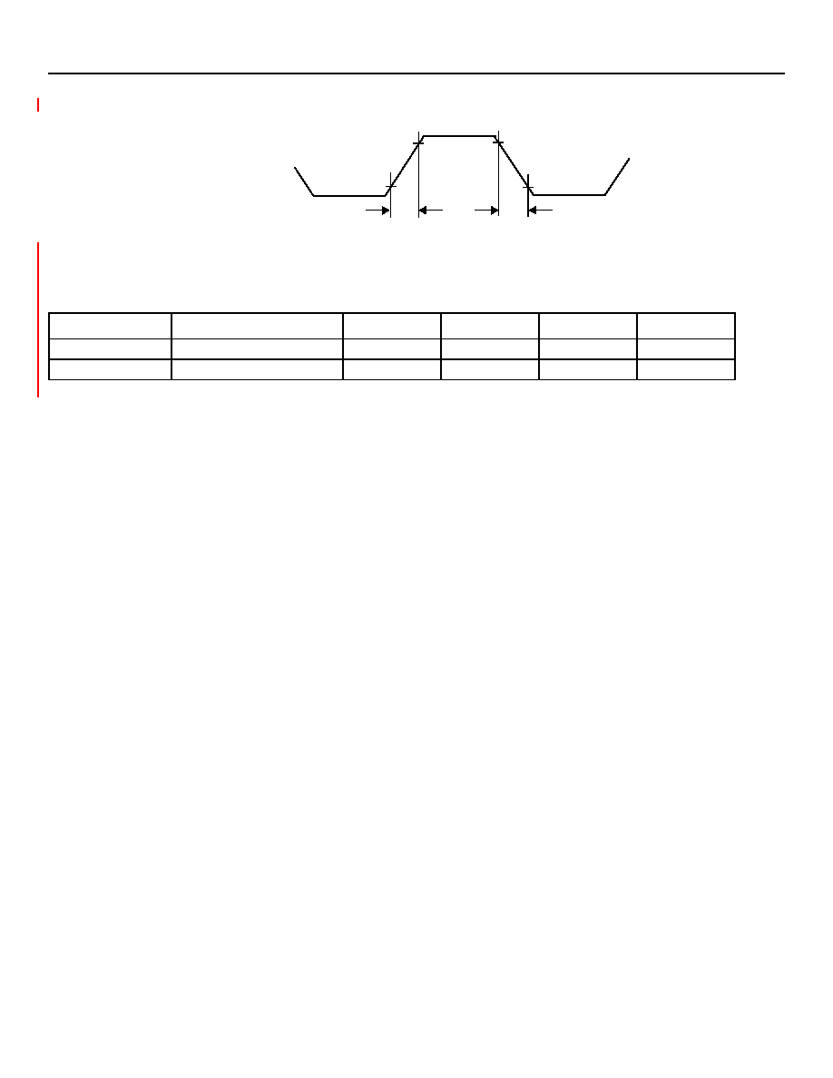
Figure 5-3 shows the ac timing specifications for the
CMOS outputs on the
device.
Figure 5-3. ac Timing Specification
* Test load = 50 pF (total).
Table 5-3. CMOS Output ac Timing Specification *
Parameter
Description
Min
Typ
Max
Unit
t
9
Rise Time (20%--80%)
--
1.5
7
ns
t
10
Fall Time (80%--20%)
--
1.5
7
ns
20%
80 %
20 %
80 %
t9
t10

Data Sheet, Revision 3
TSI-1
September 21, 2005
1k x 1k Time-Slot Interchanger
Agere Systems Inc.
21
Note: This figure assumes the device is programmed to sample FSYNC on the rising edge of CHICLK.
Figure 5-4. CHI Interface Timing
* Applies if Driver_Enable_Control = 01. For Driver_Enable_Control = 11 refer to
Figure 5-15, CHI 3-State Output Control on page 27
.
All timing specifications apply under the following conditions:
If FS is active-low.
If the falling edge of CHICLK is specified as the active edge.
At all RXD and TXD rates (16.384 Mbits/s, 8.192 Mbits/s, 4.096 Mbits/s, or 2.048 Mbits/s) with a CHICLK frequency of
16.384 MHz or 8.192 MHz.
Table 5-4. CHI Interface Timing
Parameter
Description
Min
Max
Unit
t
13
FSYNC Setup Time to Active CHICLK Edge
10
--
ns
t
14
FSYNC Hold Time from Active CHICLK Edge
5
--
ns
t
15
RXD Setup to Active CHICLK Edge
10
--
ns
t
16
RXD Hold Time from Active CHICLK Edge
5
--
ns
t
17
TXD High Z to Data Valid
--
15
ns
t
18
TXD Propagation Delay from Active CHICLK Edge
2
12
ns
t
19
Transmit Data High Impedance*
--
15
ns
t
18
t
19
TXD
CHICLK
t
13
t
14
t
17
RXD
FSYNC
t
15
t
16
TSI-1
Data Sheet, Revision 3
1k x 1k Time-Slot Interchanger
September 21, 2005
22
22
Agere Systems Inc.
Note: For this timing diagram, it is assumed that FSYNC has been programmed to be active-high, and to be sampled by the rising edge of the CHICLK.
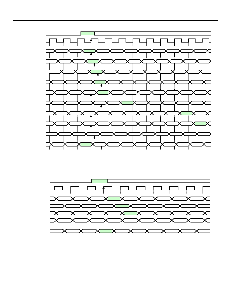
Figure 5-5. Typical Receive CHI Timing with 16.384 Mbits/s Data and 16.384 MHz CHICLK
Notes:
1/4 bit offset not valid with 16 Mbits/s data.
For this timing diagram, it is assumed that FSYNC has been programmed to be active-high, and to be sampled by the rising edge of the
CHICLK.
Figure 5-6. Transmit CHI Timing with 16.384 Mbits/s Data and 16.384 MHz CHICLK
FSYNC
CHICLK
w/ 0 offset
data sampled
w/ � bit offset
data sampled
w/ � bit offset
data sampled
w/ � bit offset
data sampled
w/ bit offset = 1
data sampled
w/ 2� bit offset
data sampled
w/ bit offset = 7
data sampled
data sampled
data sampled
data sampled
w/ TS offset = 1,
bit offset = 0
TS254 B6
TS254 B7
TS255 B0
TS0 B1
TS0 B0
TS255 B1
TS255 B2
TS255 B3
TS255 B4
TS0 B4
TS0 B5
TS254 B7
TS255 B0
TS255 B1
TS255 B2
TS255 B3
TS255 B4
TS255 B5
TS255 B6
TS0 B0
TS0 B1
TS0 B2
TS0 B3
TS255 B6
TS255 B7
TS0 B0
TS0 B1
TS0 B2
TS0 B3
TS0 B4
TS0 B5
TS255 B6
TS255 B7
TS0 B0
TS0 B1
TS0 B2
TS0 B3
TS0 B4
TS0 B5
TS255 B5
TS255 B3
TS255 B4
TS255 B5
TS255 B5
TS255 B6
TS255 B7
TS255 B6
TS255 B7
TS255 B6
TS255 B7
TS0 B0
TS0 B1
TS0 B2
TS0 B3
TS255 B6
TS255 B7
TS255 B5
TS255 B7
TS0 B 0
w/ TS offset = 13,
bit offset = 3�
TS242 B3
TS242 B4
TS242 B5
TS243 B4
TS243 B5
TS242 B6
TS242 B7
TS243 B0
TS243 B1
TS255 B7
TS0 B0
TS243 B2
TS243 B3
TS0 B5
TS0 B6
TS0 B3
TS0 B4
TS0 B1
TS0 B2
TS0 B3
TS0 B7
TS1 B0
TS0 B1
TS0 B2
w/ TS offset = 255,
bit offset = 7�
TS255 B6
TS0 B4
TS0 B0
TS255 B6
TS255 B7
TS0 B0
TS0 B1
TS0 B2
TS0 B3
TS0 B4
TS0 B5
FSYNC
CHICLK
w/ 0 offset
w/ � bit offset
w/ bit offset = 1
w/ TS offset = 255,
bit offset = 7�
TS255 B6
TS255 B7
TS0 B0
w/ TS offset = 1,
bit offset = 0
TS0 B2
TS0 B3
TS0 B4
TS254 B5
TS254 B6
TS254 B7
TS255 B0
TS255 B4
TS255 B5
TS0 B3
TS0 B4
TS255 B1
TS255 B2
TS255 B3
TS0 B0
TS0 B1
TS255 B4
TS255 B5
TS255 B5
TS255 B6
TS255 B7
TS0 B0
TS0 B3
TS0 B4
TS0 B5
TS0 B5
TS0 B1
TS0 B2
TS0 B1
TS0 B2
TS255 B6
TS255 B7
TS255 B5
TS255 B6
TS255 B7
TS0 B0
TS0 B1
TS0 B2
TS0 B3
TS0 B4
Data Sheet, Revision 3
TSI-1
September 21, 2005
1k x 1k Time-Slot Interchanger
Agere Systems Inc.
23
Note: For this timing diagram, it is assumed that FSYNC has been programmed to be active-high, and to be sampled by the rising edge of the CHICLK.
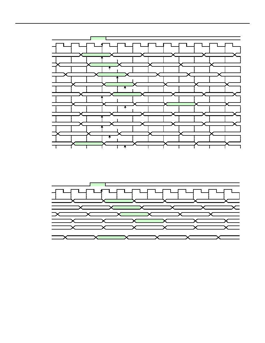
Figure 5-7. Typical Receive CHI Timing with 8.192 Mbits/s Data and 16.384 MHz CHICLK
Note: For this timing diagram, it is assumed that FSYNC has been programmed to be active-high, and to be sampled by the rising edge of the CHICLK.
Figure 5-8. Transmit CHI Timing with 8.192 Mbits/s Data and 16.384 MHz CHICLK
FSYNC
CHICLK
w/ 0 offset
data sampled
w/ � bit offset
data sampled
w/ � bit offset
data sampled
w/ � bit offset
data sampled
w/ bit offset = 1
data sampled
w/ 2� bit offset
data sampled
w/ bit offset = 7
data sampled
data sampled
data sampled
data sampled
TS0 B2
TS0 B3
TS0 B4
w/ TS offset = 127,
bit offset = 7�
TS 127 B7
TS0 B0
TS0 B1
TS127 B2
TS127 B3
TS127 B4
w/ TS offset = 13,
bit offset = 3�
TS114 B4
TS114 B5
TS114 B6
TS114 B7
TS115 B0
TS115 B1
w/ TS offset = 1,
bit offset = 0
TS126 B7
TS127 B0
TS127 B1
TS127 B4
TS127 B5
TS 127 B4
TS127 B5
TS127 B0
TS127 B1
TS127 B2
TS127 B3
TS127 B6
TS127 B7
TS0 B2
TS0 B3
TS0 B2
TS0 B3
TS0 B0
TS0 B1
TS127 B6
TS127 B7
TS0 B0
TS0 B1
TS 127 B6
TS127 B7
TS0 B0
TS0 B1
TS0 B3
TS0 B4
TS127 B7
TS0 B0
TS0 B1
TS0 B2
TS0 B3
TS127 B7
TS0 B0
TS0 B1
TS0 B2
TS127 B7
TS0 B0
TS0 B1
TS0 B2
TS0 B3
TS0 B4
FSYNC
CHICLK
w/ 0 offset
w/ � bit offset
w/ � bit offset
w/ bit offset = 1
TS 127 B6
TS127 B7
TS0 B0
TS0 B1
TS0 B2
TS0 B3
TS0 B2
TS0 B3
TS127 B6
TS127 B7
TS0 B0
TS0 B1
TS0 B2
TS127 B6
TS127 B7
TS0 B0
TS0 B1
TS 127 B5
TS127 B6
TS127 B7
TS0 B0
w/ TS offset = 1,
bit offset = 0
TS127 B7
TS0 B0
TS0 B1
w/ TS offset = 127,
bit offset = 7�
TS 126 B6
TS126 B7
TS127 B0
TS127 B1
TS0 B2
TS0 B3
TS0 B1
TS0 B2
TS127 B2
TS127 B3
TS0 B3
TSI-1
Data Sheet, Revision 3
1k x 1k Time-Slot Interchanger
September 21, 2005
24
24
Agere Systems Inc.
Note: For this timing diagram, it is assumed that FSYNC has been programmed to be active-high, and to be sampled by the rising edge of the CHICLK.
Figure 5-9. Typical Receive CHI Timing with 4.096 Mbits/s Data and 16.384 MHz CHICLK
Note: For this timing diagram, it is assumed that FSYNC has been programmed to be active-high, and to be sampled by the rising edge of the CHICLK.
Figure 5-10. Transmit CHI Timing with 4.096 Mbits/s Data and 16.384 MHz CHICLK
FSYNC
CHICLK
w/ 0 offset
data sampled
w/ � bit offset
data sampled
w/ � bit offset
data sampled
w/ � bit offset
data sampled
w/ bit offset = 1
data sampled
w/ 2� bit offset
data sampled
w/ bit offset = 7
data sampled
data sampled
data sampled
data sampled
TS50 B7
w/ TS offset = 63,
bit offset = 7�
TS0 B0
TS0 B1
TS0 B2
w/ TS offset = 13,
bit offset = 3�
TS50 B4
TS50 B5
TS50 B6
w/ TS offset = 1,
bit offset = 0
TS63 B0
TS63 B1
TS63 B2
TS63 B5
TS63 B6
TS63 B7
TS63 B1
TS63 B2
TS63 B3
TS63 B7
TS0 B0
TS0 B1
TS63 B7
TS0 B0
TS0 B1
TS63 B7
TS0 B0
TS0 B1
TS0 B2
TS0 B0
TS0 B1
TS0 B2
TS63 B7
TS0 B0
TS0 B1
TS0 B2
FSYNC
CHICLK
w/ 0 offset
w/ � bit offset
w/ � bit offset
w/ bit offset = 1
w/ TS offset = 63,
bit offset = 7�
TS62 B7
TS63 B0
TS63 B1
w/ TS offset = 1,
bit offset = 0
TS63 B6
TS63 B7
TS0 B0
TS63 B7
TS0 B0
TS0 B1
TS0 B2
TS63 B6
TS63 B7
TS0 B0
TS0 B1
TS63 B7
TS0 B0
TS0 B1
TS63 B7
TS0 B0
TS0 B1
Data Sheet, Revision 3
TSI-1
September 21, 2005
1k x 1k Time-Slot Interchanger
Agere Systems Inc.
25
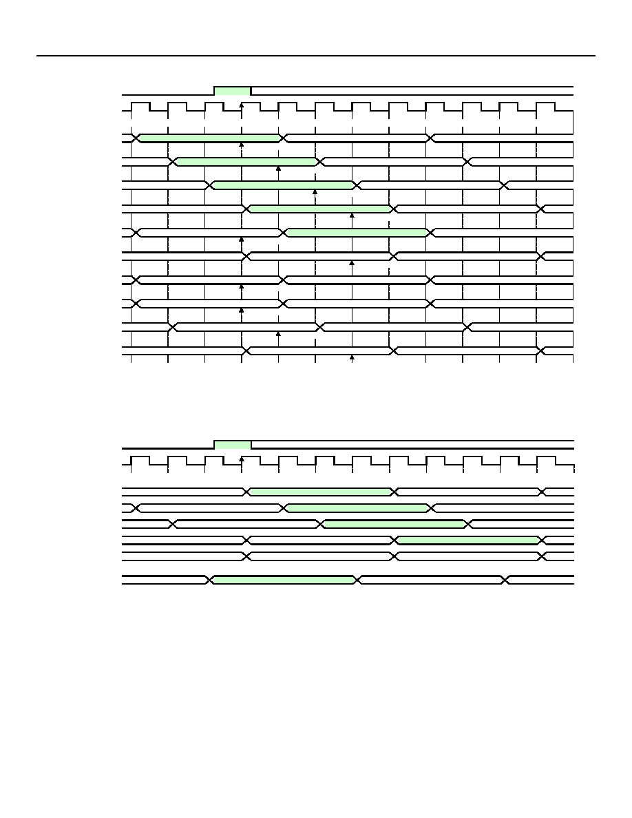
Note: For this timing diagram, it is assumed that FSYNC has been programmed to be active-high, and to be sampled by the rising edge of the CHICLK.
Figure 5-11. Typical Receive CHI Timing with 2.048 Mbits/s Data and 16.384 MHz CHICLK
Note: For this timing diagram, it is assumed that FSYNC has been programmed to be active-high, and to be sampled by the rising edge of the CHICLK.
Figure 5-12. Transmit CHI Timing with 2.048 Mbits/s Data and 16.384 MHz CHICLK
FSYNC
CHICLK
w/ 0 offset
data sampled
w/ � bit offset
data sampled
w/ � bit offset
data sampled
w/ � bit offset
data sampled
w/ bit offset = 1
data sampled
w/ 2� bit offset
data sampled
w/ bit offset = 7
data sampled
data sampled
data sampled
data sampled
w/ TS offset = 31,
bit offset = 7�
TS0 B0
TS0 B1
TS0
w/ TS offset = 1,
bit offset = 0
TS31 B0
TS31 B1
w/ TS offset = 13,
bit offset = 3�
TS18 B5
TS18 B6
TS31 B5
TS31 B6
TS31
TS31 B1
TS31 B2
TS31 B7
TS0 B0
TS0
TS31 B7
TS0 B0
TS0 B0
TS0 B1
TS0 B0
TS0 B1
TS31 B7
TS0 B0
TS0 B1
FSYNC
CHICLK
w/ 0 offset
w/ � bit offset
w/ � bit offset
w/ bit offset = 1
TS30 B7
TS31 B0
TS31 B01
w/ TS offset = 1,
bit offset = 0
TS31 B7
TS0 B0
TS0 B1
w/ TS offset = 31,
bit offset = 7�
TS31 B7
TS0 B0
TS31 B6
TS31 B7
TS0 B0
TS31 B7
TS0 B0
TS0 B1
TS31 B7
TS0 B0
TSI-1
Data Sheet, Revision 3
1k x 1k Time-Slot Interchanger
September 21, 2005
26
26
Agere Systems Inc.
Note: For this timing diagram, it is assumed that FSYNC has been programmed to be active-high, and to be sampled by the rising edge of the CHICLK.
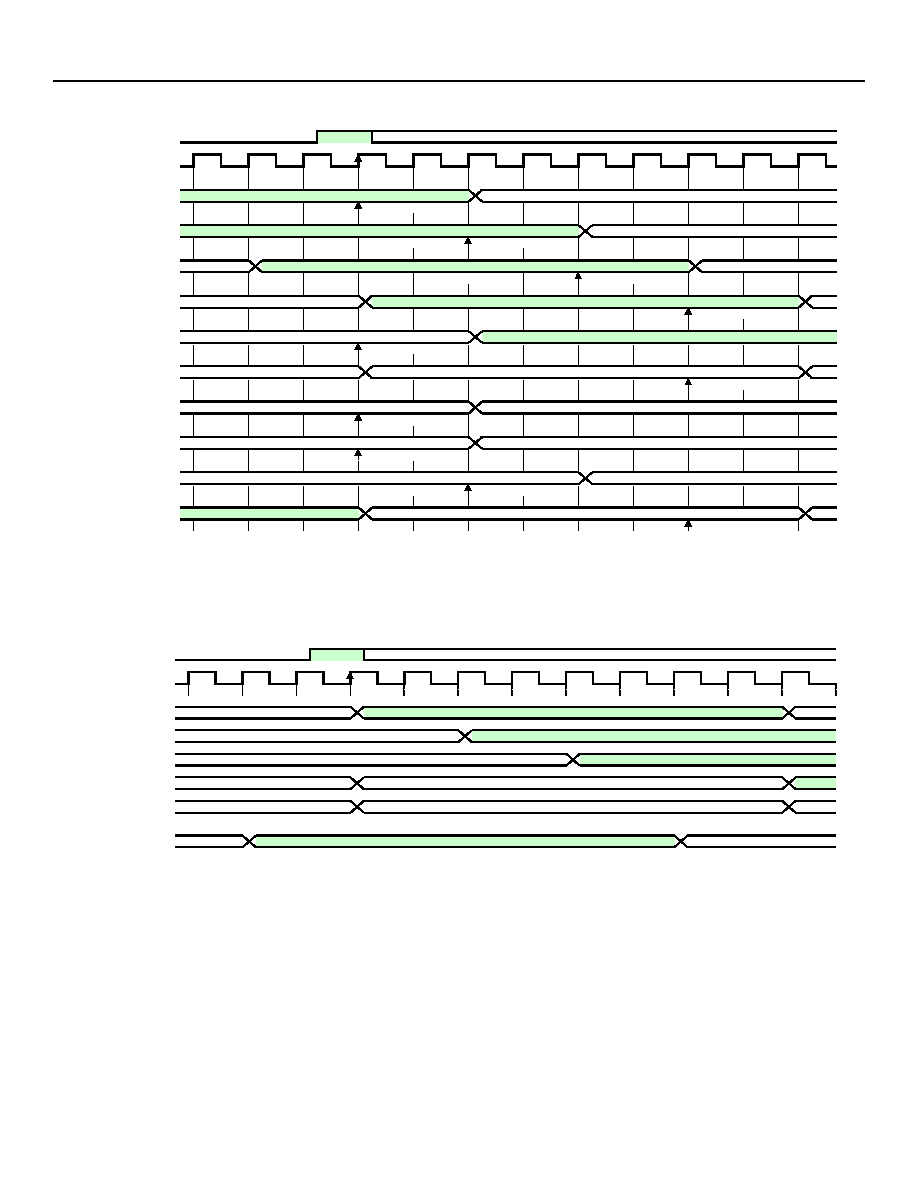
Figure 5-13. Typical Receive CHI Timing with 8.192 Mbits/s Data and 8.192 MHz CHICLK
Notes:
1/4 bit offset not valid with 8 MHz data and 8 MHz clock.
For this timing diagram, it is assumed that FSYNC has been programmed to be active-high, and to be sampled by the rising edge of the
CHICLK.
Figure 5-14. Transmit CHI Timing with 8.192 Mbits/s Data and 8.192 MHz CHICLK
FSYNC
CHICLK
w/ 0 offset
data sampled
w/ � bit offset
data sampled
w/ � bit offset
data sampled
w/ � bit offset
data sampled
w/ bit offset = 1
data sampled
w/ 2� bit offset
data sampled
w/ bit offset = 7
data sampled
data sampled
data sampled
data sampled
TS0 B5
TS0 B6
TS0 B7
TS1 B0
TS0 B1
TS0 B2
TS0 B3
TS0 B4
w/ TS offset = 127,
bit offset = 7�
TS127 B6
TS127 B7
TS0 B0
TS115 B2
TS115 B3
TS115 B4
TS115 B5
TS114 B6
TS114 B7
TS115 B0
TS115 B1
w/ TS offset = 13,
bit offset = 3�
TS114 B3
TS114 B4
TS114 B5
TS127 B5
TS127 B6
TS127 B7
TS0 B0
TS0 B 0
TS0 B1
w/ TS offset = 1,
bit offset = 0
TS126 B6
TS126 B7
TS127 B0
TS127 B1
TS127 B2
TS127 B3
TS127 B4
TS0 B3
TS126 B7
TS127 B0
TS127 B1
TS127 B2
TS127 B3
TS127 B4
TS127 B5
TS127 B6
TS127 B7
TS127 B7
TS0 B0
TS0 B1
TS0 B2
TS127 B3
TS127 B4
TS127 B5
TS127 B6
TS0 B5
TS127 B5
TS127 B6
TS127 B7
TS0 B0
TS0 B1
TS0 B2
TS0 B3
TS0 B4
TS0 B1
TS0 B2
TS0 B3
TS0 B4
TS127 B5
TS127 B6
TS127 B7
TS0 B0
TS0 B2
TS0 B3
TS0 B4
TS0 B5
TS127 B6
TS127 B7
TS0 B0
TS0 B1
TS0 B2
TS0 B3
TS0 B4
TS0 B5
TS127 B6
TS127 B7
TS0 B0
TS0 B1
TS127 B6
TS127 B7
TS0 B0
TS0 B1
TS0 B2
TS0 B3
TS0 B4
TS0 B5
FSYNC
CHICLK
w/ 0 offset
w/ � bit offset
w/ bit offset = 1
TS127 B5
w/ TS offset = 127,
bit offset = 7�
TS127 B6
TS127 B7
TS0 B0
TS0 B1
TS0 B2
TS0 B3
TS0 B4
TS0 B5
TS0 B4
w/ TS offset = 1,
bit offset = 0
TS126 B5
TS126 B6
TS126 B7
TS127 B0
TS127 B1
TS127 B2
TS127 B3
TS127 B4
TS0 B0
TS0 B1
TS0 B2
TS0 B3
TS127 B4
TS127 B5
TS127 B6
TS127 B7
TS0 B1
TS0 B2
TS0 B3
TS0 B4
TS127 B5
TS127 B6
TS127 B7
TS0 B0
TS127 B5
TS127 B6
TS127 B7
TS0 B0
TS0 B1
TS0 B2
TS0 B3
TS0 B4
TS0 B5
Data Sheet, Revision 3
TSI-1
September 21, 2005
1k x 1k Time-Slot Interchanger
Agere Systems Inc.
27
Figure 5-15. CHI 3-State Output Control
Table 5-5. CHI 3-State Output Control
Control in the table below refers to bits [6:4] in
Table 6-51 Transmit_CHI_Global_Configuration (Read/Write) on page 52
.
This only applies if bits 13 and 12 of the corresponding register in
Table 6-48 Transmit_CHI_Configuration (Read/Write) on
page 50
are set to 11.
Parameter Control
Reference Point
*
*
Like edge is the reference edge (rising or falling) as defined by bit 0 in
Table 6-51 Transmit_CHI_Global_Configuration (Read/Write) on page 52
.
Min
Max
*
Unit
t
20
000
After Previous Like Edge in 16 MHz
50
59
ns
001
After Previous Like Edge in 16 MHz
44
53
ns
010
After Previous Like Edge in 16 MHz
38
47
ns
011
After Previous Like Edge in 16 MHz
32
41
ns
t
21
000
After Previous Opposite Edge in 8 MHz
50
59
ns
001
After Previous Opposite Edge in 8 MHz
44
53
ns
010
After Previous Opposite Edge in 8 MHz
38
47
ns
011
After Previous Opposite Edge in 8 MHz
32
41
ns
t
22
100
After Previous Like Edge (8 MHz mode only)
111
120
ns
101
After Previous Like Edge (8 MHz mode only)
105
114
ns
110
After Previous Like Edge (8 MHz mode only)
99
108
ns
111
After Previous Like Edge (8 MHz mode only)
93
102
ns
CHICLK
16.384 MHz
t
20
TXD
16.384 Mbits/s
CHICLK
8.192 MHz
TXD
8.192 Mbits/s
CHICLK
8.192 MHz
TXD
8.192 Mbits/s
t
21
t
22
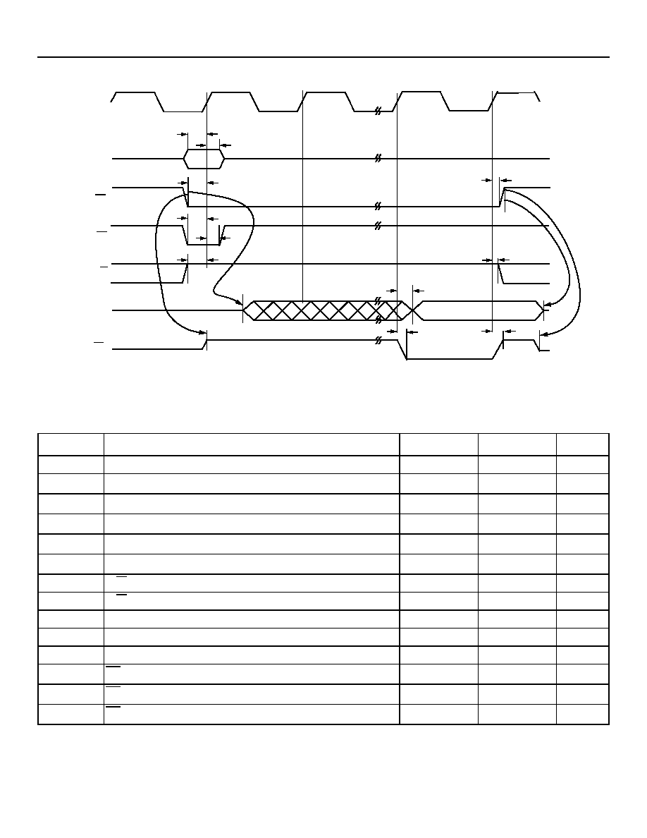
TSI-1
Data Sheet, Revision 3
1k x 1k Time-Slot Interchanger
September 21, 2005
28
28
Agere Systems Inc.
Figure 5-16. Microprocessor Port Timing--Read Cycle
Table 5-6. Microprocessor Port Timing--Read Cycle
Parameter
Description
Min
Max
Unit
t
23
Address Setup
5
--
ns
t
24
Address Hold
1
--
ns
t
25
Chip Select Setup
5
--
ns
t
26
Chip Select Hold
1
--
ns
t
27
Address Strobe Setup
5
--
ns
t
28
Address Strobe Hold
1
--
ns
t
29
R/W Setup
5
--
ns
t
30
R/W Hold
1
--
ns
t
31
Data Output Enable
--
15
ns
t
32
Data Clock to Valid
1
7
ns
t
33
Data High Impedance
--
8
ns
t
34
DT High Impedance to Valid
1
15
ns
t
35
DT Clock to Out
1
7
ns
t
36
DT Valid to High Impedance
1
8
ns
MPUCLK
DATA[15:0]
PAR[1:0]
t
24
t
23
ADDR[15:0]
CS
AS
R/W
DT
t
25
t
27
t
28
t
29
t
31
t
35
t
34
t
26
t
30
t
32
t
35
t
36
t
33

Data Sheet, Revision 3
TSI-1
September 21, 2005
1k x 1k Time-Slot Interchanger
Agere Systems Inc.
29
Figure 5-17. Microprocessor Port Timing--Write Cycle
Note: Posted writes follow the same timing shown in
Figure 5-17 on page 29
and
Table 5-7 on page 29
. A posted write may
return a DT prior to the device completing the write cycle. This allows the microprocessor to continue operation while
the device completes the write.
Table 5-7. Microprocessor Port Timing--Write Cycle
Parameter
Description
Min
Max
Unit
t
37
Address Setup
5
--
ns
t
38
Address Hold
1
--
ns
t
39
Chip Select Setup
5
--
ns
t
40
Chip Select Hold
1
--
ns
t
41
Address Strobe Setup
5
--
ns
t
42
Address Strobe Hold
1
--
ns
t
43
R/W Setup
5
--
ns
t
44
R/W Hold
1
--
ns
t
45
Data Setup
5
--
ns
t
46
Data Hold
1
--
ns
t
47
DT High Impedance to Valid
1
15
ns
t
48
DT Clock to Out
1
7
ns
t
49
DT Valid to High Impedance
1
8
ns
MPUCLK
DATA[15:0]
PAR[1:0]
t
38
t
37
ADDR[15:0]
CS
AS
R/W
DT
t
39
t
41
t
42
t
43
t
45
t
48
t
47
t
40
t
44
t
46
t
48
t
49

TSI-1
Data Sheet, Revision 3
1k x 1k Time-Slot Interchanger
September 21, 2005
30
30
Agere Systems Inc.
Register Description

Data Sheet, Revision 3
TSI-1
September 21, 2005
1k x 1k Time-Slot Interchanger
Agere Systems Inc.
31
6 Register Description
This section describes the purpose and operation of each register bit, its dependencies, and its initial state.
6.1 Device Addressing Notes
All device addresses shown are physical byte offset addresses in the microprocessor space, not the actual addresses in the
device itself. The device uses 2
17
bytes of address spectrum.
The following assumptions are made:
The device is connected to the microprocessor as a 16-bit word accessed device (not byte addressable), with ADDR[00]
connected to address bit 1 of the microprocessor.
The microprocessor's address bit 0 (high/low byte) is not used by the device.
Note: All addresses are expressed in hexadecimal. Unless otherwise indicated by a 0x, register bit states (in default states)
are expressed in binary.
6.2 Acronyms Used
CS--Connection store.
CSG--Connection store generator.
PLL--Phase-locked loop.
SF--Switch fabric.
TPG--Test pattern generator.
TPM--Test pattern monitor.
VCO--Voltage-controlled oscillator.
6.3 Address Map
Note: The address space is expressed in decimal. Because ADDR[00] on the device is connected to ADDR[01] on the mi-
croprocessor, the device only occupies even addresses in the microprocessor address space.
Table 6-1. Address Map
Register Groups
Address Space (Words)
Address Range
Global Control
512
0x00000--0x003FE
Connection Store Generator
256
0x00400--0x005FE
Test Pattern Generator and Monitor
256
0x00600--0x007FE
Reserved
256
0x00800--0x009FE
CHI Control
896
0x00A00--0x010FE
Switch Fabric Control
1,920
0x01100--0x01FFE
Reserved
4,096
0x02000--0x03FFE
Reserved
24,576
0x04000--0x0FFFE
Connection Store
8,192
0x10000--0x13FFE
Reserved
24,576
0x14000--0x1FFFE
TSI-1
Data Sheet, Revision 3
1k x 1k Time-Slot Interchanger
September 21, 2005
32
32
Agere Systems Inc.
6.4 Register Summary
Table 6-2. Global Registers
Address
Register
Access Mode
0x00000
Version_Control
Read Only
0x00002
Chip_Identity
Read Only
0x00004
Summary_Interrupt_Status
Read Only
0x00006
Summary_Interrupt_Mask
Read/Write
0x00008
CPU_Access_Error
CORWN
*
* Clear-on-read/clear-on-write.
0x0000A
CPU_Access_Error_Mask
Read/Write
0x0000C
Global_Control
Read/Write
0x0000E
PLL_Control
Read/Write
0x00010
Power_Control
Read/Write
0x00012
Invalid_Address_Trap
Read Only
0x00014
Scratch_Register
Read/Write
Table 6-3. Connection Store Generator Registers
Address
Register
Access Mode
0x00400
CSG_Control
Read/Write
0x00402
CSG_Status
Read Only
0x00404
CSG_Starting_Address
Read/Write
0x00406
CSG_Ending_Address
Read/Write
0x00408
CSG_Write_Enable_Low
Read/Write
0x0040A
CSG_Write_Enable_High
Read/Write
0x00410
CSG_Seed_Low
Read/Write
0x00412
CSG_Seed_High
Read/Write
0x00418
CSG_OR_Mask_Low
Read/Write
0x0041A
CSG_OR_Mask_High
Read/Write
0x0041C
CSG_AND_Mask_Low
Read/Write
0x0041E
CSG_AND_Mask_High
Read/Write
0x00428
CS_Stream_Control
Read/Write
0x0042A
CSG_Configuration
Read/Write
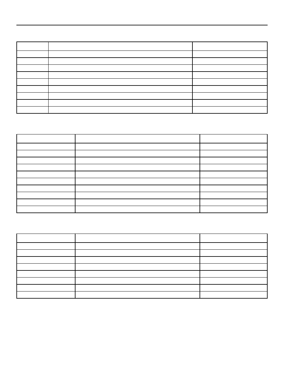
Data Sheet, Revision 3
TSI-1
September 21, 2005
1k x 1k Time-Slot Interchanger
Agere Systems Inc.
33
Table 6-4. Test Pattern Generator and Monitor Registers
Address
Register
Access Mode
0x00600
TPG_Configuration
Read/Write
0x00602
TPG_User_Pattern
Read/Write
0x00604
TPM_Configuration
Read/Write
0x00606
TPM_User_Pattern
Read/Write
0x00608
TPM_Error_Count
Sat/Roll
*
* Saturate/rollover.
0x0060A
TPG_Inject_Error_Count
Write Only
0x0060C
TPG_Data_Invert_Mask
Read/Write
0x0060E
TPM_Status
Read Only
0x00610
TPM_Status_Mask
Read/Write
Table 6-5. Concentration Highway Configuration Registers
Address
Register
Access Mode
0x00A00--0x00A1E
Receive_CHI_Configuration
Read/Write
0x00A80
Receive_CHI_Status
CORWN
*
* Clear-on-read/clear-on-write.
0x00A82
Receive_CHI_Status_Mask
Read/Write
0x00A84
Receive_CHI_Global_Configuration
Read/Write
0x00C00--0x00C1E
Transmit_CHI_Configuration
Read/Write
0x00C80
Transmit_CHI_Status
CORWN*
0x00C82
Transmit_CHI_Status_Mask
Read/Write
0x00C84
Transmit_CHI_Global_Configuration
Read/Write
0x01000--0x0101E
Receive_CHI_Time_Slot_Offset
Read/Write
0x01080--0x0109E
Transmit_CHI_Time_Slot_Offset
Read/Write
Table 6-6. Switch Fabric Control
Address
Register
Access Mode
0x01124
SF_Status
CORWN
*
* Clear-on-read/clear-on-write.
0x01126
SF_Status_Mask
Read/Write
0x01142
Data_Store_Time_Slot_Capture_Select
Read/Write
0x01144
Data_Store_Captured_Data
Read Only
0x01146
Connection_Store_Parity_Error_Address_Trap
CORWN*
0x01148
Receive_Link_Offset
Read Only
0x0114C
Transmit_Link_Offset
Read/Write
0x0114E
Wide_Mode_Control
Read/Write

TSI-1
Data Sheet, Revision 3
1k x 1k Time-Slot Interchanger
September 21, 2005
34
34
Agere Systems Inc.
Table 6-8. Reserved Registers
The following register will not cause an Invalid_Address_Error (see
Table 6-13 on page 36
) and are reserved.
6.5 Global Control Registers
The default field indicates the state of each register bit following a hardware or software reset cycle.
These registers are located at the top level of the design and are used to determine operations that affect more than one
block within the device. These could be registers required for control of the microprocessor port block or register functions
that are not naturally associated with other blocks. Global resets and output enables are included in this section.
Table 6-7. Connection Store
Address
Register
Access Mode
0x10000--0x13FFC Low_Control_Word
Read/Write
0x10002--0x13FFE High_Control_Word
Read/Write
Address
Register
Access Mode
0x00016
Reserved_0
Read/Write
Table 6-9. Version_Control (Read Only)
Address
Bit
Name/Description
Default
0x00000
15
Reserved.
0
14:12 Version_Number. TSI version number. TSI version register will change each time the
device is changed.
001
11:0 Agere_Systems_Identification_Number. This is the ID code assigned to Agere Systems
Inc. by the JTAG standards body.
0x190
Table 6-10. Chip_Identity (Read Only)
Address
Bit
Name/Description
Default
0x00002
15:0 Chip_Identity. This register contains the unique identification code for the device.
0x26D1
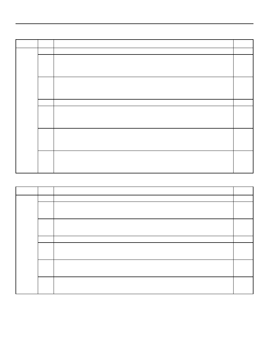
Data Sheet, Revision 3
TSI-1
September 21, 2005
1k x 1k Time-Slot Interchanger
Agere Systems Inc.
35
Table 6-11. Summary_Interrupt_Status (Read Only)
Address
Bit
Name/Description
Default
0x00004
15:6 Unused.
--
5
Transmit_CHI_Interrupt. Active-high flag indicating an unmasked error or status is present
in the Transmit_CHI_Status register (see
Table 6-49 on page 51
).
0 = No transmit CHI error(s) detected.
1 = Transmit CHI Error(s) detected.
--
4
Receive_CHI_Interrupt. Active-high flag indicating that an unmasked error or status is
present in the Receive_CHI_Status register (see
Table 6-45 on page 48
).
0 = No receive CHI error(s) detected.
1 = Receive CHI error(s) detected.
--
3
Unused.
--
2
TPM_Interrupt. Active-high flag indicating an unmasked error or status is present in the
TPM_Status register (see
Table 6-42 on page 47
).
0 = No test pattern monitor error(s) detected.
1 = Test pattern error(s) detected.
--
1
SF_Interrupt. Active-high flag indicating an unmasked error is present in the SF_Status reg-
ister (see
Table 7-1 on page 54
).
0 = No switch fabric error(s) detected.
1 = Switch fabric error(s) detected.
--
0
CPU_Access_Interrupt. Active-high flag indicating an unmasked error has been detected
by the CPU_Access_Error register (see
Table 6-13 on page 36
).
0 = No microprocessor access error(s) detected.
1 = Microprocessor access error(s) detected.
--
Table 6-12. Summary_Interrupt_Mask (Read/Write)
Address
Bit
Name/Description
Default
0x00006
15:6 Unused.
--
5
Transmit_CHI_Interrupt_Mask.
0 = The Transmit_CHI_Interrupt bit (see Table 6-11) will cause an interrupt if active.
1 = The Transmit_CHI_Interrupt bit is blocked from causing an interrupt.
1
4
Receive_CHI_Interrupt_Mask.
0 = The Receive_CHI_Interrupt bit (see Table 6-11) will cause an interrupt if active.
1 = The Receive_CHI_Interrupt bit is blocked from causing an interrupt.
1
3
Unused.
--
2
TPM_Interrupt_Mask.
0 = The TPM_Interrupt bit (see Table 6-11) will cause an interrupt if active.
1 = The TPM_Interrupt bit is blocked from causing an interrupt.
1
1
SF_Interrupt_Mask.
0 = The SF_Interrupt bit will (see Table 6-11) cause an interrupt if active.
1 = The SF_Interrupt bit is blocked from causing an interrupt.
1
0
CPU_Access_Interrupt_Mask.
0 = The CPU_Access_Interrupt bit (see Table 6-11) will cause an interrupt if active.
1 = The CPU_Access_Interrupt bit is blocked from causing an interrupt.
1

TSI-1
Data Sheet, Revision 3
1k x 1k Time-Slot Interchanger
September 21, 2005
36
36
Agere Systems Inc.
Table 6-13. CPU_Access_Error (CORWN)
Address
Bit
Name/Description
Default
0x00008
15:4 Unused.
--
3
PLL_Lock_Error. This bit indicates if the device's master PLL is locked to the incoming CHI
reference clock (CHICLK).
0 = Locked.
1 = Not locked.
--
2
Access_Time_Out_Error.
0 = No time-out.
1 = Indicates that a time-out has occurred internal to the TFRA84J13 device on a
microprocessor access.
--
1
Invalid_Address_Error.
0 = No invalid address.
1 = Indicates that a microprocessor access to an invalid address has occurred. The address
causing this error can be found in the Invalid_Address_Trap register (see
Table 6-18 on
page 38
).
--
0
Data_Parity_Error.
0 = No data parity error.
1 = Indicates that a microprocessor data bus parity error has occurred.
--
Table 6-14. CPU_Access_Error_Mask (Read/Write)
Address
Bit
Name/Description
Default
0x0000A
15:4 Unused.
--
3
PLL_Lock_Error_Mask.
0 = The PLL_Lock_Error bit (see Table 6-13) will cause an interrupt if active.
1 = The PLL_Lock_Error bit is blocked from causing an interrupt.
1
2
Access_Time-out_Error_Mask.
0 = The Access_Time_Out_Error bit (see Table 6-13) will cause an interrupt if active.
1 = The Access_Time_Out_Error bit is blocked from causing an interrupt.
1
1
Invalid_Address_Error_Mask.
0 = The Invalid_Address_Error bit will (see Table 6-13) cause an interrupt if active.
1 = The Invalid_Address_Error bit is blocked from causing an interrupt.
1
0
Data_Parity_Error_Mask.
0 = The Data_Parity_Error bit will (see Table 6-13) cause an interrupt if active.
1 = The Data_Parity_Error bit is blocked from causing an interrupt.
1

Data Sheet, Revision 3
TSI-1
September 21, 2005
1k x 1k Time-Slot Interchanger
Agere Systems Inc.
37
Table 6-15. Global_Control (Read/Write)
Address Bit
Name/Description
Default
0x0000C 15 Software_Reset. This bit forces and holds the device in reset.
0 = Normal.
1 = Reset.
0
14:9 Unused.
--
8
Reserved.
--
7:5 Unused.
--
4
DT_Wait_State_Control. During write posting, a data transfer acknowledge (DT) can be
generated on the first or second cycle following address strobe. If a DT immediately following
address strobe is too fast for the microprocessor, then a single wait-state can be inserted.
0 = Zero wait-states inserted.
1 = One wait-state inserted.
1
3
Write_Posting_Enable. This bit enables write posting, which will provide an early DT to the
microprocessor.
0 = Write posting disabled.
1 = Write posting enabled.
0
2
Saturate_Rollover_Select. This control bit changes the behavior of event counter registers. In
saturation mode, a register will stick at the maximum value once it is reached. In roll-over mode,
an event register will continue counting as its value cycles back to zero.
0 = Roll over.
1 = Saturation.
When in saturate mode, the counters will operate in a clear-on-read mode. When in the roll-over
mode, the counters will not be directly writable.
0
1
Data_Parity_Mode. This bit controls the parity setting and checking on the microprocessor data
bus.
0 = Even parity on microprocessor byte data/parity bus.
1 = Odd parity on microprocessor byte data/parity bus.
0
0
Register_Clearing_Mode. This bit controls the way clearing is performed on status bits in clear-
on-read/clear-on-write registers.
0 = The status bit is cleared by writing a 1 to it.
1 = The status bit is cleared when a microprocessor read is performed.
0
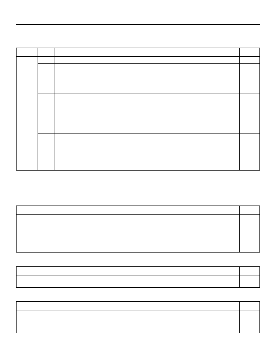
TSI-1
Data Sheet, Revision 3
1k x 1k Time-Slot Interchanger
September 21, 2005
38
38
Agere Systems Inc.
Table 6-16. PLL_Control (Read/Write)
This register provides control over the PLL filter parameters. This register is unaffected by software reset.
Table 6-17. Power_Control (Read/Write)
To minimize power consumption when parts of the device are not used in any given application, individual sections of the
device may be powered off.
Note: All contents and information in a section that is powered off may be lost.
Address
Bit
Name/Description
Default
0x0000E 15:11 Unused.
--
10
Reserved.
--
9:7
Loop_Filter_Resistor. These bits provide loop filter resistor control over the PLL. The loop
filter damping resistor is approximately (Loop_Filter_Resistor + 1) x (20 k
). This field is only
enabled if Enable_PLL_Control is set to a 1. If Enable_PLL_Control is set to 0, default val-
ues are used within the PLL.
000
6:4
VCO_Gain_Control. These bits provide control over the VCO gain in the PLL. The gain is
approximately (VCO_Gain_Control x 100 MHz/V). This field is only enabled if
Enable_PLL_Control is set to 1. If Enable_PLL_Control is set to 0, default values are used
within the PLL.
000
3:1
Charge_Pump_Current. These bits provide control over the charge pump in the PLL.
Charge_Pump_Current is approximately (Charge_Pump_Current + 1) x (2 �A). This field is
always enabled. The typical value is 0x4.
100
0
Enable_PLL_Control. This bit is the master control for user programmability of the PLL loop
parameters. If set to 1, the VCO_Gain_Control and Loop_Filter_Resistor bit fields in this reg-
ister are allowed to serve as loop filter parameters for the PLL. If set to 0, these fields are ig-
nored and the PLL uses default values.
0 = Disable user loop parameters.
1 = Enable user loop parameters.
0
Address
Bit
Name/Description
Default
0x00010
15:1 Unused.
--
0
Data_Store_Enable. This bit enables the data store. For low-power mode, the data store can
be disabled. However, if the CHI interface is used, this bit should be set to 1. If none of the
CHIs are used, this bit can be set to 0 to save power.
0 = Data store disabled.
1 = Data store enabled.
0
Table 6-18. Invalid_Address_Trap (Read Only)
Address
Bit
Name/Description
Default
0x00012
15:0 Invalid_Address. This register traps the value of an invalid address during a microproces-
sor access.
--
Table 6-19. Scratch_Register (Read/Write)
Address
Bit
Name/Description
Default
0x00014
15:0 Scratch_Pad. This register is for test and diagnostics purposes. It is not connected to any
internal functions. Therefore, it can be used during early testing to establish that the connec-
tions between the device and the microprocessor are intact, without affecting the configura-
tion of the device.
0x0000

Data Sheet, Revision 3
TSI-1
September 21, 2005
1k x 1k Time-Slot Interchanger
Agere Systems Inc.
39
Table 6-20. Reserved_0 (Read/Write)
This register is reserved for use by Agere Systems.
6.6 Connection Store Generator Registers
The connection store is not initialized on powerup nor reset. Although it can be manually initialized by writing all locations
via the microprocessor interface, the CSG is provided to independently fill the connection store with known data. The user
can program the CSG to fill with a variety of patterns or with user-defined fixed data. Since the connection store is greater
than 16 bits wide, the CSG, in general, has pairs of registers associated with controlling the data to be loaded.
Table 6-21. CSG_Control (Read/Write)
This register provides general control over the CSG.
Address
Bit
Name/Description
Default
0x00016
15:3
Unused.
--
2
Reserved.
--
1:0
Unused.
--
Address
Bit
Name/Description
Default
0x00400
15:4 Unused.
--
3
Enable_Stream_Switching. Controls the enable for filling the Stream_Select field of the con-
nection store.
0 = Stream switching is disabled. The Stream_Select field of the connection store RAM is filled
with pseudorandom data.
1 = Enables stream switching. The Stream_Select fields of the connection store is filled with
the contents of CS_Source_Stream_Select (see
Table 6-33 on page 42
) for all time slots
associated with the stream specified in CS_Destination_Stream_Select (see
Table 6-33
).
Note: In this mode, all other connection store RAM locations are filled with N-to-N mapping.
0
2
LFSR_Seed_Control. Selects user-definable seed value or predefined seed value for the
pseudorandom pattern generator.
0 = Default seed is loaded into the linear feedback shift register (LFSR) (0x3FFFFFFF).
1 = The 31-bit LFSR is loaded with the contents of the CSG_Seed registers.
0
1
CSG_Mode_Select. Defines the type of pattern that will be filled into the connection store.
0 = Channel N to channel N mapping.
1 = Pseudorandom generated bit pattern (8-bit LFSR).
0
0
CSG_Enable. Enables the pattern generator. After setting the other CSG registers, setting this
bit to a 1 triggers the CSG to start programming of the connection store RAM.
0 = Pattern generator off.
1 = Pattern generator on.
Note: During the CSG operation, the function of the switch fabric is halted and the outputs of
the CHIs and HSLs are nondeterministic. To reuse the CSG for subsequent
programming of the connection store, this bit must be set back to 0 then to a 1.
0
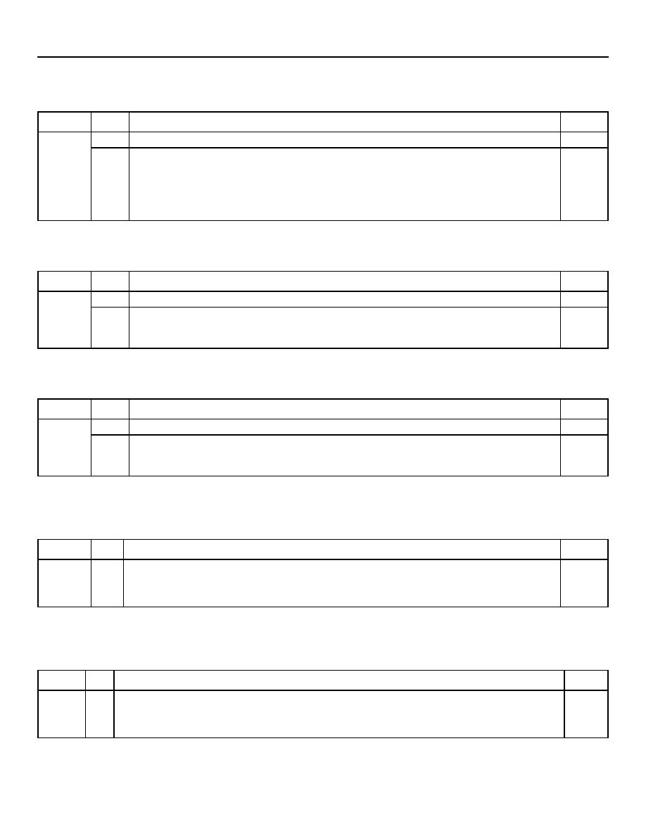
TSI-1
Data Sheet, Revision 3
1k x 1k Time-Slot Interchanger
September 21, 2005
40
40
Agere Systems Inc.
Table 6-22. CSG_Status (Read Only)
This register provides general status of the connection store generator.
Table 6-23. CSG_Starting_Address (Read/Write)
This register defines the starting address of the connection store RAM for the CSG.
Table 6-24. CSG_Ending_Address (Read/Write)
This register defines the ending address of the connection store RAM for the CSG.
Table 6-25. CSG_Write_Enable_Low (Read/Write)
This register provides write enable control on a per-bit basis for the low word of the connection store when using the CSG
to fill the connection store RAM.
Table 6-26. CSG_Write_Enable_High (Read/Write)
This register provides write enable control on a per-bit basis for the high word of the connection store when using the CSG
to fill the connection store RAM.
Address
Bit
Name/Description
Default
0x00402
15:1 Unused.
--
0
CSG_Operation_Complete. Pattern generation for connection and data store is complete.
The bit is normally asserted, but it is deasserted when the CSG update is in progress. This
status bit is cleared when the CSG_Enable bit (see
Table 6-21
) is cleared.
0 = Pattern generator is busy.
1 = Pattern generation is finished.
--
Address
Bit
Name/Description
Default
0x00404
15:13 Unused.
--
12:0 CSG_Start_Address. Connection store updates will start at this address. To apply the start
address to a single CS memory, disable the bit write enable register bits for the other CS
memory.
0x0000
Address
Bit
Name/Description
Default
0x00406
15:13 Unused.
--
12:0 CSG_End_Address. Connection store updates will end at this address. To apply the end
address to a single CS memory, disable the bit write enable register bits for the other CS
memory.
0x1FFF
Address
Bit
Name/Description
Default
0x00408
15:0 CSG_Bit_Write_Enable_Low. Controls writing of bits [15:0] in the connection store memory.
0 = Ignore the corresponding bit (this bit in memory maintains its present value).
1 = Write the corresponding bit.
0xFFFF
Address Bit
Name/Description
Default
0x0040A 15:0 CSG_Bit_Write_Enable_High. Controls writing of bits [31:16] in the connection store memory.
0 = Ignore the corresponding bit (this bit in memory maintains its present value).
1 = Write the corresponding bit.
0xFFFF
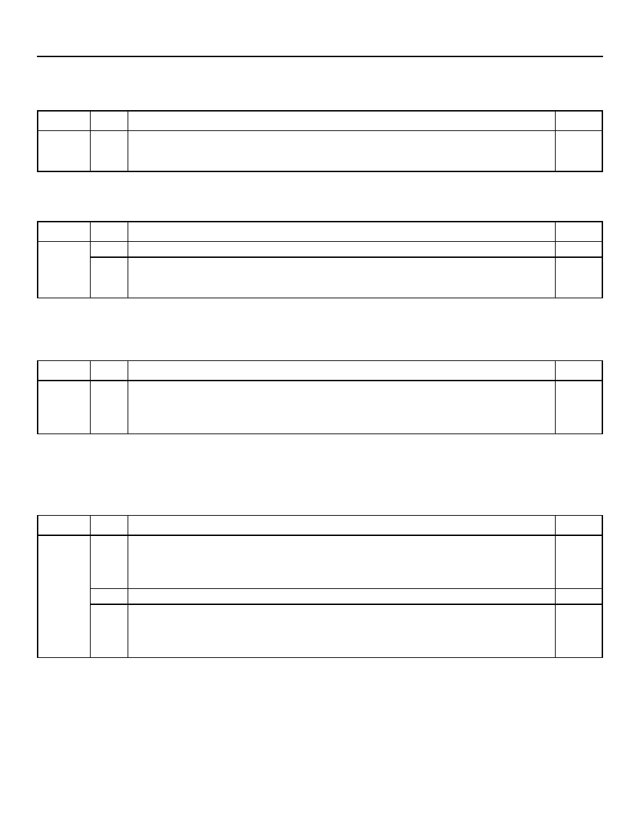
Data Sheet, Revision 3
TSI-1
September 21, 2005
1k x 1k Time-Slot Interchanger
Agere Systems Inc.
41
Table 6-27. CSG_Seed_Low (Read/Write)
Seed value for the pseudorandom pattern generator for the low word of the connection store RAM.
Table 6-28. CSG_Seed_High (Read/Write)
Seed value for the pseudorandom pattern generator for the high word of the connection store RAM.
Table 6-29. CSG_OR_Mask_Low (Read/Write)
This register allows bits in the connection store to be forced to 1. CS[15:0] = (pseudorandom data [15:0] OR
CSG_OR_Mask_Low) AND CSG_AND_Mask_Low, bit enabled by CSG_Write_Enable_Low.
Table 6-30. CSG_OR_Mask_High (Read/Write)
This register allows bits in the connection store to be forced to 1. CS[31:16] = (pseudorandom data [31:16] OR
CSG_OR_Mask_High) AND CSG_AND_Mask_High, bit enabled by CSG_Write_Enable_High.
Note: CS[22:18] are always 0.
Address
Bit
Name/Description
Default
0x00410
15:0 CSG_Seed_Low. If the LFSR_Seed_Control bit (see
Table 6-21 on page 39
) is asserted, at
the beginning of a CSG operation, bits [15:0] of the LFSR supplying the connection store
RAM with data are loaded with this programmable seed.
0xFFFF
Address
Bit
Name/Description
Default
0x00412
15
Unused.
--
14:0 CSG_Seed_High. If the LFSR_Seed_Control bit (see
Table 6-21
) is asserted, at the begin-
ning of a CSG operation, bits [30:16] of the LFSR supplying the connection store RAM with
data are loaded with this programmable seed.
0x7FFF
Address
Bit
Name/Description
Default
0x00418
15:0 CSG_OR_Mask_Low. This register allows bit fields in the connection store to be forced to a
one during a CSG fill operation. A bit-wise OR of this register and bits [15:0] of the pseudo-
random generated data are performed to obtain the data for connection store. The resultant
is then ANDed with CSG_AND_Mask_Low.
0x0000
Address
Bit
Name/Description
Default
0x0041A
15:7 CSG_OR_Mask_High_B. This register allows bit fields in the connection store to be forced
to a 1 during a CSG fill operation. A bit-wise OR of this register and bits [31:23] of the pseu-
dorandom generated data are performed to obtain the data for connection store. The result-
ant is then ANDed with CSG_AND_Mask_High.
0x000
6:2
Unused.
--
1:0
CSG_OR_Mask_High_A. This register allows bit fields in the connection store to be forced
to a 1 during a CSG fill operation. A bit-wise OR of this register and bits [17:16] of the pseu-
dorandom generated data are performed to obtain the data for connection store. The result-
ant is then ANDed with CSG_AND_Mask_High.
00

TSI-1
Data Sheet, Revision 3
1k x 1k Time-Slot Interchanger
September 21, 2005
42
42
Agere Systems Inc.
Table 6-31. CSG_AND_Mask_Low (Read/Write)
This register allows bits in the connection store to be forced to 0. This register takes precedence over CSG_OR_Mask_Low.
CS[15:0] = (pseudorandom data [15:0] OR CSG_OR_Mask_Low) AND CSG_AND_Mask_Low, bit enabled by
CSG_Write_Enable_Low.
Table 6-32. CSG_AND_Mask_High (Read/Write)
This register allows bits in the connection store to be forced to 0. This register takes precedence over CSG_OR_Mask_High.
CS[31:16] = (pseudorandom data [31:16] OR CSG_OR_Mask_High) AND CSG_AND_Mask_High, bit enabled by
CSG_Write_Enable_High.
Note: CS[22:18] are always 0.
Table 6-33. CS_Stream_Control (Read/Write)
If enabled, this register allows the CSG to program the connection store to map an incoming stream to an outgoing stream.
Address
Bit
Name/Description
Default
0x0041C
15:0 CSG_AND_Mask_Low. This register allows bit fields in the connection store to be forced to
a 0 during a CSG fill operation. A bit-wise AND of this register and bits [15:0] of the result
from the OR of CSG_OR_Mask_Low with the pseudorandom generated data are performed
to obtain the data for connection store.
0xFFFF
Address
Bit
Name/Description
Default
0x0041E
15:7 CSG_AND_Mask_High_B. This register allows bit fields in the connection store to be
forced to a 0 during a CSG fill operation. A bit-wise AND of this register and bits [31:23] of
the result from the OR of CSG_OR_Mask_High with the pseudorandom generated data are
performed to obtain the data for connection store.
0x1FF
6:2
Unused.
--
1:0
CSG_AND_Mask_High_A. This register allows bit fields in the connection store to be
forced to a 0 during a CSG fill operation. A bit-wise AND of this register and bits [17:16] of
the result from the OR of CSG_OR_Mask_High with pseudorandom generated data are per-
formed to obtain the data for connection store.
11
Address
Bit
Name/Description
Default
0x00428
15:13 Unused.
--
12:8 CS_Destination_Stream_Select. Specifies destination channel in stream switching
function. All time slots for this specified stream will be sourced from the stream specified in
CS_Source_Stream_Select. The Enable_Stream_Switching control bit (see
Table 6-21
)
must be set to enable this function.
0x00
7:5
Unused.
--
4:0
CS_Source_Stream_Select. Specifies the source stream in the stream switching function.
All time slots for this stream will be sent to the stream specified by
CS_Destination_Stream_Select. The Enable_Stream_Switching control bit (see
Table 6-21
)
must be set to enable this function.
0x00

Data Sheet, Revision 3
TSI-1
September 21, 2005
1k x 1k Time-Slot Interchanger
Agere Systems Inc.
43
Table 6-34. CSG_Configuration (Read/Write)
This register is used to populate the specified connection store RAM fields when the CSG is in the N-to-N mapping mode.
This register is not used when in the LFSR pattern mode (see CSG_Mode_Select on
Table 6-21 on page 39
bit 1).
Address
Bit
Name/Description
Default
0x0042A 15:11 Reserved.
00000
10
TPM_Enable_Field_Fill. The Test_Pattern_Monitor_Enable field (see
Table 8-2 on
page 59
) in the connection store RAM is filled with this value.
0
9:8
Mode_Field_Fill. The Time_Slot_Mode bits (see
Table 8-2
) in the connection store are filled
with this pattern.
00 = Low latency.
01 = Frame integrity.
10 = Alternate data.
11 = TGP data.
00
7
High_Impedance_Control_Field_Fill. Fills the Time_Slot_High_Impedance control bit
(see
Table 8-2
) in the connection store.
0
6:0
Unused.
--
TSI-1
Data Sheet, Revision 3
1k x 1k Time-Slot Interchanger
September 21, 2005
44
44
Agere Systems Inc.
6.7 Test Pattern Generator and Monitor Registers
Table 6-35. TPG_Configuration (Read/Write)
The TPG can be configured to generate any one of the ITU-T test patterns specified in O.150, O.151, or O.152, as well as
idle code or user-specified data.
Address
Bit
Name/Description
Default
0x00600
15:7 Unused.
--
6
TPG_Pattern_Invert. Data output patterns are inverted when this bit is selected.
0 = Do not invert TPG data.
1 = Invert TPG data.
0
5
Enable_Error_Exercise. This works in conjunction with both the TPG_Inject_Error_Count
(see
Table 6-40 on page 46
) and the Data_Invert_Mask (see
Table 6-41
). The latter is an 8-
bit register that allows for bit-wise XORing of the data output. The former gets loaded with
the number of N-bit errors that will be generated with N being the number bits set in the
Data_Invert_Mask. If the Data_Invert_Mask is set to 0x00, then no errors will be injected
despite the fact the TPG_Inject_Error_Count register will continue to decrement.
0 = Disable error exercising.
1 = Enable error exercise option.
0
4
Pattern_Generator_Enable. Enable the pattern generator:
0 = Pattern generator off.
1 = Pattern generator on.
Note: Setting this bit to 0 will not reset the TPM_Error_Count (see
Table 6-39 on page 46
)
nor the Pattern_Error_Detected (see
Table 6-42 on page 47
). Setting this bit to a 1
will reset the aforementioned.
0
3:0
TPG_Pattern_Select. These bits select the test pattern to be generated and inserted into
the selected time slots. Changing the pattern will reset the TPM_Error_Count register (see
Table 6-39 on page 46
) and Pattern_Error_Detected (see
Table 6-42 on page 47
).
0000 = Idle pattern (0011).
0001 = Mark (all ones AIS).
0010 = Alternating 0s and 1s--0x55.
0011 = 2
9
� 1.
0100 = 2
11
� 1.
0101 = 2
11
� 1 with zero suppression when previous 7 bits are zero.
0110 = 2
11
� 1 with zero suppression when next 7 bits are zero.
0111 = 2
15
� 1.
1000 = 2
20
� 1.
1001 = QRSS (2
20
� 1 with zero suppression when the next 14 bits are zero).
1010 = QRSS (2
20
� 1 with zero suppression when the next 14 bits are zero).
1011 = 2
23
� 1.
1100 = 2
29
� 1.
1101 = 2
31
� 1.
1110 = Indexed (data increments each time slot).
1111 = User pattern (repeating 2 bytes of data as specified in TPG_User_Pattern).
0x0
Table 6-36. TPG_User_Pattern (Read/Write)
Address
Bit
Name/Description
Default
0x00602
15:0 TPG_User_Pattern. Pattern-generator programmable user word. If pattern 0xF is specified
by the TPG_Pattern_Select field, this data will be sent out as TPG data. Bit [15] gets trans-
mitted first in time.
0x0000
Data Sheet, Revision 3
TSI-1
September 21, 2005
1k x 1k Time-Slot Interchanger
Agere Systems Inc.
45
Table 6-37. TPM_Configuration (Read/Write)
The TPG can be configured to monitor any one of the ITU-T test patterns specified in O.150, O.151, or O.152, as well as
idle code or user-specified data.
Address
Bit
Name/Description
Default
0x00604
15:7 Unused.
--
6
TPM_Pattern_Invert. Incoming data patterns are inverted prior to checking when this bit is
selected.
0 = Do not invert TPM data.
1 = Invert TPM data.
0
5
Reset_TPM_Error_Counter. Resets the error counter (TPM_Error_Count see
Table 6-39
on page 46
).
0 = Allow TPM_Error_Count to advance.
1 = Reset TPM_Error_Count (to zero).
0
4
Pattern_Monitor_Enable. Enable the pattern monitor:
0 = Pattern monitor off.
1 = Pattern monitor on.
0
3:0
TPM_Pattern_Select. These bits select the test pattern to be monitored from the selected
time slots.
0000 = Idle pattern (0011).
0001 = Mark (all ones AIS).
0010 = Alternating 0s and 1s--0x55.
0011 = 2
9
� 1.
0100 = 2
11
� 1.
0101 = 2
11
� 1 with zero suppression when previous 7 bits are zero.
0110 = 2
11
� 1 with zero suppression when next 7 bits are zero.
0111 = 2
15
� 1.
1000 = 2
20
� 1.
1001 = QRSS (2
20
� 1 with zero suppression when the next 14 bits are zero).
1010 = QRSS (2
20
� 1 with zero suppression when the next 14 bits are zero).
1011 = 2
23
� 1.
1100 = 2
29
� 1.
1101 = 2
31
� 1.
1110 = Indexed (data increments each time slot).
1111 = User pattern (repeating 2 bytes of data as specified in TPG_User_Pattern).
0x0
Table 6-38. TPM_User_Pattern (Read/Write)
Address
Bit
Name/Description
Default
0x00606
15:0 TPM_User_Pattern. User-definable data for pattern monitoring. If pattern 0xF is specified
by the TPM_Pattern_Select field, this data will be used to check against incoming data. Bit
[15] gets checked first in time.
0x0000

TSI-1
Data Sheet, Revision 3
1k x 1k Time-Slot Interchanger
September 21, 2005
46
46
Agere Systems Inc.
* See
Table 6-15 on page 37
bit 2.
This register provides a mask for specifying which bits of TPG data are to be inverted when forcing errors.
Table 6-39. TPM_Error_Count (Sat/Roll*)
Address
Bit
Name/Description
Default
0x00608
15:0 TPM_Error_Count. This status register accumulates the number of pattern bit errors
detected in the monitored time slot(s).
If Saturate_Rollover_Select (see
Table 6-15 on page 37
) is set to a 1, this register will sat-
urate at 0xFFFF and not be allowed to roll over.
If Saturate_Rollover_Select is set to a 0, the counter will roll over (count to 0x0 on the next
error after 0XFFFF), the Pattern_Error_Detected status bit (see
Table 6-42 on page 47
)
will not be reset.
The TPM_Error_Count register can be reset in one of the following four ways:
1. The pattern is changed.
2. The bit RESET_TPM_Error_Counter (in the TPM_Configuration register, see
Table 6-37
on page 45
) is asserted.
3. This register is written. The TPM_Error_Count register will be set to 0x0000 independent
of the value written.
4. This register is read when Register_Clearing_Mode = 1 (see
Table 6-15 on page 37
).
Note: Since TPM_Error_Count is the source of Pattern_Error_Detected status bit (see
Table 6-42 on page 47
), then the clearing of this register will also clear the error bit.
0x0000
Table 6-40. TPG_Inject_Error_Count (Write Only)
Address
Bit
Name/Description
Default
0x0060A
15:0 TPG_Inject_Error_Count. This register specifies the number of errors to be injected. The
actual number of bit errors that will be injected will equal to the TPG_Inject_Error_Count x
N, where N is the number of bits set to 1 in the TPG_Data_Invert_Mask. The readback of
this register will always reflect the remaining error count and not the original number written
to this register.
0x0000
Table 6-41. TPG_Data_Invert_Mask (Read/Write)
Address
Bit
Name/Description
Default
0x0060C
15:8 Unused.
--
7:0
Data_Invert_Mask. The contents of this register are XORed with the TPG output word pro-
viding bit-wise error control.
Note: If Data_Invert_Mask = 0x00, then no errors will be injected.
0x00
Data Sheet, Revision 3
TSI-1
September 21, 2005
1k x 1k Time-Slot Interchanger
Agere Systems Inc.
47
Table 6-43. TPM_Status_Mask (Read/Write)
Mask bits for the TPM_Status register.
Table 6-42. TPM_Status (Read Only)
Address
Bit
Name/Description
Default
0x0060E
15:2 Unused.
--
1
Test_Pattern_Lock. This status bit indicates if the monitor has achieved a pattern lock on
all selected time slots.
0 = Monitor is locked on the pattern.
1 = Monitor is searching for the pattern.
--
0
Pattern_Error_Detected. This status bit indicates if the TPM_Error_Count register (see
Table 6-39 on page 46
) is nonzero.
0 = No errors detected.
1 = Nonzero (one or more errors detected).
Note: This bit is cleared by clearing TPM_Error_Count. Refer to function description of
TPM_Error_Count.
--
Address
Bit
Name/Description
Default
0x00610
15:2 Unused.
--
1
Test_Pattern_Lock_Mask. This bit masks the Test_Pattern_Lock bit (see Table 6-42) from
causing an interrupt.
0 = Nonmasked. If the monitor is not locked, an interrupt will be generated.
1 = Masked. An error will not cause an interrupt.
1
0
Pattern_Error_Mask. This bit masks the Pattern_Error_Detected bit (see Table 6-42) from
causing an interrupt.
0 = Nonmasked. An error will cause an interrupt.
1 = Masked. An error will not cause an interrupt.
1
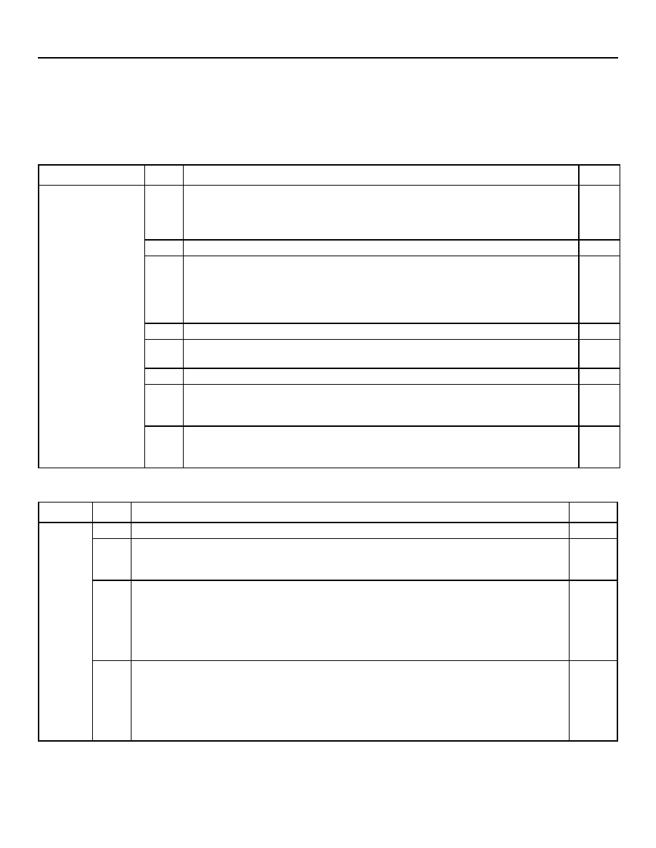
TSI-1
Data Sheet, Revision 3
1k x 1k Time-Slot Interchanger
September 21, 2005
48
48
Agere Systems Inc.
6.8 Concentration Highway Configuration Registers
Table 6-44. Receive_CHI_Configuration (Read/Write)
Each of the incoming CHIs can be independently designed and programmed with a unique offset from the master frame
synchronization. This bank of registers works in conjunction with the corresponding Receive_CHI_Time_Slot_Offset regis-
ters (see
Table 6-52 on page 53
) to provide this control. These registers provide the bit and fractional bit offset control.
Address
Bit
Name/Description
Default
0x00A00--0x00A1E
15
Receive_CHI_Loopback_Enable.
0 = Input data for this receive CHI comes from the corresponding RXD pin.
1 = Input data for this receive CHI comes from the corresponding transmit CHI (see
CHI_Feedback_Source_Selection in
Table 6-48 on page 50
bit 15).
0
14:10 Unused.
--
9:8
Receive_CHI_Bit_Rate. These bits indicate the data rate of this receive CHI.
00 = 2 Mbits/s.
01 = 4 Mbits/s.
10 = 8 Mbits/s.
11 = 16 Mbits/s. (Only valid with 16 MHz CHICLK clock.)
00
7
Unused.
--
6:4
Receive_CHI_Bit_Offset. These bits represent the bit offset relative to the frame
synchronization sample point for this receive CHI (in binary, 0--7 bits).
000
3:2
Unused.
--
1
Receive_CHI_Half_Bit_Offset.
0 = No additional offset.
1 = Indicates an additional 1/2 bit of offset for this receive CHI.
0
0
Receive_CHI_Quarter_Bit_Offset.
0 = No additional offset.
1 = Indicates an additional 1/4 bit of offset for this receive CHI.
0
Table 6-45. Receive_CHI_Status (CORWN) Receive_CHI_Status (CORWN)
Address
Bit
Name/Description
Default
0x00A80
15:3 Unused.
--
2
Receive_Clock_Error.
0 = No clock error detected.
1 = Indicates a slow (or missing) CHICLK.
--
1
Receive_Lock_Error.
0 = No clock error detected.
1 = Indicates a synchronization error has occurred between the CHICLK and the internal
PLL clock. If Enable_Receive_CHI_Automatic_Resynchronization (see
Table 6-47 on
page 49
) is not a 1, then a manual resynchronization should be performed
(Force_Receive_CHI_Resynchronization, see
Table 6-47
).
--
0
Receive_Frame_Sync_Error.
0 = No frame synchronization error detected.
1 = Indicates a frame synchronization error has occurred. This means the CHI frame
synchronization was either missing or misplaced. For missing frame synchronizations,
this status is the only action taken. For misplaced frame synchronizations, the device
automatically synchronizes to the new frame synchronization position.
--
Data Sheet, Revision 3
TSI-1
September 21, 2005
1k x 1k Time-Slot Interchanger
Agere Systems Inc.
49
Table 6-46. Receive_CHI_Status_Mask (Read/Write)
Mask bits for the Receive_CHI_Status register (see
Table 6-45
).
Table 6-47. Receive_CHI_Global_Configuration (Read/Write)
Global configuration control for all the receive CHIs.
Address
Bit
Name/Description
Default
0x00A82
15:3 Unused.
--
2
Receive_Clock_Error_Mask.
0 = The Receive_Clock_Error bit (see
Table 6-45
) will cause an interrupt if active (unless
masked at a higher level).
1 = The Receive_Clock_Error bit is blocked from causing an interrupt.
1
1
Receive_Lock_Error_Mask.
0 = The Receive_Lock_Error bit (see
Table 6-45
) will cause an interrupt if active (unless
masked at a higher level).
1 = The Receive_Lock_Error bit is blocked from causing an interrupt.
1
0
Receive_Frame_Sync_Error_Mask.
0 = The Receive_Frame_Sync_Error bit (see
Table 6-45
) will cause an interrupt if active
(unless masked at a higher level).
1 = The Receive_Frame_Sync_Error bit is blocked from causing an interrupt.
1
Address
Bit
Name/Description
Default
0x00A84
15:4 Unused.
--
3
Force_Receive_CHI_Resynchronization.
0 = Normal operation.
1 = This forces the receive CHI/PLL interface to resynchronize.
0
2
Enable_Receive_CHI_Automatic_Resynchronization.
0 = The device will inhibit automatic resynchronization of the receive CHI/PLL interface if it
detects it is out-of-synchronization (not recommended).
1 = The device will automatically resynchronize the receive CHI/PLL interface if it detects it
is out-of-synchronization.
0
1
Receive_Frame_Sync_Polarity. This bit indicates the polarity of the frame synchronization
signal.
0 = Indicates the frame synchronization is active-low. The reference point for all receive CHI
timing is the first active edge of CHICLK (see Receive_Clock_Edge) after the frame
synchronization transitions to the active level as defined here.
1 = Indicates the frame synchronization is active-high.
0
0
Receive_Clock_Edge. This bit indicates which edge of the CHICLK to use to sample the
frame synchronization signal.
0 = Indicates sampling on the falling edge. This also defines the reference point for all
receive CHI timing and offsets.
1 = Indicates sampling on the rising edge of the clock.
0

TSI-1
Data Sheet, Revision 3
1k x 1k Time-Slot Interchanger
September 21, 2005
50
50
Agere Systems Inc.
Table 6-48. Transmit_CHI_Configuration (Read/Write)
Each of the incoming CHIs can be independently designed and programmed with a unique offset from the master frame
synchronization. This bank of registers works in conjunction with the corresponding Transmit_CHI_Time_Slot_Offset regis-
ters (see
Table 6-53 on page 53
) to provide this control. These registers provide the bit and fractional bit offset control.
Figure 6-1. Transmit CHI Configuration (R/W)
Address
Bit
Name/Description
Default
0x00C00--0x00C1E
15 CHI_Feedback_Source_Selection. Selects which data is sent to corresponding
receive CHI.
0 = Means pre-output data is sent.
1 = Means the input from the bidirectional TXD pin is sent. This bit has no effect
unless the corresponding receive CHI's Receive_CHI_Loopback_Enable bit is
one (see
Table 6-44 on page 48
).
0
14 Unused.
--
13:12 Driver_Enable_Control. These two bits determine how the output TXD pin is
actually driven.
00 = Always disabled.
01 = Based on time-slot programming (timing from CHICLK).
10 = Reserved.
11 = Similar to 01 except all time slots are disabled near end of time slot (see
Transmit_High_Impedance_Delay in
Table 6-51 on page 52
bits [6:4]).
00
11:10 Unused.
--
9:8 Transmit_CHI_Bit_Rate. These bits indicate the data rate of this transmit CHI.
00 = 2 Mbits/s.
01 = 4 Mbits/s.
10 = 8 Mbits/s.
11 = 16 Mbits/s (only valid with 16 MHz CHICLK).
00
7
Unused.
--
6:4 Transmit_CHI_Bit_Offset. These bits represent the bit offset relative to the frame
synchronization sample point for this transmit CHI (in binary, 0--7 bits).
000
3:2 Unused.
--
1
Transmit_CHI_Half_Bit_Offset.
0 = No additional delay.
1 = Indicates an additional 1/2 bit of offset for this transmit CHI.
0
0
Transmit_CHI_Quarter_Bit_Offset.
0 = No additional delay.
1 = Indicates an additional 1/4 bit of offset for this transmit CHI. This bit must be 0
when the CHI rate is 16 Mbits/s or when the CHI rate is 8 Mbits/s mode and the
CHICLK is 8.192 MHz.
0
SWITCH FABRIC
TXD
RXD
RECEIVE_CHI_LOOPBACK_ENABLE
CHI_FEEDBACK_SOURCE_SELECTION
Data Sheet, Revision 3
TSI-1
September 21, 2005
1k x 1k Time-Slot Interchanger
Agere Systems Inc.
51
Table 6-49. Transmit_CHI_Status (CORWN)
Table 6-50. Transmit_CHI_Status_Mask (Read/Write)
Mask register for the Transmit_CHI_Status register.
Address
Bit
Name/Description
Default
0x00C80
15:2 Unused.
--
1
Transmit_Lock_Error.
0 = No error detected.
1 = Indicates a synchronization error has occurred between the CHICLK and the internal
PLL clock. If Enable_Transmit_CHI_Automatic_Resynchronization is not a 1 (see
Table 6-51 on page 52
), then a manual resynchronization should be performed
(Force_Transmit_CHI_Resynchronization, see
Table 6-51
).
--
0
Transmit_Frame_Sync_Error.
0 = No error detected.
1 = Indicates a frame synchronization error has occurred in the transmit CHI section of the
device. This means the CHI frame synchronization was either missing or misplaced. For
missing frame synchronizations, this status is the only action taken. For misplaced frame
synchronizations, the device automatically synchronizes to the new frame synchroniza-
tion position.
--
Address
Bit
Name/Description
Default
0x00C82
15:2 Unused.
--
1
Transmit_Lock_Error_Mask.
0 = The Transmit_Lock_Error bit (see Table 6-49) will cause an interrupt if active (unless
masked at a higher level).
1 = The Transmit_Lock_Error bit is blocked from causing an interrupt.
1
0
Transmit_Frame_Sync_Error_Mask.
0 = The Transmit_Frame_Sync_Error bit (see Table 6-49) will cause an interrupt if active
(unless masked at a higher level).
1 = The Transmit_Frame_Sync_Error bit is blocked from causing an interrupt.
1

TSI-1
Data Sheet, Revision 3
1k x 1k Time-Slot Interchanger
September 21, 2005
52
52
Agere Systems Inc.
Table 6-51. Transmit_CHI_Global_Configuration (Read/Write)
Address Bit
Name/Description
Defaul
t
0x00C84 15:8 Unused.
--
7 Global_Transmit_CHI_Output_Enable. This bit is a global control over the 3-state enables of
the transmit CHIs.
0 = All CHIs transmit pins are forced into the high-impedance state.
1 = 3-state control of individual CHIs is placed under control of the CHI
Transmit_CHI_Configuration register (see
Table 6-48 on page 50
).
0
6:4 Transmit_High_Impedance_Delay. These bits are used in conjunction with Driver_Enable_Control
(see
Table 6-48
bits [13:12]) bits. When the Driver_Enable_Control bits = 11, then the
Transmit_High_Impedance_Delay bits determine how early the device will 3-state the output driver at
the end of a time slot. These numbers are approximate because of the sampling error between the
CHICLK and the internal clock. The numbers are actually how much time after the previous clock
edge the output 3-states. For bit settings [6:4]:
000 = Approximately 55 ns after the previous same edge with a 16.384 MHz CHICLK.
= Approximately 55 ns after the previous opposite edge with an 8.192 MHz CHICLK.
001 = Approximately 49 ns after the previous same edge with a 16.384 MHz CHICLK.
= Approximately 49 ns after the previous opposite edge with an 8.192 MHz CHICLK.
010 = Approximately 43 ns after the previous same edge with a 16.384 MHz CHICLK.
= Approximately 43 ns after the previous opposite edge with an 8.192 MHz CHICLK.
011 = Approximately 37 ns after the previous same edge with a 16.384 MHz CHICLK.
= Approximately 37 ns after the previous opposite edge with an 8.192 MHz CHICLK.
100 = Approximately 116 ns after the previous same edge (8.192 MHz CHICLK only).
101 = Approximately 110 ns after the previous same edge (8.192 MHz CHICLK only).
110 = Approximately 104 ns after the previous same edge (8.192 MHz CHICLK only).
111 = Approximately 98 ns after the previous same edge (8.192 MHz CHICLK only).
See
Figure 5-15 on page 27
and
Table 5-5 on page 27
.
000
3 Force_Transmit_CHI_Resynchronization.
0 = Normal operation.
1 = This forces the transmit CHI/PLL interface to resynchronize.
0
2 Enable_Transmit_CHI_Automatic_Resynchronization.
0 = The device will inhibit automatic resynchronization of the transmit CHI/PLL interface if it
detects it is out-of-synchronization (not recommended).
1 = The device will automatically resynchronize the CHI/PLL interface if it detects it is out-of-syn-
chronization.
0
1 Transmit_Frame_Sync_Polarity. This bit indicates the polarity of the frame synchronization sig-
nal.
0 = Indicates the frame synchronization is active-low. Generally, this should be programmed with
the same value as Receive_Frame_Sync_Polarity (see
Table 6-47 on page 49
). The refer-
ence point for all receive CHI timing is the first active edge of CHICLK (see
Transmit_Clock_Edge below) after the frame synchronization transitions to the active level as
defined here.
1 = Indicates the frame synchronization is active-high.
0
0 Transmit_Clock_Edge. This bit indicates which edge of the CHICLK to use to sample the frame
synchronization signal.
0 = Indicates sampling on the falling edge. Generally, this should be programmed with the same
value as Receive_Clock_Edge (see
Table 6-47 on page 49
). This also defines the reference
point for all transmit CHI timing and offsets.
1 = Indicates sampling on the rising edge of the clock.
0
Data Sheet, Revision 3
TSI-1
September 21, 2005
1k x 1k Time-Slot Interchanger
Agere Systems Inc.
53
Table 6-52. Receive_CHI_Time_Slot_Offset (Read/Write)
Each of the incoming CHIs can be independently designed and programmed with a unique offset from the master frame
synchronization. This bank of registers works in conjunction with the corresponding Receive_CHI_Configuration registers
(see
Table 6-44 on page 48
) to provide this control. These registers provide the time-slot offset. The
Receive_CHI_Configuration registers provide the bit and fractional bit offset control.
Table 6-53. Transmit_CHI_Time_Slot_Offset (Read/Write)
Each of the outgoing CHIs can be independently designed and programmed with a unique offset from the master frame syn-
chronization. This bank of registers works in conjunction with the corresponding Transmit_CHI_Configuration registers (see
Table 6-48 on page 50
) to provide this control. These registers provide the time-slot offset. The Transmit_CHI_Configuration
registers provide the bit and fractional bit offset control.
Address
Bit
Name/Description
Default
0x01000--0x0101E
15:8 Unused.
--
7:0
Receive_CHI_Offset. Time-slot offset for the receive CHIs. This value should be
programmed as follows (RTO = the number of receive time slots to be offset):
--
CHI Rate
Offset
RC_TS_OFF Value
16 Mbits/s
RTO (0--255)
RTO
8 Mbits/s
RTO (0--127)
((RTO x 2) + 2) modulo 256
4 Mbits/s
RTO (0--63)
((RTO x 4) + 6) modulo 256
2 Mbits/s
RTO (0--31)
((RTO x 8) + 14) modulo 256
Address
Bit
Name/Description
Default
0x01080--0x0109E
15:8 Unused.
--
7:0
Transmit_CHI_Offset. Time-slot offset for the transmit CHIs. This value should
be programmed as follows (TTO = the number of transmit time slots to be offset):
--
CHI Rate
Offset
TC_TS_OFF Value
16 Mbits/s
TTO (0--255)
TTO
8 Mbits/s
TTO (0--127)
TTO x 2
4 Mbits/s
TTO (0--63)
TTO x 4
2 Mbits/s
TTO (0--31)
TTO x 8

TSI-1
Data Sheet, Revision 3
1k x 1k Time-Slot Interchanger
September 21, 2005
54
54
Agere Systems Inc.
7 Switch Fabric Control
Table 7-1. SF_Status (CORWN)
Table 7-2. SF_Status_Mask (Read/Write)
Provides a mask for all bits in the SF_Status register (see Table 7-1). These bits are output masks of the register. That is,
setting the mask will not stop the error bit from being set, but will block an interrupt from being propagated if the correspond-
ing error is set.
Address
Bit
Name/Description
Default
0x01124
15:3 Unused.
--
2
Receive_Link_Synchronization_Error.
0 = No error detected.
1 = Missing or misplaced synchronization on interface between the receive CHI and the
switch fabric (clear-on-read/clear-on-write).
--
1
Transmit_Sync_Error.
0 = No error detected.
1 = Missing or misplaced synchronization on interface between the transmit CHI and the
switch fabric (clear-on-read/clear-on-write).
--
0
Connection_Store_Parity_Error.
0 = No error detected.
1 = Connection store parity error detected (read only, clear by clearing
Connection_Store_Parity_Error_Address_Trap, see
Table 7-5 on page 56
). The location
with the parity error can be found in Connection_Store_Parity_Error_Address_Trap.
--
Address
Bit
Name/Description
Default
0x01126
15:3 Unused.
--
2
Receive_Link_Synchronization_Error_Mask.
0 = Unmasked, Receive_Link_Synchronization_Error will (see Table 7-1) cause interrupt
(unless masked at higher level).
1 = Masked, Receive_Link_Synchronization_Error will not cause an interrupt.
1
1
Transmit_Sync_Error_Mask.
0 = Unmasked, Transmit_Sync_Error (see Table 7-1) will cause interrupt (unless masked at
higher level).
1 = Masked, Transmit_Sync_Error will not cause an interrupt.
1
0
Connection_Store_Parity_Error_Mask.
0 = Unmasked, Connection_Store_Parity_Error (see Table 7-1) will cause interrupt (unless
masked at higher level).
1 = Masked, Connection_Store_Parity_Error will not cause an interrupt.
1

Data Sheet, Revision 3
TSI-1
September 21, 2005
1k x 1k Time-Slot Interchanger
Agere Systems Inc.
55
Table 7-3. Data_Store_Time_Slot_Capture_Select (Read/Write)
For diagnostic and other purposes, a single incoming time slot can be sampled and made available to be read from the mi-
croprocessor interface. This register specifies which time slot will be sampled.
Table 7-4. Data_Store_Captured_Data (Read Only)
This register contains data sampled in two consecutive frames from the time slot specified in
Data_Store_Time_Slot_Capture, see Table 7-3. This register is continually updated every frame (alternating high/low byte
each frame).
Address
Bit
Name/Description
Default
0x01142
15:13 Unused.
--
12:0 Data_Store_Time_Slot_Capture. Specifies which time slot should be captured (sampled)
(0--8,191). This value is a function of the stream (CHI) number, the data rate of the CHI, the
time-slot offset of the CHI (RTO), and the desired time slot (TS) of the CHI. The following
algorithms can be used to determine the value for this field:
For a 16 Mbits/s CHI:
-- (32 x [(TS + RTO) mod 256]) + CHI, where TS and RTO range from 0--255.
For an 8 Mbits/s CHI:
-- (32 x [([2 x (TS + RTO)] + 2) mod 256]) + CHI, where TS and RTO range from 0--127.
For a 4 Mbits/s CHI:
-- (32 x [([4 x (TS + RTO)] + 6) mod 256]) + CHI, where TS and RTO range from 0--63.
For a 2 Mbits/s CHI:
-- (32 x [([8 x (TS + RTO)] + 14) mod 256]) + CHI, where TS and RTO range from 0--31.
0x0000
Address
Bit
Name/Description
Default
0x01144
15:8 Captured_Data_1. Data captured from the time slot specified by
Data_Store_Time_Slot_Capture (see Table 7-3). This field is updated every other frame
alternating with Captured_Data_0. Depending on when this is read by the microprocessor, it
may be either from the frame before or after that sampled in Captured_Data_0.
--
7:0
Captured_Data_0. Data captured from the time slot specified by
Data_Store_Time_Slot_Capture (see Table 7-3). This field is updated every other frame
alternating with Captured_Data_1. Depending on when this is read by the microprocessor, it
may be either from the frame before or after that sampled in Captured_Data_1.
--
TSI-1
Data Sheet, Revision 3
1k x 1k Time-Slot Interchanger
September 21, 2005
56
56
Agere Systems Inc.
Table 7-5. Connection_Store_Parity_Error_Address_Trap (CORWN)
As the connection store is continually read, its parity is checked. If an error is detected, the location with the error is saved
in this register and the Connection_Store_Parity_Error (see
Table 7-1 on page 54
) error bit is set. If in clear-on-read (COR)
mode, when this register is read, the Connection_Store_Parity_Error bit is cleared. If in clear-on-write (COW) mode, any
write to this register clears Connection_Store_Parity_Error.
Table 7-6. Receive_Link_Offset (Read Only)
This register displays the offset of the receive link with respect to the switch fabric. See also Transmit_Link_Offset and
Force_Transmit_Link_Offset in Table 7-7.
Table 7-7. Transmit_Link_Offset (Read/Write)
This register displays/controls the offset of the transmit links with respect to the switch fabric. Normally, the
Transmit_Link_Offset is determined by the CHI frame synchronization's relative position to the switch fabric synchronization.
In this case, bit [15] of this register should be set to 0.
Address
Bit
Name/Description
Default
0x01146
15
Unused.
--
14:0 Connection_Store_Parity_Error_Address. This bit field contains the address within the
connection store with a parity error. The address of the first error (after a clear) is sampled
and saved.
--
Address
Bit
Name/Description
Default
0x01148
15:12 Unused.
--
11:0 Link_Offset. This field contains the time-slot offset of the receive link.
--
Address
Bit
Name/Description
Default
0x0114C
15
Force_Transmit_Link_Offset.
0 = Allows the switch fabric to self-determine its offsets.
1 = Forces the device to use the Transmit_Offset value to align the switch fabric to a deter-
ministic position relative to the CHI frame synchronization. If this is set to 1, this register
value should be set and the system allowed to stabilize (more than 250 �s) prior to read-
ing the value in Receive_Link_Offset (see Table 7-6).
--
14:12 Unused.
--
11:0 Transmit_Offset. If Force_Transmit_Link_Offset is set to 1, this value will force the switch
fabric to align itself this many time slots off from the CHI frame synchronization. Please con-
tact your FAE if you plan on using this feature.
--

Data Sheet, Revision 3
TSI-1
September 21, 2005
1k x 1k Time-Slot Interchanger
Agere Systems Inc.
57
Table 7-8. Wide_Mode_Control (Read/Write)
For applications that require switching of time slots of greater than 8 bits, parallel devices must be used. These bits can be
used to facilitate such operation. Please contact your FAE if setting these bits to other than the default value of 0.
Address
Bit
Name/Description
Default
0x0114E
15:3 Unused.
--
2:0
Wide_Mode_Operation.
000 = Disable multifabric synchronization (i.e., normal mode) (default).
001 = Software algorithm mode, maximum allowable receive delay of approximately 7 �s.
010 = Software algorithm mode, maximum allowable receive delay of approximately 15 �s.
011 = Software algorithm mode, maximum allowable receive delay of approximately 31 �s.
100 = Disable multifabric synchronization (i.e., normal mode).
101 = Minimal latency mode, maximum allowable receive delay of approximately 7 �s.
110 = Minimal latency mode, maximum allowable receive delay of approximately 15 �s.
111 = Minimal latency mode, maximum allowable receive delay of approximately 31 �s.
Note: For the last three modes, the minimum, average, and maximum delay in low-latency
(LL) mode will be up to 7 �s, 15 �s, and 31 �s larger than regular LL mode. For the
software modes, the minimum delay in LL mode will be up to 7 �s, 15 �s, and 31 �s
larger, and the maximum delay will be up to 132 �s, 140 �s, and 156 �s larger than
regular mode.
000
TSI-1
Data Sheet, Revision 3
1k x 1k Time-Slot Interchanger
September 21, 2005
58
58
Agere Systems Inc.
8 Connection Store
The connection store RAM contains the per-time-slot control information for outgoing time slots. Each location in the RAM
corresponds to one outgoing time slot and contains all the time-slot specific control information for that time slot. The specific
address offset into the RAM is calculated as follows:
ADDR[15] = 0.
ADDR[14:7] destination (outgoing) time-slot number of stream identified by address bits [6:2].
ADDR[6:2] destination (outgoing) stream (CHI) number.
ADDR[01] 0 = Low_Control, 1 = High_Control.
ADDR[00] = 0 (no byte addressability).
Address bits [14:7] are dependent on the destination (outgoing) CHI rate and should be calculated as follows, where TS is
the outgoing CHI time-slot number:
Table 8-1. Low_Control_Word (Read/Write)
The low-control word in the connection store has two functions. Normally, it is used to program the address of the incoming
time slot to which the outgoing time slot is connected. The outgoing time slot is implied by the connection store address as
described above. This normal switch operation will apply if the time-slot mode bits in the high-control word are set to low
latency or frame integrity switching modes. If alternate data mode is selected, the low control word contains the alternate
data (see
Table 8-2
, bit [9:8]).
* Bits [15:0] have dual meaning based on the value in the Time_Slot_Mode field of the High_Control_Word (see Table 8-2).
If the Time_Slot_Mode field is set to 10 (alternate data), then bits [15:0] have the following meaning:
Bits [7:0] are set to Alternate_Data_Pattern_1.
Bits [15:8] are set to Alternate_Data_Pattern_2.
If the Time_Slot_Mode field is set to anything other than 10, then bits [15:0] have the following meaning:
Bits [4:0] are set to Stream_Pointer.
Bits [12:5] are set to Time_Slot_Pointer.
Bits [15:13] are reserved.
Rate
A[14:7]
16 MHz
TS (0--255)
8 MHz
TS x 2 (TS = 0--127)
4 MHz
TS x 4 (TS = 0--63)
2 MHz
TS x 8 (TS = 0--31)
Address
Bit
*
Name/Description
Default
0x10000--
0x13FFC
15:8 Alternate_Data_Pattern_2. If alternate data is selected by the mode bits in the corre-
sponding high control location, the data in this byte will alternate with the
Alternate_Data_Pattern_1 pattern and be sent out on the transmit time slot.
--
12:5 Time_Slot_Pointer. This field selects the desired time slot from the source stream (CHI).
This value is dependent on the speed (data rate) of the receive CHI specified by
Stream_Pointer and should be programmed as follows, where TS is the desired time-slot
number:
--
Receive CHI Rate
Time_Slot_Pointer [7:0]
16 Mbits/s
TS (0--255)
8 Mbits/s
TS x 2 (TS = 0--127)
4 Mbits/s
TS x 4 (TS = 0--63)
2 Mbits/s
TS x 8 (TS = 0--31)
7:0
Alternate_Data_Pattern_1. If alternate data is selected by the mode bits in the corre-
sponding high control location, the data in this byte will alternate with the
Alternate_Data_Pattern_2 pattern and be sent out on the transmit time slot.
--
4:0
Stream_Pointer. This field selects one of 32 incoming streams.
--
Data Sheet, Revision 3
TSI-1
September 21, 2005
1k x 1k Time-Slot Interchanger
Agere Systems Inc.
59
Table 8-2. High_Control_Word (Read/Write)
Address
Bit
Name/Description
Default
0x10002--0x13FFE 15:11 Reserved.
0x0
10
Test_Pattern_Monitor_Enable.
0 = The TPM is disable for this time slot.
1 = This bit causes data for this time slot to be sent to the test pattern monitor for
checking.
--
9:8
Time_Slot_Mode. This field defines in which of the following modes the time slot
will operate:
00 = Low latency.
01 = Frame integrity.
10 = Alternate data.
11 = TPG data.
--
7
Reserved.
Note: This bit must be set to zero.
--
6:5
Unused.
--
4
General_Purpose_Bit. This is a general-purpose read/write bit. It causes no
action within the device.
--
3:0
Unused.
--
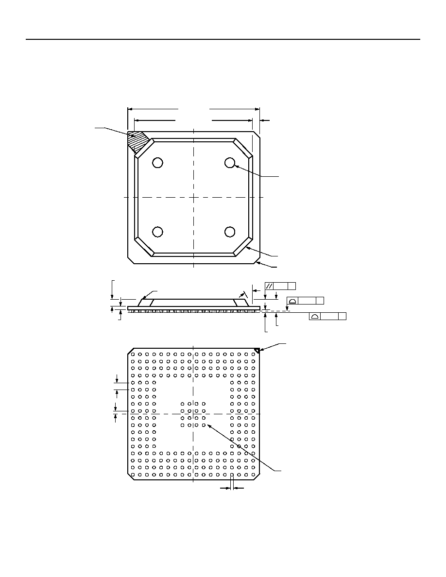
TSI-1
Data Sheet, Revision 3
1k x 1k Time-Slot Interchanger
September 21, 2005
60
60
Agere Systems Inc.
9 Outline Diagrams
Note: Dimensions are in millimeters.
0.20
BOTTOM VIEW
1.75 TYP.
1.20 x 45� APPROX
A1 INDICATOR
(PLATED)
0.80 � 0.050
0.56 � 0.06
30�
0.50 � 0.10
Z
0.35 Z
A
B
C
D
E
F
G
H
J
K
L
M
N
P
R
T
1
2
3
4
5
6
7
8
9
10
11
13
16
18
1.00
15
17.70
SEATING PLANE
0.50 R MAX
SQUARE
19.00
SQUARE
APPROX
ALL SIDES
0.10
Z
ALL EDGES
1.86 � 0.21
TYP 3 PLACES
4.00 x 45� APPROX
TYP 4 CORNERS
USE OF EJECTOR
PINS IS OPTIONAL
12
14
17
TYP
0.63 DIA
U
V
A1 INDICATOR
(UNDER SOLDER MASK)
TOP VIEW
CENTER ARRAY
FOR THERMAL
ENHANCEMENT
0.50
+0.70
�0.05
+0.07
�0.13
Copyright � 2005 Agere Systems Inc.
All Rights Reserved
September 21, 2005
DS05-115STSI-3 (Replaces DS05-115STSI-2)
Data Sheet, Revision 3
TSI-1
September 21, 2005
1k x 1k Time-Slot Interchanger
Agere Systems Inc. reserves the right to make changes to the product(s) or information contained herein without notice. No liability is assumed as a result of their use or application.
Agere, Agere Systems, and the Agere logo are registered trademarks of Agere Systems Inc.
For additional information, contact your Agere Systems Account Manager or the following:
INTERNET:
Home: http://www.agere.com Sales: http://www.agere.com/sales
E-MAIL:
docmaster@agere.com
N. AMERICA: Agere Systems Inc., Lehigh Valley Central Campus, Room 10A-301C, 1110 American Parkway NE, Allentown, PA 18109-9138
1-800-372-2447, FAX 610-712-4106 (In CANADA: 1-800-553-2448, FAX 610-712-4106)
ASIA:
CHINA: (86) 21-54614688 (Shanghai), (86) 755-25881122 (Shenzhen), (86) 10-65391096 (Beijing)
JAPAN: (81) 3-5421-1600 (Tokyo), KOREA: (82) 2-767-1850 (Seoul), SINGAPORE: (65) 6741-9855, TAIWAN: (886) 2-2725-5858 (Taipei)
EUROPE:
Tel. (44) 1344 296 400
10 Ordering Information
11 Change History
On pages 1, 15, and 61 changed the device name. On page 61 changed the part numbers.
On
page 20
deleted 2 sentences at the beginning of the page. (All timing parameters are referenced to V
IHmin
and V
IL
max.
The reference signal polarity may be inverted for some timing parameters.)
On
page 20
updated Figure 5-3, ac Timing Specification.
On
page 20
updated Table 5-3. CMOS Output ac Timing Specification * .
On
page 21
under Table 5-4 eliminated the following sentence: All timing specifications are with respect to VIHmin and VIL-
max as shown in Figure 5-3. Also, clarified the footnote.
On
page 27
deleted footnote under Table 5-5 and clarified the remaining footnote.
On
page 28
deleted the footnote under Table 5-6
.
On
page 29
deleted the footnote under Table 5-7
.
11.1 Navigating Through an Adobe Acrobat Document
If the reader displays this document in Acrobat Reader, clicking on any blue entry in the text will bring the reader to that ref-
erence point.
Adobe Acrobat and Acrobat Reader are registered trademarks of Adobe Systems Incorporated.
Table 10-1. Ordering Information
Device
Part Number
Ball Count
Package
Comcode
TSI-1
TTSI001161BL-2
-DB
240
PBGAM1
700085515
L-TTSI001161BL-2
-DB
700084937*
* Pb-free/RoHS.