Document Outline
- Features
- Applications
- Description
- Pin Information
- Functional Description
- Microprocessor Interface
- Absolute Maximum Ratings
- Handling Precautions
- Recommended Operating Conditions
- Electrical Characteristics
- Timing Characteristics
- Outline Diagram
- Ordering Information
- List of Figures
- List of Tables
- Table 1. Pin Assignments for 600-Pin LBGA by Pin Number Order
- Table 2. Pin Assignments for 600-Pin LBGA by Signal Name Order
- Table 3. Pin DescriptionsĄSystem Control
- Table 4. Pin DescriptionsĄReceive Line Interface
- Table 5. Pin DescriptionsĄTransmit Line Interface
- Table 6. Pin DescriptionsĄLVDS Reference, Line Interface
- Table 7. Pin DescriptionsĄReceive Drop Equipment Interface
- Table 8. Pin DescriptionsĄTransmit Add Equipment Interface
- Table 9. Pin DescriptionsĄLVDS Reference, Equipment Interface
- Table 10. Pin DescriptionsĄTransport Overhead Interface
- Table 11. Pin DescriptionsĄMicroprocessor Interface
- Table 12. Pin DescriptionsĄJTAG Interface
- Table 13. Pin DescriptionsĄPLL References
- Table 14. Pin DescriptionsĄPower and Ground
- Table 15. Pin Summary
- Table 16. LOS Detector Register Summary
- Table 17. Framer Register Summary
- Table 18. Descrambler Register Summary
- Table 19. STS-192 Byte Ordering
- Table 20. STS-48 Byte Ordering
- Table 21. Receive Overhead Serial Links Register Summary
- Table 22. J0 Register Summary
- Table 23. B1 Register Summary
- Table 24. BER Threshold Time and Error Limits for Line SD and SF Detection
- Table 25. B2 Register Summary
- Table 26. APS Channel (K1 and K2) Register Summary
- Table 27. Synchronization Status (S1) Register Summary
- Table 28. Line REI (M1) Register Summary
- Table 29. STS-12 Byte Ordering
- Table 30. Pointer Interpreter Register Summary
- Table 31. Elastic Store Register Summary
- Table 32. Pointer Generator Bypass Register Summary
- Table 33. AIS-P Insertion Conditions
- Table 34. Path AIS Insertion Register Summary
- Table 35. Concatenation Register Summary
- Table 36. Pointer Justification Binning Register Summary
- Table 37. J1 Register Summary
- Table 38. BER Threshold Time Window and Error Limits for Path SF Detection
- Table 39. Time Window Sizes for Path SF Detection
- Table 40. B3 Register Summary
- Table 41. STS Path Signal Label Assignments
- Table 42. Path Signal Label (C2) Alarm Scenarios
- Table 43. C2 Register Summary
- Table 44. RDI-P Codes and Interpretation
- Table 45. G1 Register Summary
- Table 46. Path Alarm Information Encoding
- Table 47. Line Alarm Information Encoding
- Table 48. Drop Interface Overhead and Scrambling Register Summary
- Table 49. Timing Enable Bit Definitions
- Table 50. Receive Data Path Parity Register Summary
- Table 51. LTE Transmit Channel RegistersĄRegenerator Loopback Summary
- Table 52. Regenerator Loopback Bit Definitions
- Table 53. Path AIS Insertion Encoding
- Table 54. Add Interface Overhead and Scrambling Register Summary
- Table 55. Transmit Synchronization Buffer Register Summary
- Table 56. Frame Pulse Provisioning Bit Definitions
- Table 57. Transmit Framing Register Summary
- Table 58. LTE Transmit Channel RegistersĄTOH Transparency Summary
- Table 59. TOH Transparency Bit Definitions
- Table 60. Transmit Overhead Serial Links Register Summary
- Table 61. Transmit Section Trace (J0) Register Summary
- Table 62. Transmit B1 Register Summary
- Table 63. Transmit STS Payload Pointer Register Summary
- Table 64. Transmit B2 Register Summary
- Table 65. K Byte Select Control Bits
- Table 66. Transmit APS Channel (K1K2) Register Summary
- Table 67. Transmit Synchronization Status (S1) Register Summary
- Table 68. Transmit M1 Register Summary
- Table 69. Transmit Line Scrambler Register Summary
- Table 70. Transmit Data Path Parity Register Summary
- Table 71. Register Summary��
- Table 72. Interrupt Status (RO)
- Table 73. Interrupt Status Mask (R/W)
- Table 74. Chip ID (RO)
- Table 75. Chip Vintage (RO)
- Table 76. Scratch Pad, Clock Loss Alarm (R/W)
- Table 77. Chip-Level Maintenance (R/W)
- Table 78. Chip Status (RO)
- Table 79. Clock Loss Alarm/PM Clock Detection (W1C)
- Table 80. Clock Loss Alarm/PM Clock Detection Mask (R/W)
- Table 81. Software Chip Reset (WO)
- Table 82. LTE Interrupt Status (RO)
- Table 83. LTE Interrupt Status Mask (R/W)
- Table 84. Section Trace (J0) Access Maintenance (R/W)
- Table 85. J0 Access Done (W1C)
- Table 86. J0 Access Message Start (WO)
- Table 87. J0 Access Message Buffers 1Ą32 (R/W)
- Table 88. Line Signal Degrade/Signal Fail Bit Error Rate Detection Time (1�x�10Ö3) (R/W)
- Table 89. Line Signal Degrade/Signal Fail Bit Error Rate Detection Time (1�x�10Ö4) (R/W)
- Table 90. Line Signal Degrade/Signal Fail Bit Error Rate Detection Time (1�x�10Ö5) (R/W)
- Table 91. Line Signal Degrade/Signal Fail Bit Error Rate Detection Time (1�x�10Ö6) (R/W)
- Table 92. Line Signal Degrade/Signal Fail Bit Error Rate Detection Time (1�x�10Ö7) (R/W)
- Table 93. Line Signal Degrade/Signal Fail Bit Error Rate Detection Time (1�x�10Ö8) (R/W)
- Table 94. Line Signal Degrade/Signal Fail Bit Error Rate Detection Time (1�x�10Ö9) (R/W)
- Table 95. Line Signal Degrade/Signal Fail Bit Error Rate Detection Time (1�x�10Ö10) (R/W)
- Table 96. Line Signal Degrade/Signal Fail Detect Error Limit (1�x�10Ö3) (R/W)
- Table 97. Line Signal Degrade/Signal Fail Detect Error Limit (1�x�10Ö4) (R/W)
- Table 98. Line Signal Degrade/Signal Fail Detect Error Limit (1�x�10Ö5) (R/W)
- Table 99. Line Signal Degrade/Signal Fail Detect Error Limit (1�x�10Ö6) (R/W)
- Table 100. Line Signal Degrade/Signal Fail Detect Error Limit (1�x�10Ö7) (R/W)
- Table 101. Line Signal Degrade/Signal Fail Detect Error Limit (1�x�10Ö8) (R/W)
- Table 102. Line Signal Degrade/Signal Fail Detect Error Limit (1�x�10Ö9) (R/W)
- Table 103. Line Signal Degrade/Signal Fail Clear Error Limit (1�x�10Ö4) (R/W)
- Table 104. Line Signal Degrade/Signal Fail Clear Error Limit (1�x�10Ö5) (R/W)
- Table 105. Line Signal Degrade/Signal Fail Clear Error Limit (1�x�10Ö6) (R/W)
- Table 106. Line Signal Degrade/Signal Fail Clear Error Limit (1�x�10Ö7) (R/W)
- Table 107. Line Signal Degrade/Signal Fail Clear Error Limit (1�x�10Ö8) (R/W)
- Table 108. Line Signal Degrade/Signal Fail Clear Error Limit (1�x�10Ö9) (R/W)
- Table 109. Line Signal Degrade/Signal Fail Clear Error Limit (1�x�10Ö10) (R/W)
- Table 110. LTE Receive Channel 1 Provisioning (R/W)
- Table 111. LTE Receive Channel 1 Maintenance (R/W)
- Table 112. LTE Receive Channel 1 Loss-of-Signal (LOS) Threshold (R/W)
- Table 113. LTE Receive Channel 1 K Byte Status (RO)
- Table 114. LTE Receive Channel 1 S1 Byte Status (RO)
- Table 115. LTE Receive Channel 1 Service-Affecting Interrupt Alarm (W1C)
- Table 116. LTE Receive Channel 1 Service-Affecting Interrupt Alarm Mask (R/W)
- Table 117. LTE Receive Channel 1 Service-Affecting Persistency Alarm (RO)
- Table 118. LTE Receive Channel 1 Nonservice-Affecting Interrupt Alarm (W1C)
- Table 119. LTE Receive Channel 1 Nonservice-Affecting Interrupt Mask (R/W)
- Table 120. LTE Receive Channel 1 Nonservice-Affecting Persistency Alarm (RO)
- Table 121. LTE Receive Channel 1 Performance Monitoring (RO)
- Table 122. LTE Receive Channel 1 REI-L Performance Monitoring (L) (RO)
- Table 123. LTE Receive Channel 1 REI-L Performance Monitoring (U) (RO)
- Table 124. LTE Receive Channel 1 CV-L Performance Monitoring (L) (RO)
- Table 125. LTE Receive Channel 1 CV-L Performance Monitoring (U) (RO)
- Table 126. LTE Receive Channel 1 CV-S Performance Monitoring (RO)
- Table 127. LTE TransmitĄFrame Pulse Offset Count (R/W)
- Table 128. LTE TransmitĄAdd Interface Self-Sync Option (R/W)
- Table 129. LTE TransmitĄB1 Corrupt Frame Count (R/W)
- Table 130. LTE TransmitĄB2 Corrupt Frame Count (R/W)
- Table 131. LTE TransmitĄM1 Corrupt Frame Count (R/W)
- Table 132. LTE TransmitĄTFRM S1 Byte (RO)
- Table 133. LTE TransmitĄInterrupt Alarm Register (W1C)
- Table 134. LTE TransmitĄInterrupt Mask Register (R/W)
- Table 135. LTE Transmit Channel 1 Provisioning (R/W)
- Table 136. LTE Transmit Bit Assignment
- Table 137. LTE Transmit Channel 1 Maintenance (R/W)
- Table 138. LTE Transmit Channel 1 Path Unequipped (UNEQ-P) Insert Enable #1 (R/W)
- Table 139. LTE Transmit Channel 1 Path Unequipped (UNEQ-P) Insert Enable #2 (R/W)
- Table 140. LTE Transmit Channel 1 Path Unequipped (UNEQ-P) Insert Enable #3 (R/W)
- Table 141. LTE Transmit Channel 1 Path Unequipped (UNEQ-P) Insert Enable #4 (R/W)
- Table 142. LTE Transmit Channel 1 Path AIS (AIS-P) Insert Enable #1 (R/W)
- Table 143. LTE Transmit Channel 1 Path AIS (AIS-P) Insert Enable #2 (R/W)
- Table 144. LTE Transmit Channel 1 Path AIS (AIS-P) Insert Enable #3 (R/W)
- Table 145. LTE Transmit Channel 1 Path AIS (AIS-P) Insert Enable #4 (R/W)
- Table 146. LTE Transmit Channel 1 K1K2 Byte Insert Values (R/W)
- Table 147. LTE Transmit Channel 1 S1 Byte Insert Value (R/W)
- Table 148. LTE Transmit Channel 1 Interrupt Alarm (W1C)
- Table 149. LTE Transmit Channel 1 Interrupt Alarm Mask (R/W)
- Table 150. EQPT Interrupt Status (RO)
- Table 151. EQPT Interrupt Mask (R/W)
- Table 152. Receive Drop Common Service-Affecting Alarm (W1C)
- Table 153. Receive Drop Common Service-Affecting Alarm Mask (R/W)
- Table 154. Receive Drop STS-48 Channel Provisioning Register 1 (R/W)
- Table 155. J0 TraceĄSTS-12 Channel 1 (R/W)
- Table 156. J0 TraceĄSTS-12 Channel 2 (R/W)
- Table 157. J0 TraceĄSTS-12 Channel 3 (R/W)
- Table 158. J0 TraceĄSTS-12 Channel 4 (R/W)
- Table 159. Receive Drop STS-48 Channel Nonservice-Affecting Alarm (W1C)
- Table 160. Receive Drop STS-48 Channel Nonservice Affecting Alarm Mask (R/W)
- Table 161. Transmit Add STS-48 Channel Provisioning (R/W)
- Table 162. J0 Status RegisterĄ1 (RO)
- Table 163. J0 Status RegisterĄ2 (RO)
- Table 164. J0 Status RegisterĄ3 (RO)
- Table 165. J0 Status RegisterĄ4 (RO)
- Table 166. AIS Insert Status Register, STS-12 Channel #1 (RO)
- Table 167. AIS Insert Status Register, STS-12 Channel #2 (RO)
- Table 168. AIS Insert Status Register, STS-12 Channel #3 (RO)
- Table 169. AIS Insert Status Register, STS-12 Channel #4 (RO)
- Table 170. Transmit Add STS-48 Channel Alarm (W1C)
- Table 171. Transmit Add STS-48 Channel Alarm Mask (R/W)
- Table 172. STS-12 Pointer Processor Provisioning, STS-1 #1 to STS-1 #12 (R/W)
- Table 173. STS-12 Pointer Processor Maintenance, STS-1 #1 to STS-1 #12 (R/W)
- Table 174. STS-12 Pointer Interpreter PM, Last Second Increments, STS-1 #1 to STS-1 #12 (RO)
- Table 175. STS-12 Pointer Interpreter PM, Last Second Decrements, STS-1 #1 to STS-1 #12 (RO)
- Table 176. STS-12 Pointer Generator PM, Last Second Increments, STS-1 #1 to STS-1 #12 (RO)
- Table 177. STS-12 Pointer Generator PM, Last Second Decrements, STS-1 #1 to STS-1 #12 (RO)
- Table 178. STS-1 #1 Path Overhead Provisioning (R/W)
- Table 179. STS-1 #1 Path Overhead Maintenance (R/W)
- Table 180. STS-1 #1 Path Overhead Status (RO)
- Table 181. STS-1 #1 Alarm Interrupt Status (W1C)
- Table 182. STS-1 #1 Alarm Interrupt Status Mask (R/W)
- Table 183. STS-1 #1 Alarm Persistency (RO)
- Table 184. STS-1 #1 PM Last Second Indicators (RO)
- Table 185. STS-1 #1 Last Second CV-P Count (RO)
- Table 186. STS-1 #1 Last Second REI-P Count (RO)
- Table 187. Path Overhead (POH) Interrupt Status (RO)
- Table 188. Path Overhead (POH) Interrupt Status Mask (R/W)
- Table 189. STS-1 Signal Fail Detect Threshold, Window Size Select 0 (R/W)
- Table 190. STS-1 Signal Fail Clear Threshold, Window Size Select 0 (R/W)
- Table 191. STS-1 Signal Fail Detect Threshold, Window Size Select 1 (R/W)
- Table 192. STS-1 Signal Fail Clear Threshold, Window Size Select 1 (R/W)
- Table 193. STS-Nc Signal Fail Detect Threshold, Window Size Select 2 (R/W)
- Table 194. STS-Nc Signal Fail Clear Threshold, Window Size Select 2 (R/W)
- Table 195. STS-Nc Signal Fail Detect Threshold, Window Size Select 3 (R/W)
- Table 196. STS-Nc Signal Fail Clear Threshold, Window Size Select 3 (R/W)
- Table 197. STS-Nc Signal Fail Detect Threshold, Window Size Select 4 (R/W)
- Table 198. STS-Nc Signal Fail Clear Threshold, Window Size Select 4 (R/W)
- Table 199. STS-Nc Signal Fail Detect Threshold, Window Size Select 5 (R/W)
- Table 200. STS-Nc Signal Fail Clear Threshold, Window Size Select 5 (R/W)
- Table 201. STS-Nc Signal Fail Detect Threshold, Window Size Select 6 (R/W)
- Table 202. STS-Nc Signal Fail Clear Threshold, Window Size Select 6 (R/W)
- Table 203. STS-Nc Signal Fail Detect Threshold, Window Size Select 7 (R/W)
- Table 204. STS-Nc Signal Fail Clear Threshold, Window Size Select 7 (R/W)
- Table 205. Signal Fail Window Size 0 (R/W)
- Table 206. Signal Fail Window Size 1 (R/W)
- Table 207. Signal Fail Window Size 2 (R/W)
- Table 208. Signal Fail Window Size 3 (R/W)
- Table 209. Path Trace Access Control (R/W)
- Table 210. Path Trace Access Complete Status (W1C)
- Table 211. Path Trace Access Start
- Table 212. Path Trace Buffer Word #1ĄWord #32
- Table 213. STS-1 Channel Interrupt Status, STS-1 #1 to STS-1 #16 (RO)
- Table 214. STS-1 Channel Interrupt Status Mask, STS-1 #1 to STS-1 #16 (R/W)
- Table 215. STS-1 Channel Interrupt Status, STS-1 #17 to STS-1 #32 (RO)
- Table 216. STS-1 Channel Interrupt Status Mask, STS-1 #17 to STS-1 #32 (R/W)
- Table 217. STS-1 Channel Interrupt Status, STS-1 #33 to STS-1 #48 (RO)
- Table 218. STS-1 Channel Interrupt Status Mask, STS-1 #33 to STS-1 #48 (R/W)
- Table 219. STS-48 Channel Path Trace Control (R/W)
- Table 220. S/W Concatenation Map STS-1 #1 to STS-1 #12 (R/W)
- Table 221. S/W Concatenation Map STS-1 #13 to STS-1 #24 (R/W)
- Table 222. S/W Concatenation Map STS-1 #25 to STS-1 #36 (R/W)
- Table 223. S/W Concatenation Map STS-1 #37 to STS-1 #48 (R/W)
- Table 224. S/W Concatenation Mask STS-1 #1 to STS-1 #12 (R/W)
- Table 225. S/W Concatenation Mask STS-1 #13 to STS-1 #24 (R/W)
- Table 226. S/W Concatenation Mask STS-1 #25 to STS-1 #36 (R/W)
- Table 227. S/W Concatenation Mask STS-1 #37 to STS-1 #48 (R/W)
- Table 228. Received Concatenation Map STS-1 #1 to STS-1 #12 (RO)
- Table 229. Received Concatenation Map STS-1 #13 to STS-1 #24 (RO)
- Table 230. Received Concatenation Map STS-1 #25 to STS-1 #36 (RO)
- Table 231. Received Concatenation Map STS-1 #37 to STS-1 #48 (RO)
- Table 232. STS-48 Channel Path Alarms 1 (W1C)
- Table 233. STS-48 Channel Path Alarms 1 Mask (W1C)
- Table 234. Absolute Maximum Ratings
- Table 235. Recommended Operating Conditions
- Table 236. Thermal ResistanceĄJunction to Ambient
- Table 237. LVDS Driver dc Data
- Table 238. LVDS Driver ac Data
- Table 239. LVDS Driver Reference Data
- Table 240. LVDS Receiver Data
- Table 241. Receive Payload Add Interface
- Table 242. Receive Payload Drop Interface
- Table 243. LVTTL 3.3�V Logic Interface Characteristics
- Table 244. Receive Data Timing
- Table 245. RLCLOW/RSUSER/REXPOW Timing
- Table 246. RSDCC Timing
- Table 247. RLDCC Timing
- Table 248. Receive Overhead Serial Timing
- Table 249. Transmit Data Timing
- Table 250. Transmit Frame Timing
- Table 251. TLCLOW/TSUSER/TEXPOW Timing
- Table 252. TSDCC Timing
- Table 253. TLDCC Timing
- Table 254. Transmit Overhead Serial Timing
- Table 255. Drop Frame Timing (Pointer Processor Bypassed)
- Table 256. Drop Frame Timing (Pointer Processor Active)
- Table 257. RDDCC Timing
- Table 258. TADCC Timing
- Table 259. TA_N/TEA_N Cycle Termination for Synchronous Write Cycle
- Table 260. Microprocessor Interface Synchronous Write Cycle Specifications
- Table 261. TA_N/TEA_N Cycle Termination for Synchronous Read Cycle
- Table 262. Microprocessor Interface Synchronous Read Cycle Specifications
- Table 263. Microprocessor Interface Asynchronous Write Cycle Specifications
- Table 264. TA_N/TEA_N Cycle Termination for Asynchronous Write Cycle
- Table 265. TA_N/TEA_N Cycle Termination for Asynchronous Read Cycle
- Table 266. Microprocessor Interface Asynchronous Read Cycle Specifications
- Contact Us
Data Sheet
May 2003
TSOT0410G4 SONET/SDH
STS-192 Overhead and Path Processor
Features
General
s
Section overhead (RSOH) and line overhead
(MSOH) termination, and path overhead monitoring
for one SONET STS-192 (SDH STM-64) or four
STS-48 (STM-16) signals.
s
Supports any valid combination of STS-1 and
concatenated payloads from STS-3c to STS-192c.
s
Microprocessor interface configurable to operate
with most commercial microprocessors.
s
IEEE
ģ
1149.1 port with memory built-in self-test
(BIST), scan, and boundary scan (JTAG).
s
Low-power 2.5 V operation with 3.3 V (5 V tolerant)
inputs and outputs.
s
EIA
ģ
-644, IEEE 1596.3 compliant LVDS buffers*.
s
600-pin LBGA package.
s
≠40 įC to +85 įC temperature range.
STS-192/STM-64 (Line Interface)
s
Provides a 16-bit (or 4
◊
4-bit) wide, 622 MHz differ-
ential line interface.
s
Synchronizes to the receive data frames and
detects severely errored framing (SEF) and loss of
frame (LOF). Also inserts the framing bytes (A1 and
A2) in the transmit data.
s
Supports enhanced framing (A1, A1, A2, A2).
s
Performs frame-synchronous scrambling and
descrambling of the STS-192/STS-48 data, and
loss of signal (LOS) is detected.
s
Extracts the 64-byte or 16-byte section trace mes-
sage (J0) from the receive data and optionally
stores it in, or compares it to, an internal register
bank. Unstable or mismatched messages are
detected, and path alarm indication signal (AIS)
may be optionally inserted in the drop data.
s
Optionally inserts a 64-byte or 16-byte section trace
message or a fixed pattern in the J0 byte of the
transmit data.
s
Extracts and outputs, on a serial link, all transport
overhead bytes in the receive data and inserts any,
or all, transport overhead bytes in the transmit data
using a corresponding serial input.
s
Extracts and outputs, on serial links, the section
user channel (F1), orderwire channels (E1, E2),
and data communication channels (D1--D3 and
D4--D12) for the receive data. Inserts correspond-
ing serial input signals into the transmit data.
s
Extracts, integrates, and stores the automatic pro-
tection switch (APS) channel bytes (K1, K2) for the
receive data and detects protection switch failure
alarms. Inserts APS bytes in the transmit data from
internal registers or from add data overhead bytes.
s
Detects line alarm indication signal (AIS) and
remote defect indication (RDI) based on the K2
byte of the receive data. Inserts line AIS and RDI in
the transmit data. Optionally inserts line RDI auto-
matically due to LOS, LOF, or line AIS defects.
s
Extracts, integrates, and stores the synchronization
status byte (S1) for the receive data. Inserts the
synchronization status byte into the transmit data
from an internal register or from a value encoded on
the transmit frame synchronous input.
s
Calculates, detects, and counts section and line
BIP-8 errors (B1, B2) for the receive data, and
inserts BIP-8 in the transmit data. Supports either
bit or block error accumulation of B1 errors (sepa-
rately provisionable), and bit error accumulation of
B2 errors.
s
Extracts and counts line remote errors (REI) for the
receive data (M1), and inserts REI in the transmit
data based on B2 errors.
s
SS bit mode supports SONET (00) or SDH (10) val-
ues and defines the value of the SS bits for
unequipped signal insertion. In normal mode,
SS bits can be passed through or overwritten with a
provisioned value. All SS bit provisioning is done at
a STM-16 level affecting all AU-3s.
s
The B1 error mask can be extracted serially on the
ROHDAT interface, and the B2 error mask can be
extracted serially on the local orderwire, express
orderwire, and orderwire clock pins.
* Refer to LVDS Receiver Buffer Capabilities section on page 169 for additional details.

Table of Contents
Contents
Page
2
Agere Systems Inc.
Data Sheet
May 2003
STS-192 Overhead and Path Processor
TSOT0410G4 SONET/SDH
Features ................................................................................................................................................................... 1
General .................................................................................................................................................................. 1
STS-192/STM-64 (Line Interface).......................................................................................................................... 1
Add/Drop (Equipment Interface) .......................................................................................................................... 12
Applications ............................................................................................................................................................ 12
Description.............................................................................................................................................................. 13
Block Diagrams.................................................................................................................................................... 13
Glossary............................................................................................................................................................... 14
Receive Direction Overview................................................................................................................................. 15
Transmit Direction Overview................................................................................................................................ 15
STS-192 Mode Options ....................................................................................................................................... 16
TOH Transparency............................................................................................................................................ 16
Regenerator Loopback...................................................................................................................................... 16
Device Mode Setup.............................................................................................................................................. 16
Pin Information ....................................................................................................................................................... 17
Functional Description ............................................................................................................................................ 47
Receive STS-192 Line Interface.......................................................................................................................... 47
Loss-of-Signal (LOS) Detector .......................................................................................................................... 47
Framer (A1 and A2)........................................................................................................................................... 48
Descrambler...................................................................................................................................................... 50
Time-Slot Interchanger (TSI)............................................................................................................................. 50
Receive Transport Overhead (TOH) Processor................................................................................................... 52
Receive Overhead Serial Links......................................................................................................................... 52
Section Trace (J0)............................................................................................................................................. 53
Section Growth (Z0) .......................................................................................................................................... 54
Section BIP-8 (B1)............................................................................................................................................. 54
Section BIP-8 (B1) Errors Serial Access ........................................................................................................... 54
Local Orderwire (E1) ......................................................................................................................................... 55
Section User Channel (F1)................................................................................................................................ 55
Section Data Communications Channel (D1, D2, and D3) ............................................................................... 55
Line BIP-8 (B2).................................................................................................................................................. 56
Line BIP-8 (B2) Errors Serial Access ................................................................................................................ 58
APS Channel (K1 and K2)................................................................................................................................. 58
Line Data Communication Channel (D4--D12) ................................................................................................ 60
Synchronization Status (S1).............................................................................................................................. 60
STS-192 Line Remote Error Indication (M1) ..................................................................................................... 61
Express Orderwire (E2)..................................................................................................................................... 61
Receive STS Path Processor .............................................................................................................................. 61
1:4 Demultiplex TSI........................................................................................................................................... 62
Receive Pointer Processor................................................................................................................................ 62
Receive Path Overhead (POH) Processor........................................................................................................ 69
Receive Payload Drop Interface .......................................................................................................................... 76
STS-12 Overhead Insertion and Scrambling..................................................................................................... 77
Drop Interface Output Format ........................................................................................................................... 78
Data Path Parity ................................................................................................................................................ 79
Regenerator Loopback (STS-192 Mode Only) .................................................................................................... 80
Transmit Payload Add Interface........................................................................................................................... 80
STS-12 Framing, Descrambling, and TOH Processing..................................................................................... 81
Transmit Synchronization Buffer ....................................................................................................................... 82
Add Interface Framing (A1 and A2)................................................................................................................... 82
4:1 Time-Slot Multiplex (TSM)........................................................................................................................... 84

Table of Contents
(continued)
Contents
Page
Agere Systems Inc.
3
Data Sheet
May 2003
STS-192 Overhead and Path Processor
TSOT0410G4 SONET/SDH
Transmit Transport Overhead (TOH) Processor.................................................................................................. 84
TOH Transparency............................................................................................................................................ 85
Transmit Overhead Serial Links ........................................................................................................................ 86
Section Trace/Section Growth (J0/Z0) .............................................................................................................. 86
Section BIP-8 (B1)............................................................................................................................................. 87
Local Orderwire (E1) ......................................................................................................................................... 87
Section User Channel (F1)................................................................................................................................ 87
Section Data Communications Channel (D1, D2, and D3) ............................................................................... 88
STS Payload Pointer (H1 and H2) .................................................................................................................... 88
Line BIP-8 (B2).................................................................................................................................................. 89
APS Channel (K1 and K2)................................................................................................................................. 90
Line Data Communication Channel (D4--D12) ................................................................................................ 90
Synchronization Status (S1).............................................................................................................................. 91
STS-192 Line Remote Error Indication (M1) ..................................................................................................... 91
Express Orderwire (E2)..................................................................................................................................... 92
Transmit STS-192 Line Interface ......................................................................................................................... 92
Time-Slot Multiplexer (TSM).............................................................................................................................. 92
Scrambler .......................................................................................................................................................... 92
Data Path Parity ................................................................................................................................................ 92
Microprocessor Interface ........................................................................................................................................ 93
Architecture.......................................................................................................................................................... 93
Transfer Error Acknowledge (TEA_N)............................................................................................................... 93
Interrupt Structure ............................................................................................................................................. 93
Parity Bits .......................................................................................................................................................... 94
Clock Domains .................................................................................................................................................. 94
Persistency Registers .......................................................................................................................................... 96
Register Description............................................................................................................................................. 96
Software Reset .................................................................................................................................................... 96
Device-Level Registers ...................................................................................................................................... 110
Line Terminating Equipment (LTE) Registers.................................................................................................... 115
LTE Common Registers .................................................................................................................................. 115
LTE J0 Access Registers ................................................................................................................................ 117
Signal Degrade/Signal Fail Registers.............................................................................................................. 119
LTE Receive Channel 1, 2, 3, and 4 Registers ............................................................................................... 122
LTE Transmit Common Registers...................................................................................................................... 128
LTE Transmit Channel Registers .................................................................................................................... 130
Equipment (EQPT) Registers ............................................................................................................................ 134
EQPT Common Registers............................................................................................................................... 134
EQPT Receive Drop STS-48 Channel Registers 1--4 ................................................................................... 137
EQPT Transmit Add STS-48 Channel Registers 1--4.................................................................................... 139
Path Overhead (POH) Registers ....................................................................................................................... 144
STS-12, STS-1 Level POH Registers ............................................................................................................. 145
STS-192 Level POH Registers........................................................................................................................ 149
STS-192 Level Path Trace Registers.............................................................................................................. 154
STS-48 Level POH Registers.......................................................................................................................... 155
Absolute Maximum Ratings.................................................................................................................................. 166
Handling Precautions ........................................................................................................................................... 166
Recommended Operating Conditions .................................................................................................................. 166
Electrical Characteristics ...................................................................................................................................... 167
Power Sequencing............................................................................................................................................. 167
Low-Voltage Differential Signal (LVDS) Buffers................................................................................................. 167

Table of Contents
(continued)
Contents
Page
4
Agere Systems Inc.
Data Sheet
May 2003
STS-192 Overhead and Path Processor
TSOT0410G4 SONET/SDH
LVDS Receiver Buffer Capabilities.................................................................................................................. 169
Timing Characteristics .......................................................................................................................................... 172
Receive Data Interface ...................................................................................................................................... 172
Receive STS-48/STS-192 Data ...................................................................................................................... 172
Receive Transport Overhead Interface.............................................................................................................. 173
Receive Local Orderwire................................................................................................................................. 173
Receive Section User...................................................................................................................................... 173
Receive Express Orderwire............................................................................................................................. 174
Receive Section Data Com ............................................................................................................................. 174
Receive Line Data Com .................................................................................................................................. 174
Receive Overhead Serial Link......................................................................................................................... 175
Transmit Data Interface ..................................................................................................................................... 176
Transmit STS-48/STS-192 Data ..................................................................................................................... 176
Transmit Frame............................................................................................................................................... 177
Transmit Transport Overhead Interface............................................................................................................. 178
Transmit Local Orderwire................................................................................................................................ 178
Transmit Section User..................................................................................................................................... 178
Transmit Express Orderwire............................................................................................................................ 178
Transmit Section Data Com ............................................................................................................................ 179
Transmit Line Data Com ................................................................................................................................. 179
Transmit Overhead Serial Link........................................................................................................................ 180
Receive Drop Interface ...................................................................................................................................... 181
Drop Clock, Drop Frame, and Drop Data........................................................................................................ 181
Receive Drop Section Data Com .................................................................................................................... 182
Transmit Add Interface....................................................................................................................................... 183
Transmit Add Data .......................................................................................................................................... 183
Transmit Add Section Data Com..................................................................................................................... 183
Microprocessor Interface Timing........................................................................................................................ 183
Synchronous Mode ......................................................................................................................................... 183
Asynchronous Mode........................................................................................................................................ 186
Use of a Synchronous Microprocessor with the TSOT0410G4 in Asynchronous Mode ................................. 188
Outline Diagram.................................................................................................................................................... 189
600-Pin LBGA .................................................................................................................................................... 189
Ordering Information............................................................................................................................................. 190

List of Figures
Contents
Page
Agere Systems Inc.
5
Data Sheet
May 2003
STS-192 Overhead and Path Processor
TSOT0410G4 SONET/SDH
Figure 1. TSOT0410G4 Block Diagram, STS-192 Mode ...................................................................................... 13
Figure 2. TSOT0410G4 Block Diagram, STS-48 Mode ........................................................................................ 14
Figure 3. Suggested Schematic for 1.0 V and 1.4 V Reference Voltages ............................................................. 35
Figure 4. Framer FSM ........................................................................................................................................... 49
Figure 5. Example of STS-192 SD Detection (10
≠5
BER) and Clearing (10
≠6
BER) ............................................. 57
Figure 6. Timing Diagram for RFRM ..................................................................................................................... 60
Figure 7. Pointer Interpreter State Machine .......................................................................................................... 63
Figure 8. STS-12 Data Outputs and Timing .......................................................................................................... 79
Figure 9. TSOT0410G4 Timing Domains .............................................................................................................. 95
Figure 10. Persistency Register Operation ............................................................................................................ 96
Figure 11. Path Register Structure ...................................................................................................................... 144
Figure 12. LVDS Driver and Receiver and Associated Internal Components ..................................................... 168
Figure 13. LVDS Driver and Receiver ................................................................................................................. 168
Figure 14. LVDS Driver ....................................................................................................................................... 168
Figure 15. Receive Data Timing .......................................................................................................................... 172
Figure 16. Receive Data Communication Channels Timing ................................................................................ 173
Figure 17. Receive Overhead Serial Timing ........................................................................................................ 175
Figure 18. Transmit Data Timing ......................................................................................................................... 176
Figure 19. Transmit Frame Timing ...................................................................................................................... 177
Figure 20. Transmit Data Communication Channels Timing ............................................................................... 178
Figure 21. Transmit Overhead Serial Timing ....................................................................................................... 180
Figure 22. Receive Frame Timing (Pointer Processor Bypassed) ...................................................................... 181
Figure 23. Receive Frame Timing (Pointer Processor Active) ............................................................................ 182
Figure 24. Microprocessor Interface Synchronous Write Cycle (MPMODE = 1) ................................................. 184
Figure 25. Microprocessor Interface Synchronous Read Cycle (MPMODE = 1) ................................................. 185
Figure 26. Microprocessor Interface Asynchronous Write Cycle (MPMODE = 0) ............................................... 186
Figure 27. Microprocessor Interface Asynchronous Read Cycle (MPMODE = 0) ............................................... 187

List of Tables
Contents
Page
6
Agere Systems Inc.
Data Sheet
May 2003
STS-192 Overhead and Path Processor
TSOT0410G4 SONET/SDH
Table 1. Pin Assignments for 600-Pin LBGA by Pin Number Order....................................................................... 17
Table 2. Pin Assignments for 600-Pin LBGA by Signal Name Order ..................................................................... 22
Table 3. Pin Descriptions--System Control ........................................................................................................... 26
Table 4. Pin Descriptions--Receive Line Interface ................................................................................................ 27
Table 5. Pin Descriptions--Transmit Line Interface ............................................................................................... 28
Table 6. Pin Descriptions--LVDS Reference, Line Interface ................................................................................. 30
Table 7. Pin Descriptions--Receive Drop Equipment Interface ............................................................................. 31
Table 8. Pin Descriptions--Transmit Add Equipment Interface ............................................................................. 33
Table 9. Pin Descriptions--LVDS Reference, Equipment Interface....................................................................... 35
Table 10. Pin Descriptions--Transport Overhead Interface................................................................................... 36
Table 11. Pin Descriptions--Microprocessor Interface .......................................................................................... 42
Table 12. Pin Descriptions--JTAG Interface.......................................................................................................... 43
Table 13. Pin Descriptions--PLL References ........................................................................................................ 44
Table 14. Pin Descriptions--Power and Ground.................................................................................................... 44
Table 15. Pin Summary .......................................................................................................................................... 46
Table 16. LOS Detector Register Summary ........................................................................................................... 48
Table 17. Framer Register Summary ..................................................................................................................... 50
Table 18. Descrambler Register Summary ............................................................................................................ 50
Table 19. STS-192 Byte Ordering .......................................................................................................................... 51
Table 20. STS-48 Byte Ordering ............................................................................................................................ 51
Table 21. Receive Overhead Serial Links Register Summary ............................................................................... 52
Table 22. J0 Register Summary ............................................................................................................................. 54
Table 23. B1 Register Summary ............................................................................................................................ 55
Table 24. BER Threshold Time and Error Limits for Line SD and SF Detection .................................................... 56
Table 25. B2 Register Summary ............................................................................................................................ 58
Table 26. APS Channel (K1 and K2) Register Summary ....................................................................................... 59
Table 27. Synchronization Status (S1) Register Summary .................................................................................... 61
Table 28. Line REI (M1) Register Summary........................................................................................................... 61
Table 29. STS-12 Byte Ordering ............................................................................................................................ 62
Table 30. Pointer Interpreter Register Summary.................................................................................................... 64
Table 31. Elastic Store Register Summary............................................................................................................. 65
Table 32. Pointer Generator Bypass Register Summary ....................................................................................... 65
Table 33. AIS-P Insertion Conditions ..................................................................................................................... 66
Table 34. Path AIS Insertion Register Summary.................................................................................................... 67
Table 35. Concatenation Register Summary.......................................................................................................... 68
Table 36. Pointer Justification Binning Register Summary..................................................................................... 68
Table 37. J1 Register Summary ............................................................................................................................. 70
Table 38. BER Threshold Time Window and Error Limits for Path SF Detection................................................... 71
Table 39. Time Window Sizes for Path SF Detection............................................................................................. 71
Table 40. B3 Register Summary ............................................................................................................................ 72
Table 41. STS Path Signal Label Assignments...................................................................................................... 73
Table 42. Path Signal Label (C2) Alarm Scenarios ................................................................................................ 74
Table 43. C2 Register Summary ............................................................................................................................ 75
Table 44. RDI-P Codes and Interpretation ............................................................................................................. 76
Table 45. G1 Register Summary ............................................................................................................................ 76
Table 46. Path Alarm Information Encoding........................................................................................................... 77
Table 47. Line Alarm Information Encoding ........................................................................................................... 78
Table 48. Drop Interface Overhead and Scrambling Register Summary ............................................................... 78
Table 49. Timing Enable Bit Definitions.................................................................................................................. 79
Table 50. Receive Data Path Parity Register Summary......................................................................................... 79
Table 51. LTE Transmit Channel Registers--Regenerator Loopback Summary................................................... 80

List of Tables
(continued)
Contents
Page
Agere Systems Inc.
7
Data Sheet
May 2003
STS-192 Overhead and Path Processor
TSOT0410G4 SONET/SDH
Table 52. Regenerator Loopback Bit Definitions .................................................................................................... 80
Table 53. Path AIS Insertion Encoding................................................................................................................... 81
Table 54. Add Interface Overhead and Scrambling Register Summary................................................................. 82
Table 55. Transmit Synchronization Buffer Register Summary.............................................................................. 82
Table 56. Frame Pulse Provisioning Bit Definitions................................................................................................ 84
Table 57. Transmit Framing Register Summary..................................................................................................... 84
Table 58. LTE Transmit Channel Registers--TOH Transparency Summary......................................................... 85
Table 59. TOH Transparency Bit Definitions .......................................................................................................... 85
Table 60. Transmit Overhead Serial Links Register Summary .............................................................................. 86
Table 61. Transmit Section Trace (J0) Register Summary .................................................................................... 87
Table 62. Transmit B1 Register Summary ............................................................................................................. 87
Table 63. Transmit STS Payload Pointer Register Summary ................................................................................ 89
Table 64. Transmit B2 Register Summary ............................................................................................................. 89
Table 65. K Byte Select Control Bits ...................................................................................................................... 90
Table 66. Transmit APS Channel (K1K2) Register Summary ................................................................................ 90
Table 67. Transmit Synchronization Status (S1) Register Summary ..................................................................... 91
Table 68. Transmit M1 Register Summary............................................................................................................. 91
Table 69. Transmit Line Scrambler Register Summary.......................................................................................... 92
Table 70. Transmit Data Path Parity Register Summary........................................................................................ 92
Table 71. Register Summary.................................................................................................................................. 97
Table 72. Interrupt Status (RO) ............................................................................................................................ 110
Table 73. Interrupt Status Mask (R/W) ................................................................................................................. 111
Table 74. Chip ID (RO)......................................................................................................................................... 111
Table 75. Chip Vintage (RO) ................................................................................................................................ 111
Table 76. Scratch Pad, Clock Loss Alarm (R/W).................................................................................................. 112
Table 77. Chip-Level Maintenance (R/W) ............................................................................................................ 112
Table 78. Chip Status (RO) .................................................................................................................................. 112
Table 79. Clock Loss Alarm/PM Clock Detection (W1C)...................................................................................... 113
Table 80. Clock Loss Alarm/PM Clock Detection Mask (R/W) ............................................................................. 114
Table 81. Software Chip Reset (WO) ................................................................................................................... 114
Table 82. LTE Interrupt Status (RO)..................................................................................................................... 115
Table 83. LTE Interrupt Status Mask (R/W) ......................................................................................................... 116
Table 84. Section Trace (J0) Access Maintenance (R/W).................................................................................... 117
Table 85. J0 Access Done (W1C) ........................................................................................................................ 118
Table 86. J0 Access Message Start (WO) ........................................................................................................... 118
Table 87. J0 Access Message Buffers 1--32 (R/W) ............................................................................................ 118
Table 88. Line Signal Degrade/Signal Fail Bit Error Rate Detection Time (1 x 10
≠3
) (R/W) ................................ 119
Table 89. Line Signal Degrade/Signal Fail Bit Error Rate Detection Time (1 x 10
≠4
) (R/W) ................................ 119
Table 90. Line Signal Degrade/Signal Fail Bit Error Rate Detection Time (1 x 10
≠5
) (R/W) ................................ 119
Table 91. Line Signal Degrade/Signal Fail Bit Error Rate Detection Time (1 x 10
≠6
) (R/W) ................................ 119
Table 92. Line Signal Degrade/Signal Fail Bit Error Rate Detection Time (1 x 10
≠7
) (R/W) ................................ 119
Table 93. Line Signal Degrade/Signal Fail Bit Error Rate Detection Time (1 x 10
≠8
) (R/W) ................................ 120
Table 94. Line Signal Degrade/Signal Fail Bit Error Rate Detection Time (1 x 10
≠9
) (R/W) ................................ 120
Table 95. Line Signal Degrade/Signal Fail Bit Error Rate Detection Time (1 x 10
≠10
) (R/W)............................... 120
Table 96. Line Signal Degrade/Signal Fail Detect Error Limit (1 x 10
≠3
) (R/W) ................................................... 120
Table 97. Line Signal Degrade/Signal Fail Detect Error Limit (1 x 10
≠4
) (R/W) ................................................... 120
Table 98. Line Signal Degrade/Signal Fail Detect Error Limit (1 x 10
≠5
) (R/W) ................................................... 120
Table 99. Line Signal Degrade/Signal Fail Detect Error Limit (1 x 10
≠6
) (R/W) ................................................... 121
Table 100. Line Signal Degrade/Signal Fail Detect Error Limit (1 x 10
≠7
) (R/W) ................................................. 121
Table 101. Line Signal Degrade/Signal Fail Detect Error Limit (1 x 10
≠8
) (R/W) ................................................. 121
Table 102. Line Signal Degrade/Signal Fail Detect Error Limit (1 x 10
≠9
) (R/W) ................................................. 121

List of Tables
(continued)
Contents
Page
8
Agere Systems Inc.
Data Sheet
May 2003
STS-192 Overhead and Path Processor
TSOT0410G4 SONET/SDH
Table 103. Line Signal Degrade/Signal Fail Clear Error Limit (1 x 10
≠4
) (R/W) ................................................... 121
Table 104. Line Signal Degrade/Signal Fail Clear Error Limit (1 x 10
≠5
) (R/W) ................................................... 121
Table 105. Line Signal Degrade/Signal Fail Clear Error Limit (1 x 10
≠6
) (R/W) ................................................... 121
Table 106. Line Signal Degrade/Signal Fail Clear Error Limit (1 x 10
≠7
) (R/W) ................................................... 122
Table 107. Line Signal Degrade/Signal Fail Clear Error Limit (1 x 10
≠8
) (R/W) ................................................... 122
Table 108. Line Signal Degrade/Signal Fail Clear Error Limit (1 x 10
≠9
) (R/W) ................................................... 122
Table 109. Line Signal Degrade/Signal Fail Clear Error Limit (1 x 10
≠10
) (R/W).................................................. 122
Table 110. LTE Receive Channel 1 Provisioning (R/W)....................................................................................... 122
Table 111. LTE Receive Channel 1 Maintenance (R/W)...................................................................................... 123
Table 112. LTE Receive Channel 1 Loss-of-Signal (LOS) Threshold (R/W)........................................................ 123
Table 113. LTE Receive Channel 1 K Byte Status (RO) ...................................................................................... 123
Table 114. LTE Receive Channel 1 S1 Byte Status (RO) .................................................................................... 123
Table 115. LTE Receive Channel 1 Service-Affecting Interrupt Alarm (W1C) ..................................................... 124
Table 116. LTE Receive Channel 1 Service-Affecting Interrupt Alarm Mask (R/W)............................................. 124
Table 117. LTE Receive Channel 1 Service-Affecting Persistency Alarm (RO)................................................... 124
Table 118. LTE Receive Channel 1 Nonservice-Affecting Interrupt Alarm (W1C) ............................................... 125
Table 119. LTE Receive Channel 1 Nonservice-Affecting Interrupt Mask (R/W) ................................................. 126
Table 120. LTE Receive Channel 1 Nonservice-Affecting Persistency Alarm (RO)............................................. 127
Table 121. LTE Receive Channel 1 Performance Monitoring (RO) ..................................................................... 127
Table 122. LTE Receive Channel 1 REI-L Performance Monitoring (L) (RO)...................................................... 127
Table 123. LTE Receive Channel 1 REI-L Performance Monitoring (U) (RO) ..................................................... 127
Table 124. LTE Receive Channel 1 CV-L Performance Monitoring (L) (RO)....................................................... 127
Table 125. LTE Receive Channel 1 CV-L Performance Monitoring (U) (RO) ...................................................... 127
Table 126. LTE Receive Channel 1 CV-S Performance Monitoring (RO)............................................................ 128
Table 127. LTE Transmit--Frame Pulse Offset Count (R/W) .............................................................................. 128
Table 128. LTE Transmit--Add Interface Self-Sync Option (R/W)....................................................................... 128
Table 129. LTE Transmit--B1 Corrupt Frame Count (R/W)................................................................................. 128
Table 130. LTE Transmit--B2 Corrupt Frame Count (R/W)................................................................................. 128
Table 131. LTE Transmit--M1 Corrupt Frame Count (R/W) ................................................................................ 129
Table 132. LTE Transmit--TFRM S1 Byte (RO) .................................................................................................. 129
Table 133. LTE Transmit--Interrupt Alarm Register (W1C)................................................................................. 129
Table 134. LTE Transmit--Interrupt Mask Register (R/W)................................................................................... 130
Table 135. LTE Transmit Channel 1 Provisioning (R/W)...................................................................................... 130
Table 136. LTE Transmit Bit Assignment ............................................................................................................. 131
Table 137. LTE Transmit Channel 1 Maintenance (R/W)..................................................................................... 131
Table 138. LTE Transmit Channel 1 Path Unequipped (UNEQ-P) Insert Enable #1 (R/W)................................. 131
Table 139. LTE Transmit Channel 1 Path Unequipped (UNEQ-P) Insert Enable #2 (R/W)................................. 131
Table 140. LTE Transmit Channel 1 Path Unequipped (UNEQ-P) Insert Enable #3 (R/W)................................. 131
Table 141. LTE Transmit Channel 1 Path Unequipped (UNEQ-P) Insert Enable #4 (R/W)................................. 132
Table 142. LTE Transmit Channel 1 Path AIS (AIS-P) Insert Enable #1 (R/W) ................................................... 132
Table 143. LTE Transmit Channel 1 Path AIS (AIS-P) Insert Enable #2 (R/W) ................................................... 132
Table 144. LTE Transmit Channel 1 Path AIS (AIS-P) Insert Enable #3 (R/W) ................................................... 132
Table 145. LTE Transmit Channel 1 Path AIS (AIS-P) Insert Enable #4 (R/W) ................................................... 132
Table 146. LTE Transmit Channel 1 K1K2 Byte Insert Values (R/W) .................................................................. 132
Table 147. LTE Transmit Channel 1 S1 Byte Insert Value (R/W) ........................................................................ 132
Table 148. LTE Transmit Channel 1 Interrupt Alarm (W1C) ................................................................................ 133
Table 149. LTE Transmit Channel 1 Interrupt Alarm Mask (R/W)........................................................................ 133
Table 150. EQPT Interrupt Status (RO) ............................................................................................................... 134
Table 151. EQPT Interrupt Mask (R/W) ............................................................................................................... 135
Table 152. Receive Drop Common Service-Affecting Alarm (W1C) .................................................................... 136
Table 153. Receive Drop Common Service-Affecting Alarm Mask (R/W)............................................................ 136

List of Tables
(continued)
Contents
Page
Agere Systems Inc.
9
Data Sheet
May 2003
STS-192 Overhead and Path Processor
TSOT0410G4 SONET/SDH
Table 154. Receive Drop STS-48 Channel Provisioning Register 1 (R/W).......................................................... 137
Table 155. J0 Trace--STS-12 Channel 1 (R/W) .................................................................................................. 137
Table 156. J0 Trace--STS-12 Channel 2 (R/W) .................................................................................................. 137
Table 157. J0 Trace--STS-12 Channel 3 (R/W) .................................................................................................. 137
Table 158. J0 Trace--STS-12 Channel 4 (R/W) .................................................................................................. 137
Table 159. Receive Drop STS-48 Channel Nonservice-Affecting Alarm (W1C) .................................................. 138
Table 160. Receive Drop STS-48 Channel Nonservice Affecting Alarm Mask (R/W).......................................... 138
Table 161. Transmit Add STS-48 Channel Provisioning (R/W)............................................................................ 139
Table 162. J0 Status Register--1 (RO)................................................................................................................ 139
Table 163. J0 Status Register--2 (RO)................................................................................................................ 139
Table 164. J0 Status Register--3 (RO)................................................................................................................ 139
Table 165. J0 Status Register--4 (RO)................................................................................................................ 139
Table 166. AIS Insert Status Register, STS-12 Channel #1 (RO)........................................................................ 140
Table 167. AIS Insert Status Register, STS-12 Channel #2 (RO)........................................................................ 140
Table 168. AIS Insert Status Register, STS-12 Channel #3 (RO)........................................................................ 141
Table 169. AIS Insert Status Register, STS-12 Channel #4 (RO)........................................................................ 141
Table 170. Transmit Add STS-48 Channel Alarm (W1C)..................................................................................... 142
Table 171. Transmit Add STS-48 Channel Alarm Mask (R/W) ............................................................................ 143
Table 172. STS-12 Pointer Processor Provisioning, STS-1 #1 to STS-1 #12 (R/W) ........................................... 145
Table 173. STS-12 Pointer Processor Maintenance, STS-1 #1 to STS-1 #12 (R/W) .......................................... 145
Table 174. STS-12 Pointer Interpreter PM, Last Second Increments, STS-1 #1 to STS-1 #12 (RO) .................. 145
Table 175. STS-12 Pointer Interpreter PM, Last Second Decrements, STS-1 #1 to STS-1 #12 (RO) ................ 146
Table 176. STS-12 Pointer Generator PM, Last Second Increments, STS-1 #1 to STS-1 #12 (RO) .................. 146
Table 177. STS-12 Pointer Generator PM, Last Second Decrements, STS-1 #1 to STS-1 #12 (RO)................. 146
Table 178. STS-1 #1 Path Overhead Provisioning (R/W) .................................................................................... 146
Table 179. STS-1 #1 Path Overhead Maintenance (R/W) ................................................................................... 146
Table 180. STS-1 #1 Path Overhead Status (RO) ............................................................................................... 147
Table 181. STS-1 #1 Alarm Interrupt Status (W1C) ............................................................................................. 147
Table 182. STS-1 #1 Alarm Interrupt Status Mask (R/W) .................................................................................... 147
Table 183. STS-1 #1 Alarm Persistency (RO)...................................................................................................... 148
Table 184. STS-1 #1 PM Last Second Indicators (RO)........................................................................................ 148
Table 185. STS-1 #1 Last Second CV-P Count (RO) .......................................................................................... 148
Table 186. STS-1 #1 Last Second REI-P Count (RO) ......................................................................................... 148
Table 187. Path Overhead (POH) Interrupt Status (RO)...................................................................................... 149
Table 188. Path Overhead (POH) Interrupt Status Mask (R/W)........................................................................... 149
Table 189. STS-1 Signal Fail Detect Threshold, Window Size Select 0 (R/W) .................................................... 150
Table 190. STS-1 Signal Fail Clear Threshold, Window Size Select 0 (R/W)...................................................... 150
Table 191. STS-1 Signal Fail Detect Threshold, Window Size Select 1 (R/W) .................................................... 150
Table 192. STS-1 Signal Fail Clear Threshold, Window Size Select 1 (R/W)...................................................... 150
Table 193. STS-Nc Signal Fail Detect Threshold, Window Size Select 2 (R/W).................................................. 151
Table 194. STS-Nc Signal Fail Clear Threshold, Window Size Select 2 (R/W) ................................................... 151
Table 195. STS-Nc Signal Fail Detect Threshold, Window Size Select 3 (R/W).................................................. 151
Table 196. STS-Nc Signal Fail Clear Threshold, Window Size Select 3 (R/W) ................................................... 151
Table 197. STS-Nc Signal Fail Detect Threshold, Window Size Select 4 (R/W).................................................. 152
Table 198. STS-Nc Signal Fail Clear Threshold, Window Size Select 4 (R/W) ................................................... 152
Table 199. STS-Nc Signal Fail Detect Threshold, Window Size Select 5 (R/W).................................................. 152
Table 200. STS-Nc Signal Fail Clear Threshold, Window Size Select 5 (R/W) ................................................... 152
Table 201. STS-Nc Signal Fail Detect Threshold, Window Size Select 6 (R/W).................................................. 152
Table 202. STS-Nc Signal Fail Clear Threshold, Window Size Select 6 (R/W) ................................................... 152
Table 203. STS-Nc Signal Fail Detect Threshold, Window Size Select 7 (R/W).................................................. 153
Table 204. STS-Nc Signal Fail Clear Threshold, Window Size Select 7 (R/W) ................................................... 153

List of Tables
(continued)
Contents
Page
10
Agere Systems Inc.
Data Sheet
May 2003
STS-192 Overhead and Path Processor
TSOT0410G4 SONET/SDH
Table 205. Signal Fail Window Size 0 (R/W)........................................................................................................ 153
Table 206. Signal Fail Window Size 1 (R/W)........................................................................................................ 153
Table 207. Signal Fail Window Size 2 (R/W)........................................................................................................ 153
Table 208. Signal Fail Window Size 3 (R/W)........................................................................................................ 153
Table 209. Path Trace Access Control (R/W) ...................................................................................................... 154
Table 210. Path Trace Access Complete Status (W1C) ...................................................................................... 154
Table 211. Path Trace Access Start..................................................................................................................... 154
Table 212. Path Trace Buffer Word #1--Word #32.............................................................................................. 154
Table 213. STS-1 Channel Interrupt Status, STS-1 #1 to STS-1 #16 (RO) ......................................................... 155
Table 214. STS-1 Channel Interrupt Status Mask, STS-1 #1 to STS-1 #16 (R/W) .............................................. 155
Table 215. STS-1 Channel Interrupt Status, STS-1 #17 to STS-1 #32 (RO) ....................................................... 157
Table 216. STS-1 Channel Interrupt Status Mask, STS-1 #17 to STS-1 #32 (R/W) ............................................ 158
Table 217. STS-1 Channel Interrupt Status, STS-1 #33 to STS-1 #48 (RO) ....................................................... 159
Table 218. STS-1 Channel Interrupt Status Mask, STS-1 #33 to STS-1 #48 (R/W) ............................................ 160
Table 219. STS-48 Channel Path Trace Control (R/W) ....................................................................................... 161
Table 220. S/W Concatenation Map STS-1 #1 to STS-1 #12 (R/W).................................................................... 161
Table 221. S/W Concatenation Map STS-1 #13 to STS-1 #24 (R/W).................................................................. 161
Table 222. S/W Concatenation Map STS-1 #25 to STS-1 #36 (R/W).................................................................. 162
Table 223. S/W Concatenation Map STS-1 #37 to STS-1 #48 (R/W).................................................................. 162
Table 224. S/W Concatenation Mask STS-1 #1 to STS-1 #12 (R/W) .................................................................. 162
Table 225. S/W Concatenation Mask STS-1 #13 to STS-1 #24 (R/W) ................................................................ 162
Table 226. S/W Concatenation Mask STS-1 #25 to STS-1 #36 (R/W) ................................................................ 162
Table 227. S/W Concatenation Mask STS-1 #37 to STS-1 #48 (R/W) ................................................................ 163
Table 228. Received Concatenation Map STS-1 #1 to STS-1 #12 (RO) ............................................................. 163
Table 229. Received Concatenation Map STS-1 #13 to STS-1 #24 (RO) ........................................................... 163
Table 230. Received Concatenation Map STS-1 #25 to STS-1 #36 (RO) ........................................................... 163
Table 231. Received Concatenation Map STS-1 #37 to STS-1 #48 (RO) ........................................................... 163
Table 232. STS-48 Channel Path Alarms 1 (W1C) .............................................................................................. 164
Table 233. STS-48 Channel Path Alarms 1 Mask (W1C) .................................................................................... 165
Table 234. Absolute Maximum Ratings................................................................................................................ 166
Table 235. Recommended Operating Conditions ................................................................................................ 166
Table 236. Thermal Resistance--Junction to Ambient ........................................................................................ 167
Table 237. LVDS Driver dc Data .......................................................................................................................... 169
Table 238. LVDS Driver ac Data .......................................................................................................................... 169
Table 239. LVDS Driver Reference Data ............................................................................................................. 170
Table 240. LVDS Receiver Data .......................................................................................................................... 170
Table 241. Receive Payload Add Interface .......................................................................................................... 170
Table 242. Receive Payload Drop Interface......................................................................................................... 171
Table 243. LVTTL 3.3 V Logic Interface Characteristics ...................................................................................... 171
Table 244. Receive Data Timing .......................................................................................................................... 172
Table 245. RLCLOW/RSUSER/REXPOW Timing ............................................................................................... 174
Table 246. RSDCC Timing ................................................................................................................................... 174
Table 247. RLDCC Timing ................................................................................................................................... 174
Table 248. Receive Overhead Serial Timing........................................................................................................ 175
Table 249. Transmit Data Timing ......................................................................................................................... 176
Table 250. Transmit Frame Timing ...................................................................................................................... 177
Table 251. TLCLOW/TSUSER/TEXPOW Timing................................................................................................. 178
Table 252. TSDCC Timing ................................................................................................................................... 179
Table 253. TLDCC Timing.................................................................................................................................... 179
Table 254. Transmit Overhead Serial Timing....................................................................................................... 181
Table 255. Drop Frame Timing (Pointer Processor Bypassed)............................................................................ 181

List of Tables
(continued)
Contents
Page
Agere Systems Inc.
11
Data Sheet
May 2003
STS-192 Overhead and Path Processor
TSOT0410G4 SONET/SDH
Table 256. Drop Frame Timing (Pointer Processor Active).................................................................................. 182
Table 257. RDDCC Timing................................................................................................................................... 182
Table 258. TADCC Timing ................................................................................................................................... 183
Table 259. TA_N/TEA_N Cycle Termination for Synchronous Write Cycle ......................................................... 184
Table 260. Microprocessor Interface Synchronous Write Cycle Specifications ................................................... 184
Table 261. TA_N/TEA_N Cycle Termination for Synchronous Read Cycle ......................................................... 185
Table 262. Microprocessor Interface Synchronous Read Cycle Specifications ................................................... 185
Table 263. Microprocessor Interface Asynchronous Write Cycle Specifications.................................................. 186
Table 264. TA_N/TEA_N Cycle Termination for Asynchronous Write Cycle ....................................................... 187
Table 265. TA_N/TEA_N Cycle Termination for Asynchronous Read Cycle ....................................................... 187
Table 266. Microprocessor Interface Asynchronous Read Cycle Specifications ................................................. 187

12
Agere Systems Inc.
Data Sheet
May 2003
STS-192 Overhead and Path Processor
TSOT0410G4 SONET/SDH
Features
(continued)
Add/Drop (Equipment Interface)
s
Provides sixteen 1-bit serial 622 MHz (STS-12 rate)
differential data links at the add and drop interfaces.
Path overhead and SPE timing indication is provided
by the drop interface.
s
Clock recovery and data skew compensation are
provided at the add interface. Transmit frame
alignment synchronization may be controlled via an
input (TFRM), or may optionally derived from any one
of sixteen add inputs.
s
Interprets the pointer bytes (H1, H2) for each receive
STS and detects loss of pointer (LOP) and path AIS.
Generates new pointer bytes in each drop STS to
adapt the receive data to the drop frequency and
phase. Pointer generation can be bypassed for
synchronous applications.
s
Optionally inserts path AIS in all drop STS pointer
bytes during LOS, LOF, SEF, or line AIS (MS-AIS)
defects. Optionally inserts path AIS in each drop STS
due to LOP or path AIS defects in the corresponding
receive STS, or under software control.
s
Inserts pointer bytes in the transmit data based on
values received in the transport overhead bytes of
the add data. Optionally inserts path AIS in each
transmit STS under control by software, or through
bits in the transport overhead of the add data.
s
Extracts the 64-byte or 16-byte path trace message
(J1) from up to four selectable receive STS channels
(one per STS-48), and stores it in an internal register
bank. Optionally compares the message to an
expected message stored in the internal register
bank and detects an unstable or mismatched
message.
s
Calculates, detects, and accumulates path BIP-8
errors (B3) for each receive STS (provisionable
based on bit or block errors). Provides signal fail
detection with provisionable BER.
s
Extracts and counts path REI for each receive STS
(G1).
s
Detects path unequipped, payload label mismatch
(PLM), and optionally, payload defect indication (PDI)
in the C2 byte of each receive STS. Optionally inserts
unequipped signal in each transmit STS under
software control.
s
Detects 1-bit and enhanced path RDI (3-bit) in each
receive STS (G1).
s
Outputs path alarm information for each receive STS
in the overhead bytes of the drop data (E1/F1).
s
Optional TOH transparency capability on the line
interface to/from the TOH on the equipment interface.
Either full TOH transparency, or just line overhead
(MSOH) transparency with section overhead (RSOH)
insertion/extraction, may be selected. In the receive
direction, the section overhead will be used for path
alarm information if section overhead transparency is
not selected. The pointer processor will be
automatically bypassed if any of these options are
selected.
s
Optional loopback of the receive data and overhead
towards the transmit line interface in STS-192 mode.
The transmit clock is replaced by the receive clock at
the 622 MHz level external to the chip, with the add
interface buffers used to align the data between the
receive and transmit clock domains. The TFRM
signal is replaced by receive frame timing to transfer
from the receive to the transmit clock domains.
s
Active per-STS-48 transmit line AIS insert controls
during receive LOS, receive LOF, or R_CLK failure
while in regenerator loopback mode.
s
The add interface self-sync provides the option to use
frame timing being recovered from one of the add
pseudo-STS-12 links as the transmit frame sync
instead of TFRM. The resynchronizing is inhibited if
the selected add pseudo-STS-12 link is out of frame
(OOF).
Applications
s
SONET/SDH add/drop multiplex equipment.
s
SONET/SDH terminal equipment.
s
SONET/SDH digital cross connect equipment.
s
SONET/SDH regenerator equipment.
s
SONET/SDH test equipment.
s
ATM or packet over SONET/SDH equipment.
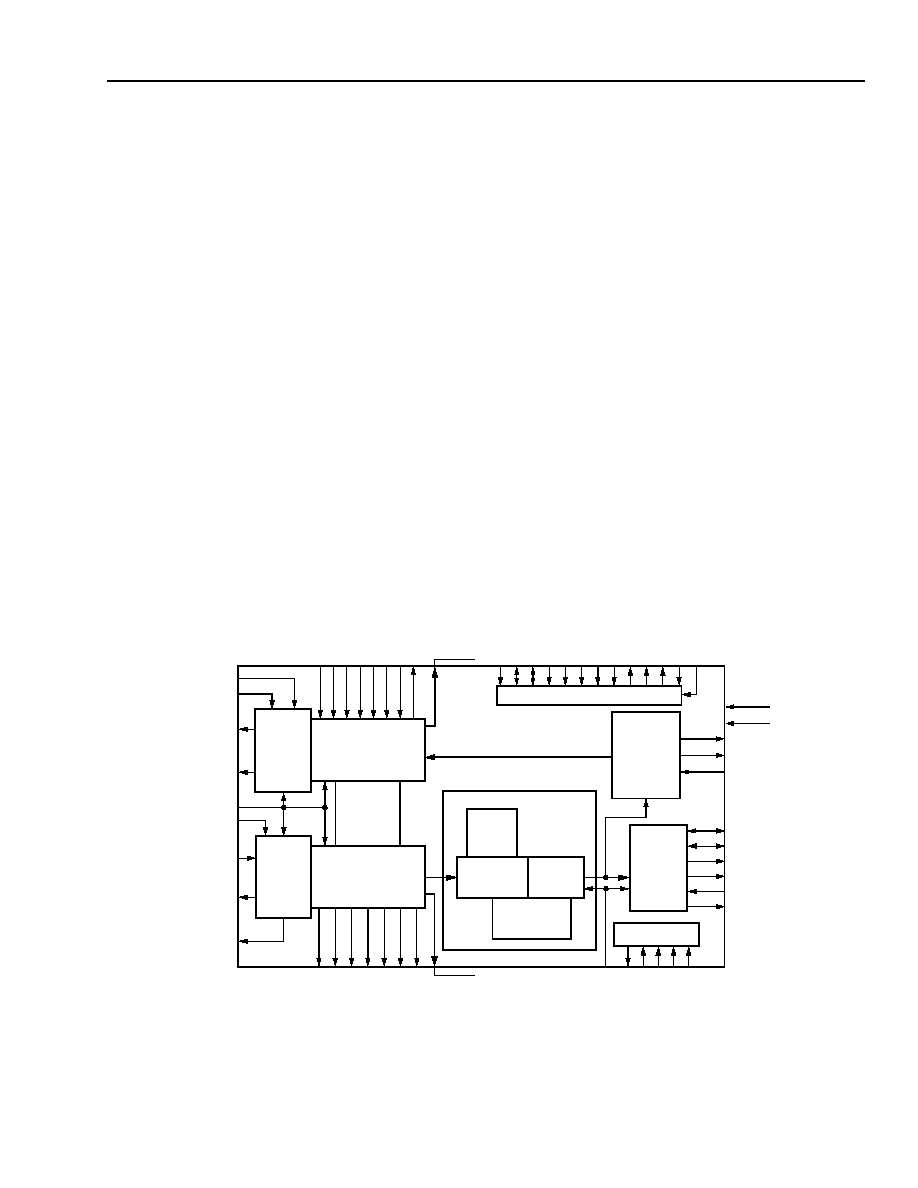
Agere Systems Inc.
13
Data Sheet
May 2003
STS-192 Overhead and Path Processor
TSOT0410G4 SONET/SDH
Description
The TSOT0410G4 is used to terminate the transport overhead in a single SONET STS-192 (SDH STM-64) signal
or four SONET STS-48 (SDH STM-16) signals. It monitors the STS path pointers and overhead in the receive data
and provides timing signals for payload mapping devices on the equipment side. The TSOT0410G4 can be
provisioned to support any mix of STS-1 (AU-3) or STS-Nc (AU-4-Xc) payloads from a single STS-192c
(AU-4-64c) channel to 192 STS-1 (AU-3) channels. Block diagrams are shown in Figure 1 and Figure 2.
The TSOT0410G4 is a 2.5 V, 0.25
Ķ
m high-density device which is packaged in a 600-pin laminate ball grid array
(LBGA). The I/O circuitry uses a 3.3 V, 0.25
Ķ
m technology (5 V tolerant) for LVTTL, and LVDS for high-speed
signals.
The microprocessor interface allows an external processor to access the TSOT0410G4 for configuration and
maintenance. The microprocessor interface is designed to support various 16-bit microprocessors with minimal
glue logic.
The TSOT0410G4 includes an IEEE 1149.1 compliant JTAG port to support boundary scan and memory BIST
testing of the device.
Block Diagrams
Figure 1, below, is a block diagram of the TSOT0410G4 when operating in STS-192 mode (pin AM17,
STS_MODE = 0). Figure 2 on page 14 is a block diagram of the TSOT0410G4 when operating in quad STS-48
mode (pin AM17, STS_MODE = 1). For convenience, two symbol sets are provided for the transmit and receive
line interface pins, based on the mode of the device. Both sets of symbols are included in the pin tables.
5-7952.f (F)
Figure 1. TSOT0410G4 Block Diagram, STS-192 Mode
TRANSMIT
STS-192
LINE
INTERFACE
TD[15:0]
STS_MODE = 0
RECEIVE
STS-192
LINE
INTERFACE
RD[15:0]
STS-48 RECEIVE
TRANSPORT OVERHEAD
PROCESSOR
STS-48 TRANSMIT
TRANSPORT OVERHEAD
PROCESSOR
SECTION
TRACE
BUFFER
X4
X4
X4
RECEIVE PATH
OVERHEAD
PROCESSOR
RECEIVE
DROP
ALIGNER
RECEIVE
POINTER
PROCESSOR
PATH
TRACE
BUFFER
STS PATH
PROCESSING
BLOCK
RECEIVE
PAYLOAD
DROP
INTERFACE
JTAG INTERFACE
DFRM
D_CLK
DDATA_[16:1]
DCTL_[1--4]
TD
O
TD
I
TC
K
TM
S
TR
S
T
_
N
TRANSMIT
PAYLOAD
ADD
INTERFACE
TADCC_[16:1]
TADCK
ADATA_[16:1]
T
O
H_
CL
K
_
[1
--4
]
T
O
HF
P
_
[1
--4]
T
O
HEN_
[1
--4
]
T
O
HDA
T
_
[1
--4]_[1
:0]
T
L
DCC_
[1
--4
]
T
S
DCC
_
[
1
--
4
]
T
S
U
S
E
R
_[1--4
]
T
E
X
P
OW
_[1--
4]
TL
C
L
O
W
_
[
1
--
4
]
T
O
W_CL
K
_
[1--4]
T
S
D_
CL
K_
[1
--4
]
T
L
D
_
CLK
_
[1--4]
MICROPROCESSOR INTERFACE
PA
R
I
TY
_
[
1
:
0
]
DA
T
A
_
[
1
5
:
0
]
A
DDRES
S
_
[
1
5
:0
]
CS
_
N
TS
_
N
DS
_
N
RW
_
N
MP
MO
D
E
RL
CL
OW_
[
1
--
4
]
RE
XPO
W_
[
1
--
4
]
R
S
U
S
E
R
_[1--4]
RSDCC_
[1
--4
]
RL
DCC_
[1
--4
]
R
O
H
D
A
T
_[1--4]_
[
1:0]
RO
H
F
P
_
[1--4]
ROH_
CL
K_
[1
--4
]
ROW_
CL
K_
[1
--4
]
RSD_
CL
K_
[1
--4
]
RL
D_
CL
K_
[1
--4
]
T_CLK
TFRM
T_CLKO_1
R_CLK_1
RFRM[1--4]
DRPB
Y
P
X4
X4
RDDCC_[16:1]
RDDCK_[1--4]
X4
PCL
K
TA_
N
TEA
_
N
IN
T
_
N
PM
_
C
L
K
R_CLKO_1
RST_N
HIZ_N
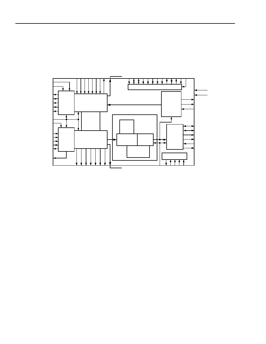
14
Agere Systems Inc.
Data Sheet
May 2003
STS-192 Overhead and Path Processor
TSOT0410G4 SONET/SDH
Description
(continued)
5-7982.e (F)
Figure 2. TSOT0410G4 Block Diagram, STS-48 Mode
Glossary
This glossary is not intended to list standard SDH or SONET terminology; rather, it is intended to describe terms
that may be specific to this device and/or may be unfamiliar to the reader.
s
Persistency Bit--a register bit that indicates the raw alarm has been continuously present since the alarm was
latched in the latched alarm register bit. (See the Persistency Registers section on page 96.)
s
PM--performance monitoring. Indication of the presence of an alarm or condition during the last second as
indicated by successive rising edges of the PM_CLK input. PM counters count the number of occurrences of a
condition, and 1-bit PM indicates that a condition was present at some time during the last second.
TRANSMIT
STS-48
LINE
INTERFACE
TD_1_[3:0]
TD_2_[3:0]
TD_3_[3:0]
TD_4_[3:0]
STS_MODE = 1
RECEIVE
STS-48
LINE
INTERFACE
RD_1_[3:0]
RD_2_[3:0]
RD_3_[3:0]
RD_4_[3:0]
STS-48 RECEIVE
TRANSPORT OVERHEAD
PROCESSOR
STS-48 TRANSMIT
TRANSPORT OVERHEAD
PROCESSOR
SECTION
TRACE
BUFFER
X4
X4
X4
RECEIVE PATH
OVERHEAD
PROCESSOR
RECEIVE
DROP
ALIGNER
RECEIVE
POINTER
PROCESSOR
PATH
TRACE
BUFFER
STS PATH
PROCESSING
BLOCK
RECEIVE
PAYLOAD
DROP
INTERFACE
JTAG INTERFACE
DFRM
D_CLK
DDATA_[16:1]
DCTL_[1--4]
TD
O
TD
I
TC
K
TM
S
TR
ST_
N
TRANSMIT
PAYLOAD
ADD
INTERFACE
TADCC_[16:1]
TADCK
ADATA_[16:1]
T
O
H
_
CLK
_
[1--4]
T
O
HF
P
_
[
1
--4]
T
O
HEN_
[1
--4
]
T
O
HDA
T
_
[1
--4]_[1
:0]
T
L
DCC_
[1
--4
]
T
S
DCC_
[1
--4
]
TS
U
S
E
R
_
[
1
--
4
]
T
E
X
P
OW
_[1
--
4]
TL
C
L
O
W
_
[
1
--
4
]
T
O
W
_
C
L
K
_
[1--4]
T
S
D_
CL
K_
[1
--4
]
T
L
D_
CL
K_
[1
--4
]
MICROPROCESSOR INTERFACE
PA
R
I
TY
_
[
1
:
0
]
DA
T
A
_
[
1
5
:0
]
A
DDRES
S
_
[
1
5
:0
]
CS
_
N
TS
_
N
DS
_
N
RW
_
N
MP
MOD
E
R
L
C
L
OW
_[1--4]
RE
XPO
W_
[
1
--
4
]
R
S
U
S
E
R
_[1--4]
RSDCC_
[1
--4
]
RL
DCC_
[1
--4
]
ROHDA
T
_
[1--4]
_
[1:0]
R
O
HF
P
_
[1--4]
ROH_
CL
K_
[1
--4
]
ROW_
CL
K_
[1
--4
]
RSD_
CL
K_
[1
--4
]
RL
D_
CL
K_
[1
--4
]
T_CLK
TFRM
T_CLKO_[1--4]
R_CLK_[1--4]
RFRM[1--4]
DRPB
Y
P
X4
X4
RDDCC_[16:1]
RDDCK_[1--4]
X4
PCL
K
TA
_
N
TE
A_
N
INT
_
N
PM
_
C
L
K
R_CLKO_[1--4]
RST_N
HIZ_N

Agere Systems Inc.
15
Data Sheet
May 2003
STS-192 Overhead and Path Processor
TSOT0410G4 SONET/SDH
Description
(continued)
Receive Direction Overview
In the receive direction, the receive line interface can accept either a single STS-192 (STM-64) signal or four
STS-48 (STM-16) signals, from optical-to-electrical modules, in 16-bit or 4-bit wide serial 622 MHz format. The
receive line interface synchronizes to the frames in each data channel and rotates the data to frame and byte align
it. The data may also be optionally descrambled.
The aligned data is received by the receive transport overhead processor, and the section (regenerator section)
and line (multiplex section) overhead are extracted. Most of the overhead is then either stored internally or pro-
vided on external serial outputs, except for the pointer bytes, which are passed to the receive pointer processor.
The receive pointer processor interprets the pointer bytes and provides the SONET payload envelope (SPE) timing
for the receive-path overhead processor and the receive-drop data aligner (pointer processor).
The receive-path overhead processor extracts the path overhead and either stores it internally or processes it for
alarms and performance statistics. The receive-drop data aligner then translates the data from the receive clock
domain to the drop clock domain using a small elastic store and pointer adjustments to the data. The resulting
aligned data is then converted to sixteen 1-bit wide serial 622 MHz streams by the receive payload drop interface
and output along with SPE timing signals for use by a payload mapping device.
Transmit Direction Overview
In the transmit direction, the transmit payload add interface accepts sixteen 1-bit wide serial 622 MHz pseudo*
STS-12 (STM-4) signals and recovers the clock for each. The resulting 16 clocks must be synchronous in fre-
quency, but can be asynchronous in phase. Each clock is used to frame, byte align, descramble, and then write its
associated data stream into a small buffer. The data is then read out of all 16 buffers using transmit clock (T_CLK)
and transmit frame (TFRM) timing.
The converted data is passed along to the transmit transport overhead processor which adds the appropriate sec-
tion and line overhead. This overhead is either provided by internal configuration registers or external serial inputs,
except for the pointer bytes, which are received in the add data. The resulting valid STS-192 (STM-64) or STS-48
(STM-16) data is then optionally scrambled, converted to one 16-bit wide or four 4-bit wide serial 622 MHz signals,
and output for use by electrical-to-optical modules.
Transmit frame alignment synchronization may optionally be derived from any one of the 16 (selectable) add
inputs. A software provisioning option allows transmit frame alignment synchronization to be provided using the
timing that is being recovered from one of the add pseudo STS-12 links as the transmit frame sync instead of
TFRM.
* The data is formatted as an STS-12 signal; however, most of the transport overhead bytes are either unused or may be used for proprietary
purposes.

16
Agere Systems Inc.
Data Sheet
May 2003
STS-192 Overhead and Path Processor
TSOT0410G4 SONET/SDH
Description
(continued)
STS-192 Mode Options
TOH Transparency
In applications where it is desired, a pass-through capability using software provisioning for the TOH on the line
interface to/from the TOH on the equipment interface is provided for the receive and transmit direction. This feature
is always supported on individual STS-48 channels and will require all four channels to be provisioned in STS-192
mode.
On the receive side, when TOH transparency is enabled, the pointer generators and elastic stores in all path pro-
cessing blocks are bypassed. In this case, receive timing will be used by the payload drop interface. The receive
direction has the option for full TOH transparency, or just line overhead transparency with section overhead is used
for the normal proprietary drop I/F overhead. When TOH transparency is enabled, the pointer processor (PP) will
be bypassed on a per STS-48 level. See the Receive Pointer Processor section on page 62 for more information
on how this mode effects the device.
The transmit direction has the option for full TOH transparency or just line overhead (MSOH) transparency with
section (RSOH) overhead inserted. If enabled, AIS insertion due to an E1/F1 code in the add TOH will be disabled.
Regenerator Loopback
In applications where the receive data and overhead bytes need to be transmitted towards the transmit line inter-
face, a software regenerator loopback provisioning option is provided. To use this feature, the transmit clock must
be derived from the receive clock at the 622 MHz level external to the device. The add interface buffers align the
data between the receive and transmit clock domains. This mode will only function correctly when the device is in
STS-192 mode. It will not work in STS-48 mode since the four STS-48 streams need to be aligned through the
transmit side. Four received STS-48 streams are unlikely to be aligned to the same clock and frame alignment. The
appropriate per STS-48 transmit line AIS insert control will be active during receive LOS, receive LOF, or R_CLK
failure while in regenerator loopback.
Device Mode Setup
The basic operating mode of the TSOT0410G4 is set using external pins.
The device can operate as a single STS-192 channel or as four separate STS-48 channels. The STS_MODE pin
(AM17) determines which mode is used. Pulling the STS_MODE pin down to V
SS
selects STS-192 mode.
In applications where no rate adaptation is required or desired, the pointer generators and elastic stores in all path
processing blocks can be bypassed by pulling up the DRPBYP pin (AP11) to V
DD
. In this case, receive timing will
be used by the payload drop interface. This mode should only be used if the device is in STS-192 mode. See the
Receive Pointer Processor section on page 62 for more information on how this mode affects the device.
The microprocessor interface can be set up to be synchronous by pulling up the MPMODE pin (E14) to V
DD
, or
asynchronous by pulling down the pin to V
SS
. See the Microprocessor Interface section on page 93 for more infor-
mation.
For normal device operation, the TRST_N pin (AP30) should be tied low (to V
SS
). If TRST_N is high, a TCK clock
must be present.

Agere Systems Inc.
17
Data Sheet
May 2003
STS-192 Overhead and Path Processor
TSOT0410G4 SONET/SDH
Pin Information
Table 1. Pin Assignments for 600-Pin LBGA by Pin Number Order
Note: NC refers to no connect. Do not connect pins so designated.
Pin
Signal Name
Pin
Signal Name
Pin
Signal Name
Pin
Signal Name
A1
V
DD
B1
V
DD
C1
V
SS
D1
V
SS
A2
V
DD
B2
V
DD
C2
V
SS
D2
V
SS
A3
V
SS
B3
V
SS
C3
V
DD
D3
V
SS
A4
V
SS
B4
V
SS
C4
V
SS
D4
V
DD
2
A5
V
DD
2
B5
TADCC_14
C5
TADCC_15
D5
TADCC_16
A6
V
DD
2
B6
TADCC_10
C6
TADCC_11
D6
TADCC_12
A7
V
SS
B7
TADCC_6
C7
TADCC_7
D7
TADCC_8
A8
V
SS
B8
TADCC_2
C8
TADCC_3
D8
TADCC_4
A9
DATA_15
B9
PARITY_1
C9
PARITY_0
D9
TADCK
A10
DATA_10
B10
DATA_11
C10
DATA_12
D10
DATA_13
A11
DATA_6
B11
DATA_7
C11
DATA_8
D11
DATA_9
A12
DATA_1
B12
DATA_2
C12
DATA_3
D12
DATA_4
A13
V
SS
B13
TA_N
C13
TEA_N
D13
INT_N
A14
CS_N
B14
RW_N
C14
PCLK
D14
PM_CLK
A15
ADDRESS_2
B15
ADDRESS_1
C15
ADDRESS_0
D15
DS_N
A16
V
SS
B16
ADDRESS_5
C16
ADDRESS_4
D16
ADDRESS_3
A17
V
DD
B17
ADDRESS_9
C17
ADDRESS_8
D17
ADDRESS_7
A18
V
DD
B18
ADDRESS_13
C18
ADDRESS_10
D18
ADDRESS_12
A19
ADDRESS_14
B19
TSUSER_4
C19
ADDRESS_15
D19
TEXPOW_4
A20
V
SS
B20
TLDCC_4
C20
TSDCC_4
D20
TOW_CLK_4
A21
TLD_CLK_4
B21
TSD_CLK_4
C21
TOHDAT_4_0
D21
TOHEN_4
A22
TOH_CLK_4
B22
TOHFP_4
C22
TLCLOW_3
D22
TSUSER_3
A23
V
SS
B23
TOW_CLK_3
C23
TLD_CLK_3
D23
TSD_CLK_3
A24
TSDCC_3
B24
TOHDAT_3_0
C24
TOHDAT_3_1
D24
TOHEN_3
A25
TOHFP_3
B25
TLCLOW_2
C25
TOW_CLK_2
D25
TLD_CLK_2
A26
TSD_CLK_2
B26
TEXPOW_2
C26
TSUSER_2
D26
NC
A27
TSDCC_2
B27
TOHDAT_2_0
C27
TOHDAT_2_1
D27
TOHEN_2
A28
V
SS
B28
TOH_CLK_2
C28
TOHFP_2
D28
TLCLOW_1
A29
V
SS
B29
TSUSER_1
C29
TLDCC_1
D29
TSDCC_1
A30
V
DD
2
B30
TSD_CLK_1
C30
TLD_CLK_1
D30
TOH_CLK_1
A31
V
DD
2
B31
TOHDAT_1_1
C31
TOHEN_1
D31
TOHFP_1
A32
V
SS
B32
V
SS
C32
V
SS
D32
V
DD
2
A33
V
SS
B33
V
SS
C33
V
DD
D33
V
SS
A34
V
DD
B34
V
DD
C34
V
SS
D34
V
SS
A35
V
DD
B35
V
DD
C35
V
SS
D35
V
SS

18
Agere Systems Inc.
Data Sheet
May 2003
STS-192 Overhead and Path Processor
TSOT0410G4 SONET/SDH
Pin Information
(continued)
Table 1. Pin Assignments for 600-Pin LBGA by Pin Number Order (continued)
Note: NC refers to no connect. Do not connect pins so designated.
Pin
Signal Name
Pin
Signal Name
Pin
Signal Name
Pin
Signal Name
E1
V
DD
2
F1
V
DD
2
J31
TD12N/TD_4_0N
N1
V
SS
E2
ADATA_16
F2
ADATA_14
J32
T_CLKO_3
N2
NC
E3
ADATA_16N
F3
ADATA_14N
J33
T_CLKO_3N
N3
ADATA_5
E4
CTAP_ADD4
F4
ADATA_15
J34
TD11/TD_3_3
N4
ADATA_5N
E5
V
DD
2
F5
ADATA_15N
J35
TD11N/TD_3_3N
N5
NC
E6
TADCC_13
F31
TFRM
K1
ADATA_9
N31
TD5/TD_2_1
E7
TADCC_9
F32
TFRMN
K2
ADATA_9N
N32
TD5N/
TD_2_1N
E8
TADCC_5
F33
T_CLKO_4
K3
NC
N33
TD4/TD_2_0
E9
TADCC_1
F34
T_CLKO_4N
K4
ADATA_10
N34
TD4N/
TD_2_0N
E10
DATA_14
F35
V
DD
2
K5
ADATA_10N
N35
V
SS
E11
V
DD
G1
V
SS
K31
NC
P1
ADATA_3
E12
DATA_5
G2
REXT_ADD
K32
TD10/TD_3_2
P2
ADATA_3N
E13
DATA_0
G3
NC
K33
TD10N/TD_3_2N
P3
ADATA_4
E14
MPMODE
G4
ADATA_13
K34
TD9/TD_3_1
P4
NC
E15
TS_N
G5
ADATA_13N
K35
TD9N/TD_3_1N
P5
ADATA_4N
E16
V
DD
2
G31
CTAP_TFRM
L1
ADATA_8
P31
T_CLKO_1
E17
ADDRESS_6
G32
TD15/TD_4_3
L2
ADATA_8N
P32
T_CLKO_1N
E18
ADDRESS_11
G33
TD15N/TD_4_3N
L3
NC
P33
TD3/TD_1_3
E19
TLCLOW_4
G34
TD14/TD_4_2
L4
CTAP_ADD2
P34
TD3N/
TD_1_3N
E20
V
DD
2
G35
V
SS
L5
V
DD
P35
TD2/TD_1_2
E21
TOHDAT_4_1
H1
V
SS
L31
V
DD
R1
ADATA_1
E22
TEXPOW_3
H2
ADATA_12
L32
TD8/TD_3_0
R2
ADATA_1N
E23
TLDCC_3
H3
ADATA_12N
L33
TD8N/TD_3_0N
R3
NC
E24
TOH_CLK_3
H4
NC
L34
T_CLKO_2
R4
ADATA_2
E25
V
DD
H5
CTAP_ADD3
L35
T_CLKO_2N
R5
ADATA_2N
E26
TLDCC_2
H31
TD14N/
TD_4_2N
M1
CTAP_ADD1
R31
TD2N/
TD_1_2N
E27
NC
H32
TD13/TD_4_1
M2
ADATA_6
R32
TD1/TD_1_1
E28
TEXPOW_1
H33
TD13N/
TD_4_1N
M3
ADATA_6N
R33
TD1N/
TD_1_1N
E29
TOW_CLK_1
H34
TD12/TD_4_0
M4
ADATA_7
R34
TD0/TD_1_0
E30
TOHDAT_1_0
H35
V
SS
M5
ADATA_7N
R35
TD0N/
TD_1_0N
E31
V
DD
2
J1
NC
M31
TD7/TD_2_3
T1
V
SS
E32
T_CLK
J2
ADATA_11
M32
TD7N/TD_2_3N
T2
V
DD
A
E33
T_CLKN
J3
ADATA_11N
M33
NC
T3
V
SS
A
E34
CTAP_TCLK
J4
V
DD
A
M34
TD6/TD_2_2
T4
NC
E35
V
DD
2
J5
V
SS
A
M35
TD6N/TD_2_2N
T5
V
DD
2

Agere Systems Inc.
19
Data Sheet
May 2003
STS-192 Overhead and Path Processor
TSOT0410G4 SONET/SDH
Pin Information
(continued)
Table 1. Pin Assignments for 600-Pin LBGA by Pin Number Order (continued)
Note: NC refers to no connect. Do not connect pins so designated.
Pin
Signal Name
Pin
Signal Name
Pin
Signal Name
Pin
Signal Name
T31
V
DD
2
Y1
V
SS
AC31
R_CLK_2
AG1
NC
T32
NC
Y2
NC
AC32
R_CLK_2N
AG2
DCTL_4
T33
R_CLKO_1N
Y3
V
SS
A
AC33
CTAP_RCLK2
AG3
DCTL_4N
T34
R_CLKO_1
Y4
V
DD
A
AC34
RD3/RD_1_3
AG4
DDATA_13
T35
V
SS
Y5
V
DD
2
AC35
V
SS
AG5
DDATA_13N
U1
DDATA_1
Y31
V
DD
2
AD1
V
SS
A
AG31
RD10/RD_3_2
U2
NC
Y32
CTAP_RCLK1
AD2
V
DD
A
AG32
RD10N/
RD_3_2N
U3
NC
Y33
RFRM_4
AD3
DCTL_3
AG33
RD9/RD_3_1
U4
DCTL_1
Y34
RFRM_4N
AD4
DCTL_3N
AG34 RD9N/RD_3_1N
U5
DCTL_1N
Y35
V
SS
AD5
REXT_DRP3
AG35
CTAP_RD3
U31
NC
AA1
DCTL_2
AD31
RD5/RD_2_1
AH1
V
SS
U32
RFRM_1N
AA2
DCTL_2N
AD32 RD5N/RD_2_1N
AH2
V
SS
A
U33
RFRM_1
AA3
DDATA_5
AD33
RD4/RD_2_0
AH3
V
DD
A
U34
R_CLKO_2N
AA4
DDATA_5N
AD34 RD4N/RD_2_0N
AH4
DDATA_14
U35
V
DD
AA5
REXT_DRP2
AD35
CTAP_RD2
AH5
DDATA_14N
V1
V
DD
AA31 RD0N/RD_1_0N
AE1
DDATA_9
AH31
CTAP_RCLK4
V2
DDATA_1N
AA32
RD0/RD_1_0
AE2
DDATA_9N
AH32
RD11/RD_3_3
V3
REXT_DRP1
AA33
CTAP_RD1
AE3
DDATA_10
AH33
RD11N/
RD_3_3N
V4
DDATA_2
AA34
R_CLK_1
AE4
DDATA_10N
AH34
NC
V5
DDATA_2N
AA35
R_CLK_1N
AE5
V
DD
AH35
V
SS
V31
RFRM_2N
AB1
NC
AE31
V
DD
AJ1
V
SS
V32
RFRM_2
AB2
DDATA_6
AE32
RD7/RD_2_3
AJ2
NC
V33
R_CLKO_2
AB3
DDATA_6N
AE33 RD7N/RD_2_3N
AJ3
REXT_DRP4
V34
R_CLKO_3N
AB4
DDATA_7
AE34
RD6/RD_2_2
AJ4
DDATA_15
V35
V
DD
AB5
DDATA_7N
AE35 RD6N/RD_2_2N
AJ5
DDATA_15N
W1
V
DD
AB31
RD2/RD_1_2
AF1
NC
AJ31
RD12/RD_4_0
W2
DDATA_3
AB32 RD3N/RD_1_3N
AF2
DDATA_11
AJ32
RD12N/
RD_4_0N
W3
DDATA_3N
AB33 RD2N/RD_1_2N
AF3
DDATA_11N
AJ33
R_CLK_4
W4
DDATA_4
AB34
RD1/RD_1_1
AF4
DDATA_12
AJ34
R_CLK_4N
W5
DDATA_4N
AB35 RD1N/RD_1_1N
AF5
DDATA_12N
AJ35
V
SS
W31
RFRM_3
AC1
V
SS
AF31
RD8/RD_3_0
AK1
V
DD
2
W32
R_CLKO_4N
AC2
NC
AF32 RD8N/RD_3_0N
AK2
DDATA_16
W33
RFRM_3N
AC3
DDATA_8
AF33
R_CLK_3
AK3
DDATA_16N
W34
R_CLKO_4
AC4
DDATA_8N
AF34
R_CLK_3N
AK4
NC
W35
R_CLKO_3
AC5
NC
AF35
CTAP_RCLK3
AK5
REF10E

20
Agere Systems Inc.
Data Sheet
May 2003
STS-192 Overhead and Path Processor
TSOT0410G4 SONET/SDH
Pin Information
(continued)
Table 1. Pin Assignments for 600-Pin LBGA by Pin Number Order (continued)
Note: NC refers to no connect. Do not connect pins so designated.
Pin
Signal Name
Pin
Signal Name
Pin
Signal Name
Pin
Signal Name
AK31
RD14/RD_4_2
AL31
V
DD
2
AM31
RESLOL
AN31
RESHIL
AK32 RD14N/RD_4_2N
AL32
RD15/RD_4_3
AM32
V
DD
2
AN32
V
SS
AK33
RD13/RD_4_1
AL33 RD15N/RD_4_3N
AM33
V
SS
AN33
V
DD
AK34 RD13N/RD_4_1N
AL34
CTAP_RD4
AM34
V
SS
AN34
V
SS
AK35
V
DD
2
AL35
V
DD
2
AM35
V
SS
AN35
V
SS
AL1
V
DD
2
AM1
V
SS
AN1
V
SS
AP1
V
DD
AL2
REF14E
AM2
V
SS
AN2
V
SS
AP2
V
DD
AL3
RESHIE
AM3
V
SS
AN3
V
DD
AP3
V
SS
AL4
RESLOE
AM4
V
DD
2
AN4
V
SS
AP4
V
SS
AL5
V
DD
2
AM5
PULLDN
AN5
PULLDN
AP5
PULLDN
AL6
PULLDN
AM6
PULLDN
AN6
PULLDN
AP6
PULLUP
AL7
PULLUP
AM7
PULLDN
AN7
PULLDN
AP7
PULLDN
AL8
NC
AM8
NC
AN8
NC
AP8
NC
AL9
NC
AM9
NC
AN9
NC
AP9
NC
AL10
PULLDN
AM10
PULLDN
AN10
PULLDN
AP10
PULLDN
AL11
V
DD
AM11
DFRM
AN11
D_CLK
AP11
DRPBYP
AL12
RDDCC_15
AM12
RDDCC_14
AN12
RDDCC_13
AP12
RDDCK_4
AL13
RDDCC_11
AM13
RDDCC_10
AN13
RDDCC_9
AP13
RDDCK_3
AL14
RDDCC_7
AM14
RDDCC_8
AN14
RDDCC_6
AP14
RDDCC_5
AL15
RDDCC_3
AM15
RDDCC_4
AN15
RDDCC_2
AP15
RDDCC_1
AL16
V
DD
2
AM16
PULLUP
AN16
PULLUP
AP16
RST_N
AL17
RSUSER_4
AM17
STS_MODE
AN17
RSD_CLK_4
AP17
HIZ_N
AL18
ROHFP_4
AM18
ROH_CLK_4
AN18
ROHDAT_4_1
AP18
ROW_CLK_4
AL19
RLCLOW_4
AM19
RLDCC_4
AN19
RLD_CLK_4
AP19
ROHDAT_4_0
AL20
V
DD
2
AM20
RSD_CLK_3
AN20
RSUSER_3
AP20
REXPOW_4
AL21
ROHDAT_3_1
AM21
ROHFP_3
AN21
ROH_CLK_3
AP21
ROW_CLK_3
AL22
REXPOW_3
AM22
RLCLOW_3
AN22
RLDCC_3
AP22
RLD_CLK_3
AL23
ROW_CLK_2
AM23
RSDCC_2
AN23
RSD_CLK_2
AP23
RSUSER_2
AL24
RLD_CLK_2
AM24
ROHDAT_2_0
AN24
ROHDAT_2_1
AP24
ROHFP_2
AL25
V
DD
AM25
RSUSER_1
AN25
REXPOW_2
AP25
RLCLOW_2
AL26
ROHFP_1
AM26
ROH_CLK_1
AN26
ROW_CLK_1
AP26
RSDCC_1
AL27
RLCLOW_1
AM27
RLDCC_1
AN27
RLD_CLK_1
AP27
ROHDAT_1_0
AL28
PULLDN
AM28
PULLDN
AN28
PULLDN
AP28
REXPOW_1
AL29
TDI
AM29
TCK
AN29
NC
AP29
PULLDN
AL30
REF10L
AM30
TDO
AN30
TMS
AP30
TRST_N

Agere Systems Inc.
21
Data Sheet
May 2003
STS-192 Overhead and Path Processor
TSOT0410G4 SONET/SDH
Pin Information
(continued)
Table 1. Pin Assignments for 600-Pin LBGA by Pin Number Order (continued)
Note: NC refers to no connect. Do not connect pins so designated.
Pin
Signal Name
Pin
Signal Name
Pin
Signal Name
Pin
Signal Name
AP31
REF14L
AR6
V
DD
2
AR16
V
SS
AR26
RSD_CLK_1
AP32
V
SS
AR7
V
SS
AR17
RSDCC_4
AR27
ROHDAT_1_1
AP33
V
SS
AR8
V
SS
AR18
V
DD
AR28
V
SS
AP34
V
DD
AR9
NC
AR19
V
DD
AR29
V
SS
AP35
V
DD
AR10
PULLDN
AR20
V
SS
AR30
V
DD
2
AR1
V
DD
AR11
RDDCC_16
AR21
RSDCC_3
AR31
V
DD
2
AR2
V
DD
AR12
RDDCC_12
AR22
ROHDAT_3_0
AR32
V
SS
AR3
V
SS
AR13
V
SS
AR23
V
SS
AR33
V
SS
AR4
V
SS
AR14
RDDCK_2
AR24
ROH_CLK_2
AR34
V
DD
AR5
V
DD
2
AR15
RDDCK_1
AR25
RLDCC_2
AR35
V
DD

22
Agere Systems Inc.
Data Sheet
May 2003
STS-192 Overhead and Path Processor
TSOT0410G4 SONET/SDH
Pin Information
(continued)
Table 2. Pin Assignments for 600-Pin LBGA by Signal Name Order
Note: NC refers to no connect. Do not connect pins so designated.
Pin
Signal Name
Pin
Signal Name
Pin
Signal Name
Pin
Signal Name
R1
ADATA_1
D16
ADDRESS_3
A11
DATA_6
AE2
DDATA_9N
R2
ADATA_1N
C16
ADDRESS_4
B11
DATA_7
AE3
DDATA_10
R4
ADATA_2
B16
ADDRESS_5
C11
DATA_8
AE4
DDATA_10N
R5
ADATA_2N
E17
ADDRESS_6
D11
DATA_9
AF2
DDATA_11
P1
ADATA_3
D17
ADDRESS_7
A10
DATA_10
AF3
DDATA_11N
P2
ADATA_3N
C17
ADDRESS_8
B10
DATA_11
AF4
DDATA_12
P3
ADATA_4
B17
ADDRESS_9
C10
DATA_12
AF5
DDATA_12N
P5
ADATA_4N
C18
ADDRESS_10
D10
DATA_13
AG4
DDATA_13
N3
ADATA_5
E18
ADDRESS_11
E10
DATA_14
AG5
DDATA_13N
N4
ADATA_5N
D18
ADDRESS_12
A9
DATA_15
AH4
DDATA_14
M2
ADATA_6
B18
ADDRESS_13
U4
DCTL_1
AH5
DDATA_14N
M3
ADATA_6N
A19
ADDRESS_14
U5
DCTL_1N
AJ4
DDATA_15
M4
ADATA_7
C19
ADDRESS_15
AA1
DCTL_2
AJ5
DDATA_15N
M5
ADATA_7N
A14
CS_N
AA2
DCTL_2N
AK2
DDATA_16
L1
ADATA_8
M1
CTAP_ADD1
AD3
DCTL_3
AK3
DDATA_16N
L2
ADATA_8N
L4
CTAP_ADD2
AD4
DCTL_3N
AM11
DFRM
K1
ADATA_9
H5
CTAP_ADD3
AG2
DCTL_4
AP11
DRPBYP
K2
ADATA_9N
E4
CTAP_ADD4
AG3
DCTL_4N
D15
DS_N
K4
ADATA_10
Y32
CTAP_RCLK1
U1
DDATA_1
AP17
HIZ_N
K5
ADATA_10N
AC33
CTAP_RCLK2
V2
DDATA_1N
D13
INT_N
J2
ADATA_11
AF35
CTAP_RCLK3
V4
DDATA_2
E14
MPMODE
J3
ADATA_11N
AH31
CTAP_RCLK4
V5
DDATA_2N
D26
NC
H2
ADATA_12
AA33
CTAP_RD1
W2
DDATA_3
E27
NC
H3
ADATA_12N
AD35
CTAP_RD2
W3
DDATA_3N
G3
NC
G4
ADATA_13
AG35
CTAP_RD3
W4
DDATA_4
H4
NC
G5
ADATA_13N
AL34
CTAP_RD4
W5
DDATA_4N
J1
NC
F2
ADATA_14
E34
CTAP_TCLK
AA3
DDATA_5
K3
NC
F3
ADATA_14N
G31
CTAP_TFRM
AA4
DDATA_5N
K31
NC
F4
ADATA_15
AN11
D_CLK
AB2
DDATA_6
L3
NC
F5
ADATA_15N
E13
DATA_0
AB3
DDATA_6N
M33
NC
E2
ADATA_16
A12
DATA_1
AB4
DDATA_7
N2
NC
E3
ADATA_16N
B12
DATA_2
AB5
DDATA_7N
N5
NC
C15
ADDRESS_0
C12
DATA_3
AC3
DDATA_8
P4
NC
B15
ADDRESS_1
D12
DATA_4
AC4
DDATA_8N
R3
NC
A15
ADDRESS_2
E12
DATA_5
AE1
DDATA_9
T4
NC

Agere Systems Inc.
23
Data Sheet
May 2003
STS-192 Overhead and Path Processor
TSOT0410G4 SONET/SDH
Pin Information
(continued)
Table 2. Pin Assignments for 600-Pin LBGA by Signal Name Order (continued)
Note: NC refers to no connect. Do not connect pins so designated.
Pin
Signal Name
Pin
Signal Name
Pin
Signal Name
Pin
Signal Name
T32
NC
AN5
PULLDN
AB33
RD2N/RD_1_2N
AN13
RDDCC_9
U2
NC
AN6
PULLDN
AC34
RD3/RD_1_3
AM13
RDDCC_10
U3
NC
AN7
PULLDN
AB32
RD3N/RD_1_3N
AL13
RDDCC_11
U31
NC
AN10
PULLDN
AD33
RD4/RD_2_0
AR12
RDDCC_12
Y2
NC
AN28
PULLDN
AD34
RD4N/RD_2_0N
AN12
RDDCC_13
AB1
NC
AP5
PULLDN
AD31
RD5/RD_2_1
AM12
RDDCC_14
AC2
NC
AP7
PULLDN
AD32
RD5N/RD_2_1N
AL12
RDDCC_15
AC5
NC
AP10
PULLDN
AE34
RD6/RD_2_2
AR11
RDDCC_16
AF1
NC
AP29
PULLDN
AE35
RD6N/RD_2_2N
AR15
RDDCK_1
AG1
NC
AR10
PULLDN
AE32
RD7/RD_2_3
AR14
RDDCK_2
AH34
NC
AL7
PULLUP
AE33
RD7N/RD_2_3N
AP13
RDDCK_3
AJ2
NC
AP6
PULLUP
AF31
RD8/RD_3_0
AP12
RDDCK_4
AK4
NC
AM16
PULLUP
AF32
RD8N/RD_3_0N
AK5
REF10E
AL8
NC
AN16
PULLUP
AG33
RD9/RD_3_1
AL30
REF10L
AL9
NC
AA34
R_CLK_1
AG34
RD9N/RD_3_1N
AL2
REF14E
AM8
NC
AA35
R_CLK_1N
AG31
RD10/RD_3_2
AP31
REF14L
AM9
NC
AC31
R_CLK_2
AG32 RD10N/RD_3_2N
AL3
RESHIE
AN8
NC
AC32
R_CLK_2N
AH32
RD11/RD_3_3
AN31
RESHIL
AN9
NC
AF33
R_CLK_3
AH33 RD11N/RD_3_3N
AL4
RESLOE
AN29
NC
AF34
R_CLK_3N
AJ31
RD12/RD_4_0
AM31
RESLOL
AP8
NC
AJ33
R_CLK_4
AJ32 RD12N/RD_4_0N
AP28
REXPOW_1
AP9
NC
AJ34
R_CLK_4N
AK33
RD13/RD_4_1
AN25
REXPOW_2
AR9
NC
T34
R_CLKO_1
AK34 RD13N/RD_4_1N
AL22
REXPOW_3
C9
PARITY_0
T33
R_CLKO_1N
AK31
RD14/RD_4_2
AP20
REXPOW_4
B9
PARITY_1
V33
R_CLKO_2
AK32 RD14N/RD_4_2N
G2
REXT_ADD
C14
PCLK
U34
R_CLKO_2N
AL32
RD15/RD_4_3
V3
REXT_DRP1
D14
PM_CLK
W35
R_CLKO_3
AL33 RD15N/RD_4_3N
AA5
REXT_DRP2
AL6
PULLDN
V34
R_CLKO_3N
AP15
RDDCC_1
AD5
REXT_DRP3
AL10
PULLDN
W34
R_CLKO_4
AN15
RDDCC_2
AJ3
REXT_DRP4
AL28
PULLDN
W32
R_CLKO_4N
AL15
RDDCC_3
U33
RFRM_1
AM5
PULLDN
AA32
RD0/RD_1_0
AM15
RDDCC_4
U32
RFRM_1N
AM6
PULLDN
AA31
RD0N/RD_1_0N
AP14
RDDCC_5
V32
RFRM_2
AM7
PULLDN
AB34
RD1/RD_1_1
AN14
RDDCC_6
V31
RFRM_2N
AM10
PULLDN
AB35
RD1N/RD_1_1N
AL14
RDDCC_7
W31
RFRM_3
AM28
PULLDN
AB31
RD2/RD_1_2
AM14
RDDCC_8
W33
RFRM_3N

24
Agere Systems Inc.
Data Sheet
May 2003
STS-192 Overhead and Path Processor
TSOT0410G4 SONET/SDH
Pin Information
(continued)
Table 2. Pin Assignments for 600-Pin LBGA by Signal Name Order (continued)
Note: NC refers to no connect. Do not connect pins so designated.
Pin
Signal Name
Pin
Signal Name
Pin
Signal Name
Pin
Signal Name
Y33
RFRM_4
AN23
RSD_CLK_2
C6
TADCC_11
H33
TD13N/TD_4_1N
Y34
RFRM_4N
AM20
RSD_CLK_3
D6
TADCC_12
G34
TD14/TD_4_2
AL27
RLCLOW_1
AN17
RSD_CLK_4
E6
TADCC_13
H31
TD14N/TD_4_2N
AP25
RLCLOW_2
AP26
RSDCC_1
B5
TADCC_14
G32
TD15/TD_4_3
AM22
RLCLOW_3
AM23
RSDCC_2
C5
TADCC_15
G33
TD15N/TD_4_3N
AL19
RLCLOW_4
AR21
RSDCC_3
D5
TADCC_16
AL29
TDI
AN27
RLD_CLK_1
AR17
RSDCC_4
D9
TADCK
AM30
TDO
AL24
RLD_CLK_2
AP16
RST_N
AM29
TCK
C13
TEA_N
AP22
RLD_CLK_3
AM25
RSUSER_1
R34
TD0/TD_1_0
E28
TEXPOW_1
AN19
RLD_CLK_4
AP23
RSUSER_2
R35
TD0N/TD_1_0N
B26
TEXPOW_2
AM27
RLDCC_1
AN20
RSUSER_3
R32
TD1/TD_1_1
E22
TEXPOW_3
AR25
RLDCC_2
AL17
RSUSER_4
R33
TD1N/TD_1_1N
D19
TEXPOW_4
AN22
RLDCC_3
B14
RW_N
P35
TD2/TD_1_2
F31
TFRM
AM19
RLDCC_4
AM17
STS_MODE
R31
TD2N/TD_1_2N
F32
TFRMN
AM26
ROH_CLK_1
E32
T_CLK
P33
TD3/TD_1_3
D28
TLCLOW_1
AR24
ROH_CLK_2
E33
T_CLKN
P34
TD3N/TD_1_3N
B25
TLCLOW_2
AN21
ROH_CLK_3
P31
T_CLKO_1
N33
TD4/TD_2_0
C22
TLCLOW_3
AM18
ROH_CLK_4
P32
T_CLKO_1N
N34
TD4N/TD_2_0N
E19
TLCLOW_4
AP27 ROHDAT_1_0
L34
T_CLKO_2
N31
TD5/TD_2_1
C30
TLD_CLK_1
AR27 ROHDAT_1_1
L35
T_CLKO_2N
N32
TD5N/TD_2_1N
D25
TLD_CLK_2
AM24 ROHDAT_2_0
J32
T_CLKO_3
M34
TD6/TD_2_2
C23
TLD_CLK_3
AN24 ROHDAT_2_1
J33
T_CLKO_3N
M35
TD6N/TD_2_2N
A21
TLD_CLK_4
AR22 ROHDAT_3_0
F33
T_CLKO_4
M31
TD7/TD_2_3
C29
TLDCC_1
AL21
ROHDAT_3_1
F34
T_CLKO_4N
M32
TD7N/TD_2_3N
E26
TLDCC_2
AP19 ROHDAT_4_0
B13
TA_N
L32
TD8/TD_3_0
E23
TLDCC_3
AN18 ROHDAT_4_1
E9
TADCC_1
L33
TD8N/TD_3_0N
B20
TLDCC_4
AL26
ROHFP_1
B8
TADCC_2
K34
TD9/TD_3_1
AN30
TMS
AP24
ROHFP_2
C8
TADCC_3
K35
TD9N/TD_3_1N
D30
TOH_CLK_1
AM21
ROHFP_3
D8
TADCC_4
K32
TD10/TD_3_2
B28
TOH_CLK_2
AL18
ROHFP_4
E8
TADCC_5
K33
TD10N/TD_3_2N
E24
TOH_CLK_3
AN26
ROW_CLK_1
B7
TADCC_6
J34
TD11/TD_3_3
A22
TOH_CLK_4
AL23
ROW_CLK_2
C7
TADCC_7
J35
TD11N/TD_3_3N
E30
TOHDAT_1_0
AP21
ROW_CLK_3
D7
TADCC_8
H34
TD12/TD_4_0
B31
TOHDAT_1_1
AP18
ROW_CLK_4
E7
TADCC_9
J31
TD12N/TD_4_0N
B27
TOHDAT_2_0
AR26
RSD_CLK_1
B6
TADCC_10
H32
TD13/TD_4_1
C27
TOHDAT_2_1

Agere Systems Inc.
25
Data Sheet
May 2003
STS-192 Overhead and Path Processor
TSOT0410G4 SONET/SDH
Pin Information
(continued)
Table 2. Pin Assignments for 600-Pin LBGA by Signal Name Order (continued)
Note: NC refers to no connect. Do not connect pins so designated.
Pin
Signal Name
Pin
Signal Name
Pin
Signal Name
Pin
Signal Name
B24
TOHDAT_3_0
A35
V
DD
D4
V
DD
2
A7
V
SS
C24
TOHDAT_3_1
B1
V
DD
D32
V
DD
2
A8
V
SS
C21
TOHDAT_4_0
B2
V
DD
E1
V
DD
2
A13
V
SS
E21
TOHDAT_4_1
B34
V
DD
E5
V
DD
2
A16
V
SS
C31
TOHEN_1
B35
V
DD
E16
V
DD
2
A20
V
SS
D27
TOHEN_2
C3
V
DD
E20
V
DD
2
A23
V
SS
D24
TOHEN_3
C33
V
DD
E31
V
DD
2
A28
V
SS
D21
TOHEN_4
E11
V
DD
E35
V
DD
2
A29
V
SS
D31
TOHFP_1
E25
V
DD
F1
V
DD
2
A32
V
SS
C28
TOHFP_2
L5
V
DD
F35
V
DD
2
A33
V
SS
A25
TOHFP_3
L31
V
DD
T5
V
DD
2
B3
V
SS
B22
TOHFP_4
U35
V
DD
T31
V
DD
2
B4
V
SS
E29
TOW_CLK_1
V1
V
DD
Y5
V
DD
2
B32
V
SS
C25
TOW_CLK_2
V35
V
DD
Y31
V
DD
2
B33
V
SS
B23
TOW_CLK_3
W1
V
DD
AK1
V
DD
2
C1
V
SS
D20
TOW_CLK_4
AE5
V
DD
AK35
V
DD
2
C2
V
SS
AP30
TRST_N
AE31
V
DD
AL1
V
DD
2
C4
V
SS
E15
TS_N
AL11
V
DD
AL5
V
DD
2
C32
V
SS
B30
TSD_CLK_1
AL25
V
DD
AL16
V
DD
2
C34
V
SS
A26
TSD_CLK_2
AN3
V
DD
AL20
V
DD
2
C35
V
SS
D23
TSD_CLK_3
AN33
V
DD
AL31
V
DD
2
D1
V
SS
B21
TSD_CLK_4
AP1
V
DD
AL35
V
DD
2
D2
V
SS
D29
TSDCC_1
AP2
V
DD
AM4
V
DD
2
D3
V
SS
A27
TSDCC_2
AP34
V
DD
AM32
V
DD
2
D33
V
SS
A24
TSDCC_3
AP35
V
DD
AR5
V
DD
2
D34
V
SS
C20
TSDCC_4
AR1
V
DD
AR6
V
DD
2
D35
V
SS
B29
TSUSER_1
AR2
V
DD
AR30
V
DD
2
G1
V
SS
C26
TSUSER_2
AR18
V
DD
AR31
V
DD
2
G35
V
SS
D22
TSUSER_3
AR19
V
DD
J4
V
DD
A
H1
V
SS
B19
TSUSER_4
AR34
V
DD
T2
V
DD
A
H35
V
SS
A1
V
DD
AR35
V
DD
Y4
V
DD
A
N1
V
SS
A2
V
DD
A5
V
DD
2
AD2
V
DD
A
N35
V
SS
A17
V
DD
A6
V
DD
2
AH3
V
DD
A
T1
V
SS
A18
V
DD
A30
V
DD
2
A3
V
SS
T35
V
SS
A34
V
DD
A31
V
DD
2
A4
V
SS
Y1
V
SS

26
Agere Systems Inc.
Data Sheet
May 2003
STS-192 Overhead and Path Processor
TSOT0410G4 SONET/SDH
Pin Information
(continued)
Table 2. Pin Assignments for 600-Pin LBGA by Signal Name Order (continued)
Note: NC refers to no connect. Do not connect pins so designated.
Table 3. Pin Descriptions--System Control
Pin
Signal Name
Pin
Signal Name
Pin
Signal Name
Pin
Signal Name
Y35
V
SS
AM33
V
SS
AP4
V
SS
AR23
V
SS
AC1
V
SS
AM34
V
SS
AP32
V
SS
AR28
V
SS
AC35
V
SS
AM35
V
SS
AP33
V
SS
AR29
V
SS
AH1
V
SS
AN1
V
SS
AR3
V
SS
AR32
V
SS
AH35
V
SS
AN2
V
SS
AR4
V
SS
AR33
V
SS
AJ1
V
SS
AN4
V
SS
AR7
V
SS
J5
V
SS
A
AJ35
V
SS
AN32
V
SS
AR8
V
SS
T3
V
SS
A
AM1
V
SS
AN34
V
SS
AR13
V
SS
Y3
V
SS
A
AM2
V
SS
AN35
V
SS
AR16
V
SS
AD1
V
SS
A
AM3
V
SS
AP3
V
SS
AR20
V
SS
AH2
V
SS
A
Pin
Symbol
Type
1
1. I = input, I
d
= input with internal pull-down resistor, I
u
= input with internal pull-up resistor. The value of all internal pull-up/pull-down re-
sistors is 50 k
.
All I/Os in Table 3 are 5 V tolerant, 3.3 V TTL. They will tolerate 5 V at their inputs or outputs.
Name/Description
AP17
HIZ_N
I
u
Global Pin 3-State Control (Active-Low). This input incorporates a Schmitt
trigger. The minimum hysteresis is 0.3 V. Setting this input to 0 causes all
TSOT0410G4 outputs to assume a high-impedance state except for the JTAG
test data output (TDO) pin.
AP16
RST_N
I
u
Asynchronous Chip Reset (Active-Low). This input incorporates a Schmitt
trigger. The minimum hysteresis is 0.3 V. Setting this input to 0 causes an
asynchronous reset of the device. To ensure proper reset, this input should be
held low for a minimum of 26 ns (at least two 77.76 MHz clock cycles).
AM17
STS_MODE
I
d
STS Mode Select. See the Device Mode Setup section on page 16 for details.
1 = STS-48.
0 = STS-192.
AP11
DRPBYP
I
d
Pointer Generator Bypass Enable. See Pointer Generator Functions on
page 65 for details.
1 = Bypass.
0 = Enable pointer generator.
E14
MPMODE
I
u
Microprocessor Mode. See the Microprocessor Interface section on page 93
for details.
1 = Synchronous mode.
0 = Asynchronous mode.
D14
PM_CLK
I
One Second Performance Monitoring Clock. The performance monitoring
registers are updated on the rising edge of this signal. The internal PM anom-
aly counters are cleared at the same time. PM_CLK must be high for at least
26 ns, and low for at least 26 ns. The period of the performance monitoring
clock will normally be 1 s, but the minimum period required for proper operation
is 325 ns (during testing and development, for example).

Agere Systems Inc.
27
Data Sheet
May 2003
STS-192 Overhead and Path Processor
TSOT0410G4 SONET/SDH
Pin Information
(continued)
Table 4. Pin Descriptions--Receive Line Interface
Pin
STS-192
Symbol
STS-48
Symbol
Type
1
1. I = input, O = output, LVDS = low-voltage differential signal.
Name/Description
AA34
AA35
R_CLK_1
R_CLK_1N
R_CLK_1
R_CLK_1N
I
LVDS
STS_MODE = 1: STS-48 receive channel 1 clock (622 MHz).
STS_MODE = 0: STS-192 receive channel 1 clock (622 MHz).
T34
T33
R_CLKO_1
R_CLKO_1N
R_CLKO_1
R_CLKO_1N
O
LVDS
Receive Clock 1 Loopback.
STS_MODE = 1: STS-48 clock loopback output for channel 1.
STS_MODE = 0: STS-192 clock loopback.
AA32
AA31
RD0
RD0N
RD_1_0
RD_1_0N
I
LVDS
STS_MODE = 1: STS-48 receive channel 1 bit 1 (LSB).
STS_MODE = 0: STS-192 receive channel 1 bit 0 (LSB).
AB34
AB35
RD1
RD1N
RD_1_1
RD_1_1N
I
LVDS
STS_MODE = 1: STS-48 receive channel 1 bit 2.
STS_MODE = 0: STS-192 receive channel 1 bit 1.
AB31
AB33
RD2
RD2N
RD_1_2
RD_1_2N
I
LVDS
STS_MODE = 1: STS-48 receive channel 1 bit 3.
STS_MODE = 0: STS-192 receive channel 1 bit 2.
AC34
AB32
RD3
RD3N
RD_1_3
RD_1_3N
I
LVDS
STS_MODE = 1: STS-48 receive channel 1 bit 4.
STS_MODE = 0: STS-192 receive channel 1 bit 3.
U33
U32
RFRM_1
RFRM_1N
RFRM_1
RFRM_1N
O
LVDS
STS_MODE = 1: STS-48 receive channel 1 frame sync.
STS_MODE = 0: STS-192 receive channel 1 frame sync.
AC31
AC32
R_CLK_2
R_CLK_2N
R_CLK_2
R_CLK_2N
I
LVDS
STS_MODE = 1: STS-48 receive channel 2 clock (622 MHz).
STS_MODE = 0: Not used.
V33
U34
R_CLKO_2
R_CLKO_2N
R_CLKO_2
R_CLKO_2N
O
LVDS
Receive Clock 2 Loopback.
STS_MODE = 1: STS-48 clock loopback output for channel 2.
STS_MODE = 0: Copy of receive clock 1 loopback.
AD33
AD34
RD4
RD4N
RD_2_0
RD_2_0N
I
LVDS
STS_MODE = 1: STS-48 receive channel 2 bit 1 (LSB).
STS_MODE = 0: STS-192 receive channel 1 bit 4.
AD31
AD32
RD5
RD5N
RD_2_1
RD_2_1N
I
LVDS
STS_MODE = 1: STS-48 receive channel 2 bit 2.
STS_MODE = 0: STS-192 receive channel 1 bit 5.
AE34
AE35
RD6
RD6N
RD_2_2
RD_2_2N
I
LVDS
STS_MODE = 1: STS-48 receive channel 2 bit 3.
STS_MODE = 0: STS-192 receive channel 1 bit 6.
AE32
AE33
RD7
RD7N
RD_2_3
RD_2_3N
I
LVDS
STS_MODE = 1: STS-48 receive channel 2 bit 4.
STS_MODE = 0: STS-192 receive channel 1 bit 7.
V32
V31
RFRM_1
RFRM_1N
RFRM_1
RFRM_1N
O
LVDS
STS_MODE = 1: STS-48 receive channel 2 frame sync.
STS_MODE = 0: Not used.
AF33
AF34
R_CLK_3
R_CLK_3N
R_CLK_3
R_CLK_3N
I
LVDS
STS_MODE = 1: STS-48 receive channel 3 clock (622 MHz).
STS_MODE = 0: Not used.
W35
V34
R_CLKO_3
R_CLKO_3N
R_CLKO_3
R_CLKO_3N
O
LVDS
Receive Clock 3 Loopback.
STS_MODE = 1: STS-48 clock loopback output for channel 3.
STS_MODE = 0: Copy of receive clock 1 loopback.
AF31
AF32
RD8
RD8N
RD_3_0
RD_3_0N
I
LVDS
STS_MODE = 1: STS-48 receive channel 3 bit 1 (LSB).
STS_MODE = 0: STS-192 receive channel 1 bit 8.
AG33
AG34
RD9
RD9N
RD_3_1
RD_3_1N
I
LVDS
STS_MODE = 1: STS-48 receive channel 3 bit 2.
STS_MODE = 0: STS-192 receive channel 1 bit 9.

28
Agere Systems Inc.
Data Sheet
May 2003
STS-192 Overhead and Path Processor
TSOT0410G4 SONET/SDH
Pin Information
(continued)
Table 4. Pin Descriptions--Receive Line Interface (continued)
Table 5. Pin Descriptions--Transmit Line Interface
Pin
STS-192
Symbol
STS-48
Symbol
Type
1
1. I = input, O = output, LVDS = low-voltage differential signal.
Name/Description
AG31
AG32
RD10
RD10N
RD_3_2
RD_3_2N
I
LVDS
STS_MODE = 1: STS-48 receive channel 3 bit 3.
STS_MODE = 0: STS-192 receive channel 1 bit 10.
AH32
AH33
RD11
RD11N
RD_3_3
RD_3_3N
I
LVDS
STS_MODE = 1: STS-48 receive channel 3 bit 4.
STS_MODE = 0: STS-192 receive channel 1 bit 11.
W31
W33
RFRM_3
RFRM_3N
RFRM_3
RFRM_3N
O
LVDS
STS_MODE = 1: STS-48 receive channel 3 frame sync.
STS_MODE = 0: Not used.
AJ33
AJ34
R_CLK_4
R_CLK_4N
R_CLK_4
R_CLK_4N
I
LVDS
STS_MODE = 1: STS-48 receive channel 4 clock (622 MHz).
STS_MODE = 0: Not used.
W34
W32
R_CLKO_4
R_CLKO_4N
R_CLKO_4
R_CLKO_4N
O
LVDS
Receive Clock 4 Loopback.
STS_MODE = 1: STS-48 clock loopback output for channel 4.
STS_MODE = 0: Copy of receive clock 1 loopback.
AJ31
AJ32
RD12
RD12N
RD_4_0
RD_4_0N
I
LVDS
STS_MODE = 1: STS-48 receive channel 4 bit 1 (LSB).
STS_MODE = 0: STS-192 receive channel 1 bit 12.
AK33
AK34
RD13
RD13N
RD_4_1
RD_4_1N
I
LVDS
STS_MODE = 1: STS-48 receive channel 4 bit 2.
STS_MODE = 0: STS-192 receive channel 1 bit 13.
AK31
AK32
RD14
RD14N
RD_4_2
RD_4_2N
I
LVDS
STS_MODE = 1: STS-48 receive channel 4 bit 3.
STS_MODE = 0: STS-192 receive channel 1 bit 14.
AL32
AL33
RD15
RD15N
RD_4_3
RD_4_3N
I
LVDS
STS_MODE = 1: STS-48 receive channel 4 bit 4.
STS_MODE = 0: STS-192 receive channel 1 bit 15 (MSB).
Y33
Y34
RFRM_4
RFRM_4N
RFRM_4
RFRM_4N
O
LVDS
STS_MODE = 1: STS-48 receive channel 4 frame sync.
STS_MODE = 0: Not used.
Pin
STS-192
Symbol
STS-48
Symbol
Type
1
1. I = input, O = output, LVDS = low-voltage differential signal.
Name/Description
E32
E33
T_CLK
T_CLKN
T_CLK
T_CLKN
I
LVDS
Transmit Clock. 622 MHz clock input for all channels. This is
the clock input to the entire transmit section.
F31
F32
TFRM
TFRMN
TFRM
TFRMN
I
LVDS
Transmit Frame Sync. Frame sync input for all channels. This
signal is required for operation of the transmit section. TFRM
must be low for at least 32 T_CLK clock periods and then stay
high for at least 32 more T_CLK periods after the rising edge.
See the Add Interface Framing (A1 and A2) section on
page 82 for details.
P31
P32
T_CLKO_1
T_CLKO_1N
T_CLKO_1
T_CLKO_1N
O
LVDS
Transmit Clock 1 Loopback. Transmit clock output.
STS_MODE = 1: STS-48 clock output for channel 1.
STS_MODE = 0: STS-192 transmit clock output.
R34
R35
TD0
TD0N
TD_1_0
TD_1_0N
O
LVDS
STS_MODE = 1: STS-48 transmit channel 1 bit 1 (LSB).
STS_MODE = 0: STS-192 transmit channel 1 bit 0 (LSB).

Agere Systems Inc.
29
Data Sheet
May 2003
STS-192 Overhead and Path Processor
TSOT0410G4 SONET/SDH
Pin Information
(continued)
Table 5. Pin Descriptions--Transmit Line Interface (continued)
Pin
STS-192
Symbol
STS-48
Symbol
Type
1
1. O = output, LVDS = low-voltage differential signal.
Name/Description
R32
R33
TD1
TD1N
TD_1_1
TD_1_1N
O
LVDS
STS_MODE = 1: STS-48 transmit channel 1 bit 2.
STS_MODE = 0: STS-192 transmit channel 1 bit 1.
P35
R31
TD2
TD2N
TD_1_2
TD_1_2N
O
LVDS
STS_MODE = 1: STS-48 transmit channel 1 bit 3.
STS_MODE = 0: STS-192 transmit channel 1 bit 2.
P33
P34
TD3
TD3N
TD_1_3
TD_1_3N
O
LVDS
STS_MODE = 1: STS-48 transmit channel 1 bit 4.
STS_MODE = 0: STS-192 transmit channel 1 bit 3.
L34
L35
T_CLKO_2
T_CLKO_2N
T_CLKO_2
T_CLKO_2N
O
LVDS
Transmit Clock 2 Loopback. Transmit clock output.
STS_MODE = 1: STS-48 clock output for channel 2.
STS_MODE = 0: Copy of transmit clock 1 loopback.
N33
N34
TD4
TD4N
TD_2_0
TD_2_0N
O
LVDS
STS_MODE = 1: STS-48 transmit channel 2 bit 1 (LSB).
STS_MODE = 0: STS-192 transmit channel 1 bit 4.
N31
N32
TD5
TD5N
TD_2_1
TD_2_1N
O
LVDS
STS_MODE = 1: STS-48 transmit channel 2 bit 2.
STS_MODE = 0: STS-192 transmit channel 1 bit 5.
M34
M35
TD6
TD6N
TD_2_2
TD_2_2N
O
LVDS
STS_MODE = 1: STS-48 transmit channel 2 bit 3.
STS_MODE = 0: STS-192 transmit channel 1 bit 6.
M31
M32
TD7
TD7N
TD_2_3
TD_2_3N
O
LVDS
STS_MODE = 1: STS-48 transmit channel 2 bit 4.
STS_MODE = 0: STS-192 transmit channel 1 bit 7.
J32
J33
T_CLKO_3
T_CLKO_3N
T_CLKO_3
T_CLKO_3N
O
LVDS
Transmit Clock 3 Loopback. Transmit clock output.
STS_MODE = 1: STS-48 clock output for channel 3.
STS_MODE = 0: Copy of transmit clock 1 loopback.
L32
L33
TD8
TD8N
TD_3_0
TD_3_0N
O
LVDS
STS_MODE = 1: STS-48 transmit channel 3 bit 1 (LSB).
STS_MODE = 0: STS-192 transmit channel 1 bit 8.
K34
K35
TD9
TD9N
TD_3_1
TD_3_1N
O
LVDS
STS_MODE = 1: STS-48 transmit channel 3 bit 2.
STS_MODE = 0: STS-192 transmit channel 1 bit 9.
K32
K33
TD10
TD10N
TD_3_2
TD_3_2N
O
LVDS
STS_MODE = 1: STS-48 transmit channel 3 bit 3.
STS_MODE = 0: STS-192 transmit channel 1 bit 10.
J34
J35
TD11
TD11N
TD_3_3
TD_3_3N
O
LVDS
STS_MODE = 1: STS-48 transmit channel 3 bit 4.
STS_MODE = 0: STS-192 transmit channel 1 bit 11.
F33
F34
T_CLKO_4
T_CLKO_4N
T_CLKO_4
T_CLKO_4N
O
LVDS
Transmit Clock 4 Loopback. Transmit clock output.
STS_MODE = 1: STS-48 clock output for channel 4.
STS_MODE = 0: Copy of transmit clock 1 loopback.
H34
J31
TD12
TD12N
TD_4_0
TD_4_0N
O
LVDS
STS_MODE = 1: STS-48 transmit channel 4 bit 1 (LSB).
STS_MODE = 0: STS-192 transmit channel 1 bit 12.
H32
H33
TD13
TD13N
TD_4_1
TD_4_1N
O
LVDS
STS_MODE = 1: STS-48 transmit channel 4 bit 2.
STS_MODE = 0: STS-192 transmit channel 1 bit 13.
G34
H31
TD14
TD14N
TD_4_2
TD_4_2N
O
LVDS
STS_MODE = 1: STS-48 transmit channel 4 bit 3.
STS_MODE = 0: STS-192 transmit channel 1 bit 14.
G32
G33
TD15
TD15N
TD_4_3
TD_4_3N
O
LVDS
STS_MODE = 1: STS-48 transmit channel 4 bit 4.
STS_MODE = 0: STS-192 transmit channel 1 bit 15 (MSB).

30
Agere Systems Inc.
Data Sheet
May 2003
STS-192 Overhead and Path Processor
TSOT0410G4 SONET/SDH
Pin Information
(continued)
Table 6. Pin Descriptions--LVDS Reference, Line Interface
Pin
Symbol
Type
1
1. I = input. I LVDS term = low-voltage differential signal termination pin.
Name/Description
AA33
CTAP_RD1
I
LVDS
Term
Center Tap for RD_1 Inputs. Provides center-tapped common-mode
termination. This input should be terminated through an external 0.01
Ķ
F
capacitor to ground.
AD35
CTAP_RD2
I
LVDS
Term
Center Tap for RD_2 Inputs. Provides center-tapped common-mode
termination. This input should be terminated through an external 0.01
Ķ
F
capacitor to ground.
AG35
CTAP_RD3
I
LVDS
Term
Center Tap for RD_3 Inputs. Provides center-tapped common-mode
termination. This input should be terminated through an external 0.01
Ķ
F
capacitor to ground.
AL34
CTAP_RD4
I
LVDS
Term
Center Tap for RD_4 Inputs. Provides center-tapped common-mode
termination. This input should be terminated through an external 0.01
Ķ
F
capacitor to ground.
Y32
CTAP_RCLK1
I
LVDS
Term
Center Tap for R_CLK_1 Input. Provides center-tapped common-mode
termination. This input should be terminated through an external 0.01
Ķ
F
capacitor to ground.
AC33
CTAP_RCLK2
I
LVDS
Term
Center Tap for R_CLK_2 Input. Provides center-tapped common-mode
termination. This input should be terminated through an external 0.01
Ķ
F
capacitor to ground.
AF35
CTAP_RCLK3
I
LVDS
Term
Center Tap for R_CLK_3 Input. Provides center-tapped common-mode
termination. This input should be terminated through an external 0.01
Ķ
F
capacitor to ground.
AH31
CTAP_RCLK4
I
LVDS
Term
Center Tap for R_CLK_4 Input. Provides center-tapped common-mode
termination. This input should be terminated through an external 0.01
Ķ
F
capacitor to ground.
E34
CTAP_TCLK
I
LVDS
Term
Center Tap for T_CLK Input. Provides center-tapped common-mode
termination. This input should be terminated through an external 0.01
Ķ
F
capacitor to ground.
G31
CTAP_TFRM
I
LVDS
Term
Center Tap for TFRM Input. Provides center-tapped common-mode
termination. This input should be terminated through an external 0.01
Ķ
F
capacitor to ground.
AL30
REF10L
I
1.0 V
Ī
3% reference voltage for line interface I/Os. An example circuit is
shown in Figure 3 on page 35.
AP31
REF14L
I
1.4 V
Ī
3% reference voltage for line interface I/Os. An example circuit is
shown in Figure 3 on page 35.
AN31
RESHIL
I
Connect a 100
Ī
1% resistor between these pins.
AM31
RESLOL
I

Agere Systems Inc.
31
Data Sheet
May 2003
STS-192 Overhead and Path Processor
TSOT0410G4 SONET/SDH
Pin Information
(continued)
Table 7. Pin Descriptions--Receive Drop Equipment Interface
Pin
Symbol
Type
1
1. I = input, O = output, I/O = bidirectional pin, LVDS = low-voltage differential signal. All I/O not explicitly stated with a buffer type are 3.3 V TTL.
Name/Description
AN11
D_CLK
I/O
DRPBYP = 1: output: receive channel 1 clock (78 MHz).
DRPBYP = 0: input: receive drop clock (78 MHz)--all channels.
AM11
DFRM
I/O
DRPBYP = 1: output: receive channel 1 frame sync.
DRPBYP = 0: input: receive drop frame sync--all channels.
U1
V2
DDATA_1
DDATA_1N
O
LVDS
Receive drop STS-12 channel 1 serial data (622 MHz).
AP15
RDDCC_1
I
Receive drop STS-12 channel 1 section DCC serial link.
V4
V5
DDATA_2
DDATA_2N
O
LVDS
Receive drop STS-12 channel 2 serial data (622 MHz).
AN15
RDDCC_2
I
Receive drop STS-12 channel 2 section DCC serial link.
W2
W3
DDATA_3
DDATA_3N
O
LVDS
Receive drop STS-12 channel 3 serial data (622 MHz).
AL15
RDDCC_3
I
Receive drop STS-12 channel 3 section DCC serial link.
W4
W5
DDATA_4
DDATA_4N
O
LVDS
Receive drop STS-12 channel 4 serial data (622 MHz).
AM15
RDDCC_4
I
Receive drop STS-12 channel 4 section DCC serial link.
U4
U5
DCTL_1
DCTL_1N
O
LVDS
Receive drop STS-12 channels 1--4 timing control (622 MHz).
AR15
RDDCK_1
O
Receive drop STS-12 channels 1--4 section DCC clock.
AA3
AA4
DDATA_5
DDATA_5N
O
LVDS
Receive drop STS-12 channel 5 serial data (622 MHz).
AP14
RDDCC_5
I
Receive drop STS-12 channel 5 section DCC serial link.
AB2
AB3
DDATA_6
DDATA_6N
O
LVDS
Receive drop STS-12 channel 6 serial data (622 MHz).
AN14
RDDCC_6
I
Receive drop STS-12 channel 6 section DCC serial link.
AB4
AB5
DDATA_7
DDATA_7N
O
LVDS
Receive drop STS-12 channel 7 serial data (622 MHz).
AL14
RDDCC_7
I
Receive drop STS-12 channel 7 section DCC serial link.
AC3
AC4
DDATA_8
DDATA_8N
O
LVDS
Receive drop STS-12 channel 8 serial data (622 MHz).
AM14
RDDCC_8
I
Receive drop STS-12 channel 8 section DCC serial link.
AA1
AA2
DCTL_2
DCTL_2N
O
LVDS
Receive drop STS-12 channels 5--8 timing control (622 MHz).
AR14
RDDCK_2
O
Receive drop STS-12 channels 5--8 section DCC clock.

32
Agere Systems Inc.
Data Sheet
May 2003
STS-192 Overhead and Path Processor
TSOT0410G4 SONET/SDH
Pin Information
(continued)
Table 7. Pin Descriptions--Receive Drop Equipment Interface (continued)
Pin
Symbol
Type
1
1. I = input, O = output, I/O = bidirectional pin, LVDS = low-voltage differential signal. All I/O not explicitly stated with a buffer type are 3.3 V TTL.
Name/Description
AE1
AE2
DDATA_9
DDATA_9N
O
LVDS
Receive drop STS-12 channel 9 serial data (622 MHz).
AN13
RDDCC_9
I
Receive drop STS-12 channel 9 section DCC serial link.
AE3
AE4
DDATA_10
DDATA_10N
O
LVDS
Receive drop STS-12 channel 10 serial data (622 MHz).
AM13
RDDCC_10
I
Receive drop STS-12 channel 10 section DCC serial link.
AF2
AF3
DDATA_11
DDATA_11N
O
LVDS
Receive drop STS-12 channel 11 serial data (622 MHz).
AL13
RDDCC_11
I
Receive drop STS-12 channel 11 section DCC serial link.
AF4
AF5
DDATA_12
DDATA_12N
O
LVDS
Receive drop STS-12 channel 12 serial data (622 MHz).
AR12
RDDCC_12
I
Receive drop STS-12 channel 12 section DCC serial link.
AD3
AD4
DCTL_3
DCTL_3N
O
LVDS
Receive drop STS-12 channels 9--12 timing control (622 MHz).
AP13
RDDCK_3
O
Receive drop STS-12 channels 9--12 section DCC clock.
AG4
AG5
DDATA_13
DDATA_13N
O
LVDS
Receive drop STS-12 channel 13 serial data (622 MHz).
AN12
RDDCC_13
I
Receive drop STS-12 channel 13 section DCC serial link.
AH4
AH5
DDATA_14
DDATA_14N
O
LVDS
Receive drop STS-12 channel 14 serial data (622 MHz).
AM12
RDDCC_14
I
Receive drop STS-12 channel 14 section DCC serial link.
AJ4
AJ5
DDATA_15
DDATA_15N
O
LVDS
Receive drop STS-12 channel 15 serial data (622 MHz).
AL12
RDDCC_15
I
Receive drop STS-12 channel 15 section DCC serial link.
AK2
AK3
DDATA_16
DDATA_16N
O
LVDS
Receive drop STS-12 channel 16 serial data (622 MHz).
AR11
RDDCC_16
I
Receive drop STS-12 channel 16 section DCC serial link.
AG2
AG3
DCTL_4
DCTL_4N
O
LVDS
Receive drop STS-12 channels 13--16 timing control (622 MHz).
AP12
RDDCK_4
O
Receive drop STS-12 channels 13--16 section DCC clock.

Agere Systems Inc.
33
Data Sheet
May 2003
STS-192 Overhead and Path Processor
TSOT0410G4 SONET/SDH
Pin Information
(continued)
Table 8. Pin Descriptions--Transmit Add Equipment Interface
Pin
Symbol
Type
1
1. I = input, O = output, LVDS = low-voltage differential signal. All I/O not explicitly stated with a buffer type are 3.3 V TTL.
Name/Description
R1
R2
ADATA_1
ADATA_1N
I
LVDS
Transmit add STS-12 channel 1 serial data (622 MHz).
E9
TADCC_1
O
Transmit add STS-12 channel 1 section DCC serial link.
R4
R5
ADATA_2
ADATA_2N
I
LVDS
Transmit add STS-12 channel 2 serial data (622 MHz).
B8
TADCC_2
O
Transmit add STS-12 channel 2 section DCC serial link.
P1
P2
ADATA_3
ADATA_3N
I
LVDS
Transmit add STS-12 channel 3 serial data (622 MHz).
C8
TADCC_3
O
Transmit add STS-12 channel 3 section DCC serial link.
P3
P5
ADATA_4
ADATA_4N
I
LVDS
Transmit add STS-12 channel 4 serial data (622 MHz).
D8
TADCC_4
O
Transmit add STS-12 channel 4 section DCC serial link.
N3
N4
ADATA_5
ADATA_5N
I
LVDS
Transmit add STS-12 channel 5 serial data (622 MHz).
E8
TADCC_5
O
Transmit add STS-12 channel 5 section DCC serial link.
M2
M3
ADATA_6
ADATA_6N
I
LVDS
Transmit add STS-12 channel 6 serial data (622 MHz).
B7
TADCC_6
O
Transmit add STS-12 channel 6 section DCC serial link.
M4
M5
ADATA_7
ADATA_7N
I
LVDS
Transmit add STS-12 channel 7 serial data (622 MHz).
C7
TADCC_7
O
Transmit add STS-12 channel 7 section DCC serial link.
L1
L2
ADATA_8
ADATA_8N
I
LVDS
Transmit add STS-12 channel 8 serial data (622 MHz).
D7
TADCC_8
O
Transmit add STS-12 channel 8 section DCC serial link.
K1
K2
ADATA_9
ADATA_9N
I
LVDS
Transmit add STS-12 channel 9 serial data (622 MHz).
E7
TADCC_9
O
Transmit add STS-12 channel 9 section DCC serial link.
K4
K5
ADATA_10
ADATA_10N
I
LVDS
Transmit add STS-12 channel 10 serial data (622 MHz).
B6
TADCC_10
O
Transmit add STS-12 channel 10 section DCC serial link.

34
Agere Systems Inc.
Data Sheet
May 2003
STS-192 Overhead and Path Processor
TSOT0410G4 SONET/SDH
Pin Information
(continued)
Table 8. Pin Descriptions--Transmit Add Equipment Interface (continued)
Pin Symbol
Type
1
1. I = input, O = output, LVDS = low-voltage differential signal. All I/O not explicitly stated with a buffer type are 3.3 V TTL.
Name/Description
J2
J3
ADATA_11
ADATA_11N
I
LVDS
Transmit add STS-12 channel 11 serial data (622 MHz).
C6
TADCC_11
O
Transmit add STS-12 channel 11 section DCC serial link.
H2
H3
ADATA_12
ADATA_12N
I
LVDS
Transmit add STS-12 channel 12 serial data (622 MHz).
D6
TADCC_12
O
Transmit add STS-12 channel 12 section DCC serial link.
G4
G5
ADATA_13
ADATA_13N
I
LVDS
Transmit add STS-12 channel 13 serial data (622 MHz).
E6
TADCC_13
O
Transmit add STS-12 channel 13 section DCC serial link.
F2
F3
ADATA_14
ADATA_14N
I
LVDS
Transmit add STS-12 channel 14 serial data (622 MHz).
B5
TADCC_14
O
Transmit add STS-12 channel 14 section DCC serial link.
F4
F5
ADATA_15
ADATA_15N
I
LVDS
Transmit add STS-12 channel 15 serial data (622 MHz).
C5
TADCC_15
O
Transmit add STS-12 channel 15 section DCC serial link.
E2
E3
ADATA_16
ADATA_16N
I
LVDS
Transmit add STS-12 channel 16 serial data (622 MHz).
D5
TADCC_16
O
Transmit add STS-12 channel 16 section DCC serial link.
D9
TADCK
O
Transmit add STS-12 section DCC clock--all channels.

Agere Systems Inc.
35
Data Sheet
May 2003
STS-192 Overhead and Path Processor
TSOT0410G4 SONET/SDH
Pin Information
(continued)
Table 9. Pin Descriptions--LVDS Reference, Equipment Interface
0622(F)
Figure 3. Suggested Schematic for 1.0 V and 1.4 V Reference Voltages
Pin
Symbol
Type
1
1. I = input. I LVDS term = low-voltage differential signal termination pin.
Name/Description
M1
CTAP_ADD1
I
LVDS
Term
Center Tap for ADATA_1 Through ADATA_4 Inputs. Provides cen-
ter-tapped common-mode termination. This input should be terminated
through an external 0.01
Ķ
F capacitor to ground.
L4
CTAP_ADD2
I
LVDS
Term
Center Tap for ADATA_5 Through ADATA_8 Inputs. Provides cen-
ter-tapped common-mode termination. This input should be terminated
through an external 0.01
Ķ
F capacitor to ground.
H5
CTAP_ADD3
I
LVDS
Term
Center Tap for ADATA_9 Through ADATA_12 Inputs. Provides cen-
ter-tapped common-mode termination. This input should be terminated
through an external 0.01
Ķ
F capacitor to ground.
E4
CTAP_ADD4
I
LVDS
Term
Center Tap for ADATA_13 Through ADATA_16 Inputs. Provides cen-
ter-tapped common-mode termination. This input should be terminated
through an external 0.01
Ķ
F capacitor to ground.
AK5
REF10E
I
1.0 V
Ī
3% reference voltage for equipment interface I/Os. An example cir-
cuit is shown in Figure 3.
AL2
REF14E
I
1.4 V
Ī
3% reference voltage for equipment interface I/Os. An example cir-
cuit is shown in Figure 3.
AL3
RESHIE
I
Connect a 100
Ī
1% resistor between these pins.
AL4
RESLOE
I
3.3 V
2.32 k
1%
1 k
1%
10 nF
3.3 V
1.91 k
1%
1.43 k
1%
10 nF
LVDSREF10
LVDSREF14

36
Agere Systems Inc.
Data Sheet
May 2003
STS-192 Overhead and Path Processor
TSOT0410G4 SONET/SDH
Pin Information
(continued)
Table 10. Pin Descriptions--Transport Overhead Interface
Pin Symbol
Type
1
1. I = input, O = output. All I/O not explicitly stated with a buffer type are 3.3 V TTL.
Name/Description
AP28
REXPOW_1
O
STS_MODE = 1: STS-48 receive channel 1 express orderwire.
STS_MODE = 0: STS-192 receive channel 1 express orderwire.
AL27
RLCLOW_1
O
STS_MODE = 1: STS-48 receive channel 1 local orderwire.
STS_MODE = 0: STS-192 receive channel 1 local orderwire.
AM25
RSUSER_1
O
STS_MODE = 1: STS-48 receive channel 1 section user channel.
STS_MODE = 0: STS-192 receive channel 1 section user channel.
AN26
ROW_CLK_1
O
STS_MODE = 1: STS-48 receive channel 1 orderwire/user clock.
STS_MODE = 0: STS-192 receive channel 1 orderwire/user clock.
AM27
RLDCC_1
O
STS_MODE = 1: STS-48 receive channel 1 line DCC.
STS_MODE = 0: STS-192 receive channel 1 line DCC.
AN27
RLD_CLK_1
O
STS_MODE = 1: STS-48 receive channel 1 line DCC clock.
STS_MODE = 0: STS-192 receive channel 1 line DCC clock.
AP26
RSDCC_1
O
STS_MODE = 1: STS-48 receive channel 1 section DCC.
STS_MODE = 0: STS-192 receive channel 1 section DCC.
AR26
RSD_CLK_1
O
STS_MODE = 1: STS-48 receive channel 1 section DCC clock.
STS_MODE = 0: STS-192 receive channel 1 section DCC clock.
AP27
ROHDAT_1_0
O
STS_MODE = 1: STS-48 receive channel 1 TOH data (LSB).
STS_MODE = 0: Receive STS-1 channel 1--48 TOH data (LSB).
AR27
ROHDAT_1_1
O
STS_MODE = 1: STS-48 receive channel 1 TOH data (MSB).
STS_MODE = 0: Receive STS-1 channel 1--48 TOH data (MSB).
AL26
ROHFP_1
O
STS_MODE = 1: STS-48 receive channel 1 TOH frame pulse.
STS_MODE = 0: Receive STS-1 channel 1--48 TOH frame pulse.
AM26
ROH_CLK_1
O
STS_MODE = 1: STS-48 receive channel 1 TOH clock.
STS_MODE = 0: Receive STS-1 channel 1--48 TOH clock.
E28
TEXPOW_1
I
STS_MODE = 1: STS-48 transmit channel 1 express orderwire.
STS_MODE = 0: STS-192 transmit channel 1 express orderwire.
D28
TLCLOW_1
I
STS_MODE = 1: STS-48 transmit channel 1 local orderwire.
STS_MODE = 0: STS-192 transmit channel 1 local orderwire.
B29
TSUSER_1
I
STS_MODE = 1: STS-48 transmit channel 1 section user channel.
STS_MODE = 0: STS-192 transmit channel 1 section user channel.
E29
TOW_CLK_1
O
STS_MODE = 1: STS-48 transmit channel 1 orderwire/user clock.
STS_MODE = 0: STS-192 transmit channel 1 orderwire/user clock.
C29
TLDCC_1
I
STS_MODE = 1: STS-48 transmit channel 1 line DCC.
STS_MODE = 0: STS-192 transmit channel 1 line DCC.
C30
TLD_CLK_1
O
STS_MODE = 1: STS-48 transmit channel 1 line DCC clock.
STS_MODE = 0: STS-192 transmit channel 1 line DCC clock.

Agere Systems Inc.
37
Data Sheet
May 2003
STS-192 Overhead and Path Processor
TSOT0410G4 SONET/SDH
Pin Information
(continued)
Table 10. Pin Descriptions--Transport Overhead Interface (continued)
Pin
Symbol
Type
1
1. I = input, O = output. All I/O not explicitly stated with a buffer type are 3.3 V TTL.
Name/Description
D29
TSDCC_1
I
STS_MODE = 1: STS-48 transmit channel 1 section DCC.
STS_MODE = 0: STS-192 transmit channel 1 section DCC.
B30
TSD_CLK_1
O
STS_MODE = 1: STS-48 transmit channel 1 section DCC clock.
STS_MODE = 0: STS-192 transmit channel 1 section DCC clock.
E30
TOHDAT_1_0
I
STS_MODE = 1: STS-48 transmit channel 1 TOH data (LSB).
STS_MODE = 0: Transmit STS-1 channel 1--48 TOH data (LSB).
B31
TOHDAT_1_1
I
STS_MODE = 1: STS-48 transmit channel 1 TOH data (MSB).
STS_MODE = 0: Transmit STS-1 channel 1--48 TOH data (MSB).
C31
TOHEN_1
I
STS_MODE = 1: STS-48 transmit channel 1 TOH insert enable.
STS_MODE = 0: Transmit STS-1 channel 1--48 TOH insert enable.
D31
TOHFP_1
O
STS_MODE = 1: STS-48 transmit channel 1 TOH frame pulse.
STS_MODE = 0: Transmit STS-1 channel 1--48 TOH frame pulse.
D30
TOH_CLK_1
O
STS_MODE = 1: STS-48 transmit channel 1 TOH clock.
STS_MODE = 0: Transmit STS-1 channel 1--48 TOH clock.
AN25
REXPOW_2
O
STS_MODE = 1: STS-48 receive channel 2 express orderwire.
STS_MODE = 0: Not used.
AP25
RLCLOW_2
O
STS_MODE = 1: STS-48 receive channel 2 local orderwire.
STS_MODE = 0: Not used.
AP23
RSUSER_2
O
STS_MODE = 1: STS-48 receive channel 2 section user channel.
STS_MODE = 0: Not used.
AL23
ROW_CLK_2
O
STS_MODE = 1: STS-48 receive channel 2 orderwire/user clock.
STS_MODE = 0: Not used.
AR25
RLDCC_2
O
STS_MODE = 1: STS-48 receive channel 2 line DCC.
STS_MODE = 0: Not used.
AL24
RLD_CLK_2
O
STS_MODE = 1: STS-48 receive channel 2 line DCC clock.
STS_MODE = 0: Not used.
AM23
RSDCC_2
O
STS_MODE = 1: STS-48 receive channel 2 section DCC.
STS_MODE = 0: Not used.
AN23
RSD_CLK_2
O
STS_MODE = 1: STS-48 receive channel 2 section DCC clock.
STS_MODE = 0: Not used.
AM24
ROHDAT_2_0
O
STS_MODE = 1: STS-48 receive channel 2 TOH data (LSB).
STS_MODE = 0: Receive STS-1 channel 49--96 TOH data (LSB).
AN24
ROHDAT_2_1
O
STS_MODE = 1: STS-48 receive channel 2 TOH data (MSB).
STS_MODE = 0: Receive STS-1 channel 49--96 TOH data (MSB).
AP24
ROHFP_2
O
STS_MODE = 1: STS-48 receive channel 2 TOH frame pulse.
STS_MODE = 0: Receive STS-1 channel 49--96 TOH frame pulse.
AR24
ROH_CLK_2
O
STS_MODE = 1: STS-48 receive channel 2 TOH clock.
STS_MODE = 0: Receive STS-1 channel 49--96 TOH clock.

38
Agere Systems Inc.
Data Sheet
May 2003
STS-192 Overhead and Path Processor
TSOT0410G4 SONET/SDH
Pin Information
(continued)
Table 10. Pin Descriptions--Transport Overhead Interface (continued)
Pin Symbol
Type
1
1. I = input, O = output. All I/O not explicitly stated with a buffer type are 3.3 V TTL.
Name/Description
B26
TEXPOW_2
I
STS_MODE = 1: STS-48 transmit channel 2 express orderwire.
STS_MODE = 0: Not used.
B25
TLCLOW_2
I
STS_MODE = 1: STS-48 transmit channel 2 local orderwire.
STS_MODE = 0: Not used.
C26
TSUSER_2
I
STS_MODE = 1: STS-48 transmit channel 2 section user channel.
STS_MODE = 0: Not used.
C25
TOW_CLK_2
O
STS_MODE = 1: STS-48 transmit channel 2 orderwire/user clock.
STS_MODE = 0: Not used.
E26
TLDCC_2
I
STS_MODE = 1: STS-48 transmit channel 2 line DCC.
STS_MODE = 0: Not used.
D25
TLD_CLK_2
O
STS_MODE = 1: STS-48 transmit channel 2 line DCC clock.
STS_MODE = 0: Not used.
A27
TSDCC_2
I
STS_MODE = 1: STS-48 transmit channel 2 section DCC.
STS_MODE = 0: Not used.
A26
TSD_CLK_2
O
STS_MODE = 1: STS-48 transmit channel 2 section DCC clock.
STS_MODE = 0: Not used.
B27
TOHDAT_2_0
I
STS_MODE = 1: STS-48 transmit channel 2 TOH data (LSB).
STS_MODE = 0: Transmit STS-1 channel 49--96 TOH data (LSB).
C27
TOHDAT_2_1
I
STS_MODE = 1: STS-48 transmit channel 2 TOH data (MSB).
STS_MODE = 0: Transmit STS-1 channel 49--96 TOH data (MSB).
D27
TOHEN_2
I
STS_MODE = 1: STS-48 transmit channel 2 TOH insert enable.
STS_MODE = 0: Transmit STS-1 channel 49--96 TOH insert enable.
C28
TOHFP_2
O
STS_MODE = 1: STS-48 transmit channel 2 TOH frame pulse.
STS_MODE = 0: Transmit STS-1 channel 49--96 TOH frame pulse.
B28
TOH_CLK_2
O
STS_MODE = 1: STS-48 transmit channel 2 TOH clock.
STS_MODE = 0: Transmit STS-1 channel 49--96 TOH clock.
AL22
REXPOW_3
O
STS_MODE = 1: STS-48 receive channel 3 express orderwire.
STS_MODE = 0: Not used.
AM22
RLCLOW_3
O
STS_MODE = 1: STS-48 receive channel 3 local orderwire.
STS_MODE = 0: Not used.
AN20
RSUSER_3
O
STS_MODE = 1: STS-48 receive channel 3 section user channel.
STS_MODE = 0: Not used.
AP21
ROW_CLK_3
O
STS_MODE = 1: STS-48 receive channel 3 orderwire/user clock.
STS_MODE = 0: Not used.
AN22
RLDCC_3
O
STS_MODE = 1: STS-48 receive channel 3 line DCC.
STS_MODE = 0: Not used.
AP22
RLD_CLK_3
O
STS_MODE = 1: STS-48 receive channel 3 line DCC clock.
STS_MODE = 0: Not used.

Agere Systems Inc.
39
Data Sheet
May 2003
STS-192 Overhead and Path Processor
TSOT0410G4 SONET/SDH
Pin Information
(continued)
Table 10. Pin Descriptions--Transport Overhead Interface (continued)
Pin Symbol
Type
1
1. I = input, O = output. All I/O not explicitly stated with a buffer type 3.3 V TTL.
Name/Description
AR21
RSDCC_3
O
STS_MODE = 1: STS-48 receive channel 3 section DCC.
STS_MODE = 0: Not used.
AM20
RSD_CLK_3
O
STS_MODE = 1: STS-48 receive channel 3 section DCC clock.
STS_MODE = 0: Not used.
AR22
ROHDAT_3_0
O
STS_MODE = 1: STS-48 receive channel 3 TOH data (LSB).
STS_MODE = 0: Receive STS-1 channels 97--144 TOH data (LSB).
AL21
ROHDAT_3_1
O
STS_MODE = 1: STS-48 receive channel 3 TOH data (MSB).
STS_MODE = 0: Receive STS-1 channels 97--144 TOH data (MSB).
AM21
ROHFP_3
O
STS_MODE = 1: STS-48 receive channel 3 TOH frame pulse.
STS_MODE = 0: Receive STS-1 channels 97--144 TOH frame pulse.
AN21
ROH_CLK_3
O
STS_MODE = 1: STS-48 receive channel 3 TOH clock.
STS_MODE = 0: Receive STS-1 channels 97--144 TOH clock.
E22
TEXPOW_3
I
STS_MODE = 1: STS-48 transmit channel 3 express orderwire.
STS_MODE = 0: Not used.
C22
TLCLOW_3
I
STS_MODE = 1: STS-48 transmit channel 3 local orderwire.
STS_MODE = 0: Not used.
D22
TSUSER_3
I
STS_MODE = 1: STS-48 transmit channel 3 section user channel.
STS_MODE = 0: Not used.
B23
TOW_CLK_3
O
STS_MODE = 1: STS-48 transmit channel 3 orderwire/user clock.
STS_MODE = 0: Not used.
E23
TLDCC_3
I
STS_MODE = 1: STS-48 transmit channel 3 line DCC.
STS_MODE = 0: Not used.
C23
TLD_CLK_3
O
STS_MODE = 1: STS-48 transmit channel 3 line DCC clock.
STS_MODE = 0: Not used.
A24
TSDCC_3
I
STS_MODE = 1: STS-48 transmit channel 3 section DCC.
STS_MODE = 0: Not used.
D23
TSD_CLK_3
O
STS_MODE = 1: STS-48 transmit channel 3 section DCC clock.
STS_MODE = 0: Not used.
B24
TOHDAT_3_0
I
STS_MODE = 1: STS-48 transmit channel 3 TOH data (LSB).
STS_MODE = 0: Transmit STS-1 channels 97--144 TOH data (LSB).
C24
TOHDAT_3_1
I
STS_MODE = 1: STS-48 transmit channel 3 TOH data (MSB).
STS_MODE = 0: Transmit STS-1 channels 97--144 TOH data (MSB).
D24
TOHEN_3
I
STS_MODE = 1: STS-48 transmit channel 3 TOH insert enable.
STS_MODE = 0: Transmit STS-1 channels 97--144 TOH insert enable.
A25
TOHFP_3
O
STS_MODE = 1: STS-48 transmit channel 3 TOH frame pulse.
STS_MODE = 0: Transmit STS-1 channels 97--144 TOH frame pulse.

40
Agere Systems Inc.
Data Sheet
May 2003
STS-192 Overhead and Path Processor
TSOT0410G4 SONET/SDH
Pin Information
(continued)
Table 10. Pin Descriptions--Transport Overhead Interface (continued)
Pin
Symbol
Type
1
1. I = input, O = output. All I/O not explicitly stated with a buffer type 3.3 V TTL.
Name/Description
E24
TOH_CLK_3
O
STS_MODE = 1: STS-48 transmit channel 3 TOH clock.
STS_MODE = 0: Transmit STS-1 channels 97--144 TOH clock.
AP20
REXPOW_4
O
STS_MODE = 1: STS-48 receive channel 4 express orderwire.
STS_MODE = 0: Not used.
AL19
RLCLOW_4
O
STS_MODE = 1: STS-48 receive channel 4 local orderwire.
STS_MODE = 0: Not used.
AL17
RSUSER_4
O
STS_MODE = 1: STS-48 receive channel 4 section user channel.
STS_MODE = 0: Not used.
AP18
ROW_CLK_4
O
STS_MODE = 1: STS-48 receive channel 4 orderwire/user clock.
STS_MODE = 0: Not used.
AM19
RLDCC_4
O
STS_MODE = 1: STS-48 receive channel 4 line DCC.
STS_MODE = 0: Not used.
AN19
RLD_CLK_4
O
STS_MODE = 1: STS-48 receive channel 4 line DCC clock.
STS_MODE = 0: Not used.
AR17
RSDCC_4
O
STS_MODE = 1: STS-48 receive channel 4 section DCC.
STS_MODE = 0: Not used.
AN17
RSD_CLK_4
O
STS_MODE = 1: STS-48 receive channel 4 section DCC clock.
STS_MODE = 0: Not used.
AP19
ROHDAT_4_0
O
STS_MODE = 1: STS-48 receive channel 4 TOH data (LSB).
STS_MODE = 0: Receive STS-1 channels 145--192 TOH data (LSB).
AN18
ROHDAT_4_1
O
STS_MODE = 1: STS-48 receive channel 4 TOH data (MSB).
STS_MODE = 0: Receive STS-1 channels 145--192 TOH data (MSB).
AL18
ROHFP_4
O
STS_MODE = 1: STS-48 receive channel 4 TOH frame pulse.
STS_MODE = 0: Receive STS-1 channels 145--192 TOH frame pulse.
AM18
ROH_CLK_4
O
STS_MODE = 1: STS-48 receive channel 4 TOH clock.
STS_MODE = 0: Receive STS-1 channels 145--192 TOH clock.
D19
TEXPOW_4
I
STS_MODE = 1: STS-48 transmit channel 4 express orderwire.
STS_MODE = 0: Not used.
E19
TLCLOW_4
I
STS_MODE = 1: STS-48 transmit channel 4 local orderwire.
STS_MODE = 0: Not used.
B19
TSUSER_4
I
STS_MODE = 1: STS-48 transmit channel 4 section user channel.
STS_MODE = 0: Not used.
D20
TOW_CLK_4
O
STS_MODE = 1: STS-48 transmit channel 4 orderwire/user clock.
STS_MODE = 0: Not used.
B20
TLDCC_4
I
STS_MODE = 1: STS-48 transmit channel 4 line DCC.
STS_MODE = 0: Not used.
A21
TLD_CLK_4
O
STS_MODE = 1: STS-48 transmit channel 4 line DCC clock.
STS_MODE = 0: Not used.

Agere Systems Inc.
41
Data Sheet
May 2003
STS-192 Overhead and Path Processor
TSOT0410G4 SONET/SDH
Pin Information
(continued)
Table 10. Pin Descriptions--Transport Overhead Interface (continued)
Pin
Symbol
Type
1
1. I = input, O = output. All I/O not explicitly stated with a buffer type are 3.3 V TTL.
Name/Description
C20
TSDCC_4
I
STS_MODE = 1: STS-48 transmit channel 4 section DCC.
STS_MODE = 0: Not used.
B21
TSD_CLK_4
O
STS_MODE = 1: STS-48 transmit channel 4 section DCC clock.
STS_MODE = 0: Not used.
C21
TOHDAT_4_0
I
STS_MODE = 1: STS-48 transmit channel 4 TOH data (LSB).
STS_MODE = 0: Transmit STS-1 channels 145--192 TOH data (LSB).
E21
TOHDAT_4_1
I
STS_MODE = 1: STS-48 transmit channel 4 TOH data (MSB).
STS_MODE = 0: Transmit STS-1 channels 145--192 TOH data (MSB).
D21
TOHEN_4
I
STS_MODE = 1: STS-48 transmit channel 4 TOH insert enable.
STS_MODE = 0: Transmit STS-1 channels 145--192 TOH insert enable.
B22
TOHFP_4
O
STS_MODE = 1: STS-48 transmit channel 4 TOH frame pulse.
STS_MODE = 0: Transmit STS-1 channels 145--192 TOH frame pulse.
A22
TOH_CLK_4
O
STS_MODE = 1: STS-48 transmit channel 4 TOH clock.
STS_MODE = 0: Transmit STS-1 channels 145--192 TOH clock.

42
Agere Systems Inc.
Data Sheet
May 2003
STS-192 Overhead and Path Processor
TSOT0410G4 SONET/SDH
Pin Information
(continued)
Table 11. Pin Descriptions--Microprocessor Interface
Pin
Symbol
Type
1
1. I/O = bidirectional pin, I = input, O = output. All I/O not explicitly stated with a buffer type are 5 V tolerant, 3.3 V TTL. They will tolerate 5 V
at their inputs or outputs.
Name/Description
C14
PCLK
I
Microprocessor Clock. This clock can operate at up to 78 MHz when the
microprocessor interface is in asynchronous mode (MPMODE = 0). This
clock can operate to a maximum of 40 MHz when the microprocessor inter-
face is in synchronous mode (MPMODE = 1).
A14
CS_N
I
Chip Select (Active-Low). This signal must be low during register access.
E15
TS_N
(AS_N)
I
Transfer Start or Address Strobe (Active-Low).
Transfer start (TS_N) when MPMODE = 1 (synchronous).
Address strobe (AS_N) when MPMODE = 0 (asynchronous).
D15
DS_N
I
Data Strobe (Active-Low). This signal, when used in the asynchronous
mode (MPMODE = 0), indicates that the data is valid for MPU writes.
B14
RW_N
I
Read/Write. This signal is used to indicate a read or write operation.
1 = Read.
0 = Write.
B13
TA_N
O
Data Transfer Acknowledge (Active-Low). This signal goes low to
acknowledge the completion of a data transfer cycle.
C13
TEA_N
O
Transfer Error Acknowledge (Active-Low). This signal goes low to indi-
cate an internal error related to the data transfer cycle. This is used only
when the microprocessor interface is in synchronous mode (MPMODE = 1).
D13
INT_N
O
Interrupt (Active-Low). This signal goes low when the device generates an
unmasked interrupt. The interrupt signal is cleared when the unmasked raw
alarm that generated the interrupt is cleared.
C19
ADDRESS_15
I
Address Bus [15:0]. This bus is used to address registers. ADDRESS_15
is the MSB, ADDRESS_0 is the LSB.
A19
ADDRESS_14
I
B18
ADDRESS_13
I
D18
ADDRESS_12
I
E18
ADDRESS_11
I
C18
ADDRESS_10
I
B17
ADDRESS_9
I
C17
ADDRESS_8
I
D17
ADDRESS_7
I
E17
ADDRESS_6
I
B16
ADDRESS_5
I
C16
ADDRESS_4
I
D16
ADDRESS_3
I
A15
ADDRESS_2
I
B15
ADDRESS_1
I
C15
ADDRESS_0
I

Agere Systems Inc.
43
Data Sheet
May 2003
STS-192 Overhead and Path Processor
TSOT0410G4 SONET/SDH
Pin Information
(continued)
Table 11. Pin Descriptions--Microprocessor Interface (continued)
Table 12. Pin Descriptions--JTAG Interface
Pin Symbol
Type
1
1. I/O = bidirectional pin, I = input, O = output. All I/O not explicitly stated with a buffer type are 5 V tolerant, 3.3 V TTL. They will tolerate 5 V
at their inputs or outputs.
Name/Description
A9
DATA_15
I/O
Data Bus [15:0]. This bus is a bidirectional data bus for writing and reading software
registers. DATA_15 is the MSB, DATA_0 is the LSB.
E10 DATA_14
I/O
D10 DATA_13
I/O
C10 DATA_12
I/O
B10 DATA_11
I/O
A10 DATA_10
I/O
D11
DATA_9
I/O
C11
DATA_8
I/O
B11
DATA_7
I/O
A11
DATA_6
I/O
E12
DATA_5
I/O
D12
DATA_4
I/O
C12
DATA_3
I/O
B12
DATA_2
I/O
A12
DATA_1
I/O
E13
DATA_0
I/O
C9 PARITY_0
I/O
Data Bus Parity--Lower Byte. Odd parity for lower byte [7:0], when MPMODE = 1
(synchronous). Unused when MPMODE = 0 (asynchronous); may be left uncon-
nected if not used.
B9
PARITY_1
I/O
Data Bus Parity--Upper Byte. Odd parity for upper byte [15:8], when MPMODE = 1
(synchronous). Unused when MPMODE = 0 (asynchronous); may be left uncon-
nected if not used.
Pin
Symbol Type
1
1. O = output, I
d
= input with internal pull-down resistor, I
u
= input with internal pull-up resistor. The value of all internal pull-up/pull-down
resistors is 50 k
. All I/O not explicitly stated with a buffer type are 5 V tolerant, 3.3 V TTL. They will tolerate 5 V at their inputs or outputs.
Name/Description
AM29
TCK
I
d
Test Clock. This signal provides timing for test operations.
AN30
TMS
I
d
Test Mode Select. Controls test operations. TMS is sampled on the rising edge of
TCK.
AL29
TDI
I
d
Test Data In. TDI is sampled on the rising edge of TCK.
AM30
TDO
O
Test Data Out. This output is updated on the falling edge of TCK. The TDO output is
3-stated except when scanning out test data.
AP30 TRST_N
I
u
Test Reset (Active-Low). This signal provides an asynchronous reset for the TAP.
This input should be tied low (to V
SS
) for normal device operation. If TRST_N is high, a
TCK must be present to ensure that the correct test mode is clocked in on the TMS
input.

44
Agere Systems Inc.
Data Sheet
May 2003
STS-192 Overhead and Path Processor
TSOT0410G4 SONET/SDH
Pin Information
(continued)
Table 13. Pin Descriptions--PLL References
Table 14. Pin Descriptions--Power and Ground
Pin Symbol
Type
1
1. I = input. All inputs in Table 13 are 3.3 V TTL.
Name/Description
G2
REXT_ADD
I
External PLL Bypass Resistor for Add Interface. Should be externally
connected through a 100 k
resistor to analog ground (V
SS
A).
V3
REXT_DRP1
I
External PLL Bypass Resistor for Drop Interface STS-48 #1. Should be
externally connected through a 100 k
resistor to analog ground (V
SS
A).
AA5
REXT_DRP2
I
External PLL Bypass Resistor for Drop Interface STS-48 #2. Should be
externally connected through a 100 k
resistor to analog ground (V
SS
A).
AD5
REXT_DRP3
I
External PLL Bypass Resistor for Drop Interface STS-48 #3. Should be
externally connected through a 100 k
resistor to analog ground (V
SS
A).
AJ3
REXT_DRP4
I
External PLL Bypass Resistor for Drop Interface STS-48 #4. Should be
externally connected through a 100 k
resistor to analog ground (V
SS
A).
Pin
Symbol
Type
1
1. P = power, G = ground.
Name/Description
A1, A2, A17,
A18, A34, A35,
B1, B2, B34,
B35, C3, C33,
E11, E25, L5,
L31, U35, V1,
V35, W1, AE5,
AE31, AL11,
AL25, AN3,
AN33, AP1, AP2,
AP34, AP35,
AR1, AR2,
AR18, AR19,
AR34, AR35
V
DD
P
3.3 V Positive Supply Voltage.
A5, A6, A30,
A31, D4, D32,
E1, E5, E16,
E20, E31, E35,
F1, F35, T5, T31,
Y5, Y31, AK1,
AK35, AL1, AL5,
AL16, AL20,
AL31, AL35,
AM4, AM32,
AR5, AR6,
AR30, AR31
V
DD
2
P
2.5 V Positive Supply Voltage.

Agere Systems Inc.
45
Data Sheet
May 2003
STS-192 Overhead and Path Processor
TSOT0410G4 SONET/SDH
Pin Information
(continued)
Table 14. Pin Descriptions--Power and Ground (continued)
Pin Symbol
Type
1
1. P = power, G = ground.
Name/Description
A3, A4, A7,
A8, A13, A16,
A20, A23,
A28, A29,
A32, A33, B3,
B4, B32, B33,
C1, C2, C4,
C32, C34,
C35, D1, D2,
D3, D33, D34,
D35, G1, G35,
H1, H35, N1,
N35, T1, T35,
Y1, Y35, AC1,
AC35, AH1,
AH35, AJ1,
AJ35, AM1,
AM2, AM3,
AM33, AM34,
AM35, AN1,
AN2, AN4,
AN32, AN34,
AN35, AP3,
AP4, AP32,
AP33, AR3,
AR4, AR7,
AR8, AR13,
AR16, AR20,
AR23, AR28,
AR29, AR32,
AR33
V
SS
G
Digital Ground.
J4, T2, Y4,
AD2, AH3
V
DD
A
P
Analog Positive Supply Voltage for PLL Circuits. 3.3 Vdc supply for
PLL circuitry. Each should be connected in such a way that EMI is
decoupled between V
DD
As, and to or from V
DD
. The maximum analog
PLL power is 350 mW for the device.
s
J4 is the power supply for the add interface PLL.
s
T2, Y4, AD2, and AH3 are the power supplies for the drop interface
PLLs.
J5, T3, Y3,
AD1, AH2
V
SS
A
G
Analog Ground for PLL Circuits. Ground for the PLL circuitry. These
should be connected to V
SS
in a manner appropriate to minimize EMI
between V
SS
A pins, and between V
SS
and V
SS
A.
s
J5 is the analog ground for the add interface PLL.
s
T3, Y3, AD1, and AH2 are the analog grounds for the drop interface
PLLs.
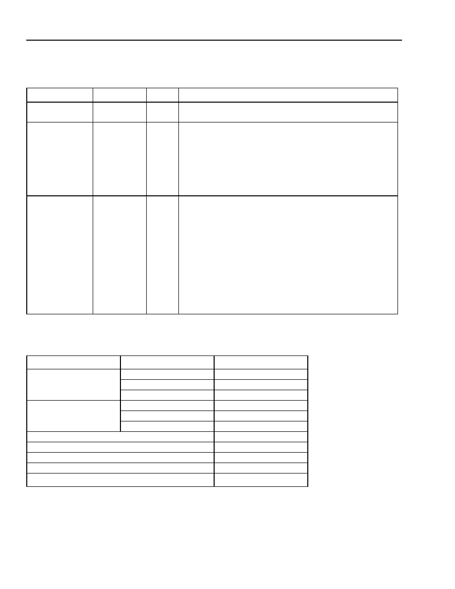
46
Agere Systems Inc.
Data Sheet
May 2003
STS-192 Overhead and Path Processor
TSOT0410G4 SONET/SDH
Pin Information
(continued)
Table 14. Pin Descriptions--Power and Ground (continued)
Table 15. Pin Summary
Pin
Symbol
Type
1
1. P = power, G = ground.
2. No connect (NC) pins indicated with a footnote (2) are unused. There is no connection between the pin and the die.
Name/Description
AP6, AL7, AN16,
AM16
PULLUP
--
Manufacturing Test. These pins must be individually pulled up to
V
DD
2 through 47 k
resistors for normal operation.
AM5, AN5, AP5,
AL6, AM6, AN6,
AM7, AN7, AP7,
AL10, AM10,
AN10, AP10,
AR10, AN28,
AM28, AL28,
AP29
PULLDN
--
Manufacturing Test. These pins must be individually pulled
down to V
SS
through 47 k
resistors for normal operation.
AL8, AL9, AM8,
AM9, AN8, AN9,
AP8, AP9, AN29,
AR9, D26
2
, E27
2
,
G3
2
, H4
2
, J1
2
,
K3
2
, K31
2
, L3
2
,
M33
2
, N2
2
, N5
2
,
P4
2
, R3
2
, T4
2
,
T32
2
, U2
2
, U3
2
,
U31
2
, Y2
2
, AB1
2
,
AC2
2
, AC5
2
, AF1
2
,
AG1
2
, AH34
2
,
AJ2
2
, AK4
2
NC
--
No Connect. Do not connect to these pins.
Pin Type
Pin Direction
Count
LVDS
Input
76
Output
96
Reference
27
TTL
Input
81
Output
93
Bidirectional
20
NC
37
Other (Manufacturing Test)
20
Power
73
Ground
77
Total
600

Agere Systems Inc.
47
Data Sheet
May 2003
STS-192 Overhead and Path Processor
TSOT0410G4 SONET/SDH
Functional Description
Receive STS-192 Line Interface
The receive STS-192 line interface is configured to accept either a single 16-bit wide serial STS-192 stream at
622.08 MHz or four 4-bit wide serial STS-48 streams at 622.08 MHz, and convert them to four STS-48 streams.
The conversion process is essentially the same for both input formats, except that for STS-48 data, each function
is divided into four independent blocks running on separate clocks, while the STS-192 data is processed in one
block and must be passed through a time-slot interchange (TSI) block after the conversion process to demultiplex
its four constituent STS-48 channels.
Regardless of which line format is being used, each input serial stream is first byte and frame aligned by passing it
through a bit rotator to align it. The frame alignment used by the bit rotator is determined by a framer circuit which
monitors the nonaligned word. The data from the bit rotator is then passed to a BIP-8 parity calculator before being
optionally descrambled.
The descrambled data is then either passed directly to one of the STS-48 processing modules when in STS-48
mode, or first passed to a TSI when in STS-192 mode. This TSI reorders the STS-1 slots within the STS-192 to
appear as four STS-48 signals, as required by the STS-48 processing modules.
In STS-192 mode, all 16 data streams are clocked on the positive edge of R_CLK_1. In STS-48 mode, the four
data streams associated with each STS-48 are clocked in on the positive edge of a corresponding clock,
R_CLK_n.
Loss-of-Signal (LOS) Detector
Before the data is optionally descrambled, it is monitored for loss-of-signal (LOS). In STS-192 mode, there is a sin-
gle LOS detector. In STS-48 mode, there is a separate LOS detector on each STS-48 input. On powerup, an LOS
defect is declared if all zeros data is received continuously for 13.8
Ķ
s. This time threshold is provisionable through
the loss-of-signal (LOS) threshold register for each channel, and can be set to any value from 0
Ķ
s (i.e., LOS
detection disabled) to 105
Ķ
s, with a resolution of 102.88 ns (64 times the period of the 622.08 MHz clock).
The LOS defect is subsequently cleared when two successive valid framing patterns are received with no period of
all zeros exceeding the time threshold. Detection of an LOS defect is indicated by a latched alarm status bit, a per-
sistency bit, and a one second PM bit being set in the corresponding LTE receive channel n registers. In addition,
alarm indication signal (AIS) will be inserted by the framer block in all 48 or 192 STS-1 channels affected.
If an optical transponder is connected to the receive line interface, the most appropriate method to declare LOS is
by monitoring the power level monitor of the received signal from the transponder. In some transponders, the
amplifier gain is high enough to cause the LVDS receive data lines to move above zero, even when there is no
optical input. Should this occur, the TSOT0410G4 might not indicate an LOS defect. This is not a deficiency of the
devices, but is a characteristic of the methods of detecting LOS.
If an optical transponder is used, the LOS detector of the TSOT0410G4 monitors the connection from the tran-
sponder to the receive line interface. The LOS detector in the TSOT0410G4 is appropriate for monitoring LOS in
an electrical SONET or SDH system.
48
Agere Systems Inc.
Data Sheet
May 2003
STS-192 Overhead and Path Processor
TSOT0410G4 SONET/SDH
Functional Description
(continued)
Note: Register summary tables occur throughout the Functional Description section on page 47, and describe the
first occurrence of registers that are used for a particular function. Refer to the register map (Table 71 on
page 97) for details on other occurrences of similar registers.
Table 16. LOS Detector Register Summary
Framer (A1 and A2)
In STS-192 mode, when in frame, the framer outputs byte-aligned and frame-aligned data. In STS-48 mode, fram-
ing is performed on four independent channels. Frame timing, parity generation, and AIS insertion are also per-
formed.
Enhanced framing, where every other A1 and A2 byte is inverted to better maintain the dc balance on the optical
line, is also supported in STS-192 mode.
A1A1A1A1 . . . A1A1 = F609F609 . . . F609.
A2A2A2A2 . . . A2A2 = 28D728D7 . . . 28D7.
The STS-192 framer is described below. The STS-48 framer is similar. Enhanced framing is not used when in
STS-48 mode (it is not part of the SONET/SDH specifications). Bit 1 of registers 0x1C00, 0x1D00, 0x1E00, and
0x1F00 should be set to normal mode when the TSOT0410G4 is operating in STS-48 mode.
Framer FSM. The framer FSM is responsible for determining the severely errored framing (SEF) and loss-of-fram-
ing (LOF) SONET framing alarms for each channel. The framer FSM is shown in Figure 4 on page 49.
The FSM comes out of reset in the SEF state with the SEF and LOF alarms active. The framing pattern used is the
16-bit word consisting of the last A1 byte, the first A2 byte, plus two additional A1 bytes. The first occurrence of the
framing pattern transfers the FSM to the frame confirm state. Frame timing is also synchronized. Another framing
pattern match coincident with expected frame timing transfers the state to in frame (i.e., it takes two consecutive
valid framing patterns to frame to an incoming signal). Outside the SEF and frame confirm states, the SEF alarm
output is inactive. As shown in the FSM, when in frame, it requires four consecutive framing errors to be transferred
back to the SEF state.
s
The LOF alarm is asserted if SEF persists for 24 frames (3 ms).
s
The LOF alarm is terminated eight frames (1 ms) after the SEF alarm is terminated (i.e., eight frames after the
FSM enters the in-frame state), provided the SEF state is not re-entered (as per SONET objectives).
Function
Register Name
(First Occurrence)
Register Bits
Qty.
1
1. Qty. refers to the number of registers that are similar to the one shown in the table. There may be more registers to control different chan-
nels, or several registers of similar type used for a particular function.
2. 1st Addr refers to the address (in hex) of the first occurrence of this type of register.
3. Page refers to the relevant page number in this document.
1st
Addr
2
(hex)
Page
3
LOS Detect Time
LTE Receive Channel 1 Loss-of-Signal
(LOS) Threshold (R/W)
LTE_RX_n_LOS_
THRESHOLD1[9:0]
4
1402
123
Latched LOS Alarm
LTE Receive Channel 1
Service-Affecting Interrupt Alarm
(W1C)
LOS
4
1405
124
LOS Persistency
LTE Receive Channel 1
Service-Affecting Persistency Alarm
(RO)
LOS_PER
4
1407
124
LOS One Second PM
LTE Receive Channel 1 Performance
Monitoring (RO)
LOS_PM
4
140B
127
Agere Systems Inc.
49
Data Sheet
May 2003
STS-192 Overhead and Path Processor
TSOT0410G4 SONET/SDH
Functional Description
(continued)
5-8401(F).a
Figure 4. Framer FSM
The framing pattern is a subset of the A1A2 STS-N pattern. This design uses the 16-bit A1A2 boundary as the
framing pattern which evaluates to an average SEF defect occurrence time of 31.79 minutes, assuming a Poisson
bit error rate (BER) of 10
≠3
. This is greater than the minimum average SONET requirement of 6 minutes.
The SEF alarm is reported by a latched register bit in the LTE receive nonservice-affecting alarm register for the
respective channel. The LOF alarm is reported by a latched register bit in the LTE receive service-affecting alarm
register for the respective channel. In addition, a persistency bit for LOF exists in the LTE receive service-affecting
persistency register. Detection of LOF and SEF defects are also indicated by the LTE receive last second PM reg-
ister.
On powerup, detection of an LOF defect causes AIS to be inserted in all affected STS-1 channels by the framer.
During AIS insertion, transport overhead (TOH) processing is disabled. This AIS insertion can be disabled using
the LOF AIS disable control register bit for each channel, or replaced by insertion upon SEF detection using the
SEF AIS disable control bit. Another control bit is the enhanced framing mode. These control bits are part of the
LTE receive provisioning register for the respective channel. The framer is also responsible for sourcing parity with
the framed channels. Parity errors can be forced using the chip-level maintenance register.
IN
FRAME
FRAMING PATTERN
RESET
SEF
FRAME
CONFIRM
CONFIRMED
FRAMING PATTERN
FOUND
FRAMING PATTERN
NOT COMFIRMED
FOUR CONSECUTIVE
FRAMING ERRORS

50
Agere Systems Inc.
Data Sheet
May 2003
STS-192 Overhead and Path Processor
TSOT0410G4 SONET/SDH
Functional Description
(continued)
Table 17. Framer Register Summary
Descrambler
The data from the framer is descrambled using the SONET/SDH standard generator polynomial: 1 + x
6
+ x
7
. The
descrambling can be disabled through the DESCRM_DIS bit in the LTE receive channel provisioning register for
each channel.
Table 18. Descrambler Register Summary
Time-Slot Interchanger (TSI)
For STS-192 data, the input stream must be demultiplexed to create four STS-48 data streams for further process-
ing. The TSI reorders the data so that the STS-192 is divided into its four constituent STS-48 data streams.
Table 19 on page 51 shows the order of the bytes belonging to the individual STS-1s, or STS-1, components of an
STS-Nc that comprise the STS-192 as it enters the TSI. Table 20 on page 51 shows the order of bytes after the TSI
(STS-48 byte ordering). In the tables, the bytes arrive starting in the top left of the table, and then down each col-
umn. The STS-48 table should be interpreted as four simultaneous data streams, where the bytes are ordered
starting with the top left of each channel, and then down each column.
If the TSOT0410G4 is in STS-48 mode, the data is received on all four channels and the TSI is bypassed.
Function
Register Name
(First Occurrence)
Register Bits
Qty.
1st
Addr
(hex)
Page
Enhanced Framing
LTE Receive Channel 1
Provisioning (R/W)
ENH_FRMG_CTL_1
4
1400
122
AIS Insertion on SEF, LOF
LTE Receive Channel 1
Provisioning (R/W)
SEF_AIS_DIS_1
LOF_AIS_DIS_1
4
1400
122
LOF Latched Alarm
LTE Receive Channel 1
Service-Affecting Interrupt Alarm
(W1C)
LOF
4
1405
124
SEF Latched Alarm
LTE Receive Channel 1
Nonservice-Affecting Interrupt
Alarm (W1C)
SEF
4
1408
125
LOF Persistency
LTE Receive Channel 1
Service-Affecting Persistency
Alarm (RO)
LOF_PER
4
1407
124
LOF, SEF One Second PM
LTE Receive Channel 1
Performance Monitoring (RO)
LOF_PM
SEF_PM
4
140B
127
Forcing Parity Errors
Chip-Level Maintenance (R/W)
FRC_PAR_ERR
1
0005
112
Function
Register Name
(First Occurrence)
Register Bits
Qty.
1st
Addr
(hex)
Page
Descrambling Control
LTE Receive Channel 1
Provisioning (R/W)
DESCRM_DIS_1
4
1400
122
Agere Systems Inc.
51
Data Sheet
May 2003
STS-192 Overhead and Path Processor
TSOT0410G4 SONET/SDH
Functional Description
(continued)
Table 19. STS-192 Byte Ordering
Table 20. STS-48 Byte Ordering
Note: STS-12 byte ordering is shown in Table 29 on page 62.
Time (Top to Bottom, Then Left to Right)
STS-192
Number
1
49
97
145
2
50
98
146
3
51
99
147
1
4
52
100
148
5
53
101
149
6
54
102
150
7
55
103
151
8
56
104
152
9
57
105
153
10
58
106
154
11
59
107
155
12
60
108
156
13
61
109
157
14
62
110
158
15
63
111
159
16
64
112
160
17
65
113
161
18
66
114
162
19
67
115
163
20
68
116
164
21
69
117
165
22
70
118
166
23
71
119
167
24
72
120
168
25
73
121
169
26
74
122
170
27
75
123
171
28
76
124
172
29
77
125
173
30
78
126
174
31
79
127
175
32
80
128
176
33
81
129
177
34
82
130
178
35
83
131
179
36
84
132
180
37
85
133
181
38
86
134
182
39
87
135
183
40
88
136
184
41
89
137
185
42
90
138
186
43
91
139
187
44
92
140
188
45
93
141
189
46
94
142
190
47
95
143
191
48
96
144
192
Time (Top to Bottom, Then Left to Right for Each STS-48 Channel)
STS-48
Number
1
13
25
37
2
14
26
38
3
15
27
39
1
4
16
28
40
5
17
29
41
6
18
30
42
7
19
31
43
8
20
32
44
9
21
33
45
10
22
34
46
11
23
35
47
12
24
36
48
49
61
73
85
50
62
74
86
51
63
75
87
2
52
64
76
88
53
65
77
89
54
66
78
90
55
67
79
91
56
68
80
92
57
69
81
93
58
70
82
94
59
71
83
95
60
72
84
96
97
109
121
133
98
110
122
134
99
111
123
135
3
100
112
124
136
101
113
125
137
102
114
126
138
103
115
127
139
104
116
128
140
105
117
129
141
106
118
130
142
107
119
131
143
108
120
132
144
145
157
169
181
146
158
170
182
147
159
171
183
4
148
160
172
184
149
161
173
185
150
162
174
186
151
163
175
187
152
164
176
188
153
165
177
189
154
166
178
190
155
167
179
191
156
168
180
192

52
Agere Systems Inc.
Data Sheet
May 2003
STS-192 Overhead and Path Processor
TSOT0410G4 SONET/SDH
Functional Description
(continued)
Receive Transport Overhead (TOH) Processor
This block is responsible for terminating the transport overhead and is replicated four times. Each block accepts
the frame and byte-aligned data for one STS-48 channel and extracts the transport section and line overhead. The
extracted overhead is then either stored internally, or provided externally on a serial output, and may also be fur-
ther processed for alarm or performance monitoring purposes.
In STS-48 mode, each channel is synchronized to a separate clock and carries complete transport overhead. In
STS-192 mode, all channels are synchronized to the same clock and only the first STS-48 carries complete trans-
port overhead, while the other channels only carry line BIP-8. The definition and associated storage or processing
of each byte is detailed in the subsections that follow.
All processing of overhead bytes is inhibited while the following alarm defects are detected:
s
LOS (if not disabled)
s
LOF (if AIS insertion is enabled)
s
SEF (if AIS insertion is enabled)
s
Line AIS (only the line overhead bytes are inhibited)
Receive Overhead Serial Links
In addition to the individual storage or external availability of the overhead bytes described below, the full set of
transport overhead bytes for each STS-48 channel (1296 bytes) are serialized and output on the ROHDAT_n_[1:0]
pins. The bytes are sent, MSB first, with each pair of bits output on the positive edge of ROH_CLK_n
(41.472 MHz). The location of the MSB of the first A1 byte is identified by the ROHFP_n output going high.
In STS-48 mode, each pair of ROHDAT_n_[1:0] pins transmits the transport overhead for an STS-48 channel. In
STS-192 mode, the four pairs of ROHDAT_n_[1:0] pins transmit the entire STS-192 overhead (5184 bytes), where
the ROHDAT1 pins transmit STS channels 1 through 48, and the ROHDAT2, ROHDAT3, and ROHDAT4 pins
transmit STS channels 49 through 96, 97 through 144, and 145 through 192, respectively. The timing for this is
described in the Receive Overhead Serial Link section on page 175.
Each interface determines its ROHFP by sampling the Rx frame using a metastable hand-off. Even in 10 Gbits/s
mode, where the RXCLK and ROHCLK are the same, the different delays on the signals in each channel will cre-
ate the potential for the metastable handlers to sample the channels, Ī1 clock cycles, of each other. This is
unavoidable due to the possibility of the four channels being asynchronous. Any external logic that interfaces to
ROHDAT should synchronize to each of the four channels independently using the individual ROHFP signals.
Internally, a memory is used for each channel to buffer the data and transfer it between the internal processing rate
and the external data rate. This allows for the data to be transmitted in a nongapped manner. The operation of the
memory is monitored using parity, and any errors are reported using the ROHDAT parity error alarm bit. This alarm
bit is present in the corresponding LTE receive channel n nonservice affecting interrupt alarm register and is valid
regardless of the mode (STS-48 or STS-192) in which the device is operating.
During AIS insertion due to LOS, LOF, or SEF (provisionable), 0xFF is constantly output for the overhead byte val-
ues.
Table 21. Receive Overhead Serial Links Register Summary
Function
Register Name
(First Occurrence)
Register Bits
Qty.
1st
Addr
(hex)
Page
Parity Alarm
LTE Receive Channel 1 Nonser-
vice-Affecting Interrupt Alarm (W1C)
RX_OH_MEM_PAR_
ERR_1
4
1408
125

Agere Systems Inc.
53
Data Sheet
May 2003
STS-192 Overhead and Path Processor
TSOT0410G4 SONET/SDH
Functional Description
(continued)
Section Trace (J0)
The section trace byte is present in the first STS-1 of the STS-48 or STS-192 only. Specified by the J0 message
type control bit, the TOH processor supports extraction of either SONET 64-byte (ASCII, <CR><LF> terminated) or
SDH 16-byte (E.164) section trace messages that are stored in internal memory. Processing of the received mes-
sage then depends on the J0 message mode control bit. The content of the message is either monitored for a mis-
match from a provisioned expected message or monitored for a sustained change (validation) in the received
message.
If the J0 message mode control bit is set to the provisioned mode, then the incoming message is compared against
the software programmed expected message. The expected message is stored in internal memory for each
STS-48 channel. A mismatch is declared if a consistent received message differs from the expected message for
ten consecutive messages. The mismatch clears when four out of five received messages match the expected
message (fixed windowing is used for clearing). This mismatch state is reflected in the J0 message mismatch
alarm bit.
When the J0 message mode control bit is set to the validated mode, the incoming message is monitored for a sus-
tained change. A sustained change is detected when the received message differs from the last stable message
for ten consecutive messages. The new message then becomes the stable message, is stored in internal memory,
and the processor starts checking for a sustained change from this new stable message (i.e., there is no clearing
criteria for a sustained change). The J0 new message alarm bit is set when a sustained change is detected.
Selection of the message type, SONET or SDH format, and the content monitoring mode (provisioned or vali-
dated), are provisionable on a per STS-48 channel basis through a corresponding LTE receive channel n mainte-
nance register. The associated alarms for the two modes are reported in the LTE receive channel n
nonservice-affecting interrupt alarm register.
The expected messages for all channels are provisioned through the microprocessor interface using the 64-byte
J0 access message buffer. This message buffer is also used to read the contents of the expected, stable, or
received messages for all channels. Accesses using the data buffer are paged according to direction (transmit and
receive), STS-48 channel, and message type (expected/stable or received) through the use of the section trace
access register. If the J0 message mode is set to the provisioned mode, the expected message is accessible. If the
J0 message mode is set to the validated mode, then the stable message is accessible. Once the section trace
access register is configured, the actual access is triggered by writing a 0x0001 value to the section trace access
start register. The transfer from internal memory to/from the message buffer is performed on the next message
boundary. Completion of the access is indicated by the access done flag being set in the section trace access sta-
tus register.
Note: To insert J0 into the transmit stream, 0x0020 must be written register 0x1C01 (the enable insertion of provi-
sioned J0 message register). See Table 137 on page 131 for detailed register information.
Internally, a memory is used to store the currently received section trace message as well as the stable or provi-
sioned message. The operation of the memory is monitored using parity, and any errors are reported using the J0
parity error alarm bit.

54
Agere Systems Inc.
Data Sheet
May 2003
STS-192 Overhead and Path Processor
TSOT0410G4 SONET/SDH
Functional Description
(continued)
Table 22. J0 Register Summary
Section Growth (Z0)
No receive function has currently been defined for the section growth byte present in the remaining STS-1 loca-
tions of the STS-48 or STS-192 J0 byte.
Section BIP-8 (B1)
The section BIP-8 byte is located in the first STS-1 of the STS-48 or STS-192 only, and carries the even parity of the
scrambled data in the previous STS-48 or STS-192 frame. In every frame, the received B1 value is extracted and
compared to the calculated BIP-8 for the previous frame. Errors in the BIP-8 code are tabulated in an internal 16-bit
counter based on either bit or block errors as provisioned for each channel through the B1 BIP mode control bit.
In bit mode (selected by default), each BIP-8 bit in error causes the counter to increment. If block error is selected,
each BIP-8 code in error causes the counter to increment only once. Regardless of which mode is selected, the
value in the counter is transferred to the section coding violation (CV-S) register on the positive edge of PM_CLK,
at which point the counter is cleared. The counter will stop at the maximum value and will not roll over.
Section BIP-8 (B1) Errors Serial Access
The errors detected in section BIP-8 byte are located in the first STS-1 of the STS-48 or STS-192 and can option-
ally be extracted serially on the local the ROHDAT interface. See the Receive Overhead Serial Links section on
page 52 for details on the ROHDAT interface.
A provisioning bit (B1_ERROR_MASK_EN (bit 7)) is provided in each LTE Rx channel provisioning register as a
B1 error mask enable. When the B1_ERROR_MASK_EN bit is set, the B1 byte in ROHDAT is replaced with the B1
error mask from the previous frame. An error in the Rx B1 BIP-8 code will result in the corresponding bit in the error
mask being set for one frame, with a one-frame delay due to retiming.
Function
Register Name
(First Occurrence)
Register Bits
Qty. 1st
Addr
(hex)
Page
Message Type Control
LTE Receive Channel 1 Maintenance
(R/W)
J_MSG_TYPE_1
4
1401 123
Message Mode
(Provisioned or
Validated)
LTE Receive Channel 1 Maintenance
(R/W)
J_MSG_MODE_1
4
1401 123
Message Mismatch
Latched Alarm
LTE Receive Channel 1
Nonservice-Affecting Interrupt Alarm
(W1C)
J_MSG_MISMATCH_INT
_1
4
1408 125
New Message Latched
Alarm
LTE Receive Channel 1
Nonservice-Affecting Interrupt Alarm
(W1C)
J_NEW_MSG_INT_1
4
1408 125
J0 Access Message Buffer
J0 Access Message Buffers 1--32
(R/W)
LTE_J_ACCESS_
BUF_n[15:0]
32
1110
118
Message Buffer Access
Control
Section Trace (J0) Access
Maintenance (R/W)
All bits
1
1100
117
Message Buffer Access
Start
J0 Access Message Start (WO)
LTE_J_ACCESS_MSG_
START
1
1102
118
Message Buffer Access
Complete Flag
J0 Access Done (W1C)
J_ACCESS_DONE_
FLAG
1
1101
118
Buffer Parity Error Latched
Alarm
LTE Receive Channel 1
Nonservice-Affecting Interrupt Alarm
(W1C)
J_MEM_PARITY_
ERR_1S
4
1408 125
Agere Systems Inc.
55
Data Sheet
May 2003
STS-192 Overhead and Path Processor
TSOT0410G4 SONET/SDH
Functional Description
(continued)
The ROHDAT interface B1 error mask extraction is enabled by provisioning the B1_ERROR_MASK_EN bit in the
LTE Rx channel provisioning registers (0x1400, 0x1500, 0x1600, and 0x1700 respectively). (See Table 110 on
page 122.) The appropriate bit definitions are shown in Table 23. The B1 error mask extract feature is always sup-
ported on individual STS-48 channels and will require all four channels to be provisioned in STS-192 mode.
Table 23. B1 Register Summary
Local Orderwire (E1)
The local orderwire byte is located in the first STS-1 of the STS-48 or STS-192 only, and provides a 64 kHz chan-
nel for voice communications between regenerators, hubs, and remote terminals. The byte is extracted from each
frame, buffered, and then output serially, MSB first, on the RLCLOWn pin. During AIS insertion due to LOS, LOF,
or SEF (provisionable), 0x7F is constantly output. The data is clocked out on the positive edge of ROWCKn.
The ROWCKn clock is divided down from the section data communications channel clock, RSDCKn (192 kHz/3),
giving a frequency of 64 kHz and a duty cycle of 33%. In STS-48 mode, each of the four RLCLOW pins transmit
the E1 byte for a channel. In STS-192 mode, only the RLCLOW1 pin transmits the E1 byte, while the other pins
transmit a constant 0x7F serial stream.
Section User Channel (F1)
The section user channel byte is located in the first STS-1 of the STS-48 or STS-192 only, and provides a 64 kHz
channel for use by the network provider. The byte is extracted in each frame, buffered, and output serially, MSB
first, on the RSUSERn pin. During AIS insertion due to LOS, LOF, or SEF (provisionable), 0x7F is constantly out-
put. The data is clocked out on the positive edge of ROWCKn.
In STS-48 mode, each of the four RSUSERn pins transmit the F1 byte for a channel. In STS-192 mode, only the
RSUSER1 pin transmits the F1 byte, while the other pins transmit a constant 0x7F serial stream.
Section Data Communications Channel (D1, D2, and D3)
The section data communications channel bytes are located in the first STS-1 of the STS-48 or STS-192 only and
are used as one 192 kHz message-based channel for operations, administration, and maintenance (OA&M) com-
munication. The bytes are extracted from each frame, buffered, and output serially, MSB first, on the RSDCCn pin
in the order that they are received. During AIS insertion due to LOS, LOF, or SEF (provisionable), 0xFF is con-
stantly output. The data is clocked out on the positive edge of RSDCKn.
The RSDCKn clock is divided down from the line data communications channel clock, RLDCKn (576 kHz/3), giving
a frequency of 192 kHz and a duty cycle of 33%. In STS-48 mode, each of the four RSDCC pins transmit the sec-
tion data communication channel bytes for a channel. In STS-192 mode, only the RSDCC1 pin transmits these
bytes, while the other pins are set high.
Function
Register Name
(First Occurrence)
Register Bits
Qty. 1st
Addr
(hex)
Page
B1 Error Bit Enable
LTE Receive Channel 1 Provisioning (R/W) B1_ERROR_MASK_EN
4
1400 122
Bit Error/Block Error
Control
LTE Receive Channel 1 Provisioning (R/W)
B1_BIP_MODE_1
4
1400 122
Last Second Coding
Violations Count
LTE Receive Channel 1 CV-S Performance
Monitoring (RO)
CV_S_REG_1
4
1410 128

56
Agere Systems Inc.
Data Sheet
May 2003
STS-192 Overhead and Path Processor
TSOT0410G4 SONET/SDH
Functional Description
(continued)
Line BIP-8 (B2)
The line BIP-8 is located in each STS-1 of the STS-48 or STS-192 and carries the even parity for the line overhead
and SPE data within the previous STS-1 frame. The n line BIP-8 bytes in an STS-N are intended to provide a single
error monitoring facility for the entire STS-N signal. Thus, each TOH processor block is used to check the 48 line
BIP-8 codes, whether in STS-48 or STS-192 mode. Each BIP-8 bit found to be in error causes an internal 22-bit
counter to increment.
The value in the counter is transferred to the line coding violation (CV-L) registers on the positive edge of PM_CLK,
at which point the counter is cleared. The counter will stop at the maximum value and will not roll over. When in
STS-192 mode, a read of the STS-48 channel 1 CV-L register returns the 24-bit sum of the four constituent
STS-48 channel CV-L counts. However, reading channels 2--4 returns the CV-L count for the corresponding
STS-48.
In addition to the CV-L counter, line BIP-8 errors are also tracked in 16-bit signal fail (SF) and signal degrade (SD)
counters. These counters are used to detect SF and SD conditions for protection switching. The BER threshold for
each defect is separately provisionable for each channel over a range of 1
◊
10
≠N
values, where N = 3 to 5 for SF
and N = 5 to 9 for SD.
The detection times and error limits used to detect and clear both defects are dependent on the provisioned BER
threshold as shown in Table 24. The values shown in the table are the powerup defaults and are dependent on the
STS mode selected (48 or 192). These values can be changed through the corresponding registers and are com-
mon to all channels.
The clearing BER threshold for each defect is always 1/10th of the detection threshold. As can be seen in Table 24,
the range of possible detect thresholds is 1 x 10
≠3
to 1 x 10
≠9
, which results in clear thresholds of 1 x 10
≠4
to
1 x 10
≠10
. For example, to detect SD at 1 x 10
≠5
BER in an STS-192, the detection time is 4 ms and the detect
error limit is 358. The clearing would take place at 1
◊
10
≠6
BER, with a clearing time of 6.5 ms and a clearing error
limit of 77. Figure 5 on page 57 illustrates SD detection and clearing using the default values specified in Table 24.
SD thresholds of 1 x 10
≠10
to 1 x 10
≠15
are supported through software.
Table 24. BER Threshold Time and Error Limits for Line SD and SF Detection
BER Threshold
Detection Time
Detect Error Limit
Clear Error Limit
STS-48
STS-192
STS-48
STS-192
STS-48
STS-192
1
◊
10
≠3
4 ms
4 ms
4818
19453
--
--
1
◊
10
≠4
4 ms
4 ms
862
3543
957
3734
1
◊
10
≠5
4 ms
4 ms
81
358
114
423
1
◊
10
≠6
31 ms
6.5 ms
62
51
91
77
1
◊
10
≠7
312.5 ms
65 ms
62
51
91
77
1
◊
10
≠8
2600 ms
650 ms
51
51
77
77
1
◊
10
≠9
21 s
5250 ms
40
40
63
63
1
◊
10
≠10
170 s
41 s
--
--
52
51
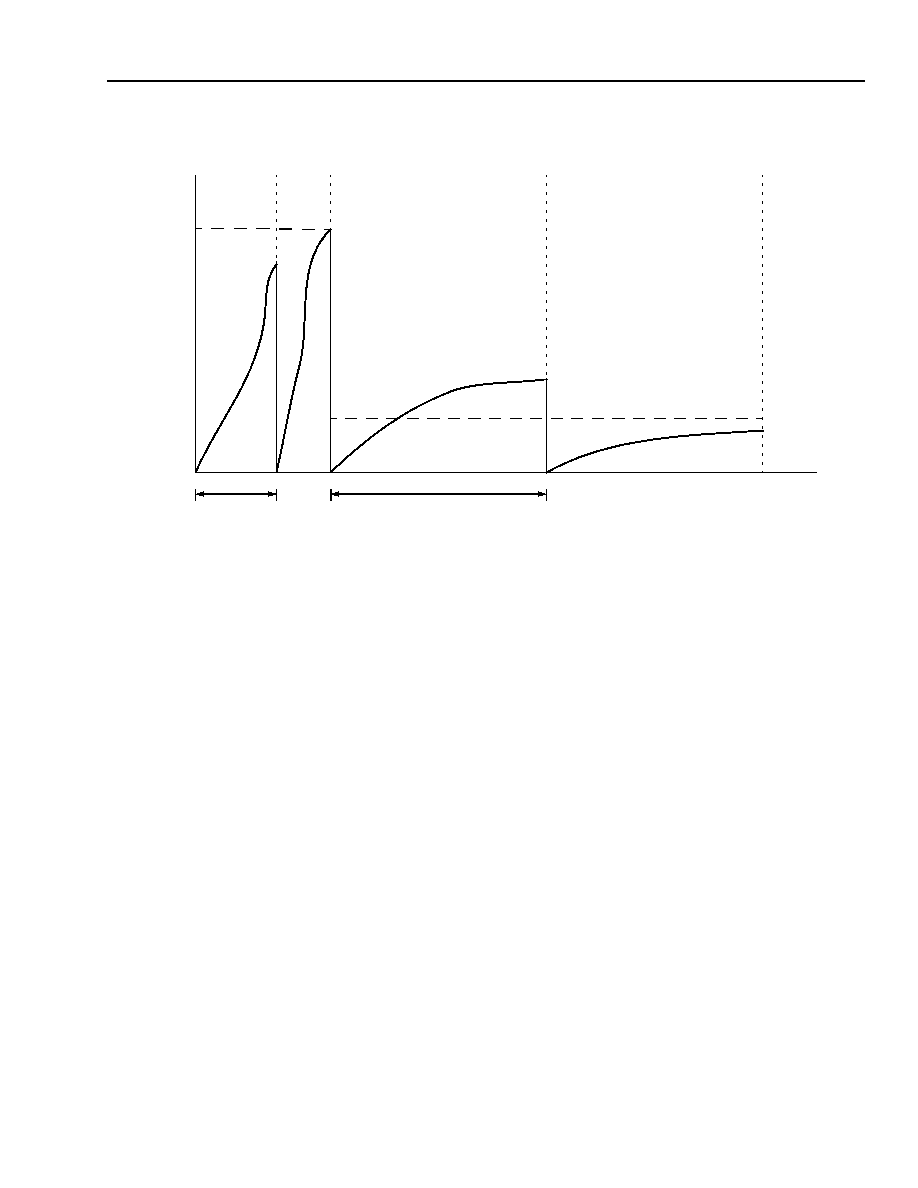
Agere Systems Inc.
57
Data Sheet
May 2003
STS-192 Overhead and Path Processor
TSOT0410G4 SONET/SDH
Functional Description
(continued)
5-8406(F)r.1
Figure 5. Example of STS-192 SD Detection (10
≠5
BER) and Clearing (10
≠6
BER)
In STS-192 mode, the thresholds are compared against the sum of the four STS-48 channel SF and SD counts. A
detected SF or SD defect causes a corresponding maskable interrupt status bit to be set in the LTE receive
channel n service-affecting alarm register.
The SD/SF BER control bits in the LTE receive channel n maintenance register select the bit error rate for a partic-
ular channel. These control bits then select the detection time, the detect error limit, and the clear error limits for
each channel from the LTE receive common SD/SF registers. The detect error limit and the clear error limit regis-
ters contain 16-bit values, while the detection time registers use the lower 15 bits for a value and the upper bit for a
time unit specifier. For the detection time register, the value contained in the lower 15 bits is either specified in
0.5 ms units (upper bit = 0) or in seconds (upper bit = 1). Note that the PM_CLK input to the device is used as the
timing reference when the detection time is expressed in seconds.
A fixed windowing scheme is used for SD/SF detection. The window size is determined by the value in the detec-
tion time register for the specified bit error rate. An SD or SF alarm is declared immediately when the accumulated
error count exceeds the value specified in the detect error limit register.
If this error limit is not reached by the end of the window, then the accumulated error count is reset to zero. When
an SD or SF alarm is declared, the accumulated error count resets and clearing begins using the bit error rate
threshold that is 1/10th of the specified value along with the corresponding detection time registers. Clearing of the
SD or SF alarm only occurs at the end of the window when the accumulated error count is less than the value
specified in the clear error limit register.
During AIS insertion due to LOS, LOF, SEF, or line AIS, processing of the B2 byte is inhibited and the internal
SF/SD counters are reset back to zero. Because it takes five frames of line AIS before the actual line AIS alarm is
declared, it is likely that the signal degrade alarm will also be triggered. Once AIS insertion is removed, processing
of the B2 byte is delayed for two frames before it is enabled.
SD
AC
C
U
MU
LA
TE
D
B2 ER
R
O
R
S
TIME (MS)
358
77
4
8
6
12.5
19
SD DETECTED
SD CLEARED
SD DETECTION WINDOW
SD CLEARING WINDOW

58
Agere Systems Inc.
Data Sheet
May 2003
STS-192 Overhead and Path Processor
TSOT0410G4 SONET/SDH
Functional Description
(continued)
Table 25. B2 Register Summary
Line BIP-8 (B2) Errors Serial Access
The errors detected in the line BIP-8 (B2) byte for each STS-1 can optionally be extracted serially on the local
orderwire (RLCLOWn), express orderwire (REXPOWn), and orderwire clock (OW_CLKn) pins of each STS-48.
This extraction is enabled on a global basis (i.e., all channels) by provisioning the LTE Transmit--B2 Corrupt
Frame Count (R/W) register (on page 128) with a value greater than 8063
10
. The appropriate bit definitions are
shown in Table 130 on page 128, register 1B02. The TOH transparency feature is always supported on individual
STS-48 channels and will require all four channels to be provisioned in STS-192 mode. When enabled, the B2
errors detected in each STS-1 of an STS-48 are output serially on the REXPOWn pin as a byte containing a 1 in
each bit position found in error. These error masks are clocked out on the positive edge of a 78 MHz clock that is
provided on the OW_CLKn pin. Because this frequency is much higher than the bit rate of the B2 bytes, the 48
error masks on each REXPOWn pin are output in a burst fashion once per frame. The presence of this burst is indi-
cated by a continuous logical high on the RLCLOWn pin. The data within the burst follows SONET STS-1 channel
ordering, but with the 48 channels serialized in 4-byte chunks with the LSB (newest data) sent first. In other words,
the STS-1 error masks for each STS-48 are sent LSB first in the following order: 10, 7, 4, 1; 22, 19, 16, 13; 34, 31,
28, 25; 46, 43, 40, 37; 11, 8, 5, 2; 23, 20, 17, 14; 35, 32, 29, 26; 47, 44, 41, 38; 12, 9, 6, 3; 24, 21, 18, 15; 36, 33,
30, 27; 48, 45, 42, 39.
APS Channel (K1 and K2)
The APS channels bytes are located in the first STS-1 of the STS-48 or STS-192 only and are used for automatic
protection switching (APS) signaling to coordinate line level protection switching. In addition, the K2 byte is also
used to carry line AIS (AIS-L) and line RDI (RDI-L) signals.
A new value in either byte is only validated after it has been received N times consecutively, where N is provision-
able to 3 or 5 using the K1K2 validate select control bit. When a K1 or K2 byte is validated, the value is stored in
the K byte status register and the K1K2 new byte alarm bit is set. These two alarms are only generated when the
value of the new validated K1 or K2 byte is different from the value of the last validated byte. Validation of the K1
and K2 bytes, and the generation of the alarms, are not affected by the line AIS status.
Function
Register Name
(First Occurrence)
Register Bits
Qty.
1st
Addr
(hex)
Page
Last Second Coding Violations
Count
LTE Receive Channel 1 CV-L
Performance Monitoring (L) (RO)
CV_L_REG_1_L/
CV_L_REG_1_U
4
140E/
140F
127
SD/SF Detection Time
Line Signal Degrade/Signal Fail Bit
Error Rate Detection Time
(1 x 10
≠3
) (R/W)
SD_SF_DETECT_
TIME_3
8
1300
119
SD/SF Detect Error Limit
Line Signal Degrade/Signal Fail
Detect Error Limit (1 x 10
≠3
) (R/W)
SD_SF_ERR_
LIMIT_3
7
1310
120
SD/SF Clear Error Limit
Line Signal Degrade/Signal Fail
Clear Error Limit (1 x 10
≠4
) (R/W)
SD_SF_CLR_ERR_
LIMIT_3
7
1320
121
SD/SF Threshold Selection
LTE Receive Channel 1
Maintenance (R/W)
SD_BER_1/
SF_BER_1
4
1401
123
SD/SF Latched Alarms
LTE Receive Channel 1
Service-Affecting Interrupt Alarm
(W1C)
SD_ALARM_1/
SF_ALARM_1
4
1405
124

Agere Systems Inc.
59
Data Sheet
May 2003
STS-192 Overhead and Path Processor
TSOT0410G4 SONET/SDH
Functional Description
(continued)
The validated K1 and K2 bytes are further processed for the following defects:
s
Protection switching byte. This defect occurs when either an inconsistent APS byte or an invalid code is detected.
An inconsistent APS byte occurs when no N consecutive K1 bytes of the last 12 successive frames are identical,
starting with the last frame containing a previously consistent byte. An invalid code occurs when the incoming K1
byte contains an unused code or a code irrelevant for the specific switching operation in three consecutive
frames. An invalid code also occurs when the incoming K1 byte contains an invalid channel number in three
consecutive frames. As invalid code detection requires information not readily available to hardware; it must be
detected by software polling of the validated K1 byte value. An inconsistent APS byte defect is detected by
hardware and will cause a latched alarm status bit to be set in the corresponding LTE receive channel n
nonservice affecting interrupt alarm register. It is cleared when a K1 byte is received and validated. An
inconsistent APS byte defect is neither detected nor terminated during AIS-L defect. Processing of the
inconsistent APS byte defect is also inhibited when the validated K1 byte has a value of 0xFF and bits 6--8 of the
validated K2 byte have a value of 111. This additional feature prevents a change in the inconsistent APS defect
state just before line AIS is declared.
s
Channel mismatch. This defect occurs when the channel numbers in the transmitted K1 byte (bits 5--8) and the
validated received K2 byte (bits 1--4) are not identical. Detection of a channel mismatch defect causes a latched
alarm status bit to be set in the corresponding LTE receive channel n nonservice-affecting interrupt alarm register.
A channel mismatch defect is neither detected nor terminated during an AIS-L defect. Processing of the channel
mismatch defect is also inhibited when the validated K2 byte has a value of 1111x111 binary. This additional
feature prevents a change in the channel mismatch defect state just before line AIS is declared.
In addition, the currently received K2 byte is processed for the following defects:
s
Line AIS (AIS-L). Declared when bits 6--8 of K2 contain 111 for five consecutive frames. Cleared when any other
pattern is received for five consecutive frames. Detection of a line AIS defect is indicated by a latched alarm
status bit, persistency bit, and one second PM bit being set in the registers for the affected channel.
s
Line RDI (RDI-L). Declared when bits 6--8 of K2 contain 110 (binary) for five consecutive frames. Cleared when
any other pattern is received for five consecutive frames. Detection of a line RDI defect is indicated by a latched
alarm status bit, persistency bit, and one second PM bit being set in the registers for the affected channel.
Table 26. APS Channel (K1 and K2) Register Summary
Function
Register Name
(First Occurrence)
Register Bits
Qty.
1st
Addr
(hex)
Page
K1K2 Validation
Length (3 or 5)
LTE Receive Channel 1
Provisioning (R/W)
K_VALIDATE_LIMIT_SEL_1
4
1400
122
Validated K1K2
Storage
LTE Receive Channel 1 K Byte
Status (RO)
RX_K1_VALIDATED_BYTE_1
RX_K2_VALIDATED_BYTE_1
4
1403
123
New Validated
K1K2 Alarm
LTE Receive Channel 1
Nonservice-Affecting Interrupt
Alarm (W1C)
RX_K1_NEW_BYTE_RAW_INT_1
RX_K2_NEW_BYTE_RAW_INT_1
4
1408
125
Inconsistent APS
Alarm
LTE Receive Channel 1
Nonservice-Affecting Interrupt
Alarm (W1C)
INCONSISTENT_APS_ALARM_1
4
1408
125
Channel Mis-
match Alarm
LTE Receive Channel 1
Nonservice-Affecting Interrupt
Alarm (W1C)
CHANNEL_MISMATCH_ALARM_1
4
1408
125
AIS-L Latched
Alarm
LTE Receive Channel 1
Service-Affecting Interrupt
Alarm (W1C)
RX_LINE_AIS_ALARM_1
4
1405
124
AIS-L Persistency
LTE Receive Channel 1
Service-Affecting Persistency
Alarm (RO)
AISL_PER
4
1407
124
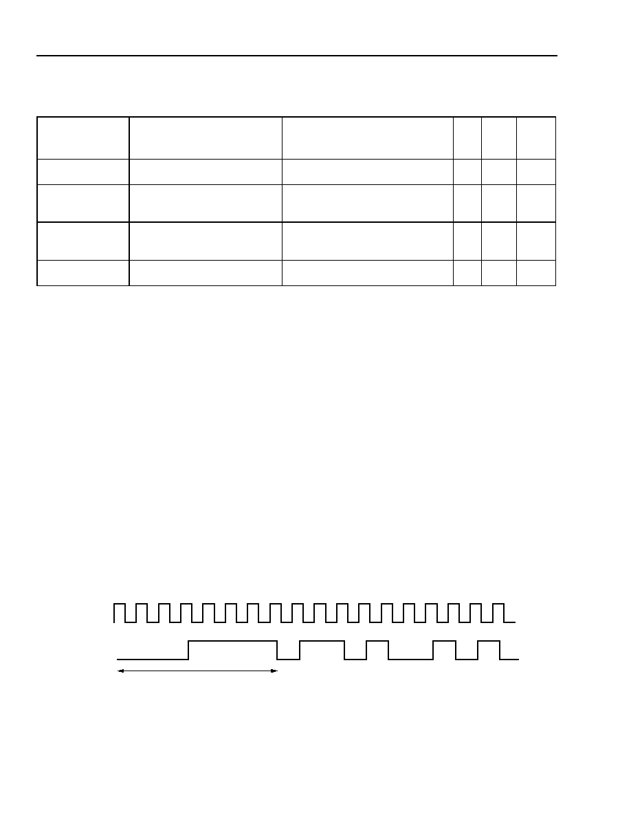
60
Agere Systems Inc.
Data Sheet
May 2003
STS-192 Overhead and Path Processor
TSOT0410G4 SONET/SDH
Line Data Communication Channel (D4--D12)
The line data communication channel bytes are located in the first STS-1 of the STS-48 or STS-192 only, and are
used as one 576 kHz message-based channel for operations, administration, and maintenance communication
(OA&M). The bytes are extracted from each frame, buffered, and are output serially, MSB first, on the RLDCC_n
pin. During AIS insertion due to LOS, LOF, or SEF (provisionable), 0xFF is constantly output. The data is clocked
out on the positive edge of RLD_CLK_n. The RLD_CLK_n clock is divided down from the internal data clock
(622.08 MHz/1080), giving a frequency of 576 kHz and a duty cycle of roughly 50%.
In STS-48 mode, each of the four RLDCC pins transmit the line data communication channel bytes for that chan-
nel. In STS-192 mode, only the RLDCC_1 pin transmits these bytes, while the other pins are set high.
Synchronization Status (S1)
The synchronization status byte is located in the first STS-1 of the STS-48 or STS-192 only, and is used to convey
the synchronization status of a network element. The byte is extracted from each frame. A new value is only vali-
dated and stored in the S1 byte after it has been received eight consecutive times. Detection of a new validated
byte is indicated by the latched S1 new byte alarm bit. The alarm is only generated when the value of the new vali-
dated byte is different from the value of the last validated byte.
The validated synchronization status byte is also transmitted on the RFRMn pin for each channel when the RFRM
output enable control bit is set high. The byte is serialized MSB first as a repeating 77.76 MHz Manchester
encoded* 16-bit code that is interrupted once per frame by the frame sync pattern 00001111. While the data rate of
the signal is 77.76 MHz, the output pin is driven with 622 MHz low-voltage differential drivers, synchronous to the
corresponding R_CLKO_n clock. When the RFRM output enable control bit is set low (the default value), an 8 kHz
clock is transmitted on the RFRMn pin.
5-8402(F)
Figure 6. Timing Diagram for RFRM
Last Second AIS-L
PM
LTE Receive Channel 1
Performance Monitoring (RO)
RX_LINE_AIS_PM_1
4
140B
127
RDI-L Latched
Alarm
LTE Receive Channel 1
Nonservice-Affecting Interrupt
Alarm (W1C)
RX_LINE_RDI_ALARM_1
4
1408
125
RDI-L Persistency
LTE Receive Channel 1
Nonservice-Affecting
Persistency Alarm (RO)
RX_LINE_RDI_PER_1
4
140A
127
Last Second
RDI-L PM
LTE Receive Channel 1
Performance Monitoring (RO)
RX_LINE_RDI_PM_1
4
140B
127
* A logic 0 is encoded as an upward transition at the bit center; a logic 1 is encoded as a downward transition at the bit center. Each Manches-
ter encoded bit requires two clock cycles. The frame sync pattern is not Manchester encoded, and therefore each bit only requires one clock
cycle.
Function
Register Name
(First Occurrence)
Register Bits
Qty.
1st
Addr
(hex)
Page
CLK
RFRM
FRAMING PATTERN
0
1
1
0
0
Functional Description
(continued)
Table 26. APS Channel (K1 and K2) Register Summary (continued)

Agere Systems Inc.
61
Data Sheet
May 2003
STS-192 Overhead and Path Processor
TSOT0410G4 SONET/SDH
Functional Description
(continued)
During AIS insertion due to LOS, LOF, SEF, or line AIS, a constant high signal is transmitted on the RFRMn pin,
regardless of the RFRM output enable control bit.
In STS-48 mode, each of the four RFRMn pins operates according to the functionality specified above. In STS-192
mode, only the RFRM1 pin transmits the validated synchronization status byte or the 8 kHz clock.
Table 27. Synchronization Status (S1) Register Summary
STS-192 Line Remote Error Indication (M1)
The line remote error indication (REI-L) byte is located in the third STS-1 of the STS-48 or STS-192 only (in order
of appearance in the STS-192 signal), and is used to convey to the far end the number of errors detected using the
line BIP-8 bytes (truncated at 255). The byte is extracted from each frame and the value added to an internal 21-bit
counter. The value in the counter is transferred to the REI-L registers on the positive edge of the PM_CLK input, at
which point the counter is cleared. The counter will stop at the maximum value and will not roll over.
Table 28. Line REI (M1) Register Summary
Express Orderwire (E2)
The express orderwire byte is located in the first STS-1 of the STS-48 or STS-192 only, and provides a 64 kHz
channel for voice communications between line entities. The byte is extracted from each frame, buffered, and then
output serially, MSB first, on the REXPOW_n pin. During AIS insertion due to LOS, LOF, SEF (provisionable), or
line AIS, 0x7F is constantly output. The data is clocked out on the positive edge of ROW_CLK_n.
In STS-48 mode, each of the four REXPOW pins transmit the E2 byte for a channel. In STS-192 mode, only the
REXPOW_1 pin transmits the E2 byte while the other pins transmit a constant 0x7F serial stream.
Receive STS Path Processor
This block is replicated four times. Each block accepts the data for one STS-48 channel and terminates the
SONET/SDH path layer overhead, without terminating the full path layer (i.e., demapping the payload). It provides
pointer interpretation, path overhead processing, and drop interface alignment (pointer generation) for any mix of
valid STS payloads from 48 channels of STS-1 to one channel of STS-48c, or part of an STS-192c channel. The
exact mix of payloads is determined automatically by hardware by examining the pointer bytes. The received pay-
loads can be optionally compared to a software provisioned map using the software concatenation map registers in
the microprocessor interface. Concatenated payloads must follow the basic position requirement specified in
GR-256-CORE that concatenated payloads start on an STS-3 boundary (STS-1 payloads may start anywhere).
Note that the terminology used is from SONET, although SDH is also supported.
Function
Register Name
(First Occurrence)
Register Bits
Qty.
1st
Addr
(hex)
Page
New Validated S1 Latched
Alarm
LTE Receive Channel 1
Nonservice-Affecting Interrupt
Alarm (W1C)
RX_S1_NEW_BYTE_
RAW_INT_1
4
1408
125
RFRM Output Enable
Control Bit
LTE Receive Channel 1
Provisioning (R/W)
RX_FRM_EN_1
4
1400
122
Function
Register Name
(First Occurrence)
Register Bits
Qty.
1st
Addr
(hex)
Page
Last Second REI-L Count
LTE Receive Channel 1 REI-L
Performance Monitoring (U) (RO)
REI_L_REG_1_U/
REI_L_REG_1_L
4/
4
140D,
140C
127/
127

62
Agere Systems Inc.
Data Sheet
May 2003
STS-192 Overhead and Path Processor
TSOT0410G4 SONET/SDH
Functional Description
(continued)
The pointer interpretation, path overhead processing, and drop interface alignment functions are actually grouped
on an STS-12 level. Thus, each path processor block contains four instances of each of these functions along with
a TSI module to convert the input data into four STS-12 channels. Of the path overhead processing functions, how-
ever, path trace monitoring is supported on any single STS-1 in each STS-48.
1:4 Demultiplex TSI
In order to demultiplex the STS-48 data stream into four valid STS-12 data streams, the bytes in the STS-48 data
must be reordered. Table 20 on page 51 shows the STS-1 ordering at the input to the four demultiplexers. Table 29
shows the STS-1 ordering after the demultiplexers.
Table 29. STS-12 Byte Ordering
Receive Pointer Processor
The STS pointer processor is used for phase absorption and frequency synchronization of SONET payload from
one clock domain (the receive or line timing) to another (the drop interface timing). This is accomplished by three
basic functions: pointer interpreter, elastic store, and pointer generator. The pointer interpreter extracts the SONET
synchronous payload envelope (SPE) from the incoming data by interpreting the H1 and H2 pointer bytes of the
line overhead. The SPE is then written to the elastic store. The pointer generator reads the SPE from the elastic
store and regenerates the H1 and H2 pointer bytes. Since the pointer processor does not terminate the path, inter-
mediate performance monitoring is performed (i.e., the path overhead is not modified).
Pointer Interpreter Functions. The STS pointer interpreter interprets the H1 and H2 bytes for each incoming
STS-1. The interpreter has four states: loss of pointer (LOP), alarm indication signal (AIS), normal (NORM), and
concatenation indication (CONC). The state diagram is shown in Figure 7 on page 63.
Time (Left to Right for Each STS-12 Channel)
STS-12
Number
1
4
7
10
2
5
8
11
3
6
9
12
1
13
16
19
22
14
17
20
23
15
18
21
24
2
25
28
31
34
26
29
32
35
27
30
33
36
3
37
40
43
46
38
41
44
47
39
42
45
48
4
49
52
55
58
50
53
56
59
51
54
57
60
5
61
64
67
70
62
65
68
71
63
66
69
72
6
73
76
79
82
74
77
80
83
75
78
81
84
7
85
88
91
94
86
89
92
95
87
90
93
96
8
97
100
103
106
98
101
104
107
99
102
105
108
9
109
112
115
118
110
113
116
119
111
114
117
120
10
121
124
127
130
122
125
128
131
123
126
129
132
11
133
136
139
142
134
137
140
143
135
138
141
144
12
145
148
151
154
146
149
152
155
147
150
153
156
13
157
160
163
166
158
161
164
167
159
162
165
168
14
169
172
175
178
170
173
176
179
171
174
177
180
15
181
184
187
190
182
185
188
191
183
186
189
192
16

Agere Systems Inc.
63
Data Sheet
May 2003
STS-192 Overhead and Path Processor
TSOT0410G4 SONET/SDH
Functional Description
(continued)
5-8400(F)r.1
Figure 7. Pointer Interpreter State Machine
Incoming pointers are categorized into one or more of the following categories:
1. Normal pointer.
2. New data flag (NDF) pointer.
3. Concatenation indicator.
4. AIS pointer.
5. Invalid pointer.
Consecutive (and identical, in the case of normal) pointers in each category are counted and used to determine
state transitions, as shown in Figure 7. When changing states, NORM, CONC, and AIS always take precedence
over LOP (NORM, CONC, and AIS being mutually exclusive) if conditions indicate that two different transitions are
possible.
In NORM state, increments and decrements can be evaluated in either SONET or SDH modes on a per-STS-12
basis. The provisioning is done with the INT_SONET_SDH bit in the STS-12 pointer processor provisioning regis-
ter, using the following rules:
s
In SONET mode, the 8 of 10 rule is used, where eight of the ten I and D bits must be correct for the pointer to be
considered an increment or decrement. Register 0x3000 bit 4 should be set to 1 for this mode.
s
In SDH mode, the 3 of 5 rule is used, where three of the five I bits and three of the five D bits must be correct for
the pointer to be considered an increment or decrement. Register 0x3000 bit 4 should be set to 0 for this mode.
Also in NORM state, three identical normal pointers with an offset different from the currently validated offset, or a
single NDF pointer with a valid offset will cause the new offset to become the validated offset. The SPE will then be
extracted at the new offset.
NORM
LOP
AIS
CONC
3
X
NORM
3
X
NORM
3
X
NO
RM
1
X
ND
F
3
X
AIS
3
X
AI
S
3
X
AI
S
3
X
CONC
3
X
CONC
3
X
CO
NC
8xIN
VA
LID
8xINVALID
8xINV
A
LID
8
X
NDF

64
Agere Systems Inc.
Data Sheet
May 2003
STS-192 Overhead and Path Processor
TSOT0410G4 SONET/SDH
Functional Description
(continued)
Classification of invalid pointers depends on the state. In NORM state, any pointer that is not one of the following is
considered invalid:
s
Normal NDF with the offset equal to the currently validated offset.
s
NDF set with a valid offset.
s
AIS pointer (all ones).
s
An increment or decrement where all ten I and D bits are correct.
In AIS state, any pointer that is not an AIS pointer is considered invalid. In CONC state, any pointer that is not a
concatenation indicator or an AIS pointer is considered invalid.
The pointer interpreter provides the following information:
s
AIS-P and LOP-P defect indications on a per-STS-1 basis: these are used to create the LOP-P and AIS-P alarms
in the STS-1 channel path alarms register, whose persistency is shown in the AIS_P_PERS and LOP_P_PERS
bits of the STS-1 path alarm persistency register, and the AIS_P_PM and LOP_P_PM alarms in the path
overhead last second bin register.
s
A per-STS-1 indication of CONC state (RECD_CONC_MAP).
Table 30. Pointer Interpreter Register Summary
Elastic Store Functions. The elastic store provides a 20-byte deep buffer for each STS-1 channel. The receive
SPE bytes for each STS-1 are written into the store along with an indication of SPE phase. The bytes are then read
out of the store using drop interface timing, under control of the pointer generator. If the receive and drop timing is
synchronous, the elastic store will remain half filled with the write and read pointers 180 degrees (10 bytes) apart.
Any difference in the rates, or pointer adjustments on the receive side, will cause the store to fill or empty. A phase
comparator in the elastic store monitors the fill level of the store and generates a pointer adjustment in the pointer
generator whenever the level crosses a minimum or maximum threshold. These thresholds are symmetrical
around the half-fill point in the store and are selected to provide 5 bytes of uncertainty for the transport overhead, a
3-byte window for pointer adjustments, and 2 bytes of dead band. Thus, the elastic store will cause a pointer
adjustment in the pointer generator when the path timing of the incoming STS-1 has drifted more than an average
of Ī2 bytes from start-up conditions.
Function
Register Name
(First Occurrence)
Register Bits
Qty.
1st
Addr
(hex)
Page
SONET/SDH Increment/
Decrement Evaluation Rules
STS-12 Pointer Processor
Provisioning, STS-1 #1 to STS-1
#12 (R/W)
INT_SONET_SDH
16
3000
145
Received Concatenation Map
Received Concatenation Map
STS-1 #1 to STS-1 #12 (RO)
RECD_CONC_MAP
16
440F
163
AIS-P Latched Alarm
STS-1 #1 Alarm Interrupt Status
(W1C)
AIS_P
192
3013
147
AIS-P Persistency
STS-1 #1 Alarm Persistency (RO)
AIS_P_PERS
192
3015
148
Last Second AIS-P PM
STS-1 #1 PM Last Second
Indicators (RO)
AIS
192
3016
148
LOP-P Latched Alarm
STS-1 #1 Alarm Interrupt Status
(W1C)
LOP_P
192
3013
147
LOP-P Persistency
STS-1 #1 Alarm Persistency (RO)
LOP_P_PERS
192
3015
148
Last Second LOP-P PM
STS-1 #1 PM Last Second
Indicators (RO)
LOP
192
3016
148

Agere Systems Inc.
65
Data Sheet
May 2003
STS-192 Overhead and Path Processor
TSOT0410G4 SONET/SDH
Functional Description
(continued)
The integrity of the elastic store is constantly monitored for overflow/underflow conditions. If either of these condi-
tions is detected, the read and write pointers are reset and the ES_OVRUN bit in the corresponding STS-1 channel
path alarms register is set.
Table 31. Elastic Store Register Summary
Pointer Generator Functions. The pointer generator monitors the elastic store and produces a new pointer to
align the read data to the frame phase of the drop interface. The base value of the pointer is determined by the off-
set between the phase of the SPE in the read data and the drop frame indication (DFRM). This value is then mod-
ified by the following conditions:
s
An increment or decrement operation is performed whenever the elastic store indicates the phase difference
between the read and write pointers exceeds a minimum or maximum threshold. No increment or decrement
operation will be performed for three frames following any pointer change operation.
s
A new pointer value is sent along with an NDF for one frame whenever the SPE phase suddenly changes
position.
s
A new pointer value is sent along with an NDF for one frame whenever an elastic store overflow or underflow
occurs, causing the read and write pointers to be reset.
s
An all ones pointer value is sent whenever the pointer interpreter indicates the channel is in LOP or AIS state, or
when AIS insertion is enabled for the channel through the microprocessor interface. If the channel is the head of
a concatenated payload, all STS-1 channels associated with the payload will also have AIS inserted. A new
pointer value is sent along with an NDF for one frame following the termination of the all ones.
s
An all ones pointer value is sent within 125
Ķ
s of the interpreter receiving an all ones pointer (as per SONET
objective O3-99).
s
Bits 5 and 6 of H1 (the SS-bits in SDH) pass through from the pointer interpreter, except during AIS-P, when they
are set to 11.
The output of the pointer generator is the SPE data and the H1, H2, and H3 bytes for each STS-1 processed. All
other bytes in the SONET frames are defined by the receive payload drop interface.
Pointer Generator Bypass Function. The pointer processor has the ability to bypass the pointer generator for
use in applications where the line timing is passed on (i.e., through timing, in an OC-192 to OC-12 deMUX). This is
achieved by pulling up the DRPBYP pin to V
DD
. When the pointer generator is bypassed, the output data is taken
from the pointer interpreter instead of from the output of the pointer generator. In this case, receive timing will be
used by the payload drop interface.
Table 32. Pointer Generator Bypass Register Summary
Function
Register Name
(First Occurrence)
Register Bits
Qty.
1st
Addr
(hex)
Page
Elastic Store Overrun Alarm
STS-1 #1 Alarm Interrupt Status
(W1C)
ES_OVRUN
192
3013
147
Function
Register Name
(First Occurrence)
Register Bits
Qty.
1st
Addr
(hex)
Page
DRPBYP Pin Readback Bit
Chip Status (RO)
DRPBYP
1
0006
112
66
Agere Systems Inc.
Data Sheet
May 2003
STS-192 Overhead and Path Processor
TSOT0410G4 SONET/SDH
Functional Description
(continued)
Receive TOH Transparency. A passthrough capability using software provisioning for the TOH on the line inter-
face to/from the TOH on the equipment interface is provisioned for the receive direction when the device setup
STS-192 mode. In this case, receive timing will be used by the payload drop interface. The receive direction has
the option for full TOH transparency of just line overhead transparency with section overhead used for the normal
proprietary drop I/F OH. This feature is enabled in software by setting the appropriate bits in the LTE transmit chan-
nel 1--4 provisioning (R/W) registers (0x1C00, 0x1D00, 0x1E00, and 0x1F00, respectively). TOH transparency
feature is always supported on individual STS-48 channels and will require all four channels to be provisioned in
STS-192 mode. When this feature is enabled, both the transmit and receive sections will be provisioned to the
same mode (i.e., the function cannot be set up differently in transmit and receive directions). A full description is
found in the TOH Transparency section on page 85.
This feature is available on a per STS-48 level. When TOH transparency is enabled, the PP will be bypassed on a
per STS-48 level. See the Receive Pointer Processor section on page 62 for more information on how this mode
affects the device.
AIS Insertion Functions. The pointer interpreter decides when to insert AIS-P on output data. The conditions
under which AIS-P is inserted are summarized in Table 33. The conditions are provisioned on a per-STS-12 basis
in the STS-N pointer processor control (provisioning) register with the AUTO_AIS_DIS bit.
Table 33. AIS-P Insertion Conditions
The flow-through data, as indicated in the table, will be different based on whether the pointer generator is being
bypassed--specifically, the H1, H2, and H3 bytes will be different. If the pointer generator is not bypassed, the H1,
H2, and H3 bytes will be generated by the pointer generator and will be normal pointers with the last known offset.
In pointer generator bypass mode, the H1, H2, and H3 bytes will be the same as those received by the pointer
interpreter, and any downstream equipment will see the same defects as the pointer interpreter.
Note: It is not recommended to set the AUTO_AIS_DIS bit unless in pointer generator bypass mode. This feature
is intended to be used only in the pointer generator bypass mode.
Concatenated STS-1s will follow the AIS insertion of the STS-1 at the head of the concatenation. Changes to con-
catenated STS-1s will take effect during the pointer bytes (H1, H2, and H3). Thus, when using software AIS insert
on the first STS-1 in the concatenation, it will immediately begin sending AIS-P data and the rest of the concatena-
tion will begin sending AIS-P data after the next pointer (as seen in the pointer interpreter). In addition, AIS-P can
be inserted on any STS-1 within a concatenation individually by writing the appropriate bit in the software AIS insert
register.
Condition
AUTO_AIS_DIS
Bit Value
Output Data
Interpreter AIS-P
0
AIS-P
1
1. AIS-P affects H1, H2, H3, and all SPE bytes.
1
Flow-Through
Interpreter LOP-P
0
AIS-P
1
1
Flow-Through
Software AIS Insert Register
NA
AIS-P
1
Receive (line) Clock Lost
NA
AIS-P
1
First STS-1 in STS-48/STS-192 Stream
Receives a Valid Concatenation Indicator
NA
AIS-P
1
Agere Systems Inc.
67
Data Sheet
May 2003
STS-192 Overhead and Path Processor
TSOT0410G4 SONET/SDH
Functional Description
(continued)
Table 34. Path AIS Insertion Register Summary
Concatenation. Each STS-1 position has its own state machine. When an STS-1 enters the CONC state, indicat-
ing receipt of validated concatenation indicators, it begins following all pointer operations indicated by the first
STS-1 in the concatenation. Information is passed between STS-12 pointer processing blocks to facilitate concate-
nations up to STS-192c. This allows the TSOT0410G4 to automatically adjust to incoming concatenated payloads.
An unsupported concatenation alarm and a concatenation mismatch alarm are created to indicate status of the
received concatenated payloads. The unsupported concatenation alarm is asserted when the received concatena-
tion map from the pointer interpreter contains concatenations that cross an STS-3 boundary, but do not start at an
STS-3 boundary, because the pointer interpreter and pointer generator cannot process such concatenations cor-
rectly.
The concatenation mismatch alarm is generated if an STS-1's concatenation state does not match the provisioned
expect state for that STS-1 and the comparison is enabled. The expect values are provisioned in the software con-
catenation map registers and the comparisons are enabled (on an STS-1 basis) in the software concatenation
mask registers.
The unsupported concatenation alarms and concatenation mismatch alarms are both reported on an STS-12
basis. In order to find the offending STS-1(s), the corresponding received concatenation map register(s) must be
read and examined. The unsupported concatenation map alarm will be reported in the STS-12 that contains the
first STS-1 of the unsupported concatenation.
In the received concatenation map and the software concatenation map, the first STS-1 in a concatenation is
flagged with 0 and all other STS-1s in the concatenation are flagged with 1s. In the registers, the first STS-1 of the
STS-12 is in the LSB and the STS-1s are in SONET order. Since only 12 STS-1s are reported in each register, the
four most significant bits are ignored. For example, if a read of a received concatenation map register returns
0x0FB6 (binary xxxx 1111 1011 0110), this means that there is an STS-3c starting at the first STS-1 of that particu-
lar STS-12, and an STS-3c starting at position 4, and an STS-6c (or larger) starting at position 7. To determine if
the last concatenation is larger than STS-6c, the concatenation map for the next STS-12 must be read.
In order to check the software concatenation map against the received concatenation map, every STS-1 in the
concatenation (including the first) should have the compare enabled with the appropriate compare enable bit.
Function
Register Name
(First Occurrence)
Register Bits
Qty.
1st
Addr
(hex)
Page
Disabling of AIS-P Insertion
on AIS-P and LOP-P
Defects
STS-12 Pointer Processor
Provisioning, STS-1 #1 to STS-1
#12 (R/W)
AUTO_AIS_DIS
16
3000
145
Software AIS-P Insertion
Control
STS-12 Pointer Processor
Maintenance, STS-1 #1 to STS-1
#12 (R/W)
PP_CH_SW_AIS_INS_n
16
3001
145

68
Agere Systems Inc.
Data Sheet
May 2003
STS-192 Overhead and Path Processor
TSOT0410G4 SONET/SDH
Functional Description
(continued)
Table 35. Concatenation Register Summary
Pointer Justification (Increment and Decrement) Binning. For performance monitoring purposes, there is a
provision to accumulate last second pointer justifications for one STS-1 in each STS-12 pointer processor. On each
positive edge of the PM_CLK input, the last second counts of received and generated increments and decrements
are transferred to the appropriate registers.
The STS-1 within the STS-12 that will be monitored is provisioned by setting the INT_INC_BIN bits to the SONET
STS-1 number desired in the STS-12 pointer processor control (provisioning) register. Programming this register to
an invalid value will stop accumulation of justification information, but will not clear any justifications already
counted.
All of the justification counters will saturate at a value of 2000 (decimal). This is the maximum number of justifica-
tions that can be performed in one second.
Table 36. Pointer Justification Binning Register Summary
Function
Register Name
(First Occurrence)
Register Bits
Qty.
1st
Addr
(hex)
Page
Concatenation Mismatch
Alarm
STS-48 Channel Path Alarms 1
(W1C)
CONC_MAP_MMCH_1
4
4413
164
Unsupported
Concatenation Alarm
STS-48 Channel Path Alarms 1
(W1C)
UNSUPP_CONC_MAP_1
4
4413
164
Received Concatenation
Map
Received Concatenation Map
STS-1 #1 to STS-1 #12 (RO)
RECD_CONC_MAP
16
440F
163
Software Provisioned
Expected Concatenation
Map
S/W Concatenation Map STS-1
#1 to STS-1 #12 (R/W)
SW_CONC_MAP
16
4406
161
Provisioned Concatenation
Map Compare Enable
S/W Concatenation Mask STS-1
#1 to STS-1 #12 (R/W)
SW_CONC_MASK
16
440B
162
Function
Register Name
(First Occurrence)
Register Bits
Qty.
1st
Addr
(hex)
Page
Selection of STS-1 within
STS-12 to Monitor
STS-12 Pointer Processor Provi-
sioning, STS-1 #1 to STS-1 #12
(R/W)
INT_INC_BIN
16
3000
145
Last Second Increments
Received
STS-12 Pointer Interpreter PM,
Last Second Increments, STS-1
#1 to STS-1 #12 (RO)
PP_CH_INT_INC_PM
16
3002
145
Last Second Decrements
Received
STS-12 Pointer Interpreter PM,
Last Second Decrements, STS-1
#1 to STS-1 #12 (RO)
PP_CH_INT_DEC_PM
16
3003
146
Last Second Increments
Generated
STS-12 Pointer Generator PM,
Last Second Increments, STS-1
#1 to STS-1 #12 (RO)
PP_CH_GEN_INC_PM
16
3004
146
Last Second Decrements
Generated
STS-12 Pointer Generator PM,
Last Second Decrements, STS-1
#1 to STS-1 #12 (RO)
PP_CH_GEN_DEC_PM
16
3005
146

Agere Systems Inc.
69
Data Sheet
May 2003
STS-192 Overhead and Path Processor
TSOT0410G4 SONET/SDH
Functional Description
(continued)
Receive Path Overhead (POH) Processor
This block accepts the payload mapping information, status, and timing from the receive pointer interpreter, and
extracts the path overhead from up to 12 STS channels. The extracted overhead is then stored internally and may
be further processed for alarm or performance monitoring purposes. While an STS channel is in AIS or LOP sta-
tus, all path overhead processing for the channel is inhibited. The definition and associated storage or processing
of each byte is detailed as follows.
Path Trace (J1). The path trace (J1) byte is the first POH byte of each unconcatenated STS-1 and carries a
repeating message. Path trace messages are 64-bytes long (ASCII, <CR><LF> terminated) in SONET and
16 bytes long (E.164) in SDH systems. The POH processor supports extraction of one path trace message per
STS-48. There are four path trace extraction message buffers. In STS-192 mode, there are four path trace extrac-
tion message buffers--one for each of the STS-48 streams contained within the STS-192.
The content of the message is either monitored for a mismatch from a provisioned expected message or monitored
for a sustained change (validation) in the received message. If the message mode control bit is set to the provi-
sioned mode, then the incoming message is compared against the software programmed expected message. The
expected message is stored in internal memory for each STS-48 channel. A mismatch is declared if the received
message differs from this expected message for ten consecutive messages. The mismatch clears when four out of
five received messages match the expected message (fixed windowing is used for clearing). If the message mode
control bit is set to the validated mode, the incoming message is monitored for a sustained change. A sustained
change is detected when the received message differs from the last stable message for ten consecutive mes-
sages. The new message then becomes the stable message, is stored in internal memory, and the processor
starts checking for a sustained change from this new stable message (i.e., there is no clearing criteria for a sus-
tained change). The message mismatch state or the new (sustained) message state are reflected by maskable
latched alarm bits in the STS-48 channel path alarms register.
For path trace processing, provisioning of the selected STS-1 within the STS-48, SDH, or SONET message type,
and validated or provisioned message mode is done using the STS-48 channel path trace control register.
The expected messages for the four STS-48 channels are provisioned through the microprocessor interface using
the path trace access control and 64-byte message buffer registers. This message buffer is also used to read the
contents of the expected/stable or received messages from the internal message memories for all channels. The
STS-48 channel and message type (expected/stable or received), and the access type (read/write) are specified
using the path trace access control register. Once this register is configured, the actual access is triggered by writ-
ing a 0x0001 value to the path trace access start register. The transfer from internal memory to the message buffer
is performed on the next message boundary. Completion of the access is indicated by the path trace access com-
plete status register.
Internally, for each STS-48 channel, a memory is used to store the currently received path trace message as well
as the stable or provisioned message. The operation of the memory is monitored using parity, and any errors are
reported using the J1 parity error alarm bit.

70
Agere Systems Inc.
Data Sheet
May 2003
STS-192 Overhead and Path Processor
TSOT0410G4 SONET/SDH
Functional Description
(continued)
Table 37. J1 Register Summary
Path BIP-8 (B3). The path BIP-8 byte carries the even parity of the data in the previous STS SPE frame (783 bytes
for STS-1, M
◊
783 for STS-Mc). During every frame, the received B3 value is extracted and compared to the cal-
culated BIP-8 for the previous frame. Detected errors are accumulated in an internal 16-bit counter based on either
bit or block errors, as provisioned, per-channel. If bit error mode is enabled for the channel, each BIP-8 bit found to
be in error causes the counter to increment. If block error mode is enabled for the channel, the counter only incre-
ments by one, regardless of the number of BIP-8 bits in error, provided that there are one or more bits in error. The
control bit for counting bit or block errors is in the per STS-1 path overhead provisioning register. The value of the
internal counter is transferred to the per STS-1 last second CV-P (path coding violation) count register on the posi-
tive edge of the PM clock input, at which point the counter is cleared. The counter will stop at the maximum value
and will not roll over.
In addition to the CV-P counter, path BIP-8 errors are also tracked in a signal fail (SF) counter. Individual STS-1s
have a 9-bit counter. Concatenated payloads have a 14-bit counter. This counter is used to detect SF defects for
protection switching. An SF defect is detected when the error count reaches a selected threshold within a fixed win-
dow of time (typically representing a BER of 10
≠N
, where N = 3 to 5), where the error count is cleared at the end of
the time window. The defect is then cleared when the error count within a full time window is less than a threshold,
where both the window and threshold represent a BER that is 1/10th the detection BER.
The time windows and thresholds used are provisionable on a per-channel basis from eight pairs of common regis-
ters. Each pair of common registers represents the detection and clearing values for a particular payload type (i.e.,
STS-1, STS-3c, etc.) and BER threshold. Each register includes 2 bits to select one of four common-time windows
and either 9 or 14 bits to select an error threshold. Two of the pairs of registers are reserved for STS-1 payloads
and only support 9-bit thresholds, while the remaining six pairs support STS-Nc payloads. While a channel does
not have an SF defect, the detection register of the pair defines the error threshold and time window.
When a channel detects an SF defect, it switches to the clearing register to define the error threshold and time win-
dow. The four common-time windows each support a 16-bit value that represents the time window in 0.5 ms units.
Function
Register Name
(First Occurrence)
Register Bits
Qty.
1st
Addr
(hex)
Page
Message Type Select
STS-48 Channel Path Trace
Control (R/W)
TYPE_SEL
4
4406
161
Message Mode (Provisioned or
Validated)
STS-48 Channel Path Trace
Control (R/W)
MODE_SEL
4
4406
161
Message mismatch Latched
Alarm
STS-48 Channel Path Alarms 1
(W1C)
J1_MSG_MMCH
4
4413
164
New Message Latched Alarm
STS-48 Channel Path Alarms 1
(W1C)
J1_NEW_MSG
4
4413
164
J1 Access Message Buffer
Path Trace Buffer Word #1--Word
#32
J1_UP_BUFFER
32
4110
154
Message Buffer Access
Control
Path Trace Access Control (R/W)
All Bits
1
4100
154
Message Buffer Access Start
Path Trace Access Start
J1_AXS_START
1
4102
154
Message Buffer Access
Complete Flag
Path Trace Access Complete
Status (W1C)
J1_AXS_DONE
1
4101
154
Buffer Parity Error Latched
Alarm
STS-48 Channel Path Alarms 1
(W1C)
J1_BUF_PAR_ERR
4
4413
164
Agere Systems Inc.
71
Data Sheet
May 2003
STS-192 Overhead and Path Processor
TSOT0410G4 SONET/SDH
Functional Description
(continued)
Note that the time windows are continually cycling. Thus, the clearing time window for an STS-1 that has declared
SF does not necessarily start at the exact time that SF is declared. The same can be said for the detect time win-
dows. Also, when a new value is programmed into a time window register, it does not take effect until the end of the
current window.
Essentially, the eight pairs of threshold registers are intended to be used in groups of two, with each group repre-
senting two BER thresholds for a particular payload size. Thus, this facility supports separate working and protec-
tion channel SF defect BER thresholds for four payload sizes. This concept is demonstrated in Table 38, which
shows the default powerup detection and clearing time windows and error limits for the common threshold regis-
ters, along with the payload sizes and BER thresholds they correspond to. Table 39 shows the default powerup
values for the four common-time windows.
Detection of an SF defect for a channel is indicated by the SIG_FAIL bit in the appropriate STS-1 channel path
alarms register and causes a code to be sent in the E1 and F1 overhead bytes for that channel on the drop inter-
face. SD defect detection is not supported in hardware; however, a control bit is provided (SD_INSERT in the path
overhead maintenance STS-1 register) for each channel to force an SD defect code to be sent in the E1 and F1
overhead bytes for that channel on the drop interface.
Table 38. BER Threshold Time Window and Error Limits for Path SF Detection
Table 39. Time Window Sizes for Path SF Detection
To set up an SF threshold, select one of the signal fail window size registers for the detect window and write the
appropriate value to it. Select another signal fail window size register for the clear window (if different from the
detect window) and write the appropriate value to it. Next, select a threshold register set (0--7) and write the
detect threshold into the corresponding signal fail detect threshold register, using the two most significant bits of
the register to choose the detect time window as chosen earlier. Then, write the clear threshold into the corre-
sponding signal fail clear threshold register, using the two most significant bits to indicate the clear window as cho-
sen earlier. Finally, for each STS-1 that is to use the new threshold, set the SF_THRESH_SEL bits in the path
overhead maintenance STS-1 register to the number of the register set that has just been set up.
Payload
Size
1
1. Measurements for STS-48c and STS-192c are not realistic. Refer to SONET/SDH specifications for details.
Register
Set
BER
Threshold
Detection
Window
Detection Error
Limit
Clearing
Window
Clearing Error
Limit
STS-1
0
1
◊
10
≠4
1
207
2
275
1
1
◊
10
≠5
2
222
3
277
STS-3c
2
1
◊
10
≠4
1
563
2
779
3
1
◊
10
≠5
2
690
3
795
STS-6c
4
1
◊
10
≠4
1
931
2
1496
5
1
◊
10
≠5
2
1374
3
1560
STS-12c
6
1
◊
10
≠4
1
1309
2
2824
7
1
◊
10
≠5
2
2658
3
3068
Time Window
Length (in ms)
Register Value
0
5
10
1
50
100
2
500
1000
3
5000
10000

72
Agere Systems Inc.
Data Sheet
May 2003
STS-192 Overhead and Path Processor
TSOT0410G4 SONET/SDH
Functional Description
(continued)
As soon as SF is declared, the counters immediately switch to the clearing window, so it is only at the end of the
current running clear time window that path BIP-8 errors begin to be considered for the clearing of SF. This ensures
that an entire clearing window is used for clearing SF.
Any STS-1 that does not belong to a concatenation has only a 9-bit counter. Thus, if a 14-bit clear threshold that is
greater than 511 is used for such an STS-1, any SF defect is cleared at the end of the current clear time window,
since the clear threshold can never be reached.
To disable SF detection, a window of the smallest possible size (0.5 ms) can be set up and used with a detect
threshold of more than 32, since a maximum of 32 B3 errors can be detected in 0.5 ms.
Table 40. B3 Register Summary
Function
Register Name
(First Occurrence)
Register Bits
Qty.
1st
Addr
(hex)
Page
Bit or Block Error Counting
Control
STS-1 #1 Path Overhead
Provisioning (R/W)
CNT_BLK_ERRS
192
3010
146
Last Second CV-P
STS-1 #1 Last Second CV-P
Count (RO)
PM_STS1_CVP_CNT
192
3017
148
Signal Degrade E1/F1 Code
Insertion Control
STS-1 #1 Path Overhead
Maintenance (R/W)
SD_INSERT
192
3011
146
Signal Fail Register Set
Selection Control
STS-1 #1 Path Overhead
Maintenance (R/W)
SF_THRESH_SEL
192
3011
146
Signal Fail Detection
Threshold and Window
Select
STS-1 Signal Fail Detect
Threshold, Window Size
Select 0 (R/W)
SF_STS1_DET_THRESH_n
8
4002
150
Signal Fail Clear Threshold
and Window Select
STS-1 Signal Fail Clear
Threshold, Window Size
Select 0 (R/W)
SF_STS1_CLR_THRESH_n
8
4003
150
Signal Fail Window Size
Control
Signal Fail Window Size 0
(R/W)
SF_WIN_SIZE_0
4
4012
153
Signal Fail Latched Alarm
STS-1 #1 Alarm Interrupt
Status (W1C)
SIG_FAIL
192
3013
147

Agere Systems Inc.
73
Data Sheet
May 2003
STS-192 Overhead and Path Processor
TSOT0410G4 SONET/SDH
Functional Description
(continued)
Path Signal Label (C2). The path signal label byte is used to indicate either the type of payload carried in the STS
SPE or the status of the payload. See Table 41 for label assignments.
Table 41. STS Path Signal Label Assignments
Of the 256 possible values, only the codes 0x01 to 0x04 and 0x12 to 0x15 are currently defined to identify payload
types, while the codes 0xE1 to 0xFC are defined to indicate payload defects (see Table 41). The valid payload spe-
cific codes are, by default, 0x02 to 0xE0, 0xFD, and 0xFE. The codes 0xE1 to 0xFC are used for indicating defects
in the payload. The code 0xFF is a special reserved code due to its appearance in an STS AIS and is treated as a
do not care during any defect detection or clearing.
The C2 byte is extracted each frame and can be accessed from the per STS-1 path C2, RDI status register. The
extracted C2 byte is also validated for five consecutive frames. If the locally provisioned value, configured in the
per STS-1 path overhead provisioning registers, is any equipped value (i.e., not 0x00), the validated signal label is
processed for the following listed defects.
Code
(Hex)
Content of the STS SPE
Code
(Hex)
Content of the STS SPE
00
Unequipped
12
Asynchronous mapping for DS4NA
01
Equipped--nonspecific payload
13
Mapping for ATM
02
VT-structured STS-1 SPE
14
Mapping for DQDB
03
Locked VT mode
15
Asynchronous mapping for FDDI
04
Asynchronous mapping DS3
16
Mapping for HDLC-PPP (proposed)
E1
VT-structured STS-1 SPE with 1 VTx pay-
load defect (STS-1 w/1 VTx PD)
EF
STS-1 with 15 VTx PDs
E2
STS-1 with 2 VTx PDs
F0
STS-1 with 16 VTx PDs
E3
STS-1 with 3 VTx PDs
F1
STS-1 with 17 VTx PDs
E4
STS-1 with 4 VTx PDs
F2
STS-1 with 18 VTx PDs
E5
STS-1 with 5 VTx PDs
F3
STS-1 with 19 VTx PDs
E6
STS-1 with 6 VTx PDs
F4
STS-1 with 20 VTx PDs
E7
STS-1 with 7 VTx PDs
F5
STS-1 with 21 VTx PDs
E8
STS-1 with 8 VTx PDs
F6
STS-1 with 22 VTx PDs
E9
STS-1 with 9 VTx PDs
F7
STS-1 with 23 VTx PDs
EA
STS-1 with 10 VTx PDs
F8
STS-1 with 24 VTx PDs
EB
STS-1 with 11 VTx PDs
F9
STS-1 with 25 VTx PDs
EC
STS-1 with 12 VTx PDs
FA
STS-1 with 26 VTx PDs
ED
STS-1 with 13 VTx PDs
FB
STS-1 with 27 VTx PDs
EE
STS-1 with 14 VTx PDs
FC
VT-structured STS-1 SPE with 28 VT1.5
payload defects, or a nonstructured
STS-1 or STS-Nc SPE with a payload
defect
74
Agere Systems Inc.
Data Sheet
May 2003
STS-192 Overhead and Path Processor
TSOT0410G4 SONET/SDH
Functional Description
(continued)
s
Payload Label Mismatch (PLM)--Detected if the validated signal label is a valid payload-specific code and does
not match the provisioned expected signal label code in the per STS-1 path overhead provisioning register.
Cleared if the extracted signal label, validated for five consecutive frames, matches the locally provisioned value,
the equipped nonspecific code (0x01), the unequipped code (0x00), or a valid PDI code. If the locally provisioned
value is the equipped nonspecific code, then it matches any equipped code (including PDI). Detection of a PLM
defect is indicated by a maskable latched alarm bit in the per STS-1 channel path alarms register. The PLM alarm
is also followed by a persistency register bit in the per STS-1 path alarm persistency register. Detection of a PLM
defect causes a PLM-specific code to be sent in the E1 and F1 overhead bytes for that STS-channel on the drop
interface.
s
Path Unequipped (UNEQ)--Detected if the validated signal label matches the unequipped code (0x00). Cleared
if the extracted signal label does not match the unequipped code for five consecutive frames. Detection of an
UNEQ defect is indicated by a maskable latched alarm bit in the per STS-1 channel path alarms register and by a
PM status bit in the per STS-1 path overhead last second bin register. The UNEQ alarm is also represented by a
persistency register bit in the per STS-1 path alarm persistency register. Detection of an UNEQ defect causes a
UNEQ-specific code to be sent in the E1 and F1 overhead bytes for that STS-channel on the drop interface; see
the STS-12 Overhead Insertion and Scrambling section on page 77.
s
Payload Defect Indication (PDI)--Detected if the validated signal label matches a valid PDI code. Codes 0xE1 to
0xFC are valid if the locally provisioned payload is VT-structured (0x02 or 0x03) or equipped nonspecific (0x01).
Only 0xFC is a valid PDI code for other payload types which are not VT-structured. Cleared if the extracted signal
label does not match a valid PDI code for five consecutive frames. PDI detection can be disabled by a control bit
in the per STS-1 path overhead provisioning register. Detection of a PDI defect causes the PDI code to be sent in
the E1 and F1 overhead bytes for that STS-channel on the drop interface; see the STS-12 Overhead Insertion
and Scrambling section on page 77.
The scenarios presented by different expected and received (validated) signal label codes are presented in
Table 42.
Table 42. Path Signal Label (C2) Alarm Scenarios
All C2 Code
Values
are in Hex
Extracted C2 Byte (Validated Five Consecutive Frames)
00
[Unequipped]
01
[Equipped
Nonsp]
02, 03
[VT-Structur
ed]
04--E0,
FD, FE
E1--FB
[VT PDI]
FC
[PDI]
FF
[AIS]
Pr
o
v
isioned
C2 Byte
00
No Alarms
01
UNEQ-P
MATCH
MATCH
MATCH
PDI-P
1
1. If PDI-P detection is provisioned.
PDI-P
1
No Change
02, 03
UNEQ-P
MATCH
MATCH
2
/
PLM-P
3
2. If extracted, validated C2 code
=
provisioned C2 code.
3. If extracted, validated C2 code
provisioned C2 code.
PLM-P
PDI-P
1
PDI-P
1
No Change
04--E0,
FD, FE
UNEQ-P
MATCH
PLM-P
MATCH
2
/
PLM-P
3
PLM-P
1
PDI-P
1
No Change
E1--FB
Invalid
Provisioning
FC
FF

Agere Systems Inc.
75
Data Sheet
May 2003
STS-192 Overhead and Path Processor
TSOT0410G4 SONET/SDH
Functional Description
(continued)
Table 43. C2 Register Summary
Path Status (G1). The path status byte is used to convey the path termination status and performance back to the
originating STS PTE. This allows the performance of the full-duplex path to be monitored from any single point
along the path. Bits 1 to 4 are used as a remote error indication (formerly far-end block error, or FEBE), while
bits 5--7 are used as a remote defect indication. The G1 byte is extracted from each frame and processed for the
following functions:
s
Remote error indication (REI-P). Indicates the count of bit errors detected at the far-end STS PTE using the path
BIP-8. The error count is a binary number from 0 to 8 (values above eight are invalid and are interpreted as zero)
and is accumulated in an internal 16-bit counter based on either bit or block errors as provisioned per channel
through the microprocessor interface. If bit error mode is enabled for the channel, the counter is incremented by
the actual error count. If block error mode is enabled for the channel the counter is only incremented by one, when
the error count is between 1 and 8, regardless of the actual value. The control bit for counting bit or block errors
is in the per STS-1 path overhead provisioning register. The value in the counter accumulates until it is transferred
to the per STS-1 last second REI-P count registers at the positive edge of the PM_CLK input, at which point the
counter is cleared. The counter will stop at the maximum value and will not roll over.
s
Remote defect indication (RDI-P). Indicates the detection of a defect at the far-end STS PTE. Initially, RDI-P was
defined as a 1-bit value in bit 5, but has since been expanded to a 3-bit enhanced value (ERDI-P). Table 44 on
page 76 shows the valid codes and interpretation for both the 1-bit and enhanced RDI schemes. As can be seen,
bits 6 and 7 are always set to opposite values for ERDI while they are set to the same value for 1-bit RDI. The
POH uses this fact to determine which RDI scheme is being used on a per STS basis. An RDI-P defect is then
detected if a valid defect code for one of the RDI schemes is received for ten consecutive frames. The RDI-P
defect is cleared when the no defects code for that scheme is received for ten consecutive frames. Any validated
RDI-P defect is indicated by a maskable latched alarm bit in the per STS-1 channel path alarms register. Any
validated 3-bit RDI code extracted is stored in the per STS-1 path C2, RDI status register. The RDI alarm is also
followed by a persistency register bit in the per STS-1 path alarm persistency register. In addition, there are 4 PM
status bits to report decoded RDI in the per STS-1 path overhead last second bin register, which are updated at
the positive edge of the PM_CLK input.
Function
Register Name
(First Occurrence)
Register Bits
Qty.
1st
Addr
(hex)
Page
Extracted C2 Byte
STS-1 #1 Path Overhead
Status (RO)
RCV_C2_BYTE
192
3012
147
Provisioned (Expected) C2
Value
STS-1 #1 Path Overhead
Provisioning (R/W)
PROV_STS1_EXP_C2
192
3010
146
PLM Latched Alarm
STS-1 #1 Alarm Interrupt
Status (W1C)
PLM_P
192
3013
147
PLM Persistency
STS-1 #1 Alarm Persistency
(RO)
PLM_P_PERS
192
3015
148
UNEQ Latched Alarm
STS-1 #1 Alarm Interrupt
Status (W1C)
UNEQ_P
192
3013
147
UNEQ Persistency
STS-1 #1 Alarm Persistency
(RO)
UNEQ_P_PERS
192
3015
148
Last Second UNEQ PM
STS-1 #1 PM Last Second
Indicators (RO)
UNEQ
192
3016
148
PDI Detection Disable
STS-1 #1 Path Overhead
Provisioning (R/W)
PDI_EN
192
3010
146
76
Agere Systems Inc.
Data Sheet
May 2003
STS-192 Overhead and Path Processor
TSOT0410G4 SONET/SDH
Functional Description
(continued)
Table 44. RDI-P Codes and Interpretation
Table 45. G1 Register Summary
Receive Payload Drop Interface
This block is replicated four times. Each block accepts four STS-12 data streams from the path processor and con-
verts them to four 1-bit wide STS-12 serial streams at 622 MHz. The data is formatted as an STS-12 signal; how-
ever, most of the transport overhead bytes are either unused or are used for proprietary purposes.
Framing, BIP-8 parity, and alarm status are inserted into the TOH bytes of each STS-12, and then the data is
optionally scrambled.
Each STS-12 data stream is output as a 1-bit wide 622 MHz serial stream. The four 1-bit wide serial STS-12 data
streams are output along with a single 1-bit wide control output that carries timing information for all four of the data
outputs.
G1[5:7]
Priority of Enhanced
RDI-P Codes
Trigger
Interpretation
0xx
1
1. These codes are transmitted by STS PTE that do not support enhanced RDI-P. If enhanced RDI-P is not supported, G1 bits 6
and 7 must be set to the same value, and should be set to 00.
Not Applicable
No Defects
No RDI-P Defect
1xx
1
Not Applicable
AIS-P, LOP-P
1-bit RDI-P Defect
001
2
2. These codes are transmitted by STS PTE that support enhanced RDI-P.
4
No Defects
No ERDI-P Defects
010
2
3
PLM-P, LCD-P
ERDI-P Payload Defect
101
2
1
AIS-P, LOP-P
ERDI-P Server Defect
110
2
2
UNEQ-P, TIM-P
ERDI-P Connectivity Defect
Function
Register Name
(First Occurrence)
Register Bits
Qty.
1st
Addr
(hex)
Page
Bit/Block Error Counting
Selection
STS-1 #1 Path Overhead
Provisioning (R/W)
CNT_BLK_ERRS
192
3010
146
Last Second REI-P Count
STS-1 #1 Last Second REI-P
Count (RO)
PM_STS1_REIP_CNT 192
3018
148
RDI-P Latched Alarm
STS-1 #1 Alarm Interrupt
Status (W1C)
RDI_P
192
3013
147
Validated 3-bit RDI-P Code
STS-1 #1 Path Overhead
Status (RO)
RCV_RDI_CODE
192
3012
147
RDI-P Persistency
STS-1 #1 Alarm Persistency
(RO)
RDI_P_PERS
192
3015
148
Last Second RDI-P PM
STS-1 #1 PM Last Second
Indicators (RO)
RDI_ONE_BIT
ERDI_PYLD
ERDI_CONN
ERDI_SRVR
192
3016
148

Agere Systems Inc.
77
Data Sheet
May 2003
STS-192 Overhead and Path Processor
TSOT0410G4 SONET/SDH
Functional Description
(continued)
STS-12 Overhead Insertion and Scrambling
The payload drop interface uses several of the TOH bytes to pass information to the payload device. All unused
bytes have all zeros inserted in them. After the overhead bytes are inserted, all bytes in the STS-12, except the
framing bytes, are scrambled with the SONET standard 1 + x
6
+ x
7
algorithm, unless scrambling is disabled (for all
STS-12 links) through the scrambling disable bit in the receive drop STS-48 channel n provisioning register. The
bytes used, and their functions, are described as follows:
s
A1 and A2 positions: carry normal STS-12 framing.
s
J0 position: inserted in the first STS-1 of each STS-12 only, and carries an 8-bit provisionable ID value for the
STS-12. This value is specified in the J0 trace--STS-12 channel n register.
s
B1 position: inserted in the first STS-1 of each STS-12 only, and carries a BIP-8 calculated for all of the bits in the
previous frame. As per the section BIP definition in GR-253, the BIP-8 is calculated on the scrambled data and
then inserted in B1 for the next frame, before the byte is scrambled. Errors can be inserted in the B1 bytes of all
STS-12 links through the BIP-8 error insertion bit in the receive drop STS-48 channel n provisioning register.
s
E1 and F1 positions: inserted in each STS-1 and carry path level alarms for that STS channel. Both bytes carry
the same 6-bit value, which encodes the path alarm information, as shown in Table 46.
Table 46. Path Alarm Information Encoding
s
D1, D2, and D3 positions: inserted in the first STS-1 of each STS-12 only and carry a 192 kHz data channel that
is sourced by the RDDCCn (1 to 16) input, and is clocked on the positive edge of RDDCKn (1 to 4).
s
K1 and K2 positions: inserted in both the first and second STS-1 of each STS-12. The first STS-1 carries the
validated K bytes, while the second STS-1 carries the raw K bytes for the STS-48 or STS-192 that contained the
STS-1 channel. The K bytes are extracted in the receive TOH processing block. See the APS Channel (K1 and
K2) section on page 58.
s
E2 position: inserted in the first STS-1 of each STS-12 only, and carries line level alarms for the STS-48 or
STS-192 that contained the STS-12 channel. The bit assignments for the E2 byte are shown in Table 47 on
page 78.
E1/F1 Value
Definition
00111111
Loss of pointer or path AIS.
11111111
Concatenation mismatch or software AIS insertion.
00111110
Unequipped signal label.
00111101
Signal fail (SF).
00111100--
00100001
PDI code 28 to PDI code 1.
00011111
Signal degrade (SD).
00011110
Payload label mismatch.
00000000
No alarms.
78
Agere Systems Inc.
Data Sheet
May 2003
STS-192 Overhead and Path Processor
TSOT0410G4 SONET/SDH
Functional Description
(continued)
Table 47. Line Alarm Information Encoding
Table 48. Drop Interface Overhead and Scrambling Register Summary
Drop Interface Output Format
Drop Data and Drop Clock. Each STS-12 data stream is output as a 1-bit wide 622 MHz serial stream. The
622 MHz clock is internally generated with a PLL whose reference is the 77.76 MHz D_CLK input (or the R_CLKn
that corresponds to the STS-48 in which the STS-12 belongs, if drop alignment is bypassed).
DCTL Outputs. In addition to the four STS-12 data streams, a 1-bit wide control signal (DCTL_[1--4]) that sup-
plies timing enables for the data streams is output. These timing enables are encoded using a 2-bit vector for each
byte of each STS-12. Thus, there is one byte of timing control for each byte of data from the four STS-12 streams.
This byte of timing control is then scrambled using the standard 1 + x
6
+ x
7
algorithm, passed to a high-speed mul-
tiplexer module, and output at 622 MHz synchronized to the STS-12 data as shown in Figure 8 on page 79. The
encoding of the timing enable bits is shown in Table 49 on page 79.
The DCTL_[1--4] outputs may be used by other devices that terminate the SPE path, such as external data
engines. By using the DCTL codes, the SPE can be extracted from the output data without the need for another
pointer interpreter inside the path terminator. The path overhead and payload can be separated as well. These out-
puts may be left unconnected if not used.
DFRM. The frame alignment is determined by the DFRM input, which is synchronous to the D_CLK input, and is
determined from the rising edge of the DFRM if it remains high for at least four D_CLK edges. Therefore, DFRM
can be an 8 kHz clock or frame pulse meeting the minimum requirement of being high for four D_CLK edges. The
beginning of the first A1 byte on each of the STS-12 outputs occurs approximately nine D_CLK cycles after the ris-
ing edge of DFRM.
E2 Value
Definition
00111
Loss of Signal
00110
Loss of Frame
00101
Line AIS
00100
Signal Fail (SF)
00011
Signal Degrade (SD)
00000000
No Alarms
Function
Register Name
(First Occurrence)
Register Bits
Qty.
1st
Addr
(hex)
Page
Scrambling Disable Control
Receive Drop STS-48 Channel
Provisioning Register 1 (R/W)
SCRM_DISABLE
4
2400
137
Section Trace (J0) ID Value
J0 Trace--STS-12 Channel 1
(R/W)
J0_BYTE_n
16
2401
137
B1 Error Insertion
Receive Drop STS-48 Channel
Provisioning Register 1 (R/W)
B1_ERROR_INS
4
2400
137
Agere Systems Inc.
79
Data Sheet
May 2003
STS-192 Overhead and Path Processor
TSOT0410G4 SONET/SDH
Functional Description
(continued)
5-8407(F)r.1
Figure 8. STS-12 Data Outputs and Timing
Table 49. Timing Enable Bit Definitions
All control bytes follow this format, except the A1, A2, and B1 bytes in the section overhead. The A1 and A2 bytes
carry the standard nonscrambled STS framing, while the B1 byte carries a BIP-8 calculated for all bytes in the pre-
vious frame after scrambling. If any STS-1 channel has AIS inserted in it by the path processor, the timing enables
for that channel will always indicate a nominal SPE (i.e., no stuffs) with POH in column 4 and no J1 byte.
Data Path Parity
The receive payload drop interface terminates the internal data path including 1 bit of parity that is added to every
byte of STS-48/STS-192 data through the device. This parity bit is compared to the calculated parity of the data
path, and parity errors are reported in the corresponding bit in the receive drop STS-48 channel nonservice-affect-
ing alarm register.
Table 50. Receive Data Path Parity Register Summary
Timing Enable Bits
Definition
00
TOH bytes
01
SPE bytes
10
POH bytes
11
J1 byte
Function
Register Name
(First Occurrence)
Register Bits
Qty.
1st
Addr
(hex)
Page
Data Path Parity Latched
Alarm
Receive Drop STS-48 Channel
Nonservice-Affecting Alarm (W1C)
RX_DATA_PAR_
ERR_n
4
2405
138
CHANNEL
CHANNEL
CHANNEL
CHANNEL
CHANNEL
CHANNEL
CHANNEL
CHANNEL
CHANNEL
. . .
STS-12 CHANNEL 1 BYTE N
STS-12 CHANNEL 1 BYTE N + 1
. . .
STS-12 CHANNEL 2 BYTE N
STS-12 CHANNEL 2 BYTE N + 1
. . .
STS-12 CHANNEL 3 BYTE N
STS-12 CHANNEL 3 BYTE N + 1
. . .
STS-12 CHANNEL 4 BYTE N
STS-12 CHANNEL 4 BYTE N + 1
. . .
STS-12
CHANNEL 1
STS-12
CHANNEL 2
STS-12
CHANNEL 3
STS-12
CHANNEL 4
TIMING
ENABLES
1
2
3
4
1
2
3
4
1
80
Agere Systems Inc.
Data Sheet
May 2003
STS-192 Overhead and Path Processor
TSOT0410G4 SONET/SDH
Functional Description
(continued)
Regenerator Loopback (STS-192 Mode Only)
This feature is software provisioned to set up a regenerator loopback mode that loops back receive data and over-
head towards the transmit line interface. When this feature is enabled, the transmit clock is derived from the
receive clock at the 622 MHz level external to the device. The add interface buffers align the data between the
receive and transmit clock domains. The TFRM signal is replaced by receive frame timing using the new add inter-
face self sync option to transfer from the receive to the transmit clock domains.
The option is enabled in software by setting the appropriate bit, REGEN_LOOPBACK, in the LTE transmit channel
1--4 provisioning (R/W) registers (0x1C00, 0x1D00, 0x1E00, and 0x1F00, respectively). The appropriate bit defini-
tions are shown in Table 52. This mode will only function correctly when the device is in STS-192 mode. It will not
work in STS-48 mode, since the four STS-48 streams need to be aligned through the transmit side. Four received
STS-48 streams are unlikely to be aligned to the same clock and frame alignment.
The REGEN loopback control from channel 1 will enable this mode for all four STS-48 channels when in STS-192
mode. The appropriate per-STS-48 transmit line AIS insert control will be active during receive LOS, receive LOF,
or R_CLK failure while in regenerator loopback.
Table 51. LTE Transmit Channel Registers--Regenerator Loopback Summary
Table 52. Regenerator Loopback Bit Definitions
Transmit Payload Add Interface
This block is replicated four times. Each block accepts four 1-bit wide STS-12 serial streams at 622 MHz and con-
verts them to STS-48 data. This conversion is performed in three stages.
In the first stage, each STS-12 has framing recovered, is optionally descrambled, and has certain TOH bytes pro-
cessed.
In the second stage, each STS-12 is passed through a buffer to synchronize the data to the common transmit clock
and frame.
Finally, in the third stage, the four STS-12 data streams are multiplexed into a single STS-48 data stream. This
multiplexing is performed by a time-slot multiplex (TSM) module that reorders the bytes in the STS-12 data streams
to provide a correctly ordered STS-48 data stream.
Function
Register Name
Register Bits
Qty.
1st
Addr
(hex)
Page
Regenerator
Loopback Enable
LTE Transmit Channel 1
Provisioning (R/W)
REGEN_LOOPBACK
4
1C00
130
Bit 8
Definition
0
Powerup default.
1
Regenerator loopback--drop data looped back to add side.

Agere Systems Inc.
81
Data Sheet
May 2003
STS-192 Overhead and Path Processor
TSOT0410G4 SONET/SDH
Functional Description
(continued)
STS-12 Framing, Descrambling, and TOH Processing
As the transmit TOH processor overwrites all of the TOH bytes in all STS channels, the payload add interface uses
several of these TOH bytes to receive information from the payload device. The bytes used, and their functions,
are described as follows:
s
A1 and A2 positions: carry normal STS-12 framing. The payload add interface recovers framing for each of the
STS-12 data streams and uses it to frame and byte align the STS-12 data word. In addition to byte alignment, the
frame timing is also used to descramble all bytes in each STS-12, except the framing, using the SONET standard
1 + x
6
+ x
7
algorithm (unless descrambling is disabled for all STS-12 links, through the transmit add STS-48
channel provisioning register). Once in-frame, an out-of-frame (OOF) defect is detected when two consecutive
errored framing sequences are received. The detection of an OOF defect is indicated by a latched alarm status
bit in the transmit add STS-48 channel n alarm register, and causes AIS to be inserted in all affected STS-1
channels.
s
J0 position: present in the first STS-1 of each STS-12 only, and carries an 8-bit ID value for the STS-12. This
value is extracted and stored in the J0 status register.
s
B1 position: present in the first STS-1 of each STS-12 only, and carries a BIP-8 calculated for all bits in the
previous frame. As per the section BIP definition in GR-253, the BIP-8 is calculated on the scrambled data, and
then compared to the B1 in the next frame after the byte is descrambled. Any errors detected will cause the BIP-8
error latched alarm status bit to be set in the transmit add STS-48 channel alarm register. Detection of BIP errors
is inhibited while the STS-12 is OOF, and for one frame following reframe.
s
E1 and F1 positions: present in each STS-1 and carry path AIS insertion control for that STS channel. Both bytes
carry the same value which encodes the path AIS insertion control as shown in Table 53. An AIS insertion request
in either byte will cause AIS to be inserted in that channel and will set a read-only status bit in the AIS insert status
register.
Table 53. Path AIS Insertion Encoding
s
D1, D2, and D3 positions: present in the first STS-1 of each STS-12 only, and carries a 192 kHz data channel that
is serialized, and then output, on the TDDCCn (1 to 16) pin on the positive edge of TADCK. While the
STS-12 is OOF, an HDLC abort (0x7F) is continually sent.
s
K1 and K2 positions: present in both the first and second STS-1 of each STS-12. The first STS-1 carries validated
K bytes, while the second STS-1 carries raw K bytes that can be optionally inserted in the TOH bytes of the
STS-48 or STS-192, that contain that STS-12 channel as their first STS-12 of data. While the STS-12 is OOF, the
K1 values inserted in the TOH bytes are inverted in each frame to cause a downstream APS failure, while the K2
values are held.
s
E2 position: the transmit add interface does not process the E2 byte.
E1/F1 Value
Definition
00111111
Path AIS Insertion
00000000
No Alarms

82
Agere Systems Inc.
Data Sheet
May 2003
STS-192 Overhead and Path Processor
TSOT0410G4 SONET/SDH
Functional Description
(continued)
Table 54. Add Interface Overhead and Scrambling Register Summary
Transmit Synchronization Buffer
Each STS-12 data stream recovers its own clock and possesses a slightly different frame phase. The purpose of
this buffer is to synchronize the STS-12 data to the common transmit clock and frame phase. Note, however, that it
is only intended to compensate for a phase offset between the STS-12 data stream and the transmit timing. It will
not compensate for a frequency offset. Any frequency offset will eventually cause a buffer overflow/underflow,
which is indicated by a latched status bit in the transmit add STS-48 channel alarm register.
The buffer is also only intended to compensate for 75 ns of delay skew between the STS-12 data stream and the
transmit frame phase. Any additional phase offset, which must be common to all STS-12 data streams, can be
compensated using the transmit frame offset feature described in Add Interface Framing (A1 and A2).
Since the detection of a buffer overflow/underflow is asynchronous in nature, the transmit add STS-48 channel pro-
visioning register contains a force add buffer overflow bit which allows testing of the add buffer overflow alarm bit.
Table 55. Transmit Synchronization Buffer Register Summary
Add Interface Framing (A1 and A2)
The STS framing bytes are present in all STS-1 time slots of the STS-48 or STS-192. When normal framing is
selected, the A1 bytes are set to 0xF6, while the A2 bytes are set to 0x28. If enhanced framing is selected, using
the framing mode control bit, the A1 and A2 bytes contain normal framing in odd STS-1 time slots and the inverse
value in even STS-1 time slots. The add interface framer is a simplified SONET/SDH framer. It frames based on
both the A1/A2 boundary and the repetitive nature of the boundary (that the A1/A2 boundary recurs every
810
◊
12 bytes).
Function
Register Name
(First Occurrence)
Register Bits
Qty.
1st
Addr
(hex)
Page
Descrambling Disable
Transmit Add STS-48 Channel
Provisioning (R/W)
DESCRM_DISABLE
4
2C00
139
OOF Latched Alarm
Transmit Add STS-48 Channel
Alarm (W1C)
OOF_1
4
2C09
142
Section Trace (J0) ID Value
J0 Status Register--1 (RO)
J0_BYTE--STS-12
Channel 1
16
2C01
139
B1 Error Latched Alarm
Transmit Add STS-48 Channel
Alarm (W1C)
B1_ERROR_1
4
2C09
142
E1/F1 AIS Insertion Status
AIS Insert Status Register, STS-12
Channel #1 (RO)
AIS_INSERT_n
16
2C05
140
K1K2 Insertion Into Line TOH
Control
LTE Transmit Channel 1 Mainte-
nance (R/W)
TX_K_BYTES_
SELECT_1
4
1C01
131
Function
Register Name
(First Occurrence)
Register Bits
Qty.
1st
Addr
(hex)
Page
Force Add Buffer Overflow
Control
Transmit Add STS-48 Channel
Provisioning (R/W)
FRC_ADD_BUFFER
_OVRFLW
4
2C00
139
Buffer Overflow Latched Alarm
Transmit Add STS-48 Channel
Alarm (W1C)
ADD_12_BUFFER_
OVRFLW_1
4
2C09
142

Agere Systems Inc.
83
Data Sheet
May 2003
STS-192 Overhead and Path Processor
TSOT0410G4 SONET/SDH
Functional Description
(continued)
TFRM Framing Signal. The alignment of the generated frame is determined by the TFRM input signal and the
value stored in the Tx frame offset register. The TFRM input provides a common frame reference for all add
STS-12 data streams. The TFRM input is an 8 kHz signal and is sampled with the 622.08 MHz T_CLK. The frame
position is at the rising edge of the TFRM signal when it has been low for at least 32 T_CLK clock periods and then
stays high for at least 32 more (i.e., a 0000 1111 pattern). This transition should be present at approximately the
average position of the start of the first A1 byte in all of the add interface STS-12 serial inputs.
If the TFRM is not aligned to the input data, the frame position can be delayed by the value in the Tx frame offset
register, specified in multiples of 12.86 ns (eight 622.08 MHz clock cycles), which produces the transmit frame tim-
ing reference. A value of zero specifies no delay and the maximum value for this register is 9719. This range is
equivalent to advancing the frame timing reference over an entire STS-12 period. This offset is required to align
the transmit frame position with the frame position of the add STS-12 data streams as described in the Transmit
Synchronization Buffer section on page 82.
If the TFRM rising edge should jitter with respect to the 622.08 MHz T_CLK, jitter on the TFRM input can be com-
pensated for up to Ī16 T_CLK cycles from the starting position without affecting the generated frame position. This
compensation is enabled with the TX_FRM_DEJITTER_EN bit in the LTE transmit provisioning register. If the
TFRM input drifts more than Ī16 T_CLK cycles from its starting position, the transmit frame position is realigned to
the next TFRM frame position (plus any offset added in the offset register), and a TX_FRM_RESYNC alarm is pro-
duced.
If the TFRM frame signal is not received at least once every eight frames (i.e., 1 kHz), TFRM synchronization loss
is indicated in the TFRM LOF alarm bit. During TFRM synchronization loss, AIS-P is inserted as described in the
STS Payload Pointer (H1 and H2) section on page 88. While frame synchronization, once established, could be
continued by counting clock cycles, the requirement for the TFRM signal to be provided at least once every eight
frames provides an important check on system function. The TFRM input is a required signal for the transmit side
of the TSOT0410G4. Recovery of TFRM frame sync is described in the Synchronization Status (S1) section on
page 91.
Add Interface Self-Sync Option. The TFRM input can be obtained from the add interface through a self-sync
option to provide a common frame reference for all add STS-12 data streams as an alternate to the TFRM input.
The transmit add synchronization enable option provides for the use of the frame timing from one of the add
pseudo STS-12 links as the transmit frame sync instead of TFRM. This option provides the frame sync from the
add clock domain to the T_CLK clock domain. The option is enabled with the ADD_TX_SYNC (bit 15) in the LTE
transmit common provisioning register. When the self-sync option is enabled, the frame is sampled and then the
add interface free-runs until either the feature is disabled and reenabled, or when the ADD12 (out of frame on used
link) or T_CLK failure alarm is set and clears. Therefore, when changing the ADD12 link, the feature should be dis-
abled and then reenabled after the channel is changed.
The add interface self-sync feature automatically resynchronizes when a buffer overflow/underflow is detected.
This resyncing is inhibited if the selected ADD12 is out-of-frame. The resync function is implemented by resam-
pling the selected ADD12 frame timing and using that to realign the buffer write pointer. The only limit to the resync
property is that it only resamples the frame timing once after an overflow/underflow and there is no guarantee that
the buffer is centered; i.e., if the clock drift continues after the overflow/underflow.
When the ADD_TX_SYNC bit in the LTE transmit common provisioning is set to 1, the frame pulse will be derived
from the add interface input. Bit 0 through bit 3 in the LTE transmit common provisioning register then select which
add channel (1--16) the TFRM will be obtained from. Bits 4--14 are unused in that case. See Table 128 on
page 128.
The preferred method of provisioning the add interface self-sync option is to provision the ADD_TX_SYNC register
with the selected channel first, and then in the next write, provision the ADD_TX_SYNC enable.
Note: The add-sync option should be disabled before the regenerator loopback option is enabled. Enabling
regenerator loopback before the add sync option can cause transmit timing to corrupt overhead bytes.

84
Agere Systems Inc.
Data Sheet
May 2003
STS-192 Overhead and Path Processor
TSOT0410G4 SONET/SDH
Functional Description
(continued)
Table 56. Frame Pulse Provisioning Bit Definitions
Table 57. Transmit Framing Register Summary
4:1 Time-Slot Multiplex (TSM)
In order to multiplex the four STS-12 data streams into a valid STS-48 data stream, the bytes in the STS-12 data
streams must be reordered. This reordering is needed due to the STS-N multiplexing rules, which require an
STS-12 channel to be interleaved in 4-byte chunks.
Transmit Transport Overhead (TOH) Processor
This block is replicated four times. Each block accepts the data for one STS-48 channel from the transmit payload
add interface, and inserts the transport section and line overhead. The inserted overhead is either sourced inter-
nally, or provided externally on serial inputs. If sourced internally, the overhead may be from registers in the micro-
processor interface, or derived.
In STS-48 mode, each channel carries complete transport overhead. In STS-192 mode, only the first STS-48 chan-
nel carries complete transport overhead, while the other channels only carry framing (A1, A2), Z0, and line BIP-8.
In addition, the line overhead bytes can all be overwritten with all ones (along with all of the payload SPE bytes) by
enabling line AIS insertion in the memory map.
Bit 15
ADD_TX_SYNC
Bit 14
TX_FRM_DEJITTER_EN
Definition
0
0
Reset default.
1
0
Transmit add synchronization enabled.
0
1
TFRM dejitter circuit enable.
Function
Register Name
(First Occurrence)
Register Bits
Qty.
1st
Addr
(hex)
Page
Enhanced Framing
Mode Control
LTE Transmit Channel 1
Provisioning (R/W)
TX_FRAMING_MODE_1
4
1C00
130
Transmit Frame Offset
Control
LTE Transmit--Frame
Pulse Offset Count (R/W)
LTE_TX_FRM_OFFSET_COUNT
1
1B00
128
Transmit Frame Dejitter
Control
LTE Transmit--Frame
Pulse Offset Count (R/W)
TX_FRM_DEJITTER_EN
1
1B00
128
Transmit Frame Resyn-
chronization Latched
Alarm
LTE Transmit--Interrupt
Alarm Register (W1C)
TX_FRM_RESYNC
1
1B05
129
TFRM Synchronization
Loss Latched Alarm
LTE Transmit--Interrupt
Alarm Register (W1C)
TX_FRM_LOF
1
1B05
129
Transmit Add
Synchronization
Enable
LTE Transmit--Frame
Pulse Offset Count
ADD_TX_SYNC
1
1B00
128

Agere Systems Inc.
85
Data Sheet
May 2003
STS-192 Overhead and Path Processor
TSOT0410G4 SONET/SDH
Functional Description
(continued)
TOH Transparency
The TOH transparency option provides a passthrough capability for the TOH on the line interface to/from the TOH
on the equipment interface. When this feature is enabled, both the transmit and receive sections will be provi-
sioned to the same mode (i.e., the function cannot be set up differently in transmit and receive directions).
The transmit direction has the option for full TOH transparency or just line overhead (MSOH) transparency with
section (RSOH) overhead insertion. The receive direction has the option for full TOH transparency or just line over-
head transparency with section overhead used for the normal proprietary drop I/F OH.
This feature is available on a per STS-48 level by setting the TOH transparency enabled bit and the line TOH
transparency only enabled bit of the LTE transmit channel provisioning register. When TOH transparency is appro-
priately provisioned, the pointer processor will be bypassed on a per STS-48 level. If enabled, AIS insertion due to
an E1/F1 code in the add TOH will be disabled. Enforcing AIS-L from the transmit side does operate even using full
transparency.
During full or line transparency, the only access to the OH bytes is through the TOHDAT interface. The micropro-
cessor-based features that would modify the line or section overhead will not be available. If overhead bytes are
inserted using the TOHDAT interface, a valid B1 must be inserted for full transparency and/or B2 for full or line
transparency.
The option is enabled in software by setting the appropriate bits, TOH_TRANS_EN and LINE_TRANS_ONLY_EN,
in the LTE transmit channel 1--4 provisioning registers (0x1C00, 0x1D00, 0x1E00, and 0x1F00, respectively). The
appropriate bit definitions are shown in Table 58. TOH transparency feature is always supported on individual
STS-48 channels and will require all four channels to be provisioned in STS-192 mode.
Table 58. LTE Transmit Channel Registers--TOH Transparency Summary
Table 59. TOH Transparency Bit Definitions
Note: X denotes either state.
Function
Register Name
(First Occurrence)
Register Bits
Qty.
1st
Addr
(hex)
Page
TOH Transparency
Enabled
LTE Transmit Channel 1
Provisioning (R/W)
TOH_TRANS_EN
4
1C00
130
Line TOH Transparency
Only Enabled
LTE Transmit Channel 1
Provisioning (R/W)
LINE_TRANS_ONLY_EN
4
1C00
130
Bit 7
LINE_TRANS_ONLY_EN
Bit 6
TOH_TRANS_EN
Definition
X
0
Section and Line Terminated (pointer processor
state dependent on DRPBYP pin).
0
1
Full Section and Line Overhead Transparency
(pointer processor is bypassed automatically).
1
1
Line Overhead Transparency Section Is Terminated
(pointer processor is bypassed).

86
Agere Systems Inc.
Data Sheet
May 2003
STS-192 Overhead and Path Processor
TSOT0410G4 SONET/SDH
Functional Description
(continued)
Transmit Overhead Serial Links
In addition to the individual provisioning or external availability of the overhead bytes, the full set of transport over-
head bytes for the STS-48 channel (1296 bytes) can be sourced serially using the TOHDAT_n_[1:0] pins. Insertion
must be globally enabled in software, using the TOH data insert control bit, and then enabled on a per-byte basis
by strobing the TOHEN_n pin high during the LSB of the byte to insert (the state of the TOHEN_n is ignored during
the other bits). The bytes are received MSB first, with each pair of bits input on the positive edge of TOH_CLK_n
(41.472 MHz). The location of the MSB bit of the first A1 byte is identified by the TOHFP_n output going high. For
B1 and B2, the value received is actually used as an XOR corruption mask for the internally calculated values.
In STS-48 mode, the TOHDAT_n_[1:0] pins, along with the TOHEN_n pin, capture the transport overhead for that
STS-48 channel. In STS-192 mode, the four pairs of TOHDAT_n_[1:0] pins, along with their respective TOHEN
pins, capture the entire STS-192 overhead (5184 bytes), where the TOHDAT_1 pins capture STS channels
1 through 48, and the TOHDAT_2, TOHDAT_3, and TOHDAT_4 pins capture STS channels 49 through 96,
97 through 144, and 145 through 192, respectively. The timing for this is described in the Transmit Overhead Serial
Link section on page 180.
Internally, a memory is used for each channel to buffer the data and transfer it between the external data rate and
the internal data rate. The operation of the memory is monitored using parity and any errors are reported using the
TOHDAT parity error alarm bit. This alarm bit is present in the LTE transmit channel n interrupt alarm register and is
valid regardless of the mode (STS-48 or STS-192) in which the device is operating.
When enabled, the overhead serial link takes precedence over all other overhead sources, with the exception of
software enabled line or path AIS insertion or path unequipped insertion.
Table 60. Transmit Overhead Serial Links Register Summary
Section Trace/Section Growth (J0/Z0)
The section trace byte is present in the first STS-1 of the STS-48 or STS-192 only. The TOH processor supports
insertion of either SONET 64-byte (ASCII, <CR><LF> terminated) or SDH 16-byte (E.164) section trace mes-
sages. The message is stored in internal memory and should be repeated four times if a 16-byte SDH message is
to be sent. The message is provisioned by software using the section trace access registers (see the Section Trace
(J0) section on page 53 for details). After the message is provisioned, insertion of the message must be enabled
through the J0 Msg insert control bit. If insertion is not enabled, the J0 byte is instead sent as 0x01 for STS-48
mode or 0xCC for STS-192 mode.
The section growth bytes present in the remaining STS-1 locations of the STS-48 or STS-192 are set to the fixed
pattern 0xCC in STS-192 mode, or to an increasing binary count (2 to 48, corresponding to order of appearance) in
STS-48 mode.
Internally, a memory is used to store four section trace messages, one for each channel. The operation of the
memory is monitored using parity, and any errors are reported using the transmit J0 parity error alarm bit that is
reported in the LTE transmit interrupt alarm register.
Function
Register Name
(First Occurrence)
Register Bits
Qty.
1st
Addr
(hex)
Page
Global TOH Data Insert
Control
LTE Transmit Channel 1
Provisioning (R/W)
TX_TOH_DATA_INSERT_1
4
1C00
130
TOH Buffer Parity Error
LTE Transmit Channel 1
Interrupt Alarm (W1C)
TX_OH_MEM_PARITY_ERR_1
4
1C0C
133

Agere Systems Inc.
87
Data Sheet
May 2003
STS-192 Overhead and Path Processor
TSOT0410G4 SONET/SDH
Functional Description
(continued)
Table 61. Transmit Section Trace (J0) Register Summary
Section BIP-8 (B1)
The section BIP-8 byte is located in the first STS-1 of the STS-48 or STS-192 only, and carries the even parity of
the scrambled data in the previous STS-192 frame. In every frame, the calculated BIP-8 for the previous frame is
inserted in the B1 byte of the current frame prior to scrambling. The B1 value can be fully corrupted (by inverting all
bits) on a per-channel basis, using the B1 corrupt enable control bit. The duration of the corruption is defined in
frames per second, up to a maximum of 8000 frames between rising edges of PM_CLK. The B1 corrupt frame
count register specifies this duration and is shared between the four channels.
Table 62. Transmit B1 Register Summary
Local Orderwire (E1)
The local orderwire byte is located in the first STS-1 of the STS-48 or STS-192 only, and provides a 64 kHz chan-
nel for voice communications between regenerators, hubs, and remote terminals. The byte is input MSB first, on
the TLCLOW_n pin, and is inserted in each frame. The data is clocked in on the positive edge of TOW_CLK_n.
The TOWCKn clock is divided down from the section data communications channel clock, TSDCKn (192 kHz/3),
giving a frequency of 64 kHz and a duty cycle of 33%.
In STS-48 mode, each of the four TLCLOW pins input the E1 byte for that channel. In STS-192 mode, only the
TLCLOW_1 pin inputs the E1 byte, while the other pins are unused.
Section User Channel (F1)
The section user channel byte is located in the first STS-1 of the STS-48 or STS-192 only, and provides a 64 kHz
channel for use by the network provider. The byte is input serially, MSB first, on the TSUSERn pin, and is inserted
each frame. The data is clocked in on the positive edge of TOW_CLK_n.
In STS-48 mode, each of the four TSUSER pins input the F1 byte for that channel. In STS-192 mode, only the
TSUSER_1 pin inputs the F1 byte, while the other pins are unused.
Function
Register Name
(First Occurrence)
Register Bits
Qty.
1st
Addr
(hex)
Page
Section Trace Message
Insert Enable Control
LTE Transmit Channel 1
Maintenance (R/W)
TX_J0_MSG_INSERT_EN_1
4
1C01
131
J0 Memory Parity Error
LTE Transmit--Interrupt
Alarm Register (W1C)
TX_J0_MEM_PARITY_ERR
1
1B05
129
Function
Register Name
(First Occurrence)
Register Bits
Qty.
1st
Addr
(hex)
Page
B1 Corrupt Enable
LTE Transmit Channel
1 Provisioning (R/W)
B1_CORRUPT_EN_1
4
1C00
130
B1 Corrupt Duration Control
LTE Transmit--B1
Corrupt Frame Count
(R/W)
LTE_TX_B1_NUM_CORRUPT_
FRAMES
1
1B01
128

88
Agere Systems Inc.
Data Sheet
May 2003
STS-192 Overhead and Path Processor
TSOT0410G4 SONET/SDH
Functional Description
(continued)
Section Data Communications Channel (D1, D2, and D3)
The section data communications channel bytes are located in the first STS-1 of the STS-48 or STS-192 only, and
are used as one 192 kHz message-based channel for operations, administration, and maintenance communica-
tion. The bytes are input serially, MSB first, on the TSDCC_n pin, and are inserted in each frame. The data is
clocked in on the positive edge of TSD_CLK_n.
The TSD_CLK_n clock is divided down from the line data communications channel clock, TLD_CLK_n
(576 kHz/3), giving a frequency of 192 kHz and a duty cycle of 33%.
In STS-48 mode, each of the four TSDCC pins input the section data communication channel bytes for that chan-
nel. In STS-192 mode, only the TSDCC_1 pin inputs these bytes, while the other pins are unused.
STS Payload Pointer (H1 and H2)
The STS payload pointer bytes are normally set to the values received at the transmit payload add interface. These
values are overwritten under the following conditions (in order of precedence from highest to lowest):
s
Line AIS: enabled using the AIS-L insert control bit.
s
Unequipped signal insertion: enabled on a per STS-1 channel basis using the UNEQ-P insert enable registers;
overwrites the pointer bytes (H1, H2) for that channel with 0x60 0x00 or 0x68 0x00, based on SS_MODE (see the
SS Bits section below) and the SPE bytes with all zeros.
s
Software AIS insertion: enabled on a per STS-1 channel basis using the path AIS insert enable registers;
overwrites the pointer bytes for that channel with 0xFF 0xFF (H1 H2) and the SPE bytes with all ones.
s
TFRM loss of frame sync: overwrites the pointer bytes in all STS-1 channels with 0xFF 0xFF (H1 H2) and all SPE
bytes with all ones (AIS-P).
s
TOHDAT insertion: enabled on a per STS-48 channel basis using the TOH data insert control bit; overwrites the
pointer bytes with the data serially received on the TOHDAT_n_[1:0] pins if the TOHEN_n pin is high for H1 and
H2.
The pointer bytes are also automatically overwritten with all ones in the transmit payload add interface under the
following conditions:
s
In all STS channels of an STS-12 due to an OOF on that STS-12 data input.
s
For the affected STS channel due to a path AIS insert request received for that STS in the STS-12 overhead.
SS Bits. The SS bits in the STS payload pointer (H1 and H2) are provisioned using SS_MODE (bit 9) and
TX_SS_OVERWRITE_EN (bit 10) in each LTE Tx channel provisioning register. The SS bit mode is set to 0 for
SONET (00) or 1 for SDH (10) and defines the value of the SS bits for unequipped signal insertion. The SS bits
mode also defines the value of the SS bits that are inserted in all of the outgoing H1 bytes for that OC-48 channel if
the Tx SS bit overwrite feature is enabled. The SS bits are passed through untouched if the transmit SS bit over-
write feature is not enabled. The overwrite feature is disabled during AIS (line and path) insertion when TOHDAT
insertion is enabled for that H1 byte or when the incoming H1 byte is 0xFF.

Agere Systems Inc.
89
Data Sheet
May 2003
STS-192 Overhead and Path Processor
TSOT0410G4 SONET/SDH
Functional Description
(continued)
Table 63. Transmit STS Payload Pointer Register Summary
Line BIP-8 (B2)
The line BIP-8 is located in each STS-1 of the STS-48 or STS-192, and carries the even parity for the line over-
head and SPE data in the previous STS-1 frame. Since the B2 byte is calculated for each STS-1, independent of
the other STS-1s, the device mode (STS-48 or STS-192) does not affect the operation of this block. The B2 values
in all STS-1s in an STS-48 channel can be fully corrupted (by inverting all bits) on a per-STS-48 basis using the B2
corrupt enable control bit. The duration of the corruption is defined in frames per second, up to a maximum of
8000 frames between rising edges of PM_CLK. The B2 corrupt frame count register specifies this duration and is
shared between the four channels.
Table 64. Transmit B2 Register Summary
Function
Register Name
(First Occurrence)
Register Bits
Qty.
1st
Addr
(hex)
Page
AIS-L Insert Control
LTE Transmit Channel 1
Maintenance (R/W)
TX_LINE_AIS_INSERT_1
4
1C01
131
UNEQ-P Insert Control
LTE Transmit Channel 1
Path Unequipped
(UNEQ-P) Insert Enable
#1 (R/W)
LTE_TX_1_UNEQ_P_EN_1
16
1C02
131
Software AIS-P Insert
Control
LTE Transmit Channel 1
Path AIS (AIS-P) Insert
Enable #1 (R/W)
LTE_TX_1_PATH_AIS_EN_1
16
1C06
132
TOH Data Insert Control
LTE Transmit Channel 1
Provisioning (R/W)
TX_TOH_DATA_INSERT_1
4
1C00
130
Transmit SS Bit Overwrite
Enable Control
LTE Transmit Channel 1
Provisioning (R/W)
TX_SS_OVERWRITE_EN
4
1C00
130
SS Bit Mode for
Unequipped Signal
Insertion Control
LTE Transmit Channel 1
Provisioning (R/W)
SS_MODE
4
1C00
130
Function
Register Name
(First Occurrence)
Register Bits
Qty.
1st
Addr
(hex)
Page
B2 Corrupt Enable
LTE Transmit Channel 1
Provisioning (R/W)
B2_CORRUPT_EN_1
4
1C00
130
B2 Corrupt Duration
Control
LTE Transmit--B2 Cor-
rupt Frame Count (R/W)
LTE_TX_B2_NUM_CORRUPT
_FRAMES
1
1B02
128

90
Agere Systems Inc.
Data Sheet
May 2003
STS-192 Overhead and Path Processor
TSOT0410G4 SONET/SDH
Functional Description
(continued)
APS Channel (K1 and K2)
The APS channel bytes are located in the first STS-1 of the STS-48 or STS-192 only, and are used for automatic
protection switching (APS) signaling to coordinate line level protection switching. In addition, the K2 byte is also
used to carry line AIS and line RDI signals. Both bytes are inserted during each frame, normally using either values
stored in the K byte register, or using the raw or validated values received at the transmit payload add interface.
The K byte select bits in the LTE transmit channel n maintenance register determine which source to use. This is
outlined in Table 65.
In addition, the value of bits 6--8 in K2 can optionally be automatically overwritten by 110 (RDI-L) when AIS-L,
LOS, SEF, or LOF (SEF and LOF only if AIS insertion is enabled) are detected for the receive STS-48 or STS-192.
This insertion is controlled by the RDI-L select bit in the LTE transmit channel n maintenance register. When RDI-L
is triggered, it will be inserted for a minimum of 20 consecutive frames, regardless of the length of the receive
defect.
Table 65. K Byte Select Control Bits
Table 66. Transmit APS Channel (K1K2) Register Summary
Line Data Communication Channel (D4--D12)
The line data communications channel bytes are located in the first STS-1 of the STS-48 or STS-192 only, and are
used as one 576 kHz message-based channel for operations, administration, and maintenance communication
(OA&M). The bytes are input serially, MSB first, on the TLDCCn pin, and are inserted in each frame. The data is
clocked in on the positive edge of TLDCKn.
The TLDCKn clock is divided down from the internal data clock (77.76 MHz/135), giving a frequency of 576 kHz
and a duty cycle of roughly 50%.
In STS-48 mode, each of the four TLDCC pins input the line data communication channel bytes for that channel. In
STS-192 mode, only the TLDCC1 pin is used to input these bytes, while the other pins are not used.
K Byte Select Value
(Binary)
Source for K1K2 Insertion
00
LTE transmit channel 1 K1K2 byte insert values register.
01
Raw K1K2 byte from the transmit payload add interface.
10
Validated K1K2 byte from the transmit payload add interface.
11
Invalid. Do not program this value.
Function
Register Name
(First Occurrence)
Register Bits
Qty.
1st
Addr
(hex)
Page
K1K2 Source Control
LTE Transmit Channel 1
Maintenance (R/W)
TX_K_BYTES_SELECT_1
4
1C01
131
K1K2 Software Insert Value
LTE Transmit Channel 1
K1K2 Byte Insert Values
(R/W)
TX_K1_SW_BYTE_1
TX_K2_SW_BYTE_1
4
1C0A
132
RDI-L Insert Control
LTE Transmit Channel 1
Maintenance (R/W)
RDI_L_SELECT_1
4
1C01
131

Agere Systems Inc.
91
Data Sheet
May 2003
STS-192 Overhead and Path Processor
TSOT0410G4 SONET/SDH
Functional Description
(continued)
Synchronization Status (S1)
The synchronization status byte is located in the first STS-1 of the STS-48 or STS-192 only, and is used to convey
the synchronization status of a network element. The byte is inserted in each frame using either a value provi-
sioned in the S1 byte control register, or from a value received on the TFRM signal. The S1 byte insert control bit
determines which of these two sources to use.
The data on TFRM is clocked in on the positive edge of T_CLK, MSB first, as a repeating 77.76 MHz Manchester
encoded 16-bit code that is interrupted once per frame by the frame sync pattern 00001111 (at 77.76 MHz). If the
frame sync pattern is not received at least every eight frames (i.e., 1 kHz), a TFRM sync loss is indicated in the
TFRM LOF alarm bit and the value 0x0F is used for S1 if insertion is enabled. During TFRM sync loss, AIS-P is
inserted as described in the STS Payload Pointer (H1 and H2) section on page 88. The 8-bit (16 bits of Manches-
ter) value received is then validated three times before being optionally inserted into the transport overhead as the
S1 byte. This validated value is reflected in the TFRM S1 byte status register and if a value is not validated over
the course of the frame, the TFRM S1 byte invalid alarm bit is set. This alarm bit, along with the TFRM LOF alarm
bit, is found in the LTE transmit interrupt alarm register.
Table 67. Transmit Synchronization Status (S1) Register Summary
STS-192 Line Remote Error Indication (M1)
The line remote error indication (REI-L) byte is located in the third STS-1 of the STS-48 or STS-192 only (in order
of appearance in the STS-192 signal), and is used to convey to the far end the number of errors detected in the
receive direction using the line BIP-8 bytes. The byte is inserted each frame with a binary value indicating the num-
ber of line BIP-8 errors (truncated at 255) detected in the previous receive frame for the entire STS-48 or STS-192.
The value of the byte can be fully corrupted (by setting all bits) on a per-channel basis using the M1 corrupt enable
control bit. The duration of the corruption is defined in frames per second, up to a maximum of 8000 frames
between rising edges of PM_CLK. The M1 corrupt frame count register specifies this duration and is shared
between the four channels.
Table 68. Transmit M1 Register Summary
Function
Register Name
(First Occurrence)
Register Bits
Qty.
1st
Addr
(hex)
Page
S1 Source Control
LTE Transmit Channel 1
Maintenance (R/W)
S1_BYTE_TX_FRM_INSERT_1
4
1C01
131
Provisioned S1 Byte
LTE Transmit Channel 1
S1 Byte Insert Value
(R/W)
LTE_TX_1_S1_DATA_1
4
1C0B
132
TFRM S1 Validated
Value
LTE Transmit--TFRM S1
Byte (RO)
LTE_TX_S1_BYTE_TX_FRM
1
1B04
129
TFRM S1 Byte Invalid
Latched Alarm
LTE Transmit--Interrupt
Alarm Register (W1C)
TX_FRM_S1_BYTE_INVALID
1
1B05
129
Function
Register Name
(First Occurrence)
Register Bits
Qty.
1st
Addr
(hex)
Page
M1 Corrupt Enable
LTE Transmit Channel 1
Provisioning (R/W)
M1_CORRUPT_EN_1
4
1C00
130
M1 Corrupt Duration
Control
LTE Transmit--M1 Cor-
rupt Frame Count (R/W)
LTE_TX_M1_NUM_CORRUPT_
FRAMES
1
1B03
129

92
Agere Systems Inc.
Data Sheet
May 2003
STS-192 Overhead and Path Processor
TSOT0410G4 SONET/SDH
Functional Description
(continued)
Express Orderwire (E2)
The express orderwire byte is located in the first STS-1 of the STS-48 or STS-192 only, and provides a 64 kHz
channel for voice communications between line entities. The byte is input serially, MSB first, on the TEXPOW_n pin
and is inserted in each frame. The data is clocked in on the positive edge of TOW_CLK_n.
In STS-48 mode, each of the four TEXPOW pins input the E2 byte for that channel. In STS-192 mode, only the
TEXPOW_1 pin captures the E2 byte, while the other pins are unused.
Transmit STS-192 Line Interface
This block is hardware configured to accept four STS-48 streams and convert them to either a single 16-bit wide
serial STS-192 stream at 622.08 MHz or four 4-bit wide serial STS-48 streams at 622.08 MHz. The conversion pro-
cess is essentially the same for both output formats, except that for STS-192 mode, the four STS-48 channels
must be passed through a time-slot multiplex (TSM) block first to multiplex them into a STS-192 data stream. The
resulting STS-192, or each of the STS-48 streams, is then optionally scrambled, has section BIP-8 calculated for it,
and is multiplexed up to a 622 MHz signal.
Time-Slot Multiplexer (TSM)
In STS-192 mode, the bytes in the four STS-48 channels need to be combined and reordered to create an
STS-192 data stream. This is performed by the time-slot multiplexer (TSM).
Table 20 on page 51 shows the input ordering to the TSM and Table 19 on page 51 shows the output ordering of
the TSM.
Scrambler
The data stream is normally scrambled using the standard generator polynomial 1 + x
6
+ x
7
. The scrambling can
be disabled by the corresponding transmit scrambler disable bit of the LTE transmit channel n provisioning register.
Table 69. Transmit Line Scrambler Register Summary
Data Path Parity
The transmit line interface terminates the internal data path, including one bit of parity that is added for every byte
of STS-48/STS-192 data through the device. This parity bit is compared to the calculated parity of the data path
and parity errors are reported using the corresponding bit in the LTE transmit channel n interrupt alarm register.
Table 70. Transmit Data Path Parity Register Summary
Function
Register Name
(First Occurrence)
Register Bits
Qty.
1st
Addr
(hex)
Page
Scrambler Disable Control
LTE Transmit Channel 1
Provisioning (R/W)
SCRM_DIS_1
4
1C00
130
Function
Register Name
(First Occurrence)
Register Bits
Qty.
1st
Addr
(hex)
Page
Data Path Parity Error Latched
Alarm
LTE Transmit Channel 1
Interrupt Alarm (W1C)
TX_DATA_PAR_ERR_1
4
1C0C
133

Agere Systems Inc.
93
Data Sheet
May 2003
STS-192 Overhead and Path Processor
TSOT0410G4 SONET/SDH
Microprocessor Interface
Architecture
The TSOT0410G4 microprocessor interface architecture is configured for glueless interface to two specific micro-
processors, the Motorola
ģ
MPC860 and MC68360; however, other processors may also be utilized. Bus transfers
using the MC68360 are asynchronous, while the MPC860 transfers are synchronous to the processor clock.
There is a difference in definition of MSB and LSB of data, address, and parity pins between the TSOT0410G4 and
some microprocessors, such as the Motorola MPC860. For example, the TSOT0410G4 provides Parity_1 and
Parity_0. Parity_1 is the odd parity for the data bus MSB, and parity_0 is the odd parity for the data bus LSB. The
MPC860 DP0 calculates across the data bus MSB, and DP1 across the data bus LSB.
The microprocessor interface operates at the frequency of the microprocessor clock (PCLK) input in synchronous
mode. The state of the MPMODE input signal determines whether bus transfers are synchronous or asynchronous
with respect to PCLK.
The TSOT0410G4 has separate 16-bit wide address and data buses. The microprocessor interface generates an
external processor bus error if an internal data acknowledgement is not received in a predetermined period of time
or on parity errors.
Persistency alarm registers are used in conjunction with interrupt alarm registers to indicate whether alarms are
persistent.
Transfer Error Acknowledge (TEA_N)
The TSOT0410G4 contains a bus time-out counter. When this counter saturates, a bus error is generated to the
external processor through the transfer error acknowledge (TEA_N) signal. This feature must be considered with
respect to the external processor's ability to generate its own internal bus time-out. TEA_N will be asserted if an
internal data acknowledgement is not received within 32 PCLK periods of the start of the access. This interval is
used since all valid internal accesses to the device will be completed in significantly less than 32 PCLK periods.
TEA_N is also asserted if the calculated parity value does not match the parity generated by the external micropro-
cessor on a data transfer.
Interrupt Structure
The interrupt structure of the TSOT0410G4 is designed to minimize the effort for software/firmware to isolate the
interrupt source. The interrupt structure is comprised of different registers depending on the consolidation level. At
the lowest level (source level) there are two registers. The first is an alarm register (AR). An alarm register is typi-
cally of the write 1 clear (W1C) type. The second is an interrupt mask (IM) register of the read/write (RW) type.
An alarm register latches a raw status alarm. This latched alarm may contribute to an interrupt if its corresponding
interrupt mask bit is disabled. Individual latched alarms are consolidated into an interrupt status register (ISR). If
any of the latched alarms that are consolidated into a bit of an ISR are set and unmasked, the ISR bit is set. The
ISR bit may contribute to an interrupt if its corresponding interrupt mask bit is disabled. ISRs may be consolidated
into higher-level ISR in a similar fashion until all alarms are consolidated into the chip-level ISR. The alarm register
that causes an interrupt can be determined by traversing the tree of ISRs, starting at the chip-level ISR, until the
source alarm is found.
The interrupt requests can be selectively disabled on a per-function (per-bit) basis. The interrupt mask register
serves this function. A bit position set to 1 indicates that the status flag in the corresponding bit position will not
contribute to the generation of an interrupt when it is set (status itself is not affected by the interrupt mask). All
interrupts are disabled on RST_N assertion.

94
Agere Systems Inc.
Data Sheet
May 2003
STS-192 Overhead and Path Processor
TSOT0410G4 SONET/SDH
Microprocessor Interface
(continued)
Parity Bits
There are two parity bits associated with the microprocessor interface. They are only active when the microproces-
sor interface is in synchronous mode (MPMODE = 1). PARITY_1 is the odd parity bit for the most significant 8 bits
of the data bus (DATA_15 through DATA_8), and PARITY_0 is the odd parity bit for the least significant 8 bits of the
data bus (DATA_7 through DATA_0).
The parity bits may be ignored when the interface is operating in synchronous mode (MPMODE = 1); however,
TEA_N must then be ignored on a write cycle. A TEA_N will never be asserted on a synchronous read cycle since
the interface is presenting the parity on the output pins for the microprocessor interface to check. The parity bit pins
may be left unconnected if not used.
The parity bits are not used by the microprocessor interface when in asynchronous mode (MPMODE = 0), and can
be unconnected.
Clock Domains
There are seven primary clock domains in the TSOT0410G4. Each has a separate clock source, related to the
function of the domain. The microprocessor interface is a distinct clock domain and PCLK is its input clock. It con-
tains the device-level registers. The clock domains are shown in Figure 9 on page 95.
In the event that any domain loses its primary clock source, the microprocessor interface will not be able to access
registers related to those regions until the clock is restored. The domain's clock is necessary internally to transfer
data between that region of the device and the microprocessor interface.
The receive line interface contains four clock domains, each clocked by R_CLK_[1--4], although they are all
clocked by R_CLK_1 in STS-192 mode. The receive payload drop interface is a separate clock domain and is
clocked by D_CLK. The separation between the receive domains is the receive drop aligner block. The transmit
side of the device is an entire clock domain, with T_CLK as its input clock.
The TSOT0410G device monitors RX_CLK_n, TX_CLK, and DRP_CLK to effectively detect loss of R_CLK_n,
T_CLK, and D_CLK. Each clock is monitored by the same logic. P_CLK is divided by eight to produce a test signal
that is less than 1/8th the clocks being monitored. This test signal is sampled using each of the monitored clocks,
and then the sample is XORed with the test signal to generate a difference signal. This difference signal is then
sampled by P_CLK at the end of each half cycle of the test clock. If the monitored clock is still active, the difference
signal should be low by the end of the half cycle and the fail flag will stay low. If the monitored clock fails, the differ-
ence signal will be high during one of the half cycles of test signal, causing the fail alarm to strobe high. The status
of RX_CLK_n, TX_CLK, and DRP_CLK are monitored using the clock loss alarm/PM clock detection register,
address 0x7 (see Table 79 on page 113).

Agere Systems Inc.
95
Data Sheet
May 2003
STS-192 Overhead and Path Processor
TSOT0410G4 SONET/SDH
Microprocessor Interface
(continued)
5-7982(F).b
Note: See text for description of the timing domains.
Figure 9. TSOT0410G4 Timing Domains
TRANSMIT
STS-192
LINE
INTERFACE
TD_1_[3:0]
TD_2_[3:0]
TD_3_[3:0]
TD_4_[3:0]
STS_MODE
RECEIVE
STS-192
LINE
INTERFACE
RD_1_[3:0]
RD_2_[3:0]
RD_3_[3:0]
RD_4_[3:0]
STS-48 RECEIVE
TRANSPORT OVERHEAD
PROCESSOR
STS-48 TRANSMIT
TRANSPORT OVERHEAD
PROCESSOR
SECTION
TRACE
BUFFER
X4
X4
X4
RECEIVE PATH
OVERHEAD
PROCESSOR
RECEIVE
DROP
ALIGNER
RECEIVE
POINTER
PROCESSOR
PATH
TRACE
BUFFER
STS PATH
PROCESSING
BLOCK
RECEIVE
PAYLOAD
DROP
INTERFACE
JTAG INTERFACE
DFRM
D_CLK
DDATA_[16:1]
DCTL_[1--4]
TD
O
TD
I
TC
K
TM
S
TR
S
T
_
N
TRANSMIT
PAYLOAD
ADD
INTERFACE
TADCC_[16:1]
TADCK
ADATA_[16:1]
T
O
H_
CL
K_
[1
--4
]
T
O
HF
P
_
[1--4]
T
O
HEN_
[1
--4
]
T
O
HDA
T
_
[1--4]_[
1
:0]
T
L
DCC_
[
1
--4
]
T
S
DCC_
[1
--4
]
TS
U
S
E
R
_
[
1
--
4
]
T
EXP
O
W
_
[
1
--
4
]
T
L
C
L
OW
_[1--4]
T
O
W
_
CLK
_
[1--4]
T
S
D_
CL
K_
[1
--4
]
T
L
D_
CL
K_
[1
--4
]
MICROPROCESSOR INTERFACE
P
A
R
I
T
Y
_[
1:0]
D
A
T
A
_[
1
5
:
0]
A
DDRESS
_
[
1
5
:0
]
CS
_
N
TS
_
N
DS
_
N
RW
_
N
MP
MOD
E
R
L
C
L
OW
_[1--4
]
RE
XPO
W_
[
1
--
4
]
RSUS
ER_
[
1
--
4
]
RSDCC_
[1
--4
]
RL
DCC_
[1
--4
]
ROHDA
T
_
[1--4
]_[1:0
]
ROHF
P_
[1
--4
]
ROH_
CL
K_
[1
--4
]
ROW_
CL
K_
[1
--4
]
RS
D_
CL
K_
[1
--4
]
RL
D_
CL
K_
[1
--4
]
T_CLK
TFRM
T_CLKO_[1--4]
R_CLK_[1--4]
RFRM[1--4]
DRPBY
P
X4
X4
RDDCC_[16:1]
RDDCK_[1--4]
X4
PC
L
K
TA
_
N
TE
A_
N
INT
_
N
PM
_
C
L
K
R_CLKO_[1--4]
RST_N
HIZ_N
x1 IN STS-192 MODE
x4 IN STS-48 MODE
96
Agere Systems Inc.
Data Sheet
May 2003
STS-192 Overhead and Path Processor
TSOT0410G4 SONET/SDH
Microprocessor Interface
(continued)
Persistency Registers
An alarm is persistent if it has been asserted continuously (i.e., the alarm has not been negated from the time it
was asserted to the time it was read by software). An alarm is not persistent if it is negated one or more times from
the point at which it was asserted to the point at which it was read by software.
The persistency register monitors the state of an alarm point, and indicates to software whether the alarm is persis-
tent. The following timing diagram indicates the operation of the persistency register relative to the raw status
alarm, and its corresponding interrupt alarm register. It also describes the software interaction with respect to its
attempt to clear the alarm, and its interpretation.
At the rising edge of the raw alarm point, the corresponding interrupt alarm and persistency alarm register are set.
The falling edge of the raw alarm causes the persistency alarm register to be reset (cleared). Any subsequent
assertion of the raw alarm does not cause the persistency alarm register to be asserted. It remains reset until the
interrupt alarm register is cleared (after the raw alarm is negated, and the interrupt alarm register is cleared). Once
the interrupt alarm register is cleared, its corresponding persistency alarm register reset is released. The persis-
tency register is now able to be set on the next assertion of the raw alarm point.
5-8408(F)
Figure 10. Persistency Register Operation
Register Description
A summary of the available register addresses is provided in Table 71, beginning on page 97. Where two reset val-
ues exist, the first refers to STS-48 mode and the second refers to STS-192 mode.
Software Reset
The software reset (writing 0xEAEA to register 0xFF) resets most registers of the TSOT, with the exception of the
device level registers: addresses 0x0 through 0x8. This is by design, since there is a design constraint in resetting
the register that causes the reset. If necessary after a software reset, reconfigure 0x0 through 0x8. These registers
do return to default values after a hardware reset.
Note: The PLLs are not reset by a software reset. Although unlikely, should the need to reset the PLLs arise, a
hardware reset should be asserted (RST_N).
RAW ALARM
INTERRUPT ALARM REGISTER
PERSISTENCY REGISTER

Agere Systems Inc.
97
Data Sheet
May 2003
STS-192 Overhead and Path Processor
TSOT0410G4 SONET/SDH
Microprocessor Interface
(continued)
Table 71. Register Summary
Address
(Hex)
Name
Bits
Reset
0
Chip Level Interrupt Status Register
7:0
0x0
1
Chip Level Interrupt Status Mask Register
7:0
0x0
2
Chip ID Register
15:0
0x1515
3
Chip Vintage Register
15:0
0x1
4
Scratch Pad Register
15:0
0x0
5
Chip Level Maintenance Register
0:0
0x0
6
Chip Status Register
2:0
--
7
Clock Loss Alarm Register
6:0
0x0
8
Clock Loss Alarm Mask Register
6:0
0x0
9--FE
Not Used
--
--
FF
Software Chip Reset Register
15:0
0x0
100--FFF Not Used
--
--
1000
LTE Interrupt Status Register
13:0
0x0
1001
LTE Interrupt Status Mask Register
13:0
0x0
1100
Section Trace (J0) Access Maintenance Register
4:0
0x0
1101
J0 Access Done Register
0
0x0
1102
J0 Access Message Start
0
0x0
1110
J0 Access Message Buffer, Word 1
15:0
0x0
1111
J0 Access Message Buffer, Word 2
15:0
0x0
1112
J0 Access Message Buffer, Word 3
15:0
0x0
1113
J0 Access Message Buffer, Word 4
15:0
0x0
1114
J0 Access Message Buffer, Word 5
15:0
0x0
1115
J0 Access Message Buffer, Word 6
15:0
0x0
1116
J0 Access Message Buffer, Word 7
15:0
0x0
1117
J0 Access Message Buffer, Word 8
15:0
0x0
1118
J0 Access Message Buffer, Word 9
15:0
0x0
1119
J0 Access Message Buffer, Word 10
15:0
0x0
111A
J0 Access Message Buffer, Word 11
15:0
0x0
111B
J0 Access Message Buffer, Word 12
15:0
0x0
111C
J0 Access Message Buffer, Word 13
15:0
0x0
111D
J0 Access Message Buffer, Word 14
15:0
0x0
111E
J0 Access Message Buffer, Word 15
15:0
0x0
111F
J0 Access Message Buffer, Word 16
15:0
0x0
1120
J0 Access Message Buffer, Word 17
15:0
0x0
1121
J0 Access Message Buffer, Word 18
15:0
0x0
1122
J0 Access Message Buffer, Word 19
15:0
0x0
1123
J0 Access Message Buffer, Word 20
15:0
0x0
1124
J0 Access Message Buffer, Word 21
15:0
0x0
1125
J0 Access Message Buffer, Word 22
15:0
0x0
1126
J0 Access Message Buffer, Word 23
15:0
0x0
1127
J0 Access Message Buffer, Word 24
15:0
0x0

98
Agere Systems Inc.
Data Sheet
May 2003
STS-192 Overhead and Path Processor
TSOT0410G4 SONET/SDH
1128
J0 Access Message Buffer, Word 25
15:0
0x0
1129
J0 Access Message Buffer, Word 26
15:0
0x0
112A
J0 Access Message Buffer, Word 27
15:0
0x0
112B
J0 Access Message Buffer, Word 28
15:0
0x0
112C
J0 Access Message Buffer, Word 29
15:0
0x0
112D
J0 Access Message Buffer, Word 30
15:0
0x0
112E
J0 Access Message Buffer, Word 31
15:0
0x0
112F
J0 Access Message Buffer, Word 32
15:0
0x0
1130--
12FF
Not Used
--
--
1300
Line Signal Degrade/Signal Fail Bit Error Rate Detection Time (1
◊
10
≠3
)
15:0
0x8/0x8
1301
Line Signal Degrade/Signal Fail Bit Error Rate Detection Time (1
◊
10
≠4
)
15:0
0x8/0x8
1302
Line Signal Degrade/Signal Fail Bit Error Rate Detection Time (1
◊
10
≠5
)
15:0
0x8/0x8
1303
Line Signal Degrade/Signal Fail Bit Error Rate Detection Time (1
◊
10
≠6
)
15:0
0x3E/0xD
1304
Line Signal Degrade/Signal Fail Bit Error Rate Detection Time (1
◊
10
≠7
)
15:0
0x271/0x82
1305
Line Signal Degrade/Signal Fail Bit Error Rate Detection Time (1
◊
10
≠8
)
15:0
0x1450/
0x514
1306
Line Signal Degrade/Signal Fail Bit Error Rate Detection Time (1
◊
10
≠9
)
15:0
0x8015/
0x2904
1307
Line Signal Degrade/Signal Fail Bit Error Rate Detection Time (1
◊
10
≠10
)
15:0
0x80AA/
0x8029
1308--
1309
Not Used
--
--
1310
Line Signal Degrade/Signal Fail Detect Error Limit (1
◊
10
≠3
)
15:0
0x12D2/
0x4BFD
1311
Line Signal Degrade/Signal Fail Detect Error Limit (1
◊
10
≠4
)
15:0
0x35E/
0xDD7
1312
Line Signal Degrade/Signal Fail Detect Error Limit (1
◊
10
≠5
)
15:0
0x51/0x166
1313
Line Signal Degrade/Signal Fail Detect Error Limit (1
◊
10
≠6
)
15:0
0x3E/0x33
1314
Line Signal Degrade/Signal Fail Detect Error Limit (1
◊
10
≠7
)
15:0
0x3E/0x33
1315
Line Signal Degrade/Signal Fail Detect Error Limit (1
◊
10
≠8
)
15:0
0x33/0x33
1316
Line Signal Degrade/Signal Fail Detect Error Limit (1
◊
10
≠9
)
15:0
0x28/0x28
1317--
1319
Not Used
--
--
1320
Line Signal Degrade/Signal Fail Clear Error Limit (1
◊
10
≠4
)
15:0
0x3BD/
0xE96
1321
Line Signal Degrade/Signal Fail Clear Error Limit (1
◊
10
≠5
)
15:0
0x72/0x1A7
1322
Line Signal Degrade/Signal Fail Clear Error Limit (1
◊
10
≠6
)
15:0
0x5B/0x4D
1323
Line Signal Degrade/Signal Fail Clear Error Limit (1
◊
10
≠7
)
15:0
0x5B/0x4D
1324
Line Signal Degrade/Signal Fail Clear Error Limit (1
◊
10
≠8
)
15:0
0x4D/0x4D
1325
Line Signal Degrade/Signal Fail Clear Error Limit (1
◊
10
≠9
)
15:0
0x3F/0x3F
1326
Line Signal Degrade/Signal Fail Clear Error Limit (1
◊
10
≠10
)
15:0
0x34/0x33
Microprocessor Interface
(continued)
Table 71. Register Summary (continued)
Address
(Hex)
Name
Bits
Reset

Agere Systems Inc.
99
Data Sheet
May 2003
STS-192 Overhead and Path Processor
TSOT0410G4 SONET/SDH
1327--
13FF
Not Used
--
--
1400
LTE Receive Channel 1 Provisioning Register
6:0
0x2
1401
LTE Receive Channel 1 Maintenance Register
6:0
0x20
1402
LTE Receive Channel 1 Loss of Signal (LOS) Threshold
9:0
0x86
1403
LTE Receive Channel 1 K Byte Status Register
15:0
0x0
1404
LTE Receive Channel 1 S1 Byte Status Register
7:0
0x0
1405
LTE Receive Channel 1 Service-Affecting Interrupt Alarm Register
4:0
0x0
1406
LTE Receive Channel 1 Service-Affecting Interrupt Alarm Mask Register
4:0
0x0
1407
LTE Receive Channel 1 Service-Affecting Persistency Alarm Register
2:0
0x0
1408
LTE Receive Channel 1 Nonservice-Affecting Interrupt Alarm Register
10:0
0x0
1409
LTE Receive Channel 1 Nonservice-Affecting Interrupt Alarm Mask Register
10:0
0x0
140A
LTE Receive Channel 1 NSA Persistency Alarm Register
5:0
0x0
140B
LTE Receive Channel 1 Performance Monitoring Register
4:0
0x0
140C
LTE Receive Channel 1 REI-L Performance Monitoring Register (L)
15:0
0x0
140D
LTE Receive Channel 1 REI-L Performance Monitoring Register (U)
4:0
0x0
140E
LTE Receive Channel 1 CV-L Performance Monitoring Register (L)
15:0
0x0
140F
LTE Receive Channel 1 CV-L Performance Monitoring Register (U)
7:0
0x0
1410
LTE Receive Channel 1 CV-S Performance Monitoring Register
15:0
0x0
1411--
14FF
Not Used
--
--
1500
LTE Receive Channel 2 Provisioning Register
6:0
0x2
1501
LTE Receive Channel 2 Maintenance Register
6:0
0x20
1502
LTE Receive Channel 2 Loss of Signal (LOS) Threshold
9:0
0x86
1503
LTE Receive Channel 2 K Byte Status Register
15:0
0x0
1504
LTE Receive Channel 2 S1 Byte Status Register
7:0
0x0
1505
LTE Receive Channel 2 Service-Affecting Interrupt Alarm Register
4:0
0x0
1506
LTE Receive Channel 2 Service-Affecting Interrupt Alarm Mask Register
4:0
0x0
1507
LTE Receive Channel 2 Service-Affecting Persistency Alarm Register
2:0
0x0
1508
LTE Receive Channel 2 Nonservice-Affecting Interrupt Alarm Register
10:0
0x0
1509
LTE Receive Channel 2 Nonservice-Affecting Interrupt Alarm Mask Register
10:0
0x0
150A
LTE Receive Channel 2 NSA Persistency Alarm Register
5:0
0x0
150B
LTE Receive Channel 2 Performance Monitoring Register
4:0
0x0
150C
LTE Receive Channel 2 REI-L Performance Monitoring Register (L)
15:0
0x0
150D
LTE Receive Channel 2 REI-L Performance Monitoring Register (U)
4:0
0x0
150E
LTE Receive Channel 2 CV-L Performance Monitoring Register (L)
15:0
0x0
150F
LTE Receive Channel 2 CV-L Performance Monitoring Register (U)
7:0
0x0
1510
LTE Receive Channel 2 CV-S Performance Monitoring Register
15:0
0x0
1511--
15FF
Not Used
--
--
1600
LTE Receive Channel 3 Provisioning Register
6:0
0x2
Microprocessor Interface
(continued)
Table 71. Register Summary (continued)
Address
(Hex)
Name
Bits
Reset

100
Agere Systems Inc.
Data Sheet
May 2003
STS-192 Overhead and Path Processor
TSOT0410G4 SONET/SDH
1601
LTE Receive Channel 3 Maintenance Register
6:0
0x20
1602
LTE Receive Channel 3 Loss of Signal (LOS) Threshold
9:0
0x86
1603
LTE Receive Channel 3 K Byte Status Register
15:0
0x0
1604
LTE Receive Channel 3 S1 Byte Status Register
7:0
0x0
1605
LTE Receive Channel 3 Service-Affecting Interrupt Alarm Register
4:0
0x0
1606
LTE Receive Channel 3 Service-Affecting Interrupt Alarm Mask Register
4:0
0x0
1607
LTE Receive Channel 3 Service-Affecting Persistency Alarm Register
2:0
0x0
1608
LTE Receive Channel 3 Nonservice-Affecting Interrupt Alarm Register
10:0
0x0
1609
LTE Receive Channel 3 Nonservice-Affecting Interrupt Alarm Mask Register
10:0
0x0
160A
LTE Receive Channel 3 NSA Persistency Alarm Register
5:0
0x0
160B
LTE Receive Channel 3 Performance Monitoring Register
4:0
0x0
160C
LTE Receive Channel 3 REI-L Performance Monitoring Register (L)
15:0
0x0
160D
LTE Receive Channel 3 REI-L Performance Monitoring Register (U)
4:0
0x0
160E
LTE Receive Channel 3 CV-L Performance Monitoring Register (L)
15:0
0x0
160F
LTE Receive Channel 3 CV-L Performance Monitoring Register (U)
7:0
0x0
1610
LTE Receive Channel 3 CV-S Performance Monitoring Register
15:0
0x0
1611--
16FF
Not Used
--
--
1700
LTE Receive Channel 4 Provisioning Register
6:0
0x2
1701
LTE Receive Channel 4 Maintenance Register
6:0
0x20
1702
LTE Receive Channel 4 Loss of Signal (LOS) Threshold
9:0
0x86
1703
LTE Receive Channel 4 K Byte Status Register
15:0
0x0
1704
LTE Receive Channel 4 S1 Byte Status Register
7:0
0x0
1705
LTE Receive Channel 4 Service-Affecting Interrupt Alarm Register
4:0
0x0
1706
LTE Receive Channel 4 Service-Affecting Interrupt Alarm Mask Register
4:0
0x0
1707
LTE Receive Channel 4 Service-Affecting Persistency Alarm Register
2:0
0x0
1708
LTE Receive Channel 4 Nonservice-Affecting Interrupt Alarm Register
10:0
0x0
1709
LTE Receive Channel 4 Nonservice-Affecting Interrupt Alarm Mask Register
10:0
0x0
170A
LTE Receive Channel 4 NSA Persistency Alarm Register
5:0
0x0
170B
LTE Receive Channel 4 Performance Monitoring Register
4:0
0x0
170C
LTE Receive Channel 4 REI-L Performance Monitoring Register (L)
15:0
0x0
170D
LTE Receive Channel 4 REI-L Performance Monitoring Register (U)
4:0
0x0
170E
LTE Receive Channel 4 CV-L Performance Monitoring Register (L)
15:0
0x0
170F
LTE Receive Channel 4 CV-L Performance Monitoring Register (U)
7:0
0x0
1710
LTE Receive Channel 4 CV-S Performance Monitoring Register
15:0
0x0
1711--
1AFF
Not Used
--
--
1B00
LTE Transmit--Frame Pulse Offset Count
13:0
0x0
1B01
LTE Transmit--B1 Corrupt Frame Count
12:0
0x0
1B02
LTE Transmit--B2 Corrupt Frame Count
12:0
0x0
1B03
LTE Transmit--M1 Corrupt Frame Count
12:0
0x0
Microprocessor Interface
(continued)
Table 71. Register Summary (continued)
Address
(Hex)
Name
Bits
Reset

Agere Systems Inc.
101
Data Sheet
May 2003
STS-192 Overhead and Path Processor
TSOT0410G4 SONET/SDH
1B04
LTE Transmit--TFRM S1 Byte
7:0
0x0
1B05
LTE Transmit--Interrupt Alarm Register
2:0
0x0
1B06
LTE Transmit--Interrupt Alarm Mask Register
2:0
0x0
1B07--
1BFF
Not Used
--
--
1C00
LTE Transmit Channel 1 Provisioning Register
5:0
0x0
1C01
LTE Transmit Channel 1 Maintenance Register
5:0
0x0
1C02
LTE Transmit Channel 1 Path Unequipped (UNEQ-P) Insert Enable #1
11:0
0x0
1C03
LTE Transmit Channel 1 Path Unequipped (UNEQ-P) Insert Enable #2
11:0
0x0
1C04
LTE Transmit Channel 1 Path Unequipped (UNEQ-P) Insert Enable #3
11:0
0x0
1C05
LTE Transmit Channel 1 Path Unequipped (UNEQ-P) Insert Enable #4
11:0
0x0
1C06
LTE Transmit Channel 1 Path AIS (AIS-P) Insert Enable #1
11:0
0x0
1C07
LTE Transmit Channel 1 Path AIS (AIS-P) Insert Enable #2
11:0
0x0
1C08
LTE Transmit Channel 1 Path AIS (AIS-P) Insert Enable #3
11:0
0x0
1C09
LTE Transmit Channel 1 Path AIS (AIS-P) Insert Enable #4
11:0
0x0
1C0A
LTE Transmit Channel 1 K1K2 Byte Insert Values
15:0
0x0
1C0B
LTE Transmit Channel 1 S1 Byte Insert Value
7:0
0x0
1C0C
LTE Transmit Channel 1 Interrupt Alarm Register
1:0
0x0
1C0D
LTE Transmit Channel 1 Interrupt Alarm Mask Register
1:0
0x0
1C0E--
1CFF
Not Used
--
--
1D00
LTE Transmit Channel 2 Provisioning Register
5:0
0x0
1D01
LTE Transmit Channel 2 Maintenance Register
5:0
0x0
1D02
LTE Transmit Channel 2 Path Unequipped (UNEQ-P) Insert Enable #1
11:0
0x0
1D03
LTE Transmit Channel 2 Path Unequipped (UNEQ-P) Insert Enable #2
11:0
0x0
1D04
LTE Transmit Channel 2 Path Unequipped (UNEQ-P) Insert Enable #3
11:0
0x0
1D05
LTE Transmit Channel 2 Path Unequipped (UNEQ-P) Insert Enable #4
11:0
0x0
1D06
LTE Transmit Channel 2 Path AIS (AIS-P) Insert Enable #1
11:0
0x0
1D07
LTE Transmit Channel 2 Path AIS (AIS-P) Insert Enable #2
11:0
0x0
1D08
LTE Transmit Channel 2 Path AIS (AIS-P) Insert Enable #3
11:0
0x0
1D09
LTE Transmit Channel 2 Path AIS (AIS-P) Insert Enable #4
11:0
0x0
1D0A
LTE Transmit Channel 2 K1K2 Byte Insert Values
15:0
0x0
1D0B
LTE Transmit Channel 2 S1 Byte Insert Value
7:0
0x0
1D0C
LTE Transmit Channel 2 Interrupt Alarm Register
1:0
0x0
1D0D
LTE Transmit Channel 2 Interrupt Alarm Mask Register
1:0
0x0
1D0E--
1DFF
Not Used
--
--
1E00
LTE Transmit Channel 3 Provisioning Register
5:0
0x0
1E01
LTE Transmit Channel 3 Maintenance Register
5:0
0x0
1E02
LTE Transmit Channel 3 Path Unequipped (UNEQ-P) Insert Enable #1
11:0
0x0
1E03
LTE Transmit Channel 3 Path Unequipped (UNEQ-P) Insert Enable #2
11:0
0x0
Microprocessor Interface
(continued)
Table 71. Register Summary (continued)
Address
(Hex)
Name
Bits
Reset

102
Agere Systems Inc.
Data Sheet
May 2003
STS-192 Overhead and Path Processor
TSOT0410G4 SONET/SDH
1E04
LTE Transmit Channel 3 Path Unequipped (UNEQ-P) Insert Enable #3
11:0
0x0
1E05
LTE Transmit Channel 3 Path Unequipped (UNEQ-P) Insert Enable #4
11:0
0x0
1E06
LTE Transmit Channel 3 Path AIS (AIS-P) Insert Enable #1
11:0
0x0
1E07
LTE Transmit Channel 3 Path AIS (AIS-P) Insert Enable #2
11:0
0x0
1E08
LTE Transmit Channel 3 Path AIS (AIS-P) Insert Enable #3
11:0
0x0
1E09
LTE Transmit Channel 3 Path AIS (AIS-P) Insert Enable #4
11:0
0x0
1E0A
LTE Transmit Channel 3 K1K2 Byte Insert Values
15:0
0x0
1E0B
LTE Transmit Channel 3 S1 Byte Insert Value
7:0
0x0
1E0C
LTE Transmit Channel 3 Interrupt Alarm Register
1:0
0x0
1E0D
LTE Transmit Channel 3 Interrupt Alarm Mask Register
1:0
0x0
1E0E--
1EFF
Not Used
--
--
1F00
LTE Transmit Channel 4 Provisioning Register
5:0
0x0
1F01
LTE Transmit Channel 4 Maintenance Register
5:0
0x0
1F02
LTE Transmit Channel 4 Path Unequipped (UNEQ-P) Insert Enable #1
11:0
0x0
1F03
LTE Transmit Channel 4 Path Unequipped (UNEQ-P) Insert Enable #2
11:0
0x0
1F04
LTE Transmit Channel 4 Path Unequipped (UNEQ-P) Insert Enable #3
11:0
0x0
1F05
LTE Transmit Channel 4 Path Unequipped (UNEQ-P) Insert Enable #4
11:0
0x0
1F06
LTE Transmit Channel 4 Path AIS (AIS-P) Insert Enable #1
11:0
0x0
1F07
LTE Transmit Channel 4 Path AIS (AIS-P) Insert Enable #2
11:0
0x0
1F08
LTE Transmit Channel 4 Path AIS (AIS-P) Insert Enable #3
11:0
0x0
1F09
LTE Transmit Channel 4 Path AIS (AIS-P) Insert Enable #4
11:0
0x0
1F0A
LTE Transmit Channel 4 K1K2 Byte Insert Values
15:0
0x0
1F0B
LTE Transmit Channel 4 S1 Byte Insert Value
7:0
0x0
1F0C
LTE Transmit Channel 4 Interrupt Alarm Register
1:0
0x0
1F0D
LTE Transmit Channel 4 Interrupt Alarm Mask Register
1:0
0x0
1F0E--
1FFF
Not Used
--
--
2000
EQPT Interrupt Status Register
12:0
0x0
2001
EQPT Interrupt Mask Register
12:0
0x0
2002
Receive Drop Common Service-Affecting Alarm Register
0
0x0
2003
Receive Drop Common Service-Affecting Alarm Mask Register
0
0x0
2004--
23FF
Not Used
--
--
2400
Receive Drop STS-48 Channel Provisioning Register 1
1:0
0x0
2401
J0 Trace--STS-12 Channel 1
7:0
0x1
2402
J0 Trace--STS-12 Channel 2
7:0
0x2
2403
J0 Trace--STS-12 Channel 3
7:0
0x3
2404
J0 Trace--STS-12 Channel 4
7:0
0x4
2405
Receive Drop STS-48 Channel Nonservice-Affecting Alarm Register 1
4:0
0x0
2406
Receive Drop STS-48 Channel Nonservice-Affecting Alarm Mask Register 1
4:0
0x0
Microprocessor Interface
(continued)
Table 71. Register Summary (continued)
Address
(Hex)
Name
Bits
Reset

Agere Systems Inc.
103
Data Sheet
May 2003
STS-192 Overhead and Path Processor
TSOT0410G4 SONET/SDH
2407--
24FF
Not Used
--
--
2500
Receive Drop STS-48 Channel Provisioning Register 2
1:0
0x0
2501
J0 Trace--STS-12 Channel 5
7:0
0x5
2502
J0 Trace--STS-12 Channel 6
7:0
0x6
2503
J0 Trace--STS-12 Channel 7
7:0
0x7
2504
J0 Trace--STS-12 Channel 8
7:0
0x8
2505
Receive Drop STS-48 Channel Nonservice-Affecting Alarm Register 2
4:0
0x0
2506
Receive Drop STS-48 Channel Nonservice-Affecting Alarm Mask Register 2
4:0
0x0
2507--
25FF
Not Used
--
--
2600
Receive Drop STS-48 Channel Provisioning Register 3
1:0
0x0
2601
J0 Trace--STS-12 Channel 9
7:0
0x9
2602
J0 Trace--STS-12 Channel 10
7:0
0x10
2603
J0 Trace--STS-12 Channel 11
7:0
0x11
2604
J0 Trace--STS-12 Channel 12
7:0
0x12
2605
Receive Drop STS-48 Channel Nonservice-Affecting Alarm Register 3
4:0
0x0
2606
Receive Drop STS-48 Channel Nonservice-Affecting Alarm Mask Register 3
4:0
0x0
2607--
26FF
Not Used
--
--
2700
Receive Drop STS-48 Channel Provisioning Register 4
1:0
0x0
2701
J0 Trace--STS-12 Channel 13
7:0
0x13
2702
J0 Trace--STS-12 Channel 14
7:0
0x14
2703
J0 Trace--STS-12 Channel 15
7:0
0x15
2704
J0 Trace--STS-12 Channel 16
7:0
0x16
2705
Receive Drop STS-48 Channel Nonservice-Affecting Alarm Register 4
4:0
0x0
2706
Receive Drop STS-48 Channel Nonservice-Affecting Alarm Mask Register 4
4:0
0x0
2707--
27FF
Not Used
--
--
2C00
Transmit Add STS-48 Channel Provisioning Register #1
1:0
0x0
2C01
J0 Status Register--1, STS-48 #1
7:0
0x0
2C02
J0 Status Register--2, STS-48 #1
7:0
0x0
2C03
J0 Status Register--3, STS-48 #1
7:0
0x0
2C04
J0 Status Register--4, STS-48 #1
7:0
0x0
2C05
AIS Insert Status Register, STS-12 Channel #1, STS-48 #1
11:0
0x0
2C06
AIS Insert Status Register, STS-12 Channel #2, STS-48 #1
11:0
0x0
2C07
AIS Insert Status Register, STS-12 Channel #3, STS-48 #1
11:0
0x0
2C08
AIS Insert Status Register, STS-12 Channel #4, STS-48 #1
11:0
0x0
2C09
Transmit Add STS-48 Channel Alarm Register #1
14:0
0x0
2C0A
Transmit Add STS-48 Channel Alarm Mask Register #1
14:0
0x0
Microprocessor Interface
(continued)
Table 71. Register Summary (continued)
Address
(Hex)
Name
Bits
Reset

104
Agere Systems Inc.
Data Sheet
May 2003
STS-192 Overhead and Path Processor
TSOT0410G4 SONET/SDH
2C0B--
2CFF
Not Used
--
--
2D00
Transmit Add STS-48 Channel Provisioning Register #2
1:0
0x0
2D01
J0 Status Register--1, STS-48 #2
7:0
0x0
2D02
J0 Status Register--2, STS-48 #2
7:0
0x0
2D03
J0 Status Register--3, STS-48 #2
7:0
0x0
2D04
J0 Status Register--4, STS-48 #2
7:0
0x0
2D05
AIS Insert Status Register, STS-12 Channel #1, STS-48 #2
11:0
0x0
2D06
AIS Insert Status Register, STS-12 Channel #2, STS-48 #2
11:0
0x0
2D07
AIS Insert Status Register, STS-12 Channel #3, STS-48 #2
11:0
0x0
2D08
AIS Insert Status Register, STS-12 Channel #4, STS-48 #2
11:0
0x0
2D09
Transmit Add STS-48 Channel Alarm Register #2
14:0
0x0
2D0A
Transmit Add STS-48 Channel Alarm Mask Register #2
14:0
0x0
2D0B--
2DFF
Not Used
--
--
2E00
Transmit Add STS-48 Channel Provisioning Register #3
1:0
0x0
2E01
J0 Status Register--1, STS-48 #3
7:0
0x0
2E02
J0 Status Register--2, STS-48 #3
7:0
0x0
2E03
J0 Status Register--3, STS-48 #3
7:0
0x0
2E04
J0 Status Register--4, STS-48 #3
7:0
0x0
2E05
AIS Insert Status Register, STS-12 Channel #1, STS-48 #3
11:0
0x0
2E06
AIS Insert Status Register, STS-12 Channel #2, STS-48 #3
11:0
0x0
2E07
AIS Insert Status Register, STS-12 Channel #3, STS-48 #3
11:0
0x0
2E08
AIS Insert Status Register, STS-12 Channel #4, STS-48 #3
11:0
0x0
2E09
Transmit Add STS-48 Channel Alarm Register #3
14:0
0x0
2E0A
Transmit Add STS-48 Channel Alarm Mask Register #3
14:0
0x0
2E0B--
2EFF
Not Used
--
--
2F00
Transmit Add STS-48 Channel Provisioning Register #4
1:0
0x0
2F01
J0 Status Register--1, STS-48 #4
7:0
0x0
2F02
J0 Status Register--2, STS-48 #4
7:0
0x0
2F03
J0 Status Register--3, STS-48 #4
7:0
0x0
2F04
J0 Status Register--4, STS-48 #4
7:0
0x0
2F05
AIS Insert Status Register, STS-12 Channel #1, STS-48 #4
11:0
0x0
2F06
AIS Insert Status Register, STS-12 Channel #2, STS-48 #4
11:0
0x0
2F07
AIS Insert Status Register, STS-12 Channel #3, STS-48 #4
11:0
0x0
2F08
AIS Insert Status Register, STS-12 Channel #4, STS-48 #4
11:0
0x0
2F09
Transmit Add STS-48 Channel Alarm Register #4
14:0
0x0
2F0A
Transmit Add STS-48 Channel Alarm Mask Register #4
14:0
0x0
2F0B--
2FFF
Not Used
--
--
Microprocessor Interface
(continued)
Table 71. Register Summary (continued)
Address
(Hex)
Name
Bits
Reset

Agere Systems Inc.
105
Data Sheet
May 2003
STS-192 Overhead and Path Processor
TSOT0410G4 SONET/SDH
3000
STS-12 Pointer Processor Provisioning, STS-1 #1 to STS-1 #12
5:0
0x11
3001
STS-12 Pointer Processor Maintenance, STS-1 #1 to STS-1 #12
11:0
0x0
3002
STS-12 Pointer Interpreter PM, Last Second Increments, STS-1 #1 to
STS-1 #12
10:0
0x0
3003
STS-12 Pointer Interpreter PM, Last Second Decrements, STS-1 #1 to
STS-1 #12
10:0
0x0
3004
STS-12 Pointer Generator PM, Last Second Increments, STS-1 #1 to
STS-1 #12
10:0
0x0
3005
STS-12 Pointer Generator PM, Last Second Decrements, STS-1 #1 to
STS-1 #12
10:0
0x0
3006--
300F
Not Used
--
--
3010
STS-1 #1 Path Overhead Provisioning
15:0
0x0
3011
STS-1 #1 Path Overhead Maintenance
3:0
0x0
3012
STS-1 #1 Path Overhead Status
10:0
0x0
3013
STS-1 #1 Alarm Interrupt Status
6:0
0x0
3014
STS-1 #1 Alarm Interrupt Status Mask
6:0
0x0
3015
STS-1 #1 Alarm Persistency
4:0
0x0
3016
STS-1 #1 PM Last Second Indicators
6:0
0x0
3017
STS-1 #1 Last Second CV-P Count
15:0
0x0
3018
STS-1 #1 Last Second REI-P Count
15:0
0x0
3019
Not Used
--
--
3020
STS-1 #2 Path Overhead Provisioning
15:0
0x0
. . .
. . .
3028
STS-1 #2 Last Second REI-P Count
15:0
0x0
. . .
. . .
30C0
STS-1 #12 Path Overhead Provisioning
15:0
0x0
. . .
. . .
30C8
STS-1 #12 Last Second REI-P Count
15:0
0x0
3100
STS-12 Pointer Processor Provisioning, STS-1 #13 to STS-1 #24
5:0
0x11
. . .
. . .
31C8
STS-1 #24 Last Second REI-P Count
15:0
0x0
. . .
. . .
3F00
STS-12 Pointer Processor Provisioning, STS-1 #181 to STS-1 #192
5:0
0x11
. . .
. . .
3FC8
STS-1 #192 Last Second REI-P Count
15:0
0x0
3FC9--
3FFF
Not Used
--
--
4000
Path Overhead (POH) Interrupt Status Register
15:0
0x0
4001
Path Overhead (POH) Interrupt Status Mask Register
15:0
0x0
4002
Path STS-1 Signal Fail Detect Threshold, Window Size Select 0
15:0
0x40CF
Microprocessor Interface
(continued)
Table 71. Register Summary (continued)
Address
(Hex)
Name
Bits
Reset

106
Agere Systems Inc.
Data Sheet
May 2003
STS-192 Overhead and Path Processor
TSOT0410G4 SONET/SDH
4003
Path STS-1 Signal Fail Clear Threshold, Window Size Select 0
15:0
0x8113
4004
Path STS-1 Signal Fail Detect Threshold, Window Size Select 1
15:0
0x80DE
4005
Path STS-1 Signal Fail Clear Threshold, Window Size Select 1
15:0
0xC115
4006
Path STS-Nc Signal Fail Detect Threshold, Window Size Select 2
15:0
0x4233
4007
Path STS-Nc Signal Fail Clear Threshold, Window Size Select 2
15:0
0x830B
4008
Path STS-Nc Signal Fail Detect Threshold, Window Size Select 3
15:0
0x82B2
4009
Path STS-Nc Signal Fail Clear Threshold, Window Size Select 3
15:0
0xC31B
400A
Path STS-Nc Signal Fail Detect Threshold, Window Size Select 4
15:0
0x43A3
400B
Path STS-Nc Signal Fail Clear Threshold, Window Size Select 4
15:0
0x85D8
400C
Path STS-Nc Signal Fail Detect Threshold, Window Size Select 5
15:0
0x855E
400D
Path STS-Nc Signal Fail Clear Threshold, Window Size Select 5
15:0
0xC618
400E
Path STS-Nc Signal Fail Detect Threshold, Window Size Select 6
15:0
0x451D
400F
Path STS-Nc Signal Fail Clear Threshold, Window Size Select 6
15:0
0x8B08
4010
Path STS-Nc Signal Fail Detect Threshold, Window Size Select 7
15:0
0x8A62
4011
Path STS-Nc Signal Fail Clear Threshold, Window Size Select 7
15:0
0xCBFC
4012
Path Signal Fail Window Size
15:0
0xA
4013
Path Signal Fail Window Size
15:0
0x64
4014
Path Signal Fail Window Size
15:0
0x3E8
4015
Path Signal Fail Window Size
15:0
0x2710
4016--
46FF
Not Used
--
--
4100
Path Trace Access Control
3:0
0x0
4101
Path Trace Access Complete Status
0
0x0
4102
Path Trace Access Start
0
0x0
4110
Path Trace Buffer Word #1
15:0
0x0
4111
Path Trace Buffer Word #2
15:0
0x0
4112
Path Trace Buffer Word #3
15:0
0x0
4113
Path Trace Buffer Word #4
15:0
0x0
4114
Path Trace Buffer Word #5
15:0
0x0
4115
Path Trace Buffer Word #6
15:0
0x0
4116
Path Trace Buffer Word #7
15:0
0x0
4117
Path Trace Buffer Word #8
15:0
0x0
4118
Path Trace Buffer Word #9
15:0
0x0
4119
Path Trace Buffer Word #10
15:0
0x0
411A
Path Trace Buffer Word #11
15:0
0x0
411B
Path Trace Buffer Word #12
15:0
0x0
411C
Path Trace Buffer Word #13
15:0
0x0
411D
Path Trace Buffer Word #14
15:0
0x0
411E
Path Trace Buffer Word #15
15:0
0x0
411F
Path Trace Buffer Word #16
15:0
0x0
4120
Path Trace Buffer Word #17
15:0
0x0
Microprocessor Interface
(continued)
Table 71. Register Summary (continued)
Address
(Hex)
Name
Bits
Reset

Agere Systems Inc.
107
Data Sheet
May 2003
STS-192 Overhead and Path Processor
TSOT0410G4 SONET/SDH
4121
Path Trace Buffer Word #18
15:0
0x0
4122
Path Trace Buffer Word #19
15:0
0x0
4123
Path Trace Buffer Word #20
15:0
0x0
4124
Path Trace Buffer Word #21
15:0
0x0
4125
Path Trace Buffer Word #22
15:0
0x0
4126
Path Trace Buffer Word #23
15:0
0x0
4127
Path Trace Buffer Word #24
15:0
0x0
4128
Path Trace Buffer Word #25
15:0
0x0
4129
Path Trace Buffer Word #26
15:0
0x0
412A
Path Trace Buffer Word #27
15:0
0x0
412B
Path Trace Buffer Word #28
15:0
0x0
412C
Path Trace Buffer Word #29
15:0
0x0
412D
Path Trace Buffer Word #30
15:0
0x0
412E
Path Trace Buffer Word #31
15:0
0x0
412F
Path Trace Buffer Word #32
15:0
0x0
4130--
43FF
Not Used
--
--
4400
STS-1 Channel Interrupt Status, STS-1 #1 to STS-1 #16 (STS-48 #1)
15:0
0x0
4401
STS-1 Channel Interrupt Status Mask, STS-1 #1 to STS-1 #16 (STS-48 #1)
15:0
0x0
4402
STS-1 Channel Interrupt Status, STS-1 #17 to STS-1 #32 (STS-48 #1)
15:0
0x0
4403
STS-1 Channel Interrupt Status Mask, STS-1 #17 to STS-1 #32 (STS-48 #1)
15:0
0x0
4404
STS-1 Channel Interrupt Status, STS-1 #33 to STS-1 #48 (STS-48 #1)
15:0
0x0
4405
STS-1 Channel Interrupt Status Mask, STS-1 #33 to STS-1 #48 (STS-48 #1)
15:0
0x0
4406
STS-48 #1 Channel Path Trace Control
9:0
0x200
4407
S/W Concatenation Map STS-1 #1 to STS-1 #12 (STS-48 #1)
11:0
0x0
4408
S/W Concatenation Map STS-1 #13 to STS-1 #24 (STS-48 #1)
11:0
0x0
4409
S/W Concatenation Map STS-1 #25 to STS-1 #36 (STS-48 #1)
11:0
0x0
440A
S/W Concatenation Map STS-1 #37 to STS-1 #48 (STS-48 #1)
11:0
0x0
440B
S/W Concatenation Mask STS-1 #1 to STS-1 #12 (STS-48 #1)
11:0
0x0
440C
S/W Concatenation Mask STS-1 #13 to STS-1 #24 (STS-48 #1)
11:0
0x0
440D
S/W Concatenation Mask STS-1 #25 to STS-1 #36 (STS-48 #1)
11:0
0x0
440E
S/W Concatenation Mask STS-1 #37 to STS-1 #48 (STS-48 #1)
11:0
0x0
440F
Received Concatenation Map STS-1 #1 to STS-1 #12 (STS-48 #1)
11:0
0x0
4410
Received Concatenation Map STS-1 #13 to STS-1 #24 (STS-48 #1)
11:0
0x0
4411
Received Concatenation Map STS-1 #25 to STS-1 #36 (STS-48 #1)
11:0
0x0
4412
Received Concatenation Map STS-1 #37 to STS-1 #48 (STS-48 #1)
11:0
0x0
4413
STS-48 Channel 1, Path Interrupt Status
11:0
0x0
4414
STS-48 Channel 1, Path Interrupt Status Mask
11:0
0x0
4415--
44FF
Not Used
--
--
Microprocessor Interface
(continued)
Table 71. Register Summary (continued)
Address
(Hex)
Name
Bits
Reset

108
Agere Systems Inc.
Data Sheet
May 2003
STS-192 Overhead and Path Processor
TSOT0410G4 SONET/SDH
4500
STS-1 Channel Interrupt Status, STS-1 #49 to STS-1 #64 (STS-48 #2)
15:0
0x0
4501
STS-1 Channel Interrupt Status Mask, STS-1 #1 to STS-1 #16 (STS-48 #2)
15:0
0x0
4502
STS-1 Channel Interrupt Status, STS-1 #17 to STS-1 #32 (STS-48 #2)
15:0
0x0
4503
STS-1 Channel Interrupt Status Mask, STS-1 #17 to STS-1 #32 (STS-48 #2)
15:0
0x0
4504
STS-1 Channel Interrupt Status, STS-1 #33 to STS-1 #48 (STS-48 #2)
15:0
0x0
4505
STS-1 Channel Interrupt Status Mask, STS-1 #33 to STS-1 #48 (STS-48 #2)
15:0
0x0
4506
STS-48 #2 Channel Path Trace Control
9:0
0x200
4507
S/W Concatenation Map STS-1 #1 to STS-1 #12 (STS-48 #2)
11:0
0x0
4508
S/W Concatenation Map STS-1 #13 to STS-1 #24 (STS-48 #2)
11:0
0x0
4509
S/W Concatenation Map STS-1 #25 to STS-1 #36 (STS-48 #2)
11:0
0x0
450A
S/W Concatenation Map STS-1 #37 to STS-1 #48 (STS-48 #2)
11:0
0x0
450B
S/W Concatenation Mask STS-1 #1 to STS-1 #12 (STS-48 #2)
11:0
0x0
450C
S/W Concatenation Mask STS-1 #13 to STS-1 #24 (STS-48 #2)
11:0
0x0
450D
S/W Concatenation Mask STS-1 #25 to STS-1 #36 (STS-48 #2)
11:0
0x0
450E
S/W Concatenation Mask STS-1 #37 to STS-1 #48 (STS-48 #2)
11:0
0x0
450F
Received Concatenation Map STS-1 #1 to STS-1 #12 (STS-48 #2)
11:0
0x0
4510
Received Concatenation Map STS-1 #13 to STS-1 #24 (STS-48 #2)
11:0
0x0
4511
Received Concatenation Map STS-1 #25 to STS-1 #36 (STS-48 #2)
11:0
0x0
4512
Received Concatenation Map STS-1 #37 to STS-1 #48 (STS-48 #2)
11:0
0x0
4513
STS-48 Channel 2, Path Interrupt Status
11:0
0x0
4514
STS-48 Channel 2, Path Interrupt Status Mask
11:0
0x0
4515--
45FF
Not Used
--
--
4600
STS-1 Channel Interrupt Status, STS-1 #97 to STS-1 #112 (STS-48 #3)
15:0
0x0
4601
STS-1 Channel Interrupt Status Mask, STS-1 #1 to STS-1 #16 (STS-48 #3)
15:0
0x0
4602
STS-1 Channel Interrupt Status, STS-1 #17 to STS-1 #32 (STS-48 #3)
15:0
0x0
4603
STS-1 Channel Interrupt Status Mask, STS-1 #17 to STS-1 #32 (STS-48 #3)
15:0
0x0
4604
STS-1 Channel Interrupt Status, STS-1 #33 to STS-1 #48 (STS-48 #3)
15:0
0x0
4605
STS-1 Channel Interrupt Status Mask, STS-1 #33 to STS-1 #48 (STS-48 #3)
15:0
0x0
4606
STS-48 #3 Channel Path Trace Control
9:0
0x200
4607
S/W Concatenation Map STS-1 #1 to STS-1 #12 (STS-48 #3)
11:0
0x0
4608
S/W Concatenation Map STS-1 #13 to STS-1 #24 (STS-48 #3)
11:0
0x0
4609
S/W Concatenation Map STS-1 #25 to STS-1 #36 (STS-48 #3)
11:0
0x0
460A
S/W Concatenation Map STS-1 #37 to STS-1 #48 (STS-48 #3)
11:0
0x0
460B
S/W Concatenation Mask STS-1 #1 to STS-1 #12 (STS-48 #3)
11:0
0x0
460C
S/W Concatenation Mask STS-1 #13 to STS-1 #24 (STS-48 #3)
11:0
0x0
460D
S/W Concatenation Mask STS-1 #25 to STS-1 #36 (STS-48 #3)
11:0
0x0
460E
S/W Concatenation Mask STS-1 #37 to STS-1 #48 (STS-48 #3)
11:0
0x0
460F
Received Concatenation Map STS-1 #1 to STS-1 #12 (STS-48 #3)
11:0
0x0
4610
Received Concatenation Map STS-1 #13 to STS-1 #24 (STS-48 #3)
11:0
0x0
4611
Received Concatenation Map STS-1 #25 to STS-1 #36 (STS-48 #3)
11:0
0x0
Microprocessor Interface
(continued)
Table 71. Register Summary (continued)
Address
(Hex)
Name
Bits
Reset

Agere Systems Inc.
109
Data Sheet
May 2003
STS-192 Overhead and Path Processor
TSOT0410G4 SONET/SDH
4612
Received Concatenation Map STS-1 #37 to STS-1 #48 (STS-48 #3)
11:0
0x0
4613
STS-48 Channel 3, Path Interrupt Status
11:0
0x0
4614
STS-48 Channel 3, Path Interrupt Status Mask
11:0
0x0
4615--
46FF
Not Used
--
--
4700
STS-1 Channel Interrupt Status, STS-1 #145 to STS-1 #160 (STS-48 #4)
15:0
0x0
4701
STS-1 Channel Interrupt Status Mask, STS-1 #1 to STS-1 #16 (STS-48 #4)
15:0
0x0
4702
STS-1 Channel Interrupt Status, STS-1 #17 to STS-1 #32 (STS-48 #4)
15:0
0x0
4703
STS-1 Channel Interrupt Status Mask, STS-1 #17 to STS-1 #32 (STS-48 #4)
15:0
0x0
4704
STS-1 Channel Interrupt Status, STS-1 #33 to STS-1 #48 (STS-48 #4)
15:0
0x0
4705
STS-1 Channel Interrupt Status Mask, STS-1 #33 to STS-1 #48 (STS-48 #4)
15:0
0x0
4706
STS-48 #4 Channel Path Trace Control
9:0
0x200
4707
S/W Concatenation Map STS-1 #1 to STS-1 #12 (STS-48 #4)
11:0
0x0
4708
S/W Concatenation Map STS-1 #13 to STS-1 #24 (STS-48 #4)
11:0
0x0
4709
S/W Concatenation Map STS-1 #25 to STS-1 #36 (STS-48 #4)
11:0
0x0
470A
S/W Concatenation Map STS-1 #37 to STS-1 #48 (STS-48 #4)
11:0
0x0
470B
S/W Concatenation Mask STS-1 #1 to STS-1 #12 (STS-48 #4)
11:0
0x0
470C
S/W Concatenation Mask STS-1 #13 to STS-1 #24 (STS-48 #4)
11:0
0x0
470D
S/W Concatenation Mask STS-1 #25 to STS-1 #36 (STS-48 #4)
11:0
0x0
470E
S/W Concatenation Mask STS-1 #37 to STS-1 #48 (STS-48 #4)
11:0
0x0
470F
Received Concatenation Map STS-1 #1 to STS-1 #12 (STS-48 #4)
11:0
0x0
4710
Received Concatenation Map STS-1 #13 to STS-1 #24 (STS-48 #4)
11:0
0x0
4711
Received Concatenation Map STS-1 #25 to STS-1 #36 (STS-48 #4)
11:0
0x0
4712
Received Concatenation Map STS-1 #37 to STS-1 #48 (STS-48 #4)
11:0
0x0
4713
STS-48 Channel 4, Path Interrupt Status
11:0
0x0
4714
STS-48 Channel 4, Path Interrupt Status Mask
11:0
0x0
Microprocessor Interface
(continued)
Table 71. Register Summary (continued)
Address
(Hex)
Name
Bits
Reset

110
Agere Systems Inc.
Data Sheet
May 2003
STS-192 Overhead and Path Processor
TSOT0410G4 SONET/SDH
Microprocessor Interface
(continued)
Device-Level Registers
This section gives a brief description of each register bit and its functionality. The abbreviations after each register
indicate if the register is read only (RO), write one clear (W1C), read/write (R/W), or write only (WO).
W1C mode will clear bits to which a 1 is written. Bits written to 0 are not cleared.
Table 72. Interrupt Status (RO)
Address
(Hex)
Bit
Name
Description
Reset
0
15:8
--
Unused.
0
7
CHIP_EQPT_NSA
EQPT Nonservice-Affecting Alarms. Source--regis-
ter 0x2000, bits 4--7, 9--12. See Table 150 on
page 134.
0
6
CHIP_EQPT_SA
EQPT Service-Affecting Alarms. Source--register
0x2000, bits 0--3, 8. See Table 150 on page 134.
0
5
CHIP_POH_STS48
POH STS-48 Channel Alarms. Source--register
0x4000, bits 12--15. See Table 187 on page 149.
0
4
CHIP_POH_STS1
POH STS-1 Channel Alarms. Source--register
0x4000, bits 0--11. See Table 187 on page 149.
0
3
CHIP_LTE_NSA
LTE Nonservice-Affecting Alarms. Source--register
0x1000, bits 4--7, 9--13. See Table 82 on page 115.
0
2
CHIP_LTE_SA
LTE Service-Affecting Alarms. Source--register
0x1000, bits 0--3, 8. See Table 82 on page 115.
0
1
CHIP_PM_CLK
PMCLK Positive Edge Detected. Source--register
0x7, bit 6. See Table 79 on page 113.
0
0
CHIP_CLK_LOSS
Clock Loss Alarms. Source--register 0x7, bits 0--5.
See Table 79 on page 113.
0

Agere Systems Inc.
111
Data Sheet
May 2003
STS-192 Overhead and Path Processor
TSOT0410G4 SONET/SDH
Microprocessor Interface
(continued)
Table 73. Interrupt Status Mask (R/W)
Table 74. Chip ID (RO)
Table 75. Chip Vintage (RO)
Address
(Hex)
Bit
Name
Description
Reset
1
15:8
--
Unused. Program to zero.
0
7
CHIP_EQPT_NSA_M EQPT Nonservice-Affecting Alarms Interrupt Mask.
1 = Enable interrupt.
0 = Mask interrupt.
0
6
CHIP_EQPT_SA_M
EQPT Service-Affecting Alarms Interrupt Mask.
1 = Enable interrupt.
0 = Mask interrupt.
0
5
CHIP_POH_STS48_M POH STS-48 Channel Alarms Interrupt Mask.
1 = Enable interrupt.
0 = Mask interrupt.
0
4
CHIP_POH_STS1_M POH STS-1 Channel Alarms Interrupt Mask.
1 = Enable interrupt.
0 = Mask interrupt.
0
3
CHIP_LTE_NSA_M
LTE Nonservice-Affecting Alarms Interrupt Mask.
1 = Enable interrupt.
0 = Mask interrupt.
0
2
CHIP_LTE_SA_M
LTE Service-Affecting Alarms Interrupt Mask.
1 = Enable interrupt.
0 = Mask interrupt.
0
1
CHIP_PM_CLK_M
PMCLK Positive Edge Detected Interrupt Mask.
1 = Enable interrupt.
0 = Mask interrupt.
0
0
CHIP_CLK_LOSS_M
Clock Loss Alarms Interrupt Mask.
1 = Enable interrupt.
0 = Mask interrupt.
0
Address
(Hex)
Bit
Name
Description
Reset
2
15:0
CHIP_ID
Chip Identification Code. Register always reads
as 0x1515.
0x1515
Address
(Hex)
Bit
Name
Description
Reset
3
15:0
CHIP_VINTAGE
Chip Vintage Code. Register always reads as
0x0005.
0x1

112
Agere Systems Inc.
Data Sheet
May 2003
STS-192 Overhead and Path Processor
TSOT0410G4 SONET/SDH
Microprocessor Interface
(continued)
Table 76. Scratch Pad, Clock Loss Alarm (R/W)
Table 77. Chip-Level Maintenance (R/W)
Table 78. Chip Status (RO)
Address
(Hex)
Bit
Name
Description
Reset
4
15:0
SCRATCH_PAD
Scratch Pad Register. Does not impact device
operation.
0
Address
(Hex)
Bit
Name
Description
Reset
5
15:1
--
Unused. Program to zero.
0
0
FRC_PAR_ERR
Force Parity Error Alarms (all data paths and
memories).
1 = Forces an internal parity error alarm.
0 = Normal operation.
0
Address
(Hex)
Bit
Name
Description
Reset
6
15:3
--
Unused.
0
2
DRPBYP
State of DRPBYP Pin.
1 = Pointer generator is bypassed.
0 = Pointer generator is enabled.
Pin
State
1
STS_MODE
State of STS_MODE Pin.
1 = STS-48.
0 = STS-192.
Pin
State
0
CHIP_INT
Chip Interrupt Activity Status (i.e., inverted
INT_N).
1 = Interrupt pin is asserted.
0 = No interrupt.
0

Agere Systems Inc.
113
Data Sheet
May 2003
STS-192 Overhead and Path Processor
TSOT0410G4 SONET/SDH
Microprocessor Interface
(continued)
Table 79. Clock Loss Alarm/PM Clock Detection (W1C)
Address
(Hex)
Bit
Name
Description
Reset
7
15:7
--
Unused. May write ones on clear (W1C) if
desired.
0
6
PM_CLK
PMCLK Strobe Positive Edge Detected
(sampled by PCLK).
1 = PMCLK detected.
0 = PMCLK not detected.
0
5
D_CLK_FAIL
Loss of Clock--D_CLK.
1 = Loss of clock.
0 = D_CLK detected.
0
4
T_CLK_FAIL
Loss of Clock--T_CLK.
1 = Loss of clock.
0 = T_CLK detected.
0
3
R_CLK_4_FAIL
Loss of Clock--R_CLK_4.
1 = Loss of clock.
0 = R_CLK_4 detected.
0
2
R_CLK_3_FAIL
Loss of Clock--R_CLK_3.
1 = Loss of clock.
0 = R_CLK_3 detected.
0
1
R_CLK_2_FAIL
Loss of Clock--R_CLK_2.
1 = Loss of clock.
0 = R_CLK_2 detected.
0
0
R_CLK_1_FAIL
Loss of Clock--R_CLK_1.
1 = Loss of clock.
0 = R_CLK_1 detected.
0

114
Agere Systems Inc.
Data Sheet
May 2003
STS-192 Overhead and Path Processor
TSOT0410G4 SONET/SDH
Microprocessor Interface
(continued)
Table 80. Clock Loss Alarm/PM Clock Detection Mask (R/W)
Table 81. Software Chip Reset (WO)
Address
(Hex)
Bit
Name
Description
Reset
8
15:7
--
Unused. Program to zero.
0
6
PM_CLK_M
PMCLK Strobe Positive Edge Detected
(sampled by PCLK) Interrupt Mask.
1 = Enable interrupt.
0 = Mask interrupt.
0
5
D_CLK_FAIL_M
Loss of Clock--D_CLK Interrupt Mask.
1 = Enable interrupt.
0 = Mask interrupt.
0
4
T_CLK_FAIL_M
Loss of Clock--T_CLK Interrupt Mask.
1 = Enable interrupt.
0 = Mask interrupt.
0
3
R_CLK_4_FAIL_M
Loss of Clock--R_CLK_4 Interrupt Mask.
1 = Enable interrupt.
0 = Mask interrupt.
0
2
R_CLK_3_FAIL_M
Loss of Clock--R_CLK_3 Interrupt Mask.
1 = Enable interrupt.
0 = Mask interrupt.
0
1
R_CLK_2_FAIL_M
Loss of Clock--R_CLK_2 Interrupt Mask.
1 = Enable interrupt.
0 = Mask interrupt.
0
0
R_CLK_1_FAIL_M
Loss of Clock--R_CLK_1 Interrupt Mask.
1 = Enable interrupt.
0 = Mask interrupt.
0
Address
(Hex)
Bit
Name
Description
Reset
FF
15:0
CHIP_SW_RESET
Force Hardware Reset to Entire Chip. Write
0xEAEA to initiate reset. Register always
reads as 0x0000. See the Software Reset sec-
tion on page 96 for details.
0
Agere Systems Inc.
115
Data Sheet
May 2003
STS-192 Overhead and Path Processor
TSOT0410G4 SONET/SDH
Microprocessor Interface
(continued)
Line Terminating Equipment (LTE) Registers
The LTE registers are divided into six functional groups as follows:
s
LTE Common Registers: contains the interrupt status register and the associated mask register that consolidates
the alarms for the LTE.
s
LTE J0 Access Registers: used to read and provision J0 messages for both the receive and transmit direction.
s
Signal Degrade/Signal Fail Registers: allows the configuration of the detection time, error limits, and clear error
limit for signal fail and signal degrade detection. These registers are common to all four receive STS-48 channels.
s
LTE Receive Channel 1, 2, 3, and 4 Registers: provisioning, maintenance, alarm, and status registers for the
individual receive STS-48 channels. In STS-192 mode, only the first channel registers are used (except for the
receive overhead data (ROHDAT) memory parity error alarm, which is valid in all four channels).
s
LTE Transmit Common Registers: provisioning, maintenance, alarm, and status registers that are shared
between all four transmit STS-48 channels.
s
LTE Transmit Channel 1, 2, 3, and 4 Registers: provisioning, maintenance, alarm, and status registers for the
individual transmit STS-48 channels. In STS-192 mode, only the first channel registers are used (except for the
transmit overhead data (ROHDAT) memory parity error alarm, which is valid in all four channels).
LTE Common Registers
Table 82. LTE Interrupt Status (RO)
Address
(Hex)
Bit
Name
Description
Reset
1000
15:14
--
Unused.
0
13
LTE_TX_4_NSA
Transmit Channel 4 Nonservice-Affecting
Alarms.
0
12
LTE_TX_3_NSA
Transmit Channel 3 Nonservice-Affecting
Alarms.
0
11
LTE_TX_2_NSA
Transmit Channel 2 Nonservice-Affecting
Alarms.
0
10
LTE_TX_1_NSA
Transmit Channel 1 Nonservice-Affecting
Alarms.
0
9
LTE_TX_COMMON_NSA
Transmit Nonservice-Affecting Alarms.
0
8
LTE_TX_COMMON_SA
Transmit Service-Affecting Alarms.
0
7
LTE_RX_4_NSA
Receive Channel 4 Nonservice-Affecting
Alarms.
0
6
LTE_RX_3_NSA
Receive Channel 3 Nonservice-Affecting
Alarms.
0
5
LTE_RX_2_NSA
Receive Channel 2 Nonservice-Affecting
Alarms.
0
4
LTE_RX_1_NSA
Receive Channel 1 Nonservice-Affecting
Alarms.
0
3
LTE_RX_4_SA
Receive Channel 4 Service-Affecting Alarms.
0
2
LTE_RX_3_SA
Receive Channel 3 Service-Affecting Alarms.
0
1
LTE_RX_2_SA
Receive Channel 2 Service-Affecting Alarms.
0
0
LTE_RX_1_SA
Receive Channel 1 Service-Affecting Alarms.
0

116
Agere Systems Inc.
Data Sheet
May 2003
STS-192 Overhead and Path Processor
TSOT0410G4 SONET/SDH
Microprocessor Interface
(continued)
Table 83. LTE Interrupt Status Mask (R/W)
Address
(Hex)
Bit
Name
Description
Reset
1001
15:14
--
Unused. Program to zero.
0
13
LTE_TX_4_NSA_M
Transmit Channel 4 Nonservice-Affecting
Alarms Interrupt Mask.
1 = Enable interrupt.
0 = Mask interrupt.
0
12
LTE_TX_3_NSA_M
Transmit Channel 3 Nonservice-Affecting
Alarms Interrupt Mask.
1 = Enable interrupt.
0 = Mask interrupt.
0
11
LTE_TX_2_NSA_M
Transmit Channel 2 Nonservice-Affecting
Alarms Interrupt Mask.
1 = Enable interrupt.
0 = Mask interrupt.
0
10
LTE_TX_1_NSA_M
Transmit Channel 1 Nonservice-Affecting
Alarms Interrupt Mask.
1 = Enable interrupt.
0 = Mask interrupt.
0
9
LTE_TX_COMMON_NSA_M Transmit Nonservice-Affecting Alarms Inter-
rupt Mask.
1 = Enable interrupt.
0 = Mask interrupt.
0
8
LTE_TX_COMMON_SA_M Transmit Service-Affecting Alarms Interrupt
Mask.
1 = Enable interrupt.
0 = Mask interrupt.
0
7
LTE_RX_4_NSA_M
Receive Channel 4 Nonservice-Affecting
Alarms Interrupt Mask.
1 = Enable interrupt.
0 = Mask interrupt.
0
6
LTE_RX_3_NSA_M
Receive Channel 3 Nonservice-Affecting
Alarms Interrupt Mask.
1 = Enable interrupt.
0 = Mask interrupt.
0
5
LTE_RX_2_NSA_M
Receive Channel 2 Nonservice-Affecting
Alarms Interrupt Mask.
1 = Enable interrupt.
0 = Mask interrupt.
0
4
LTE_RX_1_NSA_M
Receive Channel 1 Nonservice-Affecting
Alarms Interrupt Mask.
1 = Enable interrupt.
0 = Mask interrupt.
0

Agere Systems Inc.
117
Data Sheet
May 2003
STS-192 Overhead and Path Processor
TSOT0410G4 SONET/SDH
Microprocessor Interface
(continued)
Table 83. LTE Interrupt Status Mask (R/W) (continued)
LTE J0 Access Registers
The J0 access registers are used to read and provision the section trace messages for both the receive and trans-
mit direction. The first step in reading or provisioning a message involves configuring the section trace access
maintenance register for the type of access that is to be performed. If a message write operation is being per-
formed, the message buffer should then be programmed with the desired section trace message to be written to
the selected J0 memory. To start the transfer, write a 0x0001 to the J0 access message start register at which point
the transfer occurs on a non-real-time basis. The J0 access done flag indicates the completion of the message
transfer. If a read operation was specified, the J0 access message buffer now contains the contents of the selected
message.
Note: To insert J0 into the transmit stream, 0x0020 must be written register 0x1C01 (the enable insertion of provi-
sioned J0 message register). See Table 137 on page 131 for detailed register information.
Table 84. Section Trace (J0) Access Maintenance (R/W)
Note: When the J_Access_Dir bit is set to 1 (transmit), the J_Access_Msg_Type bit is unused.
Address
(Hex)
Bit
Name
Description
Reset
1001
3
LTE_RX_4_SA_M
Receive Channel 4 Service-Affecting Alarms
Interrupt Mask.
1 = Enable interrupt.
0 = Mask interrupt.
0
2
LTE_RX_3_SA_M
Receive Channel 3 Service-Affecting Alarms
Interrupt Mask.
1 = Enable interrupt.
0 = Mask interrupt.
0
1
LTE_RX_2_SA_M
Receive Channel 2 Service-Affecting Alarms
Interrupt Mask.
1 = Enable interrupt.
0 = Mask interrupt.
0
0
LTE_RX_1_SA_M
Receive Channel 1 Service-Affecting Alarms
Interrupt Mask.
1 = Enable interrupt.
0 = Mask interrupt.
0
Address
(Hex)
Bit
Name
Description
Reset
1100
15:5
--
Unused. Program to zero.
0
4:3
J_ACCESS_CH_NUM
J0 Access Channel Number (0 to 3).
0
2
J_ACCESS_DIR
J0 Access Direction.
1 = Transmit.
0 = Receive.
0
1
J_ACCESS_MSG_TYPE
Received Message Type.
1 = Provisioned.
0 = Validated.
0
0
J_ACCESS_RW
Message Read/Write.
1 = Write.
0 = Read.
0
118
Agere Systems Inc.
Data Sheet
May 2003
STS-192 Overhead and Path Processor
TSOT0410G4 SONET/SDH
Microprocessor Interface
(continued)
Table 85. J0 Access Done (W1C)
Note: The J0 access done flag is a write 1 clear (W1C) register, but does not generate an interrupt.
Table 86. J0 Access Message Start (WO)
To start a J0 message transfer, write the value 0x0001 to this register. A read of this register is undefined and
should not be performed.
Table 87. J0 Access Message Buffers 1--32 (R/W)
The J0 access message buffer is organized as thirty-two 16-bit registers, which allows storage of 1 section trace
message. The beginning of the message should be stored in the lower byte of the first register (i.e., J0 access
message buffer word 1, address 1110, bits 7:0). For SDH messages, only the first eight registers contain the actual
message (i.e., 16 bytes); the other registers are undefined. During a read operation, the contents of the J0 access
message buffer is overwritten with the contents of the desired message.
Address
(Hex)
Bit
Name
Description
Reset
1101
15:1
--
Unused. May write ones on clear (W1C) if
desired.
0
0
J_ACCESS_DONE_FLAG
Access Done Flag.
0
Address
(Hex)
Bit
Name
Description
Reset
1102
15:1
--
Unused. Program to zero.
0
0
LTE_J_ACCESS_MSG_START Access Started Flag.
0
Address
(Hex)
Bit
Name
Description
Reset
1110--112F
15:0
LTE_J_ACCESS_BUF_n
J0 Message Bytes.
0
Agere Systems Inc.
119
Data Sheet
May 2003
STS-192 Overhead and Path Processor
TSOT0410G4 SONET/SDH
Microprocessor Interface
(continued)
Signal Degrade/Signal Fail Registers
The SD/SF registers listed below are shared between all four receive STS-48 channels. Selection of the bit rate for
each channel is done using the corresponding LTE receive channel [1--4] maintenance register. The reset value
for the SD/SF registers depends on the state of the STS_MODE pin. In the tables below, the first value in the reset
field indicates the reset value of the register when the device is operating in STS-48 mode, and the second value is
used in STS-192 mode. Both values are given in decimal format.
Table 88. Line Signal Degrade/Signal Fail Bit Error Rate Detection Time (1 x 10
≠3
) (R/W)
Table 89. Line Signal Degrade/Signal Fail Bit Error Rate Detection Time (1 x 10
≠4
) (R/W)
Table 90. Line Signal Degrade/Signal Fail Bit Error Rate Detection Time (1 x 10
≠5
) (R/W)
Table 91. Line Signal Degrade/Signal Fail Bit Error Rate Detection Time (1 x 10
≠6
) (R/W)
Table 92. Line Signal Degrade/Signal Fail Bit Error Rate Detection Time (1 x 10
≠7
) (R/W)
Address
(Hex)
Bit
Name
Description
Reset
1300
15
SD_SF_DETECT_UNIT_3
Time Unit 0.5 ms(0)/1 s(1).
0/0
14:0
SD_SF_DETECT_TIME_3
Detection Time Value--BER: 1 x 10
≠3
.
8/8
Address
(Hex)
Bit
Name
Description
Reset
1301
15
SD_SF_DETECT_UNIT_4
Time Unit 0.5 ms(0)/1 s(1).
0/0
14:0
SD_SF_DETECT_TIME_4
Detection Time Value--BER: 1 x 10
≠4
.
8/8
Address
(Hex)
Bit
Name
Description
Reset
1302
15
SD_SF_DETECT_UNIT_5
Time Unit 0.5 ms(0)/1 s(1).
0/0
14:0
SD_SF_DETECT_TIME_5
Detection Time Value--BER: 1 x 10
≠5
.
8/8
Address
(Hex)
Bit
Name
Description
Reset
1303
15
SD_SF_DETECT_UNIT_6
Time Unit 0.5 ms(0)/1 s(1).
0/0
14:0
SD_SF_DETECT_TIME_6
Detection Time Value--BER: 1 x 10
≠6
.
62/13
Address
(Hex)
Bit
Name
Description
Reset
1304
15
SD_SF_DETECT_UNIT_7
Time Unit 0.5 ms(0)/1 s(1).
0/0
14:0
SD_SF_DETECT_TIME_7
Detection Time Value--BER: 1 x 10
≠7
.
625/130

120
Agere Systems Inc.
Data Sheet
May 2003
STS-192 Overhead and Path Processor
TSOT0410G4 SONET/SDH
Microprocessor Interface
(continued)
Table 93. Line Signal Degrade/Signal Fail Bit Error Rate Detection Time (1 x 10
≠8
) (R/W)
Table 94. Line Signal Degrade/Signal Fail Bit Error Rate Detection Time (1 x 10
≠9
) (R/W)
Table 95. Line Signal Degrade/Signal Fail Bit Error Rate Detection Time (1 x 10
≠10
) (R/W)
Table 96. Line Signal Degrade/Signal Fail Detect Error Limit (1 x 10
≠3
) (R/W)
Table 97. Line Signal Degrade/Signal Fail Detect Error Limit (1 x 10
≠4
) (R/W)
Table 98. Line Signal Degrade/Signal Fail Detect Error Limit (1 x 10
≠5
) (R/W)
Address
(Hex)
Bit
Name
Description
Reset
1305
15
SD_SF_DETECT_UNIT_8
Time Unit 0.5 ms(0)/1 s(1).
0/0
14:0
SD_SF_DETECT_TIME_8
Detection Time Value--BER: 1 x 10
≠8
.
5200/1300
Address
(Hex)
Bit
Name
Description
Reset
1306
15
SD_SF_DETECT_UNIT_9
Time Unit 0.5 ms(0)/1 s(1).
1/0
14:0
SD_SF_DETECT_TIME_9
Detection Time Value--BER: 1 x 10
≠9
.
21/10500
Address
(Hex)
Bit
Name
Description
Reset
1307
15
SD_SF_DETECT_UNIT_10
Time Unit 0.5 ms(0)/1 s(1).
1/1
14:0
SD_SF_DETECT_TIME_10
Detection Time Value--BER: 1 x 10
≠10
.
170/41
Address
(Hex)
Bit
Name
Description
Reset
1310
15:0
SD_SF_ERR_LIMIT_3
Detect Error Limit--BER: 1 x 10
≠3
.
4818/19453
Address
(Hex)
Bit
Name
Description
Reset
1311
15:0
SD_SF_ERR_LIMIT_4
Detect Error Limit--BER: 1 x 10
≠4
.
862/3543
Address
(Hex)
Bit
Name
Description
Reset
1312
15:0
SD_SF_ERR_LIMIT_5
Detect Error Limit--BER: 1 x 10
≠5
.
81/358
Agere Systems Inc.
121
Data Sheet
May 2003
STS-192 Overhead and Path Processor
TSOT0410G4 SONET/SDH
Microprocessor Interface
(continued)
Table 99. Line Signal Degrade/Signal Fail Detect Error Limit (1 x 10
≠6
) (R/W)
Table 100. Line Signal Degrade/Signal Fail Detect Error Limit (1 x 10
≠7
) (R/W)
Table 101. Line Signal Degrade/Signal Fail Detect Error Limit (1 x 10
≠8
) (R/W)
Table 102. Line Signal Degrade/Signal Fail Detect Error Limit (1 x 10
≠9
) (R/W)
Table 103. Line Signal Degrade/Signal Fail Clear Error Limit (1 x 10
≠4
) (R/W)
Table 104. Line Signal Degrade/Signal Fail Clear Error Limit (1 x 10
≠5
) (R/W)
Table 105. Line Signal Degrade/Signal Fail Clear Error Limit (1 x 10
≠6
) (R/W)
Address
(Hex)
Bit
Name
Description
Reset
1313
15:0
SD_SF_ERR_LIMIT_6
Detect Error Limit--BER: 1 x 10
≠6
.
62/51
Address
(Hex)
Bit
Name
Description
Reset
1314
15:0
SD_SF_ERR_LIMIT_7
Detect Error Limit--BER: 1 x 10
≠7
.
62/51
Address
(Hex)
Bit
Name
Description
Reset
1315
15:0
SD_SF_ERR_LIMIT_8
Detect Error Limit--BER: 1 x 10
≠8
.
51/51
Address
(Hex)
Bit
Name
Description
Reset
1316
15:0
SD_SF_ERR_LIMIT_9
Detect Error Limit--BER: 1 x 10
≠9
.
40/40
Address
(Hex)
Bit
Name
Description
Reset
1320
15:0
SD_SF_CLR_ERR_LIMIT_3
Clear Error Limit--BER: 1 x 10
≠4
.
957/3734
Address
(Hex)
Bit
Name
Description
Reset
1321
15:0
SD_SF_CLR_ERR_LIMIT_4
Clear Error Limit--BER: 1 x 10
≠5
.
114/423
Address
(Hex)
Bit
Name
Description
Reset
1322
15:0
SD_SF_CLR_ERR_LIMIT_5
Clear Error Limit--BER: 1 x 10
≠6
.
91/77

122
Agere Systems Inc.
Data Sheet
May 2003
STS-192 Overhead and Path Processor
TSOT0410G4 SONET/SDH
Microprocessor Interface
(continued)
Table 106. Line Signal Degrade/Signal Fail Clear Error Limit (1 x 10
≠7
) (R/W)
Table 107. Line Signal Degrade/Signal Fail Clear Error Limit (1 x 10
≠8
) (R/W)
Table 108. Line Signal Degrade/Signal Fail Clear Error Limit (1 x 10
≠9
) (R/W)
Table 109. Line Signal Degrade/Signal Fail Clear Error Limit (1 x 10
≠10
) (R/W)
LTE Receive Channel 1, 2, 3, and 4 Registers
s
Base address: 0x1400
s
Channel offset: 0x0100
Table 110. LTE Receive Channel 1 Provisioning (R/W)
Address
(Hex)
Bit
Name
Description
Reset
1323
15:0
SD_SF_CLR_ERR_LIMIT_6
Clear Error Limit--BER: 1 x 10
≠7
.
91/77
Address
(Hex)
Bit
Name
Description
Reset
1324
15:0
SD_SF_CLR_ERR_LIMIT_7
Clear Error Limit--BER: 1 x 10
≠8
.
77/77
Address
(Hex)
Bit
Name
Description
Reset
1325
15:0
SD_SF_CLR_ERR_LIMIT_8
Clear Error Limit--BER: 1 x 10
≠9
.
63/63
Address
(Hex)
Bit
Name
Description
Reset
1326
15:0
SD_SF_CLR_ERR_LIMIT_9
Clear Error Limit--BER: 1 x 10
≠10
.
52/51
Address
(Hex)
Bit
Name
Description
Reset
1400
15:8
--
Unused. Program to zero.
0
7
B1_ERROR_MASK_EN
B1 Error Mask Enable.
1 = ROHDAT B1 byte error mask.
0 = ROHDAT B1 byte.
0
6
B1_BIP_MODE_1
B1 BIP-8 Mode.
1 = Block error mode.
0 = Bit error mode.
0
5
K_VALIDATE_LIMIT_SEL_1 K1K2 Validate Select.
1 = Five consecutive frames.
0 = Three consecutive frames.
0
4
RX_FRM_EN_1
RFRM Output Enable.
1 = Validated S1 byte.
0 = 8 kHz signal.
0
3
DESCRM_DIS_1
Disable Descrambling LTE Receive Input Signals.
0
2
ENH_FRMG_CTL_1
Enable Enhanced Framing.
0
1
SEF_AIS_DIS_1
Disable AIS Generation Due to Severely Errored
Frame (SEF).
1
0
LOF_AIS_DIS_1
Disable AIS Generation Due to Loss of Frame
(LOF).
0

Agere Systems Inc.
123
Data Sheet
May 2003
STS-192 Overhead and Path Processor
TSOT0410G4 SONET/SDH
Microprocessor Interface
(continued)
Table 111. LTE Receive Channel 1 Maintenance (R/W)
Table 112. LTE Receive Channel 1 Loss-of-Signal (LOS) Threshold (R/W)
Table 113. LTE Receive Channel 1 K Byte Status (RO)
Table 114. LTE Receive Channel 1 S1 Byte Status (RO)
Address
(Hex)
Bit
Name
Description
Reset
1401
15:7
--
Unused. Program to zero.
0
6
J_MSG_TYPE_1
J0 Message Type.
1 = SDH.
0 = SONET.
0
5
J_MSG_MODE_1
J0 Message Mode.
1 = Validated.
0 = Provisioned.
1
4:2
SD_BER_1
Signal Degrade Bit Error Rate.
4 = 1 x 10
≠9
.
3 = 1 x 10
≠8
.
2 = 1 x 10
≠7
.
1 = 1 x 10
≠6
.
0 = 1 x 10
≠5
.
0
1:0
SF_BER_1
Signal Fail Bit Error Rate.
2 = 1 x 10
≠5
.
1 = 1 x 10
≠4
.
0 = 1 x 10
≠3
.
0
Address
(Hex)
Bit
Name
Description
Reset
1402
15:10
--
Unused. Program to zero.
0
9:0
LTE_RX_1_LOS_THRESHOLD1 Threshold to Declare LOS (all zeros),
Measured in Multiples of Eight R_CLK_n
Cycles.
0x86
Address
(Hex)
Bit
Name
Description
Reset
1403
15:8
RX_K1_VALIDATED_BYTE_1
K1 Byte--Validated (3/5) K1 Bytes.
0
7:0
RX_K2_VALIDATED_BYTE_1
K2 Byte--Validated (3/5) K2 Bytes.
0
Address
(Hex)
Bit
Name
Description
Reset
1404
15:8
--
Unused.
0
7:0
LTE_RX_1_RX_S1_BYTE_1
S1 Byte--Validated (7) S1 Bytes.
0

124
Agere Systems Inc.
Data Sheet
May 2003
STS-192 Overhead and Path Processor
TSOT0410G4 SONET/SDH
Microprocessor Interface
(continued)
Table 115. LTE Receive Channel 1 Service-Affecting Interrupt Alarm (W1C)
Table 116. LTE Receive Channel 1 Service-Affecting Interrupt Alarm Mask (R/W)
Table 117. LTE Receive Channel 1 Service-Affecting Persistency Alarm (RO)
Address
(Hex)
Bit
Name
Description
Reset
1405
15:5
--
Unused. May write ones on clear (W1C) if
desired.
0
4
SD_ALARM_1
Signal Degrade.
0
3
SF_ALARM_1
Signal Fail.
0
2
RX_LINE_AIS_ALARM_1
Line AIS.
0
1
LOF
Loss of Frame.
1
0
LOS
Loss of Signal.
0
Address
(Hex)
Bit
Name
Description
Reset
1406
15:5
--
Unused. Program to zero.
0
4
SD_ALARM_1_M
Signal Degrade Interrupt Mask.
1 = Enable interrupt.
0 = Mask interrupt.
0
3
SF_ALARM_1_M
Signal Fail Interrupt Mask.
1 = Enable interrupt.
0 = Mask interrupt.
0
2
RX_LINE_AIS_ALARM_1_M Line AIS Interrupt Mask.
1 = Enable interrupt.
0 = Mask interrupt.
0
1
LOF_M
Loss of Frame Interrupt Mask.
1 = Enable interrupt.
0 = Mask interrupt.
0
0
LOS_M
Loss of Signal Interrupt Mask.
1 = Enable interrupt.
0 = Mask interrupt.
0
Address
(Hex)
Bit
Name
Description
Reset
1407
15:3
--
Unused.
0
2
AISL_PER
Persistent Line AIS Alarm.
0
1
LOF_PER
Persistent LOF Alarm.
1
0
LOS_PER
Persistent LOS Alarm.
0

Agere Systems Inc.
125
Data Sheet
May 2003
STS-192 Overhead and Path Processor
TSOT0410G4 SONET/SDH
Microprocessor Interface
(continued)
Table 118. LTE Receive Channel 1 Nonservice-Affecting Interrupt Alarm (W1C)
Address
(Hex)
Bit
Name
Description
Reset
1408
15:11
--
Unused. May write ones on clear (W1C)
if desired.
0
10
RX_OH_MEM_PAR_ERR_1
Receive Overhead Data (ROHDAT)
Memory Parity Error.
0
9
J_MEM_PARITY_ERR_1
J0 Message Buffer Parity Error.
0
8
RX_S1_NEW_BYTE_RAW_INT_1 New Validated S1 Byte Received.
0
7
RX_K2_NEW_BYTE_RAW_INT_1 New Validated K2 Byte Received.
0
6
RX_K1_NEW_BYTE_RAW_INT_1 New Validated K1 Byte Received.
0
5
INCONSISTENT_APS_ALARM_1 Inconsistent APS Byte Received.
0
4
CHANNEL_MISMATCH_ALARM_1 Receive/Transmit K1K2 Byte Channel
Mismatch.
0
3
RX_LINE_RDI_ALARM_1
Line Remote Defect Indication (RDI-L).
0
2
J_NEW_MSG_INT_1
New Validated J0 Message Received.
0
1
J_MSG_MISMATCH_INT_1
Received J0 Message Mismatch (with
expected message).
0
0
SEF
Severely Errored Frame (SEF).
1

126
Agere Systems Inc.
Data Sheet
May 2003
STS-192 Overhead and Path Processor
TSOT0410G4 SONET/SDH
Microprocessor Interface
(continued)
Table 119. LTE Receive Channel 1 Nonservice-Affecting Interrupt Mask (R/W)
Address
(Hex)
Bit
Name
Description
Reset
1409
15:11
--
Unused. Program to zero.
0
10
RX_OH_MEM_PAR_ERR_1_M Receive Overhead Data (ROHDAT) Memory
Parity Error Interrupt Mask.
1 = Enable interrupt.
0 = Mask interrupt.
0
9
J_MEM_PARITY_ERR_1_M
J0 Message Buffer Parity Error Interrupt
Mask.
1 = Enable interrupt.
0 = Mask interrupt.
0
8
RX_S1_NEW_BYTE_RAW_
INT_1_M
New Validated S1 Byte Received Interrupt
Mask.
1 = Enable interrupt.
0 = Mask interrupt.
0
7
RX_K2_NEW_BYTE_RAW_
INT_1_M
New Validated K2 Byte Received Interrupt
Mask.
1 = Enable interrupt.
0 = Mask interrupt.
0
6
RX_K1_NEW_BYTE_RAW_
INT_1_M
New Validated K1 Byte Received Interrupt
Mask.
1 = Enable interrupt.
0 = Mask interrupt.
0
5
INCONSISTENT_APS_ALARM_
1_M
Inconsistent APS Byte Received Interrupt
Mask.
1 = Enable interrupt.
0 = Mask interrupt.
0
4
CHANNEL_MISMATCH_
ALARM_1_M
Receive/Transmit K1K2 Byte Channel Mis-
match Interrupt Mask.
1 = Enable interrupt.
0 = Mask interrupt.
0
3
RX_LINE_RDI_ALARM_1_M
Line Remote Defect Indication (RDI-L) Inter-
rupt Mask.
1 = Enable interrupt.
0 = Mask interrupt.
0
2
J_NEW_MSG_INT_1_M
New Validated J0 Message Received Inter-
rupt Mask.
1 = Enable interrupt.
0 = Mask interrupt.
0
1
J_MSG_MISMATCH_INT_1_M Received J0 Message Mismatch (with
Expected) Interrupt Mask.
1 = Enable interrupt.
0 = Mask interrupt.
0
0
SEF_M
Severely Errored Frame (SEF) Interrupt
Mask.
1 = Enable interrupt.
0 = Mask interrupt.
0

Agere Systems Inc.
127
Data Sheet
May 2003
STS-192 Overhead and Path Processor
TSOT0410G4 SONET/SDH
Microprocessor Interface
(continued)
Table 120. LTE Receive Channel 1 Nonservice-Affecting Persistency Alarm (RO)
Table 121. LTE Receive Channel 1 Performance Monitoring (RO)
Table 122. LTE Receive Channel 1 REI-L Performance Monitoring (L) (RO)
Table 123. LTE Receive Channel 1 REI-L Performance Monitoring (U) (RO)
Table 124. LTE Receive Channel 1 CV-L Performance Monitoring (L) (RO)
Table 125. LTE Receive Channel 1 CV-L Performance Monitoring (U) (RO)
Address
(Hex)
Bit
Name
Description
Reset
140A
15:6
--
Unused.
0
5
INCONSISTENT_APS_PER_1
Inconsistent APS Byte Received.
0
4
CHANNEL_MISMATCH_PER_1 Receive/Transmit K1K2 Byte Channel
Mismatch.
0
3
RX_LINE_RDI_PER_1
Line Remote Defect Indication (RDI-L).
0
2:0
--
Unused.
0
Address
(Hex)
Bit
Name
Description
Reset
140B
15:5
--
Unused.
0
4
RX_LINE_RDI_PM_1
Line Remote Defect Indication (RDI-L) Detect
Last Second.
0
3
SEF_PM
Severely Errored Frame (SEF) Detect Last Sec-
ond.
0
2
RX_LINE_AIS_PM_1
Line AIS (AIS-L) Detect Last Second.
0
1
LOF_PM
Loss of Frame (LOF) Detect Last Second.
0
0
LOS_PM
Loss of Signal (LOS) Detect Last Second.
0
Address
(Hex)
Bit
Name
Description
Reset
140C
15:0
REI_L_REG_1_L
Remote Error Indications in Last Second (LSW).
0
Address
(Hex)
Bit
Name
Description
Reset
140D
15:5
--
Unused.
0
4:0
REI_L_REG_1_U
Remote Error Indications in Last Second
(MSW).
0
Address
(Hex)
Bit
Name
Description
Reset
140E
15:0
CV_L_REG_1_L
Line BIP-8 Errors (B2) Errors in Last Second
(LSW).
0
Address
(Hex)
Bit
Name
Description
Reset
140F
15:8
--
Unused.
0
7:0
CV_L_REG_1_U
Line BIP-8 Errors (B2) Errors in Last Second
(MSW).
0

128
Agere Systems Inc.
Data Sheet
May 2003
STS-192 Overhead and Path Processor
TSOT0410G4 SONET/SDH
Microprocessor Interface
(continued)
Table 126. LTE Receive Channel 1 CV-S Performance Monitoring (RO)
LTE Transmit Common Registers
Table 127. LTE Transmit--Frame Pulse Offset Count (R/W)
Table 128. LTE Transmit--Add Interface Self-Sync Option (R/W)
Table 129. LTE Transmit--B1 Corrupt Frame Count (R/W)
Table 130. LTE Transmit--B2 Corrupt Frame Count (R/W)
Address
(Hex)
Bit
Name
Description
Reset
1410
15:0
CV_S_REG_1
Section BIP-8 Errors (B1) in Last Second.
0
Address
(Hex)
Bit
Name
Description
Reset
1B00
15
ADD_TX_SYNC
Transmit Add Synchronization Enable
(ADD_TX_SYNC = 0).
0
14
TX_FRM_DEJITTER_EN
TFRM Dejitter Circuit Enable
(bit 15 set to 0).
0
13:0
LTE_TX_FRM_OFFSET_
COUNT
Frame Pulse Offset Position (in Multiples of
Eight T_CLK Clock Cycles). See the Add
Interface Framing (A1 and A2) section on
page 82 for details.
0
Address
(Hex)
Bit
Name
Description
Reset
1B00
15
ADD_TX_SYNC
Transmit Add Synchronization Enable
(ADD_TX_SYNC = 1).
1
14:4
--
Unused (when bit 15 set to 1).
0
3:0
LTE_TX_FRM_ADDCHNL_
SEL
When Bit 15 is Set to 1, Bits 3:0 Select
Transmit Frame Sync Add Channel (1--16).
See the Add Interface Framing (A1 and A2)
section on page 82 for details.
0
Address
(Hex)
Bit
Name
Description
Reset
1B01
15:13
--
Unused. Program to zero.
0
12:0
LTE_TX_B1_NUM_CORRUPT_
FRAMES
Number of Frames to Corrupt Inserted
B1 Byte. Used by register 0x1C00. See
Table 135 on page 130.
0
Address
(Hex)
Bit
Name
Description
Reset
1B02
15:13
--
Unused. Program to zero.
0
12:0
LTE_TX_B2_NUM_CORRUPT_
FRAMES
Number of Frames to Corrupt Inserted B2
Bytes. Used by register 0x1C00. See
Table 135 on page 130.
B2 Error Serial Access. Enabled when
value is greater than or equal to 8064(dec).
0

Agere Systems Inc.
129
Data Sheet
May 2003
STS-192 Overhead and Path Processor
TSOT0410G4 SONET/SDH
Microprocessor Interface
(continued)
Table 131. LTE Transmit--M1 Corrupt Frame Count (R/W)
Table 132. LTE Transmit--TFRM S1 Byte (RO)
Table 133. LTE Transmit--Interrupt Alarm Register (W1C)
Address
(Hex)
Bit
Name
Description
Reset
1B03
15:13
--
Unused. Program to zero.
0
12:0
LTE_TX_M1_NUM_CORRUP
T_FRAMES
Number of Frames to Corrupt Inserted M1
Byte. Used by register 0x1C00. See Table 135
on page 130.
0
Address
(Hex)
Bit
Name
Description
Reset
1B04
15:8
--
Unused.
0
7:0
LTE_TX_S1_BYTE_TX_FRM Validated S1 Byte from TFRM Signal. See
the Synchronization Status (S1) section on
page 91 for details.
0
Address
(Hex)
Bit
Name
Description
Reset
1B05
15:4
--
Unused. May write ones on clear (W1C) if
desired.
0
3
TX_FRM_RESYNC
TFRM Resynchronization Alarm. Latched
alarm. See the Add Interface Framing (A1 and
A2) section on page 82 for details.
0
2
TX_J0_MEM_PARITY_ERR
Transmit J0 Memory Parity Error. See the
Section Trace/Section Growth (J0/Z0) section
on page 86 for details.
0
1
TX_FRM_S1_BYTE_INVALID Valid S1 Byte Not Received. See the Syn-
chronization Status (S1) section on page 91 for
details.
0
0
TX_FRM_LOF
TFRM Loss of Frame. See the Add Interface
Framing (A1 and A2) section on page 82 for
details.
0

130
Agere Systems Inc.
Data Sheet
May 2003
STS-192 Overhead and Path Processor
TSOT0410G4 SONET/SDH
Microprocessor Interface
(continued)
Table 134. LTE Transmit--Interrupt Mask Register (R/W)
LTE Transmit Channel Registers
s
Base address: 0x1C00
s
Channel offset: 0x0100
Table 135. LTE Transmit Channel 1 Provisioning (R/W)
Address
(Hex)
Bit
Name
Description
Reset
1B06
15:4
--
Unused. Program to zero.
0
3
TX_FRM_RESYNC_M
TFRM Resynchronization Alarm Interrupt Mask.
1 = Enable interrupt.
0 = Mask interrupt.
0
2
TX_J0_MEM_PARITY_ERR_M Transmit J0 Memory Parity Error Interrupt Mask.
1 = Enable interrupt.
0 = Mask interrupt.
0
1
TX_FRM_S1_BYTE_INVALID_M Valid S1 Byte Not Received Error Interrupt Mask.
1 = Enable interrupt.
0 = Mask interrupt.
0
0
TX_FRM_LOF_M
TFRM Loss of Frame Error Interrupt Mask.
1 = Enable interrupt.
0 = Mask interrupt.
0
Address
(Hex)
Bit
Name
Description
Reset
1C00
15:11
--
Unused. Program to zero.
0
10
TX_SS_OVERWRITE_EN
Enable Insertion of Defined SS Bits in All of the Out-
going H1 Bytes.
0
9
SS_MODE
SS Bit Mode Define SS Bit.
1 = SDH (10).
0 = SONET (00).
0
8
REGEN_LOOPBACK
Powerup Default.
0
7
LINE_TRANS_ONLY_EN
Powerup Default.
0
6
TOH_TRANS_EN
Powerup Default.
0
5
SCRM_DIS_1
Disable Scrambling on Transmit Data.
0
4
M1_CORRUPT_EN_1
Enable Corruption of M1 Byte for N Frames. (The
number of frames (N) is selected in register 0x1B03,
Table 131 on page 129.)
0
3
B2_CORRUPT_EN_1
Enable Corruption of B2 Bytes for N Frames. (The
number of frames (N) is selected in register 0x1B02,
Table 130 on page 128.)
0
2
B1_CORRUPT_EN_1
Enable Corruption of B1 Byte for N Frames. (The
number of frames (N) is selected in register 0x1B01,
Table 129 on page 128.)
0
1
TX_FRAMING_MODE_1
Framing Mode. Enhanced mode is normally used only
when in STS-192 mode.
1 = Enhanced.
0 = Normal.
0
0
TX_TOH_DATA_INSERT_1 Enable Transport Overhead Data (TOHDAT) Inser-
tion.
0

Agere Systems Inc.
131
Data Sheet
May 2003
STS-192 Overhead and Path Processor
TSOT0410G4 SONET/SDH
Microprocessor Interface
(continued)
Table 136. LTE Transmit Bit Assignment
Note: X indicates either value.
Table 137. LTE Transmit Channel 1 Maintenance (R/W)
Table 138. LTE Transmit Channel 1 Path Unequipped (UNEQ-P) Insert Enable #1 (R/W)
Table 139. LTE Transmit Channel 1 Path Unequipped (UNEQ-P) Insert Enable #2 (R/W)
Table 140. LTE Transmit Channel 1 Path Unequipped (UNEQ-P) Insert Enable #3 (R/W)
Bit 7
LINE_TRANS_ONLY_EN
Bit 6
TOH_TRANS_EN
Description
X
0
Section and line terminated (pointer processor state depen-
dent on DRPBYP pin).
0
1
Full section and line overhead transparency (pointer proces-
sor bypassed automatically).
1
1
Line overhead transparency section is terminated (pointer
processor bypassed).
Address
(Hex)
Bit
Name
Description
Reset
1C01
15:6
--
Unused. Program to zero.
0
5
TX_J0_MSG_INSERT_EN_1
Enable Insertion of Provisioned J0 Message.
0
4
S1_BYTE_TX_FRM_INSERT_1 Insert Validated S1 Byte from TFRM.
0
3:2
TX_K_BYTES_SELECT_1
K Byte Select. SW(0)/Raw K Bytes(1)/Validated K
Bytes(2).
0
1
RDI_L_SELECT_1
Enable RDI-L Insertion. When set to 1, enables
RDI-L when a condition arises to cause RDI-L.
0
0
TX_LINE_AIS_INSERT_1
Force Line AIS Insertion. Forces AIS_L Insertion
when set to 1.
0
Address
(Hex)
Bit
Name
Description
Reset
1C02
15:12
--
Unused. Program to zero.
0
11:0
LTE_TX_1_UNEQ_P_EN_1
Insert UNEQ-P on Specific STS-1 (1 to 12).
0
Address
(Hex)
Bit
Name
Description
Reset
1C03
15:12
--
Unused. Program to zero.
0
11:0
LTE_TX_1_UNEQ_P_EN_2
Insert UNEQ-P on Specific STS-1 (13 to 24).
0
Address
(Hex)
Bit
Name
Description
Reset
1C04
15:12
--
Unused. Program to zero.
0
11:0
LTE_TX_1_UNEQ_P_EN_3
Insert UNEQ-P on Specific STS-1 (25 to 36).
0

132
Agere Systems Inc.
Data Sheet
May 2003
STS-192 Overhead and Path Processor
TSOT0410G4 SONET/SDH
Microprocessor Interface
(continued)
Table 141. LTE Transmit Channel 1 Path Unequipped (UNEQ-P) Insert Enable #4 (R/W)
Table 142. LTE Transmit Channel 1 Path AIS (AIS-P) Insert Enable #1 (R/W)
Table 143. LTE Transmit Channel 1 Path AIS (AIS-P) Insert Enable #2 (R/W)
Table 144. LTE Transmit Channel 1 Path AIS (AIS-P) Insert Enable #3 (R/W)
Table 145. LTE Transmit Channel 1 Path AIS (AIS-P) Insert Enable #4 (R/W)
Table 146. LTE Transmit Channel 1 K1K2 Byte Insert Values (R/W)
Table 147. LTE Transmit Channel 1 S1 Byte Insert Value (R/W)
Address
(Hex)
Bit
Name
Description
Reset
1C05
15:12
--
Unused. Program to zero.
0
11:0
LTE_TX_1_UNEQ_P_EN_4
Insert UNEQ-P on Specific STS-1 (37 to 48).
0
Address
(Hex)
Bit
Name
Description
Reset
1C06
15:12
--
Unused. Program to zero.
0
11:0
LTE_TX_1_PATH_AIS_EN_1 Insert AIS-P on Specific STS-1 (1 to 12).
0
Address
(Hex)
Bit
Name
Description
Reset
1C07
15:12
--
Unused. Program to zero.
0
11:0
LTE_TX_1_PATH_AIS_EN_2 Insert AIS-P on Specific STS-1 (13 to 24).
0
Address
(Hex)
Bit
Name
Description
Reset
1C08
15:12
--
Unused. Program to zero.
0
11:0
LTE_TX_1_PATH_AIS_EN_3 Insert AIS-P on Specific STS-1 (25 to 36).
0
Address
(Hex)
Bit
Name
Description
Reset
1C09
15:12
--
Unused. Program to zero.
0
11:0
LTE_TX_1_PATH_AIS_EN_4 Insert AIS-P on Specific STS-1 (37 to 48).
0
Address
(Hex)
Bit
Name
Description
Reset
1C0A
15:8
TX_K1_SW_BYTE_1
K1 Byte Value to Insert.
0
7:0
TX_K2_SW_BYTE_1
K2 Byte Value to Insert.
0
Address
(Hex)
Bit
Name
Description
Reset
1C0B
15:8
--
Unused. Program to zero.
0
7:0
LTE_TX_1_S1_DATA_1
S1 Byte Value to Insert.
0

Agere Systems Inc.
133
Data Sheet
May 2003
STS-192 Overhead and Path Processor
TSOT0410G4 SONET/SDH
Microprocessor Interface
(continued)
Table 148. LTE Transmit Channel 1 Interrupt Alarm (W1C)
Table 149. LTE Transmit Channel 1 Interrupt Alarm Mask (R/W)
Address
(Hex)
Bit
Name
Description
Reset
1C0C
15:2
--
Unused. May write ones on clear (W1C) if
desired.
0
1
TX_OH_MEM_PARITY_ERR_1 Transport Overhead Data Memory Parity
Error.
0
0
TX_DATA_PAR_ERR_1
Transmit Data Path Internal Parity Error.
0
Address
(Hex)
Bit
Name
Description
Reset
1C0D
15:2
--
Unused. Program to zero.
0
1
TX_OH_MEM_PARITY_ERR_1_M Transport Overhead Data Memory Parity
Error Interrupt Mask.
1 = Enable interrupt.
0 = Mask interrupt.
0
0
TX_DATA_PAR_ERR_1_M
Transmit Data Path Internal Parity Error
Interrupt Mask.
1 = Enable interrupt.
0 = Mask interrupt.
0

134
Agere Systems Inc.
Data Sheet
May 2003
STS-192 Overhead and Path Processor
TSOT0410G4 SONET/SDH
Microprocessor Interface
(continued)
Equipment (EQPT) Registers
EQPT Common Registers
Table 150. EQPT Interrupt Status (RO)
Address
(Hex)
Bit
Name
Description
Reset
2000
15:13
--
Unused.
0
12
EQPT_RX_DRP_NSA_4 Receive Drop STS-48 Channel Nonservice-Affecting
Alarms.
0
11
EQPT_RX_DRP_NSA_3 Receive Drop STS-48 Channel Nonservice-Affecting
Alarms.
0
10
EQPT_RX_DRP_NSA_2 Receive Drop STS-48 Channel Nonservice-Affecting
Alarms.
0
9
EQPT_RX_DRP_NSA_1 Receive Drop STS-48 Channel Nonservice-Affecting
Alarms.
0
8
EQPT_RX_DRP_SA
Receive Drop Common Service-Affecting Alarms.
0
7
EQPT_TX_ADD_NSA_4 Transmit Add STS-48 Channel 4 Nonservice-Affecting
Alarms.
0
6
EQPT_TX_ADD_NSA_3 Transmit Add STS-48 Channel 3 Nonservice-Affecting
Alarms.
0
5
EQPT_TX_ADD_NSA_2 Transmit Add STS-48 Channel 2 Nonservice-Affecting
Alarms.
0
4
EQPT_TX_ADD_NSA_1 Transmit Add STS-48 Channel 1 Nonservice-Affecting
Alarms.
0
3
EQPT_TX_ADD_SA_4
Transmit Add STS-48 Channel 4 Service-Affecting
Alarms.
0
2
EQPT_TX_ADD_SA_3
Transmit Add STS-48 Channel 3 Service-Affecting
Alarms.
0
1
EQPT_TX_ADD_SA_2
Transmit Add STS-48 Channel 2 Service-Affecting
Alarms.
0
0
EQPT_TX_ADD_SA_1
Transmit Add STS-48 Channel 1 Service-Affecting
Alarms.
0

Agere Systems Inc.
135
Data Sheet
May 2003
STS-192 Overhead and Path Processor
TSOT0410G4 SONET/SDH
Microprocessor Interface
(continued)
Table 151. EQPT Interrupt Mask (R/W)
Address
(Hex)
Bit
Name
Description
Reset
2001
15:13
--
Unused. Program to zero.
0
12
EQPT_RX_DRP_NSA_4_M Receive Drop STS-48 Channel Nonser-
vice-Affecting Alarms Interrupt Mask.
1 = Enable interrupt.
0 = Mask interrupt.
0
11
EQPT_RX_DRP_NSA_3_M Receive Drop STS-48 Channel Nonser-
vice-Affecting Alarms Interrupt Mask.
1 = Enable interrupt.
0 = Mask interrupt.
0
10
EQPT_RX_DRP_NSA_2_M Receive Drop STS-48 Channel Nonser-
vice-Affecting Alarms Interrupt Mask.
1 = Enable interrupt.
0 = Mask interrupt.
0
9
EQPT_RX_DRP_NSA_1_M Receive Drop STS-48 Channel Nonser-
vice-Affecting Alarms Interrupt Mask.
1 = Enable interrupt.
0 = Mask interrupt.
0
8
EQPT_RX_DRP_SA_M
Receive Drop Common Service-Affecting
Alarms Interrupt Mask.
1 = Enable interrupt.
0 = Mask interrupt.
0
7
EQPT_TX_ADD_NSA_4_M Transmit Add STS-48 Channel 4 Nonser-
vice-Affecting Alarms Interrupt Mask.
1 = Enable interrupt.
0 = Mask interrupt.
0
6
EQPT_TX_ADD_NSA_3_M Transmit Add STS-48 Channel 3 Nonser-
vice-Affecting Alarms Interrupt Mask.
1 = Enable interrupt.
0 = Mask interrupt.
0
5
EQPT_TX_ADD_NSA_2_M Transmit Add STS-48 Channel 2 Nonser-
vice-Affecting Alarms Interrupt Mask.
1 = Enable interrupt.
0 = Mask interrupt.
0
4
EQPT_TX_ADD_NSA_1_M Transmit Add STS-48 Channel 1 Nonser-
vice-Affecting Alarms Interrupt Mask.
1 = Enable interrupt.
0 = Mask interrupt.
0
3
EQPT_TX_ADD_SA_4_M
Transmit Add STS-48 Channel 4 Ser-
vice-Affecting Alarms Interrupt Mask.
1 = Enable interrupt.
0 = Mask interrupt.
0
2
EQPT_TX_ADD_SA_3_M
Transmit Add STS-48 Channel 3 Ser-
vice-Affecting Alarms Interrupt Mask.
1 = Enable interrupt.
0 = Mask interrupt.
0

136
Agere Systems Inc.
Data Sheet
May 2003
STS-192 Overhead and Path Processor
TSOT0410G4 SONET/SDH
Microprocessor Interface
(continued)
Table 151. EQPT Interrupt Mask (R/W) (continued)
Table 152. Receive Drop Common Service-Affecting Alarm (W1C)
Table 153. Receive Drop Common Service-Affecting Alarm Mask (R/W)
Address
(Hex)
Bit
Name
Description
Reset
2001
1
EQPT_TX_ADD_SA_2_M
Transmit Add STS-48 Channel 2 Ser-
vice-Affecting Alarms Interrupt Mask.
1 = Enable interrupt.
0 = Mask interrupt.
0
0
EQPT_TX_ADD_SA_1_M
Transmit Add STS-48 Channel 1 Ser-
vice-Affecting Alarms Interrupt Mask.
1 = Enable interrupt.
0 = Mask interrupt.
0
Address
(Hex)
Bit
Name
Description
Reset
2002
15:1
--
Unused. May write ones on clear (W1C) if
desired.
0
0
DFRM_LOSS
Loss of DFRM Signal.
1 = Loss of DFRM.
0 = DFRM detected.
0
Address
(Hex)
Bit
Name
Description
Reset
2003
15:1
--
Unused. Program to zero.
0
0
DFRM_LOSS_M
Loss of DFRM Signal Interrupt Mask.
1 = Enable interrupt.
0 = Mask interrupt.
0
Agere Systems Inc.
137
Data Sheet
May 2003
STS-192 Overhead and Path Processor
TSOT0410G4 SONET/SDH
Microprocessor Interface
(continued)
EQPT Receive Drop STS-48 Channel Registers 1--4
s
Base address: 0x2400
s
Channel offset: 0x0100
Table 154. Receive Drop STS-48 Channel Provisioning Register 1 (R/W)
Table 155. J0 Trace--STS-12 Channel 1 (R/W)
Table 156. J0 Trace--STS-12 Channel 2 (R/W)
Table 157. J0 Trace--STS-12 Channel 3 (R/W)
Table 158. J0 Trace--STS-12 Channel 4 (R/W)
Address
(Hex)
Bit
Name
Description
Reset
2400
15:2
--
Unused. Program to zero.
0
1
B1_ERROR_INS
Insert BIP-8 Error.
1 = Insert a BIP-8 error.
0
0
SCRM_DISABLE
Scrambler Disable.
1 = Disables the receive drop interface scrambler.
0 = Enables the receive drop interface scrambler.
0
Address
(Hex)
Bit
Name
Description
Reset
2401
15:8
--
Unused. Program to zero.
0
7:0
J0_BYTE_1
J0 Byte for Insert in STS-12 Channel 1.
1
Address
(Hex)
Bit
Name
Description
Reset
2402
15:8
--
Unused. Program to zero.
0
7:0
J0_BYTE_2
J0 Byte for Insert in STS-12 Channel 2.
2
Address
(Hex)
Bit
Name
Description
Reset
2403
15:8
--
Unused. Program to zero.
0
7:0
J0_BYTE_3
J0 Byte for Insert in STS-12 Channel 3.
3
Address
(Hex)
Bit
Name
Description
Reset
2404
15:8
--
Unused. Program to zero.
0
7:0
J0_BYTE_4
J0 Byte for Insert in STS-12 Channel 4.
4

138
Agere Systems Inc.
Data Sheet
May 2003
STS-192 Overhead and Path Processor
TSOT0410G4 SONET/SDH
Microprocessor Interface
(continued)
Table 159. Receive Drop STS-48 Channel Nonservice-Affecting Alarm (W1C)
Table 160. Receive Drop STS-48 Channel Nonservice Affecting Alarm Mask (R/W)
Address
(Hex)
Bit
Name
Description
Reset
2405
15:5
--
Unused. May write ones on clear (W1C) if
desired.
0
4
RX_DATA_PAR_ERR_4
Data Path Parity Error Timing Control
Channel.
0
3
RX_DATA_PAR_ERR_3
Data Path Parity Error STS-12 Channel 3.
0
2
RX_DATA_PAR_ERR_2
Data Path Parity Error STS-12 Channel 2.
0
1
RX_DATA_PAR_ERR_1
Data Path Parity Error STS-12 Channel 1.
0
0
RX_DATA_PAR_ERR_0
Data Path Parity Error STS-12 Channel 0.
0
Address
(Hex)
Bit
Name
Description
Reset
2406
15:5
--
Unused. Program to zero.
0
4
RX_DATA_PAR_ERR_4_M
Data Path Parity Error Timing Control
Channel Interrupt Mask.
1 = Enable interrupt.
0 = Mask interrupt.
0
3
RX_DATA_PAR_ERR_3_M
Data Path Parity Error STS-12 Channel 3
Interrupt Mask.
1 = Enable interrupt.
0 = Mask interrupt.
0
2
RX_DATA_PAR_ERR_2_M
Data Path Parity Error STS-12 Channel 2
Interrupt Mask.
1 = Enable interrupt.
0 = Mask interrupt.
0
1
RX_DATA_PAR_ERR_1_M
Data Path Parity Error STS-12 Channel 1
Interrupt Mask.
1 = Enable interrupt.
0 = Mask interrupt.
0
0
RX_DATA_PAR_ERR_0_M
Data Path Parity Error STS-12 Channel 0
Interrupt Mask.
1 = Enable interrupt.
0 = Mask interrupt.
0
Agere Systems Inc.
139
Data Sheet
May 2003
STS-192 Overhead and Path Processor
TSOT0410G4 SONET/SDH
Microprocessor Interface
(continued)
EQPT Transmit Add STS-48 Channel Registers 1--4
s
Base address: 0x2C00
s
Channel offset: 0x0100
Table 161. Transmit Add STS-48 Channel Provisioning (R/W)
Table 162. J0 Status Register--1 (RO)
Table 163. J0 Status Register--2 (RO)
Table 164. J0 Status Register--3 (RO)
Table 165. J0 Status Register--4 (RO)
Address
(Hex)
Bit
Name
Description
Reset
2C00
15:2
--
Unused. Program to zero.
0
1
FRC_ADD_BUFFER_OVRFLW Force Add Buffer Overflow/Underflow
Alarm in STS-12s.
1 = Force an add buffer overflow/underflow
alarm.
0 = Normal operation.
0
0
DESCRM_DISABLE
Descrambler Disable.
1 = Disables the transmit add interface
scrambler.
0 = Enables the transmit add interface scram-
bler.
0
Address
(Hex)
Bit
Name
Description
Reset
2C01
15:8
--
Unused.
0
7:0
J0_BYTE--STS-12 Channel 1
J0 Status Byte.
0
Address
(Hex)
Bit
Name
Description
Reset
2C02
15:8
--
Unused.
0
7:0
J0_BYTE--STS-12 Channel 2
J0 Status Byte.
0
Address
(Hex)
Bit
Name
Description
Reset
2C03
15:8
--
Unused.
0
7:0
J0_BYTE--STS-12 Channel 3
J0 Status Byte.
0
Address
(Hex)
Bit
Name
Description
Reset
2C04
15:8
--
Unused.
0
7:0
J0_BYTE--STS-12 Channel 4
J0 Status Byte.
0

140
Agere Systems Inc.
Data Sheet
May 2003
STS-192 Overhead and Path Processor
TSOT0410G4 SONET/SDH
Microprocessor Interface
(continued)
Table 166. AIS Insert Status Register, STS-12 Channel #1 (RO)
Table 167. AIS Insert Status Register, STS-12 Channel #2 (RO)
Address
(Hex)
Bit
Name
Description
Reset
2C05
15:12
--
Unused.
0
11
AIS_INSERT11
STS Channel #12 AIS Insert Status.
0
10
AIS_INSERT10
STS Channel #11 AIS Insert Status.
0
9
AIS_INSERT9
STS Channel #10 AIS Insert Status.
0
8
AIS_INSERT8
STS Channel #9 AIS Insert Status.
0
7
AIS_INSERT7
STS Channel #8 AIS Insert Status.
0
6
AIS_INSERT6
STS Channel #7 AIS Insert Status.
0
5
AIS_INSERT5
STS Channel #6 AIS Insert Status.
0
4
AIS_INSERT4
STS Channel #5 AIS Insert Status.
0
3
AIS_INSERT3
STS Channel #4 AIS Insert Status.
0
2
AIS_INSERT2
STS Channel #3 AIS Insert Status.
0
1
AIS_INSERT1
STS Channel #2 AIS Insert Status.
0
0
AIS_INSERT0
STS Channel #1 AIS Insert Status.
0
Address
(Hex)
Bit
Name
Description
Reset
2C06
15:12
--
Unused.
0
11
AIS_INSERT11
STS Channel #12 AIS Insert Status.
0
10
AIS_INSERT10
STS Channel #11 AIS Insert Status.
0
9
AIS_INSERT9
STS Channel #10 AIS Insert Status.
0
8
AIS_INSERT8
STS Channel #9 AIS Insert Status.
0
7
AIS_INSERT7
STS Channel #8 AIS Insert Status.
0
6
AIS_INSERT6
STS Channel #7 AIS Insert Status.
0
5
AIS_INSERT5
STS Channel #6 AIS Insert Status.
0
4
AIS_INSERT4
STS Channel #5 AIS Insert Status.
0
3
AIS_INSERT3
STS Channel #4 AIS Insert Status.
0
2
AIS_INSERT2
STS Channel #3 AIS Insert Status.
0
1
AIS_INSERT1
STS Channel #2 AIS Insert Status.
0
0
AIS_INSERT0
STS Channel #1 AIS Insert Status.
0

Agere Systems Inc.
141
Data Sheet
May 2003
STS-192 Overhead and Path Processor
TSOT0410G4 SONET/SDH
Microprocessor Interface
(continued)
Table 168. AIS Insert Status Register, STS-12 Channel #3 (RO)
Table 169. AIS Insert Status Register, STS-12 Channel #4 (RO)
Address
(Hex)
Bit
Name
Description
Reset
2C07
15:12
--
Unused.
0
11
AIS_INSERT11
STS Channel #12 AIS Insert Status.
0
10
AIS_INSERT10
STS Channel #11 AIS Insert Status.
0
9
AIS_INSERT9
STS Channel #10 AIS Insert Status.
0
8
AIS_INSERT8
STS Channel #9 AIS Insert Status.
0
7
AIS_INSERT7
STS Channel #8 AIS Insert Status.
0
6
AIS_INSERT6
STS Channel #7 AIS Insert Status.
0
5
AIS_INSERT5
STS Channel #6 AIS Insert Status.
0
4
AIS_INSERT4
STS Channel #5 AIS Insert Status.
0
3
AIS_INSERT3
STS Channel #4 AIS Insert Status.
0
2
AIS_INSERT2
STS Channel #3 AIS Insert Status.
0
1
AIS_INSERT1
STS Channel #2 AIS Insert Status.
0
0
AIS_INSERT0
STS Channel #1 AIS Insert Status.
0
Address
(Hex)
Bit
Name
Description
Reset
2C08
15:12
--
Unused.
0
11
AIS_INSERT11
STS Channel #12 AIS Insert Status.
0
10
AIS_INSERT10
STS Channel #11 AIS Insert Status.
0
9
AIS_INSERT9
STS Channel #10 AIS Insert Status.
0
8
AIS_INSERT8
STS Channel #9 AIS Insert Status.
0
7
AIS_INSERT7
STS Channel #8 AIS Insert Status.
0
6
AIS_INSERT6
STS Channel #7 AIS Insert Status.
0
5
AIS_INSERT5
STS Channel #6 AIS Insert Status.
0
4
AIS_INSERT4
STS Channel #5 AIS Insert Status.
0
3
AIS_INSERT3
STS Channel #4 AIS Insert Status.
0
2
AIS_INSERT2
STS Channel #3 AIS Insert Status.
0
1
AIS_INSERT1
STS Channel #2 AIS Insert Status.
0
0
AIS_INSERT0
STS Channel #1 AIS Insert Status.
0

142
Agere Systems Inc.
Data Sheet
May 2003
STS-192 Overhead and Path Processor
TSOT0410G4 SONET/SDH
Microprocessor Interface
(continued)
Table 170. Transmit Add STS-48 Channel Alarm (W1C)
Address
(Hex)
Bit
Name
Description
Reset
2C09
15
--
Unused. May write ones on clear (W1C) if
desired.
0
14
B1_ERROR_4
BIP-8 Error STS-12 Channel 4--NSA.
0
13
ADD12_BUFFER_OVRFLW_4 Synchronization Buffer Overflow/Underflow
STS-12 Channel 4--NSA.
0
12
OOF_4
Out-of-Frame Alarm STS-12 Channel 4--SA.
0
11
--
Unused. May write ones on clear (W1C) if
desired.
0
10
B1_ERROR_3
BIP-8 Error STS-12 Channel 3--NSA.
0
9
ADD12_BUFFER_OVRFLW_3 Synchronization Buffer Overflow/Underflow
STS-12 Channel 3--NSA.
0
8
OOF_3
Out-of-Frame Alarm STS-12 Channel 3--SA.
0
7
--
Unused. May write ones on clear (W1C) if
desired.
0
6
B1_ERROR_2
BIP-8 Error STS-12 Channel 2--NSA.
0
5
ADD12_BUFFER_OVRFLW_2 Synchronization Buffer Overflow/Underflow
STS-12 Channel 2--NSA.
0
4
OOF_2
Out-of-Frame Alarm STS-12 Channel 2--SA.
0
3
--
Unused. May write ones on clear (W1C) if
desired.
0
2
B1_ERROR_1
BIP-8 Error STS-12 Channel 1--NSA.
0
1
ADD12_BUFFER_OVRFLW_1 Synchronization Buffer Overflow/Underflow
STS-12 Channel 1--NSA.
0
0
OOF_1
Out-of-Frame Alarm STS-12 Channel 1--SA.
0

Agere Systems Inc.
143
Data Sheet
May 2003
STS-192 Overhead and Path Processor
TSOT0410G4 SONET/SDH
Microprocessor Interface
(continued)
Table 171. Transmit Add STS-48 Channel Alarm Mask (R/W)
Address
(Hex)
Bit
Name
Description
Reset
2C0A
15
--
Unused. Program to zero.
0
14
B1_ERROR_4_M
BIP-8 Error STS-12 Channel 4--NSA Interrupt Mask.
1 = Enable interrupt.
0 = Mask interrupt.
0
13
ADD12_BUFFER_
OVRFLW_4_M
Synchronization Buffer Overflow/Underflow STS-12
Channel 4--NSA Interrupt Mask.
1 = Enable interrupt.
0 = Mask interrupt.
0
12
OOF_4_M
Out-of-Frame Alarm STS-12 Channel 4--SA inter-
rupt Mask.
1 = Enable interrupt.
0 = Mask interrupt.
0
11
--
Unused. Program to zero.
0
10
B1_ERROR_3_M
BIP-8 Error STS-12 Channel 3--NSA Interrupt Mask.
1 = Enable interrupt.
0 = Mask interrupt.
0
9
ADD12_BUFFER_
OVRFLW_3_M
Synchronization Buffer Overflow/Underflow STS-12
Channel 3--NSA Interrupt Mask.
1 = Enable interrupt.
0 = Mask interrupt.
0
8
OOF_3_M
Out-of-Frame Alarm STS-12 Channel 3--SA Inter-
rupt Mask.
1 = Enable interrupt.
0 = Mask interrupt.
0
7
--
Unused. Program to zero.
0
6
B1_ERROR_2_M
BIP-8 Error STS-12 Channel 2--NSA Interrupt Mask.
1 = Enable interrupt.
0 = Mask interrupt.
0
5
ADD12_BUFFER_
OVRFLW_2_M
Synchronization Buffer Overflow/Underflow STS-12
Channel 2--NSA Interrupt Mask.
1 = Enable interrupt.
0 = Mask interrupt.
0
4
OOF_2_M
Out-of-Frame Alarm STS-12 Channel 2--SA Inter-
rupt Mask.
1 = Enable interrupt.
0 = Mask interrupt.
0
3
--
Unused. Program to zero.
0
2
B1_ERROR_1_M
BIP-8 Error STS-12 Channel 1--NSA Interrupt Mask.
1 = Enable interrupt.
0 = Mask interrupt.
0
1
ADD12_BUFFER_
OVRFLW_1_M
Synchronization Buffer Overflow/Underflow STS-12
Channel 1--NSA Interrupt Mask.
1 = Enable interrupt.
0 = Mask interrupt.
0
0
OOF_1_M
Out-of-Frame Alarm STS-12 Channel 1--SA Inter-
rupt Mask.
1 = Enable interrupt.
0 = Mask interrupt.
0
144
Agere Systems Inc.
Data Sheet
May 2003
STS-192 Overhead and Path Processor
TSOT0410G4 SONET/SDH
Microprocessor Interface
(continued)
Path Overhead (POH) Registers
Registers pertaining to the path are organized as shown in Figure 11. As can be seen, some functions are per-
formed at the STS-1 level. Registers for these functions are arranged as a group of 12 and then grouped with func-
tions that are performed at the STS-12 level. This group is repeated 16 times in the memory map. Functions that
are performed at the STS-48 level are also grouped together.
In the diagram, the numbers to the top left of each box represent the base address of registers in the first occur-
rence of that block of registers. The numbers to the bottom right represent the offset to the next occurrence of that
block of registers. Note that register offsets refer to SONET number, not interleave order (i.e., STS-1 number two is
one offset from STS-1 number 1).
For example, to find the base address of the STS-1 level registers for STS-1 number 77, take 0x3010, add six
times 0x0100 (since STS-1 number 77 is in the seventh STS-12), and then add 4 times 0x0010 (since STS-1 num-
ber 77 is the fifth STS-1 in the STS-12), and the result is 0x3650.
5-9097(F)r.1
Figure 11. Path Register Structure
STS-12 LEVEL REGISTERS
CHIP (STS-192) LEVEL REGISTERS
STS-1 LEVEL REGISTERS
12
16
0
X
3000
4
STS-48 LEVEL REGISTERS
+0
X
0100
0
X
3010
+0
X
0010
0
X
4400
+0
X
0100
0
X
4000
Agere Systems Inc.
145
Data Sheet
May 2003
STS-192 Overhead and Path Processor
TSOT0410G4 SONET/SDH
Microprocessor Interface
(continued)
STS-12, STS-1 Level POH Registers
s
Base address: 0x3000
s
STS-12 channel offset: 0x0100
s
STS-1 channel offset: 0x0010
Table 172. STS-12 Pointer Processor Provisioning, STS-1 #1 to STS-1 #12 (R/W)
Table 173. STS-12 Pointer Processor Maintenance, STS-1 #1 to STS-1 #12 (R/W)
Table 174. STS-12 Pointer Interpreter PM, Last Second Increments, STS-1 #1 to STS-1 #12 (RO)
Address
(Hex)
Bit
Name
Description
Reset
3000
15:4
--
Unused. Program to zero.
0
5
AUTO_AIS_DIS
Disable Automatic AIS Insertion.
Note: It is recommended that automatic AIS inser-
tion remain enabled unless in pointer gener-
ator bypass mode.
1 = Disable automatic AIS insertion.
0 = Enable automatic AIS insertion.
0
4
INT_SONET_SDH
Pointer Increment/Decrement Standard.
1 = SONET. The 8 of 10 rule will be used. Eight of
the ten I and D bits must be correct for the pointer to
be considered an increment or decrement.
0 = SDH. The 3 of 5 rule is used. Three of the five I
and D bits must be correct for the pointer to be con-
sidered an increment or decrement.
0
3:0
INT_INC_BIN
STS-1 Increment/Decrement Binning Select.
1
Address
(Hex)
Bit
Name
Description
Reset
3001
15:12
--
Unused. Program to zero.
0
11
PP_CH_SW_AIS_INS_12
STS-1 #12 AIS Insert.
0
10:0
PP_CH_SW_AIS_INS_11--
PP_CH_SW_AIS_INS_1
STS-1 #11 to STS-1 #1 AIS Insert.
0
Address
(Hex)
Bit
Name
Description
Reset
3002
15:11
--
Unused.
0
10:0
PP_CH_INT_INC_PM
Last Second Increments on Selected
Pointer Interpreter.
0
146
Agere Systems Inc.
Data Sheet
May 2003
STS-192 Overhead and Path Processor
TSOT0410G4 SONET/SDH
Microprocessor Interface
(continued)
Table 175. STS-12 Pointer Interpreter PM, Last Second Decrements, STS-1 #1 to STS-1 #12 (RO)
Table 176. STS-12 Pointer Generator PM, Last Second Increments, STS-1 #1 to STS-1 #12 (RO)
Table 177. STS-12 Pointer Generator PM, Last Second Decrements, STS-1 #1 to STS-1 #12 (RO)
Table 178. STS-1 #1 Path Overhead Provisioning (R/W)
Table 179. STS-1 #1 Path Overhead Maintenance (R/W)
Address
(Hex)
Bit
Name
Description
Reset
3003
15:11
--
Unused.
0
10:0
PP_CH_INT_DEC_PM
Last Second Decrements on Selected
Pointer Interpreter.
0
Address
(Hex)
Bit
Name
Description
Reset
3004
15:11
--
Unused.
0
10:0
PP_CH_GEN_INC_PM
Last Second Increments on Selected
Pointer Generator.
0
Address
(Hex)
Bit
Name
Description
Reset
3005
15:11
--
Unused.
0
10:0
PP_CH_GEN_DEC_PM
Last Second Decrements on Selected
Pointer Generator.
0
Address
(Hex)
Bit
Name
Description
Reset
3010
15:8
PROV_STS1_EXP_C2
Expected C2 Byte.
0
7:2
--
Unused. Program to zero.
0
1
CNT_BLK_ERRS
Count B3 BIP-8 Errors, and G1 RDI-P and
REI-P Errors.
1 = Block.
0 = Bit.
0
0
PDI_EN
Enable Payload Defect Indicator.
0
Address
(Hex)
Bit
Name
Description
Reset
3011
15:4
--
Unused. Program to zero.
0
3
SD_INSERT
Insert Signal Degrade.
0
2:0
SF_THRESH_SEL
Signal Fail Threshold Select (selects 1 of 8
SF detect/clear register sets at STS-192
level).
0
Agere Systems Inc.
147
Data Sheet
May 2003
STS-192 Overhead and Path Processor
TSOT0410G4 SONET/SDH
Microprocessor Interface
(continued)
Table 180. STS-1 #1 Path Overhead Status (RO)
Table 181. STS-1 #1 Alarm Interrupt Status (W1C)
Table 182. STS-1 #1 Alarm Interrupt Status Mask (R/W)
Address
(Hex)
Bit
Name
Description
Reset
3012
15:11
--
Unused.
0
10:8
RCV_RDI_CODE
Received RDI-P Code (currently validated
(raw) RDI-P; may differ from PM register).
0
7:0
RCV_C2_BYTE
Received C2 Byte.
0
Address
(Hex)
Bit
Name
Description
Reset
3013
15:7
--
Unused. May write ones on clear (W1C) if
desired.
0
6
ES_OVRUN
Elastic Store Overrun/Underrun.
0
5
SIG_FAIL
Signal Fail.
0
4
RDI_P
Remote Defect Indicator.
0
3
PLM_P
Payload Label Mismatch.
0
2
UNEQ_P
Unequipped Received.
0
1
AIS_P
AIS Received.
0
0
LOP_P
Loss of Pointer.
0
Address
(Hex)
Bit
Name
Description
Reset
3014
15:7
--
Unused. Program to zero.
0
6
ES_OVRUN_M
Elastic Store Overrun/Underrun Interrupt
Mask.
1 = Enable interrupt.
0 = Mask interrupt.
0
5
SIG_FAIL_M
Signal Fail Interrupt Mask.
1 = Enable interrupt.
0 = Mask interrupt.
0
4
RDI_P_M
Remote Defect Indicator Interrupt Mask.
1 = Enable interrupt.
0 = Mask interrupt.
0
3
PLM_P_M
Payload Label Mismatch Interrupt Mask.
1 = Enable interrupt.
0 = Mask interrupt.
0
2
UNEQ_P_M
Unequipped Received Interrupt Mask.
1 = Enable interrupt.
0 = Mask interrupt.
0
1
AIS_P_M
AIS Received Interrupt Mask.
1 = Enable interrupt.
0 = Mask interrupt.
0
0
LOP_P_M
Loss of Pointer Interrupt Mask.
1 = Enable interrupt.
0 = Mask interrupt.
0

148
Agere Systems Inc.
Data Sheet
May 2003
STS-192 Overhead and Path Processor
TSOT0410G4 SONET/SDH
Microprocessor Interface
(continued)
Table 183. STS-1 #1 Alarm Persistency (RO)
Table 184. STS-1 #1 PM Last Second Indicators (RO)
Table 185. STS-1 #1 Last Second CV-P Count (RO)
Table 186. STS-1 #1 Last Second REI-P Count (RO)
Address
(Hex)
Bit
Name
Description
Reset
3015
15:5
--
Unused.
0
4
RDI_P_PERS
Remote Defect Indicator Persistent.
0
3
PLM_P_PERS
Payload Label Mismatch Persistent.
0
2
UNEQ_P_PERS
Unequipped Received Persistent.
0
1
AIS_P_PERS
AIS Received Persistent.
0
0
LOP_P_PERS
Loss of Pointer Persistent.
0
Address
(Hex)
Bit
Name
Description
Reset
3016
15:7
--
Unused.
0
6
RDI_ONE_BIT
1-bit RDI-P Defect.
0
5
ERDI_PYLD
ERDI-P Payload Defect.
0
4
ERDI_CONN
ERDI-P Connectivity Defect.
0
3
ERDI_SRVR
ERDI-P Server Defect.
0
2
UNEQ
UNEQ-P Received.
0
1
AIS
AIS-P Received.
0
0
LOP
Loss of Pointer.
0
Address
(Hex)
Bit
Name
Description
Reset
3017
15:0
PM_STS1_CVP_CNT
CV-P Count.
0
Address
(Hex)
Bit
Name
Description
Reset
3018
15:0
PM_STS1_REIP_CNT
REI-P Count.
0
Agere Systems Inc.
149
Data Sheet
May 2003
STS-192 Overhead and Path Processor
TSOT0410G4 SONET/SDH
Microprocessor Interface
(continued)
STS-192 Level POH Registers
s
Base address: 0x4000
Table 187. Path Overhead (POH) Interrupt Status (RO)
Table 188. Path Overhead (POH) Interrupt Status Mask (R/W)
Address
(Hex)
Bit
Name
Description
Reset
4000
15
STS48_CH4_ALARMS4
STS-48 Channel 4 Path Alarms.
0
14
STS48_CH4_ALARMS3
STS-48 Channel 3 Path Alarms.
0
13
STS48_CH4_ALARMS2
STS-48 Channel 2 Path Alarms.
0
12
STS48_CH4_ALARMS1
STS-48 Channel 1 Path Alarms.
0
11:0
STS1_CH_ALARMS
STS-1 Channel Alarms (points to registers
consolidating alarms per STS-1).
0
Address
(Hex)
Bit
Name
Description
Reset
4001
15
STS48_CH4_ALARMS4_M STS-48 Channel 4 Path Alarms Interrupt
Mask.
1 = Enable interrupt.
0 = Mask interrupt.
0
14
STS48_CH4_ALARMS3_M STS-48 Channel 3 Path Alarms Interrupt
Mask.
1 = Enable interrupt.
0 = Mask interrupt.
0
13
STS48_CH4_ALARMS2_M STS-48 Channel 2 Path Alarms Interrupt
Mask.
1 = Enable interrupt.
0 = Mask interrupt.
0
12
STS48_CH4_ALARMS1_M STS-48 Channel 1 Path Alarms Interrupt
Mask.
1 = Enable interrupt.
0 = Mask interrupt.
0
11:0
STS1_CH_ALARMS_M
STS-1 Channel Alarms (points to registers
consolidating alarms per STS-1) Interrupt
Mask.
1 = Enable interrupt.
0 = Mask interrupt.
0
150
Agere Systems Inc.
Data Sheet
May 2003
STS-192 Overhead and Path Processor
TSOT0410G4 SONET/SDH
Microprocessor Interface
(continued)
Table 189. STS-1 Signal Fail Detect Threshold, Window Size Select 0 (R/W)
Table 190. STS-1 Signal Fail Clear Threshold, Window Size Select 0 (R/W)
Table 191. STS-1 Signal Fail Detect Threshold, Window Size Select 1 (R/W)
Table 192. STS-1 Signal Fail Clear Threshold, Window Size Select 1 (R/W)
Address
(Hex)
Bit
Name
Description
Reset
4002
15:14
SF_STS1_DET_WIN_SEL_0 Window Size Select (chooses one of four
SF window size registers).
1
13:9
--
Unused. Program to zero.
0
8:0
SF_STS1_DET_THRESH_0
Detect Threshold.
CF
Address
(Hex)
Bit
Name
Description
Reset
4003
15:14
SF_STS1_CLR_WIN_SEL_0 Window Size Select (chooses one of four
SF window size registers).
2
13:9
--
Unused. Program to zero.
0
8:0
SF_STS1_CLR_THRESH_0
Clear Threshold.
113
Address
(Hex)
Bit
Name
Description
Reset
4004
15:14
SF_STS1_DET_WIN_SEL_1 Window Size Select (chooses one of four
SF window size registers).
2
13:9
--
Unused. Program to zero.
0
8:0
SF_STS1_DET_THRESH_1
Detect Threshold.
DE
Address
(Hex)
Bit
Name
Description
Reset
4005
15:14
SF_STS1_CLR_WIN_SEL_1 Window Size Select (chooses one of four
SF window size registers).
3
13:9
--
Unused. Program to zero.
0
8:0
SF_STS1_CLR_THRESH_1
Clear Threshold.
115
Agere Systems Inc.
151
Data Sheet
May 2003
STS-192 Overhead and Path Processor
TSOT0410G4 SONET/SDH
Microprocessor Interface
(continued)
Table 193. STS-Nc Signal Fail Detect Threshold, Window Size Select 2 (R/W)
Table 194. STS-Nc Signal Fail Clear Threshold, Window Size Select 2 (R/W)
Table 195. STS-Nc Signal Fail Detect Threshold, Window Size Select 3 (R/W)
Table 196. STS-Nc Signal Fail Clear Threshold, Window Size Select 3 (R/W)
Address
(Hex)
Bit
Name
Description
Reset
4006
15:14
SF_STSNC_DET_WIN_SEL_2 Window Size Select (chooses one of four
SF window size registers).
1
13:0
SF_STS1_DET_THRESH_2
Detect Threshold.
233
Address
(Hex)
Bit
Name
Description
Reset
4007
15:14
SF_STSNC_CLR_WIN_SEL_2 Window Size Select (chooses one of four
SF window size registers).
2
13:0
SF_STS1_CLR_THRESH_2
Clear Threshold.
30B
Address
(Hex)
Bit
Name
Description
Reset
4008
15:14
SF_STSNC_DET_WIN_SEL_3 Window Size Select (chooses one of four
SF window size registers).
2
13:0
SF_STS1_DET_THRESH_3
Detect Threshold.
2B2
Address
(Hex)
Bit
Name
Description
Reset
4009
15:14
SF_STSNC_CLR_WIN_SEL_3 Window Size Select (chooses one of four
SF window size registers).
3
13:0
SF_STS1_CLR_THRESH_3
Clear Threshold.
31B

152
Agere Systems Inc.
Data Sheet
May 2003
STS-192 Overhead and Path Processor
TSOT0410G4 SONET/SDH
Microprocessor Interface
(continued)
Table 197. STS-Nc Signal Fail Detect Threshold, Window Size Select 4 (R/W)
Table 198. STS-Nc Signal Fail Clear Threshold, Window Size Select 4 (R/W)
Table 199. STS-Nc Signal Fail Detect Threshold, Window Size Select 5 (R/W)
Table 200. STS-Nc Signal Fail Clear Threshold, Window Size Select 5 (R/W)
Table 201. STS-Nc Signal Fail Detect Threshold, Window Size Select 6 (R/W)
Table 202. STS-Nc Signal Fail Clear Threshold, Window Size Select 6 (R/W)
Address
(Hex)
Bit
Name
Description
Reset
400A
15:14
SF_STSNC_DET_WIN_SEL_4 Window Size Select (chooses one of four
SF window size registers).
1
13:0
SF_STS1_DET_THRESH_4
Detect Threshold.
3A3
Address
(Hex)
Bit
Name
Description
Reset
400B
15:14
SF_STSNC_CLR_WIN_SEL_4 Window Size Select (chooses one of four
SF window size registers).
2
13:0
SF_STS1_CLR_THRESH_4
Clear Threshold.
5D8
Address
(Hex)
Bit
Name
Description
Reset
400C
15:14
SF_STSNC_DET_WIN_SEL_5 Window Size Select (chooses one of four
SF window size registers).
2
13:0
SF_STS1_DET_THRESH_5
Detect Threshold.
55E
Address
(Hex)
Bit
Name
Description
Reset
400D
15:14
SF_STSNC_CLR_WIN_SEL_5 Window Size Select (chooses one of four
SF window size registers).
3
13:0
SF_STS1_CLR_THRESH_5
Clear Threshold.
618
Address
(Hex)
Bit
Name
Description
Reset
400E
15:14
SF_STSNC_DET_WIN_SEL_6 Window Size Select (chooses one of four
SF window size registers).
1
13:0
SF_STS1_DET_THRESH_6
Detect Threshold.
51D
Address
(Hex)
Bit
Name
Description
Reset
400F
15:14
SF_STSNC_CLR_WIN_SEL_6 Window Size Select (chooses one of four
SF window size registers).
2
13:0
SF_STS1_CLR_THRESH_6
Clear Threshold.
B08

Agere Systems Inc.
153
Data Sheet
May 2003
STS-192 Overhead and Path Processor
TSOT0410G4 SONET/SDH
Microprocessor Interface
(continued)
Table 203. STS-Nc Signal Fail Detect Threshold, Window Size Select 7 (R/W)
Table 204. STS-Nc Signal Fail Clear Threshold, Window Size Select 7 (R/W)
Table 205. Signal Fail Window Size 0 (R/W)
Table 206. Signal Fail Window Size 1 (R/W)
Table 207. Signal Fail Window Size 2 (R/W)
Table 208. Signal Fail Window Size 3 (R/W)
Address
(Hex)
Bit
Name
Description
Reset
4010
15:14
SF_STSNC_DET_WIN_SEL_7 Window Size Select (chooses one of four SF
window size registers).
2
13:0
SF_STS1_DET_THRESH_7
Detect Threshold.
A62
Address
(Hex)
Bit
Name
Description
Reset
4011
15:14
SF_STSNC_CLR_WIN_SEL_7 Window Size Select (chooses one of four SF
window size registers).
3
13:0
SF_STS1_CLR_THRESH_7
Clear Threshold.
BFC
Address
(Hex)
Bit
Name
Description
Reset
4012
15:0
SF_WIN_SIZE_0
Signal Fail Window Size (in 0.5 ms incre-
ments).
A
Address
(Hex)
Bit
Name
Description
Reset
4013
15:0
SF_WIN_SIZE_1
Signal Fail Window Size (in 0.5 ms incre-
ments).
64
Address
(Hex)
Bit
Name
Description
Reset
4014
15:0
SF_WIN_SIZE_2
Signal Fail Window Size (in 0.5 ms incre-
ments).
3E8
Address
(Hex)
Bit
Name
Description
Reset
4015
15:0
SF_WIN_SIZE_3
Signal Fail Window Size (in 0.5 ms incre-
ments).
2710

154
Agere Systems Inc.
Data Sheet
May 2003
STS-192 Overhead and Path Processor
TSOT0410G4 SONET/SDH
Microprocessor Interface
(continued)
STS-192 Level Path Trace Registers
s
Base address: 0x4100
The operation of the path trace registers is identical to the operation of the section trace registers. Refer to the sec-
tion trace registers for a description on how to use the path trace registers.
Table 209. Path Trace Access Control (R/W)
Table 210. Path Trace Access Complete Status (W1C)
Table 211. Path Trace Access Start
Table 212. Path Trace Buffer Word #1--Word #32
Address
(Hex)
Bit
Name
Description
Reset
4100
15:4
--
Unused. Program to zero.
0
3:2
CH_SEL
STS-48 Channel Select for J1.
3 = Channel 4.
2 = Channel 3.
1 = Channel 2.
0 = Channel 1.
0
1
BUF_MSG_SEL
J1 Buffer Message Type Select.
1 = Compare value.
0 = Received message.
0
0
BUF_RNW
J1 Buffer Access Mode.
1 = Write.
0 = Read.
0
Address
(Hex)
Bit
Name
Description
Reset
4101
15:1
--
Unused. May write ones on clear (W1C) if
desired.
0
0
J1_AXS_DONE
J1 Access Done.
0
Address
(Hex)
Bit
Name
Description
Reset
4102
15:1
--
Unused. May write ones on clear (W1C) if
desired.
0
0
J1_AXS_START
Begin J1 Access.
0
Address
(Hex)
Bit
Name
Description
Reset
4110--412F
15:0
J1_UP_BUFFERn
Path Trace Bytes.
0

Agere Systems Inc.
155
Data Sheet
May 2003
STS-192 Overhead and Path Processor
TSOT0410G4 SONET/SDH
Microprocessor Interface
(continued)
STS-48 Level POH Registers
s
Base address: 0x4400
s
STS-48 channel offset: 0x0100
Table 213. STS-1 Channel Interrupt Status, STS-1 #1 to STS-1 #16 (RO)
Table 214. STS-1 Channel Interrupt Status Mask, STS-1 #1 to STS-1 #16 (R/W)
Address
(Hex)
Bit
Name
Description
Reset
4400
15
CH_ISR_BIT15
STS-1 #16 Interrupt Alarm.
0
14
CH_ISR_BIT14
STS-1 #15 Interrupt Alarm.
0
13
CH_ISR_BIT13
STS-1 #14 Interrupt Alarm.
0
12
CH_ISR_BIT12
STS-1 #13 Interrupt Alarm.
0
11
CH_ISR_BIT11
STS-1 #12 Interrupt Alarm.
0
10
CH_ISR_BIT10
STS-1 #11 Interrupt Alarm.
0
9
CH_ISR_BIT9
STS-1 #10 Interrupt Alarm.
0
8
CH_ISR_BIT8
STS-1 #9 Interrupt Alarm.
0
7
CH_ISR_BIT7
STS-1 #8 Interrupt Alarm.
0
6
CH_ISR_BIT6
STS-1 #7 Interrupt Alarm.
0
5
CH_ISR_BIT5
STS-1 #6 Interrupt Alarm.
0
4
CH_ISR_BIT4
STS-1 #5 Interrupt Alarm.
0
3
CH_ISR_BIT3
STS-1 #4 Interrupt Alarm.
0
2
CH_ISR_BIT2
STS-1 #3 Interrupt Alarm.
0
1
CH_ISR_BIT1
STS-1 #2 Interrupt Alarm.
0
0
CH_ISR_BIT0
STS-1 #1 Interrupt Alarm.
0
Address
(Hex)
Bit
Name
Description
Reset
4401
15
CH_ISR_BIT15_M
STS-1 #16 Interrupt Mask.
1 = Enable interrupt.
0 = Mask interrupt.
0
14
CH_ISR_BIT14_M
STS-1 #15 Interrupt Mask.
1 = Enable interrupt.
0 = Mask interrupt.
0
13
CH_ISR_BIT13_M
STS-1 #14 Interrupt Mask.
1 = Enable interrupt.
0 = Mask interrupt.
0
12
CH_ISR_BIT12_M
STS-1 #13 Interrupt Mask.
1 = Enable interrupt.
0 = Mask interrupt.
0
11
CH_ISR_BIT11_M
STS-1 #12 Interrupt Mask.
1 = Enable interrupt.
0 = Mask interrupt.
0

156
Agere Systems Inc.
Data Sheet
May 2003
STS-192 Overhead and Path Processor
TSOT0410G4 SONET/SDH
Microprocessor Interface
(continued)
Table 214. STS-1 Channel Interrupt Status Mask, STS-1 #1 to STS-1 #16 (R/W) (continued)
Address
(Hex)
Bit
Name
Description
Reset
4401
10
CH_ISR_BIT10_M
STS-1 #11 Interrupt Mask.
1 = Enable interrupt.
0 = Mask interrupt.
0
9
CH_ISR_BIT9_M
STS-1 #10 Interrupt Mask.
1 = Enable interrupt.
0 = Mask interrupt.
0
8
CH_ISR_BIT8_M
STS-1 #9 Interrupt Mask.
1 = Enable interrupt.
0 = Mask interrupt.
0
7
CH_ISR_BIT7_M
STS-1 #8 Interrupt Mask.
1 = Enable interrupt.
0 = Mask interrupt.
0
6
CH_ISR_BIT6_M
STS-1 #7 Interrupt Mask.
1 = Enable interrupt.
0 = Mask interrupt.
0
5
CH_ISR_BIT5_M
STS-1 #6 Interrupt Mask.
1 = Enable interrupt.
0 = Mask interrupt.
0
4
CH_ISR_BIT4_M
STS-1 #5 Interrupt Mask.
1 = Enable interrupt.
0 = Mask interrupt.
0
3
CH_ISR_BIT3_M
STS-1 #4 Interrupt Mask.
1 = Enable interrupt.
0 = Mask interrupt.
0
2
CH_ISR_BIT2_M
STS-1 #3 Interrupt Mask.
1 = Enable interrupt.
0 = Mask interrupt.
0
1
CH_ISR_BIT1_M
STS-1 #2 Interrupt Mask.
1 = Enable interrupt.
0 = Mask interrupt.
0
0
CH_ISR_BIT0_M
STS-1 #1 Interrupt Mask.
1 = Enable interrupt.
0 = Mask interrupt.
0

Agere Systems Inc.
157
Data Sheet
May 2003
STS-192 Overhead and Path Processor
TSOT0410G4 SONET/SDH
Microprocessor Interface
(continued)
Table 215. STS-1 Channel Interrupt Status, STS-1 #17 to STS-1 #32 (RO)
Address
(Hex)
Bit
Name
Description
Reset
4402
15
CH_ISR_BIT15
STS-1 #32 Interrupt Alarm.
0
14
CH_ISR_BIT14
STS-1 #31 Interrupt Alarm.
0
13
CH_ISR_BIT13
STS-1 #30 Interrupt Alarm.
0
12
CH_ISR_BIT12
STS-1 #29 Interrupt Alarm.
0
11
CH_ISR_BIT11
STS-1 #28 Interrupt Alarm.
0
10
CH_ISR_BIT10
STS-1 #27 Interrupt Alarm.
0
9
CH_ISR_BIT9
STS-1 #26 Interrupt Alarm.
0
8
CH_ISR_BIT8
STS-1 #25 Interrupt Alarm.
0
7
CH_ISR_BIT7
STS-1 #24 Interrupt Alarm.
0
6
CH_ISR_BIT6
STS-1 #23 Interrupt Alarm.
0
5
CH_ISR_BIT5
STS-1 #22 Interrupt Alarm.
0
4
CH_ISR_BIT4
STS-1 #21 Interrupt Alarm.
0
3
CH_ISR_BIT3
STS-1 #20 Interrupt Alarm.
0
2
CH_ISR_BIT2
STS-1 #19 Interrupt Alarm.
0
1
CH_ISR_BIT1
STS-1 #18 Interrupt Alarm.
0
0
CH_ISR_BIT0
STS-1 #17 Interrupt Alarm.
0

158
Agere Systems Inc.
Data Sheet
May 2003
STS-192 Overhead and Path Processor
TSOT0410G4 SONET/SDH
Microprocessor Interface
(continued)
Table 216. STS-1 Channel Interrupt Status Mask, STS-1 #17 to STS-1 #32 (R/W)
Address
(Hex)
Bit
Name
Description
Reset
4403
15
CH_ISR_BIT15_M
STS-1 #32 Interrupt Mask.
1 = Enable interrupt.
0 = Mask interrupt.
0
14
CH_ISR_BIT14_M
STS-1 #31 Interrupt Mask.
1 = Enable interrupt.
0 = Mask interrupt.
0
13
CH_ISR_BIT13_M
STS-1 #30 Interrupt Mask.
1 = Enable interrupt.
0 = Mask interrupt.
0
12
CH_ISR_BIT12_M
STS-1 #29 Interrupt Mask.
1 = Enable interrupt.
0 = Mask interrupt.
0
11
CH_ISR_BIT11_M
STS-1 #28 Interrupt Mask.
1 = Enable interrupt.
0 = Mask interrupt.
0
10
CH_ISR_BIT10_M
STS-1 #27 Interrupt Mask.
1 = Enable interrupt.
0 = Mask interrupt.
0
9
CH_ISR_BIT9_M
STS-1 #26 Interrupt Mask.
1 = Enable interrupt.
0 = Mask interrupt.
0
8
CH_ISR_BIT8_M
STS-1 #25 Interrupt Mask.
1 = Enable interrupt.
0 = Mask interrupt.
0
7
CH_ISR_BIT7_M
STS-1 #24 Interrupt Mask.
1 = Enable interrupt.
0 = Mask interrupt.
0
6
CH_ISR_BIT6_M
STS-1 #23 Interrupt Mask.
1 = Enable interrupt.
0 = Mask interrupt.
0
5
CH_ISR_BIT5_M
STS-1 #22 Interrupt Mask.
1 = Enable interrupt.
0 = Mask interrupt.
0

Agere Systems Inc.
159
Data Sheet
May 2003
STS-192 Overhead and Path Processor
TSOT0410G4 SONET/SDH
Microprocessor Interface
(continued)
Table 216. STS-1 Channel Interrupt Status Mask, STS-1 #17 to STS-1 #32 (R/W) (continued)
Table 217. STS-1 Channel Interrupt Status, STS-1 #33 to STS-1 #48 (RO)
Address
(Hex)
Bit
Name
Description
Reset
4403
4
CH_ISR_BIT4_M
STS-1 #21 Interrupt Mask.
1 = Enable interrupt.
0 = Mask interrupt.
0
3
CH_ISR_BIT3_M
STS-1 #20 Interrupt Mask.
1 = Enable interrupt.
0 = Mask interrupt.
0
2
CH_ISR_BIT2_M
STS-1 #19 Interrupt Mask.
1 = Enable interrupt.
0 = Mask interrupt.
0
1
CH_ISR_BIT1_M
STS-1 #18 Interrupt Mask.
1 = Enable interrupt.
0 = Mask interrupt.
0
0
CH_ISR_BIT0_M
STS-1 #17 Interrupt Mask.
1 = Enable interrupt.
0 = Mask interrupt.
0
Address
(Hex)
Bit
Name
Description
Reset
4404
15
CH_ISR_BIT15
STS-1 #48 Interrupt Alarm.
0
14
CH_ISR_BIT14
STS-1 #47 Interrupt Alarm.
0
13
CH_ISR_BIT13
STS-1 #46 Interrupt Alarm.
0
12
CH_ISR_BIT12
STS-1 #45 Interrupt Alarm.
0
11
CH_ISR_BIT11
STS-1 #44 Interrupt Alarm.
0
10
CH_ISR_BIT10
STS-1 #43 Interrupt Alarm.
0
9
CH_ISR_BIT9
STS-1 #42 Interrupt Alarm.
0
8
CH_ISR_BIT8
STS-1 #41 Interrupt Alarm.
0
7
CH_ISR_BIT7
STS-1 #40 Interrupt Alarm.
0
6
CH_ISR_BIT6
STS-1 #39 Interrupt Alarm.
0
5
CH_ISR_BIT5
STS-1 #38 Interrupt Alarm.
0
4
CH_ISR_BIT4
STS-1 #37 Interrupt Alarm.
0
3
CH_ISR_BIT3
STS-1 #36 Interrupt Alarm.
0
2
CH_ISR_BIT2
STS-1 #35 Interrupt Alarm.
0
1
CH_ISR_BIT1
STS-1 #34 Interrupt Alarm.
0
0
CH_ISR_BIT0
STS-1 #33 Interrupt Alarm.
0

160
Agere Systems Inc.
Data Sheet
May 2003
STS-192 Overhead and Path Processor
TSOT0410G4 SONET/SDH
Microprocessor Interface
(continued)
Table 218. STS-1 Channel Interrupt Status Mask, STS-1 #33 to STS-1 #48 (R/W)
Address
(Hex)
Bit
Name
Description
Reset
4405
15
CH_ISR_BIT15_M
STS-1 #48 Interrupt Mask.
1 = Enable interrupt.
0 = Mask interrupt.
0
14
CH_ISR_BIT14_M
STS-1 #47 Interrupt Mask.
1 = Enable interrupt.
0 = Mask interrupt.
0
13
CH_ISR_BIT13_M
STS-1 #46 Interrupt Mask.
1 = Enable interrupt.
0 = Mask interrupt.
0
12
CH_ISR_BIT12_M
STS-1 #45 Interrupt Mask.
1 = Enable interrupt.
0 = Mask interrupt.
0
11
CH_ISR_BIT11_M
STS-1 #44 Interrupt Mask.
1 = Enable interrupt.
0 = Mask interrupt.
0
10
CH_ISR_BIT10_M
STS-1 #43 Interrupt Mask.
1 = Enable interrupt.
0 = Mask interrupt.
0
9
CH_ISR_BIT9_M
STS-1 #42 Interrupt Mask.
1 = Enable interrupt.
0 = Mask interrupt.
0
8
CH_ISR_BIT8_M
STS-1 #41 Interrupt Mask.
1 = Enable interrupt.
0 = Mask interrupt.
0
7
CH_ISR_BIT7_M
STS-1 #40 Interrupt Mask.
1 = Enable interrupt.
0 = Mask interrupt.
0
6
CH_ISR_BIT6_M
STS-1 #39 Interrupt Mask.
1 = Enable interrupt.
0 = Mask interrupt.
0
5
CH_ISR_BIT5_M
STS-1 #38 Interrupt Mask.
1 = Enable interrupt.
0 = Mask interrupt.
0
4
CH_ISR_BIT4_M
STS-1 #37 Interrupt Mask.
1 = Enable interrupt.
0 = Mask interrupt.
0
3
CH_ISR_BIT3_M
STS-1 #36 Interrupt Mask.
1 = Enable interrupt.
0 = Mask interrupt.
0
2
CH_ISR_BIT2_M
STS-1 #35 Interrupt Mask.
1 = Enable interrupt.
0 = Mask interrupt.
0
Agere Systems Inc.
161
Data Sheet
May 2003
STS-192 Overhead and Path Processor
TSOT0410G4 SONET/SDH
Microprocessor Interface
(continued)
Table 218. STS-1 Channel Interrupt Status Mask, STS-1 #33 to STS-1 #48 (R/W) (continued)
Table 219. STS-48 Channel Path Trace Control (R/W)
Table 220. S/W Concatenation Map STS-1 #1 to STS-1 #12 (R/W)
Table 221. S/W Concatenation Map STS-1 #13 to STS-1 #24 (R/W)
Address
(Hex)
Bit
Name
Description
Reset
4405
1
CH_ISR_BIT1_M
STS-1 #34 Interrupt Mask.
1 = Enable interrupt.
0 = Mask interrupt.
0
0
CH_ISR_BIT0_M
STS-1 #33 Interrupt Mask.
1 = Enable interrupt.
0 = Mask interrupt.
0
Address
(Hex)
Bit
Name
Description
Reset
4406
15:10
--
Unused. Program to zero.
0
9
MODE_SEL
J1 Message Mode Select.
1 = Validated mode.
0 = Provisioned mode.
0
8
TYPE_SEL
J1 Message Type Select.
1 = SDH.
0 = SONET.
0
7:6
--
Unused. Program to zero.
0
5:0
STS48_CH_J1_STS_SEL
STS-1 # Select for J1 Accumulation (1--48;
other values disable the feature).
0
Address
(Hex)
Bit
Name
Description
Reset
4407
15:12
--
Unused. Program to zero.
0
11
SW_CONC_MAP_STS12
STS-1 #12 Concatenation Map Bit.
0
10:0
SW_CONC_MAP_STS11--
SW_CONC_MAP_STS1
STS-1 #11 to STS-1 #1 Concatenation Map
Bits.
0
Address
(Hex)
Bit
Name
Description
Reset
4408
15:12
--
Unused. Program to zero.
0
11
SW_CONC_MAP_STS24
STS-1 #24 Concatenation Map Bit.
0
10:0
SW_CONC_MAP_STS23--
SW_CONC_MAP_STS13
STS-1 #23 to STS-1 #13 Concatenation Map
Bits.
0

162
Agere Systems Inc.
Data Sheet
May 2003
STS-192 Overhead and Path Processor
TSOT0410G4 SONET/SDH
Microprocessor Interface
(continued)
Table 222. S/W Concatenation Map STS-1 #25 to STS-1 #36 (R/W)
Table 223. S/W Concatenation Map STS-1 #37 to STS-1 #48 (R/W)
Table 224. S/W Concatenation Mask STS-1 #1 to STS-1 #12 (R/W)
Table 225. S/W Concatenation Mask STS-1 #13 to STS-1 #24 (R/W)
Table 226. S/W Concatenation Mask STS-1 #25 to STS-1 #36 (R/W)
Address
(Hex)
Bit
Name
Description
Reset
4409
15:12
--
Unused. Program to zero.
0
11
SW_CONC_MAP_STS36
STS-1 #36 Concatenation Map Bit.
0
10:0
SW_CONC_MAP_STS35--
SW_CONC_MAP_STS25
STS-1 #35 to STS-1 #25 Concatenation Map
Bits.
0
Address
(Hex)
Bit
Name
Description
Reset
440A
15:12
--
Unused. Program to zero.
0
11
SW_CONC_MAP_STS48
STS-1 #48 Concatenation Map Bit.
0
10:0
SW_CONC_MAP_STS47--
SW_CONC_MAP_STS37
STS-1 #47 to STS-1 #37 Concatenation Map
Bits.
0
Address
(Hex)
Bit
Name
Description
Reset
440B
15:12
--
Unused. Program to zero.
0
11
SW_CONC_MASK_STS12
STS-1 #12 Concatenation Mask Bit.
0
10:0
SW_CONC_MASK_STS11--
SW_CONC_MASK_STS1
STS-1 #11 to STS-1 #1 Concatenation Mask
Bits.
0
Address
(Hex)
Bit
Name
Description
Reset
440C
15:12
--
Unused. Program to zero.
0
11
SW_CONC_MASK_STS24
STS-1 #24 Concatenation Mask Bit.
0
10:0
SW_CONC_MASK_STS23--
SW_CONC_MASK_STS13
STS-1 #23 to STS-1 #13 Concatenation
Mask Bits.
0
Address
(Hex)
Bit
Name
Description
Reset
440D
15:12
--
Unused. Program to zero.
0
11
SW_CONC_MASK_STS36
STS-1 #36 Concatenation Mask Bit.
0
10:0
SW_CONC_MASK_STS35--
SW_CONC_MASK_STS25
STS-1 #35 to STS-1 #25 Concatenation
Mask Bits.
0

Agere Systems Inc.
163
Data Sheet
May 2003
STS-192 Overhead and Path Processor
TSOT0410G4 SONET/SDH
Microprocessor Interface
(continued)
Table 227. S/W Concatenation Mask STS-1 #37 to STS-1 #48 (R/W)
Table 228. Received Concatenation Map STS-1 #1 to STS-1 #12 (RO)
Table 229. Received Concatenation Map STS-1 #13 to STS-1 #24 (RO)
Table 230. Received Concatenation Map STS-1 #25 to STS-1 #36 (RO)
Table 231. Received Concatenation Map STS-1 #37 to STS-1 #48 (RO)
Address
(Hex)
Bit
Name
Description
Reset
440E
15:12
--
Unused. Program to zero.
0
11
SW_CONC_MASK_STS48
STS-1 #48 Concatenation Mask Bit.
0
10:0
SW_CONC_MASK_STS47--
SW_CONC_MASK_STS37
STS-1 #47 to STS-1 #37 Concatenation
Mask Bits.
0
Address
(Hex)
Bit
Name
Description
Reset
440F
15:12
--
Unused. Program to zero.
0
11
RECD_CONC_MAP_STS12
STS-1 #12 Received Concatenation Map
Bit.
0
10:0
RECD_CONC_MAP_STS11--
RECD_CONC_MAP_STS1
STS-1 #11 to STS-1 #1 Received Concate-
nation Map Bits.
0
Address
(Hex)
Bit
Name
Description
Reset
4410
15:12
--
Unused. Program to zero.
0
11
RECD_CONC_MAP_STS24
STS-1 #24 Received Concatenation Map
Bit.
0
10:0
RECD_CONC_MAP_STS23--
RECD_CONC_MAP_STS13
STS-1 #23 to STS-1 #13 Received Concate-
nation Map Bits.
0
Address
(Hex)
Bit
Name
Description
Reset
4411
15:12
--
Unused. Program to zero.
0
11
RECD_CONC_MAP_STS36
STS-1 #36 Received Concatenation Map
Bit.
0
10:0
RECD_CONC_MAP_STS35--
RECD_CONC_MAP_STS25
STS-1 #35 to STS-1 #25 Received Concate-
nation Map Bits.
0
Address
(Hex)
Bit
Name
Description
Reset
4412
15:12
--
Unused. Program to zero.
0
11
RECD_CONC_MAP_STS48
STS-1 #48 Received Concatenation Map
Bit.
0
10:0
RECD_CONC_MAP_STS47--
RECD_CONC_MAP_STS37
STS-1 #47 to STS-1 #37 Received Concate-
nation Map Bits.
0

164
Agere Systems Inc.
Data Sheet
May 2003
STS-192 Overhead and Path Processor
TSOT0410G4 SONET/SDH
Microprocessor Interface
(continued)
Table 232. STS-48 Channel Path Alarms 1 (W1C)
Address
(Hex)
Bit
Name
Description
Reset
4413
15:12
--
Unused. May write ones on clear (W1C) if
desired.
0
11
CONC_MAP_MMCH_4
Concatenation Map Mismatch in
STS-1 #37--STS-1 #48.
0
10
CONC_MAP_MMCH_3
Concatenation Map Mismatch in
STS-1 #25--STS-1 #36.
0
9
CONC_MAP_MMCH_2
Concatenation Map Mismatch in
STS-1 #13--STS-1 #24.
0
8
CONC_MAP_MMCH_1
Concatenation Map Mismatch in
STS-1 #1--STS-1 #12.
0
7
UNSUPP_CONC_MAP_4
Unsupported Concatenation in STS-1 #37--
STS-1 #48.
0
6
UNSUPP_CONC_MAP_3
Unsupported Concatenation in STS-1 #25--
STS-1 #36.
0
5
UNSUPP_CONC_MAP_2
Unsupported Concatenation in STS-1 #13--
STS-1 #24.
0
4
UNSUPP_CONC_MAP_1
Unsupported Concatenation in STS-1 #1--
STS-1 #12.
0
3
--
Unused. May write ones on clear (W1C) if
desired.
0
2
J1_BUF_PAR_ERR
J1 Memory Parity Error.
0
1
J1_NEW_MSG
J1 New Validated Message.
0
0
J1_MSG_MMCH
J1 Message Mismatch.
0

Agere Systems Inc.
165
Data Sheet
May 2003
STS-192 Overhead and Path Processor
TSOT0410G4 SONET/SDH
Microprocessor Interface
(continued)
Table 233. STS-48 Channel Path Alarms 1 Mask (W1C)
Address
(Hex)
Bit
Name
Description
Reset
4414
15:12
--
Unused. May write ones on clear (W1C) if
desired.
0
11
CONC_MAP_MMCH_4_M
Concatenation Map Mismatch in
STS-1 #37--STS-1 #48 Interrupt Mask.
1 = Enable interrupt.
0 = Mask interrupt.
0
10
CONC_MAP_MMCH_3_M
Concatenation Map Mismatch in
STS-1 #25--STS-1 #36 Interrupt Mask.
1 = Enable interrupt.
0 = Mask interrupt.
0
9
CONC_MAP_MMCH_2_M
Concatenation Map Mismatch in
STS-1 #13--STS-1 #24 Interrupt Mask.
1 = Enable interrupt.
0 = Mask interrupt.
0
8
CONC_MAP_MMCH_1_M
Concatenation Map Mismatch in
STS-1 #1--STS-1 #12 Interrupt Mask.
1 = Enable interrupt.
0 = Mask interrupt.
0
7
UNSUPP_CONC_MAP_4_M Unsupported Concatenation in STS-1 #37--
STS-1 #48 Interrupt Mask.
1 = Enable interrupt.
0 = Mask interrupt.
0
6
UNSUPP_CONC_MAP_3_M Unsupported Concatenation in STS-1 #25--
STS-1 #36 Interrupt Mask.
1 = Enable interrupt.
0 = Mask interrupt.
0
5
UNSUPP_CONC_MAP_2_M Unsupported Concatenation in STS-1 #13--
STS-1 #24 Interrupt Mask.
1 = Enable interrupt.
0 = Mask interrupt.
0
4
UNSUPP_CONC_MAP_1_M Unsupported Concatenation in STS-1 #1--
STS-1 #12 Interrupt Mask.
1 = Enable interrupt.
0 = Mask interrupt.
0
3
--
Unused. May write ones on clear (W1C) if
desired.
0
2
J1_BUF_PAR_ERR_M
J1 Memory Parity Error Interrupt Mask.
1 = Enable interrupt.
0 = Mask interrupt.
0
1
J1_NEW_MSG_M
J1 New Validated Message Interrupt Mask.
1 = Enable interrupt.
0 = Mask interrupt.
0
0
J1_MSG_MMCH_M
J1 Message Mismatch Interrupt Mask.
1 = Enable interrupt.
0 = Mask interrupt.
0
166
Agere Systems Inc.
Data Sheet
May 2003
STS-192 Overhead and Path Processor
TSOT0410G4 SONET/SDH
Absolute Maximum Ratings
Stresses in excess of the absolute maximum ratings can cause permanent or latent damage to the device. These
are absolute stress ratings only. Functional operation of the device is not implied at these or any other conditions in
excess of those given in the operational sections of this device specification. Exposure to absolute maximum rat-
ings for extended periods can adversely affect device reliability.
Table 234. Absolute Maximum Ratings
Handling Precautions
Although protection circuitry has been designed into this device, proper precautions should be taken to avoid expo-
sure to electrostatic discharge (ESD) during handling and mounting. Agere Systems Inc. employs a human-body
model (HBM) and charged-device model (CDM) for ESD-susceptibility testing and protection design evaluation.
ESD voltage thresholds are dependent on the circuit parameters used in the defined model. No industry-wide stan-
dard has been adopted for the CDM. However, a standard HBM (resistance = 1500
, capacitance = 100 pF) is
widely used and, therefore, can be used for comparison purposes. The HBM ESD threshold presented here was
obtained by using these circuit parameters.
Recommended Operating Conditions
Table 235. Recommended Operating Conditions
Parameter
Symbol
Min
Typ
Max
Unit
dc Supply Voltage:
3.3 V Power
2.5 V Power
Analog Power
V
DD
V
DD
2
V
DD
A
≠0.5
≠0.5
≠0.5
3.3
2.5
3.3
3.8
3.0
3.8
V
V
V
Storage Temperature
T
stg
≠65
--
125
įC
Maximum Power Dissipation:
3.3 V Power Supply
2.5 V Power Supply
P
D3
P
D2
--
--
--
--
6.7
1
3.5
1. The maximum power dissipation for the five analog power supply inputs is 350 mW (5
◊
70 mW each). This total is included in P
D3
.
W
W
Device
Model
Voltage
TSOT0410G4
HBM
TBD
CDM (corner pins)
TBD
CDM (noncorner pins)
TBD
Parameter
Symbol
Min
Typ
Max
Unit
Junction Temperature Range
T
J
≠40
--
125
įC
Ambient Operating Temperature Range
T
A
≠40
--
85
įC
3.3 V Power Supply
V
DD
3.135
3.3
3.465
V
2.5 V Power Supply
V
DD
2
2.375
2.5
2.625
V
Analog Power Supply
V
DD
A
3.135
3.3
3.465
V
Agere Systems Inc.
167
Data Sheet
May 2003
STS-192 Overhead and Path Processor
TSOT0410G4 SONET/SDH
Recommended Operating Conditions
(continued)
s
The TSOT0410G4 is packaged in a 9-layer LBGA. The heat sink is not grounded in the TSOT0410G4.
s
The thermal resistance junction to case,
JC
, of the 600-pin LBGA package is 0.4 įC/W.
s
The thermal resistance junction to ambient (to the nearest 0.5 įC/W),
JA
, of the 600-pin LBGA package is given
in Table 236.
Table 236. Thermal Resistance--Junction to Ambient
Electrical Characteristics
Power Sequencing
The device power may be applied concurrently to both voltage level inputs. If power sequencing is used for other
devices on a board or in a system, it is a preferred that the highest voltage be applied first and removed last.
Low-Voltage Differential Signal (LVDS) Buffers
The LVDS buffers are compliant with the EIA-644 standard. The only exception to compliance with this standard is
associated with the input leakage current. The LVDS input buffers have an input leakage current of 300
Ķ
A maxi-
mum.
The LVDS buffers are also compliant to the IEEE 1596.3 standard. The only exception to compliance with this
standard is the input termination resistance. The LVDS input buffers have an input termination resistance of
80
--135
.
The LVDS outputs are hot-swap compatible, and can be connected to other vendor's LVDS I/O buffers. The maxi-
mum input current for the Agere LVDS input buffers is 9 mA. Prolonged exposure to higher current levels will have
an impact on long-term reliability.
CML or open collector transmitters cannot be directly connected to the TSOT0410G4 LVDS inputs. This is not pos-
sible, since up to four LVDS inputs share one center tap line with one center tap pin. The 10
Ķ
m center tap line is
relatively long in the TSOT0410G4; therefore, resistances and capacitances cannot be ignored.
Unused LVDS inputs may be left unconnected. There are internal pull-up resistors (nominal 14 k
) that pull open
inputs to greater than 2.75 Vdc (the common mode range is 0 Vdc to 2.4 Vdc). A sense circuit becomes active for
input voltages above 2.75 Vdc and clamps the buffer output to a defined state. Open inputs will not oscillate for this
reason.
For board layout, LVDS traces should be run on controlled-impedance layers, and should be specified as 50
line-to-ground. The LVDS buffers support point-to-point connections. They are not intended for bused implementa-
tions.
Air Speed in Linear Feet per Minute (LFPM)
JA
(įC/W)
JEDEC Standard Natural Convection
9
0
8.5
200
6.5
500
6
800
5

168
Agere Systems Inc.
Data Sheet
May 2003
STS-192 Overhead and Path Processor
TSOT0410G4 SONET/SDH
Electrical Characteristics
(continued)
5-8703(F)
Figure 12. LVDS Driver and Receiver and Associated Internal Components
5-8704(F)
Figure 13. LVDS Driver and Receiver
5-8705(F)
Figure 14. LVDS Driver
LVDS DRIVER
50
50
LVDS RECEIVER
CENTER TAP
DEVICE PINS
100
EXTERNAL
V
GPD
V
OA
V
OB
V
IA
V
IB
A
B
AA
BB
DRIVER INTERCONNECT RECEIVER
V
OA
A
V
OB
B
C
A
C
B
R
LOAD
V
OD
= (V
OA
≠ V
OB
)
V
Agere Systems Inc.
169
Data Sheet
May 2003
STS-192 Overhead and Path Processor
TSOT0410G4 SONET/SDH
Electrical Characteristics
(continued)
LVDS Receiver Buffer Capabilities
A disabled or unpowered LVDS receiver can withstand a driving LVDS transmitter over the full range of driver oper-
ating range, for an unlimited period of time, without being damaged. Table 237 illustrates LVDS driver dc data,
Table 238 the ac data, and Table 240 on page 170 the LVDS receiver data.
Note: V
DD
= 3.1 V--3.5 V, 0 įC--125 įC, slow-fast process.
Table 237. LVDS Driver dc Data
Table 238. LVDS Driver ac Data
Parameter
Symbol
Conditions
Min
Typ
Max
Unit
Driver Output Voltage High,
V
OA
or V
OB
V
OH
R
LOAD
= 100
Ī
1%.
--
--
1.500
1
1. External reference, REF10 = 1.0 V
Ī
3%, REF14 = 1.4 V
Ī
3%.
V
Driver Output Voltage Low,
V
OA
or V
OB
V
OL
R
LOAD
= 100
Ī
1%.
0.925
1
--
--
V
Driver Output Differential Volt-
age V
OD
= (V
OA
≠ V
OB
)
(with external reference
resistor)
V
OD
R
LOAD
= 100
Ī
1%.
0.25
--
0.45
1
V
Driver Output Offset Voltage
V
OS
= (V
OA
+ V
OB
)/2
V
OS
R
LOAD
= 100
Ī
1%,
refer to Figure 14 on page 168.
1.125
1
--
1.275
1
V
Output Impedance, Sin-
gle-ended
R
O
V
CM
= 1.0 V and 1.4 V.
40
50
60
R
O
Mismatch Between
A and B
" R
O
V
CM
= 1.0 V and 1.4 V.
--
--
10
%
Change in
V
OD
Between
0 and 1
V
OD
R
LOAD
= 100
Ī
1%.
--
--
25
mV
Change in
V
OS
Between
0 and 1
V
OS
R
LOAD
= 100
Ī
1%.
--
--
25
mV
Output Current
I
SA,
I
SB
Driver shorted to ground.
--
--
24
mA
Output Current
I
SAB
Driver shorted together.
--
--
12
mA
Power-off Output Leakage
I
XA
,
I
XB
V
DD
= 0 V,
V
PAD
, V
PADN
= 0 V--3 V.
--
--
30
Ķ
A
Parameter
Symbol
Conditions
Min
Max
Unit
V
OD
Fall Time, 80% to 20%
t
FALL
Z
LOAD
= 100
Ī 1%,
C
PAD
= 3.0 pF, C
PADN
= 3.0 pF.
100
200
ps
V
OD
Rise Time, 20% to 80%
t
RISE
Z
LOAD
= 100
Ī 1%,
C
PAD
= 3.0 pF, C
PADN
= 3.0 pF.
100
200
ps
Differential Skew
tp
HLA
≠ tp
LHB
or
tp
HLB
≠ tp
LHA
t
SKEW
1
Any differential pair on package at 50%
point of the transition.
--
50
ps
170
Agere Systems Inc.
Data Sheet
May 2003
STS-192 Overhead and Path Processor
TSOT0410G4 SONET/SDH
Electrical Characteristics
(continued)
Table 239. LVDS Driver Reference Data
Table 240. LVDS Receiver Data
Table 241. Receive Payload Add Interface
Parameter
Conditions
Min
Typ
Max
Unit
REF10E, REF10L Voltage Range
--
0.95
1.0
1.05
V
REF14E, REF14L Voltage Range
--
1.35
1.4
1.45
V
Nominal Input Current--REF10 and
REF14 Reference Inputs
--
--
10
--
Ķ
A
Parameter
Symbol
Conditions
Min
Typ
Max
Unit
Receiver input Voltage Range, V
IA
or V
IB
(common mode voltage)
V
I
V
GPD
< 925 mV dc--1 MHz.
0
1.2
2.4
V
Receiver Input Differential Thresh-
old (differential mode voltage)
V
IDTH
V
GPD
< 925 mV 400 MHz.
≠100
--
100
mV
Receiver Input Differential
Hysteresis
V
HYST
V
IDTHH
≠ V
IDTHL
.
--
--
--
1
1. Buffer will not produce transition when input is open-circuited.
mV
Receiver Differential Input
Impedance
R
IN
With built-in termination, center
tapped.
80
100
135
Parameter
Conditions
Min
Typ
Max
Unit
Input Data
1
1. 622.08 Mbits/s scrambled data stream conforming to SONET STS-12 and SDH STM-4 data format using either a PN7 or PN9 sequence:
-- PN7 characteristic is 1 + x
6
+ x
7
.
-- PN9 characteristic is 1 + x
4
+ x
9
.
Stream of Nontransitional 622 Mbits/s
2
2. This sequence should not occur more than once per minute.
--
--
--
60
bits
Phase Change, Input Signal
Over a 200 ns time interval.
3
3. Translates to a frequency change of 500 ppm.
--
--
100
ps
Eye Opening
4
4. A unit interval for 622.08 Mbits/s data is 1.6075 ns.
--
0.4
--
--
UIp-p
Jitter
Jitter Tolerance:
250 kHz
25 kHz
2 kHz
--
--
--
--
--
--
--
--
--
0.6
6
60
UIp-p
UIp-p
UIp-p

Agere Systems Inc.
171
Data Sheet
May 2003
STS-192 Overhead and Path Processor
TSOT0410G4 SONET/SDH
Electrical Characteristics
(continued)
Table 242. Receive Payload Drop Interface
Table 243. LVTTL 3.3 V Logic Interface Characteristics
Parameter
Conditions
Min
Typ
Max
Unit
Output Jitter, Generated
250 kHz to 5 MHz.
--
--
0.25
UIp-p
Parameter
Symbol
Conditions
Min
Typ
Max
Unit
Input Leakage
I
L
--
--
--
1.0
Ķ
A
Input Voltage:
Low
High
V
ILLVTTL
V
IHLVTTL
--
--
GND
V
DD
≠ 1.0
--
--
1.0
V
DD
V
V
Output Voltage:
Low
High
V
OLLVTTL
V
OHLVTTL
≠5.0 mA
5.0 mA
GND
V
DD
≠ 1.0
--
--
0.5
V
DD
V
V
Input Capacitance
C
I
--
--
2.2
3.0
pF
Load Capacitance
C
L
--
--
0.4
--
pF
172
Agere Systems Inc.
Data Sheet
May 2003
STS-192 Overhead and Path Processor
TSOT0410G4 SONET/SDH
Timing Characteristics
Receive Data Interface
Receive STS-48/STS-192 Data
Figure 15 illustrates the timing for the receive STS-48/STS-192 data stream. Both the clock and data pins are
low-voltage differential signal (LVDS) input buffers. The expected clock rate is 622.08 MHz and the receive data is
clocked on the rising edge of the clock. In STS-48 mode, each channel uses one set of R_CLK_n and RD_n_[3:0]
data pins. In STS-192 mode, only R_CLK_1 is used, along with the 16 RD pins. The timing values for the diagram
are given in Table 244.
5-9085(F)r.1
Figure 15. Receive Data Timing
Table 244. Receive Data Timing
Symbol
Parameter
Min
Typ
Max
Unit
t1
Clock Period
--
1608
--
ps
t2
Data Setup Time Required
250
--
--
ps
t3
Data Hold Time Required
250
--
--
ps
t4
R_CLK to R_CLKO Rising Edge
2.35
--
5.54
ns
R_CLK to R_CLKO Falling Edge
2.40
--
5.61
ns
R_CLK
RD
P
N
P
N
t1
t3
t2
R_CLKO
P
N
t4

Agere Systems Inc.
173
Data Sheet
May 2003
STS-192 Overhead and Path Processor
TSOT0410G4 SONET/SDH
Timing Characteristics
(continued)
Receive Transport Overhead Interface
Figure 16 illustrates the timing for the following receive data communication channel interfaces: local orderwire
(RLCLOW), express orderwire (REXPOW), section user channel (RSUSER), section data com (RSDCC), and line
data com (RLDCC).
Figure 16 is also appropriate to illustrate the timing for the transmit add section data com channel (TADCC and
TADCK). Table 258 on page 183 also references this figure.
5-9087(F)
Figure 16. Receive Data Communication Channels Timing
Receive Local Orderwire
The receive local orderwire (RLCLOW) pin is timed using the rising edge of the receive orderwire clock
(ROW_CLK) pin. Sampling of the RLCLOW pin is intended to occur at the negative edge of ROW_CLK signal. The
frequency of ROWCK is 64 kHz with a duty cycle of 33%. The timing characteristics for these pins are given in
Table 245 on page 174.
Receive Section User
The receive section user (RSUSER) pin is timed using the rising edge of the receive orderwire clock (ROW_CLK)
pin. Sampling of the RSUSER pin is intended to occur at the negative edge of ROW_CLK signal. The timing char-
acteristics for these pins are given in Table 245.
DCC DATA PIN
t10
t11
t12
DCC CLOCK PIN
t10
t11
t12

174
Agere Systems Inc.
Data Sheet
May 2003
STS-192 Overhead and Path Processor
TSOT0410G4 SONET/SDH
Timing Characteristics
(continued)
Receive Express Orderwire
The receive express orderwire (REXPOW) pin is timed using the rising edge of the receive orderwire clock
(ROW_CLK) pin. Sampling of the REXPOW pin is intended to occur at the negative edge of ROW_CLK signal. The
timing characteristics for these pins are given in Table 245.
Table 245. RLCLOW/RSUSER/REXPOW Timing
Receive Section Data Com
The receive section data com (RSDCC) pin is timed using the rising edge of the receive section data com clock
(RSDCK) pin. Sampling of the RSDCC pin is intended to occur at the negative edge of RSD_CLK signal. The fre-
quency of RSD_CLK is 192 kHz with a duty cycle of 33%. The timing characteristics for these pins are given in
Table 246. (See Figure 16 on page 173.)
Table 246. RSDCC Timing
Receive Line Data Com
The receive line data com (RLDCC) pin is timed using the rising edge of the receive line data com clock
(RLD_CLK) pin. Sampling of the RLDCC pin is intended to occur at the negative edge of RLD_CLK signal. The fre-
quency of RLD_CLK is 576 kHz with a duty cycle of roughly 50%. The timing characteristics for these pins are
given in Table 247. (See Figure 16 on page 173.)
Table 247. RLDCC Timing
Symbol
Parameter
Min
Typ
Max
Unit
t10
Clock Period
--
15.625
--
Ķ
s
t11
Clock High Width
--
5.21
--
Ķ
s
t12
Clock to Data Delay
--
30
--
ns
Symbol
Parameter
Min
Typ
Max
Unit
t10
Clock Period
--
5.208
--
Ķ
s
t11
Clock High Width
--
1.736
--
Ķ
s
t12
Clock to Data Delay
--
30
--
ns
Symbol
Parameter
Min
Typ
Max
Unit
t10
Clock Period
--
1.736
--
Ķ
s
t11
Clock High Width
--
0.823
--
Ķ
s
t12
Clock to Data Delay
--
30
--
ns
Agere Systems Inc.
175
Data Sheet
May 2003
STS-192 Overhead and Path Processor
TSOT0410G4 SONET/SDH
Timing Characteristics
(continued)
Receive Overhead Serial Link
The ROHDAT_n_[1:0] pins transmit the complete transport overhead data for every received frame. The
ROHDAT_n_ [1:0] pins are timed using the rising edge of the ROH_CLK signal. Sampling of the ROHDAT_n_[1:0]
pins is intended to occur at the positive edge of the ROH_CLK signal.
Since 1296 overhead bytes are transmitted in 125
Ķ
s using a 2-bit interface, the average frequency of ROH_CLK
is 41.472 MHz. Internally, this clock is produced using a 155.52 MHz reference, which requires a divide-down fac-
tor of 3.75. This is accomplished by producing three 38.88 MHz clock cycles (long clocks), followed by one
51.84 MHz clock cycle (short clock).
The ROHFP pin indicates the frame position by toggling high during the most significant bit of the first A1 byte in
the data stream, as illustrated in Figure 17.
External logic that interfaces to ROHDAT should synchronize to each of the four channels independently using the
ROHFP_[1--4] signals.
Even in 10 Gbits/s mode, where RXCLK and ROHCLK are the same, the different delays on the signals in each
channel will create the potential for the metastability handlers to sample the channels, within Ī1 clock cycles, of
each other. This is due to the possibility of the four channels being asynchronous.
The timing characteristics for the receive overhead serial pins are given in Table 248.
5-9088.e (F)
Figure 17. Receive Overhead Serial Timing
Table 248. Receive Overhead Serial Timing
Symbol
Parameter
Min
Typ
Max
Unit
t13
Clock Period (long clock)
--
25.6
--
ns
t14
Clock High Width
12.8
12.9
13.3
ns
t15
Clock Period (short clock)
--
19.2
--
ns
t16
Clock to Data Delay
0.9
--
8
ns
t17
Clock to Frame Pulse Delay
0.6
--
7
ns
t14
t16
ROH_CLK[4--1]
ROHDAT_[4--1]_[1:0]
ROHFP_[4--1]
A1 [7:6]
A1 [5:4]
A1 [3:2]
A1 [1:0]
A1 ...
t17
MSB
t13
t15
t14
E2...
LSB

176
Agere Systems Inc.
Data Sheet
May 2003
STS-192 Overhead and Path Processor
TSOT0410G4 SONET/SDH
Timing Characteristics
(continued)
Transmit Data Interface
Transmit STS-48/STS-192 Data
Figure 18 illustrates the timing for the transmit STS-48/STS-192 data stream. Both the clock and data pins are
driven with low-voltage differential signal buffers. T_CLK, being a 622.08 MHz input clock, starts at the transmit
add interface and clocks out the transmit data on the negative edge. The clock is then output on the T_CLKO_N
pin. The timing values for the diagram are given in Table 249.
5-9089(F)r.2
Figure 18. Transmit Data Timing
Table 249. Transmit Data Timing
Symbol
Parameter
Min
Typ
Max
Unit
t18
Clock Period
--
1608
--
ps
t19
Data Delay from Clock Edge
≠50
250
ps
t20
Data Uncertainty
--
--
200
ps
t21
Data Rise Time: 20%--80%
100
--
200
ps
t22
Data Fall Time: 80%--20%
100
--
200
ps
t23
Clock In to Clock Out
2400
--
4600
ps
t20
T_CLKO
TD
P
N
P
N
t21
t22
t19
t18
T_CLK
P
N
t23

Agere Systems Inc.
177
Data Sheet
May 2003
STS-192 Overhead and Path Processor
TSOT0410G4 SONET/SDH
Timing Characteristics
(continued)
Transmit Frame
Figure 19 illustrates the timing for the transmit frame (TFRM) signal, which is sampled using a high-speed,
low-voltage differential input buffer on the positive edge of T_CLK. The timing values are given in Table 250.
5-9090(F)
Figure 19. Transmit Frame Timing
Table 250. Transmit Frame Timing
Symbol
Parameter
Min
Typ
Max
Unit
t24
Clock Period
--
1608
--
ps
t25
Data Setup Time Required
300
--
--
ps
t26
Data Hold Time Required
300
--
--
ps
T_CLK
TFRM
P
N
P
N
t24
t25
t26
178
Agere Systems Inc.
Data Sheet
May 2003
STS-192 Overhead and Path Processor
TSOT0410G4 SONET/SDH
Timing Characteristics
(continued)
Transmit Transport Overhead Interface
Figure 20 illustrates the timing for the following transmit data communication channel interfaces: local orderwire
(TLCLOW), express orderwire (TEXPOW), section user channel (TSUSER), section data com (TSDCC), and line
data com (TLDCC).
5-9091(F)
Figure 20. Transmit Data Communication Channels Timing
Transmit Local Orderwire
The transmit local orderwire (TLCLOW) pin is clocked in using the rising edge of the transmit orderwire clock
(TOW_CLK) pin. Generation of the signal feeding the TLCLOW_n pin is intended to occur at the negative edge of
TOW_CLK signal. This clock signal, running at 64 kHz, is an output of the device. The timing characteristics for
these pins are given in Table 251.
Table 251. TLCLOW/TSUSER/TEXPOW Timing
Transmit Section User
The transmit section user (TSUSER) pin is clocked in using the rising edge of the transmit orderwire clock
(TOW_CLK) pin. Generation of the signal feeding the TSUSER pin is intended to occur at the negative edge of
TOW_CLK signal. The timing characteristics for these pins are given in Table 251.
Transmit Express Orderwire
The transmit express orderwire (TEXPOW) pin is clocked in using the rising edge of the transmit orderwire clock
(TOW_CLK) pin. Generation of the signal feeding the TEXPOW pin is intended to occur at the negative edge of
TOW_CLK signal. The timing characteristics for these pins are given in Table 251.
Symbol
Parameter
Min
Typ
Max
Unit
t27
Clock Period
--
15.625
--
Ķ
s
t28
Clock High Width
--
5.21
--
Ķ
s
t29
Data Setup Time Required
--
30
--
ns
t30
Data Hold Time Required
--
0
--
ns
DCC CLOCK PIN
DCC DATA PIN
t27
t28
t29
t30

Agere Systems Inc.
179
Data Sheet
May 2003
STS-192 Overhead and Path Processor
TSOT0410G4 SONET/SDH
Timing Characteristics
(continued)
Transmit Section Data Com
The transmit section data com (TSDCC) pin is clocked in using the rising edge of the transmit section data com
clock (TSD_CLK) pin. Generation of the signal feeding the TSDCC pin is intended to occur at the negative edge of
TSD_CLK signal. This clock signal, running at 192 kHz, is an output of the device. The timing characteristics for
these pins are given in Table 252. (See Figure 20 on page 178.)
Table 252. TSDCC Timing
Transmit Line Data Com
The transmit line data com (TLDCC) pin is clocked in using the rising edge of the transmit line data com clock
(TLD_CLK) pin. Generation of the signal feeding the TLDCC pin is intended to occur at the negative edge of
TLD_CLK signal. This clock signal, running at 576 kHz, is an output of the device. The timing characteristics for
these pins are given in Table 253. (See Figure 20 on page 178.)
Table 253. TLDCC Timing
Symbol
Parameter
Min
Typ
Max
Unit
t27
Clock Period
--
5.208
--
Ķ
s
t28
Clock High Width
--
1.736
--
Ķ
s
t29
Data Setup Time Required
--
30
--
ns
t30
Data Hold Time Required
--
0
--
ns
Symbol
Parameter
Min
Typ
Max
Unit
t27
Clock Period
--
1.736
--
Ķ
s
t28
Clock High Width
--
0.823
--
Ķ
s
t29
Data Setup Time Required
--
30
--
ns
t30
Data Hold Time Required
--
0
--
ns
180
Agere Systems Inc.
Data Sheet
May 2003
STS-192 Overhead and Path Processor
TSOT0410G4 SONET/SDH
Timing Characteristics
(continued)
Transmit Overhead Serial Link
5-9092(F)
Figure 21. Transmit Overhead Serial Timing
The TOHDAT_n_[1:0] pins are optionally used to insert transport overhead bytes into the transmit data stream. The
TOHDAT_n_[1:0] pins are sampled internally using the rising edge of the TOH_CLK signal. Generation of the
TOHDAT signal is intended to occur at the positive edge of the TOH_CLK signal. This is possible since there is
zero hold time required on the TOHDAT inputs.
All of the TOH inputs/outputs are synchronous. Internal to TSOT, one TOH clock is generated and routed to all four
TOH_CLK_n pins. The TOH_CLK outputs are redundant copies, and only one has to be used if the TOH_DAT sig-
nals are brought to a common device, such as an FPGA. (There will not be any phase jumps between the outputs.)
The skew between the four TOH_CLK outputs is 1 ns maximum.
Since 1296 overhead bytes are received in 125
Ķ
s using a 2-bit interface, the average frequency of TOH_CLK is
41.472 MHz. Internally, this clock is produced using a 155.52 MHz reference, which requires a divide-down factor
of 3.75. This is accomplished by producing three 38.88 MHz clock cycles (long clocks), followed by one 51.84 MHz
clock cycle (short clock).
The TOHFP pin indicates the frame position by toggling high during the most significant bit of the first A1 byte in the
data stream, as illustrated in Figure 21. Only one TOHFP frame pulse signal is generated inside the TSOT0410G4,
and it is routed to all four TOHFP_n pins. The TOHFP_n signals are all aligned. Only one is needed if the
TOH_DAT signals are brought to a common device, such as an FPGA.
The timing characteristics for the transmit overhead serial pins are given in Table 254 on page 181.
TOHEN is only sampled on the rising edge of the clock during the least significant bit(s) of the byte; however, it can
be generated for the entire byte time (as indicated by dashed line waveforms in Figure 21).
TOH_CLK
TOHDAT_[1:0]
TOHFP
A1 [7:6]
A1 [5:4]
A1 [3:2]
A1 [1:0]
A1...
t38
... E2
t34
LSB
MSB
TOHEN
t36
t31
t35
t37
t33
t32
t32

Agere Systems Inc.
181
Data Sheet
May 2003
STS-192 Overhead and Path Processor
TSOT0410G4 SONET/SDH
Timing Characteristics
(continued)
Table 254. Transmit Overhead Serial Timing
Receive Drop Interface
Drop Clock, Drop Frame, and Drop Data
The drop clock (D_CLK) and drop frame (DFRM) pins are driven using bidirectional TTL buffers. If the pointer pro-
cessor is bypassed, the receive clock and receive frame are used for the drop interface and are output on the
D_CLK and DFRM pins.
5-9086(F)
Figure 22. Receive Frame Timing (Pointer Processor Bypassed)
Table 255. Drop Frame Timing (Pointer Processor Bypassed)
Symbol
Parameter
Min
Typ
Max
Unit
t31
Clock Period (long clock)
--
25.7
--
ns
t32
Clock Low Width
10.0
12.9
14.0
ns
t33
Clock Period (short clock)
--
19.2
--
ns
t34
Data Setup Time Required
8.0
--
--
ns
t35
Data Hold Time Required
0
--
--
ns
t36
TOHEN Setup Time Required
8.5
--
--
ns
t37
TOHEN Hold Time Required
0
--
--
ns
t38
Clock to Frame Pulse Delay
1
1. The frame pulse may occur after either a long clock or a short clock.
0
--
7.0
ns
Symbol
Parameter
Min
Typ
Max
Unit
t5
Clock Period
--
12.86
--
ns
t6
DFRM Delay from Clock Edge
0.3
--
1.97
ns
D_CLK
DFRM
P
N
N
P
t5
t6
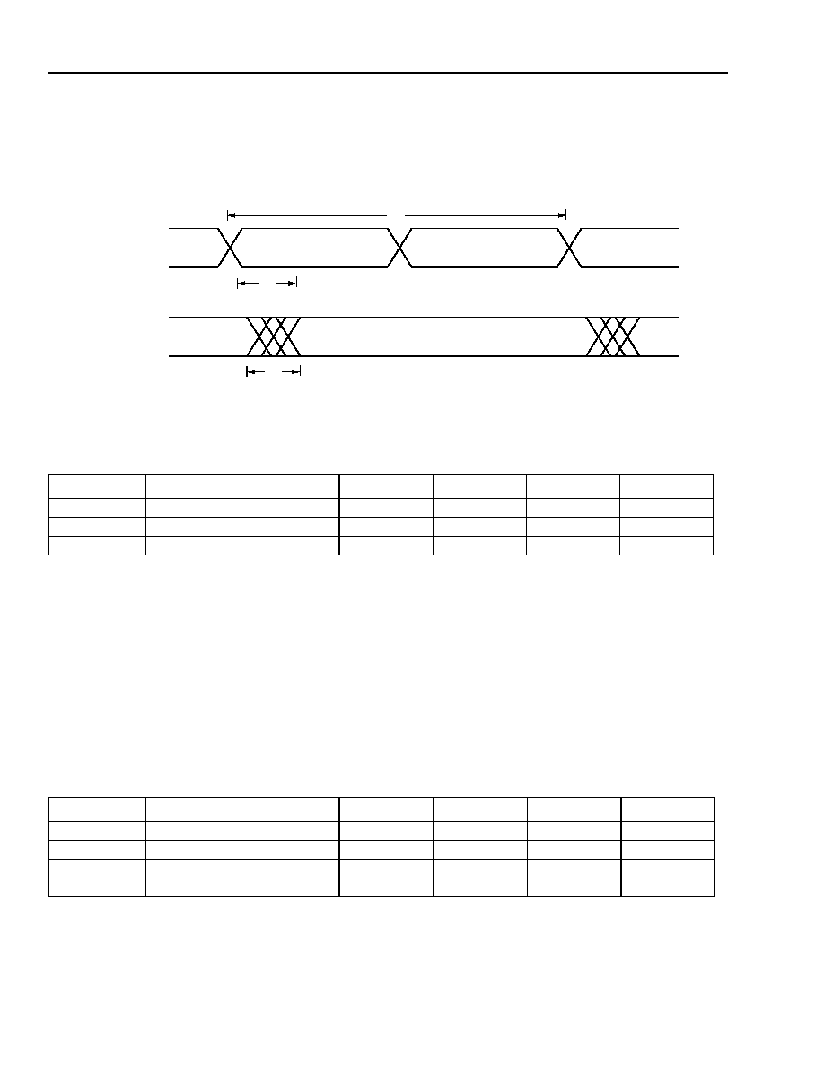
182
Agere Systems Inc.
Data Sheet
May 2003
STS-192 Overhead and Path Processor
TSOT0410G4 SONET/SDH
Timing Characteristics
(continued)
If the pointer processor is not bypassed, D_CLK and DFRM are inputs to the device and are used to clock out the
drop data. The drop clock signal has a frequency of 77.76 MHz, which is multiplexed/divided internally to provide a
622.08 MHz clock for the drop data signals.
5-9086.a (F)
Figure 23. Receive Frame Timing (Pointer Processor Active)
Table 256. Drop Frame Timing (Pointer Processor Active)
Receive Drop Section Data Com
The receive drop data com (RDDCC) input is provided to allow the D1, D2, and D3 to be used for data transmission
across a backplane, or between devices. Since the section TOH (RSOH) has been previously terminated, these
bytes are no longer used and are available. Use of this input is optional. There is a corresponding output on the
add interface, the TADCC. These outputs would output a similar, proprietary DCC message from another device, or
across a backplane.
The receive drop data com (RDDCC) pin is clocked in using the rising edge of the receive drop section data com
clock (RDDCK) pin. Generation of the signal feeding the RDDCC pin is intended to occur at the negative edge of
RDDCK signal. This clock signal, running at 192 kHz, is an output of the device. In reference to Figure 20 on
page 178, the timing characteristics for these pins are given in Table 257.
Table 257. RDDCC Timing
Symbol
Parameter
Min
Typ
Max
Unit
t5
Clock Period
--
12.86
--
ns
t6
DFRM Setup Time
0
--
--
ns
t7
DFRM Hold Time Required
3
--
--
ns
Symbol
Parameter
Min
Typ
Max
Unit
t27
Clock Period
--
5.208
--
Ķ
s
t28
Clock High Width
2.594
--
2.714
Ķ
s
t29
Data Setup Time Required
30
--
--
ns
t30
Data Hold Time Required
--
0
--
ns
D_CLK
DFRM
P
N
N
P
t5
t6
t7
Agere Systems Inc.
183
Data Sheet
May 2003
STS-192 Overhead and Path Processor
TSOT0410G4 SONET/SDH
Timing Characteristics
(continued)
Transmit Add Interface
Transmit Add Data
The transmit add pins, ADATA[16:1], are asynchronous inputs to the device, and while they do not have a phase
relationship to a clock, they are expected to have the same frequency as T_CLK (622.08 MHz). Furthermore, the
transmit add signals for a STS-48/STS-192 channel are expected to be aligned within 75 ns of each other.
Transmit Add Section Data Com
The transmit add data com (TADCC) output is provided to allow the D1, D2, and D3 to be used for data transmis-
sion across a backplane, or between devices. Since the section TOH (RSOH) has not yet been formed and path is
being input at the add interface, these bytes are available. Use of this output is optional. There is a corresponding
input on the add interface, the RDDCC. These inputs would be used to send a similar, proprietary DCC message to
another device, or across a backplane.
The transmit add section data com (TADCC) pins are timed using the rising edge of the transmit add section data
com clock (TADCK) pin. The data is clocked out at the rising edge of TADCK, and the TADCC pins should be read
at the negative edge of TADCK signal. The timing characteristics for these pins are given in Table 258. (See
Figure 16 on page 173.)
Table 258. TADCC Timing
Microprocessor Interface Timing
Synchronous Mode
The synchronous microprocessor interface mode is selected when MPMODE = 1. Interface timing for the synchro-
nous mode write cycle is given in Figure 24 on page 184 and in Table 260 on page 184. Interface timing for the
read cycle is given in Figure 25 on page 185 and in Table 262 on page 185.
The parity bits, PARITY_1 and PARITY_0, are optional and may be left unconnected if not used. If unused, TEA_N
should be ignored on a synchronous write.
Symbol
Parameter
Min
Typ
Max
Unit
t10
Clock Period
--
5.208
--
Ķ
s
t11
Clock High Width
2.594
--
2.714
Ķ
s
t12
Clock to Data Delay
30
--
--
ns
184
Agere Systems Inc.
Data Sheet
May 2003
STS-192 Overhead and Path Processor
TSOT0410G4 SONET/SDH
Timing Characteristics
(continued)
In synchronous mode, a transfer error (TA_N = 1, TEA_N = 0) will occur if the internal cycle is not terminated in
32 PCLK cycles from the first rising edge of PCLK, where CS_N = 0 and TS_N = 0.
5-9093(F)
Figure 24. Microprocessor Interface Synchronous Write Cycle (MPMODE = 1)
Table 259. TA_N/TEA_N Cycle Termination for Synchronous Write Cycle
Table 260. Microprocessor Interface Synchronous Write Cycle Specifications
TA_N
TEA_N
Encoding Description
0
0
Write data parity error.
0
1
Normal cycle termination.
1
0
Access to undefined address region--transfer error.
1
1
No cycle termination--processor generated time-out.
Symbol
Parameter
Min
Max
Unit
tc
PCLK Period
20
--
ns
tcycle
Bus Transfer Cycle Time
8
12
tc
t39
CS_N, TS_N, RW_N Valid to PCLK
4
--
ns
t40
ADDRESS, DATA Valid to PCLK
18
--
ns
t41
CS_N, TS_N, RW_N, ADDRESS, DATA Hold
2
--
ns
t42
PCLK to TA_N/TEA_N 3-State to High
3.5
13.5
ns
t43
PCLK to TA_N/TEA_N High to Low
5.5
15
ns
t44
PCLK to TA_N/TEA_N Low to High
5
13.5
ns
t45
PCLK to TA_N/TEA_N 3-State
--
4
ns
PCLK
ADDRESS_[15:0]
CS_N
TS_N
RW_N
TA_N/TEA_N
DATA_[15:0]/PARITY_[1:0]
(INPUT)
t39
t40
t42
t43
t44
t45
tc
t41
INSERTED
WAIT-
STATES
tcycle
HIGH Z
HIGH Z
Agere Systems Inc.
185
Data Sheet
May 2003
STS-192 Overhead and Path Processor
TSOT0410G4 SONET/SDH
Timing Characteristics
(continued)
5-9094(F)
Figure 25. Microprocessor Interface Synchronous Read Cycle (MPMODE = 1)
Table 261. TA_N/TEA_N Cycle Termination for Synchronous Read Cycle
Table 262. Microprocessor Interface Synchronous Read Cycle Specifications
TA_N
TEA_N
Encoding Description
0
0
Not possible during read cycle.
0
1
Normal cycle termination.
1
0
Access to undefined address region--transfer error.
1
1
No cycle termination--processor generated time-out.
Symbol
Parameter
Min
Max
Unit
t46
Data Valid to PCLK with TA_N Low
2
3
tc
t47
PCLK to DATA 3-State
2
--
ns
PCLK
ADDRESS_[15:0]
CS_N
TS_N
RW_N
TA_N/TEA_N
DATA_[15:0]/PARITY_[1:0]
(OUTPUT)
t39
t40
t42
t46
t47
t41
t44
t45
INSERTED
WAIT-
STATES
t47
tcycle
HIGH Z
HIGH Z

186
Agere Systems Inc.
Data Sheet
May 2003
STS-192 Overhead and Path Processor
TSOT0410G4 SONET/SDH
Timing Characteristics
(continued)
Asynchronous Mode
The asynchronous microprocessor interface mode is selected when MPMODE = 0. Interface timing for the asyn-
chronous mode write cycle is given in Figure 26 and in Table 263 below. Interface timing for the read cycle is given
in Figure 27 on page 187 and in Table 266 on page 187.
In asynchronous mode, the PCLK can be connected to a 77.76 MHz clock. This can be the same source as the
D_CLK input when DRPBYP = 0. If DRPBYP is 1, then the D_CLK output can be used. The microprocessor should
run at no more than half the frequency of PCLK in asynchronous mode. The timing numbers shown assume a
PCLK frequency of 77.76 MHz.
5-9095(F)
Figure 26. Microprocessor Interface Asynchronous Write Cycle (MPMODE = 0)
Table 263. Microprocessor Interface Asynchronous Write Cycle Specifications
Symbol
Parameter
Min
Max
Unit
tc
PCLK Period
12.86
15
ns
1
1. This value represents the timing for a transfer error (TA_N = 1, TEA_N = 0). The typical value during normal access would be 9 tc.
t48
ADDRESS Valid to CS_N/DS_N/TS_N Fall
0
--
ns
t49
TA_N Fall to CS_N/DS_N/TS_N Rise
0
--
ns
t50
TA_N Fall to DATA/ADDRESS Invalid
0
--
ns
t51
RW_N Fall to CS_N/DS_N/TS_N Fall
0
--
ns
t52
DS_N Rise to RW_N Rise
0
--
ns
t53
DATA Valid to DS_N Fall
0
--
ns
t54
CS_N/DS_N/TS_N Fall to TA_N/TEA_N High
4
--
tc
t55
CS_N/DS_N/TS_N Fall to TA_N/TEA_N Fall
5
35
1
tc
t56
CS_N/DS_N/TS_N Rise to TA_N/TEA_N Rise
43
54
ns
t57
CS_N/DS_N/TS_N Rise to TA_N/TEA_N 3-state
42
80
ns
ADDRESS_[15:0]
CS_N
TS_N
DS_N
RW_N
DATA_[15:0]
TA_N/TEA_N
(INPUT)
t48
t53
t54
t55
t56
t57
t52
t51
t48
HIGH Z
HIGH Z
t48
t49
t49
t49
t50
t51

Agere Systems Inc.
187
Data Sheet
May 2003
STS-192 Overhead and Path Processor
TSOT0410G4 SONET/SDH
Timing Characteristics
(continued)
Table 264. TA_N/TEA_N Cycle Termination for Asynchronous Write Cycle
5-9096(F)
Figure 27. Microprocessor Interface Asynchronous Read Cycle (MPMODE = 0)
Table 265. TA_N/TEA_N Cycle Termination for Asynchronous Read Cycle
Table 266. Microprocessor Interface Asynchronous Read Cycle Specifications
TA_N
TEA_N
Encoding Description
0
0
Not possible during asynchronous write cycle.
0
1
Normal cycle termination.
1
0
Access to undefined address region--transfer error.
1
1
No cycle termination--processor generated time-out.
TA_N
TEA_N
Encoding Description
0
0
Not possible during read cycle.
0
1
Normal cycle termination.
1
0
Access to undefined address region--transfer error.
1
1
No cycle termination--processor generated time-out.
Symbol
Parameter
Min
Max
Unit
t58
TA_N/TEA_N Valid to DATA Valid
13
15
ns
t59
CS_N/TS_N/DS_N Rise to DATA 3-State
43
56
ns
ADDRESS_[15:0]
CS_N
TS_N
DS_N
TA_N/TEA_N
DATA_[15:0]
t59
t57
t56
RW_N
t48
t48
t58
t55
t54
HIGH Z
HIGH Z
HIGH Z
HIGH Z
t48

188
Agere Systems Inc.
Data Sheet
May 2003
STS-192 Overhead and Path Processor
TSOT0410G4 SONET/SDH
Timing Characteristics
(continued)
Use of a Synchronous Microprocessor with the TSOT0410G4 in Asynchronous Mode
The use of a synchronous microprocessor (such as the M860/M8260) to communicate with a TSOT0410G4 config-
ured for asynchronous mode (MPMODE = 0) requires one additional consideration. There is a difference between
the operation of a synchronous processor (e.g., M860/M8260) and the asynchronous processors (e.g., 68360). In
a synchronous processor, the data is latched on the same edge that detects the assertion of TA_N. In an asynchro-
nous processor, the TA_N (DSACK) signal is detected, and the data is latched one clock period later.
In both cases, the TSOT0410G4 meets the timing required by these two different processors. However, a synchro-
nous processor operating with the TSOT0410G4 configured in asynchronous mode will have problems consis-
tently latching the correct data. It will depend on the relationship between the two clocks. As shown in Figure 27 on
page 187, the data is presented on the bus 13 ns--15 ns after TA_N is asserted. If the microprocessor has a rising
edge within this window, it will capture incorrect data.
To operate the TSOT in asynchronous mode with an synchronous processor, add a delay on the TA_N signal from
the TSOT0410G4; otherwise, consider using synchronous mode.
Agere Systems Inc.
189
Data Sheet
May 2003
STS-192 Overhead and Path Processor
TSOT0410G4 SONET/SDH
Outline Diagram
600-Pin LBGA
Dimensions are in millimeters.
5-9212.a (F)
45.00
45.00
A1 BALL
T
D
H
AL
F
K
B
P
M
L
J
AH
R
C
E
Y
N
U
AN
G
AD
V
AM
AJ
AG
AE
AC
AA
W
AP
AK
AF
AB
AR
A
34 SPACES @ 1.27 = 43.18
34 SPACES
A1 BALL
0.75
Ī
0.15
IDENTIFIER ZONE
@ 1.27 = 43.18
CORNER
1.95/2.35
SEATING PLANE
SOLDER BALL
0.60
Ī
0.10
0.20
1.45/1.85
ELECTRICALLY ISOLATED
HEAT SPREADER
2.45/3.05
41.3/42.3
41.3/42.3
19
30
26
28
24
32
22 20 18
4
6
8
10
12
14
16
2
34
5
23
25
7
31 29
15
21
3
27
11
17
9
13
1
35 33

Data Sheet
May 2003
STS-192 Overhead and Path Processor
TSOT0410G4 SONET/SDH
Copyright © 2003 Agere Systems Inc.
All Rights Reserved
May 2003
DS02-252SONT-1 (Replaces DS02-252SONT)
Agere Systems Inc. reserves the right to make changes to the product(s) or information contained herein without notice. No liability is assumed as a result of their use or application. Agere,
Agere Systems, and the Agere Logo are trademarks of Agere Systems Inc.
For additional information, contact your Agere Systems Account Manager or the following:
INTERNET:
http://www.agere.com
E-MAIL:
docmaster@agere.com
N. AMERICA: Agere Systems Inc., Lehigh Valley Central Campus, Room 10A-301C, 1110 American Parkway NE, Allentown, PA 18109-9138
1-800-372-2447, FAX 610-712-4106 (In CANADA: 1-800-553-2448, FAX 610-712-4106)
ASIA:
Agere Systems Hong Kong Ltd., Suites 3201 & 3210-12, 32/F, Tower 2, The Gateway, Harbour City, Kowloon
Tel. (852) 3129-2000, FAX (852) 3129-2020
CHINA: (86) 21-5047-1212 (Shanghai), (86) 755-25881122 (Shenzhen)
JAPAN: (81) 3-5421-1600 (Tokyo), KOREA: (82) 2-767-1850 (Seoul), SINGAPORE: (65) 6778-8833, TAIWAN: (886) 2-2725-5858 (Taipei)
EUROPE:
Tel. (44) 1344 296 400
Ordering Information
IEEE is a registered trademark of The Institute of Electrical and Electronics Engineers, Inc.
EIA is a registered trademark of The Electronic Industries Association.
Motorola is a registered trademark of Motorola, Inc.
Device Code
Package
Temperature
Comcode
TSOT0410G14
600-pin LBGA
≠40 įC to +85 įC
700017424