Product Brief
September 2000
TSWC01622 SONET/SDH/PDH/ATM
Clock Synthesizer and Protection Switch
Features
s
Fully-integrated clock synthesis
s
Clock or sync protection switching
s
Fast, autonomous switching with software-override
capability
s
Supports a wide choice of SONET/SDH/ATM
output clock frequencies:
622.08 MHz
155.52 MHz
77.76 MHz
51.84 MHz
44.736 MHz
38.88 MHz
34.368 MHz
32.768 MHz
24.704 MHz
19.44 MHz
16.384 MHz
8.192 MHz
4.096 MHz
2.43 MHz
2.048 MHz
1.544 MHz
s
Supports multiple input clock frequencies:
51.84 MHz
38.88 MHz
19.44 MHz
8.192 MHz
6.48 MHz
2.048 MHz
1.544 MHz
8 kHz
s
Generates sync outputs at 8 kHz aligned to an
8 kHz input clock/sync
s
Locks to backup reference clock if both working
and protection reference clocks are lost
s
Compatible with Lucent Technologies TTRN012G5
2.5 Gbits/s MUX/Synthesizer, TDAT042G5/
TADM042G5 SONET/ATM/POS devices,
TSOT0410G, and TMXF28155 Super Mapper
s
Single 3.3 V supply
s
Supports multiple output levels: CMOS, LVPECL,
or LVDS
Applications
s
SONET/SDH and PDH add/drop multiplexers
s
SONET/SDH and PDH cross connects
s
ATM and packet over SONET switches and routers
s
SONET/SDH and PDH test equipment
s
Remote access servers
Description
The Lucent Technologies Microelectronics Group
TSWC01622 is designed for a wide variety of syn-
chronous timing applications. It serves as a clock
synthesizer and low-skew clock fanout device gener-
ating clocks at frequencies up to 622.08 MHz that are
synchronized to the system reference clock. It also
serves as an intelligent clock protection switch with
fast, autonomous selection based on the presence of
the two input clocks. Alternatively, clock switching
can be controlled entirely through a software inter-
face.
The TSWC01622 also delivers an output sync signal
that is aligned to the input clock. If 8 kHz system sync
signals are applied as the clock A and clock B inputs,
the TSWC01622 will generate an output sync signal
that is phase-aligned to the selected input sync. A
programmable phase offset is provided to allow the
user to offset the output sync relative to the input
sync. The output sync can be used for global align-
ment of cells or frames in SONET/SDH/PDH cross
connects or ATM switch applications. The device
allows flexible choices of LVDS, LVPECL, or CMOS
input and output levels.
The TSWC01622 is intended for clock distribution
and protection switching on a line card, a switch
card, or a shelf timing card. Along with the wide vari-
ety of input and output frequencies, a unique feature
of the device is a guaranteed correct number of out-
put clock cycles between output sync pulses before,
during, and after a clock selection switching event.
The number of clock cycles between sync pulses
remains correct even during a switch between work-
ing and protection clock sources that have an arbi-
trary phase relationship between them. The
TSWC01622 also solves the skew problem associ-
ated with timing distribution over cable or backplane
traces of different lengths.
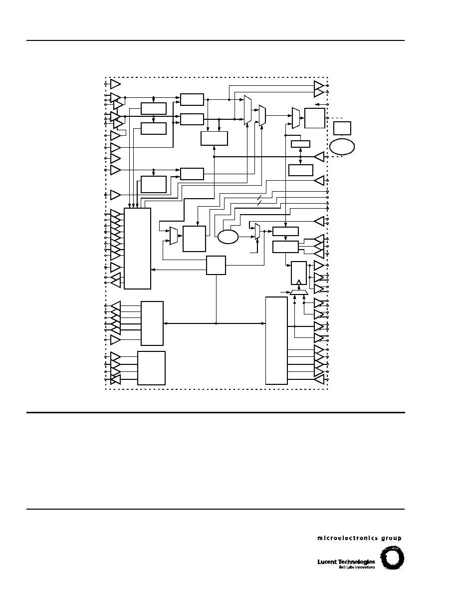
The block diagram is shown on the next page. Note
that the diagram is representative of device function-
ality and conceptual signal flow. Internal implementa-
tion details may be different than shown.
TSWC01622 SONET/SDH/PDH/ATM
Product Brief
Clock Synthesizer and Protection Switch
September 2000
Lucent Technologies Inc. reserves the right to make changes to the product(s) or information contained herein without notice. No liability is assumed as a result of their use or application. No
rights under any patent accompany the sale of any such product(s) or information.
Copyright � 2000 Lucent Technologies Inc.
All Rights Reserved
September 2000
PB00-144HSPL
For additional information, contact your Microelectronics Group Account Manager or the following:
INTERNET:
http://www.lucent.com/micro
E-MAIL:
docmaster@micro.lucent.com
N. AMERICA:
Microelectronics Group, Lucent Technologies Inc., 555 Union Boulevard, Room 30L-15P-BA, Allentown, PA 18109-3286
1-800-372-2447, FAX 610-712-4106 (In CANADA: 1-800-553-2448, FAX 610-712-4106)
ASIA PACIFIC: Microelectronics Group, Lucent Technologies Singapore Pte. Ltd., 77 Science Park Drive, #03-18 Cintech III, Singapore 118256
Tel. (65) 778 8833, FAX (65) 777 7495
CHINA:
Microelectronics Group, Lucent Technologies (China) Co., Ltd., A-F2, 23/F, Zao Fong Universe Building, 1800 Zhong Shan Xi Road, Shanghai
200233 P. R. China Tel. (86) 21 6440 0468, ext. 325, FAX (86) 21 6440 0652
JAPAN:
Microelectronics Group, Lucent Technologies Japan Ltd., 7-18, Higashi-Gotanda 2-chome, Shinagawa-ku, Tokyo 141, Japan
Tel. (81) 3 5421 1600, FAX (81) 3 5421 1700
EUROPE:
Data Requests: MICROELECTRONICS GROUP DATALINE: Tel. (44) 7000 582 368, FAX (44) 1189 328 148
Technical Inquiries: GERMANY: (49) 89 95086 0 (Munich), UNITED KINGDOM: (44) 1344 865 900 (Ascot),
FRANCE: (33) 1 40 83 68 00 (Paris), SWEDEN: (46) 8 594 607 00 (Stockholm), FINLAND: (358) 9 3507670 (Helsinki),
ITALY: (39) 02 6608131 (Milan), SPAIN: (34) 1 807 1441 (Madrid)
Description
(continued)
0795(F)r.1
Figure 1. Functional Block Diagram of TSWC01622
SDHSEL[3:0]
CK19
CK38
CK51
CK77
CK155N[1:0]
CK155P[1:0]
PCK155N[1:0]
PCK155P[1:0]
CK622N[1:0]
CK622P[1:0]
PCK622N[1:0]
PCK622P[1:0]
SYPCLN[1:0]
SYPCLP[1:0]
SYLVSN[1:0]
SYLVSP[1:0]
SYNC8K
SYDU
SYOFFPOS
SYOFF[9:0]
TSTCLKN
TSTCLKP
VBB
VNGATES
VC[P:N]
LF[P:N]
INLOSN
LSVCO
LOOP
LF[2:0]
RREF
MONB
MONA
PD
DIVIDE
LOC
DIVIDE
SYNC
OFFSET
D
Q
BASED ON SDHSEL
SONET
CLOCK
GEN.
DIVIDE
ENABLE
VCO
CHARGE
PD
LOSS OF
CONTROL
AND
SWITCH
STATE
MACHINE
PDH
CLOCK
GEN.
INTERNAL
TEST
CONTROL
PHASE
COMPARE
LOSS OF
DIVIDE
RSVA
CLKAP
CLKAN
CLKA
CLKBP
CLKBN
CLKB
SELLVDS
FINSEL[3:0]
RSVB
CLKBU
FBUSEL[3:0]
SELCLK
SELBUN
AUTOSWN
REVERTN
SWCONTN
ENSQLN
ENLON
LORSTN
RESETN
SWSTATE[1:0]
INT[8:0]
CKPDH5
CKPDH4
CKPDH3
CKPDH2
CKPDH1
PDHSEL[3:0]
TSTMODE
SERCLK
SERENBLN
SERDAT
CLOCK A
LOSS OF
CLOCK B
BY M
DIVIDE
BY M
DIVIDE
BY N
CLOCK
BACKUP
TEST
CLOCK
PUMP/
LOOP
FILTER
38.88 MHz
CHARGE
PUMP
FILTER
VCXO
38.88 MHz