 | –≠–ª–µ–∫—Ç—Ä–æ–Ω–Ω—ã–π –∫–æ–º–ø–æ–Ω–µ–Ω—Ç: TTRN0110G | –°–∫–∞—á–∞—Ç—å:  PDF PDF  ZIP ZIP |

Data Sheet
March 29, 2002
TTRN0110G
10 Gbits/s Clock Synthesizer, 16:1 Data Multiplexer
Features
s
Supports standard OC-192/STM-64 data rate of
9.95328 Gbits/s up through forward error correc-
tion (FEC) rate of 10.7092 Gbits/s as well as the
Ethernet rate of 10.3125 Gbits/s
s
Supports clockless data transfer mode
s
Supports forward directional clocking for parallel
transfer of input data with 311 MHz or 622 MHz
clocks
s
Supports contradirectional clocking for parallel
transfer of input data based on a 622 MHz output
clock
s
Allows a 155.52 MHz or 622.08 MHz reference
clock using common phase-locked loop (PLL) loop
components
s
Additional 10 Gbits/s current-mode logic (CML)
serial data output for system loopback
s
Supports 10 GHz clock output for clocked laser
driver applications
s
Loss of lock indication
s
Single 3.3 V supply
s
Low-voltage differential signaling (LVDS)
622.08 Mbits/s signal I/Os
s
CMOS I/Os compatible with low-voltage transistor-
transistor logic (LVTTL) signaling
s
Power dissipation as low as 1.35 W
s
Available in a 198-ball grid array (CBGA) package
s
Jitter generation/transfer compliant with the
following:
-- Telcordia TechnologiesTM GR-253 CORE
-- ITU-T G.825
-- ITU-T G.958
Applications
s
SONET/SDH optical modules
s
SONET/SDH line origination equipment
s
SONET/SDH add/drop multiplexers
s
SONET/SDH cross connects
s
SONET/SDH test equipment
s
Digital video transmission
Description
The Agere Systems Inc. TTRN0110G device
provides a 16:1 multiplexer, accepts 16 differential
LVDS data inputs and a 155.52 MHz or 622.08 MHz
reference clock, and generates a CML 10 Gbits/s
clock and data output. Both forward directional and
contradirectional clocking schemes are supported for
transferring data across the parallel interface. When
contraclocking is used, the TTRN0110G provides
one of four phases of a 622.08 MHz clock output
back upstream to the data chip. The device also
supports a clockless parallel data transfer mode. The
TTRN0110G can be operated within the standard
OC-192/STM-64 data rate of 9.9532 GHz and the
FEC rate of 10.7092 Gbits/s.

Table of Contents
Contents
Page
2
Agere Systems Inc.
Data Sheet
March 29, 2002
10 Gbits/s Clock Synthesizer, 16:1 Data Multiplexer
TTRN0110G
Features .................................................................................................................................................................... 1
Applications ............................................................................................................................................................... 1
Description................................................................................................................................................................. 1
Block Diagram......................................................................................................................................................... 3
Ball Information.......................................................................................................................................................... 4
Ball Diagram ........................................................................................................................................................... 4
Ball Assignments .................................................................................................................................................... 5
Ball Description ....................................................................................................................................................... 7
Functional Overview ................................................................................................................................................ 11
Ethernet and FEC Rate Support.............................................................................................................................. 11
Clock Synthesizer Operation ................................................................................................................................... 11
Clock Synthesizer Loop Filter ............................................................................................................................... 11
Clock Synthesizer Settling Time ........................................................................................................................... 12
Loss of Lock Indicator (LCKLOSSN) .................................................................................................................... 12
Clock Synthesizer Generated Jitter ...................................................................................................................... 12
Clock Synthesizer Jitter Transfer .......................................................................................................................... 13
Multiplexer Operation .............................................................................................................................................. 14
10 GHz Clock Output Enable (ENCK10G)............................................................................................................14
Loopback 10 GHz Data Output (LBDP/N, ENLBDN) ............................................................................................ 14
Reset (RESETN)................................................................................................................................................... 14
Clocking Modes and Timing Adjustments ............................................................................................................... 15
Forward Directional 622 Clocking Mode (CLKMOD[1:0] = 00, EXTCNTR, PICLKP/N, OVRFLW) ...................... 15
Forward Directional 311 Clocking Mode (CLKMOD[1:0] = 10, EXTCNTR, PICLKP/N, OVRFLW) ...................... 15
Contradirectional Clocking Mode (CLKMOD[1:0] = 01, PHADJ[1:0], EXTCNTR) ................................................ 16
Clockless Transfer Mode (CLKMOD[1:0]= 11, EXTCNTR) ..................................................................................17
CML Output Structure (Used on Balls D10GP/N, CK10GP/N, LBDP/N)................................................................. 18
Absolute Maximum Ratings.....................................................................................................................................19
Handling Precautions .............................................................................................................................................. 19
Recommended Operating Conditions ..................................................................................................................... 19
Electrical Characteristics ......................................................................................................................................... 20
LVDS, CMOS, CML Inputs and Outputs ............................................................................................................... 20
Frequency Characteristics....................................................................................................................................... 22
Reference Frequency (REFCLKP/N, REFFREQ) (Standard SONET Rate)......................................................... 22
Reference Frequency (REFCLKP/N, REFFREQ) (FEC Rate) ............................................................................. 22
Timing Characteristics ............................................................................................................................................. 23
Transmit Timing .................................................................................................................................................... 23
Packaging Characteristics ....................................................................................................................................... 27
Package Crush Characteristics............................................................................................................................. 27
CBGA Package Information .................................................................................................................................. 27
PWB Design Information....................................................................................................................................... 27
Assembly Information ...........................................................................................................................................28
Reference Materials.............................................................................................................................................. 28
Package Diagram--198-Ball CBGA (Bottom View) .............................................................................................. 29
Ordering Information................................................................................................................................................ 30

Agere Systems Inc.
3
Data Sheet
March 29, 2002
10 Gbits/s Clock Synthesizer, 16:1 Data Multiplexer
TTRN0110G
Description
(continued)
Block Diagram
0356.a(F)
Note: Diagram is representative of device functionality and conceptual signal flow. Internal implementation details may be different than shown.
Figure 1. Functional Block Diagram of TTRN0110G
D0P
D0N
D1P
D1N
D15P
D15N
OVERFLOW
EXTCNTR
CLKMOD[1:0]
PICLKP
PICLKN
ENCK155N
CK155P
CK155N
CK622P
CK622N
PHADJ[1:0]
REFFREQ
REFCLKP
REFCLKN
LCKLOSSN
ACQUISITION
INDICATOR
MANUAL
PHASE
ADJUST
DIVIDE
BY 4
DECODE
TIMING GENERATION
IN
P
U
T
PHASE/
FREQ.
DETECTOR
CHARGE
PUMP
DIVIDE
BY 16
RE
GIS
T
E
R
DAT
A
BUFF
ER
16:
1
M
U
L
T
I
P
L
EXER
DATA
RETIME
TO DIGITAL LOGIC
RESETN
ENLBDN
LBDP
LBDN
D10GP
D10GN
INVDATN
ENCK10G
CK10GP
CK10GN
RREFCML
RREFVCO
RREFLVDS
TESTN
TSTCKP
FECN
0
1
LFP
LFN
VCO
TEST

4
Agere Systems Inc.
Data Sheet
March 29, 2002
10 Gbits/s Clock Synthesizer, 16:1 Data Multiplexer
TTRN0110G
Ball Information
Ball Diagram
0642.a(F)
Figure 2. TTRN0110G CBGA Ball Diagram (198-ball)
D
E
F
G
H
J
K
L
N
P
C
B
A
M
R
1
2
3
4
5
6
7
8
9
10
11
12
13
14
15
TOP VIEW
Agere Systems Inc.
5
Data Sheet
March 29, 2002
10 Gbits/s Clock Synthesizer, 16:1 Data Multiplexer
TTRN0110G
Ball Information
(continued)
Ball Assignments
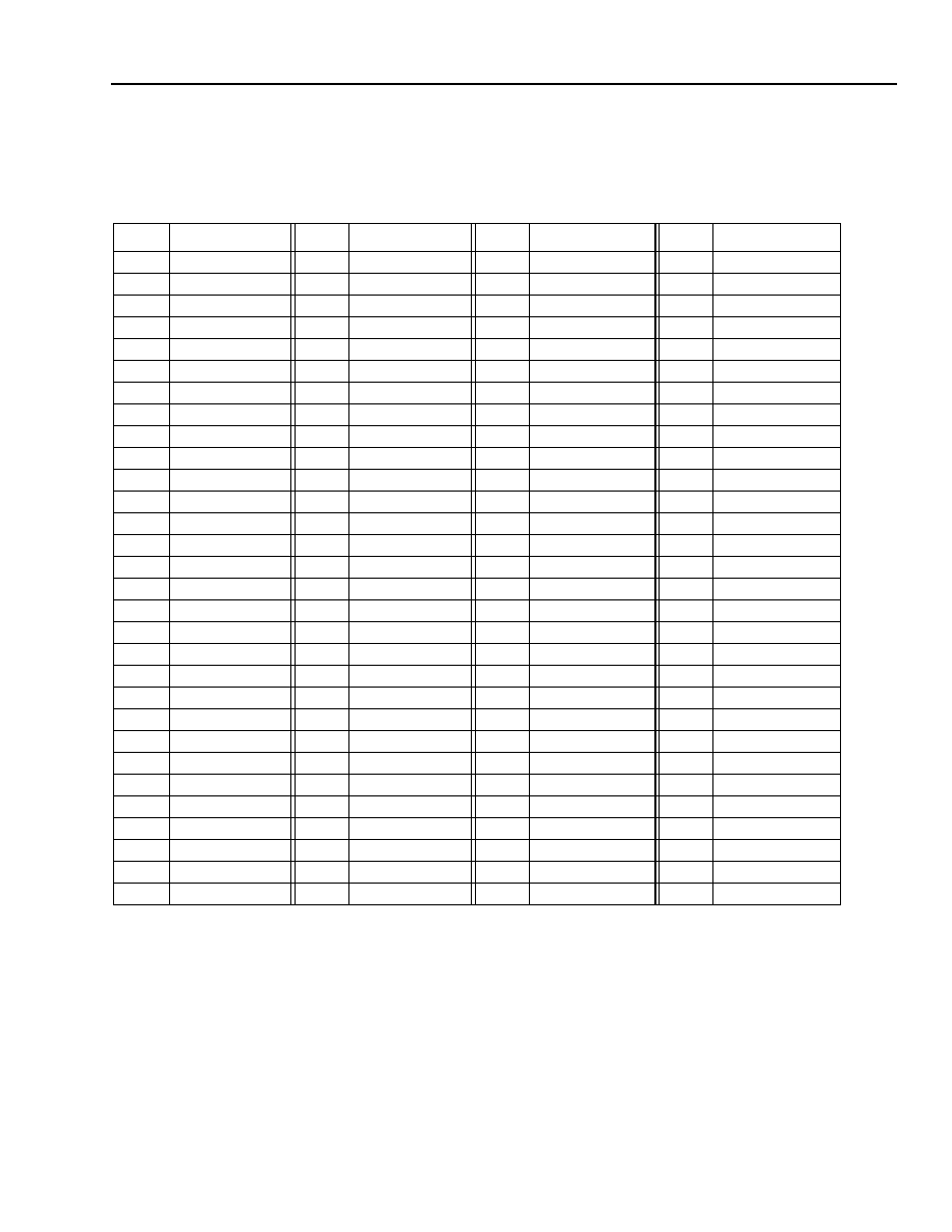
Table 1. Ball Assignments for 198-Ball CBGA by Ball Number Order
Note: -- refers to no ball. A ball has been removed for routing purposes.
Ball
Signal Name
Ball
Signal Name
Ball
Signal Name
Ball
Signal Name
A1
GND
C1
GND
E1
GND
G1
GND
A2
GND
C2
GND
E2
GND
G2
GND
A3
GND
C3
GND
E3
GND
G3
GND
A4
GND
C4
V
CCD
E4
GND
G4
GND
A5
CK10GN
C5
--
E5
--
G5
V
CCD
A6
GND
C6
GND
E6
GND
G6
GND
A7
CK10GP
C7
--
E7
INVDATN
G7
GND
A8
GND
C8
--
E8
GND
G8
GND
A9
D10GN
C9
--
E9
TESTN
G9
GND
A10
GND
C10
GND
E10
GND
G10
GND
A11
D10GP
C11
--
E11
GND
G11
GND
A12
GND
C12
GND
E12
GND
G12
LCKLOSSN
A13
GND
C13
--
E13
V
CCA
G13
--
A14
GND
C14
--
E14
V
CCA
G14
V
CCD
A15
GND
C15
TSTCKP
E15
LFN
G15
V
CCA
B1
GND
D1
LBDP
F1
LBDN
H1
V
CCD
B2
GND
D2
--
F2
--
H2
GND
B3
GND
D3
--
F3
--
H3
GND
B4
GND
D4
--
F4
--
H4
--
B5
--
D5
GND
F5
GND
H5
GND
B6
GND
D6
--
F6
GND
H6
GND
B7
--
D7
V
CCD
F7
ENLBDN
H7
GND
B8
GND
D8
RREFCML
F8
GND
H8
GND
B9
--
D9
V
CCD
F9
ENCK10G
H9
GND
B10
GND
D10
--
F10
GND
H10
GND
B11
--
D11
GND
F11
GND
H11
GND
B12
GND
D12
--
F12
RREFLVDS
H12
GND
B13
V
CCD
D13
GND
F13
V
CCA
H13
GND
B14
GND
D14
GND
F14
RREFVCO
H14
RESETN
B15
GND
D15
GND
F15
LFP
H15
CLKMOD[0]

6
Agere Systems Inc.
Data Sheet
March 29, 2002
10 Gbits/s Clock Synthesizer, 16:1 Data Multiplexer
TTRN0110G
Ball Information
(continued)
Ball Assignments
(continued)
Table 1. Ball Assignments for 198-Ball CBGA by Ball Number Order (continued)
Note: -- refers to no ball. A ball has been removed for routing purposes.
Ball
Signal Name
Ball
Signal Name
Ball
Signal Name
Ball
Signal Name
J1
D0P
L1
D1P
N1
D2P
R1
GND
J2
GND
L2
GND
N2
D3P
R2
D5P
J3
GND
L3
GND
N3
D4N
R3
D5N
J4
GND
L4
GND
N4
GND
R4
D6N
J5
V
CCD
L5
GND
N5
D7N
R5
D8N
J6
V
CCD
L6
V
CCD
N6
GND
R6
D9N
J7
GND
L7
GND
N7
D10N
R7
D11P
J8
GND
L8
V
CCD
N8
D12P
R8
D11N
J9
GND
L9
--
N9
GND
R9
D13P
J10
GND
L10
GND
N10
D15N
R10
D14P
J11
GND
L11
GND
N11
GND
R11
CK155P
J12
GND
L12
GND
N12
GND
R12
PICLKP
J13
V
CCD
L13
GND
N13
GND
R13
CK622P
J14
OVRFLW
L14
PHADJ[1]
N14
REFCLKP
R14
GND
J15
CLKMOD[1]
L15
REFFREQ
N15
GND
R15
GND
K1
D0N
M1
D1N
P1
D2N
K2
GND
M2
GND
P2
D3N
K3
GND
M3
D4P
P3
GND
K4
GND
M4
GND
P4
D6P
K5
--
M5
D7P
P5
D8P
K6
GND
M6
GND
P6
D9P
K7
GND
M7
GND
P7
D10P
K8
GND
M8
--
P8
D12N
K9
V
CCD
M9
GND
P9
D13N
K10
GND
M10
D15P
P10
D14N
K11
V
CCD
M11
GND
P11
CK155N
K12
--
M12
GND
P12
PICLKN
K13
ENCK155N
M13
GND
P13
CK622N
K14
FECN
M14
REFCLKN
P14
GND
K15
EXTCNTR
M15
PHADJ[0]
P15
GND

Agere Systems Inc.
7
Data Sheet
March 29, 2002
10 Gbits/s Clock Synthesizer, 16:1 Data Multiplexer
TTRN0110G
Ball Information
(continued)
Ball Description
Note: In Table 2, when operating the TTRN0110G device at the OC-192/STM-64 rate, 10 Gbits/s should be
interpreted as 9.9532 Gbits/s. When operating the TTRN0110G device at the Ethernet rate, 10 Gbits/s
should be interpreted as 10.3125 Gbits/s. When operating the TTRN0110G device at RS FEC OC-192/
STM64 rates, 10 Gbits/s should be interpreted as 10.6642 Gbits/s or 10.7092 Gbits/s.
Table 2. Ball Descriptions--10 Gbits/s and Related Signals
Ball
Symbol
*
* Differential pairs are indicated by P and N suffixes. For nondifferential pins, N at the end of the symbol name designates active-low.
Type
I = input, O = output. I
u
indicates an internal pull-up resistor on this pin. I
d
indicates an internal pull-down resistor on this pin. I
t
= an
internal termination resistance of 50
to V
CCD
on this pin.
Level
Name/Description
A11
A9
D10GP
D10GN
O
CML
Data Output (10 Gbits/s NRZ). 10 Gbits/s differential data
output.
Note: This data rate will scale when operating at different rates.
D1
F1
LBDP
LBDN
O
CML
Loopback Data Output. Additional 10 Gbits/s differential data
output for system loopback.
Note: This data rate will scale when operating at different rates.
A7
A5
CK10GP
CK10GN
O
CML
Clock Output (10 GHz). 10 GHz differential clock output.
Note: This clock rate will scale when operating at different rates.
K14
FECN
I
u
CMOS
FEC Rate (Active-Low). Selects between two operating rate
ranges within the OC-192/STM-64 rate of 9.9532 GHz and the
FEC rate of 10.7092 GHz.
0 = Will extend the operating range out to the FEC rate of
10.7092 GHz.
1 or no connection = OC-192/STM-64 rate of 9.9532 GHz to the
Ethernet rate of 10.3 GHz.
Note: All input and output SONET/SDH clock and data rates will
scale when operating at different rates.
D8
RREFCML
I
Analog
Resistor Reference CML. CML current bias reference resistor.
F9
ENCK10G
I
u
CMOS
Enable CK10GP/N Clock Output.
0 = CK10GP/N buffer powered off.
1 or no connection = CK10GP/N buffer enabled.
F7
ENLBDN
I
u
CMOS
Enable LBDP/N Data Output (Active-Low).
0 = LBDP/N buffer enabled.
1 or no connection = LBDP/N buffer powered off.
E7
INVDATN
I
u
CMOS
Invert D10G Data Output (Active-Low).
0 = Invert.
1 or no connection = Noninvert.
C15
TSTCKP
I
t
CML
Test Clock Input. (Buffer is powered down when TESTN = 1.)
E9
TESTN
I
u
CMOS
Select Test Clock (Active-Low).
0 = Select test clock.
1 or no connection = Select VCO.
F14
RREFVCO
I
Analog
Resistor Reference VCO. VCO bias reference resistor. Connect
an 806 k
resistor to V
CCD
.

8
Agere Systems Inc.
Data Sheet
March 29, 2002
10 Gbits/s Clock Synthesizer, 16:1 Data Multiplexer
TTRN0110G
Ball Information
(continued)
Ball Description
(continued)
Note: In Table 3, when operating the TTRN0110G device at the OC-192/STM-64 rate, 622 Mbits/s and
155 Mbits/s should be interpreted as 622.08 Mbits/s and 155.52 Mbits/s, respectively. When operating the
TTRN0110G device at the Ethernet rate, 622 Mbits/s and 155 Mbits/s should be interpreted as
641.52 Mbits/s and 166.63 Mbits/s, respectively. When operating the TTRN0110G device at the RS FEC
OC-192/STM-64 rates, 622 Mbits/s and 155 Mbits/s should be interpreted as 669.33 Mbits/s and
167.33 Mbits/s, respectively.
Table 3. Ball Descriptions--622.08 Mbits/s and Related Signals
Ball
Symbol
*
* Differential pairs are indicated by P and N suffixes. For nondifferential pins, N at the end of the symbol name designates active-low.
Type
I = input, O = output. I
u
indicates an internal pull-up resistor on this pin. I
d
indicates an internal pull-down resistor on this pin. I
t
= an
internal termination resistance of 50
to V
CCD
on this pin.
Level
Name/Description
M10
N10
R10
P10
R9
P9
N8
P8
R7
R8
P7
N7
P6
R6
P5
R5
M5
N5
P4
R4
R2
R3
M3
N3
N2
P2
N1
P1
L1
M1
J1
K1
D15P
D15N
D14P
D14N
D13P
D13N
D12P
D12N
D11P
D11N
D10P
D10N
D9P
D9N
D8P
D8N
D7P
D7N
D6P
D6N
D5P
D5N
D4P
D4N
D3P
D3N
D2P
D2N
D1P
D1N
D0P
D0N
I
LVDS
Data Input (622 Mbits/s). 622 Mbits/s differential data input.
D15 is the most significant bit and is transmitted first on the
D10GP/N output.
Note: This data rate will scale when operating at different rates.

Agere Systems Inc.
9
Data Sheet
March 29, 2002
10 Gbits/s Clock Synthesizer, 16:1 Data Multiplexer
TTRN0110G
Ball Information
(continued)
Ball Description
(continued)
Table 3. Ball Descriptions--622.08 Mbits/s and Related Signals (continued)
Ball
Symbol
*
* Differential pairs are indicated by P and N suffixes. For nondifferential pins, N at the end of the symbol name designates active-low.
Type
I = input, O = output. I
u
indicates an internal pull-up resistor on this pin. Id indicates an internal pull-down resistor on this pin. It = an
internal termination resistance of 50
to V
CCD
on this pin.
Level
Name/Description
R13
P13
CK622P
CK622N
O
LVDS
Clock Output (622 MHz). 622 MHz differential clock output.
Note: This clock frequency will scale when operating at different rates.
M15
L14
PHADJ[0]
PHADJ[1]
I
d
CMOS
Phase Adjust. Adjusts phase of CK622 in 90 degree steps.
R11
P11
CK155P
CK155N
O
LVDS
Clock Output (155 MHz). 155 MHz differential clock output.
Note: This clock frequency will scale when operating at different rates.
K13
ENCK155N
I
u
CMOS
Enable CK155P/N Clock Output (Active-Low).
0 = CK155P/N buffer enabled.
1 or no connection = CK155P/N buffer powered off.
R12
P12
PICLKP
PICLKN
I
LVDS
Parallel Input Clock (622 MHz 311 MHz). 622 MHz or 311 MHz
differential clock input used to register parallel data when using forward
directional clocking mode.
Note: This clock frequency will scale when operating at different rates.
H15
J15
CLKMOD[0]
CLKMOD[1]
I
u
CMOS
Clock Mode Select. Selects clocking method for data transfer mode.
[0] [1]
0 0 = Forward directional clocking mode (622 MHz).
0 1 = Forward directional clocking mode (311 MHz).
1 0 = Contraclocking mode.
1 1 or no connections = Clockless mode.
G12
LCKLOSSN
O
CMOS
Loss of Lock (Active-Low).
0 = PLL out of lock.
K15
EXTCNTR
I
d
CMOS
External Center. Centers the pointers in the parallel data storage
element. Connected to OVRFLW for fastest FIFO overrun recovery.
J14
OVRFLW
O
CMOS
Data Storage Overflow. Indicates (active-high) when an overflow has
occurred in the parallel data storage element.
N14
M14
REFCLKP
REFCLKN
I
LVDS
Reference Clock Input (622.08 MHz or 155.52 MHz).
Note: This clock frequency will scale when operating at different rates.
L15
REFFREQ
I
u
CMOS
Reference Clock Frequency. Selects frequency of REFCLKP/N.
0 = 155 MHz.
1 or no connection = 622 MHz.
F15
E15
LFP
LFN
I
Analog Loop Filter PLL. Connect LFP and LFN to loop filter (see Table 6 on
page 11).
F12
RREFLVDS
I
Analog Resistor Reference LVDS. LVDS bias reference resistor. Connect a
1.5 k
resistor to V
CCD
.

10
Agere Systems Inc.
Data Sheet
March 29, 2002
10 Gbits/s Clock Synthesizer, 16:1 Data Multiplexer
TTRN0110G
Ball Information
(continued)
Ball Description
(continued)
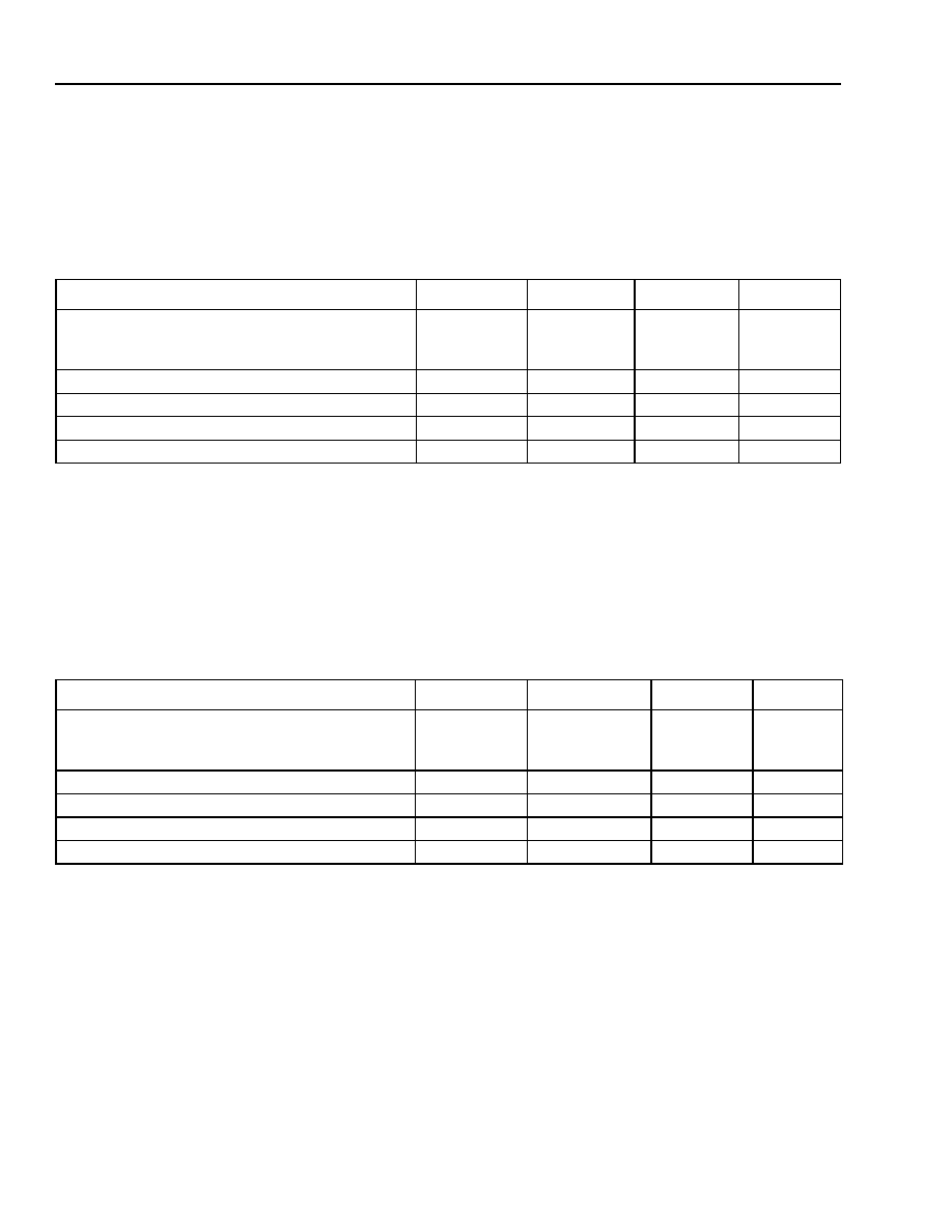
Table 4. Ball Descriptions--Reset
Table 5. Ball Descriptions--Power and Ground
Note: V
CCA
and V
CCD
have the same dc value, which is represented as V
CC
unless otherwise specified. However,
high-frequency filtering is suggested between the individual supplies.
Ball
Symbol
*
* Differential pairs are indicated by P and N suffixes. For nondifferential pins, N at the end of the symbol name designates active-low.
Type
I = input, O = output. I
u
indicates an internal pull-up resistor on this pin. I
d
indicates an internal pull-down resistor on this pin. I
t
= an
internal termination resistance of 50
to V
CCD
on this pin.
Level
Name/Description
H14
RESETN
I
u
CMOS
Reset (Active-Low). Resets all synchronous logic. During a reset, the
true data outputs are in the low state and the barred data outputs are in
the high state. Reset must be held active low for a minimum of 6.4 ns
while the internal oscillator is active.
0 = Reset.
1 or no connection = Normal operation.
Ball
Symbol
*
* Differential pairs are indicated by P and N suffixes. For nondifferential pins, N at the end of the symbol name designates active-low.
Type
I = input, O = output. I
u
indicates an internal pull-up resistor on this pin. I
d
indicates an internal pull-down resistor on this pin. I
t
= an
internal termination resistance of 50
to V
CCD
on this pin.
Level
Name/Description
E13, E14, F13, G15
V
CCA
I
Power
Analog Power Supply (3.3 V).
B13, C4, D7, D9, G5, G14, H1, J5, J6,
J13, K9, K11, L6, L8
V
CCD
I
Power
Digital Power Supply (3.3 V).
A1--A4, A6, A8, A10, A12--A15,
B1--B4, B6, B8, B10, B12, B14, B15,
C1--C3, C6, C10, C12,
D5, D11, D13--D15,
E1--E4, E6, E8, E10--E12,
F5, F6, F8, F10, F11,
G1--G4, G6--G11,
H2, H3, H5--H13,
J2--J4, J7--J12,
K2--K4, K6--K8, K10,
L2--L5, L7, L10--L13,
M2, M4, M6, M7, M9, M11--M13,
N4, N6, N9, N11--N13, N15,
P3, P14, P15,
R1, R14, R15
GND
I
Ground
Ground.

Agere Systems Inc.
11
Data Sheet
March 29, 2002
10 Gbits/s Clock Synthesizer, 16:1 Data Multiplexer
TTRN0110G
Functional Overview
The TTRN0110G performs the clock synthesis and
16:1 data multiplexing operations required to support
10 Gbits/s
1
OC-192/STM-64 applications compliant
with Telcordia Technologies and ITU standards.
Parallel 622 Mbits/s data is clocked into an input
register. Both forward directional and contradirectional
clocking modes are supported as well as a clockless
data transfer mode. The data is then multiplexed into a
10 Gbits/s serial stream and output buffered for
interfacing to a laser driver. A 10 GHz clock is
synthesized from a reference clock and is used to
retime the serial data. The 10 GHz clock is optionally
available as an output.
Ethernet and FEC Rate Support
The TTRN0110G will support both the normal OC-192/
STM-64 rate of 9.9532 GHz and the forward error
correction (FEC) rate of 10.7092 GHz. The FECN pin
selects the rate range at which the part is operated.
Throughout this document, the specifications are given
in terms of the normal operating rate only. All
frequency-based specifications are to be multiplied by
the appropriate scaling factor when not operating at the
OC-192/STM-64 rate. All time-based specifications,
with the exception of electrical signal rise and fall
times, are also to be multiplied by the appropriate
scaling factor. For example, a reference clock would
need to be applied at 167.33 MHz or 669.32 MHz (a
multiplication factor of 255/237), for the parallel data
interface to operate at 669.32 MHz when FECN = 0.
Clock Synthesizer Operation
The clock synthesizer uses a PLL to synthesize a
10 GHz clock from a reference frequency. A 622 MHz
clock derived from the 10 GHz synthesized clock may
be used to clock in the parallel data in contradirectional
clocking applications.
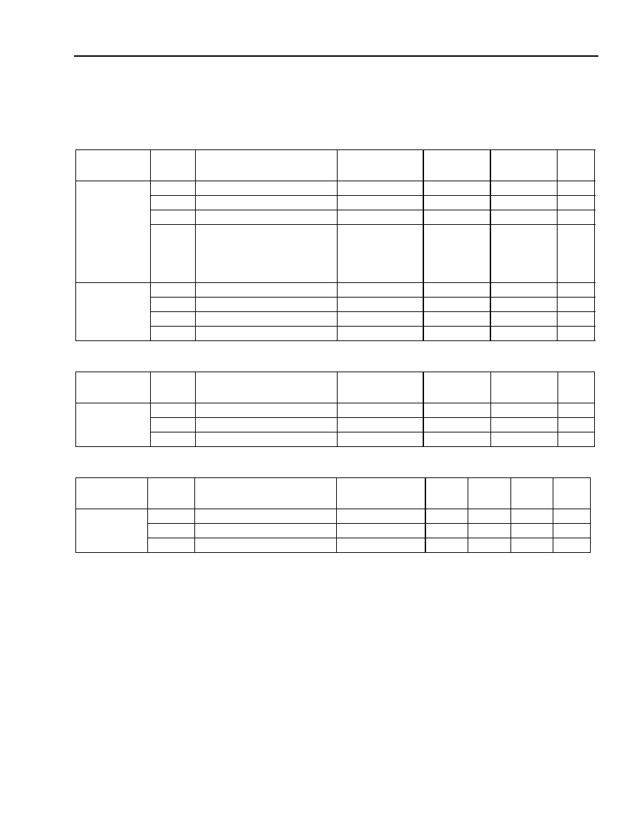
Clock Synthesizer Loop Filter
A typical loop filter that provides adequate damping for
less than 0.1 dB of jitter peaking is shown in Table 6.
Connect the filter components to LFP and LFN. The
component values can be varied to adjust the loop
dynamic response (see Table 6).
Table 6. Clock Synthesizer Loop Filter Component
Values
2249(F)
Figure 3. Clock Synthesizer Loop Filter
Components
1. The OC-192/STM-64 data rate of 9.95328 Gbits/s is typically
approximated as 10 Gbits/s in this document when referring to the
application rate. Similarly, the low-speed parallel interface data
rate of 622.08 Mbits/s is typically approximated as 622 Mbits/s.
The exact frequencies are used only when necessary for clarity.
Components
Values for 8 MHz Loop Bandwidth
C1
*
* Capacitor C1 should be either ceramic or nonpolar.
0.15
µ
F ± 10%
C2, C3
~1 pF
This value is the composite of any physical capacitance in
addition to any parasitic capacitance. These capacitors are
by default not populated.
R1
3 k
± 5%
C
3
C
2
C
1
R
1
LFN
LFP
V
CCA
V
CCA

12
Agere Systems Inc.
Data Sheet
March 29, 2002
10 Gbits/s Clock Synthesizer, 16:1 Data Multiplexer
TTRN0110G
Clock Synthesizer Operation
(continued)
Clock Synthesizer Settling Time
The clock synthesizer will acquire phase/frequency lock after a valid REFCLKP/N signal is applied. The actual time
to acquire lock is a function of the loop bandwidth selected. The loop will acquire lock within 5 ms when using the
external loop bandwidth components corresponding to a corner of less than 8 MHz.
Loss of Lock Indicator (LCKLOSSN)
The LCKLOSSN pin indicates (active-low) when the clock synthesizer has exceeded phase-lock limits with the
incoming REFCLKP/N phase. The lock detect function compares the phases of the input 155 MHz or 622 MHz
clock at the REFCLKP/N pins with the internally generated 622 MHz output clock at the CK622P/N pin. When the
phase difference in the two signals is close to zero, as determined by a second internal phase detector and filter,
the lock detect signal LCKLOSSN is set to a logic high. When the phase difference between the two signals is
changing at a rate exceeding the filter's cut-off frequency, the TTRN0110G is declared out of lock and LCKLOSSN
is set to a logic low. If a set of highly damped phase-locked loop parameters is chosen, LCKLOSSN may exhibit
more than one positive edge transition during the acquisition process before a steady logic-high state is achieved.
Upon a transition from the out-of-lock condition to the in-lock condition, the parallel data storage element pointers
are centered.
Clock Synthesizer Generated Jitter
The clock synthesizer's generated jitter performance meets the requirements shown in Table 7. These
specifications apply to the jitter generated at the 10 GHz clock pins CK10GP/N when the jitter on the reference
clock REFCLKP/N is within the specifications given in Table 12 on page 20 or Table 18 on page 22, and the loop
filter components are chosen to provide a loop bandwidth of less than 8 MHz.
Table 7. Clock Synthesizer Generated Jitter Specifications
Parameter
Typical
Max
(Device)
*
* This denotes the device specification for system SONET/SDH compliance when the loop filter in Table 6 and Figure 3 is used while
meeting the transfer jitter bandwidth of 8 MHz.
Unit
Generated Jitter (p-p) SONET Rate:
Measured with 50 kHz to 80 MHz Bandpass Filter
1 UI = 1/9.95328 GHz
0.050
0.090
UIp-p
Generated Jitter (p-p) FEC Rate:
Measured with 53.6 kHz to 85.7 MHz Bandpass Filter
1 UI = (14/15)(9.95328 GHz)
0.050
0.090
UIp-p

Agere Systems Inc.
13
Data Sheet
March 29, 2002
10 Gbits/s Clock Synthesizer, 16:1 Data Multiplexer
TTRN0110G
Clock Synthesizer Operation
(continued)
Clock Synthesizer Jitter Transfer
The clock synthesizer's jitter transfer performance meets the requirement shown in Figure 4 when the loop filter
values shown in Table 6 on page 11 are used.
2250(F)
Figure 4. Clock Synthesizer Jitter Transfer
≠60
≠40
≠20
0
0.001
0.01
0.1
1
10
≠50
≠30
≠10
100
FREQUENCY (MHz)
J
I
TT
ER
OUT/
JI
TTE
R
I
N
(
d
B
)
(8 MHz, 0.1 dB)
10
0.001
14
Agere Systems Inc.
Data Sheet
March 29, 2002
10 Gbits/s Clock Synthesizer, 16:1 Data Multiplexer
TTRN0110G
Multiplexer Operation
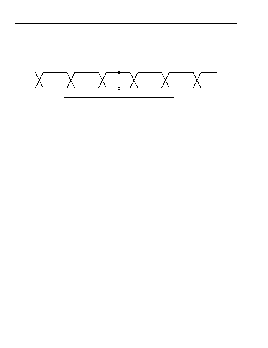
The parallel 622 Mbits/s data is clocked into an input buffer, then clocked into a 16:1 multiplexer. The relationship
between the parallel D[15:0]P/N input data and the serial output data D10GP/N is given in Figure 5. The D15 bit is
the most significant bit (MSB) and is shifted out first in time in the serial output stream.
5-8063(F)
Figure 5. Parallel Input to Serial Output Data Relationship
10 GHz Clock Output Enable (ENCK10G)
The 10 GHz CML clock output CK10GP/N may be disabled by setting the ENCK10G pin to logic low. ENCK10G is
an active-high CMOS input with an internal pull-up resistor so the default condition will enable the CK10GP/N
output and a ground or logic-low signal must be applied to disable the CK10GP/N output. When disabled, the
CK10GP/N pins should either be left floating or be connected to a load, which returns to V
CC
. The output must not
be connected directly to ground when it is disabled.
Loopback 10 GHz Data Output (LBDP/N, ENLBDN)
An alternate 10 Gbits/s CML data output is available on the LBDP/N pin. This pin is provided for use in system
loopback testing and avoids the need for off-chip signal splitting of the data signal path. Setting the ENLBDN pin to
logic-low will enable the alternate 10 Gbits/s loopback data output. ENLBDN enable is an active-low CMOS input
with an internal pull-up resistor so the default condition will disable the LBDP/N output, and a ground or logic-low
signal must be applied to enable the loopback output. When disabled, the LBDP/N pin should either be left floating,
or be connected to a load which returns to V
CC
. The output must not be connected directly to ground when it is
disabled.
Reset (RESETN)
The RESETN signal must be held active-low for a minimum of 6.4 ns when the internal VCO is active and running,
in order for the internal logic to be completely reset.
D15
D14
D1
D0
D15
TIME
(D15 SERIALLY SHIFTED OUT FIRST)
(D0 SERIALLY SHIFTED OUT LAST)
(MSB)
(LSB)

Agere Systems Inc.
15
Data Sheet
March 29, 2002
10 Gbits/s Clock Synthesizer, 16:1 Data Multiplexer
TTRN0110G
Clocking Modes and Timing
Adjustments
The TTRN0110G supports four timing modes for the
622 Mbits/s data input: forward directional 622, forward
directional 311, contradirectional, and clockless
transfer, as selected by the CLKMOD[1:0] pins.
Forward Directional 622 Clocking Mode
(CLKMOD[1:0] = 00, EXTCNTR, PICLKP/N,
OVRFLW)
In forward directional 622 clocking mode
(CLKMOD[1:0] = 00), data is clocked into a 16-bit wide
input register on the TTRN0110G device by the
PICLKP/N parallel input clock. The setup and hold
times for the data relative to PICLK are given in
Figure 8 on page 23 and Table 19 on page 25. An
internal data buffer is used to absorb timing drift
between PICLK and the internal clocks derived from
the 10 GHz internal oscillator. A PICLK phase drift of
up to ±2400 ps relative to the internal clocks can be
absorbed by the buffer, as long as the bandwidth of this
phase drift is less than 500 kHz. Note that the read and
write addresses for the data buffer must be initially
reset in order for the buffer to absorb the full range of
PICLK phase drift.
The read and write addresses for the data buffer are
reset at the time the PLL acquires lock and the loss-of-
lock indicator transitions from the out-of-lock condition
to the in-lock condition. After LCKLOSSN goes high,
the buffer will be centered and data integrity will be
obtained within approximately 2
µ
s.
The data buffer can also be recentered by applying
EXTCNTR (active-high) for a minimum of 6.4 ns. After
EXTCNTR goes low, the buffer will be centered and
data integrity will be lost and subsequently restored
within approximately 2
µ
s.
If the timing drift exceeds ±2400 ps, the data buffer will
indicate overflow with a logic-high signal on the
OVRFLW pin for a minimum of 6.4 ns. After a time
interval of 4.8 ns after OVRFLW goes low, the buffer
will be recentered and data integrity will be lost and
subsequently restored within approximately 2
µ
s.
During the 11.2 ns between the rising edge of
OVRFLW and the recentering of the buffer, data
integrity may be lost if the timing drift exceeds
±2000 ps.
If the output clock CK622P/N is not used when in
CLKMOD[1:0] = 00, it can be left unconnected to
conserve power.
Forward Directional 311 Clocking Mode
(CLKMOD[1:0] = 10, EXTCNTR, PICLKP/N,
OVRFLW)
In forward directional 311 clocking mode
(CLKMOD[1:0] = 10), data is clocked into a 16-bit wide
input register on the TTRN0110G device by the
PICLKP/N parallel input clock. In contrast to forward
directional 622 mode, the PICLK signal is at half the
data rate (311 MHz instead of 622 MHz). The setup
and hold times for the data relative to PICLK are given
in Figure 9 on page 23 and Table 19 on page 25. An
internal data buffer is used to absorb timing drift
between PICLK and the internal clocks derived from
the 10 GHz internal oscillator. A PICLK phase drift of
up to ±2400 ps relative to the internal clocks can be
absorbed by the buffer, as long as the bandwidth of this
phase drift is less than 500 kHz. Note that the read and
write addresses for the data buffer must be initially
reset in order for the buffer to absorb the full range of
PICLK phase drift.
The read and write addresses for the data buffer are
reset at the time the PLL acquires lock and the loss-of-
lock indicator transitions from the out-of-lock condition
to the in-lock condition. After LCKLOSSN goes high,
the buffer will be centered and data integrity will be
obtained within approximately 2
µ
s.
The data buffer can also be recentered by applying
EXTCNTR (active-high) for a minimum of 6.4 ns. After
EXTCNTR goes low, the buffer will be centered and
data integrity will be lost and subsequently restored
within approximately 2
µ
s.
If the timing drift exceeds ±2400 ps, the data buffer will
indicate overflow with a logic-high signal on the
OVRFLW pin for a minimum of 6.4 ns. After a time
interval of 4.8 ns after OVRFLW goes low, the buffer
will be recentered and data integrity will be lost and
subsequently restored within approximately 2
µ
s.
During the 11.2 ns between the rising edge of
OVRFLW and the recentering of the buffer, data
integrity may be lost if the timing drift exceeds
±2000 ps.
If the output clock CK622P/N is not used when in
CLKMOD[1:0] = 10, it can be left unconnected to
conserve power.

16
Agere Systems Inc.
Data Sheet
March 29, 2002
10 Gbits/s Clock Synthesizer, 16:1 Data Multiplexer
TTRN0110G
Clocking Modes and Timing Adjustments
(continued)
Contradirectional Clocking Mode (CLKMOD[1:0] = 01, PHADJ[1:0], EXTCNTR)
In the contradirectional clocking mode (CLKMOD[1:0] = 01), the TTRN0110G device sends a 622 MHz clock with
one of four user-selectable phases out to the upstream device for clocking the data toward the TTRN0110G. The
user can program PHADJ[1:0] to adjust the phase of CK622P/N as a function of printed wiring board (PWB) layout
and upstream device propagation delay in order to meet the setup and hold time of the 622 Mbits/s data input to
the TTRN0110G. PHADJ[1:0] changes the phase of the CK622P/N clock without changing the input data sampling
time. PHADJ[1:0] setting information is given in Table 8, and the phase relationship of CK622P/N for each
PHADJ[1:0] setting is shown in Figure 6.
Table 8. PHADJ Settings for CK622 Output Clock (Contraclocking Mode)
In this mode, the TTRN0110G input data still passes through the data buffer described in the forward directional
clocking sections; however, there will no longer be any phase drift or overflow since the CK622P/N output serves
as the master clock for the upstream device. The read and write addresses for the data buffer are initially reset
at the time the PLL acquires lock and the loss-of-lock indicator transitions from the out-of-lock condition to the in-
lock condition. After LCKLOSSN goes high, the buffer will be recentered and data integrity will be obtained within
approximately 2
µ
s.
5-8064(F)
Figure 6. CK622 Phase Relation vs. PHADJ Setting
Input Pins
Phase
PHADJ[1]
PHADJ[0]
0
0
0 (See part A of Figure 6.)
0
1
≠270 (See part D of Figure 6.)
1
0
≠180 (See part C of Figure 6.)
1
1
≠90 (See part B of Figure 6.)
A. (0 DEG.)
B. (≠90 DEG.)
C. (≠180 DEG.)
D. (≠270 DEG.)
TIME

Agere Systems Inc.
17
Data Sheet
March 29, 2002
10 Gbits/s Clock Synthesizer, 16:1 Data Multiplexer
TTRN0110G
Clocking Modes and Timing Adjustments
(continued)
Clockless Transfer Mode (CLKMOD[1:0]= 11, EXTCNTR)
In clockless transfer mode (CLKMOD[1:0] = 11), data may be sent to the TTRN0110G device without providing
PICLKP/N. An internal delay-locked loop (DLL) automatically produces a 622 MHz clock that is aligned to the
parallel data based on the phase of the D0P/N data input. The skew of all data bits D[15:1]P/N relative to D0P/N
must be less than 650 ps, as shown in Figure 11 on page 24.
An internal data buffer is used to absorb timing drift between D0 and the internal clocks derived from the 10 GHz
internal oscillator. A D0 phase drift of up to ±1600 ps relative to the internal clocks can be absorbed by the buffer,
as long as the bandwidth of this phase drift is less than 500 kHz.
Note: The read and write addresses for the data buffer must be initially reset in order for the buffer to absorb the
full range of D[15:0]P/N phase drift.
The read and write addresses for the data buffer are reset at the time the PLL acquires lock and the loss-of-lock
indicator transitions from the out-of-lock condition to the in-lock condition. After LCKLOSSN goes high, the buffer
will be centered and data integrity will be obtained within approximately 2
µ
s.
The data buffer can also be recentered by applying EXTCNTR (active-high) for a minimum of 6.4 ns. After
EXTCNTR goes low, the buffer will be centered and data integrity will be lost and subsequently restored within
approximately 2
µ
s.
If the timing drift exceeds ±1600 ps, the data buffer will indicate overflow with a logic-high signal on the OVRFLW
pin for a minimum of 6.4 ns. After a time interval of 4.8 ns after OVRFLW goes low, the buffer will be recentered
and data integrity will be lost and subsequently restored within approximately 2
µ
s. During the 11.2 ns between the
rising edge of OVRFLW and the recentering of the buffer, data integrity may be lost if the timing drift exceeds
±2000 ps.
If the output clock CK622P/N is not used when in CLKMOD[1:0] = 11, it can be left unconnected to conserve
power.
Because the clockless data transfer mode uses the transitions on the D0 data bit as a phase reference for clocking
the data, a constraint of a maximum number of consecutive zeros of less than 128 data periods is placed on the D0
bit when operating in the clockless data transfer mode.

18
Agere Systems Inc.
Data Sheet
March 29, 2002
10 Gbits/s Clock Synthesizer, 16:1 Data Multiplexer
TTRN0110G
CML Output Structure (Used on Outputs D10GP/N, CK10GP/N, LBDP/N)
The CML architecture is essentially a current-steering mechanism combined with an amplifier. This makes the
output swing of the signal a function of the termination resistor and the output current. The on-chip, 50
termination resistor provides a back termination and the output may be direct or ac-coupled to the load. For the
direct coupled case, the 50
load should be referenced to the positive 3.3 V supply, V
CCD
. This will ensure dc
levels that comply with the limits set.
2251(F)
Figure 7. Typical CML Output Structure
INPUT SIGNAL
50
RREFCML
V
CCD
I
OUT
X
ENABLE
≠
+
V
REF
I
REF
DEVICE-INTERNAL CML OUTPUT BUFFER CIRCUIT
C
C
EXTERNAL OUTPUT TERMINATION
50
50
V
TT
V
TT
NOTE: SHOWN FOR ac COUPLING WHERE V
TT
MAY BE EITHER V
CCD
OR GND;
≠
+
50
V
CCD
3 k
DIRECT COUPLING MAY ALSO BE USED,
BUT V
TT
MUST BE V
CCD
.

Agere Systems Inc.
19
Data Sheet
March 29, 2002
10 Gbits/s Clock Synthesizer, 16:1 Data Multiplexer
TTRN0110G
Absolute Maximum Ratings
Stresses in excess of the absolute maximum ratings can cause permanent damage to the device. These are
absolute stress ratings only. Functional operation of the device is not implied at these or any other conditions in
excess of those given in the operational sections of the data sheet. Exposure to absolute maximum ratings for
extended periods can adversely affect device reliability.
Table 9. Absolute Maximum Ratings
Handling Precautions
Although protection circuitry has been designed into this device, proper precautions should be taken to avoid
exposure to electrostatic discharge (ESD) during handling and mounting. Agere Systems employs a human-body
model (HBM) and charged-device model (CDM) for ESD-susceptibility testing and protection design evaluation.
ESD voltage thresholds are dependent on the circuit parameters used in the defined model. No industrywide
standard has been adopted for the CDM. However, a standard HBM (resistance = 1500
, capacitance = 100 pF)
is widely used and, therefore, can be used for comparison purposes.
Table 10. Handling Precautions
Note: All LVDS, CMOS, and analog pins have an ESD HBM threshold of
2,000 V.
Recommended Operating Conditions
Table 11. Recommended Operating Conditions
Parameter
Min
Max
Unit
Power Supply Voltage (V
CC
)
GND ≠ 0.5
V
CC
+ 0.5
V
Storage Temperature
≠40
125
∞C
Pin Voltage
GND ≠ 0.5
V
CC
+ 0.5
V
Device
Voltage
Model
TTRN0110G
200 V
HBM (human-body model)
200 V
CDM (charged-device model)
Parameter
Symbol
Min
Typ
Max
Unit
Power Supply (dc voltage)
V
CCD
, V
CCA
3.135
3.3
3.465
V
Temperature:
Case
T
C
0
25
85
∞C
Power Dissipation:
D10G Active, CK10G Disabled,
LBD Disabled, CLK Disabled
P
D
1.25
1.35
1.45
W
Power Dissipation:
D10G Active, CK10G Active,
LBD Disabled, CLK Disabled
P
D
1.50
1.65
1.75
W
Power Dissipation:
D10G Active, CK10G Active,
LBD Active, CLK Disabled
P
D
1.70
1.90
2.05
W
Power Dissipation:
D10G Active, CK10G Active,
LBD Active, CLK Active
P
D
1.80
1.95
2.10
W

20
Agere Systems Inc.
Data Sheet
March 29, 2002
10 Gbits/s Clock Synthesizer, 16:1 Data Multiplexer
TTRN0110G
Electrical Characteristics
LVDS, CMOS, CML Inputs and Outputs
Notes:
1. For Table 12 through Table 16, V
CC
= 3.3 V ± 5%, T
C
= 0 ∞C to 85 ∞C.
2. For more information on interpreting CML specifications, see the CML Output Structure (Used on Outputs
D10GP/N, CK10GP/N, LBDP/N) section on page 18.
Table 12. LVDS Input dc Characteristics
Table 13. LVDS Output dc Characteristics
Applicable
Pins
Symbol
Parameter
Conditions
Min
Typ
Max
Unit
D[15:0]P/N,
REFCLKP/N
PICLKP/N
V
CM
Input Common-mode
Voltage Range
Avg(V
IA
,V
IB
)
0
1200
2400
mV
V
DIFF
Input Peak Differential
Voltage
|V
IA
≠ V
IB
|
100
--
800
mV
R
IN
Differential Input
Impedance
*
* Looser than ICORE/IEEE
Æ
spec of ±10
.
V
IA
,V
IB
represent P and N differential pins.
f = 622.08 MHz
80
100
120
Applicable
Pins
Symbol
Parameter
Conditions
Min
Typ
Max
Unit
CK622P/N,
CK155P/N
V
OH
Output Voltage High,
V
OA
or V
OB
R
LOAD
= 100
± 1%
--
--
1475
mV
V
OL
Output Voltage Low,
V
OA
or V
OB
R
LOAD
= 100
± 1%
925
--
--
mV
|V
OD
|
Output Differential Volt-
age
R
LOAD
= 100
± 1%
250
--
400
mV
V
OS
Output Offset Voltage
R
LOAD
= 100
± 1%
1125
--
1275
mV
R
O
Differential Output
Impedance
Vcm = 1.0 V and 1.4 V
80
100
280
R
O
R
O
Mismatch Between
A and B
Vcm = 1.0 V and 1.4 V
--
--
20
%
|
V
OD
|
Change in |V
OD
|
Between Logic 0 and
Logic 1
R
LOAD
= 100
± 1%
--
--
25
mV
|
V
OS
|
Change in |V
OS
|
Between Logic 0 and
Logic 1
R
LOAD
= 100
± 1%
--
--
25
mV
I
SA
, I
SB
Output Current
Driver shorted to GND
--
--
24
mA
I
SAB
Output Current
Drivers shorted
together
--
--
12
mA
|I
XA
|,|I
XB
| Power-off Output
Leakage
--
--
--
--
*
* This leakage parameter is not specified due to EDS clamp diode conducting current during forward bias test.
This voltage is measured on each P/N output.
mA
Agere Systems Inc.
21
Data Sheet
March 29, 2002
10 Gbits/s Clock Synthesizer, 16:1 Data Multiplexer
TTRN0110G
Electrical Characteristics
(continued)
LVDS, CMOS, CML Inputs and Outputs
(continued)
Table 14. CMOS Input dc Characteristics
Table 15. CMOS Output dc Characteristics
Table 16. CML Input Characteristics
Applicable
Pins
Symbol
Parameter
Conditions
Min
Max
Unit
RESETN,
FECN,
CLKMOD[1:0],
REFFREQ,
ENCK10G,
ENLBDN,
ENCK155N,
TESTN
V
IH
Input Voltage High
--
V
CC
≠ 1.0
V
CC
V
V
IL
Input Voltage Low
--
GND
1.0
V
I
IH
Input Current High Leakage
V
IN
= V
CC
--
10
µ
A
I
IL
Input Current Low Leakage
V
IN
= GND
≠225
--
µ
A
PHADJ[1:0],
EXTCNTR
V
IH
Input Voltage High
--
V
CC
≠ 1.0
V
CC
V
V
IL
Input Voltage Low
--
GND
1.0
V
I
IH
Input Current High Leakage
V
IN
= V
CC
--
225
µ
A
I
IL
Input Current Low Leakage
V
IN
= GND
≠10
--
µ
A
Applicable
Pins
Symbol
Parameter
Conditions
Min
Max
Unit
LCKLOSSN
OVRFLW
V
OH
Output Voltage High
I
OH
= ≠4.0 mA
V
CC
≠ 0.5
V
CC
V
V
OL
Output Voltage Low
I
OL
= 4.0 mA
GND
0.5
V
C
l
Output Load Capacitance
--
--
15
pF
Applicable
Pins
Symbol
Parameter
Conditions
Min
Typ
Max
Unit
TSTCLKP
V
AMP1
Single-ended Input Amplitude
--
200
≠
1000
mV
R
LOSS
Input Return Loss
At 10 GHz
12
12
--
dB
R
LOSS
Input Return Loss
At <7 GHz
15
15
--
dB
22
Agere Systems Inc.
Data Sheet
March 29, 2002
10 Gbits/s Clock Synthesizer, 16:1 Data Multiplexer
TTRN0110G
Frequency Characteristics
Reference Frequency (REFCLKP/N, REFFREQ) (Standard SONET Rate)
The device requires a 155.52 MHz or a 622.08 MHz differential LVDS reference clock input. Table 17 provides the
characteristics of the REFCLKP/N input.
Table 17. Reference Frequency Characteristics (Standard SONET)
Reference Frequency (REFCLKP/N, REFFREQ) (FEC Rate)
The device requires a (255/237)155.52 MHz or a (255/237)622.08 MHz differential LVDS reference clock input.
Table 18 provides the characteristics of the REFCLKP/N input.
Table 18. Reference Frequency Characteristics (FEC Rate)
Parameter
Min
Typ
Max
Unit
Reference Frequency (REFCLKP/N):
When REFFREQ = 0
When REFFREQ = 1
--
--
155.52
622.08
--
--
MHz
MHz
Duty Cycle
40
50
60
%
Phase Jitter
*
* Measured under one 3.3 V LVDS load. Includes frequency components up to 8 MHz. Assumes
0.500 ps for the device and
0.100 ps
for laser driver and optics for a total rms jitter performance of less than 0.01 UI.
--
--
0.750
ps(rms)
Temperature
Specified range is to be compatible with environmental specification of TTRN0110G. Applications requiring a reduced temperature
range may specify the reference frequency oscillator accordingly.
0
25
85
∞C
Supply Voltage
3.15
--
3.45
V
Parameter
Min
Typ
Max
Unit
Reference Frequency (REFCLKP/N):
When REFFREQ = 0
When REFFREQ = 1
--
--
(255/237)155.52
(255/237)622.08
--
--
MHz
MHz
Duty Cycle
40
50
60
%
Phase Jitter
*
* Measured under one 3.3 V LVDS load. Includes frequency components up to 8 MHz. Assumes
0.500 ps for the device and
0.100 ps
for laser driver and optics for a total rms jitter performance of less than 0.01 UI.
--
--
0.750
ps(rms)
Temperature
Specified range is to be compatible with environmental specification of TTRN0110G. Applications requiring a reduced temperature range
may specify the reference frequency oscillator accordingly.
0
--
85
∞C
Supply Voltage
3.15
--
3.45
V

Agere Systems Inc.
23
Data Sheet
March 29, 2002
10 Gbits/s Clock Synthesizer, 16:1 Data Multiplexer
TTRN0110G
Timing Characteristics
Note: All timing diagrams involving differential signals represent the positive signal as a solid line and the nega-
tive signal as a dashed line. This is especially important when referencing the rising or falling edge of a dif-
ferential signal.
Transmit Timing
Figure 8 shows the required timing relationships between the input clock PICLKP/N and the input data D[15:0]P/N
in forward directional 622 clocking mode.
2252(F)
Figure 8. Transmit Timing Waveforms (Forward Directional 622 Clocking Mode)
Figure 9 shows the timing relationships between the input clock PICLKP/N and the input data D[15:0]P/N in
forward directional 311 clocking mode.
2253(F)
Figure 9. Transmit Timing Waveform (Forward Directional 311 Clocking Mode)
PICLKP/N
D[15:0]P/N
INPUTS
INPUT
tPERIOD
(622 MHz)
(622 Mbits/s)
DATA 1
DATA 2
tHOLD
tSU
PICLKP/N
D[15:0]P/N
INPUTS
INPUT
(0.5)tPERIOD
(311 MHz)
(622 Mbits/s)
DATA 1
DATA 2
tHOLD
tSU

24
Agere Systems Inc.
Data Sheet
March 29, 2002
10 Gbits/s Clock Synthesizer, 16:1 Data Multiplexer
TTRN0110G
Timing Characteristics
(continued)
Transmit Timing
(continued)
Figure 10 shows the timing relationships between the output clock CK622P/N and the input data D[15:0]P/N. This
relationship is true for both the contraclocking mode and the clockless transfer mode.
2254(F)
Note: T
SU
and T
HOLD
only apply in contraclocking mode when CLKMOD[1:0] = 01.
Figure 10. Transmit Timing Waveform (Contradirectional Clocking Mode)
Figure 11 shows the skew relationship between the D0P/N data remainder of the D[15:1]P/N data bus required to
support clockless data transfer.
2255(F)
Figure 11. Transmit Timing Waveform (Clockless Transfer Mode)
D[15:0]P/N
INPUTS
OUTPUT
tPERIOD
DATA 1
DATA 2
tHOLD
tSU
CK622
D0P/N
D[15:1]P/N
INPUTS
INPUT
tPERIOD
DATA 1
DATA 2
tSKEW
DATA 1
DATA 2
Agere Systems Inc.
25
Data Sheet
March 29, 2002
10 Gbits/s Clock Synthesizer, 16:1 Data Multiplexer
TTRN0110G
Timing Characteristics
(continued)
Transmit Timing
(continued)
The output 622 MHz clock and data signals are specified in Table 19.
Table 19. LVDS Input ac Timing Characteristics
Table 20. LVDS Output ac Timing Characteristics
Applicable
Pins
Symbol
Parameter
Conditions
Min
Typ
Max
Unit
PICLKP/N
--
Duty Cycle
All signals differential
40
50
60
%
PICLKP/N
t
PERIOD
Clock Period
622 MHz
311 MHz
--
--
1.6
3.2
--
--
ns
ns
D[15:0]P/N
PICLKP/N
(622 MHz)
t
SU
Setup from Clock Edge to
D[15:0]P/N
CLKMOD[1:0] = 00,
all signals differential
0.07
--
--
ns
t
HOLD
Hold from Clock Edge to
D[15:0]P/N
CLKMOD[1:0] = 00,
all signals differential
0.07
--
--
ns
D[15:0]P/N
PICLKP/N
(311 MHz)
t
SU
Setup from Clock Edge to
D[15:0]P/N
CLKMOD[1:0] = 10,
all signals differential
0.68
--
--
ns
t
HOLD
Hold from Clock Edge to
D[15:0]P/N
CLKMOD[1:0] = 10,
all signals differential
0.78
--
--
ns
D[15:0]P/N
t
SKEW
*
* Will be maintained for 100 mV < V
ID
< 400 mV throughout the receiver common-mode operating range.
Skew Tolerable at Receiver
Input to Meet Setup and
Hold Time Requirements
Any two package
inputs
--
--
200
ps
Applicable
Pins
Symbol
Parameter
Conditions
Min
Typ
Max
Unit
CK622P/N
CK155P/N
--
Duty Cycle
All signals differential
40
50
60
%
CK622P/N
t
PERIOD
Clock Period
--
--
1.6
--
ns
CK155P/N
--
6.4
--
ns
D[15:0]P/N
CK622P/N
*
* CLKMOD[1:0] = 01, all signals differential.
t
SU
Setup from Clock Edge to
D[15:0]P/N
9.95328 Gbits/s
10.70920 Gbits/s
--
--
≠200
≠400
--
--
ns
ns
t
HOLD
Hold from Clock Edge to
D[15:0]P/N
9.95328 Gbits/s
10.70920 Gbits/s
--
--
350
520
--
--
ns
ns
CK622P/N
CK155P/N
t
RISE
Rise Time, 20% to 80%
Z
LOAD
= 100
± 1%
100
260
400
ps
t
FALL
Fall Time, 20% to 80%
Z
LOAD
= 100
± 1%
100
260
400
ps
t
SKEW1
As defined in the IEEE standard 1596.3--1996.
Differential Skew
--
--
--
70
ps
CK622P/N
V
AMP
Single Ended Output
Amplitude
--
250
--
500
mV
CK155P/N

26
Agere Systems Inc.
Data Sheet
March 29, 2002
10 Gbits/s Clock Synthesizer, 16:1 Data Multiplexer
TTRN0110G
Timing Characteristics
(continued)
Transmit Timing
(continued)
Figure 12 shows the timing relationships between the output 10 GHz clock CK10GP/N and the output 10 Gbits/s
data D10GP/N.
0357(F)
Figure 12. Transmit Timing Waveform with 10 GHz Clock
The output 10 GHz clock and data signals from Figure 12 are characterized in Table 21.
Table 21. CML Output Pin ac Timing Characteristics
Applicable
Pins
Symbol
Parameter
Conditions
Min
Typ
Max
Unit
CK10GP/N
--
Duty Cycle
RREFCML = 3 k
,
R
L
= 50
40
50
60
%
t
PERIOD
CK10GP/N Clock Period
--
100
--
ps
D10GP/N,
CK10GP/N
t
DD
Time Delay from Clock
Edge to Data Edge
30
50
70
ps
CK10GP/N
D10GP/N,
LBDP/N
t
RISE
Rise Time, 20% to 80%
10
20
35
ps
t
FALL
Fall Time, 20% to 80%
10
20
35
ps
t
SKEW1
Differential Skew
--
--
3
ps
R
LOSS
Output Return Loss:
10 GHz
<7 GHz
--
--
--
--
12
15
--
--
dB
dB
D10GP/N,
LBDP/N
V
AMP
Voltage Amplitude Single-
ended
RREFCML = 2.2 k
,
R
L
= 50
600
--
800
mV
RREFCML = 3.0 k
,
R
L
= 50
450
--
650
mV
RREFCML = 3.5 k
,
R
L
= 50
350
--
500
mV
CK10GP/N
V
AMP
Voltage Amplitude Single-
ended
RREFCML = 2.2 k
,
R
L
= 50
800
--
1.0 V
mV
RREFCML = 3 k
,
R
L
= 50
600
--
800
mV
RREFCML = 3.5 k
,
R
L
= 50
500
--
650
mV
CK10GP/N
D10GP/N
OUTPUT
OUTPUT
DATA 1
DATA 2
tPERIOD
tDD
DATA 3

Agere Systems Inc.
27
Data Sheet
March 29, 2002
10 Gbits/s Clock Synthesizer, 16:1 Data Multiplexer
TTRN0110G
Packaging Characteristics
Package Crush Characteristics
Table 22. Crush Specifications
Additional test information available upon request.
CBGA Package Information
The package used for the TTRN0110G is a ceramic ball grid array (CBGA). The substrate is 99.6% alumina
(Al2O3) material. The standoff height is accomplished by using 0.013 in. diameter copper silver (CuAg) balls,
which are attached using a eutectic braze to the thin film metal pads on the substrate. After brazing, the balls have
a diameter at the braze fillet of 0.016 in. (at the interface of the ball and substrate), but still maintain their height of
0.013 in. for standoff height.
PWB Design Information
The layout of the bare PWB should use a 0.016 in. diameter pad. The pad should be defined by the copper and not
by solder mask. (The only copper leading away from the pad should be the trace connected to it; the pad should
not be part of a large ground plane unless only connected to the ground plane by a single trace.) Avoid placement
of vias in the pads used for ball attachment on the PWB. Vias should be connected by a trace (or tear dropped)
with a sufficient dam of solder mask to prevent solder from wicking into the via and away from the ball/PWB solder
joint.
The stencil opening should be designed at 0.016 in. as well, to match up with the CBGA pads.
Device Code
Package
Dimensions
Conditions
Min
Typ
Max
Unit
TTRN0110G
198-ball CBGA
15 mm x 15 mm
Without pad
--
25
--
lbs
With pad (0.040 in.)
--
25
--
lbs
28
Agere Systems Inc.
Data Sheet
March 29, 2002
10 Gbits/s Clock Synthesizer, 16:1 Data Multiplexer
TTRN0110G
Packaging Characteristics
(continued)
Assembly Information
Note: Each assembly process will have its own idiosyncrasies, due to product design, material differences, and
equipment variations. Assembly information provided here is a beginning point from which the assembly
process engineer should apply their knowledge and experience to obtain optimal results.
It is recommended that the stencil thickness be set at 0.006 in. for a starting point. After trials with the recom-
mended stencil opening size, stencil thickness, and process specific solder paste, a visual inspection should be
done to assure a proper fillet and wetting is obtained for each ball. The reflowed solder fillet should resemble a
cylindrical column from the PWB to the center of the ball.
The reflow profile should be determined using a known set point for the oven such as the Joint Electron Device
Engineering Council (JEDEC) profile. The JEDEC profile is defined as the following parameters:
Table 23. JEDEC Profile
Belt speed = 28 in./min.
A representative sample of the product (fitted with multiple thermocouples and a data logger) should be run
through the oven to determine the optimum profile. The temperature of the CBGA device should not exceed
225 ∞C, and only be above the liquidus of the solder alloy (typically 180 ∞C) for less than 60 s.
Reference Materials
For further information, the user may wish to consult some of the many references that are available on the
technical market today for CBGA assembly. The following are suggested for more detailed information, but there
are many others too:
s
Ceramic Ball Grid Array Surface Mount Assembly and Rework, IBM Document #APD-SBSC-101.0, Cindy
Milkovich, Lisa Jimarez, IBM Corporation, 1701 North Street, Endicott, NY 13760, (800) 925-3157
s
Ball Grid Array Technology, John Lau (Editor), ISBN 0-07-036608-X, McGraw-Hill, Inc., 1221 Avenue of the
Americas, New York, NY 10020
Zone
Temp
Unit
1
Upper
140
∞C
Lower
140
∞C
2
Upper
150
∞C
Lower
150
∞C
3
Upper
150
∞C
Lower
150
∞C
4
Upper
180
∞C
Lower
180
∞C
5
Upper
180
∞C
Lower
180
∞C
6
Upper
205
∞C
Lower
205
∞C
7
Upper
245
∞C
Lower
245
∞C

Agere Systems Inc.
29
Data Sheet
March 29, 2002
10 Gbits/s Clock Synthesizer, 16:1 Data Multiplexer
TTRN0110G
Packaging Characteristics
(continued)
Package Diagram--198-Ball CBGA (Bottom View)
Dimensions are in millimeters. Tolerance is ±0.076 mm unless otherwise noted.
0627(F)
A1 BALL
CORNER
D
E
F
G
H
J
K
L
N
P
C
B
A
14 SPACES
@ 1.00 = 14.00
1.00 TYP.
A1 BALL
IDENTIFIER ZONE
SEATING PLANE
SOLDER BALL
14 SPACES
@ 1.00 = 14.00
1.143 REF
M
1
2
3
4
5
6
7
8
9
10 11 12 13 14
1.885
0.330
±
0.051 TYP
0.3734
±
0.0013
15.00
±
0.080
15.00
±
0.080
0.330
±
0.051
TYP DIA.
15
R
SQR
SQR

Telcordia Technologies is a trademark of Telcordia Technologies Inc.
IEEE is a registered trademark of The Institute of Electrical and Electronics Engineers, Inc.
Copyright © 2002 Agere Systems Inc.
All Rights Reserved
March 29, 2002
DS02-062HSPL (Replaces DS01-236HSPL)
Agere Systems Inc. reserves the right to make changes to the product(s) or information contained herein without notice. No liability is assumed as a result of their use or application.
For additional information, contact your Agere Systems Account Manager or the following:
INTERNET:
http://www.agere.com
E-MAIL:
docmaster@agere.com
N. AMERICA:
Agere Systems Inc., 555 Union Boulevard, Room 30L-15P-BA, Allentown, PA 18109-3286
1-800-372-2447, FAX 610-712-4106 (In CANADA: 1-800-553-2448, FAX 610-712-4106)
ASIA:
Agere Systems Hong Kong Ltd., Suites 3201 & 3210-12, 32/F, Tower 2, The Gateway, Harbour City, Kowloon
Tel. (852) 3129-2000, FAX (852) 3129-2020
CHINA: (86) 21-5047-1212 (Shanghai), (86) 10-6522-5566 (Beijing), (86) 755-695-7224 (Shenzhen)
JAPAN: (81) 3-5421-1600 (Tokyo), KOREA: (82) 2-767-1850 (Seoul), SINGAPORE: (65) 778-8833, TAIWAN: (886) 2-2725-5858 (Taipei)
EUROPE:
Tel. (44) 7000 624624, FAX (44) 1344 488 045
Data Sheet
March 29, 2002
10 Gbits/s Clock Synthesizer, 16:1 Data Multiplexer
TTRN0110G
Ordering Information
Device Code
Package
Temperature (T
C
)
Comcode
(Ordering Number)
TTRN0110G
198-ball CBGA
0 ∞C to 85 ∞C
108698465