Preliminary Data Sheet
August 2000
TTRN012G5 (2.5 Gbits/s) and TTRN012G7 (2.5 Gbits/s and 2.7 Gbits/s)
Clock Synthesizer, 16:1 Data Multiplexer
Features
s
TTRN012G5 supports OC-48/STM-16 data rate
s
TTRN012G7 supports:
-- OC-48/STM-16 data rate
-- RS (255, 239) forward error correction (FEC)
OC-48/STM-16 data rate
s
Fully integrated clock synthesizer and 16:1 data
multiplexer
s
Supports clockless data transfer into the 16:1
multiplexer
s
Parity checking and valid data indication
s
Data inversion option
s
Additional high-speed CML serial data output for
system loopback
s
Loss of lock indication
s
Single 3.3 V supply
s
Available in either MBIC 025 BiCMOS technology
or lower-power MBIC 025 silicon germanium
BiCMOS technology
s
LVPECL 155.52 Mbits/s digital I/O
s
Jitter generation and jitter transfer compliant with
the following:
--
Telcordia Technologies
* GR-253
-- ITU-T G.825
-- ITU-T G.958
Applications
s
SONET/SDH line origination equipment
s
SONET/SDH add/drop multiplexers
s
SONET/SDH cross connects
s
SONET/SDH test equipment
s
Digital video transmission
*
Telcordia Technologies
is a registered trademark of Bell Com-
munications Research, Inc.
Description
The Lucent Technologies Microelectronics Group
TTRN012G5 operates at the OC-48/STM-16 data
rate of 2.5 Gbits/s. The TTRN012G7 device operates
at either 2.5 Gbits/s or the RS FEC OC-48/STM-16
data rate of 2.7 Gbits/s. For clarity, this data sheet
refers to the TTRN012G5 serial data rate as
2.5 Gbits/s and the parallel data and reference clock
frequency as 155 MHz. (The precise rates are
2.48832 Gbits/s and 155.52 MHz.) When using the
TTRN012G7 at the FEC rate, the 2.5 Gbits/s data
rate should be interpreted as 2.7 Gbits/s and the par-
allel and clock frequency should be interpreted as
166 MHz. (The precise rates are 2.66606 Gbits/s and
166.62 MHz.)
The devices provide a 16:1 multiplexer and clock
multiplier unit. Both a high-speed serial clock and
data output are generated. The devices accept 16
differential PECL data inputs and a low-speed refer-
ence clock. A unique feature of the multiplexer is that
no clock is required to feed in the 16 data lines, as
long as the upstream data chip clock is synchronous
with the device REFCLKP/N input.
Alternatively, contra-clocking may be used, whereby
the device provides one of four phases of a
155.52 MHz or 166.62 MHz clock output back
upstream to the data chip.
Other features include a parity bit input and parity
check on the 16 input data lines, a second
2.5 Gbits/s or 2.7 Gbits/s data output for loopback
toward the TRCV012G5 or TRCV012G7 device, and
a user-configurable PLL bandwidth. Both devices are
available in either BiCMOS or in SiGe BiCMOS tech-
nology for lower power operation.

TTRN012G5 and TTRN012G7
Preliminary Data Sheet
Clock Synthesizer, 16:1 Data Multiplexer
August 2000
2
Lucent Technologies Inc.
Table of Contents
Contents
Page
Features .................................................................................................................................................................... 1
Applications ............................................................................................................................................................... 1
Description................................................................................................................................................................. 1
Pin Information .......................................................................................................................................................... 4
Functional Overview .................................................................................................................................................. 9
Clock Synthesizer Operation .................................................................................................................................. 9
Multiplexer Operation............................................................................................................................................ 11
Clocking Modes and Timing Adjustments ............................................................................................................... 12
Clockless Transfer Mode (CLKMODE, EXTADJN, MONAPAP/N) ....................................................................... 12
Contra-Directional Clocking Mode (CLKMODE, PHADJ[1:0]) .............................................................................. 13
CML Output Structure (Used on Pins D2G5P/N, CK2G5P/N)................................................................................. 14
Choosing the Value of the External CML Reference Resistors (RREF1, RREF2) ............................................... 14
Absolute Maximum Ratings.....................................................................................................................................15
Handling Precautions .............................................................................................................................................. 15
Operating Conditions............................................................................................................................................... 15
Electrical Characteristics ......................................................................................................................................... 16
Reference Frequency (REFCLKP/N) Specifications............................................................................................. 16
LVPECL, CMOS, CML Input and Output Pins ......................................................................................................17
Timing Characteristics ............................................................................................................................................. 19
Transmit Timing .................................................................................................................................................... 19
Outline Diagram....................................................................................................................................................... 21
128-Pin QFP ......................................................................................................................................................... 21
Ordering Information................................................................................................................................................ 22
DS00-375HSPL Replaces DS00-155HSPL to Incorporate the Following Updates................................................. 22

Preliminary Data Sheet
TTRN012G5 and TTRN012G7
August 2000
Clock Synthesizer, 16:1 Data Multiplexer
3
Lucent Technologies Inc.
Description
(continued)
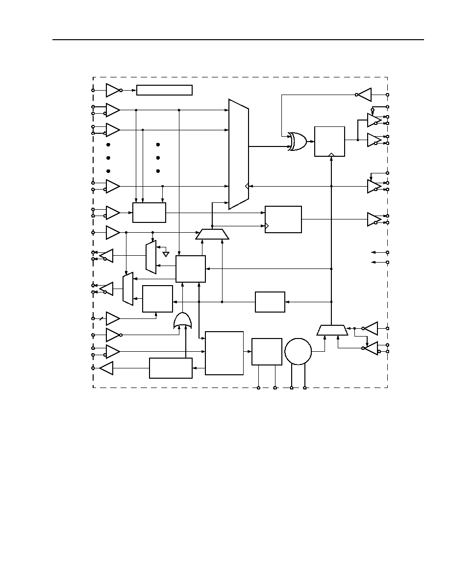
5-8060(F)r.3
Note: Diagram is representative of device functionality and conceptual signal flow. Internal implementation details may be different than shown.
Figure 1. Functional Block Diagram
CK155P
CK155N
16:
1 MU
LT
IPLE
X
E
R
PARITY
D0P
D0N
PHASE/
VCO
PARITY
CHARGE
LFP
LFN
D1P
D1N
D15P
D15N
DIVIDE
CK2G5P
CK2G5N
ENCK2G5
DATA
VALIDP
VALIDN
D2G5P
D2G5N
INVDATN
RESETN
TO DIGITAL LOGIC
TSTCKP
TSTCKN
TESTN
REFCLKP
REFCLKN
PHADJ[1:0]
MANUAL
CLKMODE
0
1
INVDAT
TEST
0
1
ACQUISITION
LCKLOSSN
EXTADJN
LOAD
MONAPAP
MONAPAN
1
0
RREF2
0
1
LBDP
LBDN
ENLBDN
VCP VCN
RREF1
PARITYP
PARITYN
CHECK
PHASE
ADJUST
INDICATOR
AUTO
PHASE
ADJUST
FREQ.
DETECTOR
PUMP
BY 16
REGISTER
RETIME

TTRN012G5 and TTRN012G7
Preliminary Data Sheet
Clock Synthesizer, 16:1 Data Multiplexer
August 2000
4
Lucent Technologies Inc.
Pin Information
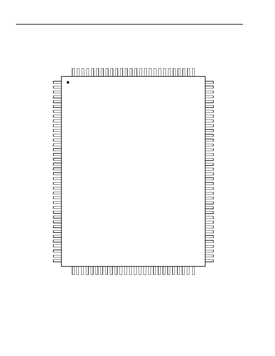
5-8066(F)r.3
Figure 2. Pin Diagram of 128-Pin QFP (Top View)
1
2
3
5
4
6
7
9
8
18
10
11
13
12
14
15
17
16
19
20
22
21
23
24
26
25
35
27
28
30
29
31
32
34
33
36
37
38
39
41
40
42
43
45
44
54
46
47
49
48
50
51
53
52
55
56
58
57
59
60
62
61
63
64
100
99
98
96
97
95
94
92
93
83
91
90
88
89
87
86
84
85
82
81
79
80
78
77
75
76
66
74
73
71
72
70
69
67
68
65
128
127
126
124
125
123
122
120
121
111
119
118
116
117
115
114
112
113
110
109
107
108
106
105
103
104
102
101
NC
V
CCD
V
CCD
LCKLOSSN
GND
GND
ENLBDN
V
CCD
GND
LBDP
LBDN
GND
V
CCD
RREF1
RREF2
ENCK2G5
V
CCD
GND
CK2G5N
CK2G5P
GND
D2G5N
D2G5P
GND
V
CCD
INVDATN
TESTN
V
CCD
TSTCKN
V
CCD
TSTCKP
V
CCD
GND
V
CCD
V
CCD
GND
GND
GND
D2N
D2P
D3N
D3P
V
CCD
D4N
D4P
D5N
D5P
GND
D6N
D6P
D7N
D7P
V
CCD
D8N
D8P
D9N
D9P
GND
D10N
D10P
D11N
D11P
V
CCD
D12N
D12P
D13N
D13P
GND
D14N
D14P
D15N
D15P
V
CCD
GN
D
D1
N
D1
P
D0
P
D0
N
PARI
T
Y
P
GN
D
GN
D
PARI
T
YN
V
CCD
C
K
1
55P
V
CCD
C
K
15
5N
VAL
I
D
N
VAL
I
D
P
V
CCD
MO
N
A
P
A
P
NC
M
O
NA
PAN
PHADJ1
PHADJ0
CL
K
M
ODE
EXT
ADJN
GN
D
RESET
N
GND
GND
GND
GND
V
CCD
GN
D
RE
F
C
L
K
P
RE
F
C
L
K
N
V
CCA
V
CCD
VCN
V
CCA
LF
N
LF
P
V
CCA
VCP
NC
NC
GN
D
GN
D
GN
D
GN
D
GN
D
GN
D
GN
D
GN
D
V
CCA
NC
GN
D
V
CCA

Preliminary Data Sheet
TTRN012G5 and TTRN012G7
August 2000
Clock Synthesizer, 16:1 Data Multiplexer
5
Lucent Technologies Inc.
Pin Information
(continued)
Table 1. Pin Descriptions--2.5 Gbits/s and Related Signals
Note: In Table 1, when operating the TTRN012G7 device at the OC-48/STM-16 rate, 2.5 Gbits/s should be inter-
preted as 2.48832 Gbits/s. When operating the TTRN012G7 device at the RS FEC OC-48/STM-16 rate,
2.5 Gbits/s should be interpreted as 2.66606 Gbits/s. (A similar interpretation should be made for 2.5 GHz.)
* Differential pairs are indicated by P and N suffixes. For nondifferential pins, N at the end of the symbol name designates active-low.
I = input, O = output. I
u
indicates an internal pull-up resistor on this pin.
Pin
Symbol*
Type
Level
Name/Description
14
D2G5P
O
CML
Data Output (2.5 Gbits/s NRZ). 2.5 Gbits/s differential data
output.
15
D2G5N
27
LBDP O
CML
Loopback Data Output. Additional 2.5 Gbits/s differential data
output for system loopback.
26
LBDN
17
CK2G5P
O
CML
Clock Output (2.5 GHz). 2.5 GHz differential clock output.
18
CK2G5N
23
RREF1
I
Analog
Resistor Reference 1. CML current bias reference resistor.
(See Table 15, page 18 for values.)
22
RREF2
I
Analog
Resistor Reference 2. CML bias reference resistor. Connect a
1.5 k
resistor to V
CCD
.
21
ENCK2G5
I
u
CMOS
Enable CK2G5P/N Clock Output.
0 = CK2G5P/N buffer powered off
1 or no connection = CK2G5P/N buffer enabled
30
ENLBDN
I
u
CMOS
Enable LBDP/N Data Output (Active-Low).
0 = LBDP/N buffer enabled
1 or no connection = LBDP/N buffer powered off
11
INVDATN
I
u
CMOS
Invert D2G5P/N Data Output (Active-Low).
0 = invert
1 or no connection = noninvert

TTRN012G5 and TTRN012G7
Preliminary Data Sheet
Clock Synthesizer, 16:1 Data Multiplexer
August 2000
6
Lucent Technologies Inc.
Pin Information
(continued)
Table 2. Pin Descriptions--155.52 Mbits/s and Related Signals
Note: In Table 2, when operating the TTRN012G7 device at the OC-48/STM-16 rate, 155 Mbits/s should be inter-
preted as 155.52 Mbits/s. When operating the TTRN012G7 device at the RS FEC OC-48/STM-16 rate,
155 Mbits/s should be interpreted as 166.62 Mbits/s. (A similar interpretation should be made for 155 MHz.)
* Differential pairs are indicated by P and N suffixes. For nondifferential pins, N at the end of the symbol name designates active-low.
I = input, O = output. I
u
indicates an internal pull-up resistor on this pin.
Pin
Symbol*
Type
Level
Name/Description
99
D15P
I
LVPECL
Data Input (155 Mbits/s). 155 Mbits/s differential data input.
D15 is the most significant bit and is transmitted first on the
D2G5P/N output.
98
D15N
97
D14P
LVPECL
96
D14N
94
D13P
LVPECL
93
D13N
92
D12P
LVPECL
91
D12N
89
D11P
LVPECL
88
D11N
87
D10P
LVPECL
86
D10N
84
D9P
LVPECL
83
D9N
82
D8P
LVPECL
81
D8N
79
D7P
LVPECL
78
D7N
77
D6P
LVPECL
76
D6N
74
D5P
LVPECL
73
D5N
72
D4P
LVPECL
71
D4N
69
D3P
LVPECL
68
D3N
67
D2P
LVPECL
66
D2N
62
D1P
LVPECL
61
D1N
60
D0P
LVPECL
59
D0N

Preliminary Data Sheet
TTRN012G5 and TTRN012G7
August 2000
Clock Synthesizer, 16:1 Data Multiplexer
7
Lucent Technologies Inc.
Pin Information
(continued)
Table 2. Pin Descriptions--155.52 Mbits/s and Related Signals (continued)
* Differential pairs are indicated by P and N suffixes. For nondifferential pins, N at the end of the symbol name designates active-low.
I = input, O = output. I
u
indicates an internal pull-up resistor on this pin.
Pin
Symbol*
Type
Level
Name/Description
53
CK155P
O
LVPECL
Clock Output (155 MHz). 155 MHz differential clock output.
52
CK155N
43
44
PHADJ1
PHADJ0
I
u
CMOS
Phase Adjust. Adjusts phase of CK155P/N in 90 degree steps.
42
CLKMODE
I
u
CMOS
Clock Mode Select. Selects clockless data transfer mode.
0 = clockless transfer
1 or no connection = contra clock
57
PARITYP
I
LVPECL
Parity Input over Data (D[15:0]).
56
PARITYN
50
VALIDP
O
LVPECL
Parity Check Output. Validates the input of PARITYP/N.
0 = parity check does not agree with input PARITYP/N pins
1 = parity check agrees
49
VALIDN
33
LCKLOSSN
O
CMOS
Loss of Lock (Active-Low). 0 = PLL out of lock.
41
EXTADJN
I
u
CMOS
External Automatic Phase Adjust (Active-Low). Adjusts the
155 MHz clock output, CK155P/N.
0 = adjust phase of 155 MHz clock to data upon next transition
of the D0P/N input signal
1 = no adjust
Must be held low until the first rising transition of D0P/N.
47
MONAPAP
O
LVPECL
Monitor Automatic Phase Adjust. Indicates when a phase
adjustment in the automatic phase adjust block occurs.
46
MONAPAN
105
REFCLKP
I
LVPECL
Reference Clock Input (155 MHz). This clock is required.
When applying the REFCLKP/N, set the REFCLKP/N to one of
the following frequencies:
s
155.52 MHz if using the TRCV012G5, or the TRCV012G7 at
the 0C-48/STM-16 rate of 2.48832 GHz.
s
166.62 MHz if using the TRCV012G7 at the RS FEC
0C-48/STM-16 rate of 2.66606 GHz.
106
REFCLKN
112
LFP
I
Analog
Loop Filter PLL. Connect LFP to VCP, and LFN to VCN.
111
LFN
113
VCP
I
Analog
VCO Control. Connect VCP to LFP, and VCN to LFN.
110
VCN

TTRN012G5 and TTRN012G7
Preliminary Data Sheet
Clock Synthesizer, 16:1 Data Multiplexer
August 2000
8
Lucent Technologies Inc.
Pin Information
(continued)
Table 3. Pin Descriptions--Reset and Test Signals
* Differential pairs are indicated by P and N suffixes. For nondifferential pins, N at the end of the symbol name designates active-low.
I = input, O = output. I
u
indicates an internal pull-up resistor on this pin.
Table 4. Pin Descriptions--Power and No-Connect Signals
Note: V
CCA
and V
CCD
have the same dc value, which is represented as V
CC
unless otherwise specified. However,
high-frequency filtering is suggested between the individual supplies.
* Differential pairs are indicated by P and N suffixes. For nondifferential pins, N at the end of the symbol name designates active-low.
I = input, O = output. I
u
indicates an internal pull-up resistor on this pin.
Pin
Symbol*
Type
Level
Name/Description
40
RESETN
I
u
CMOS
Reset (Active-Low). Resets all synchronous logic. During a
reset, the true data outputs are in the low state and the barred
data outputs are in the high state.
0 = reset
1 or no connection = normal operation
6
TSTCKP
I
CML
Test Clock Input. Buffer is powered down when TESTN = 1.
8
TSTCKN
10
TESTN
I
u
CMOS
Test Clock Select (Active-Low).
0 = select test clock
1 or no connection = select internal VCO
Pin
Symbol*
Type
Level
Name/Description
108, 109, 114,
126, 127
V
CCA
I
Power
Analog Power Supply (3.3 V).
2, 3, 5, 7, 9,
12, 20, 24, 29,
34, 35, 48, 51,
54, 63, 70, 80,
90, 104, 107
V
CCD
I
Power
Digital Power Supply (3.3 V).
1, 4, 13, 16,
19, 25, 28, 31,
32, 37--39,
55, 58, 64, 65,
75, 85, 95,
100--103,
117--124, 128
GND
I
Ground
Ground.
36, 45, 115,
116, 125
NC
--
--
No Connection. Pin 45 has an internal pull-up resistance
of approximately 25 k
. All of these pins must be left open.

Preliminary Data Sheet
TTRN012G5 and TTRN012G7
August 2000
Clock Synthesizer, 16:1 Data Multiplexer
9
Lucent Technologies Inc.
Functional Overview
The Lucent Technologies Microelectronics Group TTRN012G5 operates at the OC-48/STM-16 data rate of
2.5 Gbits/s.* The TTRN012G7 device operates at either 2.5 Gbits/s or the RS FEC OC-48/STM-16 data rate of
2.7 Gbits/s. The device performs the clock synthesis and 16:1 data multiplexing operations required to support
2.5 Gbits/s applications compliant with
Telcordia Technologies
and ITU standards. Parallel 155 Mbits/s data is
clocked into an input register and checked for valid parity. Both clockless data transfer and contra-directional clock-
ing modes are supported. The data is then multiplexed into a 2.5 Gbits/s serial stream and output buffered for inter-
facing to a laser driver. A 2.5 GHz clock is synthesized from a reference clock and is used to retime the serial data.
The 2.5 GHz clock is optionally available as an output. The serial data stream polarity can be inverted under pin
control to make interfacing easier.
Clock Synthesizer Operation
The clock synthesizer uses a PLL to synthesize a 2.5 GHz clock from a reference frequency. A 155 MHz clock
derived from the 2.5 GHz synthesized clock may be used to clock in the parallel data.
Clock Synthesizer Loop Filter
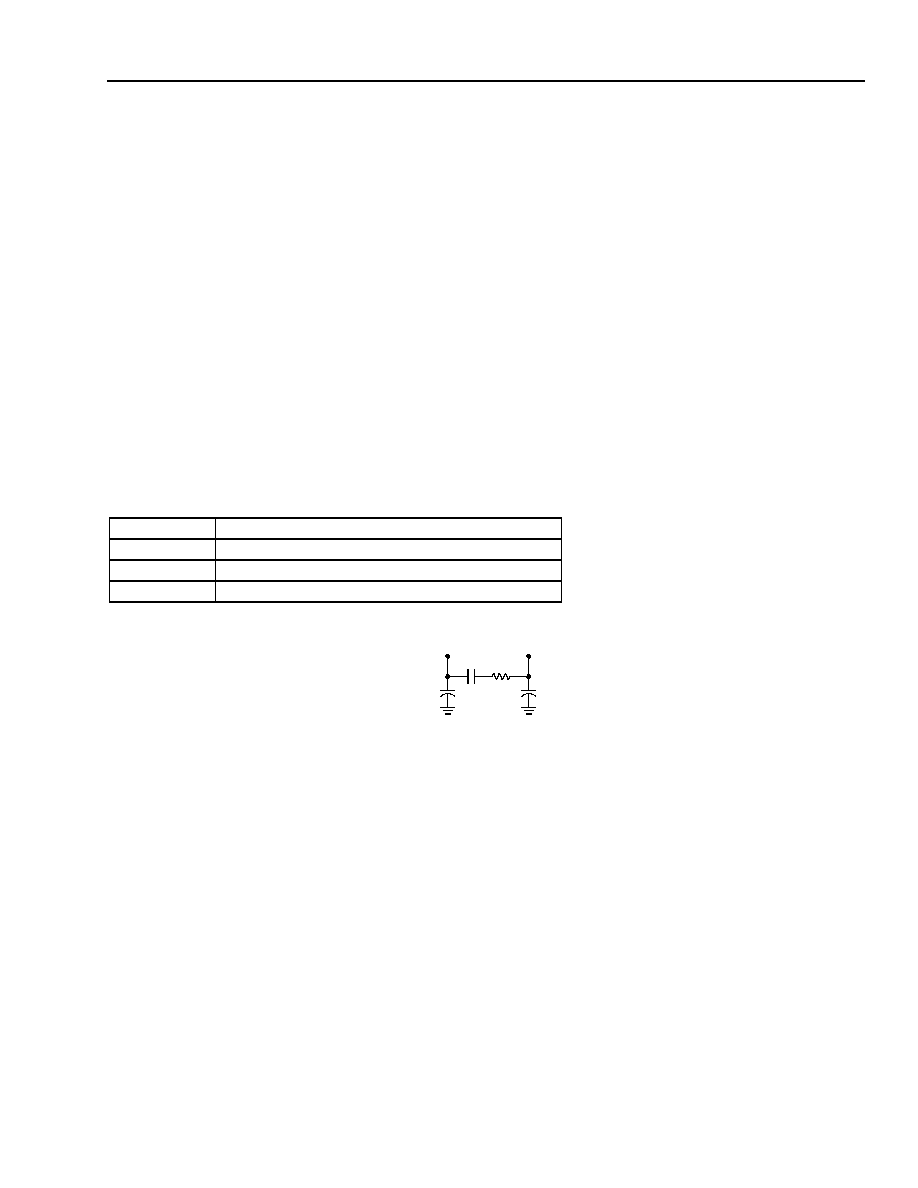
A typical loop filter that provides adequate damping for less than 0.1 dB of jitter peaking is shown in Figure 3. Con-
nect the filter components and also connect LFP to VCP and connect LFN to VCN. The component values can be
varied to adjust the loop dynamic response (see Table 5).
Table 5. Clock Synthesizer Loop Filter Component Values
* Capacitor C1 should be either ceramic or nonpolar.
5-8061(F)
Figure 3. Clock Synthesizer Loop Filter Components
Clock Synthesizer Settling Time
The clock synthesizer will acquire phase/frequency lock after a valid reference clock is applied to the REFCLKP/N
input pins. The actual time to acquire lock is a function of the loop bandwidth selected. The loop will acquire lock
within 5 ms when using the external loop bandwidth components corresponding to 2 MHz.
Loss of Lock Indicator (LCKLOSSN)
The LCKLOSSN pin indicates (active-low) when the clock synthesizer has exceeded phase-lock limits with the
incoming REFCLKP/N phase. The lock detect function compares the phases of the input 155 MHz clock at the
REFCLKP/N pins with the internally generated 155 MHz output clock at the CK155P/N pins. When the phase dif-
ference in the two signals is close to zero as determined by a second internal phase detector and filter, the lock
detect signal LCKLOSSN is set to the logic high state. When the phase difference between the two signals is
changing with time at a rate exceeding the filter's cutoff frequency, the device is declared out of lock and lock
detect signal LCKLOSSN is set to a logic low. If a set of highly damped phase-locked loop parameters is chosen
for the device, LCKLOSSN may exhibit more than one positive edge transition during the acquisition process
before a steady logic high state is achieved.
* The OC-48/STM-16 data rate of 2.48832 Gbits/s is typically approximated as 2.5 Gbits/s in this document when referring to the application
rate. The RS FEC OC-48/STM-16 data rate is 2.66606 Gbits/s and is approximated as 2.7 Gbits/s in this document. Similarly, the OC-3/
STM-1 data rate of 155.52 Mbits/s is typically approximated as 155 Mbits/s, and the RS FEC OC-3/STM-1 data rate of 166.62 Mbits/s is
approximated as 166 Mbits/s. The exact frequencies are used only when necessary for clarity.
Components
Values for 2 MHz Loop Bandwidth
C1*
0.10
µ
F ± 10%
C2, C3
10 pF ± 20%
R1
680
± 5%
C
3
C
2
C
1
R
1
LFN/VCN
LFP/VCP

TTRN012G5 and TTRN012G7
Preliminary Data Sheet
Clock Synthesizer, 16:1 Data Multiplexer
August 2000
10
Lucent Technologies Inc.
Functional Overview
(continued)
Clock Synthesizer Operation
(continued)
Clock Synthesizer Generated Jitter
The clock synthesizer's generated jitter performance meets the requirements shown in Table 6. These specifica-
tions apply to the jitter generated at the 2.5 GHz clock pins (CK2G5P/N) when the jitter on the reference clock
(REFCLKP/N) is within the specifications given in Table 9 on page 16, and the loop filter components are chosen to
provide a loop bandwidth of 2 MHz.
Table 6. Clock Synthesizer Generated Jitter Specifications
* This denotes the device specification for system SONET/SDH compliance when the loop filter in
Table 5 and Figure 3 is used.
Clock Synthesizer Jitter Transfer
The clock synthesizer's jitter transfer performance meets the requirement shown in Figure 4 when the loop filter
values shown in Table 5 are used.
5-8062(F)r.1
Figure 4. Clock Synthesizer Jitter Transfer
Parameter
Typical
Max
(Device)*
Unit
Generated Jitter (p-p):
Measured with 12 kHz to 20 MHz Bandpass
Filter
0.02
0.09
UIp-p
Generated Jitter (rms):
Measured with 12 kHz to 20 MHz Bandpass
Filter
0.002
0.009
UIrms
60
40
20
0
1k
10k
100k
1M
10M
50
30
10
100M
FREQUENCY (Hz)
JI
TTE
R OUT
/
J
I
T
T
ER
IN
(dB
)
(2 MHz, 0.1 dB)

Preliminary Data Sheet
TTRN012G5 and TTRN012G7
August 2000
Clock Synthesizer, 16:1 Data Multiplexer
11
Lucent Technologies Inc.
Functional Overview
(continued)
Multiplexer Operation
The parallel 155 Mbits/s data is clocked into an input buffer by a 155 MHz clock derived from the synthesized
2.5 GHz clock. The data is checked for parity and then clocked into a 16:1 multiplexer. The relationship between
the parallel D[15:0] input data and the serial output data (D2G5P/N) is given in Figure 5. The D15 bit is the most
significant bit (MSB) and is shifted out first in time in the serial output stream.
5-8063(F)
Figure 5. Parallel Input to Serial Output Data Relationship
High-Speed Serial Clock Output Enable (ENCK2G5)
A separate output enable is provided for the 2.5 GHz clock output (CK2G5P/N). The enable is an active-high
CMOS input with an internal pull-up resistor. The default condition will enable the CK2G5P/N output, and applying
a ground or setting the enable pin (ENCK2G5) to logic low will disable the CK2G5P/N output. When disabled, the
CK2G5P/N output pins should be either left floating, or be connected to a load which returns to V
CC
. The output
must not be connected directly to ground when it is disabled.
Loopback 2.5 GHz Data Output (LBDP/N, ENLBDN)
An alternate 2.5 Gbits/s CML data output is available on the LBDP/N pin. This pin is provided for use in system
loopback testing and avoids the need for off-chip signal splitting of the data signal path. The alternate
2.5 Gbits/s loopback data output may be enabled by setting the ENLBDN pin to logic low. ENLBDN enable is an
active-low CMOS input with an internal pull-up resistor so the default condition will disable the LBDP/N output, and
a ground or logic-low signal must be applied to enable the loopback output. When disabled, the LBDP/N pin should
be either left floating, or be connected to a load which returns to V
CC
. The output must not be connected directly to
ground when it is disabled.
Parity Validation (VALIDP/N)
The parity signal is expected to be a logic 0 when the number of 1s in the 16-bit input register is an even number,
and the parity signal is expected to be a logic 1 when the number of 1s in the input register is an odd number. If the
parity bit agrees with the parity in the input register, then the VALIDP/N signal will be logic high. If the parity signal
is not generated, the VALIDP/N pin should be left open without termination to avoid meaningless signal swings and
avoid unnecessary power dissipation.
D15
D14
D1
D0
D15
TIME
(D15 SERIALLY SHIFTED OUT FIRST)
(D0 SERIALLY SHIFTED OUT LAST)
(MSB)
(LSB)

TTRN012G5 and TTRN012G7
Preliminary Data Sheet
Clock Synthesizer, 16:1 Data Multiplexer
August 2000
12
Lucent Technologies Inc.
Clocking Modes and Timing Adjustments
Clockless Transfer Mode
(CLKMODE, EXTADJN, MONAPAP/N)
The device supports two timing modes for the 155 Mbits/s data input. In clockless transfer mode (CLKMODE = 0),
data may be sent to the device without a clock. After phase/frequency lock has been obtained by the clock
synthesizer, the device automatically finds the correct phase of the internal 155 MHz clock by sampling the rising
edge of the D0P/N data bit. The skew of any data bit D[15:0]P/N must be less than 500 ps relative to D0P/N. If the
phase of the incoming data shifts more than ±2400 ps from the time the automatic phase adjustment occurred, the
device will automatically readjust its internal clocking phase. Data integrity may not be obtained at the instant of
phase adjustment, and an error burst of up to 16 data bits may occur.
The user may optionally force the automatic phase adjustment to occur by toggling the EXTADJN pin (active-low)
and keeping it low for at least 12.8 ns after the next rising edge of the D0P/N input. The phase will be adjusted one
time upon the first occurrence of a low-to-high transition of the D0P/N data bit while the EXTADJN pin is in the
logic-low state. To externally adjust the phase again, the RESETN pin must be brought low then high to enable
another phase adjustment. When CLKMODE = 0, the 155 MHz output clock (CK155P/N) is active but should be
left unconnected to conserve power.
MONAPAP/N can be used for the monitoring and reporting of phase adjustments. The MONAPAP/N output will go
high in the following sequence:
s
EXTADJN pin transitions to logic-low state
s
A rising edge of the D0P/N input occurs
s
MONAPAP/N transitions to logic 1 three CK2G5 cycles (1.2 ns) later
s
MONAPAP/N will stay high for 12 CK2G5 cycles (4.8 ns)
The first sixteen D2G5 data output bits after the rising edge of MONAPAP/N are invalid.

Preliminary Data Sheet
TTRN012G5 and TTRN012G7
August 2000
Clock Synthesizer, 16:1 Data Multiplexer
13
Lucent Technologies Inc.
Clocking Modes and Timing Adjustments
(continued)
Contra-Directional Clocking Mode
(CLKMODE, PHADJ[1:0])
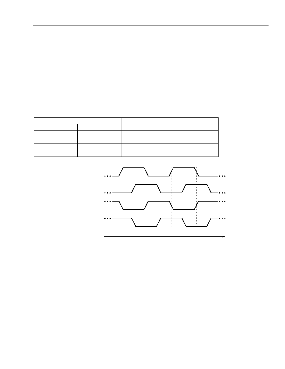
In the contra-directional clocking mode (CLKMODE = 1), the data is sampled with the internal 2.5 GHz clock at the
time of the falling edge of CK155P (see Figure 8 on page 19 for timing details). The device sends a 155 MHz clock
with one of four user-selectable phases out to the upstream device for clocking the data toward the device. The
user can program PHADJ[1:0] to adjust the phase of CK155 as a function of PWB layout and upstream device
propagation delay in order to meet the setup and hold time of the 155 Mbits/s data to the device. With a
PHADJ[1:0] = [11], the data is sampled by the internal CK2G5 clock at the falling edge of CK155P. PHADJ[1:0]
changes the phase of the CK155P clock without changing the input data sampling time. PHADJ[1:0] setting infor-
mation is given in Table 7, and the phase relationship of CK155 for each PHADJ[1:0] setting is shown in Figure 6.
Table 7. PHADJ Settings for CK155 Output Clock (Contra-Clocking Mode)
5-8064(F)r.2
Figure 6. CK155 Phase Relation vs. PHADJ Setting
Input Pins
Phase
PHADJ1
PHADJ0
1
1
(See part A of Figure 6.)
1
0
(See part B of Figure 6.)
0
1
(See part C of Figure 6.)
0
0
(See part D of Figure 6.)
A. (0 DEG.)
B. (≠90 DEG.)
C. (≠180 DEG.)
D. (≠270 DEG.)
TIME

TTRN012G5 and TTRN012G7
Preliminary Data Sheet
Clock Synthesizer, 16:1 Data Multiplexer
August 2000
14
Lucent Technologies Inc.
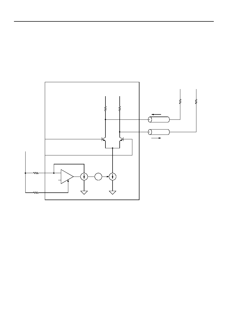
CML Output Structure (Used on Pins D2G5P/N, CK2G5P/N)
The CML architecture is essentially a current-steering mechanism combined with an amplifier. This makes the out-
put swing of the signal a function of the termination resistor and the programmable output current. The user should
connect external termination resistors from the CML output pins to V
CC
. The on-chip, 100
pull-up resistors pro-
vide a dc path when using an ac-coupled load.
The voltage swing of a CML signal is typically 400 mV, half that of ECL/PECL. The lower pulse amplitude reduces
noise transients, crosstalk, and EMI. It also uses half the amount of current through the termination resistors. The
schematic of a typical CML output structure is shown in Figure 7.
5-8065(F)r.2
Figure 7. Typical CML Output Structure
Choosing the Value of the External CML Reference Resistors (RREF1, RREF2)
The flexibility of the CML interface permits certain parameters to be customized for a particular application. The
RREF1 resistor controls the CML output driver current source. Adjusting this tail
current and termination resistors
will allow signal amplitude control (see the CML output specifications for limitations, page 18 and page 20) and
flexibility in termination schemes.
With RREF2 set to 1.5 k
, the equation for the CML output current is the following:
Iout = (18)*(1.21)/RREF1
The CML outputs have on-chip 100
load resistors to V
CC
to accommodate capacitive ac coupling. With a 50
1% load, the effective load resistance will be 33.33
± 6%. For a 400 mV voltage swing into the 50
load, set
RREF1 to 1.8 k
. For a 600 mV voltage swing, set RREF1 to 1.2 k
. In both cases, RREF2 remains fixed at a
value of 1.5 k
.
DEVICE-INTERNAL CML OUTPUT BUFFER CIRCUIT
EXTERNAL OUTPUT TERMINATION
V
CC
V
CC
50
50
V
CC
V
CC
100
100
VREF
18X
V
CC
RREF1
RREF2
+
≠
I
OUT
I
OUT

Preliminary Data Sheet
TTRN012G5 and TTRN012G7
August 2000
Clock Synthesizer, 16:1 Data Multiplexer
15
Lucent Technologies Inc.
Absolute Maximum Ratings
Stresses in excess of the absolute maximum ratings can cause permanent damage to the device. These are
absolute stress ratings only. Functional operation of the device is not implied at these or any other conditions in
excess of those given in the operational sections of the data sheet. Exposure to absolute maximum ratings for
extended periods can adversely affect device reliability.
Handling Precautions
Although protection circuitry has been designed into this device, proper precautions should be taken to avoid
exposure to electrostatic discharge (ESD) during handling and mounting. Lucent employs a human-body model
(HBM) and charged-device model (CDM) for ESD-susceptibility testing and protection design evaluation. ESD
voltage thresholds are dependent on the circuit parameters used in the defined model. No industrywide standard
has been adopted for the CDM. However, a standard HBM (resistance = 1500
, capacitance = 100 pF) is widely
used and, therefore, can be used for comparison purposes:
Operating Conditions
Table 8. Recommended Operating Conditions
Parameter
Min
Max
Unit
Power Supply Voltage (V
CC
)
--
4.0
V
Storage Temperature
≠40
125
∞C
Pin Voltage
GND ≠ 0.5
V
CC
+ 0.5
V
Device
Voltage
TTRN012G5
200 V
TTRN012G7
200 V
Parameter
Symbol
Min
Typ
Max
Unit
Power Supply (dc voltage)
--
3.135
3.3
3.465
V
Ground
--
--
--
--
V
Input Voltage:
Low
High
V
IL
V
IH
See Table 10,
Table 12,
Table 14.
See Table 10,
Table 12,
Table 14.
See Table 10,
Table 12,
Table 14.
V
V
Temperature:
Ambient
T
A
≠40
--
85
∞C
Power Dissipation:
MBIC 025 BiCMOS
MBIC 025 SiGe BiCMOS
P
D
P
D
--
--
1.5
0.9
TBD
1.14
W
W

TTRN012G5 and TTRN012G7
Preliminary Data Sheet
Clock Synthesizer, 16:1 Data Multiplexer
August 2000
16
Lucent Technologies Inc.
Electrical Characteristics
Reference Frequency (REFCLKP/N) Specifications
The device requires a differential LVPECL reference clock input.
s
When using the TTRN012G5 device, a 155.52 MHz differential LVPECL clock must be applied to the
REFCLKP/N input.
s
When using the TTRN012G7 device at the OC-48/STM-16 rate, a 155.52 MHz differential LVPECL clock must
be applied to the REFCLKP/N input.
s
When using the TTRN012G7 device at the RS FEC OC-48/STM-16 rate, a 166.62 MHz differential LVPECL
clock must be applied to the REFCLKP/N input.
Table 9 provides the characteristics of the REFCLKP/N input.
Table 9. Reference Frequency Characteristics
* Includes effects of power supply variation, temperature, electrical loading, and aging. The ±20 ppm tolerance is
required to meet SONET/SDH requirements. For non-SONET/SDH compliant systems, looser tolerances may apply.
Measured under one 3.3 V LVPECL load. Includes frequency components up to 2 MHz.
Specified range is to be compatible with environmental specification of TTRN012G5 or TTRN012G7. Applications
requiring a reduced temperature range may specify the reference frequency oscillator accordingly.
Parameter
Min
Typ
Max
Unit
Reference Frequency (REFCLKP/N)
--
155.52
--
MHz
--
166.62
--
MHz
Reference Frequency Tolerance*
≠20
--
20
ppm
Duty Cycle
40
--
60
%
Phase Jitter
--
--
3
ps(rms)
Temperature
≠40
--
85
∞C
Supply Voltage
3.10
--
3.60
V

Preliminary Data Sheet
TTRN012G5 and TTRN012G7
August 2000
Clock Synthesizer, 16:1 Data Multiplexer
17
Lucent Technologies Inc.
Electrical Characteristics
(continued)
LVPECL, CMOS, CML Input and Output Pins
Notes:
1. For Table 10 through Table 17, V
CC
= 3.3 V ± 5%, T
A
= ≠40 ∞C to +85 ∞C; these tables apply to both MBIC 025
BiCMOS and MBIC 025 SiGe BiCMOS technologies.
2. For more information on interpreting CML specifications, see the CML Output Structure (Used on Pins
D2G5P/N, CK2G5P/N) section on page 14.
Table 10. LVPECL Input Pin Characteristics
Table 11. LVPECL Output Pin Characteristics
Table 12. CMOS Input Pin Characteristics
Table 13. CMOS Output Pin Characteristics
Applicable
Pins
Symbol
Parameter
Conditions
Min
Typ
Max
Unit
D[15:0]P/N,
PARITYP/N,
REFCLKP/N
V
IH
Input Voltage High
Referred to V
CC
≠1165
--
≠880
mV
V
IL
Input Voltage Low
Referred to V
CC
≠1810
--
≠1475
mV
I
IH
Input Current High Leakage
V
IN
= V
IH
(max)
--
--
20
µ
A
I
IL
Input Current Low Leakage
V
IN
= V
IL
(min)
5
--
µ
A
Applicable
Pins
Symbol
Parameter
Conditions
Min
Typ
Max
Unit
CK155P/N,
VALIDP/N,
MONAPAP/N
V
OH
Output Voltage High
Load = 50
connected to
V
CC
≠ 2.0 V
V
CC
≠ 1.31
V
CC
≠ 1.20
V
CC
≠ 0.90
V
V
OL
Output Voltage Low
Load = 50
connected to
V
CC
≠ 2.0 V
V
CC
≠ 1.95
V
CC
≠ 1.88
V
CC
≠ 1.80
V
Applicable
Pins
Symbol
Parameter
Conditions
Min
Max
Unit
RESETN,
PHADJ[1:0],
EXTADJN,
INVDATN,
TESTN,
CLKMODE,
ENCK2G5,
ENLBDN
V
IH
Input Voltage High
--
V
CC
≠ 1.0
V
CC
V
V
IL
Input Voltage Low
--
GND
1.0
V
I
IH
Input Current High Leakage
V
IN
= V
CC
--
10
µ
A
I
IL
Input Current Low Leakage
V
IN
= GND
≠225
--
µ
A
Applicable
Pins
Symbol
Parameter
Conditions
Min
Max
Unit
LCKLOSSN
V
OH
Output Voltage High
I
OH
= ≠4.0 mA
V
CC
≠ 0.5
V
CC
V
V
OL
Output Voltage Low
I
OL
= 4.0 mA
GND
0.5
V
C
l
Output Load Capacitance
--
--
15
pF

TTRN012G5 and TTRN012G7
Preliminary Data Sheet
Clock Synthesizer, 16:1 Data Multiplexer
August 2000
18
Lucent Technologies Inc.
Electrical Characteristics
(continued)
LVPECL, CMOS, CML Input and Output Pins
(continued)
Table 14. CML Input Pin dc Characteristics
Table 15. CML Output Pin dc Characteristics
* Applies when RREF1 = 1 k
.
Applies when RREF1 = 1.8 k
.
Applies when RREF1 = 6 k
.
Applicable
Pins
Symbol
Parameter
Conditions
Min
Typ
Max
Unit
TSTCKP/N
V
IL
Input Voltage Low
--
--
V
CC
≠ 0.4
--
V
V
IH
Input Voltage High
--
V
CC
--
V
Applicable
Pins
Symbol
Parameter
Conditions
Min*
Typ
Max
Unit
D2G5P/N,
LBDP/N,
CK2G5P/N
V
OL
Output Voltage Low
RREF2 = 1.5 k
,
R
L
= 50
,
All signals
differential
V
CC
≠ 1.2
V
CC
≠ 0.4
--
V
V
OH
Output Voltage High
--
V
CC
V
CC
+ 0.3
V
I
OL
Output Current Low
3.6
12
18
mA
I
OH
Output Current High
--
0
1
µ
A

Preliminary Data Sheet
TTRN012G5 and TTRN012G7
August 2000
Clock Synthesizer, 16:1 Data Multiplexer
19
Lucent Technologies Inc.
Timing Characteristics
Transmit Timing
Figure 8 shows the timing relationships between the 155.52 MHz or 166.62 MHz output clock (CK155P/N) and the
155.52 Mbits/s or 166.62 Mbits/s input data (D[15:0]P/N) and the input parity valid check (PARITYP/N). Also
shown is the relationship of the VALIDP/N output signal to CK155P/N; this relationship is true for both the contra-
clocking mode and the clockless transfer mode.
5-7726(F).hr.2
Note: T
SU
and T
HOLD
only apply in contra-clocking mode when CLKMODE = 1.
Figure 8. Transmit Timing Waveform
The 155 MHz or 166 MHz output clock and data signals from Figure 8 are characterized in Table 16.
Table 16. LVPECL Input/Output Pin ac Timing Characteristics
Applicable
Pins
Symbol
Parameter
Conditions
Min
Typ
Max
Unit
CK155P/N
--
Duty Cycle
All signals
differential
40
50
60
%
t
PERIOD
155.52 MHz Clock Period
--
6.43
--
ns
166.62 MHz Clock Period
--
6.00
--
ns
Input Timing
D[15:0]P/N,
PARITYP/N,
CK155P/N
t
SU
Setup from Clock Edge to
D[15:0]P/N or to
PARITYP/N Edge
CLKMODE = 1, All
signals differential
2.0
--
--
ns
t
HOLD
Hold from Clock Edge to
D[15:0]P/N or to
PARITYP/N Edge
CLKMODE = 1,
All signals
differential
0.5
--
--
ns
t
RISE
,
t
FALL
Rise, Fall Times:
20%--80%
All signals
differential
200
500
800
ps
t
SKEW
Transition Skew Rise to Fall
≠100
0
100
ps
Output Timing
VALIDP/N,
CK155P/N
t
DD
Time Delay from Clock Edge
to VALIDP/N Edge
All signals
differential
≠300
800
1500
ps
t
RISE
,
t
FALL
Rise, Fall Times:
20%--80%
200
500
800
ps
t
SKEW
Transition Skew Rise to Fall
≠100
0
100
ps
OUTPUT
CK155P
CK155N
INPUTS
D[15:0]P/N,
PARITYP/N
t
SU
DATA 1
t
PERIOD
DATA 2
t
HOLD
OUTPUT
VALIDP/N
VALID 1
VALID 2
t
DD

TTRN012G5 and TTRN012G7
Preliminary Data Sheet
Clock Synthesizer, 16:1 Data Multiplexer
August 2000
20
Lucent Technologies Inc.
Timing Characteristics
(continued)
Transmit Timing
(continued)
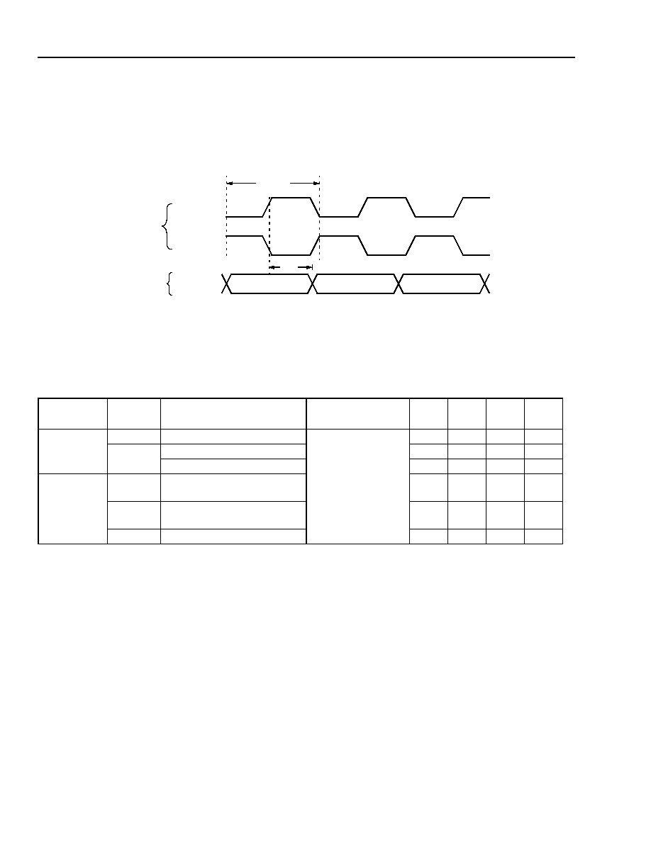
Figure 9 shows the timing relationship between the 2.5 GHz or 2.7 GHz output clock (CK2G5P/N) and the
2.5 Gbits/s or 2.7 Gbits/s output data (D2G5P/N).
5-7726(F).er.4
Figure 9. Transmit Timing Waveform with 2.5 GHz or 2.7 GHz Clock
The 2.5 GHz or 2.7 GHz output clock and data signals from Figure 9 are characterized in Table 17.
Table 17. CML Output Pin ac Timing Characteristics
Applicable
Pins
Symbol
Parameter
Conditions
Min
Typ
Max
Unit
CK2G5P/N
--
Duty Cycle
RREF1 = 1.8 k
RREF2 = 1.5 k
R
L
= 50
All signals
differential
40
50
60
%
t
PERIOD
2.48832 GHz Clock Period
--
402
--
ps
2.66606 GHz Clock Period
--
375
--
ps
D2G5P/N,
CK2G5P/N,
LBDP/N
t
DD
Time Delay from Clock Edge
to Data Edge
151
201
251
ps
t
RISE
,
t
FALL
Rise, Fall Times:
20%--80%
50
80
120
ps
t
SKEW
Transition Skew Rise to Fall
≠10
0
10
ps
OUTPUT
CK2G5P
CK2G5N
OUTPUT
D2G5P/N
DATA 1
t
PERIOD
DATA 2
DATA 3
t
DD

Preliminary Data Sheet
TTRN012G5 and TTRN012G7
August 2000
Clock Synthesizer, 16:1 Data Multiplexer
21
Lucent Technologies Inc.
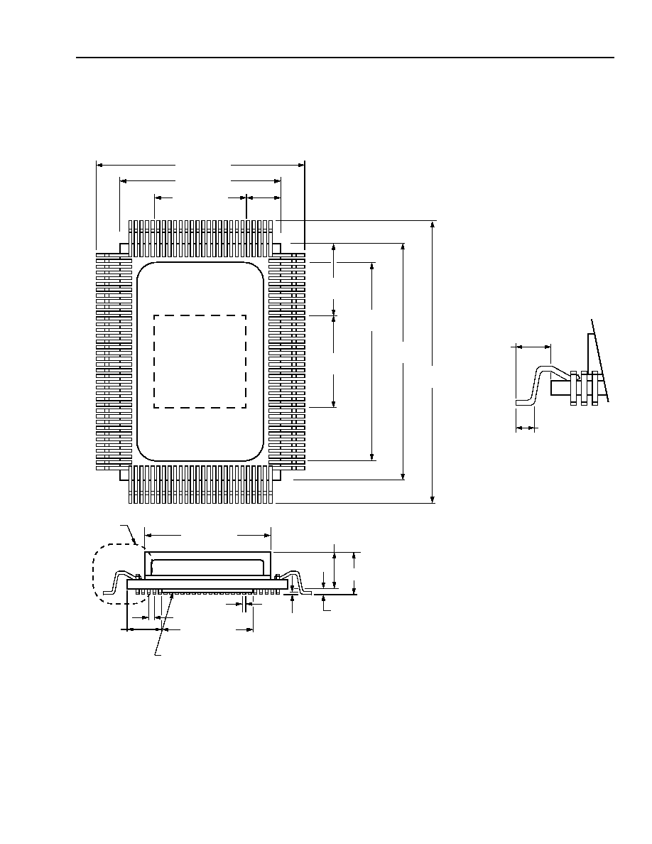
Outline Diagram
128-Pin QFP
Dimensions are in millimeters.
5-8416(F)r.2
3.30 (REF)
0.50 (TYP)
2.80 (REF)
1
38
65
102
103
128
17.20
±
0.20
19.86
±
0.10
64
39
0.800
±
0.150
1.600
±
0.150
DETAIL A
1
LUCENT
Co
de
N
a
me
YY
WW
L
X
XXX
XKNV
0.38 (REF)
DETAIL A
11.43
±
0.18
23.20
±
0.20
13.89
±
0.10
8.13 (REF)
2.89
(REF)
17.52
±
0.18
8.13
(REF)
0.20
±
0.06
0.000 TO 0.100
8.13 (REF)
2.89
(REF)
(8.13)
2
x 0.305 HEAT SINK
5.87
(REF)

TTRN012G5 and TTRN012G7
Preliminary Data Sheet
Clock Synthesizer, 16:1 Data Multiplexer
August 2000
Lucent Technologies Inc. reserves the right to make changes to the product(s) or information contained herein without notice. No liability is assumed as a result of their use or application. No
rights under any patent accompany the sale of any such product(s) or information.
Copyright © 2000 Lucent Technologies Inc.
All Rights Reserved
August 2000
DS00-375HSPL (Replaces DS00-155HSPL)
For additional information, contact your Microelectronics Group Account Manager or the following:
INTERNET:
http://www.lucent.com/micro
E-MAIL:
docmaster@micro.lucent.com
N. AMERICA:
Microelectronics Group, Lucent Technologies Inc., 555 Union Boulevard, Room 30L-15P-BA, Allentown, PA 18109-3286
1-800-372-2447, FAX 610-712-4106 (In CANADA: 1-800-553-2448, FAX 610-712-4106)
ASIA PACIFIC: Microelectronics Group, Lucent Technologies Singapore Pte. Ltd., 77 Science Park Drive, #03-18 Cintech III, Singapore 118256
Tel. (65) 778 8833, FAX (65) 777 7495
CHINA:
Microelectronics Group, Lucent Technologies (China) Co., Ltd., A-F2, 23/F, Zao Fong Universe Building, 1800 Zhong Shan Xi Road, Shanghai
200233 P. R. China Tel. (86) 21 6440 0468, ext. 325, FAX (86) 21 6440 0652
JAPAN:
Microelectronics Group, Lucent Technologies Japan Ltd., 7-18, Higashi-Gotanda 2-chome, Shinagawa-ku, Tokyo 141, Japan
Tel. (81) 3 5421 1600, FAX (81) 3 5421 1700
EUROPE:
Data Requests: MICROELECTRONICS GROUP DATALINE: Tel. (44) 7000 582 368, FAX (44) 1189 328 148
Technical Inquiries: GERMANY: (49) 89 95086 0 (Munich), UNITED KINGDOM: (44) 1344 865 900 (Ascot),
FRANCE: (33) 1 40 83 68 00 (Paris), SWEDEN: (46) 8 594 607 00 (Stockholm), FINLAND: (358) 9 3507670 (Helsinki),
ITALY: (39) 02 6608131 (Milan), SPAIN: (34) 1 807 1441 (Madrid)
Ordering Information
DS00-375HSPL Replaces DS00-155HSPL to Incorporate the Following Updates
1. Added a second technology, MBIC 025 SiGe BiCMOS, to the data sheet.
2. Page 7, REFCLKP/N pins, corrected definition.
3. Page 15, Absolute Maximum Ratings, added maximum power supply value of 4.0 V.
4. Page 15, Handling Precautions, corrected ESD threshold value from TBD to
200 V.
5. Page 15, Table 8, added MBIC 025 SiGe BiCMOS power dissipation values.
6. Page 17, Table 11, updated LVPECL Output Pin Characteristics.
7. Page 22, Ordering Information, added MBIC 025 SiGe BiCMOS comcodes.
Device Code
Package
Temperature
Comcode
(Ordering Number)
TTRN012G5:
TTRN012G5 (BiCMOS)
TTRN012G53XE1 (SiGe BiCMOS)
128-pin QFP
128-pin QFP
≠40 ∞C to +85 ∞C
≠40 ∞C to +85 ∞C
108419961
108700709
TTRN012G7:
TTRN012G7 (BiCMOS)
TTRN012G73XE1 (SiGe BiCMOS)
128-pin QFP
128-pin QFP
≠40 ∞C to +85 ∞C
≠40 ∞C to +85 ∞C
108560335
108700717
--
--
--
--


