Hardware Design Guide, Revision 1
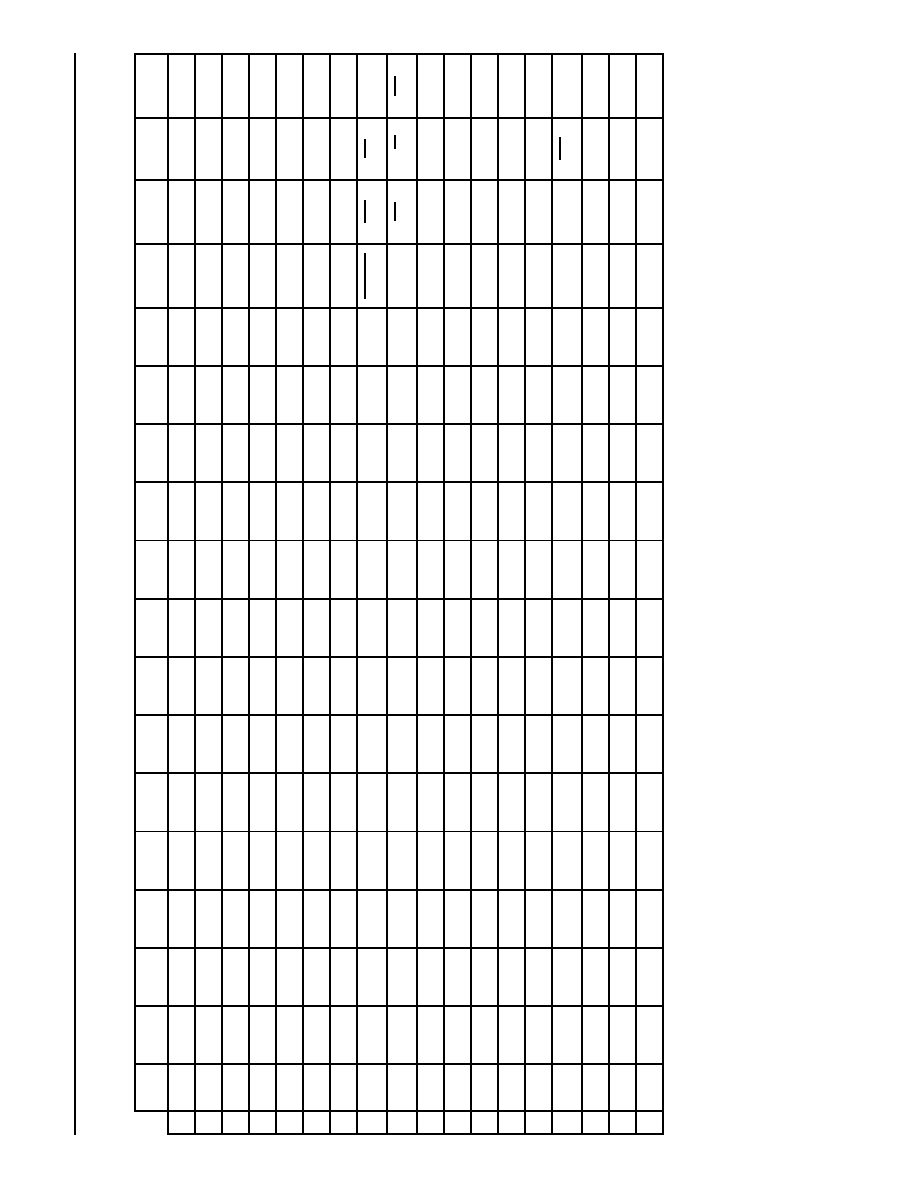
November 2, 2005
TSI-8
8K x 8K Time-Slot Interchanger
1 Introduction
The last issue of this data sheet was May, 2002 (This docu-
ment was previously labeled Advance Information.) A
change history is included in
9 Change History on page 25
.
Red change bars have been installed on all text, figures,
and tables that were added or changed. All changes to the
text are highlighted in red. Changes within figures, and the
figure title itself, are highlighted in red, if feasible. Formatting
or grammatical changes have not been highlighted. Deleted
sections, paragraphs, figures, or tables will be specifically
mentioned.
If the reader displays this document in Acrobat Reader
Æ
,
clicking on any blue entry in the text will bring the reader to
that reference point.
This document describes the hardware interfaces to the
Agere Systems Inc. TSI-8 device. Information relevant to
the use of the device in a board design is covered. Ball de-
scriptions, dc electrical characteristics, timing diagrams, ac
timing parameters, packaging, and operating conditions are
included.
1.1 Related Documents
More information on the TSI-8 is contained in the following
documents:
TSI-8 Product Description
TSI-8 Register Description
TSI-8 Systems Design Guide
2 Description
2.1 Block Diagram and High-Level Interface Definition
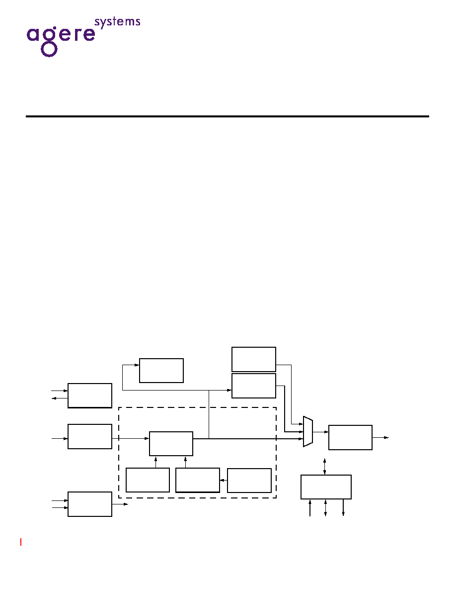
Figure 2-1. Block Diagram and High-Level Interface Definition
TEST ACCESS
PORT
READ ADDRESS
COUNTER
CONNECTION
STORE
WRITE ADDRESS
COUNTER
DATA
STORE
MICROPROCESSOR
INTERFACE
TRANSMIT
CHI
TEST PATTERN
GENERATOR
TEST PATTERN
MONITOR
8K X 8K
SWITCH
FABRIC
CLOCK
GENERATOR
RECEIVE
CHI
TRANSLATION
TABLE LOOKUP
32
32

Table of Contents
Contents
Page
Contents
Page
2
Agere Systems Inc.
TSI-8
Hardware Design Guide, Revision 1
8K x 8K Time-Slot Interchanger
November 2, 2005
1 Introduction .............................................................. 1
1.1 Related Documents .......................................... 1
2 Description ............................................................... 1
2.1 Block Diagram and High-Level Interface
Definition .......................................................... 1
3 Ball Information ........................................................ 3
3.1 Ball Diagram ..................................................... 3
3.2 Package Ball Assignments ............................... 4
3.3 Ball Types ......................................................... 8
3.4 Ball Definitions .................................................. 8
4 Absolute Maximum Ratings ................................... 11
4.1 Handling Precautions ..................................... 11
4.2 ESD Tolerance ............................................... 11
4.3 Package Thermal Characteristics ................... 11
4.4 Recommended Operating Conditions ............ 12
5 dc Electrical Characteristics .................................. 13
6 Timing Diagrams and ac Characteristics ............... 14
7 Outline Diagrams ................................................... 24
8 Ordering Information .............................................. 25
9 Change History ...................................................... 25
Figures
Page
Figure 2-1. Block Diagram and High-Level Interface
Definition ................................................... 1
Figure 3-1. Package Diagram (Top View) ................... 3
Figure 6-1. CHICLK Timing Specifications ................ 14
Figure 6-2. MPUCLK Timing Specifications .............. 14
Figure 6-3. ac Timing Specification ........................... 15
Figure 6-4. CHI Interface Timing ............................... 15
Figure 6-5. Typical Receive CHI Timing with 16.384
Mbits/s Data and 16.384 MHz CHICLK... 16
Figure 6-6. Transmit CHI Timing with 16.384 Mbits/s
Data and 16.384 MHz CHICLK ............... 16
Figure 6-7. Typical Receive CHI Timing with 8.192
Mbits/s Data and 16.384 MHz CHICLK... 17
Figure 6-8. Transmit CHI Timing with 8.192 Mbits/s
Data and 16.384 MHz CHICLK ............... 17
Figure 6-9. Typical Receive CHI Timing with 4.096
Mbits/s Data and 16.384 MHz CHICLK... 18
Figure 6-10. Transmit CHI Timing with 4.096 Mbits/s
Data and 16.384 MHz CHICLK ............... 18
Figure 6-11. Typical Receive CHI Timing with 2.048
Mbits/s Data and 16.384 MHz CHICLK... 19
Figure 6-12. Transmit CHI Timing with 2.048 Mbits/s
Data and 16.384 MHz CHICLK ............... 19
Figure 6-13. Typical Receive CHI Timing with 8.192
Mbits/s Data and 8.192 MHz CHICLK.....20
Figure 6-14. Transmit CHI Timing with 8.192 Mbits/s
Data and 8.192 MHz CHICLK .................20
Figure 6-15. CHI 3-State Output Control ...................21
Figure 6-16. Microprocessor Port Timing--
Read Cycle.............................................22
Figure 6-17. Microprocessor Port Timing--
Write Cycle.............................................23
Tables
Page
Table 3-1. Package Ball Assignments in Signal Name
Order ...........................................................4
Table 3-2. Package Ball Assignments in Ball Number
Order (Top View) .........................................6
Table 3-3. Package Ball Assignments in Ball Number
Order (Bottom View) (continued).................7
Table 3-4. Ball Types ...................................................8
Table 3-5. Timing Port..................................................8
Table 3-6. Transmit and Receive Concentration
Highways.....................................................8
Table 3-7. Control Port.................................................9
Table 3-8. Initialization and Test Access......................9
Table 3-9. Power Balls...............................................10
Table 4-1. Absolute Maximum Ratings ...................... 11
Table 4-2. ESD Tolerance.......................................... 11
Table 4-3. Power Consumption ................................. 11
Table 4-4. Operating Conditions ................................12
Table 5-1. CMOS Inputs ............................................13
Table 5-2. CMOS Outputs .........................................13
Table 5-3. CMOS Bidirectionals (Excluding
TXD[31:00]) ...............................................13
Table 5-4. CMOS Bidirectionals (TXD[31:00]) ...........13
Table 6-1. CHICLK Timing Specifications ..................14
Table 6-2. MPUCLK Timing Specifications ................14
Table 6-3. CMOS Output ac Timing Specification * ...15
Table 6-4. CHI Interface Timing .................................15
Table 6-5. CHI 3-State Output Control.......................21
Table 6-6. Microprocessor Port Timing--
Read Cycle................................................22
Table 6-7. Microprocessor Port Timing--
Write Cycle23
Table 8-1. Ordering Information.................................25

Hardware Design Guide, Revision 1
TSI-8
November 2, 2005
8K x 8K Time-Slot Interchanger
Agere Systems Inc.
3
3 Ball Information
3.1 Ball Diagram
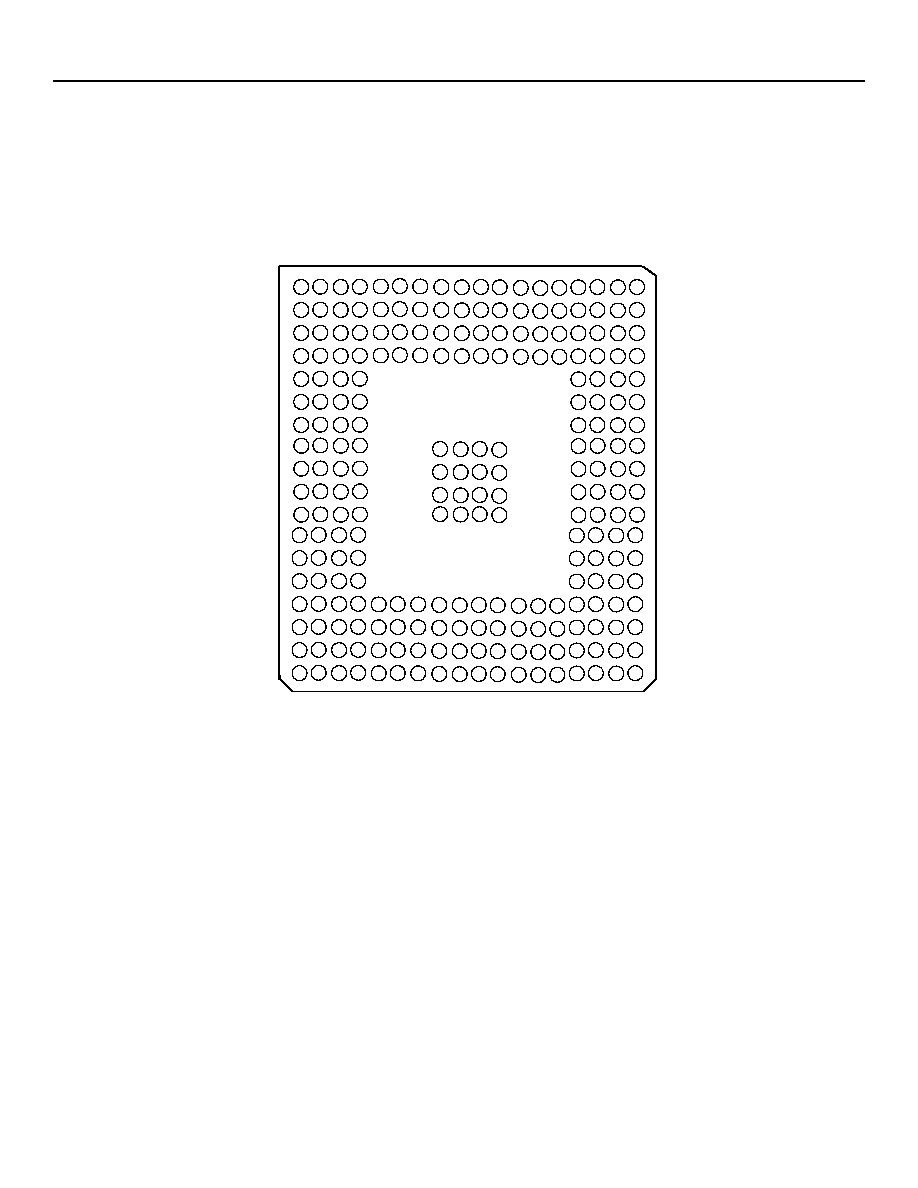
The TSI-8 is housed in a 240-ball plastic ball grid array. Figure 3-1 shows the ball arrangement viewed from the top of the
package. The balls are spaced on a 1.0 mm pitch.
Figure 3-1. Package Diagram (Top View)
B
C
A
E
F
D
H
J
G
L
M
K
P
R
N
U
V
T
2
3
1
5
6
4
8
7
10
11
9
13
14
12
16
15
17
18

TSI-8
Hardware Design Guide, Revision 1
8K x 8K Time-Slot Interchanger
November 2, 2005
4
4
Agere Systems Inc.
3.2 Package Ball Assignments
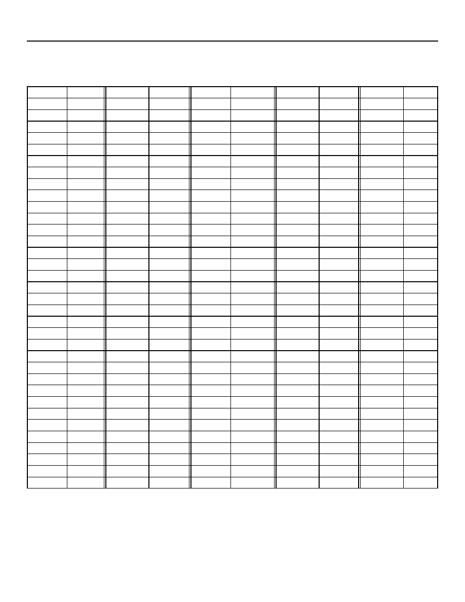
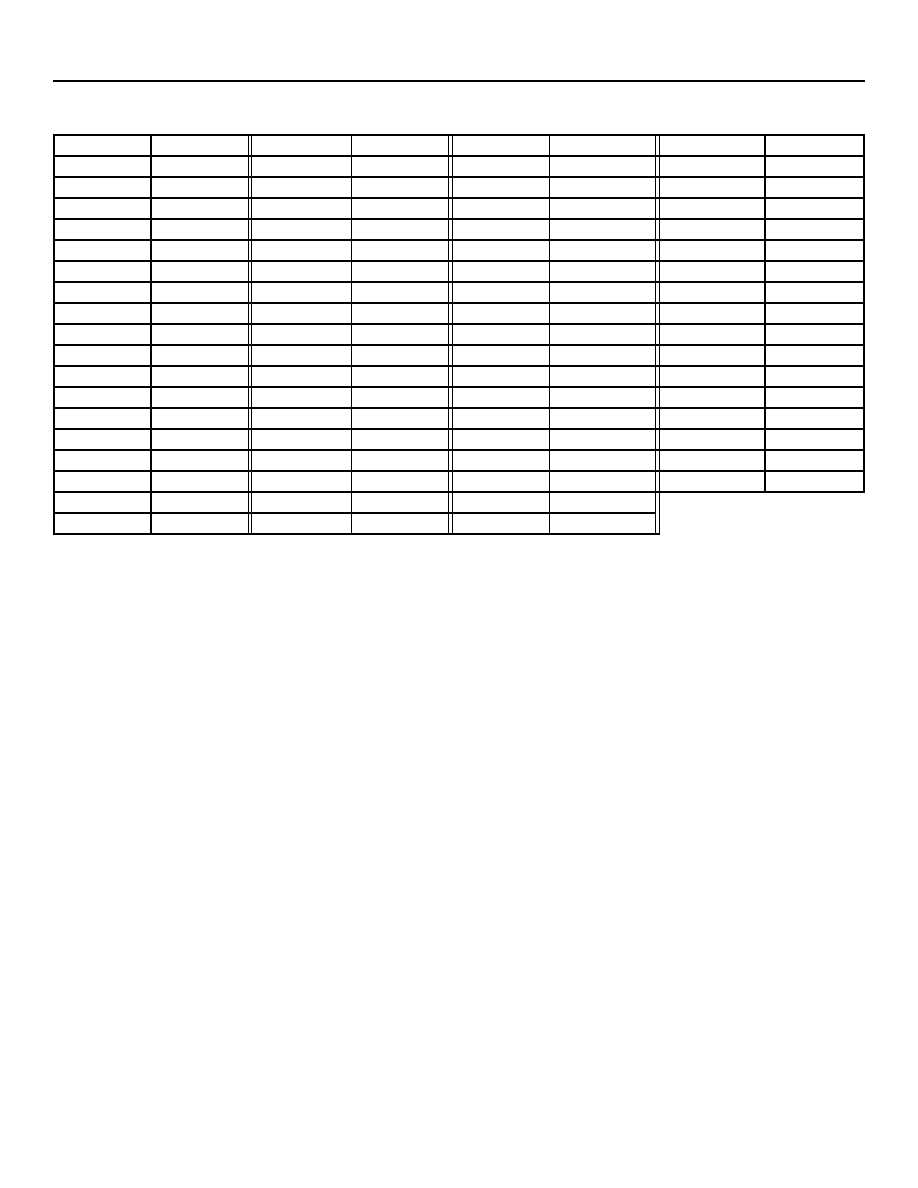
Table 3-1. Package Ball Assignments in Signal Name Order
Symbol
Ball Symbol
Ball
Symbol
Ball
Symbol
Ball
Symbol
Ball
ADDR00
A17
DATA13
P18
RXD11
V7
TXD08
F1
V
DD15
D13
ADDR01
A16
DATA14
P17
RXD12
T8
TXD09
G3
V
DD15
D14
ADDR02
A15
DATA15
P16
RXD13
U8
TXD10
G2
V
DD15
G4
ADDR03
A14
DT
H17
RXD14
V8
TXD11
G1
V
DD15
H4
ADDR04
A13
FSYNC
T11
RXD15
U9
TXD12
H2
V
DD15
L4
ADDR05
A12
HIZ
R17
RXD16
V9
TXD13
H1
V
DD15
M4
ADDR06
A11
INT
H16
RXD17
V10
TXD14
J2
V
DD15
R7
ADDR07
A10
MPUCLK
K15
RXD18
U10
TXD15
J1
V
DD15
R8
ADDR08
A9
PAR0
R18
RXD19
V11
TXD16
K1
V
DD15
R11
ADDR09
A8
PAR1
P15
RXD20
U11
TXD17
K2
V
DD15
R12
ADDR10
A7
R/W
J17
RXD21
V12
TXD18
L1
V
DD33
C9
ADDR11
A6
RESET
H15
RXD22
U12
TXD19
L2
V
DD33
C10
ADDR12
A5
RSV1
F17
RXD23
V13
TXD20
M1
V
DD33
C17
ADDR13
A4
RSV2
F18
RXD24
U13
TXD21
M2
V
DD33
D9
ADDR14
A3
RSV3
E15
RXD25
V14
TXD22
N1
V
DD33
D10
ADDR15
A2
RSV4
E16
RXD26
U14
TXD23
N2
V
DD33
E3
AS
J16
RSV5
E17
RXD27
V15
TXD24
N3
V
DD33
F3
CHICLK
R16
RSV6
D17
RXD28
U15
TXD25
P1
V
DD33
F15
CKSPD0
E18
RSV7
B18
RXD29
T15
TXD26
P2
V
DD33
H3
CKSPD1
D16
RSV8
C18
RXD30
V16
TXD27
R1
V
DD33
J3
CS
J18
RSV9
D18
RXD31
U16
TXD28
R2
V
DD33
K16
DATA00
K18
RSV10
T18
TCK
G17
TXD29
T1
V
DD33
P3
DATA01
K17
RSV11
V17
TDI
G16
TXD30
T2
V
DD33
R3
DATA02
L18
RXD00
V2
TDO
G18
TXD31
U1
V
DD33
T5
DATA03
L17
RXD01
U3
TMS
G15
V
DD15
C5
V
DD33
T6
DATA04
L16
RXD02
V3
TRSTN
H18
V
DD15
C6
V
DD33
T9
DATA05
M18
RXD03
U4
TXD00
B1
V
DD15
C7
V
DD33
T10
DATA06
M17
RXD04
V4
TXD01
C2
V
DD15
C12
V
DD33
T14
DATA07
M16
RXD05
U5
TXD02
C1
V
DD15
C13
V
DD33
T17
DATA08
M15
RXD06
V5
TXD03
D2
V
DD15
C14
V
DDPLL
R14
DATA09
N18
RXD07
U6
TXD04
D1
V
DD15
D5
V
IO
K3
DATA10
N17
RXD08
V6
TXD05
E2
V
DD15
D6
V
PRE
T4
DATA11
N16
RXD09
T7
TXD06
E1
V
DD15
D7
V
SS
A1
DATA12
N15
RXD10
U7
TXD07
F2
V
DD15
D12
V
SS
A18

Hardware Design Guide, Revision 1
TSI-8
November 2, 2005
8K x 8K Time-Slot Interchanger
Agere Systems Inc.
5
Table 3-1. Package Ball Assignments in Signal Name Order (continued)
Symbol
Ball
Symbol
Ball
Symbol
Ball
Symbol Ball
V
SS
B2
V
SS
C8
V
SS
J9
V
SS
R4
V
SS
B3
V
SS
C11
V
SS
J10
V
SS
R5
V
SS
B4
V
SS
C15
V
SS
J11
V
SS
R6
V
SS
B5
V
SS
C16
V
SS
J15
V
SS
R9
V
SS
B6
V
SS
D3
V
SS
K4
V
SS
R10
V
SS
B7
V
SS
D4
V
SS
K8
V
SS
R15
V
SS
B8
V
SS
D8
V
SS
K9
V
SS
T3
V
SS
B9
V
SS
D11
V
SS
K10
V
SS
T12
V
SS
B10
V
SS
D15
V
SS
K11
V
SS
T13
V
SS
B11
V
SS
E4
V
SS
L3
V
SS
T16
V
SS
B12
V
SS
F4
V
SS
L8
V
SS
U2
V
SS
B13
V
SS
F16
V
SS
L9
V
SS
U17
V
SS
B14
V
SS
H8
V
SS
L10
V
SS
U18
V
SS
B15
V
SS
H9
V
SS
L11
V
SS
V1
V
SS
B16
V
SS
H10
V
SS
L15
V
SS
V18
V
SS
B17
V
SS
H11
V
SS
M3
V
SSPLL
R13
V
SS
C3
V
SS
J4
V
SS
N4
V
SS
C4
V
SS
J8
V
SS
P4

6
Agere Systems Inc.
TSI-8
Hardware Design Guide, Revision 1
8K x 8K Time-Slot Interchanger
November 2, 2005
Table 3-2. Package Ball Assignments in Ball Number Order
(Top View) (continued)
1
2
3
4
5
6
7
8
9
10
11
12
13
14
15
16
17
18
A
VSS ADDR15 ADDR14 ADDR13 ADDR12 ADDR11 ADDR10 ADDR09 ADDR08 ADDR07 ADDR06 ADDR05 ADDR04 ADDR03 ADDR02 ADDR01 ADDR00
VSS
B TXD00
VSS
VSS
VSS
VSS
VSS
VSS
VSS
VSS
VSS
VSS
VSS
VSS
VSS
VSS
VSS
VSS
RSV7
C TXD02 TXD01
VSS
VSS
VDD15 VDD15 VDD15
VSS
VDD33 VDD33
VSS
VDD15 VDD15 VDD15
VSS
VSS
VDD33
RSV8
D TXD04 TXD03
VSS
VSS
VDD15 VDD15 VDD15
VSS
VDD33 VDD33
VSS
VDD15 VDD15 VDD15
VSS
CKSPD1
RSV6
RSV9
E TXD06 TXD05
VDD33
VSS
--
--
--
--
--
--
--
--
--
--
RSV3
RSV4
RSV5
CKSPD0
F TXD08 TXD07
VDD33
VSS
--
--
--
--
--
--
--
--
--
--
VDD33
VSS
RSV1
RSV2
G TXD11 TXD10
TXD09
VDD15
--
--
--
--
--
--
--
--
--
--
TMS
TDI
TCK
TDO
H TXD13 TXD12
VDD33 VDD15
--
--
--
VSS
VSS
VSS
VSS
--
--
--
RESET
INT
DT
TRSTN
J TXD15 TXD14
VDD33
VSS
--
--
--
VSS
VSS
VSS
VSS
--
--
--
VSS
AS
R/W
CS
K TXD16 TXD17
VIO
VSS
--
--
--
VSS
VSS
VSS
VSS
--
--
--
MPUCLK VDD33
DATA01 DATA00
L TXD18 TXD19
VSS
VDD15
--
--
--
VSS
VSS
VSS
VSS
--
--
--
VSS
DATA04 DATA03 DATA02
M TXD20 TXD21
VSS
VDD15
--
--
--
--
--
--
--
--
--
--
DATA08
DATA07 DATA06 DATA05
N TXD22 TXD23
TXD24
VSS
--
--
--
--
--
--
--
--
--
--
DATA12
DATA11 DATA10 DATA09
P TXD25 TXD26
VDD33
VSS
--
--
--
--
--
--
--
--
--
--
PAR1
DATA15 DATA14 DATA13
R TXD27 TXD28
VDD33
VSS
VSS
VSS
VDD15 VDD15
VSS
VSS
VDD15 VDD15 VSSPLL VDDPLL
VSS
CHICLK
HIZ
PAR0
T TXD29 TXD30
VSS
VPRE
VDD33 VDD33 RXD09 RXD12 VDD33 VDD33 FSYNC
VSS
VSS
VDD33
RXD29
VSS
VDD33
RSV10
U TXD31
VSS
RXD01 RXD03 RXD05 RXD07 RXD10 RXD13 RXD15 RXD18 RXD20 RXD22 RXD24 RXD26
RXD28
RXD31
VSS
VSS
V
VSS
RXD00 RXD02 RXD04 RXD06 RXD08
RXD11
RXD14 RXD16 RXD17 RXD19 RXD21 RXD23 RXD25
RXD27
RXD30
RSV11
VSS

Hardware Design Guide, Revision 1
TSI-8
November 2, 2005
8K x 8K Time-Slot Interchanger
Agere Systems Inc.
7
Table 3-3. Package Ball Assignments in Ball Number Order
(Bottom View)
18
17
16
15
14
13
12
11
10
9
8
7
6
5
4
3
2
1
A
VSS
ADDR00 ADDR01 ADDR02 ADDR03 ADDR04 ADDR05 ADDR06 ADDR07 ADDR08 ADDR09 ADDR10 ADDR11 ADDR12 ADDR13 ADDR14 ADDR15 VSS
B
RSV7
VSS
VSS
VSS
VSS
VSS
VSS
VSS
VSS
VSS
VSS
VSS
VSS
VSS
VSS
VSS
VSS
TXD00
C
RSV8
VDD33
VSS
VSS
VDD15
VDD15
VDD15
VSS
VDD33 VDD33
VSS
VDD15 VDD15 VDD15
VSS
VSS
TXD01 TXD02
D
RSV9
RSV6
CKSPD1
VSS
VDD15
VDD15
VDD15
VSS
VDD33 VDD33
VSS
VDD15 VDD15 VDD15
VSS
VSS
TXD03 TXD04
E CKSPD0
RSV5
RSV4
RSV3
--
--
--
--
--
--
--
--
--
--
VSS
VDD33 TXD05 TXD06
F
RSV2
RSV1
VSS
VDD33
--
--
--
--
--
--
--
--
--
--
VSS
VDD33 TXD07 TXD08
G
TDO
TCK
TDI
TMS
--
--
--
--
--
--
--
--
--
--
VDD15 TXD09 TXD10 TXD11
H
TRSTN
DT
INT
RESET
--
--
--
VSS
VSS
VSS
VSS
--
--
--
VDD15 VDD33 TXD12 TXD13
J
CS
R/W
AS
VSS
--
--
--
VSS
VSS
VSS
VSS
--
--
--
VSS
VDD33 TXD14 TXD15
K DATA00
DATA01
VDD33
MPUCLK
--
--
--
VSS
VSS
VSS
VSS
--
--
--
VSS
VIO
TXD17 TXD16
L
DATA02
DATA03
DATA04
VSS
--
--
--
VSS
VSS
VSS
VSS
--
--
--
VDD15
VSS
TXD19 TXD18
M DATA05
DATA06
DATA07
DATA08
--
--
--
--
--
--
--
--
--
--
VDD15
VSS
TXD21 TXD20
N DATA09
DATA10
DATA11
DATA12
--
--
--
--
--
--
--
--
--
--
VSS
TXD24 TXD23 TXD22
P DATA13
DATA14
DATA15
PAR1
--
--
--
--
--
--
--
--
--
--
VSS
VDD33 TXD26 TXD25
R
PAR0
HIZ
CHICLK
VSS
VDDPLL VSSPLL VDD15 VDD15
VSS
VSS
VDD15 VDD15
VSS
VSS
VSS
VDD33 TXD28 TXD27
T
RSV10
VDD33
VSS
RXD29
VDD33
VSS
VSS
FSYNC VDD33 VDD33 RXD12 RXD09 VDD33 VDD33
VPRE
VSS
TXD30 TXD29
U
VSS
VSS
RXD31
RXD28
RXD26
RXD24
RXD22 RXD20 RXD18 RXD15 RXD13 RXD10 RXD07 RXD05 RXD03 RXD01
VSS
TXD31
V
VSS
RSV11
RXD30
RXD27
RXD25
RXD23
RXD21 RXD19 RXD17 RXD16 RXD14 RXD11 RXD08 RXD06 RXD04 RXD02 RXD00
VSS

TSI-8
Hardware Design Guide, Revision 1
8K x 8K Time-Slot Interchanger
November 2, 2005
8
8
Agere Systems Inc.
3.3 Ball Types
This table describes each type of input, output, and I/O ball used on the TSI-8.
The dc switching and other electrical characteristics are specified later in this document.
3.4 Ball Definitions
This section describes the function of each of the device balls. The balls are listed by ball name. Package ball numbers are
listed in
Table 3-1
of this document. The static parameters (drive currents, switching thresholds, etc.) for each ball type (in-
put, output, etc.) are described in
Table 5-1
through
Table 5-4
.
Table 3-4. Ball Types
Type Label
Description
I
CMOS input, TTL switching thresholds.
I pd
CMOS input, TTL switching thresholds with internal pull-down resistor.
I pu
CMOS input, TTL switching thresholds with internal pull-up resistor.
O
CMOS output.
O od
Open drain output.
I/O
Bidirectional ball; CMOS input with TTL switching thresholds and CMOS output.
None
Analog inputs for external resistors, capacitors, voltage references, etc.
P
Power and ground.
Table 3-5. Timing Port
Ball Name Type
Name/Description
FSYNC
I
Frame Synchronization. This signal indicates the beginning of a 125 µs frame event (8 kHz). The
FSYNC ball can be programmed as active-low or active-high, but its polarity is the same for all concen-
tration highway interfaces (CHI). FSYNC can be sampled on either the positive or negative edge of
CHICLK. Time-slot numbers and bit offsets for each CHI are assigned relative to the detection of
FSYNC.
CHICLK
I
Clock. This is the master synchronous clock for the transmit and receive concentration highways. The
frequency can be 8.192 MHz or 16.384 MHz. It must be at least as fast as the highest CHI data rate.
CKSPD0
I
Clock Speed. Static control input that should be tied according to the frequency of CHICLK. If CHICLK
is connected to an 8.192 MHz source, CKSPD0 should be tied to V
SS
. If CHICLK is connected to a
16.384 MHz source, CKSPD0 should be tied to V
DD33
.
CKSPD1
I pd Clock Speed. Reserved, leave disconnected. 20 k
pull-down resistor.
Table 3-6. Transmit and Receive Concentration Highways
Ball Name Type
Name/Description
RXD[31:00] I pd Receive Data [31:00]. Receive concentration highways. These are serial, synchronous data streams
which may be individually programmed to operate at 2.048 Mbits/s, 4.096 Mbits/s, 8.192 Mbits/s, or
16.384 Mbits/s. They carry 32, 64, 128, or 256 time slots (respectively) each occupying eight contiguous
bits. 20 k
pull-down resistor.
TXD[31:00] I/O Transmit Data [31:00]. Normally these are output concentration highway data streams with data rate
options identical to the RXD inputs. These balls can be configured to operate as bidirectional multiplex
ports such as H.110. Further information can be found in the system design guide. 20 k
resistor
connected to V
PRE
.

Hardware Design Guide, Revision 1
TSI-8
November 2, 2005
8K x 8K Time-Slot Interchanger
Agere Systems Inc.
9
Table 3-7. Control Port
Ball Name Type
Name/Description
MPUCLK
I
Processor Clock. This clock is used to sample address, data, and control signals from the
microprocessor. This clock must be within the range of 0 MHz--66 MHz. Required for operation.
CS
I
Chip Select. Active-low chip select. This input is held low for the duration of any read or write access
to the TSI-8. Required for operation.
AS
I
Address Strobe. Active-low address strobe that is one MPUCLK cycle wide at the start of a
microprocessor access cycle to the TSI-8. This is used to initiate a microprocessor access. Required
for operation.
R/W
I
Read/Write. Cycle selection. R/W is set high during a read cycle, or set low for a write cycle.
Required for operation.
ADDR[15:00] I pu Address [15:00]. ADDR[15] is the most significant bit and ADDR[00] is the least significant bit for
addressing all the internal registers during microprocessor access cycles. All addresses are
16-bit word addresses; hence, in a typical application ADDR[00] of the TSI-8 device would be
connected to address bit 1 of a byte addressable system address bus. Required for operation. 200
k
pull-up resistor.
Note: The TSI-8 is little-endian; the least significant byte is stored in the lowest address and the most
significant byte is stored in the highest address. Care must be exercised in connection to
microprocessors that use big-endian byte ordering.
DATA[15:00]
I/O Data [15:00]. Data bus for all transfers between the microprocessor and the internal registers. The
balls are inputs during write cycles and outputs during read cycles. DATA[15] is the most significant
bit, and DATA[00] is the least significant bit. Required for operation.
PAR[1:0]
I/O Control Port Parity [1:0]. Byte-wide parity bits for data. PAR[1] is the parity for DATA[15:8], and
PAR[0] is the parity for DATA[7:0]. The parity sense (even or odd) is application programmable via a
register bit in the TSI-8. Not required for operation.
DT
O
Data Transfer Acknowledge. Active-low for one MPUCLK cycle. Indicates that data has been
written during write cycles or that data is valid during read cycles. High impedance when CS is a 1
and driven when CS is 0. Required for operation.
INT
O od Interrupt. This output is asserted low to indicate that an interrupt condition has occurred. This signal
remains active-low until the interrupt status register has been cleared or masked.
Table 3-8. Initialization and Test Access
Ball Name Type
Name/Description
RESET
I pu Reset. Global reset, active-low. Initializes all internal registers to their default state. The reset occurs
asynchronously, but RESET should be held low for at least two CHICLK periods. 20 k
pull-up resistor.
TCK
I pu Test Clock. This signal provides timing for the boundary scan and test access port (TAP) controller.
Should be static except during boundary-scan testing. 20 k
pull-up resistor.
TDI
I pu Test Data In. Data input for the boundary scan. Sampled on the rising edge of TCK. 20 k
pull-up
resistor.
TMS
I pu Test Mode Select (Active-Low). Controls boundary-scan test operations. TMS is sampled on the rising
edge of TCK. 20 k
pull-up resistor.
TRSTN
I pd Test Reset (Active-Low). This signal is an asynchronous reset for the TAP controller. 20 k
pull-down
resistor.
TDO
O
Test Data Out. Updated on the falling edge of TCK. The TDO output is high impedance except when
scanning out test data.
HIZ
I pu Output Enable. All output and bidrectional buffers will be high impedance when this input is low unless
boundary scan is enabled (TRSTN = 1). 20 k
pull-up resistor.
RSV[11:1]
-- Reserved [11:1]. These balls are used by Agere Systems during the manufacturing process. They must
be left unconnected.

TSI-8
Hardware Design Guide, Revision 1
8K x 8K Time-Slot Interchanger
November 2, 2005
10
10
Agere Systems Inc.
Table 3-9. Power Balls
Symbol Type
Name/Description
V
DD33
P
I/O Power. Power supply balls for the I/O pads (3.3 V ± 5%).
V
DD15
P
Core Power. Power supply balls for the core (1.5 V ± 5%).
V
SS
P
Ground. Common ground balls for 3.3 V and 1.5 V supplies.
V
PRE
P
Precharge. Precharge voltage to support H.110 hot insertion on TXD[31:00]. If the device is used in an
H.110 hot insertion applications, the signal should be connected to backplane early voltage; otherwise
connect this signal to ground.
V
IO
P
PCI Buffer Voltage Select. For an H.110 application using TXD[31:00] in a 5 V signaling environment,
connect this signal to 5 V. For an H.110 application using TXD[31:00] in a 3 V signaling environment,
connect this signal to V
DD33
. For all other applications, connect this signal to V
DD33
.
V
DDPLL
P
PLL Power. 1.5 V power supply for the internal phase-locked loop. Must include local 0.01 µF capacitor to
V
SSPLL
.
V
SSPLL
P
PLL Ground. Isolated ground for the internal phase-locked loop.

Hardware Design Guide, Revision 1
TSI-8
November 2, 2005
8K x 8K Time-Slot Interchanger
Agere Systems Inc.
11
4 Absolute Maximum Ratings
Stresses in excess of the absolute maximum ratings can cause permanent damage to the device. These are absolute stress
ratings only. Functional operation of the device is not implied at these or any other conditions in excess of those given in the
operational sections of the data sheet. Exposure to absolute maximum ratings for extended periods can adversely affect
device reliability.
4.1 Handling Precautions
Although electrostatic discharge (ESD) protection circuitry has been designed into this device, proper precautions must be
taken to avoid exposure to ESD and electrical overstress (EOS) during all handling, assembly, and test operations. Agere
employs both a human-body model (HBM) and a charged-device model (CDM) qualification requirement in order to deter-
mine ESD-susceptibility limits and protection design evaluation. ESD voltage thresholds are dependent on the circuit param-
eters used in each of the models, as defined by JEDEC's JESD22-A114 (HBM) and JESD22-C101 (CDM) standards.
4.2 ESD Tolerance
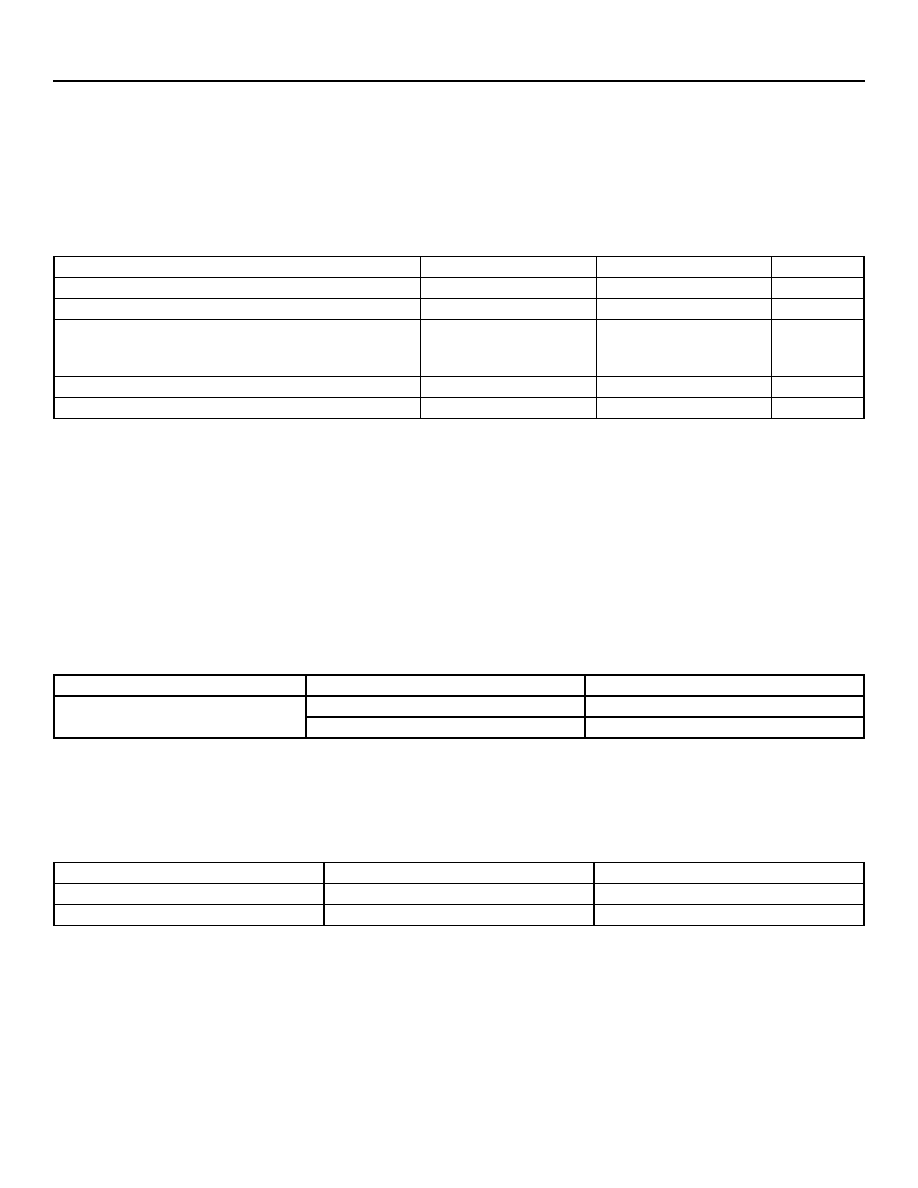
4.3 Package Thermal Characteristics
JA
= 24.0 ∞C/W.
Table 4-1. Absolute Maximum Ratings
Parameter
Min
Max
Unit
Supply Voltage (V
DD33
)
≠0.5
4.2
V
Supply Voltage (V
DD15
)
≠0.5
1.8
V
Input Voltage:
TXD[31:00]
All Other Inputs
≠0.5
≠0.3
5.5
V
DD33
+ 0.3
V
Storage Temperature
≠40
125
∞C
Junction Temperature
--
125
∞C
Table 4-2. ESD Tolerance
Device
Voltage
Type
TSI-8
2,000 V
HBM (human-body model)
500 V
CDM (charged-device model)
Table 4-3. Power Consumption
Supply Voltage
Typ
*
*MPUCLK = 66 MHz, CHICLK = 16.384 MHz, TA = 25 ∞C, all CHIs active, all outputs loaded with 50 pF.
Max
V
DD33
100 mW at 3.3 V
150 mW at 3.47 V
V
DD15
275 mW at 1.5 V
325 mW at 1.6 V

TSI-8
Hardware Design Guide, Revision 1
8K x 8K Time-Slot Interchanger
November 2, 2005
12
12
Agere Systems Inc.
4.4 Recommended Operating Conditions
Recommended conditions apply unless otherwise specified.
Table 4-4. Operating Conditions
Parameter
Min
Typ
Max
Unit
Supply Voltage (V
DD33
)
3.14
3.3
3.47
V
Supply Voltage (V
DD15
)
1.4
1.5
1.6
V
Ambient Temperature
≠40
--
85
∞C

Hardware Design Guide, Revision 1
TSI-8
November 2, 2005
8K x 8K Time-Slot Interchanger
Agere Systems Inc.
13
5 dc Electrical Characteristics
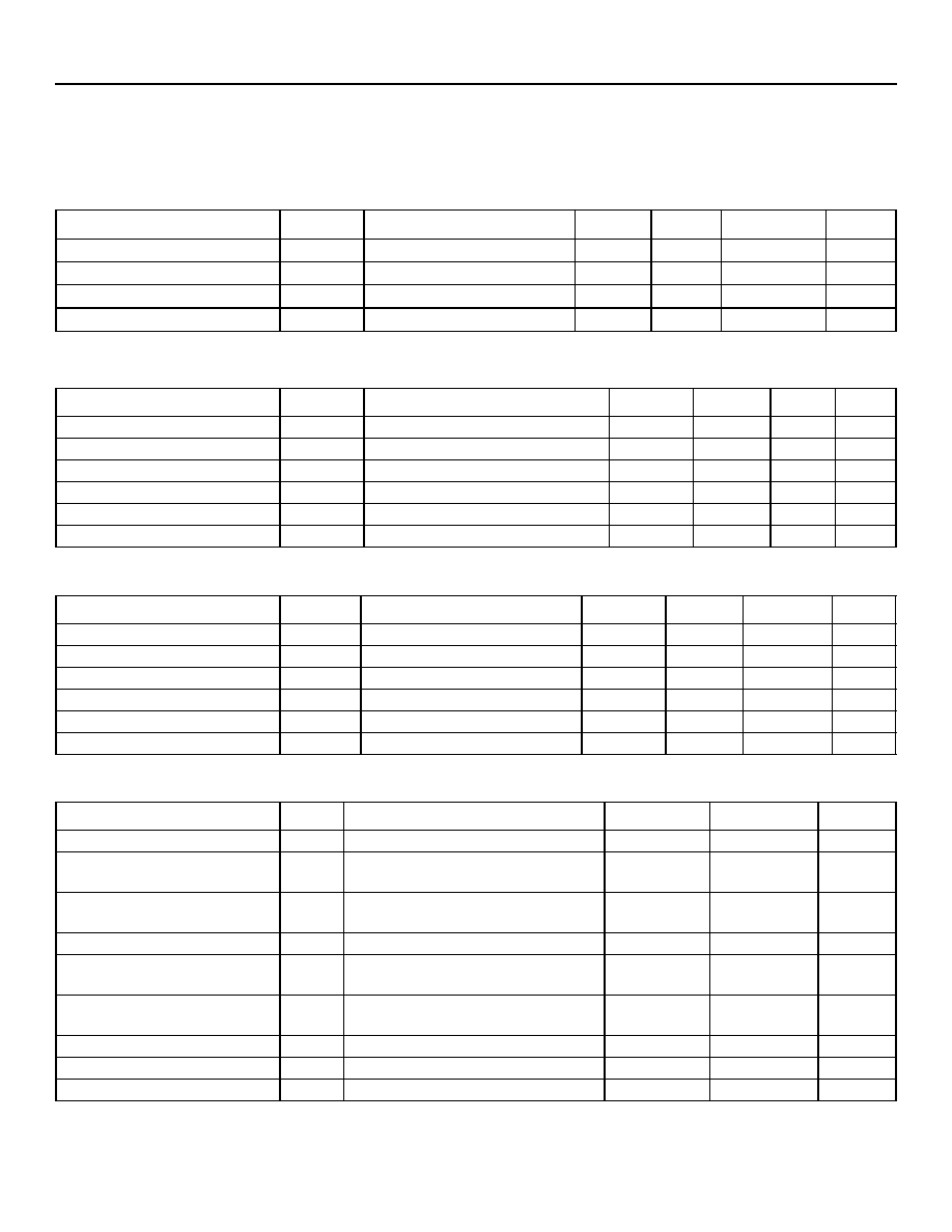
This section describes the static parameters associated with all the ball types used in the TSI-8 device.
* Excludes current due to pull-up or pull-down resistors.
Table 5-1. CMOS Inputs
Parameter
Symbol
Conditions
Min
Typ
Max
Unit
Input Leakage Current
I
IL
V
SS
< V
IN
< V
DD33
--
--
1
*
µA
High-Input Voltage
V
IH
--
2.0
--
V
DD33
+ 0.3
V
Low-Input Voltage
V
IL
--
≠0.3
--
0.8
V
Input Capacitance
C
I
--
--
2.5
--
pF
Table 5-2. CMOS Outputs
Parameter
Symbol
Conditions
Min
Typ
Max
Unit
Output Voltage Low
V
OL
I
OL
= ≠10 mA
--
--
0.4
V
Output Voltage High
V
OH
I
OL
= 10 mA
2.4
--
--
V
Output Current Low
I
OL
--
--
--
10
mA
Output Current High
I
OH
--
--
--
10
mA
Output Capacitance
C
O
--
--
3
--
pF
HIZ Output Leakage Current
I
OZ
--
--
--
10
µA
Table 5-3. CMOS Bidirectionals (Excluding TXD[31:00])
Parameter
Symbol
Conditions
Min
Typ
Max
Unit
Leakage Current
I
L
V
SS
< V
IN
< V
DD33
--
--
11
µA
High-Input Voltage
V
IH
--
2.0
--
V
DD33
+ 0.3
V
Low-Input Voltage
V
IL
--
≠0.3
--
0.8
V
Biput Capacitance
C
IB
--
--
5.0
--
pF
Output Voltage Low
V
OL
I
OL
= ≠10 mA
--
--
0.4
V
Output Voltage High
V
OH
I
OL
= 10 mA
2.4
--
--
V
Table 5-4. CMOS Bidirectionals (TXD[31:00])
Parameter
Symbol
Conditions
Min
Max
Unit
Leakage Current
I
L
V
SS
< V
IN
< V
DD33
--
10
µA
High-Input Voltage
V
IH
V
IO
= 5.0 V
V
IO
= 3.3 V
2.0
0.5 V
DD33
5.5
V
DD33
+ 0.5
V
Low-Input Voltage
V
IL
V
IO
= 5.0 V
V
IO
= 3.3 V
≠0.5
≠0.5
0.8
0.3 V
DD33
V
Biput Capacitance
C
IB
--
--
10
pF
Output Voltage Low
V
OL
I
OL
= 1.5 mA, V
IO
= 3.3 V
I
OL
= 6.0 mA, V
IO
= 5.0 V
--
--
0.1 V
DD33
0.55
V
Output Voltage High
V
OH
I
OL
= ≠0.5 mA, V
IO
= 3.3 V
I
OL
= ≠2.0 mA, V
IO
= 5.0 V
0.9 V
DD33
2.4
--
--
V
Positive-Going Threshold
V
t+
--
1.2
2.0
V
Negative-Going Threshold
V
t≠
--
0.6
1.6
V
Hysteresis (V
t+
≠ V
t≠
)
V
HYS
--
0.4
--
V

TSI-8
Hardware Design Guide, Revision 1
8K x 8K Time-Slot Interchanger
November 2, 2005
14
14
Agere Systems Inc.
6 Timing Diagrams and ac Characteristics
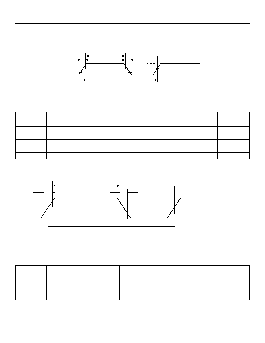
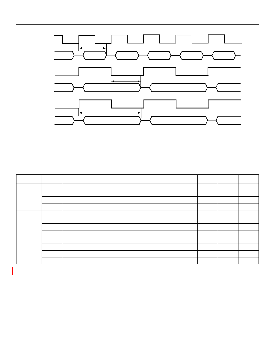
Figure 6-1 and Figure 6-2 describe the timing specifications for the input clocks on the TSI-8.
Figure 6-1. CHICLK Timing Specifications
* V
IH
to V
IH
or V
IL
to V
IL
.
Figure 6-2. MPUCLK Timing Specifications
* V
IH
to V
IH
or V
IL
to V
IL
.
Table 6-1. CHICLK Timing Specifications
Parameter
Description
Min
Typ
Max
Unit
t
1
CHICLK Rise Time
--
2
7
ns
t
2
CHICLK Width (8.192 MHz)*
48.84
--
73.24
ns
t
2
CHICLK Width (16.384 MHz)*
24.42
--
36.62
ns
t
3
CHICLK Fall Time
--
2
7
ns
t
4
CHICLK Period (8.192 MHz)
--
122.07
--
ns
t
4
CHICLK Period (16.384 MHz)
--
61.03
--
ns
Table 6-2. MPUCLK Timing Specifications
Parameter
Description
Min
Typ
Max
Unit
t
5
MPUCLK Rise Time
--
2
7
ns
t
6
MPUCLK Width*
6.06
--
--
ns
t
7
MPUCLK Fall Time
--
2
7
ns
t
8
MPUCLK Period
15.2
--
--
ns
t
1
V
DD33
V
IL
V
IH
V
IH
V
IL
t
3
t
4
50%
t
2
t5
VDD33
VIL
VIH
VIH
VIL
t
7
t8
50%
t6

Hardware Design Guide, Revision 1
TSI-8
November 2, 2005
8K x 8K Time-Slot Interchanger
Agere Systems Inc.
15
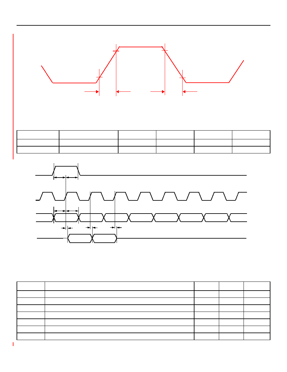
Figure 6-3 shows the ac timing specifications for the
CMOS outputs
on the device.
Figure 6-3. ac Timing Specification
* Test load = 50 pF (total).
Note: This figure assumes TSI-8 is programmed to sample FSYNC on rising edge of CHICLK.
Figure 6-4. CHI Interface Timing
* Applies if Driver_Enable_Control = 01. For Driver_Enable_Control = 11 refer to
Figure 6-15 CHI 3-State Output Control on page 21
.
Table 6-3. CMOS Output ac Timing Specification *
Parameter
Description
Min
Typ
Max
Unit
t
9
Rise Time (20%--80%)
--
1.5
7
ns
t
10
Fall Time (80%--20%)
--
1.5
7
ns
Table 6-4. CHI Interface Timing
Parameter
Description
Min
Max
Unit
t
13
FSYNC Setup Time to Active CHICLK Edge
10
--
ns
t
14
FSYNC Hold Time from Active CHICLK Edge
5
--
ns
t
15
RXD Setup to Active CHICLK Edge
10
--
ns
t
16
RXD Hold Time from Active CHICLK Edge
5
--
ns
t
17
TXD High Z to Data Valid
--
15
ns
t
18
TXD Propagation Delay from Active CHICLK Edge
2
12
ns
t
19
Transmit Data High Impedance*
--
15
ns
20%
80 %
20 %
80 %
t9
t10
t
18
t
19
TXD
CHICLK
t
13
t
14
t
17
RXD
FSYNC
t
15
t
16

TSI-8
Hardware Design Guide, Revision 1
8K x 8K Time-Slot Interchanger
November 2, 2005
16
16
Agere Systems Inc.
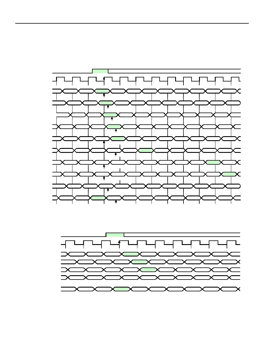
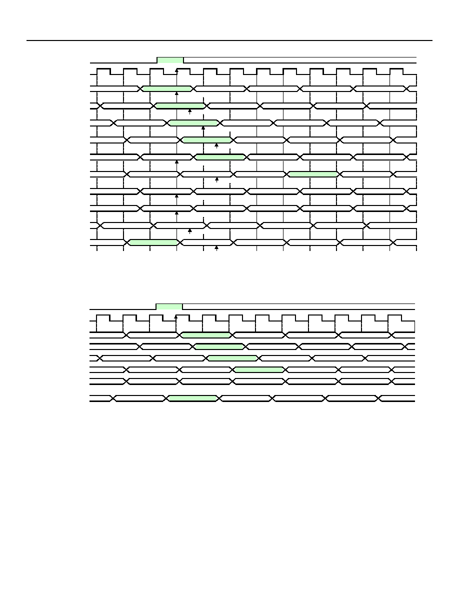
All timing specifications also apply under the following conditions:
If FS is active-low.
If the falling edge of CHICLK is specified as the active edge.
At all RXD and TXD rates (16.384 Mbits/s, 8.192 Mbits/s, 4.096 Mbits/s, or 2.048 Mbits/s) with a CHICLK frequency of
16.384 MHz or 8.192 MHz.
Note: For this timing diagram, it is assumed that FSYNC has been programmed to be active-high, and to be sampled by the rising edge of the CHICLK.
Figure 6-5. Typical Receive CHI Timing with 16.384 Mbits/s Data and 16.384 MHz CHICLK
Notes:
1/4 bit offset not valid with 16 Mbits/s data.
For this timing diagram, it is assumed that FSYNC has been programmed to be active-high, and sampled by the rising edge of the CHICLK.
Figure 6-6. Transmit CHI Timing with 16.384 Mbits/s Data and 16.384 MHz CHICLK
FSYNC
CHICLK
w/ 0 offset
data sampled
w/ º bit offset
data sampled
w/ Ω bit offset
data sampled
w/ æ bit offset
data sampled
w/ bit offset = 1
data sampled
w/ 2æ bit offset
data sampled
w/ bit offset = 7
data sampled
data sampled
data sampled
data sampled
w/ TS offset = 1,
bit offset = 0
TS254 B6
TS254 B7
TS255 B0
TS0 B1
TS0 B0
TS255 B1
TS255 B2
TS255 B3
TS255 B4
TS0 B4
TS0 B5
TS254 B7
TS255 B0
TS255 B1
TS255 B2
TS255 B3
TS255 B4
TS255 B5
TS255 B6
TS0 B0
TS0 B1
TS0 B2
TS0 B3
TS255 B6
TS255 B7
TS0 B0
TS0 B1
TS0 B2
TS0 B3
TS0 B4
TS0 B5
TS255 B6
TS255 B7
TS0 B0
TS0 B1
TS0 B2
TS0 B3
TS0 B4
TS0 B5
TS255 B5
TS255 B3
TS255 B4
TS255 B5
TS255 B5
TS255 B6
TS255 B7
TS255 B6
TS255 B7
TS255 B6
TS255 B7
TS0 B0
TS0 B1
TS0 B2
TS0 B3
TS255 B6
TS255 B7
TS255 B5
TS255 B7
TS0 B 0
w/ TS offset = 13,
bit offset = 3º
TS242 B3
TS242 B4
TS242 B5
TS243 B4
TS243 B5
TS242 B6
TS242 B7
TS243 B0
TS243 B1
TS255 B7
TS0 B0
TS243 B2
TS243 B3
TS0 B5
TS0 B6
TS0 B3
TS0 B4
TS0 B1
TS0 B2
TS0 B3
TS0 B7
TS1 B0
TS0 B1
TS0 B2
w/ TS offset = 255,
bit offset = 7æ
TS255 B6
TS0 B4
TS0 B0
TS255 B6
TS255 B7
TS0 B0
TS0 B1
TS0 B2
TS0 B3
TS0 B4
TS0 B5
FSYNC
CHICLK
w/ 0 offset
w/ Ω bit offset
w/ bit offset = 1
w/ TS offset = 255,
bit offset = 7Ω
TS255 B6
TS255 B7
TS0 B0
w/ TS offset = 1,
bit offset = 0
TS0 B2
TS0 B3
TS0 B4
TS254 B5
TS254 B6
TS254 B7
TS255 B0
TS255 B4
TS255 B5
TS0 B3
TS0 B4
TS255 B1
TS255 B2
TS255 B3
TS0 B0
TS0 B1
TS255 B4
TS255 B5
TS255 B5
TS255 B6
TS255 B7
TS0 B0
TS0 B3
TS0 B4
TS0 B5
TS0 B5
TS0 B1
TS0 B2
TS0 B1
TS0 B2
TS255 B6
TS255 B7
TS255 B5
TS255 B6
TS255 B7
TS0 B0
TS0 B1
TS0 B2
TS0 B3
TS0 B4

Hardware Design Guide, Revision 1
TSI-8
November 2, 2005
8K x 8K Time-Slot Interchanger
Agere Systems Inc.
17
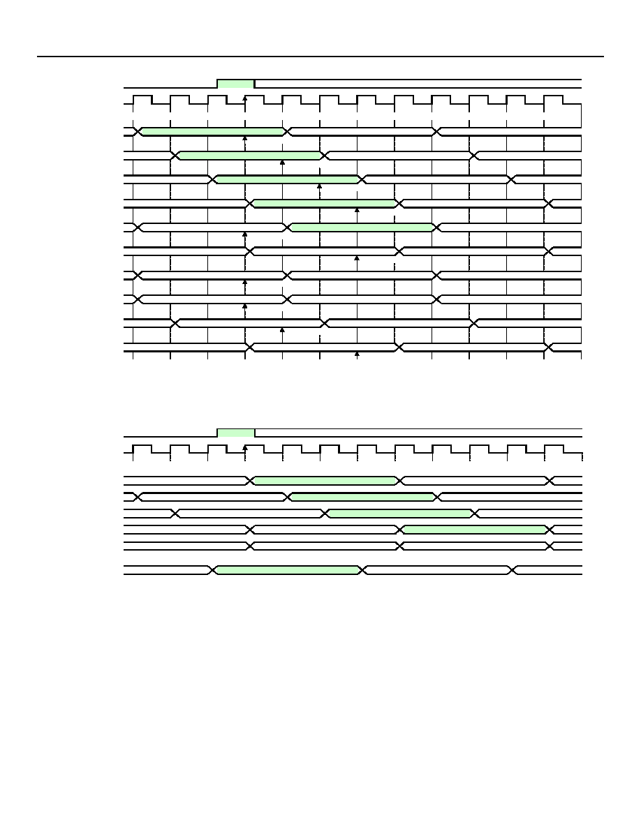
Note: For this timing diagram, it is assumed that FSYNC has been programmed to be active-high, and to be sampled by the rising edge of the CHICLK.
Figure 6-7. Typical Receive CHI Timing with 8.192 Mbits/s Data and 16.384 MHz CHICLK
Note: For this timing diagram, it is assumed that FSYNC has been programmed to be active-high, and to be sampled by the rising edge of the CHICLK.
Figure 6-8. Transmit CHI Timing with 8.192 Mbits/s Data and 16.384 MHz CHICLK
FSYNC
CHICLK
w/ 0 offset
data sampled
w/ º bit offset
data sampled
w/ Ω bit offset
data sampled
w/ æ bit offset
data sampled
w/ bit offset = 1
data sampled
w/ 2æ bit offset
data sampled
w/ bit offset = 7
data sampled
data sampled
data sampled
data sampled
TS0 B2
TS0 B3
TS0 B4
w/ TS offset = 127,
bit offset = 7æ
TS 127 B7
TS0 B0
TS0 B1
TS127 B2
TS127 B3
TS127 B4
w/ TS offset = 13,
bit offset = 3º
TS114 B4
TS114 B5
TS114 B6
TS114 B7
TS115 B0
TS115 B1
w/ TS offset = 1,
bit offset = 0
TS126 B7
TS127 B0
TS127 B1
TS127 B4
TS127 B5
TS 127 B4
TS127 B5
TS127 B0
TS127 B1
TS127 B2
TS127 B3
TS127 B6
TS127 B7
TS0 B2
TS0 B3
TS0 B2
TS0 B3
TS0 B0
TS0 B1
TS127 B6
TS127 B7
TS0 B0
TS0 B1
TS 127 B6
TS127 B7
TS0 B0
TS0 B1
TS0 B3
TS0 B4
TS127 B7
TS0 B0
TS0 B1
TS0 B2
TS0 B3
TS127 B7
TS0 B0
TS0 B1
TS0 B2
TS127 B7
TS0 B0
TS0 B1
TS0 B2
TS0 B3
TS0 B4
FSYNC
CHICLK
w/ 0 offset
w/ º bit offset
w/ Ω bit offset
w/ bit offset = 1
TS 127 B6
TS127 B7
TS0 B0
TS0 B1
TS0 B2
TS0 B3
TS0 B2
TS0 B3
TS127 B6
TS127 B7
TS0 B0
TS0 B1
TS0 B2
TS127 B6
TS127 B7
TS0 B0
TS0 B1
TS 127 B5
TS127 B6
TS127 B7
TS0 B0
w/ TS offset = 1,
bit offset = 0
TS127 B7
TS0 B0
TS0 B1
w/ TS offset = 127,
bit offset = 7æ
TS 126 B6
TS126 B7
TS127 B0
TS127 B1
TS0 B2
TS0 B3
TS0 B1
TS0 B2
TS127 B2
TS127 B3
TS0 B3

TSI-8
Hardware Design Guide, Revision 1
8K x 8K Time-Slot Interchanger
November 2, 2005
18
18
Agere Systems Inc.
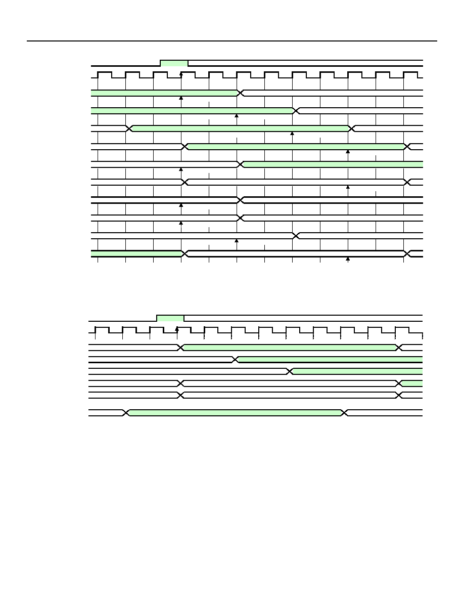
Note: For this timing diagram, it is assumed that FSYNC has been programmed to be active-high, and to be sampled by the rising edge of the CHICLK.
Figure 6-9. Typical Receive CHI Timing with 4.096 Mbits/s Data and 16.384 MHz CHICLK
Note: For this timing diagram, it is assumed that FSYNC has been programmed to be active-high, and to be sampled by the rising edge of the CHICLK.
Figure 6-10. Transmit CHI Timing with 4.096 Mbits/s Data and 16.384 MHz CHICLK
FSYNC
CHICLK
w/ 0 offset
data sampled
w/ º bit offset
data sampled
w/ Ω bit offset
data sampled
w/ æ bit offset
data sampled
w/ bit offset = 1
data sampled
w/ 2æ bit offset
data sampled
w/ bit offset = 7
data sampled
data sampled
data sampled
data sampled
TS50 B7
w/ TS offset = 63,
bit offset = 7æ
TS0 B0
TS0 B1
TS0 B2
w/ TS offset = 13,
bit offset = 3º
TS50 B4
TS50 B5
TS50 B6
w/ TS offset = 1,
bit offset = 0
TS63 B0
TS63 B1
TS63 B2
TS63 B5
TS63 B6
TS63 B7
TS63 B1
TS63 B2
TS63 B3
TS63 B7
TS0 B0
TS0 B1
TS63 B7
TS0 B0
TS0 B1
TS63 B7
TS0 B0
TS0 B1
TS0 B2
TS0 B0
TS0 B1
TS0 B2
TS63 B7
TS0 B0
TS0 B1
TS0 B2
FSYNC
CHICLK
w/ 0 offset
w/ º bit offset
w/ Ω bit offset
w/ bit offset = 1
w/ TS offset = 63,
bit offset = 7æ
TS62 B7
TS63 B0
TS63 B1
w/ TS offset = 1,
bit offset = 0
TS63 B6
TS63 B7
TS0 B0
TS63 B7
TS0 B0
TS0 B1
TS0 B2
TS63 B6
TS63 B7
TS0 B0
TS0 B1
TS63 B7
TS0 B0
TS0 B1
TS63 B7
TS0 B0
TS0 B1

Hardware Design Guide, Revision 1
TSI-8
November 2, 2005
8K x 8K Time-Slot Interchanger
Agere Systems Inc.
19
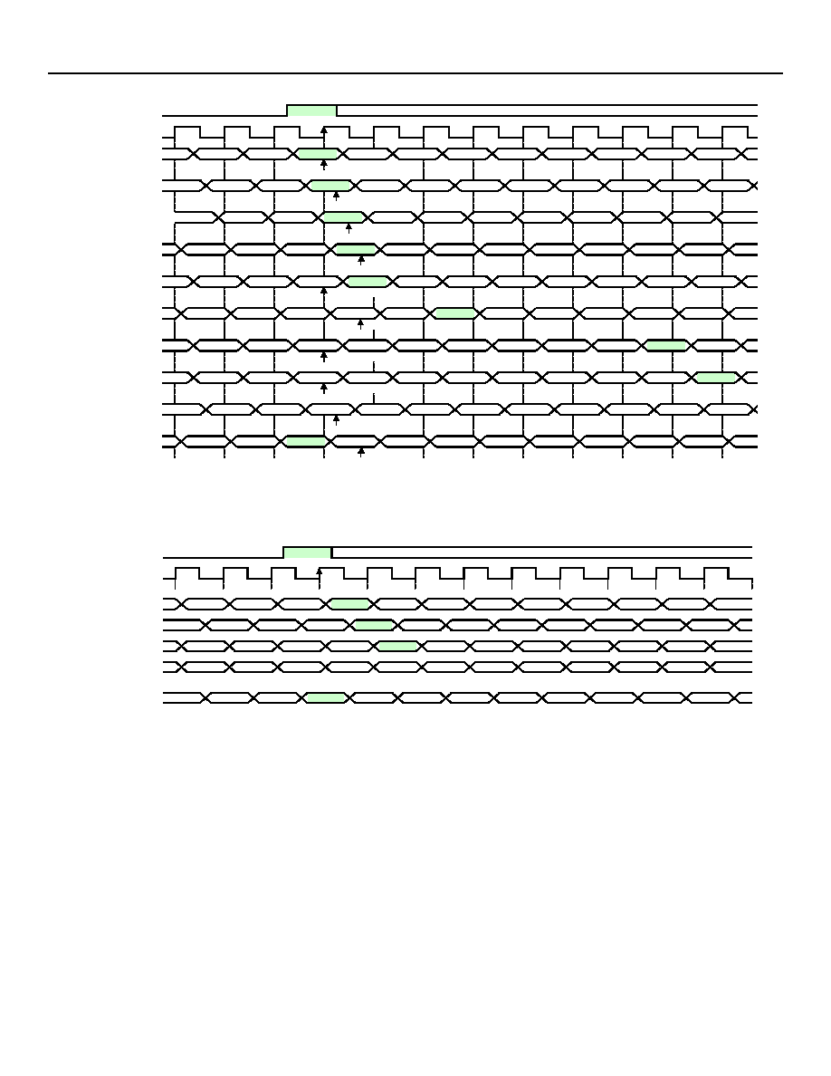
Note: For this timing diagram, it is assumed that FSYNC has been programmed to be active-high, and to be sampled by the rising edge of the CHICLK.
Figure 6-11. Typical Receive CHI Timing with 2.048 Mbits/s Data and 16.384 MHz CHICLK
Note: For this timing diagram, it is assumed that FSYNC has been programmed to be active-high, and to be sampled by the rising edge of the CHICLK.
Figure 6-12. Transmit CHI Timing with 2.048 Mbits/s Data and 16.384 MHz CHICLK
FSYNC
CHICLK
w/ 0 offset
data sampled
w/ º bit offset
data sampled
w/ Ω bit offset
data sampled
w/ æ bit offset
data sampled
w/ bit offset = 1
data sampled
w/ 2æ bit offset
data sampled
w/ bit offset = 7
data sampled
data sampled
data sampled
data sampled
w/ TS offset = 31,
bit offset = 7æ
TS0 B0
TS0 B1
TS0
w/ TS offset = 1,
bit offset = 0
TS31 B0
TS31 B1
w/ TS offset = 13,
bit offset = 3º
TS18 B5
TS18 B6
TS31 B5
TS31 B6
TS31
TS31 B1
TS31 B2
TS31 B7
TS0 B0
TS0
TS31 B7
TS0 B0
TS0 B0
TS0 B1
TS0 B0
TS0 B1
TS31 B7
TS0 B0
TS0 B1
FSYNC
CHICLK
w/ 0 offset
w/ º bit offset
w/ Ω bit offset
w/ bit offset = 1
TS30 B7
TS31 B0
TS31 B01
w/ TS offset = 1,
bit offset = 0
TS31 B7
TS0 B0
TS0 B1
w/ TS offset = 31,
bit offset = 7æ
TS31 B7
TS0 B0
TS31 B6
TS31 B7
TS0 B0
TS31 B7
TS0 B0
TS0 B1
TS31 B7
TS0 B0

TSI-8
Hardware Design Guide, Revision 1
8K x 8K Time-Slot Interchanger
November 2, 2005
20
20
Agere Systems Inc.
Note: For this timing diagram, it is assumed that FSYNC has been programmed to be active-high, and to be sampled by the rising edge of the CHICLK.
Figure 6-13. Typical Receive CHI Timing with 8.192 Mbits/s Data and 8.192 MHz CHICLK
Notes:
1/4 bit offset not valid with 8 MHz data and 8 MHz clock.
For this timing diagram, it is assumed that FSYNC has been programmed to be active-high, and to be sampled by the rising edge of the CHICLK.
Figure 6-14. Transmit CHI Timing with 8.192 Mbits/s Data and 8.192 MHz CHICLK
FSYNC
CHICLK
w/ 0 offset
data sampled
w/ º bit offset
data sampled
w/ Ω bit offset
data sampled
w/ æ bit offset
data sampled
w/ bit offset = 1
data sampled
w/ 2æ bit offset
data sampled
w/ bit offset = 7
data sampled
data sampled
data sampled
data sampled
TS0 B5
TS0 B6
TS0 B7
TS1 B0
TS0 B1
TS0 B2
TS0 B3
TS0 B4
w/ TS offset = 127,
bit offset = 7æ
TS127 B6
TS127 B7
TS0 B0
TS115 B2
TS115 B3
TS115 B4
TS115 B5
TS114 B6
TS114 B7
TS115 B0
TS115 B1
w/ TS offset = 13,
bit offset = 3º
TS114 B3
TS114 B4
TS114 B5
TS127 B5
TS127 B6
TS127 B7
TS0 B0
TS0 B 0
TS0 B1
w/ TS offset = 1,
bit offset = 0
TS126 B6
TS126 B7
TS127 B0
TS127 B1
TS127 B2
TS127 B3
TS127 B4
TS0 B3
TS126 B7
TS127 B0
TS127 B1
TS127 B2
TS127 B3
TS127 B4
TS127 B5
TS127 B6
TS127 B7
TS127 B7
TS0 B0
TS0 B1
TS0 B2
TS127 B3
TS127 B4
TS127 B5
TS127 B6
TS0 B5
TS127 B5
TS127 B6
TS127 B7
TS0 B0
TS0 B1
TS0 B2
TS0 B3
TS0 B4
TS0 B1
TS0 B2
TS0 B3
TS0 B4
TS127 B5
TS127 B6
TS127 B7
TS0 B0
TS0 B2
TS0 B3
TS0 B4
TS0 B5
TS127 B6
TS127 B7
TS0 B0
TS0 B1
TS0 B2
TS0 B3
TS0 B4
TS0 B5
TS127 B6
TS127 B7
TS0 B0
TS0 B1
TS127 B6
TS127 B7
TS0 B0
TS0 B1
TS0 B2
TS0 B3
TS0 B4
TS0 B5
FSYNC
CHICLK
w/ 0 offset
w/ Ω bit offset
w/ bit offset = 1
TS127 B5
w/ TS offset = 127,
bit offset = 7Ω
TS127 B6
TS127 B7
TS0 B0
TS0 B1
TS0 B2
TS0 B3
TS0 B4
TS0 B5
TS0 B4
w/ TS offset = 1,
bit offset = 0
TS126 B5
TS126 B6
TS126 B7
TS127 B0
TS127 B1
TS127 B2
TS127 B3
TS127 B4
TS0 B0
TS0 B1
TS0 B2
TS0 B3
TS127 B4
TS127 B5
TS127 B6
TS127 B7
TS0 B1
TS0 B2
TS0 B3
TS0 B4
TS127 B5
TS127 B6
TS127 B7
TS0 B0
TS127 B5
TS127 B6
TS127 B7
TS0 B0
TS0 B1
TS0 B2
TS0 B3
TS0 B4
TS0 B5

Hardware Design Guide, Revision 1
TSI-8
November 2, 2005
8K x 8K Time-Slot Interchanger
Agere Systems Inc.
21
Figure 6-15. CHI 3-State Output Control
Table 6-5. CHI 3-State Output Control
Control in the table below refers to bits [6:4] in the Transmit_CHI_Global_Configuration register (0x0C84). This only applies
if bits 13 and 12 of the corresponding Transmit_CHI_Control register (0x0C00--0x0C3E) are set to 11. See the TSI-8 Reg-
ister Description document.
Parameter Control
Reference Point
*
* Like edge is the reference edge (rising or falling) as defined by the Transmit_Clock_Edge bit in the Transmit_CHI_Global_Configuration (0x0C84) regis-
ter. See the TSI-8 Register Description document for further details.
Min
Max
*
Unit
t
20
000
After Previous Like Edge in 16 MHz
50
59
ns
001
After Previous Like Edge in 16 MHz
44
53
ns
010
After Previous Like Edge in 16 MHz
38
47
ns
011
After Previous Like Edge in 16 MHz
32
41
ns
t
21
000
After Previous Opposite Edge in 8 MHz
50
59
ns
001
After Previous Opposite Edge in 8 MHz
44
53
ns
010
After Previous Opposite Edge in 8 MHz
38
47
ns
011
After Previous Opposite Edge in 8 MHz
32
41
ns
t
22
100
After Previous Like Edge (8 MHz mode only)
111
120
ns
101
After Previous Like Edge (8 MHz mode only)
105
114
ns
110
After Previous Like Edge (8 MHz mode only)
99
108
ns
111
After Previous Like Edge (8 MHz mode only)
93
102
ns
CHICLK
16.384 MHz
t
20
TXD
16.384 Mbits/s
CHICLK
8.192 MHz
TXD
8.192 Mbits/s
CHICLK
8.192 MHz
TXD
8.192 Mbits/s
t
21
t
22

TSI-8
Hardware Design Guide, Revision 1
8K x 8K Time-Slot Interchanger
November 2, 2005
22
22
Agere Systems Inc.
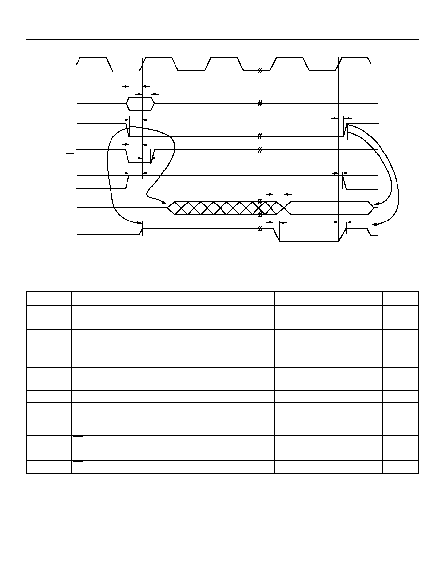
Figure 6-16. Microprocessor Port Timing--Read Cycle
Table 6-6. Microprocessor Port Timing--Read Cycle
Parameter
Description
Min
Max
Unit
t
23
Address Setup
5
--
ns
t
24
Address Hold
1
--
ns
t
25
Chip Select Setup
5
--
ns
t
26
Chip Select Hold
1
--
ns
t
27
Address Strobe Setup
5
--
ns
t
28
Address Strobe Hold
1
--
ns
t
29
R/W Setup
5
--
ns
t
30
R/W Hold
1
--
ns
t
31
Data Output Enable
--
15
ns
t
32
Data Clock to Valid
1
7
ns
t
33
Data High-Impedance
--
8
ns
t
34
DT High-Impedance to Valid
1
15
ns
t
35
DT Clock to Out
1
7
ns
t
36
DT Valid to High-Impedance
1
8
ns
MPUCLK
DATA[15:00]
PAR[1:0]
t
24
t
23
ADDR[15:00]
CS
AS
R/W
DT
t
25
t
27
t
28
t
29
t
31
t
35
t
34
t
26
t
30
t
32
t
35
t
36
t
33

Hardware Design Guide, Revision 1
TSI-8
November 2, 2005
8K x 8K Time-Slot Interchanger
Agere Systems Inc.
23
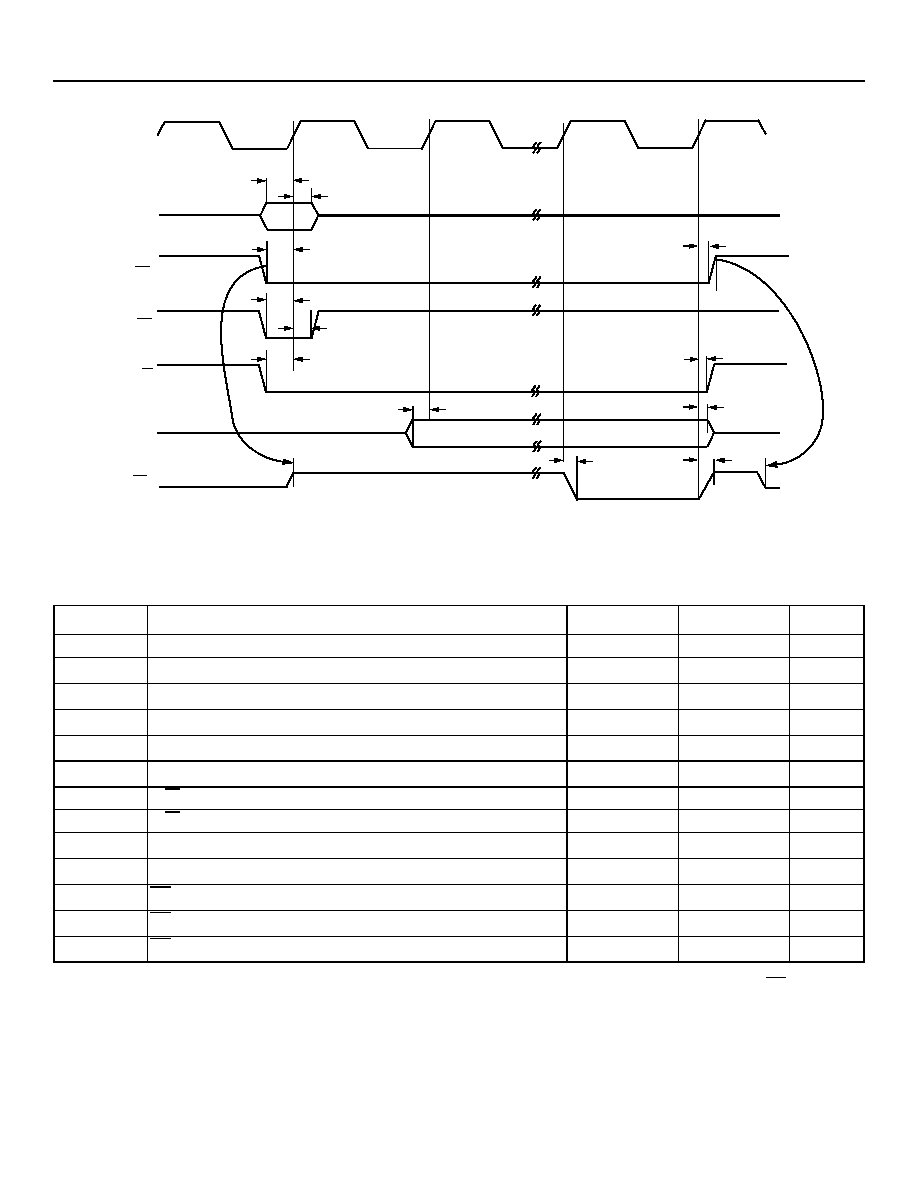
Figure 6-17. Microprocessor Port Timing--Write Cycle
Note: Posted writes follow the same timing shown in Figure 6-17 and Table 6-7. A posted write may return a DT prior to the
device completing the write cycle. This allows the microprocessor to continue operation while the TSI-8 completes the
write.
Table 6-7. Microprocessor Port Timing--Write Cycle
Parameter
Description
Min
Max
Unit
t
37
Address Setup
5
--
ns
t
38
Address Hold
1
--
ns
t
39
Chip Select Setup
5
--
ns
t
40
Chip Select Hold
1
--
ns
t
41
Address Strobe Setup
5
--
ns
t
42
Address Strobe Hold
1
--
ns
t
43
R/W Setup
5
--
ns
t
44
R/W Hold
1
--
ns
t
45
Data Setup
5
--
ns
t
46
Data Hold
1
--
ns
t
47
DT High-Impedance to Valid
1
15
ns
t
48
DT Clock to Out
1
7
ns
t
49
DT Valid to High-Impedance
1
8
ns
MPUCLK
DATA[15:00]
PAR[1:0]
t
38
t
37
ADDR[15:00]
CS
AS
R/W
DT
t
39
t
41
t
42
t
43
t
45
t
48
t
47
t
40
t
44
t
46
t
48
t
49

TSI-8
Hardware Design Guide, Revision 1
8K x 8K Time-Slot Interchanger
November 2, 2005
24
24
Agere Systems Inc.
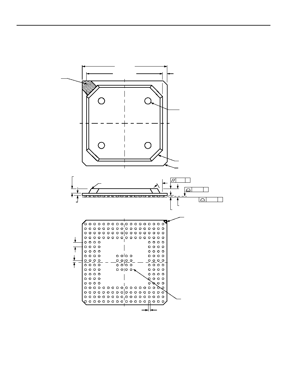
7 Outline Diagrams
Dimensions are in millimeters.
0.20
BOTTOM VIEW
1.75 TYP.
1.20 x 45∞ APPROX
A1 INDICATOR
(PLATED)
0.80 ± 0.050
0.56 ± 0.06
30∞
0.50 ± 0.10
Z
0.35 Z
A
B
C
D
E
F
G
H
J
K
L
M
N
P
R
T
1
2
3
4
5
6
7
8
9
10
11
13
16
18
1.00
15
17.70
SEATING PLANE
0.50 R MAX
SQUARE
19.00
SQUARE
APPROX
ALL SIDES
0.10
Z
ALL EDGES
1.86 ± 0.21
TYP 3 PLACES
4.00 x 45∞ APPROX
TYP 4 CORNERS
USE OF EJECTOR
PINS IS OPTIONAL
12
14
17
TYP
0.63 DIA
U
V
A1 INDICATOR
(UNDER SOLDER MASK)
TOP VIEW
CENTER ARRAY
FOR THERMAL
ENHANCEMENT
0.50
+0.70
≠0.05
+0.07
≠0.13

Copyright © 2005 Agere Systems Inc.
All Rights Reserved
November 2, 2005
DS02-122SWCH-1 (Replaces DS02-122SWCH)
Hardware Design Guide, Revision 1
TSI-8
November 2, 2005
8K x 8K Time-Slot Interchanger
Agere Systems Inc. reserves the right to make changes to the product(s) or information contained herein without notice. No liability is assumed as a result of their use or application.
Agere, Agere Systems, and the Agere logo are registered trademarks of Agere Systems Inc.
For additional information, contact your Agere Systems Account Manager or the following:
INTERNET:
Home: http://www.agere.com Sales: http://www.agere.com/sales
E-MAIL:
docmaster@agere.com
N. AMERICA: Agere Systems Inc., Lehigh Valley Central Campus, Room 10A-301C, 1110 American Parkway NE, Allentown, PA 18109-9138
1-800-372-2447, FAX 610-712-4106 (In CANADA: 1-800-553-2448, FAX 610-712-4106)
ASIA:
CHINA: (86) 21-54614688 (Shanghai), (86) 755-25881122 (Shenzhen), (86) 10-65391096 (Beijing)
JAPAN: (81) 3-5421-1600 (Tokyo), KOREA: (82) 2-767-1850 (Seoul), SINGAPORE: (65) 6741-9855, TAIWAN: (886) 2-2725-5858 (Taipei)
EUROPE:
Tel. (44) 1344 296 400
8 Ordering Information
9 Change History
On
page 1
, updated Figure 2-1.
On
page 15
,
deleted 2 sentences at the beginning of the page. (All timing parameters are referenced to V
IHmin
and V
IL
max.
The reference signal polarity may be inverted for some timing parameters.)
On
page 15
, updated Figure 6-3, ac Timing Specification.
On
page 15
, updated Table 6-3. CMOS Output ac Timing Specification * .
On
page 15
,
under Table 6-4 eliminated the following sentence: All timing specifications are with respect to VIHmin and
VILmax as shown in Figure 5.
On
page 21
,
deleted footnote under Table 6-5 and clarified the remaining footnote.
On
page 22
,
deleted the footnote under Table 6-6
.
On
page 23
,
deleted the footnote under Table 6-7
.
On page 26, changed the part numbers.
Adobe Acrobat and Acrobat Reader are registered trademarks of Adobe Systems Incorporated.
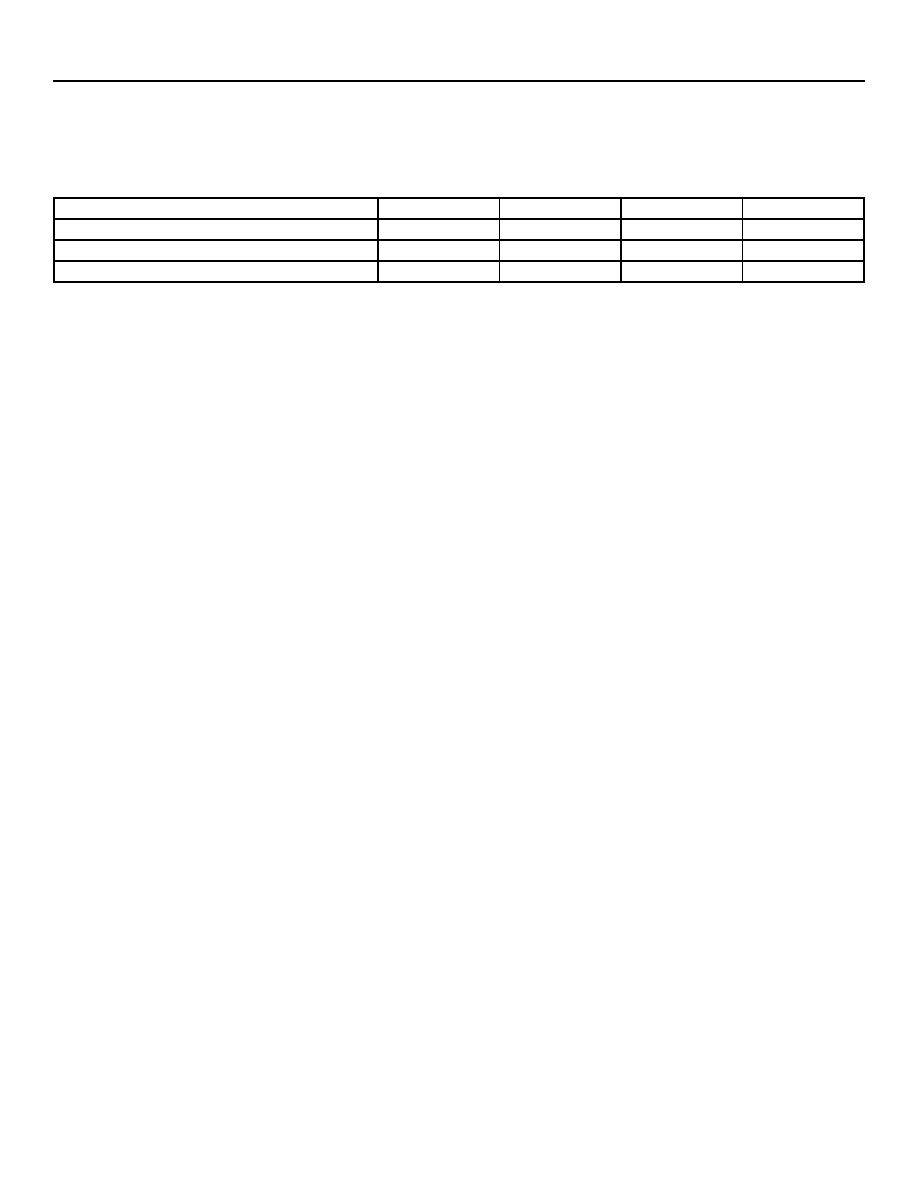
Table 8-1. Ordering Information
Device
Part Number
Ball Count
Package
Comcode
TSI-8
TTSI008321BL-2-DB
240
PBGAM1
700046829
L-TTSI008321BL-2-DB
700078759*
* Pb-free/RoHS.
