 | –≠–ª–µ–∫—Ç—Ä–æ–Ω–Ω—ã–π –∫–æ–º–ø–æ–Ω–µ–Ω—Ç: TTSI1K16T | –°–∫–∞—á–∞—Ç—å:  PDF PDF  ZIP ZIP |

Preliminary Data Sheet
February 1999
TTSI1K16T
1024-Channel, 16-Highway Time-Slot Interchanger
Features
s
Sixteen full-duplex, serial time-division multiplexed
(TDM) highways.
s
Full availability, nonblocking 1024-channel time/
space switch.
s
2.048 Mbits/s (32 time slots), 4.096 Mbits/s (64
time slots), or 8.192 Mbits/s (128 time slots) data
rates, independently programmable per highway.
s
64 kbits/s granularity with optional 32 kbits/s (4-bit)
and 16 kbits/s (2-bit) subrate switching, selectable
per highway.
s
Low-latency mode for voice channels.
s
Frame integrity for wideband data applications.
s
Concentration highway interface (CHI) compatible
with the IOM2, GCI, K2, SLD,
MVIP
*, ST-Bus,
SC-Bus, and H.100.
s
Single highway clock and frame synchronization
input.
s
Independently programmable bit and byte offsets
with 1/4 bit resolution for all highways.
s
Capable of broadcasting data to the transmit high-
ways from a variety of sources including host data.
s
High-impedance control per time slot.
s
Software-compatible family of 1K, 2K, and 4K time-
slot interchangers.
s
Sixteen independent high-impedance indicators
(output enables) for transmit highways, allowing
external drivers.
s
Direct access to device registers, connection store,
and data store via microprocessor interface.
s
IEEE
1149.1 boundary scan (JTAG).
s
Test-pattern generation and checking for on-line
system testing (PRBS, QRSS, or user-defined
byte).
s
User-accessible BIST for data and connection
stores.
s
3.3 V power supply with 5 V tolerant I/O.
s
Low-power, high-density CMOS technology, and
TTL compatible switching thresholds.
s
144-pin TQFP package.
s
≠40
∞
C to +85
∞
C operating temperature range.
*
MVIP
is a registered trademark of Natural Microsystems Corpo-
ration.
IEEE
is a registered trademark of The Institute of Electrical and
Electronics Engineers, Inc.
Applications
s
Small and medium digital switch matrices.
s
Computer telephony integration (CTI).
s
Access concentrators.
s
PABX.
s
Cellular infrastructure.
s
ISP modem banks.
s
T1/E1 multiplexers.
s
Digital cross connects.
s
Digital loop carriers.
s
Multiport DS1/E1 service cards.
s
LAN/WAN gateways.
s
TDM highway data rate adaptation.
Description
The TTSI1K16T Time-Slot Interchanger (TSI)
switches data between 16 full-duplex, serial, time-
division multiplexed highways. The TTSI1K16T can
make any connection between 1024 input and output
time slots.
Each of the 16 transmit and 16 receive highways can
be independently programmed for data rate
(2.048 Mbits/s, 4.096 Mbits/s, or 8.192 Mbits/s) and
offset. The offset can range from 0 bits to 127 bytes
and 7 3/4 bits on a 8.192 Mbits/s highway. The
TTSI1K16T can perform rate adaptation between
varying speed highways as well.
The TTSI1K16T is configured via a microprocessor
interface with a demultiplexed address and data bus.
In addition to accessing the registers and connection
store, this interface can also be used to read
received time slots and specify user data for trans-
mission.
The TTSI1K16T ensures that interchanged time slots
retain their frame integrity. Frame integrity is required
for applications that switch wideband data (i.e., ISDN
H-channels). For voice applications where low delay
is important, a low-latency mode can be selected.

TTSI1K16T
Preliminary Data Sheet
1024-Channel, 16-Highway Time-Slot Interchanger
February 1999
2
Lucent Technologies Inc.
Table of Contents
Contents
Page
Features .................................................................................................................................................................. 1
Applications ............................................................................................................................................................. 1
Description............................................................................................................................................................... 1
Functional Description ............................................................................................................................................. 5
Pin Information ........................................................................................................................................................ 7
Typical TSI Application .......................................................................................................................................... 13
Interchange Fabric................................................................................................................................................. 14
Small and Large TSIs ............................................................................................................................................ 15
Microprocessor Interface ....................................................................................................................................... 16
Asynchronous Mode (MM = 0)........................................................................................................................... 16
Synchronous Mode (MM = 1) ............................................................................................................................ 17
Highway Data Rate Selection................................................................................................................................ 18
Mixed-Highway Data Rates ................................................................................................................................... 19
TDM Highway Interface Timing ............................................................................................................................. 20
Virtual and Physical Frames .............................................................................................................................. 20
TDM Highway Alignment at Zero Offset ............................................................................................................ 21
TDM Highway Offsets............................................................................................................................................ 21
Reset Sequence .................................................................................................................................................... 22
Low-Latency and Frame-Integrity Modes .............................................................................................................. 23
Low Latency....................................................................................................................................................... 23
Frame Integrity................................................................................................................................................... 24
Test-Pattern Generation ........................................................................................................................................ 27
Test-Pattern Checking........................................................................................................................................... 27
Error Injection ........................................................................................................................................................ 28
Error Checking....................................................................................................................................................... 28
JTAG Boundary-Scan Specification ...................................................................................................................... 29
Principle of the Boundary Scan.......................................................................................................................... 29
Test Access Port Controller ............................................................................................................................... 30
Instruction Register ............................................................................................................................................ 32
Boundary-Scan Register.................................................................................................................................... 33
BYPASS Register .............................................................................................................................................. 33
IDCODE Register............................................................................................................................................... 33
3-State Procedures ............................................................................................................................................ 33
Register Architecture ............................................................................................................................................. 34
Configuration Register Architecture....................................................................................................................... 36
Transmit Highway 3-State Options .................................................................................................................... 49
Data Store Memory ............................................................................................................................................... 50
Connection Store Memory..................................................................................................................................... 50
Absolute Maximum Ratings................................................................................................................................... 53
Operating Conditions............................................................................................................................................. 53
Handling Precautions ............................................................................................................................................ 53
Electrical Characteristics ....................................................................................................................................... 54
Timing Characteristics ........................................................................................................................................... 54
Outline Diagram..................................................................................................................................................... 61
144-Pin TQFP .................................................................................................................................................... 61
Ordering Information.............................................................................................................................................. 62
DS99-177PDH Replaces DS98-290TIC to Incorporate the Following Updates .................................................... 62

Preliminary Data Sheet
TTSI1K16T
February 1999
1024-Channel, 16-Highway Time-Slot Interchanger
3
Lucent Technologies Inc.
List of Figures
Figures
Page
Figure 1. Block Diagram of the TTSI1K16T .............................................................................................................6
Figure 2. 144-Pin TQFP Pin Assignment (Top View)...............................................................................................7
Figure 3. A Typical TSI Application ........................................................................................................................13
Figure 4. An 8K Time-Slot Switch Made from 4K TSIs ..........................................................................................15
Figure 5. Asynchronous Read................................................................................................................................16
Figure 6. Asynchronous Write ................................................................................................................................16
Figure 7. Synchronous Read .................................................................................................................................17
Figure 8. Synchronous Write..................................................................................................................................17
Figure 9. Mixed-Highway Data Rates ....................................................................................................................19
Figure 10. Virtual and Physical Frames .................................................................................................................20
Figure 11. Synchronization to FSYNC ...................................................................................................................21
Figure 12. Highway Offsets ....................................................................................................................................22
Figure 13. Mixed Low-Latency and Frame-Integrity Modes ...................................................................................26
Figure 14. Block Diagram of the TTSI1K16T's Boundary-Scan Test Logic ...........................................................29
Figure 15. BS TAP Controller State Diagram.........................................................................................................30
Figure 16. Asynchronous Read Cycle Timing Using DT Handshake.....................................................................55
Figure 17. Asynchronous Write Cycle Timing Using DT Handshake .....................................................................55
Figure 18. Asynchronous Read Cycle Timing Using Only CS ...............................................................................56
Figure 19. Asynchronous Write Cycle Timing Using Only CS ...............................................................................56
Figure 20. Synchronous Read Cycle Timing..........................................................................................................57
Figure 21. Synchronous Write Cycle Timing ..........................................................................................................57
Figure 22. TDM Highway Timing............................................................................................................................59
Figure 23. JTAG Interface Timing ..........................................................................................................................60

TTSI2K32T
Preliminary Data Sheet
1024-Channel, 16-Highway Time-Slot Interchanger
February 1999
4
Lucent Technologies Inc.
List of Tables
Tables
Page
Table 1. Data Rate and Switch Size Examples ....................................................................................................... 5
Table 2. Pin Assignments for a 144-Pin TQFP--Pin Number Order....................................................................... 8
Table 3. Pin Assignments for a 144-Pin TQFP--Signal Name Order ..................................................................... 9
Table 4. TTSI1K16T Pin Descriptions ................................................................................................................... 10
Table 5. The TSI Family ........................................................................................................................................ 15
Table 6. Rx Highway Data Rate Options............................................................................................................... 18
Table 7. Tx Highway Data Rate Options ............................................................................................................... 18
Table 8. Time-Slot Separation Required for Transmission with Minimum Latency (0 Offsets) ............................. 23
Table 9. Offset Difference and Its Effect on Frame for Transmission.................................................................... 25
Table 10. Offset Difference Boundaries ................................................................................................................ 25
Table 11. TAP Controller States in the Data Register Branch............................................................................... 31
Table 12. TAP Controller States in the Instruction Register Branch...................................................................... 31
Table 13. TTSI1K16T's Boundary-Scan Instructions ............................................................................................ 32
Table 14. TTSI1K16T Register Summary ............................................................................................................. 34
Table 15. General Command Register (0x00) ...................................................................................................... 36
Table 16. Software Reset Register (0x01) ............................................................................................................ 37
Table 17. BIST Command Register (0x02) ........................................................................................................... 37
Table 18. Idle Code 1 Register (0x03)................................................................................................................... 38
Table 19. Idle Code 2 Register (0x04)................................................................................................................... 38
Table 20. Idle Code 3 Register (0x05)................................................................................................................... 38
Table 21. Global Interrupt Mask Register (0x06)................................................................................................... 38
Table 22. Interrupt Status Register (0x07) ............................................................................................................ 39
Table 23. Interrupt Mask Register (0x08) .............................................................................................................. 40
Table 24. Test Command Register (0x09) ............................................................................................................ 41
Table 25. Test-Pattern Style Register (0x0A)........................................................................................................ 42
Table 26. Test-Pattern Checker Highway Register (0x0B).................................................................................... 43
Table 27. Test-Pattern Checker Upper Time-Slot Register (0x0C) ....................................................................... 43
Table 28. Test-Pattern Checker Lower Time-Slot Register (0x0D) ....................................................................... 43
Table 29. Test-Pattern Checker Data Register (0x0E).......................................................................................... 43
Table 30. Test-Pattern Error Injection Register (0x0F).......................................................................................... 43
Table 31. Test-Pattern Error Counter (Byte 0) (0x10) ........................................................................................... 44
Table 32. Test-Pattern Error Counter (Byte 1) (0x11) ........................................................................................... 44
Table 33. Test-Pattern Generator Data Register (0x12) ....................................................................................... 44
Table 34. Version Register (0x13)......................................................................................................................... 44
Table 35. Transmit Highway Configuration Register (Byte 0) (0x1000 + 4i) ......................................................... 45
Table 36. Transmit Highway Configuration Register (Byte 1) (0x1001 + 4i) ......................................................... 46
Table 37. Transmit Highway Configuration Register (Byte 2) (0x1002 + 4i) ......................................................... 46
Table 38. Receive Highway Configuration Register (Byte 0) (0x1800 + 4i) .......................................................... 47
Table 39. Receive Highway Configuration Register (Byte 1) (0x1801 + 4i) .......................................................... 48
Table 40. Receive Highway Configuration Register (Byte 2) (0x1802 + 4i) .......................................................... 48
Table 41. Transmit Highway 3-State Options........................................................................................................ 49
Table 42. Address Scheme for Data Store Memory ............................................................................................. 50
Table 43. Address Scheme for Connection Store Memory .................................................................................. 50
Table 44. Connection Store Memory (Byte 0) ....................................................................................................... 51
Table 45. Connection Store Memory (Byte 1) ....................................................................................................... 51
Table 46. Clock Specifications .............................................................................................................................. 54
Table 47. Asynchronous Read and Write Interface Timing Using DT Handshake ................................................ 55
Table 48. Asynchronous Microprocessor Interface Timing Using Only CS .......................................................... 56
Table 49. Synchronous Microprocessor Interface Timing ..................................................................................... 58
Table 50. TDM Highway Timing ............................................................................................................................ 59
Table 51. JTAG Interface Timing........................................................................................................................... 60

Preliminary Data Sheet
TTSI1K16T
February 1999
1024-Channel, 16-Highway Time-Slot Interchanger
5
Lucent Technologies Inc.
Functional Description
The TTSI1K16T is a 1024 time-slot switch that can be used in a variety of ways, with some or all of the highways
active and running at different data rates. The table below lists a few of the possible combinations of switch size
and data rates. By selecting different rates for receive and transmit highways, rate adaptation can be performed
also. Each one of the 32 (16 transmit and 16 receive) highways can be independently programmed for data rate
(2.048 Mbits/s, 4.096 Mbits/s, or 8.192 Mbits/s) as well as a full range of bit (0--7.75) and byte (0--127) offsets.
Table 1. Data Rate and Switch Size Examples
This device uses a single clock (CK) and frame synchronization (FSYNC) signal for all highways. The CK rate can
be 2.048 MHz, 4.096 MHz, 8.192 MHz, or 16.384 MHz, and this speed is indicated to the device via the CKSPD
[0--2] strap pins. A pulse is expected on the FSYNC pin once every 125
µ
s.
Each one of the 1024 time slots can be independently programmed in any one of the data modes listed below:
s
Low latency
s
Frame integrity
s
Host data substitution
s
Idle code substitution
s
Test-pattern substitution (PRBS, QRSS, or a fixed byte)
s
High impedance
The low-latency mode causes a receive highway time slot to be transmitted as soon as possible, which is depen-
dent on the relative offset of the input and output time slots. This mode is useful for voice channels where it is
important to keep the transmission delay to a minimum.
The frame integrity mode will guarantee that all selected time slots received in a common frame will be transmitted
together in a common frame. This mode is useful for wideband data (e.g., ISDN H-channels) where multiple time
slots received in a single frame cannot be split across two transmit frames.
The TTSI1K16T is a nonblocking DS0 (64 kbits/s channel) switch where a time slot is 8 bits. Since each Rx and Tx
highway data rate can be individually selected, the TTSI1K16T can also be used to switch time slots that are
smaller than 8 bits.
s
32 kbits/s channels (4-bit time slots) such as in compressed voice (ADPCM) applications. The TTSI1K16T will
be configured to sample the data at twice the data rate for highways carrying traffic at 2.048 Mbits/s or
4.096 Mbits/s.
s
16 kbits/s channels (2-bit time slots) such as in cellular (GSM) applications. The TTSI1K16T will be set to sample
the data at four times the data rate on a 2.048 Mbits/s highway carrying such traffic.
s
8 kbits/s channels (1-bit time slots) such as in half-rate GSM applications. This can be done by looping the data
through the TSI multiple times, thus oversampling the same data multiple times. However, in this configuration,
the total switching capacity of the device will drop and the latency will go up.
The TTSI1K16T is one in a family of 1K, 2K, and 4K TSIs. The high-impedance control per time-slot feature allows
four of the 4K devices to be connected to make an 8K time-slot switch.
If external drivers are needed on the transmit highway pins, support for 16 output enables, corresponding to the 16
transmit highways, is provided.
Number of
Receive
Highways
Used
Receive
Highway Data
Rates (Mbits/s)
Receive
Time Slots
per Frame
Total
Switch
Size
Number of
Transmit
Highways
Used
Transmit
Highway Data
Rates (Mbits/s)
Transmit
Time Slots
per Frame
16
4.096
64
1024
16
4.096
64
8
8.192
128
1024
8
8.192
128
8
8.192
128
1024
16
4.096
64
8
and 4
4.096
8.192
64
128
1024
6
and 5
4.096
8.192
64
128

TTSI1K16T
Preliminary Data Sheet
1024-Channel, 16-Highway Time-Slot Interchanger
February 1999
6
Lucent Technologies Inc.
Functional Description
(continued)
The device capabilities include several test features for board and device diagnostics.
s
Test-pattern checking on input time slots (PRBS, QRSS, or a fixed byte).
s
Test-pattern generation on output time slots (PRBS, QRSS, or a fixed byte).
s
JTAG on all I/O.
s
Software-controlled BIST of data store and connection store memory.
s
TEST pin for isolating the TTSI1K16T during board test.
The microprocessor interface supports two modes of operation, synchronous and asynchronous. These modes are
selected based on the MM input pin. Both modes provide an 8-bit demultiplexed address and data bus. Fifteen
address pins allow direct access to the 32 Kbyte address space. This interface provides direct access to the control
registers and data store and connection store memories.
The TTSI1K16T is fabricated using a low-power, high-density, CMOS process that nominally operates at 3.3 V with
TTL switching thresholds and 5 V tolerance on the inputs and outputs. A basic block diagram of the architecture is
shown in Figure 1.
5-5780(F).c
Figure 1. Block Diagram of the TTSI1K16T
CONNECTION
STORE
MICROPROCESSOR INTERFACE
TRANSMIT
HIGHWAYS
DATA
JTAG
PLL
RXD0
RXD1
RXD2
RXD3
RXD14
RXD15
CK
CKSPD0
CKSPD1
CKSPD2
FSYNC
MM
TXD0
TXOE0
TXD1
TXOE1
TXD15
TXOE15
TCK
TDI
TMS
TRST
TDO
RESET
INT
TEST
A[14--0]
D[7--0]
CS
AS
DS
R/W
DT
STORE
RECEIVE
HIGHWAYS
PCLK
AND
CK
LOGIC
DATA STORE
ADDRESS
TDM
DATA
TDM
DATA
HOST ADDRESS/DATA BUS

Preliminary Data Sheet
TTSI1K16T
February 1999
1024-Channel, 16-Highway Time-Slot Interchanger
7
Lucent Technologies Inc.
Pin Information
The TTSI1K16T is available in a 144-pin TQFP with 0.5 mm (19.7 mil) pin pitch.
5-4712(F).dr.2
Figure 2. 144-Pin TQFP Pin Assignment (Top View)
VSS
TX
D
2
TX
O
E
2
VDD
TX
D
1
VSS
TX
O
E
1
VSS
RXD12
RXD5
RXD4
VDD
VSS
RXD3
RXD2
VDD
VDD
RXD1
RXD0
A7
RXD11
RXD10
RXD9
RXD8
VDD
VSS
A8
A9
A10
A11
A4
A5
A6
VDD
VS
S
MM
36
37
RX
D1
5
TX
D
1
4
TXO
E
14
DS
PCL
K
DT
D0
D1
VDD
D2
VS
S
D3
VDD
D4
D5
D6
VS
S
VS
S
D7
TX
D
1
3
TXO
E
13
TX
D
1
2
TXO
E
12
VDD
VSS
A12
A14
VDD
VDD
A0
A1
VS
S
A2
A3
TX
D
1
1
38
39
40
41
42
43
44
45
46
47
48
49
50
51
52
53
54
55
56
57
58
59
60
61
62
63
64
65
66
67
68
69
70
71
72
35
34
33
32
31
30
29
28
27
26
25
24
23
22
21
20
19
18
17
16
15
14
13
12
11
10
9
8
7
6
5
4
3
2
1
73
74
75
76
77
78
79
80
81
82
83
84
85
86
87
88
89
90
91
92
93
94
95
96
97
98
99
100
101
102
103
104
105
106
107
108
VSS
RESET
VDD
TEST
TDI
TDO
TCK
TMS
TRST
VSS
FSYNC
TXOE5
TXD5
TXOE8
VDD
TXD8
TXOE9
TXD9
TXOE10
VSS
VDD
TXD10
TXOE6
TXD6
VSS
VSS
TXOE7
TXD7
VSS
INT
VDD
TXOE11
CS
VDD
AS
R/W
14
4
14
3
14
2
14
1
14
0
13
9
13
8
13
7
13
6
13
5
13
4
13
3
13
2
13
1
13
0
12
9
12
8
12
7
12
6
12
5
12
4
12
3
12
2
12
1
12
0
11
9
11
8
11
7
11
6
11
5
11
4
11
3
11
2
11
1
11
0
10
9
TX
O
E
0
VS
S
VD
D
V
SSP
L
L
NC
V
DDPL
L
CK
VD
D
VS
S
CK
SPD0
CK
SPD1
VD
D
CK
SPD2
NC
TX
O
E
3
TX
D
3
TX
O
E
4
VS
S
TX
D
4
VD
D
NC
NC
VS
S
VDD
RXD6
RXD13
VDD
RXD7
RXD14
TX
D
0
VS
S
TX
O
E
1
5
VDD
TX
D
1
5
VD
D
VS
S
A13

TTSI1K16T
Preliminary Data Sheet
1024-Channel, 16-Highway Time-Slot Interchanger
February 1999
8
Lucent Technologies Inc.
Pin Information
(continued)
Table 2. Pin Assignments for a 144-Pin TQFP--Pin Number Order
Pin
Signal Name
Pin
Signal Name
Pin
Signal Name
Pin
Signal Name
1
V
SS
39
A0
77
TXOE11
115
TXD4
2
RXD14
40
A1
78
V
DD
116
V
SS
3
RXD7
41
V
SS
79
INT
117
TXOE4
4
V
DD
42
A2
80
V
SS
118
TXD3
5
RXD13
43
A3
81
TXD7
119
TXOE3
6
RXD6
44
A4
82
TXOE7
120
NC
7
V
DD
45
A5
83
V
SS
121
CKSPD2
8
V
SS
46
A6
84
V
SS
122
V
DD
9
RXD12
47
V
DD
85
TXD6
123
CKSPD1
10
RXD5
48
V
SS
86
TXOE6
124
CKSPD0
11
RXD4
49
TXD14
87
TXD10
125
V
SS
12
V
DD
50
TXOE14
88
V
DD
126
V
DD
13
V
SS
51
DS
89
TXOE10
127
CK
14
RXD3
52
PCLK
90
V
SS
128
V
DD
PLL
15
RXD2
53
DT
91
TXD9
129
NC
16
V
DD
54
D0
92
TXOE9
130
V
SS
PLL
17
V
DD
55
D1
93
TXD8
131
V
DD
18
RXD1
56
V
DD
94
V
DD
132
V
SS
19
RXD0
57
D2
95
TXOE8
133
TXD2
20
A7
58
V
SS
96
TXD5
134
TXOE2
21
RXD11
59
D3
97
TXOE5
135
V
DD
22
RXD10
60
V
DD
98
FSYNC
136
TXD1
23
RXD9
61
D4
99
V
SS
137
V
SS
24
RXD8
62
D5
100
TRST
138
TXOE1
25
V
DD
63
D6
101
TMS
139
TXD15
26
V
SS
64
V
SS
102
TCK
140
V
DD
27
A8
65
V
SS
103
TDO
141
TXOE15
28
A9
66
D7
104
TDI
142
V
SS
29
A10
67
TXD13
105
TEST
143
TXD0
30
A11
68
TXOE13
106
V
DD
144
TXOE0
31
V
SS
69
TXD12
107
RESET
32
A12
70
TXOE12
108
V
SS
33
A13
71
V
DD
109
V
SS
34
A14
72
TXD11
110
V
DD
35
V
DD
73
R/W
111
V
SS
36
MM
74
AS
112
NC
37
RXD15
75
V
DD
113
NC
38
V
DD
76
CS
114
V
DD

Preliminary Data Sheet
TTSI1K16T
February 1999
1024-Channel, 16-Highway Time-Slot Interchanger
9
Lucent Technologies Inc.
Pin Information
(continued)
Table 3. Pin Assignments for a 144-Pin TQFP--Signal Name Order
Signal Name
Pin
Signal Name
Pin
Signal Name
Pin
Signal Name
Pin
A0
39
PCLK
52
TXD13
67
V
DD
131
A1
40
R/W
73
TXD14
49
V
DD
135
A2
42
RESET
107
TXD15
139
V
DD
140
A3
43
RXD0
19
TXOE0
144
V
DD
12
A4
44
RXD1
18
TXOE1
138
V
DD
17
A5
45
RXD2
15
TXOE2
134
V
DD
PLL
128
A6
46
RXD3
14
TXOE3
119
V
SS
1
A7
20
RXD4
11
TXOE4
117
V
SS
8
A8
27
RXD5
10
TXOE5
97
V
SS
13
A9
28
RXD6
6
TXOE6
86
V
SS
26
A10
29
RXD7
3
TXOE7
82
V
SS
31
A11
30
RXD8
24
TXOE8
95
V
SS
41
A12
32
RXD9
23
TXOE9
92
V
SS
48
A13
33
RXD10
22
TXOE10
89
V
SS
58
A14
34
RXD11
21
TXOE11
77
V
SS
64
AS
74
RXD12
9
TXOE12
70
V
SS
65
CK
127
RXD13
5
TXOE13
68
V
SS
80
CKSPD0
124
RXD14
2
TXOE14
50
V
SS
83
CKSPD1
123
RXD15
37
TXOE15
141
V
SS
90
CKSPD2
121
TCK
102
V
DD
4
V
SS
99
CS
76
TDI
104
V
DD
7
V
SS
108
D0
54
TDO
103
V
DD
16
V
SS
111
D1
55
TEST
105
V
DD
25
V
SS
116
D2
57
TMS
101
V
DD
35
V
SS
125
D3
59
TRST
100
V
DD
38
V
SS
132
D4
61
TXD0
143
V
DD
47
V
SS
137
D5
62
TXD1
136
V
DD
56
V
SS
142
D6
63
TXD2
133
V
DD
60
V
SS
84
D7
66
TXD3
118
V
DD
71
V
SS
109
DS
51
TXD4
115
V
DD
75
V
SS
PLL
130
DT
53
TXD5
96
V
DD
78
FSYNC
98
TXD6
85
V
DD
88
INT
79
TXD7
81
V
DD
94
MM
36
TXD8
93
V
DD
106
NC
112
TXD9
91
V
DD
110
NC
113
TXD10
87
V
DD
114
NC
120
TXD11
72
V
DD
122
NC
129
TXD12
69
V
DD
126
TTSI1K16T
Preliminary Data Sheet
1024-Channel, 16-Highway Time-Slot Interchanger
February 1999
10
Lucent Technologies Inc.
Pin Information
(continued)
* I
u
indicates internal 100 k
pull-up resistor, and I
d
indicates 17.5 k
pull-down resistor.
Table 4. TTSI1K16T Pin Descriptions
Symbol
Type*
Description
RESET
I
Reset (Active-Low). A low on this pin resets the TTSI1K16T. It is asynchronous to
any other clock or input signal. All flip-flops will be cleared when RESET is low. All
counters, state machines, and configuration registers will be set to the default state
following a reset.
TEST
I
u
Test (Active-Low). When low, TEST causes the output and bidirectional pins of the
TTSI1K16T device to be in a high-impedance state. This pin has an internal pull-up
resistor.
MM
I
Microprocessor Mode. When MM = 0, the TTSI1K16T uses an asynchronous type
handshake (equal to mode 1 of the Lucent dual T1/E1 terminator devices). When
MM = 1, the TTSI1K16T uses a synchronous type handshake which requires a host
processor clock (PCLK) input. Both modes use a demultiplexed address and data
bus.
--
Synchronous Mode (MM = 1)
Asynchronous Mode (MM = 0)
PCLK
I
Host Processor Clock. Valid from
0 MHz to 65 MHz.
Unused. Must be either tied high or low.
AS
I
Address Valid (Active-Low). Valid for
one PCLK cycle. Indicates the start of a
processor access.
Address Valid (Active-Low). Indicates
a valid address for a processor access.
Must be held low for the duration of the
access.
CS
I
Chip Select (Active-Low). This pin is
asserted low to enable any transfers
through the microprocessor interface.
CS should be a decode of all address
and cycle type signals defining the mem-
ory map location of the TTSI1K16T.
Chip Select (Active-Low). This pin is
asserted low to enable any transfers
through the microprocessor interface.
CS should be a decode of all address
and cycle type signals defining the mem-
ory map location of the TTSI1K16T. In
this mode, CS is used to control the
tristating of DT at the end of the cycle.
The input timing requirement of CS rela-
tive to AS is described in the Timing
Characteristics section on page 54.
DS
I
Not Used. Must be tied high.
Data Valid (Active-Low). Indicates valid
data during processor writes. The
TTSI1K16T will start driving D[7--0]
when this signal is asserted during pro-
cessor reads.
DT
O
Data Transfer Acknowledge (Active-
Low). Active for one PCLK cycle. Indi-
cates that data has been written during
processor writes. Indicates that read
data is valid during processor reads.
An external pull-up is required on this
output.
Data Transfer Acknowledge (Active-
Low). Indicates that data has been writ-
ten during processor writes. Indicates
that read data is valid during processor
reads. Once driven active, this signal is
held active until AS , DS, or CS is
removed.
An external pull-up is required on this
output.

Preliminary Data Sheet
TTSI1K16T
February 1999
1024-Channel, 16-Highway Time-Slot Interchanger
11
Lucent Technologies Inc.
Pin Information
(continued)
Table 4. TTSI1K16T Pin Descriptions (continued)
*I
u
indicates internal 100 k
pull-up resistor, and I
d
indicates 17.5 k
pull-down resistor.
Symbol
Type*
Description
D[7--0]
I/O
Host Processor Data Bus. These pins
provide an 8-bit, bidirectional data bus.
Read data is valid for one PCLK cycle
coincident with the assertion of DT. Write
data must be held throughout the
access.
Host Processor Data Bus. These pins
provide an 8-bit, bidirectional data bus.
Write data must be valid for the duration
of DS. Read data is valid while DT is
asserted.
A[14--0]
I
Host Processor Address Bus. A14--A0 must remain valid throughout the entire
processor access. A0 is the least significant address signal and is used to select
byte locations.
R/W
I
Read/Write. This signal indicates a read or write cycle. Read cycle is indicated with
a logic 1; a write cycle is indicated with a logic 0.
INT
O
Interrupt. This pin will be asserted to indicate that an interrupt condition has
occurred. This output will remain active until the interrupt status register has been
cleared (read). The polarity of this output is controlled through the INTP bit (bit 3) of
the general command register. The default value of this register is 0, which indi-
cates active-high. This output is tristated until INTOE (bit 4) of the general command
register is set to 1. The polarity of this output should be selected before the pin is
enabled.
RXD[0--15]
I
u
Receive Data Highways 0--15. Serial TDM highways receiving data at rates of
2.048 Mbits/s, 4.096 Mbits/s, or 8.192 Mbits/s.
FSYNC
I
Frame Synchronization. This signal indicates the beginning of a frame every
125
µ
s (8 kHz). FSYNC can be active-low or active-high, but its polarity is the same
for all highways. FSYNC can be sampled on a positive or negative CK edge. Time-
slot numbers and bit offsets are assigned relative to the detection of FSYNC. There
are no restrictions on the duty cycle of FSYNC as long as the setup and hold timing
requirements relative to CK are met.
CK
I
Clock. This input is the clock reference for all the transmit and receive highways. Its
frequency can be 2.048 MHz, 4.096 MHz, 8.192 MHz, or 16.384 MHz. The fre-
quency selection for CK must be set equal to or greater than the fastest highway
data rate.
CKSPD[2--0]
I
Clock Speed Select for CK Pin. These strap pins indicate the frequency of CK:
CKSPD2
CKSPD1
CKSPD0
CK (MHz)
0
0
0
2.048
0
0
1
4.096
0
1
0
8.192
0
1
1
16.384
1
X
X
Reserved
TXD[0--15]
O
Transmit Data Highways 0--15. Serial TDM highway transmitting data at rates of
2.048 Mbits/s, 4.096 Mbits/s, or 8.192 Mbits/s. During external driver mode, the
TXD[0--15] outputs will be continuously driven. The only exception to this is when
the TEST input is asserted. When not in external driver mode, this highway can be
tristated on a per-time-slot basis.
See Table 41, Transmit Highway 3-State Options, on page 49 for a detailed descrip-
tion of all methods for 3-stating the transmit highways.

TTSI1K16T
Preliminary Data Sheet
1024-Channel, 16-Highway Time-Slot Interchanger
February 1999
12
Lucent Technologies Inc.
Pin Information
(continued)
Table 4. TTSI1K16T Pin Descriptions (continued)
*I
u
indicates internal 100 k
pull-up resistor, and I
d
indicates internal 17.5 k
pull-down resistor.
Symbol
Type*
Description
TXOE[0--15]
O
Transmit Output Enables 0--15. These output pins reflect the active/high-imped-
ance status for the corresponding transmit highways. They are continuously driven
to reflect the status of the output enables of the transmit highways, regardless of
whether or not external driver mode is enabled via the ED (bit 6) in the general com-
mand register. The external driver for transmit highway [i] should be enabled when
TXOE[i] is a 1.
Also see Table 41, Transmit Highway 3-State Options, on page 49 for other meth-
ods of 3-stating the transmit highways.
TDI
I
u
JTAG Test Data Input.
TCK
I
JTAG Test Clock. Maximum 10 MHz.
TMS
I
u
JTAG Test Mode Select.
TRST
I
d
JTAG Test Reset (Active-Low). To disable the JTAG interface, tie TRST low or
leave unconnected.
TDO
O
Test Data Output.
V
DD
P
3.3 V Supply. All V
DD
leads must be connected to the 3.3 V supply.
V
SS
P
Ground.
V
DD
PLL
P
3.3 V PLL Supply. V
SS
PLL and V
DD
PLL should be decoupled with a high-speed
capacitor with a value in the range of 2
µ
F--5
µ
F.
V
SS
PLL
P
PLL Ground. V
SS
PLL and V
DD
PLL should be decoupled with a high-speed capaci-
tor with a value in the range of 2
µ
F--5
µ
F.
NC
--
No Connect. This pin must be left unconnected.

Preliminary Data Sheet
TTSI1K16T
February 1999
1024-Channel, 16-Highway Time-Slot Interchanger
13
Lucent Technologies Inc.
Typical TSI Application
5-7074(F)r.2
Figure 3. A Typical TSI Application
A typical application that requires a TSI is where TDM highways that are carrying different types of data in 8-bit
time slots (64 kbits/s channels) need to be switched and sent to different destinations. For example, TDM high-
ways may contain time slots that are carrying voice, Internet traffic, signaling information, etc.
The TSI could be programmed to select all the time slots, carrying Internet data from different Rx highways to be
put on a another Tx highway that is connected to a bank of V.90 modems. Return data from these modems would
be sent via another set of Rx highways back to the TSI, which could send the data back out over a Tx highway and
to a T1 line via a T1 framer and LIU.
Similarly, time slots containing signaling information which is HDLC formatted can be sent to a bank of HDLC for-
matters. Voice channels that have echo on them could be selectively sent to echo cancellers. Data that needs to
be sent to another card in the system could be put on the system backplane via optional bus drivers.
HDLC
FORMATTERS
ECHO
CANCELLERS
V.90 MODEMS
(DSPs)
DS0 SERVICE
COMPLEX
MICROPROCESSOR
T1/E1
LINES
T1/E1
LIUs
T7698
T7693
T1/E1 LIU AND FRAMER ICs
T7630/T7633
T1/E1
FRAMERS
T7230A
TFRA08C13
SYSTEM
BACKPLANE
(8.192 Mbits/s)
TSI
T
X
HIGHWA
YS
R
X
H
I
GH
WA
YS
MICROPROCESSOR BUS

TTSI1K16T
Preliminary Data Sheet
1024-Channel, 16-Highway Time-Slot Interchanger
February 1999
14
Lucent Technologies Inc.
Interchange Fabric
The time-slot interchanger core has a memory-based architecture. The received time slots are converted from
serial to parallel by the receive highways block and stored in an internal dual-ported memory called the data store,
see Figure 1, Block Diagram of the TTSI1K16T on page 6. These time slots are then read out of the data store in
the order specified by the connection store, converted from parallel to serial by the transmit highways section, and
sent out on the transmit highways.
All the time slots (bytes) coming into the device are stored in the data store. Each TDM highway can bring in up to
32 valid time slots at 2.048 Mbits/s, 64 time slots at 4.096 Mbits/s, or 128 time slots on an 8.192 Mbits/s highway,
during a 125
µ
s frame. With 8 Rx highways running at the maximum rate of 8.192 Mbits/s, the maximum capacity
of the switch will be utilized. The addresses used to retreive the data from the data store are stored in the connec-
tion store. If host substituted data is to be transmitted instead of data that was received on a TDM highway, then it
is stored in the connection store.
Note that this device can switch any 1024 time slots from the 2048 possible recieve time-slot positions, restricted
only by the data rate selection criteria for the Rx highways (see Table 6, Rx Highway Data Rate Options, on page
18). Similarily on the Tx side, this device can place the 1024 switched time slots into any of the 2048 possible
transmit time-slot positions, restricted only by the Tx data rate selection criteria (see Table 7, Tx Highway Data
Rate Options, on page 18).
Any mode that is selected on a time-slot basis is typically made via the connection store. There are 4096 bytes in
the connection store, two for each time slot that can be selected for transmission. Each one of the 2048 possible
transmit time slots can be individually 3-stated. This is useful when multiple devices need to drive the same TDM
highway as a bus or backplane. For extra drive, 16 individual output enables (TXOE pins) are also provided to indi-
vidually control an external bus or backplane driver, one for each transmit highway. A low latency (send as soon as
possible) or frame integrity (keep tagged time slots from the same highway together in the same frame) can also
be selected on a time-slot basis. The user also has the option to send one of 13 predefined test patterns, a user-
defined byte, or one of three user-defined idle codes, on any time slot of any Tx highway.
Time slots received on any TDM highway can be easily broadcasted on any transmit highway using the connection
store. If, for example, the entire connection store is filled with all zeros, this then implies low-latency mode and that
the source for all transmitted data is Rx highway 0, time slot 0. Thus, the data received on RXD0 time slot 0 will end
up being broadcasted on all outgoing time slots.
Preliminary Data Sheet
TTSI1K16T
February 1999
1024-Channel, 16-Highway Time-Slot Interchanger
15
Lucent Technologies Inc.
Small and Large TSIs
The TTSI1K16T is one in a family of time-slot interchanger (TSI) devices offered by Lucent Technologies Micro-
electronics Group. This family of devices are all software compatible since they all have similar register maps. The
larger devices of course have extra registers to configure the extra highways and also have larger connection and
data stores. However, software written for a smaller TSI will run without alterations with a larger device. The
TTSI2K32T and TTSI4K32T are also pin compatible, since they are in the same package.
The capacity of the TTSI1K16T can be fully utilized by receiving and/or transmitting data on all 16 highways at
4.096 Mbits/s or eight highways at 8.192 Mbits/s. Similarly, the TTSI2K32T can be fully utilized by receiving and/or
transmitting data on all 32 highways at 4.096 Mbits/s or 16 highways at 8.192 Mbits/s. Other combinations of differ-
ent data rates on different highways can also be used to fully utilize the TTSI1K16T and TTSI2K32T. The capacity
of the TTSI4K32T is fully utilized only when data is being received and/or transmitted on all 32 highways at
8.192 Mbits/s.
The TTSI4K32T can be used to make even larger switches; for example, an 8192 time-slot switch with 64 Rx and
64 Tx highways. The Rx and Tx highways of the 8K switch are labeled LRXD[0--63] and LTXD[0--63], respec-
tively, in the figure below.
5-7076(F)r.1
Figure 4. An 8K Time-Slot Switch Made from 4K TSIs
LRXD[0--31] are sent to both TSI #1 and #2. Similarly, LRXD[32--63] are sent to both TSI #3 and #4. The
TXD[0--31] of TSI #1 are wire-ORed with the TXD[0--31] of TSI #3, to make LTXD[0--31]. Similarly, the
TXD[0--31] of TSI #2 are wire-ORed with the TXD[0--31] of TSI #4, to make LTXD[32--63].
Now, if time slots on highway LRXD0 need to be switched to LTXD63, it can be done via TSI #2. The connection
stores of TSI #2 and #4 must be programmed such that they both never drive their TXD31 simultaneously. The
3-state per time-slot feature of the TSI allows this to be accomplished easily.
Table 5. The TSI Family
Device
Time-Slot Capacity
Number of Rx/Tx Highways
Package
TTSI1K16T
1024
16/16
144-pin TQFP
TTSI2K32T
2048
32/32
217-pin PBGA
TTSI4K32T
4096
32/32
217-pin PBGA
TTSI4K32T
#1
LTXD[0--31]
LRXD[32--63]
LTXD[32--63]
LRXD[0--31]
TTSI4K32T
#2
TTSI4K32T
#3
TTSI4K32T
#4

TTSI1K16T
Preliminary Data Sheet
1024-Channel, 16-Highway Time-Slot Interchanger
February 1999
16
Lucent Technologies Inc.
Microprocessor Interface
The host interface is designed to connect directly to a typical synchronous or asynchronous host bus. The interface
to the TTSI1K16T includes a separate clock, PCLK, which is used only in the synchronous interface mode. This
device will be a slave on the host bus and will provide the host microprocessor with the capability to read and write
the TTSI1K16T address space in a minimal number of clock cycles. There is no posting of writes in the host inter-
face, and all registers and the data and connection stores are directly accessible.
Asynchronous Mode (MM = 0)
The following two timing diagrams show read and write in the asynchronous mode.
5-6954(F).r3
Figure 5. Asynchronous Read
5-6955(F)r.3
Figure 6. Asynchronous Write
The presence of AS, CS, and DS being asserted will start the TTSI1K16T internal access. Once data has been
retrieved or written, DT will be asserted indicating the TTSI1K16T is ready to terminate the access. DT will continue
to be asserted until AS, CS, or DS is negated.
The duration of an asynchronous read or write cycle will be a maximum of 183 ns. This duration is measured from
when AS, CS, and DS are all asserted low until DT is asserted low by the TTSI1K16T.
READ DATA
TSI READ ADDRESS
D[7--0]
A[14--0]
CS
AS
R/W
DS
DT
HIGH IMPEDANCE
183 ns MAX
TSI WRITE DATA
TSI WRITE ADDRESS
D[7--0]
A[14--0]
CS
AS
R/W
DS
DT
HIGH IMPEDANCE
183 ns MAX

Preliminary Data Sheet
TTSI1K16T
February 1999
1024-Channel, 16-Highway Time-Slot Interchanger
17
Lucent Technologies Inc.
Microprocessor Interface
(continued)
Synchronous Mode (MM = 1)
The following two timing diagrams show read and write in the synchronous mode.
5-6956(F)r.4
Figure 7. Synchronous Read
5-6957(F)r.3
Figure 8. Synchronous Write
The synchronous write or read cycle is started when AS is sampled active with the rising edge of PCLK. In order
for the TTSI1K16T to respond, CS must be active during the first or second cycle of an access depending on the
value of CSV (bit 7) of the general command register. Once data has been retrieved or written, DT will be asserted
for one clock, terminating the access.
The duration of a synchronous read or write cycle is a combination of two periods of time. One period is the dura-
tion of the internal cycle, which will be a maximum of 160 ns. The other time period is the initiation, termination, and
synchronization of activity on the processor bus, which will be a maximum of six PCLK cycles. The total duration of
the cycle, from the assertion of AS to the removal of DT, will be the sum of these two periods of time.
Note: The number of processor clock cycles can be reduced by one PCLK cycle if the CS input signal can be
delivered soon enough to be sampled with AS and CSV (bit 7) of the general command register is set to a 1.
READ ADDRESS
PCLK
D[7--0]
A[14--0]
CS
AS
DT
R/W
READ DATA
HIGH IMPEDANCE
WRITE DATA
WRITE ADDRESS
PCLK
D[7--0]
A[14--0]
CS
AS
DT
R/W
HIGH IMPEDANCE

TTSI1K16T
Preliminary Data Sheet
1024-Channel, 16-Highway Time-Slot Interchanger
February 1999
18
Lucent Technologies Inc.
Highway Data Rate Selection
The highway data rate for a particular transmit or receive highway is selected by setting HDR[1--0] (bits 1--0) in
byte 2 of the highway configuration registers. All of the highways in the TTSI1K16T are grouped into pairs. RXD0 is
paired with RXD1, RXD2 is paired with RXD3, . . . , and RXD14 is paired with RXD15. Similarly, TXD0 is paired
with TXD1, TXD2 is paired with TXD3, . . . , and TXD14 is paired with TXD15.
The maximum combined bandwidth that each pair can handle is 8.192 Mbits/s. If the programmed bandwidth of a
pair exceeds 8.192 Mbits/s, one or both highways will be set to idle automatically. The register contents will not be
altered to reflect this, but that particular receive or transmit highway will not carry any traffic.
Table 6 shows the valid Rx highway data rate options for a particular Rx highway pair.
Table 6. Rx Highway Data Rate Options
* i = 0, 1, 2, . . . , 7.
Table 7 shows the valid Tx highway data rate options for a particular Tx highway pair.
Table 7. Tx Highway Data Rate Options
* i = 0, 1, 2, . . . , 7.
To meet the 8.192 Mbits/s bandwidth requirement for a transmit highway pair, a transmit highway may have to be
disabled. This is done by setting its data rate to 0.000 Mbits/s and not by setting its XE bit to 0 in the transmit con-
figuration register.
RXD[2i] Data Rate (Mbits/s)*
RXD[2i + 1] Data Rate (Mbits/s)*
0.000
0.000
0.000
2.048
0.000
4.096
0.000
8.192
2.048
0.000
2.048
2.048
2.048
4.096
4.096
0.000
4.096
2.048
4.096
4.096
8.192
0.000
TXD[2i] Data Rate (Mbits/s)*
TXD[2i + 1] Data Rate (Mbits/s)*
0.000
0.000
0.000
2.048
0.000
4.096
0.000
8.192
2.048
0.000
2.048
2.048
2.048
4.096
4.096
0.000
4.096
2.048
4.096
4.096
8.192
0.000

Preliminary Data Sheet
TTSI1K16T
February 1999
1024-Channel, 16-Highway Time-Slot Interchanger
19
Lucent Technologies Inc.
Mixed-Highway Data Rates
Each receive (Rx) highway can be selected to sample at a rate of either 2.048 Mbits/s, 4.096 Mbits/s, or
8.192 Mbits/s. This rate selection is made via the HDR[1--0] field in the receive highways configuration register
(byte 2). Similarly, each transmit (Tx) highway can be programmed to clock the data out at 2.048 Mbits/s,
4.096 Mbits/s, or 8.192 Mbits/s via the transmit highway configuration register (byte 2). Thus, 32 independent data
rate selections can be made: 16 on the Rx side and 16 on the Tx side. Highways can also be selected to be idle,
i.e., neither receiving nor transmitting data.
The data rate on a receive highway does not have to match that on its corresponding transmit highway either, e.g.,
RXD0 and TXD0 data rates can be different. Data received on a 2.048 Mbits/s highway can be transmitted on a
4.096 Mbits/s or 8.192 Mbits/s highway too. All of this flexibility allows this device to be used to solve a variety of
design problems such as data rate adaptation, etc. Many slow-speed highways can also be combined and sent out
on a single high-speed highway.
The figure below depicts an example where time slots are being received on different highways at different data
rates and are being switched and sent out at a slower, same, or faster data rate. Each rectangle, labeled A--N,
represents an 8-bit time slot.
5-7077(F)
Figure 9. Mixed-Highway Data Rates
FSYNC
RXD0 (2 Mbits/s)
A
RXD1 (4 Mbits/s)
B
C
D
E
F
G
H
I
J
K
L
M
N
RXD2 (8 Mbits/s)
TXD2 (2 Mbits/s)
TXD3 (4 Mbits/s)
TXD4 (8 Mbits/s)
A
C
G
D
E
B
F
H
I
J
K
L
N
M

TTSI1K16T
Preliminary Data Sheet
1024-Channel, 16-Highway Time-Slot Interchanger
February 1999
20
Lucent Technologies Inc.
TDM Highway Interface Timing
Virtual and Physical Frames
Figure 10 below shows a virtual frame offset from the physical frame. The FSYNC pulse marks the beginning of the
physical frame, but the TSI can be programmed to interpret the location of time slot 0 at any point in a frame. Sev-
eral parameters are available to make up the offset for a virtual frame with various levels of granularity. There is
XTSOFF/RTSOFF for transmit/receive time-slot offsets. This offset can be up to 31 time slots for a 2.048 Mbits/s
highway, 63 time slots for a 4.096 Mbits/s highway, or 127 time slots for an 8.192 Mbits/s highway. XBITOFF/
RBITOFF allow the setting of up to a 7-bit offset for transmit/receive frames. XFBOFF/RFBOFF allow fractional bit
offsets of 0, 1/4, 1/2, or 3/4 bits. All of these offsets mentioned above can be independently programmed for each
one of the transmit and receive highways. The maximum offset that can be introduced on an 8.192 Mbits/s highway
is 127 time slots, 7 3/4 bits. The maximum offset on a 4.096 Mbits/s highway is 63 time slots and 7 3/4 bits. The
maximum offset on a 2.048 Mbits/s highway is 31 time slots, 7 3/4 bits.
The following examples indicate how virtual offsets can be used to simplify system designs. For example, data that
is being sent to the TSI on a particular Rx highway may have incurred a several time-slot delay due to processing
by HDLC formatters, echo cancellers, communication protocol processors, etc. Rather than adding an external
buffer to realign all the highway data to the next FSYNC, an offset to create a virtual frame on that Rx highway can
be used instead. On a transmit highway, for example, there may be a device downstream that has a processing
latency of N time slots. An offset of (32 ≠ N) time slots can be added beforehand on a 2.048 Mbits/s highway so
that after processing, the TDM data is aligned to FSYNC again.
Fractional bit offsets are handy for adjusting the sampling point on a Rx highway. With a 1/4-bit resolution possible,
setup and hold time requirements on the Rx TDM highways for the TSI should be easily met. On transmit high-
ways, fractional bit offsets can be used to shift the outgoing highway data slightly, so the destination device's setup
and hold times can be met with adequate margins. Note that the time slot, bit, and fractional bit offsets are relative
to the highway data rate and imply different durations on different speed highways. For example, a 1/4-bit offset on
a 2.048 Mbits/s highway means 122 ns, on a 4.096 Mbits/s highway, it is 61 ns, and on an 8.192 Mbits/s highway,
it implies a 30.5 ns offset.
5-7464(F)r.2
Figure 10. Virtual and Physical Frames
FSYNC
Rx HIGHWAY
Tx HIGHWAY
PHYSICAL FRAME, N
PHYSICAL FRAME, N + 1
VIRTUAL Rx FRAME, N
VIRTUAL Rx FRAME, N + 1
VIRTUAL Tx FRAME, N
VIRTUAL Tx FRAME, N + 1
Tx OFFSET
Rx OFFSET

Preliminary Data Sheet
TTSI1K16T
February 1999
1024-Channel, 16-Highway Time-Slot Interchanger
21
Lucent Technologies Inc.
TDM Highway Interface Timing
(continued)
TDM Highway Alignment at Zero Offset
The TDM highway interface logic is designed to make interconnection to the TTSI1K16T as simple as possible.
Consider the timing diagram shown in Figure 11 below. Assume the following configuration register settings:
s
FSYNC is active-high, FSP (bit 2) is set to 1 in the general command register.
s
FSYNC is sampled by the rising edge of CK, FSSE (bit 1) is set to 1 in the general command register.
s
The Tx and Rx highways are all set for zero bit and time-slot offset.
s
The input CK speed is equal to the highway data rate.
One can see that time slot 0 of a frame coincides with the sampling of an active FSYNC.
At that edge:
s
Bit 0 of time slot 0 is latched from the Rx highway with the coincident clock.
s
Bit 0 of time slot 0 is transmitted starting with the coincident clock.
5-6958(F)r.2
Figure 11. Synchronization to FSYNC
TDM Highway Offsets
An offset may be added to the sampling of Rx time slot 0, bit 0 or the transmission of Tx time slot 0, bit 0. This can
be done on any of the receive and/or transmit highways, totally independent from one another. This is done by set-
ting the time-slot offset number, bit offset number, and fractional bit offset number on a per-highway basis using the
receive and transmit highway configuration registers. To illustrate this point, consider the timing diagram shown in
Figure 12 on page 22. Assume the following configuration register programming:
s
The input CK speed is set to 8.192 MHz.
s
FSYNC is active-high, FSP (bit 2) is set to 1 in the general command register.
s
FSYNC is sampled by the rising edge of CK, FSSE (bit 1) is set to 1 in the general command register.
s
The RXD0 highway is set for 3/4-bit offset and a highway data rate of 4.096 Mbits/s.
s
The TXD0 highway is set for 1-bit offset and a highway data rate of 2.048 Mbits/s.
One can see that bit 0 of the receive time slot 0 is sampled 1 and 1/2 CK cycles after FSYNC is sampled active.
Since CK is set for 8.192 MHz and RXD0 is set for 4.096 Mbits/s, then 1 and 1/2 CK cycles equals 3/4 of a
4.096 Mbits/s bit period.
FSYNC SAMPLED ACTIVE
Rx TIME SLOT 0, BIT 0
Rx TIME SLOT 0, BIT 0
Tx TIME SLOT 0, BIT 0
Tx TIME SLOT 0, BIT 1
FSYNC
CK
T
X
HIGHWAY
R
X
HIGHWAY
Rx TIME SLOT 0 BIT 0 SAMPLE POINT

TTSI1K16T
Preliminary Data Sheet
1024-Channel, 16-Highway Time-Slot Interchanger
February 1999
22
Lucent Technologies Inc.
TDM Highway Offsets
(continued)
One can also see that bit 0 of the transmit time slot 0 is driven four CK cycles after FSYNC is sampled active. Since
CK is set for 8.192 MHz and TXD0 is set for 2.048 Mbits/s, then four CK cycles equals one 2.048 Mbits/s bit period.
5-7062(F)r.2
Figure 12. Highway Offsets
Reset Sequence
The reset sequence of the TTSI1K16T is related to the PLL operation. In order for the chip to be properly reset, the
PLL must have already established a lock on the CK input signal. That event will occur 250
µ
s after the CK input is
functioning. After the PLL is locked onto the input clock, the TTSI1K16T will be in a reset state within 200 ns. This
results in a reset time of 250.2
µ
s. Subsequent resets will take 200 ns, provided CK is not interrupted.
RESET is an asynchronous signal and requires no setup or hold margins relative to any other input clock or signal.
After a reset, BIST must be run on the TTSI1K16T to bring all the memories in the device to a known state. This is
required for correct operation of the chip. See the description below Table 17, BIST Command Register (0x02), on
page 37, on how to run BIST.
TIME SLOT 63, BIT 7
TIME SLOT 0, BIT 0
TIME SLOT 0, BIT 1
TIME SLOT 31, BIT 6
TIME SLOT 31, BIT 7
TIME SLOT 0, BIT 0
FSYNC
CK--8.192 MHz
RXD0--4.096 Mbits/s
TXD0--2.048 Mbits/s
FSYNC SAMPLED ACTIVE
Rx TIME SLOT 0 BIT 0 SAMPLE POINT
(3/4-bit OFFSET)
(1-bit OFFSET)

Preliminary Data Sheet
TTSI1K16T
February 1999
1024-Channel, 16-Highway Time-Slot Interchanger
23
Lucent Technologies Inc.
Low-Latency and Frame-Integrity Modes
Transmit time slots can be selected for low-latency (minimum delay) or for frame-integrity modes using the connec-
tion store memory.
Low Latency
Low latency causes a received time slot to be transmitted as soon as possible. This mode is useful for voice chan-
nels where minimum delay through the network is desirable. If the transmit (Tx) time slot is very close or before the
receive (Rx) time slot, then the data will be transmitted in the next frame. If a particular transmit time slot is physi-
cally later in time than the receive time slot by a certain duration (time-slot separation), then the data will be trans-
mitted in the current frame. The latency will be equal to the separation of the two time slots involved. The maximum
latency that data can encounter through the TSI in low-latency mode is 134
µ
s. If this latency is sufficient for a par-
ticular application, disregard any of the following details.
The required separation that will cause the time slot to be transmitted in the current frame is as follows: the Tx
time-slot position in the physical frame must be greater than or equal to the Rx time-slot position in the physical
frame, by a duration of 2 Rx time slots + (4 + i) x 30.5176 ns, where i is the Tx highway number.
When Rx and Tx highway data rates are equal and the Rx and Tx highway offsets are set to zero, the following
table shows the result of the above relationship for various Tx highways.
Table 8. Time-Slot Separation Required for Transmission with Minimum Latency (0 Offsets)
For example:
s
If data is received in time slot 0 at 2.048 Mbits/s, it could be passed through the device with minimum latency if
transmitted on time slot 3 at 2.048 Mbits/s of TXD0.
s
If data is received in time slot 1 at 4.096 Mbits/s, it could be passed through the device with minimum latency if
transmitted on time slot 4 at 4.096 Mbits/s of TXD8.
s
If data is received in time slot 2 at 8.192 Mbits/s, it could be passed through the device with minimum latency if
transmitted on time slot 5 at 8.192 Mbits/s of TXD15.
If the Rx highway has an offset, then the relationship can be updated. The Rx_time-slot_position is defined as the
Rx_time-slot_number + Rx_highway offset. The new relationship will determine the transmit time-slot position in
the physical frame at which the received data can be transmitted with minimum delay. The new relationship is (i =
Tx highway number):
Tx_time-slot_position
Rx_time-slot_number + Rx highway offset + 2 Rx time slots + (4 + i) x 30.5176 ns
If the Tx highway also has an offset, then the relationship becomes (i = Tx highway number):
Tx_time-slot_number + Tx highway offset
Rx_time-slot_number + Rx highway offset + 2 Rx time slots + (4 + i) x 30.5176 ns
Rx Highway
Data Rate
(Mbits/s)
Tx Highway
Data Rate
(Mbits/s)
Time-Slot (ts) Separation Required for Transmission in
Current Frame on Highway
TXD0
TXD4
TXD8
TXD15
2.048
2.048
2 ts, 1/4 bit
2 ts, 1/2 bit
2 ts, 3/4 bit
2 ts, 1 1/4 bits
4.096
4.096
2 ts, 1/2 bit
2 ts, 1 bit
2 ts, 1 1/2 bits
2 ts, 2 1/2 bits
8.192
8.192
2 ts, 1 bit
2 ts, 2 bits
2 ts, 3 bits
2 ts, 4 3/4 bits

TTSI1K16T
Preliminary Data Sheet
1024-Channel, 16-Highway Time-Slot Interchanger
February 1999
24
Lucent Technologies Inc.
Low-Latency and Frame-Integrity Modes
(continued)
Low Latency
(continued)
For example, consider any Rx highway running at 4.096 Mbits/s using time slot 5 to receive data, with an Rx high-
way offset of 3 time slots. It is to be transmitted on TXD6. The right hand side of the relationship evaluates to:
5
time slots @ 4.096 Mbits/s
+
3
time slots @ 4.096 Mbits/s
+
2
time slots @ 4.096 Mbits/s
+ (4 + 6) x 30.5176 ns
19,836.426 ns
The results of the calculation show that the received data can be transmitted with minimum delay using a Tx time
slot located 19,836.426 ns (or later) into the physical frame on TXD6. With a zero offset on TXD6, the time-slot
number for transmission with minimum delay would be:
Tx time slot 21 @ 8.192 Mbits/s
Tx time slot 11 @ 4.096 Mbits/s
Tx time slot 6 @ 2.048 Mbits/s
Frame Integrity
Frame integrity is applied to multiple transmit time slots in order to force data received in the same frame to be
transmitted together in a subsequent frame. This rule causes added delay, but it is useful for wideband data. Such
data could be ISDN BRI (2B channels) that take up two time slots on a receive highway. It could also be an ISDN
H0 channel (six contiguous time slots) that is being used to carry video.
The maximum latency through the device for any time slot marked for frame integrity mode is 378
µ
s. If that latency
is sufficient for a particular application, disregard any of the following details.
To understand the latency involved with frame-integrity mode, consider the following information. The definition of
frame integrity states that integrity is maintained between a particular Rx and Tx highway pair. This pair can be
made up of any Rx highway and any Tx highway.
Latency due to frame integrity mode is a function of the highway offsets of the Rx and Tx pair rather than the rela-
tive position of the time slots. Latency in this mode will be expressed in terms of physical frames. Whether time
slots received in virtual Rx frame N will end up going out in virtual Tx frame N + 1, N + 2, or N + 3 is dependent on
the relative highway Rx and Tx highway offsets. For a description of virtual frames, see Figure 10, Virtual and
Physical Frames on page 20.
Consider the following example. Assume RXD0 is switched to TXD1 with all Tx time slots marked for frame integ-
rity (FI) on TXD1. If it is desirable to have the lowest possible latency for the data received on RXD0, then TXD1
must have a highway offset which is 3.90625
µ
s (1 time slot @ 2.048 Mbits/s) greater than the highway offset
selected for RXD0. In that case, time slots received in the virtual Rx frame (frame N) will be transmitted in the next
virtual Tx frame (frame N + 1).
The greatest latency will be incurred when the RXD0 offset is at least 121.09375
µ
s (31 time slots @
2.048 Mbits/s) greater than the offset selected for TXD1. In that case, time slots received in the current virtual Rx
frame (frame N) will be transmitted three frames later, i.e., in virtual Tx frame N + 3.
For all other RXD0 and TXD1 offset values, time slots received in the current virtual Rx frame will be transmitted
two frames later, i.e., in virtual Tx frame N + 2.
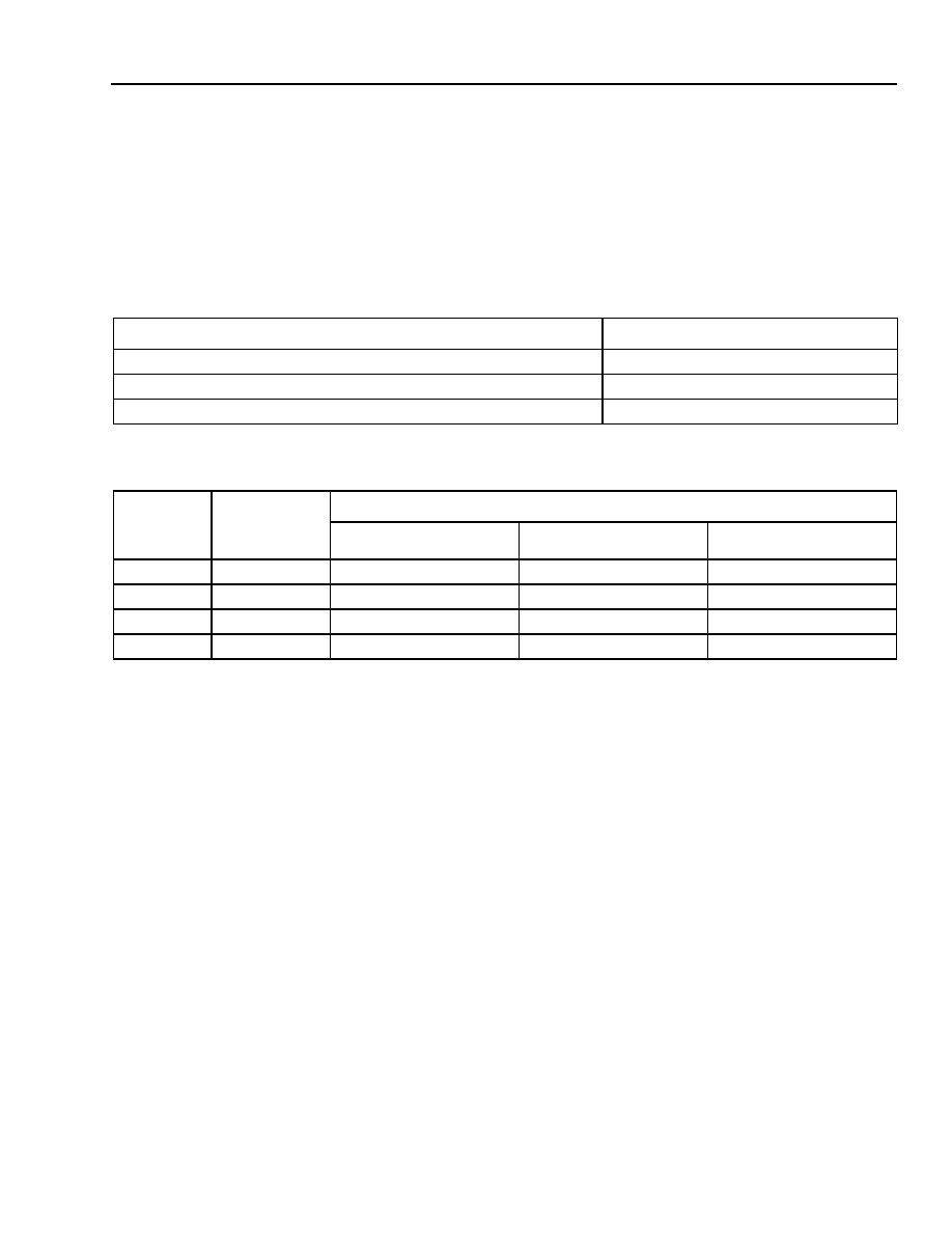
Preliminary Data Sheet
TTSI1K16T
February 1999
1024-Channel, 16-Highway Time-Slot Interchanger
25
Lucent Technologies Inc.
Low-Latency and Frame-Integrity Modes
(continued)
Frame Integrity
(continued)
The range of Rx and Tx offsets can be independently selected from 0
µ
s to (125 ≠
)µ
s via the Rx and Tx highway
configuration registers, bytes 0 and 1, where
= 1/4 bit. The offset difference (Tx highway offset ≠ Rx highway off-
set) can therefore take the range from
-
(125 ≠
)µ
s to +(125 ≠
)µ
s. The table below shows the virtual frame for
transmission for the various cases of offset difference.
Table 9. Offset Difference and Its Effect on Frame for Transmission
* The values for A, B, C, and D are specified in Table 10 below.
Table 10. Offset Difference Boundaries
Table 9 and Table 10 can be used to determine the latency of time slots through the TSI in a frame integrity situa-
tion. Keep in mind that the offset difference is the major factor in determining which virtual Tx frame the time slots
will go out in. The boundary values given in Table 10 are accurate to within ±1 time slot @ 8.192 Mbits/s (= ±4 bits
@ 4.096 Mbits/s = ±2 bits @ 2.048 Mbits/s) and will depend on your particular register settings.
This example can be used to determine the latency of a frame integrity situation. Keep in mind that only the Tx and
Rx highway offsets are relevant when determining the number of physical frames that the transmit data will incur.
However, there is a small range of offset separation where the data will go out in either virtual Tx frame N + 2 or
N + 3, depending on the actual Rx and Tx offsets chosen.
There may be many Rx/Tx highway pairs performing frame integrity simultaneously, but the definition of frame
integrity states that integrity is maintained between each Rx and Tx pair and not across multiple receive highways.
However, in practice, if a Tx highway contains FI time slots from multiple Rx highways and those Rx highways
have the same highway offset, then all of the FI time slots will incur equal delay with frame integrity through the
switch.
Offset Difference = (Tx Highway Offset ≠ Rx Highway Offset)
Virtual Frame for Transmission
A
offset difference < B*
N + 3
B
offset difference < C*
N + 2
C
offset difference
D*
N + 1
Offset
Difference
Boundary
Boundary
Value
(
µ
s)
Boundary Value in Terms of Time Slots (ts) and Bits, at Different Data Rates
2.048 Mbits/s
4.096 Mbits/s
8.192 Mbits/s
A
-
(125
-
)
-
(31 ts, 7 3/4 bits)
-
(63 ts, 7 3/4 bits)
-
(127 ts, 7 3/4 bits)
B
-
121.09375
-
31 ts
-
62 ts
-
124 ts
C
+
3.90625
1 ts
2 ts
4 ts
D
+
(125
-
)
31 ts, 7 3/4 bits
63 ts, 7 3/4 bits
127 ts, 7 3/4 bits
TTSI1K16T
Preliminary Data Sheet
1024-Channel, 16-Highway Time-Slot Interchanger
February 1999
26
Lucent Technologies Inc.
Low-Latency and Frame-Integrity Modes
(continued)
Frame Integrity
(continued)
In the example shown below in Figure 13, a receive and transmit highway are both running at 2.048 Mbits/s. There
are 32 time slots for each 125
µ
s frame. The Rx and Tx highway offsets are zero. This makes the offset difference
zero. Therefore, time slots selected for FI will be transmitted two frames later.
The TSI is configured to perform the following switching function:
Tx time slot 31 is sourced from Rx time slot 0 in low-latency mode. It goes out in frame N.
Tx time slot 2 is sourced from Rx time slot 2 in low-latency mode. It goes out in frame N + 1.
Tx time slot 30 is source from Rx time slot 1 in frame-integrity mode. It goes out in frame N + 2.
Tx time slot 0 is sourced from Rx time slot 3 in frame-integrity mode. It goes out in frame N + 2.
5-7075(F)r.1
Figure 13. Mixed Low-Latency and Frame-Integrity Modes
A
2
Z
1
B
0
A
1
C
0
E
1
E
2
E
0
B
1
B
2
B
3
B
29
B
30
B
31
B
0
C
1
C
2
C
3
C
29
C
30
C
31
C
0
C
2
D
1
D
2
D
0
Z
3
A
3
B
3
C
3
D
2
B
2
D
3
D
29
D
30
D
31
D
0
B
1
FRAME B
FRAME C
FRAME D
FRAME E
R
X
HIGHWAY
T
X
HIGHWAY
FSYNC

Preliminary Data Sheet
TTSI1K16T
February 1999
1024-Channel, 16-Highway Time-Slot Interchanger
27
Lucent Technologies Inc.
Test-Pattern Generation
Test-pattern generation involves selecting outgoing time slots on a particular transmit highway for use in transmit-
ting one of 15 patterns of data. The patterns available are selected using TPS[3--0] (bits 7--4) of the Test-Pattern
Style Register (0x0A), Table 25 on page 42. The transmit highway and time slots involved are selected using the
connection store.
Using the connection store, time slots can be set for test-pattern mode and the on-chip test-pattern generator will
be the source for that transmitted data. The type of test pattern used is determined by the values in the Test-Pat-
tern Style Register (0x0A), Table 25 on page 42. Test-pattern data can be applied to any number of time slots on
only one highway at a time. Any highway may be selected to transmit test-pattern data. The only restrictions for
selecting the time slots set for test-pattern mode are that the time slots must be from the same highway and they
must be contiguous.
The sequence for enabling test-pattern generation is as follows:
1.
Set TSDSM[2--0] (bits 7--5) in byte 1 of the connection store locations which correspond to the time slots
involved in test-pattern substitution mode. Any range of time slots may be selected for test-pattern substitution
mode, starting at any time-slot position. The remaining time slots of that highway will be unaffected.
2.
Set TPS[3--0] (bits 7--4) of the Test-Pattern Style Register (0x0A), Table 25 on page 42 to select the test pat-
tern to be sent. If a fixed user-defined byte is selected for transmission via the TPS[3--0] bits, then the Test-
Pattern Generator Data Register (0x12), Table 33 on page 44 must also be programmed.
3.
Select the data rate of the test-pattern generator via GENHDR[1--0] (bits 5--4) and set STTPG (bit 7) to 1 in
the Test Command Register (0x09), Table 24 on page 41 to start transmitting a good test pattern on the
selected time slots.
In order for data to be transmitted, highways need to be enabled using XE (bit 2) of the Transmit Highway Configu-
ration Register (Byte 2) (0x1002 + 4i), Table 37 on page 46 and GXE (bit 0) of the General Command Register
(0x00), Table 15 on page 36. This can be done before or after the above sequence.
The Tx highway that has been selected for test-pattern generation must be the only highway that has time slots
selected for test-pattern substitution mode (i.e., TSDSM[2--0] = 110) in the connection store. No time slots on any
other Tx highway may be selected for test-pattern substitution mode. If the Tx highway selected for test-pattern
generation is changed, then the previous highway must have all its time slots that were in the TSDSM[2--0] = 110
mode, to be changed to a non-test-pattern substitution mode.
Test-Pattern Checking
Test-pattern checking involves selecting incoming time slots on a particular receive highway for reception of one of
15 test patterns. The patterns available are selected by setting CPS[3--0] (bits 3--0) of the Test-Pattern Style
Register (0x0A), Table 25 on page 42. The input highway and time slots involved are selected using the following
registers:
s
Test-Pattern Checker Highway Register (0x0B), Table 26 on page 43
s
Test-Pattern Checker Upper Time-Slot Register (0x0C), Table 27 on page 43
s
Test-Pattern Checker Lower Time-Slot Register (0x0D), Table 28 on page 43
Test-pattern data can be checked on any number of time slots on only one highway at a time. Any receive highway
may be selected to check for test-pattern data. The only restriction on selecting the time slots set for test-
pattern checking is that the time slots must be from the same highway and they must be contiguous.
The sequence for enabling test-pattern checking is as follows:
1.
Set Test-Pattern Checker Highway Register (0x0B), Table 26 on page 43 to select a highway for receiving the
test data.

TTSI1K16T
Preliminary Data Sheet
1024-Channel, 16-Highway Time-Slot Interchanger
February 1999
28
Lucent Technologies Inc.
Test-Pattern Checking
(continued)
2.
Set the Test-Pattern Checker Upper Time-Slot Register (0x0C), Table 27 on page 43 and the Test-Pattern
Checker Lower Time-Slot Register (0x0D), Table 28 on page 43 to indicate the range of input time slots which
will be carrying test data. The range is inclusive of the time slots indicated in both registers. If only one time slot
is to be selected, then the upper and lower registers should be set to the same value.
3.
Set CPS[3--0] (bits 3--0) of the Test-Pattern Style Register (0x0A), Table 25 on page 42 to select the test pat-
tern to detect. If a fixed, user-defined byte is to be detected, the CTP[7--0] bits in the Test-Pattern Checker
Data Register (0x0E), Table 29 on page 43 should also be programmed with the user-defined pattern.
4.
Select the data rate of the test-pattern checker via CHKHDR[1--0] (bits 3--2) and set STTPC (bit 6) in the Test
Command Register (0x09), Table 24 on page 41 to prompt the checker to attempt to lock onto the selected
test-pattern style.
If there is a need to restart the checker (i.e., the test-pattern style has changed), then STTPC (bit 6) of the Test
Command Register (0x09), Table 24 on page 41 must first be cleared to 0, and then steps 3 and 4 should be
repeated.
There is an interrupt register status bit related to the test-pattern checker. TPD (bit 5) of the Interrupt Status Regis-
ter (0x07), Table 22 on page 39 is used to determine when, if ever, the pattern is detected. The TPD interrupt status
bit will remain 0 until the pattern has been detected. This bit is cleared when read. Once TPD is set, it will not be set
again until the checker is instructed to relock on the test pattern by clearing and then setting STTPC (bit 6) in the
test command register.
Error Injection
The error injection feature provides the capability to inject errors into the outgoing test-pattern data. The number of
errors injected is set using the Test-Pattern Error Injection Register (0x0F), Table 30 on page 43.
If error injection is required, the process should start by setting up the test-pattern generator using steps 1--3 in
the Test-Pattern Generation section on page 27. In order to start injecting errors into the outgoing test pattern, write
the Test-Pattern Error Injection Register (0x0F), Table 30 on page 43 with the number of errors desired. When all of
the errors have been injected into the outgoing data stream, the interrupt status bit BEI (bit 0) will be set in the
Interrupt Status Register (0x07), Table 22 on page 39. Errors will be injected at the rate of one per time slot. Test
Command Register (0x09), Table 24 on page 41 will be cleared to 0 when BEI is set.
Error Checking
Errors are checked on time slots marked for test-pattern data once the checker has locked onto the test pattern.
Every time an error is detected, the ERD (bit 3) interrupt status bit is set and the test-pattern error counter register
contents are incremented. There are two registers Test-Pattern Error Counter (Byte 0) (0x10), Table 31 on page 44
and Test-Pattern Error Counter (Byte 1) (0x11), Table 32 on page 44, that are used to track the number of errors
detected on incoming test patterns.
The error counter registers are reset after both have been read. In order to ensure that the correct value is read
from these registers, byte 0 must be read first followed by byte 1. This action will latch the counter value and allow
the counter logic to be reset and then continue recording.

Preliminary Data Sheet
TTSI1K16T
February 1999
1024-Channel, 16-Highway Time-Slot Interchanger
29
Lucent Technologies Inc.
JTAG Boundary-Scan Specification
Principle of the Boundary Scan
The boundary scan (BS) is a test aid for chip, module, and system testing. The key aspects of BS are as follows:
1. Testing the connections between ICs on a particular board.
2. Observation of signals to the IC pins during normal operating functions.
3. Controlling the built-in self-test (BIST) of an IC. TTSI1K16T does not support BS-BIST.
Designed according to the
IEEE
Std. 1149.1-1990 standard, the BS test logic consists of a defined interface: the
test access port (TAP). The TAP is made up of four signal pins assigned solely for test purposes. The fifth test pin
ensures that the test logic is initialized asynchronously. The BS test logic also comprises a 16-state TAP controller,
an instruction register with a decoder, and several test data registers (BS register, BYPASS register, and IDCODE
register). The main component is the BS register that links all the chip pins to a shift register by means of special
logic cells. The test logic is designed in such a way that it is operated independently of the application logic of the
TTSI1K16T (the mode multiplexer of the BS output cells may be shared). Figure 14 illustrates the block diagram of
the TTSI1K16T's BS test logic.
5-3923(F)r.4
Figure 14. Block Diagram of the TTSI1K16T's Boundary-Scan Test Logic
BOUNDARY-SCAN REGISTER
TDI
TRST
TMS
TCK
TAP
CONTROLLER
INSTRUCTION
DECODER
OUT
TDO
IN
MUX
CHIP KERNEL
(UNAFFECTED BY BOUNDARY-SCAN TEST)
IDCODE REGISTER
BYPASS REGISTER
INSTRUCTION REGISTER

TTSI1K16T
Preliminary Data Sheet
1024-Channel, 16-Highway Time-Slot Interchanger
February 1999
30
Lucent Technologies Inc.
JTAG Boundary-Scan Specification
(continued)
Test Access Port Controller
The test access port controller is a synchronous sequence controller with 16 states. The state changes are preset
by the TMS, TCK, and TRST signals and by the previous state. The state changes always take place when the
TCK edge rises. Figure 15 shows the TAP controller state diagram.
5-3924(F)r.5
Figure 15. BS TAP Controller State Diagram
The value shown next to each state transition in Figure 15 represents the signal present at TMS at the time of a ris-
ing edge at TCK.
The description of the TAP controller states is given in
IEEE
Std. 1149.1-1990 Section 5.1.2 and is reproduced in
Table 11 and Table 12.
SELECT DR
CAPTURE DR
1
0
0
1
1
SHIFT DR
EXIT1 DR
PAUSE DR
0
1
EXIT2 DR
UPDATE DR
1
1
0
0
0
0
TEST LOGIC
RESET
RUN TEST/
IDLE
1
0
SELECT IR
CAPTURE IR
1
0
0
1
1
SHIFT IR
EXIT1 IR
PAUSE IR
0
1
EXIT2 IR
UPDATE IR
1
1
0
0
0
0
TRST = 0
0
1
1

Preliminary Data Sheet
TTSI1K16T
February 1999
1024-Channel, 16-Highway Time-Slot Interchanger
31
Lucent Technologies Inc.
JTAG Boundary-Scan Specification
(continued)
Test Access Port Controller
(continued)
Table 11. TAP Controller States in the Data Register Branch
Table 12. TAP Controller States in the Instruction Register Branch
Name
Description
TEST LOGIC RESET
The BS logic is switched in such a way that normal operation of the ASIC is
adjusted. The IDCODE instruction is initialized by TEST LOGIC RESET.
Irrespective of the initial state, the TAP controller has achieved TEST LOGIC
RESET after five control pulses at the latest when TMS = 1. The TAP controller
then remains in this state. This state is also achieved when TRST = 0.
RUN TEST/IDLE
Using the appropriate instructions, this state can activate circuit parts or initiate
a test. All of the registers remain in their present state if other instructions are
used.
SELECT DR
This state is used for branching to the test data register control.
CAPTURE DR
The test data is loaded in the test data register parallel to the rising edge of TCK
in this state.
SHIFT DR
The test data is clocked by the test data register serially to the rising edge of TCK
in the state. The TDO output driver is active.
EXIT (1/2) DR
This temporary state causes a branch to a subsequent state.
PAUSE DR
The input and output of test data can be interrupted in this state.
UPDATE DR
The test data is clocked into the second stage of the test data register parallel to
the falling edge of TCK in this state.
Name
Description
SELECT IR
This state is used for branching to the instruction register control.
CAPTURE IR
The instruction code 0001 is loaded in the first stage of the instruction register
parallel to the rising edge of TCK in this state.
SHIFT IR
The instructions are clocked into the instruction register serially to the rising edge
of TCK in the state. The TDO output driver is active.
EXIT (1/2) IR
This temporary state causes a branch to a subsequent state.
PAUSE IR
The input and output of instructions can be interrupted in this state.
UPDATE IR
The instruction is clocked into the second stage of the instruction register parallel
to the falling edge of TCK in this state.

TTSI1K16T
Preliminary Data Sheet
1024-Channel, 16-Highway Time-Slot Interchanger
February 1999
32
Lucent Technologies Inc.
JTAG Boundary-Scan Specification
(continued)
Instruction Register
The instruction register (IR) is 4 bits in length. Table 13 shows the BS instructions implemented by the TTSI1K16T.
Table 13. TTSI1K16T's Boundary-Scan Instructions
The instructions not supported in TTSI1K16T are INTEST, RUNBIST, and TOGGLE. A fixed binary 0001 pattern
(the 1 into the least significant bit) is loaded into the IR in the CAPTURE IR controller state. The IDCODE instruc-
tion (binary 0001) is loaded into the IR during the test-logic-reset controller state and at powerup.
The following is an explanation of the instructions supported by TTSI1K16T and their effect on the devices' pins.
EXTEST:
This instruction enables the path cells, the pins of the ICs, and the connections between ASICs to be tested via the
circuit board. The test data can be loaded in the chosen position of the BS register by means of the SAMPLE/PRE-
LOAD instruction. The EXTEST instruction selects the BS register as the test data register. The data at the function
inputs is clocked into the BS register on the rising edge of TCK in the CAPTURE DR state. The contents of the BS
register can be clocked out via TDO in the SHIFT DR state. The value of the function outputs is solely determined
by the contents of the data clocked into the BS register and only changes in the UPDATE DR state on the falling
edge of TCK.
IDCODE:
Information regarding the manufacturer's ID for Lucent, the IC number, and the version number can be read out
serially by means of the IDCODE instruction. The IDCODE register is selected, and the BS register is set to normal
mode in the UPDATE IR state. The IDCODE is loaded at the rising edge of TCK in the CAPTURE DR state. The
IDCODE register is read out via TDO in the SHIFT DR state.
HIGHZ:
All 3-statable outputs are forced to a high-impedance state, and all bidirectional ports are forced to an input state
by means of the HIGHZ instruction. The impedance of the outputs is set to high in the UPDATE IR state. The func-
tion outputs are only determined in accordance with another instruction if a different instruction becomes active in
the UPDATE IR state. The BYPASS register is selected as the test data register. The HIGHZ instruction is imple-
mented in a similar manner to that used for the BYPASS instruction.
SAMPLE/PRELOAD:
The SAMPLE/PRELOAD instruction enables all the input and output pins to be sampled during operation (SAM-
PLE) and the result to be output via the shift chain. This instruction does not impair the internal logic functions.
Defined values can be serially loaded in the BS cells via TDI while the data is being output (PRELOAD).
Instruction
Code
Act. Register
TDI
TDO
Mode
Function
Output Defined Via
EXTEST
0000
Boundary Scan
TEST
Test external
connections
BS Register
IDCODE
0001
Identification
NORMAL
Read Manuf.
Register
Core Logic
HIGHZ
0100
BYPASS
X
3-state
Output--High Impedance
SAMPLE/PRELOAD
0101
Boundary Scan
NORMAL
Sample/load
Core Logic
BYPASS
1111
BYPASS
NORMAL
Min shift path
Core Logic
EVERYTHING ELSE
--
BYPASS
X
--
Output--High Impedance

Preliminary Data Sheet
TTSI1K16T
February 1999
1024-Channel, 16-Highway Time-Slot Interchanger
33
Lucent Technologies Inc.
JTAG Boundary-Scan Specification
(continued)
Instruction Register
(continued)
BYPASS:
This instruction selects the BYPASS register. A minimal shift path exists between TDI and TDO. The BYPASS reg-
ister is selected after the UPDATE IR. The BS register is in normal mode. A 0 is clocked into the BYPASS register
during CAPTURE DR state. Data can be shifted by the BYPASS register during SHIFT DR. The contents of the BS
register do not change in the UPDATE DR state. Please note that a 0 that was loaded during CAPTURE DR
appears first when the data is being read out.
Boundary-Scan Register
The boundary-scan register is a shift register, whereby one or more BS cells are assigned to every digital
TTSI1K16T pin. The TTSI1K16T's boundary-scan register bit-to-pin assignment is defined in the BSDL file, which
is available upon request.
BYPASS Register
The BYPASS register is a one-stage shift register that enables the shift chain to be reduced to one stage in the
TTSI1K16T.
IDCODE Register
The IDCODE register identifies the TTSI1K16T by means of a parallel, loadable, 32-bit shift register. The code is
loaded on the rising edge of TCK in the CAPTURE DR state. The contents of this register is indicated in the BSDL
file.
3-State Procedures
The 3-state input participates in the boundary scan. It has a BS cell, but buffer blocking via this input is suppressed
for the EXTEST instruction. The 3-state input is regarded as a signal input that is to participate in the connection
test during EXTEST. The buffer blocking function should not be active during EXTEST to ensure that the update
pattern at the TTSI1K16T outputs does not become corrupted.

TTSI1K16T
Preliminary Data Sheet
1024-Channel, 16-Highway Time-Slot Interchanger
February 1999
34
Lucent Technologies Inc.
Register Architecture
Table 14 is an overview of the register architecture. The table is a summary of the register function and address.
Complete detail of each register is given in the following sections.
Table 14. TTSI1K16T Register Summary
Register Name/Function
Register
Address (Hex)
Reserved 5000--7FFF
Connection Store Memory
4000--4FFF
Reserved
2800--3FFF
Data Store Memory
2000--27FF
Reserved
1840--1FFF
Receive Highway 15--Reserved
183F
Receive Highway 15 Configuration Byte 2
183E
Receive Highway 15 Configuration Byte 1
183D
Receive Highway 15 Configuration Byte 0
183C
. . .
. . .
Receive Highway 0--Reserved
1803
Receive Highway 0 Configuration Byte 2
1802
Receive Highway 0 Configuration Byte 1
1801
Receive Highway 0 Configuration Byte 0
1800
Reserved
1040--17FF
Transmit Highway 15--Reserved
103F
Transmit Highway 15 Configuration Byte 2
103E
Transmit Highway 15 Configuration Byte 1
103D
Transmit Highway 15 Configuration Byte 0
103C
. . .
. . .
Transmit Highway 0--Reserved
1003
Transmit Highway 0 Configuration Byte 2
1002
Transmit Highway 0 Configuration Byte 1
1001
Transmit Highway 0 Configuration Byte 0
1000
Reserved
0014--0FFF
Version Register
0013
Test-Pattern Generator Data Register
0012
Test-Pattern Error Counter Byte 1
0011
Test-Pattern Error Counter Byte 0
0010

Preliminary Data Sheet
TTSI1K16T
February 1999
1024-Channel, 16-Highway Time-Slot Interchanger
35
Lucent Technologies Inc.
Register Architecture
(continued)
Table 14. TTSI1K16T Register Summary (continued)
Register Name/Function
Register
Address (Hex)
Test-Pattern Error Injection Register
000F
Test-Pattern Checker Data Register
000E
Test-Pattern Checker Lower Time-Slot Register
000D
Test-Pattern Checker Upper Time-Slot Register
000C
Test-Pattern Checker Highway Register
000B
Test-Pattern Style Register
000A
Test Command Register
0009
Interrupt Mask Register
0008
Interrupt Status Register
0007
Global Interrupt Mask Register
0006
Idle Code 3 Register
0005
Idle Code 2 Register
0004
Idle Code 1 Register
0003
BIST Command Register
0002
Software Reset Register
0001
General Command Register
0000

TTSI1K16T
Preliminary Data Sheet
1024-Channel, 16-Highway Time-Slot Interchanger
February 1999
36
Lucent Technologies Inc.
Configuration Register Architecture
Note: All registers' bits default to 0 upon reset, unless noted otherwise.
All TDM highway data, which is stored in the TSI, will have the following convention. Bit 7 is first transmitted
and first received; bit zero is last transmitted and last received. This convention applies to the data read from
the data store, the host data transmitted via the connection store, and any other configuration register which
stores highway data, such as the idle code registers and the test-pattern generator data register.
Table 15. General Command Register (0x00)
Bit
Symbol
Name/Description
7
CSV
Chip Select Valid. This bit is valid while the TTSI1K16T is in synchronous micropro-
cessor interface mode only. When this bit is programmed to be 1, the chip select input
pin is sampled when AS is active. When 0, chip select is latched one PCLK after AS is
active.
6
ED
External Drivers. Used to select the use of external drivers on transmit highways. A 0
indicates that no external buffers are being used; therefore, the TXD pins will become
3-stated for time slots that are programmed as such. A 1 indicates that the TXD output
highways are connected to external drivers; thus, the TXD pins will always be driven
to prevent floating nodes at the inputs of the external drivers. The TXOE[0--15] out-
puts always reflect the high-impedance status of the corresponding TXD[0--15] high-
ways, regardless of the ED bit setting. The only exception to this is when TEST is
asserted, which 3-states all outputs.
See Table 41, Transmit Highway 3-State Options, on page 49 for other methods of
3-stating the transmit highways.
5
--
Reserved. Read as 0.
4
INTOE
Interrupt Output Enable. This bit, when set to a 1, enables the INT output signal to
be driven based on the status of the internal interrupts and their corresponding individ-
ual mask bits. When 0, the output will remain 3-stated.
3
INTP
Interrupt Polarity. This bit defines the polarity of INT, as output from the TTSI1K16T.
A 1 selects an active-low interrupt output (INT). A 0 selects an active-high interrupt
output (INT), and is the default polarity.
2
FSP
Frame Sync Polarity. This bit defines the polarity of FSYNC, as sampled by CK,
which designates the beginning of the frame. A 1 selects an active-high frame syn-
chronization (FSYNC). A 0 selects an active-low frame synchronization (FSYNC).
1
FSSE
Frame Sync Sample Edge. This bit selects the clock edge of the CK input that is
used to sample the frame synchronization input. A 1 selects the rising edge; and a 0
selects the falling edge of CK.
0
GXE
Global Transmit Enable. When 0, all 16 transmit highways are 3-stated. GXE
defaults to 0 so that all outputs can be held in a high-impedance state until they have
been configured and individually enabled.
For other methods of 3-stating transmit highways, see Table 41, Transmit Highway
3-State Options, on page 49.

Preliminary Data Sheet
TTSI1K16T
February 1999
1024-Channel, 16-Highway Time-Slot Interchanger
37
Lucent Technologies Inc.
Configuration Register Architecture
(continued)
Table 16. Software Reset Register (0x01)
Table 17. BIST Command Register (0x02)
The BIST test sequence is performed as follows:
1.
Set RB (bit 7) in the BIST command register to 1 in order to initiate the internal BIST test.
2.
Wait for the BIST complete (BC) (bit 1 of the interrupt status register) interrupt to occur via the interrupt status
register, if it is not masked via the interrupt mask register MASKBC bit (bit 1). Alternatively, the host can poll
the BD bit in the BIST command register which will also indicate the completion of BIST.
3.
Once the BIST interrupt occurs or the BD bit is set, the BPF bit in the BIST command register will reflect the
BIST pass/fail result. A BPF set to 0 indicates a pass.
4.
Set RB (bit 7) in the BIST command register to a 0 in order to end the internal BIST test.
5.
Issue a software reset via the SR bit in the software reset register.
During BIST, the TTSI1K16T will corrupt traffic and the contents of the connection store memory. The TTSI1K16T
should, therefore, be taken off-line prior to running BIST and reprogrammed afterwards.
Bit
Symbol
Name/Description
7--1
--
Reserved. Read as 0.
0
SR
Software Reset. Writing a 1 to this bit resets the chip. This bit has a function
similar to the RESET pin. When set to 1, all registers and control logic will be ini-
tialized to their default values except the software reset register. A 0 must be
written to this bit in order to clear and release the software reset. The micropro-
cessor interface will not be affected by the software reset, and the write to this bit
will terminate normally.
Bit
Symbol
Name/Description
7
RB
Run BIST. Writing a 1 to this bit begins the built-in self-test for all internal mem-
ory blocks (i.e., the data and connection stores). This bit must be cleared by writ-
ing a 0 when BIST is complete. That event is indicated via the BIST complete
(BC) bit in the interrupt status register, as well as the BIST done (BD) bit in the
BIST command register. Writing a 0 to this bit position will also clear the BD bit. A
software reset should be performed after the BIST testing sequence is complete.
6
BD
BIST Done (Read Only). This bit indicates when the BIST test is complete. This
bit is used for polling to determine the completion of the BIST test. The real-time
duration of the TSI BIST test is 2.8 seconds. This bit will remain set to a 1 reflect-
ing the fact that the BIST is complete until the RB bit is written to a 0.
5
BPF
BIST Pass/Fail (Read Only). This bit indicates the status of the BIST test
results. A 0 indicates that no errors were detected.
4--0
--
Reserved. Read as 0.

TTSI1K16T
Preliminary Data Sheet
1024-Channel, 16-Highway Time-Slot Interchanger
February 1999
38
Lucent Technologies Inc.
Configuration Register Architecture
(continued)
Table 18. Idle Code 1 Register (0x03)
Table 19. Idle Code 2 Register (0x04)
Table 20. Idle Code 3 Register (0x05)
Table 21. Global Interrupt Mask Register (0x06)
Bit
Symbol
Name/Description
7--0
IC1
Idle Code 1[7--0]. This register is used to identify the data to be sent on any
outgoing time slot marked for idle code 1 transmission. Idle code transmission is
enabled via the time-slot data select mode bits. See Table 45, Connection Store
Memory (Byte 1), on page 51.
Bit
Symbol
Name/Description
7--0
IC2
Idle Code 2[7--0]. This register is used to identify the data to be sent on any
outgoing time slot marked for idle code 2 transmission. Idle code transmission is
enabled via the time-slot data select mode bits. See Table 45, Connection Store
Memory (Byte 1), on page 51.
Bit
Symbol
Name/Description
7--0
IC3
Idle Code 3[7--0]. This register is used to identify the data to be sent on any
outgoing time slot marked for idle code 3 transmission. Idle code transmission is
enabled via the time-slot data select mode bits. See Table 45, Connection Store
Memory (Byte 1), on page 51.
Bit
Symbol
Name/Description
7--1
--
Reserved. Read as 0.
0
GIE
Global Interrupt Enable. This bit must be written to a 1 in order for INT to be
asserted as a result of the possible interrupt conditions. This is in addition to
the mask bits in the interrupt mask register. When 0, the INT output is blocked
independent of the programming of the interrupt mask register. When 1, the
INT output is enabled and will be asserted based on the interrupt status and
mask bits.

Preliminary Data Sheet
TTSI1K16T
February 1999
1024-Channel, 16-Highway Time-Slot Interchanger
39
Lucent Technologies Inc.
Configuration Register Architecture
(continued)
Table 22. Interrupt Status Register* (0x07)
* Read-only register.
This register is clear on read. Once the status bits are read, they will remain cleared until the next interrupt event
occurs. The interrupt mask register in combination with the global interrupt enable GIE (bit 0) in the global interrupt
mask register determines when the INT pin gets asserted when an interrupt status bit gets set. In general, the
interrupt status register bits will update regardless of the mask bits. The exception to this is the FSERR bit, which
will not be set if the corresponding mask bit is set.
Bit
Symbol
Name/Description
7
--
Reserved. Read as 0.
6
FSERR
Frame Sync Error. When set to 1, this bit indicates that an error related to frame
sync has occurred. This error could be a result of a missing FSYNC or a mis-
aligned FSYNC.
5
TPD
Test Pattern Detected. The TPD bit indicates the state of the test-pattern
checker. When TPD = 0, the test-pattern checker has not yet located the
selected test pattern. When TPD = 1, the test-pattern checker has located the
selected test pattern. Test-pattern data must be error-free for 32 time slots before
it is considered detected. If 32 or more time slots are selected for test-pattern
checking, this event could occur within one 125
µ
s frame. If only two time slots
are selected for test-pattern checking, then the test pattern will be detected after
16 frames.
4
--
Reserved. Read as 0 or 1.
3
ERD
Error Detected. This bit is set to 1 each time an error has been detected in the
test pattern once the test pattern has first been detected.
2
--
Reserved. Read as 0.
1
BC
BIST Complete. When set to 1, this status bit indicates that the BIST sequence is
complete.
0
BEI
Bit Errors Inserted. When set to 1, this status bit indicates that the request to
insert bit errors into the outgoing test pattern is complete.

TTSI1K16T
Preliminary Data Sheet
1024-Channel, 16-Highway Time-Slot Interchanger
February 1999
40
Lucent Technologies Inc.
Configuration Register Architecture
(continued)
Table 23. Interrupt Mask Register (0x08)
Bit
Symbol
Name/Description
7
--
Reserved. Read as 0.
6
MASKFS
Mask Frame Sync Error Interrupt. Set this bit to a 1 to mask the generation of
an interrupt as a result of a frame sync error. Resets to a 1, which prevents the
status bit from generating an interrupt. Setting this bit to a 1 also prevents the
detection of a frame sync error and, thus, the setting of the FSERR bit in the
interrupt status register. This is done to prevent an unintended interrupt at the
first FSYNC pulse after the reset sequence.
5
MASKTPD
Mask Test-Pattern Detection Interrupt. Set this bit to a 1 to mask the genera-
tion of an interrupt as a result of a test-pattern detection. Resets to a 1, which
prevents the status bit from generating an interrupt.
4
--
Reserved. Read as 1. Always write a 1 to this bit when writing this register.
3
MASKERD
Mask Error Detected Interrupt. Set this bit to a 1 to mask the generation of an
interrupt as a result of a single bit error detected in the incoming test pattern.
Resets to a 1, which prevents the status bit from generating an interrupt.
2
--
Reserved. Read as 1. Always write a 1 to this bit when writing this register.
1
MASKBC
Mask BIST Complete Interrupt. Set this bit to a 1 to mask the generation of an
interrupt as a result of completing the memory BIST. Resets to a 1, which pre-
vents the status bit from generating an interrupt.
0
MASKBEI
Mask Bit Errors Inserted Interrupt. Set this bit to a 1 to mask the generation of
an interrupt as a result of completing the insertion of all requested bit errors.
Resets to a 1, which prevents the status bit from generating an interrupt.

Preliminary Data Sheet
TTSI1K16T
February 1999
1024-Channel, 16-Highway Time-Slot Interchanger
41
Lucent Technologies Inc.
Configuration Register Architecture
(continued)
Table 24. Test Command Register (0x09)
Bit
Symbol
Name/Description
7
STTPG
Start Test-Pattern Generator. Writing a 1 to this register will cause the genera-
tor to start generating a test pattern based on the pattern indicated in the test-
pattern style register. Writing a 0 to this register will stop the test-pattern genera-
tion and provide the opportunity to change the test-pattern style.
6
STTPC
Start Test-Pattern Checker. Writing a 1 to this register will cause the checker to
start locking on to a test pattern based on the pattern indicated in the test-
pattern style register. Writing a 0 to this register will stop the test-pattern check-
ing and provide the opportunity to change the test-pattern style.
5--4
GENHDR
[1--0]
Test-Pattern Generator Highway Data Rate. These bits are used to indicate
the highway data rate of the transmit highway selected for test-pattern genera-
tion. It must match the Tx highway data rate which was set in transmit highway
configuration register (byte 2), HDR[1--0] bits. The transmit highway selection
for test-pattern generation is done using the connection store. Only one highway
at a time can be involved with test-pattern generation. Test-pattern generation
and checking does not affect the operation of other time slots or highways.
GENHDR1
GENHDR0
0
0
2.048 Mbits/s (default)
0
1
4.096 Mbits/s
1
0
8.192 Mbits/s
1
1
0.000 Mbits/s (idle, not transmitting data)
3--2
CHKHDR
[1--0]
Test-Pattern Checker Highway Data Rate. These bits are used to indicate the
highway data rate of the receive highway selected for test-pattern checking. It
must match the Rx highway data rate which was set in receive highway configu-
ration register (byte 2), HDR[1--0] bits. The transmit highway selection for test-
pattern generation is done using the test-pattern checker highway register. Only
one highway at a time can be involved with test-pattern checking. Test-pattern
generation and checking does not affect the operation of other time slots or high-
ways.
CHKHDR1
CHKHDR0
0
0
2.048 Mbits/s (default)
0
1
4.096 Mbits/s
1
0
8.192 Mbits/s
1
1
0.000 Mbits/s (idle, not receiving data)
1--0
--
Reserved. Read as 0.

TTSI1K16T
Preliminary Data Sheet
1024-Channel, 16-Highway Time-Slot Interchanger
February 1999
42
Lucent Technologies Inc.
Configuration Register Architecture
(continued)
Table 25. Test-Pattern Style Register (0x0A)
Bit
Symbol
Name/Description
7--4
TPS[3--0]
Generator Test-Pattern Style[3--0]. These 4 bits determine the type of test pattern
that will be generated by the on-line maintenance test-pattern generator.
TPS3
TPS2
TPS1
TPS0
Test-Pattern Description
0
0
0
0
MARK (all 1s) (AIS - red alarm)
0
0
0
1
QRSS (2
20
≠ 1 with zero suppression) (O.151)
0
0
1
0
31(2
5
≠ 1)
PRBS
0
0
1
1
63(2
6
≠ 1)
PRBS
0
1
0
0
511(2
9
≠ 1)
PRBS
(O.153)
0
1
0
1
511(2
9
≠ 1)
PRBS
(reversed)
0
1
1
0
2047(2
11
≠ 1) PRBS
(O.152)
0
1
1
1
2047(2
11
≠ 1) PRBS
(reversed)
1
0
0
0
2
15
≠ 1
PRBS
(O.151) (noninverted)
1
0
0
1
2
20
≠ 1
PRBS
(O.153)
1
0
1
0
2
20
≠ 1
PRBS
(reversed)
1
0
1
1
2
23
≠ 1
PRBS
(V.33) (noninverted)
1
1
0
0
1:1 (alternating 1s and 0s).
1
1
0
1
Reserved.
1
1
1
0
Reserved.
1
1
1
1
Fixed. User-defined byte, stored in the test-
pattern generator data register will be sent.
PRBS = pseudorandom binary sequence.
QRSS = quasi-random signal source.
3--0
CPS[3--0]
Checker Test-Pattern Style[3--0]. These 4 bits determine the type of test pattern
that will be detected by the on-line maintenance test-pattern checker.
CPS3
CPS2
CPS1
CPS0
Test-Pattern Description
0
0
0
0
MARK (all 1s) (AIS - red alarm)
0
0
0
1
QRSS (2
20
≠ 1 with zero suppression) (O.151)
0
0
1
0
31(2
5
≠ 1)
PRBS
0
0
1
1
63(2
6
≠ 1)
PRBS
0
1
0
0
511(2
9
≠ 1)
PRBS
(O.153)
0
1
0
1
511(2
9
≠ 1)
PRBS
(reversed)
0
1
1
0
2047(2
11
≠ 1) PRBS
(O.152)
0
1
1
1
2047(2
11
≠ 1) PRBS
(reversed)
1
0
0
0
2
15
≠ 1
PRBS
(O.151) (noninverted)
1
0
0
1
2
20
≠ 1
PRBS
(O.153)
1
0
1
0
2
20
≠ 1
PRBS
(reversed)
1
0
1
1
2
23
≠ 1
PRBS
(V.33) (noninverted)
1
1
0
0
1:1 (alternating 1s and 0s).
1
1
0
1
Reserved.
1
1
1
0
Reserved.
1
1
1
1
Fixed. The checker will compare against the user-
defined byte, stored in the test-pattern checker
data register.
PRBS = pseudorandom binary sequence.
QRSS = quasi-random signal source.

Preliminary Data Sheet
TTSI1K16T
February 1999
1024-Channel, 16-Highway Time-Slot Interchanger
43
Lucent Technologies Inc.
Configuration Register Architecture
(continued)
Table 26. Test-Pattern Checker Highway Register (0x0B)
Table 27. Test-Pattern Checker Upper Time-Slot Register (0x0C)
Table 28. Test-Pattern Checker Lower Time-Slot Register (0x0D)
Table 29. Test-Pattern Checker Data Register (0x0E)
Table 30. Test-Pattern Error Injection Register (0x0F)
Bit
Symbol
Name/Description
7--4
--
Reserved. Must be written to 0.
3--0
CHS[3--0]
Checker Highway Select[3--0]. These 4 bits determine the receive highway to
which the test-pattern checker is connected.
Bit
Symbol
Name/Description
7
--
Reserved.
6--0
CKRUP[6--0] Checker Upper Time-Slot Select[6--0]. These 7 bits determine the upper time
slot in the input highway to which the test-pattern checker is connected. All con-
tiguous time slots that lie between the lower and upper time-slot boundaries
inclusive are monitored for the test pattern. The range of time slots that can be
monitored is from 1 time slot to the entire span (32, 64, and 128 time slots for a
2.048 Mbits/s, 4.096 Mbits/s, 8.192 Mbits/s highway, respectively). If one time
slot is to be monitored, then CKRUP and CKRLOW should be set to the same
value.
Bit
Symbol
Name/Description
7
--
Reserved.
6--0
CKRLOW
[6--0]
Checker Lower Time-Slot Select[6--0]. These 7 bits determine the lower time
slot in the input highway to which the test-pattern checker is connected. All con-
tiguous time slots that lie between the lower and upper time-slot boundaries
inclusive are monitored for the test pattern. The range of time slots that can be
monitored is from 1 time slot to the entire span (32, 64, and 128 time slots for a
2.048 Mbits/s, 4.096 Mbits/s, 8.192 Mbits/s highway, respectively). If one time
slot is to be monitored, then CKRUP and CKRLOW should be set to the same
value.
Bit
Symbol
Name/Description
7--0
CTP[7--0]
Checker Test Pattern[7--0]. The data written here will be used for comparison
when the fixed mode is programmed into the test-pattern style register.
Bit
Symbol
Name/Description
7--0
BEC[7--0]
Bit Error Count[7--0]. This register is used to indicate the number of single bit
errors that are to be injected into the outgoing test pattern (QRSS, PRBS, or
fixed user-defined byte). This register can be programmed to inject up to 255 bit
errors. The BEI bit in the interrupt status register will indicate when all of the
errors have been injected. BEC[7--0] will automatically be reset when BEI is
set. In order to send out additional errors, BEC[7--0] should be rewritten. Errors
are injected at the rate of one per time slot.

TTSI1K16T
Preliminary Data Sheet
1024-Channel, 16-Highway Time-Slot Interchanger
February 1999
44
Lucent Technologies Inc.
Configuration Register Architecture
(continued)
Table 31. Test-Pattern Error Counter (Byte 0) (0x10)*
* Read-only register.
Table 32. Test-Pattern Error Counter (Byte 1) (0x11)*
* Read-only register.
Note: The error counter will be incremented each time a bit error is detected by the pattern checker.
In order to ensure that the correct value is read from these registers, byte 0 must be read first followed by
byte 1. This action will latch the error counter value and allow the counter to be reset and continue recording
as time proceeds.
Table 33. Test-Pattern Generator Data Register (0x12)
Table 34. Version Register (0x13)*
* Read-only register.
Reading a 00 from this register indicates version number 1.0.
Bit
Symbol
Name/Description
7--0
EC[7--0]
Error Counter[7--0]. Least significant bits of 16-bit error counter. See note
below for resetting counter.
Bit
Symbol
Name/Description
7--0
EC[15--8]
Error Counter[15--8]. Most significant bits of 16-bit error counter. See note
below for resetting counter.
Bit
Symbol
Name/Description
7--0
GTP[7--0]
Generator Test Pattern[7--0]. The data written here will be sent out repeatedly
if the fixed data test-pattern mode is selected in the test-pattern style register.
Bit
Symbol
Name/Description
7--2
--
Reserved.
1--0
VER[1--0]
Version Number. Read as 00
.

Preliminary Data Sheet
TTSI1K16T
February 1999
1024-Channel, 16-Highway Time-Slot Interchanger
45
Lucent Technologies Inc.
Configuration Register Architecture
(continued)
Table 35. Transmit Highway Configuration Register (Byte 0) (0x1000 + 4i)*
* i = the transmit highway number.
Bit
Symbol
Name/Description
7
--
Reserved. Read as 0.
6--4
XBITOFF
[2--0]
Transmit Highway Bit Offset[2--0]. XBITOFF is used to offset the beginning of
an outgoing frame by the indicated number of bit times. If no bit offsets are
required, these bits should be set to 000. The following list shows the effect of
setting these bits.
000 = no bit offset
001 = 1-bit offset
010 = 2-bit offset
. . .
111 = 7-bit offset
Note: Bit periods are relative to the highway data rate set for each highway.
XTSOFF, XBITOFF, and XFBOFF are used in conjunction to define the start of
the outgoing frame. The values are added together to position the sampling of
time slot 0, bit 0 for each highway.
3--2
XFBOFF
[1--0]
Transmit Highway Fractional Bit Offset[1--0]. XFBOFF is used to offset the
beginning of an outgoing frame by the indicated number of fractional bit times. If
no fractional bit offsets are required, these bits should be set to 00. The following
list shows the effect of these bits.
00 = no fractional bit offset
01 = 1/4-bit fractional offset
10 = 1/2-bit fractional offset
11 = 3/4-bit fractional offset
Note: Bit periods are relative to the highway data rate set for each highway.
XTSOFF, XBITOFF, and XFBOFF are used in conjunction to define the start of
the outgoing frame. The values are added together to position the sampling of
time slot 0, bit 0 for each highway.
1--0
--
Reserved. Must be written to 00.

TTSI1K16T
Preliminary Data Sheet
1024-Channel, 16-Highway Time-Slot Interchanger
February 1999
46
Lucent Technologies Inc.
Configuration Register Architecture
(continued)
Table 36. Transmit Highway Configuration Register (Byte 1) (0x1001 + 4i)*
* i = the transmit highway number.
Table 37. Transmit Highway Configuration Register (Byte 2) (0x1002 + 4i)*
* i = the transmit highway number.
Note: During CK input interruptions (e.g., clock switching), the transmit highways should be 3-stated by clearing
the GXE (bit 0) of the general command register. The highways can be enabled by writing a 1 to the GXE bit
once the PLL has regained lock (250
µ
s later).
Bit
Symbol
Name/Description
7
--
Reserved. Read as 0.
6--0
XTSOFF
[6--0]
Transmit Highway Time-Slot Offset[6--0]. XTSOFF is used to offset the
beginning of an outgoing frame by the indicated number of time slots (bytes). If
no time-slot offsetting is required, these bits should be set to zero. The following
table shows the range of offsets for the different highway data rates.
Highway Data Rate Time-Slot Offset Range
2.048 Mbits/s 0--31
4.096 Mbits/s 0--63
8.192 Mbits/s 0--127
Note: A time slot is always 8 bits. A bit period is relative to the highway data rate
set for each highway.
XTSOFF, XBITOFF, and XFBOFF are used in conjunction to define the start of
the outgoing frame. The values are added together to position the transmission
of time slot 0, bit 0.
Bit
Symbol
Name/Description
7--3
--
Reserved. Read as 0.
2
XE
Transmit Highway 3-State Enable. The associated output highway is high
impedance when this bit is 0 (default after reset). When this bit is set to 1, the
output driver is enabled. The effect of this bit is dependent on the status of the
external drive bit of the general command register. See Table 15, General
Command Register (0x00), on page 36 for details. For other methods of 3-stat-
ing transmit highways, see Table 41, Transmit Highway 3-State Options, on
page 49.
1--0
HDR[1--0]
Transmit Highway Data Rate[1--0].
HDR1
HDR0
0
0
2.048 Mbits/s (default)
0
1
4.096 Mbits/s
1
0
8.192 Mbits/s
1
1
0.000 Mbits/s (idle, not transmitting data)
All of the transmit highways are grouped into pairs. TXD0 with TXD1, TXD2
with TXD3, . . . , and TXD14 with TXD15. The maximum combined bandwidth
for each pair is 8.192 Mbits/s. Refer to Table 7, Tx Highway Data Rate Options,
on page 18 for highway rate combination.

Preliminary Data Sheet
TTSI1K16T
February 1999
1024-Channel, 16-Highway Time-Slot Interchanger
47
Lucent Technologies Inc.
Configuration Register Architecture
(continued)
Table 38. Receive Highway Configuration Register (Byte 0) (0x1800 + 4i)*
* i = the receive highway number.
Bit
Symbol
Name/Description
7
--
Reserved. Read as 0.
6--4
RBITOFF
[2--0]
Receive Highway Bit Offset[2--0]. RBITOFF is used to offset the beginning
of an incoming frame by the indicated number of bit times. If no bit offsets are
required, these bits should be set to 000. The following list shows the effect of
setting these bits.
000 = no bit offset
001 = 1-bit offset
010 = 2-bit offset
. . .
111 = 7-bit offset
Note: Bit periods are relative to the highway data rate set for each highway.
RTSOFF, RBITOFF, and RFBOFF are used in conjunction to define the start of
the incoming frame. The values are added together to position the sampling of
time slot 0, bit 0 for each highway.
3--2
RFBOFF
[1--0]
Receive Highway Fractional Bit Offset[1--0]. RFBOFF is used to offset the
beginning of an incoming frame by the indicated number of fractional bit times.
If no fractional bit offsets are required, these bits should be set to 00. The fol-
lowing list shows the effect of these bits.
00 = no fractional bit offset
01 = 1/4-bit fractional offset
10 = 1/2-bit fractional offset
11 = 3/4-bit fractional offset
Note: Bit periods are relative to the highway data rate set for each highway.
RTSOFF, RBITOFF, and RFBOFF are used in conjunction to define the start of
the incoming frame. The values are added together to position the sampling of
time slot 0, bit 0 for each highway.
1--0
--
Reserved. (Read/Write) Must be written to 00.

TTSI1K16T
Preliminary Data Sheet
1024-Channel, 16-Highway Time-Slot Interchanger
February 1999
48
Lucent Technologies Inc.
Configuration Register Architecture
(continued)
Table 39. Receive Highway Configuration Register (Byte 1) (0x1801 + 4i)*
* i = the receive highway number.
Table 40. Receive Highway Configuration Register (Byte 2)
(0x1802 + 4i)*
* i = the receive highway number.
Bit
Symbol
Name/Description
7
--
Reserved. Read as 0.
6--0
RTSOFF
[6--0]
Receive Highway Time-Slot Offset[6--0]. RTSOFF is used to offset the begin-
ning of an incoming frame by the indicated number of time slots (bytes). If no
time-slot offsetting is required, these bits should be set to zero. The following
table shows the range of offsets for the different highway data rates.
Highway Data Rate Time-Slot Offset Range
2.048 Mbits/s 0--31
4.096 Mbits/s 0--63
8.192 Mbits/s 0--127
Note: A time slot is always 8 bits. A bit period is relative to the highway data rate
set for each highway.
RTSOFF, RBITOFF, and RFBOFF are used in conjunction to define the start of
the incoming frame. The values are added together to position the sampling of
time slot 0, bit 0.
Bit
Symbol
Name/Description
7--3
--
Reserved. Read as 0.
2
LC
Loopback Control. This bit is used to control the internal loopback of the TXD
highway to the corresponding RXD highway. When set to 1, the TXD highway as
input to this RXD highway. The transmit highway involved will be internally
looped back to the matching receive highway so that the TXD[i] output is now the
input to RXD[i]. When a particular highway is in this mode, the receive highway
offset must be 1/2-bit greater than the corresponding transmit highway offset.
When LC is cleared to 0, the RXD pin is the source of highway data (default).
1--0
HDR[1--0]
Receive Highway Data Rate[1--0].
HDR1
HDR0
0
0
2.048 Mbits/s (default)
0
1
4.096 Mbits/s
1
0
8.192 Mbits/s
1
1
0.000 Mbits/s (idle, not receiving data)
All of the receive highways are grouped into pairs. RXD0 with RXD1, RXD2 with
RXD3, . . . , and RXD14 with RXD15. The maximum combined bandwidth for
each pair is 8.192 Mbits/s. Refer to Table 6, Rx Highway Data Rate Options, on
page 18 for highway rate combination.

Preliminary Data Sheet
TTSI1K16T
February 1999
1024-Channel, 16-Highway Time-Slot Interchanger
49
Lucent Technologies Inc.
Configuration Register Architecture
(continued)
Transmit Highway 3-State Options
There are several ways of 3-stating the transmit highways:
TEST (active-low) is the input pin that 3-states all outputs and bidirectional pins of the device.
GXE (bit 0) (active-high) is the global transmit enable bit in the general command register. It applies to all transmit
highways.
XE (bit 2) (active-high) is the transmit highway 3-state enable bit in the transmit highway configuration register
(byte 2). There is a separate XE bit for each one of the 16 transmit highways.
ED (bit 6) (active-high) is the external drivers bit in the general command register. This bit applies to all the transmit
highways. It affects the 3-stating of the transmit highways. Time slots that are selected to be 3-stated, by setting
the TSDSM[2--0] bits to 0x7 in byte 2 of the connection store, will be driven with random data if ED = 1. Otherwise,
these time slots will be 3-stated.
Table 41. Transmit Highway 3-State Options
TEST
(Input
Pin)
GXE
(Cfg
Bit)
ED
(Cfg
Bit)
XE for
Transmit
Highway [i]
(Cfg Bit)
TXD[0--15] Pins
TXOE[0--15] Pins
0
X
X
X
All high impedance.
All high impedance.
1
0
0
X
All high impedance.
All 0.
1
0
1
X
All driven with random data.
All 0.
1
1
0
0
TXD[i] = high impedance.
TXOE[i] = 0.
1
1
0
1
TXD[i] = 0, 1, or high impedance
according to connection store pro-
gramming.
TXOE[i] = 0 or 1, representing high-imped-
ance state according to connection store
programming.
1
1
1
0
TXD[i] is driven with random data.
TXOE[i] = 0.
1
1
1
1
TXD[i] = 0 or 1 reflecting the correct
transmit data. Time slots which are
selected for high-impedance mode
via the connection store will be
driven with random data and not
3-stated.
TXOE[i] = 0 or 1, representing high-imped-
ance state according to connection store
programming.

TTSI1K16T
Preliminary Data Sheet
1024-Channel, 16-Highway Time-Slot Interchanger
February 1999
50
Lucent Technologies Inc.
Data Store Memory
Microprocessor access to the incoming highway data is provided by directly reading the data store memory. Each
one of the time slots is addressable by constructing the address in the following way
.
Microprocessor reads to this
address space will occur immediately. Microprocessor writes to this address space will not change the contents of
the data store. If user data is to be sent out on a particular time slot, the host data substitution mode in the connec-
tion store should be used.
Table 42. Address Scheme for Data Store Memory
To illustrate the addressing scheme, consider the following examples:
To read the data received in time slot 7 on RXD6, the following address is used to access the TSI data store mem-
ory location.
A[14--0] = 010_00110_0000111 = 0x2307
Note: All TDM highway data which is stored in the TSI will have the following convention. The most significant bit
of a byte is first transmitted and first received, the least significant bit is last transmitted and last received.
This convention applies to the data read from the data store, the host data transmitted via the connection
store, and any other configuration register that stores highway data.
Connection Store Memory
The connection store memory is primarily used to set up the switching matrix and selects the transmit data source
for each one of the outgoing time slots. There are two connection store byte locations associated with each one of
the outgoing time slots. The address for each of the corresponding connection store memory locations is con-
structed in the following way.
Table 43. Address Scheme for Connection Store Memory
If any particular transmit highway is not programmed to use the total available bandwidth (8.192 Mbits/s), then the
connection store memory locations representing the unused time slots are not used. For example, assume high-
way 7 is set for a highway data rate of 4.096 Mbits/s. This translates to a total of 64 time slots being transmitted on
highway 7. In that case, addresses A[14--0] = 0x4700--0x477F must be set. Addresses A[14--0] = 0x4780--
0x47FF are irrelevant for a 4.096 Mbits/s highway and need not be set.
The connection store memory does not have a default state. Therefore, after powerup, the relevant locations in the
connection store must be programmed. However, the connection store contents are not affected by a software or
hardware reset of the TTSI1K16T.
Data Store
Memory Address
14
13
12
11
10
9
8
7
6
5
4
3
2
1
0
0
1
0
0
Receive Highway
Number (0--15)
Receive Time-Slot Address
(0--127)
Connection Store
Memory Address
14
13
12
11
10
9
8
7
6
5
4
3
2
1
0
1
0
0
Transmit Highway
Number (0--15)
Transmit Time-Slot Address
(0--127)
Byte 0, 1
Select

Preliminary Data Sheet
TTSI1K16T
February 1999
1024-Channel, 16-Highway Time-Slot Interchanger
51
Lucent Technologies Inc.
Connection Store Memory
(continued)
Table 44. Connection Store Memory (Byte 0)
Table 45. Connection Store Memory (Byte 1)
To illustrate the connection store programming scheme, consider the following example:
To configure the transmission of time slot 7 on TXD6, the following addresses are used to access the relevant TSI
connection store memory locations.
A[14--0] = 10_00110_0000111_0 = 0x460E--to access byte 0
A[14--0] = 10_00110_0000111_1 = 0x460F--to access byte 1
Now, if it is desired to send Rx time slot 4 from RXD3 to time slot 7 on TXD6 in frame integrity mode, then the fol-
lowing data should be written to the above addresses.
Data byte 0 = 0_0000100 = 0x04
Data byte 1 = 001_00011 = 0x23
Thus, to map Rx time slot 4 from RXD3 to Tx time slot 7 on TXD6, in frame integrity mode, the following two TSI
writes must be performed.
Write location 0x460E with 0x04
Write location 0x460F with 0x23
Bit
Symbol
Name/Description
7--0
RTSA[6--0]/
HSD[7--0]
Receive Time-Slot Address[6--0]/Host Substituted Data[7--0]. If low-
latency or frame-integrity time-slot data select modes are selected for the partic-
ular transmit time slot being configured, then these bits are used to indicate the
receive time-slot address from which the transmit time-slot data is sourced. Bit 7
should be set to 0.
If the host data substitution mode is selected for the particular transmit time slot
being configured, then these 8 bits will represent the data byte to be transmitted.
These bits are not valid for time-slot data select modes 3--7.
Bit
Symbol
Name/Description
7--5
TSDSM[2--0] Time-Slot Data Select Mode[2--0]
0
0
0
Low-latency mode.
0
0
1
Frame-integrity mode.
0
1
0
Host data substitution mode.
0
1
1
Idle code 1 substitution mode.
1
0
0
Idle code 2 substitution mode.
1
0
1
Idle code 3 substitution mode.
1
1
0
Test-pattern substitution mode--test pattern is
selected via test-pattern style register.
1
1
1
High-impedance mode.
4
--
Reserved. Must be written to 0.
3--0
RXHWY
[3--0]
Receive Highway Number. Used to select the receive highway from which the
outgoing time-slot data is sourced. These bits are only valid for time-slot data
select modes 0 and 1.

TTSI1K16T
Preliminary Data Sheet
1024-Channel, 16-Highway Time-Slot Interchanger
February 1999
52
Lucent Technologies Inc.
Connection Store Memory
(continued)
TSDSM[5--0] (bits 7--5) of byte 1 of the connection store select the source of data for each of the time slots being
transmitted by the TTSI1K16T. The configuration can be divided into three groups.
Group 1
Low-Latency Mode. For the time slots marked as low latency, the transmit data will be retrieved from
the data store based on the programming of TSA[6--0] (bits 6--0) of byte 0 and RXHWY[4--0]
(bits 4--0) of byte 1. Bit 7 of byte 0 is ignored. When each of the individual transmit time slots are
retrieved from the data store memory for transmission, the most recent copy of the receive time slot will
be fetched resulting in a latency that never exceeds 134
µ
s. This is the maximum latency for low-
latency mode independent of highway configurations (e.g., highway speed, clock speed, offsets, etc.).
Refer to the Low-Latency and Frame-Integrity Modes section on page 23 for a detailed description of
the latency calculation.
Frame-Integrity Mode. For the time slots marked as frame integrity, the transmit data will be retrieved
from the data store based on the programming of TSA[6--0] (bits 6--0) of byte 0 and RXHWY[4--0]
(bits 4--0) of byte 1. Bit 7 of byte 0 is ignored. Any number of time slots from any number of transmit
highways can be marked for frame integrity. When each of the individual transmit time slots marked for
frame integrity are retrieved from the data-store memory for transmission, the internal controller
ensures that they are chosen from a receive frame which has already been entirely stored in the data
store, thereby ensuring frame integrity.
Refer to the Low-Latency and Frame-Integrity Modes section on page 23 for a detailed description of
the actual latency incurred through the device.
Group 2
Host-Data Substitution Mode. This mode also provides the means to transmit host-supplied data
repeatedly onto any or all of the 1024 transmit time slots; however, the data to be substituted is stored
in HSD[7--0] (bits 7--0) of byte 0 for each transmit time slot. RXHWY[3--0] (bits 3--0) of byte 1 are
ignored in this mode. Host-data mode can be used to customize the data for each of the 1024 transmit
time slots. When a time slot is configured for host-data substitution mode, the data written to byte 0 of
the connection store will have the following convention. Bit 7 is first transmitted, and bit 0 is last trans-
mitted.
Idle-Code Substitution Mode. These three idle-code substitution modes provide the means to trans-
mit microprocessor data repeatedly onto any or all of the 1024 transmit time slots. Three idle-code reg-
isters (separate from the connection store memory) provide the capability to repeatedly broadcast three
different programmed values to any or all time slots set for idle-code substitution mode. When program-
ming idle-code substitution mode, only the TSDSM[2--0] (bits 7--5) of byte 1 for all of the transmit time
slots involved needs to be written. Byte 0 and RXHWY[3--0] (bits 3--0) of byte 1 are both ignored.
Test-Pattern Substitution Mode. This mode is also used to substitute alternative transmit data rather
than use the receive time slots being stored in the data store. Since the test-pattern selection is done
outside of the connection store, only TSDSM[2--0] (bits 7--5) of byte 1 for each of the time slots
involved needs to be programmed. Byte 0 and RXHWY[3--0] (bits 3--0) of byte 1 are both ignored.
The test-pattern selection and usage rules are described in the Test-Pattern Generation section on
page 27.
Group 3
High-Impedance Mode. This mode is used to 3-state any of the 1024 transmit time slots on an individ-
ual basis. For example, consider the case where an 8.192 Mbits/s highway is shared by four devices,
each having one-fourth of the total bandwidth. If the TTSI1K16T were allocated time slots 64--95, then
high-impedance mode would be set for time slots 0--63 and 96--127. Time slots 64--95 could be set
to any combination of the eight possible modes. When programming the high-impedance mode, only
TSDSM[2--0] (bits 7--5) of byte 1 for all of the transmit time slots involved needs to be written. Con-
nection store byte 0 and RXHWY[3--0] (bits 3--0) of byte 1 are both ignored.

Preliminary Data Sheet
TTSI1K16T
February 1999
1024-Channel, 16-Highway Time-Slot Interchanger
53
Lucent Technologies Inc.
Absolute Maximum Ratings
Stresses in excess of the absolute maximum ratings can cause permanent damage to the device. These are abso-
lute stress ratings only. Functional operation of the device is not implied at these or any other conditions in excess
of those given in the operations sections of this data sheet. Exposure to absolute maximum ratings for extended
periods can adversely affect device reliability. External leads can be safely soldered or bonded at temperatures up
to 300
∞
C.
* This maximum rating only applies when the device is powered up with V
DD
.
Operating Conditions
Handling Precautions
Although protection circuitry has been designed into this device, proper precautions should be taken to avoid expo-
sure to electrostatic discharge (ESD) during handling and mounting. Lucent employs a human-body model (HBM)
and a charged-device model (CDM) for ESD-susceptibility testing and protection design evaluation. ESD voltage
thresholds are dependent on the circuit parameters used to define the model. No industry-wide standard has been
adopted for the CDM. However, a standard HBM (resistance = 1500
, capacitance = 100 pF) is widely used and,
therefore, can be used for comparison. The HBM ESD threshold presented here was obtained by using these cir-
cuit parameters:
Parameter
Symbol
Min
Max
Unit
Storage Temperature
T
stg
≠65
125
∞
C
Voltage on Any Pin with Respect to Ground
V
IN
≠0.5
5.8*
V
Power Dissipation
P
D
--
400
mW
Parameter
Symbol
Min
Max
Unit
Power Supply
V
DD
2.97
3.63
V
Low-level Input Voltage
V
IL
--
0.8
V
High-level Input Voltage
V
IH
2.1
5.8
V
Ambient Operating Temperature Range
T
A
≠40
85
∞
C
Human-Body Model ESD Threshold
Device
Voltage
TTSI1K16T
>1000 V

TTSI1K16T
Preliminary Data Sheet
1024-Channel, 16-Highway Time-Slot Interchanger
February 1999
54
Lucent Technologies Inc.
Electrical Characteristics
T
A
= ≠40
∞
C to +85
∞
C; V
DD
= 3.3 V
±
10%; V
SS
= 0 V
Timing Characteristics
T
A
= ≠40
∞
C to +85 ∞C; V
DD
= 3.3 V ± 10%; V
SS
= 0 V
The following timing characteristics are generated for the TTL input and output levels.
Table 46. Clock Specifications
Parameter
Symbol
Test Conditions
Min
Typ
Max
Unit
Input Leakage Current:
Non-pull-up Pins
Pull-up Pins
Non-pull-up I/O Pins
Pull-down Pins
I
IL
I
IL
I
IL
I
IL
V
SS
< V
IN
< V
DD
±
10%
V
IN
= V
SS
V
SS
< V
IN
< V
DD
±
10%
V
IN
= V
DD
±
10%
--
--
--
--
--
--
--
--
10
60
70
300
µ
A
µ
A
µ
A
µ
A
Output Voltage:
Low:
DT, D[7--0]
TXD[15--0], TXOE[15--0]
TDO, INT
High:
DT, D[7--0]
TXD[15--0], TXOE[15--0]
TDO, INT
V
OL
V
OH
I
OL
= ≠10 mA
I
OL
= ≠6 mA
I
OL
= ≠2 mA
I
OH
= 10 mA
I
OH
= 6 mA
I
OH
= 2 mA
--
--
--
2.4
2.4
2.4
--
--
--
--
--
--
0.4
0.4
0.4
--
--
--
V
V
V
V
V
V
Load Capacitance:
DT, D[7--0], INT
TXD[15--0]
TXOE[15--0]
TDO
C
L
C
L
C
L
C
L
--
--
--
--
--
--
--
--
--
--
--
--
50
25
20
70
pF
pF
pF
pF
Pin Name
Frequency
Duty Cycle
Clock Period
Stability
Rise Time
(max)
Fall Time
(max)
PCLK
0 MHz--65 MHz
50%
±
10%
--
--
--
CK
2.048 MHz
4.096 MHz
8.192 MHz
16.384 MHz
50%
±
10%
50%
±
10%
50%
±
10%
50%
±
10%
±
64 ns
±
32 ns
±
16 ns
±
8 ns
10 ns
10 ns
10 ns
10 ns
10 ns
10 ns
10 ns
10 ns
TCK
10 MHz
50%
±
10%
--
--
--
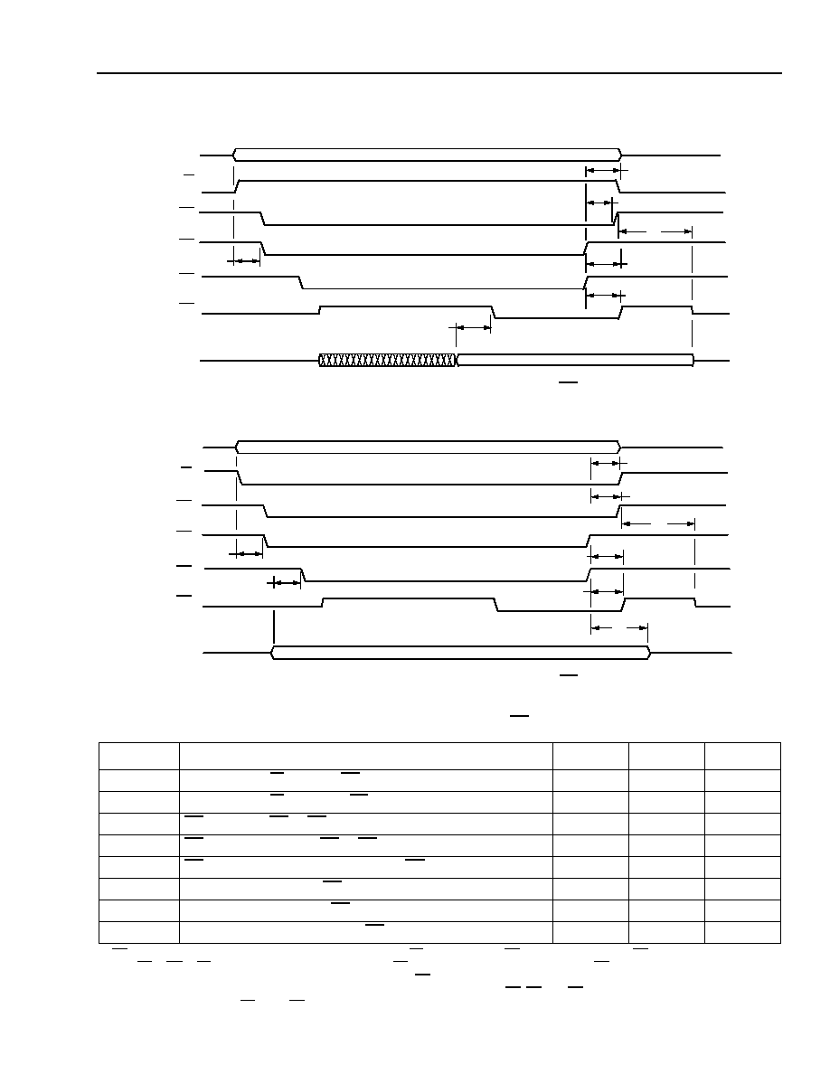
Preliminary Data Sheet
TTSI1K16T
February 1999
1024-Channel, 16-Highway Time-Slot Interchanger
55
Lucent Technologies Inc.
Timing Characteristics
(continued)
5-7063(F)r.2
Figure 16. Asynchronous Read Cycle Timing Using DT Handshake
5-7064(F)r.2
Figure 17. Asynchronous Write Cycle Timing Using DT Handshake
Table 47. Asynchronous Read and Write Interface Timing Using DT Handshake
* CS asynchronously controls the output enable of D[7--0] and DT. The delay from CS to the output enable of DT is equivalent to the delay
from AS or DS to DT. Therefore, in order to guarantee that DT is driven high before being 3-stated, a CS hold time is required (t3). If this tim-
ing cannot be met, then there are two options. One, disconnect DT and rely on wait-states to terminate the cycle. The read or write cycle will
be completed by the device 183 ns after the start of the cycle, which is defined by CS, AS, and DS all being active. The second option is to
use an external pull-up on DT to pull DT high within the timing requirements of the microprocessor.
Symbol
Description
Min
Max
Unit
t1
A[14--0] or R/W Setup to AS
0
--
ns
t2
A[14--0] or R/W Hold from AS
0
--
ns
t3
CS Hold from AS or DS
4*
--
ns
t4
DT Output Delay from AS or DS (C
L
= 50 pF)
3*
8*
ns
t5
DT or D[7--0] High-impedance from CS (C
L
= 50 pF)
--
8.5*
ns
t6
D[7--0] Input Setup to DS (C
L
= 50 pF)
0
--
ns
t7
D[7--0] Input Hold from DS (C
L
= 50 pF)
0
--
ns
t8
D[7--0] Output Setup Prior to DT Output (C
L
= 50 pF)
0
--
ns
D[7--0]
AS
DS
DT
READ DATA
t4
t4
t8
CS
A[14--0]
READ ADDRESS
t3
R/W
t1
t2
t5
HIGH IMPEDANCE
D[7--0]
AS
DS
DT
WRITE DATA
t4
t6
CS
A[14--0]
WRITE ADDRESS
t3
R/W
t1
t2
t7
t4
t5
HIGH IMPEDANCE
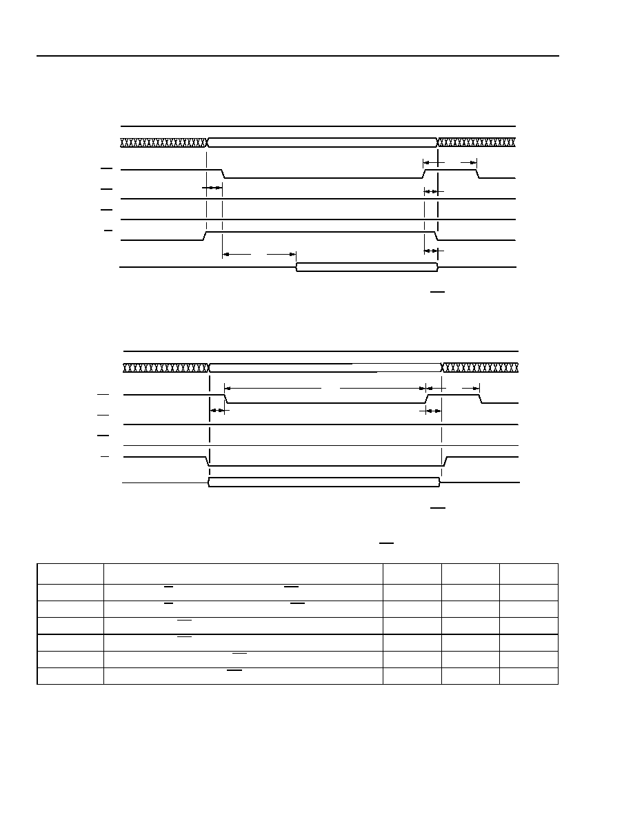
TTSI1K16T
Preliminary Data Sheet
1024-Channel, 16-Highway Time-Slot Interchanger
February 1999
56
Lucent Technologies Inc.
Timing Characteristics
(continued)
5-7065(F)r.3
Figure 18. Asynchronous Read Cycle Timing Using Only CS
5-7066(F)r.3
Figure 19. Asynchronous Write Cycle Timing Using Only CS
Table 48. Asynchronous Microprocessor Interface Timing Using Only CS
Symbol
Description
Min
Max
Unit
t9
A[14--0], R/W, D[7--0] Input Setup to CS
0
--
ns
t10
A[14--0], R/W, D[7--0] Input Hold from CS
0
--
ns
t11
Pulse Width of CS Inactive
100
--
ns
t12
Pulse Width of CS Active
200
--
ns
t13
D[7--0] Output Delay from CS (C
L
= 50 pF)
--
200
ns
t14
D[7--0] Output Hold from CS (C
L
= 50 pF)
0
--
ns
READ ADDRESS
READ DATA
MM
A[14--0]
CS
AS
DS
R/W
D[7--0]
t9
t10
t14
t11
t13
WRITE ADDRESS
WRITE DATA
MM
A[14--0]
CS
AS
DS
R/W
D[7--0]
t9
t10
t11
t12

Preliminary Data Sheet
TTSI1K16T
February 1999
1024-Channel, 16-Highway Time-Slot Interchanger
57
Lucent Technologies Inc.
Timing Characteristics
(continued)
5-7067(F)r.3
Figure 20. Synchronous Read Cycle Timing
5-7068(F)r.2
Figure 21. Synchronous Write Cycle Timing
t23
t25
PCLK
CS
AS
DT
D[7--0]
A[14--0]
READ ADDRESS
R/W
t19
t17
t22
t21
t16
t21
t24
t15
t15
t18
t22
t22
HIGH IMPEDANCE
WRITE DATA
t22
t23
t21
PCLK
CS
AS
DT
D[7--0]
A[14--0]
WRITE ADDRESS
R/W
t19
t17
t18
t22
t22
t21
t16
t21
t20
t15
t15
HIGH IMPEDANCE
TTSI1K16T
Preliminary Data Sheet
1024-Channel, 16-Highway Time-Slot Interchanger
February 1999
58
Lucent Technologies Inc.
Timing Characteristics
(continued)
Table 49. Synchronous Microprocessor Interface Timing
* The CS setup timing requirement relative to PCLK can be programmed for either the first or second clock cycle of a microprocessor access
using CSV (bit 7) of the general command register.
The input setup timing requirement assumes a PCLK frequency of at least 25 MHz. For frequencies slower than 25 MHz, the D[7--0] propa-
gation delay must be less than 40 ns from the rising edge of PCLK which samples AS.
When data is driven by the TSI during a synchronous read cycle, good data is driven prior to DT being asserted.
Symbol
Description
Min
Max
Unit
t15
CS Setup to Rising PCLK Edge
10*
--
ns
t16
CS Hold from Rising PCLK Edge
0
--
ns
t17
AS Setup to Rising PCLK Edge
6
--
ns
t18
AS Hold from Rising PCLK Edge
0
--
ns
t19
R/W, A[14--0] Input Setup to Rising PCLK Edge
0
--
ns
t20
D[7--0] Input Setup to Rising PCLK Edge
0
--
ns
t21
R/W, A[14--0], D[7--0] Input Hold from Rising PCLK Edge
0
--
ns
t22
DT Output Delay from Rising PCLK Edge (C
L
= 10 pF to 50 pF)
2.6
10
ns
t23
DT High Impedance from Falling PCLK Edge (C
L
= 50 pF)
--
7
ns
t24
D[7--0] Output Delay from Rising PCLK Edge (C
L
= 50 pF)
--
0
ns
t25
D[7--0] Output High Impedance from Rising PCLK Edge
(C
L
= 10 pF to 50 pF)
4
12
ns

Preliminary Data Sheet
TTSI1K16T
February 1999
1024-Channel, 16-Highway Time-Slot Interchanger
59
Lucent Technologies Inc.
Timing Characteristics
(continued)
TDM highway timing is shown below for the following scenario (i = 0, 1, 2 . . . 15; j = 0, 1, 2 . . . 15):
s
The input CK speed is set to 8.192 MHz.
s
FSYNC is programmed to be active-high and sampled by a rising edge of CK.
s
The RXD[i] highway is set for 0-bit offset and a highway data rate of 4.096 Mbits/s.
s
The TXD[j] highway is set for 0-bit offset and a highway data rate of 8.192 Mbits/s.
5-7465(F)r.3
Figure 22. TDM Highway Timing
Table 50. TDM Highway Timing
The TDM highway timing numbers, t26--t30, also apply for all other cases as well, i.e.,
s
CK speed is 2.048 MHz, 4.096 MHz, or 16.384 MHz.
s
FSYNC is sampled on the falling edge of CK.
s
FSYNC is active-low.
s
RXD[i] is sampled on the falling edge of CK.
s
RXD[i] data rate is 2.048 Mbits/s or 8.192 Mbits/s.
s
TXD[j] is driven on the falling edge of CK.
s
TXD[j] data rate is 2.048 Mbits/s or 4.096 Mbits/s.
s
TXOE[j] is driven on the falling edge of CK. TXOE[j] is driven on the same edge as TXD[j].
Symbol
Description
Min
Max
Unit
t26
FSYNC, RXD[0--15] Setup to Active CK Edge
10
--
ns
t27
FSYNC, RXD[0--15] Hold from Active CK Edge
5
--
ns
t28
TXD[0--15] Delay from Active CK Edge (C
L
= 25 pF)
5
15
ns
t29
TXD[0--15] High Impedance (C
L
= 25 pF)
--
15
ns
t30
TXOE[0--15] Delay from Active CK Edge (C
L
= 20 pF)
5
15
ns
FSYNC
CK
RXD[i]
TXD[j]
FSYNC SAMPLED ACTIVE
TXOE[j]
t26
t27
t28
t29
BIT 0
t30
(8.192 MHz)
(4.096 Mbits/s)
t27
t26
BIT 1
BIT 2
BIT 5
BIT 6
BIT 5
t29
t30
BIT 0
BIT 1
BIT 2
BIT 3
BIT 4
BIT 5
BIT 6
BIT 7
(8.192 Mbits/s)

TTSI1K16T
Preliminary Data Sheet
1024-Channel, 16-Highway Time-Slot Interchanger
February 1999
60
Lucent Technologies Inc.
Timing Characteristics
(continued)
5-7070(F)r.2
Figure 23. JTAG Interface Timing
Table 51. JTAG Interface Timing
Symbol
Description
Min
Max
Unit
t31
TDI, TMS Setup to Rising TCK Edge
10
--
ns
t32
TDI, TMS Hold from Rising TCK Edge
--
10
ns
t33
TDO Delay from Falling TCK Edge (C
L
= 70 pF)
5
35
ns
t34
TDO High Impedance from Falling TCK Edge (C
L
= 70 pF)
--
35
ns
TCK
TMS
TDI
TDO
t32
t31
t34
t33
t32
t31
HIGH IMPEDANCE
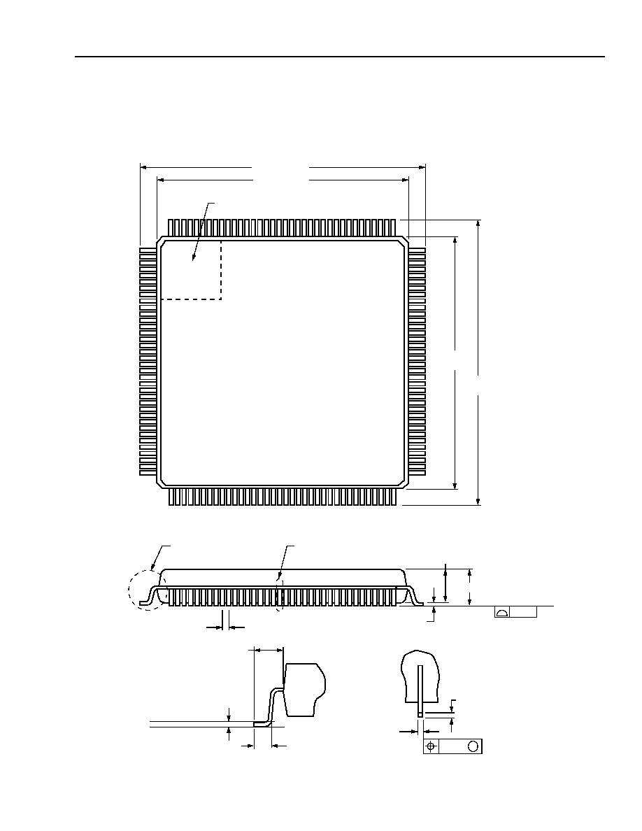
Preliminary Data Sheet
TTSI1K16T
February 1999
1024-Channel, 16-Highway Time-Slot Interchanger
61
Lucent Technologies Inc.
Outline Diagram
144-Pin TQFP
Dimensions are in millimeters.
5-3815(F)r.6
0.45/0.75
GAGE PLANE
SEATING PLANE
1.00 REF
0.25
0.19/0.27
0.08
M
0.106/0.200
1.60 MAX
SEATING PLANE
0.08
0.50 TYP
1.40
±
0.05
0.05/0.15
DETAIL A
DETAIL B
PIN #1 IDENTIFIER ZONE
20.00
±
0.20
22.00
±
0.20
109
144
1
36
37
72
73
108
20.00
±
0.20
22.00
±
0.20

TTSI1K16T
Preliminary Data Sheet
1024-Channel, 16-Highway Time-Slot Interchanger
February 1999
62
Lucent Technologies Inc.
Ordering Information
DS99-177PDH Replaces DS98-290TIC to Incorporate the Following Updates
1. Page 18, Highway Data Rate Selection section, added paragraph on meeting the 8.192 Mbits/s bandwidth
requirement for a transmit highway pair at the bottom of the page.
2. Page 20, updated Figure 10, Virtual and Physical Frames on page 20.
3. Page 22, Reset Sequence section, added paragraph on BIST requirement.
4. Page 23--page 26, Low-Latency and Frame-Integrity Modes section updated.
5. Page 27, Test-Pattern Generation section updated.
6. Page 27 and page 28, Test-Pattern Checking section updated.
7. Page 36, Table 15, General Command Register (0x00), removed last sentence in description of bit 2 and bit 1.
8. Page 36, Table 15, General Command Register (0x00), updated bit 0 symbol from GXEN to GXE.
9. Page 37, Table 16, Software Reset Register (0x01), updated bit 0, software reset description.
10. Page 39, Table 22, Interrupt Status Register (0x07), updated bit 4 and bit 2 to reserved status.
11. Page 40, Table 23, Interrupt Mask Register (0x08), updated bit 4 and bit 2 to reserved status.
12. Page 40, Table 23, Interrupt Mask Register (0x08), bit 3 symbol changed from MASKED to MASKERD.
13. Page 42, Table 25, Test-Pattern Style Register (0x0A), updated test-pattern descriptions.
14. Page 43, Table 26, Test-Pattern Checker Highway Register (0x0B), updated bit 4 to reserved status.
15. Page 43, Table 27, Test-Pattern Checker Upper Time-Slot Register (0x0C), updated description.
16. Page 43, Table 28, Test-Pattern Checker Lower Time-Slot Register (0x0D), updated description.
17. Page 43, Table 30, Test-Pattern Error Injection Register (0x0F), changed register name from test-pattern error
selection register to test-pattern error injection register and added sentence to end of description.
18. Page 45, Table 35, Transmit Highway Configuration Register (Byte 0) (0x1000 + 4i), updated bit 3--bit 2 sym-
bol from XCEOFF to XFBOFF.
19. Page 46, Table 37, Transmit Highway Configuration Register (Byte 2) (0x1002 + 4i), updated bit 2 symbol name
from XEN to XE.
20. Page 47, Table 38, Receive Highway Configuration Register (Byte 0) (0x1800 + 4i), updated bit 3--bit 2 symbol
from RCEOFF to RFBOFF.
21. Page 49, Transmit Highway 3-State Options section and Table 41, Transmit Highway 3-State Options updated.
22. Page 50, Data Store Memory section updated.
23. Page 51, Table 44, Connection Store Memory (Byte 0), changed TSA symbol to RTSA and updated
description.
24. Page 51, Table 45, Connection Store Memory (Byte 1), changed PORTNUM[4--0] symbol to RXHWY[3--0].
25. Page 51, Table 45, Connection Store Memory (Byte 1), updated bit 4 to reserved status.
26. Page 50--page 52, Connection Store Memory section updated.
27. Page 54, Table 46, Clock Specifications, updated clock period stability for CK.
28. Page 59, Timing Characteristics section, updated Figure 22, TDM Highway Timing and text.
29. Page 59, Table 50, TDM Highway Timing, timing parameter t26, minimum changed from 15 ns to 10 ns.
Device Code
Package
Temperature
Comcode
(Ordering Number)
TTSI1K16T3TL
144-pin TQFP
≠40
∞
C to +85
∞
C
108269762

Preliminary Data Sheet
TTSI1K16T
February 1999
1024-Channel, 16-Highway Time-Slot Interchanger
63
Lucent Technologies Inc.
Notes

TTSI2K32T
Preliminary Data Sheet
2048-Channel, 32-Highway Time-Slot Interchanger
February 1999
Lucent Technologies Inc. reserves the right to make changes to the product(s) or information contained herein without notice. No liability is assumed as a result of their use or application. No
rights under any patent accompany the sale of any such product(s) or information.
Copyright © 1999 Lucent Technologies Inc.
All Rights Reserved
February 1999
DS99-177PDH (Replaces DS98-290TIC and AY98-029TIC)
For additional information, contact your Microelectronics Group Account Manager or the following:
INTERNET:
http://www.lucent.com/micro
E-MAIL:
docmaster@micro.lucent.com
N. AMERICA: Microelectronics Group, Lucent Technologies Inc., 555 Union Boulevard, Room 30L-15P-BA, Allentown, PA 18103
1-800-372-2447, FAX 610-712-4106 (In CANADA: 1-800-553-2448, FAX 610-712-4106)
ASIA PACIFIC: Microelectronics Group, Lucent Technologies Singapore Pte. Ltd., 77 Science Park Drive, #03-18 Cintech III, Singapore 118256
Tel. (65) 778 8833, FAX (65) 777 7495
CHINA:
Microelectronics Group, Lucent Technologies (China) Co., Ltd., A-F2, 23/F, Zao Fong Universe Building, 1800 Zhong Shan Xi Road, Shanghai
200233 P. R. China Tel. (86) 21 6440 0468, ext. 316, FAX (86) 21 6440 0652
JAPAN:
Microelectronics Group, Lucent Technologies Japan Ltd., 7-18, Higashi-Gotanda 2-chome, Shinagawa-ku, Tokyo 141, Japan
Tel. (81) 3 5421 1600, FAX (81) 3 5421 1700
EUROPE:
Data Requests: MICROELECTRONICS GROUP DATALINE: Tel. (44) 1189 324 299, FAX (44) 1189 328 148
Technical Inquiries:
GERMANY: (49) 89 95086 0 (Munich), UNITED KINGDOM: (44) 1344 865 900 (Ascot),
FRANCE: (33) 1 40 83 68 00 (Paris), SWEDEN: (46) 8 594 607 00 (Stockholm), FINLAND: (358) 9 4354 2800 (Helsinki),
ITALY: (39) 02 6608131 (Milan), SPAIN: (34) 1 807 1441 (Madrid)