 | –≠–ª–µ–∫—Ç—Ä–æ–Ω–Ω—ã–π –∫–æ–º–ø–æ–Ω–µ–Ω—Ç: TTSV02622 | –°–∫–∞—á–∞—Ç—å:  PDF PDF  ZIP ZIP |

Data Sheet
June 2003
TTSV02622 STS-24 Backplane Transceiver
Features
s
Allows wide range of applications for SONET net-
work termination application as well as generic
data moving for high-speed backplane data
transfer.
s
Clock/data recovery (CDR) function for high-speed
serial backplane data transfer.
s
CDR function uses Agere Systems Inc. proven
622 Mbits/s serial interface core.
s
Two-channel CDR function provides 622 Mbits/s
serial interface per channel for a total chip
bandwidth of 1.24 Gbits/s (full duplex).
s
Low-voltage differential signaling (LVDS) I/Os for
CDR and reference clock signals.
s
8:1 data multiplexing/demultiplexing (MUX/
deMUX) for 77.76 MHz byte-wide data processing.
s
CDR meets B jitter tolerance specification of ITU-T
recommendation G.958.
s
Powerdown option of CDR receiver on a per-
channel basis.
s
Pseudo-SONET protocol including A1/A2 framing.
s
SONET scrambling and descrambling for required
ones density (optional).
s
Selected transport overhead (TOH) bytes insertion
and detection for interdevice communication via
the TOH serial link.
s
Streamlined pointer processor (pointer mover) for
8 kHz frame alignment.
s
FIFOs for alignment of incoming data to reference
clock.
s
FIFOs optionally align incoming data across all two
channels for synchronous transport signal STS-24
operation (in dual STS-12 format).
s
Independent data stream enables in pseudo-
SONET processor.
s
Supports STS-12/STS-24 redundancy by either
software or hardware control for protection
switching applications.
s
Low-power 3.3 V supply.
s
≠40 ∞C to +
125 ∞C industrial temperature range.
s
272-pin ball grid array (PBGA) package.
Description
The TTSV02622 can support a 1.24 Gbits/s interface
for backplane connections. The 1.24 Gbits/s inter-
face is implemented as dual 622 Mbits/s LVDS links.
The HSI macrocell is used for clock/data recovery
(CDR) and MUX/deMUX between 77.76 MHz byte-
wide internal data buses and the 622 Mbits/s external
serial links.
Each 622 Mbits/s serial link uses a pseudo-SONET
protocol. SONET A1/A2 framing is used on the link
for locating the 8 kHz frame location. The link is also
scrambled using the standard SONET scrambler def-
inition to ensure proper transitions on the link for
improved CDR performance. Selectable transport
overhead (TOH) bytes are insertable in the transmit
direction. All bytes can be transparently passed
through the device, or all bytes can be inserted via
the TOH serial link. In addition, certain microproces-
sor unit (MPU) selectable bytes can be passed
through transparently while in insert mode.
Elastic buffers (FIFOs) are used to align each incom-
ing STS-12 link to the core 77.76 MHz clock and
8 kHz frame. These FIFOs will absorb delay varia-
tions between 622 Mbits/s links due to timing skews
between cards and along backplane traces. For
greater variations, a streamlined pointer processor
(pointer mover) within the device will align the 8 kHz
frames regardless of their incoming frame position.
The TTSV02622 supports dual STS-12 mode of
operation on the input/output ports. STS-24 is also
supported, but it must be received in the dual
STS-12 format. When operating in dual STS-12
mode, each of the independent byte streams carries
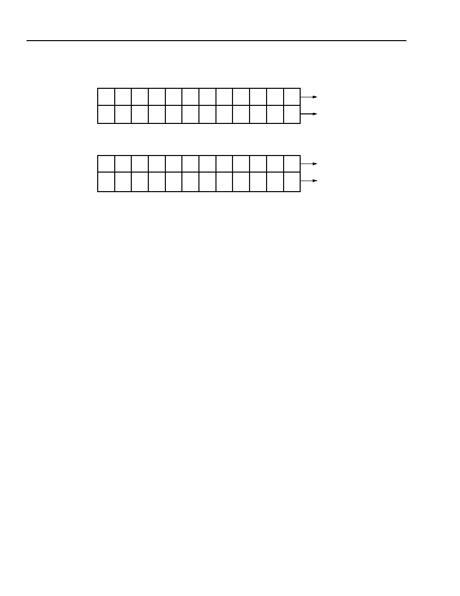
an entire STS-12 within it. Figure 1 on page 2 reveals
the byte ordering of the individual STS-12 streams.
2
Agere Systems Inc.
Data Sheet
June 2003
TTSV02622 STS-24 Backplane Transceiver
Description
(continued)
Figure 1. Byte Ordering on Input/Output Interface in STS-12 Mode
12
24
9
21
6
18
3
15
11
23
8
20
5
17
2
14
10
22
7
19
4
16
1
13
1, 12
2, 12
1, 9
2, 9
1, 6
2, 6
1, 3
2, 3
1, 11
2, 11
1, 8
2, 8
1, 5
2, 5
1, 2
2, 2
1, 10
2, 10
1, 7
2, 7
1, 4
2, 4
1, 1
2, 1
STS-12 #1
STS-12 #2
STS-12 #1
STS-12 #2
STS-24 IN DUAL STS-12 FORMAT
DUAL STS-12

Table of Contents
Contents
Page
Agere Systems Inc.
3
Data Sheet
June 2003
TTSV02622 STS-24 Backplane Transceiver
Features ................................................................................................................................................................... 1
Description................................................................................................................................................................ 1
Pin Information ......................................................................................................................................................... 6
Synchronization ...................................................................................................................................................... 17
HSI Block Interface................................................................................................................................................. 17
Line Interface.......................................................................................................................................................... 17
Architecture ............................................................................................................................................................ 17
Powerdown Mode................................................................................................................................................... 19
Supervisory Features ............................................................................................................................................. 20
Test Features ......................................................................................................................................................... 21
Transmit Direction (Line to Backplane) .................................................................................................................. 22
Transport Overhead Serial Link ........................................................................................................................... 23
A1/A2 Frame Insert and Corruption ..................................................................................................................... 23
B1 Calculation and Insertion ................................................................................................................................ 23
Stream Disable .................................................................................................................................................... 23
Scrambler............................................................................................................................................................. 23
Receiver Block........................................................................................................................................................ 24
Framer Subblock (Backplane to Line).................................................................................................................. 24
B1 Calculate and Descramble (Backplane to Line) ............................................................................................. 27
Internal Parity Generation .................................................................................................................................... 27
FIFO Subblock (Backplane to Line) ..................................................................................................................... 28
Pointer Mover Subblock (Backplane to Line)....................................................................................................... 28
Miscellaneous Functions ........................................................................................................................................ 31
K1/K2, A1/A2 Handling ........................................................................................................................................ 31
SPE C1J1 Outputs............................................................................................................................................... 31
Registers ................................................................................................................................................................ 32
Definition of Register Types................................................................................................................................. 32
Register Map........................................................................................................................................................ 33
Register Descriptions ............................................................................................................................................. 36
Absolute Maximum Ratings.................................................................................................................................... 48
Handling Precautions ............................................................................................................................................. 48
Recommended Operating Conditions .................................................................................................................... 48
Thermal Characteristics.......................................................................................................................................... 49
Power Consumption (Advance).............................................................................................................................. 49
Electrical Characteristics ........................................................................................................................................ 49
Propagation Delay Specifications........................................................................................................................... 49
LVDS I/O ................................................................................................................................................................ 50
LVDS Receiver Buffer Capabilities ...................................................................................................................... 52
Clock and Data Recovery (CDR)............................................................................................................................ 54
Input Data ............................................................................................................................................................ 54
Jitter Tolerance .................................................................................................................................................... 54
Generated Output Jitter ....................................................................................................................................... 54
PLL....................................................................................................................................................................... 54
Input Reference Clock ......................................................................................................................................... 54
Timing Characteristics ............................................................................................................................................ 55
CPU Interface Timing........................................................................................................................................... 61
Outline Diagram...................................................................................................................................................... 63
272-Pin PBGA...................................................................................................................................................... 63
Ordering Information............................................................................................................................................... 64

List of Figures
Contents
Page
4
Agere Systems Inc.
Data Sheet
June 2003
TTSV02622 STS-24 Backplane Transceiver
Figure 1. Byte Ordering on Input/Output Interface in STS-12 Mode ........................................................................ 2
Figure 2. Pin Diagram of 272-Pin PBGA (Bottom View)........................................................................................... 6
Figure 3. Suggested Schematic for 1.0 V and 1.4 V Reference Voltages.............................................................. 16
Figure 4. Alignment of Two STS-12 Streams ......................................................................................................... 17
Figure 5. Interior View of TTSV02622 .................................................................................................................... 18
Figure 6. Interconnect of Streams for FIFO Alignment........................................................................................... 19
Figure 7. Transmitter Block .................................................................................................................................... 22
Figure 8. Receiver Block ........................................................................................................................................ 24
Figure 9. Framer State Machine............................................................................................................................. 26
Figure 10. Pointer Mover State Machine ................................................................................................................ 30
Figure 11. LVDS Driver and Receiver and Associated Internal Components ........................................................ 51
Figure 12. LVDS Driver and Receiver .................................................................................................................... 51
Figure 13. LVDS Driver .......................................................................................................................................... 51
Figure 14. Input Parallel Port Timing ...................................................................................................................... 55
Figure 15. Transmitter Transport Delay.................................................................................................................. 56
Figure 16. Output Parallel Port Timing ................................................................................................................... 57
Figure 17. Protection Switch Timing....................................................................................................................... 58
Figure 18. Input Serial Port Timing......................................................................................................................... 59
Figure 19. Output Serial Port Timing ...................................................................................................................... 60
Figure 20. Write Transaction .................................................................................................................................. 61
Figure 21. Read Transaction .................................................................................................................................. 62

List of Tables
Contents
Page
Agere Systems Inc.
5
Data Sheet
June 2003
TTSV02622 STS-24 Backplane Transceiver
Table 1. Pin Assignments for 272-Pin PBGA by Pin Number Order ........................................................................ 7
Table 2. Pin Assignments for 272-Pin PBGA by Signal Name............................................................................... 10
Table 3. Pin Descriptions ....................................................................................................................................... 12
Table 4. Valid Starting Positions for a STS-MC...................................................................................................... 29
Table 5. SPE and C1J1 Functionality..................................................................................................................... 31
Table 6. Register Map ............................................................................................................................................ 33
Table 7. Register Description ................................................................................................................................. 36
Table 8. Absolute Maximum Ratings...................................................................................................................... 48
Table 9. Handling Precautions ............................................................................................................................... 48
Table 10. Recommended Operating Conditions .................................................................................................... 48
Table 11. Thermal Resistance--Junction to Ambient ............................................................................................ 49
Table 12. Power Consumption (Advance).............................................................................................................. 49
Table 13. LVTTL Electrical Characteristics ............................................................................................................ 49
Table 14. LVDS Receiver dc Data* ........................................................................................................................ 52
Table 15. LVDS Receiver ac Data* ........................................................................................................................ 52
Table 16. LVDS Driver dc Data*............................................................................................................................. 53
Table 17. LVDS Driver ac Data*............................................................................................................................. 53
Table 18. LVDS Driver Reference Data ................................................................................................................. 53
Table 19. Jitter Tolerance....................................................................................................................................... 54
Table 20. Input Parallel Port Timing Requirements................................................................................................ 55
Table 21. Transmitter Transport Delay Timing Requirements................................................................................ 56
Table 22. Output Parallel Port Timing Requirements ............................................................................................. 57
Table 23. Protection Switch Timing Requirements................................................................................................. 58
Table 24. Input Serial Port Timing Requirements................................................................................................... 59
Table 25. Output Serial Port Timing Requirements................................................................................................ 60
Table 26. Write Transaction Timing Requirements ................................................................................................ 61
Table 27. Read Transaction Timing Requirements ................................................................................................ 62
6
Agere Systems Inc.
Data Sheet
June 2003
TTSV02622 STS-24 Backplane Transceiver
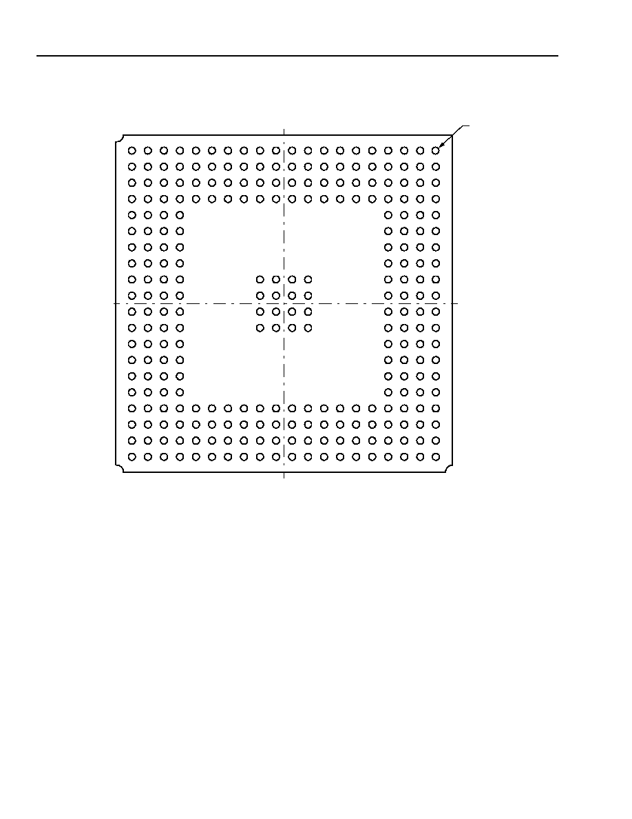
Pin Information
Figure 2. Pin Diagram of 272-Pin PBGA (Bottom View)
A
B
C
D
E
F
G
H
J
K
L
M
Y
N
P
R
T
U
V
W
A1 BALL
PAD CORNER
1
2
3
4
5
6
7
8
9
10
11
12
13
14
15
16
17
18
20 19

Agere Systems Inc.
7
Data Sheet
June 2003
TTSV02622 STS-24 Backplane Transceiver
Pin Information
(continued)
Table 1. Pin Assignments for 272-Pin PBGA by Pin Number Order
Note: NC refers to no connect. Do not connect pins so designated.
Pin
Signal Name
Pin
Signal Name
Pin
Signal Name
Pin
Signal Name
A1
V
SS
B1
TDO
C1
NC
D1
NC
A2
TCK
B2
TRSTN
C2
NC
D2
NC
A3
TDI
B3
TSTMD
C3
LVDS_EN
D3
NC
A4
TMS
B4
SCANEN
C4
NC
D4
V
SS
A5
DXP
B5
NC
C5
NC
D5
NC
A6
NC
B6
DXN
C6
NC
D6
V
DD
A7
PROT_SWITCH_A
B7
PROT_SWITCH_C
C7
NC
D7
NC
A8
TOH_INA
B8
TOH_INB
C8
TX_TOH_CKEN
D8
V
SS
A9
NC
B9
NC
C9
TOH_CLK
D9
NC
A10
NC
B10
NC
C10
NC
D10
NC
A11
TOH_OUTA
B11
TOH_OUTB
C11
RX_TOH_CKEN
D11
V
DD
A12
NC
B12
NC
C12
RX_TOH_FP
D12
NC
A13
NC
B13
NC
C13
NC
D13
V
SS
A14
NC
B14
NC
C14
NC
D14
NC
A15
DOUTA7
B15
DOUTA6
C15
DOUTA5
D15
V
DD
A16
DOUTA4
B16
DOUTA3
C16
DOUTA2
D16
DOUTA1
A17
DOUTA0
B17
DOUTA_PAR
C17
DOUTA_SPE
D17
V
SS
A18
DOUTA_C1J1
B18
DOUTB5
C18
DOUTB2
D18
DOUTB_PAR
A19
DOUTB7
B19
DOUTB4
C19
DOUTB1
D19
DOUTB_SPE
A20
DOUTB6
B20
DOUTB3
C20
DOUTB0
D20
DOUTB_C1J1

8
Agere Systems Inc.
Data Sheet
June 2003
TTSV02622 STS-24 Backplane Transceiver
Pin Information
(continued)
Table 1. Pin Assignments for 272-Pin PBGA by Pin Number Order (continued)
Note: NC refers to no connect. Do not connect pins so designated.
Pin
Signal Name
Pin
Signal Name
Pin
Signal Name
Pin
Signal Name
E1
STS_INA_P
H17
V
SS
L1
STS_OUTB_P
N17
V
SS
E2
STS_INA_N
H18
NC
L2
STS_OUTB_N
N18
DINA7
E3
CTAP_REFA H19
NC
L3
NC
N19
DINA6
E4
NC
H20
NC
L4
NC
N20
DINA5
E17
NC
J1
STS_OUTA_P
L9
V
SS
P1
NC
E18
NC
J2
STS_OUTA_N
L10
V
SS
P2
NC
E19
NC
J3
NC
L11
V
SS
P3
NC
E20
NC
J4
NC
L12
V
SS
P4
NC
F1
STS_INB_P
J9
V
SS
L17
V
DD
P17
DINA4
F2
STS_INB_N
J10
V
SS
L18
NC
P18
DINA3
F3
CTAP_REFB
J11
V
SS
L19
NC
P19
DINA2
F4
V
DD
J12
V
SS
L20
NC
P20
DINA1
F17
V
DD
J17
NC
M1
REF10
R1
NC
F18
NC
J18
NC
M2
REF14
R2
NC
F19
NC
J19
NC
M3
LVDS_RESH
R3
NC
F20
NC
J20
NC
M4
LVDS_RESL
R4
V
DD
G1
NC
K1
PLL REF
M9
V
SS
R17
V
DD
G2
NC
K2
PLL_VDDA
M10
V
SS
R18
DINB7
G3
NC
K3
PLL_VSSA
M11
V
SS
R19
DINA0
G4
NC
K4
V
DD
M12
V
SS
R20
DINA_PAR
G17
NC
K9
V
SS
M17
SYS_CLK
T1
TSTMODE
G18
NC
K10
V
SS
M18
SYS_FP
T2
BYPASS
G19
NC
K11
V
SS
M19
LINE_FP
T3
RESETRN
G20
NC
K12
V
SS
M20
NC
T4
RESETTN
H1
NC
K17
NC
N1
NC
T17
DINB6
H2
NC
K18
NC
N2
NC
T18
DINB5
H3
NC
K19
NC
N3
NC
T19
DINB4
H4
V
SS
K20
NC
N4
V
SS
T20
DINB3

Agere Systems Inc.
9
Data Sheet
June 2003
TTSV02622 STS-24 Backplane Transceiver
Pin Information
(continued)
Table 1. Pin Assignments for 272-Pin PBGA by Pin Number Order (continued)
Note: NC refers to no connect. Do not connect pins so designated.
Pin
Signal Name
Pin
Signal Name
Pin
Signal Name
Pin
Signal Name
U1
TSTCLK
V1
MRESET
W1
EXDNUP
Y1
NC
U2
TSTSHFTLD
V2
ECSEL
W2
TSTPHASE
Y2
NC
U3
ETOGGLE
V3
LOOPBKEN
W3
TSTMUX8S
Y3
TSTMUX7S
U4
V
SS
V4
TSTMUX6S
W4
TSTMUX5S
Y4
TSTMUX4S
U5
TSTMUX3S
V5
TSTMUX2S
W5
TSTMUX1S
Y5
TSTMUX0S
U6
V
DD
V6
NC
W6
NC
Y6
NC
U7
CPU_ADDR6
V7
CPU_ADDR5
W7
CPU_ADDR4
Y7
CPU_ADDR3
U8
V
SS
V8
CPU_ADDR2
W8
CPU_ADDR1
Y8
CPU_ADDR0
U9
CS_N
V9
RD_WRN
W9
RST_N
Y9
HIZ_N
U10
V
DD
V10
INT_N
W10
NC
Y10
NC
U11
CPU_DATA7
V11
CPU_DATA6
W11
CPU_DATA5
Y11
CPU_DATA4
U12
CPU_DATA3
V12
CPU_DATA2
W12
CPU_DATA1
Y12
CPU_DATA0
U13
V
SS
V13
NC
W13
NC
Y13
NC
U14
NC
V14
NC
W14
NC
Y14
NC
U15
V
DD
V15
NC
W15
NC
Y15
NC
U16
DIND4
V16
NC
W16
NC
Y16
NC
U17
V
SS
V17
NC
W17
NC
Y17
NC
U18
DINB2
V18
NC
W18
NC
Y18
NC
U19
DINB1
V19
NC
W19
NC
Y19
NC
U20
DINB0
V20
DINB_PAR
W20
NC
Y20
NC

10
Agere Systems Inc.
Data Sheet
June 2003
TTSV02622 STS-24 Backplane Transceiver
Pin Information
(continued)
Table 2. Pin Assignments for 272-Pin PBGA by Signal Name
Note: NC refers to no connect. Do not connect pins so designated.
Signal Name
Pin
Signal Name
Pin
Signal Name
Pin
Signal Name
Pin
BYPASS
T2
DINB4
T19
LINE_FP
M19
NC
D12
CPU_ADDR0
Y8
DINB5
T18
LOOPBKEN
V3
NC
D14
CPU_ADDR1
W8
DINB6
T17
LVDS_EN
C3
NC
E4
CPU_ADDR2
V8
DINB7
R18
LVDS_RESH
M3
NC
E17
CPU_ADDR3
Y7
DIND4
U16
LVDS_RESL
M4
NC
E18
CPU_ADDR4
W7
DOUTA_C1J1
A18
MRESET
V1
NC
E19
CPU_ADDR5
V7
DOUTA_PAR
B17
NC
A6
NC
E20
CPU_ADDR6
U7
DOUTA_SPE
C17
NC
A9
NC
F18
CPU_DATA0
Y12
DOUTA0
A17
NC
A10
NC
F19
CPU_DATA1
W12
DOUTA1
D16
NC
A12
NC
F20
CPU_DATA2
V12
DOUTA2
C16
NC
A13
NC
G1
CPU_DATA3
U12
DOUTA3
B16
NC
A14
NC
G2
CPU_DATA4
Y11
DOUTA4
A16
NC
B5
NC
G3
CPU_DATA5
W11
DOUTA5
C15
NC
B9
NC
G4
CPU_DATA6
V11
DOUTA6
B15
NC
B10
NC
G17
CPU_DATA7
U11
DOUTA7
A15
NC
B12
NC
G18
CS_N
U9
DOUTB_C1J1
D20
NC
B13
NC
G19
CTAP_REFA E3
DOUTB_PAR
D18
NC
B14
NC
G20
CTAP_REFB
F3
DOUTB_SPE
D19
NC
C1
NC
H1
DINA_PAR
R20
DOUTB0
C20
NC
C2
NC
H2
DINA0
R19
DOUTB1
C19
NC
C4
NC
H3
DINA1
P20
DOUTB2
C18
NC
C5
NC
H18
DINA2
P19
DOUTB3
B20
NC
C6
NC
H19
DINA3
P18
DOUTB4
B19
NC
C7
NC
H20
DINA4
P17
DOUTB5
B18
NC
C10
NC
J3
DINA5
N20
DOUTB6
A20
NC
C13
NC
J4
DINA6
N19
DOUTB7
A19
NC
C14
NC
J17
DINA7
N18
DXN
B6
NC
D1
NC
J18
DINB_PAR
V20
DXP
A5
NC
D2
NC
J19
DINB0
U20
ECSEL
V2
NC
D3
NC
J20
DINB1
U19
ETOGGLE
U3
NC
D5
NC
K17
DINB2
U18
EXDNUP
W1
NC
D7
NC
K18
DINB3
T20
HIZ_N
Y9
NC
D9
NC
K19
DINB3
T20
INT_N
V10
NC
D10
NC
K20

Agere Systems Inc.
11
Data Sheet
June 2003
TTSV02622 STS-24 Backplane Transceiver
Pin Information
(continued)
Table 2. Pin Assignments for 272-Pin PBGA by Signal Name (continued)
Note: NC refers to no connect. Do not connect pins so designated.
Signal Name
Pin
Signal Name
Pin
Signal Name
Pin
Signal Name
Pin
NC
L3
NC
W20
STS_OUTB_P
L1
V
DD
L17
NC
L4
NC
Y1
SYS_CLK
M17
V
DD
R4
NC
L18
NC
Y2
SYS_FP
M18
V
DD
R17
NC
L19
NC
Y6
TCK
A2
V
DD
U6
NC
L20
NC
Y10
TDI
A3
V
DD
U10
NC
M20
NC
Y13
TDO
B1
V
DD
U15
NC
N1
NC
Y14
TMS
A4
V
SS
A1
NC
N2
NC
Y15
TOH_CLK
C9
V
SS
D4
NC
N3
NC
Y16
TOH_INA
A8
V
SS
D8
NC
P1
NC
Y17
TOH_INB
B8
V
SS
D13
NC
P2
NC
Y18
TOH_OUTA
A11
V
SS
D17
NC
P3
NC
Y19
TOH_OUTB
B11
V
SS
H4
NC
P4
NC
Y20
TRSTN
B2
V
SS
H17
NC
R1
PLL REF
K1
TSTCLK
U1
V
SS
J9
NC
R2
PLL_VDDA
K2
TSTMD
B3
V
SS
J10
NC
R3
PLL_VSSA
K3
TSTMODE
T1
V
SS
J11
NC
U14 PROT_SWITCH_A
A7
TSTMUX0S
Y5
V
SS
J12
NC
V6
PROT_SWITCH_C
B7
TSTMUX1S
W5
V
SS
K9
NC
V13
RD_WRN
V9
TSTMUX2S
V5
V
SS
K10
NC
V14
REF10
M1
TSTMUX3S
U5
V
SS
K11
NC
V15
REF14
M2
TSTMUX4S
Y4
V
SS
K12
NC
V16
RESETRN
T3
TSTMUX5S
W4
V
SS
L9
NC
V17
RESETTN
T4
TSTMUX6S
V4
V
SS
L10
NC
V18
RST_N
W9
TSTMUX7S
Y3
V
SS
L11
NC
V19
RX_TOH_CKEN
C11
TSTMUX8S
W3
V
SS
L12
NC
W6
RX_TOH_FP
C12
TSTPHASE
W2
V
SS
M9
NC
W10
SCANEN
B4
TSTSHFTLD
U2
V
SS
M10
NC
W13
STS_INA_N
E2
TX_TOH_CKEN
C8
V
SS
M11
NC
W14
STS_INA_P
E1
V
DD
D6
V
SS
M12
NC
W15
STS_INB_N
F2
V
DD
D11
V
SS
N4
NC
W16
STS_INB_P
F1
V
DD
D15
V
SS
N17
NC
W17
STS_OUTA_N
J2
V
DD
F4
V
SS
U4
NC
W18
STS_OUTA_P
J1
V
DD
F17
V
SS
U8
NC
W19
STS_OUTB_N
L2
V
DD
K4
V
SS
U13
--
--
--
--
--
--
V
SS
U17

12
Agere Systems Inc.
Data Sheet
June 2003
TTSV02622 STS-24 Backplane Transceiver
Pin Information
(continued)
Table 3. Pin Descriptions
Pin
Symbol
Type
I/O
Description
N18, N19, N20,
P17, P18, P19,
P20, R19
DINA[7:0]
TTL
I/
Pull-up
Input parallel bus of transmitter #1.
R20
DINA_PAR
TTL
I/
Pull-up
Parity for input bus of transmitter #1.
R18, T17, T18,
T19, T20, U18,
U19, U20
DINB[7:0]
TTL
I/
Pull-up
Input parallel bus of transmitter #2.
V20
DINB_PAR
TTL
I/
Pull-up
Parity for input bus of transmitter #2.
A15, B15, C15,
A16, B16, C16,
D16, A17
DOUTA[7:0]
TTL
O/
HI-Z/
Pull-up
Output parallel bus of receiver #1.
B17
DOUTA_PAR
TTL
O/
HI-Z/
Pull-up
Parity for output parallel bus of receiver #1.
C17
DOUTA_SPE
TTL
O/
HI-Z/
Pull-up
SPE signal for output parallel bus of receiver #1.
A18
DOUTA_C1J1
TTL
O/
HI-Z/
Pull-up
C1J1 signal for output parallel bus of receiver #1.
A19, A20, B18,
B19, B20, C18,
C19, C20
DOUTB[7:0]
TTL
O/
HI-Z/
Pull-up
Output parallel bus of receiver #2.
D18
DOUTB_PAR
TTL
O/
HI-Z/
Pull-up
Parity for output parallel bus of receiver #2.
D19
DOUTB_SPE
TTL
O/
HI-Z/
Pull-up
SPE signal for output parallel bus of receiver #2.
D20
DOUTB_C1J1
TTL
O/
HI-Z/
Pull-up
C1J1 signal for output parallel bus of receiver #2.
C9
TOH_CLK
TTL
I/
Pull-up
Tx and Rx TOH serial links clock (25 MHz--
77.76 MHz).
A8
TOH_INA
TTL
I/
Pull-up
TOH serial link input for transmitter #1.
B8
TOH_INB
TTL
I/
Pull-up
TOH serial link input for transmitter #2.
C8
TX_TOH_CKEN
TTL
I/
Pull-up
Tx TOH serial link clock enable.
A11
TOH_OUTA
TTL
O/
HI-Z/
Pull-up
TOH serial link output for receiver #1.

Agere Systems Inc.
13
Data Sheet
June 2003
TTSV02622 STS-24 Backplane Transceiver
B11
TOH_OUTB
TTL
O/
HI-Z/
Pull-up
TOH serial link output for receiver #2.
C11
RX_TOH_CKEN
TTL
O/
HI-Z/
Pull-up
Rx TOH serial link clock enable.
C12
RX_TOH_FP
TTL
O/
HI-Z/
Pull-up
Rx TOH serial link frame pulse.
E1
STS_INA_P
LVDS
I
LVDS input receiver #1.
E2
STS_INA_N
LVDS
I
LVDS input receiver #1.
F1
STS_INB_P
LVDS
I
LVDS input receiver #2.
F2
STS_INB_N
LVDS
I
LVDS input receiver #2.
J1
STS_OUTA_P
LVDS
O
LVDS output transmitter #1.
J2
STS_OUTA_N
LVDS
O
LVDS output transmitter #1.
L1
STS_OUTB_P
LVDS
O
LVDS output transmitter #2.
L2
STS_OUTB_N
LVDS
O
LVDS output transmitter #2.
E3
CTAP_REFA
--
--
LVDS input center tap (Rx #1) (use 0.01 µF to GND).
F3
CTAP_REFB
--
--
LVDS input center tap (Rx #2) (use 0.01 µF to GND).
U11, V11, W11,
Y11, U12, V12,
W12, Y12
CPU_DATA[7:0]
TTL
I/
O/
Pull-up
Central processing unit (CPU) interface data bus.
U7, V7, W7, Y7,
V8, W8, Y8
CPU_ADDR[6:0]
TTL
I/
Pull-up
CPU interface address bus.
V9
RD_WRN
TTL
I/Pull-Up CPU interface read/write.
U9
CS_N
TTL
I/
Pull-up
SCHMITT
Chip select.
M18
SYS_FP
TTL
I/
Pull-up
System frame pulse for transmitter section.
M19
LINE_FP
TTL
I/
Pull-up
Line frame pulse for receiver section.
M17
SYS_CLK
TTL
I/
Pull-up
System clock (77.76 MHz).
A7
PROT_SW_A
TTL
I/
Pull-up
Protection switching control signal.
B7
PROT_SW_C
TTL
I/
Pull-up
Protection switching control signal.
V10
INT_N
TTL
O/
Open
Drain
Interrupt output.
W9
RST_N
TTL
I/
Pull-down/
SCHMITT
Global reset.
Pin Information
(continued)
Table 3. Pin Descriptions (continued)
Pin
Symbol
Type
I/O
Description

14
Agere Systems Inc.
Data Sheet
June 2003
TTSV02622 STS-24 Backplane Transceiver
Y9
HIZ_N
TTL
I/
Pull-up/
SCHMITT
Global 3-state control.
K1
PLL_REF
--
--
Reference for PLL (10 k
to GND).
M1
REF10
--
I
1.0 V reference for LVDS reference block. See
Figure 3 on page 16.
M2
REF14
--
I
1.4 V reference for LVDS reference block. See
Figure 3 on page 16.
M3
LVDS_RESH
--
--
Resistance high input (use 100
to LVDS_RESL
input).
M4
LVDS_RESL
--
--
Resistance low input (use 100
to LVDS_RESH
input).
A5
DXP
--
--
Temperature-sensing diode (anode +).
B6
DXN
--
--
Temperature-sensing diode (cathode ≠).
K2
PLL_VDDA
--
--
PLL analog V
DD
(3.3 V).
K3
PLL_VSSA
--
--
PLL analog V
SS
(GND).
A2
TCLK
TTL
I/
Pull-up
JTAG clock input.
A3
TDI
TTL
I/
Pull-up
JTAG data input.
A4
TMS
TTL
I/
Pull-up
JTAG mode select input.
B1
TDO
TTL
O
JTAG data output.
B2
TRSTN
TTL
I/
Pull-up
JTAG reset input.
B3
TSTMD
TTL
I/
Pull-up
Scan test mode input.
B4
SCANEN
TTL
I/
Pull-Up
Scan mode enable input.
C3
LVDS_EN
--
I/
Pull-up
LVDS enable used during boundary scan (B-S).
T1
TSTMODE
--
I/
Pull-down
Enables CDR test mode.
T2
BYPASS
--
I/
Pull-down
Enables bypassing of the 622 MHz clock synthesis
with TSTCLK.
U1
TSTCLK
--
I/
Pull-down
Test clock for emulation of 622 MHz clock during PLL
bypass.
V1
MRESET
--
I/
Pull-down
Test mode reset.
T3
RESETRN
--
I/
Pull-up
Resets receiver clock division counter.
T4
RESETTN
--
I/
Pull-up
Resets transmitter clock division counter.
U2
TSTSHFTLD
--
I/
Pull-down
Enables the test mode control register for shifting-in
selected tests by a serial port.
Pin Information
(continued)
Table 3. Pin Descriptions (continued)
Pin
Symbol
Type
I/O
Description

Agere Systems Inc.
15
Data Sheet
June 2003
TTSV02622 STS-24 Backplane Transceiver
V2
ECSEL
--
I/
Pull-down
Enables external test control of 622 MHz clock phase
selection.
W1
EXDNUP
--
I/
Pull-down
Direction of phase change.
U3
ETOGGLE
--
I/
Pull-down
Moves 622.08 MHz clock selection on phase per
positive pulse.
V3
LOOPBKEN
--
I/
Pull-Down
Enables 622 Mbits/s loopback mode.
W2
TSTPHASE
--
I/
Pull-down
Controls bypass of 16 PLL-generated phases with
16 low-speed phases.
W3, Y3, V4, W4,
Y4, U5, V5, W5, Y5
TSTMUX[8:0]S
--
O
Test mode output port.
A1, D4, D8, D13,
D17, H4, H17, N4,
N17, U4, U8, U13,
U17, J9, J10, J11,
J12, K9, K10, K11,
K12, L9, L10, L11,
L12, M9, M10,
M11, M12
V
SS
--
--
--
D6, D11, D15, F4,
F17, K4, L17, R4,
R17, U6, U10, U15
V
DD
--
--
--
Pin Information
(continued)
Table 3. Pin Descriptions (continued)
Pin
Symbol
Type
I/O
Description

16
Agere Systems Inc.
Data Sheet
June 2003
TTSV02622 STS-24 Backplane Transceiver
Pin Information
(continued)
Figure 3. Suggested Schematic for 1.0 V and 1.4 V Reference Voltages
3.3 V
2.32 k
1%
1 k
1%
10 nF
3.3 V
1.91 k
1%
1.43 k
1%
10 nF
REF10
REF14
Agere Systems Inc.
17
Data Sheet
June 2003
TTSV02622 STS-24 Backplane Transceiver
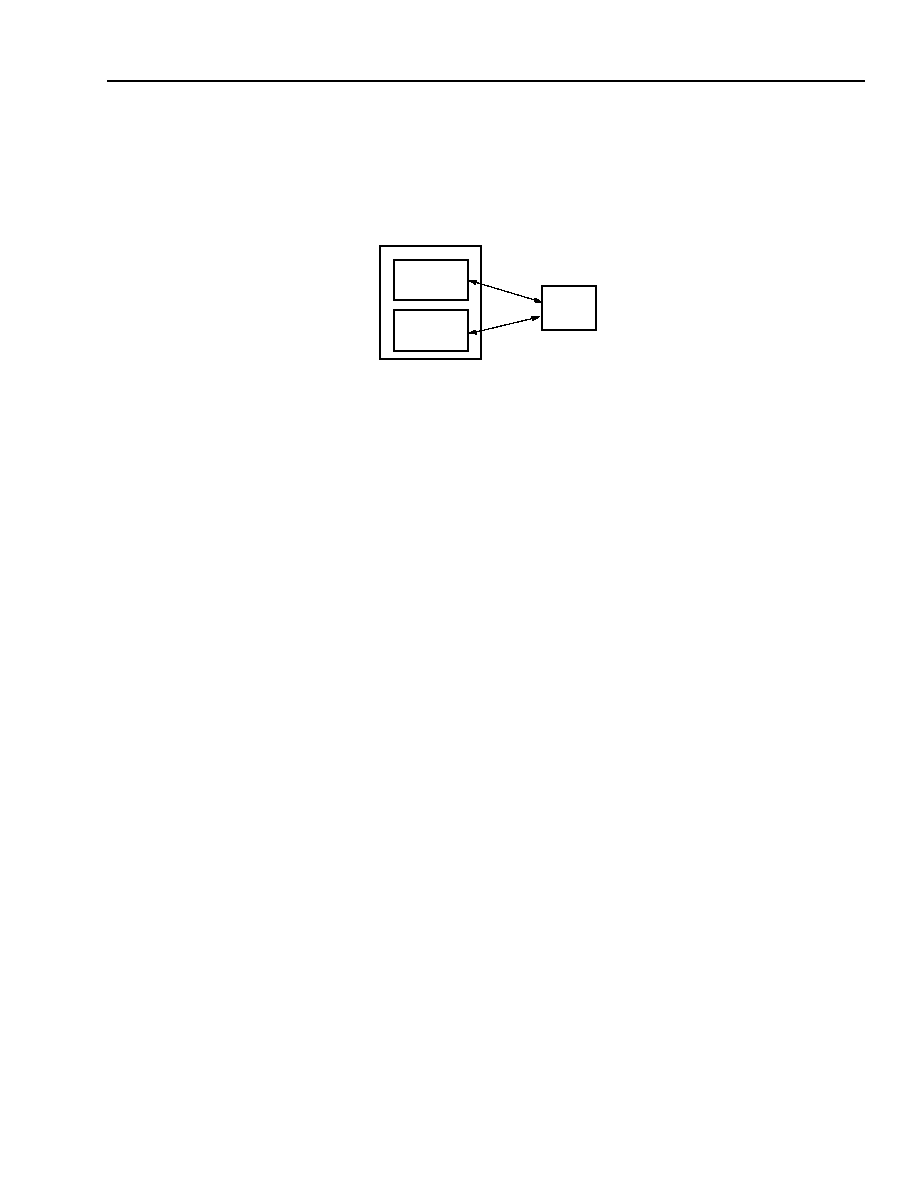
Synchronization
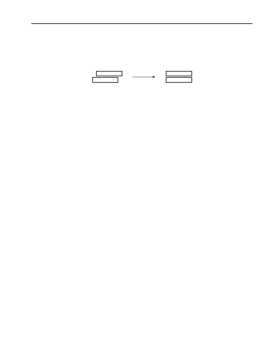
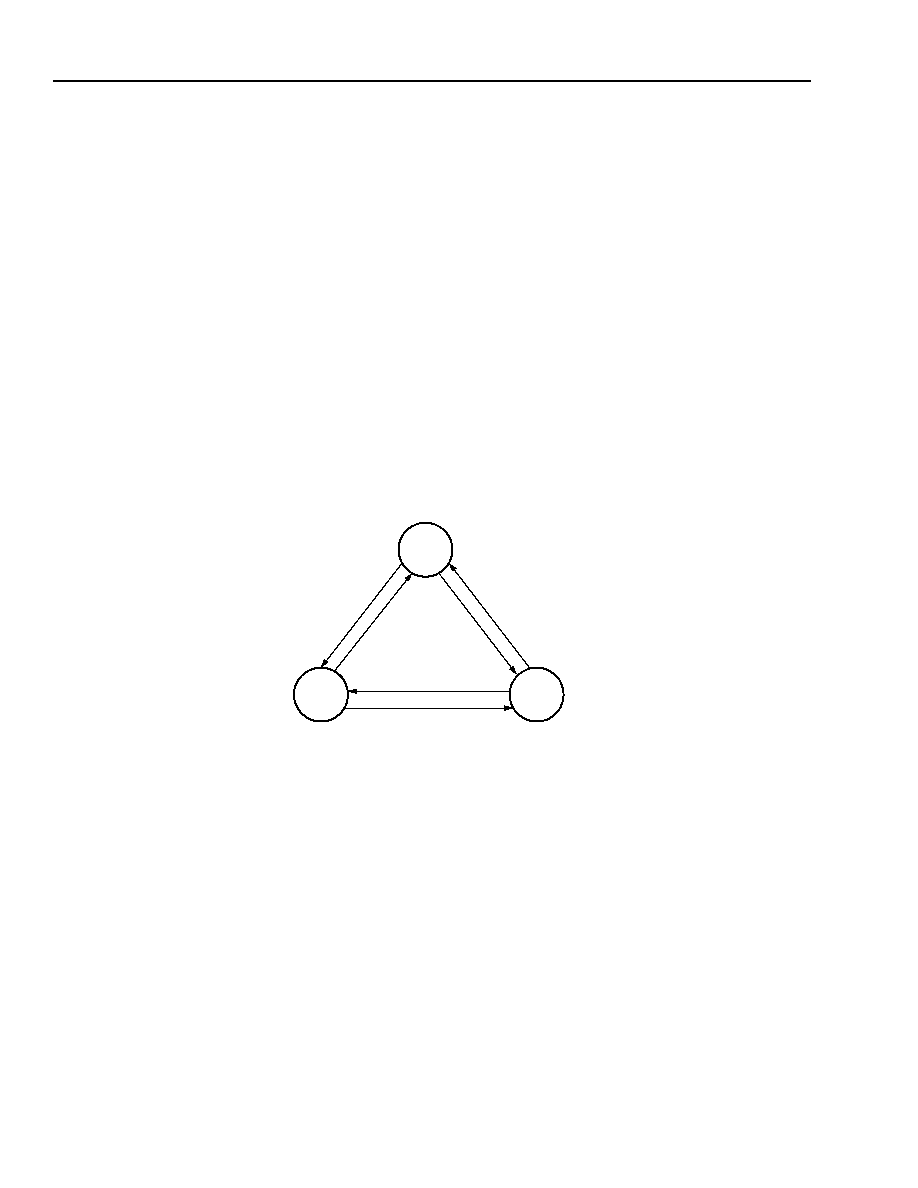
The incoming data from the high-speed interface (HSI) can be separated into two STS-12 channels per slice (A
and B).
Example of TTSV02622 alignment.
Figure 4. Alignment of Two STS-12 Streams
There is also a provision to allow certain streams to be disabled (i.e., not producing interrupts or affecting synchro-
nization). These streams can be enabled at a later time without disrupting other streams.
HSI Block Interface
The HSI block should provide two independent 77.76 MHz interfaces. Each interface will consist of a byte-wide
data stream and its recovered clock. There is no requirement for bit alignment since SONET type framing will take
place inside the TTSV02622 device.
Line Interface
The line side will receive/transmit frame-aligned streams of STS-12 data. All frames transmitted to the line will be
aligned to the line frame pulse, which will be provided to the TTSV02622. All frames received from the line will be
aligned to the system frame pulse, which will be supplied to the TTSV02622.
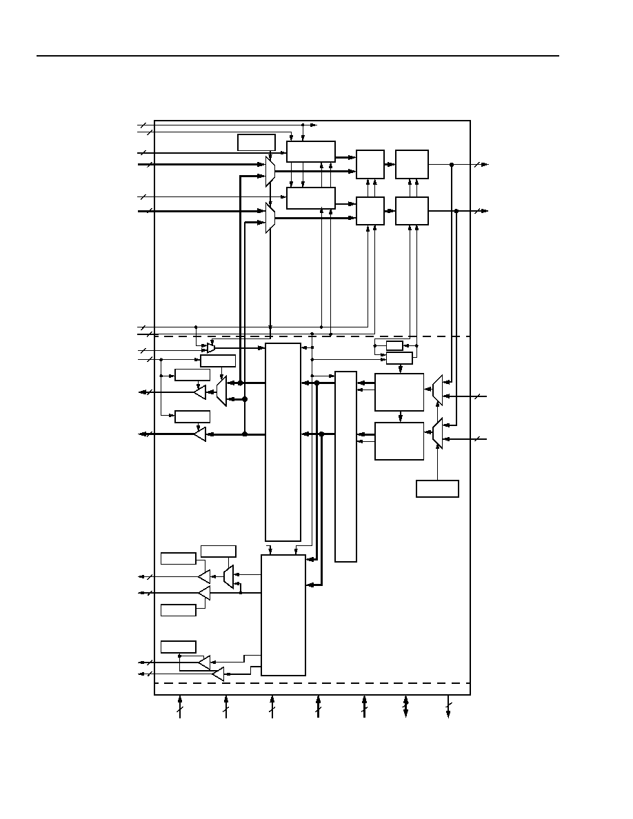
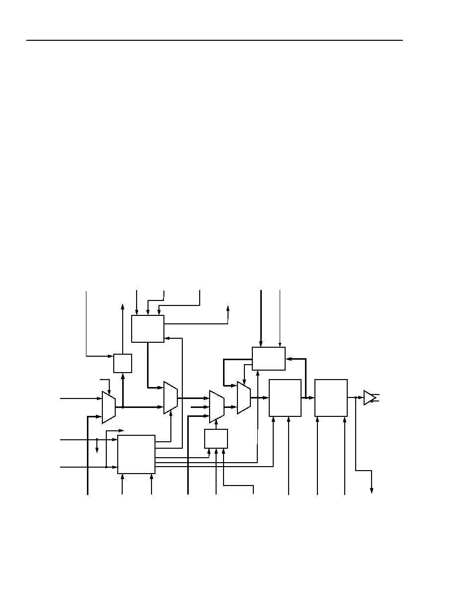
Architecture
The TTSV02622 is composed of transmit (Tx) and receive (Rx) sections. The device (see Figure 1 on page 2)
receives two byte-wide data streams at 77.76 MHz (STS-12 rate) and the associated clock. The incoming streams
are framed, and descrambled before they are then written into a FIFO that absorbs phase and delay variations and
allows the shift to system clock. The TOH is then extracted and sent out on the two serial ports. The pointer inter-
preter will then put the synchronous transport signal (STS) synchronous payload envelopes (SPEs) into a small
elastic store from which the pointer generator will produce two byte-wide STS-12 streams of data that are aligned
to the line timing pulse.
STREAM A
STREAM B
STREAM A
STREAM B
18
Agere Systems Inc.
Data Sheet
June 2003
TTSV02622 STS-24 Backplane Transceiver
Architecture
(continued)
Figure 5. Interior View of TTSV02622
TX TOH
PROCESSOR
FRAME
PROC.
TX CH#1
(MACRO)
TX TOH
PROCESSOR
FRAME
PROC.
TX CH#2
(MACRO)
LINE LBPK
(SOFT CTL)
TO RX TOH PROC.
DUAL CHANNEL
TRANSMITTER
/8
PLL
RX CH#1
(MACROCELL)
77.76
MHz
FIFO
POINTER
MOVER
STS-24
CH#
1
RX CH#2
(MACROCELL)
77.76
MHz
CH#
2
LVDS LPBK
(SOFT CTL)
SOFT CTL
SOFT CTL
SOFT CTL
RX TOH
PROCESSOR
TOH CLK
DUAL CHANNEL
RECEIVER
CH#1
CH#2
SOFT CTL
SOFT CTL
TOH OUTPUT #2
RX TOH FRAME
TOH CLK
TX TOH CLK ENA
TOH INPUT #1
TOH INPUT #2
INPUT BUS #1
INPUT BUS #2
SYSTEM FRAME
LINE FRAME
PROT SWITCH A/B
OUTPUT BUS #1
OUTPUT BUS #2
2
2
2
2
LVDS
OUT #1
LVDS
OUT #2
LVDS
IN #1
LVDS
IN #2
7
SOFT CTL
RX TOH CLK ENA
622 MHz CLKs
REF
FDBK
77.76
MHz
622 MHz
77.76
MHz
FRAME
CLOCK
TOH OUTPUT #1
DATA(8)/PARITY(1)
SYSTEM CLOCK
(77.76 MHz)
DATA(8)
1
1
1
1
PARITY(1)
DATA(8)
PARITY(1)
1
1
1
1
SPE(1) C1J1(1)
DATA(8)/PARITY(1)
SPE(1) C1J1(1)
SOFT CTL
1
1
1
1
CPU INTERFACE (ASYNC)
HIZ_N
RST_N
CS_N
RD/WR_N
ADDR
INT_N
(HARD RST)
DATA
8
1
1
1
1
1
LINE
LVDS
SIDE
SIDE
Agere Systems Inc.
19
Data Sheet
June 2003
TTSV02622 STS-24 Backplane Transceiver
Architecture
(continued)
The alignment FIFO allows the transfer of all data to the system clock. The FIFO sync block allows the system to
be configured to allow the frame alignment of multiple slightly varying data streams (see the FIFO Sync Subblock
(Backplane to Line) section on page 28).
Figure 6. Interconnect of Streams for FIFO Alignment
The pointer mover (see the Pointer Mover Subblock (Backplane to Line) section on page 28) is responsible for
mapping incoming frames to line frames. The pointer mover is a pseudo SONET implementation which is
streamlined wherever possible to minimize gate count and complexity. As a result, it is only capable of correcting
single bit, nonrepeating pointer errors. This pointer mover (i.e., interpreter, elastic store, and generator) will be
capable of handling intra STS-12 concatenation as well as inter STS-12 concatenation as long as the STS-12
streams are frame aligned.
Powerdown Mode
Powerdown mode should be entered when the corresponding channel is disabled. Channels can be independently
enabled or disabled under software control.
Note: The EXT PROT SW FUNC is low for STS-12 mode.
When a channel is disabled, the disabled channel of the clock and data recovery module is powered down, as well
as the LVDS buffers and TTL buffers for that channel. When all channels are powered down, PLL in the CDR mod-
ule is also powered down.
In addition, a pin has been added to enable the LVDS pins during boundary scan. This pin should be pulled high on
the board for functional operation.
STS-12
STREAM A
STS-12
STREAM B
FIFO
SYNC

20
Agere Systems Inc.
Data Sheet
June 2003
TTSV02622 STS-24 Backplane Transceiver
Supervisory Features
s
Parallel bus integrity:
-- Parity error checking is implemented on each of the four parallel input buses. Even and odd parity is sup-
ported as controlled from the CPU interface (per device control). Upon detection of an error, an interrupt is
raised. This feature is on a per-channel basis.
Note: On parallel output ports, parity is calculated over the 8-bit data bus and not on the SPE and C1J1 lines.
s
TOH serial port integrity:
-- There is even parity generation on each of the four TOH serial output ports. There is even parity error check-
ing on each of the four TOH serial input ports. There is one parity bit imbedded in the TOH frame. It occupies
the most significant bit location of A1 byte of STS-1. Upon detection of an error, an interrupt is raised. This fea-
ture is on a per-channel basis.
s
LVDS link integrity:
-- There is B1 parity generation on each of the four LVDS output channels. There is also performance monitoring
on each of the four LVDS input channels, implemented as B1 parity error checking. Upon detection of an error,
a counter is incremented (one count per errored bit) and an interrupt is raised. The counter is 7 bits wide plus
one overflow indicator bit. This feature is on a per-channel basis.
s
Framer monitor:
-- The framer in the receive direction will report loss of frame (LOF) as an interrupt, as well as a LOF count and
errored frame count. The LOF interrupt must not be clearable as long as the channel is in the LOF state. In
addition, the errored frame count must represent errored frames, and should not increment more than once
per frame even if there are multiple errors.
s
Receiver internal path integrity:
-- There is even parity generation in the receiver section (after descrambler). There is also even parity error
checking in the receiver section (before output). Upon detection of an error, an interrupt is raised. This feature
is on a per-channel basis.
s
Pointer mover performance monitoring:
-- There is pointer mover performance monitoring in the receiver section. Alarm indication signal path (AIS-P)
and concatenation is reported, as well as elastic store overflows.
s
AIS-P is implemented as a per STS-1 interrupt. In case of concatenated payload, only the interrupt associated
with the head of the group will be active.
s
Concatenation is reported as a per STS-1 status, and is high when STS-1 is concatenated; and low when not
concatenated.
s
Elastic store overflow will generate an interrupt on a per STS-1 basis.
s
FIFO aligner monitoring:
-- There is monitoring of the FIFO aligner operating point, and upon deviating from the nominal operating point
of the FIFO by more than user-programmable threshold values (min and max threshold values), an interrupt is
raised. Threshold values are defined per device, flags are per channel.
s
Frame offset monitoring:
-- There is monitoring of the frame offset between all enabled channels (disabled channels must not interfere
with the monitoring). Monitoring is performed continuously. Upon exceeding the maximum allowed frame off-
set (18 bytes) between all enabled channels, an interrupt is raised.
s
CPU interface monitoring:
-- There is monitoring of potential write cycles that may occur when operating in write protect mode. Upon
detecting a write access to the application specific integrated circuit (ASIC) when the device is in write protect
mode, an interrupt is raised (W-LOCK flag).

Agere Systems Inc.
21
Data Sheet
June 2003
TTSV02622 STS-24 Backplane Transceiver
Test Features
s
Line loopback:
-- There is a line loopback feature allowing the user to perform a loopback on the line side (per device control).
The line frame signal used by the pointer mover is automatically replaced by the system frame signal when
operating in line loopback mode.
s
LVDS loopback:
-- There is a LVDS loopback feature allowing the user to perform a loopback on the LVDS side (per device
control).
s
A1/A2 error insert:
-- There is a frame error inject feature, in the transmitter section, allowing the user to replace framing bytes
A1/A2 (only last A1 byte and first A2 byte) with a selectable A1/A2 byte value for a selectable number of con-
secutive frames. The number of consecutive frames to alter is specified by a 4-bit field, while A1/A2 value is
specified by two 8-bit fields. The error insert feature is on a per-channel basis, A1/A2 values and 4-bit frame
count value are on a per-device basis.
s
B1 error insert:
-- There is a B1 error insert feature, in the transmitter section, allowing the user to insert errors on user select-
able bits in the B1 byte. Errors are created by simply inverting bit values. Bits to invert will be specified through
an 8-bit register (each bit is associated with one of the eight B1 bits). To insert an error, software will first set
the bits in the transmitter B1 error insert mask. Then, on a per-channel basis, software will write a one to the
b1 error insert command. The insertion circuitry performs a rising edge detect on the bit, and will issue a cor-
ruption signal for the next frame, for one frame only. This feature is on a per-channel basis.
s
TOH serial output port parity error insert:
-- There is a parity error inject feature, in the receive section, allowing the user to invert the parity bit of each
serial output port. This feature inserts a single error. This feature is on a per-channel basis.
s
Parallel output bus parity error insert:
-- There is a parity error inject feature, in the receive section, allowing the user to invert parity lines associated
with each output parallel buses. This feature inserts a single error. This feature is on a per-channel basis. This
feature supports both even and odd parities.
s
Scrambler/descrambler disable:
-- There is a scrambler/descrambler disable feature, allowing the user to disable the scrambler of the transmitter
and the descrambler of the receiver. The B1 is calculated (in transmitter and receiver) on the nonscrambled
data stream. This feature is per device.
22
Agere Systems Inc.
Data Sheet
June 2003
TTSV02622 STS-24 Backplane Transceiver
Transmit Direction (Line to Backplane)
Each TOH insert block receives two byte-wide 77.76 MHz data from the line, which nominally represents two
STS-12 streams (A and B). Transport overhead bytes are then optionally inserted into these streams and the
streams are forwarded to the HSI. All byte timing pulses required to isolate individual overhead bytes (e.g., A1, A2,
B1, D1--D12, etc.) are generated internally based on a Frame_Sync received from the system (SYS_FP).
s
A1 and A2 insertion and optional corruption.
s
H1, H2, and H3 pass through transparently.
s
B1 calculation (after scrambling), insertion and optional corruption (before scrambling).
s
Optional K1 and K2 insert.
s
Optional S1/M0 insert.
s
Optional E1/F1/E2 insert.
s
Optional section and line data communication channel (DCC, D1--D12) insertion (for intercard communications
channel).
s
Scrambling of outgoing data stream with optional scrambler disabling.
s
Optional stream disabling.
All streams operate byte wide at 77.76 MHz (622 Mbits/s) in all modes.
Figure 7. Transmitter Block
PAR ERR FLAG
(SOFT REG)
LPBK
MUX
TOH
MUX
A1/A2
MUX
B1
MUX
B1 ERROR
B1 ERROR
TOH CLOCK
TOH CLOCK
TOH
PAR ERR FLAG
EVEN/ODD
PARITY
(SOFT CTL)
(SOFT REG)
SERIAL
DATA IN
(COMMON TO
THE 2 CH)
ENA (COMMON
TO THE 2 CH)
MASK
(SOFT REG)
INSERT CMD
(SOFT CTL)
B1 BYTE
PARITY
GENERATOR
B1
TOH
SER TO PAR
CONVERTER
+
BUFFER
BUS
PAR
CHECK
TOH
LINE LPBK
(SOFT CTL)
SPE + TOH
A1/A2
77.76 MHz
(TO ALL BLOCKS)
INPUT BUS
DATA(8)
PARITY(1)
SYSTEM
FRAME
SYSTEM
CLOCK
TO RX
TX SYNC
(COMMON TO
THE 2 TX
CHANNELS)
LINE LPBK
(FROM RX)
TOH MODE TOH BYTES
A1/A2 ERROR A1/A2 ERROR
A1/A2 ERROR
SCRAMBLER 77.76 MHz
622 MHz
LVDS LPBK
(TO RX)
(FROM PLL)
(FROM PLL)
DISABLE
(SOFT CTL)
INSERTCMD
(SOFT CTL)
INSERT-
COUNT
(SOFT REG)
INSERT
VALUE
(SOFT REG)
INS/PASS
SEL
(SOFT CTL)
(INS/PASS)
(SOFT CTL)
A1/A2
MUX
CTL
SONET
SCRAMBLER
PARALLEL
TO SERIAL
(MEGACELL
FROM ASIC
VENDOR)
LVDS
OUT#1

Agere Systems Inc.
23
Data Sheet
June 2003
TTSV02622 STS-24 Backplane Transceiver
Transmit Direction (Line to Backplane)
(continued)
Transport Overhead Serial Link
The TOH serial links are used to insert TOH bytes into the transmit data. TOH_IN and TOH_CLK_EN get retimed
by TOH_CLK in order to meet setup and hold specifications of the device.
Insertion or passthrough of the TOH is under software control.
TOH parity is calculated using the initial retimed data (TOH_IN_D).
A1/A2 Frame Insert and Corruption
When not corrupted, for each stream, all twelve A1 bytes of the STS-12 are set to 0xF6 and all twelve A2 bytes of
the STS-12 are set to 0◊28.
Corruption is controlled per stream by the A1/A2 error insert register. When A1/A2 corruption is set for a particular
stream, the A1/A2 value in the corrupted A1/A2 value registers are sent for the number of frames defined in the
corrupted A1/A2 frame count register (see Table 6 on page 33 and Table 7 on page 36 for register details).
Note: When the corrupted A1/A2 frame count register is set to zero, A1A2 corruption will continue until the A1/A2
error insert register is cleared, i.e., indefinitely.
On a per-device basis, the A1 and A2 byte values are set, as well as the number of frames of corruption. Then, to
insert the specified A1/A2 values, each channel has an enable register. When the enable register is set, the A1/A2
values are corrupted for the number specified in the number of frames to corrupt. To insert errors again, the per-
channel fault insert register must be cleared, and set again.
Only the last A1 and the first A2 are corrupted.
B1 Calculation and Insertion
The B1 calculation block computes a BIP-8 code, using even parity over all bits of the previous STS-n frame after
scrambling and is inserted in the B1 byte of the current STS-n frame before scrambling. Per-bit B1 corruption is
controlled by the force BIP-8 corruption register (per device register). For any bit set in this register, the corre-
sponding bit in the calculated BIP-8 is inverted before insertion into the B1 byte position. Each stream has an inde-
pendent fault insert register that enables the inversion of the B1 bytes. B1 bytes in all other STS-1s in the stream
are passed through transparently.
Stream Disable
When disabled via the appropriate bit in the stream enable register, the prescrambled data for a stream is set to all
ones, feeding the HSI. The HSI macro is powered down on a per-stream basis, as is the LVDS outputs.
Scrambler
The data stream is scrambled using a frame synchronous scrambler of sequence length 127, operating at the line
rate. The scrambling function can be disabled by software.
The generating polynomial for the scrambler is 1 + x
6
+ x
7
.
The scrambler is reset to 111_1111 on the first byte of the SPE (byte following the Z0 byte in the twelfth STS-1).
That byte and all subsequent bytes to be scrambled are exclusive ORed, with the output from the byte-wise scram-
bler. The scrambler runs continuously from that byte on throughout the remainder of the frame.
A1, A2, J0, and Z0 bytes are not scrambled.
24
Agere Systems Inc.
Data Sheet
June 2003
TTSV02622 STS-24 Backplane Transceiver
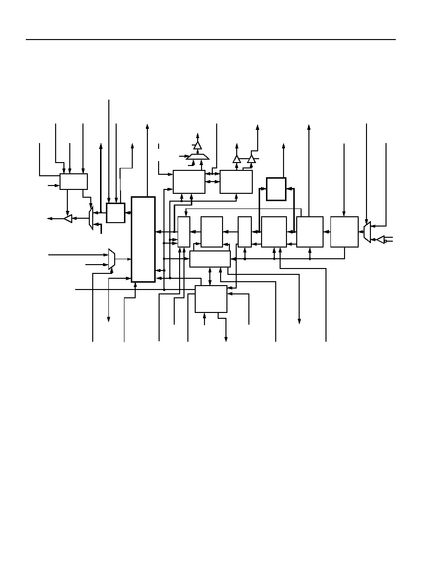
Receiver Block
Figure 8. Receiver Block
Framer Subblock (Backplane to Line)
The framer block takes byte-wide data from the HSI, and outputs a byte-aligned byte-wide stream and 8 kHz sync
pulse (asserted one clock before the first A1 byte). The framer algorithm determines the out-of-frame/in-frame sta-
tus of the incoming data and will cause interrupts on both an errored frame and an OOF state.
Features
s
A1--A2 framing pattern detection.
s
Framing similar to SONET specification.
s
Generates timing and an 8 kHz frame pulse.
s
Detects OOF and generates an interrupt.
s
Detects errored frame and increments counter.
PROT
SWITCH
FUNCTION
(SOFT CTL)
PROT
SWITCH
ENA
(SOFT CTL)
HI-Z
(SOFT CTL)
CH#1--2
MUX
(SOFT CTL)
LINE
LPBK
(TO TX)
EVEN/ODD
PARITY
(SOFT CTL)
PAR ERR
INSERT
(SOFT CTL)
PAR ERR
FLAG
(SOFT REG)
PERF
MONITORS
(SOFT REG)
PAR ERR
INSERT
(SOFT CTL)
TOH SERIAL
DATA OUT
TOH CLOCK
(COMMON TO
THE 2 CH)
TOH CLOCK
ENABLE
(COMMON TO
TOH FRAME
(COMMON TO
THE 2 CH)
B1 PAR ERR
COUNT, B1
PAR ERR FLAG
LOF FLAG,
LOF COUNT,
A1/A2 ERR COUNT
THE 2 CH)
(SOFT REG)
(SOF REG)
16--622 MHz
CLOCKS
(FROM PLL)
LVDS LPBK
(SOFT CTL)
LVDS LPBK
(FROM TX)
SERIAL
TO
PARALLEL
(MEGACELL
FROM ASIC
VENDOR)
SONET
FRAME
RECOVERY
B1
PARITY
ERROR
COUNT
LPBK
MUX
LVDS
#1
RX CLK
77.76 MHz
FP
SONET
DESCRAM-
BLER
FP
FP
PAR
GEN
WR
FP
B1
RD
PROT
SWITCH
CTL
PROT
SWITCH
FP
LOF
CTLS
HI-Z
(SOFT
CH#2
OUT DATA
TOH
PAR TO SER
CONVERTER
+ BUFFER
TOH PORT
CONTROL
(COMMON TO
THE 2 CH)
DATA
PARTIY
SPE
C1J1
STS-12
POINTER
MOVER
BUS
PARTIY
GEN
/CHECK
CH#2
OUT DATA
AIS
INS
FIFO
ALIGNER
FIFO READ/WRITE
CONTROL
FP
CT
L
S
FIFO SYNC
(COMMON TO
THE 2
CHANNELS)
FP = FRAME PULSE
CH#1
OUT BUS
DATA(8)
PARITY(1)
SPE(1)
C1J1(1)
LINE
FRAME
SYSTEM
FRAME
(FROM TX)
SYSTEM
CLOCK
(77.76 MHz)
LINE LPBK
(SOFT CTL)
CTLS
(TO/FROM
OTHER
K1/K2
PASS
/REGEN
AIS-L
ON LOF
(SOFT CTL)
FORCE
AIS-L
(SOFT CTL)
CTLS
(TO OTHER
CH)
FIFO
RE-ALIGN
(SOFT CTL)
FRAME
OFFSET
ALARM FLAG
CTLS
(TO OTHER
CH)
FIFO
MIN/MAX
THRESHOLDS
FIFO
THRESHOLD
ALARM FLAG
DESCRAMBLER
DISABLE
(SOFT CTL)
(SOFT CTL)
(SOFT REG)
(SOFT REG)
HI-Z
(SOFT
0
1
CTL)
CTL)
CH#1--2 MUX
(SOFT CTL)
(SOFT REG)
CH)

Agere Systems Inc.
25
Data Sheet
June 2003
TTSV02622 STS-24 Backplane Transceiver
Receiver Block
(continued)
Framer Subblock (Backplane to Line)
(continued)
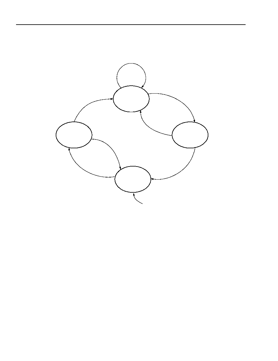
Framer State Machine
Figure 9 shows the state machine that controls the framer. Since the TTSV02622 is intended for use between
ASICs via a backplane, there is only one errored frame state; thus, after two transitions are missed, the state
machine goes into the OOF state and there is no SEF or LOF indication.
OOF State. In this state, the A1 pattern is searched for on every clock cycle.
A second stage of comparison is implemented to locate the A1/A2 transition. When the A1/A2 transition is found,
the following occurs:
s
The state machine moves from the OOF state to the frame confirm state.
s
The A1offset for the byte start location is locked.
s
The row, column, and STS counters are set.
Frame Confirm. In this state, the A1/A2 transition is only compared for at the appropriate location, i.e., beginning
at the twelfth A1 location. This location is determined from the row, column, and STS counters which were set at
the transition from OOF to frame confirm. If at this time the comparison fails, the state machine reverts to the OOF
state. If the comparison passes, the next state will be In frame.
In Frame. This state is similar to the frame confirm state except that if the comparison at the A1/A2 time is incor-
rect, the next state will be the errored frame state. If the comparison is correct, the next state will be in frame.
Errored Frame. Once the errored frame state has been reached, if the next comparison is incorrect, the next state
will be OOF. Otherwise, if correct, the next state will be in frame. This state will generate an error interrupt to the
micro.
26
Agere Systems Inc.
Data Sheet
June 2003
TTSV02622 STS-24 Backplane Transceiver
Receiver Block
(continued)
Framer Subblock (Backplane to Line)
(continued)
Notes:
Row, column, and STS counters are only set/reset by state transition from OOF to frame confirm.
Expect A1/A2 means that row/col/STS counter values indicate time for last (twelfth) A1 byte.
Figure 9. Framer State Machine
IN
FRAME
OOF
ERRORED
FRAME
FRAME
CONFIRM
RESET
- FIND A1/A2 TRANSITION
EXPECT A1/A2
EXPECT A1/A2
& FIND A1/A2
& !FIND A1/A2
EXPECT A1/A2
& FIND A1/A2
EXPECT A1/A2
& !FIND A1/A2
- LOCK BARREL SHIFTER
- SET ROW/COL/STS COUNTERS
EXPECT A1/A2
& FIND A1/A2
EXPECT A1/A2
& !FIND A1/A2

Agere Systems Inc.
27
Data Sheet
June 2003
TTSV02622 STS-24 Backplane Transceiver
Receiver Block
(continued)
B1 Calculate and Descramble (Backplane to Line)
Each Rx block receives byte-wide scrambled 77.76 MHz data and a frame sync from the framer. Since each HSI is
independently clocked, the Rx block operates on individual streams. Timing signals required to locate overhead
bytes to be extracted are generated internally based on the frame sync. The frame sync occurs one clock pulse
before the first A1 byte of the stream. The Rx block produces byte-wide descrambled data and an output frame
sync for the alignment FIFO block. The output frame sync occurs two clocks before the first A1 byte of the
descrambled data stream to allow for metastable hardening by the write control subblock.
On the received data, the following functionality is needed:
s
Descrambling of received data stream with optional descrambling disable.
s
B1 verification.
Descrambling
The streams are scrambled using a frame synchronous scrambler of sequence length 127, operating at the line
rate. The descrambling function can be disabled by software.
The generating polynomial for the scramble is 1 + x
6
+ x
7
.
The scrambler is reset to 1111111 on the first byte of the SPE (byte following the Z0 byte in the twelfth STS-1). That
byte and all subsequent bytes to be scrambled are exclusive ORed, with the output from the byte-wise scrambler.
The scrambler runs continuously from that byte on throughout the remainder of the frame.
A1, A2, J0, and Z0 bytes are not scrambled.
B1 Verification
The B1 calculation block computes a BIP-8 code, using even parity over all bits of the previous STS-12 frame
before descrambling, and this value is checked against the B1 byte of the current frame after descrambling. A per-
stream B1 error counter is incremented for each bit that is in error.
Alarm Indication Signal Line (AIS-L) Insertion
If enabled via AIS_L_INSERT[x] bit in the AIS_L force register, AIS-L is inserted into the received frame by writing
all ones for all bytes of the descrambled stream.
AIS-L Insertion on Out of Frame
If enabled via the appropriate bit in the AIS_L force on out of frame register, AIS-L is inserted into the received
frame by writing all ones for all bytes of the descrambled stream when the framer indicates that an out of frame
condition exists.
Internal Parity Generation
An even parity is generated on all data bytes and is routed in parallel with the data to be checked before the protec-
tion switch MUX at the parallel output.

28
Agere Systems Inc.
Data Sheet
June 2003
TTSV02622 STS-24 Backplane Transceiver
Receiver Block
(continued)
FIFO Subblock (Backplane to Line)
The FIFO subblock consists of a 24 by 10-bit FIFO per STS-12. This FIFO will be used to align up to ±154.3 ns of
interlink skew and to transfer to the system clock.
FIFO Sync Subblock (Backplane to Line)
This FIFO sync block takes metastable hardened frame pulses from the write control blocks and produces sync
signals that indicate when the read control blocks should begin reading from the first FIFO location. On top of the
sync signals, this block produces an error indicator which indicates that the signals to be aligned are too far apart
for alignment (i.e., greater than 18 clocks apart). Sync and error signals are sent to read control block for align-
ment.
The read control block is synchronized only once on start-up, and any further synchronizing is software (S/W) con-
trolled. The action of resynchronizing a read control block will always cause a data hit. A software register allows
the read control block to be resynchronized.
Recommended Procedure for Synchronization of Selected Streams
s
Force AIS-L in all streams to be synchronized.
s
Wait four frames.
s
Write a 1 to the FIFO alignment resynchronizing register, bit DB1 of register 0x06.
s
Wait four frames.
s
Release the AIS-L in all streams.
Pointer Mover Subblock (Backplane to Line)
The pointer mover simply maps incoming frames to the line framing. The K1/K2 bytes and H1--SS bits are also
passed through to the pointer generator so that the line can receive them. The mover will handle both concatena-
tions inside the STS-12, and to other STS-12s inside the TTSV02622.
Pointer Interpreter State Machine
The pointer interpreter is minimized as much as possible to keep the gate count low. In keeping with that goal, the
pointer interpreter has only three states (NORM, AIS, and CONC). The interpreter's highest priority is to maintain
accurate dataflow (i.e., valid SPE only). This will ensure that any errors in the pointer value will be corrected by a
standard pointer interpreter without any data hits. This means that error checking for increment, decrement, and
NDF (i.e., 8 of 10) are maintained in order to ensure accurate dataflow. A single valid pointer (i.e., 0--782) that dif-
fers from the current pointer will be ignored. Two consecutive incoming valid pointers that differ from the current
pointer will cause a reset of the J1 location to the latest pointer value (the generator will then produce an NDF).
This block is designed to handle single bit errors without affecting dataflow or changing state, but it is not compliant
with SONET standards.

Agere Systems Inc.
29
Data Sheet
June 2003
TTSV02622 STS-24 Backplane Transceiver
Receiver Block
(continued)
Pointer Mover Subblock (Backplane to Line)
(continued)
Rules for Concatenation. The pointer mover block can correctly process any length of concatenation (multiple of
three) as long as it begins on an STS-3 boundary (i.e., STS-1 number 1, 4, 7, 10, etc.) and is contained within the
smaller of STS-3, 12 or 24 (see Table 4).
Table 4. Valid Starting Positions for a STS-MC
Notes:
Y = STS-Mc SPE can start in that STS-1.
NO = STS-Mc SPE cannot start in that STS-1.
-- = Y or NO, depending on the particular value of M.
Rules for Pointer Interpretation.
s
NDF
N bits in H1 byte = (1001 + single bit error).
s
NRMNBTS (i.e., NDF not set)
N bits in H1 byte = (0110 + single bit error).
s
CONC pointer
(N bits in H1 byte = 1001 + single bit error) and offset = 11_1111_1111.
s
AIS pointer
offset and N bits are all 1s (SS bits are ignored).
s
NORM pointer
(offset 0--782) and (NDF or NRMNBITS).
STS-1
Number
STS-3c
SPE
STS-6c
SPE
STS-9c
SPE
STS-12c
SPE
STS-15c
SPE
STS-18c to STS-24c
SPEs
1
Y
Y
Y
Y
Y
Y
4
Y
Y
Y
NO
Y
--
7
Y
Y
NO
NO
Y
--
10
Y
NO
NO
NO
Y
--
13
Y
Y
Y
Y
Y
--
16
Y
Y
Y
NO
Y
--
19
Y
Y
NO
NO
Y
--
22
Y
NO
NO
NO
Y
--
30
Agere Systems Inc.
Data Sheet
June 2003
TTSV02622 STS-24 Backplane Transceiver
Receiver Block
(continued)
Pointer Mover Subblock (Backplane to Line)
(continued)
NORM State. This state will begin whenever two consecutive NORM pointers are received. If two consecutive
NORM pointers are received, such that both differ from the current offset, then the current offset will be reset to the
last received NORM pointer. When the pointer interpreter changes its offset, it causes the pointer generator to
receive a J1 value in a new position. When the pointer generator gets an unexpected J1, it resets its offset value to
the new location and declares an NDF.
Note: The interpreter is only looking for two consecutive pointers that are different from the current value. These
two consecutive NORM pointers do not have to have the same value.
For example; if the current pointer is 10 and you receive a NORM pointer with offset of 15 and a second NORM
pointer with offset of 25, then the interpreter will change the current pointer to be 25.
CONC State. The receipt of two consecutive CONC pointers causes this state to be entered. Once in this state, off-
set values from the head of the concatenation chain are used to determine the location of the STS SPE for each
STS in the chain.
AIS State. Two consecutive AIS pointers cause this state to occur. Any two consecutive normal or concatenation
pointers will end this state. This state will cause the data leaving the pointer generator to be overwritten with 0xFF.
Figure 10. Pointer Mover State Machine
Pointer Generator
The pointer generator simply maps the corresponding bytes into their appropriate location in the outgoing byte
stream. The generator also creates offset pointers based on the location of the J1 byte as indicated by the pointer
interpreter. The generator will signal NDFs when the interpreter signals that it is coming out of AIS state. The gen-
erator resets the pointer value and generates NDF every time a byte marked J1 is read from the elastic store that
doesn't match the previous offset.
Increments and decrements signals from the pointer interpreter are latched once per frame on either the F1 or E2
byte times (depending on collisions), this ensures constant values during the H1 through H3 times. The choice of
which byte time to do the latching on is made when the relative frame phases (i.e., received and system) is deter-
mined. This latch point will then be stable, unless the relative framing changes and the received H byte times col-
lide with the system F1 or E2 times, in which case the latch point would be switched to the collision-free byte time.
NORM
CONC
AIS
2
x
C
O
N
C
2 x
N
O
R
M
2
x
N
O
R
M
2 x
A
IS
2 x CONC
2 x AIS
Agere Systems Inc.
31
Data Sheet
June 2003
TTSV02622 STS-24 Backplane Transceiver
Receiver Block
(continued)
Pointer Mover Subblock (Backplane to Line)
(continued)
There is no restriction on how many or how often increments and decrements are processed. Any received incre-
ment or decrement is immediately passed to the generator for implementation regardless of when the last pointer
adjustment was made. The responsibility for meeting the SONET criteria for max frequency of pointer adjustments
is then left to the upstream pointer processor.
When the interpreter signals an AIS state, the generator will immediately begin sending out 0xFF in place of data
and H1, H2, H3. This will continue until the interpreter returns to NORM or CONC states and a J1 byte is received.
Miscellaneous Functions
K1/K2, A1/A2 Handling
K1/K2 bytes can be optionally passed through the pointer mover under software control, or it can be set to zero
with the other TOH bytes. A1/A2 bytes are regenerated and set to F6 and 28, respectively.
SPE C1J1 Outputs
In an attempt to minimize the complexity required from the pointer processor that may be hooked-up to the
TTSV02622 parallel output port, two signals (per channel) must be provided to the external world; these are called
SPE and C1J1. These two signals will allow a pointer processor to extract payload without interpreting the point-
ers.
Table 5. SPE and C1J1 Functionality
The following rules must be observed for generating SPE and C1J1 signals:
s
On occurrence of AIS-P on any of the STS-1, there must be no corresponding J1 pulse.
s
In case of concatenated payloads (up to STS-24c), only the head STS-1 of the group must have an associated J1
pulse.
s
C1J1 signal must track any pointer movements.
s
During a negative justification event, SPE must be set high during the H3 byte to indicate that payload data is
available.
s
During a positive justification event, SPE must be set low during the positive stuff opportunity byte to indicate that
payload data is not available.
SPE
C1J1
Description
0
0
TOH information excluding C1(J0) of STS-1 #1.
0
1
Position of C1(J0) of STS-1 #1.
1
0
SPE information excluding the 12 J1 bytes.
1
1
Position of the twelve J1 bytes.

32
Agere Systems Inc.
Data Sheet
June 2003
TTSV02622 STS-24 Backplane Transceiver
Registers
Definition of Register Types
The TTSV02622 design contains six structural register elements: SREG, CREG, PREG, IAREG, ISREG, and
IEREG. There are no mixed registers in TTSV02622. This means that all bits of a particular register (particular
address) are structurally the same and are as follows:
s
Status register (SREG):
-- A status register is read only, and as the name implies is used to convey the status information of a particular
element or function of the TTSV02622 chip. The reset value of an SREG is really the reset value of the partic-
ular element or function that is being read. In some cases, an SREG is really a fixed value; an example of
which is the fixed id and revision registers.
s
Control register (CREG):
-- A control register is read and writable memory element inside CORE_CONTROL. The value of a CREG will
always be the value written to it. Events inside the TTSV02622 chip cannot affect a CREG value. The only
exception is a soft reset, in which case the CREG will return to its reset value. The control register have reset
values as defined in the reset value column of Table 6 on page 33.
s
Pulse register (PREG):
-- Each element, or bit, of a pulse register is a control or event signal that is asserted and then deasserted when
a value of 1 is written to it. This means that each bit is always of value 0 until it is written to, upon which it is
pulsed to the value of 1 and then returned to a value of 0. A pulse register will always have a read value of 0.
s
Interrupt alarm register (IAREG):
-- Each bit of an interrupt alarm register is a event latch. When a particular event is produced in the TTSV02622
chip, its occurrence is latched by its associated IAREG bit. To clear a particular IAREG bit, a value of 1 must
be written to it. In the TTSV02622 chip, all IAREG reset values are 0.
s
Interrupt status register (ISREG):
-- Each bit of an interrupt status register is physically the logical OR function. It is a consolidation of lower-level
interrupt alarms and/or ISREG bits from other registers. A direct result of the fact that each bit of the ISREG is
a logical OR function means that it will have a read value of 1 if any of the consolidation signals are of value 1,
and will be of value 0 if and only if all consolidation signals are of value 0. In the TTSV02622 chip, all ISREG
reset values are 0.
s
Interrupt enable register (IEREG):
-- Each bit of a status register or alarm register has an associated enable bit. If this bit is set to value 1, then the
event is allowed to propagate to the next higher level of consolidation. If this bit is set to zero, then the associ-
ated IAREG or ISREG bit can still be asserted but an alarm will not propagate to the next higher level. Obvi-
ously, an interrupt enable bit is an interrupt mask bit when it is set to value 0.
Agere Systems Inc.
33
Data Sheet
June 2003
TTSV02622 STS-24 Backplane Transceiver
Registers
(continued)
Register Map
Table 6. Register Map
ADDR
*
[6:0]
* ADDR values delimited by a comma indicate the address for each of two channels, from channel 1 or 2. For example, the register for Tx
control signals has addresses of 20 and 38. This indicates that channel 1 Tx control signals are at address 20 and channel 2 Tx control
signals are at address 38.
Reg.
Type
DB7
DB6
DB5
DB4
DB3
DB2
DB1
DB0
Reset
Value
(hex)
Comments
00
SREG
FIXED ID MSB
A0
Generic
register
block.
01
SREG
FIXED ID LSB
01
02
SREG
FIXED REV
01
03
CREG
SCRATCH PAD
00
04
CREG
LOCKREG MSB
00
05
CREG
LOCKREG LSB
00
06
PREG
--
Reserved.
--
--
--
--
--
FIFO
ALIGNMENT
COMMAND
GLOBAL
RESET
COMMAND
NA
Device Register Block
08
CREG
--
--
--
Rx TOH
FRAME
AND
Rx TOH
CLOCK
ENABLE
HI-Z
CONTROL
EXT PROT
SW EN
EXT PROT
SW FUNC
STS-12
SELECT
LVDS LPBK
CONTROL
00
Device
register block
(Rx).
09
CREG
--
--
--
--
--
PARALLEL
PORT
OUTPUT
MUX
SELECT
FOR CH1
--
SERIAL
PORT
OUTPUT
MUX
SELECT
FOR CH1
0F
0A
CREG
--
--
--
FIFO ALIGNER THRESHOLD VALUE (min)
02
0B
CREG
--
--
--
FIFO ALIGNER THRESHOLD VALUE (max)
15
0C
CREG
--
SCRAMBLER/
DESCREAMBLER
CONTROL
I/O
PARALLEL
BUS
PARITY
CONTROL
LINE LPBK
CONTROL
NUMBER OF CONSECUTIVE A1/A2 ERRORS TO
GENERATE [3:0]
60
Device
register block
(Tx).
0D
CREG
A1 ERROR INSERT VALUE
00
0E
CREG
A2 ERROR INSERT VALUE
00
0F
CREG
TRANSMITTER B1 ERROR INSERT MASK
00
10
ISREG
--
--
--
PER DEVICE
INT
--
--
CH 2 INT
CH 1 INT
00
Top-level
interrupts.
11
IEREG
--
--
--
ENABLE/MASK REGISTER [4:0]
00
12
IAREG
--
--
--
--
--
--
WRITE TO
LOCKED
REGISTER
ERROR FLAG
FRAME
OFFSET
ERROR
FLAG
00
13
IEREG
--
--
--
--
--
--
ENABLE/MASK REGISTER
00

34
Agere Systems Inc.
Data Sheet
June 2003
TTSV02622 STS-24 Backplane Transceiver
Registers
(continued)
Register Map
(continued)
Table 6. Register Map (continued)
ADDR
*
[6:0]
* ADDR values delimited by a comma indicate the address for each of two channels, from channel 1 or 2. For example, the register for Tx
control signals has addresses of 20 and 38. This indicates that channel 1 Tx control signals are at address 20 and channel 2 Tx control
signals are at address 38.
Reg.
Type
DB7
DB6
DB5
DB4
DB3
DB2
DB1
DB0
Reset
Value
(Hex)
Comments
Channel Register Block
20, 38
CREG
HI-Z
CONTROL OF
TOH DATA
OUTPUT
HI-Z
CONTROL
OF
PARALLEL
OUTPUT
BUS
CHANNEL
ENABLE /
DISABLE
CONTROL
PARALLEL
OUTPUT
BUS
PARITY
ERR INS
CMD
Rx K1/K2
SOURCE
SELECT
TOH SERIAL
OUTPUT
PORT PAR
ERR INS
CMD
FORCE
AIS-L
CONTROL
Rx
BEHAVIOR IN
LOF
01
Rx
control
signals.
21, 39
CREG
Tx MODE OF
OPERATION
Tx E1/F1/E2
SOURCE
SELECT
Tx S1/M0
SOURCE
SELECT
Tx K1/K2
SOURCE
SELECT
Tx D12
SOURCE
SELECT
Tx D11
SOURCE
SELECT
Tx D10
SOURCE
SELECT
Tx D9
SOURCE
SELECT
00
Tx control
signals.
22, 3A
CREG
Tx D8
SOURCE
SELECT
Tx D7
SOURCE
SELECT
Tx D6
SOURCE
SELECT
Tx D5
SOURCE
SELECT
Tx D4
SOURCE
SELECT
Tx D3
SOURCE
SELECT
Tx D2
SOURCE
SELECT
Tx D1
SOURCE
SELECT
00
23, 3B
CREG
--
Reserved.
--
--
--
--
--
B1 ERROR
INSERT
COMMAND
A1/A2 ERROR
INSERT
COMMAND
00
24, 3C
SREG
--
--
--
--
CONCAT
INDICATION
12
CONCAT
INDICATION
9
CONCAT
INDICATION
6
CONCAT
INDICATION
3
NA
Per STS-1
change of
state flag.
25, 3D
SREG
CONCAT
INDICATION
11
CONCAT
INDICATION
8
CONCAT
INDICATION
5
CONCAT
INDICATION
2
CONCAT
INDICATION
10
CONCAT
INDICATION
7
CONCAT
INDICATION
4
CONCAT
INDICATION
1
NA
26, 3E
ISREG
--
--
--
--
--
ELASTIC
STORE
OVERFLOW
FLAG
AIS-P FLAG
PER STS-12
ALARM FLAG
00
Per-channel
interrupt
consolida-
tion.
27, 3F
IEREG
--
--
--
--
--
ENABLE/MASK REGISTER [2:0]
00
28, 40
IAREG
--
--
TOH
SERIAL
INPUT
PORT
PARITY
ERROR
FLAG
INPUT
PARALLEL
BUS
PARITY
ERROR
FLAG
LVDS LINK
B1 PARITY
ERROR
FLAG
LOF FLAG
RECEIVER
INTERNAL
PATH
PARITY
ERROR
FLAG
FIFO ALIGNER
THRESHOLD
ERROR FLAG
00
Per STS-12
interrupt
flags.
29, 41
IEREG
--
--
ENABLE/MASK REGISTER [5:0]
00
Agere Systems Inc.
35
Data Sheet
June 2003
TTSV02622 STS-24 Backplane Transceiver
Registers
(continued)
Register Map
(continued)
Table 6. Register Map (continued)
ADDR
*
[6:0]
* ADDR values delimited by a comma indicate the address for each of two channels, from channel 1 or 2. For example, the register for Tx
control signals has addresses of 20 and 38. This indicates that channel 1 Tx control signals are at address 20 and channel 2 Tx control
signals are at address 38.
Reg.
Type
DB7
DB6
DB5
DB4
DB3
DB2
DB1
DB0
Reset
Value
(hex)
Comments
Channel Register Block (continued)
2A, 42
IAREG
--
Reserved.
--
--
--
AIS
INTERRUPT
FLAGS
12
AIS
INTERRUPT
FLAG
9
AIS
INTERRUPT
FLAGS
6
AIS
INTERRUPT
FLAGS
3
00
Per STS-1
interrupt flags.
2B, 43
IAREG
AIS
INTERRUPT
FLAG
11
AIS
INTERRUPT
FLAG
8
AIS
INTERRUPT
FLAG
5
AIS
INTERRUPT
FLAG
2
AIS
INTERRUPT
FLAG
10
AIS
INTERRUPT
FLAG
7
AIS
INTERRUPT
FLAG
4
AIS
INTERRUPT
FLAG
1
00
2C, 44
IEREG
--
--
--
--
ENABLE/
MASK AIS
INTERRUPT
FLAGS
12
ENABLE/
MASK AIS
INTERRUPT
FLAG
9
ENABLE/
MASK AIS
INTERRUPT
FLAGS
6
ENABLE/
MASK AIS
INTERRUPT
FLAGS
3
00
2D, 45
IEREG
ENABLE/
MASK AIS
INTERRUPT
FLAG
11
ENABLE/
MASK AIS
INTERRUPT
FLAG
8
ENABLE/
MASK AIS
INTERRUPT
FLAG
5
ENABLE/
MASK AIS
INTERRUPT
FLAG
2
ENABLE/
MASK AIS
INTERRUPT
FLAG
10
ENABLE/
MASK AIS
INTERRUPT
FLAG
7
ENABLE/
MASK AIS
INTERRUPT
FLAG
4
ENABLE/
MASK AIS
INTERRUPT
FLAG
1
00
2E, 46
IAREG
--
--
--
--
ES
OVERFLOW
FLAGS
12
ES
OVERFLOW
FLAG
9
ES
OVERFLOW
FLAGS
6
ES
OVERFLOW
FLAGS
3
00
2F, 47
IAREG
ES
OVERFLOW
FLAG
11
ES
OVERFLOW
FLAG
8
ES
OVERFLOW
FLAG
5
ES
OVERFLOW
FLAG
2
ES
OVERFLOW
FLAG
10
ES
OVERFLOW
FLAG
7
ES
OVERFLOW
FLAG
4
ES
OVERFLOW
FLAG
1
00
30, 48
IEREG
--
--
--
--
ENABLE/
MASK ES
OVERFLOW
FLAGS
12
ENABLE/
MASK ES
OVERFLOW
FLAG
9
ENABLE/
MASK ES
OVERFLOW
FLAGS
6
ENABLE/
MASK ES
OVERFLOW
FLAGS
3
00
31, 49
IEREG
ENABLE/
MASK ES
OVERFLOW
FLAG
11
ENABLE/
MASK ES
OVERFLOW
FLAG
8
ENABLE/
MASK ES
OVERFLOW
FLAG
5
ENABLE/
MASK ES
OVERFLOW
FLAG
2
ENABLE/
MASK ES
OVERFLOW
FLAG
10
ENABLE/
MASK ES
OVERFLOW
FLAG
7
ENABLE/
MASK ES
OVERFLOW
FLAG
4
ENABLE/
MASK ES
OVERFLOW
FLAG
1
00
32, 4A COUNTER OVERFLOW
LVDS LINK B1 PARITY ERROR COUNTER
00
Binning.
33, 4B COUNTER OVERFLOW
LOF COUNTER
00
34, 4C COUNTER OVERFLOW
A1/A2 FRAME ERROR COUNTER
00

36
Agere Systems Inc.
Data Sheet
June 2003
TTSV02622 STS-24 Backplane Transceiver
Register Descriptions
Table 7. Register Description
Address
(hex)
Bit
Name
Type
Description
Reset
Value
(hex)
00
[7:0]
FIXED ID MSB
SREG NA.
A0
01
[7:0]
FIXED ID LSB
SREG NA.
01
02
[7:0]
FIXED REV
SREG NA.
01
03
[7:0]
SCRATCH PAD
CREG The scratch pad has no function and is not used any-
where in the TTSV02622 chip. However, this register can
be written to and read from.
00
04
[7:0]
LOCKREG MSB
CREG In order to write to registers in memory locations 06--7F,
LOCKREG MSB and LOCKREG LSB must be respec-
tively set to the values of A0 and 01. If the LOCKREG
MSB and LOCKREG LSB values are not set to A0 and 01
respectively, then any values written to the registers in
memory locations 06--7F will be ignored.
After reset (both hard and soft), the TTSV02622 chip is in
a write locked mode. The TTSV02622 chip needs to be
unlocked before it can be written to.
Also note that the scratch pad register (03) can always be
written to since it is unaffected by write lock mode.
00
05
[7:0]
LOCKREG LSB
CREG See address 0x04 bits [7:0] description.
00
06
0
GLOBAL RESET
COMMAND
PREG The FIFO ALIGNMENT and GLOBAL RESET COM-
MANDS are both accessed via the pulse register in mem-
ory address 06. The FIFO ALIGNMENT command is
used to frame align the outputs of the four receive STM
stream FIFOs. The GLOBAL RESET COMMAND is a soft
(software initiated) reset. Nevertheless, the GLOBAL
RESET COMMAND will have the exact reset effect as a
hard (RST_N pin) reset.
NA
1
FIFO ALIGNMENT
COMMAND
PREG See address 0x06 bit 0 description.
[7:2]
Reserved.

Agere Systems Inc.
37
Data Sheet
June 2003
TTSV02622 STS-24 Backplane Transceiver
Device Register Blocks
08
0
LVDS LPBK
CONTROL
CREG 0 = No loopback.
1 = LVDS loopback, transmit to receive on.
00
1
STS-12 SELECT
CREG This control signal is untracked in the TTSV02622 chip. It
is a scratch bit, and its value has no effect on the
TTSV02622 chip.
00
[3:2]
EXT PROT SW EN
(bit 3)
EXT PROT SW FUNC
(bit 2)
CREG EXT PORT
SW EN
EXT
PROT SW
FUNC
Switching Control Master
00
0
--
s
MUX is controlled by software
(1 control bit per MUX).
s
Output buffers are controlled
by software (1 control bit per
channel).
1
0
s
MUX on parallel output bus of
CH 1 is controlled by
PROT_SWITCH_A/B pin.
0 = CH 1.
1 = CH 2.
s
Output buffers are controlled
by software (1 control bit per
channel).
1
1
s
MUX is controlled by software
(1 control bit per MUX).
s
Output buffers on parallel out-
put bus of CH 1 and CH 2 are
controlled by
PROT_SWITCH_A/B pin.
0 = Buffers active.
1 = HI-Z.
4
Rx TOH FRAME
AND Rx TOH CLOCK
ENABLE HI-Z
CONTROL
CREG 0 = High impedance.
1 = Enable receive TOH CLK and FP outputs.
00
[7:5]
Reserved.
Register Descriptions
(continued)
Table 7. Register Description (continued)
Address
(hex)
Bit
Name
Type
Description
Reset
Value
(hex)
38
Agere Systems Inc.
Data Sheet
June 2003
TTSV02622 STS-24 Backplane Transceiver
Device Register Blocks (continued)
09
0
SERIAL PORT
OUTPUT MUX
SELECT FOR CH 1
CREG 0 = TOH output 1 is multiplexed to CH 2.
1 = TOH output 1 is multiplexed to CH 1.
0F
1
Reserved.
2
PARALLEL PORT
OUTPUT MUX
SELECT FOR CH 1
CREG 0 = Parallel output data bus 1 is multiplexed to CH 2.
1 = Parallel output data bus 1 is multiplexed to CH 1.
0F
3
Reserved.
[7:4]
Reserved.
0A
[4:0]
FIFO ALIGNER
THRESHOLD VALUE
(min)
CREG This is the minimum threshold value for the per-channel
receive direction alignment FIFOS. If and when the mini-
mum threshold value is violated by a particular channel,
then the interrupt event FIFO ALIGNER THRESHOLD
ERROR will be generated for that channel and latched as
a FIFO ALIGNER THRESHOLD ERROR FLAG in the
respective per STS-12 interrupt alarm register.
The allowable range for minimum threshold values is 1
to 23.
Note: The minimum FIFO aligner threshold values apply
to both channels.
02
[7:5]
Reserved.
0B
[4:0]
FIFO ALIGNER
THRESHOLD VALUE
(max)
CREG This is the maximum threshold value for the per-channel
receive direction alignment FIFOS. If and when the maxi-
mum threshold value is violated by a particular channel,
then the interrupt event FIFO ALIGNER THRESHOLD
ERROR will be generated for that channel and latched as
a FIFO ALIGNER THRESHOLD ERROR FLAG in the
respective per STS-12 interrupt alarm register.
The allowable range for maximum threshold values is 0
to 22.
Note: The minimum FIFO aligner threshold values apply
to both channels.
15
[7:5]
Reserved.
Register Descriptions
(continued)
Table 7. Register Description (continued)
Address
(hex)
Bit
Name
Type
Description
Reset
Value
(hex)

Agere Systems Inc.
39
Data Sheet
June 2003
TTSV02622 STS-24 Backplane Transceiver
Device Register Blocks (continued)
0C
[3:0]
NUMBER OF
CONSECUTIVE
A1/A2 ERRORS TO
GENERATE
[3:0]
CREG These three (0C, 0D, and 0E) per-device control signals
are used in conjunction with the per channel A1/A2
ERROR INSERT COMMAND control bits to force A1/A2
errors in the transmit direction.
If a particular channel's A1/A2 ERROR INSERT COM-
MAND control bit is set to the value 1, then the A1 and A2
error insert values will be inserted into that channels
respective A1 and A2 bytes. The number of consecutive
frames to be corrupted is determined by the NUMBER
OF CONSECUTIVE A1 A2 ERRORS TO GENERATE
[3:0] control bits.
The error insertion is based on a rising edge detector. As
such, the control must be set to value 0 before trying to
initiate a second A1 A2 corruption.
60
4
LINE LPBK
CONTROL
CREG 0 = No loopback.
1 = Rx to Tx loopback on line side.
0
5
INPUT/OUTPUT
PARALLEL BUS
PARITY CONTROL
CREG 0 = Odd parity.
1 = Even parity.
1
6
SCRAMBLER/
DESCREAMBLER
CONTROL
CREG 0 = No Rx direction descramble/Tx direction scramble.
1 = In Rx direction, descramble channel after SONET
frame recovery. In Tx direction, scramble data just
before parallel-to-serial conversion.
1
7
Reserved.
0D
[7:0] A1 ERROR INSERT
VALUE
CREG See address 0x0C bits [3:0] description.
00
0E
[7:0] A2 ERROR INSERT
VALUE
CREG See address 0x0C bits [3:0] description.
00
0F
[7:0]
TRANSMIT B1
ERROR INSERT
MASK
CREG 0 = No error insertion.
1 = Invert corresponding bit in B1 byte.
00
Register Descriptions
(continued)
Table 7. Register Description (continued)
Address
(hex)
Bit
Name
Type
Description
Reset
Value
(hex)

40
Agere Systems Inc.
Data Sheet
June 2003
TTSV02622 STS-24 Backplane Transceiver
Device Register Blocks (continued)
10
0
CH 1 INT
ISREG Consolidation interrupts.
0 = No interrupt.
1 = Interrupt.
00
1
CH 2 INT
ISREG Consolidation interrupts.
0 = No interrupt.
1 = Interrupt.
00
[3:2]
Reserved.
4
PER DEVICE INT
ISREG Consolidation interrupts.
0 = No interrupt.
1 = Interrupt.
00
[7:5]
Reserved.
11
[4:0]
ENABLE/MASK
REGISTER
IEREG
00
[7:5]
Reserved.
12
0
FRAME OFFSET
ERRROR FLAG
IAREG If in the receive direction the phase offset between any
two channels exceeds 17 bytes, then a frame offset error
event will be issued. This condition is continuously moni-
tored.
If the TTSV02622 memory map has not been unlocked
(by writing a 001 to the lock registers), and any address
other than the LOCKREG registers or SCRATCH PAD
register is written to, then a WRITE TO LOCKED REGIS-
TER event will be generated.
00
1
WRITE TO LOCKED
REGISTER ERROR
FLAG
IAREG See address 0x12 bit 0 description.
00
[7:2]
Reserved.
13
[1:0]
ENABLE/MASK
REGISTER
IEREG See address 0x12 bit 0 description.
00
[7:2]
Reserved.
Register Descriptions
(continued)
Table 7. Register Description (continued)
Address
(hex)
Bit
Name
Type
Description
Reset
Value
(hex)

Agere Systems Inc.
41
Data Sheet
June 2003
TTSV02622 STS-24 Backplane Transceiver
Channel Register Blocks
20, 38
0
Rx BEHAVIOR IN
LOF
CREG 0 = When Rx direction OOF occurs, do not insert AIS-L.
1 = When Rx direction OOF occurs, insert AIS-L.
1
1
FORCE AIS-L
CONTROL
CREG 0 = Do not force AIS-L.
1 = Force AIS-L.
0
2
TOH SERIAL
OUTPUT PORT PAR
ERR INS CMD
CREG 0 = Do not insert a parity error.
1 = Insert parity error in parity bit of receive TOH serial
output for as long as this bit is set.
0
3
Rx K1/K2 SOURCE
SELECT
CREG 0 = Set receive direction K2/K2 bytes to 0.
1 = Pass receive direction K1/K2 though pointer mover.
0
4
PARALLEL OUTPUT
BUS PARITY ERR
INS CMD
CREG 0 = Do not insert parity error.
1 = Insert parity error in the parity bit of receive direction
parallel output bus for as long as this bit is set.
0
5
CHANNEL ENABLE/
DISABLE CONTROL
CREG 0 = Powerdown channel and 3-state output buses.
1 = Functional mode.
0
6
HI-Z CONTROL OF
PARALLEL OUTPUT
BUS
CREG 0 = 3-state output bus.
1 = Functional mode.
0
7
HI-Z CONTROL OF
TOH DATA OUTPUT
CREG 0 = 3-state output lines.
1 = Functional mode.
0
21, 39
0
Tx D9 SOURCE
SELECT
CREG 0 = Insert TOH from serial ports.
1 = Pass through that particular TOH byte.
0
1
Tx D10 SOURCE
SELECT
CREG 0 = Insert TOH from serial ports.
1 = Pass through that particular TOH byte.
0
2
Tx D11 SOURCE
SELECT
CREG 0 = Insert TOH from serial ports.
1 = Pass through that particular TOH byte.
0
3
Tx D12 SOURCE
SELECT
CREG 0 = Insert TOH from serial ports.
1 = Pass through that particular TOH byte.
0
4
Tx K1/K2 SOURCE
SELECT
CREG 0 = Insert TOH from serial ports.
1 = Pass through that particular TOH byte.
0
5
Tx S1/M0 SOURCE
SELECT
CREG 0 = Insert TOH from serial ports.
1 = Pass through that particular TOH byte.
0
6
Tx E1/F2/E2
SOURCE SELECT
CREG 0 = Insert TOH from serial ports.
1 = Pass through that particular TOH byte.
0
7
Tx MODE OF
OPERATION
CREG 0 = Insert TOH from serial ports.
1 = Pass through all TOH.
0
Register Descriptions
(continued)
Table 7. Register Description (continued)
Address
(hex)
Bit
Name
Type
Description
Reset
Value
(hex)
42
Agere Systems Inc.
Data Sheet
June 2003
TTSV02622 STS-24 Backplane Transceiver
Channel Register Blocks (continued)
22, 3A
0
Tx D1 SOURCE
SELECT
CREG 0 = Insert TOH from serial ports.
1 = Pass through that particular TOH byte.
0
1
Tx D2 SOURCE
SELECT
CREG 0 = Insert TOH from serial ports.
1 = Pass through that particular TOH byte.
0
2
Tx D3 SOURCE
SELECT
CREG 0 = Insert TOH from serial ports.
1 = Pass through that particular TOH byte.
0
3
Tx D4 SOURCE
SELECT
CREG 0 = Insert TOH from serial ports.
1 = Pass through that particular TOH byte.
0
4
Tx D5 SOURCE
SELECT
CREG 0 = Insert TOH from serial ports.
1 = Pass through that particular TOH byte.
0
5
Tx D6 SOURCE
SELECT
CREG 0 = Insert TOH from serial ports.
1 = Pass through that particular TOH byte.
0
6
Tx D7 SOURCE
SELECT
CREG 0 = Insert TOH from serial ports.
1 = Pass through that particular TOH byte.
0
7
Tx D8 SOURCE
SELECT
CREG 0 = Insert TOH from serial ports.
1 = Pass through that particular TOH byte.
0
23, 3B
0
A1/A2 ERROR
INSERT COMMAND
CREG 0 = Do not insert error.
1 = Insert error for number of frames in register 0x0C.
The error insertion is based on a rising edge detector. As
such, the control must be set to value 0 before trying to
initiate a second A1 A2 corruption.
00
1
B1 ERROR INSERT
COMMAND
CREG 0 = Do not insert error.
1 = Insert error for 1 frame in B1 bits defined by register
0x0F.
The error insertion is based on a rising edge detector. As
such, the control must be set to value 0 before trying to
initiate a second B1 corruption.
00
[7:2]
Reserved.
24, 3C
0
CONCAT
INDICATION 3
SREG The value 1 in any bit location indicates that STS# is in
CONCAT mode. A 0 indicates that the STS is not in CON-
CAT mode, or is the head of a concatenation group.
NA
1
CONCAT
INDICATION 6
SREG The value 1 in any bit location indicates that STS# is in
CONCAT mode. A 0 indicates that the STS is not in CON-
CAT mode, or is the head of a concatenation group.
NA
2
CONCAT
INDICATION 9
SREG The value 1 in any bit location indicates that STS# is in
CONCAT mode. A 0 indicates that the STS is not in CON-
CAT mode, or is the head of a concatenation group.
NA
3
CONCAT
INDICATION 12
SREG The value 1 in any bit location indicates that STS# is in
CONCAT mode. A 0 indicates that the STS is not in CON-
CAT mode, or is the head of a concatenation group.
NA
[7:4]
Reserved.
Register Descriptions
(continued)
Table 7. Register Description (continued)
Address
(hex)
Bit
Name
Type
Description
Reset
Value
(hex)
Agere Systems Inc.
43
Data Sheet
June 2003
TTSV02622 STS-24 Backplane Transceiver
Channel Register Blocks (continued)
25, 3D
0
CONCAT
INDICATION 1
SREG The value 1 in any bit location indicates that STS# is in
CONCAT mode. A 0 indicates that the STS is not in CON-
CAT mode, or is the head of a concatenation group.
NA
1
CONCAT
INDICATION 4
SREG The value 1 in any bit location indicates that STS# is in
CONCAT mode. A 0 indicates that the STS is not in CON-
CAT mode, or is the head of a concatenation group.
NA
2
CONCAT
INDICATION 7
SREG The value 1 in any bit location indicates that STS# is in
CONCAT mode. A 0 indicates that the STS is not in CON-
CAT mode, or is the head of a concatenation group.
NA
3
CONCAT
INDICATION 10
SREG The value 1 in any bit location indicates that STS# is in
CONCAT mode. A 0 indicates that the STS is not in CON-
CAT mode, or is the head of a concatenation group.
NA
4
CONCAT
INDICATION 2
SREG The value 1 in any bit location indicates that STS# is in
CONCAT mode. A 0 indicates that the STS is not in CON-
CAT mode, or is the head of a concatenation group.
NA
5
CONCAT
INDICATION 5
SREG The value 1 in any bit location indicates that STS# is in
CONCAT mode. A 0 indicates that the STS is not in CON-
CAT mode, or is the head of a concatenation group.
NA
6
CONCAT
INDICATION 8
SREG The value 1 in any bit location indicates that STS# is in
CONCAT mode. A 0 indicates that the STS is not in CON-
CAT mode, or is the head of a concatenation group.
NA
7
CONCAT
INDICATION 11
SREG The value 1 in any bit location indicates that STS# is in
CONCAT mode. A 0 indicates that the STS is not in CON-
CAT mode, or is the head of a concatenation group.
NA
26, 3E
0
PER STS-12 ALARM
FLAG
ISREG These flag register bits PER STS-12 ALARM FLAG,
AIS-P FLAG, and ELASTIC STORE OVERFLOW FLAG
are the per-channel interrupt status (consolidation)
register.
00
1
AIS-P FLAG
ISREG
00
2
ELASTIC STORE
OVERFLOW FLAG
ISREG
00
[7:3]
Reserved.
27, 3F
[2:0]
ENABLE/MASK
REGISTER
IEREG These enable/mask register bits are the per-channel
interrupt status (consolidation) register.
0
[7:3]
Reserved.
Register Descriptions
(continued)
Table 7. Register Description (continued)
Address
(hex)
Bit
Name
Type
Description
Reset
Value
(hex)
44
Agere Systems Inc.
Data Sheet
June 2003
TTSV02622 STS-24 Backplane Transceiver
Channel Register Blocks (continued)
28, 40
0
FIFO ALIGNER
THRESHOLD
ERROR FLAG
IAREG These are the PER STS-12 ALARM FLAGs.
00
1
RECEIVER INTER-
NAL PATH PARITY
ERROR FLAG
IAREG These are the PER STS-12 ALARM FLAGs.
00
2
LOF FLAG
IAREG These are the PER STS-12 ALARM FLAGs.
00
3
LVDS LINK B1 PAR-
ITY ERROR FLAG
IAREG These are the PER STS-12 ALARM FLAGs.
00
4
INPUT PARALLEL
BUS PARITY ERROR
FLAG
IAREG These are the PER STS-12 ALARM FLAGs.
00
5
TOH SERIAL INPUT
PORT PARITY
ERROR FLAG
IAREG These are the PER STS-12 ALARM FLAGs.
00
[7:6]
Reserved.
29, 41
[5:0]
ENABLE/MASK
REGISTER
IEREG These are the PER STS-12 ALARM FLAGs.
0
[7:6]
Reserved.
2A, 42
0
AIS INTERRUPT
FLAGS 3
IAREG These are the AIS-P ALARM FLAGs.
0
1
AIS INTERRUPT
FLAGS 6
IAREG These are the AIS-P ALARM FLAGs.
0
2
AIS INTERRUPT
FLAGS 9
IAREG These are the AIS-P ALARM FLAGs.
0
3
AIS INTERRUPT
FLAGS 12
IAREG These are the AIS-P ALARM FLAGs.
0
[7:4]
Reserved.
Register Descriptions
(continued)
Table 7. Register Description (continued)
Address
(hex)
Bit
Name
Type
Description
Reset
Value
(hex)

Agere Systems Inc.
45
Data Sheet
June 2003
TTSV02622 STS-24 Backplane Transceiver
Channel Register Blocks (continued)
2B, 43
0
AIS INTERRUPT
FLAGS 1
IAREG These are the AIS-P ALARM FLAGs.
0
1
AIS INTERRUPT
FLAGS 4
IAREG These are the AIS-P ALARM FLAGs.
0
2
AIS INTERRUPT
FLAGS 7
IAREG These are the AIS-P ALARM FLAGs.
0
3
AIS INTERRUPT
FLAGS 10
IAREG These are the AIS-P ALARM FLAGs.
0
4
AIS INTERRUPT
FLAGS 2
IAREG These are the AIS-P ALARM FLAGs.
0
5
AIS INTERRUPT
FLAGS 5
IAREG These are the AIS-P ALARM FLAGs.
0
6
AIS INTERRUPT
FLAGS 8
IAREG These are the AIS-P ALARM FLAGs.
0
7
AIS INTERRUPT
FLAGS 11
IAREG These are the AIS-P ALARM FLAGs.
0
2C, 44
0
ENABLE/MASK AIS
INTERRUPT FLAG 3
IEREG These are the AIS-P ALARM FLAGs.
0
1
ENABLE/MASK AIS
INTERRUPT FLAG 6
IEREG These are the AIS-P ALARM FLAGs.
0
2
ENABLE/MASK AIS
INTERRUPT FLAG 9
IEREG These are the AIS-P ALARM FLAGs.
0
3
ENABLE/MASK AIS
INTERRUPT FLAG 12
IEREG These are the AIS-P ALARM FLAGs.
0
[7:4]
Reserved.
2D, 45
0
ENABLE/MASK AIS
INTERRUPT FLAG 1
IEREG These are the AIS-P ALARM FLAGs.
0
1
ENABLE/MASK AIS
INTERRUPT FLAG 4
IEREG These are the AIS-P ALARM FLAGs.
0
2
ENABLE/MASK AIS
INTERRUPT FLAG 7
IEREG These are the AIS-P ALARM FLAGs.
0
3
ENABLE/MASK AIS
INTERRUPT FLAG 10
IEREG These are the AIS-P ALARM FLAGs.
0
4
ENABLE/MASK AIS
INTERRUPT FLAG 2
IEREG These are the AIS-P ALARM FLAGs.
0
5
ENABLE/MASK AIS
INTERRUPT FLAG 5
IEREG These are the AIS-P ALARM FLAGs.
0
6
ENABLE/MASK AIS
INTERRUPT FLAG 8
IEREG These are the AIS-P ALARM FLAGs.
0
7
ENABLE/MASK AIS
INTERRUPT FLAG 11
IEREG These are the AIS-P ALARM FLAGs.
0
Register Descriptions
(continued)
Table 7. Register Description (continued)
Address
(hex)
Bit
Name
Type
Description
Reset
Value
(hex)
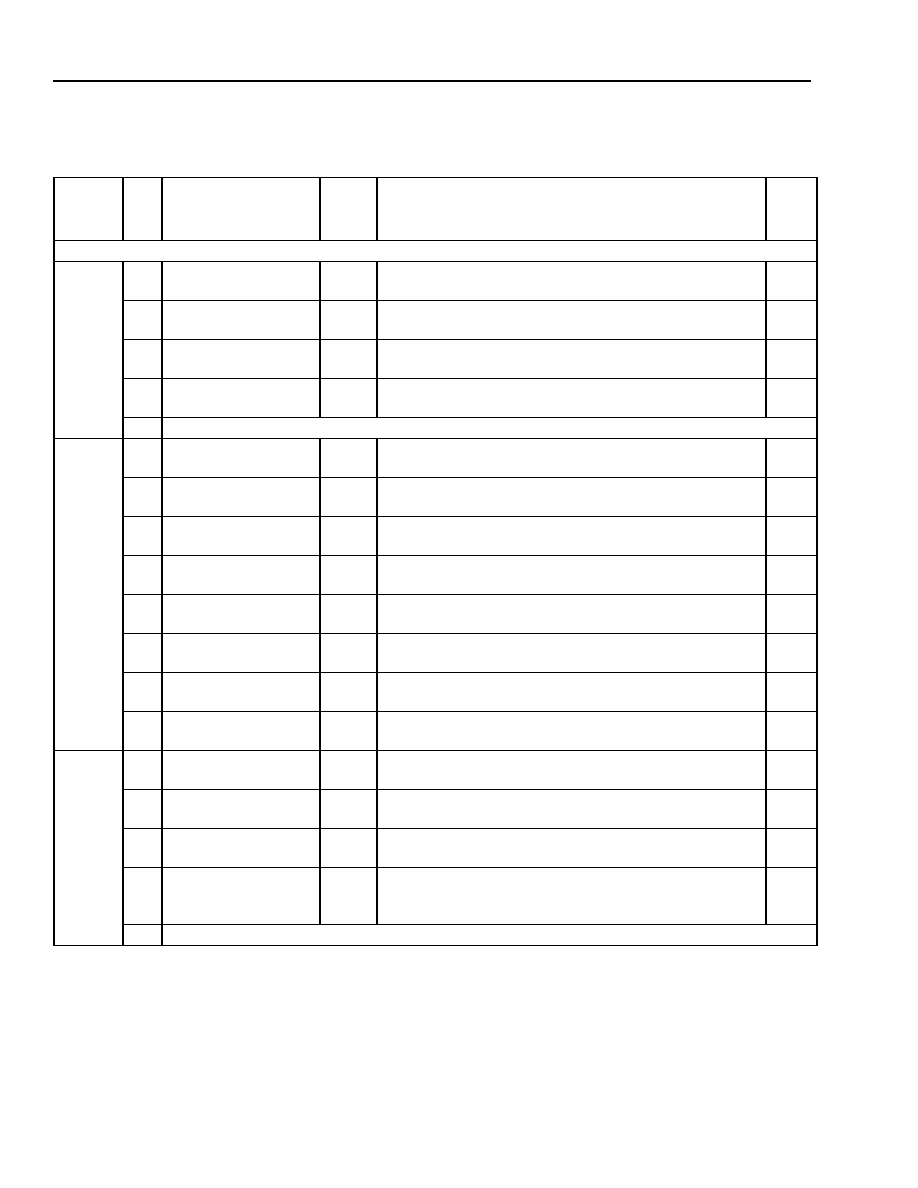
46
Agere Systems Inc.
Data Sheet
June 2003
TTSV02622 STS-24 Backplane Transceiver
Channel Register Blocks (continued)
2E, 46
0
ES OVERFLOW
FLAGS 3
IAREG These are the ELASTIC STORE OVERFLOW alarm
flags.
0
1
ES OVERFLOW
FLAGS 6
IAREG These are the ELASTIC STORE OVERFLOW alarm
flags.
0
2
ES OVERFLOW
FLAGS 9
IAREG These are the ELASTIC STORE OVERFLOW alarm
flags.
0
3
ES OVERFLOW
FLAGS 12
IAREG These are the ELASTIC STORE OVERFLOW alarm
flags.
0
[7:4]
Reserved.
2F, 47
0
ES OVERFLOW
FLAGS 1
IAREG These are the ELASTIC STORE OVERFLOW alarm
flags.
0
1
ES OVERFLOW
FLAGS 4
IAREG These are the ELASTIC STORE OVERFLOW alarm
flags.
0
2
ES OVERFLOW
FLAGS 7
IAREG These are the ELASTIC STORE OVERFLOW alarm
flags.
0
3
ES OVERFLOW
FLAGS 10
IAREG These are the ELASTIC STORE OVERFLOW alarm
flags.
0
4
ES OVERFLOW
FLAGS 2
IAREG These are the ELASTIC STORE OVERFLOW alarm
flags.
0
5
ES OVERFLOW
FLAGS 5
IAREG These are the ELASTIC STORE OVERFLOW alarm
flags.
0
6
ES OVERFLOW
FLAGS 8
IAREG These are the ELASTIC STORE OVERFLOW alarm
flags.
0
7
ES OVERFLOW
FLAGS 11
IAREG These are the ELASTIC STORE OVERFLOW alarm
flags.
0
30, 48
0
ENABLE/MASK ES
OVERFLOW FLAG 3
IEREG These are the AIS-P ALARM FLAGs.
0
1
ENABLE/MASK ES
OVERFLOW FLAG 6
IEREG These are the AIS-P ALARM FLAGs.
0
2
ENABLE/MASK ES
OVERFLOW FLAG 9
IEREG These are the AIS-P ALARM FLAGs.
0
3
ENABLE/MASK ES
OVERFLOW FLAG
12
IEREG These are the AIS-P ALARM FLAGs.
0
[7:4]
Reserved.
Register Descriptions
(continued)
Table 7. Register Description (continued)
Address
(hex)
Bit
Name
Type
Description
Reset
Value
(hex)

Agere Systems Inc.
47
Data Sheet
June 2003
TTSV02622 STS-24 Backplane Transceiver
Channel Register Blocks (continued)
31, 49
0
ENABLE/MASK ES
OVERFLOW FLAG 1
IEREG These are the AIS-P ALARM FLAGs.
0
1
ENABLE/MASK ES
OVERFLOW FLAG 4
IEREG These are the AIS-P ALARM FLAGs.
0
2
ENABLE/MASK ES
OVERFLOW FLAG 7
IEREG These are the AIS-P ALARM FLAGs.
0
3
ENABLE/MASK ES
OVERFLOW FLAG
10
IEREG These are the AIS-P ALARM FLAGs.
0
4
ENABLE/MASK ES
OVERFLOW FLAG 2
IEREG These are the AIS-P ALARM FLAGs.
0
5
ENABLE/MASK ES
OVERFLOW FLAG 5
IEREG These are the AIS-P ALARM FLAGs.
0
6
ENABLE/MASK ES
OVERFLOW FLAG 8
IEREG These are the AIS-P ALARM FLAGs.
0
7
ENABLE/MASK ES
OVERFLOW FLAG 11
IEREG These are the AIS-P ALARM FLAGs.
0
32, 4A
[6:0]
LVDS LINK B1
PARITY ERROR
COUNTER
COUN
TER
7-bit count + overflow ≠ reset on read.
0
7
OVERFLOW
COUN
TER
--
0
33, 4B
[6:0]
LOF COUNTER
COUN
TER
7-bit count + overflow ≠ reset on read.
0
7
OVERFLOW
COUN
TER
--
0
34, 4C
[6:0]
A1/A2 FRAME
ERROR COUNTER
COUN
TER
7-bit count + overflow ≠ reset on read.
0
7
OVERFLOW
COUN
TER
--
0
Register Descriptions
(continued)
Table 7. Register Description (continued)
Address
(hex)
Bit
Name
Type
Description
Reset
Value
(hex)
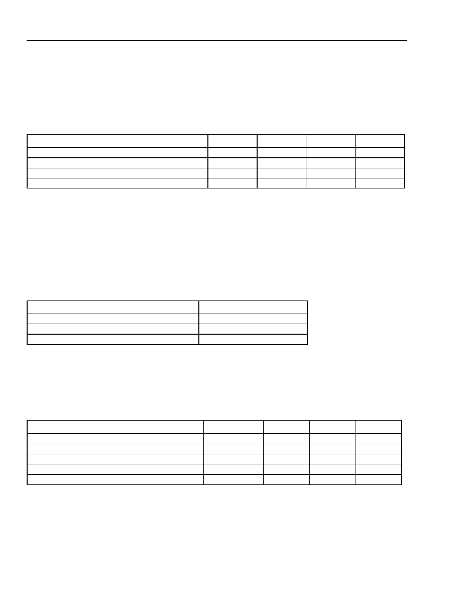
48
Agere Systems Inc.
Data Sheet
June 2003
TTSV02622 STS-24 Backplane Transceiver
Absolute Maximum Ratings
Stresses in excess of the absolute maximum ratings can cause permanent damage to the device. These are abso-
lute stress ratings only. Functional operation of the device is not implied at these or any other conditions in excess
of those given in the operational sections of the data sheet. Exposure to absolute maximum ratings for extended
periods can adversely affect device reliability.
Table 8. Absolute Maximum Ratings
Handling Precautions
Although electrostatic discharge (ESD) protection circuitry has been designed into this device, proper precautions
must be taken to avoid exposure to ESD and electrical overstress (EOS) during all handling, assembly, and test
operations. Agere employs both a human-body model (HBM) and a charged-device model (CDM) qualification
requirement in order to determine ESD-susceptibility limits and protection design evaluation. ESD voltage thresh-
olds are dependent on the circuit parameters used in each of the models, as defined by JEDEC's JESD22-A114
(HBM) and JESD22-C101 (CDM) standards.
Table 9. Handling Precautions
Recommended Operating Conditions
The following tables list the voltages required for proper operation of the TTSV02622 device, along with their toler-
ances.
Table 10. Recommended Operating Conditions
Parameter
Symbol
Min
Max
Unit
Power Supply Voltage with Respect to Ground
V
DD
--
4.2
V
Input Voltages
V
IN
Vss ≠ 0.3
5.5
V
Power Dissipation
P
D
--
--
mW
Storage Temperature Range
T
stg
--
--
∞C
Model
Voltage
Minimum HBM Threshold
2000 V
Minimum CDM on the corner pins only and the LU
1000 V
Minimum CDM on all other pins
500 V
Parameter
Symbol
Min
Max
Unit
Power Supply Voltage with Respect to Ground
V
DD
3.14
3.47
V
Input High Voltage (TTL input)
V
IH
2.0
5.5
V
Input Low Voltage (TTL input)
V
IL
--
0.8
V
Input Voltages
V
IN
Vss ≠ 0.3
5.5
V
Junction Temperature
T
j
≠40
125
∞C
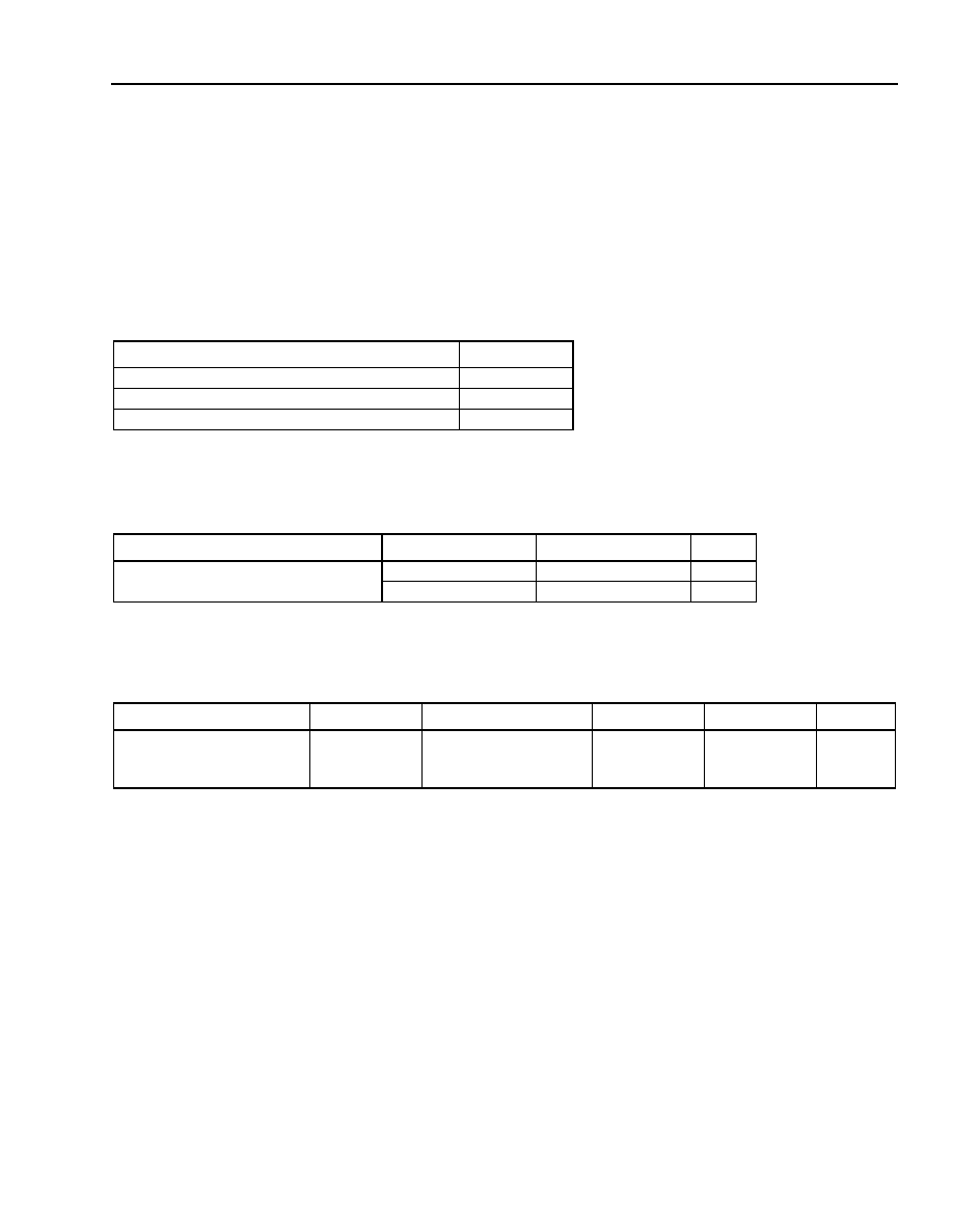
Agere Systems Inc.
49
Data Sheet
June 2003
TTSV02622 STS-24 Backplane Transceiver
Thermal Characteristics
The TTSV02622 is a 5.86 mm x 6.49 mm die in the 272-pin PBGA (2-layer BGA). For thermal characteristics, the
following values should be used:
s
Jc = 15.38 ∞C/W
s
Jb = 25.09 ∞C/W
s
Ja = 31.92 ∞C/W
s
Jt = 1.00 ∞C/W
Table 11. Thermal Resistance--Junction to Ambient
Power Consumption (Advance)
Table 12. Power Consumption (Advance)
Electrical Characteristics
Table 13. LVTTL Electrical Characteristics
Propagation Delay Specifications
1. Delay in 77.78 MHz system clocks from the Tx line input to the LVDS backplane output is seven clocks (see
Figure 15, Transmitter Transport Delay on page 56).
2. Propagation delay from a change on the PROT SW pin to a protection switch activity:
s
NORM to HI-Z:
-- Five rising edges of SYS_CLK from assertion of the PROT_SW_A/C pins to the data changing to HI-Z.
s
NORM to MUX switch:
-- Eight rising edges of SYS_CLK from assertion of the PROT_SW_A/C pins to the data changing from stream
A to B. (See Figure 17 on page 58.)
3. Propagation delay from A1 STS-1 #1 arriving at LVDS input to RX_TOH_FP is 56 SYS_CLKs, and
six TOH_CLKs. This will vary by ±14 SYS_CLKs, 12 each way for the FIFO alignment, and ±2 SYS_CLKs due
to the variability in the clock recovery of the CDR macro.
4. Delay from CS_N going active (CPU write access to reset the chip) to reset being deactivated and CPU inter-
face being ready to handle another access is nine SYS_CLKs.
Air Speed in Linear Feet per Minute (LFPM)
Ja (∞C/W)
JEDEC Standard Natural Convection
29.48
200
28.65
500
27.42
Parameter
Condition
Max
Unit
2 Channel
At 3.3 V
1.6
W
At 3.465 V
1.7
W
Parameter
Symbol
Test Conditions
Min
Max
Unit
Output Voltage:
Low
High
V
OL
V
OH
--
--
--
2.4
0.4
--
V
V

50
Agere Systems Inc.
Data Sheet
June 2003
TTSV02622 STS-24 Backplane Transceiver
LVDS I/O
The LVDS buffers are compatible with IEEE
Æ
1596.3 and EIA
Æ
/TIA-644. However, not all specs listed in the
IEEE document pertained to just the buffer itself; rather they are system-level specifications. LVDS buffers in the
TTSV02622 are compliant to all parts of the IEEE 1596.3 spec that pertain to silicon implementation.
Unused inputs will not oscillate when they are open or short-circuited. Both P and N terminals of an input pad should
not be held at voltages lower than 2.4 V. A 100
resistor is included internally, so no board termination is necessary.
Unused outputs do not need any termination, since they are terminated internally. This is valid for both powerdown
mode and functional mode.
The pin LVDS_EN is an enable that overrides any processor control over the powerdown of the LVDS input and
output pads. This is for boundary scan use only, and should be pulled high during functional mode. For boundary
scan, LVDS_EN = 0 and HIZ_N = 1.
For board layout, LVDS traces should be run on controlled impedance layers, and should be specified as 50
line-
to-ground. The LVDS buffers support point-to-point connections. They are not intended for bussed implementations.
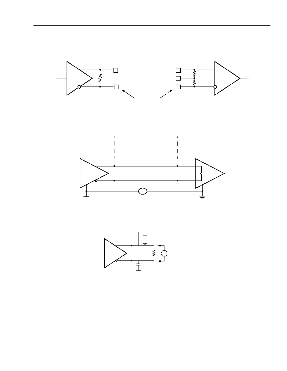
Agere Systems Inc.
51
Data Sheet
June 2003
TTSV02622 STS-24 Backplane Transceiver
LVDS I/O
(continued)
Figure 11. LVDS Driver and Receiver and Associated Internal Components
Figure 12. LVDS Driver and Receiver
Figure 13. LVDS Driver
LVDS DRIVER
50
50
LVDS RECEIVER
CENTER TAP
DEVICE PINS
100
EXTERNAL
V
GPD
V
OA
V
OB
V
IA
V
IB
A
B
AA
BB
DRIVER INTERCONNECT RECEIVER
V
OA
A
V
OB
B
C
A
C
B
R
LOAD
V
OD
= (V
OA
≠ V
OB
)
V
52
Agere Systems Inc.
Data Sheet
June 2003
TTSV02622 STS-24 Backplane Transceiver
LVDS I/O
(continued)
LVDS Receiver Buffer Capabilities
A disabled or unpowered LVDS receiver can withstand a driving LVDS transmitter over the full range of driver oper-
ating range, for an unlimited period of time, without being damaged. Table 16 illustrates LVDS driver dc data,
Table 17 the ac data, and Table 14 on page 52 and Table 15 on page 52 the LVDS receiver data.
Table 14. LVDS Receiver dc Data*
* V
DD
= 3.1 V--3.5 V, 0 ∞C--125 ∞C, slow--fast process.
Buffer will not produce output transition when input is open-circuited.
Table 15. LVDS Receiver ac Data*
* V
DD
= 3.1 V--3.5 V, 0 ∞C--125 ∞C, slow--fast process.
Parameter
Symbol
Conditions
Min
Typ
Max
Unit
Input Voltage Range, V
IA
or V
IB
(Common-Mode Voltage)
V
I
|V
GPD
| < 925 mV
dc ≠ 1 MHz
0
1.2
2.4
V
Input Differential Threshold
(Differential-Mode Voltage)
V
IDTH
|V
GPD
| < 925 mV
800 MHz
≠100
--
100
mV
Input Differential Hysteresis
V
HYST
(+V
IDTHH
) ≠ (≠V
IDTHL
)
--
--
--
mV
Receiver Differential Input Impedance
R
IN
With Build-In Termination,
Center-Tapped
80
100
120
Parameter
Symbol
Conditions
Min
Max
Unit
Rise Time (20%--80%)
t
R
C
L
= 1.5 pF
50
150
ps
Fall Time (80%--20%)
t
F
C
L
= 1.5 pF
50
150
ps
Agere Systems Inc.
53
Data Sheet
June 2003
TTSV02622 STS-24 Backplane Transceiver
LVDS I/O
(continued)
Table 16. LVDS Driver dc Data*
* V
DD
= 3.1 V--3.5 V, 0 ∞C--125 ∞C, slow--fast process.
External references selected (CNT = 0), REF10 = 1.0 V ± 3%, REF14 = 1.4 V ± 3%.
Table 17. LVDS Driver ac Data*
* V
DD
= 3.1 V--3.5 V, 0 ∞C--125 ∞C, slow--fast process.
Table 18. LVDS Driver Reference Data
Parameter
Symbol
Conditions
Min
Typ
Max
Unit
Output Voltage High, V
OA
or V
OB
V
OH
R
LOAD
= 100
± 1%
--
--
1.475
V
Output Voltage Low, V
OA
or V
OB
V
OL
R
LOAD
= 100
± 1%
0.925
--
--
V
Output Differential Voltage
|V
OD
|
R
LOAD
= 100
± 1%
0.25
--
0.45
V
Output Offset Voltage
V
OS
R
LOAD
= 100
± 1%
1.125
--
1.275
V
Output Impedance, Signal Ended
R
O
V
CM
= 1.0 V and 1.4 V
40
50
60
R
O
Mismatch Between A and B
R
O
V
CM
= 1.0 V and 1.4 V
--
--
10
%
Change in Differential Voltage
Between Complementary States
|
V
OD
|
R
LOAD
= 100
± 1%
--
--
25
mV
Change in Output Offset Voltage
Between Complementary States
VOS
R
LOAD
= 100
± 1%
--
--
25
mV
Output Current
I
SA
, I
SB
Driver Shorted to GND
--
--
24
mA
Output Current
I
SAB
Drivers Shorted Together
--
--
12
mA
Power-Off Output Leakage
|Ixa|, |Ixb|
V
DD
= 0 V
V
PAD
, V
PADN
= 0 V--3 V
--
--
30
µ
A
Parameter
Symbol
Conditions
Min
Max
Unit
V
OD
Fall Time, 80%--20%
t
F
Z
L
= 100
± 1%
C
PAD
= 3.0 pF, C
PADN
= 3.0 pF
100
200
ps
VOD Rise Time, 20%--80%
t
R
Z
L
= 100
± 1%
C
PAD
= 3.0 pF, C
PADN
= 3.0 pF
100
200
ps
Differential Skew
|t
PHLA
≠ t
PHLB
| or |T
PHLB
≠ T
PLHA
|
t
SKEW1
Any Differential Pair on Package
at the 50% Point of the Transition
--
50
ps
Parameter
Conditions
Min
Typ
Max
Unit
REF10 Voltage Range
--
0.95
1.0
1.05
V
REF14 Voltage Range
--
1.35
1.4
1.45
V
Nominal Input Current--
REF10 and REF14 Reference Inputs
--
--
10
--
µ
A
54
Agere Systems Inc.
Data Sheet
June 2003
TTSV02622 STS-24 Backplane Transceiver
Clock and Data Recovery (CDR)
The following specifications are in reference to the clock and data recovery macro that is used for the backplane
interface on the TTSV02622 chip.
Input Data
s
622 Mbits/s scrambled data stream conforms to SONET STS-12 and SDH STM-4 data format using either a PN7
or PN9 sequence. The PN7 characteristic is 1+ x
6
+ x
7
and The PN9 characteristic is 1+ x
4
+ x
9
.
s
Longest stream of nontransitional 622 Mbits/s input data is 60 bits. This sequence should not occur more often
than once per minute.
s
Input signal phase change of no more than 100 ps over 200 ns time interval, which translates to a frequency
change of 500 ppm.
s
Eye opening greater than 0.4 UIp-p. Unit interval for 622 Mbits/s is 1.6075 ns.
Jitter Tolerance
Table 19. Jitter Tolerance
Generated Output Jitter
s
0.2 UIp-p from 250 kHz to 5 MHz as measured on a spectrum analyzer.
PLL
s
Loop bandwidth of less than 6 MHz.
s
Jitter peaking of less than 2 dB.
s
Minimum powerup reset duration of 10 µs.
s
Maximum lock acquisition of less than 1 ms.
s
External 10 k
resistor to ground required.
Input Reference Clock
s
Frequency deviation of no more than ± 20 ppm.
s
Phase change of no more than 100 ps in 200 ns.
s
Time interval that translates to a frequency change of 500 ppm.
s
Input reference clock of 77.76 MHz.
Frequency
UIp-p
250 kHz
0.6
25 kHz
6.0
2 kHz
60

Agere Systems Inc.
55
Data Sheet
June 2003
TTSV02622 STS-24 Backplane Transceiver
Timing Characteristics
All timing numbers are measured relative to 1.5 V.
All outputs are driving 35 pF maximum, 5 pF minimum, except DB pins which drive 100 pF.
Figure 14. Input Parallel Port Timing
Table 20. Input Parallel Port Timing Requirements
Symbol
Parameter
Min
Typ
Max
Unit
T
P
Clock Period
--
12.86
--
ns
T
L
Clock Low Time
5.1
--
7.7
ns
T
H
Clock High Time
5.1
--
7.7
ns
T
SU
Data Setup Time
3
--
--
ns
T
HD
Data Hold Time
0
--
--
ns
T
L
T
P
T
H
T
SU
T
HD
FIRST A1 OF STS-1 #1
SYS_CLK
SYS_FP
INPUT BUS
56
Agere Systems Inc.
Data Sheet
June 2003
TTSV02622 STS-24 Backplane Transceiver
Timing Characteristics
(continued)
Figure 15. Transmitter Transport Delay
Table 21. Transmitter Transport Delay Timing Requirements
Notes:
LVDS data transmitted MSB first.
Min/max variation due to clock phase selected in clock recovery block.
Symbol
Parameter
Typ
Unit
T
PROP
Number of Clocks of Delay from Parallel Bus Input to LVDS Output
7
SYS_CLK
T
PROP
A1 OF STS-1 #1
SYS_CLK
SYS_FP
PARALLEL
DATA INPUT
BUS
LVDS
DATA
OUT
MSB OF FIRST A1
OF STS-1 #1
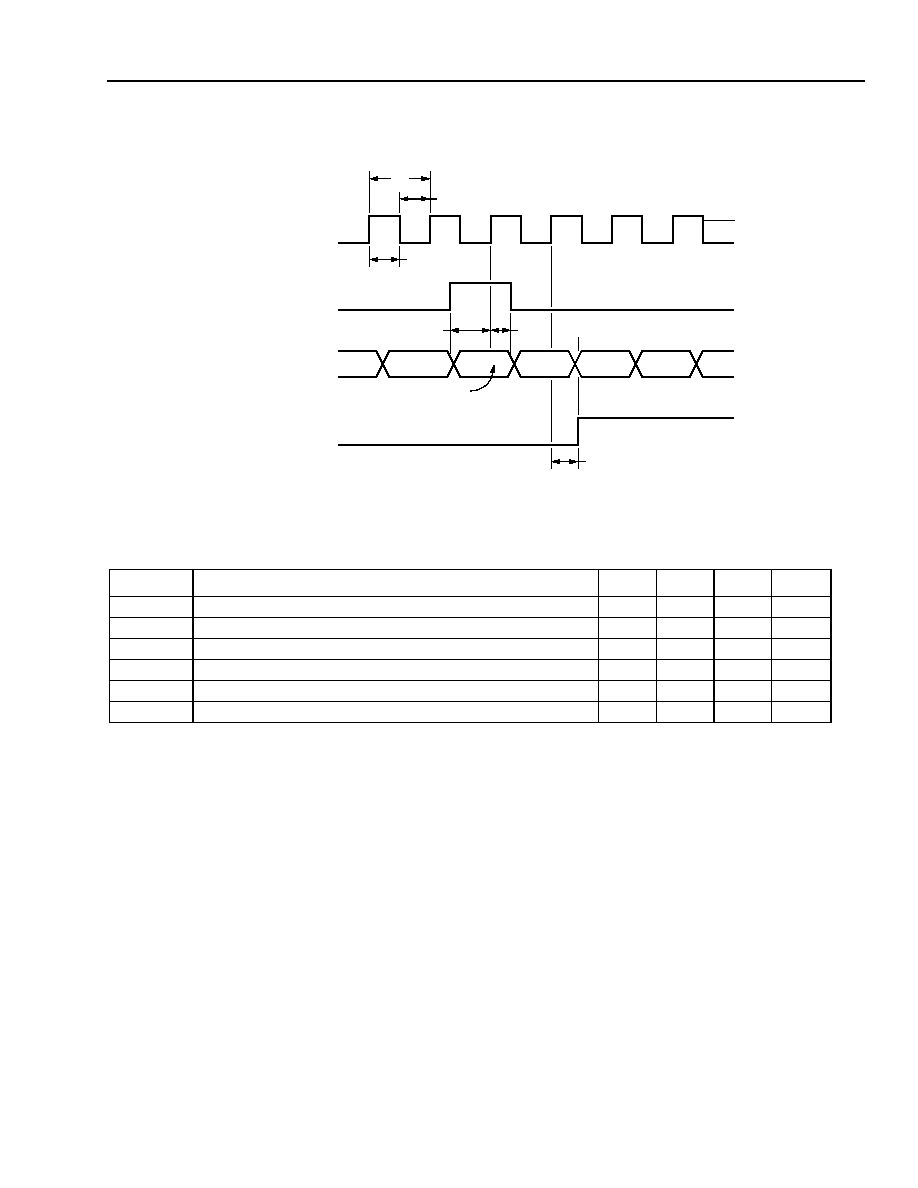
Agere Systems Inc.
57
Data Sheet
June 2003
TTSV02622 STS-24 Backplane Transceiver
Timing Characteristics
(continued)
Figure 16. Output Parallel Port Timing
Table 22. Output Parallel Port Timing Requirements
Note: Min T
CO
number is calculated based on 5 pF load. Max T
CO
is calculated based on 35 pF load.
Symbol
Parameter
Min
Typ
Max
Unit
T
P
Clock Period
--
12.86
--
ns
T
L
Clock Low Time
5.1
6.43
7.7
ns
T
H
Clock High Time
5.1
6.43
7.7
ns
T
SU
Data Setup Time
3
--
--
ns
T
HD
Data Hold Time
0
--
--
ns
T
CO
Clock to Output Time of Data, Parity, SPE, and C1J1 Pins
1.3
--
7
ns
T
L
T
P
T
H
T
SU
T
HD
SYS_CLK
LINE_FP
OUTPUT BUS
FIRST A1 OF STS-1 #1
T
CO
PARITY,
SPE,
C1J1 PINS

58
Agere Systems Inc.
Data Sheet
June 2003
TTSV02622 STS-24 Backplane Transceiver
Timing Characteristics
(continued)
Figure 17. Protection Switch Timing
Table 23. Protection Switch Timing Requirements
Notes:
Output bus refers to 8 bits data, 1 bit parity, 1 bit SPE, and 1 bit C1J1.
Channel A refers to whether the PROT_SW_A pins that are activated. For example, if the PROT_SW_A pin is activated, the timing diagram for
output bus A refers to output bus A.
Min/max variation on T
RT
and T
HIZ
due to clock phase selected in clock recovery block.
Symbol
Parameter
Min
Typ
Max
Unit
T
TR
Transport Delay from Latching of PROT_SW_A to Actual Data
Switch
--
8
--
Leading edge
SYS_CLKs
T
HIZ
Transport Delay from Latching of PROT_SW_A to Actual Data
HI-Z
--
5
--
Leading edge
SYS_CLKs
T
CH
Propagation Delay from SYS_CLK to HI_Z of Output Bus
--
--
25
ns
T
SU
Setup Time Required from Change in PROT_SW_A to Rising
SYS_CLK
3
--
--
ns
T
HD
Hold Time Required from Rising SYS_CLK to Change in
PROT_SW_A
0
--
--
ns
SYS_CLK
PROT_SW_A
OUTPUT BUS*
A
SYS_CLK
OUTPUT BUS
A & B
CH A
CH A
CH A
CH A
CH B
T
TR
T
SU
T
HD
T
HIZ
T
CH
CH A & B
CH A & B
CH A & B
CH A & B

Agere Systems Inc.
59
Data Sheet
June 2003
TTSV02622 STS-24 Backplane Transceiver
Timing Characteristics
(continued)
Figure 18. Input Serial Port Timing
Table 24. Input Serial Port Timing Requirements
Symbol
Parameter
Min
Typ
Max
Unit
T
P
Clock Period
12.86
--
40
ns
T
HI
Clock High Time
5.1
--
24
ns
T
LO
Clock Low Time
5.1
--
24
ns
T
S
Data Setup Time
3
--
--
ns
T
H
Data Hold Time
0
--
--
ns
SYS_CLK
SYS_FP
INPUT
TOH_CLK
1044 bytes SPE
TX TOH_
PARALLEL
BUS
TOH SERIAL
INPUT
CLK_ENA
ROW #1
ROW #9
36 bytes TOH
1044 bytes SPE
36 bytes TOH
GUARD BAND
(4 TOH CLK)
GUARD BAND
(4 TOH CLK)
T
S
T
H
MSBIT(7)
OF B1 BYTE
STS-1 #1
BIT 6
OF B1 BYTE
STS-1 #1
T
P
T
HI
T
LO
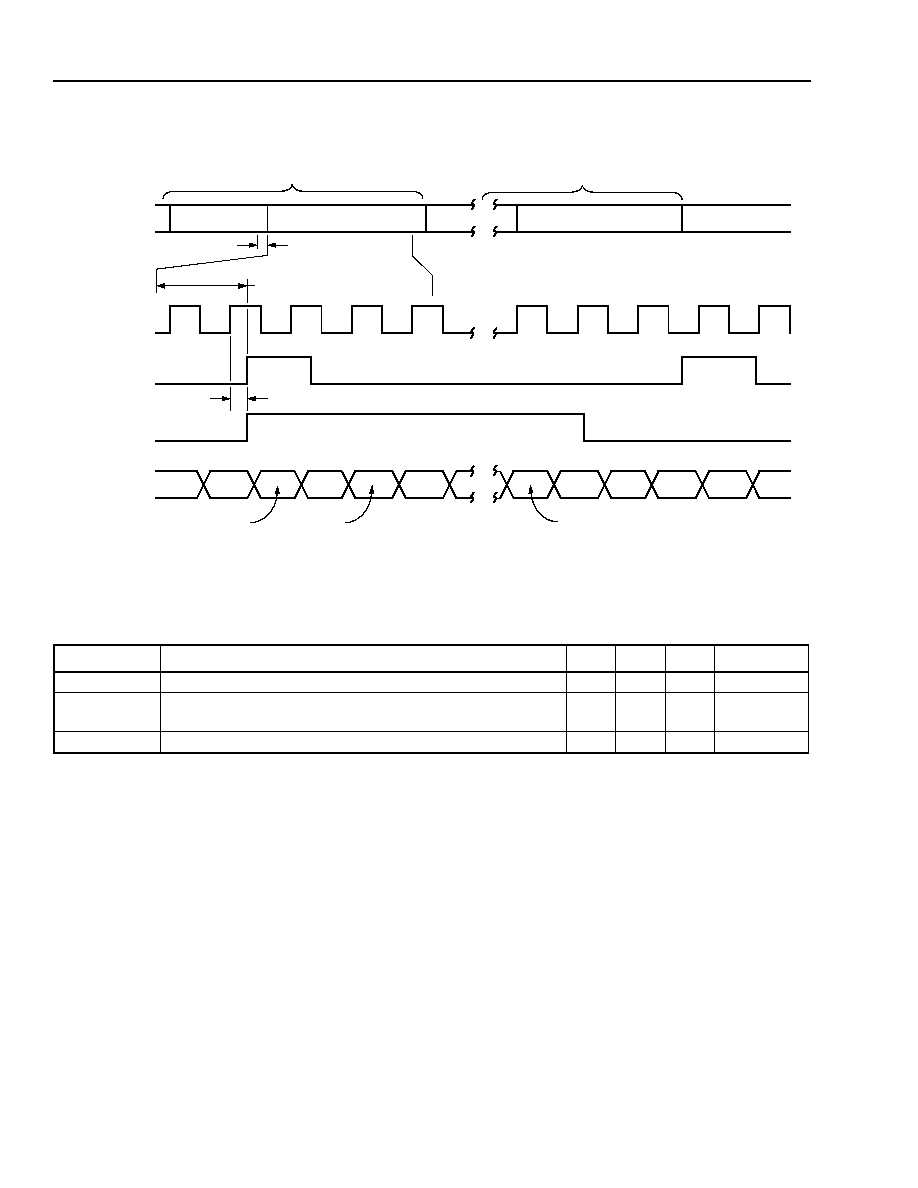
60
Agere Systems Inc.
Data Sheet
June 2003
TTSV02622 STS-24 Backplane Transceiver
Timing Characteristics
(continued)
Figure 19. Output Serial Port Timing
Table 25. Output Serial Port Timing Requirements
Note: The total delay from A1 STS-1 #1 arriving at LVDS input to RX_TOH_FP is 56 SYS_CLKs, and 6 TOH_CLKs. This will vary by
±14 SYS_CLKs, 12 each way for the FIFO alignment, and ± 2 SYS_CLKs due to the variability in the clock recovery of the CDR macro.
Symbol
Parameter
Min
Typ
Max
Unit
T
CO
Data Clock to Out
2
--
8
ns
T
TRANS_SYS
Delay from First A1 LVDS Serial Input to Transfer to
TOH_CLK
44
56
68
SYS_CLKs
T
TRANS_TOH
Delay from Transfer to TOH_CLK to RX_TOH_FP
--
6
--
TOH_CLKs
RX TOH FP
TOH_CLK
1044 bytes SPE
RX TOH
INPUT LVDS
SERIAL 622 Mbits/s
DATA
TOH SERIAL
OUTPUT
CLK ENA
ROW #1
ROW #9
36 bytes TOH
1044 bytes SPE
36 bytes TOH
MSBIT(7)
OF A1 BYTE
STS-1 #1
BIT 6
OF A1 BYTE
STS-1 #1
T
TRANS_SYS
T
TRANS_TOH
T
CO
BIT 0
OF A1 BYTE
STS-1 #1
STS-1 #1
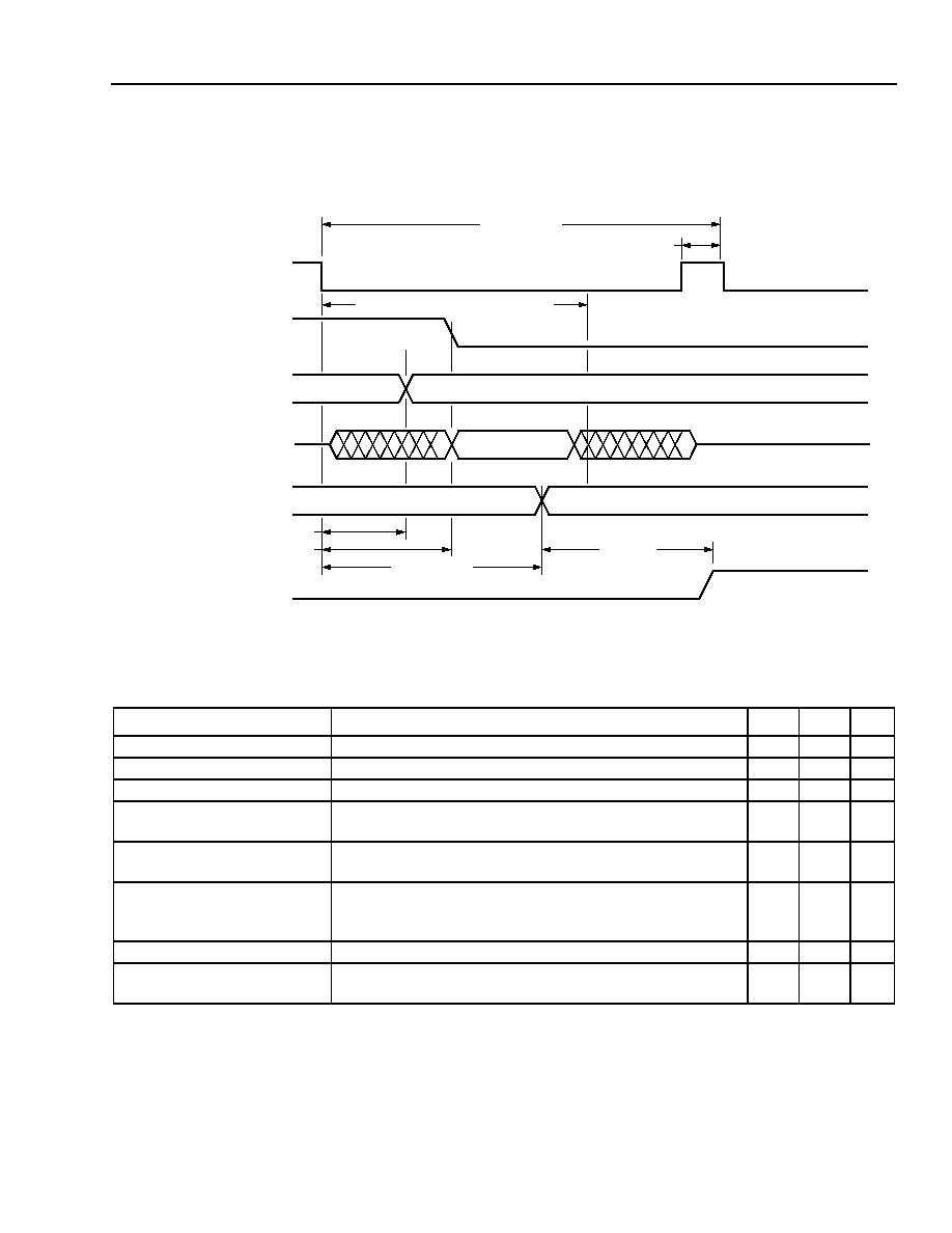
Agere Systems Inc.
61
Data Sheet
June 2003
TTSV02622 STS-24 Backplane Transceiver
Timing Characteristics
(continued)
CPU Interface Timing
Figure 20. Write Transaction
Table 26. Write Transaction Timing Requirements
Symbol
Parameter
Min
Max
Unit
T
PULSE
Minimum Pulse Width for CS_N
5
--
ns
T
ADDR_MAX
Maximum Time from Negative Edge of CS_N to ADDR Valid
--
18
ns
T
DAT_MAX
Maximum Time from Negative Edge of CS_N to Data Valid
--
25
ns
T
RD_WR_MAX
Maximum Time from Negative Edge of CS_N to Negative
Edge of RD_WR_N
--
26
ns
T
WRITE_MAX
Maximum Time from Negative Edge of CS_N to Contents of
Internal Register Latching DB[7:0]
--
60
ns
T
ACCESS_MIN
Minimum Time Between a Write Cycle (falling edge of
CS_N) and Any other Transaction (read or write, at falling
edge of CS_N)
60
--
ns
T
INT_MAX
Maximum Time from Register FF to Pad
--
20
ns
T
RD_WR_N
,
ADDR_MAX
,
DB_HOLD
Minimum Hold Time that RD_WR_N, ADDR, and DB Must
Be Held Valid from the Negative Edge of CS_N
57
--
ns
DATA VALID
T
ACCESS_MIN
T
PULSE
OLD VALUE
NEW VALUE
T
WRITE_MAX
T
INT_MAX
T
ADDR_MAX
T
DAT_MAX,
T
RD_WR_MAX
CS_N
RD_WR_N
ADDR[6:0]
INTERNAL REGISTER
(SYS_CLK
DOMAIN)
T
RD_WR_N, ADDR_MAX, DB_HOLD
DB[7:0]
INT_N
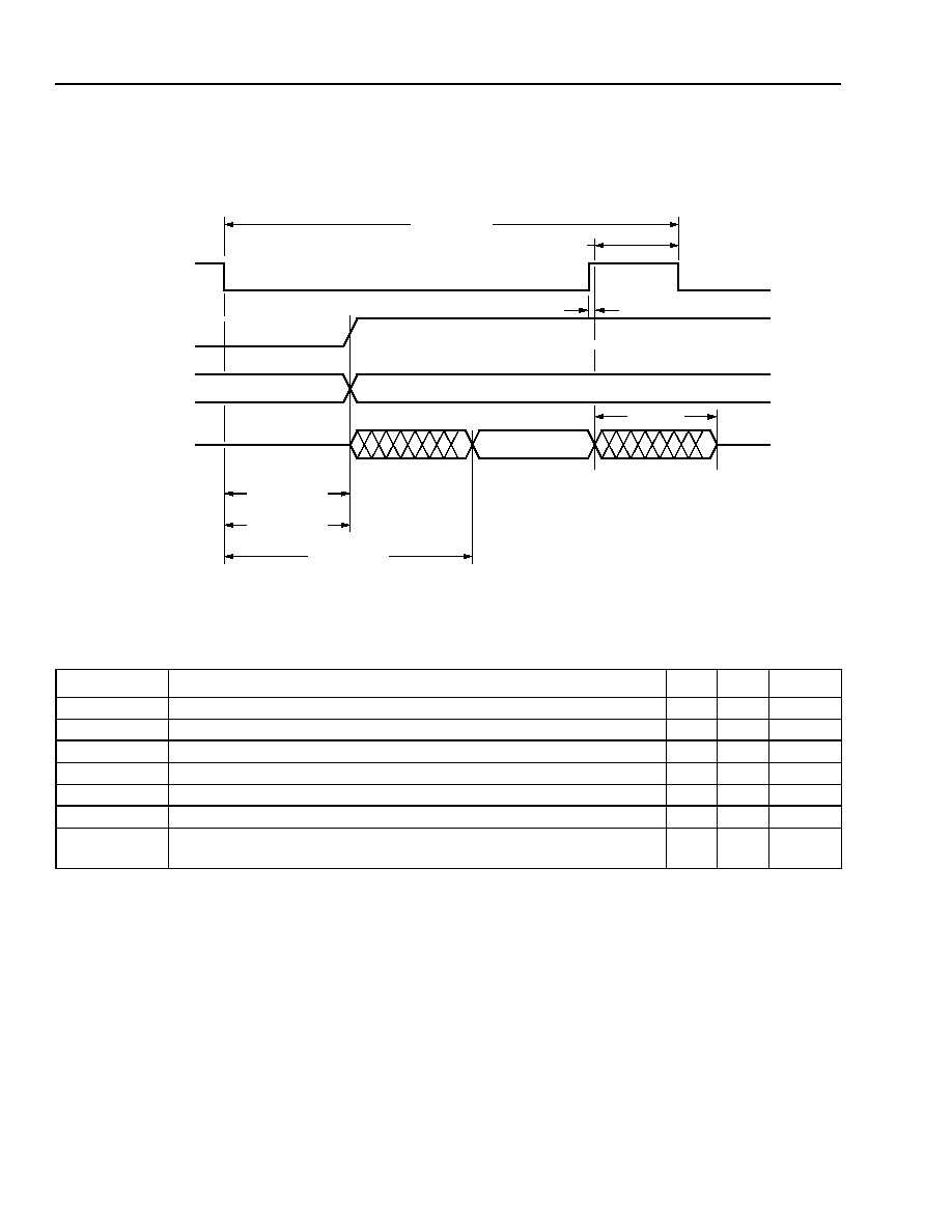
62
Agere Systems Inc.
Data Sheet
June 2003
TTSV02622 STS-24 Backplane Transceiver
Timing Characteristics
(continued)
CPU Interface Timing
(continued)
Figure 21. Read Transaction
Table 27. Read Transaction Timing Requirements
Symbol
Parameter
Min
Max
Unit
T
PULSE
Minimum Pulse Width for CS_N
5
--
ns
T
ADDR_MAX
Maximum Time from Negative Edge of CS_N to Addr Valid
--
5
ns
T
RD_WR_MAX
Maximum Time from Negative Edge of CS_N to RD_WR_N Rising
--
5
ns
T
DATA_MAX
Maximum Time from Negative Edge of CS_N to Data Valid on DB Port
--
56
ns
T
HIZ_MAX
Maximum Time from Rising Edge of CS_N to DB Port Going HI-Z
--
12
ns
T
DH
Data Hold Time After CS_N Is Deasserted
0
--
ns
T
ACCESS_MIN
Minimum Time Between a Read Cycle (falling edge of CS_N) and Any
Other Transaction (read or write, at falling edge of CS_N)
60
--
ns
DATA VALID
T
ACCESS_MIN
T
PULSE
T
DATA_MAX
CS_N
RD_WR_N
ADDR[6:0]
T
HIZ_MAX
T
ADDR_MAX
T
RD_WR_MAX
DB[7:0]
T
DH

Agere Systems Inc.
63
Data Sheet
June 2003
TTSV02622 STS-24 Backplane Transceiver
Outline Diagram
272-Pin PBGA
Dimensions are in millimeters.
0.36
±
0.04
1.17
±
0.05
2.13
±
0.19
SEATING PLANE
SOLDER BALL
0.60
±
0.10
0.20
PWB
MOLD
COMPOUND
27.00
±
0.20
27.00
±
0.20
24.00
+0.70
≠0.00
24.00
+0.70
≠0.00
A1 BALL
IDENTIFIER ZONE
A
B
C
D
E
F
G
H
J
K
L
M
Y
N
P
R
T
U
V
W
1 2 3 4 5 6 7 8 9 10
11
12
13
14
15
16
17
18
20
19
CENTER ARRAY
FOR THERMAL
ENHANCEMENT
(OPTIONAL)
19 SPACES @ 1.27 = 24.13
A1 BALL
CORNER
19 SPACES
@ 1.27 = 24.13
0.75
±
0.15

Data Sheet
June 2003
TTSV02622 STS-24 Backplane Transceiver
Copyright © 2003 Agere Systems Inc.
All Rights Reserved
June 2003
DS02-340SONT
Agere Systems Inc. reserves the right to make changes to the product(s) or information contained herein without notice. No liability is assumed as a result of their use or application. Agere,
Agere Systems, and the Agere Logo are trademarks of Agere Systems Inc.
For additional information, contact your Agere Systems Account Manager or the following:
INTERNET:
http://www.agere.com
E-MAIL:
docmaster@agere.com
N. AMERICA: Agere Systems Inc., Lehigh Valley Central Campus, Room 10A-301C, 1110 American Parkway NE, Allentown, PA 18109-9138
1-800-372-2447, FAX 610-712-4106 (In CANADA: 1-800-553-2448, FAX 610-712-4106)
ASIA:
Agere Systems Hong Kong Ltd., Suites 3201 & 3210-12, 32/F, Tower 2, The Gateway, Harbour City, Kowloon
Tel. (852) 3129-2000, FAX (852) 3129-2020
CHINA: (86) 21-5047-1212 (Shanghai), (86) 755-25881122 (Shenzhen)
JAPAN: (81) 3-5421-1600 (Tokyo), KOREA: (82) 2-767-1850 (Seoul), SINGAPORE: (65) 6778-8833, TAIWAN: (886) 2-2725-5858 (Taipei)
EUROPE:
Tel. (44) 1344 296 400
Ordering Information
Device Code
Package
Temperature
Comcode
(Ordering Number)
TTSV02622V2-DB
272-pin PBGA
≠40 ∞C to +
125 ∞C
700034617