Document Outline
- Features
- Applications
- Description
- Applicable Documents and Specifications
- Pin Information
- Register Overview
- PCI Registers
- USB Registers
- Legacy Support Registers
- Connection Instructions
- Legacy Configuration
- Power Connection Recommendations
- Power Management Interface
- NAND Tree Mode
- Absolute Maximum Ratings
- Electrical Characteristics
- Physical Markings
- Outline Diagram
- Ordering Information
- List of Figures
- List of Tables
- Table 1 .�Numeric Pin Cross Reference
- Table 2 .�PCI Signals
- Table 3 .�USB Port Signals
- Table 4 .�Legacy Support Signals
- Table 5 .�Chip Test Signals
- Table 6 .�PCI Bus Configuration Memory Summary (Function 0)
- Table 7 . PCI Bus Configuration Memory Summary (Function 1)
- Table 8 . PCI Bus Configuration Memory Summary (Function 2)
- Table 9 . PCI Bus Configuration Memory Summary (Function 3)
- Table 10 . Vendor ID Register (00hĄ01h)
- Table 11 . Device ID Register (02hĄ03h)
- Table 12 . Command Register (04hĄ05h)
- Table 13 . Status Register (06hĄ07h)
- Table 14 . Revision ID Register (08h)
- Table 15 . Class Code Register (09hĄ0Bh)
- Table 16 . Cache Line Size Register (0Ch)
- Table 17 . Latency Timer Register (0Dh)
- Table 18 . Header Type Register (0Eh)
- Table 19 . BIST Register (0Fh)
- Table 20 . Base Address Register 0 (10hĄ13h)
- Table 21 . Base Address Register 1, 2, 3, 4, 5 (14hĄ17h), (18hĄ1Bh), (1ChĄ1Fh), (20hĄ23h), (24hĄ27h)
- Table 22 . Cardbus CIS Pointer Register (28hĄ2Bh)
- Table 23 . Subsystem Vendor ID Register (2ChĄ2Dh)
- Table 24 . Subsystem ID Register (2EhĄ2Fh)
- Table 25 . Expansion ROM Base Address Register (30hĄ33h)
- Table 26 . Capabilities Pointer Register (34h)
- Table 27 . Interrupt Line Register (3Ch)
- Table 28 . Interrupt Pin Register (3Dh)
- Table 29 . Min_Gnt Register (3Eh)
- Table 30 . Max_Lat Register (3Fh)
- Table 31 . SpecialĄSubsystem Write Capability (4Ch)
- Table 32 . Vendor ID Register (00hĄ01h)
- Table 33 . Device ID Register (02hĄ03h)
- Table 34 . Command Register (04hĄ05h)
- Table 35 . Status Register (06hĄ07h)
- Table 36 . Revision ID Register (08h)
- Table 37 . Class Code Register (09hĄ0Bh)
- Table 38 . Cache Line Size Register (0Ch)
- Table 39 . Latency Timer Register (0Dh)
- Table 40 . Header Type Register (0Eh)
- Table 41 . BIST Register (0Fh)
- Table 42 . Base Address Register 0 (10hĄ13h)
- Table 43 . Base Address Register 1, 2, 3, 4, 5 (14hĄ17h), (18hĄ1Bh), (1ChĄ1Fh), (20hĄ23h), (24hĄ27h)
- Table 44 . Cardbus CIS Pointer Register (28hĄ2Bh)
- Table 45 . Subsystem Vendor ID Register (2ChĄ2Dh)
- Table 46 . Subsystem ID Register (2EhĄ2Fh)
- Table 47 . Expansion ROM Base Address Register (30hĄ33h)
- Table 48 . Capabilities Pointer Register (34h)
- Table 49 . Interrupt Line Register (3Ch)
- Table 50 . Interrupt Pin Register (3Dh)
- Table 51 . Min_Gnt Register (3Eh)
- Table 52 . Max_Lat Register (3Fh)
- Table 53 . SpecialĄSubsystem Write Capability (4Ch)
- Table 54 . Vendor ID Register (00hĄ01h)
- Table 55 . Device ID Register (02hĄ03h)
- Table 56 . Command Register (04hĄ05h)
- Table 57 . Status Register (06hĄ07h)
- Table 58 . Revision ID Register (08h)
- Table 59 . Class Code Register (09hĄ0Bh)
- Table 60 . Cache Line Size Register (0Ch)
- Table 61 . Latency Timer Register (0Dh)
- Table 62 . Header Type Register (0Eh)
- Table 63 . BIST Register (0Fh)
- Table 64 . Base Address Register 0 (10hĄ13h)
- Table 65 . Base Address Register 1, 2, 3, 4, 5 (14hĄ17h), (18hĄ1Bh), (1ChĄ1Fh), (20hĄ23h), (24hĄ27h)
- Table 66 . Cardbus CIS Pointer Register (28hĄ2Bh)
- Table 67 . Subsystem Vendor ID Register (2ChĄ2Dh)
- Table 68 . Subsystem ID Register (2EhĄ2Fh)
- Table 69 . Expansion ROM Base Address Register (30hĄ33h)
- Table 70 . Capabilities Pointer Register (34h)
- Table 71 . Interrupt Line Register (3Ch)
- Table 72 . Interrupt Pin Register (3Dh)
- Table 73 . Min_Gnt Register (3Eh)
- Table 74 . Max_Lat Register (3Fh)
- Table 75 . SpecialĄSubsystem Write Capability (4Ch)
- Table 76 . Vendor ID Register (00hĄ01h)
- Table 77 . Device ID Register (02hĄ03h)
- Table 78 . Command Register (04hĄ05h)
- Table 79 . Status Register (06hĄ07h)
- Table 80 . Revision ID Register (08h)
- Table 81 . Class Code Register (09hĄ0Bh)
- Table 82 . Cache Line Size Register (0Ch)
- Table 83 . Latency Timer Register (0Dh)
- Table 84 . Header Type Register (0Eh)
- Table 85 . BIST Register (0Fh)
- Table 86 . Base Address Register 0 (10hĄ13h)
- Table 87 . Base Address Register 1, 2, 3, 4, 5 (14hĄ17h), (18hĄ1Bh), (1ChĄ1Fh), (20hĄ23h), (24hĄ27h)
- Table 88 . Cardbus CIS Pointer Register (28hĄ2Bh)
- Table 89 . Subsystem Vendor ID Register (2ChĄ2Dh)
- Table 90 . Subsystem ID Register (2EhĄ2Fh)
- Table 91 . Expansion ROM Base Address Register (30hĄ33h)
- Table 92 . Capabilities Pointer Register (34h)
- Table 93 . Interrupt Line Register (3Ch)
- Table 94 . Interrupt Pin Register (3Dh)
- Table 95 . Min_Gnt Register (3Eh)
- Table 96 . Max_Lat Register (3Fh)
- Table 97 . SpecialĄSubsystem Write Capability (4Ch)
- Table 98 . USB Operational Registers Summary
- Table 99 . HcRevision Register (00h)
- Table 100 . HcControl Register (04h)
- Table 101 . HcCommandStatus Register (08h)
- Table 102 . HcInterruptStatus Register (0Ch)
- Table 103 . HcInterruptEnable Register (10h)
- Table 104 . HcInterruptDisable Register (14h)
- Table 105 . HcHCCA Register (18h)
- Table 106 . HcPeriodCurrentED Register (1Ch)
- Table 107 . HcControlHeadED Register (20h)
- Table 108 . HcControlCurrentED Register (24h)
- Table 109 . HcBulkHeadED Register (28h)
- Table 110 . HcBulkCurrentED Register (2Ch)
- Table 111 . HcDoneHead Register (30h)
- Table 112 . HcFmInterval Register (34h)
- Table 113 . HcFmRemaining Register (38h)
- Table 114 . HcFmNumber Register (3Ch)
- Table 115 . HcPeriodicStart Register (40h)
- Table 116 . HcLSThreshold (44h)
- Table 117 . HcRhDescriptorA Register (48h)
- Table 118 . HcRhDescriptorB Register (4Ch)
- Table 119 . HcRhStatus Register (50h)
- Table 120 . HcRhPortStatus1 Register (54h)
- Table 121 . Legacy Support Registers
- Table 122 . Emulated Registers
- Table 123 . HceInput Register (104h)
- Table 124 . HceOutput Register (108h)
- Table 125 . HceStatus Register (10Ch)
- Table 126 . HceControl Register (100h)
- Table 127 . PCI Signaling Levels
- Table 128 . Test Mode Decodes
- Table 129 . USS-344 Support for Power Management States
- Table 130 . Capabilities Identifier (Cap_ID) Register
- Table 131 . Next Item Pointer Register
- Table 132 . Power Management Capabilities Register
- Table 133 . Power Management Control/Status Register
- Table 134 . Power Management Bridge Support Extensions
- Table 135 . Data Register
- Table 136 . Power Consumption/Dissipation Reporting
- Table 137 . NAND Tree
- Table 138 . Absolute Maximum Ratings
- Table 139 . Power Dissipation
- Table 140 . Clock and Reset Specifications
- Table 141 . 5 V and 3.3 V PCI Timing Parameters
- Table 142 . Full-Speed Source USB Electrical Characteristics
- Table 143 . Low-Speed Source USB Electrical Characteristics
- Table 144 . CLK48 Clock Specification
- Contact Us

Advance Data Sheet, Rev. 9
June 2001
USS-344
QuadraBus
TM
Four-Host PCI-to-USB OpenHCI Host Controller
Features
s
32-bit, 33 MHz PCI interface compliant with
PCI Local
Bus Specification Revision 2.2
s
Four downstream USB ports
s
Each USB port dedicated to providing full USB band-
width to the attached device
s
Full compliance with
Universal Serial Bus Specifica-
tion Revision 1.1
s
OpenHCI Open Host Controller Interface Specifica-
tion for USB Release 1.0a compatible
s
Fully compatible with
Microsoft Windows 98/95/Win-
dows NT
ģ
standard OpenHCI drivers
s
Fully compatible with
Mac
ģ
OS 8.5 and 8.6
s
Integrated dual-speed USB transceivers
s
3 V or 5 V switchable PCI signaling
s
Low-power mode and wake-up compatible with
PCI
Power Management Interface Specification Revision
1.1
s
Supports up to 127 devices per port
s
Supports peripheral hot swap and wake-up
s
Support for legacy keyboard and mouse
s
128-pin TQFP package
s
Full 12 Mbits/s bandwidth per port
s
Evaluation kit:
-- PCI card
-- Data sheet
s
0.25
Ķ
m technology
Applications
s
Seamless integration with 3 V or 5 V PCI-based com-
puter products
s
Supports all USB compliant devices and hubs
s
Simultaneous operation of multiple high-performance
devices
Description
The Agere Systems Inc. USS-344
QuadraBus provides
a single-chip four-host PCI-to-Universal Serial Bus
(USB) solution. The USS-344 interfaces directly to any
32-bit, 33 MHz PCI bus and is ideal for either onboard
applications or add-in card applications. It can easily be
configured to communicate in either a 3 V PCI environ-
ment or 5 V PCI environment simply by selecting the
appropriate communications voltage level on the VIO
input pin.
The USS-344 provides four downstream USB ports for
connectivity with any USB compliant device or hub. Full-
speed or low-speed peripherals are supported along
with all of the USB transfer types: control, interrupt,
bulk, or isochronous. The USS-344's OpenHCI compli-
ance offers significant USB performance benefits and
reduced CPU overhead compared to other USB UHCI
host controllers.
In addition, the USS-344 offers a significant perfor-
mance advantage over all other USB host controllers
(both UHCI and OHCI) by providing full USB bandwidth
to each port rather than sharing the USB bandwidth
over all ports. This results in an increase in the number
of devices which can feasibly be connected to a
computer system as well as ensuring high-bandwidth
devices, such as video cameras and audio devices, are
always provided with the high bandwidth they need
while other USB devices are in use.
The USS-344 is a multifunction PCI device with one
single-port USB host controller per PCI function. There
are four PCI functions in the USS-344 for a total of four
single-port USB host controllers. Each single-port host
controller provides the full USB bandwidth (12 Mbits/s)
for devices connected downstream of its port.
The USS-344 is fully compatible with the
Microsoft
Windows standard OpenHCI drivers. The USS-344
pinout is compatible with the future release of the Agere
USB 2.0 host controller.The USS-344 is a 3.3 V device
fabricated in 0.25
Ķ
m technology. Integrated dual-speed
USB transceivers enable a single-chip PCI-to-USB
solution. The USS-344 provides full support for legacy
PC peripherals as defined in the
OpenHCI Open Host
Controller Interface Specification for USB Release 1.0a.

Table of Contents
Contents
Page
USS-344
QuadraBus
Advance Data Sheet, Rev. 9
Four-Host PCI-to-USB OpenHCI Host Controller
June 2001
2
Agere Systems Inc.
Features .................................................................................................................................................................. 1
Applications ............................................................................................................................................................. 1
Description ............................................................................................................................................................... 1
Applicable Documents and Specifications ............................................................................................................... 4
Pin Information ........................................................................................................................................................ 4
Register Overview ................................................................................................................................................... 8
PCI Registers ........................................................................................................................................................ 12
PCI Function 0--Single-Port USB Host Controller 0 .......................................................................................12
PCI Function 1--Single-Port USB Host Controller 1 .......................................................................................16
PCI Function 2--Single-Port USB Host Controller 2 .......................................................................................20
PCI Function 3--Single-Port USB Host Controller 3 .......................................................................................24
USB Registers ....................................................................................................................................................... 28
Legacy Support Registers ..................................................................................................................................... 35
HceInput Register............................................................................................................................................35
HceOutput Register .........................................................................................................................................36
HceStatus Register..........................................................................................................................................36
HceControl Register ........................................................................................................................................37
Connection Instructions ......................................................................................................................................... 37
PCI Connection Instructions ............................................................................................................................37
USB Connection Instructions...........................................................................................................................38
Test Mode Connection Instructions .................................................................................................................38
Legacy Configuration ............................................................................................................................................. 40
Power Connection Recommendations .................................................................................................................. 41
Power Management Interface ............................................................................................................................... 42
Configuration Space Offset 50h.......................................................................................................................43
Configuration Space Offset 51h.......................................................................................................................43
Configuration Space Offset 52h.......................................................................................................................44
Configuration Space Offset 54h.......................................................................................................................44
Configuration Space Offset 56h.......................................................................................................................45
Configuration Space Offset 57h.......................................................................................................................45
Power Consumption/Dissipation Reporting .....................................................................................................45
NAND Tree Mode .................................................................................................................................................. 46
Absolute Maximum Ratings ................................................................................................................................... 48
Electrical Characteristics ....................................................................................................................................... 49
PCI Electrical Characteristics ..........................................................................................................................49
USB Electrical Characteristics.........................................................................................................................52
Physical Markings .................................................................................................................................................. 53
Outline Diagram ..................................................................................................................................................... 53
128-Pin TQFP..................................................................................................................................................53
Ordering Information .............................................................................................................................................. 54

Agere Systems Inc.
3
Advance Data Sheet, Rev. 9
June 2001
Four-Host PCI-to-USB OpenHCI Host Controller
USS-344
QuadraBus
Description
(continued)
5-7828.r1
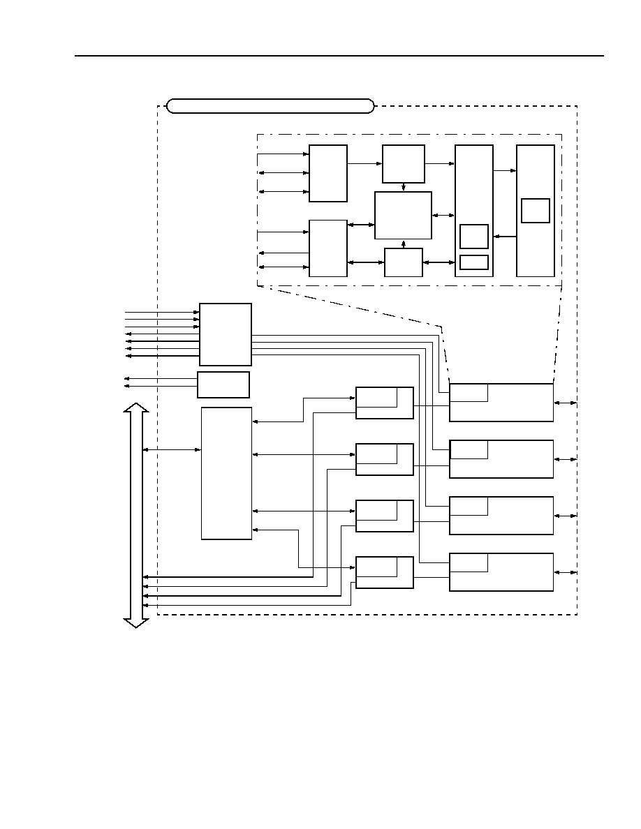
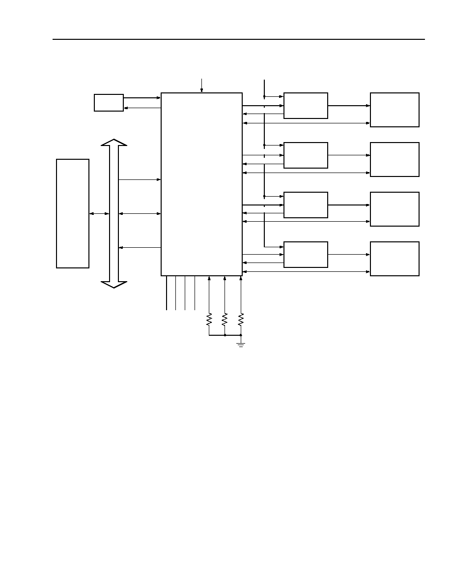
Figure 1. USS-344 Interconnection Diagram
USB HOST CONTROLLER
CORE 0
USB
USB
USB
USB
HCI
SLAVE
BLOCK
HCI
MASTER
BLOCK
USB
STATE
CONTROL
LIST
PROCESSOR
BLOCK
FIFO
ADDRESS
DATA
CONTROL
DATA
ADDRESS/
CONTROL
DATA
ROOT
HUB
AND
HOST
SIE
HSIE
S/M
DPLL
TX
RX
OHCI
ROOT
HUB
PORT
1
USS-344 PCI-TO-USB OpenHCI HOST CONTROLLER
PC
I
B
U
S
PCI CORE 0
PCI
ARBITER
INTA
POWER
MNGMNT
PCI CORE 1
POWER
MNGMNT
PCI CORE 2
POWER
MNGMNT
PCI CORE 3
POWER
MNGMNT
LEGACY
LOGIC
USB HOST CONTROLLER
CORE 1
LEGACY
LOGIC
USB HOST CONTROLLER
CORE 2
LEGACY
LOGIC
USB HOST CONTROLLER
CORE 3
LEGACY
LOGIC
POWER
MNGMNT
LOGIC
LEGACY
SUPPORT
MIRQ121
KIRQ1I
A20I
IRQ1
IRQ12
A20MN
SMIN
CLK48STOP
PMEN
INTB
INTC
INTD
AD[31:0]
CBE[3:0]
REQN
GNTN
IDSEL
FRAMEN
IRDYN
TRDYN
DEVSELN
STOPN
PERRN
SERRN
PAR

4
4
Agere Systems Inc.
Advance Data Sheet, Rev. 9
June 2001
Four-Host PCI-to-USB OpenHCI Host Controller
USS-344
QuadraBus
Applicable Documents and Specifications
s
PCI Local Bus Specification Revision 2.1s
., June 1, 1995. PCI Special Interest Group.
s
Universal Serial Bus Specification Revision 1.1.
, September 23, 1998. Compaq/Digital Equipment Corporation/
IBM PC Company/Intel/Microsoft/NEC/Northern Telecom.
s
OpenHCI Open Host Controller Interface Specification for USB Release 1.0a
., July 31, 1997. Compaq/Microsoft/
National Semiconductor.
s
PCI Bus Power Management Interface Specification Revision 1.1
., December 18, 1998. PCI Special Interest
Group.
Pin Information
5-7830
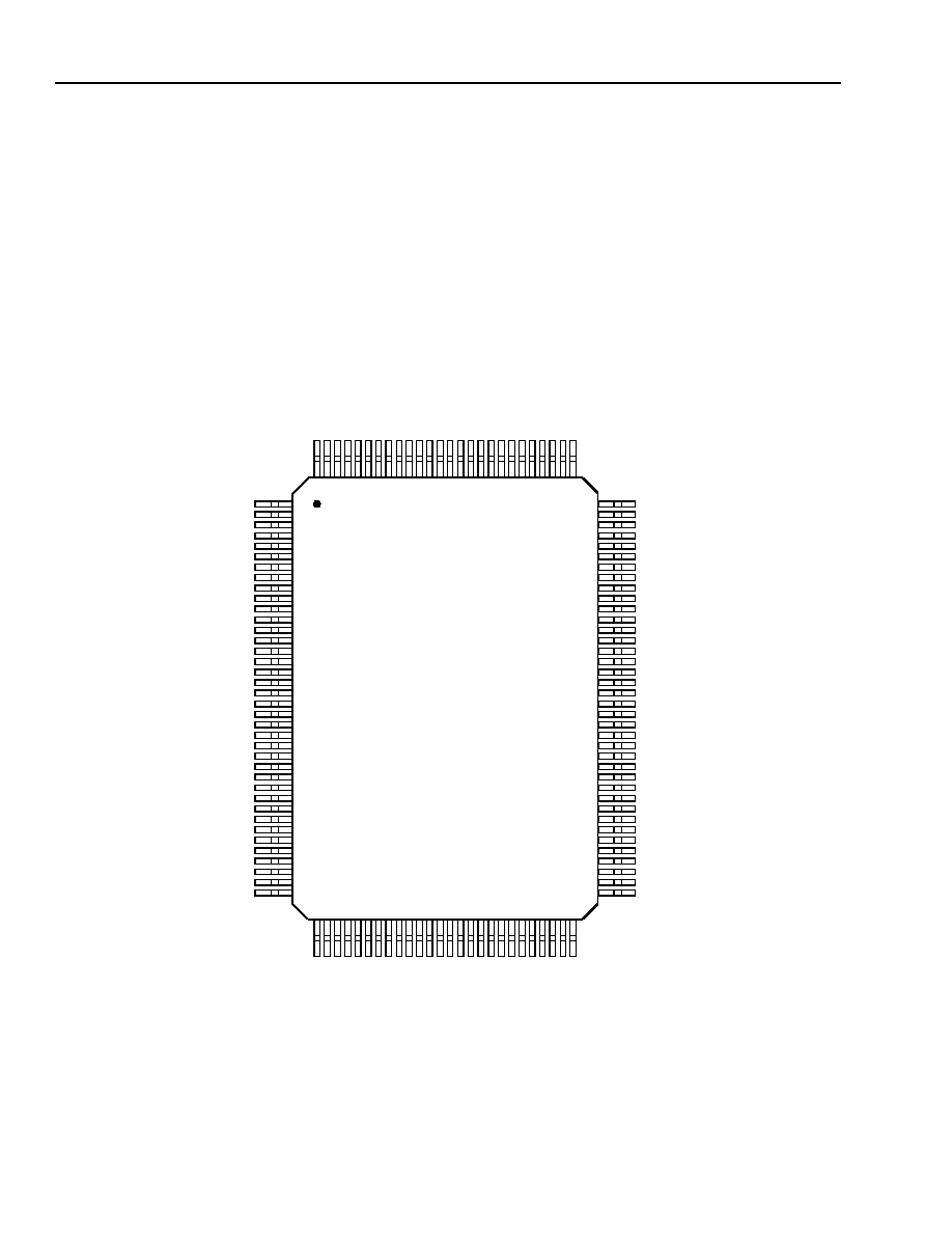
Figure 2. USS-344 Pin Diagram
AD
9
AD
8
C/B
E
N0
VS
S
VD
D
AD
7
AD
6
AD
5
AD
4
VS
S
VD
D
AD
3
AD
2
AD
1
AD
0
VS
S
VI
O
VD
D
VS
S
T
EST
0
T
EST
1
T
EST
2
T
EST
3
PR
T
P
W
R
3
P
W
R
F
LT
3N
INT
A
N
VD
D
VS
S
INT
B
N
INT
C
N
RS
T
N
VD
D
CL
K
VS
S
GN
T
N
RE
Q
N
AD
3
1
AD
3
0
AD
2
9
VS
S
VD
D
AD
2
8
AD
2
7
AD
2
6
AD
2
5
INT
D
N
1
2
3
4
5
6
7
8
9
10
11
12
13
14
15
16
17
18
19
20
21
22
23
24
25
26
27
28
29
30
31
32
33
34
35
36
37
38
AD24
C/BEN3
IDSEL
AD23
AD22
VSS
VDD
AD21
AD20
AD19
AD18
VSS
VDD
AD17
AD16
C/BEN2
FRAMEN
VDD
VSS
IRDYN
TRDYN
DEVSELN
STOPN
PERRN
VSS
VDD
SERRN
PAR
C/BEN1
AD15
VDD
AD14
AD13
AD12
AD11
39
40
41
42
43
44
45
46
47
48
49
50
51
52
53
54
55
56
57
58
59
60
61
62
63
64
VSS
MIRQ12I
KIRQ1I
A20I
A20MN
IRQ1
IRQ12
VDD
VSS
SMIN
PRTPWR0
PWRFLT0N
PRTPWR1
PWRFLT1N
VDD
CLK48STOP
VSSA
XLO/CLK48
XHI
VDDA
RREF
VDDT
VSST
DPLS0
DMNS0
DPLS1
DMNS1
VDDT
VSST
DPLS2
DMNS2
DPLS3
DMNS3
VDDT
VSST
PRTPWR2
PWRFLT2N
65
66
67
68
69
70
71
72
73
74
75
76
77
78
79
80
81
82
83
84
85
86
87
88
89
90
91
92
93
94
95
96
97
98
99
100
101
102
103
105
106
107
108
109
110
111
112
113
114
115
116
117
118
119
120
121
122
123
124
125
126
127
128
104
USS-344
VDD
VDD
VSS
VSS
VD
D
VS
S
AD
1
0
PM
E
N
VSS
VD
D

Agere Systems Inc.
5
Advance Data Sheet, Rev. 9
June 2001
Four-Host PCI-to-USB OpenHCI Host Controller
USS-344
QuadraBus
Pin Information
(continued)
Table 1. Numeric Pin Cross Reference
* Pins identified as NC are unused and should be left unconnected. Active-low signals within this document are indicated by an N following the
symbol names.
Pin
Symbol*
Pin
Symbol*
Pin
Symbol*
Pin
Symbol*
1
V
DD
33
V
DD
65
V
DD
97
DPLS3
2
V
SS
34
V
SS
66
V
SS
98
DMNS3
3
AD24
35
AD14
67
MIRQ12I
99
V
DD
T
4
C/BEN3
36
AD13
68
KIRQ1I
100
V
SS
T
5
IDSEL
37
AD12
69
A20I
101
PRTPWR2
6
AD23
38
AD11
70
A20MN
102
PWRFLT2N
7
AD22
39
V
DD
71
IRQ1
103
PRTPWR3
8
V
SS
40
V
SS
72
IRQ12
104
PWRFLT3N
9
V
DD
41
AD10
73
V
DD
105
INTAN
10
AD21
42
AD9
74
V
SS
106
V
DD
11
AD20
43
AD8
75
SMIN
107
V
SS
12
AD19
44
C/BEN0
76
PRTPWR0
108
INTBN
13
AD18
45
V
SS
77
PWRFLT0N
109
INTCN
14
V
SS
46
V
DD
78
PRTPWR1
110
INTDN
15
V
DD
47
AD7
79
PWRFLT1N
111
RSTN
16
AD17
48
AD6
80
V
DD
112
V
DD
17
AD16
49
AD5
81
CLK48STOP
113
CLK
18
C/BEN2
50
AD4
82
V
SS
A
114
V
SS
19
FRAMEN
51
V
SS
83
XLO/CLK48
115
GNTN
20
V
DD
52
V
DD
84
XHI
116
REQN
21
V
SS
53
AD3
85
V
DD
A
117
V
SS
22
IRDYN
54
AD2
86
RREF
118
V
DD
23
TRDYN
55
AD1
87
V
DD
T
119
PMEN
24
DEVSELN
56
AD0
88
V
SS
T
120
AD31
25
STOPN
57
V
SS
89
DPLS0
121
AD30
26
PERRN
58
VIO
90
DMNS0
122
AD29
27
V
SS
59
V
DD
91
DPLS1
123
V
SS
28
V
DD
60
V
SS
92
DMNS1
124
V
DD
29
SERRN
61
TEST0
93
V
DD
T
125
AD28
30
PAR
62
TEST1
94
V
SS
T
126
AD27
31
C/BEN1
63
TEST2
95
DPLS2
127
AD26
32
AD15
64
TEST3
96
DMNS2
128
AD25

6
6
Agere Systems Inc.
Advance Data Sheet, Rev. 9
June 2001
Four-Host PCI-to-USB OpenHCI Host Controller
USS-344
QuadraBus
Pin Information
(continued)
Table 2. PCI Signals
* An N following the symbol names indicates active-low for the USS-344.
Table 3. USB Port Signals
* An N following the symbol names indicates active-low for the USS-344.
Pin
Symbol*
Type
Description
111
RSTN
Input
PCI Reset (Active-Low).
113
CLK
Input
PCI System Clock (33 MHz).
116
REQN
Output/3-State
PCI Request (Active-Low).
115
GNTN
Input
PCI Grant (Active-Low).
120, 121, 122, 125, 126, 127, 128,
3, 6, 7, 10, 11, 12, 13, 16, 17, 32,
35, 36, 37, 38, 41, 42, 43, 47, 48,
49, 50, 53, 54, 55, 56
AD[31:0]
Bidir
PCI Address and Data.
30
PAR
Bidir
PCI Parity.
4, 18, 31, 44
C/BEN[3:0]
Bidir
PCI Bus Command and Byte Enables.
19
FRAMEN
Bidir
PCI Cycle Frame (Active-Low).
22
IRDYN
Bidir
PCI Initiator Ready (Active-Low).
23
TRDYN
Bidir
PCI Target Ready (Active-Low).
25
STOPN
Bidir
PCI Stop (Active-Low).
5
IDSEL
Input
PCI Initialization Device Select.
24
DEVSELN
Bidir
PCI Device Select (Active-Low).
26
PERRN
Bidir
PCI Parity Error (Active-Low).
29
SERRN
Output/Open Drain PCI System Error (Active-Low).
105
INTAN
Output/Open Drain PCI Interrupt A (Active-Low).
108
INTBN
Output/Open Drain PCI Interrupt B (Active-Low).
109
INTCN
Output/Open Drain PCI Interrupt C (Active-Low).
110
INTDN
Output/Open Drain PCI Interrupt D (Active-Low).
119
PMEN
Output/Open Drain Power Management Event (Active-Low).
1, 9, 15, 20, 28, 33, 39, 46, 52, 59,
65, 73, 80, 106, 112, 118, 124
V
DD
Power
3.3 V V
DD.
2, 8, 14, 21, 27, 34, 40, 45, 51, 57,
60, 66, 74, 107, 114, 117, 123
V
SS
Power
V
SS.
58
VIO
Power
PCI Environment Selection (3.3 V or 5 V).
Pin
Symbol*
Type
Description
89
DPLS0
Bidir
USB Port 0 DPLUS.
90
DMNS0
Bidir
USB Port 0 DMINUS.
91
DPLS1
Bidir
USB Port 1 DPLUS.
92
DMNS1
Bidir
USB Port 1 DMINUS.
95
DPLS2
Bidir
USB Port 2 DPLUS.
96
DMNS2
Bidir
USB Port 2 DMINUS.
97
DPLS3
Bidir
USB Port 3 DPLUS.
98
DMNS3
Bidir
USB Port 3 DMINUS.
76
PRTPWR0
Bidir
USB Port 0 Power Enable (Active-Low).
78
PRTPWR1
Bidir
USB Port 1 Power Enable (Active-Low).
101
PRTPWR2
Bidir
USB Port 2 Power Enable (Active-Low).
103
PRTPWR3
Bidir
USB Port 3 Power Enable (Active-Low).

Agere Systems Inc.
7
Advance Data Sheet, Rev. 9
June 2001
Four-Host PCI-to-USB OpenHCI Host Controller
USS-344
QuadraBus
Pin Information
(continued)
Table 3. USB Port Signals (continued)
* An N following the symbol names indicates active-low for the USS-344.
Table 4. Legacy Support Signals
* An N following the symbol names indicates active-low for the USS-344.
Table 5. Chip Test Signals
* An N following the symbol names indicates active-low for the USS-344.
Pin
Symbol*
Type
Description
77
PWRFLT0N
Input
USB Port 0 Overcurrent (Active-Low).
79
PWRFLT1N
Input
USB Port 1 Overcurrent (Active-Low).
102
PWRFLT2N
Input
USB Port 2 Overcurrent (Active-Low).
104
PWRFLT3N
Input
USB Port 3 Overcurrent (Active-Low).
81
CLK48STOP
Bidir
USB Clock Stop (Optional). Used to stop external
48 MHz clock in PCI power management state D3.
87, 93, 99
V
DD
T
Power
USB Transceiver V
DD
(3.3 V).
88, 94, 100
V
SS
T
Power
USB Transceiver V
SS.
86
RREF
Input
USB 2.0 1 k
Precision Resistor Connection. Hi-Z if
implementation does not expect upgrade to USB 2.0.
85
V
DD
A
Power
USB 2.0 Analog Power. Connect to V
DD
if implementa-
tion does not expect upgrade to USB 2.0.
82
V
SS
A
Power
USB 2.0 Analog Power. Connect to V
SS
if implementa-
tion does not expect upgrade to USB 2.0.
84
XHI
Power
USB 2.0 Crystal Oscillator XHI Connection. Hi-Z if
implementation does not expect upgrade to USB 2.0.
83
XLO/CLK48
Power/Input
USB 2.0 Crystal Oscillator XHI Connection/USB 1.X
CLK 48 MHz Input.
Pin
Symbol*
Type
Description
68
KIRQ1I
Input
Legacy Keyboard Controller Interrupt (IRQ1 Input from
Keyboard Controller).
67
MIRQ12I
Input
Legacy Mouse Controller Interrupt (IRQ12 Input from
Mouse Controller).
69
A20I
Input
Legacy Gate A20 Input.
70
A20MN
Output/Open Drain Legacy Gate A20 Output (to Memory Controller).
71
IRQ1
Output/Open Drain System Keyboard Interrupt (Active-High).
72
IRQ12
Output/Open Drain System Mouse Interrupt (Active-High).
75
SMIN
Output/Open Drain System Management Interrupt (Active-Low).
Pin
Symbol*
Type
Description
61
TEST0
Input
Chip Test Signal. Refer to Test Mode Connection
Instructions section for usage information.
62
TEST1
Input
Chip Test Signal. Refer to Test Mode Connection
Instructions section for usage information.
63
TEST2
Input
Chip Test Signal. Refer to Test Mode Connection
Instructions section for usage information.
64
TEST3
Input
Chip Test Signal. Refer to section Test Mode Connection
Instructions for usage information.

8
8
Agere Systems Inc.
Advance Data Sheet, Rev. 9
June 2001
Four-Host PCI-to-USB OpenHCI Host Controller
USS-344
QuadraBus
Register Overview
Table 6. PCI Bus Configuration Memory Summary (Function 0)
Refer to Tables 10--31 for more details on each of these registers.
* The revision can be identified electronically using the standard PCI Revision ID register described in this table. The revision can also be iden-
tified by physical markings using the last letter of the USS-344 identifier code printed on the device. The USS-344 identifier code will be
printed using the format USS344XY, where X will identify the package type (T) and Y will identify the revision.
This register is normally read only. Write capability of this register is available to system BIOS only.
Configuration Space Offset
Register Name
Read/Write
Default Value (Reset)
00h--01h
Vendor ID
R
11C1h
02h--03h
Device ID
R
5803h
04h--05h
Command
R/W
0000h
06h--07h
Status
R/W
TEST1 = 0b: 0210h
TEST1 = 1b: 0200h
08h
Revision ID*
R
10h
09h--0Bh
Class Code
R
0C0310h
0Ch
Cache Line Size
R
00h
0Dh
Latency Timer
R/W
00h
0Eh
Header Type
R
80h
0Fh
BIST
R
00h
10h--13h
BAR 0
R/W
00000000h
14h--17h
BAR 1
R
00000000h
18h--1Bh
BAR 2
R
00000000h
1Ch--1Fh
BAR 3
R
00000000h
20h--23h
BAR 4
R
00000000h
24h--27h
BAR 5
R
00000000h
28h--2Bh
CardBus CIS Pointer
R
00000000h
2Ch--2Dh
Subsystem Vendor ID
R/W
11C1h
2Eh--2Fh
Subsystem ID
R/W
5803h
30h--33h
Expansion ROM Base Address
R
00000000h
34h
Capabilities Pointer
R
TEST1 = 0b: 50h
TEST1 = 1b: 00h
3Ch
Interrupt Line
R/W
00h
3Dh
Interrupt Pin
R
01h
3Eh
Min_Gnt
R
03h
3Fh
Max_Lat
R
56h
4Ch
Special--Subsystem Write Capability
R/W
00000000h

Agere Systems Inc.
9
Advance Data Sheet, Rev. 9
June 2001
Four-Host PCI-to-USB OpenHCI Host Controller
USS-344
QuadraBus
Register Overview
(continued)
Table 7. PCI Bus Configuration Memory Summary (Function 1)
Refer to Tables 32--53 for more details on each of these registers.
* The revision can be identified electronically using the standard PCI Revision ID register described in this table. The revision can also be iden-
tified by physical markings using the last letter of the USS-344 identifier code printed on the device. The USS-344 identifier code will be
printed using the format USS344XY, where X will identify the package type (T) and Y will identify the revision.
This register is normally read only. Write capability of this register is available to system BIOS only.
Configuration Space Offset
Register Name
Read/Write
Default Value (Reset)
00h--01h
Vendor ID
R
11C1h
02h--03h
Device ID
R
5803h
04h--05h
Command
R/W
0000h
06h--07h
Status
R/W
TEST1 = 0b: 0210h
TEST1 = 1b: 0200h
08h
Revision ID*
R
10h
09h--0Bh
Class Code
R
0C0310h
0Ch
Cache Line Size
R
00h
0Dh
Latency Timer
R/W
00h
0Eh
Header Type
R
80h
0Fh
BIST
R
00h
10h--13h
BAR 0
R/W
00000000h
14h--17h
BAR 1
R
00000000h
18h--1Bh
BAR 2
R
00000000h
1Ch--1Fh
BAR 3
R
00000000h
20h--23h
BAR 4
R
00000000h
24h--27h
BAR 5
R
00000000h
28h--2Bh
CardBus CIS Pointer
R
00000000h
2Ch--2Dh
Subsystem Vendor ID
R/W
11C1h
2Eh--2Fh
Subsystem ID
R/W
5803h
30h--33h
Expansion ROM Base Address
R
00000000h
34h
Capabilities Pointer
R
TEST1 = 0b: 50h
TEST1 = 1b: 00h
3Ch
Interrupt Line
R/W
00h
3Dh
Interrupt Pin
R
TEST0 = 0b: 01h
TEST0 = 1b: 02h
3Eh
Min_Gnt
R
03h
3Fh
Max_Lat
R
56h
4Ch
Special--Subsystem Write Capability
R/W
00000000h

10
10
Agere Systems Inc.
Advance Data Sheet, Rev. 9
June 2001
Four-Host PCI-to-USB OpenHCI Host Controller
USS-344
QuadraBus
Register Overview
(continued)
Table 8. PCI Bus Configuration Memory Summary (Function 2)
Refer to Tables 54--75 for more details on each of these registers.
* The revision can be identified electronically using the standard PCI Revision ID register described in this table. The revision can also be iden-
tified by physical markings using the last letter of the USS-344 identifier code printed on the device. The USS-344 identifier code will be
printed using the format USS344XY, where X will identify the package type (T) and Y will identify the revision.
This register is normally read only. Write capability of this register is available to system BIOS only.
Configuration Space Offset
Register Name
Read/Write
Default Value (Reset)
00h--01h
Vendor ID
R
11C1h
02h--03h
Device ID
R
5803h
04h--05h
Command
R/W
0000h
06h--07h
Status
R/W
TEST1 = 0b: 0210h
TEST1 = 1b: 0200h
08h
Revision ID*
R
10h
09h--0Bh
Class Code
R
0C0310h
0Ch
Cache Line Size
R
00h
0Dh
Latency Timer
R/W
00h
0Eh
Header Type
R
80h
0Fh
BIST
R
00h
10h--13h
BAR 0
R/W
00000000h
14h--17h
BAR 1
R
00000000h
18h--1Bh
BAR 2
R
00000000h
1Ch--1Fh
BAR 3
R
00000000h
20h--23h
BAR 4
R
00000000h
24h--27h
BAR 5
R
00000000h
28h--2Bh
CardBus CIS Pointer
R
00000000h
2Ch--2Dh
Subsystem Vendor ID
R/W
11C1h
2Eh--2Fh
Subsystem ID
R/W
5803h
30h--33h
Expansion ROM Base Address
R
00000000h
34h
Capabilities Pointer
R
TEST1 = 0b: 50h
TEST1 = 1b: 00h
3Ch
Interrupt Line
R/W
00h
3Dh
Interrupt Pin
R
TEST0 = 0b: 01h
TEST0 = 1b: 03h
3Eh
Min_Gnt
R
03h
3Fh
Max_Lat
R
56h
4Ch
Special--Subsystem Write Capability
R/W
00000000h

Agere Systems Inc.
11
Advance Data Sheet, Rev. 9
June 2001
Four-Host PCI-to-USB OpenHCI Host Controller
USS-344
QuadraBus
Register Overview
(continued)
Table 9. PCI Bus Configuration Memory Summary (Function 3)
Refer to Tables 76--97 for more details on each of these registers.
* The revision of the USS-344 can be identified either electronically or by physical markings. The revision can be identified electronically using
the standard PCI Revision ID register described in this table. The revision can also be identified by physical markings using the last letter of
the USS-344 identifier code printed on the device. The USS-344 identifier code will be printed using the format USS344XY, where X will iden-
tify the package type (T) and Y will identify the revision.
This register is normally read only. Write capability of this register is available to system BIOS only.
Configuration Space Offset
Register Name
Read/Write
Default Value (Reset)
00h--01h
Vendor ID
R
11C1h
02h--03h
Device ID
R
5803h
04h--05h
Command
R/W
0000h
06h--07h
Status
R/W
TEST1 = 0b: 0210h
TEST1 = 1b: 0200h
08h
Revision ID*
R
10h
09h--0Bh
Class Code
R
0C0310h
0Ch
Cache Line Size
R
00h
0Dh
Latency Timer
R/W
00h
0Eh
Header Type
R
80h
0Fh
BIST
R
00h
10h--13h
BAR 0
R/W
00000000h
14h--17h
BAR 1
R
00000000h
18h--1Bh
BAR 2
R
00000000h
1Ch--1Fh
BAR 3
R
00000000h
20h--23h
BAR 4
R
00000000h
24h--27h
BAR 5
R
00000000h
28h--2Bh
CardBus CIS Pointer
R
00000000h
2Ch--2Dh
Subsystem Vendor ID
R/W
11C1h
2Eh--2Fh
Subsystem ID
R/W
5803h
30h--33h
Expansion ROM Base Address
R
00000000h
34h
Capabilities Pointer
R
TEST1 = 0b: 50h
TEST1 = 1b: 00h
3Ch
Interrupt Line
R/W
00h
3Dh
Interrupt Pin
R
TEST0 = 0b: 01h
TEST0 = 1b: 04h
3Eh
Min_Gnt
R
03h
3Fh
Max_Lat
R
56h
4Ch
Special--Subsystem Write Capability
R/W
00000000h

12
12
Agere Systems Inc.
Advance Data Sheet, Rev. 9
June 2001
Four-Host PCI-to-USB OpenHCI Host Controller
USS-344
QuadraBus
PCI Registers
PCI Function 0--Single-Port USB Host Controller 0
Table 10. Vendor ID Register (00h--01h)
This register is fixed as the Agere Systems vendor ID assigned by the PCI SIG.
Table 11. Device ID Register (02h--03h)
This register is fixed as the Agere Systems product USS-344.
Table 12. Command Register (04h--05h)
All read-only bits represent nonconfigurable features of the USS-344.
Table 13. Status Register (06h--07h)
All read-only bits represent nonconfigurable features of the USS-344.
Bits
Field
Read/Write
Reset/Description
15:0
Vendor ID
R
Assigned 11C1h
Bits
Field
Read/Write
Reset/Description
15:0
Device ID
R
Assigned 5803h
Bits
Field
Read/Write
Reset/Description
0
IO Space
R/W
0
1
Memory Space
R/W
0
2
Bus Master
R/W
0
3
Special Cycles
R
0
4
Memory Write and
Invalidate Enable
R/W
0
5
VGA Palette Snoop
R
0
6
Parity Error Response
R/W
0
7
Wait Cycle Control
R
0
8
SERRN Enable
R/W
0
9
Fast Back-to-back
Enable
R/W
0
15:10
Reserved
R
000000b
Bits
Field
Read/Write
Reset/Description
3:0
Reserved
R
0000b
4
Capabilities
R
TEST1 = 0b: 1
TEST1 = 1b: 0
5
66 MHz Capable
R
0
6
UDF Support
R
0
7
Fast Back-to-back
Capable
R
0
8
Data Parity Error
Detected
R/W
0
10:9
DEVSEL Timing
R
01
11
Signaled Target Abort
R/W
0
12
Received Target Abort
R/W
0
13
Received Master Abort
R/W
0
14
Signaled System Error
R/W
0
15
Detected Parity Error
R/W
0

Agere Systems Inc.
13
Advance Data Sheet, Rev. 9
June 2001
Four-Host PCI-to-USB OpenHCI Host Controller
USS-344
QuadraBus
PCI Registers
(continued)
Table 14. Revision ID Register (08h)
Represents the current revision of the USS-344.
* The revision of the USS-344 can be identified either electronically or by physical markings. The revision can be identified
electronically using the standard PCI Revision ID register described in this table. The revision can also be identified by phys-
ical markings using the last letter of the USS-344 identifier code printed on the device. The USS-344 identifier code will be
printed using the format USS344XY, where X will identify the package type (M or T) and Y will identify the revision.
Table 15. Class Code Register (09h--0Bh)
The PCI class code for all OpenHCI host controllers is defined in the OpenHCI specification.
Table 16. Cache Line Size Register (0Ch)
No cache line is supported by the USS-344.
Table 17. Latency Timer Register (0Dh)
Controls the number of clock cycles the USS-344 may remain on the PCI bus after becoming bus master.
Table 18. Header Type Register (0Eh)
The USS-344 supports PCI header type 0 only.
Table 19. BIST Register (0Fh)
BIST is not supported by the USS-344.
Bits
Field
Read/Write
Reset/Description
7:0
Revision ID*
R
10h
Bits
Field
Read/Write
Reset/Description
7:0
Programming Interface
R
10h = OpenHCI Host Controller
15:8
Subclass
R
03h = Universal Serial Bus
23:16
Base Class
R
0Ch = Serial Bus Controller
Bits
Field
Read/Write
Reset/Description
7:0
Cache Line Size
R
00h
Bits
Field
Read/Write
Reset/Description
7:0
Latency Timer
R/W
Upper 5 bits are read/write. Lower
3 bits are read only.
Bits
Field
Read/Write
Reset/Description
7:0
Header Type
R
80h = Multifunction PCI Device
Bits
Field
Read/Write
Reset/Description
7:0
BIST
R
00h

14
14
Agere Systems Inc.
Advance Data Sheet, Rev. 9
June 2001
Four-Host PCI-to-USB OpenHCI Host Controller
USS-344
QuadraBus
PCI Registers
(continued)
Table 20. Base Address Register 0 (10h--13h)
The Base Address register is used to specify to the PCI operating system the memory size of the USS-344 device.
As recommended by the OpenHCI specification, the lower 12 bits are read only (fixed to logic 0) to indicate 4K (2
12
)
memory size.
Table 21. Base Address Register 1, 2, 3, 4, 5 (14h--17h), (18h--1Bh), (1Ch--1Fh), (20h--23h), (24h--27h)
These Base Address registers are unused by the USS-344 device.
Table 22. Cardbus CIS Pointer Register (28h--2Bh)
Cardbus CIS pointer not required for the USS-344.
Table 23. Subsystem Vendor ID Register (2Ch--2Dh)
The subsystem vendor ID is R/W for compliance with
Microsoft
PC98 specifications. On reset, this register is read
only. System BIOS may write a 1 to Special--Subsystem Write Capability register (4Ch) bit 0 to enable write capa-
bility of this register. After configuring this register, the system BIOS must write a 0 to Special--Subsystem Write
Capability register (4Ch) bit 0 to disable write capability of this register.
Table 24. Subsystem ID Register (2Eh--2Fh)
The subsystem vendor ID is R/W for compliance with
Microsoft
PC98 specifications. On reset, this register is read
only. System BIOS may write a 1 to Special--Subsystem Write Capability register (4Ch) bit 0 to enable write capa-
bility of this register. After configuring this register, the system BIOS must write a 0 to Special--Subsystem Write
Capability register (4Ch) bit 0 to disable write capability of this register.
Table 25. Expansion ROM Base Address Register (30h--33h)
Expansion ROM not supported by the USS-344.
Bits
Field
Read/Write
Reset/Description
31:0
BAR 0
R/W
Lower 12 bits are read only. Upper
20 bits are read/write.
Bits
Field
Read/Write
Reset/Description
31:0
BAR 1--5
R
00000000h
Bits
Field
Read/Write
Reset/Description
31:0
CardBus CIS Pointer
R
00000000h
Bits
Field
Read/Write
Reset/Description
15:0
Subsystem Vendor ID
R/W
11C1h
Bits
Field
Read/Write
Reset/Description
15:0
Subsystem ID
R/W
5803h
Bits
Field
Read/Write
Reset/Description
31:0
Expansion ROM Base
Address
R
00000000h

Agere Systems Inc.
15
Advance Data Sheet, Rev. 9
June 2001
Four-Host PCI-to-USB OpenHCI Host Controller
USS-344
QuadraBus
PCI Registers
(continued)
Table 26. Capabilities Pointer Register (34h)
Table 27. Interrupt Line Register (3Ch)
Table 28. Interrupt Pin Register (3Dh)
Interrupt A used as the PCI interrupt for this core.
Table 29. Min_Gnt Register (3Eh)
The USS-344 can support a four DWORD master burst read or write which requires less than 500 ns.
Table 30. Max_Lat Register (3Fh)
The USS-344 requires service at a minimum interval of 21.3
Ķ
s.
Table 31. Special--Subsystem Write Capability (4Ch)
This is a special register implemented for compliance with
Microsoft
PC98 Specification, Chapter 9, Item 11. Bit 0 is
read/write to allow the system BIOS to enable write capability of the Subsystem Vendor ID and Subsystem ID reg-
isters (refer to Tables 23 and 24).
Bits
Field
Read/Write
Reset/Description
7:0
Cap_Ptr
R
TEST1 = 0b: 50h
TEST1 = 1b: 00h
Bits
Field
Read/Write
Reset/Description
7:0
Interrupt Line
R/W
00h
Bits
Field
Read/Write
Reset/Description
7:0
Interrupt Pin
R
01h
Bits
Field
Read/Write
Reset/Description
7:0
Min_Gnt
R
03h
Bits
Field
Read/Write
Reset/Description
7:0
Max_Lat
R
56h
Bits
Field
Read/Write
Reset/Description
31:1
Reserved
R
00000000h
0
Subsystem Write
R/W
0b
0 = Subsystem write disabled
1 = Subsystem write enabled

16
16
Agere Systems Inc.
Advance Data Sheet, Rev. 9
June 2001
Four-Host PCI-to-USB OpenHCI Host Controller
USS-344
QuadraBus
PCI Registers
(continued)
PCI Function 1--Single-Port USB Host Controller 1
Table 32. Vendor ID Register (00h--01h)
This register is fixed as the Agere Systems vendor ID assigned by the PCI SIG.
Table 33. Device ID Register (02h--03h)
This register is fixed as the Agere Systems product USS-344.
Table 34. Command Register (04h--05h)
All read-only bits represent nonconfigurable features of the USS-344.
Table 35. Status Register (06h--07h)
All read-only bits represent nonconfigurable features of the USS-344.
Bits
Field
Read/Write
Reset/Description
15:0
Vendor ID
R
Assigned 11C1h
Bits
Field
Read/Write
Reset/Description
15:0
Device ID
R
Assigned 5803h
Bits
Field
Read/Write
Reset/Description
0
IO Space
R/W
0
1
Memory Space
R/W
0
2
Bus Master
R/W
0
3
Special Cycles
R
0
4
Memory Write and Invalidate
Enable
R/W
0
5
VGA Palette Snoop
R
0
6
Parity Error Response
R/W
0
7
Wait Cycle Control
R
0
8
SERRN Enable
R/W
0
9
Fast Back-to-back Enable
R/W
0
15:10
Reserved
R
000000b
Bits
Field
Read/Write
Reset/Description
3:0
Reserved
R
0000b
4
Capabilities
R
TEST1 = 0b: 1
TEST1 = 1b: 0
5
66 MHz Capable
R
0
6
UDF Support
R
0
7
Fast Back-to-back Capable
R
0
8
Data Parity Error Detected
R/W
0
10:9
DEVSEL Timing
R
01
11
Signaled Target Abort
R/W
0
12
Received Target Abort
R/W
0
13
Received Master Abort
R/W
0
14
Signaled System Error
R/W
0
15
Detected Parity Error
R/W
0

Agere Systems Inc.
17
Advance Data Sheet, Rev. 9
June 2001
Four-Host PCI-to-USB OpenHCI Host Controller
USS-344
QuadraBus
PCI Registers
(continued)
Table 36. Revision ID Register (08h)
Represents the current revision of the USS-344.
* The revision of the USS-344 can be identified either electronically or by physical markings. The revision can be identified
electronically using the standard PCI Revision ID register described in this table. The revision can also be identified by phys-
ical markings using the last letter of the USS-344 identifier code printed on the device. The USS-344 identifier code will be
printed using the format USS344XY, where X will identify the package type (M or T) and Y will identify the revision.
Table 37. Class Code Register (09h--0Bh)
The PCI class code for all OpenHCI host controllers is defined in the OpenHCI specification.
Table 38. Cache Line Size Register (0Ch)
No cache line is supported by the USS-344.
Table 39. Latency Timer Register (0Dh)
Controls the number of clock cycles the USS-344 may remain on the PCI bus after becoming bus master.
Table 40. Header Type Register (0Eh)
The USS-344 supports PCI header type 0 only.
Bits
Field
Read/Write
Reset/Description
7:0
Revision ID*
R
10h
Bits
Field
Read/Write
Reset/Description
7:0
Programming Interface
R
10h = OpenHCI Host Controller
15:8
Subclass
R
03h = Universal Serial Bus
23:16
Base Class
R
0Ch = Serial Bus Controller
Bits
Field
Read/Write
Reset/Description
7:0
Cache Line Size
R
00h
Bits
Field
Read/Write
Reset/Description
7:0
Latency Timer
R/W
Upper 5 bits are read/write. Lower
3 bits are read only.
Bits
Field
Read/Write
Reset/Description
7:0
Header Type
R
80h = Multifunction PCI Device

18
18
Agere Systems Inc.
Advance Data Sheet, Rev. 9
June 2001
Four-Host PCI-to-USB OpenHCI Host Controller
USS-344
QuadraBus
PCI Registers
(continued)
Table 41. BIST Register (0Fh)
BIST is not supported by the USS-344.
Table 42. Base Address Register 0 (10h--13h)
The Base Address register is used to specify to the PCI operating system the memory size of the USS-344 device.
As recommended by the OpenHCI specification, the lower 12 bits are read only (fixed to logic 0) to indicate 4K (2
12
)
memory size.
Table 43. Base Address Register 1, 2, 3, 4, 5 (14h--17h), (18h--1Bh), (1Ch--1Fh), (20h--23h), (24h--27h)
These Base Address registers are unused by the USS-344 device.
Table 44. Cardbus CIS Pointer Register (28h--2Bh)
Cardbus CIS pointer not required for the USS-344.
Table 45. Subsystem Vendor ID Register (2Ch--2Dh)
The subsystem vendor ID is R/W for compliance with
Microsoft
PC98 specifications. On reset, this register is read
only. System BIOS may write a 1 to Special--Subsystem Write Capability register (4Ch) bit 0 to enable write capa-
bility of this register. After configuring this register, the system BIOS must write a 0 to Special--Subsystem Write
Capability register (4Ch) bit 0 to disable write capability of this register.
Table 46. Subsystem ID Register (2Eh--2Fh)
The subsystem vendor ID is R/W for compliance with
Microsoft
PC98 specifications. On reset, this register is read
only. System BIOS may write a 1 to Special--Subsystem Write Capability register (4Ch) bit 0 to enable write capa-
bility of this register. After configuring this register, the system BIOS must write a 0 to Special--Subsystem Write
Capability register (4Ch) bit 0 to disable write capability of this register.
Bits
Field
Read/Write
Reset/Description
7:0
BIST
R
00h
Bits
Field
Read/Write
Reset/Description
31:0
BAR 0
R/W
Lower 12 bits are read only. Upper
20 bits are read/write.
Bits
Field
Read/Write
Reset/Description
31:0
BAR 1--5
R
00000000h
Bits
Field
Read/Write
Reset/Description
31:0
CardBus CIS Pointer
R
00000000h
Bits
Field
Read/Write
Reset/Description
15:0
Subsystem Vendor ID
R/W
11C1h
Bits
Field
Read/Write
Reset/Description
15:0
Subsystem ID
R/W
5803h

Agere Systems Inc.
19
Advance Data Sheet, Rev. 9
June 2001
Four-Host PCI-to-USB OpenHCI Host Controller
USS-344
QuadraBus
PCI Registers
(continued)
Table 47. Expansion ROM Base Address Register (30h--33h)
Expansion ROM not supported by the USS-344.
Table 48. Capabilities Pointer Register (34h)
Table 49. Interrupt Line Register (3Ch)
Table 50. Interrupt Pin Register (3Dh)
If TEST0 = 0b, interrupt A is used as the PCI interrupt for this core.
If TEST0 = 1b, interrupt B is used as the PCI interrupt for this core.
Table 51. Min_Gnt Register (3Eh)
The USS-344 can support a four DWORD master burst read or write which requires less than 500 ns.
Table 52. Max_Lat Register (3Fh)
The USS-344 requires service at a minimum interval of 21.3
Ķ
s.
Table 53. Special--Subsystem Write Capability (4Ch)
This is a special register implemented for compliance with
Microsoft
PC98 Specification, Chapter 9, Item 11. Bit 0 is
read/write to allow the system BIOS to enable write capability of the Subsystem Vendor ID and Subsystem ID reg-
isters (refer to Tables 23 and 24).
Bits
Field
Read/Write
Reset/Description
31:0
Expansion ROM Base
Address
R
00000000h
Bits
Field
Read/Write
Reset/Description
7:0
Cap_Ptr
R
TEST1 = 0b: 50h
TEST1 = 1b: 00h
Bits
Field
Read/Write
Reset/Description
7:0
Interrupt Line
R/W
00h
Bits
Field
Read/Write
Reset/Description
7:0
Interrupt Pin
R
TEST0 = 0b: 01h
TEST0 = 1b: 02h
Bits
Field
Read/Write
Reset/Description
7:0
Min_Gnt
R
03h
Bits
Field
Read/Write
Reset/Description
7:0
Max_Lat
R
56h
Bits
Field
Read/Write
Reset/Description
31:1
Reserved
R
00000000h
0
Subsystem Write
R/W
0b
0 = Subsystem write disabled
1 = Subsystem write enabled

20
20
Agere Systems Inc.
Advance Data Sheet, Rev. 9
June 2001
Four-Host PCI-to-USB OpenHCI Host Controller
USS-344
QuadraBus
PCI Registers
(continued)
PCI Function 2--Single-Port USB Host Controller 2
Table 54. Vendor ID Register (00h--01h)
This register is fixed as the Agere Systems vendor ID assigned by the PCI SIG.
Table 55. Device ID Register (02h--03h)
This register is fixed as the Agere Systems product USS-344.
Table 56. Command Register (04h--05h)
All read-only bits represent nonconfigurable features of the USS-344.
Table 57. Status Register (06h--07h)
All read-only bits represent nonconfigurable features of the USS-344.
Bits
Field
Read/Write
Reset/Description
15:0
Vendor ID
R
Assigned 11C1h
Bits
Field
Read/Write
Reset/Description
15:0
Device ID
R
Assigned 5803h
Bits
Field
Read/Write
Reset/Description
0
IO Space
R/W
0
1
Memory Space
R/W
0
2
Bus Master
R/W
0
3
Special Cycles
R
0
4
Memory Write and Invalidate Enable
R/W
0
5
VGA Palette Snoop
R
0
6
Parity Error Response
R/W
0
7
Wait Cycle Control
R
0
8
SERRN Enable
R/W
0
9
Fast Back-to-back Enable
R/W
0
15:10
Reserved
R
000000b
Bits
Field
Read/Write
Reset/Description
3:0
Reserved
R
0000b
4
Capabilities
R
TEST1 = 0b: 1
TEST1 = 1b: 0
5
66 MHz Capable
R
0
6
UDF Support
R
0
7
Fast Back-to-back Capable
R
0
8
Data Parity Error Detected
R/W
0
10:9
DEVSEL Timing
R
01
11
Signaled Target Abort
R/W
0
12
Received Target Abort
R/W
0
13
Received Master Abort
R/W
0
14
Signaled System Error
R/W
0
15
Detected Parity Error
R/W
0

Agere Systems Inc.
21
Advance Data Sheet, Rev. 9
June 2001
Four-Host PCI-to-USB OpenHCI Host Controller
USS-344
QuadraBus
PCI Registers
(continued)
Table 58. Revision ID Register (08h)
Represents the current revision of the USS-344.
* The revision of the USS-344 can be identified either electronically or by physical markings. The revision can be identified
electronically using the standard PCI Revision ID register described in this table. The revision can also be identified by phys-
ical markings using the last letter of the USS-344 identifier code printed on the device. The USS-344 identifier code will be
printed using the format USS344XY, where X will identify the package type (M or T) and Y will identify the revision.
Table 59. Class Code Register (09h--0Bh)
The PCI class code for all OpenHCI host controllers is defined in the OpenHCI specification.
Table 60. Cache Line Size Register (0Ch)
No cache line is supported by the USS-344.
Table 61. Latency Timer Register (0Dh)
Controls the number of clock cycles the USS-344 may remain on the PCI bus after becoming bus master.
Table 62. Header Type Register (0Eh)
The USS-344 supports PCI header type 0 only.
Bits
Field
Read/Write
Reset/Description
7:0
Revision ID*
R
10h
Bits
Field
Read/Write
Reset/Description
7:0
Programming Interface
R
10h = OpenHCI Host Controller
15:8
Subclass
R
03h = Universal Serial Bus
23:16
Base Class
R
0Ch = Serial Bus Controller
Bits
Field
Read/Write
Reset/Description
7:0
Cache Line Size
R
00h
Bits
Field
Read/Write
Reset/Description
7:0
Latency Timer
R/W
Upper 5 bits are read/write. Lower
3 bits are read only.
Bits
Field
Read/Write
Reset/Description
7:0
Header Type
R
80h = Multifunction PCI Device

22
22
Agere Systems Inc.
Advance Data Sheet, Rev. 9
June 2001
Four-Host PCI-to-USB OpenHCI Host Controller
USS-344
QuadraBus
PCI Registers
(continued)
Table 63. BIST Register (0Fh)
BIST is not supported by the USS-344.
Table 64. Base Address Register 0 (10h--13h)
The Base Address register is used to specify to the PCI operating system the memory size of the USS-344 device.
As recommended by the OpenHCI specification, the lower 12 bits are read only (fixed to logic 0) to indicate 4K (2
12
)
memory size.
Table 65. Base Address Register 1, 2, 3, 4, 5 (14h--17h), (18h--1Bh), (1Ch--1Fh), (20h--23h), (24h--27h)
These Base Address registers are unused by the USS-344 device.
Table 66. Cardbus CIS Pointer Register (28h--2Bh)
Cardbus CIS pointer not required for the USS-344.
Table 67. Subsystem Vendor ID Register (2Ch--2Dh)
The subsystem vendor ID is R/W for compliance with
Microsoft
PC98 specifications. On reset, this register is read
only. System BIOS may write a 1 to Special--Subsystem Write Capability register (4Ch) bit 0 to enable write capa-
bility of this register. After configuring this register, the system BIOS must write a 0 to Special--Subsystem Write
Capability register (4Ch) bit 0 to disable write capability of this register.
Table 68. Subsystem ID Register (2Eh--2Fh)
The subsystem vendor ID is R/W for compliance with
Microsoft
PC98 specifications. On reset, this register is read
only. System BIOS may write a 1 to Special--Subsystem Write Capability register (4Ch) bit 0 to enable write capa-
bility of this register. After configuring this register, the system BIOS must write a 0 to Special--Subsystem Write
Capability register (4Ch) bit 0 to disable write capability of this register.
Bits
Field
Read/Write
Reset/Description
7:0
BIST
R
00h
Bits
Field
Read/Write
Reset/Description
31:0
BAR 0
R/W
Lower 12 bits are read only. Upper
20 bits are read/write.
Bits
Field
Read/Write
Reset/Description
31:0
BAR 1--5
R
00000000h
Bits
Field
Read/Write
Reset/Description
31:0
CardBus CIS Pointer
R
00000000h
Bits
Field
Read/Write
Reset/Description
15:0
Subsystem Vendor ID
R/W
11C1h
Bits
Field
Read/Write
Reset/Description
15:0
Subsystem ID
R/W
5803h

Agere Systems Inc.
23
Advance Data Sheet, Rev. 9
June 2001
Four-Host PCI-to-USB OpenHCI Host Controller
USS-344
QuadraBus
PCI Registers
(continued)
Table 69. Expansion ROM Base Address Register (30h--33h)
Expansion ROM not supported by the USS-344.
Table 70. Capabilities Pointer Register (34h)
Table 71. Interrupt Line Register (3Ch)
Table 72. Interrupt Pin Register (3Dh)
If TEST0 = 0b, interrupt A is used as the PCI interrupt for this core.
If TEST0 = 1b, interrupt C is used as the PCI interrupt for this core.
Table 73. Min_Gnt Register (3Eh)
The USS-344 can support a four DWORD master burst read or write which requires less than 500 ns.
Table 74. Max_Lat Register (3Fh)
The USS-344 requires service at a minimum interval of 21.3
Ķ
s.
Table 75. Special--Subsystem Write Capability (4Ch)
This is a special register implemented for compliance with
Microsoft
PC98 Specification, Chapter 9, Item 11. Bit 0 is
read/write to allow the system BIOS to enable write capability of the Subsystem Vendor ID and Subsystem ID reg-
isters (refer to Tables 23 and 24).
Bits
Field
Read/Write
Reset/Description
31:0
Expansion ROM Base
Address
R
00000000h
Bits
Field
Read/Write
Reset/Description
7:0
Cap_Ptr
R
TEST1 = 0b: 50h
TEST1 = 1b: 00h
Bits
Field
Read/Write
Reset/Description
7:0
Interrupt Line
R/W
00h
Bits
Field
Read/Write
Reset/Description
7:0
Interrupt Pin
R
TEST0 = 0b: 01h
TEST0 = 1b: 03h
Bits
Field
Read/Write
Reset/Description
7:0
Min_Gnt
R
03h
Bits
Field
Read/Write
Reset/Description
7:0
Max_Lat
R
56h
Bits
Field
Read/Write
Reset/Description
31:1
Reserved
R
00000000h
0
Subsystem Write
R/W
0b
0 = Subsystem write disabled
1 = Subsystem write enabled

24
24
Agere Systems Inc.
Advance Data Sheet, Rev. 9
June 2001
Four-Host PCI-to-USB OpenHCI Host Controller
USS-344
QuadraBus
PCI Registers
(continued)
PCI Function 3--Single-Port USB Host Controller 3
Table 76. Vendor ID Register (00h--01h)
This register is fixed as the Agere Systems vendor ID assigned by the PCI SIG.
Table 77. Device ID Register (02h--03h)
This register is fixed as the Agere Systems product USS-344.
Table 78. Command Register (04h--05h)
All read-only bits represent nonconfigurable features of the USS-344.
Table 79. Status Register (06h--07h)
All read-only bits represent nonconfigurable features of the USS-344.
Bits
Field
Read/Write
Reset/Description
15:0
Vendor ID
R
Assigned 11C1h
Bits
Field
Read/Write
Reset/Description
15:0
Device ID
R
Assigned 5803h
Bits
Field
Read/Write
Reset/Description
0
IO Space
R/W
0
1
Memory Space
R/W
0
2
Bus Master
R/W
0
3
Special Cycles
R
0
4
Memory Write and
Invalidate Enable
R/W
0
5
VGA Palette Snoop
R
0
6
Parity Error Response
R/W
0
7
Wait Cycle Control
R
0
8
SERRN Enable
R/W
0
9
Fast Back-to-back
Enable
R/W
0
15:10
Reserved
R
000000b
Bits
Field
Read/Write
Reset/Description
3:0
Reserved
R
0000b
4
Capabilities
R
TEST1 = 0b: 1
TEST1 = 1b: 0
5
66 MHz Capable
R
0
6
UDF Support
R
0
7
Fast Back-to-back
Capable
R
0
8
Data Parity Error
Detected
R/W
0
10:9
DEVSEL Timing
R
01
11
Signaled Target Abort
R/W
0
12
Received Target Abort
R/W
0
13
Received Master Abort
R/W
0
14
Signaled System Error
R/W
0
15
Detected Parity Error
R/W
0

Agere Systems Inc.
25
Advance Data Sheet, Rev. 9
June 2001
Four-Host PCI-to-USB OpenHCI Host Controller
USS-344
QuadraBus
PCI Registers
(continued)
Table 80. Revision ID Register (08h)
Represents the current revision of the USS-344.
* The revision of the USS-344 can be identified either electronically or by physical markings. The revision can be identified
electronically using the standard PCI Revision ID register described in this table. The revision can also be identified by phys-
ical markings using the last letter of the USS-344 identifier code printed on the device. The USS-344 identifier code will be
printed using the format USS344XY, where X will identify the package type (M or T) and Y will identify the revision.
Table 81. Class Code Register (09h--0Bh)
The PCI class code for all OpenHCI host controllers is defined in the OpenHCI specification.
Table 82. Cache Line Size Register (0Ch)
No cache line is supported by the USS-344.
Table 83. Latency Timer Register (0Dh)
Controls the number of clock cycles the USS-344 may remain on the PCI bus after becoming bus master.
Table 84. Header Type Register (0Eh)
The USS-344 supports PCI header type 0 only.
Bits
Field
Read/Write
Reset/Description
7:0
Revision ID*
R
10h
Bits
Field
Read/Write
Reset/Description
7:0
Programming Interface
R
10h = OpenHCI Host Controller
15:8
Subclass
R
03h = Universal Serial Bus
23:16
Base Class
R
0Ch = Serial Bus Controller
Bits
Field
Read/Write
Reset/Description
7:0
Cache Line Size
R
00h
Bits
Field
Read/Write
Reset/Description
7:0
Latency Timer
R/W
Upper 5 bits are read/write. Lower
3 bits are read only.
Bits
Field
Read/Write
Reset/Description
7:0
Header Type
R
80h = Multifunction PCI Device

26
26
Agere Systems Inc.
Advance Data Sheet, Rev. 9
June 2001
Four-Host PCI-to-USB OpenHCI Host Controller
USS-344
QuadraBus
PCI Registers
(continued)
Table 85. BIST Register (0Fh)
BIST is not supported by the USS-344.
Table 86. Base Address Register 0 (10h--13h)
The Base Address register is used to specify to the PCI operating system the memory size of the USS-344 device.
As recommended by the OpenHCI specification, the lower 12 bits are read only (fixed to logic 0) to indicate 4K (2
12
)
memory size.
Table 87. Base Address Register 1, 2, 3, 4, 5 (14h--17h), (18h--1Bh), (1Ch--1Fh), (20h--23h), (24h--27h)
These base address registers are unused by the USS-344 device.
Table 88. Cardbus CIS Pointer Register (28h--2Bh)
Cardbus CIS pointer not required for the USS-344.
Table 89. Subsystem Vendor ID Register (2Ch--2Dh)
The subsystem vendor ID is R/W for compliance with
Microsoft
PC98 specifications. On reset, this register is read
only. System BIOS may write a 1 to Special--Subsystem Write Capability register (4Ch) bit 0 to enable write capa-
bility of this register. After configuring this register, the system BIOS must write a 0 to Special--Subsystem Write
Capability register (4Ch) bit 0 to disable write capability of this register.
Table 90. Subsystem ID Register (2Eh--2Fh)
The subsystem vendor ID is R/W for compliance with
Microsoft
PC98 specifications. On reset, this register is read
only. System BIOS may write a 1 to Special--Subsystem Write Capability register (4Ch) bit 0 to enable write capa-
bility of this register. After configuring this register, the system BIOS must write a 0 to Special--Subsystem Write
Capability register (4Ch) bit 0 to disable write capability of this register.
Bits
Field
Read/Write
Reset/Description
7:0
BIST
R
00h
Bits
Field
Read/Write
Reset/Description
31:0
BAR 0
R/W
Lower 12 bits are read only. Upper
20 bits are read/write.
Bits
Field
Read/Write
Reset/Description
31:0
BAR 1--5
R
00000000h
Bits
Field
Read/Write
Reset/Description
31:0
CardBus CIS Pointer
R
00000000h
Bits
Field
Read/Write
Reset/Description
15:0
Subsystem Vendor ID
R/W
11C1h
Bits
Field
Read/Write
Reset/Description
15:0
Subsystem ID
R/W
5803h

Agere Systems Inc.
27
Advance Data Sheet, Rev. 9
June 2001
Four-Host PCI-to-USB OpenHCI Host Controller
USS-344
QuadraBus
PCI Registers
(continued)
Table 91. Expansion ROM Base Address Register (30h--33h)
Expansion ROM not supported by the USS-344.
Table 92. Capabilities Pointer Register (34h)
Table 93. Interrupt Line Register (3Ch)
Table 94. Interrupt Pin Register (3Dh)
If TEST0 = 0b, interrupt A is used as the PCI interrupt for this core.
If TEST0 = 1b, interrupt D is used as the PCI interrupt for this core.
Table 95. Min_Gnt Register (3Eh)
The USS-344 can support a four DWORD master burst read or write which requires less than 500 ns.
Table 96. Max_Lat Register (3Fh)
The USS-344 requires service at a minimum interval of 21.3
Ķ
s.
Table 97. Special--Subsystem Write Capability (4Ch)
This is a special register implemented for compliance with
Microsoft
PC98 Specification, Chapter 9, Item 11. Bit 0 is
read/write to allow the system BIOS to enable write capability of the Subsystem Vendor ID and Subsystem ID reg-
isters (refer to Tables 23 and 24).
Bits
Field
Read/Write
Reset/Description
31:0
Expansion ROM Base
Address
R
00000000h
Bits
Field
Read/Write
Reset/Description
7:0
Cap_Ptr
R
TEST1 = 0b: 50h
TEST1 = 1b: 00h
Bits
Field
Read/Write
Reset/Description
7:0
Interrupt Line
R/W
00h
Bits
Field
Read/Write
Reset/Description
7:0
Interrupt Pin
R
TEST0 = 0b: 01h
TEST0 = 1b: 04h
Bits
Field
Read/Write
Reset/Description
7:0
Min_Gnt
R
03h
Bits
Field
Read/Write
Reset/Description
7:0
Max_Lat
R
56h
Bits
Field
Read/Write
Reset/Description
31:1
Reserved
R
00000000h
0
Subsystem Write
R/W
0b
0 = Subsystem write disabled
1 = Subsystem write enabled

28
28
Agere Systems Inc.
Advance Data Sheet, Rev. 9
June 2001
Four-Host PCI-to-USB OpenHCI Host Controller
USS-344
QuadraBus
USB Registers
Table 98. USB Operational Registers Summary
Each PCI Function has one set of USB operational registers available through the memory mapped Base Address
register 0. Each set of USB operational registers represents one single-port USB host controller. Refer to Tables
99--120 for more details on each of these registers.
Table 99. HcRevision Register (00h)
Offset
Register Name
00h
HcRevision
04h
HcControl
08h
HcCommandStatus
0Ch
HcInterruptStatus
10h
HcInterruptEnable
14h
HcInterruptDisable
18h
HcHCCA
1Ch
HcPeriodCurrentED
20h
HcControlHeadED
24h
HcControlCurrentED
28h
HcBulkHeadED
2Ch
HcBulkCurrentED
30h
HcDoneHead
34h
HcFmInterval
38h
HcFmRemaining
3Ch
HcFmNumber
40h
HcPeriodicStart
44h
HcLSThreshold
48h
HcRhDescriptorA
4Ch
HcRhDescriptorB
50h
HcRhStatus
54h
HcRhPortStatus1
100h
HceControl
104h
HceInput
108h
HceOutput
10Ch
HceStatus
Bits
Field
Reset
HCD
(Host Controller Driver)
HC
(Host Controller)
7:0
Revision (REV)
10h
R
R
8
Legacy (L)
1b
R
R

Agere Systems Inc.
29
Advance Data Sheet, Rev. 9
June 2001
Four-Host PCI-to-USB OpenHCI Host Controller
USS-344
QuadraBus
USB Registers
(continued)
Table 100. HcControl Register (04h)
Table 101. HcCommandStatus Register (08h)
Table 102. HcInterruptStatus Register (0Ch)
Bits
Field
Reset
HCD
(Host Controller Driver)
HC
(Host Controller)
1:0
Control Bulk Service Ratio (CBSR)
00b
R/W
R
2
Periodic List Enable (PLE)
0b
R/W
R
3
Isochronous Enable (IE)
0b
R/W
R
4
Control List Enable (CLE)
0b
R/W
R
5
Bulk List Enable (BLE)
0b
R/W
R
7:6
Host Controller Functional State (HCFS)
00b: UsbReset
01b: UsbResume
10b: UsbOperational
11b: UsbSuspend
00b
R/W
R/W
8
Interrupt Routing (IR)
0b
R/W
R
9
Remote Wakeup Connected (WC)
0b
R/W
R/W
10
Remote Wakeup Enable (RWE)
0b
R/W
R
Bits
Field
Reset
HCD
HC
0
Host Controller Reset (HCR)
0b
R/W
R/W
1
Control List Filled (CLF)
0b
R/W
R/W
2
Bulk List Filled (BLF)
0b
R/W
R/W
3
Ownership Change Request (OCR)
0b
R/W
R/W
17:16
Scheduling Overrun Count (SOC)
0b
R
R/W
Bits
Field
Reset
HCD
HC
0
Scheduling Overrun (SO)
0b
R/W
R/W
1
Writeback Done Head (WDH)
0b
R/W
R/W
2
Start of Frame (SF)
0b
R/W
R/W
3
Resume Detected (RD)
0b
R/W
R/W
4
Unrecoverable Error (UE)
0b
R/W
R/W
5
Frame Number Overflow (FNO)
0b
R/W
R/W
6
Root Hub Status Change (RHSC)
0b
R/W
R/W
30
Ownership Change (OC)
0b
R/W
R/W

30
30
Agere Systems Inc.
Advance Data Sheet, Rev. 9
June 2001
Four-Host PCI-to-USB OpenHCI Host Controller
USS-344
QuadraBus
USB Registers
(continued)
Table 103. HcInterruptEnable Register (10h)
Bits
Field
Reset
HCD
(Host Controller Driver)
HC
(Host Controller)
0
Scheduling Overrun (SO)
0--Ignore
1--Enable interrupt
0b
R/W
R
1
Writeback Done Head (WDH)
0--Ignore
1--Enable interrupt
0b
R/W
R
2
Start of Frame (SF)
0--Ignore
1--Enable interrupt
0b
R/W
R
3
Resume Detected (RD)
0--Ignore
1--Enable interrupt
0b
R/W
R
4
Unrecoverable Error (UE)
0--Ignore
1--Enable interrupt
0b
R/W
R
5
Frame Number Overflow (FNO)
0--Ignore
1--Enable interrupt
0b
R/W
R
6
Root Hub Status Change (RHSC)
0--Ignore
1--Enable interrupt
0b
R/W
R
30
Ownership Change (OC)
0--Ignore
1--Enable interrupt
0b
R/W
R
31
Master Interrupt Enable (MIE)
0--Ignored by HC
1--Enables interrupt generation due to events
specified in the other bits of this register
0b
R/W
R

Agere Systems Inc.
31
Advance Data Sheet, Rev. 9
June 2001
Four-Host PCI-to-USB OpenHCI Host Controller
USS-344
QuadraBus
USB Registers
(continued)
Table 104. HcInterruptDisable Register (14h)
Bits
Field
Reset
HCD
(Host Controller Driver)
HC
(Host Controller)
0
Scheduling Overrun (SO)
0--Ignore
1--Disable interrupt generation
0b
R/W
R
1
Writeback Done Head (WDH)
0--Ignore
1--Disable interrupt
0b
R/W
R
2
Start of Frame (SF)
0--Ignore
1--Disable interrupt
0b
R/W
R
3
Resume Detected (RD)
0--Ignore
1--Disable interrupt
0b
R/W
R
4
Unrecoverable Error (UE)
0--Ignore
1--Disable interrupt
0b
R/W
R
5
Frame Number Overflow (FNO)
0--Ignore
1--Disable interrupt
0b
R/W
R
6
Root Hub Status Change (RHSC)
0--Ignore
1--Disable interrupt
0b
R/W
R
30
Ownership Change (OC)
0--Ignore
1--Disable interrupt
0b
R/W
R
31
Master Interrupt Enable (MIE)
0--Ignored by HC
1--Disables interrupt generation due to events
specified in the other bits of this register
0b
R/W
R

32
32
Agere Systems Inc.
Advance Data Sheet, Rev. 9
June 2001
Four-Host PCI-to-USB OpenHCI Host Controller
USS-344
QuadraBus
USB Registers
(continued)
Table 105. HcHCCA Register (18h)
Table 106. HcPeriodCurrentED Register (1Ch)
Table 107. HcControlHeadED Register (20h)
Table 108. HcControlCurrentED Register (24h)
Table 109. HcBulkHeadED Register (28h)
Table 110. HcBulkCurrentED Register (2Ch)
Table 111. HcDoneHead Register (30h)
Bits
Field
Reset
HCD
(Host Controller Driver)
HC
(Host Controller)
31:8
Host Controller Communications Area (HCCA)
Base Address
Bits 7:0 will always return a 0.
0h
R/W
R
Bits
Field
Reset
HCD
HC
31:4
Period Current ED (PCED) Base Address
Bits 3:0 will always return a 0.
0h
R/W
R
Bits
Field
Reset
HCD
HC
31:4
Control Head ED (CHED) Base Address
Bits 3:0 will always return a 0.
0h
R/W
R
Bits
Field
Reset
HCD
HC
31:4
Control Current ED (CCED) Base Address
Bits 3:0 will always return a 0.
0h
R/W
R/W
Bits
Field
Reset
HCD
HC
31:4
Bulk Head ED (BHED) Base Address
Bits 3:0 will always return a 0.
0h
R/W
R
Bits
Field
Reset
HCD
HC
31:4
Bulk Current ED (BCED) Base Address
Bits 3:0 will always return a 0.
0h
R/W
R/W
Bits
Field
Reset
HCD
HC
31:4
Done Head ED (DH) Base Address
Bits 3:0 will always return a 0.
0h
R
R/W

Agere Systems Inc.
33
Advance Data Sheet, Rev. 9
June 2001
Four-Host PCI-to-USB OpenHCI Host Controller
USS-344
QuadraBus
USB Registers
(continued)
Table 112. HcFmInterval Register (34h)
Table 113. HcFmRemaining Register (38h)
Table 114. HcFmNumber Register (3Ch)
Table 115. HcPeriodicStart Register (40h)
Table 116. HcLSThreshold (44h)
Table 117. HcRhDescriptorA Register (48h)
Bits
Field
Reset
HCD
(Host Controller Driver)
HC
(Host Controller)
13:0
Frame Interval (FI)
2EDFh
R/W
R
30:16
FS Largest Data Packet (FSMPS)
0h
R/W
R
31
Frame Interval Toggle (FIT)
0b
R/W
R
Bits
Field
Reset
HCD
HC
13:0
Frame Remaining (FR)
0h
R
R/W
31
Frame Remaining Toggle (FRT)
0b
R
R/W
Bits
Field
Reset
HCD
HC
15:0
Frame Number (FN)
0h
R
R/W
Bits
Field
Reset
HCD
HC
13:0
Periodic Start (PS)
0h
R/W
R
Bits
Field
Reset
HCD
HC
11:0
LS Threshold
628h
R/W
R
Bits
Field
Reset
HCD
HC
7:0
Number Downstream Ports
(NDP)
01h
R
R
8
Power Switching Mode (PSM)
1b
R/W
R
9
No Power Switching (NPS)
0b
R/W
R
10
Device Type (DT)
0b
R
R
11
Overcurrent Protection Mode
(OCPM)
1b
R/W
R
12
No Overcurrent Protection
(NOCP)
0b
R/W
R
24:31
Power On to Power Good Time
(POTPGT)
10h
R/W
R

34
34
Agere Systems Inc.
Advance Data Sheet, Rev. 9
June 2001
Four-Host PCI-to-USB OpenHCI Host Controller
USS-344
QuadraBus
USB Registers
(continued)
Table 118. HcRhDescriptorB Register (4Ch)
Table 119. HcRhStatus Register (50h)
Table 120. HcRhPortStatus1 Register (54h)
Bits
Field
Reset
HCD
(Host Controller Driver)
HC
(Host Controller)
15:0
Device Removable (DR)
0000h
R/W
R
17:16
Port Power Control Mask (PPCM)
0002h
R/W
R
Bits
Field
Reset
HCD
HC
0
Local Power Status (LPS)
0b
R/W
R
1
Overcurrent Indicator (OCI)
0b
R
R/W
15
Device Remote Wakeup Enable (DRWE)
0b
R/W
R
16
Local Power Status Change (LPSC)
0b
R/W
R
17
Overcurrent Indicator Change (OCIC)
0b
R/W
R/W
31
Clear Remote Wakeup Enable (CRWE)
0b
W
R
Bits
Field
Reset
HCD
HC
0
Current Connect Status (CCS)
0b
R/W
R/W
1
Port Enable Status (PES)
0b
R/W
R/W
2
Port Suspend Status (PSS)
0b
R/W
R/W
3
Port Overcurrent Indicator (POCI)
0b
R/W
R/W
4
Port Reset Status (PRS)
0b
R/W
R/W
8
Port Power Status (PPS)
0b
R/W
R/W
9
Low-speed Device Attached (LSDA)
0b
R/W
R/W
16
Connect Status Change (CSC)
0b
R/W
R/W
17
Port Enable Status Change (PESC)
0b
R/W
R/W
18
Port Suspend Status Change (PSSC)
0b
R/W
R/W
19
Port Overcurrent Indicator Change (OCIC)
0b
R/W
R/W
20
Port Reset Status Change (PRSC)
0b
R/W
R/W

Agere Systems Inc.
35
Advance Data Sheet, Rev. 9
June 2001
Four-Host PCI-to-USB OpenHCI Host Controller
USS-344
QuadraBus
Legacy Support Registers
The legacy support function and all registers described in this section are available on all four embedded USB host
controllers. Four operational registers are used to provide the legacy support. Each of these registers is located on
a 32-bit boundary. The offset of these registers is relative to the base address of the respective host controller core
operational registers with HceControl located at offset 100h.
Table 121. Legacy Support Registers
Three of the operational registers (HceStatus, HceInput, HceOutput) are accessible at I/O address 60h and 64h
when emulation is enabled. Reads and writes to the registers using I/O addresses have side effects as outlined in
the Table 122.
Table 122. Emulated Registers
HceInput Register
Table 123. HceInput Register (104h)
I/O data that is written to ports 60h and 64h is captured in this register when emulation is enabled. This register
may be read or written directly by accessing it with its memory address in the host controller's operational register
space. When accessed directly with a memory cycle, reads and writes of this register have no side effects.
Offset
Register
Description
100h
HceControl
Used to enable and control the emulation hardware and report various status
information.
104h
HceInput
Emulation side of the Legacy Input Buffer register.
108h
HceOutput
Emulation side of the Legacy Output Buffer register where keyboard and
mouse data is to be written by software.
10Ch
HceStatus
Emulation side of the Legacy Status register.
I/O
Address
Cycle
Type
Register Contents
Accessed/Modified
Side
Effects
60h
IN
HceOutput
IN from port 60h will set OutputFull in HceStatus to 0.
60h
OUT
HceInput
OUT to port 60h will set InputFull to 1 and CmdData to 0 in
HceStatus.
64h
IN
HceStatus
IN from port 64h returns current value of HceStatus with no
other side effect.
64h
OUT
HceInput
OUT to port 64h will set InputFull to 0 and CmdData in
HceStatus to 1.
Bit
Field
R/W
Description
7:0
InputData
R/W
This register holds data that is written to I/O ports 60h and 64h.
31:8
Reserved
--
--

36
36
Agere Systems Inc.
Advance Data Sheet, Rev. 9
June 2001
Four-Host PCI-to-USB OpenHCI Host Controller
USS-344
QuadraBus
Legacy Support Registers
(continued)
HceOutput Register
Table 124. HceOutput Register (108h)
The data placed in this register by the emulation software is returned when I/O port 60h is read and emulation is
enabled. On a read of this location, the OutputFull bit in HceStatus is set to 0.
HceStatus Register
Table 125. HceStatus Register (10Ch)
The contents of the HceStatus register are returned on an I/O Read of port 64h when emulation is enabled. Reads
and writes of port 60h and writes to port 64h can cause changes in this register. Emulation software can directly
access this register through its memory address in the host controller's operational register space. Accessing this
register through its memory address produces no side effects.
Bit
Field
R/W
Description
7:0
OutputData
R/W
This register hosts data that is returned when an I/O read of port 60h is per-
formed by application software.
31:8
Reserved
--
--
Bit
Field
R/W
Description
0
OutputFull
R/W
The HC sets this bit to 0 on a read of I/O port 60h. If IRQEn is set and Aux-
OutputFull is set to 0, then an IRQ1 is generated as long as this bit is set to 1.
If IRQEn is set and AuxOutputFull is set to 1, then an IRQ12 is generated as
long as this bit is set to 1. While this bit is 0 and CharacterPending in Hce-
Control is set to 1, an emulation interrupt condition exists.
1
InputFull
R/W
Except for the case of a Gate A20 sequence, this bit is set to 1 on an I/O write
to address 60h or 64h. While this bit is set to 1 and emulation is enabled, an
emulation interrupt condition exists.
2
Flag
R/W
Nominally used as a system flag by software to indicate a warm or cold boot.
3
CmdData
R/W
The HC sets this bit to 0 on an I/O write to port 60h and to 1 on an I/O write to
port 64h.
4
Inhibit Switch
R/W
This bit reflects the state of the keyboard inhibit switch and is set if the key-
board is not inhibited.
5
AuxOutputFull
R/W
IRQ12 is asserted whenever this bit is set to 1 and OutputFull is set to 1 and
the IRQEn bit is set.
6
Time-out
R/W
Used to indicate a time-out.
7
Parity
R/W
Indicates parity error on keyboard/mouse data.
31:8
Reserved
--
--

Advance Data Sheet, Rev. 9
June 2001
Agere Systems Inc.
37
Four-Host PCI-to-USB OpenHCI Host Con-
USS-344
QuadraBus
Legacy Support Registers
(continued)
HceControl Register
Table 126. HceControl Register (100h)
Bit
Field
Reset
R/W
Description
0
EmulationEnable
0b
R/W
When set to 1, the HC is enabled for legacy emulation. The
HC decodes accesses to I/O registers 60h and 64h and gen-
erates IRQ1 and/or IRQ12 when appropriate. Additionally,
the HC generates an emulation interrupt at appropriate times
to invoke the emulation software.
1
EmulationInterrupt
--
R
This bit is a static decode of the emulation interrupt condi-
tion.
2
CharacterPending
0b
R/W
When set, an emulation interrupt is generated when the Out-
putFull bit of the HceStatus register is set to 0.
3
IRQEn
0b
R/W
When set, the HC generates IRQ1 or IRQ12 as long as the
OutputFull bit in HceStatus is set to 1. If the AuxOutputFull
bit of HceStatus is 0, then IRQ1 is generated; if it is 1, then
an IRQ12 is generated.
4
ExternalIRQEn
0b
R/W
When set to 1, IRQ1 and IRQ12 from the keyboard controller
causes an emulation interrupt. The function controlled by this
bit is independent of the setting of the EmulationEnable bit in
this register.
5
GateA20Sequence
0b
R/W
Set by HC when a data value of D1h is written to I/O port
64h. Cleared by HC on write to I/O port 64h of any value
other than D1h.
6
IRQ1Active
0b
R/W
Indicates that a positive transition on IRQ1 from keyboard
controller has occurred. SW may write a 1 to this bit to clear
it (set it to 0). SW write of a 0 to this bit has no effect.
7
IRQ12Active
0b
R/W
Indicates that a positive transition on IRQ12 from keyboard
controller has occurred. SW may write a 1 to this bit to clear
it (set it to 0). SW write of a 0 to this bit has no effect.
8
A20State
0b
R/W
Indicates current state of gate A20 on keyboard controller.
Used to compare against value written to 60h when
GateA20Sequence is active.
31:9
Reserved
--
--
Must read as 0s.
Connection Instructions
Figure 6 shows a typical connection of the USS-344 to
provide four USB ports and full legacy support to a
PCI-based system. For each of the following sections,
refer to Figure 6 for guidance.
PCI Connection Instructions
The USS-344 interfaces directly with any 32-bit,
33 MHz PCI bus simply by connecting all PCI related
signals directly to the signals on the host motherboard
or card edge of an expansion card. The PCI signaling
level for all PCI signals of the USS-344 is selected by
connecting the VIO signal to the signaling voltage on
the motherboard or VIO pin on the card edge of the
expansion card. The VIO pin will select the PCI
signaling level as indicated in Table 127. A 5 V refer-
ence voltage is not required for the USS-344 to be 5 V
compatible.
Table 127. PCI Signaling Levels
VIO Pin Input Voltage
USS-344 PCI Signaling
Level (All PCI Signals)
4.75 V--5.25 V
5 V signaling
3.0 V--3.6 V
3.3 V signaling

USS-344
QuadraBus
Advance Data Sheet, Rev. 9
Four-Host PCI-to-USB OpenHCI Host Controller
June 2001
38
Agere Systems Inc.
Connection Instructions
(continued)
USB Connection Instructions
The USS-344 is a port-powered OHCI host controller
(refer to OHCI specification) requiring an external
switchable power regulator to supply downstream USB
port power controlled by the USS-344. The power
regulator interface has been designed to interface
directly with commonly used USB power regulators
with very little additional circuitry. The PRTPWR[0, 1, 2,
3] output signal is used as the switch for the power
regulator. The PRTPWR[0, 1, 2, 3] signal must be boot-
strapped with a pull-up or pull-down resistor to select
the appropriate power switch polarity. Bootstrapping
with a pull-up resistor will select an active-low power
switch while bootstrapping with a pull-down will select
an active-high power switch. Figure 3 depicts a typical
board connection for both power regulator enable
polarities.
The PWRFLT[0, 1, 2, 3]N can be connected directly to
an active-low power fault regulator output to inform the
USS-344 of a USB port overcurrent condition.
DPLS[0, 1, 2, 3] and DMNS[0, 1, 2, 3] are related to the
integrated USB transceiver and are connected directly
to the USB port connector through a 28
--32
series
resistor for each signal. Figure 5 shows complete detail
of the USS-344 connection to USB.
CLK48 must be connected to a 48 MHz oscillator to
provide a suitable USB clock to the USS-344. If
CLK48STOP signal is used to disable the external
oscillator during D3 Power Management state,
CLK48STOP must be bootstrapped with a pull-up or
pull-down resistor to select the appropriate disable
polarity. Bootstrapping with a pull-up resistor will select
an active-low disable while bootstrapping with a pull-
down will select an active-high disable. Figure 4
depicts a typical board connection for both oscillator
enable polarities. CLK48STOP must be pulled to a
stable logic value with a resistor if CLK48STOP is not
used. Figure 4 also shows the typical board connection
when CLK48STOP is not used.
Test Mode Connection Instructions
TEST[3:0] input pins present various options and test
modes for the USS-344. These pins can be connected
directly to V
DD
or ground as needed. One test mode
(NAND tree mode) is available for a system designer to
implement. For a system designer who wishes to
implement NAND tree mode, it is recommended that a
pull-down resistor be used on TEST2 input. This will
allow an in-circuit tester to drive TEST2 high and acti-
vate NAND tree mode (see NAND Tree Mode section).
TEST3, TEST1, and TEST0 can be grounded without a
resistor.
It is also recommended that all NAND tree pins have a
corresponding PWB trace that can be driven by the in-
circuit tester during NAND tree mode.
Table 128. Test Mode Decodes
TEST[3:0]
Description
00X0
Share Interrupt A. All four controllers
return a 01h in the Interrupt Pin register
(3Dh) and use the PCI interrupt A pin.
00X1
Individual Interrupt. Controller 0 returns
01h in the Interrupt Pin register (3Dh)
and uses the PCI interrupt A pin.
Controller 1 returns 02h in the interrupt
pin register (3Dh) and uses the PCI inter-
rupt B pin.
Controller 2 returns 03h in the Interrupt
Pin register (3Dh) and uses the PCI inter-
rupt C pin.
Controller 3 returns 04h in the Interrupt
Pin register (3Dh) and uses the PCI inter-
rupt D pin.
000X
Power Management Interface
Enabled. Power management interface
enabled in all four controllers.
001X
Power Management Interface
Disabled. Power management interface
disabled in all four controllers.
01XX
NAND Test.

Agere Systems Inc.
39
Advance Data Sheet, Rev. 9
June 2001
Four-Host PCI-to-USB OpenHCI Host Controller
USS-344
QuadraBus
Connection Instructions
(continued)
5-8738.r1
Figure 3. Typical Board Connection for Both Power Regulator Enable Polarities
5-8739
Figure 4. Typical Board Connection for Both Oscillator Enable Polarities or Without Oscillator
5-9289
Figure 5. USB Transceiver Connection
USS-344
5 Vdc-5 Vdc
SWITCHED
REGULATOR
ACTIVE-
LOW
ENABLE
EN
PRTPWRX
2 k
USS-344
5 Vdc-5 Vdc
SWITCHED
REGULATOR
ACTIVE-
HIGH
ENABLE
EN
PRTPWRX
2 k
USS-344
48 MHz
OSCILLATOR
ACTIVE-
HIGH
ENABLE
EN
CLK48STOP
2 k
USS-344
48 MHz
OSCILLATOR
ACTIVE-
LOW
ENABLE
EN
CLK48STOP
2 k
USS-344
CLK48STOP
2 k
DPLS
DMNS
28
--32
28
--32
15 k
DOWNSTREAM
USB
CONNECTOR
PORT
Ī
5%
15 k
Ī
5%
INTEGRATED
USB
TRANSCEIVER
INTEGRATED
USB
TRANSCEIVER

40
40
Agere Systems Inc.
Advance Data Sheet, Rev. 9
June 2001
Four-Host PCI-to-USB OpenHCI Host Controller
USS-344
QuadraBus
Legacy Configuration
Also included in the USS-344 is the legacy PS/2 mouse and keyboard interface as defined in the
OpenHCI Open
Host Controller Interface Specification for USB Release 1.0a.
This legacy interface along with standard USB BIOS
drivers allows USB mice and keyboards to operate in
MS-DOS
ģ
mode. Legacy support need not be implemented
by the system designer if not desired. If not implemented, A20I, MIRQ12I, and KIRQ12I must be connected to a
stable logic level. Figure 6 shows the typical legacy support connection to the USS-344. Figure 7 shows the typical
connection of the unused legacy support signals when legacy support is not desired.
5-7829
Figure 6. Typical Legacy Support Connection
SMI
A20MN
USB
8259
INTERRUPT
CONTROLLER
5 Vdc-5 Vdc
SWITCHED
REGULATOR
PC
I
B
U
S
CONNECTOR
USB
CONNECTOR
USB
CONNECTOR
USB
CONNECTOR
VBUS = 5 Vdc
CPU
5 Vdc
PRTPWR0
PWRFLT0N
DPLS0/DMNS0
5 Vdc-5 Vdc
SWITCHED
REGULATOR
VBUS = 5 Vdc
PRTPWR1
PWRFLT1N
DPLS1/DMNS1
5 Vdc-5 Vdc
SWITCHED
REGULATOR
VBUS = 5 Vdc
PRTPWR2
PWRFLT2N
DPLS2/DMNS2
5 Vdc-5 Vdc
SWITCHED
REGULATOR
VBUS = 5 Vdc
PRTPWR3
PWRFLT3N
DPLS3/DMNS3
AGERE USS-344
PCI-TO-USB
OHCI HOST
CONTROLLER
PCI VIO
PCI SIGNALS
32-bit, 33 MHz
OPTIONAL LEGACY SUPPORT
IRQ1
IRQ12
8042
LEGACY
DEVICE
CONTROLLER
PS/2 MOUSE
PS/2 KEYBOARD
KIRQ1I
MIRQ12I
A2OI
3.3 Vdc
PMEN
48 MHz
OSC
CLK48
CLK48STOP

Agere Systems Inc.
41
Advance Data Sheet, Rev. 9
June 2001
Four-Host PCI-to-USB OpenHCI Host Controller
USS-344
QuadraBus
Legacy Configuration
(continued)
5-8740
Figure 7. Typical Connection When Not Using Legacy Support
Power Connection Recommendations
The USS-344 is a 3.3 V device. Therefore, all V
DD
inputs must be connected to an appropriate 3.3 V source. V
DD
T
provides all transceiver power and must be connected to a 3.3 V source. It is recommended that the system
designer undertake special board routing and filtering of V
DD
T and V
SS
T to isolate these power inputs from noise
induced by other components.
5 Vdc-5 Vdc
SWITCHED
REGULATOR
5 Vdc-5 Vdc
SWITCHED
REGULATOR
5 Vdc-5 Vdc
SWITCHED
REGULATOR
5 Vdc-5 Vdc
SWITCHED
REGULATOR
USB
CONNECTOR
USB
CONNECTOR
USB
CONNECTOR
USB
CONNECTOR
AGERE USS-344
PCI-TO-USB
OHCI HOST CONTROLLER
5 Vdc
3.3 Vdc
SM
IN
A2
0
M
N
IR
Q
1
IR
Q
1
2
A2
0
1
KIRQ
1
I
MI
R
Q
12
I
48 MHz
OSC
CLK48
CLK48STOP
VBUS = 5 Vdc
DPLS0/DMNS0
VBUS = 5 Vdc
VBUS = 5 Vdc
VBUS = 5 Vdc
DPLS1/DMNS1
DPLS2/DMNS2
DPLS3/DMNS3
PWRFLT3N
PRTPWR3
PRTPWR2
PWRFLT2N
PRTPWR1
PWRFLT1N
PRTPWR0
PWRFLT0N
CPU
PCI
B
US
PCI VIO
PCI SIGNALS
32-bit, 33 MHz
PMEN
2k
2k
2k

42
42
Agere Systems Inc.
Advance Data Sheet, Rev. 9
June 2001
Four-Host PCI-to-USB OpenHCI Host Controller
USS-344
QuadraBus
Power Management Interface
An advanced power management capabilities interface compliant with
PCI Bus Power Management Interface
Specification Revision 1.1
has been incorporated into each of the USS-344 controllers. This interface allows the
USS-344 to be placed in various power management states offering a variety of power savings for a host system.
Table 129 highlights the USS-344 support for power management states and features supported for each of the
power management states. The USS-344 has the ability to internally gate-off the CLK48 input, disable the USB
transceivers, and assert USB resume signaling asynchronously (without active CLK48) in response to upstream
USB resume being detected. The USS-344 will assert PMEN and retain chip context in accordance with the rules
defined in the
PCI Bus Power Management Interface Specification Revision 1.1.
* Asynchronous resume logic active only when PME_Enable register bit is active.
A wakeup event (power management event) detected by a USB host controller is considered either an upstream
resume detected or a connect status change (device disconnecting/connecting) detected. Any of these events
detected by the USS-344 while the power management event is enabled will cause PMEN to be issued.
This power management feature is considered an extension of the PCI Specification and is only present when
enabled by the TEST1 input pin. While the TEST1 input pin is logic 0 (or ground), the power management function
is enabled, the Power Management registers and Capabilities Pointer register are accessible, and the PCI Config-
uration Space Status register, bit 4, will read as logic 1 (capabilities list present). While the TEST1 input pin is
logic 1, the power management function is disabled, the Power Management registers and Capabilities Pointer
register are inaccessible and read as 0h, and the PCI Configuration Space Status register, bit 4, will read as logic 0
(no capabilities list).
Table 129. USS-344 Support for Power Management States
Power
Management
State
State
Required/
Optional
Clk48
Active
Internally
CLK48
STOP
Active
USB
Trans-
ciever
Active
Async
Resume
Logic
Active
PMEN
Assert
Enabled
Chip
Context
Main-
tained
Comments
D0
Required
X
X
--
--
X
Fully awake backwards com-
patible state. All logic in full-
power mode.
D1
Optional
X
X
--
X
X
Fully awake state with PCI
bus master capabilities turned
off by host. All logic in full-
power mode because of low
latency returning to D0 State.
D2
Optional
--
--
X*
X
X
USB sleep state with PCI bus
master capabilities turned off
by host. PCI clocks may be
turned off by the system.
D3
hot
Required
--
X
--
X*
X
--
Deep USB sleep state with
PCI bus master capabilities
turned off by host. PCI clocks
may be turned off by the sys-
tem.
D3
cold
Required
--
--
--
--
--
Fully asleep backwards com-
patible state. All power turned
off. Reset required to recover
to D0 state. All downstream
devices disconnected
because of power loss.

Agere Systems Inc.
43
Advance Data Sheet, Rev. 9
June 2001
Four-Host PCI-to-USB OpenHCI Host Controller
USS-344
QuadraBus
Power Management Interface
(continued)
The CLK48STOP output pin is active if all four PCI cores in the USS-344 multifunction PCI device have been
placed into the D3
hot
state. This will allow the external 48 MHz oscillator to be disabled and in a low-power mode
while in this state. CLK48STOP is only active in D3
hot
state since this is the only low-power state with sufficient
state-change latency to allow the external oscillator to be stopped.
PMEN is an open collector output allowing wire-OR of several PMEN signals.
The following Power Management register definitions present the specific implementation of the
PCI Bus Power
Management Interface Specification
for the USS-344. All the following registers are located in the PCI configura-
tion memory space of each controller in the USS-344. All further information concerning the register functions and
the system implementation of this interface should be referenced from the
PCI Bus Power Management Interface
Specification Revision 1.1
available from the PCI Special Interest Group.
Configuration Space Offset 50h
Configuration Space Offset 51h
Table 130. Capabilities Identifier (Cap_ID) Register
Bits
Default
Value
Read/Write
Description
7:0
01h
R
This capability is for the PCI power management data structure.
Table 131. Next Item Pointer Register
Bits
Default
Value
Read/Write
Description
7:0
00h
R
No other PCI capabilities are implemented.

44
44
Agere Systems Inc.
Advance Data Sheet, Rev. 9
June 2001
Four-Host PCI-to-USB OpenHCI Host Controller
USS-344
QuadraBus
Power Management Interface
(continued)
Configuration Space Offset 52h
Configuration Space Offset 54h
Table 132. Power Management Capabilities Register
Bits
Default
Value
Read/
Write
Name/Description
15:11
01110b
R
PME_Support. Specifies the states in which the PME signal can be asserted.
XXXX0b--PME cannot be asserted in D0 state.
XXX1Xb--PME can be asserted in D1 state.
XX1XXb--PME can be asserted in D2 state.
X1XXXb--PME can be asserted in D3
hot
state.
0XXXXb--PME cannot be asserted in D3
cold
state.
10
1b
R
D2_Support. This device supports the D2 power management state.
9
1b
R
D1_Support. This device supports the D1 power management state.
8:6
000b
R
Aux_Current. PMEN generation is not supported by this function. Therefore,
this register is not applicable and returns 000b.
5
0b
R
DSI. No device specific initialization sequence is required before using this
device.
4
0b
R
Reserved.
3
0b
R
PME Clock. No clocks are required for this device to issue PMEN.
2:0
010b
R
Version. PCI Power Management Interface Specification Revision 1.1 compli-
ant.
Table 133. Power Management Control/Status Register
Bits
Default
Value
Read/
Write
Name/Description
15
0b
Read/
Write-
Clear
PME_Status. This bit is set when the function would normally assert the
PMEN signal independent of the state of the PME_En bit.
Writing a 1b to this bit will clear the PME_Status bit and force the function to
stop asserting PMEN.
14:13
See
Table 136
R
Data Scale. Variable based upon data select. See Table 136.
12:9
0000b
R/W
Data_Select. The system uses this register to select the appropriate data for
reporting in the Data Scale register and Data register.
8
0b
R/W
PME_En. When active (1b), the function is enabled to assert PMEN.
7:2
000000b
R
Reserved.
1:0
00b
R/W
Power_State. Represents the current power state of the function.

Agere Systems Inc.
45
Advance Data Sheet, Rev. 9
June 2001
Four-Host PCI-to-USB OpenHCI Host Controller
USS-344
QuadraBus
Power Management Interface
(continued)
Configuration Space Offset 56h
Configuration Space Offset 57h
Power Consumption/Dissipation Reporting
Table 134. Power Management Bridge Support Extensions
Bits
Default
Value
Read/
Write
Name/Description
7
0b
R
BPCC_En (Bus Power/Clock Control Enable). This is not a PCI bridge func-
tion.
6
0b
R
B2_B3# (B2/B3 Support for D3
hot
). This is not a PCI bridge function.
5:0
000000b
R
Reserved.
Table 135. Data Register
Bits
Default
Value
Read/
Write
Description
7:0
See
Table 136
R
Represents the amount of power dissipated or consumed in various power
management states. Variable based upon data select. See Table 136.
Table 136. Power Consumption/Dissipation Reporting
Value In Data
Select
Data Reported
Data
Data Scale
Units (Interpreting Data
Scale)
0000b
D0 Power Consumed
1Fh
01b
mW * 100
0001b
D1 Power Consumed
38h
10b
mW * 100
0010b
D2 Power Consumed
66h
11b
mW
0011b
D3 Power Consumed
07h
11b
mW
0100b
D0 Power Dissipated
37h
10b
mW * 10
0101b
D1 Power Dissipated
37h
10b
mW * 10
0110b
D2 Power Dissipated
64h
11b
mW
0111b
D3 Power Dissipated
03h
11b
mW
1000b--1111b
Reserved (single-function
PCI device configuration)
00000000b
00b
NA

46
46
Agere Systems Inc.
Advance Data Sheet, Rev. 9
June 2001
Four-Host PCI-to-USB OpenHCI Host Controller
USS-344
QuadraBus
NAND Tree Mode
The USS-344 can be placed in a NAND tree mode of operation for board-level production testing. The NAND tree
is designed to allow board-level contact testing of inputs and bidirectional pins of the USS-344.
To activate the NAND tree in the USS-344, force pin 63 (TEST2) to a logic high and force pin 64 (TEST3) to a logic
low. Pins 62 and 61 (TEST1 and TEST0) may be high or low. No clocks are required. When this is performed, the
NAND tree will be active and follow the order of the map presented in Table 137. Figure 8 shows the NAND tree
logic structure. The test mode connection instructions should be followed to place the USS-344 in NAND tree
mode.
Table 137. NAND Tree
Order
Assignment
Pin
Number
Pin
Name
Order
Assignment
Pin
Number
Pin
Name
1 (Start)
81
CLK48STOP
41
10
AD21
2
83
XLO/CLK48
42
11
AD20
3
75
SMIN
43
12
AD19
4
76
PRTPWR0
44
13
AD18
5
77
PWRFLT0N
45
16
AD17
6
78
PRTPWR1
46
17
AD16
7
79
PWRFLT1N
47
18
C/BEN2
8
89
DPLS0
48
19
FRAMEN
9
90
DMNS0
49
22
IRDYN
10
91
DPLS1
50
23
TRDYN
11
92
DMNS1
51
24
DEVSELN
12
95
DPLS2
52
25
STOPN
13
96
DMNS2
53
26
PERRN
14
97
DPLS3
54
29
SERRN
15
98
DMNS3
55
30
PAR
16
101
PRTPWR2
56
31
C/BEN1
17
102
PWRFLT2N
57
32
AD15
18
103
PRTPWR3
58
35
AD14
19
104
PWRFLT3N
59
36
AD13
20
105
INTAN
60
37
AD12
21
108
INTBN
61
38
AD11
22
109
INTCN
62
41
AD10
23
110
INTDN
63
42
AD9
24
111
RSTN
64
43
AD8
25
113
CLK
65
44
C/BEN0
26
115
GNTN
66
47
AD7
27
116
REQN
67
48
AD6
28
119
PMEN
68
49
AD5
29
120
AD31
69
50
AD4
30
121
AD30
70
53
AD3
31
122
AD29
71
54
AD2
32
125
AD28
72
55
AD1
33
126
AD27
73
56
AD0
34
127
AD26
74
67
MIRQ12I
35
128
AD25
75
68
KIRQ1I
36
3
AD24
76
69
A20I
37
4
C/BEN3
77
70
A20MN
38
5
IDSEL
78
71
IRQ1
39
6
AD23
Output Pin
72
IRQ12
40
7
AD22

Agere Systems Inc.
47
Advance Data Sheet, Rev. 9
June 2001
Four-Host PCI-to-USB OpenHCI Host Controller
USS-344
QuadraBus
NAND Tree Mode
(continued)
5-7276a
Figure 8. NAND Tree Logic Structure
CLK48STOP
CLK48
SMIN
PRTPWR0
PWRFLT0N
A20MN
IRQ1
IRQ12
V
DD

48
48
Agere Systems Inc.
Advance Data Sheet, Rev. 9
June 2001
Four-Host PCI-to-USB OpenHCI Host Controller
USS-344
QuadraBus
Absolute Maximum Ratings
Table 138. Absolute Maximum Ratings
Parameter
Symbol
Min
Max
Unit
Ambient Operating Temperature Range
T
A
0
70
į
C
Storage Temperature
T
stg
-
40
125
į
C
Voltage on Any Pin with Respect to Ground
--
V
SS
-
0.3
5.5
V
V
DD
--
3.0
3.6
V
V
DD
T
--
3.135
3.465
V
VIO (3.3 V operation)
--
3.0
3.6
V
VIO (5 V operation)
--
4.75
5.25
V

Agere Systems Inc.
49
Advance Data Sheet, Rev. 9
June 2001
Four-Host PCI-to-USB OpenHCI Host Controller
USS-344
QuadraBus
Electrical Characteristics
Table 139. Power Dissipation
PCI Electrical Characteristics
PCI Timing Specifications
The clock waveform must be delivered to each PCI component in the system. In the case of expansion boards,
compliance with the clock specification is measured at the expansion board component, not at the connector slot.
Figure 9 shows the clock waveform and required measurement points for both 5 V and 3.3 V signaling environ-
ments. Table 140 summarizes the clock specifications.
5-6474
Figure 9. Clock Waveforms
Parameter
Symbol
Min
Typ
Max
Unit
Power Dissipation
P
D
283
345
410
mW
5 V CLOCK
2.4 V
0.4 V
2 Vp-p
(MINIMUM)
2.0 V
1.5 V
0.5 V
3.3 V CLOCK
0.6V
CC
0.2V
CC
0.4V
CC
Vp-p
(MINIMUM)
0.5V
CC
0.4V
CC
0.3V
CC
t
HIGH
t
LOW
t
CYC

50
50
Agere Systems Inc.
Advance Data Sheet, Rev. 9
June 2001
Four-Host PCI-to-USB OpenHCI Host Controller
USS-344
QuadraBus
Electrical Characteristics
(continued)
PCI Timing Parameters
Table 140. Clock and Reset Specifications
1. In general, all PCI components must work with any clock frequency between nominal dc and 33 MHz. Device operational parameters at
frequencies under 16 MHz may be guaranteed by design rather than by testing. The clock frequency may be changed at any time during the
operation of the system, as long as the clock edges remain clean (monotonic), and the minimum cycle and high and low times are not
violated. The clock may only be stopped in a low state. A variance on this specification is allowed for components designed for use on the
system motherboard only. These components may operate at any single fixed frequency up to 33 MHz and may enforce a policy of no
frequency changes.
2. Rise and fall times are specified in terms of the edge rate measured in V/ns. This slew rate must be met across the minimum peak-to-peak
portion of the clock waveform, as shown in Figure 9.
3. The minimum RSTN slew rate applies only to the rising (deassertion) edge of the reset signal and ensures that system noise cannot render
an otherwise monotonic signal to appear to bounce in the switching range.
Symbol
Parameter
Min
Max
Unit
t
CYC
CLK Cycle Time
1
30
ns
t
HIGH
CLK High Time
11
--
ns
t
LOW
CLK Low Time
11
--
ns
--
CLK Slew Rate
2
1
4
V/ns
--
RSTN Slew Rate
3
50
--
mV/ns

Agere Systems Inc.
51
Advance Data Sheet, Rev. 9
June 2001
Four-Host PCI-to-USB OpenHCI Host Controller
USS-344
QuadraBus
Electrical Characteristics
(continued)
Table 141
.
5 V and 3.3 V PCI Timing Parameters
1. See the timing measurement conditions in Figure 4-8 of PCI Specification Revision 2.1.
2. For parts compliant to the 5 V signaling environment:
Minimum times are evaluated with 0 pF equivalent load; maximum times are evaluated with 50 pF equivalent load. Actual test capacitance
may vary, but results should be correlated to these specifications. Note that faster buffers may exhibit some ring back when attached to a
50 pF lump load, which should be of no consequence as long as the output buffers are in full compliance with slew rate and V/I curve spec-
ifications.
For parts compliant to the 3.3 V signaling environment:
Minimum times are evaluated with same load used for slew rate measurement (see PCI Specification, Rev. 2.1s); maximum times are eval-
uated with the following load circuits, for high-going and low-going edges, respectively.
3. REQN and GNTN are point-to-point signals and have different output valid delay and input setup times than bused signals. GNTN has a
setup time of 10 ns; REQN has a setup time of 12 ns. All other signals are bused.
4. See the timing measurement conditions in Figure 4-8 of PCI Specification Revision 2.1.
5. RSTN is asserted and deasserted asynchronously with respect to CLK.
6. All output drivers must be asynchronously floated when RSTN is active.
7. For purposes of active/float timing measurements, the Hi-Z or off state is defined to be when the total current delivered through the compo-
nent pin is less than or equal to the leakage current specification.
Symbol
Parameter
Min
Max
Unit
t
VAL
CLK to Signal Valid Delay--Bused Signals
1, 2, 3
2
11
ns
t
VAL(ptp)
CLK to Signal Valid Delay--Point to Point
1, 2, 3
2
12
ns
t
ON
Float to Active Delay
1, 7
2
--
ns
t
OFF
Active to Float Delay
1, 7
--
28
ns
t
SU
Input Setup Time to CLK--Bused Signals
3, 4
7
--
ns
t
SU(ptp)
Input Setup Time to CLK--Point to Point
3, 4
10, 12
--
ns
t
H
Input Hold Time from CLK
4
0
--
ns
t
RST
Reset Active Time After Power Stable
5
1
--
ns
t
RST-CLK
Reset Active Time After CLK Stable
5
100
--
ns
t
RST-OFF
Reset Active to Output Float Delay
5, 6, 7
--
40
ns
t
RRSU
REQN to RSTN Setup Time
10
◊
t
CYC
--
ns
t
RRH
RSTN to REQN Hold Time
0
50
ns
OUTPUT
BUFFER
1/2 IN. MAX.
PIN
25
10 pF
T
VAL
(MAX) RISING EDGE
1/2 IN. MAX.
25
10 pF
T
VAL
(MAX) FALLING EDGE
V
CC

52
52
Agere Systems Inc.
Advance Data Sheet, Rev. 9
June 2001
Four-Host PCI-to-USB OpenHCI Host Controller
USS-344
QuadraBus
Electrical Characteristics
(continued)
USB Electrical Characteristics
Table 142. Full-Speed Source USB Electrical Characteristics
1. All voltages measured from the local ground potential, unless otherwise specified.
2. All timings use a capacitive load (CL) to ground of 50 pF, unless otherwise specified.
3. Full-speed timings have a 1.5 k
pull-up to 2.8 V on the D+ data line.
4. Measured from 10% to 90% of the data signal.
5. The rising and falling edges should be smoothly transitioning (monotonic).
Table 143. Low-Speed Source USB Electrical Characteristics
1. Measured from 10% to 90% of the data signal.
2. The rising and falling edges should be smoothly transitioning (monotonic).
Table 144. CLK48 Clock Specification
Parameter
Symbol
Conditions
1, 2, 3
Min
Max
Unit
Driver Characteristics
Transition Time
4, 5
:
Rise Time
Fall Time
t
R
t
F
CL = 50 pF
CL = 50 pF
4
4
20
20
ns
ns
Rise/Fall Time Matching
t
RFM
(TR/TF)
90
110
%
Output Signal Crossover Voltage
V
CRS
--
1.3
2.0
V
Driver Output Resistance
Z
DRV
Steady-State Drive
28
43
Data Source Timings
Full-speed Data Rate
t
DRATE
Average Bit Rate
(12 Mbits/s
Ī
0.25%)
11.97
12.03
Mbits/s
Frame Interval
t
FRAME
1.0 ms
Ī
0.05%
0.9995
1.0005
ms
Parameter
Symbol
Conditions
Min
Max
Unit
Driver Characteristics
Transition Time
1, 2
:
Rise Time
Fall Time
t
R
t
F
CL = 50 pF
CL = 350 pF
CL = 50 pF
CL = 350 pF
75
--
75
--
--
300
--
300
ns
ns
ns
ns
Rise/Fall Time Matching
t
RFM
(TR/TF)
80
120
%
Output Signal Crossover Voltage
V
CRS
--
1.3
2.0
V
Data Source Timings
Low-speed Data Rate
t
DRATE
Average Bit Rate
(1.5 Mbits/s
Ī
1.5%)
1.4775
1.5225
Mbits/s
Parameter
Symbol
Min
Max
Unit
CLK Cycle Time
t
CYC
20.8
-
0.01%
20.8 + 0.01%
ns
CLK High Time
t
HIGH
8.32
12.48
ns
CLK Low Time
t
LOW
8.32
12.48
ns

Agere Systems Inc.
53
Advance Data Sheet, Rev. 9
June 2001
Four-Host PCI-to-USB OpenHCI Host Controller
USS-344
QuadraBus
Physical Markings
Each USS-344 will be physically marked as follows:
5-8116a
Outline Diagram
128-Pin TQFP
Dimensions are in millimeters.
5-4427
USS344
X
Y
REVISION IDENTIFICATION.
PACKAGE TYPE.
T: 128-PIN TQFP
USS-344 DEVICE
i.e., B IS USS-344 REVISION B
DETAIL A
DETAIL B
1.60 MAX
0.50 TYP
SEATING PLANE
0.08
1.40
Ī
0.05
0.05/0.15
1
38
65
102
103
128
PIN #1 IDENTIFIER ZONE
16.00
Ī
0.20
14.00
Ī
0.20
20.00
Ī
0.20
22.00
Ī
0.20
64
39
0.19/0.27
0.08
M
0.106/0.200
DETAIL B
0.25
0.45/0.75
1.00 REF
GAGE PLANE
SEATING PLANE
DETAIL A

Advance Data Sheet, Rev. 9
June 2001
Four-Host PCI-to-USB OpenHCI Host Controller
USS-344
QuadraBus
Agere Systems Inc. reserves the right to make changes to the product(s) or information contained herein without notice. No liability is assumed as a result of their use or application.
QuadraBus
is a trademark of Agere Systems Inc.
Copyright © 2002 Agere Systems Inc.
All Rights Reserved
June 2001
DS99-330CMPR-9 (Replaces DS99-330CMPR-8)
For additional information, contact your Agere Systems Account Manager or the following:
INTERNET:
http://www.agere.com
E-MAIL:
docmaster@agere.com
N. AMERICA:
Agere Systems Inc., 555 Union Boulevard, Room 30L-15P-BA, Allentown, PA 18109-3286
1-800-372-2447, FAX 610-712-4106 (In CANADA: 1-800-553-2448, FAX 610-712-4106)
ASIA:
Agere Systems Hong Kong Ltd., Suites 3201 & 3210-12, 32/F, Tower 2, The Gateway, Harbour City, Kowloon
Tel. (852) 3129-2000, FAX (852) 3129-2020
CHINA: (86) 21-5047-1212 (Shanghai), (86) 10-6522-5566 (Beijing), (86) 755-695-7224 (Shenzhen)
JAPAN: (81) 3-5421-1600 (Tokyo), KOREA: (82) 2-767-1850 (Seoul), SINGAPORE: (65) 6778-8833, TAIWAN: (886) 2-2725-5858 (Taipei)
EUROPE:
Tel. (44) 7000 624624, FAX (44) 1344 488 045
Ordering Information
The USB-IF logo is a trademark of the Universal Serial Bus Implementers Forum, Inc.
Microsoft
,
Windows
,
Windows NT
and
MS-DOS
are registered trademarks of Microsoft Corporation.
Mac
is a registered trademark of Apple Computer, Inc.
Device Code
Package
Comcode
USS344S-DB
128-Pin TQFP
108556937
