
Data Sheet, Rev. 6
March 2006
USS810 USB 2.0
Full-Speed/Low-Speed Transceiver
1 Features
Complies with Universal Serial Bus Specification
Rev. 2.0.
Can be used as a USB device transceiver or a
USB host transceiver.
Supports full-speed (12 Mbits/s) and low-speed
(1.5 Mbits/s) serial data rates.
Includes two single-ended receivers with hystere-
sis.
Low-power operation helps maximize battery life of
portable electronic devices.
Available in a small MLCC16 package measuring
3 mm x 3 mm. (A lead-free package is also avail-
able. See Ordering Information on page 14.)
Supports a digital I/O voltage range from 1.75 V to
3.3 V.
Supports the full industrial operating temperature
range,
-40 �C to +85 �C.
2 Description
Agere's USS810 is a Universal Serial Bus (USB)
transceiver that is fully compliant with the Universal
Serial Bus Specification Rev. 2.0. The USS810 can
transmit and receive serial data at full-speed
(12 Mbits/s) and low-speed (1.5 Mbits/s) data rates
and, therefore, can be used as either a USB device
transceiver or a USB host transceiver.
Since the USS810 operates at digital I/O voltages
between 1.75 V to 3.3 V, it is particularly suitable for
portable electronic devices such as mobile phones,
digital still cameras, personal digital assistants
(PDAs), and a variety of information appliances. This
transceiver provides an ideal interface to the physical
layer of the universal serial bus for application-spe-
cific ICs (ASICs) and programmable logic devices
(PLDs) with power supply voltages in the above
range.
The USB transceiver is currently available in an
MLCC16 package that supports single-ended input
data interface.
3 Suitable Applications
Portable electronic devices, such as the following:
Mobile phone
Digital still camera
Personal digital assistant (PDA)
Information appliances

2
Agere Systems Inc.
USS810 USB 2.0
Data Sheet, Rev. 6
Full-Speed/Low-Speed Transceiver
March 2006
Table of Contents
Contents
Page
1 Features ............................................................................................................................................................... 1
2 Description ............................................................................................................................................................ 1
3 Suitable Applications ............................................................................................................................................ 1
4 Functional Diagram .............................................................................................................................................. 3
5 Pin Information ..................................................................................................................................................... 3
5.1 Pin Descriptions ............................................................................................................................................ 4
6 Functional Description .......................................................................................................................................... 5
6.1 Function Selection ........................................................................................................................................ 5
6.1 Operating Functions...................................................................................................................................... 5
7 Limiting Values ..................................................................................................................................................... 6
7.1 Absolute Maximum Ratings .......................................................................................................................... 6
8 Static Characteristics ............................................................................................................................................ 6
9 Dynamic Characteristics ....................................................................................................................................... 8
10 Test Information ................................................................................................................................................ 11
11 Package Outline Diagrams ............................................................................................................................... 12
11.1 16-Pin MLCC, 3 mm x 3 mm..................................................................................................................... 12
12 USB Application Support Contact Information .................................................................................................. 14
13 Ordering Information ......................................................................................................................................... 14
Figure
Page
Figure 1. USS810 Functional Diagram .....................................................................................................................3
Figure 2. USS810 MLCC Pin Diagram (Top View) ...................................................................................................3
Figure 3. Rise and Fall Times ...................................................................................................................................9
Figure 4. Timing of OE to D+, D� ...........................................................................................................................10
Figure 5. Timing of D+, D� to RCV, VP, VM ..........................................................................................................10
Figure 6. Timing of VO, FSE0 to D+, D� ................................................................................................................10
Figure 7. Load for D+, D� .......................................................................................................................................11
Table
Page
Table 1. USS810 Pin Description ............................................................................................................................ 4
Table 2. Function Table........................................................................................................................................... 5
Table 3. Transmit Function Using Single-Ended Input Data Interface (OE = L)...................................................... 5
Table 4. Receive Function (OE = H) ....................................................................................................................... 5
Table 5. Absolute Maximum Ratings....................................................................................................................... 6
Table 6. Recommended Operating Conditions ....................................................................................................... 6
Table 7. Static Characteristics: Supply Pins............................................................................................................ 6
Table 8. Static Characteristics: Digital Pins............................................................................................................. 7
Table 9. Static Characteristics: Analog I/O Pins (D+, D�) ....................................................................................... 7
Table 10. Dynamic Characteristics: Analog I/O Pins (D+, D�)1 .............................................................................. 8
Table 11. Pitch Variation ....................................................................................................................................... 13
Table 12. Common Dimensions ............................................................................................................................ 13
Agere Systems Inc.
3
Data Sheet, Rev. 6
USS810 USB 2.0
March 2006
Full-Speed/Low-Speed Transceiver
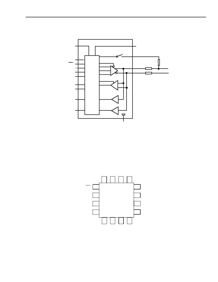
4 Functional Diagram
1. Connect pull-up to D� for low-speed operation.
Figure 1. USS810 Functional Diagram
5 Pin Information
Figure 2. USS810 MLCC Pin Diagram (Top View)
LEVEL
SHIFTER
GND
VM
VP
RCV
SUSPND
OE
VO
V
DD(I/O)
SOFTCON
SPEED
FSE0
+
�
D�
D+
24
(1%)
24
(1%)
1.5 k
1
V
PU(3.3)
V
DD
12
11
10
9
8
7
6
5
13
14
15
16
1
2
3
4
RCV
USS810
MLCC
OE
SO
FTCON
V
PU(3
.3)
NU
V
DD
VP
VM
FSE0
VO
D+
D�
SPEED
V
DD
(
I
/O)
GND
SU
S
P
N
D

4
Agere Systems Inc.
USS810 USB 2.0
Data Sheet, Rev. 6
Full-Speed/Low-Speed Transceiver
March 2006
5 Pin Information
(continued)
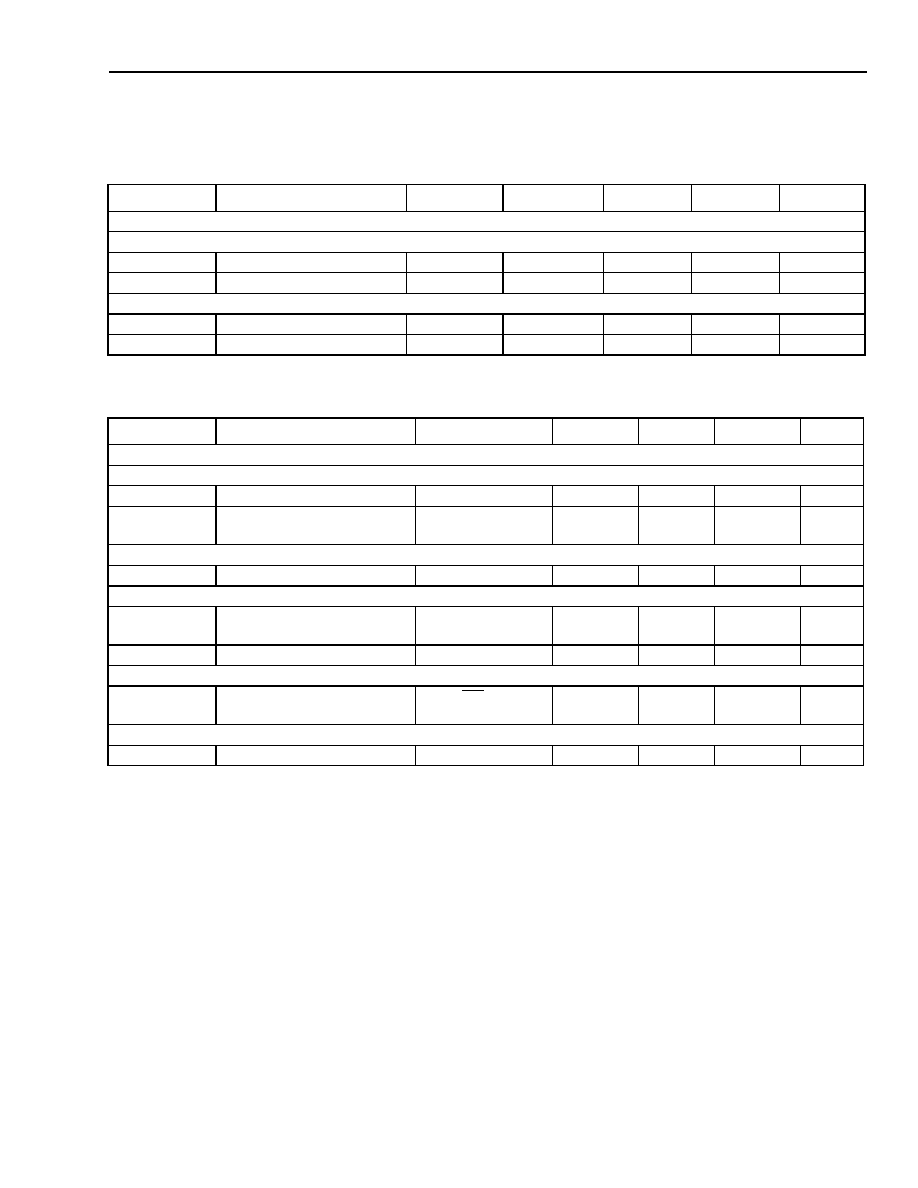
5.1 Pin Descriptions
Table 1. USS810 Pin Description
1. Symbol names with an overscore (e.g., NAME) indicate active-low signals.
Symbol
MLCC
Pin
Type
Description
V
PU(3.3)
15
--
Pull-Up Voltage Source. Connect this pin through an external 1.5 k
resistor to D+
(for full-speed operation) or D� (for low-speed operation). This pin's function is
controlled by the SOFTCON input pin. To ensure zero pull-up current, set
SOFTCON = low to cause V
PU(3.3)
to float (high impedance); when
SOFTCON = high, V
PU(3.3)
= 3.3 V.
SOFTCON
16
I
Software-Controlled USB Connection. This pin allows USB connect/disconnect
signaling to be controlled by software. A high level on this pin applies 3.3 V to pin
V
PU(3.3)
, which is connected to an external 1.5 k
pull-up resistor.
OE
1
1
I
Output Enable. This active-low pin enables the transceiver to transmit data on the
USB bus.
RCV
2
O
Differential Data Receiver. When the SUSPND input is high, this pin is driven low.
The state of RCV is unknown when FSE0 = 1.
VP
3
O
Single-Ended D+ Receiver. The VP pin is used for external detection of single-
ended zero (SE0), error conditions, and speed of connected device.
VM
4
O
Single-Ended D
- Receiver. The VM pin is used for external detection of single-
ended zero (SE0), error conditions, and speed of connected device.
SUSPND
5
I
Suspend. When SUSPND is high, it enables a low-power state while the USB is
inactive and drives output RCV to a low level. No dc power is consumed when
SUSPND is high.
GND
6
P
Device Ground.
V
DD(I/O)
7
P
Power Supply for Digital I/O. 1.75 V to 3.3 V.
SPEED
8
I
Speed Selection. This pin adjusts the slew rate of differential data outputs D+ and
D�. Tie this pin low to enable low-speed data transmission (1.5 Mbits/s) and high to
enable full-speed data transmission (12 Mbits/s).
D�
9
Analog
I/O
Negative USB Differential Data Bus. If this device is used in a USB peripheral
application, connect an external 24
� 1% resistor in series with this signal in
order to meet the USB Specification, Rev. 2.0 impedance requirement. Connect
this signal to pin V
PU(3.3)
via a 1.5 k
� 5% resistor for low-speed USB peripheral
applications.
D+
10
Analog
I/O
Positive USB Differential Data Bus. If this device is used in a USB peripheral
application, connect an external 24
� 1% resistor in series with this signal in
order to meet the USB Specification Rev. 2.0 impedance requirement. Connect this
signal to pin V
PU(3.3)
via a 1.5 k
� 5% resistor for full-speed USB peripheral appli-
cations.
VO
11
I
Single-Ended Data Input. Refer to Table 3..
FSE0
12
I
Single-Ended Zero Mode. Refer to Table 3..
V
DD
13
P
3.3 V Power Supply. This voltage supply is used for the USB signals D+/D� and the
internal level shifter.
NU
14
--
Not Usable. No external connections to this pin are allowed.

Agere Systems Inc.
5
Data Sheet, Rev. 6
USS810 USB 2.0
March 2006
Full-Speed/Low-Speed Transceiver
6 Functional Description
6.1 Function Selection
Table 2. Function Table
1. Signal levels on (D
+, D�) are determined by other USB devices and external pull-up/down resistors.
2. In suspend mode (SUSPND = high), the differential receiver is inactive and output RCV is always low. Out-of-suspend (K) signaling is
detected via the single-ended receivers VP and VM.
3. In suspend mode, the D+/D� output is tristated.
6.1 Operating Functions
Table 3. Transmit Function Using Single-Ended Input Data Interface (OE = L)
Table 4. Receive Function (OE = H)
1. The state of RCV is unknown when FSE0 = 1.
SUSPND
OE
(D+, D�)
RCV
VP/VM
Function
L
L
Transmitting
and Receiving
Active
Active
Normal transmit (differential receiver active)
L
H
Receiving
1
Active
Active
Receiving
H
L
High-Z
3
L
2
Active
Transmitting during suspend (differential
receiver inactive)
H
H
High-Z
3
L
2
Active
Low-power state
FSE0
VO
Data
L
L
Differential logic 0
L
H
Differential logic 1
H
L
SE0
H
H
SE0
(D+, D�)
RCV
VP
VM
Differential Logic 0
L
L
H
Differential Logic 1
H
H
L
SE0
Unknown
1
L
L

6
Agere Systems Inc.
USS810 USB 2.0
Data Sheet, Rev. 6
Full-Speed/Low-Speed Transceiver
March 2006
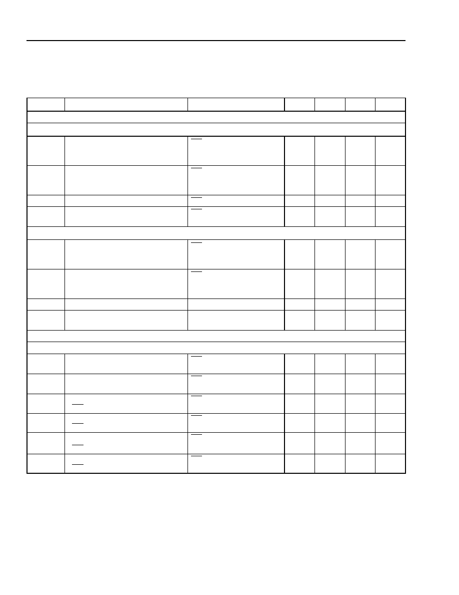
7 Limiting Values
7.1 Absolute Maximum Ratings
Stresses in excess of the absolute maximum ratings can cause permanent damage to the device. These are abso-
lute stress ratings only. Functional operation of the device is not implied at these or any other conditions in excess of
those given in the operational sections of the data sheet. Exposure to absolute maximum ratings for extended
periods can adversely affect device reliability.
Table 5. Absolute Maximum Ratings
Table 6. Recommended Operating Conditions
8 Static Characteristics
Table 7. Static Characteristics: Supply Pins
V
DD
= 3.3 V; V
DD(I/O)
= 1.75 V to 3.3 V; V
GND
= 0 V; T
amb
= �40
�C to +85 �C; unless otherwise specified.
Symbol
Parameter
Conditions
Min
Max
Unit
V
DD(I/O)
I/O Supply Voltage
--
1.7
3.3
V
V
DD(3.3)
3.3 V Supply Voltage
--
3.0
3.6
V
V
I
dc Input Voltage
--
�0.5
V
DD
+ 0.5
V
T
stg
Storage Temperature
--
�40
125
�C
Symbol
Parameter
Conditions
Min
Typical
Max
Unit
V
DD(I/O)
I/O Supply Voltage
--
1.75
--
3.3
V
V
DD(3.3)
3.3 V Supply Voltage
3.3 V operation
3.135
3.3
3.465
V
V
I
Input Voltage
--
0
--
3.3
V
V
I(AI/O)
Input Voltage on Analog
I/O Pins (D+/D�)
--
0
--
V
DD(I/O)
V
T
amb
Operating Ambient
Temperature
--
�40
--
85
�C
Symbol
Parameter
Conditions
Min
Typical
Max
Unit
I
DD
Operating Supply Current
Full-speed transmit and
receive
--
5
8
mA
I
DD(I/O)
Operating I/O Supply
Current
Full-speed transmit and
receive at 12 Mbits/s
--
--
100
�A
I
DD(susp)
Suspend Supply Current
SUSPND = high
--
--
10
�A
Agere Systems Inc.
7
Data Sheet, Rev. 6
USS810 USB 2.0
March 2006
Full-Speed/Low-Speed Transceiver
8 Static Characteristics
(continued)
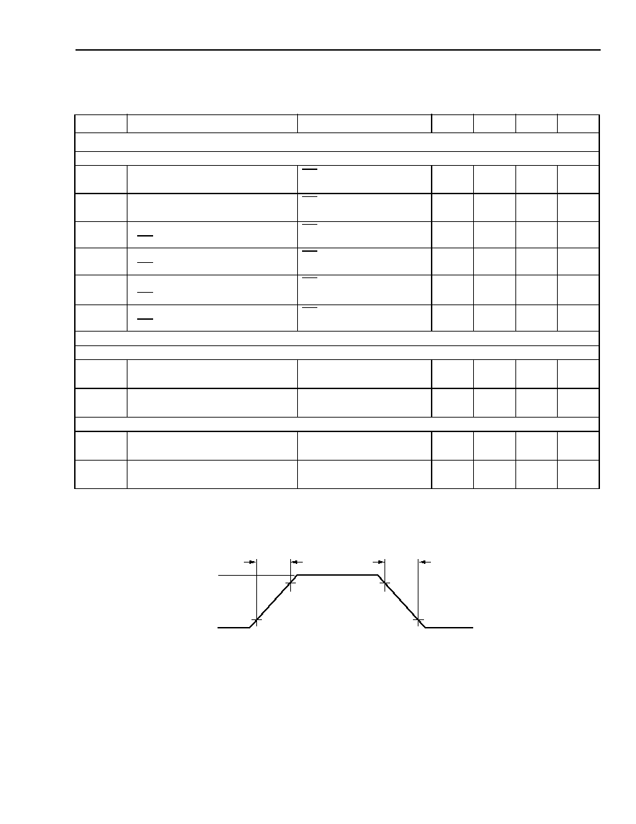
Table 8. Static Characteristics: Digital Pins
V
DD(I/O)
= 1.75 V to 3.3 V; V
GND
= 0 V; T
amb
=
-40 �C to +85 �C; unless otherwise specified.
Table 9. Static Characteristics: Analog I/O Pins (D+, D�)
V
DD
= 3.3 V; V
GND
= 0 V; T
amb
=
-40 �C to +85 �C; unless otherwise specified.
Symbol
Parameter
Conditions
Min
Typical
Max
Unit
V
DD(I/O)
= 1.75 V to 3.3 V
Input Levels:
V
IL
Low-level Input Voltage
--
--
--
0.7
V
V
IH
High-level Input Voltage
--
1.7
--
--
V
Output Levels:
V
OL
Low-level Output Voltage
I
OL
6 mA
--
--
0.4
V
V
OH
High-level Output Voltage
I
OH
6 mA
V
DD
� 0.4
--
--
V
Symbol
Parameter
Conditions
Min
Typical
Max
Unit
Input Levels
Differential Receiver
V
DI
Differential Input Sensitivity
IV
I(D+)
� V
I(D�)
I
0.2
--
--
V
V
CM
Differential Common-mode
Voltage
Includes V
DI
range
0
--
V
DD
V
Single-Ended Receiver
V
hys
Hysteresis Voltage
--
0.3
--
--
V
Output Levels
V
OL
Low-level Output Voltage
R
L
= 1.5 k
to
3.6 V
--
--
0.3
V
V
OH
High-level Output Voltage
R
L
= 15 k
to GND
2.8
--
3.6
V
Leakage Current
I
LZ
High-impedance Leakage
Current
OE = 1
�10
--
10
�A
Capacitance
C
IN
Transceiver Capacitance
Pin to GND
--
--
3
pF
8
Agere Systems Inc.
USS810 USB 2.0
Data Sheet, Rev. 6
Full-Speed/Low-Speed Transceiver
March 2006
9 Dynamic Characteristics
Table 10. Dynamic Characteristics: Analog I/O Pins (D+, D�)
1
V
DD
= 3.3 V; V
DD(I/O)
= 1.75 V to 3.3 V; V
GND
= 0 V; Tamb = �40
�C to +85 �C; unless otherwise specified.
1. Test circuit: see Figure 7.
Symbol
Parameter
Conditions
Min
Typical
Max
Unit
Driver Characteristics
Full-Speed Mode (Speed = 1)
t
R
Rise Time
OE = 0, CL = 50 pF;
10% to 90% of
|V
OL
- V
OH
|;
see Figure 3..
4
--
20
ns
t
F
Fall Time
OE = 0, CL = 50 pF;
90% to 10% of
|V
OH
- V
OL
|;
see Figure 3.
4
--
20
ns
DRFM
Differential Rise/Fall Time Matching OE = 0, CL = 50 pF.
90
100
110
%
V
CRS
Output Signal Crossover Voltage
OE = 0, CL = 50 pF:
see Figures 4, 5, 6.
1.3
--
2.0
V
Low-Speed Mode (Speed = 0)
t
R
Rise Time
OE = 0, CL = 50 pF or
350 pF; 10% to 90% of
|V
OL
- V
OH
|; see Figure 3.
75
--
300
ns
t
F
Fall Time
OE = 0, CL = 50 pF or
350 pF; 90% to 10% of
|V
OH
- V
OL
|; see Figure 3.
75
--
300
ns
DRFM
Differential Rise/Fall Time Matching CL = 50 pF or 350 pF.
80
100
120
%
V
CRS
Output Signal Crossover Voltage
CL = 50 pF or 350 pF;
see Figures 4, 5, 6.
1.3
--
2.0
V
Driver Timing
Full-Speed Mode (Speed = 1)
t
PLH
Driver Propagation Delay:
Low-to-High (VO, FSE0 to D+, D�)
OE = 0, CL = 50 pF; see
Figure 6.
--
--
18
ns
t
PHL
Driver Propagation Delay:
High-to-Low (VO, FSE0 to D+, D�)
OE = 0, CL = 50 pF; see
Figure 6.
--
--
18
ns
t
PHZ
Tristate Output Disable: High-to-Off
(OE to D+, D-)
OE switching; see Figure 4.
--
--
2.5
ns
t
PLZ
Tristate Output Disable: Low-to-Off
(OE to D+, D-)
OE switching; see Figure 4.
--
--
2.5
ns
t
PZH
Tristate Output Enable: Off-to-High
(OE to D+, D-)
OE switching; see Figure 4.
--
--
20
ns
t
PZL
Tristate Output Enable: Off-to-Low
(OE to D+, D-)
OE switching; see Figure 4.
--
--
20
ns
Agere Systems Inc.
9
Data Sheet, Rev. 6
USS810 USB 2.0
March 2006
Full-Speed/Low-Speed Transceiver
9 Dynamic Characteristics
(continued)
Table 10. Dynamic Characteristics: Analog I/O Pins (D+, D�)
1
(continued)
1. Test circuit: see Figure 7
.
Figure 3. Rise and Fall Times
Symbol
Parameter
Conditions
Min
Typical
Max
Unit
Driver Timing (continued)
Low-Speed Mode (SPEED = 0)
t
PLH
Driver Propagation Delay:
Low-to-High (VO, FSE0 to D+, D�)
OE = 0, CL = 50 pF; see
Figure 6.
--
--
250
ns
t
PHL
Driver Propagation Delay:
High-to-Low (VO, FSE0 to D+, D�)
OE = 0, CL = 50 pF; see
Figure 6.
--
--
250
ns
t
PHZ
Tristate Output Disable: High-to-Off
(OE to D+, D-)
OE switching; see Figure 4.
--
--
4
ns
t
PLZ
Tristate Output Disable: Low-to-Off
(OE to D+, D-)
OE switching; see Figure 4.
--
--
4
ns
t
PZH
Tristate Output Enable: Off-to-High
(OE to D+, D-)
OE switching; see Figure 4.
--
--
400
ns
t
PZL
Tristate Output Enable: Off-to-Low
(OE to D+, D-)
OE switching; see Figure
4..
--
--
400
ns
Receiver Timing (Full-Speed and Low-Speed Mode)
Differential Receiver
t
PLH(dif)
Propagation Delay; Low-to-High
(D
+, D- to RCV)
See Figure 5..
--
--
5
ns
t
PHL(dif)
Propagation Delay; High-to-Low
(D
+, D- to RCV)
See Figure 5..
--
--
5
ns
Single-Ended Receiver
t
PLH(se)
Propagation Delay; Low-to-High
(D
+, D- to VP, VM)
See Figure 5..
--
--
3
ns
t
PHL(se)
Propagation Delay; High-to-Low
(D
+, D- to VP, VM)
See Figure 5..
--
--
3
ns
MGS963
VOL
tFR, tLR
tFF, tLF
VOH
90%
10%
10%
90%
tR
tF

10
Agere Systems Inc.
USS810 USB 2.0
Data Sheet, Rev. 6
Full-Speed/Low-Speed Transceiver
March 2006
9 Dynamic Characteristics
(continued)
Figure 4. Timing of OE to D+, D�
Figure 5. Timing of D+, D� to RCV, VP, VM
Figure 6. Timing of VO, FSE0 to D+, D�
MGS966
VOL
VOH
tPZH
tPZL
tPHZ
tPLZ
VOH -0.3 V
VOL +0.3 V
VCRS
0.9 V
0.9 V
1.65 V
0 V
logic input
differential
data lines
DIFFERENTIAL
DATA LINES
LOGIC INPUT
1.75 V
MGS965
VOL
VOH
tPHL(rcv)
tPHL(se)
tPLH(rcv)
tPLH(se)
VCRS
VCRS
0.9 V
0.9 V
2.0 V
0.8 V
logic output
differential
data lines
LOGIC OUTPUT
DIFFERENTIAL
DATA LINES
MGS964
VOL
VOH
tPHL(drv)
tPLH(drv)
VCRS
VCRS
0.9 V
0.9 V
1.65 V
0 V
logic input
differential
data lines
DIFFERENTIAL
DATA LINES
LOGIC INPUT
1.75 V

Agere Systems Inc.
11
Data Sheet, Rev. 6
USS810 USB 2.0
March 2006
Full-Speed/Low-Speed Transceiver
10 Test Information
Load Capacitance:
CL = 50 pF (full-speed mode).
CL = 50 pF or 350 pF (low-speed mode).
1. Full-speed mode: connected to D+, low-speed mode: connected to D�.
2. Complies with USB2.0.
Figure 7. Load for D+, D�
24
2
DUT
V
PU(3.3)
15 k
D+/D�
TEST POINT
C
L
1.5 k
1
12
12
Agere Systems Inc.
USS810 USB 2.0
Data Sheet, Rev. 6
Full-Speed/Low-Speed Transceiver
March 2006
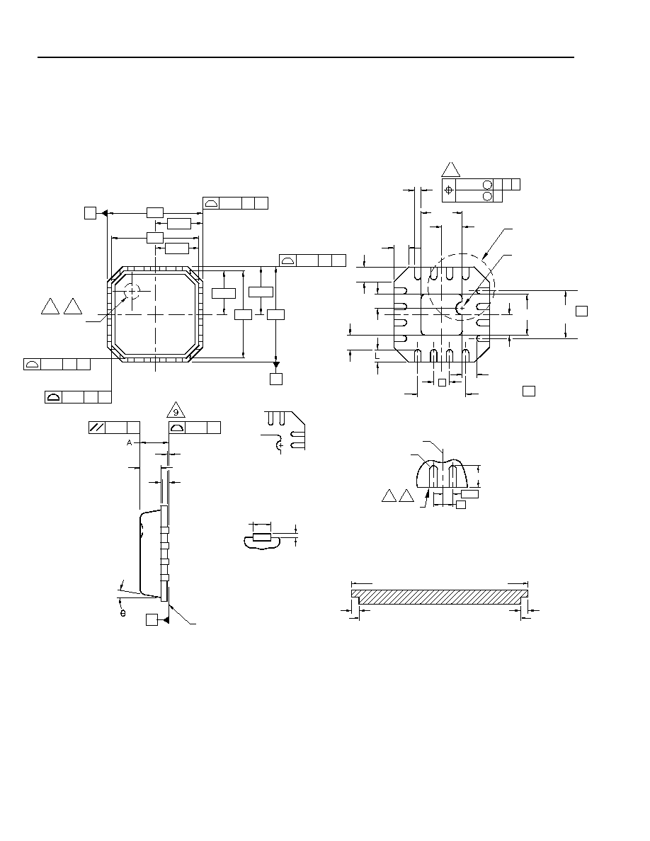
11 Package Outline Diagram
11.1 16-Pin MLCC, 3 mm x 3 mm
Dimensions are in millimeters.
Notes (Refer also to Tables 11 and 12):
1. Die thickness allowable is 0.305 mm maximum (0.012 inches maximum).
2. Dimensioning and tolerances conform to ASME Y14.5M-1994.
3. N is the number of terminals. Nd is the number of terminals in X direction, and Ne is the number of terminals in the Y direction.
4. Dimension b applies to plated terminal and is measured between 0.2 mm and 0.25 mm from terminal tip.
5. The pin #1 identifier must be existed on the top surface of the package by using identification mark or other feature of package body.
6. Exact shape and size of this feature is optional.
7. All dimensions are in millimeters.
8. The shape shown on four corners is not actual I/O.
9. Bilateral coplanarity zone applies to the exposed pad as well as the terminals.
10. Applied only for terminals.
11. Q and R apply only for straight tie bar shapes.
N
2
1
TOP VIEW
SEE DETAIL A
FOR PIN #1 ID
AND TIE BAR
MARK OPTION
PIN #1 ID
R0.20
BOTTOM VIEW
SIDE VIEW
SEATING
PLANE
0.50 DIA
2X
2X
A
0.10 C
B
0.10 C
B
0.10 C
A
0.10 C
2X
2X
5
6
A
D
D/2
D1/2
D1
E1/2
E/2
E
E1
B
(MIN. 0.35)
4
0.10 M C A B
M C
0.05
b
D2
D2/2
4X P
4X P
0.45
N
(MIN. 0.35)
1
2
e
e
e
(Ne � 1) X
REF.
E2
E2/2
(Nd � 1) X
REF.
0.10 C
0.05 C
A1
A3
A2
C
SECTION C-C
SCALE: NONE
b
A1
GENERAL: NOMINAL EXPOSED PAD (D2/E2) DIMENSION =
NOMINAL DIE ATACHED PAD DIMENSION � 0.
NOMINAL DIE ATTACH PAD DIMENSION
NOMINAL EXPOSED PAD (D2/E2) DIMENSION
<DIE ATTACH PAD X -- SECTION VIEW>
0.10
0.10
e/2
FOR EVEN TERMINAL/SIDE
DATUM A OR B
NX R
4
10
(L)
e
DETAIL A - PIN# ID AND
TIEBAR MARK FIGURES
STANDARD
Agere Systems Inc.
13
Data Sheet, Rev. 6
USS810 USB 2.0
March 2006
Full-Speed/Low-Speed Transceiver
11 Package Outline Diagram
(continued)
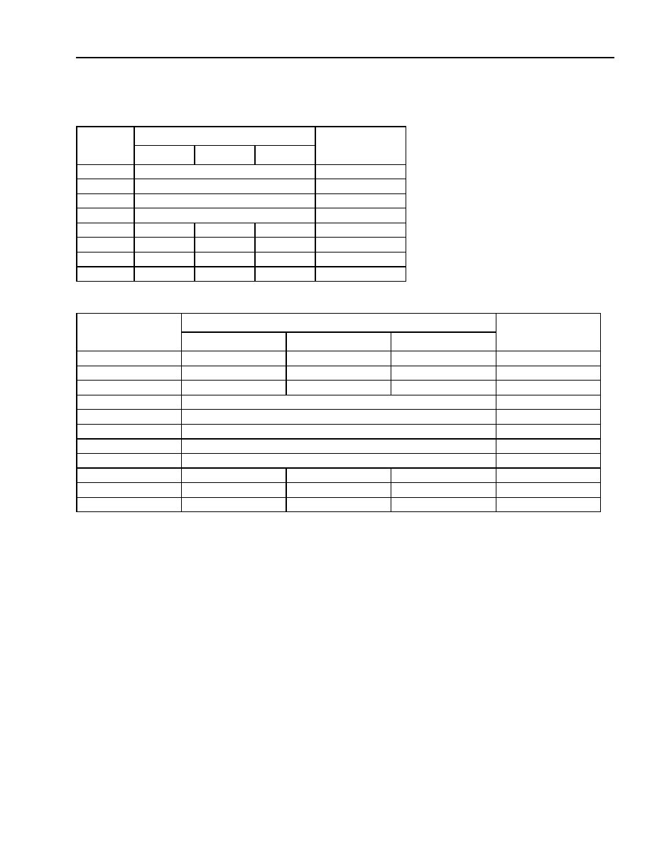
Table 11. Pitch Variation
Table 12. Common Dimensions
Symbol
Pitch Variation
Notes
Min
Nom
Max
e
0.5 BSC
--
N
16
3
Nd
4
3
Ne
4
3
L
0.3
0.4
0.5
--
b
0.18
0.23
0.3
4
D2
1.40
1.50
1.60
--
E2
1.40
1.50
1.60
--
Symbol
Common Dimensions
Notes
Min
Nom
Max
A
0.8
0.85
0.9
--
A1
0.0
0.01
0.05
11
A2
0.6
0.65
0.70
--
A3
0.20 REF
--
D
3.0 BSC
--
D1
2.75 BSC
--
E
3.0 BSC
--
E1
2.75 BSC
--
0
--
12
--
P
0.24
0.42
0.6
--
R
0.13
0.17
0.23
12
USS810 USB 2.0
Data Sheet, Rev. 6
Full-Speed/Low-Speed Transceiver
March 2006
Agere Systems Inc. reserves the right to make changes to the product(s) or information contained herein without notice. No liability is assumed as a result of their use or application.
Agere, Agere Systems, and the Agere logo are registered trademarks of Agere Systems Inc.
Copyright � 2006 Agere Systems Inc.
All Rights Reserved
March 2006
DS05-035CMPR-6 (Replaces DS05-035CMPR-5)
For additional information, contact your Agere Systems Account Manager or the following:
INTERNET:
Home: http://www.agere.com Sales: http://www.agere.com/sales
E-MAIL:
docmaster@agere.com
N. AMERICA: Agere Systems Inc., Lehigh Valley Central Campus, Room 10A-301C, 1110 American Parkway NE, Allentown, PA 18109-9138
1-800-372-2447, FAX 610-712-4106 (In CANADA: 1-800-553-2448, FAX 610-712-4106)
ASIA:
CHINA: (86) 21-54614688 (Shanghai), (86) 755-25881122 (Shenzhen), (86) 10-65391096 (Beijing)
JAPAN: (81) 3-5421-1600 (Tokyo), KOREA: (82) 2-767-1850 (Seoul), SINGAPORE: (65) 6741-9855, TAIWAN: (886) 2-2725-5858 (Taipei)
EUROPE:
Tel. (44) 1344 296 400
12 USB Application Support Contact Information
E-mail: usb@agere.com
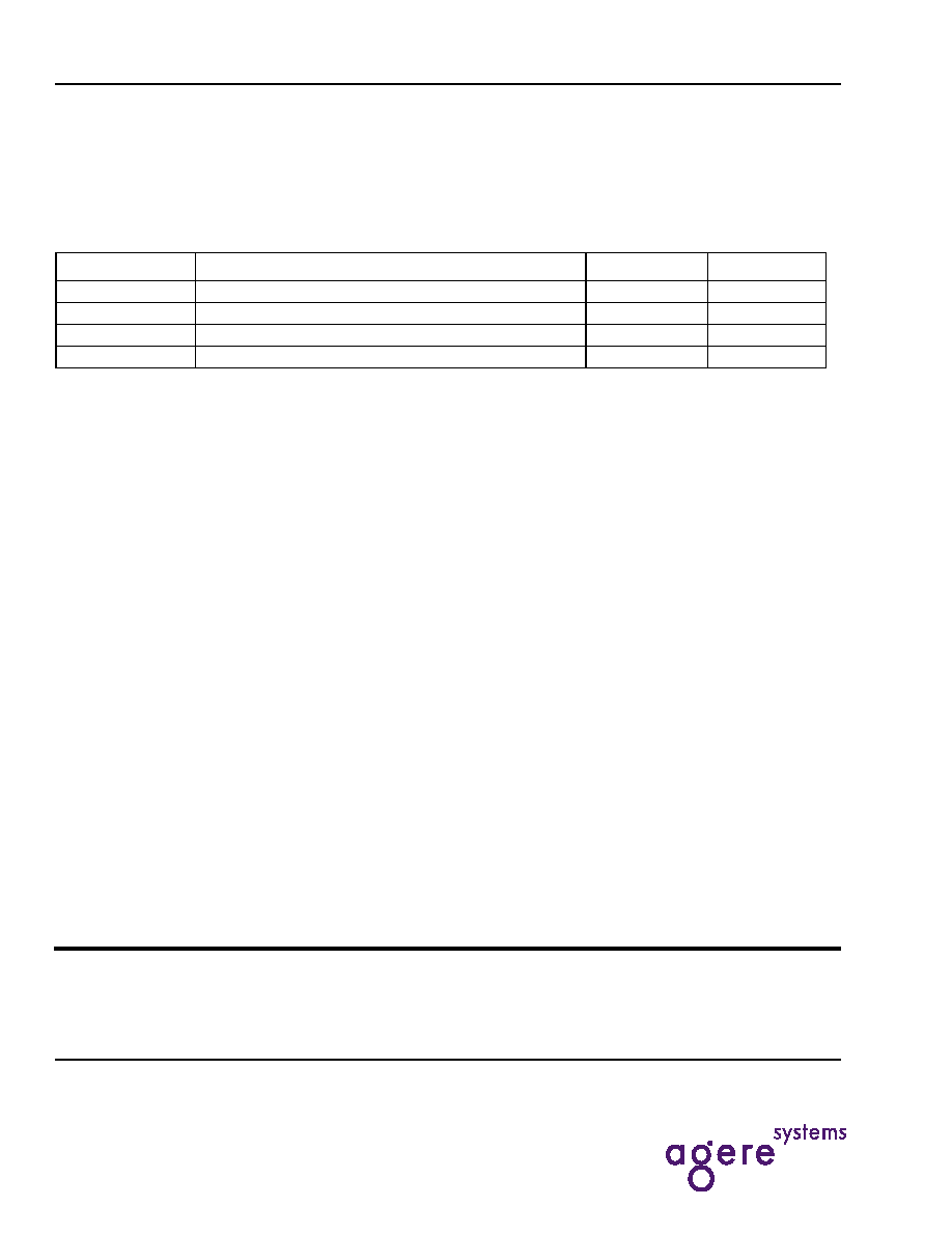
13 Ordering Information
* Lead-free: No intentional addition of lead, and less than 1000 ppm.
Agere Systems lead-free devices are fully compliant with the Restriction of Hazardous Substances (RoHS) directive that restricts the content
of six hazardous substances in electronic equipment in the European Union. Beginning July 1, 2006, electronic equipment sold in the Euro-
pean Union must be manufactured in accordance with the standards set by the RoHS directive.
Device Code
Description
Package
Comcode
USS810M-D
USS810 in dry-packed tube
MLCC16
700057479
USS810M-DT
USS810 in dry-packed tape and reel
MLCC16
700058082
L-USS810M-D*
Lead-free USS810 in dry-packed tube
MLCC16
700067200
L-USS810M-D*
Lead-free USS810 in dry-packed tape and reel
MLCC16
700067201