 | –≠–ª–µ–∫—Ç—Ä–æ–Ω–Ω—ã–π –∫–æ–º–ø–æ–Ω–µ–Ω—Ç: USS-820FD | –°–∫–∞—á–∞—Ç—å:  PDF PDF  ZIP ZIP |

Data Sheet, Rev. 1
August 2004
USS-820FD
USB Device Controller
Features
Full compliance with the Universal Serial Bus
Specification Revision 1.1.
Backward compatible with USS-820B, USS-820C,
and USS-820D revisions.
Self-powered or bus-powered USB device. Meets
USB power specifications for bus-powered
devices.
Full-speed USB device (12 Mbits/s).
USB device controller with protocol control and
administration for up to 16 USB endpoints.
Supports control, interrupt, bulk, and isochronous
transfers for all 16 endpoints.
Programmable endpoint types, FIFO sizes, and
internal 1120-byte logical (2240-byte physical for
dual-packet mode) shared FIFO storage allow a
wide variety of configurations.
Dual-packet mode of FIFOs reduces latency.
Supports USB remote wake-up feature.
On-chip crystal oscillator allows external 12 MHz
crystal or 3 V/5 V clock source.
On-chip analog PLL creates 48 MHz clock from
internal 12 MHz clock.
Integrated USB transceivers.
5 V tolerant I/O buffers allow operation in 3 V or
5 V system environments for 0 ∞C to 70 ∞C temper-
ature range.
5 V tolerant I/O buffers allow operation in 3 V only
system environments for ≠20 ∞C to +85 ∞C temper-
ature range.
Implemented in Agere Systems Inc. 0.25
µ
m, 3 V
standard-cell library.
48-ball TFSBGAC. (Lead-free package also avail-
able. (See Ordering Information on page 51.)
Evaluation kit available.
New Features After Revision B
New, centralized FIFO status bits and interrupt out-
put pin reduce firmware load.
New, additional nonisochronous transmit mode
allows NAK response to cause interrupt.
Isochronous behavior enhancements simplify firm-
ware control.
Additional FIFO sizes for nonisochronous end-
points.
USB reset can be programmed to clear device
address.
USB reset output status pin.
Firmware ability to wake up and reset a suspended
device.
Lower power.
5 V supply no longer required for 5 V tolerant oper-
ation.
Applications
Suitable for peripherals with embedded micropro-
cessors.
Glueless interface to microprocessor buses.
Support of multifunction USB implementations,
such as printer/scanner and integrated multimedia
applications.
Suitable for a broad range of device class peripher-
als in the USB standard.
Note: Advisories are issued as needed to update product information. When using this data sheet for design purposes, please contact
your Agere Systems Account Manager to obtain the latest advisory on this product.

Table of Contents
Contents
Page
Data Sheet, Rev. 1
August 2004
USB Device Controller
USS-820FD
2
Agere Systems Inc.
Features ....................................................................................................................................................................1
New Features After Revision B .................................................................................................................................1
Applications ...............................................................................................................................................................1
Description.................................................................................................................................................................3
Serial Interface Engine............................................................................................................................................ 3
Protocol Layer ......................................................................................................................................................... 4
FIFO Control ........................................................................................................................................................... 4
FIFO Programmability ............................................................................................................................................. 4
FIFO Access ........................................................................................................................................................... 4
Transmit FIFO ...................................................................................................................................................... 5
Receive FIFO ....................................................................................................................................................... 6
Pin Information .........................................................................................................................................................7
Register Timing Characteristics.................................................................................................................................9
Register Interface ....................................................................................................................................................11
Special Firmware Action for Shared Register Bits ................................................................................................ 13
Register Reads with Side Effects.......................................................................................................................... 14
Register Descriptions ............................................................................................................................................ 15
Interrupts .................................................................................................................................................................40
Firmware Responsibilities for USB SETUP Commands..........................................................................................41
Other Firmware Responsibilities..............................................................................................................................42
Frame Timer Behavior.............................................................................................................................................42
Suspend and Resume Behavior..............................................................................................................................42
Hardware Suspend Detect .................................................................................................................................... 43
Firmware Suspend Initiate .................................................................................................................................... 43
Hardware Resume Detect/Initiate .........................................................................................................................44
Hardware Resume Sequence ............................................................................................................................... 44
Firmware Resume Sequence ............................................................................................................................... 44
Special Suspend Considerations for Bus-Powered Devices ................................................................................ 44
Application Notes.....................................................................................................................................................46
USB Application Support Contact Information.........................................................................................................46
Absolute Maximum Ratings.....................................................................................................................................46
Electrical Characteristics .........................................................................................................................................47
dc Characteristics ................................................................................................................................................. 47
Power Considerations ...........................................................................................................................................48
USB Transceiver Driver Characteristics ............................................................................................................... 48
Connection Requirements .................................................................................................................................... 49
USB Transceiver Connection ............................................................................................................................. 49
Oscillator Connection Requirements.................................................................................................................. 50
Outline Diagrams.....................................................................................................................................................51
48-Ball TFSBGAC (USS-820FD) .......................................................................................................................... 51
Ordering Information................................................................................................................................................51
Appendix A. Special Function Register Bit Names..................................................................................................52
Appendix B. USS-820FD Register Map ..................................................................................................................53
Appendix C. Changes from USS-820/USS-825 Revision B to C ............................................................................54
Appendix D. Changes from USS-820 Revision C to D............................................................................................55
Appendix E. Changes from USS-820 Revision D to FD..........................................................................................55
Data Sheet, Rev. 1
August 2004
Agere Systems Inc.
3
USB Device Controller
USS-820FD
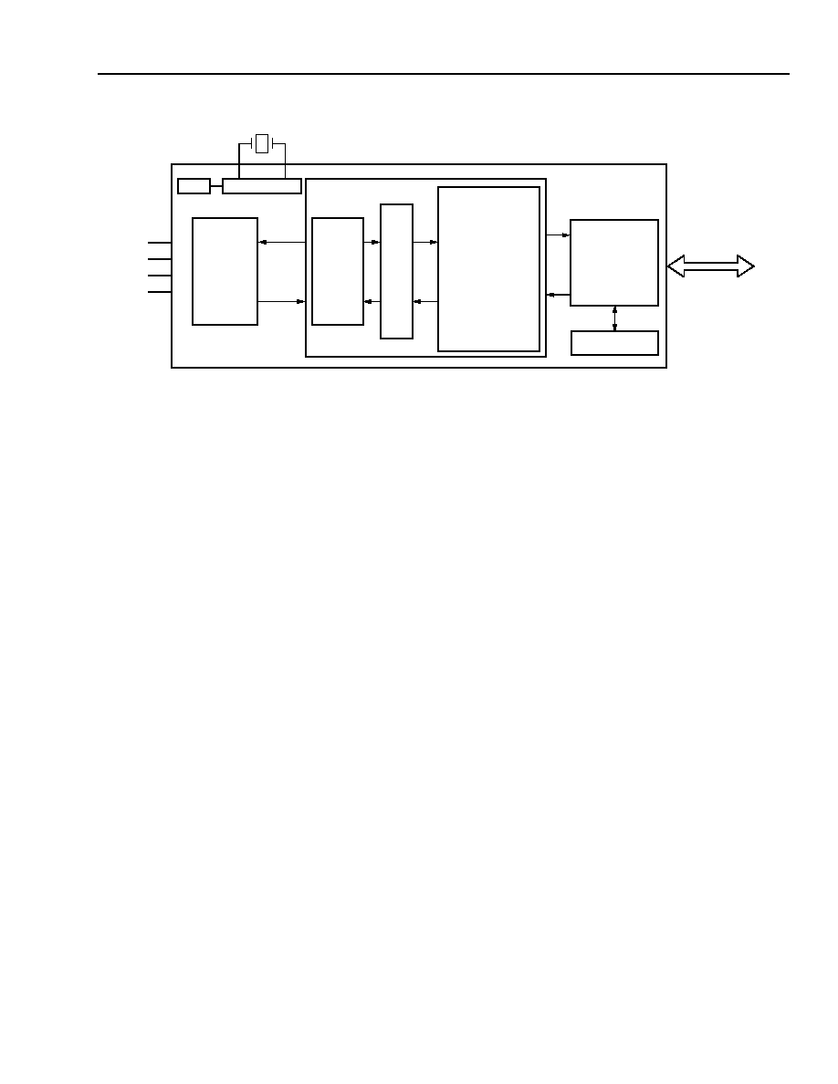
Description
5-8121
Figure 1. Block Diagram
USB
FIFO
SIE
PROTOCOL
LAYER
EXTERNAL
MICROPROCESSOR
DPLS
DMNS
CONTROL
XCVR
DIGITAL
BUS
V
SS
V
DD
FIFOs
USS-820FD
OSCILLATOR
PLL
PLL
USS-820FD is a USB device controller that provides a
programmable bridge between the USB and a local
microprocessor bus. It is available in a 48-ball
TFSBGAC package. The USS-820FD allows PC
peripherals to upgrade to USB connectivity without
major redesign effort. It is programmable through a
simple read/write register interface that is compatible
with industry-standard USB microcontrollers.
USS-820FD is designed in 100% compliance with the
USB industry standard, allowing device-side USB prod-
ucts to be reliably installed using low-cost, off-the-shelf
cables and connectors.
The integrated USB transceiver supports 12 Mbits/s
full-speed operation. FIFO options support all four
transfer types: control, interrupt, bulk, and isochronous,
as described in Universal Serial Bus Specification
Revision 1.1, with a wide range of packet sizes. Its
double sets of FIFO enable the dual-packet mode
feature. The dual-packet mode feature reduces latency
by allowing simultaneous transfers on the host and
microprocessor sides of a given unidirectional
endpoint.
The USS-820FD supports a maximum of eight bidirec-
tional endpoints with 16 FIFOs (eight for transmit and
eight for receive) associated with them. The FIFOs are
on-chip, and sizes are programmable up to a total of
1120 logical bytes. When the dual-packet mode feature
is enabled, the device uses a maximum of 2240 bytes
of physical storage. This additional physical FIFO stor-
age is managed by the device hardware and is trans-
parent to the user.
The FIFO sizes supported are 8 bytes, 16 bytes,
32 bytes, and 64 bytes for nonisochronous pipes, and
64 bytes, 256 bytes, 512 bytes, and 1024 bytes for iso-
chronous pipes. The FIFO size of a given endpoint
defines the upper limit to maximum packet size that the
hardware can support for that endpoint. This flexibility
covers a wide range of data rates, data types, and
combinations of applications.
The USS-820FD can be clocked either by connecting a
12 MHz crystal to the XTAL1 and XTAL2 pins, or by
using a 12 MHz external oscillator. The internal 12 MHz
clock period, which is a function of either of these clock
sources, is referred to as the device clock period (t
CLK
)
throughout this data sheet.
Serial Interface Engine
The SIE is the USB protocol interpreter. It serves as a
communicator between the USS-820FD and the host
through the USB lines.
The SIE functions include the following:
Package protocol sequencing.
SOP (start of packet), EOP (end of packet),
RESUME, and RESET signal detection and genera-
tion.
NRZI data encoding/decoding and bit stuffing.
CRC generation and checking for token and data.
Serial-to-parallel and parallel-to-serial data conver-
sion.

4
4
Agere Systems Inc.
Data Sheet, Rev. 1
August 2004
USB Device Controller
USS-820FD
Description
(continued)
Protocol Layer
The protocol layer manages the interface between the
SIE and FIFO control blocks. It passes all USB OUT
and SETUP packets through to the appropriate FIFO. It
is the responsibility of firmware to correctly interpret
and execute each USB SETUP command (as docu-
mented in the Firmware Responsibilities for USB
SETUP Commands section) via the register interface.
The protocol layer tracks the setup, data, and status
stages of control transfers.
FIFO Control
USS-820FD's FIFO control manager handles the data
flow between the FIFOs and the device controller's pro-
tocol layer. It handles flow control and error handling/
fault recovery to monitor transaction status and to relay
control events via interrupt vectors.
FIFO Programmability
Table 1 shows the programmable FIFO sizes. The size
of the FIFO determines the maximum packet size that
the hardware can support for a given endpoint. An end-
point is only allocated space in the shared FIFO stor-
age if its RXEPEN/TXEPEN bit = 1. If the endpoint is
disabled (RXEPEN/TXEPEN = 0), it is allocated
0 bytes. Register changes that affect the allocation of
the shared FIFO storage among endpoints must not be
made while there is valid data present in any of the
enabled endpoints' FIFOs. Any such changes will ren-
der all FIFO contents undefined. Register bits that
affect the FIFO allocation are the endpoint enable bits
(the TXEPEN and RXEPEN bits of EPCON), the size
bits of an enabled endpoint (FFSZ bits of TXCON and
RXCON), the isochronous bit of an enabled endpoint
(TXISO bit of TXCON and RXISO bit of RXCON), and
the FEAT bit of the MCSR register.
If the MCSR.FEAT register bit is set to 1, additional
FIFO sizes are enabled for nonisochronous endpoints,
as shown in Table 1.
Table 1. Programmable FIFO Sizes
* Assumes MCSR.FEAT = 1. If this bit is 0 and FFSZ = 10 or 11, both
indicate a size of 64 bytes.
Each FIFO can be programmed independently via the
TXCON and RXCON registers, but the total logical size
of the enabled endpoints (TX FIFOs + RX FIFOs) must
not exceed 1120 bytes. The 1120-byte total allows a
configuration with a full-sized, 1024-byte isochronous
endpoint, a minimum-sized, 64-byte isochronous feed-
back endpoint, and the required, bidirectional, 16-byte
control endpoint. When the dual-packet mode feature
is enabled, the device uses a maximum of 2240 bytes
of physical storage. This additional physical FIFO stor-
age is managed by the device hardware and is trans-
parent to the user.
FIFO Access
The transmit and receive FIFOs are accessed by the
application through the register interface (see
Tables 23--26 for transmit FIFO registers and
Tables 27--30 for receive FIFO registers).
The transmit FIFO is written to via the TXDAT register,
and the receive FIFO is read via the RXDAT register.
The particular transmit/receive FIFO is specified by the
EPINDEX register. Each FIFO is accessed serially,
each RXDAT read increments the receive FIFO read
pointer by 1, and each TXDAT write increments the
transmit FIFO write pointer by 1.
Each FIFO consists of two data sets to provide the
capability for simultaneous read/write access. Control
of these pairs of data sets is managed by the hard-
ware, invisible to the application, although the applica-
tion must be aware of the implications. The receive
FIFO read access is advanced to the next data set by
firmware setting the RXFFRC bit of RXCON. This bit
clears itself after the advance is complete. The transmit
FIFO write access is advanced to the next data set by
firmware writing the byte count to the TXCNTH/L regis-
ters.
The USB access to the receive and transmit FIFOs is
managed by the hardware, although the control of the
nonisochronous data sets can be overridden by the
ARM and ATM bits of RXCON and TXCON, respec-
tively. A successful USB transaction causes FIFO
access to be advanced to the next data set. A failed
USB transaction (e.g., for receive operations, FIFO
overrun, data time-out, CRC error, bit stuff error; for
transmit operations, FIFO underrun, no ACK from host)
causes the FIFO read/write pointer to be reversed to
the beginning of the data set to allow transmission retry
for nonisochronous transfers.
FFSZ[1:0]
00
01
10
11
Nonisoch-
ronous
16 bytes 64 bytes
8 bytes*
32 bytes*
Isochro-
nous
64 bytes 256 bytes 512 bytes 1024 bytes
Agere Systems Inc.
5
Data Sheet, Rev. 1
August 2004
USB Device Controller
USS-820FD
Description
(continued)
FIFO Access
(continued)
Transmit FIFO
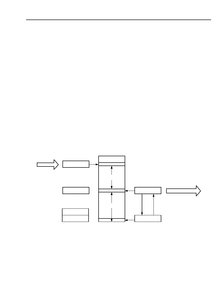
The transmit FIFOs are circulating data buffers that have the following features:
Support up to two separate data sets of variable sizes (dual-packet mode).
Include byte counter register for storing the number of bytes in the data sets.
Protect against overwriting data in a full FIFO.
Can retransmit the current data set.
All transmit FIFOs use the same architecture (see Figure 2). The transmit FIFO and its associated logic can man-
age up to two data sets: data set 0 (ds0) and data set 1 (ds1). Since two data sets can be used in the FIFO, back-
to-back transmissions are supported. Dual-packet mode for transmit FIFOs is enabled by default. Single-packet
mode can be enforced by firmware convention (see TXFIF register bits).
The CPU writes to the FIFO location that is specified by the write pointer. After a write, the write pointer automati-
cally increments by 1. The read marker points to the first byte of data written to a data set, and the read pointer
points to the next FIFO location to be read by the USB interface. After a read, the read pointer automatically incre-
ments by 1.
When a good transmission is completed, the read marker can be advanced to the position of the read pointer to set
up for reading the next data set. When a bad transmission is completed, the read pointer can be reversed to the
position of the read marker to enable the function interface to reread the last data set for retransmission. The read
marker advance and read pointer reversal can be achieved two ways: explicitly by firmware or automatically by
hardware, as indicated by bits in the transmit FIFO control register (TXCON).
5-5206
Figure 2. Transmit FIFO
READ POINTER
WRITE POINTER
READ MARKER
TXCNTH
TXCNTL
BYTE COUNT
REGISTERS
FROM CPU
CPU
WRITES TO FIFO
TO USB INTERFACE
DATA SET 0
DATA SET 1
SIE READS FIFO
ADVRM
REVRP
TXDAT
6
Agere Systems Inc.
Data Sheet, Rev. 1
August 2004
USB Device Controller
USS-820FD
USB Device Controller
Description
(continued)
FIFO Access
(continued)
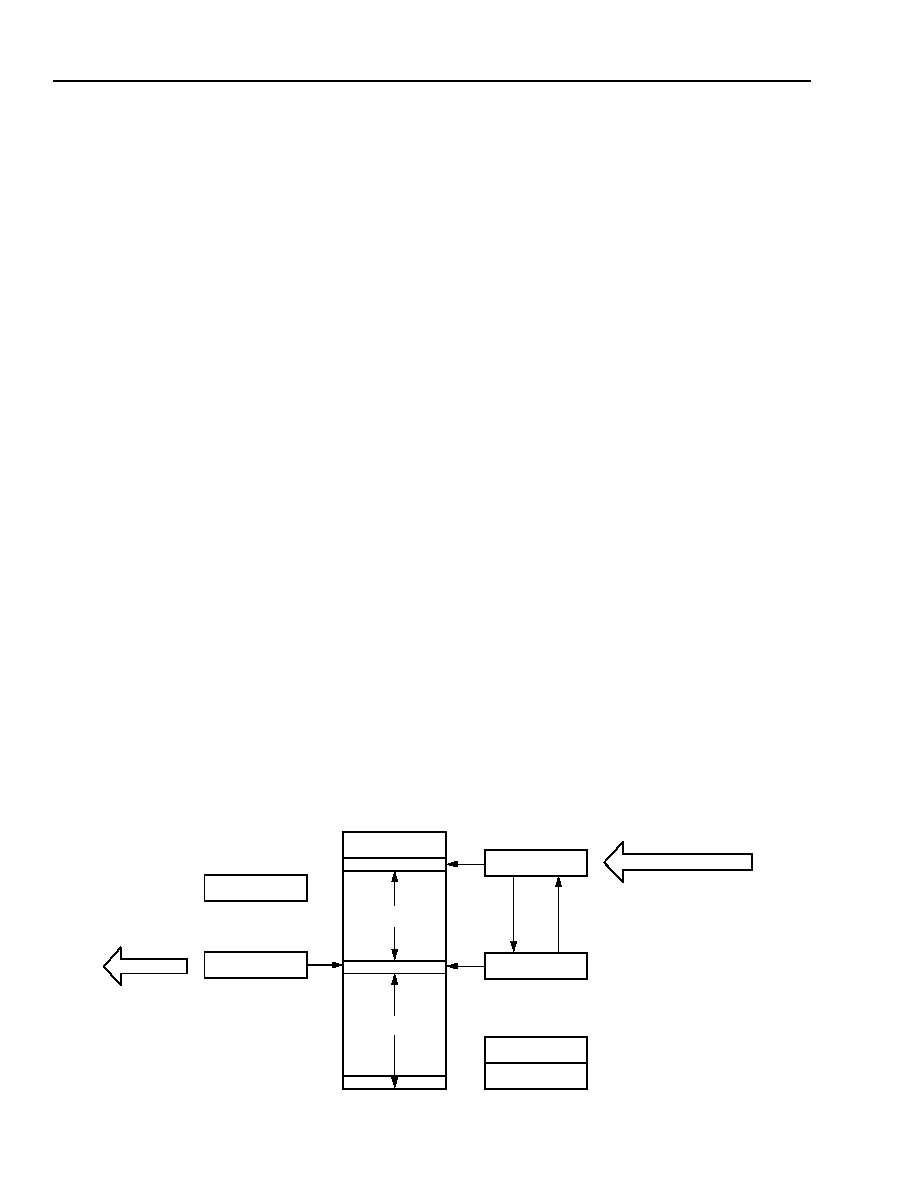
Receive FIFO
The receive FIFOs are circulating data buffers that have the following features:
Support up to two separate data sets of variable sizes (dual-packet mode).
Include byte count register that accesses the number of bytes in data sets.
Include flags to signal a full FIFO and an empty FIFO.
Can reread the last data set.
Figure 3 shows a receive FIFO. A receive FIFO and its associated logic can manage up to two data sets: data set 0
(ds0) and data set 1 (ds1). Since two data sets can be used in the FIFO, back-to-back transmissions are
supported. Single-packet mode is established by default after a USS-820FD device reset, which sets the RXSPM
register bit. Firmware can enable dual-packet mode by clearing the RXSPM bit to 0.
The receive FIFO is symmetrical to the transmit FIFO in many ways. The SIE writes to the FIFO location specified
by the write pointer. After a write, the write pointer automatically increments by 1. The write marker points to the
first byte of data written to a data set, and the read pointer points to the next FIFO location to be read by the CPU.
After a read, the read pointer automatically increments by 1.
When a good reception is completed, the write marker can be advanced to the position of the write pointer to set up
for writing the next data set. When a bad transmission is completed, the write pointer can be reversed to the posi-
tion of the write marker to enable the SIE to rewrite the last data set after receiving the data again. The write
marker advance and write pointer reversal can be achieved two ways: explicitly by firmware or automatically by
hardware, as specified by bits in the receive FIFO control register (RXCON).
The CPU should not read data from the receive FIFO before all bytes are received and successfully acknowledged
because the reception may be bad.
To avoid overwriting data in the receive FIFO, the SIE monitors the FIFO full flag (RXFULL bit in RXFLG). To avoid
reading a byte when the FIFO is empty, the CPU can monitor the FIFO empty flag (RXEMP bit in RXFLG).
The CPU must not change the value of the EPINDEX register during the process of reading a data set from a par-
ticular receive FIFO. Once the CPU has read the first byte of a data set, the processor must ensure that the EPIN-
DEX register setting remains unchanged until after the last byte is read from that data set. Registers other than
EPINDEX may be read or written during this period, except for registers which affect the overall FIFO configuration,
as described in the FIFO Programmability section. If EPINDEX is allowed to change during a data set read, incor-
rect data will be returned by the USS-820FD when subsequent bytes are read from the partially read data set.
There is no such restriction when writing FIFOs.
5-5207
Figure 3. Receive FIFO
WRITE POINTER
READ POINTER
WRITE MARKER
RXCNTH
RXCNTL
BYTE COUNT
REGISTERS
TO CPU
CPU
READS FIFO
FROM USB INTERFACE
DATA SET 0
DATA SET 1
SIE WRITES TO FIFO
RXDAT

Agere Systems Inc.
7
Data Sheet, Rev. 1
August 2004
USB Device Controller
USS-820FD
Pin Information
Note: Refer to the outline drawing on page 51 for a bottom view.
5-8117
Figure 4. USS-820FD Ball Diagram (48-Ball TFSBGAC) Top View
Table 2. USS-820FD (48-Ball TFSBGAC) Ball Coordination Table
Ball
Number
Pin Name
Ball
Number
Pin Name
Ball
Number
Pin Name
Ball
Number
Pin Name
A1
DPPU
B5
D4
E1
V
SST
G5
USBR
A2
NC
B6
D6
E2
DPLUS
G6
V
SSX
A3
D0
B7
WRN
E7
SUSPN
G7
V
SSX
A4
D2
B8
V
SSX
E8
IRQN
G8
V
SSX
A5
D3
C1
XTAL2
F1
A1
H1
A3
A6
D5
C2
V
DDA
F2
A0
H2
V
SSX
A7
D7
C7
V
SSX
F7
V
SSX
H3
DSA
A8
RDN
C8
IOCSN
F8
RWUPN
H4
V
DD0
B1
XTAL1
D1
DMINUS
G1
A4
H5
V
SSX
B2
V
DD1
D2
V
DDT
G2
A2
H6
V
SS1
B3
D1
D7
SOFN
G3
V
SS0
H7
V
SSX
B4
V
SS2
D8
RESET
G4
V
SSX
H8
V
SSX
A
B
C
D
E
F
G
H
A
B
C
D
E
F
G
H
1 2 3 4 5 6 7 8
A1 BALL PAD CORNER
1 2 3 4 5 6 7 8

8
Agere Systems Inc.
Data Sheet, Rev. 1
August 2004
USB Device Controller
USS-820FD
USB Device Controller
Pin Information
(continued)
Table 3. Pin Descriptions
* Active-low signals within this document are indicated by an N following the symbol names.
Pins marked as NC must have no external connections, except where noted.
48-Ball
TFSBGAC
Symbol*
Type
Name/Description
C2
V
DDA
P
3.3 V Power Supply for Analog PLL.
B1
XTAL1
I
Crystal/Clock Input. If the internal oscillator is used, this is the crystal input.
If an external oscillator is used, this is the clock input.
C1
XTAL2
O
Crystal/Clock Output. If the internal oscillator is used, this is the crystal
output. If an external oscillator is used, this output should be left unconnected.
D2
V
DDT
P
3.3 V Power Supply for USB Transceiver.
D1
D MINUS
I/O
USB Differential Data Bus Minus.
E2
D PLUS
I/O
USB Differential Data Bus Plus.
E1
V
SST
P
Device Ground for USB Transceiver.
G1, H1, G2,
F1, F2
A[4:0]
I
Address Bus. This is the address bus for the controller to access the register
set.
G3, H6, B4
V
SS0,
V
SS1,
V
SS2
P
Device Ground.
B8, C7, F7, G4,
G6, G7, G8,
H2, H5, H7, H8
V
SSX
P
Device Ground.
H3
DSA
O
Data Set Available. Indicates one or more receive data sets are valid, or one
or more transmit data sets are empty (available). For compatibility with USS-
820 revision B, this output is 3-stated if MCSR.BDFEAT = 0.
G5
USBR
O
USB Reset Detected. Indicates a USB reset event has been detected on
USB. This pin will remain asserted until the SSR.RESET register bit is cleared
by firmware. For compatibility with USS-820 revision B, this output is 3-stated
if MCSR.BDFEAT = 0.
A2
NC
--
No Connect.
H4,B2
V
DD0
, V
DD1
P
3.3 V Power Supply.
A1
DPPU
O
DPLS Pull-Up. Can be used to supply power to the DPLS 1.5 k
pull-up
resistor to allow firmware to simulate a device physical disconnect. This pin is
directly controlled by the DPEN register bit.
F8
RWUPN
I
Remote Wake-Up (Active-Low). Device is initiating a remote wake-up from a
suspend condition. This input is ignored if SCR register bit RWUPE = 0.
E7
SUSPN
O
Suspend (Active-Low). USB suspend has been detected; chip has entered
suspend (low power) mode. This pin is deasserted when a wake-up event is
detected.
E8
IRQN
O
Interrupt (Programmable Active-Low or Active-High). An interrupt signal
is sent to the controller whenever an event such as TX/RX done, SUSPEND,
RESUME, USBRESET, or SOF occurs.
D7
SOFN
O
Start of Frame (Active-Low). This signal is asserted low for eight tCLK
periods when an SOF token is received.
D8
RESET
I
Reset. When this signal is held high, all state machines and registers are set
at the default state.
C8
IOCSN
I
Chip Select (Active-Low).
B7
WRN
I
Control Register Write (Active-Low).
A8
RDN
I
Control Register Read (Active-Low).
A7, B6, A6, B5,
A5, A4, B3, A3
D[7:0]
I/O
Data Bus.
Agere Systems Inc.
9
Data Sheet, Rev. 1
August 2004
USB Device Controller
USS-820FD
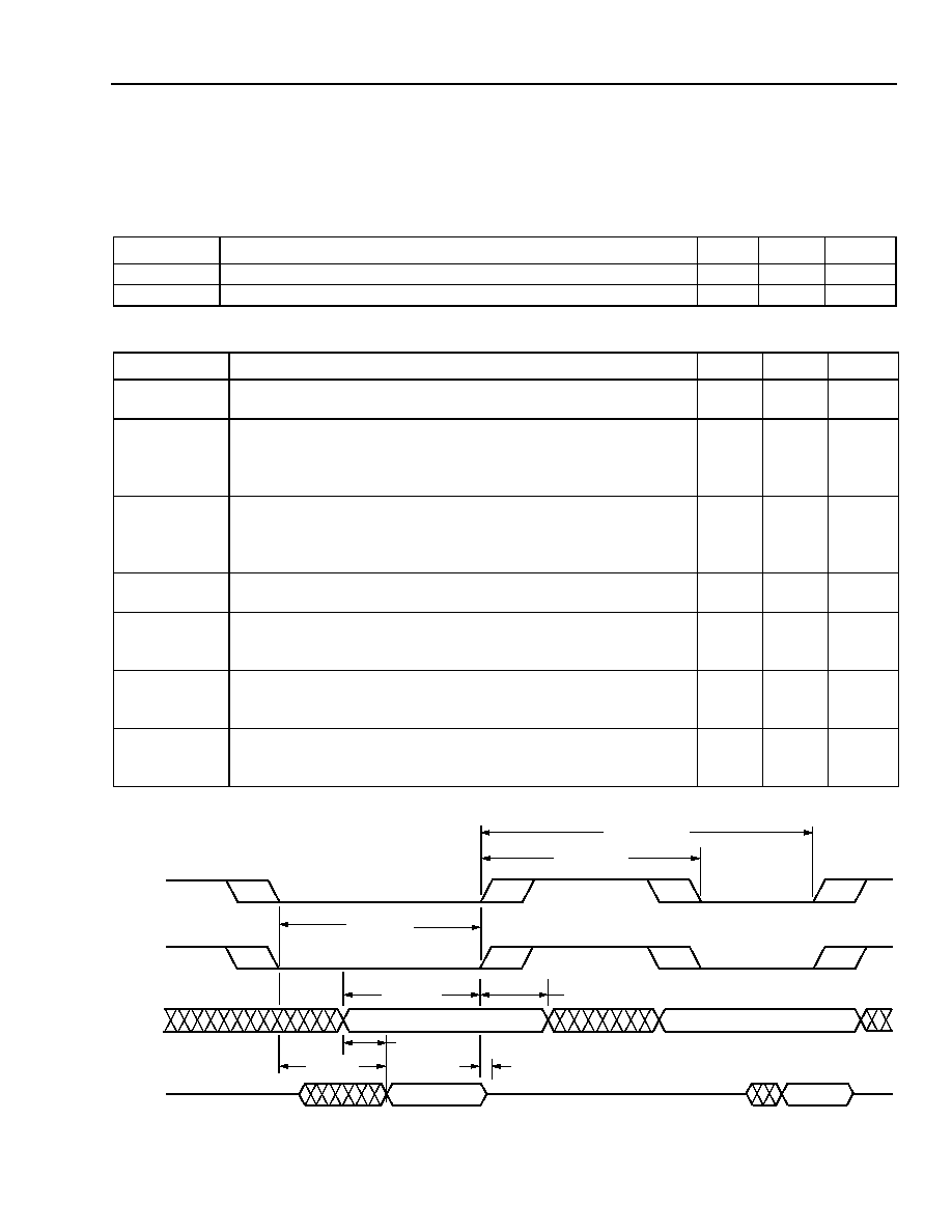
Register Timing Characteristics
All register timing specifications assume a 100 pF load on the D[7:0] package pins and a 70 pF load on all other
package pins.
Table 5. Register Access Timing--Special Function Register (SFR) Read
5-5352
Figure 5. Register Access Timing--SFR Read
Table 4. Timing Parameters
Symbol
Parameter
Min
Max
Unit
t
CLK
Internal Clock Period.
--
83.3
ns
t
RST
RESET Assert Time.
500
--
ns
Symbol
Parameter
Min
Max
Unit
tRDASU
Read Address Setup Time. Starts before the trailing edge of
RDN or IOCSN, whichever is first.
60
--
ns
tRDAHD
Read Address Hold. Starts after the trailing edge of RDN or
IOCSN, whichever is first:
Operational
Suspended
-
10
-
1
--
--
ns
ns
tRDDV1,
tRDDV2
Read Data Valid. From the leading edge of RDN or IOCSN or
from address valid, whichever is last, to data valid:
Operational
Suspended
--
--
74
33
ns
ns
tRDDZ
Read Data to Z State. Starts after the trailing edge of RDN or
IOCSN, whichever is first.
2
32
ns
tRDREC
Recovery Time Between Reads. From the trailing edge of RDN
or IOCSN, whichever is first, to the next leading edge of RDN or
IOCSN, whichever is last.
23
--
ns
tRDRECRXD
Recovery Time Between Consecutive RXDAT Reads. From the
trailing edge of RDN or IOCSN, whichever is first, to the next
trailing edge of RDN or IOCSN, whichever is first.
86
--
ns
tRDPW
Minimum Pulse Width. From the leading edge of RDN or
IOCSN, whichever is last, to the trailing edge of RDN or IOCSN,
whichever is first.
23
--
ns
tRDDV2
IOCSN
RDN
A
D
tRDREC
tRDPW
tRDASU
tRDAHD
tRDDV1
VALID
VALID
tRDDZ
VALID
HIGH IMPEDANCE
VALID
tRDRECRXD

10
Agere Systems Inc.
Data Sheet, Rev. 1
August 2004
USB Device Controller
USS-820FD
USB Device Controller
Register Timing Characteristics
(continued)
Table 6. Register Access Timing--Special Function Register (SFR) Write
5-5353
Figure 6. Register Access Timing--SFR Write
Symbol
Parameter
Min
Unit
tWRASU
Write Address Setup Time. Starts before the trailing edge of WRN or
IOCSN, whichever is first.
60
ns
tWRAHD
Write Address Hold. Starts after the trailing edge of WRN or IOCSN,
whichever is first.
-
10
ns
tWRPW
Write Minimum Pulse Width. From the leading edge of WRN or IOCSN,
whichever is last, to the trailing edge of WRN or IOCSN, whichever is
first.
23
ns
tWRDSU
Write Data Setup. From data valid to the trailing edge of WRN or
IOCSN, whichever is first.
60
ns
tWRDHD
Write Data Hold. From the trailing edge of WRN or IOCSN, whichever is
first, to data not valid.
-
10
ns
tWRREC
Recovery Time Between Write Attempts. From the trailing edge of
WRN or IOCSN, whichever is first, to the next leading edge of WRN or
IOCSN, whichever is last.
23
ns
tWRRECC
Recovery Time Between Write Completes. From the trailing edge of
WRN or IOCSN, whichever is first, to the next trailing edge of WRN or
IOCSN, whichever is first.
86
ns
IOCSN
WRN
A
D
tWRRECC
tWRPW
tWRASU
tWRAHD
tWRDSU
VALID
VALID
VALID
VALID
tWRDHD
tWRREC

Agere Systems Inc.
11
Data Sheet, Rev. 1
August 2004
USB Device Controller
USS-820FD
Register Interface
The USS-820FD is controlled through an asynchronous, read/write register interface. Registers are addressed via
the A[4:0] pins, and control is provided through the RDN, WRN, and IOCSN pins. Reserved bits of registers must
always be written with 0. Writing 1 to these bits may produce undefined results. These bits return undefined values
when read.
A register read is accomplished by placing the register address on the A bus and asserting the IOCSN and RDN
pins. After read data valid (tRDDV), the register data will appear on the D bus. A register write is accomplished by
placing the register address on the A bus and the data to be written on the D bus, and asserting the IOCSN and
WRN pins.
Tables 7 and 8 show alphabetical and numerical listings of all the available special function registers (SFR) for the
USS-820FD. For reference purposes, an alphabetized list of SFR bit names is included in Appendix A. Tables 12--
39 provide details for each of the registers. Some of these registers are replicated for each endpoint. The individ-
ual, endpoint-specific register is selected by the EPINDEX register.
Table 7. Special Function Registers (By Name)
Register
Description
Address
Table
Page
DSAV
Data Set Available
1DH
38
39
DSAV1
Data Set Available 1
1EH
39
39
EPCON*
* Contains shared bits. See Special Firmware Action for Shared Register Bits section.
Indexed by EPINDEX.
Endpoint Control Register
0BH
19
20
EPINDEX
Endpoint Index Register
0AH
18
19
FADDR
Function Address Register
10H
22
25
LOCK
Suspend Power-Off Locking Register
19H
34
37
MCSR
Miscellaneous Control/Status Register
1CH
37
38
PEND
Pend Hardware Status Update Register
1AH
35
37
REV
Hardware Revision Register
18H
33
36
RXCNTH
Receive FIFO Byte-Count High Register
07H
28
30
RXCNTL
Receive FIFO Byte-Count Low Register
06H
28
30
RXCON
Receive FIFO Control Register
08H
29
30
RXDAT
Receive FIFO Data Register
05H
27
29
RXFLG
Receive FIFO Flag Register
09H
30
32
RXSTAT*
Endpoint Receive Status Register
0DH
21
23
SBI*
Serial Bus Interrupt Register
14H
14
16
SBI1*
Serial Bus Interrupt Register 1
15H
15
17
SBIE
Serial Bus Interrupt Enable Register
16H
12
15
SBIE1
Serial Bus Interrupt Enable Register 1
17H
13
15
SCR
System Control Register
11H
31
35
SCRATCH
Scratch Firmware Information Register
1BH
36
37
SOFH*
Start of Frame High Register
0FH
16
18
SOFL*
Start of Frame Low Register
0EH
17
19
SSR*
System Status Register
12H
32
36
TXCNTH
Transmit FIFO Byte-Count High Register
02H
24
25
TXCNTL
Transmit FIFO Byte-Count Low Register
01H
24
25
TXCON
USB Transmit FIFO Control Register
03H
25
26
TXDAT
Transmit FIFO Data Register
00H
23
25
TXFLG
Transmit FIFO Flag Register
04H
26
27
TXSTAT
Endpoint Transmit Status Register
0CH
20
21

12
Agere Systems Inc.
Data Sheet, Rev. 1
August 2004
USB Device Controller
USS-820FD
USB Device Controller
Register Interface
(continued)
* Indexed by EPINDEX.
Contains shared bits. See Special Firmware Action for Shared Register Bits section.
Table 8. Special Function Registers (By Address)
Address
Register
Description
Table
Page
00H*
TXDAT
Transmit FIFO Data Register
23
25
01H*
TXCNTL
Transmit FIFO Byte-Count Low Register
24
25
02H*
TXCNTH
Transmit FIFO Byte-Count High Register
24
25
03H*
TXCON
USB Transmit FIFO Control Register
25
26
04H*
TXFLG
Transmit FIFO Flag Register
26
27
05H*
RXDAT
Receive FIFO Data Register
27
29
06H*
RXCNTL
Receive FIFO Byte-Count Low Register
28
30
07H*
RXCNTH
Receive FIFO Byte-Count High Register
28
30
08H*
RXCON
Receive FIFO Control Register
29
30
09H*
RXFLG
Receive FIFO Flag Register
30
32
0AH
EPINDEX
Endpoint Index Register
18
19
0BH*
EPCON
Endpoint Control Register
19
20
0CH*
TXSTAT
Endpoint Transmit Status Register
20
21
0DH*
RXSTAT
Endpoint Receive Status Register
21
23
0EH
SOFL
Start of Frame Low Register
17
19
0FH
SOFH
Start of Frame High Register
16
18
10H
FADDR
Function Address Register
22
25
11H
SCR
System Control Register
31
35
12H
SSR
System Status Register
32
36
14H
SBI
Serial Bus Interrupt Register
14
16
15H
SBI1
Serial Bus Interrupt Register 1
15
17
16H
SBIE
Serial Bus Interrupt Enable Register
12
15
17H
SBIE1
Serial Bus Interrupt Enable Register 1
13
15
18H
REV
Hardware Revision Register
33
36
19H
LOCK
Suspend Power-Off Locking Register
34
37
1AH
PEND
Pend Hardware Status Update Register
35
37
1BH
SCRATCH
Scratch Firmware Information Register
36
37
1CH
MCSR
Miscellaneous Control/Status Register
37
38
1DH
DSAV
Data Set Available
38
39
1EH
DSAV1
Data Set Available 1
39
39

Agere Systems Inc.
13
Data Sheet, Rev. 1
August 2004
USB Device Controller
USS-820FD
Register Interface
(continued)
Special Firmware Action for Shared Register
Bits
Since the USS-820FD registers are not bit-address-
able and contain several bits that may be written by
either firmware or hardware (shared bits), special care
must be taken to avoid incorrect behavior. In particular,
firmware must be careful not to write a bit after hard-
ware has updated the bit, but before firmware has
recognized the hardware update of the bit.
There are two general cases where this may occur:
1. Direct collision--Firmware does a read-modify-write
sequence to update a register bit, but between the
firmware read and firmware write, hardware
updates the bit. For example, in dual-packet mode,
hardware could update an SBI/SBI1 bit while firm-
ware is simultaneously resetting the same SBI/SBI1
bit. This would cause firmware to miss the fact that
a new transfer has completed.
2. Indirect collision--Firmware does a read-modify-
write sequence to update a register bit, but between
the firmware read and firmware write, hardware
updates a different bit in the same register. For
example, firmware could do a read-modify-write to
update the SOFODIS bit of the SOFH register, but
at the same time, hardware could be updating the
ASOF status bit. Firmware would inadvertently
reset the ASOF bit without being aware of the hard-
ware update.
These problems can be avoided through the use of the
PEND register, which can only be written by firmware.
Firmware must ensure that the PEND register bit is set
before writing any registers that contain shared bits.
All shared register bits have two copies: a standard
copy and a pended copy. The manner in which these
register bits are updated varies depending on the value
of the PEND register bit, as described in Table 9. The
standard copy is the bit that is read and written during
normal operation (PEND = 0). While PEND = 1, hard-
ware updates only affect the pended copy, and firm-
ware updates only affect the standard copy. When
firmware resets the PEND bit, the pended copies of the
shared bits are used to update the standard copies of
the shared bits as described in Table 10. Through
these means, hardware updates during a firmware
read-modify-write sequence will not be missed.
Firmware must execute the following sequence when
processing a shared bit (to avoid the direct collision
case), or when writing a bit which resides in a register
that contains shared bits (to avoid the indirect collision
case):
Set the PEND bit.
Read the register with the shared bit [Read].
If processing a shared bit, respond to the shared bit.
For example, for an SBI/SBI1 bit, process any data
sets present for that endpoint.
Update the bit [Modify].
Write the register with the shared bit with the modi-
fied data [Write].
Reset the PEND bit.
When a data set is written to a receive FIFO, that
FIFO's SBI/SBI1 register bit will set. Firmware must
process the indicated receive data set and, in doing so,
manage that FIFO's SBI/SBI1 bit according to the
sequence described in this section. In dual-packet
mode, it is possible that a second data set will be
written to a receive FIFO before firmware has
completed processing of the initial data set. This
second data set could have been written either before
or after firmware set the PEND bit to 1. Therefore, firm-
ware cannot determine whether or not this second
receive done indication was saved in the pended copy
of the SBI/SBI1 bit. Because of this uncertainty, firm-
ware must process all receive data sets which are
present in the indicated FIFO before resetting the
PEND bit to 0. If the receive done indication of the
second data set was in fact saved in the pended SBI/
SBI1 register, then the standard copy of the SBI/SBI1
bit will be set when firmware resets the PEND bit to 0.
Table 9. Shared Register Bit Update Behavior
(ASOF Example)
Bit
Update
Behavior
While
PEND = 0
Update
Behavior
While
PEND = 1
Update
Behavior
When
Firmware
Resets
PEND to 0
ASOF
(standard
copy)
Updated by
hardware
(firmware
must not write
this register)
Updated by
firmware
Updated as
docu-
mented in
Table 10
ASOF
(pended
copy)
Not used
Updated by
hardware
No longer
used

14
14
Agere Systems Inc.
Data Sheet, Rev. 1
August 2004
USB Device Controller
USS-820FD
Register Interface
(continued)
In this case, the SBI/SBI1 bit will be set even though
there is no corresponding data set present in the
receive FIFO. Therefore, firmware must be prepared to
service a receive done interrupt where no data sets are
present in the indicated FIFO.
Table 10 shows the values loaded into each of the
standard copies of the shared register bits when firm-
ware resets the PEND register bit
.
The register bits that are only updated by firmware, but
reside in registers with shared bits and must therefore
be updated only while PEND is set, are shown in
Table 11.
Firmware should attempt to minimize the period during
which PEND is set in order to minimize the distortion of
the detection of hardware events.
Register Reads with Side Effects
In general, USS-820FD register reads do not have side
effects--they do not cause any device state to change.
The following are exceptions to this rule:
RXDAT reads cause the internal RX FIFO read
pointer to change and possibly cause the
RXFLG.RXURF register bit to set.
RXCNTH/RXCNTL reads while RXFLG.RXFIF = 00
cause the RXFLG.RXURF register bit to set.
LOCK reads restart the register unlock sequence
after suspend (described in Special Action Required
by USS-820/USS-825 After Suspend--AP97-
058CMPR-04).
Any register reads during a register unlock sequence
after suspend, other than the LOCK register, cause
the unlock sequence to fail and require the sequence
to be restarted.
Table 10. Shared Register Update Values When
Firmware Resets PEND
Register
Bit(s)
Update Value
SBI
All bits
Set to 1 if standard copy = 1 or
pended copy = 1.
SBI1
All bits
Set to 1 if standard copy = 1 or
pended copy = 1.
RXSTAT RXSETUP Loaded with pended copy if
USB action updated RXSETUP
while PEND was set.
RXSTAT
EDOVW Set to 1 if standard copy = 1 or
pended copy = 1.
EPCON
RXSTL
Set to 1 if standard copy = 1 or
pended copy = 1.
SOFH
ASOF
Set to 1 if standard copy = 1 or
pended copy = 1.
SOFH
TS
Loaded with pended copy if
USB SOF was received while
PEND was set.
SOFL
All bits
Loaded with pended copy if
USB SOF was received while
PEND was set.
SSR
RESET
Set to 1 if standard copy = 1 or
pended copy = 1.
Table 11. Register Bits Only Updated While PEND
is Set
Register
Bit(s)
RXSTAT
RXSEQ
EPCON
All bits except RXSTL
SOFH
SOFIE, SOFODIS
SSR
SUSPPO, SUSPDIS, RESUME,
SUSPEND

Agere Systems Inc.
15
Data Sheet, Rev. 1
August 2004
USB Device Controller
USS-820FD
Register Interface
(continued)
Register Descriptions
Table 12. Serial Bus Interrupt Enable Register (SBIE)--Address: 16H; Default: 0000 0000B
This register enables and disables the receive and transmit done interrupts for function endpoints 0 through 3.
* For all bits, a 1 indicates that the interrupt is enabled and causes an interrupt to be signaled to the microcontroller. A 0 indicates that the asso-
ciated interrupt source is disabled and cannot cause an interrupt. However, the interrupt bit's value is still reflected in the SBI/SBI1 register. All
of these bits can be read/written by firmware.
Table 13. Serial Bus Interrupt Enable Register 1 (SBIE1)--Address: 17H; Default: 0000 0000B
This register enables and disables the receive and transmit done interrupts for function endpoints 4 through 7.
* For all bits, a 1 indicates that the interrupt is enabled and causes an interrupt to be signaled to the microcontroller. A 0 indicates that the asso-
ciated interrupt source is disabled and cannot cause an interrupt. However, the interrupt bit's value is still reflected in the SBI/SBI1 register. All
of these bits can be read/written by firmware.
Bit 7
Bit 6
Bit 5
Bit 4
Bit 3
Bit 2
Bit 1
Bit 0
FRXIE3
FTXIE3
FRXIE2
FTXIE2
FRXIE1
FTXIE1
FRXIE0
FTXIE0
R/W
Bit* Symbol
Function/Description
7
FRXIE3 Function Receive Interrupt Enable 3. Enables receive done interrupt for endpoint 3 (FRXD3).
6
FTXIE3 Function Transmit Interrupt Enable 3. Enables transmit done interrupt for endpoint 3 (FTXD3).
5
FRXIE2 Function Receive Interrupt Enable 2. Enables receive done interrupt for endpoint 2 (FRXD2).
4
FTXIE2 Function Transmit Interrupt Enable 2. Enables transmit done interrupt for endpoint 2 (FTXD2).
3
FRXIE1 Function Receive Interrupt Enable 1. Enables receive done interrupt for endpoint 1 (FRXD1).
2
FTXIE1 Function Transmit Interrupt Enable 1. Enables transmit done interrupt for endpoint 1 (FTXD1).
1
FRXIE0 Function Receive Interrupt Enable 0. Enables receive done interrupt for endpoint 0 (FRXD0).
0
FTXIE0 Function Transmit Interrupt Enable 0. Enables transmit done interrupt for endpoint 0 (FTXD0).
Bit 7
Bit 6
Bit 5
Bit 4
Bit 3
Bit 2
Bit 1
Bit 0
FRXIE7
FTXIE7
FRXIE6
FTXIE6
FRXIE5
FTXIE5
FRXIE4
FTXIE4
R/W
Bit* Symbol
Function/Description
7
FRXIE7 Function Receive Interrupt Enable 7. Enables receive done interrupt for endpoint 7 (FRXD7).
6
FTXIE7
Function Transmit Interrupt Enable 7. Enables transmit done interrupt for endpoint 7 (FTXD7).
5
FRXIE6 Function Receive Interrupt Enable 6. Enables receive done interrupt for endpoint 6 (FRXD6).
4
FTXIE6
Function Transmit Interrupt Enable 6. Enables transmit done interrupt for endpoint 6 (FTXD6).
3
FRXIE5 Function Receive Interrupt Enable 5. Enables receive done interrupt for endpoint 5 (FRXD5).
2
FTXIE5
Function Transmit Interrupt Enable 5. Enables transmit done interrupt for endpoint 5 (FTXD5).
1
FRXIE4 Function Receive Interrupt Enable 4. Enables receive done interrupt for endpoint 4 (FRXD4).
0
FTXIE4
Function Transmit Interrupt Enable 4. Enables transmit done interrupt for endpoint 4 (FTXD4).

16
Agere Systems Inc.
Data Sheet, Rev. 1
August 2004
USB Device Controller
USS-820FD
USB Device Controller
Register Interface
(continued)
Table 14. Serial Bus Interrupt Register (SBI)--Address: 14H; Default: 0000 0000B
This register contains the USB function's transmit and receive done interrupt flags for nonisochronous endpoints.
These bits are never set for isochronous endpoints.
* S = shared bit. See Special Firmware Action for Shared Register Bits section.
For all bits in the interrupt flag register, a 1 indicates that an interrupt is actively pending; a 0 indicates that the inter-
rupt is not active. The interrupt status is shown regardless of the state of the corresponding interrupt enable bit in
the SBIE/SBIE1.
Hardware can only set bits to 1. In normal operation, firmware should only clear bits to 0. Firmware can also set the
bits to 1 for test purposes. This allows the interrupt to be generated in firmware.
A set receive bit indicates either that valid data is waiting to be serviced in the RX FIFO for the indicated endpoint
and that the data was received without error and has been acknowledged, or that data was received with a receive
data error requiring firmware intervention to be cleared.
A set transmit bit indicates either that data has been transmitted from the TX FIFO for the indicated endpoint and
has been acknowledged by the host, or that data was transmitted with an error requiring firmware intervention to be
cleared.
If TXNAKE = 1, this also may indicate that a NAK was sent to the host in response to an IN packet that was
received when TXFIF = 00. This condition also sets TXVOID. This SBI/SBI1 setting will persist until firmware clears
TXVOID (or clears TXNAKE).
Bit 7
Bit 6
Bit 5
Bit 4
Bit 3
Bit 2
Bit 1
Bit 0
FRXD3
FTXD3
FRXD2
FTXD2
FRXD1
FTXD1
FRXD0
FTXD0
R/W (S*)
Bit
Symbol
Function/Description
7
FRXD3
Function Receive Done Flag, Endpoint 3.
6
FTXD3
Function Transmit Done Flag, Endpoint 3.
5
FRXD2
Function Receive Done Flag, Endpoint 2.
4
FTXD2
Function Transmit Done Flag, Endpoint 2.
3
FRXD1
Function Receive Done Flag, Endpoint 1.
2
FTXD1
Function Transmit Done Flag, Endpoint 1.
1
FRXD0
Function Receive Done Flag, Endpoint 0.
0
FTXD0
Function Transmit Done Flag, Endpoint 0.

Agere Systems Inc.
17
Data Sheet, Rev. 1
August 2004
USB Device Controller
USS-820FD
Register Interface
(continued)
Table 15. Serial Bus Interrupt 1 Register (SBI1)--Address: 15H; Default: 0000 0000B
This register contains the USB function's transmit and receive done interrupt flags for nonisochronous endpoints.
These bits are never set for isochronous endpoints.
* S = shared bit. See Special Firmware Action for Shared Register Bits section.
For all bits in the interrupt flag register, a 1 indicates that an interrupt is actively pending; a 0 indicates that the
interrupt is not active. The interrupt status is shown regardless of the state of the corresponding interrupt enable bit
in the SBIE/SBIE1.
Hardware can only set bits to 1. In normal operation, firmware should only clear bits to 0. Firmware can also set the
bits to 1 for test purposes. This allows the interrupt to be generated in firmware.
A set receive bit indicates either that valid data is waiting to be serviced in the RX FIFO for the indicated endpoint
and that the data was received without error and has been acknowledged, or that data was received with a receive
data error requiring firmware intervention to be cleared.
A set transmit bit indicates either that data has been transmitted from the TX FIFO for the indicated endpoint and
has been acknowledged by the host, or that data was transmitted with an error requiring firmware intervention to
be cleared.
If TXNAKE = 1, this also may indicate that a NAK was sent to the host in response to an IN packet that was
received when TXFIF = 00. This condition also sets TXVOID. This SBI/SBI1 setting will persist until firmware clears
TXVOID (or clears TXNAKE).
Bit 7
Bit 6
Bit 5
Bit 4
Bit 3
Bit 2
Bit 1
Bit 0
FRXD7
FTXD7
FRXD6
FTXD6
FRXD5
FTXD5
FRXD4
FTXD4
R/W (S*)
Bit
Symbol
Function/Description
7
FRXD7
Function Receive Done Flag, Endpoint 7.
6
FTXD7
Function Transmit Done Flag, Endpoint 7.
5
FRXD6
Function Receive Done Flag, Endpoint 6.
4
FTXD6
Function Transmit Done Flag, Endpoint 6.
3
FRXD5
Function Receive Done Flag, Endpoint 5.
2
FTXD5
Function Transmit Done Flag, Endpoint 5.
1
FRXD4
Function Receive Done Flag, Endpoint 4.
0
FTXD4
Function Transmit Done Flag, Endpoint 4.

18
Agere Systems Inc.
Data Sheet, Rev. 1
August 2004
USB Device Controller
USS-820FD
USB Device Controller
Register Interface
(continued)
Table 16. Start of Frame High Register (SOFH)--Address: 0FH; Default: 0000 0000B
This register contains isochronous data transfer enable and interrupt bits and the upper 3 bits of the 11-bit time
stamp received from the host.
* S = shared bit. P = PEND must be set when writing this bit. See Special Firmware Action for Shared Register Bits section.
Bit 7
Bit 6
Bit 5
Bit 4
Bit 3
Bit 2
Bit 1
Bit 0
SOFACK
ASOF
SOFIE
FTLOCK
SOFODIS
TS10
TS9
TS8
R
R/W (S*)
R/W (P*)
R
R/W (P*)
R/W (S*)
Bit
Symbol
Function/Description
7
SOFACK
SOF Token Received Without Error (Read Only). When set, this bit signifies that
the 11-bit time stamp stored in SOFL and SOFH is valid. This bit is updated every
time an SOF token is received from the USB bus, and it is cleared when an artificial
SOF is generated by the frame timer. This bit is set and cleared by hardware.
6
ASOF
Any Start of Frame. This bit is set by hardware to signify that a new frame has
begun. The interrupt can result either from the reception of an actual SOF packet or
from an artificially generated SOF from the frame timer. This interrupt is asserted in
hardware even if the frame timer is not locked to the USB bus frame timing. When
set, this bit indicates that either the actual SOF packet was received or an artificial
SOF was generated by the frame timer.
Setting this bit to 1 by firmware has the same effect as when it is set by hardware.
This bit must be cleared to 0 by firmware if SOFODIS = 1 or if MCSR.FEAT = 1. If
SOFODIS and MCSR.FEAT = 0, this bit clears itself after one t
CLK
, which requires the
system to detect start of frame via the SOFN device pin.
This bit also serves as the SOF interrupt flag. This interrupt is only asserted in hard-
ware if the SOF interrupt is enabled (SOFIE set) and the interrupt channel is enabled.
5
SOFIE
SOF Interrupt Enable. When set, setting the ASOF bit causes an interrupt request to
be generated if the interrupt channel is enabled. Hardware reads this bit but does not
write to it.
4
FTLOCK
Frame Timer Lock (Read Only). When set, this bit signifies that the frame timer is
presently locked to the USB bus frame time. When cleared, this bit indicates that the
frame timer is attempting to synchronize the frame time.
3
SOFODIS SOF Pin Output Disable. When set, no low pulse is driven to the SOF pin in
response to setting the ASOF bit. The SOF pin is driven to 1 when SOFODIS is set.
When this bit is clear, setting the ASOF bit causes the SOF pin to be toggled with a
low pulse for eight t
CLK
periods.
2:0
TS[10:8]
Time Stamp Received from Host. TS[10:8] are the upper 3 bits of the 11-bit frame
number issued with an SOF token. This time stamp is valid only if the SOFACK bit is
set.

Agere Systems Inc.
19
Data Sheet, Rev. 1
August 2004
USB Device Controller
USS-820FD
Register Interface
(continued)
Table 17. Start of Frame Low Register (SOFL)--Address: 0EH; Default: 0000 0000B
This register contains the lower 8 bits of the 11-bit time stamp received from the host.
* S = shared bit. See Special Firmware Action for Shared Register Bits section.
Table 18. Endpoint Index Register (EPINDEX)--Address: 0AH; Default: 0000 0000B
This register identifies the endpoint pair. The register's contents select the transmit and receive FIFO pair and
serve as an index to endpoint-specific special function registers (SFRs).
* The EPINDEX register identifies the endpoint pair and selects the associated transmit and receive FIFO pair. The value in this register plus
SFR addresses select the associated band of endpoint-indexed SFRs (TXDAT, TXCON, TXFLG, TXCNTH/L, RXDAT, RXCON, RXFLG,
RXCNTH/L, EPCON, TXSTAT, and RXSTAT).
Bit 7
Bit 6
Bit 5
Bit 4
Bit 3
Bit 2
Bit 1
Bit 0
TS7
TS6
TS5
TS4
TS3
TS2
TS1
TS0
R/W (S*)
Bit
Symbol
Function/Description
7:0
TS[7:0]
Time Stamp Received from Host. This time stamp is valid only if the SOFACK bit in
the SOFH register is set. TS[7:0] are the lower 8 bits of the 11-bit frame number
issued with an SOF token. The time stamp remains at its previous value if an artificial
SOF is generated, and it is up to firmware to update it. These bits are set and cleared
by hardware.
Bit 7
Bit 6
Bit 5
Bit 4
Bit 3
Bit 2
Bit 1
Bit 0
--
EPINX2
EPINX1
EPINX0
--
R/W
Bit
Symbol
Function/Description
7:3
--
Reserved. Write 0s to these bits. Reads always return 0s.
2:0
EPINX[2:0] Endpoint Index.
EPINDEX*
Function Endpoint
0000 0000
Function Endpoint 0
0000 0001
Function Endpoint 1
0000 0010
Function Endpoint 2
0000 0011
Function Endpoint 3
0000 0100
Function Endpoint 4
0000 0101
Function Endpoint 5
0000 0110
Function Endpoint 6
0000 0111
Function Endpoint 7
The EPINDEX register must not be changed during a sequence of RXDAT reads of a
particular data set. See the Receive FIFO section for more details.

20
Agere Systems Inc.
Data Sheet, Rev. 1
August 2004
USB Device Controller
USS-820FD
USB Device Controller
Register Interface
(continued)
Table 19. Endpoint Control Register (EPCON)--Address: 0BH; Default: Endpoint 0 = 0011 0101B;
Others = 0001 0000B
This SFR configures the operation of the endpoint specified by EPINDEX. This register is endpoint indexed.
* S = shared bit. P = PEND must be set when writing this bit. See Special Firmware Action for Shared Register Bits section.
Bit 7
Bit 6
Bit 5
Bit 4
Bit 3
Bit 2
Bit 1
Bit 0
RXSTL
TXSTL
CTLEP
RXSPM
RXIE
RXEPEN
TXOE
TXEPEN
R/W (S*)
R/W(P*)
Bit
Symbol
Function/Description
7
RXSTL
Stall Receive Endpoint. When set, this bit stalls the receive endpoint. Firmware
must clear this bit only after the host has intervened through commands sent down
endpoint 0. When this bit is set and RXSETUP is clear, the receive endpoint responds
with a STALL handshake to a valid OUT token. When this bit is set and RXSETUP is
set, the receive endpoint will NACK. This bit does not affect the reception of SETUP
tokens by a control endpoint. This bit is set by the hardware if the data phase of the
status stage of a control transfer does not use the correct data PID (DATA1) or has
more than 0 data bytes.
6
TXSTL
Stall Transmit Endpoint. When set, this bit stalls the transmit endpoint. Firmware
must clear this bit only after the host has intervened through commands sent down
endpoint 0. When this bit is set and RXSETUP is clear, the transmit endpoint
responds with a STALL handshake to a valid IN token. When this bit is set and
RXSETUP is set, the receive endpoint will NACK.
5
CTLEP
Control Endpoint. When set, this bit configures the endpoint as a control endpoint.
Only control endpoints are capable of receiving SETUP tokens.
4
RXSPM
Receive Single-Packet Mode. When set, this bit configures the receive endpoint for
single data packet operation. When enabled, only a single data packet is allowed to
reside in the receive FIFO.
Note: For control endpoints (CTLEP = 1), this bit should be set for single-packet
mode operation as the recommended firmware model. However, it is possible
to have a control endpoint configured in dual-packet mode as long as the firm-
ware handles the endpoint correctly.
3
RXIE
Receive Input Enable. When set, this bit enables data from the USB to be written
into the receive FIFO. If cleared, the endpoint responds to an OUT token by ignoring
the data and returning a NACK handshake to the host (unless RXSTL is set, in which
case a STALL is returned). This bit does not affect a valid SETUP token.
2
RXEPEN
Receive Endpoint Enable. When set, this bit enables the receive endpoint. When
disabled, the endpoint does not respond to a valid OUT or SETUP token. This bit is
hardware read only and has the highest priority among RXIE and RXSTL.
Note: Endpoint 0 is enabled for reception upon reset.
1
TXOE
Transmit Output Enable. When set, this bit enables the data in TXDAT to be trans-
mitted. If cleared, the endpoint returns a NACK handshake to a valid IN token if the
TXSTL bit is not set.
0
TXEPEN
Transmit Endpoint Enable. When set, this bit enables the transmit endpoint. When
disabled, the endpoint does not respond to a valid IN token. This bit is hardware read
only.
Note: Endpoint 0 is enabled for transmission upon reset.

Agere Systems Inc.
21
Data Sheet, Rev. 1
August 2004
USB Device Controller
USS-820FD
Register Interface
(continued)
Table 20. Endpoint Transmit Status Register (TXSTAT)--Address: 0CH; Default: 0000 0000B
This register contains the current endpoint status of the transmit FIFO specified by EPINDEX. This register is
endpoint indexed.
* For normal operation, this bit should not be modified by the user except as required by the implementation of USB standard commands, such
as SET_CONFIGURATION, SET_INTERFACE, and CLEAR_FEATURE [stall]. The SIE handles all sequence bit tracking required by normal
USB traffic, as documented in the USB specification, Section 8.6.
Only writable if TXNAKE = 1.
Bit 7
Bit 6
Bit 5
Bit 4
Bit 3
Bit 2
Bit 1
Bit 0
TXSEQ
TXDSAM
TXNAKE
TXFLUSH
TXSOVW
TXVOID
TXERR
TXACK
R/W*
R/W
R/W
R
W*
R/W
R
Bit
Symbol
Function/Description
7
TXSEQ
Transmitter Current Sequence Bit (Read, Conditional Write).* This bit is trans-
mitted in the next PID and toggled on a valid ACK handshake. This bit is toggled by
hardware on a valid SETUP token. This bit can be written by firmware if the TXSOVW
bit is set when written together with the next TXSEQ value.
6
TXDSAM
Transmit Data-Set-Available Mode. If set, a NAK response to an IN token causes
the corresponding RXAV/TXAV bit in the DSAV register to set, and the DSA output pin
to assert (if enabled by MCSR.BDFEAT), rather than the standard condition (transmit
data set empty). This only occurs on NAKs caused by TXFIF = 00. This bit must not
be set for isochronous endpoints. When reset to 0 (along with MCSR.FEAT,
MCSR.BDFEAT, and TXSTAT.TXNAKE), the device will behave like revision B.
5
TXNAKE
Transmit NAK Mode Enable. If set, a NAK response to an IN token causes the
TXVOID bit and the corresponding bits in the SBI/SBI1 register to set, causing an
IRQN interrupt (if enabled). This only occurs on NAKs caused by TXFIF = 00. This bit
must not be set for isochronous endpoints. When set this bit also changes the
meaning and usage of the TXSTAT.TXVOID bit. When reset to 0 (along with
MCSR.FEAT, MCSR.BDFEAT, and TXSTAT.TXDSAM), the device will behave like
revision B.
4
TXFLUSH Transmit FIFO Packet Flushed (Read Only). Updated at each SOF. When set, this
bit indicates that hardware flushed a stale isochronous data packet from the transmit
FIFO at SOF.
Behavior when MCSR.FEAT = 0:
To guard against a missed IN token in isochronous mode, if, with TXFIF[1:0] = 11,
no IN token is received for the current endpoint, hardware automatically flushes
the oldest packet and decrements the TXFIF[1:0] value. This flush does not occur
if there is only one data set present (TXFIF = 01/10).
Behavior when MCSR.FEAT = 1:
A firmware data set write causes a TXFIF bit to set. For isochronous endpoints,
this data set does not become visible to the host until the next SOF. The data set is
intended to be read out during that frame. If that read does not occur (possibly due
to a lost IN packet), that data set is flushed at the next SOF, setting TXFLUSH. If
firmware writes two data sets during a single frame (TXFIF must have equalled 00
at the start of that frame), the first, older data set written is flushed at the subse-
quent SOF, setting TXFLUSH.

22
Agere Systems Inc.
Data Sheet, Rev. 1
August 2004
USB Device Controller
USS-820FD
USB Device Controller
Register Interface
(continued)
Table 20. Endpoint Transmit Status Register (TXSTAT)--Address: 0CH; Default: 0000 0000B (continued)
* For normal operation, this bit should not be modified by the user except as required by the implementation of USB standard commands, such
as SET_CONFIGURATION, SET_INTERFACE, and CLEAR_FEATURE [stall]. The SIE handles all sequence bit tracking required by normal
USB traffic, as documented in the USB specification, Section 8.6.
Only writable if TXNAKE = 1.
Bit
Symbol
Function/Description
3
TXSOVW
Transmit Data Sequence Overwrite Bit.* Writing a 1 to this bit allows the value of
the TXSEQ bit to be overwritten. Writing a 0 to this bit has no effect on TXSEQ. This
bit always returns 0 when read.
2
TXVOID
Transmit Void.
Behavior when TXNAKE = 0:
This bit is read only if TXNAKE = 0. Indicates a void condition has occurred in
response to a valid IN token. Transmit void is closely associated with the NACK/
STALL handshake returned by the function after a valid IN token. This void condi-
tion occurs when the endpoint output is disabled (TXOE = 0) or stalled (TXSTL =
1), the corresponding receive FIFO contains a setup packet (RXSETUP = 1), the
FIFO contains no valid data sets (TXFIF = 00), or there is an existing FIFO error
(TXURF = 1 or TXOVF = 1).
This bit is used to check any NACK/STALL handshake returned by the function.
This bit does not affect the FTXDx, TXERR, or TXACK bits. This bit is updated by
hardware at the end of a nonisochronous transaction in response to a valid IN
token. For isochronous transactions, this bit is not updated until the next SOF. This
bit is not updated at SOF if TXFLUSH is performed.
Behavior when TXNAKE = 1:
When TXNAKE = 1, this bit becomes writable by firmware. The meaning of the bit
is also changed, to indicate only that a NAK was sent to the host in response to an
IN when TXFIF = 00. Hardware setting of this bit always takes priority over firm-
ware writes. Hardware setting of this bit also causes the corresponding SBI/SBI1
bit to set, possibly causing an interrupt. That setting will persist until TXVOID is
cleared by firmware.
1
TXERR
Transmit Error (Read Only). Indicates an error condition has occurred with the
transmission. Complete or partial data has been transmitted. The error can be one of
the following:
1. Data transmitted successfully but no handshake received.
2. Transmit FIFO goes into underrun condition while transmitting.
These conditions also cause the corresponding transmit done bit, FTXDx in SBI or
SBI1, to be set. For nonisochronous transactions, TXERR is updated by hardware
along with the TXACK bit at the end of data transmission. TEXERR and TXACK are
updated at the same time--one bit is set to 1, and the other is reset to 0. For isochro-
nous transactions, TXERR is not updated until the next SOF. This bit is not updated at
SOF if TXFLUSH is performed.
0
TXACK
Transmit Acknowledge (Read Only). Indicates data transmission completed and
acknowledged successfully. This condition also causes the corresponding transmit
done bit, FTXDx in SBI or SBI1, to be set. For nonisochronous transactions, TXACK
is updated by hardware along with the TXERR bit at the end of data transmission.
TEXERR and TXACK are updated at the same time--one bit is set to 1, and the other
is reset to 0. For isochronous transactions, TXACK is not updated until the next SOF.
This bit is not updated at SOF if TXFLUSH is performed.

Agere Systems Inc.
23
Data Sheet, Rev. 1
August 2004
USB Device Controller
USS-820FD
Register Interface
(continued)
Table 21. Endpoint Receive Status Register (RXSTAT)--Address: 0DH; Default: 0000 0000B
This register contains the current endpoint status of the receive FIFO specified by EPINDEX. This register is an
endpoint-indexed SFR.
* For normal operation, this bit should not be modified by the user except as required by the implementation of USB standard commands, such
as SET_CONFIGURATION, SET_INTERFACE, and CLEAR_FEATURE [stall]. The SIE handles all sequence bit tracking required by normal
USB traffic, as documented in the USB specification, Section 8.6.
S = shared bit. P = PEND must be set when writing this bit. See Special Firmware Action for Shared Register Bits section.
Bit 7
Bit 6
Bit 5
Bit 4
Bit 3
Bit 2
Bit 1
Bit 0
RXSEQ
RXSETUP
STOVW
EDOVW
RXSOVW
RXVOID
RXERR
RXACK
R/W* (P
)
R/W (S
)
R
R/W (S
)
W (P
)
R
Bit
Symbol
Function/Description
7
RXSEQ
Receiver Endpoint Sequence Bit (Read, Conditional Write).* This bit is toggled on
completion of an ACK handshake in response to an OUT token. This bit is set (or
cleared) by hardware after reception of a SETUP token.
If the RXSOVW bit is set, this bit can be written by firmware when written along with the
new RXSEQ value.
Note: Always verify this bit after writing to ensure that there is no conflict with hardware,
which may occur if a new SETUP token is received.
6
RXSETUP
Received SETUP Token. This bit is set by hardware when a valid SETUP token has
been received. When set, this bit causes received IN or OUT tokens to be NACKed until
the bit is cleared to allow proper data management for the transmit and receive FIFOs
from the previous transaction.
IN or OUT tokens are NACKed even if the endpoint is stalled (RXSTL or TXSTL) to allow
a control transaction to clear a stalled endpoint.
Firmware must clear this bit after it has finished reading out the SETUP packet and is
prepared for the next stage of the control transaction (data or status). For a stalled con-
trol endpoint, this bit should not be cleared until the RXSTL/TXSTL bits have been
cleared.
5
STOVW
Start Overwrite Flag (Read Only). This bit is set by hardware upon receipt of a SETUP
token for any control endpoint to indicate that the receive FIFO is being overwritten with
new SETUP data. When set, the FIFO state (RXFIF and read pointer) resets and is
locked for this endpoint until EDOVW is set. This prevents a prior, ongoing firmware read
from corrupting the read pointer as the receive FIFO is being cleared and new data is
being written into it. This bit is cleared by hardware at the end of handshake phase
transmission of the SETUP stage.
This bit is used only for control endpoints.
4
EDOVW
End Overwrite Flag. This flag is set by hardware during the handshake phase of a
SETUP stage. It is set after every SETUP packet is received and must be cleared prior
to reading the contents of the FIFO. When set, the FIFO state (RXFIF and read pointer)
remains locked for this endpoint until this bit is cleared. This prevents a prior, ongoing
firmware read from corrupting the read pointer after the new data has been written into
the receive FIFO.
This bit is used only for control endpoints.
3
RXSOVW
Receive Data Sequence Overwrite Bit.* Writing a 1 to this bit allows the value of the
RXSEQ bit to be overwritten. Writing a 0 to this bit has no effect on RXSEQ. This bit
always returns 0 when read.

24
Agere Systems Inc.
Data Sheet, Rev. 1
August 2004
USB Device Controller
USS-820FD
USB Device Controller
Register Interface
(continued)
Table 21. Endpoint Receive Status Register (RXSTAT)--Address: 0DH; Default: 0000 0000B (continued)
Bit
Symbol
Function/Description
2
RXVOID
Receive Void (Read Only). Indicates a void condition has occurred in response to a
valid OUT token. Receive void is closely associated with the NACK/STALL handshake
returned by the function after a valid OUT token. This void condition occurs when the
endpoint input is disabled (RXIE = 0) or stalled (RXSTL = 1), the FIFO contains a setup
packet (RXSETUP = 1), the FIFO has no available data sets (RXFIF = 11, or RXFIF =
01/10 and RXSPM = 1), or there is an existing FIFO error (RXURF = 1 or RXOVF = 1).
This bit is set and cleared by hardware. For nonisochronous transactions, this bit is
updated by hardware at the end of the transaction in response to a valid OUT token. For
isochronous transactions, it is not updated until the next SOF.
1
RXERR
Receive Error (Read Only). Set when an error condition has occurred with the recep-
tion of a SETUP or OUT transaction. Complete or partial data has been written into the
receive FIFO. No handshake is returned. The error can be one of the following:
1. Data failed CRC check.
2. Bit stuffing error.
3. A receive FIFO goes into overrun or underrun condition while receiving.
This bit is updated by hardware at the end of a valid SETUP or OUT token transaction
(nonisochronous) or at the next SOF on each valid OUT token transaction (isochro-
nous).
These conditions also cause the corresponding FRXDx bit of SBI or SBI1 to be set.
RXERR is updated with the RXACK bit at the end of data reception. RXERR and
RXACK are updated at the same time--one bit is set to 1, and the other is reset to 0.
0
RXACK
Receive Acknowledge (Read Only). This bit is set when an ACK handshake is sent in
response to data being written to the receive FIFO. This read-only bit is updated by
hardware at the end of a valid SETUP or OUT token transaction (nonisochronous) or at
the next SOF on each valid OUT token transaction (isochronous).
This condition also causes the corresponding FRXDx bit of SBI or SBI1 to be set.
RXACK is updated with the RXERR bit at the end of data reception. RXERR and
RXACK are updated at the same time--one bit is set to 1, and the other is reset to 0.

Agere Systems Inc.
25
Data Sheet, Rev. 1
August 2004
USB Device Controller
USS-820FD
Register Interface
(continued)
Table 22. Function Address Register (FADDR)--Address: 10H; Default: 0000 0000B
This SFR holds the address for the USB function. During bus enumeration, it is written by firmware with a unique
value assigned by the host. If MCSR.FEAT = 1, this register is reset to 0 if a USB reset is detected.
Table 23. Transmit FIFO Data Register (TXDAT)--Address: 00H; Default: 0000 0000B
Data to be transmitted by the FIFO specified by EPINDEX is first written to this register. This register is endpoint
indexed. TXDAT must not be written if TXFIF = 11.
Table 24. Transmit FIFO Byte-Count High and Low Registers (TXCNTH, TXCNTL)--Address:
TXCNTH = 02H, TXCNTL = 01H; Default: TXCNTH = 0000 0000B; TXCNTL = 0000 0000B
Written by firmware to indicate the number of bytes just written to the transmit FIFO specified by EPINDEX. This
register is endpoint indexed. TXCNTL should be written after TXCNTH. TXCNTL write increments TXFIF, vali-
dating the data set just written.
Note: To send a status stage after a control write, no data control command or a null packet, write a 0 to TXCNT.
Bit 7
Bit 6
Bit 5
Bit 4
Bit 3
Bit 2
Bit 1
Bit 0
--
A6
A5
A4
A3
A2
A1
A0
--
R/W
Bit
Symbol
Function/Description
7
--
Reserved. Write 0 to this bit. Reads always return 0.
6:0
A[6:0]
7-Bit Programmable Function Address. This register is written by firmware as a
result of commands received via endpoint 0.
Bit 7
Bit 6
Bit 5
Bit 4
Bit 3
Bit 2
Bit 1
Bit 0
TXDAT7
TXDAT6
TXDAT5
TXDAT4
TXDAT3
TXDAT2
TXDAT1
TXDAT0
W
Bit
Symbol
Function/Description
7:0
TXDAT[7:0] Transmit Data Byte (Write Only). To write data to the transmit FIFO, write to this
register. The write pointer is incremented automatically after a write.
Bit 15
Bit 14
Bit 13
Bit 12
Bit 11
Bit 10
Bit 9
Bit 8
--
BC9
BC8
--
R/W
Bit 7
Bit 6
Bit 5
Bit 4
Bit 3
Bit 2
Bit 1
Bit 0
BC7
BC6
BC5
BC4
BC3
BC2
BC1
BC0
R/W
Bit
Symbol
Function/Description
15:10
--
Reserved. Write 0s to these bits. Reads always return 0s.
9:0
BC[9:0]
Transmit Byte Count (Write, Conditional Read). 10-bit, ring buffer. These bits store
transmit byte count (TXCNT).

26
Agere Systems Inc.
Data Sheet, Rev. 1
August 2004
USB Device Controller
USS-820FD
USB Device Controller
Register Interface
(continued)
Table 25. USB Transmit FIFO Control Register (TXCON)--Address: 03H; Default: 0000 0100B
This register controls the transmit FIFO specified by EPINDEX. This register is endpoint indexed.
* Assumes MCSR.FEAT = 1. If MCSR.FEAT = 0, these FFSZ settings indicate 64 bytes.
ATM mode is recommended for normal operation. ADVRM and REVRP, which control the read marker and read pointer when ATM = 0, are
used for test purposes.
Bit 7
Bit 6
Bit 5
Bit 4
Bit 3
Bit 2
Bit 1
Bit 0
TXCLR
FFSZ1
FFSZ0
--
TXISO
ATM
ADVRM
REVRP
R/W
--
R/W
Bit
Symbol
Function/Description
7
TXCLR
Transmit FIFO Clear. Setting this bit flushes the transmit FIFO, resets all the read/write
pointers and markers, resets the TXCNTH and TXCNTL registers, resets the TXFLUSH,
TXVOID, TXERR, and TXACK bits of the TXSTAT register, sets the TXEMP bit in TXFLG,
and clears all other bits in TXFLG. Hardware clears this bit after the flush. Setting this bit
does not affect the TXSEQ bit in the TXSTAT register. This bit should only be set when the
endpoint is known to be inactive or there is a FIFO error present.
6:5
FFSZ[1:0]
FIFO Size. These bits select the size of the transmit FIFO.
FFSZ[1:0]
Nonisochronous Size
Isochronous Size
00
16
64
01
64
256
10
8*
512
11
32*
1024
4
--
Reserved. Write 0 to this bit. Reads always return 0.
3
TXISO
Transmit Isochronous Data. Firmware sets this bit to indicate that the transmit FIFO
contains isochronous data. The SIE uses this bit to determine if a handshake is required at
the end of a transmission.
2
ATM
Automatic Transmit Management.
Setting this bit (the default value) causes the read
pointer and read marker to be adjusted automatically as indicated:
Status
Read Pointer
Read Marker
ACK
Unchanged
Advanced (1)
NACK
Reversed (2)
Unchanged
1. To origin of next data set.
2. To origin of the data set last read.
This bit should always be set, except for test purposes. Setting this bit disables ADVRM
and REVRP. This bit can be set and cleared by firmware. Hardware neither clears nor sets
this bit. This bit must always be set for isochronous endpoints (TXISO = 1).
1
ADVRM
Advance Read Marker Control (Non-ATM Mode Only).
Setting this bit prepares for the
next packet transmission by advancing the read marker to the origin of the next data
packet (the position of the read pointer). Hardware clears this bit after the read marker is
advanced. This bit is effective only when the REVRP, ATM, and TXCLR bits are clear.
0
REVRP
Reverse Read Pointer (Non-ATM Mode Only).
In the case of a bad transmission, the
same data stack may need to be available for retransmit. Setting this bit reverses the read
pointer to point to the origin of the last data set (the position of the read marker) so that the
SIE can reread the last set for retransmission. Hardware clears this bit after the read
pointer is reversed. This bit is effective only when the ADVRM, ATM, and TXCLR bits are
all clear.

Agere Systems Inc.
27
Data Sheet, Rev. 1
August 2004
USB Device Controller
USS-820FD
Register Interface
(continued)
Table 26. Transmit FIFO Flag Register (TXFLG)--Address: 04H; Default: 0000 1000B
These flags indicate the status of data packets in the transmit FIFO specified by EPINDEX. This register is
endpoint indexed.
Bit 7
Bit 6
Bit 5
Bit 4
Bit 3
Bit 2
Bit 1
Bit 0
TXFIF1
TXFIF0
--
TXEMP
TXFULL
TXURF
TXOVF
R
--
R
R/W
Bit
Symbol
Function/Description
7:6
TXFIF[1:0] Transmit FIFO Index Flags (Read Only). These flags indicate which data sets are
present in the transmit FIFO (see below).
Data Sets Present
TXFIF[1:0]
ds1
ds0
Status
00
No
No
Empty
01
No
Yes
1 set
10
Yes
No
1 set
11
Yes
Yes
2 sets
The TXFIF bits are set in sequence after each write to TXCNT to reflect the addition of a
data set. Likewise, the TXFIF1 and TFIF0 are cleared in sequence after each advance of
the read marker to indicate that the set is effectively discarded. The bit is cleared whether
the read marker is advanced by firmware (setting ADVRM) or automatically by hardware
(ATM = 1). The next-state table for the TXFIF bits is shown below:
TXFIF[1:0]
Operation
Next TXFIF[1:0]
00
Write TXCNT
01
01
Write TXCNT
11
10
Write TXCNT
11
11
Write TXCNT
11 (TXOVF = 1)
00
Advance Read Marker
00
01
Advance Read Marker
00
11
Advance Read Marker
10/01
10
Advance Read Marker
00
XX
Reverse Read Pointer
Unchanged
In isochronous mode, TXOVF, TXURF, and TXFIF are handled using the following rule:
firmware events cause status change immediately, while USB events cause status change
only at SOF. TXFIF is incremented by firmware and decremented by the USB. Therefore,
writes to TXCNT increment TXFIF immediately. However, a successful USB transaction
any time within a frame decrements TXFIF only at SOF.
The TXFIF flags must be checked before and after writes to the transmit FIFO and TXCNT
for traceability. See the TXFLUSH bit in TXSTAT.
If MCSR.FEAT = 0:
TXFIF bits are immediately visible to the host after a firmware write--the device will
send the indicated data set(s) to the host in response to an IN.

28
Agere Systems Inc.
Data Sheet, Rev. 1
August 2004
USB Device Controller
USS-820FD
USB Device Controller
Register Interface
(continued)
Table 26. Transmit FIFO Flag Register (TXFLG)--Address: 04H; Default: 0000 1000B (continued)
Bit
Symbol
Function/Description
7:6
TXFIF[1:0]
Transmit FIFO Index Flags (Read Only) (continued).
If MCSR.FEAT = 1:
TXFIF bits are not visible to the host until the first SOF is written, which occurs after the
data set. Prior to that SOF, the device will return a zero-length data set in response to
an IN (unless there is another, older data set present from the prior frame). This ensures
that a given data set may only be sent during the subsequent frame, as required by the
USB specification. This behavior also allows firmware to occasionally be late in writing a
data set (write complete after SOF), without losing frame/data synchronization with the
host. The late data set write will cause a zero-length data set to be sent to the host
during the intended frame. The late set will be flushed at the end of the next frame,
assuming firmware also writes the correct data set during that frame (see
TXSTAT.TXFLUSH description). Firmware must not be late on consecutive frames (this
will cause a loss of frame/data synchronization with the host), data sets may be sent
during the wrong frame.
Note: Firmware can enforce single-packet mode by only writing a new data set to the
transmit FIFO if there are currently no data sets present in the FIFO (TXFIF = 00).
To simplify firmware development, configure control endpoints in single-packet
mode.
5:4
--
Reserved. Write 0s to these bits. Reads always return 0s.
3
TXEMP
Transmit FIFO Empty Flag (Read Only). Hardware sets this bit when firmware has not
yet written any data bytes to the current FIFO data set being written. Hardware clears this
bit when the empty condition no longer exists.
This bit always tracks the current transmit FIFO status regardless of isochronous or
nonisochronous mode.
2
TXFULL
Transmit FIFO Full Flag (Read Only). Hardware sets this bit when the number of bytes
that firmware writes to the current transmit FIFO data set equals the FIFO size. Hardware
clears this bit when the full condition no longer exists.
This bit always tracks the current transmit FIFO status regardless of isochronous or
nonisochronous mode. Check this bit to avoid causing a TXOVF condition.
1
TXURF
Transmit FIFO Underrun Flag (Read, Clear Only). Hardware sets this flag when a read
is attempted from an empty transmit FIFO. (This is caused when the value written to
TXCNT is greater than the number of bytes written to TXDAT.) This bit must be cleared by
firmware through TXCLR. When this flag is set, the FIFO is in an unknown state; there-
fore, it is recommended that the FIFO is reset in the error management routine using the
TXCLR bit in TXCON.
When the transmit FIFO underruns, the read pointer does not advance; it remains locked
in the empty position.
When this bit is set, all transmissions are NACKed.
In isochronous mode, TXOVF, TXURF, and TXFIF are handled using the following rule:
firmware events cause status change immediately, while USB events cause status change
only at SOF. Since underrun can only be caused by USB, TXURF is updated at the next
SOF regardless of where the underrun occurs in the frame.

Agere Systems Inc.
29
Data Sheet, Rev. 1
August 2004
USB Device Controller
USS-820FD
Register Interface
(continued)
Table 26. Transmit FIFO Flag Register (TXFLG)--Address: 04H; Default: 0000 1000B (continued)
Table 27. Receive FIFO Data Register (RXDAT)--Address: 05H; Default: 0000 0000B
Receive FIFO data specified by EPINDEX is stored and read from this register. This register is endpoint indexed.
Bit
Symbol
Function/Description
0
TXOVF
Transmit FIFO Overrun Flag (Read, Clear Only). This bit is set when an additional byte
is written to a full FIFO, or TXCNT is written while TXFIF[1:0] = 11. This bit must be
cleared by firmware through TXCLR. When this bit is set, the FIFO is in an unknown state;
thus, it is recommended that the FIFO is reset in the error management routine using the
TXCLR bit in TXCON.
When the transmit FIFO overruns, the write pointer does not advance; it remains locked in
the full position. Check this bit after loading the FIFO prior to writing the byte count
register.
When this bit is set, all transmissions are NACKed.
In isochronous mode, TXOVF, TXURF, and TXFIF are handled using the following rule:
firmware events cause status change immediately, while USB events cause status change
only at SOF. Since overrun can only be caused by firmware, TXOVF is updated immedi-
ately. Check the TXOVF flag after writing to the transmit FIFO before writing to TXCNT.
Bit 7
Bit 6
Bit 5
Bit 4
Bit 3
Bit 2
Bit 1
Bit 0
RXDAT[7:0]
R
Bit
Symbol
Function/Description
7:0
RXDAT[7:0]
Receive FIFO Data Register (Read Only). To write to the receive FIFO, the SIE writes
to this register. To read data from the receive FIFO, the CPU reads from this register.
The write pointer and read pointer are incremented automatically after a write and read,
respectively.
The EPINDEX register must not be changed during a sequence of RXDAT reads of a
particular data set. See the Receive FIFO section for more details.

30
Agere Systems Inc.
Data Sheet, Rev. 1
August 2004
USB Device Controller
USS-820FD
USB Device Controller
Register Interface
(continued)
Table 28. Receive FIFO Byte-Count High and Low Registers (RXCNTH, RXCNTL)--Address: RXCNTH =
07H, RXCNTL = 06H; Default: RXCNTH = 0000 0000B, RXCNTL = 0000 0000B
High and low registers are in a two-register ring buffer that is used to store the byte count for the data packets
received in the receive FIFO specified by EPINDEX. These registers are endpoint indexed.
Table 29. Receive FIFO Control Register (RXCON)--Address: 08H; Default: 0000 0100B
Controls the receive FIFO specified by EPINDEX. This register is endpoint indexed.
Bit 15
Bit 14
Bit 13
Bit 12
Bit 11
Bit 10
Bit 9
Bit 8
--
BC9
BC8
--
R
Bit 7
Bit 6
Bit 5
Bit 4
Bit 3
Bit 2
Bit 1
Bit 0
BC7
BC6
BC5
BC4
BC3
BC2
BC1
BC0
R
Bit
Symbol
Function/Description
15:10
--
Reserved. Write 0s to these bits. Reads always return 0s.
9:0
BC[9:0]
Receive Byte Count (Read Only). 10-bit, ring buffer byte. Stores receive byte count
(RXCNT).
Bit 7
Bit 6
Bit 5
Bit 4
Bit 3
Bit 2
Bit 1
Bit 0
RXCLR
FFSZ1
FFSZ0
RXFFRC
RXISO
ARM
ADVWM
REVWP
R/W
Bit
Symbol
Function/Description
7
RXCLR
Receive FIFO Clear. Setting this bit flushes the receive FIFO, resets all the read/write
pointers and markers, resets the RXSETUP, STOVW, EDOVW, RXVOID, RXERR, and
RXACK bits of the RXSTAT register, sets the RXEMP bit in RXFLG register, and clears all
other bits in RXFLG register. Hardware clears this bit when the flush operation is
completed. Setting this bit does not affect the RXSEQ bit of RXSTAT. This bit should only
be set when the endpoint is disabled or there is a FIFO error present. Firmware should
never set this bit to clear a SETUP packet. The next SETUP packet will automatically clear
the receive FIFO.
6:5
FFSZ[1:0]
FIFO Size. These bits select the size of the receive FIFO.
FFSZ[1:0]
Nonisochronous Size
Isochronous Size
00
16
64
01
64
256
10
8*
512
11
32*
1024
* Assumes MCSR.FEAT = 1. If MCSR.FEAT = 0, these FFSZ settings indicate 64 bytes.

Agere Systems Inc.
31
Data Sheet, Rev. 1
August 2004
USB Device Controller
USS-820FD
Register Interface
(continued)
Table 29. Receive FIFO Control Register (RXCON)--Address: 08H; Default: 0000 0100B (continued)
Bit
Symbol
Function/Description
4
RXFFRC
FIFO Read Complete. When set, the receive FIFO is released when a data set read is
complete. Setting this bit clears the RXFIF bit (in the RXFLG register), corresponding to
the data set that was just read. Hardware clears this bit after the RXFIF bit is cleared. All
data from this data set must have been read. For isochronous endpoints, firmware must
check RXFLUSH before setting RXFFRC, and the act of setting RXFFRC clears
RXFLUSH. See RXFLUSH description for details.
Note: FIFO read complete only works if the STOVW and EDOVW bits are both cleared.
3
RXISO
Receive Isochronous Data. When set, this indicates that the receive FIFO is
programmed to receive isochronous data and to set up the USB interface to handle an
isochronous data transfer.
2
ARM
Auto Receive Management.* When set, the write pointer and write marker are adjusted
automatically based on the following conditions:
RX Status
Write Pointer
Write Marker
ACK
Unchanged
Advanced
NACK
Reversed
Unchanged
This bit should always be set, except for test purposes. When this bit is set, setting
REVWP or ADVWM has no effect. Hardware neither clears nor sets this bit. This bit can be
set and cleared by firmware. This bit must always be set for isochronous endpoints
(RXISO = 1).
1
ADVWM
Advance Write Marker (Non-ARM Mode Only).* When set, the write marker is advanced
to the origin of the next data set. Advancing the write marker is used for back-to-back
receptions. Hardware clears this bit after the write marker is advanced. Setting this bit is
effective only when the REVWP, ARM, and RXCLR bits are clear.
0
REVWP
Reverse Write Pointer (Non-ARM Mode Only).* When set, the write pointer is returned
to the origin of the last data set received, as identified by the write marker. The SIE can
then reread the last data packet and write to the receive FIFO starting from the same
origin when the host resends the same data packet. Hardware clears this bit after the write
pointer is reversed. Setting this bit is effective only when the ADVWM, ARM, and RXCLR
bits are clear.
REVWP is used when a data packet is bad. When the function interface receives the data
packet again, the write starts at the origin of the previous (bad) data set.
* ARM mode is recommended for normal operation. ADVWM and REVWP, which control the write marker and write pointer when ARM = 0, are
used for test purposes.

32
Agere Systems Inc.
Data Sheet, Rev. 1
August 2004
USB Device Controller
USS-820FD
USB Device Controller
Register Interface
(continued)
Table 30. Receive FIFO Flag Register (RXFLG)--Address: 09H; Default: 0000 1000B
These flags indicate the status of the data packets in the receive FIFO specified by EPINDEX. This register is
endpoint indexed.
Bit 7
Bit 6
Bit 5
Bit 4
Bit 3
Bit 2
Bit 1
Bit 0
RXFIF1
RXFIF0
--
RXFLUSH
RXEMP
RXFULL
RXURF
RXOVF
R
--
R
R
R/W
Bit
Symbol
Function/Description
7:6
RXFIF[1:0]
Receive FIFO Index Flags (Read Only). These read-only flags indicate which data
packets are present in the receive FIFO (see below).
Data Sets Present
RXFIF[1:0]
ds1
ds0
Status
00
No
No
Empty
01
No
Yes
1 set
10
Yes
No
1 set
11
Yes
Yes
2 sets
The RXFIF bits are updated after each write to RXCNT to reflect the addition of a data
packet. Likewise, the RXFIF bits are cleared in sequence after each setting of the
RXFFRC bit. The next-state table for RXFIF bits is shown below for operation in dual-
packet mode.
RXFIF[1:0]
Operation
Next RXFIF[1:0]
00
Advance Write Marker
01
01
Advance Write Marker
11
10
Advance Write Marker
11
11
Advance Write Marker
11
Not Possible--Device
will NACK any OUT.
00
Set RXFFRC
00
01
Set RXFFRC
00
11
Set RXFFRC
10/01
10
Set RXFFRC
00
00
Reverse Write Pointer
Unchanged
When the receive FIFO is programmed to operate in single-packet mode (RXSPM set in
EPCON), valid RXFIF states are 00 and 01 only.
In isochronous mode, RXOVF, RXURF, and RXFIF are handled using the following rule:
firmware events cause status change immediately, while USB events cause status
change only at SOF. RXFIF is incremented by the USB and decremented by firmware.
Therefore, setting RXFFRC decrements RFIF immediately. However, a successful USB
transaction within a frame increments RXFIF only at SOF.
If MCSR.FEAT = 1:
An old data set is flushed from an isochronous FIFO if it is not read out by firmware
during the intended frame (see RXFLG.RXFLUSH description). This flush occurs at
SOF, sets RXFLG.RXFLUSH, and causes RXFIF to decrement without firmware
intervention.

Agere Systems Inc.
33
Data Sheet, Rev. 1
August 2004
USB Device Controller
USS-820FD
Register Interface
(continued)
Table 30. Receive FIFO Flag Register (RXFLG)--Address: 09H; Default: 0000 1000B (continued)
Bit
Symbol
Function/Description
7:6
RXFIF[1:0]
Receive FIFO Index Flags (Read Only) (continued).
For traceability, the RXFIF flags must be checked before and after reads from the receive
FIFO and the setting of RXFFRC in RXCON.
Note: To simplify firmware development, it is recommended that control endpoints are
used in single-packet mode only.
5
--
Reserved. Write 0s to these bits. Reads always return 0s.
4
RXFLUSH
Receive FIFO Flush (Read Only). Only available if MCSR.FEAT = 1. Updated at every
SOF, and only used for isochronous endpoints. RXFIF bits are set when valid data sets
are received from the host. For isochronous endpoints, this RXFIF increment does not
occur until the next SOF. During that subsequent frame, it is the responsibility of firmware
to read out the data set. If that read is not completed (RXFFRC set by firmware) by the
time the next SOF is received, that data set is flushed from the receive FIFO--RXFIF is
decremented by hardware. This flush is indicated by hardware by setting the RXFLUSH
bit. While this bit is set, the affect of firmware receive FIFO data (RXDAT) reads is
blocked, in order to stop potential corruption of a new data set. Before firmware sets
RXFFRC (for isochronous endpoints only), it must first check RXFLUSH. If RXFLUSH is
set, firmware must discard the data set which it just read, because it is potentially
corrupted. This situation should only occur if firmware is late in reading out a data set
(read not completed before SOF). Firmware must not be late on consecutive frames--
this will cause a loss of frame/data synchronization with the host--data sets may be
visible to firmware during the wrong frame. Firmware must always set RXFFRC at the
end of a data set read, even if RXFLUSH = 1. RXFLUSH is reset to 0 by the setting of
RXFFRC to 1.
3
RXEMP
Receive FIFO Empty Flag (Read Only). Hardware sets this flag when there are no data
bytes present in the data set currently being read. Hardware clears the bit when the
empty condition no longer exists. This bit always tracks the current status of the receive
FIFO, regardless of isochronous or nonisochronous mode.
2
RXFULL
Receive FIFO Full Flag (Read Only). Hardware sets this flag when the data set
currently being read contains the same number of data bytes as the size of the FIFO.
Hardware clears the bit when the full condition no longer exists. This bit always tracks
the current status of the receive FIFO regardless of isochronous or nonisochronous
mode.
1
RXURF
Receive FIFO Underrun Flag (Read, Clear Only). Hardware sets this bit when an addi-
tional byte is read from an empty receive FIFO or when RXCNTH or RXCNTL is read
while RXFIF[1:0] = 00. Hardware does not clear this bit, so it must be cleared by firm-
ware through RXCLR. When the receive FIFO underruns, the read pointer does not
advance. It remains locked in the empty position.
When this bit is set, all transmissions are NACKed.
In isochronous mode, RXOVF, RXURF, and RXFIF are handled using the following rule:
firmware events cause status change immediately, while USB events cause status
change only at SOF. Since underrun can only be caused by firmware, RXURF is updated
immediately. The RXURF flag must be checked after reads from the receive FIFO before
setting the RXFFRC bit in RXCON.
Note: When this bit is set, the FIFO is in an unknown state. It is recommended that the
FIFO is reset in the error management routine using the RXCLR bit in the RXCON
register.

34
Agere Systems Inc.
Data Sheet, Rev. 1
August 2004
USB Device Controller
USS-820FD
USB Device Controller
Register Interface
(continued)
Table 30. Receive FIFO Flag Register (RXFLG)--Address: 09H; Default: 0000 1000B (continued)
Bit
Symbol
Function/Description
0
RXOVF
Receive FIFO Overrun Flag (Read, Clear Only). This bit is set when the SIE writes an
additional byte to a full receive FIFO or writes a byte count to RXCNT with RXFIF[1:0] =
11. This bit must be cleared by firmware through RXCLR, although it can be cleared by
hardware if a SETUP packet is received after an RXOVF error has already occurred.
When this bit is set, all transmissions are NACKed.
In isochronous mode, RXOVF, RXURF, and RXFIF are handled using the following rule:
firmware events cause status change immediately, while USB events cause status
change only at SOF. Since overrrun can only be caused by the USB, RXOVF is updated
only at the next SOF regardless of where the overrun occurred during the current frame.
Note: When this bit is set, the FIFO is in an unknown state. It is recommended that the
FIFO is reset in the error management routine using the RXCLR bit in the RXCON
register. When the receive FIFO overruns, the write pointer does not advance. It
remains locked in the full position.

Agere Systems Inc.
35
Data Sheet, Rev. 1
August 2004
USB Device Controller
USS-820FD
Register Interface
(continued)
Table 31. System Control Register (SCR)--Address: 11H; Default: 0000 0000B
This register controls the FIFO mode, IRQ mask, and IRQ mode selection.
Bit 7
Bit 6
Bit 5
Bit 4
Bit 3
Bit 2
Bit 1
Bit 0
IRQPOL
RWUPE
IE_SUSP
IE_RESET
SRESET
IRQLVL
T_IRQ
--
R/W
--
Bit
Symbol
Function/Description
7
IRQPOL
IRQ Polarity. Determines the polarity of the IRQN output. When asserted, the IRQN output is
active-high (default is active-low). Firmware must be careful to ensure that setting this bit does
not cause a false interrupt to be detected and processed.
6
RWUPE
Enable Remote Wake-Up Feature. When set, remote wake-up is enabled.
5
IE_SUSP
Enable Suspend Interrupt. When set, the SUSPEND interrupt is enabled.
4
IE_RESET Enable Reset Interrupt. When set, the RESET interrupt is enabled.
3
SRESET
Software Reset. Setting this bit to 1 in software places the USS-820FD in the RESET state.
This is equivalent to asserting the hardware RESET pin, except that this feature is not available
if the device is suspended. Setting this bit back to 0 leaves the USS-820FD in an unconfigured
state that follows a hardware reset.
If MCSR.FEAT = 1, SSR.SUPPO = 0 and MCSR.SUSPLOE = 0:
This bit may also be set to 1 while the device is suspended. The effect of this write is to
wake up the device as if a remote wake-up had been performed, with the following excep-
tions: 1) Resume signaling is not transmitted to the host, 2) The feature is enabled regard-
less of the SCR.RWUPE setting, and 3) The MCSR.RWUPR register bit does not set. The
actual setting of the SCR.SRESET register bit does not occur until the device is resumed
and internal clocks are enabled, but the wake-up is initiated immediately. Once the wake-up
is complete, the SRESET bit sets, and the behavior is the same as if SRESET had been set
while the device was awake. Since the host will still expect the device to be suspended, this
feature should not be used with bus-powered devices, since the device will exceed the
suspend power requirement.
2
IRQLVL
Interrupt Mode. Level mode interrupt is selected when this bit is cleared. Pulse mode interrupt
is selected when this bit is set. In pulse mode, IRQ signal is driven (high or low, depending on
the IRQPOL setting) by USS-820FD for two t
CLK
periods.
1
T_IRQ
Global Interrupt Enable. When this bit is set, it enables hardware interrupt to be generated on
IRQ pin when any of TX/RX bits, ASOF bit, RESET bit, or SUSPEND bit is set.
0
--
Reserved. Write 0 to this bit. Reads always return 0.

36
Agere Systems Inc.
Data Sheet, Rev. 1
August 2004
USB Device Controller
USS-820FD
USB Device Controller
Register Interface
(continued)
Table 32. System Status Register (SSR)--Address: 12H; Default: 0000 0000B
This register allows control and monitoring of the USB suspend and reset events.
* S = shared bit. P = PEND must be set when writing this bit. See Special Firmware Action for Shared Register Bits section.
Table 33. Hardware Revision Register (REV)--Address: 18H; Default: 0001 0011B
This register contains the hardware revision number, which will be incremented for each version of the hardware.
This will allow firmware to query the hardware status and determine which functions or features are supported.
Bit 7
Bit 6
Bit 5
Bit 4
Bit 3
Bit 2
Bit 1
Bit 0
--
SUSPPO
SUSPDIS
RESUME
SUSPEND
RESET
--
R/W (P*)
R
W (P*)
R/W (S*)
Bit
Symbol
Function/Description
7:5
--
Reserved. Write 0s to these bits. Reads always return 0s.
4
SUSPPO
Suspend Power Off. This bit must be set by firmware if externally connected devices will be
powered off during a suspend. The correct value of this bit must be established before firm-
ware suspends the USS-820FD and should only need to be done once at device initialization
time.
3
SUSPDIS
Suspend Disable. When asserted, this bit disables the detection of a USB suspend event.
This bit is for test purposes and should not be set during normal system operation.
2
RESUME
Resume Detected. For a complete description of the use of this bit, see the Suspend and
Resume Behavior section of this document. When set, the USS-820FD has detected and
responded to a wake-up condition, either global or remote. A global resume is indicated when
the host asserts a non-IDLE state on the USB bus. A remote wake-up is indicated when the
device asserts the RWUPN input pin (if that feature is enabled by the RWUPE bit). This bit
should be reset by firmware as soon as possible after resuming to allow the next suspend
event to be detected.
1
SUSPEND Suspend Detected (Read Only)/Suspend Control (Write Only). For a complete description
of the use of this bit, see the Suspend and Resume Behavior section of this document. This bit
serves as both a read-only status bit and a write-only control bit. For this reason, firmware
cannot do a simple read/modify/write sequence to update this register. Firmware must always
explicitly specify the correct value of this SUSPEND control bit when writing SSR. The read-
only status bit is set by hardware when a SUSPEND condition is detected on the USB bus, and
clears itself after the SUSPEND condition ceases and the device resumes. The bit will remain
set during device wake-up. The value of this read-only bit is not affected by firmware writes.
The write-only control bit is only updated by firmware, and is used to suspend the device by
setting the bit to 1, and then setting the bit to 0. This write sequence will cause the device to
suspend regardless of the initial value of the bit, which cannot be read.
0
RESET
USB Reset Detected. When set, a RESET condition is detected on the USB bus. If interrupt is
enabled (T_IRQ and IE_RESET set), an interrupt is generated to the controller. Firmware
clears this bit.
Bit 7
Bit 6
Bit 5
Bit 4
Bit 3
Bit 2
Bit 1
Bit 0
Main Hardware Revision Number
Sub Hardware Revision Number
R
Bit
Symbol
Function/Description
7:4
--
Main Hardware Revision Number.
3:0
--
Sub Hardware Revision Number.

Agere Systems Inc.
37
Data Sheet, Rev. 1
August 2004
USB Device Controller
USS-820FD
Register Interface
(continued)
Table 34. Suspend Power-Off Locking Register (LOCK)--Address: 19H; Default: 0000 0001B
This register contains the control and status which enables the USS-820FD locking mechanism. This feature
protects the internal register set from being corrupted during and immediately after a suspend where the external
controller is powered off. The feature is enabled by the SUSPLOE bit, and its proper usage is documented in the
Special Action Required by USS-820/USS-825 After Suspend Application Note (AP97-058CMPR-04).
Table 35. Pend Hardware Status Update Register (PEND)--Address: 1AH; Default: 0000 0000B
This register contains the PEND bit.
Table 36. Scratch Firmware Information Register (SCRATCH)--Address: 1BH; Default: 0000 0000B
This register contains a 7-bit scratch field that can be used by firmware to save and restore information. One
possible use would be to save the device's USB state (e.g., DEFAULT, ADDRESSED) during suspend power off.
The register also contains the resume interrupt enable bit.
Bit 7
Bit 6
Bit 5
Bit 4
Bit 3
Bit 2
Bit 1
Bit 0
--
UNLOCKED
--
R/W
Bit
Symbol
Function/Description
7:1
--
Reserved.
0
UNLOCKED Locking Control/Status. Use of this bit is described in the Special Action Required by
USS-820/USS-825 After Suspend Application Note (AP97-058CMPR-04).
Bit 7
Bit 6
Bit 5
Bit 4
Bit 3
Bit 2
Bit 1
Bit 0
--
PEND
--
R/W
Bit
Symbol
Function/Description
7:1
--
Reserved.
0
PEND
Pend. When set, this bit modifies the behavior of other shared register bits. See the
Special Firmware Action for Shared Register Bits section of this document for a detailed
explanation.
Bit 7
Bit 6
Bit 5
Bit 4
Bit 3
Bit 2
Bit 1
Bit 0
IE_RESUME
SCRATCH
R/W
R/W
Bit
Symbol
Function/Description
7
IE_RESUME
Enable Resume Interrupt. When set, the RESUME interrupt is enabled.
6:0
SCRATCH
Scratch Information.

38
Agere Systems Inc.
Data Sheet, Rev. 1
August 2004
USB Device Controller
USS-820FD
USB Device Controller
Register Interface
(continued)
Table 37. Miscellaneous Control/Status Register (MCSR)--Address: 1CH; Default:
0001 0000B
This register contains miscellaneous control and status bits.
Bit 7
Bit 6
Bit 5
Bit 4
Bit 3
Bit 2
Bit 1
Bit 0
RWUPR
INIT
SUSPS
PKGID
FEAT
BDFEAT
SUSPLOE
DPEN
R
R
R
R
R/W
R/W
R/W
R/W
Bit
Symbol
Function/Description
7
RWUPR
Remote Wake-Up Remember. This bit is only available if MCSR.FEAT = 1; otherwise, it
always reads 0. Updated by hardware on each wake-up from a suspended state. This bit
is set to 1 if the wake-up was caused by a remote wake-up event (RWUPN pin asserted).
Otherwise, it is reset to 0 (on a global resume or USB reset). If RWUPN is asserted
simultaneously with a global wake-up, the bit is reset to 0 (global wake-up wins). When
set, this bit indicates that resume signaling will be transmitted upstream.
6
INIT
Device Initialized. This bit will read 0 until internal clocks are turned on after a hardware
reset. This bit is not affected by software reset. This bit can be used by firmware to deter-
mine when the device is operational after a hardware reset.
5
SUSPS
Suspend Status. Indicates the current suspended status of the device. This bit will be
set when the device goes suspended and will remain set until internal clocks are turned
back on at the end of a resume sequence.
4
PKGID
Package Identification. Indicates the package type. This bit will read 1 for the 48-ball
TFSBGAC package (USS-820FD). This value is established at the end of a hardware
reset sequence.
3
FEAT
Feature Enable. When set, this bit enables various features introduced in revision C of
the USS-820. This bit controls those features which do not impact existing circuit boards
using the USS-820 revision B (i.e., those features not enabled by MCSR.BDFEAT).
These features are explained in detail in the Appendix C of the data sheet. When reset to
0 (along with MCSR.BDFEAT, TXSTAT.TXDSAM and TXSTAT.TXNAKE), the device will
behave like revision B.
2
BDFEAT
Board Feature Enable. When set, this bit enables various features introduced in revi-
sion C of the USS-820. This bit controls those features which could be incompatible with
existing circuit boards using the USS-820 revision B. These features are explained in
detail in Appendix C of the data sheet. When reset to 0 (along with MCSR.FEAT,
TXSTAT.TXDSAM and TXSTAT.TXNAKE), the device will behave like revision B.
1
SUSPLOE
Suspend Lock Out Enable. Enables the device locking mechanism, which will then
engage on every device resume. The correct value of this bit must be established before
firmware suspends the device.
0
DPEN
DPLS Pull-Up Enable. Controls the DPPU output pin, which may be used to power the
external DPLS pull-up resistor. This can be used by firmware to make the device appear
disconnected from the host without a physical disconnect. When DPEN = 1, the DPPU
output pin is driven high. When DPEN = 0, the DPPU output pin is 3-stated.

Agere Systems Inc.
39
Data Sheet, Rev. 1
August 2004
USB Device Controller
USS-820FD
Register Interface
(continued)
Table 38. Data Set Available (DSAV)--Address: 1DH; Default: 0000 0000B
This register contains receive/transmit data set available bits.
Table 39. Data Set Available (DSAV1)--Address: 1EH; Default: 0000 0000B
This register contains receive/transmit data set available bits.
Bit 7
Bit 6
Bit 5
Bit 4
Bit 3
Bit 2
Bit 1
Bit 0
RXAV3
TXAV3
RXAV2
TXAV2
RXAV1
TXAV1
RXAV0
TXAV0
R
R
R
R
R
R
R
R
Bit
Symbol
Function/Description
7
RXAV3
Receive/Transmit Data Set Available. This feature is only available if MCSR.FEAT = 1
or TXDSAM = 1; otherwise, reads 0. May be used to improve firmware efficiency when
polling endpoints. For receive FIFOs, this register indicates that one or more data sets
are available to be read. For transmit FIFOs, this register indicates that one or more data
sets are available to be written. Bits always read 0 for endpoints which are not enabled
(RXEPEN/TXEPEN = 0). If a transmit endpoint has TXDSAM = 1, the corresponding
RXAV/TXAV bit of the DSAV register indicates instead that the TXVOID bit is set (a NAK
has been sent to the host). This usage when TXDSAM = 1 does not require
MCSR.FEAT = 1.
6
TXAV3
5
RXAV2
4
TXAV2
3
RXAV1
2
TXAV1
1
RXAV0
0
TXAV0
Bit 7
Bit 6
Bit 5
Bit 4
Bit 3
Bit 2
Bit 1
Bit 0
RXAV7
TXAV7
RXAV6
TXAV6
RXAV5
TXAV5
RXAV4
TXAV4
R
R
R
R
R
R
R
R
Bit
Symbol
Function/Description
7
RXAV7
Receive/Transmit Data Set Available. This feature is only available if MCSR.FEAT = 1
or TXDSAM = 1; otherwise, reads 0. May be used to improve firmware efficiency when
polling endpoints. For receive FIFOs, this register indicates that one or more data sets
are available to be read. For transmit FIFOs, this register indicates that one or more data
sets are available to be written. Bits always read 0 for endpoints which are not enabled
(RXEPEN/TXEPEN = 0). If a transmit endpoint has TXDSAM = 1, the corresponding
RXAV/TXAV bit of the DSAV register indicates instead that the TXVOID bit is set (a NAK
has been sent to the host). This usage when TXDSAM = 1 does not require
MCSR.FEAT = 1.
6
TXAV7
5
RXAV6
4
TXAV6
3
RXAV5
2
TXAV5
1
RXAV4
0
TXAV4

40
Agere Systems Inc.
Data Sheet, Rev. 1
August 2004
USB Device Controller
USS-820FD
USB Device Controller
Interrupts
Figure 7 describes the device interrupt logic. Each of the indicated USB events are logged in a status register bit.
Each status bit has a corresponding enable bit that allows the event to cause an interrupt. Interrupts can be
masked globally by the T_IRQ bit of the SCR register. The active level and signaling mode (level vs. pulse) of the
IRQN output pin can be controlled by the IRQPOL and IRQLVL bits of the SCR register. All interrupts have equal
priority--firmware establishes its own priority by the order in which it checks these status bits during interrupt
processing.
5-6402
Figure 7. USS-820FD Interrupts
USB RESET
USB SUSPEND
IE_SUSP
SUSPEND
USB RESUME
IE_RESUME
RESUME
USB START OF FRAME
PSEUDO START OF FRAME
ENDPOINT 7 RECEIVE COMPLETE
SBIE1[7]
SBI1[7]
ENDPOINT 0 RECEIVE COMPLETE
SBIE[1]
SBI[1]
ENDPOINT 7 TRANSMIT COMPLETE
SBIE1[6]
SBI1[6]
ENDPOINT 0 TRANSMIT COMPLETE
SBIE[0]
SBI[0]
IE_RESET
RESET
SOFIE
ASOF
T_IRQ
INTERRUPT
PRESENT
RISING EDGE
DETECT
&
PULSE
GENERATE
IRQLVL
I
O
IRQN PIN
IRQPOL

Agere Systems Inc.
41
Data Sheet, Rev. 1
August 2004
USB Device Controller
USS-820FD
Firmware Responsibilities for USB SETUP Commands
All SETUP commands are passed through from the USB host to the corresponding receive FIFO (assuming no
data transfer errors). Firmware must interpret and execute each command according to its USB definition.
Reception of a new SETUP command can be identified by the RXSETUP bit being set when a receive interrupt is
generated. Any old data in the receive FIFO is overwritten by a new SETUP command. The STOVW register bit is
set by hardware when a new SETUP packet is detected. When the complete SETUP packet has been written,
hardware resets the STOVW bit and sets the EDOVW bit. If either the STOVW or EDOVW bit is set, the effect of
any firmware actions on the FIFO pointers is blocked. This prevents the FIFO from underflowing as a result of firm-
ware attempting to read the FIFO while hardware is writing a new setup packet. Firmware must reset the EDOVW
bit, read the SETUP command from the FIFO, and then check the STOVW and EDOVW bits. If either is set, the
SETUP that was just read out is old and should be discarded. Firmware must then proceed with reading the new
SETUP command.
Firmware responsibilities for interpreting and executing USB standard commands are defined in Table 40.
Table 40. Firmware Responsibilities for USB SETUP Commands
USB Command
Firmware Responsibility
GET_STATUS
For device status, firmware should write two data bytes to transmit FIFO 0, where bit
0 of byte 0 indicates if the device is self-powered, and bit 1 indicates if the remote
wake-up feature is supported (which should equal the value stored in the RWUPE
register bit).
For interface status, firmware should write two data bytes of zeros.
For endpoint status, firmware should write two data bytes to transmit FIFO 0, where
bit 0 of byte 0 is the RXSTL or TXSTL bit of the endpoint indicated by the SETUP
command.
SET/CLEAR_FEATURE
For the DEVICE_REMOTE_WAKEUP feature, firmware should set/reset the RWUPE
register bit.
For the ENDPOINT_STALL feature, firmware should set/clear the RXSTL or TXSTL
register bit indicated by the SETUP command. Firmware must also handle all side
effects of these commands as documented in the USB specification, such as zeroing
an endpoint's data toggle bit on CLEAR_FEATURE[stall].
SET_ADDRESS
Firmware should write the FADDR register with the device address indicated by the
SETUP command. This write must not occur until after the status stage of the control
transfer has completed successfully.
GET_CONFIGURATION,
SET_CONFIGURATION,
GET_INTERFACE,
SET_INTERFACE
Firmware must maintain all information regarding which endpoints, interfaces, alter-
nate settings, and configurations are supported and/or currently enabled. The
enabled status of a particular endpoint direction, as specified by the current configu-
ration, interface, and alternate setting, must be indicated in the corresponding
RXEPEN or TXEPEN register bit. Firmware must also handle any side effects of
these commands as documented in the USB specification, such as zeroing an
endpoint's stall and data toggle bits on SET_INTERFACE or
SET_CONFIGURATION.
GET_DESCRIPTOR,
SET_DESCRIPTOR
Firmware must maintain all information regarding all types of descriptors and write the
appropriate descriptor information to transmit FIFO 0 upon receiving
GET_DESCRIPTOR, or read the appropriate descriptor information from receive
FIFO 0 upon receiving SET_DESCRIPTOR.

42
Agere Systems Inc.
Data Sheet, Rev. 1
August 2004
USB Device Controller
USS-820FD
USB Device Controller
Firmware Responsibilities for USB
SETUP Commands
(continued)
Firmware must keep track of the direction of data flow
during a control transfer, and detect the start of the
status stage by a change in that direction. For control
OUT transfers, the status stage will be an IN, and the
firmware should write a zero-byte data packet to the
transmit FIFO, assuming the command completed
successfully. For control IN transfers, the status stage
will be an OUT, and the firmware should read the data
packet and set the RXFFRC register bit (like any other
OUT transfer), again assuming the command
completed successfully. This will cause an ACK to be
sent to the host, indicating a successful completion.
Firmware should stall endpoint 0 if it receives a stan-
dard command that does not match any of the defined
commands or a valid command that contains a param-
eter with a bad value (e.g., GET_STATUS[Endpoint x]
when endpoint x is not enabled). Firmware should also
stall if the data stage of a control transaction attempts
to transfer more bytes than were indicated by the
SETUP stage.
Firmware must interpret any vendor or class
commands as defined by the application.
Other Firmware Responsibilities
Frame Timer Behavior
The USS-820FD contains an internal frame timer that
allows the device to lock to the USB host frame timer,
and to synthesize lost SOF packets, as required by the
USB specification. The frame timer requires three valid
SOF packets from the host in order to lock to the host
frame timer. This locked status is indicated by the
FTLOCK status bit in SOFH. In order to achieve this
lock, the interval between each SOF must be within
45 clocks of the nominal 12,000 clocks, and the
successive intervals must be within two clocks of each
other. Both of these conditions will be true in a correctly
functioning system with no bus errors. While the frame
timer is locked, it will synthesize SOFs by setting
ASOF, generating an SOF interrupt (if SOFIE = 1), and
asserting the SOFN pin (if SOFODIS = 0) for up to
three consecutive frames if SOF packets are no longer
received from the host. The frame timer will become
unlocked under any of the following conditions:
Hard or soft reset.
USB reset.
The device goes suspended.
No SOF packets are received from the host for three
frames.
An SOF is received that violates the USB specifica-
tion for frame interval or previous frame length com-
parison.
Suspend and Resume Behavior
Note: In the following sections describing suspend and
resume behavior, the following terminology is
used:
Device--The entire product that contains the USS-
820FD, such as a modem or printer.
Application--All electronic components of the device
other than the USS-820FD, such as a microcontrol-
ler, RAM, power control logic, reset logic, or crystal.
Firmware--Code running on the microcontroller
which is part of the application.
Controller--That intelligent part of the application
which uses the USS-820FD address, data and read/
write pins to access its internal registers.
Powered-off components--Those parts of the appli-
cation which are connected to the USS-820FD and
powered off during suspend, for example, a micro-
controller or RAM.
Hardware--Logic inside the USS-820FD.
Table 41. Other Firmware Responsibilities
USB Event
Firmware Responsibility
USB Reset USB reset can be detected by reading a
1 from the RESET bit of the SSR
register. If the USB interrupt is enabled
(IE_RESET), this will be indicated by the
IRQN output. At that time, firmware
must reset any information it maintains
regarding endpoints, interfaces, alter-
nate settings, and configurations. All
RXEPEN and TXEPEN endpoints
should be set to 0, except for endpoint
0, which should be set to 1. The function
address register FADDR should be set
to 0. The data toggle bits for all
endpoints should be set to 0 as well. If
MCSR.FEAT = 1, FADDR is automati-
cally cleared to 0 when USB reset is
detected.
USB
Suspend
and
Resume
Firmware must manage the SUSPEND
and RESUME register bits, as docu-
mented in the following section, in order
to meet the USB specifications for bus-
powered devices.

Agere Systems Inc.
43
Data Sheet, Rev. 1
August 2004
USB Device Controller
USS-820FD
Suspend and Resume Behavior
(continued)
During a suspend/resume sequence, the following
sequence of events occurs:
1. Hardware Suspend Detect: The USS-820FD
detects a suspend request from the host on USB
and notifies firmware.
2. Firmware Suspend Initiate: Firmware reacts to the
pending suspend request and suspends the device.
3. Hardware Resume Detect/Initiate: Some time later
a resume is initiated, either by the host or the appli-
cation.
4. Hardware Resume Sequence: When the resume is
complete, the USS-820FD notifies firmware.
5. Firmware Resume Sequence: Firmware reacts to
the resume and completes any required actions.
The following sections describe each of these steps in
more detail.
Hardware Suspend Detect
The USS-820FD detects a USB suspend condition if a
J state persists on the bus for at least 3 ms. When this
suspend condition is detected, hardware sets the
SSR.SUSPEND register status bit and, if
IE_SUSP = 1, causes an interrupt.
Suspend detection may be blocked by firmware by
setting the SSR.SUSPDIS register bit to 1.
SSR.SUSPDIS should only be set for test purposes,
never in a running system.
Firmware Suspend Initiate
When firmware detects that a suspend request from
the host has been detected, it must prepare itself, and
any other application components for which it is
responsible, for suspend mode. For bus-powered
devices, this will normally require turning off power to
application components or placing them in low-power
mode. When firmware is finished preparing for a device
suspend, it should check the SSR.SUSPEND register
status bit once more. If this status bit has reset, firm-
ware should abort the suspend sequence, since the
host has already awakened the device. This will only
happen if firmware is too slow in responding to the
suspend detect. If the status bit is still set, firmware
should proceed with the suspend sequence. This
second check of the status bit guarantees that the
device will see wake-up signaling of sufficient length
from the host.
To suspend the USS-820FD, firmware must set the
SSR.SUSPEND register control bit to 1, and then reset
the bit to 0. This action causes to the USS-820FD to
immediately enter suspend mode.
In order to guarantee correct behavior when resuming,
firmware must not attempt any register reads until at
least three tRDREC periods have elapsed since reset-
ting the SSR.SUSPEND register control bit.
Since firmware must have the PEND register bit set
when modifying the SSR.SUSPEND register bit, and
since registers cannot be written while the USS-820FD
is suspended, firmware must remember to reset the
PEND register bit after the USS-820FD resumes.
Since the SSR.SUSPEND register status bit will remain
set while the USS-820FD is suspended, a pending
SUSPEND interrupt will remain until the USS-820FD
resumes. For this reason, firmware may wish to reset
the SCR.IE_SUSP bit before suspending the USS-
820FD.
In order to meet the USB specification's current draw
limit for suspended devices, the USS-820FD must turn
off its internal clocks. This occurs when the
SSR.SUSPEND register control bit is reset by firmware
as described above and is indicated by the USS-
820FD SUSPN output pin being asserted. While in
suspend mode, the USS-820FD must remain powered,
but the USS-820FD's power consumption will be
reduced to almost zero and will remain in this state until
a wake-up is signaled.
Self-powered devices will most likely not need to turn
off power to other application components during
suspend. This is indicated to the USS-820FD by the
SSR.SUSPPO register bit = 0, which should be written
by firmware at device initialization time. In such an
environment, during suspend, the USS-820FD outputs
and inputs continue to be driven by the USS-820FD
and the application, respectively. In addition, the USS-
820FD bidirectional pins are 3-stated in the USS-
820FD and driven to 0 or 1 by the application.
Bus-powered devices will most likely need to turn off
power to other application components during
suspend. This is indicated to the USS-820FD by the
SSR.SUSPPO register bit = 1, which should be written
by firmware at device initialization time. Such devices
can be implemented so that the USS-820FD SUSPN
output pin controls power to other application compo-
nents. Issues which must be considered by bus-
powered devices are discussed in the Special Suspend
Considerations for Bus-Powered Devices section.

44
44
Agere Systems Inc.
Data Sheet, Rev. 1
August 2004
USB Device Controller
USS-820FD
Suspend and Resume Behavior
(continued)
Firmware Suspend Initiate
(continued)
While the USS-820FD is suspended, its internal regis-
ters may still be read, presumably only in self-powered
devices. The interface timing for such reads is different
from register reads during operational mode, and is
specified in the Register Timing Characteristics
section. Register writes must not be attempted while
the USS-820FD is suspended, with the possible excep-
tion of the SCR.SRESET bit (see the SCR.SRESET
description for details). Certain register reads during
the nonsuspended state can cause USS-820FD device
register states to change. These reads are described in
the Register Reads with Side Effects section. These
register reads must not be attempted while the USS-
820FD is suspended.
Hardware Resume Detect/Initiate
Wake-up can be initiated by either the host or the appli-
cation. A host-signaled wake-up (global resume) is
indicated when the host drives a K state on the USB
bus. A remote wake-up is initiated by the application by
asserting the USS-820FD RWUPN input pin. The USS-
820FD can also be awakened by firmware writing a 1
to SCR.SRESET if MCSR.FEAT = 1 (see
SCR.SRESET description for details). In these cases,
the USS-820FD will initiate a wake-up sequence as
described in the next section.
Hardware Resume Sequence
The USS-820FD starts a wake-up sequence by asyn-
chronously re-enabling its internal oscillator and PLL
and deasserting the SUSPN output pin. Once the inter-
nally generated clocks are stable (a period of 6 ms to
15 ms), then it enables clocks to the entire chip and
sets the SSR.RESUME register bit, which causes an
interrupt if SCRATCH.IE_RESUME register bit = 1. The
USS-820FD will require up to 15 ms to resume func-
tionality after a wake-up sequence is initiated. If the
wake-up was a remote wake-up, the USS-820FD will
then drive wake-up signaling (K) on the USB for 12 ms.
The USS-820FD requires a minimum of 7 ms from the
time a remote wake-up is initiated to the time it can
begin transmitting resume signaling upstream. This
guarantees adherence to the USB specification for
tWTRSM of 5 ms.
Firmware Resume Sequence
The USS-820FD indicates that the resume sequence is
complete by setting the SSR.RESUME register bit, and
possibly causing an interrupt. When firmware is
prepared for the application to return to normal opera-
tion, it must reset the SSR.RESUME register bit to
allow detection of any subsequent suspend events.
Special Suspend Considerations for Bus-
Powered Devices
In order to meet the USB current requirements while
suspended, care must be exercised to guarantee that
all board signals connected to the USS-820FD are at
their proper state. Voltages on USS-820FD input pins
must be guaranteed to be outside the switching
threshold region (i.e., either a valid CMOS logic 1 or 0).
Pins that are connected to external, powered-off
components must not be driven high.
If an external oscillator is used as the clock source for
the USS-820FD, it will most likely need to be turned off
by the USS-820FD SUSPN output pin in order to meet
the USB suspend current requirement. When the oscil-
lator is turned back on after a resume (when the
SUSPN pin deasserts) and is stabilizing (a period that
must not exceed t
OSC
as specified in Table 47), its
output clock must not have a frequency greater than
12 MHz. As a result, during this stabilization period, the
oscillator output must not provide more than
84,000 clocks.
The following list describes the expected (or required,
as noted) values on the USS-820FD pins for devices
which turn power off to external components during
suspend. Such devices must have SSR.SUSPPO = 1
to cause D[7:0], IRQN, and SOFN to be 3-stated during
suspend. They must also have MCSR.BDFEAT = 0
while suspended in order to guarantee that USBR and
DSA are 3-stated. These register settings avoid the
possibility of driving a logic 1 into a powered-off compo-
nent, which could result in excessive power consump-
tion and possible component damage.
External logic refers to components external to the
USS-820FD.
Note: Board signals which are connected to powered-
off components will most likely be naturally
pulled to logic 0 by the powered-off component.
A[4:0], IOCSN, RDN, WRN: Input-only pins. Their
value will be determined by external logic, and must
be a logic 0 or 1 to avoid current draw in the USS-
820FD.

Agere Systems Inc.
45
Data Sheet, Rev. 1
August 2004
USB Device Controller
USS-820FD
Suspend and Resume Behavior
(continued)
Special Suspend Considerations for Bus-
Powered Devices
(continued)
D[7:0], SOFN*: Bidirectional pins, forced to input
mode while suspended (assuming
SSR.SUSPPO = 1). Their value will be determined
by external logic, and must be a logic 0 or 1 to avoid
current draw in the USS-820FD.
IRQN, USBR, DSA: 3-statable outputs, forced to
3-state during suspend (assuming
SSR.SUSPPO = 1, MCSR.BDFEAT = 0). Their value
will be determined by external logic, and is a don't
care for the USS-820FD.
DPLS, DMNS: Bidirectional pins, in input mode dur-
ing suspend, driven by USB. Since they are statically
driven to 1 and 0, respectively, there is no current
draw in the USS-820FD.
RWUPN: Input-only pin, driven to 1 by (powered)
external logic during suspend, unless/until a remote
wake-up is signalled.
SUSPN: Output-only pin, driven to 0 by USS-820FD
to indicate suspend.
XTAL1: Input connection to internal oscillator. If a
crystal is used as a clock source, there are no spe-
cial considerations for this pin. If an external oscilla-
tor is used as a clock source, this input must be
driven to a stable 1 by external logic.
RESET: Driven to 0 during suspend by external logic.
DPPU: 3-statable output, drives a logic 1 during sus-
pend (assuming MCSR.DPEN = 1). This is required
in case the pin is used to power the external DPLS
pull-up resistor, which must remain powered during
suspend.
Depending on the device design, the USS-820FD
register interface signals (RDN, WRN, IOCSN) could
have unknown values immediately after a suspend
because external components have been powered off.
In this case, firmware must configure the USS-820FD
to enable the locking mechanism by setting the
MCSR.SUSPLOE register bit. This mechanism
protects the internal registers from being corrupted in
this situation. Its behavior is documented in Special
Action Required by USS-820/USS-825 After Suspend
Application Note (AP97-058CMPR-04).
* SOFN is an output-only pin during normal operation. In certain chip
test modes, this pin functions as an input.

46
Agere Systems Inc.
Data Sheet, Rev. 1
August 2004
USB Device Controller
USS-820FD
USB Device Controller
Application Notes
1. The RESET input must remain asserted for a minimum period of time after power is stable. If internal oscillator
clocking mode is used, this time is t
OSC
, the amount of time required to allow the internal oscillator output to
become stable. If external oscillator clocking mode is used, this time is tRST. The USS-820FD WRN and RWUPN
pins must not both be active (low) at the time that the RESET input is deasserted.
2. After changing the size (RXFFSZ/TXFFSZ), type (isochronous vs. nonisochronous), enabled status (RXEPEN/
TXEPEN) of a FIFO/endpoint or chip features (FEAT, BDFEAT), firmware must guarantee that at least 16 t
CLK
periods have elapsed before attempting to access the FIFO data. This is required to allow the internal FIFO RAM
to be reallocated.
3. Register writes are triggered by the rising edge of either WRN or IOCSN, whichever comes first, and are synchro-
nized to the internal 12 MHz clock. Therefore, the actual write may not occur until as much as
t
CLK
ns after that
first rising edge. This latency must be taken into account when performing subsequent register reads or writes.
4. The IRQN and SOFN pins require external pull-ups or pull-downs if the external controller will be powered off dur-
ing suspend. In that situation, those pins will be 3-stated until the USS-820FD has fully resumed. The pull-up or
pull-down is needed to establish the desired level at the controller for the time interval from when the controller is
powered on to the time when the USS-820FD has completed the resume. The same requirements hold for the
USBR and DSA outputs if they are connected to devices that will be powered off during suspend.
5. In applications where the external controller is powered off during suspend (firmware has set SSR.SUSPPO), the
SOFN pin must be connected to an external pull-down even if the pin is not functionally required. The pin is actu-
ally bidirectional, where the input mode is only used in chip test modes. The pull-down is required to avoid exces-
sive power consumption by the input stage when the device is suspended.
USB Application Support Contact Information
E-mail: usb@agere.com
Absolute Maximum Ratings
Stresses in excess of the absolute maximum ratings can cause permanent damage to the device. These are abso-
lute stress ratings only. Functional operation of the device is not implied at these or any other conditions in excess of
those given in the operations sections of this data sheet. Exposure to absolute maximum ratings for extended peri-
ods can adversely affect device reliability.
Table 42. Absolute Maximum Ratings
Table 43. Absolute Maximum Voltage Ratings (0 ∞C
TA
85 ∞C)
Table 44. Absolute Maximum Voltage Ratings (≠20 ∞C
T
A
0 ∞C)
Parameter
Symbol
Min
Max
Unit
Ambient Operating Temperature Range
T
A
≠20
85
∞
C
Storage Temperature
T
stg
≠40
125
∞
C
Power Supply Voltage with Respect to Ground
V
DD
--
4.2
V
Parameter
Symbol
Min
Max
Unit
Voltage on Any Non-USB Pin with Respect to Ground
--
V
SS
-
0.3
5.5
V
Parameter
Symbol
Min
Max
Unit
Persistent
* Voltage on Any Non-USB Pin with Respect to Ground
* A persistent voltage level is considered to be one which lasts for more than 25 ns.
--
V
SS
-
0.3
3.6
V
Non-persistent* Voltage on Any Non-USB Pin with Respect to
Ground
--
V
SS
-
0.3
5.5
V

Agere Systems Inc.
47
Data Sheet, Rev. 1
August 2004
USB Device Controller
USS-820FD
Electrical Characteristics
dc Characteristics
Table 45. dc Characteristics (T
A
= 0
∞
C to 85
∞
C, V
DD
= 3.3 V
±
0.165 V, V
SS
= 0 V)
Note: These parameters may vary slightly when operating at ambient temperatures below 0
∞
C.
Parameter
Symbol
Test Conditions
Min
Typ
Max
Unit
USB Signals
High-Z State Data Line Leakage
I
LO
0 V < V
IN
< 3.3 V
-
10
--
10
µ
A
Differential Receiver:
Common-mode Range
Sensitivity
CMR
V
DI
--
CMR = 0.8 V to 2.5 V
0
0.2
--
--
V
DD
--
V
V
Single-ended Receiver:
Low
High
Hysteresis
V
IL
V
IH
V
H
--
--
--
--
2.0
0.3
--
--
--
0.8
--
--
V
V
V
Output Voltage:
Low
High
V
OL
V
OH
R
L
of 1.5 k
to 3.6 V
R
L
of 15 k
to GND
--
2.8
--
--
0.3
3.465
V
V
Transceiver Capacitance
CIN
Pin to GND
--
--
20
pF
Other Signals
Hysteresis (RESET and RWUPN
only)
V
H
--
0.3
--
--
V
Input Voltage:
Low
High
V
IL
V
IH
--
--
--
2.0
--
--
0.8
--
V
V
Output Voltage (SUSPN, IRQN,
USBR, DSA):
Low
High
High
V
OL
V
OH
V
OH
I
OL
= 6 mA
I
OL
=
-
6 mA
I
OL
=
-
1 mA
--
2.4
V
DD
-
0.15
--
--
--
0.4
V
DD
V
DD
V
V
V
Output Voltage (D[7:0], SOFN,
DPPU):
Low
High
High
V
OL
V
OH
V
OH
I
OL
= 10 mA
I
OL
=
-
10 mA
I
OL
=
-
1 mA
--
2.4
V
DD
-
0.1
--
--
--
0.4
V
DD
V
DD
V
V
V
Device
Total Supply Current:
Configured
Preconfigured
Suspended
I
D
I
DP
I
DS
--
--
--
--
--
--
20
17
2
30
20
10
mA
mA
µ
A
Power Supply Voltage
V
DD,
V
DDA,
V
DDT
--
--
3.135
3.3
3.465
V
Leakage Current (D[7:0], SOFN)
--
--
V
IN
1.4 V
2.7 V
V
IN
5.5 V
-
10
-
10
--
--
10
10
µ
A
µ
A
Leakage Current (USBR, DSA,
DPPU)
--
0 V
V
IN
5.5 V
-
10
--
10
µ
A
Leakage Current (XTAL1, A[4:0],
RWUPN, IRQN, RESET,
IOCSN, RDN, WRN)
--
--
V
IN
1.4 V
2.7 V
V
IN
5.5 V
-
1
-
1
--
--
1
1
µ
A
µ
A

48
Agere Systems Inc.
Data Sheet, Rev. 1
August 2004
USB Device Controller
USS-820FD
USB Device Controller
Electrical Characteristics
(continued)
Power Considerations
The USB specification places current limits on bus-powered devices. The limit is tighter for a device that has not
yet been configured. The tightest limit is for a suspended device.
The current values listed in Table 45 for a preconfigured device assume fairly low activity (about 5%) on USB. The
maximum value for a configured device assumes the device is transmitting 80% of the time on USB. All current
values assume a 35 pF load on the package pins.
The limit for suspended devices can only be met if careful measures are taken to control the interface to the USS-
820FD, as documented in the Suspend and Resume Behavior section.
USB Transceiver Driver Characteristics
Table 46. USB Transceiver Driver Characteristics
* At steady-state drive, when used with an external series resistor of 24
.
Parameter
Symbol
Test Conditions
Min
Max
Unit
Rise and Fall Times:
(10%--90%)
(90%--10%)
t
R
t
F
OEN = 0, C
L
= 50 pF
OEN = 0, C
L
= 50 pF
4
4
20
20
ns
ns
Rise/Fall Time Matching
t
RFM
OEN = 0, C
L
= 50 pF
90
110
%
Crossover Point
V
CRS
OEN = 0, C
L
= 50 pF
1.3
2.0
V
Output Impedance*
Z
DRV
OEN = 0
28
43

Agere Systems Inc.
49
Data Sheet, Rev. 1
August 2004
USB Device Controller
USS-820FD
Electrical Characteristics
(continued)
Connection Requirements
USB Transceiver Connection
The physical connection of the USS-820FD to the USB
bus requires only minimal components to provide
proper USB electrical terminations.
Both DPLS and DMNS require 24
±
1% series resis-
tors for USB impedance matching. Additionally, a
1.5 k
pull-up resistor is required on DPLS for full-
speed/low-speed differentiation.
5-8119
Figure 8. USB Transceiver Connection
Example for Bus-Powered
Application
When using the USS-820FD in a self-powered device,
there are some additional considerations. The device
must refrain from supplying power through the pull-up
resistor if plugged into an unpowered bus. It must also
ensure that the DPLS and DMNS lines are in an appro-
priate state when the device is powered but not
plugged in. Figure 9 shows an example connection to
meet these requirements.
5-8120
Figure 9.
USB Transceiver Connection
Example for Self-Powered
Application
+3.3 V
±
0.3 V
DPLS
DMNS
1.5 k
±
5%
24
±
1%
24
±
1%
DPLS
DMNS
24
±
1%
24
±
1%
+3.3 V
±
0.3 V
1.5 k
±
5%
1.5 M
CLOSE SWITCH ONLY WHEN
V
BUS
IS POWERED
1.5 M
50
Agere Systems Inc.
Data Sheet, Rev. 1
August 2004
USB Device Controller
USS-820FD
USB Device Controller
Electrical Characteristics
(continued)
Connection Requirements
(continued)
Oscillator Connection Requirements
The USS-820FD requires an internal 48 MHz clock that it creates from an internal 12 MHz clock via a 4X PLL. Two
methods of clock generation may be used to create this internal 12 MHz clock. Figure 10 shows the internal oscil-
lator mode which requires only an external 12 MHz crystal and bias capacitors. The values of the capacitors should
be chosen as indicated by the crystal manufacturer in order to cause the crystal to operate in a parallel resonant
condition. A typical value is 15 pF, but the required value may differ, depending on the specific crystal and board
characteristics of the application.
Alternatively, Figure 11 shows the configuration required to input a 12 MHz clock from an external oscillator. In
either configuration, the external clock source must have the characteristics defined in Table 47.
5-5405.a
Figure 10. Internal Oscillator Mode
5-5406.a
Figure 11. External Oscillator Source
Table 47. Clock Characteristics
* Duty cycle applies to any frequency in an specified range.
Parameter
Symbol
Min
Typ
Max
Unit
External Clock Source Frequency
f
11.976
12.000
12.024
MHz
Clock Period
t
CYC
83.1
83.3
83.5
ns
Clock Duty Cycle*
t
CL
, t
CH
40
50
60
%
Oscillator Stable Time
t
OSC
--
--
7
ms
XTAL2
XTAL1
XTAL2
XTAL1
12 MHz
OSCILLATOR
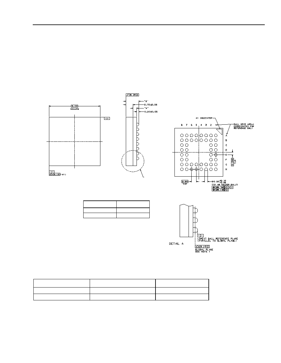
Agere Systems Inc.
51
Data Sheet, Rev. 1
August 2004
USB Device Controller
USS-820FD
Outline Diagrams
48-Ball TFSBGAC (USS-820FD)
Dimensions are in millimeters.
Ordering Information
*
In an effort to better serve its customers and the environment, Agere is converting to lead-free material set on this product.
Device Code
Package
Comcode
USS820FD
48-Ball TFSBGAC
108955543
L-USS820FD-DB
48-Ball TFSBGAC (lead-free)
*
700067325
DETAIL A
Note:
1. GLOBAL PLANE IS BEST FIT PLANE AS DETERMINED
BY COPLANARITY MEASUREMENT EQUIPMENT.
2. THIS PACKAGE CONFIGURATION HAS SOLDER MASK
DEFINED BGA PADS (SMD). FOR DETAILS SEE INDI-
VIDUL SUBSTRATE DRAWINGS (BOTTOM VIEW).
3. THE SOLDER BALL DIAMETER BEFORE REFLOW =
0.30 mm +0.10/
-0.0
5 mm.
A
B
0.36 ± 0.08
1.26 ± 0.18
0.21 ± 0.08
1.11 ± 0.18

52
Agere Systems Inc.
Data Sheet, Rev. 1
August 2004
USB Device Controller
USS-820FD
USB Device Controller
Appendix A. Special Function Register Bit Names
Table 48. Alphabetical Listing of Special Function Register Bit Names
Bit Name
Register
Table
Page
Bit Name
Register
Table
Page
A[6:0]
FADDR
22
25
RXFIF[1:0]
RXFLG
30
32
ADVRM
TXCON
25
26
RXFLUSH
RXFLG
30
32
ADVWM
RXCON
29
31
RXFULL
RXFLG
30
32
ARM
RXCON
29
31
RXIE
EPCON
19
20
ASOF
SOFH
16
18
RXISO
RXCON
29
31
ATM
TXCON
25
26
RXOVF
RXFLG
30
33
BC[7:0]
RXCNTL
28
30
RXSEQ
RXSTAT
21
23
BC[7:0]
TXCNTL
24
25
RXSETUP
RXSTAT
21
23
BC[9:8]
RXCNTH
28
30
RXSOVW
RXSTAT
21
23
BC[9:8]
TXCNTH
24
25
RXSPM
EPCON
19
20
BDFEAT
MCSR
37
38
RXSTL
EPCON
19
20
CTLEP
EPCON
19
20
RXURF
RXFLG
30
33
DPEN
MCSR
37
38
RXVOID
RXSTAT
21
24
EDOVW
RXSTAT
21
23
SCRATCH
SCRATCH
36
37
EPINX[2:0]
EPINDEX
18
19
SOFACK
SOFH
16
18
FEAT
MCSR
37
38
SOFIE
SOFH
16
18
FFSZ[1:0]
RXCON
29
30
SOFODIS
SOFH
16
18
FFSZ[1:0]
TXCON
25
26
SRESET
SCR
31
35
FRXD[3:0]
SBI
14
16
STOVW
RXSTAT
21
23
FRXD[7:4]
SBI1
15
17
SUSPDIS
SSR
32
36
FRXIE[3:0]
SBIE
12
15
SUSPEND
SSR
32
36
FRXIE[7:4]
SBIE1
13
15
SUSPLOE
MCSR
37
38
FTLOCK
SOFH
16
18
SUSPPO
SSR
32
36
FTXD[3:0]
SBI
14
16
SUSPS
MCSR
37
38
FTXD[7:4]
SBI1
15
17
T_IRQ
SCR
31
35
FTXIE[3:0]
SBIE
12
15
TS[10:8]
SOFH
16
18
FTXIE[7:4]
SBIE1
13
15
TS[7:0]
SOFL
17
19
IE_RESET
SCR
31
35
TXACK
TXSTAT
20
21
IE_RESUME
SCRATCH
36
37
TXAV[3:0]
DSAV
38
39
IE_SUSP
SCR
31
35
TXAV[7:4]
DSAV1
39
39
INIT
MCSR
37
38
TXCLR
TXCON
25
26
IRQLVL
SCR
31
35
TXDAT[7:0]
TXDAT
23
25
IRQPOL
SCR
31
35
TXDSAM
TXSTAT
20
21
PEND
PEND
35
37
TXEMP
TXFLG
26
27
PKGID
MCSR
37
38
TXEPEN
EPCON
19
20
RESET
SSR
32
36
TXERR
TXSTAT
20
21
RESUME
SSR
32
36
TXFIF[1:0]
TXFLG
26
27
REVRP
TXCON
25
26
TXFLUSH
TXSTAT
20
21
REVWP
RXCON
29
31
TXFULL
TXFLG
26
29
RWUPE
SCR
31
35
TXISO
TXCON
25
26
RWUPR
MCSR
37
38
TXNAKE
TXSTAT
20
21
RXACK
RXSTAT
21
24
TXOE
EPCON
19
20
RXAV[3:0]
DSAV
38
39
TXOVF
TXFLG
26
27
RXAV[7:4]
DSAV1
39
39
TXSEQ
TXSTAT
20
21
RXCLR
RXCON
29
30
TXSOVW
TXSTAT
20
21
RXDAT[7:0]
RXDAT
27
29
TXSTL
EPCON
19
20
RXEMP
RXFLG
30
33
TXURF
TXFLG
26
27
RXEPEN
EPCON
19
20
TXVOID
TXSTAT
20
21
RXERR
RXSTAT
21
24
UNLOCKED
LOCK
34
37
RXFFRC
RXCON
29
30

Agere Systems Inc.
53
Data Sheet, Rev. 1
August 2004
USB Device Controller
USS-820FD
Appendix B. USS-820FD Register Map
* Indexed by EPINDEX.
Table 49. USS-820FD Register Map
Register
USS-820FD Register Map
Addr
TXDAT
TXDAT[7:0]
00*
TXCNTL
BC[7:0]
01*
TXCNTH
--
BC[9:8] 02*
TXCON
TXCLR
TXFFSZ[1:0]
--
TXISO
ATM
ADVRM
REVRP
03*
TXFLG
TXFIF[1:0]
--
TXEMP
TXFULL
TXURF
TXOVF
04*
RXDAT
RXDAT[7:0]
05*
RXCNTL
BC[7:0]
06*
RXCNTH
--
BC[9:8]
07*
RXCON
RXCLR
RXFFSZ [1:0]
RXFFRC
RXISO
ARM
ADVWM
REVWP
08*
RXFLG
RXFIF[1:0]
--
RXFLUSH
RXEMP
RXFULL
RXURF
RXOVF
09*
EPINDEX
--
EPINX[2:0]
0A
EPCON
RXSTL
TXSTL
CTLEP
RXSPM
RXIE
RXEPEN
TXOE
TXEPEN
0B*
TXSTAT
TXSEQ
TXDSAM
TXNAKE
TXFLUSH
TXSOVW
TXVOID
TXERR
TXACK
0C*
RXSTAT
RXSEQ
RXSETUP
STOVW
EDOVW
RXSOVW
RXVOID
RXERR
RXACK
0D*
SOFL
TS[7:0]
0E
SOFH
SOFACK
ASOF
SOFIE
FTLOCK
SOFODIS
TS[10:8]
0F
FADDR
--
A[6:0]
10
SCR
IRQPOL
RWUPE
IE_SUSP IE_RESET
SRESET
IRQLVL
T_IRQ
--
11
SSR
--
SUSPPO
SUSPDIS
RESUME SUSPEND RESET
12
SBI
FRX03
FTX03
FRX02
FTX02
FRX01
FTX01
FRX00
FTX00
14
SBI1
FRX07
FTX07
FRX06
FTX06
FRX05
FTX05
FRX04
FTX04
15
SBIE
FRXIE3
FTXIE3
FRXIE2 FTXIE2
FRXIE1
FTXIE1
FRXIE0
FTXIE0
16
SBIE1
FRXIE7
FTXIE7
FRXIE6
FTXIE6
FRXIE5
FTXIE5
FRXIE4
FTXIE4
17
REV
REV[7:0]
18
LOCK
--
UNLOCKED
19
PEND
--
PEND
1A
SCRATCH
IE_RESUME
SCRATCH[6:0]
1B
MCSR
RWUPR
INIT
SUSPS
PKGID
FEAT
BDFEAT
SUSPLOE
DPEN
1C
DSAV
RXAV3
TXAV3
RXAV2
TXAV2
RXAV1
TXAV1
RXAV0
TXAV0
1D
DSAV1
RXAV7
TXAV7
RXAV6
TXAV6
RXAV5
TXAV5
RXAV4
TXAV4
1E

54
Agere Systems Inc.
Data Sheet, Rev. 1
August 2004
USB Device Controller
USS-820FD
USB Device Controller
Appendix C. Changes from USS-820/
USS-825 Revision B to C
Note: For Revision C, the USS-825B has been
renamed USS-820TC.
1. Hardware revision register (REV) changed from
1.0 to 1.1.
2. From the USB system and firmware points of view,
the USS-820C will appear functionally equivalent
to the USS-820B if a 1 is never written by firmware
to MCSR[3:2] or TXSTAT[6:5] (all previously
marked as reserved). The single exception is the
REV register as described above.
3. New register bits (FEAT, BDFEAT) are added to
enable new features. BDFEAT enables those fea-
tures which could impact existing boards. This
could only be an issue if NC pins were used as
connection points for other board signals. FEAT
enables all other features as indicated. FEAT is
MCSR[3]; BDFEAT is MCSR[2].
4. New FIFO status bits (RXAV/TXAV), one per FIFO,
added to indicate receive data set(s) available
(RXFIF > 00) or empty transmit data set(s) avail-
able (TXFIF < 11). If TXDSAM = 1, transmit FIFO
status bits are set if the device sends a NAK in
response to an IN packet when TXFIF = 00. The
16 register bits are formatted into two new regis-
ters (DSAV = address 1D, DSAV1 = address 1E) in
the same format as SBI/SBI1. These new read-
only bits can allow firmware to operate more effi-
ciently, because their use requires less polling
overhead. Register bits always read 0 unless FEAT
= 1 or TXDSAM = 1.
5. A logical OR of new FIFO status bits (RXAV/TXAV)
is brought out to a package pin (DSA). Package pin
is always 3-stated if BDFEAT = 0. Uses pin 15 in
44-pin package, pin 16 in 48-pin package.
6. New nonisochronous transmit mode. If enabled (by
new register bit TXNAKE = TXSTAT[5]), when the
USS-820C responds to an IN token with a NAK
because of no data sets being present (TXFIF =
00), an interrupt is generated, setting the appropri-
ate SBI/SBI1 bit. New register bit TXDSAM
(TXSTAT[6]) allows this condition to set the new
DSAV register bit and assert the new DSA output
pin (assuming they are enabled). This mode
changes the meaning of TXVOID to indicate that
such a NAK was sent, and it is the responsibility of
firmware to clear TXVOID. While TXVOID = 1, the
corresponding SBI/SBI1 register bit will remain set
as well.
7. Transmit isochronous behavior changed to discard
old data packets at the end of the intended frame if
not read out by a host IN (only enabled if
FEAT = 1). Data sets are not visible to the host
until the first SOF following the data set write. At
the start of a series of transfers, TXFIF will equal
00, which could allow firmware to write two data
sets during that same frame. In that case, the older
set is flushed by hardware at the first SOF.
8. Receive isochronous behavior changed to flush old
data packets at the end of the intended frame if not
read out by firmware (only enabled if FEAT = 1).
This flush decrements RXFIF and sets the
RXFLUSH register bit (RXFLG[4]), which firmware
must check before setting RXFFRC. While
RXFLUSH is set, the effect of firmware RXDAT
reads (FIFO pointer/flag changes) is blocked, to
avoid possible corruption of a new data set. If firm-
ware detects that RXFLUSH = 1, it must discard
the data set just read, since it is possibly truncated.
Firmware must still set RXFFRC in this situation,
which resets RXFLUSH to 0.
9. ASOF behavior changed to not automatically reset
when SOFODIS = 0 if FEAT = 1.
10. For nonisochronous endpoints, FFSZ = 2 indicates
8 bytes, FFSZ = 3 indicates 32 bytes (both are
interpreted as 64 bytes in the USS-820 revision B).
This will potentially allow more efficient usage of
the shared FIFO space. Only enabled if FEAT = 1.
11. USB-reset-detected condition clears the FADDR
register (if FEAT = 1). This avoids the potential
case where firmware is too slow in resetting
FADDR after USB RESET such that the host real-
locates the address to some other device and
sends traffic to that device, which is misinterpreted
by the USS-820C as intended for it. No other regis-
ter bits are cleared by USB reset.
12. USB-reset-detected condition brought out to pack-
age pin (USBR), allowing the external controller to
clear out a locked up device. Output is always 3-
stated if BDFEAT = 0. Uses pin 18 of 44-pin pack-
age, pin 19 of 48-pin package.
13. Firmware provided means to resume and reset
device if suspended. When suspended, if
SUSPP0 = 0, SUSPLOE = 0, FEAT = 1, a firmware
write of 1 to SCR bit 3 (SRESET) causes a remote
wake-up type of event (without resume signaling).
After the wake-up, when clocks are turned on, the
SRESET bit will be set and will take effect (i.e., the
USS-820C will be reset).

Agere Systems Inc.
55
Data Sheet, Rev. 1
August 2004
USB Device Controller
USS-820FD
Appendix C. Changes from USS-820
Revision B to C
(continued)
14. Remote-wake-up-remember condition is visible as
a register bit (RWUPR). Register bit always reads
a 0 unless FEAT = 1. RWUPR is MCSR[7].
15. Additional/updated electrical characteristics related
to the new 0.25
µ
m process (power, hysteresis
leakage current) are included.
16. The V
DD5V
pin is no longer required--may be
treated as no connect.
Appendix D. Changes from USS-820
Revision C to D
1. All (4) USS-820C/USS-820TC advisory items are
corrected.
2. Value of REV register is changed from 11h to 13h.
Appendix E. Changes from USS-820
Revision D to FD
1. Device package was changed from a 44-pin MQFP
or a 48-pin TQFP to a 48-ball TFSBGAC.

Agere Systems Inc. reserves the right to make changes to the product(s) or information contained herein without notice. No liability is assumed as a result of their use or application.
Agere is a registered trademark of Agere Systems Inc. Agere Systems and the Agere logo are trademarks of Agere Systems Inc.
Copyright © 2004 Agere Systems Inc.
All Rights Reserved
August 2004
DS03-016CMPR-1 (Replaces DS03-016CMPR)
For additional information, contact your Agere Systems Account Manager or the following:
INTERNET:
http://www.agere.com
E-MAIL:
docmaster@agere.com
N. AMERICA:
Agere Systems Inc., Lehigh Valley Central Campus, Room 10A-301C, 1110 American Parkway NE, Allentown, PA 18109-9138
1-800-372-2447, FAX 610-712-4106 (In CANADA: 1-800-553-2448, FAX 610-712-4106)
ASIA:
CHINA: (86) 21-54614688 (Shanghai), (86) 755-25881122 (Shenzhen)
JAPAN: (81) 3-5421-1600 (Tokyo), KOREA: (82) 2-767-1850 (Seoul), SINGAPORE: (65) 6778-8833, TAIWAN: (886) 2-2725-5858 (Taipei)
EUROPE:
Tel. (44) 1344 296 400
The USB-IF logo is a trademark of the Universal Serial Bus Implementers Forum, Inc.