 | –≠–ª–µ–∫—Ç—Ä–æ–Ω–Ω—ã–π –∫–æ–º–ø–æ–Ω–µ–Ω—Ç: W3011 | –°–∫–∞—á–∞—Ç—å:  PDF PDF  ZIP ZIP |
Document Outline
- Features
- Applications
- Description
- List of Figures
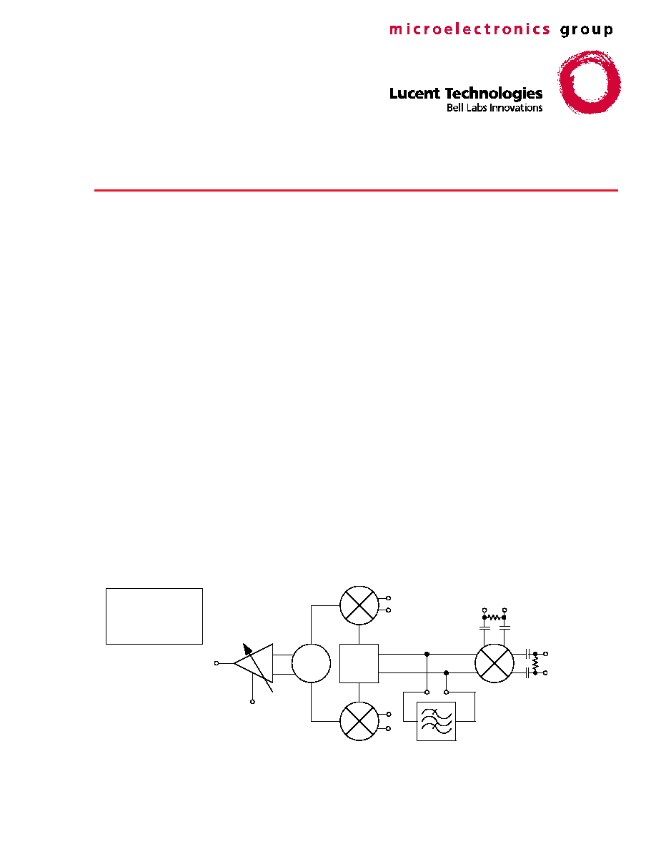
- Figure 1. Circuit Block Diagram
- Figure 2. Pin Configuration
- Figure 3. W3011 Sine-Wave Modulation Output Spectrum
- Figure 4. W3011 RF Output Diagram
- Figure 5. W3011 Application with Offset Mixer Disabled
- Figure 6. W3011 Application Using Offset Mixer
- Figure 7. Output Power vs. APC and Supply Voltage
- Figure 8. Outpur Power vs. APC Voltage and Temperature
- Figure 9. Supply Current vs. Output Power
- Figure 10. Carrier Suppression vs. Output Power and LO Level
- Figure 11. EVM vs. output Power and Temperature
- Figure 12. EVM vs. Output Power and I/Q Common-Mode Voltage
- Figure 13. Adjacent Channel Power Suppression for PDC
- List of Tables
- Table 1. Pin Descriptions
- Table 2. Absolute Maximum Ratings
- Table 3. Operating Ranges
- Table 4. dc and Digital Electrical Specifications
- Table 5. ac Specifications
- Pin Information
- Absolute Maximum Ratings
- Handling Precautions
- Operating Ranges
- Electrical Characteristics
- Explanation of Error Vector Magnitude (EVM) Testing
- RFOUT Matching: Basic Open Collector Termination
- Offset Mixer
- W3011 with Offset Mixer Disabled
- W3011 Using Offset Mixer
- Characteristic Curves
- Package Outline
- Manufacturing Information
- Ordering Information
- Contact Us
W3011
1 GHz Quadrature Modulator
Data Sheet
September 1999
Features
+
Guaranteed performance at 2.7 V power supply
+
Output power of 3 dBm into 50
load (single-
ended) with 3 V operation
+
Direct RF modulation with or without offset mixer
+
Automatic power control (APC) capability
+
Accurate 90∞ phase shifter for carrier
+
Double-balanced active mixers minimize carrier
feedthrough (origin offset)
+
Low-current sleep mode
Applications
+
PDC 800 and American digital cellular mobile
terminals
+
Cellular base stations
Description
The W3011 1 GHz Quadrature Modulator is a
monolithic integrated circuit that provides direct
modulation of an RF carrier by I & Q baseband
inputs. It is particularly suited for use in mobile and
handheld cellular telephones designed to the IS-136
(North American 824 MHz to 849 MHz), PDC
(Japan RCR-STD27 889 MHz to 958 MHz), and
other digital personal-communications standards.
The circuit block diagram is shown in Figure 1. From
two LO signals, LOL and LOH, the offset mixer
produces an internal LO signal, which prevents the
external VCOs from being pulled by the large
transmitted signal. The phase shifter splits the LO
signal into two carriers with 90∞ phase separation
and equal amplitude.
These signals are fed to the in-phase (I) and
quadrature-phase (Q) double-balanced mixers. The
resulting signals are summed and fed into the output
amplifier. This amplifier can provide 0 dBm linear
output power, minimum, into a 50
load.
The output power can be attenuated up to 50 dB by
applying a control voltage to the APC input.
Nominally, the output power is at maximum
(+3 dBm) with V
APC
> 2.2 V, and at minimum
(≠50 dBm) with V
APC
< 0.8 V.
A CMOS/TTL-compatible logic input allows the
device to be put into a powerdown mode in which
less than 10 µA of supply current is consumed.
BIAS AND CONTROL
V
CC
ENABLE
GROUND
EXTERNAL FILTER
OR
DIRECT LO INPUT
APC
RF
OUT
≠
/4
+
/4
Q
I
LOL IN
50
LOH IN
50
Figure 1. Circuit Block Diagram
W3011
Data Sheet
1 GHz Quadrature Modulator
September 1999
2
Lucent Technologies Inc.
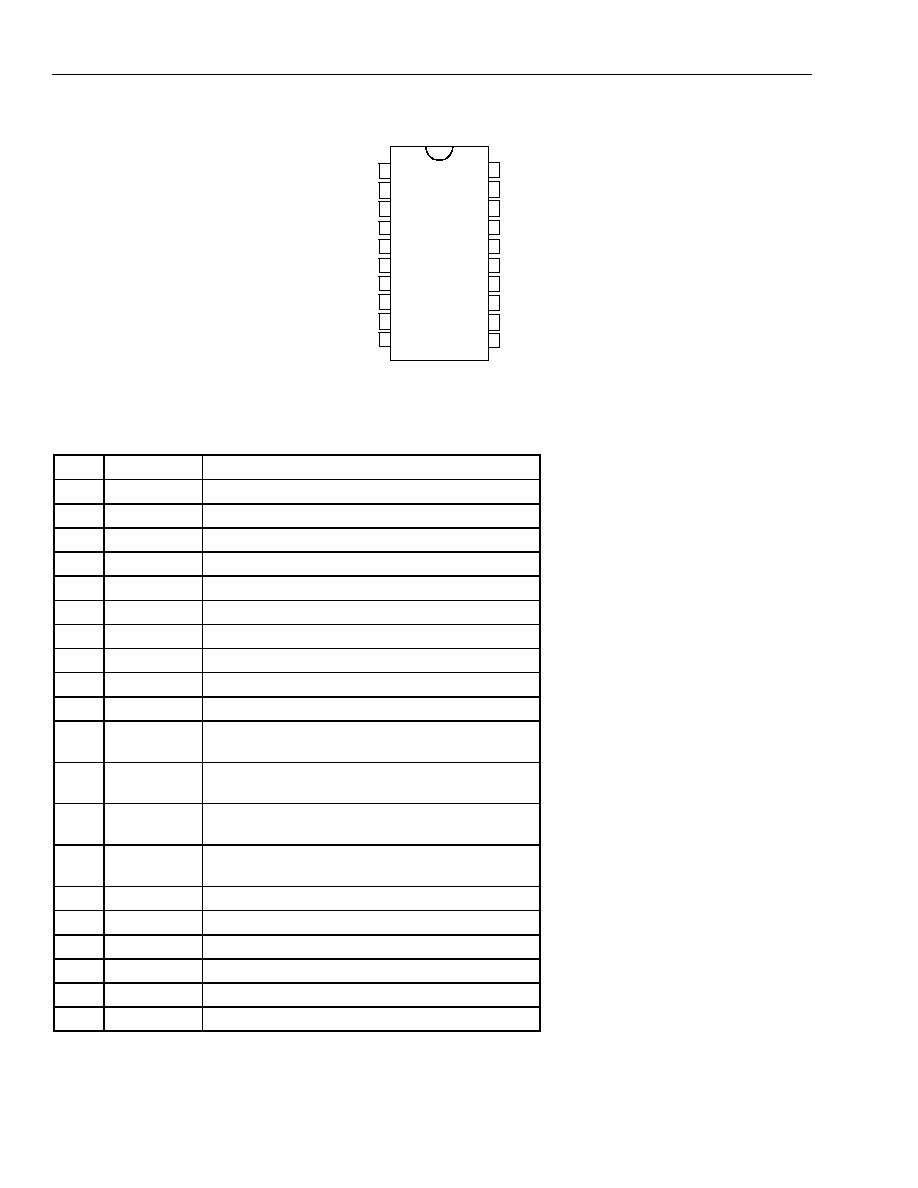
Pin Information
TOP
VIEW
20
19
18
17
16
15
14
12
13
11
1
2
3
4
5
6
7
8
9
10
IP
IN
QN
ENABLE
GND
QP
APC
GND
LC1
LC2
V
CC
V
CC
RF
GND
GND
GND
LOLP
RFOUT
LOLN
LOHP
LOHN
Figure 2. Pin Configuration
Table 1. Pin Descriptions
Pin
Name
Function
1
IP
Differential Baseband Input (in-phase)
2
IN
Differential Baseband Input (in-phase)
3
QP
Differential Baseband Input (quad-phase)
4
QN
Differential Baseband Input (quad-phase)
5
APC
Automatic Power Control dc Input
6
GND
dc Ground
7
ENABLE
Logic Enable
8
GND
dc Ground
9
LC1
Differential LO Input/External Filter
10
LC2
Differential LO Input/External Filter
11
LOHN
Differential High-frequency Local Oscillator
Input
12
LOHP
Differential High-frequency Local Oscillator
Input
13
LOLN
Differential Low-frequency Local Oscillator
Input
14
LOLP
Differential Low-frequency Local Oscillator
Input
15
GND
dc Ground
16
GND
dc Ground
17
RF
OUT
Open-collector RF Output
18
GND
dc Ground
19
V
CC
RF
Positive Power Supply for RF Output Stage
20
V
CC
Positive Power Supply (nonoutput circuits)
Data Sheet
W3011
September 1999
1 GHz Quadrature Modulator
Lucent Technologies Inc.
3
Absolute Maximum Ratings
Stresses in excess of the absolute maximum ratings can cause permanent damage to the device. These are
absolute stress ratings only, as shown in Table 2. Functional operation of the device is not implied at these or
any other conditions in excess of those given in the operations sections of the data sheet. Exposure to absolute
maximum ratings for extended periods can adversely affect device reliability.
Table 2. Absolute Maximum Ratings
Parameter
Symbol
Min
Max
Unit
Ambient Operating Temperature
T
A
≠35
85
∞C
Storage Temperature
T
stg
≠65
150
∞C
Lead Temperature (soldering, 10 s)
--
--
300
∞C
Positive Supply Voltage
V
CC
≠0.3
4.5
V
Power Dissipation
P
D
--
650
mW
ac p-p Input Voltage
Vp-p
≠0.3
V
CC
V
Digital Voltages
--
≠0.3
V
CC
V
Handling Precautions
Although protection circuitry has been designed into this device, proper precautions should be taken to avoid
exposure to electrostatic discharge (ESD) during handling and mounting. Lucent Technologies Microelectronics
Group employs a human-body model (HBM) and a charged-device model (CDM) for ESD-susceptibility testing
and protection design evaluation. ESD voltage thresholds are dependent on the circuit parameters used to define
the model. No industry-wide standard has been adopted for CDM. However, a standard HBM (resistance =
1500
, capacitance = 100 pF) is widely used and, therefore, can be used for comparison purposes. The HBM
ESD threshold presented here was obtained by using these circuit parameters:
ESD Threshold Voltage
Model
Rating
HBM
2000
CDM (corner pins)
CDM (noncorner pins)
500
500

W3011
Data Sheet
1 GHz Quadrature Modulator
September 1999
4
Lucent Technologies Inc.
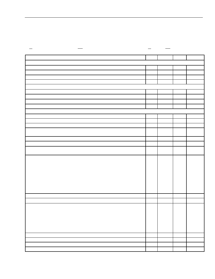
Operating Ranges
The W3011 operating ranges are shown in Table 3. Performance is not guaranteed over the full range of all
conditions possible within this table. However, the table lists the ranges of external conditions in which the
W3011 provides general functionality, which may be useful in specific applications, without risk of permanent
damage. The conditions for guaranteed performance are described in Tables 4 and 5.
Table 3. Operating Ranges
Parameter
Min
Max
Unit
V
CC
2.7
3.6
Vdc
Ambient Operating Temperature
≠35
85
∞C
f
LO
Direct Mode (pins 9 and 10)
800
1000
MHz
P
LO
Direct Mode (pins 9 and 10)
110
600
mVp-p
Offset Local Oscillator (LOL) Frequency
50
800
MHz
LOL Input Level
≠15
≠3
dBm
UHF Local Oscillator (LOH) Frequency
100
1300
MHz
LOH Input Level
≠15
≠3
dBm
External dc Bias Voltage for I & Q Inputs with
0.282 V
rms
ac Input Level
:
Differential ac Input
1.2
V
CC
≠ 0.7
Vdc
Electrical Characteristics
Table 4. dc and Digital Electrical Specifications
Conditions unless otherwise noted: 2.7
V
CC
3.3 Vdc; T
A
= 25 ∞C ± 3 ∞C; RL = 50
, VAPC = 2.7 Vdc;
f
RF
= 900 MHz, f
LOL
= 130 MHz, f
LOH
= 1030 MHz, ≠13 dBm < P
LOL
, P
LOH
< ≠5 dBm;
I ≠
I
= 0.4 cos(2
t
Y
80 kHz), Q ≠ Q = 0.4 cos(2
t
Y
80 kHz ≠
/2), Vbias of I,
I
, Q, and Q = 1.22 Vdc.
Parameter
Symbol
Min
Typ
Max
Unit
Enable Input
Logic High Voltage
V
IH
0.7 V
CC
--
V
CC
+ 0.4
V
Logic Low Voltage
V
IL
GND ≠ 0.4
--
0.3 V
CC
V
Logic High Current (V
IH
= 3.3 V)
I
IH
--
--
10
µA
Logic Low Current (V
IL
= 0.4 V)
I
IL
--
--
10
µA
Powerup/down (after ENABLE change)
--
--
--
4
µs
Power Supply Current
Powerdown (ENB = 0)
I
PDN
--
0.3
50
µA
Transmit (ENB = V
CC
):
(offset mixer on, APC @ max power)
(offset mixer off, APC @ max power)
I
CC
(on)
I
CC
(on)
--
--
52
50
66
64
mA
mA
Transmit (ENB = V
CC
):
(offset mixer on, APC @ P
OUT
< P
MAX
≠ 10
dB)
(offset mixer off, APC @ P
OUT
< P
MAX
≠ 10
dB)
--
--
--
--
46
43
--
--
mA
mA
Data Sheet
W3011
September 1999
1 GHz Quadrature Modulator
Lucent Technologies Inc.
5
Electrical Characteristics
(continued)
Table 5. ac Specifications
Conditions unless otherwise noted: 2.7
V
CC
3.3 Vdc; T
A
= 25 ∞C ± 3 ∞C; RL = 50
, VAPC = 2.7 Vdc;
f
RF
= 900 MHz, f
LOL
= 130 MHz, f
LOH
= 1030 MHz, ≠15 dBm < P
LOL
, P
LOH
< ≠5 dBm;
I ≠
I
= 0.4 cos(2
t
Y
80 kHz), Q ≠ Q = 0.4 cos(2
t
Y
80 kHz ≠
/2), Vbias of I,
I
, Q, and Q = 1.22 Vdc.
Parameter
Min
Typ
Max
Unit
I & Q
I & Q Signal Path 0.5 dB Bandwidth
--
5
--
MHz
I & Q Input Resistance
--
200
--
k
I & Q Input Capacitance to Ground
--
5
--
pF
I & Q Input Differential Signal for Max Output
--
0.8
--
Vp-p
Offset Mixer
LOL Input Impedance
--
50
--
LOH Input Impedance
--
50
--
LO Input Impedance (pins LC1, LC2)
--
480//1
--
//pF
LOL Input IP3
--
10
--
dBm
Modulation Accuracy (P
OUT
= ≠1 dBm)
Carrier Suppression (P
OUT
= ≠1 dBm)
--
≠35
≠28
dBUSB
Carrier Suppression (entire usable APC range)
--
--
≠26
dBUSB
Origin Offset (DQPSK inputs, all usable APC levels)
--
--
≠23
dBc
Error Vector Magnitude (See Explanation of Error Vector Magnitude
(EVM) Testing section.)
--
2.5
5
%
Lower Sideband (LSB) Suppression (See Figure 3.)
--
≠43
≠34
dBUSB
RF Output
Output Power (0.8 Vp-p differential or single-ended 80 kHz sine-wave
inputs to I and Q, with 90∞ between I and Q)
≠1
3
--
dBm
Adjacent Channel Suppression (0.282 Vrms differential I and Q inputs,
/4 ≠ DQPSK modulation, random data):
Per PDC (RCR STD-27):
±50 kHz, All Usable APC Levels
±100 kHz, All Usable APC Levels
±100 kHz, Max RF Output (APC > 2.2)
Per IS-136/IS-137 800 MHz Digital Mode:
±30 kHz, All Usable APC Levels
±60 kHz, All Usable APC Levels
--
--
--
--
--
≠65
--
≠75
≠45
≠60
≠55
≠62
≠65
≠36
≠50
dBc
dBc
dBc
dBc
dBc
Noise Floor Suppression, F
C
± >100 kHz
--
≠120
≠112
dBc/Hz
APC (Automatic Power Control) Function
Range of Usable Output Power Control for Japan PDC (RCR STD-27),
from Max Power at APC = 2.7 V to Minimum APC Voltage Where
Requirements for ACP and Carrier Suppression Are Still Met Using
/4 ≠ DQPSK/
= 0.5 Modulation at 0.282 Vrms Differential I and Q
Inputs:
Offset Mixer Not Used
Offset Mixer Used
29
39
40
45
--
--
dB
dB
Output Power Variation Due to Temperature, within Usable Control Range
--
4
6
dB
RF Power Change Time (after APC change)
--
--
2
µs
APC Voltage for Max Output Power
--
2.2
--
Vdc
APC Voltage for Min Output Power
--
0.8
--
Vdc