 | –≠–ª–µ–∫—Ç—Ä–æ–Ω–Ω—ã–π –∫–æ–º–ø–æ–Ω–µ–Ω—Ç: W3013 | –°–∫–∞—á–∞—Ç—å:  PDF PDF  ZIP ZIP |
Document Outline
- Features
- Applications
- Description
- Circuit Block Diagram
- Pin Information
- Absolute Maximum Ratings
- Handling Precautions
- Operating Ranges
- Electrical Characteristics
- EVM Testing
- Application Circuits
- ENB/APC Function
- Characteristic Curves
- RF Output Impedance
- Package Outline
- Manufacturing Information
- Ordering Information
- List of Figures
- Figure 1. Circuit Block Diagram
- Figure 2. Pin Diagram
- Figure 3. W3013 Sine-Wave Modulation Output Spectrum
- Figure 4. Typical Application Circuit
- Figure 5. Relative RF Output Power vs. APC Voltage
- Figure 6. Unwanted Sideband Suppression vs. LO1 Frequency and LO1 Input Level
- Figure 7. Carrier Suppression vs. LO1 Frequency
- Figure 8. Adjacent Channel Suppression for IS-136 vs. 1900 MHz Output Power
- Figure 9. Adjacent Channel Suppression for PDC vs. 940 MHz Output Power
- Figure 10. IQ Bandwidth vs. ac Input Voltage
- Figure 11. RFOUT Impedance at Pin 19 Contact with Board
- List of Tables
- Table 1. Pin Descriptions
- Table 2. Electrical Characteristics
- Table 3. RFOUT Representative Impedances
- Contact Us

W3013 Indirect Quadrature Modulator
with Gain Control
Preliminary Data Sheet
November 1998
Features
n
Low-voltage operation: 2.7 V
n
High-frequency operation: 2.2 GHz
n
High RF output power: ≠10 dBm
n
High-accuracy phase shifter, no trim required
n
Low carrier feedthrough: ≠45 dBc
n
Automatic power control (APC) capability
n
Low-current sleep mode
n
20-pin TSSOP package
Applications
n
North American IS-136
n
Japan PDC (RCR STD 27)
n
Japan PHS (RCR STD 28)
n
GSM 900, 1800, and 1900 MHz
n
Narrowband CDMA
n
Digital satellite communications
Description
The W3013 is a monolithic integrated circuit that
provides indirect, quadrature modulation of an RF
carrier by I & Q baseband inputs. The function
performed by the W3013 is particularly suited for
handheld digital cellular and digital cordless
telephones that operate between 800 MHz and
2.2 GHz.
The circuit block diagram is shown below. From a
single local-oscillator input (LO1), the phase
shifter produces two LO signals with 90∞ phase
separation and equal amplitude. The LO signals
are fed to the in-phase (I) and quadrature (Q)
double-balanced mixers. The resulting signals are
summed and fed into an RF mixer where the
frequency can be translated to over 2 GHz.
Outputs between the summer and RF mixer are
available for external filtering. Finally, the signal is
amplified to provide a single-ended output.
The ENB/APC input with a logic low allows the
device to be put into a powerdown mode. Above
the logic low threshold, the device enters a power
control mode that provides a range of desired
output power levels.
ÿ
Q
Q
I
I
LO1
LO1REF
LO2 LO2REF
RF
OUT
POWER
CONTROL
EXTERNAL
FILTER
RF
OUT
≠
/
4
+
/
4
INTERNAL
LOW-PASS
FILTER
ENAB/APC
Figure 1. Circuit Block Diagram
W3013 Indirect Quadrature Modulator
Preliminary Data Sheet
with Gain Control
November 1998
2
Lucent Technologies Inc.
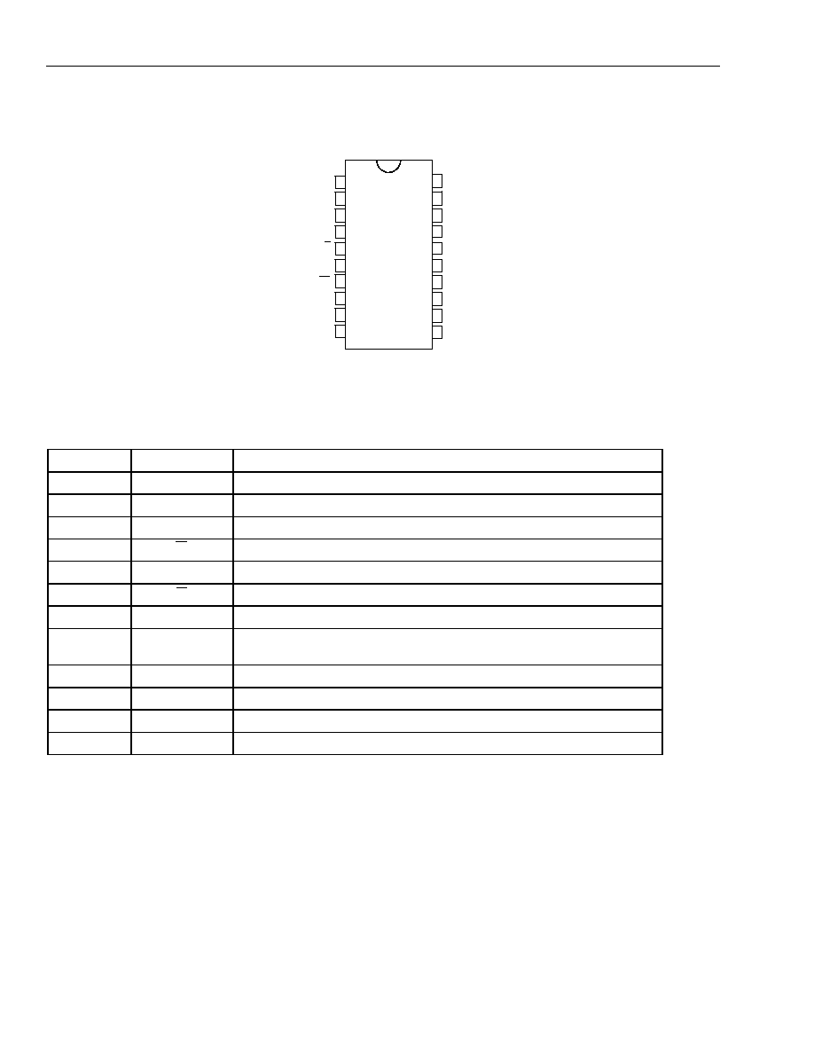
Pin Information
TOP
VIEW
20
19
18
17
16
15
14
12
13
11
1
2
3
4
5
6
7
8
9
10
V
CC
FILTA
I
Q
Q
FILTB
I
LO1REF
LO1
GND
V
CC
RF
OUT
GND
ENB/APC
GND
GND
GND
LO2REF
LO2
GND
12-2680
Figure 2. Pin Diagram
Table 1. Pin Descriptions
Pin
Symbol
Name/Description
1
V
CC
Positive Supply Voltage. For low-power/small-signal subcircuits.
2, 3
FILTA, FILTB
Filter. Nodes A & B for parallel resonant LC.
4
I
Differential Baseband Input.
5
I
Differential Baseband Input (Inverting).
6
Q
Differential Baseband Input.
7
Q
Differential Baseband Input (Inverting).
8, 9
LO1REF, LO1
First Local Oscillator Input. Either pin may be directly grounded.
10, 11, 14,
15, 17, 18
GND
Power Supply Ground.
12, 13
LO2, LO2REF
Second Local Oscillator Input. Either pin may be directly grounded.
16
ENB/APC
Enable/Automatic Power Control.
19
RF
OUT
RF Output.
20
V
CC
Positive Supply Voltage. For RF output stage.

Preliminary Data Sheet
W3013 Indirect Quadrature Modulator
November 1998
with Gain Control
Lucent Technologies Inc.
3
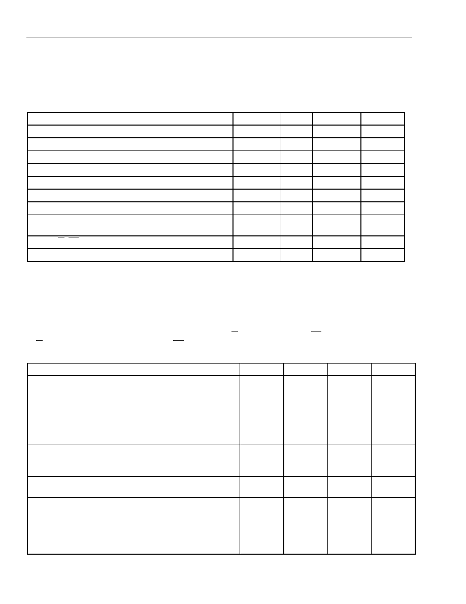
Absolute Maximum Ratings
Stresses in excess of the absolute maximum ratings can cause permanent damage to the device. These are
absolute stress ratings only. Functional operation of the device is not implied at these or any other conditions in
excess of those given in the operations sections of the data sheet. Exposure to absolute maximum ratings for
extended periods can adversely affect device reliability.
Parameter
Symbol
Min
Max
Unit
Ambient Operating Temperature
T
A
≠40
100
∞C
Storage Temperature
T
stg
≠65
150
∞C
Lead Temperature (soldering, 10 s)
T
L
--
300
∞C
Positive Supply Voltage
V
CC
--
5
Vdc
Power Dissipation
P
D
--
750
mW
Output Current (continuous)
I
OUT
--
160
mA
ac Input Voltage
--
GND
V
CC
Vp-p
Enable Input Voltage
V
ENB
GND
V
CC
Vdc
Handling Precautions
Although protection circuitry has been designed into this device, proper precautions should be taken to avoid
exposure to electrostatic discharge (ESD) during handling and mounting. Lucent Technologies Microelectronics
Group employs a human-body model (HBM) and a charged-device model (CDM) for ESD-susceptibility testing
and protection design evaluation. ESD voltage thresholds are dependent on the circuit parameters used to define
the model. No industry-wide standard has been adopted for CDM. However, a standard HBM (resistance =
1500
, capacitance = 100 pF) is widely used and, therefore, can be used for comparison purposes. The HBM
ESD threshold presented here was obtained by using these circuit parameters:
ESD Threshold Voltage
Device
Rating
Model
W3013
1000 V
HBM
W3013
1000 V
CDM
W3013 Indirect Quadrature Modulator
Preliminary Data Sheet
with Gain Control
November 1998
4
Lucent Technologies Inc.
Operating Ranges
This table lists the ranges of external conditions in which the W3013 provides general functionality that may be
useful in specific applications without risk of permanent damage. However, performance is not guaranteed over
the full range of all possible conditions. The conditions for guaranteed performance are described in the
Electrical Characteristics table.
Parameter
Min
Typ
Max
Unit
V
CC
2.7
--
3.6
V
f
LO1
100
178
350
MHz
V
LO1
100
250
600
mVp-p
f
LO2
100
1620
2200
MHz
V
LO2
100
250
600
mVp-p
f
RF
<800
--
>2200
MHz
I & Q Input Range of dc Bias for 1 Vp-p Differential Input
V
CC
/2 ≠ 0.1
V
CC
/2
V
CC
/2 + 0.1
Vdc
I & Q Input Range of dc Bias for 1 Vp-p Single-ended
Input
V
CC
/2 ≠ 0.1
V
CC
/2
V
CC
/2 + 0.1
Vdc
I (Q) to
I
(
Q
) Differential Input Swing*
--
1.0
1.1
Vp-p
Ambient Operating Temperature
≠35
25
85
∞C
* Distortion-dependent, e.g., 1.3 Vp-p
/4 DQPSK peak voltage meets PDC or IS-136 distortion specification under random data modulation.
Electrical Characteristics
Table 2. Electrical Characteristics
Conditions (unless otherwise specified): T
A
= 25 ∞C
±
3 ∞C, V
CC
= 2.7 Vdc, R
L
= 50
, f
LO1
= 178 MHz,
f
LO2
= 1620 MHz, P
LO1
= P
LO2
= ≠10 dBm, V
BIAS
(I) = V
BIAS
(
I
) = V
BIAS
(Q) = V
BIAS
(
Q
) = V
CC
/2;
I ≠
I
= 0.5
Y
cos(2
t
Y
80 kHz ≠
/2) V, Q ≠
Q
= 0.5
Y
cos(2
t
Y
80 kHz) V, f
RFOUT
= 1442.08 MHz,
V
APC
= 2.7 Vdc.
Parameter
Min
Typ
Max
Unit
V
CC
Supply Current:
Active Mode
--
37
--
mA
Sleep Mode @ V
CC
= 3.3 V, ENB/APC
0.1 Vdc
--
<1
50
µA
I & Q:
I & Q Signal Path: 3 dB Bandwidth (differential input)
--
21
--
MHz
I & Q Input Bias Current
--
500
1500
nA
I & Q Input Impedance
--
1
--
M
LO1:
LO1 Suppression (relative to output power)
--
45
--
dBc
LC Filter Pins: Differential Impedance
--
600
||
1.2
--
||
pF
LO2:
LO2 Suppression (relative to output power)
--
35
--
dBc
Modulation Accuracy:
Carrier Suppression (relative to wanted sideband)
35
50
--
dBc
Lower Sideband Suppression
35
45
--
dBc
Transmitted I and Q Amplitude Error
--
±0.1
--
dB
Transmitted I and Q Phase Error
--
±1
--
degrees
Error Vector Magnitude (See page 6.)
--
1.3
5
%

Preliminary Data Sheet
W3013 Indirect Quadrature Modulator
November 1998
with Gain Control
Lucent Technologies Inc.
5
Electrical Characteristics
(continued)
Table 2. Electrical Characteristics (continued)
Conditions (unless otherwise specified): T
A
= 25 ∞C
±
3 ∞C, V
CC
= 2.7 Vdc, R
L
= 50
, f
LO1
= 178 MHz, f
LO2
=
1620 MHz, P
LO1
= P
LO2
= ≠10 dBm, V
BIAS
(I) = V
BIAS
(
I
) = V
BIAS
(Q) = V
BIAS
(
Q
) = V
CC
/2,
I ≠
I
= 0.5
Y
cos(2
t
Y
80 kHz ≠
/2) V, Q ≠
Q
= 0.5
Y
cos(2
t ∑ 80 kHz) V, f
RFOUT
= 1442.08 MHz,
V
APC
= 2.7 Vdc.
Parameter
Min
Typ
Max
Unit
RF Output:
Output Power (narrowband match):
1442 MHz
≠13
≠8
≠3
dBm
800 MHz (LO2 = 978 MHz)
--
≠8
--
dBm
1910 MHz (LO2 = 1732 MHz)
--
≠10
--
dBm
Output Power Total Range of APC Control
--
55
--
dB
Usable APC Range:*
PDC (IQ offset < ≠23 dBc, 100 kHz adjacent channel
power < ≠60 dBc)
35
45
--
dBc
IS-136 (IQ offset < ≠23 dBc, 60 kHz adjacent channel
power < ≠45 dBc)
45
54
--
dBc
Adjacent Channel Suppression at Maximum Output
(1.3 Vp-p random data digital modulation):
0.35-DQPSK Modulation per IS-136:
±30 kHz
--
≠39
≠35
dBc
±60 kHz
--
≠64
≠57
dBc
±90 kHz
--
≠67
≠57
dBc
0.5-DQPSK Modulation per Japan PDC at Maximum
Output:
±50 kHz
--
≠60
≠54
dBc
±100 kHz
--
≠73
≠65
dBc
0.5-DQPSK Modulation per Japan PHS at Maximum
Output:
±600 kHz
--
≠62
≠50
dBc
±900 kHz
--
≠63
≠50
dBc
Enable/APC:
V
IHMIN
(higher voltage turns device on)
--
0.81
1.0
V
V
ILMAX
(lower voltage turns device off)
0.6
--
--
V
I
ILMAX
(V
ENABLE/
APC = 0.4 V)
--
--
<1
µA
I
IHMAX
(V
ENABLE/
APC = 2.7 V)
--
--
40
µA
Powerup/Powerdown Time
--
--
4
µs
APC Voltage for Minimum Output Power
--
1.0
--
Vdc
APC Voltage for Maximum Output Power
2.5
--
--
Vdc
APC Bandwidth
5
--
--
MHz
* Usable APC range is defined to be the satisfaction of respective transmitter system requirements in the adjacent and alternate channels,
as well as IQ offset and EVM requirements in each standard.
W3013 Indirect Quadrature Modulator
Preliminary Data Sheet
with Gain Control
November 1998
6
Lucent Technologies Inc.
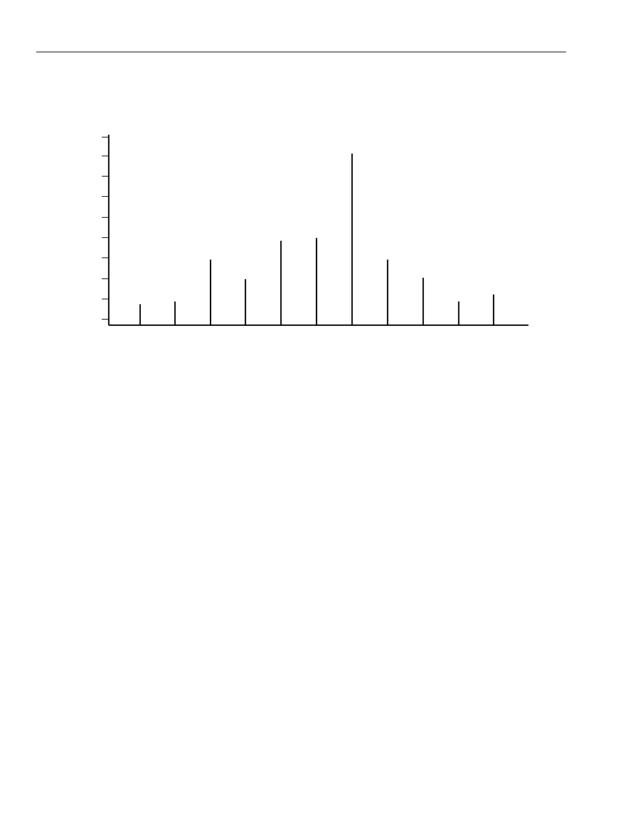
Error Vector Magnitude (EVM) Testing
Error vector magnitude (EVM) is estimated by feeding signals to the W3013 as described at the top of the
Electrical Characteristics table. A narrowband, sine-wave modulation output spectrum is shown in Figure 3.
U5
≠77 dBm
U4
≠84 dBm
U3
≠71 dBm
U2
≠63 dBm
USB
≠10 dBm
CARRIER
≠50 dBm
LSB
≠53 dBm
L2
≠72 dBm
L3
≠61 dBm
L4
≠81 dBm
L5
≠82 dBm
≠20
≠30
≠40
≠50
≠60
≠70
≠80
f
BB
= 80 kHz
f
LO1
= 178 MHz
f
LO2
= 1620 MHz
RF
OUT
= 1442.08 MHz
RELATIVE MAGNITUDE (dBm)
1441.60 1441.68 1441.76 1441.84 1441.92
1442.08 1442.16 1442.24 1442.32
1442.40
1442
≠10
≠90
0
FREQUENCY (MHz)
Figure 3. W3013 Sine-Wave Modulation Output Spectrum
Data from this spectrum are used to estimate EVM by the formula:
EVM (%) =
100
∑
[10
P(L5)/20
+ 10
P(L4)/20
+ 10
P(L3)/20
+ 10
P(L2)/20
+
10
P(LSB)/20
+ 10
P(U2)/20
+ 10
P(U3)/20
+ 10
P(U4)/20
+ 10
P(U5)/20
]/10
P(USB)/20
The data presented in the spectrum above would yield:
EVM (%) = 100
Y
[79e≠6 + 89e≠6 + 891e≠6 + 251e≠6 + 2239e≠6 + 708e≠6 + 282e≠6 + 63e≠6 +
141e≠6]/0.316e
= 1.5%
This approximates worst-case digital modulation results because the sine-wave modulation estimate assumes all
spurious outputs are in phase and adds their magnitudes as scalars. In addition, this estimate includes full-
amplitude measurements of spurious peaks that would appear in adjacent and alternate channels, where a
receiver would otherwise provide attenuation. The L3 third-order intermodulation peak and LSB (lower sideband)
are normally the unwanted output frequencies that dominate the EVM estimate.
Preliminary Data Sheet
W3013 Indirect Quadrature Modulator
November 1998
with Gain Control
Lucent Technologies Inc.
7
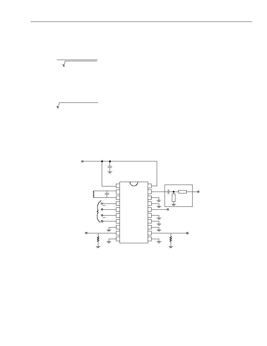
Application Circuits
A typical application circuit for the W3013 is shown in Figure 4. The LC filter components, L
F
and C
F
, are chosen
to have a parallel resonance at the same frequency as LO1, according to the formula
)
12
e
2
.
1
C
(
L
2
1
f
F
F
O
-
+
=
where f
O
is the center of the filter passband in Hz, L
F
is the filter inductor in Henries, and C
F
is the filter capacitor
in farads. Use of an inductor of 100 nH or larger in the filter will minimize the variation of output power due to
tolerance variation of the filter components.
If the transmitter frequency plan requires the use of more than one LO1 frequency, the W3013 RF output power
may be approximately equalized by designing the LC filter center frequency at
f
f LO
f LO
O
=
(
max) (
min)
1
1
,
i.e., the geometric mean of the maximum and minimum LO1 frequencies.
Board and device parasitic capacitance and inductance must be accounted for in calculating L
F
and C
F
.
The matching network will vary depending on the application, but must include a series capacitor to block dc
connections to the W3013 output pin if the load is conductive. For optimum performance, the bypass capacitor,
C
1
, should have a series self-resonant frequency that is close to the output frequency and should be mounted
near pin 20. It is expected that the positive supply (V
CC
) will appear as a low impedance to ground at low
frequencies, using a voltage regulator and/or a large capacitor such as a 10
µ
F tantalum electrolytic.
L
F
20
19
18
17
16
15
14
12
13
11
1
2
3
4
5
6
7
8
9
10
LO2
50
(OPT)
50
(OPT)
LO1
Q
Q
I
I
SIGNALS
FROM CODEC
ENB/APC
MATCHING
NETWORK
C1
+2.7 V
C
F
OUTPUT
z
z
Figure 4. Typical Application Circuit
W3013 Indirect Quadrature Modulator
Preliminary Data Sheet
with Gain Control November 1998
8 Lucent Technologies Inc.
ENB/APC Function
The ENB/APC lead is used to turn the device on and to control the output power. If the voltage on this lead is
below V
ILMAX
, the device is in a low-current mode. Between V
IHMIN
and about V
CC
, the device draws full supply
current and is in a power-control mode. In this region, the output power will vary with the voltage on the
ENB/APC lead as shown in Figure 5.
APC VOLTAGE
OUTPUT POWER
0.7 1.2 1.7 2.2 2.7
≠70
≠60
≠50
≠40
≠30
≠20
≠10
0
1910 MHz
1450 MHz
850 MHz
Figure 5. Relative RF Output Power vs. APC Voltage
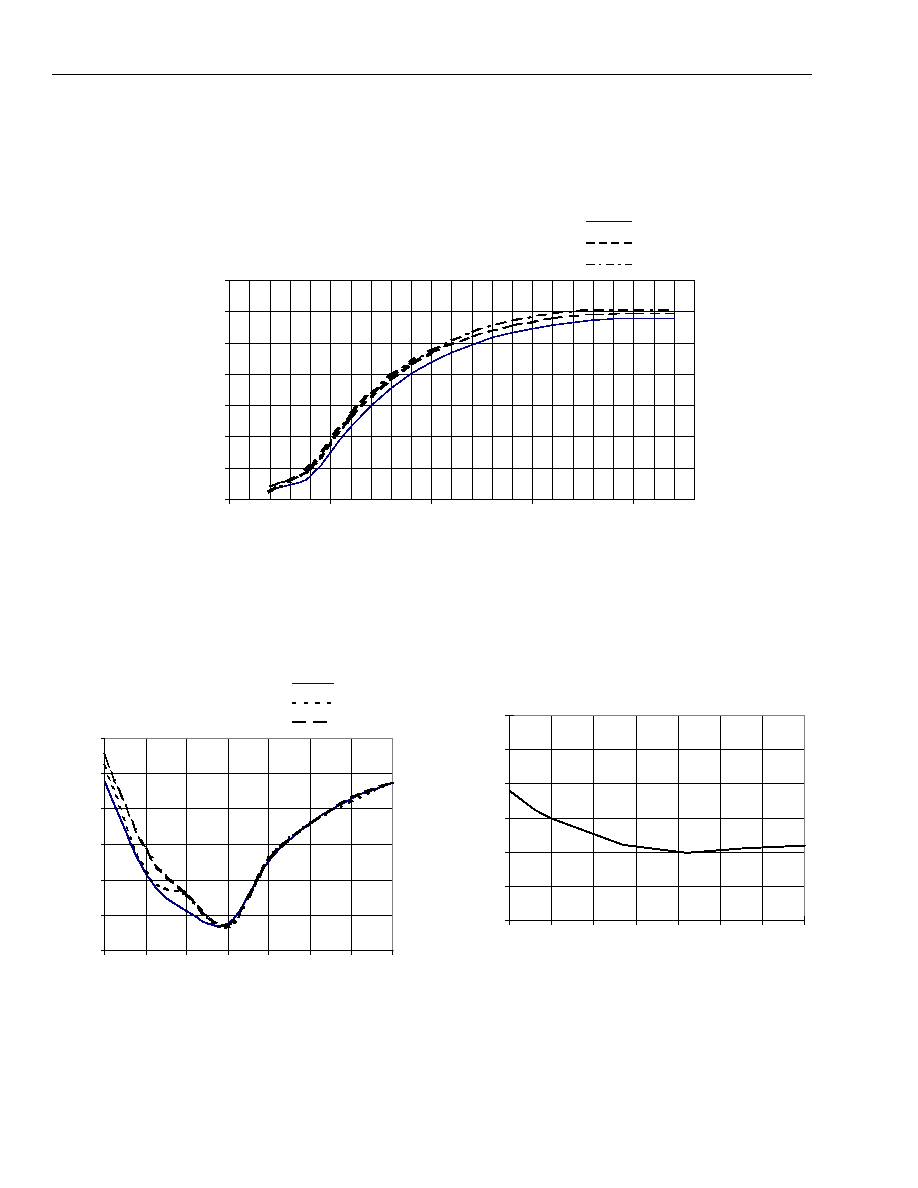
Characteristic Curves
Unless otherwise specified, the test conditions are identical to those listed for Table 2.
LO1 FREQUENCY (MHz)
SUPPRESSION (dB)
≠50
≠45
≠40
≠35
≠30
≠25
≠20
50 100 150 200 250 300 350 400
110 mVp-p
200 mVp-p
400 mVp-p
V
CC
= 3.0 V
LC FILTER = 178 MHz
Figure 6. Unwanted Sideband Suppression vs.
LO1 Frequency and LO1 Input Level
LO1 FREQUENCY (MHz)
SUPPRESSION (dB)
≠70
≠60
≠50
≠40
≠30
≠20
≠10
50 100 150 200 250 300 350 400
Figure 7. Carrier Suppression vs. LO1 Frequency

Preliminary Data Sheet
W3013 Indirect Quadrature Modulator
November 1998
with Gain Control
Lucent Technologies Inc.
9
Characteristic Curves
(continued)
Vcc = 3.0
I/Q =
/4 DQPSK
= 0.35
1.3 Vp-p (RANDOM DATA)
≠55
≠50
≠45
≠40
≠35
≠30
≠25
≠20
≠15
≠10
OUTPUT POWER/24.3 kHz (dBm)
SUPPRESSION (dBc/24.3 kHz)
≠70
≠65
≠60
≠55
≠50
≠45
≠40
≠35
≠30
≠25
≠20
30 kHz ACP
60 kHz ACP
90 kHz ACP
Figure 8. Adjacent Channel Suppression for
IS-136 vs. 1900 MHz Output Power
Vcc = 2.7
I/Q =
/4 DQPSK
= 0.35
1.3 Vp-p (RANDOM DATA)
OUTPUT POWER/21 kHz (dBm)
SUPPRESSION (dBc/21 kHz)
ACP 50 kHz
ACP 100 kHz
≠80
≠75
≠70
≠65
≠60
≠55
≠50
≠45
≠40
≠55
≠50
≠45
≠40
≠35
≠30
≠25
≠20
≠15
≠10
≠5
Figure 9. Adjacent Channel Suppression for
PDC vs. 940 MHz Output Power
0.01
0.1
1
10
100
1000
I/Q FREQUENCY (MHz)
2.8 mVp-p
500 mVp-p
1 Vp-p
NORMALIZED GAIN (dB)
≠33
≠30
≠27
≠24
≠21
≠18
≠15
≠12
≠9
≠6
≠3
0
Figure 10. IQ Bandwidth vs. ac Input Voltage
W3013 Indirect Quadrature Modulator
Preliminary Data Sheet
with Gain Control
November 1998
10
Lucent Technologies Inc.
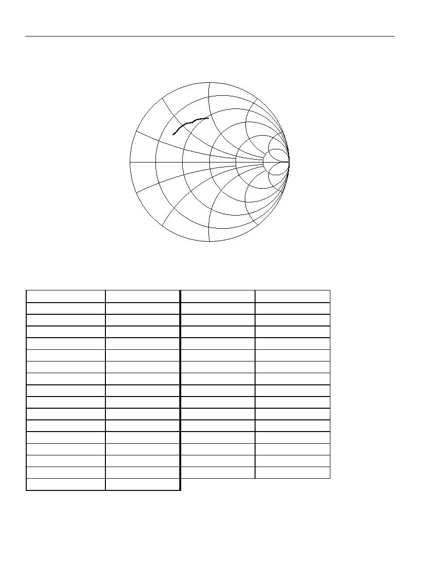
RF Output Impedance
The output impedance of the RF output pin is shown in Figure 11 and Table 3.
Figure 11. RF
OUT
Impedance at Pin 19 Contact with Board (800 MHz to 2000 MHz)
Table 3. RF
OUT
Representative Impedances
Frequency, MHz
R + jX,
Frequency, MHz
R + jX,
800
15.26 + j16.09
1440
19.04 + j29.57
840
15.48 + j16.98
1480
19.45 + j30.36
880
15.71 + j17.82
1520
19.91 + j31.11
920
16.21 + j18.77
1560
20.31 + j31.63
960
16.20 + j19.32
1600
20.75 + j32.14
1000
16.30 + j20.17
1640
20.72 + j32.78
1040
16.55 + j20.96
1680
20.67 + j33.74
1080
16.66 + j21.77
1720
20.88 + j34.94
1120
16.84 + j22.61
1760
21.18 + j36.44
1160
16.92 + j23.51
1800
21.86 + j37.98
1200
17.08 + j24.34
1840
22.44 + j39.51
1240
17.27 + j25.23
1880
23.53 + j40.99
1280
17.48 + j26.17
1920
24.09 + j42.80
1320
17.75 + j27.08
1960
24.98 + j44.50
1360
18.12 + j27.98
2000
26.01 + j46.62
1400
18.53 + j28.90

Preliminary Data Sheet
W3013 Indirect Quadrature Modulator
November 1998
with Gain Control
Lucent Technologies Inc.
11
Package Outline
20-Pin TSSOP
Dimensions are in millimeters.
4.3/4. 5
SEE DETAIL A
0.09 0/0.20
0.90 ± 0 .05
-E-
1 1
2 0
1 0
1
1.0 0
1.0 0
1.0 0
0.2 5 4
E
M
M
6. 25/ 6.5
BASE M E TA L
W ITH PLATI N G
DE TA IL C
0.2 2
± 0.0 3
0.19 /0.3 0
0.90 /0.135
0.09 0/0.20
SE AT ING
PL AN E
DE TA IL B
1
0.0 76 C
0.65 BSC
1. 10
M AX
0.1 5
M A X
6. 50 ± 0 .10
0.25 BS C
DE TA IL A
0.60 ± 0 .10
8
DE TA IL C
DE TA IL B
5-5499.r2
W3013 Indirect Quadrature Modulator
Preliminary Data Sheet
with Gain Control
November 1998
For additional information, contact your Microelectronics Group Account Manager or the following:
INTERNET:
http://www.lucent.com/micro
E-MAIL:
docmaster@micro.lucent.com
N. AMERICA
Microelectronics Group, Lucent Technologies Inc., 555 Union Boulevard, Room 30L-15P-BA, Allentown, PA 18103
1-800-372-2447, FAX 610-712-4106 (In CANADA: 1-800-553-2448, FAX 610-712-4106)
ASIA PACIFIC: Microelectronics Group, Lucent Technologies Singapore Pte. Ltd., 77 Science Park Drive, #03-18 Cintech III, Singapore 118256
Tel. (65) 778 8833, FAX (65) 777 7495
CHINA:
Microelectronics Group, Lucent Technologies (China) Co., Ltd., A-F2, 23/F, Zao Fong Universe Building, 1800 Zhong Shan Xi Road,
Shanghai 200233 P.R. China Tel. (86) 21 6440 0468, ext. 316, FAX (86) 21 6440 0652
JAPAN:
Microelectronics Group, Lucent Technologies Japan Ltd., 7-18, Higashi-Gotanda 2-chome, Shinagawa-ku, Tokyo 141, Japan
Tel. (81) 3 5421 1600, FAX (81) 3 5421 1700
EUROPE:
Data Requests: MICROELECTRONICS GROUP DATALINE: Tel. (44) 1189 324 299, FAX (44) 1189 328 148
Technical Inquiries: GERMANY: (49) 89 95086 0 (Munich), UNITED KINGDOM: (44) 1344 865 900 (Ascot),
FRANCE: (33) 1 40 83 68 00 (Paris), SWEDEN: (46) 8 594 607 00 (Stockholm), FINLAND: (358) 9 4354 2800 (Helsinki),
ITALY: (39) 02 6608131 (Milan), SPAIN: (34) 1 807 1441 (Madrid)
Lucent Technologies Inc. reserves the right to make changes to the product(s) or information contained herein without notice. No liability is assumed as a result of their use or application.
No rights under any patent accompany the sale of any such product(s) or information.
Copyright © 1998 Lucent Technologies Inc.
All Rights Reserved
November 1998
DS98-236WRF (Replaces DS98-057WRF)
Manufacturing Information
This device will be assembled in one of the following locations: assembly codes P, M, or T.
Ordering Information
Device Code
Description
Package
Comcode
W3013BCL
Indirect RF Modulator
20-pin TSSOP
107 956 492
W3013BCL-TR *
--
20-pin TSSOP, tape and reel
107 956 518
EVB3013A
Evaluation Board
--
108 051 574
* Contact your Microelectronics Group Account Manager for minimum order requirements.