Document Outline
- Features
- Applications
- Description
- Pin Information
- Absolute Maximum Ratings
- ESD Precautions
- Operating Range
- Digital Serial Inputs
- Digital Outputs
- Enable Time
- Supply Currents
- LNA
- RF Mixer
- IF/Baseband Amplifier
- Modulator
- LO2 Specification
- LO1 Input Buffer Specification
- Programming Information
- The Data Word
- TR Register
- TR Register
- CONFIG Register
- MAIN Register
- Filter Tune and dc Offset Correction Timing
- Serial Bus Timing Information
- Application Information
- Outline Diagram
- Manufacturing Information
- Evaluation Board Note
- Ordering Information
- List of Figures
- Figure 1. W3020 Circuit Block Diagram
- Figure 2. IC Block Diagram with Pinout
- Figure 3. IF Amplifier Gain Steps
- Figure 4. Actual Gain vs. Requested Gain
- Figure 5. IF Strip Balanced Input Matching
- Figure 6. IF Filtering Requirements for Wideband Noise Performance
- Figure 7. Diagram of W3020, W3000, and SC1 Interconnection
- Figure 8. Serial Bus Timing Diagram
- Figure 9. IF and I/Q Gain Distribution (dB)
- Figure 10. Programming the LO2 Phase Detector Slope
- Figure 11. GSM900 Smith Chart Noise Circles
- Figure 12. GSM1800 Smith Chart Noise Circles
- List of Tables
- Table 1. Pin Assignment
- Table 2. GSM900 LNA Performance
- Table 3. GSM1800/1900 LNA Performance
- Table 4. RF Performance: GSM900
- Table 5. RF Performance: GSM1800/1900
- Table 6. IF/Baseband Amplifier Performance
- Table 7. Low-Pass Rejection Characteristics
- Table 8. Modulator Performance
- Table 9. LO2 Performance
- Table 10. LO1 Performance
- Table 11. Serial Bus Timing Information
- Table 12. Register Addressing
- Table 13. TR Register
- Table 14. B: Band Select
- Table 15. MO[3:1]: Mode Control
- Table 16. T6: LO2 Disable
- Table 17. T5: LO1 Disable
- Table 18. T4: Receive IF Duty Cycle Corrector Disable
- Table 19. T3: Divide-by-3 Duty Cycle Corrector Disable
- Table 20. FTR: LPF Tune Filter Request
- Table 21. DP: dc Precharge Only
- Table 22. DS: dc Correction Skip
- Table 23. T2: TX IF LO Division Select Switch
- Table 24. T1: TX IF LO Divide-by-6 Select
- Table 25. T0: TX IF Duty Cycle Corrector Disable
- Table 26. G[0:6]: Digital Gain Control
- Table 27. CONFIG Register
- Table 28. C10: LO2 PLL Enable
- Table 29. OLD: Overload Output Disable
- Table 30. C9: RF Mixer On During Settling
- Table 31. VO: LO1 Buffer Mode
- Table 32. C8: LO2 Charge Pump Off
- Table 33. LD2: Lock Detect Enable
- Table 34. C7: dc Coarse/Fine Correction
- Table 35. C6: Filter Tune Disable
- Table 36. C5: dc Correction Disable
- Table 37. C4: Low-Pass Filter Bandwidth
- Table 38. C3: Receive LO1 Buffer Mode During dc Calibration
- Table 39. C2: LNA Mode During dc Calibration
- Table 40. C1: 540 MHz LO2 Phase Detector Polarity
- Table 41. DT[2:0]: dc Correction Time
- Table 42. RS: Reset Bit Content
- Table 43. Initialize CONFIG Register (Reset W3020)
- Table 44. Initialize TR Register
- Table 45. Settle PLL to GSM1800 Band for Receive Mode (W3020/W3000)
- Table 46. Perform Receive (W3020)
- Table 47. Settle PLL in GSM1800 Band for Transmit Mode (W3020/W3000)
- Table 48. Basic GSM1800 Transmit Burst (W3020)
- Table 49. GSM900 LNA S-Parameters
- Table 50. GSM1800/GSM1900 LNA S-Parameters
- Table 51. Receive IF Amplifier Input (0 dB Setting)
- Table 52. Receive IF Amplifier Input (32 dB Setting)
- Table 53. Transmit Modulator IF Output
- Table 54. Transmit IF Input to Up-Conversion Mixer
- Table 55. Transmit RF Output from Up-Conversion Mixer
- Contact Us
W3020 GSM Multiband RF Transceiver
Advance Data Sheet
December 1999
Features
n
2.7 V operation, low power consumption
n
Integrated receive, transmit, and synthesizer
functions
n
IF frequency and transmit offset frequency
generated from the same LO
n
Integrated dual LNAs and mixers
n
Minimizes PCB design work between systems
n
Surface-mount, 64-pin TQFPT package
Applications
n
GSM dual-band hand portables:
--
GSM900/1800
--
GSM900/1900
n
GSM single-band hand portables:
--
GSM900
--
GSM1800
--
GSM1900
GSM1800/1900
540 MHz VCO
DAC
�
2
�
2
�
3
W3000
FREQUENCY
SYNTHESIZER
DAC
ADC
ADC
GSM900
900:
925 MHz--960 MHz
1800: 1805 MHz--1880 MHz
1900: 1930 MHz--1990 MHz
900:
880 MHz--915 MHz
1800: 1710 MHz--1785 MHz
1900: 1850 MHz--1910 MHz
900:
1150 MHz--1230 MHz
1800: 1530 MHz--1610 MHz
1900: 1660 MHz--1730 MHz
1800/1900: 180 MHz
TX IF
VCO
SAW
IF
270 MHz
RF MODE
& AGC
CONTROL
RX I
RX Q
TX I
TX Q
Note: shaded area is off-chip.
PA
SWITCHED DIVIDER
LO2 PLL
900: 270 MHz
GSM1800/1900
GSM900
Figure 1. W3020 Circuit Block Diagram

Advance Data Sheet
W3020 GSM Multiband RF Transceiver
December 1999
2
Lucent Technologies Inc.
Table of Contents
Contents
Page
Contents
Page
Features................................................................. 1
Applications ........................................................... 1
Description ............................................................. 4
Detailed Block Diagram ...................................... 5
Pin Information....................................................... 6
Absolute Maximum Ratings.................................... 8
ESD Precautions.................................................... 8
Operating Range.................................................... 8
Digital Serial Inputs ................................................ 9
Digital Outputs ....................................................... 9
Enable Time........................................................... 9
Supply Currents ..................................................... 9
LNA...................................................................... 10
RF Mixer .............................................................. 11
IF/Baseband Amplifier.......................................... 12
Modulator............................................................. 15
LO2 Specification................................................. 17
LO1 Input Buffer Specification.............................. 17
Programming Information ..................................... 18
Serial Bus Timing Information ........................... 19
The Data Word ................................................. 20
TR Register....................................................... 21
CONFIG Register.............................................. 26
MAIN Register .................................................. 30
Filter Tune and dc Offset Correction Timing...... 31
Programming Example......................................... 33
Application Information......................................... 35
S-Parameters.................................................... 35
Outline Diagram ................................................... 43
64-Pin TQFPT .................................................. 43
Manufacturing Information.................................... 44
Evaluation Board Note.......................................... 44
Ordering Information ............................................ 44
List of Figures
Figure
Page
Figure
Page
Figure 1. W3020 Circuit Block Diagram ................. 1
Figure 2. IC Block Diagram with Pinout .................. 5
Figure 3. IF Amplifier Gain Steps ......................... 12
Figure 4. Actual Gain vs. Requested Gain............ 12
Figure 5. IF Strip Balanced Input Matching
Network ................................................ 12
Figure 6. IF Filtering Requirements for Wideband
Noise Performance ................................ 16
Figure 7. Diagram of W3020, W3000, and SC1
Interconnection...................................... 18
Figure 8. Serial Bus Timing Diagram .................... 19
Figure 9. IF and I/Q Gain Distribution (dB)............ 25
Figure 10. Programming the LO2 Phase Detector
Slope.................................................... 29
Figure 11. GSM900 Smith Chart Noise Circles ..... 35
Figure 12. GSM1800 Smith Chart Noise Circles ... 36

Advance Data Sheet
December 1999
W3020 GSM Multiband RF Transceiver
Lucent Technologies Inc.
3
List of Tables
Table
Page
Table
Page
Table 1. Pin Assignment .........................................6
Table 2. GSM900 LNA Performance.....................10
Table 3. GSM1800/1900 LNA Performance ..........10
Table 4. RF Performance: GSM900......................11
Table 5. RF Performance: GSM1800/1900 ...........11
Table 6. IF/Baseband Amplifier Performance .......13
Table 7. Low-Pass Rejection Characteristics.........14
Table 8. Modulator Performance...........................15
Table 9. LO2 Performance ...................................17
Table 10. LO1 Performance..................................17
Table 11. Serial Bus Timing Information ...............19
Table 12. Register Addressing ..............................20
Table 13. TR Register...........................................21
Table 14. B: Band Select ......................................22
Table 15. MO[3:1]: Mode Control..........................23
Table 16. T6: LO2 Disable ....................................23
Table 17. T5: LO1 Disable ....................................23
Table 18. T4: Receive IF Duty Cycle Corrector
Disable..................................................23
Table 19. T3: Divide-by-3 Duty Cycle Corrector
Disable..................................................23
Table 20. FTR: LPF Tune Filter Request ..............24
Table 21. DP: dc Precharge Only .........................24
Table 22. DS: dc Correction Skip..........................24
Table 23. T2: TX IF LO Division Select Switch .....24
Table 24. T1: TX IF LO Divide-by-6 Select ...........24
Table 25. T0: TX IF Duty Cycle Corrector Disable.24
Table 26. G[0:6]: Digital Gain Control ...................25
Table 27. CONFIG Register..................................26
Table 28. C10: LO2 PLL Enable ...........................27
Table 29. OLD: Overload Output Disable..............27
Table 30. C9: RF Mixer On During Settling...........27
Table 31. VO: LO1 Buffer Mode ...........................27
Table 32. C8: LO2 Charge Pump Off....................27
Table 33. LD2: Lock Detect Enable.......................28
Table 34. C7: dc Coarse/Fine Correction ............. 28
Table 35. C6: Filter Tune Disable......................... 28
Table 36. C5: dc Correction Disable..................... 28
Table 37. C4: Low-Pass Filter Bandwidth ............. 28
Table 38. C3: Receive LO1 Buffer Mode During dc
Calibration............................................ 29
Table 39. C2: LNA Mode During dc Calibration .... 29
Table 40. C1: 540 MHz LO2 Phase Detector
Polarity................................................. 29
Table 41. DT[2:0]: dc Correction Time ................. 30
Table 42. RS: Reset Bit Content .......................... 30
Table 43. Initialize CONFIG Register
(Reset W3020) ..................................... 33
Table 44. Initialize TR Register ............................ 33
Table 45. Settle PLL to GSM1800 Band for Receive
Mode (W3020/W3000) ......................... 33
Table 46. Perform Receive (W3020).................... 34
Table 47. Settle PLL in GSM1800 Band for
Transmit Mode (W3020/W3000) .......... 34
Table 48. Basic GSM1800 Transmit Burst
(W3020) ............................................... 34
Table 49. GSM900 LNA S-Parameters................. 37
Table 50. GSM1800/GSM1900 LNA
S-Parameters ....................................... 38
Table 51. Receive IF Amplifier Input
(0 dB Setting) ....................................... 39
Table 52. Receive IF Amplifier Input
(32 dB Setting) ..................................... 39
Table 53. Transmit Modulator IF Output............... 40
Table 54. Transmit IF Input to Up-Conversion
Mixer.................................................... 41
Table 55. Transmit RF Output from Up-Conversion
Mixer.................................................... 42

Advance Data Sheet
W3020 GSM Multiband RF Transceiver
December 1999
4
Lucent Technologies Inc.
Description
The W3020 is a highly integrated GSM transceiver
designed to operate in dual-band handsets or in
single-band handsets operating at 900, 1800, and
1900 MHz frequency bands (1900 MHz performance
is not verified in production). The IC architecture
allows the RF designer to provide solutions for three
different frequency bands with very few PCB changes,
thereby providing faster time to market and reduced
development time.
The W3020 RF transceiver and W3000 PLL have
been designed in conjunction with the SC1 (radio
interface and DSP) to provide a complete GSM
cellular solution. The W3020 interfaces to the W3000
UHF high-performance PLL IC. The W3020, in
combination with the W3000, provides the transmitter,
receiver, and frequency synthesizer. Adding a power
amplifier(s), filters, and VCO modules completes the
radio channel.
The baseband modulated signal is applied to the I/Q
double-balanced mixer in a differential manner. The
�45� phase-shifted local oscillator requires no trim to
achieve the required modulation spectral mask. Also,
I/Q input signals require no dc offset calibration to
achieve high phase accuracy signal. The IF signal
outputs from the I/Q mixers are summed and brought
out to an external filter that reduces the noise that
could be intermodulated into the receive band. This
signal is then applied to the low noise up-conversion
mixer and brought to the RF output.
The received signal is amplified through the low-noise
amplifier, which, combined with the preceding filter,
dominates the receiver sensitivity. The signal is then
passed through another external filter to attenuate the
image frequency to an acceptable level. The signal
passes through the RF down-conversion mixer to the
IF frequency. It is then filtered by an external surface
acoustic wave (SAW) filter to bring the in-band
blocking signals to an acceptable level. The signal is
amplified in the IF strip of the receiver. The IF strip
contains digital gain control (DGC) amplifiers at both
the IF and baseband frequencies and precision low-
pass filters. This allows the signal to be amplified
while in-band blocking signals are removed. The
precision I/Q demodulator splits the signal into its in-
phase and quadrature signals. The I/Q signals are low-
pass filtered and further amplified. The I/Q amplifier
contains integrated dc offset calibration circuitry. The
outputs (I/Q) are fed to the ADC for further signal
processing.
The second local oscillator (LO2), comprising a buffer
for the external voltage-controlled oscillator (VCO)
and a phase-locked loop (PLL), feeds the IF portions
of both the modulator and the receiver. An external
reference source, voltage-controlled crystal oscillator
(VCXO), is divided from 13 MHz to 1 MHz through a
counter. The 1 MHz is called the comparison
frequency. The VCO frequency of 540 MHz is also
divided down to 1 MHz. Both signals are fed into a
phase detector, and the resultant error signal is fed
through an external low-pass filter to the control input
of the VCO.
The RF receive and transmit mixers are driven by two
band-switchable external VCO modules and buffered
internally on the IC. The VCOs are both controlled by
a single W3000 PLL synthesizer and loop filter. Fast
band-locking is achieved using a proprietary scaling
technique integrated in the W3000 PLL.

Advance Data Sheet
December 1999
W3020 GSM Multiband RF Transceiver
Lucent Technologies Inc.
5
Description
(continued)
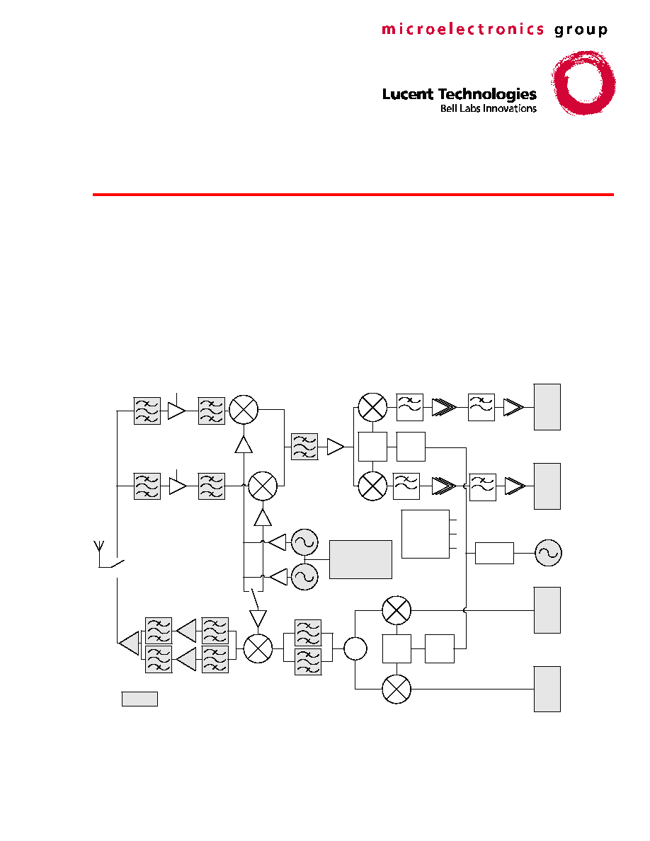
Detailed Block Diagram
GNDS1
DL1P
DL1N
GNDL1
GL1P
GL1N
V
SS
CLK
DAT
LAT
LD
GNDS2
33
34
35
36
37
38
39
40
41
42
43
44
45
46
47
48
LO2
LOCK
16
15
14
13
12
11
10
9
8
7
6
5
4
3
2
1
32
31
30
29
28
27
26
25
24
23
22
21
20
19
18
17
LNA
1800
LNA
900
RF
MIXERS
GSM
1800
GSM
900
MODULATOR
DIV BY
2 OR 3
DIV BY
2
EEL[1:3]
EEL[1:3]
TIP
TQN
TQP
TIN
LO2
BUFFER
540 MHz
G5
21 dB
G1
4 dB
G6
4 dB
G3
16 dB
G4
32 dB
G[0:6]
GND
V
CC
GND
V
CC
GND
V
CCM
V
CC
V
CC
GND
GND
EEGND
V
CC
V
CC
GND
V
CCB
GND
BIAS
V
CCB
V
CCB
B
s
s
s
s
B
TX MIXER
MUX
V
CC
GND
GNDS3
RIP
RIN
RQP
RQN
V
DD
B
GNDB
TQN
TQP
TIN
TIP
V
DD
I
GNDI
IFIP
IFIN
TEST
TEST
B
GNDS4
CP2
EEL2
DLNAI
EEL3
GLNAI
TIFIP
TIFIN
V
DD
L2
L2P
L2N
V
DD
C2
GNDC2
GNDL2
GNDP2
V
DD
P2
G2
8 dB
MCI
MCG
V
DD
L1
s
LO2
PLL
V
DD
CONTROL LOGIC/
SERIAL BUS
V
CC
GND
V
DD
GND
EEL1
DLNAO
GNDL
GLNAO
TOV
TOUT
V
DD
R
1
DMIP
MIN
GMIP
EER1
TIFOP
TIFON
RMON
RMOP
V
DD
R
2
49
50
51
52
53
54
55
56
57
58
59
60
61
62
63
64
Figure 2. IC Block Diagram with Pinout