 | –≠–ª–µ–∫—Ç—Ä–æ–Ω–Ω—ã–π –∫–æ–º–ø–æ–Ω–µ–Ω—Ç: 1N5719 | –°–∫–∞—á–∞—Ç—å:  PDF PDF  ZIP ZIP |
Document Outline
- 1N5719, 1N5767, 5082-3xxx
- Features
- Description/Applications
- Outline 15
- Maximum Ratings
- Mechanical Specifications
- Electrical Specifications
- Typical Parameters
- Diode Package Marking
PIN Diodes for RF Switching
and Attenuating
Technical Data
Features
∑ Low Harmonic Distortion
∑ Large Dynamic Range
∑ Low Series Resistance
∑ Low Capacitance
Description/Applications
These general purpose switching
diodes are intended for low
power switching applications
such as RF duplexers, antenna
switching matrices, digital phase
shifters, and time multiplex
filters. The 5082-3188 is
optimized for VHF/UHF
bandswitching.
1N5719, 1N5767,
5082-3001, 5082-3039,
5082-3077, 5082-3080/81,
5082-3188, 5082-3379
The RF resistance of a PIN diode
is a function of the current
flowing in the diode. These
current controlled resistors are
specified for use in control
applications such as variable RF
attenuators, automatic gain
control circuits, RF modulators,
electrically tuned filters, analog
phase shifters, and RF limiters.
Outline 15 diodes are available on
tape and reel. The tape and reel
specification is patterned after
RS-296-D.
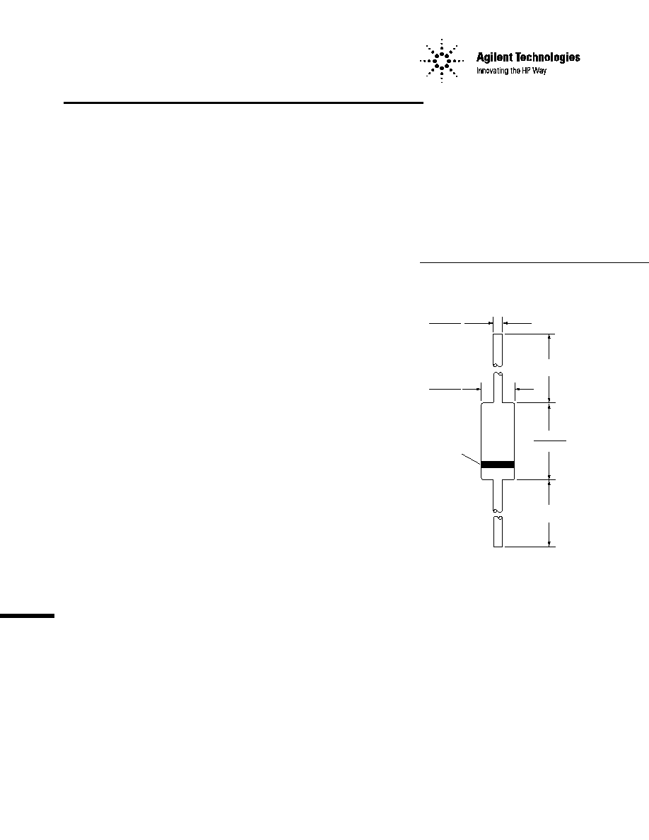
0.41 (.016)
0.36 (.014)
25.4 (1.00)
MIN.
25.4 (1.00)
MIN.
1.93 (.076)
1.73 (.068)
CATHODE
DIMENSIONS IN MILLIMETERS AND (INCHES).
4.32 (.170)
3.81 (.150)
Outline 15
Maximum Ratings
Junction Operating and
Storage Temperature Range ................................................ -65
∞
C to +150
∞
C
Power Dissipation 25
∞
C ..................................................................... 250 mW
(Derate linearly to zero at 150
∞
C)
Peak Inverse Voltage (PIV) ........................................................ same as V
BR
Maximum Soldering Temperature ....................................... 260
∞
C for 5 sec
2
Mechanical
Specifications
The Agilent Outline 15 package
has a glass hermetic seal with
dumet leads. The lead finish is 95-
5 tin-lead (SnPb) for all PIN
diodes. The leads on the Outline
15 package should be restricted
so that the bend starts at least 1/
16 inch (1.6 mm) from the glass
body. Typical package inductance
and capacitance are 2.5 nH and
0.13 pF, respectively. Marking is
by digital coding with a cathode
band.
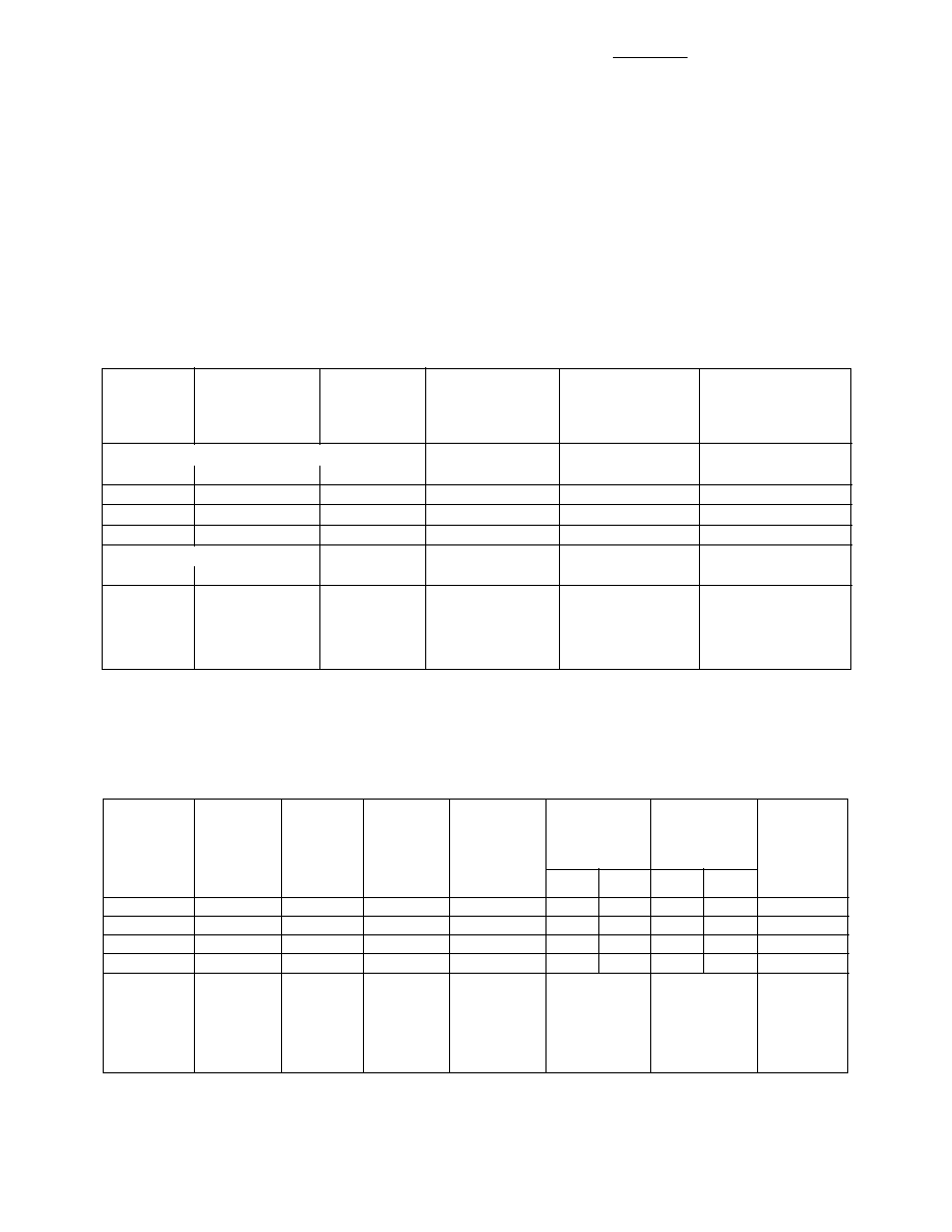
General Purpose Diodes
Electrical Specifications at T
A
= 25
∞
C
Maximum
Minimum
Maximum
Part
Total
Breakdown
Residual Series
Effective Carrier
Reverse Recovery
Number
Capacitance
Voltage
Resistance
Lifetime
Time
5082-
C
T
(pF)
V
BR
(V)
R
S
(
)
(ns)
t
rr
(ns)
General Purpose Switching and Attenuating
3001
0.25
200
1.0
100 (min.)
100 (typ.)
3039
0.25
150
1.25
100 (min.)
100 (typ.)
1N5719
0.3**
150
1.25
100 (min.)
100 (typ.)
3077
0.3
200
1.5
100 (min.)
100 (typ)
Band Switching
3188
1.0*
35
0.6**
70 (typ.)*
12 (typ.)
Test
V
R
= 50 V
V
R
= V
BR
I
F
=100 mA
I
F
= 50 mA
I
F
= 20 mA
Conditions
*V
R
= 20 V
Measure
*I
F
= 20 mA
I
R
= 250 mA
V
R
= 10 V
**V
R
= 100 V
I
R
10
µ
A
**I
F
= 10 mA
*I
F
= 10 mA
90% Recovery
f = 1 MHz
f = 100 MHz
*I
R
= 6 mA
Notes:
Typical CW power switching capability for a shunt switch in a 50
system is 2.5 W.
RF Current Controlled Resistor Diodes
Electrical Specifications at T
A
= 25
∞
C
Max.
Max.
High
Low
Difference
Effective
Min.
Residual
Max.
Resistance
Resistance
in
Carrier
Breakdown
Series
Total
Limit, R
H
(W)
Limit, R
L
(W)
Resistance
Part
Lifetime
Voltage
Resistance Capacitance
vs. Bias
Number
t (ns)
V
BR
(V)
R
S
(
)
C
T
(pF)
Min.
Max.
Min.
Max.
Slope, Dc
5082-3080
1300 (typ.)
100
2.5
0.4
1000
8**
1N5767*
1300 (typ.)
100
2.5
0.4
1000
8**
5082-3379
1300 (typ.)
50
0.4
8**
5082-3081
2500 (typ.)
100
3.5
0.4
1500
8**
Test
I
F
= 50 mA
V
R
= V
BR
,
I
F
= 100 mA
V
R
= 50 V
I
F
= 0.01 mA
I
F
= 1.0 mA
Batch
Conditions I
R
= 250 mA
Measure
f = 100 MHz
f = 1 MHz
f = 100 MHz
I
F
= 20 mA**
Matched at
I
R
10
µ
A
f = 100 MHz
I
F
= 0.01 mA
and 1.0 mA
f = 100 MHz
*The 1N5767 has the additional specifications:
= 1.0 msec minimum
I
R
= 1
µ
A maximum at V
R
= 50 V
V
F
= 1 V maximum at I
F
= 100 mA.
3
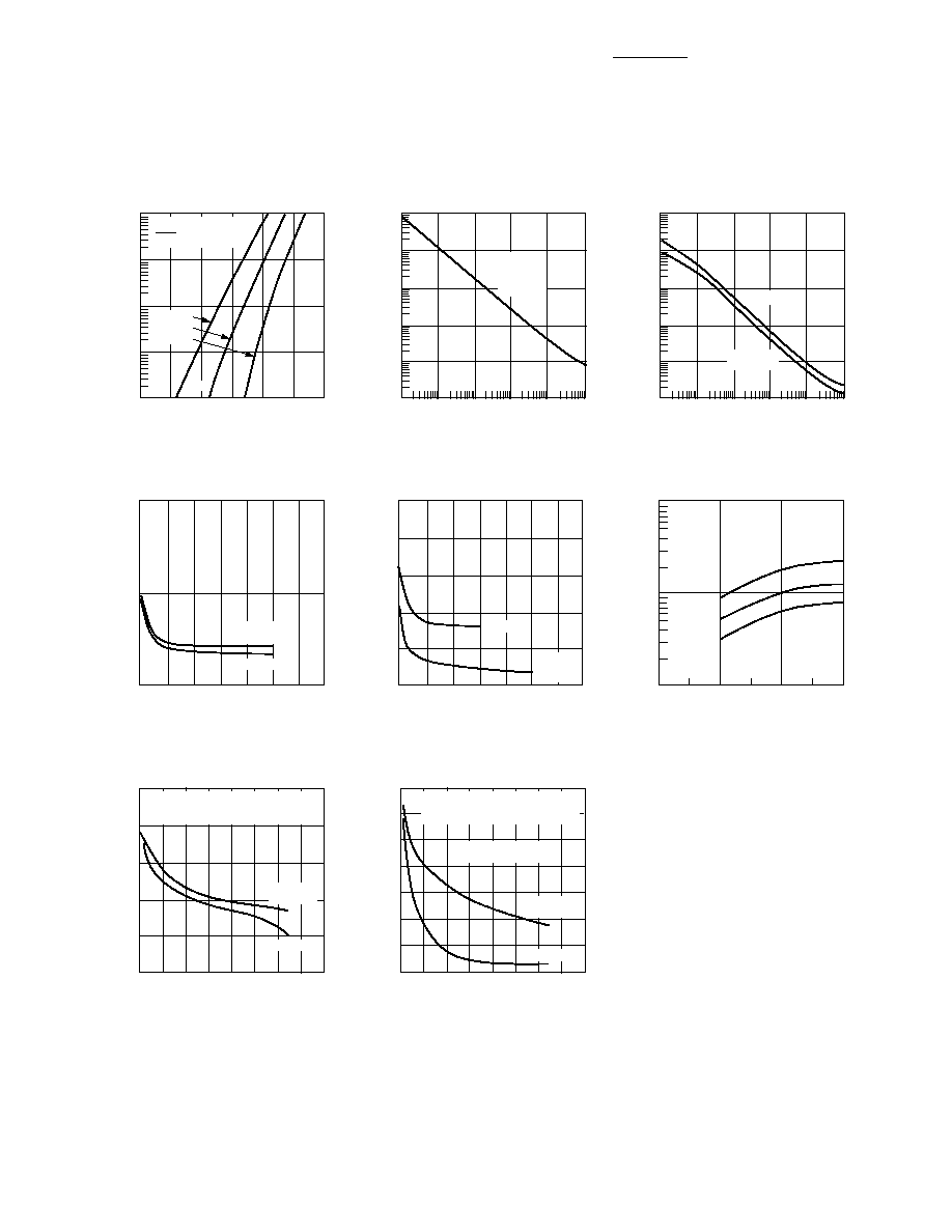
Typical Parameters at T
A
= 25
∞
C (unless otherwise noted)
I
F
≠ FORWARD BIAS CURRENT (mA)
Figure 2. Typical RF Resistance vs.
Forward Bias Current.
10,000
1000
100
10
1
0.1
RF RESISTANCE (OHMS)
0.001
0.01
0.1
1
10
100
5082-3001
5082-3039
5082-3077
IN5719
100
10
1
0.1
0.01
0
0.2
0.4
0.6
0.8
1.0
1.2
I
F
≠ FORWARD CURRENT (mA)
V
F
≠ FORWARD VOLTAGE (V)
Figure 1. Forward Current vs.
Forward Voltage.
5082-3001, 3039,
3077, 3080
IN5719
125
∞
C
25
∞
C
≠60
∞
C
Figure 3. Typical RF Resistance vs.
Forward Bias Current.
I
F
≠ FORWARD BIAS CURRENT (mA)
100,000
10,000
1000
100
10
1
RF RESISTANCE (OHMS)
0.001
0.01
0.1
1
10
100
5082-3080
5082-3379
5082-3081
REVERSE VOLTAGE (V)
Figure 4. Typical Capacitance vs.
Reverse Voltage.
1.0
.5
0
CAPACITANCE (pF)
0
10
20
30
40
50
60
70
Figure 5. Typical Capacitance vs.
Reverse Voltage.
5082-3001
3039
3077
IN5719
5082-3039
IN5719
5082-3001
REVERSE VOLTAGE (V)
2.5
.5
1.0
1.5
2.0
0
CAPACITANCE (pF)
0
10
20
30
40
50
60
70
5082-3080
5082-3081
5082-3379
5082-3188
Figure 7. Typical Second Order
Intermodulation Distortion.
FREQUENCY (MHz)
0
80
60
40
20
100
BELOW FIRST ORDER (dB)
0
10
20
30
40
50
60
80
70
10 dB Bridged Tee Attenuator
40 dB mV Output Levels
One Input Frequency Fixed 100 MHz
5082-3081
Figure 6. Typical Reverse Recovery Time
vs. Forward Current for Various Reverse
Driving Voltages.
FORWARD CURRENT (mA)
REVERSE RECOVERY TIME (ns)
0
10
20
30
V
R
= 5 V
V
R
= 10 V
V
R
= 20 V
1000
100
10
5082-3080
5082-3379
Figure 8. Typical Cross Intermodulation
Distortion.
MODULATED FREQUENCY (MHz)
10
70
60
50
40
30
20
80
BELOW FIRST ORDER (dB)
0
10
20
30
40
50
60
80
70
PIN Diode Cross Modulation
10 dB Bridged Tee Attenuator
Unmodulated Frequency 100 MHz
100% Modulation 15 kHz
40 dB mV Output Levels
5082-3081
5082-3080
5082-3379

www.semiconductor.agilent.com
Data subject to change.
Copyright © 2000 Agilent Technologies
Obsoletes 5967-5812E
5968-7182E (1/00)
Diode Package Marking
1N5xxx
5082-xxxx
would be marked:
1Nx
xx
xxx
xx
YWW
YWW
where xxxx are the last four digits of the 1Nxxxx or the 5082-xxxx part
number. Y is the last digit of the calendar year. WW is the work week of
manufacture.
Examples of diodes manufactured during workweek 45 of 1999:
1N5712
5082-3080
would be marked:
1N5
30
712
80
945
945