 | –≠–ª–µ–∫—Ç—Ä–æ–Ω–Ω—ã–π –∫–æ–º–ø–æ–Ω–µ–Ω—Ç: 5082-2300 | –°–∫–∞—á–∞—Ç—å:  PDF PDF  ZIP ZIP |
Document Outline
- 1N5711
- Features
- Description/Applications
- Maximum Ratings
- Outline 15
- Package Characteristics
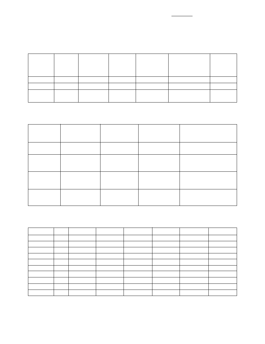
- Electrical Specifications
- Matched Pairs and Quads
- SPICE Parameters
- Typical Parameters
- Diode Package Marking

Schottky Barrier Diodes for
General Purpose Applications
Technical Data
Features
∑ Low Turn-On Voltage
As Low as 0.34 V at 1 mA
∑ Pico Second Switching Speed
∑ High Breakdown Voltage
Up to 70 V
∑ Matched Characteristics
Available
Description/Applications
The 1N5711, 1N5712, 5082-2800/
10/11 are passivated Schottky
barrier diodes which use a
patented "guard ring" design to
achieve a high breakdown
voltage. Packaged in a low cost
glass package, they are well suited
for high level detecting, mixing,
switching, gating, log or A-D
converting, video detecting,
frequency discriminating,
sampling, and wave shaping.
The 5082-2835 is a passivated
Schottky diode in a low cost glass
package. It is optimized for low
turn-on voltage. The 5082-2835 is
particularly well suited for the
UHF mixing needs of the CATV
marketplace.
The 5082-2300 Series and
5082-2900 devices are unpas-
sivated Schottky diodes in a glass
package. These diodes have
extremely low 1/f noise and are
ideal for low noise mixing, and
high sensitivity detecting. They
are particularly well suited for use
in Doppler or narrow band video
receivers.
1N5711
1N5712
5082-2300 Series
5082-2800 Series
5082-2900
0.41 (.016)
0.36 (.014)
25.4 (1.00)
MIN.
25.4 (1.00)
MIN.
1.93 (.076)
1.73 (.068)
CATHODE
DIMENSIONS IN MILLIMETERS AND (INCHES).
4.32 (.170)
3.81 (.150)
Outline 15
Maximum Ratings
Junction Operating and Storage Temperature Range
5082-2303, -2900 ................................................................. -60
∞
C to +100
∞
C
1N5711, 1N5712, 5082-2800/10/11 .................................... -65
∞
C to +200
∞
C
5082-2835 ............................................................................ -60
∞
C to +150
∞
C
DC Power Dissipation
(Measured in an infinite heat sink at T
CASE
= 25
∞
C)
Derate linearly to zero at maximum rated temperature
5082-2303, -2900 .............................................................................. 100 mW
1N5711, 1N5712, 5082-2800/10/11 ................................................. 250 mW
5082-2835 ......................................................................................... 150 mW
Peak Inverse Voltage ................................................................................. V
BR

2
Package Characteristics
Outline 15
Lead Material ........................................................................................ Dumet
Lead Finish .............................................................................. 95-5% Tin-Lead
Max. Soldering Temperature ................................................ 260
∞
C for 5 sec
Min. Lead Strength .................................................................... 4 pounds pull
Typical Package Inductance
1N5711, 1N5712: ................................................................................ 2.0 nH
2800 Series: ........................................................................................ 2.0 nH
2300 Series, 2900: .............................................................................. 3.0 nH
Typical Package Capacitance
1N5711, 1N5712: ................................................................................ 0.2 pF
2800 Series: ........................................................................................ 0.2 pF
2300 Series, 2900: ............................................................................ 0.07 pF
The leads on the Outline 15 package should be restricted so that the
bend starts at least 1/16 inch from the glass body.
Outline 15 diodes are available on tape and reel. The tape and reel
specification is patterned after RS-296-D.
Electrical Specifications at T
A
= 25
∞
C
General Purpose Diodes
Min.
Max.
V
F
= 1 V Max.
Max.
Max.
Breakdown
Forward
at Forward
Reverse Leakage
Capaci-
Part
Package
Voltage
Voltage
Current
Current
tance
Number
Outline
V
BR
(V)
V
F
(mV)
I
F
(mA)
I
R
(nA) at V
R
(V)
C
T
(pF)
5082-2800
15
70
410
15
200
50
2.0
1N5711
15
70
410
15
200
50
2.0
5082-2810
15
20
410
35
100
15
1.2
1N5712
15
20
550
35
150
16
1.2
5082-2811
15
15
410
20
100
8
1.2
5082-2835
15
8*
340
10*
100
1
1.0
Test
I
R
= 10
µ
A
I
F
= 1 mA
*V
F
= 0.45 V
V
R
= 0 V
Conditions
*I
R
= 100
µ
A
f =1.0 MHz
Note:
Effective Carrier Lifetime (
) for all these diodes is 100 ps maximum measured with Krakauer method at 5 mA except for 5082-2835
which is measured at 20 mA.

3
Low 1/f (Flicker) Noise Diodes
Min.
Max.
V
F
= 1 V Max.
Max.
Max.
Part
Breakdown
Forward
at Forward
Reverse Leakage
Capaci-
Number
Package
Voltage
Voltage
Current
Current
tance
5082-
Outline
V
BR
(V)
V
F
(mV)
I
F
(mA)
I
R
(nA) at V
R
(V)
C
T
(pF)
2303
15
20
400
35
500
15
1.0
2900
15
10
400
20
100
5
1.2
Test
I
R
= 10
µ
A
I
F
= 1 mA
V
R
= 0 V
Conditions
f =1.0 MHz
Note:
Effective Carrier Lifetime (
) for all these diodes is 100 ps maximum measured with Krakauer method at 20 mA.
Matched Pairs and Quads
Basic
Matched
Matched
Part Number
Pair
Quad
Batch
5082-
Unconnected
Unconnected
Matched
[1]
Test Conditions
2900
V
F
at I
F
= 1.0, 10 mA
2800
5082-2804
5082-2805
V
F
at I
F
= 0.5, 5 mA
V
F
= 20 mV
V
F
= 20 mV
*I
F
= 10 mA
C
O
at f = 1.0 MHz
2811
5082-2826
V
F
at I
F
= 10 mA
V
F
= 10 mV
C
O
at f = 1.0 MHz
C
O
= 0.1 pF
2835
5082-2080
V
F
at I
F
=10 mA
V
F
= 10 mV
C
O
at f = 1.0 MHz
C
O
= 0.1 pF
Note:
1. Batch matched devices have a minimum batch size of 50 devices.
SPICE Parameters
Parameter
Units
5082-2800
5082-2810
5082-2811
5082-2835
5082-2303
5082-2900
B
V
V
75
25
18
9
25
10
C
J0
pF
1.6
0.8
1.0
0.7
0.7
1.1
E
G
eV
0.69
0.69
0.69
0.69
0.69
0.69
I
BV
A
10E - 5
10E - 5
10E - 5
10E - 5
10E - 5
10E - 5
I
S
A
2.2 x 10E - 9
1.1 x 10E - 9
0.3 x 10E - 8
2.2 x 10E - 8
7 x 1.0E-9
10E-8
N
1.08
1.08
1.08
1.08
1.08
1.08
R
S
25
10
10
5
10
15
P
B
V
0.6
0.6
0.6
0.56
0.64
0.64
P
T
2
2
2
2
2
2
M
0.5
0.5
0.5
0.5
0.5
0.5

4
Typical Parameters
V
F
≠ FORWARD VOLTAGE (V)
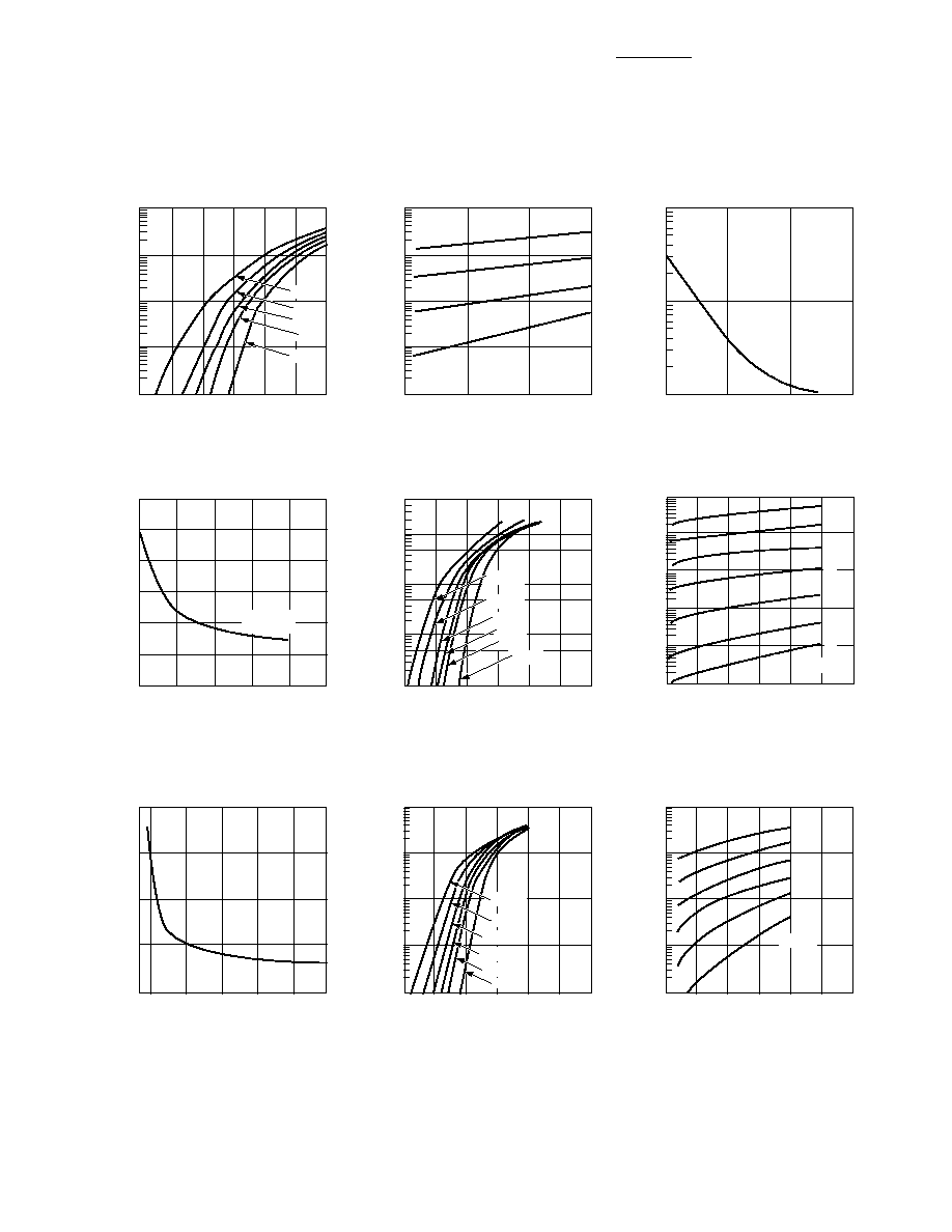
Figure 1. I-V Curve Showing Typical
Temperature Variation for 5082-2300
Series and 5082-2900 Schottky Diodes.
100
10
1
0.1
0.01
I
F
- FORWARD CURRENT (mA)
0
0.10
0.20
0.30
0.40
0.50
0.60
100
∞
C
50
∞
C
25
∞
C
0
∞
C
≠50
∞
C
V
BR
(V)
Figure 2. 5082-2300 Series Typical
Reverse Current vs. Reverse Voltage
at Various Temperatures.
10.000
1,000
100
10
1
I
R
(nA)
0
5
10
15
100
75
50
25
TA = 25
∞
C
I
F
- FORWARD CURRENT (mA)
Figure 3. 5082-2300 Series and 5082-2900
Typical Dynamic Resistance (R
D
) vs.
Forward Current (I
F
).
1000
100
10
R
D
- DYNAMIC RESISTANCE (
)
0.01
0
10
100
V
R
- REVERSE VOLTAGE (V)
Figure 4. 5082-2300 and 5082-2900
Typical Capacitance vs. Reverse
Voltage.
1.2
1.0
0.8
0.6
0.4
0.2
0
C
T
- CAPACITANCE (pF)
0
4
8
12
16
20
5082-2900
5082-2303
V
F
- FORWARD VOLTAGE (V)
Figure 5. I-V Curve Showing Typical
Temperature Variation for 5082-2800
or 1N5711 Schottky Diodes.
50
10
5
1
0.5
0.1
0.05
0.01
I
F
- FORWARD CURRENT (mA)
0
0.2
0.4
0.6
0.8
1.0
1.2
≠50
∞
C
0
∞
C
+25
∞
C
+100
∞
C
+150
∞
C
+50
∞
C
V
R
- REVERSE VOLTAGE (V)
Figure 6. (5082-2800 OR 1N5711)
Typical Variation of Reverse Current
(I
R
) vs. Reverse Voltage (V
R
) at
Various Temperatures.
100,000
10,000
1000
100
10
1
I
R
- REVERSE CURRENT (nA)
0
0.2
0.4
0.6
0.8
1.0
1.2
150
125
100
50
25
75
0
T
A
=
∞
C
V
R
- REVERSE VOLTAGE (V)
Figure 7. (5082-2800 or 1N5711)
Typical Capacitance (C
T
) vs. Reverse
Voltage (V
R
).
12.0
1.5
1.0
0.5
0
C
T
- CAPACITANCE (pF)
0
10
20
30
40
50
V
F
- FORWARD VOLTAGE (V)
Figure 8. I-V Curve Showing Typical
Temperature Variation for the 5082-
2810 or 1N5712 Schottky Diode.
100
10
1.0
0.1
0.01
I
F
- FORWARD CURRENT (mA)
0
0.4
0.2
0.6
0.8
1.0
1.2
≠50
∞
C
0
∞
C
+25
∞
C
+50
∞
C
+100
∞
C
+150
∞
C
V
R
- REVERSE VOLTAGE (V)
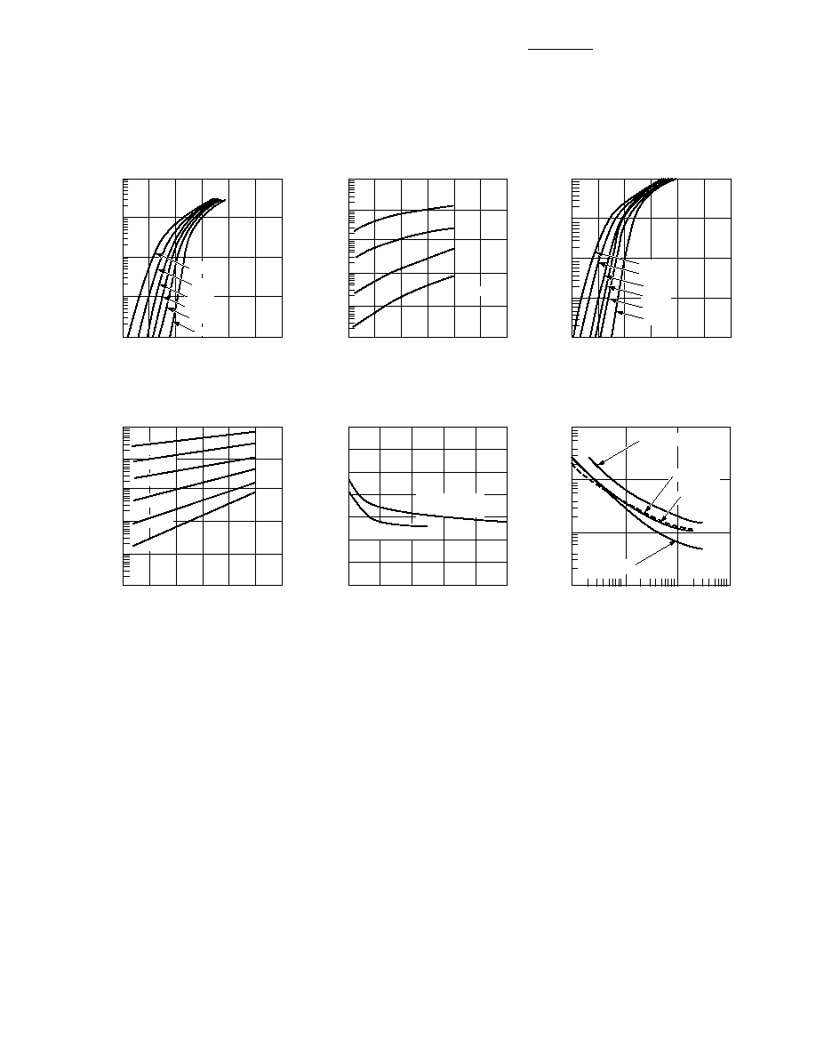
Figure 9. (5082-2810 or IN5712)
Typical Variation of Reverse Current
(I
R
) vs. Reverse Voltage (V
R
) at
Various Temperatures.
10,000
1000
100
10
1.0
I
R
- REVERSE CURRENT (nA)
0
10
5
15
20
25
30
150
125
100
75
50
25
T
A
=
∞
C

5
Typical Parameters,
continued
V
F
- FORWARD VOLTAGE (V)
Figure 10. I-V Curve Showing Typical
Temperature Variation for the 5082-2811
Schottky Diode.
100
10
1.0
0.1
0.01
I
F
- FORWARD CURRENT (mA)
0
0.4
0.2
0.6
0.8
1.0
1.2
≠50
∞
C
0
∞
C
+25
∞
C
+50
∞
C
+100
∞
C
+150
∞
C
V
R
- REVERSE VOLTAGE (V)
Figure 11. (5082-2811) Typical Variation
of Reverse Current (I
R
) vs. Reverse
Voltage (V
R
) at Various Temperatures.
100,000
10,000
1000
100
10
1
I
R
- REVERSE CURRENT (nA)
0
5
10
15
20
25
30
150
100
50
25
T
A
=
∞
C
V
F
- FORWARD VOLTAGE (V)
Figure 12. I-V Curve Showing Typical
Temperature Variations for 5082-2835
Schottky Diode.
100
10
1.0
0.1
0.01
I
F
- FORWARD CURRENT (mA)
0
0.2
0.4
0.6
0.8
1.0
1.2
+150
∞
C
+100
∞
C
+50
∞
C
+25
∞
C
0
∞
C
≠50
∞
C
V
R
- REVERSE VOLTAGE (V)
Figure 13. (5082-2835) Typical Variation
of Reverse Current (I
R
) vs. Reverse
Voltage (V
R
) at Various Temperatures.
100,000
10,000
1000
100
10
1
I
R
- REVERSE CURRENT (nA)
0
1
2
3
4
5
6
+150
∞
C
+125
∞
C
+100
∞
C
+75
∞
C
+50
∞
C
+25
∞
C
V
R
- REVERSE VOLTAGE (V)
Figure 14. Typical Capacitance (C
T
) vs.
Reverse Voltage (V
R
).
11.4
1.2
1.0
0.8
0.6
0.4
0.2
0
C
T
- CAPACITANCE (pF)
0
2
4
6
8
10
5082-2810/2811
IN5712
5082-2835
I
F
- FORWARD CURRENT (mA)
Figure 15. Typical Dynamic Resistance
(R
D
) vs. Forward Current (I
F
).
1000
100
10
1
R
D
- DYNAMIC RESISTANCE (
)
0
2
4
6
8
10
5082-2800, 1N5711
5082-2811
5082-2811
1N5712
5082-2835

