Description
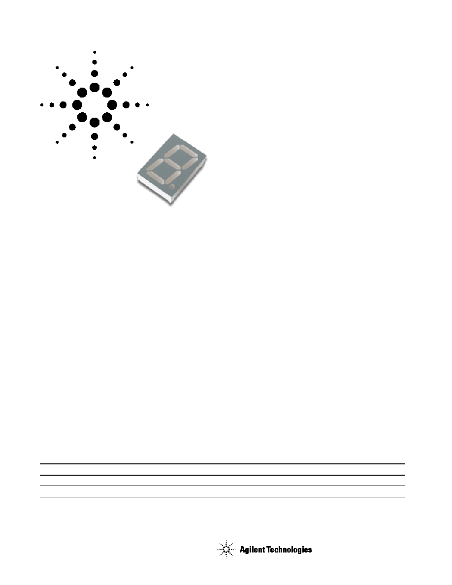
This 14.22 mm (0.56 inch) LED
seven-segment display uses industry
standard size package and pinout.
The device is available in either
common anode or common cathode.
Agilent HDSP-511x/513x
14.22 mm (0.56 inch) General Purpose
Seven-Segment Display
Data Sheet
Features
∑ Industry standard size
∑ Industry standard pinout
14.22 mm (0.56 inch)
DIP lead on 2.54 mm
∑ Choice of colors
High Efficiency Red (HER), Green,
AlGaAs Red, and Yellow
∑ Excellent appearance
Evenly lighted segments gray
package gives optimum contrast
± 50∞ viewing angle
∑ Design flexibility
Common anode or common cathode
Single digit
Left and right hand decimal point
∑ Categorized for luminous
intensity
Green and yellow categorized for
color
Applications
∑ Suitable for indoor use
∑ Not recommended for industrial
application, i.e., operating tem-
perature requirements exceeding
+85∞C or below ≠25∞C
[1]
∑ Extreme temperature cycling not
recommended
Notes:
1. For additional details, please contact your
local Agilent sales office or an authorized
distributor.
Devices
HER
Green
AlGaAs Red
Yellow
Description
HDSP-511E
HDSP-511G
HDSP-511A
HDSP-511Y
Common Anode, Right Hand Decimal
HDSP-513E
HDSP-513G
HDSP-513A
HDSP-513Y
Common Cathode, Right Hand Decimal
The choice of colors includes
High Efficiency Red (HER),
Green, AlGaAs Red, and Yellow.
The gray face displays are
suitable for indoor use.
2
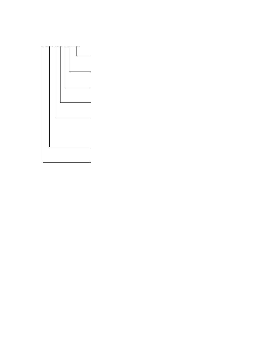
Part Numbering System
Notes:
1. For codes not listed in the figure above, please refer to the respective datasheet or contact your nearest
Agilent representative for details.
2. Bin options refer to shippable bins for a part number. Color and Intensity Bins are typically restricted to 1
bin per tube (exceptions may apply). Please refer to respective datasheet for specific bin limit information.
5082 -X X X X-X X X X X
HDSP-X X X X-X X X X X
Mechanical Options
[1]
00: No Mechanical Option
Color Bin Options
[1,2]
0: No Color Bin Limitation
Maximum Intensity Bin
[1,2]
0: No Maximum Intensity Bin Limitation
Minimum Intensity Bin
[1,2]
0: No Minimum Intensity Bin Limitation
Device Configuration/Color
[1]
A: AlGaAs Red
E: High Efficiency Red
G: Green
Y: Yellow
Device Specific Configuration
[1]
Refer to Respective Datasheet
Package
[1]
Refer to Respective Datasheet

3
Internal Circuit Diagram
Package Dimensions
17.10 ± 0.15
(0.673)
7.90 ± 0.05
(0.311)
10∞ ± 0.15∞
14.22 ± 0.05
(0.560)
12.40 ± 0.15
(0.488)
4.85
(0.191)
15.24
(0.600)
0.30
(0.012)
8.0
(0.312)
DATE CODE
0.50 ± 0.05 TYP. 10 PLACES
(0.020)
HDSP-XXXX
YWW XZ COO
TOP END VIEW
FRONT VIEW
SIDE VIEW
ALL DIMENSIONS ARE IN MILLIMETERS (INCHES).
LUMINOUS
INTENSITY
CATEGORY
1.70 ± 0.05
(0.067)
1.50 ± 0.05
(0.059)
5.0
(0.197)
2.54 x 4 = 10.16 ± 0.1
(0.100 x 4 = 0.400)
COUNTRY OF ORIGIN
+ 0.05
≠ 0.08
f
9
8
6
1
2
3
4
5
COMMON CATHODE
e
g
d
a
b
c
DP
10
7
f
9
8
6
1
2
3
4
5
COMMON ANODE
e
g
d
a
b
c
DP
10
7
COMMON ANODE
COMMON CATHODE
PIN
FUNCTION
PIN
1
CATHODE e
2
CATHODE d
3
COMMON ANODE
4
CATHODE c
5
CATHODE DP
6
CATHODE b
7
CATHODE a
8
COMMON ANODE
9
CATHODE f
10
CATHODE g
1
2
3
4
5
6
7
8
9
10
FUNCTION
ANODE e
ANODE d
COMMON CATHODE
ANODE c
ANODE DP
ANODE b
ANODE a
COMMON CATHODE
ANODE f
ANODE g
HDSP-511E/511G/511Y/511A
HDSP-513E/513G/513Y/513A

4
Green
Device
HDSP-
Parameter
Symbol
Min.
Typ.
Max.
Units
Test Conditions
Luminous Intensity/Segment
I
V
2.001
4.100
mcd
I
F
= 10 mA
Forward Voltage
V
F
2.06
V
I
F
= 10 mA
1.80
2.25
2.60
V
I
F
= 20 mA
Peak Wavelength
PEAK
568
nm
Dominant Wavelength
d
573
nm
Reverse Voltage
VR
5
V
I
R
= 100
µA
511G
513G
Absolute Maximum Ratings at T
A
= 25∞C
HER
Green
AlGaAs Red
Yellow
Description
HDSP-51xE
HDSP-51xG
HDSP-51xA
HDSP-51xY
Units
Power Dissipation Segment
60
65
30
52
mW
Forward Current Segment
25
[1]
25
[2]
15
[3]
20
[4]
mA
Peak Forward Current per Segment
100
100
80
80
mA
(1/10 Duty Factor at 10 KHz)
Operating Temperature Range
≠35 to +85
≠35 to +85
≠35 to +85
≠35 to +85
∞C
Storage Temperature Range
≠35 to +85
≠35 to +85
≠35 to +85
≠35 to +85
∞C
Reverse Voltage per Segment or DP
5
5
5
5
V
Wavesoldering Temperature for 3 seconds
250
250
250
250
∞C
(at 2 mm Distance from the body)
Notes:
1. Derate above 25∞C at 0.33 mA/∞C.
2. Derate above 25∞C at 0.33 mA/∞C.
3. Derate above 25∞C at 0.2 mA/∞C.
4. Derate above 25∞C at 0.27 mA/∞C.
Electrical/Optical Characteristics at T
A
= 25∞C
High Efficiency Red (HER)
Device
HDSP-
Parameter
Symbol
Min.
Typ.
Max.
Units
Test Conditions
Luminous Intensity/Segment
I
V
1.73
mcd
I
F
= 5 mA
2.001
4.100
mcd
I
F
= 10 mA
Forward Voltage
V
F
2.05
2.40
V
I
F
= 20 mA
Peak Wavelength
PEAK
635
nm
Dominant Wavelength
d
620
nm
Reverse Voltage
VR
5
V
I
R
= 100
µA
511E
513E
5
Color Bin Limits (nm at 10 mA)
Dominant Wavelength (nm)
Color
Bin
Min.
[1]
Max.
[1]
Green
3
569.1
571.0
4
571.1
573.0
5
573.1
575.0
Yellow
1
585.5
588.5
2
588.5
591.5
3
591.5
594.5
Note:
1. Tolerance for each bin limit is 1 nm.
Yellow
Device
HDSP-
Parameter
Symbol
Min.
Typ.
Max.
Units
Test Conditions
Luminous Intensity/Segment
I
V
1.03
mcd
I
F
= 5 mA
1.251
2.600
mcd
I
F
= 10 mA
Forward Voltage
V
F
2.15
2.60
V
I
F
= 20 mA
Peak Wavelength
PEAK
595
nm
Dominant Wavelength
d
590
nm
Reverse Voltage
VR
5
V
I
R
= 100
µA
511Y
513Y
AlGaAs Red
Device
HDSP-
Parameter
Symbol
Min.
Typ.
Max.
Units
Test Conditions
Luminous Intensity/Segment
I
V
4.93
mcd
I
F
= 5 mA
3.201
6.500
mcd
I
F
= 10 mA
Forward Voltage
V
F
1.85
2.00
V
I
F
= 20 mA
Peak Wavelength
PEAK
660
nm
Dominant Wavelength
d
643
nm
Reverse Voltage
VR
5
V
I
R
= 100
µA
511A
513A
Intensity Bin Limits (mcd at 10 mA)
Bin
HER/Green
Yellow
AlGaAs Red
Name
Min.
[1]
Max.
[1]
Min.
[1]
Max.
[1]
Min.
[1]
Max.
[1]
H
NA
NA
1.251
2.000
NA
NA
I
2.001
3.200
2.001
3.200
NA
NA
J
3.201
5.050
3.201
5.050
3.201
5.050
K
5.051
8.000
NA
NA
5.051
8.000
L
NA
NA
NA
NA
8.001
12.650
Note:
1. Tolerance for each bin limit is
± 10%.