Agilent ABA-51563
3.5 GHz Broadband Silicon
RFIC Amplifier
Data Sheet
Description
Agilent's ABA-51563 is an
economical, easy-to-use, inter-
nally 50-ohm matched silicon
monolithic broadband amplifier
that offers excellent gain and flat
broadband response from DC to
3.5 GHz. Packaged in an ultra-
miniature industry-standard
SOT-363 package, it requires half
the board space of a SOT-143
package.
At 2 GHz, the ABA-51563 offers a
small-signal gain of 21.5 dB,
output P1dB of 1.8 dBm and
11.4 dBm output third order
intercept point. It is suitable for
use as buffer amplifiers for
wideband applications. They are
designed for low cost gain blocks
in cellular applications, DBS
tuners, LNB and other wireless
communications systems.
ABA-51563 is fabricated using
Agilent's HP25 silicon bipolar
process, which employs a double-
diffused single polysilicon
process with self-aligned submi-
cron emitter geometry. The
process is capable of simulta-
neous high f
T
and high NPN
breakdown (25 GHz f
T
at 6V
BVCEO). The process utilizes
industry standard device oxide
isolation technologies and
submicron aluminum multilayer
interconnect to achieve superior
performance, high uniformity,
and proven reliability.
Features
∑ Operating frequency: DC ~ 3.5 GHz
∑ 21.5 dB gain
∑ VSWR < 2.0 throughout operating
frequency
∑ 1.8 dBm output P1dB
∑ 3.7 dB noise figure
∑ Unconditionally stable
∑ Single 5V supply (Id = 18 mA)
∑ Lead-free option available
Applications
∑ Amplifier for cellular, cordless,
special mobile radio, PCS, ISM,
wireless LAN, DBS, TVRO, and TV
tuner applications
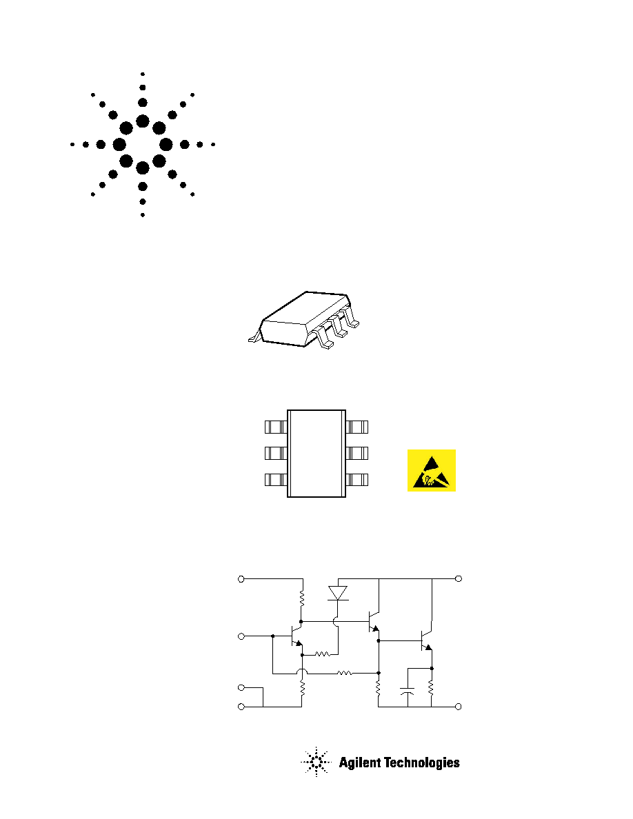
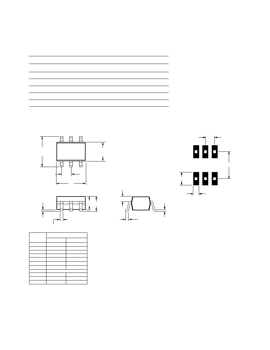
Surface Mount Package
SOT-363/SC70
Pin Connections and
Package Marking
Simplified Schematic
Note:
Top View. Package marking provides orientation
and identification. "x" is character to identify
date code.
Vcc
GND 3
AHx
Input
GND 2
GND 1
Output
& Vcc
Vcc
Ground 2
Ground 1
Ground 3
RF
Input
RF
Output
& Vcc
Attention:
Observe precautions for
handling electrostatic
sensitive devices.
ESD Machine Model (Class A)
ESD Human Body Model (Class 1A)
Refer to Agilent Application Note A004R:
Electrostatic Discharge Damage and Control.
2
ABA-51563 Absolute Maximum Ratings
[1]
Symbol
Parameter
Units
Absolute Max.
V
cc
Device Voltage, RF output to ground (T = 25
∞C)
V
+7
P
in
CW RF Input Power (Vcc = 5V)
dBm
+20
P
diss
Total Power Dissipation
[3]
W
0.3
T
j
Junction Temperature
∞C
150
T
STG
Storage Temperature
∞C
-65 to 150
Notes:
1. Operation of this device in excess of any of
these limits may cause permanent damage.
2. Thermal resistance measured using 150
∞C
Liquid Crystal Measurement Technique.
3. Board (package belly) temperature, Tb, is
25
∞C. Derate 2.3 mW/∞C for Tb
> 120.8
∞C.
Electrical Specifications
T
c
= +25
∞C, Z
o
= 50
, P
in
= -30 dBm, V
cc
= 5V, Freq = 2 GHz, unless stated otherwise.
Symbol
Parameter and Test Condition
Units
Min.
Typ.
Max.
Std Dev.
Gp
[1]
Power Gain (|S
21
|
2
)
dB
20
21.5
0.2
Gp
Power Gain Flatness, f = 0.1 ~ 2.5 GHz
dB
1.0
f = 0.1 ~ 3.5 GHz
1.3
NF
[1]
Noise Figure
dB
3.7
4
0.12
P1dB
[1]
Output Power at 1dB Gain Compression
dBm
1.8
0.13
OIP3
[1]
Output Third Order Intercept Point
dBm
11.4
0.24
VSWR
in
[1]
Input VSWR
1.2
VSWR
out
[1]
Output VSWR
1.2
Icc
[1]
Device Current
mA
18
28
0.3
td
[1]
Group Delay
ps
140
Notes:
1. Measurements taken on 50
test board shown on Figure 1. Excess circuit losses had been de-embedded from actual measurements. Standard
deviation and typical data based on at least 500 parts sample size from 6 wafer lots. Future wafers allocated to this product may have nominal values
anywhere within the upper and lower spec limits.
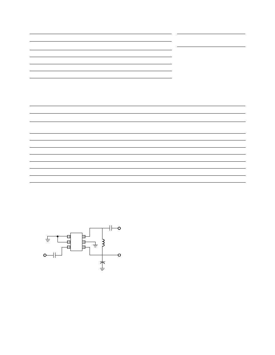
Figure 1. ABA-51563 Production Test Circuit.
RF Output
RF Input
Vcc
RFC
C
block
C
block
C
bypass
AHx
Thermal Resistance
[2]
(Vcc = 5V)
jc
= 104
∞C/W
3
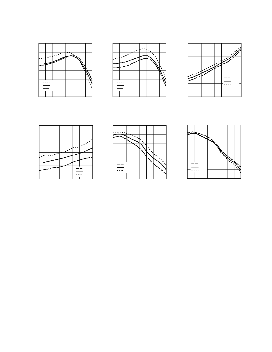
ABA-51563 Typical Performance
T
c
= +25
∞C, Z
o
= 50
, V
cc
= 5V unless stated otherwise.
FREQUENCY (GHz)
Figure 7. Output Power for 1 dB Gain
Compression vs. Frequency and Temperature.
P1dB (dBm)
0
6
4
2
0
-2
-4
-6
4
1
0.5
2
2.5
3
1.5
3.5
-40
∞C
+25
∞C
+85
∞C
FREQUENCY (GHz)
Figure 6. Output Power for 1 dB Gain
Compression vs. Frequency and Voltage.
P1dB (dBm)
0
6
4
2
0
-2
-4
-6
4
1
0.5
2
2.5
3
1.5
3.5
4.5V
5V
5.5V
FREQUENCY (GHz)
Figure 5. Noise Figure vs. Frequency and
Temperature.
NF (dB)
0
6
5
4
3
2
4
1
0.5
2
2.5
3
1.5
3.5
-40
∞C
+25
∞C
+85
∞C
FREQUENCY (GHz)
Figure 4. Noise Figure vs. Frequency and
Voltage.
NF (dB)
0
4.5
4
3.5
3
2.5
4
1
0.5
2
2.5
3
1.5
3.5
4.5V
5V
5.5V
FREQUENCY (GHz)
Figure 3. Gain vs. Frequency and Temperature.
GAIN (dB)
0
23
22
21
20
19
18
17
4
1
0.5
2
2.5
3
1.5
3.5
-40
∞C
+25
∞C
+85
∞C
FREQUENCY (GHz)
Figure 2. Gain vs. Frequency and Voltage.
GAIN (dB)
0
23
22
21
20
19
18
17
4
1
0.5
2
2.5
3
1.5
3.5
4.5V
5V
5.5V
4
FREQUENCY (GHz)
Figure 10. Input and Output VSWR vs.
Frequency.
VSWR
0
1.8
1.7
1.6
1.5
1.4
1.3
1.2
1.1
1.0
0.9
0.8
6
1
3
4
2
5
VSWR IN
VWSR OUT
VOLTAGE (V)
Figure 11. Supply Current vs. Voltage and
Temperature.
Icc (mA)
0
60
50
40
30
20
10
0
2
1
4
5
6
3
7
+25
∞C
-40
∞C
+85
∞C
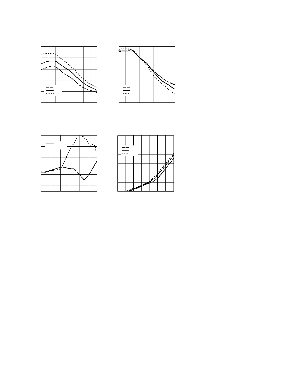
ABA-51563 Typical Performance,
continued
T
c
= +25
∞C, Z
o
= 50
, V
cc
= 5V unless stated otherwise.
FREQUENCY (GHz)
Figure 9. Output IP3 vs. Frequency and
Temperature.
OIP3 (dBm)
0
16
12
8
4
0
4
1
0.5
2
2.5
3
1.5
3.5
-40
∞C
+25
∞C
+85
∞C
FREQUENCY (GHz)
Figure 8. Output IP3 vs. Frequency and
Voltage.
OIP3 (dBm)
0
20
16
12
8
4
0
4
1
0.5
2
2.5
3
1.5
3.5
4.5V
5V
5.5V

5
ABA-51563 Typical Scattering Parameters
T
C
= +25
∞C, V
CC
= 5V, Z
O
= 50
, unless stated otherwise
Freq
S
11
S
11
S
21
S
21
S
21
S
12
S
12
S
12
S
22
S
22
K
(GHz)
Mag.
Ang.
dB
Mag.
Ang.
dB
Mag.
Ang.
Mag.
Ang.
Factor
0.05
0.06
175.8
20.8
10.93
-2.3
-27.3
0.04
-0.8
0.08
-2.3
1.294
0.10
0.06
174.1
20.7
10.88
-4.4
-27.3
0.04
-1.4
0.08
-6.0
1.297
0.20
0.06
170.4
20.8
10.93
-8.6
-27.5
0.04
-2.5
0.07
-11.5
1.313
0.30
0.06
166.0
20.8
10.93
-12.8
-27.5
0.04
-3.3
0.07
-15.1
1.313
0.40
0.06
160.6
20.8
10.97
-17.1
-27.7
0.04
-3.8
0.07
-17.7
1.331
0.50
0.07
161.9
20.8
10.97
-21.4
-27.7
0.04
-4.1
0.07
-17.7
1.330
0.60
0.07
160.0
20.8
10.99
-25.6
-28.0
0.04
-4.6
0.07
-17.8
1.351
0.70
0.07
155.8
20.9
11.04
-30.0
-28.0
0.04
-4.8
0.07
-18.9
1.346
0.80
0.08
153.5
20.9
11.10
-34.2
-28.2
0.04
-5.0
0.07
-18.5
1.365
0.90
0.08
150.4
20.9
11.13
-38.6
-28.2
0.04
-4.9
0.07
-14.7
1.361
1.00
0.08
148.0
21.0
11.20
-43.0
-28.4
0.04
-4.9
0.08
-9.9
1.380
1.20
0.08
132.5
21.1
11.35
-52.0
-28.6
0.04
-4.4
0.08
11.6
1.391
1.40
0.09
118.9
21.2
11.51
-61.1
-28.9
0.04
-3.8
0.08
26.1
1.403
1.60
0.09
102.9
21.4
11.69
-70.7
-28.9
0.04
-2.7
0.08
37.7
1.386
1.80
0.10
86.5
21.5
11.85
-80.6
-29.1
0.04
-1.3
0.09
44.3
1.399
2.00
0.10
69.6
21.5
11.94
-90.7
-29.1
0.04
0.3
0.10
47.9
1.391
2.20
0.11
50.6
21.6
12.04
-101.2
-29.1
0.04
1.9
0.11
45.1
1.382
2.40
0.10
38.4
21.7
12.15
-112.1
-29.1
0.04
3.0
0.13
41.1
1.369
2.60
0.10
30.1
21.7
12.14
-123.5
-28.9
0.04
4.3
0.16
36.7
1.339
2.80
0.10
17.8
21.6
12.00
-135.3
-28.9
0.04
5.7
0.19
31.6
1.341
3.00
0.09
10.2
21.4
11.70
-147.3
-28.9
0.04
7.4
0.21
26.7
1.354
3.20
0.10
-1.1
21.0
11.27
-158.9
-28.6
0.04
9.8
0.24
21.4
1.352
3.40
0.09
-15.7
20.6
10.73
-170.5
-28.2
0.04
10.8
0.25
14.4
1.343
3.50
0.08
-20.5
20.4
10.45
-176.2
-28.0
0.04
11.4
0.26
11.2
1.337
4.00
0.05
-52.8
18.9
8.86
157.4
-27.1
0.04
12.4
0.27
-4.6
1.389
4.50
0.00
-179.7
17.4
7.40
133.1
-26.2
0.05
12.3
0.27
-18.4
1.457
5.00
0.04
127.8
15.6
6.06
112.1
-25.2
0.06
11.0
0.24
-32.2
1.568
5.50
0.10
114.7
14.1
5.09
92.7
-24.0
0.06
7.2
0.24
-47.4
1.597
6.00
0.16
105.3
12.7
4.30
75.7
-23.0
0.07
1.9
0.20
-62.0
1.657
6
Device Models
Refer to Agilent's web site
www.agilent.com/view/rf
Package Dimensions
Outline 63 (SOT-363/SC-70)
Recommended PCB Pad Layout for
Agilent's SC70 6L/SOT-363 Products
E
HE
D
e
A1
b
A
A2
Q1
L
c
DIMENSIONS (mm)
MIN.
1.15
1.80
1.80
0.80
0.80
0.00
0.10
0.15
0.10
0.10
MAX.
1.35
2.25
2.40
1.10
1.00
0.10
0.40
0.30
0.20
0.30
SYMBOL
E
D
HE
A
A2
A1
Q1
e
b
c
L
NOTES:
1. All dimensions are in mm.
2. Dimensions are inclusive of plating.
3. Dimensions are exclusive of mold flash & metal burr.
4. All specifications comply to EIAJ SC70.
5. Die is facing up for mold and facing down for trim/form,
ie: reverse trim/form.
6. Package surface to be mirror finish.
0.650 BCS
0.026
0.079
0.018
0.039
Dimensions in inches.
Ordering Information
Part Number
Devices per Container
Container
ABA-51563-TR1
3000
7" reel
ABA-51563-TR2
10000
13" reel
ABA-51563-BLK
100
antistatic bag
ABA-51563-TR1G
3000
7" reel
ABA-51563-TR2G
10000
13" reel
ABA-51563-BLKG
100
antistatic bag
Note: For lead-free option,the part number will have the character "G" at the end.
7
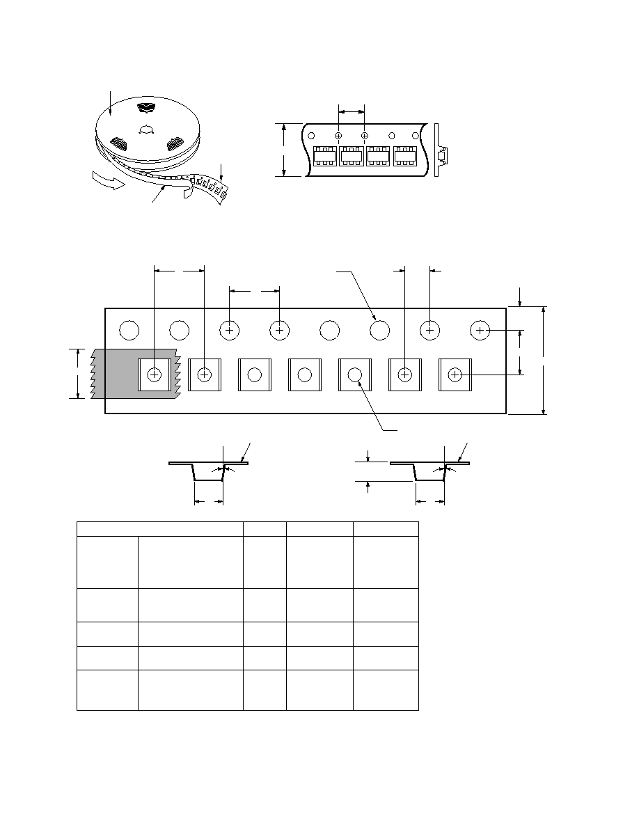
Device Orientation
Tape Dimensions and Product Orientation for Outline 63
USER
FEED
DIRECTION
COVER TAPE
CARRIER
TAPE
REEL
END VIEW
8 mm
4 mm
TOP VIEW
(Package marking example orientation shown.)
AH
AH
AH
AH
P
P
0
P
2
F
W
C
D
1
D
E
A
0
10
∞ MAX.
t
1
(CARRIER TAPE THICKNESS)
T
t
(COVER TAPE THICKNESS)
10
∞ MAX.
B
0
K
0
DESCRIPTION
SYMBOL
SIZE (mm)
SIZE (INCHES)
LENGTH
WIDTH
DEPTH
PITCH
BOTTOM HOLE DIAMETER
A
0
B
0
K
0
P
D
1
2.40
± 0.10
2.40
± 0.10
1.20
± 0.10
4.00
± 0.10
1.00 + 0.25
0.094
± 0.004
0.094
± 0.004
0.047
± 0.004
0.157
± 0.004
0.039 + 0.010
CAVITY
DIAMETER
PITCH
POSITION
D
P
0
E
1.50
± 0.10
4.00
± 0.10
1.75
± 0.10
0.061 + 0.002
0.157
± 0.004
0.069
± 0.004
PERFORATION
WIDTH
THICKNESS
W
t
1
8.00 + 0.30 - 0.10
0.254
± 0.02
0.315 + 0.012
0.0100
± 0.0008
CARRIER TAPE
CAVITY TO PERFORATION
(WIDTH DIRECTION)
CAVITY TO PERFORATION
(LENGTH DIRECTION)
F
P
2
3.50
± 0.05
2.00
± 0.05
0.138
± 0.002
0.079
± 0.002
DISTANCE
WIDTH
TAPE THICKNESS
C
T
t
5.40
± 0.10
0.062
± 0.001
0.205 + 0.004
0.0025
± 0.0004
COVER TAPE

www.agilent.com/semiconductors
For product information and a complete list of
distributors, please go to our web site.
For technical assistance call:
Americas/Canada: +1 (800) 235-0312 or
(916) 788-6763
Europe: +49 (0) 6441 92460
China: 10800 650 0017
Hong Kong: (65) 6756 2394
India, Australia, New Zealand: (65) 6755 1939
Japan: (+81 3) 3335-8152(Domestic/International), or
0120-61-1280(Domestic Only)
Korea: (65) 6755 1989
Singapore, Malaysia, Vietnam, Thailand, Philippines,
Indonesia: (65) 6755 2044
Taiwan: (65) 6755 1843
Data subject to change.
Copyright © 2004 Agilent Technologies, Inc.
Obsoletes 5988-9178EN
December 4, 2004
5989-1970EN