Äîêóìåíòàöèÿ è îïèñàíèÿ www.docs.chipfind.ru
Agilent ACPF-7001
High Rejection Tx Filter
for US PCS Band
Data Sheet
Description
This product is a high rejection
full band transmit filter designed
for US PCS handsets. Its perfor-
mance rivals splitband surface
acoustic wave (SAW) transmit
filters. Since the rejection is
provided by a single filter, no
switches are required, saving
board space and external compo-
nents, eliminating switch loss,
and reducing programming
complexity.
In typical cellular phone archi-
tectures, the transmit filter fits
between the driver amplifier and
the power amplifier. This filter
reduces the noise in the Rx band
being amplified by the transmit
chain, enhancing receiver sensi-
tivity. High rejection keeps
unwanted signals out of the
receive path.
Agilent's thin-Film Bulk Acoustic
Resonator (FBAR) technology
makes possible high-Q filters at a
fraction of their usual size.
Features
· High rejection from a single filter
with no switches required
· Passband: 1850 1910 MHz
33 dB min Attenuation,
1930 1990 MHz
3.5 dB max Insertion Loss
· Space saving solution
Small footprint: 3 x 3-mm solution
Low profile package:
1.0 mm high (typ)
1.15 mm (max)
Applications
· US PCS band handsets
· Wireless data terminals
Package
2
3
5
6
4: Input
8: Output
1, 2, 3, 5, 6, 7, 9: Grounded
Center pad grounded
See Figure 10 for details.
"x" = date code character
7
1
4
9
8
3.0
±
0.15 SQ
2
Absolute Maximum Ratings
[2]
Parameter
Unit
Value
Operating Temperature
[1]
°C
30 to +85
Storage Temperature
[1]
°C
-30 to +100
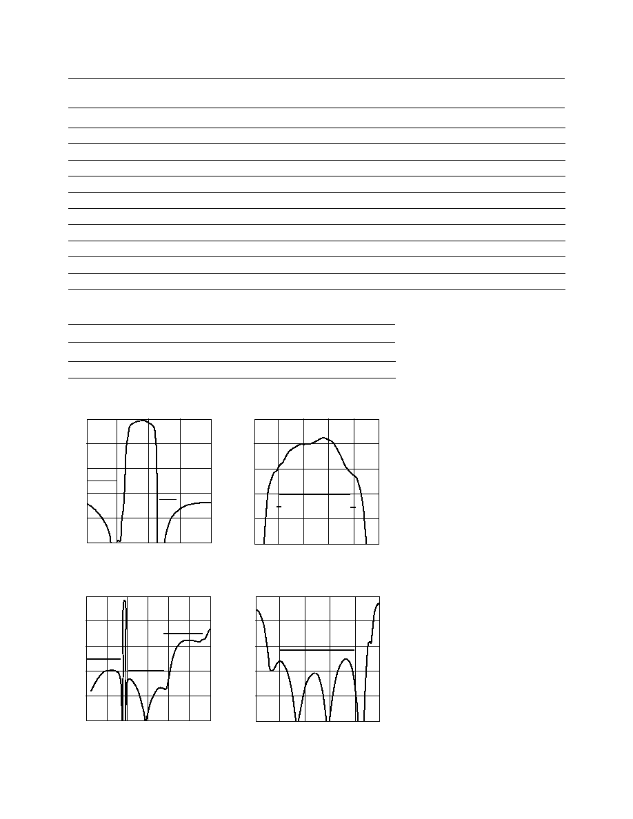
Typical Performance, 25
°C, Z
O
= 50
Figure 1. Attenuation vs. Frequency.
FREQUENCY (GHz)
ATTENUATION (dB)
1.7
2.10
1.90
1.80
2.00
0
-10
-20
-30
-40
-50
Figure 2. Insertion Loss vs. Frequency.
FREQUENCY (GHz)
ATTENUATION (dB)
1.83
1.93
1.87
1.89
1.85
1.91
0
-1
-2
-3
-4
-5
Figure 3. Attenuation vs. Frequency
(Broadband).
FREQUENCY (GHz)
ATTENUATION (dB)
0
-10
-20
-30
-40
-50
0
6.0
2.0
1.0
4.0
5.0
3.0
Figure 4. Return Loss vs. Frequency.
FREQUENCY (GHz)
RETURN LOSS (dB)
1.83
1.93
1.87
1.89
1.85
1.91
0
-4
-8
-12
-16
-20
Notes:
1. Temperature is defined at case T
C
, the
temperature of the underside of the filter
where it makes contact with the circuit board.
2. Specifications are guaranteed over the given
temperature range. Operation in excess of
any one of these conditions may result in
permanent damage to the device.
Electrical Specifications, Z
O
= 50
25
°C
-30
° to +25°C
25
° to +70°C
Symbol
Parameter
Units
Min
Typ
Max
Min
Typ
Max
Min
Typ
Max
f
Passband
MHz
1850
1910
1850
1910
1850
1910
IL
Insertion Loss 1850-1855 MHz
dB
2.0
3.5
3.7
3.2
IL
Insertion Loss 1855-1905 MHz
dB
1.5
3.0
3.0
3.0
IL
Insertion Loss 1905-1910 MHz
dB
2.5
3.5
3.2
3.7
S21
Ripple, 1850-1910 MHz
dB
2.5
S21
Min Rejection, 1930-1990 MHz
dB
33
37
33
33
S21
Min Rejection, 10-1800 MHz
dB
25
S21
Min Rejection, 1990-3820 MHz
dB
30
S21
Min Rejection, 3820-5730 MHz
dB
15
S11, S22
In-band Return Loss
dB
9.0
11
9.0
11
9.0
11
Pin max
Safe Input Power Level
dBm
20
20
20
3
1.55 SQ
0.28
0.1
0.1
0.28
0.7
0.7
0.6
1.3
7
Ground
6
Ground
5
Ground
4
Input
8
Output
9
Ground
2
Ground
1
Ground
3
Ground
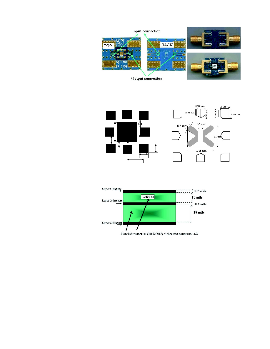
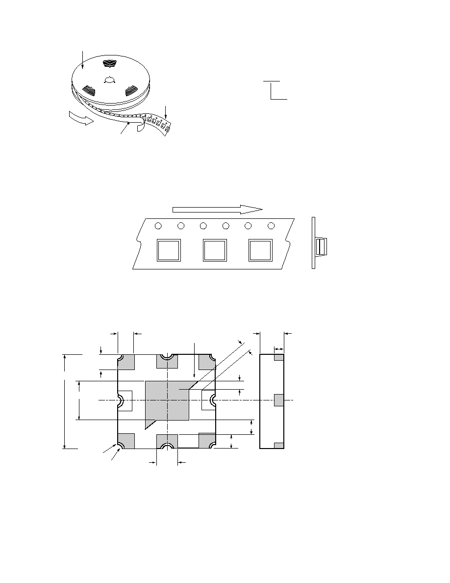
Figure 6a. PCB footprint dimensions, pad nomenclature, stencil dimensions (mm).
Figure 6b. Board stack up description.
PCB Interface and
Mounting Instructions
Mounting Consideration and
Board Description
The ACPF-7001 filter has one
input (Pin 4), one output (Pin 8)
and 6 grounds (Pins 1, 2, 3, 5, 6,
7). Furthermore, the inside of the
filter (center pad Pin 9) is
ground-plane; therefore it must
be soldered to PCB ground.
In summary:
· Pins 1, 2, 3, 5, 6, 7, 9 are
grounded. (Figure 5)
· Demo board uses 10 mil top,
18 mil bottom Greek Coplanar
Waveguide Over Ground plane
(CPWG) style board. (See
board layer Figure 5, 6)
Note: For best performance, try
to reproduce this board stack up
closely. The demoboard uses
CPWG transmission lines for high
isolation between two ports. It
uses via holes to connect the
CPWG line from the underside of
the board to the filter mounting
pads on top. If Ground-Signal-
Ground (GSG) type board is
used, better return loss can be
achieved since it eliminates
connector mismatch.
Demo Boards
SMA connectorized Demo boards
are available for sampling. (See
board drawing in Figure 5).
Figure 5. PCB top and bottom views (vias used to connect the underside of the board to the filter
mounting pads on top).
4
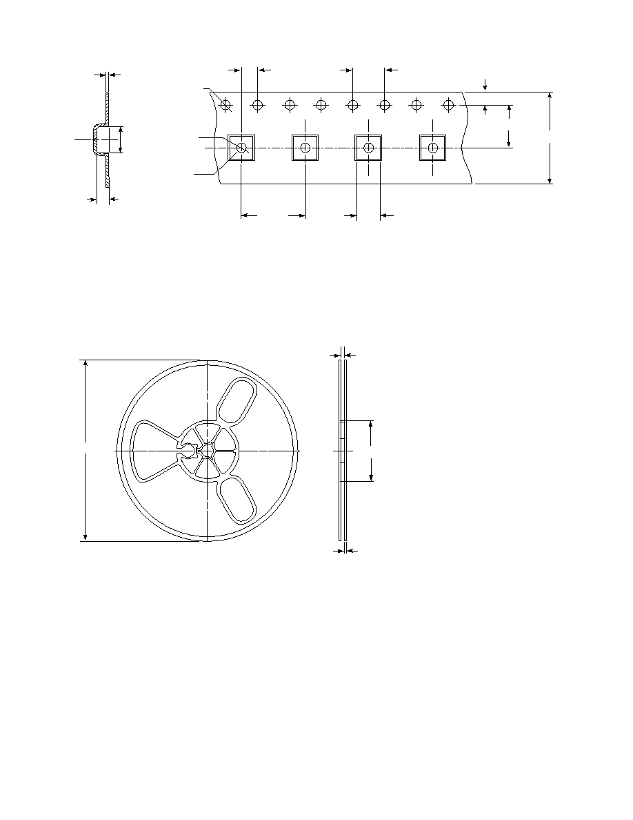
Figure 7. Tape drawing.
1.55 ± 0.05
1.6 ± 0.1
R 0.3 typ
1.55
± 0.1
3.3
± 0.1
CL
8.0
± 0.1
3.3
± 0.1
2.0
± 0.1
[1]
4.0
± 0.1
[2]
5.5
± 0.1
[3]
12.0
± 0.3
1.75
± 0.1
0.3
± 0.05
Notes:
1. Measured from centerline of sprocket hole to centerline of pocket
2. Cumulative tolerance of 10 sprocket holes is
±0.20
All dimensions in millimeters unless otherwise stated.
Figure 8. Reel drawing.
179.0
± 1.0
60.00
± 0.5
1.60
13.0
± 0.5
5
Figure 9a. Device orientation in the tape.
USER
FEED
DIRECTION
COVER TAPE
CARRIER
TAPE
REEL
Notes:
1. Material polyester and acrylic adhesive layers
2. All dimensions in mm, except tape length.
3. Surface resistivity: 10
6
to 10
12
ohms/sq
Figure 9b. Device orientation in the tape.
11XX
TXXX
11XX
TXXX
11XX
TXXX
End View
Top View
User Feed Direction
Empty Pocket/Cavity
Leader: 125 Pocket - 1 Meter
Trailer: 125 Pocket - 1 Meter
Ordering Information
Specify part number followed by option. For example:
ACPF-7001-XXX
Option Descriptions
-BLK = Bulk, 100 pcs. per antistatic bag
-TR1 = Tape and Reel, 1000 devices per 7" reel
Bulk or Tape and Reel option
Castellation height: 0.35 mm
Total height: 1.1 mm (typ)
1.25 mm (max)
Shaded region: grounded
8
9
1
2
7
6
5
3
4
0.50
± 0.15
0.50
± 0.15
Orientation
Feature
3.0
± 0.15 SQ
0.60
± 0.15
1.40 SQ
0.30 DIA
0.20 DIA
0.40
0.30 MIN
0.30 MIN
0.40
± 0.15
SIDE VIEW
1.25 max
0.35
± 0.15 8X
Figure 10. Detailed bottom and side view of package (dimensions in mm).
Document Outline
- ACPF-7001
- Description
- Package
- Features
- Applications
- Electrical Specifications
- Absolute Maximum Ratings
- Typical Performance
- PCB Interface and Mounting Instructions
- Ordering Information
- Solder Profile