Features
∑ High rejection from a single filter
With no switches required.
∑ Passband: 1850-1910 MHz
33 dB min Attenuation,
1930-1990 MHz
2.5 dB Typical Insertion Loss
∑ Space saving solution
Small footprint:
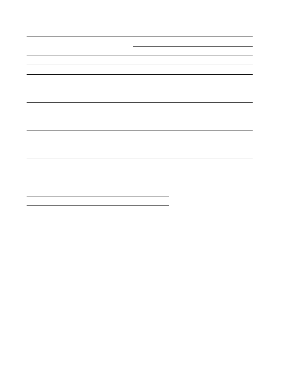
1.6 x 2.0-mm solution
Low profile package:
0.9 mm high (Typ)
1.0 mm (MAX)
Applications
∑ US PCS band handsets
∑ Wireless Data terminals
General Description
The ACPF- 7002 is a high
rejection full band transmit
filter designed for US PCS
handsets. Its performance rivals
splitband surface acoustic wave
(SAW) transmit filters. Since a
single filter provides the
rejection, no switches are
required, saving board space
and external components,
eliminating switch loss, and
reducing programming
complexity.
The ACPF- 7002 FBAR transmit
filter utilizes Agilent's Microcap
bonded- wafer chip scale
packaging technology. This
process allows the ultra small
filters to be assembled into a
Molded Chip on Board (MCOB)
module.
In typical cellular phone
architectures, the transmit filter
fits between the driver amplifier
and the Power Amplifier. The
ACPF- 7002 FBAR filter reduces
the noise in the Rx band being
amplified by the transmit chain,
enhancing receiver sensitivity.
High rejection keeps unwanted
signals out of the receive path.
Agilent's thin- Film Bulk
Acoustic Resonator (FBAR)
technology makes possible high-
Q filters at a fraction their
usual size.
Agilent ACPF-7002
High Rejection Tx Filter
for US PCS Band
Data Sheet
2
Electrical Specifications, Zo=50
Absolute Maximum Ratings
[2]
Notes:
1. Temperature is defined at case T
C
, the temperature of the underside of the filter where it makes contact with the circuit board.
2. Specifications are guaranteed over the given temperature range. Operation in excess of any one of these conditions may result in permanent damage to
the device.
Symbol
Parameters
Units
+25
∞
C
-30
∞
to +25
∞
C
25
∞
to +85
∞
C
Min
Typ
Max
Min
Typ
Max
Min
Typ
Max
f
Passband
MHz
1850
1910
1850
1910
1850
1910
IL
Insertion Loss 1850-1855 MHz
dB
2.0
3.5
3.7
3.2
IL
Insertion Loss 1855-1905 MHz
dB
1.5
2.5
2.5
2.5
IL
Insertion Loss 1905-1910 MHz
dB
2.5
3.0
2.7
3.7
D S21
Ripple, 1850-1910 MHz
dB
2.5
S21
Min Rejection, 1930-1990 MHz
dB
33
37
33
33
S21
Min Rejection 10 ≠1800 MHz
dB
25
25
25
S21
Min Rejection 1990 ≠ 3820 MHz
dB
22
22
22
S21
Min Rejection 3820
-
5730 MHz
dB
15.0
15.0
15.0
S11, S22
In-band return loss
dB
9.0
11
9.0
11
9.0
11
Pin max
Safe Input Power Level
dBm
20
20
20
Parameter
Unit
Value
Operating temperature
[1]
∞
C
-30 to +85
Storage temperature
[1]
∞
C
-30 to +100
3
Typical Performance (25
o
C, Zo = 50 Ohms)
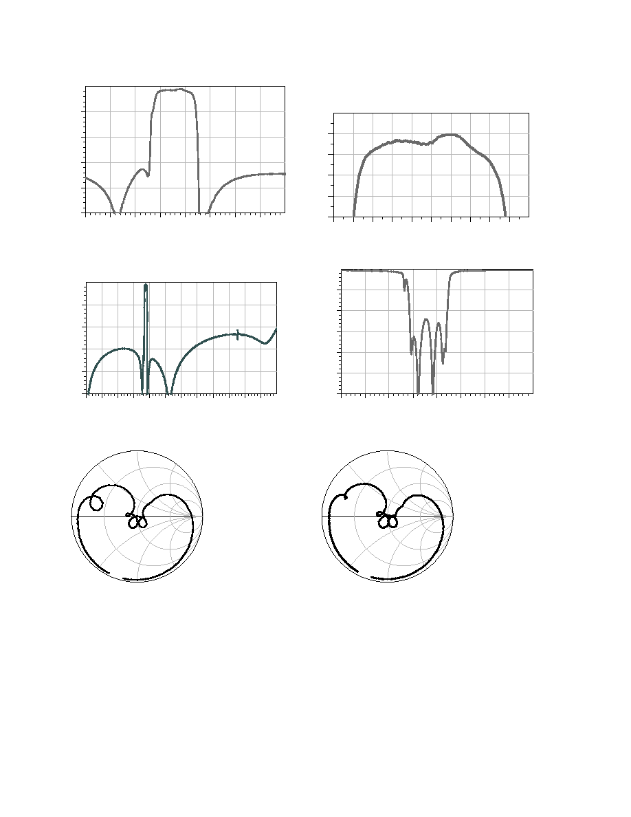
Figure 1. Attenuation [dB] vs. Frequency
Figure 2. Insertion Loss [dB] vs. Frequency
Figure 3. Attenuation [dB] vs. Frequency (broadband)
Figure 4. Return Loss [dB] vs. Frequency
Figure 5. Typical S(1,1)
Figure 6. Typical S(2,2)
1.75
1.80
1.85
1.90
1.95
2.00
2.05
1.70
2.10
-40
-30
-20
-10
-50
0
d
B
(
S
(
2,1)
)
1.84
1.85
1.86
1.87
1.88
1.89
1.90
1.91
1.92
1.83
1.93
-4
-3
-2
-1
-5
0
d
B
(S
(2
,
1
))
0.5
1.0
1.5
2.0
2.5
3.0
3.5
4.0
4.5
5.0
5.5
0.0
6.0
-40
-30
-20
-10
-50
0
d
B
(S
(2
,
1
)
)
1.75
1.80
1.85
1.90
1.95
2.00
2.05
1.70
2.10
-25
-20
-15
-10
-5
-30
0
d
B
(S
(1
,
1
)
)
freq (1.700GHz to 2.100GHz)
S(
1
,
1
)
freq (1.700GHz to 2.100GHz)
S
(
2,
2)

4
PCB Interface & Mounting instructions
Mounting Consideration and board description
The ACPF- 7002 FBAR filter has one input (Pin 1),
one output (Pin 3) and two grounds (Pins 2, 4).
∑ Demo board uses 3 mil Getek Microstrip.
The demoboard uses CPWG transmission lines for
high isolation between the two ports. It uses via
holes to connect the CPWG line from the
underside of the board to the filter mounting pads
on top.
Note:
For best performance, try to reproduce this board stack up
closely. If Ground-Signal-Ground (GSG) type board is used,
better return loss can be achieved since it eliminates
connector mismatch.
Demo boards
Demo boards are available.
(See board drawing in Figure 7, 8, 9).
Figure 7. Board stack up description
3 mils
0.7 mils
Layer1 (signal)
Layer 2 (ground)
Layer 3 (signal)
Getek
material ML200D and RG200D
Getek
ML200D (
T
=3.9)
28 mils
0.7 mils
Getek
ML200D (
T
=4.2)
3 mils
0.7 mils
Layer1 (signal)
Layer 2 (ground)
Layer 3 (signal)
Getek
material ML200D and RG200D
Getek
ML200D (
T
=3.9)
28 mils
0.7 mils
Getek
ML200D (
T
=4.2)
Figure 8. PCB Footprint pad
Figure 9. Closer look at the recommended board footprint and soldermask
Output connection
Input connection
BACK
TOP

5
Note:
Dimensions in mm
Figure 10. Detailed Bottom, Side and Top view of Package
Figure 11. Suggested PCB layers, viewed from top
Layer 1
Layer 2 (GROUND layer)
Note:
Dimensions in mm
2.0
4
2
3
1.25 MAX
: Pin 1 Location
: Work Week
: Lot Number
Shaded Region Grounded
A
0.60
±
0.15
D
C
B
A
B,C,D
Pin 1
Marking
1.
6
1
SIDE
VIEW
0.35
±
0.15
8X
0.
60
±
0.
15
0
.
5
5
0.61
OUT
3
IN
1
1
.
5
This region is Soldermask covering ground
2
1.92
0.70
0.61
0
.
3
1
Region (4) & (2) is exposed ground for soldering filter pads
4
0.30
Via to layer 2
0
.
5
5
0
.
0
5
0.33
0
.
0
5
0
.
3
0
2
0.3
0.3
Metal voided
To decrease
Capacitance at
Input Port
Metal voided
To decrease
Capacitance at
output Port
0.3
0.3
0.3
Metal voided
To decrease
Capacitance at
Input Port
Metal voided
To decrease
Capacitance at
output Port
0.3